On Track Innovations OTI-GMS-V1 User Manual 22 pages
On Track Innovations Ltd 22 pages
22 pages

Antenna Controller User Manual Ver. 1.00
FCC Compliance
P/N 1100031 page a
FCC Compliance
Labeling Requirements CFR 47, FCC part 15, Sections 15, 19, 109.
A device shall bear the following label in a conspicuous location on the Antenna
Controller.
OTi GMS FCC ID: JNX-OTI-GMS-V1
Manufacturer: On Track Innovations Ltd.
This device complies with Part 15of the FCC Rules.
Operation is subject to the following two conditions:
1. This device may not cause harmful interference, and
2. this device must accept any interference received, including
interference that may cause undesired operation.
NOTE: This equipment has been tested and found to comply with the limits for a
Class B digital device, pursuant to part 15 of the FCC Rules. These limits are
designed to provide reasonable protection against harmful interference in a
residential installation. This equipment generates, uses and can radiate radio
frequency energy and, if not installed and used in accordance with the instructions,
may cause harmful interference to radio communications. However, there is no
guarantee that interference will not occur in a particular installation. If this
equipment does cause harmful interference to radio or television reception, which
can be determined by turning the equipment off and on, the user is encouraged to
try to correct the interference by one or more of the following measures:
•
••
• Reorient or relocate the receiving antenna.
•
••
• Increase the separation between the equipment and receiver.
•
••
• Connect the equipment into an outlet on a circuit different from that to which
this receiver is connected.
•
••
• Consult the dealer or an experienced radio/TV technician for help
Changes or modifications in this equipment, not expressly approved by the party
responsible for compliance (On Track Innovations Ltd,) could void the user’s
authority to operate the equipment.
Antenna Controller User Manual Ver. 1.00
FCC Compliance
P/N 1100031 page 2-1
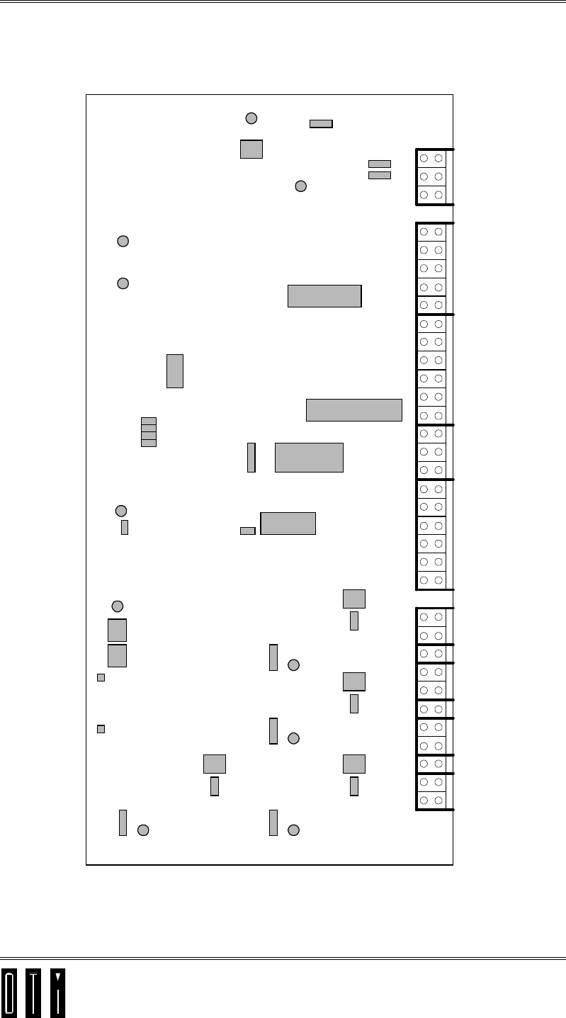
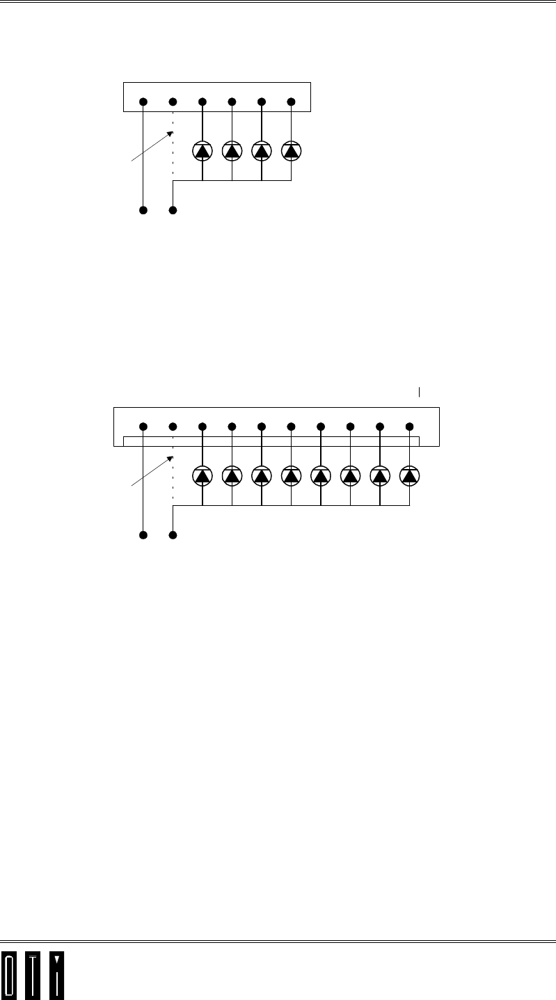
1.1 Antenna Controller Interface Summary,
By Reference Designation
Figure 0-1: Interface Layout (4 channel)
TB5
VIN
TB4
DI
TB3
DO
TB2
RS232
TB1
RS422
ANT
4
ANT
3
ANT
2
ANT
1
VIN
P5
F1
D30
D29
+VL
P3
P4
SW1J7
P1
TX
DATA
+5V
TX
+5V
D
P2
J10
to
J13
7.5V
J6
C23
J19
C21
J16
C25
J2
SL3
TR3
TR2
SL2
SL4
TR4
C39
J1
SL1
TR1
GND1
TP1
SQ
GAIN
REC

Antenna Controller User Manual Ver. 1.00
FCC Compliance
P/N 1100031 page 2-2
1.1.1 Terminals
ANT-1→
→→
→ANT-4 Antenna coils connection
TB1 RS422/485 serial communication connection.
TB2 RS232C serial communication connection
TB3 Open collector Digital outputs.
TB4 Digital inputs.
TB5 12Vac input power supply connection.
1.1.2 Molex Connectors
P1 Optional TTL Serial communication.
P3 8 Digital Inputs.
P4 8 Digital outputs (10 pin Molex connector).
1.1.3 Fuses
F1 MCI PCB main fuse (500mA).
F2, F3, F4 Automatic self resetting Poli-switch fuses
1.1.4 LED’s
Power Supply indicators (red)
VIN 12Vdc Supply to system.
+VL 12Vdc supply to Outputs.
+5VD 5Vdc supply to digital section.
+5V TX 5Vdc supply to transmitters.
+7.5V 7.5Vdc supply to receiver.
Transmit indicators (green)
TR1 Transmitter 1
TR2 Transmitter 2
TR3 Transmitter 3
TR4 Transmitter 4
REC Receive indicator led (yellow)
L1 →
→→
→ L8 Eight Digital output indicator LED’s (red)
IN1 →
→→
→ IN8 Eight Digital input indicator LED’s (red)
1.1.5 Jumpers
SL1, SL2, SL3, SL4 Transmitter mode selectors
(for transmitters 1 to 4 respectively )
J1, J2, J16, J19 50Ω load connection at transmitter output
J6 Receiver Disable, by-pass
J7 RS232/RS422(485) serial communication mode selector
J10→
→→
→J13 Channel enable.
TX DATA Data transmission enable.
1.1.6 Tuning Capacitors
C39 Transmitter #1
C25 Transmitter #2
C21 Transmitter #3
C23 Transmitter #4

Antenna Controller User Manual Ver. 1.00
FCC Compliance
P/N 1100031 page 2-3
1.1.7 Potentiometers
SQ Received data Squelch control (factory set)
GAIN Received data gain control ( optional ).
1.1.8 Diodes
D29 & D30 diode bridge’s negative diodes, These diodes must be removed
when using center taped transformer supply (refer to Figure 0-1)
1.1.9 DIP Switch
SW1 RS422/485 network address selection and self diagnostics
(see section 4.5)
1.1.10 Test Points
TP1 & GND1 Received signal measuring points.
Antenna Controller User Manual Ver. 1.00
Electrical Installation
P/N 1100031 page 2-1
2. Electrical Installation
The Antenna Controller power requirements are 12Vac/dc@500mA.
This power supply, protected by a 0.5A fuse on the reader, does not include supply to
external outputs.
Maximum consumption, including supply to external outputs, is 1A
Power to the Antenna Controller can be supplied in three different ways:
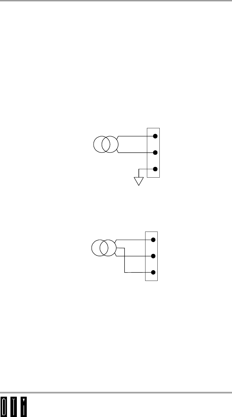
a) 12Vac, rectified by a diode bridge on the reader.
B) 12Vac from a transformer with two 12Vac outputs and a center point,
Important note! For this option the two negative polarity diodes of the diode bridge
rectifier D29 and D30 (see Figure 0-1) must be removed.
c) 12 regulated/non regulated DC voltage.
2.1 Power Connections
AC
AC
GND
TB5
VIN
GND
12V
AC
SUPPLY
TRANSFORMER
Figure 2-1: 12Vac Supply
AC
AC
GND
TB5
VIN
12V
AC
SUPPLY
TRANSFORMER
12V
AC
CENTER TAP
Figure 2-2: Center Tap Transformer Supply
Important note! For this option the two negative polarity diodes of the diode bridge
rectifier D29 and D30 (see Figure 0-1) must be removed.

Antenna Controller User Manual Ver. 1.00
Electrical Installation
P/N 1100031 page 2-2
AC
AC
GND
TB5
VIN
+
-
12VDC
Figure 2-3: 12Vdc Supply
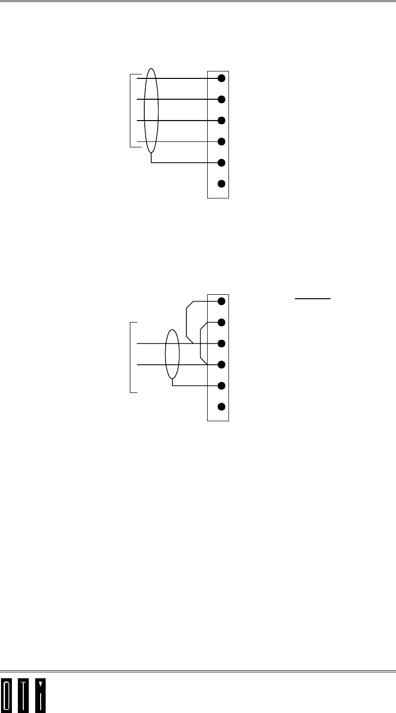
2.2 Serial Interface Connections
2.2.1 TTL - Optional Molex 6 pin connector
GND
+VB
P1
TXD
RXD
GND
TTL (NRZ)
SERIAL COM.
+
-
SUPPLY TO
MCI (OPTION) 12VDC
RS-232
6
5
4
3
1
2
Figure 2-4: TTL
2.2.2 RS-232 (Jumper 7 must be in RS232 position)
GND
RXD
TXD
RS232C
SERIAL
COMM.
TB2
Figure 2-5: RS-232
Antenna Controller User Manual Ver. 1.00
Electrical Installation
P/N 1100031 page 2-3
2.2.3 RS-422 (Jumper J7 must be in RS422 position)
TX*
RX*
RX
RS422
SERIAL
COMM.
TB1
TX
SCREEN
SCREEN
Figure 2-6: RS-422
2.2.4 RS-485
TX*
RX*
RX
RS485
SERIAL
COMM.
TB1
TX
SCREEN
SCREEN
Option
installing 0 ohm
resistors R126/127
to bridge between
RX & TX
Figure 2-7: RS-485
Antenna Controller User Manual Ver. 1.00
Electrical Installation
P/N 1100031 page 2-4
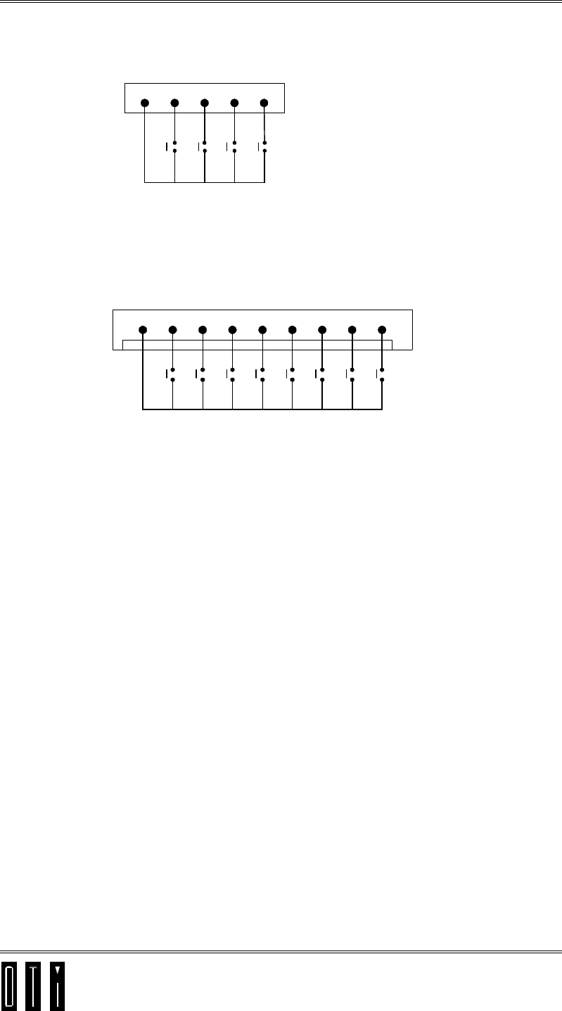
2.3 Antenna Cable Connections
GND SIG GND GND GNDSIG SIG SIG
ANT-1 ANT-2 ANT-3 ANT-4
ANTENNA
1ANTENNA
2ANTENNA
3ANTENNA
4
Figure 2-8: Antenna Terminal Block
Twisted pair wire can be used for distances of up to 20 centimeters.
At any distance ranging between 20 cm. and 1.2 m., coaxial cable should be used.
For distances from 1.2 m. to 33 m. coaxial cable is used, in half-length multiples of the
wavelength. See table 3-1 for half- wavelength calculations.
(Cable length over 33 m. is possible but reading distance will be reduced).
Table 2-1: Half Wavelengths by Cable Type
Cable Type λ
λλ
λ/2
RG-58 7.30 m.
RG-174 7.30m.
14008 7.70m
Raychem EPD 84952Q 8.20m
Belden 89307 8.83m
When using coaxial cable, the center lead is connected to “SIG”, the shield to “GND”.
Antenna Controller User Manual Ver. 1.00
Electrical Installation
P/N 1100031 page 2-5
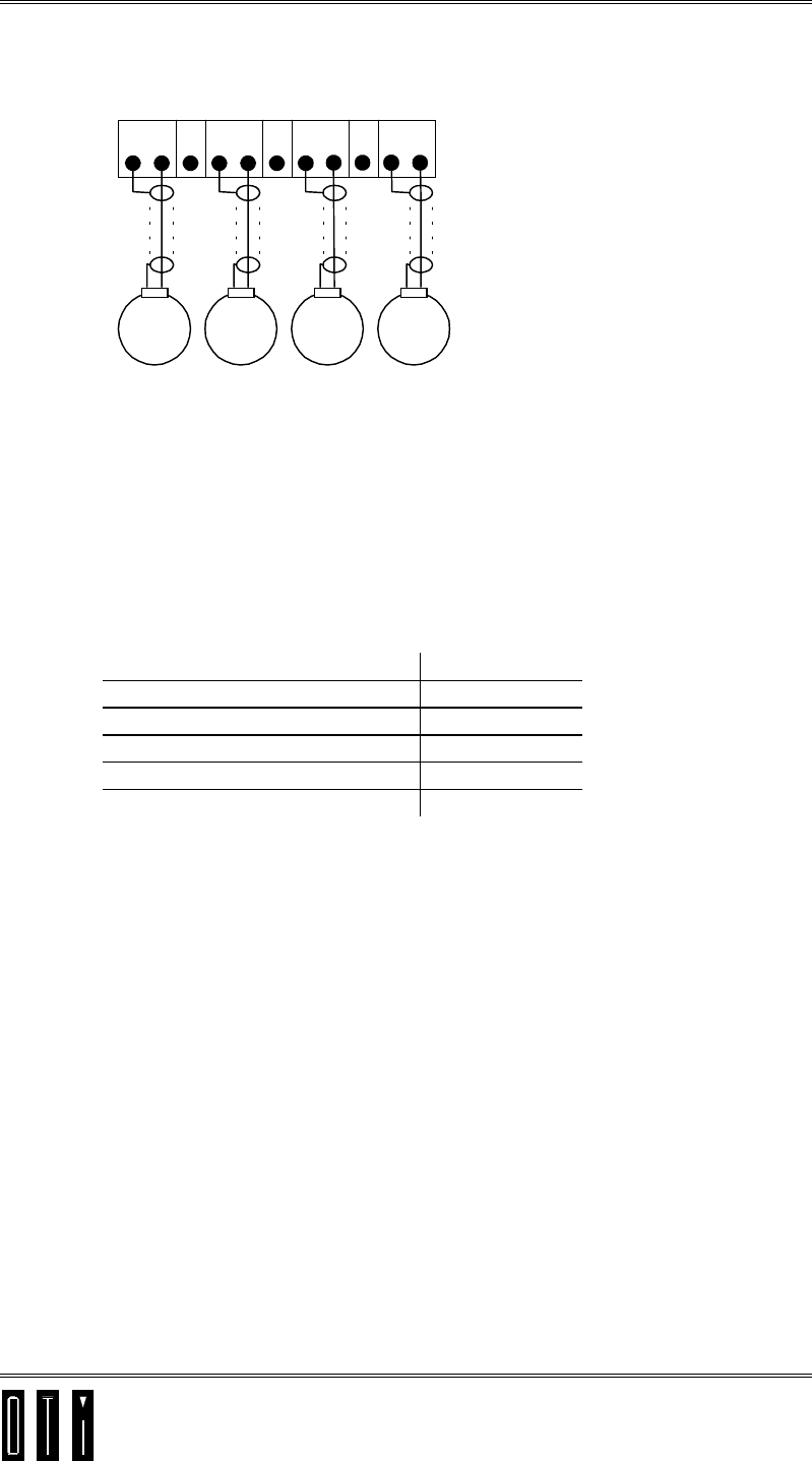
2.4 Digital Outputs
-+
12Vdc
External Supply
GND +V L1 L2 L3 L4
TB3
EXTERNAL
LEDS
INTERNAL
SUPPLY
OPTION ++ ++
-- --
Figure 2-9: Terminal TB3
-+
12Vdc
External Supply
GND +V O1 O2 O3 O4
EXTERNAL
LEDS
INTERNAL
SUPPLY
OPTION ++ ++
-- --
O5 O6 O7 O8
++ ++
-- --
P4
MOLEX
Figure 2-10: Molex connector P3
Digital outputs are open collector with a serial 750Ω resistor.
For internal 12V supply option, install jumper VL
(located between TB4 & TB 5).
Terminals L1 to L4 in TB3 and Pins O1 to O4 in connector P3
are connected in parallel.
Antenna Controller User Manual Ver. 1.00
Electrical Installation
P/N 1100031 page 2-6
2.5 Digital Inputs
GND IN1
TB4
IN2 IN3 IN4
INPUTS
1234
Figure 2-11: TB4
GND IN1 IN2 IN3 IN4 IN5 IN6 IN7 IN8
MOLEX
P3
INPUTS
123 54678
Figure 2-12: Connector P3
Inputs are Active Low.
Antenna Controller User Manual Ver. 1.00
Electrical Installation
P/N 1100031 page 2-1
2.6 Antenna Matching Circuits
2.6.1 Loop Antenna
Size - X × Y (mm).
Windings - Single-turn.
Wire - 24 AWG.
2.6.2 Matching Circuitry
Ls = matching coil (see Table 2-1).
Cp = matching capacitor (see Table 2-1)
note: Use high quality ceramic capacitors, preferably SMD.
Vcp = Variable capacitor - 30 pF (FCV05E30).
2.6.3 Typical Values
Table 2-1: Typical Antenna Matching Circuit Values
Antenna
Dimensions,
(in mm.)
Ls (µ
µµ
µH) Cp (pF)
50 × 80 3.3 560
60x100 3.3 470
100 ∅3.3 180 + 180 = 360
100 × 100 3.3 180 +180 = 360
80 × 100 3.3 150 + 150 = 300
70 x 120 3.3 150 + 150 = 300
100 × 150 3.3 270
GBI Antenna Controller User Manual Ver. 1.00
Antenna Tuning
P/N 1100031 page a
3. Antenna Tuning
3.1 Factory Tuning
The antenna is factory tuned and does not require customer adjustment. If it becomes
necessary to tune the antenna, the following sections describe the process.
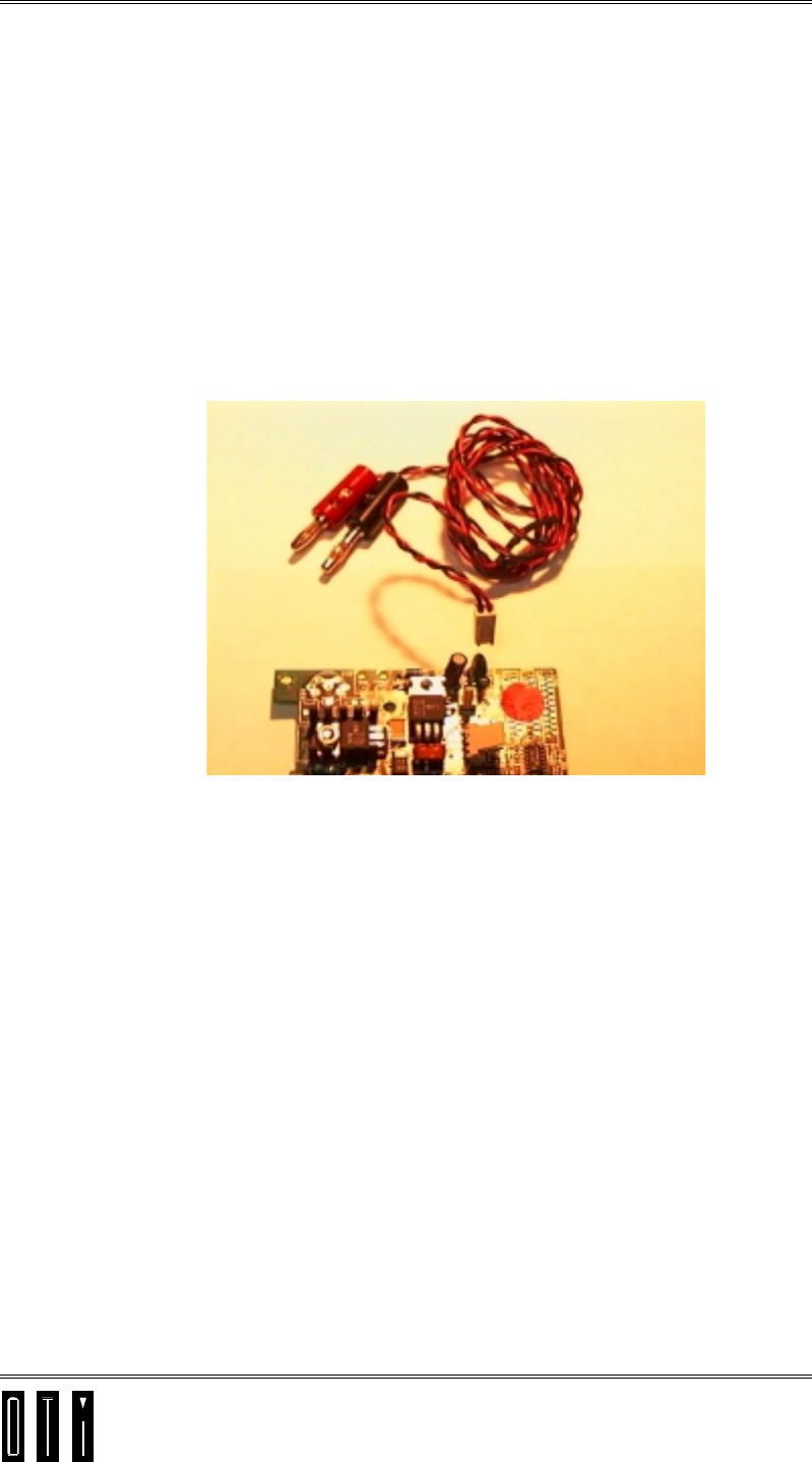
3.2 Antenna Tuning Equipment
!
!!
! DVM - Digital Voltmeter (mV range).
!
!!
! DVM adapter Cable (see Figure 3-1).
! Non-conductive ceramic screwdriver.
Figure 3-1: DVM Adapter Cable
3.3 Tuning Procedure
Antenna tuning should be performed after the antenna has been installed in its final
position. This will ensure that the tuning will compensate for the effects of nearby
metallic objects.
To tune the selected antenna, follow the procedures below:
1) Choose the transmitter of antenna to be tuned by removing it’s SL jumper
( for constant RF transmission) and by placing all other SL jumpers in
OFF position
2) Connect Antenna coax cable or twisted wires to the selected antenna
terminal block on the Reader (Figure 0-1)
3) Connect the DVM adapter Cable to connector P5 (Figure 0-1).
4) Apply power to the Reader.
Note: Do not touch the Antenna.
GBI Antenna Controller User Manual Ver. 1.00
Antenna Tuning
P/N 1100031 page b
4) Using the ceramic screwdriver, turn the antenna matching capacitor to
reach maximum capacity.
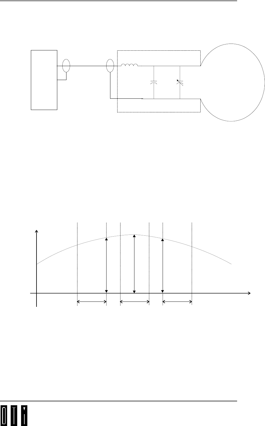
OEM
GND
SIG
Antenna
VCpCp
Ls
Matching
Capacitor
ANTENNA
MATCHING CIRCUIT
Cable
Z
0
=50 Ohm
Cable
Z
0
=50 Ohm
Figure 3-2: Antenna Matching Circuit
5) Turn the antenna matching capacitor slowly counter-clockwise (CCW)
until the maximum DVM reading is achieved (approximately
110 - 130 mV).
Note: If voltage is highest when the matching capacitor is at the position of its
maximum capacitance, replace existing Cp capacitor with one of the next
higher value. If voltage is highest when the matching capacitor is at the
position of its minimum capacitance, replace the existing Cp capacitor
with one of the next lower value (see Table 4.1).
Next, repeat steps 4 & 5.
mV
Cap
Max.
reading
in
Max.
position
Cp Value
to o h igh
Cp Value
to o low
Cp Value
OK
Vcp
min.
pos.
Vcp
min.
pos.
Vcp
min.
pos.
Vcp
max.
p
os.
Vcp
max.
p
os.
Vcp
max.
p
os.
Cp+VcpCp+Vcp Cp+Vcp
Max.
reading
in
Min.
position
Max.
reading
in
Range
Figure 3-3: Choosing the Antenna Matching Capacitor (Cp)

GBI Antenna Controller User Manual Ver. 1.00
Antenna Tuning
P/N 1100031 page c
6) Turn the Antenna matching capacitor clockwise (CW) to reduce the
reading by 10mV to 15 mV (i.e. if the maximum reading was 120mV, the
final reading should be 105mV to 110mV).
7) Slowly move a metallic object close to the Antenna assembly (up to 2 cm
from the Antenna). The reading should rise slightly towards the maximum
before it drops, when the metallic object is placed very close to the Antenna
assembly.
Note: If the reading does not rise, but only drops, readjust CCW to reduce
reading by 10 - 15mV, then re-check with a metallic object.
3.4 Antenna Tuning Final Check and Assembly
At the completion of the procedures in Section 5-3, perform the following procedures:
1) Return all SL jumpers to MT position.
2) Check Antenna operation with a card.
3) Cover and seal Antenna matching capacitor tuning opening with special
non-corrosive RTV (“Rotacil 1112”, or equivalent).
3.5 Procedure for Choosing Coil - Ls
- Refer to section 1.1 for connector and jumper positions on card.
1) Connect a 50Ω resistor, to simulate antenna load, by applying a jumper to
the selected transmitter.
(J1 - Xmtr. #1, J2 - Xmtr. #2, J16 - Xmtr. #3 or J19 - Xmtr. #4).
2) Remove the SL jumper of the selected transmitter (for constant RF
transmission) and place all other SL jumpers in OFF position
3) Connect DVM to connector P5.
4) Apply power to card and register the DVM reading.
5) Remove 50Ω resistor jumper (see step #1) and connect the selected antenna
cable to the selected antenna terminal block.
6) Perform antenna-tuning procedure. (Refer to section 1.1).
7) If DVM reading at maximum point is lower by more than 10 mv with
antenna than with 50Ω resistor, replace Coil Ls with one of the next lower
value .(i.e. 3.9µH → 3.3µH )
8) If DVM reading at maximum point is higher by more than 40 MV with
antenna than with 50Ω resistor, replace Coil Ls with one of the next higher
value. (i.e. 3.9µH →4.7µH )
9) After replacing Coil Ls, repeat procedure from step 6.
10) Return all SL jumpers to MT position.
GBI Antenna Controller User Manual Ver. 1.00
Jumper & Dip Switch Settings
P/N 1100031 page d
4. Jumper & Dip Switch Settings
4.1 J10 - J13
Channel enable Jumpers- should be placed to enable normal microprocessor
controlled operation of the desired channel.
CH1 CH2 CH3 CH4
J10 x
J11 x
J12 x
J13 x
4.2 Communication Jumper J7
Jumper J7 should be placed in RS232 position for RS232 applications or in RS422
position for RS422/RS485 applications.
4.3 Transmission Channel Jumpers
Jumpers SL1, SL2, SL3, & SL 4 for channels 1 to 4 respectively offer the following
modes:
1) MT position - normal microprocessor controlled data transmission.
2) Off position - no transmission.
3) No jumper - constant transmission.
4.4 Normal Operation Jumper Settings
1) Jumpers J10→J13 should be placed to enable operation of desired channel
2) Jumpers SL1→SL4 should be placed in MT position.
3) Jumper J7 should be placed in RS-232 or RS-422 position depending on
application
4) The following jumpers should be removed for normal operation:
J1, J2 J16 J19&J6.
5) The following jumpers should be installed for normal operation:
TXDATA
4.5 Dip Switch SW1
12345678
ON
OFF
SW1
Sw1 selects the address of the first channel of the MCI for RS-232/422
network operation. Addresses of channels 2, 3 and 4 follow in sequential
order. The address number (0-255) is binary coded, #1 being the most
significant bit and #8 being the least significant bit.
Address #0 is reserved for self-diagnostics. In this mode the channels are

GBI Antenna Controller User Manual Ver. 1.00
Jumper & Dip Switch Settings
P/N 1100031 page e
scanned sequentially in repetitive cycles
FCC Compliance
Labeling Requirements CFR 47, FCC part 15, Sections 15, 19, 109.
A device shall bear the following label in a conspicuous location on the device.
OTi GMS FCC ID: JNX-OTI-GMS-V1
Manufacturer: On Track Innovations Ltd.
This device complies with Part 15 of the FCC Rules.
Operation is subject to the following two conditions:
1) This device may not cause harmful interference, and
2) this device must accept any interference received,
including interference that may cause undesired
operation.
NOTE: This equipment has been tested and found to comply with the limits
for a Class B digital device, pursuant to part 15 of the FCC Rules. These
limits are designed to provide reasonable protection against harmful
interference in a residential installation. This equipment generates, uses and
can radiate radio frequency energy and, if not installed and used in
accordance with the instructions, may cause harmful interference to radio
communications. However, there is no guarantee that interference will not
occur in a particular installation. If this equipment does cause harmful
interference to radio or television reception, which can be determined by
turning the equipment off and on, the user is encouraged to try to correct the
interference by one or more of the following measures:
"
""
" Reorient or relocate the receiving antenna.
"
""
" Increase the separation between the equipment and receiver.
"
""
" Connect the equipment into an outlet on a circuit different from that to
which this receiver is connected.
"
""
" Consult the dealer or an experienced radio/TV technician for help
Changes or modifications in this equipment, not expressly approved by the
party responsible for compliance (On Track Innovations Ltd,) could void the
user’s authority to operate the equipment.
Antenna Controller User Manual Ver. 1.00
Product Overview
P/N 1100031 page 5-1
5. Product Overview
5.1 UL Version Models
Table 5-1 UL Version Site Controller models
Description Model No. Catalog No.
GBI 2 SC-U1-110/12-40-D9F 1001150
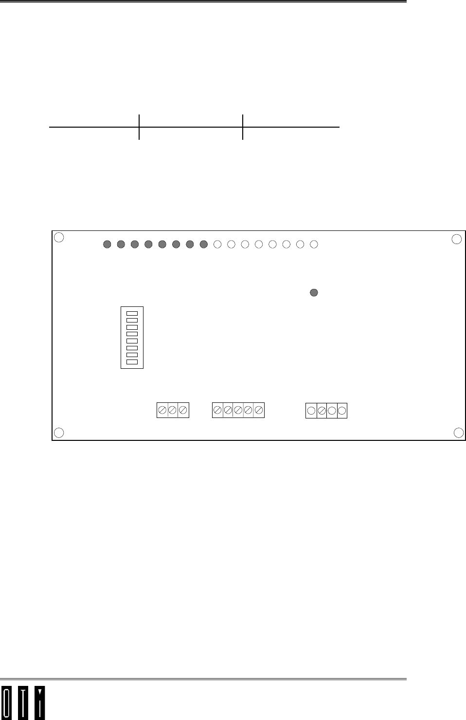
5.2 GBI 2.0 Site Controller Board Interface
Summary,
By Reference Designation
LR1 LR2 LR3 LR4 LR5 LR6 LR7 LR8 LG1 LG2 LG3 LG4 LG5 LG6 LG7 LG8
+5V
SW2
HOST
COM SCI
COM POWER
SUPPLY
R
X
D
T
X
D
G
N
D
T
X
*
T
XR
X
*
R
XG
N
D
G
N
D
A
C
A
C
+
12
GBI 2.0
P14 P15 P16
Figure 5-4: GBI 2.0 Site Controller Board
Interface Layout

Antenna Controller User Manual Ver. 1.00
Product Overview
P/N 1100031 page 5-2
5.2.1 Terminals
P14 RS232 Host communication
P15 RS422/485 Transceiver station communication
P16 AC/DC Power supply
5.2.2 Leds
LR1 →
→→
→ LR8 Channel select, 8 led binary coded indication (red)
LG1 →
→→
→ LG8 Successful response, 8 led binary coded indication (green)
+5V +5VDC power indicator (red)
5.2.3 Dip Switch
SW1 Mode selection Dip Switch
Address #0 (all switches in off position)
Self diagnostics mode: The channels are scanned
sequentially in repetitive cycles.
Address #1 (only switch#1 is in on position)
Host mode: The channels are addressed by the Host
computer.
Antenna Controller User Manual Ver. 1.00
Electrical Installation
P/N 1100031 page 6-3
6. Electrical Installation
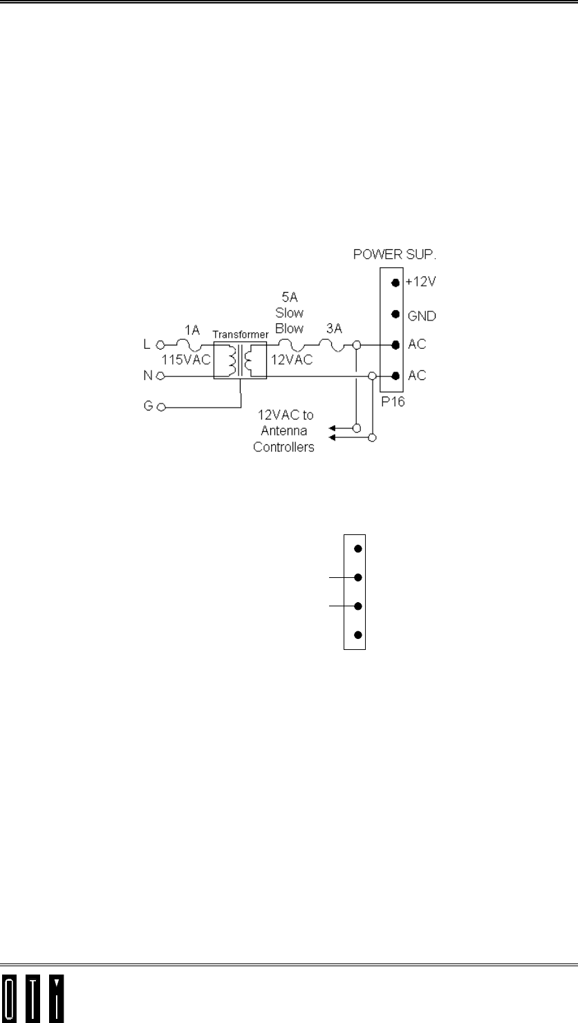
6.1 Power connections
Incoming AC power is applied to terminals L, N and GND, connected to a class 2, UL certified
transformer. This transformer converts the incoming voltage to 12VAC supplying power to the
GBI2.0 Site Controller board and the antenna controller units in the field. Please refer to
Power Supply section for transformer and fuse ratings.
The GBI 2.0 Site Controller Board can be powered either from a DC or an AC power source.
Figure 6-1:AC Supply
AC
AC
9 to 12VDC GND
+12V
POWER SUP.
P16
+
-
Figure 6-2:DC Supply
Antenna Controller User Manual Ver. 1.00
Electrical Installation
P/N 1100031 page 6-4
6.2 Network Connections
6.2.1 Host PC - RS232 Connection
Note: Use a shielded twisted pair cable.
HOST COM.
P14
RX
TX
GND
red
black
shield
3
2
5
4
6
7
8
9 PIN
D-TYPE
HOST GBI 2.0
HOST COM.
P14
RX
TX
GND
red
black
shield
2
3
7
4
5
6
25 PIN
D-TYPE
HOST GBI 2.0
20
Figure 6-3:RS232 Serial connection to PC
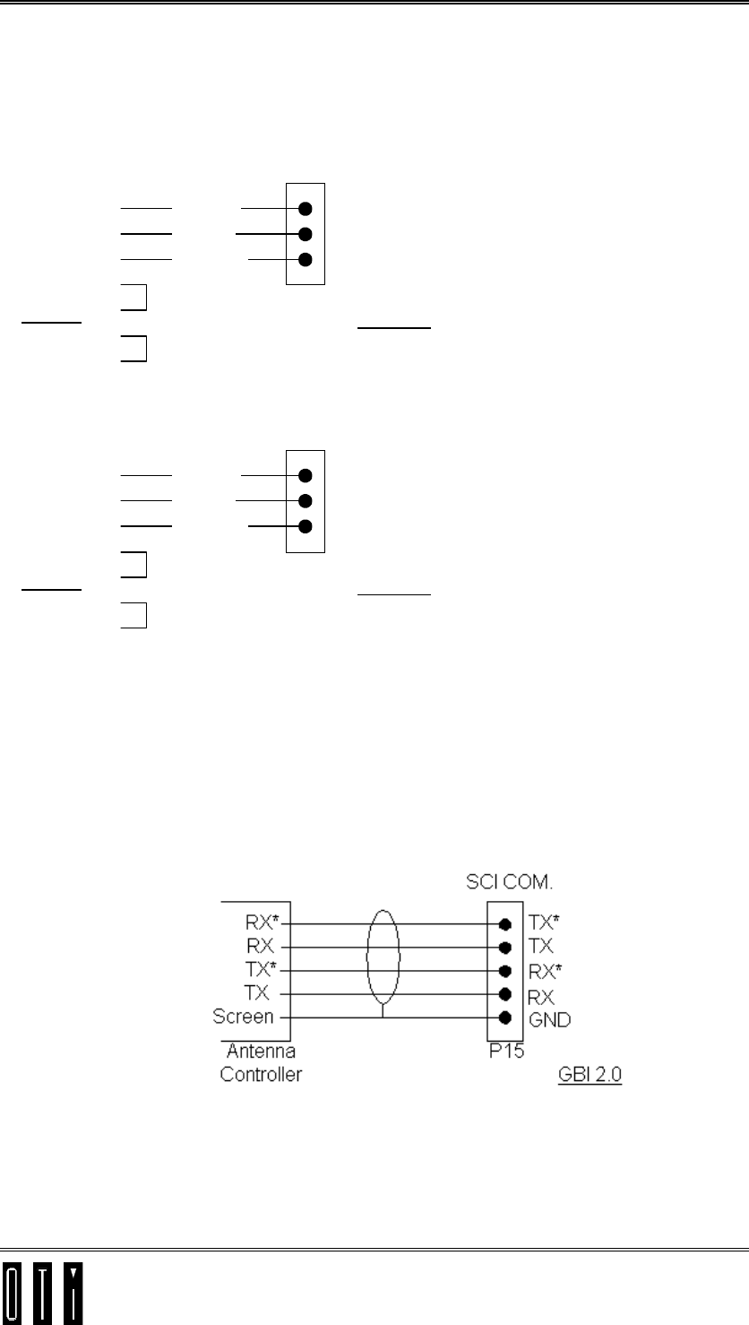
6.2.2 RS422 Network Connection
Antenna Controller units are connected to the Site Controller network via RS422
communication cable in daisy chain fashion. All communication lines are
connected in parallel (RX&RX, RX*&RX*, TX&TX, TX*&TX*).
Note: use shielded double twisted pair cable.
Figure 6-4:RS422 Serial connection to
Antenna Controller Network
6.2.3 RS485 Network Connection
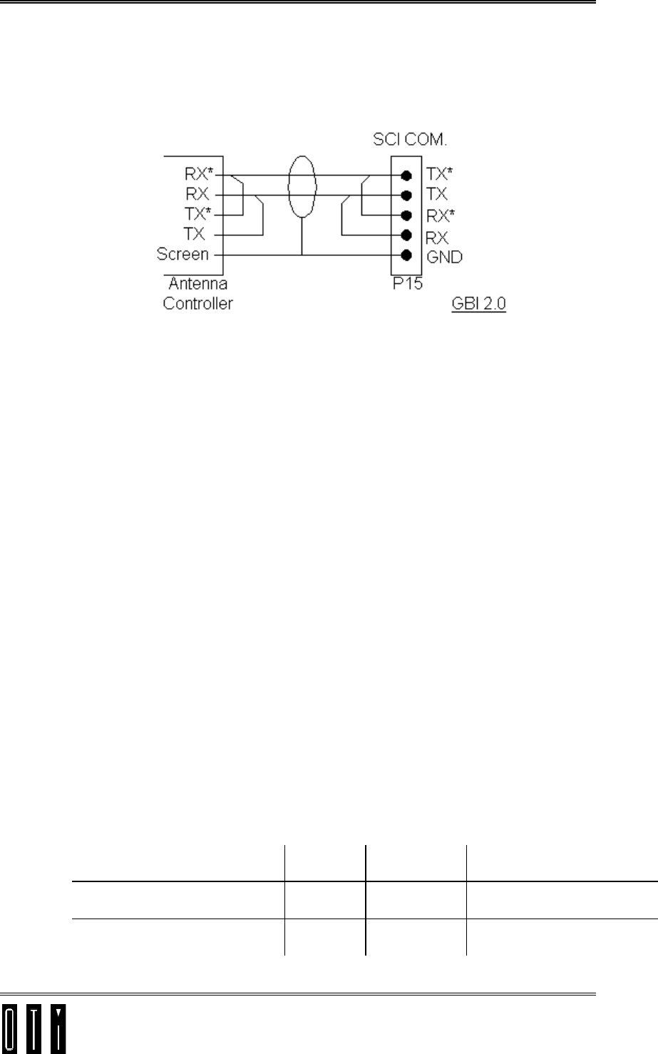
Antenna Controller User Manual Ver. 1.00
Electrical Installation
P/N 1100031 page 6-5
Each Antenna Controller unit is connected to the Site Controller network via
RS485 communication cable in daisy chain fashion. Communication lines are
connected in parallel.
Note: Use a shielded twisted pair cable.
Figure 6-5:RS422 Serial connection to
Antenna Controller Network
Power Supply
A single Site Controller supplies power to a limited network of Antenna Controllers.
Power supply to all system elements should take into consideration the total and
distributed current loads according to the routing topology of the supply lines with
the associated voltage drops. Class 2 limits the maximum allowed current via field
wiring to 8A. This actually means a maximum rating of about 5A for the fuse on the
transformers secondary circuit.
6.3 Transformer
The Site Controllers transformer is intended to convert the incoming AC power
(115/230) to 12VAC @ 3.3A used to power the Site Controller GBI 2.0 board and a
limited number of Antenna Controller units.
6.4 Fuses
The Site Controller’s AC supply system is protected by three fuses, one on the
transformer’s primary circuit and two (in series) on the transformer’s secondary
circuit.
To comply with class 2 requirements, the 5A slow blow fuse on the transformer’s
secondary circuit is non-replaceable. The 3A fuse placed in series with this 5A
fuse is replaceable and is intended to blow before the 5A fuse.
Table 6-2: Glass Fuses
Description Rating Type Recommended
Manufacturer/Series
Transformer primary circuit
Replaceable 1A Fast acting - ELU 179021, 1A
- Little Fuse 235001
Transformer secondary circuit
Replaceable 3 - 3.15A Fast acting - ELU 179021, 3.15A
- Little Fuse 235003

Antenna Controller User Manual Ver. 1.00
Electrical Installation
P/N 1100031 page 6-6
Description Rating Type Recommended
Manufacturer/Series
Transformer secondary circuit
Non-replaceable 5A Slow blow - ELU 189021, 5A
(Wire leads)