Onkyo Home Entertainment CR375 Bluetooth stereo Audio Module User Manual
Onkyo Corporation Bluetooth stereo Audio Module Users Manual
Users Manual

B
B
B4
4
42
2
26
6
6-
-
-A
A
AB
B
B1
1
15
5
51
1
10
0
0
Wireless Stereo Speaker Module
For Intensive Audio Applications
Specification
VERSION 0.40 15-Sep-2015
DATASHEET

Revision History
Version
Change Summary Date Author
0.10 Created Dec, 25
th
, 13
LY Kuo
0.20 Update Bluetooth Specification Version Jun, 15
th
, 14
LY Kuo
0.30 Remove PCM function support Oct, 15
th
, 14
LY Kuo
0.40 Modify maximum RF transmit Power descriptions
Sep, 15
th
, 15
LY Kuo

1 System Overview
1.1 General Description
B426-AB1510 is a stereo module, which are highly integrated, cost effective, low power consumptions with
Airoha AB1510 chip for intensive audio applications. It complies with Bluetooth system version 4.1 with EDR
function. The built-in noise reduction and echo cancellation functions enhance the voice quality. Advanced
multipoint supports HFP connection to two handsets for voice, or two A2DP sources for music play back. The
voice prompt function can be customized by customers for different voice commands.
1.2 Features
Bluetooth 4.1+EDR compliant
A2DP 1.3 and AVRCP 1.5 profile enable
HFP profile version 1.6 compliant
HSP profile version 1.2 compliant
AVRCP profile version 1.5 compliant
SBC decode
Class 1 or 2 type output power
Support for noise reduction and echo cancellation
Multi-band configurable EQ
Multipoint for HFP and A2DP
Support for voice prompt
Support SPI flash application
Support NFC application with wake-up and pairing function
Audio I/F:I2S
Integrated Li-ion battery charger supports 400mA fast charging
B426-AB1510
Stereo Speaker Module For Intensive Audio Applications
B426-AB1510 Stereo Speaker Module for Intensive
Audio Applications Page 4 of 17 CONFIDENTIAL
Specification
Version 0.40 Sep-2015
2 Module Package Information
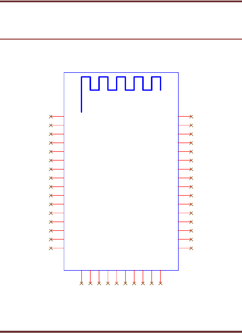
2.1 Module Pin Definition
AB1510_Module with antenna
VCHG_IN 28
BAT_IN 29
LINE_IN_R 38
SPK_LP 39
LRVCM 40
MIC_BIAS 32
MIC1_P 33
MIC2_P 36
LINE_IN_L 37
WAKE
3
VREGOUT_MV
25
UART_TX
8
UART_RX
7
LED0
20
LED1
21
PIO17
15
PIO16
14
PIO15
13
PIO14
12
PIO12
24
VCCIO
23
PIO11
9
PIO7
11
PIO6
10
PIO5
22
VREGOUT_HV 30
PIO3
6
PIO2
5
PIO1
4
NC
1
RST
26
PIO4 31
MIC2_N 35
MIC1_N 34
SDA
17
SCL
18
GND
2
GND
16 GND 27
SPK_RP 41
WP/PIO18
19
GND 42
Figure 2-1 Pin Definition

B426-AB1510
Stereo Speaker Module For Intensive Audio Applications
B426-AB1510 Stereo Speaker Module for Intensive
Audio Applications Page 5 of 17 CONFIDENTIAL
Specification
Version 0.40 Sep-2015
2.2 Pin Description
PIN
SIGNAL TYPE DESCRIPTION ALTERNATIVE
1 NC NC
2 GND
3 WAKE Input, Digital Input Pin with 125K pull up
4 PIO1 Input, Digital Input Pin with 750K pull up
5 PIO2 Input, Digital Input Pin with 750K pull up
6 PIO3 Input, Digital Input Pin with 750K pull up
7 UART_RX Input, Digital UART RX
8 UART_TX Output, Digital UART TX
9 PIO11 Input/Output, Digital Programmable IO
10 PIO6 Input/Output, Digital Programmable IO
11 PIO7 Input/Output, Digital Programmable IO
12 PIO14 Input/Output, Digital Programmable IO SPI/I2S
13 PIO15 Input/Output, Digital Programmable IO SPI/I2S
14 PIO16 Input/Output, Digital Programmable IO SPI/I2S
15 PIO17 Input/Output, Digital Programmable IO SPI/I2S
16 GND
17 SDA Input/Output, Digital I2C data line
18 SCL Input/Output, Digital I2C clock line
19 WP/PIO18 Output, Digital Write Protect Control for
EEPROM WP
20 LED0 Open Drain LED 0 for Red Light
21 LED1 Open Drain LED 1 for Blue Light
22 PIO5 Input/Output, Digital
AIO,Analog Programmable IO UART_RTS
23 VCCIO Supply, 1.8V~3.3V VCC for IO
24 PIO12 Input/Output, Digital Programmable IO LED3
25 VREGOUT_MV
Analog LDO output
26 RST Input, Digital Global reset
27 GND
28 VCHG_IN Supply, 5V VCC for Charger
B426-AB1510
Stereo Speaker Module For Intensive Audio Applications
B426-AB1510 Stereo Speaker Module for Intensive
Audio Applications Page 6 of 17 CONFIDENTIAL
Specification
Version 0.40 Sep-2015
29 BAT_IN Supply Battery input P, as
Switching/Linear regulator input
30 VREGOUT_HV
Analog LDO output
31 PIO4 Input/Output, Digital
AIO,Analog Programmable IO UART_CTS
32 MIC_BIAS Analog Microphone bias
33 MIC1_P Analog Microphone 1 P-path
34 MIC1_N Analog Microphone 1 N-path
35 MIC2_N Analog Microphone 2 N-path
36 MIC2_P Analog Microphone 2 P-path
37 LINE_IN_L Analog Line in L-path
38 LINE_IN_R Analog Line in R-path
39 SPK_LP Analog Speaker output LP
40 LRVCM Analog Speaker output LRVCM
41 SPK_RP Analog Speaker output RP
42 GND
Table 2-1 Pin Description
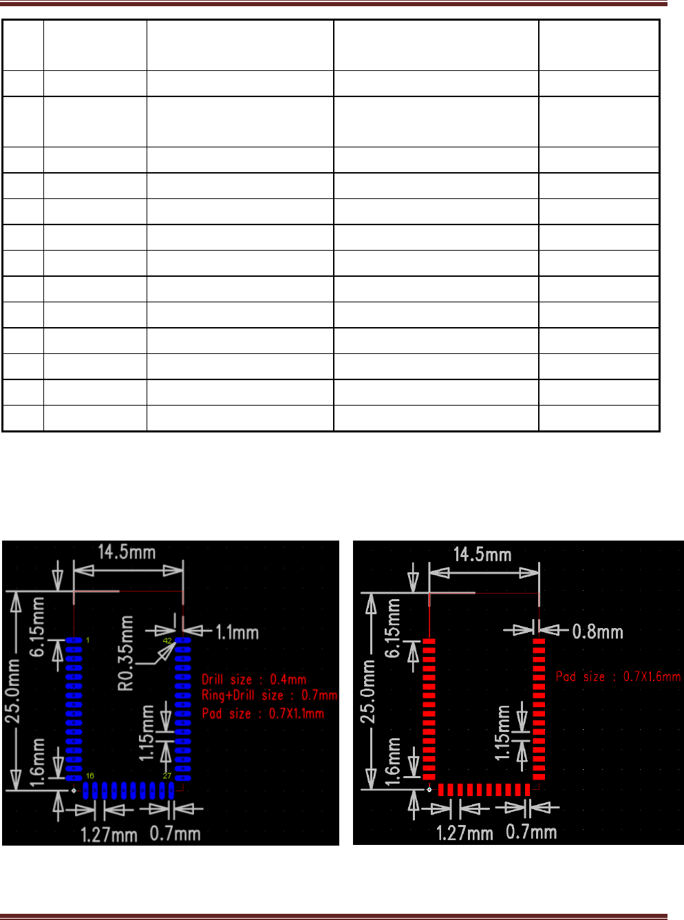
2.3 Module package and PCB footprint dimensions
Figure 2-2 Module package dimensions Figure 2-3 Module PCB footprint dimensions
Dimesion:25mm(L)x14.5mm(W)x0.8mm(H)
1
4
1
2
1
16 27
42
B426-AB1510
Stereo Speaker Module For Intensive Audio Applications
B426-AB1510 Stereo Speaker Module for Intensive
Audio Applications Page 7 of 17 CONFIDENTIAL
Specification
Version 0.40 Sep-2015
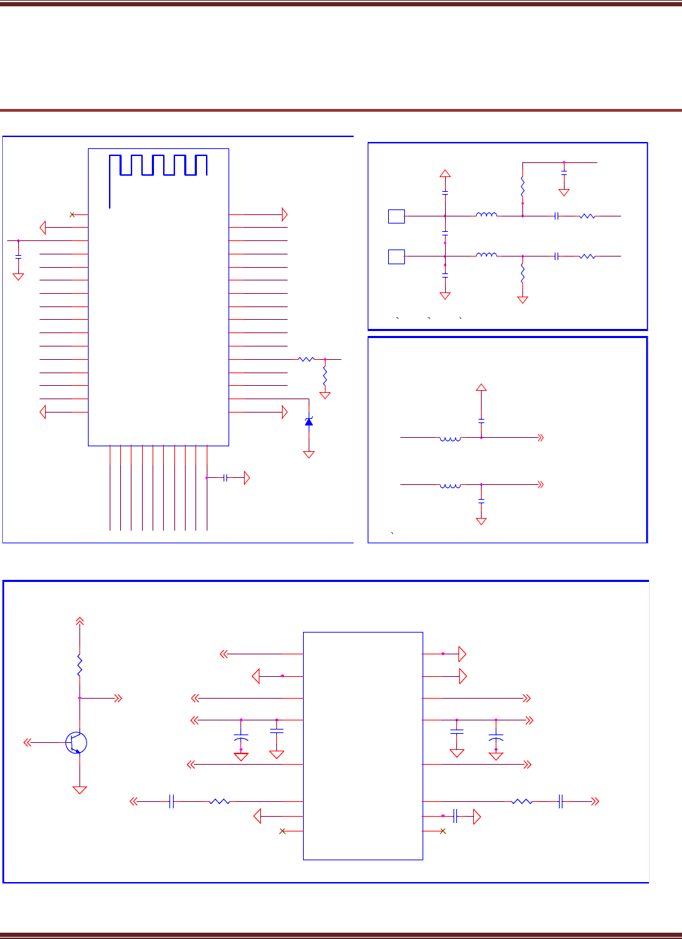
3 General Application Schematic
PIO4
C39
100nF
D5
BZT52C6V8T
PIO2
PIO1
WAKE
PIO11
UART_TX
UART_RX
PIO3
PIO16
PIO15
PIO14
PIO7
PIO6
WP/PIO18
SCL
SDA
PIO17
PIO12
VCCIO
PIO5
LED1
LED0
VREGOUT_HV
BAT_IN
VCHG_IN
LINE_IN_L
MIC2_P
MIC2_N
MIC1_N
MIC1_P
MIC_BIAS
SPK_RP
LRVCM
VREGOUT_MV
SPK_LP
LINE_IN_R
RESET
U3
AB1510_Module with antenna
VCHG_IN 28
BAT_IN 29
LINE_IN_R 38
SPK_LP 39
LRVCM 40
MIC_BIAS 32
MIC1_P 33
MIC2_P 36
LINE_IN_L 37
WAKE
3
VREGOUT_MV
25
UART_TX
8
UART_RX
7
LED0
20
LED1
21
PIO17
15
PIO16
14
PIO15
13
PIO14
12
PIO12
24
VCCIO
23
PIO11
9
PIO7
11
PIO6
10
PIO5
22
VREGOUT_HV 30
PIO3
6
PIO2
5
PIO1
4
NC
1
RST
26
PIO4 31
MIC2_N 35
MIC1_N 34
SDA
17
SCL
18
GND
2
GND
16 GND 27
SPK_RP 41
WP/PIO18
19
GND 42
R16
180 Ohm
R18
4.7 KOhm
C38
100nF
MIC1_N
C152 C154 C155
L7 & L8 are reserved for removing potential GSM TDD noise.
MIC1_P
C37
4.7uF(0603)
R12
2.2k Ohm
R11
2.2k Ohm
M+ 1
C18
22nF
C19
22nF
M- 1
MIC_BIAS
C35 C36 are reserved for removing potential GSM TDD noise.
Microphone
L7 0 Ohm
L8 0 Ohm
C154
NC
C155
NC
C152
NC
R131 3K
R133 3K
L9
120 nH
L10
120 nH
SPK_LP
C36
NC
C35
NC
SPK_RP
BT Speaker
AMP_IN_LP
AMP_IN_RP
R177
43K ohm /1%
PIO4
BAT_IN
Q6
MMBT3904
1
32
+
C156
470uF
+
C157
470uF
R19
4.7 KOhm
C11
0.22uF/X5R/X7R
C13
0.1uF C14
0.1uF
R176
43K ohm/1%
C9
1uF
C12
0.22uF/X5R/X7R
BAT_IN
AMP_OUT_RP
AMP_OUT_LN
AMP_IN_LP AMP_IN_RP
AMP_OUT_RN
Audio AMP
BAT_IN
U1
NS4248_SOP16
SD
1
GND
2
VoLP
3
VDD
4
VoLN
5
INLN
6
GND
7
NC
8
HP-IN 16
GND 15
VoRP 14
VDD 13
VoRN 12
INRN 11
NC 9
Bypass 10
SD
SD AMP_OUT_LP
Note:
The function of Q6 is for avoiding the leakage current from audio Amp.(NS4248) .
B426-AB1510
Stereo Speaker Module For Intensive Audio Applications
B426-AB1510 Stereo Speaker Module for Intensive
Audio Applications Page 8 of 17 CONFIDENTIAL
Specification
Version 0.40 Sep-2015
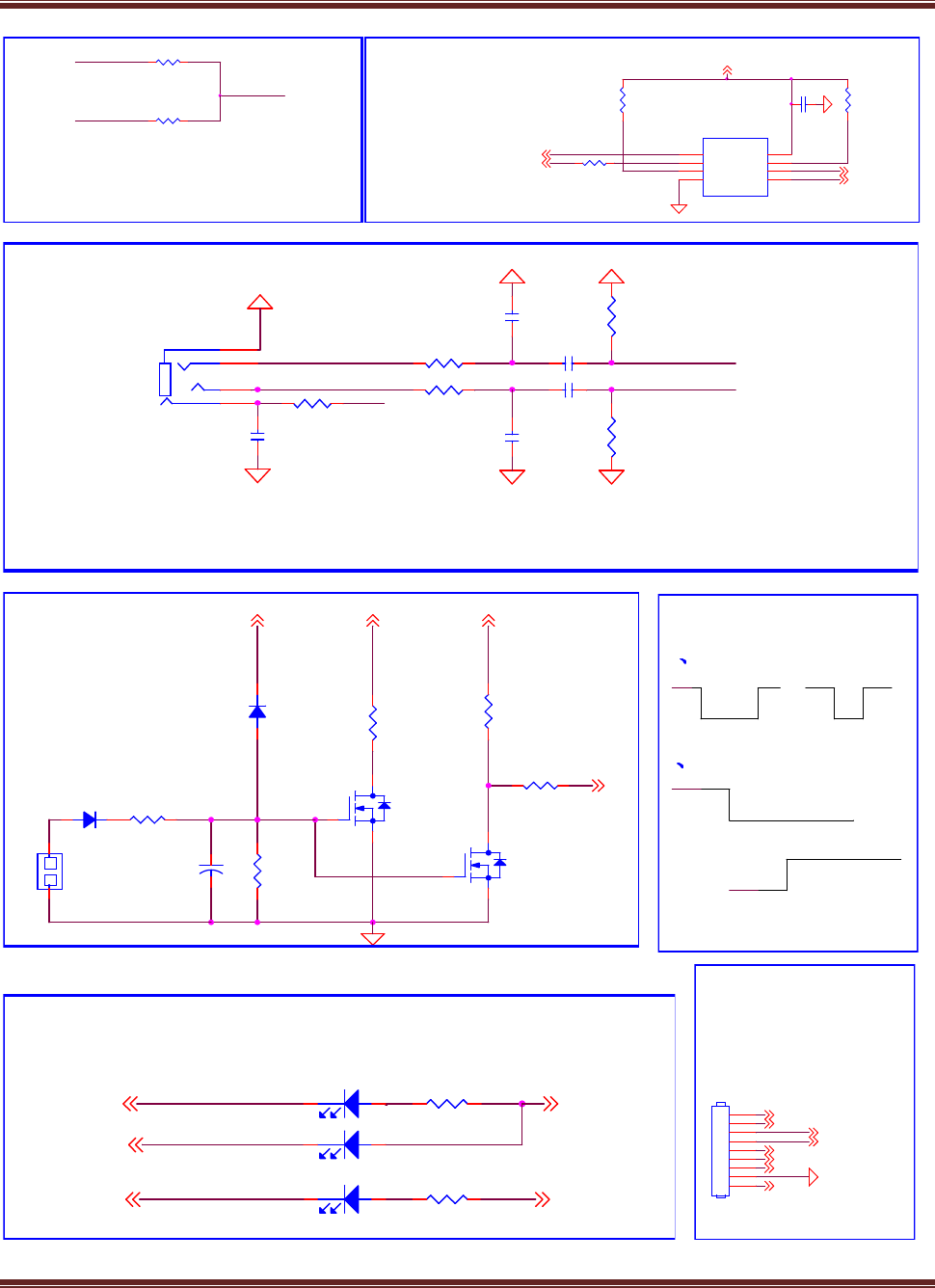
PIO16 is for SPI_MISO usage
PIO17 is for SPI_CLK usage
(CLK)
(CSN)
C21
0.1uF
SPI Flash
(MOSI)
R67
4.7k Ohm
U8
NC/MX25L512E0C-20
#CS
1
SO
2
#WP
3
GND
4SI 5
SCLK 6
HOLD# 7
VCC 8
R68
4.7K Ohm
PIO15
PIO16
PIO14
(MISO)
PIO17
VCCIO
Note:
R7
0ohm/NC
R8
NC/0ohm
If R7=0 Ohm, R8=NC, then the VCCIO=VREGOUT_HV (3.3V)
If R7=NC, R8=0 Ohm,then the VCCIO=VREGOUT_MV (1.8V)
VREGOUT_HV
VREGOUT_MV
PIO 14 is for SPI_CSN usage
VCCIO
R69
300ohm
PIO15 is for SPI_MOSI usage
The input signal of Line-in path (enter to chip) should be< 0.6 Vrms
The internal input impedance of LINE_IN_L(/LINE_IN_R) is 10Kohm
R164
240K
C158
0.1uF
LINE_IN_L
PIO11
R130 7.5K
R132 7.5K
J32
PJ320D-D4S4A-02
1
2
3
4
C159
470pF
Line-IN
C160
470pF
C161
1uF
R126
0ohm
LINE_IN_R
C162
1uF
R163
240K
The seriers resistors 7.5Kohm of R130 and R132 are used for 1 Vrms input signal
NFC
WAKE
D7
BAS516
D6
BAS516
R2
100 ohm
R1
1M ohm
R3
100 ohm
C6
0.1uF
Q1
2N7002KW
R4
10k ohm
Q2
2N7002KW
JP4
1 2
NFC_L2b
BATP
WAKE
VCC_IO
R169
0 Ohm
NFC_L1b
PIO6
BATP VCC_IO
Power on/off
1 Press Button
Power on
WAKE
Power off
≥3s
....
≥3s
....
2 Slide Switch
3 second later,then Power on
WAKE
always low
Power off at once
WAKE
R91 470 Ohm
D3
Blue LED / SMD 12
PIO12
D2
Blue LED / SMD 12
LED1
LED0
D1
Red LED / SMD 12
LED
BAT_IN
R112 1 KOhm
VREGOUT_HV
TCB Connector
for MP
download and
calibration
PIO7
BAT_IN
J15
HEADER 9
1
2
3
4
5
6
7
8
9
VCHG_IN
UART_RX
RESET
SDA
WAKE
UART_TX
B426-AB1510
Stereo Speaker Module For Intensive Audio Applications
B426-AB1510 Stereo Speaker Module for Intensive
Audio Applications Page 9 of 17 CONFIDENTIAL
Specification
Version 0.40 Sep-2015
R62
200Kohm
C97
0.1uF
Under the condition of pressing PIO1 to Low,then
plug battery charger
R64
47Kohm
R63
47Kohm
RESET
PIO1
BAT_IN
V_CHG Q4
MMBT3904
1
32
Conditional Hardware
Reset
Q5
MMBT3906
1
23
R9
47K ohm
Positive Pulse for Resetting
(20ms pluse width and
0.7V at least)
C95
0.1uF
VCHG_IN
CHARGER
1
GND
1
Ichg=1000/R6
C48
10uF
BAT_IN
C59
0.1uF
U11 ACE4054
CHRG 1
GND 2
BAT 3
VCC
4
PROG
5
R5
1K ohm
D8
Red LED
1 2
R6
4.7K ohm
Charger
V_CHG
R173
NC/0 Ohm
R166
0 Ohm/NC
R173=0 Ohm, R166=NC -->Internal charger
R173=NC,R166=0 Ohm -->External charger
B426-AB1510
Stereo Speaker Module For Intensive Audio Applications
B426-AB1510 Stereo Speaker Module for Intensive
Audio Applications Page 10 of 17 CONFIDENTIAL
Specification
Version 0.40 Sep-2015
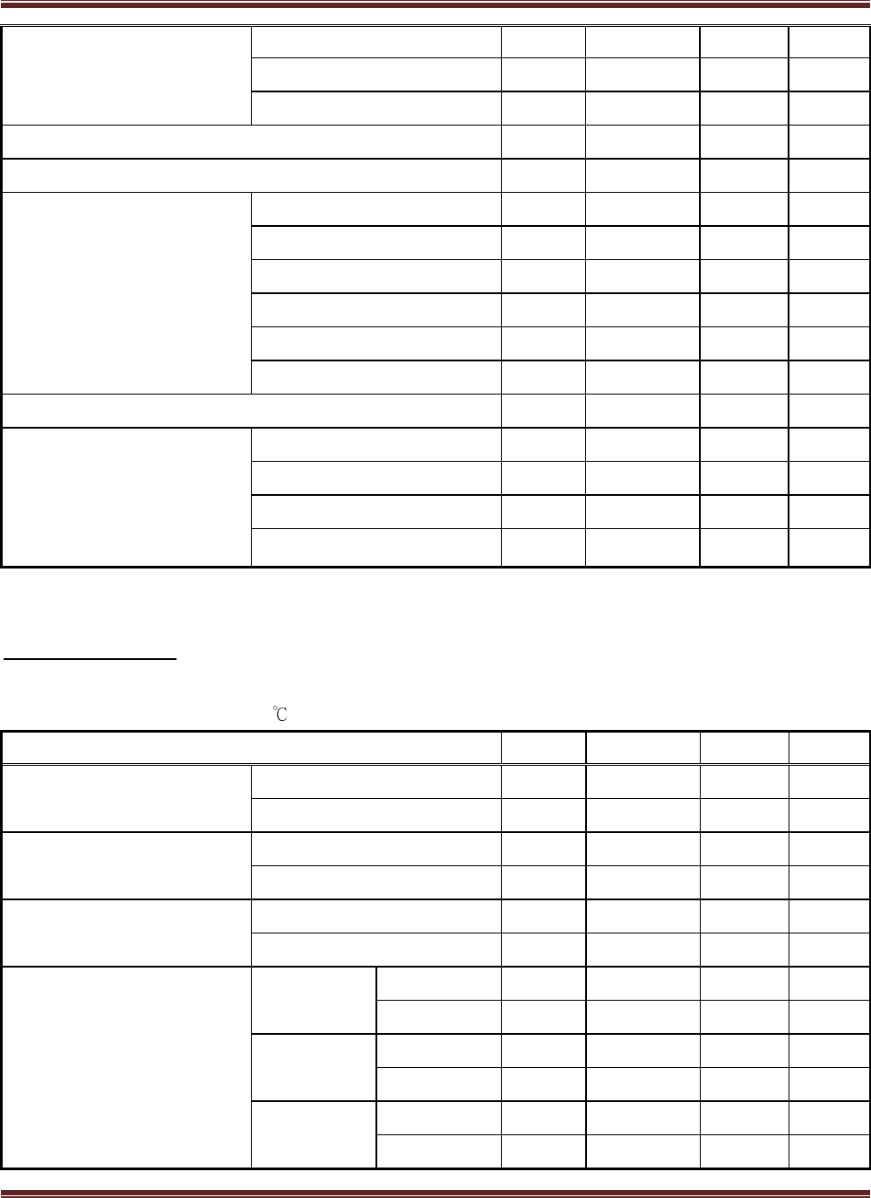
4 Electrical Characteristics
4.1 Recommended Operating Conditions
Item Min. Typ. Max. Unit
I/O supply voltage (VCCIO) 1.7 3.6 V
Battery supply voltage (BAT_P) 2.7 4.2 V
Internal charger supply voltage (V_CHG) 4.5 5 6.5 V
Table 4-1 Recommended Operating Conditions
4.2 Power
4.2.1 High-Voltage LDO (VREGOUT_HV)
Item Condition Min. Typ. Max. Unit
Input Voltage (BAT_P) 2.7 4.2 V
Output Voltage Input voltage > 3.3V 3 V
Rated Output Current (Iout) Input voltage = 4.2V 300 mA
Table 4-2 High-Voltage LDO
4.2.2 Medium Voltage LDO (VREGOUT_MV)
Item Condition Min. Typ. Max. Unit
Input Voltage (BAT_P) 2.7 4.2 V
Output Voltage 1.8 V
Rated Output Current (Iout) Input voltage = 4.2V 100 mA
Table 4-3 Medium-Voltage LDO
4.3 Battery Charger
B426-AB1510
Stereo Speaker Module For Intensive Audio Applications
B426-AB1510 Stereo Speaker Module for Intensive
Audio Applications Page 11 of 17 CONFIDENTIAL
Specification
Version 0.40 Sep-2015
Item Min. Typ. Max. Unit
Input Voltage 4.5 5 6.5 V
Charge Current (CC Mode) 25 400 mA
Trickle Charge Current 4 mA
Trickle Charge Threshold Voltage 2.92 V
Regulated Output (Float) Voltage 4.2 V
Table 4-4 Battery Charger
4.4 Radio Characteristics
4.4.1 Transmitter
Basic Data Rate
Core Supply Voltage = 1.8V @ 25
Item Min. Typ. Max. Unit
Maximum RF transmit Power 4 7 dBm
RF power control range 25 dB
20dB bandwidth for modulated carrier 900 KHz
Adjacent channel transmit
power
+2MHz -20 dBm
-2MHz -20 dBm
+3MHz -40 dBm
-3MHz -40 dBm
Frequency deviation
∆f1avg Maximum Modulation
165 KHz
∆f2max Minimum Modulation
140 KHz
∆f1avg/∆f2avg 0.9
Initial carrier frequency tolerance -75 75 KHz
Freq. Drift
DH1 packet -25 25 KHz
DH3 packet -40 40 KHz
DH5 packet -40 40 KHz
Freq. Drift Rate -20 20 KHz/50us
Harmonic Content -45 dBm
Table 4-5 Transmitter Basic Data Rate
B426-AB1510
Stereo Speaker Module For Intensive Audio Applications
B426-AB1510 Stereo Speaker Module for Intensive
Audio Applications Page 12 of 17 CONFIDENTIAL
Specification
Version 0.40 Sep-2015
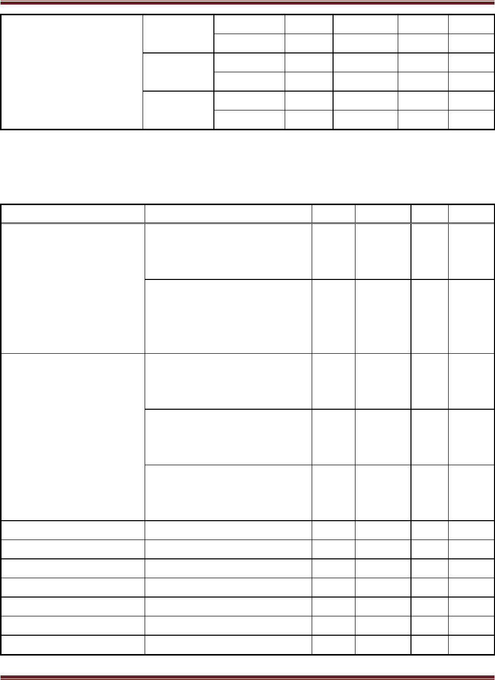
Enhanced Data Rate
Core Supply Voltage = 1.8V @ 25
Item Min. Typ. Max. Unit
Relative transmit power -1.5 dB
π/4 DQPSK max carrier frequency stability |ω
o
| -10 10 KHz
π/4 DQPSK max carrier frequency stability |ω
i
| -75 75 KHz
π/4 DQPSK max carrier frequency stability |ω
o
+ω
i
| -75 75 KHz
8DPSK max carrier frequency stability |ω
o
| -10 10 KHz
8DPSK max carrier frequency stability |ω
i
| -75 75 KHz
8DPSK max carrier frequency stability |ω
o
+ω
i
| -75 75 KHz
π/4 DQPSK Modulation Accuracy
RMS DEVM 20 %
99% DEVM 99 %
Peak DEVM 35 %
8DPSK Modulation Accuracy
RMS DEVM 13 %
99% DEVM 99 %
Peak DEVM 25 %
In-band spurious emissions
F > F0 + 3MHz -40 dBm
F < F0 - 3MHz -40 dBm
F = F0 + 3MHz -40 dBm
F = F0 - 3MHz -40 dBm
F = F0 + 2MHz -20 dBm
F = F0 - 2MHz -20 dBm
F = F0 + 1MHz -26 dB
F = F0 - 1MHz -26 dB
EDR Differential Phase Encoding 99 %
Table 4-6 Transmitter Enhanced Data Rate
4.4.2 Receiver
Basic Data Rate
Core Supply Voltage = 1.35V @ 25
Item Min. Typ. Max. Unit
B426-AB1510
Stereo Speaker Module For Intensive Audio Applications
B426-AB1510 Stereo Speaker Module for Intensive
Audio Applications Page 13 of 17 CONFIDENTIAL
Specification
Version 0.40 Sep-2015
Sensitivity at 0.1% BER
2.402GHz -92 dBm
2.441GHz -92 dBm
2.480GHz -92 dBm
Maximum input power at 0.1% BER -20 dBm
Co-Channel interference 11 dB
Adjacent channel selectivity
C/I
F = F
0
+1MHz 0 dB
F = F
0
-1MHz 0 dB
F = F
0
+2MHz -30 dB
F = F
0
-2MHz -20 dB
F = F
0
+3MHz -40 dB
F = F
image
-9 dB
Maximum level of intermodulation interference -39 dBm
Blocking @Pin=-
67dBm with
0.1%BER
30-2000 MHz -10 dBm
2000-2400 MHz -27 dBm
2500-3000 MHz -27 dBm
3000-12750 MHZ -10 dBm
Table 4-7 Receiver Basic Data Rate
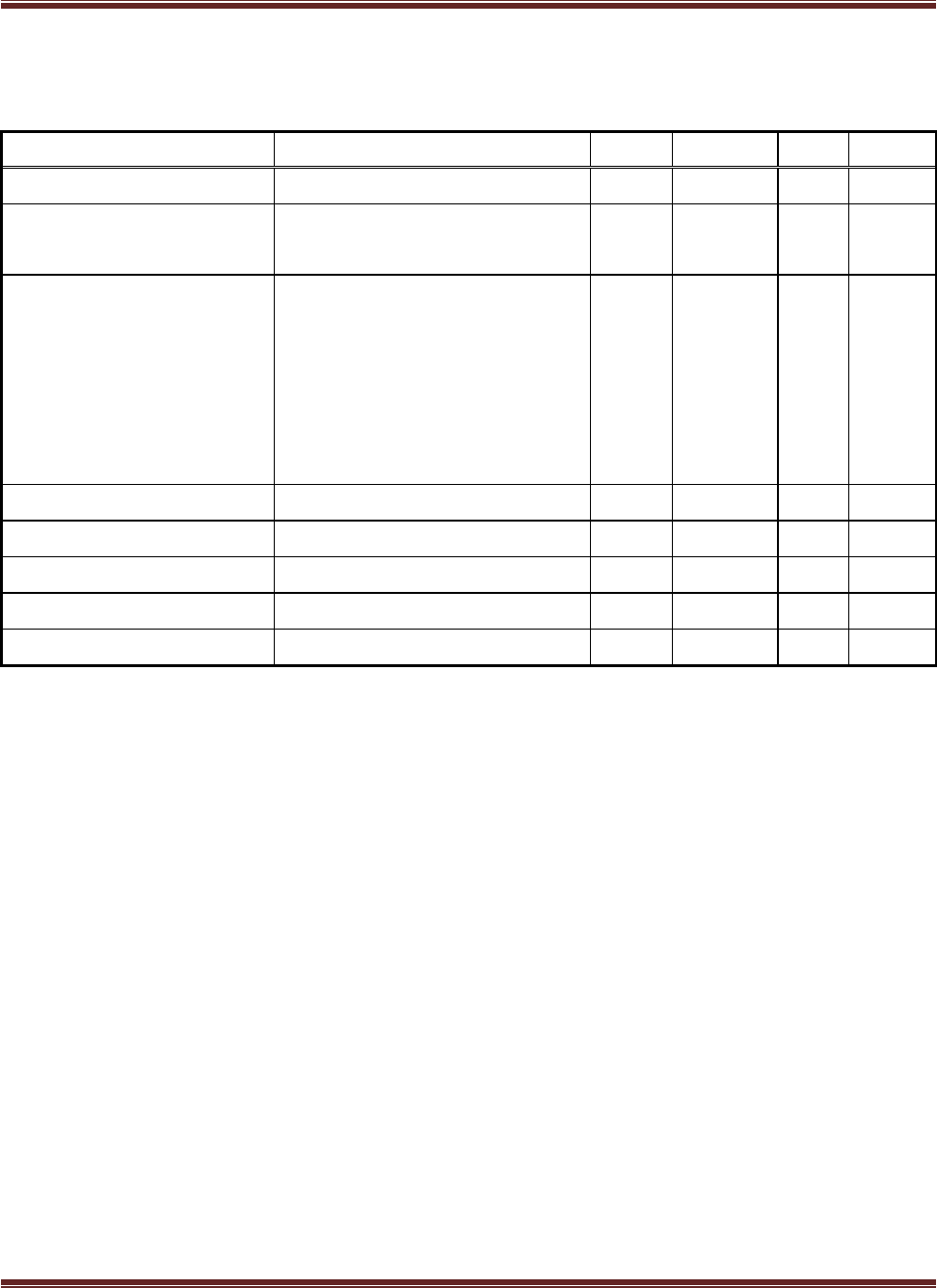
Enhanced Data Rate
Core Supply Voltage = 1.8V @ 25
Item
Min. Typ. Max. Unit
Sensitivity at 0.01% EDR
π/4 DQPSK -91 dBm
8DPSK -83 dBm
Maximum input power at 0.1%
BER
π/4 DQPSK -20 dBm
8DPSK -20 dBm
Co-Channel interference
π/4 DQPSK 13 dB
8DPSK 21 dB
Adjacent channel selectivity
C/I
F = F
0
+1MHz
π/4 DQPSK 0 dB
8DPSK 5 dB
F = F
0
-1MHz
π/4 DQPSK 0 dB
8DPSK 5 dB
F = F
0
+2MHz
π/4 DQPSK -30 dB
8DPSK -25 dB
B426-AB1510
Stereo Speaker Module For Intensive Audio Applications
B426-AB1510 Stereo Speaker Module for Intensive
Audio Applications Page 14 of 17 CONFIDENTIAL
Specification
Version 0.40 Sep-2015
F = F
0
-2MHz
π/4 DQPSK -20 dB
8DPSK -13 dB
F = F
0
+3MHz
π/4 DQPSK -40 dB
8DPSK -33 dB
F = F
image
π/4 DQPSK -7 dB
8DPSK 0 dB
Table 4-8 Receiver Enhanced Data Rate
4.5 Audio ADC
Item Condition Min. Typ. Max.
Unit
SNR
Microphone amplifier
(A-Weighted 1kHz@ full scale,
microphone input BW=20~20kHz)
84 dB
Codec bypass mode
(A-Weighted 1kHz@ full scale,
line-input BW=20~20kHz,
VCCSPK=3V EAR_AMP=0dB)
95 dB
THD+N
Microphone amplifier gain=42dB
(A-Weighted 1kHz@-10dBFS,
microphone input BW=20~4kHz)
-55 dB
Microphone amplifier gain=21dB
(A-Weighted 1kHz@-10dBFS,
microphone input BW=20~20kHz)
-66.7 DB
Microphone amplifier gain=0dB
(A-Weighted 1kHz@ -10dBFS,
line-input BW=20~20kHz)
0.05 %
Digital Gain -21 24 dB
Analog Gain 0 42 dB
Input Full-Scale at MAX gain 2.24 MVrms
Input Full-Scale at Min gain 282 MVrms
Microphone in level (Microphone input, full scale) 0.8 Vpp
Input in level (Line-input, full scale) 1.7 Vpp
Mic_bias_voltage 2.7 V
Table 4-9 Audio ADC
B426-AB1510
Stereo Speaker Module For Intensive Audio Applications
B426-AB1510 Stereo Speaker Module for Intensive
Audio Applications Page 15 of 17 CONFIDENTIAL
Specification
Version 0.40 Sep-2015
4.6 Stereo DAC
Item Condition Min. Typ. Max.
Unit
SNR 94 dB
THD+N 16 ohm load
Analog gain=0dB 0.1 %
Output swing
SPK_LP or SPK_RP Output
Full-Scale at load=16Ohm
SPK_RP -- (16Ohm)
LRVCM
SPK_LP -- (16Ohm)
speaker gain=3dB
2.1 Vpp
Digital Gain -21 24 dB
Analog Gain -12 9 dB
Allow load VCCSPK=3V 8 16 Ohm
Cross talk Load =16Ohm -50 dB
Noise floor power Analog gain=0dB -100 dBV
Table 4-10 Stereo DAC

B426-AB1510
Stereo Speaker Module For Intensive Audio Applications
B426-AB1510 Stereo Speaker Module for Intensive
Audio Applications Page 16 of 17 CONFIDENTIAL
Specification
Version 0.40 Sep-2015
Federal Communication Commission Interference Statement
This equipment has been tested and found to comply with the limits for a Class B digital device, pursuant to
Part 15 of the FCC Rules. These limits are designed to provide reasonable protection against harmful
interference in a residential installation. This equipment generates, uses and can radiate radio frequency
energy and, if not installed and used in accordance with the instructions, may cause harmful interference to
radio communications. However, there is no guarantee that interference will not occur in a particular
installation. If this equipment does cause harmful interference to radio or television reception, which can be
determined by turning the equipment off and on, the user is encouraged to try to correct the interference by
one of the following measures:
- Reorient or relocate the receiving antenna.
- Increase the separation between the equipment and receiver.
- Connect the equipment into an outlet on a circuit different from that to which the receiver is connected.
- Consult the dealer or an experienced radio/TV technician for help.
FCC Caution:
Any changes or modifications not expressly approved by the party responsible for compliance could void the
user's authority to operate this equipment.
This device complies with Part 15 of the FCC Rules. Operation is subject to the following two conditions:
(1) This device may not cause harmful interference, and
(2) This device must accept any interference received, including interference that may cause undesired
operation.
FCC Radiation Exposure Statement:
This equipment complies with FCC radiation exposure limits set forth for an uncontrolled environment. This
transmitter module must not be co-located or operating in conjunction with any other antenna or transmitter.
IMPORTANT NOTE:
In the event that these conditions can not be met (for example certain laptop configurations or co-location with
another transmitter), then the FCC authorization is no longer considered valid and the FCC ID can not be
used on the final product. In these circumstances, the OEM integrator will be responsible for re-evaluating the
end product (including the transmitter) and obtaining a separate FCC authorization.
End Product Labeling
The final end product must be labeled in a visible area with the following:
“Contains FCC ID: ATMCR375”.
Manual Information to the End User
The OEM integrator has to be aware not to provide information to the end user regarding how to install or
remove this RF module in the user’s manual of the end product which integrates this module.
Part 15B (as the un-intentional emission requirement) shall be further evaluated while module is
being installed to the end product or end host.

B426-AB1510
Stereo Speaker Module For Intensive Audio Applications
B426-AB1510 Stereo Speaker Module for Intensive
Audio Applications Page 17 of 17 CONFIDENTIAL
Specification
Version 0.40 Sep-2015
Canada Statement
This device complies with Industry Canada’s licence-exempt RSSs. Operation is subject to the following two
conditions: (1) this device may not cause interference, and (2) this device must accept any interference,
including interference that may cause undesired operation of the device.
Le présent appareil est conforme aux CNR d'Industrie Canada applicables aux appareils radio exempts de
licence. L'exploitation est autorisée aux deux conditions suivantes : (1) l'appareil ne doit pas produire de
brouillage, et (2) l'utilisateur de l'appareil doit accepter tout brouillage radioélectrique subi, même si le
brouillage est susceptible d'en compromettre le fonctionnement.
Caution Exposure:
This device meets the exemption from the routine evaluation limits in section 2.5 of RSS102 and users can
obtain Canadian information on RF exposure and compliance.
Le dispositif répond à l'exemption des limites d'évaluation de routine dans la section 2.5 de RSS102 et les
utilisateurs peuvent obtenir des renseignements canadiens sur l'exposition aux RF et le respect.
The final end product must be labelled in a visible area with the following:
The Industry Canada certification label of a module shall be clearly visible at all times when installed in the
host device, otherwise the host device must be labelled to display the Industry Canada certification number of
the module, preceded by the words “Contains transmitter module”, or the word “Contains”, or similar wording
expressing the same meaning, as follows:
Contains transmitter module IC: 6547A-CR375
The end user manual shall include all required regulatory information/warning as show in this manual.