PBE Europe as Axell Wireless 80-3014RSERIES 80-301401 Cell Enhancer User Manual 80 301401HBKM Handbook
Axell Wireless 80-301401 Cell Enhancer 80 301401HBKM Handbook
Contents
- 1. Manual 1 of 2
- 2. Manual 2 of 2
Manual 1 of 2

Axell Wireless Limited
Technical Literature
L.A. M.T.A. Remote Sites
Document Number 80-301401HBKM Issue No. 1 Date 13/06/2008 Page 1 of 148
L.A. M.T.A. BDA Line Amplifier
User/Maintenance Handbook
For
GETS Global Signalling LLC
AWL Works Order Q115342
Product Part Nos.
In-Line BDA Wall Mount 80-301401
In-Line BDA Rack Mount 80-301406
AFL and Avitec have merged to form Axell Wireless
AXELL WIRELESS UK
Aerial House
Asheridge Road
Chesham, Buckinghamshire
HP5 2QD, United Kingdom
Tel: + 44 (0) 1494 777000
Fax: + 44 (0) 1494 777002
info@axellwireless.com
www.axellwireless.com
AXELL WIRELESS SWEDEN
Box 7139
174 07 Sundbyberg
Sweden
Tel: + 46 (0) 8 475 4700
Fax: + 46 (0) 8 475 4799

Axell Wireless Limited
Technical Literature
L.A. M.T.A. Remote Sites
Document Number 80-301401HBKM Issue No. 1 Date 13/06/2008 Page 2 of 148
Table of Contents
1. INTRODUCTION.......................................................................................................................... 7
1.1. Scope and Purpose of Document............................................................................................. 7
1.2. Limitation of Liability Notice ...................................................................................................... 7
2. SAFETY CONSIDERATIONS ...................................................................................................... 8
2.1. Earthing of Equipment .............................................................................................................. 8
2.2. Electric Shock Hazard............................................................................................................... 8
2.3. RF Radiation Hazard ................................................................................................................ 8
2.4. Lifting and other Health and Safety Recommendations............................................................ 8
2.5. Chemical Hazard ...................................................................................................................... 9
2.6. Laser safety .............................................................................................................................. 9
2.7. Emergency Contact Numbers...................................................................................................9
3. IN-LINE BDA WALL MOUNT 80-301401................................................................................... 10
3.1. In-Line BDA Wall Mount 80-301401 Specification.................................................................. 11
3.1.1. In-Line BDA Wall Mount 80-301401 Overall system Diagram.......................................... 12
3.2. In-Line BDA Wall Mount 80-301401 List of Major Components ............................................. 13
3.3. Combiner 80-301402 .............................................................................................................. 13
3.3.1. Combiner 80-301402 System Diagram ............................................................................ 14
3.3.2. Combiner 80-301402 Outline Drawing ............................................................................. 15
3.3.3. Combiner 80-301402 Specification ..................................................................................16
3.3.4. Combiner 80-301402 Photographs .................................................................................. 17
3.3.4.1. Front View.................................................................................................................. 17
3.3.4.2. Underside view showing RF connectors.................................................................... 18
3.3.4.3. Interior view ............................................................................................................... 19
3.3.5. Combiner 80-301402 Major Sub-Components................................................................. 20
3.3.5.1. Bandpass Filter 02-010701........................................................................................ 20
3.3.5.2. Bandpass Filter 02-010901........................................................................................ 20
3.3.5.3. Crossband Splitter/Coupler 550/800MHz (07-004815).............................................. 21
3.3.5.4. Crossband Splitter/Coupler VHF/UHF (07-005754)................................................... 21
3.3.5.5. 30dB Directional Coupler (07-018005) ...................................................................... 22
3.3.5.6. 30dB Bi-Directional Coupler (07-022005).................................................................. 23
3.4. VHF/UHF BDA Unit (80-301403) ............................................................................................ 24
3.4.1. VHF/UHF BDA Unit (80-301403) System Diagram.......................................................... 25
3.4.2. VHF/UHF BDA Unit (80-301403) Outline Drawing........................................................... 26
3.4.3. VHF/UHF BDA Unit(80-301403) Specification ................................................................. 27
3.4.4. VHF/UHF BDA Unit(80-301403) Photographs ................................................................. 28
3.4.4.1. Front View.................................................................................................................. 28
3.4.4.2. Underside view showing connectors ......................................................................... 29
3.4.4.3. Interior view ............................................................................................................... 30
3.4.5. VHF/UHF BDA Unit(80-301403) Major Sub-components ................................................ 31
3.4.5.1. Bandpass Filter (01-002503) ..................................................................................... 31
3.4.5.2. 30dB Directional Coupler (07-002908) ...................................................................... 32
3.4.5.3. Switched Attenuator 0.25Watt, 0 - 30dB (10-000701) ............................................... 32
3.4.5.4. Low Noise Amplifier (11-005401) .............................................................................. 33
3.4.5.5. TETRA Power Amplifier 20W (12-016301) ................................................................ 34
3.4.5.6. TETRA Power Amplifier 5W (12-021601) .................................................................. 35
3.4.5.7. Low Power Amplifier (1Watt) (12-021801)................................................................. 36
3.4.5.8. VHF Power Amplifier 5W (12-025602)....................................................................... 37
3.4.5.9. Automatic Gain Control.............................................................................................. 38
3.4.5.10. 24V Relay Dual Assembly (20-001602) ................................................................... 38
3.4.5.11. 24V Relay Assembly (80-008902) ........................................................................... 39
3.4.5.12. Dual Diode Assembly (94-100004) .......................................................................... 39
3.4.5.13. DC/DC Converter, 24V in, 12V 5A out (96-200024) ................................................ 40
3.5. UHF BDA Unit (80-301404) ....................................................................................................41
3.5.1. UHF BDA Unit (80-301404) System Diagram .................................................................. 42
3.5.2. UHF BDA Unit (80-301404) Outline Drawing ................................................................... 43

Axell Wireless Limited
Technical Literature
L.A. M.T.A. Remote Sites
Document Number 80-301401HBKM Issue No. 1 Date 13/06/2008 Page 3 of 148
3.5.3. UHF BDA Unit (80-301404) Specification ........................................................................ 44
3.5.4. UHF BDA Unit (80-301404) Photographs ........................................................................ 45
3.5.4.1. Front View.................................................................................................................. 45
3.5.4.2. Underside view showing connectors ......................................................................... 46
3.5.4.3. Interior view ............................................................................................................... 47
3.5.5. UHF BDA Unit (80-301404) Major Sub-components ....................................................... 48
3.5.5.1. 30dB Directional Coupler (07-002908) ...................................................................... 48
3.5.5.2. Switched Attenuator 0.25Watt, 0 - 30dB (10-000701) ............................................... 48
3.5.5.3. Low Noise Amplifier (11-005401) .............................................................................. 49
3.5.5.4. TETRA Power Amplifier 20W (12-016301) ................................................................ 50
3.5.5.5. TETRA Power Amplifier 5W (12-021601) .................................................................. 51
3.5.5.6. Low Power Amplifier (12-021801).............................................................................. 52
3.5.5.7. DC/DC Converter, 24V in, 12V 8A out (13-003011) .................................................. 53
3.5.5.8. Automatic Gain Control.............................................................................................. 53
3.5.5.9. 24V Relay Dual Assembly (20-001602)..................................................................... 54
3.5.5.10. 24V Relay Assembly (80-008909) ........................................................................... 54
3.5.5.11. Dual Diode Assembly (94-100004) .......................................................................... 55
3.6. 800MHz BDA UNIT (80-301405) ............................................................................................ 56
3.6.1. 800MHz BDA UNIT (80-301405) System Diagram .......................................................... 57
3.6.2. 800MHz BDA UNIT (80-301405) Outline Drawing ........................................................... 58
3.6.3. 800MHz BDA UNIT (80-301405) Specification ................................................................ 59
3.6.4. 800MHz BDA UNIT (80-301405) Photographs ................................................................ 60
3.6.4.1. Front View.................................................................................................................. 60
3.6.4.2. Underside view showing connectors ......................................................................... 60
3.6.4.3. Interior view ............................................................................................................... 61
3.6.5. 800MHz BDA UNIT (80-301405) Major Sub-components................................................ 62
3.6.5.1. Bandpass Filter (02-011601) ..................................................................................... 62
3.6.5.2. Splitter/Combiner (05-002602) .................................................................................. 63
3.6.5.3. 30dB Directional Coupler (07-002907) ...................................................................... 63
3.6.5.4. Switched Attenuator 0.25Watt, 0 - 30dB (10-000701) ............................................... 64
3.6.5.5. Low Noise Amplifier (11-005902) .............................................................................. 64
3.6.5.6. 5W Power Amplifier (12-018601)............................................................................... 65
3.6.5.7. 20W Power Amplifier (12-020501)............................................................................. 66
3.6.5.8. Automatic Gain Control.............................................................................................. 67
3.6.5.9. 24V Relay Dual Assembly (20-001602)..................................................................... 67
3.6.5.10. Dual Diode Assembly (94-100004) .......................................................................... 68
3.6.5.11. DC/DC Converter, 24V in, 12V 5A out (96-200024) ................................................ 68
4. IN-LINE BDA RACK MOUNT 80-301406................................................................................... 69
4.1. In-Line BDA Rack Mount System Diagrams ........................................................................... 71
4.1.1. Overall System Diagram....................................................................................................... 71
4.1.2. Combiners System Diagram.................................................................................................72
4.2. In-Line BDA Rack Mount 80-301406 Specification................................................................. 73
4.3. In-Line BDA Rack Mount 80-301406 Illustrations................................................................... 74
4.3.1. Rack 1 Front View ................................................................................................................ 74
4.3.2. Rack 1 Rear View............................................................................................................. 75
4.3.3. Rack 2 Front View ............................................................................................................ 76
4.3.4. Rack 2 Rear View............................................................................................................. 77
4.3.5. Rack 1 Top View .............................................................................................................. 78
4.3.6. Rack 2 Top View .............................................................................................................. 79
4.4. In-Line BDA Rack Mount 80-301401 List of Major Components ............................................ 80
4.5. Downlink Input Shelf 80-301407............................................................................................. 81
4.5.1. Downlink Input Shelf 80-301407 System Schematic............................................................ 81
4.5.2. Downlink Input Shelf 80-301407 Outline Drawing................................................................ 82
4.5.3. Downlink Input Shelf 80-301407 Specification ................................................................. 83
4.5.4. Downlink Input Shelf 80-301407 Illustrations ................................................................... 83
4.5.4.1. Rear View .................................................................................................................. 83
4.5.5. Downlink Input Shelf 80-301407 Major Sub Components.................................................... 84
4.5.5.1. Bandpass Filter (02-010701) ..................................................................................... 84
4.5.5.2. Bandpass Filter 02-010901........................................................................................ 84

Axell Wireless Limited
Technical Literature
L.A. M.T.A. Remote Sites
Document Number 80-301401HBKM Issue No. 1 Date 13/06/2008 Page 4 of 148
4.5.5.3. Crossband Splitter/Coupler 550/800MHz (07-004815).............................................. 85
4.5.5.4. Crossband Splitter/Coupler VHF/UHF (07-005754)................................................... 85
4.5.5.5. 30dB Bi-Directional Coupler (07-022005).................................................................. 86
4.6. Downlink Output Shelf 80-301408 .......................................................................................... 87
4.6.1. Downlink Output Shelf 80-301408 System Schematic ........................................................ 87
4.6.2. Downlink Output Shelf 80-301408 Outline Drawing ............................................................ 88
4.6.3. Downlink Output Shelf 80-301408 Specification .............................................................. 89
4.6.4. Downlink Output Shelf 80-301408 Illustrations ................................................................ 89
4.6.4.1. Rear View .................................................................................................................. 89
4.6.5. Downlink Output Shelf 80-301408 Major Sub Components............................................. 90
4.6.5.1. 30dB Directional Coupler (07-018005) ...................................................................... 90
4.7. Uplink Input Shelf 80-301407.................................................................................................. 91
4.7.1. Uplink Input Shelf 80-301407 System Schematic ............................................................ 91
4.7.2. Uplink Input Shelf 80-301407 Outline Drawing ................................................................ 92
4.7.3. Uplink Input Shelf 80-301407 Specification...................................................................... 92
4.7.4. Uplink Input Shelf 80-301407 Illustrations........................................................................ 92
4.7.4.1. Rear View .................................................................................................................. 92
4.7.5. Uplink Input Shelf 80-301407 Major Sub Components .................................................... 93
4.8. Uplink Output Shelf 80-301407...............................................................................................94
4.8.1. Uplink Output Shelf 80-301407 System Schematic ......................................................... 94
4.8.2. Uplink Output Shelf 80-301407 Outline Drawing.............................................................. 95
4.8.3. Uplink Output Shelf 80-301407 Specification................................................................... 95
4.8.4. Uplink Output Shelf 80-301407 Illustrations ..................................................................... 95
4.8.4.1. Rear View .................................................................................................................. 95
4.8.5. Uplink Output Shelf 80-301407 Major Sub Components ................................................. 96
4.9. VHF Amplifier Shelf 80-301409 .............................................................................................. 97
4.9.1. VHF Amplifier Shelf 80-301409 System Diagram ............................................................ 98
4.9.2. VHF Amplifier Shelf 80-301409 Outline Drawing ............................................................. 99
4.9.3. VHF Amplifier Shelf 80-301409 Specification ................................................................ 100
4.9.4. VHF Amplifier Shelf 80-301409 Illustrations................................................................... 100
4.9.4.1. Front View................................................................................................................ 100
4.9.4.2. Rear View ................................................................................................................ 101
4.9.5. VHF Amplifier Shelf 80-301409 Major Sub Components ............................................... 101
4.9.5.1. Bandpass Filter (01-002503) ................................................................................... 102
4.9.5.2. Switched Attenuator 0.25Watt, 0 - 30dB (10-000701) ............................................. 102
4.9.5.3. VHF Power Amplifier 5W (12-025602)..................................................................... 103
4.9.5.4. Automatic Gain Control............................................................................................ 104
4.9.5.5. 24V Relay Dual Assembly (20-001602)................................................................... 105
4.9.5.6. Dual Diode Assembly (94-100004).......................................................................... 105
4.10. UHF Lowband Amplifier Shelf 80-301410 ......................................................................... 106
4.10.1. UHF Lowband Amplifier Shelf 80-301410 System Diagram ....................................... 107
4.10.2. UHF Lowband Amplifier Shelf 80-301410 Outline Drawing ........................................ 108
4.10.3. UHF Lowband Amplifier Shelf 80-301410 Specification ............................................. 109
4.10.4. UHF Lowband Amplifier Shelf 80-301410 Illustrations................................................ 109
4.10.4.1. Front View .............................................................................................................. 109
4.10.4.2. Rear View............................................................................................................... 110
4.10.5. UHF Lowband Amplifier Shelf 80-301410 Major Sub Components ............................ 110
4.10.5.1. 30dB Directional Coupler (07-002908)................................................................... 111
4.10.5.2. Switched Attenuator 0.25Watt, 0 - 30dB (10-000701) ........................................... 111
4.10.5.3. Low Noise Amplifier (11-005401)........................................................................... 112
4.10.5.4. TETRA Power Amplifier 20W (12-016301) ............................................................ 113
4.10.5.5. TETRA Power Amplifier 5W (12-021601) .............................................................. 114
3.10.5.6. Low Power Amplifier (1Watt) (12-021801) ............................................................. 115
4.10.5.7. Automatic Gain Control .......................................................................................... 116
4.10.5.8. 24V Relay Dual Assembly (20-001602) ................................................................. 117
4.10.5.9. 12V Relay Assembly 80-008909............................................................................ 117
4.10.5.10. Dual Diode Assembly (94-100004) ...................................................................... 118
4.10.5.11. DC/DC Converter, 24V in, 12V 5A out (96-200024) ............................................ 118
4.11. UHF Midband Amplifier Shelf 80-301410 .......................................................................... 119

Axell Wireless Limited
Technical Literature
L.A. M.T.A. Remote Sites
Document Number 80-301401HBKM Issue No. 1 Date 13/06/2008 Page 5 of 148
4.11.1. UHF Lowband Amplifier Shelf 80-301410 System Diagram ....................................... 120
4.11.2. UHF Midband Amplifier Shelf 80-301410 Outline Drawing ......................................... 120
4.11.3. UHF Midband Amplifier Shelf 80-301410 Specification .............................................. 120
4.11.4. UHF Lowband Amplifier Shelf 80-301410 Illustrations................................................ 120
4.11.4.1. Front View .............................................................................................................. 120
4.11.4.2. Rear View............................................................................................................... 121
4.11.5. UHF Midband Amplifier Shelf 80-301410 Major Sub Components............................. 121
4.12. UHF Highband Amplifier Shelf 80-301410......................................................................... 122
4.12.1. UHF Highband Amplifier Shelf 80-301410 System Diagram ...................................... 123
4.12.2. UHF Highband Amplifier Shelf 80-301410 Outline Drawing ....................................... 123
4.12.3. UHF Highband Amplifier Shelf 80-301410 Specification............................................. 123
4.12.4. UHF Highband Amplifier Shelf 80-301410 Illustrations............................................... 123
4.12.4.1. Front View .............................................................................................................. 123
4.12.4.2. Rear View............................................................................................................... 124
4.12.5. UHF Highband Amplifier Shelf 80-301410 Major Sub Components ........................... 124
4.13. 800MHz Amplifier Shelf 80-301411................................................................................... 125
4.13.1. 800MHz Amplifier Shelf 80-301411 System Diagram................................................. 126
4.13.2. 800MHz Amplifier Shelf 80-301411 Outline Drawing.................................................. 127
4.13.3. 800MHz Amplifier Shelf 80-301411 Specification ....................................................... 128
4.13.4. 800MHz Amplifier Shelf 80-301411 Illustrations ......................................................... 128
4.13.4.1. Front View .............................................................................................................. 128
4.13.4.2. Rear View............................................................................................................... 129
4.13.5. 800MHz Amplifier Shelf 80-301411 Major Sub Components...................................... 129
4.13.5.1. Bandpass Filter (02-011601)..................................................................................130
4.13.5.2. Splitter/Combiner (05-002602)............................................................................... 130
4.13.5.3. 30dB Directional Coupler (07-002907)................................................................... 131
4.13.5.4. Switched Attenuator 0.25Watt, 0 - 30dB (10-000701) ........................................... 131
4.13.5.5. Low Noise Amplifier (11-005902)........................................................................... 132
4.13.5.6. 5W Power Amplifier (12-018601) ........................................................................... 133
4.13.5.7. 20W Power Amplifier (12-020501) ......................................................................... 134
4.13.5.8. Automatic Gain Control .......................................................................................... 135
4.13.5.9. 24V Relay Dual Assembly (20-001602) ................................................................. 136
4.13.5.10. Dual Diode Assembly (94-100004) ...................................................................... 136
4.13.5.11. DC/DC Converter, 24V in, 12V 5A out (96-200024) ............................................ 136
4.14 PSU 96-300064 ................................................................................................................ 137
5. INSTALLATION........................................................................................................................ 138
5.1 Installation Record ................................................................................................................ 138
5.2 General Remarks.................................................................................................................. 138
5.3 Electrical Connections .......................................................................................................... 138
5.4 RF Connections .................................................................................................................... 138
5.5 Optical Connections.............................................................................................................. 138
5.6 Commissioning ..................................................................................................................... 139
6. MAINTENANCE ....................................................................................................................... 140
6.1 Fault Finding ......................................................................................................................... 140
6.1.1 Quick Fault Checklist...................................................................................................... 140
6.1.2 Fault Isolation ................................................................................................................. 140
6.1.3 Downlink......................................................................................................................... 140
6.1.4 Uplink ............................................................................................................................. 141
6.1.5 Checking service ............................................................................................................ 141
6.1.6 Fault repair ..................................................................................................................... 141
6.1.7 Service Support.............................................................................................................. 141
6.2 Tools & Test Equipment........................................................................................................ 142
6.3 Care of Modules.................................................................................................................... 142
6.3.1 General Comments ........................................................................................................ 142
6.3.2 Module Removal (LNAs, general procedure) ................................................................. 142
6.3.3 Module Replacement (general) ...................................................................................... 142
6.3.4 Power Amplifiers ............................................................................................................ 142
6.3.5 Low Power Amplifier Replacement ................................................................................ 143

Axell Wireless Limited
Technical Literature
L.A. M.T.A. Remote Sites
Document Number 80-301401HBKM Issue No. 1 Date 13/06/2008 Page 6 of 148
6.3.6 Module Transportation ................................................................................................... 143
APPENDIX A ..................................................................................................................................... 144
A.1. Glossary of Terms used in this document ......................................................................... 144
A.2. Key to Drawing Symbols used in this document................................................................ 145
A.3. EC Declaration of Conformity ............................................................................................ 146
A.4. Amendment List Record Sheet.......................................................................................... 147
APPENDIX B ..................................................................................................................................... 148
B.1. INITIAL EQUIPMENT SET-UP CALCULATIONS ............................................................. 148

Axell Wireless Limited
Technical Literature
L.A. M.T.A. Remote Sites
Document Number 80-301401HBKM Issue No. 1 Date 13/06/2008 Page 7 of 148
1. INTRODUCTION
1.1. Scope and Purpose of Document
This handbook is for use solely with the equipment identified by the Axell Wireless Limited (AWL) Part
Number shown on the front cover. It is not to be used with any other equipment unless specifically
authorised by AWL. This is a controlled release document and, as such, becomes a part of the Axell
Wireless Total Quality Management System. Alterations and modification may therefore only be
performed by Axell Wireless.
AWL recommends that the installer of this equipment familiarise themselves with the safety and
installation procedures contained within this document before installation commences.
The purpose of this handbook is to provide the user/maintainer with sufficient information to service
and repair the equipment to the level agreed. Maintenance and adjustments to any deeper level must
be performed by AWL, normally at the company’s repair facility in Chesham, England.
This handbook has been prepared in accordance with BS 4884, and AWL’s Quality procedures, which
maintain the company’s registration to BS EN ISO 9001:2000 and to the R&TTE Directive of the
European Parliament. Copies of the relevant certificates and the company Quality Manual can be
supplied on application to the Quality Manager.
This document fulfils the relevant requirements of Article 6 of the R&TTE Directive.
1.2. Limitation of Liability Notice
This manual is written for the use of technically competent operators/service persons. No liability is
accepted by AWL for use or misuse of this manual, the information contained therein, or the
consequences of any actions resulting from the use of the said information, including, but not limited
to, descriptive, procedural, typographical, arithmetical, or listing errors.
Furthermore, AWL does not warrant the absolute accuracy of the information contained within this
manual, or its completeness, fitness for purpose, or scope.
AWL has a policy of continuous product development and enhancement, and as such, reserves the
right to amend, alter, update and generally change the contents, appearance and pertinence of this
document without notice.
All AWL products carry a twelve month warranty from date of shipment. The warranty is expressly on
a return to base repair or exchange basis and the warranty cover does not extend to on-site repair or
complete unit exchange.
Axell Wireless Limited
Technical Literature
L.A. M.T.A. Remote Sites
Document Number 80-301401HBKM Issue No. 1 Date 13/06/2008 Page 8 of 148
2. SAFETY CONSIDERATIONS
2.1. Earthing of Equipment
Equipment supplied from the mains must be connected to grounded outlets and earthed
in conformity with appropriate local, national and international electricity supply and
safety regulations.
2.2. Electric Shock Hazard
The risk of electrical shocks due to faulty mains driven power supplies whilst
potentially ever present in any electrical equipment, would be minimised by adherence
to good installation practice and thorough testing at the following stages:
All test equipment must be in good working order prior to its use. High current power supplies can be
dangerous because of the possibility of substantial arcing. Always switch off during disconnection and
reconnection.
2.3. RF Radiation Hazard
RF radiation, (especially at UHF frequencies) arising from transmitter outputs
connected to AWL’s equipment, must be considered a safety hazard.
This condition might only occur in the event of cable disconnection, or because a
‘spare’ output has been left un-terminated. Either of these conditions would impair the
system’s efficiency. No investigation should be carried out until all RF power sources have been
removed. This would always be a wise precaution, despite the severe mismatch between the
impedance of an N type connector at 50, and that of free space at 377, which would severely
mitigate against the efficient radiation of RF power. Radio frequency burns could also be a hazard, if
any RF power carrying components were to be carelessly touched!
Antenna positions should be chosen to comply with requirements (both local & statutory) regarding
exposure of personnel to RF radiation. When connected to an antenna, the unit is capable of
producing RF field strengths, which may exceed guideline safe values especially if used with
antennas having appreciable gain. In this regard the use of directional antennas with backscreens
and a strict site rule that personnel must remain behind the screen while the RF power is on, is
strongly recommended.
Where the equipment is used near power lines or in association with temporary masts not having
lightning protection, the use of a safety earth connected to the case-earthing bolt is strongly advised.
2.4. Lifting and other Health and Safety Recommendations
Certain items of AWL equipment are heavy and care should be taken when lifting them
by hand. Ensure that a suitable number of personnel, appropriate lifting apparatus
and appropriate personal protective equipment is used especially when installing Cell
Enhancers above ground e.g. on a mast or pole.
a) Original assembly.
b) Commissioning..
c) Regular intervals, thereafter.

Axell Wireless Limited
Technical Literature
L.A. M.T.A. Remote Sites
Document Number 80-301401HBKM Issue No. 1 Date 13/06/2008 Page 9 of 148
2.5. Chemical Hazard
Beryllium Oxide, also known as Beryllium Monoxide, or Thermalox™, is sometimes
used in devices within equipment produced by Axell Wireless Ltd. Beryllium oxide dust
can be toxic if inhaled, leading to chronic respiratory problems. It is harmless if
ingested or by contact.
Products that contain beryllium are load terminations (dummy loads) and some power amplifiers.
These products can be identified by a yellow and black “skull and crossbones” danger symbol (shown
above). They are marked as hazardous in line with international regulations, but pose no threat under
normal circumstances. Only if a component containing beryllium oxide has suffered catastrophic
failure, or exploded, will there be any danger of the formation of dust. Any dust that has been created
will be contained within the equipment module as long as the module remains sealed. For this reason,
any module carrying the yellow and black danger sign should not be opened. If the equipment is
suspected of failure, or is at the end of its life-cycle, it must be returned to Axell Wireless Ltd. for
disposal.
To return such equipment, please contact the Quality Department, who will give you a Returned
Materials Authorisation (RMA) number. Please quote this number on the packing documents, and on
all correspondence relating to the shipment.
PolyTetraFluoroEthylene, (P.T.F.E.) and P.T.F.E. Composite Materials
Many modules/components in AWL equipment contain P.T.F.E. as part of the RF insulation barrier.
This material should never be heated to the point where smoke or fumes are evolved. Any person
feeling drowsy after coming into contact with P.T.F.E. especially dust or fumes should seek medical
attention.
2.6. Laser safety
General good working practices adapted from
EN60825-2: 2004/ EC 60825-2:2004
Do not stare with unprotected eyes or with any unapproved optical device at the fibre
ends or connector faces or point them at other people, Use only approved filtered or attenuating
viewing aids.
Any single or multiple fibre end or ends found not to be terminated (for example, matched, spliced)
shall be individually or collectively covered when not being worked on. They shall not be readily
visible and sharp ends shall not be exposed.
When using test cords, the optical power source shall be the last connected and the first
disconnected; use only approved methods for cleaning and preparing optical fibres and optical
connectors.
Always keep optical connectors covered to avoid physical damage and do not allow any dirt/foreign
material ingress on the optical connector bulkheads.
The optical fibre jumper cable maximum bend radius is 3cm; any smaller radii may result in optical
cable breakage or excessive transmission losses.
Caution: The FO units are NOT weather proof.
2.7. Emergency Contact Numbers
The AWL Quality Department can be contacted on:
Telephone +44 (0)1494 777000
Fax. +44 (0)1494 777002
e-mail qa@axellwireless.com

Axell Wireless Limited
Technical Literature
L.A. M.T.A. Remote Sites
Document Number 80-301401HBKM Issue No. 1 Date 13/06/2008 Page 10 of 148
3. In-Line BDA Wall Mount 80-301401
The wall mount In Line BDA consists of 4 wall mount enclosures:
80-301402 the Combiner unit.
80-301403 which houses the VHF and UHF Low Band amplification modules.
80-301404 which houses the Mid and High band UHF amplification modules.
80-301405 which houses the 800MHz amplification modules.
Downlink
The downlink signal is received from the leaky feeder and enters the Combiner 80-301402 where by
means of crossband splitter/couplers it is split into VHF, UHF and 800MHz paths, the UHF path is
further split into Low, Middle and Highband paths.
The VHF and UHF Lowband paths then leave Combiner 80-301402 and enters VHF/UHF BDA Unit
80-301403,
The UHF Mid and Highband paths leaves Combiner 80-301402 and enters UHF BDA Unit 80-301404
The 800MHz path leaves Combiner 80-301402 and enters 800MHz BDA Unit 80-301405
After being amplified the Downlink signals from the three BDA units then re-enter Splitter/Combiner
80-301402 where they are combined into a single path and fed into the leaky feeder.
Uplink
The Uplink signal signal is received from the leaky feeder and enters the Splitter/Combiner 80-301402
where by means of crossband splitter/couplers it is split into VHF, UHF and 800MHz paths, the UHF
path is further split into Low, Middle and Highband paths.
The VHF and UHF Low band paths then leave Splitter/Combiner 80-301402 and enters VHF/UHF
BDA Unit 80-301403,
The UHF Mid and Highband paths leaves Splitter/Combiner 80-301402 and enters UHF BDA Unit 80-
301404
The 800MHz path leaves Splitter/Combiner 80-301402 and enters 800MHz BDA Unit 80-301405
After being amplified the Uplink signals from the three BDA units then re-enter Splitter/Combiner 80-
301402 where they are combined into a single path and fed into the leaky feeder.

Axell Wireless Limited
Technical Literature
L.A. M.T.A. Remote Sites
Document Number 80-301401HBKM Issue No. 1 Date 13/06/2008 Page 11 of 148
3.1. In-Line BDA Wall Mount 80-301401 Specification
ELECTRICAL SPECIFICATION
Downlink 154.0 to 161.5 MHz
VHF Uplink 155.5 to 161.0 MHz
Downlink 460.4 to 460.5 MHz
UHF Low Uplink 465.4 to 465.5 MHz
Downlink 482.5 to 483.8 MHz
UHF Mid Uplink 485.7 to 486.8 MHz
Downlink 507.0 to 507.3 MHz
UHF High Uplink 510.0 to 510.3 MHz
Downlink 856.0 to 861.0 MHz
Frequency
Range
800MHz Uplink 811.0 to 816.0 MHz
Passband Ripple ± 1.5dB
VHF 5 Watts
UHF Low 20 Watts
UHF Mid 20 Watts
UHF High 20 Watts
Downlink Power
Amplifier
800MHz 40 Watts
VHF 5 Watts
UHF Low 5 Watts
UHF Mid 5 Watts
UHF High 5 Watts
Uplink Power
Amplifier
800MHz 5 Watts
Gain 30dB
Gain Adjust 0 - 30dB in 2dB Steps
Sampling Ports 30dB
VSWR 1.5:1
Impedance 50 Ohms
Power Supply 24V DC
Power Consumption < 800 Watts
Environmental/Mechanical Specification
Mechanical IP65 Wall Mount
Dimensions
(excludes handles and connectors)
Qty. 4 off,
620mm x 620mm x 250mm
(24” x 24” x 10” approx)
RF Connectors N-Type Female
Alarm Interfaces
Local Alarms to SCADA
Dry Contact with LED Indication per
band path
Axell Wireless Limited
Technical Literature
L.A. M.T.A. Remote Sites
Document Number 80-301401HBKM Issue No. 1 Date 13/06/2008 Page 12 of 148
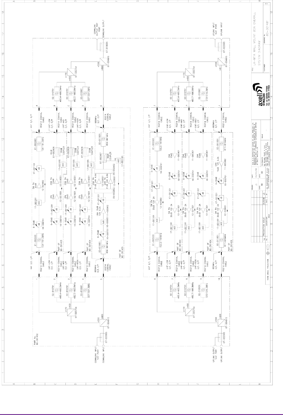
3.1.1. In-Line BDA Wall Mount 80-301401 Overall system Diagram
Drawing Number 80-301481

Axell Wireless Limited
Technical Literature
L.A. M.T.A. Remote Sites
Document Number 80-301401HBKM Issue No. 1 Date 13/06/2008 Page 13 of 148
3.2. In-Line BDA Wall Mount 80-301401 List of Major Components
Section Component
Part
Component Part Description Qty Per
Assembly
3.3. 80-301402 Combiner 1
3.4. 80-301403 VHF/UHF BDA Unit 1
3.5. 80-301404 UHF BDA Unit 1
3.6. 80-301405 800MHz BDA Unit 1
3.3. Combiner 80-301402
Splitter/Combiner 80-301402 is the main Splitter/Combiner unit. Signals are received from the leaky
feeder and are then split into their various separate paths before being amplified by external band
specific amplifiers and then the signals are re-combined for onward transmission via the leaky feeder
The unit is housed in a wall mount case 600x600x250mm (24” x 24” x 10” approx)
Downlink signals are received at the port labelled “DOWNLINK INPUT” (Annotated AA in the picture
in section 3.3.4.2.) and there is a 30dB test port labelled “DOWNLINK INPUT TEST PORT” (Z in
section 3.3.4.2.).
Ports labelled 1 to 5 (P to T in section 3.3.4.2.) are the Downlink outputs to the amplification stages
and ports labelled A to E (A to E in section 3.3.4.2.) are the Downlink inputs from the amplification
stages. These outputs and inputs are further described below.
The Downlink signal leaves the Splitter/Combiner for the leaky feeder via the port labelled
“DOWNLINK OUTPUT” (L in section 3.3.4.2.) and there is a 30dB test port labelled “DOWNLINK
OUTPUT TEST PORT” (K in section 3.3.4.2.).
Uplink signals are received at the port labelled “UPLINK INPUT” (N in section 3.3.4.2.) and there is a
30dB test port labelled “UPLINK INPUT TEST PORT” (M in section 3.3.4.2.).
Ports labelled F to J (F to J in section 3.3.4.2.) are the Uplink outputs to the amplification stages and
ports labelled 6 to 10 (U to Y in section 3.3.4.2.) are the Uplink inputs from the amplification stages.
These outputs and inputs are further described below.
The Uplink signal leaves the Splitter/Combiner for the leaky feeder via the port labelled “UPLINK
OUTPUT” (CC in section 3.3.4.2.) and there is a 30dB test port labelled “UPLINK OUTPUT TEST
PORT” (BB in section 3.3.4.2.).
Splitter/Combiner 80-301402 also incorporates bandpass filtering for the three UHF bands, the filters
are placed in the RF path before the outputs to and after the inputs from the external amplification
stages
Axell Wireless Limited
Technical Literature
L.A. M.T.A. Remote Sites
Document Number 80-301401HBKM Issue No. 1 Date 13/06/2008 Page 14 of 148
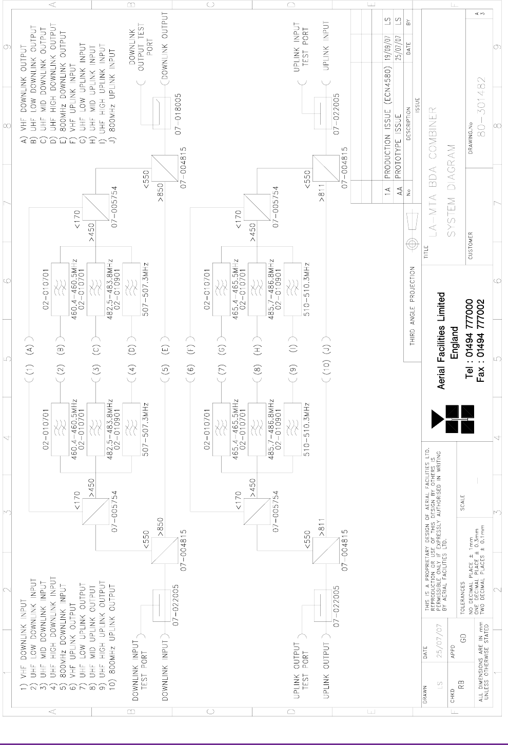
3.3.1. Combiner 80-301402 System Diagram
Drawing Number 80-301482
Axell Wireless Limited
Technical Literature
L.A. M.T.A. Remote Sites
Document Number 80-301401HBKM Issue No. 1 Date 13/06/2008 Page 15 of 148
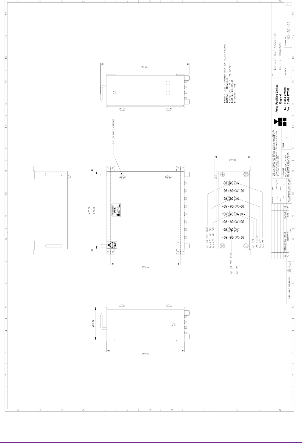
3.3.2. Combiner 80-301402 Outline Drawing
Drawing Number 80-301492
Axell Wireless Limited
Technical Literature
L.A. M.T.A. Remote Sites
Document Number 80-301401HBKM Issue No. 1 Date 13/06/2008 Page 16 of 148
3.3.3. Combiner 80-301402 Specification
Downlink
PARAMETER SPECIFICATION
Insertion Loss from Downlink Input port to port indicated
VHF Band to port 1 < 1.0dB at 154.0 – 161.3MHz
UHF Low Band to port 2 < 3.5dB at 460.4 – 460.5MHz
UHF Mid Band to port 3 < 3.5dB at 482.5 -483.8MHz
UHF High Band to port 4 < 4.0dB at 507.0 – 507.3MHz
800MHz Band to port 5 < 1.0dB at 856.0 – 861.0MHz
Insertion Loss from port indicated to Downlink Input test port
VHF Band 30dB at 154.0 – 161.3MHz
UHF Low Band 30dB at 460.4 – 460.5MHz
UHF Mid Band 30dB at 482.5 – 483.8MHz
UHF High Band 30dB at 507.0 – 507.3MHz
800MHz Band 30dB at 856.0 – 861.0MHz
Insertion Loss from port indicated to Downlink Output
VHF Band from port A < 1.0dB at 154.0 – 161.3MHz
UHF Low Band from port B < 3.5dB at 460.4 – 460.5MHz
UHF Mid Band from port C < 3.5dB at 482.5 -483.8MHz
UHF High Band from port D < 4.0dB at 507.0 – 507.3MHz
800MHz Band from port E < 1.0dB at 856.0 – 861.0MHz
Insertion Loss from port indicated to Downlink Output Test port
VHF Band from port A 31.0dB at 154.0 – 161.3MHz
UHF Low Band from port B 33dB at 460.4 – 460.5MHz
UHF Mid Band from port C 33dB at 482.5 – 483.8MHz
UHF High Band from port D 33dB at 507.0 – 507.3MHz
800MHz Band from port E 31dB at 856.0 – 861.0MHz
Uplink
PARAMETER SPECIFICATION
Insertion Loss from from Uplink Input port to port indicated
VHF Band to port F < 1.0dB at 155.7 – 160.8MHz
UHF Low Band to port G < 3.5dB at 465.4 – 465.5MHz
UHF Mid Band to port H < 3.5dB at 485.7 -486.8MHz
UHF High Band to port I < 4.0dB at 510.0 – 510.3MHz
800MHz Band to port J < 1.0dB at 811.0 – 816.0MHz
Insertion Loss from port indicated to Uplink Input test port
VHF Band 31dB at 155.7 – 160.8MHz
UHF Low Band 33dB at 465.4 – 465.5MHz
UHF Mid Band 33dB at 485.7 – 486.8MHz
UHF High Band 33dB at 510.0 – 510.3MHz
800MHz Band 31dB at 811.0 – 816.0MHz
Insertion Loss from port indicated to Uplink Output
VHF Band from port 6 < 1.0dB at 155.7 – 160.8MHz
UHF Low Band from port 7 < 3.5dB at 465.4 – 465.5MHz
UHF Mid Band from port 8 < 3.5dB at 485.7 -486.8MHz
UHF High Band from port 9 < 4.0dB at 510.0 – 510.3MHz
800MHz Band from port 10 < 1.0dB at 811.0 – 816.0MHz
Insertion Loss from port indicated to Uplink Output Test port
VHF Band from port 6 31dB at 155.7 – 160.8MHz
UHF Low Band from port 7 33dB at 465.4 – 465.5MHz
UHF Mid Band from port 8 33dB at 485.7 – 486.8MHz
UHF High Band from port 9 33dB at 510.0 – 510.3MHz
800MHz Band from port 10 31dB at 811.0 – 816.0MHz
Axell Wireless Limited
Technical Literature
L.A. M.T.A. Remote Sites
Document Number 80-301401HBKM Issue No. 1 Date 13/06/2008 Page 17 of 148
Environmental/Mechanical Specification
PARAMETER SPECIFICATION
Mechanical IP65 Wall Mount
RF connectors N type female
Dimensions
(excludes handles and connectors
620mm x 620mm x 250mm
(24” x 24” x 10” approx)
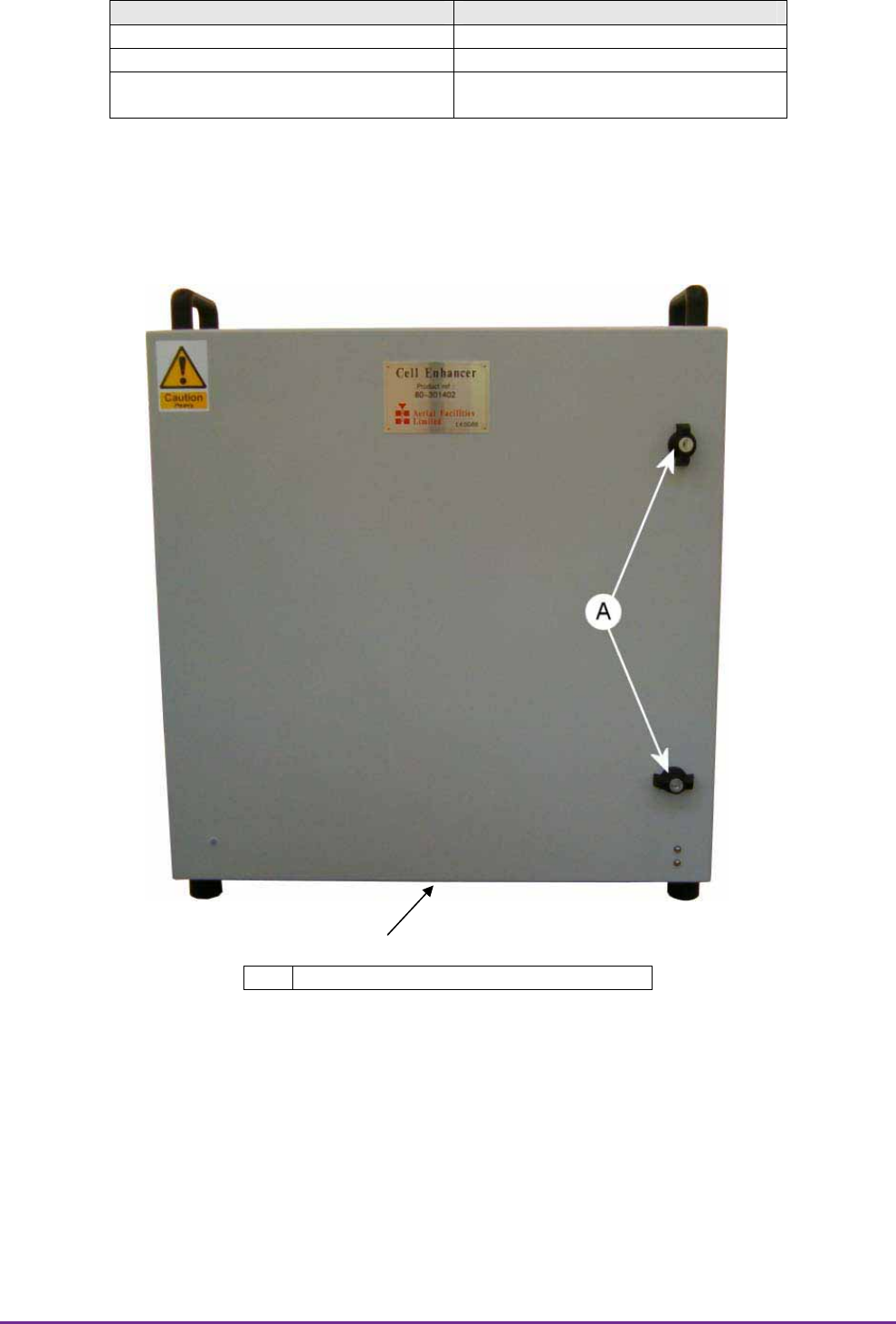
3.3.4. Combiner 80-301402 Photographs
3.3.4.1. Front View
Note: All connectors are on the underside
A Lockable Door Handles
Axell Wireless Limited
Technical Literature
L.A. M.T.A. Remote Sites
Document Number 80-301401HBKM Issue No. 1 Date 13/06/2008 Page 18 of 148
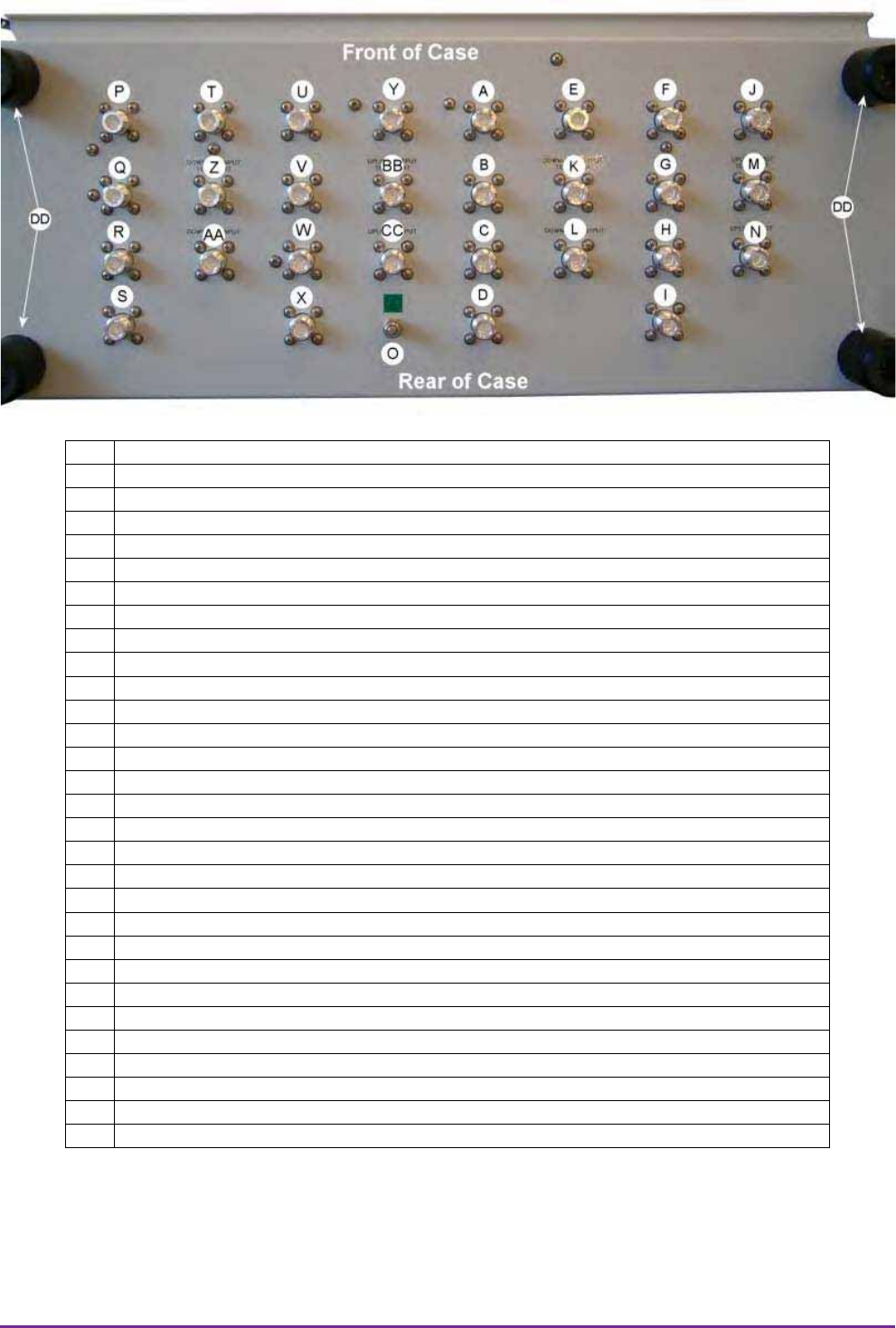
3.3.4.2. Underside view showing RF connectors
A Port A. Downlink VHF Input from VHF/UHF BDA Unit 80-301403
B Port B. Downlink UHF Lowband Input from VHF/UHF BDA Unit 80-301403
C Port C. Downlink UHF Midband Input from UHF BDA Unit 80-301404
D Port D. Downlink UHF Highband Input from UHF BDA Unit 80-301404
E Port E. Downlink 800MHz Input from 800MHz BDA Unit 80-301405
F Port F. Uplink VHF Output to VHF/UHF BDA Unit 80-301403
G Port G. Uplink UHF Lowband Output to VHF/UHF BDA Unit 80-301403
H Port H. Uplink UHF Midband Output to UHF BDA Unit 80-301404
I Port I. Uplink UHF Highband Output to UHF BDA Unit 80-301404
J Port J. Uplink 800MHz Output to 800MHz BDA Unit 80-301405
K Downlink Output Test Port (30dB Tap)
L Downlink Output to Radiating Cable
M Uplink Input Test Port (30dB Tap)
N Uplink Input from Radiating Cable
O Earth Connection
P Port 1. Downlink VHF Output to VHF/UHF BDA Unit 80-301403
Q Port 2. Downlink UHF Lowband Output to VHF/UHF BDA Unit 80-301403
R Port 3. Downlink UHF Midband Output to UHF BDA Unit 80-301404
S Port 4. Downlink UHF Highband Output to UHF BDA Unit 80-301404
T Port 5. Downlink 800MHz Output to 800MHz BDA Unit 80-301405
U Port 6. Uplink VHF Input from VHF/UHF BDA Unit 80-301403
V Port 7. Uplink UHF Lowband Input from VHF/UHF BDA Unit 80-301403
W Port 8. Uplink UHF Midband Input from UHF BDA Unit 80-301404
X Port 9. Uplink UHF Highband Input from UHF BDA Unit 80-301404
Y Port 10. Uplink 800MHz Input from 800MHz BDA Unit 80-301405
Z Downlink Input Test Port (30dB Tap)
AA Downlink Input from Radiating Cable
BB Uplink Output Test Port (30dB Tap)
CC Uplink Output to Radiating Cable
DD Case feet
Axell Wireless Limited
Technical Literature
L.A. M.T.A. Remote Sites
Document Number 80-301401HBKM Issue No. 1 Date 13/06/2008 Page 19 of 148
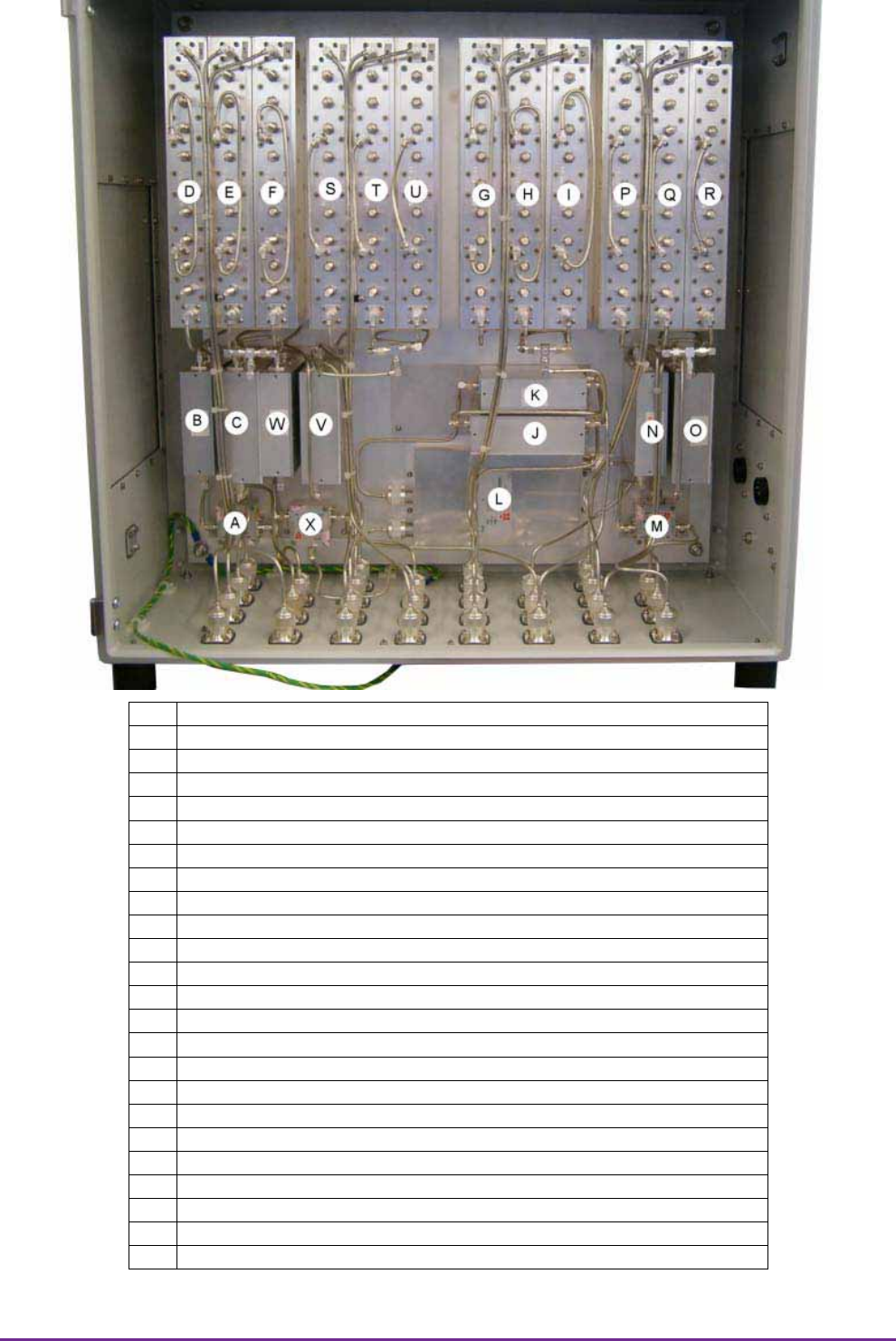
3.3.4.3. Interior view
A Downlink Input 30dB Bi-Directional Coupler 07-022005
B Downlink Input Crossband Splitter/Coupler 07-004815
C Downlink Input Crossband Splitter/Coupler 07-005754
D Downlink Input UHF Lowband Bandpass Filter 02-010701
E Downlink Input UHF Midband Bandpass Filter 02-010701
F Downlink Input UHF Highband Bandpass Filter 02-010901
G Downlink Output UHF Lowband Bandpass Filter 02-010701
H Downlink Output UHF Midband Bandpass Filter 02-010701
I Downlink Output UHF Highband Bandpass Filter 02-010901
J Downlink Output Crossband Splitter/Coupler 07-005754
K Downlink Output Crossband Splitter/Coupler 07-004815
L Downlink Output 30dB Coupler 07-018005
M Uplink Input 30dB Bi-Directional Coupler 07-022005
N Uplink Input Crossband Splitter/Coupler 07-004815
O Uplink Input Crossband Splitter/Coupler 07-005754
P Uplink Input UHF Lowband Bandpass Filter 02-010701
Q Uplink Input UHF Midband Bandpass Filter 02-010701
R Uplink Input UHF Highband Bandpass Filter 02-010901
S Uplink Output UHF Lowband Bandpass Filter 02-010701
T Uplink Output UHF Midband Bandpass Filter 02-01070
U Uplink Output UHF Highband Bandpass Filter 02-010901
V Uplink Output Crossband Splitter/Coupler 07-005754
W Uplink Output Crossband Splitter/Coupler 07-004815
X Uplink Output 30dB Bi-Directional Coupler 07-022005
Axell Wireless Limited
Technical Literature
L.A. M.T.A. Remote Sites
Document Number 80-301401HBKM Issue No. 1 Date 13/06/2008 Page 20 of 148
3.3.5. Combiner 80-301402 Major Sub-Components
Section Component
Part
Component Part Description Qty Per
Assembly
3.3.5.1. 02-010701 Bandpass Filter 8
3.3.5.2. 02-010901 Bandpass Filter 4
3.3.5.3. 07-004815 Crossband Splitter/Coupler 550/800MHz 4
3.3.5.4. 07-005754 Crossband Splitter/Coupler VHF/UHF 4
3.3.5.5. 07-018005 30dB Directional Coupler 1
3.3.5.6. 07-022005 30dB Bi-Directional Coupler 3
3.3.5.1. Bandpass Filter 02-010701
The bandpass filters are multi-section designs with a bandwidth dependent upon the passband
frequencies, (both tuned to customer requirements). The response shape is basically Chebyshev with
a passband design ripple of 0.1dB. The filters are of combline design, and are carefully aligned during
manufacture in order to optimise the insertion loss, VSWR and intermodulation characteristics of the
unit. The tuned elements are silver-plated to reduce surface ohmic losses and maintain a good VSWR
figure and 50 load at the input and output ports.
Being passive devices, the bandpass filters should have an extremely long operational life and require
no maintenance. Should a filter be suspect, it is usually most time efficient to replace the module
rather than attempt repair or re-tuning.
02-010701 Specification
PARAMETER SPECIFICATION
Downlink 460.4 to 460.5 MHz
UHF Low Uplink 465.4 to 465.5 MHz
Downlink 482.5 to 483.8 MHz
Passband
Frequency UHF Mid Uplink 485.7 to 486.8 MHz
UHF Low 0.1 MHz
Bandwidth UHF Mid 1.3 MHz
Number of sections 5
Insertion loss 2.4 dB (typical)
VSWR better than 1.2:1
Connectors SMA
Power Handling 100W max
operation -20°C to +60°C Temperature
range storage -40°C to +70°C
Weight 3 kg (typical)
3.3.5.2. Bandpass Filter 02-010901
Bandpass Filter 02-010901 is a multi-section design with a bandwidth dependent upon the passband
frequencies, (both tuned to customer requirements). The response shape is basically Chebyshev with
a passband design ripple of 0.1dB. The filters are of helical & combline design respectively, and are
carefully aligned during manufacture in order to optimise the insertion loss, VSWR and
intermodulation characteristics of the unit. The body and tuned elements are silver-plated to reduce
surface ohmic losses and maintain a good VSWR figure and 50 load at the input and output ports.
Being passive devices, the bandpass filters should have an extremely long operational life and require
no maintenance.
Axell Wireless Limited
Technical Literature
L.A. M.T.A. Remote Sites
Document Number 80-301401HBKM Issue No. 1 Date 13/06/2008 Page 21 of 148
02-010901 specification
SPECIFICATION PARAMETER
Downlink 507.0 to 507.3MHz Passband
Frequency Uplink 510.0 to 510.3MHz
Uplink 0.3 MHz
Bandwidth Downlink 0.3 MHz
Insertion Loss 2.9 dB (typical)
Power Rating 50W
Impedance 50ȍ
VSWR Better than 1.2:1
Connectors SMA
Weight 3Kg (approximately)
3.3.5.3. Crossband Splitter/Coupler 550/800MHz (07-004815)
The purpose of Crossband Splitter/Coupler (07-004815) is to split or combine RF signals from
different parts of the frequency spectrum.
It is a 3 port device comprising two filters, one a low pass, the other a high pass, connected to a
common input/output. The couplers are housed in a machined aluminium casing having a centre
screening wall between the filter sections and lid secured by screws at frequent intervals over its
perimeter to obtain a tight seal and to ensure linearity and stability of response.
07-004815 Specification
Parameter Low Pass Port High Pass Port
Passband Frequencies 380 to 550MHz 800 to 960MHz
Insertion loss <0.5dB <0.5dB
Isolation between Bands >50dB >50dB
VSWR 1.3:1
Impedance 50 ohm
Power rating 50W
operation -20C to +60C
Temperature
range storage -40C to +70C
RF Connectors SMA (female)
Weight <1kg
3.3.5.4. Crossband Splitter/Coupler VHF/UHF (07-005754)
The purpose of Crossband Splitter/Coupler (07-005754) is to split or combine RF signals from
different parts of the frequency spectrum.
It is a 3 port device comprising two filters, one a low pass, the other a high pass, connected to a
common input/output. The couplers are housed in a machined aluminium casing having a centre
screening wall between the filter sections and lid secured by screws at frequent intervals over its
perimeter to obtain a tight seal and to ensure linearity and stability of response.

Axell Wireless Limited
Technical Literature
L.A. M.T.A. Remote Sites
Document Number 80-301401HBKM Issue No. 1 Date 13/06/2008 Page 22 of 148
07-005754 Specification
Parameter Low Pass Port High Pass Port
Passband Frequencies 70 to 175 MHz 380 to 500 MHz
Insertion loss <0.5dB <0.5dB
Return loss >14dB typical >14dB typical
Isolation between Bands >60dB >60dB
Impedance 50 ohm
Power rating 50W
operation -20C to +60C
Temperature
range storage -40C to +70C
RF Connectors SMA (female)
Weight <1kg
3.3.5.5. 30dB Directional Coupler (07-018005)
The purpose of these couplers is to tap off known portions (in this case 30dB) of RF signal from
transmission lines and to combine them, for example though splitter units for different purposes
(alarms/monitoring etc.), whilst maintaining an accurate 50: load to all ports/interfaces throughout the
specified frequency range. 07-018005 is a Uni-Directional device and as such will only couple 30dB of
signal in one direction.
07-018005 Specification
PARAMETER SPECIFICATION
Frequency Range 70 MHz - 1000MHz
Mainline Insertion Loss <0.5
Coupling Loss 30 dB
VSWR Mainline Better than 1.3:1
Impedance 50 ȍ
Power Handling (CW) 100W
Outline (W x D x H) 176mm x 104mm x 24mm (ex. connectors)
Connectors N (female) on all ports
Case Material Aluminium
Finish Iridite NCP
operation -20C to +60C
Temperature
range storage -40C to +70C
Ingress Protection IP54

Axell Wireless Limited
Technical Literature
L.A. M.T.A. Remote Sites
Document Number 80-301401HBKM Issue No. 1 Date 13/06/2008 Page 23 of 148
3.3.5.6. 30dB Bi-Directional Coupler (07-022005)
The purpose of these couplers is to tap off known portions (in this case 30dB) of RF signal from
transmission lines and to combine them, for example though splitter units for different purposes
(alarms/monitoring etc.), whilst maintaining an accurate 50: load to all ports/interfaces throughout the
specified frequency range. 07-022005 is a Bi-Directional device and as such will couple 30dB of
signal whichever direction the signal is traveling.
07-022005 Specification
PARAMETER SPECIFICATION
Frequency Range 100kHz – 2.7GHz
Mainline Insertion Loss < 1.0 dB
Coupling Loss 30 dB
Coupling Loss Tolerance +/-2.0 dB
VSWR Mainline Better than 1.4:1
Impedance 50 ȍ
Power Handling (CW) 5W
Outline (W x D x H) 44.5mm x 41mm x 27mm (ex. connectors)
Connectors SMA (female) on all ports
Case Material Aluminium
Finish Iridite NCP
Operating Temperature -20 to +55°C
Ingress Protection IP54

Axell Wireless Limited
Technical Literature
L.A. M.T.A. Remote Sites
Document Number 80-301401HBKM Issue No. 1 Date 13/06/2008 Page 24 of 148
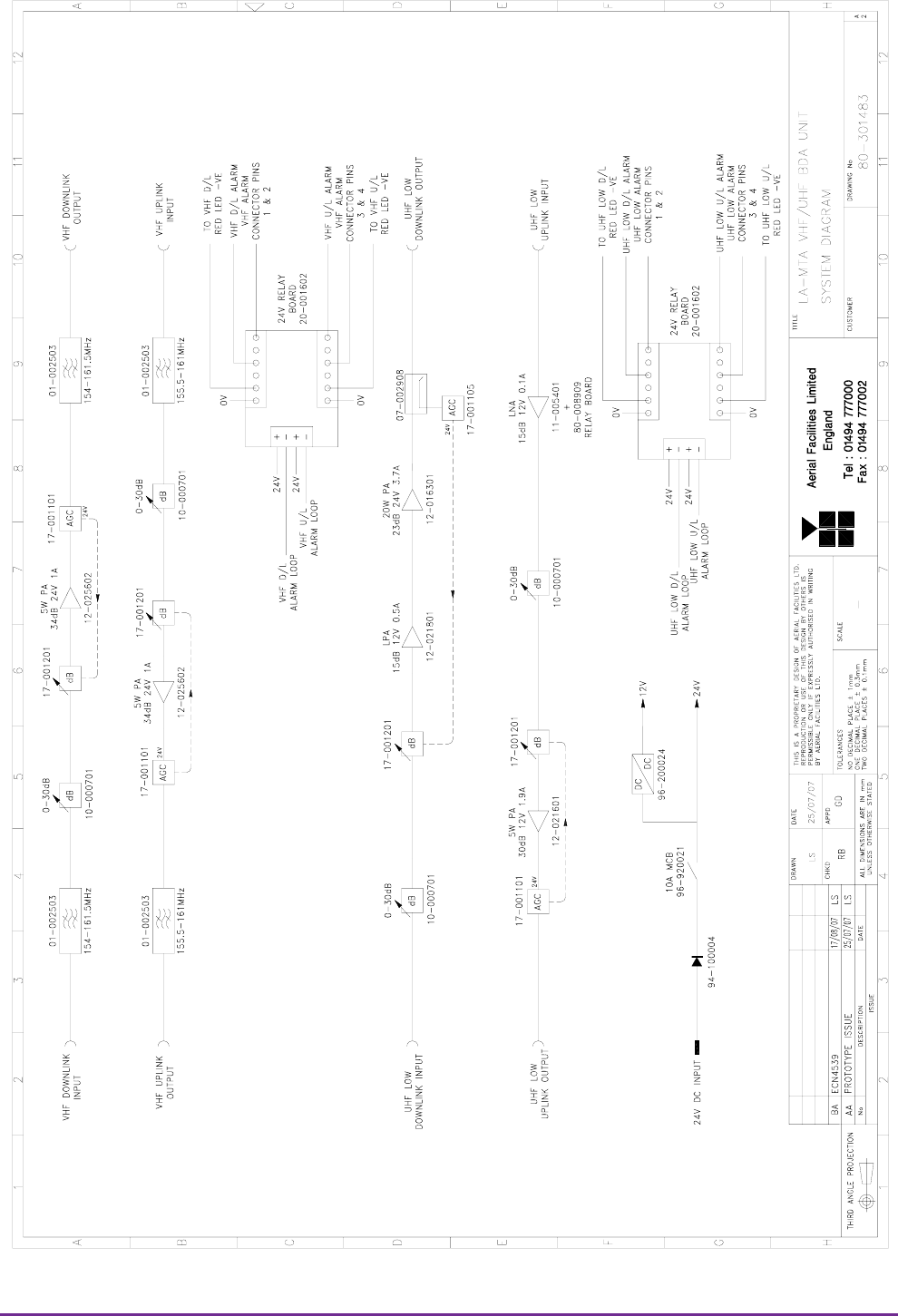
3.4. VHF/UHF BDA Unit (80-301403)
VHF/UHF BDA Unit (80-301403) provides the amplification stages for the VHF and UHF Lowband
paths, The unit is housed in a wall mount case 600x600x250mm (24” x 24” x 10” approx).
The Downlink VHF signal is received at the port labelled “VHF D/L INPUT” (Annotated A in the picture
in section 3.4.4.2.). The Downlink VHF path passes through a bandpass filter to remove out of band
noise and then a switched attenuator providing 0 to 30 dB of RF signal attenuation.
After leaving the attenuator the VHF Downlink signal passes through a 5W amplification stage, this
amplification stage is straddled by an Automatic Gain Control assembly providing limiting to the output
signals in the case of high input signals.
After leaving the Amplification/AGC stage the VHF Downlink signal passes through a second
bandpass filter and exits the BDA via the port labelled “VHF D/L OUTPUT” ( B in section 3.4.4.2.).
The Uplink VHF Signal is received at the port labelled “VHF U/L INPUT” (C in section 3.4.4.2.). The
VHF Uplink path passes through a bandpass filter to remove out of band noise and then a switched
attenuator providing 0 to 30 dB of RF signal attenuation.
After leaving the attenuator the VHF Uplink signal passes through a 5W amplification stage, this
amplification stage is straddled by an Automatic Gain Control assembly providing limiting to the output
signals in the case of high input signals.
After leaving the Amplification/AGC stage the VHF Uplink signal passes through a second bandpass
filter and exits the BDA via the port labelled “VHF U/L OUTPUT” (D in section 3.4.4.2.).
The Downlink UHF Lowband signal is received at the port labelled “UHF LOW D/L INPUT” (E in
section 3.4.4.2.). The signal passes through a switched attenuator providing 0 to 30 dB of RF signal
attenuation and then into the amplification stage. The Downlink UHF Lowband amplification stage is
provided by tow amplifier modules, the first is a 15dB gain Low Power Amplifier and the second is a
20W, 23dB gain power amplifier. Both amplification stages are straddled by an Automatic Gain
Control assembly providing limiting to the output signals in the case of high input signals.
The input to the AGC detector is provided by the output of a 30dB tap. After leaving the
Amplification/AGC stage the Downlink UHF Lowband signal exits the BDA via the port labelled “UHF
LOW D/L OUTPUT” (F in section 3.4.4.2.).
The Uplink UHF Lowband signal is received at the port labelled “UHF LOW U/L INPUT” (G in section
3.4.4.2.). The signal passes into a Low Noise Amplifier providing 15dB of gain and then into a
switched attenuator providing 0 to 30 dB of RF signal attenuation. After the attenuator the Uplink UHF
Lowband signal passes into a second stage of amplification provided by a 5W, 30dB gain Power
Amplifier, this amplification stage is straddled by an Automatic Gain Control assembly providing
limiting to the output signals in the case of high input signals.
The Uplink UHF Lowband signal exits the BDA via the port labelled “UHF LOW U/L OUTPUT” (H in
section 3.4.4.2.).
VHF/UHF BDA Unit (80-301403) is provided with a 24V DC input to power the amplifier modules
within and those amplifier modules are configured to provide alarm status reports. Separate alarm
contact outputs are provided for the VHF and the UHF Lowband paths.
Axell Wireless Limited
Technical Literature
L.A. M.T.A. Remote Sites
Document Number 80-301401HBKM Issue No. 1 Date 13/06/2008 Page 25 of 148
3.4.1. VHF/UHF BDA Unit (80-301403) System Diagram
Drawing Number 80-301483
Axell Wireless Limited
Technical Literature
L.A. M.T.A. Remote Sites
Document Number 80-301401HBKM Issue No. 1 Date 13/06/2008 Page 26 of 148
3.4.2. VHF/UHF BDA Unit (80-301403) Outline Drawing
Drawing Number 80-301493

Axell Wireless Limited
Technical Literature
L.A. M.T.A. Remote Sites
Document Number 80-301401HBKM Issue No. 1 Date 13/06/2008 Page 27 of 148
3.4.3. VHF/UHF BDA Unit(80-301403) Specification
Parameter Specification
Downlink
VHF 154.0 to 161.5MHz
Downlink Passband UHF Lowband 460.4 to 460.5MHz
VHF 30dB
Maximun gain UHF Lowband 30dB
VHF 0 to 30dB in 2dB steps
Gain Adjustment UHF Lowband 0 to 30dB in 2dB steps
VHF > +34.0dBm 1dB Compression Point
(P1dB) UHF Lowband > +42.5dBm
VHF 1dB below P1dB
ALC setting UHF Lowband 1dB below P1dB
VHF > +45.0dBm
3rd Order Intercept point UHF Lowband > +53.5dBm
Uplink
VHF 155.5 – 161.0MHz
Uplink Passband UHF Lowband 465.4 – 465.5MHz
VHF 30dB
Maximun gain UHF Lowband 30dB
VHF 0 to 30dB in 2dB steps
Gain Adjustment UHF Lowband 0 to 30dB in 2dB steps
VHF > +34.0dBm 1dB Compression Point
(P1dB) UHF Lowband > +36.5dBm
VHF +27dBm
ALC setting UHF Lowband +27dBm
VHF > +45.0dBm
3rd Order Intercept point UHF Lowband > +48.0dBm
VHF < 10dB
Noise Figure UHF Lowband < 3.0dB
Environmental/Mechanical Specification
Mechanical IP65 Wall Mount
Dimensions
(excludes handles and connectors)
620mm x 620mm x 250mm
(24” x 24” x 10” approx)
RF Connectors N-Type Female
Alarm Interfaces
Local Alarms to SCADA
Dry Contact with LED Indication per band
path
Power Supply 24V DC
Axell Wireless Limited
Technical Literature
L.A. M.T.A. Remote Sites
Document Number 80-301401HBKM Issue No. 1 Date 13/06/2008 Page 28 of 148
3.4.4. VHF/UHF BDA Unit(80-301403) Photographs
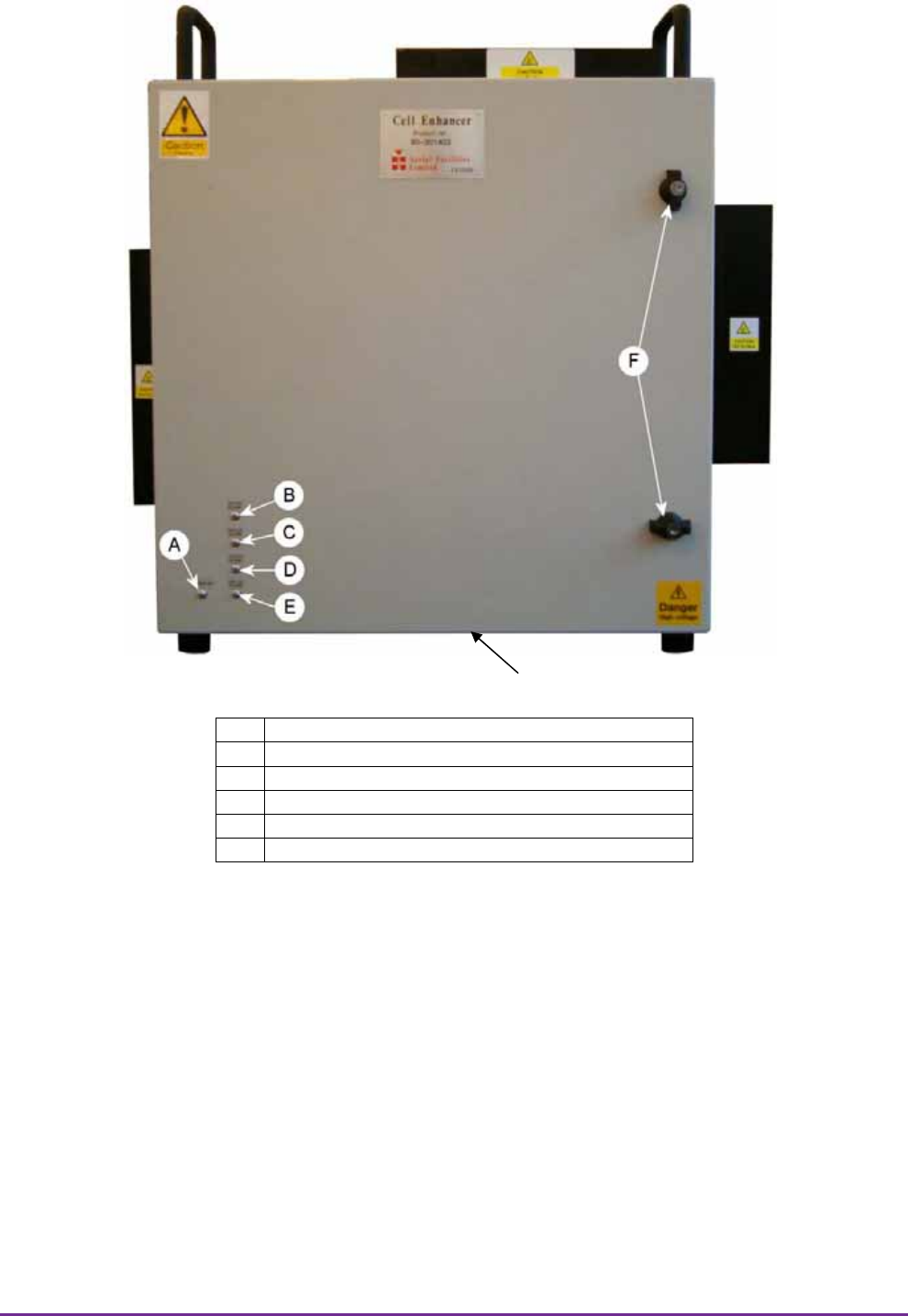
3.4.4.1. Front View
Note: All connectors (RF, DC and Alarms) are on the underside
A Green LED “Power On”
B Red LED VHF Downlink Alarm
C Red LED VHF Uplink Alarm
D Red LED UHF Lowband Downlink Alarm
E Red LED UHF Lowband Uplink Alarm
F Lockable Door Handles
Axell Wireless Limited
Technical Literature
L.A. M.T.A. Remote Sites
Document Number 80-301401HBKM Issue No. 1 Date 13/06/2008 Page 29 of 148
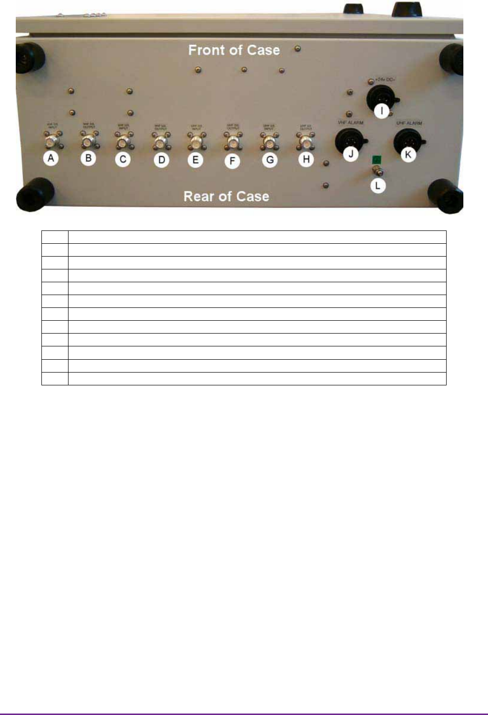
3.4.4.2. Underside view showing connectors
A VHF Downlink Input from port 1 on Combiner 80-301402
B VHF Downlink Output to port A on Combiner 80-301402
C VHF Uplink Input from port F on Combiner 80-301402
D VHF Uplink Output to port 6 on Combiner 80-301402
E UHF Lowband Downlink Input from port 2 on Combiner 80-301402
F UHF Lowband Downlink Output to port B on Combiner 80-301402
G UHF Lowband Uplink Input from port G on Combiner 80-301402
H UHF Lowband Uplink Output to port 7 on Combiner 80-301402
I 24V DC Input
J VHF Band Alarm Output
K UHF Lowband Alarm Output
L Earth Connection
Axell Wireless Limited
Technical Literature
L.A. M.T.A. Remote Sites
Document Number 80-301401HBKM Issue No. 1 Date 13/06/2008 Page 30 of 148
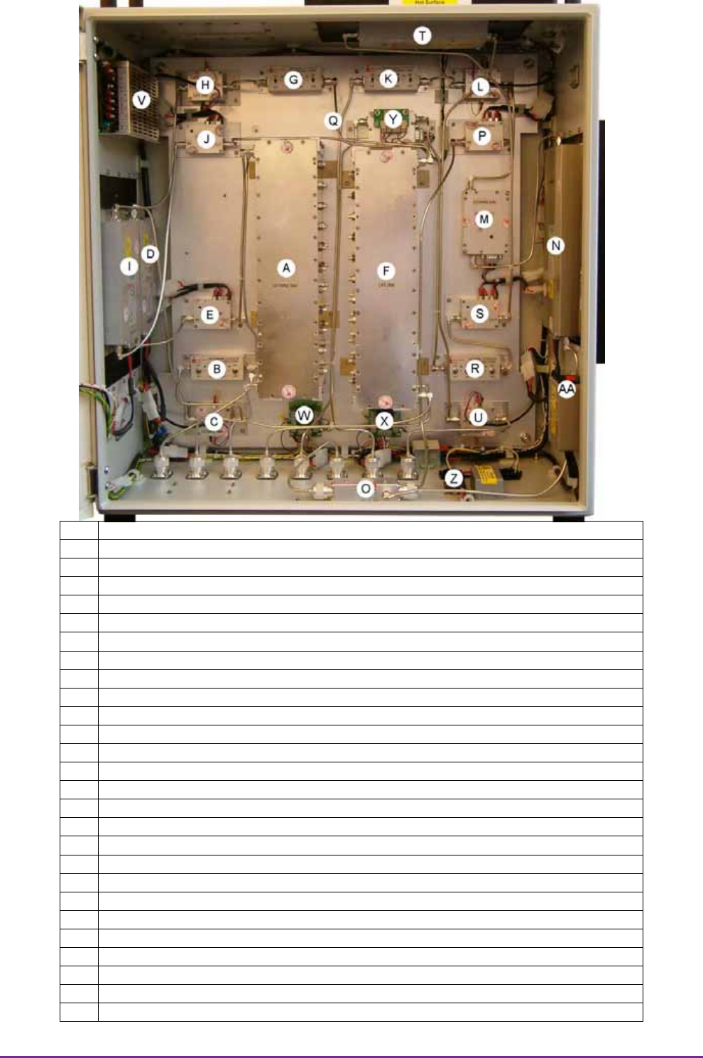
3.4.4.3. Interior view
A VHF Downlink Filters 01-002503 (Input filter below, Output filter above)
B VHF Downlink Switched Attenuator 10-000701
C VHF Downlink AGC Attenuator 17-001201
D VHF Downlink 5W Power Amplifier 12-025602
E VHF Downlink AGC Detector 17-001101
F VHF Uplink Filters 01-002503 (Input filter below, Output filter above)
G VHF Uplink Switched Attenuator 10-000701
H VHF Uplink AGC Attenuator 17-001201
I VHF Uplink 5W Power Amplifier 12-025602
J VHF Uplink AGC Detector 17-001101
K UHF Lowband Downlink Switched Attenuator 10-000701
L UHF Lowband Downlink AGC Attenuator 17-001201
M UHF Lowband Downlink Low Power Amplifier 12-021801
N UHF Lowband Downlink 20W Power Amplifier 12-016301
O UHF Lowband Downlink 30dB Directional Coupler 07-002908
P UHF Lowband Downlink AGC Detector 17-001105
Q UHF Lowband Uplink Low Noise Amplifier 11-005401
R UHF Lowband Uplink Switched Attenuator 10-000701
S UHF Lowband Uplink AGC Attenuator 17-001201
T UHF Lowband Uplink 5W Power Amplifier 12-021601
U UHF Lowband Uplink AGC Detector 17-001101
V DC/DC Converter 96-200024
W 24V Dual Relay Assembly (VHF Alarm output) 20-001602
X 24V Dual Relay Assembly (UHF Lowband output) 20-001602
Y 24V Relay Assembly 80-008902
Z Dual Diode Assembly 94-100004
AA Main DC 10A Circuit Breaker 96-920021

Axell Wireless Limited
Technical Literature
L.A. M.T.A. Remote Sites
Document Number 80-301401HBKM Issue No. 1 Date 13/06/2008 Page 31 of 148
3.4.5. VHF/UHF BDA Unit(80-301403) Major Sub-components
Section Component
Part
Component Part Description Qty Per
Assembly
3.4.5.1. 01-002503 Bandpass Filter 4
3.4.5.2. 07-002908 30dB Directional Coupler 1
3.4.5.3. 10-000701 Switched Attenuator 0.25Watt, 0 - 30dB 4
3.4.5.4. 11-005401 Low Noise Amplifier 1
3.4.5.5. 12-016301 TETRA Power Amplifier 20W 1
3.4.5.6. 12-021601 TETRA Power Amplifier 5W 1
3.4.5.7. 12-021801 Low Power Amplifier 1
3.4.5.8. 12-025602 VHF Power Amplifier 5W 2
17-001101 AGC Detector Assembly 3
17-001105 AGC Detector Assembly (Logarithmic) 1
3.4.5.9.
17-001201 AGC Attenuator Assembly 4
3.4.5.10. 20-001602 24V Dual Relay Assembly 2
3.4.5.11. 80-008902 24V Relay Assembly 1
3.4.5.12. 94-100004 Dual Diode Assembly 1
3.4.5.13. 96-200024 DC/DC Converter 1
3.4.5.1. Bandpass Filter (01-002503)
The bandpass filters are multi-section designs with a bandwidth dependent upon the passband
frequencies, (both tuned to customer requirements). The response shape is basically Chebyshev with
a passband design ripple of 0.1dB. The filters are of helical design, and are carefully aligned during
manufacture in order to optimise the insertion loss, VSWR and intermodulation characteristics of the
unit. The tuned elements are silver-plated to reduce surface ohmic losses and maintain a good VSWR
figure and 50ȍ load at the input and output ports.
Being passive devices, the bandpass filters have an extremely long operational life and require no
maintenance. Should a filter be suspect, it is usually most time efficient to replace the module rather
than attempt repair or re-tuning.
No adjustments should be attempted without full network sweep analysis facilities to monitor both
insertion loss and VSWR simultaneously.
01-002503 Specification
SPECIFICATION PARAMETER
Downlink 154.0 MHz to 161.5 MHz
Bandpass
Frequency Uplink 155.5 MHz to 161.0 MHz
Downlink 7.5MHz
Bandwidth Uplink 5.5MHz
No. of sections 6
Insertion loss 1.5dB
VSWR Better than 1.2:1
Connectors SMA
Power handling 100W maximum
operational -20°C to +60°C Temperature
range store -40°C to +70°C
Weight 3 kg
Size 384 x 82.5 x 56.4mm

Axell Wireless Limited
Technical Literature
L.A. M.T.A. Remote Sites
Document Number 80-301401HBKM Issue No. 1 Date 13/06/2008 Page 32 of 148
3.4.5.2. 30dB Directional Coupler (07-002908)
The purpose of these couplers is to tap off known portions of RF signal from transmission lines and to
combine them, for example through splitter units for different purposes (alarms/monitoring etc.), whilst
maintaining an accurate 50: load to all ports/interfaces throughout the specified frequency range.
They are known as directional couplers as they couple power from the RF mainline in one direction
only.
Directional Coupler 07-002908 is configured to tap off 30dB.
07-002908 Specification
PARAMETER SPECIFICATION
Frequency range 50 - 1000MHz
Insertion loss <0.3dB
Coupling level 30dB
Rejection N/A
Weight <200gms
Connectors N type, female
operation -20°C to +60°C Temperature
range storage -40°C to +70°C
3.4.5.3. Switched Attenuator 0.25Watt, 0 - 30dB (10-000701)
In many practical applications for Cell Enhancers etc., the gain in each path is found to be excessive.
Therefore, provision is made within the unit for the setting of attenuation in each path, to reduce the
gain.
10-000701 provides attenuation from 0 to 30dB in 2 dB steps The attenuation is simply set using the
four miniature toggle switches on the top of each unit. Each switch is clearly marked with the
attenuation it provides, and the total attenuation in line is the sum of the values switched in. They are
designed to maintain an accurate 50ȍ impedance over their operating frequency at both input and
output.
10-000701 Specification
PARAMETER SPECIFICATION
Attenuation Values 0-30dB
Attenuation Steps 2, 4, 8 and 16dB
Power Handling 0.25 Watt
Attenuation Accuracy ± 1.0 dB
Frequency Range DC to 1GHz
Impedance 50ȍ
Connectors SMA
VSWR 1.3:1
Weight 0.2kg
operation -20°C to +60°C Temperature
range storage -40°C to +70°C
Axell Wireless Limited
Technical Literature
L.A. M.T.A. Remote Sites
Document Number 80-301401HBKM Issue No. 1 Date 13/06/2008 Page 33 of 148
3.4.5.4. Low Noise Amplifier (11-005401)
The 15dB gain low noise amplifier used in the unit is a double stage solid-state low noise amplifier.
Class A circuitry is used throughout the units to ensure excellent linearity over a very wide dynamic
range. The active devices are very moderately rated to provide a long trouble-free working life. There
are no adjustments on these amplifiers, and in the unlikely event of a failure, the complete amplifier
should be replaced. The amplifier is housed in an aluminium case (Iridite NCP finish) with SMA
connectors for the RF input/output and a 9way D-type for DC and alarm outputs.
11-005401 Specification
PARAMETER SPECIFICATION
Frequency range 380 - 500MHz
Bandwidth <100MHz (as required, tuneable)
1dB compression point >+20dBm
3rd order intercept >+33dBm
Gain >15.5dB (typical)
VSWR better than 1.5:1
Input return loss >14dB
Noise figure <2.0dB (typical)
Connectors SMA female
Supply 115mA at 12V DC
operational -10°C to +60°C Temperature
range storage -40°C to +70°C
Size 88 x 50 x 34mm (ex. connectors)
Weight 0.26kg
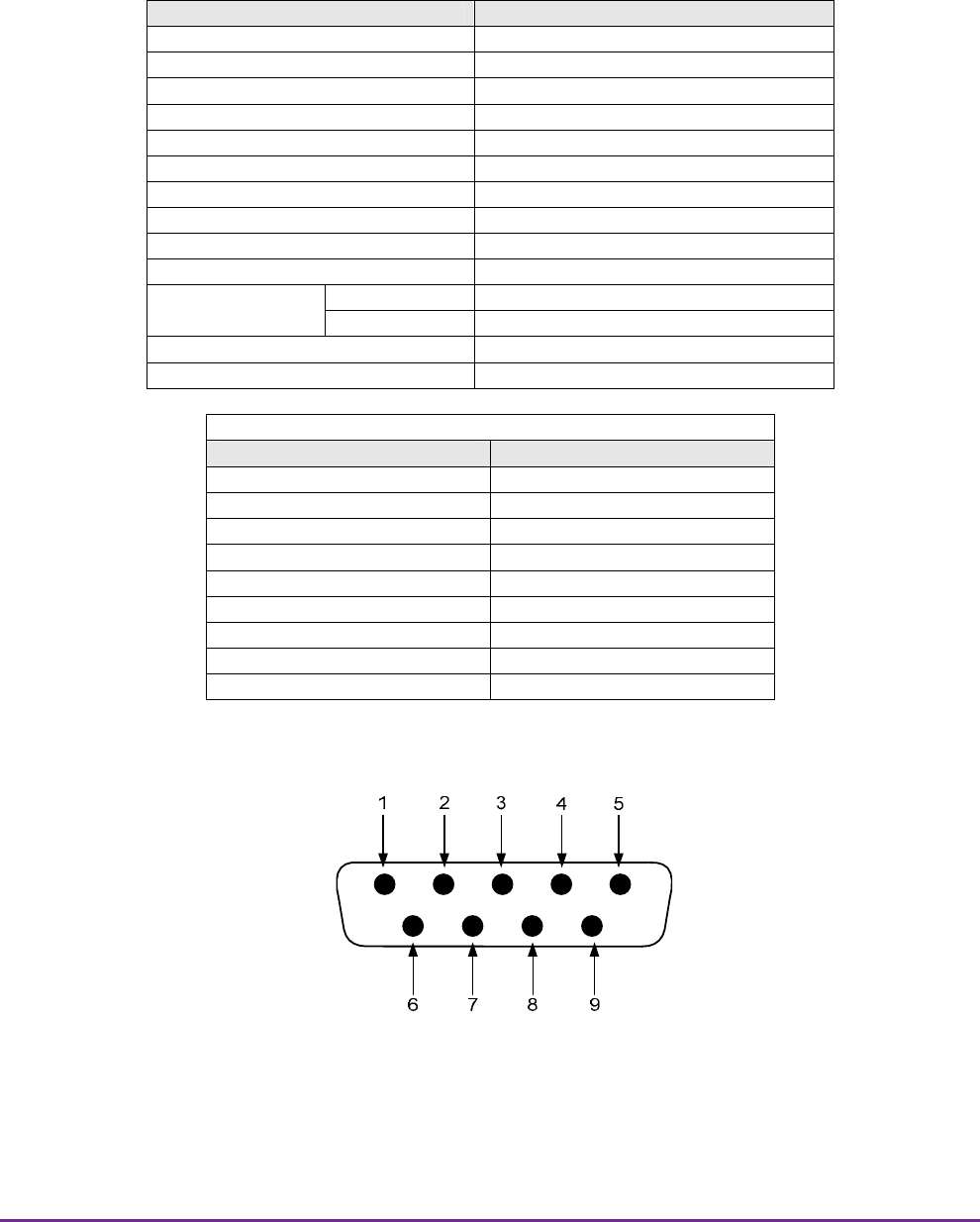
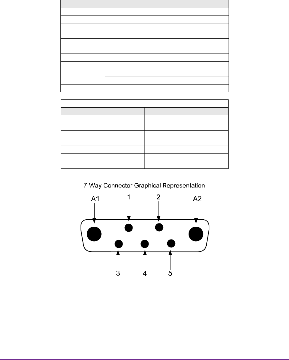
LNA ‘D’ Connector Pin-out details
Connector pin Signal
1 +ve input (10-24V)
2 GND
3 Alarm relay O/P bad
4 Alarm relay common
5 Alarm relay good
6 No connection
7 TTL voltage set
8 TTL alarm/0V (good)
9 O/C good/0V bad
9-Way Pin-Out Graphical Representation
Axell Wireless Limited
Technical Literature
L.A. M.T.A. Remote Sites
Document Number 80-301401HBKM Issue No. 1 Date 13/06/2008 Page 34 of 148
3.4.5.5. TETRA Power Amplifier 20W (12-016301)
This amplifier is a Class A 20W power amplifier from 380MHz to 470MHz in a 1 stage balanced
configuration. It demonstrates a very high linearity and a very good input/output return loss (RL). It
has built in a Current Fault Alarm Function.
It is housed is an aluminium case (Iridite NCP finish) with SMA connectors for the RF input/output and
a D-Type connector for the power supply and the Current Fault Alarm Function. Note the large
diameter DC power input pins (1 & 2) fitted to reduce volt-drop/arcing.
12-016301 Specification
PARAMETER SPECIFICATION
Frequency range 380-470MHz
Small signal gain 23dB
Gain flatness ±1.7dB
I/O Return loss >18dB
1dB compression point +43dBm
OIP3 +55dBm
Supply voltage 24V DC
Supply current 3.8Amps (Typical)
operational -10°C to +60°C Temperature
range storage -20°C to +70°C
Weight <2kg (no heatsink)
7-Way Connector Pin-out details
Connector Pin Signal
A1 (large pin) +24V DC
A2 (large pin) GND
1 Alarm relay common
2 TTL alarm/0V good
3 Alarm relay contact (bad)
4 Alarm relay contact (good)
5 O/C good/0V bad (TTL)

Axell Wireless Limited
Technical Literature
L.A. M.T.A. Remote Sites
Document Number 80-301401HBKM Issue No. 1 Date 13/06/2008 Page 35 of 148
A1 A2
1 2
3 4 5
3.4.5.6. TETRA Power Amplifier 5W (12-021601)
Power amplifier 12-021601 is a multi-stage, solid state power amplifier. Class A circuitry is employed
throughout the device to ensure excellent linearity over a wide dynamic frequency range. All the semi-
conductor devices are very conservatively rated to ensure low device junction temperatures and a
long, trouble free working lifetime.
The power amplifier should require no maintenance over its operating life. Under no circumstances
should the cover be removed or the side adjustments disturbed unless it is certain that the amplifier
has failed; since it is critically aligned during manufacture and any re-alignment will require extensive
test equipment.
The unit housing is an aluminium case (Iridite NCP finish) with SMA connectors for the RF
input/output and a D-Type connector for the power supply and the Current Fault Alarm Function.
12-021601 Specification
PARAMETER SPECIFICATION
Frequency range: 380-470MHz (as required)
Bandwidth: 10-40MHz (typical, tuned to spec.)
Maximum RF output: >5Watts
Gain: >30dB
1dB compression point: +37.5dBm
3rd order intercept point: +50dBm
VSWR: better than 1.5:1
Connectors: SMA female
Supply: 1.9Amps @ 12V DC
Weight: 1kg (excluding heatsink)
operational: -10qC to +60qC
Temperature
range: storage: -20qC to +70qC
7-Way Connector Pin-out details
Connector Pin Signal
A1 (large pin) +12V DC
A2 (large pin) GND
1 Alarm relay common
2 TTL alarm/0V good
3 Alarm relay contact (bad)
4 Alarm relay contact (good)
5 O/C good/0V bad (TTL)
7-Way Pin-Out Graphical Representation
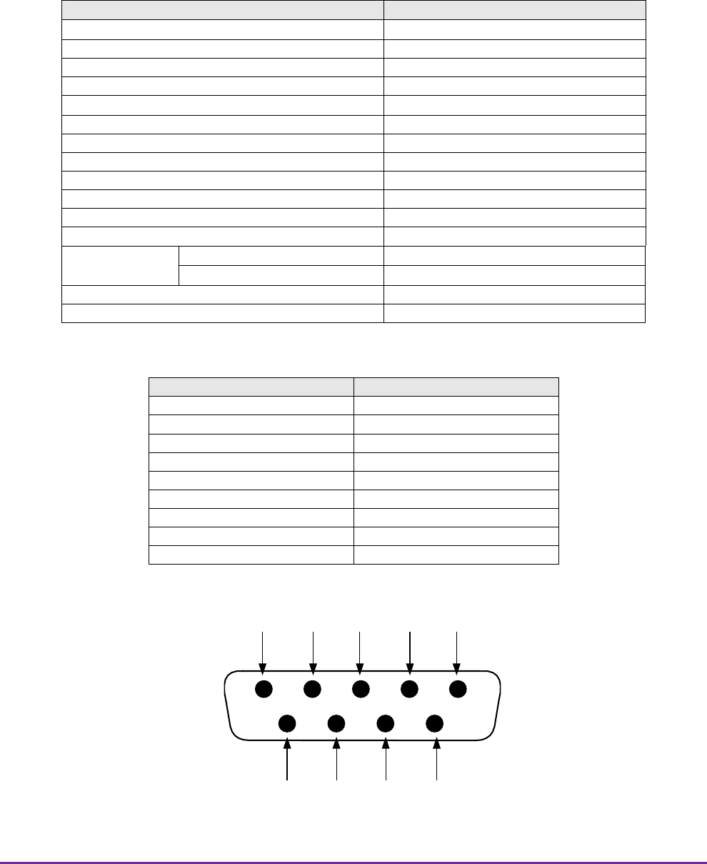
Axell Wireless Limited
Technical Literature
L.A. M.T.A. Remote Sites
Document Number 80-301401HBKM Issue No. 1 Date 13/06/2008 Page 36 of 148
7 8 96
1 2 3 4 5
9-Way Pin-Out Graphical Representation
3.4.5.7. Low Power Amplifier (1Watt) (12-021801)
The low power amplifier used is a 1 stage balanced configuration, solid-state amplifier. Class A
circuitry is used in the unit to ensure excellent linearity over a very wide dynamic range. The three
active devices are very moderately rated to provide a long trouble-free working life.
Its housing is an aluminium case (Iridite NCP finish) with SMA connectors for the RF input/output and
a D-Type connector for the power supply and the Current Fault Alarm Function.
There are no adjustments on this amplifier, and in the unlikely event of failure then the entire amplifier
should be replaced.
12-021801 Specification
PARAMETER SPECIFICATION
Temperature -20 to +70 qC
Frequency Range 380 - 500 MHz
Small Signal Gain 15.5 +/- 0.5 dB
Gain Flatness 0.7 dB p-p
'Gain vs. Temperature 0.7 dB
In RL 20 dB
Out RL 20 dB
Output Power @ 1dB Compression Point +30.5 dBm
Output 3rd Order IP +41.5 dBm
Noise Figure 6 dB
DC Supply Voltage 10-15 Vdc
DC Supply Current 540 mA
operational: -10qC to +60qC
Temperature
range storage: -40qC to +100qC
Weight: <0.5 kg
Size: 110.5 x 66mm x 24.6mm
Low Power Amplifier (12-021801) 9-Way Connector Pin-outs
Connector pin Signal
1 +ve input (10-15V)
2 GND
3 Alarm relay O/P bad
4 Alarm relay common
5 Alarm relay good
6 No connection
7 TTL voltage set
8 TTL alarm/0V (good)
9 O/C good/0V bad
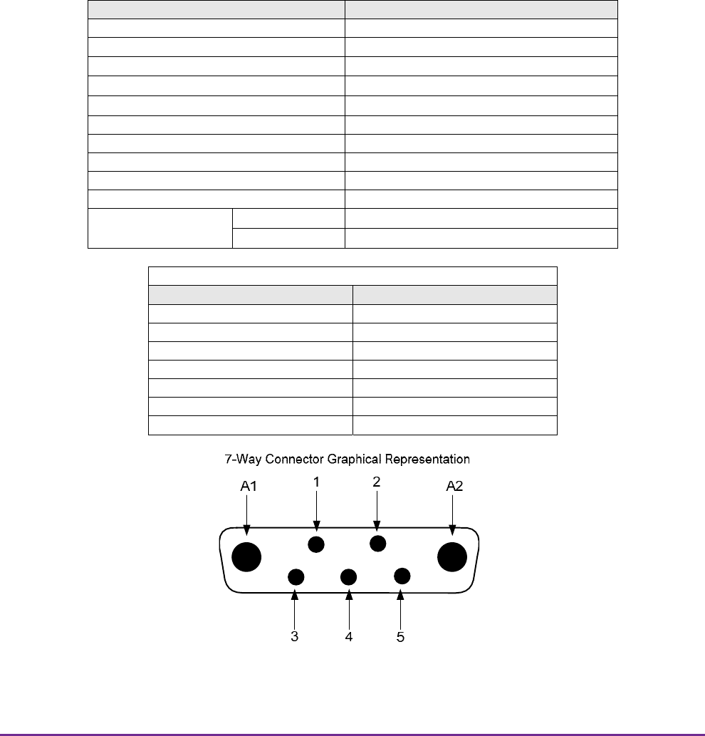
Axell Wireless Limited
Technical Literature
L.A. M.T.A. Remote Sites
Document Number 80-301401HBKM Issue No. 1 Date 13/06/2008 Page 37 of 148
3.4.5.8. VHF Power Amplifier 5W (12-025602)
Power amplifier 12-025602 is a multi-stage, solid state power amplifier. Class A circuitry is employed
throughout the device to ensure excellent linearity over a wide dynamic frequency range. All the semi-
conductor devices are very conservatively rated to ensure low device junction temperatures and a
long, trouble free working lifetime. There is a Current Fault Alarm Function, which indicates failure of
each RF transistor with an open collector of a NPN transistor. A relay is fitted to indicate the failure by
voltage free change over the relay contacts.
The power amplifier should require no maintenance over its operating life. Under no circumstances
should the cover be removed or the side adjustments disturbed unless it is certain that the amplifier
has failed; since it is critically aligned during manufacture and any re-alignment will require extensive
test equipment.
The unit housing is an aluminium case (Iridite NCP finish) with SMA connectors for the RF
input/output and a D-Type connector for the power supply and the Current Fault Alarm Function.
12-025602 Specification
PARAMETER SPECIFICATION
Frequency range 108 to 174 MHz (as required)
Maximum RF output >5Watts
Gain t 34 dB
1dB compression point t +37 dBm
3rd order intercept point t +48 dBm
In / RL 16 dB
Out / RL 15 dB
Noise Figure 9.5 dB
Connectors SMA female
Supply 24 +/- 0.5 Vdc @ 1040 mA Max
operational -10qC to +60qC
Temperature
range storage -20qC to +70qC
7-Way Connector Pin-out details
Connector Pin Signal
A1 (large pin) +24V DC
A2 (large pin) GND
1 Alarm relay common
2 TTL alarm/0V good
3 Alarm relay contact (bad)
4 Alarm relay contact (good)
5 O/C good/0V bad (TTL)

Axell Wireless Limited
Technical Literature
L.A. M.T.A. Remote Sites
Document Number 80-301401HBKM Issue No. 1 Date 13/06/2008 Page 38 of 148
3.4.5.9. Automatic Gain Control
17-001101 AGC Detector Assembly
17-001105 AGC Detector Assembly (Logarithmic)
17-001201 AGC Attenuator Assembly
VHF/UHF BDA UNIT(80-301403) is fitted with two differing types of Automatic Gain Control (AGC)
system, one linear, and one logarithmic. The Downlink UHF Lowband path is fitted with logarithmic
detector (17-001105), and attenuator (17-001201) the Uplink UHF Lowband path and the two VHF
paths are each fitted with linear detector (17-001101) and attenuator (17-001201)
The Automatic Gain Control system consists of two units, a detector/amplifier and an attenuator. The
detector/amplifier unit is inserted in the RF path on the output of the power amplifier, and the
attenuator is situated in the RF path before the amplification stage(s)
The attenuator comprises a 50ȍ P.I.N diode, voltage-variable attenuator with a range of 3 to 30dB.
The attenuation is controlled by a DC voltage which is derived from the associated detector controller
board.
Normally the attenuator is at minimum attenuation. The detector/amplifier unit monitors the RF level
being delivered by the power amplifier, and when a certain threshold is reached it begins to increase
the value of the attenuator to limit the RF output to the (factory set) threshold. Therefore overloading
of the power amplifier is avoided.
The factory set threshold is 1dB below the Enhancer 1dB compression point. Some adjustment of this
AGC threshold level is possible, a 10dB range is mostly achieved. It is not recommended under any
circumstances to adjust the AGC threshold to a level greater than the 1dB compression point as
system degradation will occur.
The detector comprises of a 50ȍ transmission line with a resistive tap which samples a small portion
of the mainline power. The sampled signal is amplified and fed to a conventional half wave diode
rectifier, the output of which is a DC voltage proportional to the RF input signal.
This DC voltage is passed via an inverting DC amplifier with integrating characteristics, to the output,
which drives the attenuation control line of the corresponding AGC attenuator. This unit is fitted at
some earlier point in the RF circuit.
For small signals, below AGC onset, the output control line will be close to 12V and the AGC
attenuator will have minimum attenuation. As the signal level increases the control line voltage will
fall, increasing the attenuator value and keeping the system output level at a constant value.
3.4.5.10. 24V Relay Dual Assembly (20-001602)
The General Purpose 24V Dual Relay Board (20-001602) allows the inversion of signals and the
isolation of circuits. It is equipped with two dual pole change-over relays RL1 and RL2, with
completely isolated wiring, accessed via screw terminals. Both relays are provided with polarity
protection diodes and diodes for suppressing the transients caused by "flywheel effect" which can
destroy switching transistors or induce spikes on neighbouring circuits. Its common use is to
amalgamate all the alarm signals into one, volts-free relay contact pair for the main alarm system.

Axell Wireless Limited
Technical Literature
L.A. M.T.A. Remote Sites
Document Number 80-301401HBKM Issue No. 1 Date 13/06/2008 Page 39 of 148
20-001602 Specification
PARAMETER SPECIFICATION
Operating voltage 8 to 30V (floating earth)
Alarm Threshold Vcc - 1.20 volt +15%
Alarm output relay contacts:
Max. switch current 1.0Amp
Max. switch volts 120Vdc/60VA
Max. switch power 24W/60VA
Min. switch load 10.0µA/10.0mV
Relay isolation 1.5kV
Mechanical life >2x10⁷ operations
Relay approval BT type 56
Connector details Screw terminals
operational -10°C to +60°C Temperature
range storage -20°C to +70°C
3.4.5.11. 24V Relay Assembly (80-008902)
The General Purpose Relay Board allows the inversion of signals and the isolation of circuits. It is
equipped with a single, dual pole, change-over relay RL1 with completely isolated wiring, accessed
via screw terminals.
The relay is provided with a polarity protection diode and diodes for suppressing the transients
caused by "flywheel effect" which can destroy switching transistors or induce spikes on neighbouring
circuits. It’s common use is to amalgamate all the alarm signals into one, volts-free relay contact pair
for the main alarm system.
80-008902 Specification
Parameter Specification
Max. switch current 1.0Amp
Max. switch volts 120Vdc/60VA
Max. switch power 24W/60VA
Min. switch load 10.0µA/10.0mV
Relay isolation 1.5kV
Mechanical life >2x10⁷ operations
Relay approval BT type 56
Connector details 15-way 0.1" pitch
operational -10°C to +55°C Temperature
range storage -40°C to +70°C
3.4.5.12. Dual Diode Assembly (94-100004)
The purpose of these dual diode assemblies is to allow two DC voltage sources to be combined, so
that the main DC rail within the equipment can be sourced from either a mains driven PSU, or
externally through an XLR connector or from dual mains driven PSUs . They are very heavy-duty
diodes and they prevent any reverse current from flowing back to their source or the alternative
supply rail. Combining diodes such as these will also be used if the equipment is to be powered from
external back-up batteries.

Axell Wireless Limited
Technical Literature
L.A. M.T.A. Remote Sites
Document Number 80-301401HBKM Issue No. 1 Date 13/06/2008 Page 40 of 148
3.4.5.13. DC/DC Converter, 24V in, 12V 5A out (96-200024)
This unit it is an O.E.M high power device with a 5 amp @ 12V (60Watts) output capability used to
derive a 12V fixed voltage power supply rail from a 24V supply. In the event of failure this unit should
not be repaired, only replaced.
96-200024 Specification
PARAMETER SPECIFICATION
Input Voltage range 18-28V DC
Output voltage 12V±0.5V
Max output current load 5.0 Amps
operation -10°C to +60°C Temperature
range storage -20°C to +70°C

Axell Wireless Limited
Technical Literature
L.A. M.T.A. Remote Sites
Document Number 80-301401HBKM Issue No. 1 Date 13/06/2008 Page 41 of 148
3.5. UHF BDA Unit (80-301404)
UHF BDA Unit (80-301404) provides the amplification stages for the UHF Midband and UHF
Highband paths, The unit is housed in a wall mount case 600x600x250mm (24” x 24” x 10” approx).
The Downlink UHF Midband signal is received at the port labelled “UHF MID D/L INPUT” (Annotated
A in the picture in section 3.5.4.2.). The signal passes through a switched attenuator providing 0 to 30
dB of RF signal attenuation and then into the amplification stage. The Downlink UHF Midband
amplification stage is provided by two amplifier modules, the first is a 15dB gain Low Power Amplifier
and the second is a 20W, 23dB gain power amplifier. Both amplification stages are straddled by an
Automatic Gain Control assembly providing limiting to the output signals in the case of high input
signals.
The input to the AGC detector is provided by the output of a 30dB tap. After leaving the
Amplification/AGC stage the Downlink UHF Midband signal exits the BDA via the port labelled “UHF
MID D/L OUTPUT” (B in section 3.5.4.2.).
The Uplink UHF Midband signal is received at the port labelled “UHF MID U/L INPUT” (D in section
3.5.4.2.). The signal passes into a Low Noise Amplifier providing 15dB of gain and then into a
switched attenuator providing 0 to 30 dB of RF signal attenuation. After the attenuator the Uplink UHF
Midband signal passes into a second stage of amplification provided by a 5W, 30dB gain Power
Amplifier, this amplification stage is straddled by an Automatic Gain Control assembly providing
limiting to the output signals in the case of high input signals.
The Uplink UHF Midband signal exits the BDA via the port labelled “UHF MID U/L OUTPUT” (C in
section 3.5.4.2.).
The Downlink UHF Highband signal is received at the port labelled “UHF HIGH D/L INPUT”
(Annotated G in the picture in section 3.5.4.2.). The signal passes through a switched attenuator
providing 0 to 30 dB of RF signal attenuation and then into the amplification stage. The Downlink UHF
Highband amplification stage is provided by two amplifier modules, the first is a 15dB gain Low Power
Amplifier and the second is a 20W, 23dB gain power amplifier. Both amplification stages are straddled
by an Automatic Gain Control assembly providing limiting to the output signals in the case of high
input signals.
The input to the AGC detector is provided by the output of a 30dB tap. After leaving the
Amplification/AGC stage the Downlink UHF Highband signal exits the BDA via the port labelled “UHF
HIGH D/L OUTPUT” (H in section 3.5.4.2.).
The Uplink UHF Highband signal is received at the port labelled “UHF HIGH U/L INPUT” (E in section
3.5.4.2.). The signal passes into a Low Noise Amplifier providing 15dB of gain and then into a
switched attenuator providing 0 to 30 dB of RF signal attenuation. After the attenuator the Uplink UHF
Highband signal passes into a second stage of amplification provided by a 5W, 30dB gain Power
Amplifier, this amplification stage is straddled by an Automatic Gain Control assembly providing
limiting to the output signals in the case of high input signals.
The Uplink UHF Highband signal exits the BDA via the port labelled “UHF HIGH U/L OUTPUT” (F in
section 3.5.4.2.).
UHF BDA Unit (80-301404) is provided with a 24V DC input to power the amplifier modules within and
those amplifier modules are configured to provide alarm status reports. Separate alarm contact
outputs are provided for the UHF Midband and the UHF Highband paths.
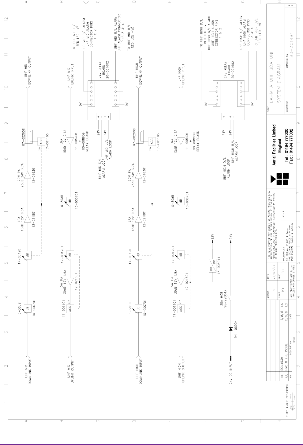
Axell Wireless Limited
Technical Literature
L.A. M.T.A. Remote Sites
Document Number 80-301401HBKM Issue No. 1 Date 13/06/2008 Page 42 of 148
3.5.1. UHF BDA Unit (80-301404) System Diagram
Drawing Number 80-301484
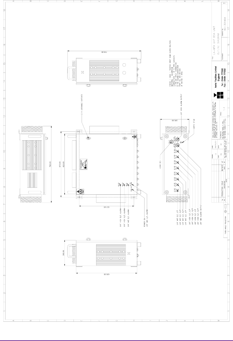
Axell Wireless Limited
Technical Literature
L.A. M.T.A. Remote Sites
Document Number 80-301401HBKM Issue No. 1 Date 13/06/2008 Page 43 of 148
3.5.2. UHF BDA Unit (80-301404) Outline Drawing
Drawing Number 80-301494

Axell Wireless Limited
Technical Literature
L.A. M.T.A. Remote Sites
Document Number 80-301401HBKM Issue No. 1 Date 13/06/2008 Page 44 of 148
3.5.3. UHF BDA Unit (80-301404) Specification
Parameter Specification
Downlink
UHF Midband 482.5 to 483.8MHz
Downlink Passband UHF Highband 507.0 to 507.3MHz
UHF Midband 30dB
Maximun gain UHF Highband 30dB
UHF Midband 0 to 30dB in 2dB steps
Gain Adjustment UHF Highband 0 to 30dB in 2dB steps
UHF Midband > +42.5dBm 1dB Compression Point
(P1dB) UHF Highband > +42.5dBm
UHF Midband 1dB below P1dB
ALC setting UHF Highband 1dB below P1dB
UHF Midband > +53.5dBm
3rd Order Intercept point UHF Highband > +53.5dBm
Uplink
UHF Midband 485.7 to 486.8MHz
Uplink Passband UHF Highband 510.0 to 510.3MHz
UHF Midband 30dB
Maximun gain UHF Highband 30dB
UHF Midband 0 to 30dB in 2dB steps
Gain Adjustment UHF Highband 0 to 30dB in 2dB steps
UHF Midband > +36.5dBm 1dB Compression Point
(P1dB) UHF Highband > +36.5dBm
UHF Midband +27dBm
ALC setting UHF Highband +27dBm
UHF Midband > +48.0dBm
3rd Order Intercept point UHF Highband > +48.0dBm
UHF Midband < 3.0dB
Noise Figure UHF Highband < 3.0dB
Environmental/Mechanical Specification
Mechanical IP65 Wall Mount
Dimensions
(excludes handles and connectors)
620mm x 620mm x 250mm
(24” x 24” x 10” approx)
RF Connectors N-Type Female
Alarm Interfaces
Local Alarms to SCADA
Dry Contact with LED Indication per band
path
Power Supply 24V DC
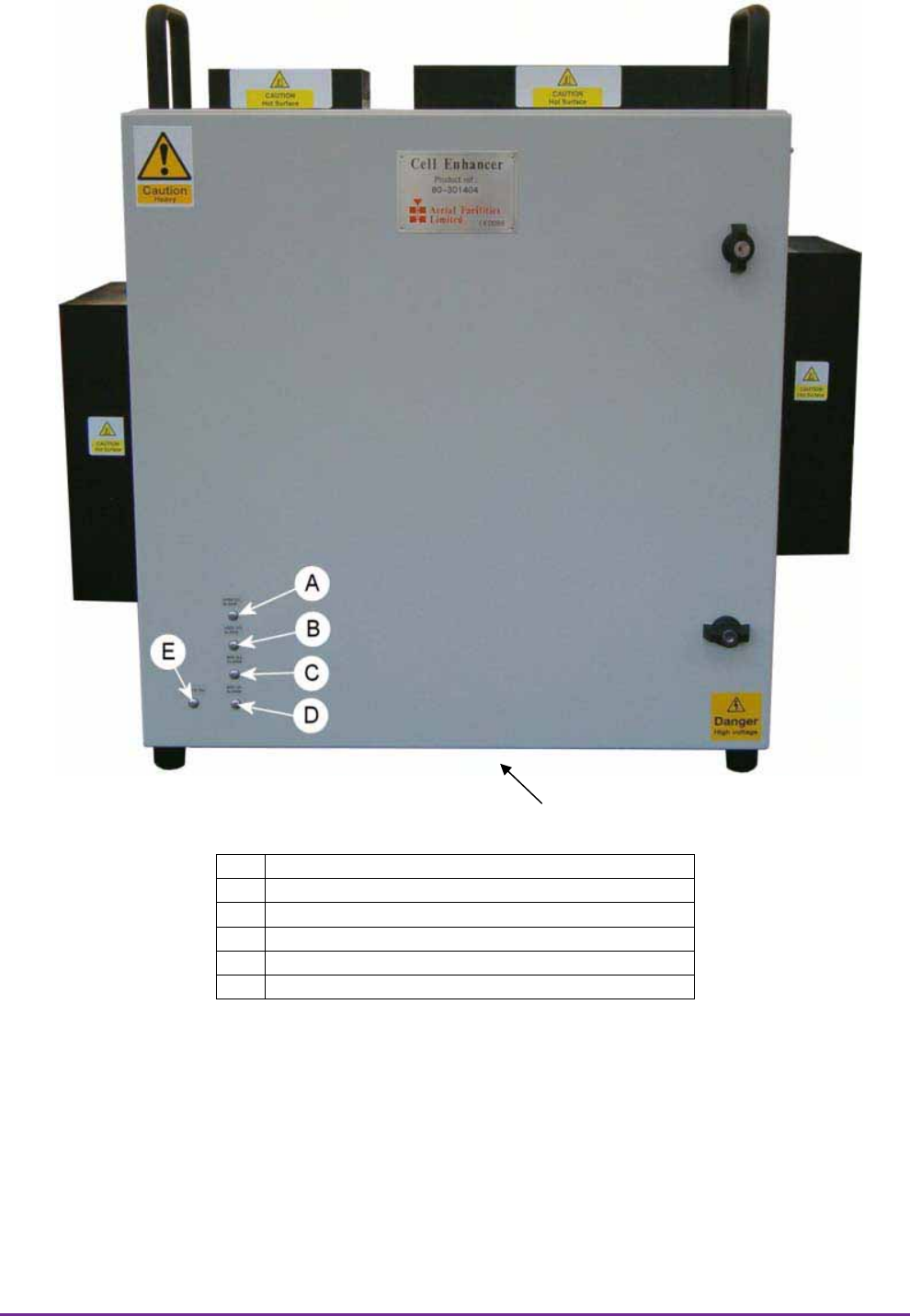
Axell Wireless Limited
Technical Literature
L.A. M.T.A. Remote Sites
Document Number 80-301401HBKM Issue No. 1 Date 13/06/2008 Page 45 of 148
3.5.4. UHF BDA Unit (80-301404) Photographs
3.5.4.1. Front View
Note: All connectors (RF, DC and Alarms) are on the underside
A Red LED UHF Highband Downlink Alarm
B Red LED UHF Highband Uplink Alarm
C Red LED UHF Midband Downlink Alarm
D Red LED UHF Midband Uplink Alarm
E Green LED “Power On”
F Lockable Door Handles
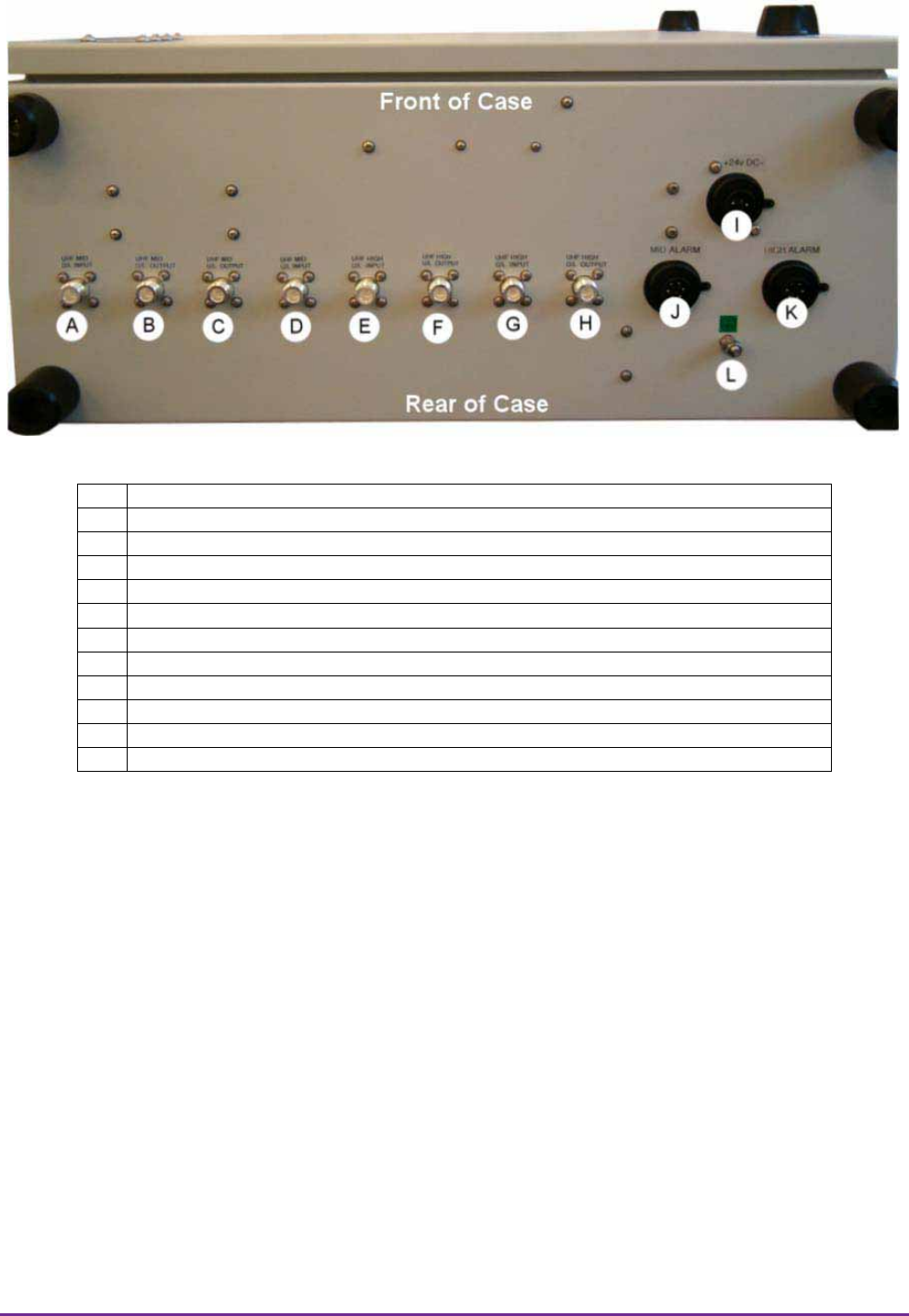
Axell Wireless Limited
Technical Literature
L.A. M.T.A. Remote Sites
Document Number 80-301401HBKM Issue No. 1 Date 13/06/2008 Page 46 of 148
3.5.4.2. Underside view showing connectors
A UHF Midband Downlink Input from port 3 on Combiner 80-301402
B UHF Midband Downlink Output to port C on Combiner 80-301402
C UHF Midband Uplink Output to port 8 on Combiner 80-301402
D UHF Midband Uplink Input from port H on Combiner 80-301402
E UHF Highband Uplink Input from port I on Combiner 80-301402
F UHF Highband Uplink Output to port 9 on Combiner 80-301402
G UHF Highband Downlink Input from port 4 on Combiner 80-301402
H UHF Highband Downlink Output to port D on Combiner 80-301402
I 24V DC Input
J UHF Midband Band Alarm Output
K UHF Highband Alarm Output
L Earth Connection
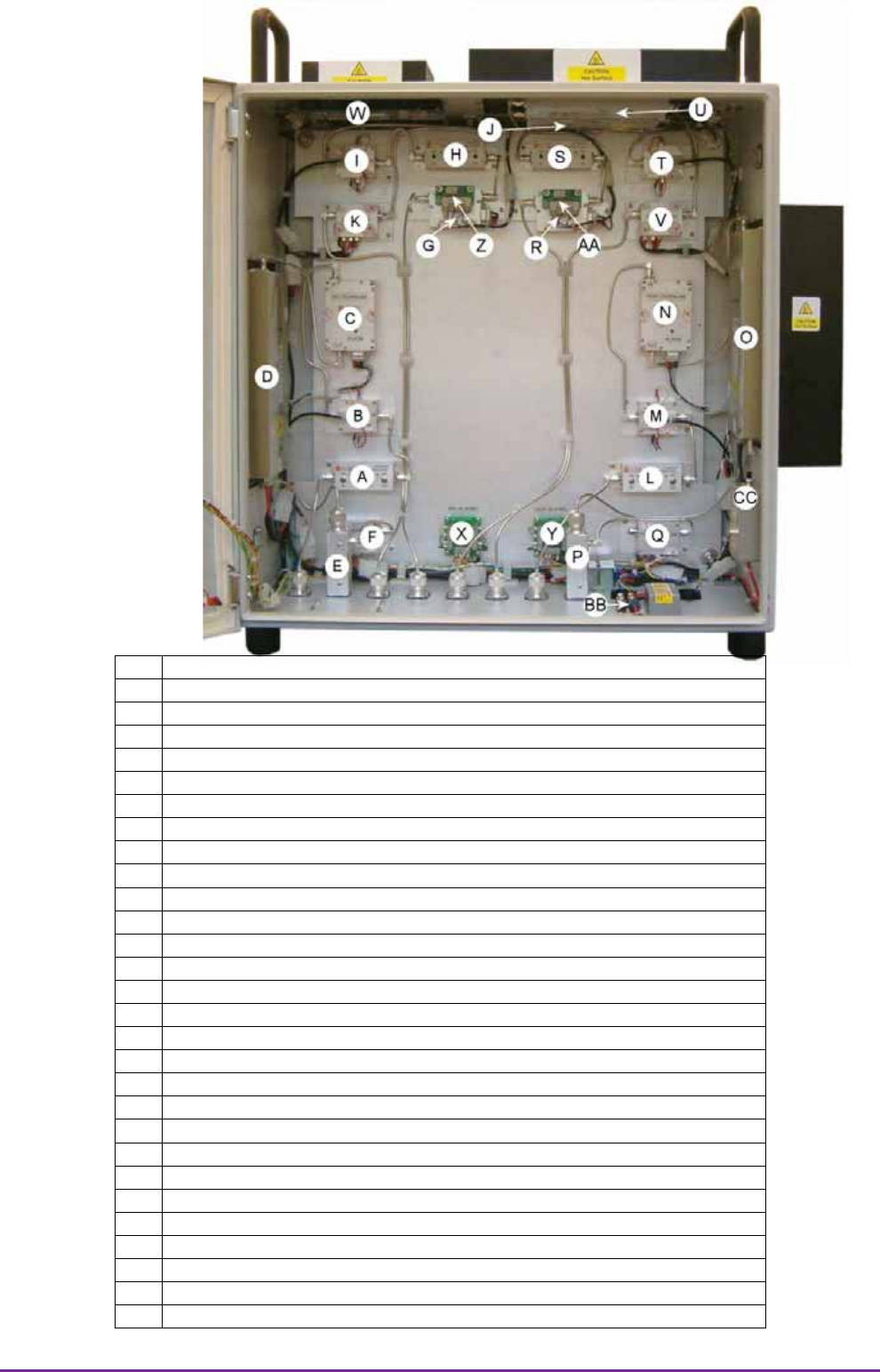
Axell Wireless Limited
Technical Literature
L.A. M.T.A. Remote Sites
Document Number 80-301401HBKM Issue No. 1 Date 13/06/2008 Page 47 of 148
3.5.4.3. Interior view
A UHF Midband Downlink Switched Attenuator 10-000701
B UHF Midband Downlink AGC Attenuator 17-001201
C UHF Midband Downlink Low Power Amplifier 12-021801
D UHF Midband Downlink 20W Power Amplifier 12-016301
E UHF Midband Downlink 30dB Directional Coupler 07-002908
F UHF Midband Downlink AGC Detector Assembly 17-001105
G UHF Midband Uplink Low Noise Amplifier 11-005401
H UHF Midband Uplink Switched Attenuator 10-000701
I UHF Midband Uplink AGC Attenuator 17-001201
J UHF Midband Uplink 5W Power Amplifier 12-021601
K UHF Midband Uplink AGC Detector Assembly 17-001101
L UHF Highband Downlink Switched Attenuator 10-000701
M UHF Highband Downlink AGC Attenuator 17-001201
N UHF Highband Downlink Low Power Amplifier 12-021801
O UHF Highband Downlink 20W Power Amplifier 12-016301
P UHF Highband Downlink 30dB Directional Coupler 07-002908
Q UHF Highband Downlink AGC Detector Assembly 17-001105
R UHF Highband Uplink Low Noise Amplifier 11-005401
S UHF Highband Uplink Switched Attenuator 10-000701
T UHF Highband Uplink AGC Attenuator 17-001201
U UHF Highband Uplink 5W Power Amplifier 12-021601
V UHF Highband Uplink AGC Detector Assembly 17-001101
W DC/DC Converter 13-003011
X 24V Dual Relay Assembly 20-001602 UHF Highband Alarms
Y 24V Dual Relay Assembly 20-001602 UHF Midband Alarms
Z 24V Relay Assembly 80-008909 UHF Midband Alarms
AA 24V Relay Assembly 80-008909 UHF Highband Alarms
BB Dual Diode Assembly 94-100004
CC DC Circuit Breaker

Axell Wireless Limited
Technical Literature
L.A. M.T.A. Remote Sites
Document Number 80-301401HBKM Issue No. 1 Date 13/06/2008 Page 48 of 148
3.5.5. UHF BDA Unit (80-301404) Major Sub-components
Section Component
Part
Component Part Description Qty Per
Assembly
3.5.5.1. 07-002908 30dB Directional Coupler 2
3.5.5.2. 10-000701 Switched Attenuator 0.25Watt, 0 - 30dB 4
3.5.5.3. 11-005401 Low Noise Amplifier 2
3.5.5.4. 12-016301 TETRA Power Amplifier 20W 2
3.5.5.5. 12-021601 TETRA Power Amplifier 5W 2
3.5.5.6. 12-021801 Low Power Amplifier 2
3.5.5.7. 13-003011 DC/DC Converter 1
17-001101 AGC Detector Assembly 2
17-001105 AGC Detector Assembly (Logarithmic) 2
3.5.5.8.
17-001201 AGC Attenuator Assembly 4
3.5.5.9. 20-001602 24V Dual Relay Assembly 2
3.5.5.10. 80-008909 24V Relay Assembly 2
3.5.5.11. 94-100004 Dual Diode Assembly 1
3.5.5.1. 30dB Directional Coupler (07-002908)
The purpose of these couplers is to tap off known portions of RF signal from transmission lines and to
combine them, for example through splitter units for different purposes (alarms/monitoring etc.), whilst
maintaining an accurate 50: load to all ports/interfaces throughout the specified frequency range.
They are known as directional couplers as they couple power from the RF mainline in one direction
only.
Directional Coupler 07-002908 is configured to tap off 30dB.
07-002908 Specification
PARAMETER SPECIFICATION
Frequency range 50 - 1000MHz
Insertion loss <0.3dB
Coupling level -30dB
Rejection N/A
Weight <200g
Connectors N type, female
operation -20°C to +60°C Temperature
range storage -40°C to +70°C
3.5.5.2. Switched Attenuator 0.25Watt, 0 - 30dB (10-000701)
In many practical applications for Cell Enhancers etc., the gain in each path is found to be excessive.
Therefore, provision is made within the unit for the setting of attenuation in each path, to reduce the
gain.
10-000701 provides attenuation from 0 to 30dB in 2 dB steps The attenuation is simply set using the
four miniature toggle switches on the top of each unit. Each switch is clearly marked with the
attenuation it provides, and the total attenuation in line is the sum of the values switched in. They are
designed to maintain an accurate 50ȍ impedance over their operating frequency at both input and
output.
Axell Wireless Limited
Technical Literature
L.A. M.T.A. Remote Sites
Document Number 80-301401HBKM Issue No. 1 Date 13/06/2008 Page 49 of 148
10-000701 Specification
PARAMETER SPECIFICATION
Attenuation Values 0-30dB
Attenuation Steps 2, 4, 8 and 16dB
Power Handling 0.25 Watt
Attenuation Accuracy ± 1.0 dB
Frequency Range DC to 1GHz
Impedance 50ȍ
Connectors SMA
VSWR 1.3:1
Weight 0.2kg
operation -20°C to +60°C Temperature
range storage -40°C to +70°C
3.5.5.3. Low Noise Amplifier (11-005401)
The 15dB gain low noise amplifier used in the unit is a double stage solid-state low noise amplifier.
Class A circuitry is used throughout the units to ensure excellent linearity over a very wide dynamic
range. The active devices are very moderately rated to provide a long trouble-free working life. There
are no adjustments on these amplifiers, and in the unlikely event of a failure, the complete amplifier
should be replaced. The amplifier is housed in an aluminium case (Iridite NCP finish) with SMA
connectors for the RF input/output and a 9way D-type for DC and alarm outputs.
11-005401 Specification
PARAMETER SPECIFICATION
Frequency range 380 - 500MHz
Bandwidth <100MHz (as required, tuneable)
1dB compression point >+20dBm
3rd order intercept >+33dBm
Gain >15.5dB (typical)
VSWR better than 1.5:1
Input return loss >14dB
Noise figure <2.0dB (typical)
Connectors SMA female
Supply 115mA at 12V DC
operational -10°C to +60°C Temperature
range storage -40°C to +70°C
Size 88 x 50 x 34mm (ex. connectors)
Weight 0.26kg
LNA ‘D’ Connector Pin-out details
Connector pin Signal
1 +ve input (10-24V)
2 GND
3 Alarm relay O/P bad
4 Alarm relay common
5 Alarm relay good
6 No connection
7 TTL voltage set
8 TTL alarm/0V (good)
9 O/C good/0V bad

Axell Wireless Limited
Technical Literature
L.A. M.T.A. Remote Sites
Document Number 80-301401HBKM Issue No. 1 Date 13/06/2008 Page 50 of 148
3.5.5.4. TETRA Power Amplifier 20W (12-016301)
This amplifier is a Class A 20W power amplifier from 380MHz to 470MHz in a 1 stage balanced
configuration. It demonstrates a very high linearity and a very good input/output return loss (RL). It
has built in a Current Fault Alarm Function.
It is housed is an aluminium case (Iridite NCP finish) with SMA connectors for the RF input/output and
a D-Type connector for the power supply and the Current Fault Alarm Function. Note the large
diameter DC power input pins (1 & 2) fitted to reduce volt-drop/arcing.
12-016301 Specification
PARAMETER SPECIFICATION
Frequency range 380-470MHz
Small signal gain 23dB
Gain flatness ±1.7dB
I/O Return loss >18dB
1dB compression point +43dBm
OIP3 +55dBm
Supply voltage 24V DC
Supply current 3.8Amps (Typical)
operational -10°C to +60°C Temperature
range storage -20°C to +70°C
Weight <2kg (no heatsink)
7-Way Connector Pin-out details
Connector Pin Signal
A1 (large pin) +24V DC
A2 (large pin) GND
1 Alarm relay common
2 TTL alarm/0V good
3 Alarm relay contact (bad)
4 Alarm relay contact (good)
5 O/C good/0V bad (TTL)
Axell Wireless Limited
Technical Literature
L.A. M.T.A. Remote Sites
Document Number 80-301401HBKM Issue No. 1 Date 13/06/2008 Page 51 of 148
A1 A2
1 2
3 4 5
3.5.5.5. TETRA Power Amplifier 5W (12-021601)
Power amplifier 12-021601 is a multi-stage, solid state power amplifier. Class A circuitry is employed
throughout the device to ensure excellent linearity over a wide dynamic frequency range. All the semi-
conductor devices are very conservatively rated to ensure low device junction temperatures and a
long, trouble free working lifetime.
The power amplifier should require no maintenance over its operating life. Under no circumstances
should the cover be removed or the side adjustments disturbed unless it is certain that the amplifier
has failed; since it is critically aligned during manufacture and any re-alignment will require extensive
test equipment.
The unit housing is an aluminium case (Iridite NCP finish) with SMA connectors for the RF
input/output and a D-Type connector for the power supply and the Current Fault Alarm Function.
12-021601 Specification
PARAMETER SPECIFICATION
Frequency range: 380-470MHz (as required)
Bandwidth: 10-40MHz (typical, tuned to spec.)
Maximum RF output: >5Watts
Gain: >30dB
1dB compression point: +37.5dBm
3rd order intercept point: +50dBm
VSWR: better than 1.5:1
Connectors: SMA female
Supply: 1.9Amps @ 12V DC
Weight: 1kg (excluding heatsink)
operational: -10qC to +60qC
Temperature
range: storage: -20qC to +70qC
7-Way Connector Pin-out details
Connector Pin Signal
A1 (large pin) +10-24V DC
A2 (large pin) GND
1 Alarm relay common
2 TTL alarm/0V good
3 Alarm relay contact (bad)
4 Alarm relay contact (good)
5 O/C good/0V bad (TTL)
7-Way Pin-Out Graphical Representation
Axell Wireless Limited
Technical Literature
L.A. M.T.A. Remote Sites
Document Number 80-301401HBKM Issue No. 1 Date 13/06/2008 Page 52 of 148
7 8 96
1 2 3 4 5
9-Way Pin-Out Graphical Representation
3.5.5.6. Low Power Amplifier (12-021801)
The low power amplifier used is a 1 stage balanced configuration, solid-state amplifier. Class A
circuitry is used in the unit to ensure excellent linearity over a very wide dynamic range. The three
active devices are very moderately rated to provide a long trouble-free working life.
Its housing is an aluminium case (Iridite NCP finish) with SMA connectors for the RF input/output and
a D-Type connector for the power supply and the Current Fault Alarm Function.
There are no adjustments on this amplifier, and in the unlikely event of failure then the entire amplifier
should be replaced.
12-021801 Specification
PARAMETER SPECIFICATION
Temperature -20 to +70 qC
Frequency Range 380 - 500 MHz
Small Signal Gain 15.5 +/- 0.5 dB
Gain Flatness 0.7 dB p-p
'Gain vs. Temperature 0.7 dB
In RL 20 dB
Out RL 20 dB
Output Power @ 1dB Compression Point +30.5dBm
Output 3rd Order IP +41.5dBm
Noise Figure 6 dB
DC Supply Voltage 10-15 Vdc
DC Supply Current 540 mA Max
operational -10qC to +60qC
Temperature
range storage -40qC to +100qC
Weight <0.5 kg
Size 110.5 x 66mm x 24.6mm
Low Power Amplifier (12-021801) 9-Way Connector Pin-outs
Connector pin Signal
1 +ve input (10-15V)
2 GND
3 Alarm relay O/P bad
4 Alarm relay common
5 Alarm relay good
6 No connection
7 TTL voltage set
8 TTL alarm/0V (good)
9 O/C good/0V bad

Axell Wireless Limited
Technical Literature
L.A. M.T.A. Remote Sites
Document Number 80-301401HBKM Issue No. 1 Date 13/06/2008 Page 53 of 148
3.5.5.7. DC/DC Converter, 24V in, 12V 8A out (13-003011)
The DC/DC converter fitted is a high power PCB unit with an 8 amp at 12V output capability. The
circuit is basically an O.E.M semiconductor regulator (one side of which has a heatsink mounting
plate, usually bolted to the casing of the unit) and smoothing components built onto a printed circuit
board with screw block terminations.
In event of failure this unit should not be repaired, only replaced.
13-003011 Specification
PARAMETER SPECIFICATION
Input Voltage range 18-28V DC
Output voltage 12V±0.5V
Max. current load 8.0Amps
operation -10°C to +60°C Temperature
range storage -20°C to +70°C
Size(PCB) 190 x 63mm
Weight (Loaded PCB) 291g
3.5.5.8. Automatic Gain Control
17-001101 AGC Detector Assembly
17-001105 AGC Detector Assembly (Logarithmic)
17-001201 AGC Attenuator Assembly
UHF BDA UNIT(80-301404) is fitted with two differing types of Automatic Gain Control (AGC) system,
one linear, and one logarithmic. The Downlink UHF Midband and Highband paths are each fitted with
logarithmic detector (17-001105), and attenuator (17-001201) the Uplink UHF Midband and Highband
paths are each fitted with linear detector (17-001101) and attenuator (17-001201) The Automatic Gain
Control system consists of two units, a detector/amplifier and an attenuator. The detector/amplifier
unit is inserted in the RF path on the output of the power amplifier, and the attenuator is situated in
the RF path before the amplification stage(s)
The attenuator comprises a 50ȍ P.I.N diode, voltage-variable attenuator with a range of 3 to 30dB.
The attenuation is controlled by a DC voltage which is derived from the associated detector controller
board. Normally the attenuator is at minimum attenuation. The detector/amplifier unit monitors the RF
level being delivered by the power amplifier, and when a certain threshold is reached it begins to
increase the value of the attenuator to limit the RF output to the (factory set) threshold. Therefore
overloading of the power amplifier is avoided.
The factory set threshold is 1dB below the Enhancer 1dB compression point. Some adjustment of this
AGC threshold level is possible, a 10dB range is mostly achieved. It is not recommended under any
circumstances to adjust the AGC threshold to a level greater than the 1dB compression point as
system degradation will occur.
The detector comprises of a 50ȍ transmission line with a resistive tap which samples a small portion
of the mainline power. The sampled signal is amplified and fed to a conventional half wave diode
rectifier, the output of which is a DC voltage proportional to the RF input signal. This DC voltage is
passed via an inverting DC amplifier with integrating characteristics, to the output, which drives the
attenuation control line of the corresponding AGC attenuator. This unit is fitted at some earlier point in
the RF circuit. For small signals, below AGC onset, the output control line will be close to 12V and the
AGC attenuator will have minimum attenuation. As the signal level increases the control line voltage
will fall, increasing the attenuator value and keeping the system output level at a constant value.
Axell Wireless Limited
Technical Literature
L.A. M.T.A. Remote Sites
Document Number 80-301401HBKM Issue No. 1 Date 13/06/2008 Page 54 of 148
3.5.5.9. 24V Relay Dual Assembly (20-001602)
The General Purpose 24V Dual Relay Board (20-001602) allows the inversion of signals and the
isolation of circuits. It is equipped with two dual pole change-over relays RL1 and RL2, with
completely isolated wiring, accessed via screw terminals. Both relays are provided with polarity
protection diodes and diodes for suppressing the transients caused by "flywheel effect" which can
destroy switching transistors or induce spikes on neighbouring circuits. Its common use is to
amalgamate all the alarm signals into one, volts-free relay contact pair for the main alarm system.
20-001602 Specification
PARAMETER SPECIFICATION
Operating voltage 8 to 30V (floating earth)
Alarm Threshold Vcc - 1.20 volt +15%
Alarm output relay contacts:
Max. switch current 1.0Amp
Max. switch volts 120Vdc/60VA
Max. switch power 24W/60VA
Min. switch load 10.0µA/10.0mV
Relay isolation 1.5kV
Mechanical life >2x10⁷ operations
Relay approval BT type 56
Connector details Screw terminals
operational -10°C to +60°C Temperature
range storage -20°C to +70°C
3.5.5.10. 24V Relay Assembly (80-008909)
Relay Board (80-008909) allows the inversion of signals and the isolation of circuits. It is equipped
with a single dual pole change-over relay RL1, with completely isolated wiring, accessed via a 15 way
in-line connector. The relay is provided with polarity protection diodes and diodes for suppressing the
transients caused by "flywheel effect" which can destroy switching transistors or induce spikes on
neighbouring circuits. It’s common use is to amalgamate all the alarm signals into one, volts-free
relay contact pair for the main alarm system. This relay board also carries an LED to serve as a
“Status OK” indicator which is illuminated during normal operation.
80-008909 Specification
PARAMETER SPECIFICATION
Operating voltage 8 to 30V (floating earth)
Alarm threshold Vcc - 1.20 volt +15%
Alarm output relay contacts
Max. switch current 1.0Amp
Max. switch volts 120Vdc/60VA
Max. switch power 24W/60VA
Min. switch load 10.0µA/10.0mV
Relay isolation 1.5kV
Mechanical life >2x10⁷ operations
Relay approval BT type 56
Connector details Screw terminals
operational -10°C to +60°C Temperature
range storage -20°C to +70°C

Axell Wireless Limited
Technical Literature
L.A. M.T.A. Remote Sites
Document Number 80-301401HBKM Issue No. 1 Date 13/06/2008 Page 55 of 148
3.5.5.11. Dual Diode Assembly (94-100004)
The purpose of these dual diode assemblies is to provide polarity protection for the DC supply input.
They are very heavy-duty diodes and they prevent any reverse current from flowing back to their
source.

Axell Wireless Limited
Technical Literature
L.A. M.T.A. Remote Sites
Document Number 80-301401HBKM Issue No. 1 Date 13/06/2008 Page 56 of 148
3.6. 800MHz BDA UNIT (80-301405)
800MHz BDA UNIT (80-301405) provides the amplification stages for the 800MHz paths, The unit is
housed in a wall mount case 600x600x250mm (24” x 24” x 10” approx).
The Downlink 800MHz signal is received at the port labelled “D/L INPUT” (Annotated A in the picture
in section 3.6.4.2.). The Downlink 800MHz path passes through a bandpass filter to remove out of
band noise and then a switched attenuator providing 0 to 30 dB of RF signal attenuation, after the
Attenuator the signal passes through the first of two amplification stages. This first stage is provided
by a low noise amplifier which gives approx. 19dB of gain.
After the Low Noise Amplifier the Downlink 800MHz signal passes through the second amplification
stage; the signal is first split into two equal paths and then each path is passed through a 20W power
amplifier and then the two signal paths are re-combined. The second stage amplifiers are straddled
by an Automatic Gain Control assembly providing limiting to the output signals in the case of high
input signals.
After leaving the second stage amplifiers the Downlink 800MHz signal path passes through a second
bandpass filter before exiting the BDA via the port labelled “D/L OUTPUT” (B in section 3.6.4.2.).
The Uplink 800MHz signal is received at the port labelled “U/L INPUT” (C in section 3.6.4.2.). The
Uplink 800MHz path passes through a bandpass filter to remove out of band noise and then into the
first of two amplification stages, the first stage is provided by a low noise amplifier which gives approx.
19dB of gain; after leaving the Low Noise Amplifier the signal passes through a switched attenuator
providing 0 to 30 dB of RF signal attenuation,
After leaving the switched attenuator the Uplink 800MHz path passes through the second stage of
amplification which is provided by a 5W power amplifier giving approx. 30db of gain; this second
amplification stage is straddled by an Automatic Gain Control assembly providing limiting to the output
signals in the case of high input signals.
After leaving the second amplification stage the Uplink 800MHz path passes through a second
bandpass filter before exiting the BDA via the port labelled “U/L OUTPUT” (D in section 3.6.4.2.).
800MHz BDA UNIT (80-301405) is provided with a 24V DC input to power the amplifier modules
within and those amplifier modules are configured to provide alarm status reports.
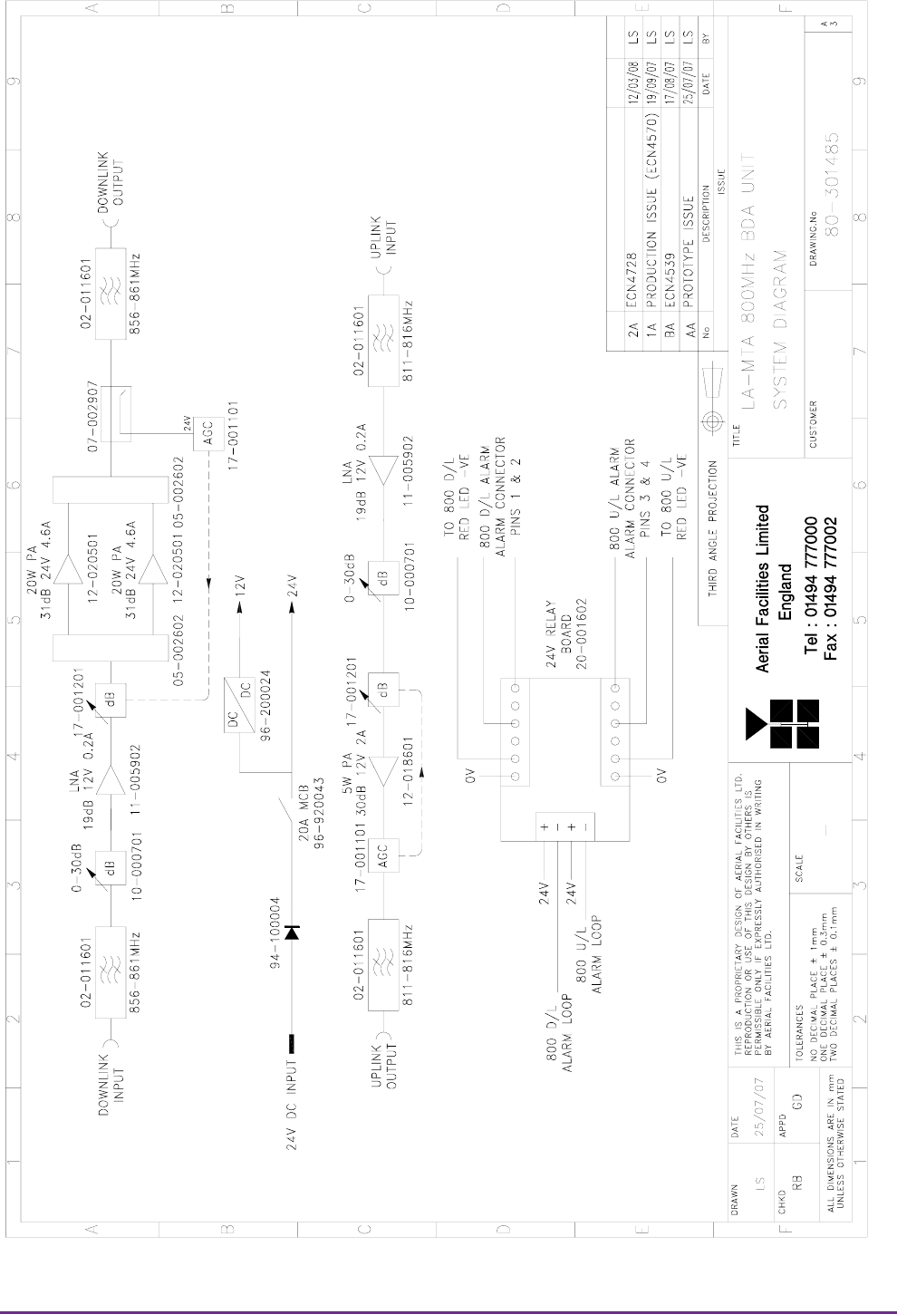
Axell Wireless Limited
Technical Literature
L.A. M.T.A. Remote Sites
Document Number 80-301401HBKM Issue No. 1 Date 13/06/2008 Page 57 of 148
3.6.1. 800MHz BDA UNIT (80-301405) System Diagram
Drawing Number 80-301485
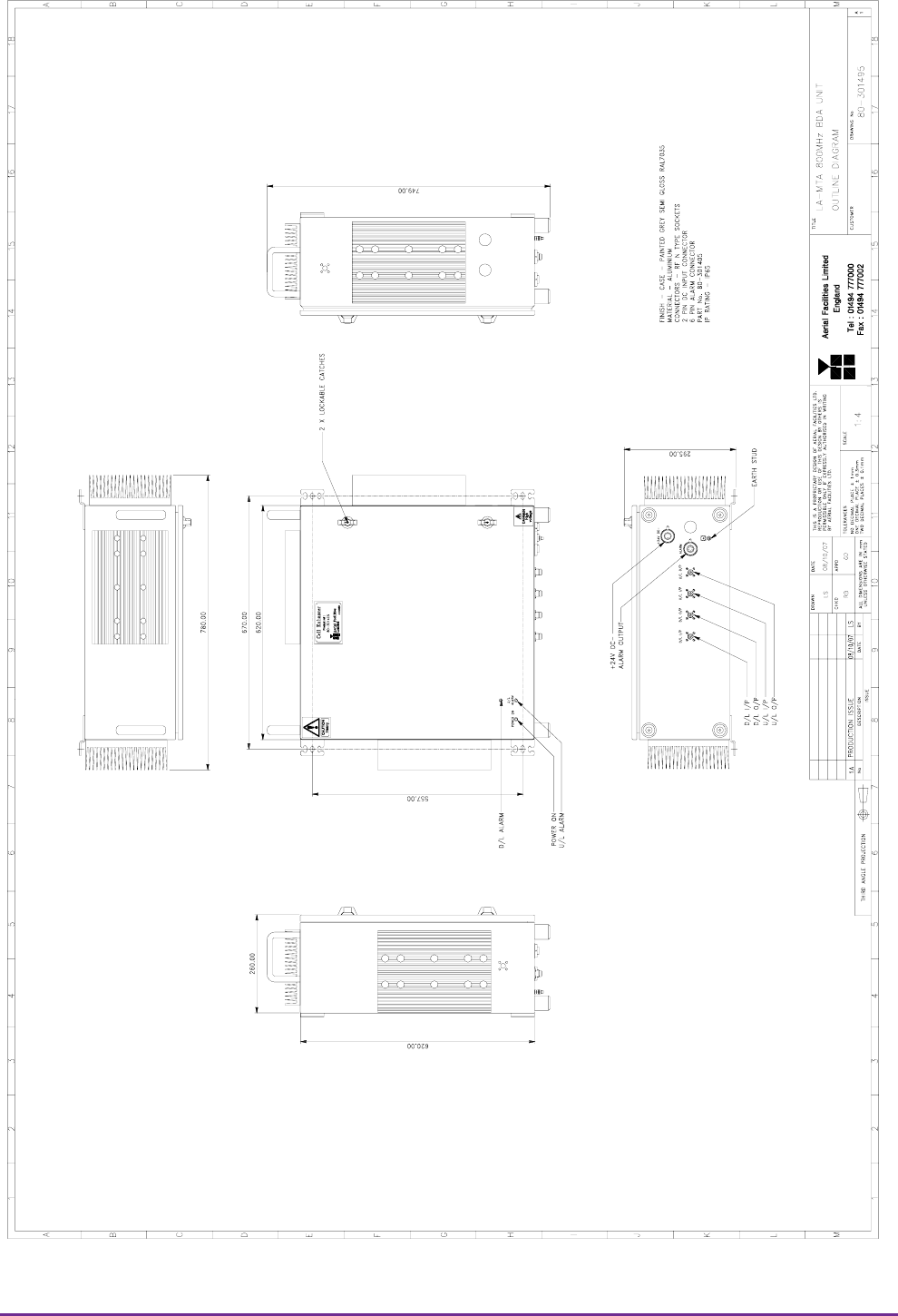
Axell Wireless Limited
Technical Literature
L.A. M.T.A. Remote Sites
Document Number 80-301401HBKM Issue No. 1 Date 13/06/2008 Page 58 of 148
3.6.2. 800MHz BDA UNIT (80-301405) Outline Drawing
Drawing Number 80-301495

Axell Wireless Limited
Technical Literature
L.A. M.T.A. Remote Sites
Document Number 80-301401HBKM Issue No. 1 Date 13/06/2008 Page 59 of 148
3.6.3. 800MHz BDA UNIT (80-301405) Specification
Parameter Specification
Downlink
Downlink Passband 856.0 to 861.0MHz
Maximun gain 30dB
Gain Adjustment 0 to 30dB in 2dB steps
1dB Compression Point (P1dB) > +45.0dBm
ALC setting 1dB below P1dB
3rd Order Intercept point > +55.0dBm
Uplink
Uplink Passband 811.0 to 816.0MHz
Maximun gain 30dB
Gain Adjustment 0 to 30dB in 2dB steps
1dB Compression Point (P1dB) > +36.0dBm
ALC setting +27dBm
3rd Order Intercept point > +46.0dBm
Noise Figure < 5.0 dB
Environmental/Mechanical Specification
Mechanical IP65 Wall Mount
Dimensions
(excludes handles and connectors)
620mm x 620mm x 250mm
(24” x 24” x 10” approx)
RF Connectors N-Type Female
Alarm Interfaces
Local Alarms to SCADA
Dry Contact with LED Indication per band
path
Power Supply 24V DC
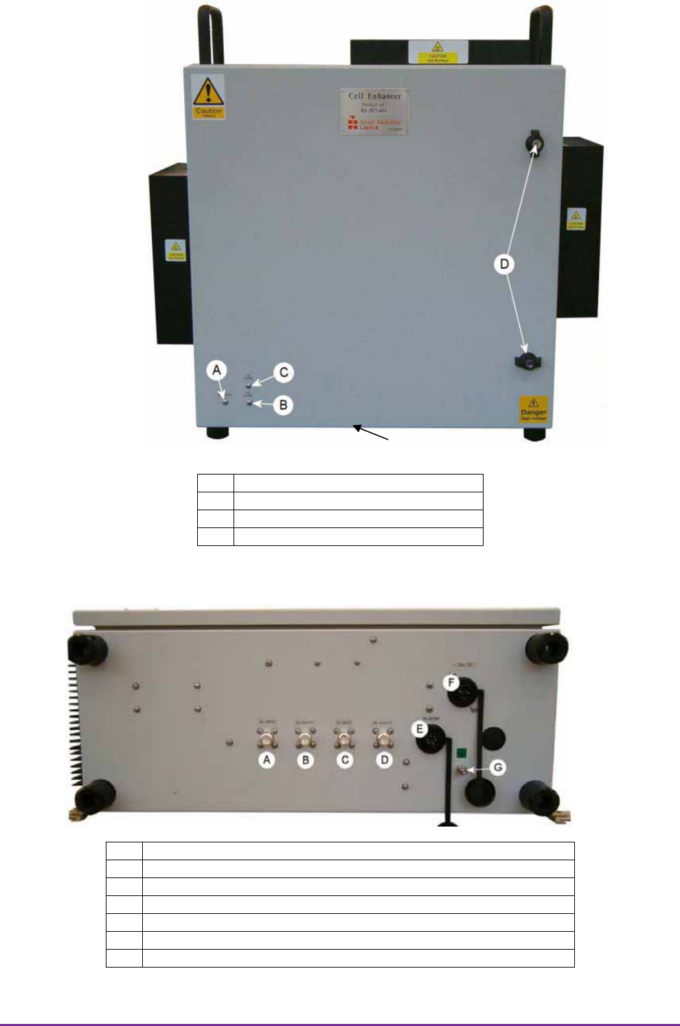
Axell Wireless Limited
Technical Literature
L.A. M.T.A. Remote Sites
Document Number 80-301401HBKM Issue No. 1 Date 13/06/2008 Page 60 of 148
3.6.4. 800MHz BDA UNIT (80-301405) Photographs
3.6.4.1. Front View
Note: All connectors (RF, DC and Alarms) are on the underside
A Green LED “Power On”
B Red LED Uplink Alarm
C Red LED Downlink Alarm
D Lockable Door Handles
3.6.4.2. Underside view showing connectors
A 800MHz Downlink Input from port 5 on Combiner 80-301402
B 800MHz Downlink output to port E on Combiner 80-301402
C 800MHz Downlink Input from port J on Combiner 80-301402
D 800MHz Downlink output to port 10 on Combiner 80-301402
E Alarm Output
F 24V DC Input
G Earth Connection
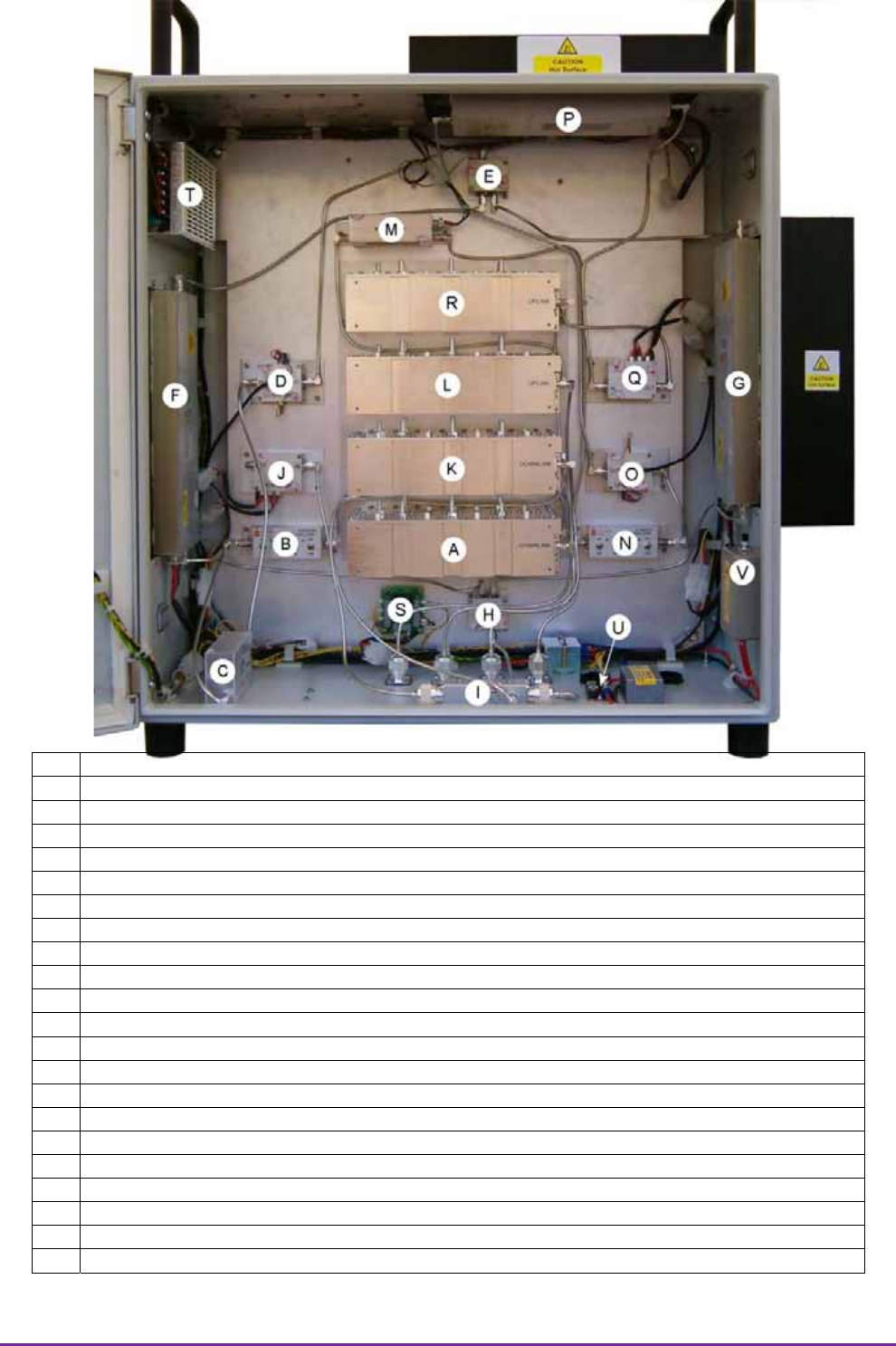
Axell Wireless Limited
Technical Literature
L.A. M.T.A. Remote Sites
Document Number 80-301401HBKM Issue No. 1 Date 13/06/2008 Page 61 of 148
3.6.4.3. Interior view
A Downlink Input Bandpass Filter 02-011601
B Downlink Switched Attenuator 10-000701
C Downlink Low Noise Amplifier 11-005902
D Downlink AGC Attenuator Assembly17-001201
E Downlink Splitter/Combiner 05-002602 (splits signal to feed Power Amplifiers)
F Downlink 20W Power Amplifier 12-020501 (1)
G Downlink 20W Power Amplifier 12-020501 (2)
H Downlink Splitter/Combiner 05-002602 (combines signals from Power Amplifiers)
I Downlink 30dB Directional Coupler 07-002907
J Downlink AGC Detector Assembly17-001105
K Downlink Output Bandpass Filter 02-011601
L Uplink Input Bandpass Filter 02-011601
M Uplink Low Noise Amplifier 11-005902
N Uplink Switched Attenuator 10-000701
O Uplink AGC Attenuator Assembly17-001201
P Uplink 5W Power Amplifier 12-018601
Q Uplink AGC Detector Assembly17-001101
R Uplink Output Bandpass Filter 02-011601
S 24V Relay Dual Assembly 20-001602
T DC/DC Converter 96-200024
U Dual Diode Assembly 94-100004
V Main DC Circuit Breaker

Axell Wireless Limited
Technical Literature
L.A. M.T.A. Remote Sites
Document Number 80-301401HBKM Issue No. 1 Date 13/06/2008 Page 62 of 148
3.6.5. 800MHz BDA UNIT (80-301405) Major Sub-components
section Component
Part
Component Part Description Qty Per
Assembly
3.6.5.1. 02-011601 Bandpass FIlter 4
3.6.5.2. 05-002602 Splitter/Combiner 2
3.6.5.3. 07-002907 30dB Directional Coupler 1
3.6.5.4. 10-000701 Switched Attenuator 0.25Watt, 0 - 30dB 2
3.6.5.5. 11-005902 Low Noise Amplifier 2
3.6.5.6. 12-018601 5W Power Amplifier 1
3.6.5.7. 12-020501 20W Power Amplifier 2
17-001101 AGC Detector Assembly 1
17-001105 AGC Detector Assembly (Logarithmic) 1
3.6.5.8.
17-001201 AGC Attenuator Assembly 2
3.6.5.9. 20-001602 24V Relay Dual Assembly 1
3.6.5.10. 94-100004 Dual Diode Assembly 1
3.6.5.11. 96-200024 DC/DC Converter, 24V in, 12V 5A out 1
3.6.5.1. Bandpass Filter (02-011601)
The bandpass filters are multi-section designs with a bandwidth dependent upon the passband
frequencies, (both tuned to customer requirements). The response shape is basically Chebyshev with
a passband design ripple of 0.1dB. The filters are of combline design, and are carefully aligned during
manufacture in order to optimise the insertion loss, VSWR and intermodulation characteristics of the
unit. The tuned elements are silver-plated to reduce surface ohmic losses and maintain a good VSWR
figure and 50ȍ load at the input and output ports.
Being passive devices, the bandpass filters should have an extremely long operational life and require
no maintenance. Should a filter be suspect, it is usually most time efficient to replace the module
rather than attempt repair or re-tuning.
02-011601 Specification
PARAMETER SPECIFICATION
Downlink 856 to 861MHz Frequency
Range Uplink 811 to 816MHz
Downlink 5 MHz
Bandwidth Uplink 5 MHz
Number of Sections 8
Insertion Loss 1.2 dB
VSWR better than 1.2:1
Connectors SMA
Power Handling 100W max
operation -10°C to +55°C Temperature
range storage -40°C to +70°C
Weight 3 kg (typical)
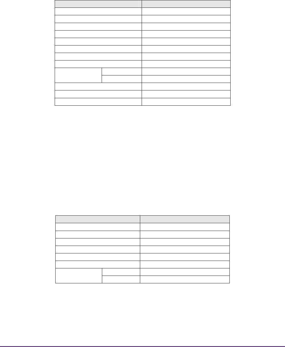
Axell Wireless Limited
Technical Literature
L.A. M.T.A. Remote Sites
Document Number 80-301401HBKM Issue No. 1 Date 13/06/2008 Page 63 of 148
3.6.5.2. Splitter/Combiner (05-002602)
The Splitter/Combiner used is a device for accurately matching two or more RF signals to single or
multiple ports, whilst maintaining an accurate 50: load to all inputs/outputs and ensuring that the
VSWR and insertion losses are kept to a minimum. Any unused ports should be terminated with an
appropriate 50: load.
Being passive devices, the splitters should have an extremely long operational life and require no
maintenance. Should a unit be suspect, it is usually most time efficient to replace the whole module
rather than attempt repair or re-tuning.
05-002602 Specification
PARAMETER SPECIFICATION
Frequency Range 800 – 1000MHz
Bandwidth 200MHz
Ports 3
Insertion loss 3.3dB typical
Return loss input & output 1.3:1
Impedance 50ȍ
Isolation >20dB
MTFB >180,000 hours
Splitting 20Watts
Power rating Combining 0.5Watt
Connectors SMA female
Weight 200g (approximately)
Size 54 x 44 x 21mm
3.6.5.3. 30dB Directional Coupler (07-002907)
The purpose of these couplers is to tap off known portions (in this case 30dB) of RF signal from
transmission lines inband to combine them, for example through splitter units for different purposes
(alarms/monitoring etc.), whilst maintaining an accurate 50: load to all ports/interfaces throughout the
specified frequency range. They are known as directional couplers as they couple power from the RF
mainline in one direction only.
07-002907 Specification
PARAMETER SPECIFICATION
Frequency range 800 - 1000MHz
Insertion loss <0.3dB
Coupling level -30dB ±0.5dB
Rejection N/A
Weight <200g
Connectors SMA, female
operation -20°C to +60°C Temperature
range storage -40°C to +70°C
Axell Wireless Limited
Technical Literature
L.A. M.T.A. Remote Sites
Document Number 80-301401HBKM Issue No. 1 Date 13/06/2008 Page 64 of 148
3.6.5.4. Switched Attenuator 0.25Watt, 0 - 30dB (10-000701)
10-000701 provides attenuation from 0 to 30dB in 2 dB steps The attenuation is simply set using the
four miniature toggle switches on the top of each unit. Each switch is clearly marked with the
attenuation it provides, and the total attenuation in line is the sum of the values switched in. They are
designed to maintain an accurate 50ȍ impedance over their operating frequency at both input and
output.
10-000701 Specification
PARAMETER SPECIFICATION
Attenuation Values 0-30dB
Attenuation Steps 2, 4, 8 and 16dB
Power Handling 0.25 Watt
Attenuation Accuracy ± 1.0 dB
Frequency Range DC to 1GHz
Impedance 50ȍ
Connectors SMA
VSWR 1.3:1
Weight 0.2kg
operation -20°C to +60°C Temperature
range storage -40°C to +70°C
3.6.5.5. Low Noise Amplifier (11-005902)
The Gallium-Arsenide low noise amplifier used in the unit is a double stage, solid-state low noise
amplifier. Class A circuitry is used throughout the units to ensure excellent linearity and extremely low
noise over a very wide dynamic range. The active devices are very moderately rated to provide a long
trouble-free working life. There are no adjustments on these amplifiers, and in the unlikely event of a
failure, then the complete amplifier should be replaced.
This amplifier features its own in-built alarm system which gives a volt-free relay contact type alarm
that is easily integrated into any alarm system. There is a Current Fault Alarm Function, which
indicates failure of each one or both RF transistors by a various alarm output options. The amplifier is
housed in an aluminium case (Iridite NCP finish) with SMA connectors for the RF input/output and a
9way D-type for DC and alarm outputs.
11-005902 Specification
PARAMETER SPECIFICATION
Frequency range 800 – 960MHz
Bandwidth <170MHz
Gain 19.5dB (typical)
1dB compression point +21dBm
OIP3 +33dBm
Input/output return loss >20dB
Noise figure 1dB (typical)
Power consumption 190mA @ 24V DC
Supply voltage 10-24V DC
Connectors SMA female
operational -10°C to +60°C Temperature
range storage -40°C to +70°C
Size 90 x 55 x 30.2mm
Weight 0.28kg
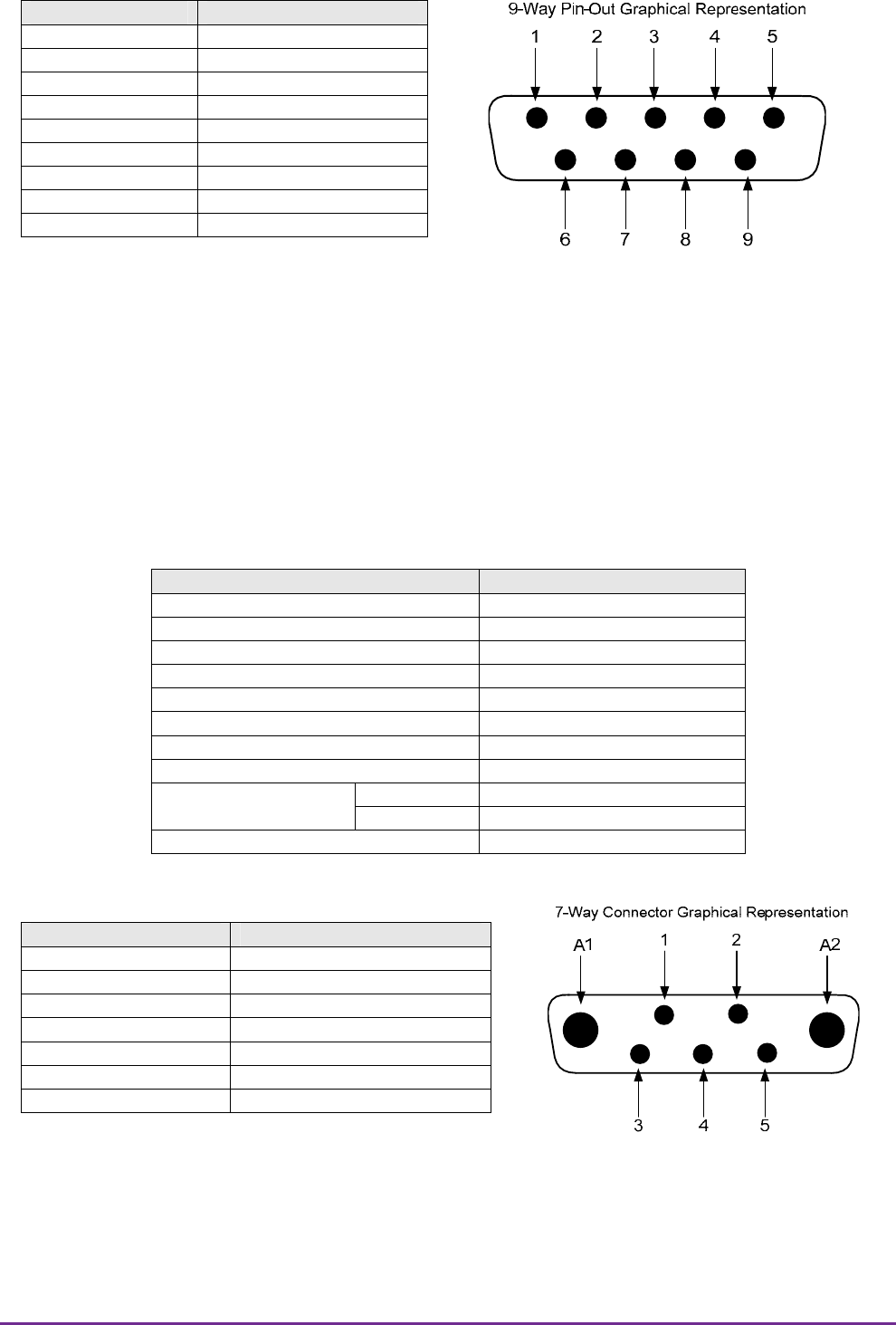
Axell Wireless Limited
Technical Literature
L.A. M.T.A. Remote Sites
Document Number 80-301401HBKM Issue No. 1 Date 13/06/2008 Page 65 of 148
LNA ‘D’ Connector Pin-out details
Connector pin Signal
1 +Ve input (10-24V)
2 GND
3 Alarm relay O/P bad
4 Alarm relay common
5 Alarm relay good
6 No connection
7 TTL voltage set
8 TTL alarm/0V (good)
9 O/C good/0V bad
3.6.5.6. 5W Power Amplifier (12-018601)
This amplifier is a Class A 5W power amplifier from 800MHz to 960MHz in a 1 stage balanced
configuration. It demonstrates a very high linearity and a very good input/output return loss (RL). It
has built in a Current Fault Alarm Function.
Its housing is an aluminium case (Iridite NCP finish) with SMA connectors for the RF input/output and
a D-Type connector for the power supply and the Current Fault Alarm Function.
12-018601 Specification
PARAMETER SPECIFICATION
Frequency range 800-960MHz
Small signal gain 30dB
Gain flatness ±0.5dB
I/O Return loss >20dB
1dB compression point +37dBm
OIP3 +52dBm
Supply voltage 12V DC
Supply current 2.0Amps (typical)
operational -10°C to +60°C Temperature
range storage -20°C to +70°C
Weight <2kg (no heatsink)
PA 7-Way Connector Pin-outs
Connector Pin Signal
A1 (large pin) +12V DC
A2 (large pin) GND
1 Alarm relay common
2 TTL alarm/0V good
3 Alarm relay contact (bad)
4 Alarm relay contact (good)
5 O/C good/0V bad (TTL)
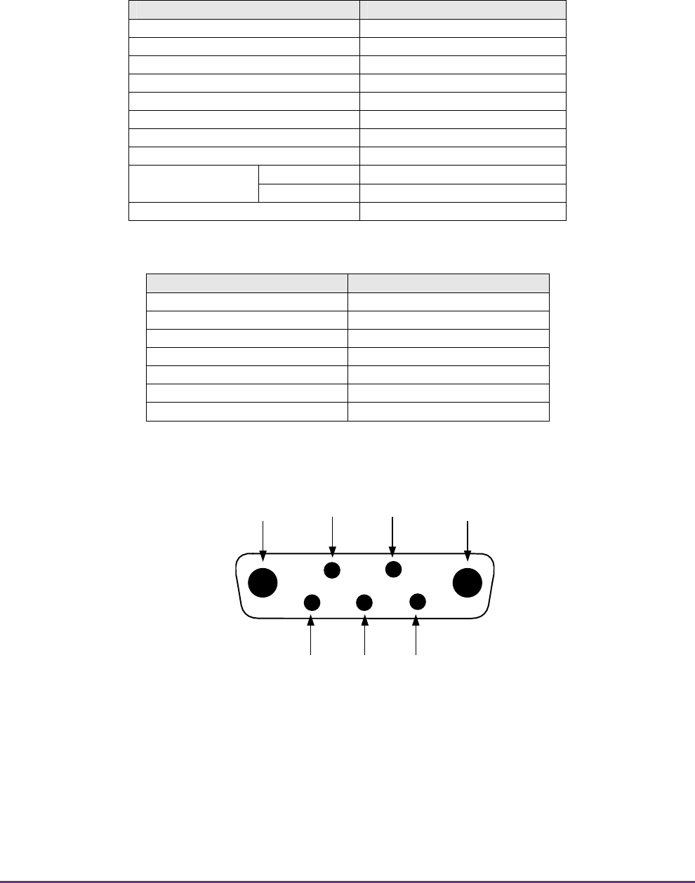
Axell Wireless Limited
Technical Literature
L.A. M.T.A. Remote Sites
Document Number 80-301401HBKM Issue No. 1 Date 13/06/2008 Page 66 of 148
A1 A2
1 2
3 4 5
7-Way Connector Graphical Representation
3.6.5.7. 20W Power Amplifier (12-020501)
This amplifier is a Class A 20W power amplifier from 800-960MHz in a 1 stage balanced
configuration. It demonstrates a very high linearity and a very good input/output return loss (RL). It
has built in a Current Fault Alarm Function.
Its housing is an aluminium case (Iridite NCP finish) with SMA connectors for the RF input/output and
a D-Type connector for the power supply and the Current Fault Alarm Function.
12-020501 Specification
PARAMETER SPECIFICATION
Frequency range 800-960MHz
Small signal gain 31.5dB
Gain flatness ±0.6dB
I/O Return loss >18dB
1dB compression point +43.5dBm
OIP3 +54dBm
Supply voltage 24V DC
Supply current 4.6Amps @12V(typical)
operational -10°C to +60°C Temperature
range storage -20°C to +70°C
Weight <2kg (no heatsink)
PA 7-Way Connector Pin-outs
Connector Pin Signal
A1 (large pin) +24V DC
A2 (large pin) GND
1 Alarm relay common
2 TTL alarm/0V good
3 Alarm relay contact (bad)
4 Alarm relay contact (good)
5 O/C good/0V bad (TTL)

Axell Wireless Limited
Technical Literature
L.A. M.T.A. Remote Sites
Document Number 80-301401HBKM Issue No. 1 Date 13/06/2008 Page 67 of 148
3.6.5.8. Automatic Gain Control
17-001101 AGC Detector Assembly
17-001105 AGC Detector Assembly (Logarithmic)
17-001201 AGC Attenuator Assembly
800MHz BDA UNIT (80-301405) is fitted with two differing types of Automatic Gain Control (AGC)
system, one linear, and one logarithmic. The Downlink path is fitted with logarithmic detector (17-
001105), and attenuator (17-001201) the Uplink path is fitted with linear detector (17-001101) and
attenuator (17-001201)
The Automatic Gain Control system consists of two units, a detector/amplifier and an attenuator. The
detector/amplifier unit is inserted in the RF path on the output of the power amplifier, and the
attenuator is situated in the RF path before the amplification stage(s)
The attenuator comprises a 50ȍ P.I.N diode, voltage-variable attenuator with a range of 3 to 30dB.
The attenuation is controlled by a DC voltage which is derived from the associated detector controller
board.
Normally the attenuator is at minimum attenuation. The detector/amplifier unit monitors the RF level
being delivered by the power amplifier, and when a certain threshold is reached it begins to increase
the value of the attenuator to limit the RF output to the (factory set) threshold. Therefore overloading
of the power amplifier is avoided.
The factory set threshold is 1dB below the Enhancer 1dB compression point. Some adjustment of this
AGC threshold level is possible, a 10dB range is mostly achieved. It is not recommended under any
circumstances to adjust the AGC threshold to a level greater than the 1dB compression point as
system degradation will occur.
The detector comprises of a 50ȍ transmission line with a resistive tap which samples a small portion
of the mainline power. The sampled signal is amplified and fed to a conventional half wave diode
rectifier, the output of which is a DC voltage proportional to the RF input signal.
This DC voltage is passed via an inverting DC amplifier with integrating characteristics, to the output,
which drives the attenuation control line of the corresponding AGC attenuator. This unit is fitted at
some earlier point in the RF circuit.
For small signals, below AGC onset, the output control line will be close to 12V and the AGC
attenuator will have minimum attenuation. As the signal level increases the control line voltage will
fall, increasing the attenuator value and keeping the system output level at a constant value.
3.6.5.9. 24V Relay Dual Assembly (20-001602)
The General Purpose 24V Dual Relay Board (20-001602) allows the inversion of signals and the
isolation of circuits. It is equipped with two dual pole change-over relays RL1 and RL2, with
completely isolated wiring, accessed via screw terminals. Both relays are provided with polarity
protection diodes and diodes for suppressing the transients caused by "flywheel effect" which can
destroy switching transistors or induce spikes on neighbouring circuits. Its common use is to
amalgamate all the alarm signals into one, volts-free relay contact pair for the main alarm system.

Axell Wireless Limited
Technical Literature
L.A. M.T.A. Remote Sites
Document Number 80-301401HBKM Issue No. 1 Date 13/06/2008 Page 68 of 148
20-001602 Specification
PARAMETER SPECIFICATION
Operating voltage 8 to 30V (floating earth)
Alarm Threshold Vcc - 1.20 volt +15%
Alarm output relay contacts:
Max. switch current 1.0Amp
Max. switch volts 120Vdc/60VA
Max. switch power 24W/60VA
Min. switch load 10.0µA/10.0mV
Relay isolation 1.5kV
Mechanical life >2x10⁷ operations
Relay approval BT type 56
Connector details Screw terminals
operational -10°C to +60°C Temperature
range storage -20°C to +70°C
3.6.5.10. Dual Diode Assembly (94-100004)
The purpose of these dual diode assemblies is to provide polarity protection for the DC voltage input.
They are very heavy-duty diodes and they prevent any reverse current from flowing back to their
source.
3.6.5.11. DC/DC Converter, 24V in, 12V 5A out (96-200024)
This unit it is an O.E.M high power device with a 5 amp @ 12V (60Watts) output capability used to
derive a 12V fixed voltage power supply rail from a 24V supply. In the event of failure this unit should
not be repaired, only replaced.
96-200024 Specification
PARAMETER SPECIFICATION
Input Voltage range 18-28V DC
Output voltage 12V±0.5V
Max. current load 5.0 Amps
operation -10°C to +60°C Temperature
range storage -20°C to +70°C

Axell Wireless Limited
Technical Literature
L.A. M.T.A. Remote Sites
Document Number 80-301401HBKM Issue No. 1 Date 13/06/2008 Page 69 of 148
4. In-Line BDA Rack Mount 80-301406
The Rack Mount In Line BDA consists of ten, 19” equipment rack mount shelves
The function is exactly the same as the Wall Mount unit in section 3 but the construction is different.
The Rack Mount BDA is divided into four main components equivalent to the four Wall Mount cases
described in section 3, these are:
x The Splitter Combiner which is comprised of four, 4U 19” rack mount shelves:
Downlink Input Shelf 80-301407
Downlink Output Shelf 80-301408
Uplink Input Shelf 80-301407
Uplink Output Shelf 80-301407
x The VHF and UHF Low Band Amplifier which is comprised of two, 4U 19” rack mount shelves:
VHF Amplifier Shelf 80-301409
UHF Lowband Amplifier Shelf 80-301410
x The Mid and High Band UHF Amplifier which is comprised of two, 4U 19” rack mount shelves:
UHF Midband Amplifier Shelf 80-301410
UHF Highband Amplifier Shelf 80-301410
x The 800MHz Amplifier which is comprised of one, 8U 19” rack mount shelf:
800MHz Amplifier Shelf 80-301411
A 2U 19” rack mount shelf houses the power supply unit that provides 24V DC feeds to the amplifier
shelves
The entire arrangement is housed in two, 40U Swing-fame 19” Equipment Mountings Racks,
Rack 1 houses:
Downlink Input Shelf 80-301407
Uplink Input Shelf 80-301407
Uplink Output Shelf 80-301407
UHF Highband Amplifier Shelf 80-301410
UHF Midband Amplifier Shelf 80-301410
UHF Lowband Amplifier Shelf 80-301410
VHF Amplifier Shelf 80-301409
PSU Shelf
Rack 2 houses:
Downlink Output Shelf 80-301408
800MHz Amplifier Shelf 80-301411
Rack interconnections, test ports and connections to the Leaky Feeders are via patch panels in the
tops of each rack

Axell Wireless Limited
Technical Literature
L.A. M.T.A. Remote Sites
Document Number 80-301401HBKM Issue No. 1 Date 13/06/2008 Page 70 of 148
Downlink
The downlink signal is received from the radiating cable and enters the Downlink Input Shelf 80-
301407 where by means of crossband splitter/couplers it is split into VHF, UHF and 800MHz paths,
the UHF path is further split into Low, Middle and Highband paths.
The VHF and UHF LowBand paths leave Downlink Input Shelf 80-301407. The VHF path goes to the
Downlink Input of VHF Amplifier Shelf 80-301409 and the UHF Lowband path goes to the Downlink
Input of UHF Lowband Amplifier Shelf 80-301410.
The UHF Mid and Highband paths leave Downlink Input Shelf 80-301407 the UHF Midband path goes
to the Downlink Input of UHF Midband Amplifier Shelf 80-301410; the UHF Highband path goes to the
Downlink Input of UHF Highband Amplifier Shelf 80-301410
The 800MHz path leaves Downlink Input Shelf 80-301407 and goes to the Downlink Input of 800MHz
Amplifier Shelf 80-301411
After their respective amplification stages the signal paths enter Downlink Output Shelf 80-301408
where they are combined into a single path and fed into the radiating cable.
Uplink
The Uplink signal signal is received from the radiating cable and enters Uplink Input Shelf 80-301407
where by means of crossband splitter/couplers it is split into VHF, UHF and 800MHz paths, the UHF
path is further split into Low, Middle and High band paths.
The VHF and UHF LowBand paths leave Uplink Input Shelf 80-301407. The VHF path goes to the
Uplink Input of VHF Amplifier Shelf 80-301409 and the UHF Lowband path goes to the Uplink Input of
UHF Lowband Amplifier Shelf 80-301410.
The UHF Mid and Highband paths leave Uplink Input Shelf 80-301407 the UHF Midband path goes to
the Uplink Input of UHF Midband Amplifier Shelf 80-301410; the UHF Highband path goes to the
Uplink Input of UHF Highband Amplifier Shelf 80-301410
The 800MHz path leaves Uplink Input Shelf 80-301407 and goes to the Uplinklink Input of 800MHz
Amplifier Shelf 80-301411
After their respective amplification stages the signal paths enter Uplink Output Shelf 80-301407 where
they are combined into a single path and fed into the radiating cable.
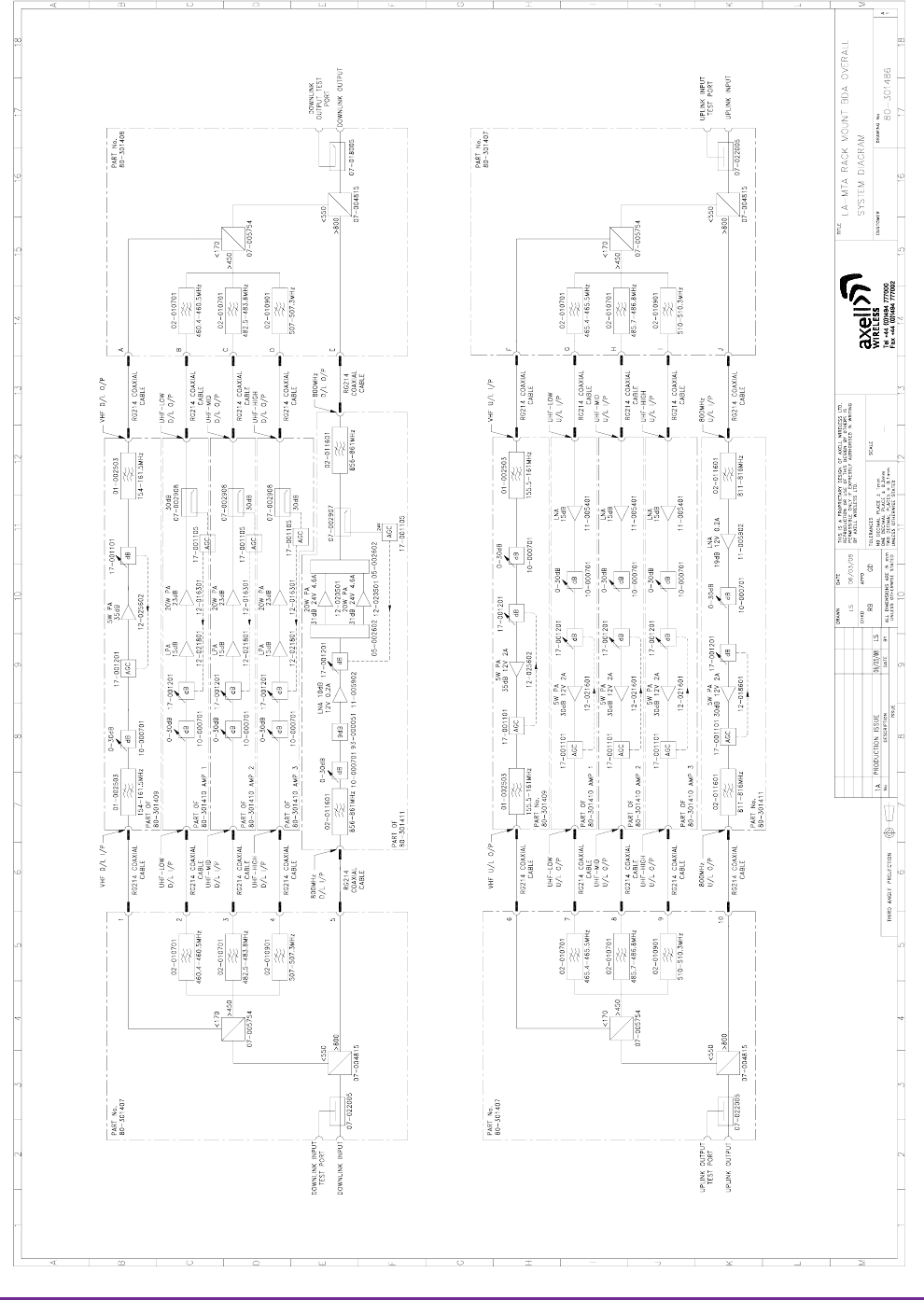
Axell Wireless Limited
Technical Literature
L.A. M.T.A. Remote Sites
Document Number 80-301401HBKM Issue No. 1 Date 13/06/2008 Page 71 of 148
4.1. In-Line BDA Rack Mount System Diagrams
4.1.1. Overall System Diagram
Drawing Number 80-301486
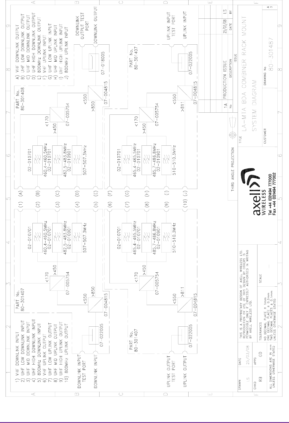
Axell Wireless Limited
Technical Literature
L.A. M.T.A. Remote Sites
Document Number 80-301401HBKM Issue No. 1 Date 13/06/2008 Page 72 of 148
4.1.2. Combiners System Diagram
Drawing Number 80-301487

Axell Wireless Limited
Technical Literature
L.A. M.T.A. Remote Sites
Document Number 80-301401HBKM Issue No. 1 Date 13/06/2008 Page 73 of 148
4.2. In-Line BDA Rack Mount 80-301406 Specification
ELECTRICAL SPECIFICATION
Downlink 154.0 to 161.5 MHz
VHF Uplink 155.5 to 161.0 MHz
Downlink 460.4 to 460.5 MHz
UHF Low Uplink 465.4 to 465.5 MHz
Downlink 482.5 to 483.8 MHz
UHF Mid Uplink 485.7 to 486.8 MHz
Downlink 507.0 to 507.3 MHz
UHF High Uplink 510.0 to 510.3 MHz
Downlink 856.0 to 861.0 MHz
Frequency
Range
800MHz Uplink 811.0 to 816.0 MHz
Passband Ripple ± 1.5dB
VHF 5 Watts
UHF Low 20 Watts
UHF Mid 20 Watts
UHF High 20 Watts
Downlink Power
Amplifier
800MHz 40 Watts
VHF 5 Watts
UHF Low 5 Watts
UHF Mid 5 Watts
UHF High 5 Watts
Uplink Power
Amplifier
800MHz 5 Watts
Gain 30dB
Gain Adjust 0 - 30dB in 2dB Steps
Sampling Ports 30dB
VSWR 1.5:1
Impedance 50 Ohms
Power Supply 24V DC
Power Consumption < 800 Watts
Mechanical Specification
Mechanical Two 40U, 19” Swingframe, 600mm x
600mm Equipment Mounting racks
RF Connectors N-Type Female
Alarm Interfaces
Local Alarms to SCADA
Dry Contact with LED Indication per
band path