PRETTL Elektronik Radeberg PER1220 Bluetooth Serial Port Module User Manual FreePDF Job 9
PRETTL Elektronik Radeberg GmbH Bluetooth Serial Port Module FreePDF Job 9
Manual

Prettl Elektronik
Radeberg GmbH
Last saved: 17.08.2005 Last editor: Scm2ra User_Manual_PER1220_V11.d
oc
PER1220
User Manual
Project: Serial Port Bluetooth Module
Phase: Approved
Author: Frank Hennig/EWG.
Status: Released
Version: 1.0

PER1220 Data Book Page 2/21
Copyright Prettl Elektronik Radeberg GmbH. All rights reserved.
Key Features
- RFCOMM Module
- Complete embedded Bluetooth-Stack up to RFCOMM
- Serial Port on chip Application
- Bluetooth V1.2 qualified
- Point to point or point to multipoint functionality
- Class 2 Bluetooth device, 4 dBm
- User payload data rate is up to 380 kbps over Bluetooth
- Module Interfacing over UART
- Temperature Range qualified: - 20 °C to + 70 °C
- Mechanical outline: 25.0 mm x 21.5 mm x 2.8 mm
-
Power Supply: 3.3 V DC
Description
The PER1220 is a ready to market Class 2 Bluetooth Modul Solution. It can easy implemented in any
electronical device to add Bluetooth connectivity. In standard configuration the module includes an 8
Mbit Flash, a radio solution, interfaces to antenna and application together with signalling at RFComm
level. The Module supports both voice and data transmissions.
Since the PER1220 is already a qualified product according to Bluetooth Specification V1.2 the
requested cost and time afford for qualification is kept to a minimum.
The standard software contains a full Bluetooth Protocol Stack up to RFComm and a serial port
application. For example this on-chip-application can support your cable-replacement.

PER1220 Data Book Page 3/21
Copyright Prettl Elektronik Radeberg GmbH. All rights reserved.
Table of Contents
1 GENERAL INFORMATION ..................................................................................................................5
2 MODULE PINOUT DIAGRAMM ..........................................................................................................6
3 DEVICE TERMINAL FUNCTIONS.......................................................................................................7
4 ELECTRICAL CHARACTERISTICS....................................................................................................9
5 RADIO CHARACTERISTICS .............................................................................................................12
6 PER1220 BLUETOOTH SOFTWARE STACK..................................................................................12
6.1 K
EY
F
EATURES
..........................................................................................................................12
7 DEVICE TERMINAL DESCRIPTION .................................................................................................14
7.1 A
NTENNA
..................................................................................................................................14
7.2 UART I
NTERFACE
.....................................................................................................................14
7.3 USB I
NTERFACE
........................................................................................................................15
7.4 S
ERIAL
P
ERIPHERAL
I
NTERFACE
.................................................................................................15
7.5 PCM.........................................................................................................................................15
7.6 PIO...........................................................................................................................................16
8 TYPICAL RADIO PERFORMANCE...................................................................................................17
9 RECOMMENDED SOLDER PROFILE ..............................................................................................17
10 INSTALLATION................................................................................................................................19
10.1 A
NTENNA
..................................................................................................................................19
10.2 P
OWER
S
UPPLY
.........................................................................................................................19
10.3 I
NTERFACES
..............................................................................................................................20
10.4 FCC C
ONFORMANCE
.................................................................................................................20
11 ORDERING AND CONTACT INFORMATION.................................................................................20
12 REGULATORY STATEMENTS .......................................................................................................21
12.1 FCC S
TATEMENTS
....................................................................................................................21
13 DOCUMENT REFERENCES............................................................................................................23
14 RECORD OF CHANGES .................................................................................................................23

PER1220 Data Book Page 4/21
Copyright Prettl Elektronik Radeberg GmbH. All rights reserved.
Acronyms and Definitions
BC Module BlueCore Module
CTS Clear To Send
HCI Host Controller Interface
LC Link Controller
LM Link Manager
MC Microcontroller
MCU Microcontroller Unit
RTS Request To Send
RxD Receive Data
TxD Transmit Data
HCI Host Controller Interface
SPP Serial Port Profile
UART Universal Asynchronous Receiver Transmitter
SPI Serial Periphal Interface
PCM Pulse Code Modulation
USB Universal Serial Bus
PIO Parallel In-/Output
AIO Analogue In-/Output
XTAL BlueCore Clock
Vin Power Supply
PER1220 Data Book Page 5/21
Copyright Prettl Elektronik Radeberg GmbH. All rights reserved.
1 General Information
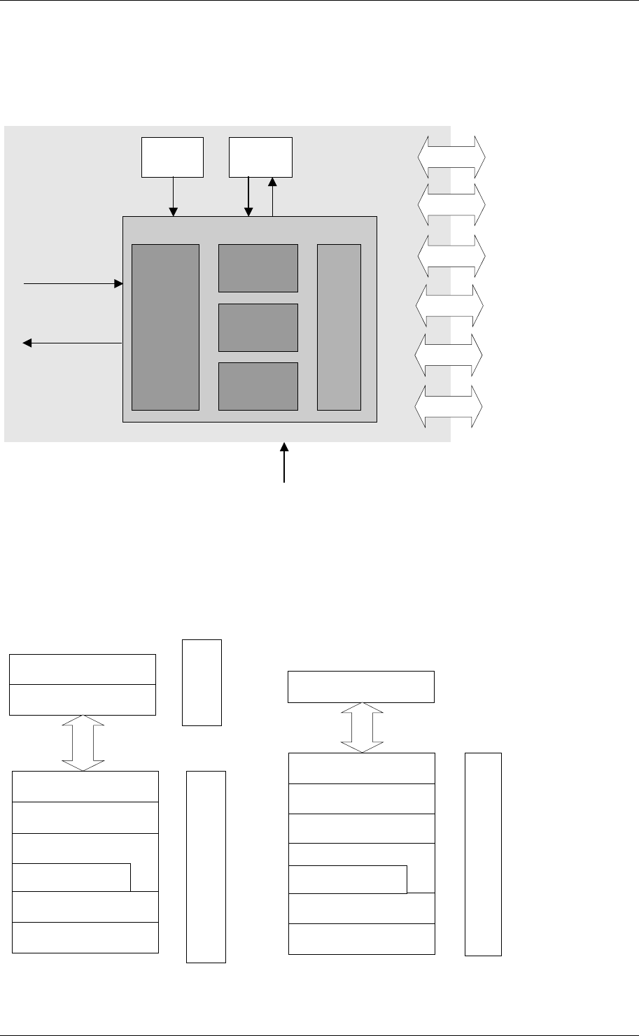
The PER1220 Module (see figure 1) is based on a Bluetooth Single Chip from Cambridge Silicon
Radio with a few external components. It has various interfaces to the target hardware / application:
UART, SPI, PCM, USB, PIO and AIO.
BlueCore
2.4 GHz
Bluetooth
Radio
RAM
Basisband
DSP
Mikro-
controller
I/O
RF in
RF out
PIO
PCM
SPI
UART
FlashXTAL
Vin = 3,3 V
USB
AIO
Figure 1: Overview PER1220
In standard configuration the PER1220 provides a complete Bluetooth protocol stack up to RFCOMM
layer (see figure 2). It is possible to upgrade the firmware and to run an on-chip-application. This gives
a true Bluetooth single chip solution (see also figure 2).
Bluetooth Baseband
BluetoothRadio
Link Manager
HCI (optional)
L2CAP
RFComm
Host Hardware (optional)
Application
Host Transport
Adoption Layer
Stack configuration
with On-Chip-Application
BT_MOD_RFC2
Default Stack configuration
Bluetooth Baseband
BluetoothRadio
Link Manager
HCI (optional)
L2CAP
RFComm
Adoption Layer
Application
Host Transport
BT_MOD_RFC2 Host Hardware
Figure 2: Firmware configurations

PER1220 Data Book Page 6/21
Copyright Prettl Elektronik Radeberg GmbH. All rights reserved.
2 Module Pinout Diagramm
1
2
3
4
5
6
7
8
9
10
11
12
13
14
15
16
17 18
19
20
21
22
23
24
25
26
27
28
29
30
31
32
33
34
1 34
PCM_OUT
PCM_SYNC
PCM_IN
PCM_CLK
USB_D+
USB_D-
PIO(7)
PIO(6)
PIO(5)
(TP +1V8)
+3V3
PIO(2)
PIO(1)
PIO(0)
GND
Antenna
GND
GND
GND
GND
UART_RX
UART_RTS
UART_TX
UART_CTS
SPI_MOSI
SPI_CLK
SPI_CSB
SPI_MISO
NC
AIO(1)
PIO(4)
AIO(0)
PIO(3)
NC
PER1220
Figure 3: BT_MOD_RFC2 Pinout Diagramm

PER1220 Data Book Page 7/21
Copyright
Prettl Elektronik Radeberg GmbH. All rights reserved.
3 Device Terminal Functions
Radio
and Power Supply
Pin Padtype Description
Antenna 16 Analogue, Z0 = 50 Ohm RF IO
Power Supply 33 3V3 Positive power supply for
PER1220
Testpoint Pin Padtype Description
Testpoint 32 +1V8 VREG Testpoint
PCM Interface Pin Padtype Description
PCM_Out 1 CMOS output, tristatable with weak
internal pull-down
Synchronous data output
PCM_IN 3 CMOS input, tristatable with weak
internal pull-down
Synchronous data input
PCM_SYNC 2 Bi-directional with weak internal pull-
down
Synchronous data SYNC
PCM_CLK 4 Bi-directional with weak internal pull-
down
Synchronous data clock
UART and USB Pin Padtype Description
UART_TX 29 CMOS output UART data output active high
UART_RX 31 CMOS input with weak internal pull-
down
UART data input active high
UART_RTS 30 CMOS output, tristatable with weak
internal pull-up
UART request to send active low
UART_CTS 28 CMOS input with internal weak pull-
down
UART clear to send active low
USB_D+
(4)
5 Bi-directional USB data plus
USB_D-
(4)
6 Bi-directional USB data minus
SPI Pin Padtype Description
SPI_CSB 25 CMOS input with weak internal pull-up Chip select for Serial Peripheral
Interface active low
SPI_CLK 26 CMOS input with weak internal pull-
down
Serial Peripheral Interface clock
SPI_MOSI 27 CMOS input with weak internal pull-
down
Serial Peripheral Interface input
SPI_MISO 24 CMOS output, tristatable with weak
internal pull-down
Serial Peripheral Interface ouput

PER1220 Data Book Page 8/21
Copyright
Prettl Elektronik Radeberg GmbH. All rights reserved.
PIO Port
(2)
Pin Padtype Description
PIO(0) 14 Bi-directional with programmable weak
internal pull-up/down
Programmable input/output line
PIO(1) 13 Bi-directional with programmable weak
internal pull-up/down
Programmable input/output line
PIO(2)/USB_PULL_UP (1) 12 Bi-directional with programmable weak
internal pull-up/down
PIO or USB pull-up (via 1.5kΩ
resistor to USB_D+)
PIO(3)/USB_WAKE_UP/R
AM_CSB (1) 11 Bi-directional with programmable weak
internal pull-up/down
PIO or output goes high to wake
up PC when in USB mode or
external RAM chip select
PIO(4)/USB_ON (1) 10 Bi-directional with programmable weak
internal pull-up/down
PIO or USB on (input senses
when VBUS is high, wake
BlueCore02)
PIO(5)USB_DETACH (1) 9 Bi-directional with programmable weak
internal pull-up/down
PIO line or chip detaches from
USB when this input is high
PIO(6)/CLK_REQ 8 Bi-directional with programmable weak
internal pull-up/down
PIO line or clock request output to
enable external clock for ecternal
clock line
PIO(7) 7 Bi-directional with programmable weak
internal pull-up/down
Programmable input/output line(1)
AIO(0) 21 Bi-directional with programmable weak
internal pull-up/down
Programmable input/output line (3)
AIO(1) 22 Bi-directional with programmable weak
internal pull-up/down
Programmable input/output line (3)
Notes:
(1)
USB functions can be software mapped to any PIO terminal
(2)
All PIO’s are configured as inputs with weak pull-downs at reset.
(3)
Unused AIO pins may be left unconnected
(4)
If unused USB_D+ and USB_D- should be connected to ground

PER1220 Data Book Page 9/21
Copyright
Prettl Elektronik Radeberg GmbH. All rights reserved.
4 Electrical Characteristics
Absolute Maximum Ratings
Rating Min Max
Storage Temperature -20 °C +70 °C
Supply Voltage +3V3
Recommended Operating Conditions
Operating Condition Min Max
Operating Temperature Range -20 °C + 70°C
Supply Voltage +3V3 3.0 V 3.6 V
Input/Output Terminal Characteristics
Digital Terminals Min Typ Max Unit
Input Voltage
-0,4 - +0.8 VVIL input logic level low (VDD=3.0 V)
(VDD=1.8 V) -0.4 - +0.4 V
VIH input logic level high 2.31 - 3.7 V
Output Voltage
VOL output logic level low, (Io=4.0mA), VDD =3.0 V - - 0.2 V
VOL output logic level low, (Io=4.0mA), VDD =1.8 V - - 0.4 V
VOH output logic level high, (Io=4.0mA), VDD =3.0 V 3.1 - - V
VOH output logic level high, (Io=4.0mA), VDD =3.0 V 2.9 - - V
Input and Tristate Current with:
Strong pull-up +100 -20 -10 µA
Strong pull-down +10 +20 +100 µA
Weak pull-up -5 -1 0 µA
Weak pull-down 0 +1 +5 µA
I/O pad leakage current -1 0 +1 µA
C Input Capacitance 2.5 - 10 pF

PER1220 Data Book Page 10/21
Copyright
Prettl Elektronik Radeberg GmbH. All rights reserved.
Input/Output Terminal Characteristics (Continued)
USB Terminals Min Typ Max Unit
Input threshold
VIL input logic level low - - 1.32 V
VIH input logic level high (VDD_PADS=3.46 V) (2) 2.31 - - V
Input leakage current
0 < V
IN
< 3.3 V
(1)
-1 - 1 µA
C
I
Input capacitance
2.5 - 10 pF
Output levels to correctly terminated USB Cable
VOL output logic level low 0 - 0.2 V
VOL output logic level high 2.8 - 3.3 V
Notes:
Current drawn into a pin is defined as positive; current supplied output of a pin is defined as negative.
(1)
Internal USB pull-up disabled.
(2)
3.46 V= 3.3 V + 5 %
Input/Output Terminal Characteristics (Continued)
Auxillary DAC, 8-Bit Resolution Min Typ Max Unit
Resolution - - 8 Bits
Average Output step size (1) 12.5 14.5 17.0 mV
Ouput Voltage monotonic(1)
Voltage Range (Io=0) 0 - VDD_PIO V
Current Rage -10 - +0.1 mA
Minimum output voltage (Io=100 µA) 0 - 0.2 V
Maximum output voltage (Io=10 mA) VDD_PIO-0.3 - VDD_PIO V
High Impedance Leakage Current -1 - +1 µA
Offset -220 - +120 mV
Integral non-linearity(1) -2 - +2 LSB
Starting time (50pF load) - - 10 µs
Setting time (50pF load) - - 5 µs
(1) Specified for an output voltage between 0.2 V and 1.6 V
PER1220 Data Book Page 11/21
Copyright
Prettl Elektronik Radeberg GmbH. All rights reserved.
Average Power Consumption
(1)
Temperature = +20 °C
Mode Min Average Max
(Peak)
Unit
Inquiry Scan
inquiry intervall = 1.28 s
inquiry window = 11.25 ms
0.065 1.3 29.1 mA
ACL link (Slave), no data transfer,
sniff intervall = 0.64 s
Sniff attempt = 2.5 ms
sniff timeout = 2.5 ms
park intervall = 1.28 s
0.065 0.342 23.2 mA
ACL link (Slave), data transfer 1.7 22.6 38.5 mA
Standby, no radio activity, UART
115.5 kbit/s, Slave
0.065 0.088 1.5 mA
Deep Sleep Leakage Current
(1)
Supply Voltage = 3.3 V Temperature = +20 °C
Mode Value Unit
Deep Sleep 65 µA
Notes:
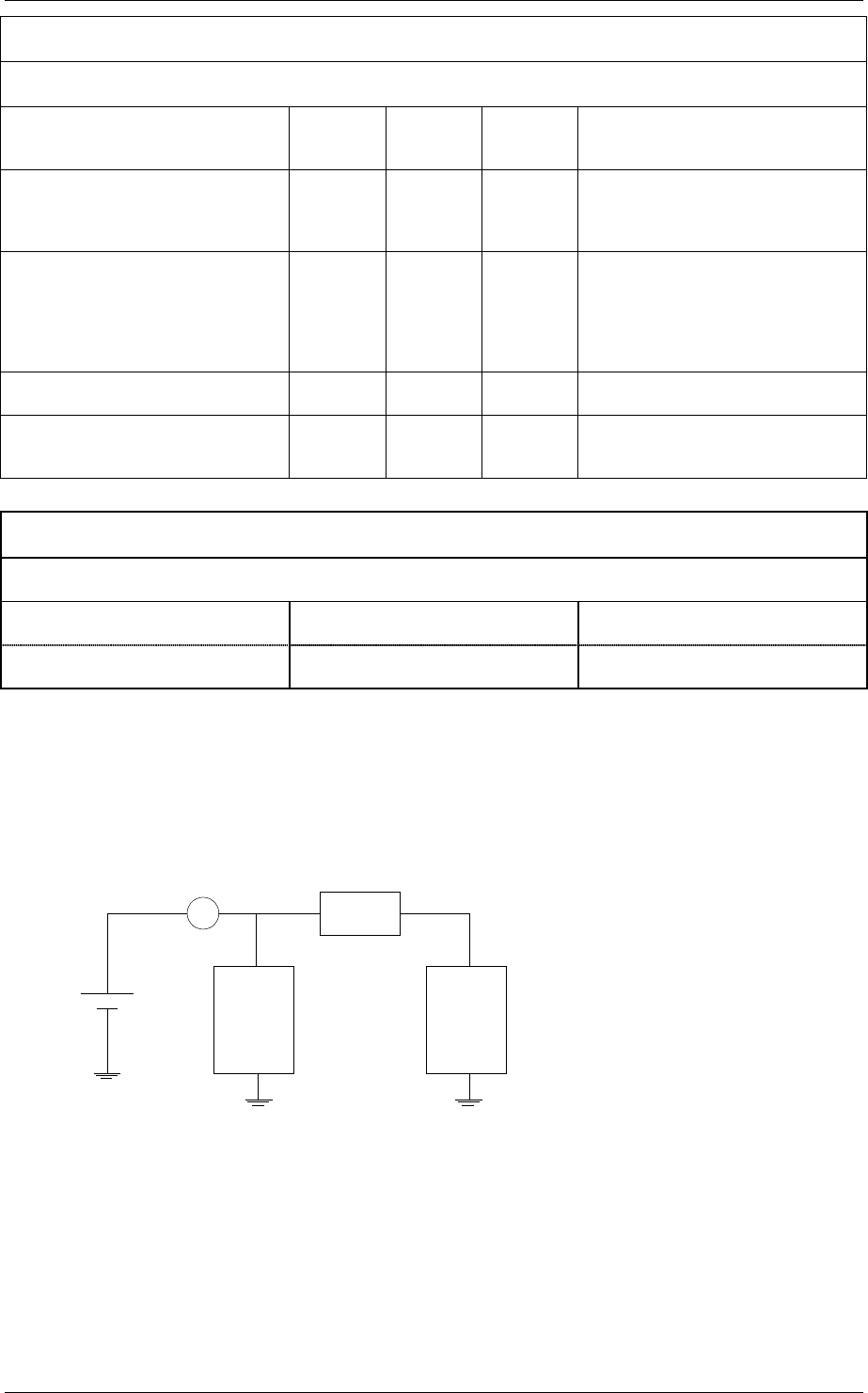
(1) Power Consumption is the sum of both Bluetooth Single Chip and flash (see figure 4)
These results are only correctly with firmware v16.4.4 and the on-chip application “Serial Port Profile”
Slave.
Flash
Bluetooth
Single
Chip
VREGA
3.3 V
1.8 V
Figure 4: Power Consumption Measurement Setup

PER1220 Data Book Page 12/21
Copyright
Prettl Elektronik Radeberg GmbH. All rights reserved.
5 Radio Characteristics
The PER1220 Bluetooth Module is qualified according to Bluetooth Specification V 1.2. So its radio
characteristics are equal or better as requested in the specification.
Please contact PRETTL support staff for more detailed information.
6 PER1220 Bluetooth Software Stack
PER1220 comes with a Bluetooth stack firmware running in the internal RISC microcontroller. This is
compliant to the Bluetooth Specification V1.2
The Bluetooth Module software architecture includes an on chip “Serial Port Profile” application. This
eliminates the need for host-side software and processing time. Therefore it is easy to implement the
PER1220 in a legacy application.
Bluetooth Baseband
BluetoothRadio
Link Manager
HCI (optional)
L2CAP
RFComm
Host Hardware (optional)
Application
Host Transport
Adoption Layer
Stack configuration
with On-Chip-Application
BT_MOD_RFC2
Figure 5: Stack configuration with On-Chip Application
This firmware requires no host processor. All software layers, including application software, run on
the internal RISC processor in a protected user software execution code environment.
6.1 Key Features
Interfaces to Host
•
RFCOMM, an RS-232 serial cable emulation protocol
•
SDP, a service database look-up protocol
Connectivity
•
Maximum number of active slaves: 3
•
Maximum number of simultaneous active ACL connections: 3
•
Maximum number of simultaneous active SCO connections: 3

PER1220 Data Book Page 13/21
Copyright
Prettl Elektronik Radeberg GmbH. All rights reserved.
•
Data Rate up to 380 kbit/s
Security
•
Full support for all Bluetooth security features up to and including strong (128-bit) encryption
Power Saving
•
Full support for all Bluetooth power saving modes (Park, Sniff and Hold)
•
System Power saving modes (Deep Sleep, Shallow Sleep)
Data Integrity
•
Channel Quality Driven Data Rate (CQDDR) increases the effective data rate in noisy
environments
•
Receiver Signal Strength Indicator (RSSI) used to minimise interference to other radio using ISM
band
PER1220 Data Book Page 14/21
Copyright
Prettl Elektronik Radeberg GmbH. All rights reserved.
7 Device Terminal Description
7.1 Antenna
- 2.4 GHz Antenna (Z
0
= 50 Ohm)
- Min. 100 MHz Bandwidth
- Temperature range: -20 °C to + 70 °C
- A ceramic antenna requires a copper free area in all PCB layers
- Antenna gain: 0 dBi (If your antenna uses another antenna gain, you must do your own FCC
approval)
This antenna gain is mandatory for the FCC limited modular approval. See Chapter 12 “Regulatory
Statements”.
7.2 UART Interface
PER1220 Universal Asynchronous Receiver Transmitter (UART) interface provides a simple
mechanism for communicating with other serial devices using the RS232 Standard
(1)
.
UART_TX
UART_RX
UART_RTS
UART_CTS
PER1220
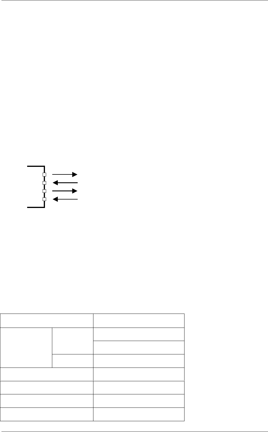
Figure 6: Universal Asynchronous Receiver Transmitter
Four signals are used to implement the UART Function as shown in figure 6. When PER1220 is
connected to another digital device UART_RX and UART_TX transfer data between the two devices.
The remaining two signals UART_CTS and UART_RTS can be used to implement RS232 hardware
flow control. Where both are active low indicators. All UART connections are implemented using
CMOS technology and have signalling levels of 0 V and 3.3 V.
UART configuration parameters, such baud rate and packet format, can optionally set
Note:
(1)
Uses RS232 Protocol, but voltage levels are 0 V to 3.3 V (requires external RS232 transceiver IC)
Parameter Possible Values
1200 Baud (<= 2% Error)Minimum
9600 Baud (<= 1% Error)
Baud Rate
Maximum 1.5 Mbaud (<= 1% Error)
Flow Control RTS/CTS or none
Parity None, odd, even
Stop Bit 1 or 2
Bits per channel 8

PER1220 Data Book Page 15/21
Copyright
Prettl Elektronik Radeberg GmbH. All rights reserved.
The UART interface is cabable of resetting the PER1220 upon reception of a break signal (see figure
8). A break is identified by a continuos logic low on the RX terminal, as shown in figure. If t
brk
is longer
than the value, defined as manufacture setting, a reset will occur.
t
brk
Figure 8: UART Break Signal
7.3 USB Interface
PER1220 contain a full speed (12 Mbit/s) USB interface, capable of driving a USB cable directly. No
external USB transceiver is required. The device operates as a USB peripheral, responding to
requests from a master host controller such a PC. Both the OHCI and the UHCI standards are
supported. The set of USB endpoints implemented behave as a specified in the USB section of the
Bluetooth Specification V1.2, part H2.
As USB is a master-slave oriented system, PER1220 only supports USB slave operation.
For more details, please contact PRETTL
®
Support.
7.4 Serial Peripheral Interface
PER1220 holds the firmware and the persistent store in a flash. It can be read/write by the SPI.
Normally, this will be done by PRETTL
®
. Ask for more details
7.5 PCM
Pulse Code Modulation (PCM) is the standard method used to digitise human voice patterns for
transmission over digital communication channels. Through it’s PCM interface, PER1220 has
hardware support for continual transmission and reception of PCM data, thus reducing processor
overhead for wireless headset applications. PER1220 offers a bi-directional digital audio interface that
routes directly into the Baseband layer to the on-chip firmware. It does not pass through the HCI
protocol layer.
Hardware on PER1220 allows the data to be sent and received from a SCO connection.
Up to three SCO connections can be supported by the PCM interface at any one time.
(1)
PER1220 can operate as the PCM interface Master generating an output clock of 128, 256 or 512
kHz. When configured as PCM interface slave it can operate with an input clock up to 2048 kHz.
PER1220 is compatible with a variety of clock formats, including Long Frame Sync, Short Frame Sync
and GCI timing environments.

PER1220 Data Book Page 16/21
Copyright
Prettl Elektronik Radeberg GmbH. All rights reserved.
It support 13- or 16-bit-linear, 8-bit-
µ
-law or A-law companded sample formats at 8 ksamples/s and
can receive and transmit on any selection of three of the first four slots following PCM_SYNC. The
PCM configuration options are enabled by setting a Persistent Store Key.
PER1220 interfaces directly to PCM devices includes the following:
•
Qualcomm MSM 3000 series and MSM 5000 series CDMA Baseband devices
•
OKI MSM7705 four channel A-law and
µ
-law CODEC
•
Motorola MC145481 8-bit-A-law and
µ
-law CODEC
•
Motorola MC145483 13-bit-A-law and
µ
-law CODEC
PER1220 is also compatible with Motorola SSi
TM
Interface
Ask for PER1220 that includes the Audio CODEC.
Note:
(1)
Subject to firmware support, contact PRETTL for details
7.6 PIO
The Parallel Input Output (PIO) Port is a general purpose I/O interface to PER1220. The port consists
of 8 programmable, bi-directional lines, PIO[7,0]
Programmable I/O lines can be accessed either via an embedded application running on PER1220 or
via private channel.

PER1220 Data Book Page 17/21
Copyright
Prettl Elektronik Radeberg GmbH. All rights reserved.
8 Typical Radio Performance
The PER1220 Bluetooth Module operates according to the Bluetooth Specification Version 1.2.
Please contact PRETTL support staff for more information.
9 Recommended Solder Profile
Detailed handling requirements for manufacturing: see IPC A 610 class 2.
Required soldering profile:
For any application the pre-qualified module PER1220 should be surface mounted to any kind of a
solid motherboard.
The pinout of the module is optimized for a standard FR4 pcb with NiAu plating.
Profile specification in case of manual soldering:
Nominal temperature: 340°C
Heat duration per pin: 6s (max)
solder: Sn 60 Pb 38 Cu Typ C 3,5%
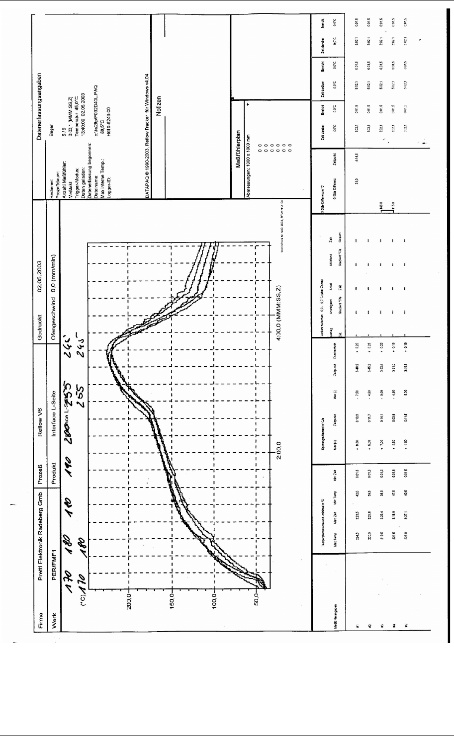
Profile specification in case of double reflow soldering:
The reflow process has to be compliant to our process specification
Reflow V6
(parameters
see below)
.
PER1220 Data Book Page 18/21
Copyright
Prettl Elektronik Radeberg GmbH. All rights reserved.
PER1220 Data Book Page 19/21
Copyright
Prettl Elektronik Radeberg GmbH. All rights reserved.
10 Installation
This guide describes the installation of the PER1220 in a target PCB. They are mandatory to be
conform to the FCC limited modular approval.
10.1 Antenna
-
The antenna must be mounted on a cupper area as you can see in figure 1
-
A 50 Ohm microstrip wire is used for connecting it to the PER1220
-
Antenna type: Phycomp 4313-115-00245 (Multilayer Ceramic Antenna)
Characteristics:
Description Value
Center frequency 2.45, 260 and 2,70 GHz
Bandwith 100 MHz
Gain 0 dBi max.
VSWR 2 max.
Polarization Linear
Azimuth beamwidth Omni-directional
Impedance 50 Ohm
Power dissipation 1 W
Operatin temperature -55 to + 125 °C
Terminations NiSn
Resistance to soldering heat 260 °C for 10s
Weight 0.16 g
Antenna
6 mm
6 mm
2 mm
copper free area
50 Ohm microstrip wire
Figure 1: Mounting the antenna on the PCB
10.2 Power Supply
PER1220 needs an external power supply:
-
stabilized 3.3 Volt DC (
±
10%)
-
max. current consumption 100 mA, peak: 120 mA
-
There are two different voltage rails inside the PER1220. One section of the module is directly
powered with 3.3 Volt input voltage. The other section is powered with 1.8 Volt. Therefore the
PER1220 includes a 1.8 V voltage regulator.

PER1220 Data Book Page 20/21
Copyright
Prettl Elektronik Radeberg GmbH. All rights reserved.
10.3 Interfaces
-
The PER1220 uses 3.3 Volt CMOS Logic.
10.4 FCC Conformance
-
The FCC conformance is achieved with these instructions.
-
The endproduct must be labeled with the following information.
-
FCC-ID
-
FCC Logo
- This label must be displayed outside of the end product.
11 Ordering and Contact Information
Order code: tbd
Prettl Elektronik Radeberg GmbH
Customer Support CST 2
Robert-Bosch-Strasse 10
D-01454 Radeberg
Germany
info.prettl-elektronik@prettl.com
www.prettl-elektronik.de

PER1220 Data Book Page 21/21
Copyright
Prettl Elektronik Radeberg GmbH. All rights reserved.
12 Regulatory Statements
The PER1220 Bluetooth module has to be implemented and used according to technical
description/specification provided by PRETTL
®
.
This Bluetooth module is intended to use in all States where the Bluetooth
TM
technology and the used
frequency band is released.
The PER1220 Bluetooth module is conform to the following specifications/standards:
Parts of:
•
FCC Part 15
•
EN 300 328-1
Bluetooth Qualification Test Report (foto einfügen):
12.1 FCC Statements
The PER1220 is certified according FCC Part 15. This is a limited modular approval. Therefore you
must comply with the following instructions. If not, you have to do your own FCC approval for your
endproduct.
The chapter “Installation” describes these instructions.
RF Exposure
This device and its antenna must not be co-located or operating in conjunction with any other antenna
or transmitter.
Label requirements
The modular transmitter is be labeled with its own FCC ID number, and, if the FCC ID is not visible
when the module is installed inside another device, then the outside of the device into which the
module is installed must also display a label referring to the enclosed module. This exterior label can
use wording such as the following: „Contains Transmitter Module FCC ID: TJXPER1220“ or „Contains
FCC ID: TJXPER1220.”
Statement according to FCC part 15.19
This device complies with Part 15 of the FCC Rules. Operation is subject to the following two
conditions: (1) this device may not cause harmful interference, and (2) this device must
accept any interference received, including interference that may cause undesired operation.
Statement according to FCC part 15.21
Modifications not expressly approved by this company could void the user's authority to operate the
equipment.

PER1220 Data Book Page 22/21
Copyright
Prettl Elektronik Radeberg GmbH. All rights reserved.
For a Class A digital device
This equipment has been tested and found to comply with the limits for a Class A digital device,
pursuant to part 15 of the FCC Rules. These limits are designed to provide reasonable protection
against harmful interference when the equipment is operated in a commercial environment. This
equipment generates, uses, and can radiate radio frequency energy and, if not installed and used in
accordance with the instruction manual, may cause harmful interference to radio communications.
Operation of this equipment in a residential area is likely to cause harmful interference in which case
the user will be required to correct the interference at his own expense.

PER1220 Data Book Page 23/21
Copyright
Prettl Elektronik Radeberg GmbH. All rights reserved.
13 Document References
•
Bluetooth Specification Version 1.2
•
Universal Serial Bus Specification Version 1.1 (September 1998)
14 Record of Changes
Date Version Reason for Change
2005-07-29 1.0 - first issue