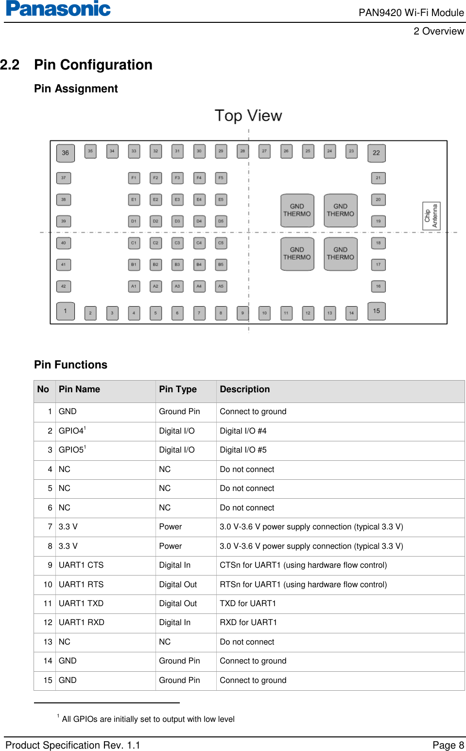
Panasonic Devices Europe 9420 WiFi Module User Manual T7V 9420 UserMan
Panasonic Industrial Devices Europe GmbH WiFi Module T7V 9420 UserMan
UserManual.wiki
>
Panasonic Devices Europe
>
9420 User Manual
T7V-9420_UserMan
Navigation menu
Upload a User Manual
Namespaces
Wiki Guide
HTML
PDF
Info
Views
User Manual
Discussion / Help
Navigation
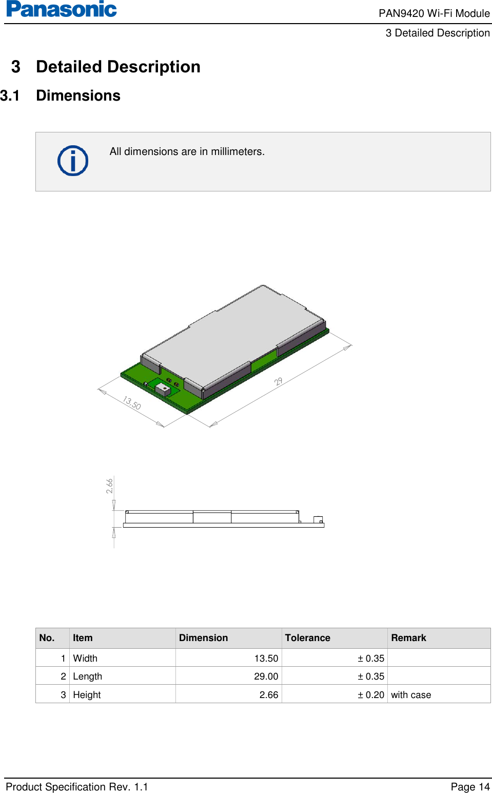
![ PAN9420 Wi-Fi Module 1 About This Document Product Specification Rev. 1.1 Page 5 1 About This Document 1.1 Purpose and Audience This Product Specification provides details on the functional, operational, and electrical characteristics of the Panasonic PAN9420 module. It is intended for hardware design, application, and OEM engineers. The product is referred to as “the PAN9420” or “the module” within this document. 1.2 Revision History Revision Date Modifications/Remarks 0.1 01.02.2017 1st preliminary version 0.2 31.05.2017 Improved layout 1.0 02.06.2017 Technical data corrected 1.1 19.06.2017 FCC/IC/RED information added 1.3 Use of Symbols Symbol Description Note Indicates important information for the proper use of the product. Non-observance can lead to errors. Attention Indicates important notes that, if not observed, can put the product’s functionality at risk. [chapter number] [chapter title] Cross reference Indicates cross references within the document. Example: Description of the symbols used in this document 1.3 Use of Symbols. 1.4 Related Documents Please refer to the Panasonic website for related documents 6.2.2 Product Information.](https://usermanual.wiki/Panasonic-Devices-Europe/9420/User-Guide-3489085-Page-5.png)
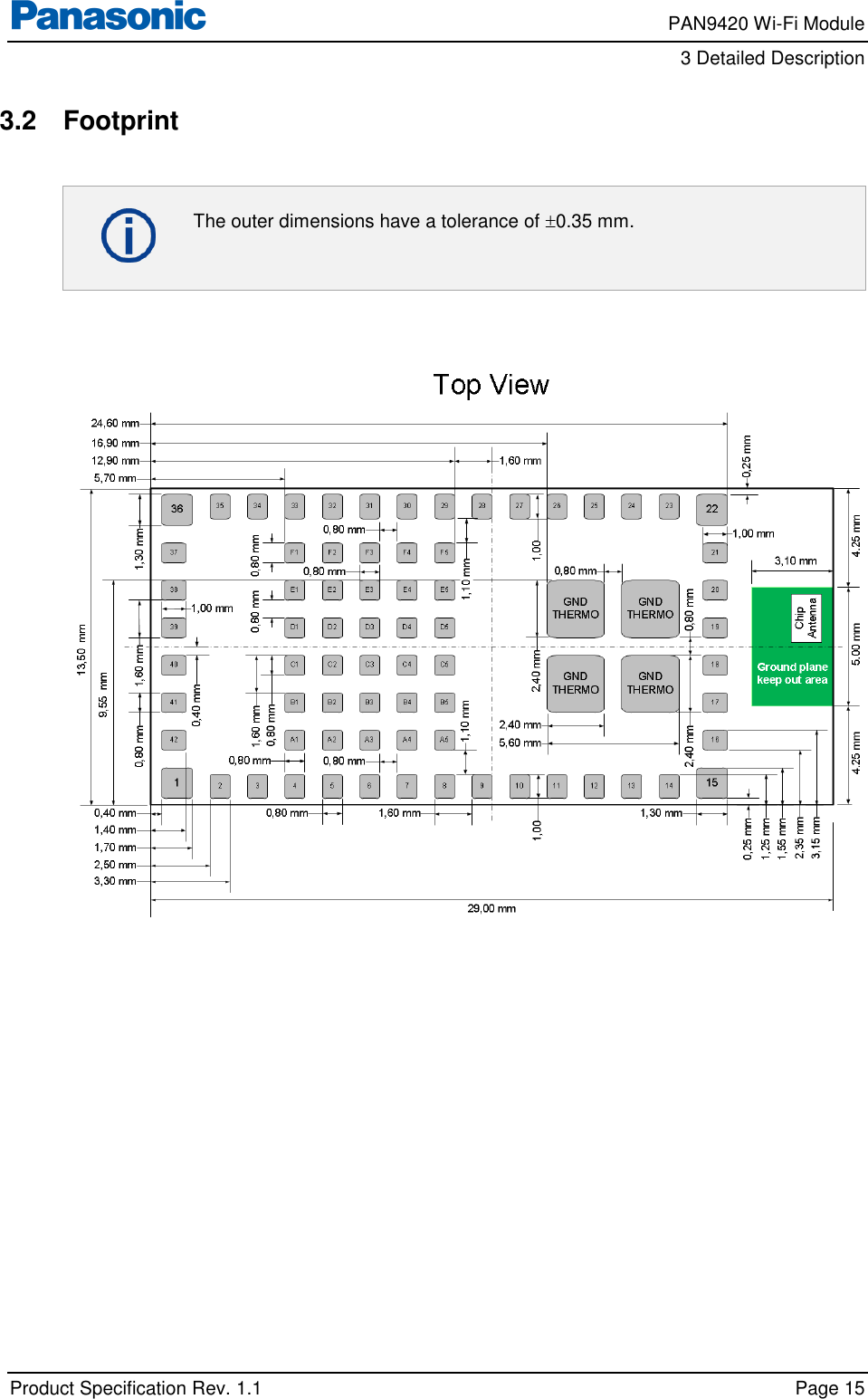
![ PAN9420 Wi-Fi Module 5 Cautions, Life Support Policy, RoHS Declaration, and Regulatory Information Product Specification Rev. 1.1 Page 43 5.4.3 European Conformity According to RED (2014/53/EU) All modules described in this product specification comply with the standards according to the following LVD (2014/35/EU), EMC-D (2014/30/EU) together with RED (2014/53/EU) articles: 3.1a Safety/Health: EN62368-1:2014 EN62311:2008 3.1b EMC: EN 301 489-1 V2.1.1:2017-02 EN 301 489-17 V3.1.1:2017-02 3.2 Radio: EN 300 328 V2.1.1:2016-11 As a result of the conformity assessment procedure described in 2014/53/EU Directive, the end customer equipment should be labelled as follows: The end customer has to assure that the device has a distance of more than 20 cm from the human body under all circumstances. The end customer equipment must meet the actual Safety/Health requirements according to RED. PAN9420 and its model versions in the specified reference design can be used in all countries of the European Economic Area (Member States of the EU, European Free Trade Association States[Iceland, Liechtenstein, Norway]), Monaco, San Marino, Andorra, and Turkey.](https://usermanual.wiki/Panasonic-Devices-Europe/9420/User-Guide-3489085-Page-43.png)