Panasonic KX F900 User Manual FAX MACHINE Manuals And Guides 97120075
PANASONIC Fax Machines Manual 97120075 PANASONIC Fax Machines Owner's Manual, PANASONIC Fax Machines installation guides
User Manual: Panasonic KX-F900 KX-F900 PANASONIC FAX MACHINE - Manuals and Guides View the owners manual for your PANASONIC FAX MACHINE #KXF900. Home:Computer & Office Equipment Parts:Panasonic Parts:Panasonic FAX MACHINE Manual
Open the PDF directly: View PDF ![]() .
.
Page Count: 230 [warning: Documents this large are best viewed by clicking the View PDF Link!]
OHUEHNO.KM[9610089C1
Service Manual
and Technical Guide
900MHz CORDLESS FAX
KX-F900
(for U.S.A.)
,_ WARNING
] his service inlormation is designed for experienced repair technicians only and _snot designed for use by the general public.
It does not contain warnings or cautions to advise non-technical individuals of potential dangers in attempting to service a product.
Products powered by electricity should be serviced or repaired only by experienced professional technicians.
Any attempt to service or repair the product or products dealt with in this service information by anyone else could result in serious
injury or death.
Panasonic I (_)1996 Kyushu Matsushita Electric Co., Ltd.All rights reserved. Unauthorized copying and distribution is a violation of law.
KX-F900
i
I...... j
When you mention the serial number, write down the 11 digits. The serial number may be found on the bottom of the unit.
TABLE OF CONTENTS
Page
INTRODUCTION
SAFETY PRECAUTIONS ....................................................................................................................................... 5
INSULATION RESISTANCE TEST ........................................................................................................................ 5
FOR SERVICE TECHNICIANS .............................................................................................................................. 5
BATTERY CAUTION .............................................................................................................................................. 6
AC CAUTION .......................................................................................................................................................... 6
STANDARD BATTERY LIFE .................................................................................................................................. 7
PERSONAL SAFETY PRECAUTIONS .................................................................................................................. 7
SPECIFICATIONS .................................................................................................................................................. 8
OPTIONAL ACCESSORIES .................................................................................................................................. 8
LOCATION OF CONTROLS .................................................................................................................................. 9
FEATURES ........................................................................................................................................................... 10
CONNECTION ...................................................................................................................................................... 11
INSTALLATION .............................................................................................................................................. 12, 13
COMPONENT LOCATIONS ................................................................................................................................. 14
MAINTENANCE ITEM .................................................................................................................................... 14, 15
CLEANING THE UNIT .......................................................................................................................................... 16
TROUBLESHOOTING GUIDE
TROUBLESHOOTING SUMMARY ...................................................................................................................... 18
USER RECEIVERABLE ERRORS ....................................................................................................................... 19
DETAIL OF TROUBLESHOOTING ................................................................................................................ 20~91
PROGRAMMING AND LISTS ........................................................................................................................ 92~97
TEST FUNCTIONS ......................................................................................................................................... 97, 98
ADJUSTMENT
TABLE OF TEST EQUIPMENTS AND TOOL ................................................................................................... 100
ADJUSTING THE FEEDER PRESURE ............................................................................................................. 101
CONFIRMATION OF SEPARATION SPRING ................................................................................................... 101
CCD ADJUSTMENTS ................................................................................................................................ 102-104
DOCUMENT READ START POSITION ADJUSTMENT ............................................................................ 104, 105
CORDLESS ADJUSTMENT ....................................................................................................................... 107-113
DISASSEMBLY INSTRUCTIONS
DISASSEMBLY INSTRUCTIONS .............................................................................................................. 115-125
HOW TO REPLACE FLAT PACKAGE IC .......................................................................................................... 126
-2-
KX-F900
GIR£;UII OPI:RA]IONS
CONNECTION DIAGRAM ................................................................................................................................ 128
GENERAL BLOCK DIAGRAM ................................................................................................................... 129, 130
CONTROL SECTION ................................................................................................................................. 131~136
FACSIMILE SECTION ................................................................................................................................ 137~145
MODEM SECTION ..................................................................................................................................... 146-152
EXPLANATION OF ANALOG SECTION BLOCK DIAGRAM .................................................................... 153, 154
NCU SECTION ........................................................................................................................................... 155, 156
ITS AND MONITOR SECTION ................................................................................................................... 157, 158
TAM INTERFACE SECTION ...................................................................................................................... 159-161
OPERATION PANEL .......................................................................................................................................... 162
LCD COG TYPE ................................................................................................................................................. 163
SWITCHING POWER SUPPLY SECTION ................................................................................................ 164-166
CORDLESS SECTION ............................................................................................................................... 167-183
PRINTED CIRCUIT BOARD (DIGITAL BOARD) ............................................................................................... 185, 186
SCHEMATIC DIAGRAM (DIGITAL CIRCUIT) ............................................................................................................ 187
SCHEMATIC DIAGRAM (ANALOG CIRCUIT) ........................................................................................................... 188
PRINTED CIRCUIT BOARD (ANALOG BOARD) .............................................................................................. 189, 190
SCHEMATIC DIAGRAM AND PRINTED CIRCUIT BOARD (CCD) ........................................................................... 191
PRINTED CIRCUIT BOARD (SWITCHING POWER SUPPLY ) ................................................................................ 192
SCHEMATIC DIAGRAM (SWITCHING POWER SUPPLY CIRCUIT) ....................................................................... 193
PRINTED CIRCUIT BOARD (OPERATION PANEL) ................................................................................................. 194
SCHEMATIC DIAGRAM (OPERATION PANEL CIRCUIT) ........................................................................................ 195
PRINTED CIRCUIT BOARD (CORDLESS BASE UNIT) ........................................................................................... 196
SCHEMATIC DIAGRAM (CORDLESS BASE UNIT) ................................................................................................. 197
PRINTED CIRCUIT BOARD (RF UNIT) ..................................................................................................................... 198
SCHEMATIC DIAGRAM (RF UNIT) ........................................................................................................................... 199
PRINTED CIRCUIT BOARD (PORTABLE HANDSET) .............................................................................................. 200
SCHEMATIC DIAGRAM (PORTABLE HANDSET) .................................................................................................... 201
SCHEMATIC DIAGRAM AND PRINTED CIRCUIT BOARD (CHARGE) ................................................................... 202
_ERMINAL GUIDE OF IC'S, TRANSISTORS AND DIOE)ES ............................................................................ 203, 2o4
205
TOOLS ......................................................................................................................................................................
CABINET, MECHANICAL AND ELECTRICAL PARTS LOCATION .................................................................. 206~211
212
ACCESSORIES AND PACKING MATERIALS ..........................................................................................................
REPLACEMENT PARTS LIST ........................................................................................... 213~230
-3-
KX-F900
INTRODUCTION
Hay_
Safety Precautions ............................................................................ 5
Insulation Resistance Test ........................................................................ 5
For Service Technicians ........................................................................... 5
Batten] Caution ......................................................................................... 6
AC Caution ............................................................................................... 6
Standard Battery Life ................................................................................ 7
Personal Safety Precautions ..................................................................... 7
Specifications ............................................................................................ 8
Optional Accessories ................................................................................ 8
Location of Controls .................................................................................. 9
Features .................................................................................................. 10
Connection .............................................................................................. 11
Installation ......................................................................................... 12, 13
Component Locations ............................................................................. 14
Maintenance Item ............................................................................. 14, 15
Cleaning the Unit .................................................................................... 16
4
KX-F900
SAFETY PRECAUTIONS
1. Before servicing, u_plugthe power cord to prevent an electric shock.
2. When replacing pads, use only the manufacturer's recommended components.
3. Check the condition of the power cord. Replace if wear or damage is evident.
4. After servicing, be sure to restore the lead dress, insulation barriers, insulation papers, _hields, etc.
5. Before returning the serviced equipment to the customer, be sure to perform the following insulation resistance
test to prevent the customer from being exposed to shock hazards.
n
z
-I
3o
0
CJ
c
0
-i
0
z
INSULATION RESISTANCE TEST
1. Unplug the power cord and short the two prongs of the plug with a jumper wire.
2. Turn on the power switch.
3. Measure the resistance value with an ohmmeter between the jumpered AC plug and each exposed metal cabinet part
(screwheads, control shafts, handle brackets, etc.).
"Note: Some exposed parts may be isolated from the chassis by design. These will read infinity.
4. If the measurement is outside the specified limits, there is a possibility of a shock hazard.
The equipment should be repaired and rechecked before it is returned to the customer.
Exposed --
metal
part Ohmmeter
Resistance = more than1M Q
(at DC 500 V)
FOR SERVICE TECHNICIANS
ICs and LSIs are vulnerable to static electricity.
When repairing, the following precautions will help prevent recurring malfunctions.
1) Cover the plastic parts boxes with aluminum foil.
2) Ground the soldering irons.
3) Use a conductive mat on the worktable.
4) Do not touch IC or LSI pins with bare fingers.
-5-
KX-F900
BATTERY CAUTION
CAUTION
Danger of explosion if battery is incorrectly replaced. Replace only with the same or equivalent type recommended by the
manufacture. Discard used batteries according to following caution:
Disposal of lithium batteries should be performed by permitted, professional disposal firms knowledgeable in state govern-
ment federal and local hazardous materials and hazardous waste transportation and disposal requirements.
Battery continues to have no transportation limitations as long as they are separated to prevent short circuits and packed
in strong packaging.
Commercial firms that dispose of any quantity of lithium cells should have a mechanism in place to account for their ulti-
mate disposition. This is a good practice for all types of commercial or industrial waste.
Recommend Type Number: CR2032 (BATT)
CR2032 (BATT) Manufactured by MATSUSHITA
Manufactured by SONY
AC CAUTION
For safety, before closing the lower cabinet, please make sure of the following precautions.
(_ The earth lead is fixed by the screw.
(_) The AC connector is connected properly.
(_) Wrap the AC lead around the core 3 times.
(BOTTOM VIEW)
AC Inlet
/I
Earth Lead
(Ferrite Core)
Earth Lead
O o
AC
Screw
AC Connector Earth
Lead

STANDARD BATTERY LIFE
If your Panason_c battery is fully charged;
While in use (,TALK) Up to about 4.5 hours
While not in use (Stand-By) Up to about 14 days
•Battery life may vary depending on usage conditions and ambient temperature.
•Clean the handset and the main unit charge contacts with adry soft cloth once a
month, or the battery may not charge properly.
• Once the battery is fully charged, you do not have to place the handset on the main unit until
the TALK/BATT LOW indicator flashes slowly.
• The battery cannot be overcharged.
KX-F900 -_
m
z
.-I
:;o
O
O
B
O
z
PERSONAL SAFETY PRECAUTIONS
Be careful not to let your hair, clothes fingers, accessories, etc., become caught in any moving sections of the unit.
These are driven by the carriage monitor, and the slow down gear, the paper feed roller, the pressure roller, the eject roller,
the spur, the pick-up roller, etc., which are driven by the paper feed motor. These separation roller and document feed roller
which are rotated by the document feed motor and a gear which makes the two rollers rotate.
Also, the spurs are metal and sharply pointed. Be careful not to touch them accidentally by hand.
Document rollers
roller gear
)aration roller gear
feedgear
KX-F900
SPECIFICATIONS
•Main unit
1. Applicable Lines:
2. Document Size:
3. Effective Scanning Width:
4. Printing Paper Size:
5. Effective Printing Width:
6. Transmission Time*:
7, Scanning Density:
8. Halftone Level:
9. Scanner Type:
10. Printer Type:
11, Data Compression System:
12. Modem Speed:
13. Operating Environment:
14. Dimensions (HXWX D):
15. Mass 0Neight):
16, Power Consumption:
17. Power Supply:
Public Switched Telephone Network
Max. 216 mm (8 1/2") in width
Max. 600 mm (23 %') in length
208 mm(8 3/18')
216 mm X max. 50 m (8 1/2"X164') roll
216 mm (81/2')
Approx.15 sec/page (Original mode)
Approx.30 sec/page (G3 Normal mode)
Horizontal : 8 pels/mm (203 pels/inch)
Vertical : 3.85 lines/mm (98 lines/inch) -Standard mode
7.7 lines/mm (196 lines/inch) -Fine/Halftone mode
15.4 lines/mm (392 lines/inch) -Superfine mode
64-level
CCD image sensor
Thermal printing
Modified Huffman (MH), Modified READ (MR)
9600/7200/4800/2400 bps; Automatic Fallback
5-35°C (41-95 °F), 45-80 % RH (Relative Humidity)
Approx. 118X366X265 mm (4 21/32"X13 %' X10 7/18')
Approx. 3.4 kg (7.5 lb.)
Standby: Approx. 5W /Transmission: Approx. 15W
Reception: Approx. 35W /Copy: Approx. 40W
Maximum: Approx. 100W
120V AC, 60Hz (This unit will not function at 50 Hz.)
This specifications is for
U.S.A. version only.
Refer to the simplified manual
(cover) for other areas.
•Handset
1. Operating Environment:
2. Dimensions (HX W× D):
3. Weight:
4. Power Supply:
5. Frequency:
6. Security Codes:
5-35°C (41-95 °F), 45-80 % RH (Relative Humidity)
Approx. 39X55X271 mm (1 17/32"X2 3/32'X10 11/16')
Approx. 200 g (0.4 lb.)
Ni-Cd battery (3.6 V, 600 mAh)
902-904 MHz, 926-928 MHz (30 channels)
1,000,000
*Transmission speed depends upon the contents of the pages, resolution, telephone line conditions and capability of
receiving unit. 15 second speed based upon CCITT No.1 Test Chart.
.Design and specifications are subject to change without notice.
OPTIONAL ACCESSORIES
Parts No. Description Comment
KX-A106 Standard Thermal Recording Paper 216 mm X 30 m (8 1/2"X98') roll,
with 25 mm (1") core
KX-A116 Standard Thermal Recording Paper 216 mm X 50 m (8 1/2"X164') roll,
with 25 mm (1") core
Super Thermal recording Paper 216 mm X30 m (8 1/2"X98') roll,
KX-A125 (Like plain paper) with 25 mm (1") core
8
Front view
LOCAl ION OF CON]-ROLS
uattery charger
(beneath the cover)
Spare battery
cover
-- Antenna
Document entrance
KX-F900 I
i
Z
.-I
0
O
C
0
.-I
0
Z
Paper stacker
-- Document feeder tray
Document guide(s)
Microphone
CHARGE Indicator
SPARE CHARGE Indicator Document exit
Front lid open button
Cont;rol panel
Dial keypad HELP Display panel RESOLUTION
DIRECTORY MENU Direct call stations LOWER
I ......... , III _1# _e"_ll RESOW1,ON..!I'_ 9 _0 ' - I
I (Z)(D(]DiI_ -__ _ °'1 I_--_--'=' I
I,.4-_@@,_L_____ _ t___
..-iv;__. __ _; \ \ ", j _ _T*,T,ooP_,r_ I
®( ))
Y-I ! t I -1
FLASH MUTE AUTO RECEIVE VOLUME |
STOP
TONE REDIAL/PAUSE SP-PHQNE LOCATOR/INTERCOM
IN USE indicator START/COPY/SET
-9-
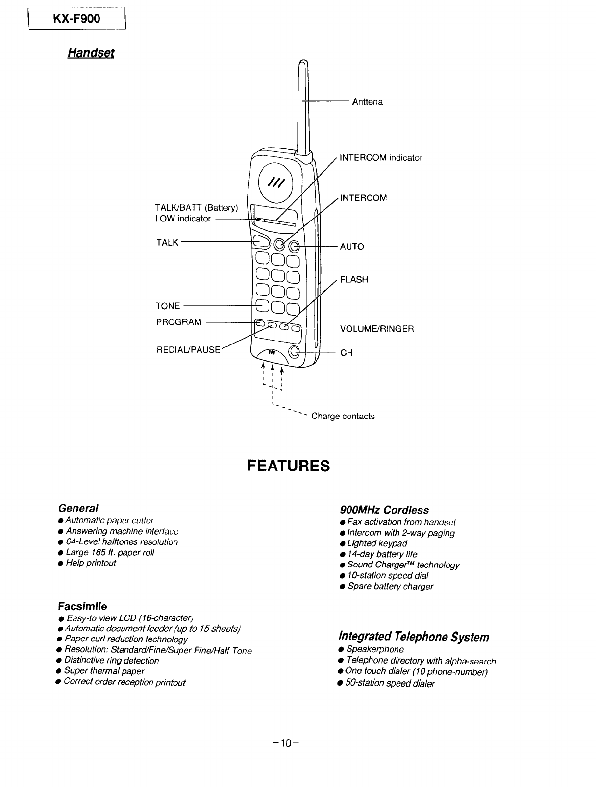
Handset
An_ena
INTERCOM indicator
TALK/BAT1 (Battery)
LOW indicator
TALK
TONE
PROGRAM
REDIAL/PAUSE _
FEATURES
General
•Automatic paper cutter
• Answering machine interface
• 64-Level halftones resolution
• Large 165 ft. paper roll
• Help printout
Facsimile
• Easy-to view LCD (16-character)
•Automatic document feeder (up to 15 sheets)
• Paper curl reduction technology
• Resolution: Standard/Fine/Super Fine/Half Tone
• Distinctive ring detection
• Super thermal paper
• Correct order reception printout
900MHz Cordless
• Fax activation from handset
• Intercom with 2-way paging
• Lighted keypad
• 14-day battery life
• Sound ChargeF _technology
• lO-station speed dial
• Spare battery charger
Integrated Telephone System
•Speakerphone
• Telephone directory with alpha-search
• One touch dialer (10 phone-number)
• 50-station speed dialer
-10-
KX-F900
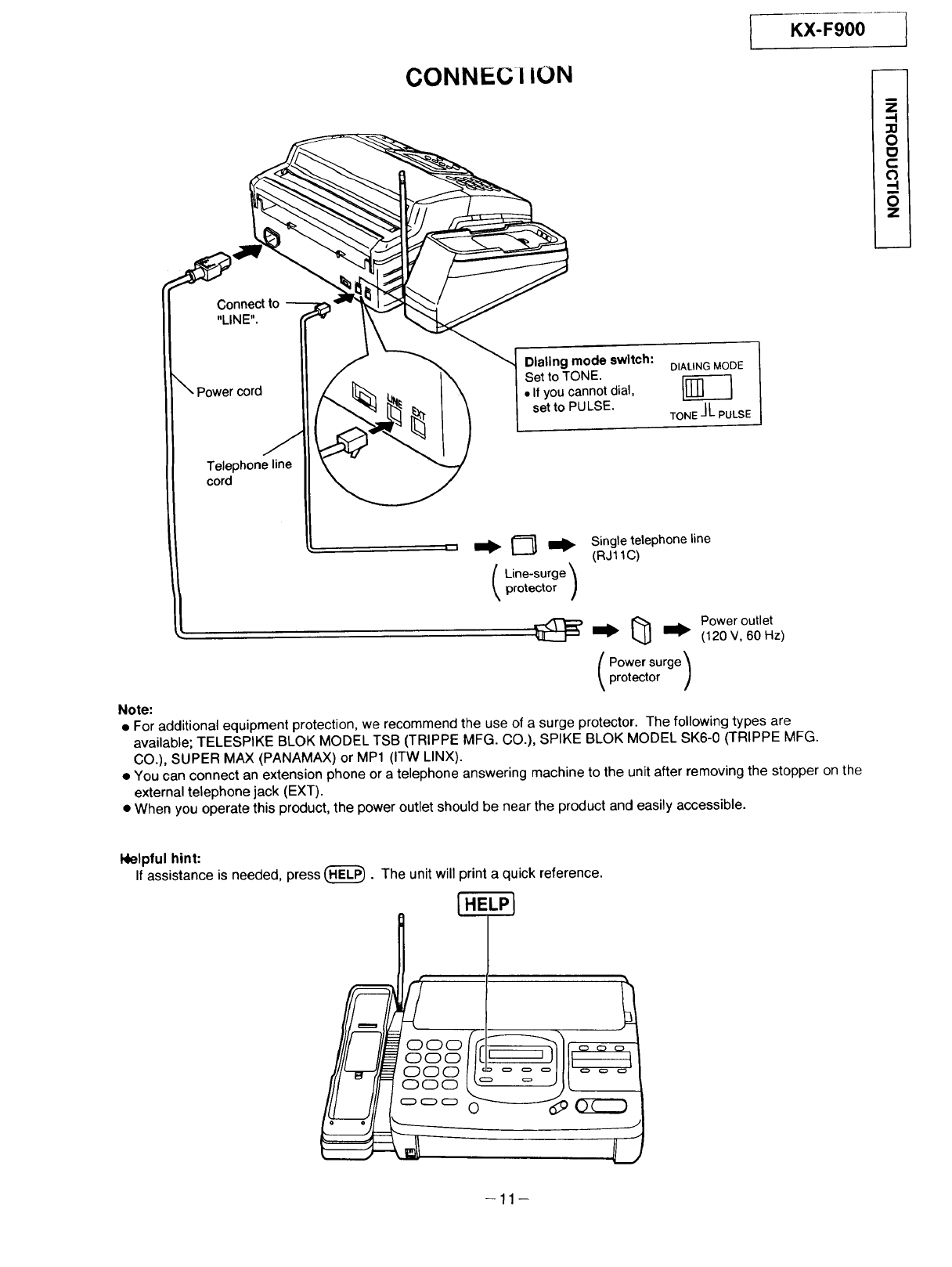
CONNEGIION
I
z
--I
30
O
c
m
O
z
Connect to
"LINE".
Dialing mode switch:
Set to TONE.
• If you cannot dial,
set to PULSE.
Telephone line
cord
DIALING MODE
TONE JLPULSE
Line-surge
protector )
Single telephone line
(RJ11 C)
Power outlet_ _ (120 V, 60 Hz)
Power surge_
protector )
Note:
• For additional equipment protection, we recommend the use of asurge protector. The following types are
available; TELESPIKE BLOK MODEL TSB (TRIPPE MFG. CO.), SPIKE BLOK MODEL SK6-0 (TRIPPE MFG.
CO.), SUPER MAX (PANAMAX) or MP1 (ITW LINX).
• You can connect an extension phone or a telephone answering machine to the unit after removing the stopper on the
external telephone jack (EXT).
•When you operate this product, the power outlet should be near the product and easily accessible.
NIelpful hint:
If assistance is needed, press _. The unit will print a quick reference.
l
-11 -
KX-F900 I
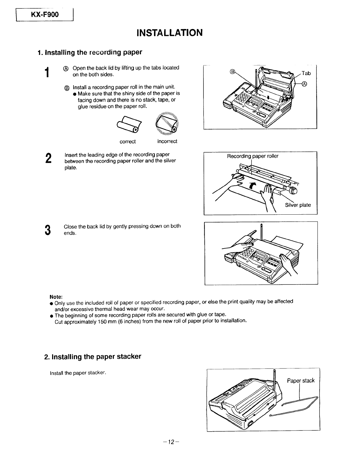
INSTALLATION
1. Installing the recording paper
(_) Open the back lid by lifting up the tabs located -
on the both sides, b
(_) Install a recording paper roll in the main unit.
• Make sure that the shiny side of the paper is
facing down and there is no stack, tape, or
glue residue on the paper roll.
,,,,..,....
correct incorrect
2Insert the leading edge of the recording paper
between the recording paper roller and the silver
plate.
Recording paper roller
plate
3Closethe backlid by gently pressing down on both
ends.
Note:
• Only use the included roll of paper or specified recording paper, or else the print quality may be affected
and/or excessive thermal head wear may occur.
•The beginning of some recording paper rollsare secured with glue or tape.
Cut approximately 150 mm (6 inches) from the new roll of paper prior to installation.
2. Installing the paper stacker
Install the paper stacker.
-12-
JKX-F900 1
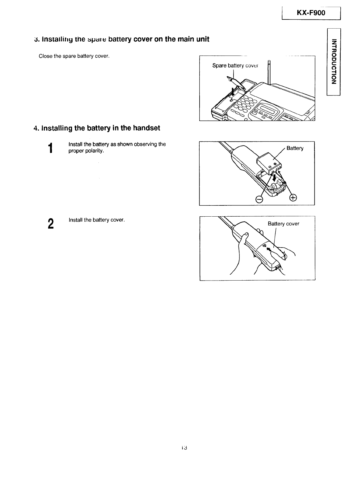
3. InslailirJg [ne _pa_u battery cover on the main unit
Close the spare battery cover.
Spare battery cover
I
Iu
z
-I
:o
0
c
0
-I
O
z
4. Installing the battery in the handset
1Install the battery as shown observing the
proper polarity. Battery
2Install the battery cover. Battery cover
i3
IKX'FgO0 I
COMPONENT LOCATIONS
Document ........
Feed Roller
Target Glass
Document --
Feed Roller
-- Separation Roller
Recording Paper Cover
Motor
_rmal Head
Recording Paper Roller
Cutter
Mirr
LED Array
Transmission Motor Reception Motor
MAINTENANCE ITEM
1. OUTLINE
MAINTENANCE AND REPAIRS ARE PERFORMED USING THE FOLLOWING STEPS.
1) Periodic maintenance
Inspect the equipment periodically and if necessary, clean any contaminated parts.
2) Check for breakdowns
Look for signs of trouble and consider how the problems arose.
If the equipment can still be used, perform copying, self-testing or communications testing.
3) Check equipment
Perform copying, self testing and communications testing to determine if the problem originates from the transmitter,
receiver or the telephone line.
4) Determine causes
Determine the causes of the equipment trouble by troubleshooting.
5) Equipment repairs
Repair or replace the defectiveparts andtake appropriate measures at thisstage to ensure thatthe problem doesnot recur.
6) Confirm normal operation of the equipment
After completing the repairs, conduct copying, self testing and communications testing to confirm that the equipment operates
normally.
7) Record keeping
Make a record of the measures taken to rectify the problem for future reference.
-14-
2-1. MAINTENANCE LIST
REMARKS
NO. OPERATION
1 Document Path
2Rollers
Recording Paper
3Roller
See page 16.
See page121.
4 Thermal Head See page 123.
5 LED Array See page 16.
6 Sensors See pages 77, 78.
CHECK ITEM
Remove any foreign matter such as scrap of paper.
If a roller is dirty, clean it with a damp cloth, then let dry thoroughly.
If the platen is dirty, clean it with a damp cloth, then let dry thoroughly.
Remove the paper before cleaning.
If the thermal head is dirty, clean the printing surface with a cloth
moistened with denatured alcohol (alcohol without water), then let dry
thoroughly.
If the LED array is dirty, clean the glass with a dry soft cloth.
Confirm the operation of the following sensors: recording paper sensor
(SW273), Document sensor (Pi302), Read position sensor (PI301),
Cover open sensor (SW271), and JAM sensor (SW272).
If the mirror and lens are dirty, clean them with a dry soft cloth.
Replace the part. Be sure that all part's screws are tight.
7Mirrors and Lens
8 Abnormal, wear and
tear or loose parts
m
z
30
0
D
c
0
0
z
2-2. MAINTENANCE CYCLE
Cleaning
No. Items Cycle Procedure
1 3 months See P. 16.
2
Separation Roller
(Ref. No. 58)
Separation Rubber
(Ref. No. 23)
Feed Roller
(Ref. No. 49, 53)
Target Glass
(Ref. No. 171)
Thermal Head
(Ref. No. 59)
Recording Paper Roller
(Ref. No. 112)
3 months
3 months
3 months
3 months
3 months
See P. 16.
See P. 16.
See P. 123.
See P. 121.
Replacement Remarks
Cycle Procedure
7 years See page 120.
(63,000 documents)
7 years
(63,000 documents)
7 years See page 120.
(63,000 documents)
7 years
(63,000 documents)
7 years See page 123.
(63,000 documents)
7 years See page 121.
(63,000 documents)
These values are only standard ones and may vary depending on
usage conditions.
--15--
KX-Fg00
CLEANING THE UNIT
Cleaning the inside of the unit
If misfeeding occurs frequently, or dirty patterns or black bands appear on a copied or transmitted document, clean
the document feeder rollers, sub roller, rubber flap, white plate and glass.
1
2
3
4
5
6
7
Disconnect the power cord and the telephone line
cord.
Open the front lid by pressing the front lid open
button.
Clean the document feeder rollers and roller with a
cloth moistened with isopropyl rubbing alcohol, and
let dry thoroughly.
Clean the rubber flap with a cotton swab moistened
with isopropyl rubbing alcohol, and let dry
thoroughly.
Clean the white plate and glass with a soft dry
cloth.
Clean the front lid by gently pressing down on both
ends.
Connect the power cord and the telephone line
cord.
White plate
Rubber fla
Sub Roller
\
Front lid open button
Document
feeder rollers
Caution:
•Do not use paper products (such as paper towels or
tissues) to clean the inside of the unit.
Cleaning the charge contacts
Clean the main unit and the handset charge contacts with a dry soft cloth once a month, or the battery may not
charge properly.
Charge contacts
Charge contacts
--16--
KX-F900
TROUBLESHOOTING GUIDE
Page
1. Troubleshooting Summary ..................................................................... 18
1-1. Troubleshooting ..................................................................... 18
1-2. Precautions ............................................................................ 18
2. User Recoverable Errors ....................................................................... 19
3. Detail of Troubleshooting ................................................................. 20~91
3-1. Outline .................................................................................... 20
3-2. Starting up troubleshooting ................................................... 20
3-3. Table of troubleshooting items .............................................. 21
3-4. Easy-check-list ....................................................................... 22
3-5. ADF section ...................................................................... 23-32
3-6. Communication section ................................................... 33-53
3-7. Digital board section ........................................................ 54-67
3-8. Analog board section ...................................................... 68-71
3-9. Power supply section ...................................................... 72-75
3-10. Operation board section ......................................................... 76
3-11. Sensor section ................................................................. 77, 78
3-12. Read section .................................................................... 79-83
3-13. Thermal head section ............................................................. 84
3-14. Cordless section .............................................................. 85~91
4. Programming and Lists .................................................................... 92-97
5. Test Functions ................................................................................. 97, 98
,-I
O
I-
Ill
,1-
O
O
,,-I
Z
Q
Ill
17-
IKX-F900
1. TROUBLESHOOTING SUMMARY
1-1. TROUBLESHOOTING
After having confirmed the abnormal condition by askingthe user, troubleshootaccording to th_ ,_L_U_;L_,,._In
Observe the following precautions whentroubleshooting.
1-2. PRECAUTIONS
1)If there is trouble with the print quality or the paper feed, first check that the installation space and the print
paper meets the specifications, that the paper selection lever/paper thickness lever is set correctly, and that the
paper is set correctly without any looseness.
2) Before troubleshooting, first check that the connectors and cables are connected correctly without any looseness.
Especially, if the abnormality occurs randomly, check very carefully.
3) When connecting the AC power cord with the unit case and checking the operation, exercise utmost care in
handling the electric parts in order to avoid electric shock and short-circuits.
4) After troubleshooting, double check that you have not forgotten any connectors, left any loose screws, etc.
5) And always test to verify that the unit is working normally.
18-
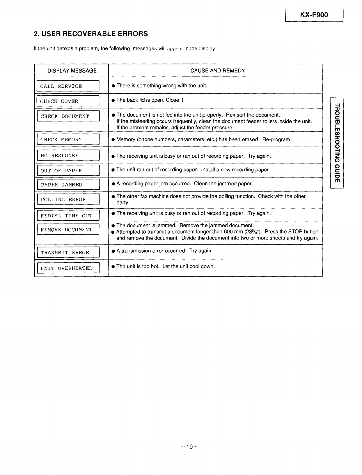
2. USER RECOVERABLE ERRORS
If the unit detects a problem, the following messages will app_af in the display.
KX-F900 I
DISPLAY MESSAGE
:ICALL SERvIcE I
I CHECK COVER I
CHECK DOCUMENT [
CHECK MEMORY
NO RESPONSE
OUT OF PAPER
PAPER JAMMED
POLLING ERROR
REDIAL TIME OUT
REMOVE DOCUMENT
TRANSMIT ERROR
UNIT OVERHEATED
J
I
I
I
l
I
I
I
CAUSE AND REMEDY
•There is something wrong with the unit.
• The back lid is open. Close it.
• The document is not fed into the unit properly. Reinsert the document.
If the misfeeding occurs frequently, clean the document feeder rollers inside the unit.
If the problem remains, adjust the feeder pressure,
•Memory (phone numbers, parameters, etc.) has been erased. Re-program.
• The receiving unit is busy or ran out of recording paper. Try again.
• The unit ran out of recording paper. Install a new recording paper.
• A recording paper jam occurred. Clean the jammed paper.
• The other fax machine does not provide the polling function. Check with the other
party.
• The receiving unit is busy or ran out of recording paper. Try again.
• The document is jammed. Remove the jammed document.
• Attempted to transmit a document longer than 600 mm (23%"). Press the STOP button
and remove the document. Divide the document into two or more sheets and try again.
• A transmission error occurred. Try again.
• The unit is too hot. Let the unit cool down.
-I
O
(=
Im
r-
I1"1
"r
O
O
.-.I
z
¢)
&')
c
Ill
-19-
iKX-F900
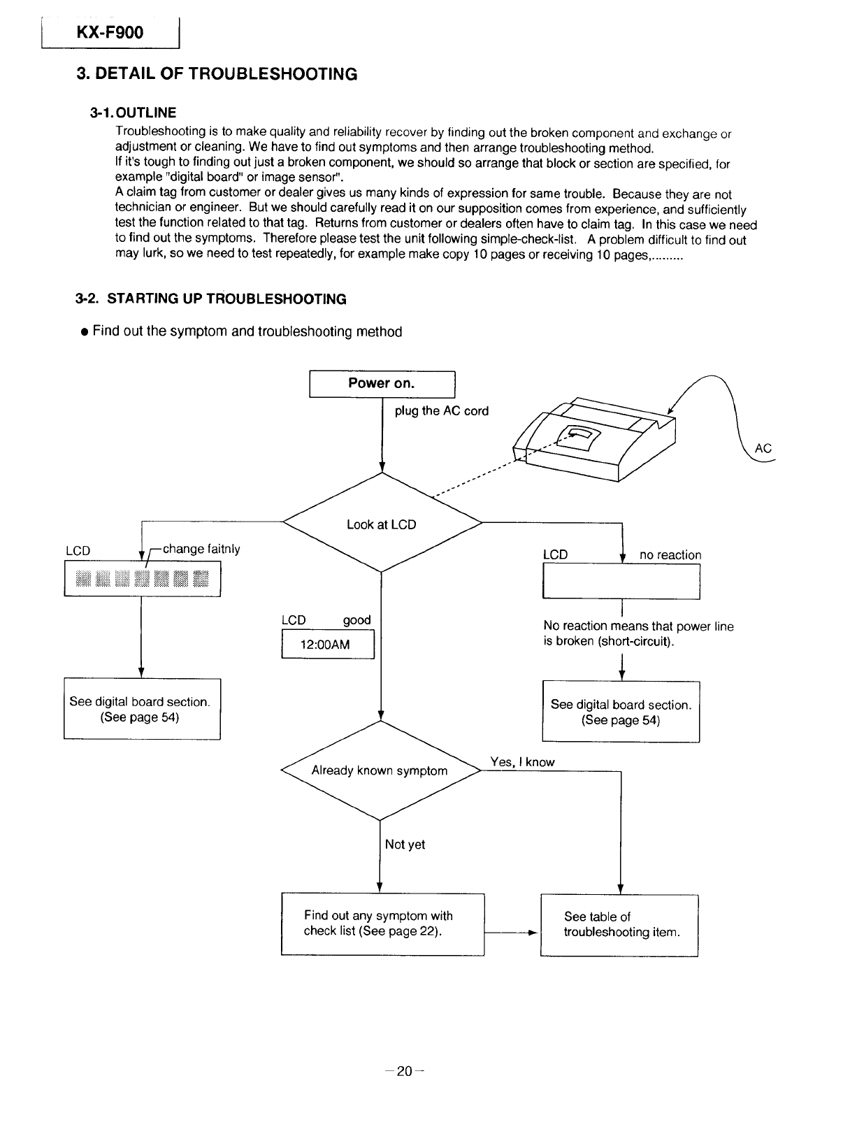
3. DETAIL OF TROUBLESHOOTING
3-1. OUTLINE
Troubleshooting is to make quality and reliability recover by finding out the broken component and exchange or
adjustment or cleaning. We have to find out symptoms and then arrange troubleshooting method.
If it's tough to finding out just a broken component, we should so arrange that block or section are specified, for
example "digital board" or image sensor".
A claim tag from customer or dealer gives us many kinds of expression for same trouble. Because they are not
technician or engineer. But we should carefully read it on our supposition comes from experience, and sufficiently
test the function related to that tag. Returns from customer or dealers often have to claim tag. In this case we need
to find out the symptoms. Therefore please test the unit following simple-check-list. A problem difficult to find out
may lurk, so we need to test repeatedly, for example make copy 10 pages or receiving 10 pages ..........
3-2. STARTING UP TROUBLESHOOTING
•Find out the symptom and troubleshooting method
Power on.
AC
LCD IFchange faitnly
See digital board section.
(See page 54)
LCD good
I 12:00AM I
LCD
II no reaction
No reaction means that power line
is broken (short-circuit).
See digital board section.
(See page 54)
Yes, I know
Not yet
r
Find out any symptom with
check list (See page 22).
4'
See table of
troubleshooting item.
20-
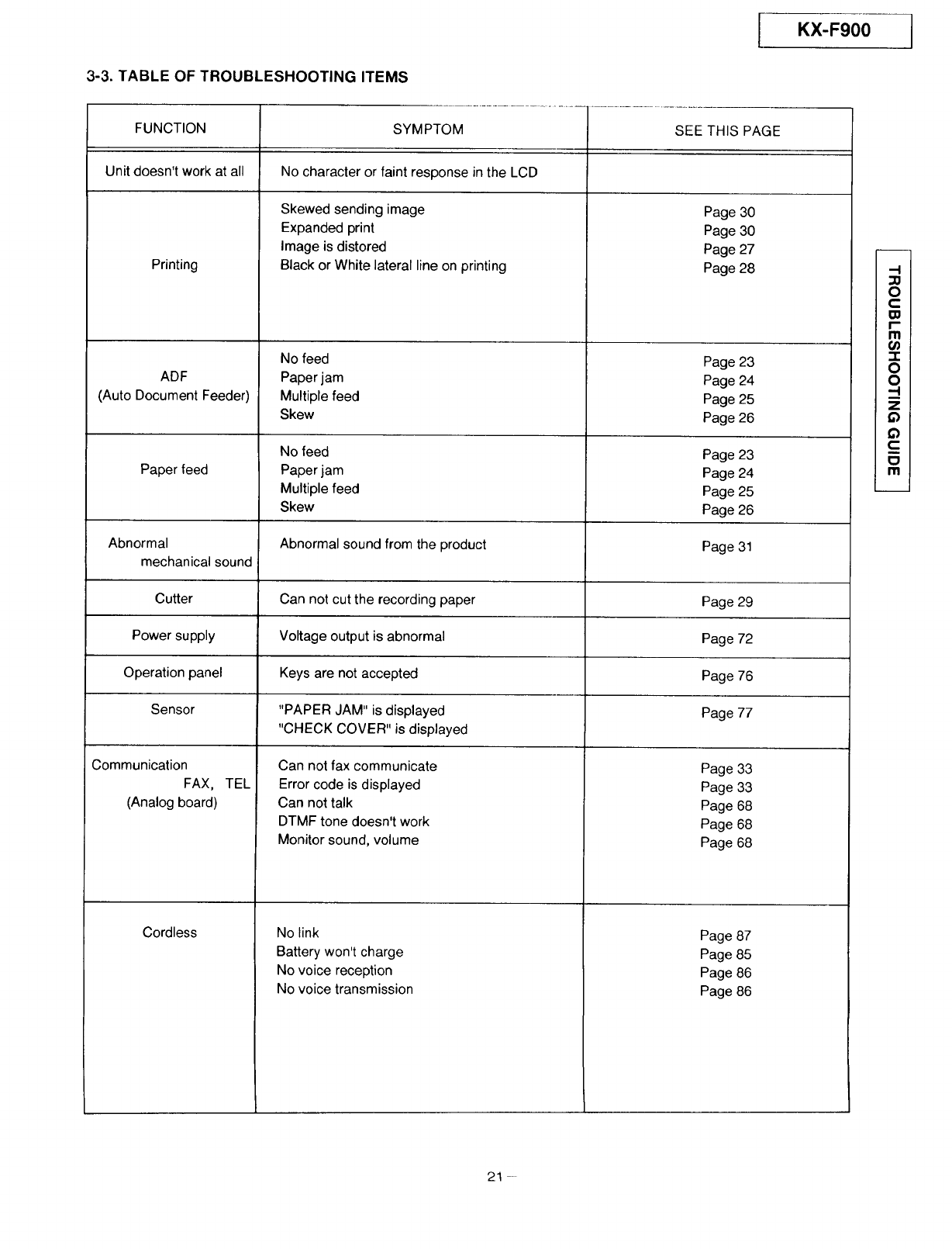
3-3. TABLE OF TROUBLESHOOTING ITEMS
IKX-F900 1
FUNCTION SYMPTOM SEE THIS PAGE
Unit doesn't work at all No character or faint response in the LCD
Printing
ADF
(Auto Document Feeder)
Paper feed
Skewed sending image
Expanded print
Image is distored
Black or White lateral line on printing
No feed
Paper jam
Multiple feed
Skew
No feed
Paper jam
Multiple feed
Skew
Page 30
Page 30
Page 27
Page 28
Page
Page
Page
Page
23
24
25
26
Can not cut the recording paper
Voltage output is abnormal
Keys are not accepted
"PAPER JAM" is displayed
"CHECK COVER" is displayed
Can not fax communicate
Error code is displayed
Can not talk
DTMF tone doesn't work
Monitor sound, volume
Page 23
Page 24
Page 25
Page 26
Abnormal Abnormal sound from the product Page 31
mechanical sound
Cutter Page 29
Power supply Page 72
Operation panel Page 76
Sensor Page 77
Communication
FAX, TEL
(Analog board)
No link
Battery won't charge
No voice reception
No voice transmission
Page 33
Page 33
Page 68
Page 68
Page 68
Page 87
Page 85
Page 86
Page 86
Cordless
-I
O
c
r-
Ill
"1-
O
O
-I
z
c
Ill
21
I....Kx-egoo
3-4. EASY-CHECK-LIST
FUNCTION
FAX operation transmission
receiving
Copy operation FINE mode
HALF TONE mode
Monitor sou nd
Telephone operation Ringer sound
Dial operation
Volume operation
REFERENCEJUDGEMENT
OK /NG
OK /NG
OK /NG
OK /NG
OK /NG
OK /NG
OK /NG
OK /NG
OK /NG
OK /NG
OK /NG
OK /NG
OK /NG
OK /NG
OK /NG
OK /NG
OK /NG
VOX detection SERVICE CODE 815
Key check SERVICE CODE 561
LED check SERVICE CODE 557
Operation panel LCD check SERVICE CODE 558
Sensor Sensor check SERVICE CODE 815
Clock
gain correctly?
External TAM Handset Transceiver/receiver compare to your watch.
Remote control
Cordless operation Portable handset Change to FAX receiving by dialing -)(-._
transmission/receiver (Refer to user mode #41 on page 52.)
Link OK J NG
Battery charge OK J NG
-22-
KX-F900 I
3-5. ADF (Auto document feed) SECTION
(1) No document feed
In document setting, confirm
that beep tone or not.
NO
I leaning of separation roller.
( page120 )
Does the separation roller
rotate?
YES
Check the separation spring
and. pad?
_ YES
Replace the separation
roller unit.
,YES
Replace the operation cover
unit.
To digital board
section. (page 54)
Check the separation
spring is distorting.
Check the sensor
lever movement.
,_ oK
Check the sensor
and digital board.
(pages 54 and 77)
OK _ END
__ Check the Motor and J
connector.
NO OK
OK
END
END
_ eplace the sen- ]
sor lever.
Replace the defec-tive parts.
_ OK? _ Replace the motor
and connector.
Check the gear.
_ Replace the gear.
YES
I Repair.
___ s the phase signal from
pins 73-77 of ICl out-
put?
NO _L
ls the solder at pins 73-
77 of IC1 OK?
I YES
l Replace IC7.
ls the voltage at emitter
of Q1 +24 V?
I YES
II Isthev°ltageatc°llect°r L--_ofQ1+24V?
No
J Is the voltage at pin 11 of J
IC7 less than 2V? [ N----O---
,_ YES
[ Replace Q1. _1
___ Check power supply
unit section. (page 72)
NO
YES
Replace IC7.
/, _ , I aeplaoe
/END II m°t°r I
OK? I
I
-I
3o
O
c:
El
r-
m
(/)
-r
O
O
-.I
m
z
¢)
¢)
c_
m
-23-
KX-FgO0 I
(2) Paper JAM
r
i
I
I
Check feed route. J
I
l
Cleaning the each rollers.
(pages 120 and 121 )
Check each sensors
movement.
Check each rollers
mount.
Check the white plate.
ING
Replacethe white plate.
Checks the paper jam lu_ markings up ubjeui.s stuck on the sheet.
Cleaning or replace of
defective parts.
OK ,END
OK ._ END
Confirms that the location tip of the read start
sensor flag works smoothly.
I
NO _! Repair or replace the
Isensor lever
IOK
_ END
I Check il the senso_
To Sensor section, reacts while the flag is
(page 77) moving.
Check the separation, feed and pinch rollers are
attached correctly.
NO
>Repair defective parts. -_ END
IOperation-] Wh.ite Plate
cover _ OK
Document
_-'_ NG
Operation Board Cover
Fig. A
-24-
KX-F900 I
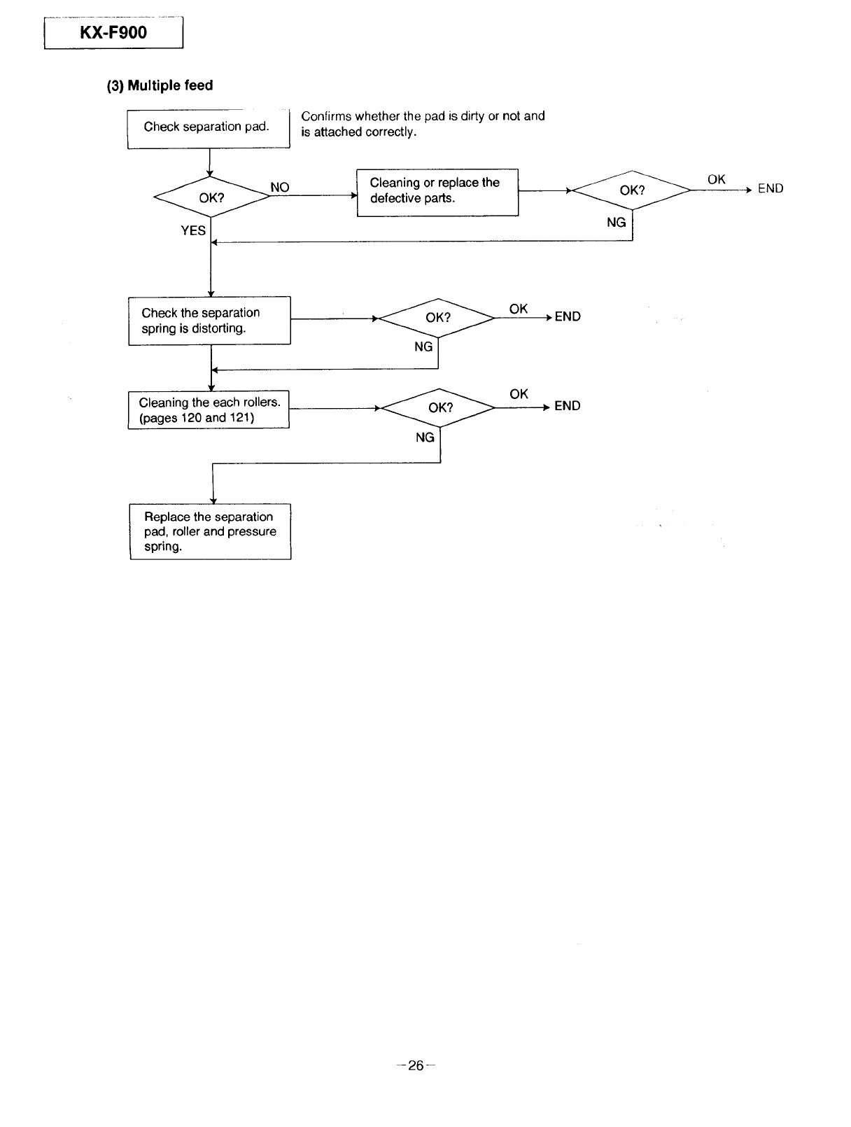
(3) Multiple feed
f
I
Check separation pad. Confirms whether the pad is dirty or not and
is attached correctly.
NO
Check the separation
spring is distorting.
Cleaning the each rollers.
(pages 120 and 121)
defective parts.
Cleaning or replace the
1
l eplace the separation
pad, roller and pressure
spring.
OK rEND
OK ._ END
OK . END
0
c
r-
Ill
-!-
0
0
-I
z
c
m
I'll
25--
(3) Multiple feed
l Check separation pad. [
NO
I heckthe separation [
spring is distorting.
1.
Cleaning the each rollers. I
(pages 120 and 121) I
Replace the separation |
/
pad, roller and pressure J
spring.
Confirms whether the pad is dirty or not and
is attached correctly.
Cleaning or replacethe I
_1 defective parts.
OK END
OK ,_ END
OK • END
-26-
KX-F900 1
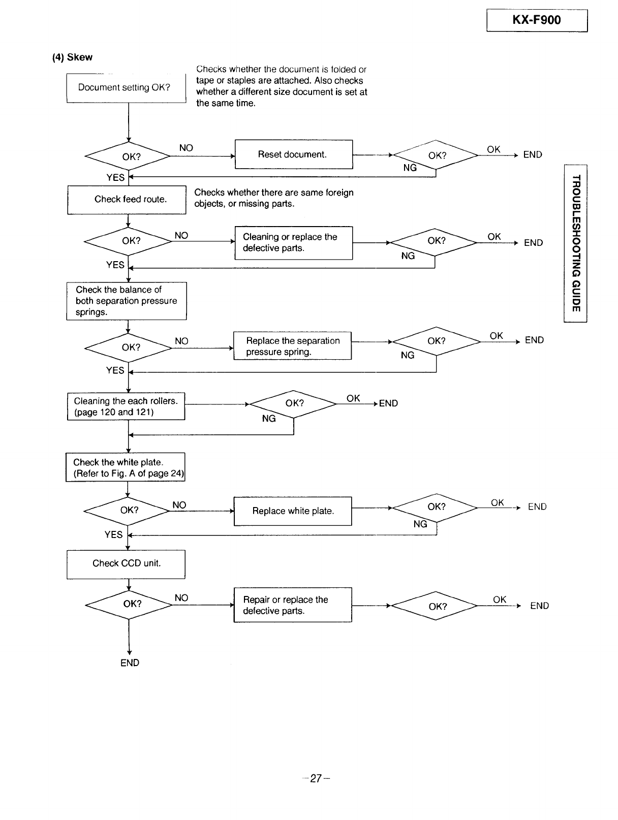
(4) Skew
Document setting OK?
Check feed route.
Checks whether the document is folded or
I ape or staples are attached. Also checks
whether a different size document is set at
the same time.
NO Reset document.
Checks whether there are same foreign
objects, or missing parts.
OK
NO
Check the balance of
both separation pressure
springs.
Cleaning the each rollers.
(page 120 and 121)
1'
Check the white plate.
(Refer to Fig. A of page 24)
Cleaning or replace the
defective parts.
I Replacethe separation ]
pressure spring. I
OK >END
OK
OK
J
1Replace white plate. ING-'_
END
END
END
END
Check CCD unit.
END
NO
Jepair or replace the
defective parts. IOK END
-.I
O
C
F
m
-r
O
O
.-I
z
Q
¢}
t-
Ill
27
f.....KX:-F'O0.......I
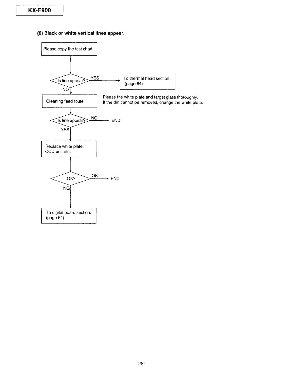
(6) Black or white vertical lines appear.
IPlease copy the test chart.
NO_ YES
Cleaning feed route.
Replace white plate,
CCD unit etc.
NO
To thermal head section.
(page 84)
Please the white plate and target glass thoroughly.
If the dirt cannot be removed, change the white plate.
-_ END
To digital board section.
(page 54)
OK END
28
KX-F900
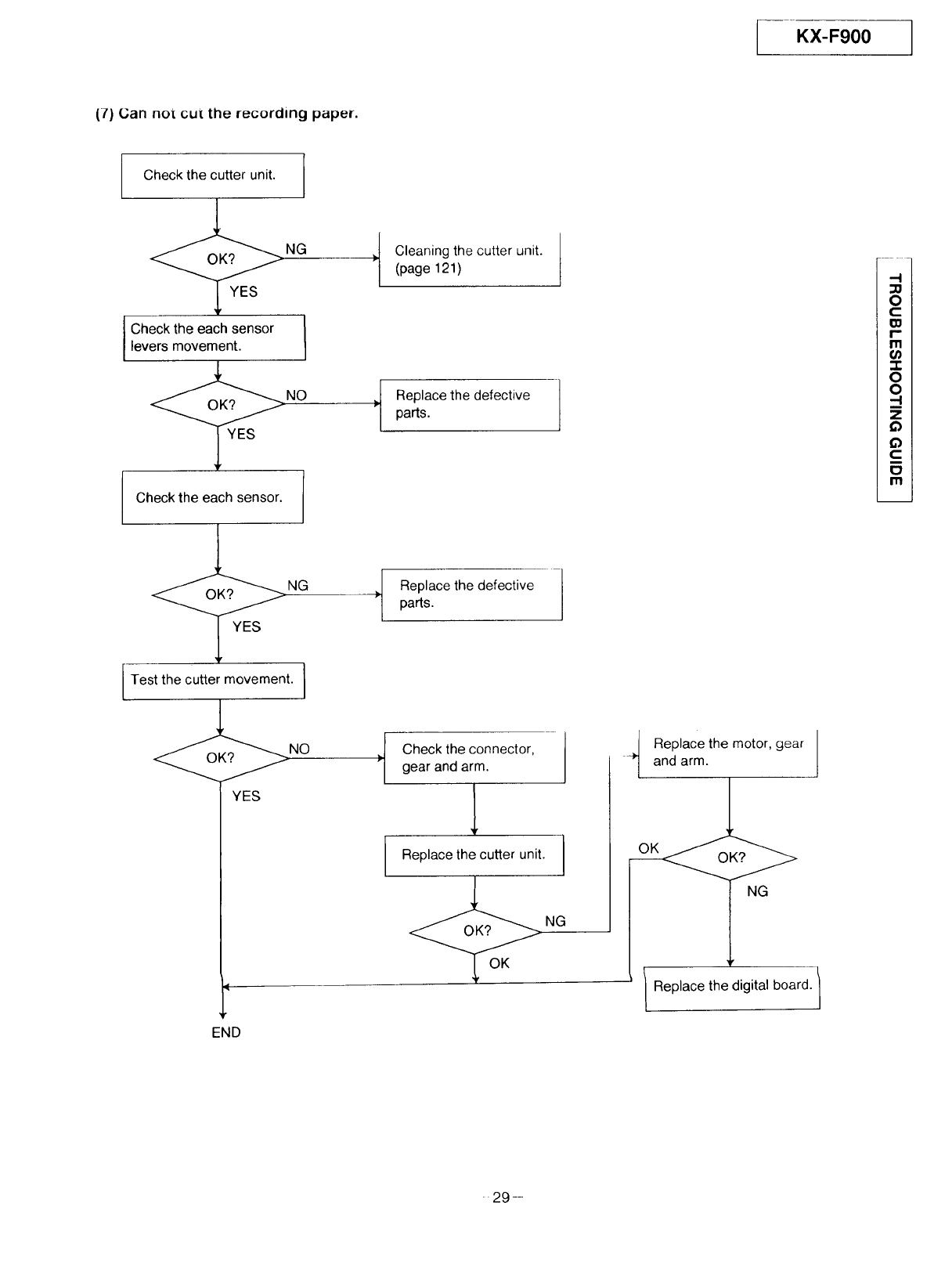
(7) (.;an noi cu[ the recording paper.
Check the cutter unit. I
I
Check the each sensor
levers movement.
Check the each sensor.
NG
Test the cutter movement. I
YES
Cleaning the cutter unit.
(page 121)
Replace the defective
parts.
I
Replace the defective [
parts. I
]p
I
Check the connector, ]
gear and arm. I
1
Replace the cutter unit.
END
Replace the motor, gear
and arm.
OK
Replace the digital board. /
-I
0
c
r
rn
-I-
0
0
n
z
ffJ
c
i
m
29-
i ,x:FoooI
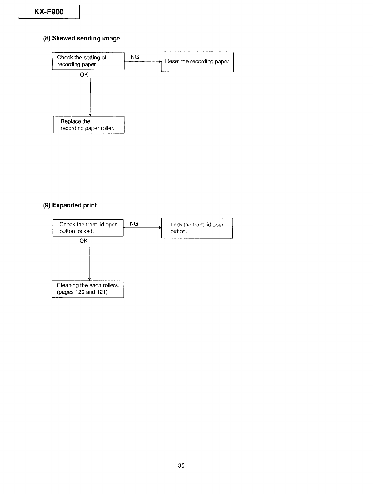
(8) Skewed sending image
Check the setting of
recording paper
OK
NG Reset the recording paper.
_v
I Replace the ]
recording paper roller.
(9) Expanded print
Check the front lid open NG
button locked.
OK
l leaning the each rollers, j(pages 120 and 121)
Lock the front lid open
button.
30--
IKX-F900
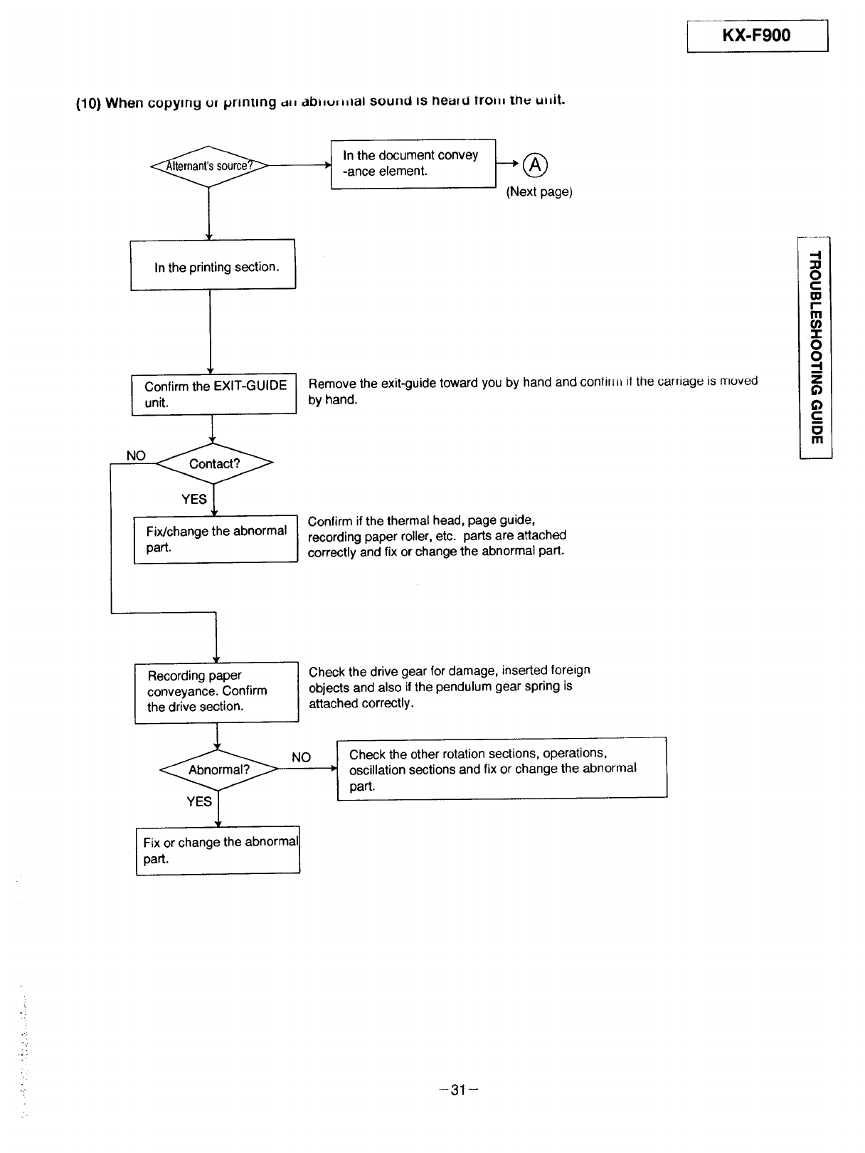
(10) When copying u_ printing _,=,abi,u_=ilal sound IS heuld lroll= inu uldt.
In the printing section.
Confirm the EXIT-GUIDE
unit.
I ix/changethe abnormal
part.
In the document convey
-ance element.
(Next page)
Remove the exit-guide toward you by hand and conlim_ it the carriage is moved
by hand.
Confirm if the thermal head, page guide,
recording paper roller, etc. parts are attached
correctly and fix or change the abnormal part.
-.I
=0
O
C
O0
I-
I1'1
-t-
O
O
,-4
z
¢)
Q
c:
m
1
Recording paper
conveyance. Confirm
the drive section.
Check the drive gear for damage, inserted foreign
objects and also if the pendulum gear spring is
attached correctly.
IFix or change the abnormal
part.
NO Check the other rotation sections, operations,
oscillation sections and fix or change the abnormal
part.
31
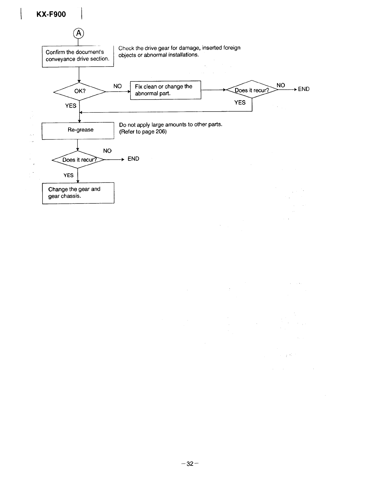
KX-F900 I
Confirm the document's
conveyance drive section.
Re-grease
Check the drive gear for damage, inserted foreign
objects or abnormal instatlations.
NO Fix clean or change the
; abnormal part.
Do not apply large amounts to other parts.
(Refer to page 206)
END
Change the gear and
gear chassis.
-32-
KX-F900
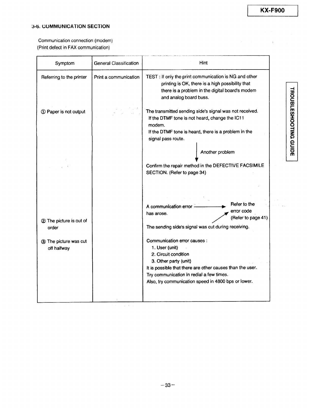
3-b. L;L)MMUNICATION SECTION
Communication connection (modem)
(Print defect in FAX communication)
Symptom
Referring to the printer
(_ Paper is not output
Hint
(_)The picture is out of
order
(_ The picture was cut
off halfway
General Classification
Print a communication TEST : If only the print communication is NG and other
printing is OK, there is a high possibility that
there is a problem in the digital board's modem
and analog board buss.
The transmitted sending side's signal was not received.
If the DTMF tone is not heard, change the IC11
modem.
If the DTMF tone is heard, there is aproblem in the
signal pass route.
Another problem
Ir
Confirm the repair method in the DEFECTIVE FACSIMILE
SECTION. (Refer to page 34)
Acommunicationerror Refer to the
has arose. _ error code
/" (Refer to page 41
The sending side's signal was cut during receiving.
Communication error causes :
1. User (unit)
2. Circuit condition
3. Other party (unit)
It is possible that there are other causes than the user.
Try communication in redial a few times.
Also, try communication speed in 4800 bps or lower.
-I
3o
O
c
Izl
i,,,=
m
-t-
O
O
-I
m
Z¢)
¢)
C
O
Ill
-33-
l KX-F900
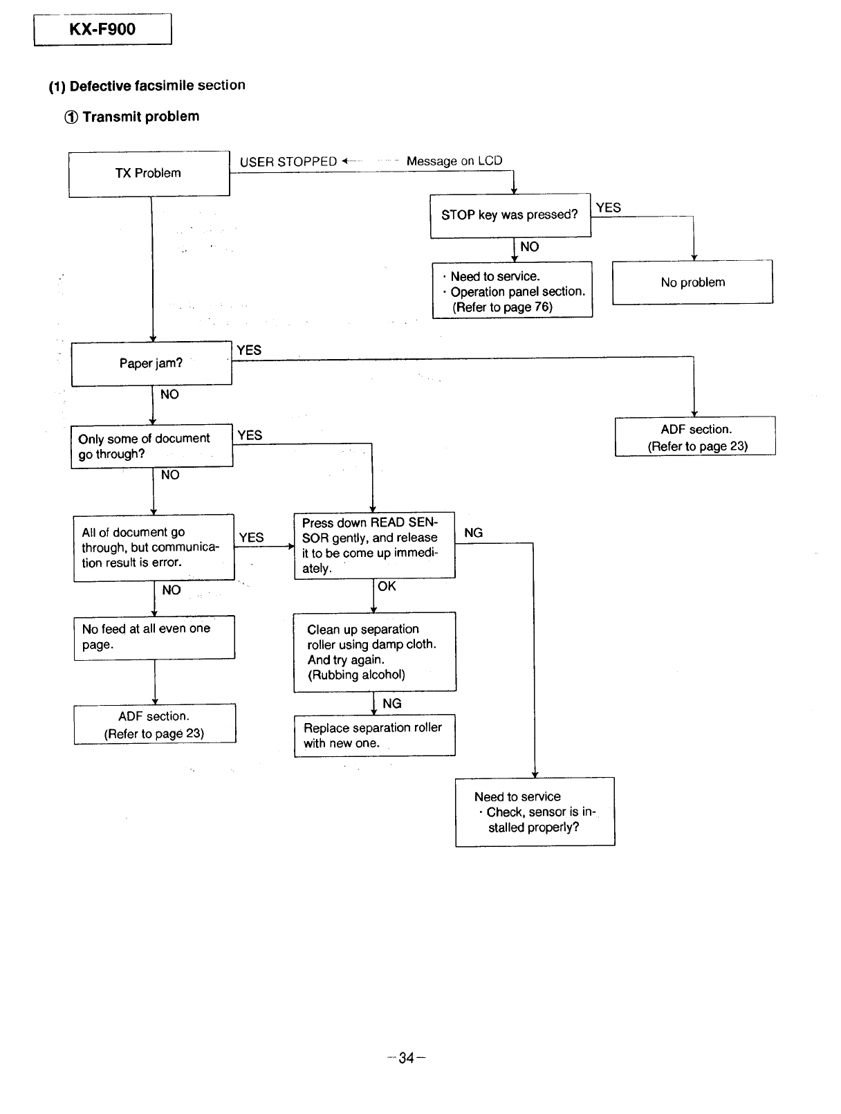
(1) Defective facsimile section
(_) Transmit problem
TX Problem
Paper jam?
1"°
Only some of document
go through?
All of document go
through, but communica-
tion result is error.
I NO
I o feed at all even one
page.
ADF section.
(Refer to page 23)
tUSER STOPPED * Message on LCD
STOP key was pressed?
JNO
•Need to service.
• Operation panel section.
(Refer to page 76)
1
No problem
I YES
YES ADF section.
(Refer to page 23)
YES
1
Press down READ SEN-
SOR gently, and release
it to be come up immedi-
ately.
Clean up separation
roller using damp cloth.
And try again.
(Rubbing alcohol)
J NG
Replace separation roller
/
with new one. J
NG
Need to service
•Check, sensor is in-
stalled properly?
-34 ¸-
IKX-F900
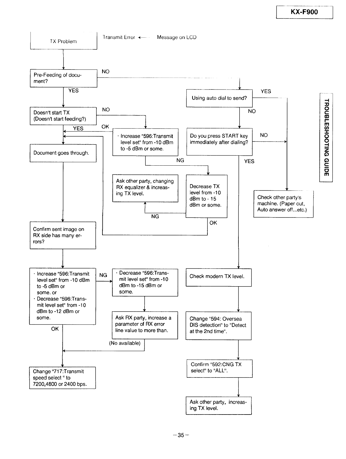
TX Problem ] ransmit Error _ Message on LCD
Pre-Feeding of docu-
ment?
I YES
Doesn't start TX
(Doesn't start feeding?)
_ YES
Document goes through.
Confirm sent image on
RX side has many er-
rors?
I
NO
OK l
• Increase "596:Transmit
level set" from -10 dBm
to -5 dBm or some.
L
Ask other party, changing
RX equalizer & increas-
ing TX level•
NG
NG
Using auto dial to send?
i
Do you press START key
immediately after dialing?
Decrease TX
level from -10
dBm to - 15
dBm or some.
J OK
l
• Increase "596:Transmit
level set" from -10 dBm
to -5 dBm or
some• or
• Decrease "596:Trans-
mit level set" from -10
dBm to -12 dBm or
some.
OK
NG • Decrease "596:Trans-
mit level set" from -10
dBm to -15 dBm or
some•
IAsk RX party, increase a
parameter of RX error
line value to more than.
(No available) ]
Change "717:Transmit
speed select" to
7200,4800 or 2400 bps.
Check modern TX level.
Change "594: Oversea
DIS detection" to "Detect
at the 2nd time".
I onfirm "592:CNG TX
select" to "ALL". 1
Ask other party, increas-
ing TX level.
t
NO
YES
I
I
YES
NO
Check other party's
machine• (Paper out,
Auto answer off...etc.)
.-I
O
C
r"-
m
(t}
O
O
.-I
u
z
Q
Q
c
Ill
-35-
I......Kx_,.oo--]
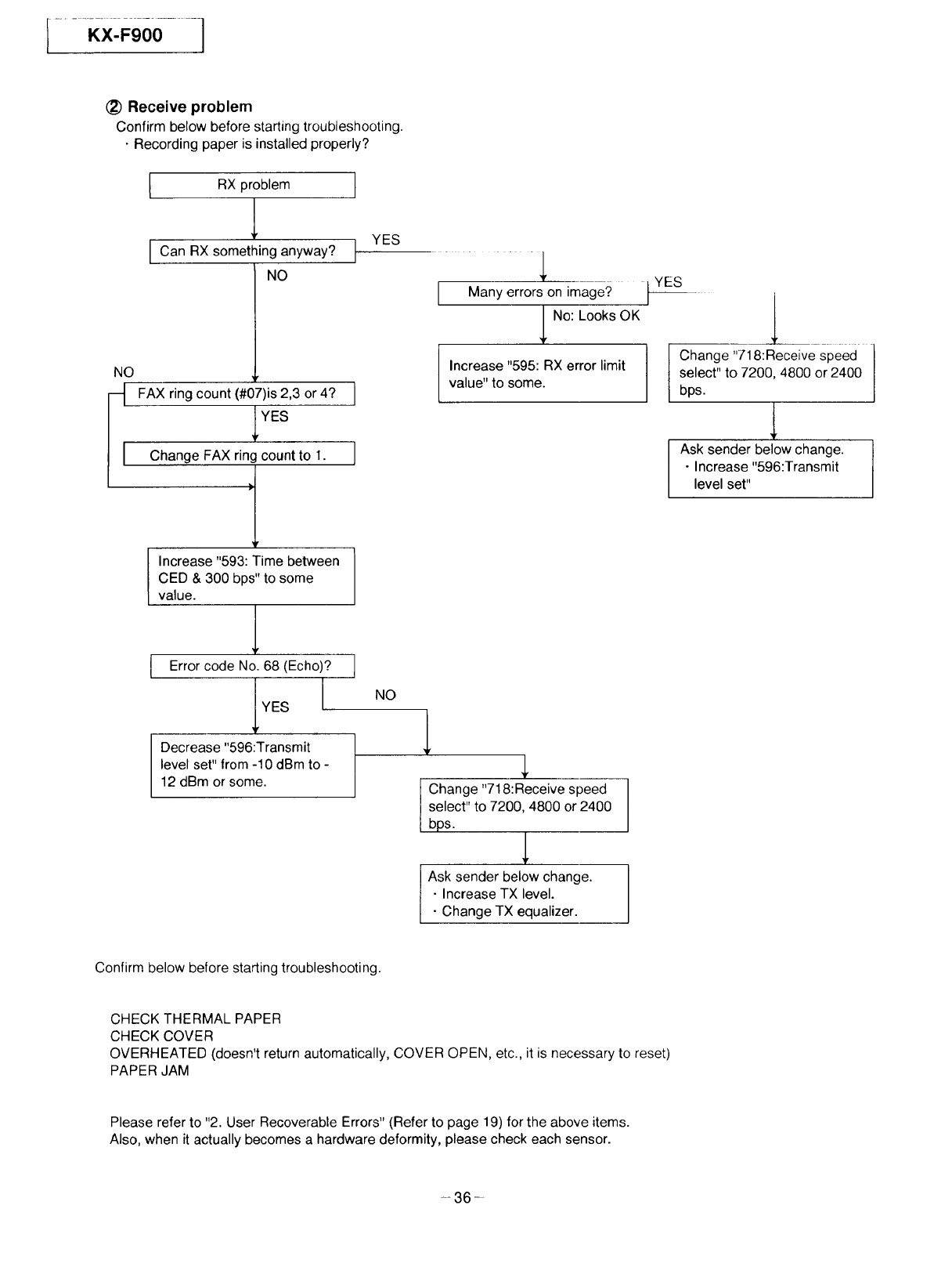
(2) Receive problem
Confirm below before starting troubleshooting.
• Recording paper is installed properly?
NO
I
I RX problem
1
Can RX something anyway?
NO
FAX ring count (#07)is 2,3 or 4?
YES
Change FAX ring count to 1.
Increase "593: Time between
CED & 300 bps" to some
value. l
I Error code No. 68 (Echo)?
YES
Decrease "596:Transmit
level set" from -10 dBm to -
12 dBm or some.
I
I
]
YES
I
Many errors on image?
J No: Looks OK
Increase "595: RX error limit
value" to some•
NO l
t hange"718:Receive speed 1
select" to 7200, 4800 or 2400
bps. l
I Ask sender below change. 1
• Increase TX level•
• Change TX equalizer•
t YES
Il
Change"718:Receive speed I
select" to 7200, 4800 or 2400 I
bps, l
Ask sender below change.
• Increase "596:lransmit
level set"
Confirm below before starting troubleshooting.
CHECK THERMAL PAPER
CHECK COVER
OVERHEATED (doesn't return automatically, COVER OPEN, etc., it is necessary to reset)
PAPER JAM
Please refer to "2. User Recoverable Errors" (Refer to page 19) for the above items.
Also, when it actually becomes a hardware deformity, please check each sensor.
-36-
KX-F900 1
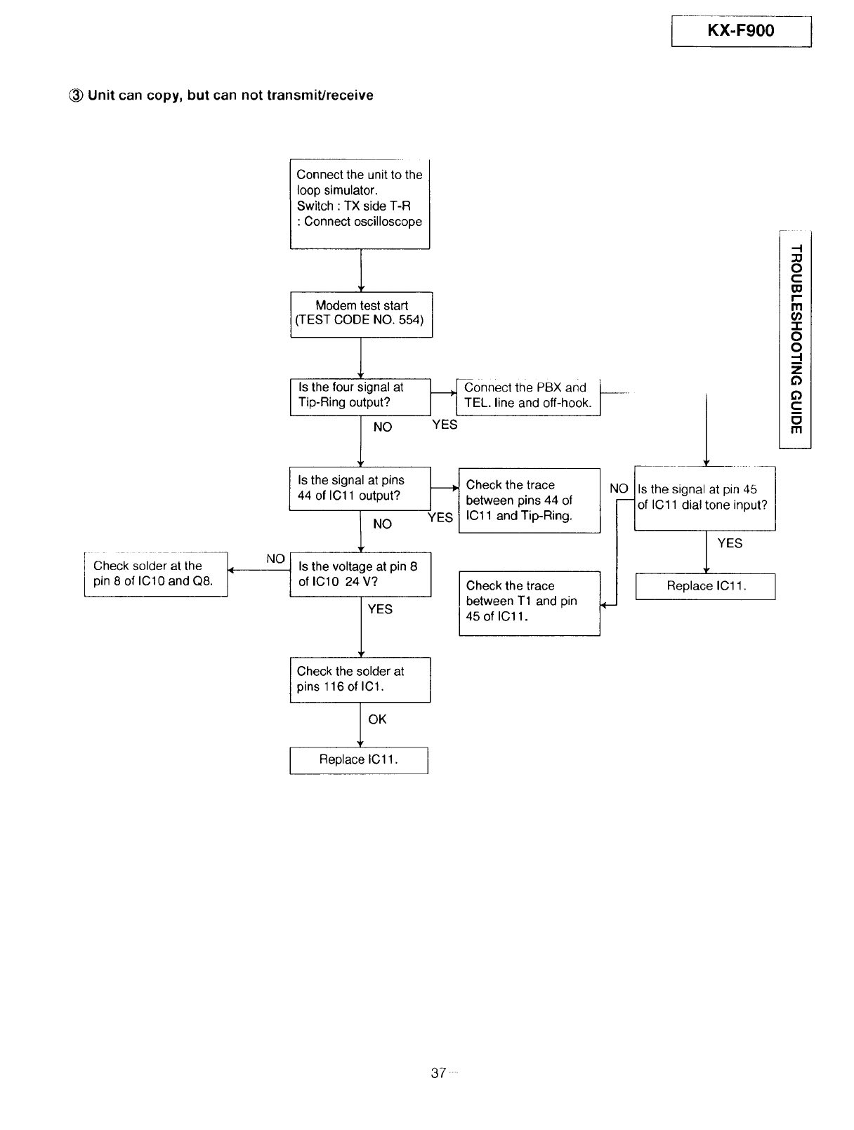
C_ Unit can copy, but can not transmiUreceive
Check solder at-thee--- _
pin 8 of IC10 and Q8.
NO
Connect the unit to the
loop simulator.
Switch : TX side T-R
: Connect oscilloscope
l
Modem test start
(TEST CODE NO. 554)
1
Is the four signal at
Tip-Ring output?
1"°
Is the signal at pins
44 of ICl 1 output?
Is the voltage at pin 8
of IC10 24 V?
YES
___connect the PBX and l
EL. line and off-hook. J
YES
YE_S Check the trace
between pins 44 of
IC11 and Tip-Ring.
Check the trace
between T1 and pin
45 of IC11.
-I
O
(:
r-
m
.1-
O
O
-I
z
D
L
_o_ tlhl lii_a_ It:tniin-_ i _
I YES
Replace IC11. J
Check the solder at
pins 116 of IC1.
l
Replace IC11.
LKX-F900
@Unit can copy, but can not transmit/receive long distance or international communication
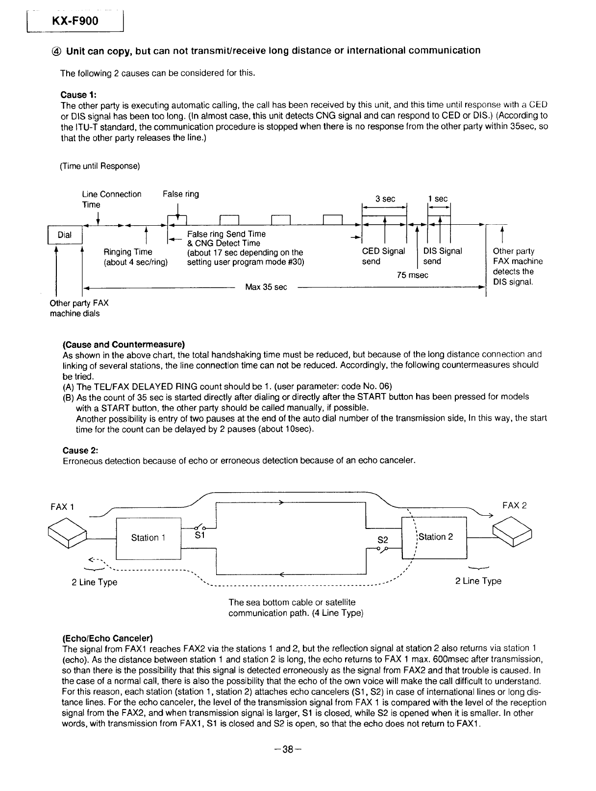
The following 2 causes can be considered for this.
Cause 1:
The other party is executing automatic calling, the call has been received by this unit, and this time until response with a CED
or DIS signal has been too long. (In almost case, this unit detects CNG signal and can respond to CED or DIS.) (According to
the ITU-T standard, the communication procedure is stopped when there is no response from the other party within 35sec, so
that the other party releases the line.)
(Time until Response)
Line Connection
Time
l
Ringing Time
(about 4 sec/ring)
Other party FAX
machine dials
False ring
i--1 I---1
- .____FaIcslel_1ngeSic?d T1_ e
(about 17 sec depending on the
setting user program mode #30)
Max 35 sec
3 sec I sec
sCEn_Signal _sD_St .gnal
75 msec
Other party
FAX machine
detects the
DIS signal.
(Cause and Countermeasure)
As shown in the above chart, the total handshaking time must be reduced, but because of the long distance connection and
linking of several stations, the line connection time can not be reduced. Accordingly, the following countermeasures should
be tried.
(A) The TEL/FAX DELAYED RING count should be 1. (user parameter: code No. 06)
(B) As the count of 35 sec is started directly after dialing or directly after the START button has been pressed for models
with a START button, the other party should be called manually, if possible.
Another possibility is entry of two pauses at the end of the auto dial number of the transmission side, In this way, the start
time for the count can be delayed by 2 pauses (about 10sec).
Cause 2:
Erroneous detection because of echo or erroneous detection because of an echo canceler.
FAX 1 j/o-J _ FAX 2
_ Station 1 Sl
t
S2 iStation 2
I S Ii
i
s
2 Line Type
The sea bottom cable or satellite
communication path. (4 Line Type)
2 Line Type
(Echo/Echo Canceler)
The signal from FAX1 reaches FAX2 via the stations 1 and 2, but the reflection signal at station 2 also returns via station 1
(echo). As the distance between station 1 and station 2 is long, the echo returns to FAX 1 max. 600msec after transmission,
so than there is the possibility that this signal is detected erroneously as the signal from FAX2 and that trouble is caused. In
the case of a normal call, there is also the possibility that the echo of the own voice will make the call difficult to understand.
For this reason, each station (station 1, station 2) attaches echo cancelers ($1, $2) in case of international lines or long dis-
tance lines. For the echo canceler, the level of the transmission signal from FAX 1 is compared with the level of the reception
signal from the FAX2, and when transmission signal is larger, $1 is closed, while $2 is opened when it is smaller. In other
words, with transmission from FAX1, $1 is closed and $2 is open, so that the echo does not return to FAX1.
-38-
I KX-F900
(Cause and Countermeasure)
(Cause A)
When the training signal is transmitted from FAX1 during the communication procedure at the time of transmission from
FAX1 to FAX2, there is a delay until the echo canceler operates and $1 is closed, so that a part of the head of the training
signal may drop out, normal reception by FAX2 may not be possible, and transmission may not be started.
(Cou ntermeasu re A)
When the international line mode becomes ON service mode (code No. 521), a dummy signal is attached to the head of
the training signal to prevent this problem. As this normally is ON, it is necessary to reconfirm that this has not becomes
OFF. When the international mode is switched OFF, the transmission side will try the training signal three times at each
speed (9600BPS, 4800BPS and 2400BPS), and in case of NG, it will drop the speed by one rank (fall-back). When the in-
ternational mode is switched ON, each speed will be tried only twice. In other words, the slower speed with fewer errors
are reached more easily. This is done as the line conditions may deteriorate and the picture may be disturbed more easily
during communication in case of international lines or long distance communication, even when the training has been OK.
The default value is ON as preference is given to clearer pictures rather than speed.
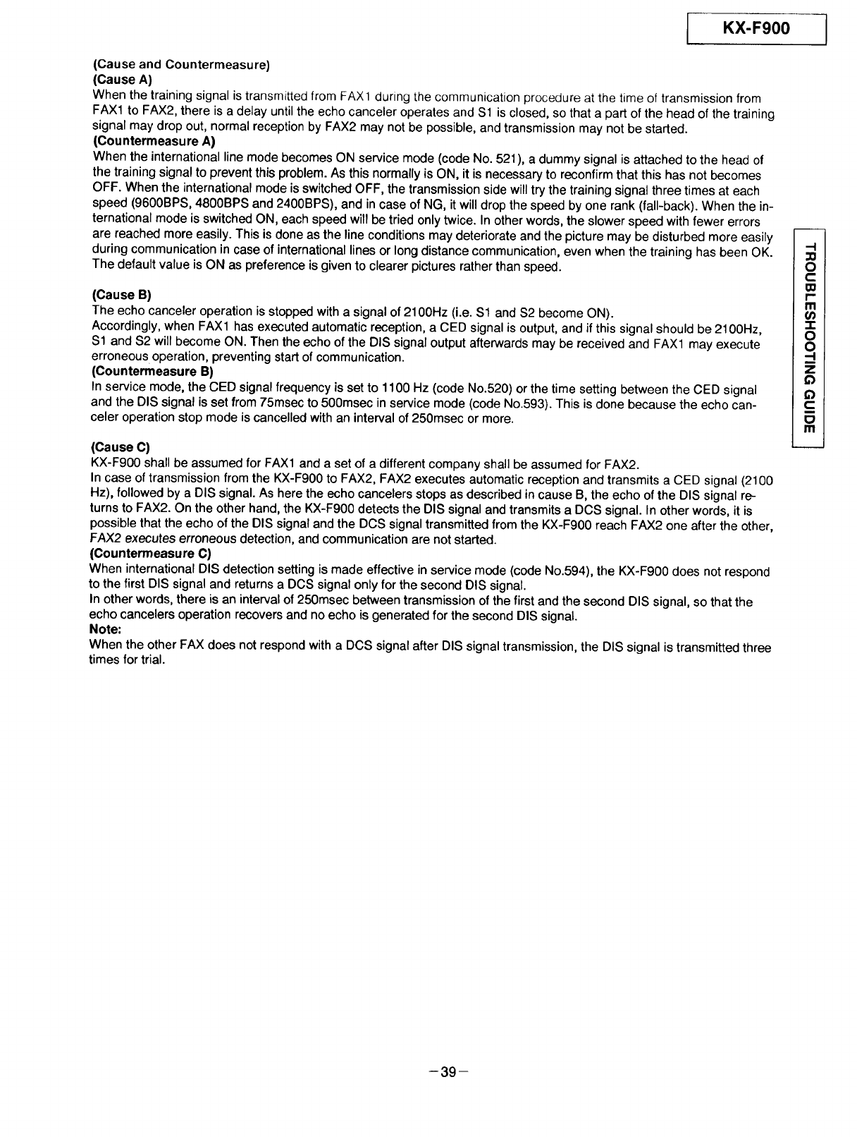
(Cause B)
The echo canceler operation is stopped with a signal of 2100Hz (i.e. $1 and $2 become ON).
Accordingly, when FAX1 has executed automatic reception, a CED signal is output, and if this signal should be 2100Hz,
$1 and $2 will become ON. Then the echo of the DIS signal output afterwards may be received and FAX1 may execute
erroneous operation, preventing start of communication.
(Countermeasure B)
In service mode, the CED signal frequency is set to 1100 Hz (code No.520) or the time setting between the CED signal
and the DIS signal is set from 75msec to 500msec in service mode (code No.593). This is done because the echo can-
celer operation stop mode is cancelled with an interval of 250msec or more.
(Cause C)
KX-F900 shall be assumed for FAX1 and a set of a different company shall be assumed for FAX2.
In case of transmission from the KX-F900 to FAX2, FAX2 executes automatic reception and transmits a CED signal (2100
Hz), followed by a DIS signal. As here the echo cancelers stops as described in cause B, the echo of the DIS signal re-
turns to FAX2. On the other hand, the KX-F900 detects the DIS signal and transmits a DCS signal. In other words, it is
possible that the echo of the DIS signal and the DCS signal transmitted from the KX-F900 reach FAX2 one after the other,
FAX2 executes erroneous detection, and communication are not started.
(Countermeasure C)
When international DIS detection setting is made effective in service mode (code No.594), the KX-F900 does not respond
to the first DIS signal and returns a DCS signal only for the second DIS signal.
In other words, there is an interval of 250msec between transmission of the first and the second DIS signal, so that the
echo cancelers operation recovers and no echo is generated for the second DIS signal.
Note:
When the other FAX does not respond with a DCS signal after DIS signal transmission, the DIS signal is transmitted three
times for trial.
.-I
O
C
00
I-
Ill
"I-
O
O
-I
z
Q
Q
c
o
m
-39-
KX-F900
Summary:
Long distance and international communication operatio_
SYMPTOM
Does not receive in automatic mode.
Does not transmit.
Does not receive.
COUNTERMEASURE
1. The TEL/FAX DELAYED RING count should be 1.
(user parameter: code No. 06)
2. If possible, manual transmission should be made from
the transmission side.
3. If possible, two pauses should be inserted at the end of
the auto dial number of the transmission side.
4. If possible, the Function Selector Switch should be
switched to FAX.
1. Confirm the international line mode ON.
(service mode: code No. 521)
2. International DIS detection setting is made
effective. (service mode: code No. 594)
1. The time setting between the CED signal and the DIS
signal is set to 500msec. (service mode: code No. 593)
2. The CED frequency is set to 1100Hz.
(service mode: code No. 520)
(_) Unit can copy, but the transmission and reception image is incorrect
(Long distance or international communication operation)
This depends widely on the transmission and reception capability of the other FAX set and the line conditions.
The countermeasures for this set are shown below.
Transmission Operation:
The transmitting speed is set to 4800BPS (service mode: code No. 717) or select overseas mode. (Individual correspon-
dence according to the other set is desirable.)
Reception Operation:
If 80% or more of the reception should be incorrect, set the receiving speed to 4800BPS. (service mode: code No. 718)
-40-
-KX-F900 .....
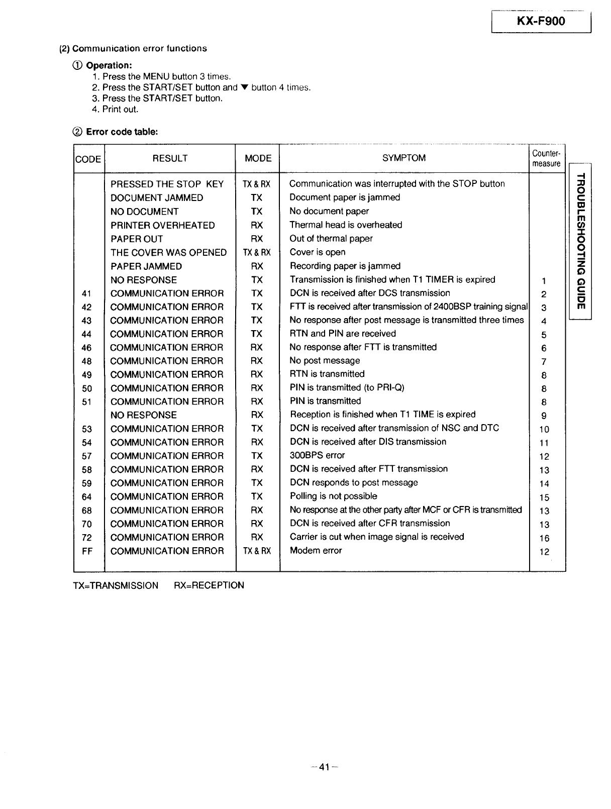
(2) Communication error functions
(_ Operation:
1. Press the MENU button 3 times.
2. Press the START/SET button and v button 4 times.
3. Press the START/SET button.
4. Print out.
(_ Error code table:
CODE RESULT MODE SYMPTOM Counter-
measure
PRESSED THE STOP KEY
DOCUMENT JAMMED
NO DOCUMENT
PRINTER OVERHEATED
PAPER OUT
THE COVER WAS OPENED
PAPER JAMMED
NO RESPONSE
41 COMMUNICATION ERROR
42 COMMUNICATION ERROR
43 COMMUNICATION ERROR
44 COMMUNICATION ERROR
46 COMMUNICATION ERROR
48 COMMUNICATION ERROR
49 COMMUNICATION ERROR
50 COMMUNICATION ERROR
51 COMMUNICATION ERROR
NO RESPONSE
53 COMMUNICATION ERROR
54 COMMUNICATION ERROR
57 COMMUNICATION ERROR
58 COMMUNICATION ERROR
59 COMMUNICATION ERROR
64 COMMUNICATION ERROR
68 COMMUNICATION ERROR
70 COMMUNICATION ERROR
72 COMMUNICATION ERROR
FF COMMUNICATION ERROR
TX& RX
TX
TX
RX
RX
TX & RX
Communication was interrupted with the STOP button
Document paper is jammed
No document paper
Thermal head is overheated
Out of thermal paper
Cover is open
RX
TX
TX
TX
TX
TX
RX
RX
RX
RX
RX
RX
TX
RX
TX
RX
TX
TX
RX
RX
RX
TX& RX
Recording paper is jammed
Transmission is finished when T1 TIMER is expired 1
DCN is received after DCS transmission 2
FTT is received after transmission of 2400BSP training signal 3
No response after post message is transmitted three times 4
RTN and PIN are received 5
No response after FTT is transmitted 6
No post message 7
RTN is transmitted 8
PIN is transmitted (to PRI-Q) 8
PIN is transmitted 8
Reception is finished when T1 TIME is expired 9
DCN is received after transmission of NSC and DTC 10
DCN is received after DIS transmission 11
300BPS error 12
DCN is received after FTT transmission 13
DCN responds to post message 14
Polling is not possible 15
No response at the other party after MCF or CFR is transmitted 13
DCN is received after CFR transmission 13
Carrier is cut when image signal is received 16
Modem error 12
1
'--I
TX=TRANSMISSION RX=RECEPTION
-41 -
IKX-F900 I
(_ Countermeasure
NO
I onfirm if the receiver's FAX ma-
chine is set to the reception mode or
answering machine's message is on.
NO
NO
_thlS the receiver's FAXN_
_per or mechanical errorC,-/"
YES
Ask the receiver to set the receiver's
FAX machine to the receivable mode
and transmit again.
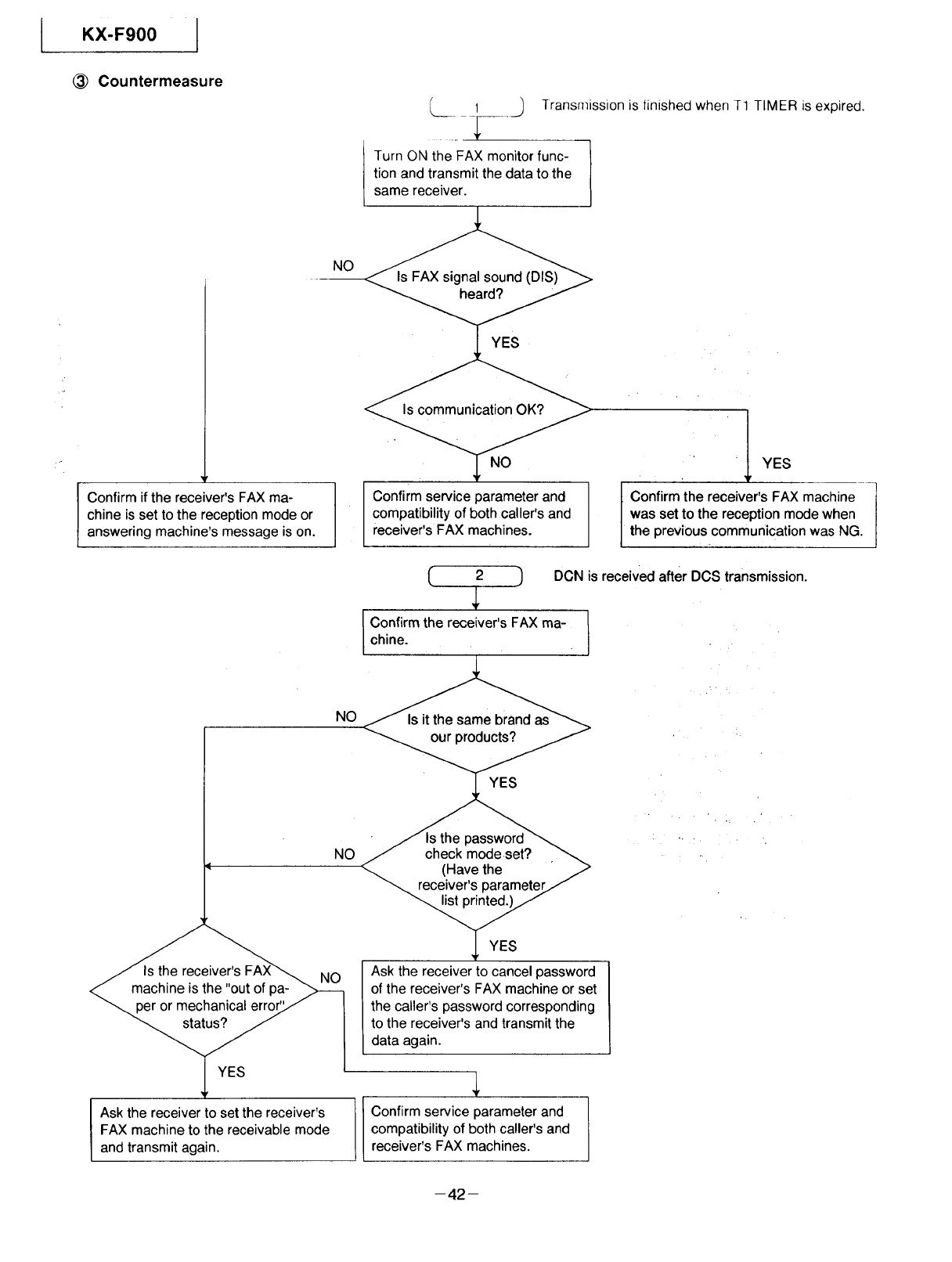
f) Transmission is finished when T1 TIMER is expired.
Turn ON the FAX monitor func-
tion and transmit the data to the
same receiver.
¸
Confirm service parameter and
compatibility of both caller's and
receiver's FAX machines.
IYES
Confirm the receiver's FAX machine
was set to the reception mode when
the previous communication was NG.
C
Confirm the receiver's FAX ma-
chine.
_, YES
Ask the receiver to cancel password
of the receiver's FAX machine or set
the caller's password corresponding
to the receiver's and transmit the
data again.
2 ") DCN is received after DOS transmission.
Confirm service parameter and
compatibility of both caller's and
receiver's FAX machines.
-42-
KX-F900
Modem test
(TEST CODE NO.554)
YES
Perform communication test us- I
ing the LOOP simulator. I
.1
FT-i is received after transmission of 2400BPS
training signal.
(1) Raise the level of transmission. (Do not
raise the level above the standard of each
country. If the communication should be
OK at the level beyond the standard, it is
attributable to line condition or the
receiver's machine sensitivity condition.)
If no effect is obtained.
(2) Slow down the transmission start speed
and taransmit to the receiver again.
Ask the receiver to perform FAX
communication from the re-
ceiver to the caller.
I Perform voice communication I
with the receiver. 1
I heck if the line is not inter-
rupted by noises or in the cross
talk. If it is not, wait until the line
is satisfactory for correct com-
munication.
YES
If this error frequently occurs at
the receiver, perform transmis-
sion in the above-mentioned
mode on the receiver.
YES
End
-I
0
c
I-
I'll
co
'1-
0
0
-I
m
z
c:
n
Ill
-43-
three times.
'Inquire the receiver if the
caller's document is facsimiled
correctly.
No response after post message is transmitted
Ask the service section of the
receiver's FAX machine to con-
firm the machine condition.
(5
l
3.1
) RTN and PIN are received.
-- t
Modem test YES
(TEST CODE NO.554)
6No response after FTT is transmitted.
Perform communication test us-
ing the LOOP simulator and
check the machine reception
condition.
6.1 )
,_ : No problem on the machine hardware.
!
Perform voice communication I
with the NG caller. I
Check if the line is not inter-
rupted by noises or in the cross
talk, If it is not, wait until the line
is satisfactory for correct com-
munication.
44-
ITry again.
KX-F900 ]
Turn ON the FAX monitor func-
tion and have the receiver trans-
mit the data.
(Receive Complete)
NO
_-_ Decrease the RX speed.
7 ) No post message
YES
Ask the service section of the
sender's FAX machine for ex-
amination.
.-I
O
C
I""
Ill
"I-
O
O
.-I
NO 7.1 _ _1
( 8 ) RTN is transmitted.
PIN is transmitted (to PRI-Q).
PIN is transmitted.
Perform communication test us-
ing the LOOP simulator and
check the machine reception
condition.
NO
Turn ON the FAX monitor func-
tion and have the receiver in
question transmit the data
again.
( 6.1 )
Modem test
(TEST CODE NO.554)
NO
End ]
-45-
I Kx-F'O0I
Modem test
(TEST CODE NO.554)
NO
NO
Confirm if the receiver's FAX
machine was set to receivable
mode.
(: 9)
Perform communication test us-
ing the LOOP simulator and
check the machine reception
condition.
Turn ON the FAX monitor func-
tion and have the receiver in
question transmit the data
again.
NO
r, 61 )
Reception is finished when T1 TIME is expired.
YES
End ......... }
46-
KX-F900
10 DCN is received after transmission of NSC and DTC.
Confirm if a mechanical trouble
occurred, e.g. transmission was
interrupted or document was out
of place, on the receiver side
(being polled).
Ask the receiver to set the poll
mode again and perform polling.
NO 1
Ask the service section ofihe
receiver/s FAX machine for ex- I
amination. J
,-I
O
C
i-
rn
-r
O
O
,-I
Z
Q
(=
Ill
(
Confirm if a mechanical trouble
occurred, e.g. the caller inter-
rupted the transmission.
11 ) DCN is received after DIS transmission.
NO
Have the caller transmit the data
again.
Ask the service section of the
caller's FAX machine for exami-
nation.
(12 _ 300BPS error
Modem error
Check the hardware of the pe-
ripherals of the modem.
-47-
l
Confirm if a mechanical trouble
occurred, e.g. the caller inter-
rupted the transmission.
Ask the caller to transmit the
data again.
DCN is received after FTT transmission.
No response at the other party after MCF or
CFR is transmitted.
DCN is received after CFR transmission.
NO [
6.1 ]
(l
Confirm if a mechanical trouble
occurred, e.g. the receiver inter-
rupted the reception.
Perform voice communication
with the NG receiver.
14 ) DCN responds to post message.
YES
l
Check if the line is not inter-
rupted by noises or in the cross
talk. If it is no, wait until the line
is satisfactory for correct com-
munication.
l ......
Ask the receiver to set the
receiver's FAX machine to the
receivable mode and communi
cate again.
48-
I......Kx-_90o........I
(
Confirm if a mechanical trouble
occurred, e.g. transmission was
interrupted or document was out
of place, on the receiver side
(being polled).
Ask the receiver to set the Poll
mode again and perform polling.
15 ) Polling is not possible.
NO
____ mr • 1
Ask the service section of the /
J
receiver's FAX machine for ex-
amination.
21
OI
CI
IXII
I'" I
ill I
t_l
.-,,,
zl
QI
Cl f
mI
lModem test
(TEST CODE NO.554)
( 16 -) Carrier is cut when image signal is received.
Perform communication test us-
ing the LOOP simulator and
check the machine reception
condition.
( 6.1 )
49_
KX-F900
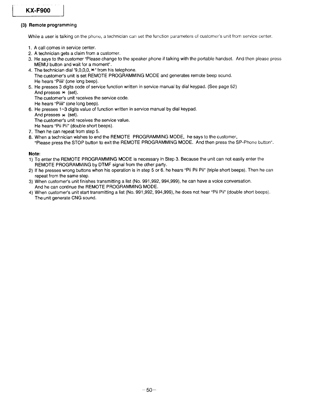
(3) Remote programming
While a user is talking on the phone, a technician call set the function parameters of customer's unit from service center.
1. A call comes in service center.
2. A technician gets a claim from a customer.
3. He says to the customer "Please change to the speaker phone if talking with the portable handset. And then please press
MEMU button and wait for a moment".
4. The technician dial '9,0,0,0, _' from his telephone.
The customer's unit is set REMOTE PROGRAMMING MODE and generates remote beep sound.
He hears "Piiii' (one long beep).
5. He presses 3 digits code of service function written in service manual by dial keypad. (See page 52)
And presses _ (set).
The customer's unit receives the service code.
He hears "Piiii" (one long beep).
6. He presses 1-3 digits value of function written in service manual by dial keypad.
And presses _ (set).
The customer's unit receives the service value.
He hears "Pii Pii" (double short beeps).
7. Then he can repeat from step 5.
8. When a technician wishes to end the REMOTE PROGRAMMING MODE, he says to the customer,
"Please press the STOP button to exit the REMOTE PROGRAMMING MODE. And then press the SP-Phone button".
Note:
1) To enter the REMOTE PROGRAMMING MODE is necessary in Step 3. Because the unit can not easily enter the
REMOTE PROGRAMMING by DTMF signal from the other party.
2) If he presses wrong buttons when his operation is in step 5 or 6. he hears "Pii Pii Pii" (triple short beeps). Then he can
repeat from the same step.
3) When customer's unit finishes transmitting a list (No. 991,992, 994,999), he can have a voice conversation.
And he can continue the REMOTE PROGRAMMING MODE.
4) When customer's unit start transmitting a list (No. 991,992,994,999), he does not hear "Pii Pii" (double short beeps).
The unit generate CNG sound.
50-
KX-F900
1_ Summary of remote programming mode
sTART
Enter the REMOTE
PROGRAMMING ID 9,0,0,0 *
I ress mistaken key "PiiPii Pii"
Iress mistaken key"Pii t
Pii Pii"
I
I
_v
REMOTE PROGRAMMING
MODE "Piiii"
Press 3 digits code of service
function and then press -_ (set)
SERVICE SETTING MODE
"Piiii" l
Press 1-3 digits value of func-
tion and then press -X- (set)
l
SETTING THE FUNCTION "Pii
Pii"
I
I
Customer press STOP
key and press the
SP-PHONE button.
END J,-I
O
c
00
I-
m
g)
"1"
O
O
--I
z
c
i
o
m
-51 -
[ KX'FgO0 I
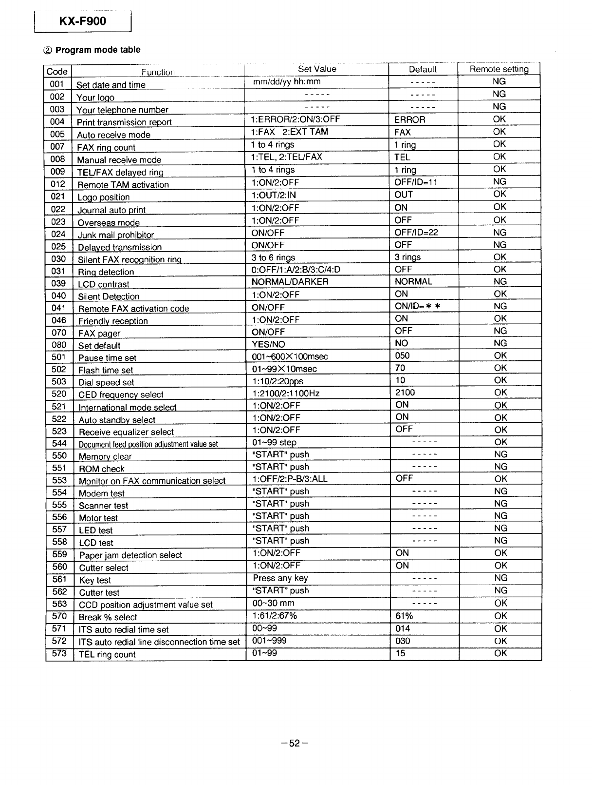
C_)Program mode table
002
003
0O4
005
007
008
009
012
021
022
023
024
025
030
031
039
040
041
046
070
O8O
501
502
503
520
521
522
523
544
550
551
553
554
555
556
557
558
559
56O
561
562
563
57O
571
572
573
Function
Set date and time
Your Io.qo
Your telephone number
Print transmission report
Auto receive mode
FAX ring count
Manual receive mode
TEL/FAX delayed ring
Remote TAM activation
Logo position
Journal auto print
Overseas mode
Junk mail prohibitor
Delayed transmission
Silent FAX recoqnition rin.q
Rin.q detection
LCD contrast
Silent Detection
Remote FAX activation code
Friendly reception
FAX pager
Set default
Pause time set
Flash time set
Dial speed set
CED frequency select
International mode select
Auto standby select
Receive equalizer select
Documentfeed positionadiustmentvalueset
Memory clear
ROM check
Monitor on FAX communication select
Modem test
Scanner test
Motor test
LED test
LCD test
Paper jam detection select
Cutter select
Key test
Cutter test
CCD position adjustment value set
Break % select
ITS auto redial time set
ITS auto redial line disconnection time set
TEL ring count
Set Value Default Remote setting
mm/dd/yy hh:mm
ERROR
FAX
1 ring
TEL
1 ring
OFF/ID=I 1
OUT
ON
OFF
OFF/ID=22
OFF
3 rings
OFF
NORMAL
ON
ON/ID= •
ON
OFF
NO
O50
70
10
2100
ON
ON
OFF
OFF
ON
ON
61%
014
030
15
1:ERROR/2:ON/3:OFF
1:FAX 2:EXT TAM
1 to 4 rings
1:TEL, 2:TEL/FAX
1 to 4 rings
1 :ON/2:OFF
1 :OUT/2:IN
1 :ON/2:OF F
1 :ON/2:OFF
ON/OFF
ON/OFF
3 to 6 rings
0:OFF/1 :A/2:B/3:CI4:D
NORMAL!DARKER
1:ON/2:OFF
ON/OFF
1:ON/2:OFF
ON/OFF
YES/NO
001 ~600X 100msec
01~99X 10msec
1:10/2:20pps
1:2100/2:1100Hz
1:ON/2:OFF
1:ON/2:OFF
1:ON/2:OFF
01-99 step
"START" push
"START" push
1:OFF/2:P-B/3:ALL
"START" push
"START" push
"START" push
"START" push
"START" push
I:ON/2:OFF
1:ON/2:OFF
Press any key
"START" push
00-30 mm
1:61/2:67%
00~99
001 ~999
01~99
NG
NG
NG
OK
OK
OK
OK
OK
NG
OK
OK
OK
NG
NG
OK
OK
NG
OK
NG
OK
NG
NG
OK
OK
OK
OK
OK
OK
OK
OK
NG
NG
OK
NG
NG
NG
NG
NG
OK
OK
NG
NG
OK
OK
OK
OK
OK
-52-
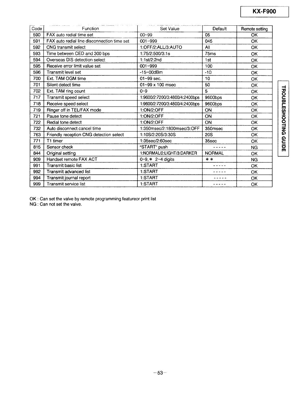
KX-F900
.... Function ........
590 FAX auto redial time set
591 FAX auto redial line disconnection time set
592 ONG transmit select
593 Time between CED and 300 bps
594 Overseas DIS detection select
595 Receive error limit value set
596 Transmit level set
700 Ext. TAM OGM time
701 Silent detect time
702 Ext. TAM ring count
717 Transmit speed select
718 Receive speed select
719 Ringer off in TEL/FAX mode
721 Pause tone detect
722 Redial tone detect
732 Auto disconnect cancel time
763 Friendly reception CNG detection select
771 T1 timer
815 Sensor check
844 Original setting
909 Handset remote FAX ACT
991 Transmit basic list
992 Transmit advanced list
994 Transmit iournal report
999 Transmit service list
Set Value
00-99
001-999
1:OFF/2:ALL/3:AUTO
1:75/2:500/3:1 s
1:1stJ2:2nd
001-999
-15~00dBm
01~99 sec.
01-99 x 100 msec
0-9
1:9600/2:7200/3:4800/4:2400bps
1:9600/2:7200/3:4800/4:2400bps
1:ON/2:OFF
1:ON/2:OFF
1:ON/2:OFF
1:350msec/2:1800msec/3:OFF
1:10S/2:20S/3:30S
1:35sec/2:60sec
"START" push
I:NORMAIJ2:LIGHT/3:DARKER
0-9, ,_ 2-4 digits
1:START
1:START
1:START
1:START
Default
05
O45
All
75ms
1st
100
-10
10
5O
5
9600bps
9600bps
ON
ON
ON
350msec
20S
35sec
NORMAL
Remote setting
OK
OK
OK
OK
OK
OK
OK
OK
OK
OK
OK
OK
OK
OK
OK
OK
OK
OK
NG
OK
NG
OK
OK
OK
OK
-I
O
C
I"
m
"1"
O
O
.--I
z
c
ill
OK : Can set the valve by remote programming featureor print list
NG : Can not set the valve.
-53-
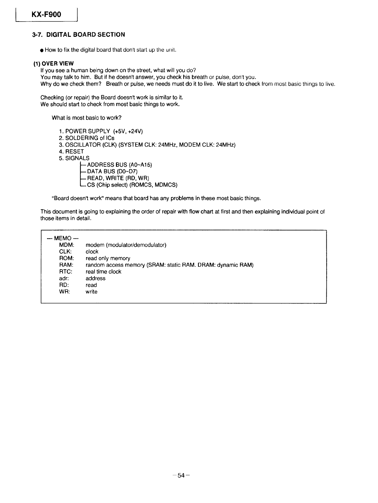
KX-F900
3-7. DIGITAL BOARD SECTION
• How to fix the digital board that don't start up the unit.
(1) OVER VIEW
If you see a human being down on the street, what will you do?
You may talk to him. But if he doesn't answer, you check his breath or pulse, don't you.
Why do we check them? Breath or pulse, we needs must do it to live. We start to check from most basic things to live.
Checking (or repair) the Board doesn't work is similar to it.
We should start to check from most basic things to work.
What is most basic to work?
1. POWER SUPPLY (+5V, +24V)
2. SOLDERING of ICs
3. OSCILLATOR (CLK) (SYSTEM CLK: 24MHz, MODEM CLK: 24MHz)
4. RESET
5. SIGNALS
ADDRESS BUS (A0~A15)
DATA BUS (D0-D7)
READ, WRITE (RD, WR)
CS (Chip select) (ROMCS, MDMCS)
"Board doesn't work" means that board has any problems in these most basic things.
This document is going to explaining the order of repair with flow chart at first and then explaining individual point of
those items in detail.
MEMO --
MDM: modem (modulator/demodulator)
CLK: clock
ROM: read only memory
RAM: random access memory (SRAM: static RAM. DRAM: dynamic RAM)
RTC: real time clock
adr: address
RD: read
WR: write
54-
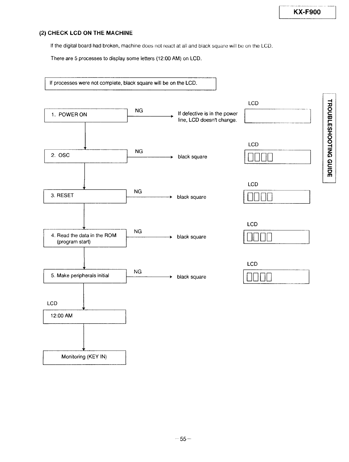
[-....KX-FgO0-]
(2) CHECK LCD ON THE MACHINE
If the digital board had broken, machine does not react at all and black square will be on the LCD.
There are 5 processes to display some letters (12:00 AM) on LCD.
IIf processes were not complete, black square will be on the LCD. ]
1. POWER ON
2. OSC
3. RESET
NG If defective is in the power
line, LCD doesn't change.
NG black square
4. Read the data in the ROM
(program start)
1
5. Make peripherals initial
NG
1,
NG
),
NG
J,
black square
black square
black square
LCD J
LCD
IDDDD
LOD
IBDDD I
LCD
[FIDDD
LCD
LDDDD
-I
_0
0
r-"
m
-1-
0
0
-I
z
c:
o
m
LCD
12:00 AM 1
Monitoring (KEY IN) 1
-55-
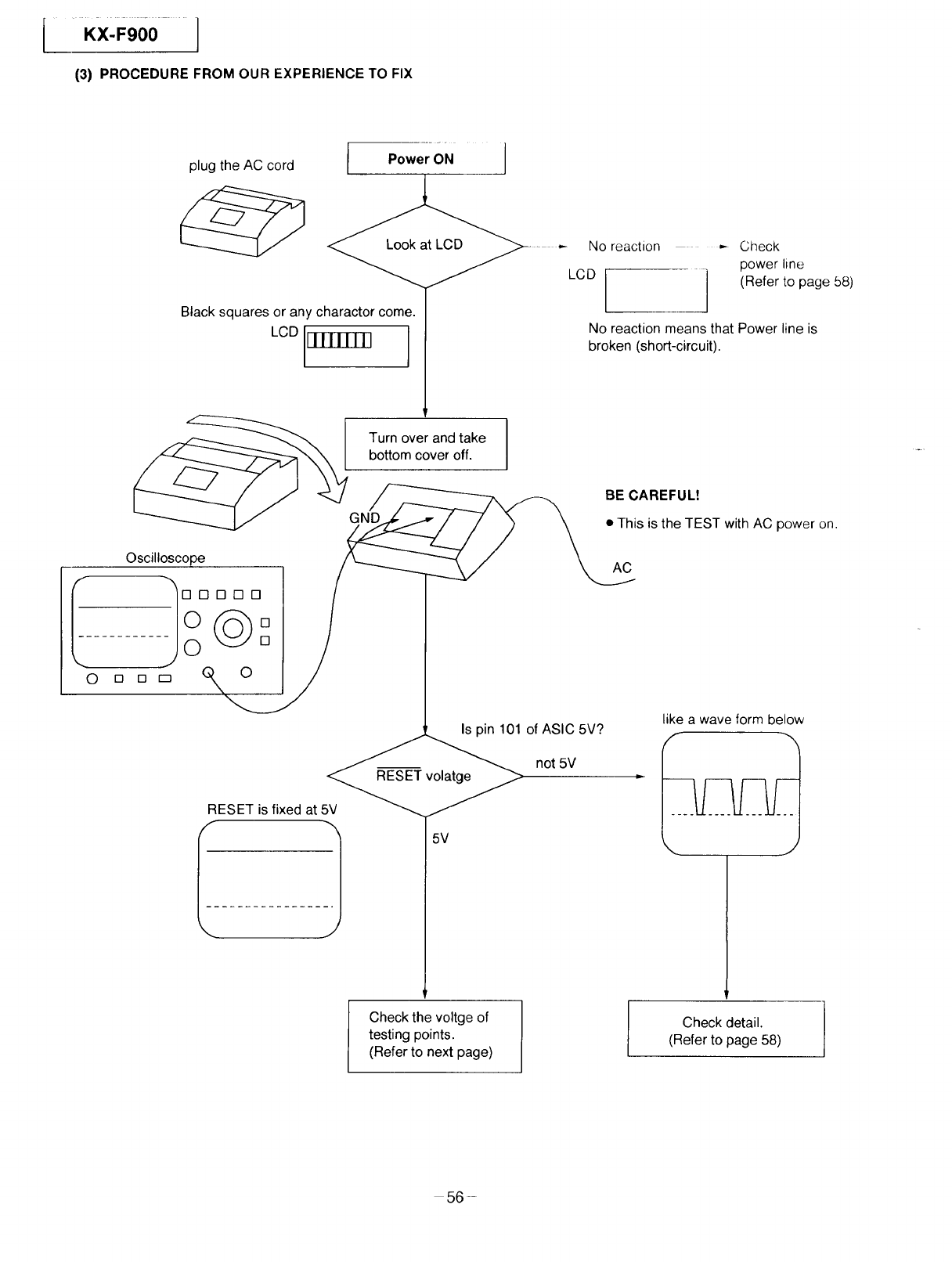
I x, ,0o1
(3) PROCEDURE FROM OUR EXPERIENCE TO FIX
plug the AC cord IPower ON J
-,,-- No reaction
LCD
Black squares or any charactor come.
I
•-_ Check
power line
I(Refer to page 58)
No reaction means that Power line is
broken (short-circuit).
Turn over and take
bottom cover off.
Oscilloscope
[]
[]
[] r_ O
GND
BE CAREFUM
• This is the TEST with AC power on.
AC
RESET is fixed at 5V
Is pin 101 of ASlC 5V?
not 5V
like a wave form below
Check the voltge of
testing points.
(Refer to next page) rCheck detail.
(Refer to page 58)
56-
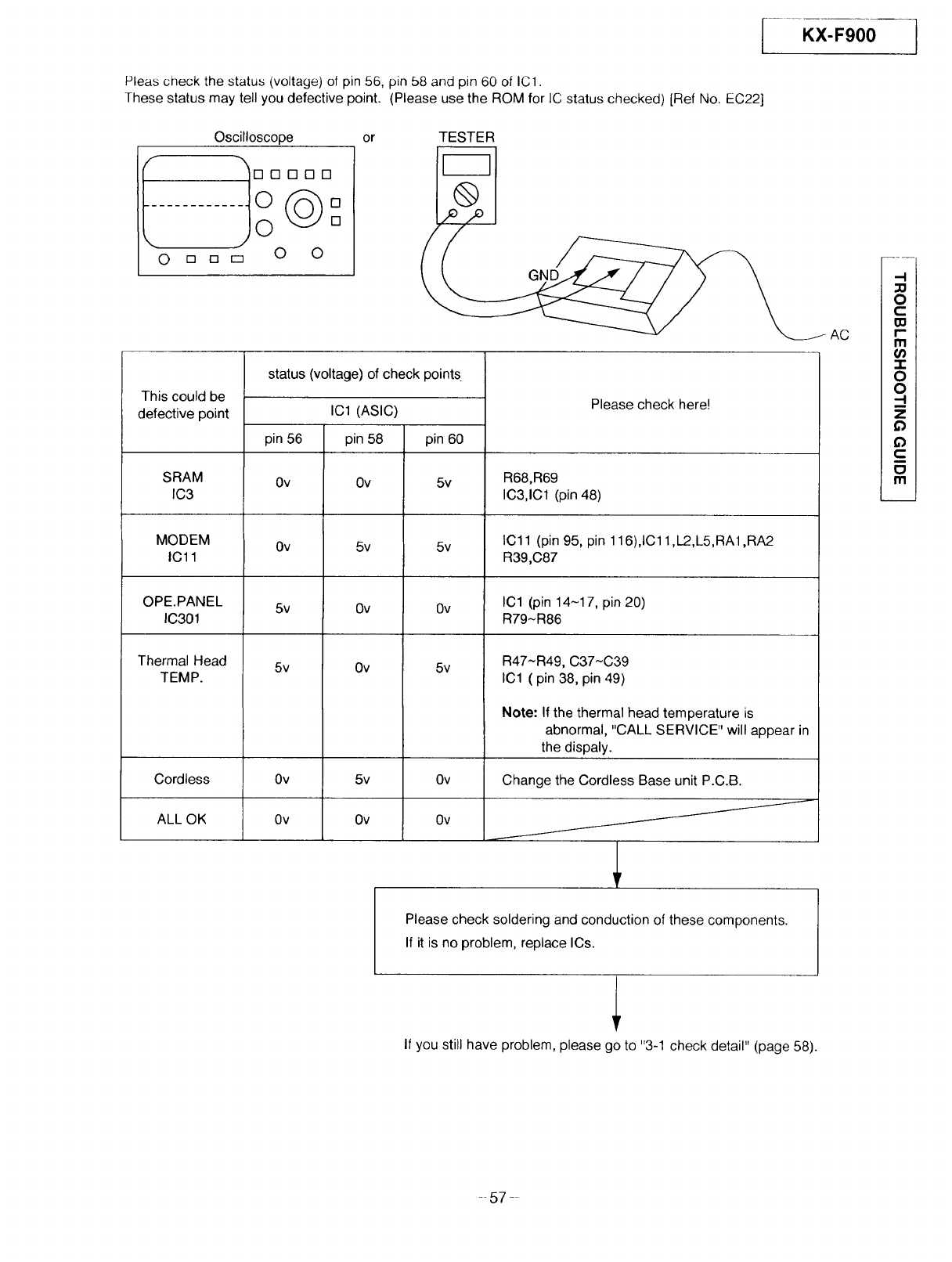
KX-F900 j
Pleas check the status (voltage) of pin 56, pin 58 and pin 60 of IC1.
These status may tell you defective point. (Please use the ROM for IC status checked) [Ref No. EC22]
Oscilloscope or TESTER
IO
DDDDD
[] m0 0
AC
This could be
defective point
SRAM
IC3
MODEM
ICll
OPE.PANEL
IC301
Thermal Head
TEMP.
Cordless
ALL OK
status (voltage) of check points
IC1 (ASIC)
pin 56
0v
0V
5v
5v
0V
0v
pin 58 pin 60
0v 5v
5v 5v
0v 0v
0v 5v
5v 0v
0v 0v
Please check here!
R68,R69
IC3,1C1 (pin 48)
IC11 (pin 95, pin 116),1C11 ,L2.,L5,RA1 ,RA2
R39,C87
IC1 (pin 14-17, pin 20)
R79-R86
R47~R49, C37-C39
IC1 ( pin 38, pin 49)
Note: If the thermal head temperature is
abnormal, "CALL SERVICE" will appear in
the dispaly.
Change the Cordless Base unit P.C.B.
-I
O
C:
I--
Ill
co
"1-
O
O
-I
z
¢)
c
Ill
Please check soldering and conduction of these components.
If it is no problem, replace ICs.
If you still have problem, please go to "3-1 check detail" (page 58).
-57-
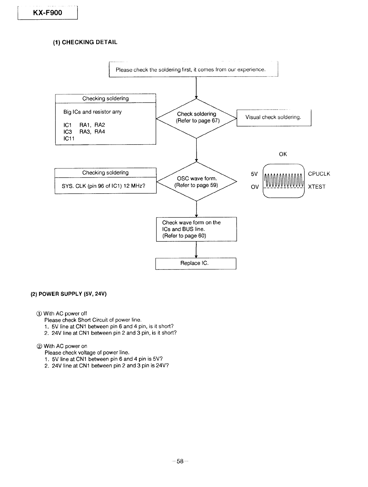
iKX-F900 ]
(1) CHECKING DETAIL
Please check the soldering first, it comes from our experience.
Checking soldering
Big ICs and resistor arry
IC1 RA1, RA2
IC3 RA3, RA4
ICll
Visual check soldering.
OK
Checking soldering
SYS. CLK (pin 96 of ICl) 12 MHz?
5V
OV
CPUCLK
XTEST
Check wave form on the
ICs and BUS line.
(Refer to page 60)
1
Replace IC.
(2) POWER SUPPLY (5V, 24V)
(_ With AC power off
Please check Short Circuit of power line.
1. 5V line at CN1 between pin 6 and 4 pin, is it short?
2. 24V line at CN1 between pin 2 and 3 pin, is it short?
(_) With AC power on
Please check voltage of power line.
1. 5V line at CN1 between pin 6 and 4 pin is 5V?
2. 24V line at CN1 between pin 2 and 3 pin is 24V?
58
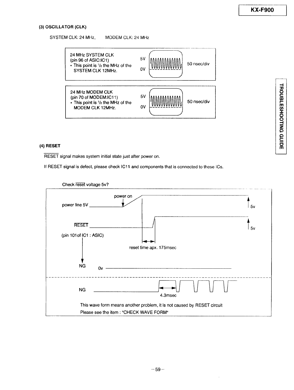
KX-F900
(3) OSCILLATOR (CLK)
SYSTEM CLK: 24 MHz, MODEM CLK: 24 MHz
24 MHz SYSTEM CLK
(pin 96 of ASIC:IC1) 5V
•This point is 1/2the MHz of the
SYSTEM CLK 12MHz. 0V
50 nsec/div
24 MHz MODEM CLK
(pin 70 of MODEM:IC11) 5V
•This point is 1/2the MHz of the
MODEM CLK 12MHz. 0V
50 nsec/div
(4) RESET
RESET signal makes system initial state just after power on.
If RESET signal is defect, please check IC11 and components that is connected to these ICs.
.-I
_0
O
C
_0
I"
rrl
¢/)
-r
O
O
-I
¢)
C
m
m
Check _ voltage 5v?
power line 5V pow_n_J
RE-CET
(pin 101of ICl : ASIC)
reset time apx. 175msec
4.3msec
5v
NG 0v
NG
This wave form means another problem, it is not caused by RESET circuit
Please see the item : "CHECK WAVE FORM"
-59-
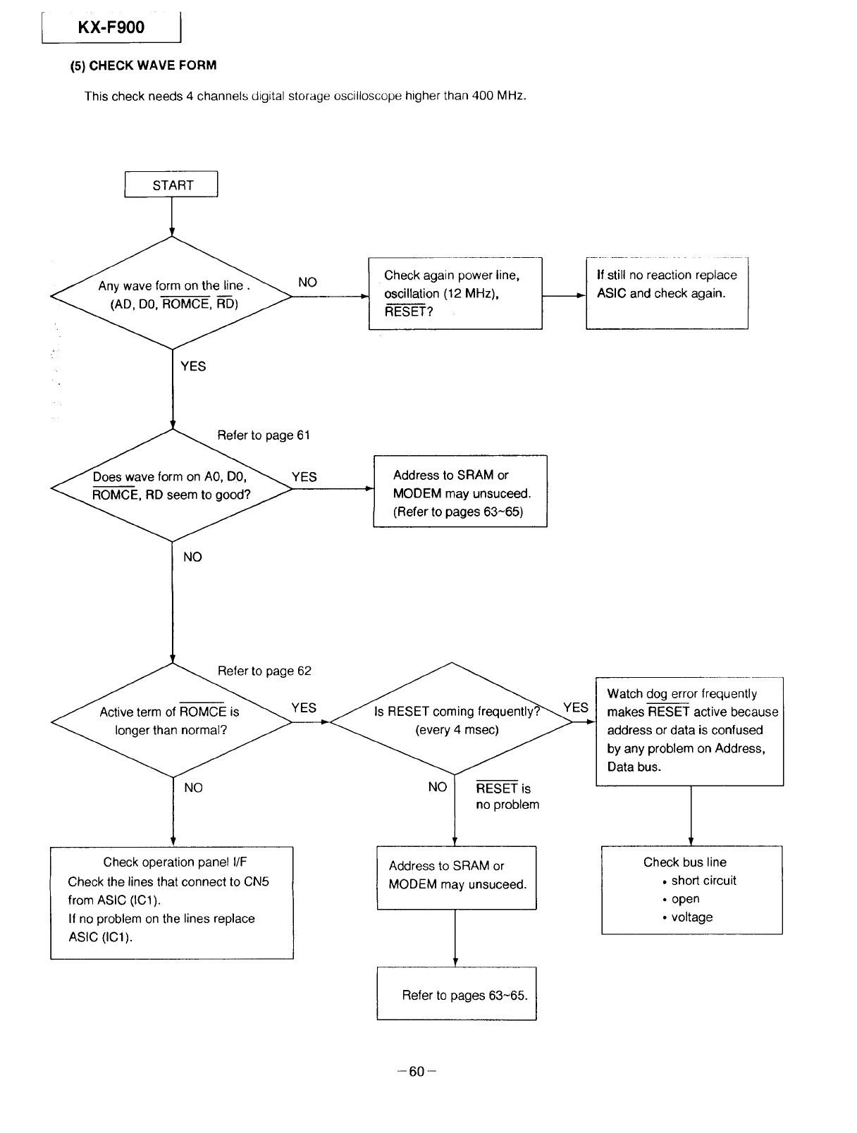
[KX-F900
(5) CHECK WAVE FORM
This check needs 4 channels digital storage oscilloscope higher than 400 MHz.
I START ]
NO
JYES
I heck again power line,
oscillation (12 MHz),
RESET?
j
NO
Address to SRAM or
MODEM may unsuceedo
(Refer to pages 63-65)
If still no reaction replace
ASlC and check again.
__ o0a0e6
._ Activetermo,_-_-6-E_n_ ,_ent,y_'_L
l 1 no problem
Check operation panel I/F
Check the lines that connect to CN5
from ASlC (IC1).
If no problem on the lines replace
ASIC (ICl).
Address to SRAM or
MODEM may unsuceed.
]
Refer to pages 63~65. /
/
Watch dog error frequently
makes RESET active because
address or data is confused
by any problem on Address,
Data bus.
Check bus line
• short circuit
• open
• voltage
-60--
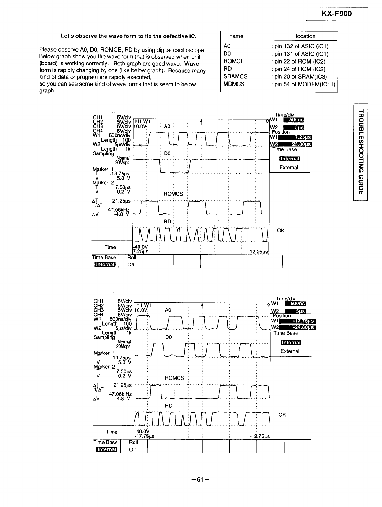
KX-F900 ]
Let's observe the wave form to fix the defective IC.
Please observe A0, DO, ROMCE, RD by using digital oscilloscope.
Below graph show you the wave form that is observed when unit
(.board) is working correctly. Both graph are good wave. Wave
form is rapidly changing by one (like below graph). Because many
kind of data or program are rapidly executed,
so you can see some kind of wave forms that is seem to below
graph.
name
AO
DO
ROMCE
RD
SRAMCS:
MDMCS
location
pin 132 of ASlC (IC1)
pin 131 of ASlC (IC1)
pin 22 of ROM (IC2)
pin 24 of ROM (IC2)
: pin 20 of SRAM(IC3)
: pin 54 of MODEM(ICl 1)
CH1 5V/div'
CH2 5V/div
CH3 .5V/div
CH4 5V/div
W1 500ns/div
Length 100
W2 b_sldiv
^Length lk
_amp=mg Normal
20Msps
Marker 1
T -13.75p.s
V 5.0 V
Marker 2
VT 70520p_
W21
&T 21.25tus
I/&T 47.06kHz
z_V -4.8 V
Time
Time Base I Roll
I Off
H1 W1 i { !
0.0v___ A0
ROMCS
Time/div
Wl
Time Base
External
OK
]
-I
O
t-
i-
ra
"1-
O
O
-I
z
Q
Q
c
Ill
CH1 5V/div
CH2 5V/div
OH3 5V/div
CH4 5V/div
Wl 500ns/div
Length 100
W2. 5ps/div
Length lk
sampling Normal
20Msps
Marker 1
T -13.751_s
V 5.0 V
Marker 2
T 70.5Op._
V
aT 21.25_s
1/&T 47.06k Hz
_V -4.8 V
Time
Timel_Base I
HIWI i t
10.0V_ _ A0
DO
: : i
i ! : i
........ i................. ;...... . i :
Ro:cs ...........i..........................:................
: : i
RD _
Roll
Off I
Time/div
Wl
Time Base
External
OK
-61 -
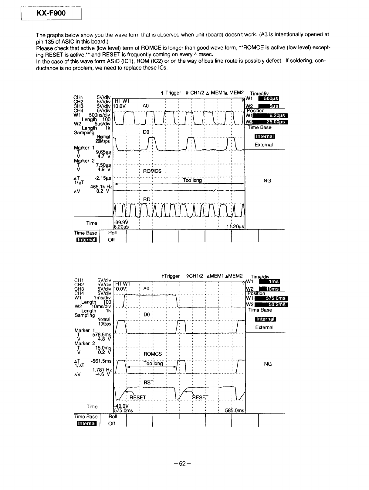
[.....Kx-Fgoo....]
The graphs below show you the wave form that is observed when unit (board) doesn't work. (A3 is intentionally opened at
pin 135 of ASIC in this board.)
Please check that active (low level) term of ROMCE is longer than good wave form, **ROMCE is active (low level) except-
ing RESET is active.** and RESET is frequently coming on every 4 msec.
In the case of this wave form ASlC (ICl), ROM (102) or on the way of bus line route is possibly defect. If soldering, con-
ductance is no problem, we need to replace these ICs.
CH 1 5V/div
CH2 5V/div
CH3 5V/div
CH4 5V/div
Wl 500ns/div
Length 100
W2 51_s/div
A Length lk
;sampling Normal
20Msps
Marker 1
T9_,.651_
V
Marker 2
AT -2.15p.s
l/AT 465. lk Hz
AV 0.2 V
Time
Time Base I Roll
I off
'1'Trigger _" CH1/2 z_ MEM1A MEM2
H1 W1
10.0V_ A0
DO
: i :
i i RoMcs _ :
........ i ........ ::........ i ..................... r_!iongi ........ i........ i ...... :
4
i i ! : i
RDi i
I
Time/div
Wl
lime Base
External
NG
CH1 5V/div
CH2 5V/div
CH3 5V/div
CH4 5V/div
Wl 1ms/div
Length 100
W2 10ms/div
Length 1k
Sampling Normal
10ksps
Marker 1
T 576.5ms
V 4.8 V
Marker 2
T 15.0ms
V 0.2 V
AT -561.5ms
l/z_T 1.781 Hz
AV -4.6 V
Time
Time__Base I
tTrigger _CH1/2 AMEM1 &MEM2 Time/div
H1 Wl oWl
10.0V_ i A0
ili ii! i--;............................................
• ..... . W2 '_l_4=l_
: Time Base
DO ;
_:i i'i ...... _ "'_" !i'"'_ _: "'i' i_ External
RO_ICS
::: ...... ::' ]oo::10ngi =................................. _: NG
:Ft$_ :
-40.0V
575.0ms i 585.0ms
o":t I I I I
-62-
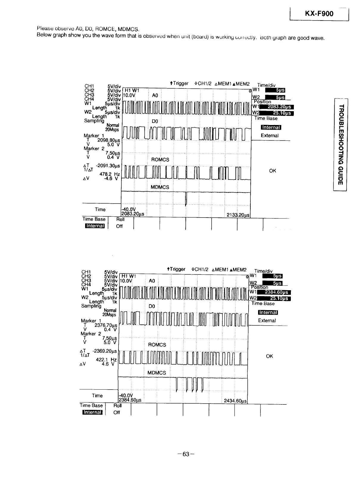
Please observe A0, DO, ROMCE, MDMCS.
Below graph show you the wave form that is observed when ullit (board) is wuiking _,uJtuutiy.
i KX-F900
_oth graph are good wave.
CH1 5V/div
CH2 5V/div
CH3 5V/div
CH4 5V/div
Wl, 51xs/div
Length lk
W2. 51zs/div
^Le,.ngth lk
bamp,ng Normal
20Msps
Marker 1
TV 20985.801a_
Marker 2
TV 705OIJ._
li_l'l_.-]
AT -2091.30p, S
l/AT 478.2 Hz
z_V -4.6 V
i'Trigger _'CH1/2 z_MEM1AMEM2
H1 W1 :
10.0V A0
D0_ i _
ROMCS i !
MDMCS
-40.OV : : :
2083.20Fs i 2133.20ps
;;"1 t I I
Time/div
Wl
Wl_
Time Base
External
OK
F- .....
t O
i J
, m
I m
: [/]
-1"
O
O
-I
Z
C
m
O
Ill
CH1 5V/div
CH2 5V/div
CH3 5V/div
CH4 5V/div
Wl. 5p,s/div
Length 1k
W2. 511s/div
^Length lk
bamplmg Normal
20Msps
Marker 1
vT23700 %
Marker 2
T 7.50#s
V 5.0 V
z_T -2369.20ps
l/z_T 422.1 Hz
z_V 4.6 V
Time
Time__Base t
HI Wl
10.OV_ _ AO
tTrigger OCH1/2 z_MEM1 &MEM2
DO i : i
i ! ! i i i
ROMCS
i i i i i i
! MDMCS : :
-40.or "
2384.60gs 243,_.60gs
F:loll I
o. 1 I
Time/div
Wl
Time Base
External
OK
-63-
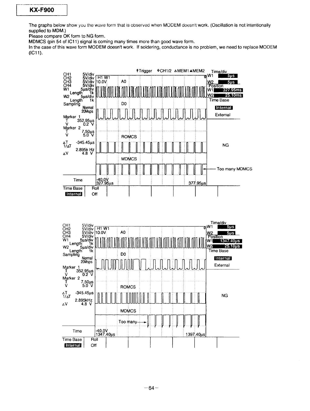
[KX-Fg00
The graphs below show you the wave form that is observed when MODEM doesn't work. (Oscillation is not intentionally
supplied to MDM.)
Please compare OK form to NG form.
MDMCS (pin 54 of ICl 1) signal is coming many times more than good wave form.
In the case of this wave form MODEM doesn't work. If soldering, conductance is no problem, we need to replace MODEM
(IC11).
CH1 5V/div
CH2 5V/div
CH3 5V/div
CH4 5V/div
Wl 5ps/div
Length 1k
W2 511s/div
^Length 1k
_ampJing Normal
20Msps
Marker 1
vT 3520951i_
Marker 2
T
V
z_T
l/AT
AV
H1 W1
I0.0V_
fTrigger _CH1/2 z_MEM1AMEM2 Time/div
Wl
A0
DO
_o% ROMCS
-345.451is _2.895k Hz
4.8 V
! MDI£1CS i ! i i
: ,,,
Time
Time Base ] Roll
l off II
Time Base
External
NG
many MDMCS
CH1 5V/div
CH2 5V/div
CH3 5V/div
CH4 5V/div
Wl
W2
S Lengtl
ampling Normal
20Msps
Marker 1
vT _%.9_
Marker 2
Tv75_°_v
AT -345.45pS
l/aT 2.895kHz
AV 4.8 V
Time
Time Base
H1 Wl
10.0V A0
DO
i : i i i
! MDMCS ! :
.................iz0°.many__
-40.0V
1347.40#s i ;1397_.40#s I
I I
Time/div
Wl
Wl_
Time Base
External
NG
-64-
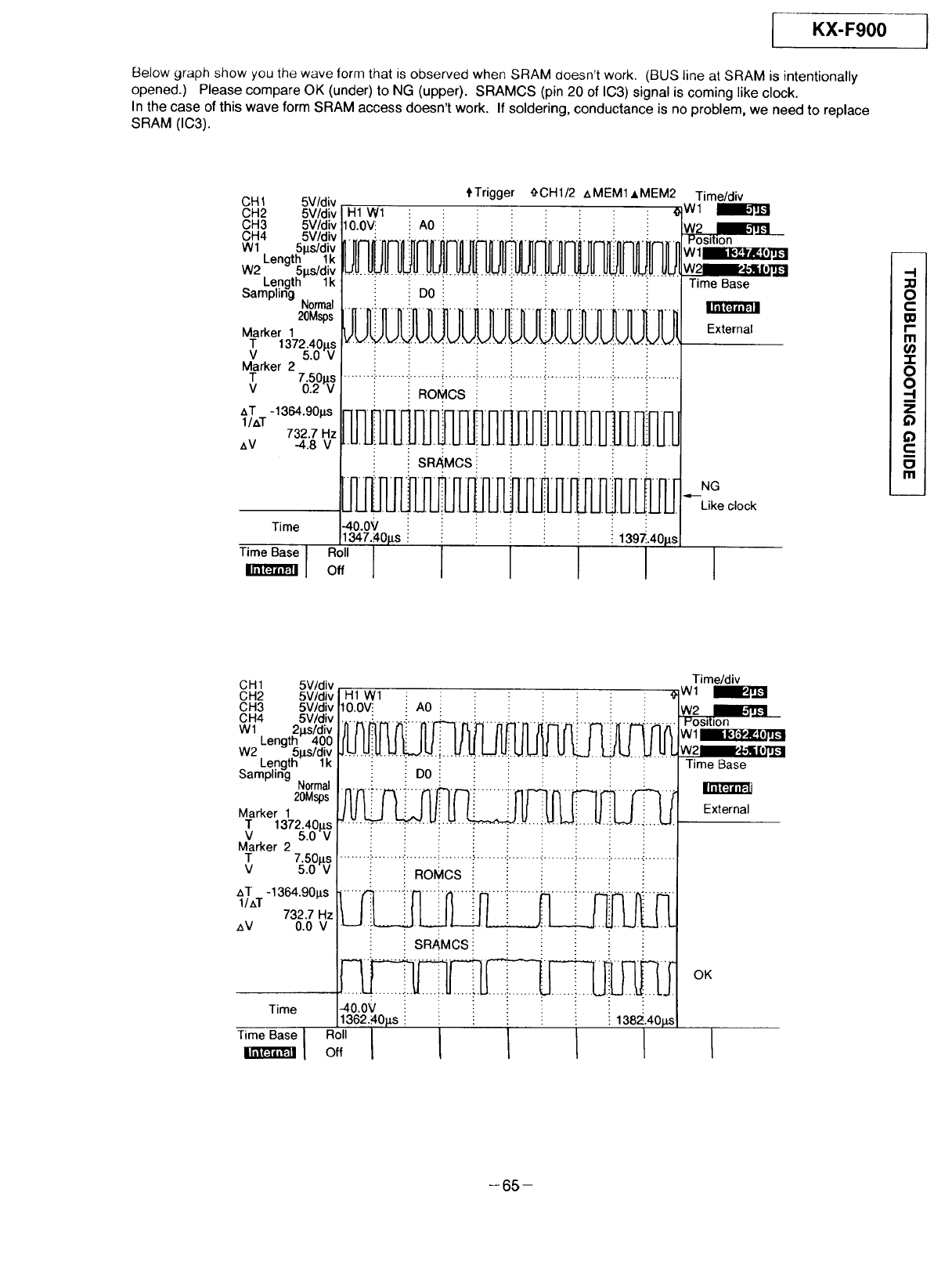
I KX-F900
Below graph show you the wave form that is observed when SRAM doesn't work. (BUS line at SRAM is intentionally
opened.) Please compare OK (under) to NG (upper). SRAMCS (pin 20 of IC3) signal is coming like clock.
In the case of this wave form SRAM access doesn't work. If soldering, conductance is no problem, we need to replace
SRAM (IO3).
CH 1 5V/div
CH2 5V/div
CH3 5V/div
CH4 5V/div
Wl 51_s/div
Length 1k
W2 51u,s/div
^ Length lk
_amp,ng Normal
20Msps
Marker 1
Tv t372_..0._
Marker 2
T
v
AT -1364.90ps
1/_T 732.7 Hz
z_V -4.8 V
Time
Time__Base I
H1 W1
10.0Vi
Roll
Off
tTrigger _'CH1/2 zxMEM1AMEM2 Time/div
Wl
A0
SRAMCS
Time Base
External
NG
Like clock
-I
O
C
m
O
O
-4
Z
Q
Q
C
m
CH1 5V/div
CH2 5Vtdiv
CH3 5V/div
CH4 5V/diM
Wl 21_s/div
Length 400
W2 5tls/div
Length 1k
bamp,ng Normal
20Msps
Marker 1
vT,37 :00.
Marker 2
V
AT -1364.90ps
l/AT
732.7 _z
AV 0.0
Time
Time__Base I
H1 W1
10.0V_ A0
DO
i : i
......................... ,...... : i i
ROMCS............................i................i........
SRAMCS :: : i :
-4o.ov
1362.:40Fs 1382-:.40ps
;,I'1 I I L
Time/div
wt
Time Base
External
OK
q
65
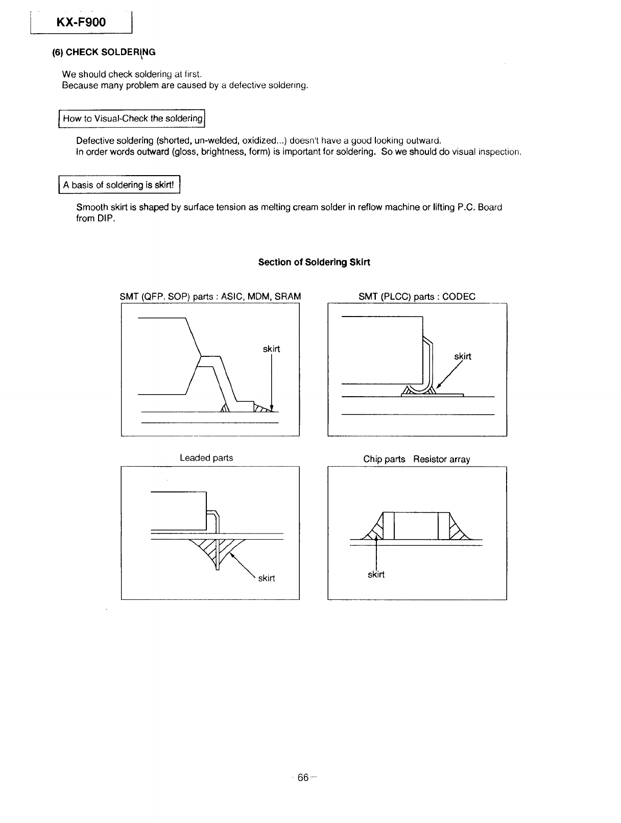
KX-F900 I
(6) CHECK SOLDERING
We should check soldering at first.
Because many problem are caused by a defective soldering.
I How to Visual-Check the soldering I
Defective soldering (shorted, un-welded, oxidized...) doesn't have a good looking outward.
In order words outward (gloss, brightness, form) is important for soldering. So we should do visual inspection.
IA basis of soldering is skirfl I
Smooth skirt is shaped by surface tension as melting cream solder in reflow machine or lifting P.C. Board
from DIP.
Section of Soldering Skirt
SMT (QFP. SOP) parts : ASIC, MDM, SRAM
skirt
SMT (PLCC) parts : CODEC
./__ skirt
//
i |
Leaded parts Chip parts Resistor array
sJirt
66-
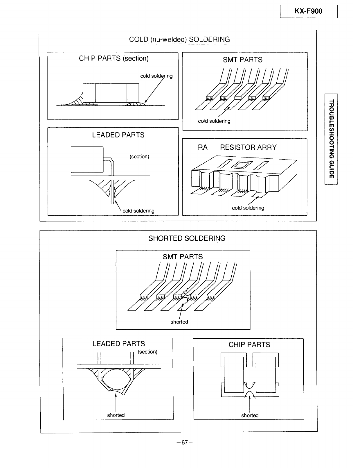
KX-F900
COLD (nu-welded) SOLDERING
CHIP PARTS (section)
cold soldering
LEADED PARTS
(section)
cold soldering
SMT PARTS
cold soldering
RA RESISTOR ARRY
cold soldering
-I
O
C
I-
I'll
-I-
O
O
,-I
Z
C
I'tl
SHORTED SOLDERING
SMT PARTS
shorted
LEADED PARTS
II I} (secti°n)
shorted
CHIP PARTS
-67-
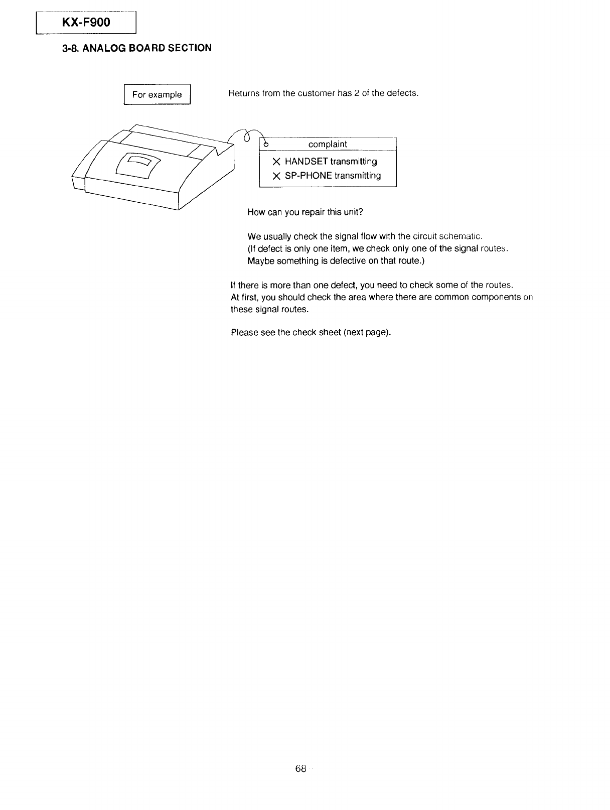
I .....I
3-8. ANALOG BOARD SECTION
For example ] Returns from the custorner has 2 of the defects.
complaint
X HANDSET transmitting
X SP-PHONE transmitting
How can you repair this unit?
We usually check the signal flow with the circuit schematic.
(If defect is only one item, we check only one of the signal routes.
Maybe something is defective on that route.)
If there is more than one defect, you need to check some of the routes.
At first, you should check the area where there are common components on
these signal routes.
Please see the check sheet (next page).
68
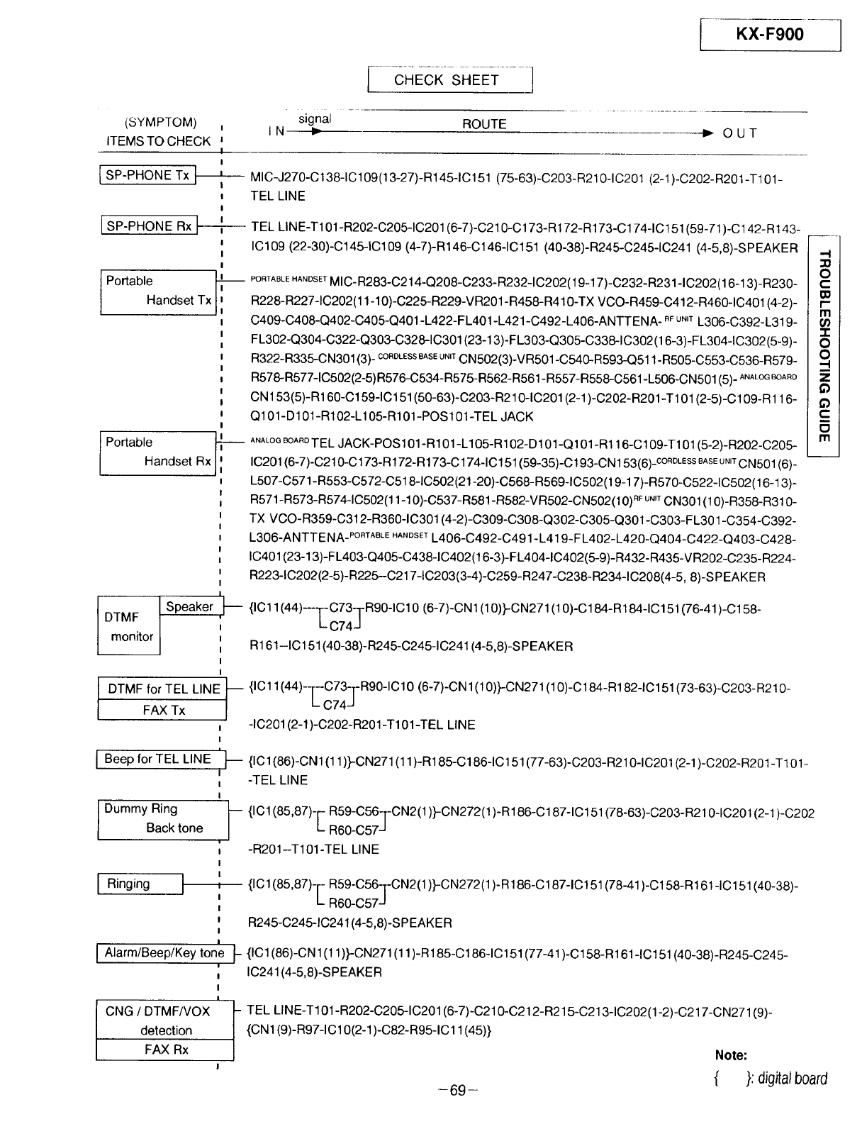
KX-F900 ]
(SYMPTOM) ,
ITEMS TO CHECK J
!
!
SP-PHONE Tx _ I
I
I
[SP-PHONERx
I Portable
Handset Tx
signal ROUTE
IN # I_ OUT
MIC-J270-C 138-1C109(13-27)-R145-1C 151 (75-63)-C203-R210-1C201 (2-1)-C202- R201 -T101 -
TEL LINE
TEL LINE-T101 -R202-C205-1C201 (6-7)-C210-C173-R172-R 173-C174-1C 151 (59-71)-C142-R 143-
IC109 (22-30)-C145-1C109 (4-7)-R146-C146-1C151 (40-38)-R245-C245-1C241 (4-5,8)-SPEAKER
-- _RTABLEHANOSETMIC_R283_C214_Q208_C233_R232_IC202(19_17)_C232_R231_IC202(16_13)_R230_
R228-R227-1C202(11-10)-C225-R229-VR201 -R458-R410-TX VCO-R459-C412-R460-1C401 (4-2)-
C409-C408-Q402-C405-Q401 -L422-FL401-L421-C492-L406-ANTTENA- RFUNITL306-C392-L319-
FL302-Q304-C322-Q303-C328-1C301 (23-13)-FL303-Q305-C338-1C302(16-3)-FL304-1C302(5-9)-
R322-R335-CN301 (3)- CORI)LIFSSBASEUNITCN502(3)-VR501-C540-R593-Q511-R505-C553-C536-R579-
R578-R577-1C502(2-5) R576-C534-R575-R562-R561 -R557-R558-C561 -L506-CN501 (5)- ANALOGOOARD
CN153(5)-R 160-Cl 59-1C151 (50-63)-C203-R210-1C201 (2-1)-C202-R201 -T101 (2-5)-C 109-R116-
Q101-D 101-R102-L105-R101-POS101-TEL JACK
Portable
Handset Rx
i
DTMF Speaker
monitor
I DTMF for TEL LINE
FAX Tx
a
I Beep for TEL LINE
I Dummy Ring
Back tone
ANALOG8OAROTEL JACK-POS101-R101-L105-R102-D101-Q101-R116-C109-T101 (5-2)-R202-C205-
IC201 (6-7)-C210-C173-R172-R173-C174-1C151 (59-35)-C193-CN153(6) -coRDLEssBASEUN,TCN501 (6)-
L507-C571-R553-C572-C518-1C502(21-20)-C568-R569-1C502(19-17)-R570-C522-1C502(16-13)-
R571-R573-R574-1C502(11-10)-C537-R581-R582-VR502-CN502(10)RF UN,TCN301 (10)-R358-R310-
TX VCO-R359-C312-R360-1C301 (4-2)-C309-C308-Q302-C305-Q301-C303-FL301-C354-C392-
L306_ANTTENA_PORTABLEHANDSETL406-C492-C491-L419-FL402-L420-Q404-C422-Q403-C428-
IC401 (23-13)-FL403-Q405-C438-1C402(16-3)-FL404-1C402(5-9)-R432-R435-V R202-C235-R224-
R223-1C202(2-5)-R225-C217-1C203(3-4)-C259-R247-C238-R234-1C208(4-5, 8)-SPEAKER
{IC11 (44)-T- C73-rR90-1C 10 (6-7)-CN 1(10)}-CN271 (10)-C184-R184-1C 151(76-41)-C158-
L_C74-J
R161-1C151 (40-38)- R245-C245-1 C241 (4-5,8)-S PEAKER
{IC11 (44)--[--C73TR90-1C 10 (6-7)-CN 1(10)}-CN271 (10)-C 184-R 182-1C151 (73-63)-C203-R210-
t_ C74.J
-IC201 (2-1)-C202-R201 -T101 -TEL LINE
{ICl (86)-CN1 (11)}-CN271 (11)-R185-C186-1C151 (77-63)-C203-R210-1C201 (2-1)-C202-R201-T101-
-TEL LINE
{IC1 (85,87)-[- R59-C56TCN2(1 )}-CN272(1 )-R186-C187-1C151 (78-63)-C203-R210-1C201 (2-1)-C202
/R60-C57 .J
-R201-T101-TEL LINE
-.,I
:;0
O
i"-
m
"I-
O
O
-I
m
z
63
63
t--
m
I Ringing I '
I
I
I
I
I
I Alarm/Beep/Key tone _-
!
I
I
I
CNG /DTMF/VOX I
detection
FAX Rx
I
{IC1 (85,87)- r- R59-C56-[-CN2 (1)}-C N272(1 )-R186-C187-1C 151(78-41)-C158-R161 -IC151 (40-38)-
LR60-C57 J
!
R245-C245-1C241 (4-5,8)-SPEAKER
{IC1 (86)-CN1 (11)}-CN271 (11)-R185-C186-1C151 (77-41)-C158-R161-1C151 (40-38)-R245-C245-
IC241 (4-5,8)-SPEAKER
TEL LINE-T101 -R202-C205-1C201 (6-7)-C210-C212-R215-C213-1C202(1-2)-C217-CN271 (9)-
{CN1 (9)-R97-1C 10(2-1 )-C82-R95-1C 11 (45)}
Note:
69 { }: digitalboard
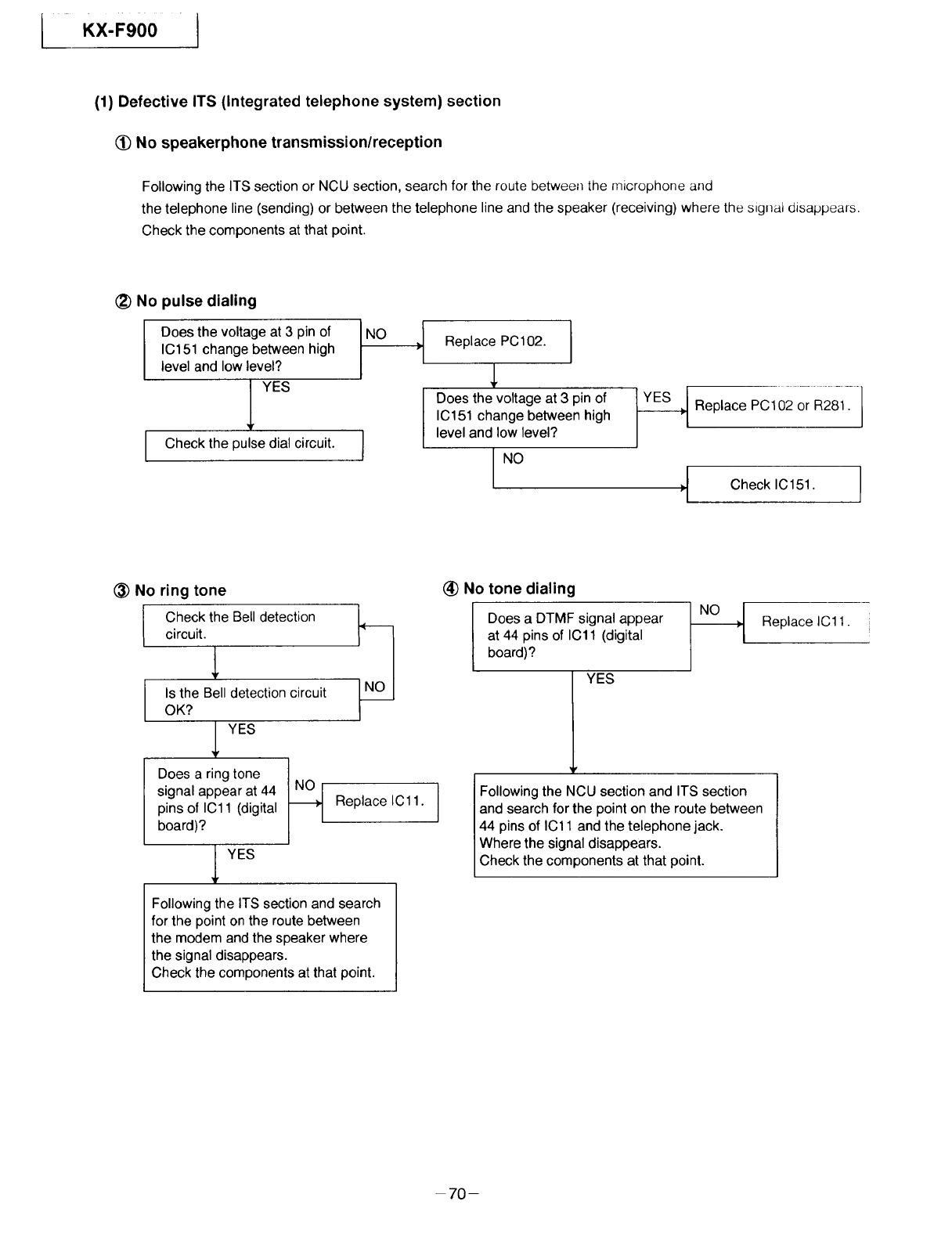
iKX-F900
(1) Defective ITS (Integrated telephone system) section
€_)No speakerphone transmission/reception
Following the ITS section or NCU section, search for the route between the microphone and
the telephone line (sending) or between the telephone line and the speaker (receiving) where the signal disappears.
Check the components at that point.
_) No pulse dialing
IDoes the voltage at 3 pin of
IC151 change between high
level and low level?
I YES
Check the pulse dial circuit.
INO
IReplace PC102. I
,r
Does the voltage at 3 pin of IYES I
IC151 change between high
level and low level?
I,I
Replace PC102 or R281.
Check IC151.
(_) No ring tone
LCheck the Bell detection
circuit. 1
Is the Bell detection circuit
OK?
YES
/
Does a ring tone I,,^
signal appear at 44
pins of IC11 (digital
board)?
YES
Replace IC11.
Following the ITS section and search
for the point on the route between
the modem and the speaker where
the signal disappears.
Check the components at that point.
(_ No tone dialing
Does a DTMF signal appear
at 44 pins of ICll (digital
board)?
YES
Following the NCU section and ITS section
and search for the point on the route between
44 pins of IC11 and the telephone jack.
Where the signal disappears.
Check the components at that point.
Replace IC11.
-70-
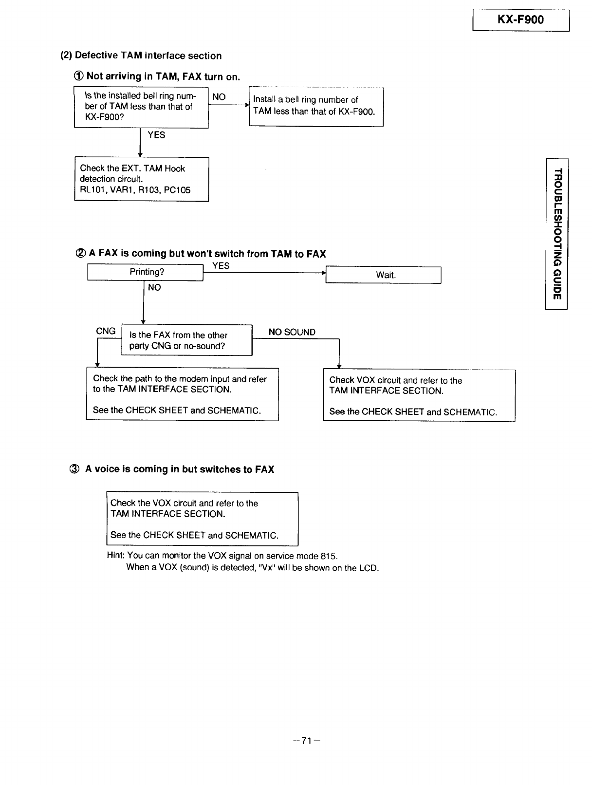
I KX-F900
(2) Defective TAM interface section
(!) Not arriving in TAM, FAX turn on.
_sthe installed bell ring num-
ber of TAM less than that of
KX-F900?
I YES
Check the EXT. TAM Hook
detection circuit.
RL101, VAR1, R103, PC105
NO -,nstal,a be;, ringnumber oi I
TAM less than that of KX-F900. I
(_ A FAX is coming but won't switch from TAM to FAX
Printing? I YES '1
l"°
Is the FAX from the other [ NO SOUND
party CNG or no-sound? /
Check the path to the modem input and refer
to the TAM INTERFACE SECTION.
See the CHECK SHEET and SCHEMATIC.
Wait. I
Check VOX circuit and refer to the
TAM INTERFACE SECTION.
See the CHECK SHEET and SCHEMATIC.
-I
O
C
f-
Ill
"1-
O
O
.-I
z
¢)
c
m
m
(_) A voice is coming in but switches to FAX
Check the VOX circuit and refer to the
TAM INTERFACE SECTION.
See the CHECK SHEET and SCHEMATIC.
Hint: You can monitor the VOX signal on service mode 815.
When a VOX (sound) is detected, "Vx" will be shown on the LCD.
71-
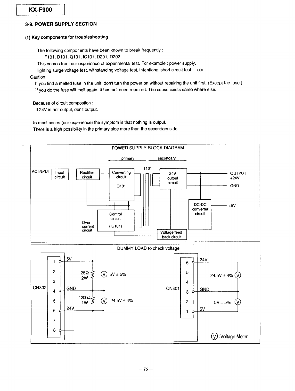
KX-F900
3-9. POWER SUPPLY SECTION
(1) Key components for troubleshooting
The following components have been known to break frequently :
F101, D101, Q101, IC101, D201, D202
This comes from our experience of experimental test. For example : power supply,
lighting surge voltage test, withstanding voltage test, intentional short circuit test .....etc.
Caution:
If you find a melted fuse in the unit, don't turn the power on without repairing the unit first. (Except the fuse.)
If you do the fuse will melt again. It has not been repaired. The cause exists same where else.
Because of circuit compostion :
If 24V is not output, don't output.
In most cases (our experience) the symptom is that nothing is output.
There is a high possibility in the primary side more than the secondary side.
POWER SUPPLY BLOCK DIAGRAM
•, primary secondary .
AC INP_ Rectifier
circuit
Over
current
circuit
C°cnrveuir_ing
Q101
t
T101[ 24v17
output
circuit
DC-DC
converter
circuit
Voltage feed
back circuit
OUTPUT
+24V
GND
-- +5V
DUMMY LOAD to check voltage
CN302
i
5V 1
25£2 <4 5V _+5%
2W :!
1200Q.
l W 24.5V + 4%
GND
24V
CN301
24V
24.5V + 4°/o (_
GND
5V+5% (
5V
(_ :VoltageMeter
-72-
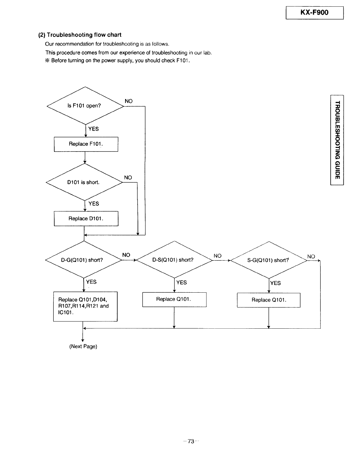
KX-F900 I
(2) Troubleshooting flow chart
Our recommendation for troubleshooting is as follows.
This procedure comes from our experience of troubleshooting in our lab.
•_Before turning on the power supply, you should check F101.
NO
R I FI !"
NO
I R I DI I.
• r
l 1 1
(Next Page)
,-I
0
C
m
i-
ra
z
0
0
-I
z
c
1:3
m
73-
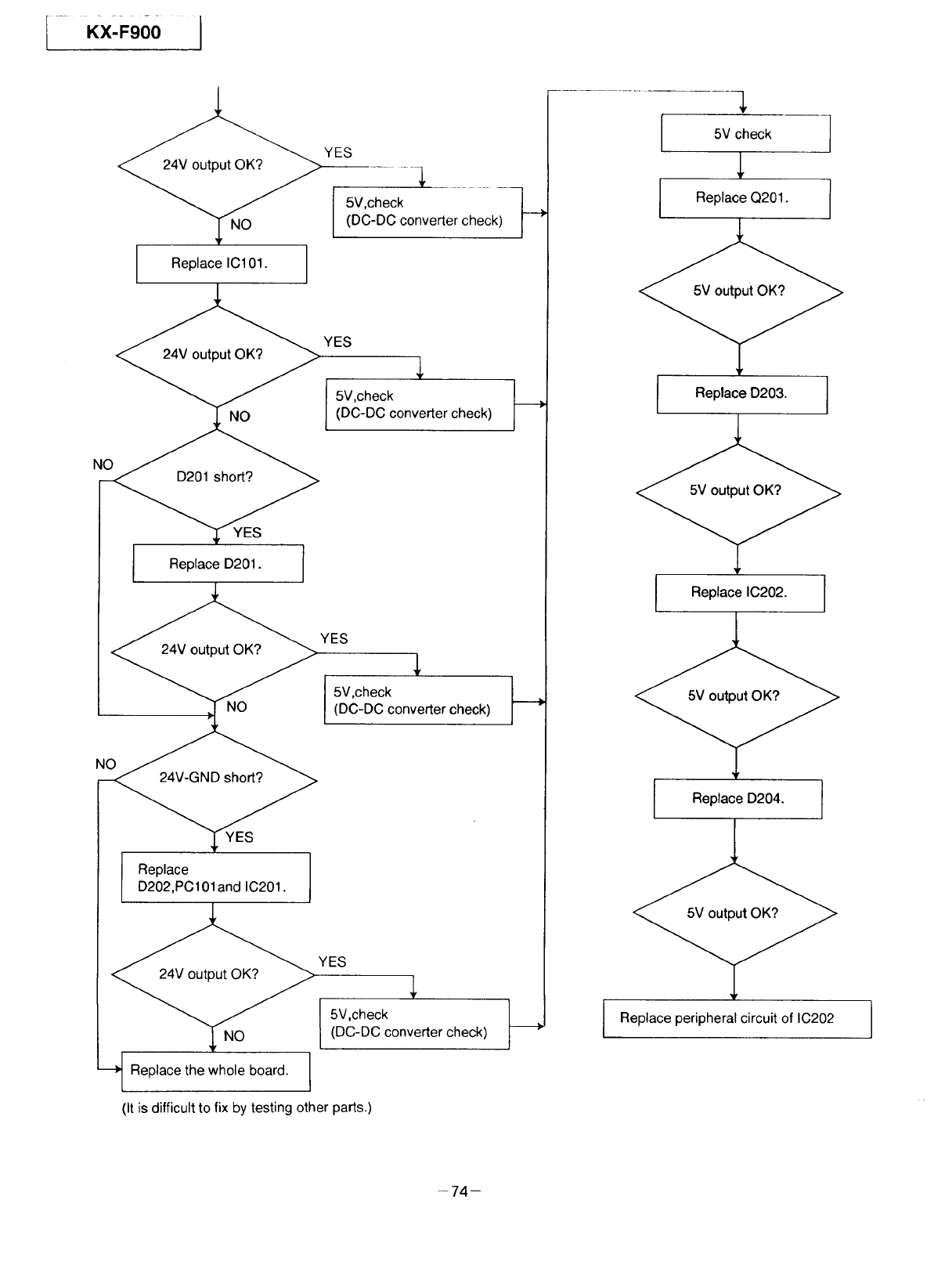
k _x:_,ooJ
YES
I
R I Ill.
5V,check ___
(DC-DC converter check)
NO
YES
5V,check
(DC-DC converter check)
NO
Replace D201. J
NO
YES
NO
YES
Replace
D202,PC101 and IC201.
I_v,che_ _-.(DC-DC converter check)
YES
5V,check
NO (DC-DC converter check)
---_ Replace the whole board. J
(It is difficult to fix by testing other parts.)
-74-
I _vcheck 1
I I
Replace D203.
Replace IC202. J
J ReplaceD204. I
Replace peripheral circuit of IC202
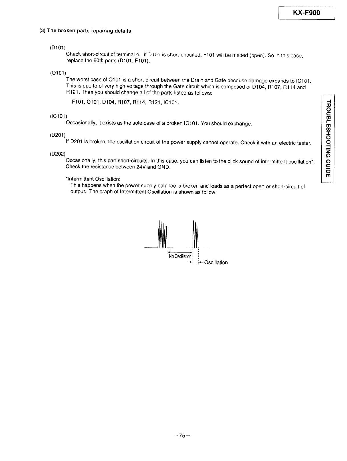
(3) The broken parts repairing details
[- --KX-Fg00 ..... J
(D101)
Check short-circuit of terminal 4. It D101 is short-circuited, F101 will be melted (open). So in this case,
replace the 60th parts (D101, F101).
(Q101)
The worst case of Q101 is a short-circuit between the Drain and Gate because damage expands to IC101.
This is due to of very high voltage through the Gate circuit which is composed of D104, R107, R114 and
R121. Then you should change all of the parts listed as follows:
F101, Q101, D104, R107, Rl14, R121, IC101.
(IC101)
Occasionally, it exists as the sole case of a broken IC101. You should exchange.
(D201)
If D201 is broken, the oscillation circuit of the power supply cannot operate. Check it with an electric tester.
(D202)
Occasionally, this part short-circuits. In this case, you can listen to the click sound of intermittent oscillation*.
Check the resistance between 24V and GND.
*Intermittent Oscillation:
This happens when the power supply balance is broken and loads as a perfect open or short-circuit of
output. The graph of Intermittent Oscillation is shown as follow.
-I
=0
O
_0
I'"
131
"I"
O
O
"-I
Z
¢)
O
rrl
,,No0sc=llatl0n[ ,,
i
_, [*-Oscillation
75--
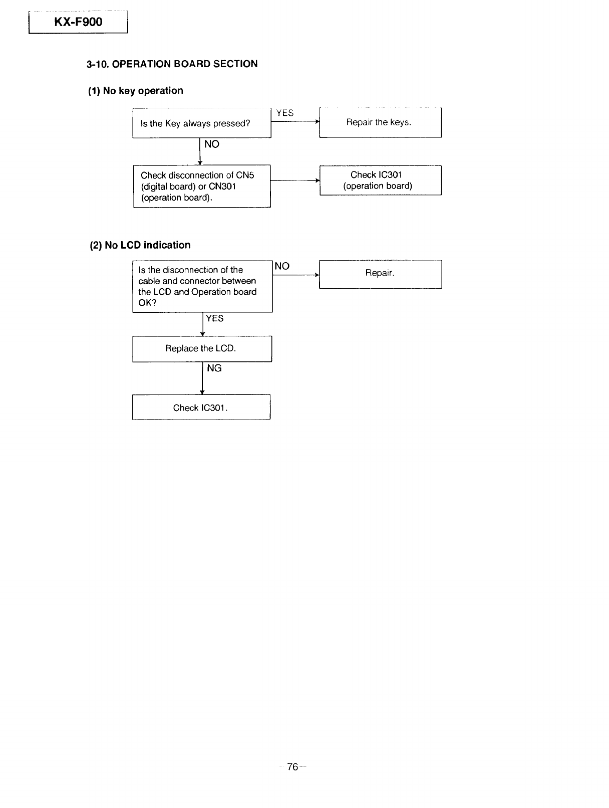
I KX:F,001
3-10. OPERATION BOARD SECTION
(1) No key operation
I Key always pressed?
Is the
[_o
Check disconnection of CN5
(digital board) or CN301
(operation board).
t YES Repair the keys.
Check IC301
(operation board)
(2) No LCD indication
I
[
Is the disconnection of the
cable and connector between
the LCD and Operation board
OK?
YES
Replace the LCD.
Check IC301.
NO Repair.
76-

[........Kx-Fgoo
3-11. SENSOR SECTION
(1) Check the read position sensor(PI301)
J
Check the voltageat pin 15 of IC301
Document set OV -L--When the pin
No document 4-5V !-_ 16 of IC301 is
low level.
OK
Replace IC301, J
N__2%,.
Check the soldering at R333.
(2) Check the document sensor (PI302)
I
Check the voltage at pin 15 of IC301
Document set 4~5V -_---When the pin
No document OV --9 of IC301 is
low level.
OK
Replace IC301. I
--_ Check the at R333. ]OK
soldering I
q
Check the soldering /
at R331. /
Replace PI301.
v
I
Check the soldering
at R332.
Replace PI302. f
O
c
i'-
m
'-r.
0
0
,-4
Z
Q
C
m
(3) Check the cover open sensor(SW271)
Check the voltage at pin 31 of IC151 _ Check the soldering at R271.
Open cover:4~5V /
Close cover: 0V
OK
ReplaceIC151. J
Check the soldering
at R272
OK
ReplaceSW271.
77
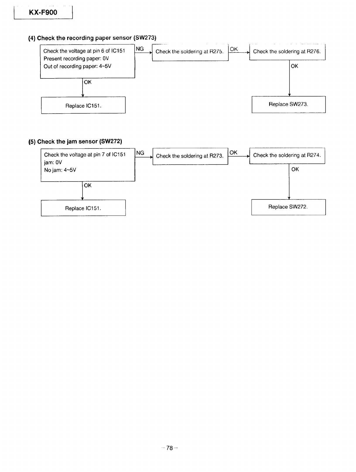
KX-Fg001
(4) Check the recording paper sensor (SW273)
Check the voltage at pin 6 of IC151
Present recording paper: 0V
Out of recording paper: 4-5V
OK
Replace IC151.
-_ Check the soldering at R275. _ Check the soldering at R276. I
OK
_r
Replace SW273.
(5) Check the jam sensor (SW272)
Check the voltage at pin 7of IC151
jam: 0V
No jam: 4-5V
OK
Replace IC151.
-_ Check the soldering at R273. _,_ Check the soldering at R274.
OK
Replace SW272.
--78-
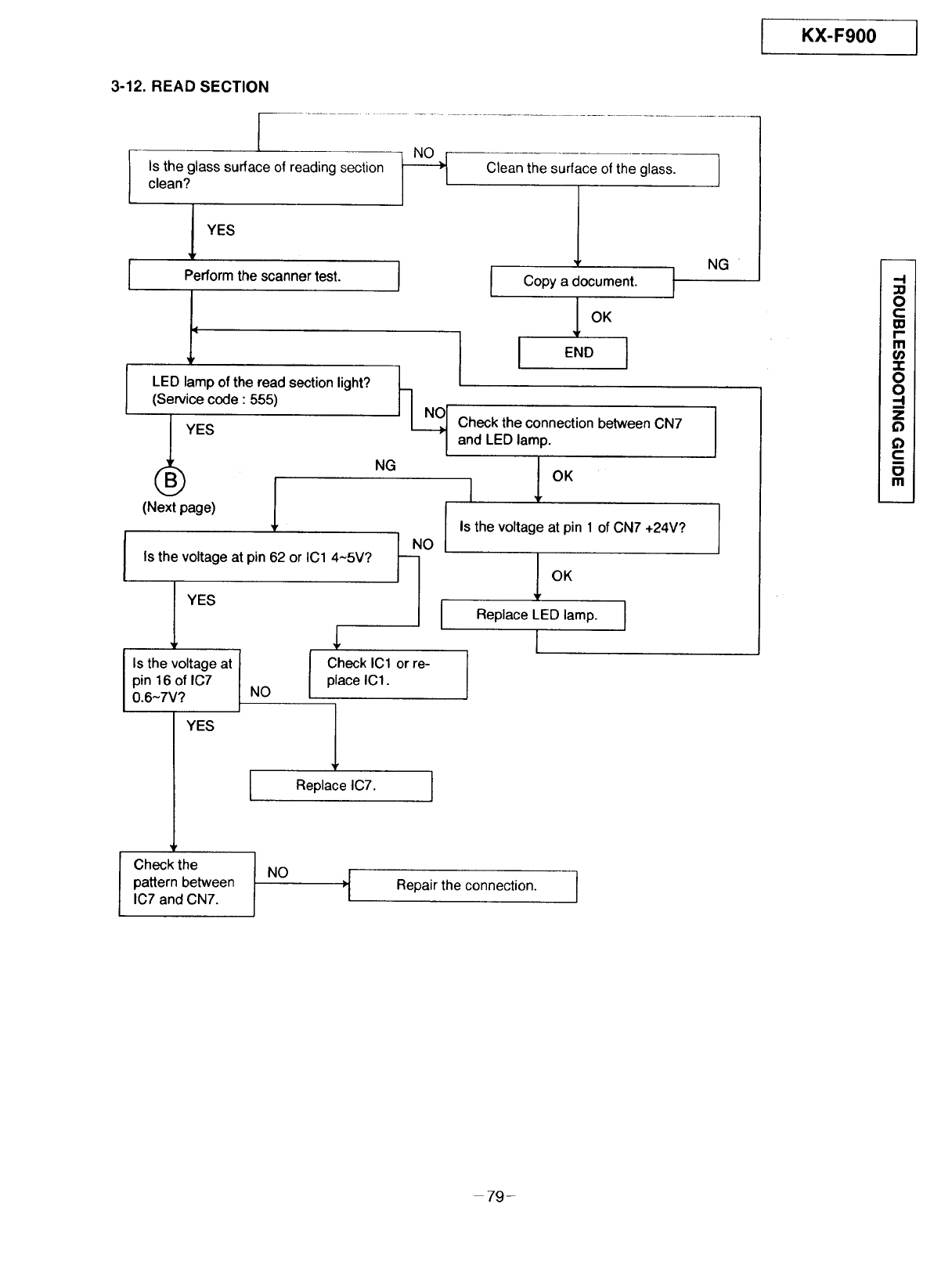
3-12. READ SECTION
I
)'sthe0'asssur'aceo,rea,,,r,0sect,onC,ear,thesu,,aceo,the0,ass.Ic,ean?
NG
IPerform the scanner test. Copy a document. /
_°_
lEND
I
LED lamp of the read section light? I-,
(Service code : 555)
YES NG
(Next page) l
Is the voltage at pin 62 or ICl 4~5V?
IYES
l ls the voltage at
pin 16 of IC7
0.6-7V?
YES
NO
1
I hecklC1 orre-
place IC1.
1
Replace IC7.
I
Check the connection between CN7 I
and LED lamp. I
IReplace lamp.
1
Is the voltage at pin 1 of CN7 +24V?
I
KX-F900
-.,I
::0
O
c
_0
r-
m
"1"
O
O
,-I
B
z
c
Io
m
I
Check the
pattern between
IC7 and CN7. NO ,{ Repair the connection. i
79-
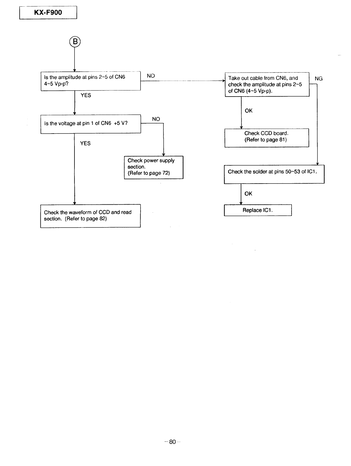
IKX-F900
Is the amplitude at pins 2~5 of CN6
4~5 Vp-p?
YES
NO
Is the voltage at pin 1 of CN6 +5 V?
YES
_r
Check power supply
section.
(Refer to page 72)
Check the waveform of CCD and read
section. (Refer to page 82)
Take out cable from CN6, and _NG
check the amplitude at pins 2~5
of CN6 (4~5 Vp-p).
OK
Check CCD board.
(Refer to page 81)
_r
Check the solder at pins 50~53 of IC1.
I OK
Replace IC1. I
-80-
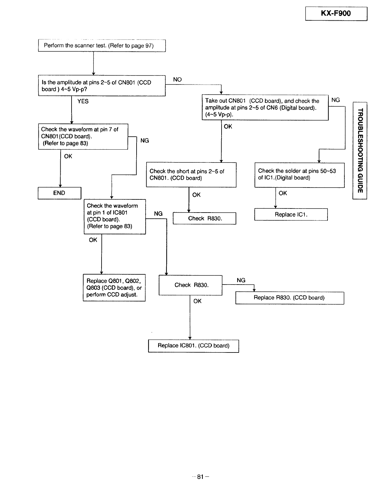
KX-F900 J
[-Pe"0;m the scanner test. (Refertopage 97_) 'I
l
I Is the amplitude at pins 2~5 of CN801 (CCDboard ) 4~5 Vp-p?
I YES
Check the waveform at pin 7 of
CN801 (CCD board).
(Refer to page 83) NG
END
OK
!t
Check the waveform
at pin 1of IC801
(CCD board).
(Refer to page 83)
OK
Replace Q801, Q802,
Q803 (CCD board), or
perform CCD adjust.
NO
Take out CN801 (CCD board), and check the
amplitude at pins 2~5 of CN6 (Digital board).
I Check the short at pins 2~5 of
0N801. (COD board)
NG Check R_O.
(4~5 Vp-p).
Check the solder at pins 50-53
of IC1 .(Digital board)
l
Replace IC1. I
NG
Check R830.
OK
ING
Replace R830. (CCD board)
Replace IC801. (CCD board) }
=01
OI
cI
001
r" i
rnl
(/)1
QI
C_l
ml
81-
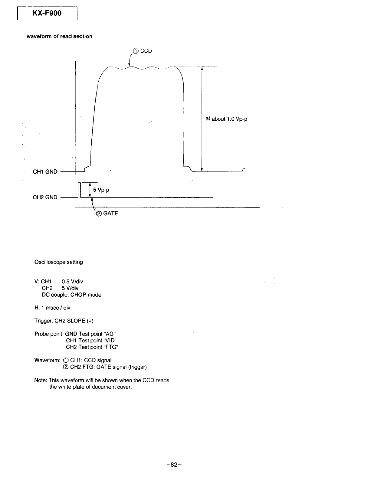
waveform of read section
CH1 GND
CH2 GND --
® CCD
._ a! about
1.0 Vlmp
Oscilloscope setting
V: CH1 0.5 V/div
CH2 5 V/div
DC couple, CHOP mode
H: 1 msec /div
Trigger: CH2 SLOPE (+)
Probe point: GND Test point "AG"
CH1 Test point "VID"
CH2 Test point "FTG"
Waveform: _ CHI CCD signal
(_) CH2 FTG: GATE signal (trigger)
Note: This waveform will be shown when the CCD reads
the white plate of document cover.
-82-
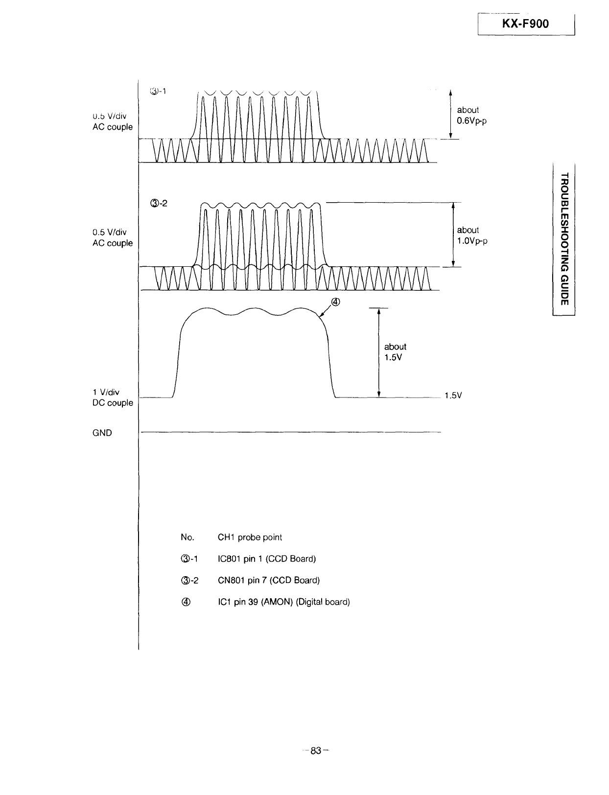
IKX-F900
U.b V/div
AC couple
0.5 V/div
AC couple
1 V/div
DC couple
GND
about
1.5V
NO.
(_-1
(_)-2
®
CH1 probe point
IC801 pin 1 (CCD Board)
0N801 pin 7 (CCD Board)
IC1 pin 39 (AMON) (Digital board)
about
0.6Vp.p
I about
1.0Vp-p
1.5V
-I
m
11
i
11
83-
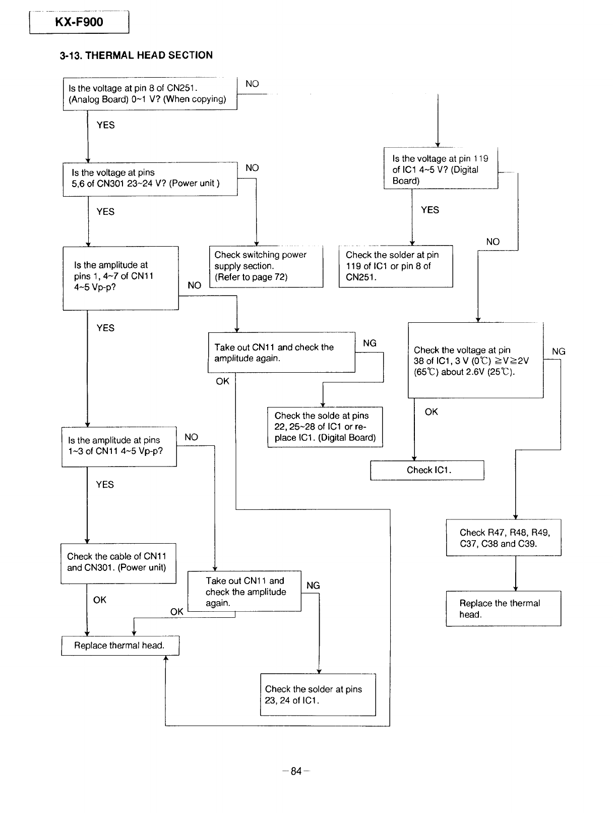
I......KxFgo0-I
3-13. THERMAL HEAD SECTION
I
Is the voltage at pin 8 of CN251.
(Analog Board) 0-1 V? (When copying)
I YES
Is the voltage at pins
5,6 of CN301 23~24 V? (Power unit )
YES
Is the amplitude at
pins 1, 4-7 of CN11
4N5 Vp-p? NO
YES
Is the amplitude at pins
1~3 of CN 11 4~5 Vp-p?
NO
YES
Check the cable of CN11
and CN301. (Power unit)
OK
Replace thermal head.
NO
Check switching power
supply section.
(Refer to page 72)
I s the voltage at pin 119
of IC1 4-5 V? (Digital
Board)
YES
Checkthe solder at pin
119 of ICl or pin 8 of
I CN251.
NO
_r
Take out CN11 and check the
amplitude again.
NG
OK 1
Check the solde at pins
22, 25-28 of IC1 or re-
place IC1. (Digital Board)
Check the voltage at pin
38 of IC1,3V (0%) >V__2V
(65%) about 2.6V (25%).
NG
OK
I ,
Check IC1. J
Take out CN11 and
check the amplitude
again.
I
NG
Check the solder at pins--/7/
23, 24 of IC1.
Check R47, R48, R49,
C37, C38 and C39.
Replace the thermal
head.
-84-
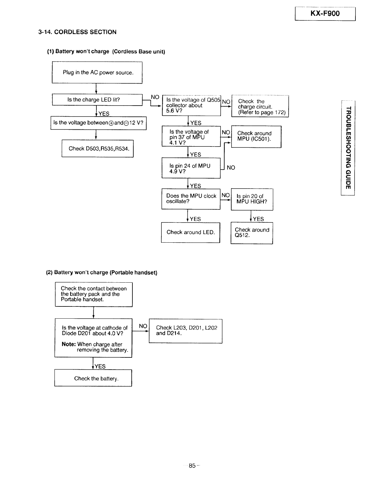
3-14. CORDLESS SECTION
/KX-F900
(1) Battery won't charge (Cordless Base unit)
Plug inthe AC power source.
Is the charge LED lit?
_YES
I Is the voltage between(_and012 V? I
I Check D503,R535,R534.
_._ Isi-_ v(_tage-oi Q505]NO[ Check{he .......
I collector about _ charge circuit
I 5.6 V? II (Refer to page 172)
IYES
Is the voltage of
pin 37 of MPU
4.1 V?
IYES
Is pin 24 of MPU
4.9 V?
l_ heck around J
MPU (IC501).
NO
I
I
_YES
/r
Does the MPU clock INOI
oscillate? r-l
IYES
Check around LED.
Is pin 20 of
MPU HIGH?
_YES
Check around
Q512.
1
I
-.I
0
cI
IzI
r-
rrl
o)
'-r
0
0
-I
i
z
i
m
(2) Battery won't charge (Portable handset)
Check the contact between
the battery pack and the
Portable handset.
Is the voltage at cathode of
Diode D201 about 4.0 V?
Note: When charge after
removing the battery.
IYES
Check the battery.
q
Check L203, D201, L202 |
and D214. J
85-
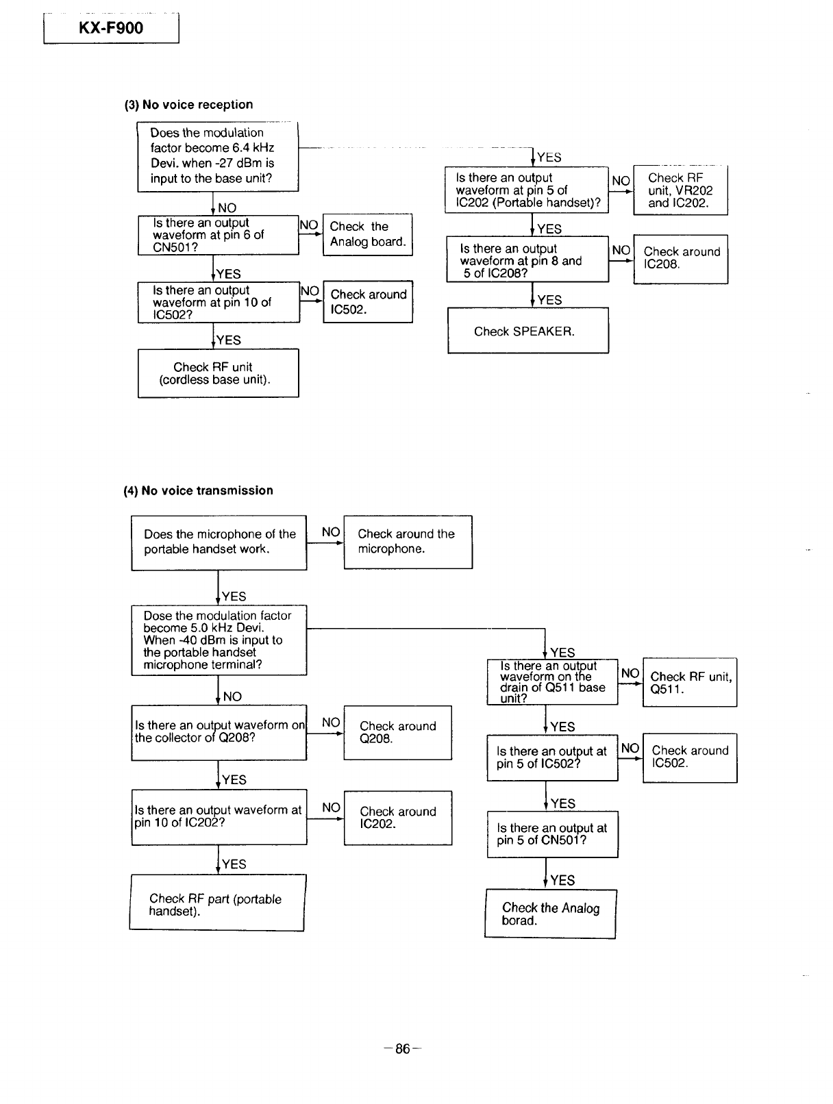
IKx:F,oo.....I
(3) No voice reception
Does the modulation
factor become 6.4 kHz
Devi. when -27 dBm is
input to the base unit?
Is there an output
waveform at pin 6 of
CN501 ?
IYES
Is there an output
waveform at pin 10 of
IC502?
_YES
Check RF unit
(cordless base unit).
....................... -_YES
__ Check theAnalog board.
._ heck around I
IC502.
Is there an output
waveform at pin 5 of
IC202 (Portable handset)?
_YES
Is there an output
waveform at pin 8 and
5 of IC208?
I YES
Check SPEAKER.
....
it, VR202
d IC202.
___ Check around
IC208.
(4) No voice transmission
Does the microphone of the
portable handset work. ._ Check around the
microphone.
IYES
Dose the modulation factor
become 5.0 kHz Devi.
When -40 dBm is input to
the portable handset
microphone terminal?
INo
Is there an output waveform I.ol
the co ector of Q208? on]
I I
IYES
Is there an output
pin 10 of IC202? waveform at NO
IYES
Check RF part (portable
handset).
Check around
Q208.
Check around
IC202.
YES
Is there an output
waveform on the
drain of Q511 base
unit?
I YES
| !
Is there an output at NLN_
pin 5 of IC502?
I YES
I
Is there an output at I
pin 5 of CN501? I
I YES
Check the Analog
borad. 1
_._ heck RF unit,
Q511.
Check around
IC502.
86
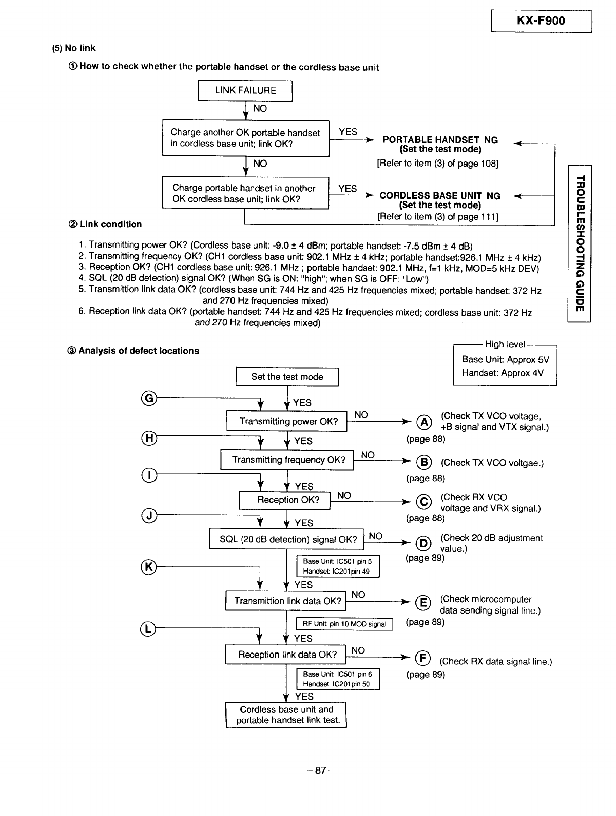
KX-F900
(5) No link
(_)How to check whether the portable handset or the cordless base unit
_) Link condition
ILINK FAILURE I
NO
Charge another OK portable handset
in cordless base unit; link OK?
NO
Charge portable handset in another
OK cordless base unit; link OK?
1
PORTABLE HANDSET NG
(Set the test mode)
[Referto item (3) of page 108]
CORDLESS BASE UNIT NG
(Set the test mode)
[Refer to item (3) of page 111]
1. Transmitting power OK? (Cordless base unit: -9.0 + 4 dBm; portable handset: -7.5 dBm + 4 dB)
2. Transmitting frequency OK? (CH1 cordless base unit: 902.1 MHz + 4 kHz; portable handset:926.1 MHz + 4 kHz)
3. Reception OK? (CH1 cordless base unit: 926.1 MHz ; portable handset: 902.1 MHz, f--1 kHz, MOD=5 kHz DEV)
4. SQL (20 dB detection) signal OK? (When SG is ON: "high"; when SG is OFF: "Low")
5. Transmittion link data OK? (cordless base unit: 744 Hz and 425 Hz frequencies mixed; portable handset: 372 Hz
and 270 Hz frequencies mixed)
6. Reception link data OK? (portable handset: 744 Hz and 425 Hz frequencies mixed; cordless base unit: 372 Hz
and 270 Hz frequencies mixed)
_) Analysis of defect locations
I Set the test mode I
(_ _ _ YES
Transmittingpower OK? INO
1_ _ _ YES
Transmitting frequency OK? I NO
_) __LyES
I ReceptionOK? ] NO
(_ __ YES
SQL (20 dB detection) signal OK? I NO
(_ 1 Base Unit: lC501pin 5 J
,_ Handset: IC201 pin 49
YES
ITransmittion link data OK? JNO
I I RF Unit: pin 10 MOD signal I
(_ +YES
I Reception,inkdataOK? I NO
Base Unit: IC501 pin 6 I
Handset: IC201 pin 50
YES
! Cordless base unit and 1
portable handset link test.
High level-
Base Unit: Approx 5V
Handset: Approx 4V
(Check TX VCO voltage,
+B signal and VTX signal.)
(page 88)
(_ (Check TX VCO voltgae.)
>
(page 88)
(Check RX VCO
voltage and VRX signal.)
(page 88)
> @ (Check 20dB adjustment
value.)
(page 89)
('_ (Check microcomputer
data sending signal line.)
(page 89)
(_ (Check RX data signal line.)
(page 89)
J
-I
O
c
I"
m
(t)
"1-
O
O
-I
z
Q
c:
o
Ill
-87-
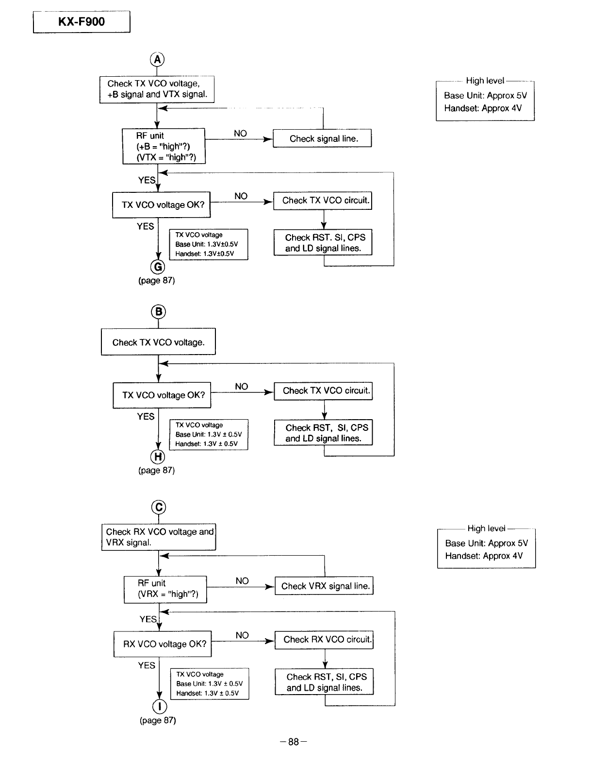
FKX-F900
Check TX VCO voltage,
+B signal and VTX signal. /
RF unit I NO
(+B = "high"?) I
(VTX = "high"?)
YESi-'_
TX VCO voltage OK? I NO
I
TX VCO voltage
Base Unit: 1.3V_+O.5V
Handset: 1.3V_+O.5V
(page 87)
I Check signal line. I
I
I Check TX VCO circuit.
[
I heck RST. SI, CPS
and LD signal lines.
L
-- - High level ....
Base Unit: Approx 5V
Handset: Approx 4V
Check TX VCO voltage.
I"° I
TX VCO voltage OK?
TX VCO voltage
Base Unit: 1.3V _+0.5V
Handset: 1.3V -+0.5V
(page 87)
I
Check TX VCO circuit. I
!
Check RST, Sl, CPS I
and LD signal lines. I
[
I
Check RX VCO voltage and I
VRX signal. I
F
RF unit
(VRX = "high"?)
YES_ "_
I I
RX VCO voltage OK?
/
YES I TX VCO voltage
Base Unit: 1.3V + 0.5V
Handset: 1.3V _+0.5V
(page 87)
NO • Check VRX signal line. I
Check RX VCO circuit.
Check RST, SI, CPS
and LD signal lines.
1
-- High level--
Base Unit: Approx 5V
Handset: Approx 4V
-88-
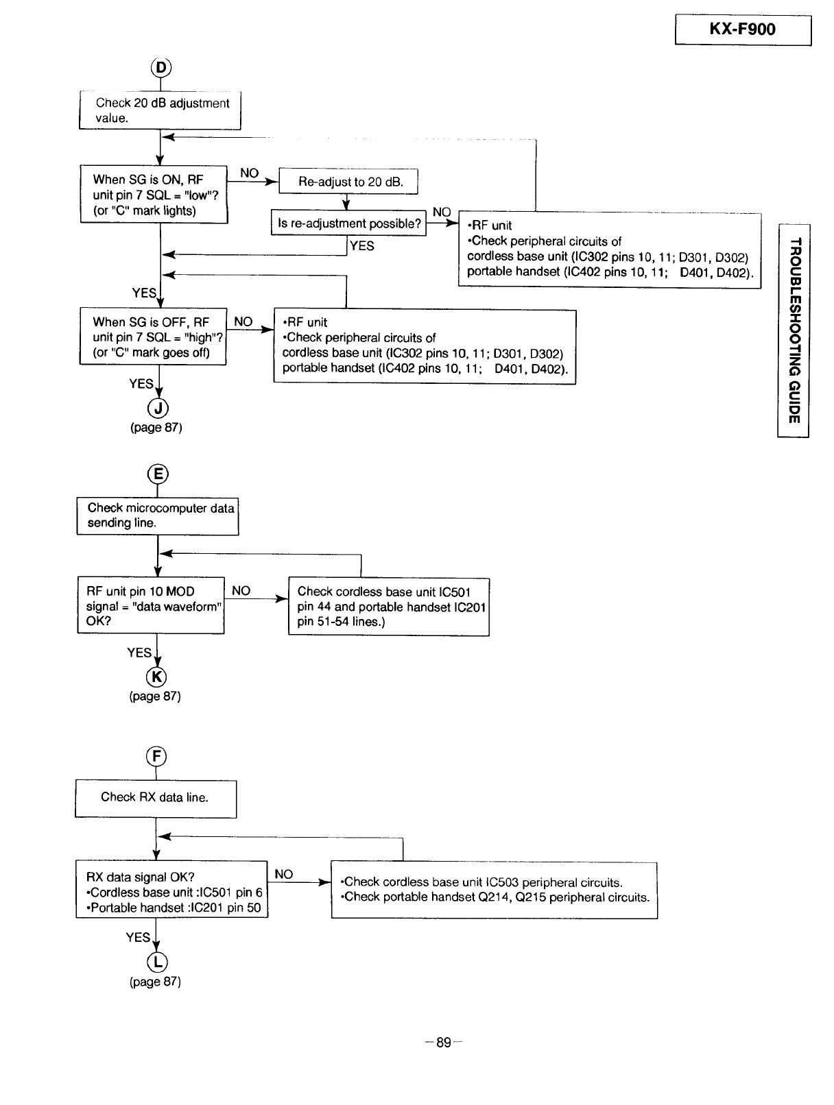
KX-F900
fCheck 20 dB adjustment
value.
When SG is ON, RF
unit pin 7 SQL = "low"?
(or "C" mark lights)
YES
When SGisOFF, RF _
unit pin 7 SQL = "high"? I °
(or "C" mark goes off) |
(page 87)
Readjust to 20 dB. 1
IIs re-adjustment possible? t-_
IYES
•RF unit
•Check peripheral circuits of
cordless base unit (IC302 pins 10, 11; D301, D302)
portable handset (IC402 pins 10, 11; D401, D402).
•RF unit
•Check peripheral circuits of
cordless base unit (IC302 pins 10, 11; D301, D302)
portable handset (IC402 pins 10, 11; D401, D402).
_____
0
C
r-
m
(/)
-!-
0
0
-I
I
z
6")
6")
c::
I
o
ill
i
iCheck microcomputer data I
sending line. I
RF unit pin 10 MOD NO
signal = "data waveform"
OK?
(page 87)
I
Check cordless base unit IC501
pin 44 and portable handset IC201
pin 51-54 lines.)
Check RX data line.
RX data signal OK?
•Cordless base unit :1C501 pin 6
-Portable handset :1C201 pin 50
Y%
(page 87)
NO
r•Check cordless base unit IC503 peripheral circuits.
•Check portable handset Q214, Q215 peripheral circuits.
- 89-
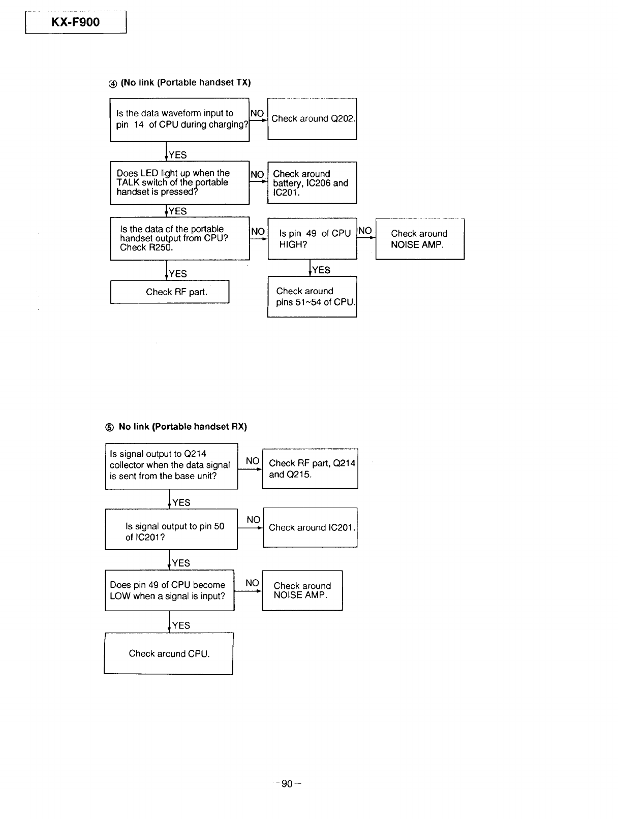
i 1....
(_) (No link (Portable handset TX)
IS the data wave,orm input to NOl_ch-el i aio i-ndQ-20 _-
pin 14 of CPU during charging_i v
IYES
Does LED _ight up when the
TALK switch of the portable
handset is pressed.
IYES
Is the data of the portable
handset output from CPU?
Check R250.
_IYES
Check RF part. J
_ heck around
battery, IC206 and
IC201.
Is pin 49 of CPU NOLNLNLN_ Check around 1
H, H? i i I
_YES
Check around I
pins 51-54 of CPU. I
(_) No link (Portable handset RX)
Is signal output to Q214
collector when the data signal
is sent from the base unit?
IYES
Is signal output to pin 50
of IC201?
IYES
Does pin 49 of CPU become
LOW when a signal is input?
IYES
.{ heck RF part, Q214
and Q215.
_ Check around IC201 'l
Check around
NOISE AMP.
Check around CPU.
90-
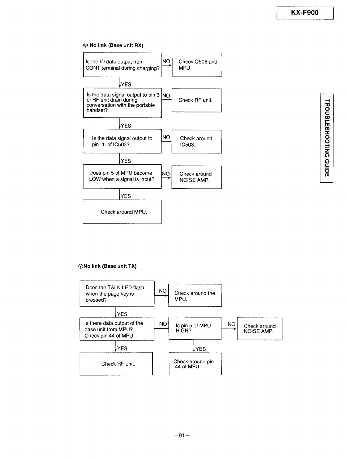
KX.F900-- 1
6_ No link (Base unit RX)
Is the ID data output from N_O -Check Q506 and
CONT terminal during charging? l°l MPU.
i i
IYES
Iv
Is the data signal output to pin 3 iNOI
of RF unit drain during _ Check RF unit.
conversation with the portable
handset?
JYES /|
Is the data signal output to ]NC) I
pin 4 of IC503? [I
IYES /
Does pin 5 of MPU become INO
LOW when a signal is input? F"
IYES
Check around
IC503.
Check around
NOISE AMP.
..N
O
C
r- ;
mi
t_
O
O
.-I
z
i'-
m
m
Check around MPU.
(_No link (Base unit TX)
I .
Does the TALK LED flash I ,,,,-, I
when the page key is
pressed?
IYES
tI
Is there data output of the I NOI
base unit from MPU? FICheck pin 44 of MPU.
IYES
Check RF unit.
Check around the
MPU.
Is pin 5 of MPU
HIGH?
IYES
Check around pin
44 of MPU.
Check around
NOISE AMP.
I
-91 -
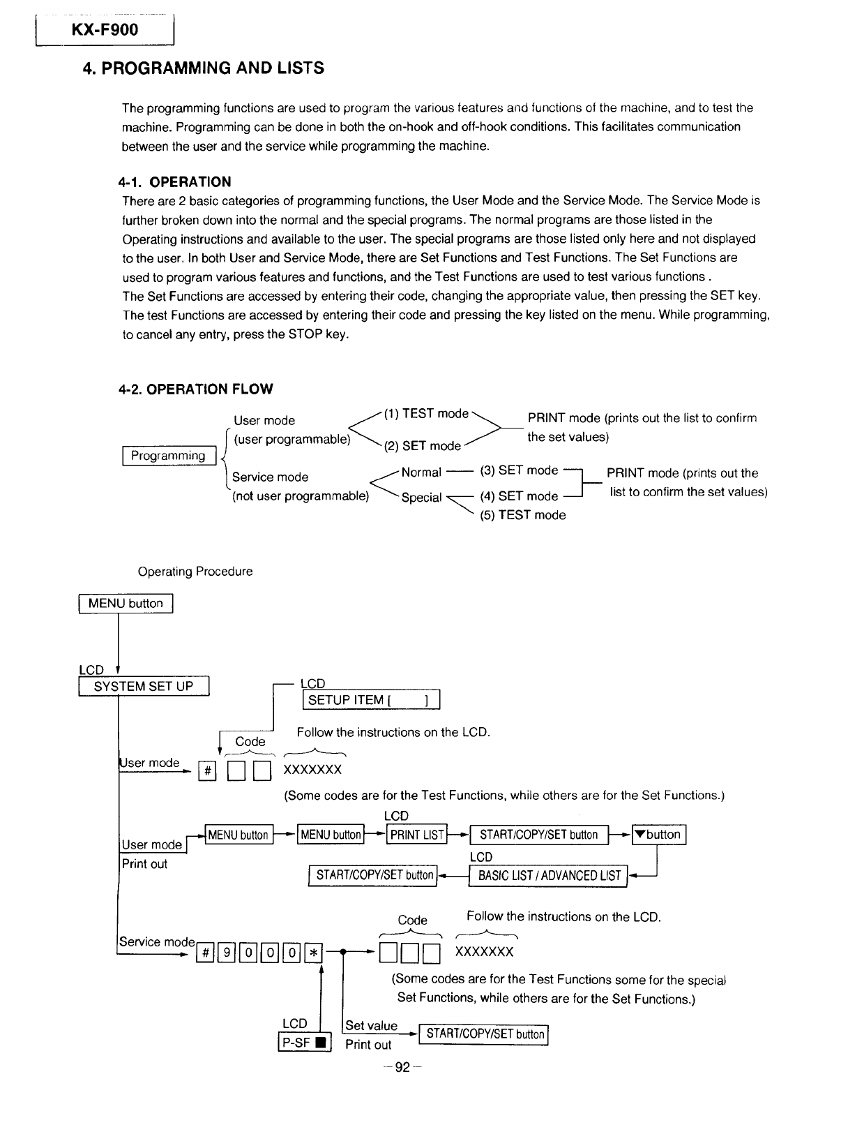
KX-F900 -- j
4. PROGRAMMING AND LISTS
The programming functions are used to program the various features and functions of the machine, and to test the
machine. Programming can be done in both the on-hook and off-hook conditions. This facilitates communication
between the user and the service while programming the machine.
4-1. OPERATION
There are 2 basic categories of programming functions, the User Mode and the Service Mode. The Service Mode is
further broken down into the normal and the special programs. The normal programs are those listed in the
Operating instructions and available to the user. The special programs are those listed only here and not displayed
to the user. In both User and Service Mode, there are Set Functions and Test Functions. The Set Functions are
used to program various features and functions, and the Test Functions are used to test various functions.
The Set Functions are accessed by entering their code, changing the appropriate value, then pressing the SET key.
The test Functions are accessed by entering their code and pressing the key listed on the menu. While programming,
to cancel any entry, press the STOP key.
4-2. OPERATION FLOW
User mode _ (1) TEST mode _ PRINT mode (prints out the list to confirm
I Programming I I (user programmable)%_(2) SET mode __ the set values)
[.Service mode _ Normal (3) SET mode _ PRINT mode (prints out the
(not user programmable) Special _ (4) SET mode list to confirm the set values)
(5) TEST mode
Operating Procedure
MENU button ]
LCD
I SYSTEM SET UP
I
Iser mode _'z-
I _-- LCD
I SETUPITEM[ ] I
Follow the instructions on the LCD.
_ Code
I-_ D [[] XXXXXXX
(Some codes are for the Test Functions, while others are for the Set Functions.)
LCD
User mode #MENU buttonI--'-I MENUbutton ----IPRINTLIST ----I START/COPY/SETbutton I----I','buttonI
Printout i START/COPY/SETbutt0nI_LCDsIc LIST/ADVANCEDLIST j_ I
Code Follow the instructions on the LCD.
Service m°del--_ 1-9] I_-I F] r-6-ii--_--i-T--_ D D D xxxxxxx
l/ (some are for the Test Functions some for the special
codes
I / Set Functions, while others are for the Set Functions.)
/ /
LCD _ ISetvalue = __
I H--,'51-• l Pr nt out
-92-
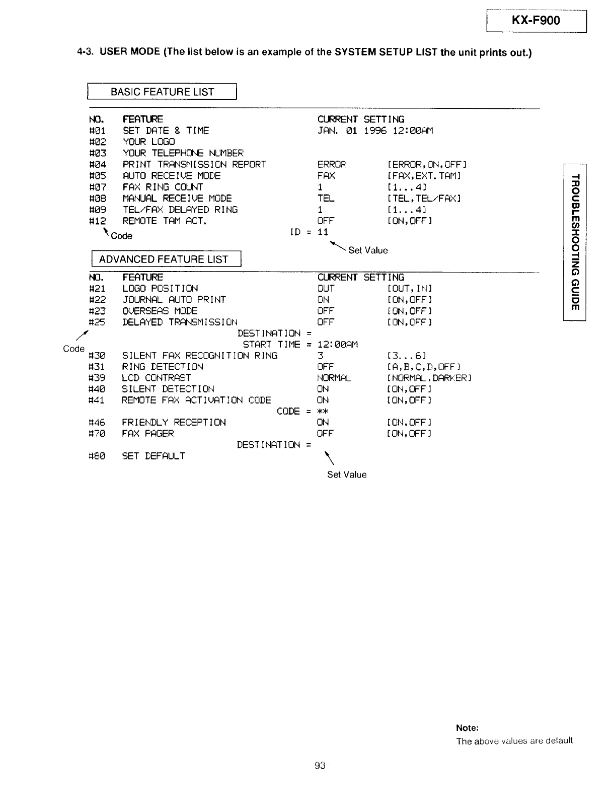
4-3. USER MODE (The list below is an example of the SYSTEM SETUP LIST the unit prints out.)
I BASIC FEATURE LIST I
NO. FEATLI_
#01 SET DATE & TIME
#02 YOUR LOGO
#03 YOUR TELEPHONE NUMBER
#04 PRINT TRANSMISSION REPORT
#05 AUTO RECEIUE MODE
#OT FAX RING COUNT
#88 MANUAL RECEIVE MODE
#09 TEL/FAX DELAYED RING
#12 REMOTE TAM ACT.
CLI_ENT SETTING
JAN. 01 199G 12:00AM
ERROR ]ERROR,ON,OFF]
FAX [FAX,EXT. TAM]
1 [I...4]
TEL ]TEL,TEL/FAX]
1 [I...4]
OFF CON,OFF]
_' Code
ADVANCED FEATURE LIST
NO. FE-_TURE
#21 LOGO POSITION
#22 JOURNAL AUTO PRINT
#23 OVERSEAS MODE
#25 BELAYED TRANSMISSION
/
Code #30
#31
#39
#40
#41
]
ID = 11
_'_SetValue
CODE =
#46 FRIENDLY RECEPTION
#20 FAX PAGER
DESTINATION =
CtJ_ENT SETTING
OUT ]OUT, IN]
ON ION,OFF]
OFF ION,OFF]
OFF ION,OFF)
DESTINATION =
START TIME =12:00AM
SILENT FAX RECOGNITION RING 3
RING DETECTION OFF
LCD CONTRAST NORMAL
SILENT DETECTION ON
REMOTE FAX ACTIUATION CODE ON
ON
OFF
#80 SET DEFAULT \
Set Value
[3...6]
[A,B,C,D,OFF]
]NORMAL,DARKER]
ION,OFF]
CON,OFF]
[ ON, OFF ]
ION, OFF]
0
c
r
m
x
0
0
z
Q
c
m
Note:
The above values are default
93
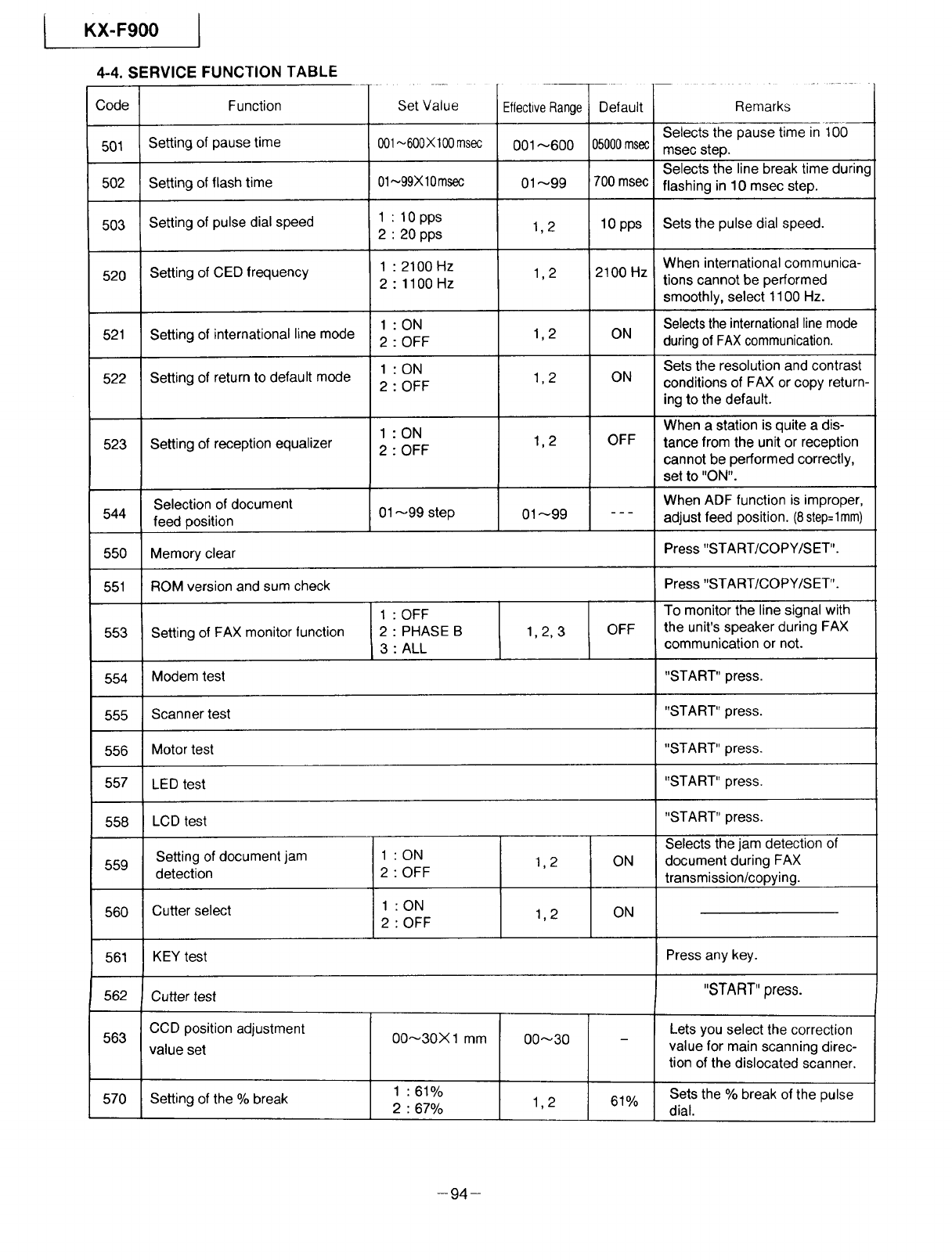
iKX-F900
4-4. SERVICE FUNCTION TABLE
Code Function
501 Setting of pause time
502 Setting of flash time
503 Setting of pulse dial speed
520 Setting of CED frequency
521
522
Setting of international line mode
Setting of return to default mode
523 Setting of reception equalizer
Selection of document
544 feed position
550 Memory clear
551 ROM version and sum check
Set Value
001~600X100msec
01~99X10msec
1 : 10 pps
2 : 20 pps
1 : 2100 Hz
2 : 1100 Hz
1 :ON
2 " OFF
1 :ON
2 : OFF
1 :ON
2 : OFF
01_99 step
EffectiveRange
001_600
01_99
1,2
1,2
1,2
01_99
Default
05000msec
700 msec
10 pps
2100 Hz
ON
ON
OFF
Remarks
Selects the pause time in 100
msec step.
Selects the line break time during
flashing in 10 msec step.
Sets the pulse dial speed.
When international communica-
tions cannot be performed
smoothly, select 1100 Hz.
Selects the international line mode
during of FAX communication.
Sets the resolution and contrast
conditions of FAX or copy return-
ing to the default.
When a station is quite a dis-
tance from the unit or reception
cannot be performed correctly,
set to "ON".
When ADF function is improper,
adjust feed position. (8step=lmm)
Press "STA RT/COPY/S ET".
Press "START/COPY/SET".
1 " OFF To monitor the line signal with
553 Setting of FAX monitor function 2 : PHASE B 1,2, 3 OFF the unit's speaker during FAX
3 : ALL communication or not.
554 Modem test "START" press.
555 Scanner test "START" press.
556 Motor test "START" press.
557 LED test "START" press.
558 LCD test "START" press.
Selects the jam detection of
559 Setting of document jam 1 • ON 1,2 ON document during FAX
detection transmission/copying.
560 Cutter select 1,2 ON
561 KEY test Press any key.
562 Cutter test "START" press.
563 CCD position adjustment 00_30X 1 mm 00_30 _ Lets you select the correction
value set value for main scanning direc-
tion of the dislocated scanner.
1 : 61% Sets the % break of the pulse
570 Setting of the % break 2 : 67% 1 2 61%
' dial.
2 - OFF
1 ON
2 : OFF
-94-
571
Function
Setting of number of times
that ITS is redialed
572 Setting of ITS redial interval
573 TEL ring count
590 Setting of number of times of
FAX redial
Setting of FAX redial interval
591
r .........1
592
Set Value
593
00_99
001_999 sec
01_99
0_99
001_999 sec
1 : OFF
Designation of CNG sending 2 : ALL
3 : AUTO
Setting of interval between
CED and 300 bps signal.
594 Setting of overseas
DIS detection
Setting of the acceptable
value of reception error
595
596 Setting of transmit level
1 : 75 msec
2:500 msec
3 : 1000 msec
700 EXT TAM OGM time
701 Silence detect time
702 EXT TAM ring count
717 Transmit speed select
718 Receive speed select
1 : Detects at the
1st time
2 : Detects at the
2nd time
001_999Xnumberoftimes
-15_00
x second
x 100 ms
x number of rings
1 : 9600 BPS
2 : 7200 BPS
3 : 4800 BPS
4 : 2400 BPS
1 : 9600 BPS
2 : 7200 BPS
3 : 4800 BPS
4 : 2400 BPS
EffectiveRange
00_99
001_999
01 _99
00_99
001_999
1,2,3
1,2,3
1,2
001_999
-15_00
01 _99
01 _99
0_9
1_4
1_4
14 times
030 sec
15 times
5 times
045 sec
ALL
75 msec
Detects
at the
1st
time
100
-10 dBm
10 sec
5O ms
5 times
9600 BPS
9600 BPS
Remarks
Selects the number of times that
ITS is redialed (not including the
first dialing).
Sets the interval of ITS redial.
Sets the' number of rings that
unit starts to receive a docu-
ment in TEL mode.
Selects the number of times of re-
dial during FAX communication (not
including the first dialing).
Sets the interval of FAX redial
during FAX communication.
Lets you select the CNG output
during FAX transmission.
ALL: CNG is output at phase A.
AUTO: CNG is output only when
the automatic dialing is per-
formed.
OFF: CNG is not output at phase
A.
Sets the interval between the
CED signal and subsequent
300 bps signal.
Sets the recognizing format of DIS
signal.
1: Detects the first DIS signal sent
from the receiver during FAX
transmission.
2: Ignores the first DIS signal sent
from the receiver during FAX
transmission.
Sets the number of error ac-
ceptable lines when the FAX re-
constructs the received data.
Selects the FAX transmission
level.
(Increase the level when the
telephone line condition is poor.)
Sets the start time of silence de-
tect.
Sets the silence of call confir-
mation times.
Sets the number of rings that
unit start to receive a document
in EXT-TAM mode.
Adjusts the speed to start train-
ing during FAX transmission.
Adjusts the speed to start train-
ing during FAX reception.
-95-
I......KX-FO00--1
Code
719
721
722
732
763
771
815
844
909
Function
Ringer off in TEL/FAX mode
Pause tone detect
Redial tone detect
AUTO disconnect
CNG detect time
T1 timer
Sensor check
Original setting
Handset Remote FAX Actication
Set Value
1 :ON
2 : OFF
1 :ON
2 : OFF
1 :ON
2 : OFF
1 : 350 ms
2 : 1.8 sec
3 : OFF
1 : 10 sec
2 : 20 sec
3 : 30 sec
1 : 35 sec
2 : 60 sec
Effective Range
1,2
1,2
1,2
1,2,3
1,2,3
1,2
Default
ON
ON
ON
350 ms
20 sec
35 sec
1 : NORMAL
2 : LIGHT
3 : DARKER
0-9,
1,2,3
2N4 digits
NORMAL
Remarks
Selects ringer off switch when
a call is received in the TEL/
FAX mode.
Selects the tone detection in
the pauses of the dialing.
Selects the tone detection
mode after redialing.
Selects the start time of detec-
tion of auto disconnect.
Selects the CNG detect time
of friendly reception.
Set to the higher value when
the response from the other
party needs much time during
FAX transmission.
"START" press.
Use this feature when you
need to transmit and copy a
document with very faint writ-
ing on very dark writing.
You can change the remote
FAX activation code using the
portable handset.
96-
4-5. SERVICE MODE SETTING VALUES (Example of a printed out list)
Kx oo ......1
[SERVICE DATA LIST]
.,_.--Code _,./SetValue
501 PAUSE TIME = 050_100ms
502 FLASH TIME = 70_10ms
503 DIAL SPEED =iBpps
520 CED FREQ. = 2100Hz
521 INTL. MODE = ON
522 AUTO STANDBY = ON
523 RX EQL, = OFF
524 TX EQL. = OFF
700 EXT, TAM OGM TIME =10s_c
701 SILENT DETECT TIME = 50_100msec
702 EXT. TAM RING COUNT = 5
909 HANDSET REMOTE FAX ACT.= _
ISPECIAL SERVICE SETTING ]
544 553 559
J
/" 50 1 1
Code _"SetValue
594 595 596 ?iT 718 719 T21
1 100 10 1 1 1 1
[001...600]_:lUSms
[Ol,.,99]_lOrnS
[1=10 2=20]pps
[1=2100 2=i100]Hz
[1=ON 2=OFF]
[1=ON 2=OFF]
[I=ON 2=OFF]
[I=ON 2=OFF]
[01...99]s_c
[01...99]_100ms_0
[0...9]
560 563 570 521 572 573 590 591 592 595
115 1 14 030 15 05 045 2 1
722 732 763 771 844
1 1 21 1
-N
0
C
l-
m
m
.I-
0
0
-N
z
¢)
¢)
c
m
Note:
The above values are default
5. TEST FUNCTIONS
Test mode
PRINT TEST
MOTOR TEST
MODEM TEST
ROM CHECK
SCAN CHECK
LCD CHECK
Type of Mode
User mode
Service Mode
Service Mode
Service Mode
Service Mode
Service Mode
oCode [--1[_
• Operation after
code input.
NN
START
N@N
START
NN@
START
[]F Fq
START
BBB
START
START
Function
Print a test pattern and check the thermal head for
abnormalities (missing dots, etc.), and also check the
operation of the reception motor.
Rotate the transmission and reception motors to check the
operation of the motors.
Send four kinds of FAX signals to check the sending function
of the modem.
1) 1100 Hz: Consecutive signal of EOM for tonal.
2) 2100 Hz: G2 carrier signal
Consecutive of CED signal
3) G3, V29 training signal [modulation wave of carrier signal
(1700 Hz)]
Indicate the version and check sum of the ROM.
Turn on the LEDs of the image sensor and operate the read
system.
Check the LCD indication.
Illuminate all dots to check if they are normal.
-97-
lKX-F900
DTMF SINGLE
TEST
LED TEST
KEY CHECK
FACTORY
SET
CUTTER
TEST
SENSOR
CHECK
Service Mode
Service Mode
Service Mode
Service Mode
Service Mode
Service Mode
UB[]
1..On
2..Off
@NN
START
{any
key }
NN@
START
®[][]
START
Output the DTMF by single tone.
All LEDs flashes on and off, or is illuminated.
Check the operation button.
Indicate the button code at LCD while the button is pressed.
Clear the memory in which the user can store data.
Check the cutter operation.
CHECK SENSOR OPERATION
IDo Sn Co Ja Pa Vx Cu ]
Do : Document Sensor
Sn : Read Position Sensor
Co : Cover Open Sensor
Ja :Jam Sensor
Pa : Recording Paper Sensor
Vx : Vox Sensor
Cu : Cutter Position SW
: LCD DISPLAY
: Paper inserted
: at the read Position
: Cover open
: Jam
: Set Recording Paper
: Vox detected
: Home Position
5-1. BUTTON CODE TABLE
Code
02
03
O4
05
O7
O8
0A
0B
0C
Button Name Qx_
RESOLUTION 0D
AUTO RECEIVE 0E
START/COPY/SET 16
MENU 18
Button Name Code Button Name
/k VOLUME 35 5
V VOLUME 36 6
ERASE 37 7
NEWMSGS.PLAYBACK 38 8
Code Button Name
3E FLASH
87 STATION 1/6
88 STATION 2/7
89 STATION 3/8
8A STATION 4/9
8B STATION 5/10
09 LOCATOR/
INTERCOM
HELP 19 MAIL BOX 39 9
SP-PHONE 31 1 3A 0
MUTE 32 2 3B
LOWER 33 3 3C #
DIRECTORY 34 4 3D REDIAL/PAUSE
-98-
KX-F900 1
ADJUSTMENT
Page
1. Table of Test Equipments and Tool ................................................. 100
2. Adjusting the Feeder Pressure ......................................................... 101
3. Confirmation of Separation Spring ................................................... 101
4. CCD Adjustments ..................................................................... 102~104
5. Document Read Start Position Adjustment .............................. 104,105
6. Codless Adjustment .................................................................. 107~113
t,_
C
t_
,-I
Ill
7'
'-'1
99--
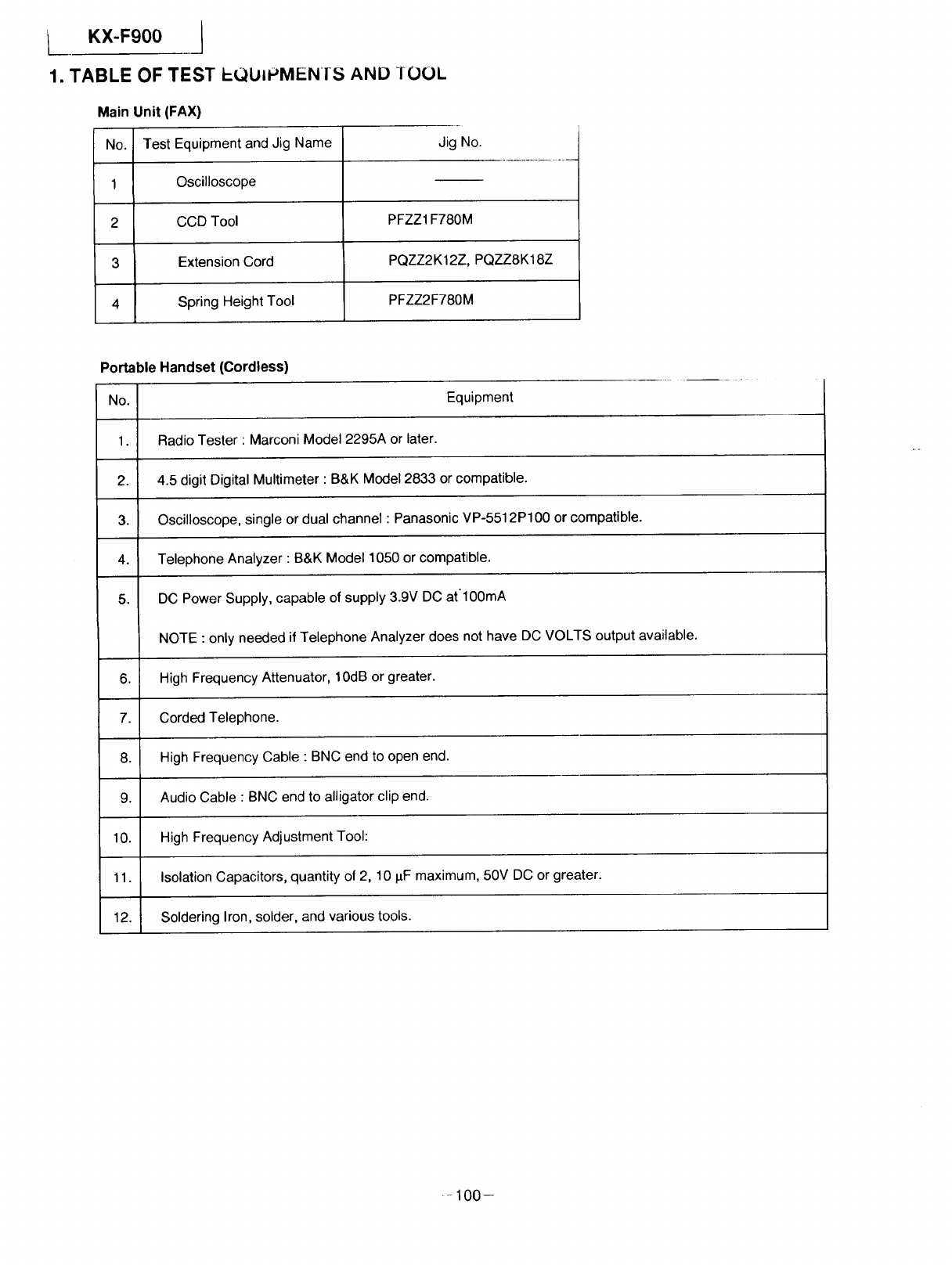
iKX-F900 I
1. TABLE OF TEST E_UIP'MEN1-5 AND TOOL
Main Unit (FAX)
No. Test Equipment and Jig Name Jig No.
1 Oscilloscope
2 CCD Tool PFZZ1 F780M
3 Extension Cord PQZZ2K12Z, PQZZ8K18Z
4 Spring Height Tool PFZZ2F780M
Portable Handset (Cordless)
No. Equipment
1. Radio Tester : Marconi Model 2295A or later.
2. 4.5 digit Digital Multimeter : B&K Model 2833 or compatible.
3. Oscilloscope, single or dual channel : Panasonic VP-5512P100 or compatible.
4. Telephone Analyzer : B&K Model 1050 or compatible.
5. DC Power Supply, capable of supply 3.9V DC at'100mA
NOTE : only needed if Telephone Analyzer does not have DC VOLTS output available.
6. High Frequency Attenuator, 10dB or greater.
7. Corded Telephone.
8. High Frequency Cable : BNC end to open end.
9. Audio Cable : BNC end to alligator clip end.
10. High Frequency Adjustment Tool:
11. Isolation Capacitors, quantity of 2, 10 #F maximum, 50V DC or greater.
12. Soldering Iron, solder, and various tools.
-100-
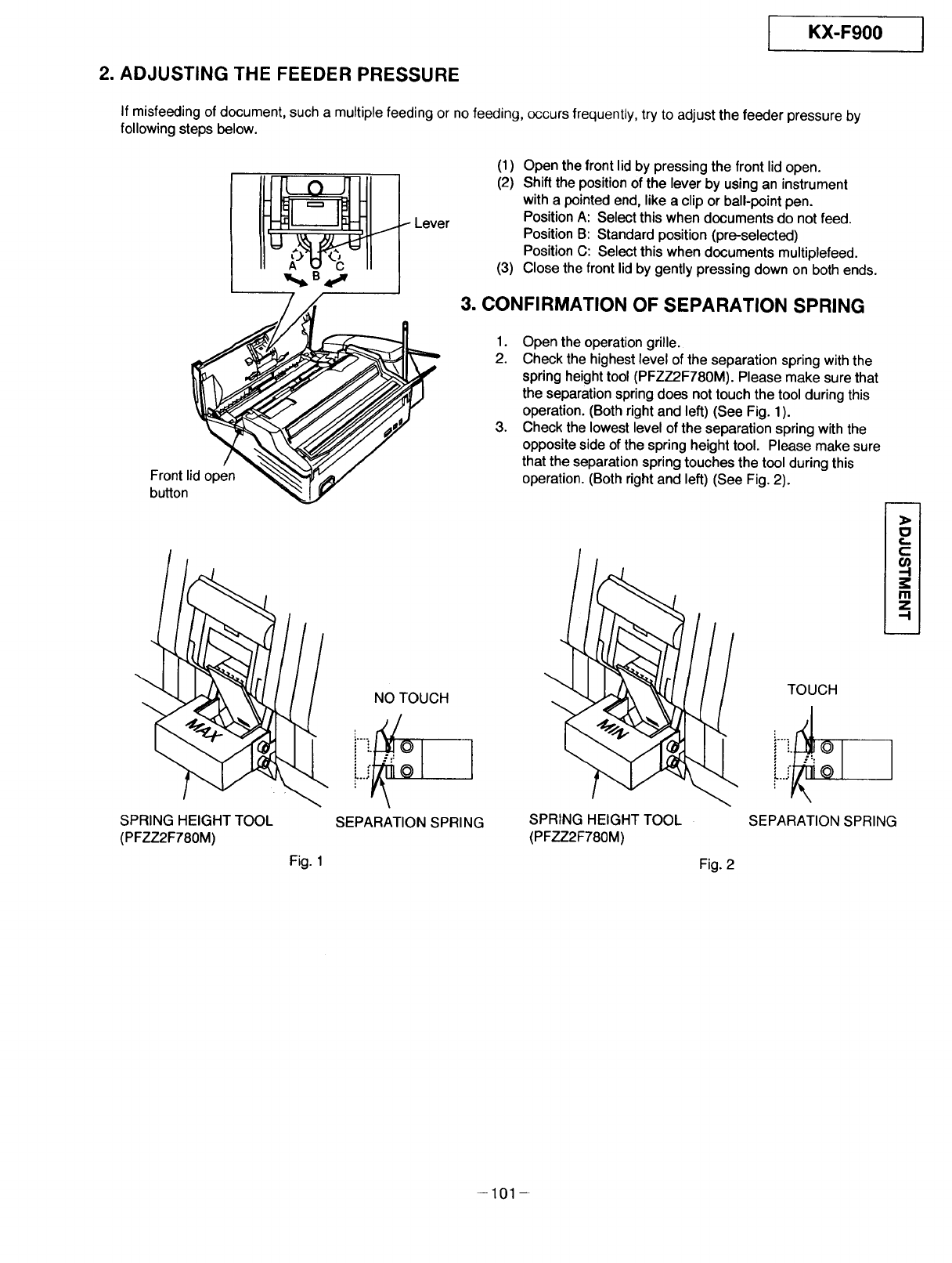
2. ADJUSTING THE FEEDER PRESSURE
I KX-F900 J
If misfeeding of document, such a multiple feeding or no feeding, occurs frequently, try to adjust the feeder pressure by
following steps below.
.--Lever
(1) Open the front lid by pressing the front lid open.
(2) Shift the position of the lever by using an instrument
with a pointed end, like a clip or ball-point pen.
Position A: Select this when documents do not feed.
Position B: Standard position (pre-selected)
Position C: Select this when documents multiplefeed.
(3) Close the front lid by gently pressing down on both ends.
3. CONFIRMATION OF SEPARATION SPRING
Front lid open
button
SPRING HEIGHT TOOL
(PFZZ2F780M)
Fig. 1
NO TOUCH
SEPARATION SPRING
1. Open the operation grille.
2. Check the highest level of the separation spring with the
spring height tool (PFZZ2F780M). Please make sure that
the separation spring does not touch the tool during this
operation. (Both right and left) (See Fig. 1).
3. Check the lowest level of the separation spring with the
opposite side of the spring height tool. Please make sure
that the separation spring touches the tool during this
operation. (Both right and left) (See Fig. 2).
0
t,..
c
o)
.-I
m
z
SPRING HEIGHT TOOL
(PFZZ2F780M)
Fig. 2
TOUCH
SEPARATION SPRING
-101 -
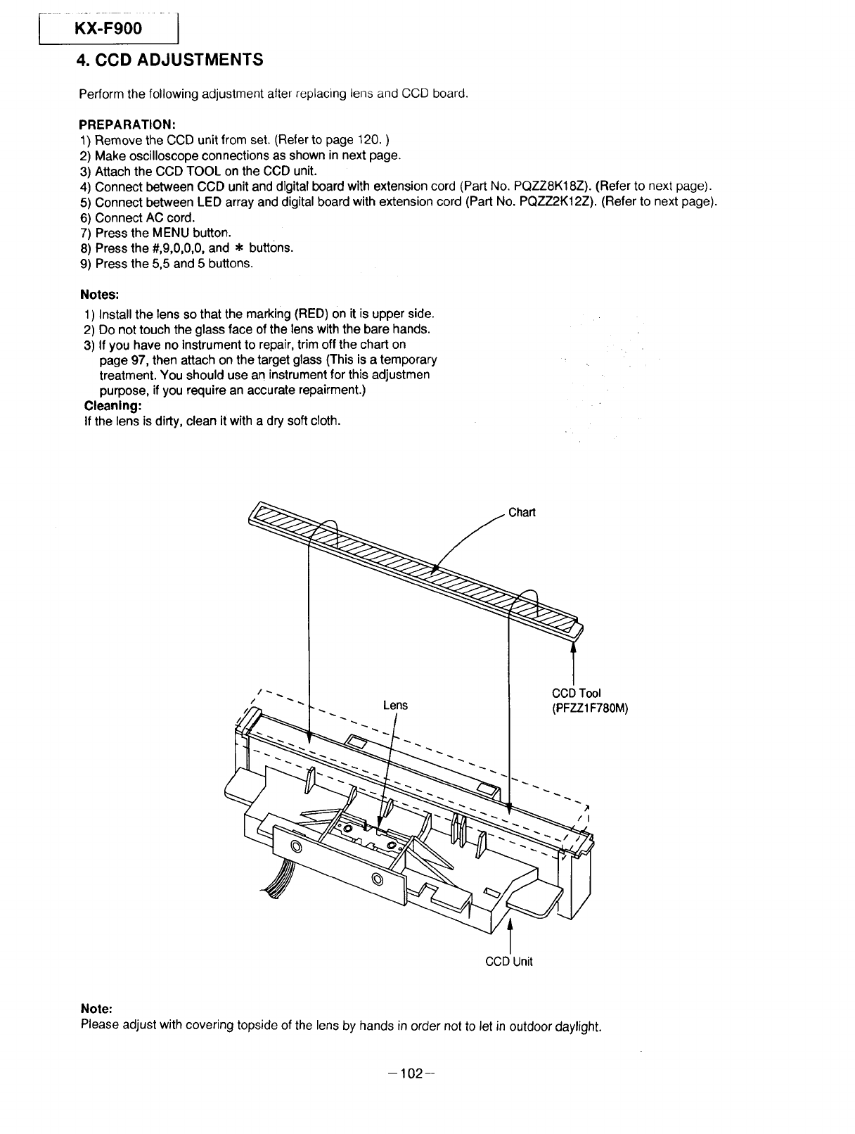
IKX_-F900 - I
4. CCD ADJUSTMENTS
Perform the following adjustment after replacing tens and CCD board.
PREPARATION:
1) Remove the CCD unit from set. (Referto page 120. )
2) Make oscilloscope connections as shown in next page.
3) Attach the CCD TOOL on the CCD unit.
4) Connect between CCD unit and dlgital board with extension cord (Part No. PQZZ8K18Z). (Refer to next page).
5) Connect between LED array and digital board with extension cord (Part No. PQZZ2K12Z). (Refer to next page).
6) Connect AC cord.
7) Press the MENU button.
8) Press the #,9,0,0,0, and • buttons.
9) Press the 5,5 and 5 buttons.
Notes:
1) Install the lens so that the marking (RED) on it is upper side.
2) Do not touch the glass face of the lens with the bare hands.
3) If you have no instrument to repair, trim off the chart on
page 97, then attach on the target glass (This is atemporary
treatment. You should use an instrument for this adjustmen
purpose, ifyou require an accurate repairment.)
Cleaning:
If the lens is dirty, clean it with a dry soft cloth.
Chart
/CCD Tool
(PFZZ1F780M)
/I
CCD Unit
Note:
Please adjust with covering topside of the lens by hands in order not to let in outdoor daylight.
-102-
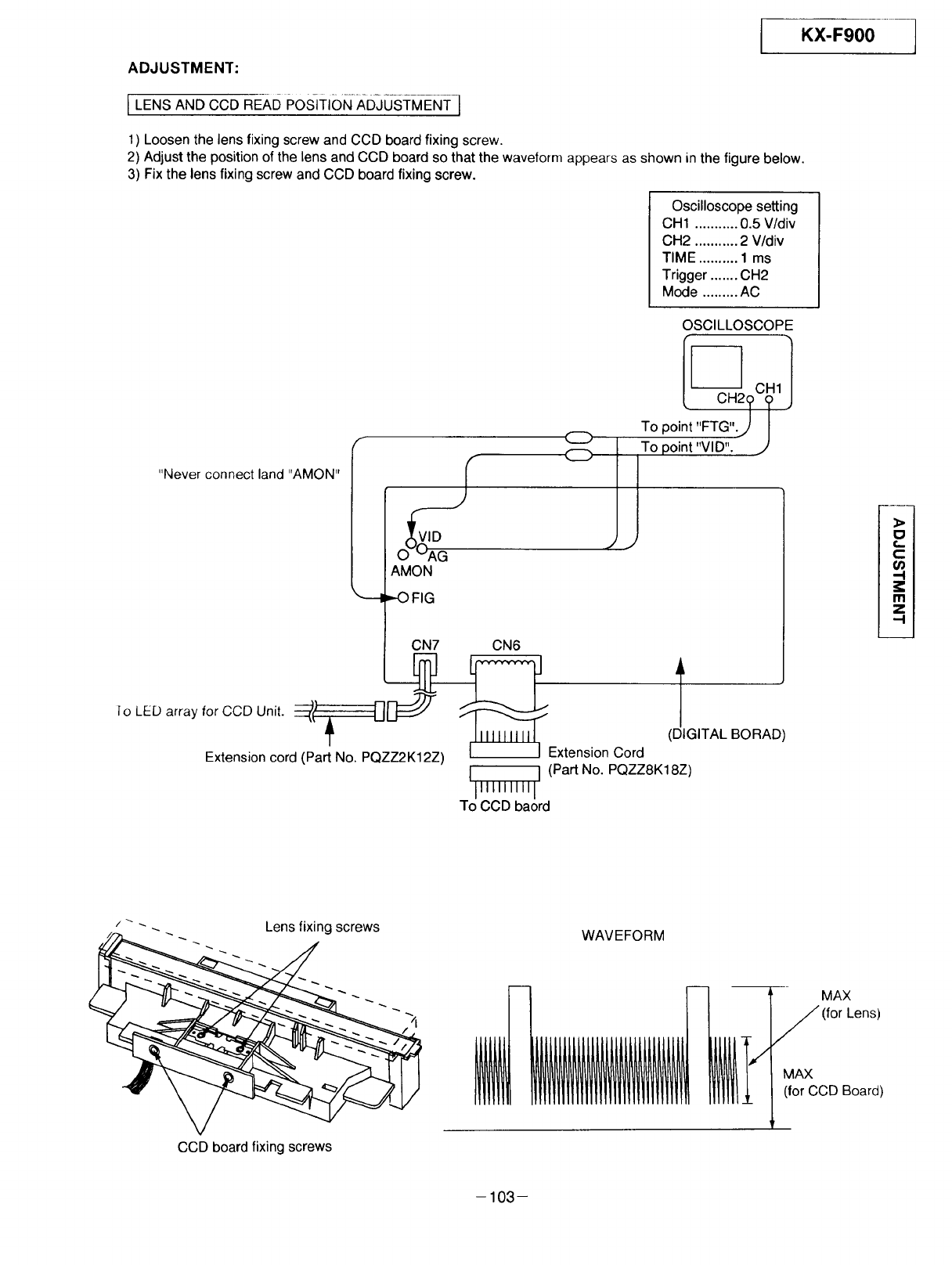
KX-F900
ADJUSTMENT:
[ LENS AND CCD READ POS-I'I-ION ADJUSTMENT
1) Loosen the lens fixing screw and CCD board fixing screw.
2) Adjust the position of the lens and CCD board so that the waveforrn appears as shown in the figure below.
3) Fix the lens fixing screw and CCD board fixing screw.
Oscilloscope setting
CH1 ........... 0.5 V/div
CH2 ........... 2 V/div
TIME .......... 1 ms
Trigger ....... CH2
Mode ......... AC
"Never connect land "AMON"
O_rvlD
O OAG
AMON
/CC>
CC>
,_) FIG
OSCILLOSCOPE J
To point 'FTG".J
To point "VID". j
Jj
CN7 CN6
Extension cord (Part No. PQZZ2K12Z) [ IExtension Cord
T
(DIGITAL BORAD)
I I (Part No. PQZZ8K18Z)
Illlllllll I
To CCD baord
?...
c
m
-I
m
z
-I
/_ _ _ Lens fixing screws WAVEFORM
MAX
MAX
(for CCD Board)
CCD board fixing screws
-103-
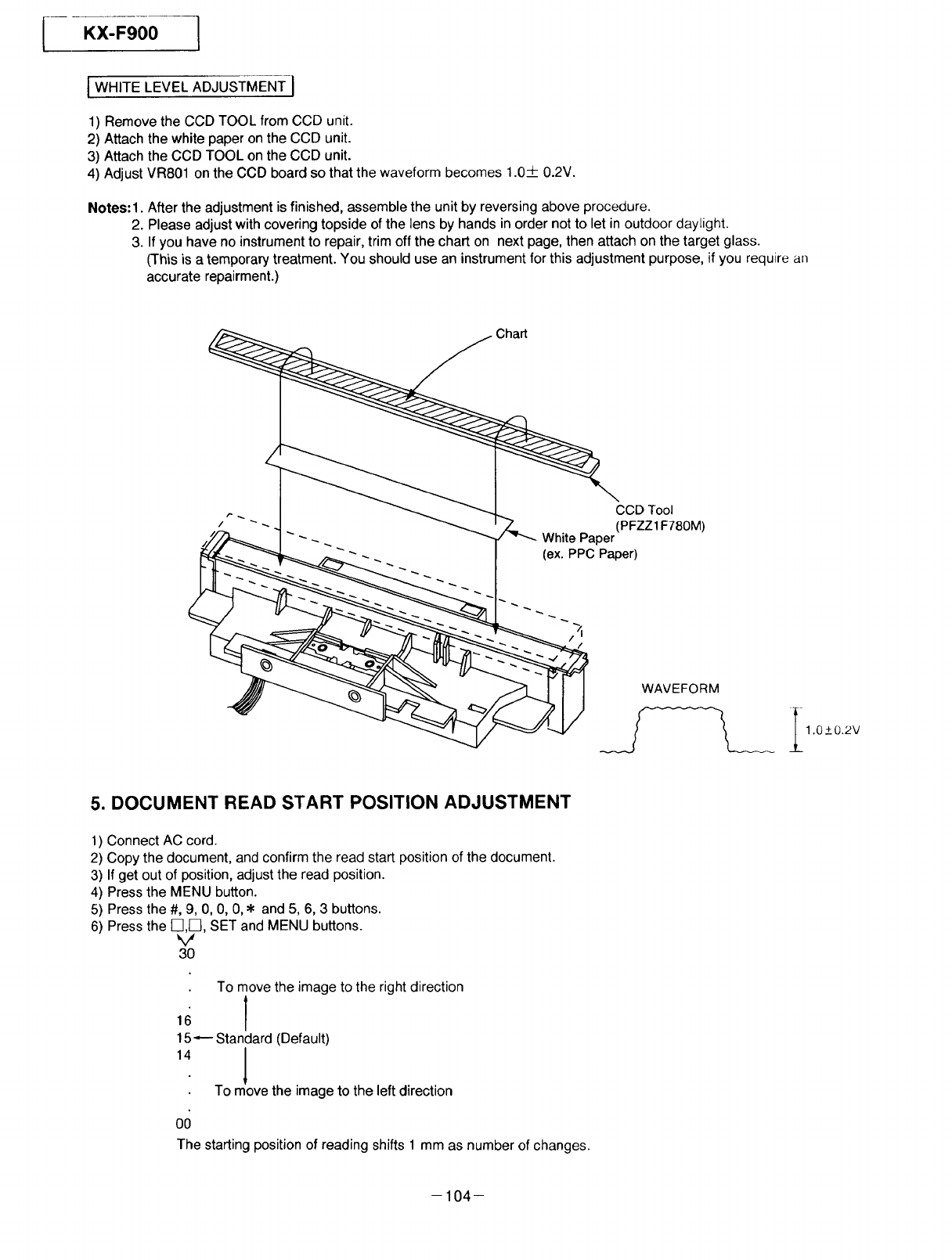
--KX-F900 1
I WHITE LEVEL ADJUSTMENT J
1) Remove the CCD TOOL from CCD unit.
2) Attach the white paper on the CCD unit.
3) Attach the CCD TOOL on the CCD unit.
4) Adjust VR801 on the CCD board so that the waveform becomes 1.0__+0.2V.
Notes: 1. After the adjustment is finished, assemble the unit by reversing above procedure.
2. Please adjust with covering topside of the lens by hands in order not to let in outdoor daylight.
3. If you have no instrument to repair, trim off the chart on next page, then attach on the target glass.
(This is a temporary treatment. You should use an instrument for this adjustment purpose, if you require an
accurate repairment.)
Chart
CCD Tool
(PFZZ 1F780M)
White Paper
(ex. PPC Paper)
WAVEFORM
_2 I_I .O+0.2V
5. DOCUMENT READ START POSITION ADJUSTMENT
1) Connect AC cord.
2) Copy the document, and confirm the read start position of the document.
3) If get out of position, adjust the read position.
4) Press the MENU button.
5) Press the #, 9, 0, 0, 0, * and 5, 6, 3 buttons.
6) Press the Fl,l--I, SET and MENU buttons.
V
3O
To move the image to the right direction
,o 1
15---- Standard (Default)
14 !o
To ve the image to the left direction
00
The starting position of reading shifts 1 mm as number of changes.
--104-
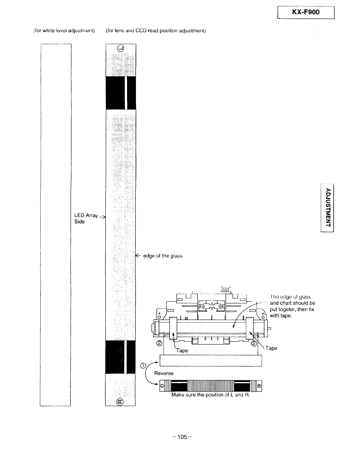
I KX-F900
(for white level adjustment) (for lens and CCD read position adjustment)
LED Array _-
Side
O
:: /'_: Z?
: :: , T: [ ]
!_i-Y] i]i !
:? :/(--- edge of the glass
L__ ,-_ -
:2; :_ : : 4
i: :=
//
[_L_ ......... _:___J [he edge ul glass
__1___-------_-_--- and chart should be
_ ___--_ _ut togeter, then fix
_t"'m i ,, ! ! 1 /! r___p_[ with tape
--I IIU
®
Tape pe
everse
Make sure the position of L and R.
t,..,
-I
m
z
-I
--105-

I_ Kx..F900
106-
KX-F900
6. CORDLESS ADJUSTMENT
6-1. OBJECTIVE
This procedure will enable the technician to make adjustments to the KX-F900 PORTABLE HANDSET and CORDLESS
BASE UNIT.
_2. GENERALINFORMATION
This procedure has 2 sections. The first section instructs the technician on how to align the PORTABLE HANDSET. We
recommend aligning the PORTABLE HANDSET first, since you will need the PORTABLE HANDSET to align the
CORDLESS BASE UNIT. The second section aligns the CORDLESS BASE UNIT. You can use either section sepa-
rately, or together to align the entire cordless phone unit.
At the beginning of each section, you will find a preparation procedure instructing you on how to prepare the unit to the
point of placing the unit in TEST mode. Please follow this procedure to insure proper alignment.
Each section's procedure consists of Adjustment Items adjusting one specific variable hardware component.
Each Item lists the equipment needed, how to connect and setup the equipment, how to make the adjustment, and how
to verify the adjustment if necessary.
Before the actual procedure, you will find a procedure detailing how to place that part in TEST mode. You will have to
perform this procedure before each individual Adjustment Item.
Once aligned, please remove all equipment connections and solder points, and reassemble the unit. As a final check,
power up the phone and check for PORTABLE HANDSET linking with the CORDLESS BASE UNIT.
IPORTABLE HANDSET I
(1)PREPARATION
Please perform the following steps to prepare the PORTABLE HANDSET for alignment. Please refer to the
HANDSET REFERENCE DRAWING for connection and test point locations.
1. Remove battery cover and battery.
2. Remove both screws at the case bottom.
3. Grabbing hold of the back near the bottom, gently pry off the back of the case.
4. Remove the antenna mounting screw.
While heating the antenna solder connection, pull out the antenna. (Refer to page 125)
5. Remove the top P.C.Board mounting screw.
6. Unsolder both speaker connections on P.C.Board.
7. Remove the PORTABLE HANDSET P.C.Board.
8. Remove the keypad membrane.
9. Solder High Frequency Cable open end to ANT and RF GND points.
10. Using the Digital Multimeter, measure DC VOLTS output on the Telephone Analyzer.
Adjust the output voltage to 3.9V DC.
11. Solder battery connection wires at the points shown in the PORTABLE HANDSET REFERENCE DRAWING.
Solder the positive lead to IC204, towards the bottom of the P.C.Board. Solder the negative lead to the MIC
minus lead, closest to IC204. DO NOT APPLY POWER TO THE PORTABLE HANDSET AT THIS TIME!!!!!!
12. Solder a small, insulated piece of wire to GND as well.
13. Solder 1 isolation capacitor's positive lead to SP+ test point (TP4). When soldering, keep the lead close to
the P.C.Board as possible since you will lay the keypad membrane over part of this lead.
14. Solder a small, short, insulated wire to MIC test point (TP8).
15. Lay the keypad membrane over the keypad switch contacts.
_>
O
€._
t-
-I
m
z
.._
-107--
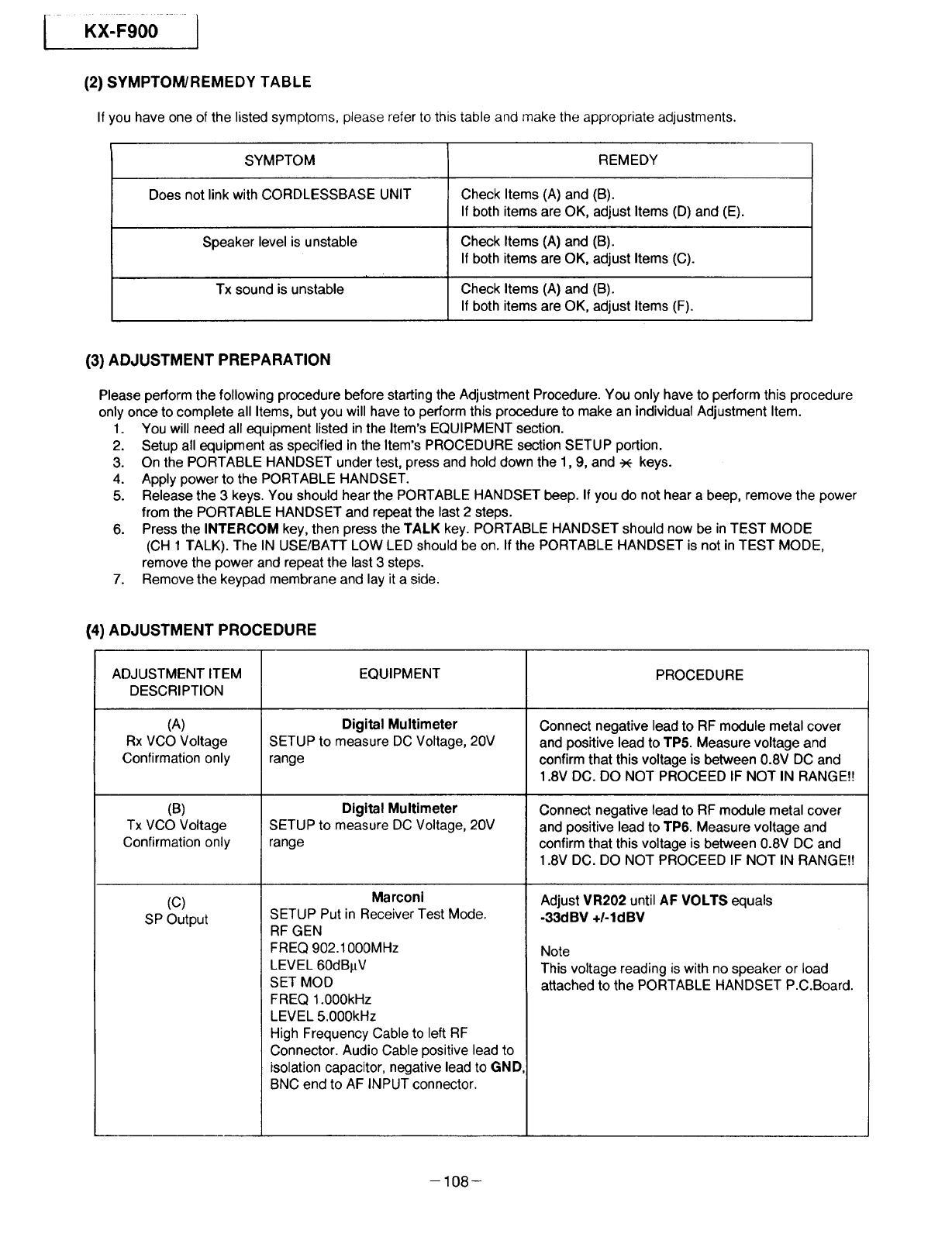
I Kx'F90o-I
(2) SYMPTOM/REMEDY TABLE
If you have oneof the listed symptoms, please refer to this table and make the appropriate adjustments.
SYMPTOM REMEDY
Does not link with CORDLESSBASE UNIT Check Items (A) and (B).
If both items are OK, adjust Items (D) and (E).
Speaker level is unstable Check Items (A) and (B).
If both items are OK, adjust Items (C).
Tx sound is unstable Check Items (A) and (B).
If both items are OK, adjust Items (F).
(3) ADJUSTMENT PREPARATION
Please perform the following procedure before starting the Adjustment Procedure. You only have to perform this procedure
only once to complete all Items, but you will have to perform this procedure to make an individual Adjustment Item.
1. You will need all equipment listed in the Item's EQUIPMENT section.
2. Setup all equipment as specified in the Item's PROCEDURE section SETUP portion.
3. On the PORTABLE HANDSET under test, press and hold down the 1,9, and -_ keys.
4. Apply power to the PORTABLE HANDSET.
5. Release the 3 keys. You should hear the PORTABLE HANDSET beep. If you do not hear a beep, remove the power
from the PORTABLE HANDSET and repeat the last 2 steps.
6. Press the INTERCOM key, then press the TALK key. PORTABLE HANDSET should now be in TEST MODE
(CH 1 TALK). The IN USE/BATT LOW LED should be on. If the PORTABLE HANDSET is not in TEST MODE,
remove the power and repeat the last 3 steps.
7. Remove the keypad membrane and lay it a side.
(4) ADJUSTMENT PROCEDURE
ADJUSTMENT ITEM
DESCRIPTION
(A)
Rx VCO Voltage
Confirmation only
(B)
Tx VCO Voltage
Confirmation only
(c)
SP Output
EQUIPMENT
Digital Multimeter
SETUP to measure DC Voltage, 20V
range
Digital Multimeter
SETUP to measure DC Voltage, 20V
range
Marconi
SETUP Put in Receiver Test Mode.
RF GEN
FREQ 902.1000MHz
LEVEL 60dBpV
SET MOD
FREQ 1.000kHz
LEVEL 5.000kHz
High Frequency Cable to left RF
Connector. Audio Cable positive lead to
isolation capacitor, negative lead to GND
BNC end to AF INPUT connector.
PROCEDURE
Connect negative lead to RF module metal cover
and positive lead to TP5. Measure voltage and
confirm that this voltage is between 0.8V DC and
1.8V DC. DO NOT PROCEED IF NOT IN RANGE!!
Connect negative lead to RF module metal cover
and positive lead to TP6. Measure voltage and
confirm that this voltage is between 0.8V DC and
1.8V DC. DO NOT PROCEED IF NOT IN RANGEfl
Adjust VR202 until AF VOLTS equals
-33dBV +l-ldBV
Note
This voltage reading is with no speaker or load
attached to the PORTABLE HANDSET P.C.Board.
-108-
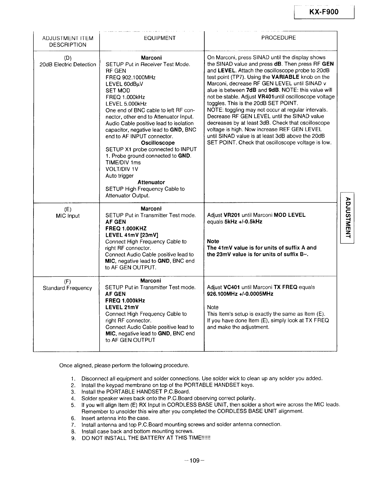
KX-F900
ADJUSTMENT ITEM
DESCRIPTION
(O)
20dB Electric Detection
(E)
MIC Input
(F)
Standard Frequency
EQUIPMENT
Marconi
SETUP Put in Receiver Test Mode.
RF GEN
FREQ 902.1000MHz
LEVEL 60dBIIV
SET MOD
FREQ 1.000kHz
LEVEL 5.000kHz
One end of BNC cable to left RF con-
nector, other end to Attenuator Input.
Audio Cable positive lead to isolation
capacitor, negative lead to GND, BNC
end to AF INPUT connector.
Oscilloscope
SETUP Xl probe connected to INPUT
1. Probe ground connected to GND.
TIME/DIV 1ms
VOLT/DIV 1V
Auto trigger Attenuator
SETUP High Frequency Cable to
Attenuator Output.
Marconi
SETUP Put in Transmitter Test mode.
AF GEN
FREQ 1.000KHZ
LEVEL 41mV [23mV]
Connect High Frequency Cable to
right RF connector.
Connect Audio Cable positive lead to
MIC, negative lead to GND, BNC end
to AF GEN OUTPUT.
Marconi
SETUP Put in Transmitter Test mode.
AF GEN
FREQ f.000kHz
LEVEL 21mV
Connect High Frequency Cable to
right RF connector.
Connect Audio Cable positive lead to
MIC, negative lead to GND, BNC end
to AF GEN OUTPUT
PROCEDURE
On Marconi, press SINAD until the display shows
the SlNAD value and press dB. Then press RF GEN
and LEVEL. Attach the oscilloscope probe to 20dB
test point (TP7). Using the VARIABLE knob on the
Marconi, decrease RF GEN LEVEL until SlNAD v
alue is between 7dB and 9dB. NOTE: this value will
not be stable. Adjust VR401until oscilloscope voltage
toggles. This is the 20dB SET POINT.
NOTE: toggling may not occur at regular intervals.
Decrease RF GEN LEVEL until the SINAD value
decreases by at least 3dB. Check that oscilloscope
voltage is high. Now increase REF GEN LEVEL
until SlNAD value is at least 3dB above the 20dB
SET POINT. Check that oscilloscope voltage is low.
Adjust MR201 until Marconi MOD LEVEL
equals 5kHz +/-0.5kHz
Note
The 41mV value is for units of suffix A and
the 23mV value is for units of suffix B~.
Adjust VC401 until Marconi TX FREQ equals
926.100MHz +/-0.0005MHz
Note
This Item's setup is exactly the same as Item (E).
If you have done Item (E), simply look at TX FREQ
and make the adjustment.
,c,
Once aligned, please perform the following procedure.
1. Disconnect all equipment and solder connections. Use solder wick to clean up any solder you added.
2. Install the keypad membrane on top of the PORTABLE HANDSET keys.
3. Install the PORTABLE HANDSET P.C.Board.
4. Solder speaker wires back onto the P.C.Board observing correct polarity.
5. If you will align Item (E) RX Input in CORDLESS BASE UNIT, then solder a short wire across the MIC leads.
Remember to unsolder this wire after you completed the CORDLESS BASE UNIT alignment.
6. Insert antenna into the case.
7. Install antenna and top P.C.Board mounting screws and solder antenna connection.
8. Install case back and bottom mounting screws.
9. DO NOT INSTALL THE BATTERY AT THIS TIME!!!!H
-109-
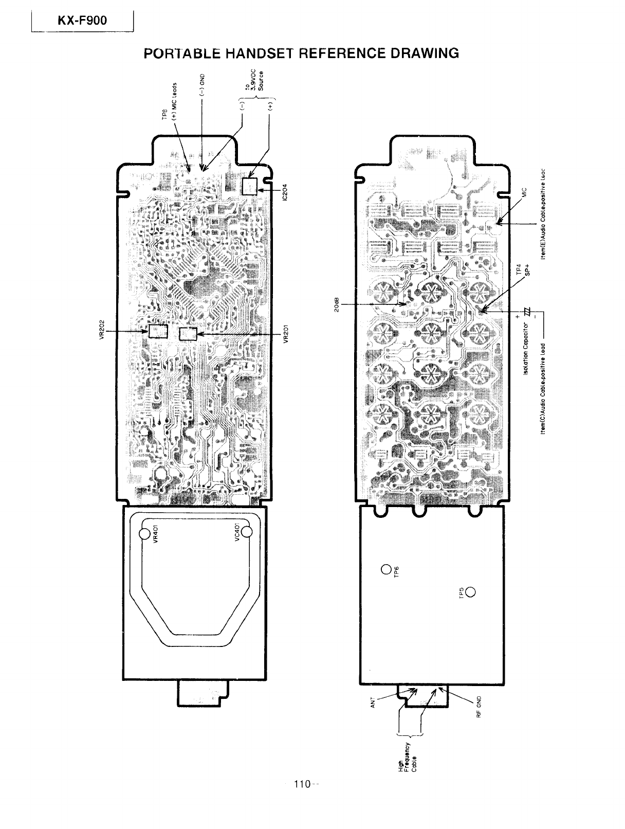
LKX-F900
POR]ABLE HANDSET REFERENCE DRAWING
P_
_t
>
©_
_©
o
/
o
110-
I
i=
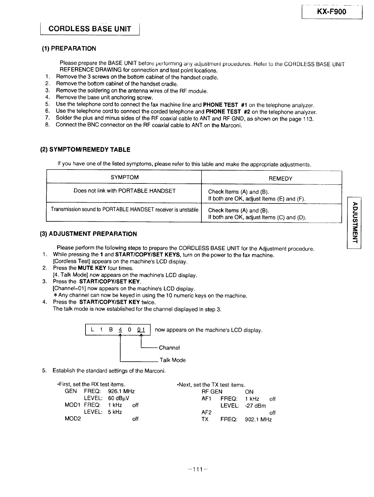
CORDLESS BASE UNIT
[ Kx: ,oo='j
(1) PREPARATION
Please prepare the BASE UNIT before performing any adjustment procedures. Refer to the CORDLESS BASE UNIT
REFERENCE DRAWING for connection and test point locations.
1. Remove the 3 screws on the bottom cabinet of the handset cradle.
2. Remove the bottom cabinet of the handset cradle.
3. Remove the soldering on the antenna wires of the RF module.
4. Remove the base unit anchoring screw.
5. Use the telephone cord to connect the fax machine line and PHONE TEST #1 on the telephone analyzer.
6. Use the telephone cord to connect the corded telephone and PHONE TEST #2 on the telephone analyzer.
7. Solder the plus and minus sides of the RF coaxial cable to ANT and RF GND, as shown on the page 113.
8. Connect the BNC connector on the RF coaxial cable to ANT on the Marconi.
(2) SYMPTOM/REMEDY TABLE
If you have one of the listed symptoms, please refer to this table and make the appropriate adjustments.
SYMPTOM REMEDY
Does not link with PORTABLE HANDSET Check Items (A) and (B).
If both are OK, adjust Items (E) and (F).
Transmission sound to PORTABLE HANDSET receiver is unstable Check Items (A) and (B).
If both are OK, adjust Items (C) and (D).
(3) ADJUSTMENT PREPARATION
Please perform the following steps to prepare the CORDLESS BASE UNIT for the Adjustment procedure.
1. While pressing the 1 and 8TART/OOPY/SET KEYS, turn on the power to the fax machine.
[Cordless Test] appears on the machine's LCD display.
2. Press the MUTE KEY four times.
[4. Talk Mode] now appears on the machine's LCD display.
3. Press the START/COPYISET KEY.
[Channel=01] now appears on the machine's LCD display.
,I, Any channel can now be keyed in using the 10 numeric keys on the machine.
4. Press the START/COPY/SET KEY twice.
The talk mode is now established for the channel displayed in step 3.
#=l
IL1B40 I
i i__
now appears on the machine's LCD display.
Channel
Talk Mode
5. Establish the standard settings of the Marconi.
•First, set the RX test items.
GEN FREQ: 926.1 MHz
LEVEL: 60 dB!_V
MOD1 FREQ: 1 kHz off
LEVEL: 5kHz
MOD2 off
•Next, set the TX test items.
RF GEN ON
AF1 FREQ: 1 kHz off
LEVEL: -27dBm
AF2 off
TX FREQ: 902.1 MHz
-111-
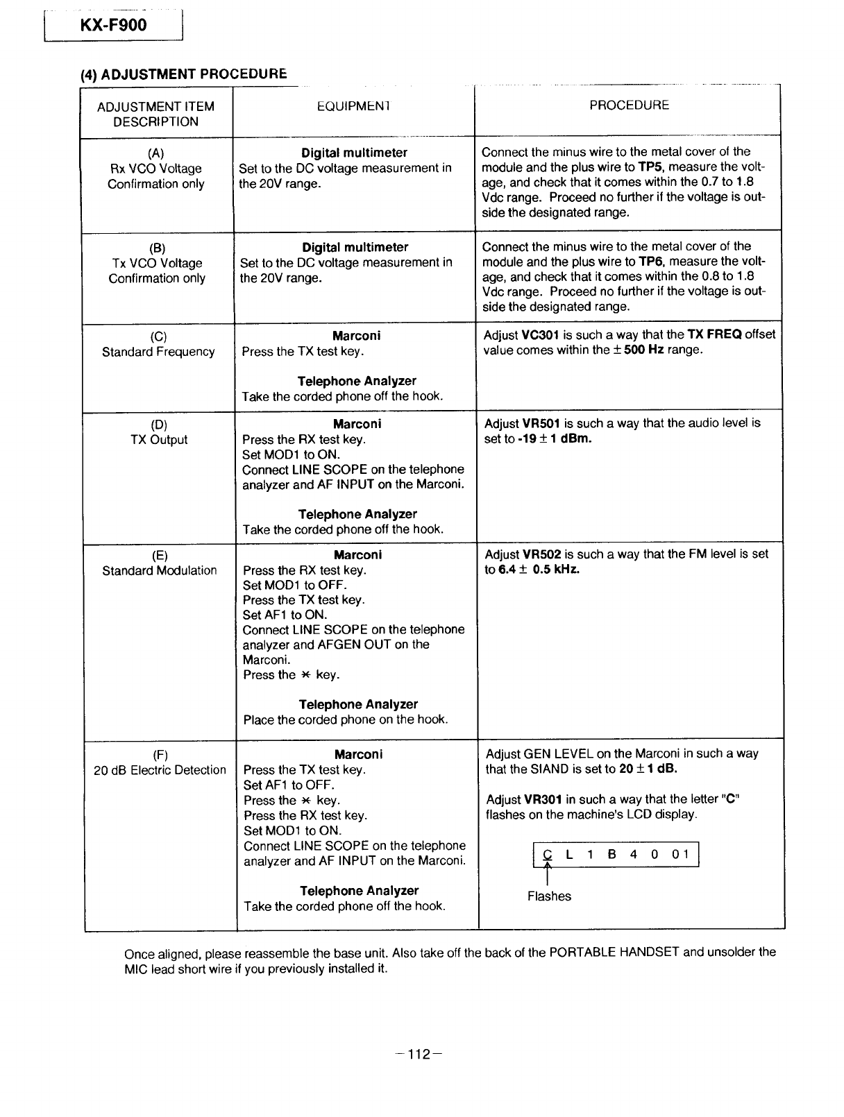
I Kx-F 0 L
(4) ADJUSTMENT PROCEDURE
ADJUSTMENT ITEM
DESCRIPTION
(A)
Rx VCO Voltage
Confirmation only
(B)
Tx VCO Voltage
Confirmation only
EQUIPMEN]
Digital multimeter
Set to the DC voltage measurement in
the 20V range.
Digital multimeter
Set to the DC voltage measurement in
the 20V range.
PROCEDURE
Connect the minus wire to the metal cover of the
module and the plus wire to TP5, measure the volt-
age, and check that it comes within the 0.7 to 1.8
Vdc range. Proceed no further if the voltage is out-
side the designated range.
Connect the minus wire to the metal cover of the
module and the plus wire to TP6, measure the volt-
age, and check that it comes within the 0.8 to 1.8
(c)
Standard Frequency
Marconi
Press the TX test key.
Telephone Analyzer
Vdc range. Proceed no further if the voltage is out-
side the designated range.
Adjust VC301 is such a way that the TX FREQ offset
value comes within the + 500 Hz range.
(D)
TX Output
(E)
Standard Modulation
(F)
20 dB Electric Detection
Take the corded phone off the hook.
Marconi
Press the RX test key.
Set MOD1 to ON.
Connect LINE SCOPE on the telephone
analyzer and AF INPUT on the Marconi.
Telephone Analyzer
Take the corded phone off the hook.
Marconi
Press the RX test key.
Set MOD1 to OFF.
Press the TX test key.
Set AF1 to ON.
Connect LINE SCOPE on the telephone
analyzer and AFGEN OUT on the
Marconi.
Press the _key.
Telephone Analyzer
Place the corded phone on the hook.
Marconi
Press the TX test key.
Set AF1 to OFF.
Press the _key.
Press the RX test key.
Set MOD1 to ON.
Connect LINE SCOPE on the telephone
analyzer and AF INPUT on the Marconi.
Telephone Analyzer
Take the corded phone off the hook.
Adjust VR501 is such a way that the audio level is
set to -19 + 1 dBm.
Adjust VR502 is such a way that the FM level is set
to 6.4 + 0.5 kHz.
Adjust GEN LEVEL on the Marconi in such a way
that the SIAND is set to 20 + 1 dB.
Adjust VR301 in such a way that the letter "C"
flashes on the machine's LCD display.
I
Flashes
Once aligned, please reassemble the base unit. Also take off the back of the PORTABLE HANDSET and unsolder the
MIC lead short wire if you previously installed it.
-112-
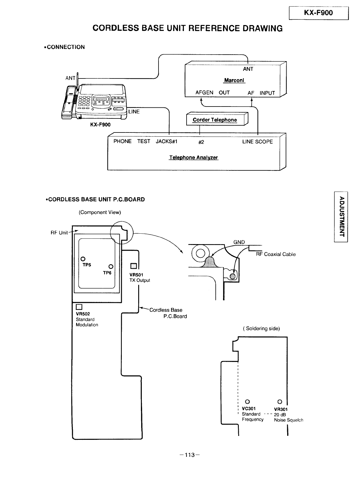
CORDLESS BASE UNIT REFERENCE DRAWING
KX-F900 ]
*CONNECTION
ANT
Marconi
Corder Telephone
KX-F900 I
/
PHONE TEST JACKS#1 #2 LINE SCOPE
Telephone Analyzer
INPUT
•CORDLESS BASE UNIT P.C.BOARD
(Component View)
RF Unit _
D
TP5 O
TP6
• J
[]
VR502
Standard
Modulation
I
VR501
TX Output
"_"'- Cordless Base
mP.C.Board
GND
_ Coaxial Cable
( Soldering side)
OO
VC301 VR301
Standard --- 20dB
Frequency Noise Squelch
--1 I
€..
C
-t
m
z
.-I
-113-
I " KX'FgOo-- I
DISASSEMBLY INSTRUCTIONS
1. How to Remove the
Cordless
2. How to Remove the
3. How to Remove the
4. How to Remove the
5. How to Remove the
6. How to Remove the
7. How to Remove the
8. How to Remove the
9. How to Remove the
10. How to Remove the
11. How to Remove the
12. How to
13. Howto
14. Howto
15. Howto
16. How to
Page
Handset Cradle Cab,
Base Unit Board and RF Unit ....................... 115
Operation Block ........................................... 116
Operation Board and LCD ........................... 117
Bottom Frame .............................................. 118
Analog, Digital Boards, Speaker and Mic .... 118
Power Supply Board and AC Inlet ............... 119
Motor Block ................................................. 119
CCD Unit ..................................................... 120
Rollers ......................................................... 120
Cutter Block ................................................. 121
Recording Paper Cover ............................... 122
Remove the Thermal Head Roller ................................... 123
Remove the Document Tray ............................................ 124
Remove the Bottom Cabinet of Portable Handset ........... 125
Remove the Antenna and Portable Handset Board ......... 125
Replace Flat Package IC ................................................. 126
114-
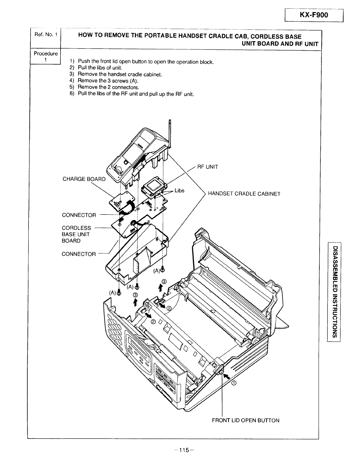
Ref.No.1
Procedure
1
HOW TO REMOVE THE PORTABLE HANDSET CRADLE CAB, CORDLESS BASE
UNIT BOARD AND RF UNIT
1) Push the front lid open button to open the operation block.
2) Pull the libs of unit.
3) Remove the handset cradle cabinet.
4) Remove the 3 screws (A).
5) Remove the 2 connectors.
6) Pull the libs of the RF unit and pull up the RF unit.
CHARGE BOARD
RF UNIT
HANDSET CRADLECABINET
CONNECTOR
CORDLESS
BASE UNIT
BOARD
CONNECTOR
(A)€ @
(A)&
FRONT LiD OPEN BUTTON
r..D i
¢.Di
¢.Di
f"rl i
I_01
m i
Ill I
i.,-i i
f.D I
r
J
i-- I
€/} I
115-
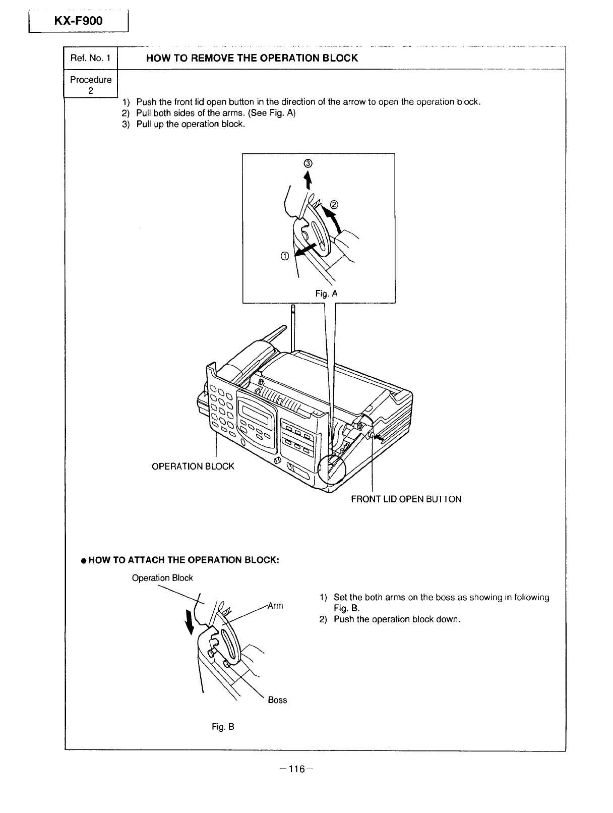
iKX-F900 I
Ref. No. 1
Procedure
2
1)
2)
3)
HOW TO REMOVE THE OPERATION BLOCK
Push the front lid open button in the direction of the arrow to open the operation block.
Pull both sides of the arms. (See Fig. A)
Pull up the operation block.
®
®
©
Fig. A
OPERATION BLOCK
FRONT LID OPEN BUTfON
• HOW TO ATTACH THE OPERATION BLOCK:
Operation Block
1) Set the both arms on the boss as showing in following
Fig. B.
2) Push the operation block down.
Boss
Fig. B
-116-
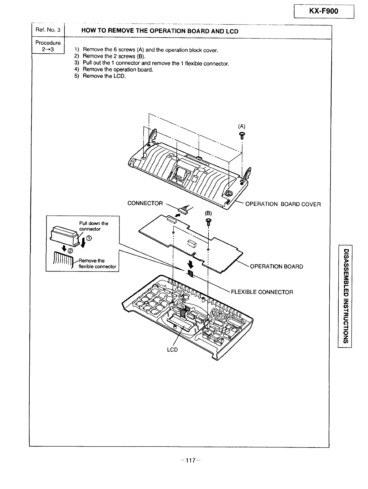
Ref. No. 3
Procedure
2--*3
HOW TO REMOVE THE OPERATION BOARD AND LCD
1) Remove the 6 screws (A) and the operation block cover.
2) Remove the 2 screws (B).
3) Pull out the 1 connector and remove the 1 flexible connector.
4) Remove the operation board.
5) Removethe LCD.
Pulldown the
nnector
O
_ fRl:x?b_eetcohnenector
CONNECTOR.__
LCD
(B)
(A)
OPERATION BOARD COVER
DN BOARD
FLEXIBLE CONNECTOR
m
Ill
m
r-
m
c_
z
--I
c
--I
0
z
€_
KX-F900
-117-
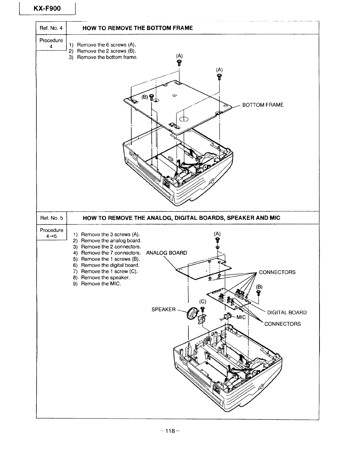
LKX-F900 I
Ref. No. 4
Procedure
4
Ref. No. 5
Procedure
4_5
1)
2)
3)
HOW TO REMOVE THE BOTTOM FRAME
Remove the 6 screws (A).
Remove the 2 screws (B).
Remove the bottom frame. _)
j_ (A)
HOW TO REMOVE THE ANALOG, DIGITAL BOARDS, SPEAKER AND MIC
BOTTOM FRAME
1) Remove the 3 screws (A).
2) Remove the analog board.
3) Remove the 2 connectors.
4) Remove the 7 connectors.
5) Remove the 1 screws (B).
6) Remove the digital board.
7) Remove the 1 screw (C).
8) Remove the speaker.
9) Remove the MIC.
(A)
'ii'
ANALOG BOARD
MIC ,__ CONNECTORS
118-
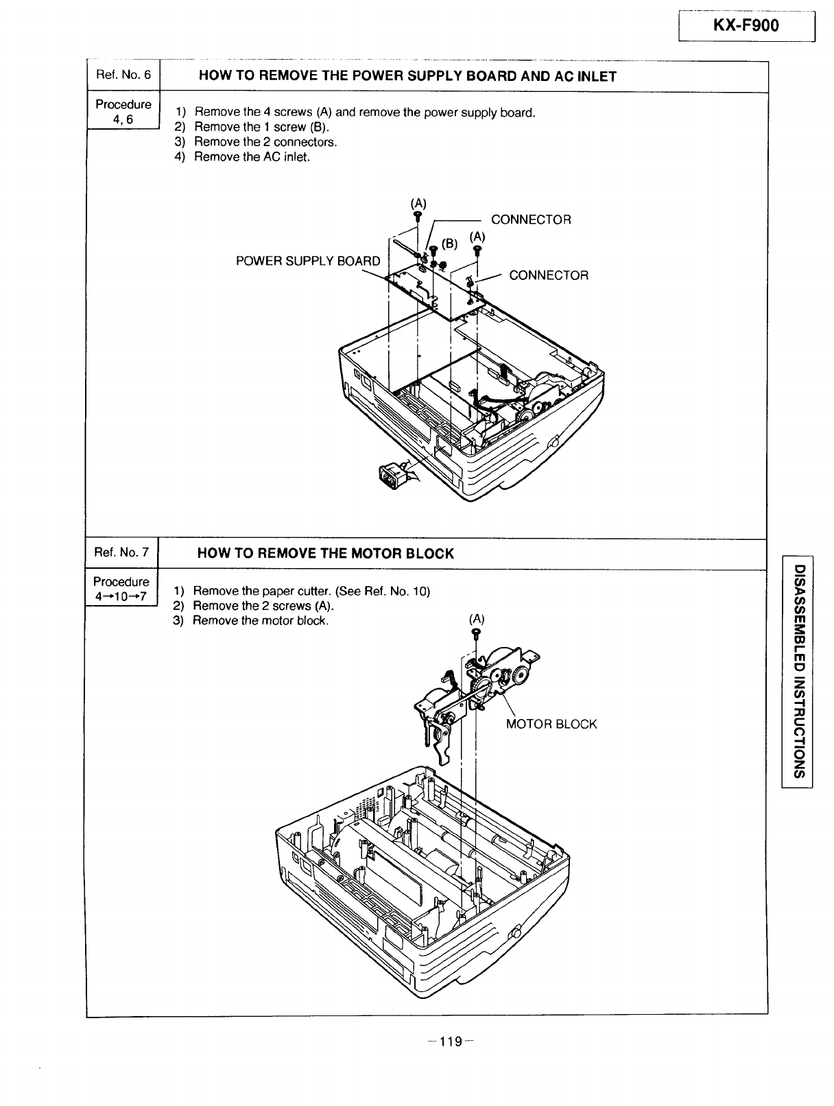
Ref. No. 6
Procedure
4,6
Ref. No. 7
Procedure
4--,10--,7 1) Remove the paper cutter. (See Ref. No. 10)
2) Remove the 2 screws (A).
3) Remove the motor block.
--KX:Fg00]
HOW TO REMOVE THE POWER SUPPLY BOARD AND AC INLET
1) Remove the 4 screws (A) and remove the power supply board.
2) Remove the 1 screw (B).
3) Remove the 2 connectors.
4) Remove the AC inlet.
(A)
¶r _ CONNECTOR
_,(B) (A,
POWER SUPPLY BOARD /.'_i_
HOW TO REMOVE THE MOTOR BLOCK
_OR BLOCK
L
o
m
_3
f-
m
o
z
00
-4
33
c
0
0
z
-119-
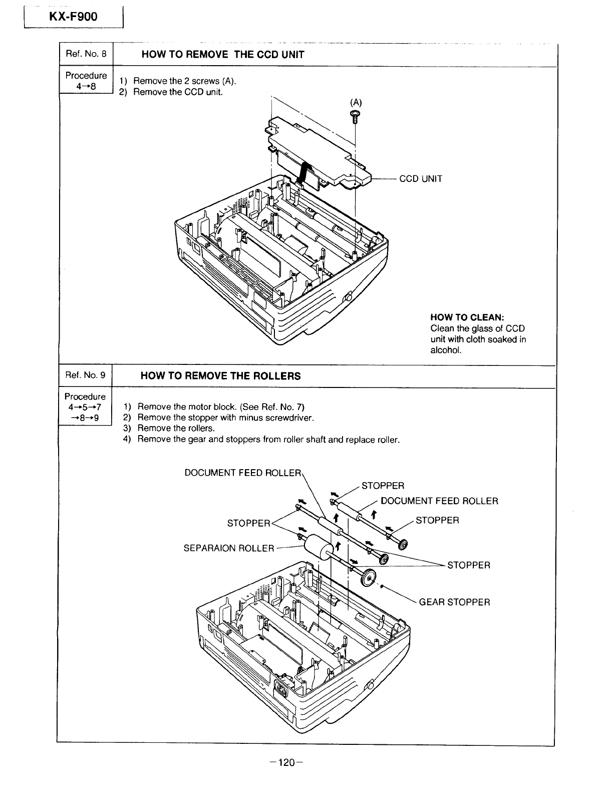
IKX-F900
Ref. No. 8
Procedure
4-*8
HOW TO REMOVE THE CCD UNIT
1) Remove the 2 screws (A).
2) Remove the CCD unit.
°
'_ (A)
i
' _ _--_- CCD
UNIT
HOW TO CLEAN:
Clean the glass of CCD
unit with cloth soaked in
alcohol.
Ref. No. 9 HOW TO REMOVE THE ROLLERS
Procedure
4--,5---7 1) Remove the motor block. (See Ref. No. 7)
--*8-*9 2) Remove the stopper with minus screwdriver.
3) Remove the rollers.
4) Remove the gear and stoppers from roller shaft and replace roller.
DOCUMENT FEED ROLLER_
STOPPER@ _
SEPARAION ROLLER
_jSTOPPER
,,,_DOCUMENT FEED ROLLER
_/,STOPPER
STOPPER
GEAR STOPPER
-120-
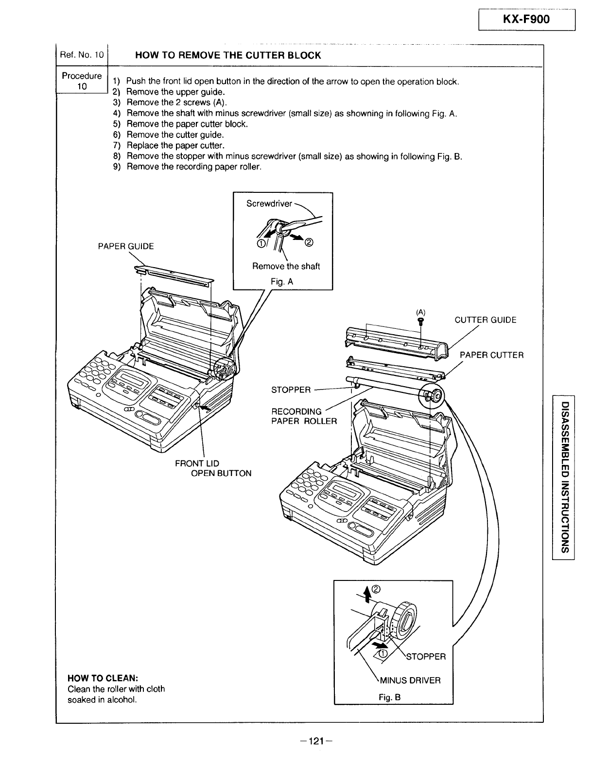
Ref. No. 10
Procedure
10
HOW TO REMOVE THE CUTTER BLOCK
1) Push the front lid open button in the direction of the arrow to open the operation block.
2) Remove the upper guide.
3) Remove the 2 screws (A).
4) Remove the shaft with minus screwdriver (small size) as showning in following Fig. A.
5) Remove the paper cutter block.
6) Remove the cutter guide.
7) Replace the paper cutter.
8) Remove the stopper with minus screwdriver (small size) as showing in following Fig. B.
9) Remove the recording paper roller.
PAPER GUIDE
FRONT LID
OPEN BUTTON
Remove the shaft
Fig. A
STOPPER
RECORDING
PAPER ROLLER
(A)
HOW TO CLEAN:
Clean the roller with cloth
soaked in alcohol.
®
JS DRIVER
Fig. B
O
I
60
60
60
m
m
iI
Ill
o
I
z
60
-I
_o
c
O
-I
i
O
z
60
-121 -
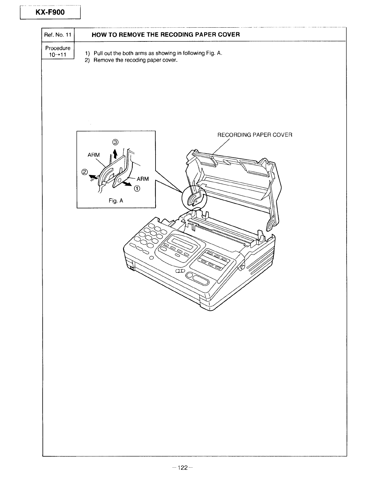
r ....KX-F'O01
Ref. No. 11
Procedure
10-* 11
HOW TO REMOVE THE RECODING PAPER COVER
1) Pull out the both arms as showing in following Fig. A.
2) Remove the recoding paper cover.
RECORDING PAPER COVER
- 122-
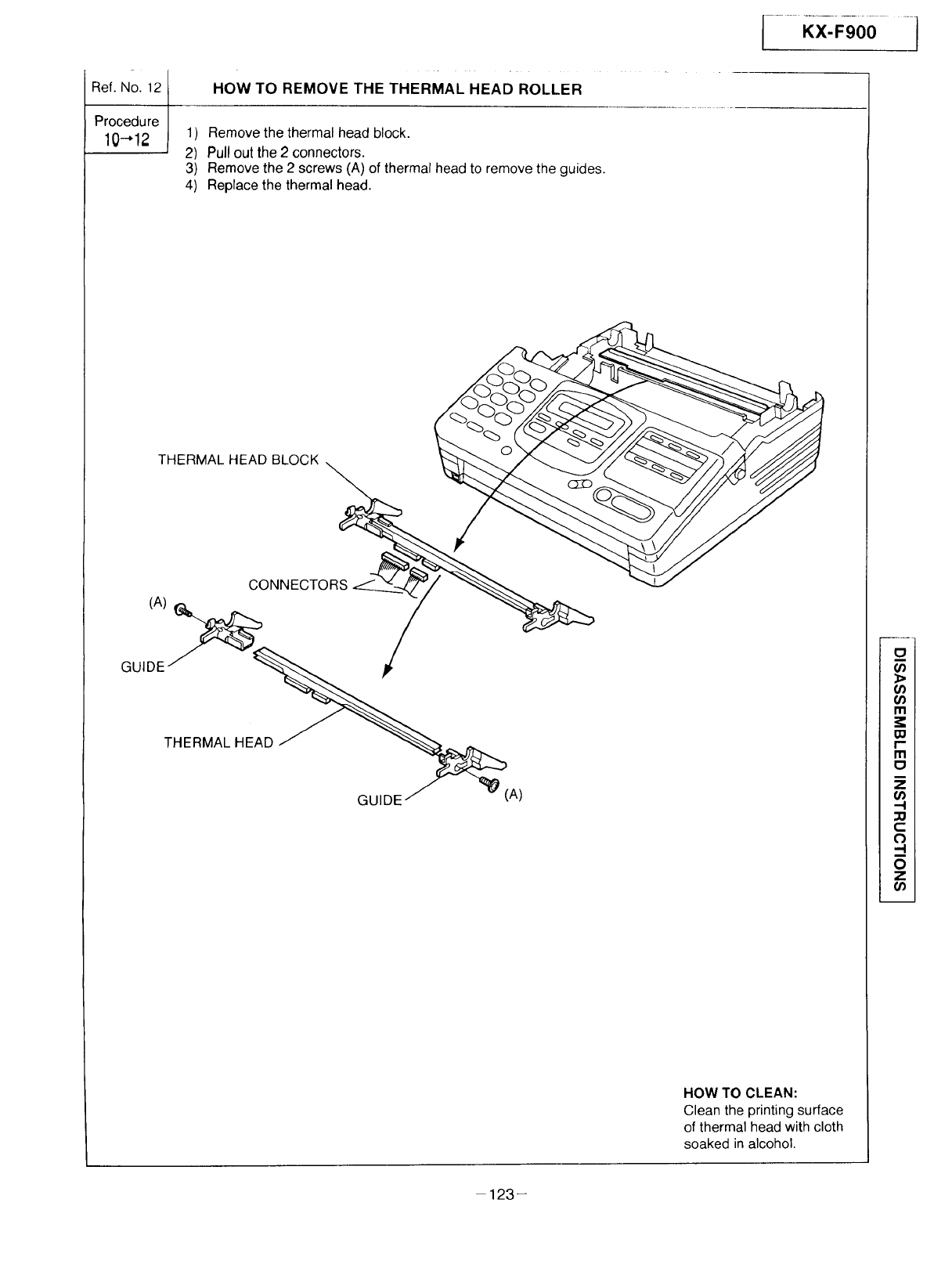
Ref. No. 12
Procedure
10-'12
HOW TO REMOVE THE THERMAL HEAD ROLLER
1) Remove the thermal head block.
2) Pull out the 2 connectors.
3) Remove the 2 screws (A) of thermal head to remove the guides.
4) Replace the thermal head.
THERMAL HEAD BLOCK .
(A)_ ONNECT
GUIDEJ
THERMAL HEAD /
GUIDE j _" (A)
HOW TO CLEAN:
Clean the printing surface
of thermal head with cloth
soaked in alcohol.
I_I
Iorj I
I _'J I
I m I
ImI
ii
i i
in,_ i
[ _m i
i i
I _') I
123-
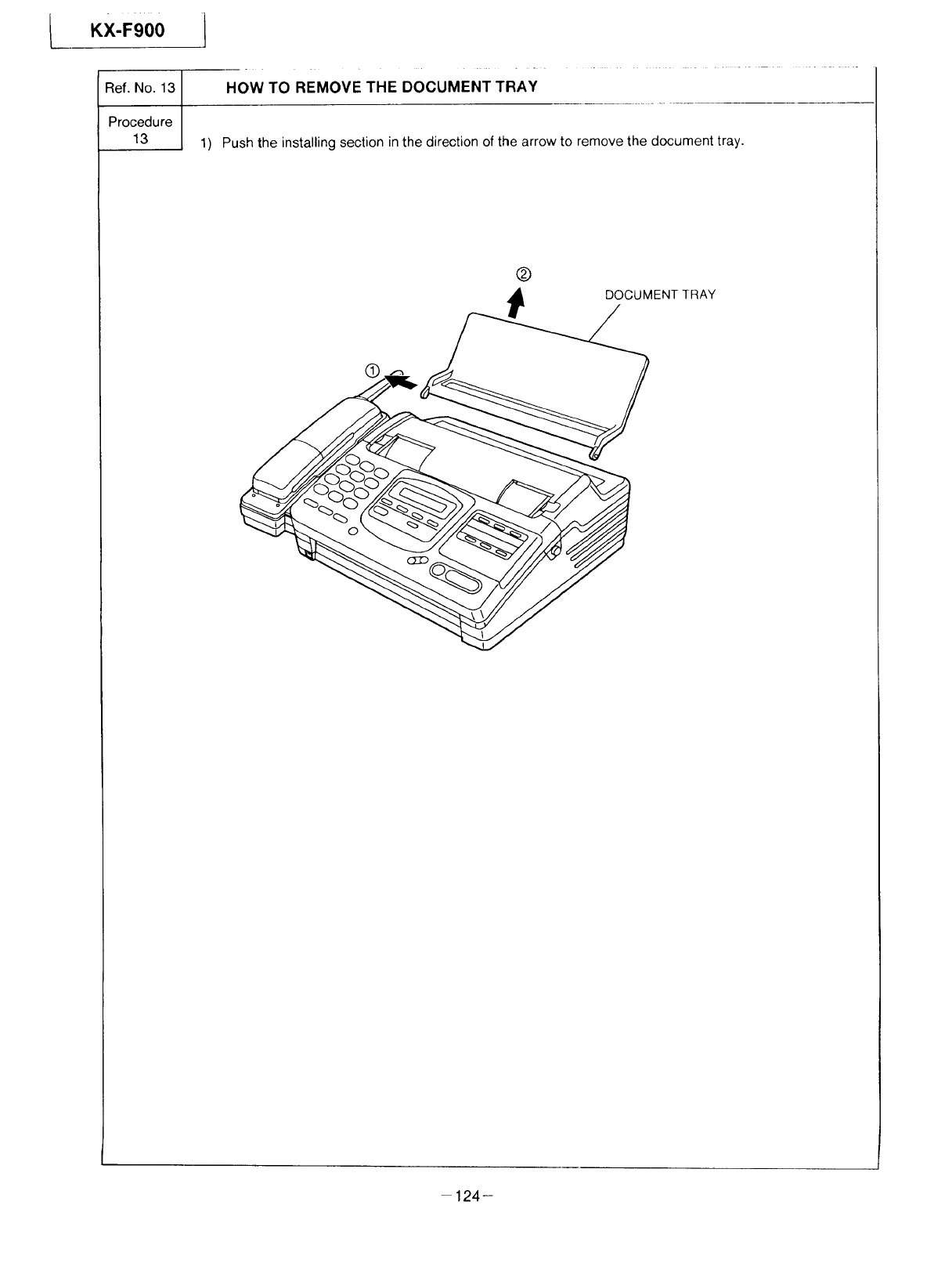
LKX-F900 I
Ref. No. 13
Procedure
13
HOW TO REMOVE THE DOCUMENT TRAY
1) Push the installing section in the direction of the arrow to remove the document tray.
®
DOCUMENT TRAY
®
-124-
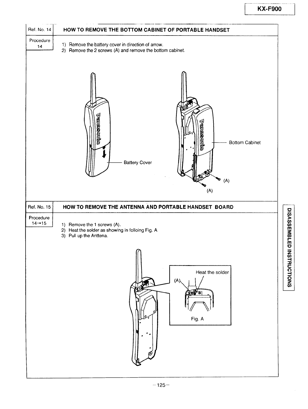
_- KX- -F9oo ..........1
Ref. No. 14
Procedure
14
Ref. No. 15
Procedure
14---15
HOW TO REMOVE THE BOTTOM CABINET OF PORTABLE HANDSET
1) Remove the battery cover in direction of arrow.
2) Remove the 2 screws (A) and remove the bottom cabinet.
i _.._) Battery Cover ,I_, f__A) (A)
HOW TO REMOVE THE ANTENNA AND PORTABLE HANDSET BOARD
1)
2)
3)
Remove the 1 screws (A).
Heat the solder as showing in folloing Fig. A
Pull up the Anttena.
i
,t!j
Heat the solder
Fig. A
- -- Bottom Cabinet
6t}
€/)
m
r"
ill
z
-4
C
0
"-I
0
Z
- 125-
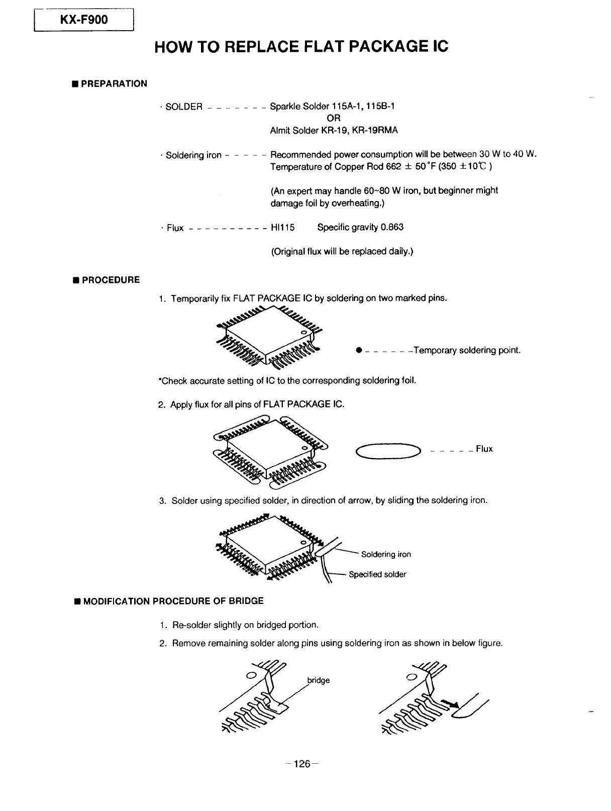
I KX-F900 1
• PREPARATION
• PROCEDURE
HOW TO REPLACE FLAT PACKAGE IC
-SOLDER
• Soldering iron
• Flux
Sparkle Solder 115A-1, 115B-1
OR
Almit Solder KR-19, KR-19RMA
Recommended power consumption will be between 30 W to 40 W.
Temperature of Copper Rod 662 + 50°F (350 +10°C )
(An expert may handle 60~80 W iron, but beginner might
damage foil by overheating.)
HI115 Specific gravity 0.863
(Original flux will be replaced daily.)
1. Temporarily fix FLAT PACKAGE IC by soldering on two marked pins.
-Temporary soldering point.
*Check accurate setting of IC to the corresponding soldering foil.
2. Apply flux for all pins of FLAT PACKAGE IC.
_._ ..... Flux
3. Solder using specified solder, in direction of arrow, by sliding the soldering iron.
Soldering iron
Specified solder
• MODIFICATION PROCEDURE OF BRIDGE
1. Re-solder slightly on bridged portion.
2. Remove remaining solder along pins using soldering iron as shown in below figure.
bddge
-126-
IKX-F900 J
CIRCUIT OPERATIONS
Page
1. Connection Diagram ........................................................................ 128
2. General Block Diagram ........................................................... 129-130
3. Control Section ........................................................................ 131-136
3-1. Block Diagram ................................................................... 132
3-2. Reset Circuit ...................................................................... 133
3-3. SRAM and RTC Back up Circuit ....................................... 134
3-4. Supervision circuit for Thermal Head Temperature .......... 135
3-5. LED Array .......................................................................... 136
4. Facsimile Section ..................................................................... 137~145
4-1. Image Data Flow during Facsimile Operation ........... 137, 138
4-2. Thermal Head ............................................................ 139, 140
4-3. Read Section ..................................................................... 141
4-4. Stepping Motor Drive Section ........................................... 142
4-5. Sensor and Switches ................................................ 143~145
5. MODEM Section ...................................................................... 146~152
5-1. Function ..................................................................... 146-151
5-2. MODEM Circuit Operation ................................................ 152
6. Explanation of Analog Section Block Diagram ........................ 153, 154
7. NCU Section ............................................................................ 155, 156
8. ITS and Monitor Section .......................................................... 157, 158
9. TAM Interface Section ............................................................ 159-161
10. Operation Panel ............................................................................. 162
11. LCD COG Type .............................................................................. 163
12. Switching Power Supply Section ........................................... t 64-166
13. Cordless Section .................................................................... 167~183
13-1. Explanation of Data Communication ........................ 167-170
13-2.
13-3.
13-4.
13-5.
13-6.
13-7.
Frequency Table ................................................................ 170
Block diagram of Cordless Base Unit ....................... 171,172
Circuit Operation of Cordless Base Unit ................... 173, 174
Circuit Operation of RF Unit ...................................... 175-177
Block diagram of Portable Handset .......................... 178, 179
Circuit Operation of Portable Handset ...................... 180~183
o
€")
C
-I
O
"o
rrl
-I
o
z
- 127-
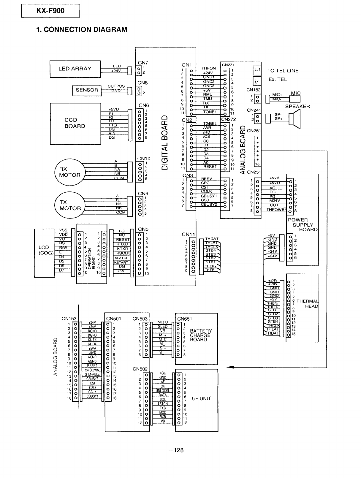
1. CONNECTION DIAGRAM
I I wl-I
LED ARRAY +24v
[ sENs°R1 °uZ °s1-1
CCD
BOARD
+SVD
A
NA
NB
COM
A
NA
NI5
COM
vSS
LCD I"-R'/_V--
(COG)I _
_-I1 11o
012 20
OI 3 30
014 40
o 15__ 5o
o,6 oo
ol 7
o 18_ 81o
O190m 910
oF0 IO10
CN7
CN8
CN6
02
O 3
O4
8
CN10
O2
O 3
O4
5
CN9
O2
O3
O4
5
CN5
o 2
o 3
O 4
o 5
O 6
o 7
O 8
o 9
O10
<
O
<
O
a
CN1
1O
2
3 O
4O
5 O
6O
7 O
8C
9 e
10 C
11 _.._..O
CN2____
1C
2C
3 C
4' C
c
7C
8 C
9 0
10 C
11 O
ON3
3
4
5
6
7
CN11
20
30
40
50
60
70
rr
<
O
rn
(D
O
J
<
Z
<
CN15
1"6
20
30
40
50
60
70
80
190o
O
11 0
12 O
13 O
14 O
15 O
16 O
170
18 O
CN501
o----I1
OI2
OI3
OI4
OI5
OI6
OI7
OI8
OI9
OI10
o111
0112
0113
0114
0115
0116
0117
OI18
CN503
1 I
3
4
5
6
7
8
CN502
1 o
20
30
40
5 o
6 o
70
80
9 o
10 O
11 O
12 O
MLED
SLED
V.._...E__R
M_+
MC
i CN651
11
O2
O 3 BATTERY
o 4 CHARGE
o 5 BOARD
O 6
O 7
8
1
OI2
OI3
OI4
OI5
ol 6 UF UNIT
OI
OI8
OI9
OI10
Oill
OI12
ON2Z1
E
4
5
6 CN152
82
9
10 CN24"
11 1F _
_N272 2
_1_ CN25"
E
z
,_ CN25"
11I
220
330
4 40
5 50
6 60
7 70
8
TO TEL LINE
Ex. TEL
SPEAKER
+5VA
+SVU 1 1
02
AG O3
DG 04
PG O 5
M24V 0 6
OUT O 7
THPC)WEF 8
POWER
SUPPLY
BOARD
02
o3
04
O5 6
O 6 THERMAL
0 7
O8 HEAD
0 9
10
OI 11
OI12
o1_3
_114
o115
-128-
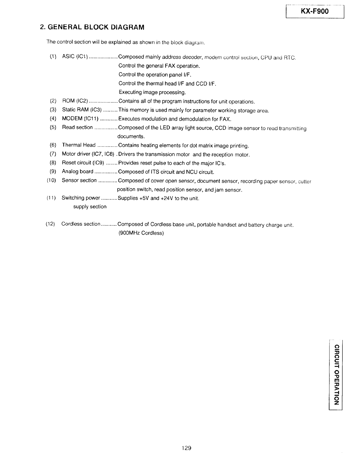
2. GENERAL BLOCK DIAGRAM
[-= KX--F 0- ]
The control section will be explained as shown in the block diagraln.
(,1) ASIC (JC1) .................... Composed mainly address decoder, modem control section, CPU and R-[C.
Control the general FAX operation.
Control the operation panel I/F.
Control the thermal head I/F and CCD I/F.
Executing image processing.
(2) RQM (IC2) .................... Contains all of the program instructions for unit operations.
(3) Static RAM (IC3) .......... This memory is used mainly for parameter working storage area.
(4) MODEM (ICl 1) ............ Executes modulation and demodulation for FAX.
(5) Read section ................ Composed of the LED array light source, CCD image sensor to read transmitting
documents.
(6) Thermal Head .............. Contains heating elements for dot matrix image printing.
(7) Motor driver (IC7, 108) .Drivers the transmission motor and the reception motor.
(8) Reset circuit (IC9) ........ Provides reset pulse to each of the major IC's.
(9) Analog board ................ Composed of ITS circuit and NCU circuit.
(10) Sensor section ............. Composed of cover open sensor, document sensor, recording paper sensor, cutter
position switch, read position sensor, and jam sensor.
(11) Switching power ........... Supplies +5V and +24V to the unit.
supply section
(12) Cordless section ........... Composed of Cordless base unit, portable handset and battery charge unit.
(900MHz Cordless)
O
O
C
m
-I
O
ill
-I
m
O
z
129
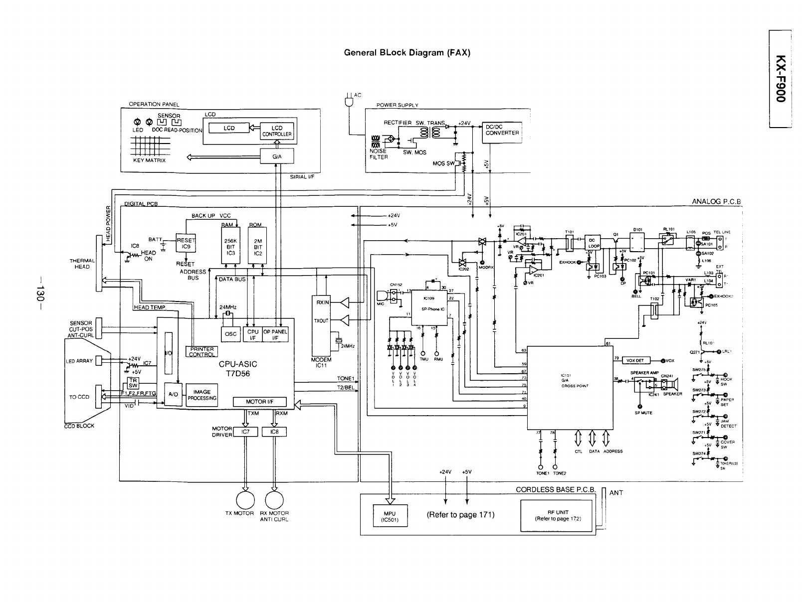
General BLock Diagram (FAX)
F
I
.--L
¢.o
OI
6£
THERMAL
HEAD
SENSOR _1
CUT-POS I I
ANT-CURL LJ
OPERATION PANEL
SENSOR LCD
LED DOC READ-POSITION LCD
iiiiii I 'ICON_
IIIlll
IIIIII _ --_
KEY MATRIX
SIRIAL VF
DIGITAL PCB BACK UP VCCM M
1C8 BA_ _ _
AD_SST÷_ATALUI,
{ !1 CPU-ASIC
_ _-] [_-_---i T7D56
v--_lnF1'F2 _ [ MOTOR_/F
EL c::=
ICll M
;OB_I L'
]
FILTER
POWER SUPPLY
RECTIFIER SW. TRANS
SW. MOS
--1 i
CONVERTER !
!
ANALOG P.C.B
sw215
_Ect
SW271
i_vEo
SW2_
TX MOTOR RX MOTOR
ANTI CURL
+24V +SV
ti
(Refer to page 171 )
'1'1 £££
tt .............
TONE1 TONE2
CORDLESS BASE P.C.B.
t UN'TJL
(Refer to page 172)
ANT
+24V
÷SV ÷5V
T 0101 RL1Ol
0 Q1 L105 pOS TEL LINE
IC202 MOOR) = EXT
+
vox
i234 CROSSPO_NT _-I_
241 SPEAKER
SP MUTE
3. CONTROL SECTION
1QASIC (IC1)
This custom IC is used for g_n_ral PAX operatior_
(1) CPU: The KX-F900 uses ai_U equivalent CHU operating at 12MHz.
(2) RTC:
(3) DECODER:
(4) ROM/RAM I/F:
(5) CCD I/F:
(6) IMAGE DATA RAM:
(7) THERMAL HEAD I/F:
(8) TX MOTOR I/F:
(9) RX MOTOR I/F:
(10) OPERATION PANEL I/F:
(11) I/O PORT:
Many of the peripheral functions are handled by custom designed LSI.
As a result, the CPU only needs to process the result.
Real time clock.
Decodes the address.
Controls the SELECT signal of ROM or RAM and bank switching.
Controls document reading.
Inside ASIC and 8KB which is used by image processing.
Transmits the recorded data to the thermal head.
Controls the transmission motor which feeds the document.
Controls the receiving motor which feeds the reading document.
Serial interface with Operation Panel.
I/O Port Interface (Exa. Sensor etc.)
ROM (IC2)
This 128 KB ROM (EPROM or MASKROM) has 32 KB of common area and bank area (BK4-BK15).
The capacity of each bank is 8 KB.
The addresses of the common area are from 0000H to 7FFFH, and addressed from 8000H to 9FFFH are for the bank
area.
@RAM (IC3)
This 32 KB RAM has 8 KB of common area and bank area (BK0, BK1 ).
The capacity of each bank is 12 KB.
The addresses of the common area are from D000H to EFFFH, and the addresses from A000H to CFFFH are for the
bank area.
O
O
C
-4
O
=o
m
0
z
131
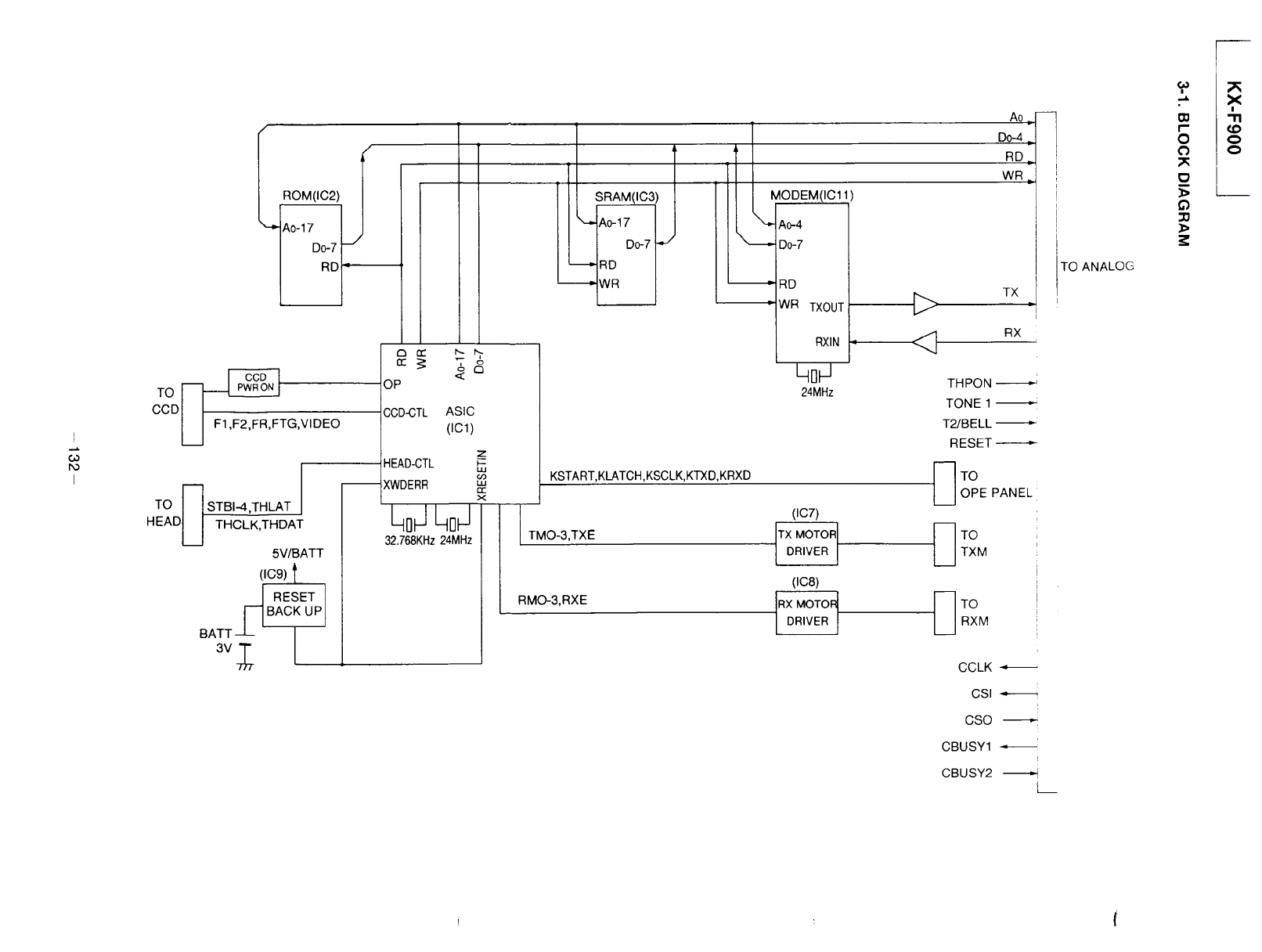
I
I
CCD
HEAD
f
/
ROM(IC2) L
A0-17D0_7F
RD'_
F1,F2,FR,FTG,VIDEO
STBI4,THLAT
THCLK,THDAT
5V/BATT
(IC9) l
RESET I
IqBACKOPI
_TT_
<
OP
CCD_TL ASIC
(IC1)
HEAD-CTL
-- XWDERR "'
x
L_oJqDJ
32.768KHz 24MHz
SRAM(IC3)
Ao-17
Do--7!*/
----_ RD
--_ WR
[ MODEM(IC11
--_ RD
WR TXOUT
RXlN
qu_
24MHz
KSTART,KLATCH,KSCLK, KTXD,KRXD
TMO-3,TXE
RMO-3,RXE
(IC7)
TX MOTOR
DR VER
(tc8)
RX MOTO_
DR VER/
A0_
D0-4
RD_
WR •
TX
RX
THPON
TONE 1
T2/BELL --_
RESET
_7°OPE PANEL
_TO
T×M
TORXM
CCLK
csm
CSO
CBUSY1 _--
!
CBUSY2
i
TO ANALOG
r
0
0
Q
oo
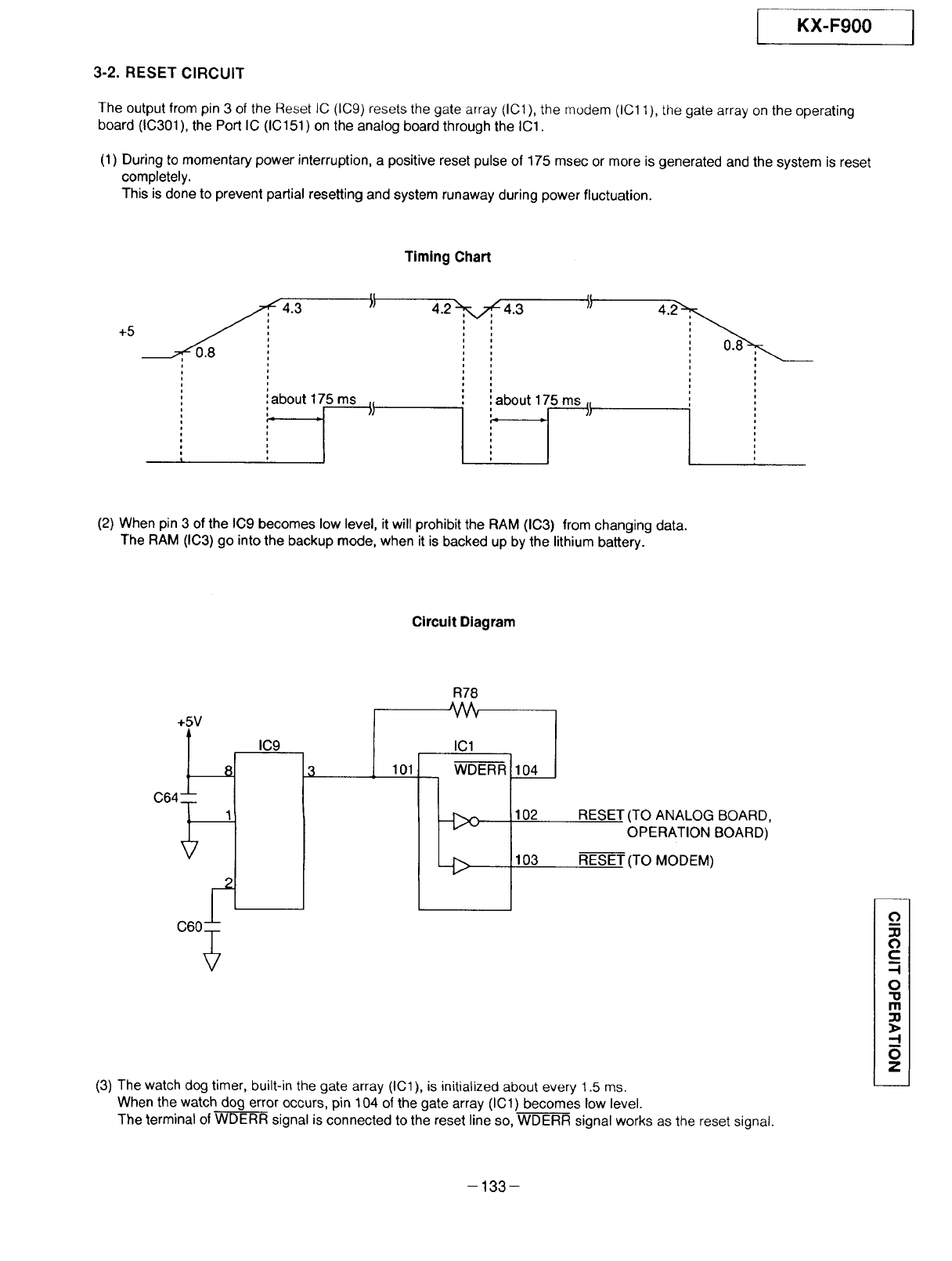
KX-F900
3-2, RESET CIRCUIT
The output from pin 3 of the Reset IC (IC9) resets the gate array (IC1), the modem (IC11), the gate array on the operating
board (10301), the Port IC (10151) on the analog board through the IC1.
(1) During to momentary power interruption, a positive reset pulse of 175 msec or more is generated and the system is reset
completely.
This is done to prevent partial resetting and system runaway during power fluctuation.
Timing Chart
+5 __ ,,_.8,_4. 3 It
i
i
: :about 175 ms jj
i
I
4.2 _ 4.3
: about 17._s_j}
(2) When pin 3 of the IO9 becomes low level, it will prohibit the RAM (IO3) from changing data.
The RAM (IC3) go into the backup mode, when it is backed up by the lithium battery.
Circuit Diagram
+5V
064
c00
IC9
101
R78
IC1
WDERR lo__L
102
103
RESET (TO ANALOG BOARD,
OPERATION BOARD)
RESET (TO MODEM)
(3) The watch dog timer, built-in the gate array (IO1), is initialized about every 1.5 ms.
When the watch dog error occurs, pin 104 of the gate array (IC1) becomes low level.
The terminal of WDERR signal is connected to the reset line so, WDERR signal works as the reset signal.
(')
C
-I
O
"1o
rn
_>
--I
i
O
Z
-133-
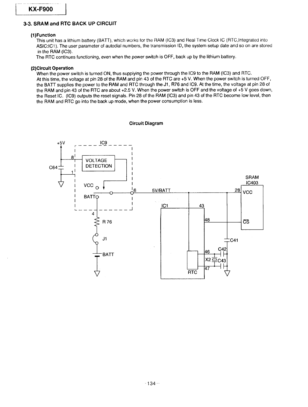
KX-F900
3-3. SRAM and RTC BACK UP CIRCUIT
(1)Function
This unit has a lithium battery (BATT), which works tor the RAM (IC3) and Real Time Clock IC (RTC,lntegrated into
ASIC:IC1 ). The user parameter of autodial numbers, the transmission ID, the system setup date and so on are stored
in the RAM (IC3).
The RTC continues functioning, even when the power switch is OFF, back up by the lithium battery.
(2)Circuit Operation
When the power switch is turned ON, thus supplying the power through the IC9 to the RAM (IC3) and RTC.
At this time, the voltage at pin 28 of the RAM and pin 43 of the RTC are +5 V. When the power switch is turned OFF,
the BATT supplies the power to the RAM and RTC through the J1, R76 and IC9. At the time, the voltage at pin 28 of
the RAM and pin 43 of the RTC are about +2.5 V. When the power switch is OFF and the voltage of +5 V goes down,
the Reset IC. (IC9) outputs the reset signals. Pin 28 of the RAM (IC3) and pin 43 of the RTC become low level, then
the RAM and RTC go into the back up mode, when the power consumption is less.
Circuit Diagram
+5V
C64 1 1
I
I
I
I
IC9
VOLTAGE J_l
DETECTION
VCC O
"
. _1
R76
BATT
5V/BATT 28
ICl 43
----q
RTC
48
--C41
,,. C421
_° _L ', H
x _Tq4 J
47 - i J_7
SRAM
IC403
vcc
C€
-134-
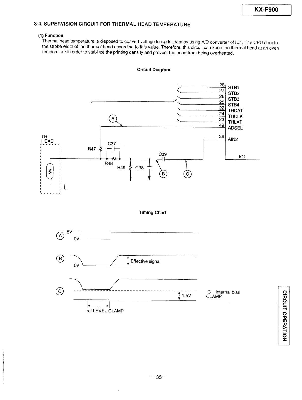
rKX-F900 ]
3-4. SUPERVISION CIRCUIT FOR THERMAL HEAD TEMPERATURE
(1) Function
Thermal head temperature is disposed to convert voltage to digital data by using A!D converter of IC1. The CPU decides
the strobe width of the thermal head according to this value. Therefore, this circuit can keep the thermal head at an even
temperature in order to stabilize the printing density and prevent the head from being overheated.
Circuit Diagram
TH-
HEAD
r ......
t C37
R47 _ __y¢l-__
R48 R49
/
28
i
_, 27
\ 26
\ 25
\ 22
\ 24
\ 23
49
C39
38
STB1
STB2
STB3
STB4
THDAT
THCLK
THLAT
ADSEL1
AIN2
IC1
Timing Chart
I
Effective signal
©1.5V
ref LEVEL CLAMP
IC1 internal bias
CLAMP t"_l
N i
:;Ol
t"_l
C:l
m ,
OI
"Ol
I1"11
21
Ol
135-
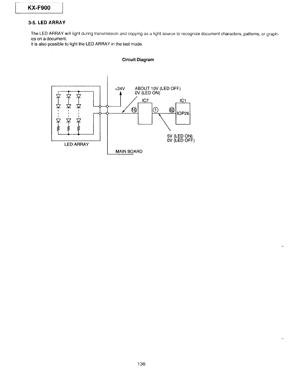
].....KX:F,00]
3-5. LED ARRAY
The LED ARRAY will light during transmission and copying as a light source to recognize document characters, patterns, or graph-
ics on a document.
It is also possible to light the LED ARRAY in the test mode.
Circuit Diagram
III
III
III
LED ARRAY
.-.-(
+24V 0V (LED ON)
ABOUT 10V (LED OFF)
IC7 ICl
MAIN BOARD
5V (LED ON)
0V (LED OFF)
136
4. FACSIMILE SECTION
4-1. IMAGE DATA FLOW DURING FACSIMILE OPERATION
COPY (Fine, Super-Fine, Half Tone)
(1) Line information is read by CCD, by way of route 1(!), it is inputted to IC1.
(2) In ICl, data is adjusted to suitable level for A/D conversion at Analog Signal P_uc_ssing Section, and by way of
route (_) it is inputted to A/D conversion (8 bit). After finishing A/D conversion, data is inputted to Image Processing
Section by way of route _, and by way of routes @ and ®, it is stored in RAM as shading data.
(3) Draft's information that is read by CCD is inputted to IC1 by way of route (!), and after adjusting to suitable level
for A/D conversion by way of route (_), draft's information is converted to A/D (8 bit), and it is inputted to Image
Processing Section. The other side, the shading data which flows from RAM by way of routes ® and (_, it is
inputted to Image Processing Section, and after finishing of draft's information's image processing, white is
regarded as "0" and black is regarded as "1", and by way of routes @ and ®, they are stored in RAM.
(4) White/Black data stored as above description 3), by way of routes @ and ®, it is inputted to P/S converter. White/
Black data converted to serial data in P/S converter is inputted to Thermal Head by way of route (_ and it is printed
out on recording paper.
Note: Standard; Read 3.85 times/mm
Fine; Read 7.7 times/mm
Super-Fine; Read 15.4 times/mm
Transmission
(1) Same processing of COPY items 1) - 3).
(2) Data stored in RAM of IO1 is outputted from IC1 by way of routes @ and _, and it is stored in system bus, and by
way of route @, it is stored in communication buffer inside RAM (IC3).
(3) While fetching data stored in communication buffer synchronous with modem, CPU inputs data to modem along
route @, where it is converted to serial analog data and forwarded over telephone lines via NCU Section.
Reception
(1) Serial analog image data is received over telephone lines and input to the modem via NCU section, where it is
demodulated to parallel digital data. Then the CPU stores the data in the communication buffer of RAM (IC3) along
route 12.
(2) Data stored in RAM (IC3) is decoded by CPU by way of way of route @, and it is stored in RAM by routes (_ and
®.
(3) Same processing of COPY item 4).
O
O
C
-I
O
"o
rrl
_0
-I
m
O
z
137
[..... Kx-F900 ..... }
Block Diagram
IC1
IC3
RAM
IC2
ROM
SYS] EM
BUS
/
/
\\"
/
IMAGE
PROCESSING
SECTION
I
cPul
RAM
.,,__ /I
P/S
CONVERTER
(9
ANALOG
SIGNAL PROCESSING
SECTION
,. THERMAL
O HEAD
MODEM
NCU
TEL.LINE
138
KX-F900
4-2. THERMAL HEAD
(1)Function
This unit utilizes state of the art thermal printer technology.
The recording paper (roll paper) is chemically processed. When the thermal head contacts this paper it emits heat momen
tarily, black dots (appearing almost as a point) are printed on the paper. If this point is continued, litters and/or diagrams
appear, and the original document is reproduced.
COMPOSITION OF THE RECEIVE RECORD SECTION (THERMAL RECORDING FORMAT)
Platen Roller
Thermal Recording Paper
T
Thermal Head
(2)Circuit Operation
There are 18 driver ICs aligned horizontally on the thermal head and each one of these ICs can drive 96 heat emitting
registers. This means that one line is at a density of 96 )< 18=1728 dots=(8 dots/mm).
White/Black (white=0, black=l) data in one line increments is synchronized at IC1 pin 24 (THCLK) and sent from IC1 pin
22 (THDAT) to the shift register of the fCs. The shift registers of the 18 tCs are connected in series, and upon shift of 1728
dot increment, all the shift register become filled with data, and a latch pulse is emitted to each IC from IC1 pin 23
(THLAT).
With this latch pulse, all the contents of shift registers are latched to the latch registers. Thereafter, through the addition of
strobe from the IC1 pins (25, 26, 27, 28) only dot of location of black (=1) among latched data activates driver, and current
passes to heat emitting body to cause heat emission.
Here the strobe of four lines STB1 to STB4 impresses at intervals of 9.216 msec, as required for one-line printout, for
each 1/4th of 18 IC unit (4 unit or 5 unit) upon each time interval divided into four equal increments.
The sequence is as shown below. [Moreover, in the case of strobe width, the resistance value of the thermistor inside the
thermal head is constantly detected by IC1 pin 38, and vales from the ROM (IC2) table corresponding to temperatures
eliminate temperature changes of density through setting by CPU.]
When the thermal head is not used, the IC1 (119, TH-POWER) becomes low level, IC7 becomes OFF, RL201 breaks, and
the +24 V power supply for the thermal head driver is not impressed to protect the IC.
O
O
t.-
.-I
O
m
--i
0
z
-139-
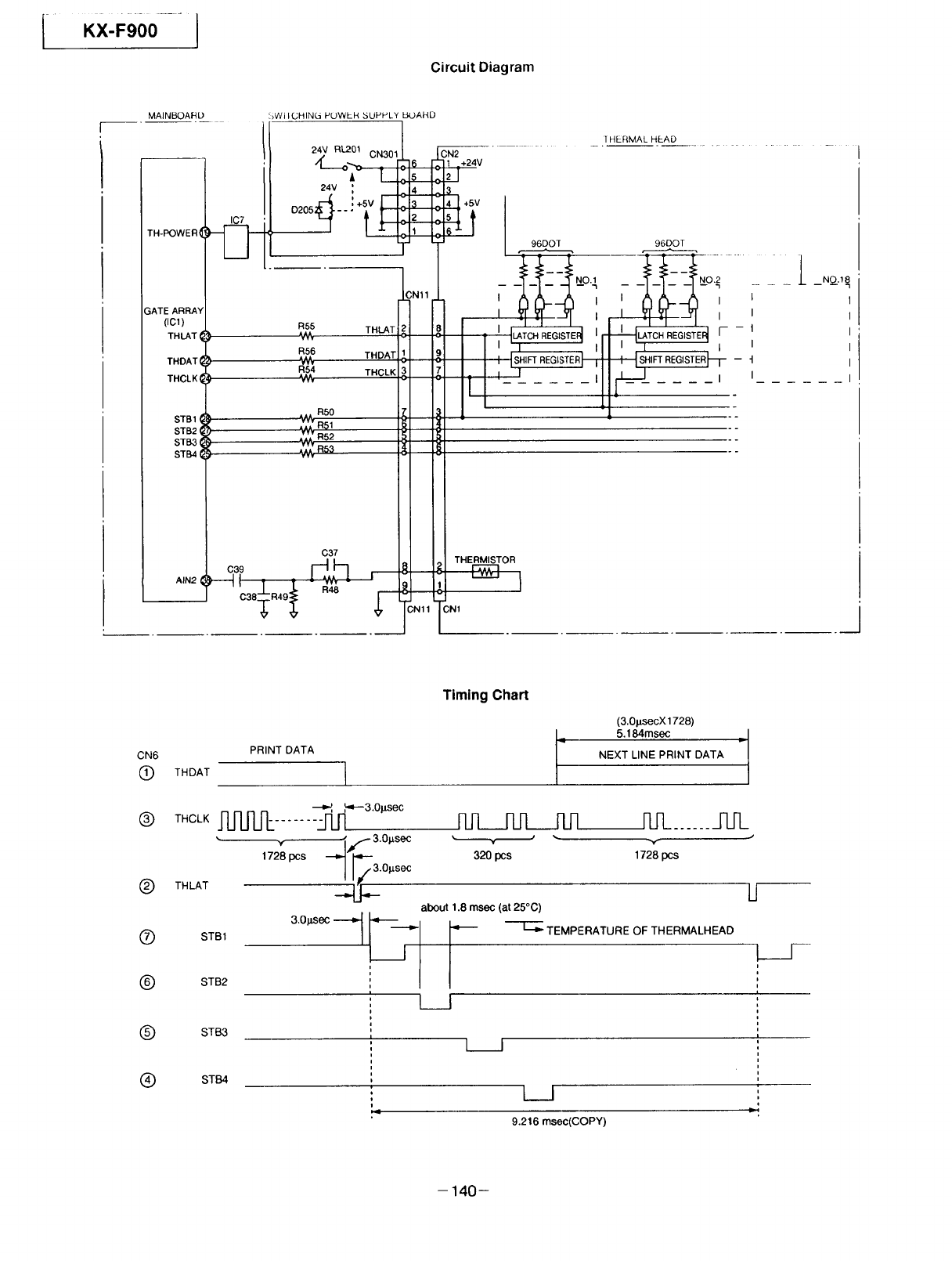
lj
Circuit Diagram
MAINBOARD ',JWIICHING POWER SUPPLY L_JAHD
24V RL201 CN301 CN2
1HERMAL HEAD
"/L_o_ "16 E 1 .+24V
iI o=o_t_.;÷_vF-2:1: _ +_v I
111 , , , ,0oo..:. ,SOOT.......
I- ll---tNO'I--{Ii'------INO'2
c I I I I I
GATE ARRAYI ] [" I _ {_}--'--_ II_ {_----_
(IC,) R55 2 8 XI XlJI ,..I I
.5° :.o.:,_ i.II '' ' ' ''
:.c_,_ = T.OL,3='"' I' _-- ' r_ ;"
STB1 R_I l -
I s:,,=t_; ,_ _
TR52 I
I Ic,o _,_ ,.,.STO°
Il°'°t"_° U .,
I_NO_._8
I
I
i
I
I
I
Timing Chart
(3.0MsecX1728)
4 5.184reset
CN6 PRINT DATA NEXT LINE PRINT DATA
@THDAT I
,_- 3.01._sec
@T.C_JqJ]J]_l_....... -I1_[1 I1Jl__J1Jl [lj1 FLIq FIFL
320 pcs 1728 pcs
@ THLAT
®
®
®
®
STB1
STB2
STB3
STB4
1728 pcs _,- 3.0psec
.0p.sec
3.0psec _ ______j._..p.
i
=
J
=
=
about 1.8 msec (at 26°C)
- [--_ TEMPERATURE OF THERMALHEAD
__J
LI
I
m
i
i
[-
LIJ
L_J
9.216 msec(COPY)
i
i
i
i
i
i
i
=I
- 140-
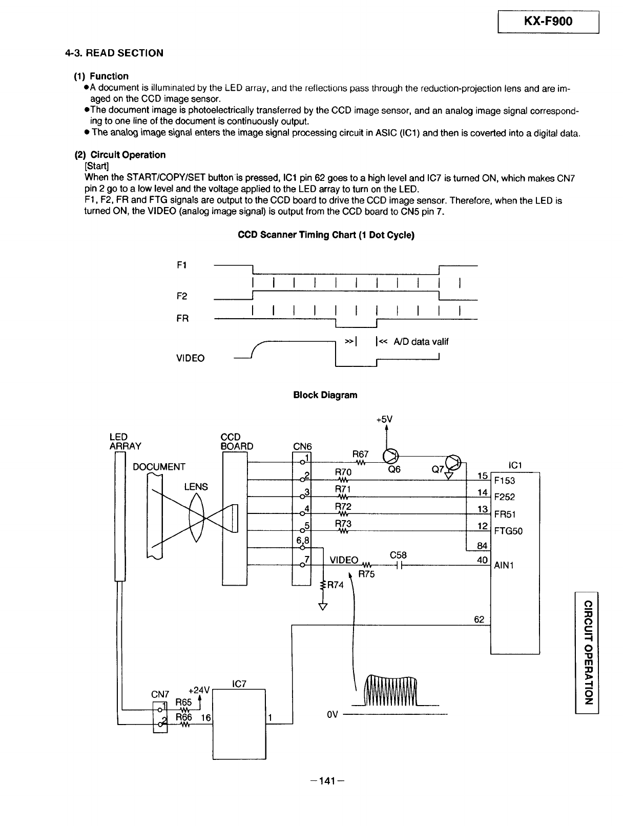
KX-F900
4-3. READ SECTION
(1) Function
eA document is illuminated by the LED array, and the reflections pass through the reduction-projection lens and are im-
aged on the CCD image sensor.
eThe document image is photoelectrically transferred by the CCD image sensor, and an analog image signal correspond-
ing to one line of the document is continuously output.
•The anatog image signal enters the image signal processing circuit in ASIC (ICl) and then is coverted into a digital data.
(2) Circuit Operation
[Start]
When the START/COPY/SET button is pressed, ICl pin 62 goes to a high level and IC7 is turned ON, which makes CN7
pin 2 go to a low level and the voltage applied to the LED array to turn on the LED.
F1, F2, FR and FTG signals are output to the CCD board to drive the CCD image sensor. Therefore, when the LED is
turned ON, the VIDEO (analog image signal) is output from the CCD board to CN5 pin 7.
CCD Scanner Timing Chart (1 Dot Cycle)
F1
F2
FR
VIDEO
m I
I
__1
I
I
I
I
I
I
I
I
I
]
I
I
I
I
!
I
I
I
I
I
I
I
I
I
I
>>1 I<< ND data valif
I
I
LED
ARRAY
1 DOCUMENT
II CN7 *24VI
CCD
BOARD
1I-I
",,,,LI
IC7
Block Diagram
CN6
c 1
o2
6,8
o-
o7
+5V
R70
R71
R72
R7a
-I V,D O
t R75
R74
15
14
13
12
84
4O
62
0V
iC1
F153
F252
FR51
FTG50
AIN1
o_
_o
O
c
.-I
O
"o
m
_0
_>
--I
O
z
-141 -
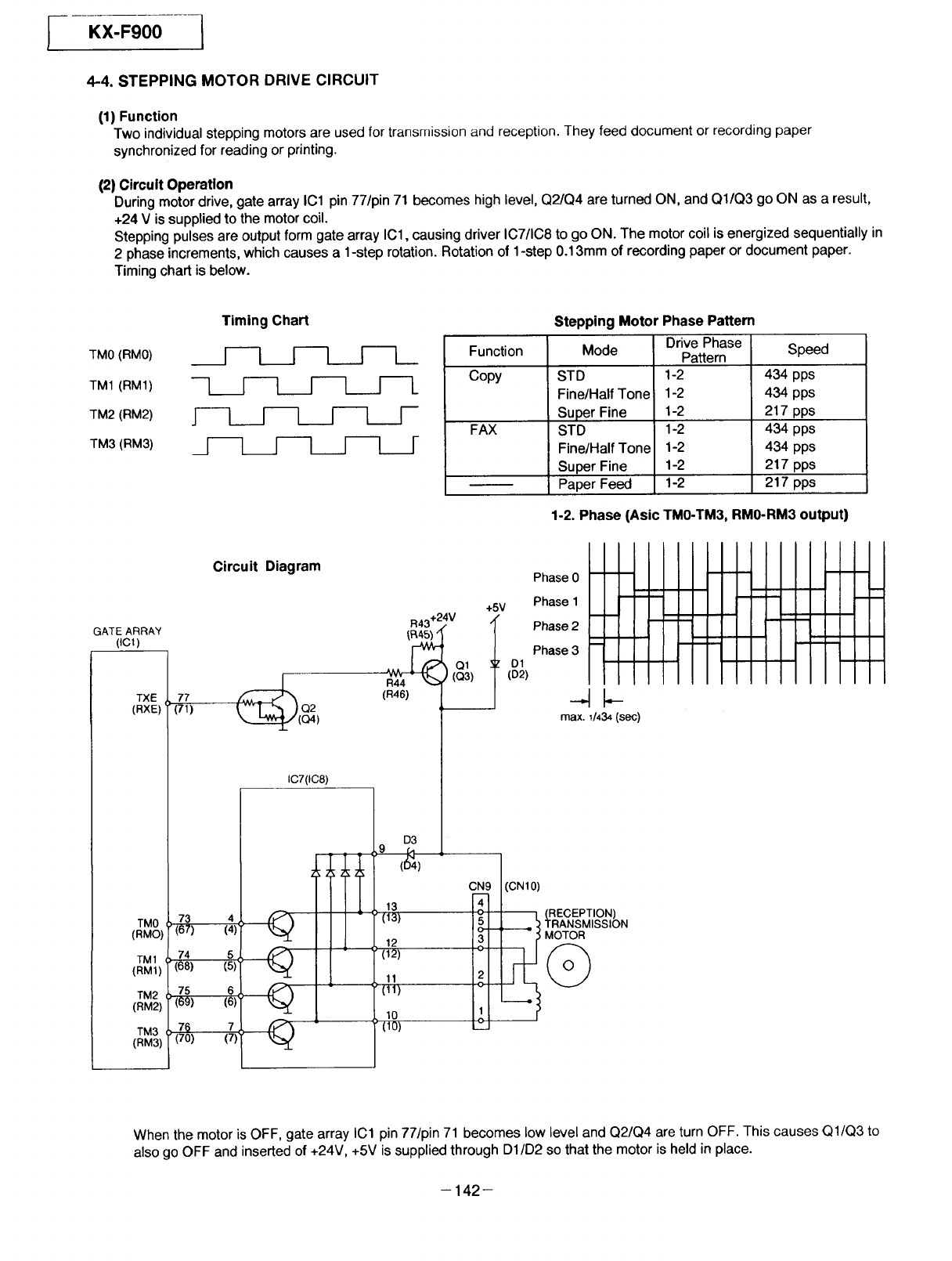
IKX-F900 1
4-4. STEPPING MOTOR DRIVE CIRCUIT
(1) Function
Two individual stepping motors are used for transmission and reception. They feed document or recording paper
synchronized for reading or printing.
(2| Circuit Operation
During motor drive, gate array IC1 pin 77/pin71 becomes high level, Q2/Q4 are turned ON, and QI/Q3 go ON as a result,
+24 V issuppliedto the motorcoil.
Steppingpulsesare outputform gate arrayIC1, causingdriverIC7/IC8 to goON. The motorcoil isenergizedsequentiallyin
2 phaseincrements,whichcausesa 1-step rotation.Rotationof 1-step 0.13mm of recordingpaperor documentpaper.
Timingchartisbelow.
TM0(RM0)
TMI(RM1)
TM2(RM2)
TM3(RM3)
Timing Chart
Function
Copy
FAX
Stepping Motor Phase Pattern
Mode
STD
Fine/Half Tone
Super Fine
STD
Fine/Half Tone
Super Fine
Paper Feed
Drive Phase
Pattern
1-2
1-2
1-2
1-2
1-2
1-2
1-2
Speed
434 pps
434 pps
217 pps
434 pps
434 pps
217 pps
217 pps
1-2. Phase (Asic TM0-TM3, RM0-RM3 output)
GATE ARRAY
(let)
TXE
(RXE) '
TM0
(RMO)
TM1
(RM1)
TM2
(RM2)
TM3
(RM3)
Circuit Diagram
(71) (_
()
IC7(IC8)
73 4
(67) (4)
74 5
(68) (5)
75 6
(69) (6)
7(_ 7
(70) (7)
Q
Q
Q
Q
ittt
1
I!
+5V
R43 +24v ,,_
(R_5)' 1
(Q3)
(R46)
D3
( )
CN9
4
5
o-
3
'(Igl o-
11 2
(11) o-
10 1
o-
)(10)
Phase 0 - -
Phase 1
m
Phase 2
Phase 3
Ol
(02)
max. _/434 (sec)
(ON 10)
_ RECEPTION)
TRANSMISSION
MOTOR
m
m m m
m mm
m
n
m m m
mm m
um
mm
I
I
m
mm
mm
When the motor is OFF, gate array IC1 pin 77/pin 71 becomes low level and Q2/Q4 are turn OFF. This causes Q1/Q3 to
also go OFF and inserted of +24V, +5V is supplied through DI/D2 so that the motor is held in place.
- 142-
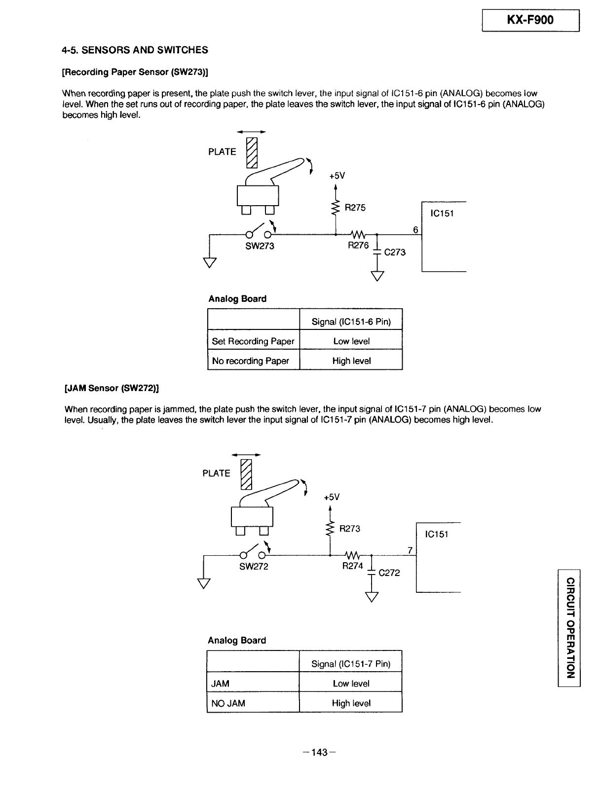
KX-F900 I
4-5. SENSORS AND SWITCHES
[Recording Paper Sensor (SW273)]
_N_en recording paper is present, the plate push the switch lever, the input signal of IC151-6 pin (ANALOG) becomes low
level. When the set runs out of recording paper, the plate leaves the switch lever, the input signal of IC151-6 pin (ANALOG)
becomes high level.
I,, ,,I
o/o_,
SW273 R276 ,_C273
IC151
6
Analog Board
Signal (IC151-6 Pin)
Set Recording Paper Low level
No recording Paper High level
[JAM Sensor (SW272)]
When recording paper is jammed, the plate push the switch lever, the input signal of IC151-7 pin (ANALOG) becomes low
level. Usually, the plate leaves the switch lever the input signal of IC151-7 pin (ANALOG) becomes high level.
I,, ,,I t
___Jo _,
,_ SW272
R273
R274 i C272
IC151
7
Analog Board
Signal (IC151-7 Pin)
JAM Low level
NO JAM High level
c__.i
'--I_
oi
m¸
-I
O
Z
- 143-
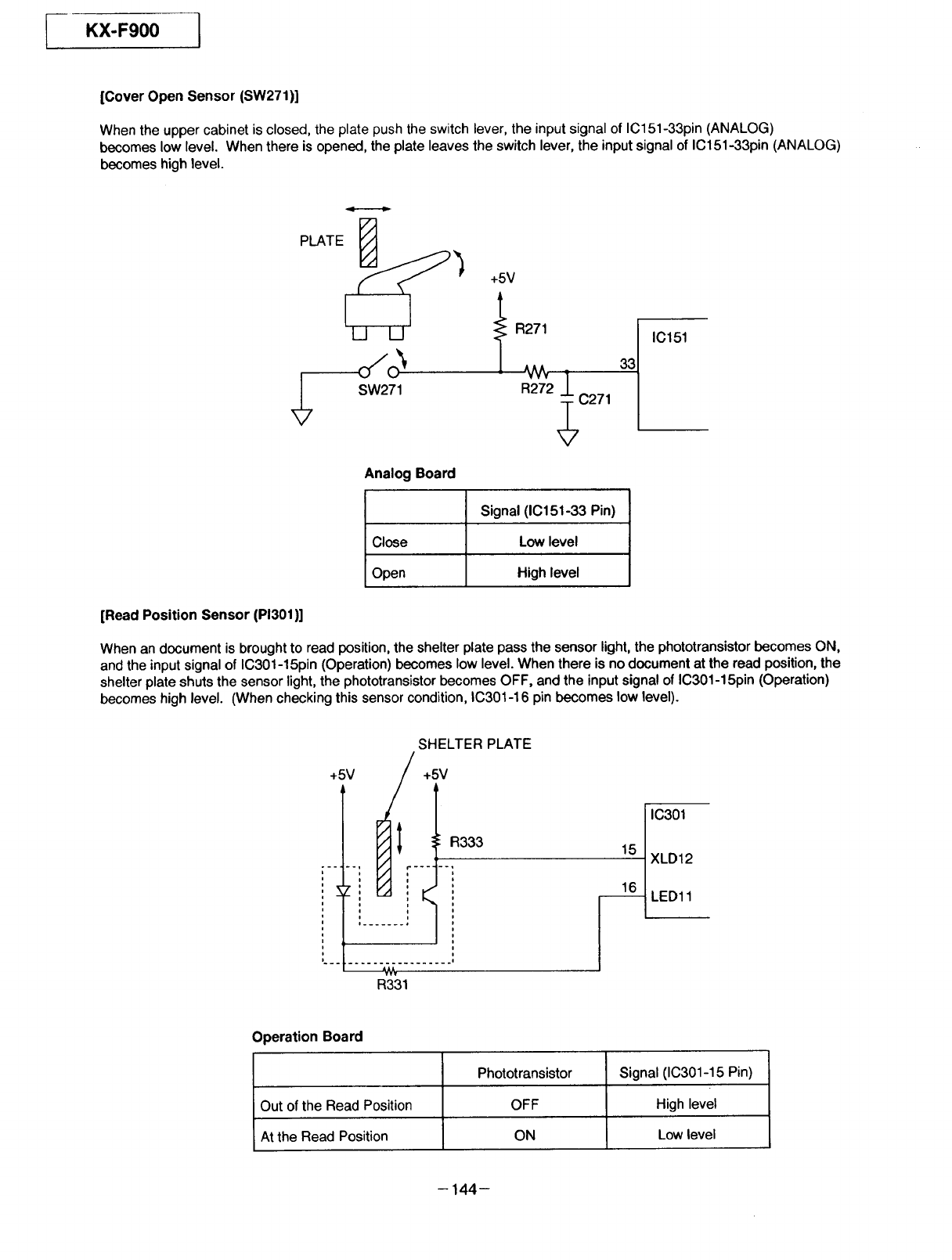
KX-F900
[Cover Open Sensor (SW271)]
When the upper cabinet is closed, the plate push the switch lever, the input signal of IC151-33pin (ANALOG)
becomes low level. When there is opened, the plate leaves the switch lever, the input signal of IC151-33pin (ANALOG)
becomes high level.
l
o/o
Analog Board
Signal (IC151-33 Pin)
Close Low level
Open High level
IC151
[Read Position Sensor (PI301)]
When an document is brought to read position, the shelter plate pass the sensor light, the phototransistor becomes ON,
and the input signal of IC301-15pin (Operation) becomes low level. When there is no document at the read position, the
shelter plate shuts the sensor light, the phototransistor becomes OFF, and the input signal of IC301-15pin (Operation)
becomes high level. (When checking this sensor condition, IC301-16 pin becomes low level).
+5V
SHELTER PLATE
+5V
i
ii
i
, i
1
i i
i i
R331
IC301
15 XLD12
16
-- LED11
Operation Board
Phototransistor Signal (IC301-15 Pin)
Out of the Read Position OFF High level
At the Read Position ON Low level
- 144-
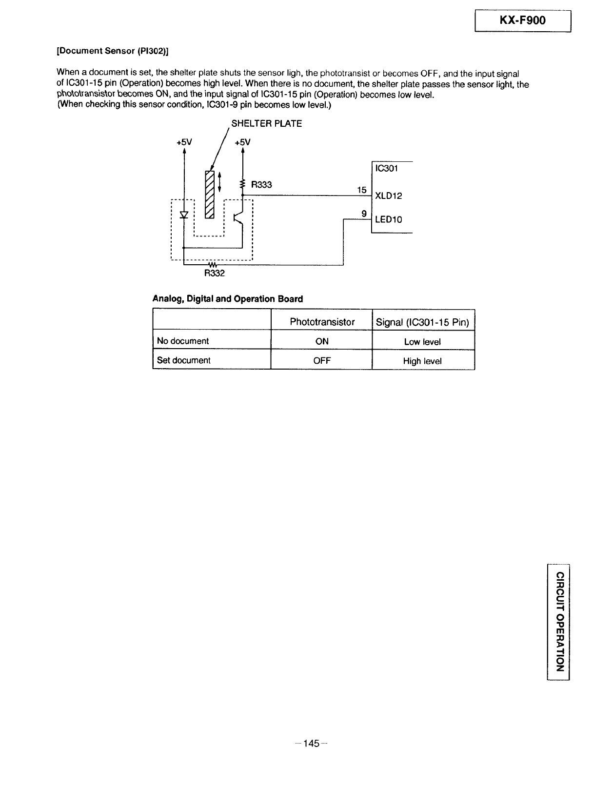
KX-F900 1
[Document Sensor (PI302)]
When a document is set, the shelter plate shuts the sensor ligh, the phototransist or becomes OFF, and the input signal
of IC301-15 pin (Operation) becomes high level. When there is no document, the shelter plate passes the sensor light, the
pt_ototTa_s'ts_.orbecomes ON, and the input signal of IC301-15 pin (Operation) becomes low level.
(When checking this sensor condition, IC301-9 pin becomes low level.)
SHELTER PLATE
+5V
15
9
................. =
R332
IC301
XLD12
_LED10
Analog, Digital and Operation Board
Phototransistor
No document ON
Set document OFF
Signal (IC301-15 Pin)
Low level
High level
_.9
30
O
C
"-4
O
"1o
m
::o
_>
-I
O
z
-145-
KX-F900
5. MODEM SECTION
5-1, FUNCTION
The unit uses a 1 chip modem (IC11 ), enabling it to act as an interface between the control section for FAX sending and
receiving, and the telephone line. During a sending operation, the digital image signals are modulated and sent to the
telephone line, while during a receiving operation, the analog image signals which are received via the telephone line are
demodulated and converted into digital image signals. The communication format and procedures for FAX communication
are standardized by ITU-T. This 1 chip modem (IC11) has hardware which sends and detects all of the necessary signals
for FAX communication and DTMF.
It can be controlled by writing commands from the ASIC (IC1) to the register in the modem (IC11).
This modem (IC11) also sends DTMF signals, generates a call tone (from the speaker), and detects a busy tone and dial
tones and DTMF.
Overview of Facsimile Communication Procedures (ITU-T Recommendation):
(1) ON ITU-T (International Telecommunications' Union.)
The No. XIV Group of ITU-T, one of the four permanent organizations of the International Telecommunications Union
(ITU), investigates and make recommendations on international standards for facsimile.
(2) Definition of Each Group
•Group I (G1)
A-4 size documents official without using formats which reduce the band width of signal sent over telephone lines.
Determined in 1968.
Transmission for about 6 minutes at scanning line density of 3.85 lines/ram.
•Group II (G2)
Using reduction technology in the modulation/demodulation format, A-4 size document is sent at an official scanning
line density of 3.85 tines/mm for about 3 minutes.
Methods to suppress redundancy are not used.
Determined in 1976.
•Group III (G3)
Method of suppressing redundancy in the image signal prior to modulation is used. A-4 size document is sent within
about one minute.
Determined in 1980.
•Group IV (G4)
Transmission is via data network. Method is provided for suppressing redundancy in signals priorto transmission,
and error-free reception of transmission is possible.
The scope of these facsimile applications is not limited simply to transmission of written statements. Through
symbiotic linkages with other communications methods, itcan be expected to expand to include integrated services.
(3) Facsimile Call Time Series
As shown in the following diagram, the facsimile call time series is divided into five phases.
Message Transmission
F- _',
PhaseA I. PhaseB I PhaseC I PhaseD
_ Facsimile Procedure
Facsimile Call
ID
Progress derection of operation
I Phase E I
"1 [
v
Phase A: Call setting
Call setting can be manual/automatic.
Phase B: Pre-message procedure
Phase B is a pre-processing procedure and a sequence for confirming status of terminal, transmission route, etc. and
for ter-minal control. It implements terminal preparation status, determines and displays terminal constants, confirms
synchronization status, etc. and prepares for transmission of facsimile messages.
Phase C: Message transmission
Phase C is the procedure for transmission of facsimile messages.
Phase D• Post message procedure
Phase D is the procedure for confirming that the message is completed and received. In the case of continuous
transmission, return is made repeatedly to phase B or phase C for transmission.
Phase E • Call retrieval
Phase E is the procedure for call retrieval, that is, for circuit disconnection.
- 146-
I KX-F900
(4) Concerning Transmission of Time
[TransmissionT,mel=IContro,T,moI+ I +
Transmission time consists of the following.
Control time :This is time at the start of transmission when functions at the sending and receiving sides are
confirmed, transmission mode is established, and transmission and reception are
synchronized.
Image transmission time:
This is the time required for transmission of document contents (image data). In general, this
time is recorded in the catalog, etc.
Hold time: This is the time required after the document contents have been sent to confirm that the
document was in fact sent, and to check for telephone reservations and/or the existence of
continuous transmission.
(5) Facsimile Standard
Item _
Connection Control Mode
Terminal Control Mode
Facsimile Signal Format
Modulation Mode
Transmission Speed
Redundancy Compression
Process 2 dimension : MR Mode (K=2.4)
(Coding Mode)
Main Scan : 8 pel/mm
Resolution Sub Scan : 3.85, 7.71/mm
Line Synchronization Signal EOL Signal
1 Line Transmission Time Depends on degree of data reduction.
[ms/line] Minimum Value : 10, 20
Can be recognized in 40ms.
Telephone Network Facimile
G3 Machine
Telephone Network Signal Mode
T. 30 Binary
Digital
PSK (V. 27 ter) or QAM (V. 29)
i
300 bps (control Signal)
2400, 4800, 7200, 9600 bps (FAX Signal)
1 dimension : MH Mode
O
O
-I
O
"o
m
30
),
-I
O
z
147
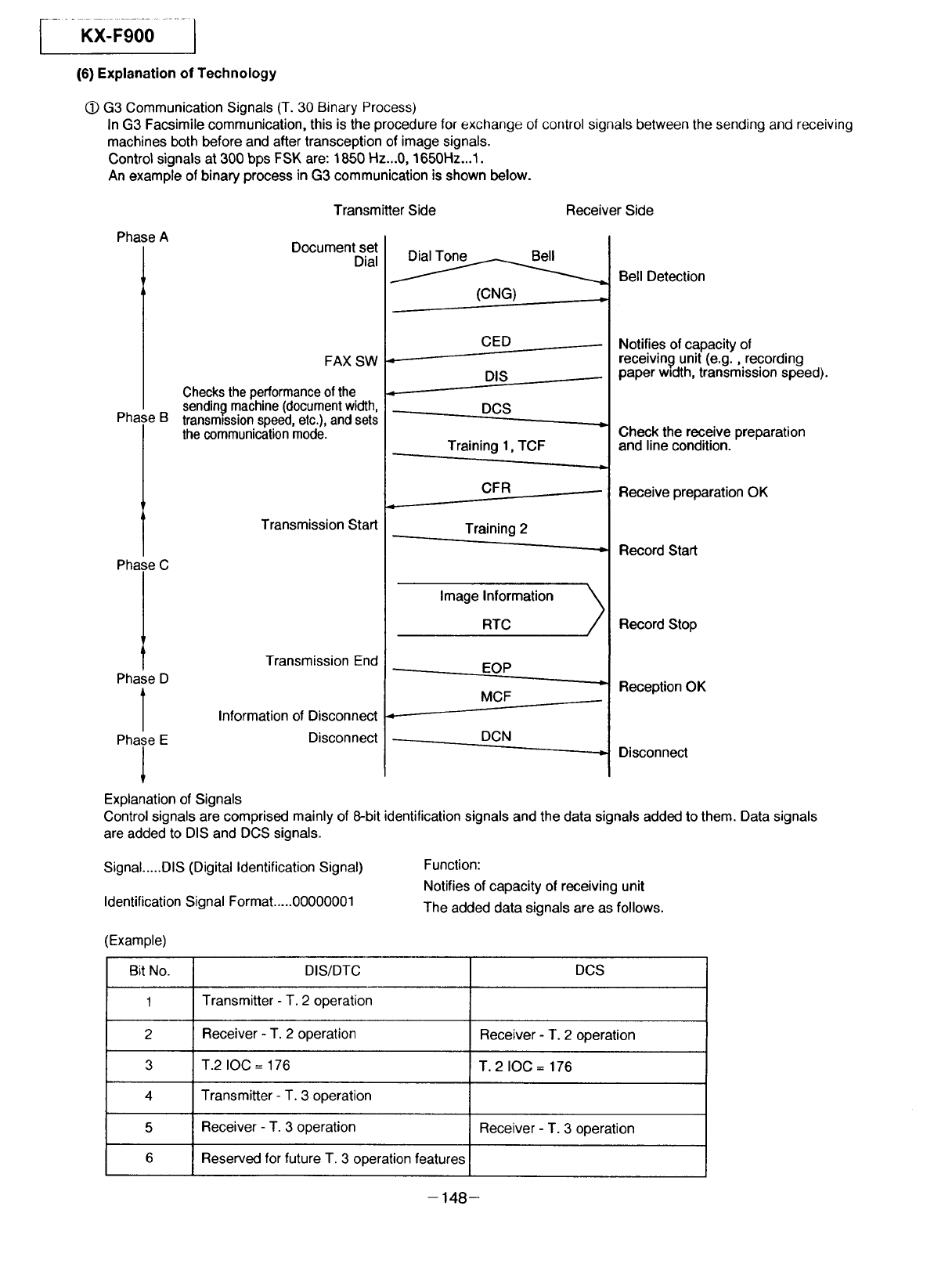
I.....KX:FgO0.........I
(6) Explanation of Technology
(j) G3 Communication Signals (T. 30 Binary Process)
In G3 Facsimile communication, this is the procedure for exchange of control signals between the sending and receiving
machines both before and after transception of image signals.
Control signals at 300 bps FSK are: 1850 Hz...0, 1650Hz...1.
An example of binary process in G3 communication is shown below.
Transmitter Side Receiver Side
Ph_LseA
Phase B
Document set
Dial
FAX SW
Checks the performance of the
sendingmachine (document width,
transmission speed, etc.), and sets
the communication mode.
Transmission Start
Phase C
Phase D
1
Phase E
Transmission End
Information of Disconnect
Disconnect
Explanation of Signals
(CNG) ._
CED
DIS
----_____ DCS
Training 1, TCF
CFR
Training 2
Image Information
EOP
MCF
.---.__._____ DCN
Bell Detection
Notifies of capacity of
receiving unit (e.g., recording
paper width, transmission speed).
Check the receive preparation
and line condition.
Receive preparation OK
Record Start
Record Stop
Reception OK
Disconnect
Control signals are comprised mainly of 8-bit identification signals and the data signals added to them. Data signals
are added to DIS and DCS signals.
Signal .....DIS (Digital Identification Signal)
Identification Signal Format .....00000001
Function:
Notifies of capacity of receiving unit
The added data signals are as follows.
(Example)
Bit No. DIS/DTC DCS
1Transmitter - T. 2 operation
2 Receiver - T. 2 operation Receiver - T. 2 operation
3 T.2 IOC = 176 T. 2 IOC = 176
4 Transmitter - T. 3 operation
5 Receiver - T. 3 operation Receiver - T. 3 operation
6 Reserved for future T. 3 operation features
- 148-
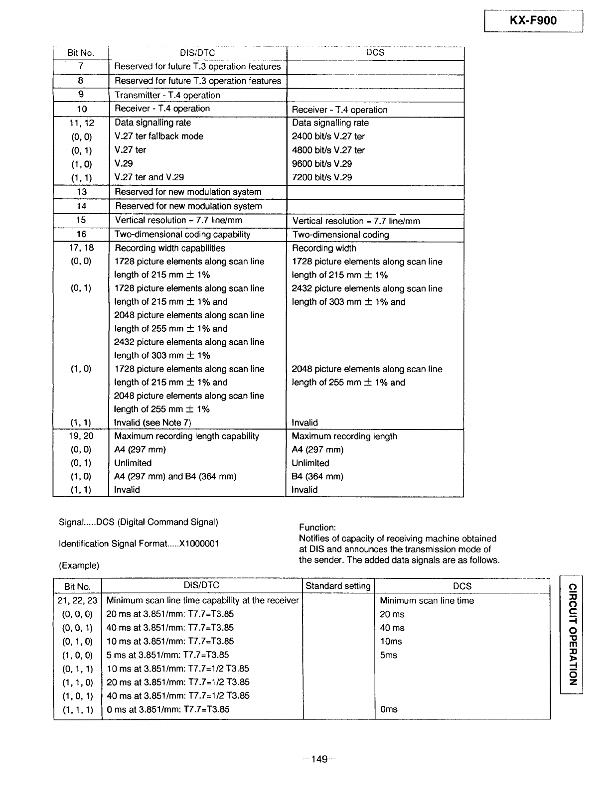
KX-F900
Bit No.
7
8
9
10
11,12
(0, O)
(0, 1)
(1, O)
(1,1)
13
14
15
16
17, 18
(0, O)
(o,1)
(1, O)
(I, 1)
19, 20
(0, 0)
(0, 1)
(1,0)
(1, 1)
DIS/DTC DCS
Reserved for future T.3 operation features
Reserved for future T.3 operation features
Transmitter - T.4 operation
Receiver - T.4 operation
Data signalling rate
V.27 ter fallback mode
V.27 ter
V.29
V.27 ter and V.29
Reserved for new modulation system
Reserved for new modulation system
Vertical resolution = 7.7 line/mm
Two-dimensional coding capability
Recording width capabilities
1728 picture elements along scan line
length of 215 mm 4- 1%
1728 picture elements along scan line
length of 215 mm __+1% and
2048 picture elements along scan line
length of 255 mm _ 1% and
2432 picture elements along scan line
length of 303 mm 4- 1%
1728 picture elements along scan line
length of 215 mm _ 1% and
2048 picture elements along scan line
length of 255 mm -I- 1%
Invalid (see Note 7)
Maximum recording length capability
A4 (297 ram)
Unlimited
A4 (297 mm) and B4 (364 mm)
Invalid
Receiver - T.4 operation
Data signalling rate
2400 bit/s V.27 ter
4800 bit/s V.27 ter
9600 bit/s V.29
7200 bit/s V.29
Vertical resolution = 7.7 line/mm
Two-dimensional coding
Recording width
1728 picture elements along scan line
length of 215 mm _ 1%
2432 picture elements along scan line
length of 303 mm 4- 1% and
2048 picture elements along scan line
length of 255 mm _ 1% and
Invalid
Maximum recording length
A4 (297 mm)
Unlimited
B4 (364 mm)
Invalid
Signal .....DCS (Digital Command Signal)
Identification Signal Format .....X1000001
(Example)
Function:
Notifies of capacity of receiving machine obtained
at DIS and announces the transmission mode of
the sender. The added data signals are as follows.
Bit No.
21,22, 23
(0, 0, 0)
(o,o,I)
(0, 1,0)
(1,0, 0)
(0,1,1)
(1, 1,0)
(1,0, 1)
(1,1,1)
DIS/DTC
Minimum scan line time capability at the receiver
20 ms at 3.851/mm: T7.7=T3.85
40 ms at 3.851/mm: T7.7=T3.85
10 ms at 3.851/mm: T7.7=T3.85
5 ms at 3.851/mm: T7.7=T3.85
10 ms at 3.851/mm: T7.7=1/2 T3.85
20 ms at 3.851/mm: T7.7=1/2 T3.85
40 ms at 3.851/mm: T7.7=1/2 T3.85
0 ms at 3.851/mm: T7.7=T3.85
Standard setting DCS
Minimum scan line time
20 ms
40 ms
10ms
5ms
0ms
L"_.I
B,
('_1
OI
m I
D, [
Ol
-149-
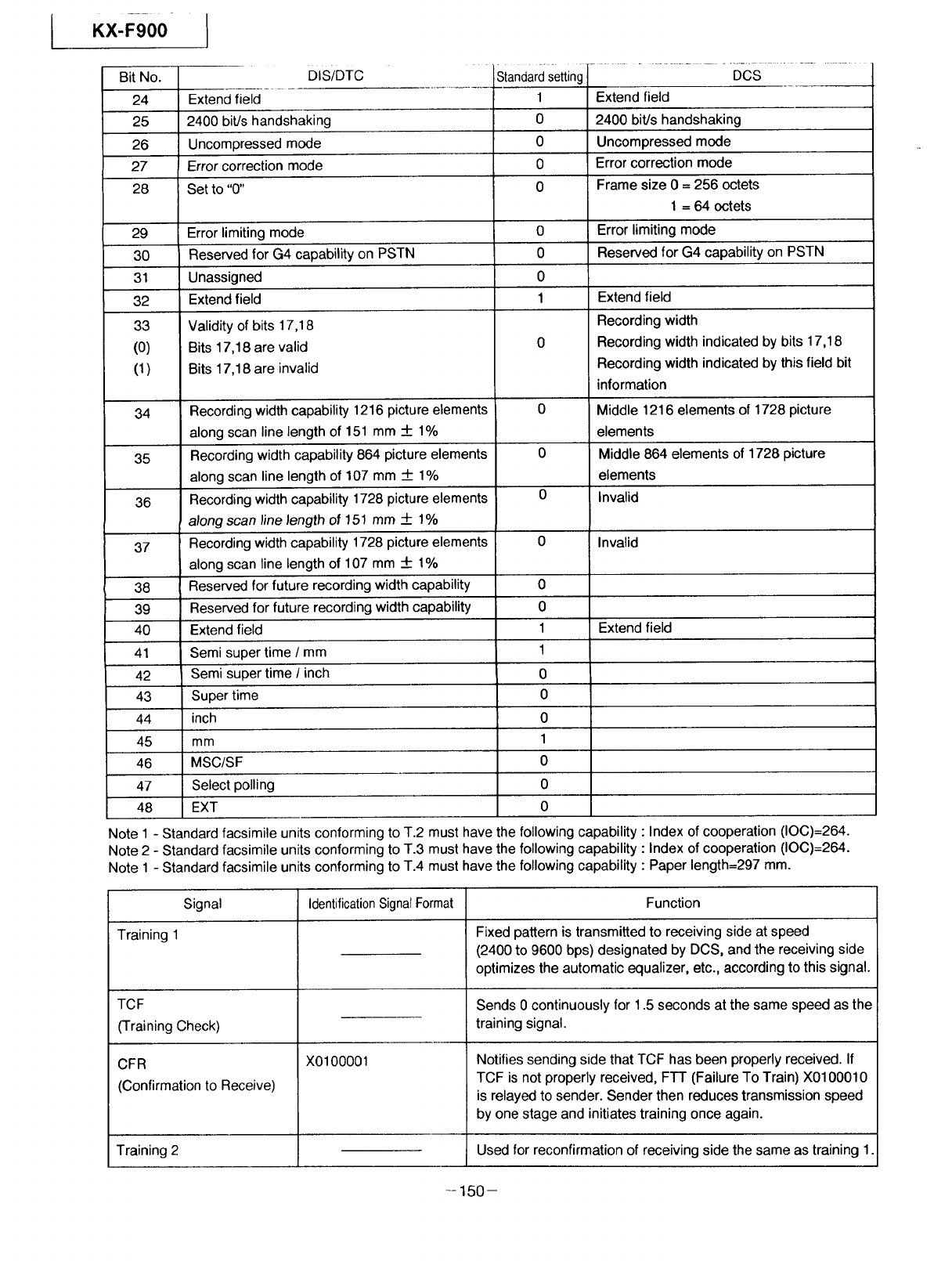
KX-F900
Bit No.
24
25
26
27
I
DIS/DTC
Extend field
2400 bitJs handshaking
Uncompressed mode
Error correction mode
28 Set to "0"
Standard setting.......... Dcs ..........
1
0
0
0
0
29 Error limiting mode 0
30 Reserved for G4 capability on PSTN 0
31 Unassigned 0
32 Extend field 1
Validity of bits 17,18
Bits 17,18 are valid
Bits 17,18 are invalid
33
(0)
(1)
0
Extend field
2400 bitJs handshaking
Uncompressed mode
Error correction mode
Frame size 0 = 256 octets
1 = 64 octets
Error limiting mode
Reserved for G4 capability on PSTN
34 Recording width capability 1216 picture elements 0
along scan line length of 151 mm __.1%
35 Recording width capability 864 picture elements 0
along scan line length of 107 mm 4- 1%
36 Recording width capability 1728 picture elements 0
along scan line Jength of 151 mm 4- 1%
37 Recording width capability 1728 picture elements 0 Invalid
along scan line length of 107 mm 4- 1%
38 Reserved for future recording width capability 0
39 Reserved for future recording width capability 0
40 Extend field 1 Extend field
41 Semi super time /mm 1
42 Semi super time /inch 0
43 Super time 0
44 inch 0
45 mm 1
46 MSC/SF 0
47 Select polling 0
48 EXT 0
Note 1 - Standard facsimile units conforming to T.2 must have the following capability : Index of cooperation (IOC)=264.
Note 2 - Standard facsimile units conforming to T.3 must have the following capability : Index of cooperation (IOC)=264.
Note 1 - Standard facsimile units conforming to T.4 must have the following capability : Paper length=297 mm.
Signal IdentificationSignalFormat Function
Training 1
Extend field
Recording width
Recording width indicated by bits 17,18
Recording width indicated by this field bit
information
Middle 1216 elements of 1728 picture
elements
Middle 864 elements of 1728 picture
elements
Invalid
TCF
(Training Check)
CFR
(Confirmation to Receive)
Training 2
X0100001
Fixed pattern is transmitted to receiving side at speed
(2400 to 9600 bps) designated by DCS, and the receiving side
optimizes the automatic equalizer, etc., according to this signal.
Sends 0 continuously for 1.5 seconds at the same speed as the
training signal.
Notifies sending side that TCF has been properly received. If
TCF is not properly received, FTT (Failure To Train) X0100010
is relayed to sender. Sender then reduces transmission speed
by one stage and initiates training once again.
Used for reconfirmation of receiving side the same as training 1
-- 150-
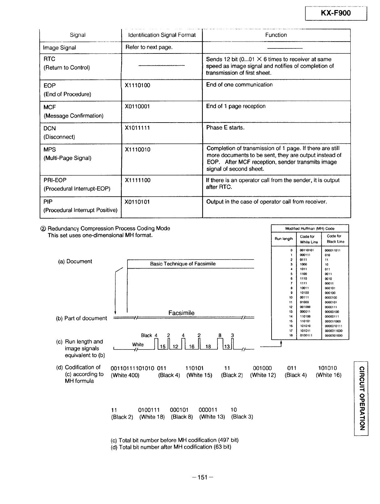
;----K_X-F9oo........
Signal
Image Signal
RTC
(Return to Control)
EOP
(End of Procedure)
MCF
(Message Confirmation)
DCN
(Disconnect)
MPS
(Multi-Page Signal)
Identification Signal Format Function
Refer to next page.
X1110100
X0110001
X1011111
X1110010
Sends 12 bit (0...01 X 6 times to receiver at same
speed as image signal and notifies of completion of
transmission of first sheet.
End of one communication
End of I page reception
Phase Estarts.
Completion of transmission of I page. If there are still
more documents to be sent, they are output instead of
EOP. After MCF reception, sender transmits image
signal of second sheet.
PRI-EOP Xl 111100 If there is an operator call from the sender, it is output
(Procedural Interrupt-EOP) after RTC.
PIP X0110101 Output in the case of operator call from receiver.
(Procedural Interrupt Positive)
Modified Huffman (MH) Code
(_) Redundancy Compression Process Coding Mode
This set uses one-dimensional MH format.
(a) Document IBasic Technique of Facsimile
Facsimile
(b) Part of document --:// /_=::
Black 4 2 4 2 8 3
(c) Run length and White _ 16 _ 18 13[-']__
image signals i // /.___
equivalent to (b)
(d) Codification of 00110111101010 011 110101 11 001000
(c) according to (White400) (Black4) (White 15) (Black 2) (White 12)
MH formula
11 0100111 000101 000011 10
(Black 2) (White 18) (Black 8) (White 13) (Black 3)
(c) Total bit number before MH codification (497 bit)
(d) Total bit number after MH codification (63 bit)
Code for Code for
Run length White Line Black Line
0 00110101 000011011
1 000111 010
2 0111 11
3 1000 10
4 1011 011
51100 0011
6 1110 0010
71111 00011
810011 o001o1
910100 000100
10 00111 0000100
11 010(30 0000101
12 001000 0000111
13 000011 00000100
14 110100 00000111
15 110101 000011000
16 101010 0000010111
17 101011 0000011000
18 0100111 0000001000
011 101010
(Black 4) (White 16)
C)
O
c::
-I
O
"o
m
3>
-I
R
0
z
-151 -
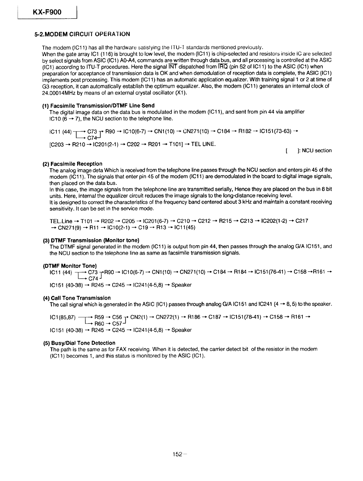
KX-F900 I
5-2.MODEM CIRCUIT OPERATION
The modem (IC11) has all the hardware satisfying the IIU-I standards mentioned previously.
When the gate array IO1 (116) is brought to low level, the modem (IO11) is chip-selected and resistors inside IC are selected
by select signals from ASlO (IO1) A0-A4, commands are written through data bus, and all processing is controlled at the ASlC
(ICl) according to ITU-T procedures. Here the signal IN"-Tdispatched from _ (pin 52 of I011) to the ASlC (IO1) when
preparation for acceptance of transmission data is OK and when demodulation of reception data is complete, the ASIC (IO1)
implements post processing. This modem (IO11) has an automatic application equalizer. With training signal 1 or 2 at time of
G3 reception, it can automatically establish the optimum equalizer. Also, the modem (IO11) generates an internal clock of
24.00014MHz by means of an external crystal oscillator (Xl).
(1) Facsimile TransmissionlDTMF Line Send
The digital image data on the data bus is modulated in the modem (ICl 1), and sent from pin 44 via amplifier
IO10 (6 -,- 7), the NCU section to the telephone line.
C73- r R90 --* 1010(6-7) _ CNI(10) _ 0N271(10) _ C184 _ R182 -* IC151(73-63)
IC11 (44) -[_ C74-'
[C203 -" R210 ---*IC201(2-1) --* C202 -" R201 _ T101] -* TEL LINE. [ ]: NCU section
(2) Facsimile Reception
The analog image deta Which is received from the telephone line passes through the NCU section and enters pin 45 of the
modem (IC11 ). The signals that enter pin 45 of the modem (IC11 ) are demodulated inthe board to digital image signals,
then placed on the data bus.
In this case, the image signals from the telephone line are transmitted serially, Hence they are placed on the bus in 8 bit
units. Here, internal the equalizer circuit reduces the image signals to the long-distance receiving level.
It is designed to correct the characteristics of the frequency band centered about 3 kHz and maintain aconstant receiving
sensitivity. It can be set in the service mode.
TEL.Line --* T101 -4 R202 --, C205 --* 10201(6-7) --* C210 --* C212 --* R215 --* C213 _ IO202(1-2) --* O217
CN271(9) --* Rll -* IC10(2-1) _ C19 ---*R13 -* IC11(45)
(3) DTMF Transmission (Monitor tone)
The DTMF signal generated in the modem (IC11) is output from pin 44, then passes through the analog G/A IO151, and
the NCU section to the telephone line as same as facsimile transmission signals.
(DTMF Monitor Tone)
IC11 (44) _ 073 _R90 -+ ICl 0(6-7) --, ON1 (10) _ 0N271 (10) --* C184 --* R184 --, I0151 (76-41) --* O158 --,R161 --,
074 -J
IC151 (40-38) --* R245 ---,0245 --, 10241 (4-5,8) _Speaker
(4) Call Tone Transmission
The call signal which is generated in the ASIC (IC1) passes through analog G/A IC151 and IC241 (4 --, 8, 5) to the speaker.
I01(85,87) -_ R59 -* 056_* 0N2(1) --* 0N272(1) -+ R186 --* O187 _ IO151(78-41) --* C158 _ R161 ---*
R60 ---*C57 -J
IC151 (40-38) --, R245 --* C245 ---,IC241 (4-5,8) _ Speaker
(5) Busy/Dial Tone Detection
The path is the same as for FAX receiving. When it is detected, the carrier detect bit of the resistor in the modem
(IC11) becomes 1, and this status is monitored by the ASIC (IC1).
152
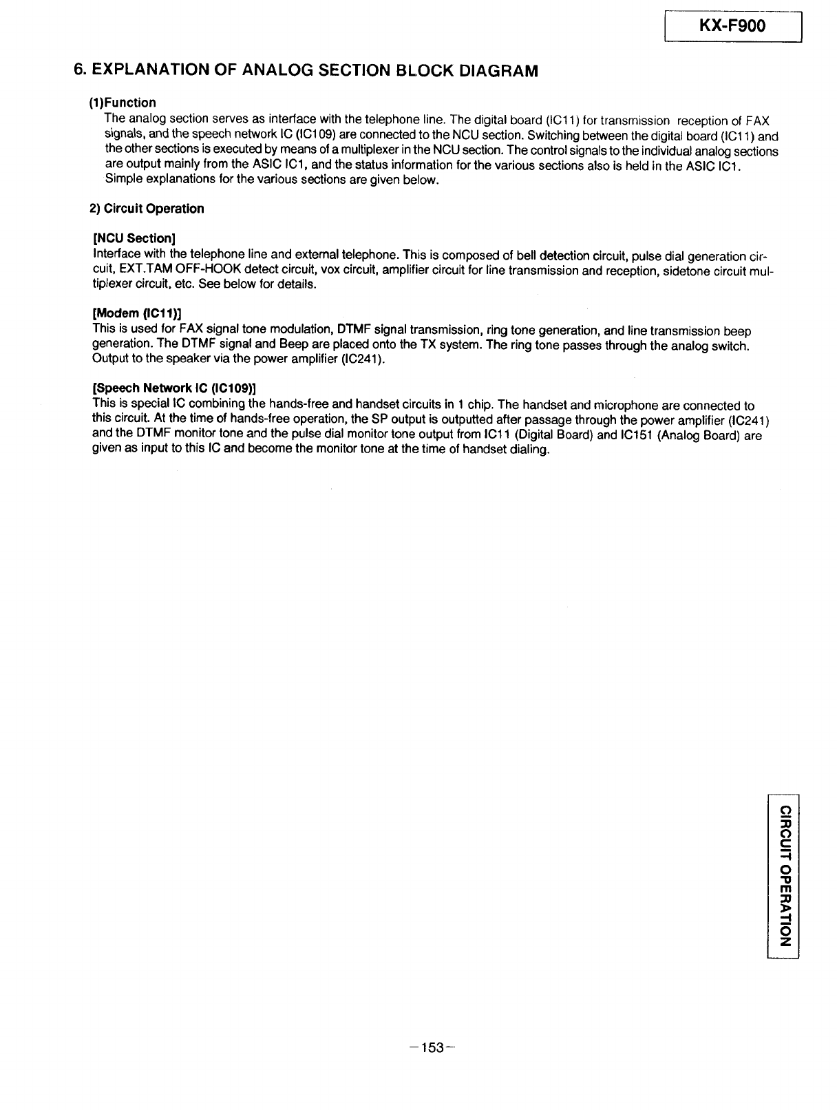
KX-F900
6. EXPLANATION OF ANALOG SECTION BLOCK DIAGRAM
(1)Function
The analog section serves as interface with the telephone line. The digital board (ICt 1) for transmission reception of FAX
signals, and the speech network IC (ICl 09) are connected to the NCU section. Switching between the digital board (IC11) and
the other sections is executed by means of a multiplexer in the NCU section. The control signals to the individual analog sections
are output mainly from the ASIC ICl, and the status information for the various sections also is held in the ASIC ICl.
Simple explanations for the various sections are given below.
2) Circuit Operation
[NCU Section]
Interfacewith the telephone line and external telephone.This is composed of bell detection circuit,pulse dial generation cir-
cuit, EXT.TAMOFF-HOOK detect circuit,voxcircuit,amplifiercircuitforlinetransmissionand reception,sidetonecircuitmul-
tiplexercircuit,etc. See belowfor details.
[Modem (ICll)]
Thisis usedfor FAX signaltone modulation, DTMF signaltransmission,ring tonegeneration, and line transmission beep
generation.The DTMF signaland Beepare placedontothe TX system.The ringtone passesthroughthe analogswitch.
Outputtothe speakervia the poweramplifier(IC241).
[Speech Network IC (IC109)]
Thisis special IC combiningthe hands-free and handsetcircuits in 1 chip. The handset and microphoneare connected to
thiscircuit.At the timeofhands-freeoperation,the SP outputisoutputtedafterpassagethroughthe poweramplifier(IC241)
andthe DTMF monitortoneandthe pulsedial monitortoneoutputfrom IC11 (DigitalBoard)and IC151 (AnalogBoard)are
givenas inputto thisIC and becomethe monitortone atthe time of handsetdialing.
o_
_0
c
m
,--!
O
"_1
m
33
3:,
--I
0
z
-153-
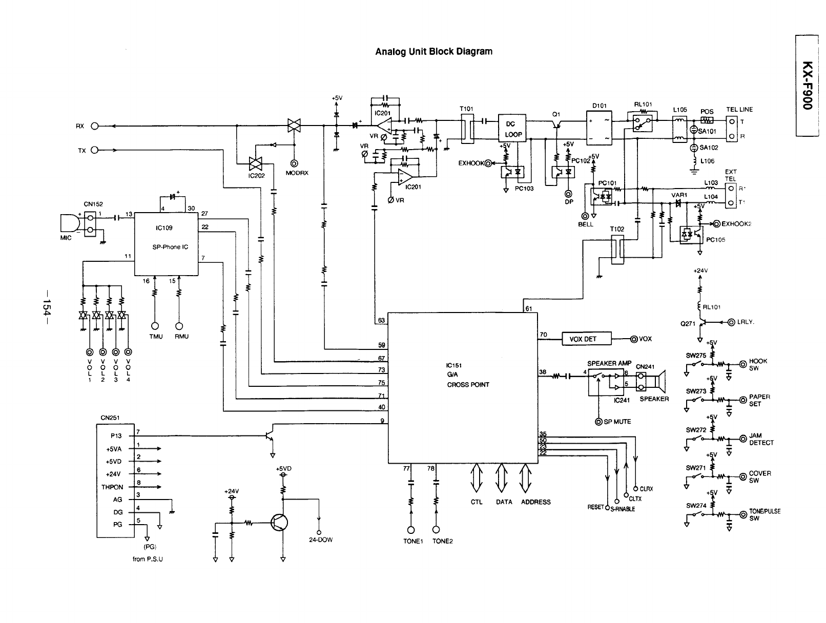
I
I
Analog Unit Block Diagram
Rx 0 "
TX 0
÷
CN152 _ 30
MIC__ I--_ IC109
11
SP-Phone IC
t
O O O O
L L L L
1 2 3 4
CN251
I
+5VA "_
+5VD '_
+24V -"
THPON --
AG
DG --
7
3
4
(PG)
from P,S.U
+5VD
l
+24V !
24-DOW
59
67
73
75
T1
4O
TONE1 TONE2
IC151
G/A
CROSS POINT
SPEAKER AMP CN241
IC241 SPEAKEo_SP MUTE R
22
CTL DATA ADDRESS
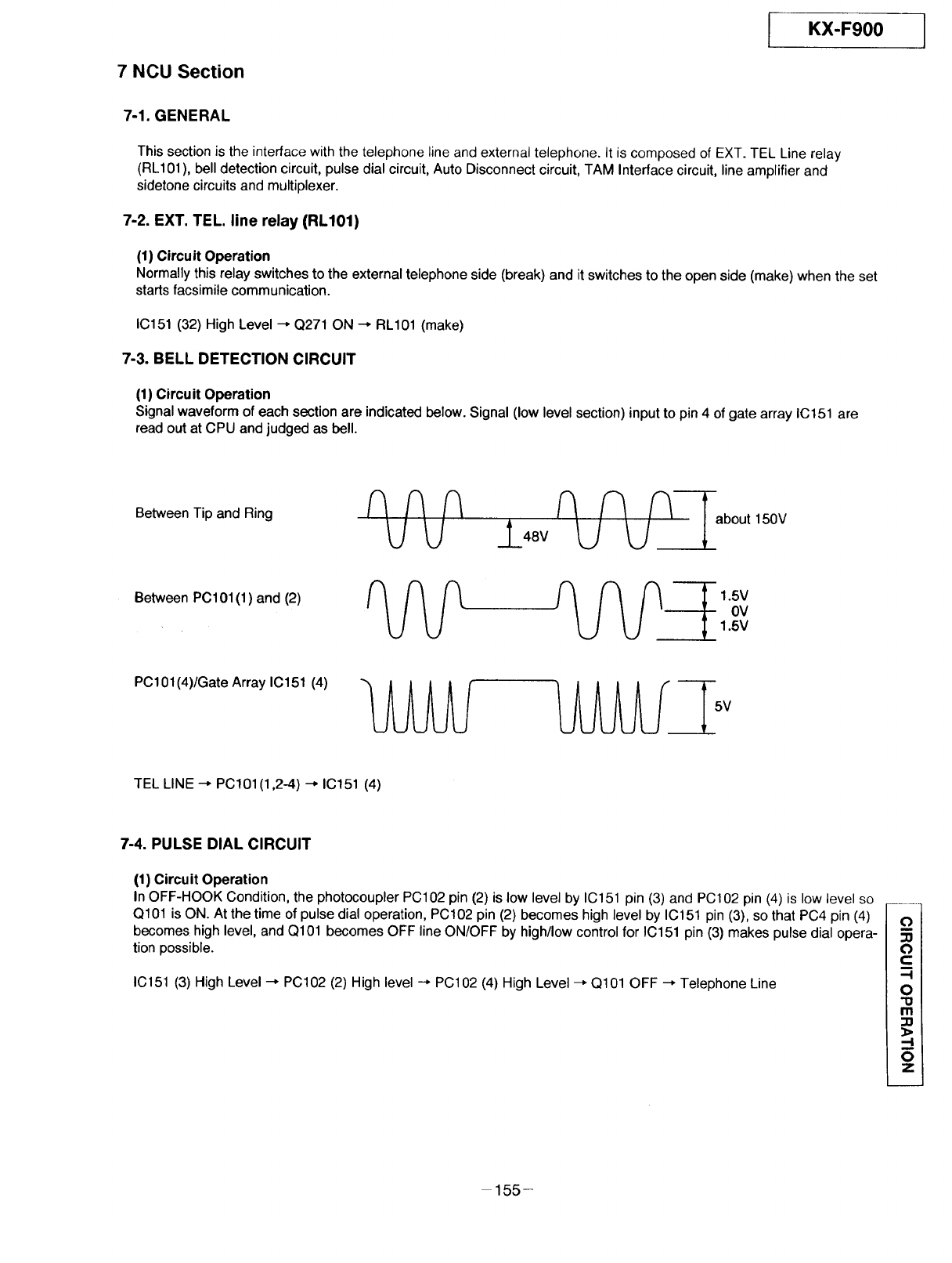
7 NCU Section
I KX-F900
7-1. GENERAL
This section is the interface with the telephone line and external telephone. It is composed of EXT. TEL Line relay
(RL101), bell detection circuit, pulse dial circuit, Auto Disconnect circuit, TAM Interface circuit, line amplifier and
sidetone circuits and multiplexer.
7-2. EXT. TEL. line relay (RL101)
(1) Circuit Operation
Normally this relay switches to the external telephone side (break) and itswitches to the open side (make) when the set
starts facsimile communication.
IC151 (32) High Level --* Q271 ON --* RL101 (make)
7-3. BELL DETECTION CIRCUIT
(1) Circuit Operation
Signal waveform of each section are indicated below. Signal (low level section) input to pin 4 of gate array IC151 are
read out at CPU and judged as bell.
Between Tip and Ring
.t48 V f__--_about 150V
Between PC101 (1) and (2)
PC101 (4)/Gate Array IO151 (4)
TEL LINE --, PC101 (1,2-4) -* IC151 (4)
7-4. PULSE DIAL CIRCUIT
(1) Circuit Operation
In OFF-HOOK Condition, the photocoupler PC102 pin (2) is low level by IC151 pin (3) and PC102 pin (4) is low level so
Q101 is ON. At the time of pulse dial operation, PC102 pin (2) becomes high level by IC151 pin (3), so that PC4 pin (4)
becomes high level, and Q101 becomes OFF line ON/OFF by high/low control for IC151 pin (3) makes pulse dial opera-
tion possible.
IC151 (3) High Level --, PC102 (2) High level ---*PC102 (4) High Level --, Q101 OFF --, Telephone Line
O
O
-I
O
"13
Ill
7>
--I
O
Z
155-
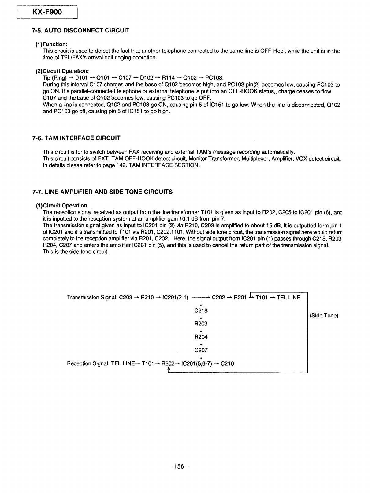
7-5. AUTO DISCONNECT CIRCUIT
(1)Function:
This circuit is used to detect the fact that another telephone connected to the same line is OFF-Hook while the unit is in the
time of TEL/FAX's arrival bell ringing operation.
(2)Circuit Operation:
Tip (Ring)---*D101 ---,Q101 -* C107 -* D102 -* Rl14 -* Q102 --* PC103.
Duringthisinterval C107 chargesand the base of Q102 becomeshigh,and PC103 pin(2)becomeslow,causingPC103 to
go ON. If a parallel-connectedtelephoneorexternaltelephoneis putintoan OFF-HOOK status,,chargeceasesto flow
Cl 07 andthe base ofQ102 becomeslow,causingPC103 to go OFF.
When a line isconnected,Q102 and PC103 goON, causingpin5 of IC151 to go low.When the line isdisconnected,Q102
and PC103 go off,causingpin 5 of IC151to gohigh.
7-6. TAM INTERFACE CIRCUIT
This circuit is for to switch between FAX receiving and external TAM's message recording automatically.
This circuit consists of EXT. TAM OFF-HOOK detect circuit, Monitor Transformer, Multiplexer, Amplifier, VOX detect circuit.
In details please refer to page 142. TAM INTERFACE SECTION.
7-7. LINE AMPLIFIER AND SIDE TONE CIRCUITS
(1)Circuit Operation
The receptionsignal received as outputfrom the line transformerT101 is given as inputto R202, C205 to IC201 pin (6), ant
it is inputtedtothe receptionsystemat an amplifiergain10.1 dB from pin7.
The transmissionsignalgivenas input to IC201 pin (2) via R210, C203 is amplifiedto about15 dB, It is outputtedform pin 1
of IC201anditistransmitttedto T101 via R201, C202,T101.Withoutsidetonecircuit,thetransmissionsignalherewouldreturr
completelyto thereceptionamplifiervia R201, C202. Here,the signaloutputfrom IC201pin (1) passesthroughC218, R203
R204, C207 andentersthe amplifierIC201 pin (5), andthisis usedto cancelthe returnpartof the transmissionsignal.
This is the sidetonecircuit.
Transmission Signal: C203 --* R210 --* IC201 (2-1) _ C202 --, R201 .L, T101 ---*TEL LINE
C218
R203
R204
C207
Reception Signal: TEL LINE--, T101 _ R202---, IC201(5,6-7) _ C210
(Side Tone)
156-
8. ITS (Integrated telephone System) and MONITOR SECTION
IKX-F900
8-1. GENERAL
The general ITS operation is executed by the special iC109. This IC has a speakerphone circuit and a handset circuit in 1
chip, and control to each mode is executed from the outside (IC151). At the time of speakerphone operation the speaker output
passes through the power amplifier (IC241). The DTMF signal and the bell tone are output from the modem (IC11 : digital
board). The alarm tone, the key tone, and the beep are outputted from the gate array IC151 (digital board). At the time of pulse
dial operation, the monitor tone is outputted from the gate array IC151.
8-2. SPEAKER PHONE CIRCUIT
(1)Function
This circuit controls the automatic switching of the transmitted and received signals, to and from the telephone line,
when the unit is used in the hands-free mode.
(2)Circuit Operation
The speakerphone can only provide a one-way communication path.
In other words, itcan either transmit an outgoing signal or receive an incoming signal at a given time, but cannot do both
simultaneously. Therefore, a switchingcircuit is necessary to control the flow of the outgoing and incoming signals.
This switching circuit is contained in IC109 and consists of voice detector, TX attenuator, RX attenuator, compara tor and
attenuator control. The circuit analyzes whether the TX (transmit) or the RX (receiver) signal is louder, and then it
processes the signals such that the louder signal is given precedence. The voice detector provides a DC input to the
attenuator control corresponding to the TX signal. The comparator receives a TX and RX signals and supplies a DC input
to the attenuator control corresponding to the RX signal. The attenuator control provides a control signal to the TX and
the RX attenuator to switch the appropriate signals ON and OFF. The attenuator control also detects the level of the
volume control to automatically adjust for changing ambient conditions.
(Transmission Signal Path)
The input signal from the microphone is sent through the circuit via the following path:
MIC --* J270 --* C138 --* IC109 (13-27) --, R145 ---*IC151 (75-63) _ C203 _ R210 ---*IC201 (2-1) --, C202 -* R201 --*
T101 --* TEL LINE
(Reception Signal Path)
Signals received from the telephone line are outputted at the speaker via the following path.
TEL LINE --, T101 --* R202 --, C205 ---*IC201(6-7) --, C210 --* C173 --, R172 --, R173 --* C174 --, IC151(59-71) --* C142
-* R143 _ IC109 (22-30) --* C145 --, IC109 (4-7) --* R146 ---*C146 -,. IC151 (40-38) ---,R245 ---*C245 _ IC241 (4-5,8)
--* SPEAKER
(Control Signal Path)
Control signals for transmission and reception are inputted to IC109 via following path.
(Transmission Control Signal Path)
MIC --* J270 --, C138 _ IC109 [(13) --* MC AMP --* SW4 --* (31)] --* C130 --* R130 --* IC109 [(1) _ AMP --, Comparator]
(Reception Control Signal Path)
TEL LINE --* NCU Section [IC201(6-7)] -* C173 --* R172 --, R173 ---*C174 --* IC151(59-71) --* C142 -* R143
IC109[(22) -," SW3 ---, RX ATT -* (30)] --* C145 --* IC109 [(4) -* SW5 -_ SP AMP -," (7)] -.. C132 --* R131 ---*IC109 [(3)
--* AMP --* Comparator]
(Voice Detector)
The transmission signal given as input from the microphone to IC109 pin (1) passes through the built-in amplifier and en-
ters the voice detection circuit for judgment of voice noise. In case of noise, the TX attenuator is made effective via the at-
tenuator control.
(Attenuator Control)
The attenuator control detects the setting of the volume control through pin 11 of IC109 to automatically adjust for changing
ambient conditions.
O
m
30
O
C:
B
-I
O
i'll
_0
.-.I
O
z
- 157-
KX-F900 1
8-3. MONITOR CIRCUIT
(1) DTMF Monitor
(Speaker Operation)
ICll (44)--_ C73-_ R90 -* IC10(6-7) --, CNI(IO) --* CN271(10) -* C184 --, R184 -* IC151(76-41) -_ C158 --, R161
C74 J.
-* IC151 (40-38) --* R245 -* C245 --* IC241 (4-5,8) -* Speaker
(Handset Operation)
IC1 1 (44).,--_ c74C73._ R90 --* IC10(6-7) --, CN1 (10) --* CN271 (10) ---*C184 --* R184 --, ICl 51(76-41) -__ L1L153j54-[*
--, Speaker
(2) AlarmlBeep/Key tone
IC1 (86) -* CN1 (11 ) --, CN271 (11 ) --, R185 --, O186 ---, IC151 (77-41) --* O158 _ R161 --* IC151 (40-38) --* R245 --* C245
IC241 (4-5,8) --* Speaker
(3) Bell Signal
IC1(85,87)-_ R59 --* C56-_ CN2(1) --* CN272(1) --_ R186 --* C187 --, IC151(78-41) --, C158 -* R161 --*
R60 -* C57 -u
IC151 (40-38) --* R245 --* C245 -4 IC241 (4-5,8) --* Speaker
158-
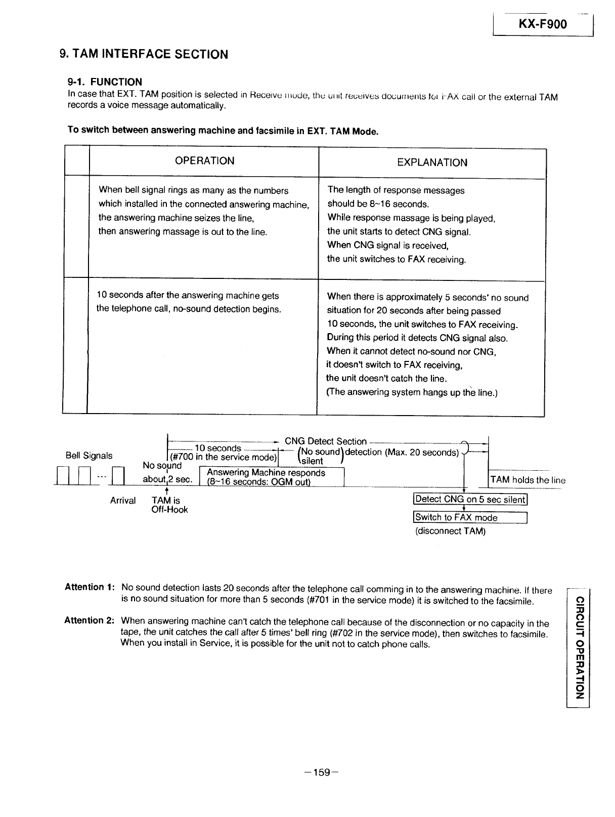
KX-F900
9. TAM INTERFACE SECTION
1
9-1. FUNCTION
In case that EXT. TAM position is selected in Receive nlude, th_ ul _itreu_iv_ documents loJ kAX call or the external TAM
records a voice message automatically.
To switch between answering machine and facsimile in EXT. TAM Mode.
OPERATION EXPLANATION
When bell signal rings as many as the numbers
which installed in the connected answering machine,
the answering machine seizes the line,
then answering massage is out to the line.
10 seconds after the answering machine gets
the telephone call, no-sound detection begins.
The length of response messages
should be 8-16 seconds.
While response massage is being played,
the unit starts to detect CNG signal.
When CNG signal is received,
the unit switches to FAX receiving.
When there is approximately 5 seconds' no sound
situation for 20 seconds after being passed
10 seconds, the unit switches to FAX receiving.
During this period it detects CNG signal also.
When it cannot detect no-sound nor CNG,
it doesn't switch to FAX receiving,
the unit doesn't catch the line.
(The answering system hangs up the line.)
Bell Signals
Arrival
I, CNG Detect Section
} ..... ! 0.seconds ,,i /'No sound_detection (Max. 20 seconds) f l
,, /(_:(uu m me service moae) ._ Ant ]
No souna J \ ........ .
Answering Machine responds / ITAM holds the line
aboutl2 sec. (8-16 seconds: OGM out)
tI
TAM is IDetect CNG on 5 sec silent I
f
Off-Hook ISwitch to FAX mode 1
(disconnect TAM)
Attention 1:
Attention 2:
No sound detection lasts 20 seconds after the telephone call comming in to the answering machine. If there
is no sound situation for more than 5 seconds (#701 in the service mode) it is switched to the facsimile.
When answering machine can't catch the telephone call because of the disconnection or no capacity in the
tape, the unit catches the call after 5 times' bell ring (#702 in the service mode), then switches to facsimile.
When you install in Service, it is possible for the unit not to catch phone calls.
O
O
.-I
O
"1o
rrl
_o
_>
.-I
O
z
-159-
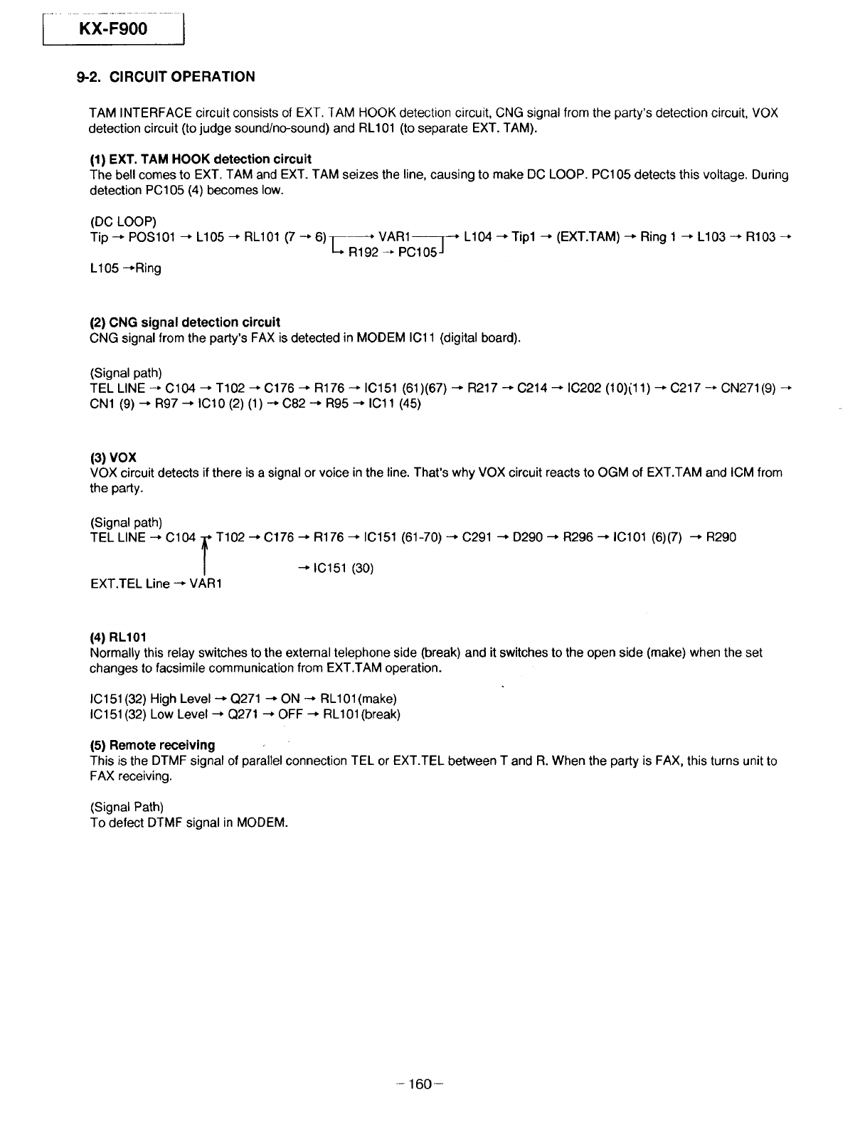
9-2, CIRCUIT OPERATION
TAM INTERFACE circuit consists of EXT. [AM HOOK detection circuit, CNG signal from the party's detection circuit, VOX
detection circuit (to judge sound/no-sound) and RL101 (to separate EXT. TAM).
(1) EXT. TAM HOOK detection circuit
The bell comes to EXT. TAM and EXT. TAM seizes the line, causing to make DC LOOP. PC105 detects this voltage. During
detection PC105 (4) becomes low.
(DC LOOP)
Tip ---*POS101 --* L105 --* RL101 (7 -_ 6)3_---* VAR1------]--* L104 --* Tip1 --, (EXT.TAM) _ Ring 1 --* L103 -* R103 --*
L-, R192 -* PC105 J
L105 -*Ring
(2) CNG signal detection circuit
CNG signal from the party's FAX is detected in MODEM IC11 (digital board).
(Signal path)
TEL LINE -* O104 --* T102 --* O176 --* R176 -* IC151 (61)(67) --, R217 --* C214 -* IC202 (10)(11) --, C217 ---*CN271 (9) -*
CN1 (9) --, R97 --, IC10 (2) (1) --* C82 --* R95 --* ICll (45)
(3) VOX
VOX circuit detects if there is a signal or voice in the line. That's why VOX circuit reacts to OGM of EXT.TAM and ICM from
the party.
(Signal path)
TEL LINE -* C104 _ T102 _ C176 --, R176 -* IC151 (61-70) -* C291 ---,D290 --, R296 --* IC101 (6)(7) --, R290
/--* IC151 (30)
EXT.TEL Line --* VAR1
(4) RL101
Normally this relay switches to the external telephone side (break) and it switches to the open side (make) when the set
changes to facsimile communication from EXT.TAM operation.
IC151 (32) High Level --* Q271 --* ON ---, RL101 (make)
IC151 (32) Low Level --* Q271 --* OFF --, RL101 (break)
(5) Remote receiving
This is the DTMF signal of parallel connection TEL or EXT.TEL between T and R. When the party is FAX, this turns unit to
FAX receiving.
(Signal Path)
To defect DTMF signal in MODEM.
- 160-
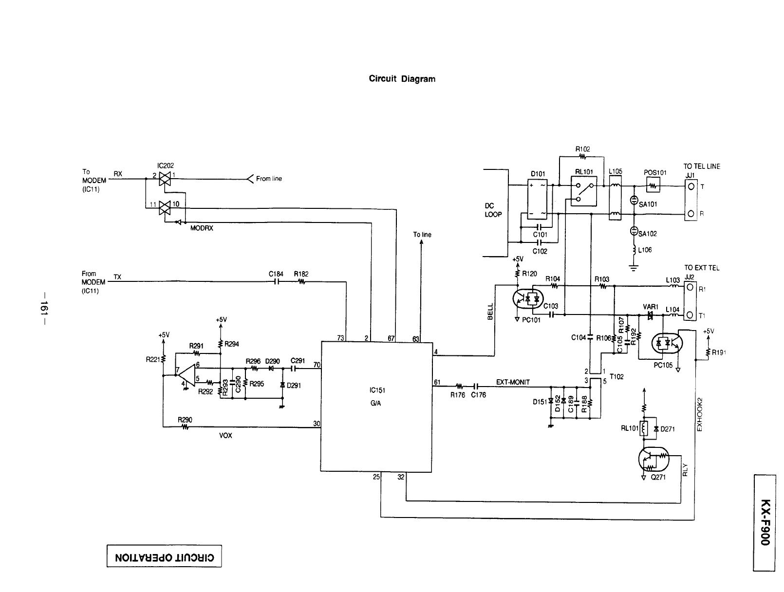
Circuit Diagram
I
o_
I
To
MODEM
0C11)
From
MODEM
(IC11)
RX
IC202
_ 2 1 From line
MODRX
"f'X C184 R182
II-----'_-,
+5V
+5V
R291
R221 _4 5 ,
_R294
R290
A,J
''V
R296 D290 C291 7n
o_._ _ R295 _D291
30
VOX
10151
G/A
r =ldO .I.II101:110
To line
DC
LOOP "_- ~
_,_--I I-
I 010'
,_1-.
C102
+5V
R102
,,,,,,
RL10_7 J_._ TO TEL LINE
POS101 JJ1
)SA 102
L106
•=- TO EXT TEL
R120 R104 R103 L103 _r_2
"1
I _ _VAHR1 LI041_ I
_PC1011"_ : " J_ [ Pl I ;_.O.JT1
/ a:_'__L ..J__..r--'m +5v
0104::.106{_#_f (0_) It
_T-MONIT • . . 3_]5 T102 _
o,,,_,4=1=._I
o 5 _ o
jjTTI o
,xr
"1"11
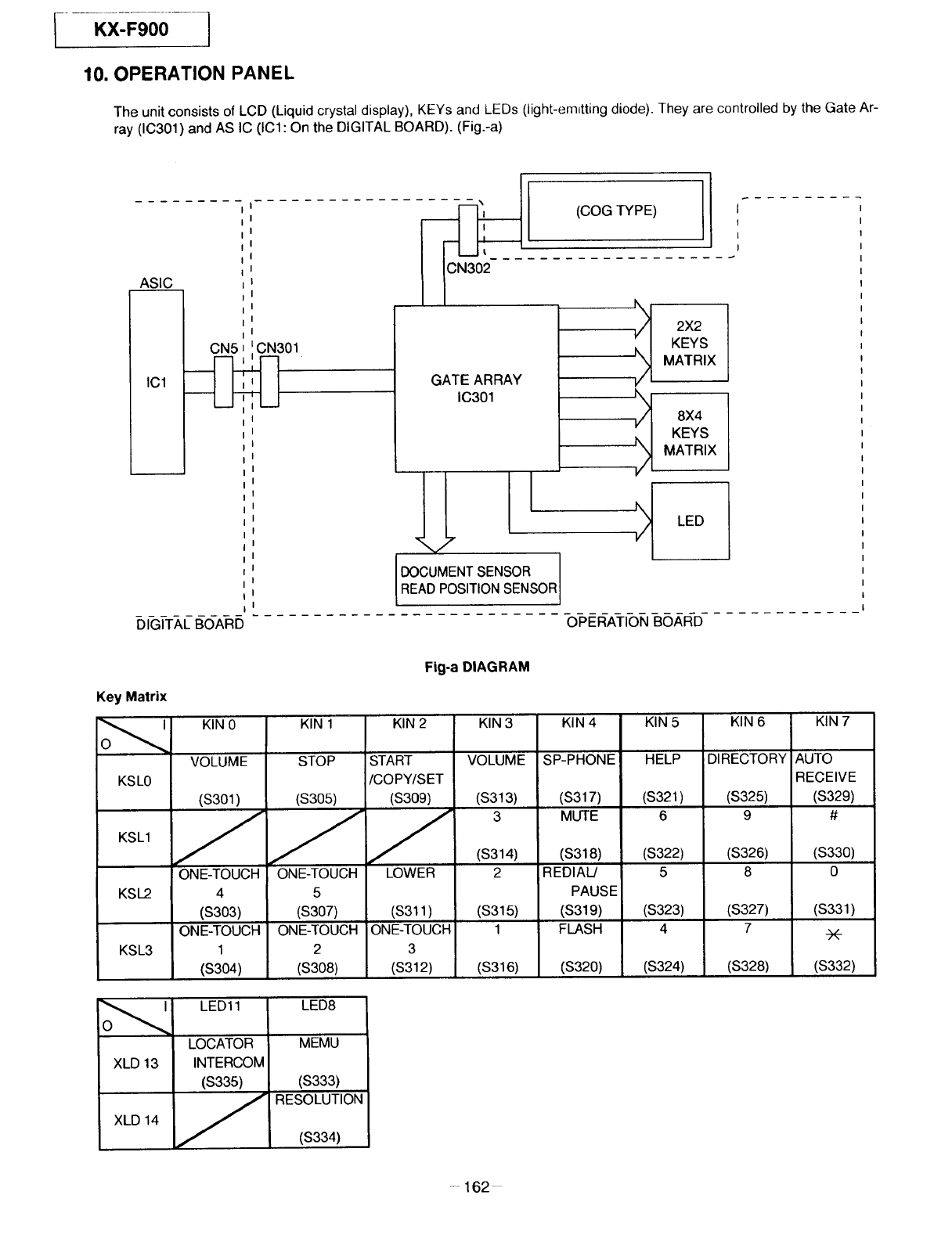
- KX-F900
10. OPERATION PANEL
The unit consists of LCD (Liquid crystal display), KEYs and LEDs (light-emitting diode). They are controlled by the Gate Ar-
ray (IC301) and AS IC (IC1 : On the DIGITAL BOARD). (Fig.-a)
ASIC
ICl
DIGITAL BOARD
CN51 CN301
I' GATE ARRAY
IC301
DOCUMENT SENSOR
READ POS T ON SENSOR
(COG TYPE) I
I
I
I
t 2X2
KEYS
MATRIX
t 8X4
KEYS
MATRIX
LED
OPERATION BOARD
Fig-a DIAGRAM
Key Matrix
o"-.<
KS L0
KSL1
KSL2
KSL3
KIN 0
VOLUME
(S301)
ONE-TOUCH
4
($303)
ONE-TOUCH
1
($304)
KIN 1
STOP
(S305)
ONE-TOUCH
5
($307)
ONE-TOUCH
2
(S308)
KIN 2
START
/COPY/SET
($309)
J
LOWER
($311 )
ONE-TOUCH
3
(S312)
KIN 3
VOLUME
($313)
3
($314)
2
(S315)
1
(S316)
KIN 4
SP-PHONE
(S317)
MUTE
($318)
REDIAL/
PAUSE
(S319)
FLASH
(S320)
KIN 5
HELP
($321)
6
($322)
5
($323)
4
($324)
KIN 6
DIRECTORY
($325)
9
($326)
8
($327)
7
($328)
XLD 14
LED11
LOCATOR
INTERCOM
($335)
LED8
MEMU
($333)
RESOLUTION
($334)
KIN 7
AUTO
RECEIVE
($329)
#
($330)
0
($331)
-X--
($332)
- 162-
11. LCD COG TYPE
KX-F900 I
The Gate Array (IC301) needs only write ASCii code from the data bus (D4~D7). V0 is power supplies for crystal drive.
R320, R322 are density control resistors.
Consequently, in this set the timing (mainly positive clock) is generated by the LCD interface circuitry of the gate array
(I0301).
Circuit Diagram
LCD UNIT
(COG TYPE)
ENABLE
RESET
Vo
C316
R322
IC301
4LED7
Timing Chart
R/W
E
DB4NDB7
/
/
DATA
\
/
/--
X
Density Normal Dark
LED 7
(IC301-4 pin) H L m
_0
t,-
-I
O
"I0
m
=4
0
z
163
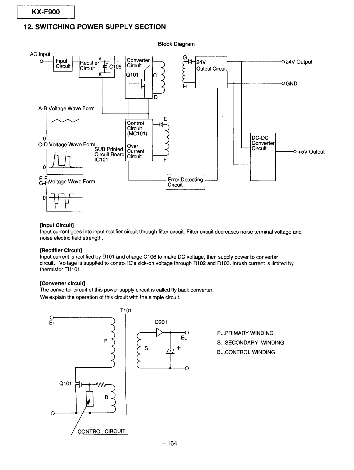
KX-F900
12. SWITCHING POWER SUPPLY SECTION
AC Input _ A
0--_ Input HRectifier--l";-, 1
A-B Voltage Wave Form
ol
C-D Voltage Wave Form
__ SUB Printed
Circuit Board
IC101
0
E-F, r
G_HVOtage Wave Form
01-3F-3 r--
VV
Block Diagram
Converter
Control
Circuit
(MC101)
Over
Current
Circuit
D
E
F
utput Circuit
DC-DC
Converter
Circuit
IError Detecting I--
Circuit /
_o24V Output
OGND
+5V Output
[Input Circuit]
Input current goes into input rectifier circuit through filter circuit. Fitter circuit decreases noise terminal voltage and
noise electric field strength.
[Rectifier Circuit]
Input current is rectified by D101 and charge C106 to make DC voltage, then supply power to converter
circuit. Voltage is supplied to control IC's kick-on voltage through R102 and R103. Inrush current is limited by
thermistor TH 101.
[Converter circuit]
The converter circuit of this power supply circuit is called fly back converter.
We explain the operation of this circuit with the simple circuit.
O
Ei
O
T101
.<
.<
p-<
.<
.<
.<
J
_CONTROL CIRCUIT
D201
O
Eo
+
O
- 164-
P...PRIMARY WINDING
S...SECONDARY WINDING
B...CONTROL WINDING
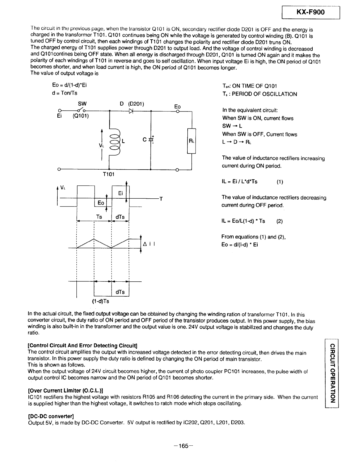
IKX-F900
The circuit in the previous page, when the transistor Q101 is ON, secondary rectifier diode D201 is OFF and the energy is
charged in the transformer T101. Q101 continues being ON while the voltage is generated by control winding (B). Q101 is
tuned OFF by control circuit, then each windings of T101 changes the polarity and rectifier diode D201 truns ON.
The charged energy of T101 supplies power through D201 to output load. And the voltage of control winding is decreased
and QlOlcontines being OFF state. When all energy is discharged through D201, Q101 is turned ON again and it makes the
polarity of each windings of T101 in reverse and goes to self oscillation. When input voltage Ei is high, the ON period of Q101
becomes shorter, and when load current is high, the ON period of Q101 becomes longer.
The value of output voltage is
Eo = d/(1-d)*Ei
d = Ton/Ts
SW D (D201) Eo
_o ' 1_ on
Ei (Q101)
I VL
c
ME
I
T101
,= T = =
J =
i i
t
', ,
i
i
i All
T
o-
t
To,: ON TIME OF Q101
T, : PERIOD OF OSCILLATION
In the equivalent circuit:
When SW is ON, current flows
SW --* L
When SW is OFF, Current flows
L-* D--" RL
The value of inductance rectifiers increasing
current during ON period.
IL = Ei/L*d*Ts (1)
The value of inductance rectifiers decreasing
current during OFF period.
IL = Eo/L(1-d) * Ts (2)
From equations (1) and (2),
Eo = d/(I-d) * Ei
In the actual circuit, the fixed output voltage can be obtained by changing the winding ration of transformer T101. In this
converter circuit, the duty ratio of ON period and OFF period of the transistor produces output. In this power supply, the bias
winding is also built-in in the transformer and the output value is one. 24V output voltage is stabilized and changes the duty
ratio.
[Control Circuit And Error Detecting Circuit]
The control circuit amplifies the output withincreasedvoltage detected inthe error detecting circuit, then drives the main
transistor.Inthispowersupply the dutyratiois definedby changingthe ON periodof maintransistor.
This isshownasfollows.
When the outputvoltageof24V circuitbecomes higher, the currentof photocouplerPC101 increases,the pulse widthof
outputcontrolIC becomesnarrowandthe ON period ofQ101 becomesshorter.
[Over Current Limiter (O.C.L.)]
IC101 rectifiers the highest voltage with resistors R105 and R106 detecting the current in the primary side. When the current
is supplied higher than the highest voltage, it switches to ratch mode which stops oscillating.
[DC-DC converter]
Output 5V, is made by DC-DC Converter. 5V output is rectified by IC202, Q201, 1_201,D203.
o_
;o
u
-I
O
"o
m
_a
-i
0
z
-165-
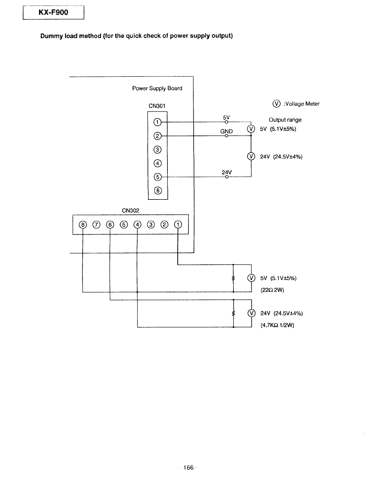
KX-F900 I
Dummy load method (for the quick check of power supply output)
Power Supply Board
CN301
®
®
®
@
®
CN302
5V
o
GND
O
24V
o
(_) :Vollage Meter
Output range
)5V (5.IV:L5%)
24V (24.5V+4%)
J
( _ 24V (24.5V+4%)
(4.7K_ 1/2W)
166
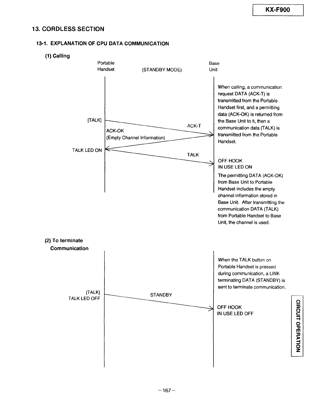
KX-F900 J
13. CORDLESS SECTION
13-1. EXPLANATION OF CPU DATA COMMUNICATION
(1) Calling
Portable
Handset (STANDBY MOD E)
Base
Unit
[TALK]
TALK LED ON
ACK-T
ACK-OK
(Empty Channel Information)
TALK
When calling, a communication
request DATA (ACK-T) is
transmitted from the Portable
Handset first, and a permitting
data (ACK-OK) is returned from
the Base Unit to it, then a
communication data (TALK) is
transmitted from the Portable
Handset.
OFF HOOK
IN USE LED ON
The permitting DATA (ACK-OK)
from Base Unit to Portable
Handset includes the empty
channel information stored in
Base Unit. After transmitting the
communication DATA (TALK)
from Portable Handset to Base
Unit, the channel is used.
(2) To terminate
Communication
[TALK]
TALK LED OFF STANDBY
When the TALK button on
Portable Handset is pressed
during communication, a LINK
terminating DATA (STANDBY) is
sent to terminate communication.
OFF HOOK
IN USE LED OFF
O
O
C
--I
O
'1:1
m
_o
-4
0
z
-167-
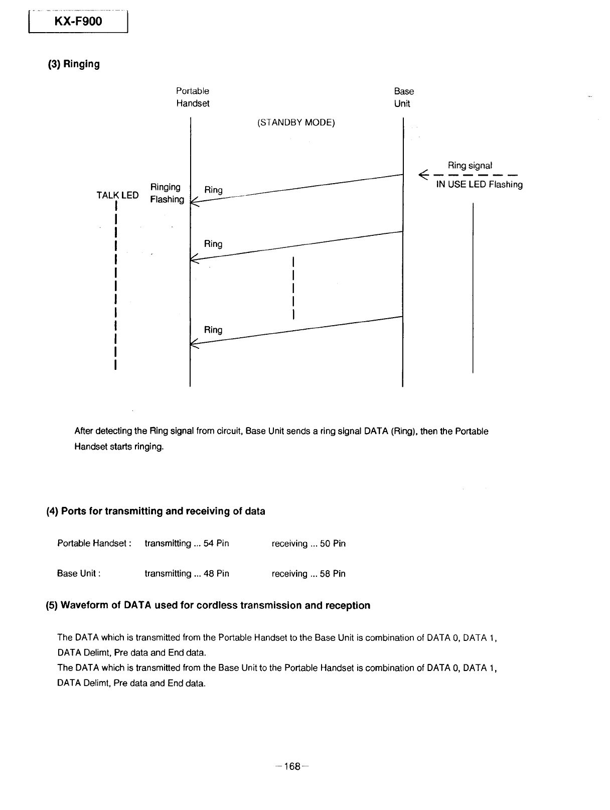
(3) Ringing
Ringing
TALK LED Flashing
Portable
Handset
(STANDBY MODE)
Base
Unit
Ring
lJ
Ring
Ring J
Ring signal
IN USE LED Flashing
After detecting the Ring signal from circuit, Base Unit sends a ring signal DATA (Ring), then the Portable
Handset starts ringing.
(4) Ports for transmitting and receiving of data
Portable Handset :transmitting ... 54 Pin receiving ... 50 Pin
Base Unit' transmitting ... 48 Pin receiving ... 58 Pin
(5) Waveform of DATA used for cordless transmission and reception
The DATA which is transmitted from the Portable Handset to the Base Unit is combination of DATA 0, DATA 1,
DATA Delimt, Pre data and End data.
The DATA which is transmitted from the Base Unit to the Portable Handset is combination of DATA 0, DATA 1,
DATA Delimt, Pre data and End data.
-168-
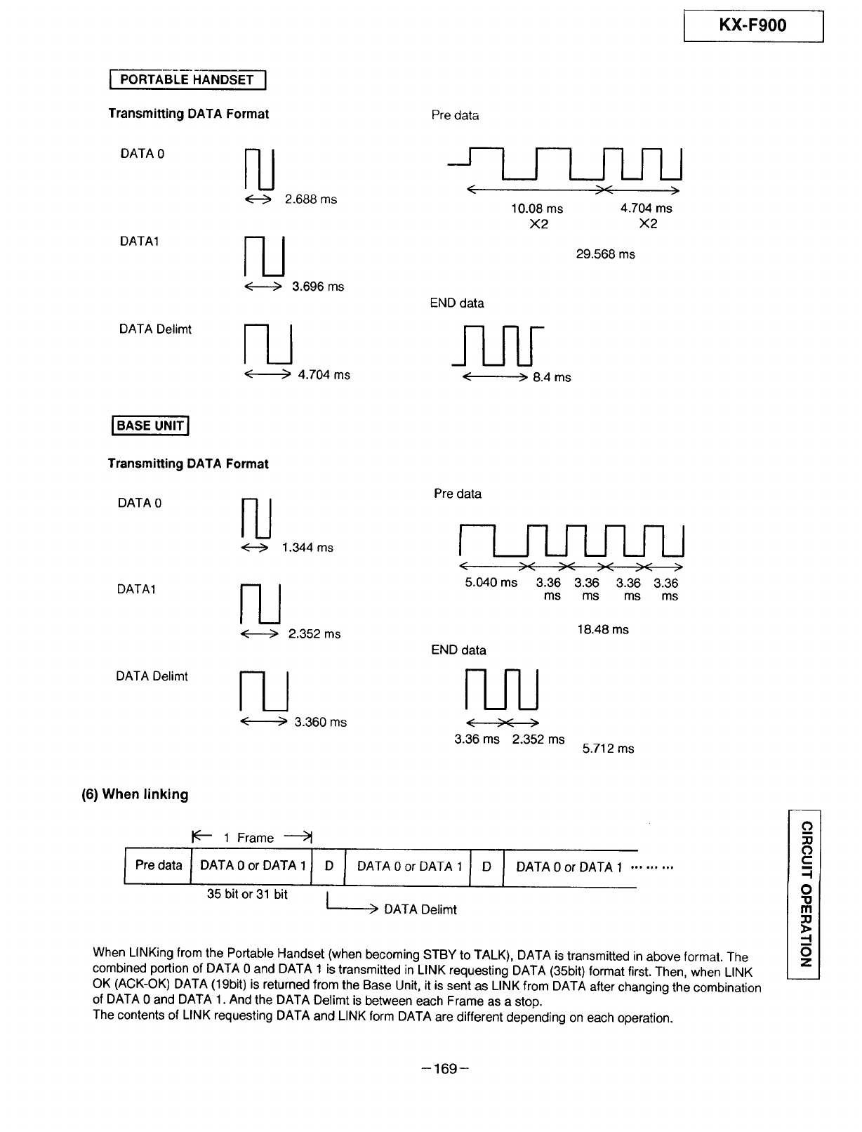
KX-F900
PORTABLE HANDSET I
Transmitting DATA Format Pre data
DATA 0
DATAI
DATA Delimt
FU
3.696 ms
FU
4.704 ms
--q_I-L_J-qJ-U
<>< >
10.08 ms 4.704 ms
X2 X2
29.568 ms
END data
<>8.4 ms
IBASEUNITI
Transmitting DATA Format
DATA 0
1.344 ms
DATA1 FU
2.352 ms
DATA Delimt FU
3.360 ms
Pre data
/qJqJqJ-LRJ
/ vvvv
f_ _ / _*, /_
5.040 ms 3.36 3.36 3.36 3.36
ms ms ms ms
END data
J v _
3.36 ms 2.352 ms
18.48 ms
5.712 ms
(6) When linking
JI(--- 1 Frame
Predata I DATA0orDATA11 D I DATA0orDATAll D I
35 bit or 31 bit /
DATA Delimt
DATA 0 or DATA I .........
When LINKing from the Portable Handset (when becoming STBY to TALK), DATA is transmitted in above format. The
combined portion of DATA 0 and DATA 1 is transmitted in LINK requesting DATA (35bit) format first. Then, when LINK
OK (ACK-OK) DATA (19bit) is returned from the Base Unit, it is sent as LINK from DATA after changing the combination
of DATA 0 and DATA 1. And the DATA Delimt is between each Frame as a stop.
The contents of LINK requesting DATA and LINK form DATA are different depending on each operation.
O
O
C
m
-I
O
"Io
m
---I
0
z
-169-
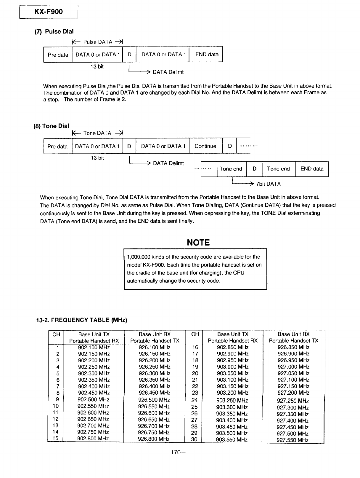
KX-F900
(7) Pulse Dial
_-- Pulse DATA
Predata IDATA0orDATA1 j D I DATA0orDATA1
13 bit /
t_____>DATA Delimt
END data 1
When executing Pulse Dial,the Pulse Dial DATA is transmitted from the Portable Handset to the Base Unit in above format.
The combination of DATA 0 and DATA 1 are changed by each Dial No. And the DATA Delimt is between each Frame as
a stop. The number of Frame is 2.
(8) Tone Dial
Pre data
Tone DATA --_
lO T OorOAt lJ0IO TA0orO T l
13 bit / DATA Delimt
I
Continue DI.........
......... I Toneend I DIToneend
_---_--> 7bit DATA
IEND data I
When executing Tone Dial, Tone Dial DATA is transmitted from the Portable Handset to the Base Unit in above format.
The DATA is changed by Dial No. as same as Pulse Dial. When Tone Dialing, DATA (Continue DATA) that the key is pressed
continuously is sent to the Base Unit during the key is pressed. When depressing the key, the TONE Dial exterminating
DATA (Tone end DATA) is send, and the END data is sent finally.
NOTE
1,000,000 kinds of the security code are available for the
model KX-F900. Each time the portable handset is set on
the cradle of the base unit (for charging), the CPU
automatically change the security code.
13-2. FREQUENCY TABLE (MHz)
CH Base Unit TX
Portable Handset RX
1 902.100 MHz
2 902.150 MHz
3 902.200 MHz
4 902.250 MHz
5 902.300 MHz
6 902.350 MHz
7 902.400 MHz
8 902.450 MHz
9 902.500 MHz
10 902.550 MHz
11 902.600 MHz
12 902.650 MHz
13 902.700 MHz
14 902.750 MHz
15 902.800 MHz
Base Unit RX
Portable Handset TX
CH
926.100 MHz
926.150 MHz
926.200 MHz
926.250 MHz
926.300 MHz
926.350 MHz
926.400 MHz
926.450 MHz
Base Unit TX
Portable Handset RX
926.500 MHz
926.550 MHz
926.600 MHz
926.650 MHz
926.700 MHz
926.750 MHz
926.800 MHz
16
17
18
19
20
21
22
23
24
25
26
27
28
29
30
902.850 MHz
902.900 MHz
902.950 MHz
903.000 MHz
903.050 MHz
903.100 MHz
903.150 MHz
903.200 MHz
903.250 MHz
903.300 MHz
903.350 MHz
903.400 MHz
903.450 MHz
903.500 MHz
903.550 MHz
Base Unit RX
Portable Handset
926.850 MHz
926.900 MHz
926.950 MHz
927.000 MHz
927.050 MHz
927.100 MHz
927.150 MHz
927.200 MHz
927.250 MHz
927.300 MHz
927.350 MHz
927.400 MHz
927.450 MHz
927.500 MHz
927.550 MHz
TX
- 170-
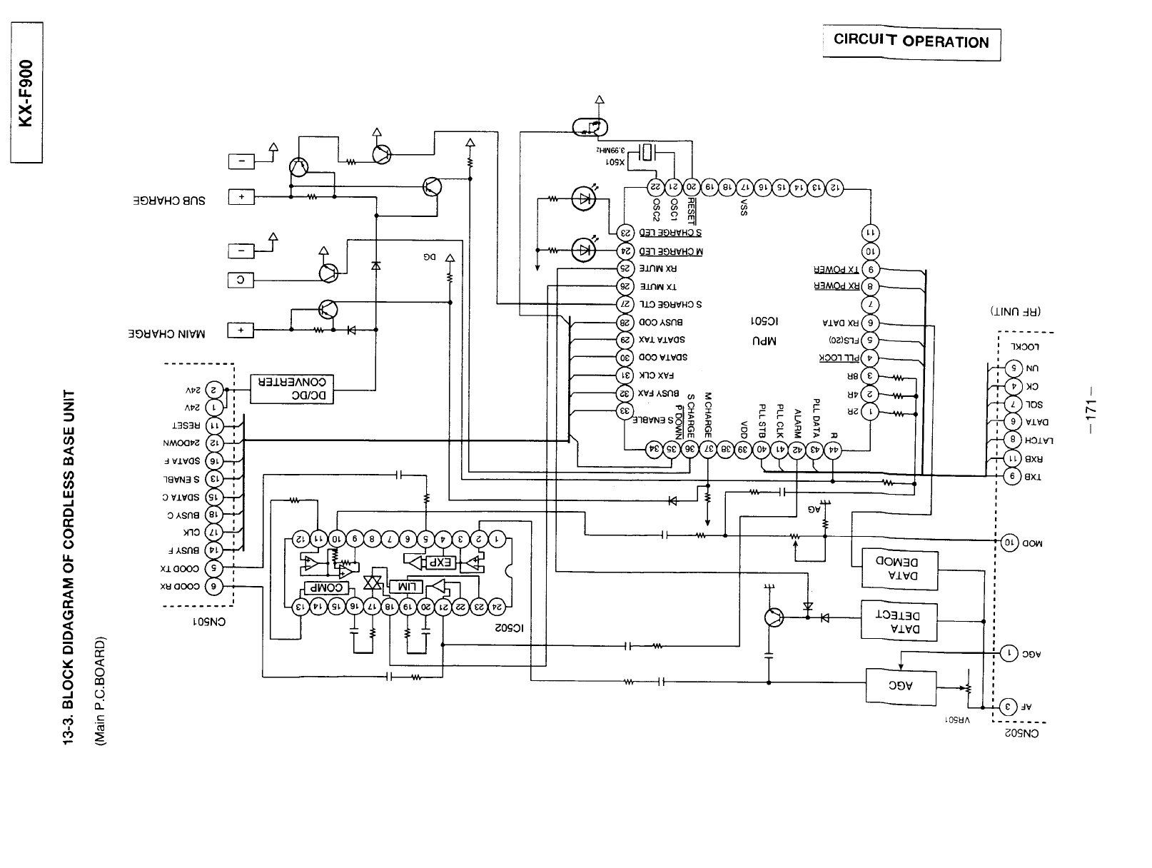
0
0
U.
i
X
I.-
1.1.1
00
cO
o0
u)
UJ
-.I
r.,
n-
O
o
I./.
0
,,:(
CE
E3 r7
r_ cc
o o
0m
- o.
cO n
._c
_ v
;CIRCUIT OPERATION j
39_VHO 8nS
I
39_VHO NIV_
Z)O
i
_°_ (°_H
_°_N_®H _ '_-7
o,_n__ ,r'lII I I I
(IINA 4U)
LO_IA ........
_OSNO
!
F--
I
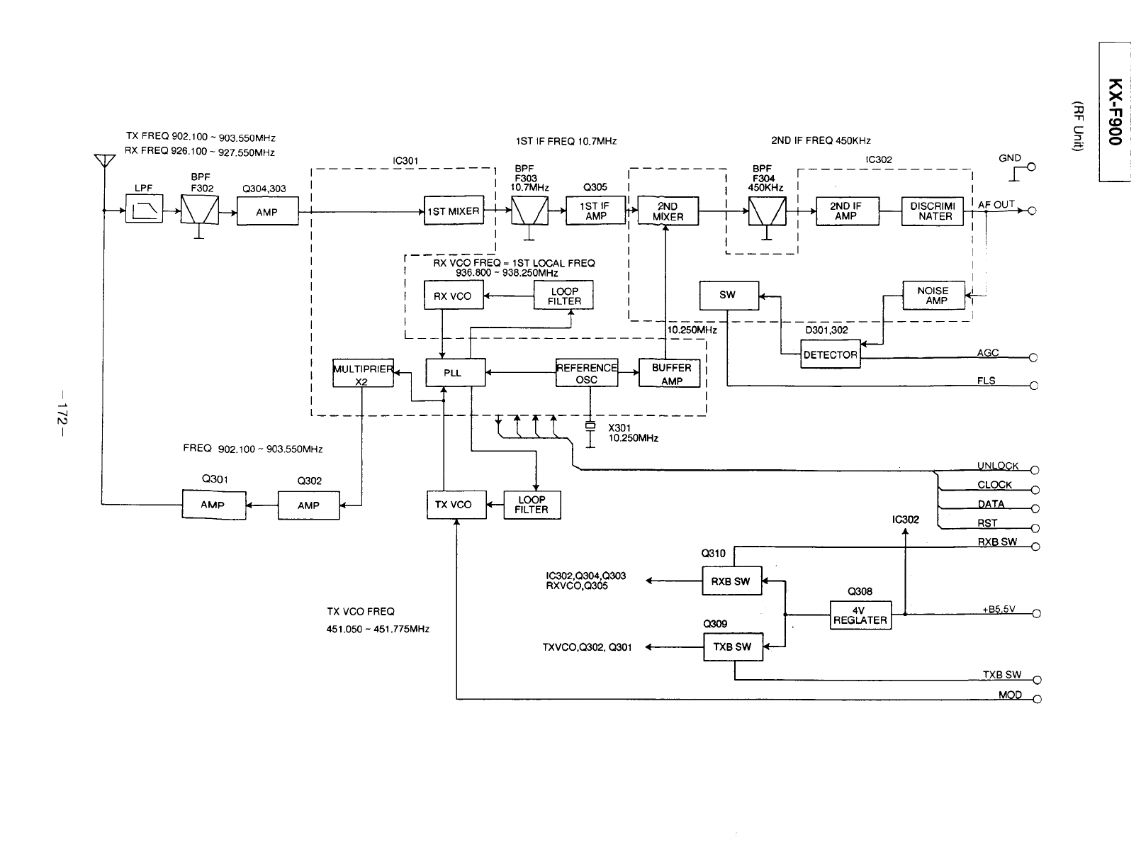
I
q
Pc
I
_7
TX FREQ 902.100 ~ 903.550MHz
RX FREQ 926.100 - 927.550MHz
BPF
LPF F302 Q304,303
AMP
I
I
I
I
1ST IF FREQ 10.7MHz 2ND IF FREQ 450KHz
IC301
l BPF BPF r
F303 II F304
I10.7MHz Q305 I I450KHz I
I I
+ TMXE
I I
,.. I
rRX VCO FREQ = 1ST LOCAL FREQ
l936.800 - 938.250MHz
IC302
2NDIF h IDISCRIMI
AMP _ NATER
GND
,_
I
I Ai OUT
I _0
I
I
I
I
TX VCO FREQ
451.050 - 451.775MHz
FREQ 902.100 N 903.550MHz
Q301 Q302
AMP
q /
', / t -- _._--
L.................. IL-'IDETECTOR
__ D301,302
IlVlULTIPRIEFL. PLL LIIREFERENCEI_J BUFFER I
1_ x2 J'l! I" IOSC I_ AMP I I
- L- I _ ,
....... [-- :_ T _" Ti- _ X3.0_5:M :Z '
1
I_ T '\-r-. LI LOOP
I .... I"_ ] F LTER 10302
°3,01 ]
_×v0o,o_o5'0_2'°3°',°_3_ .xB_w_-] _
II
rxvco,c3o2,_o_ _ _
I
NOISE !_AMP
i
AGC
FLS
O
-o
UNLOCK O
l CLOCK O
_ATA 0
RST O
RXBSW O
+B_.5v O
TXB SW O
MOD O
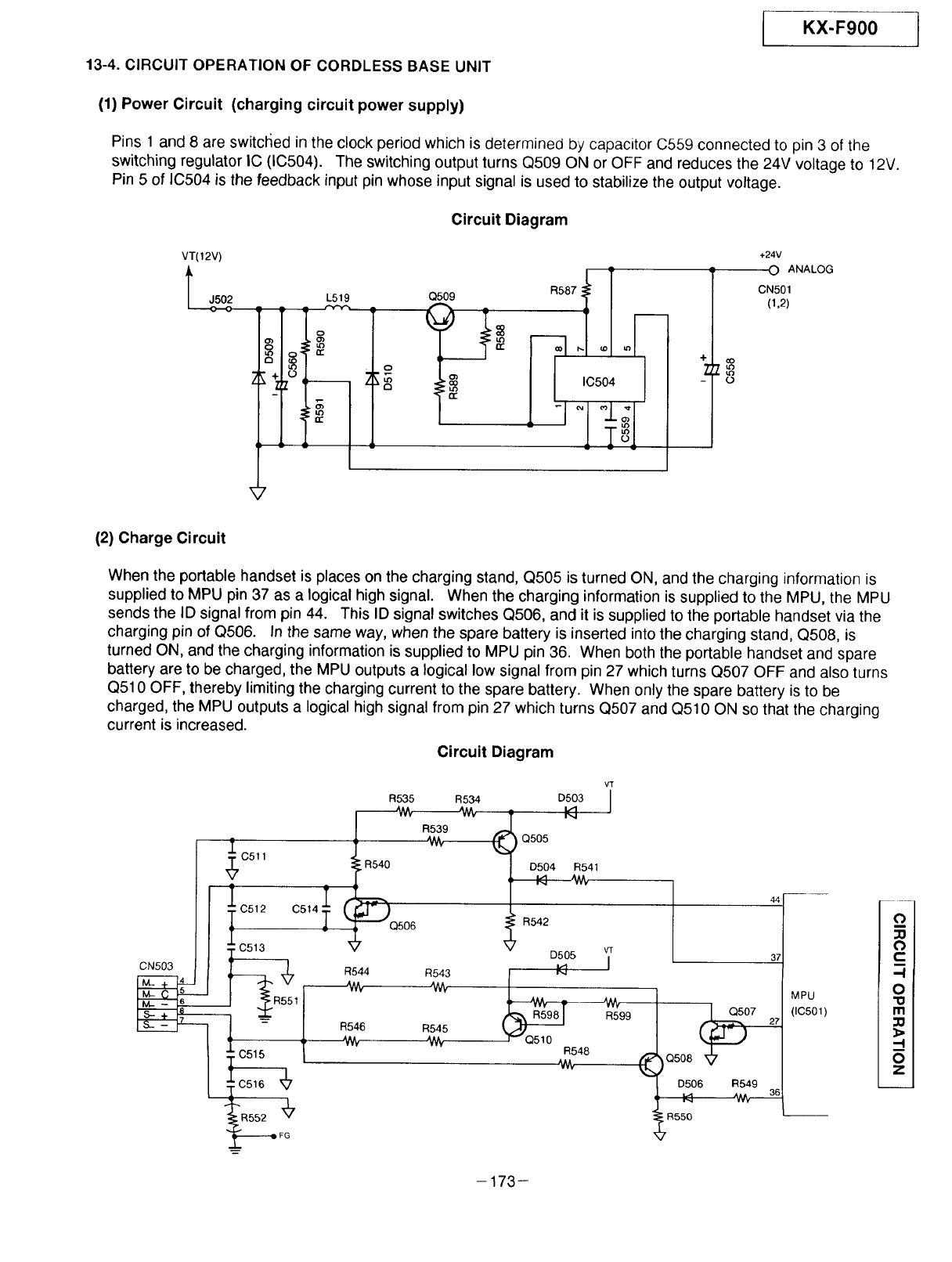
13-4. CIRCUIT OPERATION OF CORDLESS BASE UNIT
IKX-F900
(1) Power Circuit (charging circuit power supply)
Pins 1 and 8 are switcl4ed in the clock period which is determined by capacitor C559 connected to pin 3 of the
switching regulator IC (IC504). The switching output turns Q509 ON or OFF and reduces the 24V voltage to 12V.
Pin 5 of IC504 is the feedback input pin whose input signal is used to stabilize the output voltage.
Circuit Diagram
VT(12V) +24v
_J502 0 ANALOG
CN501
(1,2)
L519
O
o
_8
Q509
nr" IIIC504
÷ co
Z
- O
(2) Charge Circuit
When the portable handset is places on the charging stand, Q505 is turned ON, and the charging information is
supplied to MPU pin 37 as a logical high signal. When the charging information is supplied to the MPU, the MPU
sends the ID signal from pin 44. This ID signal switches Q506, and it is supplied to the portable handset via the
charging pin of Q506. In the same way, when the spare battery is inserted into the charging stand, Q508, is
turned ON, and the charging information is supplied to MPU pin 36. When both the portable handset and spare
battery are to be charged, the MPU outputs a logical low signal from pin 27 which turns Q507 OFF and also turns
Q510 OFF, thereby limiting the charging current to the spare battery. When only the spare battery is to be
charged, the MPU outputs a logical high signal from pin 27 which turns Q507 and Q510 ON so that the charging
current is increased.
Circuit Diagram
CN503
@
R535
R539
C511 R540
Ics, l 7"
TT( _-'_Q506
C513 -'
l _ _________4 R543
.,_R551
R546 R545
At# 'W_
'.fT
R534 D503vt I
Q505
D504 R541
R542
Q508 _07
D506 R549
D505 w
,., I
1' R599
R548
44
37
27
"_R550
MPU
(IC501)
o
o
C
-I
0
"O
m
"-4
O
Z
-173-
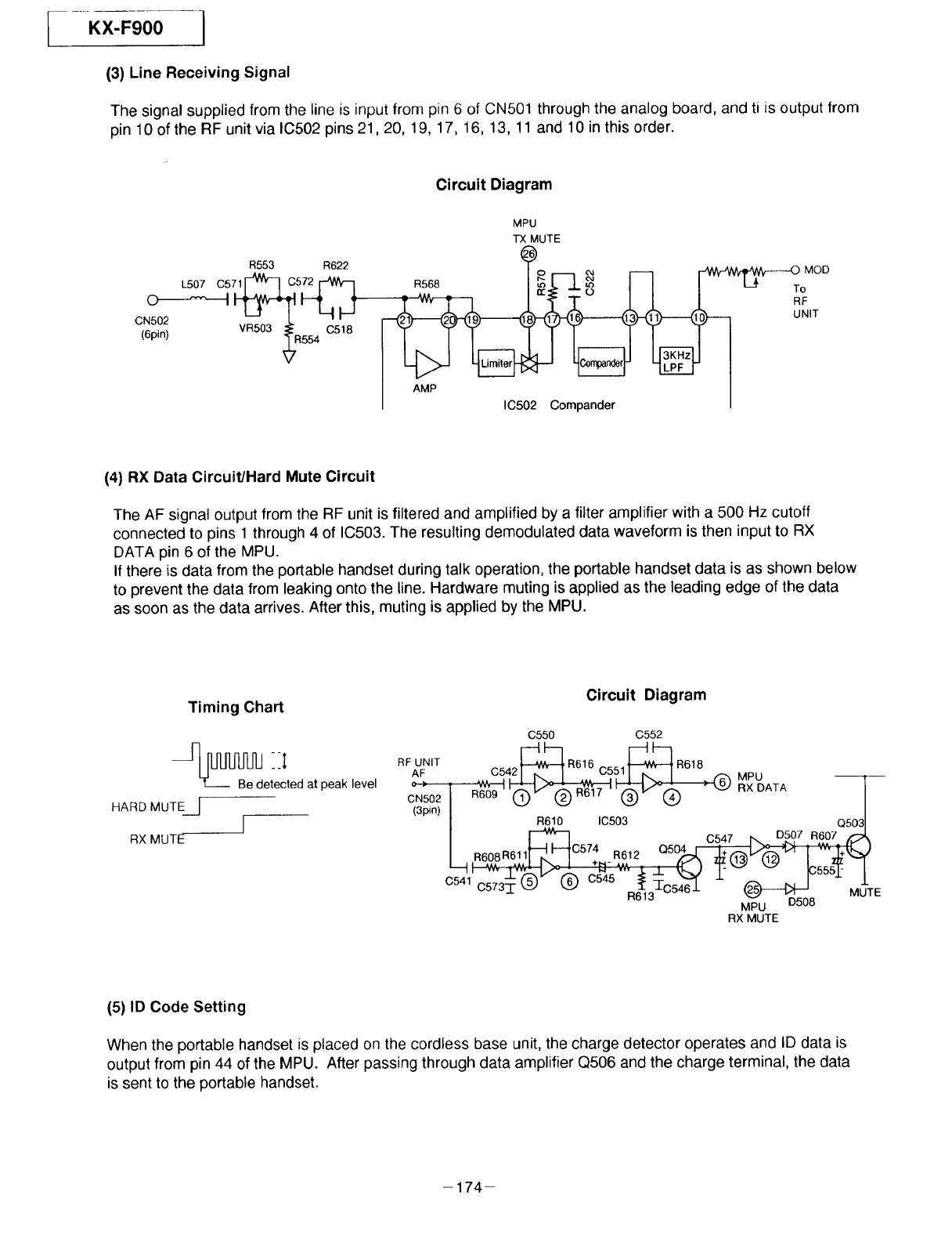
I .....KX-F900
(3) Line Receiving Signal
The signal supplied from the line is input from pin 6 of CN501 through the analog board, and ti is output from
pin 10 of the RF unit via IC502 pins 21,20, 19, 17, 16, 13, 11 and 10 in this order.
R553 R622
L507 C571_'-_ C572
(6pin) VR503 _'R554 C518
Circuit Diagram
MPU
TX MUTE
6)
_ 0 ' To
I IC502 Compander
(4) RX Data Circuit/Hard Mute Circuit
The AF signal output from the RF unit is filtered and amplified by a filter amplifier with a 500 Hz cutoff
connected to pins 1 through 4 of IC503. The resulting demodulated data waveform is then input to RX
DATA pin 6 of the MPU.
If there is data from the portable handset during talk operation, the portable handset data is as shown below
to prevent the data from leaking onto the line. Hardware muting is applied as the leading edge of the data
as soon as the data arrives. After this, muting is applied by the MPU.
Timing Chart
_J_Bed --I
eiected at peak level
HARD MUTE__[ I
RX MUTE
Circuit Diagram
C550 C552
RFAUpIT _R616 C551_--_ R618
C5421 _ i --:'1 _ I _ MPU l-
CCN502(3pin,iR60_9 __ RXDATA /
I .61o sc o3 o o31
IC547 Ix,._ D507 t:1607 t_
] R608R611_'I_I'--lC574 R612 Q504 +('_'_ _ +
C541 _':
E
MPU D508
RX MUTE
(5) ID Code Setting
When the portable handset is placed on the cordless base unit, the charge detector operates and ID data is
output from pin 44 of the MPU. After passing through data amplifier Q506 and the charge terminal, the data
is sent to the portable handset.
-174-
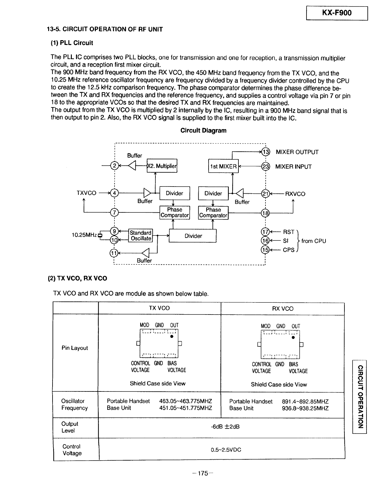
I KX-F900 I
13-5. CIRCUIT OPERATION OF RF UNIT
(1) PLL Circuit
The PLL IC comprises two PLL blocks, one for transmission and one for reception, a transmission multiplier
circuit, and a reception first mixer circuit.
The 900 MHz band frequency from the RX VCO, the 450 MHz band frequency from the TX VCO, and the
10.25 MHz reference oscillator frequency are frequency divided by a frequency divider controlled by the CPU
to create the 12.5 kHz comparison frequency. The phase comparator determines the phase difference be-
tween the TX and RX frequencies and the reference frequency, and supplies a control voltage via pin 7 or pin
18 to the appropriate VCOs so that the desired TX and RX frequencies are maintained.
The output from the TX VCO is multiplied by 2 internally by the IC, resulting in a 900 MHz band signal that is
then output to pin 2. Also, the RX VCO signal is supplied to the first mixer built into the IC.
Circuit Diagram
i
Buffer
_k--'-<_2. Multiplier[
TXVCO_ [_ Divider I
, Buffer
Phase
, Comparator
1 . _ StandardJ .I T
o oi,,a,e
', Buffer
I '@ M,XER,.PUT
Divider _ RXVCO
,_ Buffer
Phase T
Comparator (_
T
Divider I
MIXER OUTPUT
_)<---- RST }
_<--- SI from CPU
_<---- CPS
(2) TX VCO, RX VCO
TX VCO and RX VCO are module as shown below table.
Pin Layout
Oscillator
Frequency
TXVCO RXVCO
MOD GND OUT
t__J ',.... ', %_;
E ]
I
'---I ;.... :"H:I
CONTROLGND BiAS
VOLTAGE VOLTAGE
Shield Case side View
Portable Handset 463.05~463.775MHZ
Base Unit 451.05~451.775MHZ
MOD GND OUT
,__.; ',.... ', ,__;
E 3
l---i _.... i _---t
CONTROLGND BIAS
VOLTAGE VOLTAGE
Shield Case side View
Portable Handset 891.4N892.85MHZ
Base Unit 936.8~938.25MHZ
Output -6dB +2dB
Level
Control 0.5-2.5V DC
Voltage
- 175--
o
o
C:
--I
0
"1o
m
_0
_>
.-I
0
Z
IKX-F900
(3) Receiver RF Circuit ( ): Portable Handset
The electric wave received from the antenna ia attenuated by the SAW filter F302 (F402) except the received fre-
quency band Then it is amplifier Q304 (Q404) and Q303 (Q403), and supplied to the IC301 (IC401) pin 23
(MIXER input).
Circuit Diagram
R312
IC301 04 ANT
(_327 "
MIXER IN _ _ : o_ I
C390
Y
(4) MIXER IF Circuit ( ): Portable Handset
The reception frequency band signal supplied to the pin 23 MIXER input of IC301 (IC401) is converted into a 10.7
MHz first IF signal by the mixer circuit, using the reception local signal. The result is then output to pin 13 MIXO.
The resonator circuit consisting of L304, C336 (L404, C436) resonates at 10.7 MHz. The 10.7 MHz IF signal is fil-
tered by ceramic filter F303 (F403) and then supplied to IF amplifier Q305 (Q405).
Circuit Diagram
4<.-.--
IC301
__ Buffer_ RX Signal
I otM,xE.% .,x,.
C338
-41_ - _ _ . '_MIXEROUT
-I- R320 1stIF
-176-
KX-F900
(5) TX Power Circuit (): Portable Handset
After being multiplied by 2 inside IC301 (IC401) to make it a 900 MHz band frequency, the transmission signal
is amplified by Q301 and Q302 (Q401 and Q402) and frequency elements outside of the transmission fre-
quency are attenuated b_t dielectric filter F301 (F401). The signal then passes through a transmission-recep-
tion matching circuit and supplied to the antenna terminal.
Circuit Diagram
R302
cO
CD
o_E--
8:Z-
R304[-_' /
)Q302
IC301
IN
C303 F301 C354 •ANT
(6) Second Mixer, Detector, Carrier Sense Circuit ( ): Portable Handset
The 10.7 MHz IF signal from Q305 (Q405) passes through pin 16 of IC302 (IC402) and is input to the second
mixer built into the IC. The reference oscillator frequency from IC301 (IC401) is used as the second local sig-
nal. After being converted into a 450 kHz second IF by the second mixer, the signal is wave detected and out-
put to pin 9 as a low-frequency signal. This signal is output as the AF output signal and, at the same time,
used for e(ectric field determination. The FM noise is filtered by a 10 kHz BPF comprising pins 10 and 11 and
then amplified. Then it is rectified by D301 (D401) and D302 (D402), and input to the switching block consist-
ing of pins 12 through 14.
Circuit Diagram
SQL<
AF<
i
D302
R331 C340
Carrier Sense
, 1st IF
R337
-177-
14 Pin
Enable to Electric Field "L"
Disable to Electric Field "H" o
o
u
-I
O
"0
m
33
0
z
I
.--L
"4
03
I
Q208 I LC_!
VR _
MIC SENEITIVlTY ADJUSTJ- II I ',
Q21o,21, Q217 r--1-I--_ _ ',
IME I I i
SPEAKER j
,, ', _
L........
l D201
l-q, - _ _[_
Q202
MIC MUTE
33
_. RX V01 IC201O_ SPK MUTE
Q201 CPU
] _ 17 CHARGE
IC204
16 BATrERYLOW
8RESET
IC206 15 POWER down
Q205
_ Q210,Q211 TX POWER
TXB
Q208 RF PANT
Q203 _ IC202,C203
_ RXB RF PANT
TX DATA [
UNLOCK
CLOCK
DATA
RST
FLS
RX DATA
ALARM VOL
ALARM
INTERCOM
TALK
LIGHTED KEY
58 L IGHTED KEY
• RX POWER
14
)IDIN CLoGMAINKSUB
CLOCK
3L-,n¢lt r,J'
3.992MHz 32.68KHz
X201 X202
0 AGC
VR2
MAX IMUM DEVIATION ADJUST _-0 MOD
VR202
SPK LEVEL ADJUST
5O
_0 AF
_AT-_ Q214
:_ IQ215
UNLOCK
CLOCK
DATA
RST
FLS
1
4_ _R
63 _D210 1
62 *t_'%D212 +B
_._ D209
%
÷_ D207
0
Q
0
0
F
m
I
Z
C3
m
.-4
I
I
TX FREQ 926.100 - 927.550MHz
RX FREQ 902.100 - 903.550MHz
7I
BPF
LPF F402 Q404,403 I
AMP I
FREQ 926.100 - 927.550MHz
Q401 Q402
AMP _-_ AMP
INOIlVI:13dO llnOEIIO
1ST IF FREQ IO.7MHz
IC401
1 BPF
F403
I IO.TMHz
I-I 1ST MIXER _-_
_ULT'P",E__,! PL
x2 J _-_' L
--t-t-t-t- t-
2ND IF FREQ 450KHz
I
04O5 I
1ST IF _ 2ND
AMP iI_ MIXER
k T,_
RX VCO FREQ = 1ST LOCAL FREQ
891.400 ~892.850MHz
RX VCO LOOP
FILTER
J I t
TX VCO FREQ
463.050 ~ 463.775MHz
_REFERENCE[_J
I osc I"1
IJ
F
BPF
IF404 r
I 450KHz I
L..... I
IC402
1=
2ND IF [_ DISCRIMI
AMP _NATER
/
1
_Io_.2_MHz 0,,01.402
I ' _--IOETEC'O"/
BUFFER J
AMP I
I
I
NOISE
AMP
GND
,2-_
I
IAFOUT_ ©
I I
I
I
l
T
AGO o
FL$ 0
l
I
X401
10.250MHz
UNLOCK 0
l CLOCK 0
DATA 0
RST O
IC401,Q404,Q403
RXVCO,(_05
IC402
_VCO,C_02,(_O 1
RXB o
3.9V 0
TXB 0
MOD o
33
"-lq
C

Kx:F900 I
13-7. CIRCUIT OPERATION OF PORTABLE HANDSET
(1) Power Supply Ciurcuit
As indicated in Fig.40, voltage is supplied separately to each block. In order to ensure that the RF block in
particular has a stable fixed-voltage power supply, the RF block is equipped with a dedicated stabilized power
supply. In the standby mode, pin 58 drops at set intervals from high to low level, resulting in an intermittent recep-
tion signal. In the talk mode, pins 59 and 58are low level and power is supplied to all the circuitry.
Circuit Diagram
T
1
RX POWER I
sw1
Q203 R_
PU RX POWER
TX POWER I
205
SPK AMP SW
_ )_CPU TX POWER
>RINGER(Q212,Q213)
• CPU (IC201)
• DATA AMP(Q215,Q214)
IF Part (RF BLOCK )
• RF BLOCK
• COMPANDER (IC202)
(IC203)
•RF BLOCK, MICAMP(Q208)
>SPK AMP(Q210,Q211)
(2) Data Reception Circuit
The wave detection signal from the RF block has high frequency elements eliminated by a CR filter consisting of
R258 and C244. Then it is amplified by Q215 and, once again, high frequency elements are eliminated by R255
and C243. After this, the signal is amplified by Q214 and input to pin 50 of the CPU. (The cutoff frequency is 500
Hz.) The data output waveform is a block pulse. To inhibit block pulse noise, the gain of the amplifier is limited
and modulation is clipped at 3 kHz.
Circuit Diagram
-R_57
1._ _ iQ215_ from
RF BLOCK AF Output
-180-
KX-F900
(3) Ringer Circuit
If the ringer volume is set to low and the key is entered occurs, an alarm tone is output from pin 45 of the CPU
and input to Q212. This causes Q213 to turn off and results in a softer beep tone.
If the ringer volume is set to high, Q213 turns on and results in a louder beep tone.
Circuit Diagram
SPEAKER
C
_CPU ALARM
CPU ALARM
VOLUME
(4) Reception Signal Circuit
The receiver circuit comprises expander IC202, side tone control IC IC208, and a speaker amplifier.
After being adjusted to the appropriate level by VR202, the signal passes through a 3 kHz LPF and an ex-
pander built into IC202. It is then input to side tone IC IC208. The side tone IC is connected to the microphone
amplifier. If a large input is input to the microphone, the gain control built into IC208 lowers the gain to reduce
the output of the speaker amplifier. If there is no large input being input to the microphone, the amplifier in
IC208 is set to standard gain. Consequently, the sound of the received audio signal becomes fainter when the
user is talking in a loud voice and the side tone level is lowered. When the user talks more softly, the received
audio signal is audible at the standard level.
Also, in addition to the input from the microphone, the ACG signal from the RF block is input to the side tone IC.
When the base unit and portable handset are separated from each other, causing the signal to become weaker,
the DC voltage rises and this voltage is input to pin 5 of IC208. When the DC voltage input to pin 5 rises, the
gain control built into IC208 lowers the gain. Consequently, the reception level is lowered when the reception
signal is weak and there is more noise. This prevents the noise from becoming too noticeable.
The reception signal passes through receiver volume selector switch Q217, and then drives the receiver
speaker.
RXVOL H : LOW LEVEL
L : HIGH LEVEL
SPK MUTE H : SPEAKER ON
L : SPEAKER OFF o
m
_o
-I
O
"10
m
,-4
o
Z
-181--
KX-F900
Circuit Diagram
IC202 EXPANDER
3KHz LPF
RF Part -_
AF __ VR202
Receive level adjust
[__ IC208
I I I _ I Sidetone
_ ___JcontrollC
Gain control RI :0_38
R265
RX VOL
SPK MUTE (_)
SPEAKER
SPK MUTE
(5) Sending Signal
The audio signal from the microphone is amplified by Q208 and then passes through a limiter, mute circuit,
compander, and 3 kHz LPF built into IC202. It is then mixed with the TX DATA signal from the CPU, the
maximum modulation is adjusted by VR201, and input to the modulator in the RF block.
Circuit Diagram
R217
CPU R250
TX DATA_ T
CPU MIC MUTE ..LR229
LIMITER H_'ICOMPANDER_ _ :
i
=
i
=
IC202 i
............................................................. i
,_]_o RF Part
MOD
VR201
MAXIMUM
Deviation adjust
-- 182-
KX-F900
(6) ReseUPowe_ uow.luattery LowilD
When the battery is installed in the portable hm}dset, the reset circuit consisting of R289, C255, and Q204
functions, inputting a reset signal to the CPU. This ensures that the unit will operate normally without the user's
needing to switch the power off and on. When the voltage from the batteries drops to 3.5 V, 3.5 V voltage
detector IC204 operates and inputs a battery low signal to the CPU. This causes the battery low LED to flash
on and off. If voltage continues to drop and reaches 3.2 V, 3.2 V voltage detector IC206 operates and outputs
a power down signal to the CPU. This causes power to be cut off automatically and prevents the battery from
over discharging. Q201 is a charge detector that informs the CPU whether or not the portable handset is
currently being charged. During charging, ID data is sent from the base unit. Q202 receives this ID data and
sends it to the CPU.
Circuit Diagram
[]
R289 C255
D201 'W_,_ I I r_204_:
R286 IC206 _ I"' :_
Battery_e_e[ _I--- "L £ , R208 _>Q
Q20_ R205
R201 "_ _2_ R206
'_' .1_
R202 -£-
C204 D213
@
@
RESET
Powerdown
Bakery low
Charge
ID
183
KX-F900
•FOR SCHEMATIC DIAGRAM
1.
2.
DC voltage measurements are take,, wLth Ob_;lilo_bUp_:
or tester from ground.
The schematic diagram and circuit board may be
modified at any time with the development of new
technology.
v=ca_. It General Jl Zenef II LED IIPhotoDikode
CathodelJ Cathode/| Cathode][ Cathodel/AnOde
j;llLbpul[ant safety notiou
.... ............ ........ ................: ....
-184-
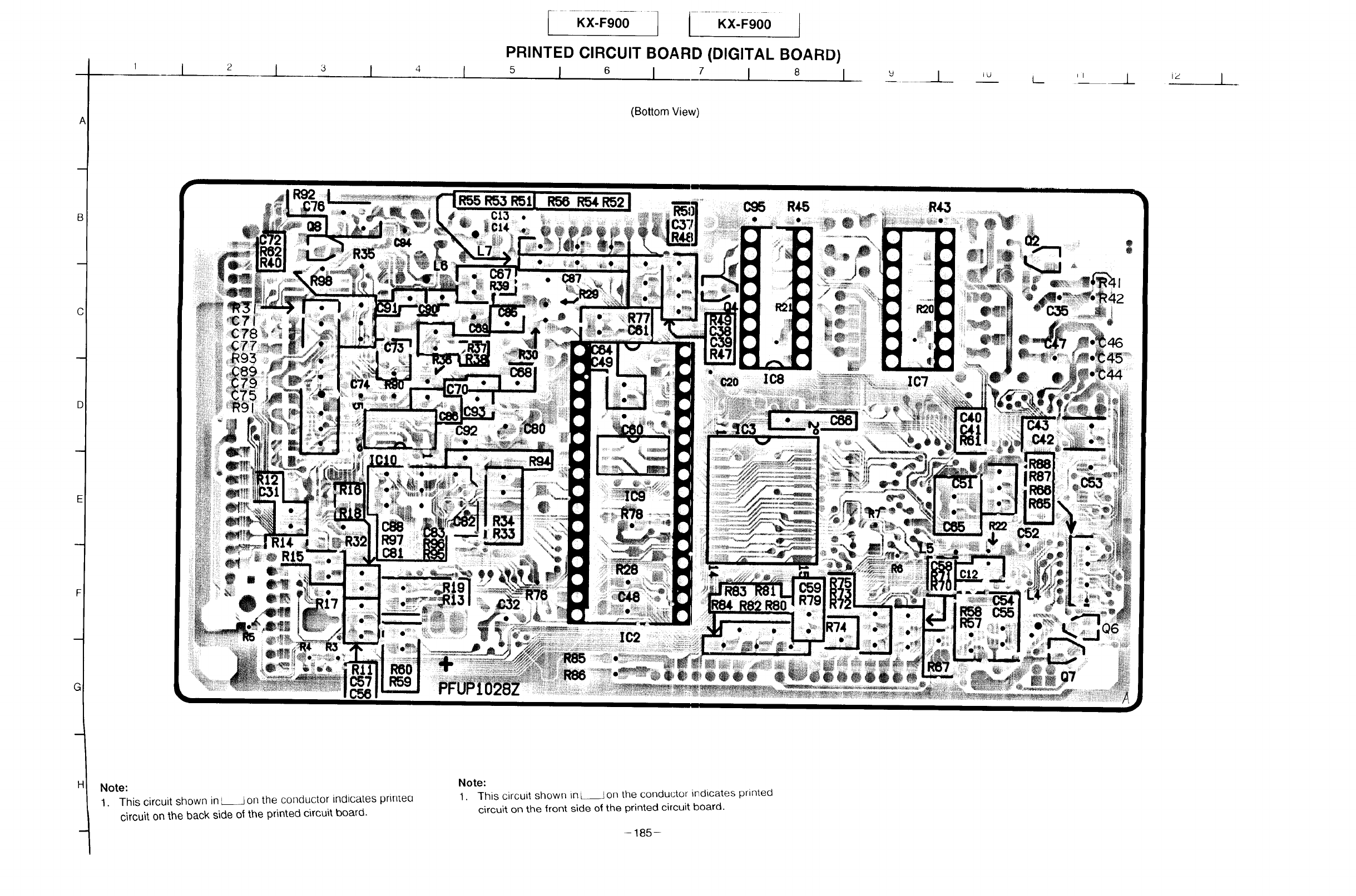
C
D
G
A
1 I 2 PRINTED CIRCUIT BOARD (DIGITAL BOARD)
5 I 6 I7 I 8
(Bottom View)
R55 R53 R5 R56 R54 R52
C13 • •
\
:I
_9
147
Note:
1. This circuit shown inL__] on the conductor indicates primea
circuit on the back side of the printed circuit board.
Note:
1. This oircuit shown in--on the conductor indicates printed
circuit on the front side of the printed circuit board.
@
m-185-
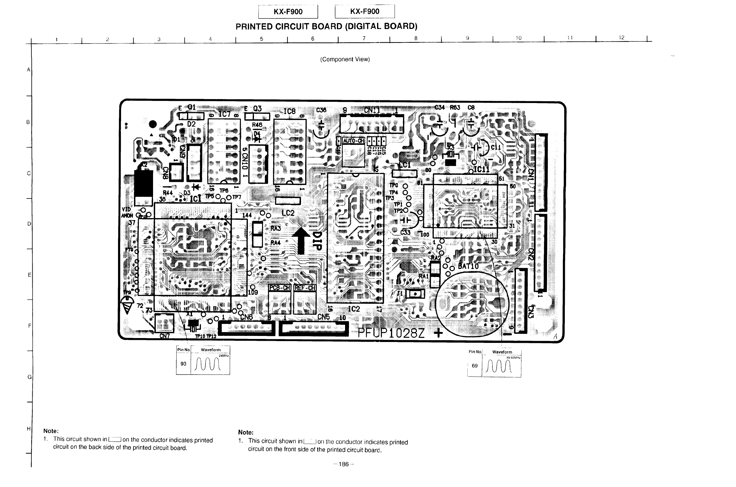
C
D
G
H
i I 2 I 3 I
iKX'FO001 1........ .... KX'_,O0---]
PRINTED CIRCUIT BOARD (DIGITAL. BOARD)
I 5 I 6 I 7 I 8 10 I 11
(Component View)
F
Note:
1. This circuit shown in _ on the conductor indicates printed
circuit on the back side of the printed circuit board.
Note:
1. This circuit shown in [___1 on the conductor indicates printed
circuit on the front side of the printed circuit boarcr.
-186-
12
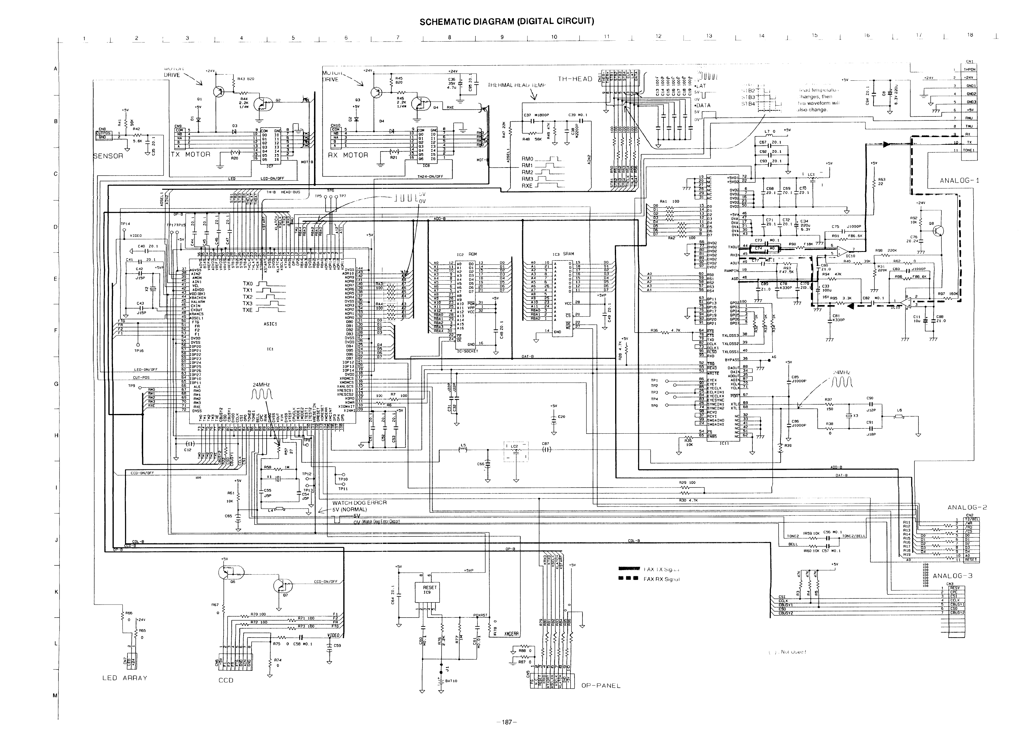
C
D
G
M
1L3 L 4 J_ _L_
SCHEMATIC DIAGRAM (DIGITAL CIRCUIT)
I 8 I 9 [ 10 I 11 __ 12 13 _ 14 j Ib 16 1/ 1 1u
ivlL, l i LJi
DRIVE _
. __ _
O!
÷5v
CNB R42
/S_o I B 2
3ENSOR v_ ITX MOTOR
+I<
TP14
VIDEO
C40 ZO. t
C42 *5VF
JI5P
C43
JI5P
+24V
03 --
v, lo I Do IO !7!-- IN2
tt lot zt s I !.;
12 IQ2 121 s I ir_
13 I 03 ][3 I 4 I _)rM(
_04 z4F-- _
ic7 I
LEO LED-ON/OFF /
LEO-0N/OFF
CUT-POS
TP9 (:> AM0
+SV
-t
o
CN9
Na _
NA 3
HEAD-BUS ,.# TP5
MU 1Uri..
[)RIVE _" "-4
03
+SV
(3
CNIO
NS _
NA 3
D 2
A !
RX MOTOR
[DP21
[DP22
[DP23
[DP24
[DP25
[0P26
[0P27
[OPiO
[OPt!
ALE
RMO
RM1
RM2
TP6
J
<
÷= i
ASICl
+24V
ICI
24MHz
TP7
+5V
_DVSS ADRIO
ADR9
AOR8
AOR7
AOR6
ADR5
ADR4
DVSS
ADR3
ADR2
ADRI
ADRO
DBO
DBt
DB2
OB3
DVSS
DVDD
DB4
DB5
DB6
OB7
IOPI2
IOP13
lOP!4
OVDD
XROMCS
XNOMCS
XANLGCS --
XRESCS!
XRESCS2
XORO
+24V
47u_
R×E _
D4 --
,.1 Io10% iol 7 l - B_,
!_ 16i lil 6IR_.,
1316_ i§1 _ I Ru0.
I_ ' =_--L_--405 15
4R_V_ 0_! NOTml
TH N/OFF
i
......JuuLo
II/ ApO-e
\AO 12
\ A4 B
\ A5 7
\A6 6
\ A7 5
\ All 25
\ A12 4
\RBAO 28
\RBAt 29
\RBA4 30
]c2 ROM
•AO DO 13 O0 /
At DI 14 01 /
A2 02 15 02 /
• A3 D3 t7 03 /
A4 D4 18 04 /
A5 D5 19 D5 /
A6 D6 20 06 /
A7 D7 21 [37 /
A8
A9 +SV
AiO PG'--M3t1..___
Art VPP _
AI2 iCE
AI3
A14
A15 .
A16 .
tB___ "_
__ u
OE GNn
IC-50CKET _7
I00 R7
5V
IHEHMAL HEAL.) iLMP
\
TH-HEAD
IC37 MIBODP C39 MO. t
R4B 56K E
RM0 .... _._[-!_
RM1 ___
RM2 __F-l__
RM3 _J---I__
RXE J---L_
<
o_i_#i_i_i<,,i,,itIOl/<,,,, oo888go8 <_
_I ....... ,LAT L, , , ......
I I I I I I I I I,I _Z£1_m_ 5V ;IB2T Lj h ,,Jd teliilJui,Jlu <
mJuuuuuuu --
I=r ,<,vU-
t'-LJ_,,t.i i J _ ,III1I.DA+A +_ B4_ l-! Ills waveform wili
"_ I I I_ It _TI _T I T_ I 5v _'_--_o-i olsochange.
\TTTT
_l_l_li\- ..... i i /,,. zo.,
lISt,ILl ........ +,zo.,! +v
II_FI_I_FI --- € ILC' -- I
_NC OVO;I TT TI
RA1 IO0 OVD,23 II I /
15 DO DVDI 5D 1 lli
.• }___
*5V .... +24V 2
o .o ,
5
6
I
I7
R63
22
\ AO I0
At 21A2 9
\ A3 8
\ A4 7
\A5 6
\ AB 26
\ A7 4
AS 5A9 25
\ AID 23
\ All 24
\RBAO 3
\RBA! 2
\RBA2 1
It3 SRAM
[
C
[
C
C
C
I
i
i
i
i
i
I
I
*5v
Q:
14
75
t2
11
D5
D6
66
B!
89
92
\AO 60
\AI 59
\A2 58
\ A3 57
\A4 56
63
+5v
14
DAT-B
A Ol 19
A Ol 1B
A OI 17
A Ol 16
A 01 15
A OI 13
A01 12
A01 11
A
A
A VCC ! 2B
A
A
A_g _01,___.__
A
WE _
-- GND
+5VF
J5
7
94
93
R35 _ 4.7K 64
82
52
55
53
B6
TP1 090
TP2 085
TP3 0
TP4 O 83
CNI
124V I
GNO!
GN02
GNO3
*SV
RNU
TMU
. R\
TX
TONE!
ANALOG- _
÷24V
-÷
0 !
:02 +SV/ 476 - " 7" R92 £
03 DVA _ l C7t lC 2 I+ C34
D4 DVA _-LZO. t -Lzo. I _ 22Du IOK _ 08
o, ov, ,ooo
07 OVA IC76
C73 == t40,1 _T-'----vvv-- ZO 24 _
44 r----'-'_ FIg0 F1BK Tr71 B . • r
OVO2 TXDU C74 NO. _ - _ 7 R 2 OK
pVD2 RXI_ __ _ IC!0 _vv',,
OYO2
4B I[I I _ I __
BS,, T_"v T T _- !°°u I I -- . 1oo
__ L_ I I !6VRs5 3.3K Ice_ No.1 I _ _ w,.-
oP!! 1oo Tn" 7-_ _ i ,, _ !_'-I ....
GP13 GPD; _ ''' _ i]m= vvv 41 ..Z._. ,._I' _ _lll. lll,i_ _+! 3=
GP16 GPD: 2 I -TJ/-/ I "_ .... 4_T
o., " b- - L
GPI9GPD! C 11 C88
GP2IGP20 GPo:GPO'_ _ _._ I _'_ K330P IOu _ :ZI.D
... _7 7
+5V
24Mitz
°°' /Wt
•Jiooo_ /
//
// R37 C90
TXLDSS"
TXD
DCLK _XLDSS2
DCLKI TXLDSSI
RXD
BYPASS
R_ DADUT
W-_ DAIF
ADOUI
EYEX ADIF
EYEY XCLk
;YECLK YCLk
;CLKINI
_YECLKX PORI
_YESYNC
4O
36 AG
B8 7"_ "
35
2_L
67
69
68
CCO-ON/OFF
CDL-B
66 _24V
•R65
D
fu
z
LED ARRAY
L5 :1 LC2
+5V
-_ (]20
TPD 0 2_
99
54
_,o_
3YNCINI XTL(
3YNCIN2 XTL1
_CVD
_CVI NC
ISWGAIND NC
!SMGAINI NC
L-- NC
ICS NC
ENB5 NC
32
41
42
51
tCO6
J!OOOP
L
150 J12P
c:3x3
R3B J- C91
_w II
0 dlBP
100 +5V
R61
!OK
C65
+SV
06
R67
O7
T_P_O
TPI 1
WATCH DOG ERROR
_5V (NORMAL)
___r-.V
_td_ Do9 E:rrcr 00;0r)
CCO-ON/OFF /
+SV
:ESET
c9
+SVP i
:...........L i CO7
_i (ii)
OP-B
oo_i
xx.J (-;
° °
.@D_0m_0 O0
I
R29 100
R30 4.7K
COL-B
II-AX IXSIg,,<.,
I•• FAX RX Sig:_al
ICll
AQ:Q-_
OA+-B __
i
ANALOG-2
ON2
i 3 IRD I
;R59 !OK C56 NO. I 4 /CS I
TONE2 TONE2/BELL 5 OnO0 i
BELL 7 02
8 D3
IR60 IOK C57 N0. I"g 04
AO
+5V
--I
CBUSY l
too
1oo
too
too
,oo ANALOG-3
tOO
tO0
SOD CN3
tO0
0 R70 tO0
R72 tO0
CCD
R71 iDO
R73 I_0
R75 OC58 MD.I
R74
D
FII
F2 /
FTG /
" BAT lO
PI_XRST
2
_o
o
R
OP-PANEL
\ CSI
CSDCBUSY2
1
2
3
4
5
t).Nut Oboe:
CPC
CSI
CCLK
CBUSYI
CSO
CBUSY;
187-
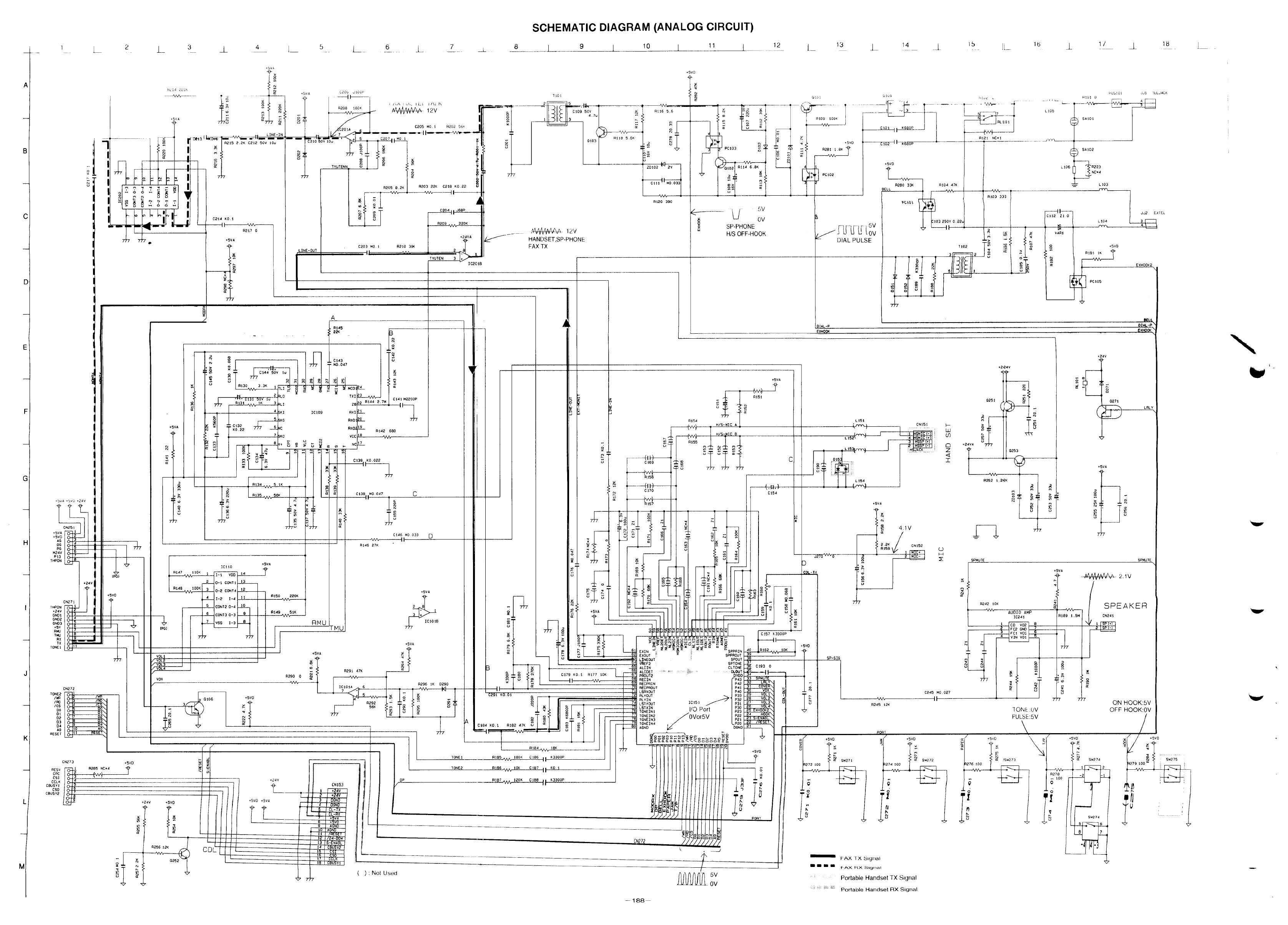
l
A
I
1
1 2 __ 3 __ 4 1__ 5 .... j__ _6 _L_ 7 _L 8
SCHEMATIC DIAGRAM (ANALOG CIRCUIT)
] 9 1 10 1 11 1 18
RII6 5,6
0169
Cl70
*5VD
4
Olol -_ _
I--T_- .....T-÷_,,......
o= 1
*5v0 C102 I
POt03 _ o "_ R28_ i.SK
N 4 *5VO
I _J_>[ _I 1 -I " I SELL R_81 31K I:1104 4:K
/I sV _
_-_ OV
0103 250V 0.22,
o s_._o,,,_ ,-,,,_,_,_v ; b_°,
DIAL PULSE
l102
w
c
÷l;/
OIAL-P
EXRO0_
LISt
L_ ) .......CN_.t.
•_! .....
_ !),_} I
+5VA
. 4,1V
2.2K CN152
R159
8
m
-'V_-.
_01
R_i N_!
_ ^€_¢N-----
L-,--
Ll05
L106
ll2 Zl 0
2"
(i
POSI0J Jj_ ILLJACK
__ 5Al01
__ SA102
R223
NCw4
_Ll03
JJ2 EXTEL
L_04 3
+5vo
._ PC105
EXHOOK2
X
8ELL
OIAL-p _
_XHOOK
i---
Iii
Z
T
+2_4V
0251 o
m _
•.v, % II
R252 i.2RK
_ m
+24V
0271
+5VA
-I
I_
o
o
LRL_
SPMUTE
+5VA
SPWUTE
-_ 2.1V
\
{
C157 K3300P
_ Z z =_= z _SPPRIN
_c EXOUT !! ! SPP_OUT
L_NE_T )! SPOUT 38 SP-SIG
64 V_EF2 SPTONE 37
--_ ALCIN CLTONE
ALCOET _" _:_ ........ _OUT
L _ PROUT2 DVOD
69 RECPRIN P42
70 RECRROUT P4_
71 LSRXOUT P40
72 PLYOUT P33
30 PLYIN P32 _ II V
74 LST×0UT ]CtS_ P3i 27 VOL3 R245 12K ON HOOK:5V
10NE:OV HO(
76 TONEINI I,_ FUll P23
77 TONEIN2 P22
-- 70 TONEIN3 /0Vor5V P2t
79 TONEIN4 /Lp20
AOND _DOND
d_ _ _ 0PgRT .
*5VD _+5VD
!5_273 SH274
_76 lO0 27'
OFF HOOK:0V
_j_ 5V Portable Handset TX Signal
0V
Portable Handset RX Signal
--188
2
KX-F900 KX-F900
PRINTED CIRCUIT BOARD (ANALOG BOARD)
5 I 6 I 7 I 8 I j._ ,1 [ IZ ./__
B
C
G
H
(Component View)
I
SAIOL
0
_102
L106
R103
R'N6
EXT TEL N
PCI05 PC101 PC102
1029Z
ztet
JlSO ¢N151
189-
.....KX_Fg001I KX:FgO_.....
PRINTED CIRCUIT BOARD (ANALOG BOARD)
I 5 I 0 I 7 I 8 10 11 12
B
G
(Bottom View)
_i_, ....
I
D101 L103
A
_190
A
B
C
G
I..-L._ L_ _ __J
CCD BOARD
(Component View)
(Bottom View)
KX-F900 1 KX-F900
PRINTED CIRCUIT BOARD AND SCHEMATIC DIAGRAM (CCD)
I 5 I 6 I 7 I 8 I 9 10 11 I12
CCD CIRCUIT
__-L_.F-q_.F-L
_H.FL_FLJ3d3d3_
_G_IN --I F t.:,_,,,_S___lL
I........ I
9.216 ms
_-SV
4
5
6
0;' __
RB03
JO
COD
1208
lVDD
% 2
4_S
2t SH
VSS
NC
NC NC
-- NC NC
NC NC
NC NC
NC NC
NC NC
NC
DOS
OS
o
22
3.5V /
3.5V_ _[ 0.5_0.6V
b
9.216 ms
e3
u
@
o
I-- o
RB02
o o
,q _ [ -- --
_ E
2K
R801
2K
i %s[
oV I
i
9.216 ms
/
o
o -t
_ o_ -
_BO
191 -
I KX-FgOO11 KX-FO00
PRINTED CIRCUIT BOARD (SWITCHING POWER SUPPLY)
4 I s I o I 7 I 8 I 10 11 .... j12
A
C
D
E
(Component View)
(_ CN31
PC102 0102 .
PRIMARY
-.NV-
......
8 CN302 I : R202 ...........
(Bottom View)
.....
DIOI
mmmm
192-
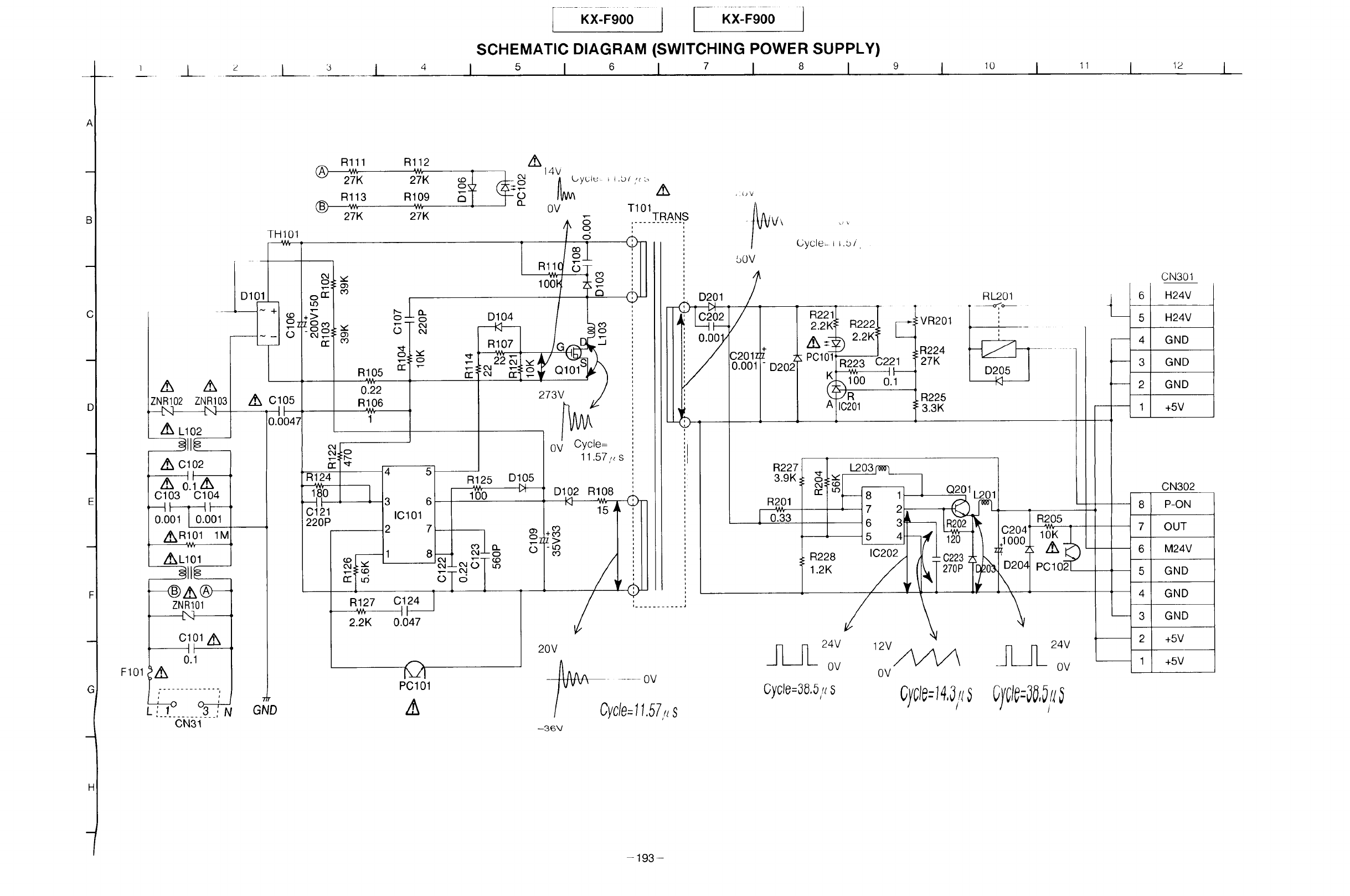
J
I....Kx-F90oI l---K-x-Fg00I
SCHEMATIC DIAGRAM (SWITCHING POWER SUPPLY)
5 I 6 I 7 I 8 I 10 11 12
A
B
C
G
F101
THI01
-I 0
ZNR102 ZNR103
Z_ C102
C103 C104
0.001F_0.001
z_R101 1a
Z_L101
----@_(N---
ZNR101
C101 /_
0.1
CN31
,/_ C105
, II
0.0047
GND
Rlll
Rl13
27K
4
3
IC101
2
• rrl_
R127 C124
2.2K 0.047
100k
D104
50V
CN301
H24V
5 H24V
4 GND
3 GND
2 GND
1 +5V
CN302
8 P-ON
7 OUT
6 M24V
5 GND
4 GND
3 GND
2 +5V
1 +5V
-193-
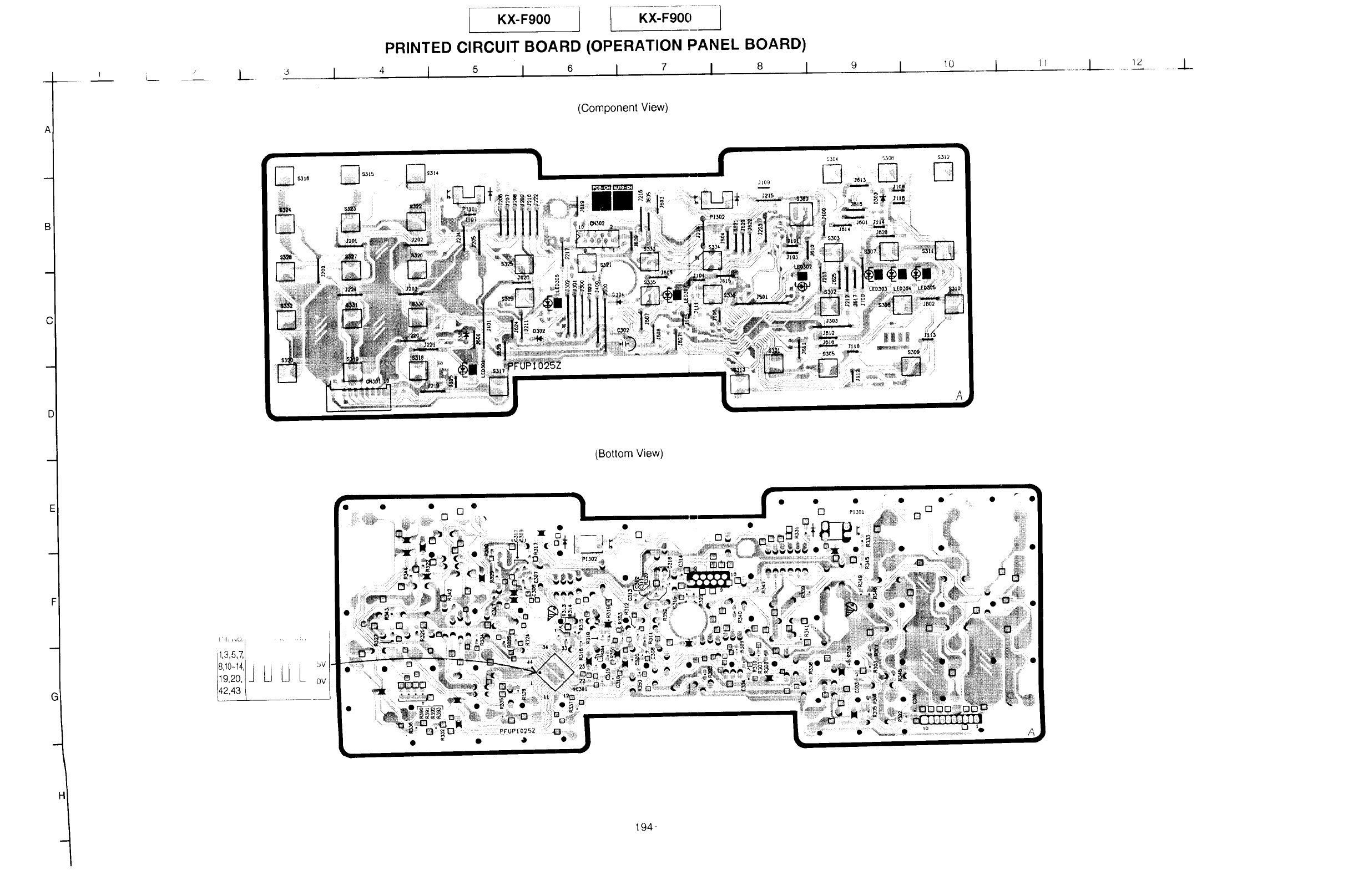
A
C
i__ L
1,3,5,7,
8,10-14,I |
1_9,2o,/J
_t2''_/
PRINTED CIRCUIT BOARD (OPERATION PANEL BOARD)
4 I s I 6 I 7 I 8 I
(Component View)
lO
(Bottom View)
bV
0V
!! o ¸
o
• • • • []
194
[]
l1
A
L .... 12 ...... _.L
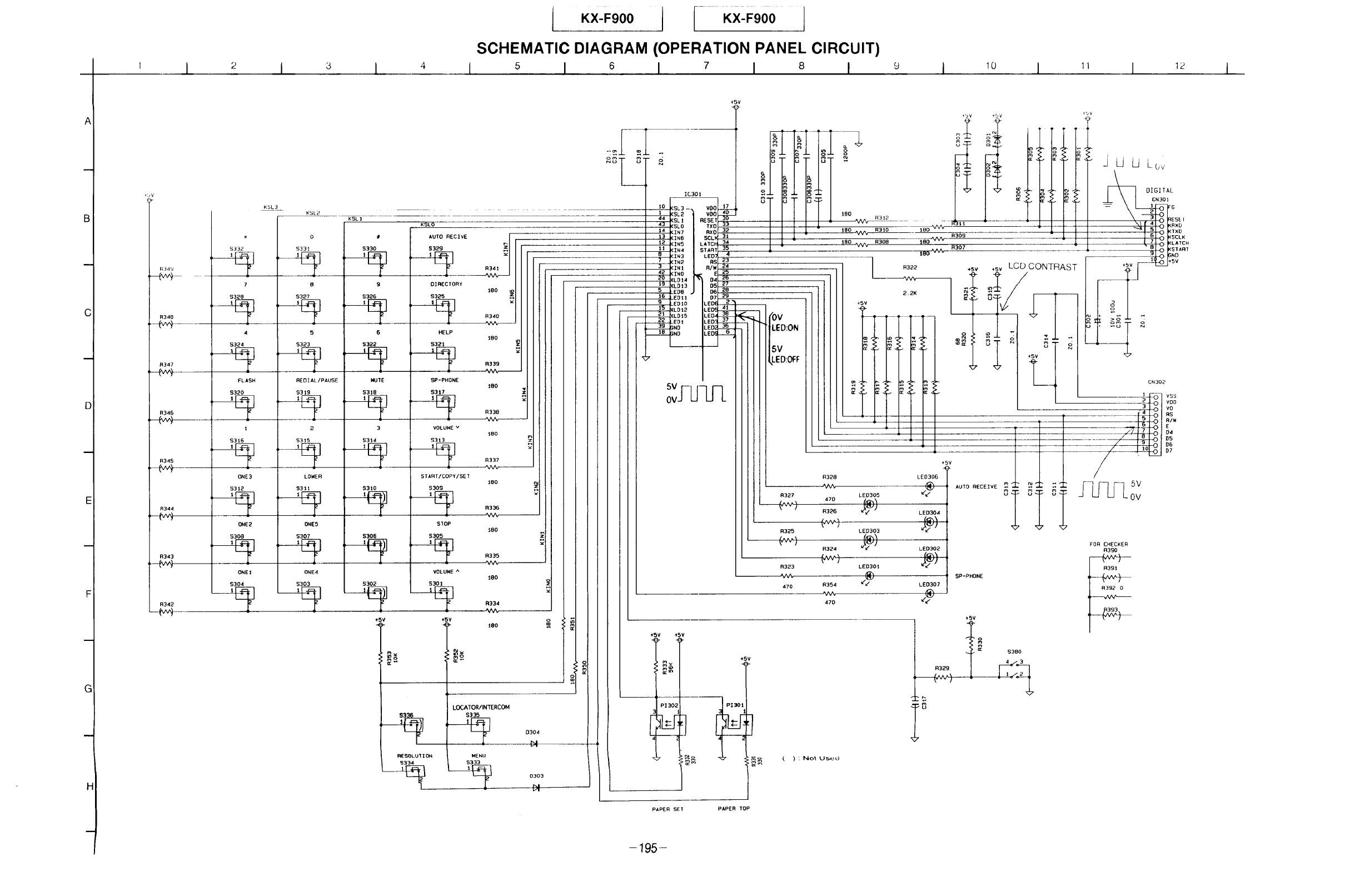
JKX-F900 I- Kx-Fg00
SCHEMATIC DIAGRAM (OPERATION PANEL CIRCUIT)
5 I 6 I 7 I 8 I 10 11 12
A
C
D
G
R349
R348
R347
R346
R345
R344
R343
R342
5332
7
5328
4
$324
FLASH
$320
5316
ONE3
5312
ONE2
5308
ONE 1
$304
KSL2
KSLI
o
$33!
8
5327
5
$323
REDIAL/PAUSE
5319
2
5315
LONER
531t
0NE5
$307
0NE4
5303
#
5330
9
5326
6
5322
MUTE
5318
3
5314
S3tO
5306
5302
+5V
KSLO
AUTO RECIVE
$329
OIRECIORY
$325
HELP
5321
SP-PHONE
$317
V0LURE v
$3t3
5TART/COPY/SET
S309
STOP
$305
VOLUNE _
5301
+5V
J
_eo
R340
150
R339
180
R338
'kA/',,,_
180
R337
IBO
R336
'VV'v---
180
R335
'VVV
_80 o
R334
leo
_g
LOCATORilNTERCOM
$33_ 0304
bl
RESOLUTION MENU
5333L_ 03o3
DI
+SV
. z. c3_ol
o
+bV
190 VVV- 1309
180 V'v%
1307
180
R322
+5V
_ m m'
R328
LED305
470 f,G_
R326 _J)
(_,_)
+SV
LE0306
LEO304
(,_
vo0 17
vo0 AO
:SET
"TXO 33
RXO 32
5CL 31
_TC 34
TART 35 4
LED 234
R$
05 27
06 28
07 29
LED 2 _
LEO 41
LEO 38 _ /OV
LED 37 --
,ED 36 LED:ON
5V
LED:Of:F
R394
LED303
_bV ,by
J LJ LJ L_,v,
KSL_ --_
K5L2 |
KS[ II
KSL0 I
KIN/ I
KIN_ I
KIN5 I
KIN4 I
K]N:_ I
KIN2 I
KIN1 I
KINO •
XLDI4 1
XLD13 I
LED8 J
IEOll
LEDIO
XLDI2
--XLD_5
LED|
GND
GND
al;l TXO
6SCLK
8_ START
9 NO
+SV 1+5V
EN302
i!l V55
VOD
VO
RS
R/_
-- E
D5
D6
D7
R325
-----_)
R323
470
_y'J
*sv ,_sv LCD CONTRAST
R354
470
LED301
LED302
(,G',_
LEO307
m_
AUTO RECEIVE _=
_z
SP-PHONE
i
,2,_ 8_ OV
_7 _
+5V +5V
oct_
=I30_ 1
+5V
4_I30
_o ( ) : NOt US,_G
+SV
m 5380
R329 4_ 7
2_
FOR CHECKER
R350
R3gl
R392 0
PAPER SET PAPER TOP
-195-
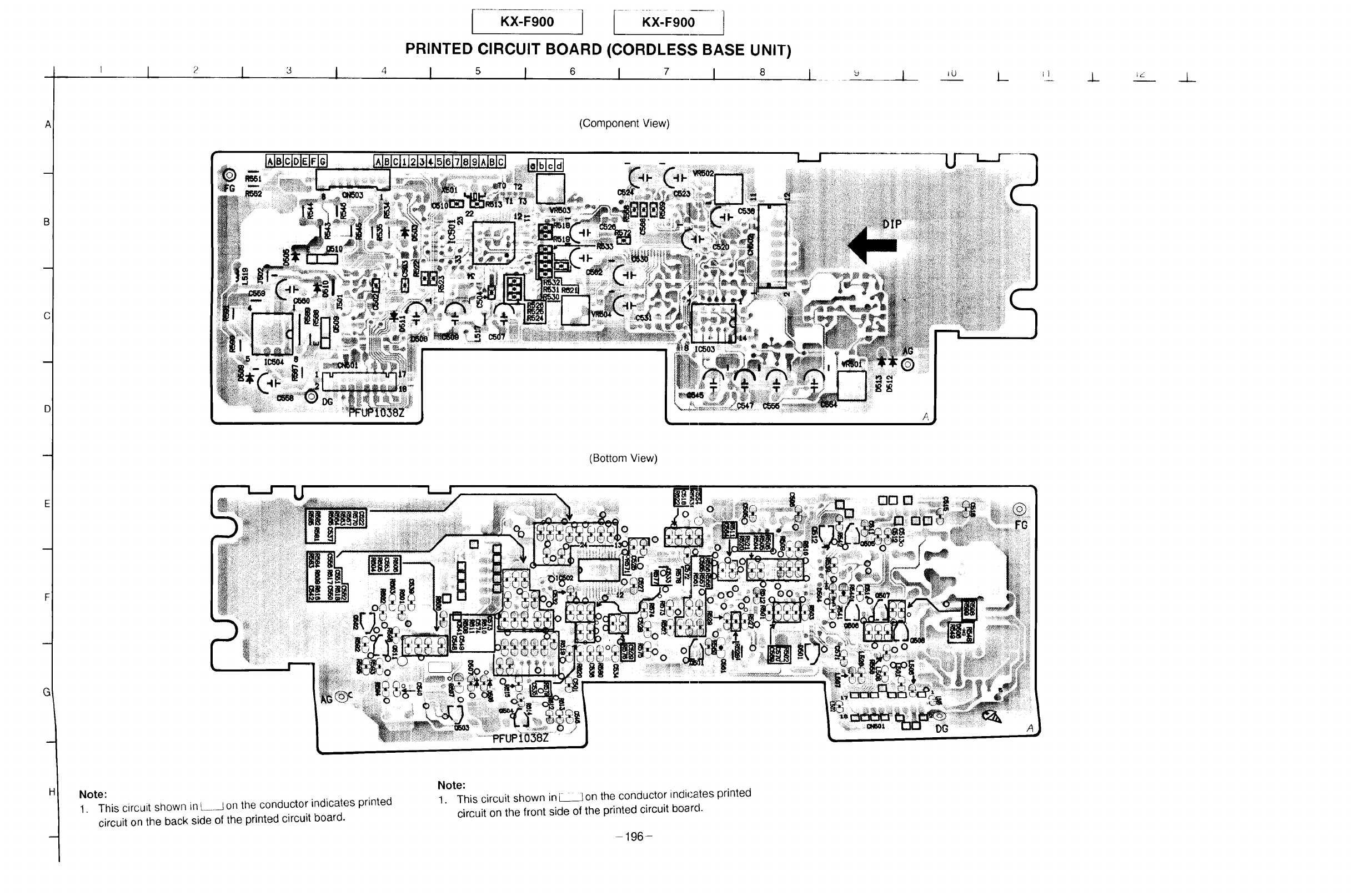
4
f oo I....... I KX.FgOO-¸ ]
PRINTED CIRCUIT BOARD (CORDLESS BASE UNIT)
s I 6 I 1_ IU 1_L_ ;¢Z _L_
B
C
D
G
Note:
1. This circuit shown in ___1 on the conductor indicates printed
circuit on the back side of the printed circuit board.
(Component View)
(Bottom View)
! i OO []
Note:
1. This circuit shown in _ on the conductor indicates printed
circuit on the front side of the printed circuit boarcl.
-196-
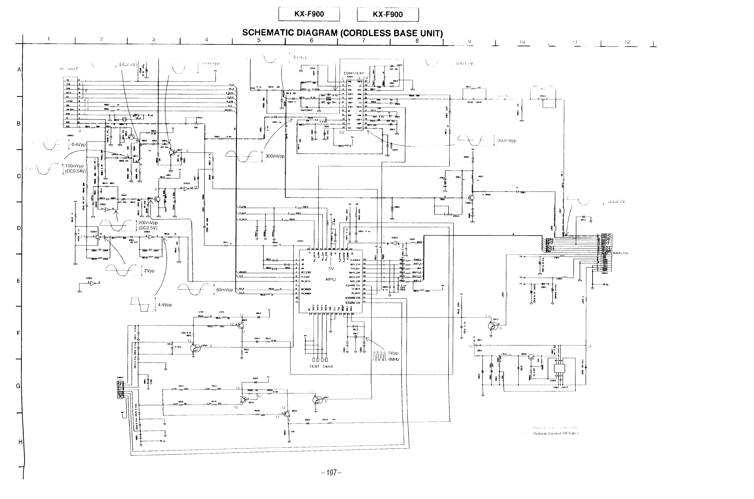
[ Kx:_,oo1 Kx:_;oo I
SCHEMATIC DIAGRAM (CORDLESS BASE UNIT)
s I 0 I7I8I_J_ '° ,_ " I 12 _L
-107-
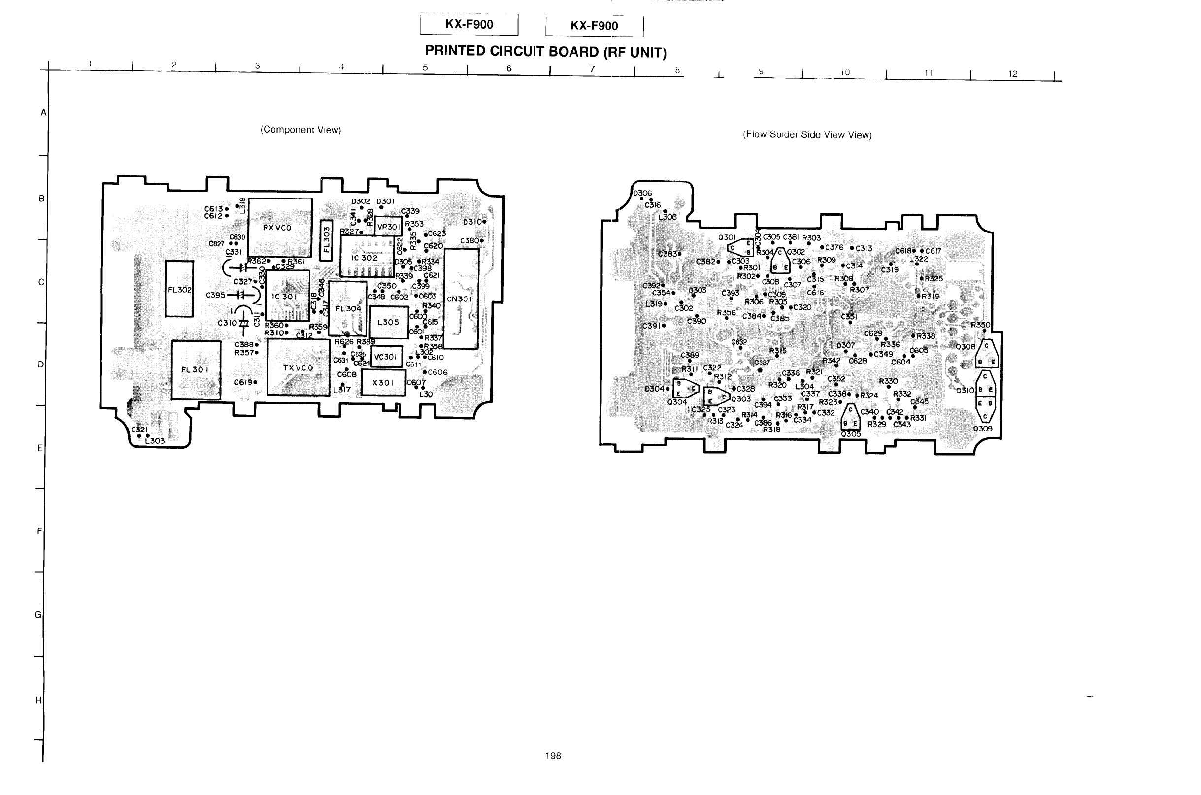
2 1 ,3 I 4 I
KX'F900 KX-F900-
PRINTED CIRCUIT BOARD (RF UNIT)
5I6I7I_1_ i ........ IL) __1 11 12
A
B
C
F
G
C613e
C612 •
(Component View)
ii!iti¸ i
D302 D301
IC 302
¢6 ii
198
(Flow Solder Side View View)
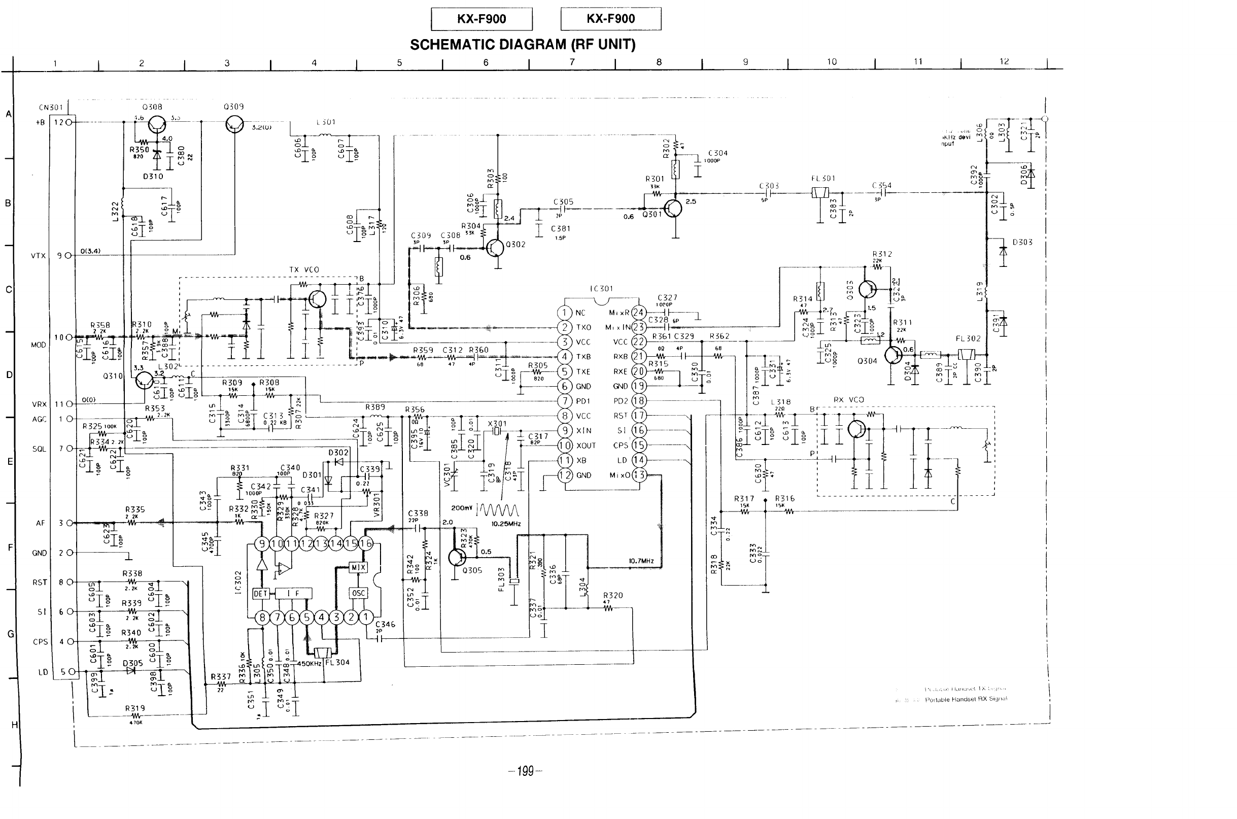
5
KX-F900 I KX-F900
SCHEMATIC DIAGRAM (RF UNIT)
I6I 7 I 10 11 12 L__
CN301
9(
i
0308 Q309
D310
C304
_ _OOOP
Z
C303
IF
5P
,o L 31B RX VCO
R338
22
o
2.0 10.25MHz
10.TMHz
I
R320
4"/
i..........
;;Pollabie Handset AX Signal
-199-
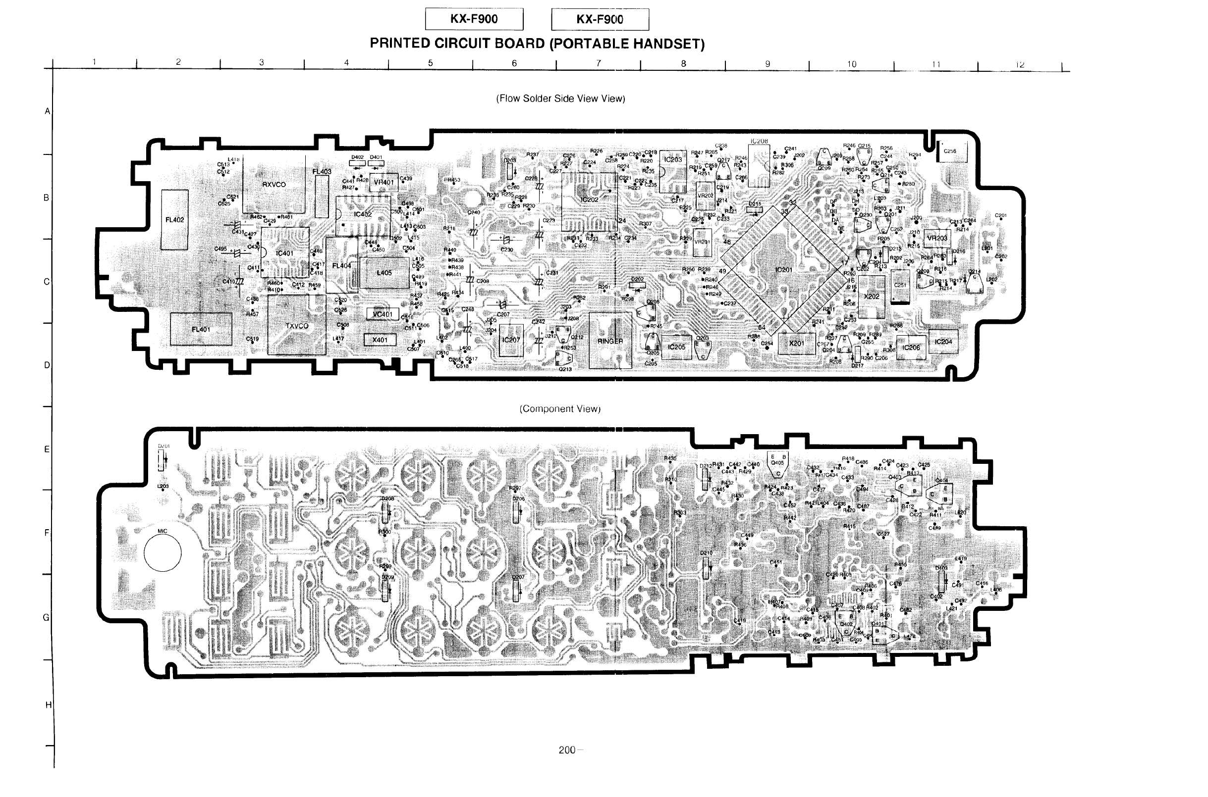
KX-F°00i I "X-Fg00']
PRINTED CIRCUIT BOARD (PORTABLE HANDSET)
I 5 I 6 I 7 I810 11 i2
A
G
i !
(Flow Solder Side View View)
(Component View)
-200
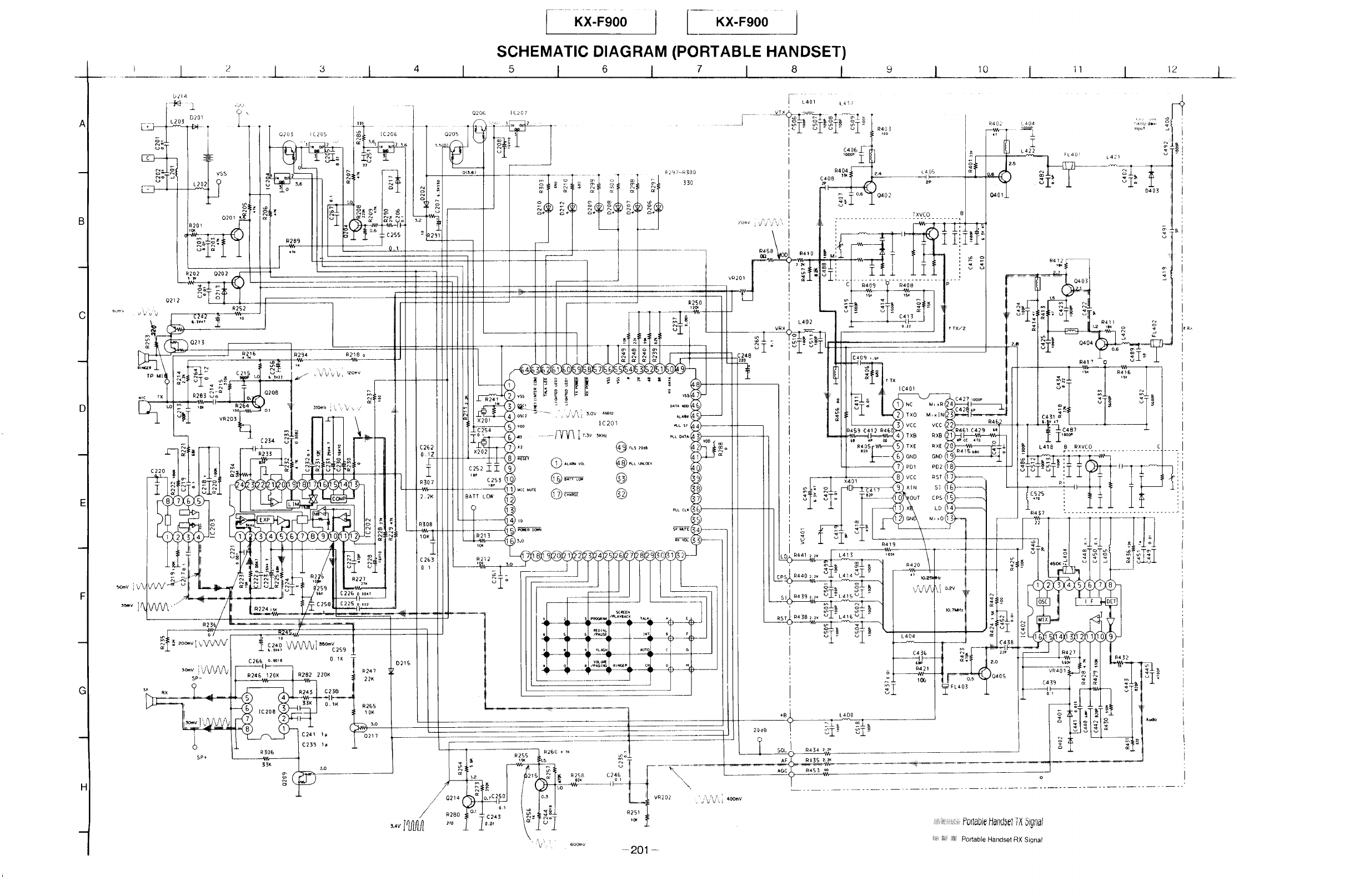
R218 o
C220
_247
22K
R2G£
1 OK
SP+
C241 1_
C259 1.
KX-F900 J 1 KX-Fg00 J
SCHEMATIC DIAGRAM (PORTABLE HANDSET)
I 6 I 7 I 8 I
1L207
IO
33O
C40G
_ooop _j-
R404
£_OB
TXVCO
R402 C404
I
L422
R250
:248
L402
R212
IC201 _L s_
,(
i
}3,o
t255
u
C246
20dB
+B
TXO
VCC
TXB
) TX[
) G.D
PD1
VCC
X401
M,_IN(
VCC (
RXB (
PD2
RST (
L400
o
FL401 L421
D403
R412
L_
&
L ............
o
R432
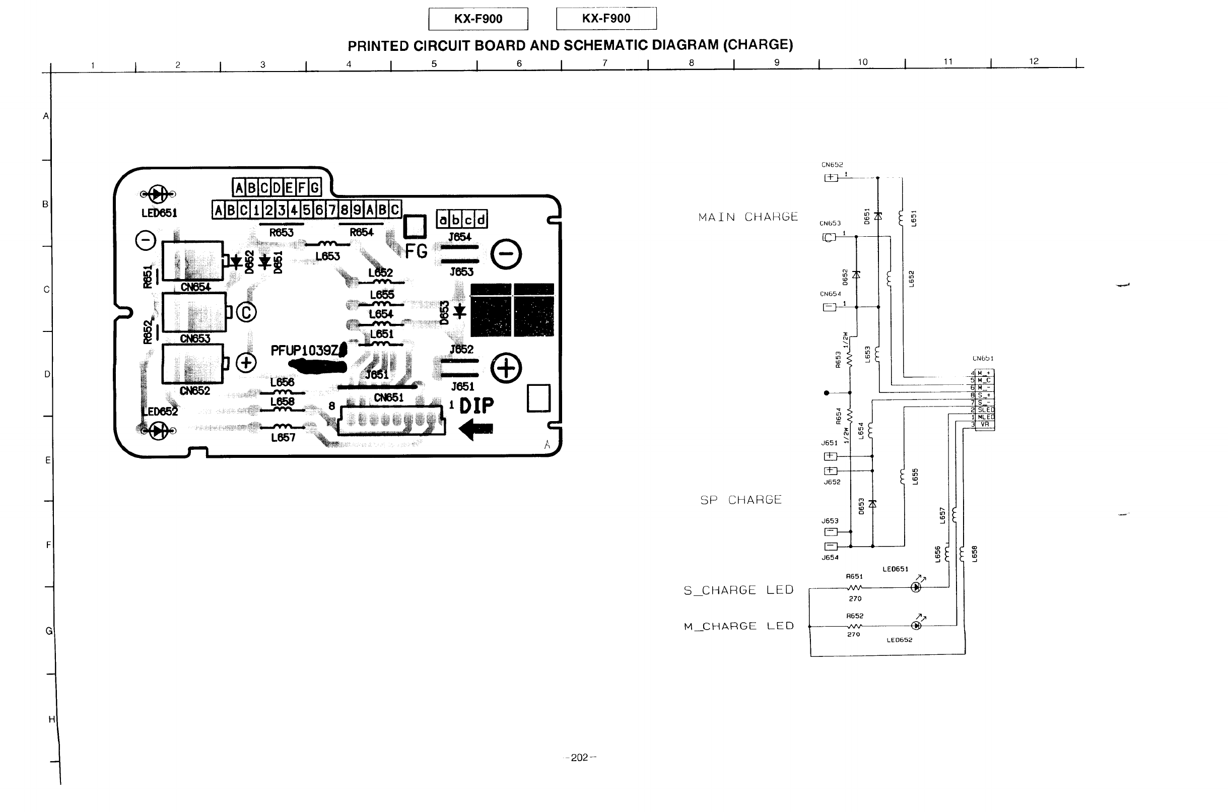
KX-F900 KX-F900
PRINTED CIRCUIT BOARD AND SCHEMATIC DIAGRAM (CHARGE)
4 I 5I6I 7 I 8 I 9 10 11 12
C
G
LEl)651
I^IBIclDIEIFIoI,
IAIBIclII2bI41sI61 IsIglAIBIcI__
,DIP
L65"/
MAIN CHARGE
SP CHARGE
S_CHARGE LED
M_CHARGE LED ,
CN652
CN654
0---
J551
EEl-- -
EEF----
J652
o
J653
E3
J654
R65t
270
R652
,/vv
27o
LF)
I,p
.J
tO
.J
LE0651
LED652
CNbb 1
ID
-J
_202 -
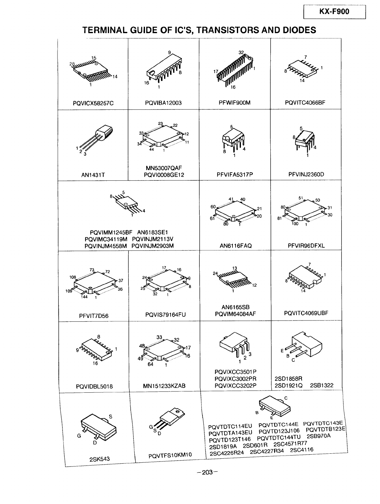
KX-F900
TERMINAL GUIDE OF IC'S, TRANSISTORS AND DIODES
15
2_14
1
PQVICX58257C
AN 1431T
9
1
PQVIBA12003
23 22
33_12
44 1
MN53007QAF
PQVI0008GE12
5
PQVlMM1245BF AN6183SE1
PQVIMC34119M PQVlNJM2113V
PQVINJM4558M PQVlNJM2903M
73 72
10_37
109<'_'_ _"....... 36
144 1
PFVIT7D56
8
16
PQVIDBL5018
32 1
PQVIS79164FU
33
48_17
4_..--76
64 1
MN 151233KZAB
D
2SK543 1
pQk/TFSIOKM10
32
_" 16
PFWlF900M
1
PFVIFA5317P
60_ 21
AN6116FAQ
24
12
1
AN6165SB
PQVIM64084AF
1
PQVIXCC3501 P
PQVlXC3002PR
PQVIXCC3202P
7
14
PQVITC4066BF
5
1
PFVINJ2360D
51
80_31
81_ .-'_ 30
100 1
PFVIR96DFXL
7
14
PQVITC4069UBF
2SD1858R
2SD1921Q 2SB1322
E
pQVTDTCl14EU PQVTDTC144E pQV3-D-I-C143E
pQVTD'IA143EU PQVTD123J106 PQVTDTB123E
pQVTD123"I"146 pQVTDTC144TU 2SB970A
2SD1819A 2SD601R 2SC4571R77
2SC4226P,24 2SC4227R34 2SC4116
-203-
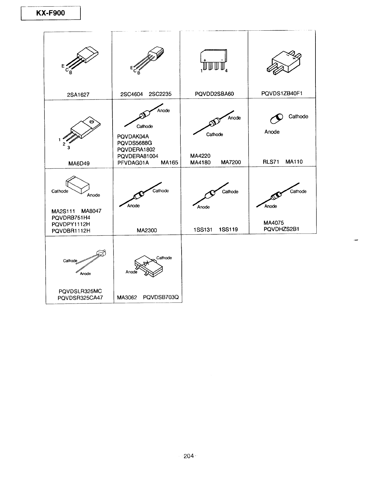
KX-F900 )
2SA1627
3
MA6D49
Cat h°de@Anod e
MA2Slll MA8047
PQVDRB751 H4
PQVDPY1112H
PQVDBR1112H
Cathod_
PQVDSLR325MC
PQVDSR325CA47
2SC4604 2SC2235
MA165
PQVDAK04A
PQVDS5688G
PQVDERA1802
PQVDERA81004
PFVDAG01A
ode
MA2300
PQVDD2SBA60
Cat,__h_ An°de
MA4220
MA4180 MA7200
Cathode
PQVDS1ZB40F1
(_ Cathode
Anode
RLS71 MAll0
hode
Anode
MA3062 PQVDSB703Q
1SS131 lSSl19
MA4075
PQVDHZS2B1
204-
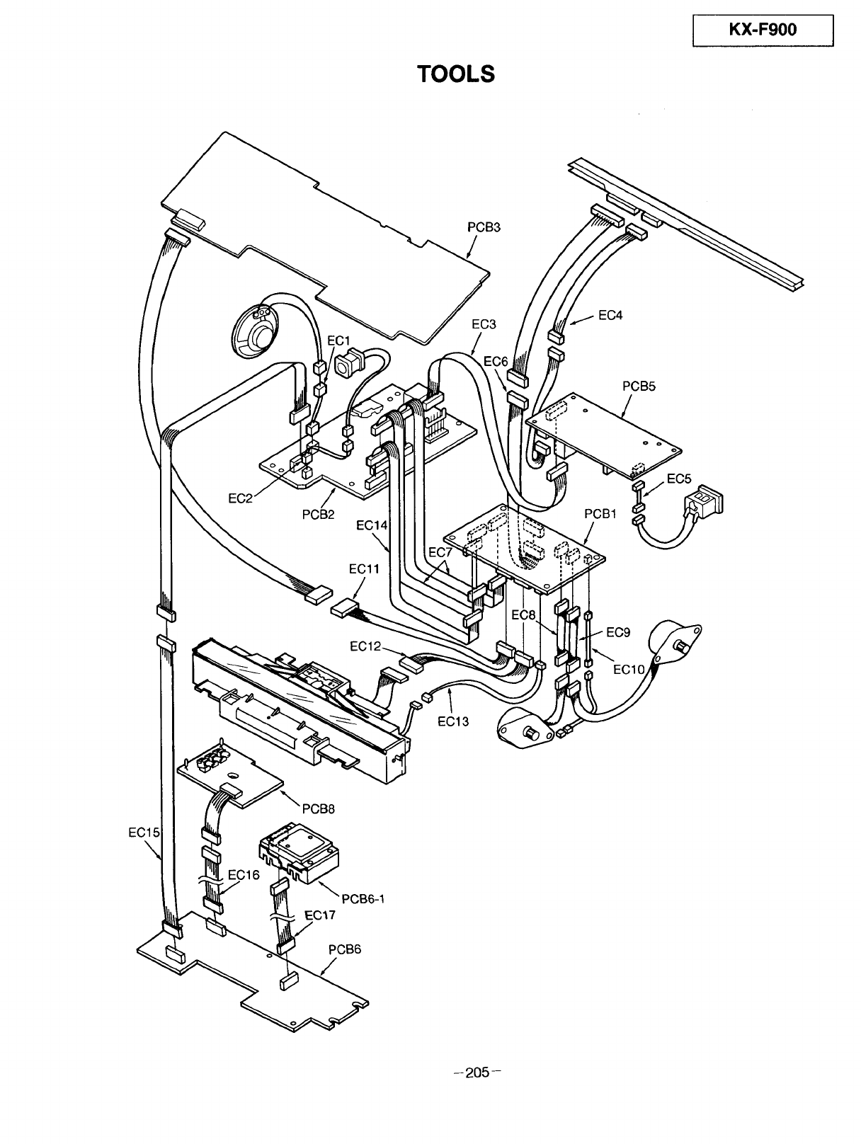
TOOLS
J KX-F900
PCB3
/
ECl
EC3 EC4
PCB5
o
EC2
PCB2 EC14
EC11
PCB1
,EC5
EC1
PCB8
6
""" PCB6-1
EC17
EC13
PCB6
-205-
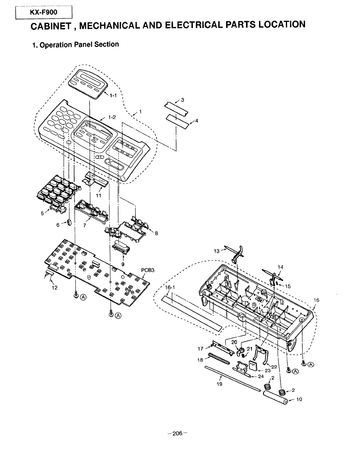
--r_0o.......I
CABINET , MECHANICAL AND ELECTRICAL PARTS LOCATION
1. Operation Panel Section
I
i
12
®
t
9
17
14
/
/I
//
- 206-
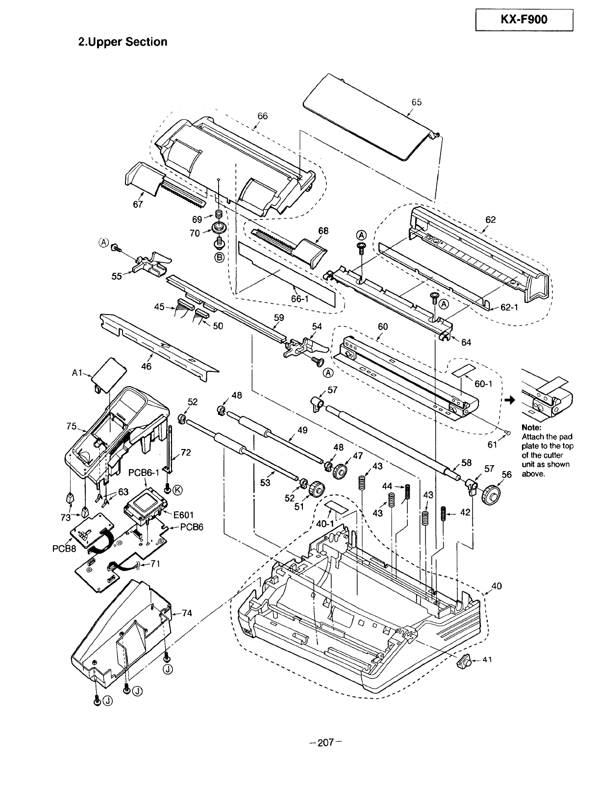
2.Upper Section
JKX-F900 J
®
55
A1
67
®
52 /
66
65
I
/I
/
/
¢
/
/
68 (_) ;
49
i /
,;40-'
62
62-1
/
64
57 56
42
Note:
Attach the pad
plate to the top
of the cutter
unit as shown
above.
I
-207-
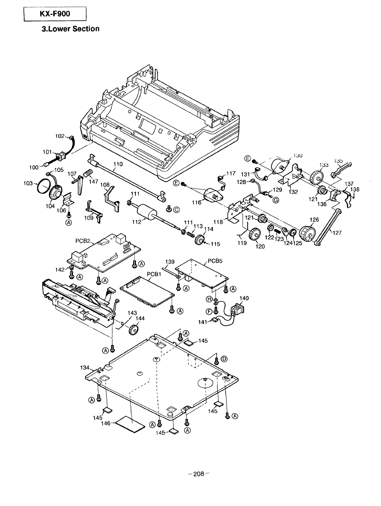
[KX-F900
3.Lower Section
147 108
®
(_) 139 PCB5
/144
®
®
(D' 140
@
®&
1
&
®
145
120
127
137
138
- 208-
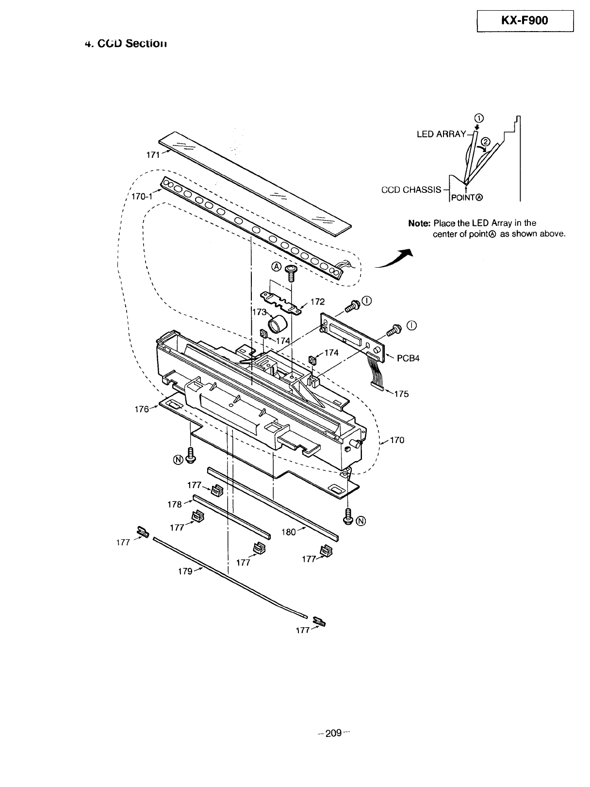
_. C(.;i3 SecI:io=_
IKX-F900 I
LED AR_
COD CHASSIS 1 POitNT(_
Note; Place the LED Array in the
center of point® as shown above.
172 (_
177
-209 --
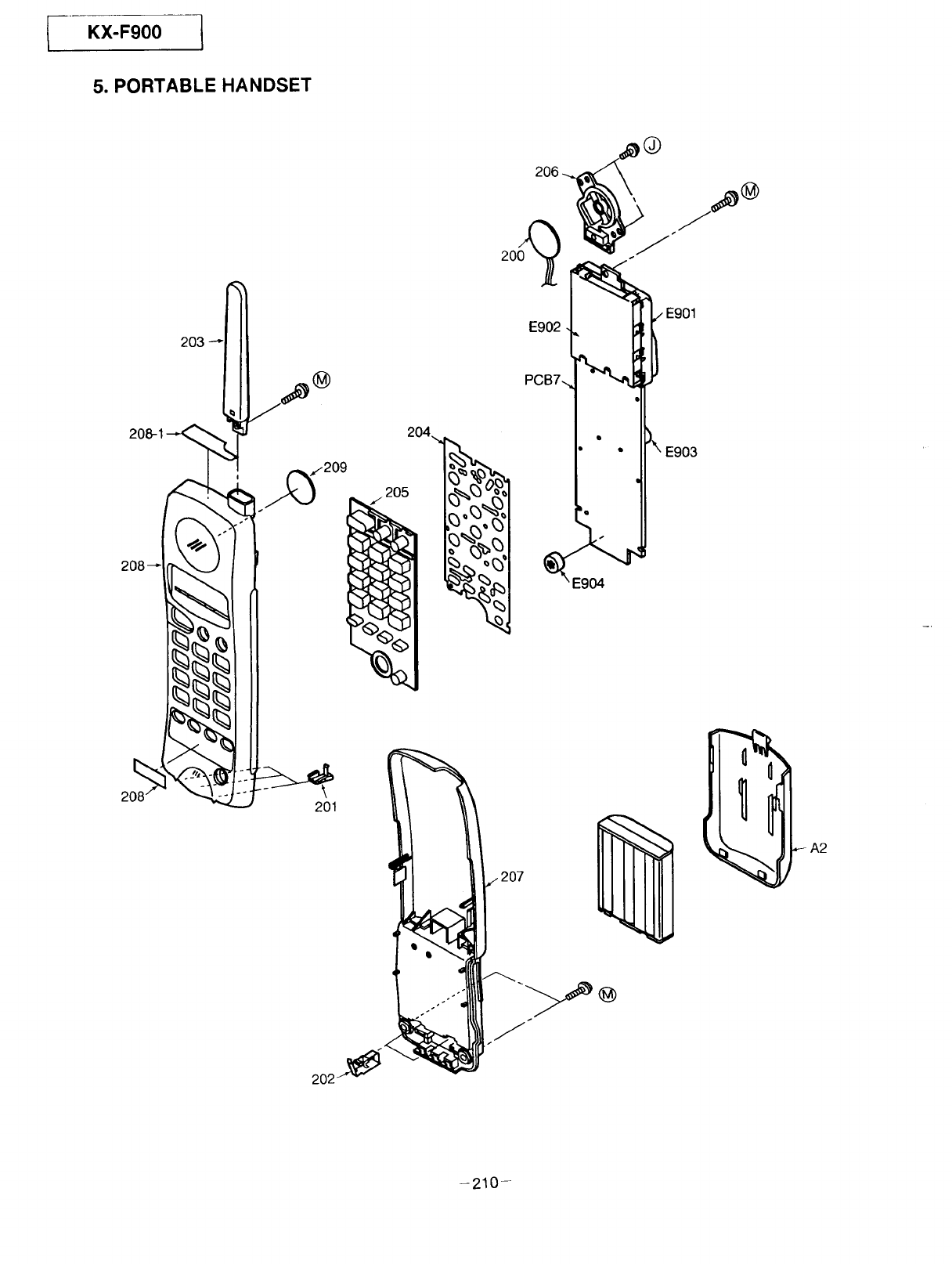
KX-F900 1
5. PORTABLE HANDSET
208-1
208
204_
205
206
E902
E903
208 201
A2
20;-
-210-
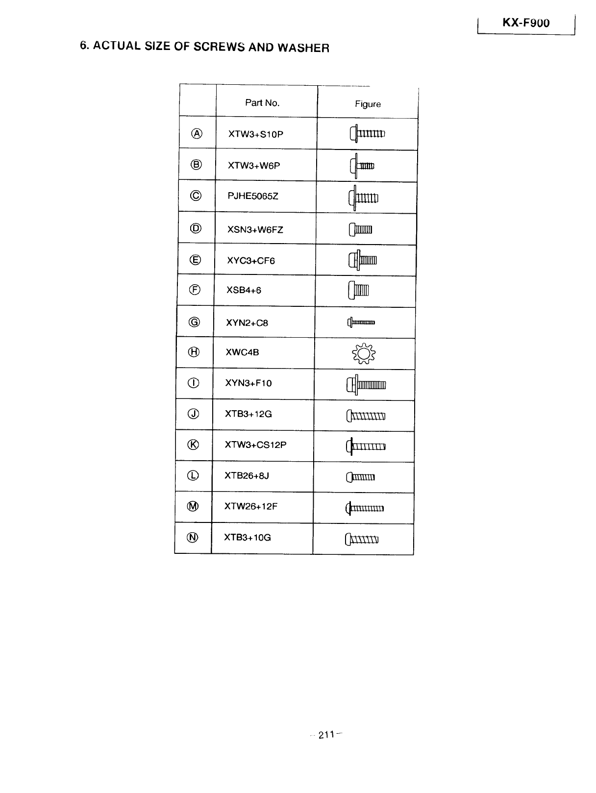
IKX-F9O0
6. ACTUAL SIZE OF SCREWS AND WASHER
Part No. Figure
(_) XTW3+Sl OP
(_ XTW3+W6P
(_ PJHE5065Z
(_) XSN3+W6FZ [_]]]]]]]
(_ XYC3+CF6 _]]]]]
(_ XSB4+6
(_ XYN2+C8 I_ _
(_ XWC4B
(_ XYN3+FIO _]]]]_]_
(_) XTB3+ 12G
(_) XTW3+CS12P
(_ XTB26+8J 0]]]]]_
(_ XTW26+12F
(_) XTB3+ 10G {_]_333_
• 211-
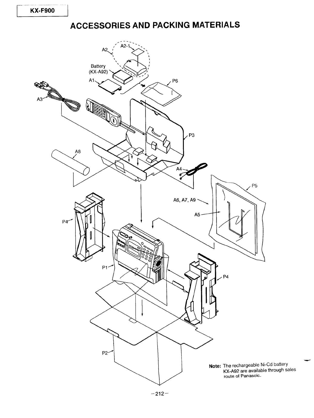
_-....KX-Fg_00I
ACCESSORIES AND PACKING MATERIALS
A2_,'
Battery
(KX-A92)
P6
P3
P1
A6, A7, A9
P4
P5
Note: The rechargeable Ni-Cd battery
KX-A92 are available through sales
route o4Panaso_c-
-212-
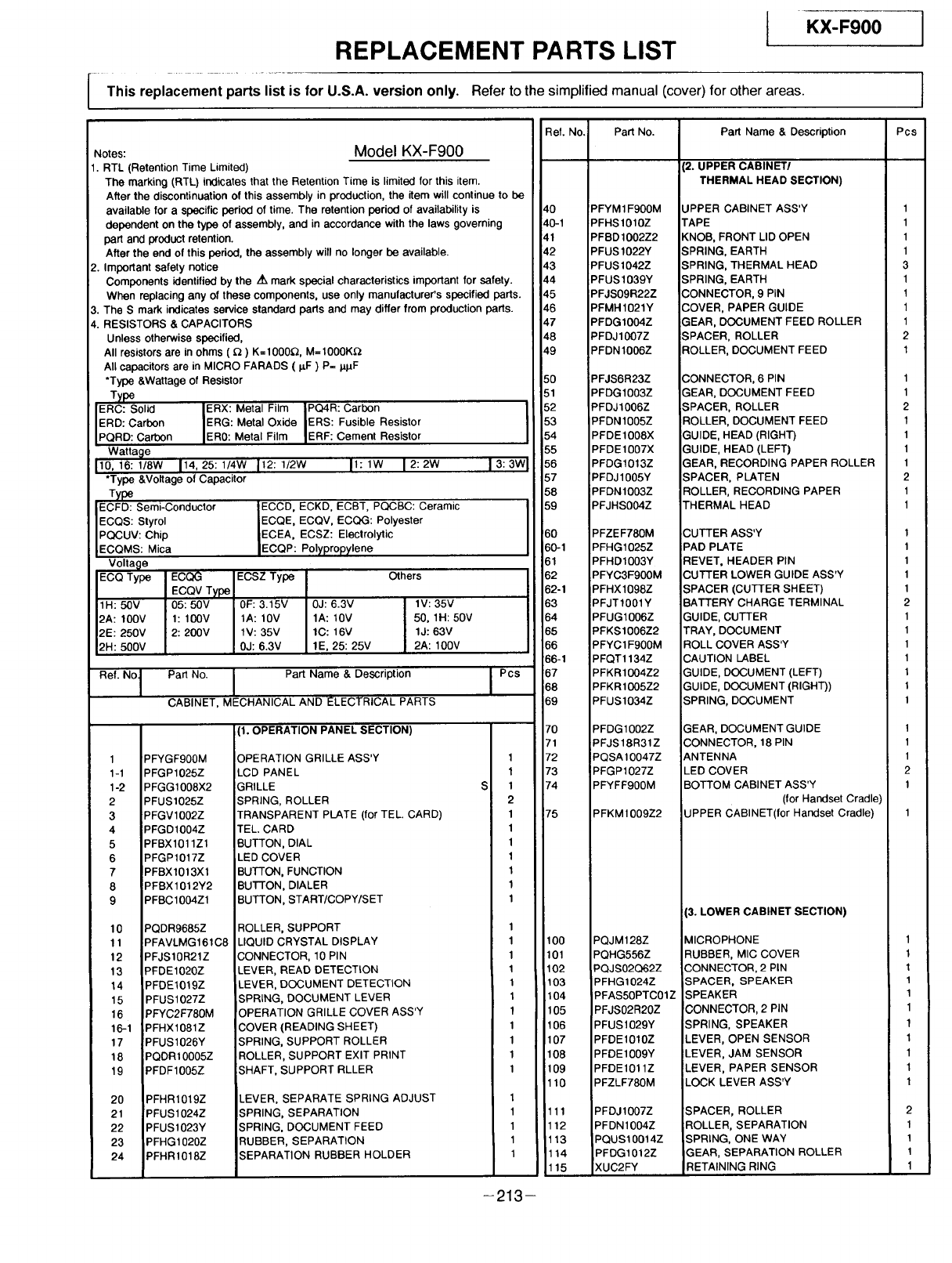
KX-F900
REPLACEMENT PARTS LIST
This replacement parts list is for U.S.A. version only. Referto the simplified manual (cover)for otherareas.
1
Notes: Model KX-F900
1. RTL (Retention Time Limited)
The marking (RTL) indicates that the Retention Time is limited for this item.
After the discontinuation of this assembly in production, the item will continue to be
available for a specific period of time. The retention period of availability is
dependent on the type of assembly, and in accordance with the laws governing
pert and product retention.
After the end of this period, the assembly will no longer be available.
2. Important safety notice
Components identified by the Z_ mark special characteristics important for safety.
When replacing any of these components, use only manufacturer's specified parts.
3. The S mark indicates service standard parts and may differ from production parts.
4. RESISTORS & CAPACITORS
Unless otherwise specified,
All resistors are in ohms ( _ ) K=1000_, M=1000K_
All capacitors are in MICRO FARADS ( pF ) P= I_I_F
*Type &Wattage of Resistor
Type
ERC:Solid [ERX: Metal Film IPQ4R:Carbon I
ERD: Carbon IERG: Metal Oxide _ERS: Fusible Resistor
PQRD: Carbon IER0: Metal Film _ERF: Cement Resistor
Watta_le
110.16:f/sw 114,25:f/4w 112:t/2w It: 1w 12:2w 13:3wI
*Type &Voltage of Capacitor
Type
ECFD: Semi-Conductor IECCD, ECKD, ECBT, PQCBC: Ceramic
ECQS: Styrol IECQE, ECQV, ECQG: Polyester
PQCUV: Chip _ECEA, ECSZ: Electrolytic
ECQMS: Mica |ECQP: Polypropylene
Volta_le
ECQ Type
1H: 50V
2A: 100V
2E: 250V
2H: 500V
Ref. No 1
1
1-1
1-2
2
3
4
5
6
7
8
9
10
11
12
13
14
15
16
16-1
17
18
19
20
21
22
23
24
ECQG I ECSZ Type
ECQV Type I
05: 50V IOF: 3.15V
1: 100V ItA: 10V
2: 200V I1V: 35V
I0J: 6.3V
Others
0J: 6.3V I iV: 35V
1A: t0V I50, 1H: 50V
1C: 16V 1J: 63V
1E, 25: 25V 2A: 100V
Part No. IPart Name &Description
I
CABINET, MECHANICAL AND ELECTRICAL PARTS
PFYGF900M
PFGP1025Z
PFGG1008X2
PFUS1025Z
PFGV 1002Z
PFGD1004Z
PFBXl011Z1
PFGP1017Z
PFBX1013Xt
PFBX1012Y2
PFBC1004Z1
PQDR9685Z
PFAVLMG161C8
PFJSf0R21Z
PFDE1020Z
PFDE1019Z
PFUS1027Z
PFYC2F780M
PFHX1081Z
PFUS1026Y
PQDR 10005Z
PFDF1005Z
PFHR1019Z
PFUS1024Z
PFUSt023Y
PFHG1020Z
PFHR1018Z
1. OPERATION PANEL SECTION)
)PERATION GRILLE ASS'Y
LCD PANEL
GRILLE
SPRING, ROLLER
TRANSPARENT PLATE (for TEL. CARD)
TEL. CARD
BUTTON, DIAL
LED COVER
BUTTON, FUNCTION
BUTTON, DIALER
BUTTON, START/COPY/SET
ROLLER, SUPPORT
LIQUID CRYSTAL DISPLAY
CONNECTOR, 10 PIN
LEVER, READ DETECTION
LEVER, DOCUMENT DETECTION
SPRING, DOCUMENT LEVER
OPERATION GRILLE COVER ASS'Y
COVER (READING SHEET)
SPRING, SUPPORT ROLLER
ROLLER, SUPPORT EXIT PRINT
SHAFT, SUPPORT RLLER
LEVER, SEPARATE SPRING ADJUST
SPRING, SEPARATION
SPRING, DOCUMENT FEED
RUBBER, SEPARATION
SEPARATION RUBBER HOLDER
I Pcs
1
1
S 1
2
1
1
1
1
1
1
1
1
1
1
1
1
1
1
1
1
1
1
1
1
1
1
1
:_ef. No.
_O
_0-1
_2
_3
_4
_5
_6
_7
_8
t9
_0
il
_2
Y3
$4
_5
_6
_7
_8
_9
30
30-1
31
32
32-1
33
34
35
36
36-1
37
38
39
70
i'1
72
73
74
75
100
101
102
lO3
104
105
106
107
108
109
110
111
112
113
114
115
Part No.
PFYM1 F900M
PFHS1010Z
PFBD1002Z2
P FUS 1022Y
P FUS 1042Z
PFUS1039Y
PFJS09R22Z
PFMH1021Y
PFDG1004Z
PFDJ1007Z
PFDN1006Z
PFJS6R23Z
PFDG1003Z
PFDJ1006Z
PFDN1005Z
PFDE1008X
PFDE1007X
PFDG1013Z
PFDJ1005Y
PFDN1003Z
PFJHS004Z
PFZEF780M
PFHG1025Z
PFHD1003Y
PFYG3F900M
PFHX1098Z
PFJT1001Y
PFUG1006Z
PFKSl006Z2
PFYC1F900M
PFQT1134Z
PFKR1004Z2
PFKRt005Z2
PFUS1034Z
PFDG1002Z
PFJS18R31Z
PQSA 10047Z
PFGP1027Z
PFYFF900M
PFKM1009Z2
PQJM128Z
PQHG556Z
PQJS02Q62Z
PFHG1024Z
PFAS50PTC01Z
PFJS02R20Z
PFUS1029Y
PFDE1010Z
PFDE1009Y
PFDE1011Z
PFZLF780M
PFDJ1007Z
PFDN1004Z
PQUS10014Z
PFDG1012Z
XUC2FY
Part Name &Description
2. UPPER CABINET/
THERMAL HEAD SECTION)
JPPER CABINET ASS'Y
"APE
KNOB, FRONT LID OPEN
SPRING, EARTH
SPRING, THERMAL HEAD
SPRING, EARTH
CONNECTOR, 9 PIN
COVER, PAPER GUIDE
GEAR, DOCUMENT FEED ROLLER
SPACER, ROLLER
ROLLER, DOCUMENT FEED
CONNECTOR, 6 PIN
GEAR, DOCUMENT FEED
SPACER, ROLLER
ROLLER, DOCUMENT FEED
GUIDE, HEAD (RIGHT)
GUIDE, HEAD (LEFT)
GEAR, RECORDING PAPER ROLLER
SPACER, PLATEN
ROLLER, RECORDING PAPER
THERMAL HEAD
CUTTER ASS'Y
PAD PLATE
REVET, HEADER PIN
CUTTER LOWER GUIDE ASS'Y
SPACER (CUTTER SHEET)
BATTERY CHARGE TERMINAL
GUIDE, CUTTER
TRAY, DOCUMENT
ROLL COVER ASS'Y
CAUTION LABEL
GUIDE, DOCUMENT (LEFT)
GUIDE, DOCUMENT (RIGHT))
SPRING, DOCUMENT
GEAR, DOCUMENT GUIDE
CONNECTOR, 18 PIN
ANTENNA
LED COVER
BOTTOM CABINET ASS'Y
(for Handset Cradle)
UPPER CABINET(for Handset Cradle)
3. LOWER CABINET SECTION)
AICROPHONE
RUBBER, MIC COVER
CONNECTOR, 2 PIN
SPACER, SPEAKER
SPEAKER
CONNECTOR, 2 PIN
SPRING, SPEAKER
LEVER, OPEN SENSOR
LEVER, JAM SENSOR
LEVER, PAPER SENSOR
LOCK LEVER ASS'Y
SPACER, ROLLER
ROLLER, SEPARATION
SPRING, ONE WAY
GEAR, SEPARATION ROLLER
RETAINING RING
Pcs
1
1
1
1
3
1
1
1
1
2
1
1
1
2
1
1
1
1
2
1
1
1
1
1
1
1
2
1
1
1
1
1
1
1
1
1
1
2
1
1
1
1
1
1
1
1
1
1
1
1
1
2
1
1
1
1
-213-
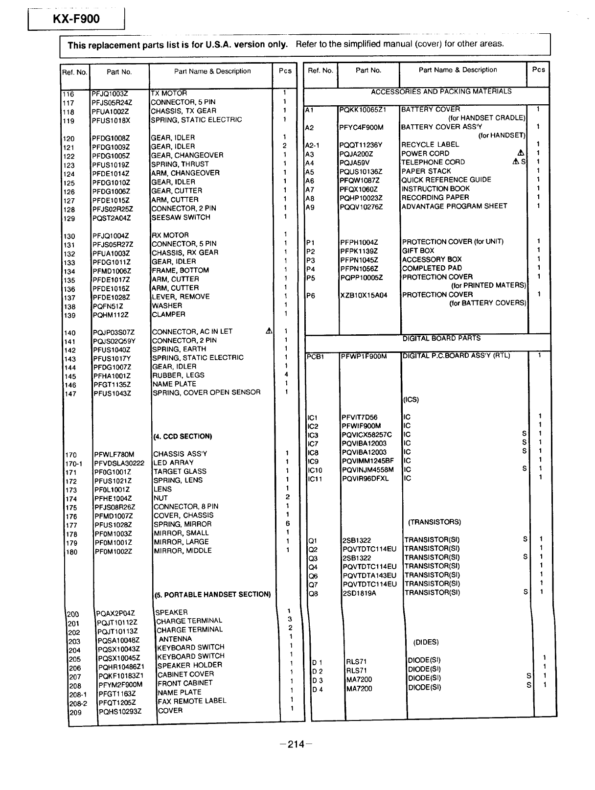
I-KX'FgO0 I
This replacement parts list is for U.S,A. version only.
:tel. No. Part No.
116 PFJQ1003Z
117 PFJS05R24Z
118 PFUA1002Z
119 PFUS1018X
120 PFDG1008Z
121 PFDG1009Z
122 PFDG1005Z
123 PFUS1019Z
124 PFDE1014Z
125 PFDG1010Z
126 PFDG1006Z
127 PFDE1015Z
128 PFJS02R25Z
129 PQST2A04Z
130 PFJQ1004Z
131 PFJS05R27Z
132 PFUA1003Z
133 PFDG1011Z
134 PFMD1006Z
135 PFDE1017Z
136 PFDE1016Z
137 PFDE1028Z
138 PQFN51Z
139 PQHMl12Z
140 PQJP03S07Z
141 PQJS02Q59Y
142 PFUS1040Z
143 PFUS1017Y
144 PFDG1007Z
145 PFHA1001Z
146 PFGT1135Z
147 PFUS1043Z
170 PFWLF780M
170-1 PFVDSLA30222
171 PFOG10OIZ
172 PFUS1021Z
173 PFOL10OlZ
174 PFHE1004Z
175 PFJS08R26Z
176 PFMD1007Z
177 PFUS1028Z
178 PFOM1003Z
179 PFOM1001Z
180 _FOM1002Z
200 PQAX2P04Z
201 pQJT10112Z
202 pQJT10113Z
203 PQSA10048Z
204 PQSX10043Z
205 PQSX10045Z
206 PQHR10486Z1
207 PQKF10183Z1
208 PFYM2F900M
208-1 PFGT1163Z
208-2 PFQT1205Z
209 PQHS10293Z
Part Name & Description
TX MOTOR
CONNECTOR, 5 PIN
CHASSIS, TX GEAR
SPRING, STATIC ELECTRIC
Pcs
1
1
1
1
Refer to the simplified manual (cover)for 0the; areas. _1
Ref. No. I Part No. Part Name & Description Pcs
IACCESSORIES AND PACKING MATERIALS
A1
A2
PQKK 10065Z1
:PFYC4F900M
BATTERY COVER 1
(for HANDSET CRADLE)
BATTERY COVER ASS'Y 1
GEAR, IDLER
GEAR, IDLER
GEAR, CHANGEOVER
SPRING, TH RUST
'_,RM, CHANGEOVER
SEAR, IDLER
SEAR, CUTTER
ARM, CUTTER
CONNECTOR, 2 PIN
SEESAW SWITCH
RX MOTOR
CONNECTOR, 5 PIN
CHASSIS, RX GEAR
GEAR, IDLER
FRAME, BOTTOM
ARM, CUTTER
ARM, CUTTER
LEVER, REMOVE
WASHER
CLAMPER
CONNECTOR, AC IN LET
CONNECTOR, 2 PIN
SPRING, EARTH
SPRING, STATIC ELECTRIC
GEAR, IDLER
RUBBER, LEGS
NAME PLATE
SPRING, COVER OPEN SENSOR
1
2
1
1
1
1
1
1
1
1
A2-1
A3
:A4
'_.5
_6
A7
A8
A9
1
1 P1
1P2
1 P3
1 P4
1 P5
1
1 P6
1
1
1
1
1
1PCB1
1
4
1
1
PQQT11236Y
PQJA200Z
PQJA59V
PQUS10136Z
P FQW 1087Z
PFQXl060Z
PQH P 10023Z
PQQV 10276Z
PFPHIOO4Z
PFPK1139Z
PFPN1045Z
PFPNlO56Z
PQPPIOOO5Z
XZB10X15A04
(for HANDSET)
RECYCLE LABEL 1
POWER CORD .Ah 1
ITELEPHONE CORD • S 1
PAPER STACK 1
QUICK REFERENCE GUIDE 1
INSTRUCTION BOOK 1
RECORDING PAPER 1
ADVANTAGE PROGRAM SHEET 1
PROTECTION COVER (tor UNIT) 1
GIFT BOX 1
ACCESSORY BOX 1
COMPLETED PAD 1
PROTECTION COVER 1
(for PRINTED MATERS
PROTECTION COVER 1
(for BATTERY COVERS
PFWP1F900M
DIGITAL BOARD PARTS
DIGITAL P.C.BOARD ASS'Y (RTL)
4. CCD SECTION)
CHASSIS ASS'Y
LED ARRAY
TARGET GLASS
SPRING, LENS
LENS
NUT
CONNECTOR, 8 PIN
COVER, CHASSIS
SPRING, MIRROR
MIRROR, SMALL
MIRROR, LARGE
MIRROR, MIDDLE
(5. PORTABLE HANDSET SECTION
SPEAKER
CHARGE TERMINAL
CHARGE TERMINAL
ANTENNA
KEYBOARD SWITCH
KEYBOARD SWITCH
SPEAKER HOLDER
CABINET COVER
FRONT CABINET
qAME PLATE
-'AX REMOTE LABEL
COVER
1
1
1
1
1
2
1
1
6
1
1
1
1
3
2
1
1
1
1
1
1
1
1
1
ICl
IC2
IC3
IC7
IC8
IC9
IC10
ICll
Q1
Q2
Q3
Q4
(36
Q7
Q8
D1
D2
D3
D4
PFVIT7D56
PFWIF900M
PQVICX582570
PQVIBA 12003
PQVIBA12003
PQVIMM1245BF
PQVINJM4558M
PQVIR96DFXL
2SB1322
PQVTDTC114EU
2SB1322
PQVTDTC114EU
PQVTDTA143EU
PQVTDTC114EU
2SD1819A
RLS71
RLS71
MA7200
MA7200
(ICS)
IC
IC
IC
IC
IC
IC
IC
IC
(TRANSISTORS)
TRANSISTOR(SI)
TRANSISTOR(SI)
TRANSISTOR(SI)
TRANSISTOR(SI)
TRANSISTOR(Sl)
TRANSISTOR(Sl)
TRANSlSTOR(Sl)
(DIDES)
DIODE(SI)
DIODE(SI)
DIODE(SI)
DIODE(Sl)
s
s
s
1
1
1
1
1
1
1
1
S 1
1
S 1
1
1
1
S 1
1
1
S 1
S 1
-214-
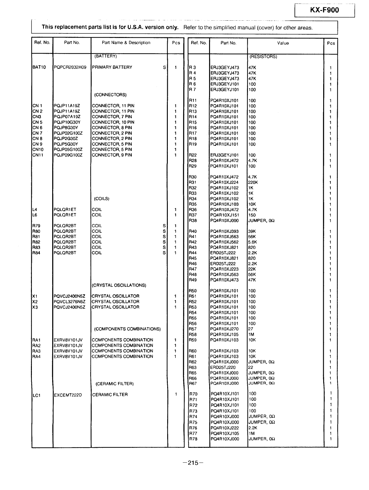
---Kx-Fg00- --
.........................................
This replacement parts list is for U.S.A. version only. Refer to the simplified manual (cover) for other areas.
Ref. No. Part No.
BAT10 PQPCR2032H09
CN 1 PQJP11A19Z
CN 2 PQJP11A19Z
CN3 PQJP07A19Z
CN 5 PQJP10G30Y
CN 6 PQJP8G30Y
CN 7 PQJP02G100Z
CN 8 PQJP2G30Z
CN 9 PQJP5G30Y
CN 10 PQJ P05G 100Z
CN11 PQJP09G100Z
L4 PQLQR 1ET
L6 PQLQR1ET
R79 PQLQR2BT
R80 PQLQR2BT
R81 PQLQR2BT
R82 PQLQR2BT
R83 PQLQR2BT
R84 PQLQR2BT
X1PQVCJ2400N5Z
X2 PQVCL3276N6Z
X 3 PQVCJ2400N5Z
RA1 EXRVSVl01JV
RA2 EXRVSV101JV
RA3 EXRVSVl01JV
RA4 EXRVSV101JV
LC1 EXCEMT222D
Part Name & Description Pcs Ref. No.
(BATTERY)
PRIMARY BA'I-FERY
(CONNECTORS)
CONNECTOR, 11 PIN
CONNECTOR, 11 PIN
CONNECTOR, 7 PIN
CONNECTOR, 10 PIN
CONNECTOR, 8 PIN
CONNECTOR, 2 PIN
CONNECTOR, 2 PIN
CONNECTOR, 5 PIN
CONNECTOR, 5 PIN
CONNECTOR, 9 PIN
(COILS)
COIL
COIL
COIL
COIL
COIL
COIL
COIL
COIL
CRYSTAL OSCILLATIONS)
CRYSTAL OSCILLATOR
CRYSTAL OSCILLATOR
CRYSTAL OSCILLATOR
(COMPONENTS COMBINATIONS)
COMPONENTS COMBINATION
COMPONENTS COMBINATION
COMPONENTS COMBINATION
COMPONENTS COMBINATION
(CERAMIC FILTER)
CERAMIC FILTER
s
s
s
s
s
s
1 R3
R4
R5
R6
R7
Rll
1R12
1 R13
1R14
1R15
1R16
1R17
1R18
1 R19
1
1 R22
R28
R29
R30
R31
R32
R33
R34
R35
1 R36
1 R37
R38
1
1 R40
1 R41
1 R42
1 R43
1 R44
R45
R46
R47
R48
R49
R50
1 R51
1 R52
1 R53
R54
R55
R56
R57
R58
1 R59
1
1 R60
1 R61
R62
R63
R65
R66
R67
1 R70
R71
R72
R73
R74
R75
R76
R77
R78
Part No.
ERJ3GEYJ473
ERJ3GEYJ473
ERJ3GEYJ473
ERJ3GEYJ101
ERJ3GEYJ101
'PQ4R10XJ101
PQ4R10XJ101
PQ4R10XJ101
PQ4R10XJ101
PQ4R10XJ101
PQ4R10XJ101
PQ4R10XJ101
PQ4R10XJ101
PQ4R10XJ101
ERJ3GEYJ101
PQ4R10XJ472
PQ4R10XJ101
PQ4R10XJ472
PQ4R10XJ224
PQ4R10XJ102
PQ4Rt0XJ102
PQ4R10XJ102
PQ4Rt0XJ103
PQ4R10XJ472
PQ4R10XJ151
POARt0XJ000
PQ4R10XJ393
PQ4R10XJ563
PQ4R10XJ562
PQ4R10XJ821
ERD25TJ222
PQ4R10XJ821
ERD25TJ222
PQ4R10XJ223
PQ4R10XJ563
PQ4R10XJ473
PQ4R10XJ101
PQ4R10XJ101
PQ4R10XJ101
PQ4R10XJ101
PQ4R10XJ101
PQ4R10XJ101
PQ4R10XJ101
PQ4R10XJ270
PQ4R10XJ105
PQ4R10XJ103
PQ4Rt0XJ103
PQ4R10XJ103
PQ4R10XJ000
ERD25TJ220
PQ4R10XJ000
PQ4R10XJ000
PQ4R10XJ000
PQ4R10XJ101
PQ4R10XJ101
PQ4R10XJ101
PQ4R10XJ101
PQ4R10XJ000
PQ4R10XJ000
PQ4R10XJ222
PCHR10XJ105
PQ4R10XJ000
Value
(RESISTORS)
47K
47K
47K
100
100
100
100
100
100
100
100
100
100
100
100
4.7K
100
4.7K
220K
1K
1K
1K
10K
4.7K
150
JUMPER, 0_
39K
56K
5.6K
820
2.2K
820
2.2K
22K
56K
47K
100
100
100
100
100
100
100
27
1M
10K
10K
10K
JUMPER, 0Q
22
JUMPER, 0_
JUMPER, 0_
JUMPER, OQ
100
100
100
100
JUMPER, 0_
JUMPER, 0_
2.2K
1M
JUMPER, OQ
I
Pcs
1
1
1
1
1
1
1
1
1
1
1
1
1
1
1
1
1
I
I
I
I
I
I
I
I
I
1
1
1
1
1
1
1
1
1
1
1
1
1
1
1
1
1
1
1
1
1
1
1
1
1
1
1
1
1
1
1
1
1
1
1
1
-215-
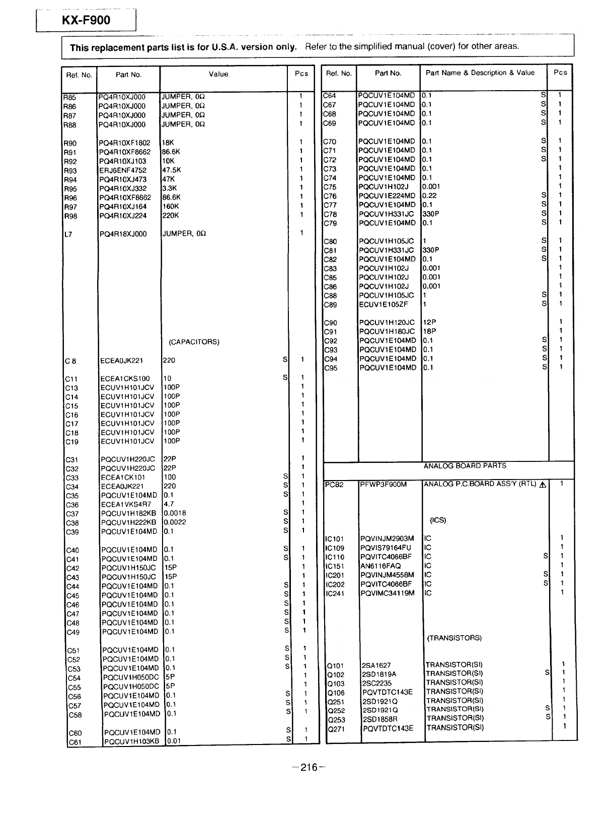
i KX-F,oI
This replacement parts list is for U.S.A. version only. Refer to the simplified manual (cover) for other areas.
Ref. No. Part No.
R85 PQ4R10XJ000
R86 PQ4R10XJ000
R87 PQ4 R10X J000
R88 PQ4R10XJ000
R90 PQ4R10XF1802
R91 PCHR 10X F8662
R92 PQ4R10XJ103
R93 ERJ6ENF4752
R94 PQ4 R10XJ473
R95 PQ4R10XJ332
R96 PQ4R 10X F8662
R97 PQ4R10XJ164
R98 PQ4R10XJ224
L7 PQ4R18XJ000
C 8 ECEAOJK221
C11 ECEA1CKS100
C13 ECUV1 H101JCV
C14 ECUV1 H101JCV
C15 ECUVl H101JCV
C16 ECUVlH101JCV
C17 ECUV1 H101JCV
C18 ECUV1 H101JCV
C19 ECUV I H101JCV
C31 PQCUV1H220JC
C32 PQCUV1H220JC
C33 ECEA1CK101
C34 ECEAOJK221
C35 PQCUV1 E104MD
C36 ECEA1 VKS4R7
C37 PQCUV1H 182KB
C38 PQCUV1H222KB
C39 PQCUV 1E104M D
C40 PQCUV1E104MD
C41 PQCUV1E104MD
C42 PQCUV1H150JC
C43 PQCUV1 H150JC
C44 PQCUV1E104MD
C45 PQCUV1E104MD
C46 PQCUV1E104MD
C47 PQCUV 1E 104MD
C48 PQCUV1 E104MD
C49 PQCUV1 E104MD
C51 PQCUV1 E104MD
C52 PQCUV 1E104MD
C53 PQCUV 1E104MD
C54 PQCUVlH050DC
C55 PQCUV1H050DC
C56 PQCUV1E104MD
C57 PQCUVt E104MD
C58 PQCUV1E104MD
C60 PQCUVlE 104MD
_.R1 PQCUVl H t03KB
Value
JUMPER, 0_
JUMPER, 0_
JUMPER, 0_
JUMPER, 0_
18K
86.6K
10K
47.5K
47K
3.3K
86.6K
16OK
220K
JUMPER, 0_
(CAPACITORS)
Pcs
I
I
I
I
I
I
I
I
I
I
I
I
I
Ref. No. Part No.
C64 PQCUV1E104MD
C67 PQCUVIE104MD
C68 PQCUV1E104MD
C69 PQCUV1E104MD
C70 PQCUVlE104MD
C71 PQCUV 1E104MD
C72 PQCUV1E104MD
C73 PQCUV1E104MD
C74 PQCUV 1EIO4MD
C75 PQCUV1H102J
C76 PQCUVlE224MD
377 PQCUV1E104MD
C78 PQCUV 1H331JC
C79 PQCUV1E104MD
38O
981
382
383
385
386
388
C89
C90
C91
C92
C93
PQCUV 1H 105JC
PQCUV 1H331JC
PQCUV 1E104MD
PQCUV 1H102J
PQCUV 1H102J
PQCUV 1H102J
PQCUV 1H105JC
ECUVlE105ZF
PQCUV1H120JC
PQCUV 1H 180JC
PQCUV1E104MD
PQCUV 1E104MD
Part Name & Description & Value
0.1
0.1
0.1
0.1
0.1
0.1
0.1
0.1
0.1
0.001
1.22
0.1
330 P
0.1
130P
0.1
0.001
O.O01
0.001
Pcs
220
10
;100P
100 P
100P
100P
100P
100P
100P
22P
22P
100
S 1
S1
1
1
1
1
1
1
1
1
1
S1
C94
C95
PQCUV1E104MD 0.1
PQCUV1E104MD 0.1
S 1
S1
S1
S 1
S 1
S 1
S 1
1
1
1
S 1
S 1
S 1
S 1
S 1
S 1
S 1
1
1
1
S 1
S 1
12P 1
18P 1
0.1 S 1
0.1 S 1
S 1
S1
ANALOG BOARD PARTS
PCB2 PFWP3F900M ANALOG P.C.BOARD ASS'Y (RTL) z_ 1
220
0.!
4.7
0.0018
0.0022
0.1
0.1
0.1
15P
15P
0,1
0.1
0.1
0.1
0.1
0.1
0.1
0.1
0.1
5P
5P
0.1
0.1
0.1
0.1
0.01
S 1
S 1
1
S 1
S 1
S 1
S 1
S1
1
1
S 1
S 1
S 1
S 1
S 1
S1
S 1
S 1
S 1
1
1
S 1
S 1
S 1
S 1
S 1
IC101 PQVINJM2903M
IC109 PQVIS79164FU
IC110 PQVITC4066BF
IC151 AN6116FAQ
IC201 PQVINJM4558M
IC202 PQVITC4066BF
IC241 PQVlMC34119M
Q101
Q102
Q103
Q106
2251
Q252
Q253
Q271
2SA1627
2SD1819A
2SC2235
PQVTDTC143E
2SD1921Q
2SD1921Q
2SD 1858R
PQVTDTC 143 E
(ICS)
IC
IC
IC
IC
IC
IC
IC
(TRANSISTORS)
TRANSISTOR(SI)
TRANSISTOR(SI)
TRANSISTOR(SI)
TRANSISTOR(SI)
TRANSISTOR(SI)
TRANSISTOR(SI)
TRANSISTOR(SI)
TRANSISTOR(S0
1
1
S1
1
S 1
S 1
1
1
S 1
1
1
1
S 1
S 1
1
-216-
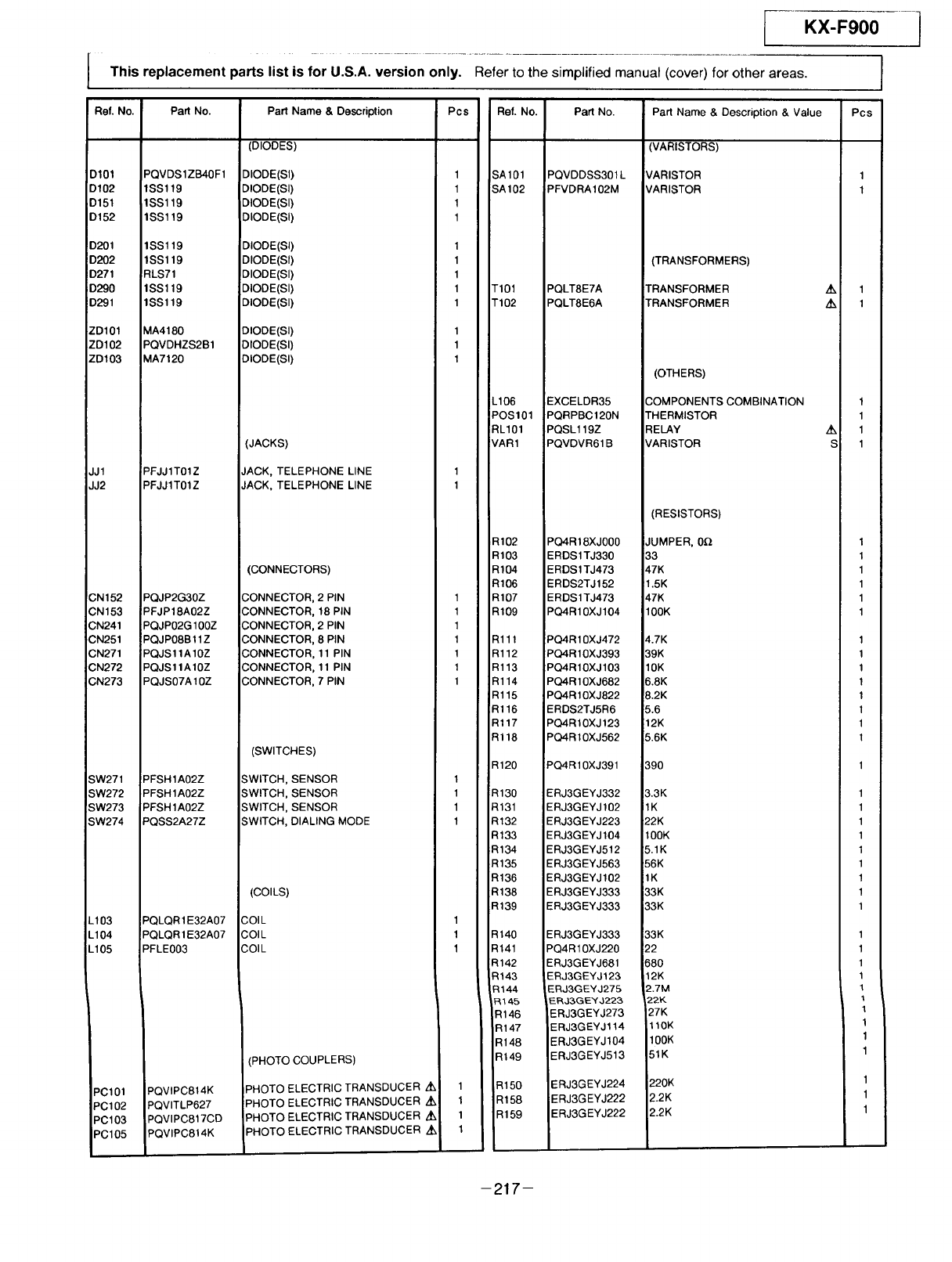
KX-F900 1
This replacement parts list is for U.S.A. version only. Refer to the simplified manual (cover) for other areas.
Ref. No
)101
)102
)151
)152
)201
)202
)271 I
)290
)291
_D101
_D102
_D103
IJ1
IJ2
;N152
;N153
;N241
;N251
;N271
;N272
;N273
;W271
;W272
;W273
;W274
103
104
.105
PC101
PC102
PC103
PC105
Pad No.
I
PQVDSIZB40F1
1SS119
1SSl19
1SSl19
1SSl19
1SS119
RLS71
1SSl19
1SSl19
MA4180
PQVDHZS2B1
MA7120
PFJJ1T01Z
PFJJ1T01Z
PQJP2G30Z
PFJP18A02Z
PQJP02G100Z
!PQJP08BtlZ
PQJS11A10Z
PQJStlA10Z
PQJS07A10Z
PFSH1A02Z
PFSH1A02Z
PFSH1A02Z
PQSS2A27Z
PQLQR 1E32A07
PQLQR 1E32A07
PFLE003
PQVIPC814K
PQVITLP627
PQVIPC817CD
PQVIPC814K
Part Name & Description
(DIODES)
DIODE(SI)
DIODE(SI)
DIODE(SI)
DIODE(SI)
DIODE(SI)
DIODE(SI)
DIODE(SI)
DIODE(SI)
DIODE(SI)
DIODE(SI)
DIODE(SI)
DIODE(SI)
(JACKS)
JACK, TELEPHONE LINE
JACK, TELEPHONE LINE
(CONNECTORS)
CONNECTOR, 2PIN
CONNECTOR, 18PIN
CONNECTOR, 2PIN
CONNECTOR, 8PIN
CONNECTOR, 11PIN
CONNECTOR, 11PIN
CONNECTOR, 7PIN
(SWITCHES)
SWITCH, SENSOR
SWITCH, SENSOR
SWITCH, SENSOR
SWITCH, DIALING MODE
(COILS)
COIL
COIL
COIL
(PHOTO COUPLERS)
PHOTO ELECTRIC TRANSDUCER zt
PHOTO ELECTRIC TRANSDUCER Z_
PHOTO ELECTRIC TRANSDUCER Z_
PHOTO ELECTRIC TRANSDUCER
Pcs
1
1
1
1
1
1
1
1
1
1
1
1
1
1
1
1
1
1
1
1
1
I
I
I
I
1
1
1
1
1
I
1
Ref. No.
;A101
;A102
101
"102
.106
_OS101
;1L101
tAR1
:1102
:1103
:1104
:1106
:1107
:1109
:1111
:1112
;1113
;1114
;1115
;1116
;1117
;1118
{120
{130
{131
{132
1133
{134
{135
{136
{138
{139
1140
1141
{142
;1143
:_144
:_145
R146
R147
R148
R149
R150
R158
R159
Part No.
PQVDDSS301L
PFVDRA102M
PQLT8E7A
PQLT8E6A
EXCELDR35
PQRPBC120N
PQSL119Z
PQVDVR61B
PQ4R18XJ000
ERDS1TJ330
ERDS1TJ473
ERDS2TJ152
ERDS1TJ473
PQ4R10XJ104
PQ4R10XJ472
PQ4R10XJ393
PQ4R10XJ103
PQ4R10XJ682
PQ4R10XJ822
ERDS2TJ5R6
PQ4R10XJ123
PQ4R10XJ562
PQ4R10XJ391
ERJ3GEYJ332
ERJ3GEYJ 102
ERJ3GEYJ223
ERJ3GEYJ104
ERJ3GEYJ512
ERJ3GEYJ563
ERJ3GEYJ102
ERJ3GEYJ333
ERJ3GEYJ333
ERJ3GEYJ333
PQ4R10XJ220
ERJ3GEYJ681
ERJ3GEYJ123
ERJ3GEYJ275
ER33GE'YJ223
ERJ3GEYJ273
ERJ3GEYJ 114
ERJ3GEYJ104
ERJ3GEYJ513
ERJ3GEYJ224
ERJ3GEYJ222
ERJ3GEYJ222
Part Name & Description & Value
VARISTORS)
VARISTOR
VARISTOR
(TRANSFORMERS)
TRANSFORMER
TRANSFORMER
(OTHERS)
COMPONENTS COMBINATION
THERMISTOR
RELAY
VARISTOR s
(RESISTORS)
JUMPER, 0_
33
47K
1.5K
47K
100K
4.7K
39K
10K
_.8K
!e.2K
5.6
12K
5.6K
ago
3.3K
1K
22K
100K
5.1K
56K
1K
33K
33K
33K
22
68O
12K
2.7M
22K
27K
110K
100K
HK
_)20K
2.2K
2.2K
Pcs
1
1
1
1
1
1
1
1
1
1
1
1
1
1
1
1
1
1
1
1
1
I
1
1
1
1
1
1
1
1
1
1
1
1
1
1
1
1
1
1
1
1
1
1
1
-217-
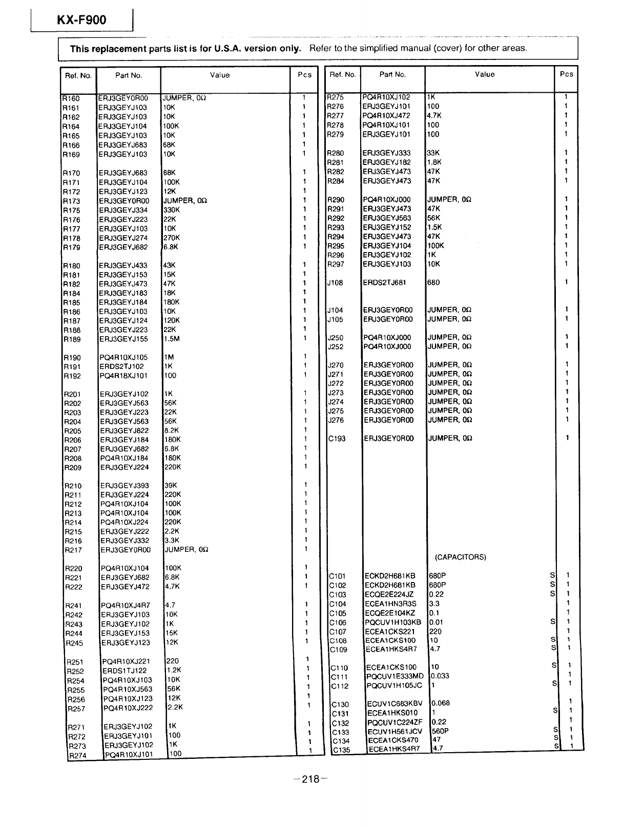
KX-F900
This replacement parts list is for U.S.A. version only. Refer to the simplified manual (cover) for other areas.
1. N_
;0
;1
;2
,4
;5
_6
19
'0
'1
'2
'3
'5
'6
'7
'8
'9
}0
_2
_4
L5
}6
}7
38
39
)0
)1
)2
)1
)2
)3
)4
)5
36
)7
)8
)9
10
11
12
13
14
15
16
17
20
21
22
41
42
43
44
45
'51
_52
_54
t55
-)56
._57
_)71
272
273
274
Pa_ No.
E RJ3GEYJ !03
E RJ3GEYJ103
ERJ3GEYJ104
E RJ3GEYJ103
ERJ3GEYJ683
E RJ3GEYJ103
E RJ3GEYJ683
ERJ3GEYJ104
E RJ3GEYJ123
ERJ3GEYOR00
ERJ3GEYJ334
ERJ3GEYJ223
ERJ3GEYJ103
ERJ3GEYJ274
ERJ3GEYJ682
ERJ3GEYJ433
ERJ3GEYJ153
ERJ3GEYJ473
ERJ3GEYJ183
ERJ3GEYJ184
E RJ3GEYJ103
ERJ3GEYJ124
ERJ3GEYJ223
ERJ3GEYJ155
PQ4R10XJ105
ERDS2TJ102
PQ4R18XJ101
ERJ3GEYJ102
ERJ3GEYJ563
ERJ3GEYJ223
ERJ3GEYJ563
ERJ3GEYJ822
ERJ3GEYJ184
ERJ3GEYJ682
PQ4 R10XJ 184
ERJ3GEYJ224
ERJ3GEYJ393
ERJ3GEYJ224
PQ4R10XJ104
PQ4R10XJ104
PQ4R10XJ224
ERJ3GEYJ222
ERJ3GEYJ332
ERJ3GEYOR00
PQ4R10XJ 104
ERJ3GEYJ682
ERJ3GEYJ472
PQ4R10XJ4R7
ERJ3GEYJ103
ERJ3GEYJ102
ERJ3GEYJ153
ERJ3GEYJ123
PQ4R10XJ221
ERDS1TJ122
PQ4R10XJ103
PQ4R10XJ563
PQ4R10XJ123
PQ4R10XJ222
ERJ3GEYJ 102
ERJ3GEYJ 101
ERJ3GEYJ102
IPQ4R10XJ101
Value
JUMPER, 0(1
10K
10K
100K
10K
68K
10K
68K
100K
12K
JUMPER, 0Q
330K
22K
10K
270K
6.8K
43K
15K
47K
18K
180K
10K
120K
22K
1.5M
1M
1K
100
1K
!56K
22K
56K
&2K
180K
&8K
180K
220K
39K
220K
100K
100K
220K
2.2K
3.3K
JUMPER, 0_
100K
6.8K
4.7K
4.7
10K
1K
15K
12K
220
1.2K
10K
56K
12K
2.2K
1K
100
1K
100
Pcs
1
1
1
1
1
1
1
1
1
1
1
1
1
1
1
1
1
1
1
1
1
1
1
1
1
1
1
1
1 :
1
1
1
1
1
1
1
1
1
1
1
1
1
1
1
1
1
1
1
1
1
1
1
1
1
1
1
1
1
1
1
1
1
L 1
;tef. No. i
275 '
276
277
278 I
279
28O
281
282
284
29O
291
292
293
294
295
296
297
108
104
105
250
252
270
271
272
273
274
275
276
;193
;101
;102
;103
;104
;105
;106
)107
;108
3109
3110
3111
3112
C130
C131
C132
C133
C134
C135
Pa_ No.
PQ4R10XJ!02
ERJ3GEYJ101
PQ4Rt0XJ472
PQ4R10XJ101
ERJ3GEYJ101
ERJ3GEYJ333
ERJ3GEYJ 182
ERJ3GEYJ473
ERJ3GEYJ473
PQ4R 10XJ 000
ERJ3GEYJ473
ERJ3GEYJ563
ERJ3GEYJ152
iERJ3GEYJ473
IERJ3GEYJ104
ERJ3GEYJI02
ERJ3GEYJI03
ERDS2TJ681
ERJ3GEYOR00
ERJ3GEYOR00
PQ4R10XJ000
PCHR10XJ000
ERJ3GEYOR00
ERJ3GEYOR00
ERJ3GEYOR00
ERJ3GEYOR00
ERJ3GEYOR00
ERJ3GEYOR00
E RJ3GEYOR00
ERJ3GEYOR00
ECKD2H681KB
ECKD2H681KB
ECQE2E224JZ
ECEA1HN3R3S
ECQE2E104KZ
PQCUV1H103KB
ECEA1CKS221
ECEA1CKS100
ECEA1HKS4R7
ECEAICKS100
PQCUV1E333MD
PQCUV1H 105JC
ECUV1C683KBV
ECEA1HKS010
PQCUVlC224ZF
ECUV1H561JCV
ECEA1CKS470
ECEA1HKS4R7
1K
100
4.7K
100
100
33K
1.8K
47K
47K
JUMPER, 0_
47K
56K
1.5K
47K
100K
1K
10K
680
JUMPER, O_
JUMPER, OQ
JUMPER, O_
JUMPER, 0_
!JUMPER, 0_
IJUMPER, 0Q
JUMPER, 0_
JUMPER, 0_
JUMPER, 0Q
JUMPER, 0_
JUMPER, 0O
JUMPER, 0_
Value
(CAPACITORS)
P°sI
!
1'
1
1
1
1
1
1
1
1
1
1
1
680P
680P
0.22
3.3
0.1
0.01
220
10
4.7
10
0.033
1
0.068
1.22
;60P
47
4.7
I
S1
SI
I
I
S I
I
s I
s I
SI
I
S I
I
I
I
S I
s, I
sl 1
-218-
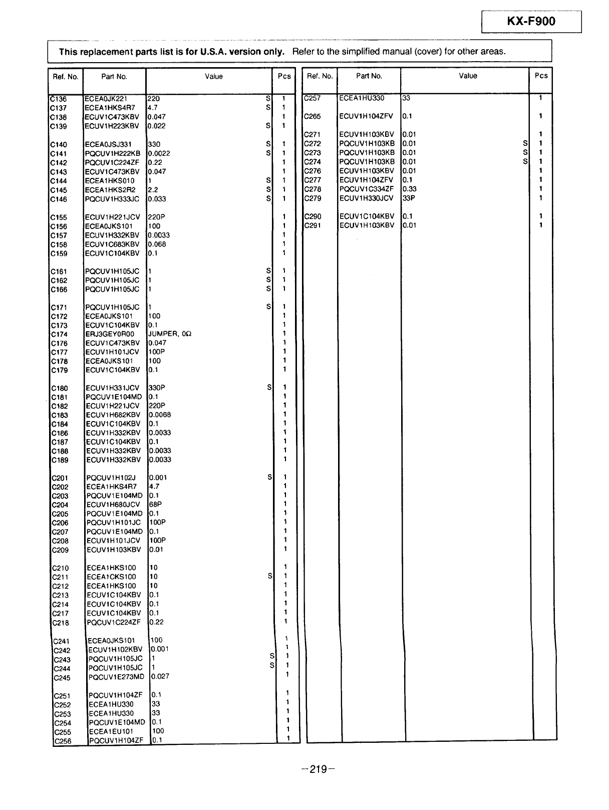
This replacement parts list is for U.S.A. version only. Refer to the simplified manual (cover) for other areas.
KX-F900
_ef. No.
:136
',137
;138
',139
;140
;141
:142
;143
;144
;145
;146
;155
;156
;157
;158
;159
;161
;162
;166
,_171
_172
_173
_.174
_176
_.177
_178
_.179
;180
;181
;182
;183
.3184
.3186
.3187
.3188
;189
.3201
.3202
.3203
.3204
.3205
.3206
.3207
-3208
.3209
.3210
.3211
.3212
.3213
.3214
.3217
.3218
C241
C242
C243
C244
C245
C251
C252
C253
C254
C255
C256
Pan No.
ECEAOJK221
ECEA1HKS4R7
ECUV1C473KBV
ECUV1H223KBV
ECEAOJSJ331
PQCUV1H222KB
PQCUVlC224ZF
ECUV1C473KBV
ECEA1HKS010
ECEA1HKS2R2
PQCUV1H333JC
ECUV1H221JCV
ECEAOJKS101
ECUV1H332KBV
ECUV1C683KBV
ECUVlCl04KBV
PQCUV1H105JC
PQCUV 1H 10550
PQCUV 1H 105JC
PQCUV1H105JC
ECEAOJKS101
ECUVIC104KBV
ERJ3GEYOR00
ECUV1C473KBV
ECUV1H101JCV
ECEAOJKSl01
ECUV1C104KBV
ECUV1H331JCV
PQCUV1E104MD
ECUV1H221JCV
ECUV1H682KBV
ECUVlCl04KBV
ECUV1H332KBV
ECUVlCl04KBV
ECUV1H332KBV
ECUV1H332KBV
PQCUV1 H102J
ECEA1 HKS4R7
PQCUV1 E104MD
ECUV1H680JCV
PQCUV1 E104MD
PQCUV1H101JC
PQCUV1 E104MD
ECUV1H101JCV
ECUV1H 103KBV
ECEA1HKS100
ECEA1CKS100
ECEA1HKS100
ECUV1C104KBV
ECUVlCl04KBV
ECUVlCl04KBV
PQCUV1C224ZF
ECEAOJKS101
ECUV1H 102KBV
PQCUV 1H 105JC
PQCUV1H 105JC
PQCUVlE273MD
PQCUV1H 104ZF
ECEA1HU330
ECEA 1HU330
PQCUV1E104MD
ECEA1EU101
IPQCUV1H 104ZF
Value
220
4.7
0.047
0.022
330
0.0022
0.22
0.047
1
2.2
0.033
220P
100
0.0033
0.068
0.1
1
1
1
1
100
0.1
JUMPER, 0_
0.047
100P
100
0.1
330P
0.1
220P
0.0068
0.1
0.0033
3.1
3.0033
0.0033
0.001
4.7
C).1
B8P
0.1
100P
0.1
100P
0.01
10
10
10
0.1
0.1
0.1
0.22
100
3.001
s
S
S
s
s
S
s
s
s
s
s
1.027
).1
33
33
0.1
100
).1
PCS
1
1
1
1
1
1
1
1
1
1
1
1
1
1
1
1
1
1
1
1
1
1
1
1
1
1
1
S1
1
1
1
1
1
1
1
1
S 1
1
1
1
1
1
1
1
1
1
1
1
1
1
1
1
1
1
1
S 1
1
1
1
1
1
1
1
Ref. No.
;257
:265
;271
;272
;273
;274
;276
;277
;278
;279
;290
;291
Part No. Value
ECEA1HU330 33
ECUVIHIO4ZFV
ECUV1H103KBV
PQCUV1H103KB
PQCUV1H103KB
PQCUV1H103KB
ECUV1H103KBV
ECUV1H104ZFV
PQCUV1C334ZF
ECUV1H330JCV
ECUVIC104KBV
ECUV1H103KBV
0.1
0.01
0.01
0.01
0.01
0.01
0.1
0.33
33P
0.1
0.01
s
s
s
Pcs
1
1
1
1
1
1
1
1
1
1
1
1
-219-
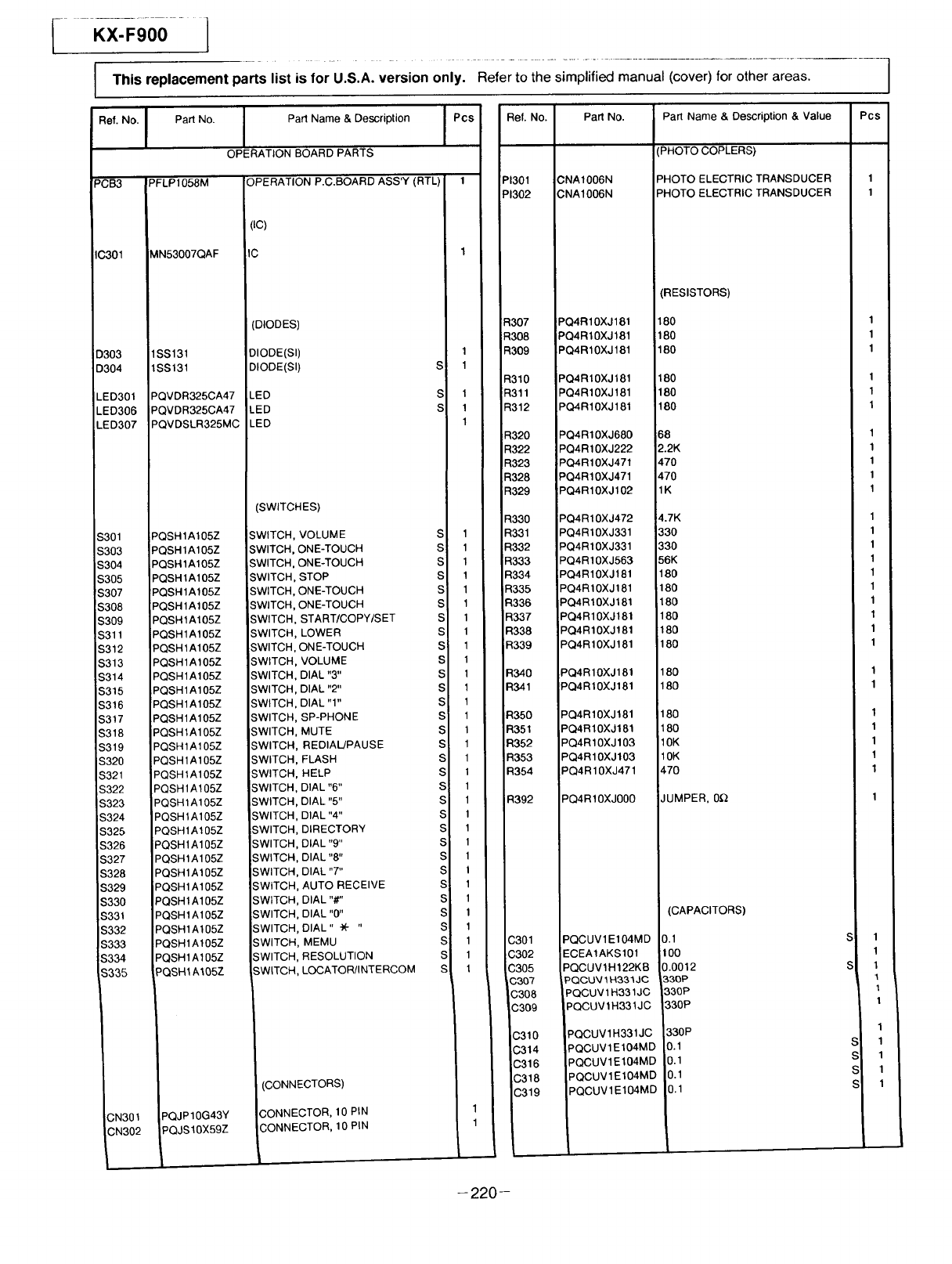
I X--F90O]
This replacement parts list is for U.S.A. version only. Refer to the simplified manual (cover) for other areas.
!
Ref. No. I Part No.
PFLP1058M
MN53007QAF
1SS131
1SS131
PQVDR325CA47
PQVDR325CA47
PQVDSLR325MC
PQSH1A105Z
PQSH1A105Z
PQSH1A105Z
PQSH1A105Z
PQSH1A105Z
F'QSH 1A 105Z
PQSH1A105Z
PQSH1A105Z
PQSH1A105Z
PQSH1A105Z
PQSH1A105Z
PQSH1A105Z
PQSH1A105Z
PQSH 1A 105Z
PQSH 1A105Z
PQSH1A105Z
PQSH1A105Z
PQSH 1A105Z
PQSH1A105Z
PQSH1A105Z
PQSH 1A105Z
PQS H1A 105Z
PQSH 1A105Z
PQSH1A105Z
PQSH1A105Z
PQSH1A105Z
PQSH 1A105Z
PQSH1A105Z
PQSH1A105Z
PQSH1A105Z
PQSH1A105Z
PQSH1 A105Z
pQJP10G43Y
pQJS10X59Z
IPart Name & Description I Pcs
OPERATION BOARD PARTS
)PERATION P.C.BOARD ASS'Y (RTL)
Ic)
IC
(DIODES)
DIODE(SI)
DIODE(SI)
LED
LED
LED
SWITCHES)
SWITCH, VOLUME S
SWITCH, ONE-TOUCH S
SWITCH, ONE-TOUCH S
SWITCH, STOP S
SWITCH, ONE-TOUCH S
SWITCH, ONE-TOUCH S
SWITCH, START/COPYtSET S
SWITCH, LOWER S
SWITCH, ONE-TOUCH S
SWITCH, VOLUME S
SWITCH, DIAL "3" S
SWITCH, DIAL "2" S
SWITCH, DIAL "1" S
SWITCH, SP-PHONE S
SWITCH, MUTE S
SWITCH, REDIAL/PAUSE S
SWITCH, FLASH S
SWITCH, HELP S
SWITCH, DIAL "6" S
SWITCH, DIAL "5" S
SWITCH, DIAL "4" S
SWITCH, DIRECTORY S
SWITCH, DIAL "9" S
SWITCH, DIAL "8" S
SWITCH, DIAL "7" S
SWITCH, AUTO RECEIVE S
SWITCH, DIAL "#"' S
SWITCH, DIAL "0" S
SWITCH, DIAL" _ " S
SWITCH, MEMU S
SWITCH, RESOLUTION S
SWITCH, LOCATOR/INTERCOM S
(CONNECTORS)
CONNECTOR, 10 PIN
CONNECTOR, 10 PIN
1
1
1
1
1
1
1
1
1
1
1
1
1
1
1
1
1
1
1
1
1
1
1
1
1
1
1
1
1
1
1
1
1
1
1
ef. No.
301
302
_,07
_08
_09
H0
_,11
312
320
322
323
328
329
330
331
332
333
334
335
336
337
338
339
34O
341
35O
351
352
353
354
392
;301
;302
;305
;307
3308
3309
3310
3314
C316
C318
C319
Part No.
CNA1006N
;NA1006N
_Q4R10XJ181
PQ4R10XJ181
PQ4R10XJ181
PQ4R10XJ181
PQ4R10XJ181
PQ4R10XJ181
PQ4R10XJ680
PQ4R10XJ222
PQ4R10XJ471
PQ4R10XJ471
PQ4R10XJ102
PQ4R10XJ472
PQ4R10XJ331
PQ4R10XJ331
PQ4R10XJ563
PQ4R10XJ181
PQ4R10XJ181
PQ4R10XJ181
PQ4R10XJ181
PQ4R10XJ!81
PQ4R10XJ181
PQ4R10XJ181
PQ4R10XJ181
PQ4R10XJ181
PQ4R10XJ181
PQ4R10XJ103
PQ4R10XJ103
PQ4R10XJ471
PQ4R10XJ000
PQCUV1 E104MD
ECEA1AKS101
PQCUV1H 122KB
PQCUk/1 _4331JC
PQCUV 1H331JC
PQCUV 1H331JC
PQCUV1H331JC
PQCUV1E104MD
PQCUVlE104MD
PQCUV 1E104MD
PQCUV 1E104MD
Part Name & Description & Value
(PHOTO COPLERS)
PHOTO ELECTRIC TRANSDUCER
PHOTO ELECTRIC TRANSDUCER
(RESISTORS)
180
180
180
180
180
180
68
2.2K
470
470
1K
4.7K
330
330
56K
180
180
180
180
180
180
180
180
180
180
10K
10K
470
JUMPER, 0£
(CAPACITORS)
0.1
100
).0012
33oP
330P
30P
_30P
1.1
0.1
0.1
0.1
'cS
1
1
1
1
s
s
s
1
1
1
1
1
1
1
1
1
1
1
1
1
1
1!
1
1
1
1
1
1
1
1
1
1
1
1
1
1
1
1
1
1
1
1
1
1
1
-220-
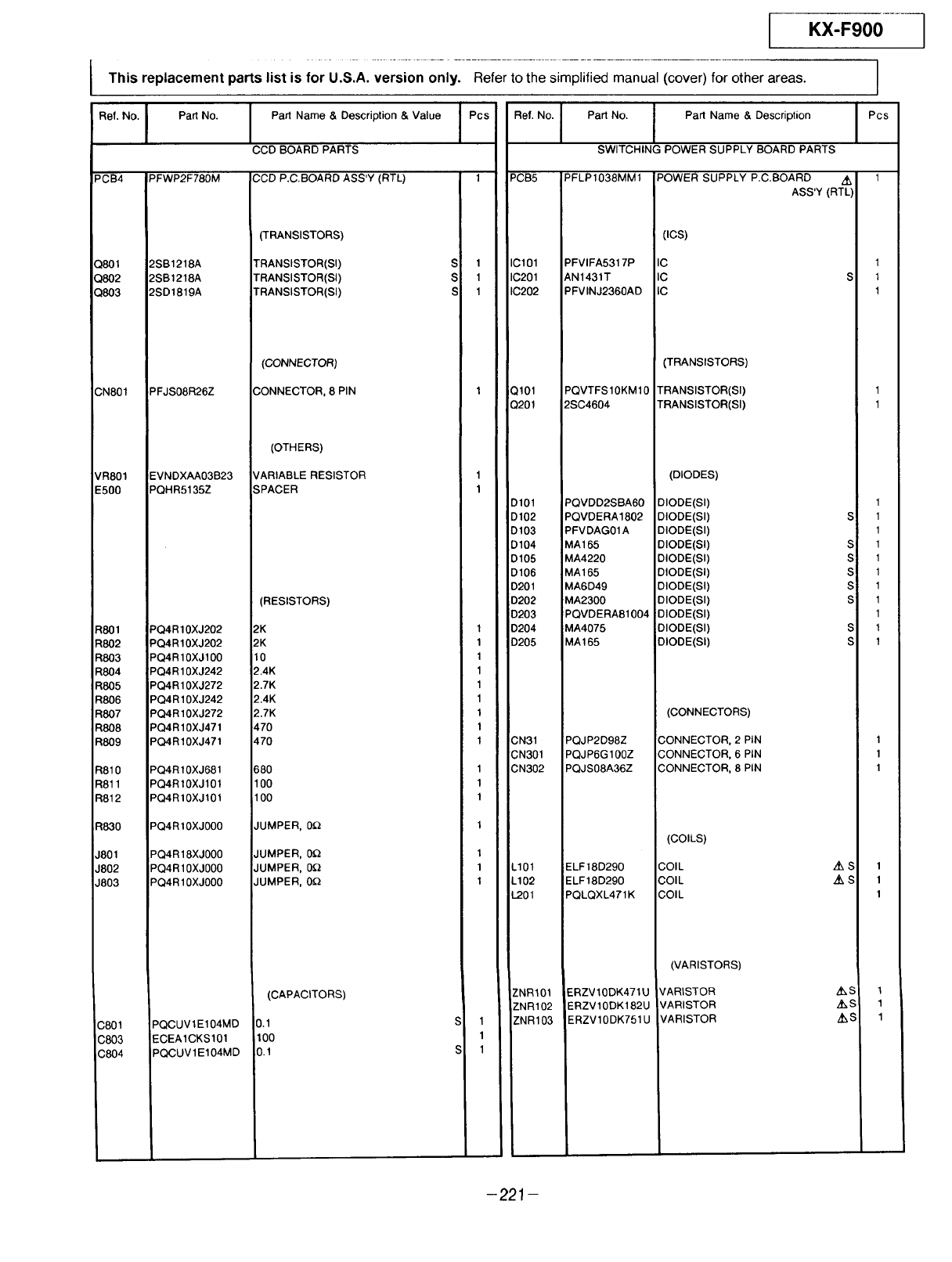
This replacement parts list is for U.S.A. version only.
I
Refer to the simplified manual (cover) for other areas.
Re,NoIPa NoI Pa Name,Oesori on,VaueIPcs
CCD BOARD PARTS
I PFWP2F780M
2SB1218A
2SB1218A
2SD1819A
PFJS08R26Z
EVNDXAA03B23
PQHR5135Z
PQ4R10XJ202
PQ4R10XJ202
IPQ4R 10XJ 100
IPQ4R 10XJ242
IPQ4R10XJ272
IPQ4R 10XJ242
IPQ4R 10XJ272
IPQ4R 10XJ47t
iPQAR10XJ47t
IPQ4R 10XJ681
IPQ4Rt0XJ101
iPQ4RIOXJt01
I PQ4R 10XJ000
1801 PQ4 R18X J000
1802 PQ4R 10X J000
1803 PQ4R 10X J000
.3801 PQCUV1E104MD
.3803 ECEA1CKS101
3804 PQCUV1E104MD
CCD P.C.BOARD ASS'Y (RTL)
(TRANSISTORS)
TRANSISTOR(SI)
TRANSISTOR(SI)
TRANSISTOR(SI)
(CONNECTOR)
CONNECTOR, 8 PIN
(OTHERS)
VARIABLE RESISTOR
SPACER
(RESISTORS)
2K
2K
10
2.4K
2.7K
2.4K
2.7K
470
470
680
100
100
JUMPER, 0_
JUMPER, 0_
JUMPER, 0_
JUMPER, 0_
(CAPACITORS)
0.1
100
0.1
1
S1
S1
S 1
1
1
1
1
1
1
1
1
1
1
1
1
1
1
1
1
1
1
1
1
1
S1
i
I I
Ref. No. I Part No. ]Part Name & Description
I I
SWITCHING POWER SUPPLY BOARD PARTS
_CB5
_101
C201
3202
_101
;)201
)101
)102
)103
)104
)105
)106
)201
)202
)203
)204
)205
;N31
;N301 I
;N302 I
.101
.102
-201
_NR101
ZNR102
ZNR103
PFLP1038MM1
PFVlFA5317P
AN1431T
PFVINJ2360AD
PQVTFS10KM10
2SC4604
PQVDD2SBA60
PQVDERA1802
PFVDAG01A
MA165
MA4220
MA165
MA6D49
MA2300
PQVDERA81004
MA4075
MA165
PQJP2D98Z
PQJP6G100Z
PQJS08A36Z
ELF18D290
ELF18D290
PQLQXL471K
ERZV10DK471U
ERZV10DK182U
ERZV10DK751U
POWER SUPPLY P.C.BOARD
(ICS)
IC
IC
IC
(TRANSISTORS)
TRANSISTOR(SI)
TRANSISTOR(SI)
(DIODES)
DIODE(SI)
DIODE(SI)
DIODE(SI)
DIODE(SI)
DIODE(SI)
DIODE(SI)
DIODE(SI)
DIODE(SI)
DIODE(SI)
DIODE(SI)
DIODE(SI)
(CONNECTORS)
CONNECTOR, 2PtN
CONNECTOR, 6PtN
CONNECTOR, 8PIN
(COILS)
COIL
COIL
COIL
(VARISTORS)
VARISTOR
VARISTOR
VARISTOR
KX-F900
I
I Pcs
,,'h 1
ASS'Y (RTL)
1
S1
1
1
1
1
S1
1
S 1
S1
S 1
S 1
S 1
1
S 1
S 1
1
1
1
z_S 1
•_S 1
1
,,k_ 1
,_S 1
,._S 1
-221 -
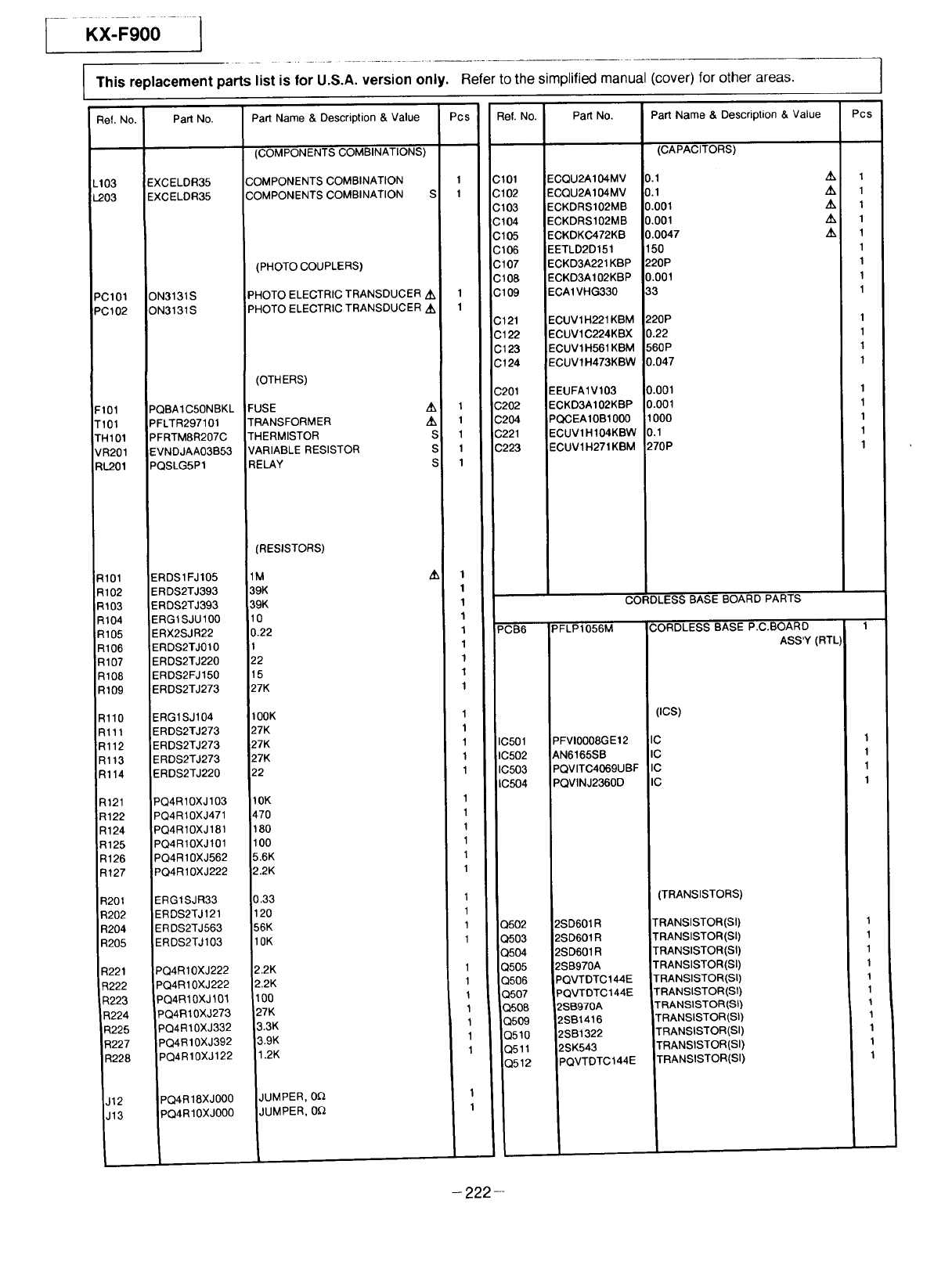
I.....Kx. ,oo....1
This replacement parts list is for U.S,A. version only. Refer to the simplified manual (cover) for other areas.
Ref. No.
L103
I..203
PC101
PC 102
F101
TI01
THI01
VR201
RL201
RIO1
R102
R103
R104
R105
R106
R107
R108
R109
Rl10
R111
Rl12
Rl13
Rl14
R121
R122
R124
R125
R126
R127
R20t
R202
R204
R205
R221
R222
R223
R224
R225
R227
_228
J12
J13
Pan No.
EXCELDR35
EXCELDR35
ON3131S
ON3131S
PQBA1C50NBKL
PFLTR297101
PFRTM8R207C
EVNDJAA03B53
PQSLG5P1
'ERDSIFJt05
E RDS2TJ393
ERDS2TJ393
ERG1SJU100
ERX2SJR22
ERDS2TJ0t0
ERDS2TJ220
ERDS2FJ150
ERDS2TJ273
ERG1SJ104
ERDS2TJ273
ERDS2TJ273
ERDS2TJ273
ERDS2TJ220
PQ4R10XJ103
PQ4R10XJ471
PQ4R10XJ181
PQ4R10XJ101
PQ4R10XJ562
PQ4R10XJ222
ERG1SJR33
ERDS2TJ121
ERDS2TJ563
ERDS2TJ103
PQ4R10XJ222
PQ4R10XJ222
PQ4R10XJ101
PQ4R10XJ273
PQ4R10XJ332
PQ4R10XJ392
PQ4R10XJ122
PQ4R18XJ000
PQ4R10XJ000
Part Name & Description & Value
(COMPONENTS COMBINATIONS)
COMPONENTS COMBINATION
COMPONENTS COMBINATION S
(PHOTO COUPLERS)
,PHOTO ELECTRIC TRANSDUCER z_
PHOTO ELECTRIC TRANSDUCER ,_
Pcs Ref. No.
C101
C102
C103
C104
C105
C106
C107
C108
C109
Pa_ No.
ECQU2A104MV
ECQU2A104MV
ECKDRS102MB
ECKDRS102MB
ECKDKC472KB
EETLD2D151
ECKD3A221 KBP
ECKD3A102KBP
ECA1 VHG330
Part Name & Description & Value
(CAPACITORS)
0.1
0.1
0.001
0.001
0.0047
150
220P
0.001
33
(OTHERS)
FUSE z_
TRANSFORMER z_
THERMISTOR S
VARIABLE RESISTOR S
RELAY S
(RESISTORS)
IM
39K
39K
10
0.22
I1
22
15
'27K
tOOK
27K
27K
27K
22
t0K
470
180
100
5.6K
2.2K
,0.33
120
56K
10K
2.2K
2.2K
100
27K
3.3K
3.9K
1.2K
JUMPER, 0Q
JUMPER, 0_
C121
C122
C123
C124
C201
1 C202
tC204
1 C221
1 C223
1
1
1
1
1
1 PCB6
1
1
1
1
1
1
1 IC501
1 IC502
1 C503
IIC504
1
1
1
1
1
1
1
1
1C}502
1Q503
Q504
1 Q505
1 Q506
1 Q507
1Q50B
1 Q509
1Q510
1 C}511
Q512
1
1
ECUV1H221KBM 220P
ECUV1C224KBX 0.22
ECUV1H561KBM 560P
'ECUV1H473KBW 0.047
EEUFA1V103 0.001
ECKD3A102KBP 0.001
PQCEA 10B1000 1000
ECUV1HIO4KBW 0.1
ECUV1H271KBM 270P
z_ 1
1
z_, 1
,_ 1
1
1
1
1
1
1
1
1
1
1
1
1
1
CORDLESS BASE BOARD PARTS
PFLPt056M 1
PFVI0008GE12
AN6165SB
PQVITC4069UBF
PQVINJ2360D
CORDLESS BASE P.C.BOARD
ASS'Y (RTL
(ICS)
IC
IC
IC
IC
(TRANSISTORS)
TRANSISTOR(SI)
TRANSISTOR(SI)
TRANSISTOR(SI)
TRANSISTOR(SI)
TRANSISTOR(SI)
,TRANSISTOR(SI)
TRANSISTOR(SI)
TRANSlSTOR(SI)
TRANSISTOR(Sl)
TRANSISTOR(Sl)
TRANSISTOR(SI)
Pcs
2SD601R
2SD601R
2SD601R
2SB970A
PQVTDTC144E
PQVTDTC144E
2SB970A
_SB1416
2SB1322
2SK543
PQVTDTC144E
1
1
1
1
1
I
1
I
I
I
I
I
I
I
I
- 222-
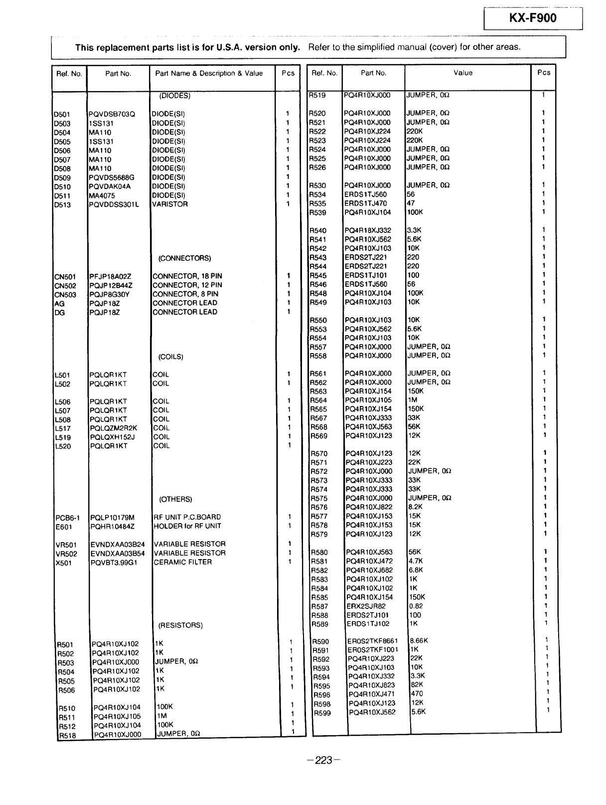
IThis replacement
_ef. No. I Part No.
I
501 _PQVDSBT03Q
503 I1SS131
504 IMA110
505 I1SS131
506 IMA110
507 IMA110
508 IMA110
509 IPQVDS5688G
510 IPQVDAK04A
511 IMA4075
513 I PQVDDSS301L
/
N50i / PFJP18A02Z
N502 I
N503 I
G
G ]
I
I
I
501
502
506
507
508
517
519 !
520
'CB6-1
i601
'R501
'R502
'.501
_501
_502
_503
_504
_505
R506
R510
R511
R512
R518
PQJP 12B44Z
PQJP8G30Y
PQJP18Z
PQJP18Z
PQLQR1KT
PQLQR1KT
PQLQR1KT
PQLQR1KT
PQLQR1KT
PQLQZM2R2K
PQLQXH152J
PQLQRtKT
PQLP10179M
PQHR10484Z
EVNDXAA03B24
EVNDXAA03B54
PQVBT3.99G 1
PQ4R10XJ102
PQ4R10XJ102
PQ4R10XJ000
PQ4R10XJ102
PQ4R10XJ102
PQ4R10XJ102
PQ4R10XJ104
PQ4R10XJ105
PQ4R10XJ104
PQ4R10XJ000
I KX-F900- ............]
parts list is for U.S.A. version only. Refer to the simplified manual (cover) for other areas.
Part Name & Description & Value
(DIODES)
DIODE(SI)
DIODE(SI)
DIODE(SI)
DIODE(SI)
DIODE(SI)
DIODE(SI)
DIODE(S0
DIODE(SI)
DIODE(SI)
DIODE(S0
VARISTOR
(CONNECTORS)
CONNECTOR, 18 PIN
CONNECTOR, 12 PIN
CONNECTOR, 8 PIN
CONNECTOR LEAD
CONNECTOR LEAD
(COl LS)
COIL
COIL
COIL
COIL
COIL
COIL
COIL
COIL
(OTHERS)
RF UNIT P.C.BOARD
HOLDER tor RF UNIT
VARIABLE RESISTOR
VARIABLE RESISTOR
;ERAMIC FILTER
(RESISTORS)
1K
1K
JUMPER, 0Q
1K
1K
1K
1O0K
1M
10OK
JUMPER, 0_
Pcs
1
1
1
1
1
1
1
1
1
1
1
1
1
1
1
1
1
1
1
1
1
1
1
1
1
1
1
1
1
1
1
1
1
1
1
1
1
1
I,
:{ef. No.
519
52O
521
522
523
524
525
526
530
534
535
539
540
:541
;542
;543
;544
1545
;546
',548
;549
',550
1553
:554
;557
;558
;561
;562
;563
L564
_565
t567
t568
t569
_570
T571
T572
_573
1574
T575
_576
1577
1578
1579
_580
_581
;t582
:1583
:1584
:1585
_587
_588
:_589
_590
R591
R592
R593
R594
R595
R596
R598
R599
Part No. Value
PQ4R10XJ000 JUMPER, 0_
PQ4R 10X J000
PQ4R 10XJ000
PQ4R 10XJ224
PQ4R 10XJ224
PQ4R 10X J000
PQ4R 10X J000
PQ4R 10X J000
PQ4R10XJ000
ERDStTJ560
ERDS1TJ470
PQ4R10XJ104
PQ4 R18XJ332
PQ4R10XJ562
PQ4R10XJ103
ERDS2TJ221
ERDS2TJ221
ERDS1TJ101
ERDS1TJ560
PQ4R10XJ104
PQ4R10XJ103
PQ4R10XJ103
PQ4R10XJ562
PQ4R10XJ103
PQ4R10XJ000
PQ4R10XJ000
PQ4Rt0XJ000
PQ4R10XJO00
PQ4R10XJ154
PQ4R10XJ105
PQ4R10XJ154
PQ4R10XJ333
PQ4R10XJ563
PQ4R10XJ123
PQ4R10XJ123
PQ4R10XJ223
PQ4R10XJ000
PQ4R10XJ333
PQ4R10XJ333
PQ4R10XJ000
PQ4R10XJ822
PQ4R10XJ153
PQ4R10XJ153
PQ4R10XJ123
PQ4R10XJ563
PQ4R10XJ472
PQ4R10XJ682
PQ4R10XJ102
PQ4R10XJ102
PQ4R10XJ154
ERX2SJR82
ERDS2TJ101
ERDStTJ102
EROS2TKF8661
EROS2TKF1001
PQ4R10XJ223
PQ4R10XJ103
PQ4R10XJ332
PQ4R10XJ823
PQ4R10XJ471
PQ4R10XJ123
PQ4R10XJ562
JUMPER, O_
JUMPER, 0_
220K
220K
JUMPER, 0_
JUMPER, 0_
JUMPER, 0_
JUMPER, OQ
56
47
100K
3.3K
5.6K
10K
220
220
100
56
100K
10K
10K
5.6K
10K
JUMPER, 0_
JUMPER, 0Q
JUMPER, 0_
JUMPER, 0_
150K
1M
150K
33K
56K
12K
12K
22K
JUMPER, 0_
33K
33K
JUMPER, 0_
8.2K
15K
15K
12K
56K
4.7K
6.8K
1K
1K
150K
0.82
100
1K
8.66K
1K
22K
1OK
3.3K
82K
470
12K
5.6K
PCS
1
1
1
1
1
1
1
1
1
1
1
1
1
1
1
1
1
1
1
1
1
1
1
1
1
1
1
1
1
1
1
1
1
1
1
1
1
1
1
1 I
,I
1
1
1
1
1
1
1
1
1
1
1
1
1
1
1
1
1
1
1
1
1
-223-
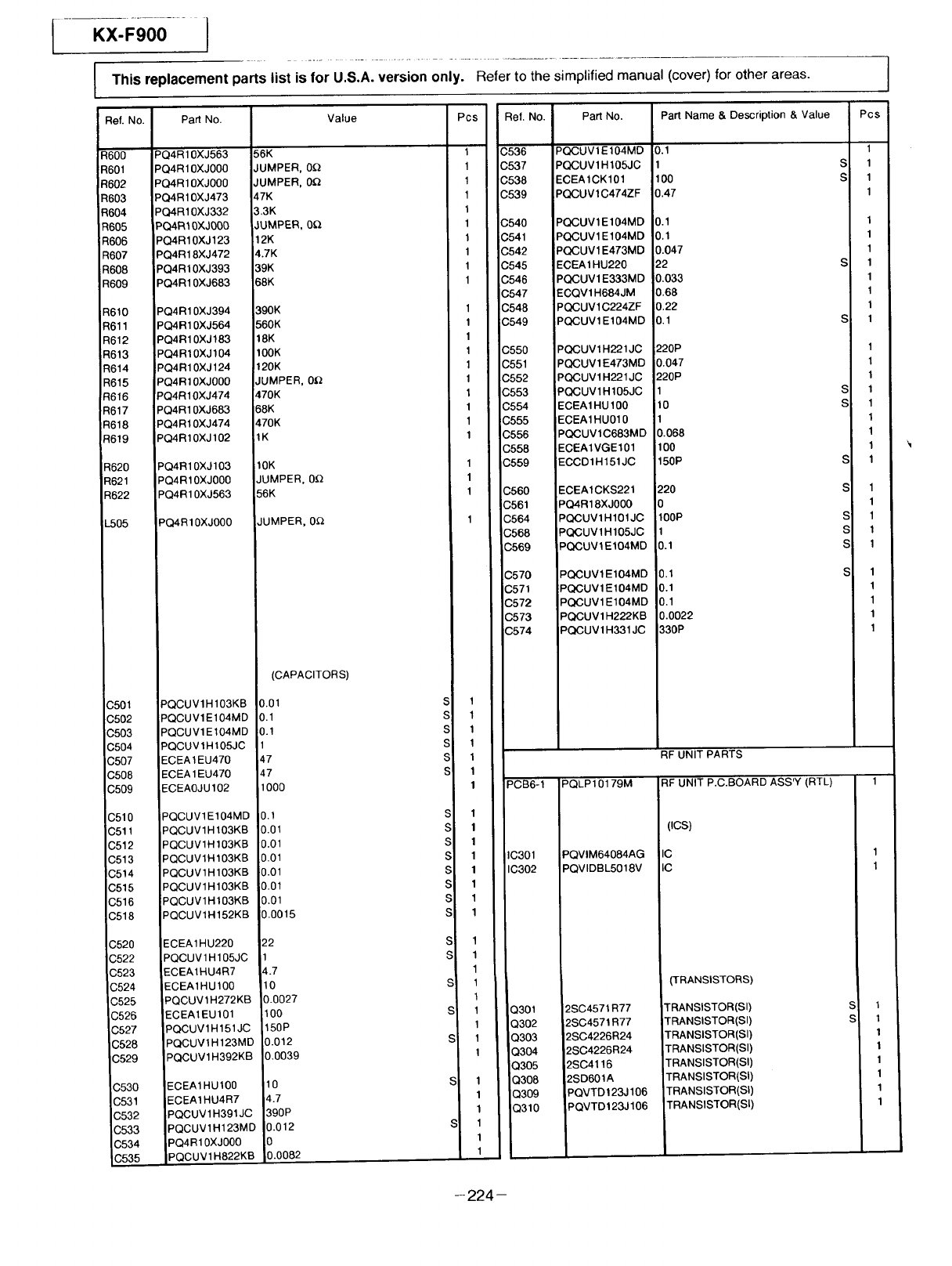
iKx--Fgoo....j
This replacement parts list is for U.S.A. version only. Refer to the simplified manual (cover) for other areas.
Ref. No.
_600
_601
9602
9603
R604
R605
R606
R607
R608
R609
R610
R611
R612
R613
R614
R615
R616
R617
R618
R619
R620
R621
R622
[-505
C501
C502
C503
C504
3507
3508
C509
C510
C511
C512
C513
C5!4
C515
C516
C518
C520
C522
C523
C524
3525
C526
C527
C528
C529
C530
C531
C532
C533
C534
Pa_ No.
PQ4R10XJ563
PQ4R10XJ000
PQ4R10XJ000
PCHR10XJ473
PQ4R10XJ332
PO4R10XJ000
PQ4R10XJ123
PQ4R18XJ472
PQ4R10XJ393
PQ4R10XJ683
PQ4R10XJ394
PQ4R10XJ564
PQ4R10XJ183
PQ4R10XJ104
PQ4R10XJ124
PQ4R10XJ000
PQ4R10XJ474
PQ4R10XJ683
PQ4R10XJ474
PQ4R10XJ102
PQ4R10XJ103
PQ4R10XJ000
PQ4R10XJ563
PQ4R10XJO00
PQCUV1H 103KB
PQCU Vl E 104MD
PQCUVl E104MD
PQCUV 1H 105JC
IECEA1EU470
ECEA 1EU470
ECEAOJU 102
PQCUV1E104MD
PQCUV1H 103KB
PQCUV1H 103KB
PQCUV1H 103KB
PQCUV1H 103KB
PQCUV1H103KB
PQCUV1H103KB
PQCUV1H 152KB
ECEA1HU220
PQCUV 1H105JC
ECEA1HU4R7
ECEA1HU100
PQCUV 1H272KB
ECEA1EU101
PQCUV1H151JC
PQCUV1H 123MD
PQCUV1H392KB
ECEA1HU100
ECEA1HU4R7
PQCUV1H391JC
PQCUV1H123MD
PQ4R10XJ000
PN_I IV1 HR??KB
56K
JUMPER, 0_
JUMPER, 0_
47K
3.3K
JUMPER, 0Q
12K
4.7K
39K
68K
390K
560K
18K
100 K
120K
JUMPER, 0_
470K
68K
470K
1K
Value Pcs ReL No.
10K
JUMPER, 0_
56K
JUMPER, 0_
(CAPACITORS)
0.01
0.1
0.1
1
47
47
1000
0.1
0.01
D.01
0.01
L01
0.01
0.01
).0015
22
1
4.7
10
3.0027
100
150P
0.012
0.0039
10
4.7
390P
0 012
0.0082
1
1
1
1
1
1
1
1
1
1
I
I
I
I
I
I
I
I
I
I
1
1
1
S 1
S 1
S 1
S 1
S 1
S1
1
S 1
S 1
S 1
S 1
S 1
S 1
S 1
S 1
S 1
S1
1
S 1
1
S1
1
S 1
1
S 1
1
1
S 1
1
1
C536
C537
C538
C539
C540
iC541
3542
0545
0546
.3547
C548
C549
C550
C551
C552
C553
C554
C555
C556
C558
C559
C560
C561
C564
C568
0569
C570
C571
C572
C573
C574
PCB6-1
IC301
IC302
Q301
Q302
Q303
Q304
Q305
Q308
Q309
Q310
Part No.
PQCUVt E104MD
PQCUV 1H 105JC
ECEA1CK101
PQCUVt C474ZF
PQCUV1E 104MD
PQCUV1E 104MD
PQCUV1 E473MD
ECEA1HU220
PQCUV1 E333MD
ECQV1H684JM
PQCUV1C224ZF
PQCUV1E104MD
PQCUV 1H221JC
PQCUV1 E473MD
PQCUV 1H221JC
PQCUV 1H 105JC
ECEA1HU100
ECEA1HU010
PQCUVlC683MD
ECEA1VGE101
ECCD1H151JC
ECEA1CKS221
PQ4R18XJ000
PQCUV1H101JC
PQCUV1H105JC
PQCUV1EIO4MD
PQCUV1EIO4MD
PQCUV1E104MD
PQCUV1 E104MD
PQCUV1 H222KB
PQCUV1H331JC
PQLP10179M
PQVlM64084AG
PQVIDBL5018V
2SC4571R77
2SC4571R77
2SC4226R24
2SC4226R24
2SC4116
'2SD601A
PQVTD123J106
PQVTD123J106
Part Name &Description & Value
0.1
1
100
0.47
0.1
0.1
0.047
22
0.033
0.68
0.22
0.1
220P
0.047
220P
1
10
1
0.068
100
150 P
220
0
lOOP
1
0.1
0.1
0.1
0.1
0.0022
330P
RF UNIT PARTS
RF UNIT P.C.BOARD ASS'Y (RTL)
Ics)
IC
IC
(TRANSISTORS)
TRANSISTOR(SI)
TRANSISTOR(SI)
TRANSISTOR(SI)
TRANSISTOR(SI)
TRANSISTOR(SI)
TRANSISTOR(SI)
TRANSISTOR(SI)
TRANSISTOR(SI)
Pcs
1
S1
S 1
1
1
1
1
S1
1
1
1
S1
1
1
1
S 1
S 1
1
1
1
S 1
S 1
1
S 1
S 1
S 1
S 1
1
1
1
1
1
1
1
1
1
1
1
1
-224-
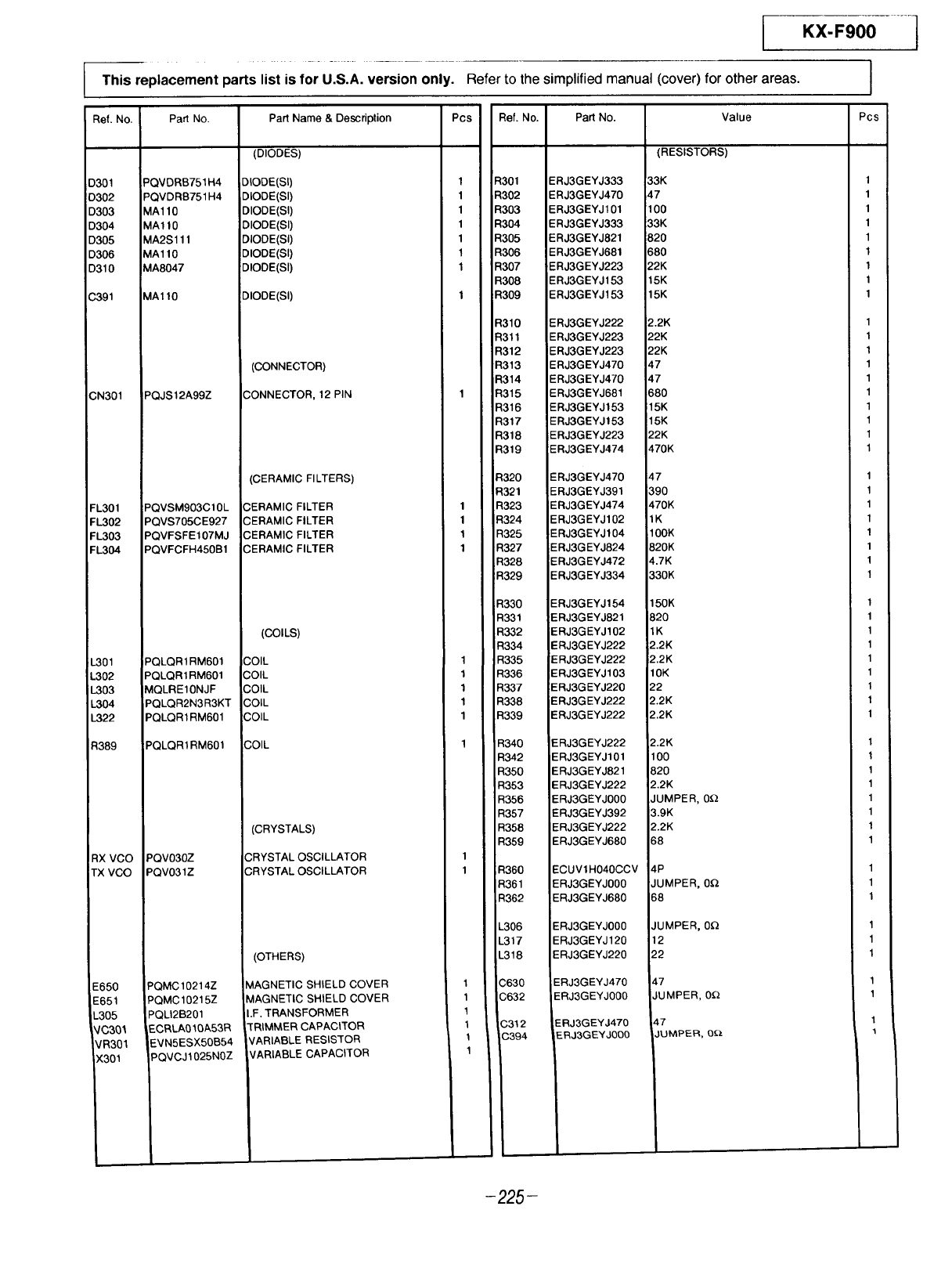
This replacement parts list is for U.S.A. version only.
I
Refer to the simplified manual (cover) for other areas.
KX-F900 ]
I
el. No, I Part No.
I
301 I PQV DRB751 N4
302 IPQVDRB751 H4
303 IMA110
304 IMAl10
305 IMA2S111
306 IMA110
310 IMA8047
I
391 IMAl10
W301 "PQJS12A99Z
.301
.302
_303
_304
I
Y01
|02
303
304
322
389
x vco
_(vco
PQVSM903Cl 0L
PQVS705CE927
PQVFSFE107MJ
PQVFCFH450B1
PQLQR1RM601
PQLQR1 RM601
MQLRE10NJF
PQLQR2N3 R3KT
PQLQR1 RM601
650
651
305
'C301
1R301
(301
PQLQR1RM601
PQV030Z
PQV031Z
PQMC 10214Z
PQMC 10215Z
PQLI2B201
F_CRLA010A53R
EVN5ESX50B54
PQVCJ 1025NOZ
PartName & Description
(DIODES)
DIODE(SI)
DIODE(SI)
DIODE(SI)
DIODE(SI)
DIODE(SI)
DIODE(SI)
DIODE(Sl)
DIODE(SI)
(CONNECTOR)
CONNECTOR, 12PIN
(CERAMIC FILTERS)
CERAMIC FILTER
CERAMIC FILTER
CERAMIC FILTER
CERAMIC FILTER
(COILS)
COIL
COIL
COIL
COIL
COIL
COIL
(CRYSTALS)
CRYSTAL OSCILLATOR
CRYSTAL OSCILLATOR
(OTHERS)
MAGNETIC SHIELD COVER
MAGNETIC SHIELD COVER
I.F. TRANSFORMER
TRIMMER CAPACITOR
/ARIABLE RESISTOR
ARIABLE CAPACITOR
_CS
1
1
1
1
1
1
1
1
1
1
I
t
1
1
1
1
1
1
1
1
1
I
I
I
I
I
I
I
',ef. No. I Part No.
I
301 IERJ3GEYJ333
302 IERJ3GEYJ470
303 IERJ3GEYJ101
_04 IERJ3GEYJ333
305 IERJ3GEYJ821
306 IERJ3GEYJ681
307 IERJ3GEYJ223
308 IERJ3GEYJ153
309 I ERJ3GEYJ153
I
310 IERJ3GEYJ222
_,11 IERJ3GEYJ223
312 I ERJ3GEYJ223
313 I ERJ3GEYJ470
314 I ERJ3GEYJ470
315 I ERJ3GEYJ681
316 I ERJ3GEYJ153
Value
(RESISTORS)
317 IERJ3GEYJt 53
318 ERJ3GEYJ223
319 ERJ3GEYJ474
320 ERJ3GEYJ470
321 ERJ3GEYJ391
323 ERJ3GEYJ474
324 ERJ3GEYJ102
325 ERJ3GEYJ104
327 ERJ3GEYJ824
328 ERJ3GEYJ472
329 ERJ3GEYJ334
330 E RJ3G EYJ 154
331 :ERJ3GEYJ821
332 ERJ3GEYJ102
334 ERJ3GEYJ222
335 ERJ3GEYJ222
336 ERJ3G EYJ 103
337 ERJ3GEYJ220
338 ERJ3GEYJ222
339 ERJ3GEYJ222
340 ERJ3GEYJ222
342 ERJ3GEYJ101
350 E RJ3G EYJ821
353 ERJ3GEYJ222
356 ERJ3GEYJ000
357 ERJ3GEYJ392
358 ERJ3GEYJ222
359 ERJ3GEYJ680
360 ECUVlH040CCV
361 ERJ3GEYJ000
362 ERJ3GEYJ680
306 ERJ3GEYJ000
317 ERJ3GEYJ120
318 ERJ3GEYJ220
',630 ERJ3GEYJ470
;632 ERJ3GEYJ000
;312 ERJ3GEYJ470
.3394 ERJ3GEYJOO0
33K
47
100
33K
820
680
22K
15K
15K
2.2K
22K
22K
47
47
58O
15K
15K
22K
470K
47
390
470K
1K
100K
820K
4.7K
330K
150K
820
1K
2.2K
2.2K
10K
22
2.2K
2.2K
2.2K
100
820
2.2K
JUMPER, 0_
3.9K
2.2K
68
4P
JUMPER, 0Q
58
JUMPER, 0_
12
22
47
JUMPER, 0Q
47
JUMPER, 0o
Pcs
1
1
1
1
1
1
1
1
1
1
1
1
1
1
1
1
1
1
1
1
1
1
1
1
1
1
1
1
1
1
1
1
1
1
1
1
1
1
1
1
1
1
1
1
I
I
I
1
1
1
1
1
1
1
L
-225-
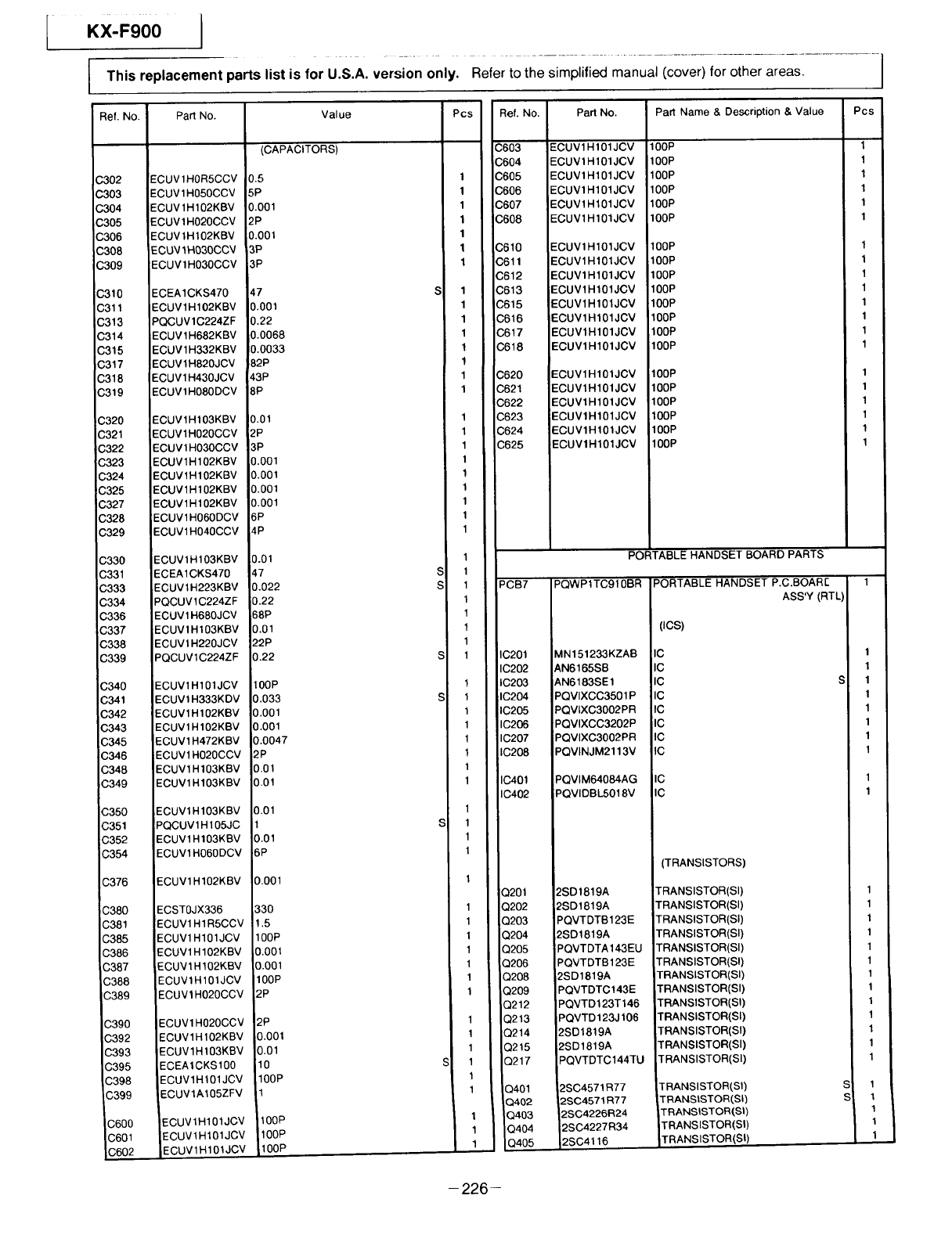
I KX-F900 I
..........................................................
This replacement parts list is for U.S.A. version only, Refer to the simplified manual (cover) for other areas.
Ref. No. Part No.
C302
C303
C304
C305
C306
C308
C309
C310
C311
C313
C314
C315
C317
C318
C319
C320
C321
,_322
C323
C324
C325
C327
C328
C329
C330
C331
C333
C334
C336
C337
C338
C339
C340
C341
C342
C343
C345
C346
C348
,C349
C350
C351
C352
C354
C376
C380
C381
C385
C386
C387
C388
C389
C390
C392
C393
C395
C398
C399
C600
C601
_02
ECUV 1HOR5CCV
ECUV 1H050CCV
ECUV 1H 102KBV
ECUV 1H020CCV
ECUV 1H102KBV
ECUV 1H030CCV
ECUVlH030CCV
ECEA1CKS470
ECUVlH102KBV
PQCUVlC224ZF
ECUV1H682KBV
ECUV1H332KBV
ECUV1H820JCV
ECUV1H430JCV
ECUVlH080DCV
ECUV1H103KBV
ECUV1H020CCV
ECUV1H030CCV
ECUV1H102KBV
ECUV1H102KBV
ECUV1H102KBV
ECUVlH102KBV
ECUV1H060DCV
ECUV1H040CCV
ECUV1H 103KBV
ECEA1CKS470
ECUV1H223KBV
PQCUVlC224ZF
ECUV1H680JCV
ECUVlH103KBV
ECUV1H220JCV
PQCUV1C224ZF
ECUVlH101JCV
ECUV1H333KDV
ECUV1H102KBV
ECUV1H102KBV
ECUV1H472KBV
ECUV1H020CCV
ECUV1H103KBV
ECUV1H103KBV
ECUV1H103KBV
PQCUV1H105JC
ECUV1H103KBV
ECUV1H060DCV
ECUV1H102KBV
ECSTOJX336
ECUV1H1R5CCV
ECUV1H101JCV
ECUV1H102KBV
ECUV1H102KBV
ECUV1H101JCV
ECUV1H020CCV
ECUV1H020CCV
ECUV1H102KBV
ECUVlH103KBV
ECEAlCKS100
ECUV1H101JCV
ECUV1A105ZFV
ECUV1H101JCV
ECUV1H101JCV
I::PI t\l II-1IN 1 .I(_,V
Value
(CAPACITORS)
0.5
5P
0.001
2P
0,001
3P
3P
47
0,001
0.22
0.0068
0.0033
82P
43P
8P
0.01
2P
3P
0.001
0.001
0.001
0.001
6P
:4P
0.01
47
0.022
0.22
68P
0.01
22P
0.22
100P
0.033
0.001
0.001
0.0047
2P
0.01
0.01
0.01
1
0.01
6P
3.001
33O
.5
100P
0.001
0.001
100P
2P
2P
0,001
0.01
10
100P
1
100P
100P
[INNP
Pcs
1
1
1
1
1
1
1
S 1
1
1
1
1
1
1
1
1
1
1
1
1
1
1
1
1
1
S1
S1
1
1
t
1
S 1
1
S 1
1
1
1
1
1
1
1
S 1
1
1
1
1
1
1
1
1
1
1
1
1
1
S1
1
1
1
1
1
Ref. No,
C603
;604
C605
C606
C607
C608
C610
C611
C612
C613
C615
C616
C617
C618
C620
C621
C622
C623
C624
C625
Pa_ No.
ECUV1H101JCV
ECUV1H101JCV
ECUV1H101JCV
ECUV1H101JCV
ECUV1H101JCV
ECUV1H101JCV
ECUV1H101JCV
ECUV1H101JCV
ECUV1H101JCV
ECUV1 H101JCV
ECUV1H101JCV
ECUV1 H101JCV
ECUVlH101JCV
ECUVl H101JCV
ECUV1H101JCV
ECUV1H101JCV
ECUV1H101JCV
ECUV1H101JCV
ECUV1H 101JCV
ECUV1 H101JCV
Part Name & Description & Value Pcs
100P
100P
100P
100P
100P
100P
100P
100P
t00P
100P
100P
100P
100P
100P
100P
100P
100P
100P
100P
100P
1
1
1
1
1
1
1
1
1
1
1
1
1
1
1
1
1
1
1
1
PORTABLE HANDSET BOARD PARTS
PCB7 PQWP1TC910BR PORTABLE HANDSET P.C.BOARr 1
ASS'Y (RTL)
IC201 MN151233KZAB IC
IC202 AN6165SB IC
IC203 AN6183SE1 IC
IC204 PQVIXCC3501P IC
IC205 PQVIXC3002PR IC
IC206 PQVIXCC3202P IC
IC207 PQVIXC3002PR IC
IC208 PQVINJM2113V IC
PQVIM64084AG
PQVIDBL5018V
2SD1819A
2SD1819A
PQVTDTB123E
2SD1819A
PQVTDTA 143EU
PQVTDTB123E
2SD1819A
PQVTDTC143E
PQVTD 123T 146
PQVTD123J 106
2SD1819A
2SD1819A
PQVTDTC144TU
2SC4571R77
2SC4571R77
2SC4226R24
2SC4227R34
2SC4116
(ics)
IC
IC
(TRANSISTORS)
TRANSISTOR(SI)
TRANSISTOR(SI)
TRANSISTOR(SI)
TRANSISTOR(SI)
TRANSISTOR(SI)
TRANSISTOR(SI)
TRANSISTOR(S0
TRANSISTOR(SI)
TRANSISTOR(SI)
TRANSlSTOR(SI)
TRANSlSTOR(SI)
TRANSISTOR(SI)
TRANSISTOR(SI)
TRANSISTOR(St)
TRANStSTOR(SI)
TRANSISTOR(SI)
TRANSISTOR(SI)
TRANSISTOR(SI)
IC401
IC402
Q201
Q202
Q203
Q204
Q205
Q206
Q208
Q209
Q212
Q213
Q214
3215
3217
Q401
Q402
Q403
Q404
Q405
1
1
1
1
1
1
1
1
1
1
1
1
1
1
1
1
1
1
1
1
1
S 1
S 1
1
1
1
-226-
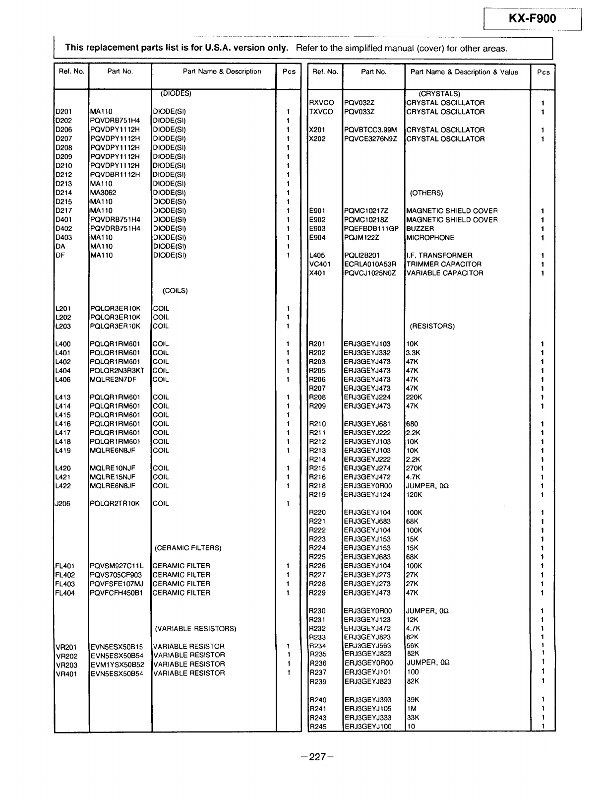
Ref. No. Part No.
IKX-F900
replacement parts list is for U.S.A. version only. Refer to the simplified manual (cover) for other areas.
POS
D201 MA110
D202 PQVDRB751H4
D206 PQVDPY 1112H
D207 PQVDPY | 112H
D208 PQVDPY1112H
D209 PQVDPY1112H
D210 PQVDPY 1112H
D212 PQVDBR1112H
D213 MAll0
D214 MA3062
D215 MA110
D217 MA110
D401 PQVDRB751H4
D402 PQVDRB751 H4
D403 MA110
DA MA110
DF MA110
L201 PQLQR3ER 10K
L202 PQLQR3ER10K
I..203 PQLQR3ER10K
L400 PQLQR1RM601
L401 PQLQR1RM601
L402 PQLQR1RM601
L404 PQLQR2N3R3KT
L406 MQLRE2N7DF
L413 PQLQR1RM601
L414 PQLQR1RM601
L415 PQLQR1RM601
L416 PQLQR1RM601
L417 PQLQR1RM601
L418 PQLQR 1RM601
L419 MQLRE6N8JF
L420 MQLRE10NJF
L421 MQLRE15NJF
L422 MQLRE6N8JF
J206 PQLQR2TR10K
FL401 PQVSM927C11L
FL402 PQVS705CF903
FL403 PQVFSFE107MJ
FL404 PQVFCFH450B1
VR201 EVN5ESX50B15
VR202 EVN5ESX50B54
VR203 EVM1YSX50B52
VR401 EVN5ESX50B54
Part Name & Description
(DIODES)
DIODE(SI)
DIODE(SI)
DIODE(SI)
DIODE(SI)
DIODE(SI)
DIODE(SI)
DIODE(SI)
DIODE(SI)
DIODE(SI)
DIODE(SI)
DIODE(SI)
DIODE(SI)
DIODE(SI)
DIODE(SI)
DIODE(SI)
DIODE(St)
DIODE(SI)
Pcs Ref. No.
(COILS)
COIL
COIL
COIL
COIL
COIL
COIL
COIL
COIL
COIL
COIL
COIL
COIL
COIL
COIL
COIL
COIL
COIL
COIL
COIL
1
1
1
1
1
1
1
1
1
1
1
1
1
I
1
1
1
1
1
1
I
I
I
I
I
1
1
1
1
1
1
1
(CERAMIC FILTERS)
CERAMIC FILTER
CERAMIC FILTER
CERAMIC FILTER
CERAMIC FILTER
1
1
1
(VARIABLE RESISTORS)
VARIABLE RESISTOR
VARIABLE RESISTOR
VAR ABLE RESISTOR
VARIABLE RESISTOR
1
1
1
1
1
1
1
1
RXVCO
TXVCO
X201
X202
E901
E902
E903
E904
L405
VC401
X401
R201
Pa_ No.
PQV032Z
PQV033Z
PQVBTCC3.99M
PQVCE3276N9Z
PQMC10217Z
PQMC 10218Z
PQEFBDB111GP
PQJM122Z
PQLI2B201
ECRLA010A53R
PQVCJ 1025N0Z
ERJ3GEYJ 103
R202 ERJ3GEYJ332
R203 ERJ3GEYJ473
R205 ERJ3GEYJ473
R206 ERJ3GEYJ473
R207 ERJ3GEYJ473
R208
R209
R210
R211
R212
R213
R214
R215
R216
R218
ERJ3GEYJ224
ERJ3GEYJ473
ERJ3GEYJ681
ERJ3GEYJ222
ERJ3GEYJ103
ERJ3GEYJ103
ERJ3GEYJ222
ERJ3GEYJ274
ERJ3GEYJ472
ERJ3GEYOR00
R219 ERJ3GEYJ124
R220 ERJ3GEYJ104
R221 ERJ3GEYJ683
R222 ERJ3GEYJ104
R223 ERJ3GEYJ153
R224 ERJ3GEYJ153
R225 ERJ3GEYJ683
R226 ERJ3GEYJ104
R227 ERJ3GEYJ273
R228 ERJ3GEYJ273
R229 ERJ3GEYJ473
R230 ERJ3GEYOR00
R231 ERJ3GEYJ123
R232 ERJ3GEYJ472
R233 ERJ3GEYJ823
R234 ERJ3GEYJ563
R235 ERJ3GEYJ823
R236 ERJ3GEYOR00
R237 ERJ3GEYJ101
R239 ERJ3GEYJ823
R240 ERJ3GEYJ393
R241 ERJ3GEYJ105
R243 ERJ3GEYJ333
R245 ERJ3GEYJ100
Part Name & Description & Value
(CRYSTALS)
CRYSTAL OSCILLATOR
CRYSTAL OSCILLATOR
CRYSTAL OSCILLATOR
CRYSTAL OSCILLATOR
(OTHERS)
MAGNETIC SHIELD COVER
MAGNETIC SHIELD COVER
BUZZER
MICROPHONE
I.F. TRANSFORMER
TRIMMER CAPACITOR
VARIABLE CAPACITOR
(RESISTORS)
10K
3.3K
47K
47K
47K
47K
220K
47K
680
2.2K
10K
10K
2.2K
270K
4.7K
JUMPER, 0Q
120K
100K
68K
100K
15K
15K
68K
100K
27K
27K
47K
JUMPER, 0Q
12K
4.7K
82K
56K
82K
JUMPER, 0Q
100
82K
39K
1M
33K
10
1
1
1
1
1
1
1
1
1
1
1
1
1
1
1
1
1
1
1
1
1
1
1
1
1
1
1
1
1
1
1
1
1
1
I
I
1
1
I
I
I
I
I
1
1
1
1
-227-
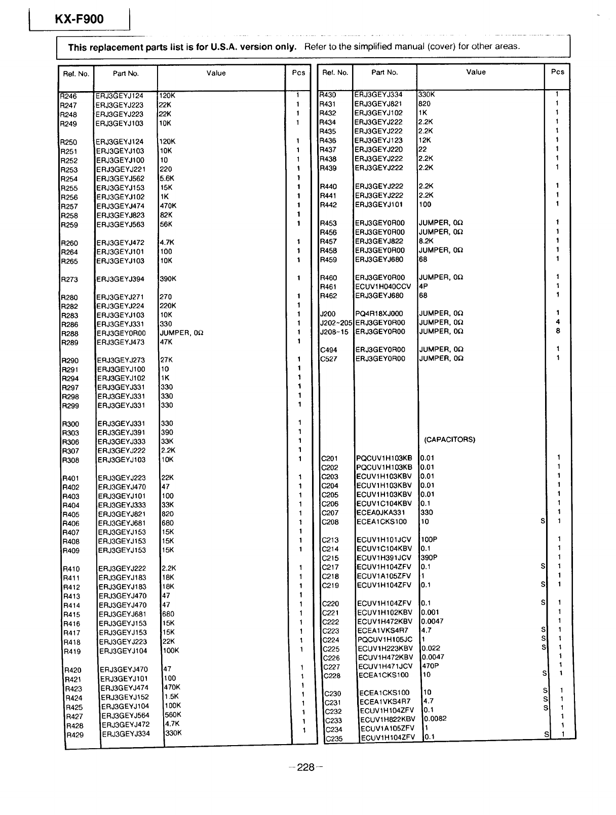
IKX-F900
I This replacement parts list is for U.S.A. version only. Refer to the simplified manual (cover) for other areas.
PaM No._el. No.
120K
22K
22K
10K
120K
10K
10
220
5.6K
15K
1K
470K
82K
56K
4.7K
100
10K
390K
270
220K
10K
330
JUMPER, 0_
47K
27K
10
1K
330
330
330
330
390
33K
2.2K
10K
22K
47
100
33K
820
680
15K
15K
15K
2.2K
18K
18K
47
47
680
15K
15K
22K
100 K
ERJ3GEYJ 124
ERJ3GEYJ223
ERJ3GEYJ223
ERJ3GEYJ 103
_>46
247
_>48
._49
47
100
470K
1.5K
100K
560K
4.7K
330K
Pcs
1
1
1
1
I
I
I
I
I
I
1
1
I
I I
I
I
I
I
I
I
I
1
1
1
1
1
1
1
1
1
1
1
1
1
1
1
1
1
1
1
1
I
I
I
I
I
I
I
I
I
I
250
251
ERJ3GEYJ124
ERJ3GEYJ103
252 ERJ3GEYJ100
253 ERJ3GEYJ221
254 ERJ3GEYJ562
255 ERJ3GEYJ153
256 ERJ3GEYJ102
257 ERJ3GEYJ474
258 ERJ3GEYJ823
259 ERJ3GEYJ563
260 ERJ3GEYJ472
264 ERJ3GEYJ101
265 ERJ3GEYJ103
273 ERJ3GEYJ394
280 ERJ3GEYJ271
282 ERJ3GEYJ224
283 ERJ3GEYJ103
286 ERJ3GEYJ331
288 ERJ3GEYOR00
289 ERJ3GEYJ473
290 ERJ3GEYJ273
:291 ERJ3GEYJ100
;294 ERJ3GEYJ102
1297 ERJ3GEYJ331
1298 ERJ3GEYJ331
1299 ERJ3GEYJ331
1300 ERJ3GEYJ331
1303 ERJ3GEYJ391
1306 ERJ3GEYJ333
I307 ERJ3GEYJ222
1308 ERJ3GEYJ103
1401 ERJ3GEYJ223
1402 ERJ3GEYJ470
1403 ERJ3GEYJ101
1404 ERJ3GEYJ333
1405 ERJ3GEYJ821
1406 ERJ3GEYJ681
1407 ERJ3GEYJ153
1408 ERJ3GEYJ153
1409 ERJ3GEYJ153
_410 ERJ3GEYJ222
_411 ERJ3GEYJ183
_412 ERJ3GEYJ183
_413 ERJ3GEYJ470
:1414 ERJ3GEYJ470
_415 ERJ3GEYJ681
_416 ERJ3GEYJ153
t417 ERJ3GEYJ153
t418 ERJ3GEYJ223
t419 ERJ3GEYJ104
:1420 ERJ3GEYJ470
_421 ERJ3GEYJ101
R423 ERJ3GEYJ474
R424 ERJ3GEYJ152
R425 ERJ3GEYJ104
R427 ERJ3GEYJ564
R428 ERJ3GEYJ472
R429 ERJ3GEYJ334
I
Value
1
1
1
1
1
1
[ 1
11
I
I
tef. No. I Part No.
I
430 IERJ3GEYJ334
431 IERJ3GEYJ821
432 IERJ3GEYJ102
434 I ERJ3GEYJ222
435 IERJ3GEYJ222
436 IERJ3GEYJ123
437 IERJ3GEYJ220
438 IERJ3GEYJ222
439 IERJ3GEYJ222
440 I ERJ3GEYJ222
441 IERJ3GEYJ222
442 IERJ3GEYJI01
453 IERJ3GEYOR00
456 IERJ3GEYOR00
457 I ERJ3GEYJ822
458 I ERJ3GEYOR00
459 IERJ3GEYJ680
460 |ERJ3GEYOR00
461 |ECUV1HO40CCV
462 / ERJ3GEYJ680
_00 /PQ4 R18XJ0O0
202~2051ERJ3GEYOR00
208-15 / ERJ3GEYOR00
i
;494 ERJ3GEYOR00
:527 ERJ3GEYOR00
;201 PQCUV1H103KB
:202 PQCUV1H103KB
:203 ECUV1H103KBV
;204 ECUV1 H103KBV
;205 ECUV1H103KBV
;206 ECUVlCl04KBV
;207 ECEAOJKA331
;208 ECEAlCKSl00
;213 ECUV1H101JCV
;214 ECUVlCl04KBV
;215 ECUV1H391JCV
;217 ECUV1H104ZFV
;218 ECUVlA105ZFV
;219 ECUV1H104ZFV
;220 ECUV1H 104ZFV
;221 ECUV1H102KBV
;222 ECUV1H472KBV
;223 ECEA1VKS4R7
;224 PQCUV 1H105JC
3225 ECUV1H223KBV
3226 ECUVlH472KBV
D227 ECUV1H471JCV
3228 ECEA1CKSIO0
C230 ECEAlCKS100
C231 ECEA1VKS4R7
C232 ECUV1HIO4ZFV
C233 ECUV1H822KBV
C234 ECUV1A105ZFV
_C235 iECUV1R104ZFV
Value
330K
820
1K
2.2K
2.2K
12K
22
2.2K
2.2K
2.2K
2.2K
100
JUMPER, 0_
JUMPER, 0_
8.2K
JUMPER, 0_
68
JUMPER, OQ
4P
68
JUMPER, 0_
JUMPER, 0_
JUMPER, 0_
JUMPER, 0_
JUMPER, 0_
(CAPACITORS)
0.01
0.01
0.01
0.01
0.01
0.1
330
10
100P
0.1
390P
0.1
1
0.1
0.1
0.001
3.0047
4.7
1
0.022
0.0047
470P
10
10
4.7
0.1
0.0082
1
0.1
Pcs
1
1
1
1
1
1
1
1
1
1
1
1
1
1
1
1
1
1
1
1
1
4
8
1
1
1
1
1
1
1
1
1
1
I
I
I
I
I
I
1
1
1
S1
S 1
S 1
1
1
s 1
S1
SI
S 1
,1
S 1
- 228-
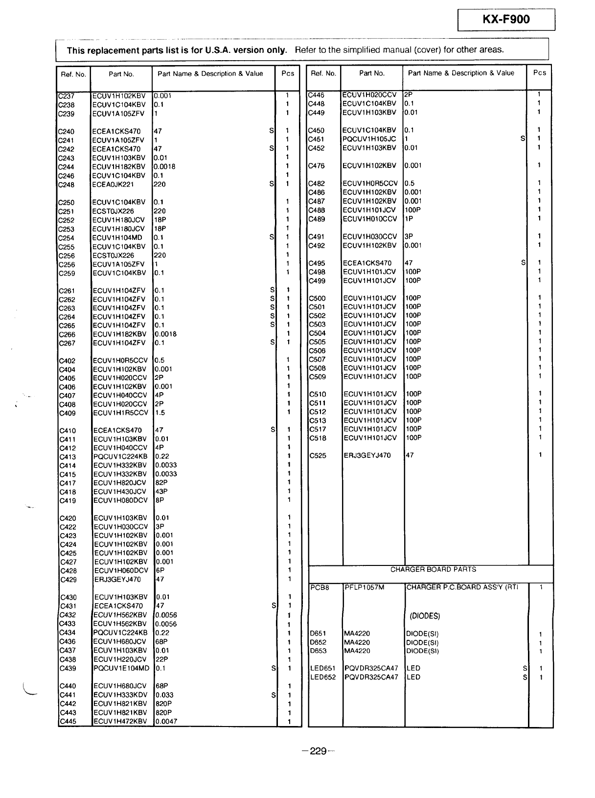
L_
IKX-F900
This replacement parts list is for U.S.A. version only. Refer to the simplified manual (cover) for other areas.
Ref. No.
C237
C238
C239
C240
C241
C242
C243
C244
C246
C248
C250
C251
C252
C253
C254
C255
C256
C256
C259
C261
C262
C263
C264
C265
C266
C267
C402
C404
C405
C406
C407
C408
0409
._410
0411
0412
0413
0,414
C415
0417
C418
C419
C420
C422
C423
C424
C425
C427
C428
C429
C430
C431
C432
C433
0434
_436
0437
C438
C439
C440
C441
C442
C443
C445
Part No.
ECUV1H 102KBV 0.001
ECUV1C104KBV 0.1
ECUVlA105ZFV 1
ECEA1CKS470 47
ECUVlA105ZFV 1
ECEA1CKS470 47
ECUV1H 103KBV 0.01
ECUVlH 182KBV 0.0018
ECUVlCl04KBV D.1
ECEAOJK221 220
ECUVIC104KBV 0.1
ECSTOJX226 220
ECUV1H 180JCV 18P
ECUV1H 180JCV 18P
ECUV1H104MD 0.1
ECUV1C104KBV 0.1
ECSTOJX226 220
ECUV1A105ZFV 1
ECUVlC104KBV 0.1
ECUV1H104ZFV 0.1
ECUVlH 104ZFV 0.1
ECUV1H104ZFV 0.1
ECUVIH104ZFV 0.1
ECUV1H104ZFV 0.1
ECUV1H182KBV 0.0018
;ECUV1H104ZFV 0.1
ECUV1HOR5CCV 0.5
ECUV1H102KBV 0.001
ECUV1H020CCV 2P
ECUV1H102KBV 0.001
ECUVlH040CCV 4P
ECUV1H020CCV 2P
ECUV1H1R5CCV 1.5
ECEA1CKS470 47
ECUVlH103KBV 0.01
ECUV 1H040CCV _4P
PQCUVlC224KB ).22
ECUV1H332KBV D.0033
ECUV1H332KBV 0.0033
ECUV 1H820JCV 82P
ECUV 1H430JCV 43P
ECUV1H080DCV 8P
ECUV1H103KBV 0.01
ECUV1H030CCV 3P
ECUV1H102KBV 0.001
ECUVlH102KBV 0.001
ECUV1H102KBV 0.001
ECUV1H102KBV 0.001
ECUVlH060DCV 6P
ERJ3GEYJ470 47
ECUV1H103KBV 0.01
ECEA 10KS470 47
ECUV1H562KBV 0.0056
ECUV 1H562KBV 0.0056
PQCUV1C224KB ).22
ECUV1H680JCV 68P
ECUV1H103KBV 0.01
ECUV1H220JCV 22P
PQCUVlE104MD 0.1
ECUV1H680JCV 68P
ECUV1H333KDV 0.033
ECUV1H821KBV 820P
ECUV1H821KBV 820P
ECUV1H472KBV 0.0047
Part Name &Description & Value Pcs
1
1
1
S 1
1
S 1
1
1
1
S 1
1
1
1
1
S 1
1
1
1
1
S 1
S 1
S 1
S 1
S1
1
S 1
1
1
1
1
I
1
1
S, 1
1
1
1
1
1
1
1
1
1
1
1
1
1
1
1
1
1
S 1
1
1
1
1
1
1
S 1
1
S1
1
1
1
Ref. No. Part No.
C446 ECUV1H020CCV
C448 ECUV1C104KBV
C449 ECUVlH103KBV
C450 ECUVlCl04KBV
C451 PQCUV1H105JC
C452 ECUV1H103KBV
C476 ECUV1H102KBV
C482 ECUV1HOR5CCV
C486 ECUV1H102KBV
C487 ECUV1H102KBV
C488 ECUV1H101JCV
C489 ECUV1H010CCV
C491 ECUV1H030CCV
C492 ECUV1H102KBV
C495 ECEA1CKS470
C498 ECUV1H101JCV
C499 ECUV1H101JCV
C500
C501
C502
C503
C504
C505
C506
C507
C508
C509
C510
C511
C512
C513
C517
C518
C525
ECUV1H101JCV
ECUV1H101JCV
ECUV1H101JCV
ECUV1 H101JCV
ECUVlH101JCV
ECUVlH101JCV
ECUV1H101JCV
ECUVl H101JCV
ECUV1 H101JCV
ECUV1 H101JCV
ECUVlH101JCV
ECUV1H101JCV
ECUV1H101JCV
ECUV1H101JCV
ECUV1H101JCV
ECUV1 H101JCV
ERJ3GEYJ470
Part Name & Description & Value
2P
0.1
0.01
0.1
1
0.01
0.001
0.5
0.001
0.001
100P
1P
3P
0.001
47
100P
100P
100P
100P
100P
100P
100P
100P
100P
100P
100P
100P
100P
100P
100P
100P
100P
100P
47
I
Pcs
1
1
1
1
S: 1
1
1
1
1
1
1
S 1
1
1
1
1
1
1
1
1
1
1
1
1
1
1
1
1
1
1
CHARGER BOARD PARTS
PCB8 PFLP1057M CHARGER P.C.BOARD ASS'Y (RTI 1
(DIODES)
DIODE(St)
DIODE(SI)
DIODE(SI)
1
1
1
D651 MA4220
D652 MA4220
D653 MA4220
LED651 PQVDR325CA47
LED652 PQVDR325CA47
LED S 1
LED S 1
-229-
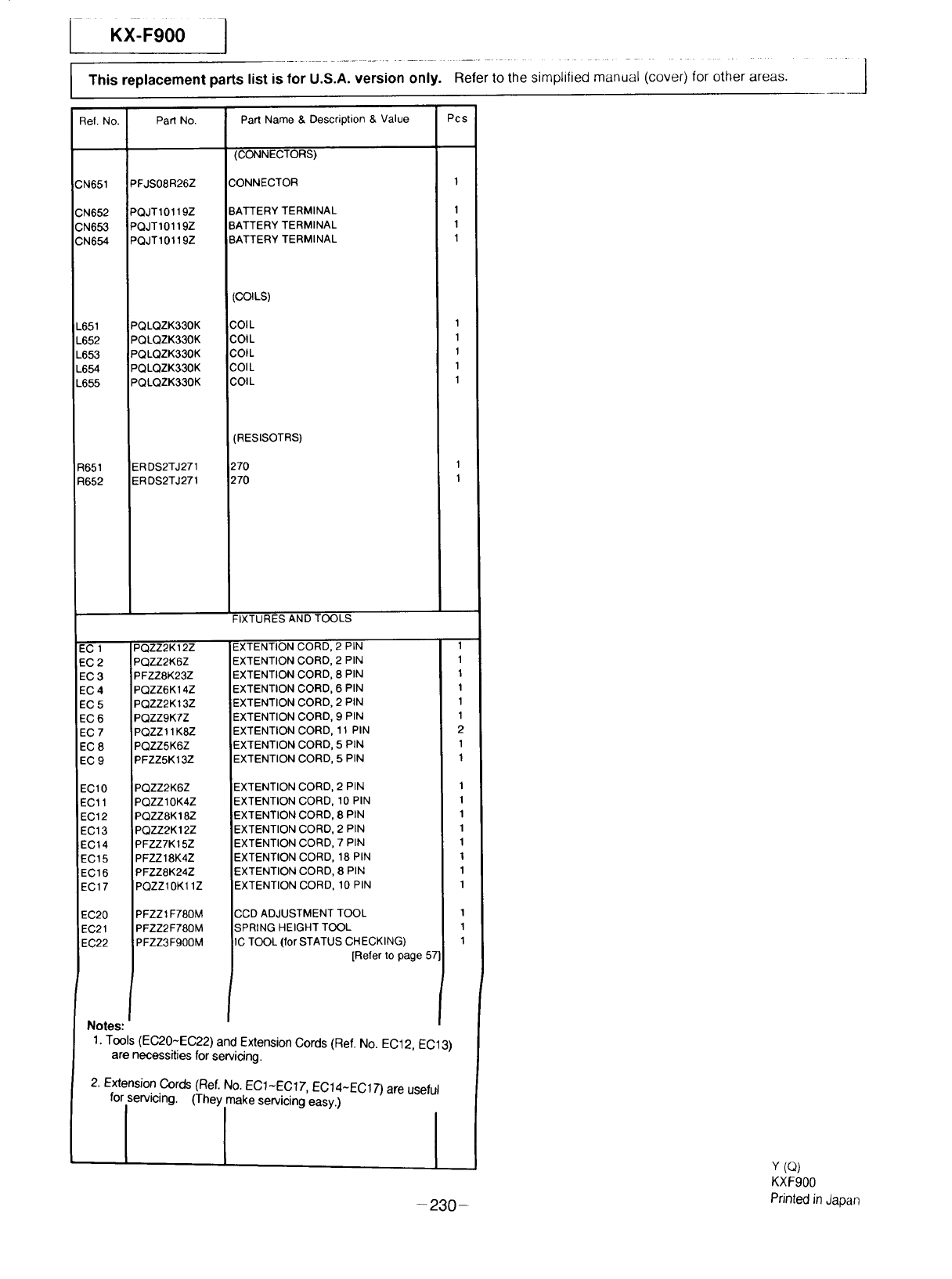
KX-Fg00I
.............................
This replacement parts list is for U.S.A. version only. Refer to the simplified manual (cover) for other areas.
Ref. No. Part No.
CN651 PFJS08R26Z
CN652 PQJT10119Z
CN653 PQJT10119Z
CN654 PQJT10119Z
L651 PQLQZK330K
L652 PQLQZK330K
L653 PQLQZK330K
L654 PQLQZK330K
L655 PQLQZK330K
R651
R652
ERDS2TJ271
ERDS2TJ271
Pa_ Name & Description & Value Pcs
(CONNECTORS)
CONNECTOR 1
BATTERYTERMINAL 1
BATTERYTERMINAL 1
BATTERY TERMINAL 1
[COILS)
COIL
COIL
COIL
COIL
COIL
(RESISOTRS)
270
270
1
1
1
1
1
FIXTURES AND TOOLS
PQZZ2K12Z
PQZZ2K6Z
PFZZ8K23Z
PQZZ6K14Z
PQZZ2Kt3Z
PQZZ9K7Z
PQZZt1K8Z
PQZZ5K6Z
PFZZ5K13Z
PQZZ2K6Z
PQZZ10K4Z
PQZZ8K18Z
PQZZ2K12Z
PFZZ7K15Z
PFZZ18K4Z
PFZZ8K24Z
PQZZ10K11Z
PFZZfF780M
PFZZ2F780M
PFZZ3F900M
otes:
EXTENTION CORD, 2 PIN
EXTENTION CORD, 2 PIN
EXTENTION CORD, 8 PIN
EXTENTION CORD, 6 PIN
EXTENTION CORD, 2 PIN
EXTENTION CORD, 9 PIN
EXTENTION CORD, 11 PIN
EXTENTION CORD, 5 PIN
EXTENTION CORD, 5 PIN
EXTENTION CORD, 2 PIN
EXTENTION CORD, 10 PIN
EXTENTION CORD, 8 PIN
EXTENTION CORD, 2 PIN
EXTENTION CORD, 7 PIN
EXTENTION CORD, 18 PIN
EXTENTION CORD, 8 PIN
EXTENTION CORD, 10 PIN
CCD ADJUSTMENT TOOL
SPRING HEIGHT TOOL
IC TOOL (for STATUS CHECKING)
[Refer to page 57:/
1. Tools (EC20-EC22) and Extension Cords (Ref. No. EC12, EC13)
are necessities for servicing.
1
1
1
1
1
1
2
1
1
I
I
I
I
I
I
I
I
1
1
1
2. Extension Cords (Ref. No. EC1-EC 17, EC14-EC 17) are useful
for servicing. (They make servicing easy.)
I I
- 230-
Y (Q)
KXF900
Printed in Japan
