0B ESP8266__Hardware_User_Guide__EN_v1.1.pages ESP8266 Hardware User Guide EN V1.1
User Manual: Pdf
Open the PDF directly: View PDF ![]() .
.
Page Count: 48

ESP8266EX Hardware User Guide
Version 1.1
Espressif Systems IOT Team
http://bbs.espressif.com
Copyright © 2015

! ! " !
Espressif Systems
ESP8266EX Hardware User Guide
Disclaimer and Copyright Notice
Information in this document, including URL references, is subject to change without notice.
THIS DOCUMENT IS PROVIDED AS IS WITH NO WARRANTIES WHATSOEVER, INCLUDING ANY
WARRANTY OF MERCHANTABILITY, NON-INFRINGEMENT, FITNESS FOR ANY PARTICULAR
PURPOSE, OR ANY WARRANTY OTHERWISE ARISING OUT OF ANY PROPOSAL, SPECIFICATION
OR SAMPLE. All liability, including liability for infringement of any proprietary rights, relating to use
of information in this document is disclaimed. No licenses express or implied, by estoppel or
otherwise, to any intellectual property rights are granted herein.
The WiFi Alliance Member Logo is a trademark of the WiFi Alliance.
All trade names, trademarks and registered trademarks mentioned in this document are property of
their respective owners, and are hereby acknowledged.
Copyright © 2015 Espressif Systems (Shanghai) Pte. Ltd. All rights reserved.
Espressif Systems / Jun 1, 2015 2 48

! ! " !
Espressif Systems
ESP8266EX Hardware User Guide
1. General Overview 5 ......................................................................................................
1.1. Introduction!5"......................................................................................................................
1.2. Features!6"...........................................................................................................................
1.3. Parameters!7".......................................................................................................................
1.4. Major Applications!8"...........................................................................................................
2. Hardware Overview 9 ...................................................................................................
2.1. Terminal Configuration and Functions!9".............................................................................
2.2. Schematics!12"....................................................................................................................
2.2.1. Power-supply Pins!13 .......................................................................................................
2.2.2. Power-on Sequence and Power Reset!14 .........................................................................
2.2.3. Flash !15 ...........................................................................................................................
2.2.4. Crystal Oscillator!15 ..........................................................................................................
2.2.5. RF!16 ................................................................................................................................
2.2.6. External Resistor 12K!17 ...................................................................................................
2.3. Layout Design!17"................................................................................................................
2.3.1. ESP-WROOM Module Design!17 ......................................................................................
2.3.2. ESP8266EX as Slave Device!20 .......................................................................................
2.3.3. FAQ On Hardware Design!22 ............................................................................................
3. ESP-LAUNCHER Development Board 24 ...................................................................
3.1. Instructions on the Use of ESP-LAUNCHER Development Board!25"................................
3.2. Pin Definitions of ESP-LAUNCHER Development Board!28"..............................................
3.3. Typical Applications Using ESP-LAUNCHER!31"................................................................
3.3.1. ESP-LAUNCHER Test Board!31 ........................................................................................
3.3.2. SMD Module ESP-WROOM-02!31 ....................................................................................
3.3.3. DIP Module ESP-WROOM-01!35 ......................................................................................
4. Compiling, Downloading, and Debugging 36 .............................................................
4.1. Set Up the Compiling Environment!36"...............................................................................
4.2. Download Firmware!38".......................................................................................................
4.3. Debugging AT Commands via UART!38".............................................................................
Espressif Systems / Jun 1, 2015 3 48
Table of Contents

! ! " !
Espressif Systems
ESP8266EX Hardware User Guide
5. Typical Applications 40 .................................................................................................
5.1. WiFi smart hardware converted from UART serial ports!40"...............................................
5.2. Sensor!40"............................................................................................................................
5.3. Smart light!40"......................................................................................................................
5.4. Smart plug!41".....................................................................................................................
6. Appendix 42 ...................................................................................................................
6.1. Schematics of ESP-LAUNCHER Development Board!42"..................................................
Part 1: Interfaces!43"..................................................................................................................
Part 2: 5V Power!46"..................................................................................................................
Part 3: Test Board!46"................................................................................................................
6.2. Schematics of ESP-LAUNCHER Test Board!46".................................................................
6.3. Schematics of ESP-WROOM Serial WiFi Modules!47"........................................................
6.4. Schematics of ESP8266EX as SDIO/SPI Slave Device!48.................................................
Espressif Systems / Jun 1, 2015 4 48
! ! " !
Espressif Systems
ESP8266EX Hardware User Guide
1. General Overview
1.1. Introduction
Espressif Systems’ Smart Connectivity Platform (ESCP) is a set of high performance, high integration
wireless SOCs, designed for space and power constrained mobile platform designers. It provides
unsurpassed ability to embed Wi-Fi capabilities within other systems, or to function as a standalone
application, with the lowest cost, and minimal space requirement.
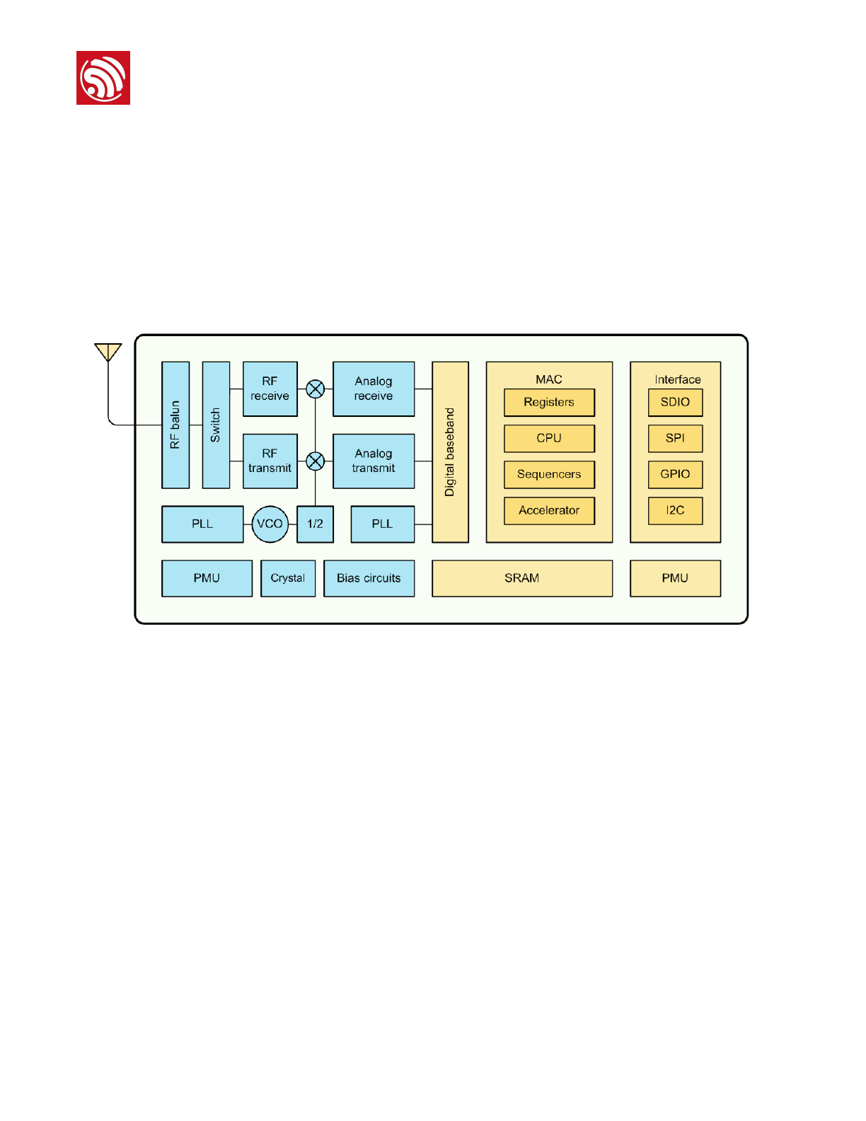
Figure 1 ESP8266EX Block Diagram
ESP8266EX offers a complete and self-contained Wi-Fi networking solution; it can be used to host
the application or to offload Wi-Fi networking functions from another application processor.
When ESP8266EX hosts the application, it boots up directly from an external flash. In has integrated
cache to improve the performance of the system in such applications.
Alternately, serving as a Wi-Fi adapter, wireless internet access can be added to any micro controller-
based design with simple connectivity (SPI/SDIO or I2C/UART interface).
ESP8266EX is among the most integrated WiFi chip in the industry; it integrates the antenna
switches, RF balun, power amplifier, low noise receive amplifier, filters, power management modules,
it requires minimal external circuitry, and the entire solution, including front-end module, is designed
to occupy minimal PCB area.
Espressif Systems / Jun 1, 2015 5 48

! ! " !
Espressif Systems
ESP8266EX Hardware User Guide
ESP8266EX also integrates an enhanced version of Tensilica’s L106 Diamond series 32-bit processor,
with on-chip SRAM, besides the Wi-Fi functionalities. ESP8266EX is often integrated with external
sensors and other application specific devices through its GPIOs; sample codes for such applications
are provided in the software development kit (SDK).
Espressif Systems’ Smart Connectivity Platform (ESCP) demonstrates sophisticated system-level
features include fast switching between sleep and wake-up mode for energy-efficiency purpose,
adaptive radio biasing for low-power operation, advance signal processing, and spur cancellation
and radio co-existence features for common cellular, Bluetooth, DDR, LVDS, LCD interference
mitigation.
1.2. Features
• 802.11 b/g/n
• Integrated low power 32-bit MCU
• Integrated 10-bit ADC
• Integrated TCP/IP protocol stack
• Integrated TR switch, balun, LNA, power amplifier and matching network
• Integrated PLL, regulators, and power management units
• Supports antenna diversity
• Wi-Fi 2.4 GHz, support WPA/WPA2
• Support STA/AP/STA+AP operation modes
• Support Smart Link Function for both Android and iOS devices
• SDIO 2.0, (H) SPI, UART, I2C, I2S, IR Remote Control, PWM, GPIO
• A-MPDU & A-MSDU aggregation & 0.4s guard interval
• Deep sleep power <10uA, Power down leakage current < 5uA
• Wake up and transmit packets in < 2ms
• Standby power consumption of < 1.0mW (DTIM3)
• +20 dBm output power in 802.11b mode
• Operating temperature range -40C ~ 125C
• FCC, CE, TELEC, Wi-Fi Alliance, and SRRC certified
Espressif Systems / Jun 1, 2015 6 48

! ! " !
Espressif Systems
ESP8266EX Hardware User Guide
1.3. Parameters
Categories
Items
Values
WiFi Paramters
Certificates
FCC/CE/TELEC/SRRC
WiFi Protocles
802.11 b/g/n
Frequency Range
2.4G-2.5G (2400M-2483.5M)
Tx Power
802.11 b: +20 dBm
802.11 g: +17 dBm
802.11 n: +14 dBm
Rx Sensitivity
802.11 b: -91 dbm (11 Mbps)
802.11 g: -75 dbm (54 Mbps)
802.11 n: -72 dbm (MCS7)
Types of Antenna
PCB Trace, External, IPEX Connector,
Ceramic Chip
Hardware
Paramaters
Peripheral Bus
UART/SDIO/SPI/I2C/I2S/IR Remote Control
GPIO/PWM
Operating Voltage
3.0~3.6V
Operating Current
Average value: 80mA
Operating Temperature Range
-40°~125°
Ambient Temperature Range
Normal temperature
Package Size
5x5mm
External Interface
N/A
Software
Parameters
Wi-Fi mode
station/softAP/SoftAP+station
Security
WPA/WPA2
Encryption
WEP/TKIP/AES
Firmware Upgrade
UART Download / OTA (via network)
Ssoftware Development
Supports Cloud Server Development / SDK
for custom firmware development
Network Protocols
IPv4, TCP/UDP/HTTP/FTP
Espressif Systems / Jun 1, 2015 7 48

! ! " !
Espressif Systems
ESP8266EX Hardware User Guide
Table 1 Parameters of ESP8266EX
1.4. Major Applications
Major fields of ESP8266EX applications to Internet-of-Things include:
• Home Appliances
• Home Automation
• Smart Plug and lights
• Mesh Network
• Industrial Wireless Control
• Baby Monitors
• IP Cameras
• Sensor Networks
• Wearable Electronics
• Wi-Fi Location-aware Devices
• Security ID Tags
• Wi-Fi Position System Beacons
Categories
Items
Values
Software
Parameters
User Configuration
AT Instruction Set, Cloud Server, Android/
iOS App
Espressif Systems / Jun 1, 2015 8 48
! ! " !
Espressif Systems
ESP8266EX Hardware User Guide
2. Hardware Overview
2.1. Terminal Configuration and Functions
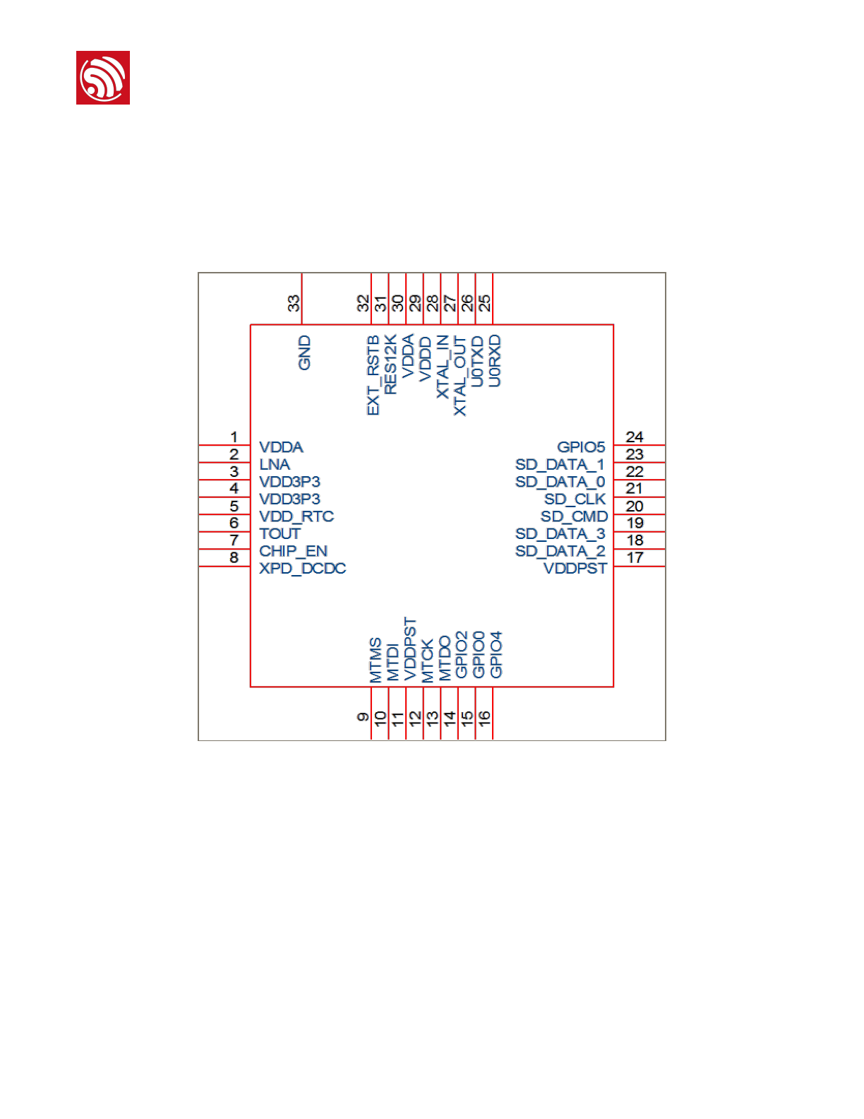
The pin assignments for 32-pin QFN package is illustrated in Fig. 2.
Figure 2 Pin Assignments
Table 2 below presents an overview on the general pin attributes and the functions of each pin.
Espressif Systems / Jun 1, 2015 9 48

! ! " !
Espressif Systems
ESP8266EX Hardware User Guide
Pin
Name
Type
Function
1
VDDA
P
Analog Power 3.0 ~3.6V
2
LNA
I/O
RF Antenna Interface,
Chip Output Impedance=50Ω
No matching required but we recommend that the π-type
matching network is retained.
3
VDD3P3
P
Amplifier Power 3.0~3.6V
4
VDD3P3
P
Amplifier Power 3.0~3.6V
5
VDD_RTC
P
NC(1.1V)
6
TOUT
I
ADC Pin
7
CHIP_EN
I
Chip Enable. High: On, chip works properly; Low: Off, small
current
8
XPD_DCDC
I/O
Deep-Sleep Wakeup;GPIO16
9
MTMS
I/O
GPIO14; HSPI_CLK
10
MTDI
I/O
GPIO12; HSPI_MISO
11
VDDPST
P
Digital/IO Power Supply (1.8V~3.3V)
12
MTCK
I/O
GPIO13; HSPI_MOSI; UART0_CTS
13
MTDO
I/O
GPIO15; HSPI_CS; UART0_RTS
14
GPIO2
I/O
UART Tx during flash programming; GPIO2
15
GPIO0
I/O
GPIO0; SPI_CS2
16
GPIO4
I/O
GPIO4
17
VDDPST
P
Digital/IO Power Supply (1.8V~3.3V)
18
SDIO_DATA_2
I/O
Connect to SD_D2 (Series R: 200Ω); SPIHD; HSPIHD; GPIO9
19
SDIO_DATA_3
I/O
Connect to SD_D3 (Series R: 200Ω); SPIWP; HSPIWP; GPIO10
20
SDIO_CMD
I/O
Connect to SD_CMD (Series R: 200Ω); SPI_CS0; GPIO11
21
SDIO_CLK
I/O
Connect to SD_CLK (Series R: 200Ω); SPI_CLK; GPIO6
22
SDIO_DATA_0
I/O
Connect to SD_D0 (Series R: 200Ω); SPI_MSIO; GPIO7
23
SDIO_DATA_1
I/O
Connect to SD_D1 (Series R: 200Ω); SPI_MOSI; GPIO8
Espressif Systems / Jun 1, 2015 10 48

! ! " !
Espressif Systems
ESP8266EX Hardware User Guide
Table 2 Attributes and Functions of Pins
Note: GPIO2, GPIO0, MTDO can be configurable as 3-bit SDIO mode.
Pin
Name
Type
Function
24
GPIO5
I/O
GPIO5
25
U0RXD
I/O
UART Rx during flash programming; GPIO3
26
U0TXD
I/O
UART Tx during flash progamming; GPIO1; SPI_CS1
27
XTAL_OUT
I/O
Connect to crystal oscillator output, can be used to provide BT
clock input
28
XTAL_IN
I/O
Connect to crystal oscillator input
29
VDDD
P
Analog Power 3.0V~3.6V
30
VDDA
P
Analog Power 3.0V~3.6V
31
RES12K
I
Serial connection with a 12 kΩ resistor and connect to the
ground
32
EXT_RSTB
I
External reset signal (Low voltage level: Active)
Espressif Systems / Jun 1, 2015 11 48
! ! " !
Espressif Systems
ESP8266EX Hardware User Guide
2.2. Schematics
ESP8266EX is very highly integrated SoC which encapsulates Transilica LX106 core$processor, RAM,
RF components and allow WiFi TCP/IP stack to be implemented on board with just few components
beside ESP8266. The chipset also incorporates built-in self-calibration to compensate for
performance errors, improving the modulation accuracy and stability of wireless communications.
High integration level of this chipset tremendously decreases the number of components used in
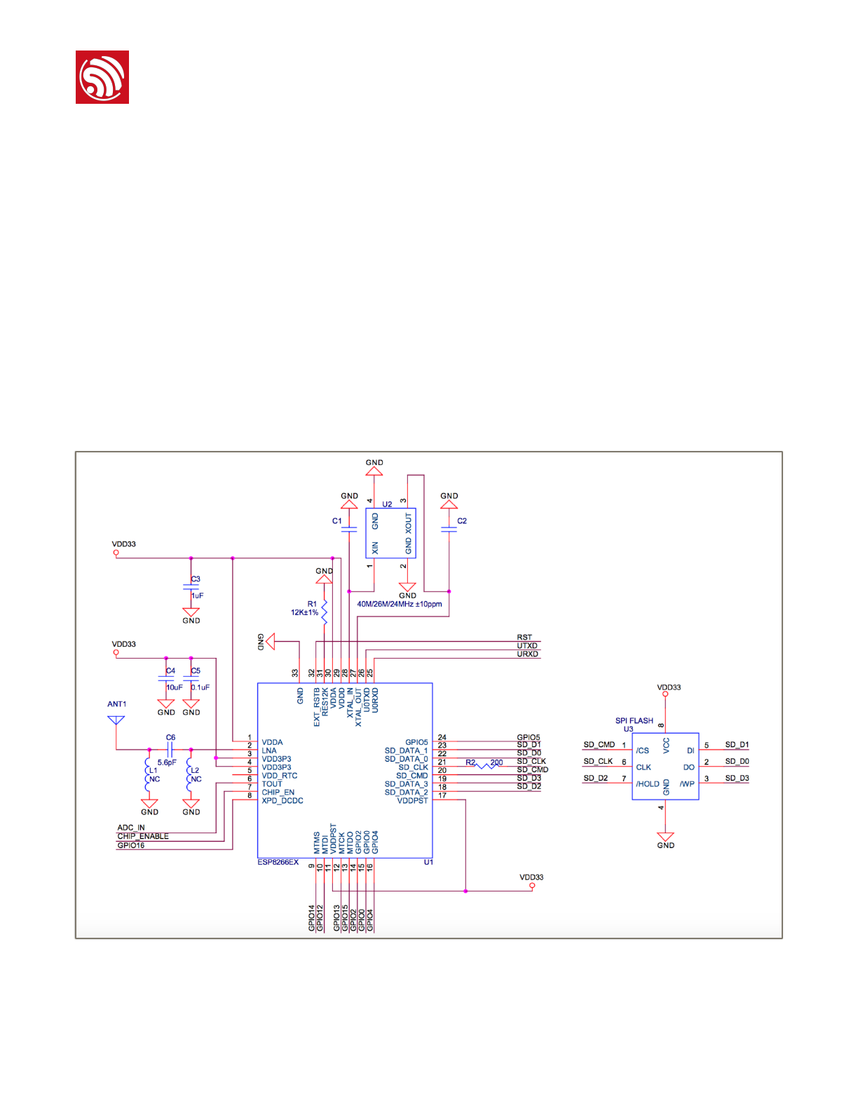
peripheral circuit design. Beside ESP8266EX, only a number of less than 10 resistors and capacitors,
one crystal oscillator, and one SPI Flash is needed to make a complete module with wireless
communication capability. A detailed description of ESP8266EX schematics and layout design are
illustrated here.
The complete circuit diagram of ESP8266EX is illustrated in Figure 3:
Figure 3 ESP8266EX Schematics
Espressif Systems / Jun 1, 2015 12 48
! ! " !
Espressif Systems
ESP8266EX Hardware User Guide
ESP8266EX SCH design covers the following five parts:
• Power supply;
• Power on sequence and reset;
• Flash;
• Crystal oscillator;
• RF.
2.2.1. Power-supply Pins
Digital Power-supply Pins
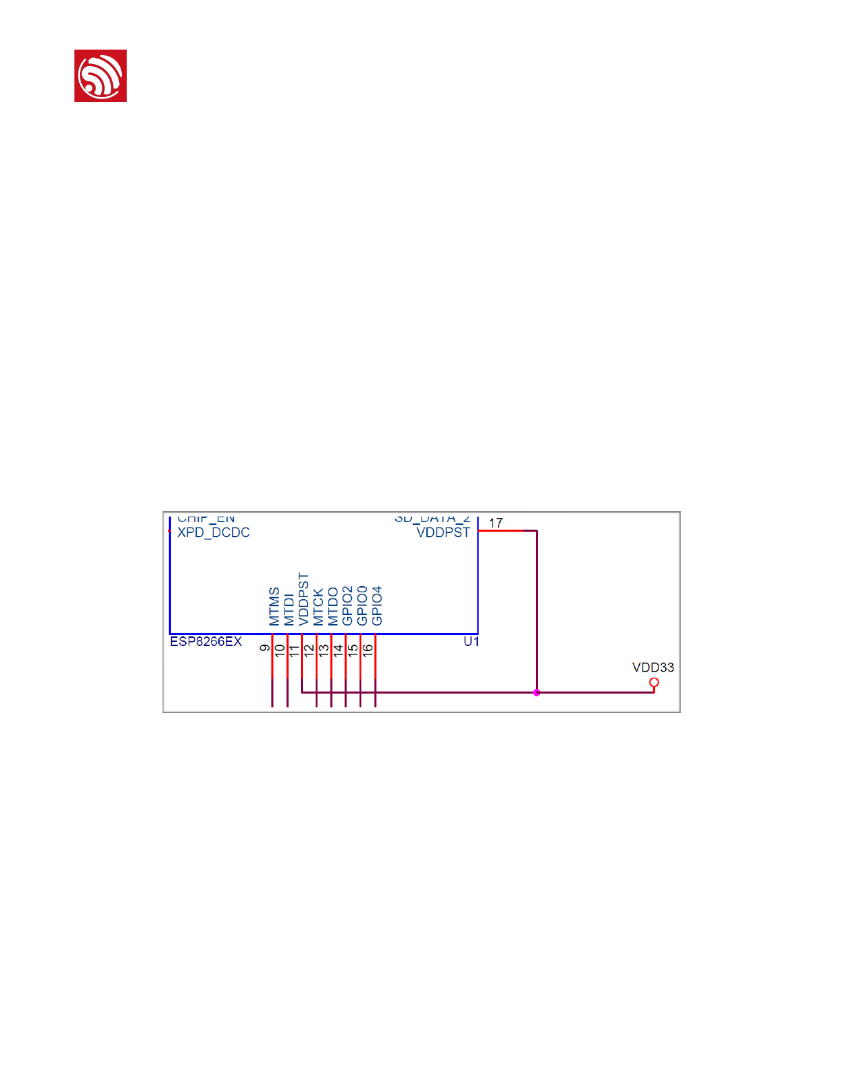
ESP8266EX has only two digital power-supply pins (abbreviated as VDDPST in the circuit diagram),
Pin11 and Pin17. In digital power supply, there is no need to add additional filter capacitors. The
operating voltage range of digital power-supply pins is between 1.8V and 3.3V.
Figure 4 ESP8266EX Digital Power-supply Pins
Analog Power-supply Pins
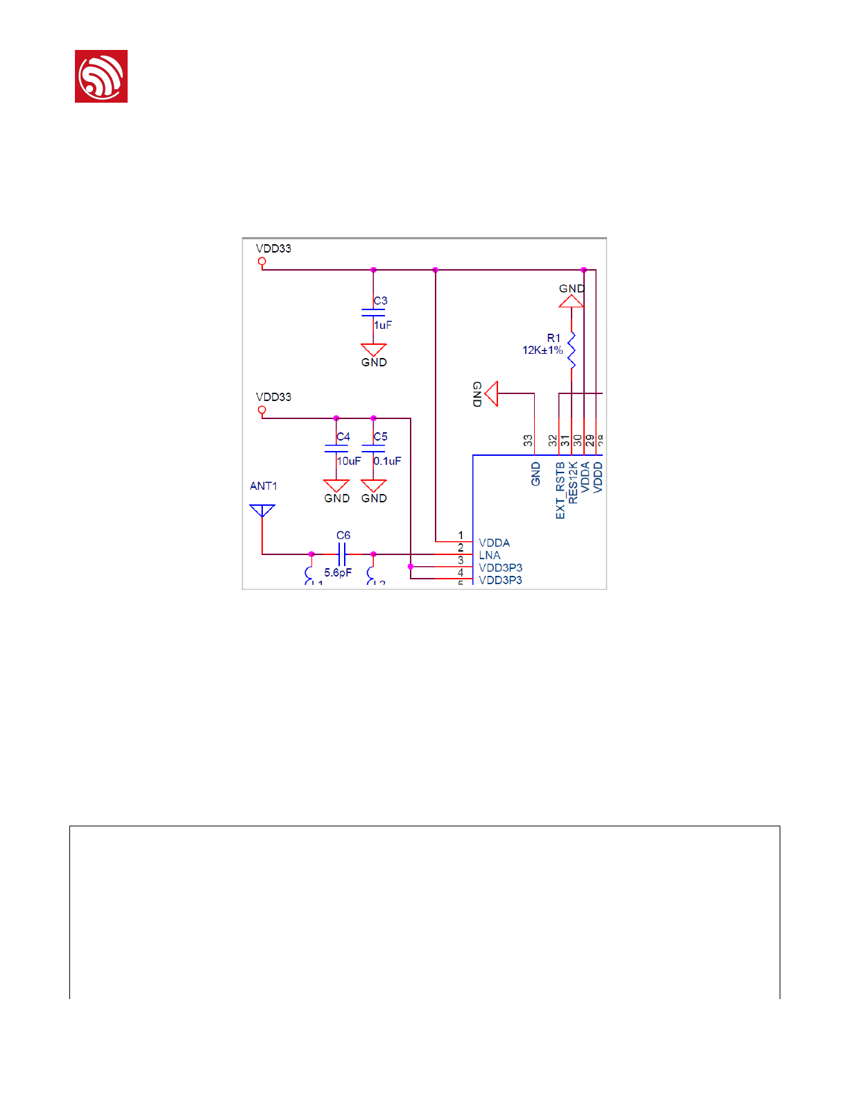
ESP8266EX has 5 analog power-supply pins (abbreviated as VDD33 in the circuit diagram), including
Pin 1, Pin 3, Pin 4, which provides internal power supply for internal PA and LNA respectively, and Pin
28, Pin 29, which supplies power for internal PLL. The operating voltage range of the analog power-
supply pins is between 1.8V and 3.3V.
It should be noted that the power supply channel might be damaged due to the sudden increase of
current when ESP8266EX is transmitting analog signals. Therefore, an additional 0.1uF capacitor with
Espressif Systems / Jun 1, 2015 13 48
! ! " !
Espressif Systems
ESP8266EX Hardware User Guide
a package size of 0603 or 0805 is needed in circuit design. This capacitor can be used in 0.1uF in
match with capacitor with 0.1uF capacitor with 0402 package.
(Notes: There is no need to add magnetic beads in the design of analog power-supply circuit, for
ESP8266EX’s EMC is in conformity with FCC and CE requirements, and has been approved. )
Figure 5 ESP8266EX AVDD
2.2.2. Power-on Sequence and Power Reset
Power-on sequence
The voltage of the chipset’s WiFi power supply systems is 3.3V, therefore only one rule should be
abide by when you power on the device: Pin7 CH_EN, the power enable pin, should be powered on
at the same time when or after the power supply system is powered on.
Note: If the power management IC is connected with the power-on enable pin CHIP_EN, it can control the
power on-and-off of ESP8266EX by output high and low voltage through its GPIOs. However, pulsed current
might be produced at the same time. In order to delay the transmission of pulsed signal and avoid unstable
current of CHIP_EN, a RC time-delay circuit (R=1kΩ, C=100nF) is needed. There is an internal pull-up in the
CHIP_EN pin, so no external pull-up is needed.
Espressif Systems / Jun 1, 2015 14 48
! ! " !
Espressif Systems
ESP8266EX Hardware User Guide
Reset
There exists internal pull-up resistor in the reset pin, Pin32, which can be left dangled when it is not
used. When the chip is enabled, the reset pin is held low. In order to avoid reset caused by external
interference, the lead is generally required to be short, and no external pull-up resistor is necessary.
The enable pin CH_EN (pin 7) can also serve as a reset pin. If voltage for CH_EN pin is low, the
chipset ESP8266EX will power off. Note that this pin cannot be dangled.
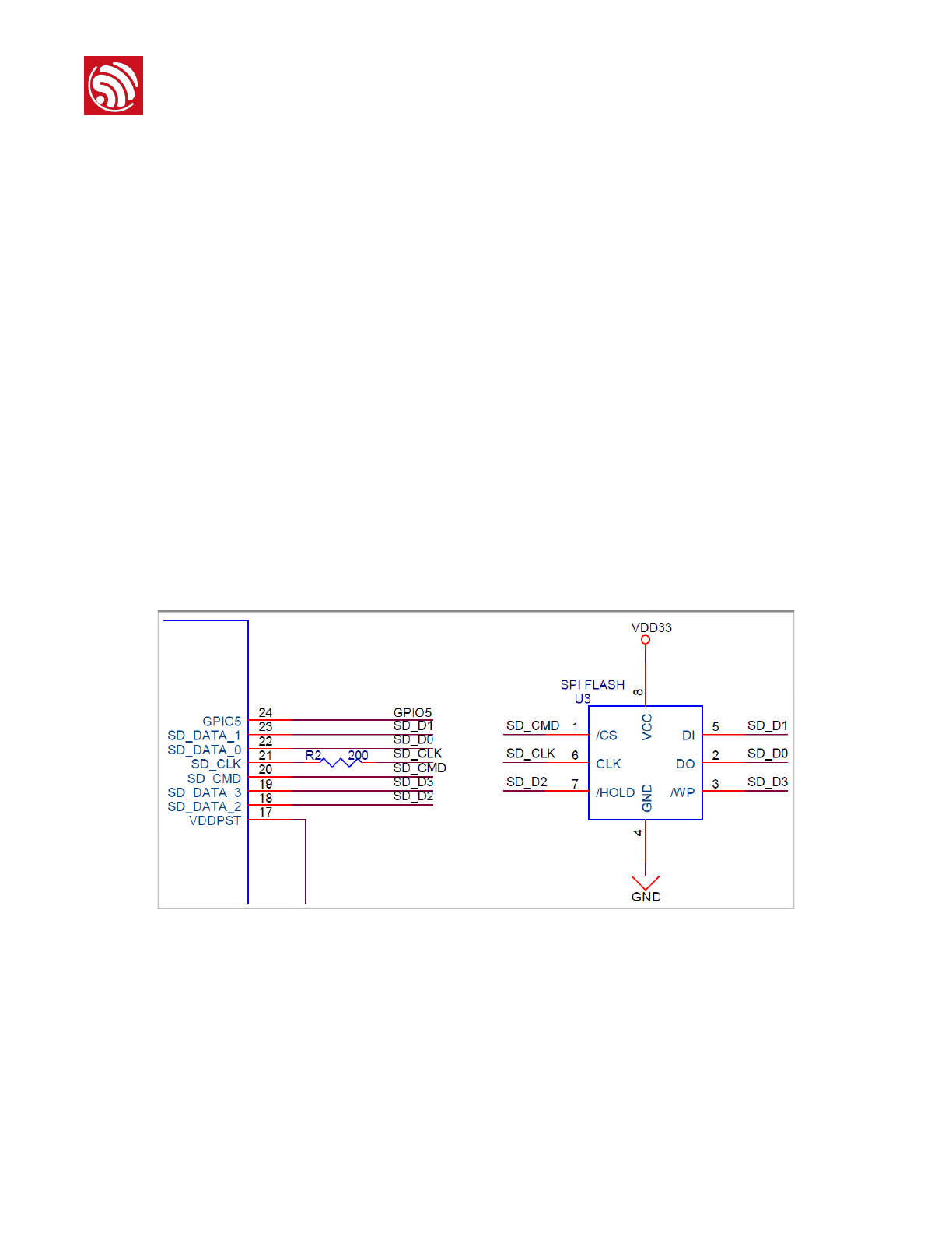
2.2.3. Flash
Currently, the size of flash that we applied in our demo and modules is SPI Flash with 2MB capacity,
and the package size is SOIC_8 (SOP_8).
A resistor (package size: 0402) is connected to Pin21, the SD_CLK pin via serial port, with the aim to
lower the driving current, decrease cross-talk and external interruption, adjust the sequence, and so
on. The initial value of the serial connection resistor is 200 ohm.
Figure 6 ESP8266EX Flash
2.2.4. Crystal Oscillator
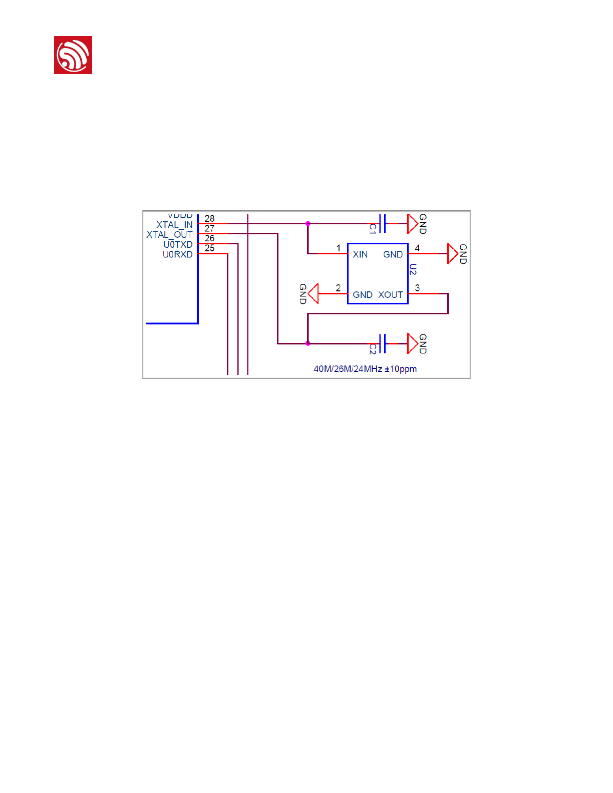
Currently, the frequency of crystal oscillators supported include 40MHz, 26MHz and 24MHz. The
accuracy of crystal oscillators applied should be ±10PPM, and the operating temperature range
should be between -20°C and 85°C. !
Espressif Systems / Jun 1, 2015 15 48
! ! " !
Espressif Systems
ESP8266EX Hardware User Guide
When using the downloading tools, please remember to select the right crystal oscillator type. In
circuit design, capacitors C1 and C2, which are connected to the earth, are added to the input and
output terminals of the crystal oscillator respectively. The values of the two capacitors can be
flexible, ranging from 6pF to 22pF, however, the specific capacitive values of C1 and C2 depend on
further testing and adjustment on the overall performance of the whole circuit. Normally, the
capacitive values of C1 and C2 are within 10pF if the crystal oscillator frequency is 26MHz, while the
values of C1 and C2 are 10pF<C1, C2<22pF if the crystal oscillator frequency is 40MHz.
Figure 7 ESP8266EX Crystal oscillators
Note: Defects in the craftsmanship of the crystal oscillators (for example, high frequency deviation,
unstable working temperature) may lead to the malfunction of ESP8266EX, resulting in the decrease
of overall performance.
2.2.5. RF
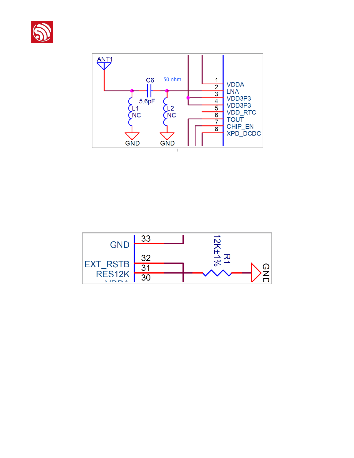
The output impedance of RF pin (Pin 2) is 50 ohm. Normally, when the antenna impedance
approaches 50 ohm, antenna matching is not necessary. However, low-price antenna commercially
available in the market does not feature 50 ohm impedance. Besides, the impedance in 2.4G to 2.5G
frequency band is rather scattered. Therefore, N-type matching network is essential in circuit design
to facilitate antenna matching.!
Espressif Systems / Jun 1, 2015 16 48
! ! " !
Espressif Systems
ESP8266EX Hardware User Guide
Figure 8 ESP8266EX RF
2.2.6. External Resistor 12K
An external resistor that is connected to the ground should be added to ERS12K pin (Pin31), so as to
control the bias current in the circuit. Therefore, relatively high resistance value accuracy is required,
an accuracy of 12K±1% is recommended.
Figure 9 External Resistor
2.3. Layout Design
PCB layout design of products using chipset ESP8266EX is demonstrated in this part. Hereto we
mainly focus on two kinds of designs, one is ESP-WROOM serial to WiFi modules, and the other is
main board mounted with ESP8266EX WiFi module.
2.3.1. ESP-WROOM Module Design
• Module layout design and the key techniques:
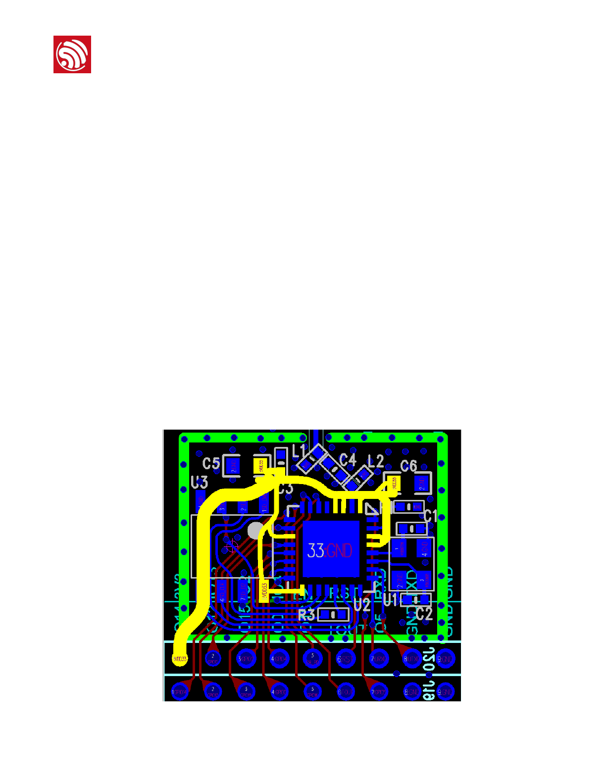
This printed circuit board has four layers.
Espressif Systems / Jun 1, 2015 17 48
! ! " !
Espressif Systems
ESP8266EX Hardware User Guide
The first layer is the TOP layer, signal lines and components are placed on the top of the printed
circuit board;
The second layer is the GND layer, no signal lines is laid so as to ensure an entire plain GND plane;
The third layer is the POWER layer, only power lines can be placed on this layer. However, there is
exceptional cases. When there is no other choice but to place some signal lines on this layer, it is
acceptable.
The forth layer is the BOTTOM layer, only signal lines are designed on this layer, no components
shall be placed on this layer.
• On design of the power-supply part
The power supply voltage of those signal lines highlighted in yellow is 3.3V. The total width of the
power line shall be larger than 15 mil.
Before the power line reaches the analog power-supply pins (including Pin 1, 3, 4, 28, 29) of
ESP8266EX, a 10uF capacitor with 0603 or 0805 package needs to be added, as is illustrated in Fig.
10. C6, which is the capacitor, should be placed adjacent to the analog power-supply pins of the
chipset.
Power lines should be placed on the third layer. When the power lines reached the pins of the
chipset, VIAs are needed so that the power lines can go through the layers to connect the pins of the
chipset on the TOP layer. The diameter of the VIA holes should exceed the width of power lines,
while the drill should be appropriate, a little bit larger than the radius of VIA is enough.
Espressif Systems / Jun 1, 2015 18 48
! ! " !
Espressif Systems
ESP8266EX Hardware User Guide
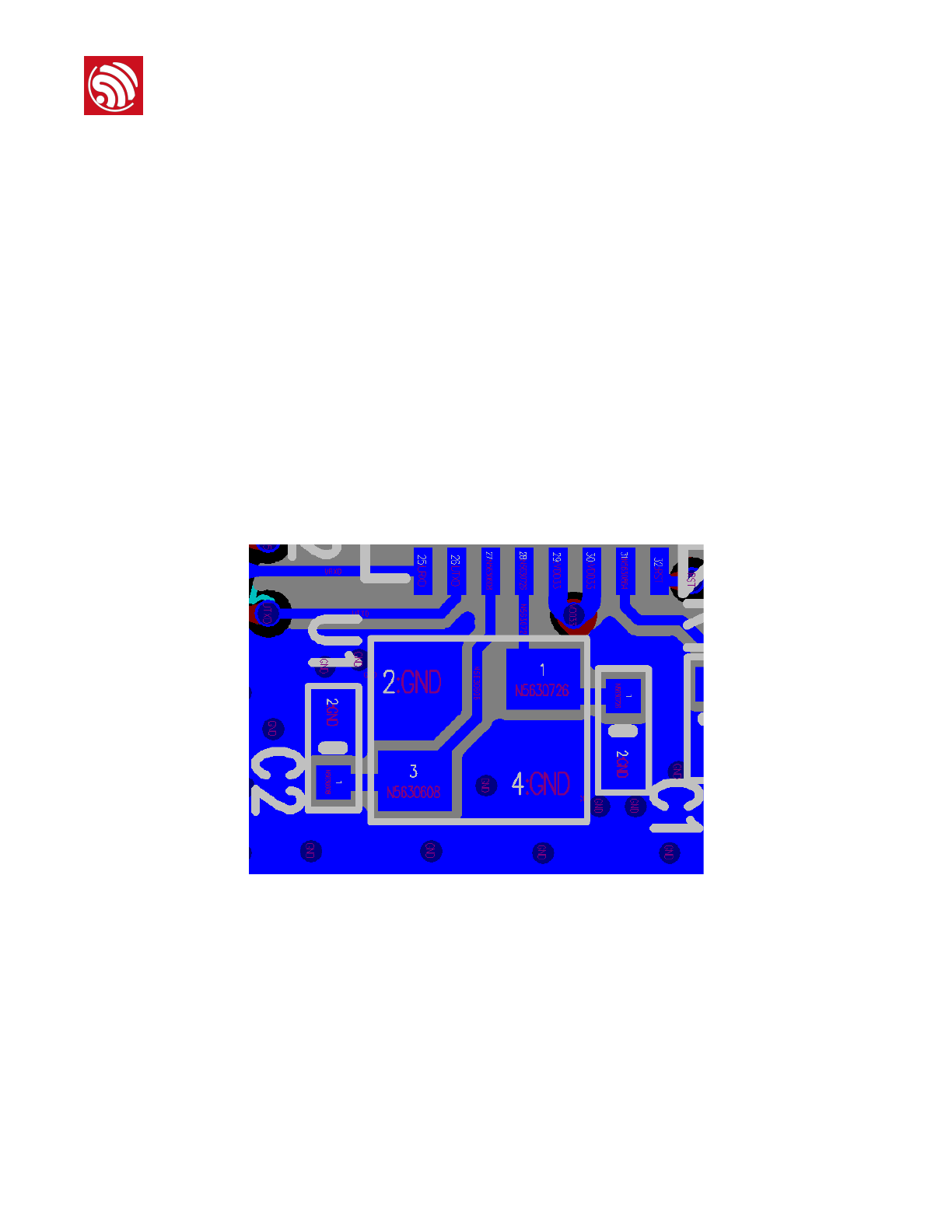
Figure 10 ESP8266EX PCB Layout
• On design of the crystal oscillator
Crystal oscillator should be placed adjacent to the XTAL Pins, the connection lines shouldn’t be too
long, and should be wrapped up for shelter.
The input and output lines cannot be punched, cannot cross the layers or be crossed.
The input and output bypass capacitor should be located near the chip; never set it on the lines.
No high frequency digital signal lines shall be placed under the four layers of the crystal oscillators.
The best choice is that no signal lines is placed under the crystal oscillator. The TOP layer where is
crystal oscillator is placed should be as large as possible.
Magnetic components, such as high current inductors, should not be placed near to crystal oscillator,
a sensitive component.
Figure 11 ESP8266EX Crystal Oscillators PCB Layout
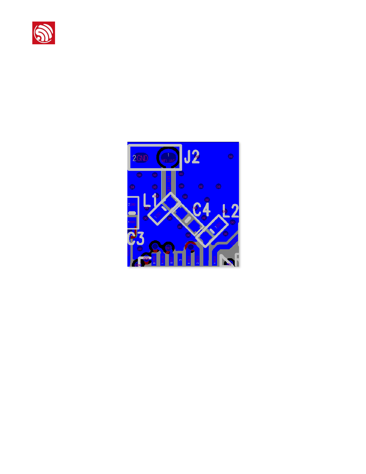
• On design of the RF part
The characteristic impedance that RF lines should control is 50Ω, in order to ensure the complete
board in the second layer. The surrounding drilled hole should be blocked and the lines should be
as short as possible. !
Espressif Systems / Jun 1, 2015 19 48
! ! " !
Espressif Systems
ESP8266EX Hardware User Guide
A π matching circuit near the RF Pin should be reserved in RF lines. RF lines connecting the chip and
antenna should not cover drills, which means cross layer lines are not allowed.
The width of RF lines should not be less than 6 mil and should keep up to10 mil.
RF lines should not be set at a vertical, or a 45-degree angle. Circular lines are allowed if necessary.
No signal lines of high frequency should be set near RF lines.
RF antenna should be set away from high frequency transmitting devices, such as crystal oscillators,
DDR, and certain high frequency clocks (SDIO_CLK, etc).
Figure 12 ESP8266EX RF PCB Layout
2.3.2. ESP8266EX as Slave Device
When ESP8266EX is matched with CPU as a slave unit, information integrity in layout design is more
important than that in analogue design.
Due to the system accountability, the increasing high frequency signals would result in interference
in ESP8266EX. Attentions should be paid to those interferences.
Main boards in PAD or TV BOX will be discussed.!
Espressif Systems / Jun 1, 2015 20 48
! ! " !
Espressif Systems
ESP8266EX Hardware User Guide
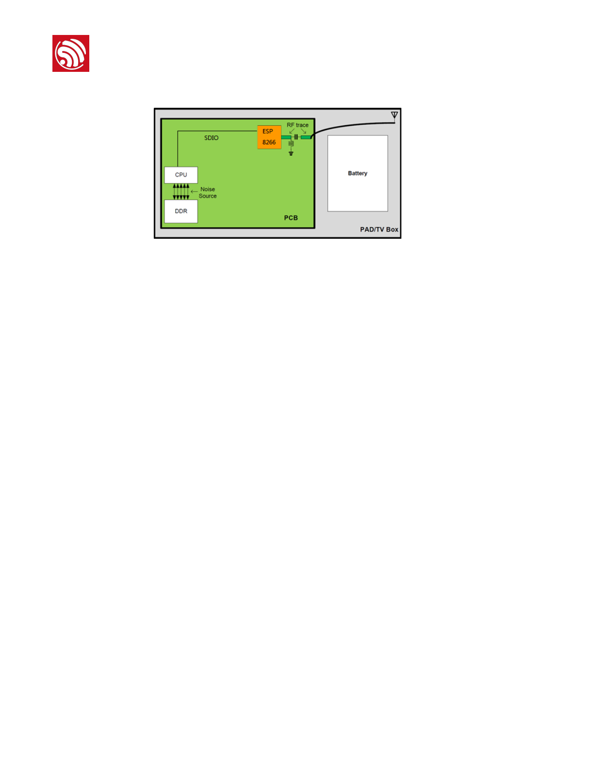
Figure 13 Planning Framework of Layout Plane Position
The digital signals between CPU and DDR produces high frequency noise and will interference WiFi
frequency in the air. Therefore, the following points should be noted in system designs:
• As shown in Fig.4, ESP8266EX is on the edge of PCB and far away from CPU and DDR(the
noise source CPU+DDR). The increase in distance will decrease the interference distance and
would reduce the coupling noise;
• When ESP8266EX communicates with CPU via SDIO, it would be optimal if the six signal lines
are connected through a 200Ω series resistor. The purpose is to reduce the drive current and
the corresponding interference and at sthe same time sequence problems due to the
inconsistent length of SDIO lines.
• PCB onboard antenna should not be selected as it receive relatively large interferences and is
vulnerable to the coupling noise that might affect RF performance. External antenna should be
applied that can be directed away from the PCB board so that the influence of interference
signals of high frequency on WiFi will be reduced.
• During layout, the high frequency signal line control between CPU and MEM should be noted.
The line layout should comply firmly with high frequency signal regulations (refer to DDR line
control documents) where CLK should be lined underground, data lines and addr lines should
be packed and lined underground.
• The GND of WiFi circuit and other high power devices should be separated and connected
through wires if there are electric machines in system design.
• Antenna should keep away from noise source of high frequency, such as LCD, HDMI, Camera
Sensor, USB and other high frequency signals.
Espressif Systems / Jun 1, 2015 21 48

! ! " !
Espressif Systems
ESP8266EX Hardware User Guide
2.3.3. FAQ On Hardware Design
1. Typical phenomenon: The current ripple is not large, but the TX performance of RF is rather
bad.
Problem description: ripple has a strong impact on the performance of RF TX. It should be noted
that ripple must be tested when ESP8266EX sends normal packets. The ripple increases when the
power gets high. Generally, the ripple value should <120mV when sending the packet 11N MCS7the
ripple value should <200mV when sending the packet 11B 11M.
Solution: add a10uF filter capacitor to the branch of source circuit ( ESP8266EX AVDD pin). 10uF
capacitor should be placed adjacent to the VDDA pin. The ripple is much small and more stable
when it’s near the pin.
2. Typical phenomenon: when the chipset is sending data packages, the power ripple is small
and the TX performance of the RF is not good
Problem description: the poor TX performance of the RF is not only caused by the problematic
power ripple, but also by abnormal crystal, for example, the crystal itself is of low quality and the
crystal frequency offset is too big (when over ±40PPM, the ESP8266EX will not be able to work
properly and the performance will get worse accordingly); or the crystal has been interfered with
high frequency signals, for example, the input signals couple with the output signals or the output
signals couple with the input signals due to the cross wiring of input and output signal wires at
different layers; or high frequency signal wires are wired below the crystal such as the SDIO wiring
and UART wiring, which will cause malfunction of the crystal. Another problem that has not received
due attention is the existence of inductive or radioactive parts beside the crystal, for example, great
inductance, antenna (many designers, when considering the area of the ESP8266EX module, often
place the crystal very close to the PCB on-board antenna, which, at the time ESP8266EX module
sends data packages, will lead to direct coupling between radioactive interference and the crystal,
the crystal and the antenna, thus resulting in very poor performance of the RF).
Solution: this problem is mainly caused by inconsiderate layout and can only be solved by re-layout.
See Chapter 2.7.2 for details about layout.
3. Typical phenomenon: when ESP8266EX is sending data packages, the power value tested
by an instrument is much higher or lower than the target power value, and the EVM is
relatively poor
Problem description: the sharp difference between the power value tested by an instrument and the
target power value is largely caused by the mismatch of the resistance in the section from the chipset
RF pin to the antenna. That is to say the resistance in the section from the chipset RF pin to the
antenna deviates from the 50Ω a lot, leading to reflections during signal transmission. The reflections
Espressif Systems / Jun 1, 2015 22 48

! ! " !
Espressif Systems
ESP8266EX Hardware User Guide
can be divided into positive reflection and negative reflection. When the resistance in the section
from the chipset RF pin to the antenna is larger than 50Ω, positive reflection will be formed and the
power will grow bigger than normal; if the resistance is smaller than 50Ω, negative reflection will be
formed and the power will become smaller than normal. By the way, mismatch of the resistance will
affect the performance of the PA within the chipset, leading to PA’s premature entry into the
saturation regions, thus resulting in large distortion of the signals and according poor EVM
performance.
Solution: leave a π shaped circuit on the RF wiring, which shall allow match of the resistance with the
antenna, so as to enable the resistance in the section from the chipset RF pin to the antenna to
approximate 50Ω.
4. Typical phenomenon: TX performance is not bad, but the RX sensitivity is rather high.
Problem description: Good TX performance means proper RF impedance matching. RX
performance is strongly influenced by the external interference coupling to the antenna. As modules
pose no other high frequency signal coupling to the antenna, RX sensitivity is thus not influenced
except when crystal oscillators are set near the antenna, or UART TX and RX conducts through RF
trace lines. If ESP8266EX serves as slave, there will be quite a number of high frequency interference.
Therefore, signal interference depends on board design.
Solution: keep the antenna away from crystal oscillators and keep RF trace lines away from high
frequency signal.!
Espressif Systems / Jun 1, 2015 23 48
! ! " !
Espressif Systems
ESP8266EX Hardware User Guide
3. ESP-LAUNCHER Development Board
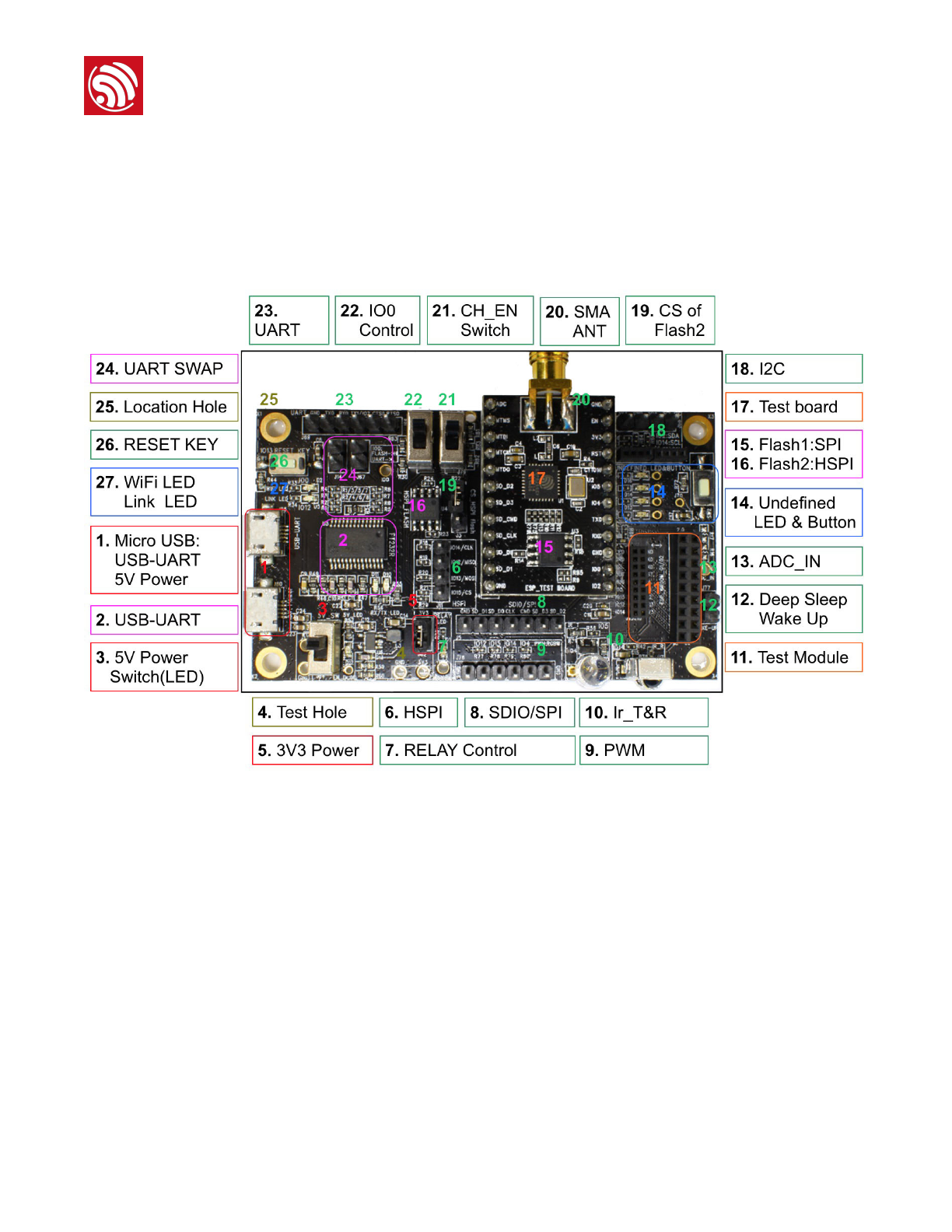
Espressif Systems provides ESP8266EX development board for quick evaluation and familiarisation
of products and for secondary development for customers. The size of the demo board is
46mm*78.5mm. Functional components on the demo board are illustrated in the Figure 14 below.
Figure 14 ESP8266EX Development Board
Espressif Systems / Jun 1, 2015 24 48

! ! " !
Espressif Systems
ESP8266EX Hardware User Guide
3.1. Instructions on the Use of ESP-LAUNCHER Development Board
Users can connect the development board to a PC using USB interface or WiFi wireless connection
interface, then configure and test the demo board. Functional descriptions of components on the
development board is illustrated in Table 3 below.
Notice ⚠:
For development board provided BEFORE July 1, 2015, both of the two Micro USB interfaces should be
powered on. Among them, one is used for 5V power supply, the other one used for serial communication.
For development board provided AFTER July 1, 2015, the two Micro USB interfaces can both be used for 5V
power supply and serial communication. You can choose any one of them.
Espressif Systems / Jun 1, 2015 25 48

! ! " !
Espressif Systems
ESP8266EX Hardware User Guide
Name
Functional Description
Micro USB Interface
There are two USB interfaces, one is used for 5V power supply, the other one is used
for serial communication. (Refer to Part 1 in Fig. 14)
Please pay attention to the notice on Page 25.
Power Supply
One USB interface is used to supply 5V power, while a DC/DC regulator is used
convert 5V to 3.3V, supplying power for WiFi part. There is one indicator light
besides the 3.3V power, and a skip stitch that can be used to test the power current.
Slide Switches
Slide switches are used to convert voltage level of GPIO0 interface and chip enable
pin CH_EN.
It should be noted that when a slide switch is pulled up, the voltage level is high,
while when pulled down, the voltage level is low. (Refer to Part 3, 21, and 22 in Fig.
14)
Reset Buttons
SW1 is connected to MTCK (GPIO13), and is used for resetting IoT applications.
Function of SW2 has not defined yet. (Refer to Part 26 and 14 in Fig. 14)
Indicator lights
Red light (D2) is an indicator light for the working condition of WiFi.
It’s not available now!
Blue light (D3) is an indicator light for the communication of the server. (Refer to Part
27 in Fig. 14)
Green light (D1) is an indicator light for relay switch control. (Refer to Part 7 in Fig. 14)
Blue light (D11) and Red light (D10) indicate working status of Rx and Tx serial ports
respectively. (Refer to Part 2 in Fig. 14)
Red light (D12) is indicator light for 5V power supply. (Refer to Part 3 in Fig. 14)
Function of D4, D13, D14, and D16 can be defined by users themselves. (Refer to
Part 14 in Fig. 14)
Jumpers
J82: It needs to be short-circuited using a jumper, so that 3.3V power supply can be
connected to other posterior circuits. It can also be used to test the power of the
circuit. (Refer to Part 5 in Fig. 14)
J3: It functions as chip selection for HSPI flash.
HSPI flash is closed when the jumper is short-circuiting connected to the upper two
needles, while HSPI is enabled when the jumper is short-circuiting connected to the
lower two needles. (Refer to Part 19 in Fig. 14)
J14 and J67: When J14 is short-circuiting connected, it indicates that GPIO13 is
connected to U0CTS; when J67 is short-circuiting connected, it indicates that
GPIO15 is connected to U0RTS. (Refer to Part 24 in Fig. 14)
J77: When J77 is short-circuiting connected, is indicates that GPIO16 is connected to
EXT_RSTB. This can be used to awake the device from deep-sleep mode. (Refer to
Part 12 in Fig. 14)
Interfaces
UART, HSPI, SDIO/SPI, I2C, ADC_IN, GPIO16, relay control, PWM, IR TX and RX
Espressif Systems / Jun 1, 2015 26 48

! ! " !
Espressif Systems
ESP8266EX Hardware User Guide
Table 3 Descriptions on the Pins of the Development Board!
Flash
Flash1 (the one mounted on the test board): Flash1 is connected to the chipset using
SPI interface. Currently, Flash1 is mainly used when the chip is working under WiFi
standalone mode. R9 and R85 can be used as chip select of Flash1. By default, Flash
1 is enabled. (Refer to Part 15 in Fig. 14)
Flash2 (the one mounted on the baseboard): Flash2 is connected to the chipset
using HSPI interface. HSPI is mainly used in SIP mode, in this application, ESP8266EX
chipset is used as slave device, and is connected to the host MCU using the SPI
interface that is defined in standard SDIO interface. HSPI is connected to Flash2. J3
can be used as chip select of Flash2. (Refer to Part 15 in Fig. 14)
Modules for Testing
There are several modules that can be connected with ESP-LAUNCHER development
board for testing and development, including the test board that is mounted on the
baseboard, modules with1.27mm double-row needles, and 2.00mm double-row
needles (including ESP-WROOM-01 and ESP-WROOM-02).
It should be noted that pins of the modules should be connected with
corresponding pins on the baseboard. Besides, only one type of module can be
used at one time. (Refer to Part 17 and 11 in Fig. 14)
Espressif Systems / Jun 1, 2015 27 48
! ! " !
Espressif Systems
ESP8266EX Hardware User Guide
3.2. Pin Definitions of ESP-LAUNCHER Development Board
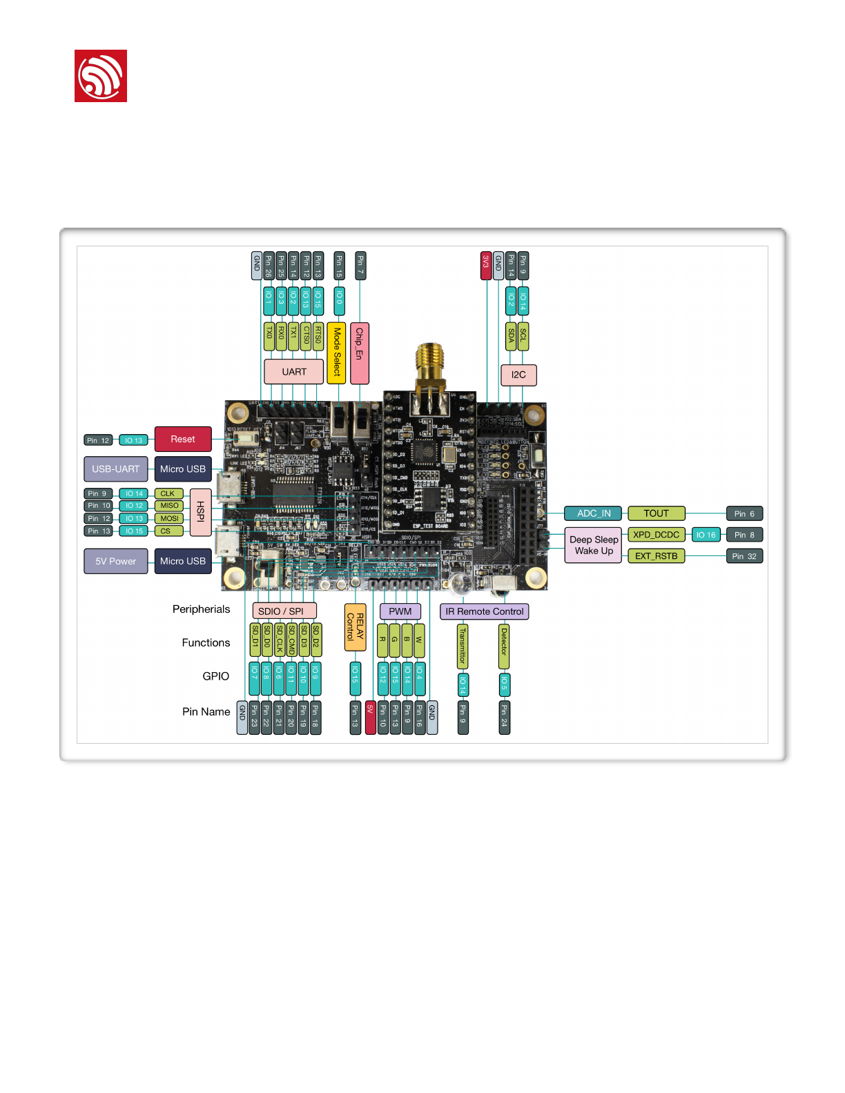
There are altogether 32 pins on the demo board, which are illustrated in Figure 15 below. Definition
of each pin can be found in Table 2.
Figure 15 Illustration of Pin Definitions of ESP-LAUNCHER
Table 4 below describes the functions of several interfaces of the development board. !
Espressif Systems / Jun 1, 2015 28 48

! ! " !
Espressif Systems
ESP8266EX Hardware User Guide
Table 4 Functions of Interfaces on ESP-LAUNCHER
Interface
Functions
HSPI
SPI Flash 2, display screen, and MCU can be connected using HSPI
interface.
SDIO/SPI
Flash, host MCU, display screen, etc. can be connected using SDIO/SPI
interface.
PWM
Currently the PWM interface has four channels, but users can extend the
channels according to their own needs. PWM interface can be used to
control LED lights, buzzers, relays, electronic machines, and so on.
IR Remote Control
The functionality of Infrared remote control interface can be
implemented via software programming. NEC coding, modulation, and
demodulation are used by this interface. The frequency of modulated
carrier signal is 38KHz.
ADC
ESP8266EX is embedded with a 10-bit precision SARADC.
ADC_IN interface is used to test the power supply voltage of VDD3P3
(Pin 3 and Pin 4), as well as the input voltage of TOUT (Pin 6). It can be
used in sensors.
I2C
Sensors and display screens with 2.54mm and 1.27mm needles can be
connected using I2C interface.
UART
UART0: U0TXD, U0RXD, MTDO(U0RTS), MTCK(U0CTS)
UART1: GPIO2(U1TXD)
Devices with UART interfaces can be connected.
Downloading: U0TXD+U0RXD or GPIO2+U0RXD
Communicating: UART0: U0TXD, U0RXD, MTDO(U0RTS), MTCK(U0CTS)
Debugging: UART1_TXD (GPIO2) can be used to print debugging
information.
By default, UART0 will output some printed information when the device
is powered on and is booting up. If this issue exerts influence on some
specific applications, users can exchange the inner pins of UART when
initializing, that is to say, exchange U0TXD, U0RXD with U0RTS, U0CTS.
R1/3/5/7 should not be mounted with other components, while
R2/4/6/8 can be mounted with other components.
J14 and J67 should be short-circuiting connected.
Relay Control Terminal
Relay control terminal is used to control the switch on-and-off of smart
plugs. There is an indicator light.
Espressif Systems / Jun 1, 2015 29 48

! ! " !
Espressif Systems
ESP8266EX Hardware User Guide
Basic steps on how to use the development board:
Step 1
Connect the development board using two USB data lines, one is used to supply 5V
power, one is used to communicate via USB UART interface.
Link for downloading FT232R driver: www.ftdichip.com/Drivers/VCP.htm
Step 2
Short-circuiting connect J82 (Part 5 in Fig. 14) so as to provide 3.3V power to the WiFi
part.
Step 3
Pull up the switch (Part 21 in Fig. 14) that controls CH_PD (the chip enable pin, valid when
the voltage level is high).
Step 4
If not necessary, short-circuiting connect J3 (the chip selection pin of HSPI flash, Part 19
in Fig. 14) so as to close HSPI flash.
Step 5
Pull down the switch that controls GPIO0 so as to enter UART download mode.
Step 6
Connect with the testing board.
Step 7
Pull up the 5V power supply switch so as the supply 5V power. Red light (D12) is an
indicator light for 5V power supply. (Part 3 in Fig. 14).
Step 8
Open the Flash Download Tool and begin downloading.
Pull down the 5V power supply switch so as to switch off power supply when
downloading is completed.
Step 9
Flash boot: pull up the switch that controls GPIO0 (Part 22 in Fig. 14).
UART debug tool can be used to debug.
Step 10
Red light (D2) is an indicator light for the working condition of WiFi.
Blue light (D3) is an indicator light for the communication of the server. (Refer to Part 27
in Fig. 14)
Step 11
Reset button SW1 is used for resetting IoT applications.
Espressif Systems / Jun 1, 2015 30 48
! ! " !
Espressif Systems
ESP8266EX Hardware User Guide
3.3. Typical Applications Using ESP-LAUNCHER
3.3.1. ESP-LAUNCHER Test Board
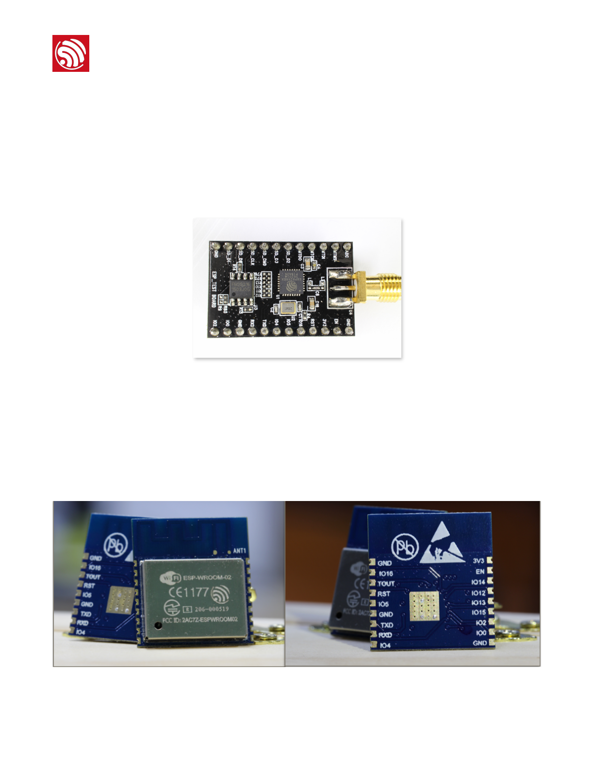
There is one test board on each ESP-LAUNCHER development board, which is shown in Fig. 16
below. The external size of the test board is 20mm*31mm. An 2DBi SMA antenna or other testing
equipment can be connected with the test board via the SMA antenna connector. The spacing of
inserting needles on the test board is 2.54mm, which can be easily inserted into breadboard for
testing.
Figure 16 ESP-LAUNCHER Test Board
3.3.2. SMD Module ESP-WROOM-02
The pin definitions and distribution of the SMD Module is illustrated in Figure 17. The external size of
the module is 18*20mm. The type of flash used on this module is an SPI flash, the package size of
which is SOP8-150mil, the antenna applied on this module is a 3DBi PCB-on-board antenna.
Figure 17 Illustration of SMD Module ESP-WROOM-02
Espressif Systems / Jun 1, 2015 31 48
! ! " !
Espressif Systems
ESP8266EX Hardware User Guide
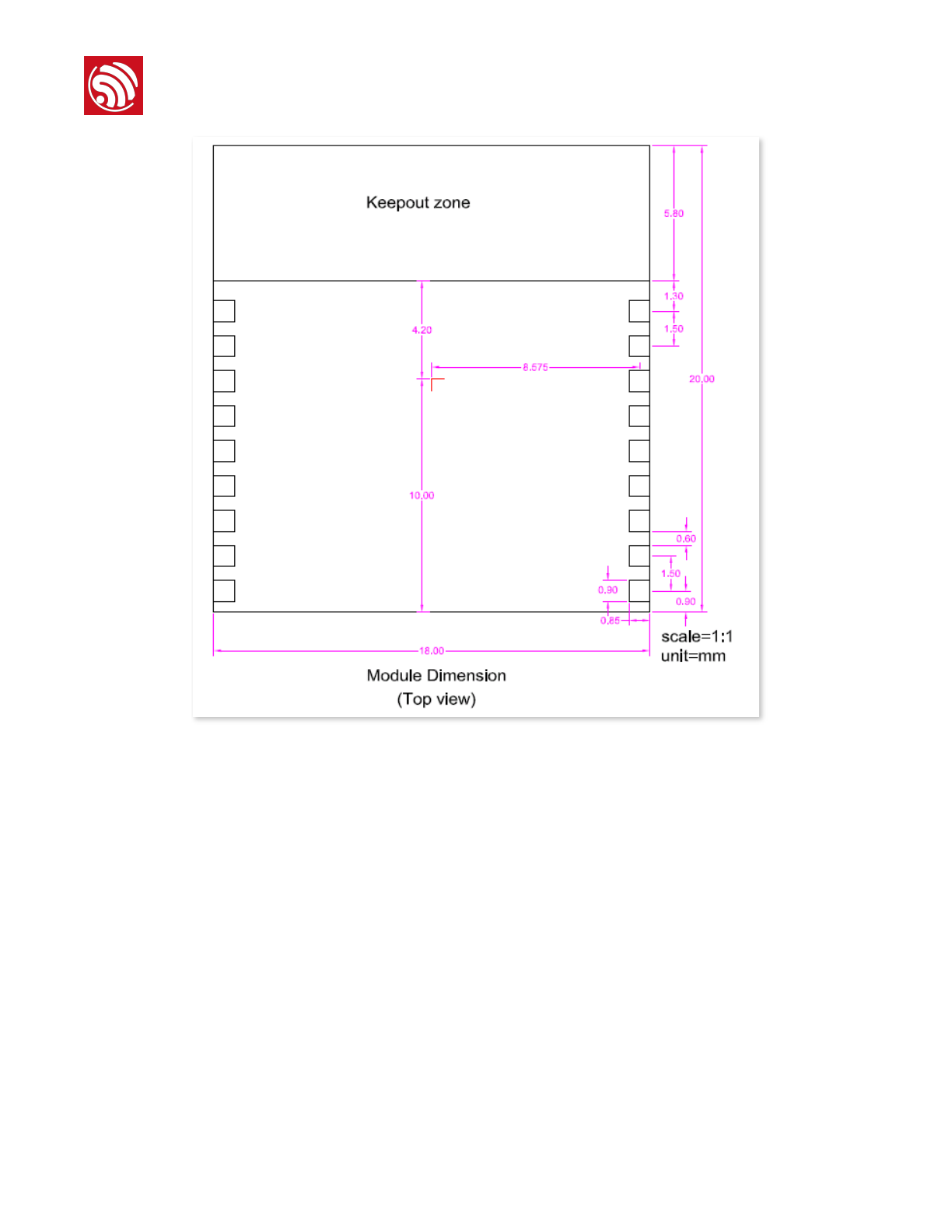
Figure 18 Dimensions of ESP-WROOM-02 WiIF Module
There are altogether 18 pin-outs, the distribution and definitions of which are listed in Table 5 below:
Espressif Systems / Jun 1, 2015 32 48

! ! " !
Espressif Systems
ESP8266EX Hardware User Guide
Table 5 Pin Definitions of ESP-WROOM-02 WiFi Module
Connect the 3.3V power-supply pin to an external 3.3V power source, for 3.3V is the power-supply
for both analog circuit and digital circuit.
When working, normally the voltage level of the EN pin, WiFi enable pin, should be set high.
SMD Module features two working modes: one is UART Download mode, the other is Flash Boot
mode. UART Download mode means that user programs can be written into the Flash or Memory by
flash downloading tools. If the programs are burnt into the Memory, the programs can run only when
the device is powered on, once the device is powered off, the programs in the Memory will be
erased. However, when the programs are burnt into the Flash, they will be stored in it, and can be
invoked and used at any time.
NO.
Pin Name
Function
1
3V3
3.3V power supply (VDD)
2
EN
Chip enable pin. Active high.
3
IO14
GPIO14; HSPI_CLK
4
IO12
GPIO12; HSPI_MISO
5
IO13
GPIO13; HSPI_MOSI; UART0_CTS
6
IO15
GPIO15; MTDO; HSPICS; UART0_RTS
7
IO2
GPIO2; UART1_TXD
8
IO0
GPIO0
9
GND
GND
10
IO4
GPIO4
11
RXD
UART0_RXD; GPIO3
12
TXD
UART0_TXD; GPIO1
13
GND
GND
14
IO5
GPIO5
15
RST
Reset the module
16
TOUT
It can be used to test the power-supply voltage of VDD3P3 (Pin3 and
Pin4) and the input power voltage of TOUT (Pin 6). However, these two
functions cannot be used simultaneously.
17
IO16
GPIO16; can be used to wake up the chipset from deep sleep mode.
18
GND
GND
Espressif Systems / Jun 1, 2015 33 48

! ! " !
Espressif Systems
ESP8266EX Hardware User Guide
Before the module is powered on, pin GND RXD TXD should be lead out, and be connected with
USB to TTL serial cable (FT232 is suggested) so as to download, print log and communicate.
By default the Flash is empty. Therefore, the following procedures should be followed when you
burn the programs into the Flash:
• Before burning, set the module to work under UART Download mode;
• Pull IO15 and IO0 to low-voltage level, leave IO2 dangled;
• Burning the programs into Flash;
• Burning the program into Flash using flash downloading tools;
• After burning the programs into Flash, pull down IO15 to low-voltage level, keep IO2 dangled,
and pull up IO0 to high-voltage level. The module is then shifted from UART Download mode to
the Flash Boot mode;
• The initialisation would read and run programs from Flash after it is powered on.
Note:
• The whole operating process can be examined through the log information printed by UART
interface. If the programs written into the Flash do not function in the right way, please check the
initial settings of the working mode through logs printed from a serial port.
• Serial printing tools (for example, SecureCRT) and flash downloading tools cannot open the serial
port simultaneously.!
Espressif Systems / Jun 1, 2015 34 48
! ! " !
Espressif Systems
ESP8266EX Hardware User Guide
3.3.3. DIP Module ESP-WROOM-01
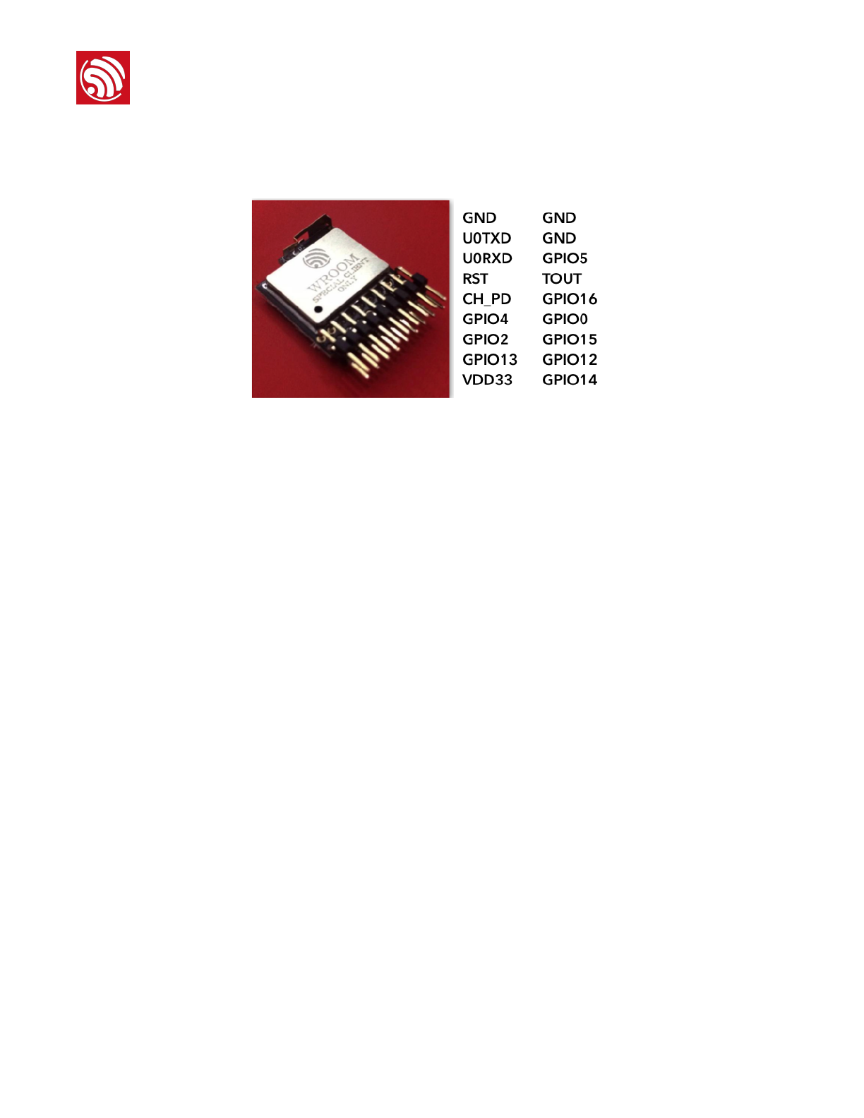
The DPI type module - ESP-WROOM-01 is illustrated in Figure 18 below.
Figure 18 DIP Module ESP-WROOM-01
The size of the module is 18*19mm, the Flash type applied is a SPI flash packed in SOP8-150mil, the
antenna used is a 1 DBi metal antenna. The 2.00mm double pitch applied can be both vertical or
straight, depending on specific applications.
Please refer to Table 5 for pin definitions of this module.
It should be noted that the DIP metal antenna is thin and prone to distortion. Change the antenna
immediately if the shape and appearance are abnormal.
Espressif Systems / Jun 1, 2015 35 48
! ! " !
Espressif Systems
ESP8266EX Hardware User Guide
4. Compiling, Downloading, and Debugging
4.1. Set Up the Compiling Environment
The current compiling environment is set up in Lubuntu System, and is entirely merged into a virtual
box. Please refer to the post on Espressif BBS for the downloading of compiling environment: http://
bbs.espressif.com/viewtopic.php?f=5&t=2
On how to compile and download: http://bbs.espressif.com/viewtopic.php?f=21&t=165
Please refer to[ESP8266_GCC_LUBUNTU.docx] on how to set up and configure when the
compiling system has been downloaded successfully. A Windows sharing folder should also be set
up before we run the virtual box. When the configuration and set up of the sharing folder is ready,
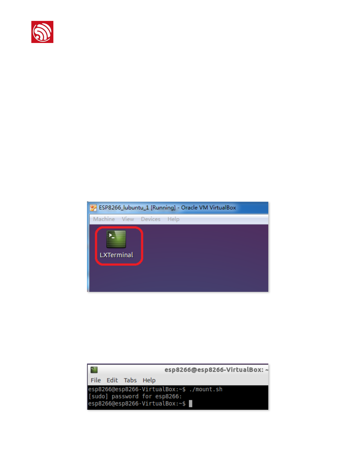
open the virtual box, and you can see this page as is shown in Figure 19 below:
• Click “LXTerminal”
Figure 19 Compiling Tool
• Input ./mount.sh, and password espressif
Please be noted that no hint will pop up when you enter the password, just click Enter Key when you
finished the input. Now, the sharing folder in Windows system is uploaded to Lubuntu Systems.
Espressif Systems / Jun 1, 2015 36 48
! ! " !
Espressif Systems
ESP8266EX Hardware User Guide
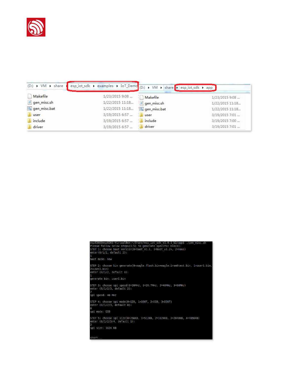
Figure 20 Command
• Copy files in subfolder esp_iot_sdk\examples and paste them in folder esp_iot_sdk\app for
compiling.
Figure 21 Example Codes
• Compiling command: “./gen_misc.sh” . Parameters can be compiled according to specific
needs. Please refer to Chapter 2 of documentation 2A-ESP8266__IOT_SDK_User_Manual on how
to compile.
1)boot_v1.1 and boot_v1.2+: boot_v1.2$ is a more compact form of compiling, thus more flash
space can be saved. While boot_v1.3 mainly supports strengthened initiating mode, and is mainly
used to do mass production test.
2)Firmware upgrade over the air is not supported: flash.bin+iromtext.bin
Firmware upgrade over the air is supported: boot.bin+user1.bin
3)It should be noted that .bin files with different size must be written to different addresses.
Espressif Systems / Jun 1, 2015 37 48
! ! " !
Espressif Systems
ESP8266EX Hardware User Guide
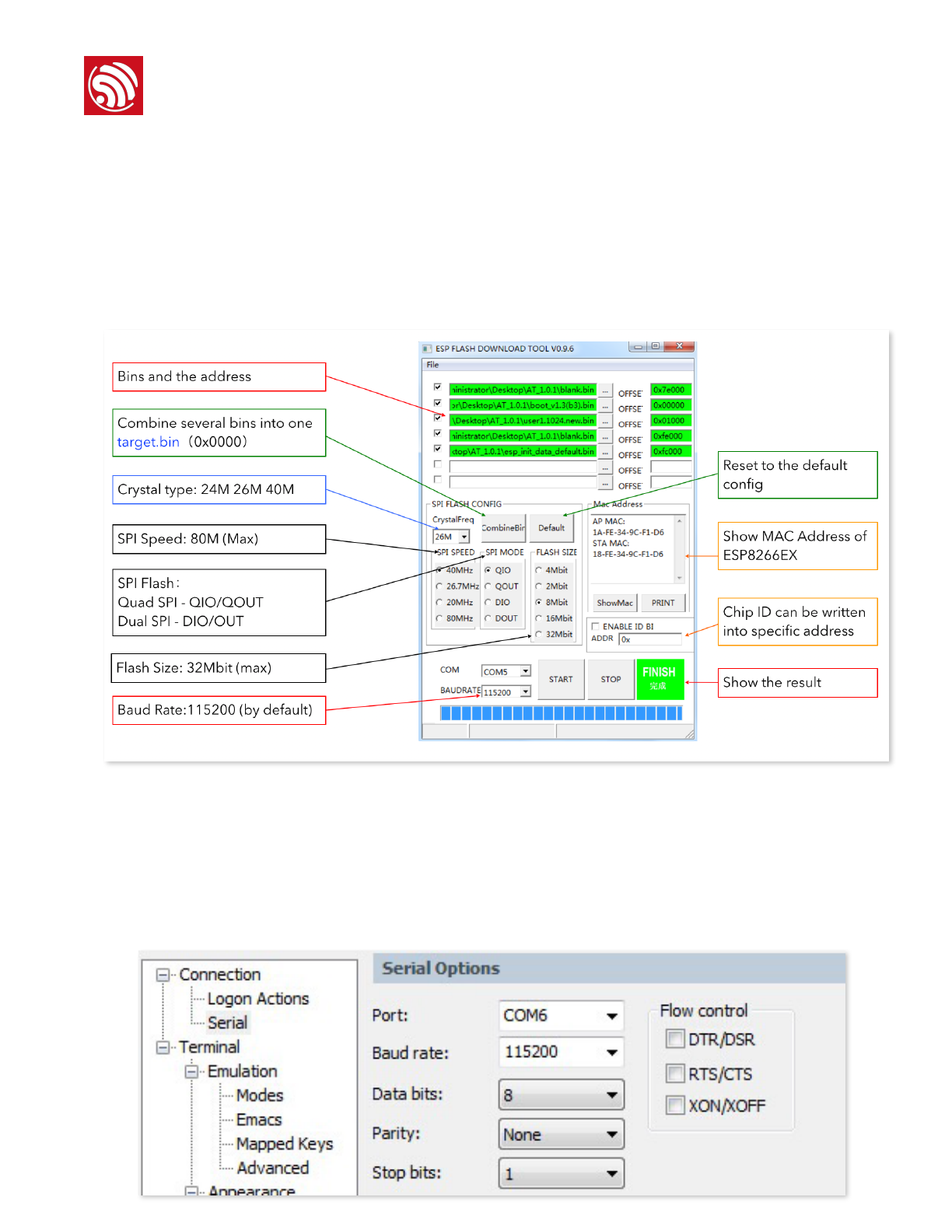
Figure 22 Options during Compiling
4.2. Download Firmware
When entering the UART download mode, set MTDO(IO15):IO0:IO2 as 0:0:1, after downloading
successfully, switch to the Flash boot mode 0:1:1.
Figure 23 below shows how to use Flash Download Tool.
Figure 23 Flash Download Tool
4.3. Debugging AT Commands via UART
1. All AT Commands has to be capitalised, and end with “/r/n”. Configure the port and enter the
commands.
Espressif Systems / Jun 1, 2015 38 48
! ! " !
Espressif Systems
ESP8266EX Hardware User Guide
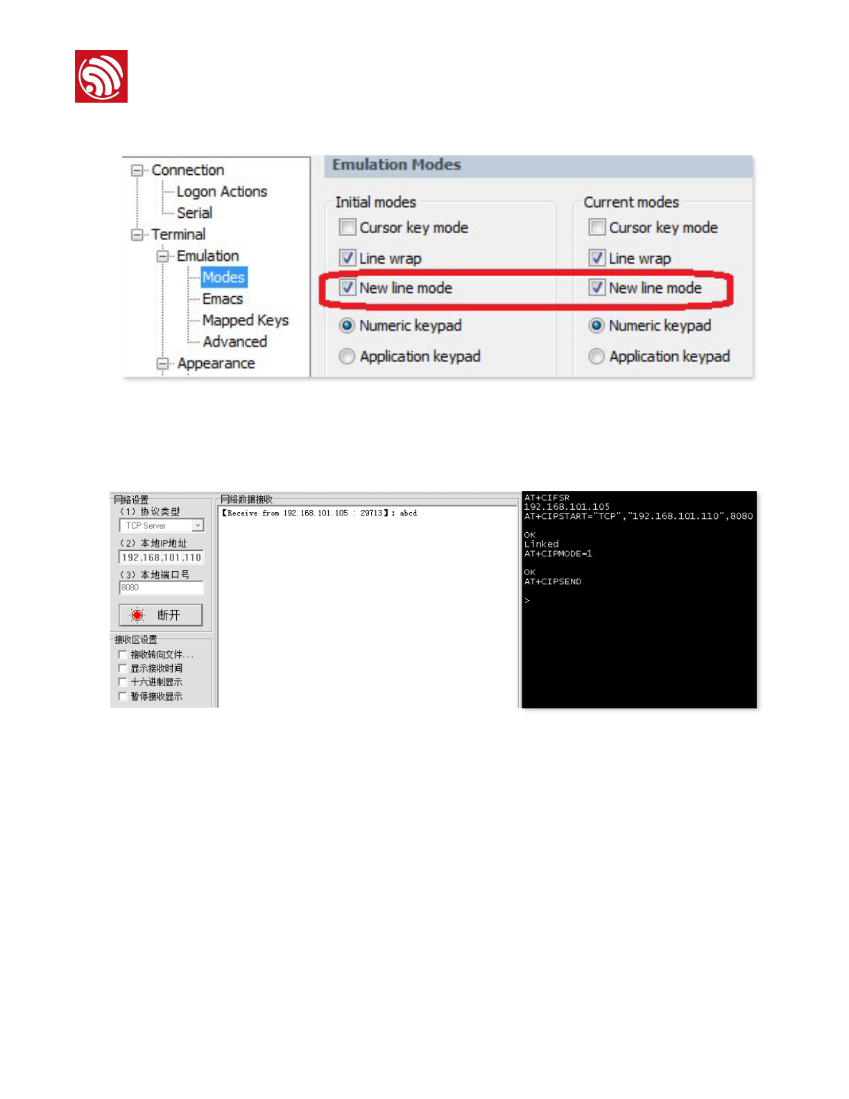
Figure 24 Configuration of UART Serial Port Debugging Tool
2. TCP/UDP debugging via the internet
Figure 25 TCP/UDP Debugging!
Espressif Systems / Jun 1, 2015 39 48
! ! " !
Espressif Systems
ESP8266EX Hardware User Guide
5. Typical Applications
5.1. WiFi smart hardware converted from UART serial ports
The pins on basis of the 2 UART ports are defined below:
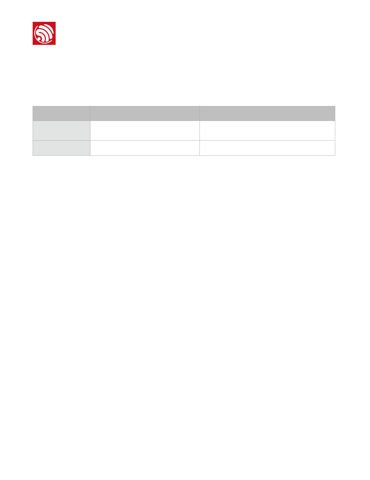
Table 19 Pin Definitions of 2 UART Interfaces
AT+ instructions and instruction sets documentations are provided for the relevant software.
Application example: ESP8266EX development board as shown in Figure14.
5.2. Sensor
ESP8266EX can be used to develop sensor products and the interface used is I2C interface. Under
this condition, I2C is working with Master mode and is connected to multiple sensors,
communicating through addressing mode which identifies Slave device (every slave device has a
unique address identity).
Such sensor products will send real-time data through I2C interface to ESP8266EX which will upload
the data to the server wirelessly. When an mobile phone is connected to the public internet, it can
access the data on the server through an app.
5.3. Smart light
ESP8266EX can be used to develop smart home products such as smart LED lights which use PWM
interfaces and infrared interfaces. The 3 PWM interfaces control the red, blue, green LED lights
respectively. Theoretically speaking, the minimal PWM duty ratio can reach 1/256, thus supporting
256*256*256 types of colors. Besides, the infrared interfaces allow specific control over LED lights,
for example, reset, on/off, adjustment of the colour.
Category
Pin Definition
Function
UART0
(Pin 25) U0RXD+ (Pin 26) U0TXD
Can be used to receive and send the users’ data
packages
UART1
(Pin 14) GPIO2 (U1TXD)
Can be used to print information
Espressif Systems / Jun 1, 2015 40 48

! ! " !
Espressif Systems
ESP8266EX Hardware User Guide
5.4. Smart plug
ESP8266EX can be used to develop smart home products such as smart plugs which use ordinary
GPIO interfaces. GPIO interfaces allow control over high and low levels as well as connection and
disconnection of relay, thus allowing smart control over plug on/off. This application is mainly
comprised of 3 modules which are: 220V to 5V power module, ESP8266EX WiFi module and relay
control module.!
Espressif Systems / Jun 1, 2015 41 48
! ! " !
Espressif Systems
ESP8266EX Hardware User Guide
6. Appendix
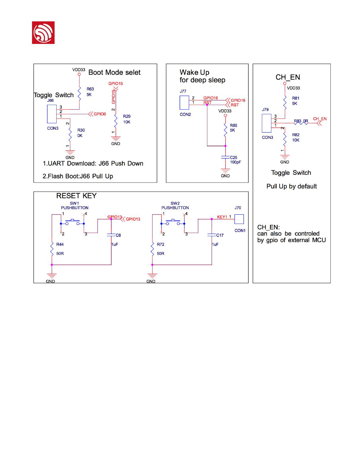
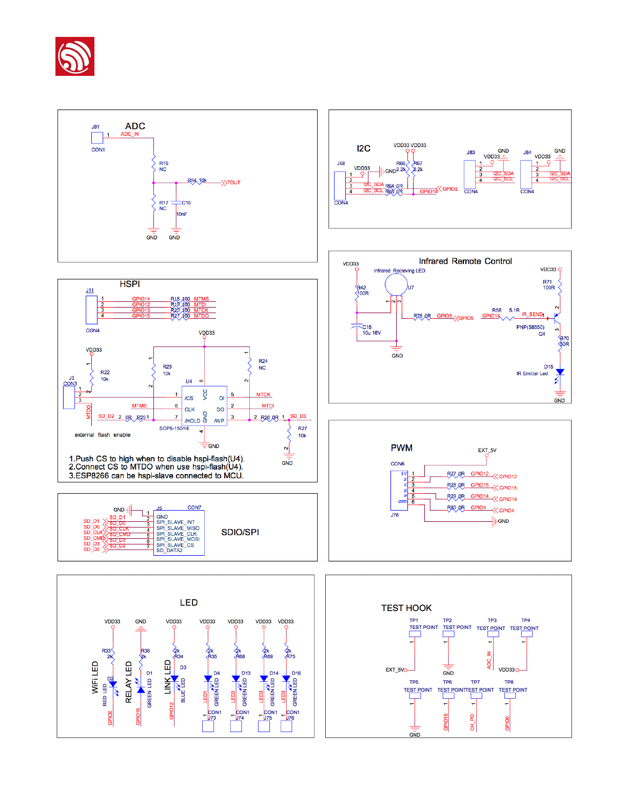
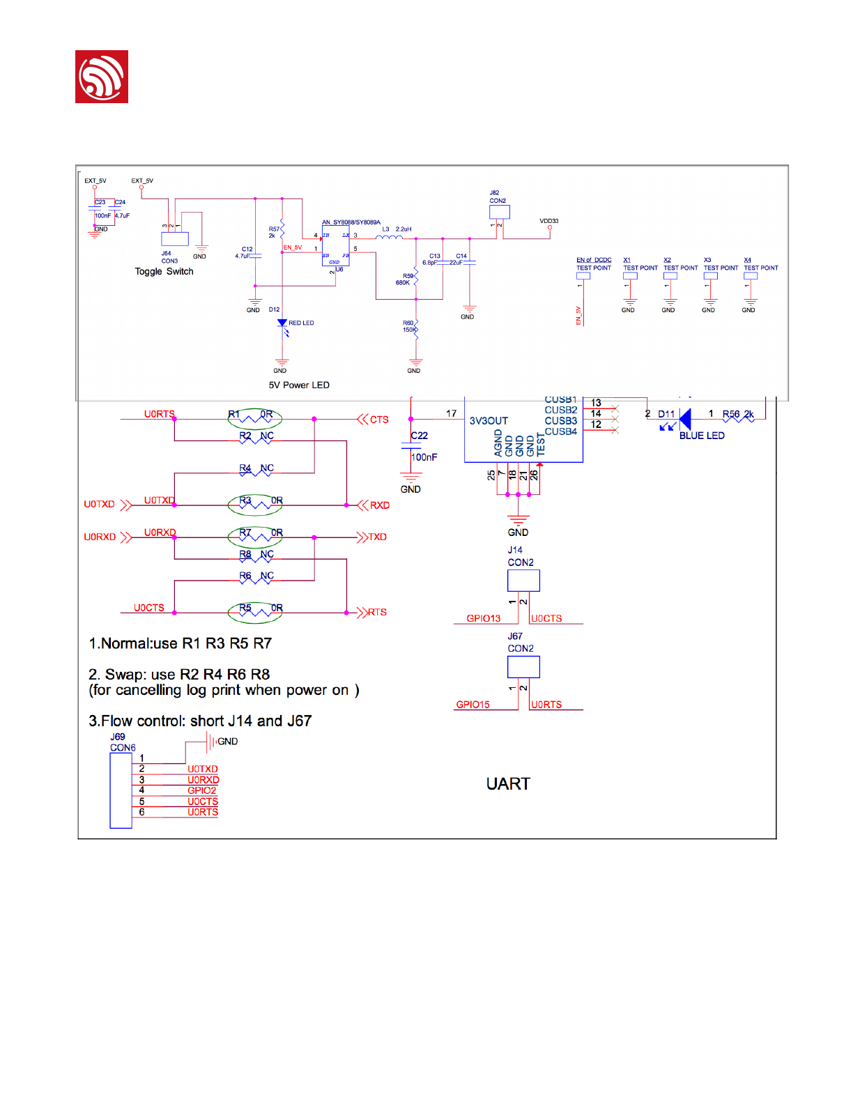
6.1. Schematics of ESP-LAUNCHER Development Board
Espressif Systems / Jun 1, 2015 42 48
! ! " !
Espressif Systems
ESP8266EX Hardware User Guide
Espressif Systems / Jun 1, 2015 43 48
! ! " !
Espressif Systems
ESP8266EX Hardware User Guide
Part 1: Interfaces
Espressif Systems / Jun 1, 2015 44 48
! ! " !
Espressif Systems
ESP8266EX Hardware User Guide
Espressif Systems / Jun 1, 2015 45 48
! ! " !
Espressif Systems
ESP8266EX Hardware User Guide
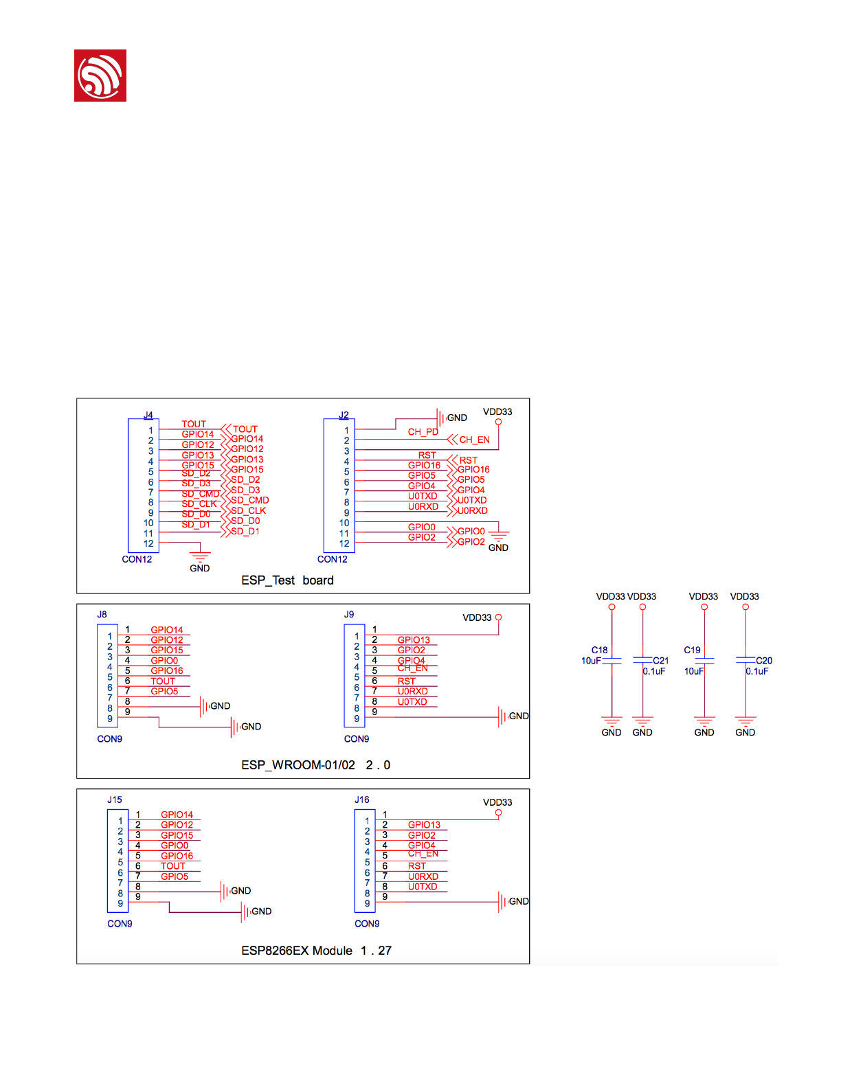
Part 2: 5V Power
Part 3: Test Board
6.2. Schematics of ESP-LAUNCHER Test Board
Espressif Systems / Jun 1, 2015 46 48
! ! " !
Espressif Systems
ESP8266EX Hardware User Guide
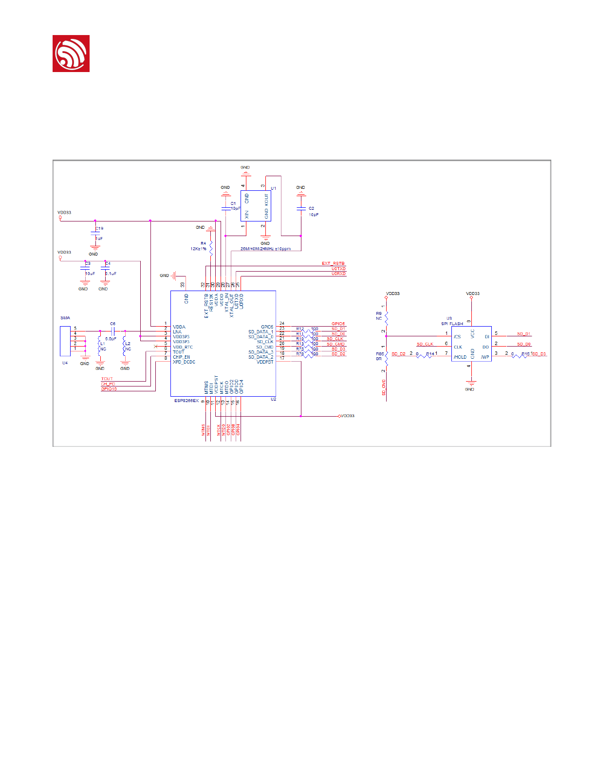
6.3. Schematics of ESP-WROOM Serial WiFi Modules
Espressif Systems / Jun 1, 2015 47 48
! ! " !
Espressif Systems
ESP8266EX Hardware User Guide
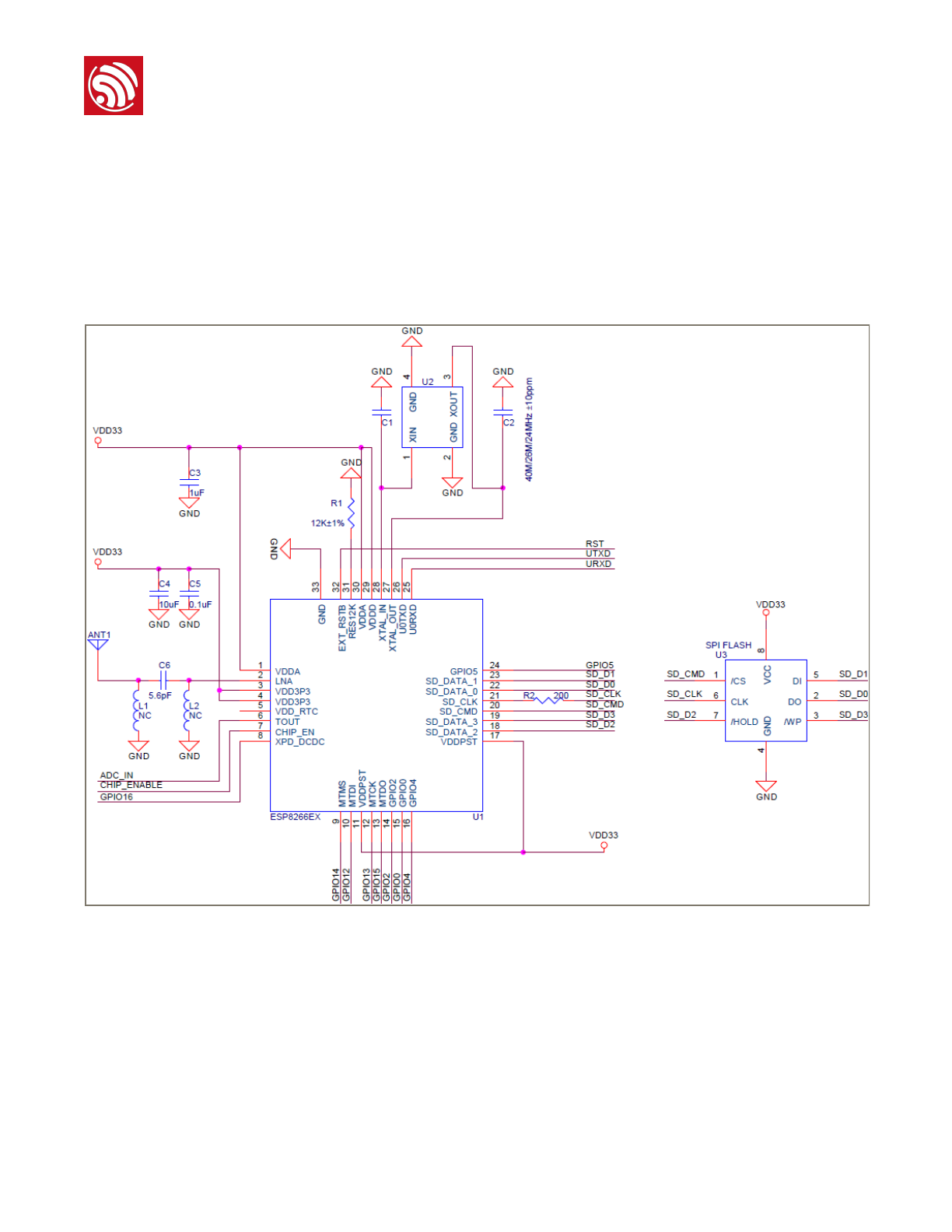
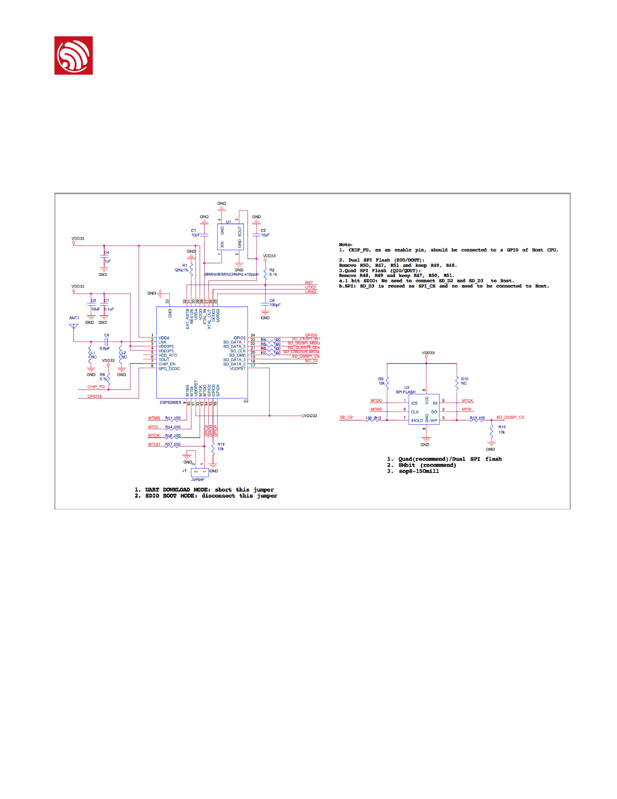
6.4. Schematics of ESP8266EX as SDIO/SPI Slave Device
Espressif Systems / Jun 1, 2015 48 48