Otbmodb 145777 Catalog
2016-10-06
: Pdf 145777-Catalog 145777-Catalog B5 unilog
Open the PDF directly: View PDF ![]() .
.
Page Count: 228 [warning: Documents this large are best viewed by clicking the View PDF Link!]
- Modbus Advantys OTB
- Introduction
- Installation
- Description, characteristics, and wiring of the OTB module
- Description, characteristics, and wiring of the expansion modules
- Modbus Network Interface of the OTB Module
- Application-Specific Functions
- Software Installation
- Diagnostics of the Advantys OTB Island
- Island Registers Table
- Appendices
- IEC Symbols
- Glossary
- Index
W9 1606383 01 11 A02 09/04
Modbus Advantys OTB
Remote I/O
September 2004
Eng V1.1

2

3
Table of Contents
SafetyInformation ....................................7
AbouttheBook.......................................9
Chapter 1 Introduction . . ......................................11
AtaGlance..................................................... 11
AboutAdvantysOTB.............................................. 12
Maximumhardwareconfiguration.................................... 18
SpecificFunctionsoftheNetworkInterfaceModule...................... 21
CommunicationOverview.......................................... 22
Chapter 2 Installation..........................................25
AtaGlance..................................................... 25
DimensionsoftheNetworkInterfaceModules.......................... 26
Dimensions for the Digital and Analog I/O Expansion Modules . . . . . . . . . . . . . 27
HowtoDirectMountonaPanelSurface .............................. 30
InstallationPreparation............................................ 32
Mounting Positions for the Network Interface Module and the Expansion Modules
.............................................................. 33
Assembly Precautions for an Island or a Panel in a Cabinet . . . . . . . . . . . . . . . 35
Assembly of an Expansion Module to a Network Interface Module . . . . . . . . . . 36
Disassembly of an Expansion Module and a Network Interface Module . . . . . . 39
RemovingaTerminalBlock ........................................ 40
How to Install and Remove a Network Interface Module from a DIN Rail. . . . . . 41
TheDINRail.................................................... 43
Chapter 3 Description, characteristics, and wiring of the OTB module . 45
AtaGlance..................................................... 45
WiringRulesandRecommendations................................. 46
OverviewoftheNetworkInterfaceModules............................ 51
Physical Description of an Advantys OTB Network Interface Module. . . . . . . . . 52
GeneralCharacteristicsoftheNetworkInterfaceModule.................. 53
I/OCharacteristicsoftheNetworkInterfaceModule...................... 55
Wiringdiagramofthenetworkinterfacemodule......................... 60
HowtoConnectthePowerSupply................................... 61

4
ConnectionoftheFieldBusorNetwork ...............................63
Chapter 4 Description, characteristics, and wiring of the expansion
modules ...........................................65
AtaGlance .....................................................65
OverviewofDigitalI/OModules......................................66
PartsDescriptionofDigitalI/OModules ...............................70
SpecificationsfortheDigitalI/OModules ..............................72
DigitalI/OModuleWiringSchematics.................................83
OverviewofAnalogI/OModules.....................................93
PartsDescriptionofAnalogI/OModules...............................94
GeneralSpecificationsfortheAnalogI/OModules.......................95
SpecificationsfortheAnalogI/OModules..............................96
AnalogI/OModulesWiringSchematics...............................100
Chapter 5 Modbus Network Interface of the OTB Module ...........105
AtaGlance ....................................................105
DescriptionoftheOTBModuleModbusNetworkInterface................106
ModbusFieldBusInterface........................................108
NetworkNodeAddress...........................................112
NetworkBaudRate..............................................114
ModbusConfiguration............................................116
CommunicationonaModbusNetwork...............................117
ManagementofIslandBehavior ....................................120
Expansionmoduleidentificationcodes...............................124
Chapter 6 Application-Specific Functions .......................125
AtaGlance ....................................................125
IslandRegisters.................................................126
ReadInputRegisters.............................................129
OutputCommandRegisters .......................................130
AdvantysOTBModuleI/OParameterRegisters........................131
Expansion Module Discrete I/O Parameter Registers 214 to 599 . . . . . . . . . . . 132
Expansion Module Analog I/O Parameter Registers 214 to 599 . . . . . . . . . . . . 135
SpecificFunctionsoftheAdvantysOTBModules.......................150
RemoteFastCounter(RFC)FunctionBlock...........................152
FastCounter(RFC)ParameterRegisters.............................155
RemoteVeryFastCounter(RVFC)FunctionBlock .....................156
RemoteVeryFastCounter(RVFC)ParameterRegisters.................169
RemotePulseGenerator(RPLS)FunctionBlock.......................171
RemotePulseWidthModulatorFunctionBlock.........................175
RemotePulseGenerators(RPLS,RPWM)ParameterRegisters...........179
Chapter7 SoftwareInstallation................................181
AdvantysConfigurationTool.......................................181

5
Chapter 8 Diagnostics of the Advantys OTB Island ................183
Overview...................................................... 183
IndicatorLights(LEDs)........................................... 184
OTBIslandDiagnosticsRegisters................................... 186
BehaviorintheEventofaFault .................................... 190
Chapter 9 Island Registers Table ...............................191
Registers Table (mapping) for Modbus Advantys OTB Module . . . . . . . . . . . . 191
Appendices ............................................. 205
AtaGlance.................................................... 205
Appendix A IEC Symbols . . .....................................207
GlossaryofSymbols............................................. 207
Glossary ............................................. 209
Index ............................................. 225

6
W9 1606383 01 11 A02 09/04 7
§
Safety Information
Important Information
NOTICE Read these instructions carefully, and look at the equipment to become familiar with
the device before trying to install, operate, or maintain it. The following special
messages may appear throughout this documentation or on the equipment to warn
of potential hazards or to call attention to information that clarifies or simplifies a
procedure.
DANGER
DANGER indicates an imminently hazardous situation, which, if not avoided, will result
in death, serious injury, or equipment damage.
WARNING
WARNING indicates a potentially hazardous situation, which, if not avoided, can result
in death, serious injury, or equipment damage.
CAUTION
CAUTION indicates a potentially hazardous situation, which,can result in
personal injury or equipment damage.
The addition of this symbol to a Danger or Warning safety label indicates
that an electrical hazard exists, which will result in personal injury if the
instructions are not followed.
This is the safety alert symbol. It is used to alert you to potential personal
injury hazards. Obey all safety messages that follow this symbol to avoid
possible injury or death.

Safety Information
8W9 1606383 01 11 A02 09/04
PLEASE NOTE Electrical equipment should be serviced only by qualified personnel. No responsi-
bility is assumed by Schneider Electric for any consequences arising out of the use
of this material. This document is not intended as an instruction manual for untrained
persons.
© 2004 Schneider Electric. All Rights Reserved.

W9 1606383 01 11 A02 09/04 9
About the Book
At a Glance
Document Scope This guide contains the information necessary to install a Modbus Advantys OTB
network interface module.
It has been designed to facilitate a rapid familiarization with the system, while
optimizing the system's features with the most advanced technology available.
This equipment's installation needs the relative communication protocol pre-
requisites and should only be installed by qualified personnel. Special points and
warnings regarding safety are highlighted in the different chapters.
The initial chapters aim to provide information for designers and fitters for installing
the mechanical and electrical part of the system. They describe the characteristics
which are common to the whole Advantys OTB range and are not dependent on the
selected communication protocol.
The following chapters, from the "network interface" section, are specific to the
communication protocol. They contain information on specific wiring for the network
interface and all the necessary information for the software application programmer,
and for the end user (diagnostics).
Chapter Subject dealt with
Introduction General introduction to the network interface module and
expansion modules
Description Software installation, dimensions, installation and assembly
of an island
Description, characteristics,
and wiring of the Advantys
OTB module
Description, electrical and mechanical characteristics and
wiring diagrams for the OTB module
Description, characteristics
and wiring of expansion
modules
Description, electrical and mechanical characteristics and
wiring diagrams for expansion modules

About the Book
10 W9 1606383 01 11 A02 09/04
User Comments We welcome your comments about this document. You can reach us by e-mail at
techpub@schneider-electric.com
Advantys OTB module
Modbus network interface
Introduction to the OTB module network interface
Reminders on the communication protocol
Management of behavior of the island on the network
Application-specific functions Description of application-specific functions
Remote I/O and specific function registers table
Software installation Software installation help
Advantys OTB island
diagnostics
Description of hardware diagnostics
Description of software diagnostics
How to perform diagnostics in the event of a failure
Advantys OTB island registers
table
Description of the registers accessible for communication
Glossary Acronyms
Definitions.
Chapter Subject dealt with

W9 1606383 01 11 A02 09/04 11
1
Introduction
At a Glance
Introduction This chapter provides an overview of the Advantys OTB network interface modules,
the different expansion modules, the maximum configuration and the specific
functions of the module, as well as a communication architecture.
What's in this
Chapter?
This chapter contains the following topics:
Topic Page
About Advantys OTB 12
Maximum hardware configuration 18
Specific Functions of the Network Interface Module 21
Communication Overview 22

Introduction
12 W9 1606383 01 11 A02 09/04
About Advantys OTB
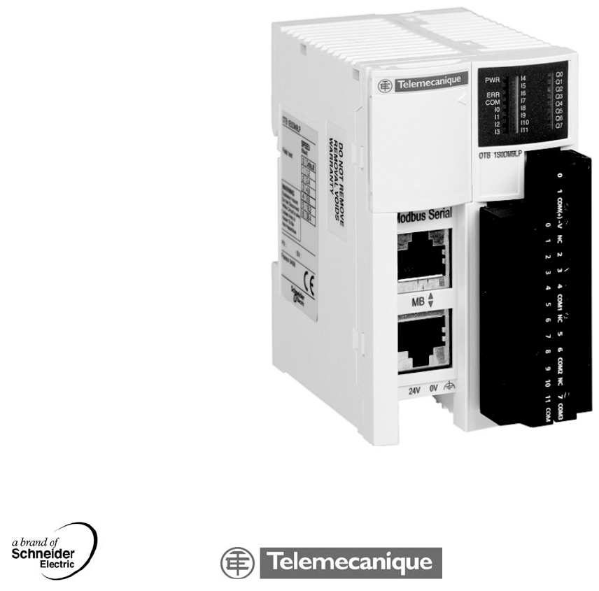
Introduction The Advantys OTB (Optimized Terminal Block) network interface module with built-
in Inputs/Outputs is small in size. Its modularity, by adding I/O expansions, can be
used to optimize an application by providing the necessary number of I/Os. The
Advantys OTB module connects directly to a field bus or communication network.
The available field buses or networks are as follows:
zCANopen field bus: Module OTB1C0DM9LP
zModbus field bus: Module OTB1S0DM9LP
zEthernet communication network: Module OTB1E0DM9LP
The network interface module accepts up to 7 I/O expansion modules
Introduction
W9 1606383 01 11 A02 09/04 13
Network
Interface Module
with Built-In I/Os
The following illustration shows the different network interface modules with built-in
I/Os:
Each network interface modules with built-in I/Os has:
z12 Discrete inputs
z6 relay outputs
z2 positive logic transistor outputs (source)
za 24 VDC power supply terminal
za dedicated connector to the communication bus
zan indicator LED to display the communication and I/O status
The following table shows the main characteristics of the network interface module:
Reference Channel
s
Channel
channel
Input/Output type Electrical
OTB1•0DM9LP 12 Inputs 24 VDC 24 VDC
6
2
Outputs
Outputs
Relay
24 VDC positive logic
transistor (source)
OTB1S0DM9LP OTB1E0DM9LP
OTB1C0DM9LP

Introduction
14 W9 1606383 01 11 A02 09/04
Digital
Expansion I/O
Modules
The following table lists the digital and relay expansion I/O modules:
Module Name Reference Channels Channel
Type
Input/Output
type
Terminal type
Input modules
8 channel input TWDDDI8DT 8 Inputs 24 VDC Screw
removable
terminal block
8 channel input TWDDAI8DT 8 Inputs 120 VAC Screw
removable
terminal block
16 channel
input
TWDDDI16DT 16 Inputs 24 VDC Screw
removable
terminal block
16 channel
input
TWDDDI16DK 16 Inputs 24 VDC Connector
HE10
32 channel
input
TWDDDI32DK 32 Inputs 24 VDC Connector
HE10
Output Modules
8 channel
output
TWDDDO8TT 8 Outputs Positive logic
transistor
(source)
Screw
removable
terminal block
8 channel
output
TWDDDO8UT 8 Outputs Transistor sink Screw
removable
terminal block
8 channel
output
TWDDRA8RT 8 Outputs Relay Screw
removable
terminal block
16 channel
output
TWDDDO16TK 16 Outputs Positive logic
transistor
(source)
Connector
HE10
16 channel
output
TWDDDDO16UK 16 Outputs Transistor sink Connector
HE10
16 channel
output
TWDDRA16RT 16 Outputs Relay Screw
removable
terminal block
32 channel
output
TWDDDO32TK 32 Outputs Positive logic
transistor
(source)
Connector
HE10
32 channel
output
TWDDDO32UK 32 Outputs Transistor sink Connector
HE10

Introduction
W9 1606383 01 11 A02 09/04 15
Mixed modules
4 channel input/
4 channel
output
TWDDMM8DRT 4 Inputs 24 VDC Screw
removable
terminal block
4 Outputs Relay
16 channel
input/8 channel
output
TWDDMM24DRF 16 Inputs 24 VDC Spring non-
removable
terminal block
8 Outputs Relay
Module Name Reference Channels Channel
Type
Input/Output
type
Terminal type

Introduction
16 W9 1606383 01 11 A02 09/04
Analog
Expansion I/O
Modules
The following table lists the analog expansion I/O modules:
Module name Reference Type Channel
type
Details Terminal type
2 inputs TWDAMI2HT 2 Inputs 12 Bit
0-10 V
4-20 mA
Screw
removable
terminal block
1 output TWDAM01HT 1 Outputs 12 Bit
0-10 V
4-20 mA
Screw
removable
terminal block
2 inputs/1 output TWDAMM3HT 2 Inputs 12 Bit
0-10 V
4-20 mA
Screw
removable
terminal block
1 Outputs
2 inputs /
1 output
TWDALM3LT 2 Inputs 12 Bit
resistance
temperature
detector,
thermocouple
Screw
removable
terminal block
1 Outputs 12 Bit
0-10 V
4-20 mA
2 outputs TWDAVO2HT 2 Outputs 10 Bit
+/-10 V
Screw
removable
terminal block
4 inputs TWDAMI4HT 4 Inputs 12 Bit
Voltage/
current
resistance
temperature
detector,
thermocouple
Ni
Screw
removable
terminal block
8 inputs TWDAMI8HT 8 Inputs 10 Bit
Voltage/
current
Screw
removable
terminal block
8 inputs TWDARI8HT 8 Inputs 10 Bit
PTC
NTC
Screw
removable
terminal block

Introduction
W9 1606383 01 11 A02 09/04 17
Communication
expansion
module block
Cables The following table catalogs the different cables:
Module name Reference Type Channel
type
Details Terminal type
Joint block OTB9ZZ61JP 16 passive 2 x 8 contacts Screw
removable
terminal block
Cable name Reference
Digital I/O Cables
0.5 meter, HE10 connector of the I/O expansion module
to 20-wire free cable
ABFT20E050
1 meter, HE10 connector of the I/O expansion module to
20-wire free cable
ABFT20E100
2 meter, HE10 connector of the I/O expansion module to
20-wire free cable
ABFT20E200
Advantys Telefast 2 prewiring system for Twido
TWDDDO16TK TWDDDO32TK compatible ABE7E16SPN20
ABE7E16SPN22
ABE7E16SRM20
TWDDDI16DK TWDDDI32DK compatible ABE7E16EPN20
Introduction
18 W9 1606383 01 11 A02 09/04
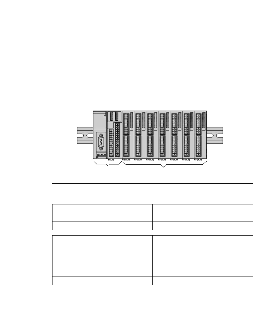
Maximum hardware configuration
Introduction This section presents the maximum hardware configuration for the network interface
module with built-in I/Os integrated associated with the expansions modules.
The hardware configuration is limited by:
zthe number of expansion modules. The OTB module accepts up to a maximum
of 7 Discrete I/O expansion modules,
zthe number of analog channels of the same type,
zthe total consumption of the expansion modules must be lower than 450 mA.
Each module (whether or not associated with the expansion modules) constitutes
an island on the bus or the communication network. Each island offers a modular
and polyvalent I/O solution.
The figure below shows an example of an I/O island.
Maximum
Number of I/Os
The following table catalogs the maximum number of discrete I/O types for the
island:
OTB 7 expansion modules
Type of built-in I/Os Number of I/Os
Standard digital inputs 12
Standard digital outputs 8
Type of I/Os with expansion modules Total number of I/Os
Max Discrete inputs (I/O module + exp I/O) 12+(7x32)=236
Max Discrete outputs (I/O module + exp I/O) 8+(7x32)=232
Max digital I/O
(I/O module + exp I/O)
20+(7x32)=244
Max relay outputs 6 base + 96 expansion

Introduction
W9 1606383 01 11 A02 09/04 19
Maximum
Number of
Analog Channels
The following table catalogs the maximum number of analog channels by types for
the island:
Type of analog I/O Number of analog channels
Analog inputs 24
Analog outputs 24

Introduction
20 W9 1606383 01 11 A02 09/04
Consumption of
the expansion
modules
The total consumption of the expansion modules must be lower than 450 mA. The
following table lists the consumption of each expansion module:
Expansion module Consumption
TWDDDI8DT 25 mA
TWDDAI8DT 60 mA
TWDDDI16DT 40 mA
TWDDDI16DK 35 mA
TWDDDI32DK 65 mA
TWDDDO8TT 10 mA
TWDDDO8UT 10 mA
TWDDRA8RT 30 mA
TWDDDO16TK 10 mA
TWDDDDO16UK 10 mA
TWDDRA16RT 45 mA
TWDDDO32TK 20 mA
TWDDDO32UK 20 mA
TWDDMM8DRT 25 mA
TWDDMM24DRF 65 mA
TWDAMI2HT 50 mA
TWDAMO1HT 50 mA
TWDAMM3HT 50 mA
TWDALM3LT 50 mA
TWDAVO2HT 50 mA
TWDAMI4LT 50 mA
TWDAMI8HT 50 mA
TWDARI8HT 50 mA
CAUTION
UNEXPECTED EQUIPMENT OPERATION
Failure to observe the 450 mA limit may lead to the inconsistent operation of the
island.
Failure to follow this instruction can result in injury.

Introduction
W9 1606383 01 11 A02 09/04 21
Specific Functions of the Network Interface Module
Introduction By default, all I/Os of the network interface module are configured as Discrete I/Os.
However, certain I/Os can be assigned to remote function blocks.
Specific
Functions
The following table lists the specific functions of the network interface module:
Function Description
Fast counter: RFC 2 fast up/down counters: 5 kHz (1-phase)
Very fast counter: RVFC 2 very fast counters: Up/down counters - 20 kHz (2-phase)
Pulse generator: RPLS 2 pulse generators
Pulse output, maximum 7 kHz.
Pulse generator with pulse
width modulation: RPWM
2 pulse generators with pulse width modulation RPWM
pulse width modulation, maximum 7 kHz.
Programmable input filter Input filter time can be changed during configuration
No filtering or filtering at 3 ms or 12 ms

Introduction
22 W9 1606383 01 11 A02 09/04
Communication Overview
Introduction The Advantys OTB network interface modules are available for CANopen and
Modbus field buses, and for the Ethernet network. They are used to exchange data
from the built-in I/Os and expansion module I/Os with the bus master or client.
Field bus or
network
A module with or without expansion constitutes an I/O island. The network interface
module manages data transfers between the island and the master or client, via the
field bus or network.
Introduction
W9 1606383 01 11 A02 09/04 23
Communication
Architecture
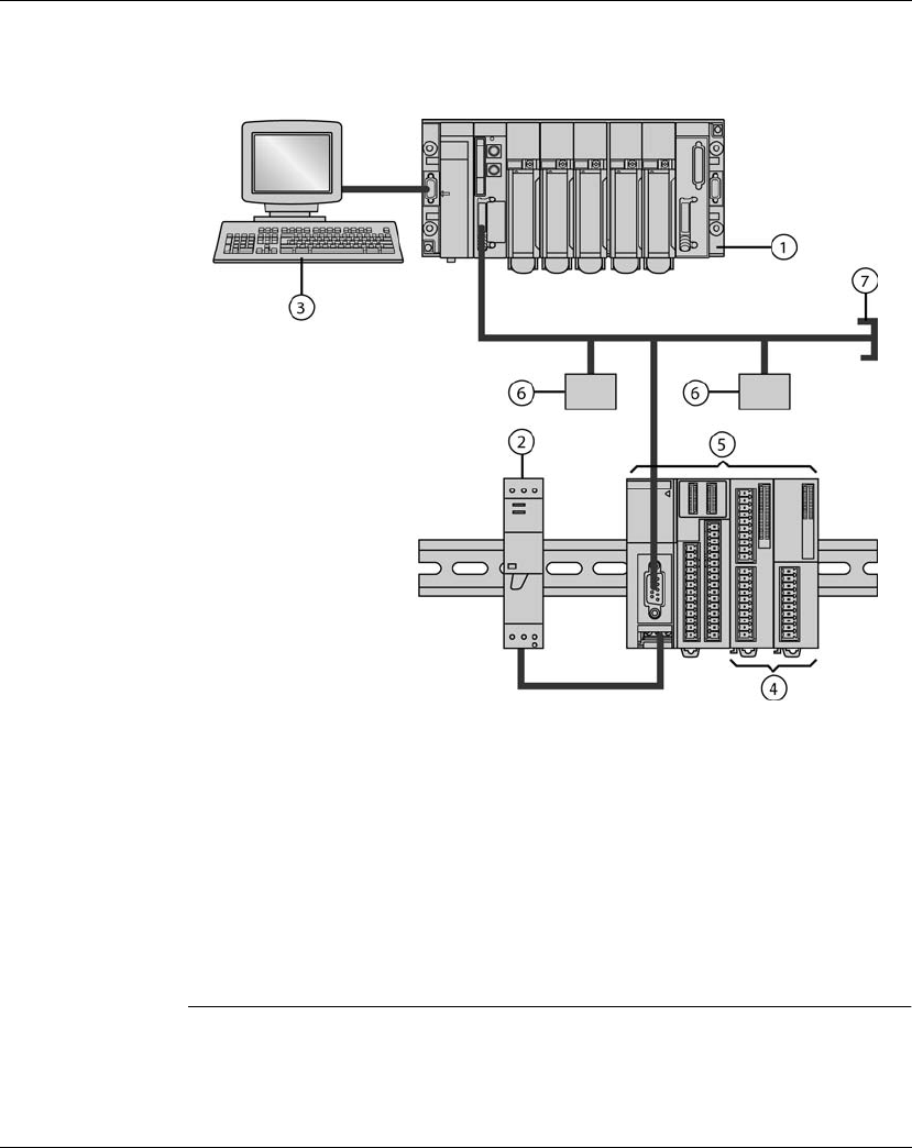
The following figure illustrates the different roles of the network interface module.
This figure shows a network architecture with all the elements necessary for its
implementation:
1PLC with master and/or client
2external 24 VDC electrical supply
3PC with the PLC configuration software
4I/O expansion module
5Advantys OTB island
6other islands or products on the field bus or network
7termination according to the field bus or network (if necessary)

Introduction
24 W9 1606383 01 11 A02 09/04

W9 1606383 01 11 A02 09/04 25
2
Installation
At a Glance
Introduction This chapter provides dimensions, installation, and mounting instructions for
Advantys OTB network interface modules, and digital and analog expansion I/O
modules.
What's in this
Chapter?
This chapter contains the following topics:
Topic Page
Dimensions of the Network Interface Modules 26
Dimensions for the Digital and Analog I/O Expansion Modules 27
How to Direct Mount on a Panel Surface 30
Installation Preparation 32
Mounting Positions for the Network Interface Module and the Expansion
Modules
33
Assembly Precautions for an Island or a Panel in a Cabinet 35
Assembly of an Expansion Module to a Network Interface Module 36
Disassembly of an Expansion Module and a Network Interface Module 39
Removing a Terminal Block 40
How to Install and Remove a Network Interface Module from a DIN Rail 41
The DIN Rail 43
Installation
26 W9 1606383 01 11 A02 09/04
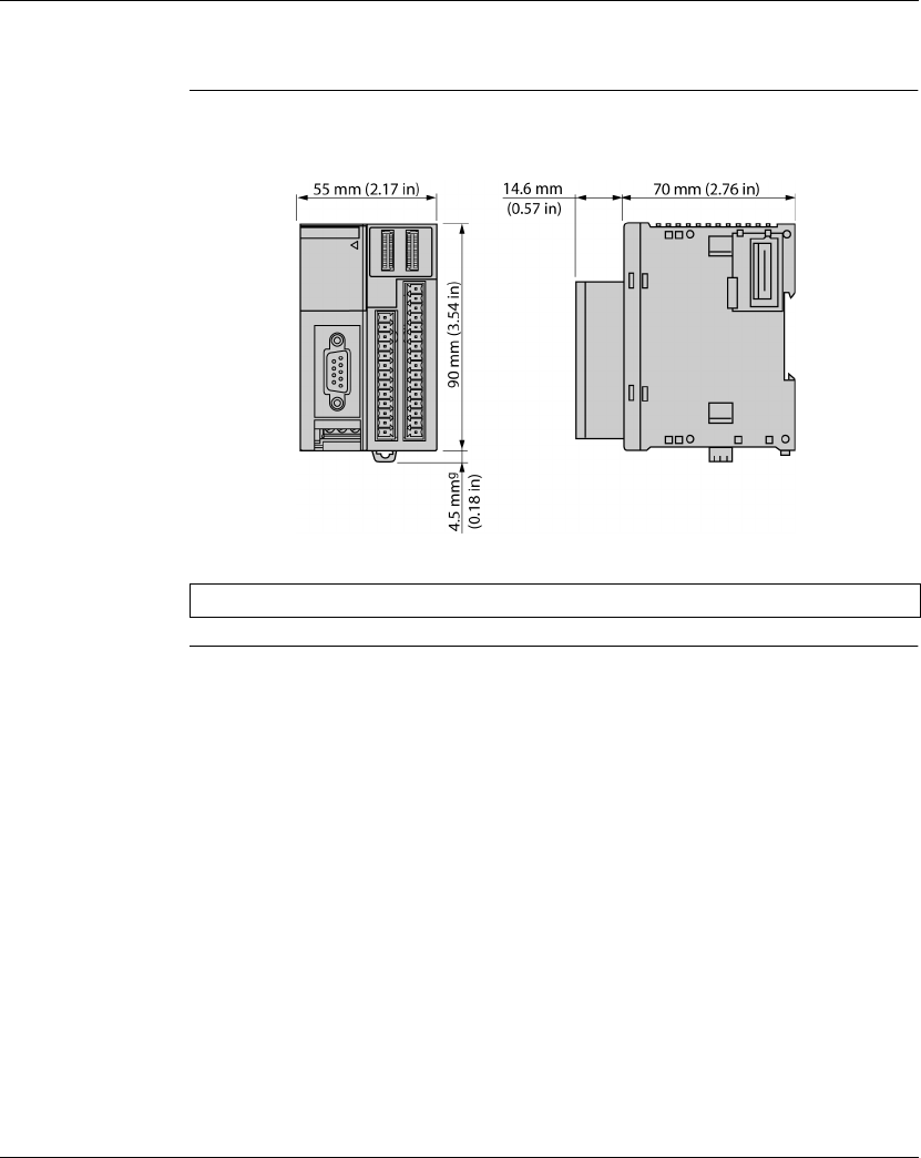
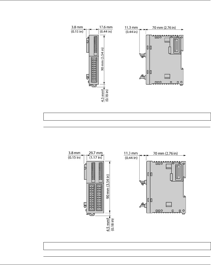
Dimensions of the Network Interface Modules
OTB1•0DM9LP
Dimensions
The following figure shows the dimensions of the Advantys OTB network interface
module (OTB1•0DM9LP).
Note: * 8.5 mm (0.33 in) when the clamp is pulled out.
Installation
W9 1606383 01 11 A02 09/04 27
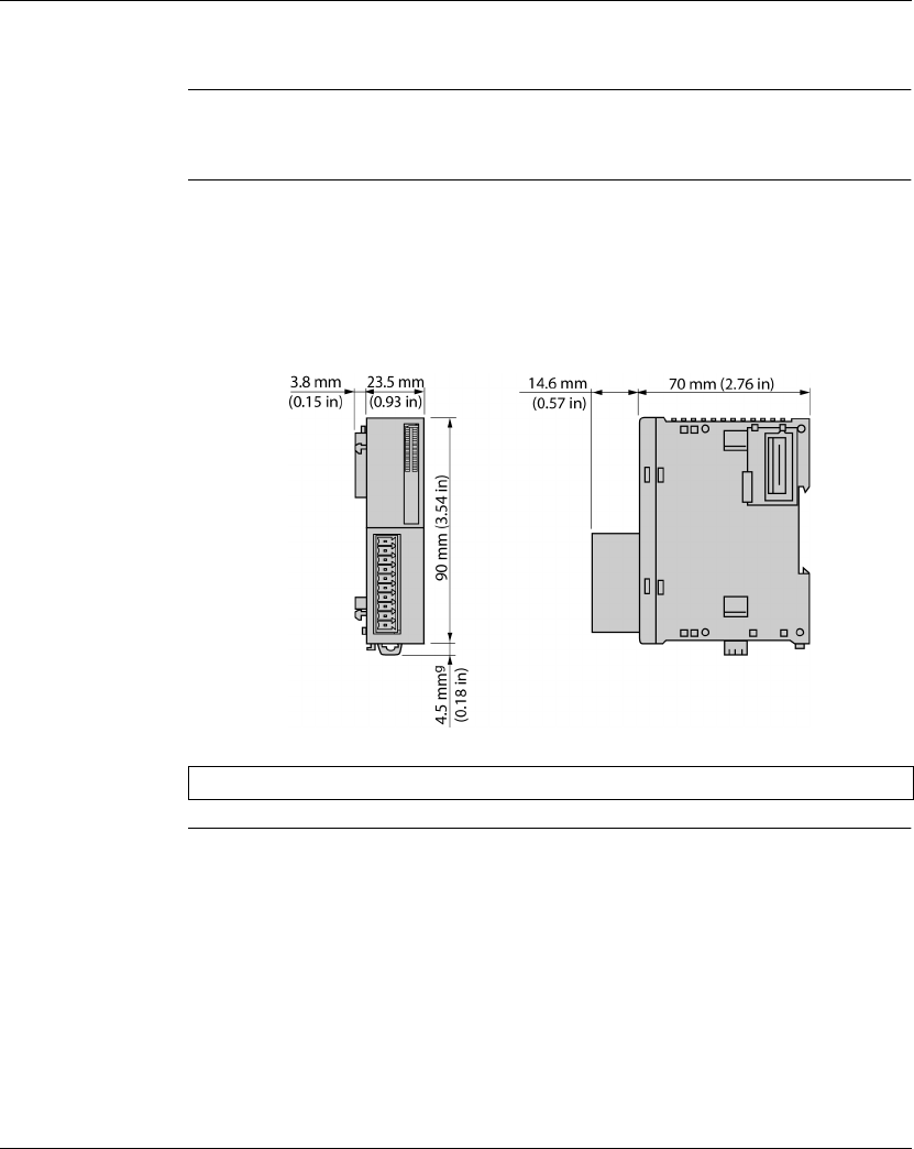
Dimensions for the Digital and Analog I/O Expansion Modules
Introduction The following section shows the dimensions for all digital and analog I/O expansion
modules.
Digital I/O and
Analog Modules The following figure shows the dimensions of the modules
zDiscrete I/Os: TWDDDI8DT, TWDDDO8TT, TWDDDO8UT, TWDDRA8RT,
TWDDMM8DRT
zAnalog I/Os: TWDAMI2HT, TWDAMO1HT, TWDAMM3HT, TWDALM3LT,
TWDAVO2HT, TWDAMI4LT, TWDAMI8HT and TWDARI8HT.
Illustrations of the TWDDDI8DT or TWDDAI8DT module:
Note: * 8.5 mm (0.33 in) when the clamp is pulled out.
Installation
28 W9 1606383 01 11 A02 09/04
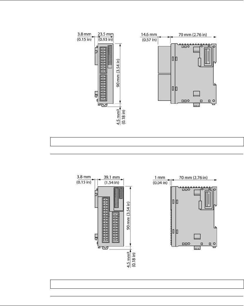
Digital I/O
Modules
The following diagrams show the dimensions for the TWDDDI16DT,
TWDDRA16RT, and OTB9ZZ61JP Discrete I/O modules.
Illustrations showing a TWDDDI16DT module:
Digital I/O
Modules
The following diagram shows the dimensions for the TWDDMM24DRF Discrete I/O
module.
Note: * 8.5 mm (0.33 in) when the clamp is pulled out.
Note: * 8.5 mm (0.33 in) when the clamp is pulled out.
Installation
W9 1606383 01 11 A02 09/04 29
Digital I/O
Modules
The following diagrams show the dimensions for the TWDDDI16DK,
TWDDDO16TK, and TWDDDO16UK Discrete I/O modules.
Illustrations showing a TWDDDI16DK module:
Digital I/O
Modules
The following diagrams show the dimensions for the TWDDDI32DK,
TWDDDO32TK and TWDDDO32UK Discrete I/O modules.
Illustrations showing a TWDDDI32DK module:
Note: * 8.5 mm (0.33 in) when the clamp is pulled out.
Note: * 8.5 mm (0.33 in) when the clamp is pulled out.
Installation
30 W9 1606383 01 11 A02 09/04
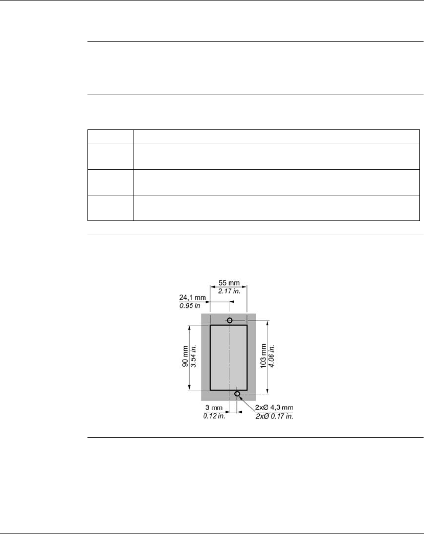
How to Direct Mount on a Panel Surface
Introduction This section provides mounting hole layouts for each network interface module or
expansion module. Your module may differ from the illustrations in this procedure
but the mechanism are the same.
Installing a
Mounting Strip
Panel assembly requires the use of a strip. The following procedure explains how to
install an assembly strip: TWD DXMT5.
Layout of the
mounting holes
of the network
interface module
The following diagram shows the Mounting hole layout for the Advantys OTB
network interface modules.
Step Action
1 Remove the clamp from the back side of the module by pushing the clamp
inward.
2 Insert the mounting strip, with the hook entering last, into the slot where the
clamp was removed.
3 Slide the mounting strip into the slot until the hook enters into the recess in the
module.
Installation
W9 1606383 01 11 A02 09/04 31
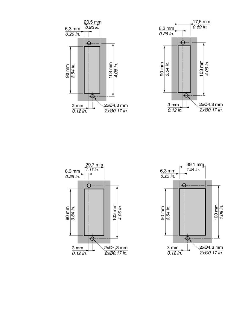
Mounting Hole
Layout of the
Expansion
Module
The following diagram shows the mounting hole layout for the expansion modules.
TWDDDI8DT
TWDDDI16DT
TWDDRA8RT
TWDDRA16RT
TWDDDO8UT
TWDDDO8TT
TWDDMM8DRT
TWDALM3LT
TWDAMM3HT
TWDAMI2HT
TWDAMO1HT
TWDDDI16DK
TWDDDO16TK
TWDDDO16UK
TWDDDI32DK
TWDDDO32TK
TWDDDO32UK
TWDDDO32UK

Installation
32 W9 1606383 01 11 A02 09/04
Installation Preparation
Introduction The following section provides information on installing network interface modules
and expansion I/O modules.
Before Starting Before installing network interface modules, read the Safety Information at the
begging of this book.
CAUTION
EQUIPMENT DAMAGE
Before removing an expansion module, power down the network interface module.
Otherwise there is a risk of damaging the modules or the modules no longer
working correctly
Failure to follow this instruction can result in injury.
Note: All options and expansion I/O modules should be installed in the network
interface module before installing an island on a DIN rail, on a mounting plate, or
in a cabinet. The island should be removed from a DIN rail, a mounting plate or a
cabinet before disassembling the different modules.
Installation
W9 1606383 01 11 A02 09/04 33
Mounting Positions for the Network Interface Module and the Expansion
Modules
Introduction This section shows the correct and incorrect mounting positions for all network
interface modules and expansion I/O modules.
Correct
Mounting
Position
Network interface modules and expansion I/O modules must be mounted
horizontally on a vertical plane as shown in the figures below.
WARNING
THE TEMPERATURE OF THE ISLAND MAY RISE
Keep adequate spacing around the island for proper ventilation and to maintain an
ambient temperature between 0°C (32°F) and 55°C (131°F).
Failure to follow this instruction can result in death or serious injury.
CAUTION
PLACING HEAT GENERATING DEVICES NEAR THE ISLAND
Do not place heat generating devices such as transformers and supply blocks
under the island.
Failure to follow this instruction can result in injury.

Installation
34 W9 1606383 01 11 A02 09/04
Incorrect
Mounting
Position
The following diagrams show the incorrect mounting positions for the network
interface modules and expansion modules.
Installation
W9 1606383 01 11 A02 09/04 35
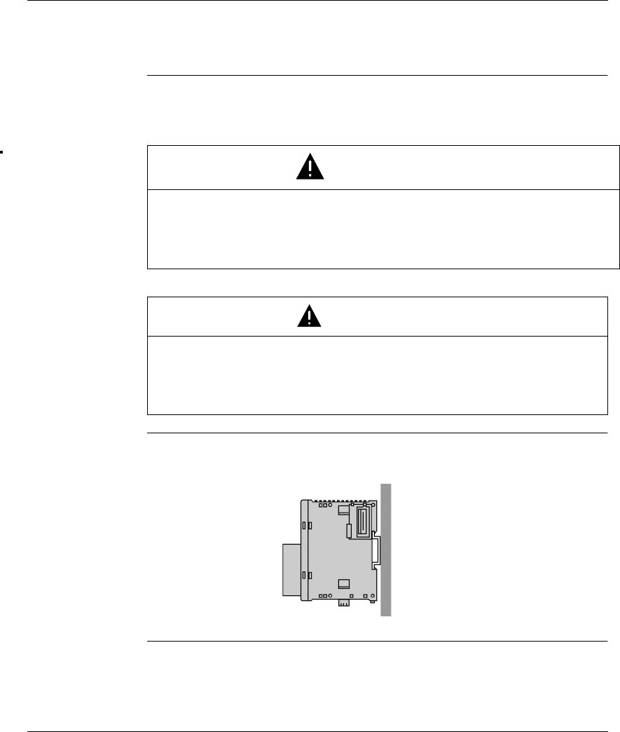
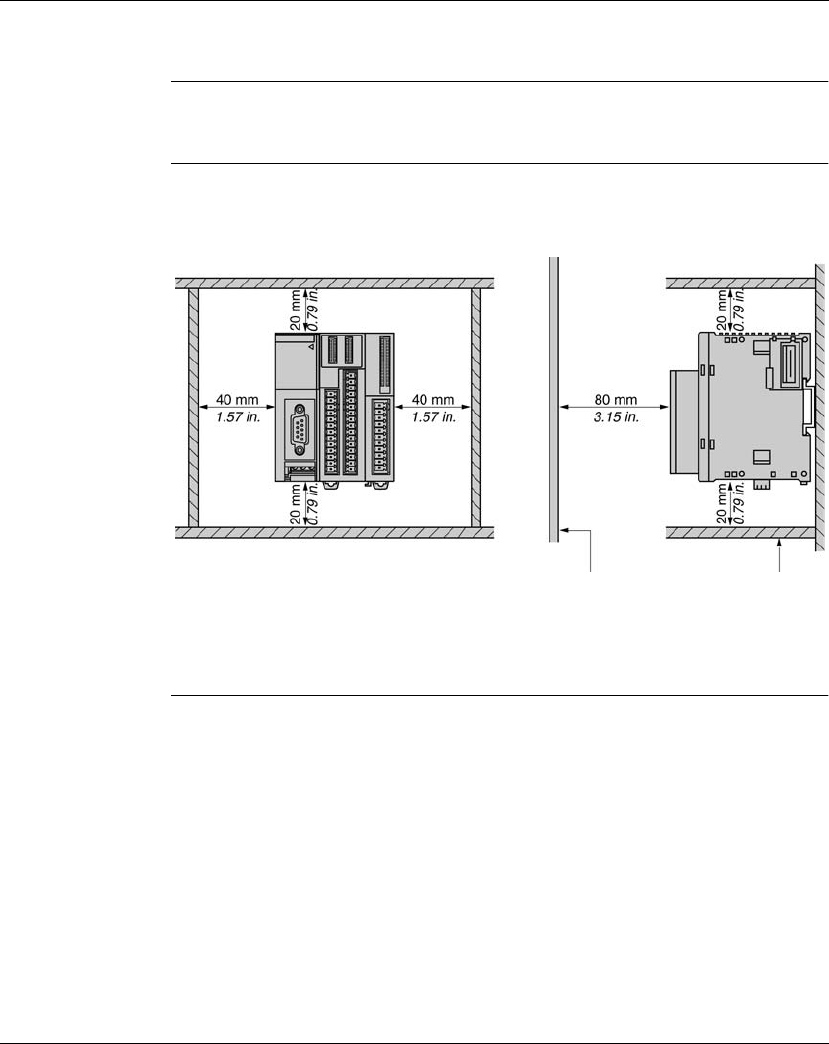
Assembly Precautions for an Island or a Panel in a Cabinet
Introduction This section presents the assembly precautions required for islands on a control
panel or in a cabinet.
Required
Assembly Space
for an Island
In order for air to be able to circulate freely around the islands mounted in a control
panel or in a cabinet, you must respect the minimum distances given in the following
diagram.
Front Panel Wiring Duct

Installation
36 W9 1606383 01 11 A02 09/04
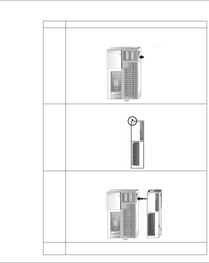
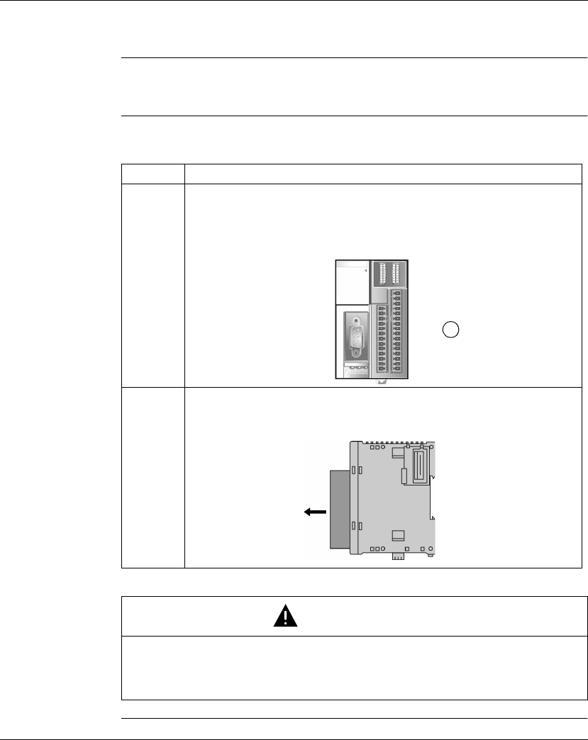
Assembly of an Expansion Module to a Network Interface Module
Introduction This section shows how to assemble an expansion module to a network interface
module. Your network interface module or expansion module may differ to the ones
shown in the illustrations for this procedure, but the mechanism remains the same.
CAUTION
UNEXPECTED EQUIPMENT OPERATION
zIf you change the hardware configuration of the island and do not update the
master or client application program, the island will no longer operate normally.
zThe I/Os built into the network interface module will continue to operate
normally.
Failure to follow this instruction can result in injury.
Installation
W9 1606383 01 11 A02 09/04 37
Assembly of an
Expansion
Module to a
Network
Interface Module
The following procedure must be performed with all products powered down. It
shows how to assemble a network interface module to an expansion module.
Step Action
1 Remove the protective label located on the side of the network interface
module.
2 Make sure the black latch button on the expansion module is in the up position.
3 Align the connector on the left side of the expansion module to the connector
on the right side of the network interface module.
4 Press the expansion module to the network interface module until it "clicks" into
place.
Installation
38 W9 1606383 01 11 A02 09/04
5 Push down the black latch button on the top of the expansion module to lock
the modules together.
6 Begin the operation again from step 1 for each expansion module to be added.
Step Action
Installation
W9 1606383 01 11 A02 09/04 39
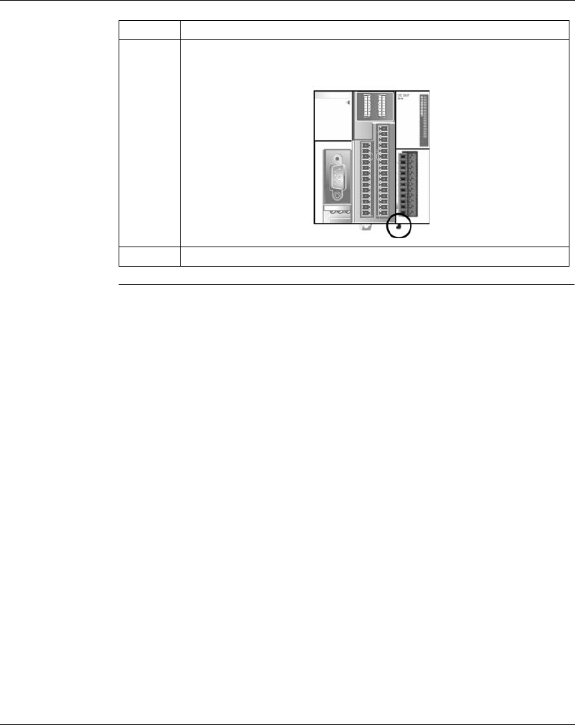
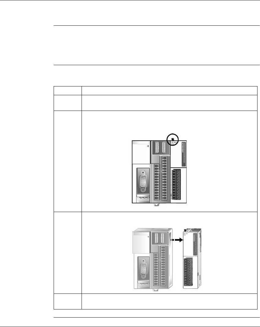
Disassembly of an Expansion Module and a Network Interface Module
Introduction This section shows how to disassemble an expansion interface from a network
interface module. Your network interface module or expansion module may differ to
the ones shown in the illustrations for this procedure, but the mechanism remains
the same.
Disassembly of
an Expansion
Module from a
Network
Interface Module
The following procedure must be performed with all products powered down. It
shows how to disassemble an expansion module from a network interface module.
Step Action
1 Remove the island (network interface module + expansion module(s)) from the
DIN rail before disassembling them. See
Introduction, p. 43
.
2 Push the black latch from the bottom of the expansion module to disengage it
from the network interface module.
3 Separate the modules.
4 Begin the operation again from step 2 for each expansion module to be
separated.
Installation
40 W9 1606383 01 11 A02 09/04
Removing a Terminal Block
Introduction This section describes the removal of terminals from Advantys OTB network
interface modules.
Removing a
Terminal Block
The following procedure describes how to remove terminals from network interface
modules.
Step Action
1 Power down the network interface module and disconnect all wires.
Note: The terminal block on the left (1) must be removed before the terminal
block on the right (2).
2 Remove the terminal block by holding the center of the terminal block and
pulling it out straight.
CAUTION
REMOVING THE TERMINAL BLOCK. ONLY PULL FROM THE SIDE.
Only pull the terminal from the side to remove it.
Failure to follow this instruction can result in injury.
2
Installation
W9 1606383 01 11 A02 09/04 41
How to Install and Remove a Network Interface Module from a DIN Rail
Introduction This section shows how to install and remove an island from a DIN rail. Your island
may differ from the illustrations in this procedure but the mechanism is the same.
Installing an
Island on a DIN
Rail
The following procedure must be performed with all products powered down. It
describes how to install an island on a DIN rail.
Note: When mounting modules on a DIN rail, use two end stops, type AB1AB8P35
or equivalent.
Step Action
1 Fasten the DIN rail to a panel using screws.
2 Before any installation on a DIN rail, attach the communication module to the
expansion modules. See
Assembly of an Expansion Module to a Network
Interface Module, p. 37
3 Pull out the clamp at the bottom of each module.
4 Put the top groove of the island on the DIN rail and press it toward the rail.
5 Push the clamp up to lock the island to the DIN rail.
6 Position the mounting stops of both sides of the modules to prevent the system
from moving sideways.
Groove
DIN rail,
Clamp
from 35 mm (13.7 in.)
Installation
42 W9 1606383 01 11 A02 09/04
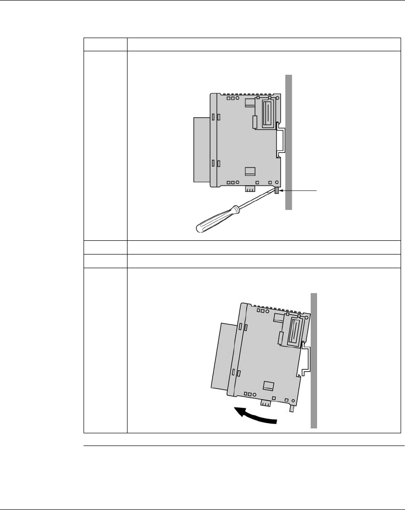
Removing an
island from a DIN
Rail
The following procedure must be performed with all products powered down. It
shows how to remove an island from the DIN rail.
Step Action
1 Insert a flat screwdriver into the slot in the module clamp.
2 Pull out the clamp.
3 Repeat steps 1 and 2 for each module comprising the island.
4 Pull the island to remove it from the DIN rail.
Clamp
Installation
W9 1606383 01 11 A02 09/04 43
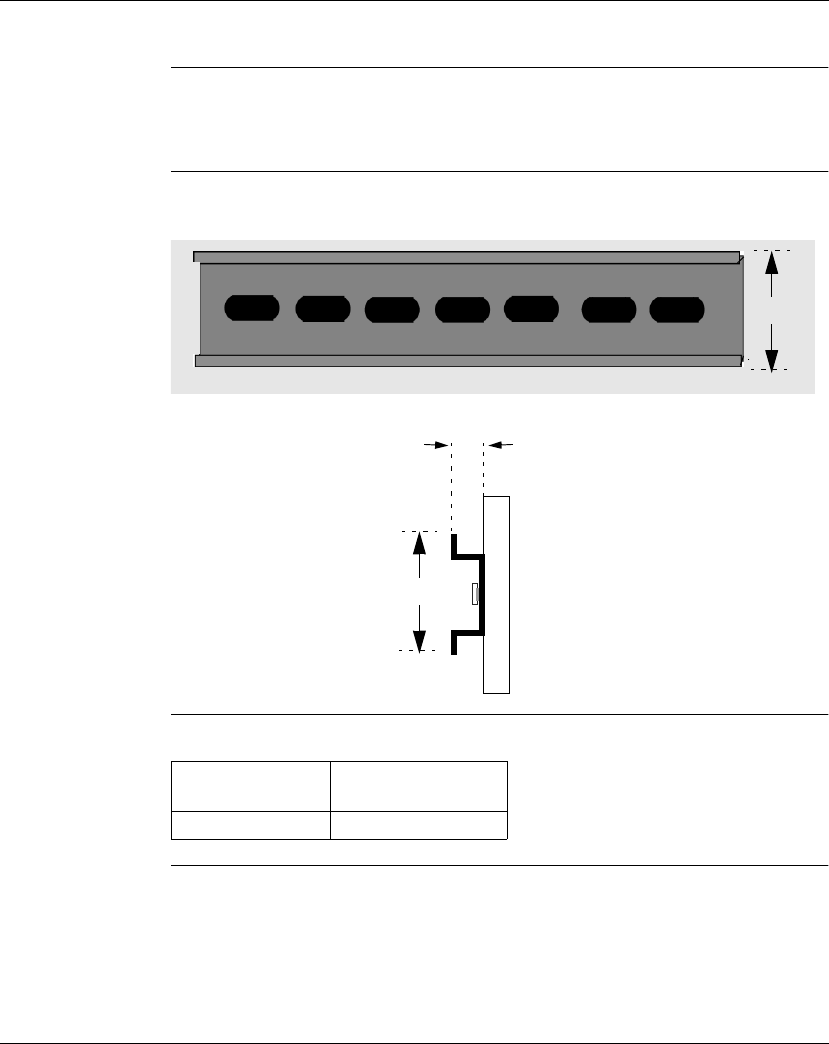
The DIN Rail
Introduction The island is mounted on a DIN rail. A DIN rail can be attached to a smooth mounting
surface or suspended from a EIA rack or in a NEMA cabinet. You can mount the
island to a 35 mm x 15 mm DIN rail (
1.38 in. x 0.59 in.
).
Dimensions of
the DIN Rail
The DIN rail measures 35 mm (
1.38 in.
) high and 15 mm (
0.59 in.
) deep, as shown
below.
Recommended
Equipment
You can order the suitable DIN rail from Schneider Electric:
35 mm
15 mm
35 mm
1.38 in.
0.59 in.
1.38 in.
Rail depth Catalogue part
number
15 mm (
0.59 in.
) AM1DE200

Installation
44 W9 1606383 01 11 A02 09/04

W9 1606383 01 11 A02 09/04 45
3
Description, characteristics, and
wiring of the OTB module
At a Glance
Introduction This chapter describes the wiring rules and recommendations, overviews, part
references, characteristics and wiring diagrams for the Advantys OTB network
interface module.
What's in this
Chapter?
This chapter contains the following topics:
Topic Page
Wiring Rules and Recommendations 46
Overview of the Network Interface Modules 51
Physical Description of an Advantys OTB Network Interface Module 52
General Characteristics of the Network Interface Module 53
I/O Characteristics of the Network Interface Module 55
Wiring diagram of the network interface module 60
How to Connect the Power Supply 61
Connection of the Field Bus or Network 63
Description, characteristics, and wiring of the OTB module
46 W9 1606383 01 11 A02 09/04
Wiring Rules and Recommendations
Introduction There are several rules that must be followed when wiring a module or network
interface. Recommendations, when needed, are provided on how to comply with the
rules.
DANGER
ELECTRIC SHOCK
zBe sure to remove ALL power from ALL devices before connecting or
disconnecting inputs or outputs to any terminal or installing or removing any
hardware.
zMake sure you have COMPLETELY powered down ALL devices before
connecting or disconnecting the bus or network.
Failure to follow this instruction will result in death or serious injury.
WARNING
UNEXPECTED EQUIPMENT OPERATION
If outputs should fail, outputs may remain on or off. Where personnel and or
equipment hazards exist, use an appropriate hard-wired safety system.
Failure to follow this instruction can result in death or serious injury.

Description, characteristics, and wiring of the OTB module
W9 1606383 01 11 A02 09/04 47
Rules zEach connector terminal accepts up to two wires fitted with cable ends or tags,
with sections between 0.08 mm2and0.75mm
2, (0.12 10-3 in.2and 1.16 10-3 in.2
)
zOutput module fusing is the responsibility of the user. It is not within the OTB
network interface module itself. Select a fuse appropriate for the load with respect
to the electrical codes.
zDepending on the load, a protection circuit may be needed for relay outputs on
modules.
zThe power supply wire should be between 0.33 mm2and 0.75 mm2(0.51 10-
3in.2and 1.16 10-3 in.2). Use the shortest wire length possible.
zThe grounding wire should be 1.50 mm2(2.3 10-3 in.2).
zBe sure to connect the grounding wire to a proper ground.
zPower supply wires routed inside the panel must be kept separate from I/O and
communication wiring. Route wiring in separate cable ducting.
zTake care when wiring output modules that are designed to work as either source
or sink. Incorrect wiring can cause equipment damage.
zMake sure that the operating conditions and environments are within the
specification values.
zUse proper wire size to meet voltage and current requirements.
zFit cable ends to the cables.
Description, characteristics, and wiring of the OTB module
48 W9 1606383 01 11 A02 09/04
Contact
Protection
Circuit for Relay
and Transistor
Outputs
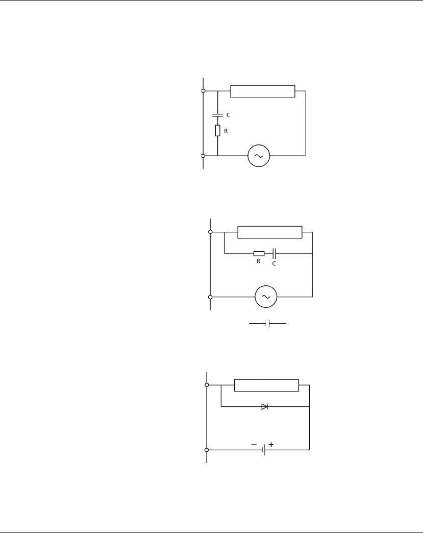
Depending on the load, a protection circuit may be needed for relay outputs. Choose
a protection circuit, from the following diagrams, according to the power supply.
Connect the protection circuit to the outside of the module for the relay outputs.
Protection Circuit A: this protection circuit can be used when the load impedance is
smaller than the RC impedance in an AC load power circuit.
zC represents a value from 0.1 to 1 µF.
zR represents a resistor of approximately the same resistance value as the load.
Protection Circuit B: this protection circuit can be used for both AC and DC load
power circuits.
zC represents a value from 0.1 to 1 µF.
zR represents a resistor of approximately the same resistance value as the load.
Protection Circuit C: this protection circuit can be used for DC load power circuits.
Use a diode with the following ratings:
zReverse withstand voltage: power voltage of the load circuit x 10.
zForward current: more than the load current.
Inductive load
Output Q
COM
Output Q
COM
or +
-
Inductive load
Output Q
COM
Inductive load

Description, characteristics, and wiring of the OTB module
W9 1606383 01 11 A02 09/04 49
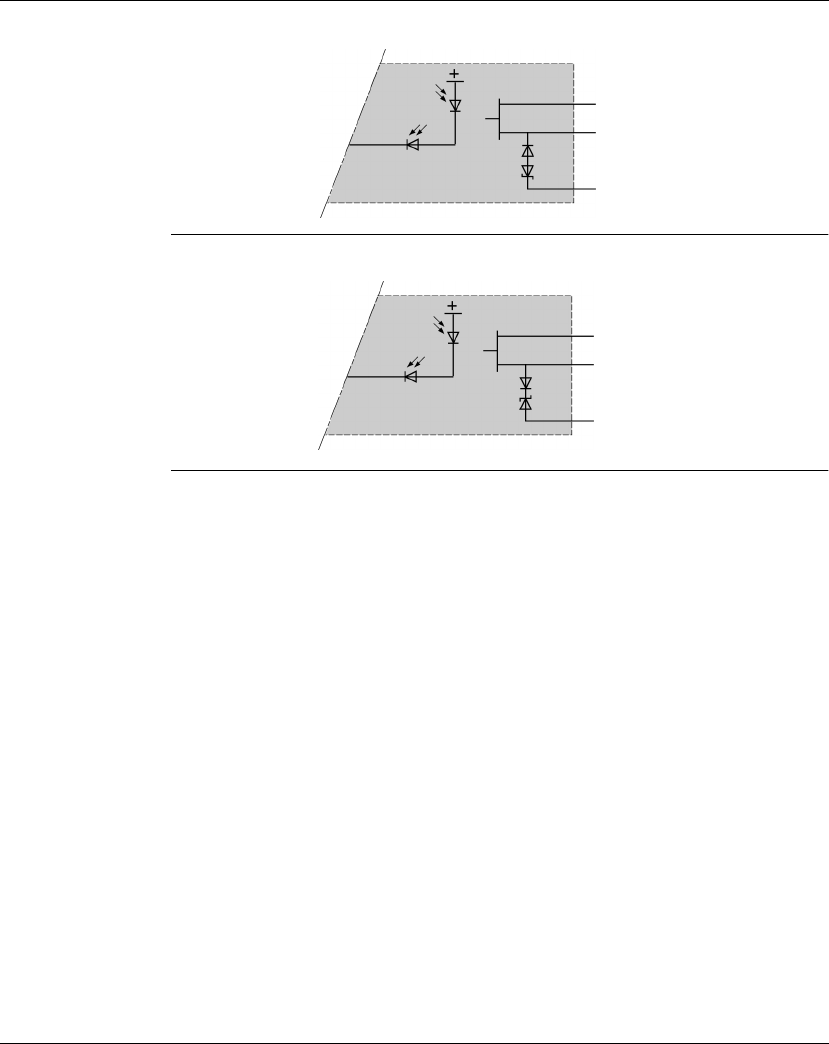
Protection Circuit D: this protection circuit can be used for both AC and DC load
power circuits.
Output Q
COM
or
Inductive load
Description, characteristics, and wiring of the OTB module
50 W9 1606383 01 11 A02 09/04
Operation of
Source Inputs/
Sink Outputs
Input side COM field terminal connects to the "-" terminal or common of the field
power supply. Output side COM field terminal connects to +24V field power supply.
Operation of
Source Inputs
and Outputs
The input side COM field terminal connects to the +24 V power supply. The output
side COM field terminal connects to the "-" terminal or common of the field power
supply.
Note: Sink corresponds to the sensors' common on the (+) terminal of the power
supply.
Current
Load
Current
Output
Input
Electrical
supply
Current Sink Inputs/Current Source Outputs
Electrical
supply
Common
Note: Source corresponds to the sensors' common on the (-) terminal of the power
supply.
Current
Load
Common
Current
Output
Input
Electrical
supply
Current Source Inputs/Current Sink Outputs
Electrical
supply
Description, characteristics, and wiring of the OTB module
W9 1606383 01 11 A02 09/04 51
Overview of the Network Interface Modules
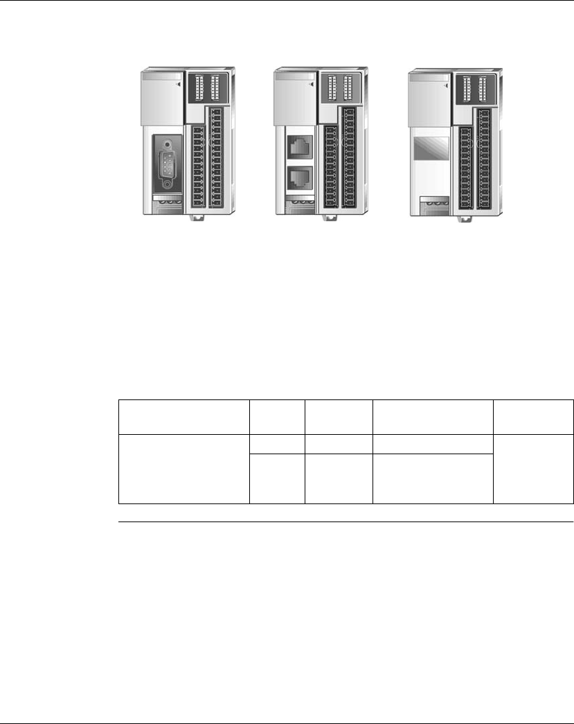
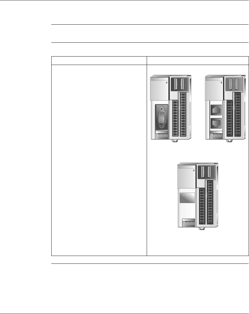
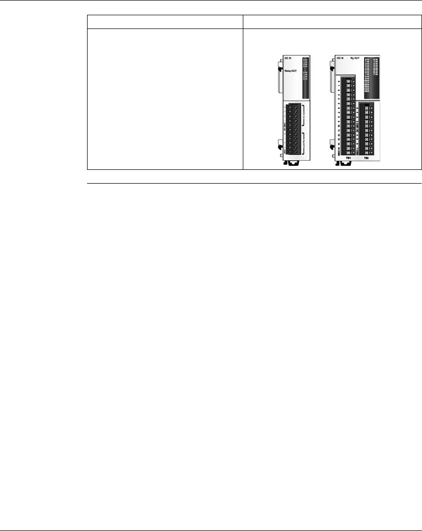
Introduction This section describes the entire range of Advantys OTB network interface modules.
Illustrations The following illustrations show the different network interface modules:
Module type Illustration
Network interface module:
zhas 12 digital inputs, 6 relay outputs, and
2 transistor source outputs
zhas a terminal block for wiring
zaccepts up to 7 expansion I/O modules
OTB1C0DM9LP OTB1S0DM9LP
OTB1E0DM9LP
Description, characteristics, and wiring of the OTB module
52 W9 1606383 01 11 A02 09/04
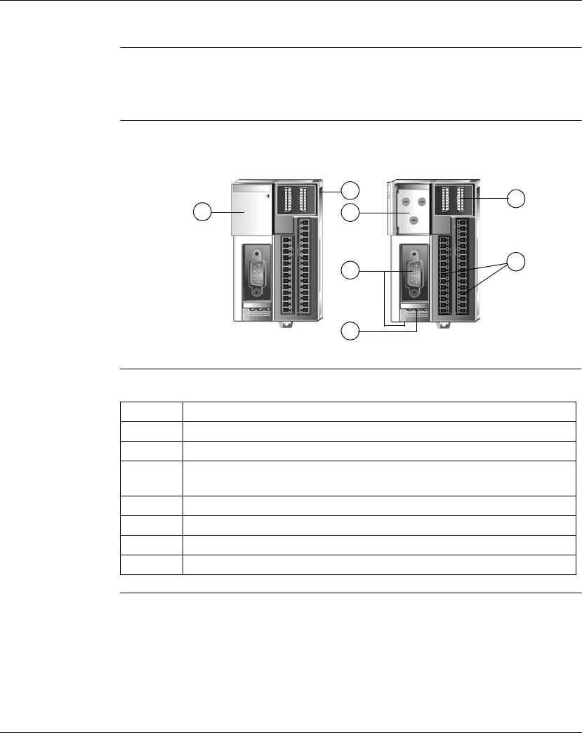
Physical Description of an Advantys OTB Network Interface Module
Introduction This section describes the different sections of a network interface module. Only the
communication section is dedicated to each field bus or network. This may differ
from the illustrations, but the general description remains the same.
Physical
Description of a
Network
Interface Module
The following illustration describes the different sections of a network interface
module.
Legend
1
2
3
4
5
6
7
Label Description
1 Hinged lid
2 Connector for expansion modules
3 Encoder wheels (sets the node address and communication speed on the bus
or network)
4 Communication bus connectors
5 24 VDC power supply terminals
6 Indicator light
7 I/O terminals

Description, characteristics, and wiring of the OTB module
W9 1606383 01 11 A02 09/04 53
General Characteristics of the Network Interface Module
Introduction This section describes the general characteristics common to the network interface
modules.
Normal
Operating
Specifications Network interface
module
OTB1•0DM9LP
Operating temperature 0 to 55°C (32°F to 131°F) operating ambient temperature
Storage temperature -25 ... +70°C
Relative humidity 30 ... 95%(non-condensing)
Pollution degree 2 (IEC60664)
Degree of protection IP20
Altitude Operation: from 0 to 2000 m
Transport: from 0 to 3000 m
Resistance to Vibration When mounted on a DIN rail:
from 10 to 57 Hz amplitude 0.075 mm, from 57 to 150 Hz
acceleration 9.8 ms2(1G), 2 hours per axis on each of three
mutually perpendicular axes.
When mounted on a panel surface:
2 to 25 Hz, amplitude 1.6 mm, 25 to 100 Hz, acceleration 39.2
ms2(4G), 90 min per axis on each of three mutually
perpendicular axes.
Impact strength 147 ms2(15G), 11 ms duration, 3 shocks per axis, on three
mutually perpendicular axes (IEC 61131).
Weight 185 g

Description, characteristics, and wiring of the OTB module
54 W9 1606383 01 11 A02 09/04
Electrical
Specifications Network interface
module
OTB1•0DM9LP
Rated power voltage 24 VDC
Allowable voltage range from 20.4 to 26.4 VDC (including ripple)
Peak voltage 39 VDC +/- 1 V
Consumed power Communication module with 7 expansion modules
19 W (26.4 VDC)
Allowable momentary
power interruption
10 ms (@ 24VDC)
Dielectric strength Between power and ground terminals: 500 VAC, 1 min
Between I/O and ground terminals: 500 VAC, 1 min
Insulation resistance Between power and ground terminals: 10 MΩminimum
(500 VDC)
Between I/O and ground terminals: 10 MΩminimum
(500 VDC)
Noise resistance
IEC 1131-2
DC power terminals: 1 kV, 50 ns to 1 µs
I/O terminals (coupling clamp): 1.5 kV, 50 ns to 1 µs
Inrush current 50 A maximum (24 VDC)
Ground wiring UL1015 22 AWG (0.33 mm2), UL1007 18 AWG (0.82 mm2)
Power supply wiring UL1015 22 AWG (0.33 mm2), UL1007 18 AWG (0.82 mm2)
Tightening torque of the
24 VDC supply terminals
0.8 Nm (7.04 in.pounds)
Tightening torque of the I/O
terminals
0.6 Nm (5.28 in.pounds)
Effect of improper power
supply connection
Reverse polarity: no operation, no damage
Improper voltage or frequency: permanent damage may be
caused
Improper lead connection: permanent damage may be caused

Description, characteristics, and wiring of the OTB module
W9 1606383 01 11 A02 09/04 55
I/O Characteristics of the Network Interface Module
Introduction This section describes the I/O characteristics of the Advantys OTB network interface
modules.
Input
Specifications Network interface
module
OTB1•0DM9LP
Input points 12 inputs with common line
Rated input voltage 24 VDC source/sink input signal
Input voltage range from 20.4 to 26.4 VDC
Rated input current I0, I1, I6, I7: 5 mA/input (24 VDC)
I2 to I5, I8 to I11: 7 mA/input (24 VDC)
Input impedance I0, I1, I6, I7: 5.7 kΩ
I2 to I5, I8 to I11: 3.4 kΩ
Switching time at high
status
(ON Time)
I0 to I7: 35 µs + filter value
I8 to I11: 40 µs + filter value
Switching time at low
status
(OFF Time)
I0, I1, I6, I7: 45 µs + filter value
I2 to I5, I8 to I11: 150 µs + filter value
Isolation Between input terminals: not isolated
Internal circuit: photocoupler isolated
1500 Vca
Filtering: 3 possibilities
znone
z3ms
z12 ms
I0 to I11
Input type Type 1 (IEC 61131)
External load for I/O
interconnection
Not needed
Signal determination
method
Static
Effect of improper input
connection
The input signals can be both sink and source. But if any input exceeding
the rated value is applied, permanent damage may be caused.
Cable length 3m (9.84 ft) for compliance with electromagnetic immunity
Connector insertion/
removal durability
100 times minimum
Description, characteristics, and wiring of the OTB module
56 W9 1606383 01 11 A02 09/04
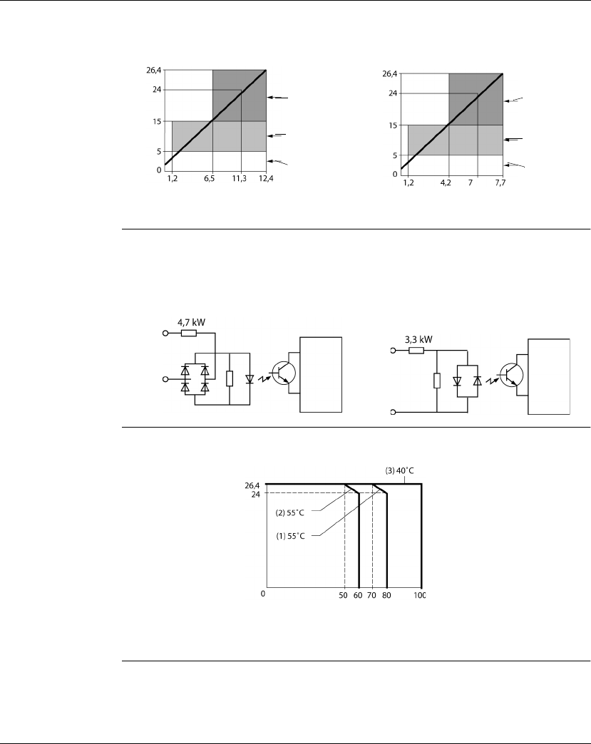
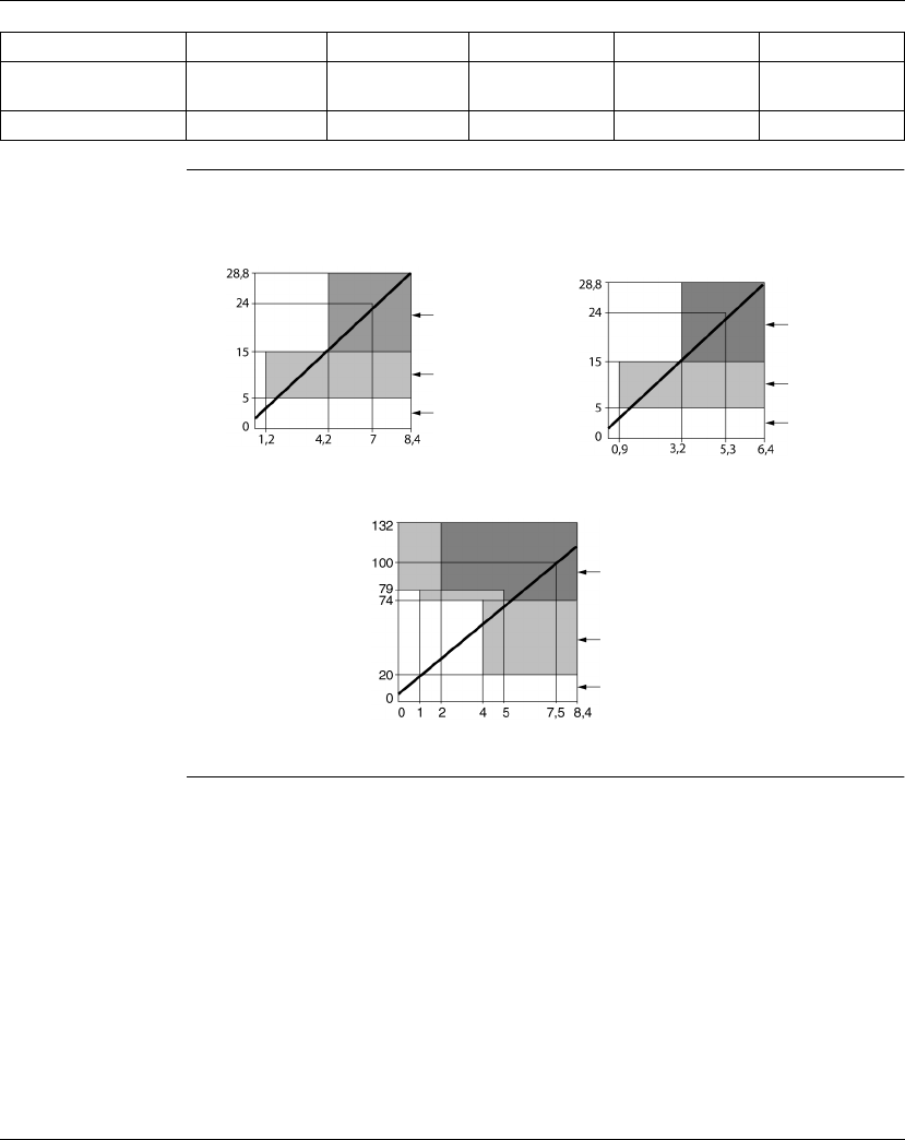
Input Operating
Range
The input operating range of the Type 1 (IEC 61131-2) input module is shown below.
Input Internal
Circuit
The internal input circuit is described below.
I/O Usage Limits
When using OTB1•0DM9LP modules, all I/O can be turned on simultaneously at
40°C, all I/O can be turned on simultaneously at 26.4 VDC as indicated with line (3).
ON Area
Transition
OFF Area
Input Current (mA)
Input Voltage (V DC)
Area
ON Area
Transition
OFF Area
Input Current (mA)
Input Voltage (V DC)
Area
Inputs I2 to I5, I8 to I11
Inputs I0, I1, I6, and I7
Internal Circuit
Input
COM
Input
COM
Inputs I0, I1, I6, and I7 Inputs I2 to I5, I8 to I11
Sink Or Source Input
with state latching or high baud rate
Sink Or Source Input
(standard)
Internal Circuit
I/O Simultaneous ON Ratio (%)
Input Voltage (V DC)

Description, characteristics, and wiring of the OTB module
W9 1606383 01 11 A02 09/04 57
Source
Transistor
Output
Characteristics
Q0,Q1
Network interface
module
OTB1•0DM9LP
Output type Source output
Output points per
common Line
2
Rated load voltage 24 VDC
Maximum load
current
1 A per common line
Operating load
voltage range
from 20.4 to 28.8 VDC
Voltage drop (on
voltage)
1 V maximum (voltage between COM and output terminals when
output is on)
Rated load current 0.3 A per output
Inrush current 1 A maximum
Leakage current 0.1 mA maximum
Clamping voltage 39 V +/-1 V
Maximum lamp load 8 W
Inductive load L/R = 10 ms (28.8 VDC, 1 Hz)
External current draw 100 mA maximum, 24 VDC
(power voltage at the -V terminal)
Isolation Between output terminal and internal circuit: photocoupler isolated
Between output terminals: not isolated
1500 Vca
Average number of
connector insertions/
removals
100 times minimum
Output delay - turn on
time
5µs maximum
Output delay - turn off
time
5µs maximum

Description, characteristics, and wiring of the OTB module
58 W9 1606383 01 11 A02 09/04
Relay Output
Specifications
Q2 to Q7
(*) for AC1 &DC1 the outputs indicated here take the maximum per point on OTB
(2A) into account.
Network interface module OTB1•0DM9LP
Number of outputs 8 digital inputs consisting of 6 relay outputs and 2
transistor source outputs
Output points per common line - COM0 2 outputs
Output points per common line - COM1 3 NO contacts
Output points per common line - COM2 2 NO contacts
Output points per common line - COM3 1 NO contact
Maximum load current 2 A per output
8 A per common line
Minimum switching load 0.1 mA/0.1 VDC (reference value)
Initial contact resistance 30 mΩmaximum
Mechanical life 20,000,000 operations minimum (rated load
18,000 operations/h)
Dielectric strength Between output to internal circuit: 1500 VAC,
1min
Between output to terminals (COMs): 1500 VAC, 1
min
Connector insertion/removal durability 100 times minimum
Output delay - turn on time 300 µs maximum
Output delay - turn off time 300 µs maximum
Usage category Rated load Electrical life (number of
operations)
AC1
Resistive load command
500 VA(*)
AC14
Weak solenoid load
250 VA
AC15
Solenoid
200 VA
DC1
Resistive load command
60 W(*)
DC13
Solenoid L/R=150ms
30 W
105
105
105
105
105
Description, characteristics, and wiring of the OTB module
W9 1606383 01 11 A02 09/04 59
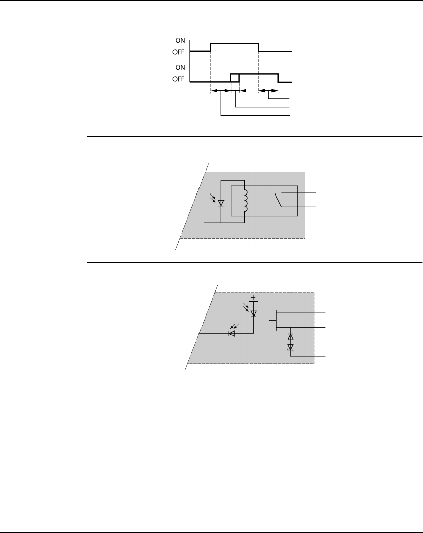
Relay Output
Delay
The output delay is illustrated below.
Relay Output
Contact
The relay output contact is shown below.
Transistor
Source Output
Contact
The transistor source output contact is shown below.
OFF delay: 10 ms maximum
Command
Output Relay Status
Rebound: 6 ms maximum
ON delay: 6 ms maximum
Internal Circuit
No
LED
Qx (Load)
COM
Terminal block
P-chan
LED
QOutput
COM (+24 V)
V- (COM)
Internal Circuit
Description, characteristics, and wiring of the OTB module
60 W9 1606383 01 11 A02 09/04
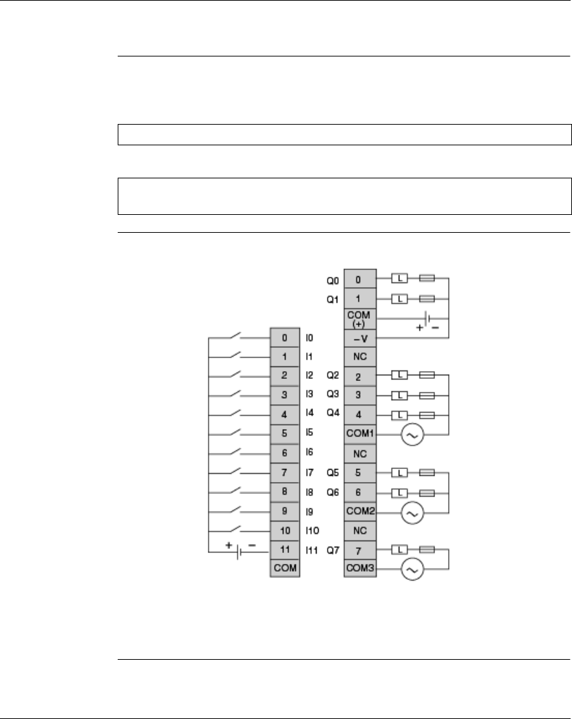
Wiring diagram of the network interface module
Introduction This section shows examples of wiring diagrams for Advantys OTB network
interface modules.
Wiring Diagram
for OTB Modules
This schematic is for OTB1•0DM9LP modules.
zOutput points 0 and 1 are transistor source outputs, all other output points are
relay.
zThe COM terminals are not connected together internally.
zConnect an appropriate fuse for the load.
Note: These schematics are for external wiring only.
Note: The shaded boxes are markings on the module. The I and Qnumbers are
the input and output points.
Output wiring
Input wiring
Relay output wiring
Relay output wiring
Relay output wiring
positive logic
positive logic
Description, characteristics, and wiring of the OTB module
W9 1606383 01 11 A02 09/04 61
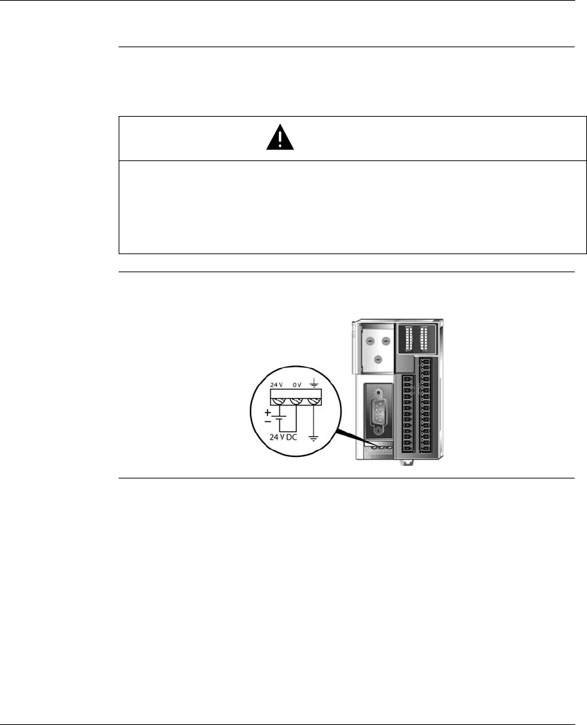
How to Connect the Power Supply
Introduction This section describes how to connect the power supply to the network interface
modules.
Power
Connection for a
Network
Interface Module
The following diagram describes the power connection for an Advantys OTB
network interface module.
WARNING
UNEXPECTED EQUIPMENT OPERATION
When operating outside of the specified voltage range, outputs may not switch
accordingly. Use an appropriate externally wired safety system (voltage controllers)
and voltage monitoring circuits.
Failure to follow this instruction can result in death or serious injury.

Description, characteristics, and wiring of the OTB module
62 W9 1606383 01 11 A02 09/04
Network
Interface Module
Power Supply
Specifications
The following table describes the power supply specifications for the network
interface module.
Item Characteristics
Power supply
voltage
Rated power voltage: 24 VDC
Allowable range: from 20.4 to 26.4 VDC
Note:Momentary power interruption for 10 ms or less at 24 VDC is not
recognized as failure.
Inrush current
flow at power-
up
50 A maximum
Power supply
wiring
0.64 mm2(UL1015 AWG22) or 1.02 mm2(UL1007 AWG18)
Make the power supply wiring as short as possible.
Ground wiring 0.64 mm2(UL1015 AWG22) or 1.02 mm2(UL1007 AWG18)
Do not connect ground wire in common with ground wire of motor
equipment.
The earth connection should be as short as possible <10 cm (3.9 inch).
Description, characteristics, and wiring of the OTB module
W9 1606383 01 11 A02 09/04 63
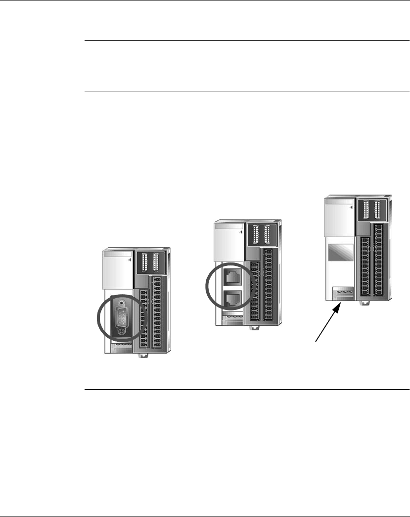
Connection of the Field Bus or Network
Overview The specific types of cables and connectors for connecting the field bus or network
of the OTB module vary according to the network used. Detailed cabling and
connector information is given in Chapter 5 "Communication".
Connection of
theFieldBusor
Network
The field bus is connected between your master or server and the complete and
physically installed OTB island. In order to make this connection, simply press the
field bus connector into the specially-provided receptacle, and lock the connector in
place.
There are three types of OTB module: CANOpen, Modbus and Ethernet. These
represent the three available field bus protocols or networks. Below are the
illustrations of the three types of different module. We draw your attention to the
different field bus or network plugs.
OTB CANopen
OTB Ethernet
OTB Modbus

Description, characteristics, and wiring of the OTB module
64 W9 1606383 01 11 A02 09/04

W9 1606383 01 11 A02 09/04 65
4
Description, characteristics, and
wiring of the expansion modules
At a Glance
Introduction This chapter provides an overview of the analog and Discrete I/O expansion
modules. Information on functions and wiring is given for each expansion module.
What's in this
Chapter?
This chapter contains the following topics:
Topic Page
Overview of Digital I/O Modules 66
Parts Description of Digital I/O Modules 70
Specifications for the Digital I/O Modules 72
Digital I/O Module Wiring Schematics 83
Overview of Analog I/O Modules 93
Parts Description of Analog I/O Modules 94
General Specifications for the Analog I/O Modules 95
Specifications for the Analog I/O Modules 96
Analog I/O Modules Wiring Schematics 100
Communication expansion module block Wiring Schematics 103

Description, characteristics, and wiring of the expansion modules
66 W9 1606383 01 11 A02 09/04
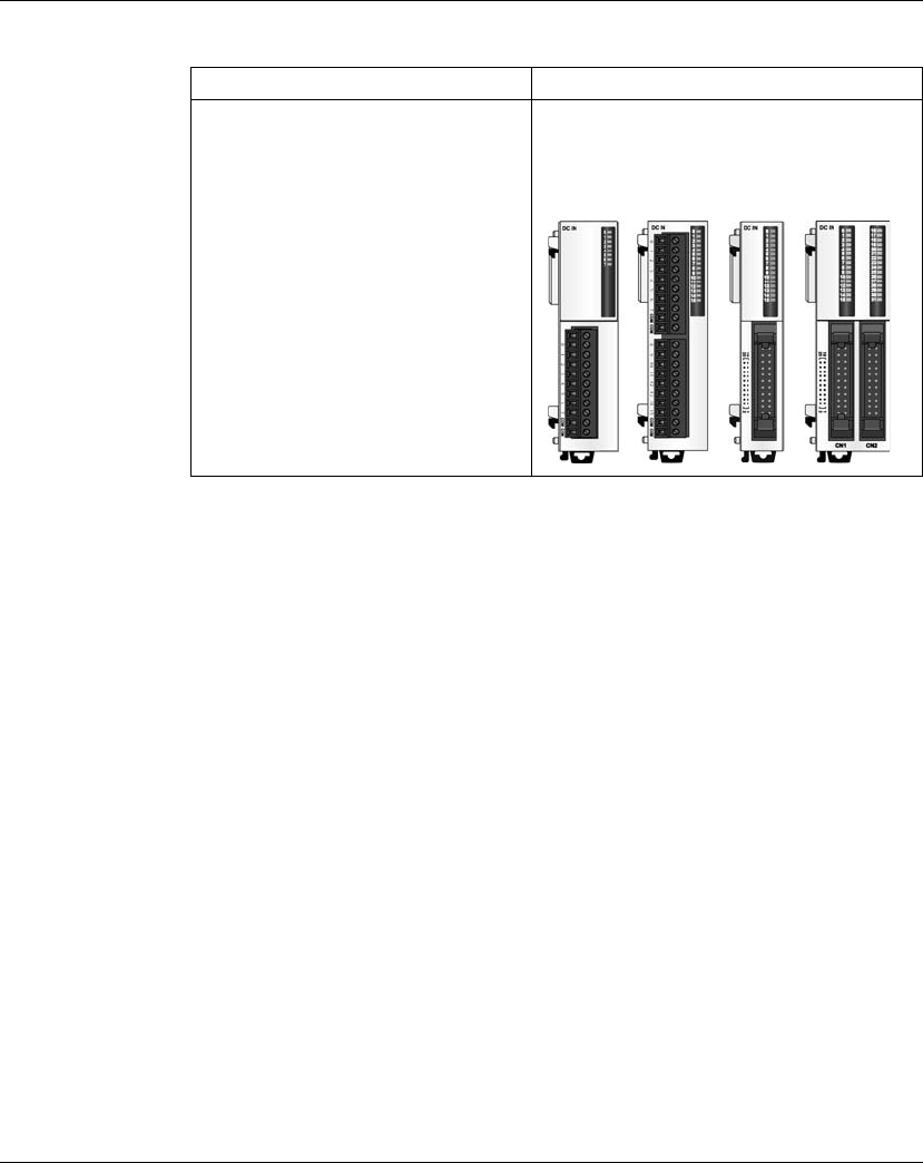
Overview of Digital I/O Modules
Introduction The following section provides an overview of the digital I/O modules.
Description, characteristics, and wiring of the expansion modules
W9 1606383 01 11 A02 09/04 67
Illustrations The following illustrations are the digital input, output, and mixed I/O modules.
Module type Illustration
There are 5 digital input modules:
z8-point module with a terminal block
(TWDDDI8DT, TWDDAI8DT)
z16-point module with a terminal block
(TWDDDI16DT)
z16-point module with a connector
(TWDDDI16DK)
z32-point module with a connector
(TWDDDI32DK)
These modules can be attached to any
communication module.
TWDDDI8DT
TWDDDI16DT TWDDDI32DK
TWDDDI16DK
TWDDAI8DT
Description, characteristics, and wiring of the expansion modules
68 W9 1606383 01 11 A02 09/04
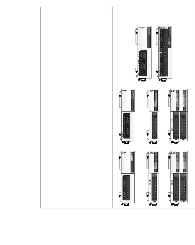
There are 8 digital output modules:
z8-point relay output module with a
terminal block (TWDDRA8RT)
z16-point relay output module with a
terminal block (TWDDRA16RT)
z8-point transistor sink module with a
connector (TWDDDO8UT)
z16-point transistor sink module with a
connector (TWDDDO16UK)
z32-point transistor sink module with a
connector (TWDDDO32UK)
z8-point transistor source module with a
terminal block (TWDDDO8TT)
z16-point transistor source module with
a connector (TWDDDO16TK)
z32-point transistor source module with
a connector (TWDDDO32TK)
These modules can be attached to any
communication module.
Module type Illustration
TWDDRA8RT TWDDRA16RT
TWDDDO8UT TWDDDO16UK TWDDDO32UK
TWDDDO8TT TWDDDO16TK TWDDDO32TK
Description, characteristics, and wiring of the expansion modules
W9 1606383 01 11 A02 09/04 69
There are 2 digital mixed input and output
modules:
z4-point input/4-point output module
with a terminal block (TWDDMM8RT)
z16-point input/8-point output module
with a wire-clamp terminal block
(TWDDMM24DRF)
These modules can be attached to any
communication module.
Module type Illustration
TWDDMM8RT TWDDMM24DRF
Description, characteristics, and wiring of the expansion modules
70 W9 1606383 01 11 A02 09/04
Parts Description of Digital I/O Modules
Introduction The following section describes the parts of a digital I/O module with a terminal block
and with a connector. Your I/O module may differ from the illustrations but the parts
will be the same.
Parts
Description of a
Digital I/O
Module with a
Terminal Block
The following figure shows the parts of a digital I/O module with a terminal block.
This figure is the TWDDDI8DT module.
Legend
Parts
Description of a
Digital I/O
Module with a
Connector
The following figure shows the parts of a digital I/O module with a connector. This
figure is the TWDDDO16TK module.
2
1
4
5
3
Label Description
1 Expansion connector - one on each side, right side not shown
2 Terminal block
3 Latch button
4LEDs
5 Clamp
2
4
5
3
1

Description, characteristics, and wiring of the expansion modules
W9 1606383 01 11 A02 09/04 71
Legend
Label Description
1 Expansion connector - one on each side, right side not shown
2 Connector
3 Latch button
4LEDs
5Clamp

Description, characteristics, and wiring of the expansion modules
72 W9 1606383 01 11 A02 09/04
Specifications for the Digital I/O Modules
Introduction This section presents the specifications for the digital I/O modules.
TWDDDI8DT,
TWDDDI16DT,
TWDDDI16DK,
TWDDDI32DK
and TWDDAI8DT
Specifications
WARNING
HAZARD OF UNINTENDED EQUIPMENT OPERATION AND EQUIPMENT
DAMAGE
If any input exceeding the rated value is applied, permanent damage may be caused.
Failure to follow this instruction can result in death or serious injury.
Reference TWDDDI8DT TWDDDI16DT TWDDDI16DK TWDDDI32DK TWDDAI8DT
Input points 8 points in 1
common line
16 points in 1
common line
16 points in 1
common line
32 points in 2
common lines
8 points in 2
common lines
Rated input voltage 24 VDC source/sink input signal 120 VAC
Input voltage range from 20.4 to 28.8 VDC
Maximum 132 VAC
Rated input current 7 mA/input (24 VDC) 5 mA/input (24 VDC) 7.5 mA/input
(100 VDC)
Input impedance 3.4 kΩ4.4 kΩ11 kΩ
Turn on time
24 VDC/120 VAC
8ms 25ms
Turn off time
24 VDC/120 VAC
8 ms 30ms
Isolation Between input terminals and internal circuit: photocoupler isolated (isolation protection up to
500 V)
Between input terminals: not isolated
External load for I/O
interconnection
Not needed
Signal determination
method
Static
Effect of improper
input connection
The input signals can be both sink and source. Input signals
must be AC type
Cable length 3m (9.84 ft.) in compliance with electromagnetic immunity
Connector insertion/
removal durability
100 times minimum
Internal current draw -
all inputs on
25 mA (5 VDC)
0 mA (24 VDC)
40 mA (5 VDC)
0 mA (24 VDC)
35 mA (5 VDC)
0 mA (24 VDC)
65 mA (5 VDC)
0 mA (24 VDC)
55 mA (5 VDC)
0 mA (24 VDC)
Description, characteristics, and wiring of the expansion modules
W9 1606383 01 11 A02 09/04 73
TWDDDI8DT,
TWDDDI16DT,
TWDDDI16DK,
TWDDDI32DK
and TWDDAI8DT
Operating Range
The operating range of the Type 1 (IEC 61131-2) input module is shown below.
Internal current draw -
all inputs off
5 mA (5 VDC)
0 mA (24 VDC)
5 mA (5 VDC)
0 mA (24 VDC)
5 mA (5 VDC)
0 mA (24 VDC)
10 mA (5 VDC)
0 mA (24 VDC)
25 mA (5 VDC)
0 mA (24 VDC)
Weight 85 g (3 oz) 100 g (3.5 oz) 65 g (2.3 oz) 100 g (3.5 oz) 81 g (2.9 oz)
Reference TWDDDI8DT TWDDDI16DT TWDDDI16DK TWDDDI32DK TWDDAI8DT
ON Area
Transition
OFF Area
Input Current (mA)
Input Voltage (V DC)
Area
ON Area
Transition
OFF Area
Input Current (mA)
Input Voltage (V DC)
Area
TWDDDI8DT and TWDDDI16DT TWDDDI16DK and TWDDDI32DK
TWDDAI8DT
Input Voltage (V AC)
Input Current (mA)
ON Area
Transition
OFF Area
Area
Description, characteristics, and wiring of the expansion modules
74 W9 1606383 01 11 A02 09/04
TWDDDI8DT,
TWDDDI16DT,
TWDDDI16DK,
TWDDDI32DK
and TWDDAI8DT
Internal Circuit
The input internal circuit is shown below.
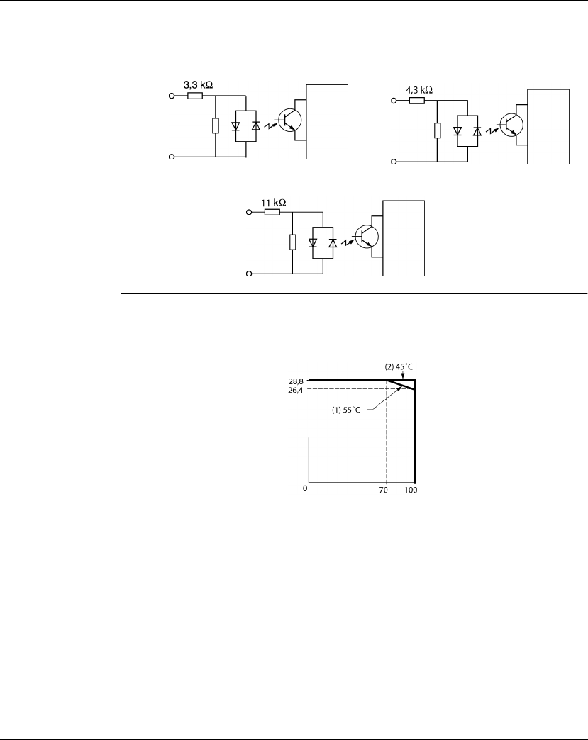
TWDDDI8DT,
TWDDDI16DT,
TWDDDI16DK,
TWDDDI32DK
and TWDDAI8DT
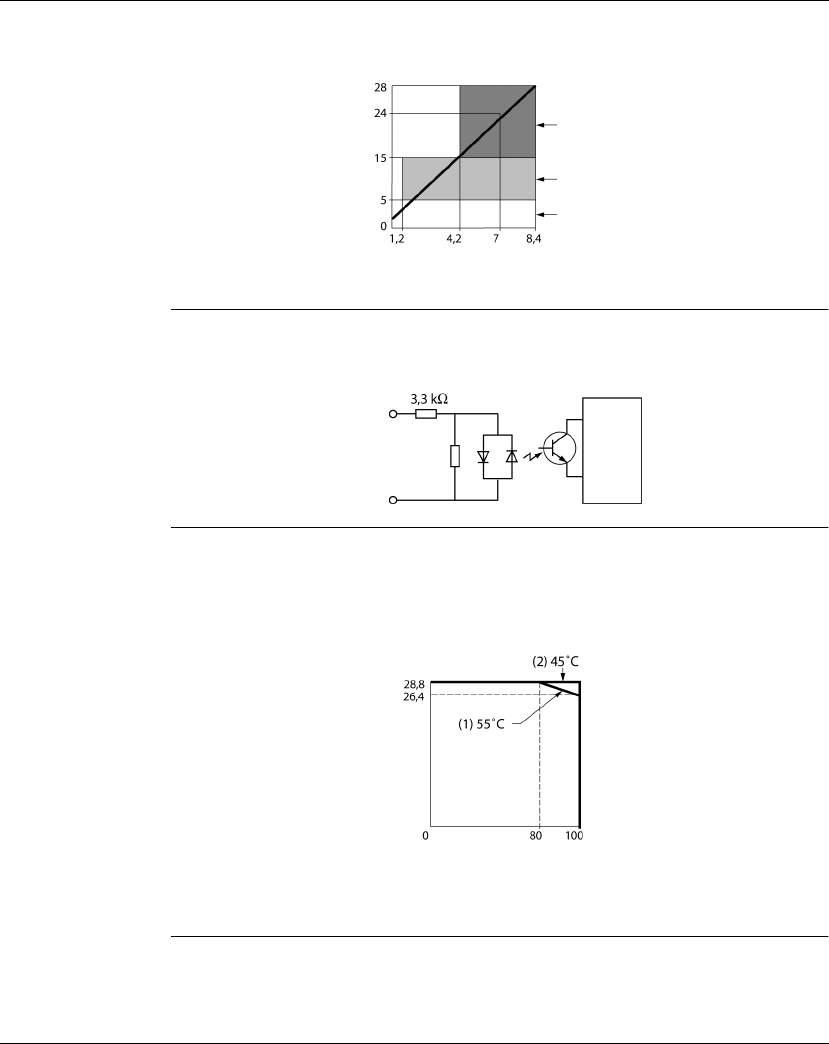
Usage Limits
When using TWDDDI16DT at 55°C (131°F) in the normal mounting direction, limit
the inputs which turn on simultaneously along line (1). At 45°C (113°F), all inputs can
be turned on simultaneously at 28.8 VDC as indicated with line (2).
Internal Circuit
Input
COM
TWDDDI8DT and TWDDDI16DT TWDDDI16DK and TWDDDI32DK
Internal Circuit
Input
COM
Sink Or Source Input
Internal Circuit
Input
COM
TWDDAI8DT
Input Simultaneous ON Ratio (%)
Input Voltage (V DC)
Description, characteristics, and wiring of the expansion modules
W9 1606383 01 11 A02 09/04 75
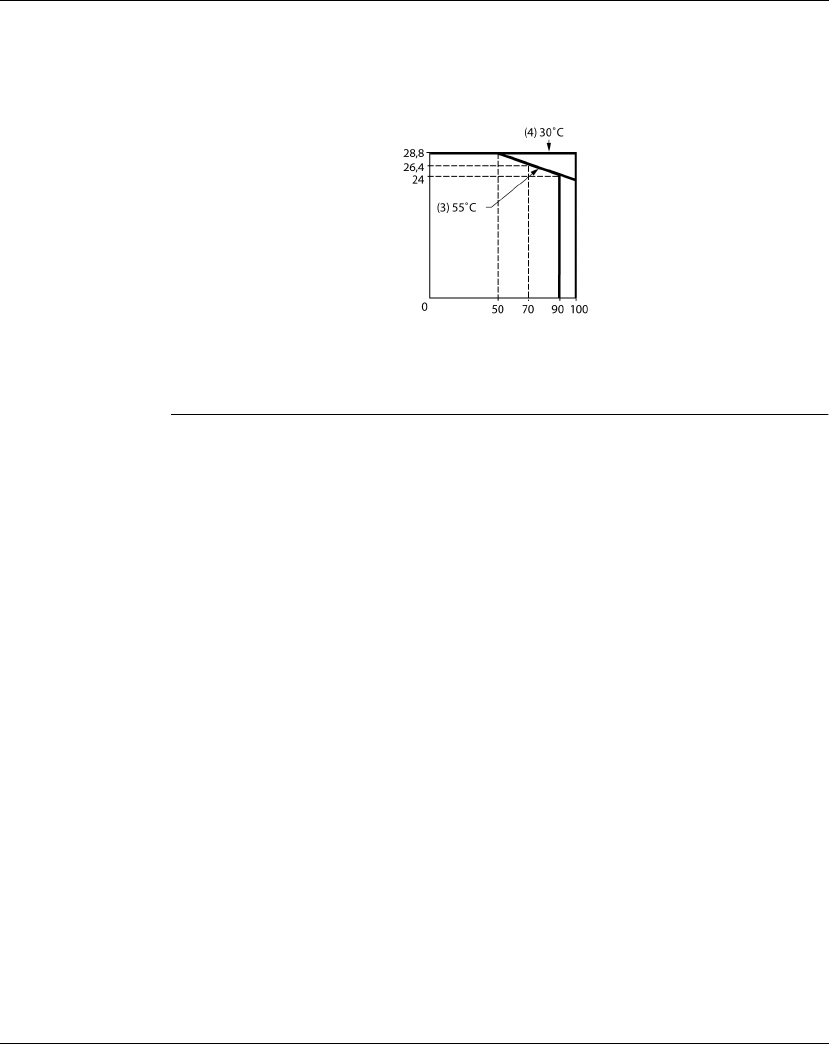
When using TWDDDI16DK and TWDDDI32DK at 55°C (131°F), limit the inputs
which turn on simultaneously on each connector along line (3). This limitation
applies per connecter. At 30°C (86°F), all inputs can be turned on simultaneously at
28.8 VDC as indicated with line (4).
When using TWDDDI8DT, all inputs can be turned on simultaneously at 55°C
(131°F), input voltage 28.8 VDC.
Input Simultaneous ON Ratio (%)
Input Voltage (V DC)
Description, characteristics, and wiring of the expansion modules
76 W9 1606383 01 11 A02 09/04
TWDDRA8RT
and
TWDDRA16RT
Specifications
TWDDRA8RT
and
TWDDRA16RT
Delay
The output delay is shown below.
CAUTION
ELECTRIC SHOCKS AND FIRE HAZARDS
Possible current overload;size cable accordingly.
Failure to follow this instruction can result in injury.
Reference number TWDDRA8RT TWDDRA16RT
Output points and common lines 8 NO contacts in 2 common
lines
16 NO contacts in 2
common lines
Maximum load current 2 A per output
7 A per common line 8 A per common line
Minimum switching load 0.1 mA/0.1 VDC (reference value)
Initial contact resistance 30 mΩmaximum
Electrical life
100,000 operations minimum (rated load 1,800 operations/h)
Mechanical life
20,000,000 operations minimum (rated load 18,000 operations/h)
Rated load (resistive/inductive) 240 VAC/2 A, 30 VDC/2 A
Dielectric strength Between output to terminals: 1,500 VAC, 1 minute
Between output terminal and internal circuit: 1,500 VAC, 1 minute
Between output terminals (COMs): 1,500 VAC, 1 minute
Connector insertion/removal durability
100 times minimum
Internal current draw -
all outputs on
30 mA (5 VDC)
40mA (24 VDC)
45 mA (5 VDC)
75 mA (24 VDC)
Internal current draw -
all outputs off
5mA(5VDC)
0mA(24VDC)
5 mA (5 VDC)
0 mA (24 VDC)
Weight 110 g (3.9 oz) 145 g (5.1 oz)
OFF delay: 10 ms maximum
Command
Output Relay Status
Contact Bounce: 6 ms maximum
ON delay: 6 ms maximum

Description, characteristics, and wiring of the expansion modules
W9 1606383 01 11 A02 09/04 77
TWDDDO8UT,
TWDDDO16UK,
and
TWDDDO32UK
Specifications
Reference number TWDDDO8UT TWDDDO16UK TWDDDO32UK
Output type Transistor sink output
Output points per common Line 8 points in 1
common line
16 points in 1
common line
32 points in 2
common lines
Rated load voltage 24 VDC
Operating load voltage range from 20.4 to 28.8 VDC
Rated load current 0.3 A per output 0.1 A per output
Maximum load current 0.36 A per output
3 A per common
line
0.12 A per output
1 A per common line
Voltage drop (on voltage) 1 V maximum (voltage between COM and output
terminals when output is on)
Inrush current 1 A maximum
Leakage current 0.1 A maximum
Clamping voltage 39 V +/-1 V
Maximum lamp load 8 W
Inductive load L/R = 10 ms (28.8 VDC, 1 Hz)
External current draw 100 mA maximum, 24 VDC
(power voltage at the +V terminal)
Isolation Between input terminals and internal circuit: photocoupler
isolated (isolation protection up to 500 V)
Between input terminals: not isolated
Connector insertion/removal
durability
100 times minimum
Internal current draw -
all outputs on
10 mA (5 VDC)
20 mA (24 VDC)
10 mA (5 VDC)
40mA (24 VDC)
20 mA (5 VDC)
70 mA (24 VDC)
Internal current draw -
all outputs off
5mA(5VDC)
0 mA (24 VDC)
5 mA (5 VDC)
0 mA (24 VDC)
10 mA (5 VDC)
0 mA (24 VDC)
Output delay Turn on time: 300 µs maximum
Turn off time: 300 µs maximum
Weight 85 g (3 oz) 70 g (2.5 oz) 105 g (3.7 oz)

Description, characteristics, and wiring of the expansion modules
78 W9 1606383 01 11 A02 09/04
TWDDDO8TT,
TWDDDO16TK,
and
TWDDDO32TK
Specifications
Reference number TWDDDO8TT TWDDDO16TK TWDDDO32TK
Output type Transistor source output
Output points per common Line 8 points in 1
common line
16 points in 1
common line
32 points in 2
common lines
Rated load voltage 24 VDC
Operating load voltage range from 20.4 to 28.8 VDC
Rated load current 0.3 A per output 0.1 A per output
Maximum load current 0.36 A per output
3Apercommon
line
0.12 A per output
1 A per common line
Voltage drop (on voltage) 1 V maximum (voltage between COM and output
terminals when output is on)
Inrush current 1 A maximum
Leakage current 0.1 mA maximum
Clamping voltage 39 V +/-1 V
Maximum lamp load 8 W
Inductive load L/R = 10 ms (28.8 VDC, 1 Hz)
External current draw 100 mA maximum, 24 VDC
(power voltage at the +V terminal)
Isolation Between input terminals and internal circuit: photocoupler
isolated (isolation protection up to 500 V)
Between input terminals: not isolated
Connector insertion/removal
durability
100 times minimum
Internal current draw - all outputs
on
10 mA (5 VDC)
20 mA (24 VDC)
10 mA (5 VDC)
40mA (24 VDC)
20 mA (5 VDC)
70 mA (24 VDC)
Internal current draw - all outputs
off
5 mA (5 VDC)
0 mA (24 VDC)
5 mA (5 VDC)
0 mA (24 VDC)
10 mA (5 VDC)
0 mA (24 VDC)
Output delay Turn on time: 300 µs maximum
Turn off time: 300 µs maximum
Weight 85 g (3 oz) 70 g (2.5 oz) 105 g (3.7 oz)

Description, characteristics, and wiring of the expansion modules
W9 1606383 01 11 A02 09/04 79
TWDDMM8DRT
and
TWDDMM24DRF
Input
Specifications
WARNING
HAZARD OF UNINTENDED EQUIPMENT OPERATION AND EQUIPMENT
DAMAGE
If any input exceeding the rated value is applied, permanent damage may be caused.
Failure to follow this instruction can result in death or serious injury.
Reference number TWDDMM8DRT TWDDMM24DRF
I/O points 4 inputs and 4 outputs 16 inputs and 8 outputs
Rated input voltage 24 VDC source/sink input signal
Input voltage range from 20.4 to 28.8 VDC
Rated input current 7 mA/input (24 VDC)
Input impedance 3.4 kΩ
Turn on time (24 VDC) 4 ms (24 VDC)
Turn off time (24 VDC) 4 ms (24 VDC)
Isolation Between input terminals and internal circuit: photocoupler
isolated (isolation protection up to 500 V)
Between input terminals: not isolated
External load for I/O
interconnection
Not needed
Signal determination method Static
Effect of improper input
connection
Both sinking and sourcing input signals can be connected.
Cable length 3m (9.84 ft.) in compliance with electromagnetic immunity
Connector insertion/removal
durability
100 times minimum Not removable
Internal current draw -
all I/O on
25 mA (5 VDC)
20 mA (24 VDC)
65 mA (5 VDC)
45 mA (24 VDC)
Internal current draw - all I/O off 5 mA (5 VDC)
0 mA (24 VDC)
10 mA (5 VDC)
0 mA (24 VDC)
Weight 95 g (3.3 oz) 140 g (4.9 oz)
Description, characteristics, and wiring of the expansion modules
80 W9 1606383 01 11 A02 09/04
TWDDMM8DRT
and
TWDDMM24DRF
Input Operating
Range
The input operating range of the Type 1 (IEC 61131-2) input module is shown below.
TWDDMM8DRT
and
TWDDMM24DRF
Input Internal
Circuit
The input internal circuit is shown below.
TWDDMM8DRT
and
TWDDMM24DRF
Usage Limits
When using TWDDMM24DRF at an ambient temperature of 55°C (131°F) in the
normal mounting direction, limit the inputs and outputs, respectively, which turn on
simultaneously along line (1). At 45°C (113°F), all inputs and outputs can be turned
on simultaneously at 28.8 VDC as indicated with line (2).
When using TWDDMM8DRT, all inputs and outputs can be turned on
simultaneously at 55°C (131°F), input voltage 28.8 VDC.
ON Area
Transition
OFF Area
Input Current (mA)
Input Voltage (V DC)
Area
Input
COM
Standard Sink or Source Input
Internal Circuit
I/O Simultaneous ON Ratio (%)
Input Voltage (V DC)
Description, characteristics, and wiring of the expansion modules
W9 1606383 01 11 A02 09/04 81
TWDDMM8DRT
and
TWDDMM24DRF
Output
Specifications
TWDDMM8DRT
and
TWDDMM24DR
Output Delay
The output delay is shown below.
Relay Output
Contact
The relay output contact is shown below.
Reference number TWDDMM8DRT TWDDMM24DRF
Output points and common lines 4 NO contacts in 1 common
line
8 NO contacts in 2 common
lines
Maximum load current 2 A per output
7 A per common line
Minimum switching load 0.1 mA/0.1 VDC (reference value)
Initial contact resistance 30 mΩmaximum
Electrical life 100,000 operations minimum (rated load 1,800
operations/h)
Mechanical life 20,000,000 operations minimum (rated load 18,000
operations/h)
Rated load (resistive/inductive) 240 VAC/2 A, 30 VDC/2 A
Dielectric strength
Between the output and ground terminals: 1,500 VAC, 1 minute
Between output terminal and internal circuit: 1,500 VAC, 1 minute
Between output terminals (COMs): 1,500 VAC, 1 minute
OFF delay: 10 ms maximum
Command
Output Relay Status
Contact bounce: 6 ms maximum
ON delay: 6 ms maximum
Internal Circuit
LED
Qx (Load)
COM
Terminal block
No
Description, characteristics, and wiring of the expansion modules
82 W9 1606383 01 11 A02 09/04
Transistor
Source Output
Contact
The transistor source output contact is shown below.
Transistor Sink
Output Contact
The transistor sink output contact is shown below.
P-chan
LED
QOutput
COM (+24 V)
V- (COM)
Internal
Internal
QOutput
COM (COM)
V+ (+24 V)
N-chan
Description, characteristics, and wiring of the expansion modules
W9 1606383 01 11 A02 09/04 83
Digital I/O Module Wiring Schematics
Introduction This section shows examples of wiring schematics for the digital I/O modules.
TWDDDI8DT
Wiring
Schematic
This schematic is for the TWDDDI8DT module.
zThe two COM terminals are connected together internally.
DANGER
ELECTRIC SHOCK
zBe sure to remove ALL power from ALL devices before connecting or
disconnecting inputs or outputs to any terminal or installing or removing any
hardware.
zMake sure you have COMPLETELY powered down ALL devices before
connecting or disconnecting the bus or network.
Failure to follow this instruction will result in death or serious injury.
Note: These schematics are for external wiring only.
Note: The shaded boxes are markings on the digital I/O modules. The I and Q
numbers are the input and output points.
Input wiring
Input wiring
negative logic
positive logic
Description, characteristics, and wiring of the expansion modules
84 W9 1606383 01 11 A02 09/04
TWDDDI16DT
Wiring
Schematic
This schematic is for the TWDDDI16DT module.
zThe four COM terminals are connected together internally.
Input wiring
Input wiring
negative logic
positive logic
Description, characteristics, and wiring of the expansion modules
W9 1606383 01 11 A02 09/04 85
TWDDDI16DK
Wiring
Schematic
This schematic is for the TWDDDI16DK module.
TWDDDI32DK
Wiring
Schematic
This schematic is for the TWDDDI32DK module.
zThe COM0 terminals are connected together internally.
zThe COM1 terminals are connected together internally.
zThe COM0 and COM1 terminals are not connected together internally.
Input wiring
Input wiring
negative logic
positive logic
Input wiring
Input wiring
positive logic
negative logic
Input wiring
Input wiring
negative logic
positive logic
Input wiring
Input wiring
positive logic
negative logic
Input wiring
Input wiring
positive logic
negative logic
Input wiring
Input wiring
negative logic
positive logic
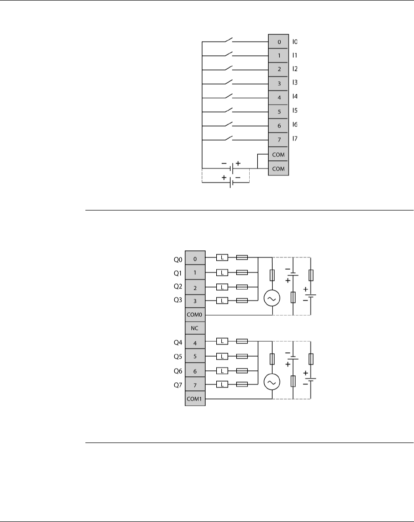
Description, characteristics, and wiring of the expansion modules
86 W9 1606383 01 11 A02 09/04
TWDDAI8DT
Wiring
Schematic
This schematic is for the TWDDAI8DT module.
zThe COM0 and COM1 terminals are not connected together internally.
TWDDRA8RT
Wiring
Schematic
This schematic is for the TWDDRA8RT module.
zThe COM0 and COM1 terminals are not connected together internally.
zConnect an appropriate fuse for the load.
Relay output wiring
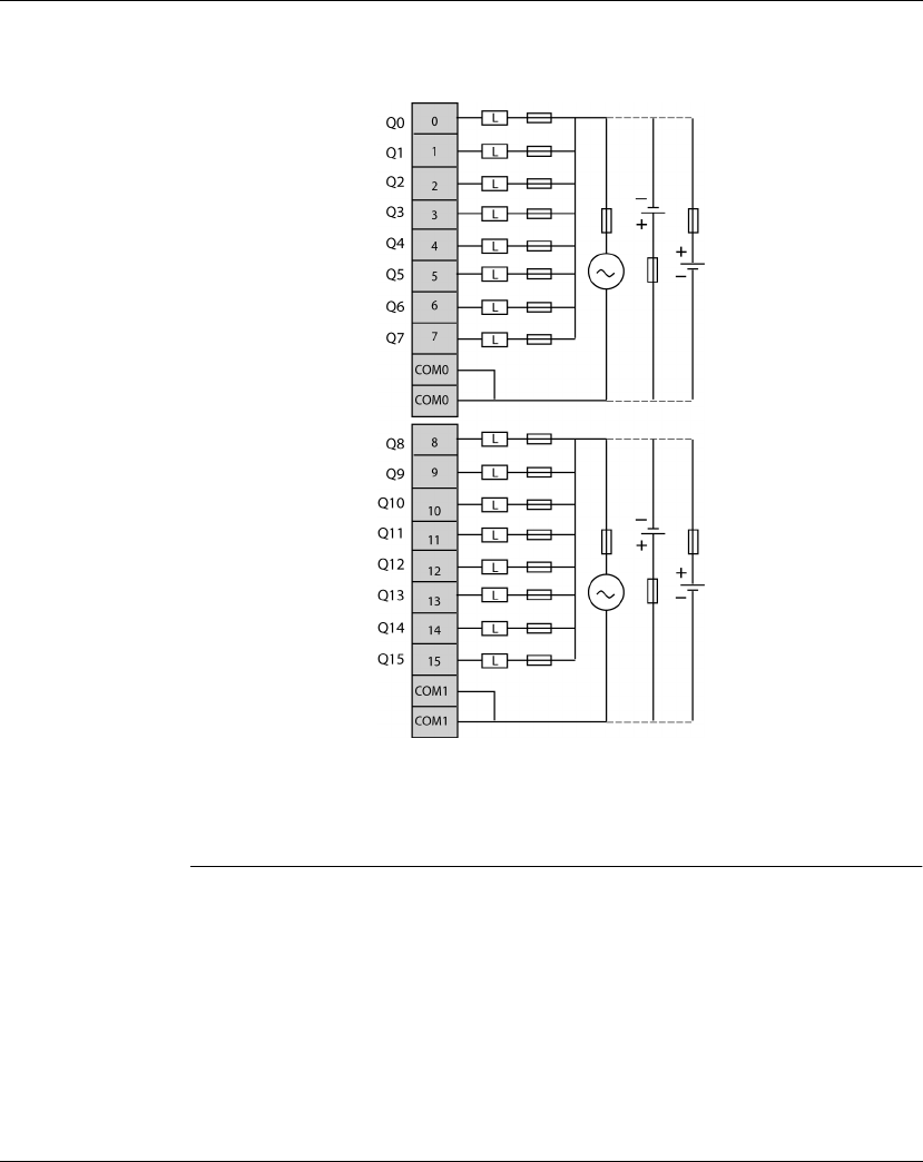
Description, characteristics, and wiring of the expansion modules
W9 1606383 01 11 A02 09/04 87
TWDDRA16RT
Wiring
Schematic
This schematic is for the TWDDRA16RT module.
zThe COM0 terminals are connected together internally.
zThe COM1 terminals are connected together internally.
zThe COM0 and COM1 terminals are not connected together internally.
zConnect an appropriate fuse for the load.
Relay output wiring
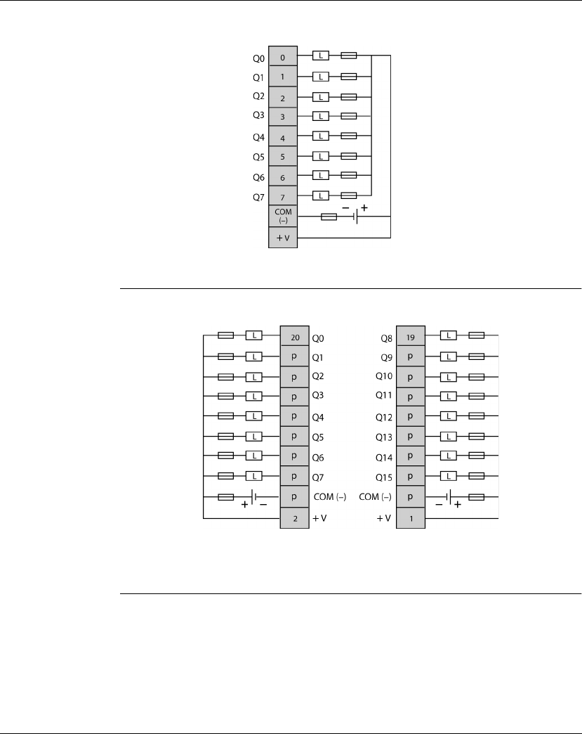
Description, characteristics, and wiring of the expansion modules
88 W9 1606383 01 11 A02 09/04
TWDDDO8UT
Wiring
Schematic
This schematic is for TWDDDO8UT module.
zConnect an appropriate fuse for the load.
TWDDDO16UK
Wiring
Schematic
This schematic is for the TWDDDO16UK module.
zThe COM(-) terminals are connected together internally.
zThe +V terminals are connected together internally.
zConnect an appropriate fuse for the load.
Output wiring
negative logic
O
utput wiring Output wiring
negative logic negative logic
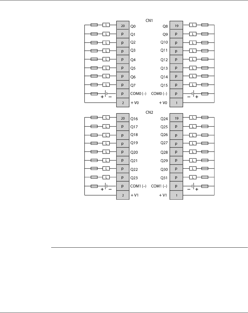
Description, characteristics, and wiring of the expansion modules
W9 1606383 01 11 A02 09/04 89
TWDDDO32UK
Wiring
Schematic
This schematic is for the TWDDDO32UK module.
zTerminals on CN1 and CN2 are not connected together internally.
zThe COM0(-) terminals are connected together internally.
zThe COM1(-) terminals are connected together internally.
zThe +V0 terminals are connected together internally.
zThe +V1 terminals are connected together internally.
zConnect an appropriate fuse for the load.
Output wiring Output wiring
Output wiring Output wiring
negative
negative
negative
negative
logic
logic
logic
logic
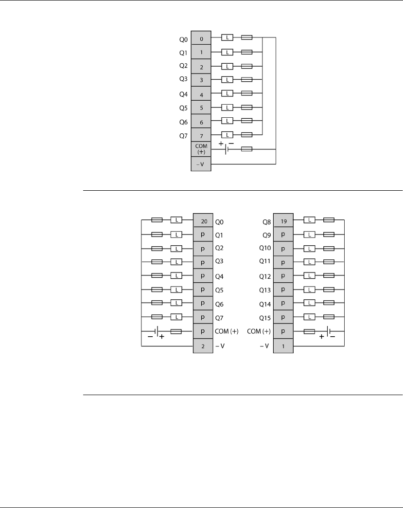
Description, characteristics, and wiring of the expansion modules
90 W9 1606383 01 11 A02 09/04
TWDDDO8TT
Wiring
Schematic
This schematic is for the TWDDDO8TT module.
zConnect an appropriate fuse for the load.
TWDDDO16TK
Wiring
Schematic
This schematic is for the TWDDDO16TK module.
zThe COM(+) terminals are connected together internally.
zThe -V terminals are connected together internally.
zConnect an appropriate fuse for the load.
Output wiring
positive logic
Output wiring
Output wiring
positive logic positive logic

Description, characteristics, and wiring of the expansion modules
W9 1606383 01 11 A02 09/04 91
TWDDDO32TK
Wiring
Schematic
This schematic is for the TWDDDO32TK module.
zTerminals CN1 and CN2 are not connected together internally.
zThe COM0(+) terminals are connected together internally.
zThe COM1(+) terminals are connected together internally.
zThe -V0 terminals are connected together internally.
zThe -V1 terminals are connected together internally.
zConnect an appropriate fuse for the load.
Output wiring
Output wiring positive logic
Output wiring
positive logic
positive logic
Output wiring
positive logic
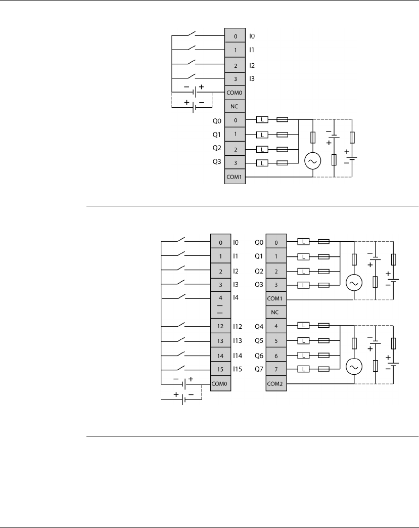
Description, characteristics, and wiring of the expansion modules
92 W9 1606383 01 11 A02 09/04
TWDDMM8DRT
Wiring
Schematic
This schematic is for the TWDDMM8DRT module.
zThe COM0 and COM1 terminals are not connected together internally.
TWDDMM24DRF
Wiring
Schematic
This schematic is for the TWDDMM24DRF module.
zThe COM0, COM1 and COM2 terminals are not connected together internally.
zConnect an appropriate fuse for the load.
Output wiring
Input wiring
Input wiring
negative logic
positive logic
relay
Relay output wiring
Input wiring
Input wiring
negative logic
positive logic
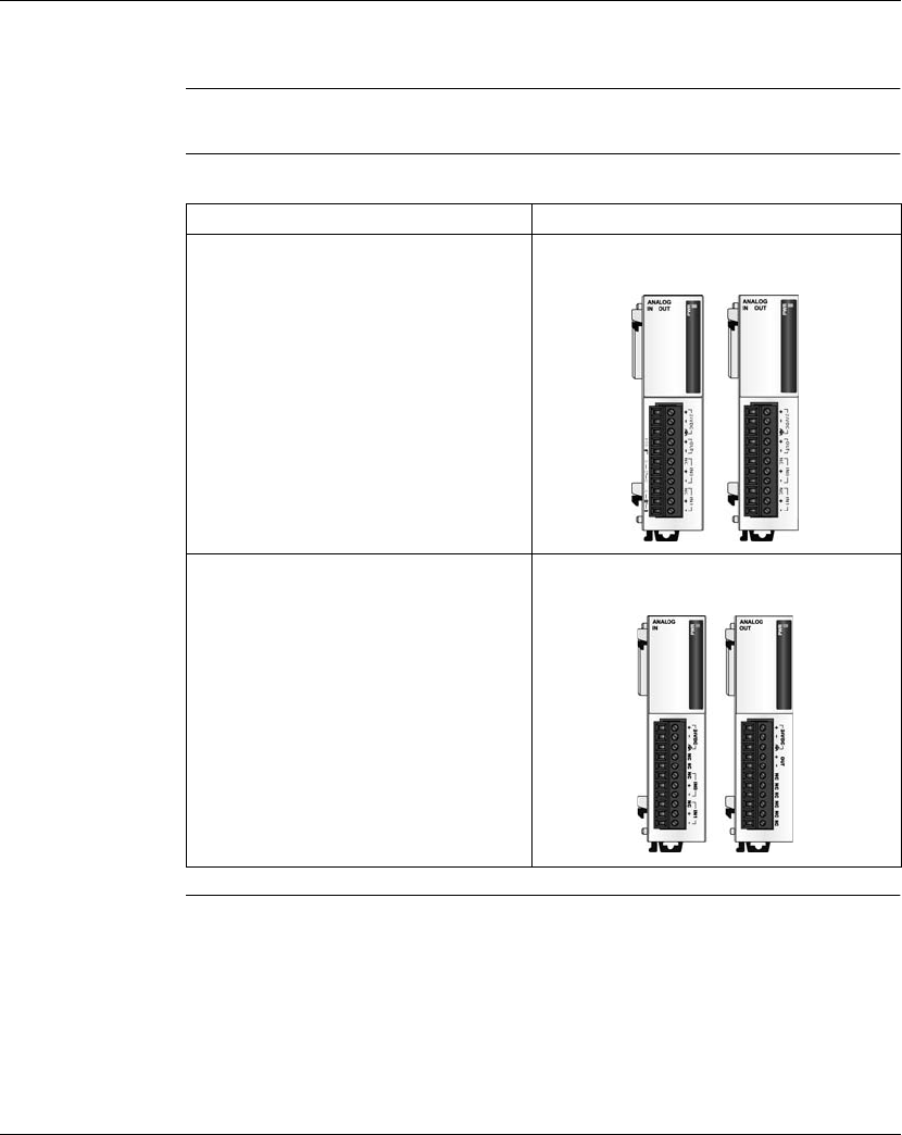
Description, characteristics, and wiring of the expansion modules
W9 1606383 01 11 A02 09/04 93
Overview of Analog I/O Modules
Introduction The following section provides an overview of the analog I/O modules.
Illustrations The following illustrations are the analog I/O modules.
Module type Illustration
These 2 analog I/O modules are:
z2-point input/1-point output module with
a terminal block, accepts thermocouple
and resistance thermometer signals
(TWDALM3LT)
z2-point input/1-point output module with
a terminal block (TWDAMM3HT)
These modules can be attached to any
communication module.
These 2 analog I/O modules are:
z2-point input module with a terminal
block (TWDAMI2HT)
z1-point output module with a terminal
block (TWDAMO1HT)
These modules can be attached to any
communication module.
TWDALM3LT TWDAMM3HT
TWDAMI2HT TWDAMO1HT
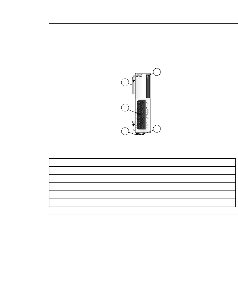
Description, characteristics, and wiring of the expansion modules
94 W9 1606383 01 11 A02 09/04
Parts Description of Analog I/O Modules
Introduction The following section describes the parts of an analog I/O module. Your I/O module
may differ from the illustrations but the parts will be the same.
Parts
Description of an
Analog I/O
Module
The following figure shows the parts of an analog I/O module. This figure is the
TWDALM3LT module.
Legend
2
1
4
5
3
Label Description
1 Expansion connector - one on each side, right side not shown
2 Removable terminal block
3 Latch button
4LEDs
5 Clamp

Description, characteristics, and wiring of the expansion modules
W9 1606383 01 11 A02 09/04 95
General Specifications for the Analog I/O Modules
Introduction This section is general specifications for analog I/O modules.
General
Specifications Reference TWDALM3LT TWDAMM3HT TWDAMI2HT TWDAMO1HT
Rated power voltage 24 VDC
Allowable voltage
range
from 20.4 to 28.8 VDC
Average number of
connector insertions/
removals
100 times minimum
Internal current draw -
internal power
50mA (5 VDC)
0 mA (24 VDC)
Internal current draw -
external power
40mA (24 VDC)
Weight 85 g (3oz)

Description, characteristics, and wiring of the expansion modules
96 W9 1606383 01 11 A02 09/04
Specifications for the Analog I/O Modules
Introduction This section contains the I/O specifications for the analog I/O modules.
Input
Specifications Analog Input
Specifications
Voltage
Input
Current
Input
Thermocouple Resistance
Thermometer
Input range from 0 to 10
VDC
from 4 to 20
mA DC
Type K
(0 to 1300 °C)
(32 to 2372 °F)
Type J
(0 to 1200 °C)
(32 to 2192 °F)
Type T
(0 to 400 °C)
(32to742°F)
Pt 100
3-wire type
(-100 to 500 °C)
(-148 to 932 °F)
Input impedance 1 MΩmin. 10 Ω1MΩmin. 1 MΩmin.
Sample duration time 16 ms max. 50 ms max.
Sample repetition time 16 ms max. 50 ms max.
Measurement conversion
time
32 ms 100 ms
Input type Single-end
ed input
Differential input
Operating mode Self-scan
Conversion mode Σ∆ type ADC
Input error - maximum
error at 25°C (77°F)
±0.2%of full scale ±0.2%of full scale
plus reference
junction
compensation
accuracy ±4°C max
±0.2%of full
scale
Input error - temperature
coefficient
±0.006%of full scale/degree C
Input error - repeatable
after stabilization time
±0.5%of full scale
Input error - nonlinear ±0.2%of full scale
Input error - maximum error
±1%of full scale
Digital resolution 4096 increments (12 bits)
Input value of LSB 2.5 mV 4 µAK:0.325°C
J: 0.300 °C
T: 0.100 °C
0.15 °C

Description, characteristics, and wiring of the expansion modules
W9 1606383 01 11 A02 09/04 97
Data type in application
program
0 to 4095 (12 bit data)
-32768 to 32767 (optional range designation)2
Monotonicity Yes
Input data out of range Detectable3
Noise resistance - maximum
temporary deviation during
electrical noise tests
±3%maximum when a 500 V clamp voltage is
applied to the power and I/O wiring
Accuracy is not
assured when
noise is applied
Noiseresistance-
common mode
characteristics
Common mode reject ration (CMRR): -50 dB
Noiseresistance-
common mode voltage
16 VDC
Noiseresistance-
input filter
No
Noise resistance - cable Twisted-pair shielded
cable is recommended for
improved noise immunity
—
Noise resistance - crosstalk
2 LSB maximum
Dielectric strength 500 V between input and power circuit
Type of protection Photocoupler between input and internal circuit
Maximum permanent allowed
overload (no damage)
13 VDC 40 mA DC —
Selection of analog input
signal type
Using software programming
Calibration or verification
to maintain rated accuracy
Approximately 10 years
Note:
1.
Total input system transfer time = repetition of the sample x 2
2.
The 12-bit data (0 to 4095) processed in the Analog I/O module can be linear-converted
to a value between -32768 and 32767. The optional range designation and analog I/O
data minimum and maximum values can be selected using data registers allocated to
analog I/O modules.
3.
When an error is detected, a corresponding error code is stored to a data register
allocated to analog I/O operating status.
Analog Input
Specifications
Voltage
Input
Current
Input
Thermocouple Resistance
Thermometer

Description, characteristics, and wiring of the expansion modules
98 W9 1606383 01 11 A02 09/04
Output
Specifications Analog Output Specifications Voltage output Current Output
Output range from 0 to 10 VDC from 4 to 20 mA DC
Load impedance 2 kΩmax 300 Ωmaximum
Application load type Resistive load
Settling time 20 ms
Total output system transfer Time
20 ms
Output error - maximum error at
25°C (77°F)
±0.2%of full scale
Output error - temperature
coefficient
±0.015%of full scale/degree C
Output error - repeatable after
stabilization time
±0.5%of full scale
Output error - output voltage drop
±1%of full scale
Output error - nonlinear ±0.2%of full scale
Output error - output ripple 1 LSB maximum
Output error - overshoot 0%
Output error - total error ±1%of full scale
Digital resolution 4096 increments (12 bits)
Output value of LSB 2.5 mV 4 µA
Data type in application program 0 to 4095 (12 bit data)
-32768 to 32767 (optional range designation)1
Monotonicity Yes
Current loop open — Detectable2
Noise resistance - maximum
temporary deviation during
electrical noise tests
±3%maximum when a 500 V clamp voltage is applied to
the power and I/O wiring
Noise resistance - cable Twisted-pair shielded cable is recommended for improved
noise immunity
Noise resistance - crosstalk No crosstalk because of 1 channel output
Dielectric strength 500 V between output and power circuit
Type of protection Photocoupler between output and internal circuit
Selection of analog input signal type
Using software programming
Calibration or verification to
maintain rated accuracy
Approximately 10 years

Description, characteristics, and wiring of the expansion modules
W9 1606383 01 11 A02 09/04 99
Note:
1.
The 12-bit data (0 to 4095) processed in the Analog I/O module can be linear-converted
to a value between -32768 and 32767. The optional range designation and analog I/O
data minimum and maximum values can be selected using data registers allocated to
analog I/O modules.
2.
When an error is detected, a corresponding error code is stored to a data register
allocated to analog I/O operating status.
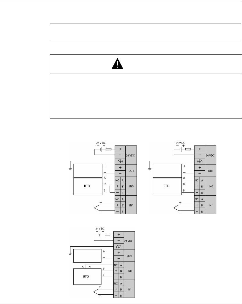
Description, characteristics, and wiring of the expansion modules
100 W9 1606383 01 11 A02 09/04
Analog I/O Modules Wiring Schematics
Introduction This section shows examples of wiring schematics for the Analog I/O modules.
TWDALM3LT
Wiring
Schematic
This schematic is for the TWDALM3LT module.
WARNING
HAZARD OF UNINTENDED EQUIPMENT OPERATION AND EQUIPMENT
DAMAGE
zDo not connect any wiring to unused channels.
z
Do not connect the thermocouple to a hazardous voltage (60 VDC or 42.4 V peak or
higher.)
Failure to follow this instruction can result in death or serious injury.
Ana
log voltage/
current input
Thermocouple
Analog voltage/
current input
Thermocouple
Analog voltage/
current input
3-wire cabling:
4-wire cabling:
Note: For 4-wire cabling,
output A’ is not connected.
Thermocouple
2-wire cabling:
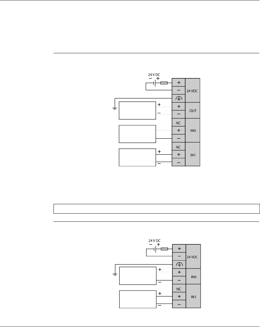
Description, characteristics, and wiring of the expansion modules
W9 1606383 01 11 A02 09/04 101
zConnect a fuse appropriate for the applied voltage and current draw, at the
position shown in the diagram.
zWhen connecting an RTD, connect the three wires to terminals A, B’, and B of
input channel 0 or 1.
zWhen connecting a thermocouple, connect the two wires to terminals B’ and B of
input channel 0 or 1.
TWDAMM3HT
Wiring
Schematic
This schematic is for the TWDAMM3HT module.
zConnect a fuse appropriate for the applied voltage and current draw, at the
position shown in the diagram.
zDo not connect any wiring to unused channels.
TWDAMI2HT
Wiring
Schematic
ThisschematicisfortheTWDAMI2HTmodule.
Note: The (-) poles of inputs IN0 and IN1 are connected internally.
Analog voltage/
current input device
Analog voltage/
current output
device
Analog voltage/
current output
device
Analog voltage/
current output
device
Analog voltage/
current output
device
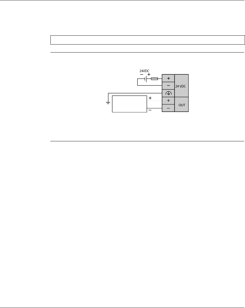
Description, characteristics, and wiring of the expansion modules
102 W9 1606383 01 11 A02 09/04
zConnect a fuse appropriate for the applied voltage and current draw, at the
position shown in the diagram.
zDo not connect any wiring to unused channels.
TWDAMO1HT
Wiring
Schematic
This schematic is for the TWDAMO1HT module.
zConnect a fuse appropriate for the applied voltage and current draw, at the
position shown in the diagram.
zDo not connect any wiring to unused channels.
Note: The (-) poles of inputs IN0 and IN1 are connected internally.
Analog voltage/
current input device

Description, characteristics, and wiring of the expansion modules
W9 1606383 01 11 A02 09/04 103
Communication expansion module block wiring schematics
OTB 9ZZ61JP
Wiring
Schematic
This schematic is for the OTB 9ZZ61JP module.
C0
C1
C2
C3
C4
C5
C6
C7
C8
COM
C9
C10
C11
C12
C13
C14
C15
C16
C17
COM
To sensors, actuators or
expansion modules commons
Power Supply
To sensors, actuators or
expansion modules commons
Power Supply

Description, characteristics, and wiring of the expansion modules
104 W9 1606383 01 11 A02 09/04

W9 1606383 01 11 A02 09/04 105
5
Modbus Network Interface of the
OTB Module
At a Glance
Introduction This chapter describes the external Modbus characteristics of the Advantys OTB
network interface module and the general Modbus features supported by the
module.
What's in this
Chapter?
This chapter contains the following topics:
Topic Page
Description of the OTB Module Modbus Network Interface 106
Modbus Field Bus Interface 108
Network Node Address 112
Network Baud Rate 114
Modbus Configuration 116
Communication on a Modbus Network 117
Management of Island Behavior 120
Expansion module identification codes 124
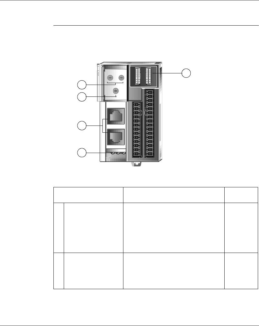
Modbus Network Interface of the OTB Module
106 W9 1606383 01 11 A02 09/04
Description of the OTB Module Modbus Network Interface
Introduction The physical characteristics necessary for Modbus operation are given in the
following illustration:
The characteristics of the above illustration are described briefly in the following
table:
Description Function Cross-
reference
1 Upper encoder wheels zLeft encoder wheel: decimal encoding
between 1 and 12
zRight encoder wheel: decimal encoding
between 1 and 9
These are used to define the address of the
interface module node on the Modbus field
bus.
Address
(See
Network
Node
Address,
p. 112
)
2 Lower encoder wheel The lower encoder wheel (decimal encoded
binary value between 0 and 9) is used to
define the value of the field bus baud rate.
Speed (See
Network
Node
Address,
p. 112
)
1
2
3
4
5

Modbus Network Interface of the OTB Module
W9 1606383 01 11 A02 09/04 107
3 Field bus interface Two eight-pin RJ45 connectors are used to
connect the interface module to a Modbus
field bus.
Interface
(See
Modbus
Field Bus
Interface,
p. 108
)
4 Electrical supply
interface
Terminal for an external 24 VDC supply of
the network interface module.
Supply (See
How to
Connect the
Power
Supply,
p. 61
)
5 Indicator LED The colored LEDs use various types of
display to visually reflect the operational
status of the island bus.
Indicator
LED (See
Indicator
Lights
(LEDs),
p. 184
)
Description Function Cross-
reference
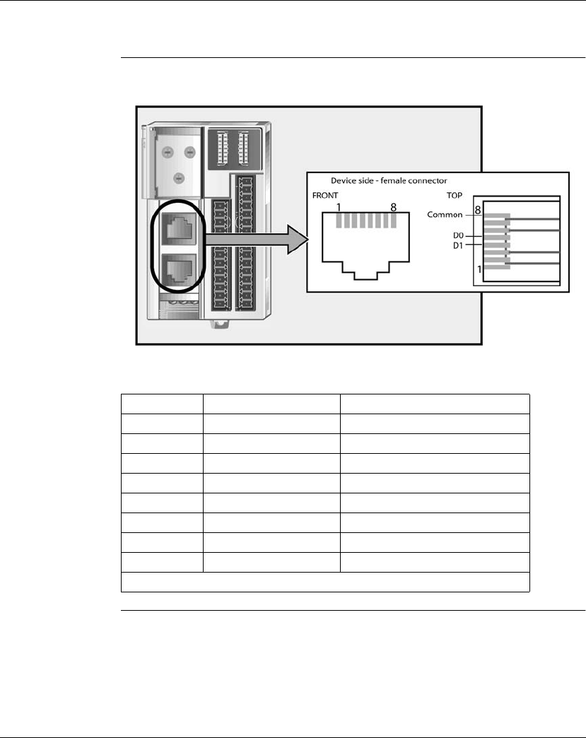
Modbus Network Interface of the OTB Module
108 W9 1606383 01 11 A02 09/04
Modbus Field Bus Interface
Connections to
the Field Bus
The connectors on the front of the interface module are wired in parallel:
We recommend that you use an 8-pin male RJ45 connector compliant with the RS
485 standard. The connection must correspond to the following table:
Contact Signal Description
1 Unused -
2 Unused -
3 Unused -
4 D1 Transmission signal
5 D0 Reception signal
6 Unused Reserved
7 VP 5...24 Vdc power supply
8 Common Common of signal and supply
Note: The contact numbers correspond to the legend for the following figure.

Modbus Network Interface of the OTB Module
W9 1606383 01 11 A02 09/04 109
Correspondence
of Contact
Names
Advantys OTB network interface modules can be connected with other Schneider
products over Modbus. These products have different contact names which are
however compliant with RS 485 standards.
The table below specifies the correspondence between contact names and products
Modbus Network
Connectors and
Cables
The branch cable between the field bus and the island must have a female
connector complying with the following contact assignment diagram. The Modbus
network cable is a shielded twisted pair cable complying with the RS 485 standard.
OTB1S0DM9LP EIA/TIA 485 TWIDO SCA64 SCA62
SCA50
Tesys LU9CG3
D1 B A or A(+) M+ D(B)
D0 A B or B(+) M- D(A)
Common C SG or 0V 0VL 0VL
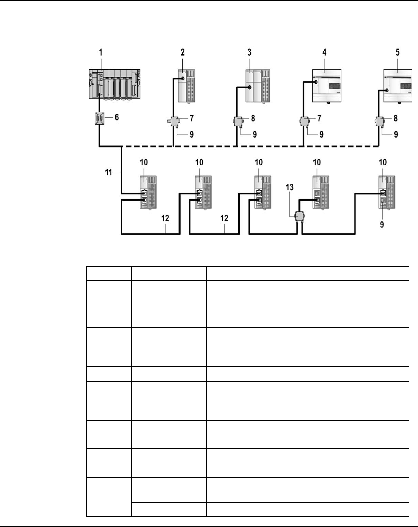
Modbus Network Interface of the OTB Module
110 W9 1606383 01 11 A02 09/04
Example of a
Network
Architecture
The illustration below provides an example of a network architecture with a Premium
or Twido bus master and the cables with the specified product references.
References and description of numbers in the above illustration
Reference Description
1 Premium +
SCY11601, or
SCY21601, or
SCP114
Premium PLC with Modbus communication card
2 TWDLMDA.0D.. Twido modular controller
3 TWDLMDA.0D.. +
TWDNOZ485D
Twido modular controller with RS 485 communication
port
4 TWDLCAA..DRF Twido compact controller
5 TWDLCAA..DRF +
TWDNAC485T
Twido compact controller with RS 485 communication
port
6 TSXSCA62/64 Subscriber socket
7 TWDXCARJ030 MiniDIN RJ45 interface cable
8 TWDXCARJ030 MiniDIN RJ45 interface cable
9 VW3A8306RC Line End Adapter
10 OTB1S0DM9LP Network interface modules
11 VW3A8306 3 m lead with one RJ45 connector and one 15-pin SUB-
D connector for TSXSCA62/64 subscriber socket
VW3A8306D30 3 m lead with one RJ45 connector and one stripped end

Modbus Network Interface of the OTB Module
W9 1606383 01 11 A02 09/04 111
12 VW3A8306R03 0.3 m lead with 2 RJ45 connectors
VW3A8306R10 1 m lead with 2 RJ45 connectors
VW3A8306R30 3 m lead with 2 RJ45 connectors
13 VW3A8306TF03 T branch with 0.3 m cable
VW3A8306TF10 T branch with 1 m cable
Reference Description
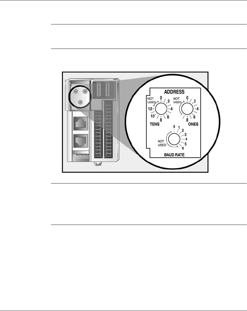
Modbus Network Interface of the OTB Module
112 W9 1606383 01 11 A02 09/04
Network Node Address
Summary Two encoder wheels on the Advantys OTB Modbus module OTB1S0DM9LP are
used to define the address of the network node.
Parts
Description
Node Addresses The Advantys OTB module only has one single field bus network address. The
Modbus interface module reads the address of the node from the encoder wheels
every time the island is powered up.
The address of the node is a numerical value between 1 and 127, which must be
different to all other node addresses on the network.

Modbus Network Interface of the OTB Module
W9 1606383 01 11 A02 09/04 113
Configuring the
Node Address
The instructions for configuring the node address are described in the following
table.
Field Bus
Communication
The Advantys OTB interface module communicates when the encoder wheels are
configured to a valid Modbus node address if the baud rate is the same as that of
the system.
If the island has a invalid node address, it cannot communicate with the master. To
establish communication, configure the encoder wheels to a valid address and
power up the island.
Step Action Comment
1 Cut the power supply to the island. The changes you make will be detected on
the next power up.
2 Select the node address currently
available on your field bus network.
The list of active nodes on the field bus
indicates which addresses are available.
3 Adjust the upper encoder wheels
zLeft encoder wheel — 0 to 12 (tens)
zRight encoder wheel — 0 to 9
(units)
Note that it is
mechanically
possible to
specify all node addresses from 00 to 129.
However, address 00 is never used as a
Modbus node address and addresses 128
and 129 are not operative.
4 Power up the island in order to
implement the new configuration.
The network interface module reads the
encoder wheel adjustments only on power
up.
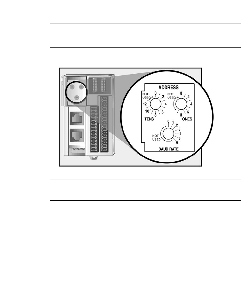
Modbus Network Interface of the OTB Module
114 W9 1606383 01 11 A02 09/04
Network Baud Rate
Summary An encoder wheel on the Advantys OTB Modbus module OTB1S0DM9LP is used
to define the network node baud rate.
Parts
Description
Baud Rate The Modbus interface module reads the node address and baud rate indicated by
the encoder wheels each time the island is powered up.

Modbus Network Interface of the OTB Module
W9 1606383 01 11 A02 09/04 115
Configuration of
Baud Rate
The instructions for configuring the baud rate of the module are given in the following
table:
Baud Rate
Selection Table
.
Step Action Comment
1 Cut the power supply to the island. The changes you make will be detected on
the next power up.
2 Select the baud rate to be used for field
bus communications.
The baud rate configuration depends on
the specifications of your system and the
network.
3 Set the lower encoder wheel to the
position corresponding to the required
baud rate.
Use the following baud rate selection table.
4 Power up the island in order to
implement the new configuration.
The network interface module reads the
encoder wheel parameters only on power
up.
Position (lower encoder
rate)
Baud Rate
0 19200 bits/s
1 1200 bits/s
2 2400 bits/s
3 4800 bits/s
4 9600 bits/s
5 19200 bits/s
6 38400 bits/s

Modbus Network Interface of the OTB Module
116 W9 1606383 01 11 A02 09/04
Modbus Configuration
Electrical
Specifications
The network interface module supports 2-wire Modbus. Communication is half
duplex type.
Communications
Configuration
The Modbus communication parameters which define the frame can be configured
in a number of different ways.
The Advantys OTB network interface module supports the following
communications parameters:
Parameter Value
Mode RTU
Parity EVEN
Stop bit 1
Data bit 8

Modbus Network Interface of the OTB Module
W9 1606383 01 11 A02 09/04 117
Communication on a Modbus Network
Introduction The Modbus protocol is a master-slave protocol that allows for one, and only one,
master to request responses from slaves, or to act based on the request. The master
can address individual slaves, or can initiate a broadcast message to all slaves.
Slaves return a message (response) to queries that are addressed to them
individually. Responses are not returned to broadcast queries from the master.
Modbus
Message
Structure
Modbus protocol uses 16 bit words. A Modbus message starts with a header. A
Modbus message uses a Modbus function code (See
List of Supported Commands,
p. 118
) as its first byte.
The following table describes the full structure of a Modbus RTU message:
Exchange report 0: Correct exchange
1: Illegal function (not supported)
2: Non-existent register
3: Non-compliant data value
4: Faulty slave
Header Address Modbus
function code
Data CRC End
- one byte one byte n-byte field two
bytes
-
Note: For further information on the message structure, please refer to the Modbus
master documentation.

Modbus Network Interface of the OTB Module
118 W9 1606383 01 11 A02 09/04
List of Supported
Commands
The following table is a summary of the Modbus commands supported by the
OTB1S0DM9LP module:
Read n registers (03):
This function code is used to read the content of one or more contiguous registers
in a slave.
Write register (06):
This function code is used to write the content of a register in a slave.
Write n registers (16):
This function code is used to write the content of one or more contiguous registers
in a slave.
Write mask (22):
This function code is used to modify the content (of all or part) of a register. This
function is a combination of an AND mask, an OR mask, and AND/ mask and the
current content of the register.
Example:
Read Write n registers (23):
This function code is used to execute a combination of reading and writing n
registers.
Modbus function
code:
Index Dec (Hex)
Sub-function:
Sub-index
Command
3 (3H) read n output registers
6 (6H) write a single register
16 (10H) write n registers
17 (11H) read slave identification report
22 (16H) mask n write registers
23 (17H) read/write n registers
43 (2BH) 14 read slave identification registers
Note: Reading or writing registers can be performed if and only if the registers are
contiguous.
Hexadecimal Binary
Current content 12 0001 0010
AND mask F2 1111 0010
OR mask 25 0010 0101
AND/ mask 0D 0000 1101
Result 17 0001 0111

Modbus Network Interface of the OTB Module
W9 1606383 01 11 A02 09/04 119
Identification (43 sub-index 14):
This function code is used to read the identification and other information relating to
the parts description of a slave.
List of Identifi-
cation Objects
The following table provides a list of the island's Modbus identification objects:
Identification
Report
The following ASCII string is sent in response to the "Read identification report"
module function code: Communication block ref, e.g OTB 1S0DM9LP
Identifier Object name, description Description Data type
0 (000H) Manufacturer name TELEMECANIQUE ASCII string
1 (0001H) Product code (065277)
2 (0002H) Version number (Major version, minor
version)
XYxy (0100H for
V01.00)
4 (0004H) Product name OTB1S0DM9LP

Modbus Network Interface of the OTB Module
120 W9 1606383 01 11 A02 09/04
Management of Island Behavior
Configuration of
Analog
Expansion
Modules
To configure analog expansion modules, you must stop activity on the island's
internal bus by writing the value 1 to the register 1005.
Once the configuration parameters of the expansion modules have been updated,
the content of the object 1005 must be reset to 0 to resume activity on the internal
bus with the new parameters.
32 Bit Function The function of the register 1008 is to define the order of 32 bit information. It can
only be used for parameters in 32 bit format. Its default value is 0 (MSB/LSB).
Register 1008 - Bit 0 = 0
The registers concerned by 32 bit format are in MSB/LSB format.
Register 1008 - Bit 0 = 1
The registers concerned by 32 bit format are in MSB/LSB format.
Setting Network
Monitoring
Times
The register 1006 is used to set the monitoring time in ms.
Values for register 1006
z0: no network monitoring (default value)
zx: monitoring time in ms (1 to 65535 ms)
Note: The expansion module outputs are deactivated and switch to zero when this
operation is performed.
Note: If a parameter is non-compliant (invalid configuration), it is impossible to
write zero to the register 1005.
Modbus Network Interface of the OTB Module
W9 1606383 01 11 A02 09/04 121
Network
Monitoring
The island goes into fallback mode if the connection to the network is lost or if no
client is present on the network.
If no frame is detected on the network before the monitoring time expires, the island
detects that the client has disconnected. The outputs and special function switch to
the fallback value defined by the user.
Bit 9 of register 900 switches to 1.
Writingthevalue0tothecommandregister1007enablesyoutosetbit9ofregister
900 to zero in order to resume network monitoring.
CAUTION
FALLBACK MODE AFTER DISCONNECTION
It is possible to write to outputs once reconnected without the need for
acknowledgement.
Failure to follow this instruction can result in injury.

Modbus Network Interface of the OTB Module
122 W9 1606383 01 11 A02 09/04
Saving and
Restoring
Parameters
Initialization
An OTB module is initialized with default parameters. When detected by the bus
master, the OTB module is configured with the parameters defined in the
configuration tool. These parameters must be backed-up in order to be
acknowledged the next time the system is started.
Current parameters
Register 1000 indicates the current set of parameters:
z0: the island is using the default parameter set (factory settings)
z1: the island is using the last saved parameter set
z2: one or more parameters have been modified since the last backup or startup.
Saving parameters
The back-up operation is performed by modifying the value of register 1002.
This saves the current parameters of the OTB module and tells it to use these saved
parameters on future start-ups.
A backup counter is available in register 1001. This counter is reset to 0 when factory
settings are restored.
Note: The backed up registers correspond to the parameter registers of the
different zones.
When a backup is in progress, the module stops communication for 300 ms and
the expansion module outputs switch to 0.

Modbus Network Interface of the OTB Module
W9 1606383 01 11 A02 09/04 123
Restoring parameters
The different possible restores are described in the following table:
Identification of
Island Modules
The following table describes the mapping of descriptions of modules on the island
To restore... you must modify the value of the
register...
the last backed up
configuration
1003
the factory settings 1004
Registers Functions Object code
1100 OTB product code FEFDH
1101 OTB software version XYxy
1102 Type of expansion module 1 (1)
1103 Type of expansion module 2 (1)
1104 Type of expansion module 3 (1)
1105 Type of expansion module 4 (1)
1106 Type of expansion module 5 (1)
1107 Type of expansion module 6 (1)
1108 Type of expansion module 7 (1)
Note: (1) depending on the type of expansion module connected. See the table of
Expansion Module Identification Codes. The default value is equal to FFFFH

Modbus Network Interface of the OTB Module
124 W9 1606383 01 11 A02 09/04
Expansion module identification codes
List of Identifi-
cation Codes
Object code table for each expansion module:
Type of digital
I/O module
Object code
Hexadecimal value
8 inputs 0004
16 inputs 0000
32 inputs 0200
8 outputs 0005
16 outputs 0001
32 outputs 0301
8 DRF 0006
24 DRF 0205
Type of analog
I/O module
Object code
Hexadecimal value
TWDAMI2HT 6002
TWDAM01HT 6003
TWDAMM3HT 6001
TWDALM3LT 6000
TWDAVO2HT 6007
TWDAMI4HT 6004
TWDAMI8HT 6005
TWDARI8HT 6006

W9 1606383 01 11 A02 09/04 125
6
Application-Specific Functions
At a Glance
Introduction This section describes the application-specific functions of the Advantys OTB
modules. Information on I/O assignments, configuration and usage are provided for
each expansion module and each specific remote function.
What's in this
Chapter?
This chapter contains the following topics:
Topic Page
Island Registers 126
Read Input Registers 129
Output Command Registers 130
Advantys OTB Module I/O Parameter Registers 131
Expansion Module Discrete I/O Parameter Registers 214 to 599 132
Expansion Module Analog I/O Parameter Registers 214 to 599 135
Specific Functions of the Advantys OTB Modules 150
Remote Fast Counter (RFC) Function Block 152
Fast Counter (RFC) Parameter Registers 155
Remote Very Fast Counter (RVFC) Function Block 156
Remote Very Fast Counter (RVFC) Parameter Registers 169
Remote Pulse Generator (RPLS) Function Block 171
Remote Pulse Width Modulator Function Block 175
Remote Pulse Generators (RPLS, RPWM) Parameter Registers 179

Application-Specific Functions
126 W9 1606383 01 11 A02 09/04
Island Registers
At a Glance The registers table depends on the configuration of the network interface module,
the connected expansion modules and the type of those modules. Specific register
zones are reserved for different types of data.
The order of the parameters (registers) is defined by expansion modules added to
the OTB module from left to right.
Registers Table
(mapping)
Zone containing the register numbers associated with the functions supported by
OTB:
Registers Function Pages
0 to 99 Status of island inputs 0 to 99 (See
Status of
inputs , p. 192
)
100 to 199 Island output commands 100 to 199 (See
Output
Commands , p. 192
)
200 to 599 Island I/O configuration parameters 200 to 599 (See
I/O
Parameters, p. 193
)
600 to 699 Remote Fast Counter (RFC) function
block
600 to 699 (See
Fast
Counters, p. 194
)
700 to 799 Remote Very Fast Counter (RVFC)
function block
700 to 799 (See
Very Fast
Counters , p. 195
)
800 to 899 Remote pulse generator function block
(RPLS)
Remote pulse generator function block
with pulse width modulation (RPWM)
800 to 899 (See
Pulse
Generator, p. 197
)
900 to 999 Island diagnostics 900 to 999 (See
Diagnostics, p. 198
)
1000 to 1099 Management of module behavior 1000 to 1099 (See
Management of Island
Behavior, p. 202
)
1100 to 1108 Description of modules constituting the
island
1100 to 1108 (See
Management of Island
Behavior, p. 202
)

Application-Specific Functions
W9 1606383 01 11 A02 09/04 127
OTB Module
Registers
For each application-specific function, the OTB network interface module uses the
number of registers indicated in the following table:
Status of
inputs
Output
commands
Parameters RFC RVFC RPLS
RPWM
Diagnostics Module
behavior
0 to 99 100 to 199 200 to 599 600 to 699 700 to 799 800 to 899 900 to 999 1000 to 1099
1 1 14 8 per
counter
14 per counter 10 per
generator
11 6

Application-Specific Functions
128 W9 1606383 01 11 A02 09/04
Expansion
Module
Registers
For each application-specific function, the expansion modules use the number of
registers indicated in the following table:
Product references Function
I/O type / voltage
Status of
inputs
Output
commands
Parameters Diagnostics
0 to 99 100 to 199 200 to 599 900 to 999
TWDDDI8DT 8 IN / 24 VDC 1 0 0 1
TWDDAI8DT 8 IN / 120 VAC 1 0 0 1
TWDDDI16DT 16 IN / 24 VDC 1 0 0 1
TWDDDI16DK 16 IN / 24 VDC 1 0 0 1
TWDDDI32DK 32 IN / 24 VDC 2 0 0 1
TWDDDO8TT 8 OUT / 24 VDC source 0 1 2 1
TWDDDO8UT 8 OUT / 24 VDC sink 0 1 2 1
TWDDRA8RT 8 OUT relay 0 1 2 1
TWDDDO16TK 16 OUT / 24 VDC source 0 1 2 1
TWDDDDO16UK 16 OUT / 24 VDC sink 0 1 2 1
TWDDRA16RT 16 OUT relay 0 1 2 1
TWDDDO32TK 32 OUT / 24 VDC source 0 2 4 1
TWDDDO32UK 32 OUT / 24 VDC sink 0 2 4 1
TWDDMM8DRT 4 IN / 24 VDC
4 OUT relay
112 1
TWDDMM24DRF 16 IN / 24 VDC
8 OUT relay
112 1
TWDAMI2HT 2 IN (U/I) 2 0 8 1
TWDAM01HT 1 OUT (U/I) 0 1 6 1
TWDAMM3HT 2 IN / 1 OUT (U/I) 2 1 14 1
TWDALM3LT Thermocouple 2 1 14 1
TWDAVO2HT 2 OUT (+/- 10 VDC,
10 bits)
02121
TWDAMI4HT 4 IN (U/I, Pt, Ni) 4 0 16 1
TWDAMI8HT 8 IN (U/I, 10 bits) 8 0 32 1
TWDARI8HT 8 IN (PTC, NTC, 10 bits) 8 0 56 1

Application-Specific Functions
W9 1606383 01 11 A02 09/04 129
Read Input Registers
At a Glance This section describes how to read the status of the Advantys OTB island inputs.
Table of Read
Input Registers 0
to 32
The following table gives the bit assignment for each of the read input registers:
Note: The order of the parameters is defined by expansion modules added to the
OTB module from left to right. The number of parameters depends on the number
and type of expansion modules connected. Discrete inputs of expansion modules
are not filtered.
Register Function Bit assignment
0 Status of Advantys OTB module
inputs
Bit 0: channel 0
...
Bit 11 channel 11
1 Input status of first expansion module
with inputs
Bit 0: channel 0
...
Bit X channel X
... ... ...
32 ... ...
Note: Only those registers that correspond to a present expansion module are
accessible in read.

Application-Specific Functions
130 W9 1606383 01 11 A02 09/04
Output Command Registers
At a Glance This section describes how to write to Advantys OTB island outputs.
Table of Output
Command
Registers 100 to
128
The following table gives the bit assignment for each of the write output registers:
Note: The order of the parameters is defined by expansion modules added to the
OTB module from left to right. The number of parameters depends on the number
and type of expansion modules connected.
Register Function Bit assignment
100 Advantys OTB module output commands Bit 0: channel 0
...
Bit 11 channel 11
101 Commands to outputs of first expansion module with
outputs
Bit 0: channel 0
...
Bit X channel X
... ... ...
128 ... ...
Note: Only those registers that correspond to a present expansion module are
accessible in read and write.

Application-Specific Functions
W9 1606383 01 11 A02 09/04 131
Advantys OTB Module I/O Parameter Registers
At a Glance The I/Os of the Advantys OTB network interface module use I/O parameter
registers.
Table of I/O
Parameter
Registers 200 to
213
The following table describes the different registers reserved for I/O parameters of
the OTB module.
Register Bit Description Parameter
200 Filtering of channel 0 0: no filtering
1: filtering at 3ms
(default value)
2: filtering at 12ms
201 Filtering of channel 1
202 Filtering of channel 2
203 Filtering of channel 3
204 Filtering of channel 4
205 Filtering of channel 5
206 Filtering of channel 6
207 Filtering of channel 7
208 Filtering of channel 8
209 Filtering of channel 9
210 Filtering of channel 10
211 Filtering of channel 11
212 Bit 0 Fallback mode for output
0
0: maintain
1: fallback value (default
value)
... ...
Bit 7 Fallback mode for output
7
213 Bit 0 Fallback value for output
0
0: fallback to 0 (default
value)
1: fallback to 1
... ...
Bit 7 Fallback value for output
7

Application-Specific Functions
132 W9 1606383 01 11 A02 09/04
Expansion Module Discrete I/O Parameter Registers 214 to 599
At a Glance The Discrete I/Os of the expansion modules use the parameter registers described
in the following tables. The register number (N) depends on the position of the
module in the island.
TWDDDI8DT,
TWDDAI8DT,
TWDDDI16DT,
TWDDDI16DK,
TWDDDI32DK
The discrete input expansion modules do not use parameter registers.
TWDDDO8TT,
TTWDDDO8UTT,
WDDRA8RT
The discrete output expansion modules use parameter registers to define the
fallback mode and value.
Note: Only those registers that correspond to a present expansion module are
accessible in read and write.
Register Bit Description Parameter
N Bit 0 Fallback mode, output 0 1: fallback value (default
value)
0: maintain
... ...
Bit 7 Fallback mode, output 7
N+1 Bit 0 Fallback value, output 0 0: fallback to 0 (default
value)
1: fallback to 1
... ...
Bit 7 Fallback value, output 7
Note: Bits 8 to 15 are non-significant

Application-Specific Functions
W9 1606383 01 11 A02 09/04 133
TWDDDO16UK,
TWDDDO16TK,
TWDDRA16RT
The discrete output expansion modules use parameter registers to define the
fallback mode and value.
TWDDDO32UKT
WDDDO32TK
The discrete output expansion modules use parameter registers to define the
fallback mode and value.
Register Bit Description Parameter
N Bit 0 Fallback mode, output 0 1: fallback value (default
value)
0: maintain
... ...
Bit 15 Fallback mode, output
15
N+1 Bit 0 Fallback value, output 0 0: fallback to 0 (default
value)
1: fallback to 1
... ...
Bit 15 Fallback value, output
15
Register Bit Description Parameter
N Bit 0 Fallback mode, output 0 1: fallback value (default
value)
0: maintain
... ...
Bit 15 Fallback mode, output
15
N+1 Bit 16 Fallback value, output 0 0: fallback to 0 (default
value)
1: fallback to 1
... ...
Bit 31 Fallback value, output
15
N+2 Bit 0 Fallback mode, output
16
1: fallback value (default
value)
0: maintain
... ...
Bit 15 Fallback mode, output
31
N+3 Bit 16 Fallback value, output
16
0: fallback to 0 (default
value)
1: fallback to 1
... ...
Bit 31 Fallback value, output
31

Application-Specific Functions
134 W9 1606383 01 11 A02 09/04
TWDDMM8DRT The discrete output expansion modules use parameter registers to define the
fallback mode and value.
TWDDMM24DRF The discrete output expansion modules use parameter registers to define the
fallback mode and value.
Register Bit Description Parameter
N Bit 0 Fallback mode, output 0 1: fallback value (default
value)
0: maintain
... ...
Bit 3 Fallback mode, output 3
N+1 Bit 0 Fallback value, output 0 0: fallback to 0 (default
value)
1: fallback to 1
... ...
Bit 3 Fallback value, output 3
Note: Bits 4 to 15 are non-significant
Register Bit Description Parameter
N Bit 0 Fallback mode, output 0 1: fallback value (default
value)
0: maintain
... ...
Bit 7 Fallback mode, output 7
N+1 Bit 0 Fallback value, output 0 0: fallback to 0
1 : fallback to 1
... ...
Bit 7 Fallback value, output 7
Note: Bits 8 to 15 are non-significant

Application-Specific Functions
W9 1606383 01 11 A02 09/04 135
Expansion Module Analog I/O Parameter Registers 214 to 599
At a Glance The Analog I/Os of the expansion modules use the parameter registers described in
the following tables. The first table shows all the possible values and the following
tables indicate the parameter registers used by each type of expansion module.
Registers
Reserved for
Analog I/Os
The analog expansion modules use different parameter registers according to their
type.
The following table shows the possible values common to all channels and for each
register.
Channel Register Description Parameter
Vx N Range 0: not used
1: 0..20mA
2: 4 .. 20 mA
3: 0..10V
4: +/- 10 V
5: thermo K
6: thermo J
7: thermo T
8: thermo PT100
9: thermo PT1000
10: thermo NI100
11: thermo NI1000
12: temperature
N+1 Unit 0: normal
1: customized
2: Celsius
3: Fahrenheit
4: Resistor
N+2 Minimum value
(where N+1 = 1)
Min.
N+3 Maximum value
(where N+1 = 1)
Max.
N+4 Fallback mode 1: fallback
0: maintain
N+5 Fallback value Fallback value

Application-Specific Functions
136 W9 1606383 01 11 A02 09/04
The following table shows the possibilities for mixing channel ranges and converter
accuracy.
TWDAMI2HT The analog input expansion module uses parameter registers to define the range of
the inputs (voltage/current) and the unit that can be customized.
Product reference Possibilities for
mixing channels
Accuracy
TWDAMI2HT Yes 12 Bit
TWDAMO1HT Not applicable 12 Bit
TWDAMM3HT Yes 12 Bit
TWDALM3LT Yes 12 Bit
TWDAVO2HT No 10 Bit
TWDAMI4LT No 12 Bit
TWDAMI8HT No 10 Bit
TWDARI8HT No 10 Bit
Channel Register Description Parameter Default value of the
parameter
V0
input
N Range 0: Not used
2:4..20mA
3: 0..10V
0
N+1 Unit 0: normal
1: customized
1
N+2 Minimum value
(where N+1 = 1)
Min. 0
N+3 Maximum value
(where N+1 = 1)
Max. 7FFFH
V1
input
N+4 Range 0: Not used
2:4..20mA
3: 0..10V
0
N+5 Unit 0: normal
1: customized
1
N+6 Minimum value
(where N+5 = 1)
Min. 0
N+7 Maximum value
(where N+5 = 1)
Max. 7FFFH

Application-Specific Functions
W9 1606383 01 11 A02 09/04 137
TWDAMO1HT The analog output expansion module uses parameter registers to define the range
of the output (voltage/current), the unit that can be customized, and the fallback
mode and value.
Channel Register Description Parameter Default value of the
parameter
V0
outputs
N Range 0: Not used
2: 4 .. 20 mA
3: 0..10V
0
N+1 Unit 0: normal
1: customized
1
N+2 Minimum value
(where N+1 = 1)
Min. 0
N+3 Maximum value
(where N+1 = 1)
Max. 7FFFH
N+4 Fallback mode 0: fallback
1: maintain
0
N+5 Fallback value Fallback value 0

Application-Specific Functions
138 W9 1606383 01 11 A02 09/04
TWDAMM3HT The analog I/O expansion module uses parameter registers to define the range of
the I/Os (voltage/current), the unit that can be customized, and the fallback mode
and value of the output.
Channel Register Description Parameter Default value of the
parameter
V0
input
N Range 0: Not used
2:4..20mA
3: 0..10V
0
N+1 Unit 0: normal
1: customized
1
N+2 Minimum value
(where N+1 = 1)
Min. 0
N+3 Maximum value
(where N+1 = 1)
Max. 7FFFH
V1
input
N+4 Range 0: Not used
2:4..20mA
3: 0..10V
0
N+5 Unit 0: normal
1: customized
1
N+6 Minimum value
(where N+5 = 1)
Min. 0
N+7 Maximum value
(where N+5 = 1)
Max. 7FFFH
V2
output
N+8 Range 0: Not used
2:4..20mA
3: 0..10V
0
N+9 Unit 0: normal
1: customized
1
N+10 Minimum value
(where N+9 = 1)
Min. 0
N+11 Maximum value
(where N+9 = 1)
Max. 7FFFH
N+12 Fallback mode 1: fallback
0: maintain
1
N+13 Fallback value Fallback value 0

Application-Specific Functions
W9 1606383 01 11 A02 09/04 139
TWDALM3LT The thermocouple input expansion module uses parameter registers to define the
range of the thermocouples and the unit that can be customized. The analog output
uses parameter registers to define the range of outputs (voltage/current), the unit
that can be customized, and the fallback mode and value.
Channel Register Description Parameter Default value of the
parameter
V0
input
N Range 0: Not used
5: thermo K
6: thermo J
7: thermo T
8: thermo PT100
0
N+1 Unit 0: normal
1: customized
2: Celsius
3: Fahrenheit
1
N+2 Minimum value
(where N+1 = 1)
Min. 0
N+3 Maximum value
(where N+1 = 1)
Max. 7FFFH
V1
input
N+4 Range 0: Not used
5: thermo K
6: thermo J
7: thermo T
8: thermo PT100
0
N+5 Unit 0: normal
1: customized
2: Celsius
3: Fahrenheit
1
N+6 Minimum value
(where N+5 = 1)
Min. 0
N+7 Maximum value
(where N+5 = 1)
Max. 7FFFH

Application-Specific Functions
140 W9 1606383 01 11 A02 09/04
V2
output
N+8 Range 0: Not used
2:4..20mA
3: 0..10V
0
N+9 Unit 0: normal
1: customized
1
N+10 Minimum value
(where N+9 = 1)
Min. 0
N+11 Maximum value
(where N+9 = 1)
Max. 7FFFH
N+12 Fallback mode 1: fallback
0: maintain
1
N+13 Fallback value Fallback value 0
Channel Register Description Parameter Default value of the
parameter

Application-Specific Functions
W9 1606383 01 11 A02 09/04 141
TWDAVO2HT The analog output expansion module uses parameter registers to define the range
of outputs, the unit that can be customized, and the fallback mode and value.
Channel Register Description Parameter Default value of the
parameter
V0
output
N Range 0: Not used
4: +/- 10 V
0
N+1 Unit 0: normal
1: customized
1
N+2 Minimum value
(where N+1 = 1)
Min. 0
N+3 Maximum value
(where N+1 = 1)
Max. 7FFFH
N+4 Fallback mode 1: fallback
0: maintain
1
N+5 Fallback value Fallback value 0
V1
output
N+6 Range 0: Not used
4: +/- 10 V
0
N+7 Unit 0: normal
1: customized
1
N+8 Minimum value
(where N+5 = 1)
Min. 0
N+9 Maximum value
(where N+5 = 1)
Max. 7FFFH
N+10 Fallback mode 1: fallback
0: maintain
1
N+11 Fallback value Fallback value 0

Application-Specific Functions
142 W9 1606383 01 11 A02 09/04
TWDAMI4LT The analog or thermocouple input expansion module uses configuration registers to
define the range of the thermocouples or voltage/current and the unit that can be
customized.
Channel Register Description Parameter Default value of the
parameter
V0
input
N Range 0: not used
1:0..20mA
3: 0..10V
8: thermo PT100
9: thermo PT1000
10: thermo NI100
11: thermo NI1000
0
N+1 Unit 0: normal
1: customized
2: Celsius
3: Fahrenheit
4: Resistor
1
N+2 Minimum value
(where N+1 = 1)
Min. 0
N+3 Maximum value
(where N+1 = 1)
Max. 7FFFH
V1
input
N+4 Range 0: not used
1:0..20mA
3: 0..10V
8: thermo PT100
9: thermo PT1000
10: thermo NI100
11: thermo NI1000
0
N+5 Unit 0: normal
1: customized
2: Celsius
3: Fahrenheit
4: Resistor
1
N+6 Minimum value
(where N+5 = 1)
Min. 0
N+7 Maximum value
(where N+5 = 1)
Max. 7FFFH

Application-Specific Functions
W9 1606383 01 11 A02 09/04 143
V2
input
N+8 Range 0: not used
1: 0 .. 20 mA
3: 0..10V
8: thermo PT100
9: thermo PT1000
10: thermo NI100
11: thermo NI1000
0
N+9 Unit 0: normal
1: customized
2: Celsius
3: Fahrenheit
4: Resistor
1
N+10 Minimum value
(where N+9 = 1)
Min. 0
N+11 Maximum value
(where N+9 = 1)
Max. 7FFFH
V3
input
N+12 Range 0: not used
1: 0 .. 20 mA
3: 0..10V
8: thermo PT100
9: thermo PT1000
10: thermo NI100
11: thermo NI1000
0
N+13 Unit 0: normal
1: customized
2: Celsius
3: Fahrenheit
4: Resistor
1
N+14 Minimum value
(where N+9 = 1)
Min. 0
N+15 Maximum value
(where N+9 = 1)
Max. 7FFFH
Channel Register Description Parameter Default value of the
parameter

Application-Specific Functions
144 W9 1606383 01 11 A02 09/04
TWDAMI8HT The analog input expansion module uses parameter registers to define the range of
the inputs (voltage/current) and the unit that can be customized.
Channel Register Description Parameter Default value of the
parameter
V0
input
N Range 0: not used
2:4..20mA
3: 0..10V
0
N+1 Unit 0: normal
1: customized
1
N+2 Minimum value
(where N+1 = 1)
Min. 0
N+3 Maximum value
(where N+1 = 1)
Max. 7FFFH
V1
input
N+4 Range 0: not used
2:4..20mA
3: 0..10V
0
N+5 Unit 0: normal
1: customized
1
N+6 Minimum value
(where N+5 = 1)
Min. 0
N+7 Maximum value
(where N+5 = 1)
Max. 7FFFH
V2
input
N+8 Range 0: not used
2:4..20mA
3: 0..10V
0
N+9 Unit 0: normal
1: customized
1
N+10 Minimum value
(where N+9 = 1)
Min. 0
N+11 Maximum value
(where N+9 = 1)
Max. 7FFFH
V3
input
N+12 Range 0: not used
2:4..20mA
3: 0..10V
0
N+13 Unit 0: normal
1: customized
1
N+14 Minimum value
(where N+13 = 1)
Min. 0
N+15 Maximum value
(where N+13 = 1)
Max. 7FFFH

Application-Specific Functions
W9 1606383 01 11 A02 09/04 145
V4
input
N+16 Range 0: not used
2: 4 .. 20 mA
3: 0..10V
0
N+17 Unit 0: normal
1: customized
1
N+18 Minimum value
(where N+17 = 1)
Min. 0
N+19 Maximum value
(where N+17 = 1)
Max. 7FFFH
V5
input
N+20 Range 0: not used
2: 4 .. 20 mA
3: 0..10V
0
N+21 Unit 0: normal
1: customized
1
N+22 Minimum value
(where N+21 = 1)
Min. 0
N+23 Maximum value
(where N+21 = 1)
Max. 7FFFH
V6
input
N+24 Range 0: not used
2: 4 .. 20 mA
3: 0..10V
0
N+25 Unit 0: normal
1: customized
1
N+26 Minimum value
(where N+25 = 1)
Min. 0
N+27 Maximum value
(where N+25 = 1)
Max. 7FFFH
V7
input
N+28 Range 0: not used
2: 4 .. 20 mA
3: 0..10V
0
N+29 Unit 0: normal
1: customized
1
N+30 Minimum value
(where N+29 = 1)
Min. 0
N+31 Maximum value
(where N+29 = 1)
Max. 7FFFH
Channel Register Description Parameter Default value of the
parameter

Application-Specific Functions
146 W9 1606383 01 11 A02 09/04
TWDARI8HT The temperature probe input expansion module uses parameter registers to define
the range of the inputs (voltage/current), the probe type and the unit that can be
customized.
Channel Register Description Parameter Default value of the
parameter
V0
input
N Range 0: not used
12: temperature
0
N+1 Unit 0: normal
1: customized
2: Celsius
3: Fahrenheit
4: Resistor
1
N+2 Minimum value
(where N+1 = 1)
Min. 0
N+3 Maximum value
(where N+1 = 1)
Max. 7FFFH
N+4 R 14AH
N+5 T 7477H
N+6 B DF1H
V1
input
N+7 Range 0: not used
12: temperature
0
N+8 Unit 0: normal
1: customized
2: Celsius
3: Fahrenheit
4: Resistor
1
N+9 Minimum value
(where N+8 = 1)
Min. 0
N+10 Maximum value
(where N+8 = 1)
Max. 7FFFH
N+11 R 14AH
N+12 T 7477H
N+13 B DF1H

Application-Specific Functions
W9 1606383 01 11 A02 09/04 147
V2
input
N+14 Range 0: not used
12: temperature
0
N+15 Unit 0: normal
1: customized
2: Celsius
3: Fahrenheit
4: Resistor
1
N+16 Minimum value
(where N+9 = 1)
Min. 0
N+17 Maximum value
(where N+9 = 1)
Max. 7FFFH
N+18 R 14AH
N+19 T 7477H
N+20 B DF1H
V3
input
N+21 Range 0: not used
12: temperature
0
N+22 Unit 0: normal
1: customized
2: Celsius
3: Fahrenheit
4: Resistor
1
N+23 Minimum value
(where N+13 = 1)
Min. 0
N+24 Maximum value
(where N+13 = 1)
Max. 7FFFH
N+25 R 14AH
N+26 T 7477H
N+27 B DF1H
Channel Register Description Parameter Default value of the
parameter

Application-Specific Functions
148 W9 1606383 01 11 A02 09/04
V4
input
N+28 Range 0: not used
12: temperature
0
N+29 Unit 0: normal
1: customized
2: Celsius
3: Fahrenheit
4: Resistor
0
N+30 Minimum value
(where N+17 = 1)
Min. 0
N+31 Maximum value
(where N+17 = 1)
Max. 7FFFH
N+32
N+33
N+34
V5
input
N+35 Range 0: not used
12: temperature
0
N+36 Unit 0: normal
1: customized
2: Celsius
3: Fahrenheit
4: Resistor
1
N+37 Minimum value
(where N+21 = 1)
Min. 0
N+38 Maximum value
(where N+21 = 1)
Max. 7FFFH
N+39 R 14AH
N+40 T 7477H
N+41 B DF1H
Channel Register Description Parameter Default value of the
parameter

Application-Specific Functions
W9 1606383 01 11 A02 09/04 149
V6
input
N+42 Range 0: not used
12: temperature
0
N+43 Unit 0: normal
1: customized
2: Celsius
3: Fahrenheit
4: Resistor
1
N+44 Minimum value
(where N+25 = 1)
Min. 0
N+45 Maximum value
(where N+25 = 1)
Max. 7FFFH
N+46
N+47
N+48
V7
input
N+49 Range 0: not used
12: temperature
0
N+50 Unit 0: normal
1: customized
2: Celsius
3: Fahrenheit
4: Resistor
1
N+51 Minimum value
(where N+29 = 1)
Min. 0
N+52 Maximum value
(where N+29 = 1)
Max. 7FFFH
N+53 R 14AH
N+54 T 7477H
N+55 B DF1H
Channel Register Description Parameter Default value of the
parameter

Application-Specific Functions
150 W9 1606383 01 11 A02 09/04
Specific Functions of the Advantys OTB Modules
Overview The network interface module Advantys OTB features specific I/Os and
programmable functions.
List of built-in functions:
z4 fast inputs (40 ms) with programmable filtering,
z8 inputs (150 ms) with programmable filtering,
z2 fast Discrete outputs (5 ms),
z6 relay outputs,
z2 remote fast counters (5kHz)
z2 remote very fast counters (20kHz)
z2 remote pulse generators (PLS or PWM)
zPossible connection of 7 expansion modules
z1 communication port
A configuration zone is reserved for each of these functions.
Discrete I/O
Filtering
The inputs can be filtered or non filtered. The filtering value is programmable to 3 ms
or 12 ms.
Remote Fast
Counter (RFC)
The Advantys OTB network interface module authorizes the use of a maximum of 2
fast counters. The function blocks RFC0 and RFC1 are allocated to the inputs I8 and
I9 respectively. These inputs can be used as standard discrete inputs if the function
block is not used.
Remote Very
Fast Counter
(RVFC)
The Advantys OTB network interface module authorizes the use of a maximum of 2
very fast counters. The function blocks RVFC0 and RVFC1 are allocated to the
inputs 0 to 3 and 4 to 7 respectively. These inputs can be used as standard discrete
inputs if the function block is not used.
Remote Pulse
Generators
(RPLS or RPWM)
The Advantys OTB network interface module authorizes the use of 2 RPLS or
RPWM pulse generators. The function blocks RPLS0/RPWM0 and RPLS1/RPWM1
are allocated to the outputs 0 and 1 respectively. These outputs can be used as
standard discrete outputs if the function block is not used.

Application-Specific Functions
W9 1606383 01 11 A02 09/04 151
Associated I/O
and Functions
The I/Os associated with the pulse counters and generators are defined in the
following table:
I/O Very fast
counter 0
(RVFC0)
Very fast
counter 1
(RVFC1)
Fast counter0
(RFC0)
Fast counter0
(RFC1)
Pulse
generator 0
(RPLS0/
RPWM0)
Pulse
generator 1
(RPLS1/
RPWM1)
Input 0 X
Input 1 X
Input 2 X
Input 3 X
Input 4 X
Input 5 X
Input 6 X
Input 7 X
Input 8 X
Input 9 X
Output 0 X
Output 1 X
Output 2 X
Output 3 X
Output 4 X
Output 5 X

Application-Specific Functions
152 W9 1606383 01 11 A02 09/04
Remote Fast Counter (RFC) Function Block
Introduction The remote fast counter (RFC) function block can be used in up- or down-counting
mode. It can count the pulses on the Discrete inputs dedicated to frequencies of up
to 5 kHz.
Two remote fast counter function blocks are available. The fast counter function
blocks RFC0 and RFC1 use the dedicated inputs I8 and I9 respectively. These
inputs are not exclusively reserved for these function blocks, and may be used as
standard Discrete inputs.
Representation The figure below shows a Remote Fast Counter (RFC) function block.
RFC.EN RFC.D
RFC.R
RFC
RFC.M
RFC.I
RFC.P
RFC.V
RFC.CD
Ix

Application-Specific Functions
W9 1606383 01 11 A02 09/04 153
Parameters The following table shows the parameters for the Remote Fast Counter function
block.
Operation When the RFC function block is configured to up-count, the current value is
incremented by one when a rising edge appears at the dedicated input. When the
preset value RFC.P is reached, the Done output bit RFC.D is set to 1 and the current
value RFC.V is set to zero.
If the RFC function block is configured to down-count, the current value is decreased
by one when a rising edge appears at the dedicated input. When the value is zero,
the Done output bit RFC.D is set to 1 and the current value RFC.P is set to the preset
value.
Parameter Description Description
RFC.M Counting mode Parameter used to select between:
znot used,
zcounter,
zDown Counter
RFC.P Preset value Value to trigger the RFC.D Done bit and reset the RFC.V
current value.
RFC.V Current Value The current value increments or decrements according the
counting mode selected. This value is between zero and
the RFC.P preset value.
RFC.EN Enter to enable Validation of the RFC block operation. When set to 0, the
block is inhibited and the current value is unchanged.
RFC.R Reset Used to initialize the block. When set to 1, the current value
is set to:
z0 if the block is configured in counting mode,
zRFC.P if the block is configured in downcounting mode.
RFC.D done Done switches to 1 if:
zRFC.V reaches RFC.P in upcounting mode,
zRFC.V reaches zero in downcounting mode.
RFC.CD Reset Done When set to 1, this bit is used to reset the RFC.D bit. This
bit is processed depending on its level;if the user does not
reset it to 0, the RFC.D bit is never reactivated.
RFC.I Physical input Input dedicated to up/down counting:
zI8 for the RFC0 fast counter,
zI9 for the RFC1. fast counter,

Application-Specific Functions
154 W9 1606383 01 11 A02 09/04
Notes The function block will only be activated after the RFC.R function block is initialized
and the RFC.EN input enabled.
The selection or modification of the RFC.M counting mode will only be taken into
account on activation of the RFC.R command.
Fallback Modes
RFC.EM
When the PLC stops or detects a communication error, the RFC function block may
operate differently according to the programmed fallback mode.
The programmable fallback modes of the RFC function block are as follows:
zcounter reset (equivalent of setting the RFC.R to 1),
zset the current value of the RFC function block counter (equivalent of setting
RFC.EN to 0),
zcontinue counting.

Application-Specific Functions
W9 1606383 01 11 A02 09/04 155
Fast Counter (RFC) Parameter Registers
At a Glance The fast counters (RFC0 and RFC1) use the configuration parameters of the
supported functions.
Registers 600 to
627
Specific function of fast counter 0 (RFC0).
Specific function of fast counter 1 (RFC1).
Registers Parameter Description Access
600
601
RFC.V Current Value read
Current Value
602 RFC.D Bit [0]: D (Done) read
603 RFC.M Counting mode:
z0: not used
z1: counter
z2: downcounter
read/write
604 RFC.EM Fallback mode:
z0: reset to zero of the counter
z1: stop counting, save the last value read and
freeze counter
z2: continue counting
read/write
605
606
RFC.P Preset value read/write
Preset value
607 RFC.EN
RFC.R
RFC.CD
Bit [0]: validation of the input EN
Bit [1]: R (Reset)
Bit [2]: reset of the RFC.D bit
read/write
Registers Description Access Access
620...627 Description identical to that for counter 0

Application-Specific Functions
156 W9 1606383 01 11 A02 09/04
Remote Very Fast Counter (RVFC) Function Block
Introduction The Remote Very Fast Counter (RVFC) function block can be configured to perform
any one of the following functions:
zUp/down counter
zUp/down 2-phase counter
zSingle Up Counter
zSingle Down Counter
zFrequency Meter
Two very fast counters are available. The RVFC function block supports counting of
Discrete inputs up to frequencies of 20 kHz. The very fast counter function blocks
RVFC0 and RVFC1 respectively use the I/Os dedicated to these functions.
A Remote Very Fast Counter (RVFC) operates at a maximum frequency of 20 kHz,
and for a value range between 0 and 4 294 967 295.
Notes The function block will only be activated after the RVFC.R function block is initialized
and the RVFC.EN input enabled.
The selection or modification of the RVFC.M counting mode will only be taken into
account on activation of the RVFC.R command.

Application-Specific Functions
W9 1606383 01 11 A02 09/04 157
Dedicated I/O
Assignments
The Remote Very Fast Counter (RVFC) function blocks use dedicated inputs and
outputs. These inputs and outputs are not exclusively reserved for these function
blocks, and may be used as Discrete I/Os.
The following array summarizes the possible assignments:
Main inputs Auxiliary inputs Reflex outputs
RVFC0 Operating mode IA input IB input IPres Ica Output 0 Output 1
Up/down counter I1
pulse
I0
0=UP/1=DO
I2 (1) I3 (1) Q2(1) Q3(1)
Up/down 2-phase
counter
I1
Phase A
I0
Phase B
I2 (1) I3 (1) Q2(1) Q3(1)
Single Up Counter I1 Not used I2 (1) I3 (1) Q2(1) Q3(1)
Single Down Counter I1 Not used I2 (1) I3 (1) Q2(1) Q3(1)
Frequency Meter I1 Not used Not used Not used Not used Not used
RVFC1 Selected Use IA input Input IB) IPres Ica Output 0 Output 1
Up/down counter I7
Pulse
I6
0=UP/1=DO
I5 (1) I4 (1) Q4(1) Q5(1)
Up/Down 2-Phase
Counter
I7
Phase A
I6
Phase B
I5 (1) I4 (1) Q4(1) Q5(1)
Single Up Counter I7 Not used I5 (1) I4 (1) Q4(1) Q5(1)
Single Down Counter I7 Not used I5 (1) I4 (1) Q4(1) Q5(1)
Frequency Meter I7 Not used Not used Not used Not used Not used
Key:
(1) = optional
Input IA = pulse input
Input IB = pulses or UP/DO
UP/DO = Up / Down counting
Ipres = preset input
Ica = catch input
When not used by the function, the input or output remains a Discrete I/O.

Application-Specific Functions
158 W9 1606383 01 11 A02 09/04
Representation The figure below shows a Remote Very Fast Counter (RVFC) function block.
RFVC.EN
RFVC.Ipres
RFVC.Ica
RFVC.R
RFVC.RFV
RFVC.TH0
RFVC.TH1
RFVC.IA
RFVC.IB
RFVC
RFVC.Q1
RFVC.D
RFVC.FV
RFVC.T
RFVC.OVS
RFVC.S0
RFVC.S1
RFVC.V
RFVC.AIca
RFVC.QxZy
RFVC.U
RFVC.Drt
RFVC.P
RFVC.C
RFVC.AIpres
RFVC.AQy
RFVC.CD
RFVC.Q0
Ix
Ix
Ix
Ix
Qx
Qx

Application-Specific Functions
W9 1606383 01 11 A02 09/04 159
Parameters The following table shows the parameters for the Remote Very Fast Counter (RVFC)
function block.
Parameter Description Description
RVFC.M Counting mode Parameter used to select between:
znot used
zup/down counter
zup/down 2-phase counter
zcounter
zdowncounter
zmeasurement frequency
RVFC.V Current Value The current value increments or decrements according the
counting mode selected. This value can be set or to the
preset value (RVFC.P) using the preset input
(RVFC.Aipres).
RVFC.Drt Counting direction This bit, which is only used in up/downcounting mode,
indicates the counting direction:
0 : upcounting
1 : downcounting
RVFC.P Preset value When the preset input (RVFC.Ipres) is activated, the
current value (RVFC.V) takes the preset value (RVFC.P).
This function is only used in up/downcounting mode,
upcounting mode and downcounting mode.
z0 if the block is configured in counting mode,
zRFC.P if the block is configured in downcounting and
upcounting/downcounting mode.
RVFC.C Capture Value When the catch input (RVFC.Ica) is activated, the current
value(RVFC.V)isstoredinthecatchvalue(RVFC.C).This
function is only used in up/downcounting mode,
upcounting mode and downcounting mode.
RVFC.TH0 Threshold Value
S0
This value contains the threshold S0 value. This value
must be less than the threshold S1 value (RVFC.TH1).
RVFC.TH1 Threshold Value
S1
This value contains the threshold S1 value. This value
must be greater than the threshold S0 value (RVFC.TH0).
RVFC.S0 Bit 0 threshold This bit is set to 1 when the current value is >=thevalueof
thresholdS0(RVFC.TH0).
RVFC.S1 Bit 1 threshold This bit is set to 1 when the current value is >=thevalueof
thresholdS1(RVFC.TH1).
RVFC.D done The Done bit switches to 1 if:
zRVFC.V reaches RVFC.P in upcounting mode,
zRVFC.V reaches zero in downcounting and upcounting/
downcounting mode.
The Done bit switches to 0 on activation of the RVFC.R bit).

Application-Specific Functions
160 W9 1606383 01 11 A02 09/04
RVFC.CD Reset Done When set to 1, this bit is used to reset the RVFC.D bit. This
bit is processed depending on its level;if the user does not
reset it to 0, the RVFC.D bit is never reactivated.
RVFC.T Frequency
Measure Time
Base
Timebase configuration element
z100 milliseconds
z1000 milliseconds
This function is only used for the frequency measurement
mode.
RVFC.
Ipres
Physical preset
input
On a rising edge, the current value (RVFC.V) is forced to
the preset value.
When set to 0, up or downcounting in progress.
RVFC.
AIpres
Validation of the
input Ipres
Validation of the preset value command.
RVFC.Ica Physical catch
input
On a rising edge, the current value (RVFC.V) is stored in
the catch value (RVFC.C).
RVFC.
AIca
Validation of the
input Ica
Validation of the catch command.
RVFC.EN Enter to enable Activation of the RVFC function.
At state 1, the current value (RVFC.V) is updated
according to the pulses.
At state 0, the current value (RVFC.V) is not updated
according to the pulses.
RVFC.R Reset The effect of this bit depends on the counting mode used
when set to 1:
zup/down counting and downcounting, the preset value
(RVFC.P) is stored in the current value (RVFC.V).
zupcounting, the current value is set to zero
zfrequency meter, reset to zero of the current value and
the valid frequency measurement bit (RVFC.FV
This function is also used to initialize the threshold outputs
and acknowledge the threshold value modifications. Reset
of the RVFC.EN bit
RVFC.FV Frequency
Measure Valid
This bit is set to 1 when the frequency measurement is
complete.
RVFC.RFV Reset frequency
measurement
This bit is set to 1 to reset the frequency measurement
(RVFC.FV).
RVFC.Q0 Physical output Q0-
RVFC.AQ0 Activation physical
output Q0
This parameter is used to activate the use of reflex output 0
RVFC.Q1 Physical output Q1-
Parameter Description Description

Application-Specific Functions
W9 1606383 01 11 A02 09/04 161
Description of
the Up and
Downcounting
Functions
When the RVFC function block is configured for upcounting, the current value is
incremented by 1 once a rising edge appears on the dedicated input. When the
RVFC.P preset value is reached, the Done bit RVFC.D is set to 1 and the current
value RVFC.V is set to zero.
When the function block RVFC is configured to downcount, the current value is
decreased by one when a rising edge appears on the dedicated input. When the
value is zero, the Done RVFC.D bit is set to 1 and the current value becomes equal
to the preset value RVFC.P.
Upcount or downcount operations are made on the rising edge of pulses, and only
if the counting block is enabled (RVFC.EN). Two optional inputs are used in
upcounting mode: RVFC.ICa and RVFC.IPres.
RVFC.AQ1 Activation physical
output Q1
This parameter is used to activate the use of reflex output 1
RVFC.Q0Z
1
State of reflex
output 0 in zone 1
State of reflex output 0 (RVFC.Q0) when the current value
(RVFC.V) is less than the threshold S0 value (RVFC.TH0)
RVFC.Q0Z
2
State of reflex
output 0 in zone 2
State of reflex output 0 (RVFC.Q0) when the current value
(RVFC.V) is between the threshold S0 value (RVFC.TH0)
and the threshold S1 value (RVFC.TH1)
RVFC.TH0 £RVFC.V £RFVC.TH1
RVFC.Q0Z
3
State of reflex
output 0 in zone 3
State of reflex output 0 (RVFC.Q0) when the current value
(RVFC.V) is greater than the threshold S1 value
(RVFC.TH1)
RVFC.Q1Z
1
State of reflex
output 1 in zone 1
State of reflex output 1 (RVFC.Q1) when the current value
(RVFC.V) is less than the threshold S0 value (RVFC.TH0)
RVFC.Q1Z
2
State of reflex
output 1 in zone 2
State of reflex output 1 (RVFC.Q1) when the current value
(RVFC.V) is between the threshold S0 value (RVFC.TH0)
and the threshold S1 value (RVFC.TH1)
RVFC.TH0 £RVFC.V £RFVC.TH1
RVFC.Q1Z
3
State of reflex
output 1 in zone 3
State of reflex output 1 (RVFC.Q1) when the current value
(RVFC.V) is greater than the threshold S1 value
(RVFC.TH1)
Parameter Description Description

Application-Specific Functions
162 W9 1606383 01 11 A02 09/04
Notes on
Function Block
Outputs
The current value is compared with two threshold values (RVFC.TH0 and
RVFC.TH1). The states of both threshold bits (RVFC.S0 and RVFC.S1) depend on
the results of this comparison. State 1 if the current value is greater than or equal to
the threshold value and 0 if the current value is less than the threshold value. Reflex
outputs (if configured) are activated in accordance with these comparisons. It is
possible to configure zero, one or two reflex outputs.
Note: Not applicable to the frequency meter counting mode
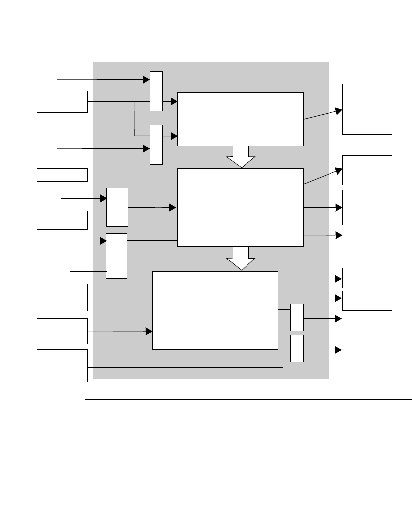
Application-Specific Functions
W9 1606383 01 11 A02 09/04 163
Counting
Function
Diagram
The following is a counting function diagram:
&
&
>1
>1
RVFC Counter
Current Value
Comparison
RVFC.U
Counting
upcounting
RVFC.F
Overflow
output
RVFC.V
Current
value
RVFC.TH0
RVFC.TH1
RVFC.C
Catch
value
Q0
Output
output 0
Q1
Output
output 1
&
&
+
-
IA = Up counter input
(Single signal or phase A)
RVFC.EN
RVFC.P
IB = (UP/DOWN flag or phase B)
SRVFC
RVFC.S0
Threshold
Value 0
RVFC.S1
Threshold
Value 1
RVFC.R
or
RVFC.S
Enable
IPres = (Preset Input)
%ICa = Catch input
Read %VFCi.V
RVFC. V
Current Value
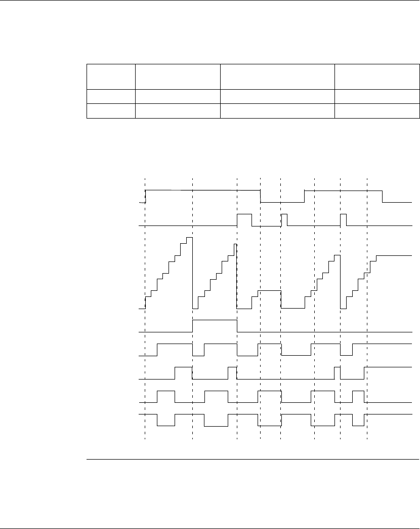
Application-Specific Functions
164 W9 1606383 01 11 A02 09/04
Usage in Simple
Upcounting
Mode
The following is an example of using RVFC in a single up counter mode. The
following configuration elements have been set for this example:
The RVFC.P preset value is 60, while the RVFC.TH0 lower threshold value is 14,
and the RVFC.TH1 upper threshold is 20.
A timing chart follows:
Reflex
Output
RVFC.V <RVFC.TH0 RVFC.TH0 £RVFC.V <
RVFC.TH1
RVFC.V >=
RVFC.TH1
Q2X
Q3X X
RVFC.P = 60
RVFC.TH0 = 14
RVFC.TH1 = 20
RVFC.V
EN
R
65535
20
14
D
S0
Output
output 0
S1
Output
output 1
60
0
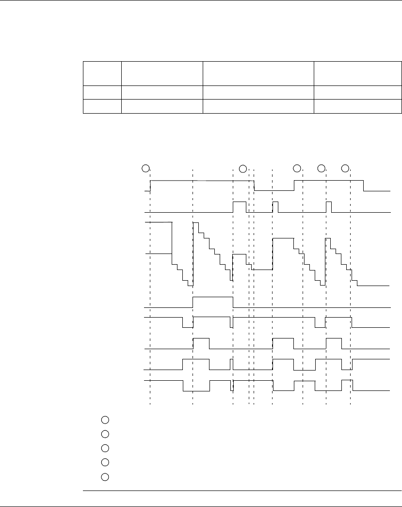
Application-Specific Functions
W9 1606383 01 11 A02 09/04 165
Usage in Simple
Downcounting
Mode
The following is an example of using RVFC in a single down counter mode. The
following configuration elements have been set for this example:
The RVFC.P preset value is 60, while the RVFC.TH0 lower threshold value is 14,
and the RVFC.TH1 upper threshold is 20.
Example :
Reflex
Output
RVFC.V <RVFC.TH0 RVFC.TH0 £RVFC.V <
RVFC.TH1
RVFC.V >= RVFC.TH1
Q2X X
Q3X
VFC0.P = 17
VFC0.S0 = 14
VFC0.S1 = 20
EN
R
60
20
14
0VFC0.V
F
TH0
Output
reflex 0
TH1
Output
reflex 1
1 3 4 5
: VFC0.U = 0 because VFC is a down-counter
: change VFC0.S1 to 17
: S input active makes threshold S1 new value to be granted in next count
1
2
3
4
2
5
: a catch of the current value is made, so VFC0.C = 17
: change VFC0.P to 20
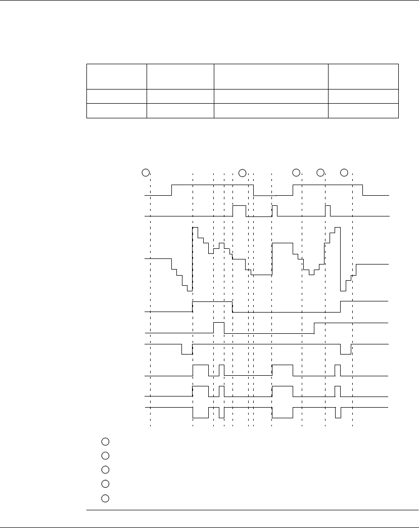
Application-Specific Functions
166 W9 1606383 01 11 A02 09/04
Usage in Up/
Downcounting
Mode
The following is an example of using RVFC in an up-down counter mode. The
following configuration elements have been set for this example:
The RVFC.P preset value is 60, while the RVFC.TH0 lower threshold value is 14,
and the RVFC.TH1 upper threshold is 20.
Example :
Reflex Output RVFC.V <
RVFC.TH0
RVFC.TH0 £RVFC.V <
RVFC.TH1
RVFC.V >=
RVFC.TH1
Q2X
Q3X X
RVFC.P = 17
RVFC.TH0 = 14
RVFC.TH1 = 20
IN
S
65535
20
14
0
%VFC0.V
F
TH0
Output
reflex 0
TH1
Output
reflex 1
1 3 4 5
: Input IN is set to 1 and input S set to 1
: change VFC0.S1 to 17
: S input active makes threshold S1 new value to be granted in next count
1
2
3
4
2
5
: a catch of the current value is made, so VFC0.C = 17
: change VFC0.P to 20
U
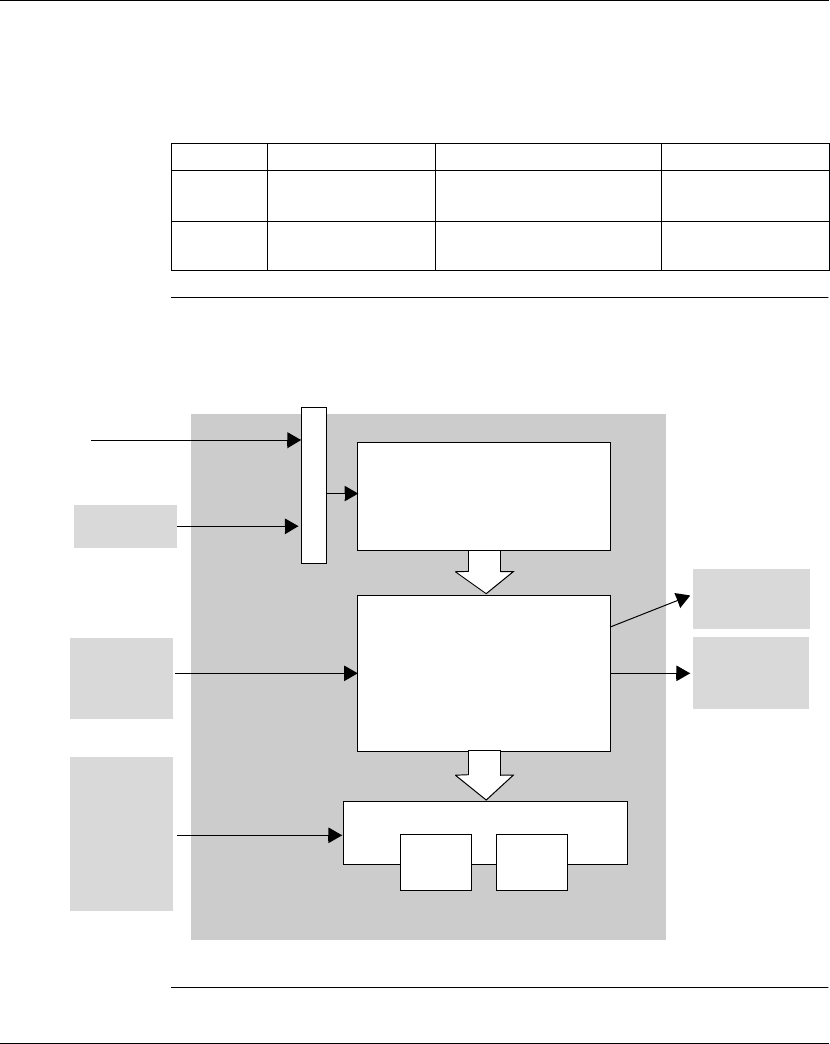
Application-Specific Functions
W9 1606383 01 11 A02 09/04 167
Frequency Meter
Function
Description
The frequency meter function of a RVFC is used to measure the frequency of a
periodic signal in Hz on input IA. The frequency range which can be measured is
from 10 to 20kHz. The user can choose between two time bases: This choice is
made by a new object RVFC.T (Time base). A value of 100 = time base of 100 ms
and a value of 1000 = time base of 1 second.
Frequency Meter
Function
Diagram
The following is a frequency meter function diagram:
Time Base Measurement range Accuracy Update
100 ms 100 Hz to 20 kHz 0.05 %for 20 kHz, 10 %for
100 Hz
10 times per second
1 s 10 Hz to 20 kHz 0.005 %for 20 kHz, 10 %for
10 Hz
Once per second
&VFC Counter
current value
VFC.F
Overflow
output
VFC.V
Frequency
+
IN VFC
SVFC
Current Value
measured
(Update flag)
1000 ms 100 ms
Set
current
VFC.T
Select
base
IA
Signal to be measured
value to 0
time
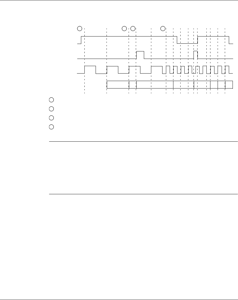
Application-Specific Functions
168 W9 1606383 01 11 A02 09/04
Use in Frequency
Meter Mode
The following is a timing diagram example of using RVFC in a frequency meter
mode.
Fallback Modes When the PLC stops or detects a communication error, the RVFC function block
may operate differently according to the programmed fallback mode.
The programmable fallback modes of the RVFC function block are as follows:
zreset to zero of the very fast counter (equivalent of setting RVFC.R to 1),
zset the current value of the RVFC function block counter (equivalent of setting
RVFC.EN to 0),
zcontinue counting.
EN
R
Timebase
VFC0.V
1 2 3 4
f1 f2 0 f3 f4 f5f30
1
2
: The first frequency measurement starts here.
: The current frequency value is updated.
: Input IN is set to 1 and input S set to 1
: Change RVFC.T to 100 ms: this change cancels the current measurement
3
4
and starts another one.

Application-Specific Functions
W9 1606383 01 11 A02 09/04 169
Remote Very Fast Counter (RVFC) Parameter Registers
At a Glance The very fast counters (RVFC0 and RVFC1) use the configuration parameters of the
supported functions.
Registers 700 to
734
Specific function of Remote Very Fast Counter 0 (RVFC0)
Registers Parameter Description Access
700
701
RVFC.V Current Value read
Current Value
702 RVFC.Drt Bit[0]: count direction read
RVFC.D Bit [1]: output overshoot
RFVC.S0 Bit [2]: S0 threshold reached. When set to 1, the
current value is greater than S0.
RFVC.S1 Bit [3]: S1 threshold reached. When set to 1, the
current value is greater than S1.
RFVC.FV Bit [4]: measurement frequency valid
703
704
RVFC.C Capture Value read
Capture Value
705 RVFC.M Counting mode:
z0: not used
z1: up/down counter
z2: 2-phase counter
z3: single up counter
z4: single down counter
z5: frequency meter
read/write
706
707
RVFC.P Preset value read/write
Preset value

Application-Specific Functions
170 W9 1606383 01 11 A02 09/04
Specific function of Remote Very Fast Counter 1 (RVFC1)
708 RVFC.
AQ0
Bit [0]: activates the reflex output 0 read/write
RVFC.
AQ1
Bit [1]: activates the reflex output 1
RVFC.T Bit [2]: frequency measure time base
0: 100ms, 1: 1s
RVFC.
AIpres
Bit [3]: validates the preset input
RVFC.
AIca
Bit [4]: validates the sensor input
RVFC.
Q0Z1
Bit [5]: status of reflex output 0 when the value is in
zone 1
RVFC.
Q0Z2
Bit [6]: status of reflex output 0 when the value is in
zone 2
RVFC.
Q0Z3
Bit [7]: status of reflex output 0 when the value is in
zone 3
RVFC.
Q1Z1
Bit [8]: status of reflex output 1 when the value is in
zone 1
RVFC.
Q1Z2
Bit [9]: status of reflex output 1 when the value is in
zone 2
RVFC.
Q1Z3
Bit [10]: status of reflex output 1 when the value is in
zone 3
709 RVFC.EM Fallback mode:
z0: reset to zero of the counter
z
1: stop counting, save the last value read and freeze counter
z2: continue counting
read/write
710
711
RVFC.TH0 Threshold Value S0 read/write
Threshold Value S0
where S0 <S1
712
713
RVFC.TH1 Threshold Value S1 read/write
Threshold Value S1
where S1 >S0
714 RVFC.EN
RVFC.R
RVFC.RFV
RVFC.CD
Bit [0]: enable input
Bit [1]: reset input
Bit [2]: reset the status of the valid measurement
frequency (RFVC.FV)
Bit [3]: reset RVFC.D bit
read/write
Registers Parameter Description Access
720...734 RVFC.
Description identical to that for very fast counter RVFC0
Registers Parameter Description Access

Application-Specific Functions
W9 1606383 01 11 A02 09/04 171
Remote Pulse Generator (RPLS) Function Block
Introduction The RPLS function block is used to generate a sequence of square wave signals.
There are two RPLS functions available. The RPLS0 block uses the dedicated
output Q0 and the RPLS1 block uses the dedicated output Q1. The RPLS and
RPWM function blocks share the same dedicated outputs. You must choose one or
other of the functions for each output.
Notes The function block will only be activated after the RPLS.R function block is initialized
and the RPLS.EN input enabled.
The selection or modification of the RPLS.M counting mode will only be taken into
account on activation of the RPLS.R command.
Representation The following figure shows a pulse generator function block:
RPLS.EN RPLS.Q
RPLS.R
RPLS
RPLS.TB
RPLS.D
RPLS.P
RPLS.N
Qx

Application-Specific Functions
172 W9 1606383 01 11 A02 09/04
Parameters The following table shows the different parameters of the RPLS pulse generator
function block.
Parameter Description Description
RPLS.TB Time base This parameter can take the following time base values:
z0.127 ms
z0.508 ms
z10 ms
z1 s (default value)
RPLS.P Period coefficient
value
Authorized values for the preset period:
znot used
z0<RPLS.P <255 with a time base 0.127 ms or
0.508 ms
z1<RPLSP <65535 (FFFF H) with a time base of
10 ms or 1 s
RPLS.N Number of pulses The number of pulses to be generated over a period T
canbelimitedto0<RPLS.N <4 294 967 295
(FFFF FFFF H).
The default value is set to 0.
To produce an unlimited number of pulses, set RPLS.N
to zero.
RPLS.EN Validation of the
pulse generator
Validation of the RPLS block operation.
When set to 0, this block is inhibited and the RPLS.Q
output reset to zero.
RPLS.R Reset At state 1, outputs RPLS.Qand RPLS.D are set to 0. The
number of pulses generated in period T is set to 0.
RPLS.QGeneration of the
pulses in progress
When set to 1, this indicates that the pulse signal is
generated at the dedicated output channel.
RPLS.Qx Dedicated outputs Physical output to which the pulse train is applied.
RPLS.D Pulse generation
done output
At state 1, signal generation is complete. The number of
desired pulses has been reached.
This is reset by activating RPLS.R
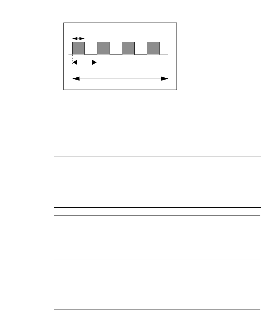
Application-Specific Functions
W9 1606383 01 11 A02 09/04 173
Operation The following diagram illustrates the RPLS function block:
Duration of the pulse train: RPLS.N * T
The output signal period is set on configuration, by selecting the time base RPLS.TB
and the period coefficient value RPLS.P.
zT = RPLS.P * RPLS.TB
zTON = T/2 for time bases 0.142 ms and 0.508 ms
= (RPLS.P * RPLS.TB)/2
zTON = [whole part (RPLS.P)/2]* RPLS.TB for the 10ms to 1s time bases.
Period Ranges
Available
The available period ranges are as follows:
z0.127 ms to 32.38 ms in steps of 0.127 ms (30.9 Hz to 7.87 kHz)
z0.508 ms to 129.54 ms in steps of 0.508 ms (7.72 Hz to 1.97 kHz)
z20 ms to 5.45 mins in steps of 10 ms
z1 sec to 1193046 hours in steps of 1 sec
Fallback Modes
RPLS.EM
When the PLC stops or detects a communication error, the RPLS function block may
operate differently according to the programmed fallback mode.
The programmable fallback modes of the RPLS function block are as follows:
zgenerator reset with output reset (equivalent of setting RPLS.R to 1).
zstop at the end of the current interval (equivalent of setting RPLS to 0),
zcontinue generating pulses.
Note:
zToobtainagoodlevelofprecisionfromthedutycyclewithtimebasesof10ms
and 1s, you are recommended to have a RPLS.P >= 100 if P is odd.
zAny modification of the RPLS.P coefficient value is immediately taken into
account.
zWhere the RPLS function is used, the writing of the Q0andQ1 outputs does not
interrupt signal generation.
Variable period
T
TON
RPLS.D

Application-Specific Functions
174 W9 1606383 01 11 A02 09/04
Pulse Generator
Example
The following is an illustration of a pulse diagram of the RPLS function block.
Input RPLS.EN
Number of pulses
Dedicated output Qx
RPLS.Q
RPLS.D
RPLS.N

Application-Specific Functions
W9 1606383 01 11 A02 09/04 175
Remote Pulse Width Modulator Function Block
Introduction The remote pulse width modulator (RPWM) function block generates a rectangular
signal on the dedicated output channels. The signal duty cycle is variable.
There are two RPWM blocks available. The RPWM0 block uses the dedicated
output Q0 and the RPMW1 block uses the dedicated output Q1. The RPLS and
RPWM function blocks share the same dedicated outputs. You must choose one or
other of the functions for each output.
Representation The following figure shows a remote pulse width modulator function block:
RPWM.EN RPWM.Q
RPWM
RPWM.TB
RPWM.P
RPWM.RA
Qx

Application-Specific Functions
176 W9 1606383 01 11 A02 09/04
Parameters The following table shows the different parameters of the remote pulse width
modulator (RPWM) function block.
Parameter Description Description
RPWM.TB Time base This parameter can take the following time base values:
z0.127 ms
z0.508 ms
z10 ms
z1 s (default value)
RPWM.P Period coefficient
value
Authorized values for the preset period:
znot used
z0<RPWM.P <255 with a time base 0.127 ms or
0.508 ms
z1<RPWM.P <65535 (FFFF H) with a time base of
10 ms or 1 s
RPWM.RA Duty cycle This value sets the percentage (0%<R<100%)ofthe
signal in state 1 in a period T.
The default value is 0 (values greater than 100 are
considered to be equal to 100).
RPWM.EN Validation of the
pulse generator
Validation of the RPWM block operation.
When set to 0, this block is inhibited and the RPLS.Q
output reset to zero.
RPLS.QGeneration of the
pulses in
progress
When set to 1, this indicates that the pulse signal is
generated at the dedicated output channel.
RPWM.Qx Dedicated
outputs
Physical output to which the pulse train is applied.

Application-Specific Functions
W9 1606383 01 11 A02 09/04 177
Operation The following diagram illustrates the RPWM function block:
The output signal period is set on configuration, by selecting the time base
RPWM.TB and the period coefficient value PWM.P. Modifying the RPWM.RA duty
cycle in the program enables the signal width to be modulated.
Range of Periods The coefficient value and the time base can be modified during configuration. They
are used to set the signal period T = RPWM.P * TB. The range of periods available:
z0.127 ms to 32.38 ms in steps of 0.127 ms (30.9 Hz to 7.87 kHz)
z0.508 ms to 129.54 ms in steps of 0.508 ms (7.72 Hz to 1.97 kHz)
z10 ms to 5.45 mins in steps of 10 ms
z1 sec to 1193046 hours in steps of 1 sec
Pulse
Modulation
Calculation of the Tp width: Tp = T * (RPWM.RA/100)
If the signal period is programmed to 500 s, then,
zwhere the RPWM.RA ratio is set to 20%, the duration of the signal at state 1 is
then: 20 %x 500 ms = 100 ms,
zwhere the RPWM.RA ratio is set to 50 %(duration = 250 ms),
zwhere the RPWM.RA ratio is set to 80 %(duration = 400 ms).
Fallback Modes
RPWM.EM
When the PLC stops or detects a communication error, the RPWM function block
may operate differently according to the programmed fallback mode.
The programmable fallback modes of the RPWM function block are as follows:
zgenerator reset with output reset,
zstop at the end of the current interval (equivalent of setting RPWM.EN to 0),
zcontinue generating pulses.
Tp
programmable width
(RPWM.P)
configurable fixed
period (RPWM.R)
T

Application-Specific Functions
178 W9 1606383 01 11 A02 09/04
Example of a
Pulse Generator
with Pulse Width
Modulation
Below is an illustration of a pulse diagram for the RPWM function block with varying
duty cycles.
Ratio
RPWM.RA 20%
50%
80%
Dedicated output Qx
Input
RPWM.EN

Application-Specific Functions
W9 1606383 01 11 A02 09/04 179
Remote Pulse Generators (RPLS, RPWM) Parameter Registers
At a Glance The pulse generators (RPLS) and pulse width modulation generators (RPWM) use
the configuration parameters of the supported functions.
Registers 800 to
828
Remote pulse generator specific function (RPLS0 or RPWM0).
Registers Parameter Description Access
800 RPLS.Q
RPWM.Q
Bit [0]: output Q. When set to 1, the pulse signal is
generated at the dedicated output channel configured.
read
RPLS.D
RPWM.D
Bit [1]: output D. When set to 1, signal generation is
complete. The number of desired pulses has been
reached.
801 RPLS/
RPWM
Operating mode:
z0: not used
z1: PLS
z2: PWM
read/
write
802 RPLS.TB
RPWM.TB
Time base:
z0: 0.127 ms
z1: 0.508 ms
z2: 10 ms
z3: 1 s
read/
write
803 RPLS.P
RPWM.P
Preset period: P
z0: not used
z0<P<255 with a time base of 0.127 ms or 0.508
ms
z1<P<65535 (FFFFH) with a time base of 10 ms or
1s
read/
write
804
805
RPLS.N Number of pulses:
z0: Unlimited number of pulses:
z1<N<4 294 967 295 (FFFF FFFFH)
read/
write
806 RPWM.RA Duty cycle: 0%<R<100%.
Duration of high status / Duration of low status
read/
write
807 RPLS.EM
RPWM.EM
Fallback mode:
z0: generator reset with zeroing of output
z1: stop at the end of current interval
z2: continue generating pulses
read/
write

Application-Specific Functions
180 W9 1606383 01 11 A02 09/04
Specific function of RPLS1 or RPWM1.
808 RPLS. EN
RPWM.EN
Bit [0]: pulse generation input. When set to 1, the pulse
generation is produced on the dedicated output
channel. When set to 0, the output channel is set to 0.
read/
write
RPLS. R
RPWM.R
Bit [1]: generator reset input. When set to 1, outputs Q
and D are reset to 0. The number of pulses generated
over a period T is reset to 0.
Registers Description Access
820...828 Description identical to that for PLS0 or PWM0 functions
Registers Parameter Description Access

W9 1606383 01 11 A02 09/04 181
7
Software Installation
Advantys Configuration Tool
At a Glance The purpose of the Advantys Configuration Tool is to help the user configure an
island. It generates a mapping image of the registers which are to be entered
manually into PL7 / TwidoSoft.
Note: Under no circumstances will the software be able to download the
configuration directly to the island.

Software Installation
182 W9 1606383 01 11 A02 09/04

W9 1606383 01 11 A02 09/04 183
8
Diagnostics of the Advantys OTB
Island
Overview
At a Glance Diagnostics of the Advantys OTB island enables us to analyze the behavior of the
network by referring to:
zThe LEDs indicating the communication and I/O status,
zThe communications objects used for diagnostics of the different functions.
What's in this
Chapter?
This chapter contains the following topics:
Topic Page
Indicator Lights (LEDs) 184
OTB Island Diagnostics Registers 186
Behavior in the Event of a Fault 190
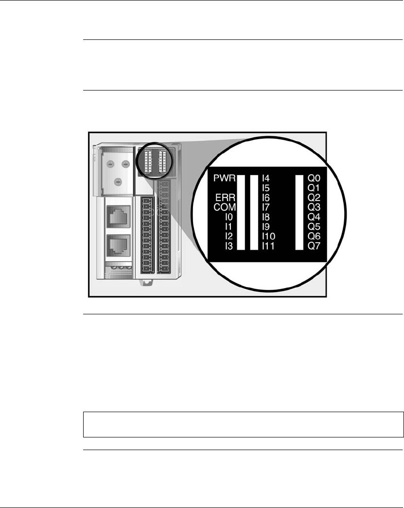
Diagnostics
184 W9 1606383 01 11 A02 09/04
Indicator Lights (LEDs)
Introduction 23 indicators on the OTB1S0DM9LP module provide information on the functional
status of the island on a Modbus network. The indicators are located in the upper
section of the network interface module.
Description The following illustration shows the LEDs used by the Advantys OTB Modbus
network interface module:
Meaning of the
indicators
zThe PWR LED indicates the presence of a 24 VDC power supply to the network
interface module.
zThe ERR and COM LEDs show the data exchange status between the Modbus
field bus master and the Advantys OTB island.
zTheLEDsI0toI11andQ0toQ7 reflect the activity and/or events observed on
the network interface module.
zTheLED2isnotused.
Note: When you consult the table, make sure you check the status of the Power
LED

Diagnostics
W9 1606383 01 11 A02 09/04 185
Modbus
Communication
LEDs
The following table describes the conditions of and the colors used by the COM and
ERR LEDs to display the normal operating modes and error conditions of an
Advantys OTB Modbus network interface module on the field bus.
I/O Status
Indicators
The following table describes the conditions of and the colors used by the PWR
LEDs, I0 to I11 and Q0toQ7 to display the normal operating modes and error
conditions for the power supply and I/Os of the Advantys OTB Modbus network
interface module.
Name LED color Type of
flashing
Function
Com
(communic
ation)
yellow random
flashing
On when sending and receiving
Err (error)
red on Internal error
random
flashing
Other errors: communication errors or
configuration fault
Name LED color Status Function
PWR
(power)
green on Presence of a 24 VDC for the OTB module
I0 to I11 green on Input set to 1
off Input set to 0
Q0toQ7 green on Active output
off Inactive output

Diagnostics
186 W9 1606383 01 11 A02 09/04
OTB Island Diagnostics Registers
At a Glance Diagnostics uses the monitoring parameters of the supported functions. All
parameters in this zone are accessible in read-only.
Registers 900 to
917
Registers 900 and 901: Island status
Registers 902 to 907: diagnostics for functions specific to Advantys OTB module
(configured functions only)
Registers Function Description
900 Island status
word
Bits [0...8]: not used
Bit [9]: communication fault or external fault
Bits [10...12]: not used
Bit [13]: configuration fault (expansion modules missing or
badly configured)
Bits [14...15]: not used
901 Expansion
modulestatus
word
Bit [0]: status word of first expansion module
Bit [1]: status word of second expansion module
Bit [2]: status word of third expansion module
Bit [3]: status word of fourth expansion module
Bit [4]: status word of fifth expansion module
Bit [5]: status word of sixth expansion module
Bit [6]: status word of seventh expansion module
Note:
Bit values:
z0: no fault
z1: fault
Registers Function Description
902 Fast Counter
0
Bits [0...8]: not used
Bit [9]: configuration consistency error
Bits [10...15]: not used
903 Fast Counter
1
Description identical to register 902
904 Very Fast
Counter 0
Description identical to register 902
905 Very Fast
Counter 1
Description identical to register 902

Diagnostics
W9 1606383 01 11 A02 09/04 187
Registers 908 to 910: diagnostics for functions specific to Advantys OTB module
(configured functions only)
906 Pulse
generator
PLS/PWM 0
Description identical to register 902
907 Pulse
generator
PLS/PWM 1
Description identical to register 902
Note:
Bit values:
z0: no fault
z1: fault
Registers Function Description
908 Inputs
associated
with Fast
Counter and
Very Fast
Counter
functions
(function
configured
and input
used)
Bit [0]: input 0 (if used by RVFC0)
Bit [1]: input 1 (if used by RVFC0)
Bit [2]: input 2 (if used by RVFC0)
Bit [3]: input 3 (if used by RVFC0)
Bit [4]: input 4 (if used by RVFC1)
Bit [5]: input 5 (if used by RVFC1)
Bit [6]: input 6 (if used by RVFC1)
Bit [7]: input 7 (if used by RVFC1)
Bit [8]: input 8 (if used by RFC0)
Bit [9]: input 9 (if used by RFC1)
Bits [10...15]: not used
909 Outputs
associated
with Very
Fast Counter,
PLS and
PWM
functions
(function
configured
and output
used)
Bit [0]: output 0 (if used by PLS/PWM 0)
Bit [1]: output 1 (if used by PLS/PWM 1)
Bit [2]: output 2 (if used by RVFC0)
Bit [3]: output 3 (if used by RVFC0)
Bit [4]: output 4 (if used by RVFC1)
Bit [5]: output 5 (if used by RVFC1)
Bits [6...15]: not used
Registers Function Description

Diagnostics
188 W9 1606383 01 11 A02 09/04
Registers 911 to 917: expansion module diagnostics (1 register per expansion
module)
910 Status of OTB
Module I/Os
Bit [0]: channels operating normally (for all its channels)
Bit [1]: module initializing (or initializing information of all
channels).
Bit [2]: hardware failure.
Bit [3]: OTB module configuration fault
Bit [4...7]: not used
Bit [8]: value error in last command
Bit [9]: value consistency error in last command
Bit [10...15]: not used
Note:
Bit values:
z0: no fault
z1: fault
Type Description of diagnostics register
Discrete
module
No diagnostics
Analog
module
Bit [0]: fault
Bit [1]: module initializing (or initializing information of all channels).
Bit [2]: hardware failure (external power supply failure, common to all
channels).
Bit [3]: analog expansion module configuration fault
Bit [4]: conversion of data input channel 0 in progress
Bit [5]: conversion of data input channel 1 in progress
Bit [6]: thermocouple input channel 0 not configured
Bit [7]: thermocouple input channel 1 not configured
Bit [8]: not used
Bit [9]: Inconsistent configuration
Bit [10]: analog input data channel 0 over range
Bit [11]: analog input data channel 1 over range
Bit [12]: incorrect wiring (analog input data channel 0 below current range, open
current loop)
Bit [13]: incorrect wiring (analog input data channel 1 below current range, open
current loop)
Bit [14]: mixing of analog input types not allowed
Bit [15]: output value outside scale
Registers Function Description

Diagnostics
W9 1606383 01 11 A02 09/04 189
Analog
module
TWDAVO2
HT
Bit [1],Bit[0]: channel 0 output
z0 , 0: no fault
z0 , 1: configuration fault
z1 , 0: incorrect value
Bit [3],Bit[2]: channel 1 output
z0 , 0: no fault
z0 , 1: configuration fault
z1 , 0: incorrect value
Bit [4...15]: not used
Analog
module
TWDAMI4
LT
Bit [1],Bit[0]: channel 0 input
z0 , 0: no fault
z0 , 1: configuration fault
z1 , 0: incorrect value (module under initialization or under conversion)
z1 , 1: incorrect value (outside range)
Bit [3],Bit[2]: channel 1 input description identical to channel 0
Bit [5],Bit[4]: channel 2 input description identical to channel 0
Bit [7],Bit[6]: channel 3 input description identical to channel 0
Bit [8...15]: not used
Analog
module
TWDAMI8
HT
TWDARI8
HT
Bit [1],Bit[0]: channel 0 input
z0 , 0: no fault
z0 , 1: configuration fault
z1 , 0: incorrect value (module under initialization or under conversion)
z1 , 1: incorrect value (outside range)
Bit [3],Bit[2]: channel 1 input description identical to channel 0
Bit [5],Bit[4]: channel 2 input description identical to channel 0
Bit [7],Bit[6]: channel 3 input description identical to channel 0
Bit [9],Bit[8]: channel 4 input description identical to channel 0
Bit [11],Bit[10]: channel 5 input description identical to channel 0
Bit [13],Bit[12]: channel 6 input description identical to channel 0
Bit [15],Bit[14]: channel 7 input description identical to channel 0
Note:
Bit values:
z0: fault
z1: no fault
Type Description of diagnostics register

Diagnostics
190 W9 1606383 01 11 A02 09/04
Behavior in the Event of a Fault
Management of
Island in the
Event of a Fault
If a fault occurs on one of the modules, the module behaves in the following way:
zisland switches to fallback mode,
zimpossible to read / write (exchange report 04),
zpossible to read exchange registers 900 to 917.

W9 1606383 01 11 A02 09/04 191
9
Island Registers Table
Registers Table (mapping) for Modbus Advantys OTB Module
At a Glance The registers table depends on the network interface module, the connected
expansion modules and the type of those modules. Specific register zones are
reserved for different types of data.
Registers Table
(mapping)
Zone containing the register numbers associated with the functions supported by
OTB. The following register numbers must be coded in Modbus requests:
Registers Function Pages
0 to 99 Status of island inputs 0 to 99 (See
Status of
inputs , p. 192
)
100 to 199 Island output commands 100 to 199 (See
Output
Commands , p. 192
)
200 to 599 Island I/O configuration parameters 200 to 599 (See
I/O
Parameters, p. 193
)
600 to 699 Remote Fast Counter (RFC) function
block
600 to 699 (See
Fast
Counters, p. 194
)
700 to 799 Remote Very Fast Counter (RVFC)
function block
700 to 799 (See
Very Fast
Counters , p. 195
)
800 to 899 Remote pulse generator function block
(RPLS)
Remote pulse generator function block
with pulse width modulation (RPWM)
800 to 899 (See
Pulse
Generator, p. 197
)
900 to 999 Island diagnostics 900 to 999 (See
Diagnostics, p. 198
)
1000 to 1099 Management of island behavior 1000 to 1099 (See
Management of Island
Behavior, p. 202
)

Mapping
192 W9 1606383 01 11 A02 09/04
Status of inputs The status of island inputs can be read in zones 0 to XX (XX depends on the number
of expansion modules connected).
Output
Commands
The island output commands can be read in zones 100 to 1XX (XX depends on the
number of expansion modules connected).
1100 to 1108 Island structure 1100 to 1108 (See
Management of Island
Behavior, p. 202
)
Registers Function Pages
Register Description
0 Status of inputs 0 to 11 of OTB module
1 first input status word of first expansion module
... following input status words of expansion modules
XX last input status word of last expansion module
Registers Description
100 Outputs 0 to 8 of OTB module
101 first output command word of first expansion module
... following output command words of expansion modules
1XX last output command word of last expansion module

Mapping
W9 1606383 01 11 A02 09/04 193
I/O Parameters The OTB module's I/O parameter registers can be read in zones 200 to 213 and the
registers for the expansion modules' I/O parameters are in zones 214 to 2XX (XX
depends on the number of expansion modules connected).
Discrete I/O
Expansion
Modules
Expansion Module Discrete I/O Parameter Registers 214 to 599, p. 132
Registers Description
200...211 Configuration of inputs 0 to 11 of OTB module
Input filtering value:
z0: no filtering
z1: filtering at 3ms (default value)
z2: filtering at 12ms
212 Configuration of fallback mode of OTB module discrete
outputs
Bit value:
z0: maintain
z1: fallback (default value)
Bit [0...7]: output 0...7
Bit [8...15]: not used
213 Configuration of fallback values of OTB module discrete
outputs
Bit value:
z0: force output to 0 (default value)
z1: force output to 1
Bit [0...7]: output 0...7
Bit [8...15]: not used
214 First input configuration word of first expansion module with
this parameter
2.. Following input configuration words of expansion module with
parameters
2XX Last input configuration word of last expansion module with
parameters
Note: The order of the parameters is defined by expansion modules added from
left to right. The number of parameters depends on the types of expansion modules
connected. Discrete inputs of expansion modules are not filtered.

Mapping
194 W9 1606383 01 11 A02 09/04
Analog I/O
Expansion
Modules
Expansion Module Analog I/O Parameter Registers 214 to 599, p. 135
Fast Counters Specific fast counter function 0 (RFC).
Specific function of fast counter 1 (RFC1).
Registers Parameter Description Access
600
601
RFC.V Current Value read
Current Value
602 RFC.D Bit [0]: D (Done) read
603 RFC.M Counting mode:
z0: not used (default value)
z1: counter
z2: downcounter
read/write
604 RFC.EM Fallback mode:
z0: Reset counter to zero (default value)
z1: stop counting, save the last value read and
freeze counter
z2: continue counting
read/write
605
606
RFC.P Preset value read/write
Preset value
607 RFC.EN
RFC.R
RFC.CD
Bit [0]: validation of the input EN
Bit [1]: R (Reset)
Bit [2]: reset of the RFC.D bit
read/write
Registers Description Access
620...627 Description identical to that for counter 0 read

Mapping
W9 1606383 01 11 A02 09/04 195
Very Fast
Counters
Specific function of Remote Very Fast Counter 0 (RVFC0)
Registers Parameter Description Access
700
701
RVFC.V Current Value read
Current Value
702 RVFC.Drt Bit[0]: count direction read
RVFC.D Bit [1]: output overshoot
RFVC.S0 Bit [2]: S0 threshold reached. When set to 1, the
current value is greater than S0.
RFVC.S1 Bit [3]: S1 threshold reached. When set to 1, the
current value is greater than S1.
RFVC.FV Bit [4]: measurement frequency valid
703
704
RVFC.C Capture Value read
Capture Value
705 RVFC.M Counting mode:
z0: not used (default value)
z1: up/down counter
z2: 2-phase counter
z3: single up counter
z4: single down counter
z5: frequency meter
read/write
706
707
RVFC.P Preset value read/write
Preset value
708 RVFC.AQ0Bit[0]: activates the reflex output 0 read/write
RVFC.AQ1Bit[1]: activates the reflex output 1
RVFC.T Bit [2]: frequency measure time base
0: 100ms, 1: 1s
RVFC.AIpre
s
Bit [3]: validates the preset input
RVFC.AIca Bit [4]: validates the sensor input
RVFC.Q0Z1
Bit [5]: status of reflex output 0 when the value is in zone 1
RVFC.Q0Z2
Bit [6]: status of reflex output 0 when the value is in zone 2
RVFC.Q0Z3
Bit [7]: status of reflex output 0 when the value is in zone 3
RVFC.Q1Z1
Bit [8]: status of reflex output 1 when the value is in zone 1
RVFC.Q1Z2
Bit [9]: status of reflex output 1 when the value is in zone 2
RVFC.Q1Z3
Bit [10]: status of reflex output 1 when the value is in zone 3

Mapping
196 W9 1606383 01 11 A02 09/04
Specific function of Remote Very Fast Counter 1 (RVFC1)
709 RVFC.EM Fallback mode:
z0: reset counter to zero (default value)
z
1: stop counting, save the last value read and freeze counter
z2: continue counting
read/write
710
711
RVFC.TH0 Threshold Value S0 read/write
Threshold Value S0
where S0 <S1
712
713
RVFC.TH1 Threshold Value S1 read/write
Threshold Value S1
where S1 >S0
714 RVFC.EN
RVFC.R
RVFC.RFV
RVFC.CD
Bit [0]: enable input
Bit [1]: reset input
Bit [2]: reset the status of the valid measurement
frequency (RFVC.FV)
Bit [3]: reset RVFC.D bit
read/write
Registers Description Access
720...733 Description identical to that for very fast counter RVFC 0
Registers Parameter Description Access

Mapping
W9 1606383 01 11 A02 09/04 197
Pulse Generator Remote pulse generator specific function (RPLS0 or RPWM0).
Specific function PLS1 or PWM1.
Registers Parameter Description Access
800 RPLS.D
RPWM.D
Bit [0]: output Q. When set to 1, the pulse signal is
generated at the dedicated output channel configured
Bit [1]: output D. When set to 1, signal generation is
complete. The number of desired pulses has been
reached.
read
801 RPLS/
RPWM
Operating mode:
z0: not used (default value)
z1: PLS
z2: PWM
read/write
802 RPLS.TB
RPWM.TB
Time base:
z0: 0.127 ms (default value)
z1: 0.508 ms
z2: 10 ms
z3: 1 s
read/write
803 RPLS.P
RPWM.P
Period coefficient: P
z0: not used (default value)
z
0<P<255withatimebaseof0.127msor0.508ms
z
1<P<65535 (FFFFH) with a time base of 10 ms or 1 s
read/write
804
805
RPLS.N Number of pulses:
z0 : unlimited number of pulses (default value)
z1<N<4 294 967 295 (FFFF FFFFH)
read/write
806 RPWM.RA Duty cycle: 0%<R<100%.
Duration of high status / Duration of low status
read/write
807 RPLS.EM
RPWM.EM
Fallback mode:
z0: generator reset with zeroing of output
z1: stop at the end of current interval
z2: continue generating pulses
read/write
808 RPLS. Q
RPWM.Q
RPLS. R
RPWM.R
Bit [0]: pulse generation input. When set to 1, the pulse
generation is produced on the dedicated output
channel. When set to 0, the output channel is set to 0.
Bit [1]: generator reset input. When set to 1, outputs Q
and D are reset to 0. The number of pulses generated
over a period T is reset to 0.
read/write
Registers Description Access
820...828 Description identical to that for PLS0 or PWM0 functions

Mapping
198 W9 1606383 01 11 A02 09/04
Diagnostics All parameters in this zone are accessible in read-only
Registers 900 and 901: Island status
Registers 902 to 907: diagnostics for functions specific to Advantys OTB module
(configured functions only)
Registers Function Description
900 Island status
word
Bits [0...8]: not used
Bit [9]: communication fault or external fault
Bits [10...12]: not used
Bit [13]: configuration fault (expansion modules missing or
badly configured)
Bits [14...15]: not used
901 Expansion
modulestatus
word
Bit [0]: status word of first expansion module
Bit [1]: status word of second expansion module
Bit [2]: status word of third expansion module
Bit [3]: status word of fourth expansion module
Bit [4]: status word of fifth expansion module
Bit [5]: status word of sixth expansion module
Bit [6]: status word of seventh expansion module
Note:
Bit values:
z0: no fault
z1: fault
Registers Function Description
902 Fast Counter
0
Bits [0...8]: not used
Bit [9]: configuration consistency error
Bits [10...15]: not used
903 Fast Counter
1
Description identical to register 902
904 Very Fast
Counter 0
Description identical to register 902
905 Very Fast
Counter 1
Description identical to register 902
906 Pulse
generator
PLS/PWM 0
Description identical to register 902
907 Pulse
generator
PLS/PWM 1
Description identical to register 902

Mapping
W9 1606383 01 11 A02 09/04 199
Registers 908 to 910: diagnostics for functions specific to Advantys OTB module
(configured functions only)
Note:
Bit values:
z0: no fault
z1: fault
Registers Function Description
908 Inputs
associated
with Fast
Counter and
Very Fast
Counter
functions
(function
configured
and input
used)
Bit [0]: input 0 (if used by RVFC0)
Bit [1]: input 1 (if used by RVFC0)
Bit [2]: input 2 (if used by RVFC0)
Bit [3]: input 3 (if used by RVFC0)
Bit [4]: input 4 (if used by RVFC1)
Bit [5]: input 5 (if used by RVFC1)
Bit [6]: input 6 (if used by RVFC1)
Bit [7]: input 7 (if used by RVFC1)
Bit [8]: input 8 (if used by RFC0)
Bit [9]: input 9 (if used by RFC1)
Bits [10...15]: not used
909 Outputs
associated
with Very
Fast Counter,
PLS and
PWM
functions
(function
configured
and output
used)
Bit [0]: output 0 (if used by PLS/PWM 0)
Bit [1]: output 1 (if used by PLS/PWM 1)
Bit [2]: output 2 (if used by RVFC0)
Bit [3]: output 3 (if used by RVFC0)
Bit [4]: output 4 (if used by RVFC1)
Bit [5]: output 5 (if used by RVFC1)
Bits [6...15]: not used
910 Status of OTB
Module I/Os
Bit [0]: channels operating normally (for all its channels)
Bit [1]: module initializing (or initializing information of all
channels).
Bit [2]: hardware failure (external power supply failure,
common to all channels).
Bit [3]: OTB module configuration fault
Bit [4...7]: not used
Bit [8]: value error in last command
Bit [9]: value consistency error in last command
Bit [10...15]: not used

Mapping
200 W9 1606383 01 11 A02 09/04
Registers 911 to 917: expansion module diagnostics (1 register per expansion
module)
Note:
Bit values:
z0: no fault
z1: fault
Type Description of diagnostics register
Discrete
module
No diagnostics
Analog
modules
TWDAMI2
HT
TWDAMO
1HT
TWDAMM
3HT
TWDALM3
LT
Bit [0]: fault
Bit [1]: module initializing (or initializing information of all channels).
Bit [2]: hardware failure (external power supply failure, common to all
channels).
Bit [3]: analog expansion module configuration fault
Bit [4]: conversion of data input channel 0 in progress
Bit [5]: conversion of data input channel 1 in progress
Bit [6]: thermocouple input channel 0 not configured
Bit [7]: thermocouple input channel 1 not configured
Bit [8]: not used
Bit [9]: inconsistent configuration
Bit [10]: analog input data channel 0 over range
Bit [11]: analog input data channel 1 over range
Bit [12]: incorrect wiring (analog input data channel 0 below current range, open
current loop)
Bit [13]: incorrect wiring (analog input data channel 1 below current range, open
current loop)
Bit [14]: mixing of analog input types not allowed
Bit [15]: output channel not available
Analog
module
TWDAVO2
HT
Bit [1],Bit[0]: channel 0 output
z0 , 0: no fault
z0 , 1: configuration fault
z1 , 0: incorrect value
Bit [3],Bit[2]: channel 1 output description identical to channel 0
Bit [4...15]: not used

Mapping
W9 1606383 01 11 A02 09/04 201
Analog
module
TWDAMI4
LT
Bit [1],Bit[0]: channel 0 input
z0 , 0: no fault
z0 , 1: configuration fault
z1 , 0: incorrect value (module under initialization or under conversion)
z1 , 1: incorrect value (outside range)
Bit [3],Bit[2]: channel 1 input description identical to channel 0
Bit [5],Bit[4]: channel 2 input description identical to channel 0
Bit [7],Bit[6]: channel 3 input description identical to channel 0
Bit [8...15]: not used
Analog
module
TWDAMI8
HT
TWDARI8
HT
Bit [1],Bit[0]: channel 0 input
z0 , 0: no fault
z0 , 1: configuration fault
z1 , 0: incorrect value (module under initialization or under conversion)
z1 , 1: incorrect value (outside range)
Bit [3],Bit[2]: channel 1 input description identical to channel 0
Bit [5],Bit[4]: channel 2 input description identical to channel 0
Bit [7],Bit[6]: channel 3 input description identical to channel 0
Bit [9],Bit[8]: channel 4 input description identical to channel 0
Bit [11],Bit[10]: channel 5 input description identical to channel 0
Bit [13],Bit[12]: channel 6 input description identical to channel 0
Bit [15],Bit[14]: channel 7 input description identical to channel 0
Note:
Bit values:
z0: no fault
z1: fault
Type Description of diagnostics register

Mapping
202 W9 1606383 01 11 A02 09/04
Management of
Island Behavior
The OTB module management registers can be read in zones 1000 to 1099.
Registers Function
1000 Indicates the source of configuration parameters:
z0: use default values
z1: use saved values
z2: use current unsaved values
1001 Indicates the number of backups performed. It is set to zero when default
settings are restored.
1002 Save parameters command. When a value different to the current value is
written to this register, the module saves the parameters and the configuration
of expansion modules.
1003 Restore parameters command. When a value different to the current value is
written to this register, the module restores the most recent saved parameters.
The current expansion module configuration is the same as the last saved
expansion module configuration.
1004 Restore default parameters command. When a value different to the current
value is written to this register, the module restores the default factory settings.
1005 Expansion bus reset . This function is used to update expansion module I/O
parameters:
z1: setting it to 1 initiates an expansion bus Reset.
zNew parameters written to expansion modules by the application.
z0: setting it to zero activates a bus reset, if the expansion bus parameters
are consistent.
A bus reset sets all the expansion module outputs to zero.TheOTB
module outputs are maintained.
This register is set to zero when the OTB module is reset.
1006 Network monitoring:
z0: default value, no monitoring
zx: monitoring time in ms.
1007 Bit [0]: This bit is used to relaunch network monitoring after a monitoring fault:
z0: monitoring active
z1: monitoring fault
1008 Bit [0]: LSB/MSB order:
z
0: the registers concerned by 32 bit format are in MSB / LSB format (default value)
z1: the registers concerned by 32 bit format are in MSB/LSB format
1009...1019 Reserved registers

Mapping
W9 1606383 01 11 A02 09/04 203
The object code values according to expansion module type are defined in the
following table.
Type of expansion module Product code value
Discrete input modules
TWDDDI8DT 0004H
TWDDAI8DT 0004H
TWDDDI16DT 0000H
TWDDDI16DK 0000H
TWDDDI32DK 0200H
Discrete output modules
TWDDDO8TT 0005H
TWDDDO8UT 0005H
TWDDRA8RT 0005H
TWDDDO16TK 0001H
TWDDDDO16UK 0001H
TWDDRA16RT 0001H
TWDDDO32TK 0301H
TWDDDO32UK 0301H
Discrete mixed modules
TWDDMM8DRT 0405H
TWDDMM24DRF 0205H
Analog modules
TWDAMI2HT 6002H
TWDAM01HT 6003H
TWDAMM3HT 6001H
TWDALM3LT 6000H
TWDAVO2HT 6007H
TWDAMI4HT 6004H
TWDAMI8HT 6005H
TWDARI8HT 6006H
Shared junction block
OTB9ZZ61JP -

Mapping
204 W9 1606383 01 11 A02 09/04


Appendices
206 W9 1606383 01 11 A02 09/04
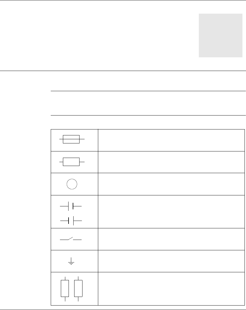
W9 1606383 01 11 A02 09/04 207
A
IEC Symbols
Glossary of Symbols
Introduction This section contains illustrations and definitions of common IEC symbols used in
describing wiring schematics.
Symbols Common IEC symbols are illustrated and defined in the table below:
Fuse
Load
AC power
DC power
Digital sensor/input, for example, contact, switch, initiator, light
barrier, and so on.
Earth ground
2-wire sensor
L
~
+
_
+
_
+
_
+
_

IEC Symbols
208 W9 1606383 01 11 A02 09/04
Thermocouple element

W9 1606383 01 11 A02 09/04 209
Glossary
10Base-T An adaptation of the IEEE 802.3 (Ethernet) standard, the 10Base-T standard
requires a twisted pair cable of a maximum segment length of 100m, terminating
with a RJ-45 connector. A 10Base-T network is a low bandwidth local area network
capable of transferring data at a maximum speed of 10 Mbit/s.
802.3u, frame A frame format specified in the IEEE 802.3 (Ethernet) standard according to which
the header species the packet length.
agent 1. SNMP — the server application that runs on a network device. 2. Fipio — a slave
device on the network.
analog input A module containing circuits that enable analog dc (direct current) input signals to
be converted into digital values that can be handled by the processor. This implies
that the analog inputs are generally direct values — in other words: a value in the
data table is a direct reflection of the analog signal value.
analog output A module containing circuits that transmit an analog dc (direct current) input signal
proportional to a digital input value to the processor module. This implies that the
analog outputs are generally direct values — in other words: a value in the data table
directly governs the analog signal value.
!
A

Glossary
210 W9 1606383 01 11 A02 09/04
application
object
On networks based on the CAN protocol, application objects represent a specific
functionality of the device, such as the state of input or output data.
ARP
Address Resolution Protocol
The IP network layer protocol uses ARP technology to
map an IP address to a MAC (hardware) address.
automatic
addressing
An address is assigned automatically to each preferred island bus I/O module and
device.
automatic baud
rate selection
Automatic assignment and detection of a common baud rate, as well as a device's
capacity to adapt to this rate.
automatic
configuration
The capacity of island modules to operate with the preset default settings. An island
bus configuration wholly based on a physical assembly of I/O modules.
BootP
boot protocol ("bootstrap").
UDP/IP protocol enabling an Internet node to obtain its
IP settings from its MAC address.
BOS
Beginning Of Segment.
If the island comprises several I/O module segments, an
STB XBE 1200 BOS module is positioned at the start of each extension segment.
Its role is to transmit communication messages from the island bus and to generate
the logic power required by the modules on the extension segment.
bus arbiter A master device on a Fipio network.
CAN
Controller Area Network.
The CAN protocol (ISO 11898) for serial bus networks is
designed to connect a series of intelligent devices (from different manufacturers)
together into intelligent systems for real-time industrial applications. Multi-master
CAN systems provide a high level of data integrity, by implementating message
broadcast mechanisms and a strict error checking procedure. Initially developed for
the automotive industry, the CAN protocol is now used in a wide range of automation
environments.
B
C

Glossary
W9 1606383 01 11 A02 09/04 211
CANopen,
protocol
An open standard industrial protocol used on the internal communication bus. This
protocol can be used to connect any CANopen standard-compliant device to the
island bus.
CI
Command Interface
CiA
CAN in Automation
. The acronym CiA denotes a non-profit making organization of
manufacturers and users who wish to promote and develop the use of high layer
protocols based on CAN.
COB
Communication Object
A communication object is a unit of transfer (a "message")
used on a CAN network. Communication objects indicate specific device
functionality. They are specified in the CANopen communication profile.
COMS
("CANopen
MasterScanner")
island bus scanner.
configuration The arrangement and connections made between the hardware components of a
system, as well as the selected hardware and software options that determine the
system's operating characteristics.
CRC
cyclic redundancy check.
The messages that use this error finding mechanism have
a CRC field that is calculated by the sender according to the content of the message.
The receiving nodes recalculate the CRC field. Any difference between the two
codes indicates a difference between the message sent and that received.
DeviceNet,
protocol
DeviceNet is a network based on low level connections and established over CAN,
using a serial bus system without a defined application layer. Consequently,
DeviceNet defines a layer for the industrial application of the CAN protocol.
DHCP
Dynamic Host Configuration Protocol.
DHCP is a TCP/IP protocol that enables a
server to assign an IP address based on a role name (host name) to a network node.
D

Glossary
212 W9 1606383 01 11 A02 09/04
differential input An input design in which two wires (+ and -) run from each signal source to the data
acquisition interface. The voltage between the input and the interface ground is
measured by two high-impedance amplifiers, and the outputs of the two amplifiers
are subtracted by a third amplifier to give the difference between the + and - inputs.
The voltage common to the two wires is thus eliminated. A differential design
eliminates the problem of ground differences encountered with single end
connections. It also minimizes the problem of noise interference between channels.
digital input/
output
Another expression used is discrete input/output. Designates an input or output
featuring an individual circuit connection to the module corresponding directly to a
bit or word of the data table storing the value of the signal on this I/O circuit. A digital
I/O gives the control logic discrete access to I/O values.
DIN
"Deutsche Industrie Norm".
German standardization body that defines dimensional
and engineering standards. These standards are currently recognized worldwide.
EDS
Electronic Data Sheet
The EDS is a file in standard ASCII format containing
information on a communication functionality of a network device and the content of
its object dictionary. The EDS also defines device-specific and manufacturer-
specific objects.
EIA
Electronic Industries Association.
Body that draws up data communication and
electrical/electronic standards.
electro-magnetic
disturbance
Electro-Magnetic Interference (EMI).
Electro-magnetic disturbances are liable to
cause interruptions, anomalies or interference in the performance of electronic
hardware. They occur when a source electronically transmits a signal that interferes
with other devices.
EMC
Electro-Magnetic Compatibility.
Devices that comply with EMC requirements are
capable of error-free operation within the specified electro-magnetic limits of the
system.
EOS
"End Of Segment".
If the island comprises several I/O module segments, an
STB XBE 1000 EOS module is positioned at the start of each extension segment,
except the last segment in the island. Its role is to pass on communication messages
from the island bus and to transmit the 24 VDC logic power supply to the next
segment.
E

Glossary
W9 1606383 01 11 A02 09/04 213
Ethernet Wiring and indicator specification for LANs (Local Area Networks) used to connect
devices together on a specific site, such as within a building. Ethernet uses a bus or
star topology to connect different network nodes together.
Ethernet II A frame format according to which the header species the packet type. Ethernet II
is the default frame format for communication with the Advantys STB NIP 2212 NIM.
fallback state A secure state to which any Advantys STB I/O module can revert should the
communication connection fail.
fallback value The value adopted by a device when it enters the fallback state. Generally, the
fallback value is either configured, or is the device's last stored value.
FED_P
Extended Fipio, device profile.
On a Fipio network, the standard type of device
profile for agents whose data length is greater than eight words and less than or
equal to 32 words.
Fipio
Fieldbus Interface Protocol (FIP)
open fieldbus protocol and standard, compliant
with FIP/World FIP standards. Fipio is designed to provide configuration, setup, data
exchange and low-level diagnostics services.
Flash memory Flash memory is a type of memory that is non-volatile (or remanent) but liable to be
overwritten. Data is stored in a special EEPROM chip, which is erasable and
reprogrammable.
FRD_P
Reduced Fipio, device profile.
On a Fipio network, the standard type of device profile
for agents whose data length is less than or equal to two words.
FSD_P
Standard Fipio, device profile.
On a Fipio network, the standard type of device profile
for agents whose data length is greater than two words and less than or equal to
eight words.
full scale The maximum level in a specific range. For an analog input circuit, for example, the
maximum authorized voltage or current is said to be at full scale when a minimal
increase in level would cause an authorized range overrun.
function block A function block performs a specific automation function, such as speed control. A
function block includes configuration data and a set of operating parameters.
F

Glossary
214 W9 1606383 01 11 A02 09/04
function code A function code is a series of instructions ordering one or more slave devices,
located at one or more specified addresses, to perform a type of action, for example
to read a set of data registers and to respond by writing the content of the set in
question.
gateway A program or hardware component whose role is to relay data between networks.
global_ID
global_identifier.
16-bit integer that uniquely identifies the position of a device on a
network. This global identifier (global_ID) is a symbol address universally
recognized by all other devices on the network.
GSD
Generic Slave Data
file. A GSD file is a device description file supplied by the
manufacturer, which defines the functionality of the device concerned on a
Profibus DP network.
HMI human-machine interface A user interface (usually graphic) for industrial devices.
HMI
human-machine interface
A user interface (usually graphic) for industrial devices.
hotswap Designates a procedure that allows a component to be replaced without needing to
interrupt system operation. It is sometimes called a "hot" replacement although this
expression can be confusing.
HTTP
HyperText Transfer Protocol.
The protocol used for communication between a web
server and a client browser.
I/O connection
base
Mounting device for an I/O module, allowing it to be attached to a DIN rail and
connected to the island bus. It can be used as a connection channel via which the
module can receive a 24 VDC or 115/230 VAC power supply from an input or output
power bus, distributed by a PDM.
G
H
I

Glossary
W9 1606383 01 11 A02 09/04 215
I/O module In a programmable control system, an I/O module communicates directly with
sensors or actuators used in the machine or process. This module is the component
that is installed in the I/O connection base and establishes the electrical connections
between the controller and the fieldbuses. The functionalities common to all I/O
modules are offered in a range of signal capacities and levels.
I/O scanning Continual polling of Advantys STB I/O modules, performed by the COMS in order to
obtain data bits and state, error and diagnostics information.
IEC
International Electrotechnical Commission.
Commission officially founded in 1906
and devoted to the advancement of theory and practice in the following sciences:
electrical engineering, electronic engineering, information technology and computer
engineering. The IEC 1131 standard covers industrial automation equipment.
IEC 1 type input Type 1 digital inputs support sensor signals from mechanical switching devices such
as contact relays and push-buttons operating under normal climatic conditions.
IEC 1+type input Type 1+ digital inputs support sensor signals from mechanical switching devices
such as contact relays and push-buttons (under normal to moderate climatic
conditions), three-wire proximity switches and two-wire proximity switches with the
following characteristics:
za voltage drop of less than or equal to 8 V
za minimum operating current capacity of less than or equal to 2 mA
za maximum current in blocked state of less than or equal to 0.8 mA
IEC 2 type input Type 2 digital inputs support sensor signals from solid-state devices and mechanical
switching devices such as contact relays, push-buttons (under normal to rigorous
climatic conditions), and two or three-wire proximity switches.
IEEE
Institute of Electrical and Electronics Engineers, Inc.
An international association for
the standardization and evaluation of compliance in all areas of electro-technology,
including electricity and electronics.
industrial I/O Advantys STB I/O modules are designed, at moderate cost, generally for continuous
high-yield cycle applications. Modules of this type are often characterized by IEC
standard threshold indices, and generally offer user-definable configuration options,
internal protection, good resolution and fieldbus wiring options. They are designed
to operate in moderate to high temperatures.
input filter The period for which a sensor must keep its signal activated/deactivated before the
input module detects a change of state.

Glossary
216 W9 1606383 01 11 A02 09/04
input polarity The polarity of an input channel determines when the input module sends a 1 (one)
and when it sends a 0 (zero) to the master controller. If the polarity is
normal
,an
input channel will send a 1 (one) to the controller as soon as its fieldbus sensor is
activated. If the polarity is
reversed
, an input channel will send a 0 (zero) to the
controller as soon as its fieldbus sensor is activated.
input response
time
The time required for an input channel to receive a signal from a fieldbus sensor and
pass it on to the island bus.
INTERBUS,
protocol
The INTERBUS fieldbus protocol complies with a master/slave network model using
an active ring topology, in which all devices are integrated to form a closed channel
of transmission.
IP
Internet Protocol.
The part of the family of TCP/IP protocols that keeps track of the
internet addresses of nodes, routes outgoing messages and recognizes incoming
messages.
LAN
Local Area Network.
Designates a data communication network covering short
distances.
light industrial I/
O
An Advantys STB I/O module designed at very low cost for less demanding
environments (intermittent, low yield cycles). Modules of this type are for use at
more moderate temperatures, subject to less strict compliance and homologation
requirements and under circumstances where limited internal protection is
acceptable. These modules offer significantly less user-configurable options or none
at all.
linearity Measurement of how closely a characteristic follows a linear function.
LSB
Least Significant Bit or Least Significant Byte.
The part of a number, address or field
that is written as the value furthest to the right in conventional hexadecimal or binary
notation.
MAC address
Medium Access Control.
48-bit number that is unique on a network, and is
programmed into every network card or device at the time of manufacture.
L
M

Glossary
W9 1606383 01 11 A02 09/04 217
mandatory
module
If an Advantys STB I/O module is configured as mandatory, it has to be present and
in good operating condition as part of the island configuration for the latter to be
functional. If a mandatory module fails or is removed from its slot on the island bus,
the whole island switches to Pre-operational mode, and ceases operation. By
default, no I/O module is mandatory. The Advantys configuration software must be
used to set this parameter.
master/slave
model
In a network using a master/slave model, the direction of control is always from the
master to slave devices.
MIB
Management Information Base.
Public database containing the network
management variables for a device compatible with SNMP (Simple Network
Management Protocol). Each network management variable is identified by a
unique name, a standardized description and the position that it is assigned in the
data structure of an internet Management Information Base (MIB). In this public
database, Schneider Electric has its own MIB extension (3833). Schneider's private
Management Information Base itself contains another MIB that is private and
devoted to Transparent Factory Ethernet (TFE). These private MIB extensions
enable Schneider to provide its proprietary and non-proprietary network
management software with additional information on network management
variables.
Modbus Modbus is an application layer messaging protocol. Modbus enables client and
server communication between devices connected via different types of bus or
network. Modbus offers a large number of services specified by function codes.
MSB
Most Significant Bit or Most Significant Byte.
The part of a number, address or field
that is written as the value furthest to the left in conventional hexadecimal or binary
notation.
N.C. contact Designates a
normally closed
contact. Also called break contacts. A pair of contact
relays that is closed when the relay coil is low and open when it is energized.
N.O. contact
Normally Open contact
Also called make contacts. A pair of contact relays that is
open when the relay coil is low and closed when it is energized.
NEMA
National Electrical Manufacturers Association.
network cycle
time
The time it takes a master to complete a single scan of all I/O modules configured
on a network device. This period is generally expressed in microseconds.
N

Glossary
218 W9 1606383 01 11 A02 09/04
NIM
Network Interface Module.
This module provides the interface between an island
bus and the fieldbus network to which the island belongs. The NIM's built-in power
supply supplies logic power of 5 V to Advantys STB I/O modules and 24 V electrical
power, as required, to support I/O modules. The NIM also includes a RS-232 port
that is used to establish a connection with the Advantys configuration software.
NMT
network management.
NMT protocols offer services for network initialization, error
checking and checking device states.
object dictionary Sometimes referred to as the "object directory", this element of the CANopen device
model provides the plan for the internal structure of CANopen devices (in
accordance with the DS-401 CANopen profile). The object dictionary of a given
device is a conversion table describing the data types, the communication objects
and the application objects used by the device. By accessing the object dictionary
structure of a specific device via the CANopen fieldbus, you can anticipate its
network behavior enabling you to design a distributed application in which it can be
implemented.
open industrial
communication
network
A distributed communication network for industrial environments, based on open
standards (EN 50235, EN50254 and EN50170, to citer a few) that enable data to be
exchanged between devices from different manufacturers.
output filter The time it takes for an output channel to transmit change of state information to an
actuator once the output module has received updated data from the NIM.
output polarity The polarity of an output channel determines when the output module activates its
fieldbus actuator and when it deactivates. If the polarity is
normal
, an output channel
will activate its actuator as soon the master controller sends it the value 1. If the
polarity is
reversed
, an output channel will activate its actuator as soon the master
controller sends it the value 0.
output response
time
The time it takes for an output module to receive an output signal from the island bus
and transmit it to its fieldbus actuator.
parameterizeTo specify the value required by a device attribute during execution.
O
P

Glossary
W9 1606383 01 11 A02 09/04 219
PDM
Power Distribution Module.
Module that distributes an AC or DC fieldbus power
supply to a group of modules positioned immediately to its right on the island bus.
The PDM provides a separate fieldbus power supply terrain to the input modules
and the output modules. It is essential that all the I/Os grouped immediately to the
right of a PDM are of the same voltage group (+ 24 VDC, 115 VAC or 230 VAC.
PDO, object
Process Data Object.
On networks based on CAN technology, PDOs (Process Data
Objects) are transmitted as broadcast messages without confirmation or sent from
a producer device to a consumer device. The transmitted PDO (TxPDO) from the
producer device has a specific identifier corresponding to the PDO (RxPDO)
received from client devices.
PE
Protective Earth
Current return line running the length of the bus, destined to carry
leakage currents generated by a sensor or actuator in the control system.
peer to peer
communications
In peer to peer communications, there is no master/slave or client/server relation.
Messages are exchanged between entities of comparable or equivalent levels of
functionality, without needing to pass via a third party such as a master device.
PLC
Programmable Logic Controller.
The PLC is the nerve center of the industrial
manufacturing process. Such a device is said to "automate a process", in contrast
to a relay control system. These PLCs are in fact simply computers designed to
survive under the sometimes harsh conditions of an industrial environment.
preferred module I/O module that functions as an auto-addressable node on an Advantys STB island
bus, but which does not have the same form factor as a standard Advantys STB I/O
module and which, therefore, cannot be installed in an I/O connection base. A
preferred device is connected to the island bus via an STB XBE 1000 EOS module
and an STB XCA 100
x
bus extension cable. The island bus can be extended to
another preferred module or to another Advantys STB I/O segment. If the device or
module is the last one on the island bus, it must be terminated using a 120 Ωbus
terminator resistor (or "bus resistance jack").
Premium
network
interface
An Advantys STB network interface module designed at relatively high cost to
support a large number of modules and provide high data transfer capacities (for
web servers, for example) and other diagnostics on the island bus.
process I/O An Advantys STB I/O module designed specially to operate in extreme temperature
ranges, in compliance with IEC type 2 thresholds. Modules of this type are generally
characterized by advanced built-in diagnostics capacities, high resolution;user-
definable configuration options, and stricter homologation criteria.

Glossary
220 W9 1606383 01 11 A02 09/04
process image Section of NIM firmware used to store real-time data for the data exchange process.
The process image includes an input buffer that contains current state information
and data from the island bus, and an output buffer that groups all current outputs
from the island bus as they are received from the fieldbus master.
producer/
consumer model
On networks employing a producer/consumer model, data packets are identified by
their data content rather than their physical position. All nodes "listen" to the network
and consume data packets with identifiers corresponding to their functionality.
Profibus DP
Profibus Decentralized Peripheral.
An open bus system that uses an electrical
network based on a shielded two-wire cable or an optical network based on a fiber
optic cable. DP transmission is designed to enable high-speed cyclical exchange of
data between the PLC processor and distributed I/O devices.
ranking Ranking (or prioritization) is an optional functionality enabling you to selectively
identify digital input modules to be scanned more frequently than others when the
NIM logically scans the island bus.
reflex action The execution of a simple logic command function configured locally on an I/O
module of the island bus. Reflex actions are executed by island bus modules on data
from various locations on the island, such as input and output modules or the NIM.
For example, reflex actions include copy and compare operations.
repeater A connection device that extends the authorized length of a bus.
reverse polarity
protection
In a circuit, use of a diode to protect against damage and any inadvertent operations
that may be caused if the polarity of the applied power is accidentally reversed.
rms
Root Mean Square.
The effective value of an alternating current, corresponding to
the DC value producing the same heating effect. The rms value is calculated by
taking the square root of the mean of the sum of the squares of the instantaneous
amplitude of a given full cycle. For a sinusoidal wave, the rms value corresponds to
0.707 of the peak value.
R

Glossary
W9 1606383 01 11 A02 09/04 221
role name A unique logical personal identifier, generated by the client and assigned to an
Ethernet Modbus TCP/IP NIM. Two methods can be used to create the role name:
either by using a combination of manual settings on a numerical rotary switch and
the reference number of the STB NIP 2212 NIM, or by going to the role name
configuration web page. Once you have configured a valid role name for the
STB NIP 2212 NIM, the DHCP server will use this value to identify the island on
power up.
RTD
Resistive Temperature Detector.
Also known as a Resistance Temperature Device
or thermocoupler. An RTD consists of a temperature transducer composed of
conducting wires generally made of platinum, nickel, copper or nickel-iron. The RTD
generates a variable resistance within a specific temperature range.
Rx
reception.
On a CAN, for example, a PDO is described as an RxPDO of the device
that receives it.
SAP
Service Access Point.
The point at which the services of a communications layer, as
defined in the ISO OSI reference model, can be accessed from the next layer.
SCADA
Supervisory Control And Data Acquisition.
In an industrial environment, these
operations are generally performed by computers.
SDO, object
Service Data Object.
On CAN networks, the fieldbus master (CANopen) uses SDO
messages for (read/write) access to the network node object dictionaries.
segment Designates a group of I/O modules and power modules connected together on an
island bus. Any island must include at least one segment and can have a maximum
of seven segments. The first module (furthest to the left) of a segment must provide
a power bus and send communications from the island bus to the I/O modules
located to its right. In the main segment, this function is always performed by a NIM.
In an extension segment, the STB XBE 1200 BOS module assumes this function.
SELV
Safety Extra Low Voltage.
A secondary circuit designed and protected to ensure that
the voltage measured between two accessible components (or between an
accessible component and the PE terminal for Class 1 devices) never exceeds a
specified safety value under normal or single fault conditions.
S

Glossary
222 W9 1606383 01 11 A02 09/04
SIM
Subscriber Identification Module.
Initially designed for the authentication of mobile
telephone subscribers, SIM cards are now used for many other applications. The
Advantys STB configuration software enables you to store configuration data
created or modified using the software on a removable SIM card, and then save
them to the NIM's flash memory.
single-ended
inputs
An analog input design in which a cable from each signal source is connected to the
data acquisition interface and the difference between the signal and the ground is
measured. The success of this design technique requires two conditions to be met:
the signal source must be connected to the ground and, in addition, the signal
ground and the data acquisition interface ground (the PDM ground wire) must have
thesamepotential.
sink load (or
positive logic
load)
Designates an output which, when activated, receives DC current from its load.
Size1
connection base
Mounting device for an Advantys STB module, allowing it to be attached to a DIN
rail and connected to the island bus. This base is 13.9 mm wide and 128.25 mm
high.
Size2
connection base
Mounting device for an Advantys STB module, allowing it to be attached to a DIN
rail and connected to the island bus. This base is 18.4 mm wide and 128.25 mm
high.
Size3
connection base
Mounting device for an Advantys STB module, allowing it to be attached to a DIN
rail and connected to the island bus. This base is 28.1 mm wide and 128.25 mm
high.
SM_MPS
State Management Message Periodic Services.
Designates the application and
network management services used for controlling processes, data exchange, error
report generation, and for automatic warning in the event of an error on the Fipio
network.
SNMP
Network Management Protocol.
The standard UDP/IP protocol used for
managing IP network nodes.
source load Also called a negative logic load. Designates a load with a directed input current.
This load must come from a current source.
Split I/O An I/O module design providing a modest number of channels (generally between
two and six) in a very compact unit. The purpose of such a design is to enable the
system manufacturer or integrator to only buy as many I/Os as he really needs,
whilst being able to distribute these I/Os around the machine in an efficient and
mechatronic manner.

Glossary
W9 1606383 01 11 A02 09/04 223
standard
network
interface
An Advantys STB network interface module developed at a reasonable cost to
support the configuration and baud rate capacities that suit most standard
applications on the island bus.
STD_P
Standard Profile.
On a Fipio network, a standard profile includes a fixed set of
configuration and operation parameters for an agent device. This profile is based on
the number of modules the device contains, and on the total length of its data. Three
types of standard profile are available: FRD_P (Fipio Reduced Device Profile),
FSD_P (Fipio Standard Device Profile), and FED_P (Fipio Extended Device Profile).
stepper motor Specialist DC motor used to obtain a discrete positioning without feedback.
sub-mask Number used to identify the sub-network.
sub-network Network segment that shares a network address with the other parts of a network.
Any sub-network can be physically and/or logically independent from the rest of the
network. It is up to a part of the Internet address – the sub-network number – to
identify the sub-network. This number is not acknowledged during IP routing.
suppression of
over-voltage
Process consisting of absorbing and limiting transient over-voltage on an incoming
AC line or a control circuit. Specially designed metal oxide limiters (varistors) and
RC networks are frequently used as over-voltage suppression mechanisms.
suppressor A circuit generally used to suppress inductive loads, comprising as standard a
resistor with a condenser (case of an RC suppressor) and/or a metal oxide limiter
placed through the AC load.
TC
Thermocoupler.
A TC (thermocoupler) comprises a bi-metal temperature transducer
that gives a temperature value by measuring the difference in potential caused by
the joining of two different metals, at different temperatures.
TCP
Transmission Control Protocol.
Connection-based transport layer protocol that
provides a reliable simultaneous bi-directional transmission of data. TCP is part of
the TCP/IP protocol suite.
telegram A data packet used in serial communications.
TFE
Transparent Factory Ethernet.
Schneider Electric’s open PLC architecture, based
on TCP/IP protocol.
T

Glossary
224 W9 1606383 01 11 A02 09/04
Tx
Transmission.
On a CAN, for example, a PDO is described as an TxPDO of the
device that transmits it.
UDP
User Datagram Protocol.
A protocol in unconnected mode to which messages are
distributed to a recipient computer in the form of a datagram (data telegram). UDP
protocol is generally provided at the same time as Internet protocol (UPD/IP).
varistor Also known as a limiter. This is a two-electrode semi-conductor device with a non-
linear varistance that causes a considerable drop as the applied voltage gradually
increases. A varistor is used to remove transient over-voltages.
voltage group A group of Advantys STB I/O modules with the same voltage requirements (for
example: AC modules), installed immediately to the right of the power distribution
module (PDM) in question, and physically separated from modules with other
voltage requirements (DC). Never mix different voltage group modules within the
same module group.
watchdog timer Tracking clock that controls a cyclical process and which is cleared at the end of
each cycle. The watchdog timer generates an error when it exceeds the assigned
delay time.
U
V
W

C
B
A
W9 1606383 0111A01 07/2004 225
A
Analog I/O modules
Dimensions, 27
Input specifications, 96
Mounting positions, 33
Output specifications, 98
Overview, 93
Parts description, 94
Specifications, 16, 95
Wiring schematics, 100
B
Baud rate
Configuration, 115
Selection, 115
C
Cabinet assembly precautions
Network interface modules, 35
Cables, 17
Characteristics
DC input of a network interface module,
55
Network interface module, 13
Normal operation of a network interface
module, 53
Relay output of a network interface
module, 58
Sink transistor output of a network
interface module, 57
Source transistor output of a network
interface module, 57
Supply of a network interface module, 54
Communication block module
Characteristics, 17
Communication module
Mounting hole layout, 30
Communications
Field bus, 113
Configuration
Hardware, 18
Connection of the field bus or network, 63
D
Data exchange, 185
Diagnostics
LEDs, 185
Index

Index
226 W9 1606383 0111A01 07/2004
Digital I/O modules
I/O usage limits, 74, 80
Input internal circuit, 80
Internal circuit, 74
Mounting positions, 33
Operating range, 73, 80
Output delay, 76, 81
Overview, 67
Parts description, 70
Relay output contact, 81
Specifications, 14, 72, 76, 77, 78, 79, 81
Transistor sink output contact, 82
Transistor source output contact, 82
Wiring schematics, 83
Dimensions
Analog I/O modules, 27
Discrete I/O modules, 27, 28, 29
Network interface module, 26
DIN rail
15 mm AM1DE200 rail, 43
Discrete I/O
Filtering, 150
Remote Fast Counters, 150
Remote Pulse Generators, 150
Remote Very Fast Counters, 150
Discrete I/O modules
Dimensions, 27, 28, 29
E
Encoder Wheel, 112, 114
Encoder wheel
Configuration of the baud rate, 115
Parts description, 112, 114
Encoder wheels
Node Address, 113
Expansion I/O Modules Analog I/O modules,
72
Expansion I/O Modules Digital I/O modules,
72
Expansion module
Assembly of an expansion module, 36
Disassembly of an expansion module, 39
Expansion modules
Mounting hole layout, 31
F
Fast counter
RFC, 21
Field bus
Address, 112
Address, specifications, 112
Baud rate, 114
Speed, specifications, 114
Field bus interface
Pin assignment, 108
Field bus master
LED, 185
Filtering
Discrete I/O, 150
Function block
RPWM, 175
I
I/O island
Overview, 23
Resistance jacks, 23
I/O usage limits
Digital I/O modules, 74, 80
Identification Objects, 119
Identification report, 119
IEC symbols, 207
Indicators
Overview, 184
Input internal circuit
Digital I/O modules, 80
Installation on a DIN rail, 41
Installation preparation, 32
Internal circuit
Digital I/O modules, 74
Internal input circuit
Network interface module, 56
Island
Address, 112
Baud rate, 115
Node Address, 113
Status, 184

Index
W9 1606383 0111A01 07/2004 227
L
LEDs
COM, 185
ERR, 185
I0,I11,185
PWR, 185
Q0, Q7, 185
M
Maximum hardware configuration, 18
Modbus, 117
Field bus interface, 108
Modbus function codes, 118
Modbus network, 106
Modbus protocol, 117
Module
Installation on a DIN rail, 41
Overview, 51
Physical description, 52
Removal of a DIN rail, 42
Mounting hole layout
Communication module, 30
Expansion modules, 31
N
Network considerations, 22
Network interface module
Assembly of an expansion module, 36
Characteristics, 13
Characteristics of a DC input, 55
Characteristics of a relay output, 58
Dimensions, 26
Disassembly of an expansion module, 39
Electrical characteristics, 54
Internal input circuit, 56
Normal operating characteristics, 53
Operating range, 56
Output delay, 59
Power connection, 61
Power supply specifications, 62
Relay output contact, 59
Removing a terminal, 40
Sink transistor output characteristics, 57
Source transistor output characteristics,
57
Specific functions, 21
Transistor source output contact, 59
Usage limits of the I/Os, 56
Wiring diagram, 60
Network interface module with built-in I/O, 12
Network Interface Modules
Mounting positions, 33
Network interface modules
Cabinet assembly precautions, 35
Node
Address, specifications, 112
Speed, specifications, 114
Node Address
Configuration, 113
O
Operating range
Digital I/O modules, 73, 80
Network interface module, 56
OTB interface module
Baud rate, 114
Node address, 112
OTB1S0DM9LP
Indicators, 184
Physical characteristics, 106

Index
228 W9 1606383 0111A01 07/2004
Output delay
Digital I/O modules, 76, 81
Network interface module, 59
Overview
Analog I/O module, 93
Digital I/O module, 67
Module, 13, 51
P
Parts description
Analog I/O modules, 94
Digital I/O modules, 70
Physical description
Module, 52
Power connection
Network interface module, 61
Power supply
Specifications, 62
Pulse generator, 171
RPLS, 21
Pulse generator with pulse width modulation
RPWM, 21
R
Read before starting, 32
Relay output contact
Digital I/O modules, 81
Network interface module, 59
Remote Fast Counter (RFC), 152
Remote Fast Counters
Discrete I/O, 150
Remote Pulse Generators
Discrete I/O, 150
Remote pulse width modulator, 175
Remote Very Fast Counter (RVFC), 156
Remote Very Fast Counters
Discrete I/O, 150
Removal
Terminal, 40
Resistance jacks, 23
RFC, 152
RPLS, 171
RPWM, 175
RVFC, 156
S
Specific functions, 21
Specifications
Analog I/O module input, 96
Analog I/O module output, 98
Analog I/O modules, 16, 95
Digital I/O modules, 14, 72, 76, 77, 78,
79, 81
Power supply, 62
Starting, 32
Symbols, 207
T
Transistor sink output contact
Digital I/O modules, 82
Transistor source output contact
Digital I/O modules, 82
Network interface module, 59
U
Usage limits of the I/Os
Network interface module, 56
V
Very fast counter
RVFC, 21
W
Wiring diagram
Network interface module, 60
Wiring schematics
Analog I/O modules, 100
Digital I/O modules, 83
