4052 4054_Technical_Service_Manual_Section_11_Monitor 4054 Technical Service Manual Section 11 Monitor
User Manual: Pdf 4052-4054_Technical_Service_Manual_Section_11_Monitor
Open the PDF directly: View PDF ![]() .
.
Page Count: 24
Section
11
4052
DISPLAY
THEORY
OF
OPERATION
DISPLA
Y
CONTROL
Display
operations
of
the
4052
require
the
drawing
of
vectors,
the
printing
of
dot
matrix
characters
and
the
display
of
a
refreshed
cursor.
Refer
to
the
4052
Parts
and
Schematics
Manual
and
also
the
display
control
block
diagram
for
the
following
descriptions.
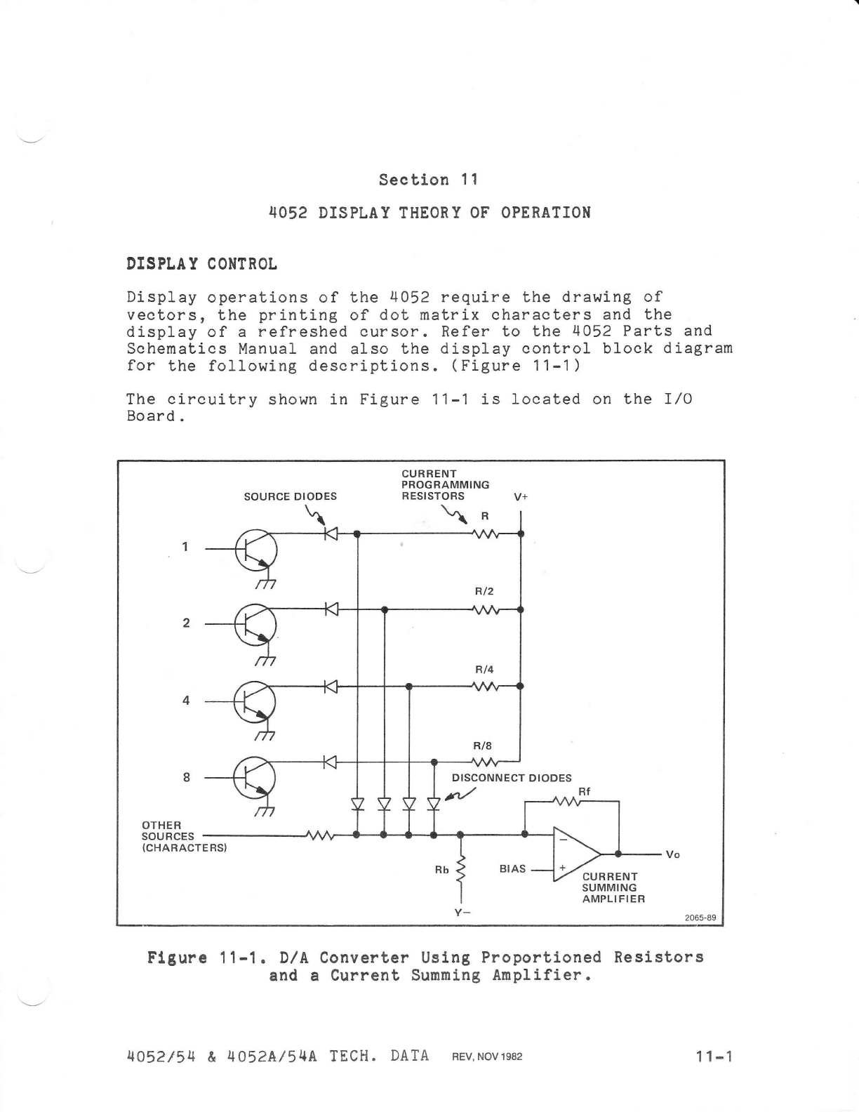
(Figure
11-1)
The
circuitry
shown
in
Figure
11-1
is
located
on
the
I/O
Board.
SOURCE
DIODES
~
2
4
8
OTHER
CURRENT
PROGRAMMING
RESISTORS
v+
"'R
R/2
R/4
R/8
SOURCES
----------~~~~~~~~--.-------~
(CHARACTERS)
Rb
BIAS
y-
Rf
'>-
........
--Vo
CURRENT
SUMMING
AMPLIFIER
2065-89
Figure
11-1.
Of
A
Converter
Using
Proportioned
Resistors
and a
Current
Summing
Amplifier.
4052/54
&
4052A/54A
TECH.
DATA
REV,NOV1982 11-1
4052 DIS
PLA
Y
The
4052
Processor
communicates
with
the
display
control
circuitry
through
a
set
of
peripheral
interface
adapters
(PIAs).
The PIA
output
lines
are
programmed
to
control
the
display
circuitry
as
directed
by
firmware
instruction
se-
quences
contained
in
ROM
(read
only
memory).
The
output
from
the
PI
As
is
changed
from
digital
information
to
analog
information
to
drive
the
deflection
circuitry
of
the
4052.
The
writing
beam
of
the
crt
is
deflected
by
this
analog
information
while
other
signals
from
the
PI
As
turn
the
beam on and
off
to
form
the
written
pattern
on
the
crt
face.
DfA
Operation
The
DIA
converters
change
the
digital
output
data
from
the
system
to
analog
signals
for
use
by
the
display
section.
Refer
to
the
diagram
(Figure
1
1-1).
The
transistors
are
the
outputs
of
TTL
logic.
Resistors
that
are
binary
fractions
of
R (R,
R/2,
R/4,
R/8)
are
current-programming
resistors.
Current
through
R/8
is
eight
times
greater
than
current
through
R.
Current
through
these
resistors
has
two
possible
paths,
through
the
transistor
logic
or
through
the
current
summing
resistor
Rb.
When
transistor
logic
is
on,
output
low,
the
transistor
takes
the
current
from
its
current
programming
resistor,
removing
the
current
from
the
summing
amplifier
input.
The
disconnect
diode
has
reverse
bias
when
the
switching
transistor
is
on.
When
the
transistor
logic
is
off,
output
high,
the
transis-
tor
provides
high
impedance
and
reverse
biases
its
source
diode.
This
causes
the
programming
resistor
current
to
be
summed
by
the
amplifier.
The
output
voltage
from
the
amplifier
is
proportional
to
the
input
current.
When
no
current
comes
through
the
disconnect
diodes
or
other
sources,
the
current
through
Rf
is
equal
to
the
current
through
to
the
operational
amplifier.
As
current
comes
through
the
disconnect
diodes
or
other
sources,
the
current
through
Rf
is
decreased
by
the
total
sum
of
input
currents.
Current
through
Rf
may
even
reverse
in
order
to
maintain
the
junction
voltage
between
Rf and
Rb
at
the
BIAS
level.
11-2
REV, NOV 1982
4052/54
& 4052A/54A
TECH.
DATA
4052
DrSPLA
Y
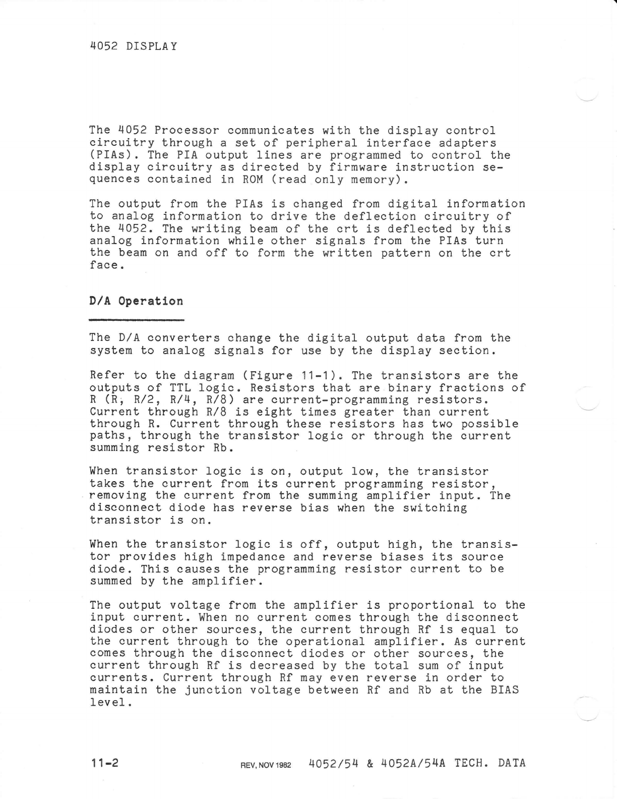
Figure
11-2
shows
the
information
flow
through
D/A
convert-
ers
in
the
4052.
4052
D/A
CONVERTERS
PIA
RESISTORS
i
IX)
v
IX
D/A)
v
=sum
PIA
i IX
CHAR)
RESISTORS
ANALOG
DIGITAL
OUTPUT
INPUT
FROM
PIAs
TO
DISPLAY
PIA
i IV
CHAR)
v
IV
D/A)
PIA
RESISTORS
i IV)
(2065)
2840-48
Figure
11-2.
Data
and
Information
Flow
Through
the
X and Y
Digital-to-Analog
Converters.
4052/54
& 4052A/54A
TECH.
DATA
REV,NOV1982
11-3
4052
DISPLA Y
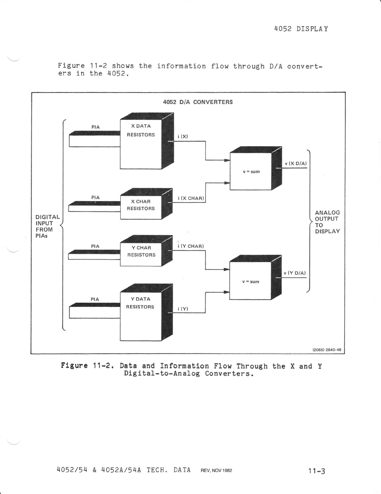
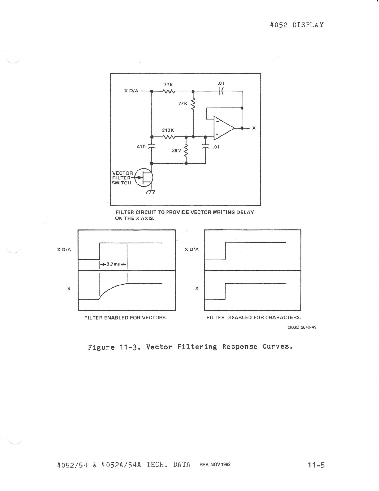
Filter
Operation
When
the
D/A
converters
switch
the
current
source
resistors
in
and
out,
the
output
signal
contains
small
variations
that
need
to
be
filtered
out.
Filtering
is
provided
by
the
RIC
filter
at
the
positive
input
of
the
operational
amplifier
(Figure
11-3).
Also
see
the
appropriate
4052
schematic.
When
the
FET
(field
effect
transistor)
is
conducting,
the
filter
network
is
given
a
ground
reference
and
is
able
to
filter
the
D/A
signal.
When
the
FET
is
off,
the
filter
is
disabled
causing
the
output
voltage
to
directly
follow
the
input
(Figure
11-4B).
Straight
vectors
can
be
drawn
because
both
filters
for
the
X
and
Y
axes
have
matched
filtering
charac-
teristics.
11-4
REV, NOV 1982
4052/54
& 4052A/54A
TECf!.
DATA
X
D/A
X
17K
.01
X
D/A
-
....
-.l\AA,--
......
-----lI---__.
VECTOR
FILTER
SWITCH
17K
>-
......
-X
FILTER
CIRCUIT
TO
PROVIDE
VECTOR
WRITING
DELAY
ON
THE
X
AXIS.
X
D/A
I
1-..3
.7m
s+-
I
/ X I
4052
DISPLA
Y
FI L
TER
ENABLED
FOR
VECTORS.
FI L
TER
DISABLED
FOR
CHARACTERS.
(2065)
2840-49
Figure
11-3.
Vector
Filtering
Response
Curves.
4052/54
&
4052A/54A
TECH. DATA REV,
NOV
1982
11-5
4052
DrSPLA Y
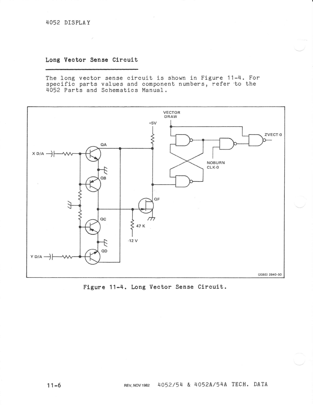
Long
Vector
Sense
Circuit
The
long
vector
sense
circuit
is
shown
in
Figure
11-4.
For
specific
parts
values
and
component
numbers,
refer
-to
the
4052
Parts
and
Schematics
Manual.
X D / A
---1
~-JV\A,---t""""'--f
47
K
-12 V
+5V
VECTOR
DRAW
(2065)
2840-50
Figure
11-4.
Long
Vector
Sense
Circuit.
11-6
REV
, NOV 1982
4052/54
&
4052A/54A
TECH.
DATA
---------------------~~~~
-
--
-
----
4052
DISPLA
Y
This
circuit,
during
static
operation,
has
an
output
voltage
of
near
+5
volts.
None
of
the
transistors
are
conducting.
A
voltage
change
of
more
than
-0.7
volts
on
either
X D/A
or
Y
D/A
line
will
cause
one
of
the
four
transistors
(QA
-
QF)
to
conduct,
and
the
output
voltage
will
drop
to
zero.
The
active
transistor
will
either
ground
the
end
of
the
resistor
corning from
the
+5
volt
line
or
the
end
of
the
resistor
corning from
the
-12
volt
line.
If
the
input
from
the
-12
volt
line
is
brought
up
to
zero,
the
FET, QF,
goes
into
conduction
to
lower
the
input
from
the
+5
volt
line.
Since
the
output
pulse
for
long
vectors
is
only
momentary
due
to
the
small
.001
uf
capacitors,
Ca
and Cb,
the
output
is
saved
by a
nand
gate
flip-flop
during
a
vector
drawing
period.
The
presence
of
a
long
vector
causes
the
NOBURN
CLK-
o
signal
to
be
disabled
before
its
effect
reaches'
the
ZVECT-O
signal
line.
The
ZVECT-O
signal
is
used
to
control
the
Z
axis
writing
beam
during
a
vector
draw
operation.
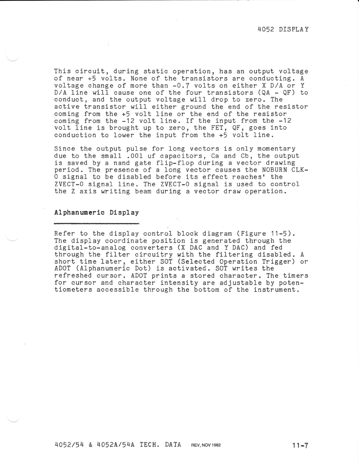
Alphanumeric
Display
Refer
to
the
display
control
block
diagram
(Figure
11-5).
The
display
coordinate
position
is
generated
through
the
digital-to-analog
converters
(X
DAC
and Y
DAC)
and
fed
through
the
filter
circuitry
with
the
filtering
disabled.
A
short
time
later,
either
SOT
(Selected
Operation
Trigger)
or
ADOT
(Alphanumeric
Dot)
is
activated.
SOT
writes
the
refreshed
cursor.
ADOT
prints
a
stored
character.
The
timers
for
cursor
and
character
intensity
are
adjustable
by
poten-
tiometers
accessible
through
the
bottom
of
the
instrument.
4052/54
&
4052A/54A
TECH.
DATA
REV,NOV1982
11-7
PIAs
4052
DrSPLA
Y
>
REG
REG
100s
VIEW
TIMER
X
DAC
Y
DAC
X
LONG
VECTOR
SENSE
Timer
Enable
3.7ms
VECTOR
TIMER
HOLD
MODE
X
Y
Z
Axis
Modulation
for
Short
Vectors
DISPLAY
DEFLECTION
CIRCUITRY
-0
)Q..----d
OSCI
LLATOR
1-----+----_
VIEW
::":':':=':"":"'L-.,..
CURSOR
INTENSITY
TIMER
CHARACTER
INTENSITY
TIM
ER
Refresh
Dot
Character
Dot
Be
am
Control
2286-5
Figure
11-5.
Display
Control
Cirouitry
Blook Diagram.
11-8
REV.
NOV
1982
4052/54
& 4052A/54A
TECH.
DATA
•
4052
DISPLAY
Other
Display
Control
Functions
Refer
to
the
display
cont
r
ol
bloc
k
diagram
(Figure
11-5).
View mode
is
active
wh
en
the
VIEW
signal
is
logically
true.
A View
Mode
Timer
keeps
the
405
2
in
View
Mode
for
100
seconds
following
either
the
closure
of
the
keyboard
SHIFT
key
or
the
display
of
any
new
information
on
the
crt.
The
View
Mode
Timer
disables
the
Hold
Mode
Oscillator.
During
Hold
Mode
operations,
the
VIEW
signal
is
activated
by
a
square
wave
having
a
12.3%
duty
cycle.
The
screen
goes
dark,
but
the
stored
information
is
retained
on
the
crt
phosphor
for
later
viewing.
If
the
system
remains
in
hold
mode
for
more
than
thirty
minutes,
the
screen
is
automatically
erased.
During
hard
copy
activity,
DRBUSY
becomes
true
to
be
sure
that
the
View
flood
guns
are
on
during
the
time
a
hard
copy
is
being
made.
Erasing
the
screen
is
accomplished
by
lowering
the
ERASE-O
line.
DISPLAY
BOARD
The
Display
Board
takes
deflection
and
control
information
from
the
1/0
Board
and
changes
these
signals
into
a
form
usable
by
the
direct
view
storage
tube
(DVST). The
Display
Board
also
uses
signals
from
an
optional
hard
copy
unit
to
copy
the
display
information
from
the
storage
tube
to
paper.
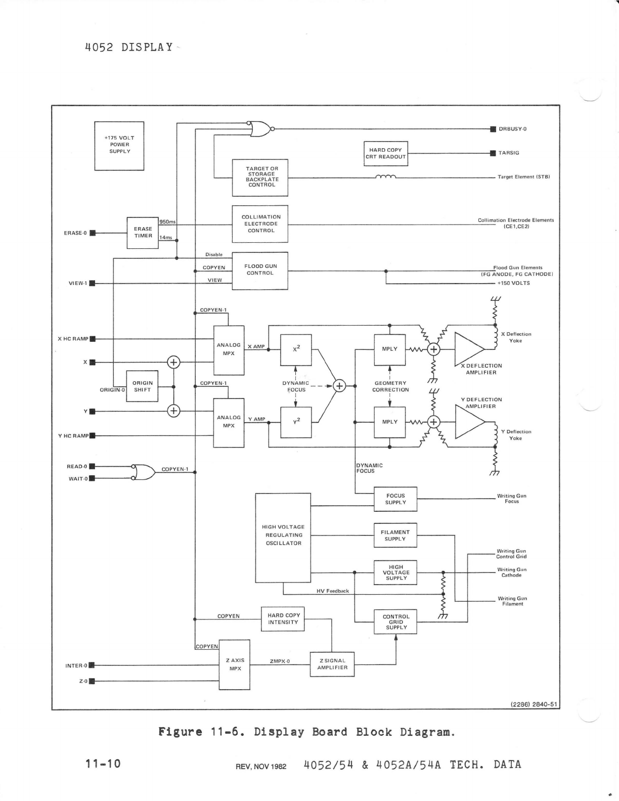
Refer
to
the
block
diagram
of
the
Display
Board
(Figure
11-
6)
and
crt
schematic
(Figure
11-7).
Display
deflection
amplifiers
and
other
analog
crt
control
circuitry
are
on
the
4052
Display
Board.
The
Display
Board
schematics
are
in
the
Parts
and
Schematics
Manual.
The
Display
Board
is
divided
into
three
operational
sections:
•
Deflection
Amplifier
circuitry
•
Storage,
View
and
Erase
circuitry
•
High
Voltage
and
Focus
circuitry
4052 /54 &
4052A/5
4A T
ECH.
D
AT
A
~~~
V'
9
~
11-9
•
4052
DISPLAY
-
+175
VOLT
POWER
SUPPLY
r-
______
-L
__
/~».----------------------------------------------------
...
IIDRBU
SY.O
950ms
ERASE·O =
__
--------i
ERASE
TIMER 114ms
VIEW
·l
=.--+-----------+--"'='---1
X
HCRAMP=
..
--f-----------r----i
ORIGTN:o
ORIGIN
SH
IFT
\..+..1
Y
....
l---------{+
f--+---l
YHCRAMP.-------------+---j
READ
·O
....
-----0,""" COPYEN.l
J
)---"",c...:..=.=--...
WAIT
·O
.-----oL..-/
I
HARD
COPY
~----------
..
II.
TARSIG
CRT
READOUT
rv-vv--T"\
_____________
Target Element
tSTB)
Collimation
Electrode Elements
f---------------------------
ICE1,CE2)
Flood
Gun
Elements
f-------------.-T-----------~IF~G~ANODE,FGCATHODEI
'---------------
+150
VOLTS
T
0f~~
X Deflection
)
Yoke
r--
MPLY
+
, X
DEFLECTION
~
AMPLIF IER
I
GEOMETRY
,
/=MPLIFIER
f--
MPLY
+
~
Y De
fl
ection
CORRrTI0Jt
Y
DEFLECTION
1
~
Yoke
~------------~----~--~
H
IGH
VOLTAGE
REGULATING
OSCILLATOR
I
HV
Feedback
DYNAMIC
FOCUS
J FOCUS
SUPPl
Y
FILAMENT
S
UPP
LY
HIGH
VOLTA
GE
SUPP
LY
l
I
f----------
wri~~:u~un
I
I
I
I
f---+---1f--+---
W~!~~~un
COPYEN
J
HARD
COPY
~
.....
---="--'='---'1
INTENSITY
J
CONTROL
I
rh
GRID
f-------I
SUPPLY
J
INTER
·
O=
..
-----------------i
Z~
~--------------------
------__l
ZAXIS
MPX
ZMPX
·O Z
SIGNAL
AMPLI
FlEA
(2286) 2840-51
Figure
11-6.
Display
Board
Block
Diagram.
11
-1
0 REV, NOV 1982
4052/54
& 4052A/54A
TECH.
DATA
F.G.
ANODE
F.G.
CATHODE
F.G.
HEATER
DEFLECTION
YOKE
+150V
FOCUS
CONTROL
GRID
TARGET
CATHODE
FILAMENT
--+---'
WRITING
GUN
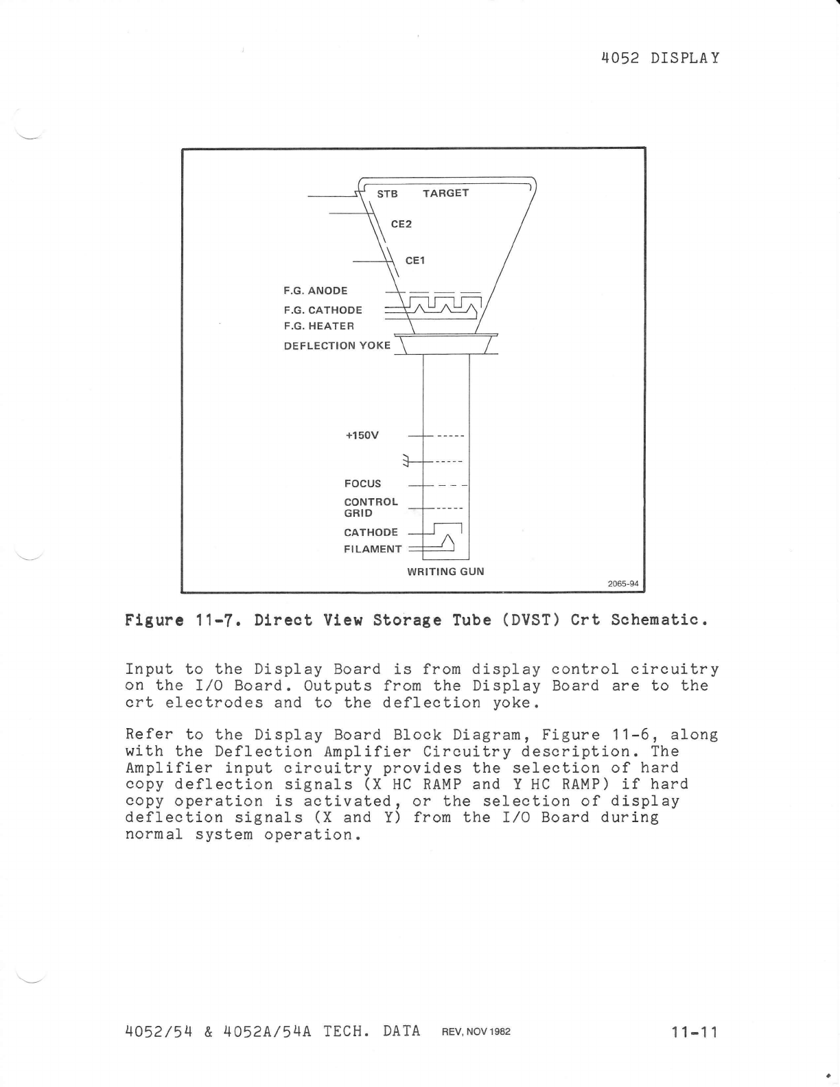
4052
DISPLA
Y
2065-94
Figure
11-7.
Direct
View
Sto~age
Tube
(DVST)
Crt
Schematic.
Input
to
the
Display
Board
is
from
display
control
circuitry
on
the
I/O
Board.
Outputs
from
the
Display
Board
are
to
the
crt
electrodes
and
to
the
deflection
yoke.
Refer
to
the
Display
Board
Block
Diagram,
Figure
11-6,
along
with
the
Deflection
Amplifier
Circuitry
description.
The
Amplifier
input
circuitry
provides
the
selection
of
hard
copy
deflection
signals
(X
HC
RAMP
and
Y
HC
RAMP)
if
hard
copy
operation
is
activated,
or
the
selection
of
display
deflection
signals
(X
and
Y)
from
the
I/O
Board
during
normal
system
operation.
4052/54
&
4052A/54A
TECH.
DATA
REV
,NOV1982
11-11
•
4052
DISPLAY
Refer
to
the
4052
Display
Block
Diagram.
The
deflection
amplifier
circuitry
has
three
circuit
sections:
dynamic
focus,
geometry
correction,
and
deflection
amplifiers.
In
this
circuitry,
the
X
AMP
and
Y
AMP
signals
are
the
primary
deflection
signal
components.
The
Geometry
Correction
section
provides
a
correction
compo-
nent
to
the
deflection
circuitry.
It
compensates
for
the
pincushion
distortion
seen
on
electromagnetic
deflection
systems.
The
amount
of
correction
is
set
by
external
resis-
tors.
Another
amplifier
generates
an
error
(Dynamic
Focus)
signal
which
is
used
to
correct
for
defocusing.
The
defocusing
is
due
to
changes
in
the
length
of
the
writing
beam
as
it
is
deflected.
The
deflection
amplifiers
are
high-gain
current
amplifiers
designed
to
provide
the
necessary
current
in
the
deflection
coils
to
deflect
the
writing
beam.
The
magnetic
field
produced
is
directly
proportional
to
the
current
in
the
deflection
coil
or
yoke.
Defleotion
Amplifier
The
deflection
amplifiers
are
composed
of
an
operational
amplifier
driving
a
complementary
pair
of
cascaded
current
amplifiers.
The X
deflection
amplifier
and Y
deflection
amplifier
have
identical
operation.
Inputs
to
the
operation-
al
amplifier
are
the
sum
of
all
input
signals
incorporated
into
writing
beam
deflection,
the
primary
deflection
signal,
geometry
correction,
position
adjustment
and
gain
adjustment.
The
GAIN
adjustment
provides
a
feedback
voltage
from
the
coil
current
sensing
resistors
to
set
the
amplifier
gain.
An
origin
shift
circuit
is
included
to
make
certain
that
the
screen
is
not
continually
written
in
the
same
spots.
To
keep
this
from
happening,
the
writing
area
is
shifted
slightly
each
time
the
screen
is
erased.
The
origin
shift
circuitry
is
made up
of
a
three-bit
binary
counter
and
a
small
range
digital
to
analog
converter.
It
supplies
small
amounts
of
current
to
the
X
and
Y
axis
deflection
signals.
The
counter
is
incremented
each
time
the
screen
is
erased.
The
origin
shift
circuitry
is
part
of
the
input
multiplexer
chip.
11-12
~~NOV1~2
4052/54
&
4052A/54A
TECH.
DATA
•
4052
DISPLAY
Storage
and
Erase
Control
Circuits
Refer
to
the
Display
Board
Block
Diagram
(Figure
11-6).
Target
control,
collimation
control,
and
flood
gun
control
circuits
are
switchable
high
voltage
sources.
Depending
upon
the
state
of
a
logic
input
signal
the
output
voltage
acquires
one
of
two
stable
voltage
levels.
One
level
erases
the
screen
and
the
other
level
allows
the
screen
to
be
written
on .
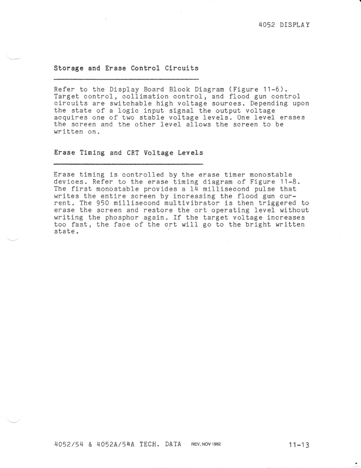
Erase
Timing and
CRT
Voltage
Levels
Erase
timing
is
controlled
by
the
erase
timer
monostable
devices.
Refer
to
the
erase
timing
diagram
of
Figure
11-8.
The
first
monostable
provides
a
14
millisecond
pulse
that
writes
the
entire
screen
by
increasing
the
flood
g~n
cur-
rent.
The
950
millisecond
multivibrator
is
then
triggered
to
erase
the
screen
and
restore
the
crt
operating
level
without
writing
the
phosphor
again.
If
the
target
voltage
increases
too
fast,
the
face
of
the
crt
will
go
to
the
bright
written
state.
4052/
54
& 4052A/5J:lA
TECH.
DATA
REV,NOV1982
11-
13
4052
DISPLA
Y
~1"1---------960ms-------~~1
~L
__
________________________
~I
-------
..
_ ... 1
(ERASE
INTERVAL
) .
TTY
LOW
f--
550
to
750ms
~I
+120
to
+280V--
0
-
v
-'
1
/
__
.:..----------
+55
to
+115V---...,
COLLIMATOR
(C
E)
I
+35V
L
__
----!....
___
__
_______
---'
"'OVlJ
FLOOD
GUN
ANODE
OV
--l
1-14ms
FLOOO
GUN
CATHo::Jj
-150V
(2286)
2840
-
52
Fisure
11-8.
Erase Timing
and
Voltage
Waveforms.
The
crt
operation
level,
as
established
by
the
target
control
circuitry,
causes
crt
information
to
run
together
when
set
too
high.
Information
fades
away
if
the
crt
operating
level
is
set
too
low.
The
operating
voltages
for
the
particular
crt
in
the
instrument
are
specified
on a
service
tag
within
the
instrument.
The
operating
voltages
for
a new
crt
will
be
specified
in
the
accompanying
informa-
tion.
Collimation
operating
level,
as
established
by
the
collima-
tion
control
circuitry,
determines
the
uniformity
of
flood
gun
intensity
across
the
face
of
the
crt.
If
the
voltage
is
too
high,
information
on
the
outer
portions
of
the
c
rt
will
tend
to
run
togeth
er
and
excessive
display
power
will
be
used.
If
the
voltage
is
too
low,
information
at
center
of
the
crt
will
run
together
and
information
on
the
outside
edges
will
tend
to
fade
away.
11-14
REV,
NOV
1982
4052/54
&
4052A/54A
TECH. DATA
.~
4052
DrSPLA
Y
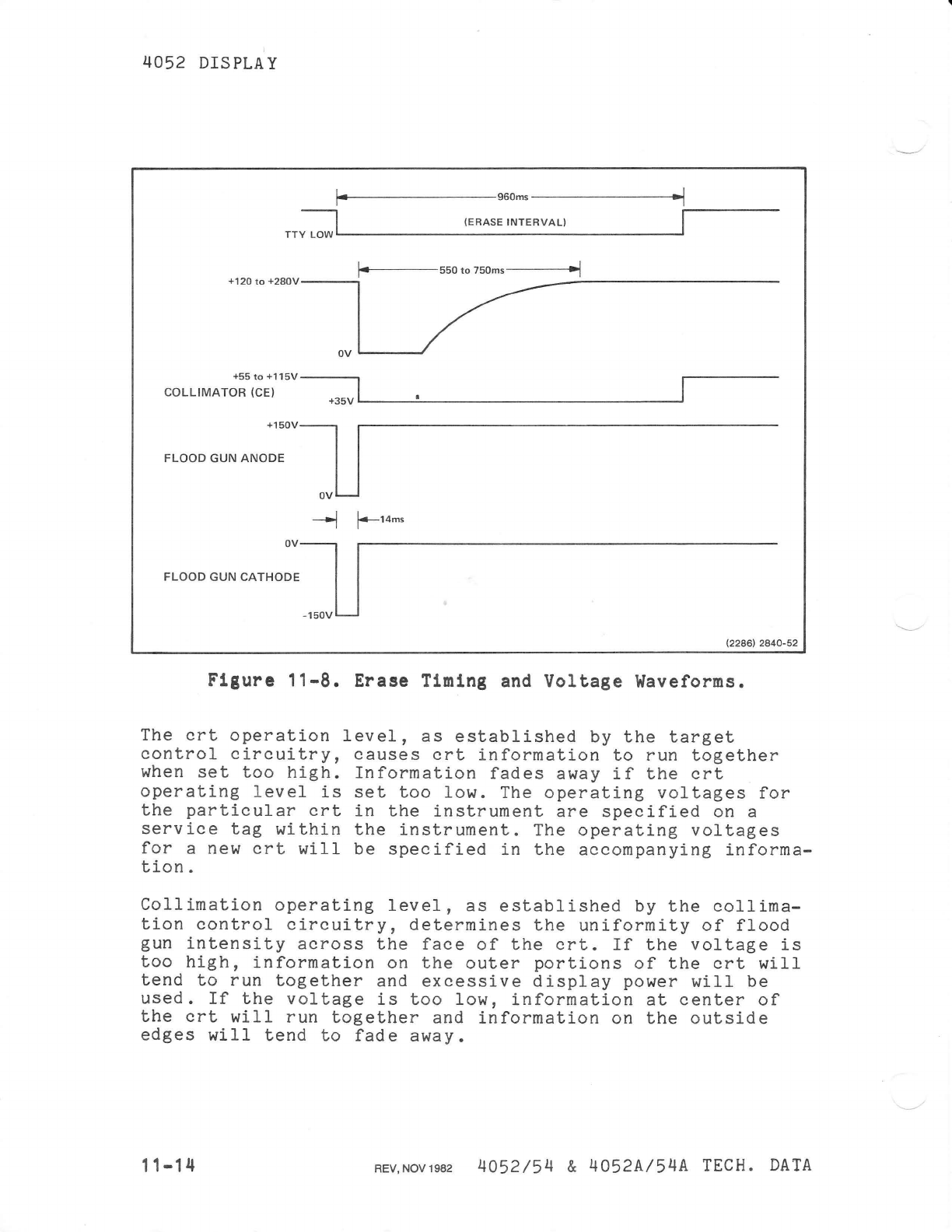
Storage
Backplate
Control
The
Storage
Backplate
Control
amplifier
controls
the
voltage
at
the
storge
backplate
of
the
crt.
(The
Backplate
is
also
called
the
Target.)
A
simplified
circuit
is
shown
in
Figure
11-9.
Normal
output
of
inverter
Ul
is
grounded.
During
the
erase
cycle,
the
output
goes
to
an
open
collector
state
placing
the
positive
timing
capacitor
lead
at
+9
volts
through
diode
CR4.
During
normal
operation,
the
voltage
across
the
timing
capacitor
(C3)
is
approximately
zero.
During
the
erase
cycle,
the
positive
side
of
the
capacitor
is
lifted
to
+9
volts
and
the
negative
lead
charges
toward
zero
through
R2.
01
buffers
the
voltage
from
the
timing
circuit
and
provides
the
necessary
current
to
the
voltage
regulating
circuitry.
At
the
end
of
the
erase
cycle,
the
positive
capacitor
lead
is
brought
to
zero
and
the
negative
lead
discharges
to
ground
through
diode
CR5.
+320V
+175
R3
R1
;-----STB
AMPLIFIER
C3
01
~-~~
OP
LEVEL
950
MS
CR4
CRS
R2
+9V
-12V
2840-53
Figure
11-9.
Simplified
Backplate
Amplifier.
4052/54
&
4052A/54A
TECH.
DATA
REV
,NOV1982
11-15
4052
DISPLA
Y
The
beginning
of
the
erase
cy
c
le
makes
about
a +5
volt
change
on
the
OP
LEVEL
adjustment
resistor.
Th
is
causes
U3
to
turn
on
hard,
grounding
the
STB
electrode
on
the
crt.
The
STB
electrode
remains
grounded
until
the
timing
current
through
01
drops
enough
to
allow
the
output
voltage
from
U3
to
rise
again.
Two
transistors,(U3),
are
required
to
drive
the
STB
line.
They
are
biased
so
that
their
electrical
breakdown
voltages
are
not
exceeded
by
the
+320
volt
unregulated
supply.
Collimation
Control
Normal
Collimation
Control
operating
range
is
established
by
the
CE
adjustment.
During
the
erase
cycle,
the
collimation
amplifier
turns
on
and
the
output
voltage
on
CE1
and
CE2
drops
to
+5
volts.
During
hard
copy
operations,
the
collimation
amplifier
conduction
is
turned
off,
allowing
CE1
and
CE2
to
go
positive.
The
amplifier
supply
is
the
+185
volt
unregulated
supply,
so
that
voltage
appears
at
CE1
and CE2.
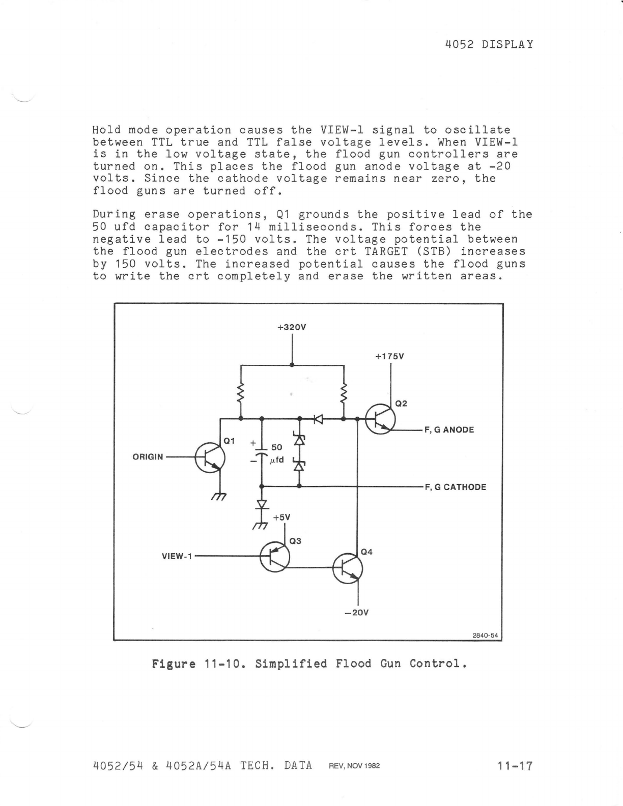
Flood
Gun
Control
Normal
operation
has
the
VIEW-1
signal
at
a
high
voltage
level.
This
causes
the
flood
gun
controllers,
03
and
04,
to
be
off
(Figure
11-10).
The
flood
gun
anode
then
has
a
voltage
of
+150
volts
regulated
by
zener
diodes.
The
flood
gun
cathode
is
near
zero.
11-16
REV,
NOV
1982
4052/54
& 4052A/54A
TECH.
DATA
4052
DISPLA Y
Hold
mode
operation
causes
the
VIEW-l
signal
to
oscillate
between
TTL
true
and
TTL
false
voltage
levels.
When
VIEW-l
is
in
the
low
voltage
state,
the
flood
gun
controllers
are
turned
on.
This
places
the
flood
gun
anode
voltage
at
-20
volts.
Since
the
cathode
voltage
remains
near
zero,
the
flood
guns
are
turned
off.
During
erase
operations,
Q1
grounds
the
positive
lead
of
the
50
ufd
capacitor
for
14
milliseconds.
This
forces
the
negative
lead
to
-150
volts.
The
voltage
potential
between
the
flood
gun
electrodes
and
the
crt
TARGET
(STB)
increases
by
150
volts.
The
increased
potential
causes
the
flood
guns
to
write
the
crt
completely
and
erase
the
written
areas.
+320V
+175V
~--F,
G
ANODE
ORIGIN
--+-I
'--~~---~-----F,GCATHODE
VIEW-1
-----+--1
-20V
2840-54
Figure
11-10.
Simplified
Flood
Gun
Control.
4052/54
&
4052A/54A
TECH.
DATA
REV,NOV1982
11-17
4052
DISPLA Y
HIGH
VOLTAGE
CIRCUITS
The
high
voltage
circuits
provide
voltages
for
the
focus
electrodes
and
writing
gun
electrodes
of
the
crt.
The
writing
gun
elements
operate
at
-4,000
volts
dc.
Power
to
the
high
voltage
circuits
is
generated
using
a
flyback
transformer
driven
by
a
regulated
blocking
oscillator.
Z
axis
control
is
provided
by
coupling
a
voltage
through
a
capacitor
to
turn
on
the
writing
beam.
With
no
Z
axis
input,
the
writing
beam
is
biased
off.
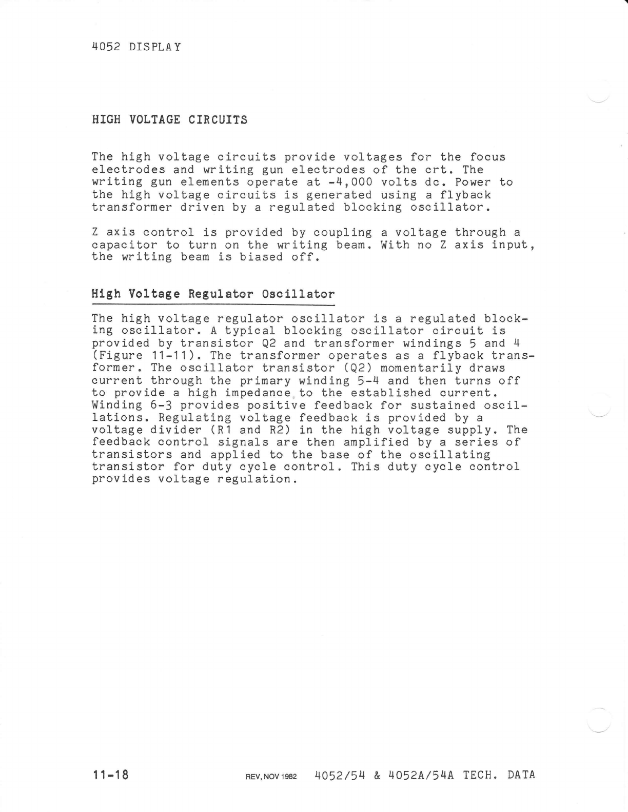
High
Voltage
Regulator
Oscillator
The
high
voltage
regulator
oscillator
is
a
regulated
block-
ing
oscillator.
A
typical
blocking
oscillator
circuit
is
provided
by
transistor
02
and
transformer
windings
5
and
4
(Figure
11-11).
The
transformer
operates
as
a
flyback
trans-
former.
The
oscillator
transistor
(02)
momentarily
draws
current
through
the
primary
winding
5-4
and
then
turns
off
to
provide
a
high
impedance
to
the
established
current.
Winding
6-3
provides
positive
feedback
for
sustained
oscil-
lations.
Regulating
voltage
feedback
is
provided
by
a
voltage
divider
(R1
and
R2)
in
the
high
voltage
supply.
The
feedback
control
signals
are
then
amplified
by
a
series
of
transistors
and
applied
to
the
base
of
the
oscillating
transistor
for
duty
cycle
control.
This
duty
cycle
control
provides
voltage
regulation.
11-18
REV, NOV 1982
4052/54
&
4052A/54A
TECH.
DATA
4052
DISPLA Y
2840-55
Figure
11-11.
High
Voltage
Oscillator.
High
Voltage
Supply
The
source
for
the
high
voltage
supply
is
winding
10-2
of
the
flyback
transformer.
This
ac
voltage
goes
to
a
voltage
doubler,
as
shown
in
Figure
11-11.
High
voltage
feedback
bias
is
determined
by
the
HV
ADJ
resistor
and
the
associated
resistance
network.
The
output
from
this
divider
is
fed
back
to
the
high
voltage
oscillator
to
establish
the
cathode
voltage
at
-4000
V.
4052/54
&
4052A/54A
TECH.
DATA
REV,NOV1982
11-19
4052
DISPLAY
Focus
Supply
The
focus
supply
consists
of
an
adjustable
gain
amplifier
for
dynamic
focus
and
an
isolated
focus
supply
from
the
high
voltage
flyback
transformer.
The
isolated
supply
uses
the
output
of
the
dynamic
focus
amplifier
as
its
voltage
refer-
ence.
A
fixed
negative
value
as
determined
by
the
FOCUS
adjustment
is
subtracted
from
the
dynamic
focus
amplifier
output
before
driving
the
crt
focus
electrode.
The
gain
of
the
dynamic
focus
amplifier
is
determined
by
the
DYNAMIC
FOCUS
adjustment.
Filament
Supply
Voltage
reference
for
the
writing
beam
filament
supply
is
the
-4,000
volt
cathode
voltage.
The
filament
supply
pro-
vides
alternating
current
to
the
filaments
from
a
winding
on
the
high
voltage
transformer.
This
winding
is
elevated
to
-
4000
volts.
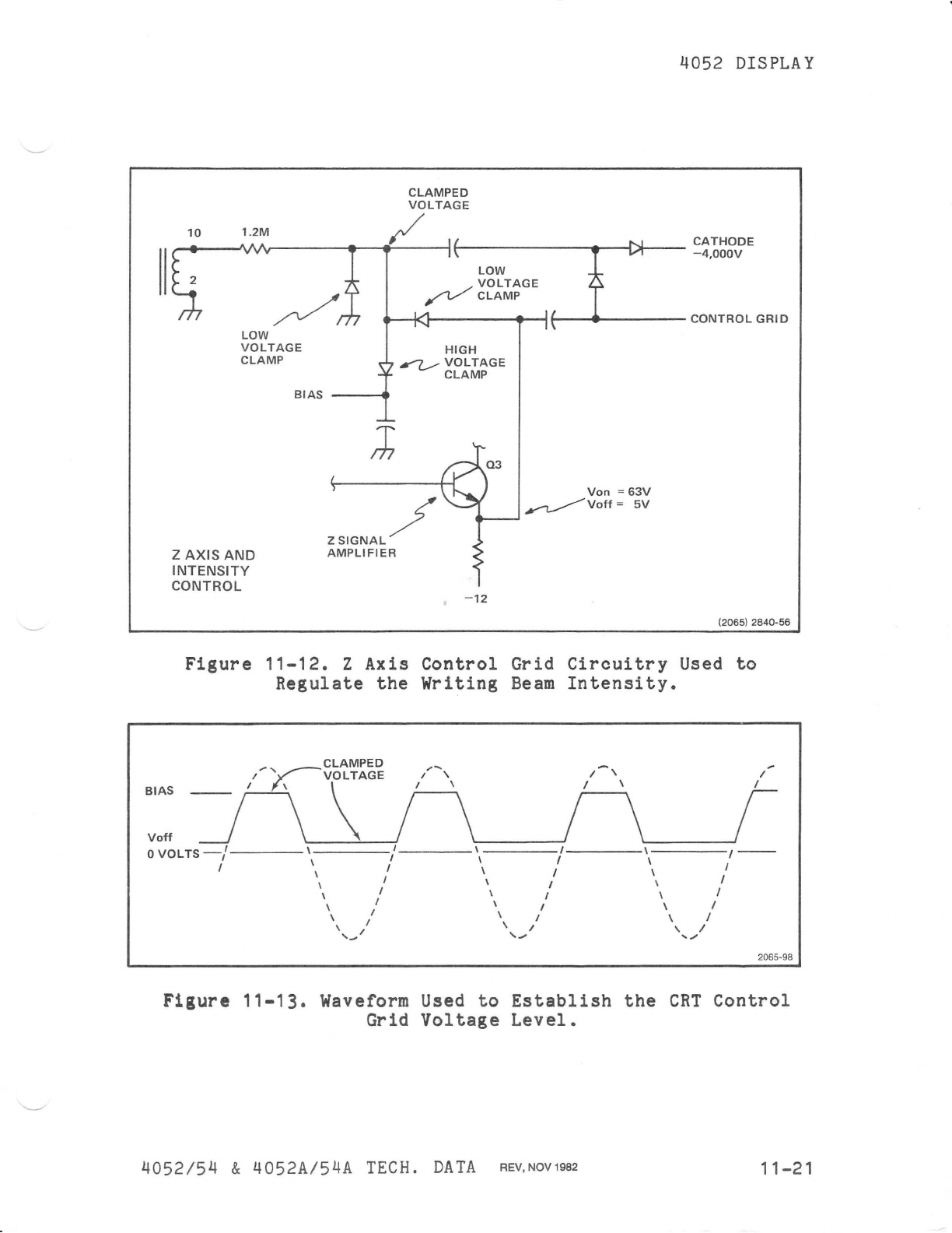
Control
Grid
Supply
A
simplified
diagram
of
the
control
grid
supply
is
shown
in
Figure
11-12.
The
supply
voltage
driving
the
rectifier
circuitry
of
the
control
grid
supply
is
a
clamped
waveform
as
shown
in
Figure
11-13.
The
1.2
megohm
resistor
enables
the
clamping
process
to
occur
by
limiting
available
current
from
the
transformer.
The BIAS
voltage
is
adjusted
to
ensure
there
is
enough
negative
potential
on
the
control
grid
to
keep
the
writing
beam
turned
off
when
the
Z
axis
is
not
active.
When
the
Z
axis
turns
on,
a
positive
voltage
is
coupled
through
a
capacitor
to
the
control
grid,
turning
on
the
crt
writing
beam.
11-20
REV, NOV 1982
4052/54
&
4052A/54A
TECH.
DATA
II
10
1.2M
2
LOW
VOLTAGE
CLAMP
Z
AXIS
AND
INTENSITY
CONTROL
BIAS
CLAMPED
VOLTAGE
,/
LOW
~VOLTAGE
CLAMP
HIGH
~VOLTAGE
CLAMP
ZSIGNAL/
AMPLIFIER
-12
Von
=
63V
~Voff
=
5V
4052
DISPLA
Y
CATHODE
-4
.
000V
CONTROL
GRID
(2065)
2840-56
Figure
11-12.
Z
Axis
Control
Grid
Circuitry
Used
to
Regulate
the
Writing
Beam
Intensity.
--
I
I
Voff
OVOLTS-/
I I I \
I--
I I \ I \
I I \ I \ I
\ I \ I \ I
I I \ I \ I
\ I I I \ I
\ I \ I \ /
I
, \ I \ /
'
....
I
'---
...."
2065-98
Figure
11-13.
Waveform Used
to
Establish
the
CRT
Control
Grid
Voltage
Level.
4052/54
&
4052A/54A
TECH. DATA
REV.
NOV
1982
11-21
4052
DISPLA
Y
Intensity
Control
and
Z
Signal
Amplifier
Refer
to
the
Simplified
Z
Axis
and
Intensity
Control
Diagram
(Figure
11-12).
Intensity
Control
Circuitry
is
a
regulated
voltage
source
referenced
to
the
+175
volt
power
supply.
Output
of
the
supply
at
transistor
Q3
is
normally
63
volts.
During
hard
copy
operations,
the
voltage
is
determined
by
the
HARD
COPY
INTENSITY
adjustment
.
The Z
signal
amplifier
normally
has
an
output
of
5
volts.
The Z
MPX-O
signal
is
at
a
TTL
high
voltage.
When
Z
MPX-O
goes
low
to
turn
on
the
writing
beam,
Q3
turns
off
and
causes
the
output
voltage
to
go
to
the
voltage
established
by
the
intensity
control
amplifier,
normally
63
volts.
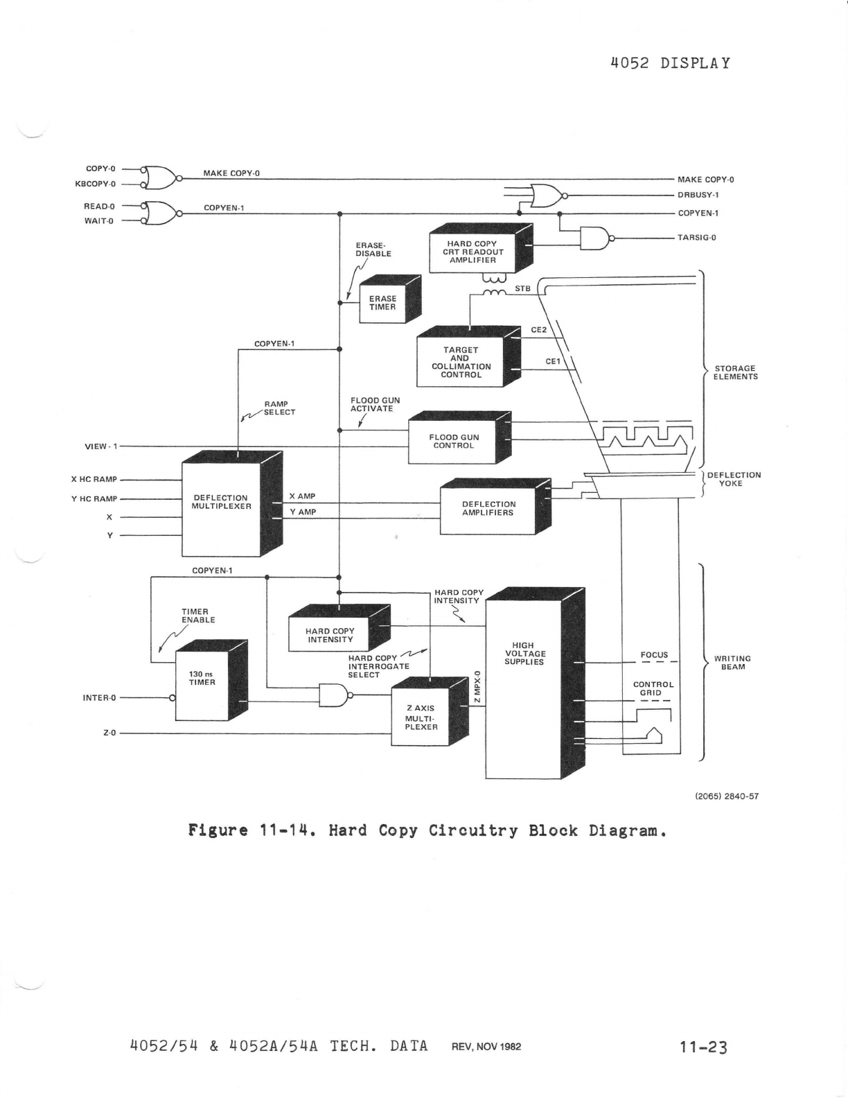
HARD
COpy
OPERATIONS
Hard
copy
signals
and
their
influence
are
shown
in
the
block
diagram
of
Figure
11-14.
The
related
schematics
are
found
in
the
4052
Parts
and
Schematics
Manual.
11-22
REV,
NOV
1982
4052/54
& 4052A/54A
TECH.
DATA
4052
DISPLA
Y
copy
-a
KBCOPY-O
~
MAKE
copy-a
~~~~~~~~----------------------------------------------------------------MAKECOPY
-
O
):>---------------
DRBUSY-l
READ
-a
WAIT
-a
x>
__
~CO~P~Y~E~N~
-
I~
______
__
____
-.
__________________________
~~
____
~---------------COPYEN
-
I
COPYEN-l
RAMP
~SELECT
FLOOD
GUN
ACTIVATE
I
TARGET
AND
COLLIMATION
CONTROL
FLOOD
GUN
VIEW
-
I--------~~~iiiiliiiiiii--------l1--
--
----~----C-O-NT-R-O-L--~~
XHCRAMP--------~
YHCRAMP--------~
x
Y
--------~
DEFLECTION
MUL
TIPLEXER
COPY EN -I
TIMER
ENABLE
~,...-
INTER
-a --------0
130
ns
TIMER
DEFLECTION
AMPLIFIERS
..--------------.
HARD
COPY,.iIIIIIII
•••••
,.........
INTE~ITY
HARD
COPY
INTENSITY
HARDCOPY~
INTERROGATE
SELECT
HIGH
VOLTAGE
SUPPLI
ES
ZOO
--------
--
----------------------------------1
ZAXIS
MULTI
-
PLEXER
p--------
TARSIG
-O
FOCUS
CONTROL
GRID
STORAGE
ELEMENTS
WRITING
BEAM
(2065)
2840
-57
Figure
11-1Q.
Hard
Copy
Circuitry
Block
Diagram.
4052/54
& 4052A/54A
TECH.
DATA
REV,
NOV
1982
11-23
4052
DISPLA Y
Hard
copy
operations
can
be
started
any
of
three
ways:
11-2lJ
1)
Press
the
MAKE
COPY
button
on
the
keyboard.
2)
Execute
a
COPY
command.
3)
Press
the
COPY
button
on
the
hard
copy
unit.
In
each
case,
the
MAKE
COPY-O
signal
is
asserted.
When
an
attached
hard
copy
unit
receives
the
MAKE
COPY-O
signal,
it
issues
a
READ-O
or
WAIT-O
to
the
calling
device.
READ
means
that
the
hard
copy
unit
is
busy
making
a
copy
of
the
display.
WAIT
means
that
the
hard
copy
unit
has
a
multiplexer
option
and
is
currently
busy
making
a
copy
from
another
display.
Upon
receiving
READ-O
or
WAIT-O
from
a
hard
copy
unit,
the
Copy
Enable
(COPYEN-l)
signal
is
sent
high.
The
COPYEN
signal
sends
a
display
busy
condi-
tion
(DRBUSY)
back
t o
the
Graphic
Computing
System.
It
also
prevents
the
display
from
being
erased.
The
HC
RAMP
signals
provide
the
writing
beam
deflection
voltage.
The
COPYEN
signal
establishes
the
writing
beam
intensity
used
for
display
interrogation
pulses.
It
also
enables
Z
axis
display
interroga-
tion
pulses
(INTER-O/C)
to
be
received
from
the
hard
copy
unit.
Hard
copy
information
is
read
from
the
face
of
the
crt
by
using
a
pulsed
writing
beam
of
low
intensi-
ty.
Whenever
the
writing
beam
touches
a
written
area
of
the
storage
backplate
(target)
of
the
crt,
there
is
an
increase
in
current.
This
current
is
sensed
as
a
differential
voltage
on
the
output
of
a
pulse
transformer
and
amplified
by
the
hard
copy
Amplifier
circuitry.
Target
signal
i
nformation
is
then
placed
on
the
TARSIG
signal
line.
The
THRESHOLD
adjustment
determines
t he
signal
l
ev-
el
used
to
discriminate
between
bright
and
dar
k
port
i
ons
of
the
c r t .
REV,
NOV
1982 40
52/54
& 4052A/54A
TECH.
DATA
