Electronic Circuits: Fundamentals And Applications, Third Edition A Guide To Circuits
User Manual: Pdf
Open the PDF directly: View PDF ![]() .
.
Page Count: 441 [warning: Documents this large are best viewed by clicking the View PDF Link!]
- Front cover
- Electronic circuits: Fundamentals and applications
- Copyright page
- Contents
- Preface
- A word about safety
- 1 Electrical fundamentals
- Fundamental units
- Derived units
- Measuring angles
- Electrical units and symbols
- Multiples and sub-multiples
- Exponent notation
- Multiplication and division using exponents
- Conductors and insulators
- Voltage and resistance
- Ohm’s Law
- Resistance and resistivity
- Energy and power
- Electrostatics
- Force between charges
- Electric fields
- Electric field strength
- Permittivity
- Electromagnetism
- Force between two current-carrying conductors
- Magnetic fields
- Magnetic field strength
- Magnetic circuits
- Reluctance and permeability
- B–H curves
- Circuit diagrams
- Practical investigation
- Important formulae introduced in this chapter
- Symbols introduced in this chapter
- Problems
- 2 Passive components
- Resistors
- Preferred values
- Power ratings
- Resistor markings
- BS 1852 coding
- Series and parallel combinations of resistors
- Resistance and temperature
- Thermistors
- Light-dependent resistors
- Variable resistors
- Capacitors
- Capacitance
- Charge, capacitance and voltage
- Energy storage
- Capacitance and physical dimensions
- Capacitor specifications
- Capacitor markings
- Series and parallel combination of capacitors
- Variable capacitors
- Inductors
- Inductance
- Energy storage
- Inductance and physical dimensions
- Inductor specifications
- Inductor markings
- Series and parallel combinations of inductors
- Variable inductors
- Surface mounted components (SMC)
- Practical investigation
- Important formulae introduced in this chapter
- Symbols introduced in this chapter
- Problems
- 3 D.C. circuits
- 4 Alternating voltage and current
- Alternating versus direct current
- Waveforms and signals
- Frequency
- Periodic time
- Average, peak, peak-peak, and r.m.s. values
- Reactance
- Capacitive reactance
- Inductive reactance
- Impedance
- Power factor
- L–C circuits
- L–C–R circuits
- Resonance
- Quality factor
- Transformers
- Voltage and turns ratio
- Practical investigation
- Important formulae introduced in this chapter
- Symbols introduced in this chapter
- Problems
- 5 Semiconductors
- Semiconductor diodes
- Diode types
- Zener diodes
- Variable capacitance diodes
- Thyristors
- Triacs
- Light emitting diodes
- Diode coding
- Bipolar junction transistors
- BJT operation
- Bipolar transistor characteristics
- Current gain
- Field effect transistors
- FET characteristics
- JFET parameters
- Transistor packages
- Transistor coding
- Integrated circuits
- IC packages
- Practical investigation
- Important formulae introduced in this chapter
- Symbols introduced in this chapter
- Problems
- 6 Power supplies
- Rectifiers
- Reservoir and smoothing circuits
- Improved ripple filters
- Full-wave rectifiers
- Bi-phase rectifier circuits
- Bridge rectifier circuits
- Voltage regulators
- Practical power supply circuits
- Voltage multipliers
- Switched mode power supplies
- Practical investigation
- Important formulae introduced in this chapter
- Symbols introduced in this chapter
- Problems
- 7 Amplifiers
- Types of amplifier
- Gain
- Class of operation
- Input and output resistance
- Frequency response
- Bandwidth
- Phase shift
- Negative feedback
- Transistor amplifiers
- Equivalent circuits
- Common-emitter input resistance (h[sub(ie)])
- Common-emitter current gain (h[sub(ie)])
- h-parameter equivalent circuit for a transistor in common-emitter mode
- Voltage gain
- Bias
- Predicting amplifier performance
- Practical amplifier circuits
- Multi-stage amplifiers
- Power amplifiers
- Practical investigation
- Important formulae introduced in this chapter
- Symbols introduced in this chapter
- Problems
- 8 Operational amplifiers
- Symbols and connections
- Operational amplifier parameters
- Operational amplifier characteristics
- Operational amplifier applications
- Gain and bandwidth
- Inverting amplifier with feedback
- Operational amplifier configurations
- Operational amplifier circuits
- Positive versus negative feedback
- Multi-stage amplifiers
- Practical investigation
- Important formulae introduced in this chapter
- Symbol introduced in this chapter
- Problems
- 9 Oscillators
- Positive feedback
- Conditions for oscillation
- Ladder network oscillator
- Wien bridge oscillator
- Multivibrators
- The astable multivibrator
- Other forms of astable oscillator
- Single-stage astable oscillator
- Crystal controlled oscillators
- Practical oscillator circuits
- Practical investigation
- Symbol introduced in this chapter
- Important formulae introduced in this chapter
- Problems
- 10 Logic circuits
- Logic functions
- Switch and lamp logic
- AND logic
- OR logic
- Logic gates
- Combinational logic
- Bistables
- R-S bistables
- D-type bistables
- J-K bistables
- Integrated circuit logic devices
- Date codes
- Logic levels
- Noise margin
- Practical investigation
- Symbols introduced in this chapter
- Important formulae introduced in this chapter
- Problems
- 11 Microprocessors
- Microprocessor systems
- Single-chip microcomputers
- Microcontrollers
- PIC microcontrollers
- Programmed logic devices
- Programmable logic controllers
- Microprocessor systems
- Data types
- Data storage
- The microprocessor
- Microprocessor operation
- A microcontroller system
- Practical investigation
- Symbols introduced in this chapter
- Problems
- 12 The 555 timer
- 13 Radio
- The radio frequency spectrum
- Electromagnetic waves
- Frequency and wavelength
- A simple CW transmitter and receiver
- Morse code
- Modulation
- Demodulation
- An AM transmitter
- An FM transmitter
- A tuned radio frequency (TRF) receiver
- A superhet receiver
- RF amplifiers
- AM demodulators
- Aerials
- Impedance and radiation resistance
- Radiated power and efficiency
- Aerial gain
- The Yagi beam aerial
- Practical investigation
- Formulae introduced in this chapter
- Problems
- 14 Test equipment and measurements
- Meters
- Multi-range meters
- Displays
- Loading
- Sensitivity
- Digital multi-range meters
- Using an analogue multi-range meter
- Using a digital multi-range meter
- Connecting a meter into a circuit
- The oscilloscope
- Using an oscilloscope
- Connecting an oscilloscope into a circuit
- Checking distortion
- Checking frequency response
- Measuring pulse parameters
- Practical investigation
- Formulae introduced in this chapter
- Problems
- 15 Fault finding
- Safety considerations
- Approach to fault finding
- Transistor faults
- Integrated circuit faults
- Diode testing
- Diode ‘go/no-go’ checks
- Bipolar transistor ‘go/no-go’ checks
- Bipolar transistor current gain checks
- A transistor/diode checker
- Logic circuit faults
- Logic probes
- Logic pulsers
- Practical investigation
- Problems
- 16 Sensors and interfacing
- 17 Circuit simulation
- 18 The PIC microcontroller
- 19 Circuit construction
- Circuit construction methods
- Using matrix boards and stripboards
- Stripboard layout techniques
- Using printed circuits
- PCB CAD packages
- Connectors
- Enclosures
- Solder and soldering technique
- Safety when soldering
- Soldering and desoldering techniques
- Component removal and replacement
- Heatsinks
- Practical heatsink arrangements
- Semiconductor mounting arrangements
- A practical example
- Practical investigation
- Problems
- Appendix 1 Student assignments
- Appendix 2 Revision problems
- Appendix 3 Answers to problems
- Appendix 4 Pin connections
- Appendix 5 1N4148 data sheet
- Appendix 6 2N3904 data sheet
- Appendix 7 Decibels
- Appendix 8 Mathematics for electronics
- Appendix 9 Useful web addresses
- Index

Electronic Circuits: Fundamentals and
Applications
This page intentionally left blank

Third Edition
Michael Tooley BA
Formerly Vice Principal
Brooklands College of Further and Higher Education
Electronic Circuits: Fundamentals and
Applications

Newnes is an imprint of Elsevier
Linacre House, Jordan Hill, Oxford OX2 8DP, UK
30 Corporate Drive, Suite 400, Burlington MA 01803, USA
First published 2006
Copyright © 2006, Mike Tooley. Published by Elsevier Ltd. All rights reserved
The right of Mike Tooley to be identified as the author of this work has been asserted in accordance with the
Copyright, Designs and Patents Act 1988
No part of this publication may be reproduced, stored in a retrieval system or transmitted in any form or by any
means electronic, mechanical, photocopying, recording or otherwise without the prior written permission of the
publisher
Permission may be sought directly from Elsevier’s Science & Technology Rights Department in Oxford, UK:
phone (+44) (0) 1865 843830; fax (+44) (0) 1865 853333; email: permissions@elsevier.com. Alternatively you
can submit your request online by visiting the Elsevier web site at http://elsevier.com/locate/permissions, and
selecting Obtaining permission to use Elsevier material
Notice
No responsibility is assumed by the publisher for any injury and/or damage to persons or property as a matter of
products liability, negligence or otherwise, or from any use or operation of any methods, products, instructions
or ideas contained in the material herein. Because of rapid advances in the medical sciences, in particular,
independent verification of diagnoses and drug dosages should be made
British Library Cataloguing in Publication Data
Acatalogue record for this book is available from the British Library
Library of Congress Cataloging-in-Publication Data
Acatalog record for this book is available from the Library of Congress
ISBN-13: 978-0-75-066923-8
ISBN-10: 0-75-066923-3
Typeset by the author
Printed and bound in Great Britain
For information on all Newnes publications visit our website at
www.books.elsevier.com

Contents
Preface vii
Aword about safety ix
1Electrical fundamentals 1
2Passive components 21
3D.C. circuits 49
4Alternating voltage and current 69
5Semiconductors 87
6Power supplies 115
7 Amplifiers 131
8Operational amplifiers 157
9Oscillators 171
10 Logic circuits 183
11 Microprocessers 199
12 The 555 timer 217
13 Radio 227
14 Test equipment and measurements 245
15 Fault finding 273
16 Sensors and interfacing 287
17 Circuit simulation 303
18 The PIC microcontroller 313
19 Circuit construction 327
Appendix 1 Student assignments 361
Appendix 2 Revision problems 364
Appendix 3 Answers to problems 374
Appendix 4 Pin connections 377
Appendix 5 1N4148 data sheet 379
Appendix 6 2N3904 data sheet 382
Appendix 7 Decibels 388
Appendix 8 Mathematics for electronics 390
Appendix 9 Useful web addresses 415
Index 417
This page intentionally left blank

Preface
This is the book that I wish I had when I first
started exploring electronics nearly half a century
ago. In those days, transistors were only just
making their debut and integrated circuits were
completely unknown. Of course, since then much
has changed but, despite all of the changes, the
world of electronics remains a fascinating one.
And, unlike most other advanced technological
disciplines, electronics is still something that you
can ‘do’ at home with limited resources and with a
minimal outlay. A soldering iron, a multi-meter,
and a handful of components are all that you need
to get started. Except, of course, for some ideas to
get you started—and that’s exactly where this book
comes in!
The book has been designed to help you
understand how electronic circuits work. It will
provide you with the basic underpinning
knowledge necessary to appreciate the operation of
awide range of electronic circuits including
amplifiers, logic circuits, power supplies and
oscillators.
The book is ideal for people who are studying
electronics for the first time at any level including a
wide range of school and college courses. It is
equally well suited to those who may be returning
to study or who may be studying independently as
well as those who may need a quick refresher. The
book has 19 chapters, each dealing with a particular
topic, and eight appendices containing useful
information. The approach is topic-based rather
than syllabus-based and each major topic looks at a
particular application of electronics. The relevant
theory is introduced on a progressive basis and
delivered in manageable chunks.
In order to give you an appreciation of the
solution of simple numerical problems related to
the operation of basic circuits, worked examples
have been liberally included within the text. In
addition, a number of problems can be found at the
end of each chapter and solutions are provided at
the end of the book. You can use these end-of-
chapter problems to check your understanding and
also to give you some experience of the ‘short
answer’ questions used in most in-course
assessments. For good measure, we have included
70 revision problems in Appendix 2. At the end of
the book you will find 21 sample coursework
assignments. These should give you plenty of ‘food
for thought’ as well as offering you some scope for
further experimentation. It is not envisaged that you
should complete all of these assignments and a
carefully chosen selection will normally suffice. If
you are following a formal course, your teacher or
lecturer will explain how these should be tackled
and how they can contribute to your course
assessment. While the book assumes no previous
knowledge of electronics you need to be able to
manipulate basic formulae and understand some
simple trigonometry in order to follow the
numerical examples. A study of mathematics to
GCSE level (or equivalent) will normally be
adequate to satisfy this requirement. However, for
those who may need a refresher or have had
previous problems with mathematics, Appendix 6
will provide you with the underpinning
mathematical knowledge required.
In the later chapters of the book, a number of
representative circuits (with component values)
have been included together with sufficient
information to allow you to adapt and modify the
circuits for your own use. These circuits can be
used to form the basis of your own practical
investigations or they can be combined together in
more complex circuits.
Finally, you can learn a great deal from building,
testing and modifying simple circuits. To do this
you will need access to a few basic tools and some
minimal test equipment. Your first purchase should
be a simple multi-range meter, either digital or
analogue. This instrument will allow you to
measure the voltages and currents present so that
you can compare them with the predicted values. If
you are attending a formal course of instruction and
have access to an electronics laboratory, do make
full use of it!

viii PREFACE
Anote for teachers and lecturers
The book is ideal for students following formal
courses (e.g. GCSE, AS, A-level, BTEC, City and
Guilds, etc.) in schools, sixth-form colleges, and
further/higher education colleges. It is equally well
suited for use as a text that can support distance or
flexible learning and for those who may need a
‘refresher’ before studying electronics at a higher
level.
While the book assumes little previous
knowledge students need to be able to manipulate
basic formulae and understand some simple
trigonometry to follow the numerical examples. A
study of mathematics to GCSE level (or beyond)
will normally be adequate to satisfy this
requirement.
However, an appendix has been added
specifically to support students who may have
difficulty with mathematics. Students will require a
scientific calculator in order to tackle the end-of-
chapter problems as well as the revision problems
that appear at the end of the book.
We have also included 21 sample coursework
assignments. These are open-ended and can be
modified or extended to suit the requirements of the
particular awarding body. The assignments have
been divided into those that are broadly at Level 2
and those that are at Level 3. In order to give
reasonable coverage of the subject, students should
normally be expected to complete between four and
five of these assignments. Teachers can
differentiate students’ work by mixing assignments
from the two levels. In order to challenge students,
minimal information should be given to students at
the start of each assignment. The aim should be that
of giving students ‘food for thought’ and
encouraging them to develop their own solutions
and interpretation of the topic.
Where this text is to be used to support formal
teaching it is suggested that the chapters should be
followed broadly in the order that they appear with
the notable exception of Chapter 14. Topics from
this chapter should be introduced at an early stage
in order to support formal lab work. Assuming a
notional delivery time of 4.5 hours per week, the
material contained in this book (together with
supporting laboratory exercises and assignments)
will require approximately two academic terms (i.e.
24 weeks) to deliver in which the total of 90 hours
of study time should be divided equally into theory
(supported by problem solving) and practical
(laboratory and assignment work). The
recommended four or five assignments will require
about 25 to 30 hours of student work to complete.
Finally, when constructing a teaching programme it
is, of course, essential to check that you fully
comply with the requirements of the awarding body
concerning assessment and that the syllabus
coverage is adequate.
Mike Tooley
January 2006

Current Physiological effect
less than 1 mA Not usually noticeable
1mA to 2 mA Threshold of perception
(a slight tingle may be felt)
2mA to 4 mA Mild shock (effects of current
flow are felt)
4mA to 10 mA Serious shock (shock is felt
as pain)
10 mA to 20 mA Motor nerve paralysis may
occur (unable to let go)
20 mA to 50 mA Respiratory control inhibited
(breathing may stop)
more than 50 mA Ventricular fibrillation of
heart muscle (heart failure)
A word about safety
When working on electronic circuits, personal
safety (both yours and of those around you) should
be paramount in everything that you do. Hazards
can exist within many circuits—even those that, on
the face of it, may appear to be totally safe.
Inadvertent misconnection of a supply, incorrect
earthing, reverse connection of a high-value
electrolytic capacitor, and incorrect component
substitution can all result in serious hazards to
personal safety as a consequence of fire, explosion
or the generation of toxic fumes.
Potential hazards can be easily recognized and it
is well worth making yourself familiar with them
but perhaps the most important point to make is
that electricity acts very quickly and you should
always think carefully before working on circuits
where mains or high voltages (i.e. those over 50 V,
or so) are present. Failure to observe this simple
precaution can result in the very real risk of electric
shock.
Voltages in many items of electronic equipment,
including all items which derive their power from
the a.c. mains supply, are at a level which can cause
sufficient current flow in the body to disrupt
normal operation of the heart. The threshold will be
even lower for anyone with a defective heart.
Bodily contact with mains or high-voltage circuits
can thus be lethal. The most critical path for
electric current within the body (i.e. the one that is
most likely to stop the heart) is that which exists
from one hand to the other. The hand-to-foot path
is also dangerous but somewhat less dangerous than
the hand-to-hand path.
So, before you start to work on an item of
electronic equipment, it is essential not only to
switch off but to disconnect the equipment at the
mains by removing the mains plug. If you have to
make measurements or carry out adjustments on a
piece of working (or ‘live’) equipment, a useful
precaution is that of using one hand only to perform
the adjustment or to make the measurement. Your
‘spare’ hand should be placed safely away from
contact with anything metal (including the chassis
of the equipment which may, or may not, be
earthed).
The severity of electric shock depends upon several
factors including the magnitude of the current,
whether it is alternating or direct current, and its
precise path through the body. The magnitude of
the current depends upon the voltage which is
applied and the resistance of the body. The
electrical energy developed in the body will depend
upon the time for which the current flows. The
duration of contact is also crucial in determining
the eventual physiological effects of the shock. As
arough guide, and assuming that the voltage
applied is from the 250 V 50 Hz a.c. mains supply,
the following effects are typical:
It is important to note that the figures are quoted as
aguide—there have been cases of lethal shocks
resulting from contact with much lower voltages
and at relatively small values of current. The upshot
of all this is simply that any potential in excess of
50 V should be considered dangerous. Lesser
potentials may, under unusual circumstances, also
be dangerous. As such, it is wise to get into the
habit of treating all electrical and electronic
circuits with great care.
This page intentionally left blank

1
Electrical fundamentals
This chapter has been designed to provide you with
the background knowledge required to help you
understand the concepts introduced in the later
chapters. If you have studied electrical science,
electrical principles, or electronics beyond school
level then you will already be familiar with many
of these concepts. If, on the other hand, you are
returning to study or are a newcomer to electronics
or electrical technology this chapter will help you
get up to speed.
Fundamental units
You will already know that the units that we now
use to describe such things as length, mass and time
are standardized within the International System of
Units. This SI system is based upon the seven
fundamental units (see Table 1.1).
Derived units
All other units are derived from these seven
fundamental units. These derived units generally
have their own names and those commonly
encountered in electrical circuits are summarized in
Table 1.2 together with the corresponding physical
quantities.
Table 1.1 SI units
(Note that 0 K is equal to 273°C and an interval of 1 K
is the same as an interval of 1°C.)
Quantity Unit Abbreviation
Current ampere A
Length metre m
Luminous intensity candela cd
Mass kilogram kg
Temperature Kelvin K
Time second s
Matter mol mol
If you find the exponent notation shown in Table
1.2 a little confusing, just remember that V1is
simply 1/V, s1is 1/s, m2is 1/m2,and so on.
Example 1.1
The unit of flux density (the Tesla) is defined as the
magnetic flux per unit area. Express this in terms of
the fundamental units.
Solution
The SI unit of flux is the Weber (Wb). Area is
directly proportional to length squared and,
expressed in terms of the fundamental SI units, this
is square metres (m2). Dividing the flux (Wb) by
the area (m2)gives Wb/m2or Wb m2.Hence, in
terms of the fundamental SI units, the Tesla is
expressed in Wb m2.
Table 1.2 Electrical quantities
Quantity Derived
unit
Equivalent
(in terms of
fundamental
units)
Capacitance Farad A s V1
Charge Coulomb A s
Energy Joule N m
Force Newton kg m s1
Frequency Hertz s1
Illuminance Lux lm m2
Inductance Henry V s A1
Luminous
flux Lumen cd sr
Magnetic flux Weber V s
Potential Volt W A1
Power Watt J s1
Resistance Ohm V A1
Abbreviation
F
C
J
N
Hz
lx
H
lm
Wb
V
W
<
Example 1.2
The unit of electrical potential, the Volt (V), is
defined as the difference in potential between two
points in a conductor which, when carrying a
current of one Amp (A), dissipates a power of one
Watt (W). Express the Volt (V) in terms of Joules
(J) and Coulombs (C).
Solution
In terms of the derived units:
Note that: Watts = Joules/seconds and also that
Amperes ×seconds = Coulombs
Alternatively, in terms of the symbols used to
denote the units:
Hence one Volt is equivalent to one Joule per
Coulomb.
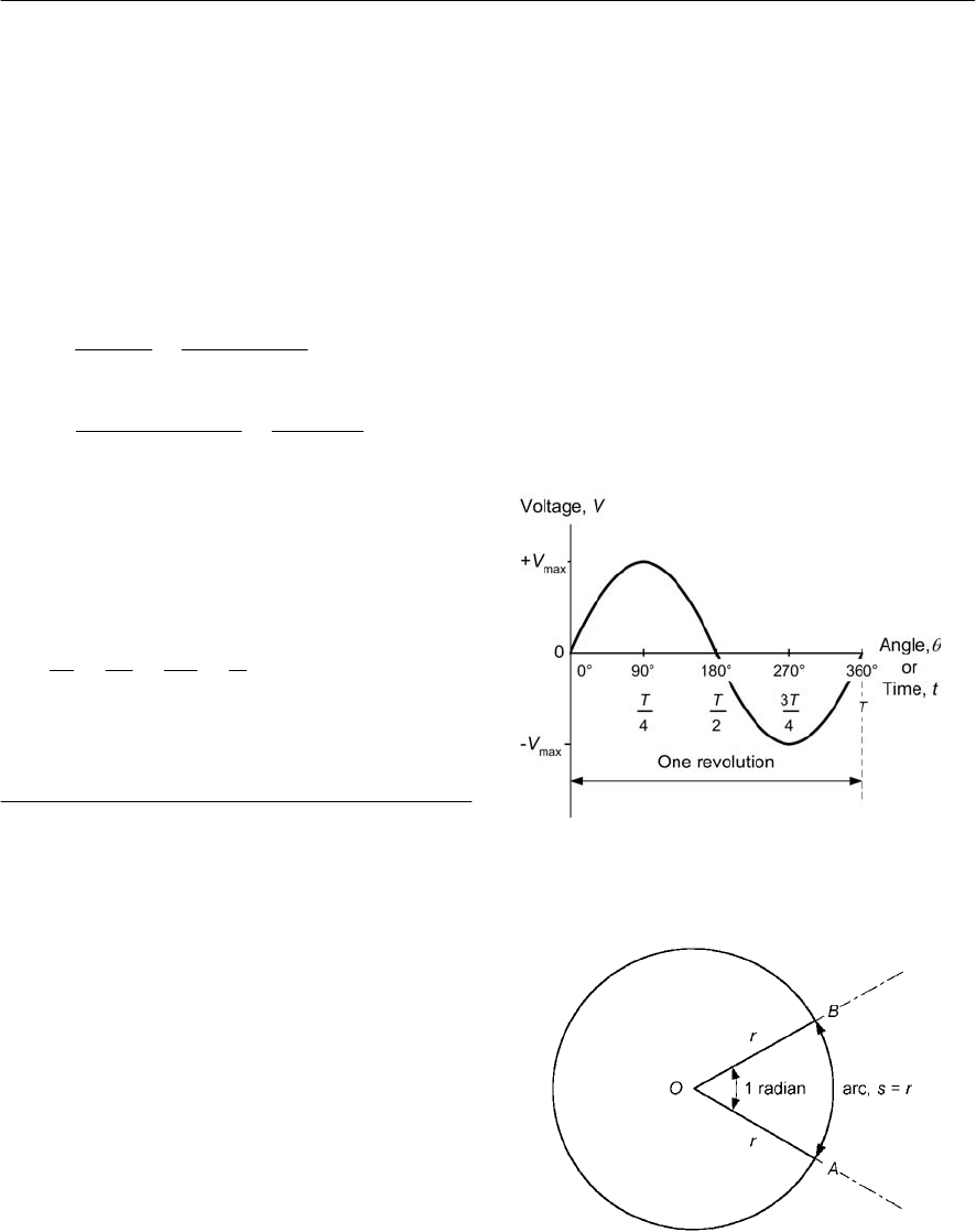
Measuring angles
You might think it strange to be concerned with
angles in electrical circuits. The reason is simply
that, in analogue and a.c. circuits, signals are based
on repetitive waves (often sinusoidal in shape). We
can refer to a point on such a wave in one of two
basic ways, either in terms of the time from the
start of the cycle or in terms of the angle (a cycle
starts at 0° and finishes as 360° (see Fig. 1.1)). In
practice, it is often more convenient to use angles
rather than time, however, the two methods of
measurement are interchangeable and it’s important
to be able to work in either of these units.
In electrical circuits, angles are measured in
either degrees or radians (both of which are strictly
dimensionless units). You will doubtless already be
familiar with angular measure in degrees where one
complete circular revolution is equivalent to an
angular change of 360°. The alternative method of
measuring angles, the radian, is defined somewhat
differently. It is the angle subtended at the centre of
acircle by an arc having length which is equal to
the radius of the circle (see Fig. 1.2).
You may sometimes find that you need to
convert from radians to degrees, and vice versa. A
complete circular revolution is equivalent to a
rotation of 360° or 2Aradians (note that Ais
approximately equal to 3.142). Thus one radian is
equivalent to 360/2Adegrees (or approximately
57.3°). Try to remember the following rules that
will help you to convert angles expressed in
degrees to radians and vice versa:
•From degrees to radians, divide by 57.3.
•From radians to degrees, multiply by 57.3.
Watts Joules/seconds
Volts = =
Amperes Amperes
Joules Joules
= =
Amperes seconds Coulombs
×
-1
WJ/s J J
V = = = = = JC
AAA sC
Figure 1.2 Definition of the radian
Figure 1.1 One cycle of a sine wave voltage
2ELECTRONIC CIRCUITS: FUNDAMENTALS AND APPLICATIONS

ELECTRICAL FUNDAMENTALS 3
Example 1.3
Express a quarter of a cycle revolution in terms of:
(a) degrees;
(b) radians.
Solution
(a) There are 360° in one complete cycle (i.e. one
full revolution. Hence there are (360/4)° or 90° in
one quarter of a cycle.
(b) There are 2Aradians in one complete cycle.
Thus there are 2A/4 or A/2 radians in one quarter of
acycle.
Example 1.4
Express an angle of 215° in radians.
Solution
To convert from degrees to radians, divide by 57.3.
So 215° is equivalent to 215/57.3 = 3.75 radians.
Example 1.5
Express an angle of 2.5 radians in degrees.
Solution
To convert from radians to degrees, multiply by
57.3. Hence 2.5 radians is equivalent to 2.5 × 57.3
=143.25°.
Electrical units and symbols
Table 1.3 shows the units and symbols that are
commonly encountered in electrical circuits. It is
important to get to know these units and also be
able to recognize their abbreviations and symbols.
You will meet all of these units later in this chapter.
Multiples and sub-multiples
Unfortunately, many of the derived units are either
too large or too small for convenient everyday use
but we can make life a little easier by using a
standard range of multiples and sub-multiples (see
Table 1.4).
Unit Symbol Notes
Ampere IUnit of electric
current (a current of 1
Aflows when a charge
of 1 C is transported in
atime interval of 1 s)
Coulomb QUnit of electric charge
or quantity of
electricity
Farad CUnit of capacitance
(a capacitor has a
capacitance of 1 F
when a potential of 1 V
across its plates
produced a charge of
1C)
Henry LUnit of inductance
(an inductor has an
inductance of 1 H
when an applied
current changing at
1A/s produces a
potential difference of
1 V across its
terminals)
Hertz fUnit of frequency
(a signal has a
frequency of 1 Hz if
one cycle occurs in an
interval of 1 s)
Joule WUnit of energy
Ohm RUnit of resistance
Second t
Unit of time
Siemen GUnit of conductance
(the reciprocal of
resistance)
Tesla BUnit of magnetic flux
density (a flux density
of 1 T is produced
when a flux of 1 Wb is
present over an area of
1square metre)
Volt VUnit of electric
potential (e.m.f. or
p.d.)
Watt PUnit of power
(equivalent to 1 J of
energy consumed in
1s)
Weber
Unit of magnetic flux
Abbrev.
A
C
F
H
Hz
J
s
S
T
V
W
Wb
Table 1.3 Electrical units

4ELECTRONIC CIRCUITS: FUNDAMENTALS AND APPLICATIONS
Example 1.6
An indicator lamp requires a current of 0.075 A.
Express this in mA.
Solution
You can express the current in mA (rather than in
A) by simply moving the decimal point three places
to the right. Hence 0.075 A is the same as 75 mA.
Example 1.7
Amedium-wave radio transmitter operates on a
frequency of 1,495 kHz. Express its frequency in
MHz.
Solution
To express the frequency in MHz rather than kHz
we need to move the decimal point three places to
the left. Hence 1,495 kHz is equivalent to 1.495
MHz.
Example 1.8
Athe value of a 27,000 pF in µF.
Solution
To express the value in µF rather than pF we need
to move the decimal point six places to the left.
Hence 27,000 pF is equivalent to 0.027 µF (note
that we have had to introduce an extra zero before
the 2 and after the decimal point).
Prefix Abbreviation Multiplier
tera T 1012 ( = 1 000 000 000 000)
giga G 109( = 1 000 000 000)
mega M 106( = 1 000 000)
kilo k 103( = 1 000)
(none) (none) 100( = 1 )
centi c 102( = 0.01)
milli m 103( = 0.001)
micro µ 106( = 0.000 001)
nano n 109( = 0.000 000 001)
pico p 1012 ( = 0.000 000 000 001)
Table 1.4 Multiples and sub-multiples Exponent notation
Exponent notation (or scientific notation)is useful
when dealing with either very small or very large
quantities. It’s well worth getting to grips with this
notation as it will allow you to simplify quantities
before using them in formulae.
Exponents are based on powers of ten. To
express a number in exponent notation the number
is split into two parts. The first part is usually a
number in the range 0.1 to 100 while the second
part is a multiplier expressed as a power of ten.
For example, 251.7 can be expressed as 2.517 ×
100, i.e. 2.517 ×10².It can also be expressed as
0.2517 ×1,000, i.e. 0.2517 ×10³.In both cases the
exponent is the same as the number of noughts in
the multiplier (i.e. 2 in the first case and 3 in the
second case). To summarize:
251.7 = 2.517 ×102=0.2517 ×10³
As a further example, 0.01825 can be expressed
as 1.825/100, i.e. 1.825 ×10².It can also be
expressed as 18.25/1,000, i.e. 18.25 ×10³.Again,
the exponent is the same as the number of noughts
but the minus sign is used to denote a fractional
multiplier. To summarize:
0.01825 = 1.825 ×102=18.25 ×10³
Example 1.9
Acurrent of 7.25 mA flows in a circuit. Express
this current in Amperes using exponent notation.
Solution
1mA = 1 ×10³Athus 7.25 mA = 7.25 ×10³A
Example 1.10
Avoltage of 3.75 ×10⁶Vappears at the input of
an amplifier. Express this voltage in (a) V and (b)
mV, using exponent notation.
Solution
(a) 1 ×10⁶V = 1 µV so 3.75 ×10⁶V = 3.75 µV
(b) There are 1,000 µV in 1 mV so we must divide
the previous result by 1,000 in order to express
the voltage in mV. So 3.75 µV = 0.00375 mV.

ELECTRICAL FUNDAMENTALS 5
Multiplication and division using
exponents
Exponent notation really comes into its own when
values have to be multiplied or divided. When
multiplying two values expressed using exponents,
you simply need to add the exponents. Here’s an
example:
(2 ×102)×(3 ×106) = (2 ×3) ×10(2+6) = 6 ×10⁸
Similarly, when dividing two values which are
expressed using exponents, you only need to
subtract the exponents. As an example:
(4 ×10⁶)÷( 2 ×10⁴) = 4/2 ×10(64)= 2 ×10²
In either case it’s important to remember to specify
the units, multiples and sub-multiples in which you
are working (e.g. A, k<,mV, µF, etc).
Example 1.11
Acurrent of 3 mA flows in a resistance of 33 k<.
Determine the voltage dropped across the resistor.
Solution
Voltage is equal to current multiplied by resistance
(see page 7). Thus:
V = I ×R = 3mA ×33 k<
Expressing this using exponent notation gives:
V=(3 ×103)×(33 ×103) V
Separating the exponents gives:
V= 3 ×33 ×103×103V
Thus V=99 ×10(3+3) =99 ×100=99 ×1 = 99 V
Example 1.12
Acurrent of 45 µA flows in a circuit. What charge
is transferred in a time interval of 20 ms?
Solution
Charge is equal to current multiplied by time (see
the definition of the ampere on page 3). Thus:
Q = I t = 45 µA ×20 ms
Expressing this in exponent notation gives:
Q=(45 ×106)×(20 ×103)Coulomb
Separating the exponents gives:
Q=45 ×20 ×106×103Coulomb
Thus Q=900 ×10(63) =900 ×l09=900 nC
Example 1.13
Apower of 300 mW is dissipated in a circuit when
avoltage of 1,500 V is applied. Determine the
current supplied to the circuit.
Solution
Current is equal to power divided by voltage (see
page 9). Thus:
I = P / V = 300 mW /1,500 V Amperes
Expressing this in exponent notation gives:
I=(300 ×103)/(1.5 ×103) A
Separating the exponents gives:
I=(300/1.5) ×(103/103) A
I=300/1.5 ×103×103A
Thus, I=200 ×10(33) =200 ×106=200 µA
Conductors and insulators
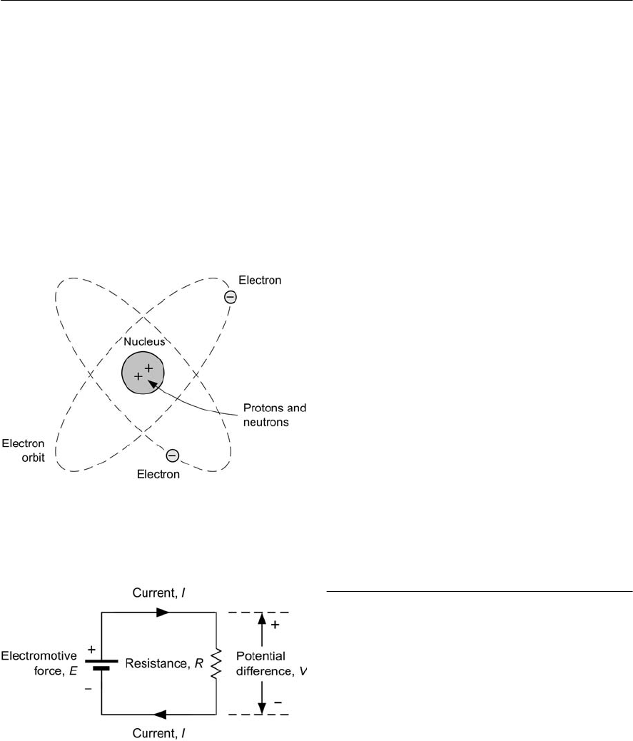
Electric current is the name given to the flow of
electrons (or negative charge carriers). Electrons
orbit around the nucleus of atoms just as the earth
orbits around the sun (see Fig. 1.3). Electrons are
held in one or more shells, constrained to their
orbital paths by virtue of a force of attraction
towards the nucleus which contains an equal
number of protons (positive charge carriers). Since
like charges repel and unlike charges attract,
negatively charged electrons are attracted to the
positively charged nucleus. A similar principle can
be demonstrated by observing the attraction
between two permanent magnets; the two North
poles of the magnets will repel each other, while a
North and South pole will attract. In the same way,
the unlike charges of the negative electron and the
6ELECTRONIC CIRCUITS: FUNDAMENTALS AND APPLICATIONS
Voltage and resistance
The ability of an energy source (e.g. a battery) to
produce a current within a conductor may be
expressed in terms of electromotive force (e.m.f.).
Whenever an e.m.f. is applied to a circuit a
potential difference (p.d.) exists. Both e.m.f. and
p.d. are measured in volts (V). In many practical
circuits there is only one e.m.f. present (the battery
or supply) whereas a p.d. will be developed across
each component present in the circuit.
The conventional flow of current in a circuit is
from the point of more positive potential to the
point of greatest negative potential (note that
electrons move in the opposite direction!). Direct
current results from the application of a direct
e.m.f. (derived from batteries or a d.c. power
supply). An essential characteristic of these
supplies is that the applied e.m.f. does not change
its polarity (even though its value might be subject
to some fluctuation).
For any conductor, the current flowing is directly
proportional to the e.m.f. applied. The current
flowing will also be dependent on the physical
dimensions (length and cross-sectional area) and
material of which the conductor is composed.
The amount of current that will flow in a
conductor when a given e.m.f. is applied is
inversely proportional to its resistance. Resistance,
therefore, may be thought of as an opposition to
current flow; the higher the resistance the lower the
current that will flow (assuming that the applied
e.m.f. remains constant).
Ohm’s Law
Provided that temperature does not vary, the ratio
of p.d. across the ends of a conductor to the current
flowing in the conductor is a constant. This
relationship is known as Ohm’s Law and it leads to
the relationship:
V / I = aconstant = R
where Vis the potential difference (or voltage drop)
in Volts (V), Iis the current in Amperes (A), and R
is the resistance in Ohms (<)(see Fig. 1.4).
The formula may be arranged to make V, I or R
the subject, as follows:
positive proton experience a force of mutual
attraction.
The outer shell electrons of a conductor can be
reasonably easily interchanged between adjacent
atoms within the lattice of atoms of which the
substance is composed. This makes it possible for
the material to conduct electricity. Typical
examples of conductors are metals such as copper,
silver, iron and aluminium. By contrast, the outer
shell electrons of an insulator are firmly bound to
their parent atoms and virtually no interchange of
electrons is possible. Typical examples of
insulators are plastics, rubber and ceramic
materials.
Figure 1.3 Asingle atom of helium (He)showing
its two electrons in orbit around its nucleus
Figure 1.4 Simple circuit to illustrate the
relationship between voltage (V), current (I)and
resistance (R). Note that the direction of
conventional current flow is from positive to
negative
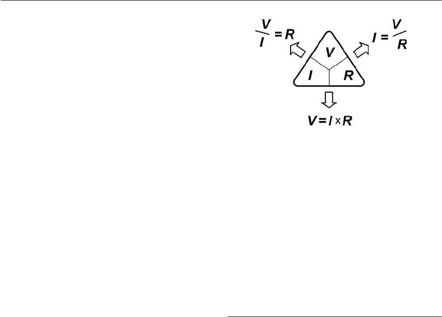
Figure 1.5 Triangle showing the relationship
between V,Iand R
ELECTRICAL FUNDAMENTALS 7
V = I ×R , I = V / R and R = V / I
The triangle shown in Fig. 1.5 should help you
remember these three important relationships.
However, it’s worth noting that, when performing
calculations of currents, voltages and resistances in
practical circuits it is seldom necessary to work
with an accuracy of better than ±1% simply
because component tolerances are usually greater
than this. Furthermore, in calculations involving
Ohm’s Law, it can sometimes be convenient to
work in units of k<and mA (or M<and µA) in
which case potential differences will be expressed
directly in V.
Example 1.14
A12 <resistor is connected to a 6V battery. What
current will flow in the resistor?
Solution
Here we must use I = V / R (where V = 6 V and
R = 12 <):
I = V / R = 6 V / 12 <=0.5 A (or 500 mA)
Hence a current of 500 mA will flow in the resistor.
Example 1.15
Acurrent of 100 mA flows in a 56 <resistor. What
voltage drop (potential difference) will be
developed across the resistor?
Solution
Here we must use V = I ×Rand ensure that we
work in units of Volts (V), Amperes (A) and Ohms
(<).
V = I ×R = 0.1 A ×56 <=5.6 V
(Note that 100 mA is the same as 0.1 A.)
This calculation shows that a p.d. of 5.6 V will
be developed across the resistor.
Example 1.16
Avoltage drop of 15 V appears across a resistor in
which a current of 1 mA flows. What is the value
of the resistance?
Solution
R = V / I = 15 V / 0.001 A = 15,000 <=15 k<
Note that it is often more convenient to work in
units of mA and V which will produce an answer
directly in k<,i.e.
R = V / I = 15 V/ l mA = 15 k<
Resistance and resistivity
The resistance of a metallic conductor is directly
proportional to its length and inversely proportional
to its area. The resistance is also directly
proportional to its resistivity (or specific
resistance).Resistivity is defined as the resistance
measured between the opposite faces of a cube
having sides of 1 cm.
The resistance, R, of a conductor is thus given by
the formula:
R = ,×l/A
where Ris the resistance (ft), ,is the resistivity
(<m), lis the length (m), and Ais the area (m2).
Table 1.5 shows the electrical properties of some
common metals.
Example 1.17
Acoil consists of an 8 m length of annealed copper
wire having a cross-sectional area of l mm2.
Determine the resistance of the coil.

8ELECTRONIC CIRCUITS: FUNDAMENTALS AND APPLICATIONS
Solution
We will use the formula, R = ,l/A.
The value of ,for annealed copper given in
Table 1.5 is 1.724 ×10⁸<m. The length of the
wire is 4 m while the area is 1 mm2or
1×10⁶m2(note that it is important to be
consistent in using units of metres for length and
square metres for area).
Hence the resistance of the coil will be given by:
Thus R = 13.792 ×10²or 0.13792 <
Example 1.18
Awire having a resistivity of 1.724 ×10⁸<m,
length 20 m and cross-sectional area 1 mm2carries
acurrent of 5 A. Determine the voltage drop
between the ends of the wire.
Solution
First we must find the resistance of the wire (as in
Example 1.17):
The voltage drop can now be calculated using
Ohm’s Law:
Metal Resistivity (at 20°C)
(<m)
Relative conductivity
(copper = 1)
Temperature coefficient
of resistance (per °C)
Silver 1.626 ×1081.06 0.0041
Copper (annealed) 1.724 ×1081.00 0.0039
Copper (hard drawn) 1.777 ×1080.97 0.0039
Aluminium 2.803 ×1080.61 0.0040
Mild steel 1.38 ×1070.12 0.0045
Lead 2.14 ×1070.08 0.0040
Nickel 8.0 ×1080.22 0.0062
Table 1.5 Properties of some common metals
V = I ×R = 5A ×0.32 <=1.6 V
This calculation shows that a potential of 1.6 V will
be dropped between the ends of the wire.
Energy and power
At first you may be a little confused about the
difference between energy and power. Put simply,
energy is the ability to do work while power is the
rate at which work is done. In electrical circuits,
energy is supplied by batteries or generators. It may
also be stored in components such as capacitors and
inductors. Electrical energy is converted into
various other forms of energy by components such
as resistors (producing heat), loudspeakers
(producing sound energy) and light emitting diodes
(producing light).
The unit of energy is the Joule (J). Power is the
rate of use of energy and it is measured in Watts
(W). A power of 1W results from energy being
used at the rate of 1 J per second. Thus:
P = W / t
where Pis the power in Watts (W), Wis the energy
in Joules (J), and tis the time in seconds (s).
The power in a circuit is equivalent to the
product of voltage and current. Hence:
P = I
×
V
where Pis the power in Watts (W), Iis the current
in Amperes (A), and Vis the voltage in Volts (V).
8
( 8+6)
6
1.724 10 8
= = 13.724 10
110
R
×× ×
×
8
2
6
1.6 10 20
= = 32 10 0.32
110
l
RA
××
=×=
×
ELECTRICAL FUNDAMENTALS 9
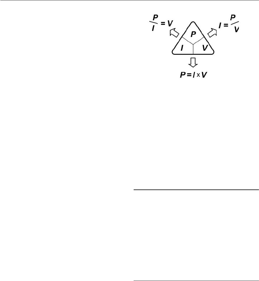
The formula may be arranged to make P, I or V
the subject, as follows:
P = I ×P, I = P / V and V = P / I
The triangle shown in Fig. 1.6 should help you
remember these relationships.
The relationship, P = I ×V, may be combined
with that which results from Ohm’s Law (V = I ×
R) to produce two further relationships. First,
substituting for Vgives:
P = I ×(I×R)= I 2R
Secondly, substituting for Igives:
P = (V / R)×V=V2/ R
Example 1.19
Acurrent of 1.5 A is drawn from a 3 V battery.
What power is supplied?
Solution
Here we must use P = I ×V(where I=1.5 A and V
= 3 V).
P = I ×V = 1.5 A × 3 V = 4.5 W
Hence a power of 4.5 W is supplied.
Example 1.20
Avoltage drop of 4 V appears across a resistor of
100 <.What power is dissipated in the resistor?
Solution
Here we use P = V 2/ R (where V = 4 V and
R = 100 <).
P = V 2/ R = (4 V ×4V) /100 <=0.16 W
Hence the resistor dissipates a power of 0.16 W (or
160 mW).
Example 1.21
Acurrent of 20 mA flows in a 1 k<resistor. What
power is dissipated in the resistor?
Solution
Here we use P = I 2×Rbut, to make life a little
easier, we will work in mA and k<(in which case
the answer will be in mW).
P = I 2×R=(20 mA ×20 mA) ×1 k<=400 mW
Thus a power of 400 mW is dissipated in the 1k<
resistor.
Electrostatics
If a conductor has a deficit of electrons, it will
exhibit a net positive charge. If, on the other hand,
it has a surplus of electrons, it will exhibit a net
negative charge. An imbalance in charge can be
produced by friction (removing or depositing
electrons using materials such as silk and fur,
respectively) or induction (by attracting or repelling
electrons using a second body which is,
respectively, positively or negatively charged).
Force between charges
Coulomb’s Law states that, if charged bodies exist
at two points, the force of attraction (if the charges
are of opposite polarity) or repulsion (if the charges
have the same polarity) will be proportional to the
product of the magnitude of the charges divided by
the square of their distance apart. Thus:
Figure 1.6 Triangle showing the relationship
between P,Iand V
10 ELECTRONIC CIRCUITS: FUNDAMENTALS AND APPLICATIONS
where Q1and Q2are the charges present at the two
points (in Coulombs), rthe distance separating the
two points (in metres), Fis the force (in Newtons),
and kis a constant depending upon the medium in
which the charges exist.
In vacuum or ‘free space’,
where R0is the permittivity of free space (8.854 ×
1012 C/Nm2).
Combining the two previous equations gives:
Electric fields
The force exerted on a charged particle is a
manifestation of the existence of an electric field.
The electric field defines the direction and
magnitude of a force on a charged object. The field
itself is invisible to the human eye but can be
drawn by constructing lines which indicate the
motion of a free positive charge within the field;
the number of field lines in a particular region
being used to indicate the relative strength of the
field at the point in question.
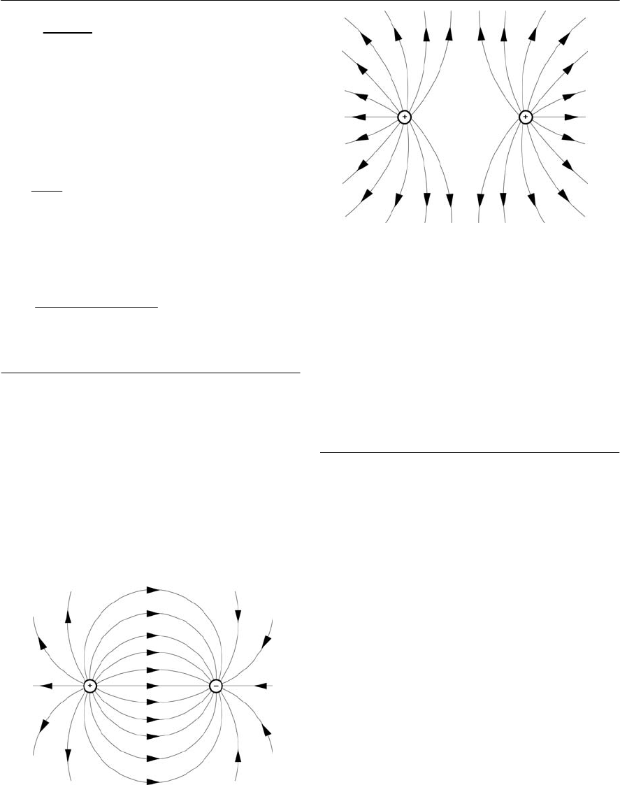
Figures 1.7 and 1.8 show the electric fields between
charges of the same and opposite polarity while
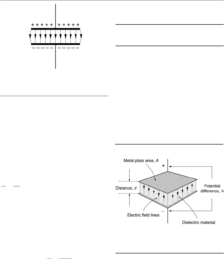
Fig. 1.9 shows the field which exists between two
charged parallel plates. You will see more of this
particular arrangement when we introduce
capacitors in Chapter 2.
Electric field strength
The strength of an electric field (5)is proportional
to the applied potential difference and inversely
proportional to the distance between the two
conductors. The electric field strength is given by:
E = V / d
where Eis the electric field strength (V/m), Vis the
applied potential difference (V) and dis the
distance (m).
Example 1.22
Two parallel conductors are separated by a distance
of 25 mm. Determine the electric field strength if
they are fed from a 600 V d.c. supply.
Solution
The electric field strength will be given by:
E = V / d = 600 / 25 ×103=24 kV/m
Figure 1.8 Electric field between two like electric
charges (in this case both positive)
Figure 1.7 Electric field between two unlike
electric charges
12
2
=
kQ Q
F
r
0
1
=
4
k
1 2
12 2
=Newtons
4 8.854 10
kQ Q
Fr
××
ELECTRICAL FUNDAMENTALS 11
Permittivity
The amount of charge produced on the two plates
shown in Fig. 1.9 for a given applied voltage will
depend not only on the physical dimensions but
also on the insulating dielectric material that
appears between the plates. Such materials need to
have a very high value of resistivity (they must not
conduct charge) coupled with an ability to
withstand high voltages without breaking down.
A more practical arrangement is shown in Fig.
1.10. In this arrangement the ratio of charge, Q,to
potential difference, V,is given by the relationship:
where Ais the surface area of the plates (in m), dis
the separation (in m), and is a constant for the
dielectric material known as the absolute
permittivity of the material (sometimes also
referred to as the dielectric constant).
The absolute permittivity of a dielectric material
is the product of the permittivity of free space (
0)
and the relative permittivity (
r)of the material.
Thus:
and
The dielectric strength of an insulating dielectric
is the maximum electric field strength that can
safely be applied to it before breakdown
(conduction) occurs. Table 1.4 shows values of
relative permittivity and dielectric strength for
some common dielectric materials.
Dielectric material
Relative
permittivity
(free space = 1)
Vacuum, or free space 1
Polythene 2.3
Paper 2.5 to 3.5
Polystyrene 2.5
Mica 4 to 7
Pyrex glass 4.5
Glass ceramic 5.9
Polyester 3.0 to 3.4
Porcelain 6.5
Dielectric
strength
(kV/mm)
S
50
14
25
160
13
40
18
4
Titanium dioxide 100 6
Ceramics 5 to 1,000 2 to 10
Air 1 3
Table 1.4 Properties of some common insulating
dielectric materials
Figure 1.10 Parallel plates with an insulating
dielectric material
Figure 1.9 Electric field between two parallel
plates
=
QA
Vd
0
=
×
0
=
r
A
Q
Vd
Electromagnetism
When a current flows through a conductor a
magnetic field is produced in the vicinity of the
conductor. The magnetic field is invisible but its
presence can be detected using a compass needle
(which will deflect from its normal North
South
position). If two current-carrying conductors are
12 ELECTRONIC CIRCUITS: FUNDAMENTALS AND APPLICATIONS
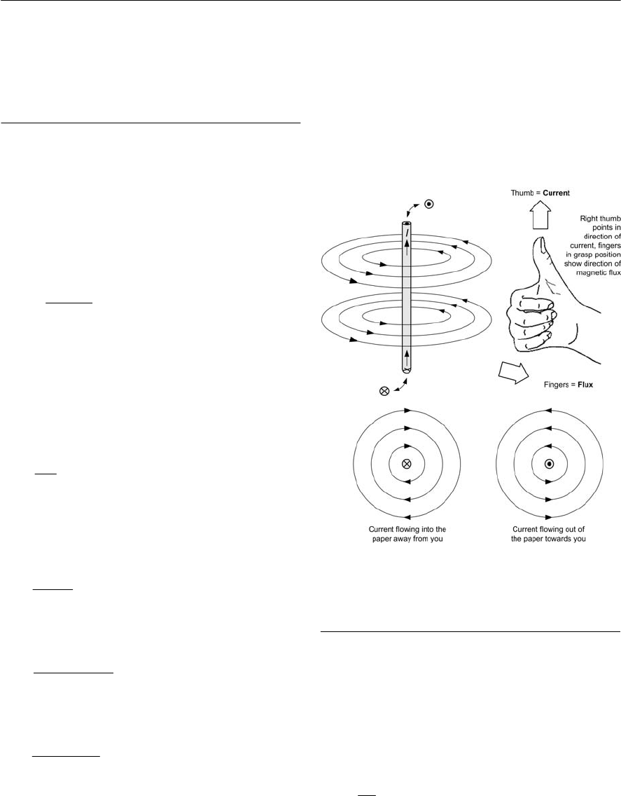
Figure 1.11 Magnetic field surrounding a straight
conductor
placed in the vicinity of one another, the fields will
interact with one another and the conductors will
experience a force of attraction or repulsion
(depending upon the relative direction of the two
currents).
Force between two current-carrying
conductors
The mutual force which exists between two parallel
current-carrying conductors will be proportional to
the product of the currents in the two conductors
and the length of the conductors but inversely
proportional to their separation. Thus:
where I1and I2are the currents in the two
conductors (in Amps), lis the parallel length of the
conductors (in metres), dis the distance separating
the two conductors (in metres), Fis the force (in
Newtons), and kis a constant depending upon the
medium in which the charges exist.
In vacuum or ‘free space’,
where µ0is a constant known as the permeability
of free space (4A×107or 12.57 ×10⁷H/m).
Combining the two previous equations gives:
or
or
12
=
kI I l
F
d
0
=
2
k
µ
012
=2
IIl
F
d
µ
7
12
410
= 2
IIl
Fd
×
7
12
210
=Newtons
IIl
Fd
×
Magnetic fields
The field surrounding a straight current-carrying
conductor is shown in Fig. 1.11. The magnetic field
defines the direction of motion of a free North pole
within the field. In the case of Fig. 1.11, the lines of
flux are concentric and the direction of the field
determined by the direction of current flow) is
given by the right-hand rule.
Magnetic field strength
The strength of a magnetic field is a measure of the
density of the flux at any particular point. In the
case of Fig. 1.11, the field strength will be
proportional to the applied current and inversely
proportional to the perpendicular distance from the
conductor. Thus:
where Bis the magnetic flux density (in Tesla), Iis
=
kI
B
d
ELECTRICAL FUNDAMENTALS 13
the current (in amperes), dis the distance from the
conductor (in metres), and kis a constant.
Assuming that the medium is vacuum or ‘free
space’, the density of the magnetic flux will be
given by:
where Bis the flux density (in Tesla), µ0is the
permeability of ‘free space’ (4A×107or 12.57 ×
107), Iis the current (in Amperes), and dis the
distance from the centre of the conductor (in
metres).
The flux density is also equal to the total flux
divided by the area of the field. Thus:
B=9/ A
where 9is the flux (in Webers) and Ais the area of
the field (in square metres).
In order to increase the strength of the field, a
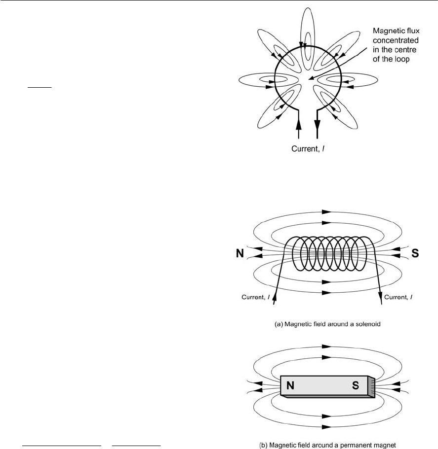
conductor may be shaped into a loop (Fig. 1.12) or
coiled to form a solenoid (Fig. 1.13). Note, in the
latter case, how the field pattern is exactly the same
as that which surrounds a bar magnet. We will see
Example 1.23
Determine the flux density produced at a distance
of 50 mm from a straight wire carrying a current of
20 A.
Solution
Applying the formula B = µ0I / 2Adgives:
from which:
B=0.8 ×10⁴Tesla
Thus B=80 ×106Tor B=80 µT.
Example 1.24
Aflux density of 2.5 mT is developed in free space
over an area of 20 cm2.Determine the total flux.
0
=2
I
B
d
µ
Figure 1.12 Forming a conductor into a loop
increases the strength of the magnetic field in the
centre of the loop
Figure 1.13 The magnetic field surrounding a
solenoid coil resembles that of a permanent magnet
77
33
12.57 10 20 251.4 10
=
2 3.142 50 10 314.2 10
B
×× ×
=
××× ×
Solution
Re-arranging the formula B=9/ A to make 9the
subject gives 9=B
×
Athus:
9=(2.5 ×10
3
)×(20 ×10
4
)=50 ×10
7
Webers
from which B=5µWb
14 ELECTRONIC CIRCUITS: FUNDAMENTALS AND APPLICATIONS
Magnetic circuits
Materials such as iron and steel possess
considerably enhanced magnetic properties. Hence
they are employed in applications where it is
necessary to increase the flux density produced by
an electric current. In effect, magnetic materials
allow us to channel the electric flux into a
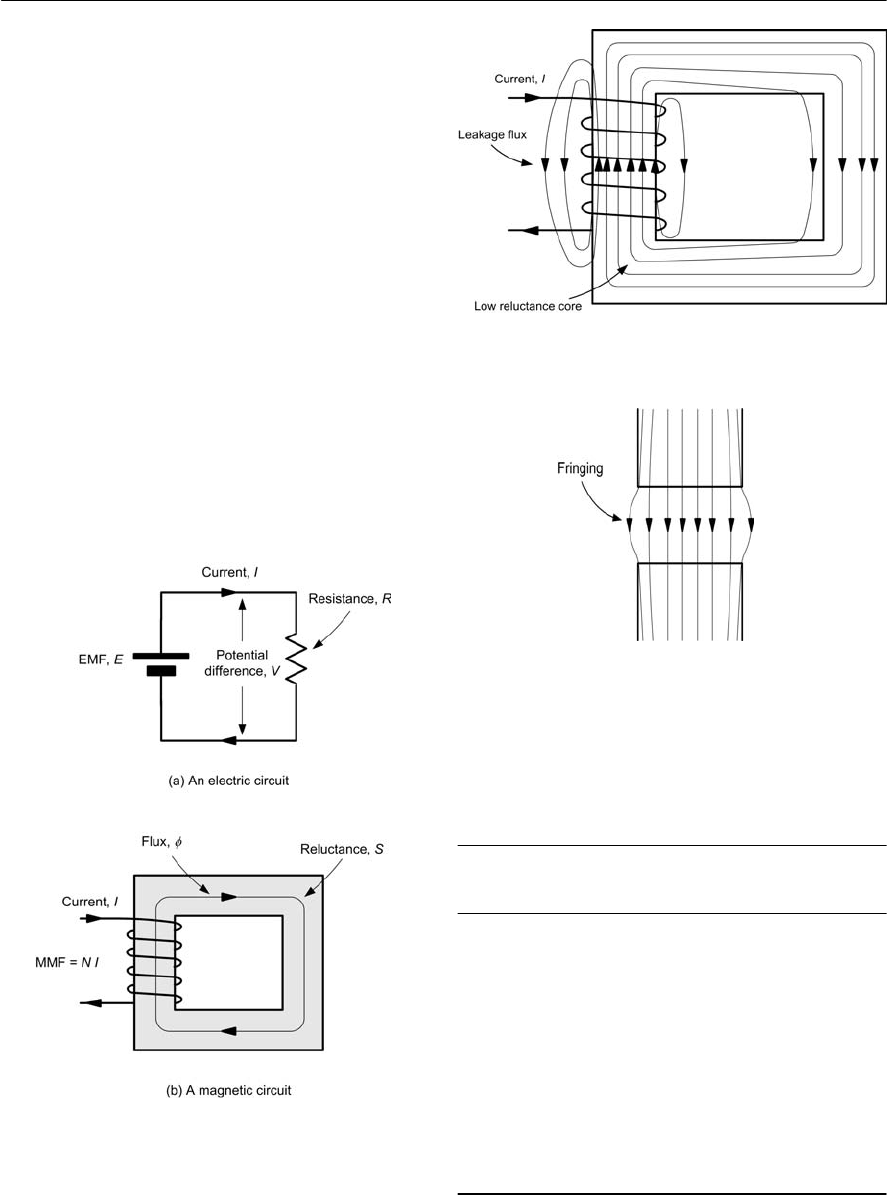
‘magnetic circuit’, as shown in Fig. 1.14.
In the circuit of Fig. 1.14(b) the reluctance of
the magnetic core is analogous to the resistance
present in the electric circuit shown in Fig. 1.14(a).
We can make the following comparisons between
the two types of circuit (see Table 1.7).
In practice, not all of the magnetic flux produced
in a magnetic circuit will be concentrated within
the core and some ‘leakage flux’ will appear in the
surrounding free space (as shown in Fig. 1.15).
Similarly, if a gap appears within the magnetic
circuit, the flux will tend to spread out as shown in
Fig. 1.16. This effect is known as ‘fringing’.
Figure 1.14 Comparison of electric and magnetic
circuits
Figure 1.15 Leakage flux in a magnetic circuit
Figure 1.16 Fringing of the magnetic flux at an
air gap in a magnetic circuit
Table 1.7 Comparison of electric and magnetic
circuits
Electric circuit
Figure 1.14(a)
Magnetic circuit
Figure 1.14(a)
Electromotive force,
e.m.f. = V
Magnetomotive force,
m.m.f. = N×I
Resistance = RReluctance = S
Current = IFlux = 9
e.m.f. = current ×resistance m.m.f. = flux ×reluctance
V = I ×RN I = S 9
ELECTRICAL FUNDAMENTALS 15
Reluctance and permeability
The reluctance of a magnetic path is directly
proportional to its length and inversely proportional
to its area. The reluctance is also inversely
proportional to the absolute permeability of the
magnetic material. Thus:
where Sis the reluctance of the magnetic path, lis
the length of the path (in metres), Ais the cross-
sectional area of the path (in square metres), and µ
is the absolute permeability of the magnetic
material.
The absolute permeability of a magnetic material
is the product of the permeability of free space (µ0)
and the relative permeability of the magnetic
medium (µ0).Thus
and
The permeability of a magnetic medium is a
measure of its ability to support magnetic flux and
it is equal to the ratio of flux density (B)to
magnetizing force (H). Thus:
where Bis the flux density (in tesla) and His the
magnetizing force (in ampere/metre). The
magnetizing force (H)is proportional to the product
of the number of turns and current but inversely
proportional to the length of the magnetic path.
where His the magnetizing force (in ampere/
metre), Nis the number of turns, Iis the current (in
amperes), and lis the length of the magnetic path
(in metres).
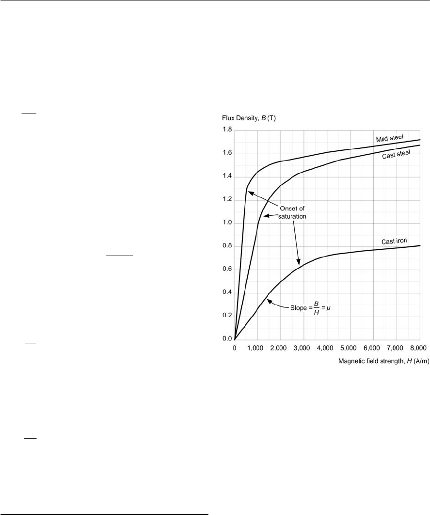
B–H curves
Figure 1.17 shows four typical B–H (flux density
plotted against permeability) curves for some
common magnetic materials. If you look carefully
at these curves you will notice that they flatten off
due to magnetic saturation and that the slope of
the curve (indicating the value of µcorresponding
to a particular value of H)falls as the magnetizing
force increases. This is important since it dictates
the acceptable working range for a particular
magnetic material when used in a magnetic circuit.
=
l
S
A
µ
0
=
µµµ
×
0r
=
l
S
A
µµ
=
B
H
µ
=
NI
H
l
Figure 1.17 B
Hcurves for three ferromagnetic
materials
Example 1.25
Estimate the relative permeability of cast steel (see
Fig. 1.18) at (a) a flux density of 0.6 T and (b) a
flux density of 1.6 T.
Solution
From Fig. 1.18, the slope of the graph at any point
gives the value of µat that point. We can easily
find the slope by constructing a tangent at the point
in question and then finding the ratio of vertical
change to horizontal change.
(a) The slope of the graph at 0.6 T is 0.6/800
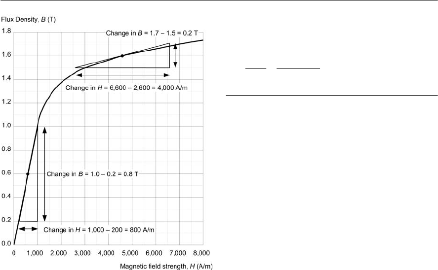
16 ELECTRONIC CIRCUITS: FUNDAMENTALS AND APPLICATIONS
Figure 1.18 B
Hcurve for a sample of cast steel
= 0.75 ×10³
Since µ = µ0×µr , µr= µ / µ0=0.75 ×10³/
12.57×10⁷,thus µr=597 at 0.6 T.
(b) The slope of the graph at 1.6 T is 0.2/4,000
= 0.05 ×10³
Since µ = µ0×µr , µr= µ / µ0=0.05 ×10³/
12.57×10⁷,thus µr=39.8 at 1.6 T.
NB: This example clearly shows the effect of
saturation on the permeability of a magnetic
material!
Example 1.26
Acoil of 800 turns is wound on a closed mild steel
core having a length 600 mm and cross-sectional
area 500 mm2.Determine the current required to
establish a flux of 0.8 mWb in the core.
Solution
Now B = 9/A = (0.8 ×10³)/(500 ×106)=1.6 T
From Fig. 1.17, a flux density of 1.6 T will occur in
mild steel when H = 3,500 A/m. The current can
now be determined by re-arranging H = N I / l as
follows:
3,500 0.6
=2.625 A
800
Hl
IN
××
==
Circuit diagrams
Finally, and just in case you haven’t seen them
before, we will end this chapter with a brief word
about circuit diagrams. We are introducing the
topic here because it’s quite important to be able to
read and understand simple electronic circuit
diagrams before you can make sense of some of the
components and circuits that you will meet later on.
Circuit diagrams use standard symbols and
conventions to represent the components and
wiring used in an electronic circuit. Visually, they
bear very little relationship to the physical layout of
acircuit but, instead, they provide us with a
‘theoretical’ view of the circuit. In this section we
show you how to find your way round simple
circuit diagrams.
To be able to understand a circuit diagram you
first need to be familiar with the symbols that are
used to represent the components and devices. A
selection of some of the most commonly used
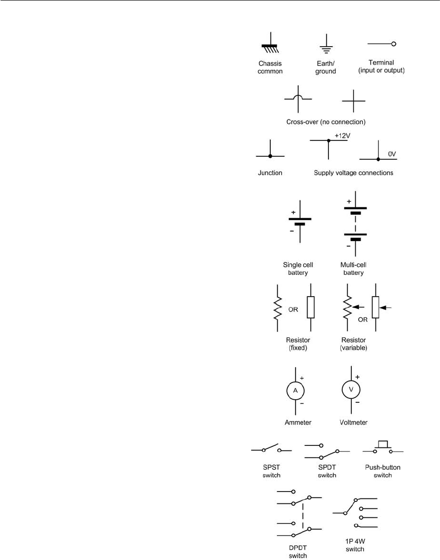
symbols are shown in Fig. 1.24. It’s important to be
aware that there are a few (thankfully quite small)
differences between the symbols used in circuit
diagrams of American and European origin.
As a general rule, the input to a circuit should be
shown on the left of a circuit diagram and the
output shown on the right. The supply (usually the
most positive voltage) is normally shown at the top
of the diagram and the common, 0V, or ground
connection is normally shown at the bottom. This
rule is not always obeyed, particularly for complex
diagrams where many signals and supply voltages
may be present.
Note also that, in order to simplify a circuit
diagram (and avoid having too many lines
connected to the same point) multiple connections
to common, 0V, or ground may be shown using the
appropriate symbol (see Fig. 1.24). The same
applies to supply connections that may be repeated
(appropriately labelled) at various points in the
diagram.
ELECTRICAL FUNDAMENTALS 17
A very simple circuit diagram (a simple resistance
tester) is shown in Fig. 1.20. This circuit may be a
little daunting if you haven’t met a circuit like it
before but you can still glean a great deal of
information from the diagram even if you don’t
know what the individual components do.
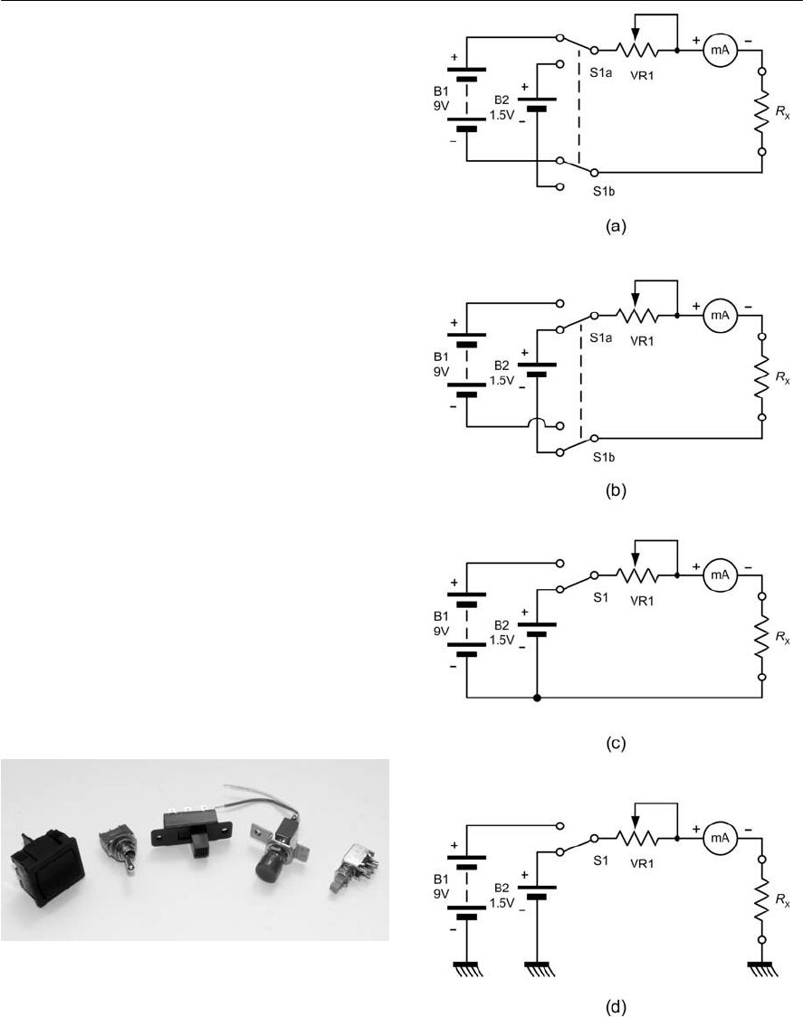
The circuit uses two batteries, B1 (a 9 V multi-
cell battery) and B2 (a 1.5 V single-cell battery).
The two batteries are selected by means of a
double-pole, double-throw (DPDT) switch. This
allows the circuit to operate from either the 9 V
battery (B1) as shown in Fig. 1.20(a) or from the
1.5 V battery (B2) as shown in Fig. 1.20(b)
depending on the setting of S1.
A variable resistor, VR1, is used to adjust the
current supplied by whichever of the two batteries
is currently selected. This current flows first
through VR1, then through the milliammeter, and
finally through the unknown resistor, RX.Notice
how the meter terminals are labelled showing their
polarity (the current flows into the positive terminal
and out of the negative terminal).
The circuit shown in Fig. 1.20(c) uses a different
type of switch but provides exactly the same
function. In this circuit a single-pole, double-throw
(SPDT) switch is used and the negative connections
to the two batteries are ‘commoned’ (i.e. connected
directly together).
Finally, Fig. 1.20(d) shows how the circuit can
be re-drawn using a common ‘chassis’ connection
to provide the negative connection between RXand
the two batteries. Electrically this circuit is
identical to the one shown in Fig. 1.20(c).
Figure 1.19 Various types of switch. From left to
right: a mains rocker switch, an SPDT miniature
toggle (changeover) switch, a DPDT slide switch,
an SPDT push-button (wired for use as an SPST
push-button), a miniature PCB mounting DPDT
push-button (with a latching action). Figure 1.20 A simple circuit diagram
18 ELECTRONIC CIRCUITS: FUNDAMENTALS AND APPLICATIONS
Practical investigation
Objective
To investigate the relationship between the
resistance in a circuit and the current flowing in it.
Components and test equipment
Breadboard, digital or analogue meter with d.c.
current ranges, 9 V d.c. power source (either a 9V
battery or an a.c. mains adapter with a 9 V 400 mA
output), test leads, resistors of 100 <,220 <,
330 <,470 <,680 <and 1k <,connecting wire.
Procedure
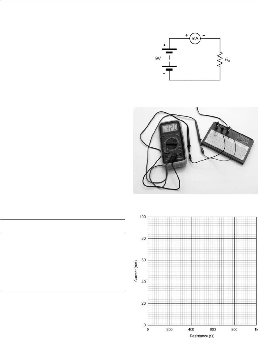
Connect the circuit as shown in Fig. 1.21 and Fig.
1.22. Before switching on the d.c. supply or
connecting the battery, check that the meter is set to
the 200 mA d.c. current range. Switch on (or
connect the battery), switch the multimeter on and
read the current. Note down the current in the table
below and repeat for resistance values of 220 <,
330 <,470 <,680 <and 1k <,switching off or
disconnecting the battery between each
measurement. Plot corresponding values of current
(on the vertical axis) against resistance (on the
horizontal axis) using the graph sheet shown in Fig.
1.23.
Measurements
Figure 1.23 Graph layout for plotting the results
Figure 1.21 Circuit diagram
Figure 1.22 Typical wiring
Conclusion
Comment on the shape of the graph. Is this what
you would expect and does it confirm that the
current flowing in the circuit is inversely
proportional to the resistance in the circuit? Finally,
use Ohm’s Law to calculate the value of each
resistor and compare this with the marked value
Resistance (<)Current (mA)
220
330
470
680
1k
100
(but before doing this, you might find it useful to
make an accurate measurement of the d.c. supply or
battery voltage).
ELECTRICAL FUNDAMENTALS 19
Important formulae introduced in this
chapter
Voltage, current and resistance (Ohm’s Law):
(page 6)
V = I R
Resistance and resistivity:
(page 7)
R = ,l/A
Charge, current and time:
(page 5)
Q = I t
Power, current and voltage:
(page 8)
P = I V
Power, voltage and resistance:
(page 9)
P = V 2/ R
Power, current and resistance:
(page 9)
P = 12R
Reluctance and permeability:
(page 15)
S = l / µ A
Flux and flux density:
(page 13)
B = 9/ A
Current and magnetic field intensity:
(page 15)
H = N I / l
Flux, current and reluctance:
(page 14)
N I = S 9
Symbols introduced in this chapter
Figure 1.24 Circuit symbols introduced in this
chapter

20 ELECTRONIC CIRCUITS: FUNDAMENTALS AND APPLICATIONS
Problems
1.1 Which of the following are not fundamental
units; Amperes, metres, Coulombs, Joules,
Hertz, kilogram?
1.2 A commonly used unit of consumer energy
is the kilowatt hour (kWh). Express this in
Joules (J).
1.3 Express an angle of 30° in radians.
1.4 Express an angle of 0.2 radians in degrees.
1.5 A resistor has a value of 39,570 <.Express
this in kilohms (k<).
1.6 An inductor has a value of 680 mH. Express
this in henries (H).
1.7 A capacitor has a value of 0.00245 µF.
Express this in nanofarads (nF).
1.8 A current of 190 µA is applied to a circuit.
Express this in milliamperes (mA).
1.9 A signal of 0.475 mV appears at the input of
an amplifier. Express this in volts using
exponent notation.
1.10 A cable has an insulation resistance of
16.5 M<.Express this resistance in ohms
using exponent notation.
1.11 Perform the following arithmetic using
exponents:
(a) (1.2 ×103)×(4 ×103)
(b) (3.6 ×106)×(2 ×103)
(c) (4.8 ×10⁹)÷(1.2 ×10⁶)
(d) (9.9 ×10⁶)÷(19.8 ×10³)
(e) (4 ×103)×(7.5 ×105)×(2.5 ×109)
1.12 Which one of the following metals is the
best conductor of electricity: aluminium,
copper, silver, or mild steel? Why?
1.13 A resistor of 270 <is connected across a
9 V d.c. supply. What current will flow?
1.14 A current of 56 µA flows in a 120 k<
resistor. What voltage drop will appear
across the resistor?
1.15 A voltage drop of 13.2 V appears across a
resistor when a current of 4 mA flows in it.
What is the value of the resistor?
1.16 A power supply is rated at 15 V, 1 A. What
value of load resistor would be required to
test the power supply at its full rated output?
1.17 A wirewound resistor is made from a 4 m
length of aluminium wire (,=2.18 ×10⁸
<m). Determine the resistance of the wire if
it has a cross-sectional area of 0.2 mm2.
1.18 A current of 25 mA flows in a 47 <resistor.
What power is dissipated in the resistor?
1.19 A 9 V battery supplies a circuit with a
current of 75 mA. What power is consumed
by the circuit?
1.20 A resistor of 150 <is rated at 0.5 W. What
is the maximum current that can be applied
to the resistor without exceeding its rating?
1.21 Determine the electric field strength that
appears in the space between two parallel
plates separated by an air gap of 4 mm if a
potential of 2.5 kV exists between them.
1.22 Determine the current that must be applied
to a straight wire conductor in order to
produce a flux density of 200 µT at a
distance of 12 mm in free space.
1.23 A flux density of 1.2 mT is developed in
free space over an area of 50 cm2.Determine
the total flux present.
1.24 A ferrite rod has a length of 250 mm and a
diameter of 10 mm. Determine the
reluctance if the rod has a relative
permeability of 2,500.
1.25 A coil of 400 turns is wound on a closed
mild steel core having a length 400 mm and
cross-sectional area 480 mm2.Determine the
current required to establish a flux of 0.6
mWb in the core.
1.26 Identify the type of switch shown in Fig.
1.25.
1.27 Figure 1.25 shows a simple voltmeter. If the
milliammeter reads 1 mA full-scale and has
negligible resistance, determine the values
for R1to R4that will provide voltage ranges
of 1V, 3 V, 10 V and 30 V full-scale.
Answers to these problems appear on page 374.
Figure 1.25 See Questions 1.26 and 1.27
2
Passive components
This chapter introduces several of the most
common types of electronic component, including
resistors, capacitors and inductors. These are often
referred to as passive components as they cannot,
by themselves, generate voltage or current. An
understanding of the characteristics and application
of passive components is an essential prerequisite
to understanding the operation of the circuits used
in amplifiers, oscillators, filters and power supplies.
Resistors
The notion of resistance as opposition to current
was discussed in the previous chapter.
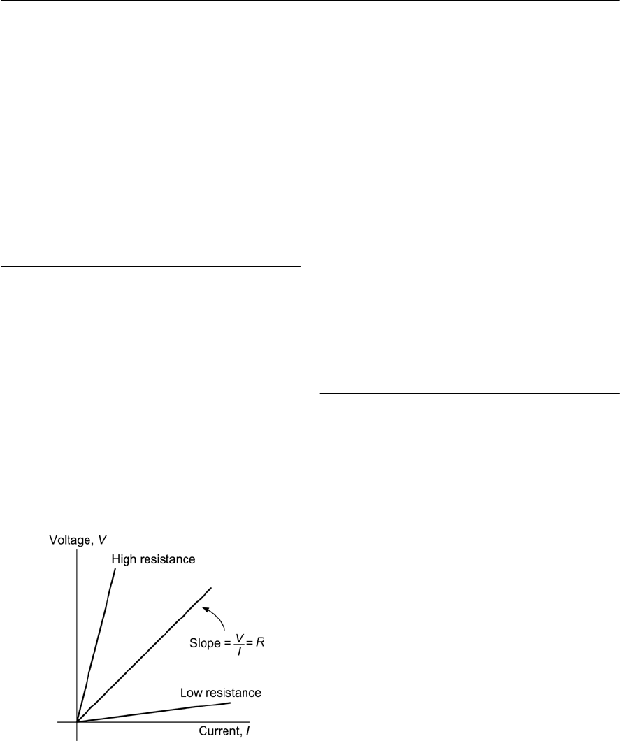
Conventional forms of resistor obey a straight line
law when voltage is plotted against current (see
Fig. 2.1) and this allows us to use resistors as a
means of converting current into a corresponding
voltage drop, and vice versa (note that doubling the
applied current will produce double the voltage
drop, and so on). Therefore resistors provide us
with a means of controlling the currents and
voltages present in electronic circuits. They can
also act as loads to simulate the presence of a
circuit during testing (e.g. a suitably rated resistor
can be used to replace a loudspeaker when an audio
amplifier is being tested).
The specifications for a resistor usually include
the value of resistance expressed in ohms ($),
kilohms (k$)or megohms (M$), the accuracy or
tolerance (quoted as the maximum permissible
percentage deviation from the marked value), and
the power rating (which must be equal to, or greater
than, the maximum expected power dissipation).
Other practical considerations when selecting
resistors for use in a particular application include
temperature coefficient, noise performance,
stability and ambient temperature range. Table 2.1
summarizes the properties of five of the most
common types of resistor. Figure 2.2 shows a
typical selection of fixed resistors with values from
15 $to 4.7 k$.
Preferred values
The value marked on the body of a resistor is not its
exact resistance. Some minor variation in resistance
value is inevitable due to production tolerance. For
example, a resistor marked 100 $and produced
within a tolerance of ±10% will have a value which
falls within the range 90 $to 110 $.Asimilar
component with a tolerance of ±1% would have a
value that falls within the range 99 $to 101 $.
Thus, where accuracy is important it is essential to
use close tolerance components.
Resistors are available in several series of fixed
decade values, the number of values provided with
each series being governed by the tolerance
involved. In order to cover the full range of
resistance values using resistors having a ±20%
tolerance it will be necessary to provide six basic
values (known as the E6 series.More values will
be required in the series which offers a tolerance of
±10% and consequently the E12 series provides
twelve basic values. The E24 series for resistors of
±5% tolerance provides no fewer than 24 basic
Figure 2.1 Voltage plotted against current for
three different values of resistor
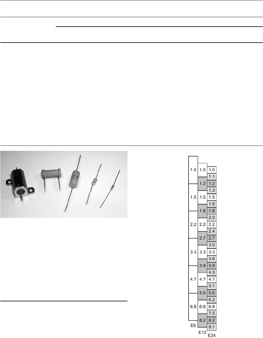
22 ELECTRONIC CIRCUITS: FUNDAMENTALS AND APPLICATIONS
Table 2.1 Characteristics of common types of resistor
Figure 2.2 A selection of resistors including
high-power metal clad, ceramic wirewound, carbon
and metal film types with values ranging from 15 $
to 4.7 k$
values and, as with the E6 and E12 series, decade
multiples (i.e. ×1, ×10, ×100, ×1 k, ×10 k, ×100 k
and × 1 M) of the basic series. Figure 2.3 shows the
relationship between the E6, E12 and E24 series.
Power ratings
Resistor power ratings are related to operating
temperatures and resistors should be derated at high
temperatures. Where reliability is important
resistors should be operated at well below their
nominal maximum power dissipation. Figure 2.3 The E6, E12 and E24 series
Property Resistor type
Carbon film Metal film Metal oxide Ceramic
wirewound
Vitreous
wirewound
Metal clad
Resistance range ($)10 to 10 M 1 to 1 M 10 to 10 M 0.47 to 22 k 0.1 to 22 k 0.05 to 10 k
Typical tolerance (%) ±5 ±1 ±2 ±5 ±5 ±5
Power rating (W) 0.25 to 2 0.125 to 0.5 0.25 to 0.5 4 to 17 2 to 4 10 to 300
Temperature coefficient
(ppm/°C)
250 +50 to +100 +250 +250 +75 +50
Stability Fair Excellent Excellent Good Good Good
Noise performance Fair Excellent Excellent n.a. n.a. n.a.
Ambient temperature
range (°C)
45 to +125 45 to +125 45 to +125 45 to +125 45 to +125 55 to +200
Typical applications General
purpose
Amplifiers, test equipment,
etc., requiring low-noise
high-tolerance components
Very high
power
applications
Power supplies, loads,
medium and high-power
applications
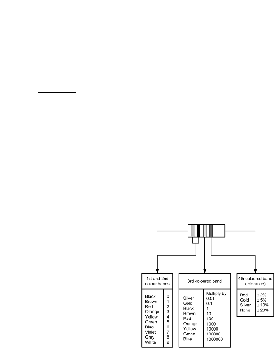
PASSIVE COMPONENTS 23
Example 2.1
Aresistor has a marked value of 220 $.Determine
the tolerance of the resistor if it has a measured
value of 207 $.
Solution
The difference between the marked and measured
values of resistance (the error) is (220 $207 $)
=13 $.The tolerance is given by:
The tolerance is thus (13 /220) × 100 = 5.9%.
Example 2.2
A 9 V power supply is to be tested with a 39 $load
resistor. If the resistor has a tolerance of 10% find:
(a) the nominal current taken from the supply;
(b) the maximum and minimum values of supply
current at either end of the tolerance range for
the resistor.
Solution
(a) If a resistor of exactly 39 $is used the
current will be:
I = V / R = 9 V /39 $=231 mA
(b) The lowest value of resistance would be
(39 $3.9 $) = 35.1 $.In which case the
current would be:
I = V / R = 9 V /35.1 $=256.4 mA
At the other extreme, the highest value
would be (39 $+3.9 $)=42.9 $.
In this case the current would be:
I = V / R = 9 V /42.9 $=209.8 mA
The maximum and minimum values of
supply current will thus be 256.4 mA and
209.8 mA respectively.
Example 2.3
Acurrent of 100 mA (±20%) is to be drawn from a
28 V d.c. supply. What value and type of resistor
should be used in this application?
Solution
The value of resistance required must first be
calculated using Ohm’s Law:
R = V / I = 28 V /100 mA =280 $
The nearest preferred value from the E12 series is
270 $(which will actually produce a current of
103.7 mA (i.e. within ±4%> of the desired value).
If a resistor of ±10% tolerance is used, current will
be within the range 94 mA to 115 mA (well within
the ±20% accuracy specified).
The power dissipated in the resistor (calculated
using P = I × V)will be 2.9 W and thus a
component rated at 3 W (or more) will be required.
This would normally be a vitreous enamel coated
wirewound resistor (see Table 2.1).
Resistor markings
Carbon and metal oxide resistors are normally
marked with colour codes which indicate their
value and tolerance. Two methods of colour coding
are in common use; one involves four coloured
bands (see Fig. 2.4) while the other uses five colour
bands (see Fig. 2.5).
error
Tolerance = 100%
marked value ×
Figure 2.4 Four band resistor colour code
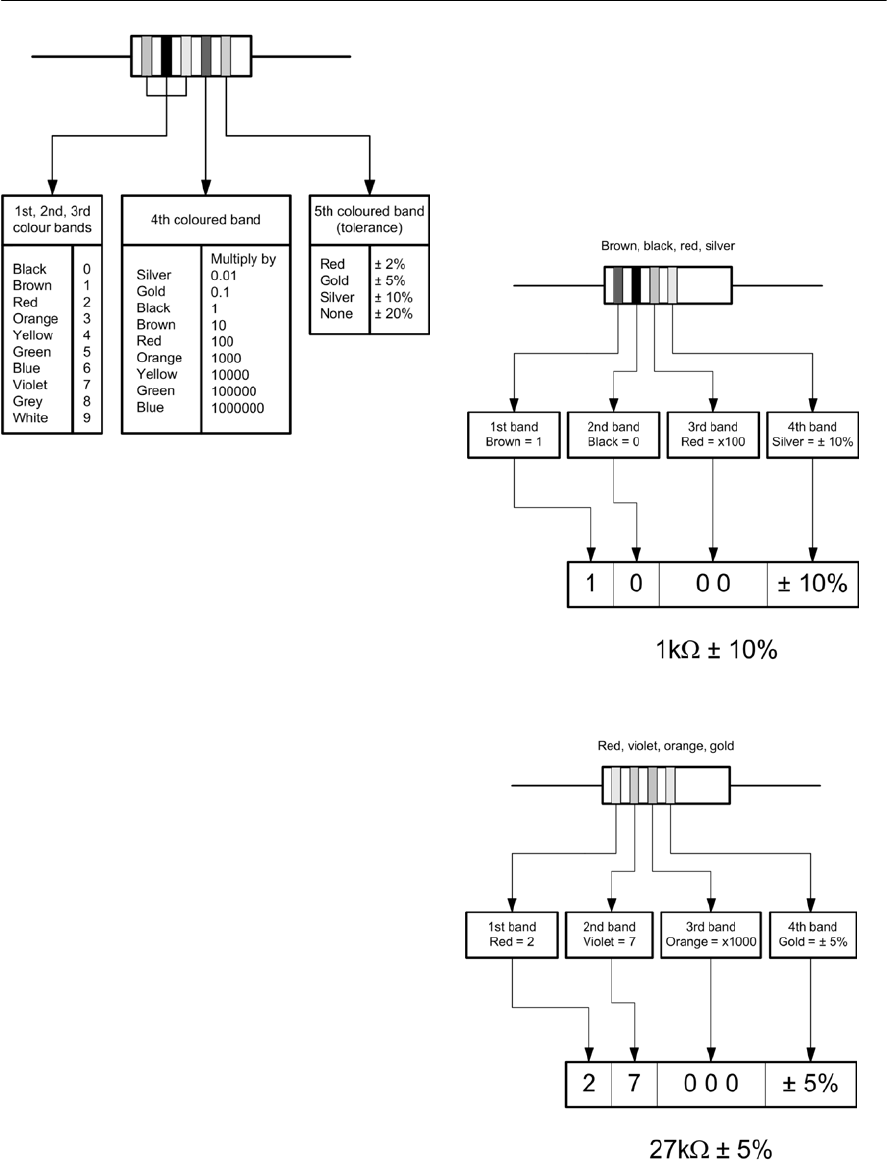
24 ELECTRONIC CIRCUITS: FUNDAMENTALS AND APPLICATIONS
Example 2.4
Aresistor is marked with the following coloured
stripes: brown, black, red, silver. What is its value
and tolerance?
Solution
See Fig. 2.6.
Example 2.5
Aresistor is marked with the following coloured
stripes: red, violet, orange, gold. What is its value
and tolerance?
Solution
See Fig. 2.7.
Example 2.6
Aresistor is marked with the following coloured
stripes: green, blue, black, gold. What is its value
and tolerance?
Solution
See Fig. 2.8.
Example 2.7
Aresistor is marked with the following coloured
stripes: red, green, black, black, brown. What is its
value and tolerance?
Solution
See Fig. 2.9.
Figure 2.5 Five band resistor colour code
Figure 2.7 See Example 2.5
Figure 2.6 See Example 2.4
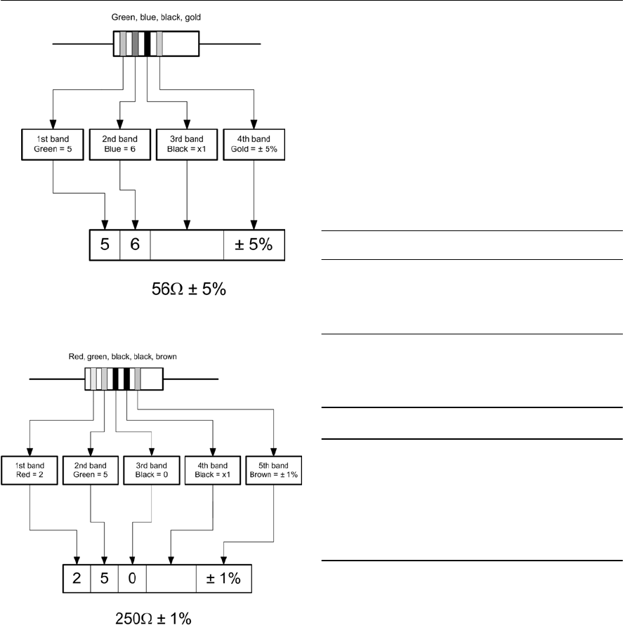
PASSIVE COMPONENTS 25
Example 2.8
A2.2 k$of ±2% tolerance is required. What four
band colour code does this correspond to?
Solution
Red (2), red (2), red (2 zeros), red (2% tolerance).
Thus all four bands should be red.
Figure 2.8 See Example 2.6
Figure 2.9 See Example 2.7
BS 1852 coding
Some types of resistor have markings based on a
system of coding defined in BS 1852. This system
involves marking the position of the decimal point
with a letter to indicate the multiplier concerned as
shown in Table 2.2. A further letter is then
appended to indicate the tolerance as shown in
Table 2.3.
Table 2.2 BS 1852 resistor multiplier markings
Letter Multiplier
R 1
K1,000
M1,000,000
Table 2.3 BS 1852 resistor tolerance markings
Letter Multiplier
F±1%
G±2%
J±5%
K±10%
M±20%
Example 2.9
Aresistor is marked coded with the legend 4R7K.
What is its value and tolerance?
Solution
4.7 $±10%
Example 2.10
Aresistor is marked coded with the legend 330RG.
What is its value and tolerance?
Solution
330 $±2%
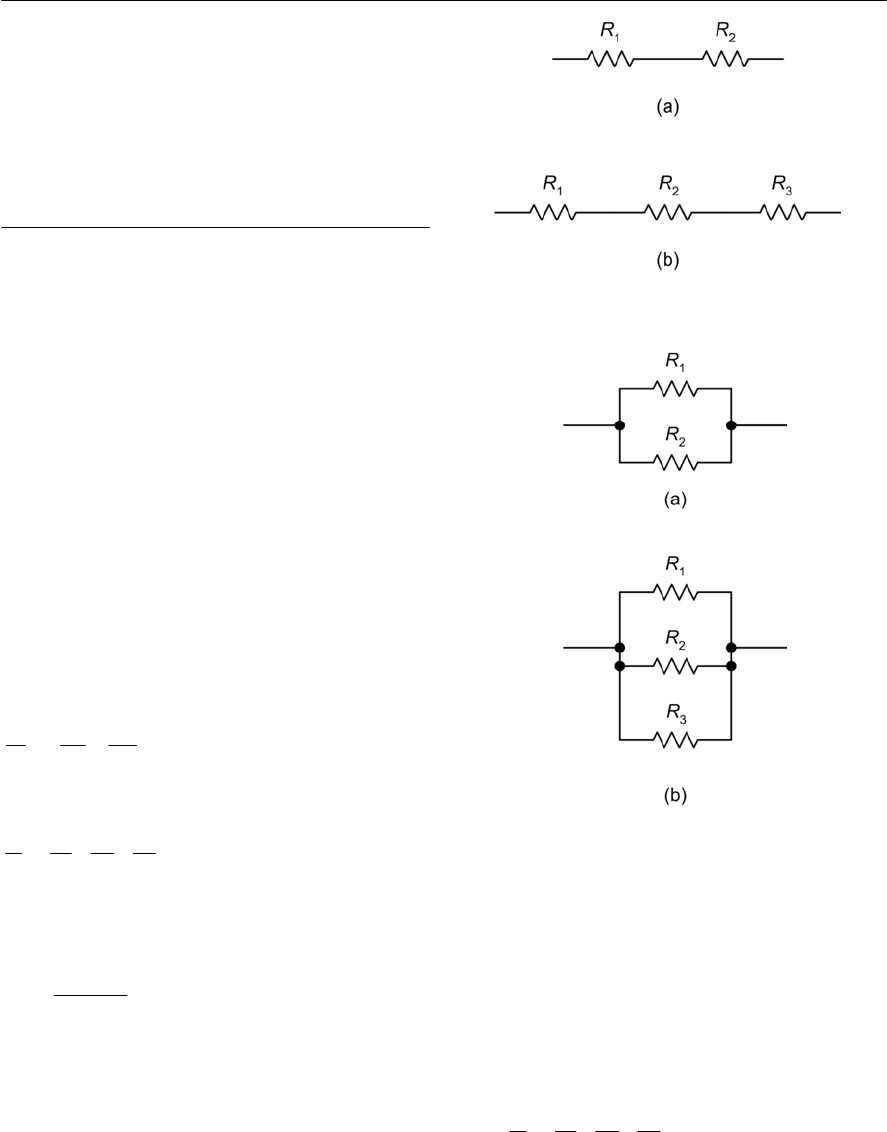
26 ELECTRONIC CIRCUITS: FUNDAMENTALS AND APPLICATIONS
Figure 2.10 Resistors in series
Figure 2.11 Resistors in parallel
Example 2.11
Aresistor is marked coded with the legend R22M.
What is its value and tolerance?
Solution
0.22 $±20%
Series and parallel combinations of
resistors
In order to obtain a particular value of resistance,
fixed resistors may be arranged in either series or
parallel as shown in Figs 2.10 and 2.11.
The effective resistance of each of the series
circuits shown in Fig. 2.10 is simply equal to the
sum of the individual resistances. So, for the circuit
shown in Fig. 2.10(a):
R = R1+R2
while for Fig. 2.10(b)
R = R1+R2+R3
Turning to the parallel resistors shown in Fig. 2.11,
the reciprocal of the effective resistance of each
circuit is equal to the sum of the reciprocals of the
individual resistances. Hence, for Fig. 2.11(a):
while for Fig. 2.12(b)
In the former case, the formula can be more
conveniently re-arranged as follows:
You can remember this as the product of the two
resistance values divided by the sum of the two
resistance values.
Example 2.12
Resistors of 22 $,47 $and 33 $are connected (a)
in series and (b) in parallel. Determine the effective
resistance in each case.
Solution
(a) In the series circuit R = R1+R2+R3,thus
R =22 $+47 $+33 $=102 $
(b) In the parallel circuit:
thus
12
111
=
RRR
+
123
1111
=
RRRR
++
12
12
=
RR
R
RR
×
+
123
1111
=
RRRR
++
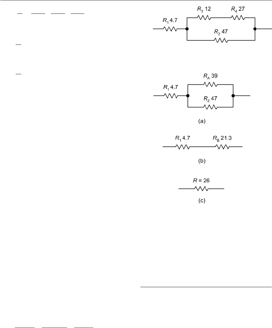
PASSIVE COMPONENTS 27
Figure 2.12 See Example 2.13
Figure 2.13 See Example 2.13
or
from which
Example 2.13
Determine the effective resistance of the circuit
shown in Fig. 2.12.
Solution
The circuit can be progressively simplified as
shown in Fig. 2.13. The stages in this simplification
are:
(a) R3and R4are in series and they can replaced
by a single resistance (RA)of (12 $+27 $) =
39 $.
(b) RAappears in parallel with R2.These two
resistors can be replaced by a single
resistance (RB)of (39 $×47 $)/(39 $+47
$) = 21.3 $.
(c) RBappears in series with R1.These two
resistors can be replaced by a single
resistance (R)of (21.3 $+4.7 $) = 26 $.
Example 2.14
Aresistance of 50 $rated at 2 W is required. What
parallel combination of preferred value resistors
will satisfy this requirement? What power rating
should each resistor have?
Solution
Two 100 $resistors may be wired in parallel to
provide a resistance of 50 $as shown below:
Note, from this, that when two resistors of the same
value are connected in parallel the resulting
resistance will be half that of a single resistor.
11 1 1
=
22 47 33
R++
1
=0.045 0.021 0.03
R
++
1
=0.096 = 10.42
R
12
12
100 100 10, 000
=50
100 100 200
RR
RRR
××
===
++
Having shown that two 100 $resistors connected
in parallel will provide us with a resistance of 50 $
we now need to consider the power rating. Since
the resistors are identical, the applied power will be
shared equally between them. Hence each resistor
should have a power rating of 1W.
Resistance and temperature
Figure 2.14 shows how the resistance of a metal
conductor (e.g. copper) varies with temperature.
Since the resistance of the material increases with
temperature, this characteristic is said to exhibit a
positive temperature coefficient (PTC).Not all
materials have a PTC characteristic. The resistance
of a carbon conductor falls with temperature and it
is therefore said to exhibit a negative temperature
coefficient (NTC).
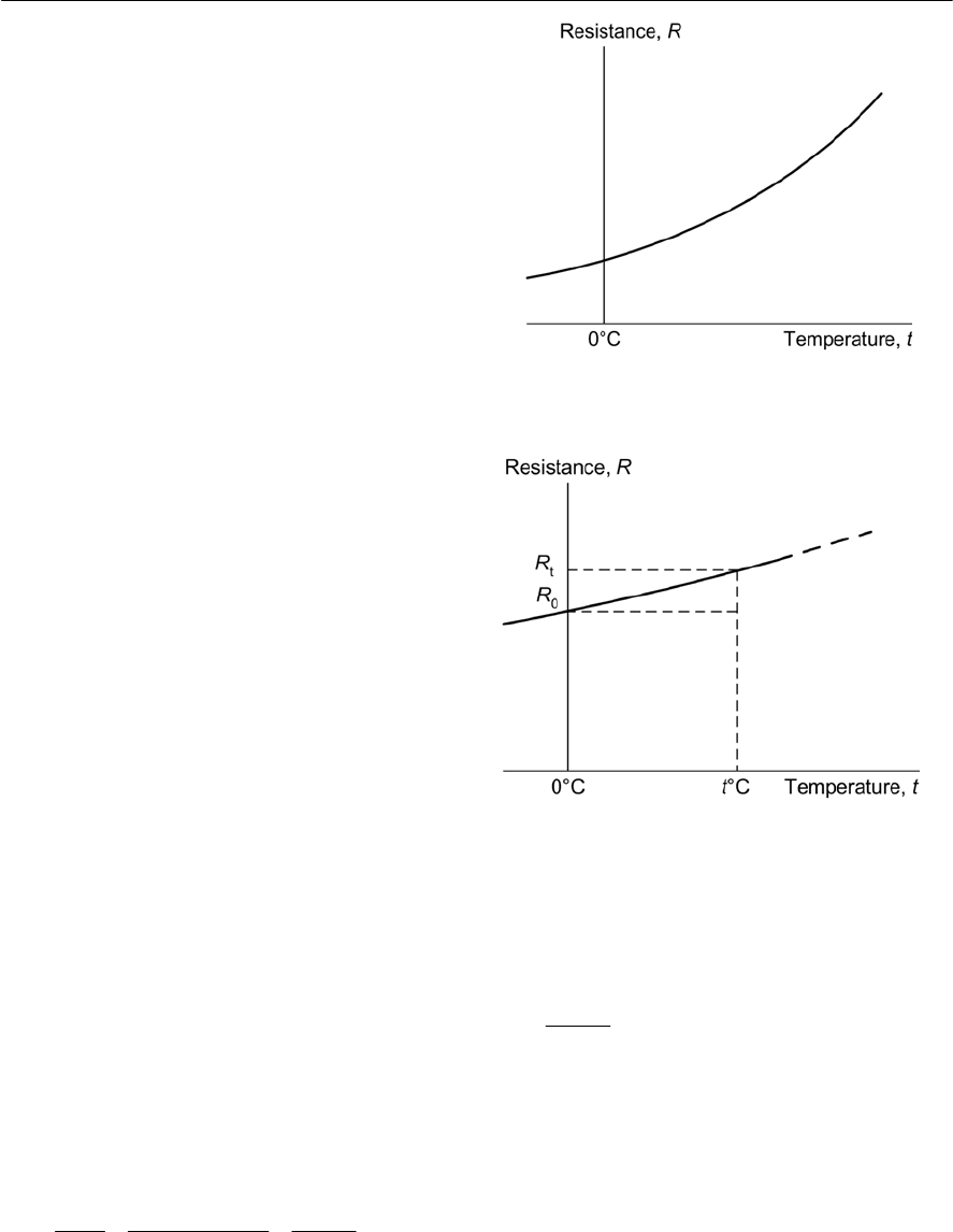
28 ELECTRONIC CIRCUITS: FUNDAMENTALS AND APPLICATIONS
The resistance of a conductor at a temperature, t,
is given by the equation:
Rt= R0(1 + "t + $t2+%t3...)
where ",$,%,etc. are constants and R0is the
resistance at 0°C.
The coefficients, $,%,etc. are quite small and
since we are normally only dealing with a relatively
restricted temperature range (e.g. 0°C to 100°C) we
can usually approximate the characteristic shown in
Fig. 2.14 to the straight line law shown in Fig. 2.15.
In this case, the equation simplifies to:
Rt= R0(1 + "t)
where "is known as the temperature coefficient
of resistance. Table 2.4 shows some typical values
for "(note that "is expressed in $/$/°C or just
/°C).
Example 2.15
Aresistor has a temperature coefficient of
0.001/°C. If the resistor has a resistance of 1.5 k$
at 0°C, determine its resistance at 80°C.
Solution
Now
Rt= R0(1 + "t)
thus
Rt=1.5k$×(1 + (0.001 × 80))
Hence
Rt=1.5 × 1.08 =1.62 k$
Example 2.16
Aresistor has a temperature coefficient of
0.0005/°C. If the resistor has a resistance of 680 $
at 20°C, what will its resistance be at 80°C?
Solution
First we must find the resistance at 0°C.
Rearranging the formula for Rtgives:
0
680 680
=
1 1 (0.0005 20) 1 0.01
t
R
Rt
==
++ × +
Figure 2.14 Variation of resistance with
temperature for a metal conductor
Figure 2.15 Straight line approximation of
Fig. 2.14
Hence
Now
Rt= R0(1 + "t)
thus
R90 = 673.3 × (1 + (0.0005 × 90))
Hence
R90 = 673.3 × 1.045 =704 $
0
680
= 673.3
1 0.01
R
=
+
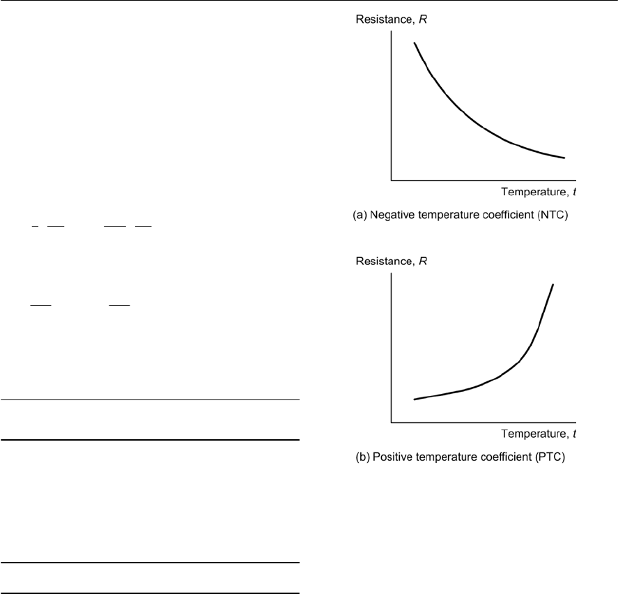
PASSIVE COMPONENTS 29
Example 2.17
Aresistor has a resistance of 40 $at at 0°C and
44 $at 100°C. Determine the resistor’s
temperature coefficient.
Solution
First we need to make "the subject of the formula:
Rt= R0(1 + "t)
Now
from which
t
0
1144
=11
100 40
R
tR
=
()
11
=1.1 1 0.1 0.001 / C
100 100
=×= °
Material Temperature coefficient of
resistance, "(/°C)
Platinum +0.0034
Silver +0.0038
Copper +0.0043
Iron +0.0065
Carbon 0.0005
Table 2.4
Temperature coefficient of resistance
Thermistors
With conventional resistors we would normally
require resistance to remain the same over a wide
range of temperatures (i.e.
"
should be zero). On
the other hand, there are applications in which we
could use the effect of varying resistance to detect a
temperature change. Components that allow us to
do this are known as
thermistors.
The resistance of
athermistor changes markedly with temperature
and these components are widely used in
temperature sensing and temperature compensating
applications. Two basic types of thermistor are
available, NTC and PTC (see Fig. 2.16).
Figure 2.16 Characteristics of (a) NTC and (b)
PTC thermistors
Typical NTC thermistors have resistances that
vary from a few hundred (or thousand) ohms at
25°C to a few tens (or hundreds) of ohms at
100°C. PTC thermistors, on the other hand, usually
have a resistance-temperature characteristic which
remains substantially flat (typically at around
100 $)over the range 0°C to around 75°C. Above
this, and at a critical temperature (usually in the
range 80°C to 120°C) their resistance rises very
rapidly to values of up to, and beyond, 10 k$(see
Fig. 2.16).
A typical application of PTC thermistors is over-
current protection. Provided the current passing
through the thermistor remains below the threshold
current, the effects of self-heating will remain
negligible and the resistance of the thermistor will
remain low (i.e. approximately the same as the
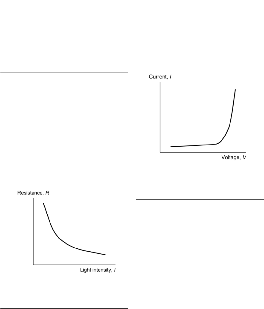
Figure 2.17 Characteristic of a light-dependent
resistor (LDR)
30 ELECTRONIC CIRCUITS: FUNDAMENTALS AND APPLICATIONS
resistance quoted at 25°C). Under fault conditions,
the current exceeds the threshold value by a
considerable margin and the thermistor starts to
self-heat. The resistance then increases rapidly and,
as a consequence, the current falls to the rest value.
Typical values of threshold and rest currents are
200 mA and 8 mA, respectively, for a device which
exhibits a nominal resistance of 25 $at 25°C.
Light-dependent resistors
Light-dependent resistors (LDR) use a
semiconductor material (i.e. a material that is
neither a conductor nor an insulator) whose
electrical characteristics vary according to the
amount of incident light. The two semiconductor
materials used for the manufacture of LDRs are
cadmium sulphide (CdS) and cadmium selenide
(CdSe). These materials are most sensitive to light
in the visible spectrum, peaking at about 0.6 µm for
CdS and 0.75 µm for CdSe. A typical CdS LDR
exhibits a resistance of around 1 M$in complete
darkness and less than 1 k$when placed under a
bright light source (see Fig. 2.17).
Voltage dependent resistors
The resistance of a voltage dependent resistor
(VDR) falls very rapidly when the voltage across it
exceeds a nominal value in either direction (see
Fig. 2.18). In normal operation, the current flowing
in a VDR is negligible, however, when the
resistance falls, the current will become appreciable
and a significant amount of energy will be
absorbed. VDRs are used as a means of ‘clamping’
the voltage in a circuit to a pre-determined level.
When connected across the supply rails to a circuit
(either a.c or d.c.) they are able to offer a measure
of protection against voltage surges.
Figure 2.18 Characteristic of a voltage dependent
resistor (VDR)
Variable resistors
Variable resistors are available in several forms
including those which use carbon tracks and those
which use a wirewound resistance element. In
either case, a moving slider makes contact with the
resistance element. Most variable resistors have
three (rather than two) terminals and as such are
more correctly known as potentiometers.Carbon
potentiometers are available with linear or semi-
logarithmic law tracks (see Fig. 2.19) and in rotary
or slider formats. Ganged controls, in which several
potentiometers are linked together by a common
control shaft, are also available. Figure 2.20 shows
aselection of variable resistors.
You will also encounter various forms of preset
resistors that are used to make occasional
adjustments (e.g. for calibration). Various forms of
preset resistor are commonly used including open
carbon track skeleton presets and fully
encapsulated carbon and multi-turn cermet types, as
shown in Fig. 2.21.
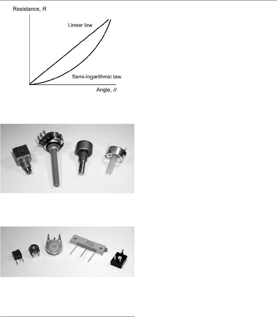
PASSIVE COMPONENTS 31
Figure 2.19 Characteristics for linear and semi-
logarithmic law variable resistors
Figure 2.20 A selection of common types of
carbon and wirewound variable resistors/
potentiometers
Figure 2.21 A selection of common types of
standard and miniature preset resistors/
potentiometers
Capacitors
Acapacitor is a device for storing electric charge.
In effect, it is a reservoir into which charge can be
deposited and then later extracted. Typical
applications include reservoir and smoothing
capacitors for use in power supplies, coupling a.c.
signals between the stages of amplifiers, and
decoupling supply rails (i.e. effectively grounding
the supply rails as far as a.c. signals are concerned).
A capacitor can consist of nothing more than two
parallel metal plates as shown in Fig. 1.10 on page
11. To understand what happens when a capacitor
is being charged and discharged take a look at Fig.
2.22. If the switch is left open (position A), no
charge will appear on the plates and in this
condition there will be no electric field in the space
between the plates nor will there be any charge
stored in the capacitor.
When the switch is moved to position B,
electrons will be attracted from the positive plate to
the positive terminal of the battery. At the same
time, a similar number of electrons will move from
the negative terminal of the battery to the negative
plate. This sudden movement of electrons will
manifest itself in a momentary surge of current
(conventional current will flow from the positive
terminal of the battery towards the positive terminal
of the capacitor).
Eventually, enough electrons will have moved to
make the e.m.f. between the plates the same as that
of the battery. In this state, the capacitor is said to
be fully charged and an electric field will be
present in the space between the two plates.
If, at some later time the switch is moved back to
position A, the positive plate will be left with a
deficiency of electrons whilst the negative plate
will be left with a surplus of electrons.
Furthermore, since there is no path for current to
flow between the two plates the capacitor will
remain charged and a potential difference will be
maintained between the plates.
Now assume that the switch is moved to position
C. The excess electrons on the negative plate will
flow through the resistor to the positive plate until a
neutral state once again exists (i.e. until there is no
excess charge on either plate). In this state the
capacitor is said to be fully discharged and the
electric field between the plates will rapidly
collapse. The movement of electrons during the
discharging of the capacitor will again result in a
momentary surge of current (current will flow from
the positive terminal of the capacitor and into the
resistor).
Figure 2.23 shows the direction of current flow
in the circuit of Fig. 2.22 during charging (switch in
position B) and discharging (switch in position C).
It should be noted that current flows momentarily
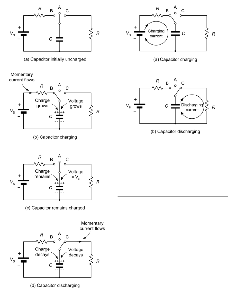
32 ELECTRONIC CIRCUITS: FUNDAMENTALS AND APPLICATIONS
Figure 2.22 Capacitor charging and discharging
Figure 2.23 Current flow during charging and
discharging
in both circuits even though you may think that the
circuit is broken by the gap between the capacitor
plates!
Capacitance
The unit of capacitance is the farad (F). A capacitor
is said to have a capacitance of 1 F if a current of
1 A flows in it when a voltage changing at the rate
of 1 V/s is applied to it. The current flowing in a
capacitor will thus be proportional to the product of
the capacitance, C,and the rate of change of
applied voltage. Hence:
i = C × (rate of change of voltage)
Note that we’ve used a small ito represent the
current flowing in the capacitor. We’ve done this
because the current is changing and doesn’t remain
constant.
The rate of change of voltage is often
represented by the expression dv/dt where dv
represents a very small change in voltage and dt

PASSIVE COMPONENTS 33
represents the corresponding small change in time.
Expressing this mathematically gives:
Example 2.18
Avoltage is changing at a uniform rate from 10 V
to 50 V in a period of 0.1 s. If this voltage is
applied to a capacitor of 22 µF, determine the
current that will flow.
Solution
Now the current flowing will be given by:
i = C × (rate of change of voltage)
Thus
From which
so
i=8.8 × 103=8.8 mA
Charge, capacitance and voltage
The charge or quantity of electricity that can be
stored in the electric field between the capacitor
plates is proportional to the applied voltage and the
capacitance of the capacitor. Thus:
Q = CV
where Qis the charge (in coulombs), Cis the
capacitance (in farads), and Vis the potential
difference (in volts).
Example 2.19
A10 uF capacitor is charged to a potential of 250
V. Determine the charge stored.
Solution
The charge stored will be given by:
=
dV
iC
dt
6
change in voltage 50 10
=22 10
change in time 0.1
iC
=× ×
66
40
=22 10 22 10 400
0.1
i
×× =××
Q = CV =10 × 10
6
×250 = 2.5 mC
Energy storage
The energy stored in a capacitor is proportional to
the product of the capacitance and the square of the
potential difference. Thus:
W = ½C V
2
where Wis the energy (in Joules), Cis the
capacitance (in Farads), and Vis the potential
difference (in Volts).
Example 2.20
Acapacitor of 47 µF is required to store 4J of
energy. Determine the potential difference that
must be applied to the capacitor.
Solution
The foregoing formula can be re-arranged to make
Vthe subject as follows:
from which
Capacitance and physical dimensions
The capacitance of a capacitor depends upon the
physical dimensions of the capacitor (i.e. the size of
the plates and the separation between them) and the
dielectric material between the plates. The
capacitance of a conventional parallel plate
capacitor is given by:
where Cis the capacitance (in farads), )
o
is the
permittivity of free space, )
r
is the
relative
permittivity
of the dielectric medium between the
plates), and dis the separation between the plates
(in metres).
6
224
=0.5
47 10
EE
VCC
×
==
×
63
6
8
=0.170 10 0.412 10 412 V
47 10
V
=×=×=
×
0
=
r
A
C
d

34 ELECTRONIC CIRCUITS: FUNDAMENTALS AND APPLICATIONS
Example 2.21
Acapacitor of 1 nF is required. If a dielectric
material of thickness 0.1 mm and relative
permittivity 5.4 is available, determine the required
plate area.
Solution
Re-arranging the formula
to make Athe subject gives:
from which
thus
A = 0.00209 m2or 20.9 cm2
0
=r
A
C
d
93
12
0
1 10 0.1 10
=
8.854 10 5.4
r
Cd
A
×××
=××
12
12
0.1 10
=
47.8116 10
A
×
×
Figure 2.24 Amulti-plate capacitor
In order to increase the capacitance of a capacitor,
many practical components employ multiple plates
(see Fig. 2.24). The capacitance is then given by:
where Cis the capacitance (in farads), )
o
is the
permittivity of free space, )
r
is the relative
permittivity of the dielectric medium between the
plates), and dis the separation between the plates
(in metres) and nis the total number of plates.
Example 2.22
Acapacitor consists of six plates each of area 20
cm
2
separated by a dielectric of relative permittivity
(
)
0
1
=
r
nA
Cd
4.5 and thickness 0.2 mm. Determine the value of
capacitance.
Solution
Using
gives:
from which
thus
C = 190 × 10
12
For 190 pF
Capacitor specifications
The specifications for a capacitor usually include
the value of capacitance (expressed in microfarads,
nanofarads or picofarads), the voltage rating (i.e.
the maximum voltage which can be continuously
applied to the capacitor under a given set of
conditions), and the accuracy or tolerance (quoted
as the maximum permissible percentage deviation
from the marked value).
Other practical considerations when selecting
capacitors for use in a particular application include
temperature coefficient, leakage current, stability
and ambient temperature range.
Table 2.5 summarizes the properties of five of
the most common types of capacitor. Note that
electrolytic capacitors require the application of a
polarizing voltage in order to the chemical action
on which they depend for their operation.
The polarizing voltages used for electrolytic
capacitors can range from as little as 1 V to several
hundred volts depending upon the working voltage
rating for the component in question.
Figure 2.25 shows some typical non-electrolytic
capacitors (including polyester, polystyrene,
ceramic and mica types) whilst Fig. 2.26 shows a
selection of electrolytic (polarized) capacitors. An
air-spaced variable capacitor is shown later in Fig.
2.34 on page 38.
(
)
0
1
=
r
nA
Cd
(
)
12 4
3
8.854 10 4.5 6 1 20 10
=0.2 10
C
×××××
×
16
13 12
3
3, 984.3 10
=19.921 10 190 10
0.2 10
C
×=×=×
×
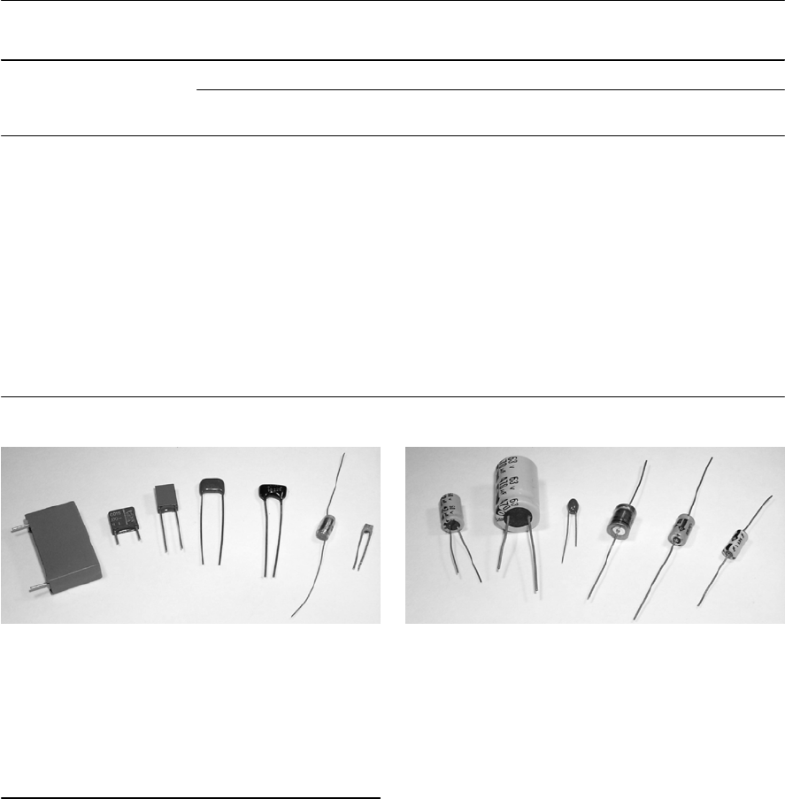
PASSIVE COMPONENTS 35
Property Capacitor type
Ceramic Electrolytic Polyester Mica Polystyrene
Capacitance range (F) 2.2 p to 100 n 100 n to 10 m 10 n to 2.2 µ 0.47 to 22 k 10 p to 22 n
Typical tolerance (%) ±10 and ±20 10 to +50 ±10 ±1 ±5
Typical voltage rating (W) 50 V to 200 V 6.3 V to 400 V 100 V to 400 V 350 V 100 V
Temperature coefficient
(ppm/°C)
+100 to 4700 +1000 typical +100 to +200 +50 +250
Stability Fair Poor Good Excellent Good
Ambient temperature range
(°C)
85 to +85 40 to +80 40 to +100 40 to +125 40 to +100
Typical applications High-frequency
and low-cost
Smoothing and
decoupling
Tuned circuits
and oscillators
General purpose General purpose
Table 2.5 Characteristics of common types of capacitor
Capacitor markings
The vast majority of capacitors employ written
markings which indicate their values, working
voltages, and tolerance. The most usual method of
marking resin dipped polyester (and other) types of
capacitor involves quoting the value (µF, nF or pF),
the tolerance (often either 10% or 20%), and the
working voltage (often using _ and ~ to indicate
d.c. and a.c. respectively). Several manufacturers
use two separate lines for their capacitor markings
and these have the following meanings:
First line: capacitance (pF or µF) and
tolerance (K = 10%, M = 20%)
Second line: rated d.c. voltage and code for the
dielectric material
Athree-digit code is commonly used to mark
monolithic ceramic capacitors. The first two digits
of this code correspond to the first two digits of the
value while the third digit is a multipler which
gives the number of zeros to be added to give the
value in picofarads. Other capacitor may use a
colour code similar to that used for marking resistor
values (see Fig. 2.28).
Figure 2.25 Atypical selection of non-
electrolytic capacitors (including polyester,
polystyrene, ceramic and mica types) with values
ranging from 10 pF to 470 nF and working voltages
from 50 V to 250 V
Figure 2.26 Atypical selection of electrolytic
(polarized) capacitors with values ranging from
1µF to 470 µF and working voltages from 10 V to
63 V
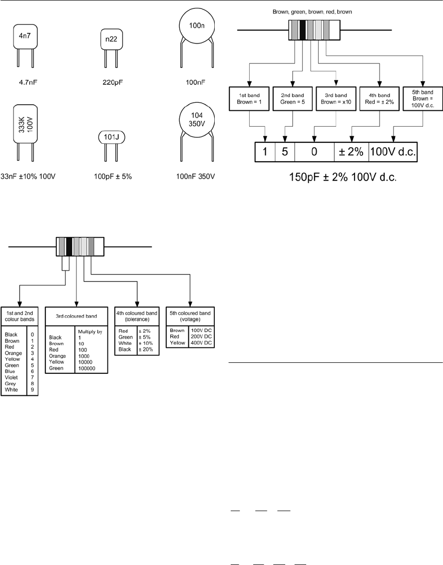
36 ELECTRONIC CIRCUITS: FUNDAMENTALS AND APPLICATIONS
Example 2.23
Amonolithic ceramic capacitor is marked with the
legend ‘103K’. What is its value?
Solution
The value (pF) will be given by the first two digits
(10) followed by the number of zeros indicated by
the third digit (3). The value of the capacitor is thus
10,000 pF or 10 nF. The final letter (K) indicates
that the capacitor has a tolerance of 10%.
Figure 2.27 Examples of capacitor markings
Figure 2.28 Capacitor colour code
Figure 2.29 See Example 2.23
Series and parallel combination of
capacitors
In order to obtain a particular value of capacitance,
fixed capacitors may be arranged in either series or
parallel (Figs 2.30 and 2.31). The reciprocal of the
effective capacitance of each of the series circuits
shown in Fig. 2.30 is equal to the sum of the
reciprocals of the individual capacitances. Hence,
for Fig. 2.30(a):
while for Fig. 2.30(b):
Example 2.24
Atubular capacitor is marked with the following
coloured stripes: brown, green, brown, red, brown.
What is its value, tolerance, and working voltage?
Solution
See Fig. 2.29.
12
111
=
CCC
+
123
1111
=
CCCC
++
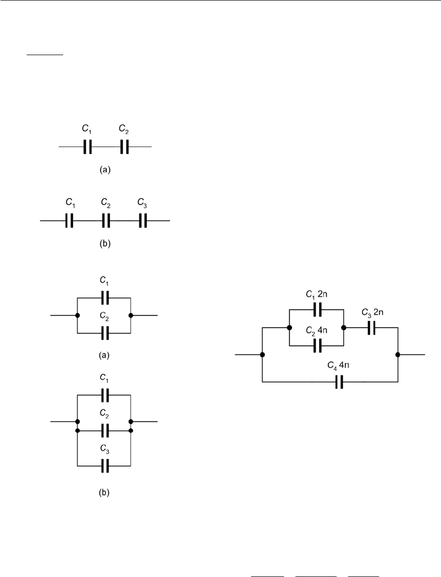
PASSIVE COMPONENTS 37
Figure 2.30 Capacitors in series
In the former case, the formula can be more
conveniently re-arranged as follows:
You can remember this as the product of the two
capacitor values divided by the sum of the two
values—just as you did for two resistors in parallel.
For a parallel arrangement of capacitors, the
effective capacitance of the circuit is simply equal
to the sum of the individual capacitances. Hence,
for Fig. 2.31(a):
C = C1+C2
12
12
=
CC
C
CC
×
+
Figure 2.31 Capacitors in parallel
while for Fig. 2.31(b)
C = C1+C2+C3
Example 2.25
Determine the effective capacitance of the circuit
shown in Fig. 2.32.
Solution
The circuit of Fig. 2.32 can be progressively
simplified as shown in Fig. 2.33. The stages in this
simplification are:
(a) C1and C2are in parallel and they can be
replaced by a single capacitor (CA)of (2 nF +
4 nF) = 6 nF.
(b) CAappears in series with C3.These two
resistors can be replaced by a single capacitor
(CB)of (6 nF × 2 nF)/(6 nF + 2 nF) =1.5 nF.
(c) CBappears in parallel with C4.These two
capacitors can be replaced by a single
capacitance (C)of (1.5 nF + 4 nF) = 5.5 nF.
Figure 2.32 See Example 2.25
Figure 2.29
Example 2.26
Acapacitance of 50 µF (rated at 100 V) is required.
What series combination of preferred value
capacitors will satisfy this requirement? What
voltage rating should each capacitor have?
Solution
Two 100 µF capacitors wired in series will provide
acapacitance of 50 µF, as follows:
12
12
100 100 10, 000
= 50
µF
100 100 200
CC
CCC
××
===
++
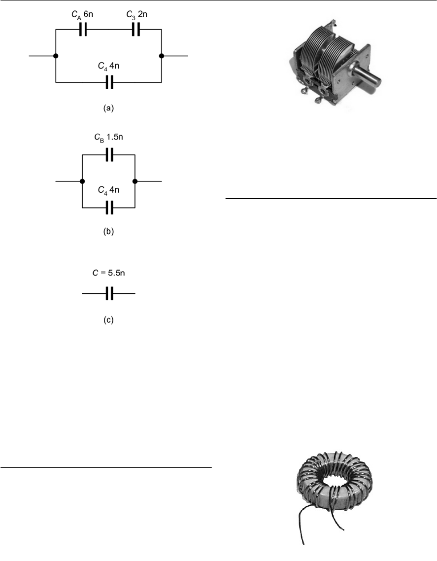
38 ELECTRONIC CIRCUITS: FUNDAMENTALS AND APPLICATIONS
Figure 2.34 An air-spaced variable capacitor.
This component (used for tuning an AM radio) has
two separate variable capacitors (each of 500 pF
maximum) operated from a common control shaft.
Figure 2.33 See Example 2.25
Since the capacitors are of equal value, the applied
d.c. potential will be shared equally between them.
Thus each capacitor should be rated at 50 V. Note
that, in a practical circuit, we could take steps to
ensure that the d.c. voltage was shared equally
between the two capacitors by wiring equal, high-
value (e.g. 100 k$)resistors across each capacitor.
Variable capacitors
By moving one set of plates relative to the other, a
capacitor can be made variable. The dielectric
material used in a variable capacitor can be either
air (see Fig. 2.34) or plastic (the latter tend to be
more compact). Typical values for variable
capacitors tend to range from about 25 pF to
500 pF. These components are commonly used for
tuning radio receivers.
Inductors
Inductors provide us with a means of storing
electrical energy in the form of a magnetic field.
Typical applications include chokes, filters and (in
conjunction with one or more capacitors) frequency
selective circuits. The electrical characteristics of
an inductor are determined by a number of factors
including the material of the core (if any), the
number of turns, and the physical dimensions of the
coil. Figure 2.35 shows the construction of a typical
toroidal inductor wound on a ferrite (high
permeability) core.
In practice every coil comprises both inductance
(L)and a small resistance (R).The circuit of Fig.
2.36 shows these as two discrete components. In
reality the inductance and the resistance (we often
refer to this as a loss resistance because it’s
something that we don’t actually want) are both
Figure 2.35 Apractical coil contains inductance
and resistance
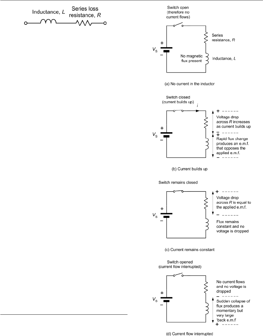
PASSIVE COMPONENTS 39
distributed throughout the component but it is
convenient to treat the inductance and resistance as
separate components in the analysis of the circuit.
To understand what happens when a changing
current flows through an inductor, take a look at the
circuit shown in Fig. 2.37(a). If the switch is left
open, no current will flow and no magnetic flux
will be produced by the inductor. If the switch is
closed, as shown in Fig. 2.37(b), current will begin
to flow as energy is taken from the supply in order
to establish the magnetic field. However, the
change in magnetic flux resulting from the
appearance of current creates a voltage (an induced
e.m.f.)across the coil which opposes the applied
e.m.f. from the battery.
The induced e.m.f. results from the changing
flux and it effectively prevents an instantaneous
rise in current in the circuit. Instead, the current
increases slowly to a maximum at a rate which
depends upon the ratio of inductance (L)to
resistance (R)present in the circuit.
After a while, a steady state condition will be
reached in which the voltage across the inductor
will have decayed to zero and the current will have
reached a maximum value determined by the ratio
of Vto R(i.e. Ohm’s Law). This is shown in Fig.
2.37(c).
If, after this steady state condition has been
achieved, the switch is opened, as shown in Fig.
2.37(d), the magnetic field will suddenly collapse
and the energy will be returned to the circuit in the
form of an induced back e.m.f. which will appear
across the coil as the field collapses. For large
values of magnetic flux and inductance this back
e.m.f. can be extremely large!
Inductance
Inductance is the property of a coil which gives rise
to the opposition to a change in the value of current
flowing in it. Any change in the current applied to a
Figure 2.36 Apractical coil contains inductance
and a small amount of series loss resistance
Figure 2.37 Flux and e.m.f. generated when a
changing current is applied to an inductor

40 ELECTRONIC CIRCUITS: FUNDAMENTALS AND APPLICATIONS
coil/inductor will result in an induced voltage
appearing across it. The unit of inductance is the
henry (H) and a coil is said to have an inductance
of 1H if a voltage of 1V is induced across it when a
current changing at the rate of 1 A/s is flowing in it.
The voltage induced across the terminals of an
inductor will thus be proportional to the product of
the inductance (L)and the rate of change of applied
current. Hence:
e =
L × (rate of change of current)
Note that the minus sign indicates the polarity of
the voltage, i.e. opposition to the change.
The rate of change of current is often represented
by the expression di/dt where di represents a very
small change in current and dt represents the
corresponding small change in time. Using
mathematical notation to write this we arrive at:
You might like to compare this with the similar
relationship that we obtained for the current
flowing in a capacitor shown on page 33.
Example 2.27
Acurrent increases at a uniform rate from 2 A to
6 A in a period of 250 ms. If this current is applied
to an inductor of 600 mH, determine the voltage
induced.
Solution
Now the induced voltage will be given by:
e =
L × (rate of change of current)
Thus
From which
so
)=9.6 V
Energy storage
The energy stored in an inductor is proportional to
the product of the inductance and the square of the
current flowing in it. Thus:
W = ½L I 2
where Wis the energy (in Joules), Lis the
capacitance (in Henries), and Iis the current
flowing in the inductor (in Amps).
Example 2.28
An inductor of 20 mH is required to store 2.5 J of
energy. Determine the current that must be applied.
Solution
The foregoing formula can be re-arranged to make
Ithe subject as follows:
From which
Inductance and physical dimensions
The inductance of an inductor depends upon the
physical dimensions of the inductor (e.g. the length
and diameter of the winding), the number of turns,
and the permeability of the material of the core.
The inductance of an inductor is given by:
where Lis the inductance (in Henries), µ0is the
permeability of free space, µris the relative
permeability of the magnetic core, lis the mean
length of the core (in metres), and Ais the cross-
sectional area of the core (in square metres).
Example 2.29
An inductor of 100 mH is required. If a closed
magnetic core of length 20 cm, cross-sectional area
15 cm2and relative permeability 500 is available,
determine the number of turns required.
=
di
eL
dt
3
3
change in current 6 2
= 60 10
change in time
250 10
eL
=××
×
33
4
=600 10 0.6 10 16
0.25
e
×× =××
3
222.5
=0.5
20 10
EE
ILL
×
==
×
3
3
5
=0.25 10 250 15.81 A
20 10
I
=×==
×
2
0r
=
nA
Ll
µµ
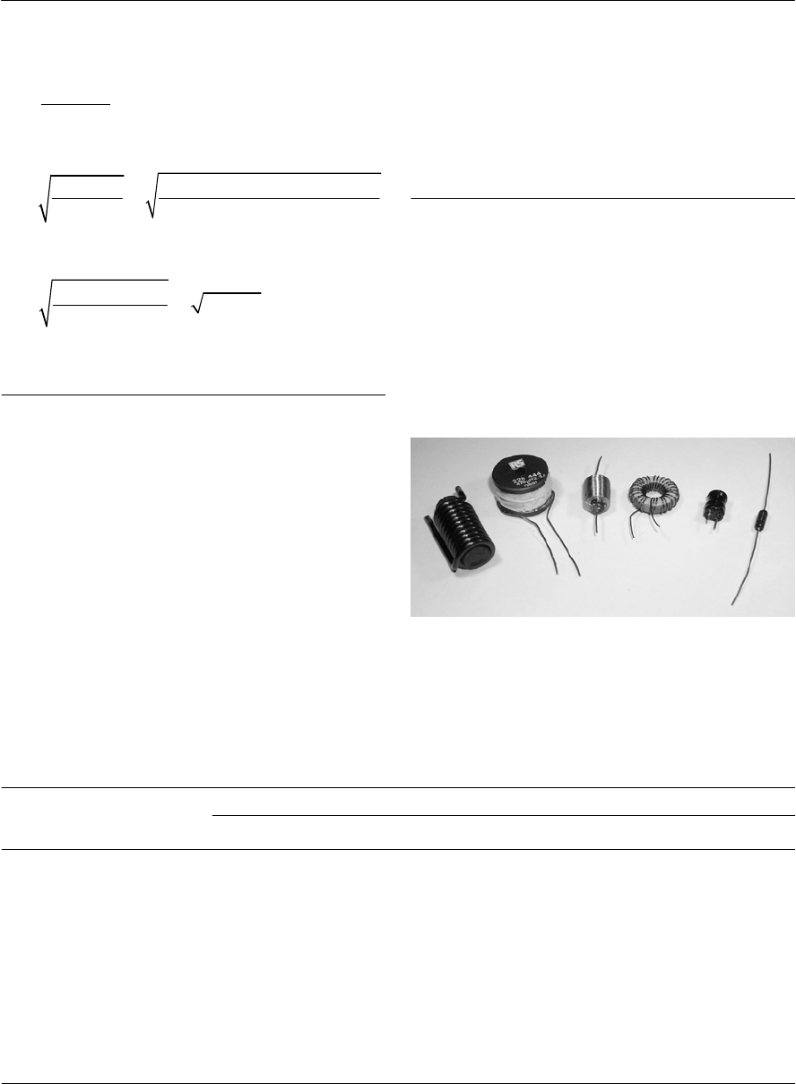
PASSIVE COMPONENTS 41
Solution
First we must re-arrange the formula
in order to make nthe subject:
From which
Hence the inductor requires 146 turns of wire.
Inductor specifications
Inductor specifications normally include the value
of inductance (expressed in henries, millihenries or
microhenries), the current rating (i.e. the maximum
current which can be continuously applied to the
inductor under a given set of conditions), and the
accuracy or tolerance (quoted as the maximum
permissible percentage deviation from the marked
value). Other considerations may include the
temperature coefficient of the inductance (usually
expressed in parts per million, p.p.m., per unit
temperature change), the stability of the inductor,
2
0r
=
nA
Ll
µµ
32
274
0r
100 10 20 10
=
12.57 10 500 15 10
Ll
nnA
µµ
××××
=××××
2
11
210
=21, 215 146
94,275 10
n
×==
×
Property Inductor type
Air cored Ferrite cored Ferrite pot cored Iron cored
Core material Air Ferrite rod Ferrite pot Laminated steel
Inductance range (H) 50 n to 100 µ 10 µ to 1 m 1 m to 100 m 20 m to 20
Typical d.c. resistance ($)0.05 to 5 0.1 to 10 5 to 100 10 to 200
Typical tolerance (%) ±5 ±10 ±10 ±20
Typical Q-factor 60 80 40 20
Typical frequency range (Hz) 1 M to 500 M 100 k to 100 M 1 k to 10 M 50 to 10 k
Typical applications Tuned circuits and
filters
Filters and HF
transformers
LF and MF filters
and transformers
Smoothing chokes
and filters
Table 2.6 Characteristics of common types of inductor
the d.c. resistance of the coil windings (ideally
zero), the Q-factor (quality factor) of the coil, and
the recommended working frequency range. Table
2.6 summarizes the properties of four common
types of inductor. Some typical small inductors are
shown in Fig. 2.38. These have values of
inductance ranging from 15 µH to 1 mH.
Inductor markings
As with capacitors, the vast majority of inductors
use written markings to indicate values, working
current, and tolerance. Some small inductors are
marked with coloured stripes to indicate their value
and tolerance (in which case the standard colour
values are used and inductance is normally
expressed in microhenries).
Figure 2.38 A selection of small inductors with
values ranging from 15 µH to 1 mH
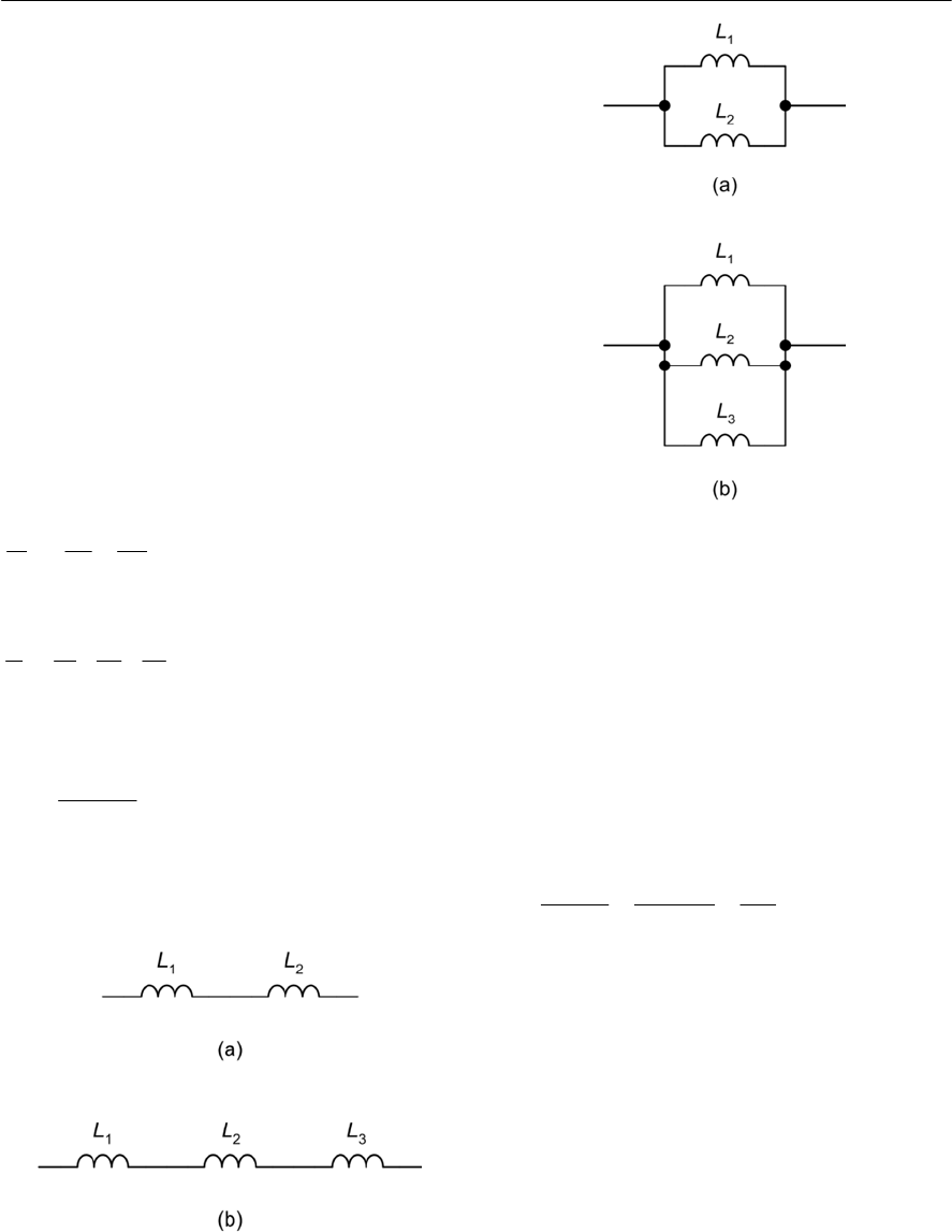
42 ELECTRONIC CIRCUITS: FUNDAMENTALS AND APPLICATIONS
Series and parallel combinations of
inductors
In order to obtain a particular value of inductance,
fixed inductors may be arranged in either series or
parallel as shown in Figs 2.39 and 2.40.
The effective inductance of each of the series
circuits shown in Fig. 2.39 is simply equal to the
sum of the individual inductances. So, for the
circuit shown in Fig. 2.39(a):
L = L1+L2
while for Fig. 2.39 (b)
L = L1+L2+L3
Turning to the parallel inductors shown in Fig.
2.40, the reciprocal of the effective inductance of
each circuit is equal to the sum of the reciprocals of
the individual inductances. Hence, for Fig. 2.40(a):
while for Fig. 2.40(b)
In the former case, the formula can be more
conveniently re-arranged as follows:
You can remember this as the product of the two
inductance values divided by the sum of the two
inductance values.
Example 2.30
An inductance of 5 mH (rated at 2 A) is required.
What parallel combination of preferred value
inductors will satisfy this requirement?
Solution
Two 10 mH inductors may be wired in parallel to
provide an inductance of 5 mH as shown below:
Since the inductors are identical, the applied
current will be shared equally between them. Hence
each inductor should have a current rating of 1 A.
Example 2.31
Determine the effective inductance of the circuit
shown in Fig. 2.41.
Solution
The circuit can be progressively simplified as
shown in Fig. 2.42. The stages in this simplification
are as follows:
12
111
=
LLL
+
123
1111
=
LLLL
++
12
12
=
LL
L
LL
×
+
Figure 2.39 Inductors in series
Figure 2.40 Inductors in parallel
12
12
10 10 100
= 5 mH
10 + 10 20
LL
LLL
××
===
+
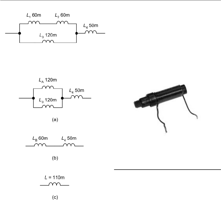
PASSIVE COMPONENTS 43
(a) L1and L2are in series and they can be
replaced by a single inductance (LA)of (60 +
60) = 120 mH.
(b) LAappears in parallel with L2.These two
inductors can be replaced by a single
inductor (LB)of (120 × 120)/(120 + 120) =
60 mH.
(c) LBappears in series with L4.These two
inductors can be replaced by a single
inductance (L)of (60 + 50) = 110 mH.
Figure 2.40 See Example 2.31
Figure 2.42 See Example 2.31
Variable inductors
Aferrite cored inductor can be made variable by
moving its core in or out of the former onto which
the coil is wound. Many small inductors have
threaded ferrite cores to make this possible (see
Fig. 2.43). Such inductors are often used in radio
and high-frequency applications where precise
tuning is required.
Figure 2.43 An adjustable ferrite cored inductor
Surface mounted components (SMC)
Surface mounting technology (SMT) is now
widely used in the manufacture of printed circuit
boards for electronic equipment. SMT allows
circuits to be assembled in a much smaller space
than would be possible using components with
conventional wire leads and pins that are mounted
using through-hole techniques. It is also possible to
mix the two technologies, i.e. some through-hole
mounting of components and some surface
mounted components present on the same circuit
board. The following combinations are possible:
•Surface mounted components (SMC) on both
sides of a printed circuit board
•SMC on one side of the board and
conventional through-hole components
(THC) on the other
•Amixture of SMC and THC on both sides of
the printed circuit board.
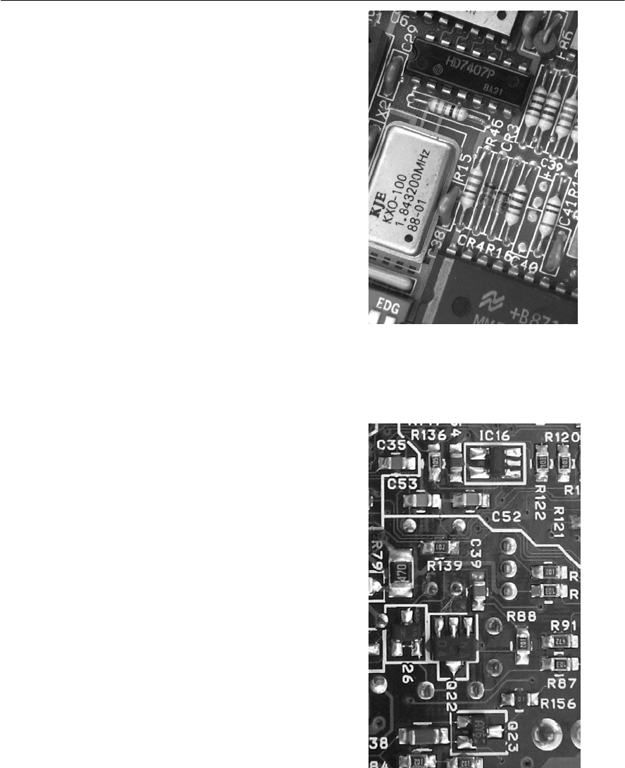
44 ELECTRONIC CIRCUITS: FUNDAMENTALS AND APPLICATIONS
Surface mounted components are supplied in
packages that are designed for mounting directly on
the surface of a PCB. To provide electrical contact
with the PCB, some SMC have contact pads on
their surface. Other devices have contacts which
extend beyond the outline of the package itself but
which terminate on the surface of the PCB rather
than making contact through a hole (as is the case
with a conventional THC). In general, passive
components (such as resistors, capacitors and
inductors) are configured leadless for surface
mounting, whilst active devices (such as transistors
and integrated circuits) are available in both surface
mountable types as well as lead as well as in
leadless terminations suitable for making direct
contact to the pads on the surface of a PCB.
Most surface mounted components have a flat
rectangular shape rather than the cylindrical shape
that we associate with conventional wire leaded
components. During manufacture of a PCB, the
various SMC are attached using re-flow soldering
paste (and in some cases adhesives) which consists
of particles of solder and flux together with binder,
solvents and additives. They need to have good
‘tack’ in order to hold the components in place and
remove oxides without leaving obstinate residues.
The component attachment (i.e. soldering!)
process is completed using one of several
techniques including convection ovens in which the
PCB is passed, using a conveyor belt, through a
convection oven which has separate zones for
preheating, flowing and cooling, and infra-red re-
flow in which infra-red lamps are used to provide
the source of heat.
Surface mounted components are generally too
small to be marked with colour codes. Instead,
values may be marked using three digits. For
example, the first two digits marked on a resistor
normally specify the first two digits of the value
whilst the third digit gives the number of zeros that
should be added.
Example 2.32
In Fig. 1.18, R88 is marked ‘102’. What is its
value?
Solution
R88 will have a value of 1,000 $(i.e. 10 followed
by two zeros).
Figure 2.44 Conventional components mounted
on a printed circuit board. Note that components
such as C38, R46, etc. have leads that pass through
holes in the printed circuit board
Figure 2.45 Surface mounted components (note
the appearance of capacitors C35, C52, and C53,
and resistors, R87, R88, R91, etc.)
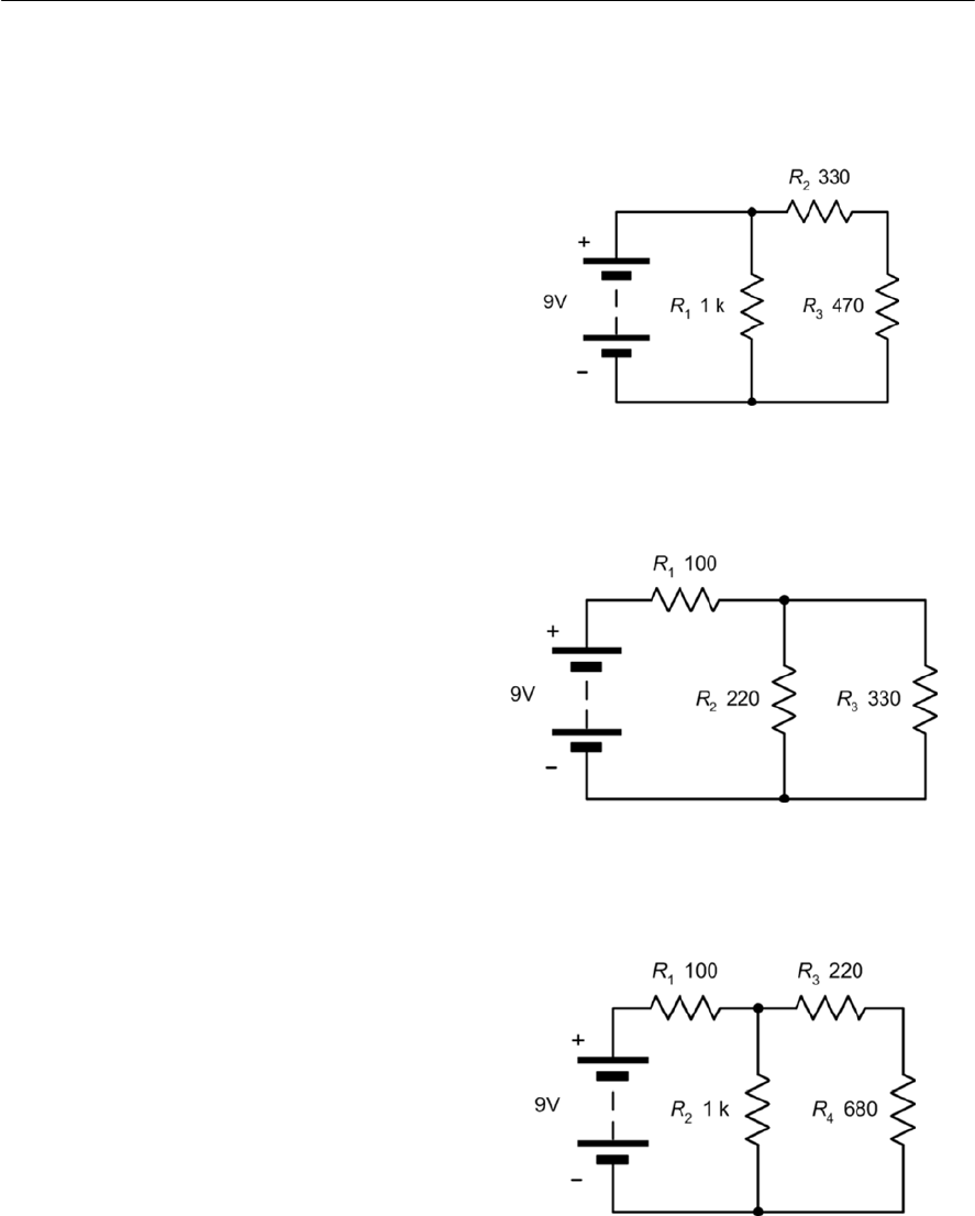
PASSIVE COMPONENTS 45
Practical investigation
Objective
To investigate the resistance of series and parallel
combinations of resistors.
Components and test equipment
Breadboard, digital or analogue meter with d.c.
current ranges, 9 V d.c. power source (either a 9 V
battery or an a.c. mains adapter with a 9 V 400 mA
output), test leads, resistors of 100 $,220 $,
330 $,470 $,680 $and 1k $,connecting wire.
Procedure
Connect the resistor network and power supply (or
battery) as shown in Fig. 2.46. Select the 20 V d.c.
voltage range on the multimeter then measure and
record the supply voltage (this should be
approximately 9 V). Now break the positive
connection to the circuit, change the range on the
multimeter to the 20 mA d.c. current range and
measure the current supplied to the circuit.
Next measure and record the voltage dropped
across each resistor (don’t forget to change ranges
on the multimeter when making each
measurement).
Finally, break the circuit at one end of each of
resistor in turn, then measure and record the current
flowing. Repeat the procedure for the other two
resistor networks circuits shown in Figs. 2.47 and
2.48.
Measurements and calculations
Record your results in a table for each network.
Use the recorded values of current and voltage for
each resistor to calculate the value of resistance and
compare this with the marked value. Check that the
measured value lies within the tolerance band for
each resistor.
Calculate the resistance of each network (looking
in at the supply terminals) and compare this with
the resistance calculated by dividing the supply
voltage by the supply current.
Conclusion
Comment on the results. Did your measured values
agree with the marked values? Were these within
Figure 2.46 Circuit diagram—first network
Figure 2.47 Circuit diagram—second network
Figure 2.48 Circuit diagram—third network
the tolerance range for the resistors used in the
investigation? If the readings were not in agreement
can you suggest why?

46 ELECTRONIC CIRCUITS: FUNDAMENTALS AND APPLICATIONS
Important formulae introduced in this
chapter
Component tolerance:
(page 18)
Resistors in series:
(page 7)
R = R1+R2+R3
Resistors in parallel:
(page 5)
Two resistors in parallel:
(page 8)
Resistance and temperature:
(page 9)
Rt= R0(1 + "t)
Current flowing in a capacitor:
(page 13)
Charge in a capacitor:
(page 15)
Q = C V
Energy stored in a capacitor:
(page 13)
W = ½C V2
Capacitance of a capacitor:
(page 15)
Capacitors in series:
(page 14)
Two capacitors in series:
(page 14)
Capacitors in parallel:
(page 36)
C = C1+C2+C3
Induced e.m.f. in an inductor:
(page 39)
Energy stored in an inductor:
(page 39)
W = ½L I 2
Inductance of an inductor:
(page 39)
Inductors in series:
(page 40)
L = L1+L2+L3
Inductors in parallel:
(page 40)
Two inductors in parallel:
(page 40)
error
Tolerance = 100%
marked value ×
123
1111
=
RRRR
++
12
12
=
RR
R
RR
×
+
=
dV
iC
dt
0
=r
A
C
d
123
1111
=
CCCC
++
12
12
=
CC
C
CC
×
+
=
di
eL
dt
2
0r
=
nA
Ll
µµ
123
1111
=
LLLL
++
12
12
=
LL
L
LL
×
+
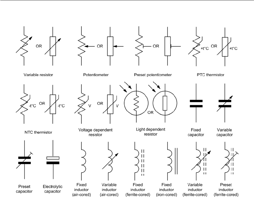
PASSIVE COMPONENTS 47
Symbols introduced in this chapter
Figure 2.49 Circuit symbols introduced in this chapter
Problems
2.1 A power supply rated at 15 V, 0.25 A is to
be tested at full rated output. What value of
load resistance is required and what power
rating should it have? What type of resistor
is most suitable for this application and
why?
2.2 Determine the value and tolerance of
resistors marked with the following coloured
bands:
(a) red, violet, yellow, gold
(b) brown, black, black, silver
(c) blue, grey, green, gold
(d) orange, white, silver, gold
(e) red, red, black, brown, red.
2.3 A batch of resistors are all marked yellow,
violet, black, gold. If a resistor is selected
from this batch, within what range would
you expect its value to be?
2.4 Resistors of 27 $,33 $,56 $and 68 $are
available. How can two or more of these be
arranged to realize the following resistance
values?
(a) 60 $
(b) 14.9 $
(b) 124 $
(b) 11.7 $
(b) 128 $.
2.5 Three 100 $resistors are connected as
shown in Fig. 2.50. Determine the effective
resistance of the circuit.
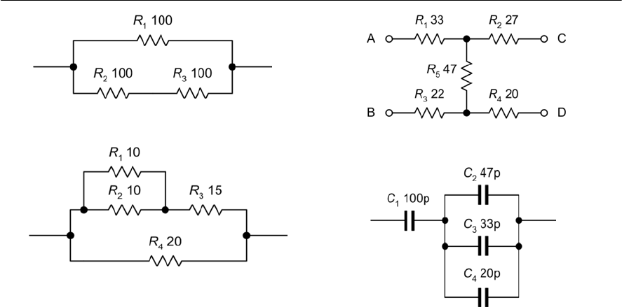
48 ELECTRONIC CIRCUITS: FUNDAMENTALS AND APPLICATIONS
2.6 Determine the effective resistance of the
circuit shown in Fig. 2.51.
2.7 Determine the resistance of the resistor
network shown in Fig. 2.52 looking into
terminal A and B with (a) terminals C and D
left open circuit and (b) terminals C and D
short circuit.
2.8 A resistor has a temperature coefficient of
0.0008/°C. If the resistor has a resistance of
390 $at 0°C, determine its resistance at
55°C.
2.9 A resistor has a temperature coefficient of
0.004/°C. If the resistor has a resistance of
82 k$at 20°C, what will its resistance be at
75°C?
2.10 A resistor has a resistance of 218 $at 0°C
and 225 $at 100°C. Determine the
resistor’s temperature coefficient.
2.11 Capacitors of 1 µF, 3.3 µF, 4.7 µF and 10 µF
are available. How can two or more of these
capacitors be arranged to realize the
following capacitance values?
(a) 8 µF
(b) 11 µF
(c) 19 µF
(d) 0.91 µF
(e) 1.94 µF
2.12 Three 180 pF capacitors are connected (a) in
series and (b) in parallel. Determine the
effective capacitance of each combination.
2.13 Determine the effective capacitance of the
circuit shown in Fig. 2.53.
2.14 A capacitor of 330 µF is charged to a
potential of 63 V. Determine the quantity of
energy stored.
2.15 A parallel plate capacitor has plates of
0.02 m2.Determine the capacitance of the
capacitor if the plates are separated by a
dielectric of thickness 0.5 mm and relative
permittivity 5.6.
2.16 A capacitor is required to store 0.5 J of
energy when charged from a 120 V d.c.
supply. Determine the value of capacitance
required.
2.17 The current in a 2.5 H inductor increases
uniformly from zero to 50 mA in 400 ms.
Determine the e.m.f. induced.
2.18 An inductor has 200 turns of wire wound on
a closed magnetic core of mean length
24 cm, cross-sectional 10 cm2and relative
permeability 650. Determine the inductance
of the inductor.
2.19 A current of 4 A flows in a 60 mH inductor.
Determine the energy stored.
2.20 Inductors of 22 mH and 68 mH are
connected (a) in series and (b) in parallel.
Determine the effective inductance in each
case.
Answers to these problems appear on page 374.
Figure 2.50 See Question 2.5
Figure 2.51 See Question 2.6
Figure 2.52 See Question 2.7
Figure 2.53 See Question 2.13
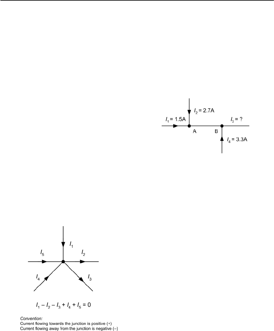
3
D.C. circuits
In many cases, Ohm’s Law alone is insufficient to
determine the magnitude of the voltages and
currents present in a circuit. This chapter introduces
several techniques that simplify the task of solving
complex circuits. It also introduces the concept of
exponential growth and decay of voltage and
current in circuits containing capacitance and
resistance and inductance and resistance. It
concludes by showing how humble C–R circuits
can be used for shaping the waveforms found in
electronic circuits. We start by introducing two of
the most useful laws of electronics.
Kirchhoff’s Laws
Kirchhoff’s Laws relate to the algebraic sum of
currents at a junction (or node)or voltages in a
network (or mesh). The term ‘algebraic’ simply
indicates that the polarity of each current or voltage
drop must be taken into account by giving it an
appropriate sign, either positive (+) or negative (–).
Kirchhoff’s Current Law states that the
algebraic sum of the currents present at a junction
(node) in a circuit is zero (see Fig. 3.1).
Figure 3.1 Kirchhoff’s Current Law
Example 3.1
In Fig. 3.2, use Kirchhoff’s Current Law to
determine:
(a) the value of current flowing between A and B
(b) the value of I3.
Solution
(a) I1and I2both flow towards Node A so, applying
our polarity convention, they must both be
positive. Now, assuming that a current I5flows
between A and B and that this current flows
away from the junction (obvious because I1and
I2both flow towards the junction) we arrive at
the following Kirchhoff’s Current Law
equation:
+I1+I24I5=0
From which:
I5= I1+I2=1.5 + 2.7 =4.2 A
(b) Moving to Node B, let’s assume that I3flows
outwards so we can say that:
+I4+I54I3=0
From which:
I3= I4+I5=3.3 + 4.2 =7.5 A
Figure 3.2 See Example 3.1
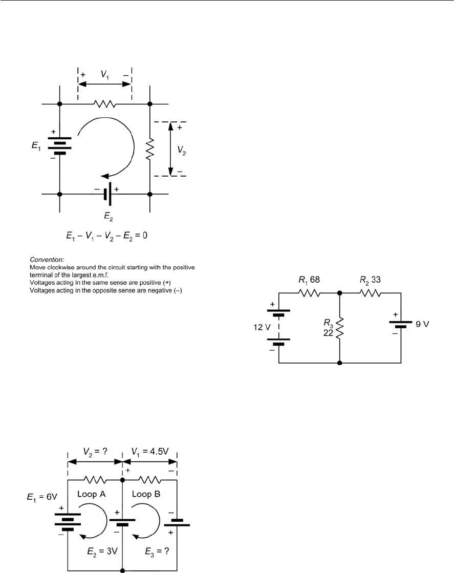
50 ELECTRONIC CIRCUITS: FUNDAMENTALS AND APPLICATIONS
Kirchhoff’s Voltage Law states that the algebraic
sum of the potential drops in a closed network (or
‘mesh’) is zero (see Fig. 3.3).
Figure 3.3 Kirchhoff’s Voltage Law
Example 3.2
In Fig. 3.4, use Kirchhoff’s Voltage Law to
determine:
(a) the value of V2
(b) the value of E3.
Figure 3.4 See Example 3.2
Solution
(a) In Loop A, and using the conventions shown in
Fig. 3.3, we can write down the Kirchhoff’s
Voltage Law equations:
E14V24E2=0
From which:
V2= E14E2=643=3 V
(b) Similarly, in Loop B, we can say that:
E24V2+E3=0
From which:
E3= V24E2=4.5 43=1.5 V
Example 3.3
Determine the currents and voltages in the circuit
of Fig. 3.5.
Figure 3.5 See Example 3.3
Solution
In order to solve the circuit shown in Fig. 3.5, it is
first necessary to mark the currents and voltages on
the circuit, as shown in Figs 3.6 and 3.7.
By applying Kirchhoff’s Current Law at Node A
that we’ve identified in Fig. 3.5:
+I1+I24I3=0
Therefore:
I1=I34I2=0(i)
By applying Kirchhoff’s Voltage Law in Loop A
we obtain:
12 4V14V3=0
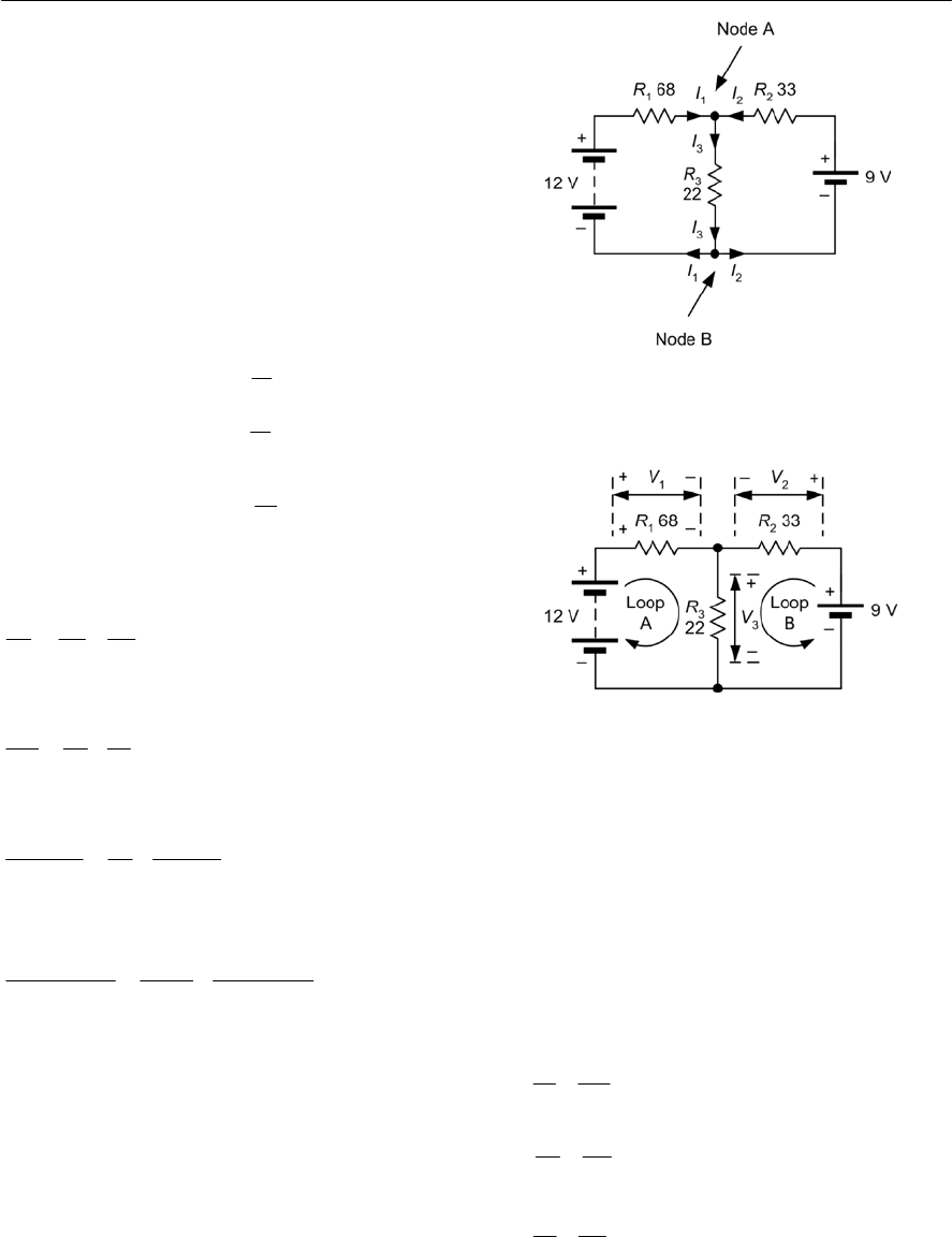
D.C. CIRCUITS 51
Figure 3.6 See Example 3.3
Figure 3.7 See Example 3.3
From which:
V1=12 4V3(ii)
By applying Kirchhoff’s Voltage Law in Loop B
we obtain:
94V24V3=0
From which:
V2= 9 4V3(iii)
Next we can generate three further relationships by
applying Ohm’s Law:
V1=I1R1from which
V2=I2R2from which
and
V3=I3R3from which
Combining these three relationships with the
Current Law equation (i) gives:
from which:
(iv)
Combining (ii) and (iii) with (iv) gives:
Multiplying both sides of the expression gives:
3(12 4V3)=15V3410(9 4V3)
From which:
36 43V3=15V3490 + V3
36 + 90 =15V3+10V3+ 3V3
and:
126 = 28V3so V3=126/28 = 4.5 V
3
12
132
=
V
VV
RRR
1
1
1
V
I
R
=
2
2
2
V
I
R
=
3
3
3
V
I
R
=
3
12
=
100 22 33
V
VV
(
)
(
)
33
3
12 9
=
100 22 33
VV
V
(
)
(
)
33
3
330 12 330 9
330
=
100 22 33
VV
V
From (ii):
V
1
=12 4V
3
so V
1
=12 44.5 = 7.5 V
From (iii):
V
2
= 9 4V
3
so V
2
= 9 44.5 = 4.5 V
Using the Ohm’s Law equations that we met earlier
gives:
1
1
1
7.5
0.068 A 68 mA
110
V
IR
== = =
2
2
2
4.5
0.136 A 136 mA
33
V
IR
== = =
3
3
3
4.5
0.204 A 204 mA
22
V
IR
== = =
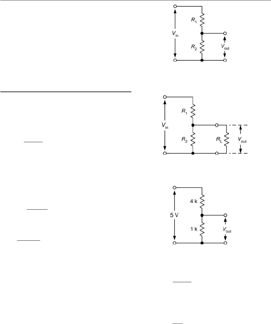
52 ELECTRONIC CIRCUITS: FUNDAMENTALS AND APPLICATIONS
Figure 3.8 Potential divider circuit
Finally, it’s worth checking these results with the
Current Law equation (i):
+I1+I24I3=0
Inserting our values for I1,I2and I3gives:
+0.068 + 0.136 4204 =0
Since the left and right hand sides of the equation
are equal we can be reasonably confident that our
results are correct.
The potential divider
The potential divider circuit (see Fig. 3.8) is
commonly used to reduce voltages in a circuit. The
output voltage produced by the circuit is given by:
It is, however, important to note that the output
voltage (Vout)will fall when current is drawn from
the arrangement.
Figure 3.9 shows the effect of loading the
potential divider circuit. In the loaded potential
divider (Fig. 3.9) the output voltage is given by:
where:
Example 3.4
The potential divider shown in Fig. 3.10 is used as
asimple voltage calibrator.Determine the output
voltage produced by the circuit:
(a) when the output terminals are left open-circuit
(i.e. when no load is connected); and
(b) when the output is loaded by a resistance of
10 kF.
Solution
(a) In the first case we can simply apply the
formula:
where Vin =5V, R1=4 kFand R2=1 kF.
Hence:
(b) In the second case we need to take into account
the effect of the 10 kFresistor connected to the
output terminals of the potential divider.
Figure 3.9 Loaded potential divider circuit
Figure 3.10 See Example 3.4
2
out in
12
R
VV
RR
=+
p
out in
1p
R
VV
RR
=+
2L
p
2L
RR
R
RR
×
=+
2
out in
12
R
VV
RR
=+
out
1
51 V
41
V=× =
+
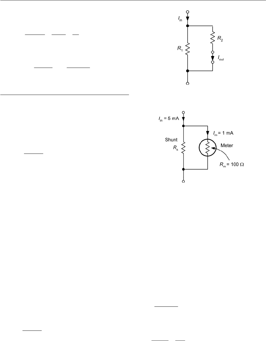
D.C. CIRCUITS 53
First we need to find the equivalent resistance
of the parallel combination of R2and RL:
Then we can determine the output voltage from:
The current divider
The current divider circuit (see Fig. 3.11) is used to
divert a known proportion of the current flowing in
acircuit. The output current produced by the circuit
is given by:
It is, however, important to note that the output
current (Iout)will fall when the load connected to
the output terminals has any appreciable resistance.
Example 3.5
Amoving coil meter requires a current of 1 mA to
provide full-scale deflection. If the meter coil has a
resistance of 100 Fand is to be used as a
milliammeter reading 5 mA full-scale, determine
the value of parallel shunt resistor required.
Solution
This problem may sound a little complicated so it is
worth taking a look at the equivalent circuit of the
meter (Fig. 3.12) and comparing it with the current
divider shown in Fig. 3.11.
We can apply the current divider formula,
replacing Iout with Im(the meter full-scale deflection
current) and R2with Rm(the meter resistance). R1is
the required value of shunt resistor, Rs,Hence:
Re-arranging the formula gives:
2L
p
2L
110 10
0.909 k
1 10 11
RR
RRR
××
====
++
p
out in
1p
0.909
5 0.925 V
4 0.909
R
VV
RR
==×=
++
1
out in
12
R
II
RR
=+
Figure 3.11 Current divider circuit
Figure 3.12 See Example 3.5
I
m
× (
R
s
+
R
m
) =
I
in
×
R
s
thus
I
m
R
s
+
I
m
R
m
=
I
in
R
s
or
I
in
R
s
4
I
m
R
s
=
I
m
R
m
from which
R
s
(
I
in
4
I
m
) =
I
m
R
m
so
Now
I
in
= 1 mA,
R
m
=100 Fand
I
in
= 5 mA, thus:
s
out in
sm
R
II
RR
=+
mm
s
in m
IR
R
II
=
s
1 100 100
25
51 4
R×
===
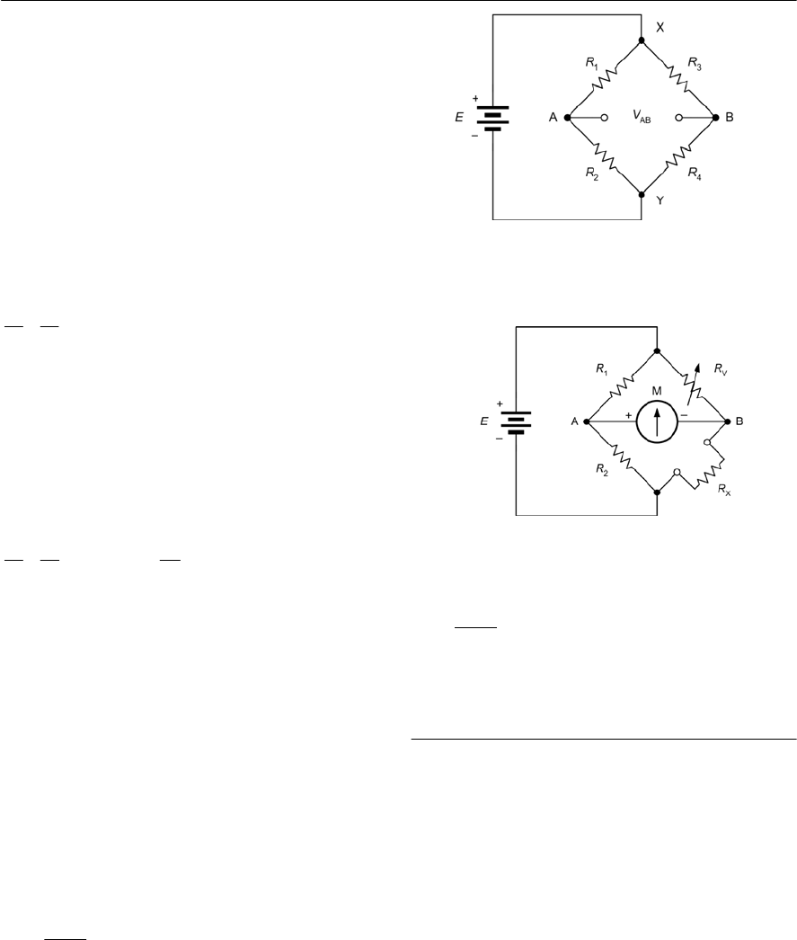
54 ELECTRONIC CIRCUITS: FUNDAMENTALS AND APPLICATIONS
The Wheatstone bridge
The Wheatstone bridge forms the basis of a number
of useful electronic circuits including several that
are used in instrumentation and measurement.
The basic form of Wheatstone bridge is shown in
Fig. 3.13. The voltage developed between A and B
will be zero when the voltage between A and Y is
the same as that between B and Y. In effect, R1and
R2constitute a potential divider as do R3and R4.
The bridge will be balanced (and VAB =0) when
the ratio of R1:R2is the same as the ratio R3:R4.
Hence, at balance:
Apractical form of Wheatstone bridge that can be
used for measuring unknown resistances is shown
in Fig. 3.14.
In this practical form of Wheatstone bridge, R1
and R2are called the ratio arms while one arm
(that occupied by R3in Fig. 3.13) is replaced by a
calibrated variable resistor. The unknown resistor,
Rx,is connected in the fourth arm. At balance:
thus
Example 3.6
AWheatstone bridge is based on the circuit shown
in Fig. 3.14. If R1and R2can each be switched so
that they have values of either 100 For 1 kFand
RVis variable between 10 Fand 10 kF,determine
the range of resistance values that can be measured.
Solution
The maximum value of resistance that can be
measured will correspond to the largest ratio of
R2:R1(i.e. when R2is 1 kFand R1is 100 F)and the
highest value of RV (i.e. 10 kF). In this case:
The minimum value of resistance that can be
measured will correspond to the smallest ratio of
R2:R1(i.e. when R1is 100 Fand R1is 1 kF)and the
smallest value of RV (i.e. 10 F). In this case:
Hence the range of values that can be measured
extends from 1 Fto 100 kF.
Thévenin’s Theorem
Thévenin’s Theorem allows us to replace a
complicated network of resistances and voltage
sources with a simple equivalent circuit comprising
asingle voltage source connected in series with a
single resistance (see Fig. 3.15).
The single voltage source in the Thévenin
equivalent circuit, Voc,is simply the voltage that
appears between the terminals when nothing is
connected to it. In other words, it is the open-circuit
voltage that would appear between A and B.
The single resistance that appears in the
Thévenin equivalent circuit, R,is the resistance that
would be seen looking into the network between A
Figure 3.13 Basic Wheatstone bridge circuit
Figure 3.14 See Example 3.6
v
1
2x
R
R
RR
=
3
1
2 4
R
R
RR
=
2
xv
1
R
RR
R
=×
x
1, 000
10,000 100,000 = 100 k
100
R
=× =
x
100
10 0.1 10 = 1
1, 00 0
R
=×=×
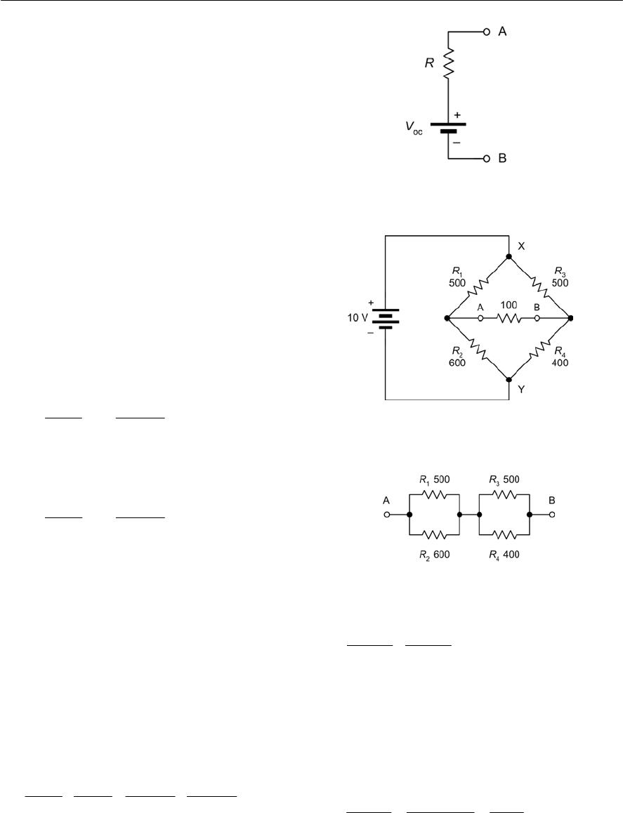
D.C. CIRCUITS 55
and B when all of the voltage sources (assumed
perfect) are replaced by short-circuit connections.
Note that if the voltage sources are not perfect (i.e.
if they have some internal resistance) the equivalent
circuit must be constructed on the basis that each
voltage source is replaced by its own internal
resistance.
Once we have values for Voc and R,we can
determine how the network will behave when it is
connected to a load (i.e. when a resistor is
connected across the terminals A and B).
Example 3.7
Figure 3.16 shows a Wheatstone bridge. Determine
the current that will flow in a 100 Fload connected
between terminals A and B.
Solution
First we need to find the Thévenin equivalent of the
circuit. To find Voc we can treat the bridge
arrangement as two potential dividers.
The voltage across R2will be given by:
Hence the voltage at A relative to Y, VAY,will be
5.454 V.
The voltage across R4will be given by:
Hence the voltage at B relative to Y, VBY,will be
4.444 V.
The voltage VAB will be the difference between
VAY and VBY.This, the open-circuit output voltage,
VAB,will be given by:
VAB = VAY 4VBY = 5.454 44.444 = 1.01 V
Next we need to find the Thévenin equivalent
resistance looking in at A and B. To do this, we can
redraw the circuit, replacing the battery (connected
between X and Y) with a short-circuit, as shown in
Fig. 3.17.
The Thévenin equivalent resistance is given by
the relationship:
From which:
The Thévenin equivalent circuit is shown in Fig.
3.18. To determine the current in a 100 Fload
connected between A and B, we can simply add a
100 Fload to the Thévenin equivalent circuit, as
shown in Fig. 3.19. By applying Ohm’s Law in Fig.
3.19 we get:
2
12
600
10 10 5.454 V
500 600
R
VRR
=× =× =
++
4
34
400
10 10 4.444 V
500 400
R
VRR
=× =× =
++
34
12
12 34
500 600 500 400
500 600 500 400
RR
RR
RRR RR
×
×××
=+= +
++ + +
300, 000 200, 000
272.7 222.2 494.9
1,100 900
R
= + =+=
Figure 3.15
Thévenin equivalent circuit
Figure 3.16
See Example 3.7
Figure 3.17
See Example 3.7
oc
1.01 1.01
1.698 mA
100 494.9 100 594.9
V
IR
== ==
++
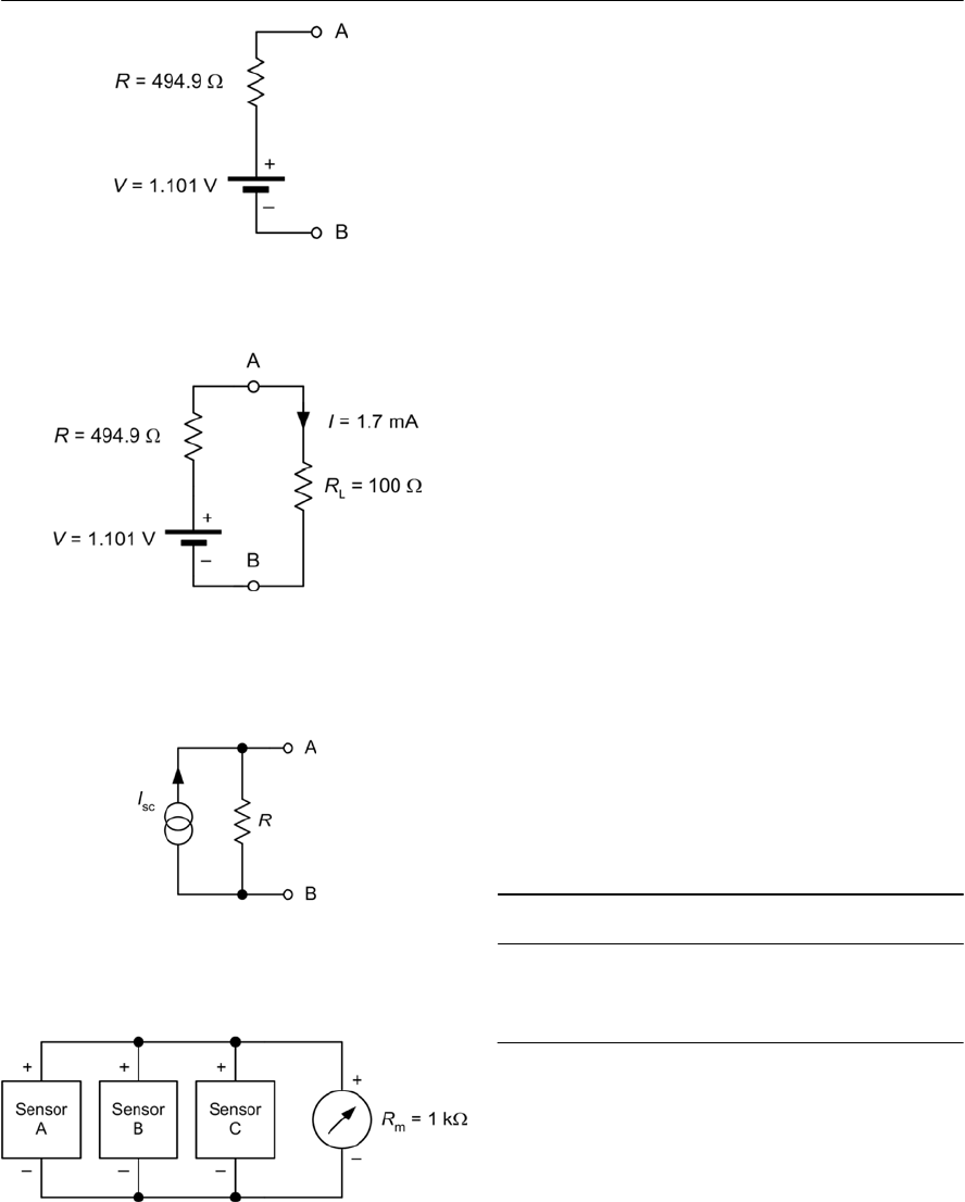
56 ELECTRONIC CIRCUITS: FUNDAMENTALS AND APPLICATIONS
Norton’s Theorem
Norton’s Theorem provides an alternative method
of reducing a complex network to a simple
equivalent circuit. Unlike Thévenin’s Theorem,
Norton’s Theorem makes use of a current source
rather than a voltage source. The Norton equivalent
circuit allows us to replace a complicated network
of resistances and voltage sources with a simple
equivalent circuit comprising a single constant
current source connected in parallel with a single
resistance (see Fig. 3.20).
The constant current source in the Norton
equivalent circuit, Isc,is simply the short-circuit
current that would flow if A and B were to be
linked directly together. The resistance that appears
in the Norton equivalent circuit, R, is the resistance
that would be seen looking into the network
between A and B when all of the voltage sources
are replaced by short-circuit connections. Once
again, it is worth noting that, if the voltage sources
have any appreciable internal resistance, the
equivalent circuit must be constructed on the basis
that each voltage source is replaced by its own
internal resistance.
As with the Thévenin equivalent, we can
determine how a network will behave by obtaining
values for Isc and R.
Example 3.8
Three temperature sensors having the following
characteristics shown in the table below are
connected in parallel as shown in Fig. 3.21:
Determine the voltage produced when the
arrangement is connected to a moving-coil meter
having a resistance of 1 kF.
Solution
First we need to find the Norton equivalent of the
circuit. To find Isc we can determine the short-
circuit current from each sensor and add them
together.
Figure 3.18 Thévenin equivalent of Fig. 3.16
Figure 3.19 Determining the current when the
Thévenin equivalent circuit is loaded
Figure 3.20 Norton equivalent circuit
Figure 3.21 See Example 3.8
Sensor A B C
Output voltage
(open circuit) 20 mV 30 mV 10 mV
Internal resistance 5 kF3 kF2 kF
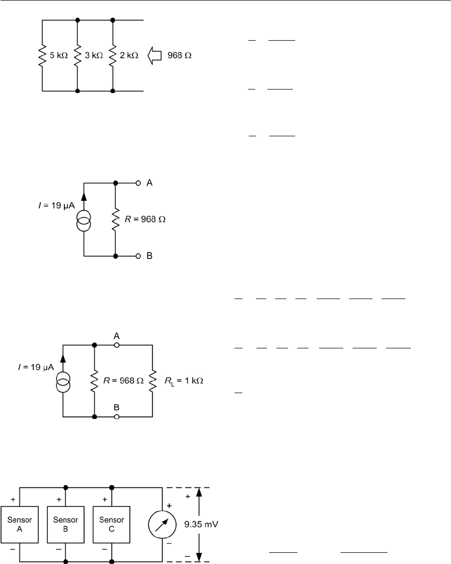
D.C. CIRCUITS 57
For sensor A:
For sensor B:
For sensor C:
The total current, Isc,will be given by:
Isc = 4µA + 10 µA + 5 µA =19 µA
Next we need to find the Norton equivalent
resistance. To do this, we can redraw the circuit
showing each sensor replaced by its internal
resistance, as shown in Fig. 3.22.
The equivalent resistance of this arrangement
(think of this as the resistance seen looking into the
circuit in the direction of the arrow shown in Fig.
3.22) is given by:
where R1= 5 kF,R2= 3 kF,R3= 2 kF.Hence:
or
from which:
R=968 F
The Norton equivalent circuit is shown in Fig. 3.23.
To determine the voltage in a l kFmoving coil
meter connected between A and B, we can make
use of the Norton equivalent circuit by simply
adding a 1 kFresistor to the circuit and applying
Ohm’s Law, as shown in Fig. 3.24.
The voltage appearing across the moving coil
meter in Fig. 3.25 will be given by:
hence:
V = 19 µA × 492 F=9.35 mV
Figure 3.22 Determining the equivalent
resistance in Fig. 3.21
Figure 3.23 Norton equivalent of the circuit in
Fig. 3.21
20 mV
= 4 A
5 kF
V
IR
µ
==
30 mV
=10 A
3 kF
V
IR
µ
= =
10 mV
= 5 A
2 k
F
V
I
R
µ
==
123
1111 1 1 1
=
5,000 3,000 2,000
RRRR
++= + +
1
=0.0002 + 0.00033 0.0005 0.00103
R
+=
m
sc
m
1,000 968
=19 A
1,000 + 968
RR
VI RR
µ
××
×=×
+
123
1111 1 1 1
=
5,000 3,000 2,000
RRRR
++= + +
Figure 3.24 Determining the output voltage when
the Norton equivalent circuit is loaded with 1 kF
Figure 3.25 The voltage drop across the meter is
found to be 9.35 mV
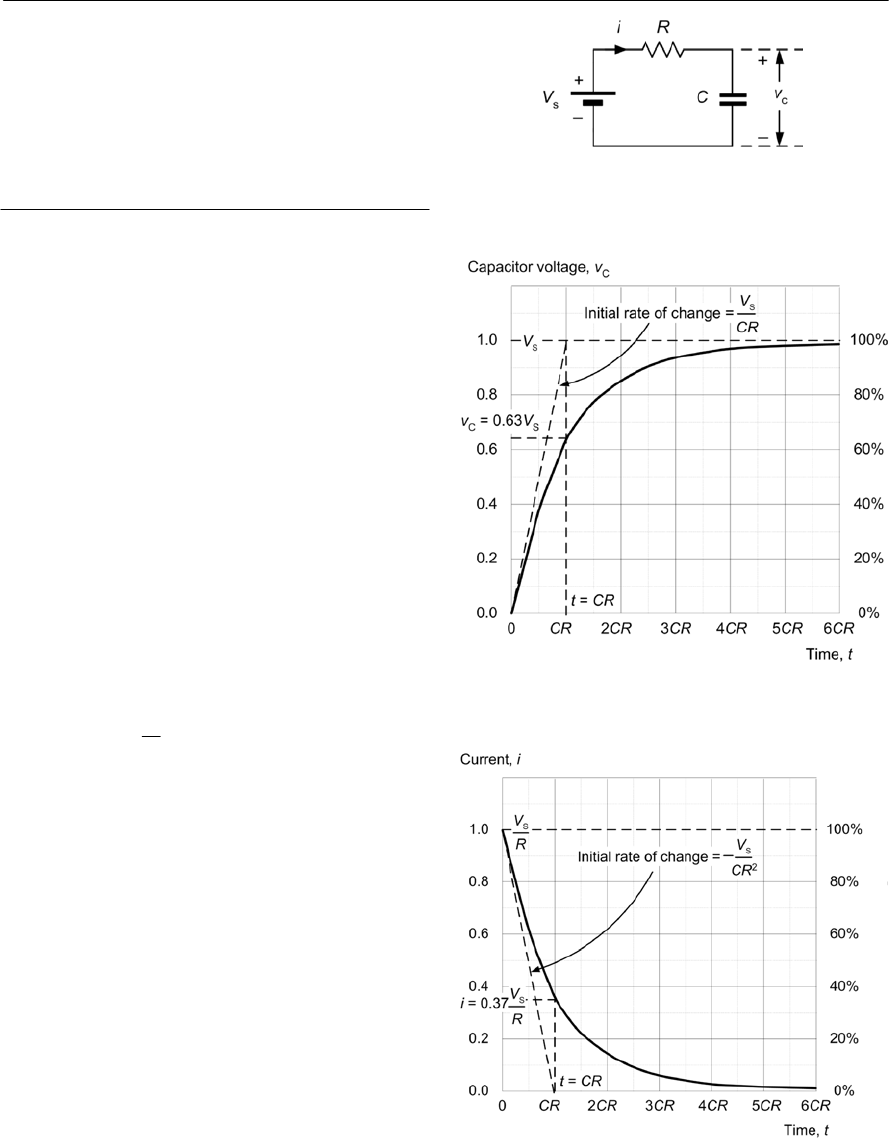
58 ELECTRONIC CIRCUITS: FUNDAMENTALS AND APPLICATIONS
C–Rcircuits
Networks of capacitors and resistors (known as C–
Rcircuits) form the basis of many timing and pulse
shaping circuits and are thus often found in
practical electronic circuits.
Charging
Asimple C–R circuit is shown in Fig. 3.26 . In this
circuit Cis charged through Rfrom the constant
voltage source, Vs.The voltage, vc,across the
(initially uncharged) capacitor voltage will rise
exponentially as shown in Fig. 3.27. At the same
time, the current in the circuit, i,will fall, as shown
in Fig. 3.28.
The rate of growth of voltage with time (and
decay of current with time) will be dependent upon
the product of capacitance and resistance. This
value is known as the time constant of the circuit.
Hence:
Time constant, t = C × R
where C is the value of capacitance (F), Ris the
resistance (F), and tis the time constant (s).
The voltage developed across the charging
capacitor, vc,varies with time, t,according to the
relationship:
where vcis the capacitor voltage, Vsis the d.c.
supply voltage, tis the time, and CR is the time
constant of the circuit (equal to the product of
capacitance, C,and resistance, R).
The capacitor voltage will rise to approximately
63% of the supply voltage, Vs,in a time interval
equal to the time constant.
At the end of the next interval of time equal to
the time constant (i.e. after an elapsed time equal to
2CR)the voltage will have risen by 63% of the
remainder, and so on. In theory, the capacitor will
never become fully charged. However, after a
period of time equal to 5CR, the capacitor voltage
will to all intents and purposes be equal to the
supply voltage. At this point the capacitor voltage
will have risen to 99.3% of its final value and we
can consider it to be fully charged.
cs
= 1
t
CR
vV e
Figure 3.26 A C–R circuit in which Cis charged
through R
Figure 3.27 Exponential growth of capacitor
voltage, v
c
,in Fig. 3.26
Figure 3.28 Exponential decay of current, i,in
Fig. 3.26
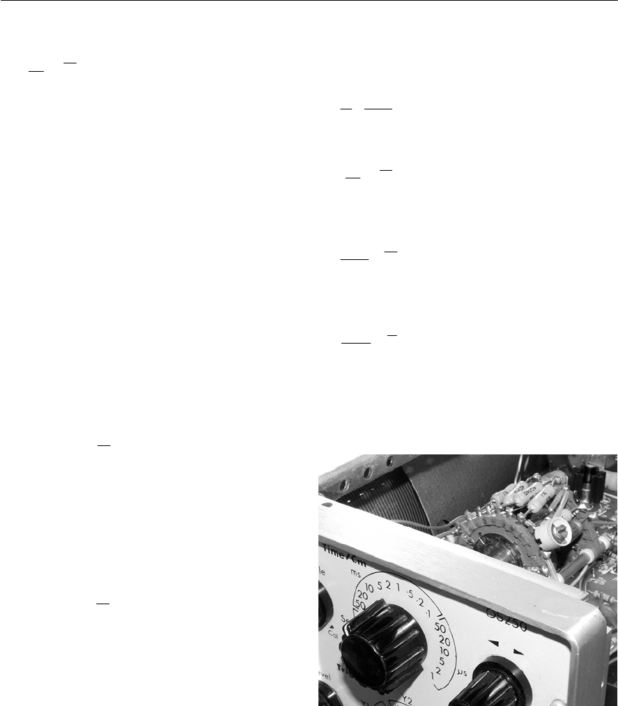
D.C. CIRCUITS 59
During charging, the current in the capacitor, i,
varies with time, t,according to the relationship:
where Vsis the d.c. supply voltage, tis the time, R
is the series resistance and Cis the value of
capacitance.
The current will fall to approximately 37% of the
initial current in a time equal to the time constant.
At the end of the next interval of time equal to the
time constant (i.e. after a total time of 2CR has
elapsed) the current will have fallen by a further
37% of the remainder, and so on.
Example 3.9
An initially uncharged 1 µF capacitor is charged
from a 9 V d.c. supply via a 3.3 MFresistor.
Determine the capacitor voltage 1 s after
connecting the supply.
Solution
The formula for exponential growth of voltage in
the capacitor is:
Here we need to find the capacitor voltage, vc,when
Vs= 9 V, t= 1 s, C= 1 µF and R=3.3 MF.The
time constant, CR,will be given by:
C R = 1 × 1046×3.3 × 106=3.3 s
Thus:
and
Example 3.10
A100 µF capacitor is charged from a 350 V d.c.
supply through a series resistance of 1 kF.
Determine the initial charging current and the
current that will flow 50 ms and 100 ms after
connecting the supply. After what time is the
capacitor considered to be fully charged?
s
=
t
CR
V
ie
R
cs
= 1
t
CR
vV e
3.3
c
= 9 1
t
ve
(
)
c
= 9 1 0.738 9 0.262 2.358 V
v=× =
Solution
At t= 0 the capacitor will be uncharged (v
c
=0) and
all of the supply voltage will appear across the
series resistance. Thus, at t=0:
When t=50 ms, the current will be given by:
Where V
s
=350 V, t = 50 ms, C = 100 µF,
R= 1 kF.Hence:
When t=100 ms (using the same equation but with
t=0.1 s) the current is given by:
The capacitor can be considered to be fully charged
when t = 5CR = 5 × 100 × 10
46
× 1 × 10
3
=0.5 s.
Note that, at this point the capacitor voltage will
have reached 99% of its final value.
s
350
=0.35 A
1, 00 0
V
iR==
0.05
0.5
0.1
350
=0.35 0.35 0.607 0.21 A
1,000
ie e
==×=
s
=
t
CR
V
ie
R
Figure 3.29 C–Rcircuits are widely used in
electronics. In this oscilloscope, for example, a
rotary switch is used to select different C–R
combinations in order to provide the various
timebase ranges (adjustable from 500 ms/cm to
1µs/cm). Each C–Rtime constant corresponds to a
different timebase range.
0.1
1
0.1
350
=0.35 0.35 0.368 0.129 A
1, 00 0
ie e
==×=
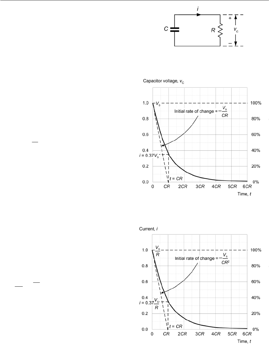
60 ELECTRONIC CIRCUITS: FUNDAMENTALS AND APPLICATIONS
Discharge
Having considered the situation when a capacitor is
being charged, let’s consider what happens when
an already charged capacitor is discharged.
When the fully charged capacitor from Fig. 3.24
is connected as shown in Fig. 3.30, the capacitor
will discharge through the resistor, and the
capacitor voltage, vC,will fall exponentially with
time, as shown in Fig. 3.31.
The current in the circuit, i,will also fall, as
shown in Fig. 3.32. The rate of discharge (i.e. the
rate of decay of voltage with time) will once again
be governed by the time constant of the circuit, C×
R.
The voltage developed across the discharging
capacitor, vC,varies with time, t,according to the
relationship:
where Vs,is the supply voltage, tis the time, Cis
the capacitance, and Ris the resistance.
The capacitor voltage will fall to approximately
37% of the initial voltage in a time equal to the
time constant. At the end of the next interval of
time equal to the time constant (i.e. after an elapsed
time equal to 2CR)the voltage will have fallen by
37% of the remainder, and so on.
In theory, the capacitor will never become fully
discharged. However, after a period of time equal
to 5CR, however, the capacitor voltage will to all
intents and purposes be zero.
At this point the capacitor voltage will have
fallen below 1% of its initial value. At this point we
can consider it to be fully discharged.
As with charging, the current in the capacitor, i,
varies with time, t, according to the relationship:
where Vs,is the supply voltage, tis the time, Cis
the capacitance, and Ris the resistance.
The current will fall to approximately 37% of the
initial value of current, Vs/R,in a time equal to the
time constant.
At the end of the next interval of time equal to
the time constant (i.e. after a total time of 2CR has
elapsed) the voltage will have fallen by a further
37% of the remainder, and so on.
Figure 3.31 Exponential decay of capacitor
voltage, vc,in Fig. 3.30
Figure 3.32 Exponential decay of current, i,in
Fig. 3.30
Figure 3.30 A C–R circuit in which Cis initially
charged and then discharges through R
cs
=
t
CR
vVe
s
=
t
CR
V
ie
R

D.C. CIRCUITS 61
Example 3.11
A10 µF capacitor is charged to a potential of 20 V
and then discharged through a 47 kFresistor.
Determine the time taken for the capacitor voltage
to fall below 10 V.
Solution
The formula for exponential decay of voltage in the
capacitor is:
where Vs=20 V and CR = 10 µF × 47 kF=0.47 s.
We need to find twhen vC=10 V. Rearranging
the formula to make tthe subject gives:
thus
or
In order to simplify the mathematics of exponential
growth and decay, Table 3.1 provides an alternative
tabular method that may be used to determine the
voltage and current in a C–R circuit.
Example 3.12
A150 µF capacitor is charged to a potential of
150 V. The capacitor is then removed from the
charging source and connected to a 2 MFresistor.
Determine the capacitor voltage 1 minute later.
Solution
We will solve this problem using Table 3.1 rather
than the exponential formula.
First we need to find the time constant:
C × R = 150 µF × 2 MF=300 s
Next we find the ratio of tto CR:
After 1 minute, t = 60 s therefore the ratio of tto
CR is 60/300 or 0.2. Table 3.1 shows that when
t/CR = 0.2, the ratio of instantaneous value to final
value (kin Table 3.1) is 0.8187.
Waveshaping with C–Rnetworks
One of the most common applications of C–R
networks is in waveshaping circuits. The circuits
shown in Figs 3.33 and 3.35 function as simple
square-to-triangle and square-to-pulse converters
by, respectively, integrating and differentiating
Table 3.1 Exponential growth and decay
C
S
=ln
v
tCR V
×
cs
=
t
CR
vVe
=0.47 0.693 0.325 s
t
×=
()
10
=0.47 ln = 0.47 ln 0.5
20
t
××
Thus
v
c
/ V
s
=0.8187
or
v
c
=0.8187 × V
s
=0.8187 × 150V = 122.8V
t/CR or t /(L/R)k(growth)k(decay)
0.0 0.0000 1.0000
0.1 0.0951 0.9048
0.2 0.1812 0.8187 (1)
0.3 0.2591 0.7408
0.4 0.3296 0.6703
0.5 0.3935 0.6065
0.6 0.4511 0.5488
0.7 0.5034 0.4965
0.8 0.5506 0.4493
0.9 0.5934 0.4065
1.0 0.6321 0.3679
1.5 0.7769 0.2231
2.0 0.8647 (2) 0.1353
2.5 0.9179 0.0821
3.0 0.9502 0.0498
3.5 0.9698 0.0302
4.0 0.9817 0.0183
4.5 0.9889 0.0111
5.0 0.9933 0.0067
Notes: (1) See Example 3.12
(2) See Example 3.16
kis the ratio of the value at time, t,to the
final value (e.g. v
c
/ V
s
)
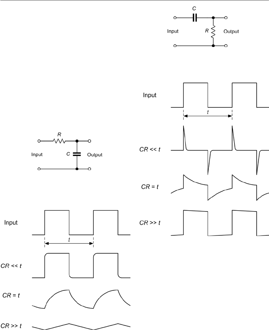
62 ELECTRONIC CIRCUITS: FUNDAMENTALS AND APPLICATIONS
their inputs.
The effectiveness of the simple integrator circuit
shown in Fig. 3.33 depends on the ratio of time
constant, C × R,to periodic time, t. The larger this
ratio is, the more effective the circuit will be as an
integrator. The effectiveness of the circuit of Fig.
3.33 is illustrated by the input and output
waveforms shown in Fig. 3.34.
Similarly, the effectiveness of the simple
differentiator circuit shown in Fig. 3.35 also
depends on the ratio of time constant C × R,to
periodic time, t. The smaller this ratio is, the more
effective the circuit will be as a differentiator.
The effectiveness of the circuit of Fig. 3.35 is
illustrated by the input and output waveforms
shown in Fig. 3.36.
Figure 3.33 A C–R integrating circuit
Figure 3.35 A C–R differentiating circuit
Figure 3.34 Typical input and output waveforms
for the integrating circuit shown in Figure 3.33
Figure 3.36 Typical input and output waveforms
for the integrating circuit shown in Fig. 3.33
Example 3.13
Acircuit is required to produce a train of
alternating positive and negative pulses of short
duration from a square wave of frequency 1 kHz.
Devise a suitable C–R circuit and specify suitable
values.
Solution
Here we require the services of a differentiating
circuit along the lines of that shown in Fig. 3.35. In
order that the circuit operates effectively as a

D.C. CIRCUITS 63
L–R circuits
Networks of inductors and resistors (known as L–R
circuits) can also be used for timing and pulse
shaping. In comparison with capacitors, however,
inductors are somewhat more difficult to
manufacture and are consequently more expensive.
Inductors are also prone to losses and may also
require screening to minimize the effects of stray
magnetic coupling. Inductors are, therefore,
generally unsuited to simple timing and
waveshaping applications.
Figure 3.37 shows a simple L–R network in
which an inductor is connected to a constant
voltage supply. When the supply is first connected,
the current, i, will rise exponentially with time, as
shown in Fig. 3.38. At the same time, the inductor
voltage VL,will fall, as shown in Fig. 3.39). The
rate of change of current with time will depend
upon the ratio of inductance to resistance and is
known as the time constant.Hence:
Time constant, t = L/R
where Lis the value of inductance (H), Ris the
resistance (F), and tis the time constant (s).
The current flowing in the inductor, i,varies with
time, t,according to the relationship:
where Vsis the d.c. supply voltage, Ris the
resistance of the inductor, and Lis the inductance.
The current, i,will initially be zero and will rise
to approximately 63% of its maximum value (i.e.
Vs/R)in a time interval equal to the time constant.
At the end of the next interval of time equal to the
time constant (i.e. after a total time of 2L/R has
elapsed) the current will have risen by a further
63% of the remainder, and so on.
In theory, the current in the inductor will never
become equal to Vs/R. However, after a period of
time equal to 5L/R, the current will to all intents
and purposes be equal to Vs/R. At this point the
differentiator, we need to make the time constant,
C × R,very much less than the periodic time of the
input waveform (1 ms).
Assuming that we choose a medium value for R
of, say, 10 kF,the maximum value which we could
allow Cto have would be that which satisfies the
equation:
C × R = 0.1 t
where R = l0 kFand t = 1ms. Thus
or
C = 10 ×1049F=10 nF
In practice, any value equal or less than 10 nF
would be adequate. A very small value (say less
than 1 nF) will, however, generate pulses of a very
narrow width.
Example 3.14
Acircuit is required to produce a triangular
waveform from a square wave of frequency 1 kHz.
Devise a suitable C–R arrangement and specify
suitable values.
Solution
This time we require an integrating circuit like that
shown in Fig. 3.33. In order that the circuit operates
effectively as an integrator, we need to make the
time constant, C × R,very much less than the
periodic time of the input waveform (1 ms).
Assuming that we choose a medium value for R
of, say, 10 kF,the minimum value which we could
allow Cto have would be that which satisfies the
equation:
C × R = 10 t
where R = l0 kFand t = 1ms. Thus
or
C = 1 ×1046F=1µF
In practice, any value equal or greater than 1 µF
would be adequate. A very large value (say more
34 8
0.1 0.1 1 ms
0.1 10 10 1 10 F
10 k
t
CR
×
== =××=×
34 6
10 10 1 ms
10 10 10 1 10 F
10 k
t
CR
×
== =×× =×
than 10 µF) will, however, generate a triangular
wave which has a very small amplitude. To put this
in simple terms, although the waveform might be
what you want there’s not a lot of it!
s
= 1
tR
L
V
ie
R
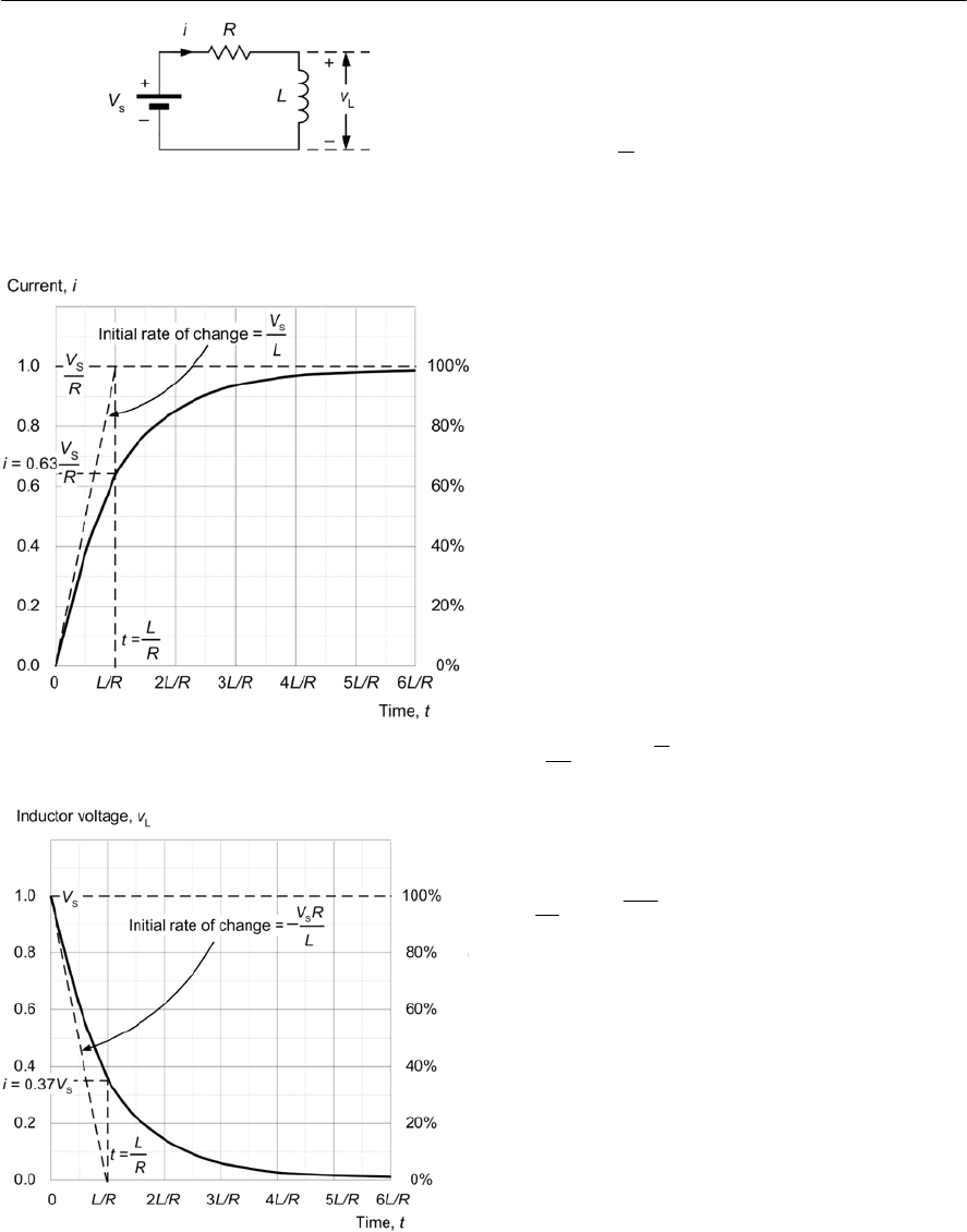
64 ELECTRONIC CIRCUITS: FUNDAMENTALS AND APPLICATIONS
current in the inductor will have risen to 99.3% of
its final value.
The voltage developed across the inductor, vL,
varies with time, t,according to the relationship:
where Vsis the d.c. supply voltage, Ris the
resistance of the inductor, and Lis the inductance.
The inductor voltage will fall to approximately
37% of the initial voltage in a time equal to the
time constant.
At the end of the next interval of time equal to
the time constant (i.e. after a total time of 2L/R has
elapsed) the voltage will have fallen by a further
37% of the remainder, and so on.
Example 3.15
Acoil having inductance 6 H and resistance 24 Fis
connected to a 12 V d.c. supply. Determine the
current in the inductor 0.1 s after the supply is first
connected.
Solution
The formula for exponential growth of current in
the coil is:
where Vs=12 V, L = 6 H and R = 24 F.
We need to find iwhen t=0.1 s
thus
i = 0.5 × 0.33 = 0.165 A
In order to simplify the mathematics of exponential
growth and decay, Table 3.1 provides an alternative
tabular method that may be used to determine the
voltage and current in an L–R circuit.
Example 3.16
Acoil has an inductance of l00 mH and a resistance
of 10 F.If the inductor is connected to a 5 V d.c.
Figure 3.38 Exponential growth of current, i,in
Fig. 3.37
Figure 3.39 Exponential decay of voltage, vL,in
Fig. 3.37
Figure 3.37 A C–R circuit in which Cis initially
charged and then discharges through R
Ls
=
tR
L
vVe
s
= 1
tR
L
V
ie
R
()
0.1 24
0.4
6
12
=1 0.5 1 0.5 (1 0.67)
24
ie e
×
==
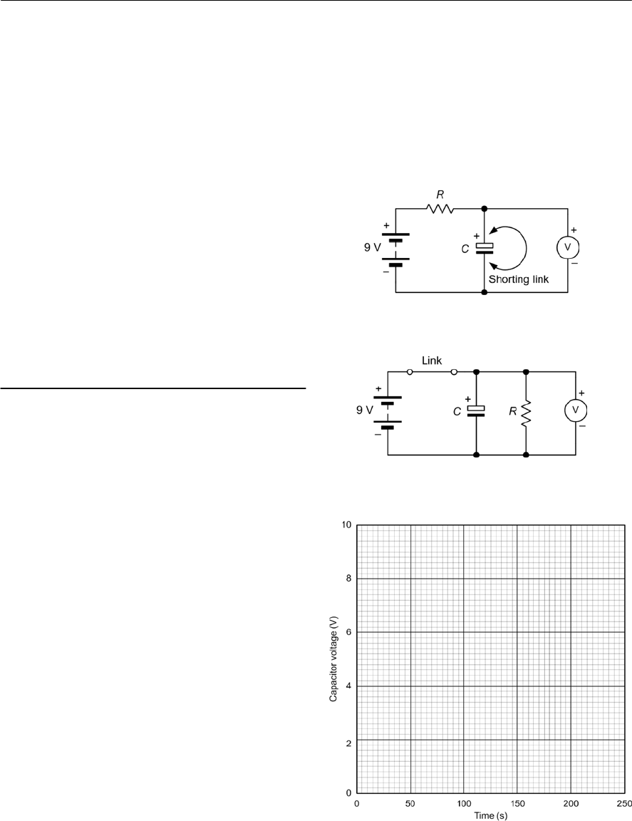
D.C. CIRCUITS 65
Practical investigation
Objective
To investigate the charge and discharge of a
capacitor.
Components and test equipment
Breadboard, 9V DC power source (either a PP9 9V
battery or an AC mains adapter with a 9V 400mA
output), digital multimeter with test leads, resistors
of 100 kF,220 kFand 47 kF,capacitor of 1,000
µF, insulated wire links (various lengths), assorted
crocodile leads, short lengths of black, red, and
green insulated solid wire. A watch or clock with a
seconds display will also be required for timing.
Procedure
Connect the charging circuit shown in Fig. 3.40
with R=100 kFand C=1,000 µF. Place a
temporary shorting link across the capacitor. Set
the meter to the 20 V DC range and remove the
shorting link. Measure and record the capacitor
voltage at 25 s intervals over the range 0 to 250 s
after removing the shorting link. Record your result
in a table showing capacitor voltage against time.
Repeat with R=220 kFand R=47 kF.
Figure 3.40 Circuit diagram—charging
Figure 3.42 Graph layout for plotting the results
Connect the discharging circuit shown in Fig. 3.41
with R=100 kFand C=1,000 µF. Leave the link
in place for a few seconds after the supply voltage
has been switched on, then remove the link.
Measure and record the capacitor voltage at 25 s
intervals over the range 0 to 250 s from removing
the link. Record your result in a table showing
capacitor voltage against time. Repeat with
R=220 kFand R=47 kF.
supply, determine the inductor voltage 20 ms after
the supply is first connected.
Solution
We will solve this problem using Table 3.1 rather
than the exponential formula.
First we need to find the time constant:
L/R =0.1 H/10 F=0.01 s
Next we find the ratio of tto L/R.
When t = 20 ms the ratio of tto L/R is 0.02/0.01
or 2. Table 3.1 shows that when t/(L/R) = 2, the
ratio of instantaneous value to final value (k)is
0.8647. Thus
vL/Vs=0.8647
or
vL=0.8647 × Vs=0.8647 × 5 V = 4.32V
Figure 3.41 Circuit diagram—discharging

66 ELECTRONIC CIRCUITS: FUNDAMENTALS AND APPLICATIONS
Formulae introduced in this chapter
Kirchhoff’s current law:
(page 49)
Algebraic sum of currents = 0
Kirchhoff’s voltage law:
(page 50)
Algebraic sum of e.m.f.s = algebraic sum of voltage
drops
Potential divider:
(page 52)
Current divider:
(page 53)
Wheatstone bridge:
(page 54)
and
Time constant of a C–R circuit:
(page 58)
t = CR
Capacitor voltage (charge):
(page 58)
Capacitor current (charge):
(page 59)
Capacitor voltage (discharge):
(page 60)
Capacitor current (discharge):
(page 60)
Time constant of an L–R circuit:
(page 63)
t = L / R
Inductor current (growth):
(page 63)
Inductor voltage (decay):
(page 64)
Measurements and calculations
Plot graphs of voltage (on the vertical axis) against
time (on the horizontal axis) using the graph layout
shown in Fig. 3.42.
Calculate the time constant for each combination
of resistance and capacitance that you used in the
investigation.
Conclusion
Comment on the shape of the graphs. Is this what
you would expect? For each combination of
resistance and capacitance estimate the time
constant from the graph. Compare these values
with the calculated values. If they are not the same
suggest possible reasons for the difference.
2
out in
12
R
VV
RR
=+
2
xv
1
R
RR
R
=×
cs
= 1
t
CR
vV e
s
=
t
CR
V
ie
R
cs
=
t
CR
vVe
s
=
t
CR
V
ie
R
s
= 1
tR
L
V
ie
R
1
out in
12
R
II
RR
=+
3
1
24
R
R
RR
=
Ls
=
tR
L
vVe
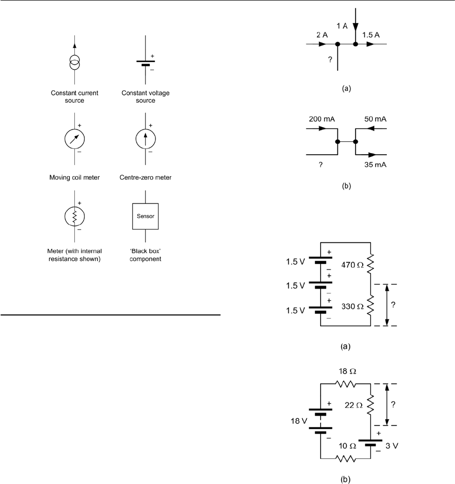
D.C. CIRCUITS 67
Problems
3.1 A power supply is rated at 500 mA
maximum output current. If the supply
delivers 150 mA to one circuit and 75 mA to
another, how much current would be
available for a third circuit?
3.2 A 15 V d.c. supply delivers a total current of
300 mA. If this current is shared equally
between four circuits, determine the
resistance of each circuit.
3.3 Determine the unknown current in each
circuit shown in Fig. 3.44.
3.4 Determine the unknown voltage in each
circuit shown in Fig. 3.45.
3.5 Determine all currents and voltages in Fig.
3.46.
3.6 Two resistors, one of 120 Fand one of
680 Fare connected as a potential divider
across a 12 V supply. Determine the voltage
developed across each resistor.
3.7 Two resistors, one of 15 Fand one of 5 F
are connected in parallel. If a current of 2 A
is applied to the combination, determine the
current flowing in each resistor.
3.8 A switched attenuator comprises five 1 kF
resistors wired in series across a 5V d.c.
supply. If the output voltage is selected by
means of a single-pole four-way switch,
sketch a circuit and determine the voltage
produced for each switch position.
Figure 3.43 Circuit symbols introduced in this
chapter
Symbols introduced in this chapter
Figure 3.44 See Question 3.3
Figure 3.45 See Question 3.4
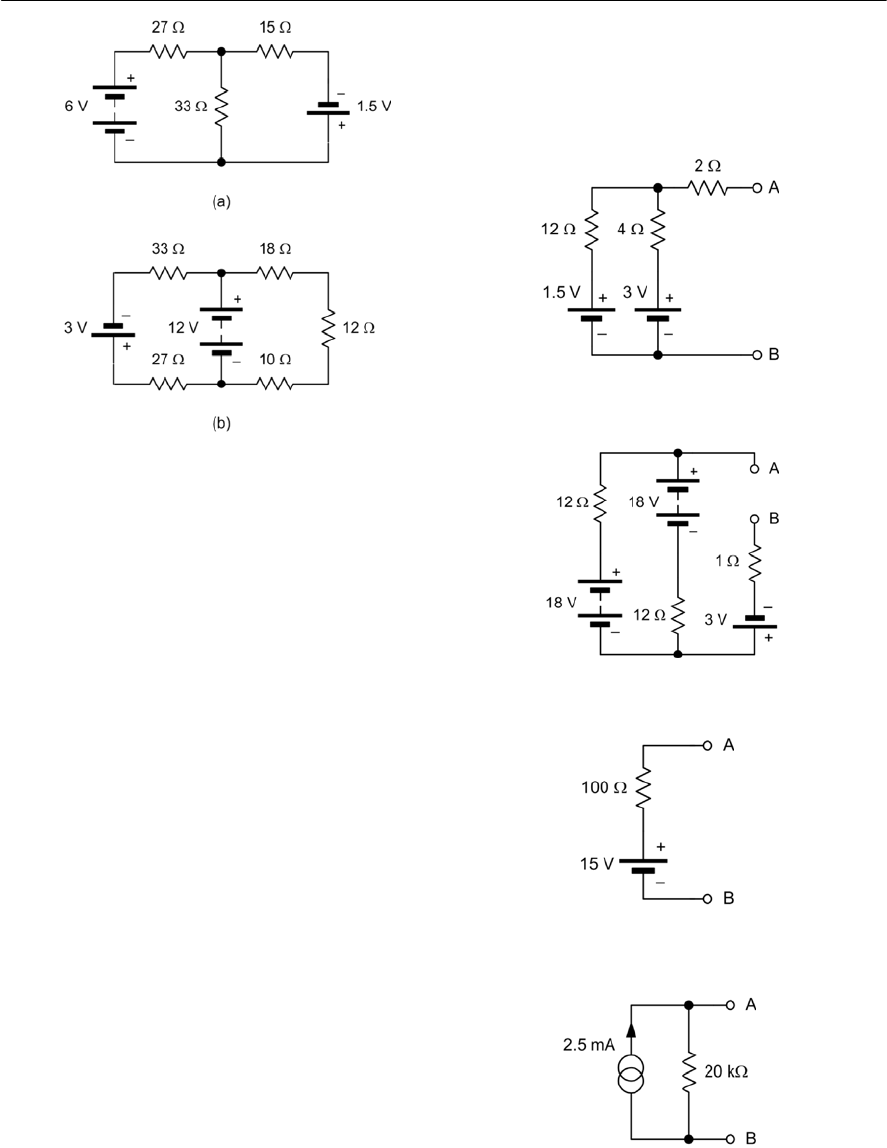
68 ELECTRONIC CIRCUITS: FUNDAMENTALS AND APPLICATIONS
3.9 A capacitor of 1 µF is charged from a 15 V
d.c. supply via a 100 kFresistor. How long
will it take for the capacitor voltage to reach
5 V?
3.10 A capacitor of 22 µF is charged to a voltage
of 50 V. If the capacitor is then discharged
using a resistor of 100 kF,determine the
time taken for the capacitor voltage to reach
10 V.
3.11 An initially uncharged capacitor is charged
from a 200 V d.c. supply through a 2 MF
resistor. If it takes 50 s for the capacitor
voltage to reach 100 V, determine the value
of capacitance.
3.12 A coil has an inductance of 2.5 H and
a resistance of 10 F.If the coil is
connected to a 5 V d.c. supply, determine
the time taken for the current to grow to
200 mA.
3.13 Determine the Thévenin equivalent of the
circuit shown in Fig. 3.47.
3.14 Determine the Norton equivalent of the
circuit shown in Fig. 3.48.
3.15 The Thévenin equivalent of a network is
shown in Fig. 3.49. Determine (a) the
short-circuit output current and (b) the
output voltage developed across a load of
200 F.
3.16 The Norton equivalent of a network is
shown in Fig. 3.50. Determine (a) the open-
circuit output voltage and (b) the output
voltage developed across a load of 5 kF.
Answers to these problems appear on page 374.
Figure 3.49 See Question 3.15
Figure 3.50 See Question 3.16
Figure 3.48 See Question 3.14
Figure 3.47 See Question 3.13
Figure 3.46 See Question 3.5
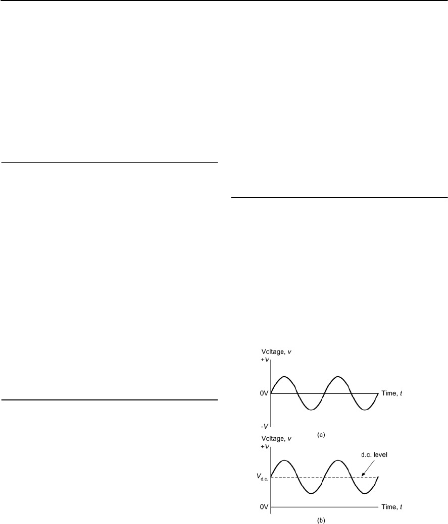
4
Alternating voltage and current
This chapter introduces basic alternating current
theory. We discuss the terminology used to
describe alternating waveforms and the behaviour
of resistors, capacitors, and inductors when an
alternating current is applied to them. The chapter
concludes by introducing another useful
component, the transformer.
Alternating versus direct current
Direct currents are currents which, even though
their magnitude may vary, essentially flow only in
one direction. In other words, direct currents are
unidirectional.Alternating currents, on the other
hand, are bidirectional and continuously reverse
their direction of flow. The polarity of the e.m.f.
which produces an alternating current must
consequently also be changing from positive to
negative, and vice versa.
Alternating currents produce alternating potential
differences (voltages) in the circuits in which they
flow. Furthermore, in some circuits, alternating
voltages may be superimposed on direct voltage
levels (see Fig. 4.1). The resulting voltage may be
unipolar (i.e. always positive or always negative) or
bipolar (i.e. partly positive and partly negative).
Waveforms and signals
Agraph showing the variation of voltage or current
present in a circuit is known as a waveform. There
are many common types of waveform encountered
in electrical circuits including sine (or sinusoidal),
square, triangle, ramp or sawtooth (which may be
either positive or negative going), and pulse.
Complex waveforms,like speech and music,
usually comprise many components at different
frequencies. Pulse waveforms are often
categorized as either repetitive or non-repetitive
(the former comprises a pattern of pulses that
Figure 4.1 (a) Bipolar sine wave; (b) unipolar sine
wave (superimposed on a d.c. level)
repeats regularly while the latter comprises pulses
which constitute a unique event). Some common
waveforms are shown in Fig. 4.2.
Signals can be conveyed using one or more of
the properties of a waveform and sent using wires,
cables, optical and radio links. Signals can also be
processed in various ways using amplifiers,
modulators, filters, etc. Signals are also classified
as either analogue (continuously variable) or
digital (based on discrete states).
Frequency
The frequency of a repetitive waveform is the
number of cycles of the waveform which occur in
unit time. Frequency is expressed in Hertz, Hz, and
afrequency of 1 Hz is equivalent to one cycle per
second. Hence, if a voltage has a frequency of
400 Hz, 400 cycles of it will occur in every second.
The equation for the voltage shown in Fig. 4.1(a)
at a time, t, is:
v=Vmax sin (20t)
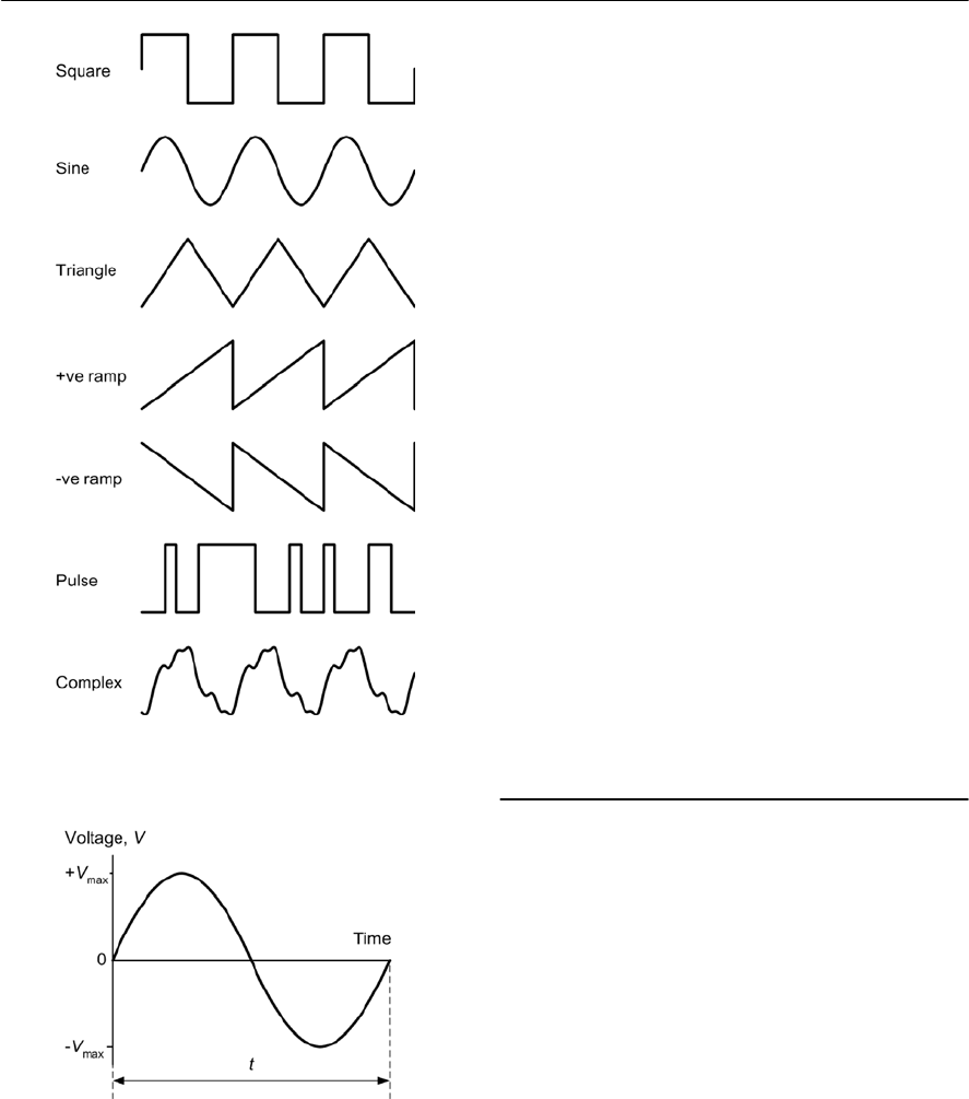
70 ELECTRONIC CIRCUITS: FUNDAMENTALS AND APPLICATIONS
whilst that in Fig. 4.1(b) is:
v=Vd.c. + Vmax sin (20t)
Figure 4.2 Common waveforms
Figure 4.3 One cycle of a sine wave voltage
showing its periodic time
where vis the instantaneous voltage, Vmax is the
maximum (or peak) voltage of the sine wave, Vd.c.,
is the d.c. offset (where present), and fis the
frequency of the sine wave.
Example 4.1
Asine wave voltage has a maximum value of 20 V
and a frequency of 50 Hz. Determine the
instantaneous voltage present (a) 2.5 ms and
(b) 15 ms from the start of the cycle.
Solution
We can find the voltage at any instant of time
using:
v=Vmax sin (20t)
where Vmax = 20 V and f=50 Hz.
In (a), t = 2.5 ms, hence:
v=20 sin (20×50 × 0.0025) = 20 sin (0.785)
=20 × 0.707 = 14.14 V
In (b), t = 15 ms, hence:
v=20 sin (20×50 × 0.0015) = 20 sin (4.71)
=20 × @1 = @20 V
Periodic time
The periodic time (or period)of a waveform is the
time taken for one complete cycle of the wave (see
Fig. 4.3). The relationship between periodic time
and frequency is thus:
t = 1/ f or f = 1/ t
where tis the periodic time (in s) and fis the
frequency (in Hz).
Example 4.2
Awaveform has a frequency of 400 Hz. What is
the periodic time of the waveform?
Solution
t = 1/f=1/400 = 0.0025 s (or 2.5 ms)
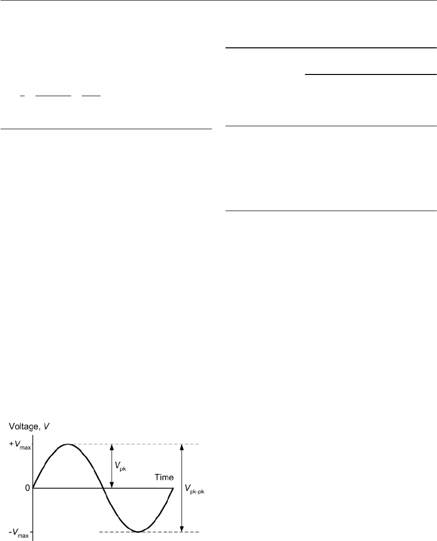
ALTERNATING VOLTAGE AND CURRENT 71
Figure 4.4 One cycle of a sine wave voltage
showing its peak and peak-peak values
Example 4.3
Awaveform has a periodic time of 40 ms. What is
its frequency?
Solution
Average, peak, peak-peak, and r.m.s.
values
The average value of an alternating current which
swings symmetrically above and below zero will
be zero when measured over a long period of time.
Hence average values of currents and voltages are
invariably taken over one complete half-cycle
(either positive or negative) rather than over one
complete full-cycle (which would result in an
average value of zero).
The amplitude (or peak value)of a waveform is
ameasure of the extent of its voltage or current
excursion from the resting value (usually zero).
The peak-to-peak value for a wave which is
symmetrical about its resting value is twice its peak
value (see Fig. 4.4).
The r.m.s. (or effective)value of an alternating
voltage or current is the value which would
produce the same heat energy in a resistor as a
direct voltage or current of the same magnitude.
Since the r.m.s. value of a waveform is very much
dependent upon its shape, values are only
meaningful when dealing with a waveform of
known shape. Where the shape of a waveform is
not specified, r.m.s. values are normally assumed to
refer to sinusoidal conditions.
For a given waveform, a set of fixed
relationships exist between average, peak, peak-
peak, and r.m.s. values. The required multiplying
factors are summarized for sinusoidal voltages and
currents in Table 4.1.
Example 4.4
Asinusoidal voltage has an r.m.s. value of 240 V.
What is the peak value of the voltage?
Solution
The corresponding multiplying factor (found from
Table 4.1) is 1.414. Hence:
Vpk =1.414 × Vr.m.s.=1.414 × 240 =339.4 V
Example 4.5
An alternating current has a peak-peak value of 50
mA. What is its r.m.s. value?
Solution
The corresponding multiplying factor (found from
Table 4.1 Multiplying factors for average, peak,
peak-peak and r.m.s. values
3
11 1
25 Hz
0.044010
ft
== = =
×
Given quantity
Average
Peak
Peak– peak
r.m.s.
Average 11.57 3.14 1.11
Peak 0.636 1 2 0.707
Peak– peak 0.318 0.5 1 0.353
r.m.s. 0.9 1.414 2.828 1
Wanted quantity
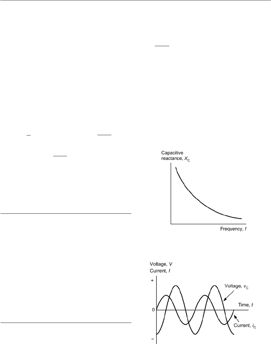
72 ELECTRONIC CIRCUITS: FUNDAMENTALS AND APPLICATIONS
Table 4.1) is 0.353. Hence:
Ir.m.s. =0.353 × Vpk-pk =0.353 × 0.05 =0.0177 A
(or 17.7mA).
Example 4.6
Asinusoidal voltage 10 V pk-pk is applied to a
resistor of 1 kFWhat value of r.m.s. current will
flow in the resistor?
Solution
This problem must be solved in two stages. First
we will determine the peak-peak current in the
resistor and then we shall convert this value into a
corresponding r.m.s. quantity.
Since we can infer that
From which
The required multiplying factor (peak-peak to
r.m.s.) is 0.353. Thus:
Ir.m.s. =0.353 × Ipk-pk =0.353 × 10 =3.53 mA
Reactance
When alternating voltages are applied to capacitors
or inductors the magnitude of the current flowing
will depend upon the value of capacitance or
inductance and on the frequency of the voltage. In
effect, capacitors and inductors oppose the flow of
current in much the same way as a resistor. The
important difference being that the effective
resistance (or reactance) of the component varies
with frequency (unlike the case of a resistor where
the magnitude of the current does not change with
frequency).
Capacitive reactance
The reactance of a capacitor is defined as the ratio
of applied voltage to current and, like resistance, it
is measured in Ohms. The reactance of a capacitor
Figure 4.5 Variation of reactance with frequency
for a capacitor
Figure 4.6 Voltage and current waveforms for a
pure capacitor (the current leads the voltage by 90°)
V
I
R
=
pk-pk
pk-pk
V
I
R
=
pk-pk
10
0.01 10 mA pk-pk
1, 00 0
I===
is inversely proportional to both the value of
capacitance and the frequency of the applied
voltage. Capacitive reactance can be found by
applying the following formula:
where X
c
is the reactance (in Ohms), fis the
frequency (in Hertz), and Cis the capacitance (in
Farads).
Capacitive reactance falls as frequency increases,
as shown in Fig. 4.5. The applied voltage, V
c
,and
current, I
c
,flowing in a pure capacitive reactance
will differ in phase by an angle of 90° or 0/2
radians (the current leads the voltage). This
relationship is illustrated in the current and voltage
waveforms (drawn to a common time scale) shown
in Fig. 4.6 and as a phasor diagram shown in Fig.
4.7.
C
1
2
X
fC
=
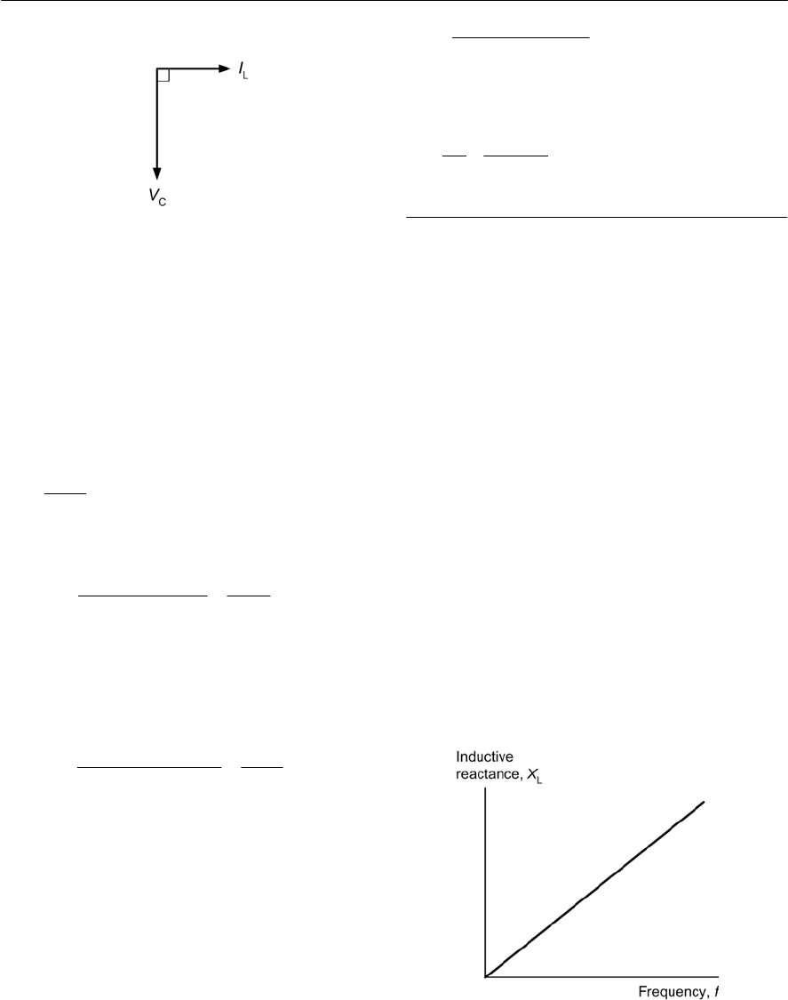
ALTERNATING VOLTAGE AND CURRENT 73
Figure 4.7 Phasor diagram for a pure capacitor
The r.m.s. current flowing in the capacitor will thus
be:
Inductive reactance
The reactance of an inductor is defined as the ratio
of applied voltage to current and, like resistance, it
is measured in ohms. The reactance of an inductor
is directly proportional to both the value of
inductance and the frequency of the applied
voltage. Inductive reactance can be found by
applying the formula:
XL= 20f L
where XLis the reactance in F,fis the frequency in
Hz, and Lis the inductance in H.
Inductive reactance increases linearly with
frequency as shown in Fig. 4.8. The applied
voltage, VL,and current, IL,developed across a pure
inductive reactance will differ in phase by an angle
of 90° or 0/2radians (the current lags the
voltage). This relationship is illustrated in the
current and voltage waveforms (drawn to a
common time scale) shown in Fig. 4.9 and as a
phasor diagram shown in Fig. 4.10.
Figure 4.8 Variation of reactance with frequency
for an inductor
Example 4.7
Determine the reactance of a 1 µF capacitor at
(a) 100 Hz and (b) 10 kHz.
Solution
This problem is solved using the expression:
(a) At 100 Hz
or
XC=1.59 kF
(b) At 10 kHz
or
XC=15.9 F
Example 4.8
A100 nF capacitor is to form part of a filter
connected across a 240 V 50 Hz mains supply.
What current will flow in the capacitor?
Solution
First we must find the reactance of the capacitor:
C
1
2
X
fC
=
3
C64
1 0.159
1.59 10
2 100 1 10 10
X
===×
×××
2
C462
1 0.159
0.159 10
2 1 10 1 10 10
X
===×
×× ××
3
C9
1
31.8 10 31.8 k
2 50 100 10
X
==×=
×× ×
3
C
C3
C
240
7.5 10 7.5 mA
31.8 10
V
IX
== =×=
×
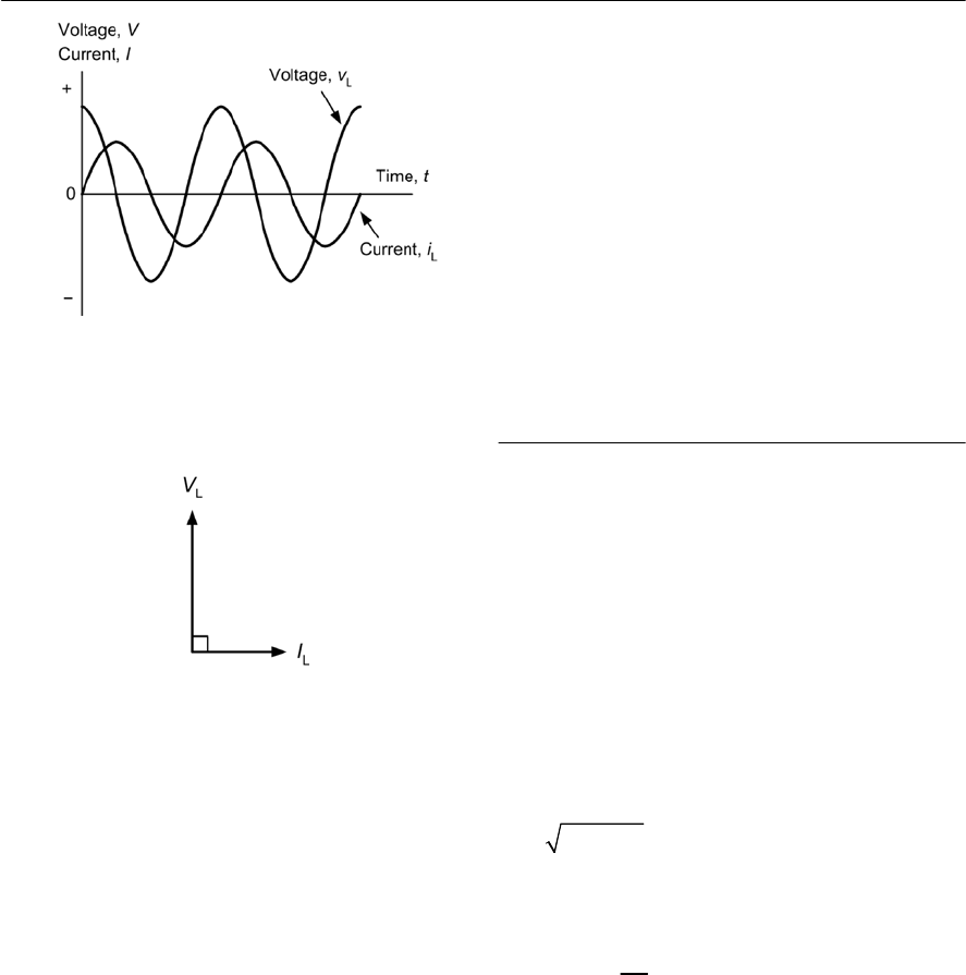
74 ELECTRONIC CIRCUITS: FUNDAMENTALS AND APPLICATIONS
Example 4.9
Determine the reactance of a 10 mH inductor at
(a) 100 Hz and (b) at 10 kHz.
Solution
(a) at 100 Hz
XL=20×100 ×10 ×10@3=6.28 F
(b) At 10 kHz
XL=20×10 ×103×10 ×10@3=628 F
Example 4.10
A100 mH inductor of negligible resistance is to
form part of a filter which carries a current of
20 mA at 400 Hz. What voltage drop will be
developed across the inductor?
Solution
The reactance of the inductor will be given by:
XL=20×400 ×100 ×10@3=251 F
The r.m.s. voltage developed across the inductor
will be given by:
VL= IL× XL=20 mA ×251 F=5.02 V
In this example, it is important to note that we have
assumed that the d.c. resistance of the inductor is
negligible by comparison with its reactance. Where
this is not the case, it will be necessary to determine
the impedance of the component and use this to
determine the voltage drop.
Impedance
Figure 4.11 shows two circuits which contain both
resistance and reactance. These circuits are said to
exhibit impedance (a combination of resistance and
reactance) which, like resistance and reactance, is
measured in ohms.
The impedance of the circuits shown in Fig. 4.11
is simply the ratio of supply voltage, VS,to supply
current, IS.The impedance of the simple C–R and
L–R circuits shown in Fig. 4.11 can be found by
using the impedance triangle shown in Fig. 4.12.
In either case, the impedance of the circuit is given
by:
and the phase angle (between VSand IS)is given
by:
where Z is the impedance (in Ohms), Xis the
reactance, either capacitive or inductive (expressed
in ohms), Ris the resistance (in Ohms), and øis
the phase angle in radians.
Example 4.11
A 2 µF capacitor is connected in series with a
100 Fresistor across a 115 V 400 Hz a.c. supply.
Determine the impedance of the circuit and the
current taken from the supply.
Figure 4.9 Voltage and current waveforms for a
pure inductor (the voltage leads the current by
90°)
Figure 4.10 Phasor diagram for a pure inductor
22
ZRX
=+
1
tan
X
R
=
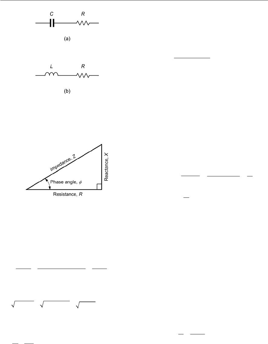
ALTERNATING VOLTAGE AND CURRENT 75
Figure 4.11 (a) Cand Rin series (b) Land Rin
series (note that both circuits exhibit an
impedance)
Figure 4.12 The impedance triangle
Solution
First we must find the reactance of the capacitor,
XC:
Now we can find the impedance of the C–R series
circuit:
The current taken from the supply can now be
found:
Power factor
The power factor in an a.c. circuit containing
resistance and reactance is simply the ratio of true
power to apparent power. Hence:
The true power in an a.c. circuit is the power
which is actually dissipated in the resistive
component. Thus:
true power = IS2×R(Watts)
The apparent power in an a.c. circuit is the
power which is apparently consumed by the circuit
and is the product of the supply current and supply
voltage (note that this is not the same as the power
which is actually dissipated as heat). Hence:
apparent power = IS×VS(Volt-Amperes)
Hence
From Fig. 4.12,
Hence the power factor of a series a.c. circuit can
be found from the cosine of the phase angle.
Example 4.12
Achoke (a form of inductor) having an inductance
of 150 mH and resistance of 250 Fis connected to
a115 V 400 Hz a.c. supply. Determine the power
factor of the choke and the current taken from the
supply.
Solution
First we must find the reactance of the inductor,
XL=20×400 ×0.15 =376.8 F
We can now determine the power factor from:
The impedance of the choke, Z,will be given by:
6
C6
1110
199
25,0246.28 400 2 10
XfC
== ==
×××
22 2 2
199 100 49,601 223
ZRX
=+= + = =
S
S
115
0.52 A
223
V
IZ
== =
true power
power factor =
apparent power
()
22
SS
SS S S
power factor IR IR
R
IV I I Z Z
××
== =
×××
cos
R
Z
=
250
power factor 0.663
376.8
R
Z
== =
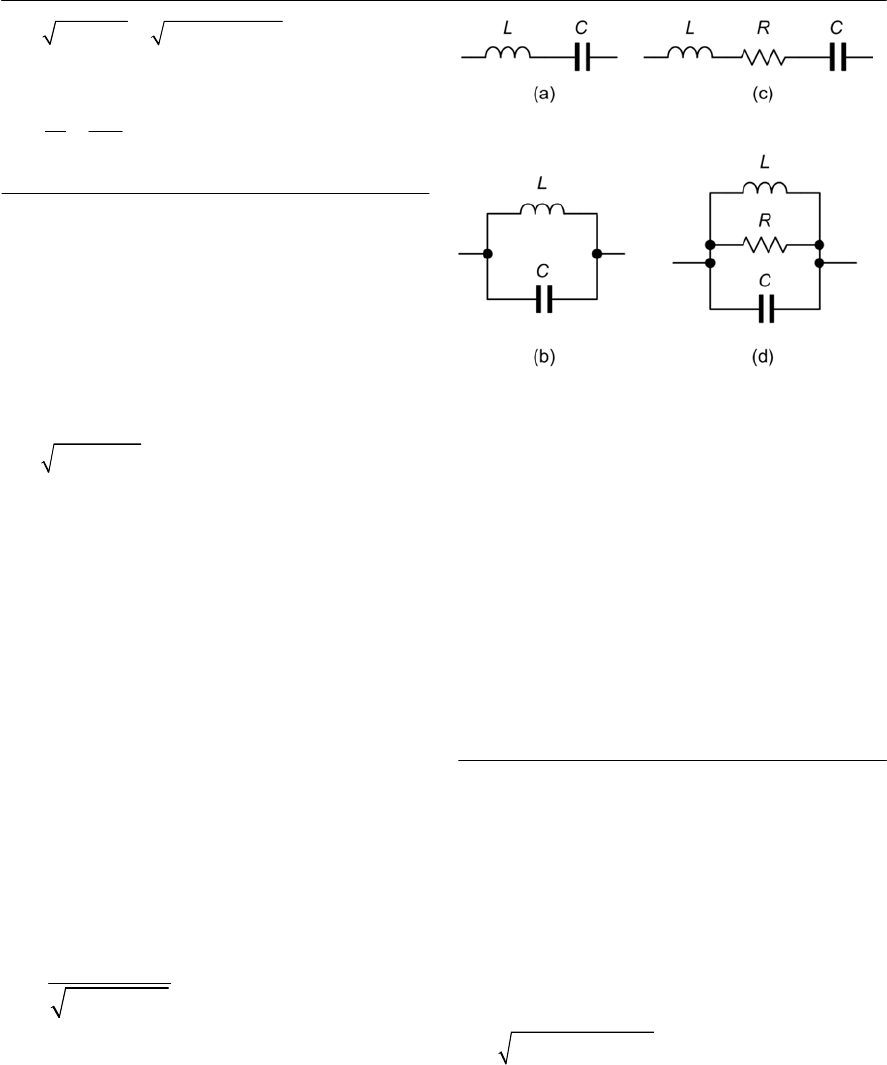
Finally, the current taken from the supply will be:
L–C circuits
Two forms of L–C circuits are illustrated in Fig.
4.13. Figure 4.13(a) is a series resonant circuit
while Fig. 4.13(b) constitutes a parallel resonant
circuit. The impedance of both circuits varies in a
complex manner with frequency.
The impedance of the series circuit in Fig. 4.13
(a) is given by:
where Z is the impedance of the circuit (in ohms),
and XLand XCare the reactances of the inductor
and capacitor respectively (both expressed in
ohms).
The phase angle (between the supply voltage and
current) will be +0/2 rad (i.e. +90°) when XL>XC
(above resonance) or @0/2 rad (or @90°) when XC>
XL(below resonance).
At a particular frequency (known as the series
resonant frequency)the reactance of the capacitor,
XC,will be equal in magnitude (but of opposite
sign) to that of the inductor, XL.Due to this
effective cancellation of the reactance, the
impedance of the series resonant circuit will be
zero at resonance. The supply current will have a
maximum value at resonance (infinite in the case of
aperfect series resonant circuit supplied from an
ideal voltage source!).
The impedance of the parallel circuit in Fig. 4.14
is given by:
where Z is the impedance of the circuit (in F), and
XLand XCare the reactances of the inductor and
capacitor, respectively (both expressed in F).
The phase angle (between the supply voltage and
current) will be +0/2 rad (i.e. +90°) when XL>XC
(above resonance) or @0/2 rad (or @90°) when XC>
XL(below resonance).
76 ELECTRONIC CIRCUITS: FUNDAMENTALS AND APPLICATIONS
Figure 4.13 Series resonant and parallel resonant
L–Cand L–C–Rcircuits
22
LC
ZXX
=
22 2 2
376.8 250 452
ZRX
=+= + =
S
S
115
0.254 A
452
V
IZ
== =
At a particular frequency (known as the
parallel
resonant frequency
)the reactance of the capacitor,
X
C
,will be equal in magnitude (but of opposite
sign) to that of the inductor, X
L
.At resonance, the
denominator in the formula for impedance becomes
zero and thus the circuit has an infinite impedance
at resonance. The supply current will have a
minimum value at resonance (zero in the case of a
perfect parallel resonant circuit).
L–C–R circuits
Two forms of L–C–R network are illustrated in
Figs 4.15 and 4.16; Fig. 4.15 is series resonant
while Fig. 4.16 is parallel resonant. As in the case
of their simpler L–C counterparts, the impedance of
each circuit varies in a complex manner with
frequency.
The impedance of the series circuit of Fig. 4.15
is given by:
where Z is the impedance of the series circuit (in
ohms), Ris the resistance (in F), X
L
is the inductive
reactance (in F)and X
C
is the capacitive reactance
(also in F). At resonance the circuit has a minimum
impedance (equal to R).
LC
22
LC
XX
Z
XX
×
=
()
2
2
LC
ZRXX= +
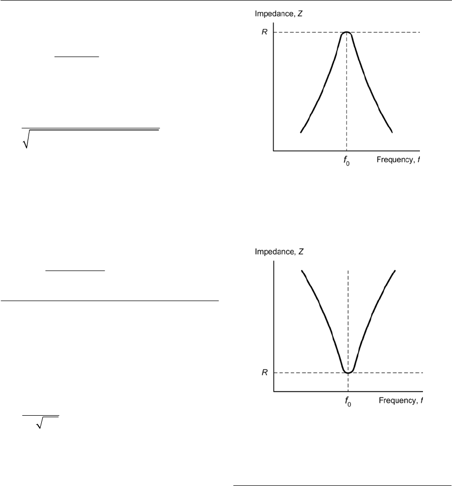
ALTERNATING VOLTAGE AND CURRENT 77
The phase angle (between the supply voltage and
current) will be given by:
The impedance of the parallel circuit of Fig. 4.16 is
given by:
where Z is the impedance of the series circuit (in
ohms), Ris the resistance (in F), XLis the inductive
reactance (in F)and XCis the capacitive reactance
(also in F). At resonance the circuit has a minimum
impedance (equal to R).
The phase angle (between the supply voltage and
current) will be given by:
Resonance
The frequency at which the impedance is minimum
for a series resonant circuit or maximum in the case
of a parallel resonant circuit is known as the
resonant frequency. The resonant frequency is
given by:
where f0is the resonant frequency (in Hertz), Lis
the inductance (in Henries) and C is the capacitance
(in Farads).
Typical impedance-frequency characteristics for
series and parallel tuned circuits are shown in Figs
4.17 and 4.18.
The series L–C–R tuned circuit has a minimum
impedance at resonance (equal to R)and thus
maximum current will flow. The circuit is
consequently known as an acceptor circuit.
The parallel L–C–R tuned circuit has a maximum
impedance at resonance (equal to R)and thus
minimum current will flow. The circuit is
consequently known as a rejector circuit.
1LC
tan XX
R
=
()
()
LC
2
222
LCLC
RX X
Z
XX RXX
××
=
+
(
)
LC
1
LC
tan
RX X
XX
=×
Figure 4.14 Impedance versus frequency for a
series L–C–Racceptor circuit
Figure 4.15 Impedance versus frequency for a
parallel L–C–Rrejector circuit
Quality factor
The quality of a resonant (or tuned) circuit is
measured by its Q-factor.The higher the Q-factor,
the sharper the response (narrower bandwidth),
conversely the lower the Q-factor, the flatter the
response (wider bandwidth), see Fig. 4.19. In the
case of the series tuned circuit, the Q-factor will
increase as the resistance, R,decreases. In the case
1
2
f
LC
=
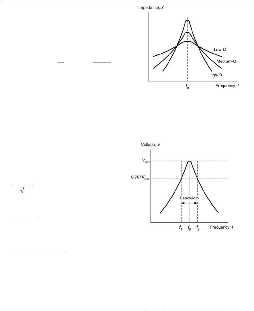
78 ELECTRONIC CIRCUITS: FUNDAMENTALS AND APPLICATIONS
of the parallel tuned circuit, the Q-factor will
increase as the resistance, R,increases. The
response of a tuned circuit can be modified by
incorporating a resistance of appropriate value
either to ‘dampen’ (low-Q)or ‘sharpen’ (high-Q)
the response. The relationship between bandwidth
and Q-factor is:
and
where f2and f1are respectively the upper and lower
cut-off (or half-power)frequencies (in Hertz), f0is
the resonant frequency (in Hertz), and Qis the
Q-factor.
Example 4.13
Aparallel L–C circuit is to be resonant at a
frequency of 400 Hz. If a 100 mH inductor is
available, determine the value of capacitance
required.
Solution
Re-arranging the formula
to make Cthe subject gives:
Thus
This value can be made from preferred values using
a2.2 µF capacitor connected in series with a 5.6 µF
capacitor.
Example 4.14
Aseries L–C–R circuit comprises an inductor of
20 mH, a capacitor of 10 nF, and a resistor of
100 F.If the circuit is supplied with a sinusoidal
signal of 1.5 V at a frequency of 2 kHz, determine
the current supplied and the voltage developed
across the resistor.
Solution
First we need to determine the values of inductive
reactance, XL,and capacitive reactance XC:
XL=20f L = 6.28 ×2×103×20 ×10@3=251 F
The impedance of the series circuit can now be
calculated:
Figure 4.16 Effect of Q-factor on the response of
aparallel resonant circuit (the response is similar,
but inverted, for a series resonant circuit)
Figure 4.17 Bandwidth of a tuned circuit
0
21
Bandwidth
f
ff
Q
==
1
2
f
LC
=
()
2
2
0
1
2
C
fL
=
6
23
1
1.58 10 1.58 F
400 39.4 100 10
C
µ
==×=
×××
C39
11
796.2
2 6.28 2 10 100 10
XfC
== =
×× × ×
0
2
fL
Q
R
=
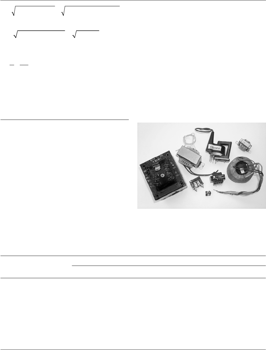
ALTERNATING VOLTAGE AND CURRENT 79
From which:
The current flowing in the series circuit will be
given by:
The voltage developed across the resistor can now
be calculated using:
V = IR = 2.7 mA × 100 F=270 mV
() ()
22
2 2
L C
100 251.2 796.2
ZRXX= + =+
10,000 297,025 307,025 554
Z
=+= =
1.5
0.0027 2.7 mA
554
V
IZ
== = =
Transformers
Transformers provide us with a means of coupling
a.c. power or signals from one circuit to another.
Voltage may be
stepped-up
(secondary voltage
greater than primary voltage) or
stepped-down
(secondary voltage less than primary voltage).
Since no increase in power is possible
(transformers are passive components like resistors,
capacitors and inductors) an increase in secondary
voltage can only be achieved at the expense of a
corresponding reduction in secondary current, and
vice versa (in fact, the secondary power will be
very slightly less than the primary power due to
losses within the transformer). Typical applications
for transformers include stepping-up or stepping-
down mains voltages in power supplies, coupling
signals in AF amplifiers to achieve impedance
matching and to isolate d.c. potentials associated
with active components.
The electrical characteristics of a transformer are
determined by a number of factors including the
core material and physical dimensions. The
specifications for a transformer usually include the
rated primary and secondary voltages and current
the required power rating (i.e. the maximum power,
usually expressed in volt-amperes, VA) which can
be continuously delivered by the transformer under
agiven set of conditions, the frequency range for
the component (usually stated as upper and lower
Table 4.2
Characteristics of common types of transformer
Note: Not usually important for this type of transformer
Property Transformer core type
Air cored Ferrite cored Iron cored (audio)
Core material/construction Air Ferrite ring or pot Laminated steel
Typical frequency range (Hz) 30 M to 1 G 10 k to 10 M 20 to 20 k
Typical power rating (VA) (see note) 1 to 200 0.1 to 50
Typical regulation (see note) (see note) (see note)
Typical applications RF tuned circuits
and filters
Filters and HF
transformers,
switched mode
power supplies
Smoothing chokes
and filters, audio
matching
Iron cored (power)
Laminated steel
50 to 400
3to 500
5% to 15%
Power supplies
Figure 4.18
Aselection of transformers with
power ratings from 0.1 VA to 100 VA
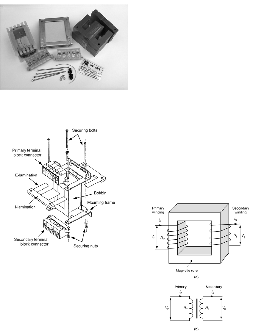
80 ELECTRONIC CIRCUITS: FUNDAMENTALS AND APPLICATIONS
Figure 4.19 Parts of a typical iron-cored power
transformer prior to assembly
working frequency limits), and the regulation of a
transformer (usually expressed as a percentage of
full-load). This last specification is a measure of the
ability of a transformer to maintain its rated output
voltage under load.
Table 4.2 summarizes the properties of three
common types of transformer. Figure 4.20 shows
the construction of a typical iron-cored power
transformer.
Figure 4.20 Construction of a typical iron-cored
transformer
Voltage and turns ratio
The principle of the transformer is illustrated in
Fig. 4.21. The primary and secondary windings are
wound on a common low-reluctance magnetic core.
The alternating flux generated by the primary
winding is therefore coupled into the secondary
winding (very little flux escapes due to leakage). A
sinusoidal current flowing in the primary winding
produces a sinusoidal flux. At any instant the flux
in the transformer is given by the equation:
where ømax is the maximum value of flux (in
Webers), fis the frequency of the applied current
(in Hertz), and tis the time in seconds.
The r.m.s. value of the primary voltage, VP,is
given by:
Similarly, the r.m.s. value of the secondary voltage,
VS,is given by:
Figure 4.21 The transformer principle
(
)
max sin 2
ft
=
PPmax
4.44VfN
=
SPmax
4.44VfN
=
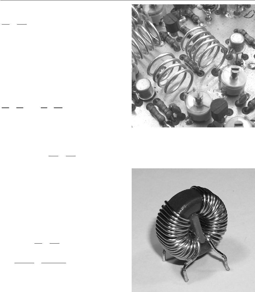
ALTERNATING VOLTAGE AND CURRENT 81
Now
where NP/Nsis the turns ratio of the transformer.
Assuming that the transformer is loss-free,
primary and secondary powers (PPand PS
respectively) will be identical. Hence:
PP= PSthus VP×IP= VS×IP
Hence
and
Finally, it is sometimes convenient to refer to a
turns-per-volt rating for a transformer. This rating
is given by:
Example 4.15
Atransformer has 2,000 primary turns and 120
secondary turns. If the primary is connected to a
220 V r.m.s. a.c. mains supply, determine the
secondary voltage.
Solution
Rearranging gives:
Example 4.16
Atransformer has 1,200 primary turns and is
designed to operate with a 200 V a.c. supply. If the
transformer is required to produce an output of
10 V, determine the number of secondary turns
required. Assuming that the transformer is loss-
free, determine the input (primary) current for a
load current of 2.5 A.
Figure 4.23 This small 1:1 ratio toroidal
transformer forms part of a noise filter connected in
the input circuit of a switched mode power supply.
The transformer is wound on a ferrite core and acts
as a choke, reducing the high-frequency noise that
would otherwise be radiated from the mains supply
wiring
Figure 4.22 Resonant air-cored transformer
arrangement. The two inductors are tuned to
resonance at the operating frequency (145 MHz) by
means of the two small preset capacitors
PP
SS
VN
VN
=
S
P
SP
I
V
VI
=
S
P
PS
I
N
IN
=
PP
PS
turns-per-volt
NN
VV
==
PP
SS
VN
VN
=
SP
S
P
120 220
13.2 V
2, 000
NV
VN
××
== =
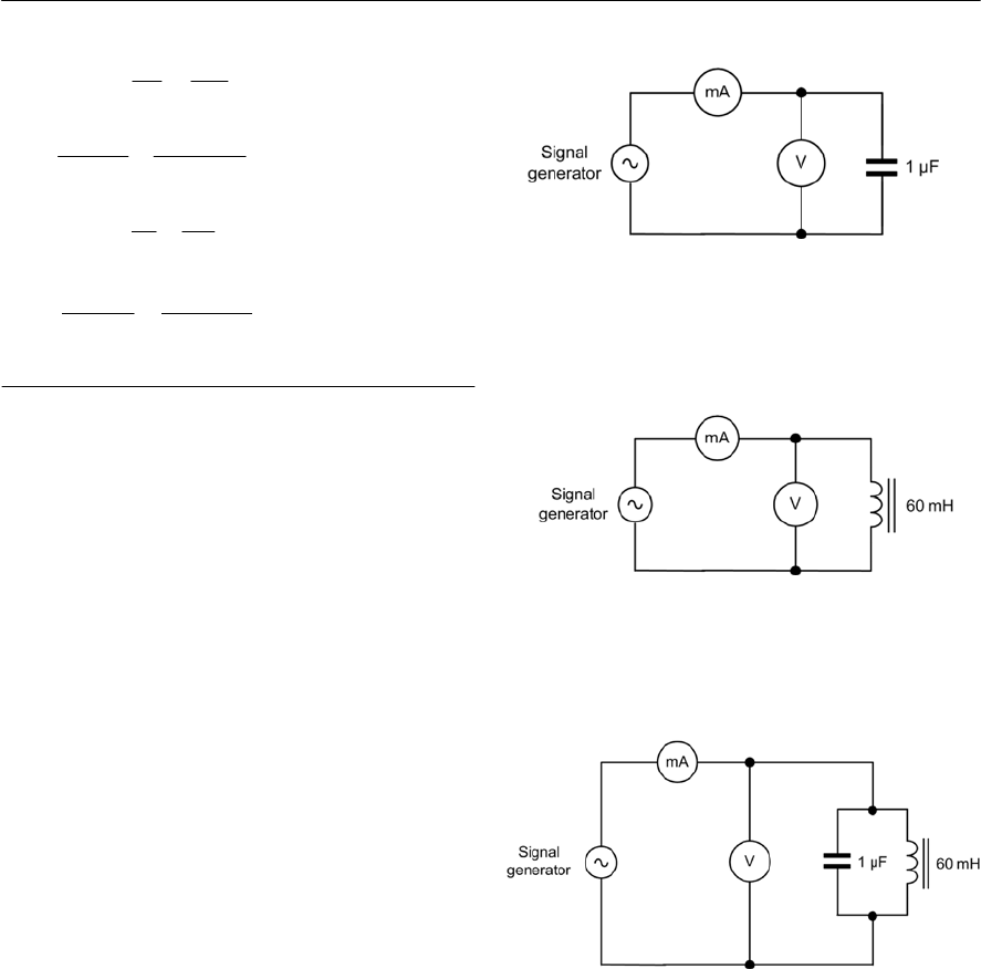
82 ELECTRONIC CIRCUITS: FUNDAMENTALS AND APPLICATIONS
Practical investigation
Objective
To investigate reactance in an a.c. circuit.
Components and test equipment
Breadboard, digital or analogue meters with a.c.
voltage and current ranges, sine wave signal
generator (with an output impedance of 50 F,or
less), 1 µF capacitor, 60 mH inductor (with low
series loss resistance), test leads, connecting wire.
Procedure
Connect the circuit shown in Fig. 4.24 (capacitive
reactance). Set the voltmeter and ammeter
respectively to the 2 V and 20 mA ranges. Set the
signal generator to produce a sine wave output at
100 Hz.
Adjust the signal generator output voltage so that
the voltmeter reads exactly 1 V before measuring
and recording the current (this should be less than 1
mA). Repeat this measurement at frequencies from
200 Hz to 1 kHz in steps of 100 Hz. At each step,
check that the voltage is exactly
1 V (adjust, if necessary).
Connect the circuit shown in Fig. 4.25 (inductive
reactance). As before, set the voltmeter and
ammeter to the 2 V and 20 mA ranges and set the
signal generator to produce a sine wave output at
100 Hz.
Adjust the signal generator output for a voltage
of exactly 1 V before measuring and recording the
current. Repeat this measurement at frequencies
over from 200 Hz to 1 kHz in steps of 100 Hz. At
Figure 4.24 Circuit diagram—capacitive reactance
Solution
Rearranging gives:
Rearranging gives:
PP
SS
VN
VN
=
PS
S
P
1, 200 10
60 turns
200
NV
NV
××
== =
S
P
PS
I
N
IN
=
SS
S
P
200 2.5
0.42 A
1, 200
NI
NN
××
== =
each step, check that the voltage is exactly 1 V
(adjust the signal generator output if necessary).
Connect the circuit shown in Fig. 4.26 (resonant
circuit). As before, set the voltmeter and ammeter
respectively to the 2 V and 20 mA ranges. Set the
signal generator to produce a sine wave output at
100 Hz.
Figure 4.25 Circuit diagram—inductive reactance
Figure 4.26 Circuit diagram—resonant circuit
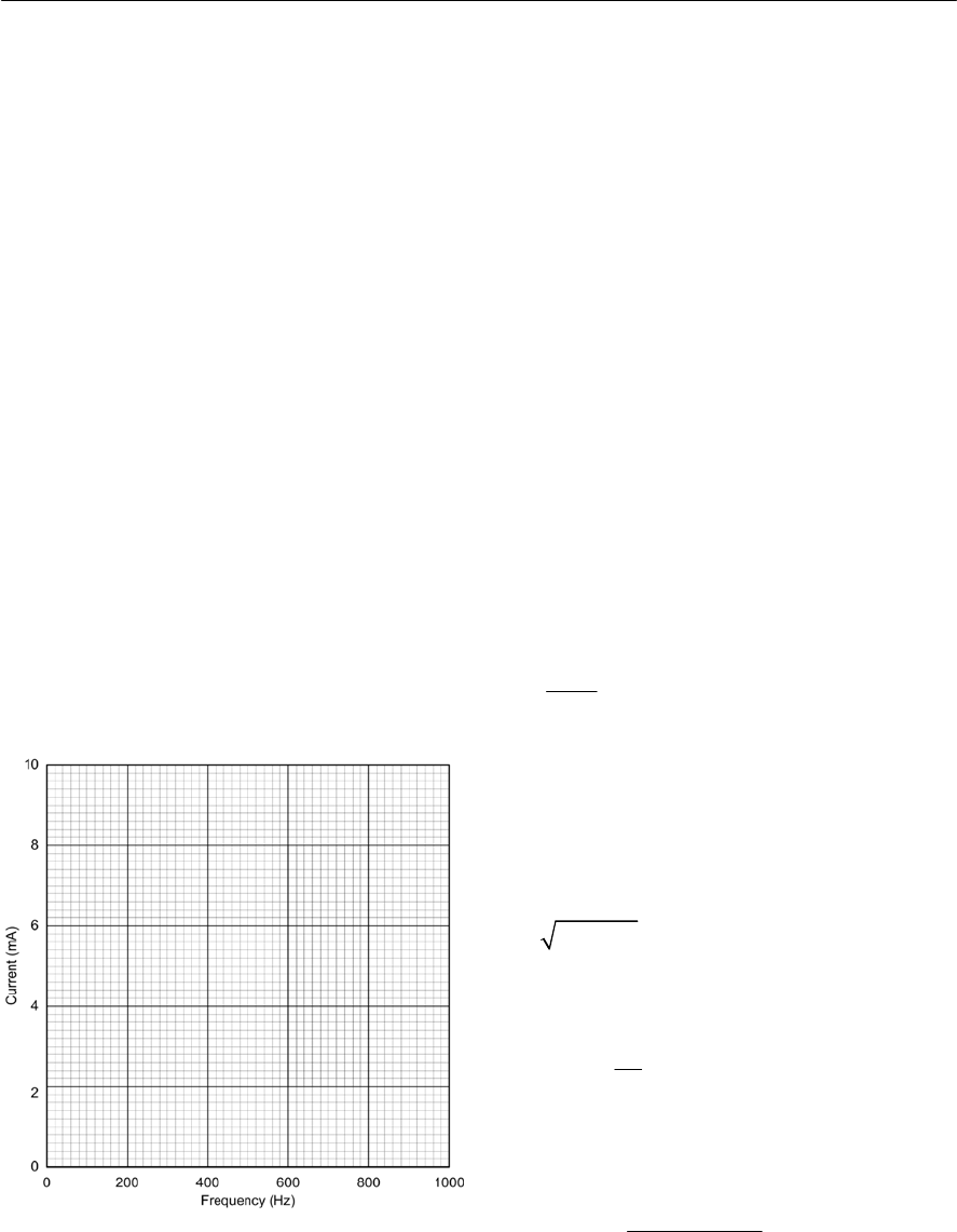
ALTERNATING VOLTAGE AND CURRENT 83
Important formulae introduced in this
chapter
Sine wave voltage:
(page 69)
v=Vmax sin (20t)
Sine wave voltage superimposed on a d.c. level:
(page 70)
v=Vd.c. +Vmax sin (20t)
Frequency and periodic time:
(page 70)
t = 1/ f or f = 1/ t
Peak and r.m.s. values for a sine wave:
(page 71)
Vpk =1.414 × Vr.m.s
Vr.m.s. =0.707 × Vpk
Capacitive reactance:
(page 72)
Inductive reactance:
(page 73)
XL= 20f L
Impedance of C–R or L–R in series:
(page 74)
Phase angle for C–R or L–R in series:
(page 74)
Power factor:
(page 75)
C
1
2
X
fC
=
22
ZRX
=+
1
tan
X
R
=
true power
power factor =
apparent power
Figure 4.27 Graph layout for plotting the results
Adjust the signal generator output voltage so that
the voltmeter reads exactly 1 V before measuring
and recording the current. Repeat this measurement
at frequencies over from 200 Hz to
1kHz in steps of 100 Hz. At each step, check that
the voltage is exactly 1 V (adjust, if necessary).
Note the frequency at which the current takes a
minimum value.
Measurements and calculations
Record your results in a table showing values of I
C
,
I
L
and I
S
,at each frequency from 100 Hz to 1 kHz.
Plot graphs showing how the current in each circuit
varies over the frequency range 100 Hz to 1 kHz.
Calculate the resonant frequency of the L–Ccircuit
shown in Fig. 4.26.
Conclusion
Comment on the shape of each graph. Is this what
you would expect (recall that the current flowing in
the circuit will be proportional to the reciprocal of
the reactance)? Compare the measured resonant
frequency with the calculated value. If they are not
the same suggest reasons for any difference.
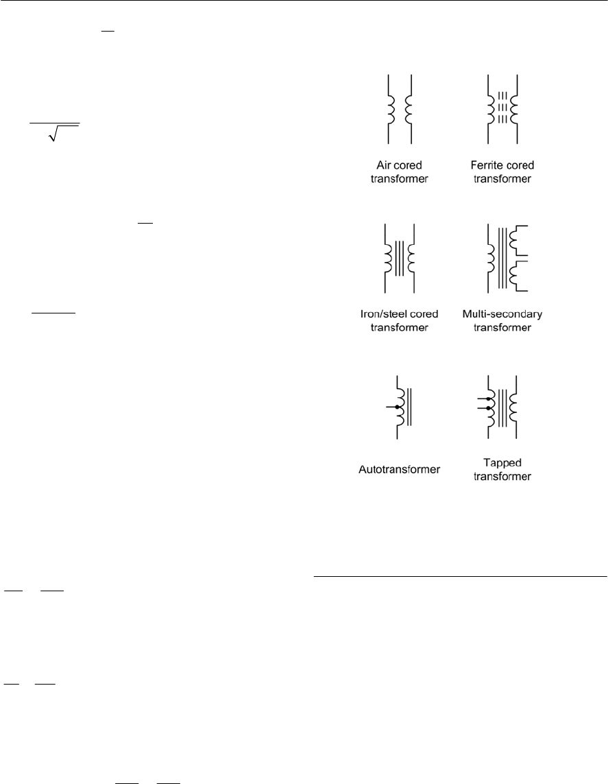
84 ELECTRONIC CIRCUITS: FUNDAMENTALS AND APPLICATIONS
Problems
4.1 A sine wave has a frequency of 250 Hz and
an amplitude of 50 V. Determine its periodic
time and r.m.s. value.
4.2 A sinusoidal voltage has an r.m.s. value of
240 V and a period of 16.7 ms. What is the
frequency and peak value of the voltage?
4.3 Determine the frequency and peak-peak
values of each of the waveforms shown in
Fig. 4.29.
4.4 A sine wave has a frequency of 100 Hz and
in amplitude of 20 V. Determine the
instantaneous value of voltage (a) 2 ms and
(b) 9 ms from the start of a cycle.
Figure 4.28 Circuit symbols introduced in this
chapter
Symbols introduced in this chapter
Resonant frequency of a tuned circuit:
(page 77)
Bandwidth of a tuned circuit:
(page 78)
Q-factor for a series tuned circuit:
(page 78)
Flux in a transformer:
(page 80)
Transformer voltages:
(page 80)
Voltage and turns ratio:
(page 81)
Current and turns ratio:
(page 81)
Turns-per-volt:
(page 81)
power factor cos
R
Z
==
1
2
f
LC
=
0
21
Bandwidth
f
ff
Q
==
0
2
fL
Q
R
=
(
)
max
sin 2
ft
=
PPmax
4.44VfN
=
SPmax
4.44VfN
=
PP
SS
VN
VN
=
S
P
PS
I
N
IN
=
PP
PS
turns-per-volt
NN
VV
==
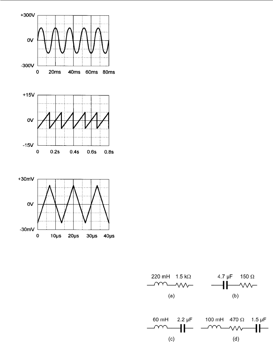
ALTERNATING VOLTAGE AND CURRENT 85
4.5 A sinusoidal current of 20 mA pk-pk flows
in a resistor of 1.5 kF.Determine the r.m.s.
voltage applied.
4.6 Determine the reactance of a 220 nF
capacitor at (a) 20 Hz and (b) 5 kHz.
4.7 A 47 nF capacitor is connected across the
240 V 50 Hz mains supply. Determine the
r.m.s. current flowing in the capacitor.
4.8 Determine the reactance of a 33 mH
inductor at (a) 50 Hz and (b) 7 kHz.
4.9 A 10 mH inductor of negligible resistance is
used to form part of a filter connected in
series with a 50 Hz mains supply. What
Figure 4.29 See Question 4.3
voltage drop will appear across the inductor
when a current of 1.5 A is flowing?
4.10 A 10 uF capacitor is connected in series
with a 500 Fresistor across a 110 V 50 Hz
a.c. supply. Determine the impedance of the
circuit and the current taken from the
supply.
4.11 A choke having an inductance of 1 H and
resistance of 250 Fis connected to a 220 V
60 Hz a.c. supply. Determine the power
factor of the choke and the current taken
from the supply.
4.12 A series-tuned L–C network is to be
resonant at a frequency of 1.8 kHz. If a
60 mH inductor is available, determine the
value of capacitance required.
4.13 Determine the impedance at 1 kHz of each
of the circuits shown in Fig. 4.30.
4.14 A parallel resonant circuit employs a fixed
inductor of 22 µH and a variable tuning
capacitor. If the maximum and minimum
values of capacitance are respectively 20 pF
and 365 pF, determine the effective tuning
range for the circuit.
4.15 A series L-C-R circuit comprises an inductor
of 15 mH (with negligible resistance), a
capacitor of 220 nF and a resistor of 100 F.
If the circuit is supplied with a sinusoidal
signal of 15 V at a frequency of 2 kHz,
determine the current supplied and the
voltage developed across the capacitor.
4.16 A 470 µH inductor has a resistance of 20 F.
If the inductor is connected in series with a
capacitor of 680 pF, determine the resonant
Figure 4.30 See Question 4.13
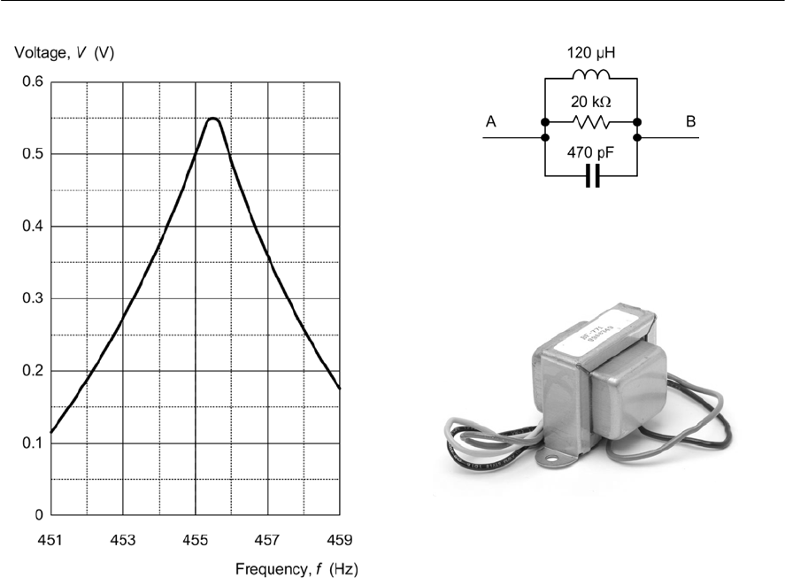
86 ELECTRONIC CIRCUITS: FUNDAMENTALS AND APPLICATIONS
frequency, Q-factor, and bandwidth of the
circuit.
4.17 The graph shown in Fig. 4.31 was obtained
during measurements on a high-Q filter.
Determine the following parameters for the
filter:
(a) resonant frequency
(b) bandwidth
(c) Q-factor.
4.18 The circuit shown in Fig. 4.32 is fed from a
2 V constant voltage source. At what
frequency will the supply current be a
minimum and what will the current be at
this frequency? What current will flow in
the inductor and capacitor at this frequency?
4.19 Identify the component shown in Fig. 4.33.
Explain how this component operates and
state a typical application for it.
Figure 4.32 See Question 4.18
Figure 4.31 See Question 4.17
Figure 4.33 See Question 4.19
4.20 A transformer has 1,600 primary turns and
120 secondary turns. If the primary is
connected to a 240 V r.m.s. a.c. mains
supply, determine the secondary voltage.
4.21 A transformer has 800 primary turns and 60
secondary turns. If the secondary is
connected to a load resistance of 15 F,
determine the value of primary voltage
required to produce a power of 22.5 W in
the load (assume that the transformer is
loss-free).
4.22 A transformer has 440 primary turns and
operates from a 110 V a.c. supply. The
transformer has two secondary windings
each rated at 12 V 20 VA. Determine:
(a) the turns-per-volt rating
(b) the secondary turns (each winding)
(c) the secondary current (each winding)
(c) the full-load primary current.
Answers to these problems appear on page 374.
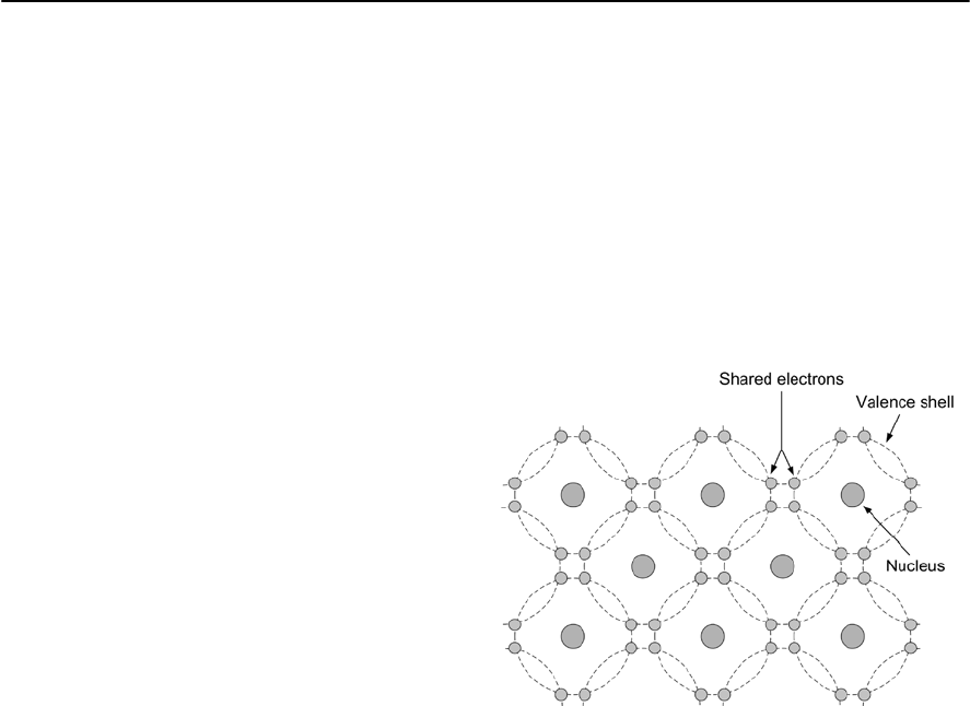
5
Semiconductors
This chapter introduces devices that are made from
materials that are neither conductors nor insulators.
These semiconductor materials form the basis of
diodes, thyristors, triacs, transistors and integrated
circuits. We start this chapter with a brief
introduction to the principles of semiconductors
before going on to examine the characteristics of
each of the most common types of semiconductor.
In Chapter 1 we described the simplified
structure of an atom and showed that it contains
both negative charge carriers (electrons) and
positive charge carriers (protons). Electrons each
carry a single unit of negative electric charge while
protons each exhibit a single unit of positive
charge. Since atoms normally contain an equal
number of electrons and protons, the net charge
present will be zero. For example, if an atom has
eleven electrons, it will also contain eleven protons.
The end result is that the negative charge of the
electrons will be exactly balanced by the positive
charge of the protons.
Electrons are in constant motion as they orbit
around the nucleus of the atom. Electron orbits are
organized into shells. The maximum number of
electrons present in the first shell is 2, in the second
shell 8, and in the third, fourth and fifth shells it is
18, 32 and 50, respectively. In electronics, only the
electron shell furthermost from the nucleus of an
atom is important. It is important to note that the
movement of electrons only involves those present
in the outer valence shell.
If the valence shell contains the maximum
number of electrons possible the electrons are
rigidly bonded together and the material has the
properties of an insulator. If, however, the valence
shell does not have its full complement of
electrons, the electrons can be easily loosened from
their orbital bonds, and the material has the
properties associated with an electrical conductor.
An isolated silicon atom contains four electrons
in its valence shell. When silicon atoms combine to
form a solid crystal, each atom positions itself
between four other silicon atoms in such a way that
Figure 5.1 Lattice showing covalent bonding
the valence shells overlap from one atom to
another. This causes each individual valence
electron to be shared by two atoms, as shown in
Fig. 5.1. By sharing the electrons between four
adjacent atoms each individual silicon atom
appears to have eight electrons in its valence shell.
This sharing of valence electrons is called covalent
bonding.
In its pure state, silicon is an insulator because the
covalent bonding rigidly holds all of the electrons
leaving no free (easily loosened) electrons to
conduct current. If, however, an atom of a different
element (i.e. an impurity)is introduced that has
five electrons in its valence shell, a surplus electron
will be present, as shown in Fig. 5.2. These free
electrons become available for use as charge
carriers and they can be made to move through the
lattice by applying an external potential difference
to the material.
Similarly, if the impurity element introduced into
the pure silicon lattice has three electrons in its
valence shell, the absence of the fourth electron
needed for proper covalent bonding will produce a
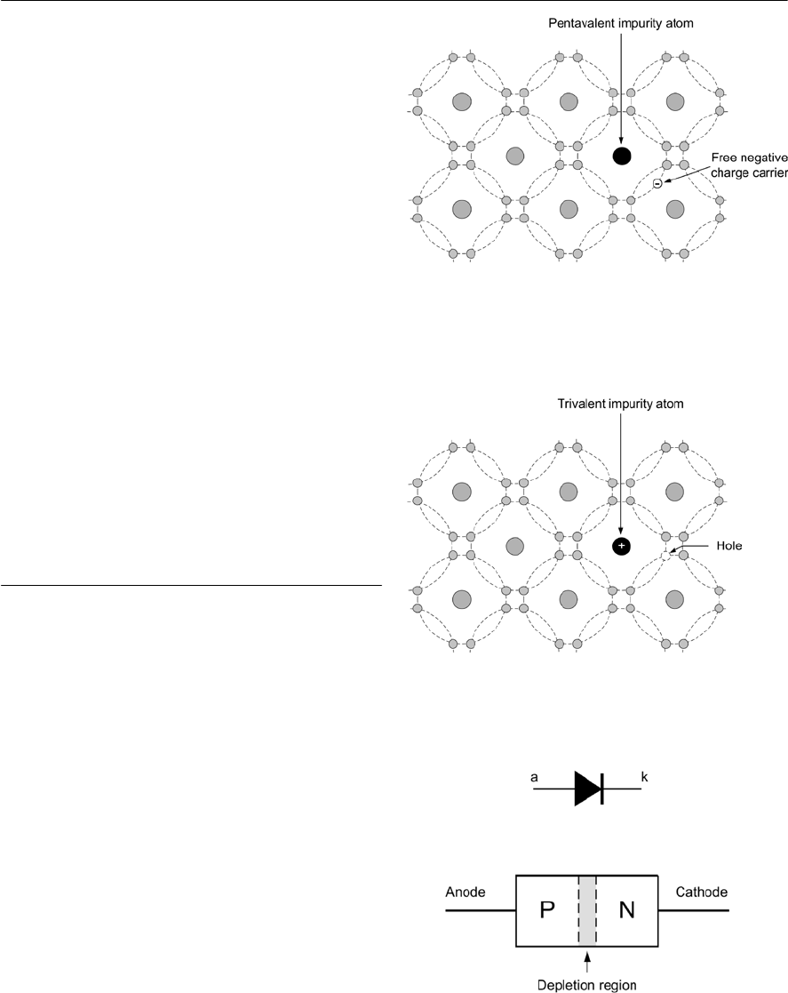
88 ELECTRONIC CIRCUITS: FUNDAMENTALS AND APPLICATIONS
number of gaps into which electrons can fit, as
shown in Fig. 5.3. These gaps are referred to as
holes.Once again, current will flow when an
external potential difference is applied to the
material.
Regardless of whether the impurity element
produces surplus electrons or holes, the material
will no longer behave as an insulator, neither will it
have the properties that we normally associate with
ametallic conductor. Instead, we call the material a
semiconductor—the term simply indicates that the
substance is no longer a good insulator or a good
conductor but is somewhere in between!
The process of introducing an atom of another
(impurity) element into the lattice of an otherwise
pure material is called doping. When the pure
material is doped with an impurity with five
electrons in its valence shell (i.e. a pentavalent
impurity)it will become an N-type material. If,
however, the pure material is doped with an
impurity having three electrons in its valence shell
(i.e. a trivalent impurity)it will become P-type
material. N-type semiconductor material contains
an excess of negative charge carriers, and P-type
material contains an excess of positive charge
carriers.
Semiconductor diodes
When a junction is formed between N-type and P–
type semiconductor materials, the resulting device
is called a diode. This component offers an
extremely low resistance to current flow in one
direction and an extremely high resistance to
current flow in the other. This characteristic allows
the diode to be used in applications that require a
circuit to behave differently according to the
direction of current flowing in it.
An ideal diode would pass an infinite current in
one direction and no current at all in the other
direction. In addition, the diode would start to
conduct current when the smallest of voltages was
present. In practice, a small voltage must be applied
before conduction takes place. Furthermore a small
leakage current will flow in the reverse direction.
This leakage current is usually a very small fraction
of the current that flows in the forward direction.
If the P-type semiconductor material is made
positive relative to the N-type material by an
Figure 5.2 Free negative charge carriers
(electrons) produced by introducing a pentavalent
impurity
Figure 5.3 Holes produced by introducing a
trivalent impurity
Figure 5.4 A P-N junction diode
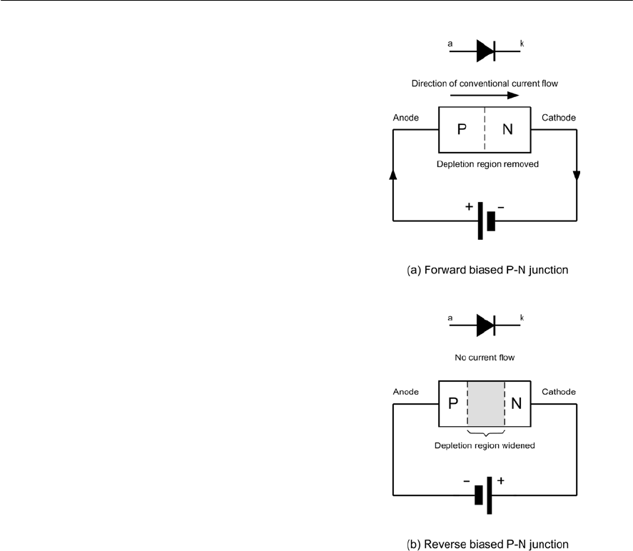
SEMICONDUCTORS 89
amount greater than its forward threshold voltage
(about 0.6 V if the material is silicon and 0.2 V if
the material is germanium), the diode will freely
pass current. If, on the other hand, the P-type
material is made negative relative to the N-type
material, virtually no current will flow unless the
applied voltage exceeds the maximum (breakdown)
voltage that the device can withstand. Note that a
normal diode will be destroyed if its reverse
breakdown voltage is exceeded.
A semiconductor junction diode is shown in Fig.
5.4. The connection to the P-type material is
referred to as the anode while that to the N-type
material is called the cathode.With no externally
applied potential, electrons from the N-type
material will cross into the P-type region and fill
some of the vacant holes. This action will result in
the production of a region either side of the
junction in which there are no free charge carriers.
This zone is known as the depletion region.
Figure 5.5(a) shows a junction diode in which
the anode is made positive with respect to the
cathode. In this forward-biased condition, the
diode freely passes current. Figure 5.5(b) shows a
diode with the cathode made positive with respect
to the cathode. In this reverse-biased condition, the
diode passes a negligible amount of current. In the
freely conducting forward-biased state, the diode
acts rather like a closed switch. In the reverse-
biased state, the diode acts like an open switch.
If a positive voltage is applied to the P-type
material, the free positive charge carriers will be
repelled and they will move away from the positive
potential towards the junction. Likewise, the
negative potential applied to the N-type material
will cause the free negative charge carriers to move
away from the negative potential towards the
junction.
When the positive and negative charge carriers
arrive at the junction, they will attract one another
and combine (recall that unlike charges attract). As
each negative and positive charge carrier combine
at the junction, a new negative and positive charge
carrier will be introduced to the semiconductor
material from the voltage source. As these new
charge carriers enter the semiconductor material,
they will move toward the junction and combine.
Thus, current flow is established and it will
continue for as long as the voltage is applied.
As stated earlier, the forward threshold voltage
must be exceeded before the diode will conduct.
The forward threshold voltage must be high enough
to completely remove the depletion layer and force
charge carriers to move across the junction. With
silicon diodes, this forward threshold voltage is
approximately 0.6 V to 0.7 V. With germanium
diodes, the forward threshold voltage is
approximately 0.2 V to 0.3 V.
Figure 5.6 shows typical characteristics for small
germanium and silicon diodes. It is worth noting
that diodes are limited by the amount of forward
current and reverse voltage they can withstand.
This limit is based on the physical size and
construction of the diode.
Figure 5.5 Forward and reverse biased P-N
junction
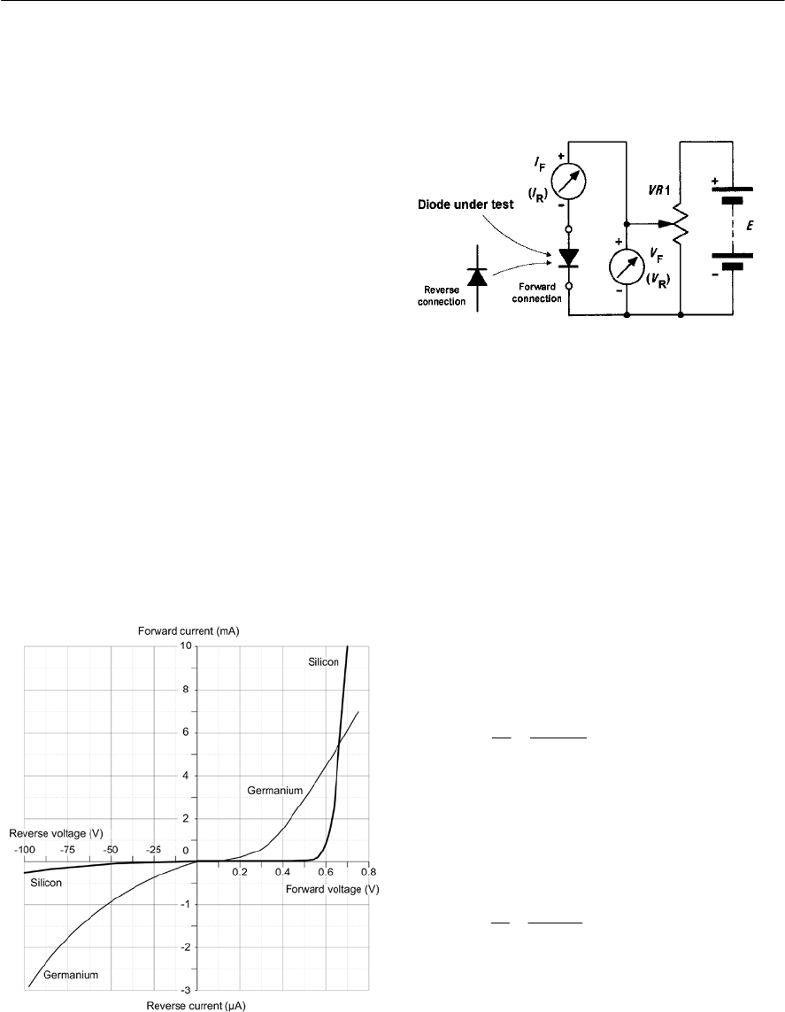
90 ELECTRONIC CIRCUITS: FUNDAMENTALS AND APPLICATIONS
In the case of a reverse biased diode, the P-type
material is negatively biased relative to the N-type
material. In this case, the negative potential applied
to the P-type material attracts the positive charge
carriers, drawing them away from the junction.
Likewise, the positive potential applied to the N-
type material attracts the negative charge carriers
away from the junction. This leaves the junction
area depleted; virtually no charge carriers exist.
Therefore, the junction area becomes an insulator,
and current flow is inhibited. The reverse bias
potential may be increased to the reverse
breakdown voltage for which the particular diode is
rated. As in the case of the maximum forward
current rating, the reverse breakdown voltage is
specified by the manufacturer. The reverse
breakdown voltage is usually very much higher
than the forward threshold voltage. A typical
general-purpose diode may be specified as having a
forward threshold voltage of 0.6 V and a reverse
breakdown voltage of 200 V. If the latter is
exceeded, the diode may suffer irreversible
damage. It is also worth noting that, where diodes
are designed for use as rectifiers, manufacturers
often quote peak inverse voltage (PIV)or
maximum reverse repetitive voltage (VRRM)
rather than maximum reverse breakdown voltage.
Figure 5.6 Typical diode characteristics
Figure 5.7 shows a test circuit for obtaining diode
characteristics (note that the diode must be reverse
connected in order to obtain the reverse
characteristic).
Figure 5.7 Diode test circuit
Example 5.1
The characteristic shown in Fig. 5.8 refers to a
germanium diode. Determine the resistance of the
diode when (a) the forward current is 2.5 mA and
(b) when the forward voltage is 0.65 V.
Solution
(a) When IF=2.5 mA the corresponding value
of VFcan be read from the graph. This
shows that VF=0.43 V. The resistance of
the diode at this point on the characteristic
will be given by:
(b) When VF=0.65 V the corresponding value
of IFcan be read from the graph. This
shows that IF=7.4 mA. The resistance of
the diode at this point on the characteristic
will be given by:
This example shows how the resistance of a diode
does not remain constant but instead changes
according to the point on the characteristic at which
it is operating.
F
F
0.43 V
172
2.5 mA
V
RI
== =
F
F
0.65 V
88
7.4 mA
V
RI
== =
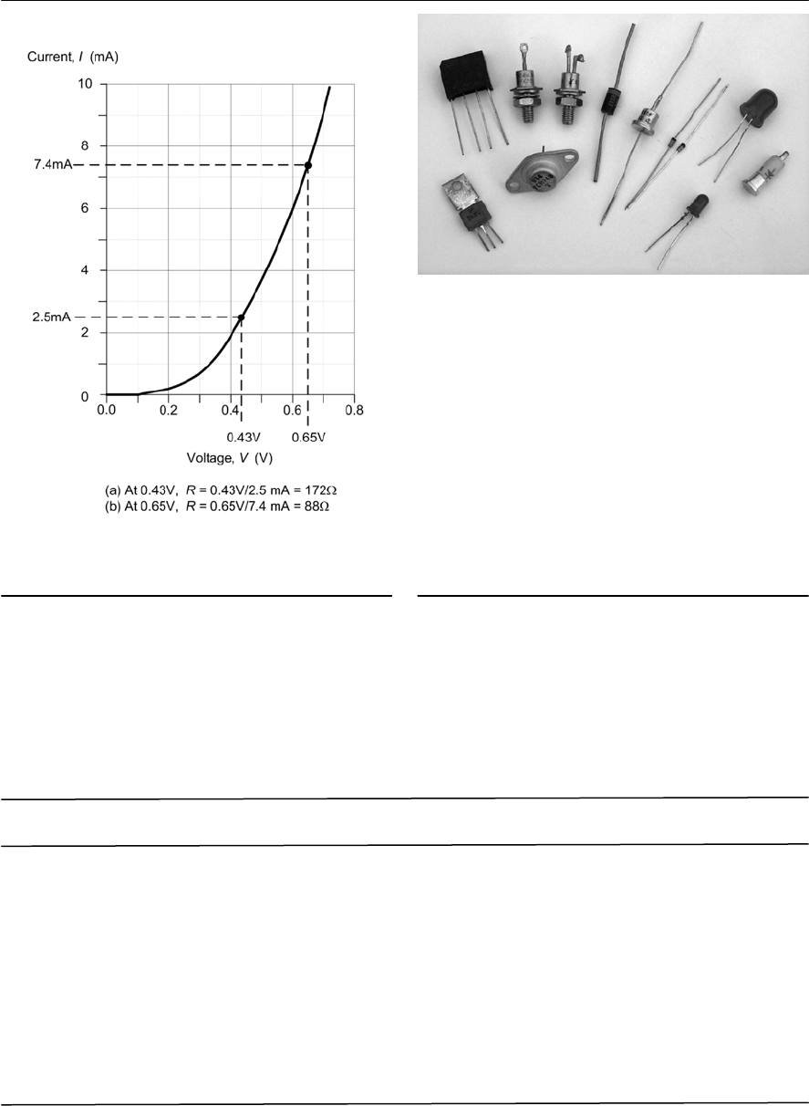
SEMICONDUCTORS 91
Table 5.1 Characteristics of some common semiconductor diodes
Device Material PIV IFmax. IRmax. Application
1N4148 Silicon 100 V 76 mA 25 nA General purpose
1N914 Silicon 100 V 75 mA 25 nA General purpose
AA113 Germanium 60 V 10 mA 200 µA RF detector
OA47 Germanium 25 V 110 mA 100 µA Signal detector
OA91 Germanium 115 V 50 mA 275 µA General purpose
1N4001 Silicon 50 V 1 A 10 µA Low-voltage rectifier
1N5404 Silicon 400 V 3 A 10 µA High-voltage rectifier
BY127 Silicon 1,250 V 1 A 10 µA High-voltage rectifier
Diode types
Diodes are often divided into signal or rectifier
types according to their principal field of
application. Signal diodes require consistent
Figure 5.8 See Example 5.1
forward characteristics with low forward voltage
drop. Rectifier diodes need to be able to cope with
high values of reverse voltage and large values of
forward current, consistency of characteristics is of
secondary importance in such applications. Table
5.1 summarizes the characteristics of some
common semiconductor diodes whilst a selection of
diodes are shown in Fig. 5.9.
Zener diodes
Zener diodes are heavily doped silicon diodes
which, unlike normal diodes, exhibit an abrupt
reverse breakdown at relatively low voltages
Figure 5.9 A selection of diodes including power
and bridge rectifiers, thyristors, signal and zener
diodes
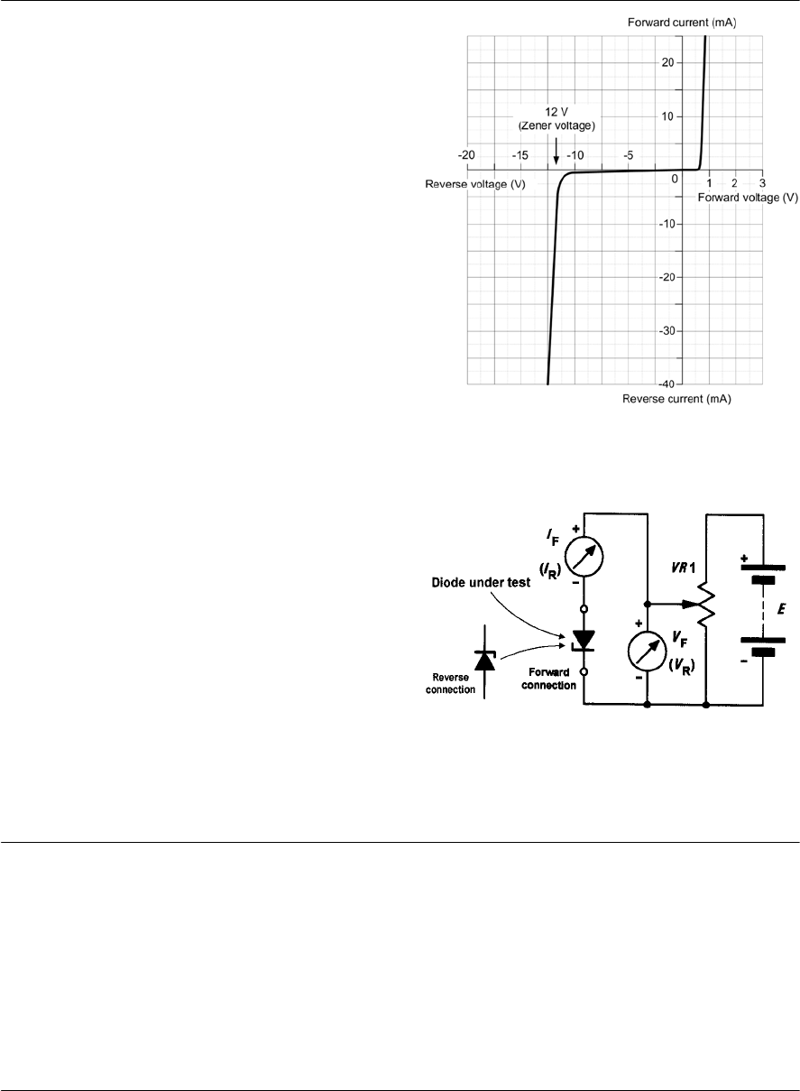
92 ELECTRONIC CIRCUITS: FUNDAMENTALS AND APPLICATIONS
(typically less than 6 V). A similar effect occurs in
less heavily doped diodes. These avalanche diodes
also exhibit a rapid breakdown with negligible
current flowing below the avalanche voltage and an
increasingly large current flowing once the
avalanche voltage has been reached. For avalanche
diodes, this breakdown voltage usually occurs at
voltages above 6 V. In practice, however, both
types of diode are referred to as zener diodes. A
typical characteristic for a 12 V zener diode is
shown in Fig. 5.10.
Whereas reverse breakdown is a highly
undesirable effect in circuits that use conventional
diodes, it can be extremely useful in the case of
zener diodes where the breakdown voltage is
precisely known. When a diode is undergoing
reverse breakdown and provided its maximum
ratings are not exceeded the voltage appearing
across it will remain substantially constant (equal to
the nominal zener voltage) regardless of the current
flowing. This property makes the zener diode ideal
for use as a voltage regulator (see Chapter 6).
Zener diodes are available in various families
(according to their general characteristics,
encapsulation and power ratings) with reverse
breakdown (zener) voltages in the E12 and E24
series (ranging from 2.4 V to 91 V). Table 5.2
summarizes the characteristics of common zener
diodes.
Figure 5.11 shows a test circuit for obtaining
zener diode characteristics. The circuit is shown
with the diode connected in the forward direction
and it must be reverse connected in order to obtain
the reverse characteristic. Finally, it is important to
note that, when used as a voltage regulator, the
cathode connection is the more positive terminal.
Figure 5.10 Typical characteristic for a 12 V
zener diode
Figure 5.11 Zener diode test circuit
BZY88 series Miniature glass encapsulated diodes rated at 500 mW (at 25°C). Zener voltages range
from 2.7 V to 15 V (voltages are quoted for 5 mA reverse current at 25°C)
BZX61 series Encapsulated alloy junction rated at 1.3 W (25°C ambient). Zener voltages range
from 7.5 V to 72 V
BZX85 series Medium-power glass-encapsulated diodes rated at 1.3 W and offering zener voltages
in the range 5.1 V to 62 V
BZY93 series High-power diodes in stud mounting encapsulation. Rated at 20 W for ambient
temperatures up to 75°C. Zener voltages range from 9.1 V to 75 V
1N5333 series Plastic encapsulated diodes rated at 5 W. Zener voltages range from 3.3 V to 24 V
Table 5.2 Characteristics of some common zener diodes
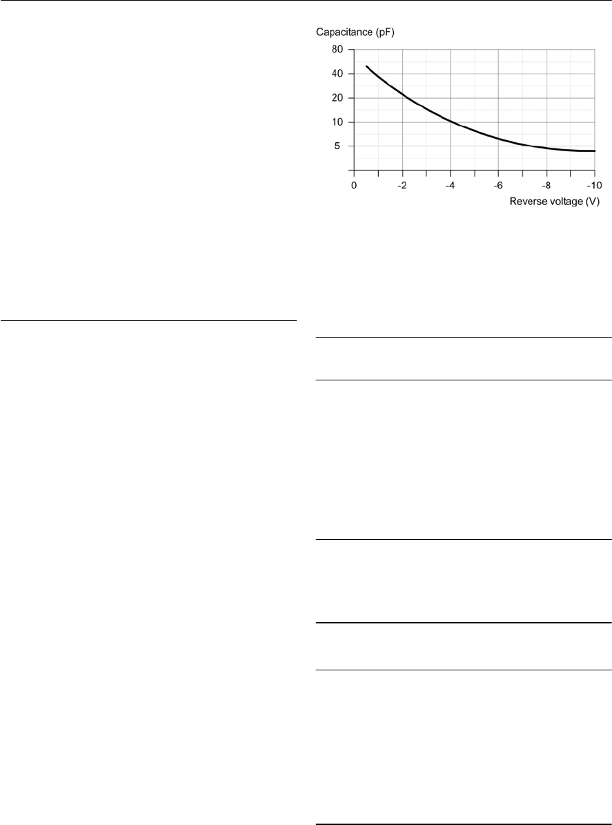
SEMICONDUCTORS 93
Figure 5.12 Typical characteristic for a variable
capacitance diode
Variable capacitance diodes
The capacitance of a reverse-biased diode junction
will depend on the width of the depletion layer
which, in turn, varies with the reverse voltage
applied to the diode. This allows a diode to be used
as a voltage controlled capacitor. Diodes that are
specially manufactured to make use of this effect
(and which produce comparatively large changes in
capacitance for a small change in reverse voltage)
are known as variable capacitance diodes (or
varicaps). Such diodes are used (often in pairs) to
provide tuning in radio and TV receivers. A typical
characteristic for a variable capacitance diode is
shown in Fig. 5.12. Table 5.3 summarizes the
characteristics of several common variable
capacitance diodes.
Thyristors
Thyristors (or silicon controlled rectifiers)are
three-terminal devices which can be used for
switching and a.c. power control. Thyristors can
switch very rapidly from a conducting to a non-
conducting state. In the off state, the thyristor
exhibits negligible leakage current, while in the on
state the device exhibits very low resistance. This
results in very little power loss within the thyristor
even when appreciable power levels are being
controlled. Once switched into the conducting state,
the thyristor will remain conducting (i.e. it is
latched in the on state) until the forward current is
removed from the device. In d.c. applications this
necessitates the interruption (or disconnection) of
the supply before the device can be reset into its
non-conducting state. Where the device is used
with an alternating supply, the device will
automatically become reset whenever the main
supply reverses. The device can then be triggered
on the next half-cycle having correct polarity to
permit conduction. Like their conventional silicon
diode counterparts, thyristors have anode and
cathode connections; control is applied by means of
agate terminal (see Fig. 5.13). The device is
triggered into the conducting (on state) by means of
the application of a current pulse to this terminal.
The effective triggering of a thyristor requires a
gate trigger pulse having a fast rise time derived
from a low-resistance source. Triggering can
Table 5.3 Characteristics of several common
types of variable capacitance diode
Table 5.4 Characteristics of several common types
of thyristor
Type Capacitance
(at 4V)
Capacitance
ratio Q-factor
1N5450 33 pF 2.6
(4 V to 60 V)
350
MV1404 50 pF >10
(2 V to 10 V)
200
MV2103 10 pF 2
(4 V to 60 V)
400
MV2115 100 pF 2.6
(4 V to 60 V)
100
Type IFave.
(A)
VRRM
(V)
VGT
(V)
2N4444 5.1 600 1.5
BT106 1 700 3.5
BT152 13 600 1
BTY79-400R 6.4 400 3
IGT
(mA)
30
50
32
30
TIC106D 3.2 400 1.2 0.2
TIC126D 7.5 400 2.5 20
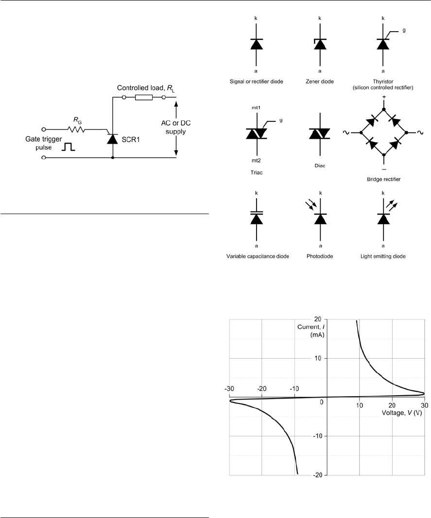
94 ELECTRONIC CIRCUITS: FUNDAMENTALS AND APPLICATIONS
become erratic when insufficient gate current is
available or when the gate current changes slowly.
Table 5.4 summarizes the characteristics of several
common thyristors.
Triacs
Triacs are a refinement of the thyristor which, when
triggered, conduct on both positive and negative
half-cycles of the applied voltage. Triacs have three
terminals known as main terminal one (MT1), main
terminal two (MT2) and gate (G), as shown in Fig.
5.14. Triacs can be triggered by both positive and
negative voltages applied between G and MT1 with
positive and negative voltages present at MT2
respectively. Triacs thus provide full-wave control
and offer superior performance in a.c. power
control applications when compared with thyristors
which only provide half-wave control.
Table 5.5 summarizes the characteristics of
several common triacs. In order to simplify the
design of triggering circuits, triacs are often used in
conjunction with diacs (equivalent to a bi-
directional zener diode). A typical diac conducts
heavily when the applied voltage exceeds
approximately 30 V in either direction. Once in the
conducting state, the resistance of the diac falls to a
very low value and thus a relatively large value of
current will flow. The characteristic of a typical
diac is shown in Fig. 5.15.
Light emitting diodes
Light emitting diodes (LED) can be used as
general-purpose indicators and, compared with
conventional filament lamps, operate from
Figure 5..13 Method of triggering a thyristor
Figure 5.14 Symbols used for various types of
diode
Figure 5.15 Typical diac characteristic
significantly smaller voltages and currents. LEDs
are also very much more reliable than filament
lamps. Most LEDs will provide a reasonable level
of light output when a forward current of between
5mA and 20 mA is applied.
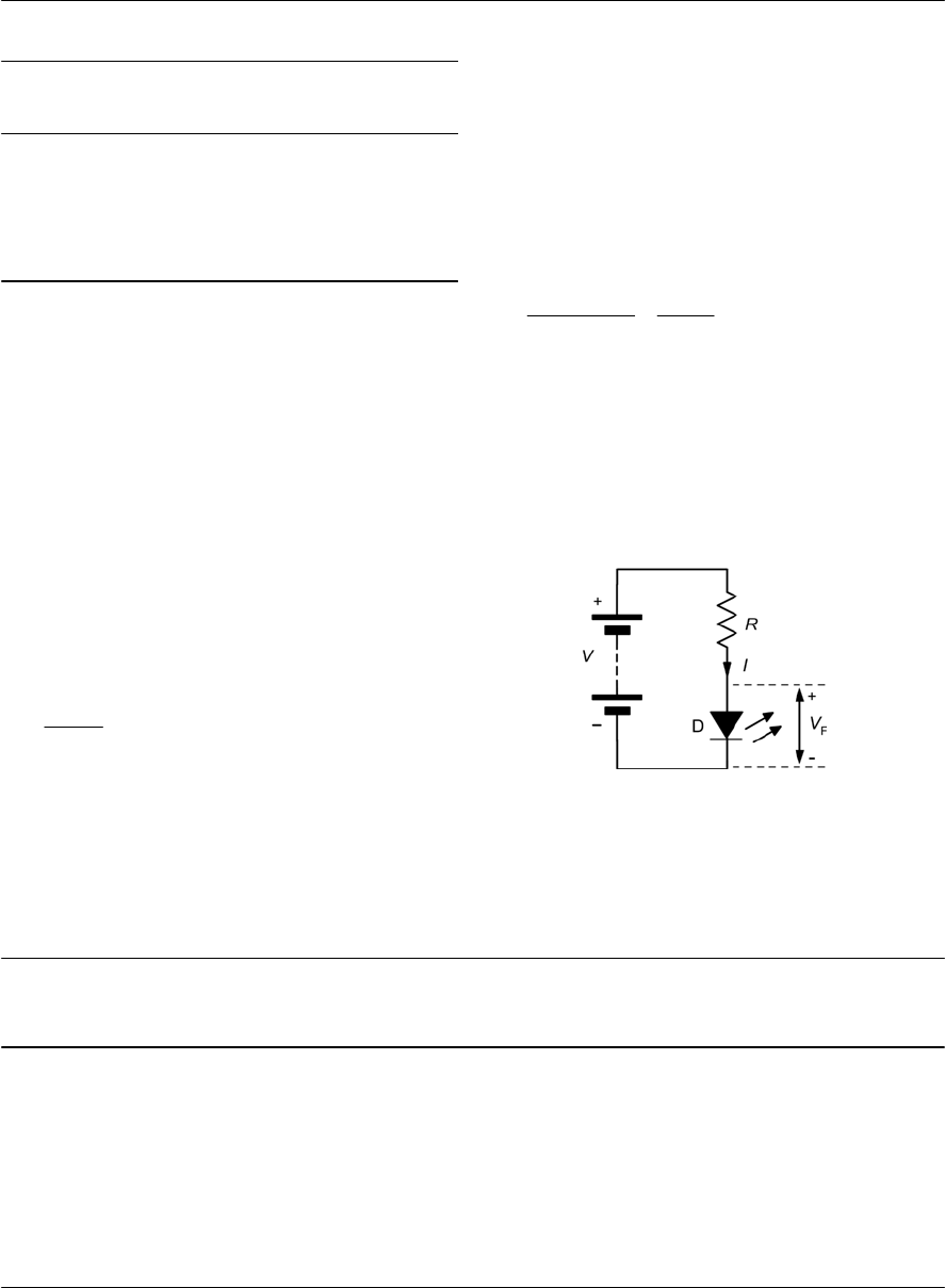
SEMICONDUCTORS 95
Table 5.5 Characteristics of some common triacs
Type IT
(A)
VRRM
(V)
VGT
(V)
2N6075 4 600 2.5
BT139 15 600 1.5
TIC206M 4 600 2
TIC226M 8 600 2
IGT
(mA)
5
5
5
50
Light emitting diodes are available in various
formats with the round types being most popular.
Round LEDs are commonly available in the 3 mm
and 5 mm (0.2 inch) diameter plastic packages and
also in a 5 mm x 2 mm rectangular format. The
viewing angle for round LEDs tends to be in the
region of 20° to 40°, whereas for rectangular types
this is increased to around 100°. Table 5.6
summarizes the characteristics of several common
types of LED.
In order to limit the forward current of an LED
to an appropriate value, it is usually necessary to
include a fixed resistor in series with an LED
indicator, as shown in Fig. 5.16. The value of the
resistor may be calculated from:
where VFis the forward voltage drop produced by
the LED and Vis the applied voltage. Note that it is
usually safe to assume that VFwill be 2 V and
choose the nearest preferred value for R.
Example 5.2
An LED is to be used to indicate the presence of a
21 V d.c. supply rail. If the LED has a nominal
forward voltage of 2.2 V, and is rated at a current
of 15 mA, determine the value of series resistor
required.
Solution
Here we can use the formula:
The nearest preferred value is 1.2 kI.The power
dissipated in the resistor will be given by:
P = I ×V = 15 mA × 18.8 V = 280 mW
Hence the resistor should be rated at 0.33 W, or
greater.
Resistance (I)
Miniature Standard High efficiency High intensity
Diameter (mm) 3 5 5 5
Maximum forward current (mA) 40 30 30 30
Typical forward current (mA) 12 10 7 10
Typical forward voltage drop (V) 2.1 2.0 1.8 2.2
Maximum reverse voltage (V) 5 3 5 5
LED type
Maximum power dissipation (mW) 150 100 27 135
Peak wavelength (nm) 690 635 635 635
Table 5.6 Characteristics of some common types of LED
Figure 5.16 Use of a current limiting resistor
with an LED
F
VV
R
I
=
21 V 2.2 V 18.8 V
1.25 k
15 mA 15 mA
R
===

96 ELECTRONIC CIRCUITS: FUNDAMENTALS AND APPLICATIONS
Diode coding
The European system for classifying semiconductor
diodes involves an alphanumeric code which
employs either two letters and three figures
(general-purpose diodes) or three letters and two
figures (special-purpose diodes). Table 5.7 shows
how diodes are coded. Note that the cathode
connection of most wire-ended diodes is marked
with a stripe.
Example 5.3
Identify each of the following diodes:
(a) AA113
(b) BB105
(c) BZY88C4V7.
First letter – semiconductor material:
A Germanium
B Silicon
C Gallium arsenide, etc.
D Photodiodes, etc.
Second letter – application:
A General-purpose diode
B Variable-capacitance diode
E Tunnel diode
P Photodiode
Q Light emitting diode
T Controlled rectifier
X Varactor diode
Y Power rectifier
Z Zener diode
Third letter – in the case of diodes for specialized
applications, the third letter does not generally have
any particular significance
Zener diodes – zener diodes have an additional
letter (which appears after the numbers) which
denotes the tolerance of the zener voltage. The
following letters are used:
A ±1%
B ±2%
C ±5%
D ±10%
Zener diodes also have additional characters which
indicate the zener voltage (e.g. 9V1 denotes 9.1V).
Table 5.7 The European system of diode coding
Solution
Diode (a) is a general-purpose germanium diode.
Diode (b) is a silicon variable capacitance diode.
Diode (c) is a silicon zener diode having ±5%
tolerance and 4.7 V zener voltage.
Bipolar junction transistors
Transistor is short for transfer resistor, a term
which provides something of a clue as to how the
device operates; the current flowing in the output
circuit is determined by the current flowing in the
input circuit. Since transistors are three-terminal
devices, one electrode must remain common to
both the input and the output.
Transistors fall into two main categories: bipolar
junction transistors (BJT)and field effect tran-
sistors (FET)and are also classified according to
the semiconductor material employed (silicon or
germanium) and to their field of application (e.g.
general-purpose, switching, high-frequency, etc.).
Various classes of transistor are available according
to the application concerned (see Table 5.8).
BJT operation
Bipolar junction transistors generally comprise
NPN or PNP junctions of either silicon (Si)or
germanium (Ge)material (see Figs 5.17 and 5.18).
The junctions are, in fact, produced in a single slice
of silicon by diffusing impurities through a
photographically reduced mask. Silicon transistors
are superior when compared with germanium
transistors in the vast majority of applications
(particularly at high temperatures) and thus
germanium devices are very rarely encountered.
Figures 5.19(a) and 5.19(b), respectively, show a
simplified representation of NPN and PNP
transistors together with their circuit symbols. In
either case the electrodes are labelled collector,
base and emitter.Note that each junction within
the transistor, whether it be collector-base or base-
emitter, constitutes a P-N junction. Figures 5.20(a)
and 5.20(b), respectively, show the normal bias
voltages applied to NPN and PNP transistors. Note
that the base-emitter junction is forward biased and
the collector-base junction is reverse biased. The
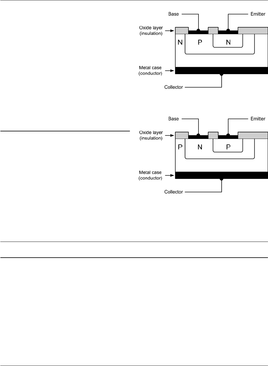
SEMICONDUCTORS 97
base region is, however, made very narrow so that
carriers are swept across it from emitter to collector
and only a relatively small current flows in the
base. To put this into context, the current flowing in
the emitter circuit is typically 100 times greater
than that flowing in the base. The direction of
conventional current flow is from emitter to
collector in the case of a PNP transistor, and
collector to emitter in the case of an NPN device.
The equation that relates current flow in the
collector, base, and emitter currents is:
IE=IB+IC
where IEis the emitter current, IBis the base
current, and ICis the collector current (all expressed
in the same units).
Bipolar transistor characteristics
The characteristics of a transistor are often
presented in the form of a set of graphs relating
voltage and current present at the transistor’s
terminals.
A typical input characteristic (IBplotted against
VBE)for a small-signal general-purpose NPN
transistor operating in common-emitter mode (see
Chapter 7) is shown in Fig. 5.21. This characteristic
shows that very little base current flows until the
Table 5.8 Classes of transistor
Classification Typical applications
Low-frequency Transistors designed specifically for audio and low-frequency linear applications
(below 100 kHz)
High-frequency Transistors designed specifically for radio and wideband linear applications
(100 kHz and above)
Power Transistors that operate at significant power levels (such devices are often sub-
divided into audio and radio frequency types)
Switching Transistors designed for switching applications (including power switching)
Low-noise Transistors that have low-noise characteristics and which are intended primarily for
the amplification of low-amplitude signals
High-voltage Transistors designed specifically to handle high voltages
Driver Transistors that operate at medium power and voltage levels and which are often
used to precede a final (power) stage which operates at an appreciable power level
Figure 5.17 NPN transistor construction
Figure 5.18 PNP transistor construction
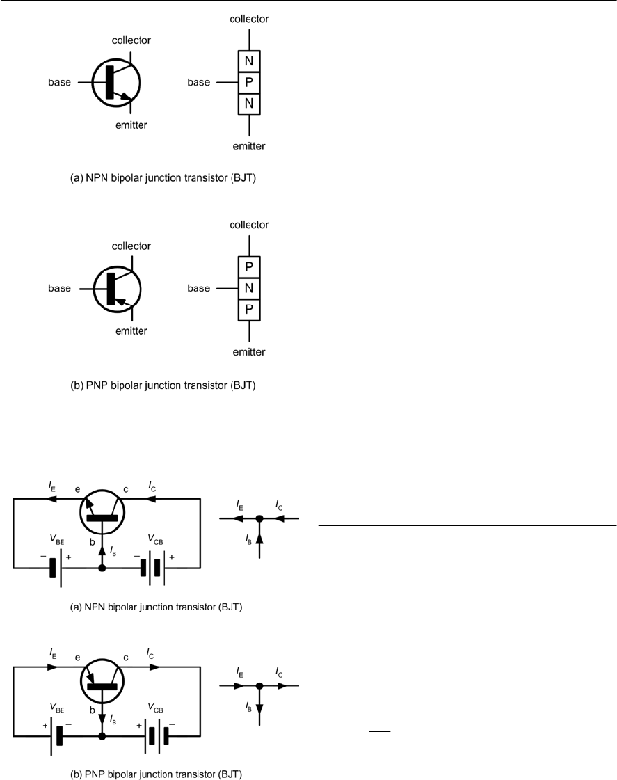
98 ELECTRONIC CIRCUITS: FUNDAMENTALS AND APPLICATIONS
base-emitter voltage (VBE)exceeds 0.6 V.
Thereafter, the base current increases rapidly (this
characteristic bears a close resemblance to the
forward part of the characteristic for a silicon
diode, see Fig. 5.5).
Figure 5.22 shows a typical output
characteristic (ICplotted against VCE)for a small-
signal general-purpose NPN transistor operating in
common-emitter mode (see Chapter 7). This
characteristic comprises a family of curves, each
relating to a different value of base current (IB). It is
worth taking a little time to get familiar with this
characteristic as we shall be putting it to good use
in Chapter 7. In particular it is important to note the
‘knee’ that occurs at values of VCE of about 2 V.
Also, note how the curves become flattened above
this value with the collector current (IC)not
changing very greatly for a comparatively large
change in collector-emitter voltage (VCE).
Finally, a typical transfer characteristic (IC
plotted against IB)for a small-signal general-
purpose NPN transistor operating in common-
emitter mode (see Chapter 7) is shown in Fig. 5.23.
This characteristic shows an almost linear
relationship between collector current and base
current (i.e. doubling the value of base current
produces double the value of collector current, and
so on). This characteristic is reasonably
independent of the value of collector-emitter
voltage (VCE)and thus only a single curve is used.
Current gain
The current gain offered by a transistor is a
measure of its effectiveness as an amplifying
device. The most commonly quoted parameter is
that which relates to common-emitter mode.In
this mode, the input current is applied to the base
and the output current appears in the collector (the
emitter is effectively common to both the input and
output circuits).
The common-emitter current gain is given by:
where hFE is the hybrid parameter which
represents large signal (d.c.) forward current
gain,ICis the collector current, and IBis the base
current. When small (rather than large) signal
Figure 5.19 Symbols and simplified models for
(a) NPN and (b) PNP bipolar junction transistors
Figure 5.20 Bias voltages and current flow for
(a) NPN and (b) PNP bipolar junction transistors
C
FE
B
I
h
I
=
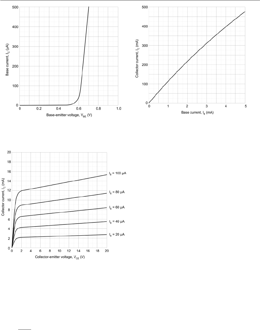
SEMICONDUCTORS 99
operation is considered, the values of ICand IBare
incremental (i.e. small changes rather than static
values). The current gain is then given by:
where hfe is the hybrid parameter which
represents small signal (a.c.) forward current
gain,RICis the change in collector current which
results from a corresponding change in base
current, RIB.
Values of hFE and hfe can be obtained from the
transfer characteristic (ICplotted against IB)as
shown in Figs 5.23 and 5.24. Note that hFE is found
from corresponding static values while hfe is found
by measuring the slope of the graph. Also note that,
if the transfer characteristic is linear, there is little
(if any) difference between hFE and hfe.
It is worth noting that current gain (hfe)varies
with collector current. For most small-signal
transistors, hfe is a maximum at a collector current
in the range 1 mA and 10 mA. Furthermore, current
gain falls to very low values for power transistors
when operating at very high values of collector
current. Another point worth remembering is that
most transistor parameters (particularly common-
emitter current gain, hfe are liable to wide variation
from one device to the next. It is, therefore,
important to design circuits on the basis of the
minimum value for hfe in order to ensure successful
operation with a variety of different devices.
Transistor parameters are listed in Table 5.9,
while Table 5.10 shows the characteristics of
several common types of bipolar transistor.
Finally, Fig. 5.25 shows a test circuit for obtaining
Figure 5.21 Typical input characteristic for a
small-signal NPN BJT operating in common-
emitter mode
Figure 5.22 Typical family of output (collector)
characteristics for a small-signal NPN BJT
operating in common-emitter mode
Figure 5.23 Typical transfer characteristic for a
small-signal NPN BJT operating in common-
emitter mode
C
fe
B
I
h
I
=
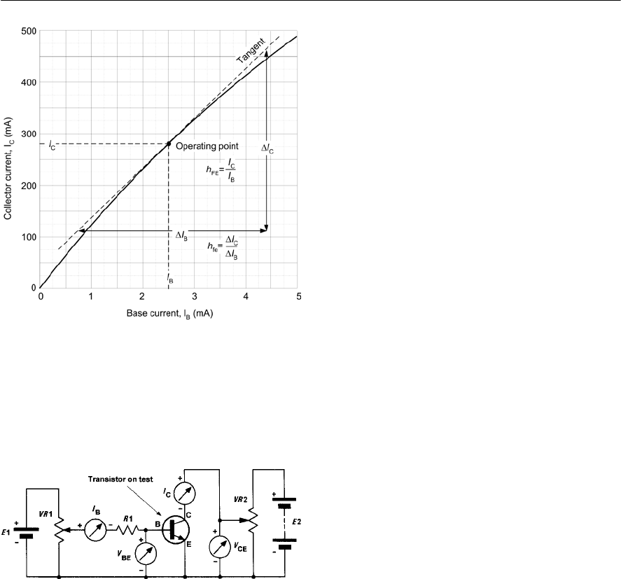
100 ELECTRONIC CIRCUITS: FUNDAMENTALS AND APPLICATIONS
NPN transistor characteristics (the arrangement for
aPNP transistor is similar but all meters and
supplies are reversed). A typical BJT data sheet is
shown in Fig. 5.26.
Example 5.4
Atransistor operates with IC=30 mA and
IB=600 µA. Determine the value of IEand hFE.
Solution
The value of IEcan be calculated from IC+ IB,thus:
IE=30 + 0.6 =30.6 mA.
The value of hFE can be found from hFE = IC/IB,
thus:
hFE = IC/IB=30/0.6 = 50.
Example 5.5
Atransistor operates with a collector current of
97 mA and an emitter current of 98 mA. Determine
the value of base current and common emitter
current gain.
Solution
Since IC= IC+ IB,the base current will be given
by:
IB= IE.IC=98 .97 =1mA
The common-emitter current gain (hFE)will be
given by:
hFE = IC/IB=97/1=97.
Example 5.6
An NPN transistor is to be used in a regulator
circuit in which a collector current of 1.5 A is to be
controlled by a base current of 50 mA. What value
of hFE will be required?
If the device is to be operated with VCE = 6 V,
which transistor selected from Table 5.10 would be
appropriate for this application and why?
Solution
The required current gain can be found from:
hFE = IC/IB=1.5 A /50 mA =1.5 /0.05 = 30
The most appropriate device would be the BD131.
The only other device capable of operating at a
collector current of 1.5 A would be a 2N3055.
The collector power dissipation will be given by:
PC= IC× VCE =1.5 A × 6 V =9 W
However, the 2N3055 is rated at 115 W maximum
total power dissipation and this is more than ten
times the power required.
Figure 5.24 Determining the static and small-
signal values of current gain (hFE and hfe
respectively) from the transfer characteristic. In this
particular example hFE =280 / 2.5 =112 whilst
hfe =350 / 3.65 =96
Figure 5.25 NPN transistor test circuit (the
arrangement for a PNP transistor is similar but all
meters and supplies must be reversed)
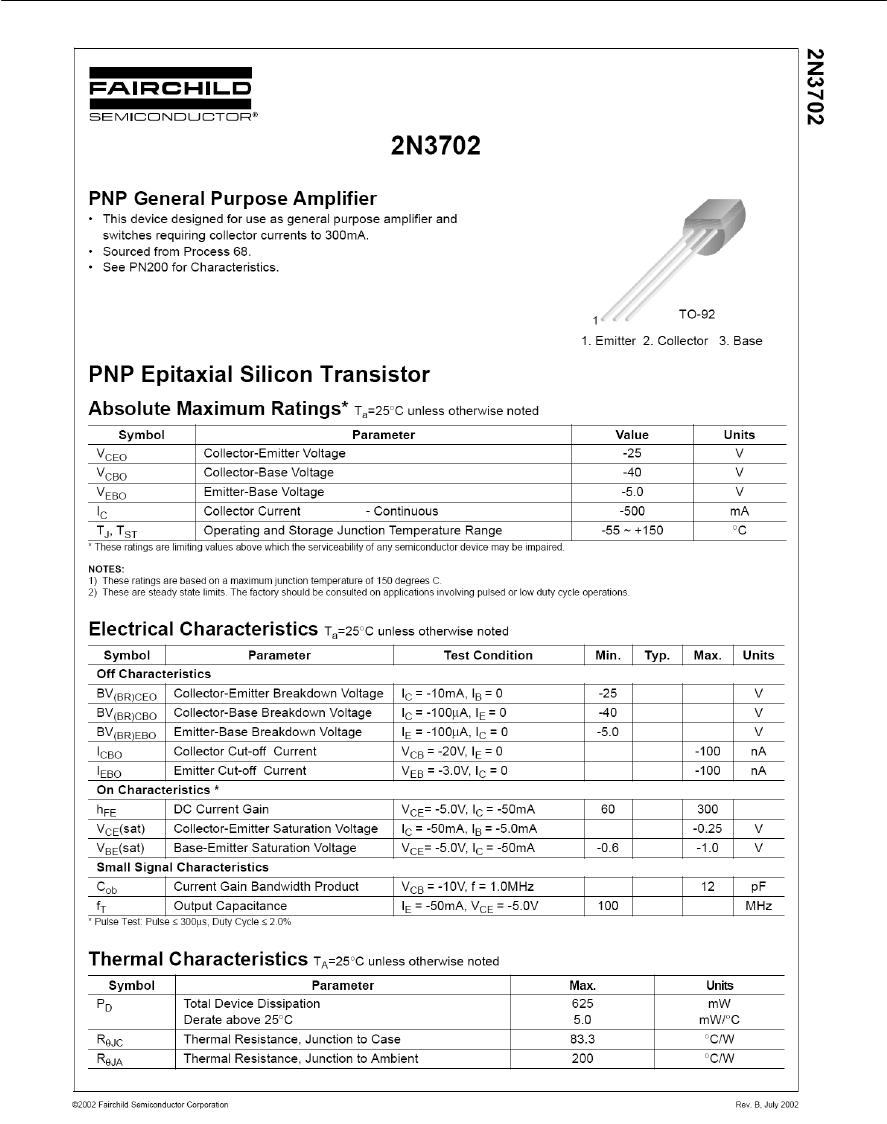
SEMICONDUCTORS 101
Figure 5.26 Extract from the data sheet for a 2N3702 BJT (courtesy of Fairchild Semiconductor)

102 ELECTRONIC CIRCUITS: FUNDAMENTALS AND APPLICATIONS
Example 5.7
Atransistor is used in a linear amplifier
arrangement. The transistor has small and large
signal current gains of 200 and 175, respectively,
and bias is arranged so that the static value of
collector current is 10 mA. Determine the value of
base bias current and the change of output
(collector) current that would result from a 10 µA
change in input (base) current.
Solution
The value of base bias current can be determined
from:
IB= IC/hFE =10 mA /200 = 50 µA
The change of collector current resulting from a
10 µA change in input current will be given by:
RIC= hfe × RIB=175 ×l0 µA =1.75mA.
Table 5.9 Bipolar transistor parameters
Parameter Meaning
ICmax. The maximum value of collector current
VCEO max. The maximum value of collector–emitter voltage with the base terminal left open-circuit
VCBO max. The maximum value of collector–base voltage with the base terminal left open-circuit
Ptmax. The maximum total power dissipation
hFE The large signal (static) common-emitter current gain
hfe The small signal (dynamic) common-emitter current gain
hfe max. The maximum value of small signal common-emitter current gain
hFE min. The minimum value of small signal common-emitter current gain
hie The small signal input resistance (see Chapter 7)
hoe The small signal output conductance (see Chapter 7)
hre The small signal reverse current transfer ratio (see Chapter 7)
fttyp. The transition frequency (i.e. the frequency at which the small signal common emitter current gain
has fallen to unity)
Table 5.10 Characteristic of some common types of bipolar transistor
Device Type ICmax. VCEO max. VCBO max. Ptmax. hfe at ICfttyp. Application
BC108 NPN 100 mA 20 V 30 V 300 mW 125 2 mA 250 MHz General purpose
BCY70 PNP 200 mA V40 V V50 V 360 mW 150 2 mA 200 MHz General purpose
BD131 NPN 3 A 45 V 70 V 15 W 50 250 mA 60 MHz AF power
BD132 PNP 3 A V45 V V45 V 15 W 50 250 mA 60 MHz AF power
BF180 NPN 20 mA 20 V 20 V 150 mW 100 10 mA 650 MHz RF amplifier
2N3053 NPN 700 mA 40 V 60 V 800 mW 150 50 mA 100 MHz Driver
2N3055 NPN 15 A 60 V 100 V 115 W 50 500 mA 1 MHz LF power
2N3866 NPN 400 mA 30 V 30 V 3 W 105 50 mA 700 MHz RF driver
2N3904 NPN 200 mA 40 V 60 V 310 mW 150 50 mA 300 MHz Switching
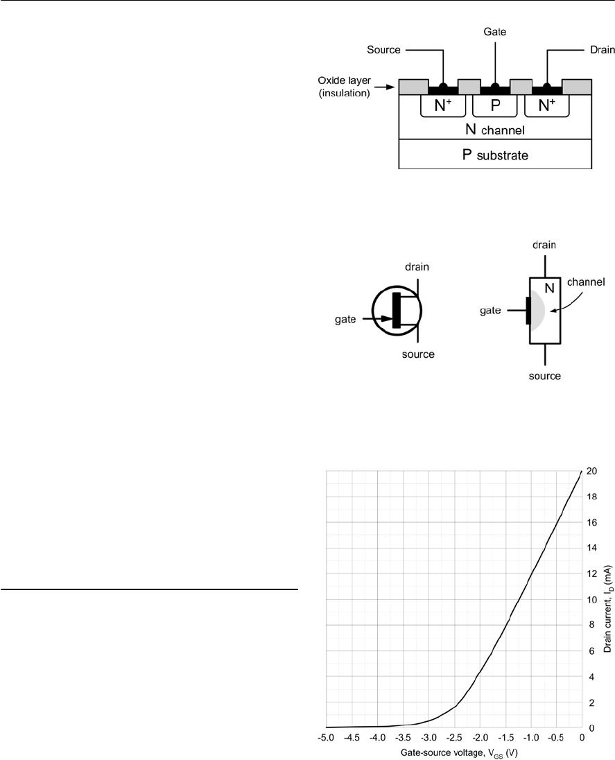
SEMICONDUCTORS 103
Figure 5.27 N-channel JFET construction
Field effect transistors
Field effect transistors (FET) comprise a channel of
P-type or N-type material surrounded by material
of the opposite polarity. The ends of the channel (in
which conduction takes place) form electrodes
known as the source and drain.The effective
width of the channel (in which conduction takes
place) is controlled by a charge placed on the third
(gate)electrode. The effective resistance between
the source and drain is thus determined by the
voltage present at the gate.
Field effect transistors are available in two basic
forms; junction gate and insulated gate.The gate
source junction of a junction gate field effect
transistor (JFET) is effectively a reverse-biased
P-N junction. The gate connection of an insulated
gate field effect transistor (IGFET), on the other
hand, is insulated from the channel and charge is
capacitively coupled to the channel. To keep things
simple, we will consider only JFET devices in this
book. Figure 5.27 shows the basic construction of
an N-channel JFET whilst Fig. 5.28 shows its
symbol and simplified model.
JFETs offer a very much higher input resistance
when compared with bipolar transistors. For
example, the input resistance of a bipolar transistor
operating in common-emitter mode (see Chapter 7)
is usually around 2.5 kIwhereas a JFET device
operating in equivalent common-source mode (see
Chapter 7) would typically exhibit an input
resistance of 100 MI.This feature makes JFET
devices ideal for use in applications where a very
high input resistance is desirable.
FET characteristics
As with bipolar transistors, the characteristics of a
FET are often presented in the form of a set of
graphs relating voltage and current present at the
transistor’s terminals. A typical mutual
characteristic (IDplotted against VGS)for a small-
signal general-purpose N-channel JFET operating
in common-source mode (see Chapter 7) is shown
in Fig. 5.29. This characteristic shows that the drain
current is progressively reduced as the gate-source
voltage is made more negative. At a certain value
of VGS the drain current falls to zero and the device
is said to be cut-off.
Figure 5.28 Symbol and simplified model for an
N-channel JFET
Figure 5.29 Typical mutual characteristic for an
N-channel JFET operating in common-source mode
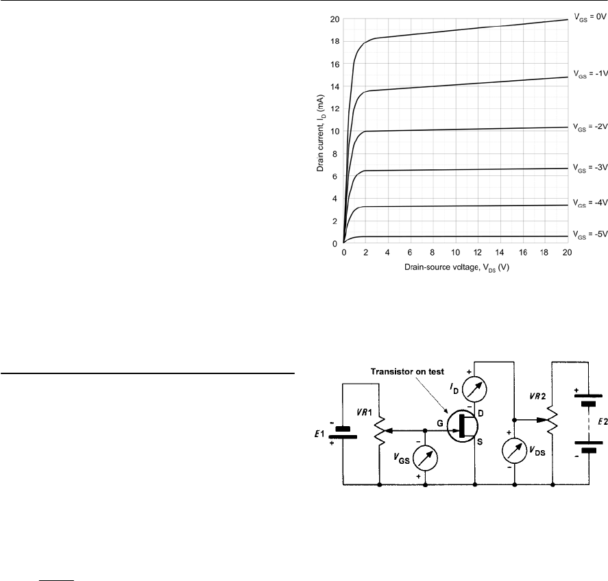
104 ELECTRONIC CIRCUITS: FUNDAMENTALS AND APPLICATIONS
Figure 5.30 shows a typical output characteristic
(IDplotted against VDS)for a small-signal general-
purpose N-channel JFET operating in common-
source mode (see Chapter 7). This characteristic
comprises a family of curves, each relating to a
different value of gate-source voltage (VGS). It is
worth taking a little time to get familiar with this
characteristic as we shall be using it again in
Chapter 7 (you might also like to compare this
characteristic with the output characteristic for a
transistor operating in common-emitter mode (see
Fig. 5.22).
Once again, the characteristic curves have a
‘knee’ that occurs at low values of VDS.Also, note
how the curves become flattened above this value
with the drain current (ID)not changing very
greatly for a comparatively large change in drain-
source voltage (VDS). These characteristics are, in
fact, even flatter than those for a bipolar transistor.
Because of their flatness, they are often said to
represent a constant current characteristic.
JFET parameters
The gain offered by a field effect transistor is
normally expressed in terms of its forward
transfer conductance (gfs or Yfs)in common-
source mode. In this mode, the input voltage is
applied to the gate and the output current appears in
the drain (the source is effectively common to both
the input and output circuits).
The common-source forward transfer
conductance is given by:
where RIDis the change in drain current resulting
from a corresponding change in gate-source voltage
(RVGS). The units of forward transfer conductance
are Siemens (S).
Forward transfer conductance (gfs)varies with
drain current collector current. For most small
signal devices, gfs is quoted for values of drain
current between 1mA and 10 mA. It’s also worth
noting that most FET parameters (particularly
forward transfer conductance) are liable to wide
variation from one device to the next. It is,
therefore, important to design circuits on the basis
of the minimum value for gfs in order to ensure
successful operation with a variety of different
devices. JFET parameters are shown in Table 5.11.
The characteristics of several common
N-channel field effect transistors are shown in
Table 5.12. Figure 5.31 shows a test circuit for
obtaining the characteristics of an N-channel FET
(the arrangement for a P-channel FET is similar but
all meters and supplies must be reversed). A typical
N-channel JFET data sheet is shown in Fig. 5.32.
Example 5.8
AFET operates with a drain current of 50 mA and
agate-source bias of V2V. If the device has a gfs of
D
fs
GS
I
g
V
=
Figure 5.31 N-channel JFET test circuit (the
arrangement for a P-channel JFET is similar but all
meters and supplies must be reversed)
Figure 5.30 Atypical family of output
characteristics for an N-channel JFET operating in
common-source mode
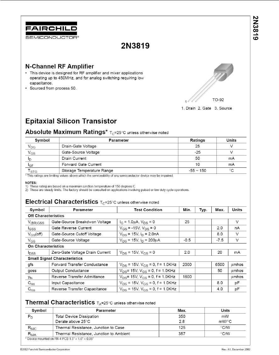
SEMICONDUCTORS 105
Figure 5.32 Extract from the data sheet for a 2N3819 JFET (courtesy of Fairchild Semiconductor)
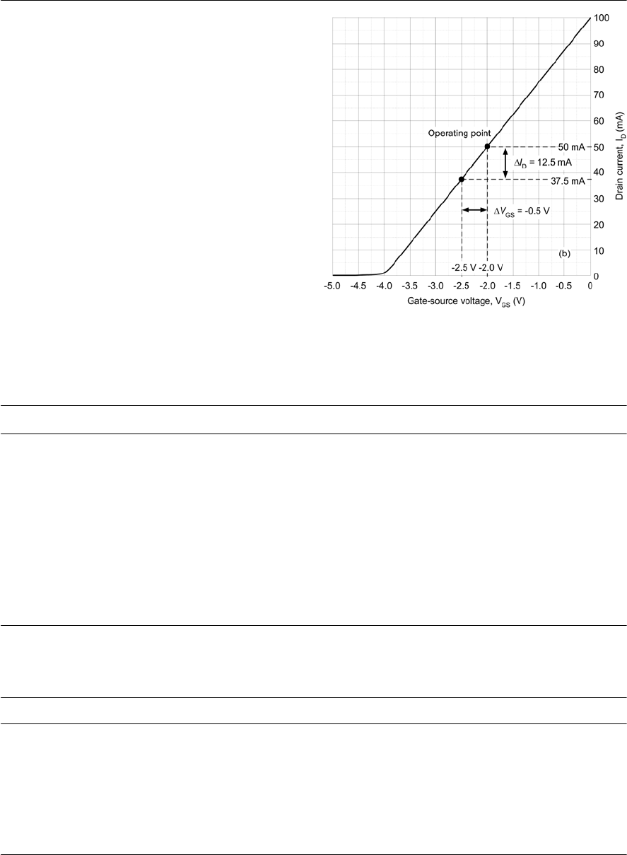
106 ELECTRONIC CIRCUITS: FUNDAMENTALS AND APPLICATIONS
0.025 S, determine the change in drain current if
the bias voltage increases to V2.5 V.
Solution
The change in gate-source voltage (RVgs)is V0.5 V
and the resulting change in drain current can be
determined from:
RID=RVGS × gfs =0.025 S × V0.5 V =V0.0125 A
This RID=V12.5 mA
The new value of drain current will thus be
(50 mA V12.5 mA) or 37.5 mA.
The mutual characteristic shown in Fig. 5.33
illustrates this change in drain current. Note how
the drain current falls in response to the change in
gate-source voltage.
Table 5.12 Characteristic of some common types of JFET
Device Type IDmax. VDS max. PDmax. gfs min. Application
2N3819 N-channel 10 mA 25 V 200 mW 4 mS General purpose
2N5457 N-channel 10 mA 25 V 310 mW 1 mS General purpose
BF244A N-channel 100 mA 30 V 360 mW 3 mS RF amplifier
2N3820 P-channel V15 mA 20 V 200 mW 0.8 mS General purpose
2N5461 P-channel V9mA 40 V 310 mW 1.5 mS Audio amplifiers
2N5459 N-channel 16 mA 15 V 310 mW 2 mS General purpose
J310 N-channel 30 mA 25 V 350 mW 8 mS VHF/UHF amplifier
Table 5.11 FET parameters
Parameter Meaning
IDmax. The maximum value of drain current
VDS max. The maximum value of drain-source voltage
VGS max. The maximum value of gate-source voltage
PDmax. The maximum drain power dissipation
gfs The common-source forward transfer conductance
trtyp. The typical output rise time in response to a perfect rectangular pulse input
tftyp. The typical output fall time in response to a perfect rectangular pulse input
RDS(on) max. The maximum value of drain-source resistance when the device is in the conducting (on) state
Figure 5.33 See Example 5.8
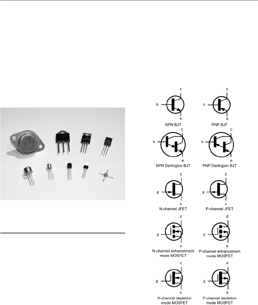
SEMICONDUCTORS 107
Transistor packages
Awide variety of packaging styles are used for
transistors. Small-signal transistors tend to have
either plastic packages (e.g. TO92) or miniature
metal cases (e.g. TO5 or TO18). Medium and high-
power devices may also be supplied in plastic cases
but these are normally fitted with integral metal
heat-sinking tabs (e.g. TO126, TO218 or TO220) in
order to conduct heat away from the junction. Some
older power transistors are supplied in metal cases
(either TO3 or TO3). Several popular transistor
case styles are shown in Fig. 5.34.
Transistor coding
The European system for classifying transistors
involves an alphanumeric code which employs
either two letters and three figures (general-purpose
transistors) or three letters and two figures (special-
purpose transistors). Table 5.13 shows how
transistors are coded.
Example 5.9
Identify each of the following transistors:
(a) AF115
(b) BC109
(c) BD135
(d) BFY51.
Solution
(a) Transistor (a) is a general-purpose, low-power,
high-frequency germanium transistor.
(b) Transistor (b) is a general-purpose, low-power,
low-frequency silicon transistor.
(c) Transistor (c) is a general-purpose, high- power,
low-frequency silicon transistor.
(d) Transistor (d) is a special-purpose, low-power,
high-frequency silicon transistor.
Figure 5.35 Symbols used for different types of
transistor including BJT, JFET and MOSFET
(metal oxide semiconductor field effect transistor)
types
Figure 5.34 Some common transistor packages
including TO3, TO220, TO5, TO18 and TO92
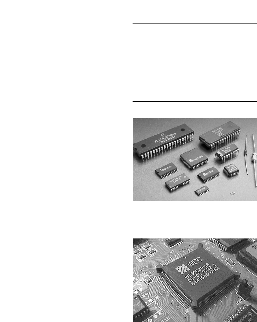
108 ELECTRONIC CIRCUITS: FUNDAMENTALS AND APPLICATIONS
Integrated circuits
Integrated circuits are complex circuits fabricated
on a small slice of silicon. Integrated circuits may
contain as few as 10 or more than 100,000 active
devices (transistors and diodes). With the exception
of a few specialized applications (such as
amplification at high-power levels) integrated
circuits have largely rendered a great deal of
conventional discrete circuitry obsolete.
Integrated circuits can be divided into two
general classes, linear (analogue) and digital.
Typical examples of linear integrated circuits are
operational amplifiers (see Chapter 8) whereas
typical examples of digital integrated are logic
gates (see Chapter 9).
A number of devices bridge the gap between the
analogue and digital world. Such devices include
analogue to digital converters (ADC), digital to
analogue converters (DAC), and timers. For
example, the ubiquitous 555 timer contains two
operational amplifier stages (configured as voltage
comparators) together with a digital bistable stage,
abuffer amplifier and an open-collector transistor.
IC packages
As with transistors, a variety of different packages
are used for integrated circuits. The most popular
form of encapsulation used for integrated circuits is
the dual-in-line (DIL)package which may be
fabricated from either plastic or ceramic material
(with the latter using a glass hermetic sealant)
Common DIL packages have 8, 14, 16, 28 and 40
pins on a 0.1 inch matrix.
Flat package (flatpack)construction (featuring
both glass-metal and glass-ceramic seals and
welded construction) are popular for planar
mounting on flat circuit boards. No holes are
required to accommodate the leads of such devices
which are arranged on a 0.05 inch pitch (i.e. half
the pitch used with DIL devices). Single-in-line
(SIL)and quad-in-line (QIL)packages are also
becoming increasingly popular while TO5, TO72,
TO3 and TO220 encapsulations are also found (the
latter being commonly used for three-terminal
voltage regulators). Figure 5.36 shows a variety of
common integrated circuit packages whilst Fig.
5.37 shows a modern LSI device.
Figure 5.37 A large-scale integrated (LSI) circuit
mounted in a socket fitted to a printed circuit board
Figure 5.36 Various common integrated circuit
packages including DIL (dual-in-line) and QIL
(quad-in-line) types
First letter – semiconductor material:
A Germanium
B Silicon
Second letter – application:
C Low-power, low-frequency
D High-power, low-frequency
F Low-power, high-frequency
L High-power, high-frequency
Third letter – in the case of transistors for
specialized applications, the third letter does not
generally have any particular significance
Table 5.13 The European system of transistor
coding
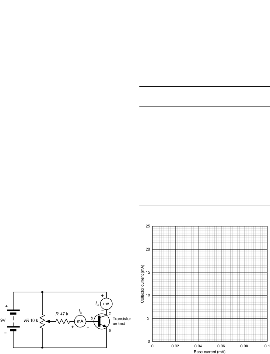
SEMICONDUCTORS 109
Figure 5.39 Graph layout for plotting the results
Practical investigation
Objective
To obtain the common emitter transfer
characteristic and small-signal current gain for
three different NPN bipolar junction transistors.
Components and test equipment
Breadboard, digital or analogue meters with d.c.
current ranges, 9 V d.c. power supply (or battery),
three different NPN transistors (e.g. 2N3904,
BC548, BFY50, 2N2222), test leads, connecting
wire.
Procedure
Connect the circuit shown in Fig. 5.38. Set the
base current meter to the 2 mA range and the
collector current meter to the 20 mA range.
Set the variable resistor to minimum position and
slowly increase base current until it reaches 0.01
mA. Measure and record the collector current.
Repeat for base currents up to 0.1 mA in steps of
0.02 m, at each stage measuring and recording the
corresponding value of collector current.
Repeat the investigation with at least two further
types of transistor.
Measurements and calculations
For each transistor, record your results in a table
showing corresponding values of ICand IB(see
Table 5.14). Plot graphs showing ICplotted against
IB(see Fig. 5.39). Calculate the value of hFE for
each transistor at IC= 2 mA. Compare your
calculated results and characteristic graphs with
manufacturer’s data.
Figure 5.38 Transistor test circuit
Table 5.14 Results
Conclusion
Comment on the shape of each graph. Is this what
you would expect? Is the graph linear? If not, what
will this imply about the static and small-signal
values of current gain? Which of the transistors had
the highest value of current gain and which had the
least value of current gain?
Collector current (mA)
2N3904 BC548 BFY50
0.01
0.02
0.03
0.04
0.05
0.06
0.07
0.08
0.09
0.1
Base current
(mA)
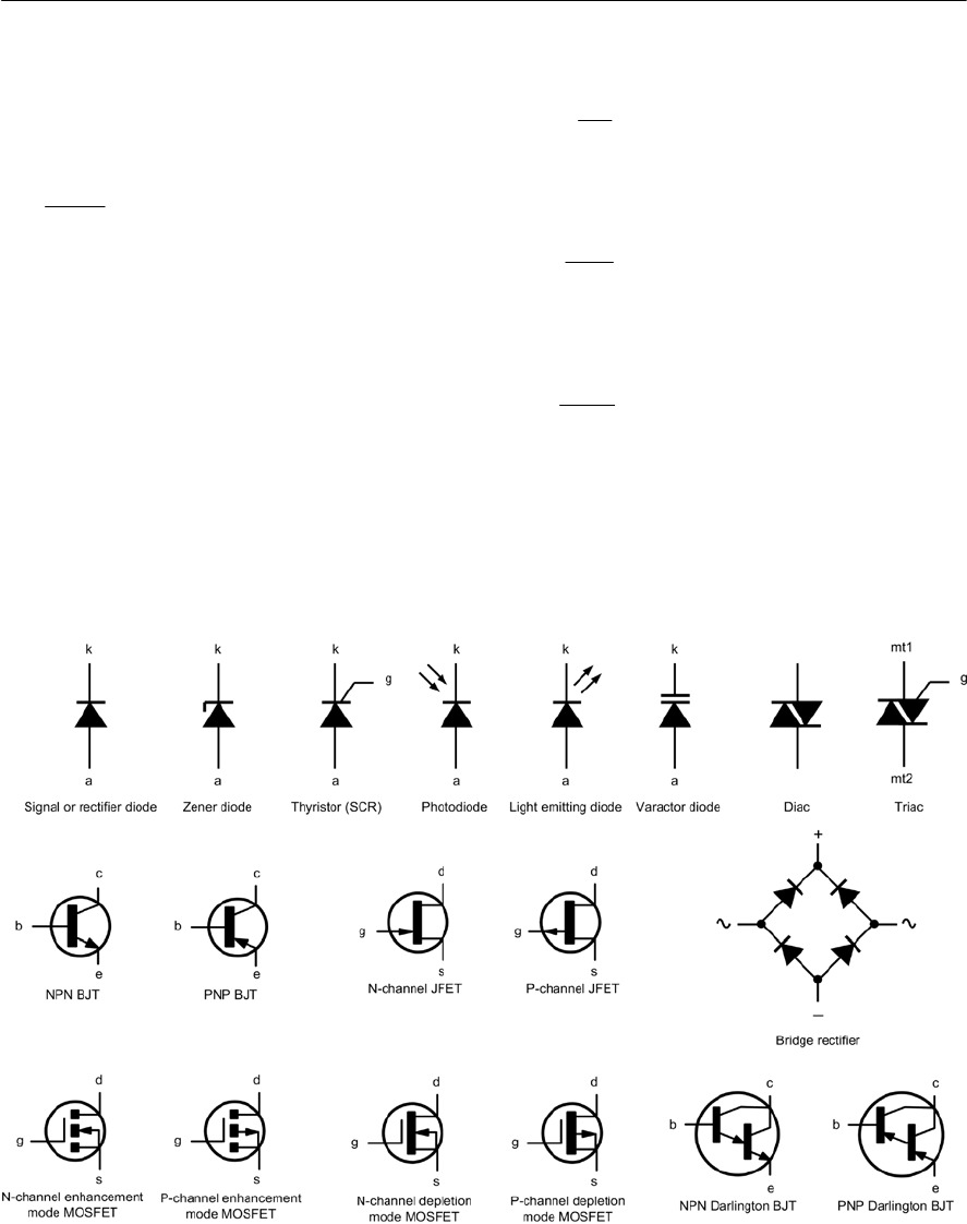
Static current gain for a bipolar transistor:
(page 98)
Small-signal current gain for a bipolar transistor:
(page 99)
Forward transfer conductance for a FET:
(page 104)
110 ELECTRONIC CIRCUITS: FUNDAMENTALS AND APPLICATIONS
Important formulae introduced in this
chapter
LED series resistor:
(page 95)
Bipolar transistor currents:
(page 97)
IE=IB+IC
IB=IEVIC
IC=IEVIB
Figure 5.40 Circuit symbols introduced in this chapter
Symbols introduced in this chapter
F
VV
R
I
=
C
FE
B
I
h
I
=
C
fe
B
I
h
I
=
D
fs
GS
I
g
V
=
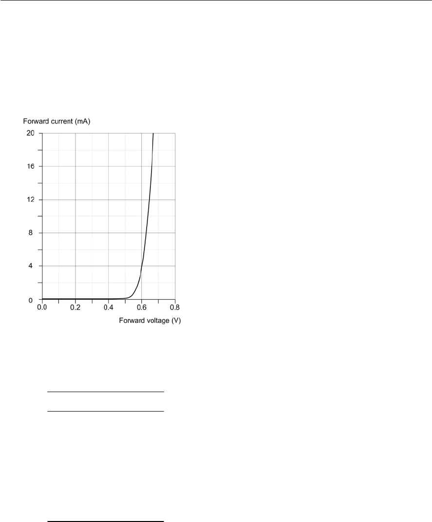
Problems
5.1 Figure 5.41 shows the characteristics of a
diode. What type of material is used in this
diode? Give a reason for your answer.
5.2 Use the characteristic shown in Fig. 5.41 to
determine the resistance of the diode when
(a) VF=0.65 V and (b) IF=4mA.
SEMICONDUCTORS 111
5.3 The following data refers to a signal diode:
Plot the characteristic and use it to
determine:
(a) the forward current when VF=350 mV;
(b) the forward voltage when IF=15 mA.
Figure 5.41 See Questions 5.1 and 5.2
5.4 A diode is marked ‘BZY88C9V1’. What
type of diode is it? What is its rated voltage?
State one application for the diode.
5.5 An LED is to be used to indicate the
presence of a 5 V d.c. supply. If the LED has
a nominal forward voltage of 2 V, and is
rated at a current of 12 mA, determine the
value of series resistor required.
5.6 Identify each of the following transistors:
(a) AF117 (b) BC184
(c) BD131 (d) BF180.
5.7 A transistor operates with a collector current
of 2.5 A and a base current 125 mA.
Determine the value of emitter current and
static common-emitter current gain.
5.8 A transistor operates with a collector current
of 98 mA and an emitter current of 103 mA.
Determine the value of base current and the
static value of common-emitter current gain.
5.9 A bipolar transistor is to be used in a driver
circuit in which a base current of 12 mA is
available. If the load requires a current of
200 mA, determine the minimum value of
common-emitter current gain required.
5.10 An NPN transistor is to operate with VCE =
10 V, IC=50 mA, and IB=400 µA. Which
of the devices listed in Table 5.10 is most
suitable for use in this application?
5.11 A transistor is used in a linear amplifier
arrangement. The transistor has small and
large signal current gains of 250 and 220,
respectively, and bias is arranged so that the
static value of collector current is 2 mA.
Determine the value of base bias current and
the change of output (collector) current that
would result from a 5 µA change in input
(base) current.
5.12 The transfer characteristic for an NPN
transistor is shown in Fig. 5.42. Use this
characteristic to determine:
(a) ICwhen IB=50 µA;
(b) hFE when IB=50 µA;
(c) hfe when IC=75 mA.
5.13 The output characteristic of an NPN
transistor is shown in Fig. 5.43. Use this
characteristic to determine:
(a) ICwhen IB=100 µA and VCE = 4 V;
(b) VCE when IB=40 µA and IC= 5 mA;
(c) IBwhen IC= 7 mA and VCE = 6 V.
5.14 An N-channel FET operates with a drain
current of 20 mA and a gate-source bias of
VF(V) IF(mA)
0.0 0.0
0.1 0.05
0.2 0.02
0.3 1.2
0.4 3.6
0.5 6.5
0.6 10.1
0.7 13.8
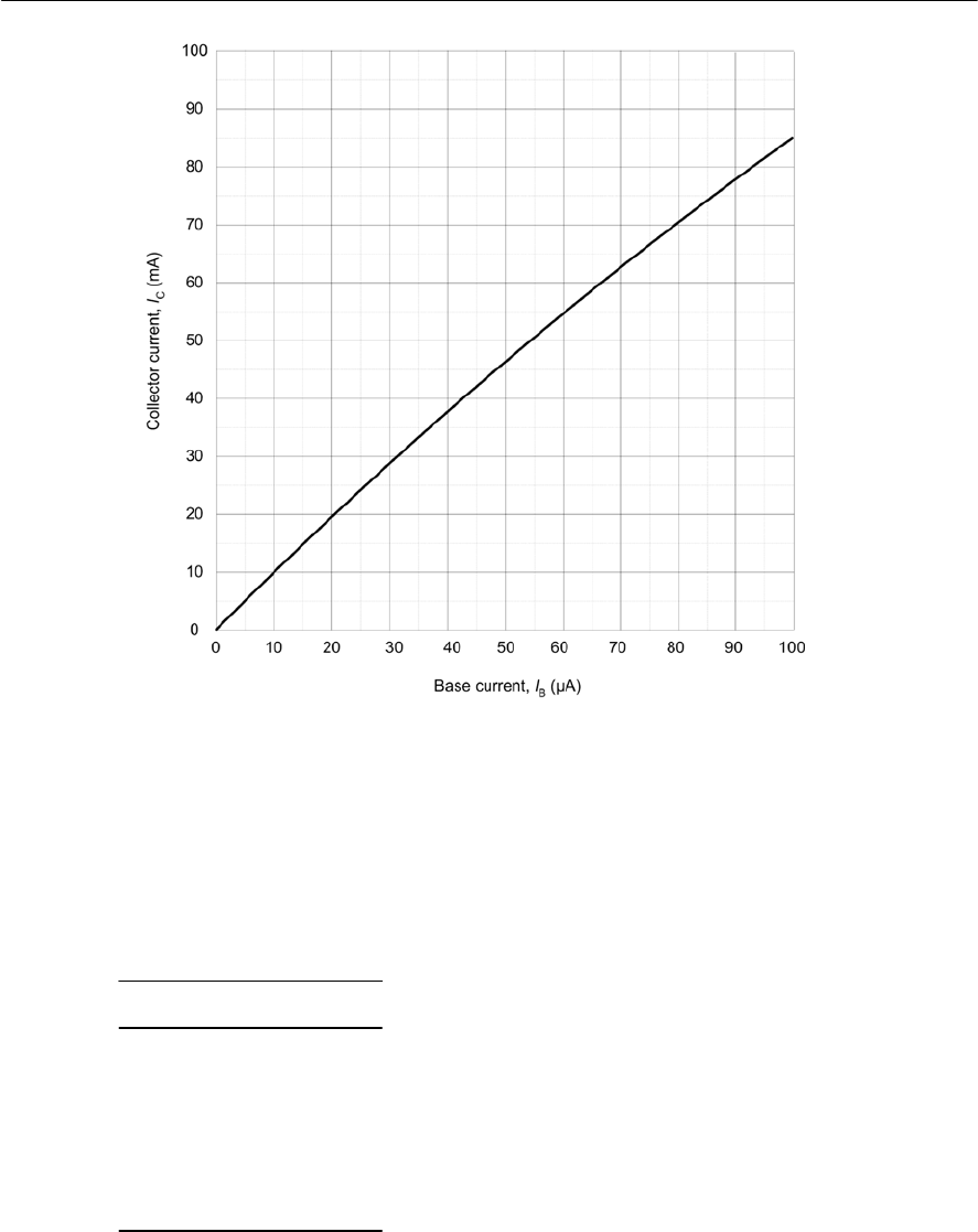
112 ELECTRONIC CIRCUITS: FUNDAMENTALS AND APPLICATIONS
V1V. If the device has a gfs of 8 mS,
determine the new drain current if the bias
voltage increases to V1.5 V.
5.15 The following results were obtained during
an experiment on an N-channel FET:
Plot the mutual characteristic for the FET
and use it to determine gfs when ID= 5 A.
5.16 In relation to integrated circuit packages,
what do each of the following
abbreviations stand for?
(a) DIL
(b) SIL
(c) QIL
(d) LSI.
5.17 Use the data sheet for a 1N4148 diode
in Appendix 8 to determine:
(a) the absolute maximum value of
reverse repetitive voltage
(b) the maximum power dissipation for
the device
(c) the typical reverse current when a
reverse voltage of 70 V is applied
(d) the typical forward voltage for a
forward current of 5 mA.
5.18 Identify each of the semiconductor devices
shown in Fig. 5.44.
VGS (V) ID(mA)
0.0 11.4
V2.0 7.6
V4.0 3.8
V6.0 0.2
V8.0 0.0
V10.0 0.0
Figure 5.42 See Question 5.12
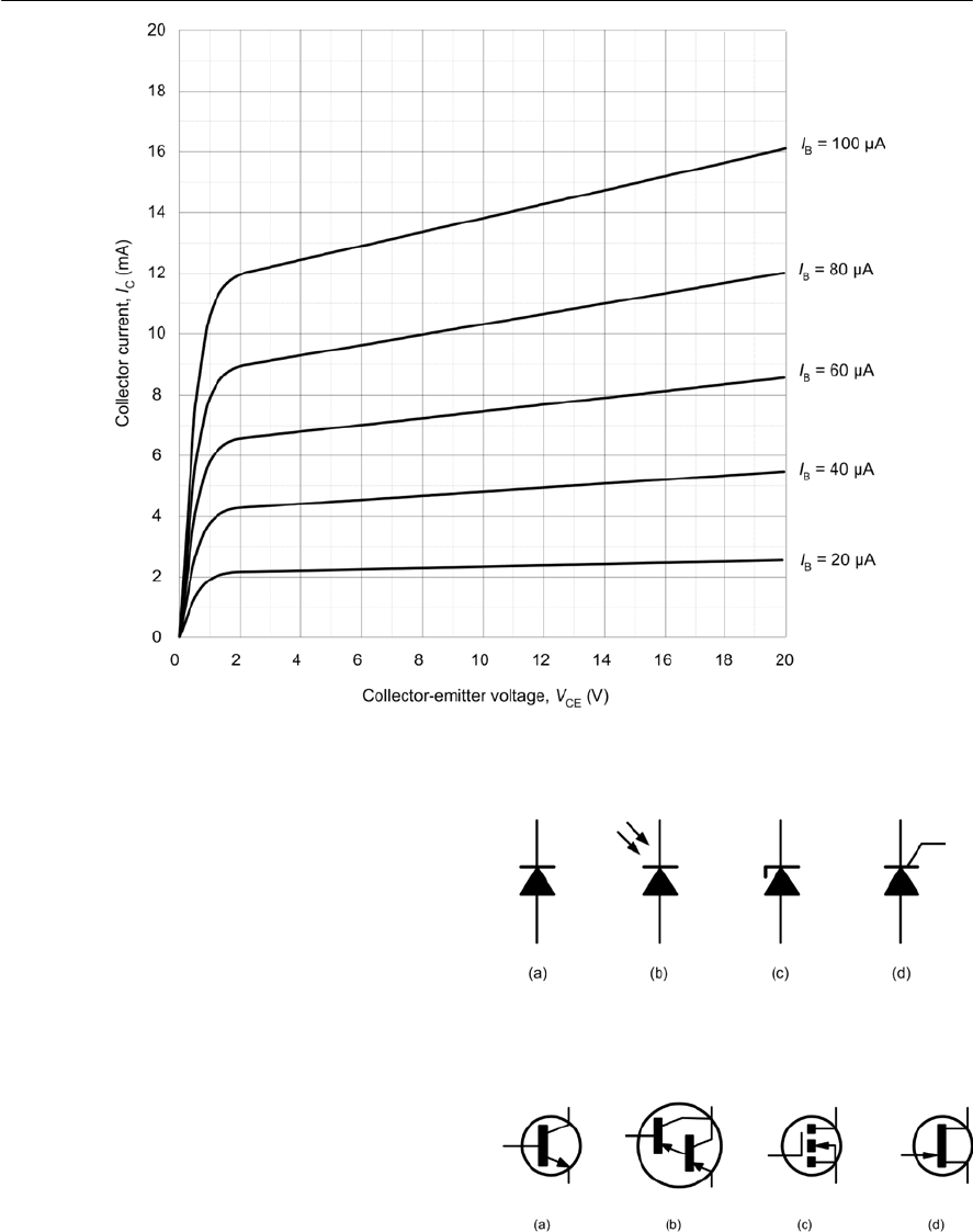
5.19 Identify each of the semiconductor devices
shown in Fig. 5.45.
5.20 Use the data sheet for a 2N3702 transistor
shown in Fig. 5.26 to determine:
(a) The type and class of device.
(b) The absolute maximum value of
collector-base voltage.
(c) The absolute maximum value of
collector current.
(d) The maximum value of collector-emitter
saturation voltage.
(e) The maximum value of total power
dissipation.
(f) The package style.
5.21 A 2N3702 transistor operates under the
following conditions: VBE = 0.7 V, IB=0.5
mA, VCE = 9 V and IC=50 mA. Determine
whether or not this exceeds the maximum
total device dissipation.
SEMICONDUCTORS 113
Figure 5.00 See Question 5.13
Figure 5.44 See Question 5.18
Figure 5.45 See Question 5.19
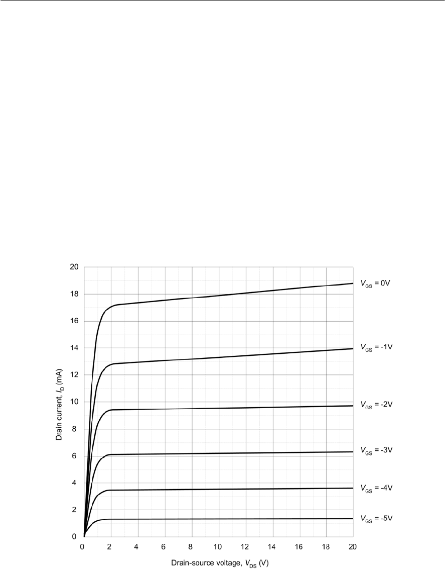
114 ELECTRONIC CIRCUITS: FUNDAMENTALS AND APPLICATIONS
5.22 Use the data sheet for a 2N3819 transistor
shown in Fig. 5.32 to determine:
(a) The type and class of device
(b) The absolute maximum value of
drain-gate voltage.
(c) The absolute maximum value of drain
current.
(d) The maximum value of reverse gate
current.
(e) The minimum value of forward transfer
conductance.
(f) The maximum value of input
capacitance.
(e) The maximum value of total device
dissipation.
(f) The package style.
5.23 The output characteristic of an N-channel
JFET is shown in Fig. 5.46. Use this
characteristic to determine:
(a) IDwhen VGS =V2 V and VDS =10 V;
(b) VDS when VGS =V1 V and ID=13 mA;
(c) VGS when ID=18 mA and VDS = 11 V.
5.24 Sketch a circuit diagram showing a test
circuit for obtaining the characteristics of a
PNP BJT. Label your diagram clearly and
indicate the polarity of all supplies and test
meters.
5.25 Sketch a circuit diagram showing a test
circuit for obtaining the characteristics of a
P-channel JFET. Label your diagram
clearly and indicate the polarity of all
supplies and test meters.
5.26 Sketch a circuit showing how a thyristor
can be used to control the current through
a resistive load. Label your diagram
clearly and explain briefly how the circuit
is triggered.
Answers to these problems appear on page 375.
Figure 5.46 See Question 5.23
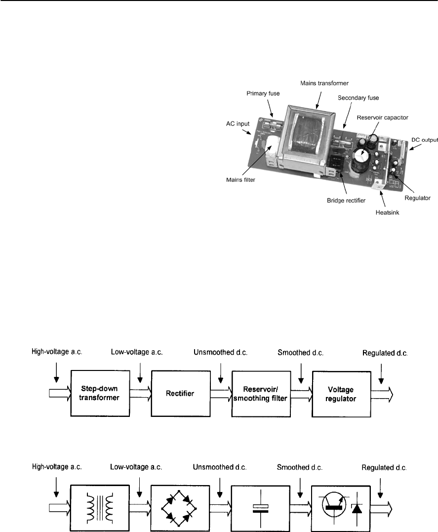
6
Power supplies
Figure 6.3 A simple d.c. power supply
This chapter deals with the unsung hero of most
electronic systems, the power supply. Nearly all
electronic circuits require a source of well regulated
d.c. at voltages of typically between 5 V and 30 V.
In some cases, this supply can be derived directly
from batteries (e.g. 6 V, 9 V, 12 V) but in many
others it is desirable to make use of a standard a.c.
mains outlet. This chapter explains how rectifier
and smoothing circuits operate and how power
supply output voltages can be closely regulated.
The chapter concludes with a brief description of
some practical power supply circuits.
The block diagram of a d.c. power supply is
shown in Fig. 6.1. Since the mains input is at a
relatively high voltage, a step-down transformer of
appropriate turns ratio is used to convert this to a
low voltage. The a.c. output from the transformer
secondary is then rectified using conventional
silicon rectifier diodes (see Chapter 5) to produce
an unsmoothed (sometimes referred to as pulsating
d.c.)output. This is then smoothed and filtered
before being applied to a circuit which will
regulate (or stabilize)the output voltage so that it
remains relatively constant in spite of variations in
both load current and incoming mains voltage.
Figure 6.2 shows how some of the electronic
components that we have already met can be used
in the realization of the block diagram in Fig. 6.1.
The iron-cored step-down transformer feeds a
rectifier arrangement (often based on a bridge
Figure 6.1 Block diagram of a d.c. power supply
Figure 6.2 Block diagram of a d.c. power supply showing principal components
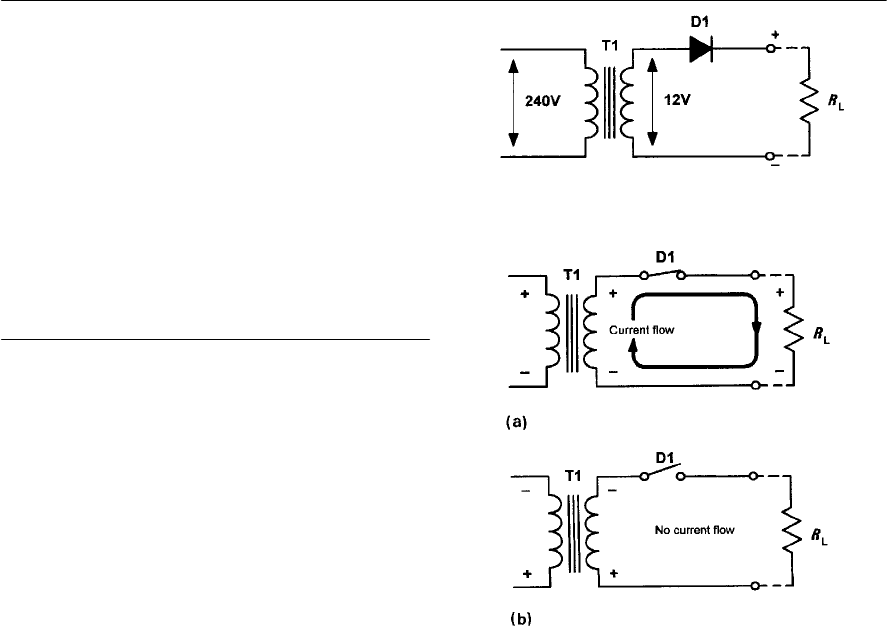
116 ELECTRONIC CIRCUITS: FUNDAMENTALS AND APPLICATIONS
circuit). The output of the rectifier is then applied
to a high-value reservoir capacitor. This capacitor
stores a considerable amount of charge and is being
constantly topped-up by the rectifier arrangement.
The capacitor also helps to smooth out the voltage
pulses produced by the rectifier. Finally, a
stabilizing circuit (often based on a series
transistor regulator and a zener diode voltage
reference)provides a constant output voltage. We
shall now examine each stage of this arrangement
in turn, building up to some complete power supply
circuits at the end of the chapter.
Rectifiers
Semiconductor diodes (see Chapter 5) are
commonly used to convert alternating current (a.c.)
to direct current (d.c), in which case they are
referred to as rectifiers.The simplest form of
rectifier circuit makes use of a single diode and,
since it operates on only either positive or negative
half-cycles of the supply, it is known as a half-
wave rectifier.
Figure 6.4 shows a simple half-wave rectifier
circuit. Mains voltage (220 to 240 V) is applied to
the primary of a step-down transformer (T1). The
secondary of T1 steps down the 240 V r.m.s. to
12 V r.m.s. (the turns ratio of T1 will thus be
240/12 or 20:1). Diode D1 will only allow the
current to flow in the direction shown (i.e. from
cathode to anode). D1 will be forward biased
during each positive half-cycle (relative to
common) and will effectively behave like a closed
switch. When the circuit current tries to flow in the
opposite direction, the voltage bias across the diode
will be reversed, causing the diode to act like an
open switch (see Figs 6.5(a) and 6.5(b),
respectively).
The switching action of D1 results in a pulsating
output voltage which is developed across the load
resistor (RL).Since the mains supply is at 50 Hz,
the pulses of voltage developed across RLwill also
be at 50 Hz even if only half the a.c. cycle is
present. During the positive half-cycle, the diode
will drop the 0.6 V to 0.7 V forward threshold
voltage normally associated with silicon diodes.
However, during the negative half-cycle the peak
a.c. voltage will be dropped across D1 when it is
reverse biased. This is an important consideration
when selecting a diode for a particular application.
Assuming that the secondary of T1 provides 12 V
r.m.s., the peak voltage output from the
transformer’s secondary winding will be given by:
Vpk =1.414 × Vr.m.s. =1.414 × 12 V =16.97 V
The peak voltage applied to D1 will thus be
approximately 17 V. The negative half-cycles are
blocked by D1 and thus only the positive half-
cycles appear across RL.Note, however, that the
actual peak voltage across RLwill be the 17 V
positive peak being supplied from the secondary on
T1, minus the 0.7 V forward threshold voltage
dropped by D1. In other words, positive half-cycle
pulses having a peak amplitude of 16.3 V will
appear across RL.
Figure 6.4 A simple half-wave rectifier circuit
Figure 6.5 (a) Half-wave rectifier circuit with D1
conducting (positive-going half-cycles of
secondary voltage) (b) half-wave rectifier with D1
not conducting (negative-going half-cycles of
secondary voltage)
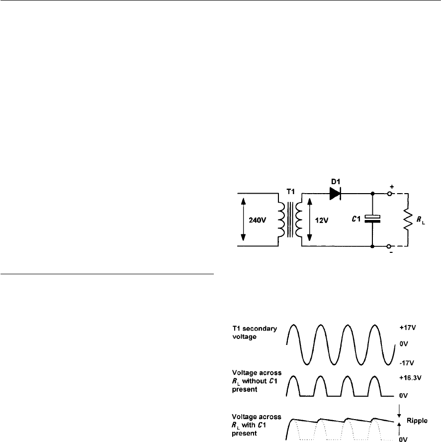
POWER SUPPLIES 117
Example 6.1
Amains transformer having a turns ratio of 44:1 is
connected to a 220 V r.m.s. mains supply. If the
secondary output is applied to a half-wave rectifier,
determine the peak voltage that will appear across a
load.
Solution
The r.m.s. secondary voltage will be given by:
VS= VP/11 =220 /44 =5 V
The peak voltage developed after rectification will
be given by:
VPK =1.414 × 5 V = 7.07 V
Assuming that the diode is a silicon device with a
forward voltage drop of 0.6 V, the actual peak
voltage dropped across the load will be:
VL=7.07 V B0.6 V = 6.47 V
Reservoir and smoothing circuits
Figure 6.6 shows a considerable improvement to
the circuit of Fig. 6.3. The capacitor, C1, has been
added to ensure that the output voltage remains at,
or near, the peak voltage even when the diode is not
conducting. When the primary voltage is first
applied to T1, the first positive half-cycle output
from the secondary will charge C1to the peak
value seen across RL.Hence C1charges to 16.3 V
at the peak of the positive half-cycle. Because C1
and RLare in parallel, the voltage across RLwill be
the same as that across C1.
The time required for C1to charge to the
maximum (peak) level is determined by the
charging circuit time constant (the series resistance
multiplied by the capacitance value). In this circuit,
the series resistance comprises the secondary
winding resistance together with the forward
resistance of the diode and the (minimal) resistance
of the wiring and connections. Hence C1charges
very rapidly as soon as D1 starts to conduct.
The time required for C1to discharge is, in
contrast, very much greater. The discharge time
constant is determined by the capacitance value and
the load resistance, RL.In practice, RLis very much
larger than the resistance of the secondary circuit
and hence C1takes an appreciable time to
discharge. During this time, D1 will be reverse
biased and will thus be held in its non-conducting
state. As a consequence, the only discharge path for
C1is through RL.
C1is referred to as a reservoir capacitor. It
stores charge during the positive half-cycles of
secondary voltage and releases it during the
negative half-cycles. The circuit of Fig. 6.5 is thus
able to maintain a reasonably constant output
voltage across RL.Even so, C1will discharge by a
small amount during the negative half-cycle
periods from the transformer secondary.
Figure 6.7 shows the secondary voltage waveform
together with the voltage developed across RLwith
and without C1present. This gives rise to a small
variation in the d.c. output voltage (known as
ripple). Since ripple is undesirable we must take
additional precautions to reduce it. One obvious
method of reducing the amplitude of the ripple is
Figure 6.6 A simple half-wave rectifier circuit
with reservoir capacitor
Figure 6.7 A simple half-wave rectifier circuit
with reservoir capacitor
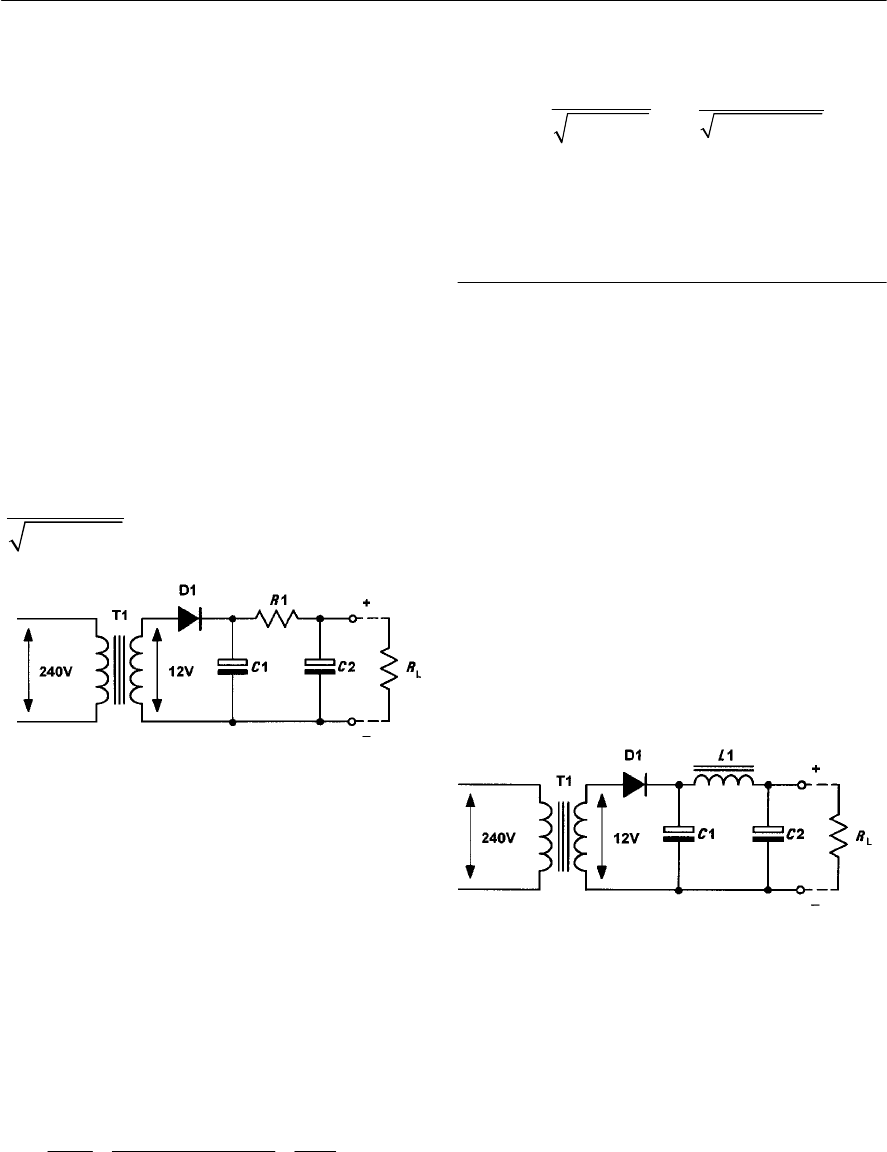
The amount of ripple at the output of the circuit
(i.e. appearing across C1)will be given by:
From which:
Improved ripple filters
Afurther improvement can be achieved by using an
inductor, L1, instead of a resistor in the smoothing
circuit. This circuit also offers the advantage that
the minimum d.c. voltage is dropped across the
inductor (in the circuit of Fig. 6.7, the d.c. output
voltage is reduced by an amount equal to the
voltage drop across R1).
Figure 6.9 shows the circuit of a half-wave
power supply with an L–C smoothing circuit. At
the ripple frequency, L1exhibits a high value of
inductive reactance while C1exhibits a low value
of capacitive reactance. The combined effect is that
of an attenuator which greatly reduces the
amplitude of the ripple while having a negligible
effect on the direct voltage.
that of simply increasing the discharge time
constant. This can be achieved either by increasing
the value of C1or by increasing the resistance
value of RL.In practice, however, the latter is not
really an option because RLis the effective
resistance of the circuit being supplied and we
don’t usually have the ability to change it!
Increasing the value of C1is a more practical
alternative and very large capacitor values (often in
excess of 4,700 µF) are typical.
Figure 6.8 shows a further refinement of the
simple power supply circuit. This circuit employs
two additional components, R1and C1,which act
as a filter to remove the ripple. The value of C1is
chosen so that the component exhibits a negligible
reactance at the ripple frequency (50 Hz for a half-
wave rectifier or 100 Hz for a full-wave rectifier—
see later). In effect, R1and C1act like a potential
divider. The amount of ripple is reduced by an
approximate factor equal to:
118 ELECTRONIC CIRCUITS: FUNDAMENTALS AND APPLICATIONS
C
ripple
2222
C
3.18
11
100 3.18
X
V
RX
=× =×
++
Example 6.2
The R–C smoothing filter in a 50 Hz mains
operated half-wave rectifier circuit consists of R1=
100 Gand C2 = 1,000 µF. If 1 V of ripple appears
at the input of the circuit, determine the amount of
ripple appearing at the output.
Solution
First we must determine the reactance of the
capacitor, C1,at the ripple frequency (50 Hz):
Figure 6.8 Half-wave rectifier circuit with R–C
smoothing filter
Figure 6.9 Half-wave rectifier circuit with L–C
smoothing filter
Example 6.3
The L–C smoothing filter in a 50 Hz mains
operated half-wave rectifier circuit consists of
L1 = 10 H and C2 = 1,000 µF. If 1 V of ripple
appears at the input of the circuit, determine the
amount of ripple appearing at the output.
C6
1 1 1, 000
3.18
2 3146.28 50 1,000 10
XfC
== ==
×× ×
0.032 V 32 mV
V
==
C
22
C
X
RX
+
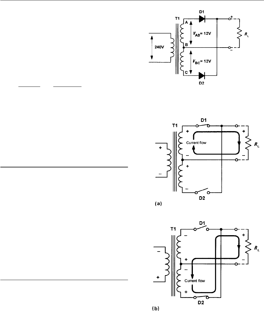
Solution
Once again, the reactance of the capacitor, C1, is
3.18 G(see Example 6.2). The reactance of L1at
50 Hz can be calculated from:
XL=2If L = 2 × 3.14 × 50 × 10 = 3,140 G
The amount of ripple at the output of the circuit
(i.e. appearing across C1) will be approximately
given by:
Hence the ripple produced by this arrangement
(with 1 V of 50 Hz a.c. superimposed on the
rectified input) will be a mere 1 mV. It is worth
comparing this value with that obtained from the
previous example!
Finally, it is important to note that the amount of
ripple present at the output of a power supply will
increase when the supply is loaded.
Full-wave rectifiers
Unfortunately, the half-wave rectifier circuit is
relatively inefficient as conduction takes place only
on alternate half-cycles. A better rectifier
arrangement would make use of both positive and
negative half-cycles. These full-wave rectifier
circuits offer a considerable improvement over
their half-wave counterparts. They are not only
more efficient but are significantly less demanding
in terms of the reservoir and smoothing
components. There are two basic forms of full-
wave rectifier; the bi-phase type and the bridge
rectifier type.
Bi-phase rectifier circuits
Figure 6.10 shows a simple bi-phase rectifier
circuit. Mains voltage (240 V) is applied to the
primary of step-down transformer (T1) which has
two identical secondary windings, each providing
12 V r.m.s. (the turns ratio of T1 will thus be
240/12 or 20:1 for each secondary winding).
On positive half-cycles, point A will be positive
with respect to point B. Similarly, point B will be
POWER SUPPLIES 119
Figure 6.11 (a) Bi-phase rectifier with D1
conducting and D2 non-conducting (b) bi-phase
rectifier with D2 conducting and D1 non-
conducting
Figure 6.10 Bi-phase rectifier circuit
C
CL
3.18
1 1 0.001 V
3140 3.18
X
VXX
=× =×
++
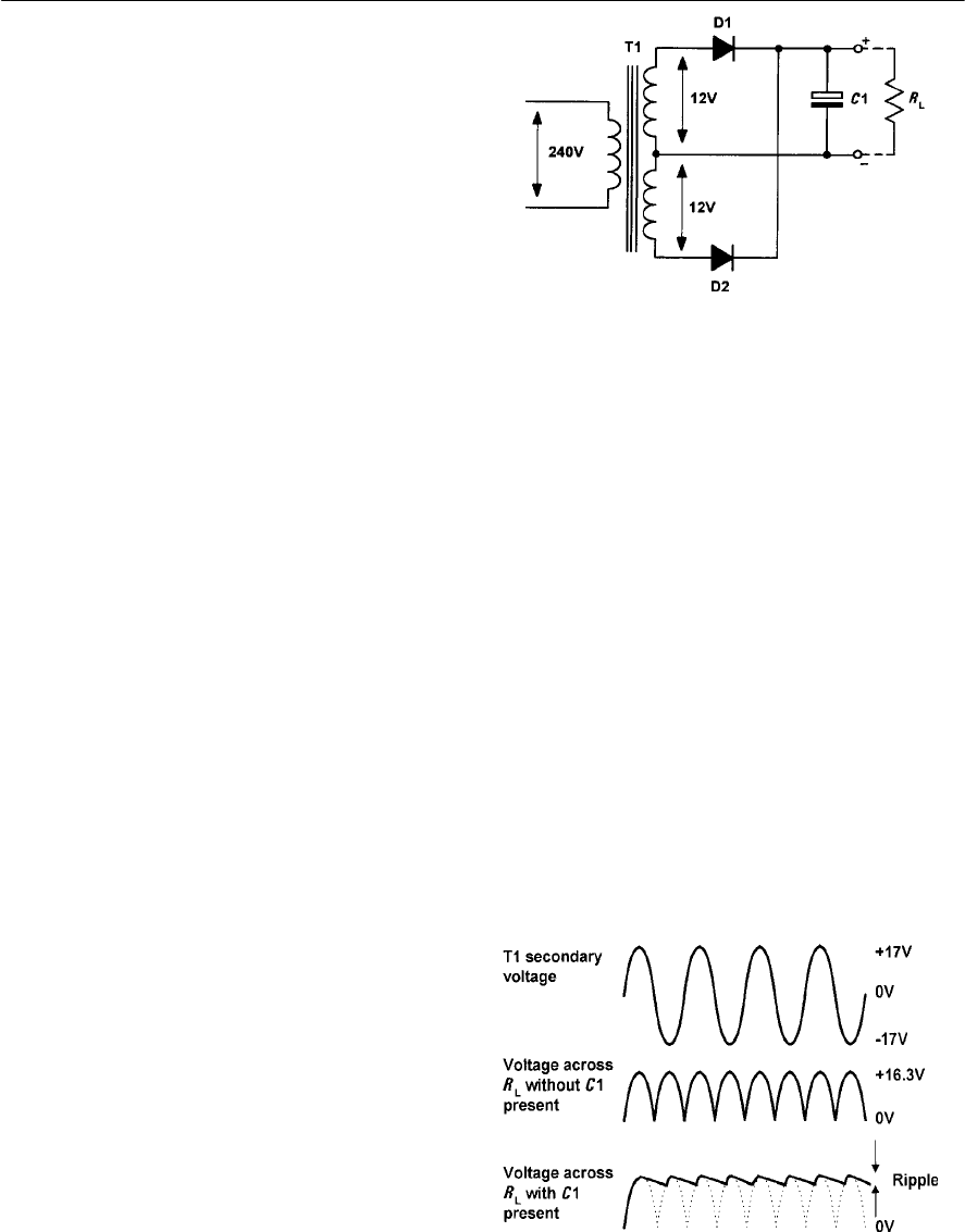
120 ELECTRONIC CIRCUITS: FUNDAMENTALS AND APPLICATIONS
positive with respect to point C. In this condition
D1 will allow conduction (its anode will be positive
with respect to its cathode) while D2 will not allow
conduction (its anode will be negative with respect
to its cathode). Thus D1 alone conducts on positive
half-cycles.
On negative half-cycles, point C will be positive
with respect to point B. Similarly, point B will be
positive with respect to point A. In this condition
D2 will allow conduction (its anode will be positive
with respect to its cathode) while D1 will not allow
conduction (its anode will be negative with respect
to its cathode). Thus D2 alone conducts on negative
half-cycles.
Figure 6.11 shows the bi-phase rectifier circuit
with the diodes replaced by switches. In Fig. 6.11
(a) D1 is shown conducting on a positive half-cycle
while in Fig. 6.11(b) D2 is shown conducting. The
result is that current is routed through the load in
the same direction on successive half-cycles.
Furthermore, this current is derived alternately
from the two secondary windings.
As with the half-wave rectifier, the switching
action of the two diodes results in a pulsating
output voltage being developed across the load
resistor (RL).However, unlike the half-wave circuit
the pulses of voltage developed across RLwill
occur at a frequency of 100 Hz (not 50 Hz). This
doubling of the ripple frequency allows us to use
smaller values of reservoir and smoothing capacitor
to obtain the same degree of ripple reduction (recall
that the reactance of a capacitor is reduced as
frequency increases).
As before, the peak voltage produced by each of
the secondary windings will be approximately 17 V
and the peak voltage across RLwill be 16.3 V (i.e.
17 V less the 0.7 V forward threshold voltage
dropped by the diodes).
Figure 6.12 shows how a reservoir capacitor
(C1) can be added to ensure that the output voltage
remains at, or near, the peak voltage even when the
diodes are not conducting. This component
operates in exactly the same way as for the half-
wave circuit, i.e. it charges to approximately 16.3 V
at the peak of the positive half-cycle and holds the
voltage at this level when the diodes are in their
non-conducting states. The time required for C1 to
charge to the maximum (peak) level is determined
by the charging circuit time constant (the series
resistance multiplied by the capacitance value). In
this circuit, the series resistance comprises the
secondary winding resistance together with the
forward resistance of the diode and the (minimal)
resistance of the wiring and connections. Hence C1
charges very rapidly as soon as either D1 or D2
starts to conduct. The time required for C1to
discharge is, in contrast, very much greater. The
discharge time contrast is determined by the
capacitance value and the load resistance, RL.In
practice, RLis very much larger than the resistance
of the secondary circuit and hence C1takes an
appreciable time to discharge. During this time, D1
and D2 will be reverse biased and held in a non-
conducting state. As a consequence, the only
discharge path for C1is through RL.Figure 6.13
shows voltage waveforms for the bi-phase rectifier,
with and without C1present. Note that the ripple
frequency (100 Hz) is twice that of the half-wave
circuit shown previously in Fig. 6.7.
Figure 6.12 Bi-phase rectifier with reservoir
capacitor
Figure 6.13 Waveforms for the bi-phase rectifier
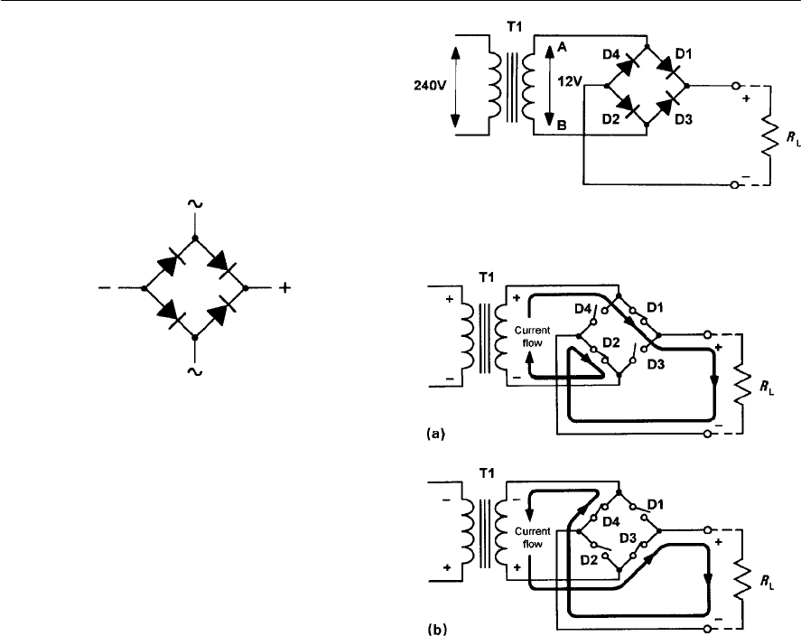
POWER SUPPLIES 121
Figure 6.14 Four diodes connected as a bridge
Bridge rectifier circuits
An alternative to the use of the bi-phase circuit is
that of using a four-diode bridge rectifier (see Fig.
6.14) in which opposite pairs of diode conduct on
alternate half-cycles. This arrangement avoids the
need to have two separate secondary windings.
Figure 6.16 (a) Bridge rectifier with D1 and D2
conducting, D3 and D4 non-conducting (b) bridge
rectifier with D1 and D2 non-conducting, D3 and
D4 conducting
Figure 6.15 Full-wave bridge rectifier circuit
Afull-wave bridge rectifier arrangement is shown
in Fig. 6.15. Mains voltage (240 V) is applied to the
primary of a step-down transformer (Tl). The
secondary winding provides 12 V r.m.s.
(approximately 17 V peak) and has a turns ratio of
20:1, as before. On positive half-cycles, point A
will be positive with respect to point B. In this
condition Dl and D2 will allow conduction while
D3 and D4 will not allow conduction. Conversely,
on negative half-cycles, point B will be positive
with respect to point A. In this condition D3 and
D4 will allow conduction while Dl and D2 will not
allow conduction.
Figure 6.16 shows the bridge rectifier circuit
with the diodes replaced by four switches. In
Fig. 6.16(a) Dl and D2 are conducting on a positive
half-cycle while in Fig. 6.16(b) D3 and D4 are
conducting. Once again, the result is that current is
routed through the load in the same direction on
successive half-cycles. As with the bi-phase
rectifier, the switching action of the two diodes
results in a pulsating output voltage being
developed across the load resistor (RL). Once again,
the peak output voltage is approximately 16.3 V
(i.e. 17 V less the 0.7 V forward threshold voltage).
Figure 6.16 shows how a reservoir capacitor
(C1) can be added to maintain the output voltage
when the diodes are not conducting. This
component operates in exactly the same way as for
the bi-phase circuit, i.e. it charges to approximately
16.3 V at the peak of the positive half-cycle and
holds the voltage at this level when the diodes are
in their non-conducting states. This component
operates in exactly the same way as for the bi-phase
circuit and the secondary and rectified output
waveforms are shown in Fig. 6.18. Once again note
that the ripple frequency is twice that of the
incoming a.c. supply.
Finally, R–C and L–C ripple filters can be added
to bi-phase and bridge rectifier circuits in exactly
the same way as those shown for the half-wave
rectifier arrangement (see Figs 6.8 and 6.9).
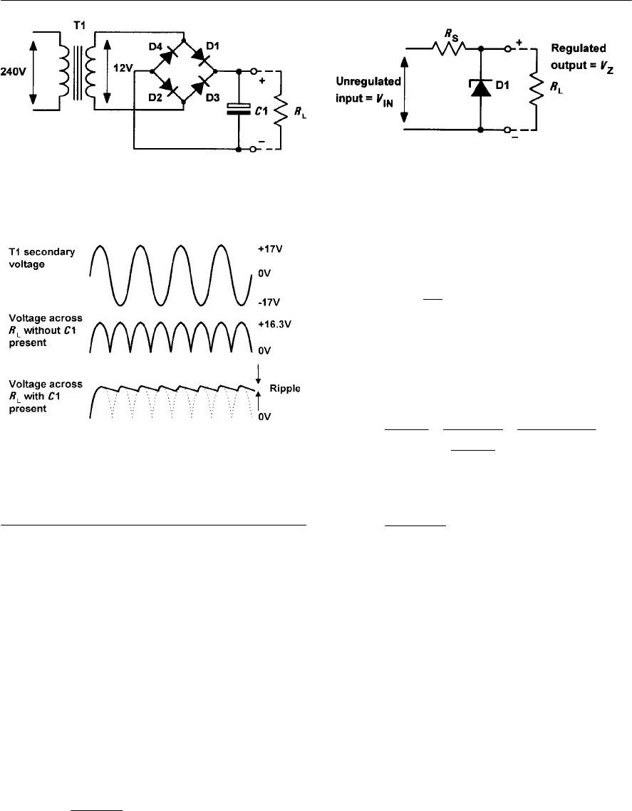
122 ELECTRONIC CIRCUITS: FUNDAMENTALS AND APPLICATIONS
Voltage regulators
Asimple voltage regulator is shown in Fig. 6.19. RS
is included to limit the zener current to a safe value
when the load is disconnected. When a load (RL)is
connected, the zener current (IZ)will fall as current
is diverted into the load resistance (it is usual to
allow a minimum current of 2 mA to 5 mA in order
to ensure that the diode regulates). The output
voltage (VZ)will remain at the zener voltage until
regulation fails at the point at which the potential
divider formed by RSand RLproduces a lower
output voltage that is less than VZ.The ratio of RS
to RLis thus important. At the point at which the
circuit just begins to fail to regulate:
where VIN is the unregulated input voltage. Thus
the maximum value for RScan be calculated from:
The power dissipated in the zener diode, will be
given by PZ=IZ×VZhence the minimum value for
RScan be determined from the off-load condition
when:
Thus:
where PZmax. is the maximum rated power
dissipation for the zener diode.
Example 6.4
A5V zener diode has a maximum rated power
dissipation of 500 mW. If the diode is to be used in
asimple regulator circuit to supply a regulated 5 V
to a load having a resistance of 400 G,determine a
suitable value of series resistor for operation in
conjunction with a supply of 9 V.
Solution
We shall use an arrangement similar to that shown
in Fig. 6.19. First we should determine the
maximum value for the series resistor, RS:
Figure 6.17 Bridge rectifier with reservoir
capacitor
Figure 6.18 Waveforms for the bridge rectifier
Figure 6.19 Bridge rectifier with reservoir
capacitor
L
ZIN
LS
R
VV
RR
=×+
(
)
IN Z Z
IN Z IN Z
S
Z Z
Z
Z
min.
max .
max .
VVV
VV VV
RIP
P
V
×
== =
2
IN Z Z
S
Z
min.
max .
VV V
RP
=
IN
SL
IN
max. 1
V
RR
V
=×

POWER SUPPLIES 123
thus:
Now we need to determine the minimum value for
the series resistor, RS:
thus:
Hence a suitable value for RSwould be 150 G
(roughly mid-way between the two extremes).
Output resistance and voltage regulation
In a perfect power supply, the output voltage would
remain constant regardless of the current taken by
the load. In practice, however, the output voltage
falls as the load current increases. To account for
this fact, we say that the power supply has internal
resistance (ideally this should be zero). This
internal resistance appears at the output of the
supply and is defined as the change in output
voltage divided by the corresponding change in
output current. Hence:
where MIout represents a small change in output
(load) current and MVout represents a corresponding
small change in output voltage.
The regulation of a power supply is given by the
relationship:
Ideally, the value of regulation should be very
small. Simple shunt zener diode regulators of the
type shown in Fig. 6.19 are capable of producing
values of regulation of 5% to 10%. More
sophisticated circuits based on discrete components
produce values of between 1% and 5% and
integrated circuit regulators often provide values of
1% or less.
Example 6.5
The following data was obtained during a test
carried out on a d.c. power supply:
(i) Load test
Output voltage (no-load) = 12 V
Output voltage (2 A load current) = 11.5 V
(ii) Regulation test
Output voltage (mains input, 220 V) = 12 V
Output voltage (mains input, 200 V) = 11.9 V
Determine (a) the equivalent output resistance of
the power supply and (b) the regulation of the
power supply.
Solution
The output resistance can be determined from the
load test data:
The regulation can be determined from the
regulation test data:
thus
Practical power supply circuits
Figure 6.20 shows a simple power supply circuit
capable of delivering an output current of up to
250 mA. The circuit uses a full-wave bridge
rectifier arrangement (Dl to D4) and a simple C–R
filter. The output voltage is regulated by the shunt-
connected 12 V zener diode.
IN
S L
IN
max. 1
V
RR
V
=×
2
IN Z Z
S
Z
min.
max .
VV V
RP
=
S
9
max. 400 1 400 (1.8 1) 320
5
R
=×=×=
(
)
2
S
95 5 45 25
min. 40
0.5 0.5
R×
===
out
out
out
change in output voltage
change in output current
V
R
I
==
change in output voltage
Regulation 100%
change in line (input) voltage
=×
out
change in output voltage 12 11.5
0.25
change in output current 2 0
R
===
change in output voltage
Regulation 100%
change in line (input) voltage
=×
12 1.9 0.1
Regulation 100% 100% 0.5%
220 200 20
=×=×=
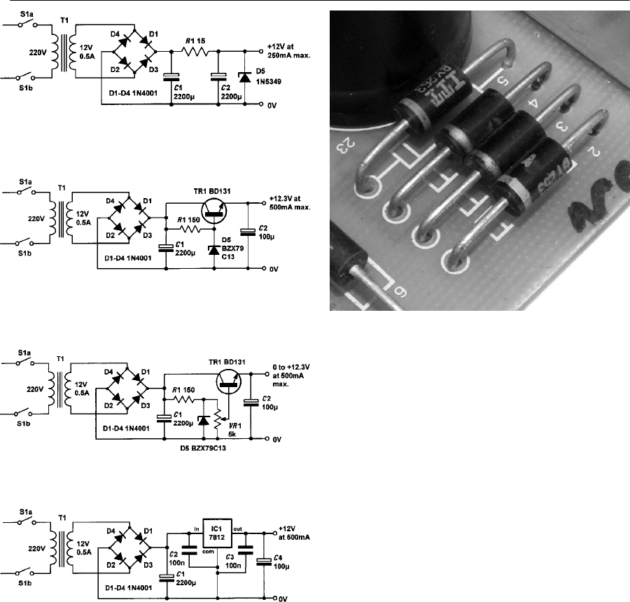
124 ELECTRONIC CIRCUITS: FUNDAMENTALS AND APPLICATIONS
Figure 6.24 This four-diode bridge rectifier
arrangement is part of a high-voltage d.c. supply.
Each BY253 diode is rated for a reverse repetitive
maximum voltage (VRRM)of 600 V, and a
maximum forward current, (IFmax.) of 3 A
Figure 6.21 shows an improved power supply in
which a transistor is used to provide current gain
and minimize the power dissipated in the zener
diode (TR1 is sometimes referred to as a series-
pass transistor). The zener diode, D5, is rated at
13 V and the output voltage will be approximately
0.7 V less than this (i.e. 13 V minus the base-
emitter voltage drop associated with TR1). Hence
the output voltage is about 12.3 V. The circuit is
Figure 6.21 Improved regulated d.c. power supply
with series-pass transistor
Figure 6.22 Variable d.c. power supply
Figure 6.23 Power supply with three-terminal IC
voltage regulator
capable of delivering an output current of up to
500 mA (note that TR1 should be fitted with a
small heatsink to conduct away any heat produced).
Figure 6.22 shows a variable power supply. The
base voltage to the series-pass transistor is derived
from a potentiometer connected across the zener
diode, D5. Hence the base voltage is variable from
0 V to 13 V. The transistor requires a substantial
heatsink (note that TRl’s dissipation increases as
the output voltage is reduced).
Finally, Fig. 6.23 shows a d.c. power supply
based on a fixed-voltage three-terminal
integrated circuit voltage regulator.These
devices are available in standard voltage and
current ratings (e.g. 5 V, 12 V, 15 V at 1 A, 2 A
and 5 A) and they provide excellent performance in
terms of output resistance, ripple rejection and
voltage regulation.
In addition, such devices usually incorporate
overcurrent protection and can withstand a direct
short-circuit placed across their output terminals.
This is an essential feature in many practical
applications!
Figure 6.20 Simple d.c. power supply with shunt
zener regulated output
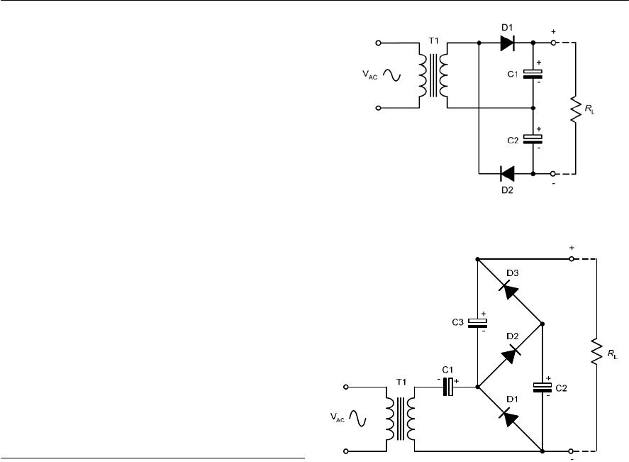
POWER SUPPLIES 125
Voltage multipliers
By adding a second diode and capacitor, we can
increase the output of the simple half-wave rectifier
that we met earlier. A voltage doubler using this
technique is shown in Fig. 6.25. In this arrangement
C1 will charge to the positive peak secondary
voltage whilst C2 will charge to the negative peak
secondary voltage. Since the output is taken from
C1 and C2 connected in series the resulting output
voltage is twice that produced by one diode alone.
The voltage doubler can be extended to produce
higher voltages using the cascade arrangement
shown in Fig. 6.26. Here C1 charges to the positive
peak secondary voltage, whilst C2 and C3 charge to
twice the positive peak secondary voltage. The
result is that the output voltage is the sum of the
voltages across C1 and C3 which is three times the
voltage that would be produced by a single diode.
The ladder arrangement shown in Fig. 6.25 can be
easily extended to provide even higher voltages but
the efficiency of the circuit becomes increasingly
impaired and high order voltage multipliers of this
type are only suitable for providing relatively small
currents.
Switched mode power supplies
Power supplies can be divided into two principal
categories, linear and non-linear types. Linear
power supplies make use of conventional analogue
control techniques—the regulating device operates
through a continuous range of current and voltage
according to the input and load conditions
prevailing at the time. Non-linear power supplies,
on the other hand, use digital techniques where the
regulating device is switched rapidly ‘on’ and ‘off’
in order to control the mean current and voltage
delivered to the load. These non-linear power
supplies are commonly referred to as switched
mode power supplies or just SMPS.Note that
SMPS can be used to step-up (boost)or step-down
(buck)the input voltage.
Compared with their conventional linear
counterparts, the advantages of SMPS are:
•ability to cope with a very wide input
voltage range
•very high efficiency (typically 80%, or more)
•compact size and light weight
The disadvantages of SMPS are:
•relatively complex circuitry
•appreciable noise generated (resulting from
the high switching frequency switching
action).
Fortunately, the principle of the basic step-down
type switched mode regulator is quite
straightforward. Take a look at the circuit diagram
shown in Fig. 6.27. With S1 closed, the switching
diode, D, will be reverse biased and will thus be in
anon-conducting state. Current will flow through
the inductor, L, charging the capacitor, C, and
delivering current to the load, RL.
Current flowing in the inductor, IL,produces a
magnetic flux in its core. When S1 is subsequently
opened, the magnetic flux within the inductor
rapidly collapses and an e.m.f. is generated across
the terminals of the inductor. The polarity of the
Figure 6.25 A voltage doubler
Figure 6.26 A voltage tripler
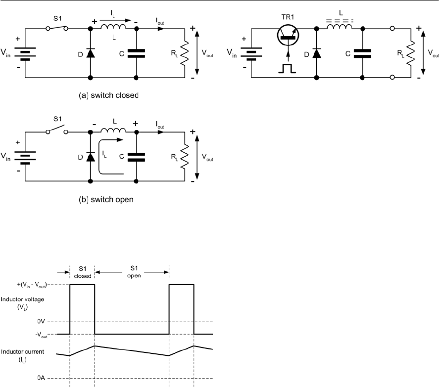
126 ELECTRONIC CIRCUITS: FUNDAMENTALS AND APPLICATIONS
Figure 6.29 Step-down switching regulator using
aseries switching transistor
induced e.m.f. is such that it opposes the original
potential and will cause current to continue to flow
in the load (i.e. clockwise around the circuit). In
this condition, the switching diode, D, will become
forward biased, completing the circuit in order to
provide a return path for the current.
Waveforms for the circuit of Fig. 6.27 are shown
in Fig. 6.28. The inductor voltage, VL,is alternately
positive and negative. When S1 is closed, the
voltage dropped across the inductor (from left to
right in the diagram) will be equal to +(Vin BVout).
When S1 is open, the voltage across the inductor
Figure 6.27 Principle of the switched mode power
supply
Figure 6.28 Waveforms for the switched mode
power supply shown in Fig. 6.27
will be equal to BVout (less the small forward
voltage drop of the switching diode, D). The
average current through the inductor, IL,is equal to
the load current, Iout.Note that a small amount of
ripple voltage appears superimposed on the steady
output voltage, Vout.This ripple voltage can be
reduced by using a relatively large value for the
capacitor, C.
In order to control the voltage delivered to the
load, Vout,it is simply necessary to adjust the ratio
of on to off time of the switch. A larger ratio of
‘on’ to ‘off’ time (i.e. a larger duty cycle or mark
to space ratio)produces a greater output voltage,
and vice versa.
In a practical switched mode power supply, the
witch, S1, is replaced by a semiconductor switching
device (i.e. a bipolar switching transistor or a
MOSFET device). The switching device must have
alow ‘on’ resistance and a high ‘off’ resistance and
must be capable of switching from the ‘on’ state to
the ‘off’ state in a very short time.
Regardless of whether it is a bipolar transistor or
aMOSFET, the switching device is controlled by a
train of rectangular pulses applied to its base or
gate terminal. The output voltage can be controlled
by varying the width of the pulses in this train. In a
practical switched mode power supply, a closed-
loop feedback path is employed in which the output
voltage is sensed and fed back to the control input
of a pulse generator. The result is pulse width
modulation (PWM)of the pulse train to the
switching device. This pulse width modulation can
be achieved using a handful of discrete components
or, more usually, is based on a dedicated switched
mode controller chip.
The job of controlling a switched mode power
supply is an ideal task for an integrated circuit and
Fig. 6.29 shows the internal arrangement of a
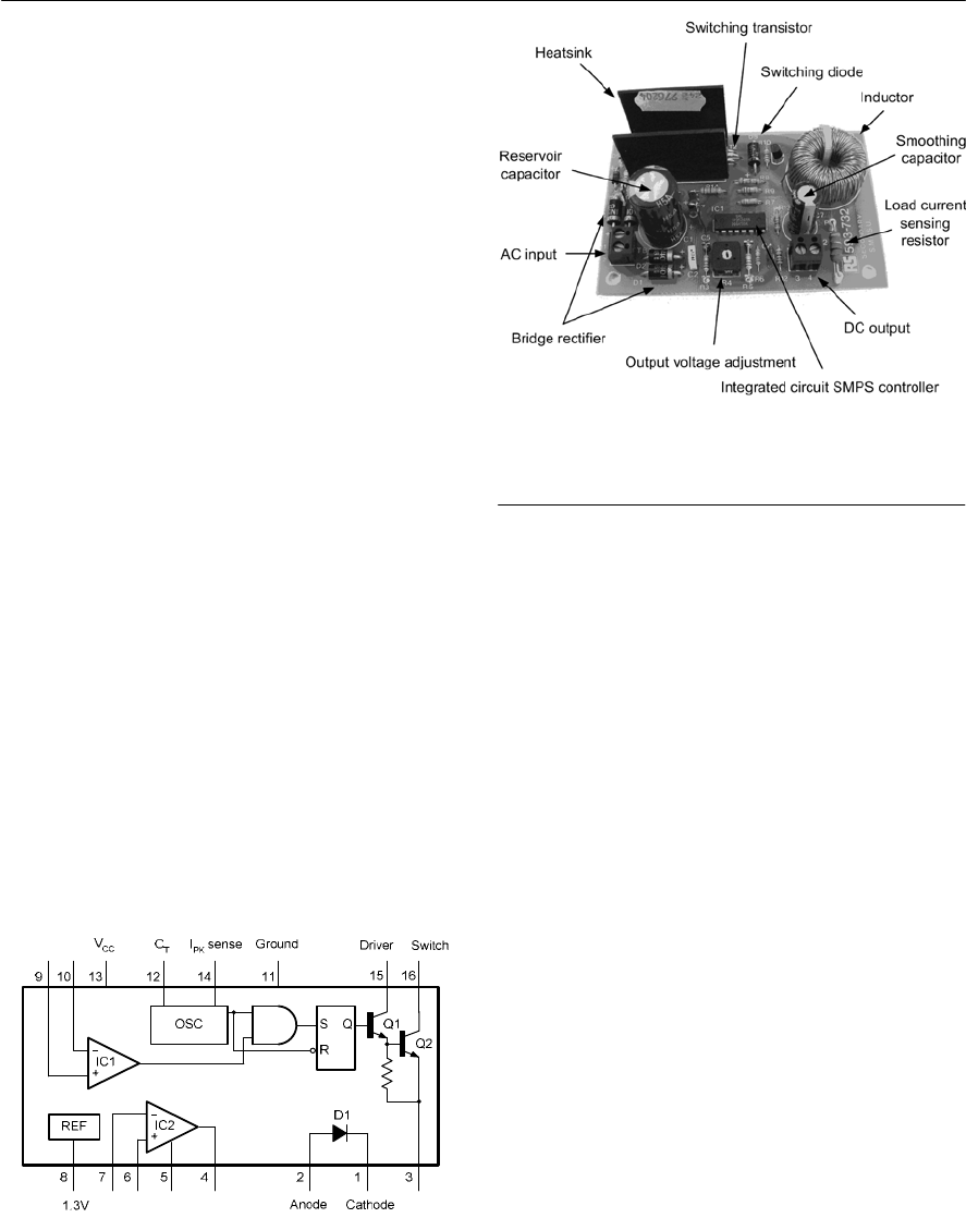
POWER SUPPLIES 127
Practical investigation
Objective
To investigate the operation of simple voltage
regulators.
Components and test equipment
Breadboard, digital or analogue meters with d.c.
voltage and current ranges, 9 V d.c. power supply
(or battery), 3.9 V zener diode (e.g. BZX85 or
BZY88), NPN TO5 transistor (e.g. 2N3053 or
BFY50), 48°C/W TO5 clip-on heatsink, 220 G
0.3W resistor, 15 G0.3W resistor, 500 Gand 1 kG
wirewound variable resistors, connecting wire,
test leads, .
Procedure
Connect the simple zener diode shunt regulator
shown in Fig. 6.32. Set the variable resistor to
produce a load current (IL)of 10 mA then measure
and record the output voltage produced across the
load, VL.Repeat for load currents from 20 mA to
100 mA in 10 mA steps.
Connect the transistor regulator shown in Fig.
6.33. Set the variable resistor to produce a load
current (IL)of 25 mA then measure and record the
output voltage produced across the load, VL.Repeat
for load current from 50 mA to 250 mA in 25 mA
steps.
Figure 6.31 A switched mode power supply
Figure 6.30 The LM78S40 switched mode power
supply controller
typical example, the LM78S40. This device
contains two operational amplifiers (IC1 and IC2)
designed to work as comparators,and a two-stage
Darlington transistor switch comprising an emitter-
follower driver, Q1, and output switch, Q2. The
LM78S40 is supplied in a 16-pin dual-in-line (DIL)
package.
The LM78S40 can be configured to provide step-
up (boost), step-down (buck), and inverting
operation. The frequency of the internal current
controlled oscillator is set by the value of capacitor
connected to pin-12. Oscillator frequencies of
between 100 Hz and 100 kHz are possible but most
practical applications operate at frequencies
between 20 kHz and 50 kHz. The oscillator duty
cycle is internally set to 6:1 but can be varied by
means of the current sensing circuit which normally
senses the current in an external resistor connected
between pins-12 and 13.
An internal band-gap voltage reference
provides a stable voltage reference of 1.3 V at pin-
8. The internal reference voltage source is capable
of providing a current of up to 10 mA drawn from
pin-8. The output transistor, Q2, is capable of
carrying a peak current of up to 1.5 A and has a
maximum collector-emitter voltage rating of 40 V.
The internal power switching diode, D1, is
accessible between pins-1 and 2 and this has
similar ratings to Q2. Both D1 and Q2 have
switching times of between 300 and 500 ns. IC1 is
used to compare the 1.3 V voltage reference (pin-
10 connected to pin-8) with a proportion of the
output (derived from a simple two-resistor potential
divider).
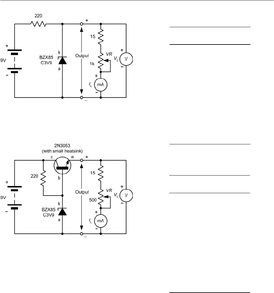
128 ELECTRONIC CIRCUITS: FUNDAMENTALS AND APPLICATIONS
Figure 6.32 Simple zener diode voltage regulator
Measurements and calculations
For each circuit, record your results in a table
showing corresponding values of ILand VL(see
Tables 6.1 and 6.2).
Plot graphs showing VLplotted against ILfor each
circuit (see Figures 6.34 and 6.35). By constructing
atangent to each graph, determine the output
resistance of each regulator circuit. For the simple
shunt zener diode regulator the output resistance
should be calculated at IL=30 mA whilst for the
transistor voltage regulator the output resistance
should be calculated at IL=100 mA.
Load current
(mA)
10
20
30
40
50
60
70
80
90
100
Output voltage
(V)
Load current
(mA)
25
50
75
100
125
150
175
200
225
250
Output voltage
(V)
Table 6.2 Table of results for the transistor
voltage regulator
Table 6.1 Table of results for the simple zener
voltage regulator
Conclusion
Comment on the shape of each graph. Is this what
you would expect? Compare the performance of
each circuit and, in particular, the range of load
currents over which effective regulation is
achieved. Which of the transistors had the lowest
value of output resistance? Can you suggest why
this is?
Figure 6.33 Transistor voltage regulator
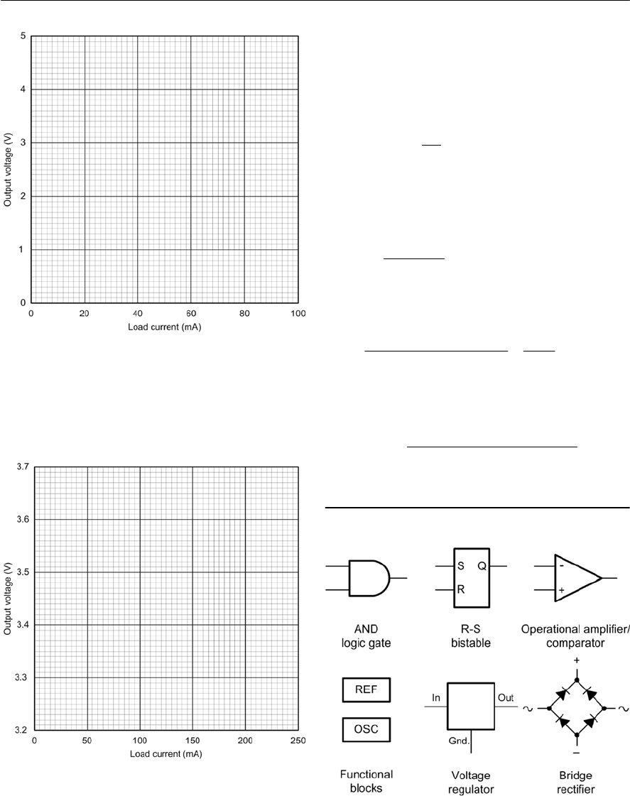
POWER SUPPLIES 129
Important formulae introduced in this
chapter
Maximum value of series resistor for a simple
shunt zener diode voltage regulator:
(page 122)
Minimum value of series resistor for a simple shunt
zener diode voltage regulator:
(page 122)
Output resistance of a power supply:
(page 123)
Input (line) regulation of a power supply:
(page 123)
Figure 6.36 Circuit symbols introduced in this
chapter
Symbols introduced in this chapter
Figure 6.34 Graph layout that can be used for the
load characteristic of the simple zener voltage
regulator (construct a tangent to the graph at IL=30
mA in order to determine the output resistance)
Figure 6.35 Graph layout that can be used for the
load characteristic of the simple zener voltage
regulator (construct a tangent to the graph at IL=
100 mA in order to determine the output resistance)
IN
S L
IN
max. 1
V
RR
V
=×
2
IN Z Z
S
Z
min.
max .
VV V
RP
=
out
out
out
change in output voltage
change in output current
V
R
I
==
change in output voltage
Regulation 100%
change in line (input) voltage
=×
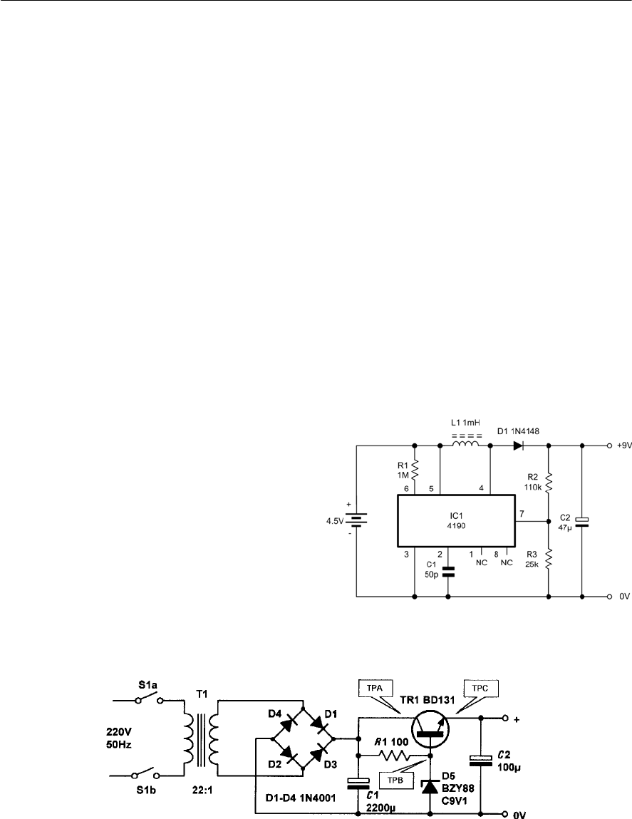
Problems
6.1 A half-wave rectifier is fitted with an R–C
smoothing filter comprising R = 200 Gand
C = 50 µF. If 2 V of 400 Hz ripple appear at
the input of the circuit, determine the mount
of ripple appearing at the output.
6.2 The L–C smoothing filter fitted to a 50 Hz
mains operated full-wave rectifier circuit
consists of L= 4 H and C = 500 µF. If 4 V
of ripple appear at the input of the circuit,
determine the amount of ripple appearing at
the output.
6.3 If a 9 V zener diode is to be used in a simple
shunt regulator circuit to supply a load
having a nominal resistance of 300 G,
determine the maximum value of series
resistor for operation in conjunction with a
supply of 15 V.
6.4 The circuit of a d.c. power supply is shown
in Fig. 6.37. Determine the voltages that will
appear at test points A, B and C.
6.5 In Fig. 6.37, determine the current flowing
in R1and the power dissipated in D5 when
the circuit is operated without any load
connected.
6.6 In Fig. 6.37, determine the effect of each of
the following fault conditions:
(a) R1open-circuit;
(b) D5 open-circuit;
(c) D5 short-circuit.
6.7 A 220 V AC supply feeds a 20:1 step-down
transformer, the secondary of which is
connected to a bridge rectifier and reservoir
capacitor. Determine the approximate d.c.
voltage that will appear across the reservoir
capacitor under ‘no-load’ conditions.
130 ELECTRONIC CIRCUITS: FUNDAMENTALS AND APPLICATIONS
6.8 The following data were obtained during a
load test carried out on a d.c. power supply:
Output voltage (no-load) = 8.5 V
Output voltage (800 mA load) = 8.1V
Determine the output resistance of the power
supply and estimate the output voltage at a
load current of 400 mA.
6.9 The following data were obtained during a
regulation test on a d.c. power supply:
Output voltage (a.c. input: 230 V) = 15 V
Output voltage (a.c. input: 190 V) = 14.6 V
Determine the regulation of the power
supply and estimate the output voltage when
the input voltage is 245 V.
6.10 Figure 6.38 shows a switching regulator
circuit that produces an output of 9 V for an
input of 4.5 V. What type of regulator is
this? Between which pins of IC1 is the
switching transistor connected? Which
pin on IC1 is used to feed back a proportion
of the output voltage to the internal
comparator stage?
Answers to these problems appear on page 375.
Figure 6.37 See Questions 6.4, 6.5 and 6.6
Figure 6.38 See Question 6.10
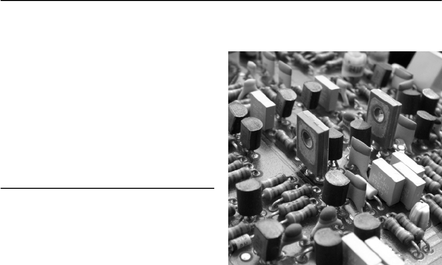
7
Amplifiers
This chapter introduces the basic concepts of
amplifiers and amplification. It describes the most
common types of amplifier and outlines the basic
classes of operation used in both linear and non-
linear amplifiers. The chapter also describes
methods for predicting the performance of an
amplifier based on equivalent circuits and on the
use of semiconductor characteristics and load lines.
Once again, we conclude with a selection of
practical circuits that can be built and tested.
Types of amplifier
Many different types of amplifier are found in
electronic circuits. Before we explain the operation
of transistor amplifiers in detail, we shall briefly
describe the main types of amplifier.
a.c. coupled amplifiers
In a.c. coupled amplifiers, stages are coupled
together in such a way that d.c. levels are isolated
and only the a.c. components of a signal are
transferred from stage to stage.
d.c. coupled amplifiers
In d.c. (or direct) coupled amplifiers, stages are
coupled together in such a way that stages are not
isolated to d.c. potentials. Both a.c. and d.c. signal
components are transferred from stage to stage.
Large-signal amplifiers
Large-signal amplifiers are designed to cater for
appreciable voltage and/or current levels (typically
from 1V to 100 V or more).
Small-signal amplifiers
Small-signal amplifiers are designed to cater for
low-level signals (normally less than 1V and often
much smaller). Small-signal amplifiers have to be
specially designed to combat the effects of noise.
Audio frequency amplifiers
Audio frequency amplifiers operate in the band of
frequencies that is normally associated with audio
signals (e.g. 20 Hz to 20 kHz).
Wideband amplifiers
Wideband amplifiers are capable of amplifying a
very wide range of frequencies, typically from a
few tens of hertz to several megahertz.
Radio frequency amplifiers
Radio frequency amplifiers operate in the band of
frequencies that is normally associated with radio
signals (e.g. from 100 kHz to over 1 GHz). Note
that it is desirable for amplifiers of this type to be
frequency selective and thus their frequency
response may be restricted to a relatively narrow
band of frequencies (see Fig. 7.9 on page 135).
Figure 7.1 Part of a high-gain, wideband d.c.
coupled amplifier using discrete components
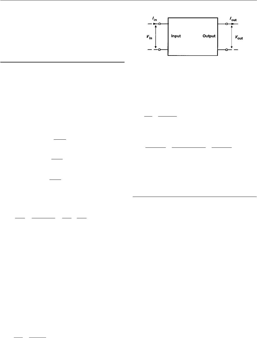
132 ELECTRONIC CIRCUITS: FUNDAMENTALS AND APPLICATIONS
Low-noise amplifiers
Low-noise amplifiers are designed so that they
contribute negligible noise (signal disturbance) to
the signal being amplified. These amplifiers are
usually designed for use with very small signal
levels (usually less than 10 mV or so).
Gain
One of the most important parameters of an
amplifier is the amount of amplification or gain that
it provides. Gain is simply the ratio of output
voltage to input voltage, output current to input
current, or output power to input power (see
Fig. 7.2). These three ratios give, respectively, the
voltage gain, current gain and power gain. Thus:
Voltage gain,
Current gain,
Power gain,
Note that, since power is the product of current and
voltage (P=I V), we can infer that:
Example 7.1
An amplifier produces an output voltage of 2 V for
an input of 50 mV. If the input and output currents
in this condition are, respectively, 4 mA and
200 mA, determine:
(a) the voltage gain;
(b) the current gain;
(c) the power gain.
Solution
(a) The voltage gain is calculated from:
Figure 7.2 Block diagram for an amplifier
showing input and output voltages and currents
(b) The current gain is calculated from:
(c) The power gain is calculated from:
Note that the same result is obtained from:
Class of operation
An important requirement of most amplifiers is that
the output signal should be a faithful copy of the
input signal, albeit somewhat larger in amplitude.
Other types of amplifier are non-linear, in which
case their input and output waveforms will not
necessarily be similar. In practice, the degree of
linearity provided by an amplifier can be affected
by a number of factors including the amount of bias
applied (see later) and the amplitude of the input
signal.
It is also worth noting that a linear amplifier will
become non-linear when the applied input signal
exceeds a threshold value. Beyond this value the
amplifier is said to be overdriven and the output
will become increasingly distorted if the input
signal is further increased.
Amplifiers are usually designed to be operated
with a particular value of bias supplied to the active
devices (i.e. transistors). For linear operation, the
out
v
in
V
A
V
=
out
i
in
I
A
I
=
out
p
in
P
A
P
=
out out out out out
piv
in in in in in
PIV IV
AAA
PIV IV
×
== =×=×
×
out
v
in
2 V
40
50 mV
V
AV
== =
out
i
in
200 mA
50
4mA
I
AI
== =
out out
p
in in
200 mA 2 V 0.4 W
2,000
4mA 50 mV 200 W
IV
AIV
µ
××
== ==
××
piv
50 40 2,000
AAA=× =× =
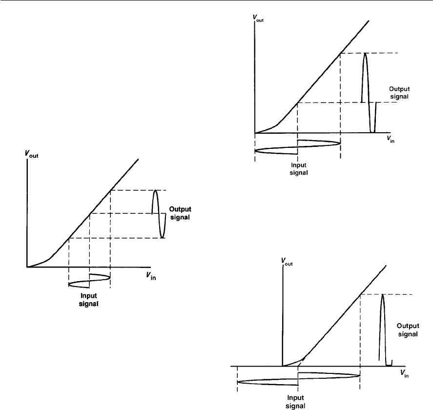
AMPLIFIERS 133
active device(s) must be operated in the linear part
of their transfer characteristic (Vout plotted
against Vin). In Fig. 7.3 the input and output signals
for an amplifier are operating in linear mode. This
form of operation is known as Class A and the bias
point is adjusted to the mid-point of the linear part
of the transfer characteristic. Furthermore, current
will flow in the active devices used in a Class A
amplifier during a complete cycle of the signal
waveform. At no time does the current fall to zero.
Figure 7.4 shows the effect of moving the bias
point down the transfer characteristic and, at the
same time, increasing the amplitude of the input
signal. From this, you should notice that the
extreme negative portion of the output signal has
become distorted. This effect arises from the non-
linearity of the transfer characteristic that occurs
near the origin (i.e. the zero point). Despite the
obvious non-linearity in the output waveform, the
active device(s) will conduct current during a
complete cycle of the signal waveform.
Now consider the case of reducing the bias even
further while further increasing the amplitude of the
input signal (see Fig. 7.5). Here the bias point has
been set at the projected cut-off point. The negative
portion of the output signal becomes cut off (or
clipped)and the active device(s) will cease to
conduct for this part of the cycle. This mode of
operation is known as Class AB.
Figure 7.3 Class A (linear) operation
Now let’s consider what will happen if no bias at
all is applied to the amplifier (see Fig. 7.6). The
output signal will only comprise a series of positive
half-cycles and the active device(s) will only be
conducting during half-cycles of the waveform (i.e.
they will only be operating 50% of the time).
This mode of operation is known as Class B and
is commonly used in high-efficiency push-pull
power amplifiers where the two active devices in
the output stage operate on alternate half-cycles of
the waveform.
Figure 7.4 Effect of reducing bias and increasing
input signal amplitude (the output waveform is no
longer a faithful reproduction of the input)
Figure 7.5 Class AB operation (bias set at
projected cut-off)
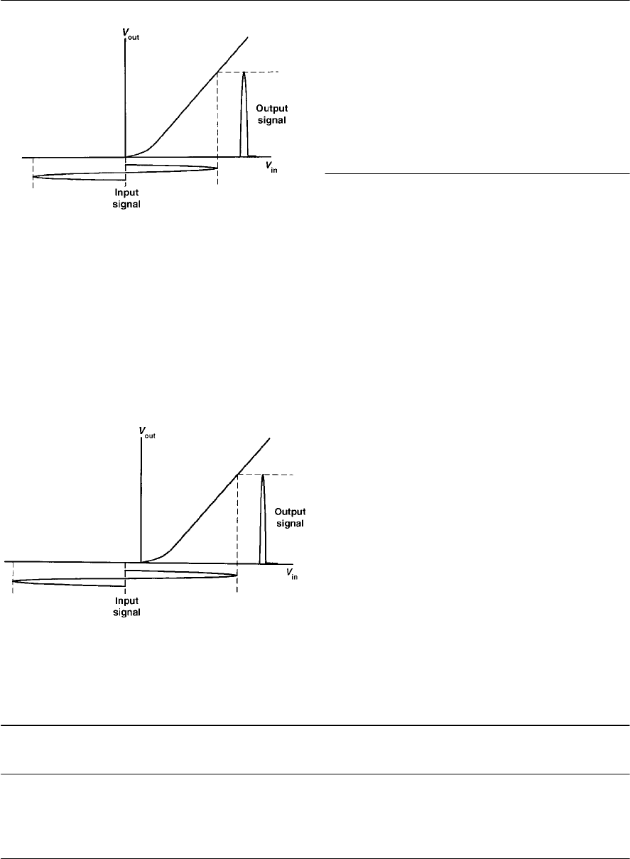
Class of operation Bias point Conduction angle
(typical)
AMid-point 360°
AB Projected cut-off 210°
BAt cut-off 180°
CBeyond cut-off 120°
Application
Linear audio amplifiers
Push-pull audio amplifiers
Push-pull audio amplifiers
Radio frequency power amplifiers
Efficiency
(typical)
5% to 20%
20% to 40%
40% to 70%
70% to 90%
134 ELECTRONIC CIRCUITS: FUNDAMENTALS AND APPLICATIONS
Finally, there is one more class of operation to
consider. The input and output waveforms for
Class C operation are shown in Fig. 7.7. Here the
bias point is set at beyond the cut-off (zero) point
and a very large input signal is applied. The output
waveform will then comprise a series of quite sharp
positive-going pulses. These pulses of current or
Figure 7.7 Class C operation (bias is set beyond
cut-off)
Figure 7.6 Class B operation (no bias applied)
voltage can be applied to a tuned circuit load in
order to recreate a sinusoidal signal. In effect, the
pulses will excite the tuned circuit and its inherent
flywheel action will produce a sinusoidal output
waveform. This mode of operation is only used in
RF power amplifiers that must operate at very high
levels of efficiency. Table 7.1 summarizes the
classes of operation used in amplifiers.
Input and output resistance
Input resistance is the ratio of input voltage to input
current and it is expressed in ohms. The input of an
amplifier is normally purely resistive (i.e. any
reactive component is negligible) in the middle of
its working frequency range (i.e. the mid-band). In
some cases, the reactance of the input may become
appreciable (e.g. if a large value of stray
capacitance appears in parallel with the input
resistance). In such cases we would refer to input
impedance rather than input resistance.
Output resistance is the ratio of open-circuit
output voltage to short-circuit output current and is
measured in ohms. Note that this resistance is
internal to the amplifier and should not be confused
with the resistance of a load connected externally.
As with input resistance, the output of an
amplifier is normally purely resistive and we can
safely ignore any reactive component. If this is not
the case, we would once again need to refer to
output impedance rather than output resistance.
Figure 7.8 shows how the input and output
resistances are ‘seen’ looking into the input and
output terminals, respectively. We shall be
returning to this equivalent circuit a little later in
this chapter. Finally, it’s important to note that,
although these resistance are meaningful in terms
of the signals present, they cannot be measured
using a conventional meter!
Table 7.1 Classes of operation
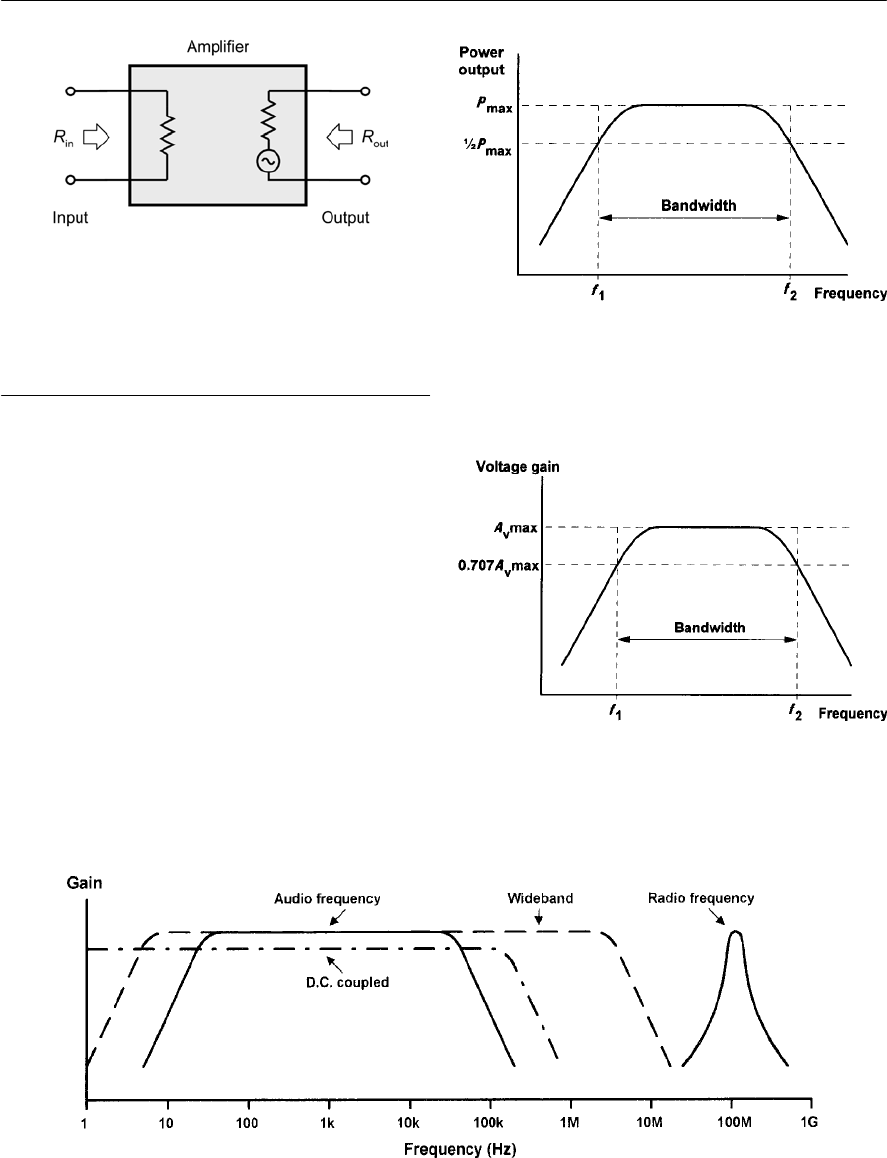
AMPLIFIERS 135
Frequency response
The frequency response characteristics for various
types of amplifier are shown in Fig. 7.9. Note that,
for response curves of this type, frequency is
almost invariably plotted on a logarithmic scale.
The frequency response of an amplifier is usually
specified in terms of the upper and lower cut-off
frequencies of the amplifier. These frequencies are
those at which the output power has dropped to
50% (otherwise known as the *3dB points)or
where the voltage gain has dropped to 70.7% of its
mid-band value.
Figures 7.10 and 7.11, respectively, show how
the bandwidth can be expressed in terms of either
power or voltage (the cut-off frequencies, f1and f2,
and bandwidth are identical).
Figure 7.8 Input and output resistances ‘seen’
looking into the input and output terminals,
respectively
Figure 7.10 Frequency response and bandwidth
(output power plotted against frequency)
Figure 7.11 Frequency response and bandwidth
(output voltage plotted against frequency)
Figure 7.9 Frequency response and bandwidth (output power plotted against frequency)
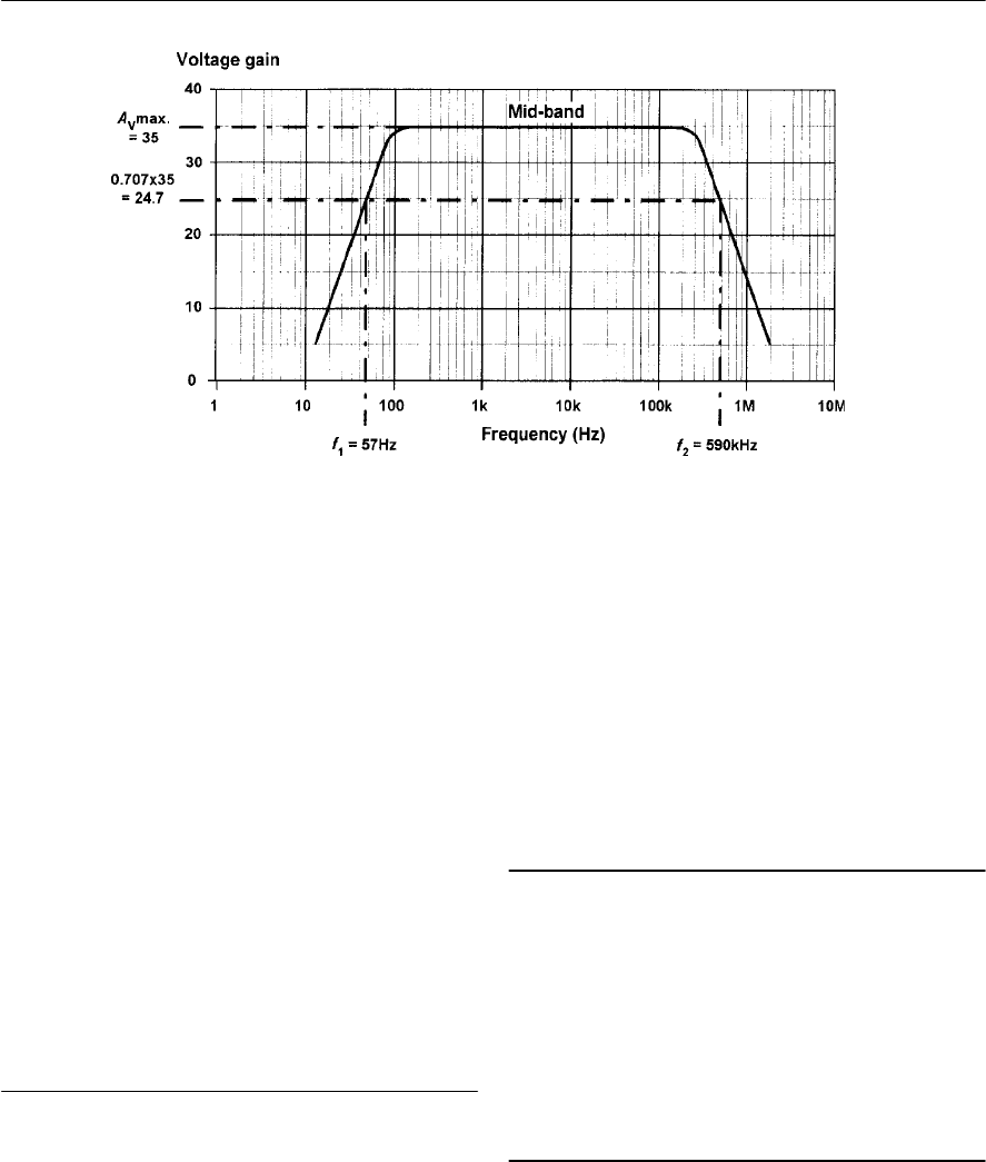
136 ELECTRONIC CIRCUITS: FUNDAMENTALS AND APPLICATIONS
Example 7.2
Determine the mid-band voltage gain and upper
and lower cut-off frequencies for the amplifier
whose frequency response is shown in Fig. 7.12.
Solution
The mid-band voltage gain corresponds with the
flat part of the frequency response characteristic. At
the point the voltage gain reaches a maximum of 35
(see Fig. 7.12).
The voltage gain at the two cut-off frequencies
can be calculated from:
Avcut-off = 0.707 × Avmax = 0.707 × 35 = 24.7
This value of gain intercepts the frequency
response graph at f1=57 Hz and f2=590 kHz (see
Fig. 7.12).
Bandwidth
The bandwidth of an amplifier is usually taken as
the difference between the upper and lower cut-off
frequencies (i.e. f2If1in Figs 7.10 and 7.11). The
bandwidth of an amplifier must be sufficient to
accommodate the range of frequencies present
within the signals that it is to be presented with.
Many signals contain harmonic components (i.e.
signals at 2f, 3f, 4f,etc. where fis the frequency of
the fundamental signal). To reproduce a square
wave, for example, requires an amplifier with a
very wide bandwidth (note that a square wave
comprises an infinite series of harmonics). Clearly
it is not possible to perfectly reproduce such a wave
but it does explain why it can be desirable for an
amplifier’s bandwidth to greatly exceed the highest
signal frequency that it is required to handle!
Phase shift
Phase shift is the phase angle between the input and
output signal voltages measured in degrees. The
measurement is usually carried out in the mid-band
where, for most amplifiers, the phase shift remains
relatively constant. Note also that conventional
single-stage transistor amplifiers provide phase
shifts of either 180° or 360°.
Negative feedback
Many practical amplifiers use negative feedback in
order to precisely control the gain, reduce distortion
and improve bandwidth. The gain can be reduced to
amanageable value by feeding back a small
Figure 7.12 See Example 7.2
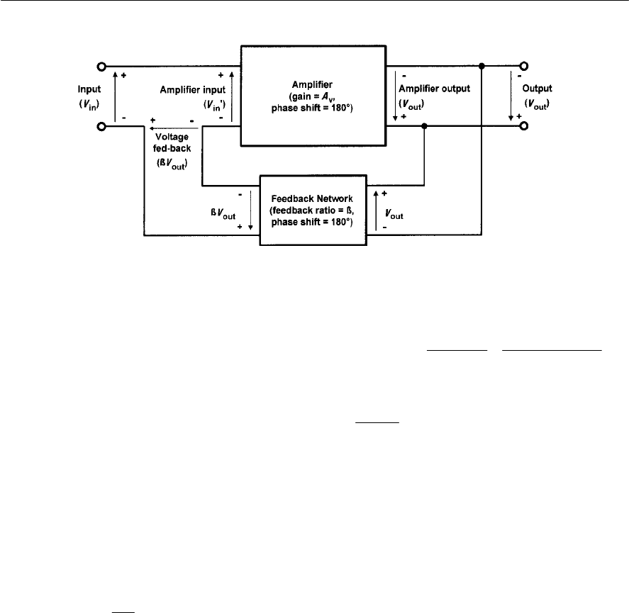
AMPLIFIERS 137
proportion of the output. The amount of feedback
determines the overall (or closed-loop)gain.
Because this form of feedback has the effect of
reducing the overall gain of the circuit, this form of
feedback is known as negative feedback.An
alternative form of feedback, where the output is
fed back in such a way as to reinforce the input
(rather than to subtract from it) is known as
positive feedback.This form of feedback is used in
oscillator circuits (see Chapter 9).
Figure 7.13 shows the block diagram of an
amplifier stage with negative feedback applied. In
this circuit, the proportion of the output voltage fed
back to the input is given by Jand the overall
voltage gain will be given by:
Now Vin' = Vin I JVout (by applying Kirchhoff’s
Voltage Law) (note that the amplifier’s input
voltage has been reduced by applying negative
feedback) thus:
Vin =Vin' + JVout
and
Vout = Av×Vin (Note that Avis the internal gain of
the amplifier)
Hence:
Thus:
Hence, the overall gain with negative feedback
applied will be less than the gain without feedback.
Furthermore, if Avis very large (as is the case with
an operational amplifier, see Chapter 8) the overall
gain with negative feedback applied will be given
by:
G=1/J(when Avis very large)
Note, also, that the loop gain of a feedback
amplifier is defined as the product of Jand Av.
Example 7.3
An amplifier with negative feedback applied has an
open-loop voltage gain of 50 and one-tenth of its
output is fed back to the input (i.e. J=0.1).
Determine the overall voltage gain with negative
feedback applied.
Solution
With negative feedback applied the overall voltage
gain will be given by:
Figure 7.13 Amplifier with negative feedback applied
out
in
Overall gain,
V
G
V
=
()
vin vin
in out in v in
''
Overall gain, '
J'J'
AV AV
GVVV AV
××
==
++×
v
v
1
J
A
G
A
=+
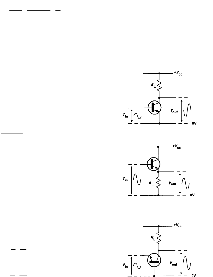
138 ELECTRONIC CIRCUITS: FUNDAMENTALS AND APPLICATIONS
Figure 7.14 Common-emitter configuration
Example 7.4
If, in Example 7.3, the amplifier’s open-loop
voltage gain increases by 20%, determine the
percentage increase in overall voltage gain.
Solution
The new value of voltage gain will be given by:
Av=Av+0.2Av=1.2 × 50 = 60
The overall voltage gain with negative feedback
will then be:
The increase in overall voltage gain, expressed as a
percentage, will thus be:
Note that this example illustrates one of the
important benefits of negative feedback in
stabilizing the overall gain of an amplifier stage.
Example 7.5
An integrated circuit that produces an open-loop
gain of 100 is to be used as the basis of an amplifier
stage having a precise voltage gain of 20.
Determine the amount of feedback required.
Solution
Re-arranging the formula,
to make Jthe subject gives:
thus
Transistor amplifiers
Regardless of what type of transistor is employed,
three basic circuit configurations are used. These
three circuit configurations depend upon which one
of the three transistor connections is made common
to both the input and the output. In the case of
bipolar transistors, the configurations are known as
common emitter,common collector (or emitter
follower)and common base.Where field effect
Figure 7.15 Common-collector (emitter follower)
configuration
Figure 7.16 Common-base configuration
()
v
v
50 50
8.33
1J1 0.1 50 6
A
GA
== ==
++×
()
v
v
60 60
7.14
1J1 0.1 60 7
A
GA
== ==
++×
8.57 8.33
100% 2.88%
8.33
×=
v
v
1
J
A
G
A
=+
v
11
J
GA
=
11
J0.05 0.01 0.04
20 100
===
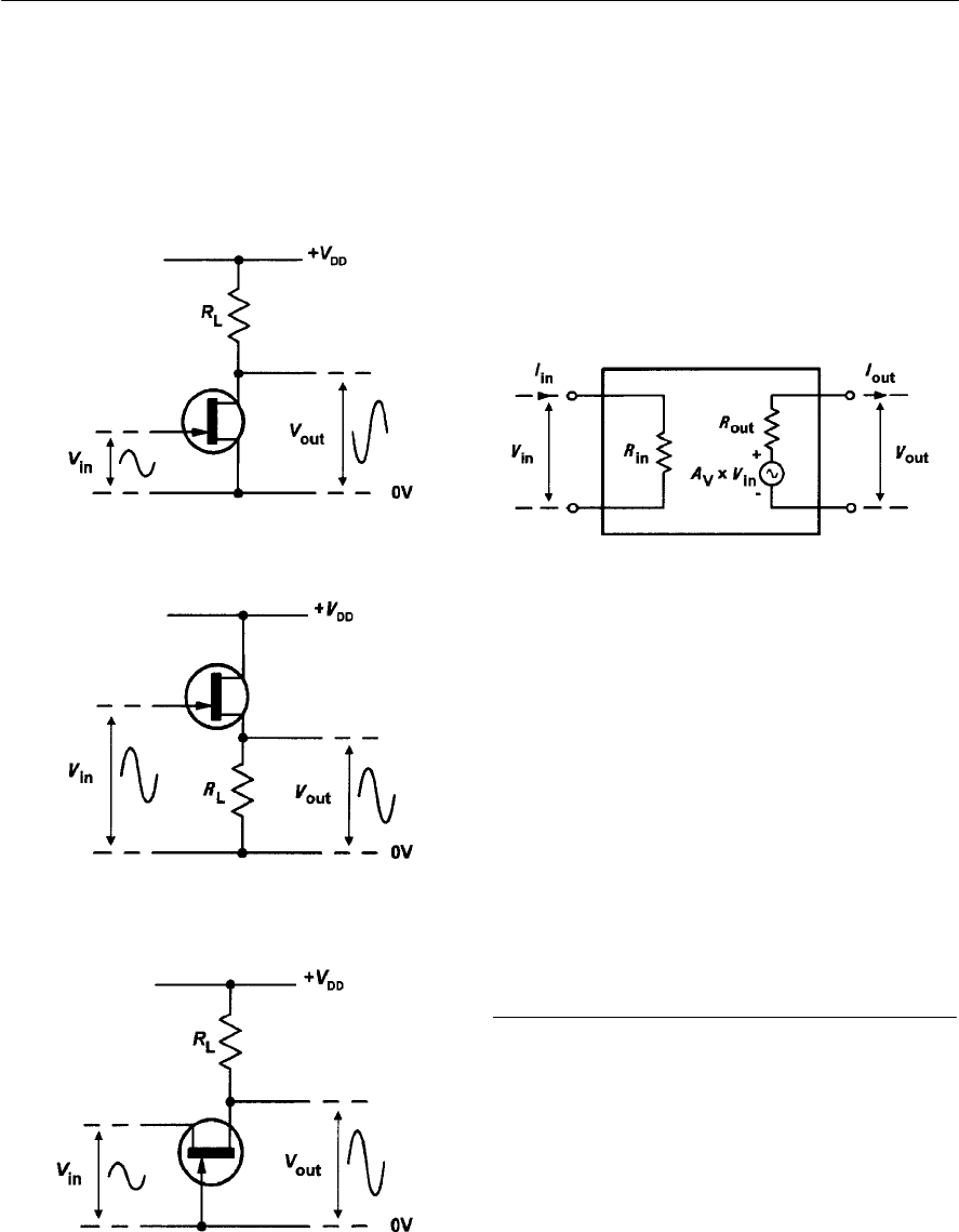
AMPLIFIERS 139
Figure 7.19 Common-gate configuration
Figure 7.18 Common-drain (source follower) con-
figuration
Figure 7.17 Common-source configuration
transistors are used, the corresponding
configurations are common source,common
drain (or source follower)and common gate.
The three basic circuit configurations (Figs 7.14
to 7.19) exhibit quite different performance
characteristics, as shown in Tables 7.2 and 7.3
(typical values are given in brackets).
Equivalent circuits
One method of determining the behaviour of an
amplifier stage is to make use of an equivalent
circuit. Figure 7.20 shows the basic equivalent
circuit of an amplifier. The output circuit is reduced
to its Thévenin equivalent (see Chapter 3)
comprising a voltage generator (Av×Vin)and a
series input resistance, resistance (Rout). This simple
model allows us to forget the complex circuitry that
might exist within the amplifier box!
Figure 7.20 Common-source configuration
In practice, we use a slightly more complex
equivalent circuit model in the analysis of a
transistor amplifier. The most frequently used
equivalent circuit is that which is based on hybrid
parameters (or h-parameters). In this form of
analysis, a transistor is replaced by four
components; hi,hr,hfand ho(see Table 7.4). In
order to indicate which one of the operating modes
is used we add a further subscript letter to each
h-parameter; e for common emitter, b for common
base and c for common collector (see Table 7.5).
However, to keep things simple, we will only
consider common-emitter operation here.
Common-emitter input resistance (hie)
The input resistance of a transistor is the resistance
that is effectively ‘seen’ between its input
terminals. As such, it is the ratio of the voltage
between the input terminals to the current flowing
into the input. In the case of a transistor operating
in common-emitter mode, the input voltage is the
voltage developed between the base and emitter,
Vbe,while the input current is the current supplied

hie input resistance,
hre reverse voltage transfer ratio,
hfe forward current transfer ratio,
hoe output conductance,
hiinput resistance,
hrreverse voltage transfer ratio,
hfforward current transfer ratio,
hooutput conductance,
140 ELECTRONIC CIRCUITS: FUNDAMENTALS AND APPLICATIONS
Table 7.2 BJT amplifier circuit configurations
Parameter
Common emitter (Fig. 7.14) Common collector (Fig. 7.15) Common base (Fig. 7.16)
Voltage gain medium/high (40) unity (1) high (200)
Current gain high (200) high (200) unity (1)
Power gain very high (8,000) high (200) high (200)
Input resistance medium (2.5 kP)high (100 kP)low (200 P)
Output resistance medium/high (20 kP)low (100 P)high (100 kP)
Phase shift 180° 0° 0°
Typical applications General-purpose AF and RF
amplifiers
Impedance matching; input and
output stages RF and VHF/UHF amplifiers
Mode of operation
Table 7.3 JFET amplifier circuit configurations
Parameter
Common source (Fig. 7.17) Common drain (Fig. 7.18) Common gate (Fig. 7.19)
Voltage gain medium (40) unity (1) high (250)
Current gain very high (200,000) very high (200,000) unity (1)
Power gain very high (800,000) very high (200,000) high (250)
Input resistance very high (1 MP)very high (10 MP)low (500 P)
Output resistance medium/high (50 kP)low (200 P)high (150 kP)
Phase shift 180° 0° 0°
Typical applications General-purpose AF and RF
amplifiers
Impedance matching; input and
output stages RF and VHF/UHF amplifiers
Mode of operation
Table 7.4 General hybrid parameters
in
in
V
I
in
out
V
V
out
in
I
I
out
out
I
V
Table 7.5 Common emitter mode h-parameters
be
b
V
I
be
ce
V
V
c
b
I
I
c
ce
I
V
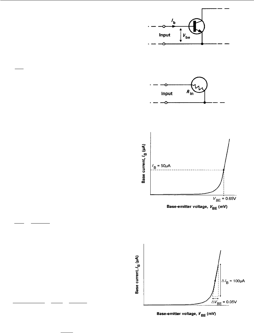
AMPLIFIERS 141
to the base, Ib.
Figure 7.21 shows the current and voltage at the
input of a common-emitter amplifier stage while
Fig. 7.22 shows how the small-signal input
resistance, Rin,appears between the base and
emitter. Note that Rin is not a discrete component it
is inside the transistor. From the foregoing we can
deduce that:
(note that this is similar to the expression for hie).
The transistor’s input characteristic can be used
to predict the input resistance of a transistor
amplifier stage. Since the input characteristic is
non-linear (recall that very little happens until the
base-emitter voltage exceeds 0.6 V), the value of
input resistance will be very much dependent on
the exact point on the graph at which the transistor
is being operated. Furthermore, we might expect
quite different values of resistance according to
whether we are dealing with larger d.c. values or
smaller incremental changes (a.c. values). Since
this can be a rather difficult concept, it is worth
expanding on it.
Figure 7.23 shows a typical input characteristic
in which the transistor is operated with a base
current, IB,of 50 µA. This current produces a base-
emitter voltage, VBE,of 0.65 V. The input
resistance corresponding to these steady (d.c.)
values will be given by:
Now, suppose that we apply a steady bias current
of, say, 70 µA and superimpose on this a signal that
varies above and below this value, swinging
through a total change of 100 µA (i.e. from 20 µA
to 120 µA). Figure 7.24 shows that this produces a
base-emitter voltage change of 0.05 V. The input
resistance seen by this small-signal input current is
given by:
In other words:
Figure 7.21 Voltage and current at the input of a
common-emitter amplifier
Figure 7.22 Input resistance of a common-emitter
amplifier stage
Figure 7.23 Using the input characteristic to
determine the large-signal (static) input resistance
of a transistor connected in common-emitter mode
Figure 7.24 Using the input characteristic to
determine the small-signal input resistance of a
transistor connected in common-emitter mode
be
in
b
=
V
R
I
BE
in
B
0.65 V
=13 k
50 µA
V
RI
==
be be
in
bb
change in 0.05 V
=500
change in 100 µA
VV
RII
== =
be
ie ie
b
=500 (since )
V
hh
I
=
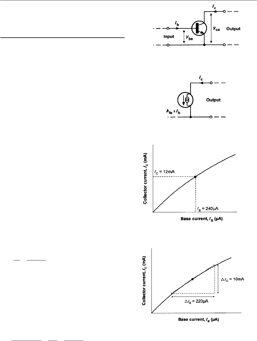
142 ELECTRONIC CIRCUITS: FUNDAMENTALS AND APPLICATIONS
It is worth comparing this value with the steady
(d.c.) value. The appreciable difference is entirely
attributable to the shape of the input characteristic!
Common-emitter current gain (hie)
The current gain produced by a transistor is the
ratio of output current to input current. In the case
of a transistor operating in common-emitter mode,
the input current is the base current, Ib,while the
output current is the collector current, Ic.
Figure 7.25 shows the small-signal input and
output currents and voltages for a common-emitter
amplifier stage. The magnitude of the current
produced at the output of the transistor is equal to
the current gain, Ai,multiplied by the applied base
current, Ib.Since the output current is the current
flowing in the collector, Ic,we can deduce that:
Ic=Ai×Ib
where Ai=hfe (the common-emitter current gain).
Figure 7.26 shows how this current source
appears between the collector and emitter. Once
again, the current source is not a discrete
component—it appears inside the transistor.
The transistor’s transfer characteristic can be used
to predict the current gain of a transistor amplifier
stage. Since the transfer characteristic is linear, the
current gain remains reasonably constant over a
range of collector current. Figure 7.27 shows a
typical transfer characteristic in which the transistor
is operated with a base current, IB,of 240 µA. This
current produces a collector current, IC,of 12 mA.
The current gain corresponding to these steady
(d.c.) values will be given by:
(note that this is similar to the expression for hfe).
Now, suppose that we apply a steady bias current
of, say, 240 µA and superimpose on this a signal
that varies above and below this value, swinging
through a total change of 220 µA (i.e. from 120 µA
to 360 µA). Figure 7.28 shows that this produces a
collector current swing of 10 mA.
The small-signal a.c. current gain is given by:
Figure 7.25 Input and output currents and voltages
in a common-emitter amplifier stage
Figure 7.26 Equivalent output current source in a
common-emitter amplifier stage
Figure 7.27 Using the transfer characteristic to
determine the large-signal (static) current gain of a
transistor connected in common-emitter mode
Figure 7.28 Using the transfer characteristic to
determine the small-signal current gain of a
transistor connected in common-emitter mode
C
i
B
2.5 mA
50
50 µA
I
AI
== =
cc
i
bb
change in 10 mA
= 45.45
change in 220 µA
II
AII
== =
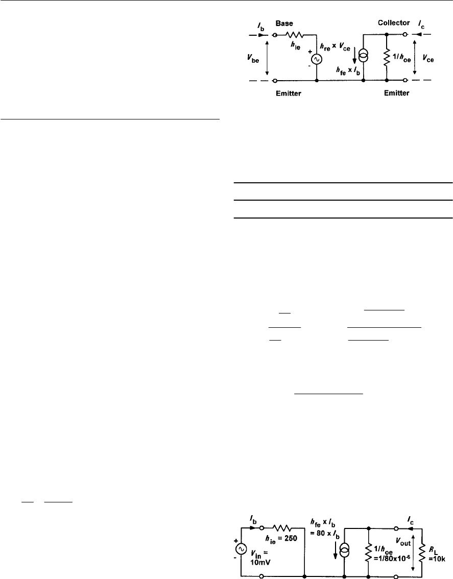
AMPLIFIERS 143
Once again, it is worth comparing this value with
the steady-state value (hFE). Since the transfer
characteristic is reasonably linear, the values are
quite close (45.45 compared with 50). However, if
the transfer characteristic was perfectly linear the
value of hfe would be exactly the same as that for
hFE.
h-parameter equivalent circuit for a
transistor in common-emitter mode
Acomplete h-parameter equivalent circuit for a
transistor operating in common-emitter mode is
shown in Fig. 7.29. We have already shown how
the two most important parameters, hie and hfe,can
be found from the transistor’s characteristic curves.
The remaining parameters, hre and hoe,can, in
many applications, be ignored. A typical set of h-
parameters for a BFY50 transistor is shown in
Table 7.6. Note how small hre and hoe are for a real
transistor!
Example 7.6
ABFY50 transistor is used in a common-emitter
amplifier stage with RL=10 kPand IC= 1 mA.
Determine the output voltage produced by an input
signal of 10 mV. (You may ignore the effect of hre
and any bias components that may be present
externally.)
Solution
The equivalent circuit (with hre replaced by a short
circuit) is shown in Fig. 7.30. The load effectively
appears between the collector and emitter while the
input signal appears between base and emitter. First
we need to find the value of input current, Ib,from:
Next we find the value of current generated, If,
from:
If=hfe × Ib=80 × 40 µA = 320 µA
This value of current is shared between the internal
resistance between collector and emitter (i.e. l/hoe)
and the external load, RL.To determine the value of
Figure 7.29 h-parameter equivalent circuit for a
transistor amplifier
collector current, we can apply the current divider
theorem (Chapter 3):
Thus:
from which:
Ic = 320 µA × 0.555 = 177.6 µA
Finally, we can determine the output voltage from:
Vout = Ic×RL=177.6 µA × 10 kP=1.776 V
in
b
ie
10 mV 40
µA
250
V
Ih
== =
Table 7.6 h-parameters for a BFY50 transistor
hie (P)hre hfe hoe (S)
250 0.85 × 10I480 35 × 10I6
Measured at IC= 1 mA, VCE = 5 V
()
()
6
oe
cf
L6
oe
1
1
80 10
320 µA
11
10 k
80 10
h
II
R
h
×
=× = ×
++
×
c
12.5 k
320 µA
12.5 k 10 k
I
=×
+
Figure 7.30 See Example 7.6
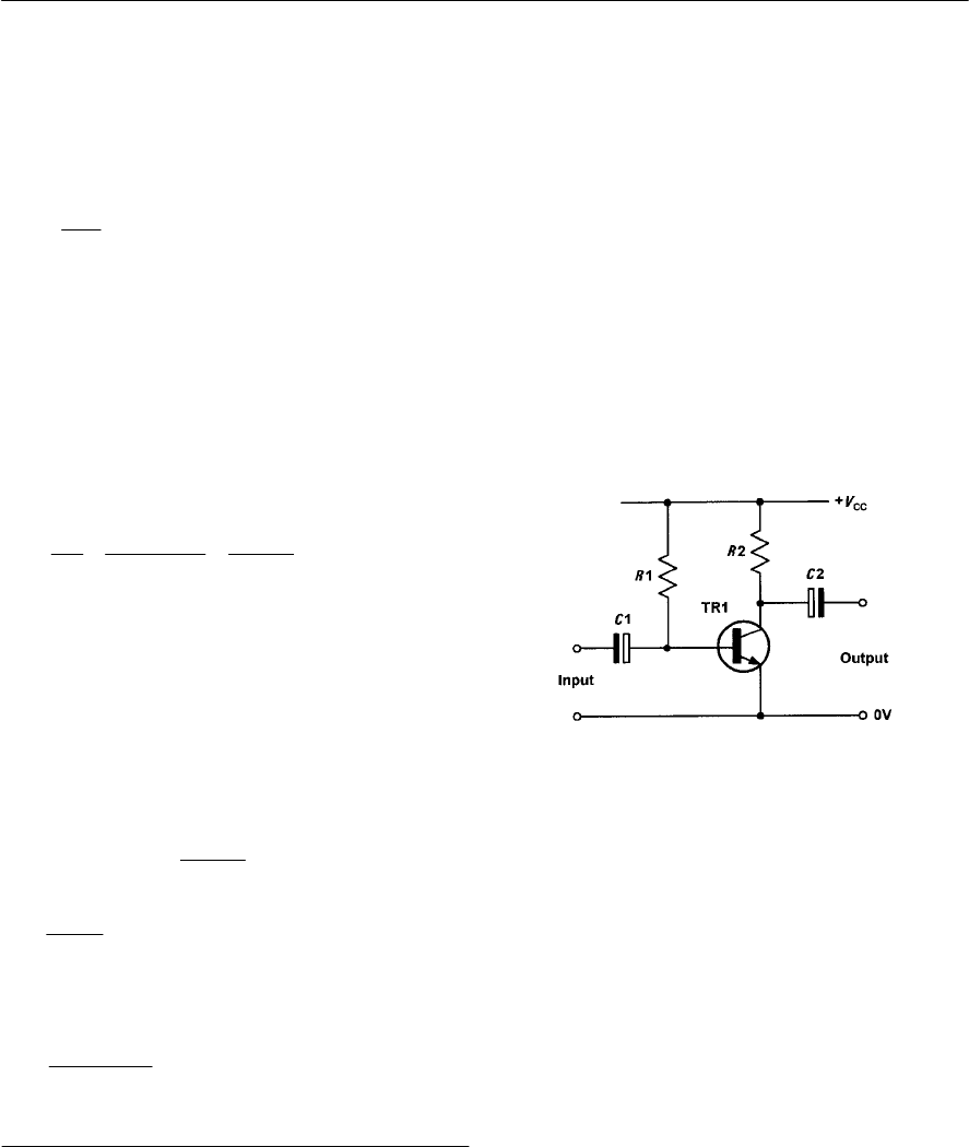
Voltage gain
We can use hybrid parameters to determine the
voltage gain of a transistor stage. We have already
shown how the voltage gain of an amplifier stage is
given by:
In the case of a common-emitter amplifier stage,
Vout =Vice and Vin = Vbe.If we assume that hoe and
hre are negligible, then:
Vout = Vce = Ic×RL= If×RL= hfe × Ib×RL
and
Vin = Vbe = Ib×Rin = Ib×hie
Thus:
Example 7.7
Atransistor has hfe = 150 and hie = 1.5 kP.
Assuming that hre and hoe are both negligible,
determine the value if load resistance required to
produce a voltage gain of 200.
Solution
Re-arranging to make RLthe subject
gives:
For a voltage gain of 200 the value of load
resistance can be determined from:
Bias
We stated earlier that the optimum value of bias for
aClass A (linear) amplifier is that value which
ensures that the active devices are operated at the
midpoint of their transfer characteristics. In
144 ELECTRONIC CIRCUITS: FUNDAMENTALS AND APPLICATIONS
out
v
in
V
A
V
=
practice, this means that a static value of collector
current will flow even when there is no signal
present. Furthermore, the collector current will
flow throughout the complete cycle of an input
signal (i.e. conduction will take place over an angle
of 360°). At no stage will the transistor be
saturated nor should it be cut-off (i.e. the state in
which no collector current flows).
In order to ensure that a static value of collector
current flows in a transistor, a small current must
therefore be applied to the base of the transistor.
This current can be derived from the same voltage
rail that supplies the collector circuit (via the load).
Figure 7.31 shows a simple Class A common-
emitter amplifier circuit in which the base bias
resistor, R1, and collector load resistor, R2, are
connected to a common positive supply rail.
The signal is applied to the base terminal of the
transistor via a coupling capacitor, C1. This
capacitor removes the d.c. component of any signal
applied to the input terminals and ensures that the
base bias current delivered by R1is unaffected by
any device connected to the input. C2couples the
signal out of the stage and also prevents d.c. current
flowing appearing at the output terminals.
In order to stabilize the operating conditions for
the stage and compensate for variations in transistor
parameters, base bias current for the transistor can
be derived from the voltage at the collector (see
Fig. 7.32). This voltage is dependent on the
collector current which, in turn, depends upon the
base current. A negative feedback loop thus exists
in which there is a degree of self-regulation. If the
collector current increases, the collector voltage
will fall and the base current will be reduced. The
out fe b L fe L
v
in b ie ie
V hIR hR
AVIh h
×× ×
== =
×
fe L
v
ie
hR
Ah
×
=
vie
L
fe
Ah
Rh
×
=
L
200 1.5 k 2 k
P
150
R×
==
Figure 7.31 Basic Class-A common-emitter
amplifier
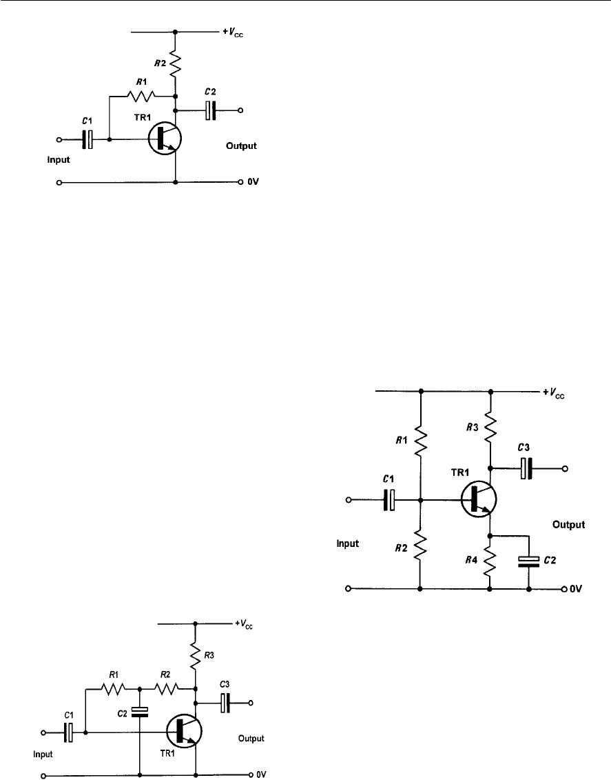
AMPLIFIERS 145
reduction in base current will produce a
corresponding reduction in collector current to
offset the original change. Conversely, if the
collector current falls, the collector voltage will rise
and the base current will increase. This, in turn,
will produce a corresponding increase in collector
current to offset the original change.
The negative feedback path in Fig. 7.32 provides
feedback that involves an a.c. (signal) component
as well as the d.c. bias. As a result of the a.c.
feedback, there is a slight reduction in signal gain.
The signal gain can be increased by removing the
a.c. signal component from the feedback path so
that only the d.c. bias component is present. This
can be achieved with the aid of a bypass capacitor
as shown in Fig. 7.33. The value of bypass
capacitor, Cl, is chosen so that the component
exhibits a very low reactance at the lowest signal
frequency when compared with the series base bias
resistance, R1. The result of this potential divider
arrangement is that the a.c. signal component is
effectively bypassed to ground.
Figure 7.34 shows an improved form of transistor
amplifier in which d.c. negative feedback is used to
stabilize the stage and compensate for variations in
transistor parameters, component values and
temperature changes. R1and R2form a potential
divider that determines the d.c. base potential, VB.
The base-emitter voltage (VBE)is the difference
between the potentials present at the base (VB)and
emitter (VE). The potential at the emitter is
governed by the emitter current (IE). If this current
increases, the emitter voltage (VE)will increase
and, as a consequence VBE will fall. This, in turn,
produces a reduction in emitter current which
largely offsets the original change. Conversely, if
the emitter current decreases, the emitter voltage
(VE)will decrease and VBE will increase (remember
that VBremains constant). The increase in bias
results in an increase in emitter current
compensating for the original change.
Example 7.8
Determine the static value of current gain and
collector voltage in the circuit shown in Fig. 7.35.
Solution
Since 2 V appears across R4, we can determine the
emitter current easily from:
Figure 7.32 An improvement on the circuit shown
in Fig. 7.31 (using negative feedback to bias the
transistor)
Figure 7.33 Improved version of Fig. 7.31
Figure 7.34 A common-emitter amplifier stage
with effective bias stabilization
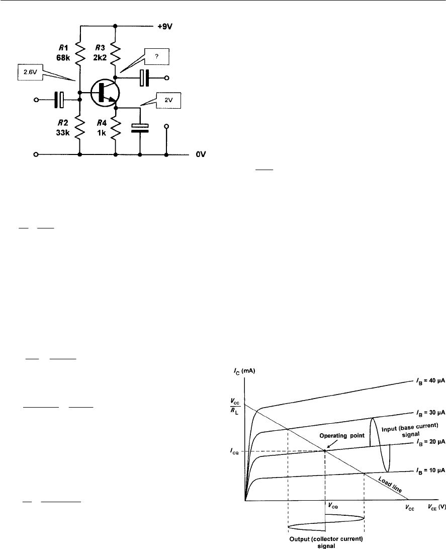
Next we should determine the base current. This is
alittle more difficult. The base current is derived
from the potential divider formed by R1and R2.
The potential at the junction of R1and R2is 2.6 V
hence we can determine the currents through R1
and R2, the difference between these currents will
be equal to the base current.
The current in R2will be given by:
The current in R1will be given by:
Hence the base current is found from:
IB=94.1 µA I79 µA =15.1 µA
Next we can determine the collector current
from:
Finally we can determine the collector voltage by
subtracting the voltage dropped across R3from the
9 V supply.
The voltage dropped across R3will be:
VR4 = IC×R4 = 2.0151 mA × 2.2 kP=4.43 V
Hence VC= 9 V I4.43 V = 4.57 V
146 ELECTRONIC CIRCUITS: FUNDAMENTALS AND APPLICATIONS
E
E
4
2 V
2mA
1 k
V
IR
== =
Predicting amplifier performance
The a.c. performance of an amplifier stage can be
predicted using a load line superimposed on the
relevant set of output characteristics. For a bipolar
transistor operating in common-emitter mode the
required characteristics are ICplotted against VCE
One end of the load line corresponds to the supply
voltage (VCC)while the other end corresponds to
the value of collector or drain current that would
flow with the device totally saturated. In this
condition:
where REis the value of collector or drain load
resistance.
Figure 7.36 shows a load line superimposed on a
set of output characteristics for a bipolar transistor
operating in common-emitter mode. The quiescent
point (or operating point) is the point on the load
line that corresponds to the conditions that exist
when no-signal is applied to the stage. In Fig. 7.36,
the base bias current is set at 20 µA so that the
quiescent point effectively sits roughly halfway
along the load line. This position ensures that the
collector voltage can swing both positively (above)
and negatively (below) its quiescent value (VCQ).
Figure 7.35 See Example 7.8
B
R2
2.6 V 79
µA
233 k
V
IR
== =
B
R1
9 V 6.4 V 94.1
µA
168 k
V
IR
===
C
FE
B
2.0151 mA
133.45
15.1 µA
I
hI
== =
CC
C
L
V
I
R
=
Figure 7.36 Operating point and quiescent values
shown on the load line for a bipolar transistor
operating in common-emitter mode
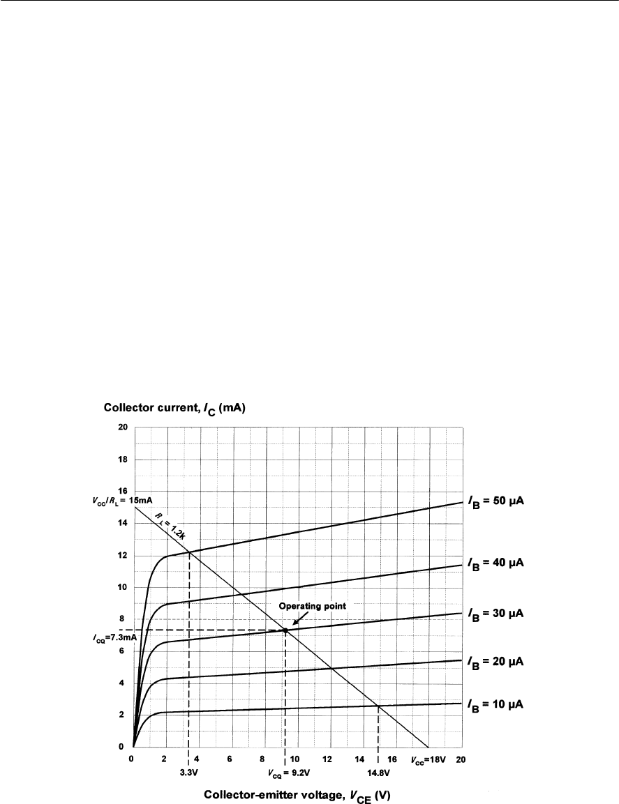
AMPLIFIERS 147
The effect of superimposing an alternating base
current (of 20 µA peak-peak) to the d.c. bias
current (of 20 µA) can be clearly seen. The
corresponding collector current signal can be
determined by simply moving up and down the
load line.
Example 7.9
The characteristic curves shown in Fig. 7.37 relate
to a transistor operating in common-emitter mode.
If the transistor is operated with IB=30 µA, a load
resistor of 1.2 kPand an 18 V supply, determine
the quiescent values of collector voltage and
current (VCQ and ICQ). Also determine the peak-
peak output voltage that would be produced by an
input signal of 40 µA peak-peak.
Solution
First we need to construct the load line. The two
ends of the load line will correspond to VCC (18 V)
on the collector-emitter voltage axis and (18V/1.2
kPor 15 mA) on the collector current axis. Next
we locate the operating point (or quiescent point)
from the point of intersection of the IB=30 µA
characteristic and the load line.
Having located the operating point we can read
off the quiescent (no-signal) values of collector
emitter voltage (VCQ)and collector current (ICQ).
Hence:
VCQ =9.2 V and ICQ =7.3 mA
Next we can determine the maximum and
minimum values of collector-emitter voltage by
locating the appropriate intercept points on Fig.
7.37.
Note that the maximum and minimum values of
base current will be (30 µA + 20 µA) on positive
peaks of the signal and (30 µA I20 µA) on
negative peaks of the signal. The maximum and
minimum values of VCE are, respectively, 14.8 V
and 3.3 V. Hence the output voltage swing will be
(14.8 V I3. 3 V) or 11.5 V peak-peak.
Figure 7.37 See Example 7.9
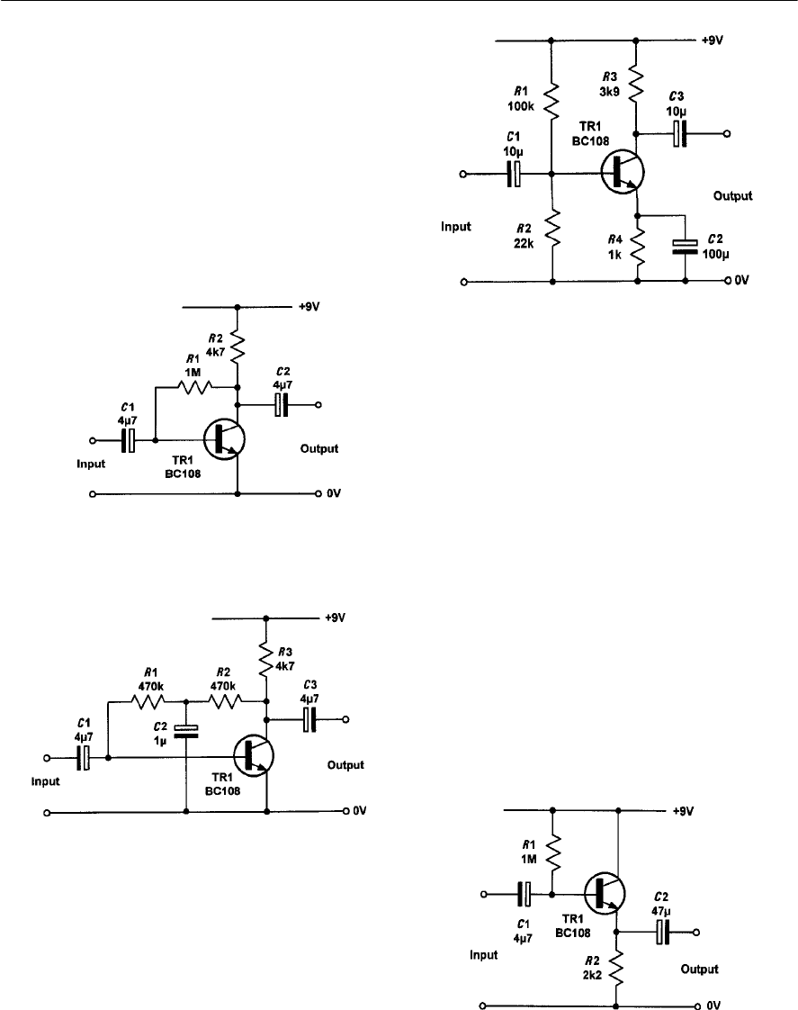
148 ELECTRONIC CIRCUITS: FUNDAMENTALS AND APPLICATIONS
Practical amplifier circuits
The simple common-emitter amplifier stage shown
in Fig. 7.38 provides a modest voltage gain (80 to
120 typical) with an input resistance of
approximately 1.5 kPand an output resistance of
around 20 kP.The frequency response extends
from a few hertz to several hundred kilohertz. The
improved arrangement shown in Fig. 7.38 provides
avoltage gain of around 150 to 200 by eliminating
the signal frequency negative feedback that occurs
through R1in Fig. 7.39.
Figure 7.41 A practical emitter-follower stage
Figure 7.40 shows a practical common-emitter
amplifier with bias stabilization. This stage
provides a gain of 150 to well over 200 (depending
upon the current gain, hie,of the individual
transistor used). The circuit will operate with
supply voltages of between 6 V and 18 V.
Two practical emitter-follower circuits are shown
in Figs 7.41 and 7.42. These circuits offer a voltage
gain of unity (1) but are ideal for matching a high
resistance source to a low resistance load. It is
important to note that the input resistance varies
with the load connected to the output of the circuit
(it is typically in the range 50 kPto 150 kP). The
input resistance can be calculated by multiplying hfe
by the effective resistance of R2in parallel with the
load connected to the output terminals.
Figure 7.42 is an improved version of Fig. 7.41
in which the base current is derived from the
potential divider formed by R1and R2. Note,
however, that the input resistance is reduced since
R1and R2effectively appear in parallel with the
input. The input resistance of the stage is thus
typically in the region of 40 kPto 70 kP.
Figure 7.38 A practical common-emitter
amplifier stage
Figure 7.39 An improved version of the
common-emitter amplifier stage
Figure 7.40 Operating point and quiescent values
shown on the load line for a bipolar transistor
operating in common-emitter mode
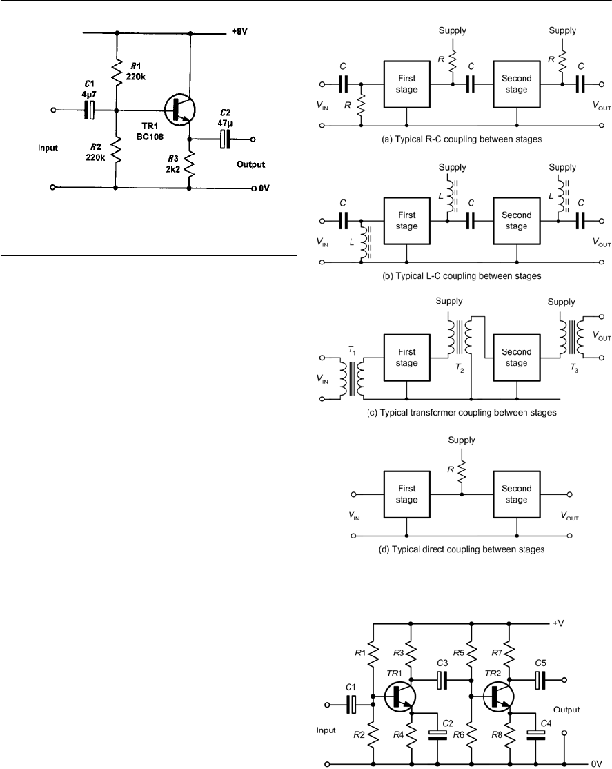
AMPLIFIERS 149
Figure 7.42 An improved emitter-follower stage
Figure 7.43 Different methods used for inter-
stage coupling
Figure 7.44 A typical two-stage high-gain R–C
coupled common-emitter amplifier
Multi-stage amplifiers
In order to provide sufficiently large values of gain,
it is frequently necessary to use a number of
interconnected stages within an amplifier. The
overall gain of an amplifier with several stages (i.e.
amulti-stage amplifier) is simply the product of the
individual voltage gains. Hence:
AV= AV1 × AV2 × AV3 etc.
Note, however, that the bandwidth of a multi-stage
amplifier will be less than the bandwidth of each
individual stage. In other words, an increase in gain
can only be achieved at the expense of a reduction
in bandwidth.
Signals can be coupled between the individual
stages of a multi-stage amplifier using one of a
number of different methods shown in Fig. 7.43.
The most commonly used method is that of R–C
coupling as shown in Fig. 7.43(a). In this coupling
method, the stages are coupled together using
capacitors having a low reactance at the signal
frequency and resistors (which also provide a
means of connecting the supply). Figure 7.44
shows a practical example of this coupling method.
A similar coupling method, known as L–C
coupling,is shown in Fig. 7.43(b). In this method,
the inductors have a high reactance at the signal
frequency. This type of coupling is generally only
used in RF and high-frequency amplifiers.
Two further methods, transformer coupling and
direct coupling are shown in Figures 7.43(c) and
7.43(d) respectively. The latter method is used
where d.c. levels present on signals must be
preserved.
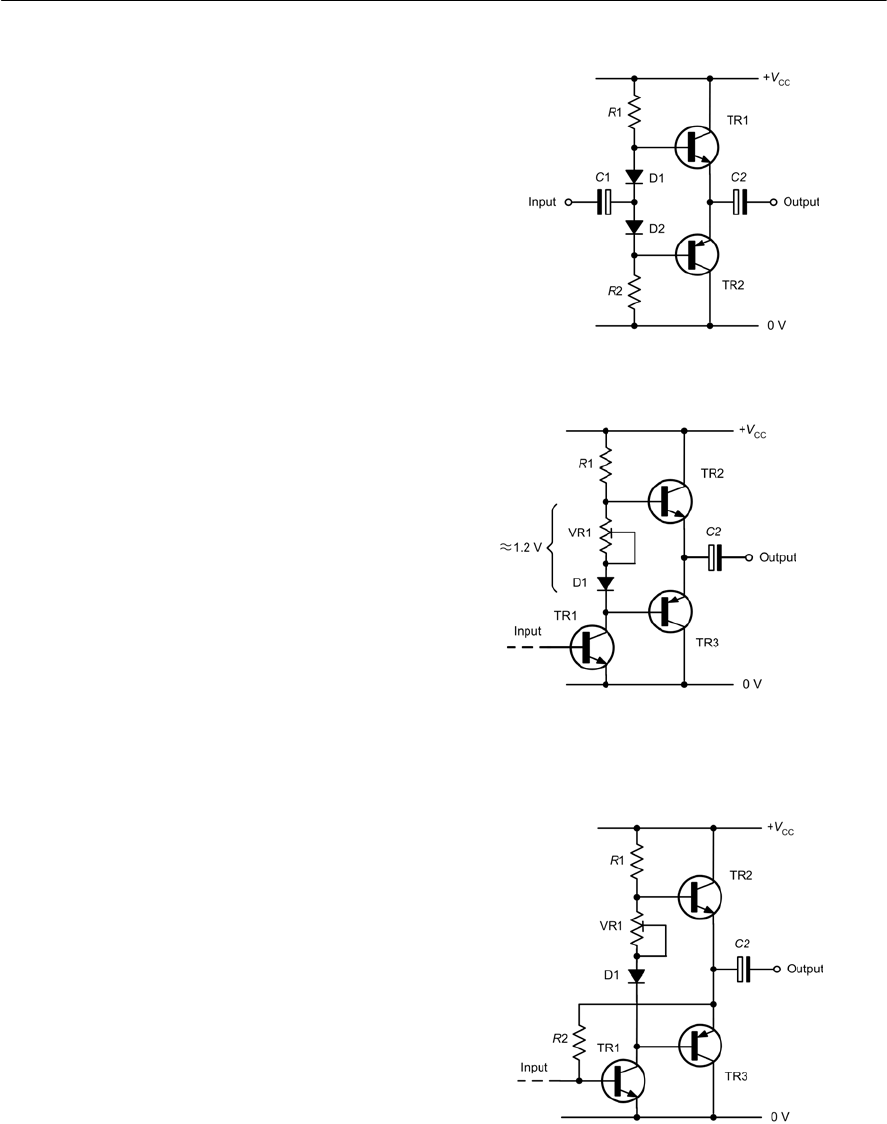
150 ELECTRONIC CIRCUITS: FUNDAMENTALS AND APPLICATIONS
Power amplifiers
The term ‘power amplifier’ can be applied to any
amplifier that is designed to deliver an appreciable
level of power. There are several important
considerations for amplifiers of this type, including
the ability to deliver current (as well as voltage) to
aload, and also the need to operate with a
reasonable degree of efficiency (recall that
conventional Class A amplifiers are inefficient).
In order to deliver sufficient current to the load,
power amplifiers must have a very low value of
output impedance. Thus the final stage (or output
stage)is usually based on a device operating in
emitter-follower configuration. In order to operate
at a reasonable level of efficiency, the output stage
must operate in Class AB or Class B mode (see
page 133). One means of satisfying both of these
requirements is with the use of a symmetrical
output stage based on complementary NPN and
PNP devices.
A simple complementary output stage is
shown in Fig. 7.45. TR1 is a suitably rated NPN
device whilst TR2 is an identically rated PNP
device. Both TR1 and TR2 operate as emitter
followers (i.e. common-collector mode) with the
output taken from the two emitters, coupled via C2
to the load. In order to bias TR1 and TR2 into Class
AB mode two silicon diodes (D1 and D2) are used
to provide a constant voltage drop of approximately
1.2 V between the two bases. This voltage drop is
required between the bases of TR1 and TR2 in
order to bring them to conduction. Since D1 and
D2 are both in forward conduction (with current
supplied via R1and R2) they have little effect on
the input signal (apart from shifting the d.c. level).
Figure 7.46 shows an improvement of the basic
complementary output stage with the addition of a
driver stage (TR1) and a means of adjusting the
bias (i.e. operating point) of the two output
transistors. VR1 is typically adjusted in order to
produce an output stage collector current of
between 15 mA and 50 mA (required for Class AB
operation). With VR1 set to minimum resistance,
the output stage will operate in Class B (this will
produce significantly more cross-over distortion
because the two devices may both be cut-off for a
brief period of each cycle). Figure 7.47 shows how
negative feedback bias (via R2) can be added in
order to stabilize the output stage. Practical power
amplifiers are shown in Figs 7.48 and 7.49.
Figure 7.45 A complementary output stage
Figure 7.46 A complementary output stage with
adjustable bias for the output transistors
Figure 7.47 A complementary output stage with
stabilized bias for the driver stage
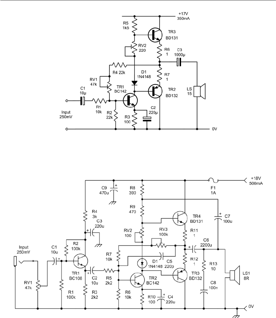
AMPLIFIERS 151
Figure 7.49 An improved 3 W audio amplifier. This amplifier has a nominal input resistance of 50 kPand
afrequency response extending from 30 Hz to 30 kHz at the I3dB power points. Capacitor C5 is added to
‘roll-off’ the high frequency response (without this component the high-frequency response extends to
around 100 kHz). RV2 is adjusted for a quiescent (no-signal) collector current for TR3 (and TR4) of 25 mA.
RV3 is adjusted for a d.c. voltage of exactly 9 V at the junction of the two low-value thermal compensating
resistors, R11 and R12. C8 and R13 form a Zobel network to provide frequency compensation of the output
load.
Figure 7.48 A simple power amplifier based on a Class AB complementary output stage and Class A
driver stage. This amplifier provides an output of 3 W into an 8 ohm load and has a frequency response
extending from 20 Hz to 50 kHz. Total harmonic distortion (THD) is less than 0.2% at 250 mW output. An
input of 2 V peak-peak is required for full output.
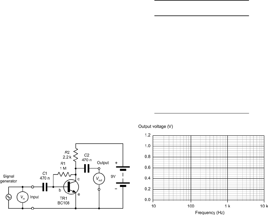
152 ELECTRONIC CIRCUITS: FUNDAMENTALS AND APPLICATIONS
Figure 7.51 Graph layout for plotting the results
Practical investigation
Objective
To measure the voltage gain and low-frequency
response of a simple common-emitter amplifier
stage.
Components and test equipment
Breadboard, d.c. voltmeter (preferably digital), AF
signal generator (with variable frequency sine wave
output), two AF voltmeters (or a dual beam
oscilloscope), 9 V d.c. power supply (or battery),
BC108 (or similar) NPN transistor, two 470 nF and
two 10 µF capacitors, resistors of 1 MPand 2.2 kP
5% 0.25 W, test leads, connecting wire.
Procedure
Connect the circuit shown in Fig. 7.50. Without the
signal generator connected, measure and record the
no-signal d.c. collector, base and emitter voltages
for TR1 (the collector voltage should be in the
range 3 V to 6 V). Connect the signal generator and
set it to produce a sine wave output at 1 kHz.
Increase the output voltage from the signal
generator until the input voltmeter reads exactly 10
mV. Measure and record the output signal voltage
(see Table 7.7).
Repeat at frequencies over the range 10 Hz to
10 kHz, at each stage recording the output voltage
produced in the table. Replace C1and C2with
10 µF capacitors and repeat the measurements.
Measurements and calculations
Use the measured value of output voltage at 1 kHz
in order to determine the voltage gain of the stage.
Figure 7.50 Transistor test circuit
Table 7.7 Results
Graphs
For each set of measurements (470 nF and 10 µF
for C1and C2) plot a graph showing the frequency
response of the amplifier stage. In each case, use
the graph to determine the low-frequency cut-off.
Conclusion
Comment on the no-signal voltages measured at the
collector, base and emitter. Are these what you
would expect? Comment on the value of voltage
gain that you have obtained. Is this what you would
expect? Comment on the shape of each frequency
response graph. Explain why there is a difference in
cut-off frequency.
Frequency (Hz)
10
20
50
100
200
500
1 k
2 k
5 k
10 k
Output voltage (V)
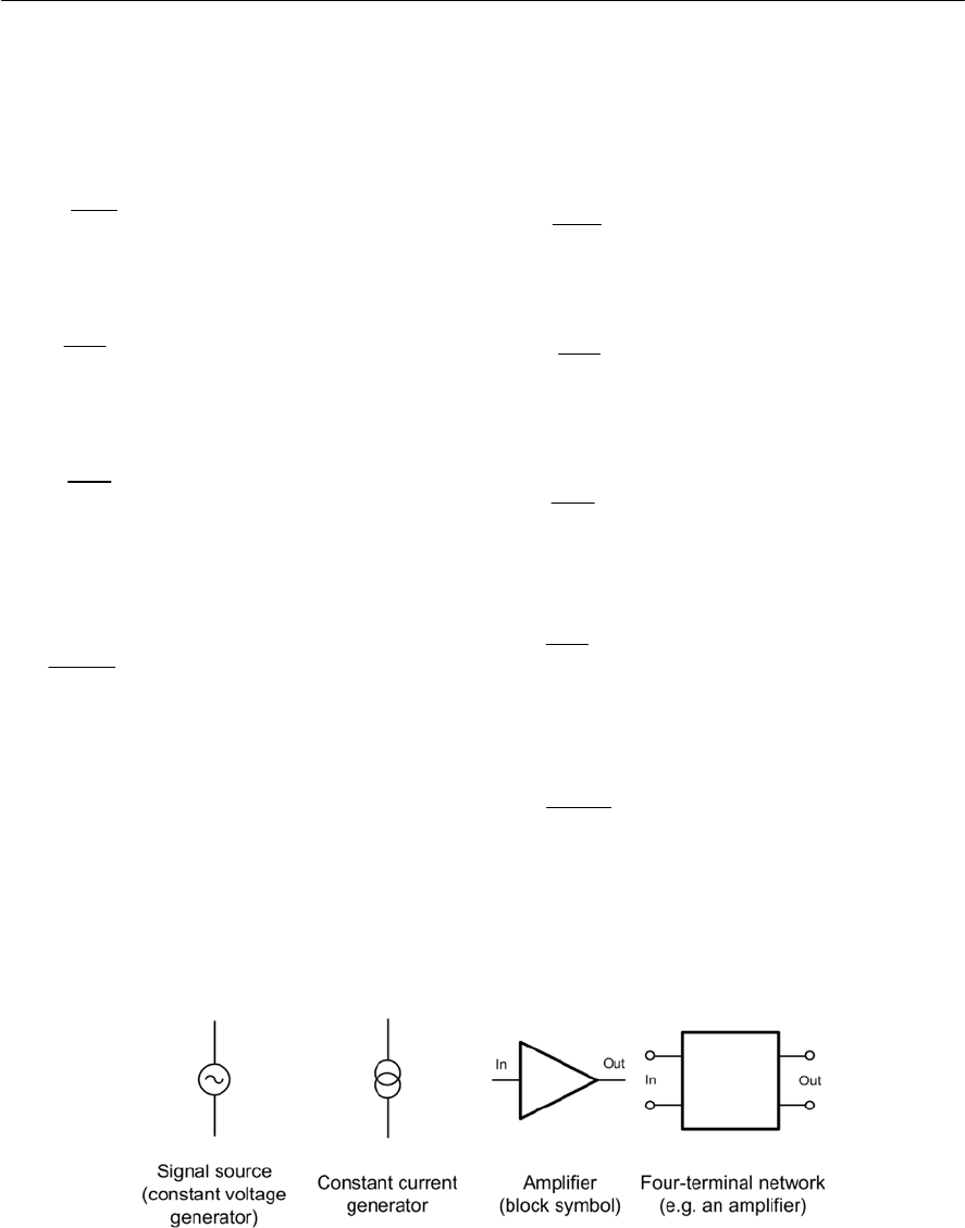
AMPLIFIERS 153
Loop gain:
(page 137)
Gloop =J×Av.
Input resistance (common-emitter):
(page 140)
Forward current transfer ratio (common-emitter):
(page 140)
Output conductance (common-emitter):
(page 140)
Reverse voltage transfer ratio (common-emitter):
(page 140)
Voltage gain (common-emitter) assuming hre and
hoe can be neglected:
(page 142)
Important formulae introduced in this
chapter
Voltage gain:
(page 132)
Current gain:
(page 132)
Power gain:
(page 132)
Gain with negative feedback applied:
(page 137)
Gain (when Avis very large):
(page 137)
G=1/J
Figure 7.52 Circuit symbols introduced in this chapter
Symbols introduced in this chapter
out
v
in
V
A
V
=
out
i
in
I
A
I
=
out
p
in
P
A
P
=
piv
AAA
=×
v
v
1
J
A
G
A
=+
be
re
ce
V
h
V
=
c
fe
b
I
h
I
=
c
oe
ce
I
h
V
=
fe L
v
ie
hR
Ah
×
=
be
ie
b
V
h
I
=
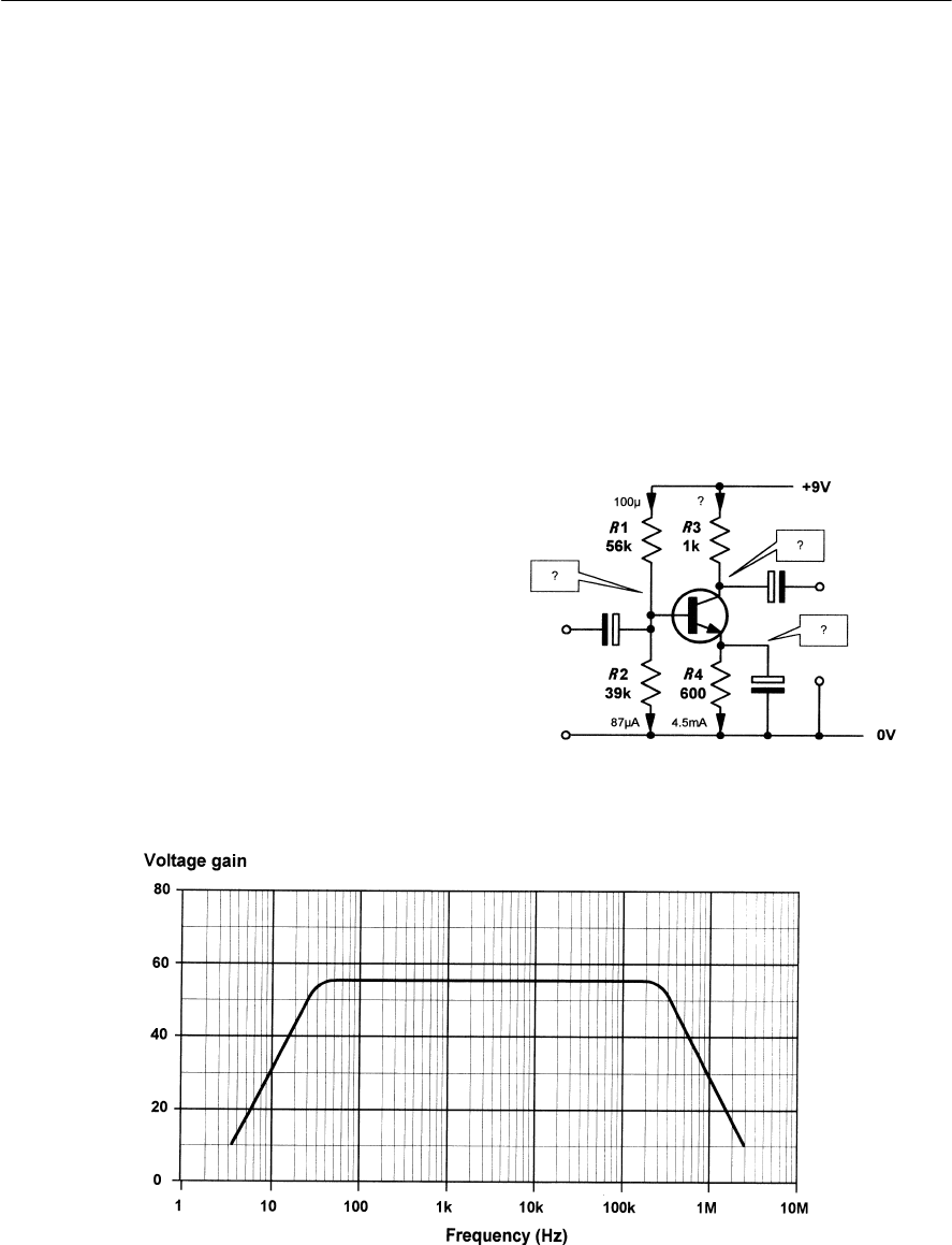
154 ELECTRONIC CIRCUITS: FUNDAMENTALS AND APPLICATIONS
Problems
7.1 The following measurements were made
during a test on an amplifier:
Vin = 250 mV, Iin = 2.5 mA,
Vout = 10 V, Iout = 400 mA
Determine:
(a) the voltage gain;
(b) the current gain;
(c) the power gain;
(d) the input resistance.
7.2 An amplifier has a power gain of 25 and
identical input and output resistances of
600 P.Determine the input voltage required
to produce an output of 10 V.
7.3 Determine the mid-band voltage gain and
upper and lower cut-off frequencies for the
amplifier whose frequency response curve is
shown in Fig. 7.53. Also determine the
voltage gain at frequencies of:
(a) 10 Hz
(b) 1 MHz
7.4 An amplifier with negative feedback applied
has an open-loop voltage gain of 250, and
5% of its output is fed back to the input.
Determine the overall voltage gain with
negative feedback applied. If the open-loop
voltage gain increases by 20% determine the
new value of overall voltage gain.
7.5 An amplifier produces an open-loop gain of
180. Determine the amount of feedback
required if it is to be operated with a precise
voltage gain of 50.
7.6 A transistor has the following parameters:
hie = 800 P
hre = negligible
hfe =120
hoe =50 µS.
If the transistor is to be used as the basis of a
common-emitter amplifier stage with
RL=12 kP,determine the output voltage
when an input signal of 2 mV is applied.
7.7 Determine the unknown current and
voltages in Fig. 7.54.
Figure 7.53 See Question 7.3
Figure 7.54 See Question 7.7
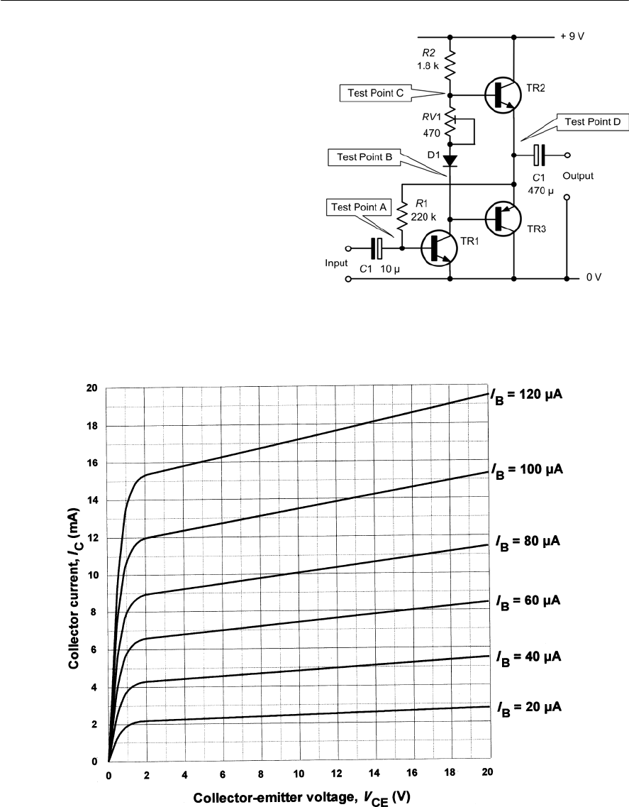
AMPLIFIERS 155
7.8 The output characteristics of a bipolar
transistor are shown in Fig. 7.55. If this
transistor is used in an amplifier circuit
operating from a 12 V supply with a base
bias current of 60 µA and a load resistor of
1 kP,determine the quiescent values of
collector-emitter voltage and collector
current. Also determine the peak-peak
output voltage produced when an 80 µA
peak-peak signal current is applied to the
base of the transistor.
7.9 Figure 7.56 shows a simple audio power
amplifier in which all of the semiconductor
devices are silicon and all three transistors
have an hFE of 100. If RV1is adjusted to
produce 4.5 V at Test Point D, determine
the base, emitter and collector currents and
voltages for each transistor and the voltages
that will appear at Test Points A to C.
Figure 7.55 See Question 7.8
Figure 7.56 See Questions 7.9, 7.12 and 7.13
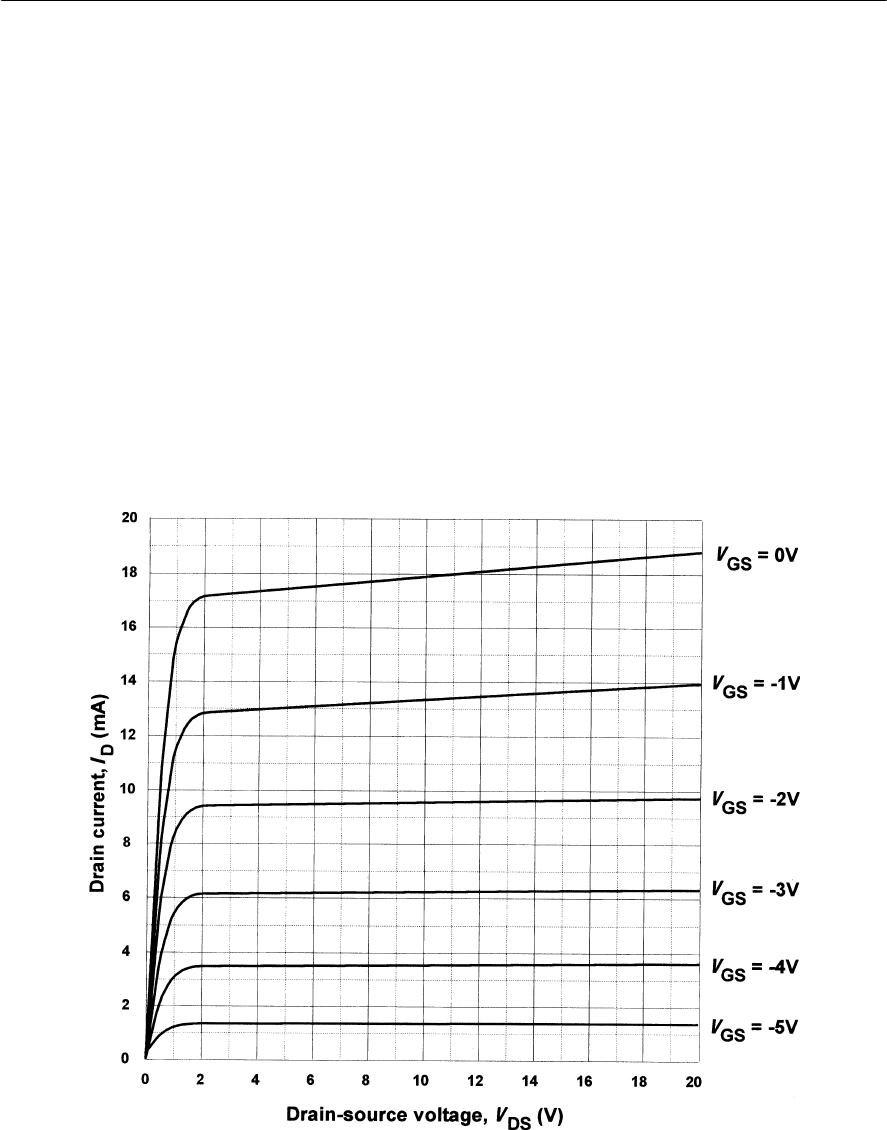
156 ELECTRONIC CIRCUITS: FUNDAMENTALS AND APPLICATIONS
7.10 The output characteristics of a junction
gate field effect transistor are shown in
Fig. 7.57. If this JFET is used in an
amplifier circuit operating from an 18V
supply with a gate-source bias voltage of
I3 V and a load resistor of 900 P,
determine the quiescent values of drain-
source voltage and drain current. Also
determine the peak-peak output voltage
when an input voltage of 2 V peak-peak is
applied to the gate. Also determine the
voltage gain of the stage.
7.11 A multi-stage amplifier consists of two
R–C coupled common-emitter stages. If
each stage has a voltage gain of 50,
determine the overall voltage gain. Draw
a circuit diagram of the amplifier and label
your drawing clearly.
Figure 7.57 See Question 7.10
7.12 The following RMS voltage measurements
were made during a signal test on the simple
power amplifier shown in Fig. 7.56 when
connected to a 15 Pload:
Vin = 50 mV
Vout = 2 V
Determine:
(a) the voltage gain
(b) the output power
(c) the output current.
7.13 If the power amplifier shown in Fig. 7.56
produces a maximum RMS output power of
0.25 W, determine its overall efficiency if
the supply current is 75 mA. Also determine
the power dissipated in each of the output
transistors in this condition.
Answers to these problems appear on page 375.
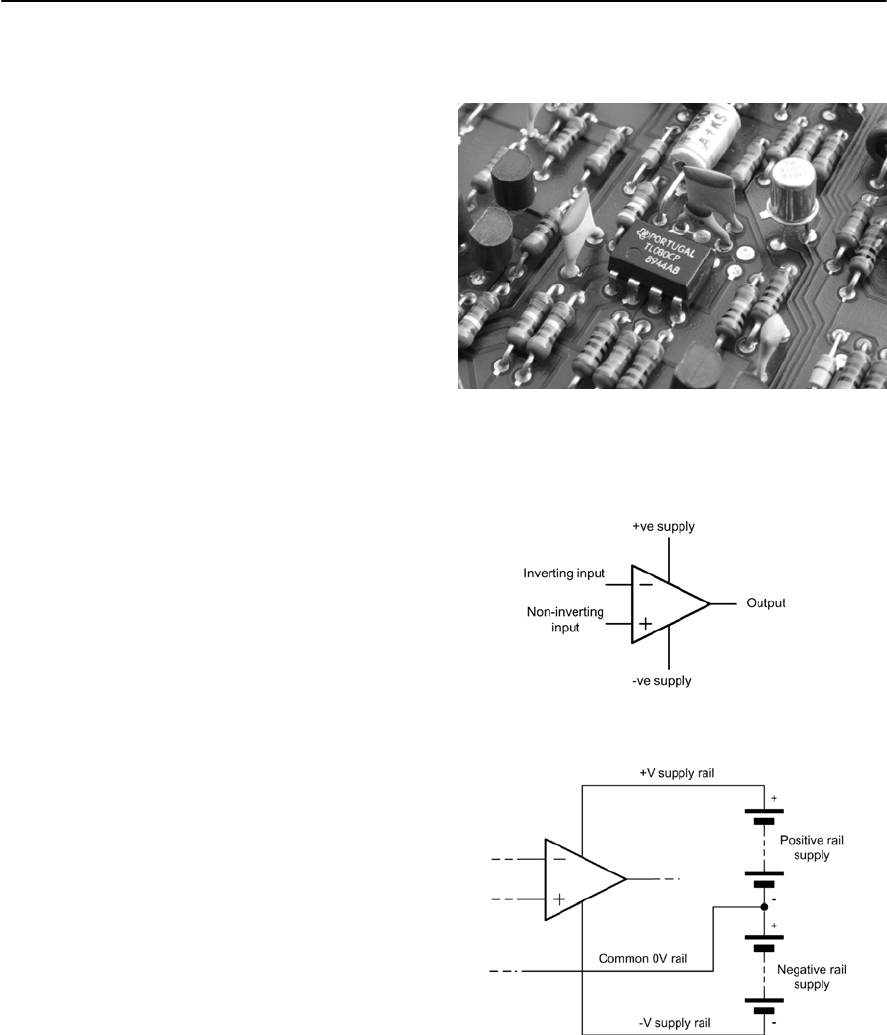
8
Operational amplifiers
Operational amplifiers are analogue integrated
circuits designed for linear amplification that offer
near-ideal characteristics (virtually infinite voltage
gain and input resistance coupled with low output
resistance and wide bandwidth).
Operational amplifiers can be thought of as
universal ‘gain blocks’ to which external
components are added in order to define their
function within a circuit. By adding two resistors,
we can produce an amplifier having a precisely
defined gain. Alternatively, with two resistors and
two capacitors we can produce a simple band-pass
filter. From this you might begin to suspect that
operational amplifiers are really easy to use. The
good news is that they are!
Symbols and connections
The symbol for an operational amplifier is shown
in Fig. 8.2. There are a few things to note about
this. The device has two inputs and one output and
no common connection. Furthermore, we often
don’t show the supply connections—it is often
clearer to leave them out of the circuit altogether!
In Fig. 8.2, one of the inputs is marked ‘*’and
the other is marked ‘+’. These polarity markings
have nothing to do with the supply connections—
they indicate the overall phase shift between each
input and the output. The ‘+’ sign indicates zero
phase shift whilst the ‘*’sign indicates 180° phase
shift. Since 180° phase shift produces an inverted
waveform, the ‘*’input is often referred to as the
inverting input.Similarly, the ‘+’ input is known
as the non-inverting input.
Most (but not all) operational amplifiers require
asymmetrical supply (of typically ±6 V to ±15 V)
which allows the output voltage to swing both
positive (above 0 V) and negative (below 0 V).
Figure 8.3 shows how the supply connections
would appear if we decided to include them. Note
that we usually have two separate supplies; a
positive supply and an equal, but opposite, negative
Figure 8.1 A typical operational amplifier. This
device is supplied in an 8-pin dual-in-line (DIL)
package. It has a JFET input stage and produces a
typical open-loop voltage gain of 200,000
Figure 8.2 Symbol for an operational amplifier
Figure 8.3 Supply connections for an operational
amplifier

applied). The effect of providing negative feedback
is to reduce the loop voltage gain to a value that is
both predictable and manageable. Practical closed-
loop voltage gains range from one to several
thousand but note that high values of voltage gain
may make unacceptable restrictions on bandwidth,
see later.
Closed-loop voltage gain is once again the ratio
of output voltage to input voltage but with negative
feedback is applied, hence:
where AV(CL) is the open-loop voltage gain, VOUT
and VIN are the output and input voltages
respectively under closed-loop conditions. The
closed-loop voltage gain is normally very much
less than the open-loop voltage gain.
Example 8.1
An operational amplifier operating with negative
feedback produces an output voltage of 2 V when
supplied with an input of 400 µV. Determine the
value of closed-loop voltage gain.
Solution
Now:
Thus:
Expressed in decibels (rather than as a ratio) this is:
Input resistance
The input resistance of an operational amplifier is
defined as the ratio of input voltage to input current
expressed in ohms. It is often expedient to assume
that the input of an operational amplifier is purely
resistive though this is not the case at high
frequencies where shunt capacitive reactance may
become significant. The input resistance of
158 ELECTRONIC CIRCUITS: FUNDAMENTALS AND APPLICATIONS
supply. The common connection to these two
supplies (i.e., the 0 V supply connection) acts as the
common rail in our circuit. The input and output
voltages are usually measured relative to this rail.
Operational amplifier parameters
Before we take a look at some of the characteristics
of ‘ideal’ and ‘real’ operational amplifiers it is
important to define some of the terms and
parameters that we apply to these devices.
Open-loop voltage gain
The open-loop voltage gain of an operational
amplifier is defined as the ratio of output voltage to
input voltage measured with no feedback applied.
In practice, this value is exceptionally high
(typically greater than 100,000) but is liable to
considerable variation from one device to another.
Open-loop voltage gain may thus be thought of
as the ‘internal’ voltage gain of the device, thus:
where AV(OL) is the open-loop voltage gain, VOUT
and VIN are the output and input voltages
respectively under open-loop conditions.
In linear voltage amplifying applications, a large
amount of negative feedback will normally be
applied and the open-loop voltage gain can be
thought of as the internal voltage gain provided by
the device.
The open-loop voltage gain is often expressed in
decibels (dB)rather than as a ratio. In this case:
Most operational amplifiers have open-loop voltage
gains of 90 dB, or more.
Closed-loop voltage gain
The closed-loop voltage gain of an operational
amplifier is defined as the ratio of output voltage to
input voltage measured with a small proportion of
the output fed back to the input (i.e. with feedback
6
V(CL) 6
2210
5, 000
400400 10
A
×
===
×
OUT
V(CL)
IN
V
A
V
=
OUT
V(OL)
IN
V
A
V
=
OUT
V(OL) 10
IN
20 log V
A
V
=
V(CL) 10
20log (5,000) 20 3.7 74 dB
A==×=
OUT
V(CL)
IN
V
A
V
=

OPERATIONAL AMPLIFIERS 159
operational amplifiers is very much dependent on
the semiconductor technology employed. In
practice values range from about 2 MGfor
common bipolar types to over 1012 Gfor FET and
CMOS devices.
Input resistance is the ratio of input voltage to
input current:
where RIN is the input resistance (in ohms), VIN is
the input voltage (in volts) and IIN is the input
current (in amps). Note that we usually assume that
the input of an operational amplifier is purely
resistive though this may not be the case at high
frequencies where shunt capacitive reactance may
become significant.
The input resistance of operational amplifiers is
very much dependent on the semiconductor
technology employed. In practice, values range
from about 2 MGfor bipolar operational amplifiers
to over 1012 Gfor CMOS devices.
Example 8.2
An operational amplifier has an input resistance of
2 MGDetermine the input current when an input
voltage of 5 mV is present.
Solution
Now:
thus
Output resistance
The output resistance of an operational amplifier is
defined as the ratio of open-circuit output voltage
to short-circuit output current expressed in ohms.
Typical values of output resistance range from less
than 10 Gto around 100 Gdepending upon the
configuration and amount of feedback employed.
Output resistance is the ratio of open-circuit
output voltage to short-circuit output current,
hence:
where ROUT is the output resistance (in ohms),
VOUT(OC) is the open-circuit output voltage (in volts)
and IOUT(SC) is the short-circuit output current (in
amps).
Input offset voltage
An ideal operational amplifier would provide zero
output voltage when 0 V difference is applied to its
inputs. In practice, due to imperfect internal
balance, there may be some small voltage present at
the output. The voltage that must be applied
differentially to the operational amplifier input in
order to make the output voltage exactly zero is
known as the input offset voltage.
Input offset voltage may be minimized by
applying relatively large amounts of negative
feedback or by using the offset null facility
provided by a number of operational amplifier
devices. Typical values of input offset voltage
range from 1 mV to 15 mV. Where AC rather than
DC coupling is employed, offset voltage is not
normally a problem and can be happily ignored.
Full-power bandwidth
The full-power bandwidth for an operational
amplifier is equivalent to the frequency at which
the maximum undistorted peak output voltage
swing falls to 0.707 of its low frequency (d.c.)
value (the sinusoidal input voltage remaining
constant). Typical full-power bandwidths range
from 10 kHz to over 1 MHz for some high-speed
devices.
Slew rate
Slew rate is the rate of change of output voltage
with time, when a rectangular step input voltage is
applied (as shown in Fig. 8.4). The slew rate of an
operational amplifier is the rate of change of output
voltage with time in response to a perfect step-
function input. Hence:
IN
IN
IN
V
R
I
=
3
9
IN
IN 6
IN
510
2.5 10 A = 2.5 nA
210
V
IR
×
== =×
×
OUT(OC)
OUT
OUT(SC)
V
RI
=
OUT
Slew rate V
t
=
IN
IN
IN
V
R
I
=
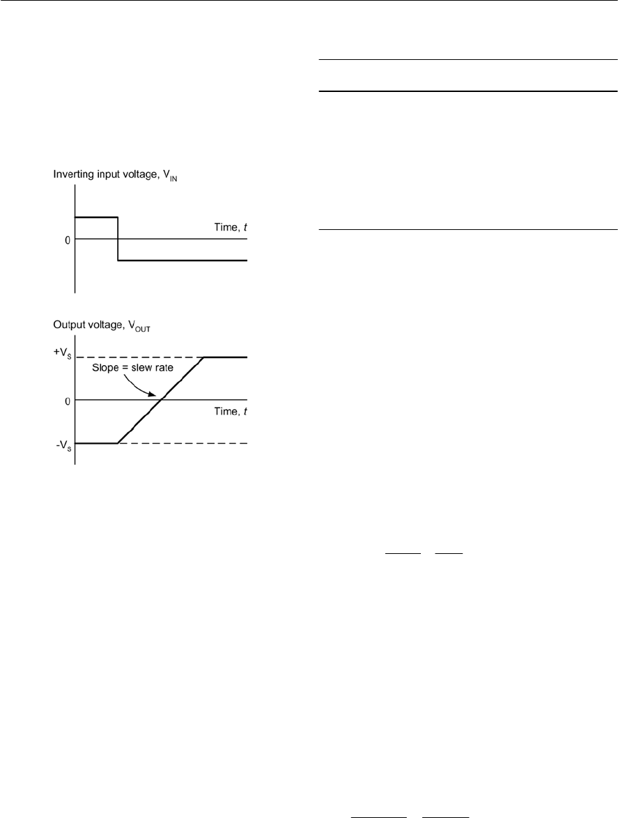
160 ELECTRONIC CIRCUITS: FUNDAMENTALS AND APPLICATIONS
where KVOUT is the change in output voltage (in
volts) and Ktis the corresponding interval of time
(in s).
Slew rate is measured in V/s (or V/µs) and
typical values range from 0.2 V/µs to over 20 V/µs.
Slew rate imposes a limitation on circuits in which
large amplitude pulses rather than small amplitude
sinusoidal signals are likely to be encountered.
Parameter Ideal Real
Voltage Gain Infinite 100,000
Input Resistance Infinite 100 MG
Output resistance Zero 20 G
Bandwidth Infinite 2 MHz
Slew-rate Infinite 10 V/µs
Input offset Zero Less than 5 mV
Table 8.1 Comparison of operational amplifier
parameters for ‘ideal’ and ‘real’ devices
Figure 8.4 Slew rate for an operational amplifier
Operational amplifier characteristics
Having now defined the parameters that we use to
describe operational amplifiers we shall now
consider the desirable characteristics for an ‘ideal’
operational amplifier. These are:
(a) The open-loop voltage gain should be very high
(ideally infinite).
(b) The input resistance should be very high
(ideally infinite).
(c) The output resistance should be very low
(ideally zero).
(d) Full-power bandwidth should be as wide as
possible.
(e) Slew rate should be as large as possible.
(f) Input offset should be as small as possible.
The characteristics of most modern integrated
circuit operational amplifiers (i.e. ‘real’ operational
amplifiers) come very close to those of an ‘ideal’
operational amplifier, as witnessed by the data
shown in Table 8.1.
Example 8.3
Aperfect rectangular pulse is applied to the input
of an operational amplifier. If it takes 4 µs for the
output voltage to change from *5 V to +5 V,
determine the slew rate of the device.
Solution
The slew rate can be determined from:
Example 8.4
Awideband operational amplifier has a slew rate of
15 V/µs. If the amplifier is used in a circuit with a
voltage gain of 20 and a perfect step input of 100
mV is applied to its input, determine the time taken
for the output to change level.
Solution
The output voltage change will be 20 × 100 = 2,000
mV (or 2 V). Re-arranging the formula for slew
rate gives:
OUT
10 V
Slew rate 2.5 V/
µs
4µs
V
t
===
OUT 2 V 0.133
µs
Slew rate 15 V/µs
V
t
===
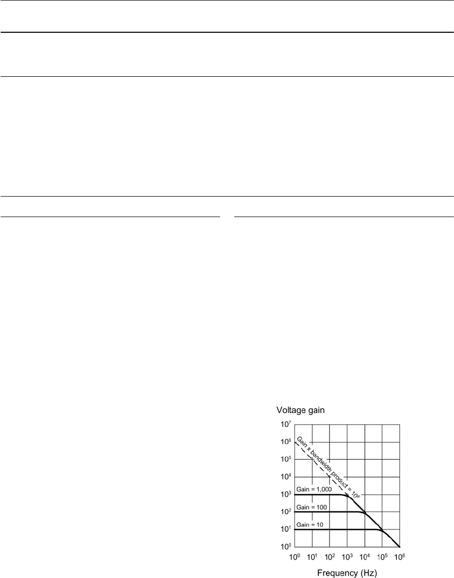
OPERATIONAL AMPLIFIERS 161
Operational amplifier applications
Table 8.2 shows abbreviated data for some
common types of integrated circuit operational
amplifier together with some typical applications.
Example 8.5
Which of the operational amplifiers in the table
would be most suitable for each of the following
applications:
(a) amplifying the low-level output from a
piezoelectric vibration sensor
(b) a high-gain amplifier that can be used to
faithfully amplify very small signals
(c) a low-frequency amplifier for audio signals.
Solution
(a) AD548 (this operational amplifier is designed
for use in instrumentation applications and it offers
avery low input offset current which is important
when the input is derived from a piezoelectric
transducer)
(b) CA3140 (this is a low-noise operational
amplifier that also offers high gain and fast slew
rate)
(c) LM348 or LM741 (both are general purpose
operational amplifiers and are ideal for non-critical
applications such as audio amplifiers).
Table 8.2 Some common examples of integrated circuit operational amplifiers
Device Type
Open-loop
voltage
gain (dB)
Input bias
current
Slew rate
(V/µs) Application
AD548 Bipolar 100 min. 0.01 nA 1.8 Instrumentation amplifier
AD711 FET 100 25 pA 20 Wideband amplifier
CA3140 CMOS 100 5 pA 9 Low-noise wideband amplifier
LF347 FET 110 50 pA 13 Wideband amplifier
LM301 Bipolar 88 70 nA 0.4 General-purpose operational amplifier
LM348 Bipolar 96 30 nA 0.6 General-purpose operational amplifier
TL071 FET 106 30 pA 13 Wideband amplifier
741 Bipolar 106 80 nA 0.5 General-purpose operational amplifier
Gain and bandwidth
It is important to note that, since the product of
gain and bandwidth is a constant for any particular
operational amplifier. Hence, an increase in gain
can only be achieved at the expense of bandwidth,
and vice versa.
Figure 8.5 shows the relationship between
voltage gain and bandwidth for a typical
operational amplifier (note that the axes use
logarithmic, rather than linear scales). The open-
loop voltage gain (i.e. that obtained with no
feedback applied) is 100,000 (or 100 dB) and the
bandwidth obtained in this condition is a mere 10
Figure 8.5 Frequency response curves for an
operational amplifier

162 ELECTRONIC CIRCUITS: FUNDAMENTALS AND APPLICATIONS
Figure 8.6 Operational amplifier with negative
feedback applied
Table 8.3 Corresponding values of voltage gain
and bandwidth for an operational amplifier with a
gain × bandwidth product of 1 × 10⁶
Voltage gain (AV)Bandwidth
1DC to 1 MHz
10 DC to 100 kHz
100 DC to 10 kHz
1,000 DC to 1 kHz
10,000 DC to 100 Hz
100,000 DC to 10 Hz
Hz. The effect of applying increasing amounts of
negative feedback (and consequently reducing the
gain to a more manageable amount) is that the
bandwidth increases in direct proportion.
The frequency response curves in Fig. 8.5 show
the effect on the bandwidth of making the closed-
loop gains equal to 10,000, 1,000, 100, and 10.
Table 8.3 summarizes these results. You should
also note that the (gain × bandwidth) product for
this amplifier is 1 × 10⁶Hz (i.e. 1 MHz).
We can determine the bandwidth of the amplifier
when the closed-loop voltage gain is set to 46 dB
by constructing a line and noting the intercept point
on the response curve. This shows that the
bandwidth will be 10 kHz. Note that, for this
operational amplifier, the (gain × bandwidth)
product is 2 × 10⁶Hz (or 2 MHz).
Inverting amplifier with feedback
Figure 8.6 shows the circuit of an inverting
amplifier with negative feedback applied. For the
sake of our explanation we will assume that the
operational amplifier is ‘ideal’. Now consider what
happens when a small positive input voltage is
applied. This voltage (VIN)produces a current (IIN)
flowing in the input resistor R1.
Since the operational amplifier is ‘ideal’ we will
assume that:
(a) the input resistance (i.e. the resistance that
appears between the inverting and non-inverting
input terminals, RIC)is infinite
(b) the open-loop voltage gain (i.e., the ratio of
VOUT to VIN with no feedback applied) is infinite.
As a consequence of (a) and (b):
(i) the voltage appearing between the inverting and
non-inverting inputs (VIC)will be zero, and
(ii) the current flowing into the chip (IIC)will be
zero (recall that IIC = VIC /RIC and RIC is infinite).
Applying Kirchhoff’s Current Law at node A
gives:
IIN = IIC + IFbut IIC =0thus IIN = IF(1)
(this shows that the current in the feedback resistor,
R2, is the same as the input current, IIN ).
Applying Kirchhoff’s Voltage Law to loop A
gives:
VIN =(IIN × R1) + VIC
but VIC =0thus VIN = IIN × R1(2)
Using Kirchhoff’s Voltage Law in loop B gives:
VOUT =*VIC + (IF×R2)
but VIC =0thus VOUT = IF×R2(3)
Combining (1) and (3) gives:
VOUT = IIN × R2(4)
The voltage gain of the stage is given by:
(5)
Combining (4) and (2) with (5) gives:
OUT
v
IN
V
A
V
=
IN
v
IN
2
2
11
IR
R
A
IR R
×
==
×
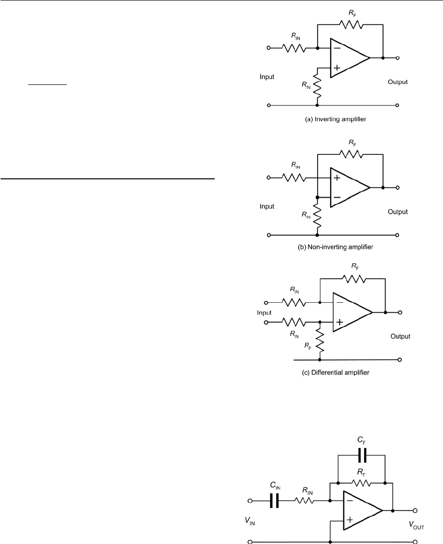
To preserve symmetry and minimize offset voltage,
athird resistor is often included in series with the
non-inverting input. The value of this resistor
should be equivalent to the parallel combination of
R1and R2. Hence:
From this point onwards (and to help you
remember the function of the resistors) we shall
refer to the input resistance as RIN and the feedback
resistance as RF(instead of the more general and
less meaningful R1and R2, respectively).
Operational amplifier configurations
The three basic configurations for operational
voltage amplifiers, together with the expressions
for their voltage gain, are shown in Fig. 8.7. Supply
rails have been omitted from these diagrams for
clarity but are assumed to be symmetrical about
0V.
All of the amplifier circuits described previously
have used direct coupling and thus have frequency
response characteristics that extend to d.c. This, of
course, is undesirable for many applications,
particularly where a wanted a.c. signal may be
superimposed on an unwanted d.c. voltage level or
when the bandwidth of the amplifier greatly
exceeds that of the signal that it is required to
amplify. In such cases, capacitors of appropriate
value may be inserted in series with the input
resistor, RIN,and in parallel with the feedback
resistor, RF,as shown in Fig. 8.8.
The value of the input and feedback capacitors,
CIN and CFrespectively, are chosen so as to roll-off
the frequency response of the amplifier at the
desired lower and upper cut-off frequencies,
respectively. The effect of these two capacitors on
an operational amplifier’s frequency response is
shown in Fig. 8.9.
By selecting appropriate values of capacitor, the
frequency response of an inverting operational
voltage amplifier may be very easily tailored to suit
aparticular set of requirements.
The lower cut-off frequency is determined by the
value of the input capacitance, CIN,and input
resistance, RIN.The lower cut-off frequency is
given by:
OPERATIONAL AMPLIFIERS 163
12
3
12
RR
R
RR
×
=
+
Figure 8.7 The three basic configurations for
operational voltage amplifiers
Figure 8.8 Adding capacitors to modify the
frequency response of an inverting operational
amplifier
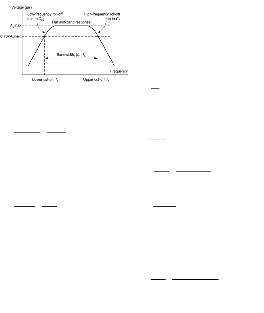
164 ELECTRONIC CIRCUITS: FUNDAMENTALS AND APPLICATIONS
where f1is the lower cut-off frequency in Hz, CIN is
in Farads and RIN is in ohms.
Provided the upper frequency response it not
limited by the gain × bandwidth product, the upper
cut-off frequency will be determined by the
feedback capacitance, CF,and feedback resistance,
RF,such that:
where f2is the upper cut-off frequency in Hz, CFis
in Farads and R2is in ohms.
Example 8.6
An inverting operational amplifier is to operate
according to the following specification:
Voltage gain = 100
Input resistance (at mid-band) = 10 kG
Lower cut-off frequency = 250 Hz
Upper cut-off frequency = 15 kHz
Devise a circuit to satisfy the above specification
using an operational amplifier.
Solution
To make things a little easier, we can break the
problem down into manageable parts. We shall
base our circuit on a single operational amplifier
configured as an inverting amplifier with capacitors
to define the upper and lower cut-off frequencies,
as shown in the previous figure.
The nominal input resistance is the same as the
value for RIN.Thus:
RIN = 10 kG
To determine the value of RFwe can make use of
the formula for mid-band voltage gain:
thus R2= Av×R1=100 × 10 kG=100kG
To determine the value of CIN we will use the
formula for the low-frequency cut-off:
from which:
hence:
Finally, to determine the value of CFwe will use
the formula for high-frequency cut-off:
from which:
hence:
For most applications the nearest preferred values
(68 nF for CIN and 100 pF for CF)would be
perfectly adequate. The complete circuit of the
operational amplifier stage is shown in Fig. 8.10.
Figure 8.9 Effect of adding capacitors, CIN and
CF,to modify the frequency response of an
operational amplifier
1
IN IN IN IN
1 0.159
2
fCR CR
==
2
FF FF
1 0.159
2
f
CR CR
==
v
2
1
R
A
R
=
1
IN IN
0.159
f
CR
=
IN
3
1IN
0.159 0.159
250 10 10
CfR
==
××
9
IN 6
0.159
63 10 F 63 nF
2.5 10
C
==×=
×
2
FF
0.159
f
CR
=
F
33
2IN
0.159 0.159
15 10 100 10
CfR
==
×× ×
9
F9
0.159
0.106 10 F 106 pF
1.5 10
C
==×=
×
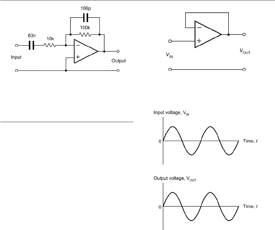
OPERATIONAL AMPLIFIERS 165
Figure 8.10 See Example 8.6. This operational
amplifier has a mid-band voltage gain of 10 over
the frequency range 250 Hz to 15 kHz
Operational amplifier circuits
As well as their application as a general-purpose
amplifying device, operational amplifiers have a
number of other uses, including voltage followers,
differentiators, integrators, comparators, and
summing amplifiers. We shall conclude this section
by taking a brief look at each of these applications.
Voltage followers
Avoltage follower using an operational amplifier is
shown in Fig. 8.11. This circuit is essentially an
inverting amplifier in which 100% of the output is
fed back to the input. The result is an amplifier that
has a voltage gain of 1 (i.e. unity), a very high input
resistance and a very high output resistance. This
stage is often referred to as a buffer and is used for
matching a high-impedance circuit to a low-
impedance circuit.
Typical input and output waveforms for a
voltage follower are shown in Fig. 8.12. Notice
how the input and output waveforms are both in-
phase (they rise and fall together) and that they are
identical in amplitude.
Differentiators
Adifferentiator using an operational amplifier is
shown in Fig. 8.13. A differentiator produces an
output voltage that is equivalent to the rate of
change of its input. This may sound a little complex
but it simply means that, if the input voltage
Figure 8.11 A voltage follower
Figure 8.12 Typical input and output waveforms
for a voltage follower
remains constant (i.e. if it isn’t changing) the output
also remains constant. The faster the input voltage
changes the greater will the output be. In
mathematics this is equivalent to the differential
function.
Typical input and output waveforms for a
differentiator are shown in Fig. 8.14. Notice how
the square wave input is converted to a train of
short duration pulses at the output. Note also that
the output waveform is inverted because the signal
has been applied to the inverting input of the
operational amplifier.
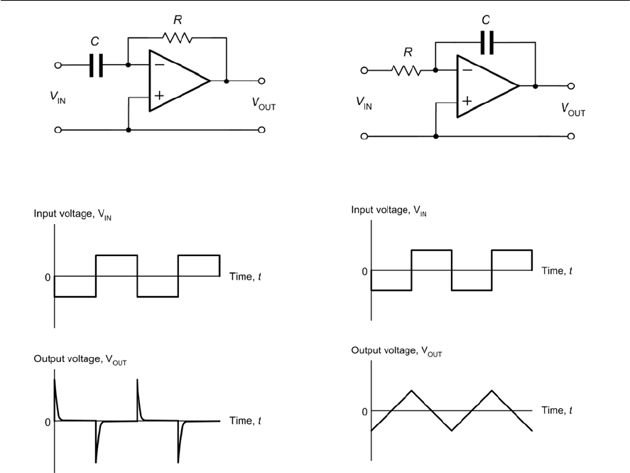
166 ELECTRONIC CIRCUITS: FUNDAMENTALS AND APPLICATIONS
Integrators
An integrator using an operational amplifier is
shown in Fig. 8.15. This circuit provides the
opposite function to that of a differentiator (see
earlier) in that its output is equivalent to the area
under the graph of the input function rather than its
rate of change. If the input voltage remains constant
(and is other than 0V) the output voltage will ramp
up or down according to the polarity of the input.
The longer the input voltage remains at a particular
value the larger the value of output voltage (of
either polarity) will be produced.
Typical input and output waveforms for an
integrator are shown in Fig. 8.16. Notice how the
square wave input is converted to a wave that has a
triangular shape. Once again, note that the output
waveform is inverted.
Comparators
Acomparator using an operational amplifier is
shown in Fig. 8.17. Since no negative feedback has
been applied, this circuit uses the maximum gain of
the operational amplifier. The output voltage
produced by the operational amplifier will thus rise
to the maximum possible value (equal to the
positive supply rail voltage) whenever the voltage
present at the non-inverting input exceeds that
present at the inverting input. Conversely, the
output voltage produced by the operational
amplifier will fall to the minimum possible value
(equal to the negative supply rail voltage) whenever
the voltage present at the inverting input exceeds
that present at the non-inverting input.
Typical input and output waveforms for a
Figure 8.13 A differentiator
Figure 8.14 Typical input and output waveforms
for a differentiator
Figure 8.15 An integrator
Figure 8.16 Typical input and output waveforms
for an integrator
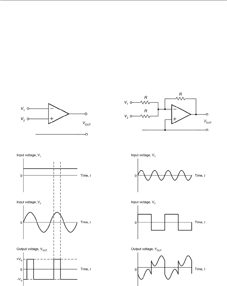
OPERATIONAL AMPLIFIERS 167
comparator are shown in Fig. 8.18. Notice how the
output is either +15V or –15V depending on the
relative polarity of the two input. A typical
application for a comparator is that of comparing a
signal voltage with a reference voltage. The output
will go high (or low) in order to signal the result of
the comparison.
Summing amplifiers
Asumming amplifier using an operational
amplifier is shown in Fig. 8.19. This circuit
produces an output that is the sum of its two input
Figure 8.17 A comparator
Figure 8.18 Typical input and output waveforms
for a comparator
voltages. However, since the operational amplifier
is connected in inverting mode, the output voltage
is given by:
VOUT =((V1+V2)
where V1and V2are the input voltages (note that all
of the resistors used in the circuit have the same
value). Typical input and output waveforms for a
summing amplifier are shown in Fig. 8.20. A
typical application is that of ‘mixing’ two input
signals to produce an output voltage that is the sum
of the two.
Figure 8.19 A summing amplifier
Figure 8.20 Typical input and output waveforms
for a summing amplifier
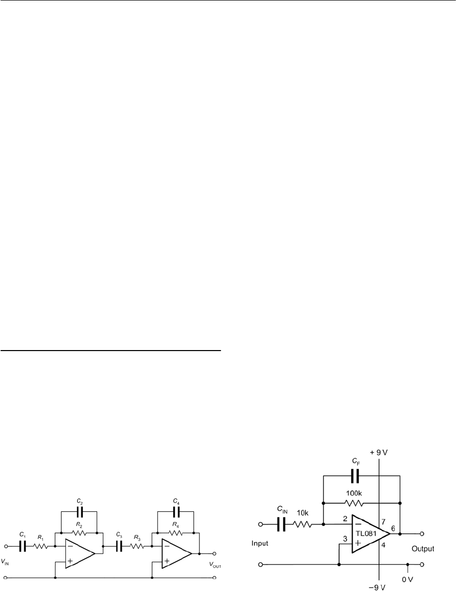
168 ELECTRONIC CIRCUITS: FUNDAMENTALS AND APPLICATIONS
Practical investigation
Objective
To measure the voltage gain and frequency
response of an inverting operational amplifier.
Components and test equipment
Breadboard, AF signal generator (with variable
frequency sine wave output), two AF voltmeters (or
adual beam oscilloscope), ±9 V d.c. power supply
(or two 9 V batteries), TL081 (or similar
operational amplifier), 22 pF, 2.2 nF, 47 nF and
220 nF capacitors, resistors of 10 kGand
100 kG5% 0.25 W, test leads, connecting wire.
Procedure
Connect the circuit shown in Fig. 8.22 with CIN =
47 nF and CF=2.2 nF, set the signal generator to
produce an output of 100 mV at 1 kHz. Measure
and record the output voltage produced and repeat
this measurement for frequencies over the range
10 Hz to 100 kHz, see Table 8.4.
Replace CIN and CFwith 220 nF and 22 pF
capacitors and repeat the measurements, this time
over the extended frequency range from 1 Hz to
1MHz, recording your results in Table 8.5.
Measurements and graphs
Use the measured value of output voltage at 1 kHz
for both sets of measurements, in order to
determine the mid-band voltage gain of the stage.
Figure 8.22 See Practical investigation
Figure 8.21 A multi-stage amplifier (both stages
have tailored frequency response)
Positive versus negative feedback
We have already shown how negative feedback can
be applied to an operational amplifier in order to
produce an exact value of gain. Negative feedback
is frequently used in order to stabilize the gain of
an amplifier and also to increase the frequency
response (recall that, for an amplifier the product of
gain and bandwidth is a constant). Positive
feedback, on the other hand, results in an increase
in gain and a reduction in bandwidth. Furthermore,
the usual result of applying positive feedback is
that an amplifier becomes unstable and oscillates
(i.e. it generates an output without an input being
present!). For this reason, positive feedback is only
used in amplifiers when the voltage gain is less
than unity.
The important thing to remember from all of this
is that, when negative feedback is applied to an
amplifier the overall gain is reduced and the
bandwidth is increased (note that the gain ×
bandwidth product remains constant). When
positive feedback is applied to an amplifier the
overall gain increases and the bandwidth is
reduced. In most cases this will result in instability
and oscillation.
Multi-stage amplifiers
Multi-stage amplifiers can easily be produced using
operational amplifiers. Coupling methods can be
broadly similar to those described earlier in Chapter
7(see page 149). As an example, Fig. 8.21 shows a
two-stage amplifier in which each stage has a
tailored frequency response. Note how C1and C3
provide d.c. isolation between the stages as well as
helping to determine the low-frequency roll-off.
OPERATIONAL AMPLIFIERS 169
Figure 8.23 Graph layout for plotting the results
Table 8.4 Results (CIN =47 nF, CF=2.2 nF)
For each set of measurements plot graphs showing
the frequency response of the amplifier stage (see
Fig. 8.23). In each case, use the graph to determine
the lower and upper cut-off frequencies.
Calculations
For each circuit calculate:
(a) the mid-band voltage gain
(b) the lower cut-off frequency
(c) the upper cut-off frequency.
Compare the calculated values with the measured
values.
Frequency (Hz)
10
20
40
100
200
400
1 k
2 k
4 k
10 k
Output voltage (V)
Conclusion
Comment on the performance of the amplifier
stage. Is this what you would expect? Do the
measured values agree with those obtained by
calculation? If not, suggest reasons for any
differences. Suggest typical applications for the
circuit.
Table 8.5 Results (CIN = 220 nF, CF=22 pF)
Frequency (Hz) Output voltage (V)
4
10
20
40
100
200
400
1k
10 k
20 k
40 k
100 k
200 k
400 k
170 ELECTRONIC CIRCUITS: FUNDAMENTALS AND APPLICATIONS
Problems
8.1 Sketch the circuit symbol for an operational
amplifier. Label each of the connections.
8.2 List four characteristics associated with an
‘ideal’ operational amplifier.
8.3 An operational amplifier with negative
feedback applied produces an output of
1.5 V when an input of 7.5 mV is present.
Determine the closed-loop voltage gain.
8.4 Sketch the circuit of an inverting amplifier
based on an operational amplifier. Label
your circuit and identify the components that
determine the closed-loop voltage gain.
8.5 Sketch the circuit of each of the following
based on the use of operational amplifiers:
(a) a comparator
(b) a differentiator
(c) an integrator.
8.6 An inverting amplifier is to be constructed
having a mid-band voltage gain of 40, an
input resistance of 5 kGand a
frequency response extending from 20 Hz to
20 kHz. Devise a circuit and specify all
component values required.
8.7 A summing amplifier with two inputs has
RF=10 kG,and RIN (for both inputs) of
2 kG.Determine the output voltage when
one input is at *2 V and the other is +0.5 V.
8.8 During measurements on an operational
amplifier under open-loop conditions, an
output voltage of 12 V is produced by an
input voltage of 1 mV. Determine the open-
loop voltage gain expressed in dB.
8.9 With the aid of a sketch, explain what is
meant by the term ‘slew rate’. Why is this
important?
Answers to these problems appear on page 375.
Important formulae introduced in this
chapter
Open-loop voltage gain
(page 158):
dB
Closed-loop voltage gain:
(page 158)
dB
Input resistance:
(page 140)
Output resistance:
(page 159)
Slew rate
(page 159)
Upper cut-off frequency:
(page 164)
Lower cut-off frequency:
(page 164)
Output voltage produced by a summing amplifier:
(page 167)
VOUT =((V1+V2)
Figure 8.24 Symbol introduced in this chapter
Symbol introduced in this chapter
OUT
V(OL)
IN
V
A
V
=
OUT
V(OL) 10
IN
20 log V
A
V
=
OUT
V(CL)
IN
V
A
V
=
OUT
V(CL) 10
IN
20 log V
A
V
=
IN
IN
IN
V
R
I
=
OUT(OC)
OUT
OUT(SC)
V
RI
=
OUT
Slew rate V
t
=
1
IN IN
0.159
fCR
=
2
FF
0.159
f
CR
=
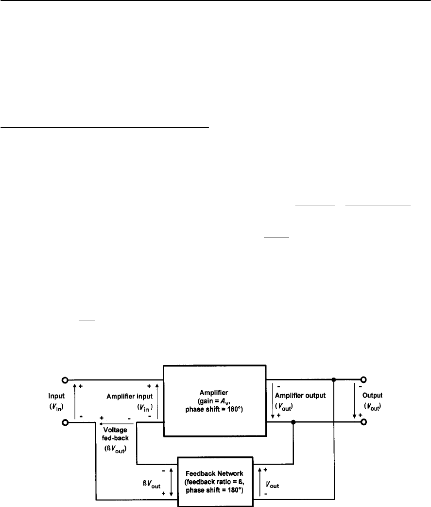
9
Oscillators
This chapter describes circuits that generate sine
wave, square wave, and triangular waveforms.
These oscillator circuits form the basis of clocks
and timing arrangements as well as signal and
function generators.
Positive feedback
In Chapter 7, we showed how negative feedback
can be applied to an amplifier to form the basis of a
stage which has a precisely controlled gain. An
alternative form of feedback, where the output is
fed back in such a way as to reinforce the input
(rather than to subtract from it), is known as
positive feedback.
Figure 9.1 shows the block diagram of an
amplifier stage with positive feedback applied.
Note that the amplifier provides a phase shift of
180° and the feedback network provides a further
180°. Thus the overall phase shift is 0°. The overall
voltage gain, G,is given by:
By applying Kirchhoff’s Voltage Law
thus
and
where Avis the internal gain of the amplifier.
Hence:
Now consider what will happen when the loop
gain, 0Av,approaches unity (i.e., when the loop
gain is just less than 1). The denominator (1 2 0Av)
will become close to zero. This will have the effect
of increasing the overall gain, i.e. the overall gain
with positive feedback applied will be greater than
the gain without feedback.
out
in
Overall gain,
V
G
V
=
in in
out
'0
VV V
=+
in in
out
'0
VV V
=
out v in
VAV
=×
()
in in
vv
in out in in
v
''
Overall gain, '
0'0'
AV AV
GVVV AV
××
==
×
v
v
Thus, 1
0
A
G
A
=
Figure 9.1
Amplifier with positive feedback applied

172 ELECTRONIC CIRCUITS: FUNDAMENTALS AND APPLICATIONS
It is worth illustrating this difficult concept using
some practical figures. Assume that you have an
amplifier with a gain of 9 and one-tenth of the
output is fed back to the input (i.e. 0=0.1). In this
case the loop gain (0× Av)is 0.9.
With negative feedback applied (see Chapter 7)
the overall voltage gain will be:
With positive feedback applied the overall voltage
gain will be:
Now assume that you have an amplifier with a gain
of 10 and, once again, one-tenth of the output is fed
back to the input (i.e. 0=0.1). In this example the
loop gain (0× Av)is exactly 1.
With negative feedback applied (see Chapter 7)
the overall voltage gain will be:
With positive feedback applied the overall voltage
gain will be:
This simple example shows that a loop gain of
unity (or larger) will result in infinite gain and an
amplifier which is unstable. In fact, the amplifier
will oscillate since any disturbance will be
amplified and result in an output.
Clearly, as far as an amplifier is concerned,
positive feedback may have an undesirable effect—
instead of reducing the overall gain the effect is
that of reinforcing any signal present and the output
can build up into continuous oscillation if the loop
gain is 1 or greater. To put this another way,
oscillator circuits can simply be thought of as
amplifiers that generate an output signal without
the need for an input!
Conditions for oscillation
From the foregoing we can deduce that the
conditions for oscillation are:
(a) the feedback must be positive (i.e. the signal
fed back must arrive back in-phase with the signal
at the input);
(b) the overall loop voltage gain must be greater
than 1 (i.e. the amplifier’s gain must be sufficient
to overcome the losses associated with any
frequency selective feedback network).
Hence, to create an oscillator we simply need an
amplifier with sufficient gain to overcome the
losses of the network that provide positive
feedback. Assuming that the amplifier provides
180° phase shift, the frequency of oscillation will
be that at which there is 180° phase shift in the
feedback network.
Anumber of circuits can be used to provide 180°
phase shift, one of the simplest being a three-stage
C–Rladder network that we shall meet next.
Alternatively, if the amplifier produces 0° phase
shift, the circuit will oscillate at the frequency at
which the feedback network produces 0° phase
shift. In both cases, the essential point is that the
feedback should be positive so that the output
signal arrives back at the input in such a sense as to
reinforce the original signal.
Ladder network oscillator
Asimple phase-shift oscillator based on a three-
stage C–Rladder network is shown in Fig. 9.2.
TR1 operates as a conventional common-emitter
amplifier stage with R1and R2providing base bias
potential and R3and C1providing emitter
stabilization.
The total phase shift provided by the C–Rladder
network (connected between collector and base) is
180° at the frequency of oscillation. The transistor
provides the other 180° phase shift in order to
realize an overall phase shift of 360° or 0° (note
that these are the same).
The frequency of oscillation of the circuit shown
in Fig. 9.2 is given by:
The loss associated with the ladder network is 29,
thus the amplifier must provide a gain of at least 29
in order for the circuit to oscillate. In practice this
is easily achieved with a single transistor.
()
v
v
999
4.7
101 0.1 9 1 0.9 1.9
A
GA
== ===
++×+
()
v
v
10 10 10
90
1010.19 10.90.1
A
GA
== ===
×
()
v
v
10 10 10
5
1010.110 112
A
GA
== ===
++×+
()
v
v
10 10 10
101 0.1 10 1 1 0
A
GA
== ===
×
1
2K6
f
CR
=×
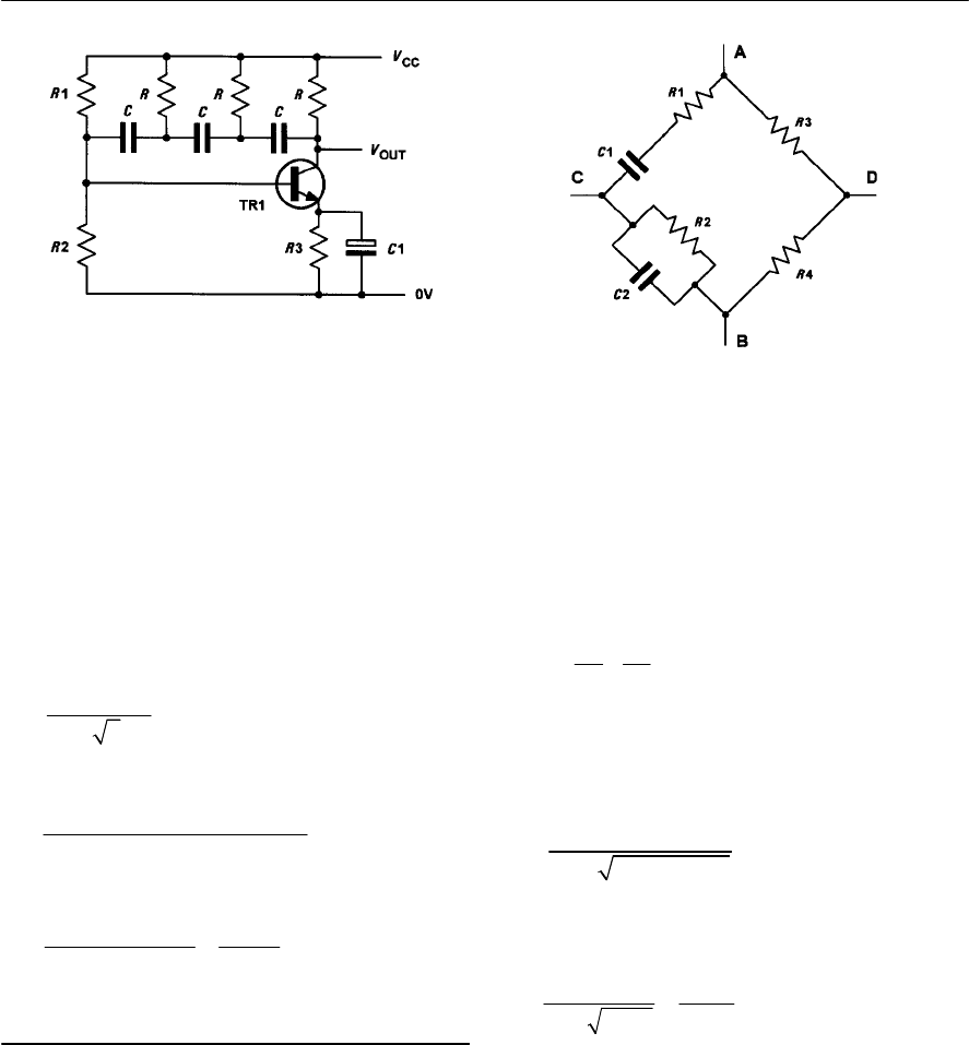
OSCILLATORS 173
Example 9.1
Determine the frequency of oscillation of a three-
stage ladder network oscillator in which
C = 10 nF and R = 10 kL.
Solution
Using
gives
from which
Wien bridge oscillator
An alternative approach to providing the phase
shift required is the use of a Wien bridge network
(Fig. 9.3). Like the C–R ladder, this network
provides a phase shift which varies with frequency.
The input signal is applied to A and B while the
output is taken from C and D. At one particular
frequency, the phase shift produced by the network
will be exactly zero (i.e. the input and output
Figure 9.2 Sine wave oscillator based on a three-
stage C–R ladder network Figure 9.3 A Wien bridge network
signals will be in-phase). If we connect the network
to an amplifier producing 0° phase shift which has
sufficient gain to overcome the losses of the Wien
bridge, oscillation will result.
The minimum amplifier gain required to sustain
oscillation is given by:
In most cases, C1 = C2and R1 = R2, hence the
minimum amplifier gain will be 3.
The frequency at which the phase shift will be
zero is given by:
When Rl= R2and Cl= C2the frequency at which
the phase shift will be zero will be given by:
where R = Rl= R2and C = Cl= C2.
Example 9.2
Figure 9.4 shows the circuit of a Wien bridge
oscillator based on an operational amplifier. If Cl=
C2=100 nF, determine the output frequencies
produced by this arrangement (a) when Rl= R2=
1 kLand (b) when Rl= R2=6 kL.
93
1
6.28 2.45 10 10 10 10
f
=×××××
1
2K6
f
CR
=×
4
4
110
647 Hz
15.3866.28 2.45 10
f
===
××
v
12
1
21
CR
A
CR
=+ +
1
2
K1212
f
CC RR
=×
22
11
2K
2K
f
CR
CR
==
×
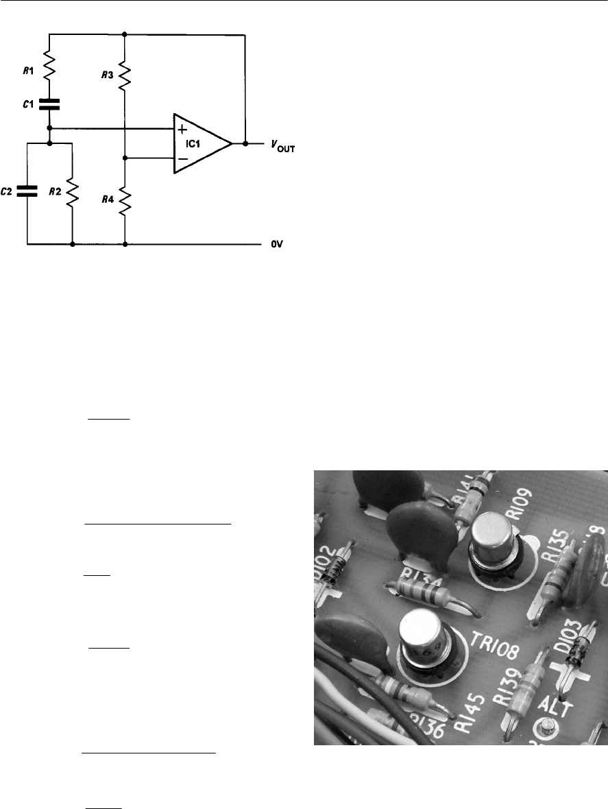
174 ELECTRONIC CIRCUITS: FUNDAMENTALS AND APPLICATIONS
Solution
(a) When R1= R2=1 kL
where R = R1= R1and C = C1= C2.
Thus
(b) When R1= R1=6 kL
where R = R1= R1and C = C1= C2.
Thus
Figure 9.4 Sine wave oscillator based on a Wien
bridge network (see Example 9.2)
1
2K
f
CR
=
93
1
6.28 100 10 1 10
f
=×× ××
1
2K
f
CR
=
93
1
6.28 100 10 6 10
f
=×× ××
4
10
1.59 kHz
6.28
f==
4
10
265 Hz
37.68
f==
Multivibrators
There are many occasions when we require a
square wave output from an oscillator rather than a
sine wave output. Multivibrators are a family of
oscillator circuits that produce output waveforms
consisting of one or more rectangular pulses. The
term ‘multivibrator’ simply originates from the fact
that this type of waveform is rich in harmonics (i.e.
‘multiple vibrations’).
Multivibrators use regenerative (i.e. positive)
feedback; the active devices present within the
oscillator circuit being operated as switches, being
alternately cut off and driven into saturation.
The principal types of multivibrator are:
(a) astable multivibrators that provide a
continuous train of pulses (these are sometimes
also referred to as free-running multivibrators)
(b) monostable multivibrators that produce a
single output pulse (they have one stable state and
are thus sometimes also referred to as ‘one-shot’)
(c) bistable multivibrators that have two stable
states and require a trigger pulse or control signal
to change from one state to another.
Figure 9.5 This high-speed bistable multivibrator
uses two general-purpose silicon transistors and
works at frequencies of up to 1 MHz triggered from
an external signal
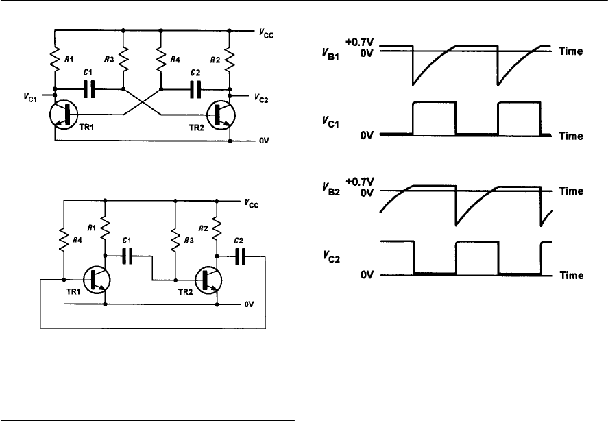
OSCILLATORS 175
The astable multivibrator
Figure 9.6 shows a classic form of astable
multivibrator based on two transistors. Figure 9.7
shows how this circuit can be redrawn in an
arrangement that more closely resembles a two-
stage common-emitter amplifier with its output
connected back to its input. In Fig. 9.5, the values
of the base resistors, R3and R4, axe such that the
sufficient base current will be available to
completely saturate the respective transistor. The
values of the collector load resistors, R1and R2,
are very much smaller than R3and R4. When
power is first applied to the circuit, assume that
TR2 saturates before TR1 when the power is first
applied (in practice one transistor would always
saturate before the other due to variations in
component tolerances and transistor parameters).
As TR2 saturates, its collector voltage will fall
rapidly from +VCC to 0 V. This drop in voltage will
be transferred to the base of TR1 via C1. This
negative-going voltage will ensure that TR1 is
initially placed in the non-conducting state. As long
as TR1 remains cut off, TR2 will continue to be
saturated. During this time, C1will charge via R4
Figure 9.6 Astable multivibrator using BJTs
Figure 9.7 Circuit of Fig. 9.6 redrawn to show
two common-emitter amplifier stages with positive
feedback
Figure 9.8 Waveforms for the BJT multivibrator
shown in Fig. 9.6
and TR1’s base voltage will rise exponentially
from 2VCC towards +VCC.However, TR1’s base
voltage will not rise much above 0 V because, as
soon as it reaches +0.7 V (sufficient to cause base
current to flow), TR1 will begin to conduct. As
TR1 begins to turn on, its collector voltage will
rapidly fall from +VCC 0 V. This fall in voltage is
transferred to the base of TR2 via C1and, as a
consequence, TR2 will turn off. C1will then
charge via R3and TR2’s base voltage will rise
exponentially from 2VCC towards +VCC.As before,
TR2’s base voltage will not rise much above 0 V
because, as soon as it reaches +0.7 V (sufficient to
cause base current to flow), TR2 will start to
conduct. The cycle is then repeated indefinitely.
The time for which the collector voltage of TR2
is low and TRl is high (T1) will be determined by
the time constant, R4 × C1. Similarly, the time for
which the collector voltage of TR1 is low and TR2
is high (T2) will be determined by the time
constant, R3 × C1.
The following approximate relationships apply:
T1 = 0.7 C2R4and T2 = 0.7 C1R3
Since one complete cycle of the output occurs in a
time, T=T1 + T2, the periodic time of the output is
given by:
T=0.7 (C2R4 + C1R3)
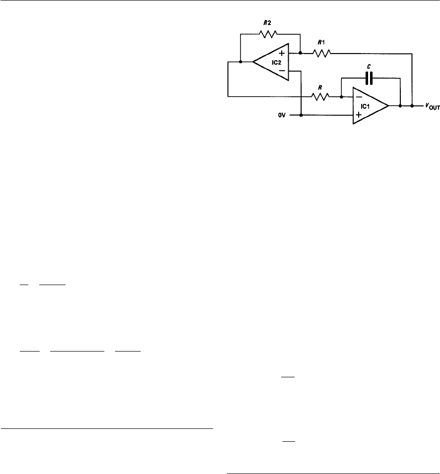
176 ELECTRONIC CIRCUITS: FUNDAMENTALS AND APPLICATIONS
Finally, we often require a symmetrical square
wave output where T1= T2 . To obtain such an
output, we should make R3 = R4and C1 = C1, in
which case the periodic time of the output will be
given by:
T=1.4 C R
where C=C1 = C2and R=R3 = R4. Waveforms
for the astable oscillator are shown in Fig. 9.8.
Example 9.3
The astable multivibrator in Fig. 9.6 is required to
produce a square wave output at 1 kHz. Determine
suitable values for R3and R4if C1and C2are both
10 nF.
Solution
Since a square wave is required and C1 and C2
have identical values, R3 must be made equal to
R4. Now:
Re-arranging T=1.4CR to make Rthe subject
gives:
hence
Other forms of astable oscillator
Figure 9.9 shows the circuit diagram of an
alternative form of astable oscillator which
produces a triangular output waveform.
Operational amplifier IC1 forms an integrating
stage while IC2 is connected with positive
feedback to ensure that oscillation takes place.
Assume that the output from IC2 is initially at,
or near, +VCC and capacitor, C,is uncharged. The
voltage at the output of IC2 will be passed, via R,
to IC1. Capacitor, C,will start to charge and the
output voltage of IC1 will begin to fall.
Eventually, the output voltage will have fallen to a
value that causes the polarity of the voltage at the
non-inverting input of IC2 to change from positive
to negative. At this point, the output of IC2 will
rapidly fall to 2VCC.Again, this voltage will be
passed, via R,to IC1. Capacitor, C,will then start
to charge in the other direction and the output
voltage of IC1 will begin to rise.
Some time later, the output voltage will have
risen to a value that causes the polarity of the non-
inverting input of IC2 to revert to its original
(positive) state and the cycle will continue
indefinitely.
The upper threshold voltage (i.e. the maximum
positive value for Vout)will be given by:
The lower threshold voltage (i.e. the maximum
negative value for Vout)will be given by:
Single-stage astable oscillator
Asimple form of astable oscillator that produces a
square wave output can be built using just one
operational amplifier, as shown in Fig. 9.10. The
circuit employs positive feedback with the output
fed back to the non-inverting input via the potential
divider formed by R1and R2. This circuit can
make a very simple square wave source with a
Figure 9.9 Astable oscillator using operational
amplifiers
3
3
11
110 s
110
Tf
== =×
×
36
6
9
110 110
=0.071 10
1.4 14
1.4 10 10
T
RC
××
== = ×
××
3
71 10 71 k
R
=× =
UT CC
1
2
R
VV
R
=×
LT CC
1
2
R
VV
R
=×
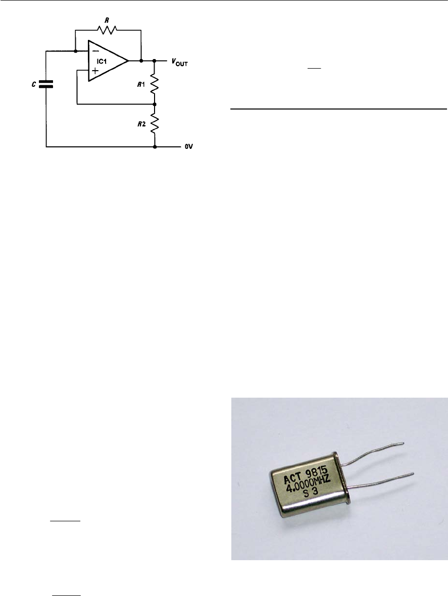
OSCILLATORS 177
Figure 9.10 Single-stage astable oscillator using an
operational amplifier
Crystal controlled oscillators
Arequirement of some oscillators is that they
accurately maintain an exact frequency of
oscillation. In such cases, a quartz crystal can be
used as the frequency determining element. The
quartz crystal (a thin slice of quartz in a
hermetically sealed enclosure, see Fig. 9.11)
vibrates whenever a potential difference is applied
across its faces (this phenomenon is known as the
piezoelectric effect). The frequency of oscillation
is determined by the crystal’s ‘cut’ and physical
size.
Most quartz crystals can be expected to stabilize
the frequency of oscillation of a circuit to within a
few parts in a million. Crystals can be
manufactured for operation in fundamental mode
over a frequency range extending from 100 kHz to
around 20 MHz and for overtone operation from
20 MHz to well over 100 MHz. Figure 9.12 shows
asimple crystal oscillator circuit in which the
crystal provides feedback from the drain to the
source of a junction gate FET.
Figure 9.11 A quartz crystal (this crystal is cut to
be resonant at 4 MHz and is supplied in an HC18
wire-ended package)
frequency that can be made adjustable by replacing
Rwith a variable or preset resistor.
Assume that Cis initially uncharged and the
voltage at the inverting input is slightly less than
the voltage at the non-inverting input. The output
voltage will rise rapidly to +VCC and the voltage at
the inverting input will begin to rise exponentially
as capacitor Ccharges through R.
Eventually, the voltage at the inverting input will
have reached a value that causes the voltage at the
inverting input to exceed that present at the non-
inverting input. At this point, the output voltage
will rapidly fall to 2VCC.Capacitor, C,will then
start to charge in the other direction and the voltage
at the inverting input will begin to fall
exponentially.
Eventually, the voltage at the inverting input will
have reached a value that causes the voltage at the
inverting input to be less than that present at the
non-inverting input. At this point, the output
voltage will rise rapidly to +VCC once again and the
cycle will continue indefinitely.
The upper threshold voltage (i.e. the maximum
positive value for the voltage at the inverting input)
will be given by:
The lower threshold voltage (i.e. the maximum
negative value for the voltage at the inverting
input) will be given by:
UT CC
2
12
R
VV
RR
=×
+
LT CC
2
12
R
VV
RR
=×
+
Finally, the time for one complete cycle of the
output waveform produced by the astable
oscillator is given by:
2
2ln12
1
R
TCR R
=+
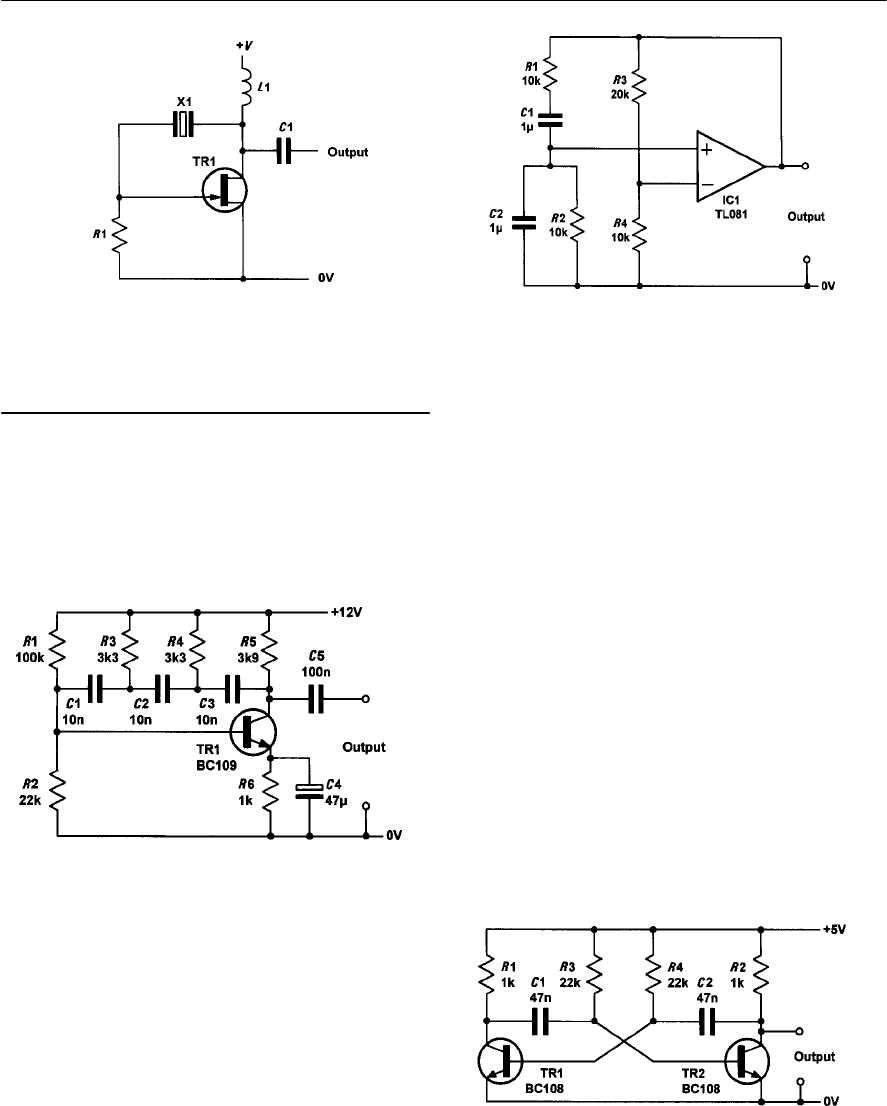
178 ELECTRONIC CIRCUITS: FUNDAMENTALS AND APPLICATIONS
Practical oscillator circuits
Figure 9.13 shows a practical sine wave oscillator
based on a three-stage C–Rladder network. The
circuit provides an output of approximately 1V pk-
pk at 1.97 kHz.
Apractical Wien bridge oscillator is shown in Fig.
9.14. This circuit produces a sine wave output at 16
Hz. The output frequency can easily be varied by
making Rland R2 a l0 kLdual-gang potentiometer
and connecting a fixed resistor of 680 Lin series
with each. In order to adjust the loop gain for an
optimum sine wave output it may be necessary to
make R3/R4adjustable. One way of doing this is to
replace both components with a 10 kLmulti-turn
potentiometer with the sliding contact taken to the
inverting input of IC1.
An astable multivibrator is shown in Fig. 9.15.
This circuit produces a square wave output of 5 V
pk-pk at approximately 690 Hz.
Atriangle wave generator is shown in Fig. 9.16.
This circuit produces a symmetrical triangular
output waveform at approximately 8 Hz. If
desired, a simultaneous square wave output can be
derived from the output of IC2. The circuit
requires symmetrical supply voltage rails (not
shown in Fig. 9.14) of between ±9V and ±15 V.
Figure 9.17 shows a single-stage astable
oscillator. This circuit produces a square wave
output at approximately 13 Hz.
Finally, Fig. 9.18 shows a high-frequency crystal
oscillator that produces an output of approximately
1V pk-pk at 4 MHz. The precise frequency of
operation depends upon the quartz crystal
employed (the circuit will operate with
fundamental mode crystals in the range 2 MHz to
about 12 MHz).
Figure 9.12 A simple JFET oscillator
Figure 9.13 A practical sine wave oscillator based
on a phase shift ladder network
Figure 9.14 Practical sine wave oscillator based on
aWien bridge
Figure 9.15 A practical square wave oscillator
based on an astable multivibrator
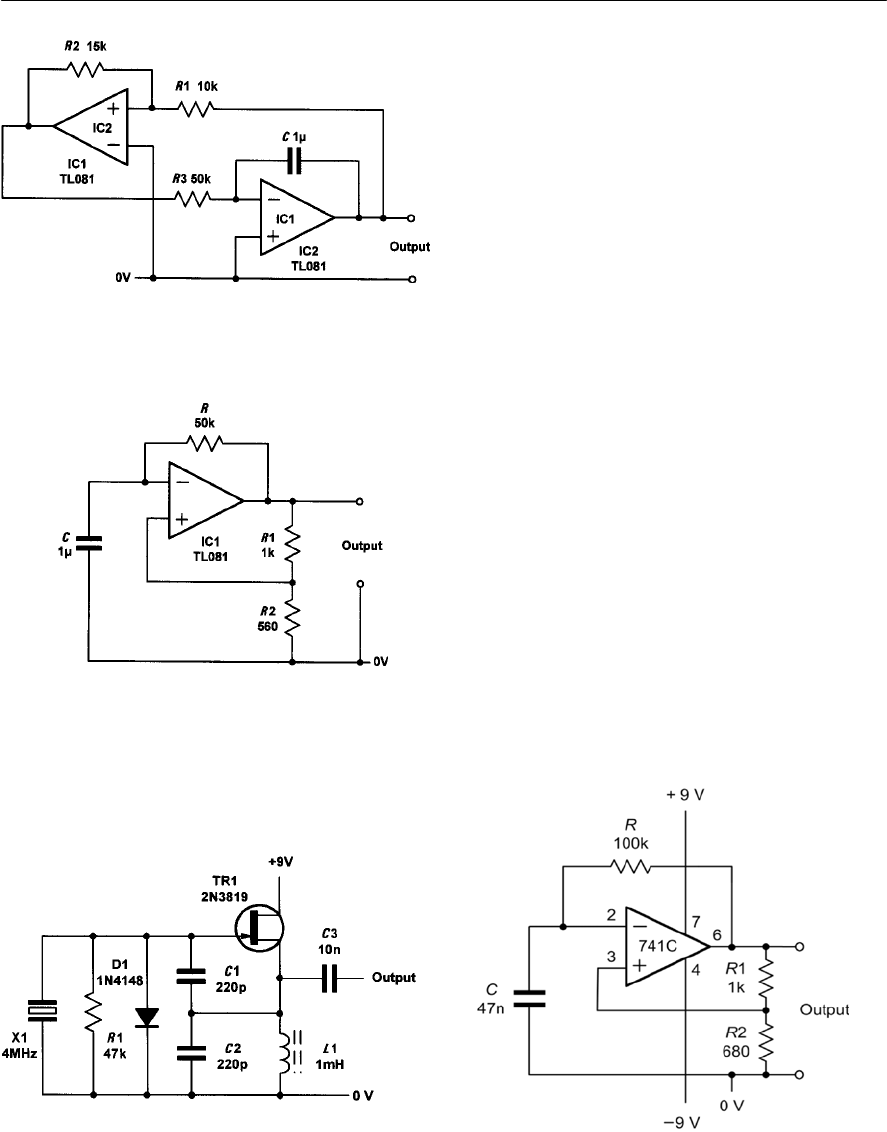
OSCILLATORS 179
Practical investigation
Objective
To investigate a simple operational amplifier
astable oscillator.
Components and test equipment
Breadboard, oscilloscope, ±9 V d.c. power supply
(or two 9 V batteries), 741CN (or similar
operational amplifier), 10 n, 22 n, 47 n and 100 n
capacitors, resistors of 100 kL, 1 kLand 680 L
5% 0.25 W, test leads, connecting wire.
Procedure
Connect the circuit shown in Fig. 9.19 with C=47
nF. Set the oscilloscope timebase to the 2 ms/cm
range and Y-attenuator to 1 V/cm. Adjust the
oscilloscope so that it triggers on a positive edge
and display the output waveform produced by the
oscillator. Make a sketch of the waveform using the
graph layout shown in Fig. 9.20.
Measure and record (using Table 9.1) the time
for one complete cycle of the output. Repeat this
measurement with C=10 nF, 22 nF and 100 nF.
Calculations
For each value of C,calculate the periodic time of
the oscillator’s output and compare this with the
measured values.
Figure 9.19 Astable oscillator circuit used in the
Practical investigation
Figure 9.16 A practical triangle wave generator
Figure 9.17 A single-stage astable oscillator that
produces a square wave output
Figure 9.18 A practical high-frequency crystal
oscillator
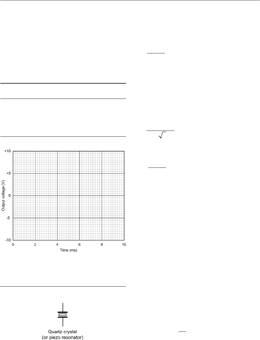
180 ELECTRONIC CIRCUITS: FUNDAMENTALS AND APPLICATIONS
Figure 9.20 Graph layout for sketching the
output waveform produced by the astable oscillator
Conclusion
Comment on the performance of the astable
oscillator. Is this what you would expect? Do the
measured values agree with those obtained by
calculation? If not, suggest reasons for any
differences. Suggest typical applications for the
circuit.
Important formulae introduced in this
chapter
Gain with positive feedback
(page 171):
Loop gain:
(page 171)
Output frequency of a three-stage C–Rladder
network oscillator:
(page 172)
Output frequency of a Wien bridge oscillator:
(page 173)
Time for which a multivibrator output is ‘high’:
(page 175)
T1 = 0.7 C2R4
Time for which a multivibrator output is ‘low’:
(page 175)
T2 = 0.7 C1R3
Periodic time for the output of a square wave
mutivibrator:
(pages 175 and 176)
T=0.7 (C2R4 + C1R3)
when C=C1 = C2and R=R3 = R4
T=1.4 C R
Periodic time for the output of a single-stage
astable oscillator:
(page 177)
Figure 9.21 Symbol introduced in this chapter
Symbol introduced in this chapter
Table 9.1 Table of results and calculated values
CMeasured
periodic time
Calculated
periodic time
10 nF
22 nF
47 nF
100 nF
1
2K6
f
CR
=×
v
v
1
0
A
G
A
=
v
0
LA
=
1
2K
f
CR
=
2
2ln12
1
R
TCR R
=+
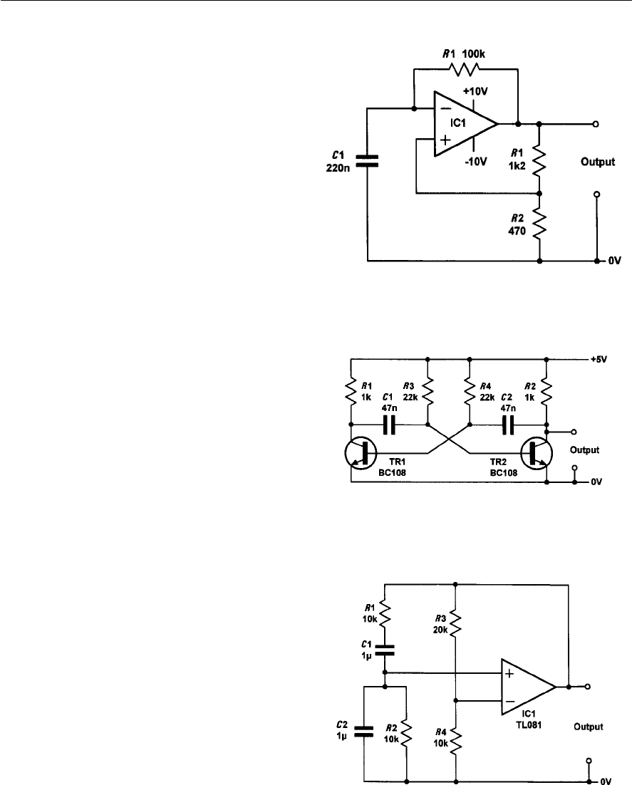
OSCILLATORS 181
Problems
9.1 An amplifier with a gain of 8 has 10% of its
output fed back to the input. Determine the
gain of the stage (a) with negative
feedback, (b) with positive feedback.
9.2 A phase-shift oscillator is to operate with
an output at 1 kHz. If the oscillator is based
on a three-stage ladder network, determine
the required values of resistance if three
capacitors of 10 nF are to be used.
9.3 A Wien bridge oscillator is based on the
circuit shown in Fig. 9.4 but Rland R2are
replaced by a dual-gang potentiometer. If
C1= C2=22 nF determine the values of
Rland R2required to produce an output at
exactly 400 Hz.
9.4 Determine the peak-peak voltage developed
across C1in the oscillator circuit shown in
Fig. 9.22.
9.5 Determine the periodic time and frequency
of the output signal produced by the
oscillator circuit shown in Fig. 9.22.
9.6 An astable multivibrator circuit is required
to produce an asymmetrical rectangular
output which has a period of 4 ms and is to
be ‘high’ for 1 ms and ‘low’ for 3 ms. If the
timing capacitors are both to be 100 nF,
determine the values of the two timing
resistors required.
9.7 Explain, briefly, how the astable
multivibrator shown in Fig. 9.23 operates.
Illustrate your answer using a waveform
sketch.
9.8 Determine the output frequency of the
signal produced by the circuit shown in Fig.
9.23.
9.9 Explain, briefly, how the Wien bridge
oscillator shown in Fig. 9.24 operates.
What factors affect the choice of values for
R3and R4?
9.10 Determine the output frequency of the
signal produced by the circuit shown in Fig.
9.24.
9.11 Sketch the circuit of an oscillator that will
produce a triangular waveform output.
Explain briefly how the circuit operates and
suggest a means of varying the output
frequency over a limited range.
9.12 Distinguish between the following types of
mulitivibrator circuit: Figure 9.24 See Questions 9.9 and 9.10.
Figure 9.23 See Questions 9.7 and 9.8.
Figure 9.22 See Questions 9.4 and 9.5.
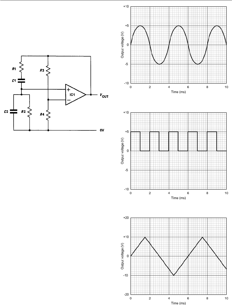
182 ELECTRONIC CIRCUITS: FUNDAMENTALS AND APPLICATIONS
(a) astable multivibrators, (b) monostable
multivibrators, (c) bistable multivibrators.
9.13 Derive an expression (in terms of R3and
R4) for the minimum value of voltage gain
required to produce oscillation in the circuit
shown in Fig. 9.25.
Figure 9.26 See Question 9.14
Figure 9.27 See Question 9.15
Figure 9.28 See Question 9.16
Figure 9.25 See Question 9.13
9.14 Design an oscillator circuit that will
generate the output waveform shown in
Fig. 9.26. Sketch a circuit diagram for the
oscillator and specify all component values
(including supply voltage). Give reasons
for your choice of oscillator circuit.
9.15 Design an oscillator circuit that will
generate the output waveform shown in
Fig. 9.27. Sketch a circuit diagram for the
oscillator and specify all component values
(including supply voltage). Give reasons
for your choice of oscillator circuit.
9.16 Design an oscillator circuit that will
generate the output waveform shown in
Fig. 9.28. Sketch a circuit diagram for the
oscillator and specify all component values
(including supply voltage). Give reasons
for your choice of oscillator circuit.
9.17 Briefly explain the term ‘piezoelectric
effect’.
9.18 Sketch the circuit diagram of simple single-
stage crystal oscillator and explain the
advantages of using a quartz crystal as the
frequency determining element.
Answers to these problems appear on page 375.
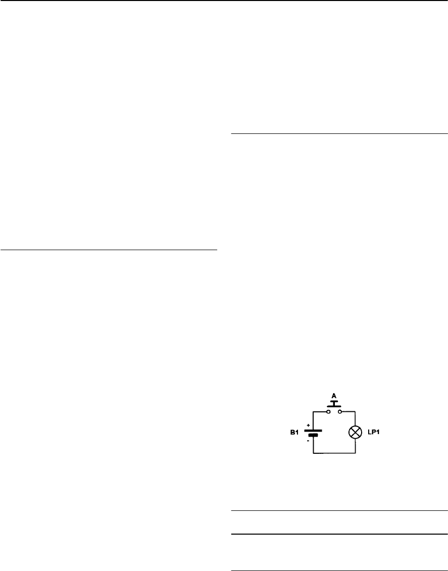
10
Logic circuits
This chapter introduces electronic circuits and
devices that are associated with digital rather than
analogue circuitry. These logic circuits are used
extensively in digital systems and form the basis of
clocks, counters, shift registers and timers.
The chapter starts by introducing the basic logic
functions (AND, OR, NAND, NOR, etc.) together
with the symbols and truth tables that describe the
operation of the most common logic gates. We then
show how these gates can be used in simple
combinational logic circuits before moving on to
introduce bistable devices, counters and shift
registers. The chapter concludes with a brief
introduction to the two principal technologies used
in modern digital logic circuits, TTL and CMOS.
Logic functions
Electronic logic circuits can be used to make
simple decisions like:
If dark then put on the light.
and
If temperature is less then 20°C then connect
the supply to the heater.
They can also be used to make more complex
decisions like:
If ‘hour’ is greater than 11 and ‘24 hour clock’
is not selected then display message ‘pm’.
All of these logical statements are similar in form.
The first two are essentially:
If {condition} then {action}.
while the third is a compound statement of the
form:
If {condition 1} and not {condition 2} then
{action}.
Both of these statements can be readily
Table 10.1 Simple switching logic
Figure 10.1 Simple switch and lamp circuit
implemented using straightforward electronic
circuits. Because this circuitry is based on discrete
states and since the behaviour of the circuits can be
described by a set of logical statements, it is
referred to as digital logic.
Switch and lamp logic
In the simple circuit shown in Fig. 10.1 a battery is
connected to a lamp via a switch. There are two
possible states for the switch, open and closed but
the lamp will only operate when the switch is
closed. We can summarize this using Table 10.1.
Since the switch can only be in one of the two
states (i.e. open or closed) at any given time, the
open and closed conditions are mutually exclusive.
Furthermore, since the switch cannot exist in any
other state than completely open or completely
closed (i.e. there is no intermediate or half-open
state) the circuit uses binary or ‘two-state’ logic.
The logical state of the switch can be represented
by the binary digits, 0 and 1. For example, if
logical 0 is synonymous with open (or ‘off’) and
logical 1 is equivalent to closed (or ‘on’), then:
Switch open (off) = 0
Switch closed (on) = 1
Condition Switch Comment
1Open No light produced
2Closed Light produced
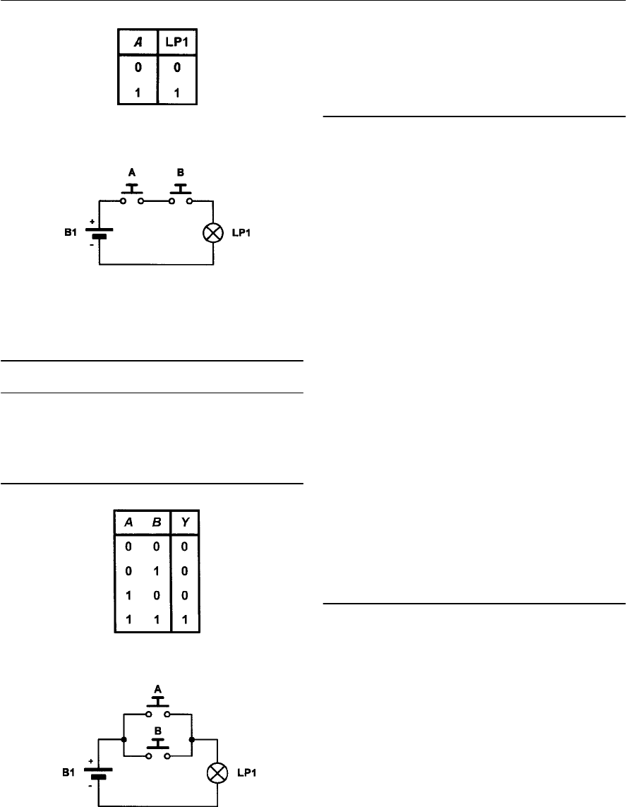
184 ELECTRONIC CIRCUITS: FUNDAMENTALS AND APPLICATIONS
We can now rewrite the truth table in terms of the
binary states as shown in Fig. 10.2 where:
No light (off) = 0
Light (on) = 1
AND logic
Now consider the circuit with two switches shown
in Fig. 10.3. Here the lamp will only operate when
switch A is closed and switch B is closed.
However, let’s look at the operation of the circuit in
alittle more detail.
Since there are two switches (A and B) and there
are two possible states for each switch (open or
closed), there is a total of four possible conditions
for the circuit. We can summarize these conditions
in Table 10.2.
Since each switch can only be in one of the two
states (i.e. open or closed) at any given time, the
open and closed conditions are mutually exclusive.
Furthermore, since the switches cannot exist in any
other state than completely open or completely
closed (i.e. there are no intermediate states) the
circuit uses binary logic.We can thus represent the
logical states of the two switches by the binary
digits, 0 and 1.
Once again, if we adopt the convention that an
open switch can be represented by 0 and a closed
switch by 1, we can rewrite the truth table in terms
of the binary states shown in Fig. 10.4 where:
No light (off) = 0
Light (on) = 1
OR logic
Figure 10.5 shows another circuit with two
switches. This circuit differs from that shown in
Fig. 10.3 by virtue of the fact that the two switches
are connected in parallel rather than in series. In
this case the lamp will operate when either of the
two switches is closed. As before, there is a total of
four possible conditions for the circuit. We can
summarize these conditions in Table 10.3.
Once again, adopting the convention that an
open switch can be represented by 0 and a closed
switch by 1, we can rewrite the truth table in terms
of the binary states as shown in Fig. 10.6.
Table 10.2 Simple AND switching logic
Figure 10.2 Truth table for the switch and lamp
Figure 10.4 Truth table for the switch and lamp
Figure 10.5 OR switch and lamp logic
Figure 10.3 AND switch and lamp logic
Condition Switch A Comment
1Open No light produced
2Open No light produced
3Closed No light produced
4Closed Light produced
Switch B
Open
Closed
Open
Closed
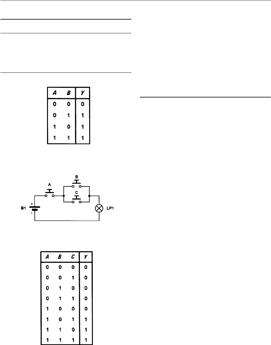
LOGIC CIRCUITS 185
Example 10.1
Figure 10.7 shows a simple switching circuit.
Describe the logical state of switches A, B, and C
in order to operate the lamp. Illustrate your answer
with a truth table.
Solution
In order to operate the lamp, switch A and either
switch B or switch C must be operated. The truth
table is shown in Fig. 10.8.
Logic gates
Logic gates are circuits designed to produce the
basic logic functions, AND, OR, etc. These circuits
are designed to be interconnected into larger, more
complex, logic circuit arrangements. Since these
circuits form the basic building blocks of all digital
systems, we have summarized the action of each of
the gates in the next section. For each gate we have
included its British Standard (BS) symbol together
with its American Standard (MIL/ANSI) symbol.
We have also included the truth tables and Boolean
expressions (using ‘+’ to denote OR, ‘·’ to denote
AND, and ‘E’to denote NOT). Note that, while
inverters and buffers each have only one input,
exclusive-OR gates have two inputs and the other
basic gates (AND, OR, NAND and NOR) are
commonly available with up to eight inputs.
Buffers (Fig. 10.9)
Buffers do not affect the logical state of a digital
signal (i.e. a logic 1 input results in a logic 1 output
whereas a logic 0 input results in a logic 0 output).
Buffers are normally used to provide extra current
drive at the output but can also be used to
regularize the logic levels present at an interface.
The Boolean expression for the output, Y,of a
buffer with an input, X,is:
Y=X
Inverters (Fig. 10.10)
Inverters are used to complement the logical state
(i.e. a logic 1 input results in a logic 0 output and
Table 10.3 Simple OR switching logic
Figure 10.6 Truth table for OR logic
Figure 10.7 See Example 10.1
Figure 10.8 See Example 10.1
Condition Switch A Comment
1Open No light produced
2Open Light produced
3Closed Light produced
4Closed Light produced
Switch B
Open
Closed
Open
Closed
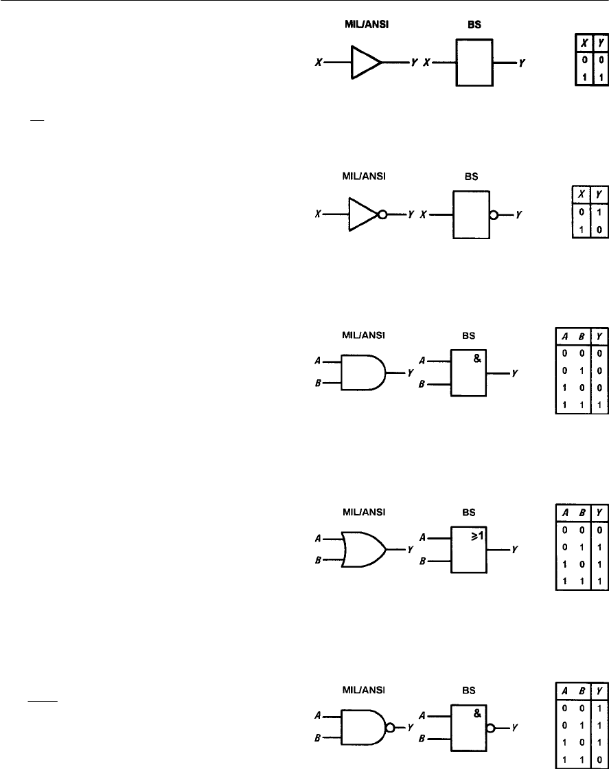
186 ELECTRONIC CIRCUITS: FUNDAMENTALS AND APPLICATIONS
vice versa). Inverters also provide extra current
drive and, like buffers, are used in interfacing
applications where they provide a means of
regularizing logic levels present at the input or
output of a digital system. The Boolean expression
for the output, Y,of a buffer with an input, X,is:
AND gates (Fig. 10.11)
AND gates will only produce a logic 1 output when
all inputs are simultaneously at logic 1. Any other
input combination results in a logic 0 output. The
Boolean expression for the output, Y,of an AND
gate with inputs, Aand B,is:
OR gates (Fig. 10.12)
OR gates will produce a logic 1 output whenever
any one, or more, inputs are at logic 1. Putting this
another way, an OR gate will only produce a logic
0output whenever all of its inputs are
simultaneously at logic 0. The Boolean expression
for the output, Y,of an OR gate with inputs, Aand
B,is:
NAND gates (Fig. 10.13)
NAND (i.e. NOT-AND) gates will only produce a
logic 0 output when all inputs are simultaneously at
logic 1. Any other input combination will produce a
logic 1 output. A NAND gate, therefore, is nothing
more than an AND gate with its output inverted!
The circle shown at the output denotes this
inversion. The Boolean expression for the output,
Y,of a NAND gate with inputs, Aand B,is:
NOR gates (Fig. 10.14)
NOR (i.e. NOT-OR) gates will only produce a
logic 1 output when all inputs are simultaneously at
logic 0. Any other input combination will produce a
Figure 10.9 Symbols and truth table for a buffer
Figure 10.10 Symbols and truth table for an
inverter
Figure 10.11 Symbols and truth table for an AND
gate
Figure 10.12 Symbols and truth table for an OR
gate
Figure 10.13 Symbols and truth table for a NAND
gate
YX
=
YAB
=
+
YAB
=
YAB
=
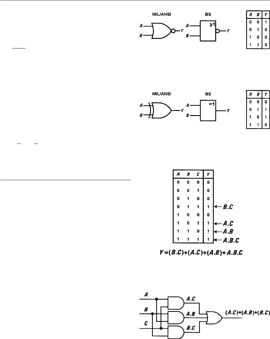
LOGIC CIRCUITS 187
logic 0 output. A NOR gate, therefore, is simply an
OR gate with its output inverted. A circle is again
used to indicate inversion. The Boolean expression
for the output, Y, of a NOR gate with inputs, Aand
B,is:
Exclusive-OR gates (Fig. 10.15)
Exclusive-OR gates will produce a logic 1 output
whenever either one of the inputs is at logic 1 and
the other is at logic 0. Exclusive-OR gates produce
alogic 0 output whenever both inputs have the
same logical state (i.e. when both are at logic 0 or
both are at logic 1). The Boolean expression for the
output, Y,of an exclusive-OR gate with inputs, A
and B,is:
Figure 10.15 Symbols and truth table for an
exclusive-OR gate
Figure 10.14 Symbols and truth table for a NOR
gate
Combinational logic
By using a standard range of logic levels (i.e.
voltage levels used to represent the logic 1 and
logic 0 states) logic circuits can be combined
together in order to solve complex logic functions.
Example 10.2
Alogic circuit is to be constructed that will produce
alogic 1 output whenever two, or more, of its three
inputs are at logic 1.
Solution
This circuit could be more aptly referred to as a
majority vote circuit. Its truth table is shown in
Fig. 10.16. Figure 10.17 shows the logic circuitry
required.
Example 10.3
Show how an arrangement of basic logic gates
(AND, OR and NOT) can be used to produce the
exclusive-OR function.
+
YAB
=
YABBA
=+
Figure 10.16 See Example 10.2
Figure 10.17 See Example 10.2
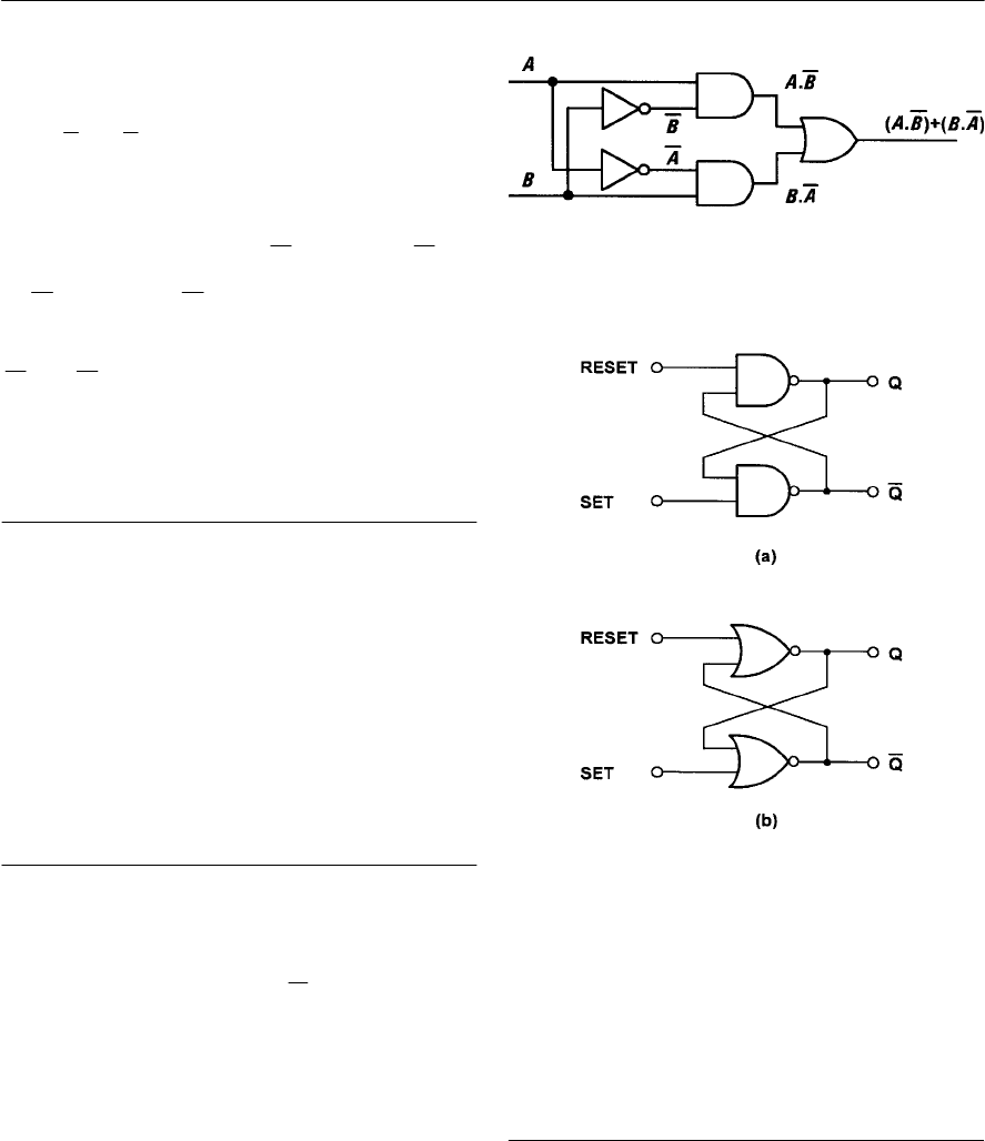
188 ELECTRONIC CIRCUITS: FUNDAMENTALS AND APPLICATIONS
Solution
In order to solve this problem, consider the Boolean
expression for the exclusive-OR function:
This expression takes the form:
can be obtained using two
two-input AND gates and the result (i.e. Pand Q)
can then be applied to an OR gate with two inputs.
can be produced using inverters. The
complete solution is shown in Fig. 10.18.
.
YABBA
=+
where and
YPQ PAB QBA
=+ ==
and
AB Q BA
=
and
AB
Bistables
The output of a bistable has two stables states
(logic 0 or logic 1) and, once set in one or other of
these states, the device will remain at a particular
logic level for an indefinite period until reset. A
bistable thus constitutes a simple form of ‘memory
cell’ because it will remain in its latched state
(whether
set
or
reset
)until a signal is applied to it
in order to change its state (or until the supply is
disconnected).
R-S bistables
The simplest form of bistable is the R-S bistable.
This device has two inputs, SET and RESET, and
complementary outputs, Q and . A logic 1 applied
to the SET input will cause the Q output to become
(or remain at) logic 1 while a logic 1 applied to the
RESET input will cause the Q output to become (or
remain at) logic 0. In either case, the bistable will
remain in its SET or RESET state until an input is
applied in such a sense as to change the state.
Two simple forms of R-S bistable based on
cross-coupled logic gates are shown in Fig. 10.19.
Figure 10.19(a) is based on NAND gates while Fig.
10.19(b) is based on NOR gates.
The simple cross-coupled logic gate bistable has
anumber of serious shortcomings (consider what
Figure 10.19
R-S bistables using cross-coupled
NAND and NOR gates
would happen if a logic 1 was simultaneously
present on both the SET and RESET inputs!) and
practical forms of bistable make use of much
improved purpose-designed logic circuits such as
D-type and J-K bistables.
D-type bistables
The D-type bistable has two inputs: D (standing
variously for ‘data’ or ‘delay’) and CLOCK (CLK).
The data input (logic 0 or logic 1) is clocked into
the bistable such that the output state only changes
Q
Figure 10.18 See Example 10.3
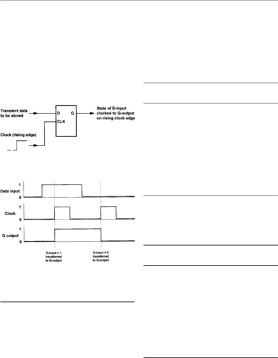
LOGIC CIRCUITS 189
Table 10.4 Input and output states for a J-K
bistable (PRESET and CLEAR inputs)
when the clock changes state. Operation is thus said
to be synchronous. Additional subsidiary inputs
(which are invariably active low) are provided
which can be used to directly set or reset the
bistable. These are usually called PRESET (PR)
and CLEAR (CLR). D-type bistables are used both
as latches (a simple form of memory) and as binary
dividers. The simple circuit arrangement in Fig.
10.20 together with the timing diagram shown in
Fig. 10.21 illustrate the operation of D-type
bistables.
J-K bistables
J-K bistables have two clocked inputs (J and K),
two direct inputs (PRESET and CLEAR), a
CLOCK (CK) input, and outputs (Q and Q). As
with R-S bistables, the two outputs are
complementary (i.e. when one is 0 the other is 1,
and vice versa). Similarly, the PRESET and
CLEAR inputs are invariably both active low (i.e. a
Figure 10.20 D-type bistable operation
Figure 10.21 Timing diagram for the D-type
bistable
0on the PRESET input will set the Q output to 1
whereas a 0 on the CLEAR input will set the Q
output to 0). Tables 10.4 and 10.5 summarize the
operation of a J-K bistable respectively for the
PRESET and CLEAR inputs and for clocked
operation.
Note: QN+1 means ‘Q after the next clock transition’
while QNmeans ‘Q in whatever state it was before’.
Note: The preset and clear inputs operate regardless of
the clock.
Inputs Output
PRESET CLEAR QN+1
0 0 ? Indeterminate
0 1 0
Qoutput changes to 0
(i.e. Q is reset) regardless
of the clock state
1 0 1
Qoutput changes to 1
(i.e. Q is set) regardless
of the clock state
1 1 See below
Enables clocked
operation (refer to Table
10.5)
Comments
Inputs Output
J K QN+1
0 0 QN
No change in state of the
Qoutput on the next
clock transition
0 1 0
Qoutput changes to 0
(i.e. Q is reset) on the
next clock transition
1 0 1
Qoutput changes to 1
(i.e. Q is set) on the next
clock transition
1 1 QN
Qoutput changes to the
opposite state on the next
clock transition
Comments
Table 10.5 Input and output states for a J-K
bistable (clocked operation)
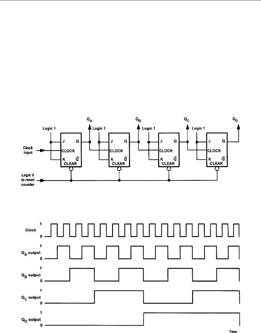
190 ELECTRONIC CIRCUITS: FUNDAMENTALS AND APPLICATIONS
Figure 10.23 Timing diagram for the four-stage binary counter shown in Fig. 10.22
J-K bistables are the most sophisticated and
flexible of the bistable types and they can be
configured in various ways including binary
dividers, shift registers, and latches.
Figure 10.22 shows the arrangement of a four-
stage binary counter based on J-K bistables. The
timing diagram for this circuit is shown in Fig.
10.23. Each stage successively divides the clock
input signal by a factor of two. Note that a logic 1
input is transferred to the respective Q-output on
the falling edge of the clock pulse and all J and K
inputs must be taken to logic 1 to enable binary
counting.
Figure 10.24 shows the arrangement of a four-
stage shift register based on J-K bistables. The
timing diagram for this circuit is shown in Fig.
10.25. Note that each stage successively feeds data
to the next stage. Note that all data transfer occurs
on the falling edge of the clock pulse.
Example 10.4
Alogic arrangement has to be designed so that it
produces the pulse train shown in Fig. 10.27.
Devise a logic circuit arrangement that will
Figure 10.22 Four-stage binary counter using J-K bistables
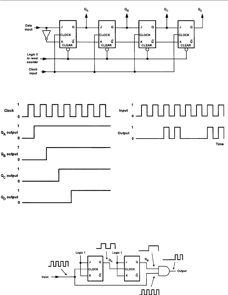
generate this pulse train from a regular square wave
input.
Solution
Atwo-stage binary divider (based on J-K bistables)
can be used together with a two-input AND gate as
shown in Fig. 10.26. The waveforms for this logic
arrangement are shown in Fig. 10.28.
LOGIC CIRCUITS 191
Figure 10.25 Timing diagram for the four-stage
shift register shown in Fig. 10.24
Figure 10.24 Four-stage shift register using J-K bistables
Figure 10.27 See Example 10.4
Figure 10.26 See Example 10.4
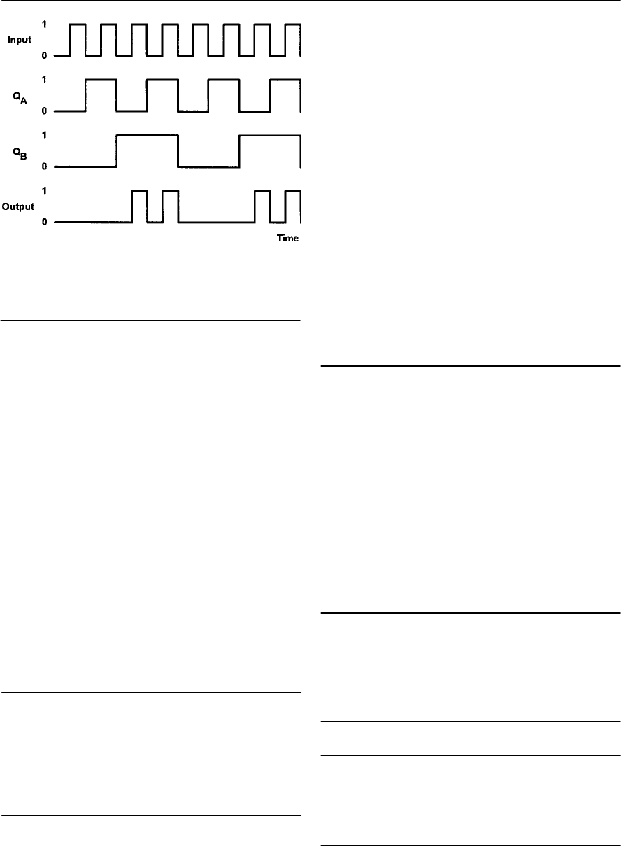
Table 10.6 TTL device coding—infix letters
192 ELECTRONIC CIRCUITS: FUNDAMENTALS AND APPLICATIONS
Figure 10.28 Waveforms for the logic
arrangement shown in Fig. 10.26
Integrated circuit logic devices
The task of realizing a complex logic circuit is
made simple with the aid of digital integrated
circuits. Such devices are classified according to
the semiconductor technology used in their
fabrication (the logic family to which a device
belongs is largely instrumental in determining its
operational characteristics, such as power
consumption, speed, and immunity to noise).
The relative size of a digital integrated circuit (in
terms of the number of active devices that it
contains) is often referred to as its scale of
integration and the terminology in Table 10.5 is
commonly used.
The two basic logic families are CMOS
(complementary metal oxide semiconductor) and
TTL (transistor transistor logic). Each of these
families is then further sub-divided. Representative
circuits for a two-input AND gate in both
technologies are shown in Figs 10.29 and 10.30.
The most common family of TTL logic devices
is known as the 74-series. Devices from this family
are coded with the prefix number 74. Variants
within the family are identified by letters which
follow the initial 74 prefix, as shown in Table 10.6.
The most common family of CMOS devices is
known as the 4000-series. Variants within the
family are identified by the suffix letters given in
Table 10.7.
Scale of
integration Abbreviation Number of logic
gates*
Small SSI 1 to 10
Medium MSI 10 to 100
Large LSI 100 to 1,000
Very large VLSI 1,000 to 10,000
Super large SLSI 10,000 to 100,000
Table 10.5 Scale of integration
*or active circuitry of equivalent complexity
Infix Meaning
None Standard TTL device
ALS Advanced low-power Schottky
CCMOS version of a TTL device
F‘Fast’ (a high-speed version)
HHigh-speed version
SSchottky input configuration (improved
speed and noise immunity)
HC High-speed CMOS version (CMOS com-
patible inputs)
HCT High-speed CMOS version (TTL com-
patible inputs)
LS Low-power Schottky
Infix Meaning
None Standard CMOS device
AStandard (unbuffered) CMOS device
B, BE Improved (buffered) CMOS device
UB, UBE Improved (unbuffered) CMOS device
Table 10.7 CMOS device coding—the most
common variants of the 4000 family are identified
using these suffix letters
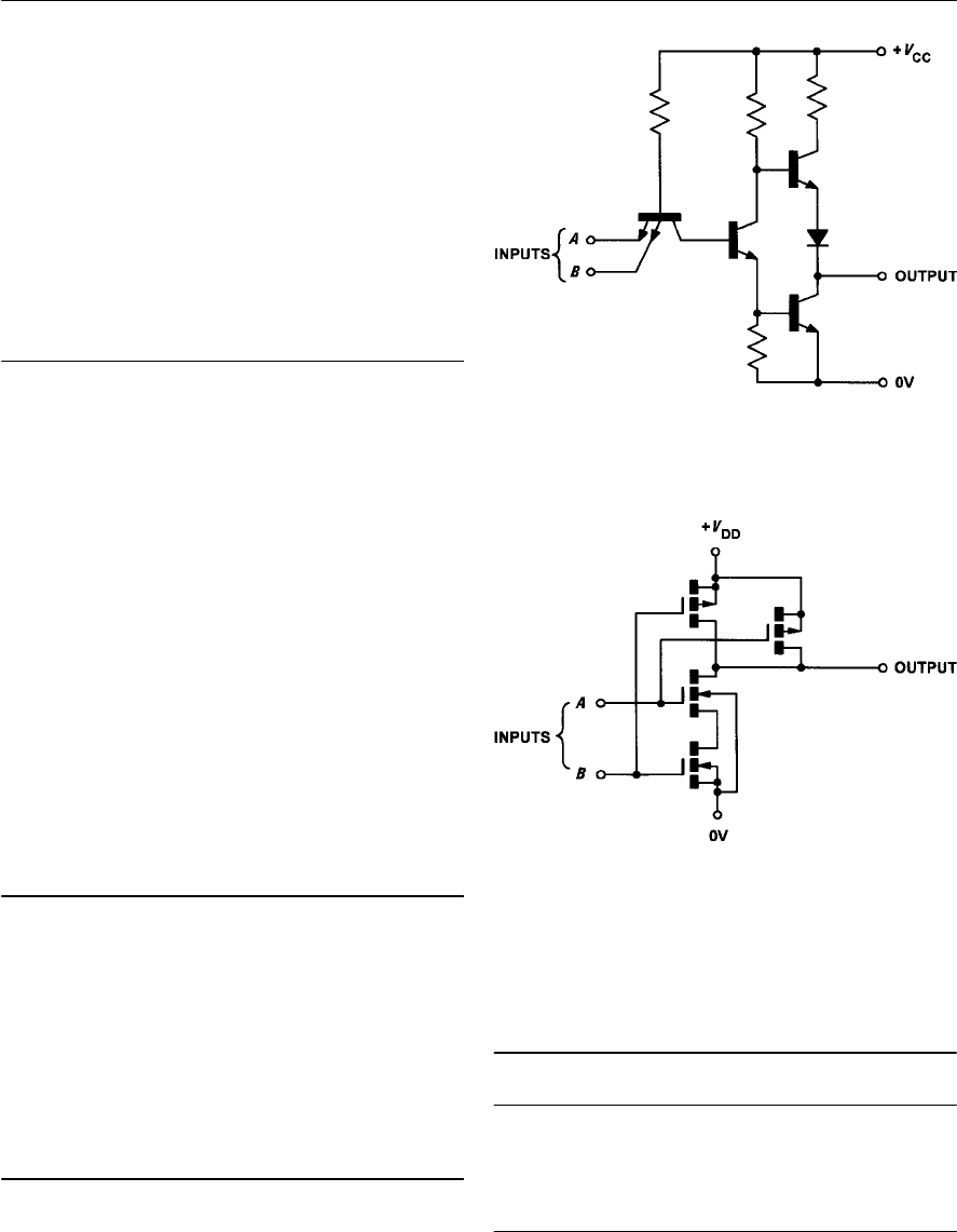
Figure 10.30 Two-input CMOS NAND gate
LOGIC CIRCUITS 193
Example 10.5
Identify each of the following integrated circuits:
(i) 4001UBE;
(ii) 74LS14.
Solution
Integrated circuit (i) is an improved (unbuffered)
version of the CMOS 4001 device. Integrated
circuit (ii) is a low-power Schottky version of the
TTL 7414 device.
Date codes
It is also worth noting that the vast majority of
logic devices and other digital integrated circuits
are marked with a four digit date code. The code
often appears alongside or below the device code.
The first two digits of this code give the year of
manufacture while the last two digits specify the
week of manufacture.
Example 10.6
An integrated circuit marked ‘4050B 9832’. What
type of device is it and when was it manufactured?
Solution
The device is a buffered CMOS 4050 manufactured
in the 32nd week of 1998.
Logic levels
Logic levels are simply the range of voltages used
to represent the logic states 0 and 1. The logic
levels for CMOS differ markedly from those
associated with TTL. In particular, CMOS logic
levels are relative to the supply voltage used while
the logic levels associated with TTL devices tend to
be absolute (see Table 10.8).
Noise margin
The noise margin of a logic device is a measure of
its ability to reject noise and spurious signals; the
Figure 10.29 Two-input TTL NAND gate
Condition CMOS TTL
Logic 0 Less than 1/3VDD More than 2 V
Logic 1 More than 2/3VDD Less than 0.8 V
Indeterminate Between 1/3VDD
and 2/3VDD
Between 0.8 V
and 2 V
Table 10.8 Logic levels for CMOS and TTL logic
devices
Note: VDD is the positive supply associated with CMOS
devices
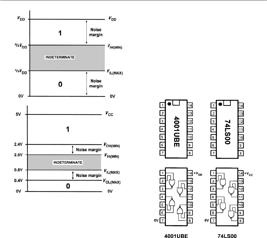
194 ELECTRONIC CIRCUITS: FUNDAMENTALS AND APPLICATIONS
larger the noise margin the better is its ability to
perform in an environment in which noise is
present. Noise margin is defined as the difference
between the minimum values of high state output
and high state input voltage and the maximum
values of low state output and low state input
voltage. Hence:
Noise margin = VOH(MIN) RVIH(MIN)
or
Noise margin = VOL(MAX) RVOH(MAX)
where VOH(MIN) is the minimum value of high state
(logic 1) output voltage, VIH(MIN) is the minimum
value of high state (logic 1) input voltage, VOL(MAX)
is the maximum value of low state (logic 0) output
voltage, and VOH(MAX) is the maximum value of low
state (logic 0) input voltage.
Figure 10.31 Logic levels and noise margins for
TTL and CMOS devices
The noise margin for standard 7400 series TTL is
typically 400 mV while that for CMOS is 1/3VDD,
as shown in Fig. 10.31.
Table 10.9 compares the more important
characteristics of common members of the TTL
family with their buffered CMOS logic
counterparts. Finally, Fig. 10.32 shows the
packages and pin connections for two common
logic devices, the 74LS00 (quad two-input NAND
gate) and the 4001UBE (quad two-input NOR
gate).
Figure 10.32 Packages and pin connections for
two common logic devices
Example 10.7
Show how a 4001UBE device (see Fig. 10.32) can
be connected to form a simple cross-coupled
bistable. Sketch a circuit diagram showing pin
connections and include LEDs that will indicate the
output state of the bistable.
Solution
See Practical investigation on Page 195. Note that
only two of the four logic gates have been used.
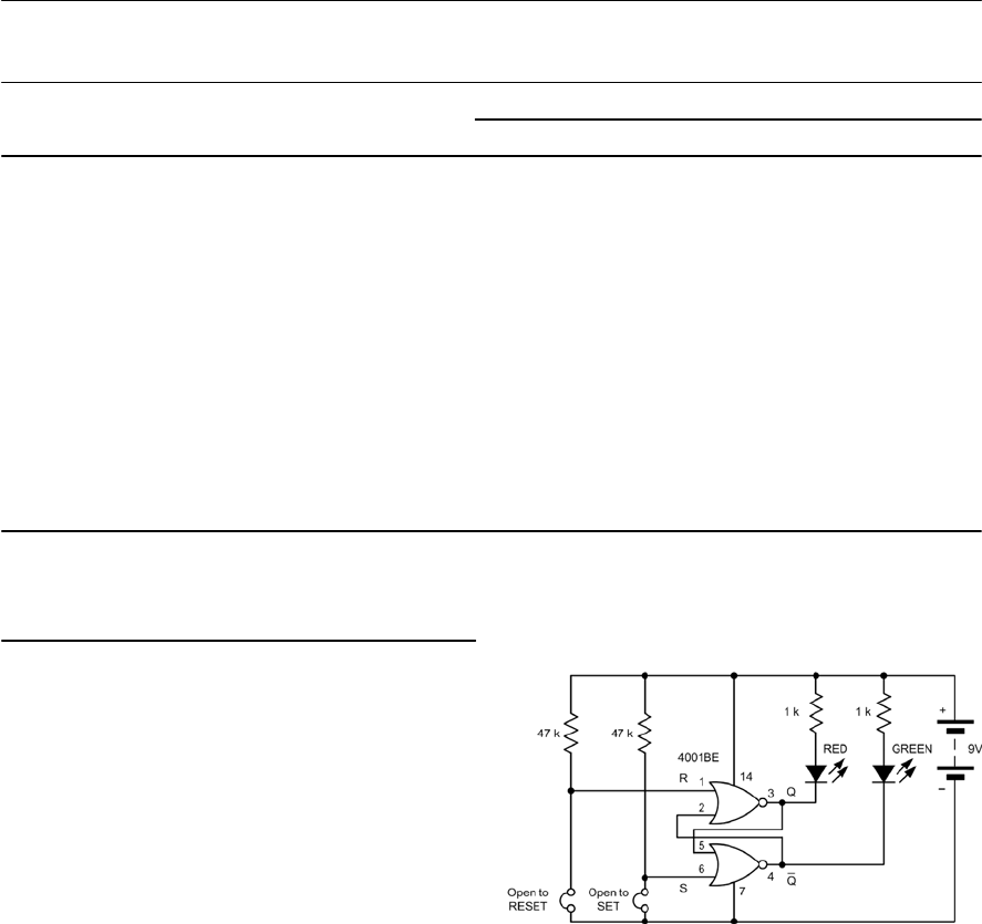
LOGIC CIRCUITS 195
Practical investigation
Objective
To investigate the operation of a simple bistable
based on cross-coupled NOR gates.
Components and test equipment
Breadboard, 9 V d.c. power supply (or a 9 V
battery), 4001BE quad two-input buffered CMOS
NOR gate, red and green LEDs, operational
amplifier), two 1 kTand two 47 kT5% 0.25 W
resistors, test leads, connecting wire.
Procedure
Connect the circuit shown in Fig. 10.33 (see also
Fig. 10.34 for the corresponding breadboard
layout). Note that the green LED should become
illuminated when the bistable is in the SET
condition (i.e. when Q is at logic 1) and the red
LED should become illuminated when the bistable
is in the RESET condition. Note also that the 47 k
resistors act as pull-up resistors.They are used to
ensure that the respective input goes to logic 1
when the corresponding link is removed.
Figure 10.33 Bistable circuit used in the Practical
investigation. The LEDs are used to indicate the
state of the outputs
With both links in place (i.e. SET = 0 and
RESET = 0) observe and record (using a truth
table) the state of the outputs.
Remove the RESET link (to make RESET = 1)
whilst leaving the SET link in place (to keep SET =
0). Once again, observe and record the state of the
outputs. Replace the RESET link (to make RESET
=0) and check that the bistable does not change
Table 10.9 Characteristics of common logic families
Characteristic 74 74LS 74HC 40BE
Maximum supply voltage (V) 5.25 5.25 5.5 18
Minimum supply voltage (V) 4.75 4.75 4.5 3
Static power dissipation (mW per gate at 100 kHz) 10 2 negligible negligible
Dynamic power dissipation (mW per gate at 100 kHz) 10 2 0.2 0.1
Typical propagation delay (ns) 10 10 10 105
Maximum clock frequency (MHz) 35 40 40 12
Speed-power product (pJ at 100 kHz) 100 20 1.2 11
Minimum output current (mA at VO=0.4 V) 16 8 4 1.6
Fan-out (number of standard loads that can be driven) 40 20 10 4
Maximum input current (mA at VI=0.4 V) R1.6 R0.4 0.001 R0.001
Logic family
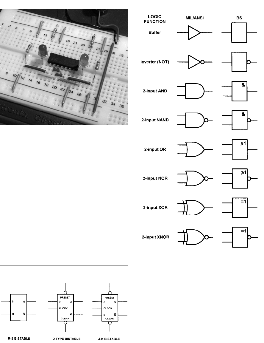
196 ELECTRONIC CIRCUITS: FUNDAMENTALS AND APPLICATIONS
Important formulae introduced in this
chapter
Noise margin:
(page 194)
Noise margin = VOH(MIN) RVIH(MIN)
or
Noise margin = VOL(MAX) RVOH(MAX)
Figure 10.36 Logic gate symbols
Symbols introduced in this chapter
Figure 10.35 Bistable symbols
state. Now remove the SET link (to make SET = 1).
Once again, observe and record the state of the
outputs. Replace the SET link (to make SET = 0)
and once again check that the bistable does not
change state. Finally, remove both links (to make
SET = 1 and RESET = 1) and observe the state of
the outputs in this disallowed state.
Conclusion
Comment on the truth table produced. Is this what
you would expect? What happened when both SET
and RESET inputs were at logic 1? Suggest a
typical application for the circuit.
Figure 10.34 Breadboard circuit layout
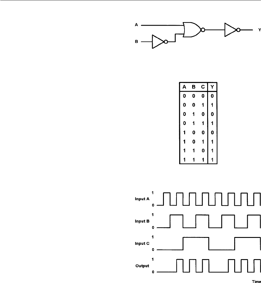
LOGIC CIRCUITS 197
Problems
10.1 Show how a four-input AND gate can be
made from three two-input AND gates.
10.2 Show how a four-input OR gate can be
made from three two-input OR gates.
10.3 Construct the truth table for the logic gate
arrangement shown in Fig. 10.37.
10.4 Using only two-input NAND gates, show
how each of the following logical functions
can be satisfied:
(a) two-input AND;
(b) two-input OR;
(c) four-input AND.
In each case, use the minimum number of
gates. (Hint: a two-input NAND gate can be
made into an inverter by connecting its two
inputs together)
10.5 The rocket motor of an air-launched missile
will operate if, and only if, the following
conditions are satisfied:
(i) ‘launch’ signal is at logic 1;
(ii) ‘unsafe height’ signal is at logic 0;
(iii) ‘target lock’ signal is at logic 1.
Devise a suitable logic arrangement that will
satisfy this requirement. Simplify your
answer using the minimum number of logic
gates.
10.6 An automatic sheet metal guillotine will
operate if the following conditions are
satisfied:
(i) ‘guard lowered’ signal is at logic 1;
(ii) ‘feed jam’ signal is at logic 0;
(iii) ‘manual start’ signal is at logic 1.
The sheet metal guillotine will also operate
if the following conditions are satisfied:
(i) ‘manual start’ signal is at logic 1;
(ii) ‘test key’ signal is at logic 1.
Devise a suitable logic arrangement that will
satisfy this requirement. Use the minimum
number of logic gates.
10.7 Devise a logic arrangement using no more
than four two-input gates that will satisfy the
truth table shown in Fig. 10.38.
10.8 Devise a logic arrangement that will produce
the output waveform from the three input
waveforms shown in Fig. 10.39.
10.9 A logic device is marked ‘74LS90 2798’. To
which family and sub-family of logic does it
belong and when was the device
manufactured?
Figure 10.37 See Questions 10.3 and 10.22
10.10 A logic family recognizes a logic 1 input as
being associated with any voltage between
2.0 V and 5.5 V. The same family produces
an output in the range 2.6 V to 5.0 V
corresponding to a logic 1 output. Determine
the noise margin.
Figure 10.38 See Question 10.7
Figure 10.39 See Question 10.8.
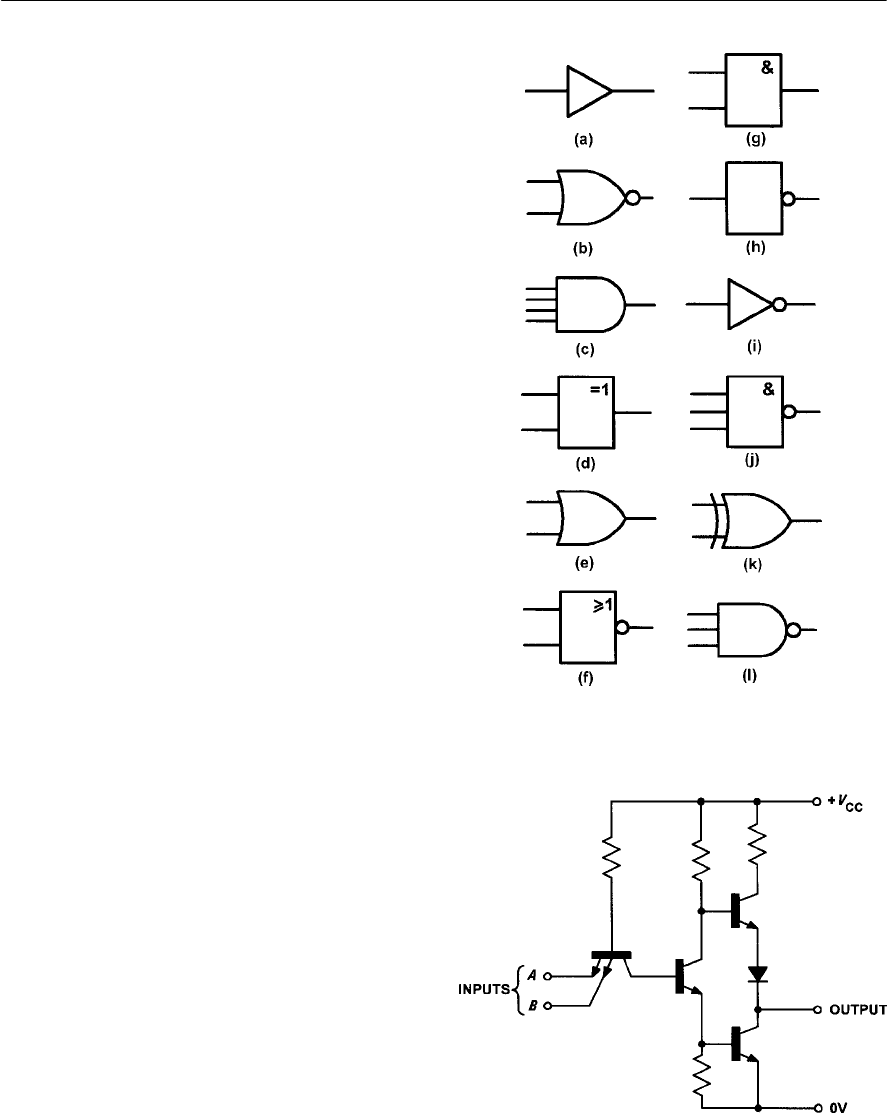
198 ELECTRONIC CIRCUITS: FUNDAMENTALS AND APPLICATIONS
Figure 10.40 See Question 10.15
Figure 10.41 See Questions 10.17 and 10.18
10.11 Sketch the circuit of a bistable using:
(a) two NAND gates;
(b) two NOR gates.
Label the inputs and outputs on your
diagram.
10.12 Sketch the symbol of each of the following
types of bistable:
(a) an R-S bistable;
(b) a D-type bistable;
(c) a J-K bistable.
Label your drawings clearly.
10.13 With the aid of a diagram, explain how a
three-stage binary counter can be built using
J-K bistables.
10.14 With the aid of a diagram, explain how a
three-stage shift register can be built using
J-K bistables.
10.15 Identify each of the logic devices shown in
Fig. 10.40.
10.16 Explain, in relation to the scale of
integration, what is meant by the terms (a)
MSI and (b) VLSI.
10.17 Figure 10.41 shows the internal schematic
for a logic device. Identify the logic family
to which this device belongs and state its
logic function.
10.18 Specify typical logic levels for the logic
device shown in Fig. 10.41. In relation to
your answer, explain the significance of the
indeterminate region and explain how this
effects the noise margin of the device.
10.19 Sketch the logic gate arrangement of a four
input majority vote circuit. Using a truth
table, briefly explain the operation of the
circuit.
10.20 Show, with the aid of a logic diagram, how
an exclusive-OR gate can be built using only
two-input NAND gates.
10.21 Specify typical values for the power
dissipation, propagation delay, and
maximum clock speed for (a) low-power
Schottky TTL and (b) buffered CMOS.
10.22 Devise a logic gate arrangement using only
two-input NAND gates that will perform the
same logic function as the arrangement
shown in Fig. 10.37. Simplify your answer
as far as possible using the minimum
number of logic gates.
Answers to these problems appear on page 375.

11
Microprocessors
Many of today’s complex electronic systems are
based on the use of a microprocessor or
microcontroller. Such systems comprise hardware
that is controlled by software. If it is necessary to
change the way that the system behaves it is the
software (rather than the hardware) that is changed.
In this chapter we provide an introduction to
microprocessors and explain, in simple terms, both
how they operate and how they are used. We shall
start by explaining some of the terminology that is
used to describe different types of system that
involve the use of a microprocessor or a similar
device.
Microprocessor systems
Microprocessor systems are usually assembled on a
single PCB comprising a microprocessor CPU
together with a number of specialized support
chips. These very large scale integrated (VLSI)
devices provide input and output to the system,
control and timing as well as storage for programs
and data.
Typical applications for microprocessor systems
include the control of complex industrial processes.
Typical examples are based on families of chips
such as the Z80CPU plus Z80PIO, Z80CTC, and
Z80SIO.
Single-chip microcomputers
Asingle-chip microcomputer is a complete
computer system (comprising CPU, RAM and
ROM etc.) in a single VLSI package. A single-chip
microcomputer requires very little external circuitry
in order to provide all of the functions associated
with a complete computer system (but usually with
limited input and output capability).
Single-chip microcomputers may be
programmed using in-built programmable
memories or via external memory chips. Typical
applications of single-chip microcomputers include
computer printers, instrument controllers, and
displays. A typical example is the Z84C.
Microcontrollers
Amicrocontroller is a single-chip microcomputer
that is designed specifically for control rather than
general-purpose applications. They are often used
to satisfy a particular control requirement, such as
controlling a motor drive. Single-chip micro-
computers, on the other hand, usually perform a
variety of different functions and may control
several processes at the same time.
Typical applications include control of peripheral
devices such as motors, drives, printers, and minor
sub-system components. Typical examples are the
Z86E, 8051, 68705 and 89C51.
PIC microcontrollers
APIC microcontroller is a general-purpose
microcontroller device that is normally used in a
stand-alone application to perform simple logic,
timing and input/output control. PIC devices
provide a flexible low-cost solution that very
effectively bridges the gap between single-chip
computers and the use of discrete logic and timer
chips, as explained in Chapter 18.
A number of PIC and microcontroller devices
have been produced that incorporate a high-level
language interpreter. The resident interpreter allows
developers to develop their programs languages
such as BASIC rather than having to resort to more
complex assembly language. This feature makes
PIC microcontrollers very easy to use. PIC
microcontrollers are used in ‘self-contained’
applications involving logic, timing and simple
analogue to digital and digital to analogue
conversion. Typical examples are the PIC12C508
and PIC16C620.
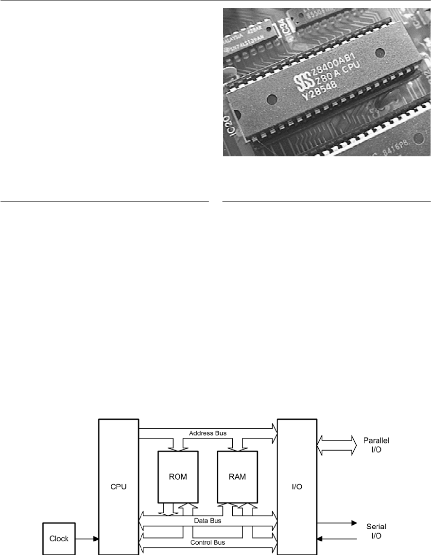
200 ELECTRONIC CIRCUITS: FUNDAMENTALS AND APPLICATIONS
Figure 11.1 Block diagram of a microprocessor system
Programmed logic devices
Whilst not an example of a microprocessor device,
aprogrammed logic device (PLD) is a
programmable chip that can carry out complex
logical operations. For completeness, we have
included a reference to such devices here. PLDs are
capable of replacing a large number of
conventional logic gates, thus minimising chip-
count and reducing printed circuit board sizes.
Programming is relatively straightforward and
simply requires the derivation of complex logic
functions using Boolean algebra (see Chapter 10)
or truth tables. Typical examples are the 16L8 and
22V10.
Programmable logic controllers
Programmable logic controllers (PLC) are
microprocessor based systems that are used for
controlling a wide variety of automatic processes,
from operating an airport baggage handling system
to brewing a pint of your favourite lager. PLCs are
rugged and modular and they are designed
specifically for operation in the process control
environment.
The control program for a PLC is usually stored
in one or more semiconductor memory devices.
The program can be entered (or modified) by
means of a simple hand-held programmer, a laptop
controller, or downloaded over a local area network
(LAN). PLC manufacturers include Allen Bradley,
Siemens and Mitsubishi.
Microprocessor systems
The basic components of any microprocessor
system (see Fig. 11.1) are:
(a) a central processing unit (CPU)
(b) a memory, comprising both ‘read/write’ and
‘read only’ devices (commonly called RAM
and ROM respectively)
(c) a means of providing input and output (I/O).
For example, a keypad for input and a display
for output.
In a microprocessor system the functions of the
CPU are provided by a single very large scale
integrated (VLSI) microprocessor chip (see Fig.
11.2). This chip is equivalent to many thousands of
Figure 11.2 A Z80 microprocessor

MICROPROCESSORS 201
Table 11.1 Binary, denary and hexadecimal
individual transistors. Semiconductor devices are
also used to provide the read/write and read-only
memory. Strictly speaking, both types of memory
permit ‘random access’ since any item of data can
be retrieved with equal ease regardless of its actual
location within the memory. Despite this, the term
‘RAM’ has become synonymous with
semiconductor read/write memory.
The basic components of the system (CPU,
RAM, ROM and I/O) are linked together using a
multiple-wire connecting system know as a bus
(see Fig. 11.1). Three different buses are present,
these are:
(a) the address bus used to specify memory
locations;
the data bus on which data is transferred
between devices; and
(c) the control bus which provides timing and
control signals throughout the system.
The number of individual lines present within the
address bus and data bus depends upon the
particular microprocessor employed. Signals on all
lines, no matter whether they are used for address,
data, or control, can exist in only two basic states:
logic 0 (low)or logic 1 (high). Data and addresses
are represented by binary numbers (a sequence of
1s and 0s) that appear respectively on the data and
address bus.
Many microprocessors designed for control and
instrumentation applications make use of an 8-bit
data bus and a 16-bit address bus. Others have data
and address buses which can operate with as many
as 128-bits at a time.
The largest binary number that can appear on an
8-bit data bus corresponds to the condition when all
eight lines are at logic 1. Therefore the largest
value of data that can be present on the bus at any
instant of time is equivalent to the binary number
11111111 (or 255). Similarly, most the highest
address that can appear on a 16-bit address bus is
1111111111111111 (or 65,535). The full range of
data values and addresses for a simple
microprocessor of this type is thus:
Data from 00000000
to 11111111
Addresses from 0000000000000000
to 1111111111111111
Data representation
Binary numbers – particularly large ones – are not
very convenient. To make numbers easier to handle
we often convert binary numbers to hexadecimal
(base 16). This format is easier for mere humans to
comprehend and offers the advantage over denary
(base 10) in that it can be converted to and from
binary with ease. The first sixteen numbers in
binary, denary, and hexadecimal are shown in the
table below. A single hexadecimal character (in the
range zero to F) is used to represent a group of four
binary digits (bits). This group of four bits (or
single hex. character) is sometimes called a nibble.
Abyte of data comprises a group of eight bits.
Thus a byte can be represented by just two
hexadecimal (hex) characters. A group of sixteen
bits (a word) can be represented by four hex
characters, thirty-two bits (a double word by eight
hex. characters, and so on).
The value of a byte expressed in binary can be
easily converted to hex by arranging the bits in
groups of four and converting each nibble into
hexadecimal using the table shown below:
Binary
(base 2)
Denary
(base 10)
Hexadecimal
(base 16)
0000 0 0
0001 1 1
0010 2 2
0011 3 3
0100 4 4
0101 5 5
0110 6 6
0111 7 7
1000 8 8
1001 9 9
1010 10 A
1011 11 B
1100 12 C
1101 13 D
1110 14 E
1111 15 F

202 ELECTRONIC CIRCUITS: FUNDAMENTALS AND APPLICATIONS
Note that, to avoid confusion about whether a
number is hexadecimal or decimal, we often place a
$symbol before a hexadecimal number or add an H
to the end of the number. For example, 64 means
decimal ‘sixty-four’; whereas, $64 means
hexadecimal ‘six-four’, which is equivalent to
decimal 100. Similarly, 7FH means hexadecimal
‘seven-F’ which is equivalent to decimal 127.
Example 11.1
Convert hexadecimal A3 into binary.
Solution
From Table 11.1, A = 1010 and 3 = 0101. Thus A3
in hexadecimal is equivalent to 10100101 in binary.
Example 11.2
Convert binary 11101000 binary to hexadecimal.
Solution
From Table 11.1, 1110 = E and 1000 = 8. Thus
11101000 in binary is equivalent to E8 in
hexadecimal.
Data types
Abyte of data can be stored at each address within
the total memory space of a microprocessor system.
Hence one byte can be stored at each of the 65,536
memory locations within a microprocessor system
having a 16-bit address bus.
Individual bits within a byte are numbered from
0(least significant bit) to 7 (most significant bit). In
the case of 16-bit words, the bits are numbered
from 0 (least significant bit) to 15 (most significant
bit).
Negative (or signed) numbers can be represented
using two’s complement notation where the
leading (most significant) bit indicates the sign of
the number (1 = negative, 0 = positive). For
example, the signed 8-bit number 10000001
represents the denary number G1.
The range of integer data values that can be
represented as bytes, words and long words are
shown in Table 11.2.
Data storage
The semiconductor ROM within a microprocessor
system provides storage for the program code as
well as any permanent data that requires storage.
All of this data is referred to as non-volatile
because it remains intact when the power supply is
disconnected.
The semiconductor RAM within a
microprocessor system provides storage for the
transient data and variables that are used by
programs. Part of the RAM is also be used by the
microprocessor as a temporary store for data whilst
carrying out its normal processing tasks.
It is important to note that any program or data
stored in RAM will be lost when the power supply
is switched off or disconnected. The only exception
to this is CMOS RAM that is kept alive by means
of a small battery. This battery-backed memory is
used to retain important data, such as the time and
date.
When expressing the amount of storage provided
by a memory device we usually use Kilobytes
(Kbyte). It is important to note that a Kilobyte of
memory is actually 1,024 bytes (not 1,000 bytes).
The reason for choosing the Kbyte rather than the
kbyte (1,000 bytes) is that 1,024 happens to be the
nearest power of 2 (note that 210 = 1,024).
The capacity of a semiconductor ROM is usually
specified in terms of an address range and the
number of bits stored at each address. For example,
2 K × 8 bits (capacity 2 Kbytes), 4 K × 8 bits
(capacity 4 Kbytes), and so on. Note that it is not
always necessary (or desirable) for the entire
memory space of a microprocessor to be populated
by memory devices.
Table 11.2 Data types
Data type Bits Range of values
Unsigned byte 8 0 to 255
Signed byte 8 G128 to +127
Unsigned word 16 0 to 65,535
Signed word 16 G32,768 to +32,767
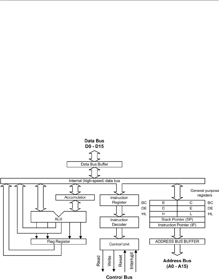
MICROPROCESSORS 203
The microprocessor
The microprocessor central processing unit
(CPU)forms the heart of any microprocessor or
microcomputer system computer and,
consequently, its operation is crucial to the entire
system.
The primary function of the microprocessor is
that of fetching, decoding, and executing
instructions resident in memory. As such, it must
be able to transfer data from external memory into
its own internal registers and vice versa.
Furthermore, it must operate predictably,
distinguishing, for example, between an operation
contained within an instruction and any
accompanying addresses of read/write memory
locations. In addition, various system housekeeping
tasks need to be performed including being able to
suspend normal processing in order to respond to
an external device that needs attention.
The main parts of a microprocessor CPU are:
(a) registers for temporary storage of addresses
and data;
(b) an arithmetic logic unit (ALU) that performs
arithmetic and logic operations;
(c) a unit that receives and decodes instructions;
and
(d) a means of controlling and timing operations
within the system.
Figure 11.3 shows the principal internal features of
atypical 8-bit microprocessor. We will briefly
explain each of these features in turn:
Accumulator
The accumulator functions as a source and
destination register for many of the basic
microprocessor operations. As a source register it
contains the data that will be used in a particular
Figure 11.3 Internal architecture of a typical 8-bit microprocessor CPU

204 ELECTRONIC CIRCUITS: FUNDAMENTALS AND APPLICATIONS
operation whilst as a destination register it will be
used to hold the result of a particular operation. The
accumulator (or A-register)features in a very large
number of microprocessor operations, consequently
more reference is made to this register than any
others.
Instruction register
The instruction register provides a temporary
storage location in which the current
microprocessor instruction is held whilst it is being
decoded. Program instructions are passed into the
microprocessor, one at time, through the data bus.
On the first part of each machine cycle,the
instruction is fetched and decoded. The instruction
is executed on the second (and subsequent)
machine cycles. Each machine cycle takes a finite
time (usually less than a microsecond) depending
upon the frequency of the microprocessor’s clock.
Data bus (D0 to D7)
The external data bus provides a highway for data
that links all of the system components (such as
random access memory, read-only memory, and
input/output devices) together. In an 8-bit system,
the data bus has eight data lines, labelled D0 (the
least significant bit)to D7 (the most significant
bit)and data is moved around in groups of eight
bits, or bytes.With a sixteen bit data bus the data
lines are labelled D0 to D15, and so on.
Data bus buffer
The data bus buffer is a temporary register through
which bytes of data pass on their way into, and out
of, the microprocessor. The buffer is thus referred
to as bi-directional with data passing out of the
microprocessor on a write operation and into the
processor during a read operation.The direction
of data transfer is determined by the control unit as
it responds to each individual program instruction.
Internal data bus
The internal data bus is a high-speed data highway
that links all of the microprocessor’s internal
elements together. Data is constantly flowing
backwards and forwards along the internal data bus
lines.
General-purpose registers
Many microprocessor operations (for example,
adding two 8-bit numbers together) require the use
of more than one register. There is also a
requirement for temporarily storing the partial
result of an operation whilst other operations take
place. Both of these needs can be met by providing
anumber of general-purpose registers. The use to
which these registers are put is left mainly up to the
programmer.
Stack pointer
When the time comes to suspend a particular task
in order to briefly attend to something else, most
microprocessors make use of a region of external
random access memory (RAM) known as a stack.
When the main program is interrupted, the
microprocessor temporarily places in the stack the
contents of its internal registers together with the
address of the next instruction in the main program.
When the interrupt has been attended to, the
microprocessor recovers the data that has been
stored temporarily in the stack together with the
address of the next instruction within the main
program. It is thus able to return to the main
program exactly where it left off and with all the
data preserved in its registers. The stack pointer is
simply a register that contains the address of the
last used stack location.
Program counter
Programs consist of a sequence of instructions that
are executed by the microprocessor. These
instructions are stored in external random access
memory (RAM) or read-only memory (ROM).
Instructions must be fetched and executed by the
microprocessor in a strict sequence. By storing the
address of the next instruction to be executed, the
program counter allows the microprocessor to keep
track of where it is within the program. The
program counter is automatically incremented
when each instruction is executed.
Address bus buffer
The address bus buffer is a temporary register
through which addresses (in this case comprising
16-bits) pass on their way out of the

MICROPROCESSORS 205
microprocessor. In a simple microprocessor, the
address buffer is unidirectional with addresses
placed on the address bus during both read and
write operations. The address bus lines are labelled
A0 to A15, where A0 is the least-significant
address bus line and A16 is the most significant
address bus line. Note that a 16-bit address bus can
be used to communicate with 65,536 individual
memory locations. At each location a single byte of
data is stored.
Control bus
The control bus is a collection of signal lines that
are both used to control the transfer of data around
the system and also to interact with external
devices. The control signals used by
microprocessors tend to differ with different types,
however the following are commonly found:
READ an output signal from the microprocessor
that indicates that the current operation is
a read operation
WRITE an output signal from the microprocessor
that indicates that the current operation
is a write operation
RESET a signal that resets the internal registers
and initializes the program counter so
that the program can be re-started from
the beginning
IRQ interrupt request from an external device
attempting to gain the attention of the
microprocessor (the request may be
obeyed or ignored according to the
state of the microprocessor at the time
that the interrupt request is received).
NMI non-maskable interrupt (i.e. an interrupt
signal that cannot be ignored by the
microprocessor).
Address bus (A0 to A15)
The address bus provides a highway for addresses
that links with all of the system components (such
as random access memory, read-only memory, and
input/output devices). In a system with a 16-bit
address bus, there are sixteen address lines, labelled
A0 (the least significant bit) to A15 (the most
significant bit). In a system with a 32-bit address
bus there are 32 address lines, labelled A0 to A31,
and so on.
Instruction decoder
The instruction decoder is nothing more than an
arrangement of logic gates that acts on the bits
stored in the instruction register and determines
which instruction is currently being referenced. The
instruction decoder provides output signals for the
microprocessor’s control unit.
Control unit
The control unit is responsible for organizing the
orderly flow of data within the microprocessor as
well as generating, and responding to, signals on
the control bus. The control unit is also responsible
for the timing of all data transfers. This process is
synchronized using an internal or external clock
signal (not shown in Fig. 11.3).
Arithmetic logic unit (ALU)
As its name suggests, the ALU performs arithmetic
and logic operations. The ALU has two inputs (in
this case these are both 8-bits wide). One of these
inputs is derived from the Accumulator whilst the
other is taken from the internal data bus via a
temporary register (not shown in Fig. 11.3). The
operations provided by the ALU usually include
addition, subtraction, logical AND, logical OR,
logical exclusive-OR, shift left, shift right, etc. The
result of most ALU operations appears in the
accumulator.
Flag register (or status register)
The result of an ALU operation is sometimes
important in determining what subsequent action
takes place. The flag register contains a number of
individual bits that are set or reset according to the
outcome of an ALU operation. These bits are
referred to as flags. The following flags are
available in most microprocessors:
ZERO the zero flag is set when the result of an
ALU operation is zero (i.e. a byte value
of 00000000)
CARRY the carry flag is set whenever the result
of an ALU operation (such as addition)
generates a carry bit (in other words,
when the result cannot be contained
within an 8-bit register)
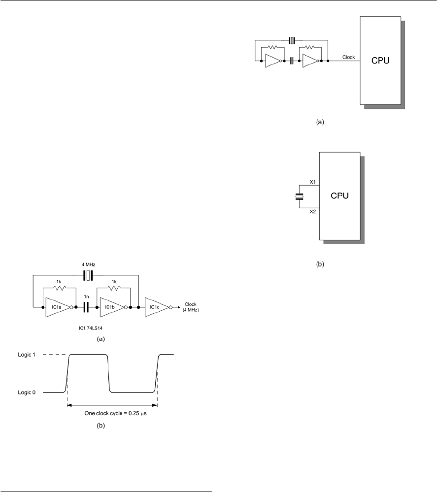
206 ELECTRONIC CIRCUITS: FUNDAMENTALS AND APPLICATIONS
INTERRUPT the interrupt flag indicates
whether external interrupts are
currently enabled or disabled.
Clocks
The clock used in a microprocessor system is
simply an accurate and stable square wave
generator. In most cases the frequency of the square
wave generator is determined by a quarts crystal. A
simple 4 MHz square wave clock oscillator
(together with the clock waveform that is produces)
is shown in Fig. 11.4. Note that one complete clock
cycle is sometimes referred to as a T-state.
Microprocessors sometimes have an internal
clock circuit in which case the quartz crystal (or
other resonant device) is connected directly to pins
on the microprocessor chip. In Fig. 11.5(a) an
external clock is shown connected to a
microprocessor whilst in Fig.11.5(b) and internal
clock oscillator is used.
Microprocessor operation
The majority of operations performed by a
microprocessor involve the movement of data.
Indeed, the program code (a set of instructions
stored in ROM or RAM) must itself be fetched
from memory prior to execution. The
microprocessor thus performs a continuous
sequence of instruction fetch and execute cycles.
The act of fetching an instruction code (or operand
or data value) from memory involves a read
operation whilst the act of moving data from the
microprocessor to a memory location involves a
write operation – see Fig. 11.6.
Each cycle of CPU operation is known as a
machine cycle. Program instructions may require
several machine cycles (typically between two and
five). The first machine cycle in any cycle consists
of an instruction fetch (the instruction code is read
from the memory) and it is known as the M1 cycle.
Subsequent cycles M2, M3, and so on, depend on
the type of instruction that is being executed. This
fetch-execute sequence is shown in Fig. 11.7.
Microprocessors determine the source of data
(when it is being read) and the destination of data
(when it is being written) by placing a unique
address on the address bus. The address at which
the data is to be placed (during a write operation) or
from which it is to be fetched (during a read
operation) can either constitute part of the memory
of the system (in which case it may be within ROM
Figure 11.4 (a) A typical microprocessor clock
circuit (b) waveform produced by the clock circuit
Figure 11.5 (a) An external CPU clock, and (b) an
internal CPU clock
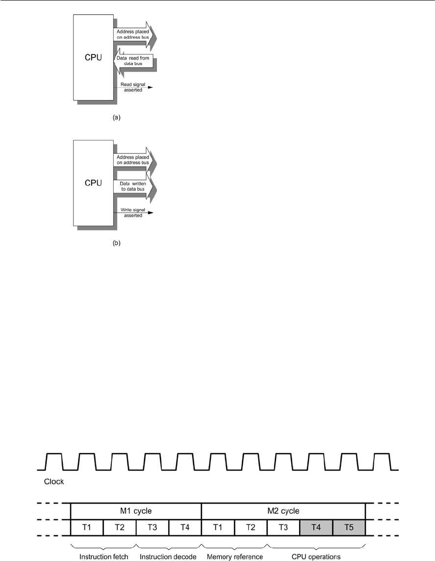
MICROPROCESSORS 207
or RAM) or it can be considered to be associated
with input/output (I/O).
Since the data bus is connected to a number of
VLSI devices, an essential requirement of such
chips (e.g., ROM or RAM) is that their data outputs
should be capable of being isolated from the bus
whenever necessary. These chips are fitted with
select or enable inputs that are driven by address
decoding logic (not shown in Fig. 11.2). This logic
ensures that ROM, RAM and I/O devices never
simultaneously attempt to place data on the bus!
The inputs of the address decoding logic are
derived from one, or more, of the address bus lines.
The address decoder effectively divides the
available memory into blocks corresponding to a
particular function (ROM, RAM, I/O, etc). Hence,
where the processor is reading and writing to RAM,
for example, the address decoding logic will ensure
that only the RAM is selected whilst the ROM and
I/O remain isolated from the data bus.
Within the CPU, data is stored in several
registers. Registers themselves can be thought of as
asimple pigeon-hole arrangement that can store as
many bits as there are holes available. Generally,
these devices can store groups of sixteen or thirty-
two bits. Additionally, some registers may be
configured as either one register of sixteen bits or
two registers of thirty-two bits.
Some microprocessor registers are accessible to
the programmer whereas others are used by the
microprocessor itself. Registers may be classified
as either general purpose or dedicated. In the latter
case a particular function is associated with the
register, such as holding the result of an operation
or signalling the result of a comparison. A typical
microprocessor and its register model is shown in
Fig. 11.8.
The arithmetic logic unit
The ALU can perform arithmetic operations
(addition and subtraction) and logic
(complementation, logical AND, logical OR, etc).
The ALU operates on two inputs (sixteen or thirty-
two bits in length depending upon the CPU type)
and it provides one output (again of sixteen or
thirty-two bits). In addition, the ALU status is
Figure 11.6 (a) Read, and (b) write operations
Figure 11.7 A typical timing diagram for a microprocessor’s fetch-execute cycle
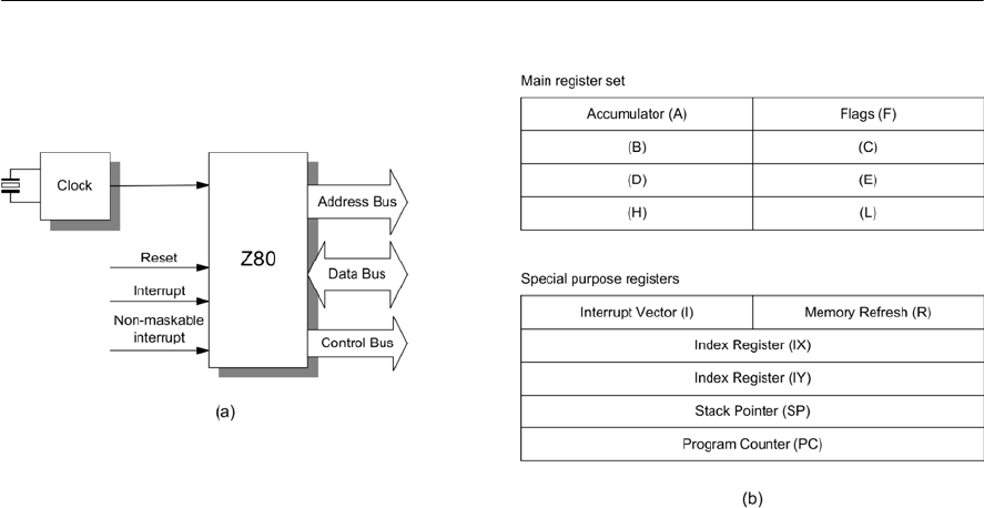
208 ELECTRONIC CIRCUITS: FUNDAMENTALS AND APPLICATIONS
preserved in the flag register so that, for example,
an overflow, zero or negative result can be
detected.
The control unit is responsible for the movement
of data within the CPU and the management of
control signals, both internal and external. The
control unit asserts the requisite signals to read or
write data as appropriate to the current instruction.
Input and output
The transfer of data within a microprocessor system
involves moving groups of 8, 16 or 32-bits using
the bus architecture described earlier. Consequently
it is a relatively simple matter to transfer data into
and out of the system in parallel form. This process
is further simplified by using a Programmable
Parallel I/O device (a Z80PIO, 8255, or equivalent
VLSI chip). This device provides registers for the
temporary storage of data that not only buffer the
data but also provide a degree of electrical isolation
from the system data bus.
Parallel data transfer is primarily suited to high-
speed operation over relatively short distances, a
typical example being the linking of a
microcomputer to an adjacent dot matrix printer.
There are, however, some applications in which
parallel data transfer is inappropriate, the most
common example being data communication by
means of telephone lines. In such cases data must
be sent serially (one bit after another) rather than in
parallel form.
To transmit data in serial form, the parallel data
from the microprocessor must be reorganized into a
stream of bits. This task is greatly simplified by
using an LSI interface device that contains a shift
register that is loaded with parallel data from the
data bus. This data is then read out as a serial bit
stream by successive shifting. The reverse process,
serial-to-parallel conversion, also uses a shift
register. Here data is loaded in serial form, each bit
shifting further into the register until it becomes
full. Data is then placed simultaneously on the
parallel output lines. The basic principles of
parallel-to-serial and serial-to-parallel data
conversion are illustrated in Fig. 11.9.
An example program
The following example program (see Table 11.3) is
written in assembly code. The program transfers 8-
bit data from an input port (Port A), complements
Figure 11.8 The Z80 microprocessor (showing some of its more important control signals) together with
its register model
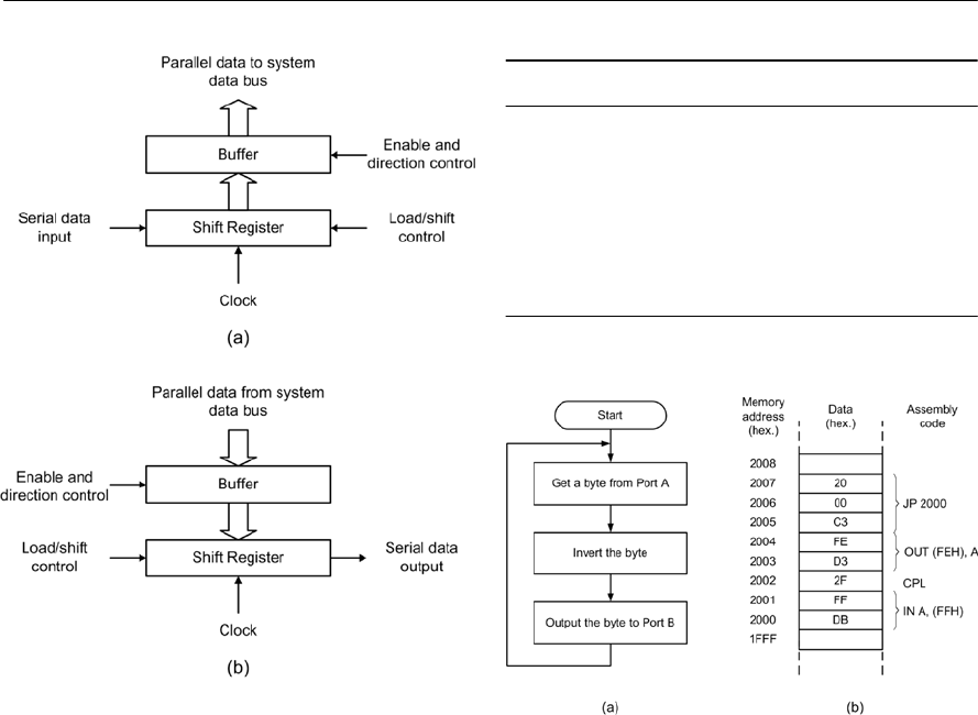
MICROPROCESSORS 209
(i.e. inverts) the data (by changing 0’s to 1’s and
1’s to 0’s in every bit position) and then outputs the
result to an output port (Port B). The program
repeats indefinitely.
Just three microprocessor instructions are
required to carry out this task together with a fourth
(jump) instruction that causes the three instructions
to be repeated over and over again. A program of
this sort is most easily written in assembly code
which consists of a series of easy to remember
mnemonics. The flowchart for the program is
shown in Fig. 11.10(a).
The program occupies a total of eight bytes of
memory, starting at a hexadecimal address of 2000
as shown in Fig. 11.10(b). You should also note
that the two ports, A and B, each have unique
addresses; Port A is at hexadecimal address FF
whilst Port B is at hexadecimal address FE.
Interrupts
Aprogram that simply executes a loop indefinitely
has a rather limited practical application. In most
microprocessor systems we want to be able to
interrupt the normal sequence of program flow in
order to alert the microprocessor to the need to do
something. We can do this with a signal known as
an interrupt.There are two types of interrupt;
maskable and non-maskable.
When a non-maskable interrupt input is
asserted, the processor must suspend execution of
the current instruction and respond immediately to
the interrupt. In the case of a maskable interrupt,
Table 11.3 A simple example program
Address Data Assembly code Comment
2002 DB FF IN A, (FFH) Get a byte from
Port A
2002 2F CPL Invert the byte
2003 D3 FE OUT (FEH), A Output the byte
to Port B
2005 C3 00 20 JP 2000 Go round again
Figure 11.9 (a) Serial-to-parallel data conversion,
and (b) parallel-to-serial data conversion Figure 11.10 (a) Flowchart for the example
program and (b) the eight bytes of program code
stored in memory

210 ELECTRONIC CIRCUITS: FUNDAMENTALS AND APPLICATIONS
the processor's response will depend upon whether
interrupts are currently enabled or disabled (when
enabled, the CPU will suspend its current task and
carry out the requisite interrupt service routine).
The response to interrupts can be enabled or
disabled by means of appropriate program
instructions. In practice, interrupt signals may be
generated from a number of sources and since each
will require its own customized response a
mechanism must be provided for identifying the
source of the interrupt and calling the appropriate
interrupt service routine. In order to assist in this
task, the microprocessor may use a dedicated
programmable interrupt controller chip.
Amicrocontroller system
Figure 11.11 shows the arrangement of a typical
microcontroller system. The sensed quantities
(temperature, position, etc.) are converted to
corresponding electrical signals by means of a
number of sensors. The outputs from the sensors (in
either digital or analogue form) are passed as input
signals to the microcontroller. The microcontroller
also accepts inputs from the user. These user set
options typically include target values for variables
(such as desired room temperature), limit values
(such as maximum shaft speed), or time constraints
(such as ‘on’ time and ‘off’ time, delay time, etc).
The operation of the microcontroller is
controlled by a sequence of software instructions
known as a control program. The control program
operates continuously, examining inputs from
sensors, user settings, and time data before making
changes to the output signals sent to one or more
controlled devices.
The controlled quantities are produced by the
controlled devices in response to output signals
from the microcontroller. The controlled device
generally converts energy from one form into
energy in another form. For example, the controlled
device might be an electrical heater that converts
electrical energy from the AC mains supply into
heat energy thus producing a given temperature
(the controlled quantity).
In most real-world systems there is a requirement
for the system to be automatic or self-regulating.
Once set, such systems will continue to operate
without continuous operator intervention. The
output of a self-regulating system is fed back to its
input in order to produce what is known as a closed
loop system. A good example of a closed-loop
system is a heating control system that is designed
to maintain a constant room temperature and
humidity within a building regardless of changes in
the outside conditions.
In simple terms, a microcontroller must produce
aspecific state on each of the lines connected to its
output ports in response to a particular combination
of states present on each of the lines connected to
its input ports (see Fig. 11.11). Microcontrollers
must also have a central processing unit (CPU)
capable of performing simple arithmetic, logical
and timing operations.
The input port signals can be derived from a
number of sources including:
•switches (including momentary action push-
buttons)
•sensors (producing logic-level compatible
outputs)
•keypads (both encoded and unencoded types).
The output port signals can be connected to a
number of devices including:
•LED indicators (both individual and multiple
bar types)
•LED seven segment displays (via a suitable
interface)
•motors and actuators (both linear and rotary
types) via a suitable buffer/driver or a dedicated
interface)
•relays (both conventional electromagnetic types
and optically couple solid-state types)
•transistor drivers and other solid-state switching
devices.
Input devices
Input devices supply information to the computer
system from the outside world. In an ordinary
personal computer, the most obvious input device
is the keyboard. Other input devices available on a
PC are the mouse (pointing device), scanner and
modem. Microcontrollers use much simpler input
devices. These need be nothing more than
individual switches or contacts that make and break
but many other types of device are also used
including many types of sensor that provide logic
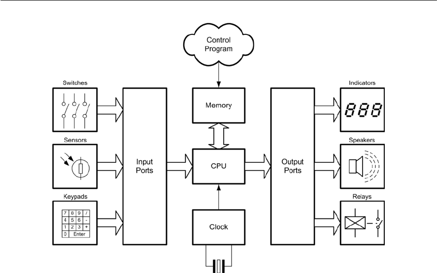
MICROPROCESSORS 211
level outputs (such as float switches, proximity
detectors, light sensors, etc).
It is important to note that, in order to be
connected directly to the input port of a
microcontroller, an input device must provide a
logic compatible signal. This is because
microcontroller inputs can only accept digital input
signals with the same voltage levels as the logic
power source. The 0 V ground level (often referred
to as VSS in the case of a CMOS microcontroller)
and the positive supply (VDD in the case of a
CMOS microcontroller) is invariably 5 V ± 5%. A
level of approximately 0V indicates a logic 0 signal
and a voltage approximately equal to the positive
power supply indicates a logic 1 signal.
Other input devices may sense analogue
quantities (such as velocity) but use a digital code
to represent their value as an input to the
microcontroller system. Some microcontrollers
provide an internal analogue-to-digital converter
(ADC) in order to greatly simplify the connection
of analogue sensors as input devices but where this
facility isn’t available it will be necessary to use an
external ADC which usually takes the form of a
single integrated circuit. The resolution of the ADC
will depend upon the number of bits used and 8, 10,
and 12-bit devices are common in control
applications.
Output devices
Output devices are used to communicate
information or actions from a computer system to
the outside world. In a personal computer system,
the most common output device is the CRT
(cathode ray tube) display. Other output devices
include printers and modems. As with input
devices, microcontroller systems often use much
simpler output devices. These may be nothing more
than LEDs, piezoelectric sounders, relays and
motors. In order to be connected directly to the
output port of a microcontroller, an output device
must, once again, be able to accept a logic
compatible signal.
Figure 11.11 A microcontroller system with typical inputs and outputs
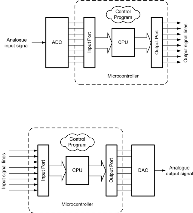
212 ELECTRONIC CIRCUITS: FUNDAMENTALS AND APPLICATIONS
Where analogue quantities (rather than simple
digital on/off operation) are required at the output a
digital-to-analogue converter (DAC) will be
needed. All of the functions associated with a DAC
can be provided by a single integrated circuit. As
with an ADC, the output resolution of a DAC
depends on the number of bits and 8, 10, and 12-
bits are common in control applications.
Interface circuits
Finally, where input and output signals are not
logic compatible (i.e. when they are outside the
range of signals that can be connected directly to
Figure 11.13 An analogue output signal can be produced by connecting a digital-to-analogue converter
(DAC) to a microcontroller output power
Figure 11.12 An analogue input signal can be connected to a microcontroller input port via an analogue-to-
digital converter (ADC)
the microcontroller) some additional interface
circuitry may be required in order to shift the
voltage levels or to provide additional current
drive. Additional circuitry may also be required
when a load (such as a relay or motor) requires
more current than is available from a standard logic
device or output port. For example, a common
range of interface circuits (solid-state relays) is
available that will allow a microcontroller to be
easily interfaced to an AC mains-connected load. It
then becomes possible for a small microcontroller
(operating from only a 5 V DC supply) to control a
central heating system operating from 240 V AC
mains.
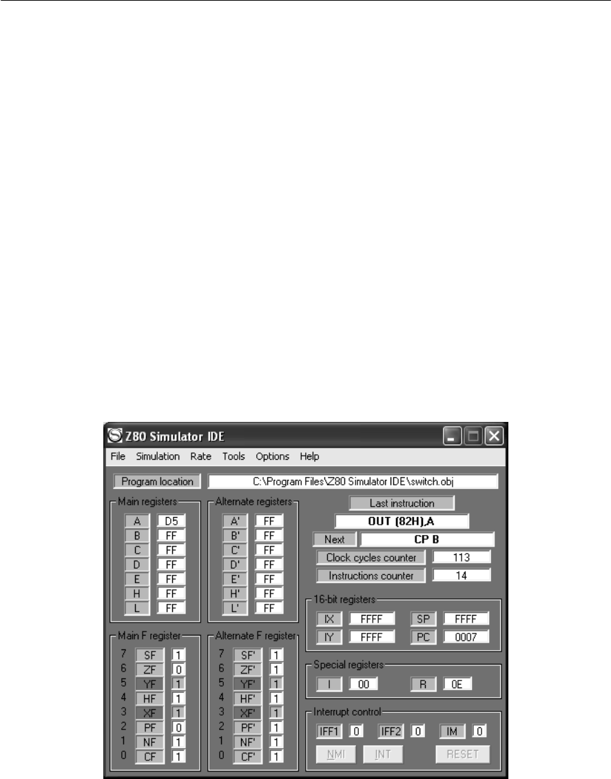
MICROPROCESSORS 213
Practical investigation
Objective
To investigate the operation of a Z80
microprocessor using a simulator to run a simple
assembly language program.
Simulator
Oshonsoft Z80 Simulator or similar Integrated
Development Environment (IDE). The Oshonsoft
IDE can be downloaded from www.oshonsoft.com.
Alternatively, a Z80 development system with
resident assembler and I/O ports can be used (note
that port addresses used in the Practical
Investigation may need to be modified in order to
agree with those available).
System configuration and required operation
For the purposes of this investigation we shall
assume that the system has eight input switches
connected to port address 80H and eight LED
Figure 11.14 The Z80 Simulator Integrated Development Environment (IDE)
indicators connected to output port address 82H.
The LEDs are to be operated from their
corresponding input switches on the following
basis:
Inputs (Port 80H)
Switch ‘on’ = logic 1
Switch ‘off’ = logic 0
Outputs (Port 82H)
Logic 1 = LED ‘off’
Logic 0 = LED ‘on’
Note that, in order to illuminate an LED the logic 1
input must be inverted in order to produce a logic 0
output. Hence it will be necessary to read the byte
from port 80H, invert (i.e. complement) it, and then
output it to port 82H.
The program is to continue to run, detecting the
state of the input switches and turning the
appropriate LEDs on, until such time as all of the
input switches are set to the ‘off’ position. If this
situation is detected the program is to halt.
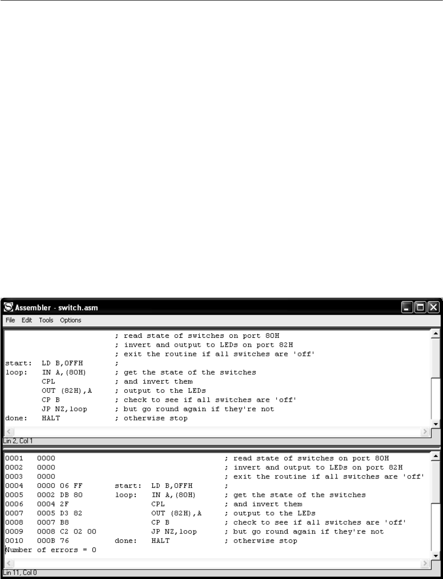
214 ELECTRONIC CIRCUITS: FUNDAMENTALS AND APPLICATIONS
Figure 11.15 Assembly language source code for the Practical investigation
Procedure
Start the Z80 Simulator (see Fig. 11.14) then select
Tools and Assembler and enter the assembly
language code shown in Fig. 11.15. When complete
select File and Save your assembly language source
code with a suitable name (e.g. switch.asm).
Next select Tools and Assemble. Correct any
errors in the assembly language source code and
repeat the process until the source code assembles
without error. Save the final assembly code and
then quit the assembler in order to return to the
main IDE screen.
Select File and Load Program and then select the
object code (switch.obj) that has just been produced
by the assembler. You will then need to configure
the input and output ports before you run the
program. You can do this by selecting Tools and
Peripheral Devices (see Fig. 11.16). Configure the
peripheral devices so that the input port address is
80H and the output port address to 82H. Then set
some of the input bits by clicking on the indicators
(which will change colour).
Next, return to the main IDE, select Tools and
Simulation Log Viewer and then Rate and Slow.
Finally, select Simulation and Start (or press the F1
key). You will see the program instructions and the
contents of the Z80’s registers displayed as the
program is executed (see Fig. 11.17). If you have
left the Peripheral Devices window open you will
also be able to change the switch settings and
observe the effect that this has. Finally, you should
set all of the switches to the ‘off’ position and
check that the program exits from the loop and
reaches the HALT instruction.
Afurther program
If you have been able to run the simple program
successfully you might like to try your hand at
developing your own assembly language program
using some of the assembly language instructions
shown in Table 11.4. This program should shift the
bits on output Port 82H to the left by the number of
places indicated by data from Port 80H. The two
ports can be preset before running the program.
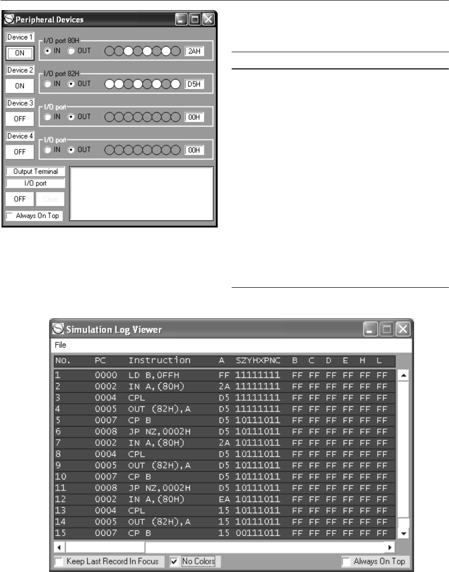
MICROPROCESSORS 215
Table 11.4 Some selected Z80 assembly language
instructions
Figure 11.17 Simulation log showing execution of individual program instructions
Assembly code Meaning
LD A, data Load the Accumulator with 8-bit data
LD B, data Load the B register with 8-bit data
LD C, data Load the C register with 8-bit data
LD C,A Load the C register with 8-bit data
from the Accumulator
CP B Compare the value in the B register
with the value in the Accumulator
DEC C Decrement the C register
CPL Complement (i.e. invert) the contents
of the Accumulator
SLA A Shift the contents of the Accumulator
left by one bit
JP NZ, label Jump to the symbolic address label of
the Zero flag has been set
HALT Halt (suspend program execution)
IN A, (port) Input the data from the specified port
to the Accumulator
OUT (port), A Output the data from the Accumulator
to the specified port
Figure 11.16 Input and output data can be set and
viewed (respectively) using the Peripheral Devices
dialogue
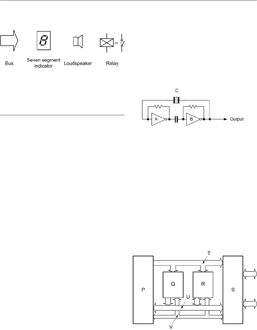
216 ELECTRONIC CIRCUITS: FUNDAMENTALS AND APPLICATIONS
Problems
11.1 Convert 3A hexadecimal to binary.
11.2 Convert 11000010 binary to hexadecimal.
11.3 Convert 63 decimal to
(a) binary
(b) hexadecimal.
11.4 Which of the following numbers is the
largest?
(a) 19H
(b) $13
(c) 3310
(d) 111012.
11.5 How many unique addresses are available to
a microprocessor CPU that has a 20-bit
address bus?
11.6 What is the largest unsigned data value that
can appear on a 10-bit data bus?
11.7 What is the largest negative data value that
can be represented using signed 16-bit
binary numbers?
11.8 The following fragment of assembly
language code is executed using a Z80
microprocessor:
IN A, (FEH)
CPL
OUT (FFH), A
HALT
(a) What are the addresses of the input and
output ports?
(b) If a data value of 10101111 appears at
the input port what value will appear at
the output port after the code has been
executed?
Symbols introduced in this chapter
Figure 11.18 Symbols introduced in this chapter
11.9 Give examples of (a) two input devices, and
(b) two output devices commonly used in
microprocessor systems.
11.10 Explain the purpose of the circuit shown in
Fig. 11.19 and state the function of the
components marked A, B and C.
11.11 Sketch two cycles of the typical output
waveform produced by the circuit shown in
Fig. 11.19. Include labelled axes of time and
voltage.
Figure 11.19 See Questions 11.10 and 11.11
11.12 Identify, and briefly explain the purpose of,
the features labelled P, Q, R, S, T, U, and V
in the microcomputer system shown in
Fig. 11.20.
11.13 Explain the function of four common control
bus signals used in a microcomputer system.
11.14 Explain the need for an ADC when a
temperature sensor is to be interfaced to a
microcomputer system.
Answers to these problems appear on page 376.
Figure 11.20 See Question 11.12

12
The 555 timer
The 555 timer is without doubt one of the most
versatile integrated circuit chips ever produced. Not
only is it a neat mixture of analogue and digital
circuitry but its applications are virtually limitless
in the world of timing and digital pulse generation.
The device also makes an excellent case study for
newcomers to electronics because it combines a
number of important concepts and techniques.
Internal features
To begin to understand how timer circuits operate,
it is worth spending a few moments studying the
internal circuitry of the 555 timer, see Fig. 12.1.
Essentially, the device comprises two operational
amplifiers (used as comparators – see page 166)
together with an R-S bistable element (see page
188). In addition, an inverting buffer (see page 185)
is incorporated so that an appreciable current can
be delivered to a load. The main features of the
device are shown in Table 12.1.
Unlike standard TTL logic devices, the 555 timer
can both source and sink current. It’s worth taking
alittle time to explain what we mean by these two
terms:
(a) When sourcing current, the 555’s output
(pin-3) is in the high state and current will
then flow out of the output pin into the load
and down to 0V, as shown in Fig. 12.2(a).
(b) When sinking current, the 555’s output
(pin-3) is in the low state in which case
current will flow from the positive supply
(+Vcc) through the load and into the output
(pin-3), as shown in Fig. 12.2(b).
Returning to Fig. 12.1, the single transistor switch,
TR1, is provided as a means of rapidly discharging
an external timing capacitor. Because the series
chain of resistors, R1, R2and R3, all have identical
values, the supply voltage (VCC)is divided equally
across the three resistors. Hence the voltage at the
non-inverting input of IC1 is one-third of the
supply voltage (VCC)whilst that at the inverting
input of IC2 is two-thirds of the supply voltage
(VCC). Hence if VCC is 9 V, 3 V will appear at each
resistor and the upper comparator will have 6 V
applied to its inverting input whilst the lower
comparator will have 3V at its non-inverting input.
The 555 family
The standard 555 timer is housed in an 8-pin dual-
in-line (DIL) package and operates from supply rail
voltages of between 4.5 V and 15 V. This, of
Table 12.1 Internal features of the 555 timer
Feature Function
A A potential divider comprising R1,R2and R3
connected in series. Since all three resistors
have the same values the input voltage (VCC)
will be divided into thirds, i.e. one third of VCC
will appear at the junction of R2and R3whilst
two thirds of VCC will appear at the junction of
R1and R2.
BTwo operational amplifiers connected as
comparators. The operational amplifiers are
used to examine the voltages at the threshold
and trigger inputs and compare these with the
fixed voltages from the potential divider (two
thirds and one third of VCC respectively).
CAn R–S bistable stage. This stage can be either
set or reset depending upon the output from
the comparator stage. An external reset input is
also provided.
DAn open-collector transistor switch. This stage
is used to discharge an external capacitor by
effectively shorting it out whenever the base of
the transistor is driven positive.
EAn inverting power amplifier. This stage is
capable of sourcing and sinking enough
current (well over 100 mA in the case of a
standard 555 device) to drive a small relay or
another low-resistance load connected to the
output.
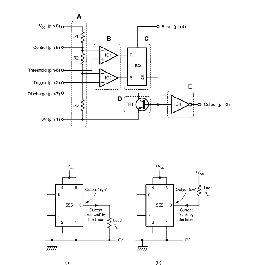
218 ELECTRONIC CIRCUITS: FUNDAMENTALS AND APPLICATIONS
Figure 12.1 Internal arrangement of a 555 timer
course, encompasses the normal range for TTL
devices (5 V ± 5%) and thus the device is ideally
suited for use with TTL circuitry.
Several versions of the 555 timer are available,
including low power (CMOS) and dual versions, as
follows:
Low power (CMOS) 555
This device is a CMOS version of the 555 timer
that is both pin and function compatible with its
standard counterpart. By virtue of its CMOS
technology the device operates over a somewhat
wider range of supply voltages (2 V to 18 V) and
Figure 12.2 Loads connected to the output of a 555 timer: (a) current sourced by the timer when the output
is high (b) current sunk by the timer when the output is low
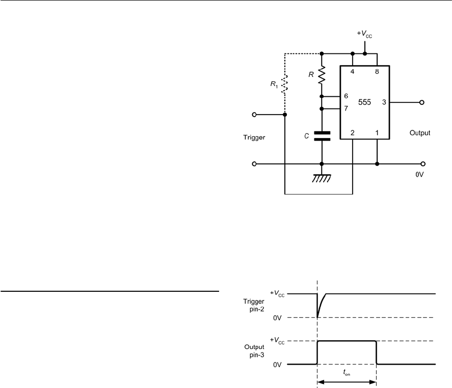
THE 555 TIMER 219
Figure 12.3 555 monostable configuration. Cand
Rare the timing components
consumes minimal operating current (120 mA)
typical for an 18 V supply). Note that, by virtue of
the low-power CMOS technology employed, the
device does not have the same output current drive
as that possessed by its standard counterparts. It
can, however supply up to two standard TTL loads.
Dual 555 timer (e.g. NE556A)
This is a dual version of the standard 555 timer
housed in a 14-pin DIL package. The two devices
may be used entirely independently and share the
same electrical characteristics as the standard 555.
Low-power (CMOS) dual 555 (e.g. ICM75561PA)
This is a dual version of the low-power CMOS 555
timer contained in a 14-pin DIL package. The two
devices may again be used entirely independently
and share the same electrical characteristics as the
low-power CMOS 555.
Pin connecting details for the above devices can
be found in Appendix 4.
Monostable pulse generator
Figure 12.3 shows a standard 555 timer operating
as a monostable pulse generator.The monostable
timing period (i.e. the time for which the output is
high) is initiated by a falling edge trigger pulse
applied to the trigger input (pin-2), see Fig. 12.4.
When this falling edge trigger pulse is received
and falls below one-third of the supply voltage, the
output of IC2 goes high and the bistable will be
placed in the set state. The inverted Q output of the
bistable then goes low,TR1 is placed in the off
(non-conducting) state and the output voltage (pin-
3) goes high.
The capacitor, C,then charges through the series
resistor, R, until the voltage at the threshold input
reaches two-thirds of the supply voltage (Vcc). At
this point, the output of the upper comparator
changes state and the bistable is reset.The inverted
Qoutput then goes high, TR1 is driven into
conduction and the final output goes low.The
device then remains in the inactive state until
another falling trigger pulse is received.
The trigger and output waveforms produced by
the circuit of Fig. 12.3 are shown in Fig. 12.4. The
waveform has the following properties:
Time for which output is high: ton = 1.1 C R
Recommended trigger pulse width:
where ton and ttr are in seconds, Cis in Farads and R
is in ohms.
The period of the 555 monostable output can be
changed very easily by simply altering the values
of the timing resistor, R,and/or timing capacitor, C.
Doubling the value of Rwill double the timing
period. Similarly, doubling the value of Cwill
double the timing period.
on
tr
4
t
t<
Figure 12.4 555 monostable configuration. Cand
Rare the timing components
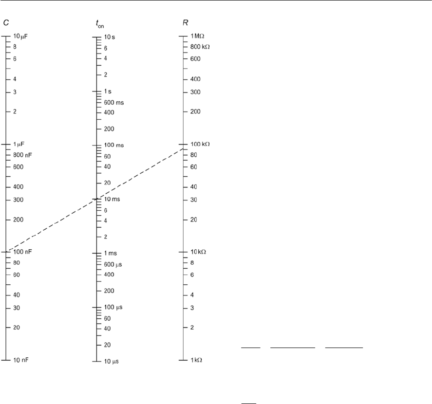
220 ELECTRONIC CIRCUITS: FUNDAMENTALS AND APPLICATIONS
Values for Cand Rcan be selected over quite a
wide range but it is worth noting that the
performance of the timer may become
unpredictable if the values of these components are
outside the recommended range:
C=470 pF to 470 µF
R= 1 kGto 3.3 MG
For any particular monostable timing period, the
required values for Cand Rcan be determined from
the formula shown earlier or by using the graph
shown in Fig. 12.5. The output period can be easily
adjusted by making R a preset resistor with a value
of about twice that of the calculated value.
Example 12.1
Design a timer circuit that will produce a 10 ms
pulse when a negative-going trigger pulse is
applied to it.
Solution
Using the circuit shown in Fig. 12.4, the value of
monostable timing period can be calculated from
the formula:
ton = 1.1 C R
We need to choose an appropriate value for Cthat
is in the range stated earlier. Since we require a
fairly modest time period we will choose a mid-
range value for C.This should help to ensure that
the value of R is neither too small nor too large. A
value of 100 nF should be appropriate and should
also be easy to obtain. Making Rthe subject of the
formula and substituting for C=100 nF gives:
From which:
Alternatively, the chart shown in Fig. 12.5 can be
used.
Example 12.2
Design a timer circuit that will produce a +5V
output for a period of 60 s when a ‘start’ button is
operated. The time period is to be aborted when a
‘stop’ button is operated.
Solution
For the purposes of this question we shall assume
that the ‘start’ and ‘stop’ buttons both have
Figure 12.5 Chart for determining values of C,ton
and Rfor a 555 operating in monostable mode. The
dotted line shows how a 10 ms pulse will be pro-
duced when C=100 nF and R=91 kG(see Exam-
ple 12.1)
3
on
9
10 ms 10 10
1.1 1.1 100 nF
110 10
t
RC
×
== =
××
66
10
10 0.091 10 = 91 k
110
R
=×= ×
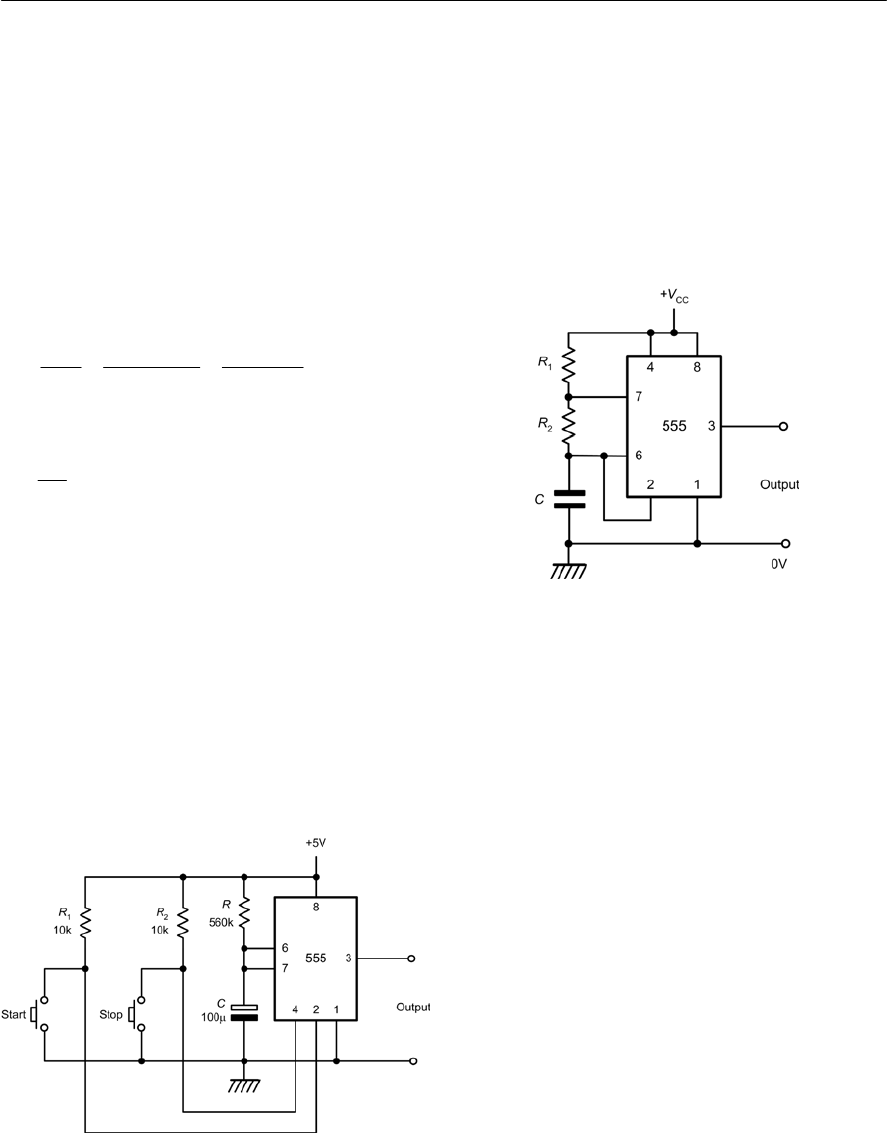
THE 555 TIMER 221
normally-open (NO) actions.
The value of monostable timing period can be
calculated from the formula:
ton = 1.1 C R
We need to choose an appropriate value for Cthat
is in the range stated earlier. Since we require a
fairly long time period we will choose a relatively
large value of Cin order to avoid making the value
of Rtoo high. A value of 100 µF should be
appropriate and should also be easy to obtain.
Making Rthe subject of the formula and
substituting for C=100 µF gives:
From which:
In practice 560 kG(the nearest preferred value –
see page 21) would be adequate.
The ‘start’ button needs to be connected between
pin-2 and ground whilst the ‘stop’ button needs to
be connected between pin-4 and ground. Each of
the inputs requires a pull-up resistor to ensure that
the input is taken high when the switch is not being
operated. The precise value of the ‘pull-up’ resistor
is unimportant and a value of 10 kGwill be
perfectly adequate in this application. The complete
circuit of the 60 s timer is shown in Fig. 12.6.
Astable pulse generator
Figure 12.7 shows how the standard 555 can be
used as an astable pulse generator.In order to
understand how this circuit operates, assume that
the output (pin-3) is initially high and that TR1 is in
the non-conducting state. The capacitor, C,will
begin to charge with current supplied by means of
series resistors, R1and R2.
on
6
60 s 60
1.1 1.1 100 µF
110 10
t
RC
== =
××
66
60
10 0.545 10 = 545 k
110
R
=×= ×
Figure 12.6 60 s timer (see Example 12.2)
Figure 12.7 555 astable configuration
When the voltage at the threshold input (pin-6)
exceeds two-thirds of the supply voltage the output
of the upper comparator, IC1, will change state and
the bistable will become reset due to voltage
transition that appears at R. This, in turn, will make
the inverted Q output go high,turning TR1 at the
same time. Due to the inverting action of the buffer,
IC4, the final output (pin-3) will go low.
The capacitor, C,will now discharge, with
current flowing through R2into the collector of
TR1. At a certain point, the voltage appearing at the
trigger input (pin-2) will have fallen back to one-
third of the supply voltage at which point the lower
comparator will change state and the voltage
transition at S will return the bistable to its original
set condition. The inverted Q output then goes low,
TR1 switches off (no longer conducting), and the
output (pin-3) goes high.Thereafter, the entire
charge/discharge cycle is repeated indefinitely.
The output waveform produced by the circuit of
Fig. 12.7 is shown in Fig. 12.8. The waveform has
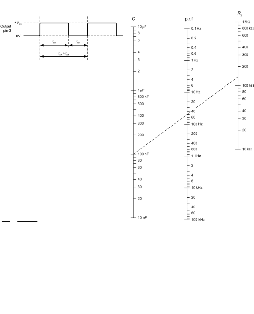
The p.r.f. of the 555 astable output can be changed
very easily by simply altering the values of R1,R2,
and C.The values chosen for R1,R2and Cshould
222 ELECTRONIC CIRCUITS: FUNDAMENTALS AND APPLICATIONS
Figure 12.8 Waveforms for astable operation
Figure 12.9 Chart for determining values of C,
p.r.f. and R2for a 555 operating in astable mode
where R2>> R1(i.e. for a square wave output). The
dotted line shows how a 50 Hz square wave will be
produced when C=100 nF and R=144 kG(see
Example 12.4)
the following properties:
Time for which output is high:
ton = 0.693 C(R1+R2)
Time for which output is low:
toff = 0.693 C R2
Period of output waveform:
t=ton +toff = 0.693 C(R1+ 2R2)
Pulse repetition frequency:
Mark to space ratio:
Duty cycle:
Where tis in seconds, Cis in Farads, R1and R2are
in ohms.
When R1=R2the duty cycle of the astable
output from the timer can be found by letting R=
R1=R2.Hence:
In this case the duty cycle will be given by:
()
12
1.44
p.r.f. = 2
CR R
+
on
12
off 2
t
RR
tR
+
=
on 12
on off 1 2
100%
2
tRR
tt R R
+
=×
++
on 12
off 2
2
2
1
tRR
RR
tR R
++
====
on
on off
2
100% 100% 67%
23
tRR
tt RR
+
=×=×
++

THE 555 TIMER 223
normally be selected from within the following
ranges in order to provide satisfactory performance:
C=10 nF to 470 µF
R1= 1 kGto 1 MG
R2= 1 kGto 1 MG
The required values of C,R1and R2for any
required p.r.f. and duty cycle can be determined
from the formulae shown earlier. Alternatively, the
graph shown in Fig. 12.9 can be used when R1and
R2are equal in value (corresponding to a 67% duty
cycle).
Square wave generators
Because the high time (ton)is always greater than
the low time (toff), the mark to space ratio produced
by a 555 timer can never be made equal to (or less
than) unity. This could be a problem if we need to
produce a precise square wave in which ton = toff.
However, by making R2very much larger than R1,
the timer can be made to produce a reasonably
symmetrical square wave output (note that the
minimum recommended value for R2is 1 kK—see
earlier).
If R2>> R1the expressions for p.r.f. and duty
cycle simplify to:
Example 12.3
Design a pulse generator that will produce a p.r.f.
of 10 Hz with a 67% duty cycle.
Solution
Using the circuit shown in Fig. 12.7, the value of
p.r.f. can be calculated from:
2
0.72
p.r.f.
CR
on 2
on off 2
1
100% 100% 50%
22
tR
tt R
×=×=
+
()
12
1.44
p.r.f. = 2
CR R
+
Since the specified duty cycle is 67% we can make
R
1
equal to R
2
.Hence if R=R
1
=R
2
we obtain the
following relationship:
We need to choose an appropriate value for Cthat
is in the range stated earlier. Since we require a
fairly low value of p.r.f. we will choose a value for
Cof 1µF. This should help to ensure that the value
of Ris neither too small nor too large. A value of
1µF should also be easy to obtain. Making Rthe
subject of the formula and substituting for C= 1 µF
gives:
Example 12.4
Design a 5 V 50 Hz square wave generator using a
555 timer.
Solution
Using the circuit shown in Fig. 12.7, when R
2
>>
R
1
,the value of p.r.f. can be calculated from:
We shall use the minimum recommended value for
R
1
(i.e. 10 kG)and ensure that the value of R
2
that
we calculate from the formula is at least ten times
larger in order to satisfy the criteria that R
2
should
be very much larger than R
1
.When selecting the
value for Cwe need to choose a value that will
keep the value of R
2
relatively large. A value of 100
nF should be about right and should also be easy to
locate. Making R
2
the subject of the formula and
substituting for C=100 nF gives:
()
1.44 1.44 0.48
p.r.f. = 23
C R R CR CR
==
+
6
0.48 0.48
p.r.f.
p.r.f. 1 10
RC
==
×××
3
3
480 10
4.8 10 4.8 k
100
R×
==×=
2
0.72
p.r.f.
CR
2
9
0.72 0.72
p.r.f.
50 100 10
RC
==
×××
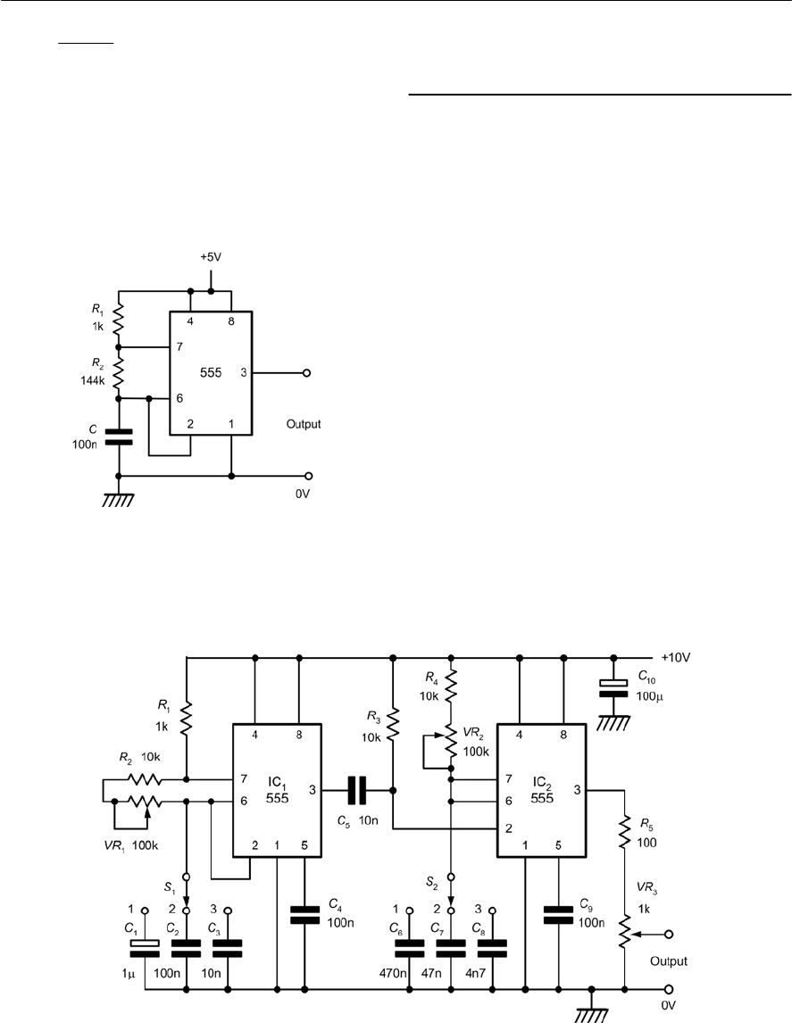
Alternatively, the chart shown in Fig. 12.9 can be
used.
The value of R2is thus more than 100 times
larger than the value that we are using for R1.As a
consequence the timer should produce a good
square wave output.
224 ELECTRONIC CIRCUITS: FUNDAMENTALS AND APPLICATIONS
6
26
0.72
0.144 10 144 k
510
R
==×=
×
Figure 12.10 A 5 V 50 Hz square wave generator
(see Example 12.4)
The complete circuit of the 5V 50 Hz square wave
generator is shown in Fig. 12.10.
Avariable pulse generator
Figure 12.11 shows how a variable pulse generator
can be constructed using two 555 timer (or one 556
dual timer). The first timer, IC1, operates in astable
mode whilst the second timer, IC2, operates in
monostable mode. The p.r.f. generated by IC1 is
adjustable by means of switch selected capacitors,
C
1
to C
3
,together with variable resistor, VR
1
.The
output from IC1 (pin-3) is fed via C
5
to the trigger
input of IC2 (pin-2).
The monostable period of IC2 is adjustable by
means of switch selected capacitors, C
6
to C
8
,
together with variable resistor, VR
2
.The output
from IC2 (pin-3) is fed to the output via VR
3
.
The p.r.f. is adjustable over the range 10 Hz to
10 kHz whilst pulse widths can be varied from 50
µs to 50 ms. The output voltage is adjustable from
0 V to 10 V. Finally, R5, is included in order to
limit the output current and provide a measure of
protection in the event of a short-circuit present at
the output.
Figure 12.11 A variable pulse generator using two 555 timers
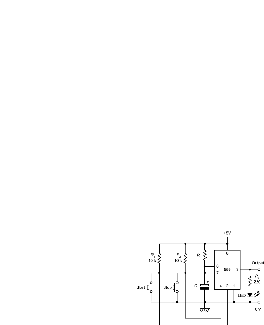
Practical investigation
Objective
To investigate the operation of a 555 monostable
timer circuit.
Simulator
Breadboard, 5 V d.c. power supply, 555 timer,
resistors of 10 kG(two required), 220 G,100 kG,
and 1 MG5% 0.25 W, capacitors of 10 µF and
100 µF 16 V, LED, two normally open (NO) push-
button switches, stopwatch or wristwatch with
seconds display.
Procedure
Connect the circuit as shown in Fig. 12.12 with C=
10 µF and R=100 kG.Connect the supply and
press the ‘stop’ button. The LED should be off
(indicating that the output is at 0 V).
Observe the time display and, at a convenient
point, press the ‘start’ button. The LED should
become illuminated after a period of about 1 s (this
will probably be too short an interval to be
measured accurately). Record the monostable time
period (i.e. the time between pressing the ‘start’
button and the LED becoming illuminated) in Table
12.2.
Repeat the procedure for each of the remaining
C–R values shown in Table 12.2. Note that you can
interrupt the timing period at any time by pressing
the ‘stop’ button.
Calculations and graph
Record your results in Table 12.2. For each pair of
C–R values calculate the product of C(in µF) and R
(in MG). Plot a graph showing corresponding
values of monostable time plotted against
corresponding values of C×Rusing the graph
layout shown in Fig. 12.13.
Conclusions
Comment on the shape of the graph. Is this what
you would expect? Measure the slope of the graph
and use this to confirm the relationship for the
monostable timing period quoted on page 219. If
the graph is not linear can you suggest any reasons
for this?
THE 555 TIMER 225
Further work
Connect a digital multimeter on the 20 V d.c. range
so that you can accurately measure the d.c. voltage
that appears between pin-6 (threshold input) and
0V. With C=100 µF and R= 1 MGpress the
‘start’ button and then measure the voltage at pin-6
at intervals of 10 s over the range 0 to 120 s.
Particularly note the voltage reached at the end of
the monostable timing period (this should be
exactly 2/3 of the supply voltage). Plot a graph of
voltage against time and justify the shape of this
graph.
Figure 12.12 Monostable timer circuit used for
the Practical investigation
C R Time
10 µF 100 kG
10 µF 220 kG
10 µF 470 kG
100 µF 220 kG
100 µF 470 kG
100 µF 1 M kG
10 µF 1 M kG
Table 12.2 Table of results for the monostable
timer circuit
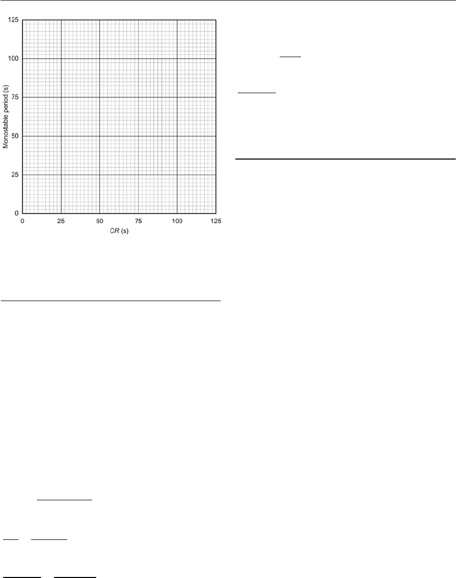
226 ELECTRONIC CIRCUITS: FUNDAMENTALS AND APPLICATIONS
Problems
12.1 Design a timer circuit that will produce a
10 V 2 ms pulse when a 10 V negative-
going trigger pulse is applied to it.
12.2 Design a timer circuit that will produce time
periods that can be varied from 1 s to 10 s.
The timer circuit is to produce a +12V
output.
12.3 Design a timer circuit that will produce a
67% duty cycle output at 400 Hz.
12.4 Design a timer circuit that will produce a
square wave output at 1 kHz.
12.5 Refer to the variable pulse generator circuit
shown in Fig. 12.11. Identify the
component(s) that provides:
(a) variable adjustment of pulse width
(b) decade range selection of pulse width
(c) limits the range of variable adjustment of
pulse width
(d) variable adjustment of p.r.f.
(e) decade range selection of p.r.f.
(f) limits the range of variable adjustment of
p.r.f.
(g) variable adjustment of output amplitude
(h) protects IC2against a short-circuit
connected at the output
(i) removes any unwanted signals appearing
on the supply rail
(j) forms the trigger pulse required by the
monostable stage
12.6 A 555 timer is rated for a maximum output
current of 120 mA. What is the minimum
value of load resistance that can be used if
the device is to be operated from a 6 V d.c.
supply?
Answers to these problem appear on page 376.
Important formulae introduced in this
chapter
Monostable 555 timer:
(page 219)
ton = 1.1 CR
Astable 555 timer:
(page 222)
ton = 0.693 C(R1+R2)
toff = 0.693 CR2
t=0.693 C(R1+ 2R2)
When R2>> R1:
(page 223)
on
12
off 2
t
RR
tR
+
=
on 12
on off 1 2
100%
2
tRR
tt R R
+
=×
++
on
on off
50%
t
tt+
2
0.72
p.r.f.
CR
()
12
1.44
p.r.f. = 2
CR R
+
Figure 12.13 Graph layout for plotting the results

13
Radio
Maxwell first suggested the existence of
electromagnetic waves in 1864. Later, Heinrich
Rudolf Hertz used an arrangement of rudimentary
resonators to demonstrate the existence of
electromagnetic waves. Hertz’s apparatus was
extremely simple and comprised two resonant
loops, one for transmitting and the other for
receiving. Each loop acted both as a tuned circuit
and as a resonant aerial. The transmitting loop was
excited by means of an induction coil and battery.
Some of the energy radiated by the transmitting
loop was intercepted by the receiving loop and the
received energy was conveyed to a spark gap where
it could be released as an arc. The energy radiated
by the transmitting loop was in the form of an
electromagnetic wave—a wave that has both
electric and magnetic field components and that
travels at the speed of light.
In 1894, Marconi demonstrated the commercial
potential of the phenomenon that Maxwell
predicted and Hertz actually used in his apparatus.
It was also Marconi that made radio a reality by
pioneering the development of telegraphy without
wires (i.e. wireless). Marconi was able to
demonstrate very effectively that information could
be exchanged between distant locations without the
need for a ‘land-line’.
Marconi’s system of wireless telegraphy
proved to be invaluable for maritime
communications (ship to ship and ship to shore)
and was to be instrumental in saving many lives.
The military applications of radio were first
exploited during the First World War (1914 to
1918) and, during that period, radio was first used
in aircraft.
The radio frequency spectrum
Radio frequency signals are generally understood
to occupy a frequency range that extends from a
few tens of kilohertz (kHz) to several hundred
Gigahertz (GHz). The lowest part of the radio
frequency range that is of practical use (below
30 kHz) is only suitable for narrow-band
communication. At this frequency, signals
propagate as ground waves (following the
curvature of the earth) over very long distances. At
the other extreme, the highest frequency range that
is of practical importance extends above 30GHz. At
these microwave frequencies, considerable
bandwidths are available (sufficient to transmit
many television channels using point-to-point links
or to permit very high definition radar systems) and
signals tend to propagate strictly along line-of-sight
paths.
At other frequencies signals may propagate by
various means including reflection from ionized
layers in the ionosphere. At frequencies between
3MHz and 30 MHz ionospheric propagation
regularly permits intercontinental broadcasting and
communications.
For convenience, the radio frequency spectrum is
divided into a number of bands, each spanning a
decade of frequency. The use to which each
frequency range is put depends upon a number of
factors, paramount amongst which is the
propagation characteristics within the band
concerned. Other factors that need to be taken into
account include the efficiency of practical aerial
systems in the range concerned and the bandwidth
available. It is also worth noting that, although it
may appear from Fig. 13.1 that a great deal of the
radio frequency spectrum is not used, it should be
stressed that competition for frequency space is
fierce. Frequency allocations are, therefore, ratified
by international agreement and the various user
services carefully safeguard their own areas of the
spectrum.
Electromagnetic waves
As with light, radio waves propagate outwards
from a source of energy (transmitter) and comprise
electric (E)and magnetic (H)fields right angles to
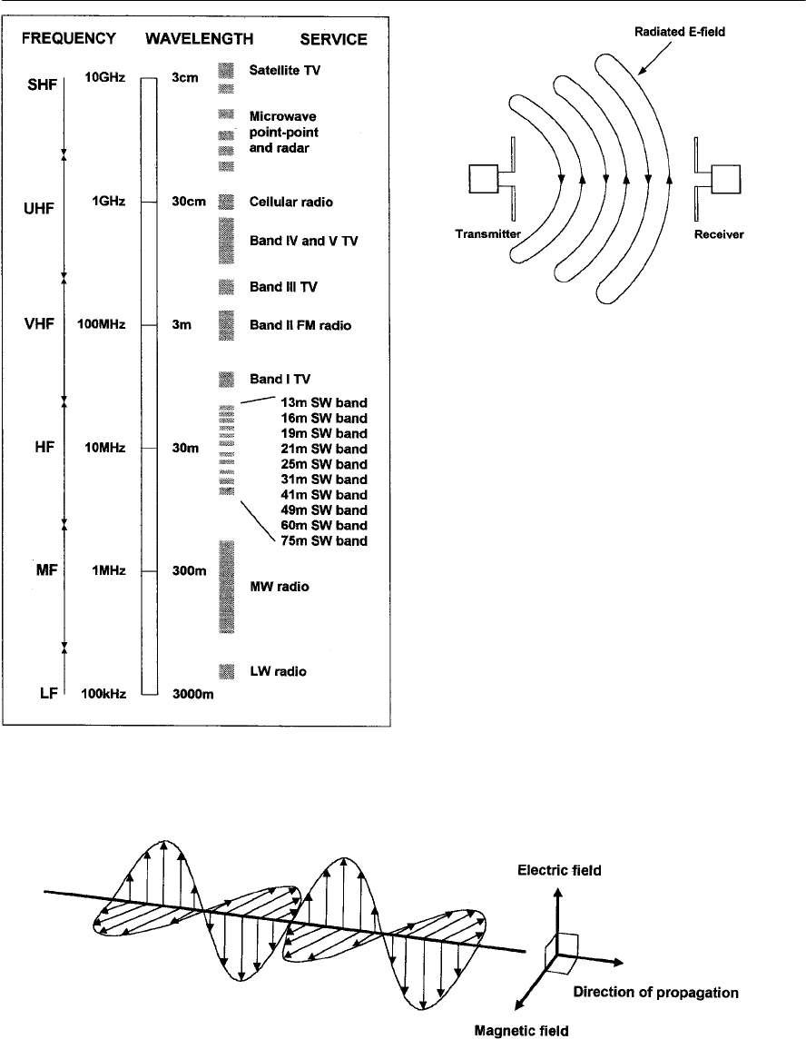
228 ELECTRONIC CIRCUITS: FUNDAMENTALS AND APPLICATIONS
one another. These two components, the E-field
and the H-field,are inseparable. The resulting
wave travels away from the source with the E and
Hlines mutually at right angles to the direction of
propagation,as shown in Fig. 13.2.
Radio waves are said to be polarized in the
plane of the electric (E) field. Thus, if the E-field is
vertical, the signal is said to be vertically polarized
whereas, if the E-field is horizontal, the signal is
said to be horizontally polarized.
Figure 13.3 shows the electric E-field lines in
the space between a transmitter and a receiver. The
transmitter aerial (a simple dipole—see page 237)
is supplied with a high frequency alternating
current. This gives rise to an alternating electric
field between the ends of the aerial and an
alternating magnetic field around (and at right
angles to) it.
Figure 13.1 The radio frequency spectrum
Figure 13.2 An electromagnetic wave
Figure 13.3 E-field lines between a transmitter
and a receiver

RADIO 229
The direction of the E-field lines is reversed on
each cycle of the signal as the wavefront moves
outwards from the source. The receiving aerial
intercepts the moving field and voltage and current
is induced in it as a consequence. This voltage and
current is similar (but of smaller amplitude) to that
produced by the transmitter.
Frequency and wavelength
Radio waves propagate in air (or space) at the
speed of light (300 million metres per second). The
velocity of propagation, v,wavelength, ,and
frequency, f,of a radio wave are related by the
equation:
v=f=3 × 10⁸
This equation can be arranged to make for the
subject, as follows:
and
As an example, a signal at a frequency of 1 MHz
will have a wavelength of 300 m whereas a signal
at a frequency of 10 MHz will have a wavelength
of 30 m.
When a radio wave travels in a cable (rather
than in air or ‘free space’) it usually travels at a
speed that is between 60% and 80% of that of the
speed of light.
Example 13.1
Determine the frequency of a radio signal that has a
wavelength of 15 m.
Solution
Using the formula:
where =15 m gives:
Example 13.2
Determine the wavelength of a radio signal that has
afrequency of 150 MHz.
Solution
Using the formula:
where f=150 MHz gives:
Example 13.3
If the wavelength of a 30 MHz signal in a cable is
8m, determine the velocity of propagation of the
wave in the cable.
Solution
Using the formula:
v=f=3 × 10⁸
where vis the velocity of propagation in the cable,
gives:
8
310
Hz
D
f×
=
8
310
Dm
f
×
=
8
310
Hz
D
f×
=
86
6
3 10 300 10
= = 20 10 Hz or 20 MHz
15 15
f××
=×
8
310
Dm
f
×
=
88 6
6
3 10 3 10 300 10 300
D=== 2 m
150 MHz 150
150 10
f
×× ×
==
×
8
D30 MHz 8 m = 2.4 10 m/s
vf== × ×
Asimple CW transmitter and receiver
Figure 13.4 shows a simple radio communication
system comprising a transmitter and receiver for
use with continuous wave (CW) signals.
Communication is achieved by simply switching
(or ‘keying’) the radio frequency signal on and off.
Keying can be achieved by interrupting the supply
to the power amplifier stage or even the oscillator
stage however it is normally applied within the
driver stage that operates at a more modest power
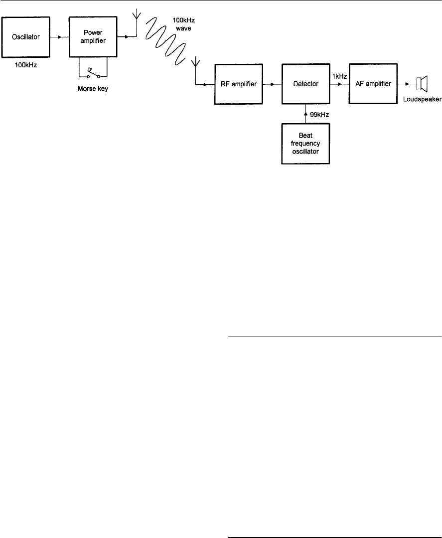
230 ELECTRONIC CIRCUITS: FUNDAMENTALS AND APPLICATIONS
Figure 13.4 Simplified block schematic of a radio communication system comprising a continuous wave
(CW) transmitter and a simple receiver with a beat frequency oscillator (BFO)
level. Keying the oscillator stage usually results in
impaired frequency stability. On the other hand,
attempting to interrupt the appreciable currents
and/or voltages that appear in the power amplifier
stage can also prove to be somewhat problematic.
The simplest form of CW receiver need consist
of nothing more than a radio frequency amplifier
(which provides gain and selectivity) followed by a
detector and an audio amplifier. The detector stage
mixes a locally generated radio frequency signal
produced by the beat frequency oscillator (BFO)
with the incoming signal to produce a signal within
the audio frequency range.
As an example, assume that the incoming signal
is at a frequency of 100 kHz and that the BFO is
producing a signal at 99 kHz. A signal at the
difference between these two frequencies (1 kHz)
will appear at the output of the detector stage. This
will then be amplified within the audio stage before
being fed to the loudspeaker.
Example 13.4
Aradio wave has a frequency of 162.5 kHz. If a
beat frequency of 1.25 kHz is to be obtained,
determine the two possible BFO frequencies.
Solution
The BFO can be above or below the incoming
signal frequency by an amount that is equal to the
beat frequency (i.e. the audible signal that results
from the ‘beating’ of the two frequencies and
which appears at the output of the detector stage).
Hence, fBFO = fRF ±fAF
from which:
fBFO = 162.5 kHz ± 1.25 kHz
= 160.75 kHz or 163.25 kHz
Morse code
Transmitters and receivers for CW operation are
extremely simple but nevertheless they can be
extremely efficient. This makes them particularly
useful for disaster and emergency communications
or for any situation that requires optimum use of
low power equipment. Signals are transmitted using
the code invented by Samuel Morse (see Fig. 13.5).
The Morse code uses a combination of dots (short
periods of transmission) and dashes (slightly longer
periods of transmission) to represent characters. As
an example, Fig. 13.6 shows how the radio
frequency carrier is repeatedly switched on and off
to transmit the character ‘C’.
Modulation
In order to convey information using a radio
frequency carrier, the signal information must be
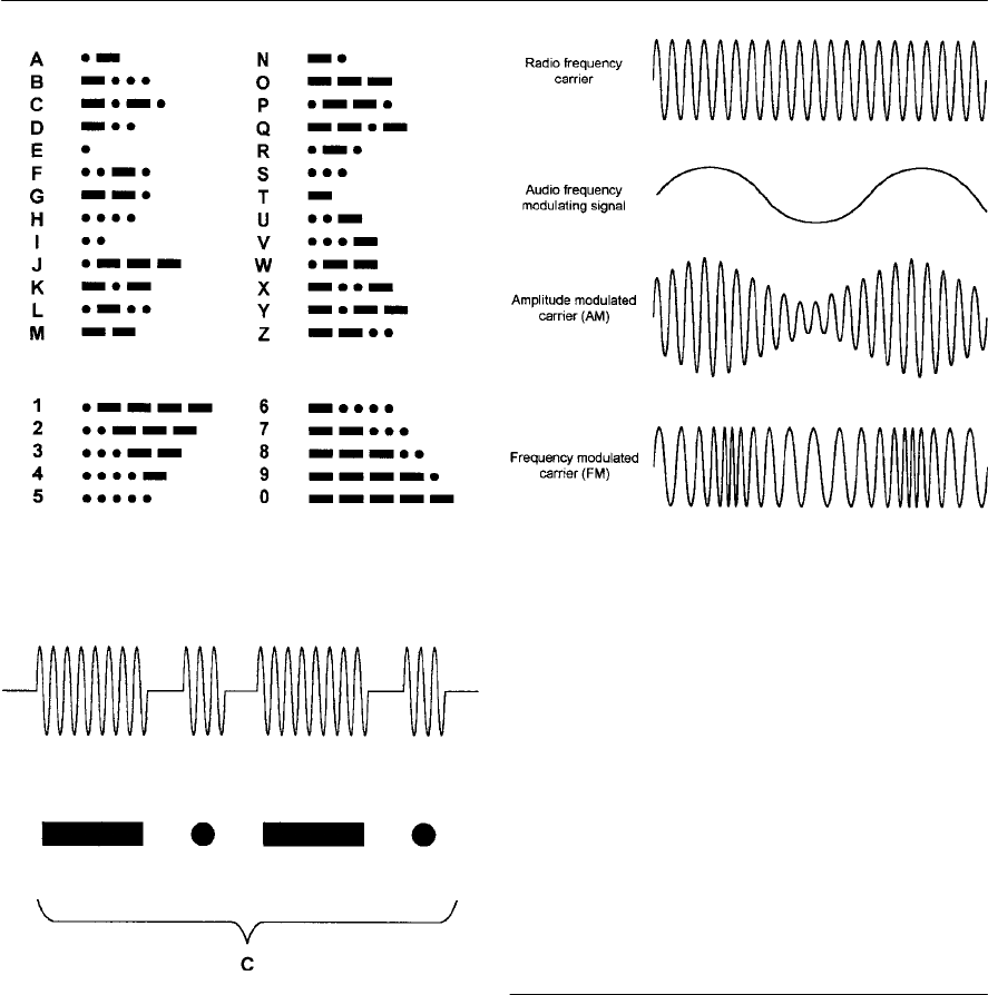
RADIO 231
Figure 13.5 Morse code
Figure 13.6 RF signal for the Morse letter ‘C’
superimposed or ‘modulated’ onto the carrier.
Modulation is the name given to the process of
changing a particular property of the carrier wave
in sympathy with the instantaneous voltage (or
current) a signal.
The most commonly used methods of
modulation are amplitude modulation (AM) and
frequency modulation (FM). In the former case,
the carrier amplitude (its peak voltage) varies
according to the voltage, at any instant, of the
modulating signal. In the latter case, the carrier
frequency is varied in accordance with the voltage,
at any instant, of the modulating signal.
Figure 13.7 shows the effect of amplitude and
frequency modulating a sinusoidal carrier (note that
the modulating signal is, in this case, also
sinusoidal). In practice, many more cycles of the
RF carrier would occur in the time-span of one
cycle of the modulating signal.
Demodulation
Demodulation is the reverse of modulation and is
the means by which the signal information is
recovered from the modulated carrier.
Demodulation is achieved by means of a
demodulator (sometimes called a detector). The
output of a demodulator consists of a reconstructed
version of the original signal information present at
the input of the modulator stage within the
transmitter. We shall see how this works a little
later.
Figure 13.7 Amplitude modulation (AM) and
frequency modulation (FM)

232 ELECTRONIC CIRCUITS: FUNDAMENTALS AND APPLICATIONS
An AM transmitter
Figure 13.8 shows the block schematic of a simple
AM transmitter. An accurate and stable RF
oscillator generates the radio frequency carrier
signal. The output of this stage is then amplified
and passed to a modulated RF power amplifier
stage. The inclusion of an amplifier between the RF
oscillator and the modulated stage also helps to
improve frequency stability.
The low-level signal from the microphone is
amplified using an AF amplifier before it is passed
to an AF power amplifier. The output of the power
amplifier is then fed as the supply to the modulated
RF power amplifier stage. Increasing and reducing
the supply to this stage is instrumental in increasing
and reducing the amplitude of its RF output signal.
The modulated RF signal is then passed through
an aerial tuning unit. This matches the aerial to the
RF power amplifier and also reduces the level of
unwanted harmonic components that may be
present.
An FM transmitter
Figure 13.9 shows the block schematic of a simple
FM transmitter. Once again, an accurate and stable
RF oscillator generates the radio frequency carrier
signal. As with the AM transmitter, the output of
this stage is amplified and passed to an RF power
amplifier stage. Here again, the inclusion of an
amplifier between the RF oscillator and the RF
power stage helps to improve frequency stability.
The low-level signal from the microphone is
amplified using an AF amplifier before it is passed
to a variable reactance element (e.g. a variable
capacitance diode—see page 93) within the RF
oscillator tuned circuit. The application of the AF
signal to the variable reactance element causes the
frequency of the RF oscillator to increase and
decrease in sympathy with the AF signal.
The final RF signal from the power amplifier is
passed through an aerial tuning unit that matches
the aerial to the RF power amplifier and also helps
to reduce the level of any unwanted harmonic
components that may be present. As with the final
stages of an AM transmitter, the RF power
amplifier usually operates at an appreciable power
level and this uses Class C to increase efficiency.
Atuned radio frequency (TRF) receiver
Tuned radio frequency (TRF) receivers provide a
means of receiving local signals using fairly
minimal circuitry. The simplified block schematic
of a TRF receiver is shown in Fig. 13.10.
The signal from the aerial is applied to an RF
amplifier stage. This stage provides a moderate
amount of gain at the signal frequency. It also
provides selectivity by incorporating one or more
tuned circuits at the signal frequency. This helps
the receiver to reject signals that may be present on
adjacent channels.
The output of the RF amplifier stage is applied to
the demodulator. This stage recovers the audio
frequency signal from the modulated RF signal.
The demodulator stage may also incorporate a
tuned circuit to further improve the selectivity of
the receiver.
The output of the demodulator stage is fed to the
input of the AF amplifier stage. This stage
increases the level of the audio signal from the
demodulator so that it is sufficient to drive a
loudspeaker.
TRF receivers have a number of limitations with
regard to sensitivity and selectivity and this makes
them generally unsuitable for use in commercial
radio equipment.
Asuperhet receiver
Superhet receivers provide both improved
sensitivity (the ability to receiver weak signals) and
improved selectivity (the ability to discriminate
signals on adjacent channels) when compared with
TRF receivers. Superhet receivers are based on the
supersonic-heterodyne principle where the wanted
input signal is converted to a fixed intermediate
frequency (IF) at which the majority of the gain
and selectivity is applied. The intermediate
frequency chosen is generally 455 kHz or 470 kHz
for AM receivers and 10.7 MHz for
communications and FM receivers. The simplified
block schematic of a simple superhet receiver is
shown in Fig. 13.11.
The signal from the aerial is applied to an RF
amplifier stage. As with the TRF receiver, this
stage provides a moderate amount of gain at the
signal frequency. The stage also provides
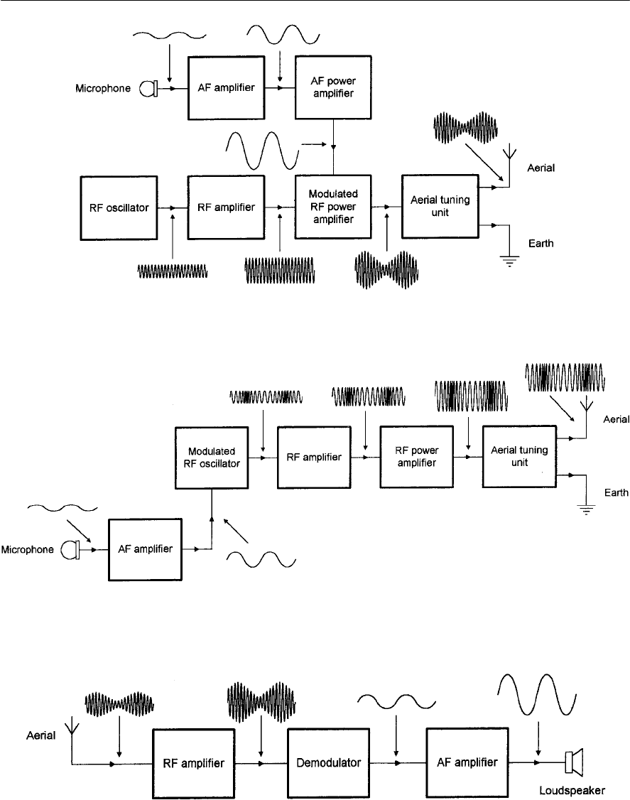
RADIO 233
Figure 13.8 An AM transmitter
Figure 13.9 An FM transmitter
Figure 13.10 A TRF receiver
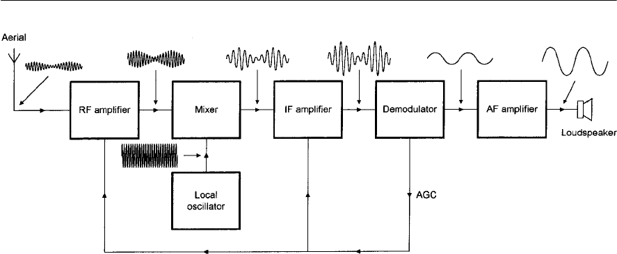
234 ELECTRONIC CIRCUITS: FUNDAMENTALS AND APPLICATIONS
selectivity by incorporating one or more tuned
circuits at the signal frequency.
The output of the RF amplifier stage is applied
to the mixer stage. This stage combines the RF
signal with the signal derived from the local
oscillator stage in order to produce a signal at the
intermediate frequency (IF). It is worth noting
that the output signal produced by the mixer
actually contains a number of signal components,
including the sum and difference of the signal and
local oscillator frequencies as well as the original
signals plus harmonic components. The wanted
signal (i.e. that which corresponds to the IF) is
passed (usually by some form of filter) to the IF
amplifier stage. This stage provides amplification
as well as a high degree of selectivity.
The output of the IF amplifier stage is fed to the
demodulator stage. As with the TRF receiver, this
stage is used to recover the audio frequency signal
from the modulated RF signal.
Finally, the AF signal from the demodulator
stage is fed to the AF amplifier. As before, this
stage increases the level of the audio signal from
the demodulator so that it is sufficient to drive a
loudspeaker.
In order to cope with a wide variation in signal
amplitude, superhet receivers invariably
incorporate some form of automatic gain control
(AGC). In most circuits the d.c. level from the AM
demodulator (see page 236) is used to control the
gain of the IF and RF amplifier stages. As the
signal level increases, the d.c. level from the
demodulator stage increases and this is used to
reduce the gain of both the RF and IF amplifiers.
The superhet receiver’s intermediate frequency
fIF,is the difference between the signal frequency,
fRF,and the local oscillator frequency, f
LO.The
desired local oscillator frequency can be calculated
from the relationship:
fLO = fRF ± fIF
Note that in most cases (and in order to simplify
tuning arrangements) the local oscillator operates
above the signal frequency, i.e. fLO = fRF + fIF
.
Example 13.5
AVHF Band II FM receiver with a 10.7 MHz IF
covers the signal frequency range, 88 MHz to 108
MHz. Over what frequency range should the local
oscillator be tuned?
Solution
Using fLO = fRF + fIF when fRF = 88 MHz gives
fLO = 88 MHz + 10.7 MHz = 98.7 MHz
Using fLO = fRF + fIF when fRF = 108 MHz gives
fLO = 108 MHz + 10.7 MHz = 118.7 MHz
The local oscillator tuning range should therefore
be from 98.7 MHz to 118.7 MHz.
Figure 13.11 Asuperhet receiver
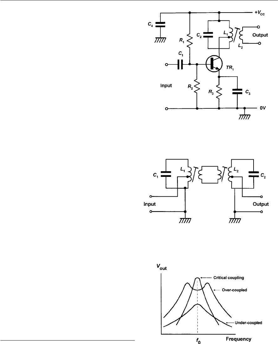
RADIO 235
RF amplifiers
Figure 13.12 shows the circuit of a typical RF
amplifier stage (this circuit can also be used as an
IF amplifier in a superhet receiver). You might like
to contrast this circuit with Fig. 7.34 shown on page
145. The amplifier operates in Class A and uses a
small-signal NPN transistor connected in common-
emitter mode. The essential difference between the
circuit shown in Fig. 13.12 and that shown in Fig.
7.34 is that the RF amplifier uses a parallel tuned
circuit as a collector load.
To improve matching and prevent damping of
the tuned circuit (which results in a reduction in Q-
factor and selectivity) the collector of TR1is
tapped into the tuned circuit rather than connected
straight across it. Since the tuned circuit has
maximum impedance at resonance (see page 78),
maximum gain will occur at the resonant
frequency. By using a tuned circuit with high-Q
factor it is possible to limit the response of the
amplifier to a fairly narrow range of frequencies.
The output (to the next stage) is taken from a
secondary winding, L2,on the main inductor, L1.
In order to further improve selectivity (i.e. the
ability to discriminate between signals on adjacent
channels) several tuned circuits can be used
together in order to form a more effective
bandpass filter.Figure 13.13 shows one possible
arrangement. When constructing an RF filter using
several tuned circuits it is necessary to use the
optimum coupling between the two tuned circuits.
Figure 13.14 illustrates this point.
If the two tuned circuits are too ‘loosely’
coupled (they are said to be under-coupled)the
frequency response characteristic becomes flat and
insufficient output is obtained. On the other hand, if
they are too ‘tightly’ coupled (they are said to be
over-coupled)the response becomes broad and
‘double-humped’. The optimum value of coupling
(when the two tuned circuits are said to be
critically-coupled)corresponds to a frequency
response that has a relatively flat top and steep
sides.
AM demodulators
Figure 13.15 shows the circuit of a typical AM
demodulator stage. The RF input is applied to a
Figure 13.14 Frequency response for two coupled
tuned circuits showing different amounts of
coupling between the tuned circuits
Figure 13.13 A tuned bandpass filter
Figure 13.12 An RF amplifier
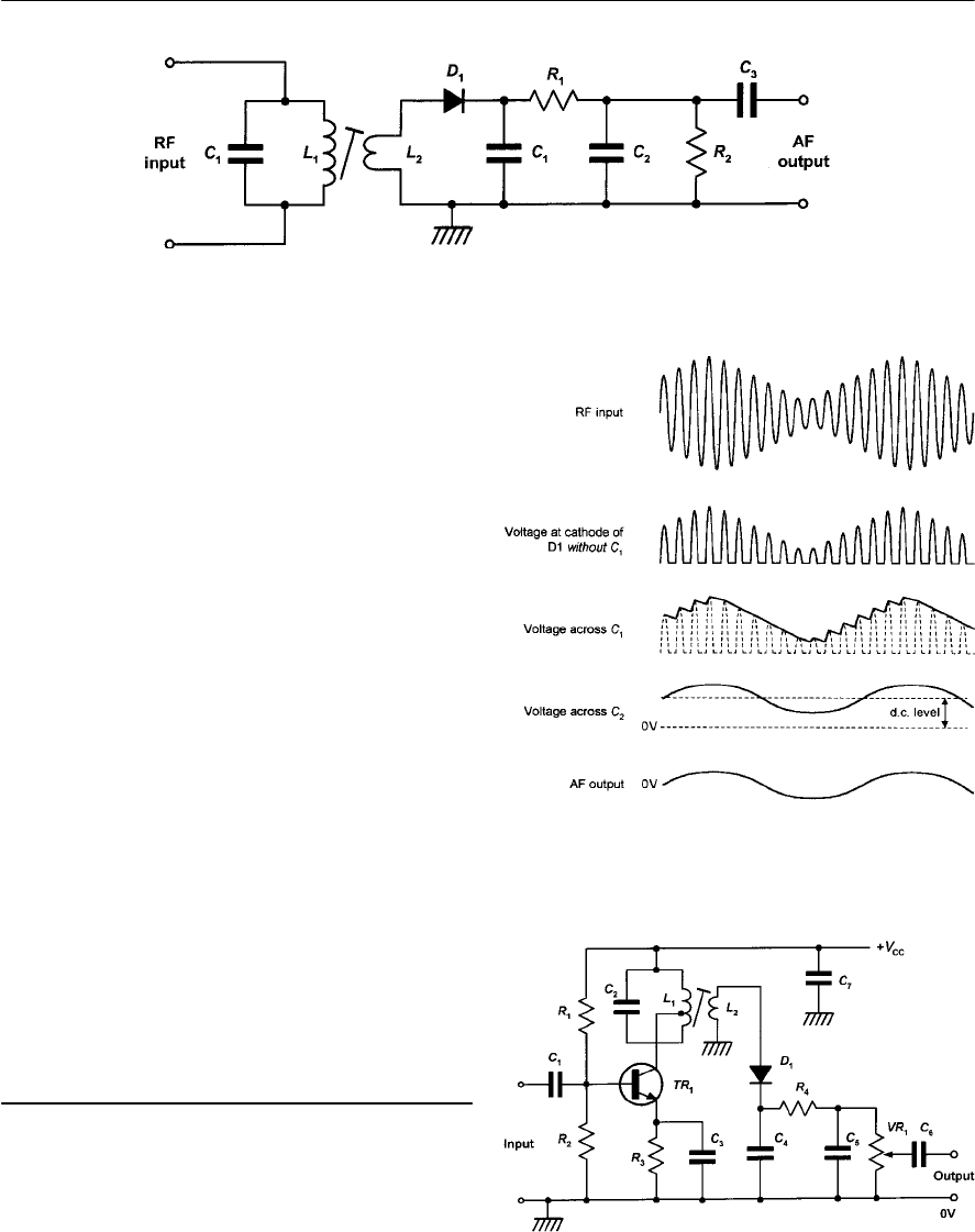
236 ELECTRONIC CIRCUITS: FUNDAMENTALS AND APPLICATIONS
parallel tuned circuit (L1and C1)which exhibits a
very high impedance at the signal frequency. A
secondary coupling winding, L2,is used to match
the relatively low impedance of the diode
demodulator circuit to the high impedance of the
input tuned circuit. Diode, D1,acts as a half-wave
rectifier conducting only on positive-going half-
cycles of the radio frequency signal. Capacitor, C1,
charges to the peak value of each positive-going
half-cycle that appears at the cathode of D1.
The voltage that appears across C1roughly
follows the peak of the half-cycles of rectified
voltage. R1and C2form a simple filter circuit to
remove unwanted RF signal components (this
circuit works in just the same way as the smoothing
filter that we met in Chapter 6—see pages 117 and
118). The final result is a voltage waveform
appearing across C2that resembles the original
modulating signal. As well as a providing a current
path for D1,R2forms a discharge path for C1and
C2.Coupling capacitor, C3,is used to remove any
d.c. component from the signal that appears at the
output of the demodulator. Waveforms for the
demodulator circuit are shown in Fig. 13.16. Figure
13.17 shows a complete IF amplifier together with
an AM demodulator stage. Circuits of this type are
used in simple superhet receivers.
Aerials
We shall start by describing one of the most
fundamental types of aerial, the half-wave dipole.
The basic half-wave dipole aerial (Fig. 13.18)
consists of a single conductor having a length equal
to one-half of the length of the wave being
Figure 13.15 Adiode AM demodulator
Figure 13.16 Waveforms for the AM demodulator
shown in Fig. 13.15
Figure 13.17 Acomplete RF/IF amplifier and AM
demodulator
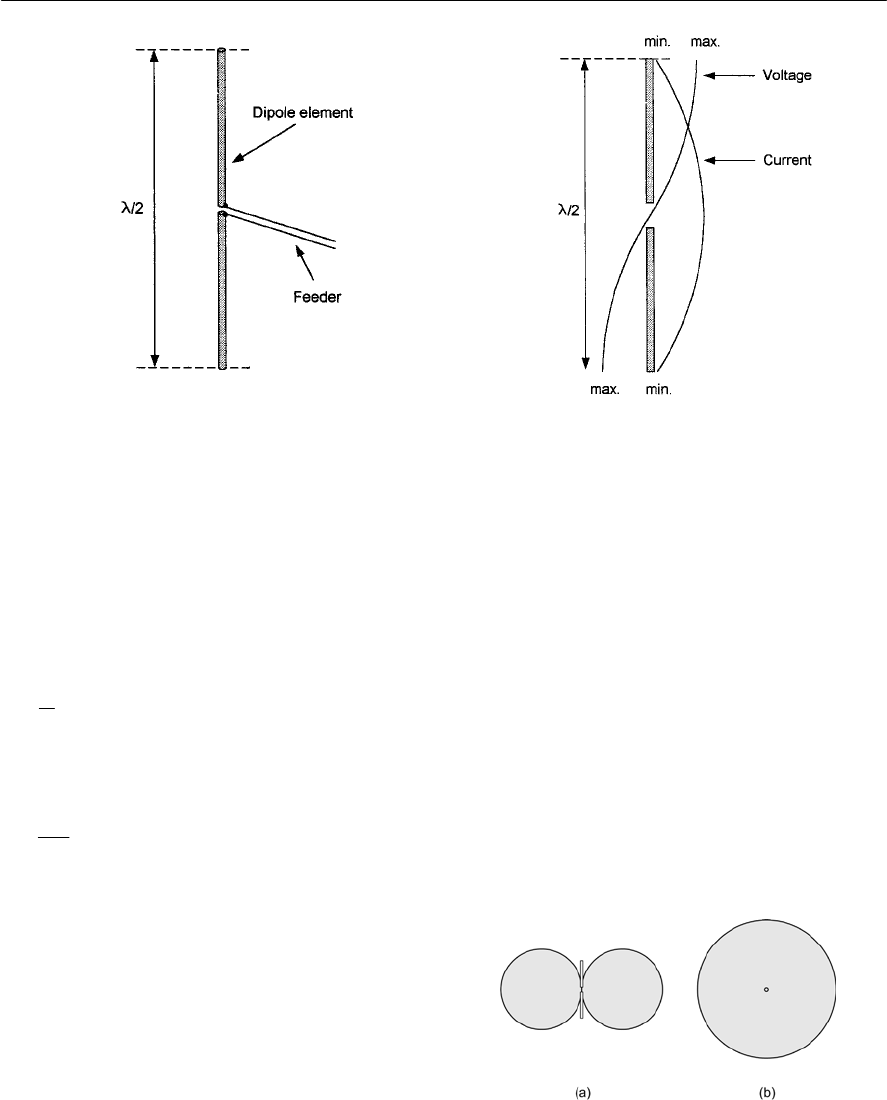
RADIO 237
transmitted or received. The conductor is then split
in the centre to enable connection to the feeder. In
practice, because of the capacitance effects between
the ends of the aerial and ground, the aerial is
invariably cut a little shorter than a half
wavelength.
The length of the aerial (from end to end) is equal
to one half wavelength, hence:
Now since v=f
we can conclude that, for a
half-wave dipole,
Note that lis the electrical length of the aerial
rather than its actual physical length.End effects,
or capacitance effects at the ends of the aerial,
require that we reduce the actual length of the aerial
and a 5% reduction in length is typically required
for an aerial to be resonant at the centre of its
designed tuning range.
Figure 13.19 shows the distribution of current
and voltage along the length of a half-wave dipole
aerial. The current is maximum at the centre and
zero at the ends. The voltage is zero at the centre
and maximum at the ends. This implies that the
impedance is not constant along the length of aerial
Figure 13.18 A half-wave dipole aerial Figure 13.19 Voltage and current distribution in a
half-wave dipole aerial
but varies from a maximum at the ends (maximum
voltage, minimum current) to a minimum at the
centre.
The dipole aerial has directional properties
illustrated in Fig. 13.20. Fig. 13.20(a) shows the
radiation pattern of the aerial in the plane of the
antenna’s electric field whilst Fig. 13.20(b) shows
the radiation pattern in the plane of the aerial’s
magnetic field. Things to note from these two
diagrams are that:
(a) in the case of Fig. 13.20(a) minimum radiation
occurs along the axis of the aerial whilst the
two zones of maximum radiation are at 90°
(i.e. are ‘normal to’) the dipole elements.
(b) in the case of Fig. 13.20(b) the aerial radiates
uniformly in all directions.
D
2
l
=
2
v
l
f
=
Figure 13.20 Radiation patterns for a half-wave
dipole: (a) radiation in the electric field plane
(b) radiation in the magnetic field plane
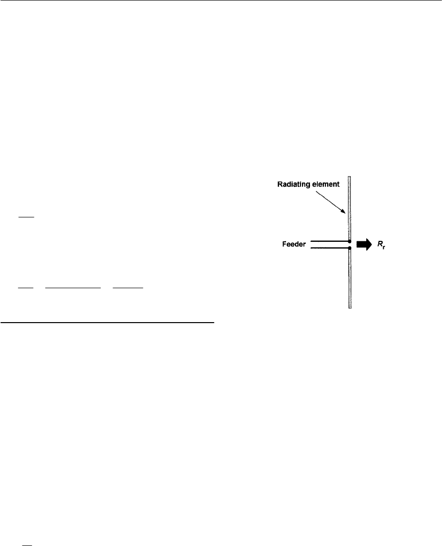
238 ELECTRONIC CIRCUITS: FUNDAMENTALS AND APPLICATIONS
Hence, a vertical dipole, will have an omni-
directional radiation pattern whilst a horizontal
dipole will have a bi-directional radiation pattern.
This is an important point as we shall see later. The
combined effect of these two patterns in three-
dimensional space will be a doughnut shape.
Example 13.6
Determine the length of a half-wave dipole aerial
for use at a frequency of 150 MHz.
Solution
The length of a half-wave dipole for 150 MHz can
be determined from:
where v=3×10⁸m/s and f=150 × 106Hz.
Hence:
Impedance and radiation resistance
Because voltage and current appear in an aerial (a
minute voltage and current in the case of a
receiving antenna and a much larger voltage and
current in the case of a transmitting antenna) an
aerial is said to have impedance.Here it’s worth
remembering here that impedance is a mixture of
resistance, R,and reactance, X,both measured in
ohms (O). Of these two quantities, Xvaries with
frequency whilst Rremains constant. This is an
important concept because it explains why aerials
are often designed for operation over a restricted
range of frequencies.
The impedance, Z,of an aerial is the ratio of the
voltage, E,across its terminals to the current, I,
flowing in it. Hence:
You might infer from Fig. 13.19 that the
impedance at the centre of the half-wave dipole
2
v
l
f
=
86
66
310 310
1 m
22 150 10 3 10
v
lf
××
== = =
×× ×
E
Z
I
=
should be zero. In practice the impedance is
usually between 70 Oand 75 O.Furthermore, at
resonance the impedance is purely resistive and
contains no reactive component (i.e. inductance
and capacitance). In this case Xis negligible
compared with R.It is also worth noting that the
d.c. resistance (or ohmic resistance)of an aerial is
usually very small in comparison with its
impedance and so it may be ignored. Ignoring the
d.c. resistance of the aerial, the impedance of an
antenna may be regarded as its radiation
resistance,R
r
(see Fig. 13.21).
Radiation resistance is important because it is
through this resistance that electrical power is
transformed into radiated electromagnetic energy
(in the case of a transmitting aerial) and incident
electromagnetic energy is transformed into
electrical power (in the case of a receiving aerial).
The equivalent circuit of an aerial is shown in
Fig. 13.22. The three series-connected components
that make up the aerial impedance are:
(a) the d.c. resistance, R
d.c.
(b) the radiation d.c. resistance, R
d.c.
(c) the ‘off-tune’ reactance, X
Note that when the antenna is operated at a
frequency that lies in the centre of its pass-band
(i.e. when it is on-tune)the off-tune reactance is
zero. It is also worth bearing in mind that the
radiation resistance of a half-wave dipole varies
according to its height above ground. The 70 Oto
Figure 13.21 Radiation resistance
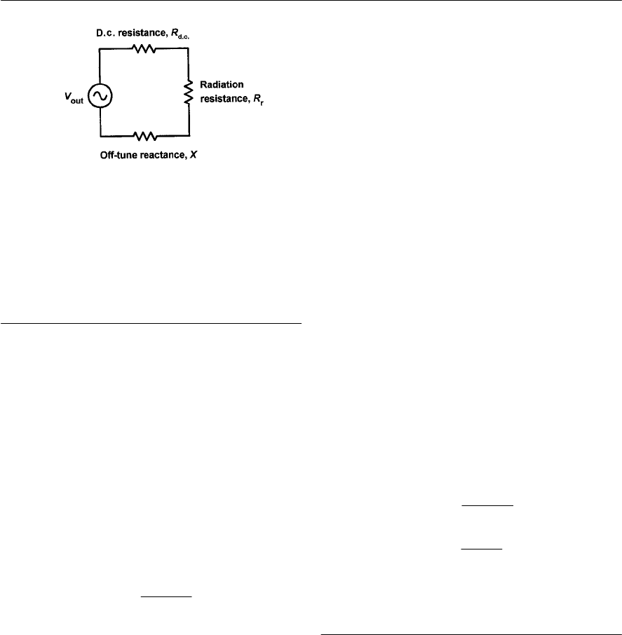
RADIO 239
Figure 13.22 Equivalent circuit of an aerial
75 Oimpedance normally associated with a half-
wave dipole is only realized when the aerial is
mounted at an elevation of 0.2 wavelengths, or
more.
Radiated power and efficiency
In the case of a transmitting aerial, the radiated
power, Pr,produced by the antenna is given by:
where Iais the aerial current, in amperes, and Rris
the radiation resistance in ohms. In most practical
applications it is important to ensure that Pris
maximized and this is achieved by ensuring that Rr
is much larger than the DC resistance of the
antenna elements.
The efficiency of an antenna is given by the
relationship:
where Ploss is the power dissipated in the DC
resistance present. At this point it is worth stating
that, whilst efficiency is vitally important in the
case of a transmitting aerial it is generally
unimportant in the case of a receiving aerial. This
explains why a random length of wire can make a
good receiving aerial but may not be very good as a
transmitting antenna!
Example 13.7
An HF transmitting aerial has a radiation resistance
r
rloss
Radiation efficiency = 100%
P
PP
×
+
of 12 O.If a current of 0.5 A is supplied to the
aerial, determine the radiated power.
Solution
In this case, Ia=0.5 A and Rr=12 O
Now hence:
Pr=(0.5)2×12 = 0.25 × 12 = 4 W
Example 13.8
If the aerial in Example 13.7 has a d.c. resistance of
2O,determine the power loss and the radiation
efficiency of the aerial.
Solution
From the equivalent circuit shown in Fig. 13.22, the
current that flows in the d.c. resistance of the aerial,
Rd.c.,is the same as that which flows in its radiation
resistance, Rr.Thus Ia=0.5 A and Rd.c. = 2 O
Now hence:
Ploss = (0.5)2× 2 = 0.25 × 2 = 0.5 W
The radiation efficiency of the aerial is given by:
In this example, more than 10% of the power
output is actually wasted!
Aerial gain
The field strength produced by an aerial is
proportional to the amount of current flowing in it.
However, since different types of aerial produce
different values of field strength for the same
applied RF power level, we attribute a power gain
to the aerial. This power gain is specified in
relation to a reference aerial and it is usually
specified in decibels (dB)—see Appendix 5.
Two types of reference aerial are used, an
isotropic radiator and a standard half-wave
2
ra r
PI R
=×
2
ra r
PI R
=×
2
loss d.c.
a
PIR
=×
4
100% 89%
40.5
=×=
+
Radiation efficiency 100%
r
rloss
P
PP
=×
+
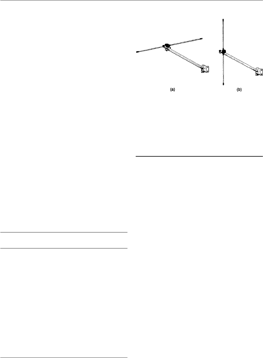
240 ELECTRONIC CIRCUITS: FUNDAMENTALS AND APPLICATIONS
dipole.The former type of reference aerial is only
atheoretical structure (it is assumed to produce a
truly spherical radiation pattern and thus could
only be realized in three-dimensional space well
away from the earth). The latter type of aerial is a
more practical reference since it is reasonably easy
to produce a half-wave dipole for comparison
purposes.
In order to distinguish between the two types of
reference aerial we use subscripts iand dto denote
isotropic and half-wave dipole reference aerials
respectively. As an example, an aerial having a
gain of 10 dBiproduces ten times power gain when
compared with a theoretical isotropic radiator.
Similarly, an aerial having a gain of 13 dBd
produces twenty times power gain when compared
with a half-wave dipole. Putting this another way,
to maintain the same field strength at a given point,
you would have to apply 20 W to a half-wave
dipole or just 1 W to the aerial in question! Some
representative values of aerial gain are given in
Table 13.1.
Figure 13.23 shows typical half-wave dipole
aerials for domestic VHF Band II FM broadcast
reception. The half-wave dipole in Fig. 13.23(a) is
horizontally polarized (and therefore has a bi-
directional characteristic) whilst the half-wave
dipole in Fig. 13.23(b) is vertically polarized (and
therefore has an omni-directional characteristic).
Application Gain
(dBd)
Half-wave wire dipole for VHF Band II FM
broadcast reception
0
Dipole and reflector for Band III digital radio
reception
3
Car roof mounted aerial for UHF private
mobile radio (PMR)
4
Four-element Yagi for high-quality FM
broadcast reception
6
Multi-element Yagi aerial for fringe area
Band V terrestrial broadcast TV reception
12
Parabolic reflector antenna for satellite TV
reception
24
3 m steerable parabolic dish reflector for
tracking space vehciles at UHF
40
Table 13.1 Some typical values of aerial gain
The Yagi beam aerial
Originally invented by two Japanese engineers,
Yagi and Uda, the Yagi aerial has remained
extremely popular in a wide variety of applications
and, in particular, for fixed domestic FM radio and
TV receiving aerials. In order to explain, in simple
terms. how the Yagi aerial works we shall use a
simple light analogy.
An ordinary filament lamp that radiates light in
all directions. Just like an aerial, the lamp converts
electrical energy into electromagnetic energy. The
only real difference is that we can see the energy
that it produces!
The action of the filament lamp is comparable
with our fundamental dipole aerial. In the case of
the dipole, electromagnetic radiation will occur all
around the dipole elements (in three dimensions the
radiation pattern will take on a doughnut shape). In
the plane that we have shown in Fig. 13.20(a), the
directional pattern will be a figure-of-eight that has
two lobes of equal size. In order to concentrate the
radiation into just one of the radiation lobes we
could simply place a reflecting mirror on one side
of the filament lamp. The radiation will be reflected
(during which the reflected light will undergo a
180° phase change) and this will reinforce the light
on one side of the filament lamp. In order to
Figure 13.23 Typical dipole aerials for local VHF
Band II FM reception: (a) horizontally polarized (b)
vertically polarized. Note that (a) is bi-directional
and (b) is omni-directional in the horizontal plane
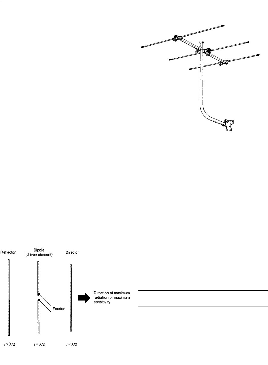
RADIO 241
achieve the same effect in our aerial system we
need to place a conducting element about one
quarter of a wavelength behind the dipole element.
This element is referred to as a reflector and it is
said to be ‘parasitic’ (i.e. it is not actually
connected to the feeder). The reflector needs to be
cut slightly longer than the driven dipole element.
The resulting directional pattern will now only have
one major lobe because the energy radiated will be
concentrated into just one half of the figure-of-eight
pattern that we started with.
Continuing with our optical analogy, in order to
further concentrate the light energy into a narrow
beam we can add a lens in front of the lamp. This
will have the effect of bending the light emerging
from the lamp towards the normal line. In order to
achieve the same effect in our aerial system we
need to place a conducting element, known as a
director,on the other side of the dipole and about
one quarter of a wavelength from it. Once again,
this element is parasitic but in this case it needs to
be cut slightly shorter than the driven dipole
element. The resulting directional pattern will now
have a narrower major lobe as the energy becomes
concentrated in the normal direction (i.e. at right
angles to the dipole elements).
The resulting aerial is known as a three-element
Yagi aerial, see Fig. 13.24. If desired, additional
directors can be added to further increase the gain
of the aerial and reduce the beamwidth of the
major lobe. A typical three-element horizontally
polarized Yagi suitable for VHF Band II broadcast
reception is shown in Fig. 13.25.
Figure 13.24 A three-element Yagi
Further director elements can be added to increase
the gain and reduce the beamwidth (i.e. the angle
between the half-power or –3dB power points on
the polar characteristic) of Yagi aerials. Some
typical gain and beamwidth figures for Yagi aerials
are given in Table 13.2. From this data it is worth
noting that aerial gain increases by an approximate
3dB every time the antenna doubles in size. It is
also worth noting the diminishing return as the
Yagi becomes large (e.g. an increase of only 1 dB
in gain as the aerial increases in size from 22 to 32
elements!).
Table 13.2 Typical gain and bandwidth figures for
Yagi aerials
Figure 13.25 A typical three-element Yagi aerial
for VHF Band II FM reception
Number of elements Gain
(dBd)
Beamwidth
(degrees)
3 4 70
4 6 60
8 9 40
16 11.5 20
22 12 13
32 13 10
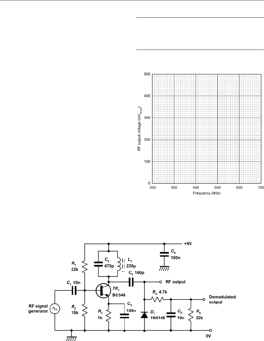
Practical investigation
Objective
To investigate the operation of a 455 kHz RF/IF
amplifier and demodulator stage.
Components and test equipment
Breadboard, 9 V d.c. power supply (or 9 V battery),
BC548 (or similar NPN transistor), resistors of
1 kO,4.7 kO,10 kO,22 kO5% 0.25 W, capacitors
of 100 pF, 470 pF, 10 nF (two required), 100 nF
(two required), ferrite cored high-Q inductor of
220 µH (with series loss resistance of 2 Oor less),
oscilloscope, digital multimeter (for checking bias
voltages), RF signal generator with amplitude
modulated output, output attenuator and frequency
adjustable over the range 200 kHz to 700 kHz, test
leads and probes.
Procedure
Connect the circuit as shown in Fig. 13.26. With
the signal generator disconnected, connect the d.c.
supply and use the digital multimeter on the 20 V
d.c. range to measure the collector, base and emitter
voltages on TR1.These should be approximately 9
V, 2.8 V, and 2.1 V respectively. If these voltages
are substantially different you should carefully
check the wiring and connections to TR1.
Figure 13.26 RF amplifier/demodulator circuit used in the Practical investigation
242 ELECTRONIC CIRCUITS: FUNDAMENTALS AND APPLICATIONS
Frequency
(kHz) 200 300 400 455 500 600 700
Voltage
(mV pk-pk)
800
Figure 13.27 Graph layout for plotting the results
Table 13.3 Table of results
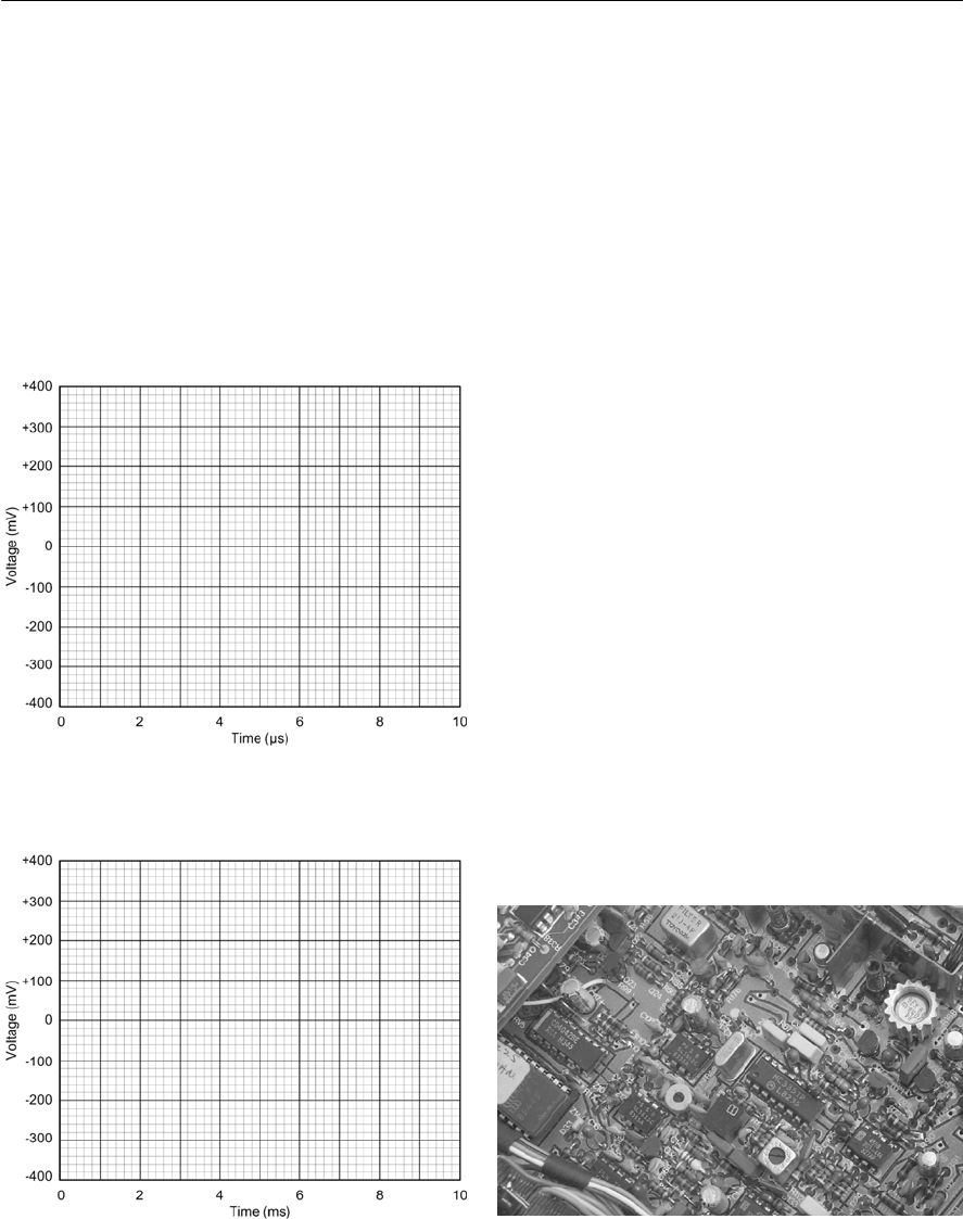
RADIO 243
Switch the signal generator on and set the output to
2mV peak-to-peak (707 µV RMS) at 455 kHz,
unmodulated. Connect the oscilloscope (using
macthed probes) to display the RF output on
Channel 1 (or Y1) and the demodulated output on
Channel 2 (or Y2). The oscilloscope timebase
should be set to 1 µs/cm whilst the Channel 1 and 2
gain settings should both be set to 100 mV/cm.
The Channel 1 input should be set to AC whilst the
Channel 2 input should be set to DC.
Display the waveforms produced and sketch two
or three cycles of both waveforms using the layout
shown in Fig. 13.28. Now select modulated RF
output on the signal generator and set to
modulation depth to 30%. Change the
oscilloscope timebase setting to 1 ms/cm and
display the output waveforms produced. Sketch two
or three cycles of the waveforms using the layout
shown in Fig. 13.29.
Switch the modulation off and check that the
output of the signal generator is still set to 455 kHz.
Accurately measure the peak-peak RF output
(Channel 1). This should be approximately 500 mV
pk-pk. Record the output voltage in a table similar
to that shown in Table 13.3.
Vary the signal generator output frequency over
the range 200 kHz to 700 kHz in suitable steps and
record the peak-peak output voltage at each step in
your table.
Calculations and graphs
Record your results in Table 13.3. Plot a graph
showing the frequency response of the RF/IF
amplifier using the graph layout shown in Fig.
13.27. Determine the frequency at which maximum
voltage gain is achieved and calculate the stage
gain at this frequency. Also determine the
bandwidth of the amplifier stage.
Conclusions
Comment on the shape of the frequency response
and the waveform sketches. Were these what you
would expect? Suggest a typical application for the
circuit.
Figure 13.28 Layout for sketching the
unmodulated RF output waveform
Figure 13.29 Layout for sketching the demodulated
waveform
Figure 13.30 10.7 MHz and 455 kHz IF amplifier
stages in a typical mobile transceiver

Table 13.4 See Question 13.5
244 ELECTRONIC CIRCUITS: FUNDAMENTALS AND APPLICATIONS
Problems
13.1 Abroadcast transmitter produces a signal
at 190 kHz. What will be the wavelength
of the radiated signal?
13.2 What frequency corresponds to the 13 m
short wave band?
13.3 A signal in a cable propagates at two-thirds
of the speed of light. If an RF signal at 50
MHz is fed to the cable, determine the
wavelength in the cable.
13.4 An AM broadcast receiver has an IF of
470 kHz. If the receiver is to be tuned over
the medium wave broadcast band from
550 kHz to 1.6 MHz, determine the required
local oscillator tuning range.
13.5 The data shown in Table 13.4 was obtained
during an experiment on an IF bandpass
filter. Plot the frequency response
characteristic and use it to determine the IF
frequency, bandwidth and Q-factor of the
filter.
13.6 Refer to the IF amplifier/AM demodulator
circuit shown in Fig. 13.17. Identify the
component(s) that provide:
(a) a tuned collector load for TR1
(b) base bias for TR1
(c) coupling of the signal from the IF
amplifier stage to the demodulator stage
(d) a low-pass filter to remove RF signal
components at the output of the
demodulator
(e) a volume control
(f) removing the d.c. level on the signal at
the output of the demodulator
(g) a bypass to the common rail for RF
signals that may be present on the supply
(h) input coupling to the IF amplifier stage.
13.7 A half-wave dipole is to be constructed for
a frequency of 50 MHz. Determine the
approximate length of the aerial.
13.8 A power of 150 W is applied to a dipole
aerial in order to produce a given signal
strength at a remote location. What power,
applied to a Yagi aerial with a gain of
8 dBd,would be required to produce the
same signal strength?
Answers to these problems appear on page 376.
Frequency
(MHz) 10.4 10.5 10.6 10.7 10.8 10.9 11.0
Voltage
(V) 0.42 0.52 0.69 1.0 0.67 0.51 0.41
Formulae introduced in this chapter
Frequency and wavelength:
(page 229)
Velocity of propagation:
(page 229)
v=3×10⁸m/s for waves in air or space.
BFO frequency:
(page 230)
fBFO = fRF ± fAF
Local oscillator frequency:
(page 234)
fLO =fRF ±fIF
Half-wave dipole aerial:
(page 237)
Aerial impedance:
(page 238)
Radiated power:
(page 239)
Radiation efficiency:
(page 239)
D
vf
=
D
v
f=D
v
f
=
D
2
l
=
E
Z
I
=
2
ra r
PI R
=×
Efficiency 100%
r
rloss
P
PP
=×
+
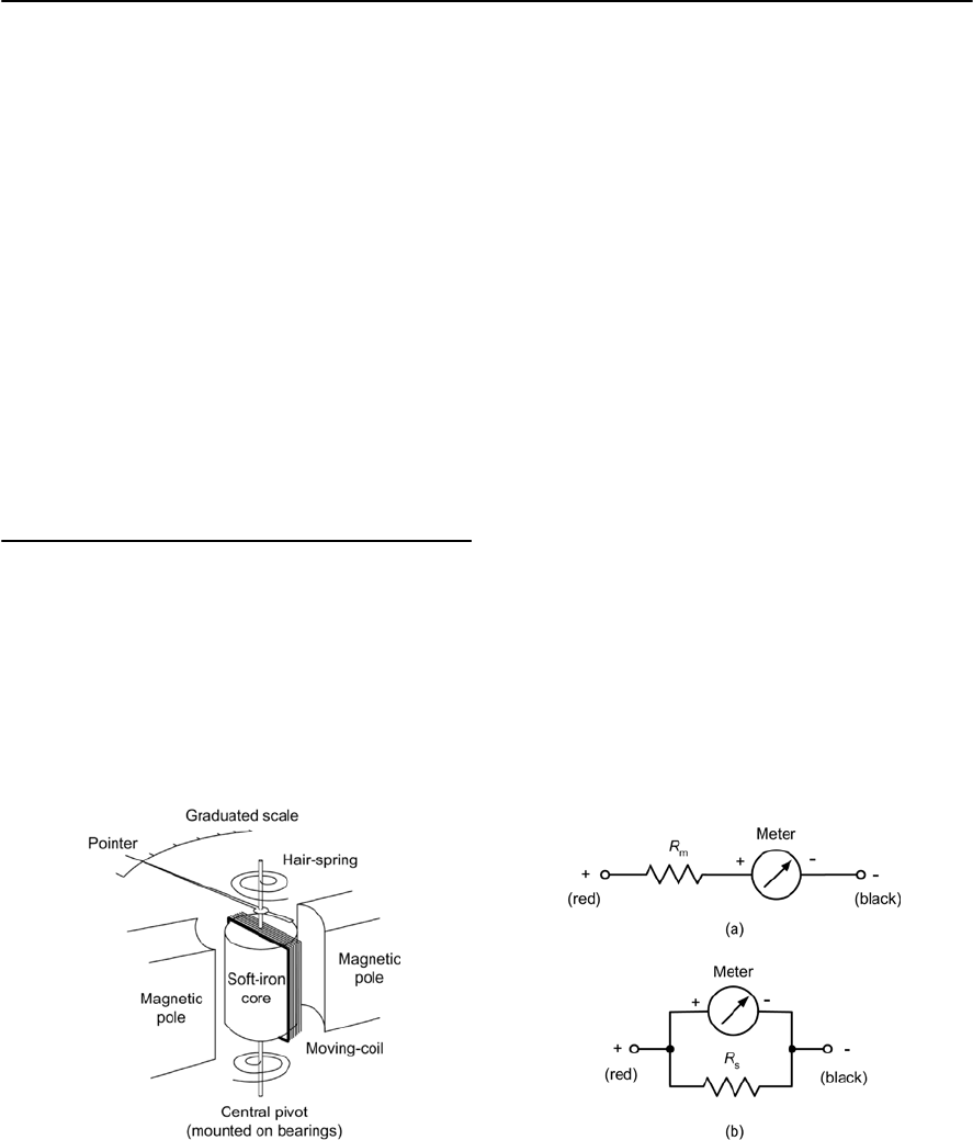
14
Test equipment and measurements
This chapter is about making practical
measurements on real electronic circuits. It
describes and explains the use of the basic items of
test equipment that you will find in any electronics
laboratory or workshop. We begin the chapter by
looking at how we use a moving coil meter to
measure voltage, current and resistance and then
quickly move on to more complex multi-range
analogue and digital instruments and the
oscilloscope. To help you make use of these test
instruments we have included some DO’s and
DONT’S. If you intend to become an electronic
engineer these will become your ‘tools of the
trade’. Being able to use them effectively is just the
first step on the ladder!
Meters
Straightforward measurements of voltage, current
and resistance can provide useful information on
the state of almost any circuit. To get the best from
ameter it is not only necessary to select an
appropriate measurement function and range but
also to be aware of the limitations of the instrument
and the effect that it might have on the circuit
under investigation. When fault finding, it is
interpretation that is put on the meter readings
rather than the indications themselves.
Figures 14.2(a) and 14.2(b) respectively show
the circuit of a simple voltmeter and a simple
ammeter.Each instrument is based on the moving
coil indicator shown in Fig. 14.1. The voltmeter
consists of a multiplier resistor connected in series
with the basic moving coil movement whilst the
ammeter consists of a shunt resistor connected in
parallel with the basic moving coil instrument.
When determining the value of multiplier or shunt
resistance (Rmand Rsrespectively in Fig. 14.2) it is
important to remember that the coil of the moving
coil meter also has a resistance. We have shown
this as a resistor, r,connected with the moving coil
in Fig. 14.3. In both cases, the current required to
produce full-scale deflection of the meter
movement is Im.
In the voltmeter circuit shown in Fig. 14.3(a):
V=ImRm+Imr
from which:
ImRm=V–Imr
Figure 14.1 A moving coil meter movement
Figure 14.2 A moving coil meter connected (a) as
avoltmeter and (b) an ammeter
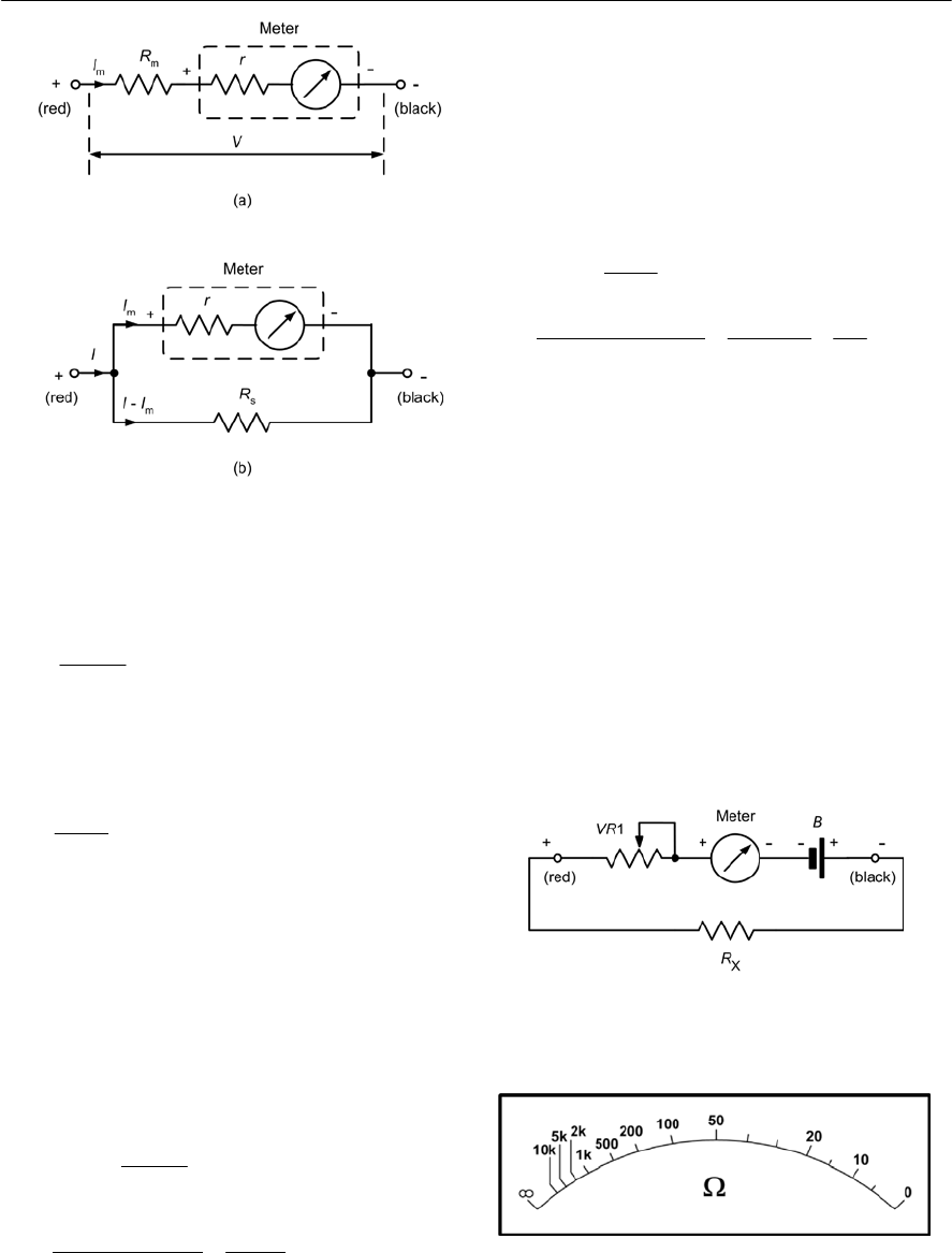
246 ELECTRONIC CIRCUITS: FUNDAMENTALS AND APPLICATIONS
Thus:
In the ammeter circuit shown in Fig. 14.3(b):
(I–Im)Rs=Imr
from which:
Example 14.1
Amoving coil meter has a full-scale deflection
current of 1 mA. If the meter coil has a resistance
of 500 ?,determine the value of multiplier resistor
if the meter is to be used as a voltmeter reading 0 to
5V.
Solution
Using gives:
m
m
m
VIr
RI
=
m
s
m
Ir
R
II
=
Example 14.2
Amoving coil meter has a full-scale deflection
current of 10 mA. If the meter coil has a resistance
of 40 ?,determine the value of shunt resistor if the
meter is to be used as an ammeter reading 0 to 100
mA.
Solution
Using gives:
The circuit of a simple ohmmeter is shown in Fig.
14.4. The battery is used to supply a current that
will flow in the unknown resistor, Rx,which is
indicated on the moving coil meter. Before use, the
variable resistor, RV,must be adjusted in order to
produce full-scale deflection (corresponding to
zero on the ohms scale). Zero resistance thus
corresponds to maximum indication. Infinite
resistance (i.e. when the two terminals are left
open-circuit) corresponds to minimum indication.
The ohms scale is thus reversed when compared
with a voltage or current scale. The scale is also
non-linear, as shown in Fig. 14.5.
Figure 14.5 A typical ohmmeter scale
Figure 14.3 Circuit for determining the values of
(a) a multiplier resistor and (b) a shunt resistor
m
m
m
VIr
RI
=
(
)
3
3
m33
5110 500 50.5
4.5 10 4.5 k
110 110
R
××
===×=
××
m
s
m
Ir
R
II
=
33
s33 3
10 10 40 400 10 400
4.44
90100 10 10 10 90 10
R
×× ×
====
×××
Figure 14.4 A simple ohmmeter
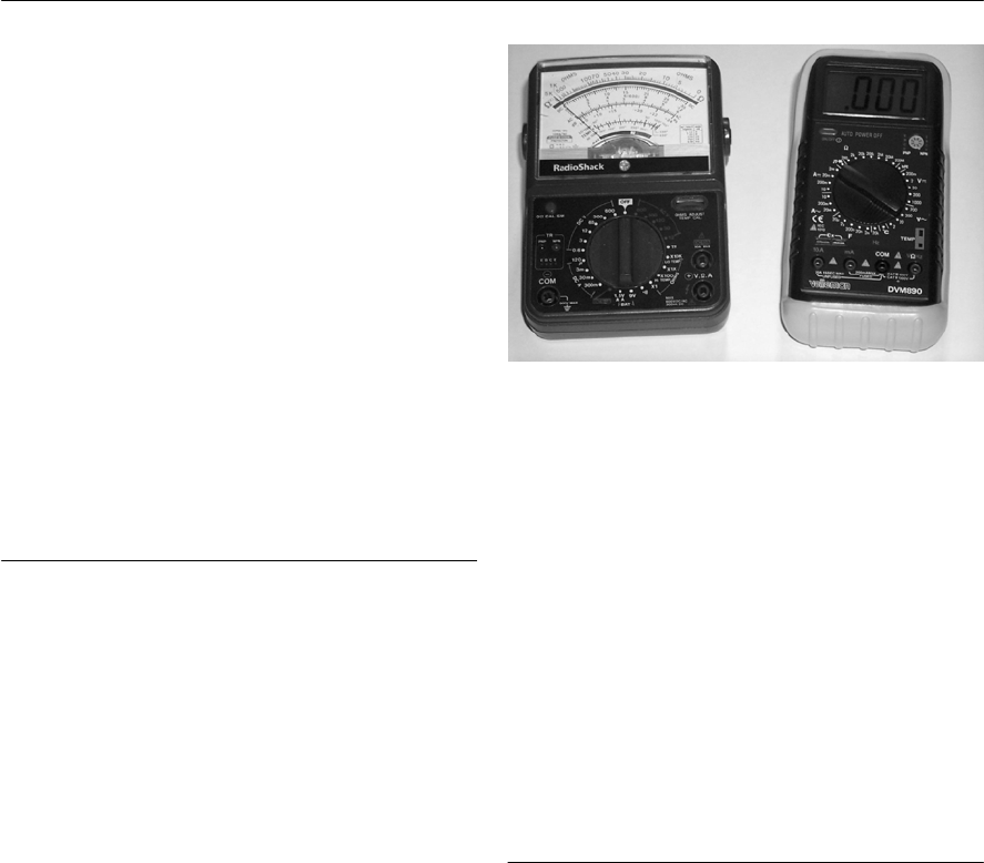
TEST EQUIPMENT AND MEASUREMENTS 247
Multi-range meters
For practical measurements on electronic circuits it
is often convenient to combine the functions of a
voltmeter, ammeter and ohmmeter into a single
instrument (known as a multi-range meter or
simply a multimeter). In a conventional
multimeter as many as eight or nine measuring
functions may be provided with up to six or eight
ranges for each measuring function. Besides the
normal voltage, current and resistance functions,
some meters also include facilities for checking
transistors and measuring capacitance. Most multi-
range meters normally operate from internal
batteries and thus they are independent of the
mains supply. This leads to a high degree of
portability which can be all-important when
measurements are to be made away from a
laboratory or workshop.
Displays
Analogue instruments employ conventional
moving coil meters and the display takes the form
of a pointer moving across a calibrated scale. This
arrangement is not so convenient to use as that
employed in digital instruments because the
position of the pointer is rarely exact and may
require interpolation. Analogue instruments do,
however, offer some advantages not the least of
which lies in the fact that it is very easy to make
adjustments to a circuit whilst observing the
relative direction of the pointer; a movement in one
direction representing an increase and in the other a
decrease. Despite this, the principal disadvantage
of many analogue meters is the rather cramped, and
sometimes confusing, scale calibration. To
determine the exact reading requires first an
estimation of the pointer’s position and then the
application of some mental arithmetic based on the
range switch setting.
Digital meters, on the other hand, are usually
extremely easy to read and have displays that are
clear, unambiguous, and capable of providing a
very high resolution. It is thus possible to
distinguish between readings that are very close.
This is just not possible with an analogue
instrument. Typical analogue and digital meters are
shown in Fig. 14.6.
The type of display used in digital multi-range
meters is either the liquid crystal display (LCD) or
the light emitting diode (LED). The former type
requires very little electrical power and thus is to
be preferred on the grounds of low battery
consumption. LCD displays are, however,
somewhat difficult to read under certain light
conditions and, furthermore, the display response
can be rather slow. LED displays can be extremely
bright but unfortunately consume considerable
power and this makes them unsuitable for use in
battery-powered portable instruments.
Loading
Another very significant difference between
analogue and digital instruments is the input
resistance that they present to the circuit under
investigation when taking voltage measurements.
The resistance of a reasonable quality analogue
multi-range meter can be as low as 50 kGon the
2.5 V. With a digital instrument, on the other hand,
the input resistance is typically 10 MGon the 2 V
range. The digital instrument is thus to be preferred
when accurate readings are to be taken. This is
particularly important when measurements are to
be made on high impedance circuits, as illustrated
by the following:
Two multi-range meters are used to measure the
voltage produced by the two potential dividers
Figure 14.6 Typical analogue (left) and digital
(right) multimeters
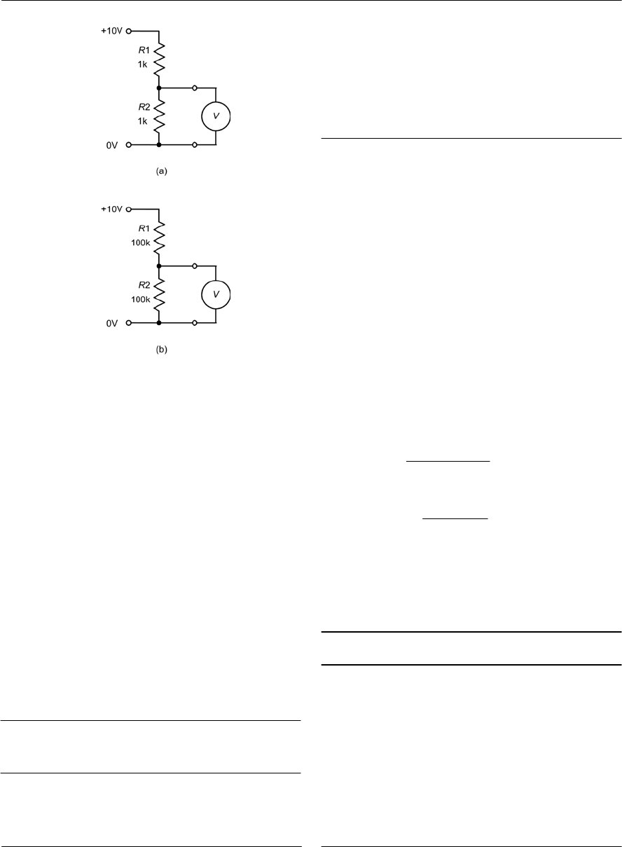
248 ELECTRONIC CIRCUITS: FUNDAMENTALS AND APPLICATIONS
shown in Fig. 14.7. One of the meters is an
analogue type having an internal resistance of 10
kW on the 10 V range. The other is a digital type
that has the much higher internal resistance of 10
MW. The two potential dividers each consist of
resistors or identical value. However, the potential
divider of Fig. 14.7(b) has a much lower resistance
than that of Fig. 14.7(a). In both cases the ‘true’
voltage produced by the potential divider should
be half the supply, i.e. exactly 5 V. The actual
readings obtained from the instruments are shown
in Table 14.1.
The large difference in the case of Fig. 14.7(b)
illustrates the effect of voltmeter loading on a high
resistance circuit. An appreciable current is drawn
away from the circuit into the measuring
instrument. Clearly this is a very undesirable
effect!
Sensitivity
The sensitivity of an analogue meter may be
expressed in several ways. One is to specify the
basic full-scale deflection (f.s.d.) current of the
moving coil meter. This is typically 50 µA or less.
An alternative method is that of quoting an ohms-
per-volt rating. This is, in effect, the resistance
presented by the meter when switched to the 1 V
range.
The ohms-per-volt rating is inversely
proportional to the basic full-scale sensitivity of the
meter movement and, to determine the resistance of
ameter on a particular voltage range, it is only
necessary to multiply the range setting by the
‘ohms-per-volt’ rating. Table 14.2 shows how
meter f.s.d. and ohms-per-volt are related. From
this we can conclude that:
or
1
Meter f.s.d. =
Ohms-per-volt
1
Ohms-per-volt =
Meter f.s.d.
Figure 14.7 Examples of voltmeter loading: (a) a
low resistance circuit (b) a high resistance circuit
Table 14.1 Readings obtained from Fig. 14.7
Meter High resistance
circuit
Fig. 14.7(a)
Low resistance
circuit
Fig. 14.7(b)
Analogue type
(100 kG)4.9 V 3.3 V
Digital type
(10 MG)4.99 V 4.97 V
Table 14.2 Relationship between meter sensitivity
and Ohms-per-volt
Meter f.s.d. Ohms-per-volt
10 µA 100 kG/V
20 µA 50 kG/V
50 µA 20 kG/V
100 µA 10 kG/V
200 µA 5 kG/V
500 µA 2 kG/V
1mA 1 kG/V

TEST EQUIPMENT AND MEASUREMENTS 249
Example 14.3
Ameter has a full-scale deflection of 40 µA. What
will its ohms-per-volt rating be?
Solution
Example 14.4
A20 kG/V meter is switched to the 10 V range.
What current will flow in the meter when it is
connected to a 6 V source?
Solution
The resistance of the meter will be given by:
Rm=10 × 20 kG=200 kG
The current flowing in the meter will thus be given
by:
Digital multi-range meters
Low-cost digital multi-range meters have been
made possible by the advent of mass-produced LSI
devices and liquid crystal displays. A 3½-digit
display is the norm and this consists of three full
digits that can display ‘0’ to ‘9’ and a fourth (most
significant) digit which can only display ‘1’. Thus,
the maximum display indication, ignoring the
range switching and decimal point, is 1999;
anything greater over-ranges the display.
The resolution of the instrument is the lowest
increment that can be displayed and this would
normally be an increase or decrease of one unit in
the last (least significant) digit. The sensitivity of a
digital instrument is generally defined as the
smallest increment that can be displayed on the
lowest (most sensitive) range. Sensitivity and
resolution are thus not quite the same. To put this
into context, consider the following example:
A digital multi-range meter has a 3½-digit
display. When switched to the 2 V range, the
maximum indication would be 1.999 V and any
input of 2 V, or greater, would produce an over-
6
m3
m
6V6 30 10 30
µA
200 10
IR
== =×=
×
range indication. On the 2 V range, the instrument
has a resolution of 0.001 V (or 1 mV). The lowest
range of the instrument is 200 mV (corresponding
to a maximum display of 199.9 mV) and thus the
meter has a sensitivity of 0.1 mV (or 100 µV).
Nearly all digital meters have automatic zero
and polarity indicating facilities and some also
have autoranging.This feature, which is only
found in the more expensive instruments,
automatically changes the range setting so that
maximum resolution is obtained without over-
ranging. There is thus no need for manual
operation of the range switch once the indicating
mode has been selected. This is an extremely
useful facility since it frees you from the need to
make repeated adjustments to the range switch
while measurements are being made.
Example 14.5
Adigital multi-range meter has a 4½-digit display.
When switched to the 200 V range, determine:
(a) the maximum indication that will appear on
the display
(b) the resolution of the instrument.
Solution
(a) The maximum indication that will appear on
the display is 199.99 V
(b) The resolution of the instrument will be 0.01 V
or 10 mV.
Using an analogue multi-range meter
Figure 14.8 shows the controls and display
provided by a simple analogue multi-range meter.
The range selector allows you to select from a total
of twenty ranges and six measurement functions.
These functions are:
•DC voltage (DC, V)
•DC current (DC, mA)
•AC voltage (AC, V)
•Resistance (OHM)
•Continuity test (BUZZ)
•Battery check (BAT)
Note that more complex instruments may have
several more ranges.
6
11
Ohms-per-volt = 25 k
Meter f.s.d. 40 10
==
×
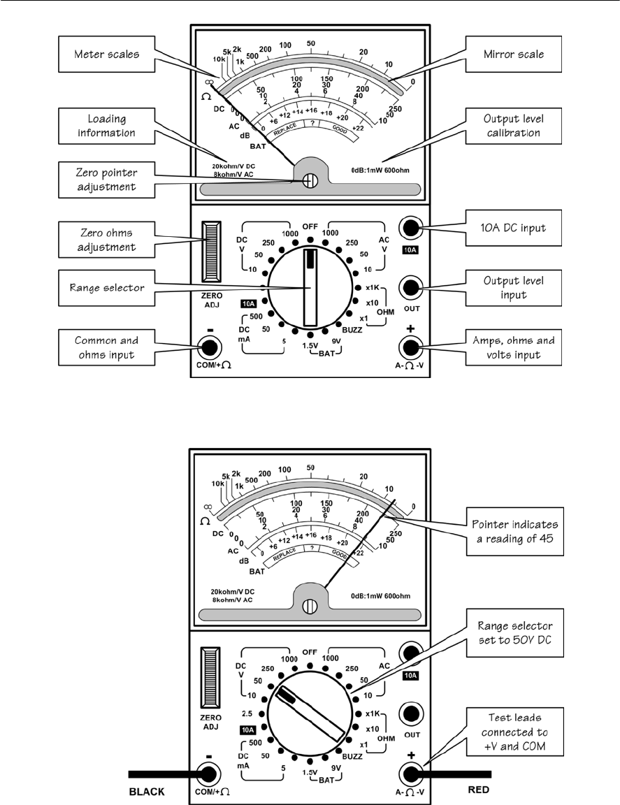
250 ELECTRONIC CIRCUITS: FUNDAMENTALS AND APPLICATIONS
Figure 14.8 Analogue multimeter display and controls
Figure 14.9 Analogue multimeter set to the DC, 50 V range
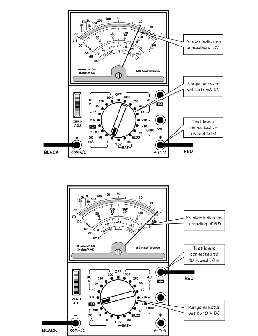
TEST EQUIPMENT AND MEASUREMENTS 251
Figure 14.10 Analogue multimeter set to the DC, 5 mA range
Figure 14.11 Analogue multimeter set to the DC, 10 A range
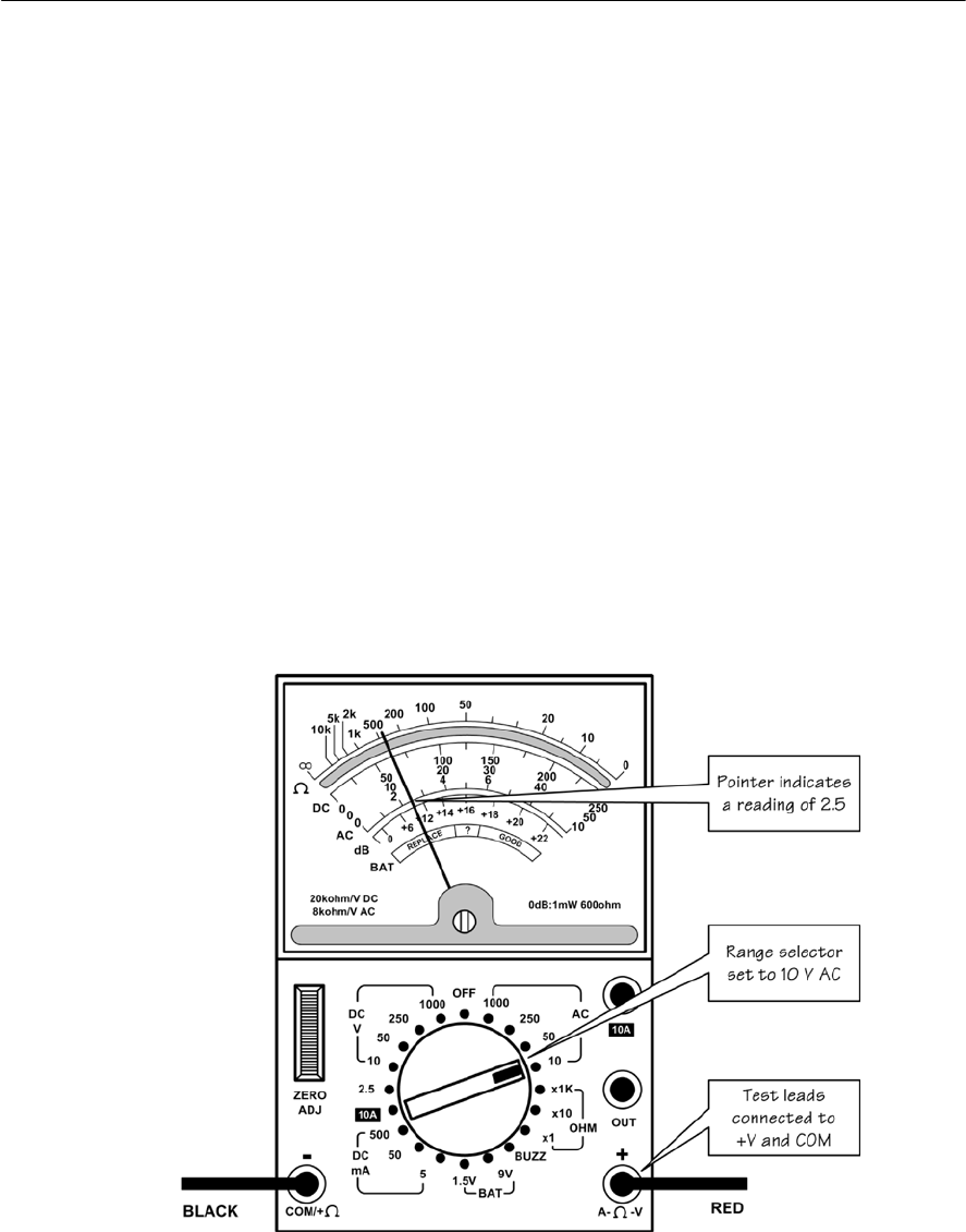
252 ELECTRONIC CIRCUITS: FUNDAMENTALS AND APPLICATIONS
DC voltage measurement
Figure 14.9 shows how to make DC voltage
measurements. In both cases, the red and black test
leads are connected to the ‘+’ and ‘O’sockets
respectively. In Fig. 14.9, the range selector is set
to DCV, 50 V. The pointer is reading just less than
45 on the range that has 50 as its full-scale
indication (note that there are three calibrated
voltage scales with maximum indications of 10 V,
50 V and 250 V respectively. The reading indicated
is approximately 45 V.
DC current measurement
Figure 14.10 shows how to make a DC current
measurement. Once again, the red and black test
leads are connected to the ‘+’ and ‘O’sockets
respectively. The range selector is set to DC, 5 mA.
In Fig. 14.10, the pointer is reading between 35 and
40 (and is actually a little closer to 35 than it is to
40) on the range that has 50 as its full-scale
indication. The actual reading indicated is thus
approximately 3.7 mA.
DC high-current measurement
In common with many simple multi-range meters,
both analogue and digital, the high current range
(e.g., 10 A) is not only selected using the range
selector switch but a separate input connection
must also be made. The reason for this is simply
that the range switch and associated wiring is not
designed to carry a high current. Instead, the high-
current shunt is terminated separately at its own
‘10 A’ socket.
Figure 14.11 shows the connections and range
selector settings to permit high-current DC
measurement. The range selector is set to DC 10 A
and the red and black test leads are connected to
‘10 A’ and ‘O’respectively. The pointer is reading
mid-way between 9 and 10 on the range that has 10
as its full-scale indication. The actual reading
indicated is thus 9.5 A.
AC voltage measurement
Figure 14.12 shows how to make AC voltage
measurements. Once again, the red and black test
Figure 14.12 Analogue multimeter set to the AC, 10 V range
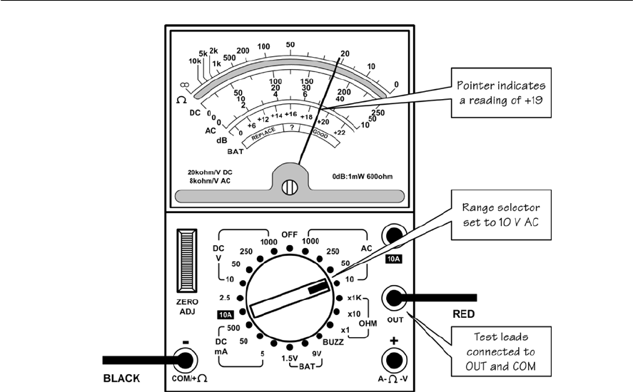
TEST EQUIPMENT AND MEASUREMENTS 253
leads are connected to the ‘+’ and ‘O’sockets
respectively. In Fig. 14.12, the range selector is set
to AC, 10 V. The pointer is reading mid-way
between 2 and 3 and the indicated reading is
approximately 2.5 V.
Output level measurement
Figure 14.13 shows how to make output level
measurements. The red and black test leads are
respectively connected to ‘OUT’ and ‘O’
respectively. The range selector is set to AC, 10 V
(note that the output level facility is actually based
on AC voltage measurement).
Output level indications are indicated in decibels
(dB) where 0 dB (the reference level)corresponds
to a power level of 1mW in a resistance of 600 G.
The pointer is reading mid-way between +18 and
+20 on the dB scale and the indicated reading is
+19 dB.
Resistance
Figure 14.14 shows how to make resistance
measurements. In all three cases, the red and black
test leads are connected to the ‘+’ and ‘O’sockets
respectively. Before making any measurements it is
absolutely essential to zero the meter. This is
achieved by shorting the test leads together and
adjusting the ZERO ADJ control until the meter
reads full-scale (i.e., zero on the ohms scale). In
Fig. 14.14, the range selector is set to OHM, ×1.
The pointer is reading mid-way between 0 and 10
and the resistance indicated is approximately 5 G.
DO’s and DON’Ts of using an analogue multimeter
DO ensure that you have selected the correct range
and measuring function before attempting to
connect the meter into a circuit.
DO select a higher range than expected and then
progressively increase the sensitivity as necessary
to obtain a meaningful indication.
DO remember to zero on the ohms range before
measuring resistance.
DO switch the meter to the ‘off’ position (if one is
available) before attempting to transport the meter.
Figure 14.13 Analogue multimeter set to the dB (output level) range
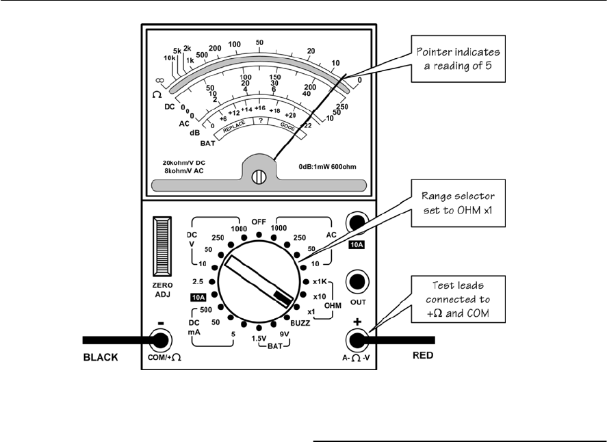
254 ELECTRONIC CIRCUITS: FUNDAMENTALS AND APPLICATIONS
DO check and, if necessary, replace the internal
batteries regularly.
DO use properly insulated test leads and prods.
DON’T attempt to measure resistance in a circuit
that has the power applied to it.
DON’T rely on voltage readings made on high-
impedance circuits (the meter’s own internal
resistance may have a significant effect on the
voltages that you measure).
DON’T rely on voltage and current readings made
on circuits where high-frequency signals may be
present (in such cases an analogue meter may
produce readings that are wildly inaccurate or
misleading).
DON’T subject the instrument to excessive
mechanical shock or vibration (this can damage the
sensitive meter movement).
DON’T leave the instrument for very long periods
without removing the batteries (these may leak and
cause damage).
Using a digital multi-range meter
Digital multi-range meters offer a number of
significant advantages when compared with their
more humble analogue counterparts. The display
fitted to a digital multi-range meter usually consists
of a 3½-digit seven-segment display Othe ½ simply
indicates that the first digit is either blank (zero) or
1. Consequently, the maximum indication on the
2 V range will be 1.999 V and this shows that the
instrument is capable of offering a resolution of
1mV on the 2 V range (i.e. the smallest increment
in voltage increment that can be measured is
1mV). The resolution obtained from a comparable
analogue meter would be of the order of 50 mV, or
so, and thus the digital instrument provides a
resolution that is many times greater than its
analogue counterpart.
Figure 14.15 shows the controls and display
provided by a simple digital multi-range meter. The
mode switch and range selector allow you to select
from a total of twenty ranges and eight
measurement functions. These functions are:
Figure 14.14 Analogue multimeter set to the OHM, ×1 range
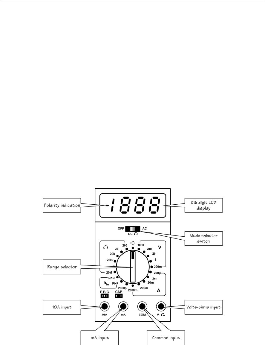
TEST EQUIPMENT AND MEASUREMENTS 255
•DC voltage (DC, V)
•DC current (DC, A)
•AC voltage (AC, V)
•AC current (AC, A)
•Resistance (OHM)
•Capacitance (CAP)
•Continuity test (buzzer)
•Transistor current gain (hFE)
DC voltage measurement
Figure 14.16 shows how to make DC voltage
measurements using a digital multi-range meter.
The red and black test leads are connected to the
‘V-OHM’ and ‘COM’ sockets respectively. In Fig.
14.6, the mode switch and range selector is set to
DCV, 200 V, and the display indicates a reading of
124.5 V.
DC current measurements
Figure 14.17 shows how to make a DC current
measurement. Here, the red and black test leads are
connected to the ‘mA’ and ‘COM’ sockets
Figure 14.15 Digital multimeter display and controls
respectively. The mode switch and range selectors
are set to DC, 200 mA, and the display indicates a
reading of 85.9 mA.
DC high-current measurement
In common with simple analogue multi-range
meters, the meter uses a shunt which is directly
connected to a separate ‘10 A’ terminal. Figure
14.18 shows the connections, mode switch and
range selector settings to permit high-current DC
measurement. The mode switch and range selectors
are set to DC, 2,000 mA (2 A) and the red and
black test leads are connected to ‘10 A’ and ‘COM’
respectively. The display indicates a reading of
2.99 A.
AC voltage measurement
Figure 14.19 shows how to make AC voltage
measurements. Once again, the red and black test
leads are connected to the ‘V-OHM’ and ‘COM’
sockets respectively. In Fig. 14.19, the mode switch
and range selectors are set to AC, 10 V, and the
display indicates a reading of 1.736 V.
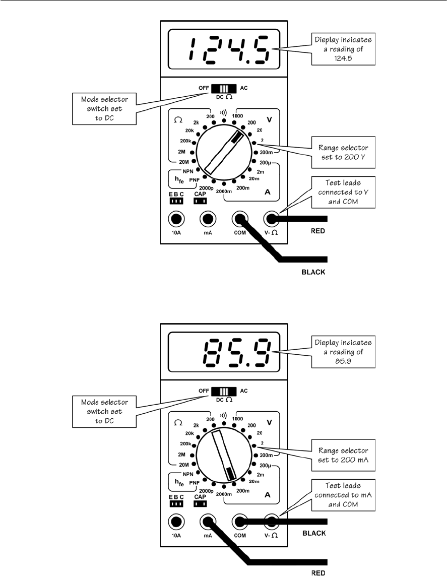
256 ELECTRONIC CIRCUITS: FUNDAMENTALS AND APPLICATIONS
Figure 14.17 Digital multimeter set to the DC, 200 mA range
Figure 14.16 Digital multimeter set to the DC, 200 V range
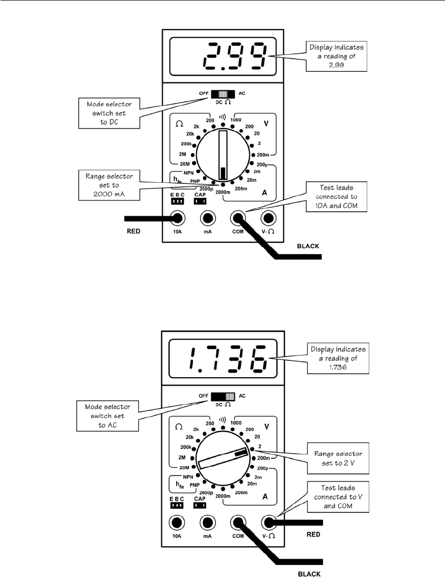
TEST EQUIPMENT AND MEASUREMENTS 257
Figure 14.19 Digital multimeter set to the AC, 2 V range
Figure 14.18 Digital multimeter set to the DC, 10 A range
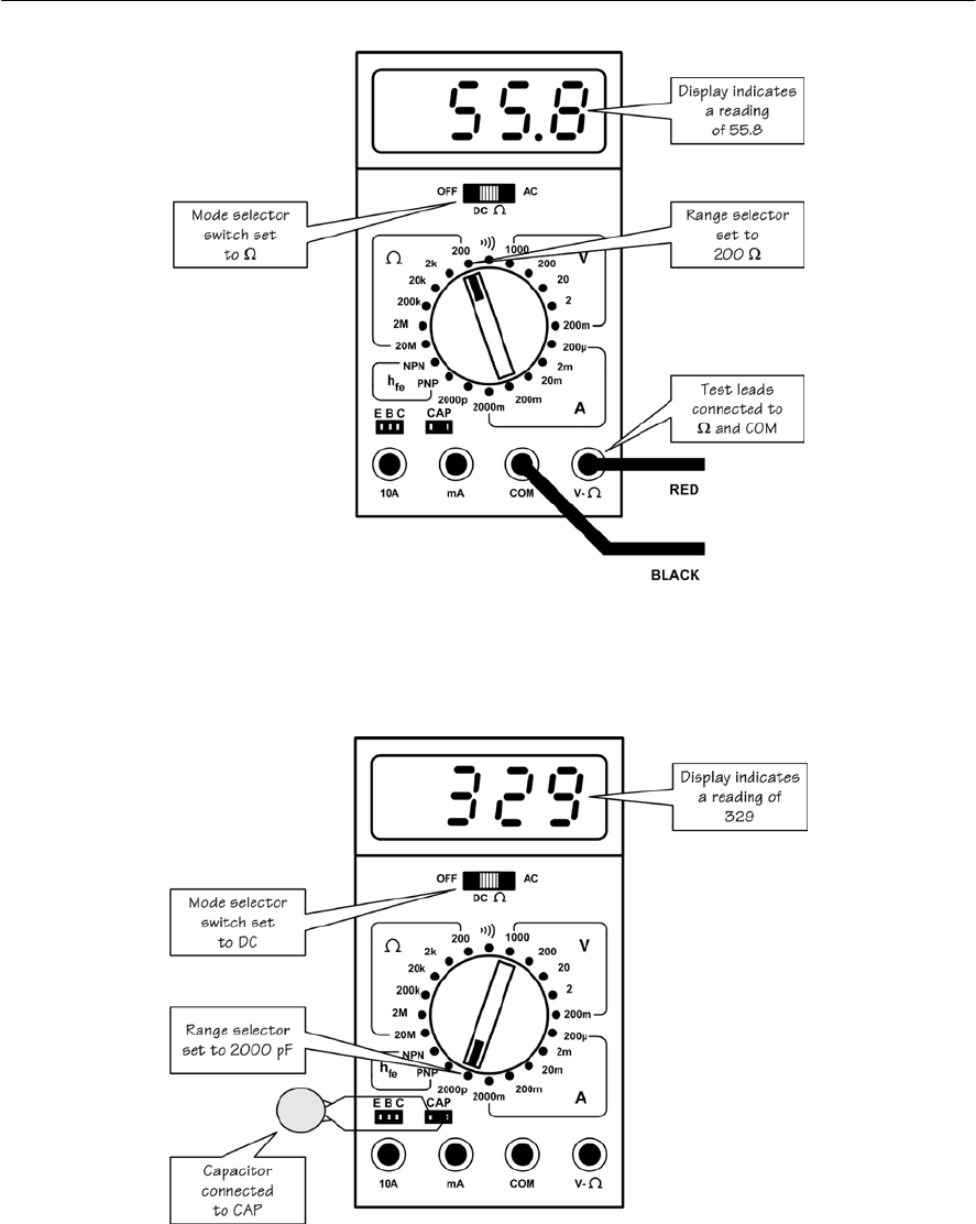
258 ELECTRONIC CIRCUITS: FUNDAMENTALS AND APPLICATIONS
Figure 14.21 Digital multimeter set to the capacitance, 2,000 pF range
Figure 14.20 Digital multimeter set to the OHM, 200 Grange
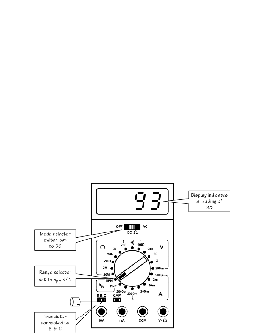
TEST EQUIPMENT AND MEASUREMENTS 259
Figure 14.22 Digital multimeter set to the transistor current gain, NPN range
Resistance measurement
Figure 14.20 shows how to make resistance
measurements. As before, the red and black test
leads are respectively connected to ‘V-OHM’ and
‘COM’ respectively. In Fig. 14.20, the mode switch
and range selectors are set to OHM, 200ohm, and
the meter indicates a reading of 55.8 G.Note that it
is not necessary to ‘zero’ the meter by shorting the
test probes together before taking any
measurements (as would be the case with an
analogue meter).
Capacitance measurement
Many modern digital multi-range meters
incorporate a capacitance measuring although this
may be limited to just one or two ranges. Figure
14.21 shows how to carry out a capacitance
measurement. The capacitor on test is inserted into
the two-way connector marked ‘CAP’ whilst the
mode switch and range selector controls are set to
DC, 2,000 pF. The display indication shown in Fig.
14.21 corresponds to a capacitance of 329 pF.
Transistor current gain (hFE)measurement
Many modern digital multi-range meters also
provide some (fairly basic) facilities for checking
transistors. Figure 14.22 shows how to measure the
current gain (hFE)of an NPN transistor (see page
142). The transistor is inserted into the three-way
connector marked ‘EBC’, taking care to ensure that
the emitter lead is connected to ‘E’, the base lead to
‘B’, and the collector lead to ‘C’. The mode switch
and range selector controls are set to DC, NPN
respectively. The display indication in Fig. 14.22
shows that the device has a current gain of 93. This
means that, for the device in question, the ratio of
collector current (IC)to base current (IB)is 93.
Connecting a meter into a circuit
Figure 14.23 shows how a meter is connected to
read the voltages and currents present at various
points in a simple transistor audio amplifier.

260 ELECTRONIC CIRCUITS: FUNDAMENTALS AND APPLICATIONS
(a) At A, the supply current is measured by
removing the supply rail fuse and inserting
the meter in its place. A suitable meter range is
2 A, DC.
(b) At B, the collector current for TR4 is
measured by removing the service link and
inserting the meter in its place. A suitable
meter range is 2 A, DC.
(c) At C, the emitter current for TR4 can be
measured by connecting the meter across the
emitter resistor, R11, and measuring the
voltage drop across it. The emitter current can
then be calculated using Ohm’s Law). This
can be much quicker than disconnecting the
emitter lead and inserting the meter switched
to the current range. A suitable range for the
meter is 2 V, DC (note that 2 V is dropped
across 1 Gwhen a current of 2 A is flowing ).
(d) At D, the voltage at the junction of R11 and
R12 is measured by connecting the meter
between the junction of R11 and R12 and
common/ground. A suitable meter range is
20 V, DC.
(e) At E, the base-emitter voltage for TR2 is
measured by connecting the meter with its
positive lead to the base of TR2 and its
negative lead to the emitter of TR2. A suitable
meter range is 2 V, DC.
DO’s and DON’Ts of using a digital multimeter
DO ensure that you have selected the correct range
and measuring function before attempting to
connect the meter into a circuit.
DO select a higher range than expected and then
progressively increase the sensitivity as necessary
to obtain a meaningful indication.
DO switch the meter to the ‘off’ position in order to
conserve battery life when the instrument is not
being used.
DO check and, if necessary, replace the internal
battery regularly.
DO use properly insulated test leads and prods.
DO check that a suitably rated fuse is used in
conjunction with the current ranges (if the current
ranges aren’t working it’s probably the fuse that’s
blown!).
DON’T attempt to measure resistance in a circuit
that has the power applied to it.
DON’T rely on voltage and current readings made
on circuits where high-frequency signals may be
present (as with analogue instruments, digital
meters may produce readings that are wildly
inaccurate or misleading in such circumstances).
DON’T rely on measurements made when
voltage/current is changing or when a significant
amount of AC may be present superimposed on a
DC level.
The oscilloscope
An oscilloscope is an extremely comprehensive
and versatile item of test equipment which can be
used in a variety of measuring applications, the
most important of which is the display of time
related voltage waveforms.
The oscilloscope display is provided by a cathode
ray tube (CRT) that has a typical screen area of
8cm ×10 cm. The CRT is fitted with a graticule
that may either be integral with the tube face or a
separate translucent sheet. The graticule is usually
ruled with a l cm grid to which further bold lines
may be added to mark the major axes on the central
viewing area. Accurate voltage and time
measurements may be made with reference to the
graticule, applying a scale factor derived from the
appropriate range switch.
A word of caution is appropriate at this stage,
however. Before taking meaningful measurements
from the CRT screen it is absolutely essential to
ensure that the front panel variable controls are set
in the calibrate (CAL) position. Results will
almost certainly be inaccurate if this is not the
case!
The use of the graticule is illustrated by the
following example:
An oscilloscope screen is depicted in Fig. 14.24.
This diagram is reproduced actual size and the fine
graticule markings are shown every 2 mm along
the central vertical and horizontal axes.
The oscilloscope is operated with all relevant
controls in the ‘CAL’ position. The timebase
(horizontal deflection) is switched to the 1 ms/cm
range and the vertical attenuator (vertical
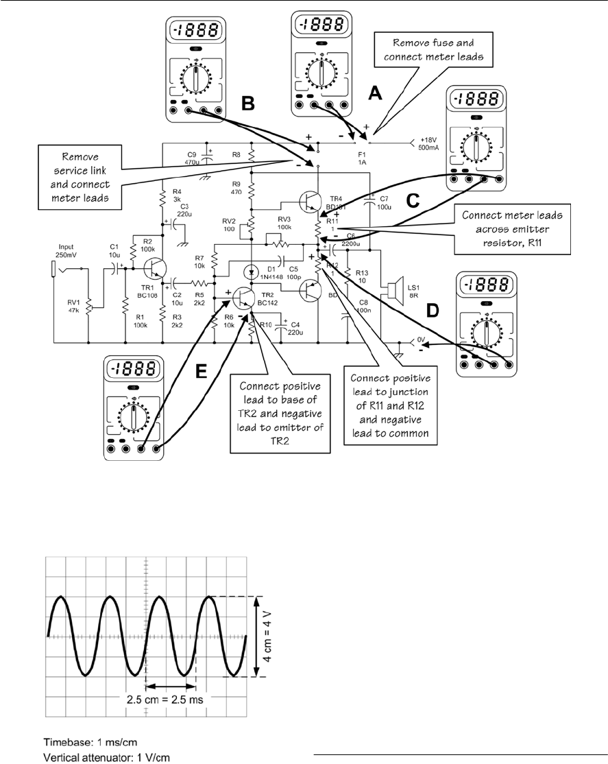
TEST EQUIPMENT AND MEASUREMENTS 261
Figure 14.23 Connecting a meter to display currents and voltages in a simple audio amplifier
deflection) is switched to the 1 V/cm range. The
overall height of the trace is 4 cm and thus the
peak-peak voltage is 4 × 1 V = 4 V. Similarly, the
time for one complete cycle (period) is 2.5 × 1 ms
=2.5 ms. One further important piece of
information is the shape of the waveform that, in
this case, is sinusoidal.
The front panel layout for a typical general-
purpose two-channel oscilloscope is shown in Figs
14.25 and 14.26. The controls and adjustments are
summarized in Table 14.3.
Using an oscilloscope
An oscilloscope can provide a great deal of
information about what is going on in a circuit. In
Figure 14.24 Using an oscilloscope graticule

Table 14.3 Oscilloscope controls and adjustments
262 ELECTRONIC CIRCUITS: FUNDAMENTALS AND APPLICATIONS
Control Adjustment
Focus Provides a correctly focused display on the CRT screen.
Intensity Adjusts the brightness of the display.
Astigmatism Provides a uniformly defined display over the entire screen area and in both x and y-directions.
The control is normally used in conjunction with the focus and intensity controls.
Trace rotation Permits accurate alignment of the display with respect to the graticule.
Scale illumination Controls the brightness of the graticule lines.
Horizontal deflection system
Timebase (time/cm) Adjusts the timebase range and sets the horizontal time scale. Usually this control takes the form
of a multi-position rotary switch and an additional continuously variable control is often
provided. The ‘CAL’ position is usually at one, or other, extreme setting of this control.
Stability Adjusts the timebase so that a stable displayed waveform is obtained.
Trigger level Selects the particular level on the triggering signal at which the timebase sweep commences.
Trigger slope This usually takes the form of a switch that determines whether triggering occurs on the positive
or negative going edge of the triggering signal.
Trigger source This switch allows selection of one of several waveforms for use as the timebase trigger. The
options usually include an internal signal derived from the vertical amplifier, a 50 Hz signal
derived from the supply mains, and a signal which may be applied to an External Trigger input.
Horizontal position Positions the display along the horizontal axis of the CRT.
Vertical deflection system
Vertical attenuator
(V/cm)
Adjusts the magnitude of the signal attenuator (V/cm) displayed (V/cm) and sets the vertical
voltage scale. This control is invariably a multi-position rotary switch; however, an additional
variable gain control is sometimes also provided. Often this control is concentric with the main
control and the ‘CAL’ position is usually at one, or other, extreme setting of the control.
Vertical position Positions the display along the vertical axis of the CRT.
a.c.-d.c.-ground Normally an oscilloscope employs d.c. coupling throughout the vertical amplifier; hence a shift
along the vertical axis will occur whenever a direct voltage is present at the input. When
investigating waveforms in a circuit one often encounters a.c. superimposed on d.c. levels; the
latter may be removed by inserting a capacitor in series with the signal. With the a.c.-d.c.-ground
switch in the d.c. position a capacitor is inserted in the input lead, whereas in the DC position the
capacitor is shorted. If ground is selected, the vertical input is taken to common (0 V) and the
oscilloscope input is left floating. This last facility is useful in allowing the accurate positioning
of the vertical position control along the central axis. The switch may then be set to d.c. and the
magnitude of any d.c. level present at the input may be easily measured by examining the shift
along the vertical axis.
Chopped-alternate This control, which is only used in dual beam oscilloscopes, provides selection of the beam
splitting mode. In the chopped position, the trace displays a small portion of one vertical channel
waveform followed by an equally small portion of the other. The traces are, in effect, sampled at
arelatively fast rate, the result being two apparently continuous displays. In the alternate
position, a complete horizontal sweep is devoted to each channel alternately.
Cathode ray tube display
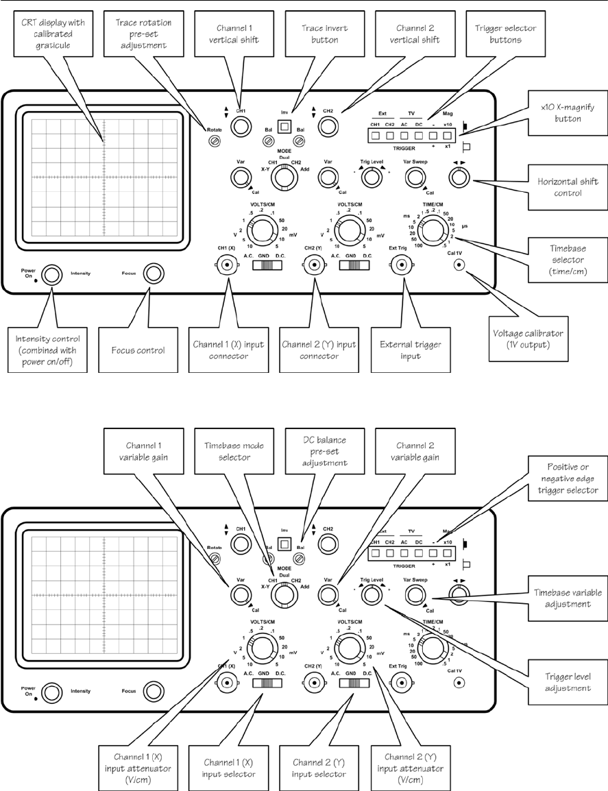
TEST EQUIPMENT AND MEASUREMENTS 263
Figure 14.25 Front panel controls and displays on a typical dual-channel oscilloscope
Figure 14.26 Front panel controls and displays on a typical dual-channel oscilloscope

264 ELECTRONIC CIRCUITS: FUNDAMENTALS AND APPLICATIONS
effect, it allows you to ‘see’ into the circuit,
displaying waveforms that correspond to the
signals that are present. The procedure and
adjustments differ according to the type of
waveform being investigated and whether the
oscilloscope is being used to display a single
waveform (i.e. single-channel operation) or
whether it is being used to display two waveforms
simultaneously (i.e. dual-channel operation).
Sinusoidal waveforms (single-channel operation)
The procedure for displaying a repetitive sine wave
waveform is shown in Fig. 14.27. The signal is
connected to the Channel 1 input (with ‘AC’ input
selected) and the mode switch in the Channel 1
position. ‘Channel 1’ must be selected as the trigger
source and the trigger level control adjusted for a
stable display. Where accurate measurements are
required it is essential to ensure that the ‘Cal’
position is selected for both the variable gain and
time controls.
Square waveforms (single-channel operation)
The procedure for displaying a repetitive square
waveform is shown in Fig. 14.28. Once again, the
signal is connected to the Channel 1 input (but this
time with ‘DC’ input selected) and the mode switch
in the Channel 1 position. ‘Channel 1’ must be
selected as the trigger source and the trigger level
control adjusted for a stable display (which can be
triggered on the positive or negative going edge of
the waveform according to the setting of the trigger
polarity button). Any DC level present on the input
can be measured from the offset produced on the
Y-axis. To do this, you must first select ‘GND’ on
the input selector then centre the trace along the Y-
axis before switching to ‘DC’ and noting how far
up or down the trace moves (above or below 0 V).
This may sound a little difficult but it is actually
quite easy to do! The same technique can be used
for measuring any DC offset present on a
sinusoidal signal.
Sine/square waveforms (dual–channel operation)
The procedure for displaying two waveforms
(either sine or square or any other repetitive signal)
simultaneously is shown in Fig. 14.29. The two
signals are connected to their respective inputs
(Channel 1 and Channel 2) and the mode switch set
to the ‘Dual’ position. The oscilloscope can be
triggered by either of the signals (Channel 1 or
Channel 2) as desired. Once again, the display can
be triggered on the positive or negative-going edge
of the waveform depending upon the setting of the
trigger polarity button. Dual-channel operation can
be invaluable when it is necessary to compare two
waveforms, e.g. the input and output waveforms of
an amplifier.
Connecting an oscilloscope into a circuit
Figure 14.30 shows how an oscilloscope can be
connected to display the waveforms present at
various points in a simple transistor audio
amplifier. To reduce the likelihood of picking up of
hum and noise, the input to the oscilloscope is via a
screened lead fitted with a probe. The ground (outer
screen) is connected to the common 0V rail whilst
the probe is simply moved around the circuit from
point to point. Note that, because of the ground
connection to the oscilloscope it is NOT usually
possible to display a waveform that appear ‘across’
acomponent (e.g. between the base and emitter of a
transistor). For this reason, waveforms are nearly
always displayed relative to ground (or common).
Checking distortion
Oscilloscopes are frequently used to investigate
distortion in amplifiers and other electronic
systems. Different forms of distortion have a
different effect on a waveform and thus it is
possible to determine which type of distortion is
present. A ‘pure’ sine wave is used as an input
signal and the output is then displayed on the
oscilloscope. Figure 14.31 shows waveforms that
correspond to the most common forms of
distortion.
Checking frequency response
An oscilloscope can also be used to provide a rapid
assessment of the frequency response of an
amplifier or other electronic system. Instead of
using a sine wave as an input signal a square wave
input is used. Different frequency response
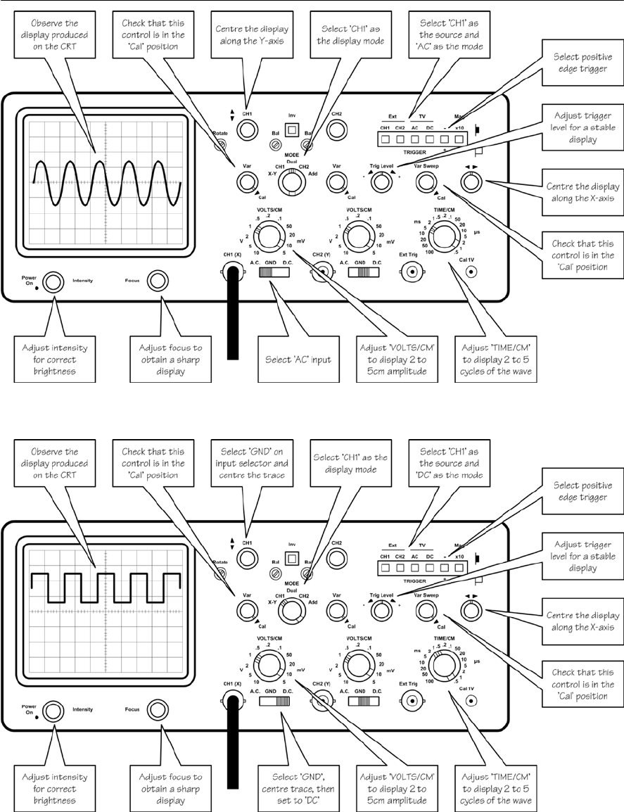
TEST EQUIPMENT AND MEASUREMENTS 265
Figure 14.27 Procedure for adjusting the controls to display a sinusoidal waveform (single-channel mode)
Figure 14.28 Procedure for adjusting the controls to display a square waveform (single-channel mode)
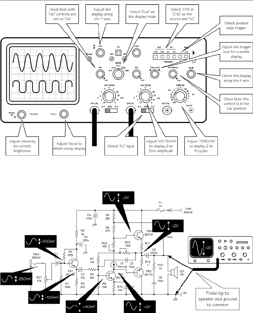
266 ELECTRONIC CIRCUITS: FUNDAMENTALS AND APPLICATIONS
Figure 14.30 Using an oscilloscope to display the waveforms in a simple audio amplifier
Figure 14.29 Procedure for adjusting the controls to display two waveforms (dual-channel mode)
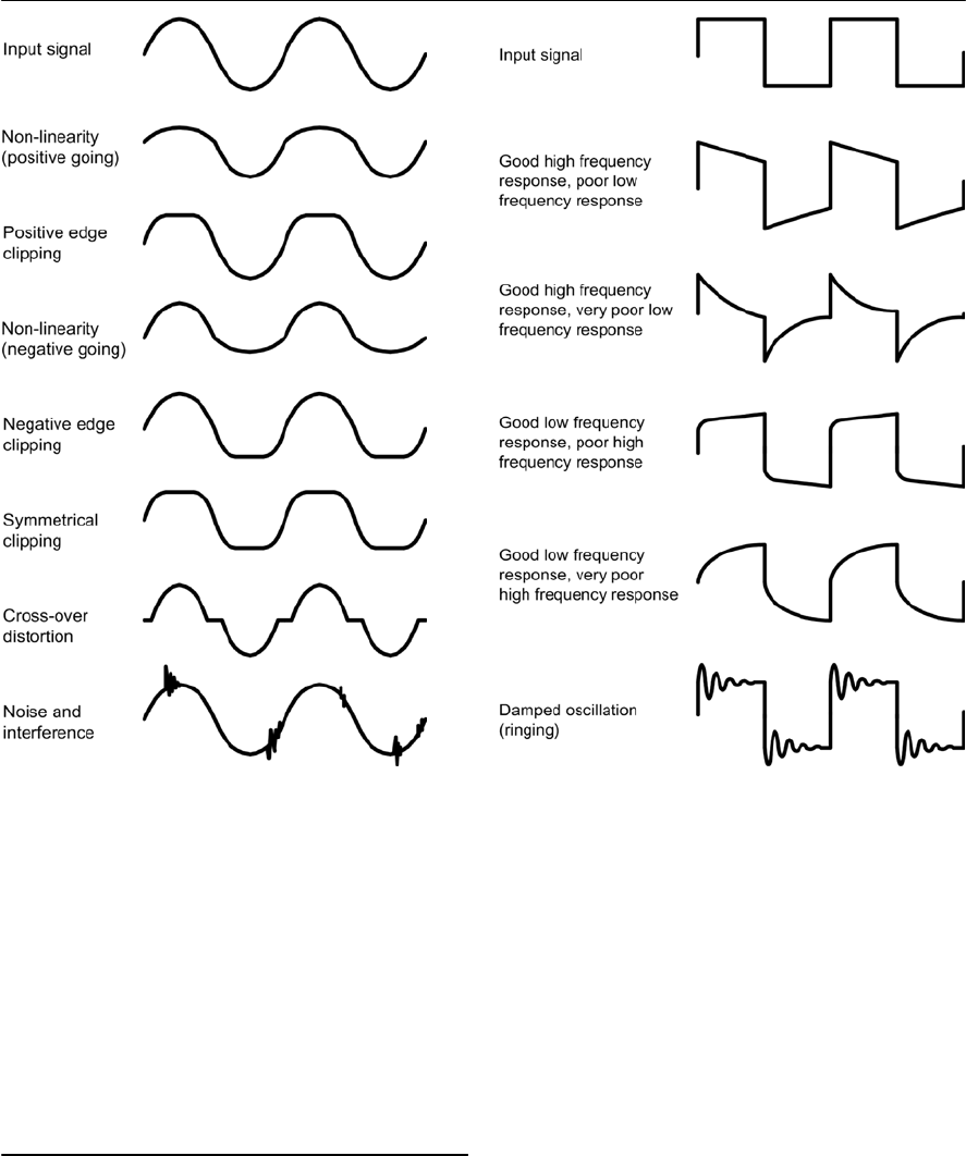
TEST EQUIPMENT AND MEASUREMENTS 267
produces a different effect on a waveform and thus
it is possible to assess whether the frequency
response is good or poor (a perfect square wave
output corresponds to a perfect frequency
response). Figure 14.32 shows waveforms that
correspond to different frequency response
characteristics.
Measuring pulse parameters
When dealing with rectangular waveforms and
pulses it is often necessary to be able to use an
oscilloscope to measure parameters such as:
Periodic time, t
This is the time (measured at the 50% amplitude
points) for one a complete cycle of a repetitive
pulse waveform. The periodic time is sometimes
referred to as the period (see page 70). Note also
that the pulse repetition frequency (p.r.f.) is the
reciprocal of the periodic time.
On time, ton
This is the time for which the pulse amplitude
exceeds 50% of its amplitude. The on-time is
sometimes referred to as the high time.
Figure 14.31 Typical waveforms produced by
different types of distortion
Figure 14.32 Using a square waveform to rapidly
assess frequency response
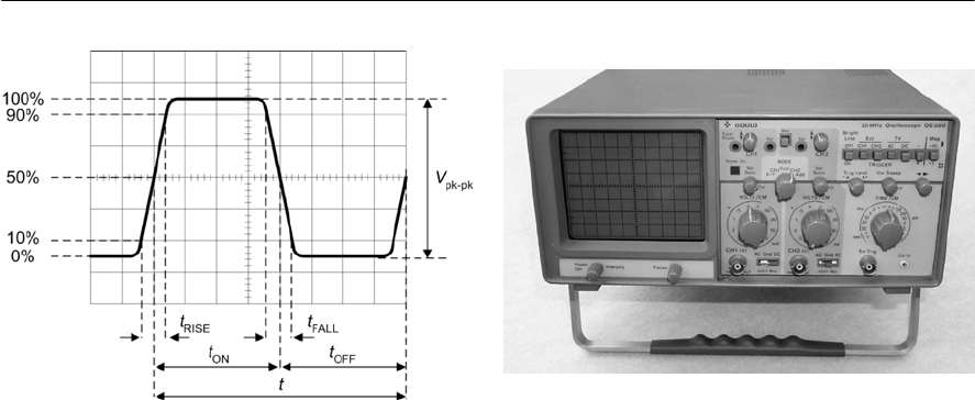
268 ELECTRONIC CIRCUITS: FUNDAMENTALS AND APPLICATIONS
Off time, toff
This is the time for which the pulse amplitude falls
below 50% of its amplitude. The off time is
sometimes referred to as the low time.
Rise time, trise
This is the time measured between the 10% and
90% points on the rising (or positive-going)edge
of the pulse.
Fall time, tfall
This is the time measured between the 90% and
10% points on the falling (or negative-going)edge
of the pulse.
These pulse parameters are shown in Fig. 14.33.
DO’s and DON’Ts of using an oscilloscope
DO ensure that the vertical gain and variable
timebase controls are set to the calibrate (CAL)
positions before attempting to make accurate
measurements based on the attenuator/timebase
settings and graticule.
DO check that you have the correct trigger source
selected for the type of waveform under
investigation.
DO remember to align the trace with the X-axis of
the graticule with the input selector set to ‘GND’
prior to taking DC offset measurements.
DO make use of the built-in calibrator facility to
check the accuracy of the attenuator and the ‘CAL’
setting of the variable gain control.
DO use properly screened leads and a suitable
probe for connecting to the circuit under
investigation.
DO check that you have made a proper connection
to ground or 0 V prior to taking measurements.
DON’T leave the intensity control set at a high
level for any length of time.
DON’T leave a bright spot on the display for even
the shortest time (this may burn the phosphor
coating of the screen).
DON’T rely on voltage measurements on circuits
where high-frequency signals may be outside the
bandwidth of the oscilloscope.
DON’T forget to set the a.c.-d.c.-gnd switch to the
d.c. position when making measurements of the d.c.
offset present on a.c. signals.
DON’T place the oscilloscope where there is a
strong local magnetic field. This may cause
unwanted deflection of electron beam!
Figure 14.33 Pulse parameters Figure 14.34 Atypical bench oscilloscope
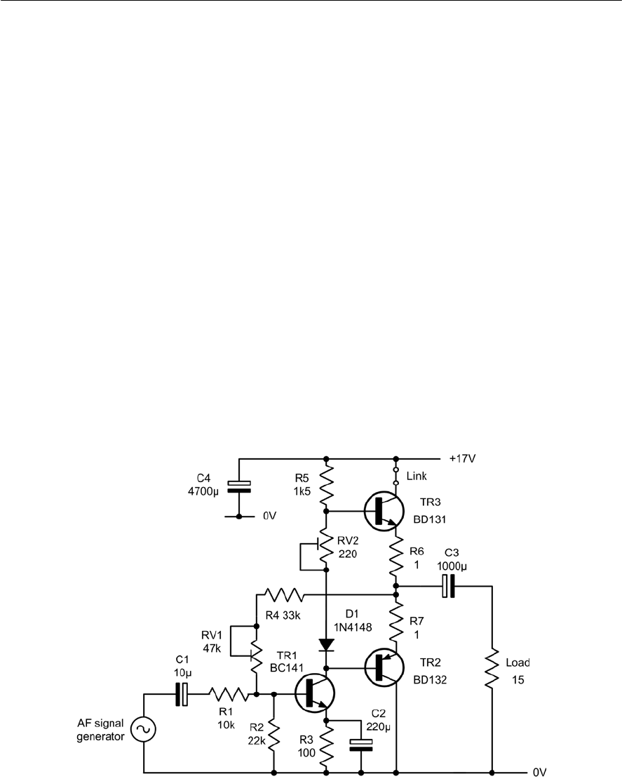
Practical investigation
Objective
To investigate the voltages, currents and
waveforms in a simple audio amplifier.
Components and test equipment
Breadboard, 17 V d.c. power supply (with a current
limited output of up to at least 500 mA), BC141,
BD131 and BD132 transistors (the latter to be fitted
with small heatsinks), 1N4148 diode, fixed
resistors of 1 G(two required), 100 G,1.5 kG,
10 kG,22 kG,and 33 kG,5% 0.25 W, capacitors
of 10 µF, 220 µF, 1,000 µF and 4,700 µF at 25 V
d.c., oscilloscope, digital multimeter, AF signal
generator with sine wave output at 1 kHz, test leads
and probes.
Procedure
Connect the circuit as shown in Fig. 14.35. With
the signal generator disconnected, connect the d.c.
supply and use the digital multimeter on the 20 V
d.c. range to measure the d.c. voltage at the
junction of R6 and R7. Adjust RV1 so that this
voltage is exactly half that of the supply (i.e.
8.5 V).
Now remove the link and use the digital
multimeter set to the 200 mA d.c. range to measure
the collector current for TR3. Adjust RV2 for a
current of exactly 24 mA. Repeat these two
adjustments until no further change is noted.
Replace the link and set the digital multimeter to
the 20 V d.c. range. Measure the d.c. voltages
present at the collector, base and emitter of TR1,
TR2 and TR3. Also measure the d.c. voltage at the
anode and cathode of D1. Record your
measurements in a table.
Connect the AF signal generator to the input of
the amplifier and set the output to 200 mV pk-pk at
1kHz sine wave. Set the Channel 1 and Channel 2
inputs of the oscilloscope to 100 mV/cm with the
a.c.-d.c.-ground switches in the a.c. position. Set
the trigger to internal and the timebase to 1ms/cm.
Display the waveforms at the input and output of
the amplifier and sketch these using the layout
shown in Fig. 14.36.
TEST EQUIPMENT AND MEASUREMENTS 269
Figure 14.35 Circuit used in the Practical investigation
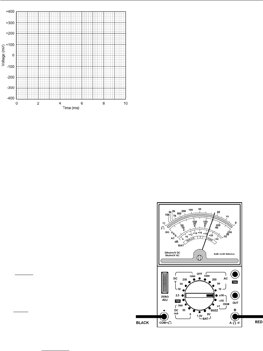
Problems
14.1 A moving coil meter has a full-scale
deflection current of 500 µA. If the meter
coil has a resistance of 400 G,determine
the value of multiplier resistor if the meter
is to be used as a voltmeter reading 0 to
10 V.
14.2 A moving coil meter has a full-scale
deflection current of 5 mA. If the meter coil
has a resistance of 100 G,determine the
value of shunt resistor if the meter is to be
used as an ammeter reading 0 to 50 mA.
14.3 A meter has a full-scale deflection of
60 µA. What will its ohms-per-volt rating
be?
14.4 A 50 kG/V meter is switched to the 3 V
range. What current will flow in the meter
when it is connected to a 2 V source?
14.5 A digital multi-range meter has a 3½-digit
display. When switched to the 20 V range,
determine:
(a) the maximum indication that will appear
on the display
(b) the resolution of the instrument.
Formulae introduced in this chapter
Voltmeter multiplier resistor
(page 246)
Ammeter shunt resistor
(page 246)
Ohms-per-volt
(page 248)
270 ELECTRONIC CIRCUITS: FUNDAMENTALS AND APPLICATIONS
Figure 14.36 Layout for the waveform sketches
Figure 14.37 See Question 14.6
Conclusions
Comment on the measured voltages. Are these
what you would have expected? Justify them by
calculation and state any assumptions made.
Comment on the waveforms obtained. What was
the voltage gain of the amplifier at 1 kHz? What
output power was produced in the load with
200 mV pk-pk input? Suggest a typical application
for the circuit.
1
Ohms-per-volt =
Meter f.s.d.
m
s
m
Ir
R
II
=
m
m
m
VIr
RI
=
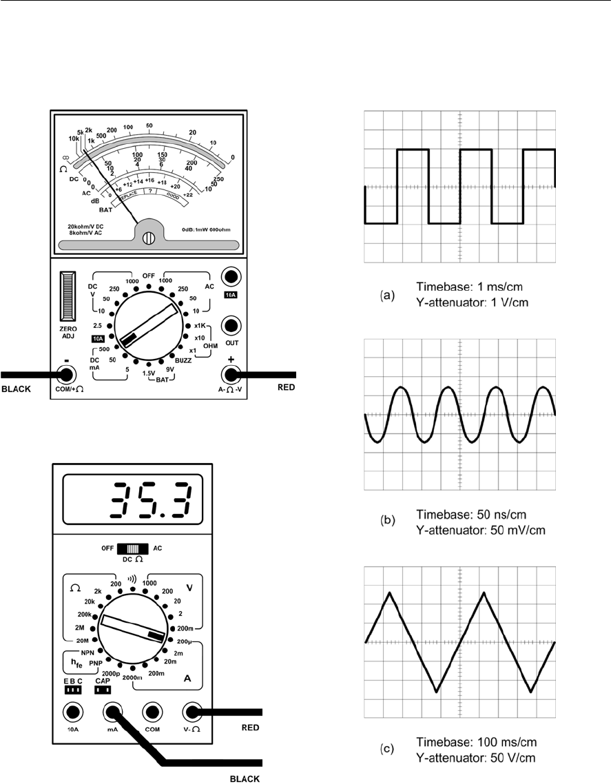
TEST EQUIPMENT AND MEASUREMENTS 271
14.6 Determine the reading on the multi-range
meter shown in Fig. 14.37.
14.7 Determine the reading on the multi-range
meter shown in Fig. 14.38.
14.8 Determine the reading on the multi-range
meter shown in Fig. 14.39
14.9 Figure 14.40 shows the display of an
oscilloscope in which the graticule is
Figure 14.38 See Question 14.7
Figure 14.39 See Question 14.8 Figure 14.40 See Question 14.9
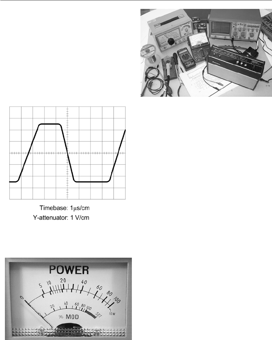
272 ELECTRONIC CIRCUITS: FUNDAMENTALS AND APPLICATIONS
divided into squares of 1 cm. Determine the
amplitude and period of each waveform.
14.10 Figure 14.41 shows the display of an
oscilloscope in which the graticule is
divided into squares of 1 cm. For the square
wave pulse shown determine:
(a) the periodic time
(b) the high time
(c) the low time
(d) the rise time
(e) the fall time
(f) the pulse amplitude.
14.11 Figure 14.42 shows the display provided by
an RF power meter. Explain why the scale is
non-linear and illustrate your answer with
reference to a formula.
14.12 Figure 14.43 shows a test set-up for radio
servicing. Identify the test instruments and
state a typical application for each.
14.13 Using a sine wave reference, sketch
waveforms to show the typical appearance
of:
(a) cross-over distortion
(b) noise
(c) positive edge clipping
(d) negative-going non-linearity.
14.14 With the aid of sketches, show how a
reference square wave input can be used to
quickly assess the frequency response of an
amplifier.
14.15 Explain the purpose of each of the following
facilities/adjustments provided on a bench
oscilloscope:
(a) timebase selector
(b) trigger source
(c) trigger slope
(d) a.c.-d.c.-ground selector
(e) scale illumination
(f) astigmatism
(g) calibrator.
14.16 Explain, with the aide of a sketch, how you
would use an oscilloscope to measure the
rise time and period of a rectangular pulse.
Answers to these problems appear on page 376.
Figure 14.41 See Question 14.10
Figure 14.42 See Question 14.11
Figure 14.43 See Question 14.12
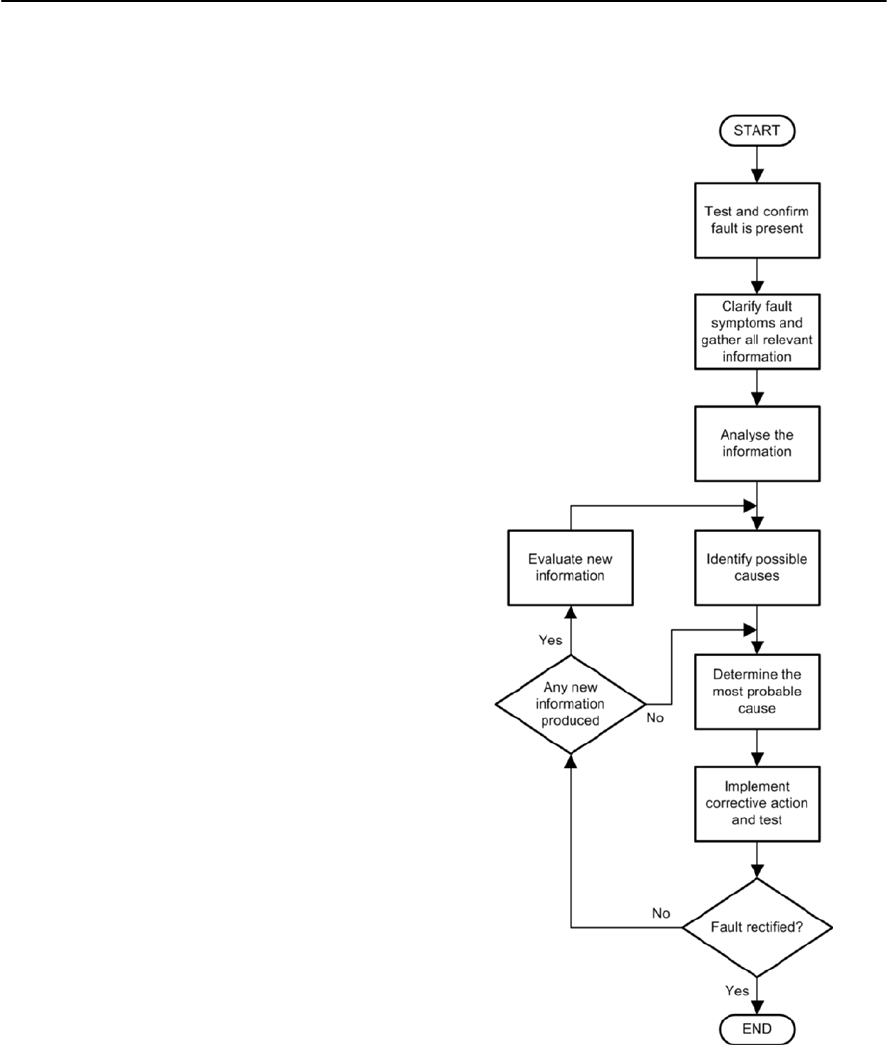
15
Fault finding
Fault finding is a disciplined and logical process in
which ‘trial fixing’ should never be contemplated.
The generalized process of fault finding is
illustrated in the flowchart of Fig. 15.1. First you
need to verify that the equipment really is faulty
and that you haven’t overlooked something obvious
(such as a defective battery or disconnected signal
cable). This may sound rather obvious but in some
cases a fault may simply be attributable to
maladjustment or misconnection. Furthermore,
where several items of equipment are connected
together, it may not be easy to pinpoint the single
item of faulty equipment.
The second stage is that of gathering all relevant
information. This process involves asking questions
such as:
•In what circumstances did the circuit fail?
•Has the circuit operated correctly before and
exactly what has changed?
•Has the deterioration in performance been
sudden or progressive?
•What fault symptoms do you notice?
The answers to these questions are crucial and,
once the information has been analysed, the next
stage involves separating the ‘effects’ from the
‘cause’. Here you should list each of the possible
causes. Once this has been done, you should be
able to identify and focus upon the most probable
cause. Corrective action (such as component
removal and replacement, adjustment or alignment)
can then be applied before further functional checks
are carried out. It should then be possible to
determine whether or not the fault has been
correctly identified. Note, however, that the failure
of one component can often result in the
malfunction or complete failure of another. As an
example, a short-circuit capacitor will often cause a
fuse to blow. When the fuse is replaced and the
supply is reconnected the fuse will once again blow
because the capacitor is still faulty. It is therefore
important to consider what other problems may be
present when a fault is located. Figure 15.1 Fault finding flowchart

274 ELECTRONIC CIRCUITS: FUNDAMENTALS AND APPLICATIONS
Safety considerations
Before we outline the basic steps for fault finding
on some simple electronic circuits, it is vitally
important that you are aware of the potential
hazards associated with equipment which uses high
voltages or is operated from the a.c. mains supply.
Whereas many electronic circuits operate from
low voltage supplies and can thus be handled quite
safely, the high a.c. voltages present in mains
operated equipment represent a potentially lethal
shock hazard. The following general rules should
always be followed when handling such equipment:
1. Switch off the mains supply and remove the
mains power connector whenever any of the
following tasks are being performed:
(a) Dismantling the equipment.
(b) Inspecting fuses.
(c) Disconnecting or connecting internal
modules.
(d) Desoldering or soldering components.
(e) Carrying out continuity tests on switches,
transformer windings, bridge rectifiers, etc.
2When measuring a.c. and d.c. voltages present
within the power unit take the following
precautions:
(a) Avoid direct contact with incoming mains
wiring.
(b) Check that the equipment is connected to an
effective earth.
(c) Use insulated test prods.
(d) Select appropriate meter ranges before
attempting to take any measurements.
(e) If in any doubt about what you are doing,
switch off at the mains, disconnect the mains
connector and think.
Approach to fault finding
Fault finding on most circuits is a relatively
straightforward process. Furthermore, and
assuming that the circuit has been correctly
assembled and wired, there is usually a limited
number of ‘stock faults’ (such as transistor or
integrated circuit failure) that can occur. To assist
in this process, it is a good idea to identify a
number of test points at which the voltages present
(both a.c. and d.c.) can be used as indicators of the
circuit’s functioning. Such test points should he
identified prior to circuit construction and marked
with appropriate terminal pins.
Readers should note that the most rapid method
of fault diagnosis is not necessarily that of
following voltages or signals from one end to the
other. Most textbooks on fault finding discuss the
relative methods of the so-called end-to-end and
half split methods. The former method involves
tracing the signal and measuring voltages from the
input to the output (or vice versa) whilst the latter
method involves dividing the circuit into two
halves and then eliminating the half that is
operational before making a further sub-division of
the half in which the fault resides.
Transistor faults
As long as a few basic rules can be remembered,
recognizing the correct voltages present at the
terminals of a transistor is a fairly simple process.
The potentials applied to the transistor terminals are
instrumental in determining the correct bias
conditions for operation as an amplifier, oscillator,
or switch. If the transistor is defective, the usual
bias voltages will be substantially changed. The
functional state of the transistor may thus be
quickly determined by measuring the d.c. potentials
present at the transistor’s electrodes while it is still
in circuit.
The potential developed across the forward
biased base-emitter junction of a silicon transistor
is approximately 0.6 V. In the case of an NPN
transistor, the base will be positive with respect to
the emitter whilst, for a PNP transistor, the base
will be negative with respect to the emitter, as
shown in Fig. 15.2. The base-emitter voltage drop
tends to be larger when the transistor is operated as
asaturated switch (and is in the ‘on’ state) or when
it is a power type carrying an appreciable collector
current. In these applications, base-emitter voltages
of between 0.65 V and 0.7 V are not unusual.
Small-signal amplifiers, on the other hand, operate
with significantly lower values of collector current
and values of base-emitter voltage in the range 0.55
Vto 0.65 V are typical.
Ameasured base-emitter voltage greatly in
excess of 0.6 V is an indication of a defective
transistor with an open-circuit base-emitter
junction. A measured base-emitter potential very
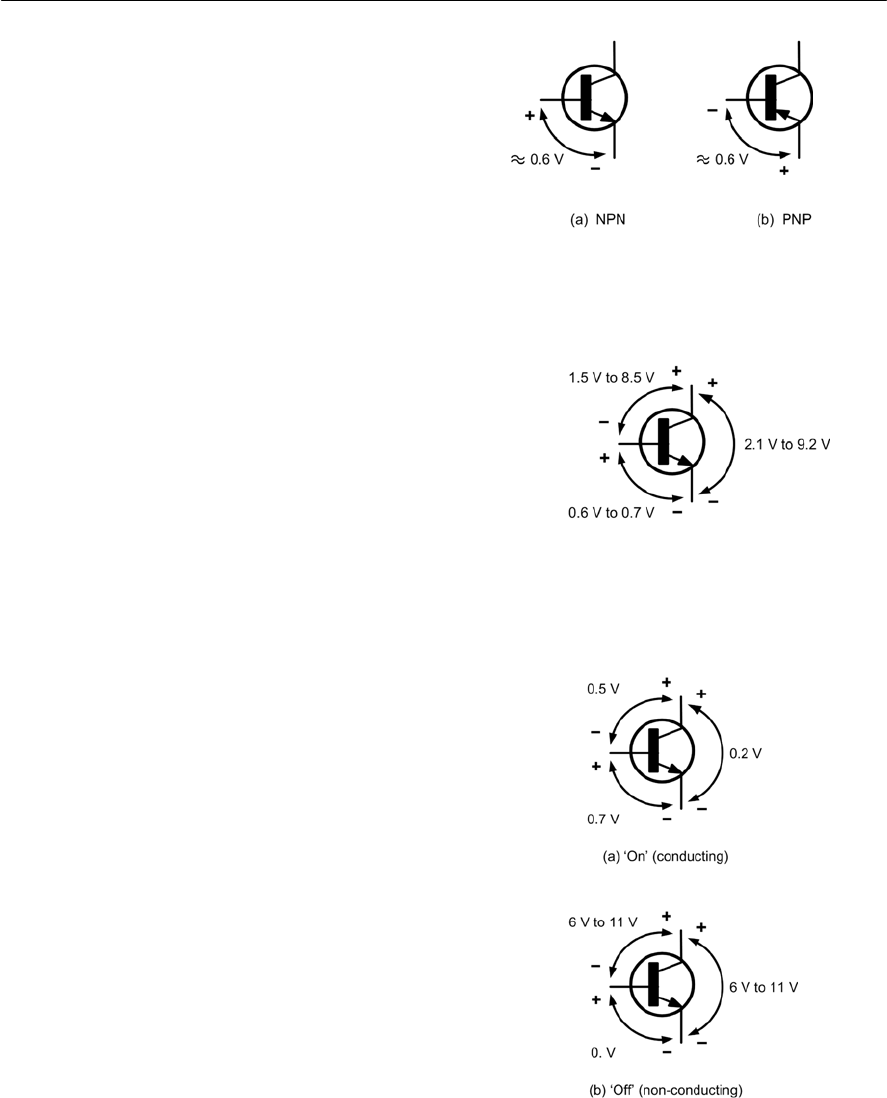
FAULT FINDING 275
much less than 0.6 V indicates that the transistor is
not being supplied with a base bias and, while this
may be normal for a switching transistor in the ‘off’
state, it is indicative of a circuit fault in the case of
alinear small-signal amplifier stage. In the case of
oscillators and medium/high power r.f. amplifiers
operating in Class C little or no bias will usually be
present and, furthermore, the presence of r.f. drive
during measurement can produce some very
misleading results. In such cases it is probably
worth removing a transistor suspected of being
defective and testing it out of circuit.
Unfortunately, it is not so easy to predict the
voltage present at the collector-base junction of a
transistor. The junction is invariably reverse biased
and the potential present will vary considerably
depending upon the magnitude of collector current,
supply voltage, and circuit conditions. As a rule-of-
thumb, small-signal amplifiers using resistive
collector loads usually operate with a collector-
emitter voltage which is approximately half that of
the collector supply. The collector-base voltage will
be slightly less than this. Hence, for a stage that is
operated from a decoupled supply rail of, say,
8.5 V a reasonable collector-base voltage would be
somewhere in the range 3 V to 4 V. Tuned
amplifiers having inductive collector loads
generally operate with a somewhat higher value of
collector-emitter voltage since there is no
appreciable direct voltage drop across the load. As
aresult, the collector-base voltage drop is greater (a
typical value being 6 V). Figure 15.3 shows the
electrode potentials normally associated with
transistors operating as linear small-signal
amplifiers.
Where a transistor is operated as a saturated
switch, the junction potentials depend upon
whether the transistor is in the ‘on’ or ‘off’ state. In
the ‘off’ condition, the base-emitter voltage will be
very low (typically 0 V) whereas the collector-base
voltage will be high and, in many cases, almost
equal to the collector supply voltage. In the ‘on’
state, the base-emitter voltage will be relatively
large (typically 0.7 V) and the collector-base
voltage will fall to a very low value (typically 0.5
V). It should be noted that, in normal saturated
switching, the collector-emitter voltage may fall to
as low as 0.2 V and thus the base-emitter voltage
will become reversed in polarity (i.e. base positive
with respect to collector in the case of an NPN
transistor). The junction potentials associated with
Figure 15.3 Typical voltages found in a small-
signal transistor amplifier (polarities will be
reversed in the case of a PNP transistor)
Figure 15.2 Base-emitter voltages for NPN and
PNP silicon transistors
Figure 15.4 Typical voltages found in a transistor
switching circuit (polarities will be reversed in the
case of a PNP transistor)

276 ELECTRONIC CIRCUITS: FUNDAMENTALS AND APPLICATIONS
transistors operating as saturated switches are
shown in Fig. 15.4.
Transistors may fail in a number of ways.
Individual junctions may become open-circuit or
short-circuit. In some cases the entire device may
become short-circuit or exhibit a very low value of
internal resistance. The precise nature of the fault
will usually depend upon the electrical conditions
prevalent at the time of failure. Excessive reverse
voltage, for example, is likely to cause a collector-
base or base-emitter junction to become open-
circuit. Momentary excessive collector current is
likely to rupture the base-emitter junction while
long-term over-dissipation is likely to cause an
internal short-circuit or very low resistance
condition which may, in some cases, affect all three
terminals of the device.
In order to illustrate the effects of various
transistor fault conditions consider the circuit of a
typical tuned amplifier stage shown in Fig. 15.5.
The transistor is operated in Class A with
conventional base bias potential divider and a tuned
transformer collector load. Normal working
voltages are shown in the circuit diagram. Note that
the junction potentials (0.6 V and 4.7 V for the
base-emitter and collector-base junctions
respectively) are in agreement with the voltages
given in Fig. 15.4. The circuit voltages
corresponding to six different transistor fault
conditions are shown in Table 15.1.
Each fault will now be discussed individually:
Fault 1
The collector-base short-circuit gives rise to
identical base and collector voltage. The base-
emitter junction is still intact and thus the normal
forward voltage drop of 0.6 V is present. In this
condition a relatively high value of current is drawn
by the stage and thus the supply voltage falls
slightly.
Fault 2
The base-emitter short-circuit produces identical
base and emitter voltages. No collector current
flows and the collector voltage rises to almost the
full supply voltage. The base and emitter voltages
are relatively low since the emitter resistor
effectively appears in parallel with the lower
section of the base bias potential divider, thus
pulling the base voltage down.
Fault 3
Identical voltages at the collector and emitter result
from a collector-emitter short-circuit. The emitter
voltage rises above the base voltage and the base-
emitter junction is well and truly turned off. The
short-circuit causes a higher value of current to be
drawn from the supply and hence the supply
voltage falls slightly.
Fault 4
Perhaps the most obvious fault condition is when a
short-circuit condition affects all three terminals.
The voltages are, naturally, identical and, as with
fault 3, more current than usual is taken from the
supply and, as a consequence, the supply voltage
falls slightly.
Fault 5
With the base-emitter junction open-circuit, the
base-emitter voltage rises well above the 0.6 V
which would normally be expected. No collector or
emitter current is flowing and thus the collector
voltage rises, while the emitter voltage falls.
Fault 6
No collector current flows when the collector-base
junction is open-circuit and, as with fault 2, the
collector voltage rises towards the supply. Note
that, since the base-emitter junction is intact, the
normal forward bias of 0.6 V is present and this
condition distinguishes this fault from that
described in Fault 2.
Table 15.1 Voltage for various fault conditions
Fault
number
Transistor voltages
e b c
12.7 3.3 3.3 b-c short
20.2 0.2 8.3 b-e short
33.0 0.8 3.0 c-e short
42.9 2.9 2.9 c-b-e short
50.0 2.2 8.3 b-e open
60.2 0.8 8.2 c-b open
Fault
condition
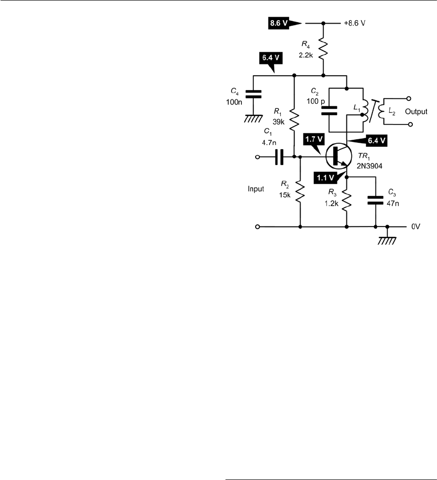
FAULT FINDING 277
Diode testing
Go/no-go checks provide you with a very rapid
method of assessing whether a junction
semiconductor device, such as a diode or bipolar
transistor, is functional. The basic principle is
simply that of checking the forward and reverse
resistance of each P–N junction that may be
present. The source of current for the resistance
Integrated circuit faults
Integrated circuits may fail in various ways.
Occasionally, the manifestation of the fault is
simply a chip which is chronically overheated—
the judicious application of a finger tip to the centre
of the plastic package will usually help you to
identify such a failure. Any chip that is noticeably
hotter than others of a similar type should be
considered suspect. Where integrated circuits are
fitted in sockets, it will be eminently possible to
remove and replace them with known functional
devices (but, do remember to switch ‘off’ and
disconnect the supply during the process).
In the case of digital circuitry, the task of
identifying a logic gate which is failing to perform
its logical function can be accomplished by various
means but the simplest and most expedient is with
the aid of a logic probe (see page 282). This
invaluable tool comprises a hand-held probe fitted
with LED to indicate the logical state of its probe
tip.
In use, the logic probe is moved from point to
point within a logic circuit and the state of each
node is noted and compared with the expected logic
level. In order to carry out checks on more complex
logic arrangements a logic pulser may be used in
conjunction with the logic probe. The pulser
provides a means of momentarily changing the
state of a node (regardless of its actual state) and
thus permits, for example, the clocking of a bistable
element (see page 284).
Operational amplifiers can usually be checked
using simple d.c. voltage measurements. The d.c.
voltages appearing at the inverting and non-
inverting inputs should be accurately measured and
compared. Where the voltage at the inverting input
is more positive with respect to that at the non-
inverting input, the output voltage will be high
(positive if the operational amplifier is operated
from a dual supply rail).
Conversely, if the voltage at the inverting input
is negative, with respect to that at the non-inverting
input, the output voltage will be high (positive if
the operational amplifier is operating from a dual
supply).
Finally, if both inputs are at 0 V and there is
virtually no difference in the input voltages, the
output should also be close to 0 V. If it is high or
low (or sitting at one or other of the supply
voltages) the device should be considered suspect.
Figure 15.5 Circuit to illustrate the effects of
various transistor faults on the d.c. voltages present
in a small-signal amplifier stage (normal d.c.
working voltages are shown)
The detection of faults within other linear
integrated circuits can be rather more difficult.
However, a good starting point is that of
disconnecting the supply and inserting a meter to
determine the supply current under quiescent
conditions. The value should be compared with that
given by the manufacturer as ‘typical’. Where there
is a substantial deviation from this figure the device
(or its immediate circuitry) should be considered
suspect.
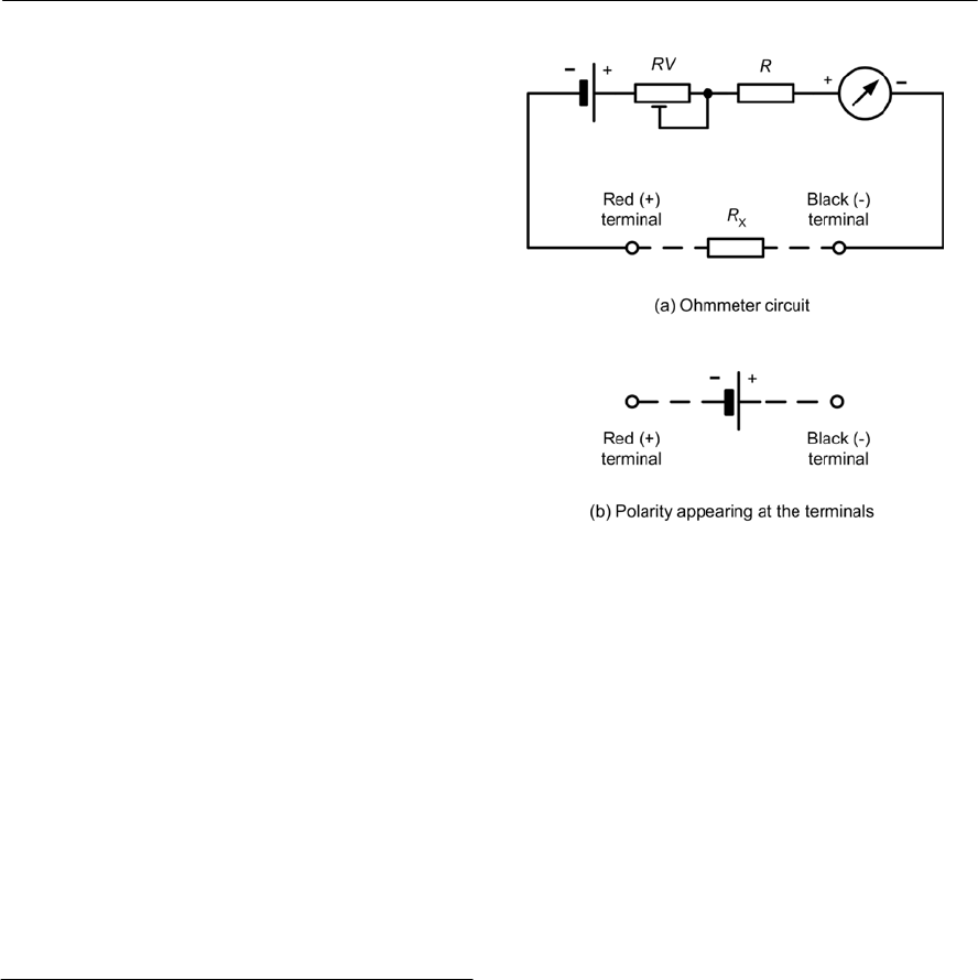
278 ELECTRONIC CIRCUITS: FUNDAMENTALS AND APPLICATIONS
checks is simply the internal battery in your
analogue multimeter.
Figure 15.6 shows the simplified internal circuit
of an analogue multimeter on the resistance (ohms)
range. This circuit consists of a battery (usually 1.5
V, 3 V, 4.5 V or 9 V) connected in series with a
preset ‘set-zero ohms’ control and a fixed, current-
limiting resistor, and a sensitive moving coil meter
movement. There is one important thing to note
from this arrangement and it relates to the polarity
of the meter leads—the red meter test lead will
have a negative polarity whilst the black meter test
lead will exhibit a positive polarity when the
instrument is switched to the ‘ohms’ range. (Note
that the same does not apply to digital multimeters).
Unfortunately, simple go/no-go checks are
unreliable when using a digital multimeter. Indeed,
some instruments sometimes fail to provide any
meaningful indication when carrying out resistance
checks on diodes and transistors! However, if you
have a more sophisticated digital instrument, you
may find that it already has a built-in diode or
transistor checker—in which case you should use
this facility to make measurements rather than
attempt to use simple go/no-go checking based on
resistance measurements.
Because the output of the analogue multimeter is
polarity conscious, it can be used to check the
ability of a component to conduct in both
directions. Thus it can, for example, be used to
distinguish between a resistor and a diode. The
former will exhibit the same resistance whichever
way it is connected to the multimeter. The diode,
on the other hand, will have a resistance which will
vary significantly depending upon which way
round it is connected.
Diode ‘go/no-go’ checks
When the red (positive) side of the ohmmeter is
connected to the anode and the black (negative)
side is connected to the cathode, the diode under
test is forward-biased, and the ohmmeter will
indicate a low-resistance reading. When the leads
are reversed, the diode will be reverse-biased, and
the ohmmeter indicates a very high, or infinite
resistance. The ohmmeter should be switched to
one of the middle resistance ranges (×10, ×100 or
×1k) for testing diodes.
Azener diode may usually be tested in the same
manner as is a general-purpose diode. If it tests the
same as does a general-purpose diode, it is
probably good. However, the most rapid method of
checking a zener diode is to apply power to the
circuit it is used in and measure the voltage across
it. If this voltage reading is the correct zener
voltage (as rated by the manufacturer), the zener is
good. If the voltage across the zener is incorrect,
either the supply to the zener is low, or not present,
or the zener itself has failed.
Typical meter indications for silicon diodes are
shown in Fig. 15.7 (forward bias is applied in Fig.
15.7(a) and reverse bias is applied in Fig. 15.7(b)) .
Corresponding indications for germanium diodes
will be somewhat lower than those shown for
silicon diodes.
Encapsulated bridge rectifiers are supplied with
all four diode connections accessible. It is thus
possible to check each individual diode for both
forward and reverse resistance. It is also possible
to check that the bridge as a whole is neither short-
circuited nor open-circuited.
Figure 15.6 Polarity of a multimeter terminals
when used as an ohmmeter (note how the red
terminal is negative and the black terminal is
positive)
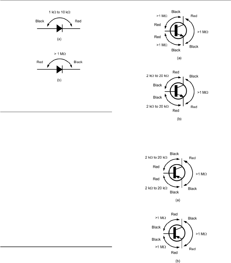
FAULT FINDING 279
Bipolar transistor ‘go/no-go’ checks
Typical meter indications for silicon NPN
transistors are shown in Fig. 15.8 (reverse bias is
applied in Fig. 15.8(a) and forward bias is applied
in Fig. 15.8(b)). Corresponding indications for
germanium NPN transistors will be somewhat
lower. Note also that the ×100 resistance range
should be used for measurements below 20 kH,and
the ×1k resistance range should be used for
measurements above 20 kH.
Typical meter indications for silicon PNP
transistors are shown in Fig. 15.9 (forward bias is
applied in Fig. 15.9(a) and reverse bias is applied in
Fig. 15.9(b)). As for NPN transistors,
corresponding indications for germanium PNP will
be somewhat lower. Once again, the ×100
resistance range should be used for measurements
below 20 kH,and the ×1k resistance range should
be used for measurements above 20 kH.
Bipolar transistor current gain checks
Simple go/no-go checks can also be used to
determine whether a transistor is providing current
gain. The principle is illustrated in Fig. 15.10. For
an NPN transistor this is achieved by measuring the
resistance between collector and emitter, as shown
in Fig. 15.10(a), before applying a small amount of
base current via a 100 kHresistor, as shown in Fig.
15.10(b). The application of base current should
Figure 15.7 Diode ‘go/no-go’ checks with typical
resistance values in the ‘go’ case
Figure 15.8 NPN transistor ‘go/no-go’ checks
with typical resistance values in the ‘go’ case
Figure 15.9 PNP transistor ‘go/no-go’ checks
with typical resistance values in the ‘go’ case
have the effect of producing a significant increase
in collector current and this, in turn, will result in a
much reduced resistance measured between the
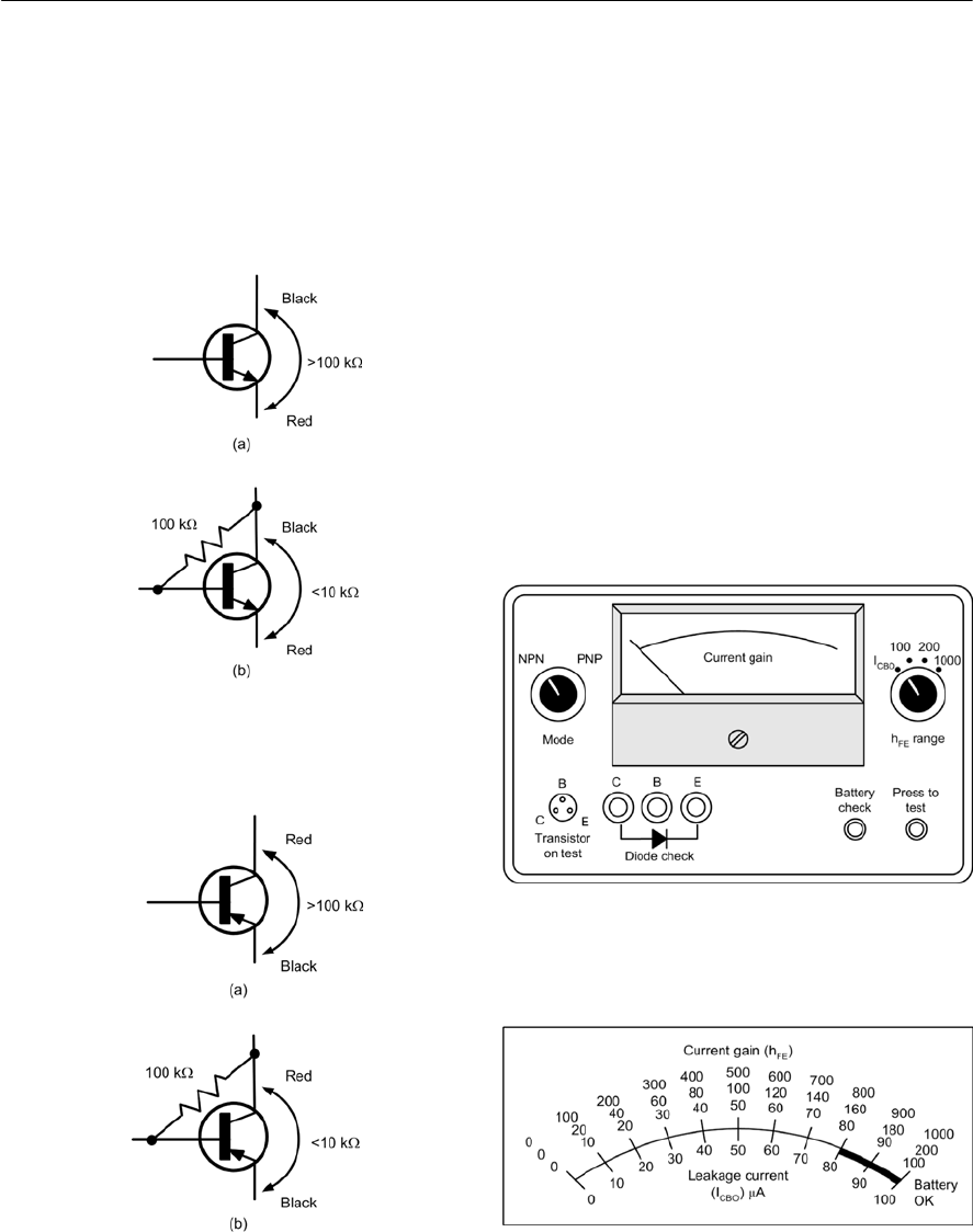
280 ELECTRONIC CIRCUITS: FUNDAMENTALS AND APPLICATIONS
collector and emitter. It is, of course, not possible
to provide an accurate indication of current gain by
this method however it will tell you whether or not
atransistor is producing current gain. The method
will also let you compare the current gain of one
(known) transistor with another. The equivalent
arrangement for testing a PNP transistor is shown
in Fig. 15.11.
Figure 15.10 Checking NPN transistor current
gain using an ohmmeter and a 100 kHresistor
Figure 15.11 Checking PNP transistor current
gain using an ohmmeter and a 100 kHresistor
Atransistor/diode checker
Asimple transistor/diode checker can make an
excellent project for the beginner to electronic
circuit construction. The instrument shown in Fig.
15.14 measures current gain for NPN and PNP
transistors up to 1,000 and leakage current up to
100 µA. It also has a diode check facility which can
be useful for rapid testing of signal, rectifier, and
zener diodes. The values of R1, R2 and R3 can be
made from series combinations of preferred value
resistors (for example, R2 can be made from a
150 kHresistor connected in series with an 18 kH
resistor) whilst the meter shunt resistor, R5, should
be calculated in order to provide a full-scale
deflection on the meter of 10 mA whenever any of
the current gain ranges are selected (see page 246).
Typical front panel layouts and meter scales are
shown in Figs 15.12 and 15.13.
Figure 15.13 Asuitable meter scale for the
transistor and diode checker
Figure 15.12 Typical front panel layout for the
transistor and diode checker
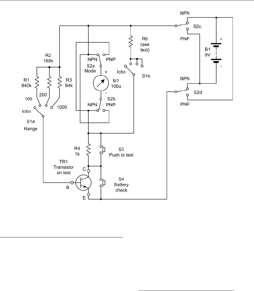
FAULT FINDING 281
Logic circuit faults
Whilst multimeters can be used for checking the
voltages present on the supply rails within digital
logic circuits they are generally unsuitable for
measuring the logic states of the points or nodes
within a circuit. There are several reasons for this,
including the fact that logic states are represented
by voltage levels that vary according to the
integrated circuit technology employed. However
the principal reason for misleading indications is
that the logic levels can be rapidly changing or may
take the form of short duration pulses that simply
cannot be detected by a conventional voltage
measuring instrument. That said, where logic levels
do remain static for periods of several seconds, a
multimeter may be used on the DC voltage ranges
to detect the presence of either a logic 0 or logic 1
state. In the case of standard TTL devices (which
operate from a +5V supply) the following voltage
levels apply:
Voltage measured Logic level indicated
<0.8 V 0
0.8 V to 2.0 V indeterminate
> 2.0 V 1
It should be noted that an ‘indeterminate’ logic
level may result from a tri-state condition where
several logic device place their outputs on a shared
signal (or bus) line. To prevent a conflict occurring
Figure 15.14 Complete circuit of the transistor and diode checker
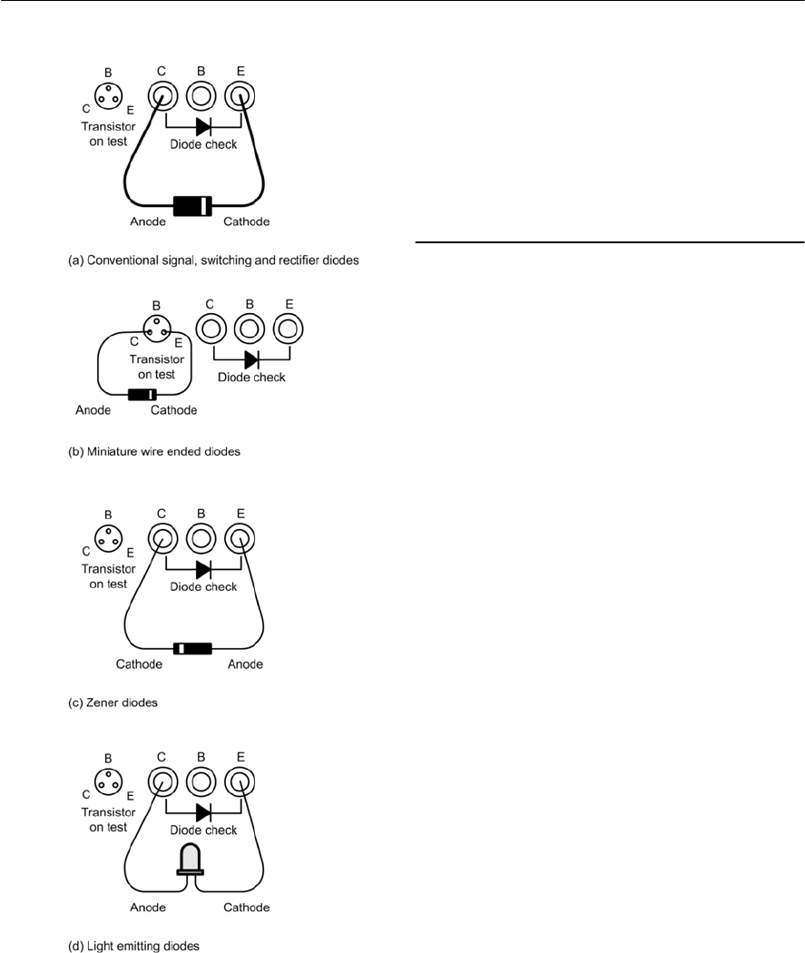
282 ELECTRONIC CIRCUITS: FUNDAMENTALS AND APPLICATIONS
between the devices, the outputs of any inactive
devices are placed in a high-impedance state in
which the voltage at the output can safely take any
value within the logic range without causing
damage to the inactive device. Modern high-
impedance instruments will usually produce a
misleading fluctuating indication in such
circumstances and this can sometimes be confused
with nodes that are actually pulsing.
Logic probes
The simplest, and by far the most convenient,
method of tracing logic states involves the use of a
logic probe. This invaluable tool comprises a
compact hand-held probe fitted with LEDs that
indicate the logical state of its probe tip.
Unlike multi-range meters, logic probes can
distinguish between lines which are actively
pulsing and those which are in a permanently tri-
state condition. In the case of a line which is being
pulsed, the logic 0 and logic 1 indicators will both
be illuminated (though not necessarily with the
same brightness) whereas, in the case of a tri-state
line neither indicator should be illuminated.
Logic probes usually also provide a means of
displaying pulses having a very short duration
which may otherwise go undetected. This is
accomplished by the inclusion of a pulse stretching
circuit (i.e. a monostable). This elongates short
duration pulses so that a visible indication is
produced on a separate ‘pulse’ LED.
Logic probes invariably derive their power
supply from the circuit under test and are connected
by means of a short length of twin flex fitted with
insulated crocodile clips. While almost any
convenient connecting point may be used, the
positive supply and ground terminals make ideal
connecting points which can be easily identified.
A typical logic probe circuit is shown in
Fig. 15.16. This circuit uses a dual comparator to
sense the logic 0 and logic 1 levels and a timer that
acts as a monostable pulse stretcher to indicate
the presence of a pulse input rather than a
continuous logic 0 or logic 1 condition. Typical
logic probe indications and waveforms are shown
in Fig. 15.18.
Figure 15.19 shows how a logic probe can be
used to check a typical combinational logic
Figure 15.15 Transistor and diode checker
connections for various different types of diode
(note particularly that the connections to a zener
diode must be reversed)
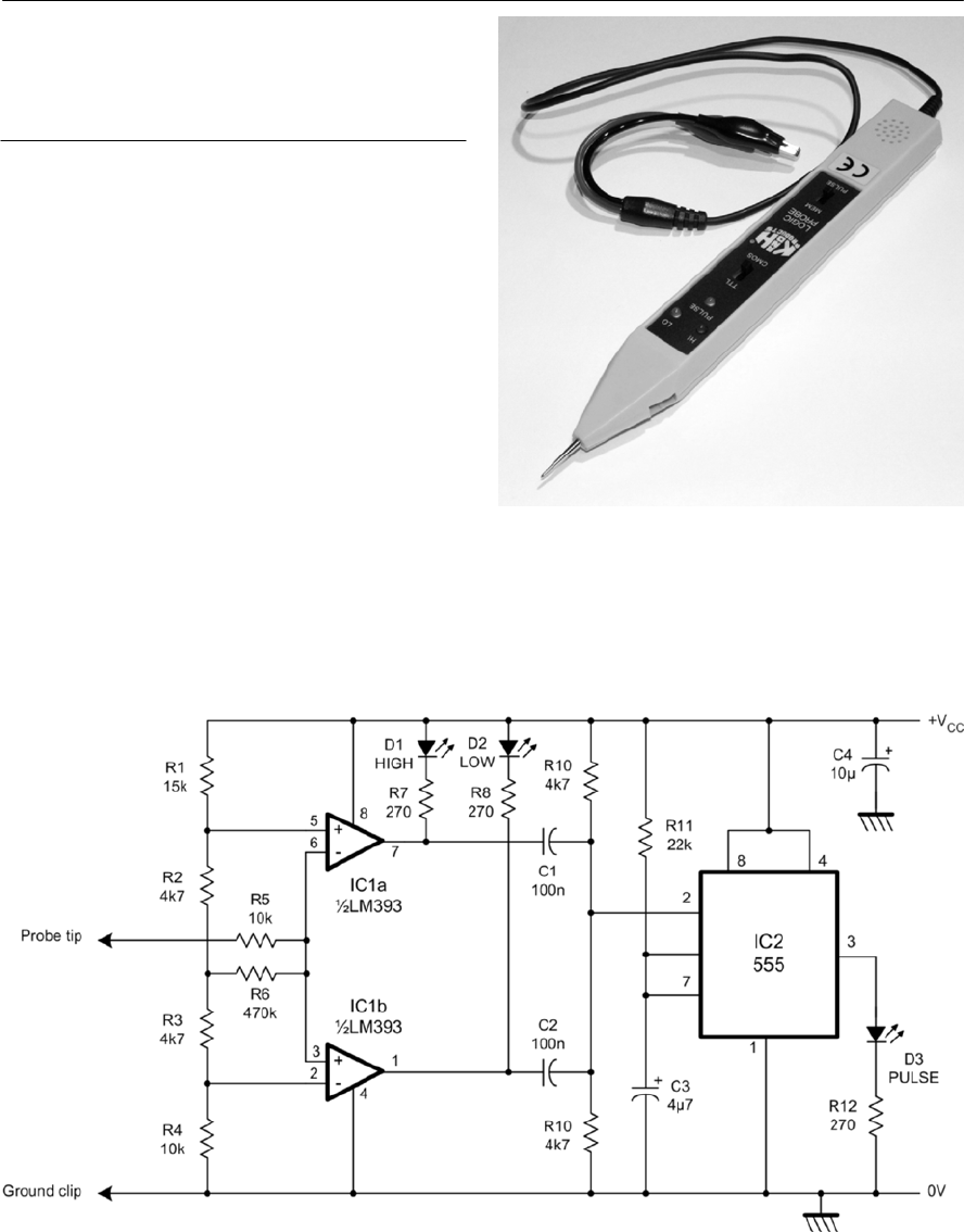
FAULT FINDING 283
arrangement. In use, the probe is simply moved
from node to node and the logic level is displayed
and compared with the expected level.
Logic pulsers
We sometimes need to simulate the logic levels
generated by a peripheral device or a sensor. A
permanent logic level can easily be generated by
pulling a line up to + 5 V via a 1 kHresistor or by
temporarily tying a line to 0 V. However, on other
occasions, you may need to simulate a pulse rather
than a permanent logic state and this can be
achieved by means of a logic pulser.
A logic pulser provides a means of momentarily
forcing a logic level transition into a circuit
regardless of its current state and thus it overcomes
the need to disconnect or de-soldering any of the
devices. The polarity of the pulse (produced at the
touch of a button) is adjusted so that the node under
investigation is momentarily forced into the
opposite logical state. During the period before the
button is depressed and for the period after the
Figure 15.17 Aversatile logic probe with logic
level and pulse indicating facilities. Note the
crocodile leads for connecting to the TTL or
CMOS supply and ground connections
Figure 15.16 Asimple logic probe for TTL and CMOS circuits with pulse stretching facilities
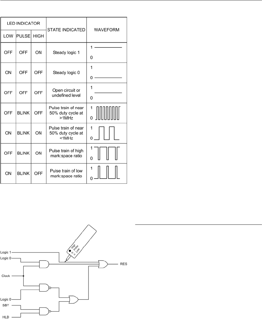
Practical investigation
Objective
To investigate faults in a typical linear regulated
power supply.
Components and test equipment
Breadboard, mains transformer with 220 V (or
110 V where appropriate) primary and 15 V 2 A
secondary winding, four 1N5401 diodes, TIP41C
transistor mounted on a heatsink of less than
2.5 °C/W, TL081 operational amplifier, fixed
resistors of 1 kH(two required) and 2.2 kH(two
required), 500 mA quick-blow fuse, 2 A slow-blow
fuse, BZX79 7.5 V zener diode, capacitors of
6,800 µF, 470 µF, and 100 µF (all rated at 50 V d.c.
working), digital multimeter, test leads and probes.
284 ELECTRONIC CIRCUITS: FUNDAMENTALS AND APPLICATIONS
pulse has been completed, the probe tip adopts a
tri-state (high impedance) condition. Hence the
probe does not permanently affect the logical state
of the point in question.
Logic pulsers derive their power supply from the
circuit under test in the same manner as logic
probes. Here again, the supply and ground
connections usually make suitable connecting
points.
A typical logic pulser circuit is shown in
Fig. 15.20. The circuit comprises a 555 monostable
pulse generator triggered from a push-button. The
output of the pulse generator is fed to a
complementary transistor arrangement in order to
make it fully TTL-compatible. As with the logic
pulser, this circuit derives its power from the circuit
under test (usually +5V).
Figure 15.21 shows an example of the combined
use of a logic probe and a logic pulser for testing a
simple J-K bistable. The logic probe is used to
check the initial state of the bistable outputs (see
Fig. 15.21(a) and (b)). Note that the outputs should
be complementary. Next, the logic pulser is applied
to the clock (CK) input of the bistable (Fig.
15.21(c)) and the Q output is checked using the
logic probe. The application of a pulse (using the
trigger button) should cause the Q output of the
bistable to change state (see Fig. 15.21(d)).
Figure 15.19 Using a logic probe to trace logic
levels in a simple logic circuit (note that the supply
and ground connections are not shown)
Figure 15.18 Typical logic probe indications
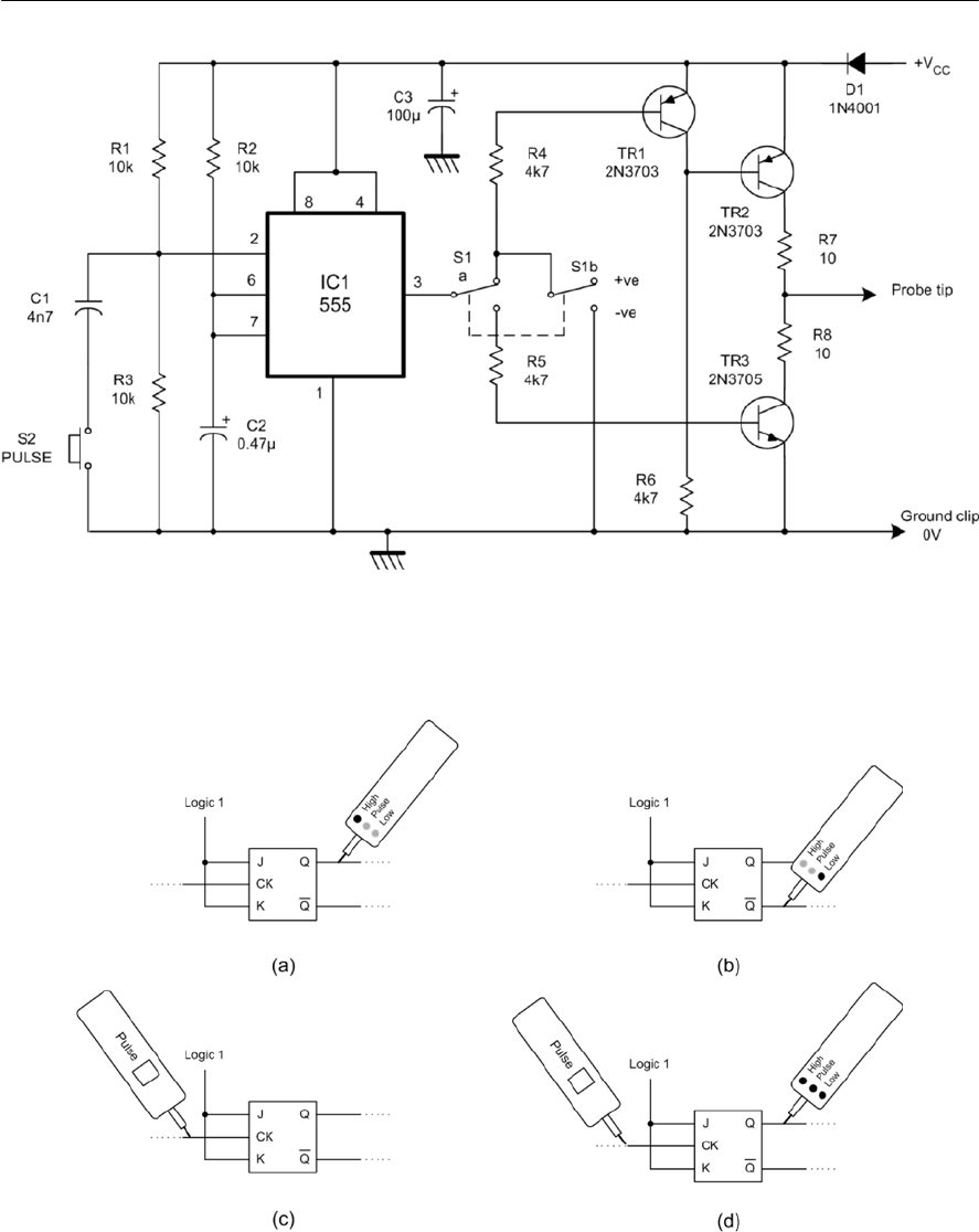
FAULT FINDING 285
Figure 15.21 Using a logic probe and a logic pulser to check a bistable
Figure 15.20 Alogic pulser suitable for fault tracing on TTL and CMOS logic circuits
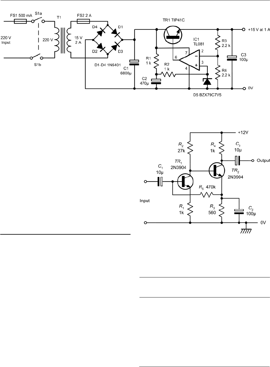
Problems
15.1 Figure 15.23 shows a two-stage high-gain
amplifier. Identify the faulty component and
the nature of the fault (e.g. open-circuit or
short-circuit) for each of the faults shown in
Table 15.2.
15.2 With the aid of a simple diagram, explain
how each of the following instruments can
be used to aid fault finding in digital
circuits:
(a) logic probe
(b) logic pulser.
15.3 Explain how an ohmmeter can be used to
perform simple ‘go/no-go’ checks on:
(a) a diode
(b) an NPN transistor.
Answers to these problems appear on page 376.
Procedure
Connect the circuit and measure the voltages at the
following test points with no fault present; TR1
collector, base and emitter; IC1 inverting input
(pin-2) and non-inverting input (pin-3). Record
your results in a suitable table.
Repeat the voltage measurements with the
following fault conditions present:
(a) R1 open circuit
(b) C2 short circuit
(c) D5 open circuit
(d) R3 open circuit.
In each case, use your knowledge of how the circuit
operates to justify the readings obtained.
286 ELECTRONIC CIRCUITS: FUNDAMENTALS AND APPLICATIONS
Condition TR1 TR2
c b e c b e
Normal 3.3 0.9 0.3 7.4 3.3 2.6
Fault 1 0.4 0.0 0.0 12.0 0.4 0.0
Fault 2 4.2 1.3 0.7 4.2 4.2 4.2
Fault 3 3.2 1.0 0.3 12.0 3.2 2.7
Fault 4 4.2 4.2 0.3 5.9 4.2 3.5
0.8 0.0 0.0 0.1 0.8 0.0 Fault 5
Fault 6 5.1 0.3 0.0 4.5 5.1 4.4
Figure 15.22 Regulated power supply used in the Practical investigation
Figure 15.23 See Question 15.1
Table 15.2 See Question 15.1
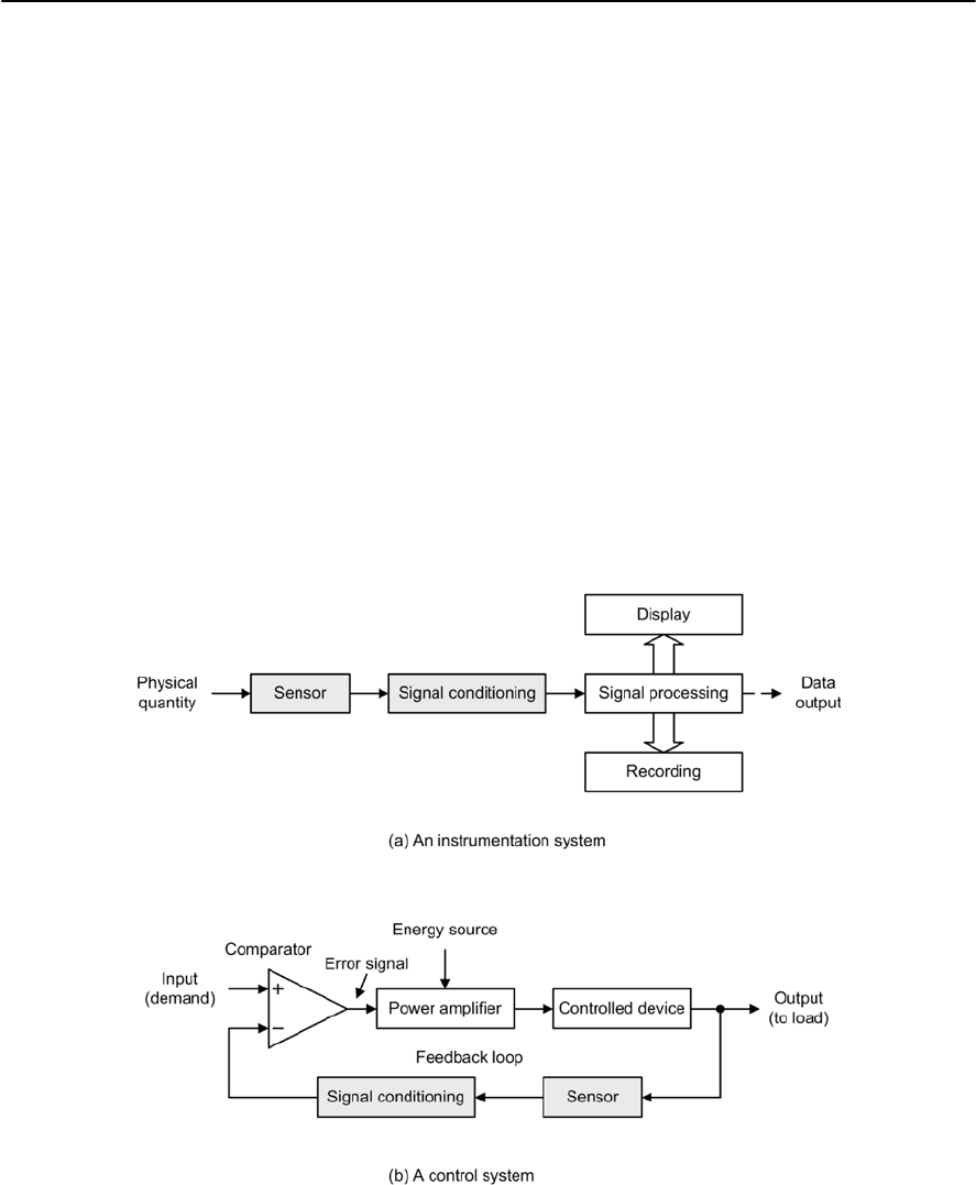
16
Sensors and interfacing
Figure 16.1 Instrumentation and control systems
Sensors provide us with a means of generating
signals that can be used as inputs to electronic
circuits. The things that we might want to sense
include physical parameters such as temperature,
light level, and pressure. Being able to generate an
electrical signal that accurately represents these
quantities allows us not only to measure and record
these values but also to control them.
Sensors are, in fact, a subset of a larger family of
devices known as transducers so we will consider
these before we look at sensors and how we
condition the signals that they produce in greater
detail. We begin, however, with a brief
introduction to the instrumentation and control
systems in which sensors, transducers, and signal
conditioning circuits are used.
Instrumentation and control systems
Figure 16.1 shows the arrangement of an
instrumentation system. The physical quantity to be
measured (e.g. temperature) acts upon a sensor that
produces an electrical output signal. This signal is
an electrical analogue of the physical input but note
that there may not be a linear relationship between
the physical quantity and its electrical equivalent.
Because of this and since the output produced by
the sensor may be small or may suffer from the
presence of noise (i.e. unwanted signals) further
signal conditioning will be required before the
signal will be at an acceptable level and in an
acceptable form for signal processing, display and

288 ELECTRONIC CIRCUITS: FUNDAMENTALS AND APPLICATIONS
Sensors
Asensor is a special kind of transducer that is used
to generate an input signal to a measurement,
instrumentation or control system. The signal
produced by a sensor is an electrical analogy of a
physical quantity, such as distance, velocity,
acceleration, temperature, pressure, light level, etc.
The signals returned from a sensor, together with
control inputs from the user or controller (as
appropriate) will subsequently be used to determine
the output from the system. The choice of sensor is
governed by a number of factors including
accuracy, resolution, cost, and physical size.
Sensors can be categorized as either active or
passive.An active sensor generates a current or
voltage output. A passive transducer requires a
source of current or voltage and it modifies this in
some way (e.g. by virtue of a change in the
sensor’s resistance). The result may still be a
voltage or current but it is not generated by the
sensor on its own.
Sensors can also be classed as either digital or
analogue.The output of a digital sensor can exist
in only two discrete states, either ‘on’ or ‘off’,
‘low’ or ‘high’, ‘logic 1’ or ‘logic 0’, etc. The
output of an analogue sensor can take any one of
an infinite number of voltage or current levels. It
is thus said to be continuously variable.Table 16.3
provides details of some common types of sensor.
recording. Furthermore, because the signal
processing may use digital rather than analogue
signals an additional stage of analogue-to-analogue
conversion may be required.
Figure 16.1(b) shows the arrangement of a
control system. This uses negative feedback in
order to regulate and stabilize the output. It thus
becomes possible to set the input or demand (i.e.
what we desire the output to be) and leave the
system to regulate itself by comparing it with a
signal derived from the output (via a sensor and
appropriate signal conditioning).
A comparator is used to sense the difference in
these two signals and where any discrepancy is
detected the input to the power amplifier is
adjusted accordingly. This signal is referred to as
an error signal (it should be zero when the output
exactly matches the demand). The input (demand)
is often derived from a simple potentiometer
connected across a stable d.c. voltage source whilst
the controlled device can take many forms (e.g. a
d.c. motor, linear actuator, heater, etc.).
Transducers
Transducers are devices that convert energy in the
form of sound, light, heat, etc., into an equivalent
electrical signal, or vice versa.
Before we go further, let’s consider a couple of
examples that you will already be familiar with. A
loudspeaker is a transducer that converts low-
frequency electric current into audible sounds. A
microphone, on the other hand, is a transducer that
performs the reverse function, i.e. that of
converting sound pressure variations into voltage
or current. Loudspeakers and microphones can thus
be considered as complementary transducers.
Transducers may be used as both inputs to
electronic circuits and outputs from them. From the
two previous examples, it should be obvious that a
loudspeaker is an output transducer designed for
use in conjunction with an audio system. Whereas,
amicrophone is an input transducer designed for
use with a recording or sound reinforcing system.
There are many different types of transducer and
Tables 16.1 and 16.2 provide some examples of
transducers that can be used to input and output
three important physical quantities; sound,
temperature, and angular position. Figure 16.2 Aselection of thermocouple probes

SENSORS AND INTERFACING 289
Table 16.1 Some examples of input transducers
Figure 16.3 Aselection of audible transducers
Physical quantity Input transducer Notes
Sound (pressure change) Dynamic microphone
(see Fig. 16.3)
Diaphragm attached to a coil is suspended in a magnetic
field. Movement of the diaphragm causes current to be
induced in the coil.
Temperature Thermocouple
(see Fig. 16.2)
Small e.m.f. generated at the junction between two
dissimilar metals (e.g. copper and constantan). Requires
reference junction and compensated cables for accurate
measurement.
Angular position Rotary potentiometer Fine wire resistive element is wound around a circular
former. Slider attached to the control shaft makes contact
with the resistive element. A stable d.c. voltage source is
connected across the ends of the potentiometer. Voltage
appearing at the slider will then be proportional to angular
position.
Physical quantity Output transducer Notes
Sound (pressure change) Loudspeaker
(see Fig. 16.3)
Diaphragm attached to a coil is suspended in a magnetic
field. Current in the coil causes movement of the
diaphragm which alternately compresses and rarefies the
air mass in front of it.
Temperature Heating element
(resistor)
Metallic conductor is wound onto a ceramic or mica
former. Current flowing in the conductor produces heat.
Angular position Rotary potentiometer Multi-phase motor provides precise rotation in discrete
steps of 15° (24 steps per revolution), 7.5° (48 steps per
revolution) and 1.8° (200 steps per revolution).
Table 16.2 Some examples of output transducers
Figure 16.4 Various switch sensors

290 ELECTRONIC CIRCUITS: FUNDAMENTALS AND APPLICATIONS
Table 16.3 Some examples of output transducers
Physical quantity Output transducer Notes
Angular position Resistive rotary
position sensor
(see Fig. 16.5)
Rotary track potentiometer with linear law produces analogue voltage
proportional to angular position.
Optical shaft encoder Encoded disk interposed between optical transmitter and receiver (infra-
red LED and photodiode or photo-transistor).
Angular velocity Tachogenerator Small d.c. generator with linear output characteristic. Analogue output
voltage proportional to shaft speed.
Toothed rotor
tachometer
Magnetic pick-up responds to the movement of a toothed ferrous disk.
The pulse repetition frequency of the output is proportional to the
angular velocity.
Flow Rotating vane flow
sensor
(see Fig. 16.9)
Turbine rotor driven by fluid. Turbine interrupts infra-red beam. Pulse
repetition frequency of output is proportional to flow rate.
Linear position Resistive linear
position sensor
Linear track potentiometer with linear law produces analogue voltage
proportional to linear position. Limited linear range.
Linear variable
differential
transformer (LVDT)
Miniature transformer with split secondary windings and moving core
attached to a plunger. Requires a.c. excitation and phase-sensitive
detector.
Magnetic linear
position sensor
Magnetic pick-up responds to movement of a toothed ferrous track.
Pulses are counted as the sensor moves along the track.
Light level Photocell Voltage-generating device. The analogue output voltage produced is
proportional to light level.
Light dependent
resistor (LDR)
(see Fig. 16.8)
An analogue output voltage results from a change of resistance within a
cadmium sulphide (CdS) sensing element. Usually connected as part of a
potential divider or bridge.
Photodiode
(see Fig, 16.8)
Two-terminal device connected as a current source. An analogue output
voltage is developed across a series resistor of appropriate value.
Phototransistor
(see Fig. 16.8)
Three-terminal device connected as a current source. An analogue output
voltage is developed across a series resistor of appropriate value.
Liquid level Float switch
(see Fig. 16.7)
Simple switch element which operates when a particular level is
detected.
Capacitive proximity
switch
Switching device which operates when a particular level is detected.
Ineffective with some liquids.
Diffuse scan
proximity switch
Switching device which operates when a particular level is detected.
Ineffective with some liquids.

SENSORS AND INTERFACING 291
Table 16.3 (continued)
Physical quantity Output transducer Notes
Pressure Microswitch pressure
sensor
(see Fig. 16.4)
Microswitch fitted with actuator mechanism and range setting springs.
Suitable for high-pressure applications.
Differential pressure
vacuum switch
Microswitch with actuator driven by a diaphragm. May be used to sense
differential pressure. Alternatively, one chamber may be evacuated and
the sensed pressure applied to a second input.
Piezo-resistive
pressure sensor
Pressure exerted on diaphragm causes changes of resistance in attached
piezo-resistive transducers. Transducers are usually arranged in the form
of a four active element bridge which produces an analogue output
voltage.
Proximity Reed switch
(see Fig. 16.4)
Reed switch and permanent magnet actuator. Only effective over short
distances.
Inductive proximity
switch
Target object modifies magnetic field generated by the sensor. Only
suitable for metals (non-ferrous metals with reduced sensitivity).
Capacitive proximity
switch
Target object modifies electric field generated by the sensor. Suitable for
metals, plastics, wood, and some liquids and powders.
Optical proximity
switch
(see Fig. 16.4)
Available in diffuse and through scan types. Diffuse scan types require
reflective targets. Both types employ optical transmitters and receivers
(usually infra-red emitting LEDs and photo-diodes or photo-transistors).
Digital input port required.
Strain Resistive strain
gauge
Foil type resistive element with polyester backing for attachment to body
under stress. Normally connected in full bridge configuration with
temperature-compensating gauges to provide an analogue output voltage.
Semiconductor strain
gauge
Piezo-resistive elements provide greater outputs than comparable
resistive foil types. More prone to temperature changes and also
inherently non-linear.
Temperature Thermocouple
(see Fig. 16.2)
Small e.m.f. generated by a junction between two dissimilar metals. For
accurate measurement, requires compensated connecting cables and
specialized interface.
Thermistor
(see Fig. 16.6)
Usually connected as part of a potential divider or bridge. An analogue
output voltage results from resistance changes within the sensing
element.
Semiconductor
temperature sensor
(see Fig. 16.6)
Two-terminal device connected as a current source. An analogue output
voltage is developed across a series resistor of appropriate value.
Weight Load cell Usually comprises four strain gauges attached to a metal frame. This
assembly is then loaded and the analogue output voltage produced is
proportional to the weight of the load.
Vibration Electromagnetic
vibration sensor
Permanent magnet seismic mass suspended by springs within a
cylindrical coil. The frequency and amplitude of the analogue output
voltage are respectively proportional to the frequency and amplitude of
vibration.
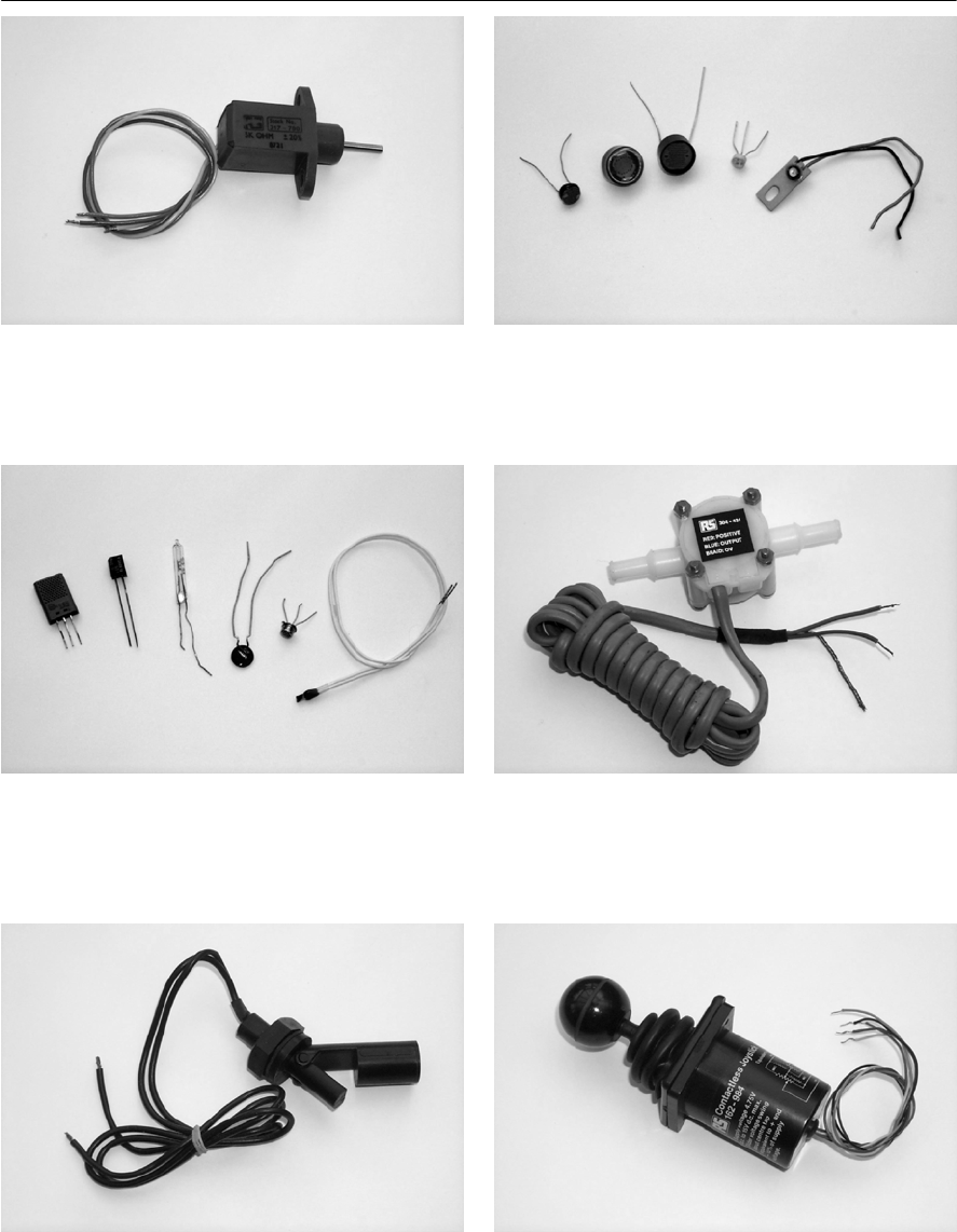
292 ELECTRONIC CIRCUITS: FUNDAMENTALS AND APPLICATIONS
Figure 16.5 Resistive linear position sensor
Figure 16.6 Various temperature and gas sensors
Figure 16.7 Liquid level float switch Figure 16.10 Contactless joystick
Figure 16.9 Liquid flow sensor (digital output)
Figure 16.8 Various optical and light sensors
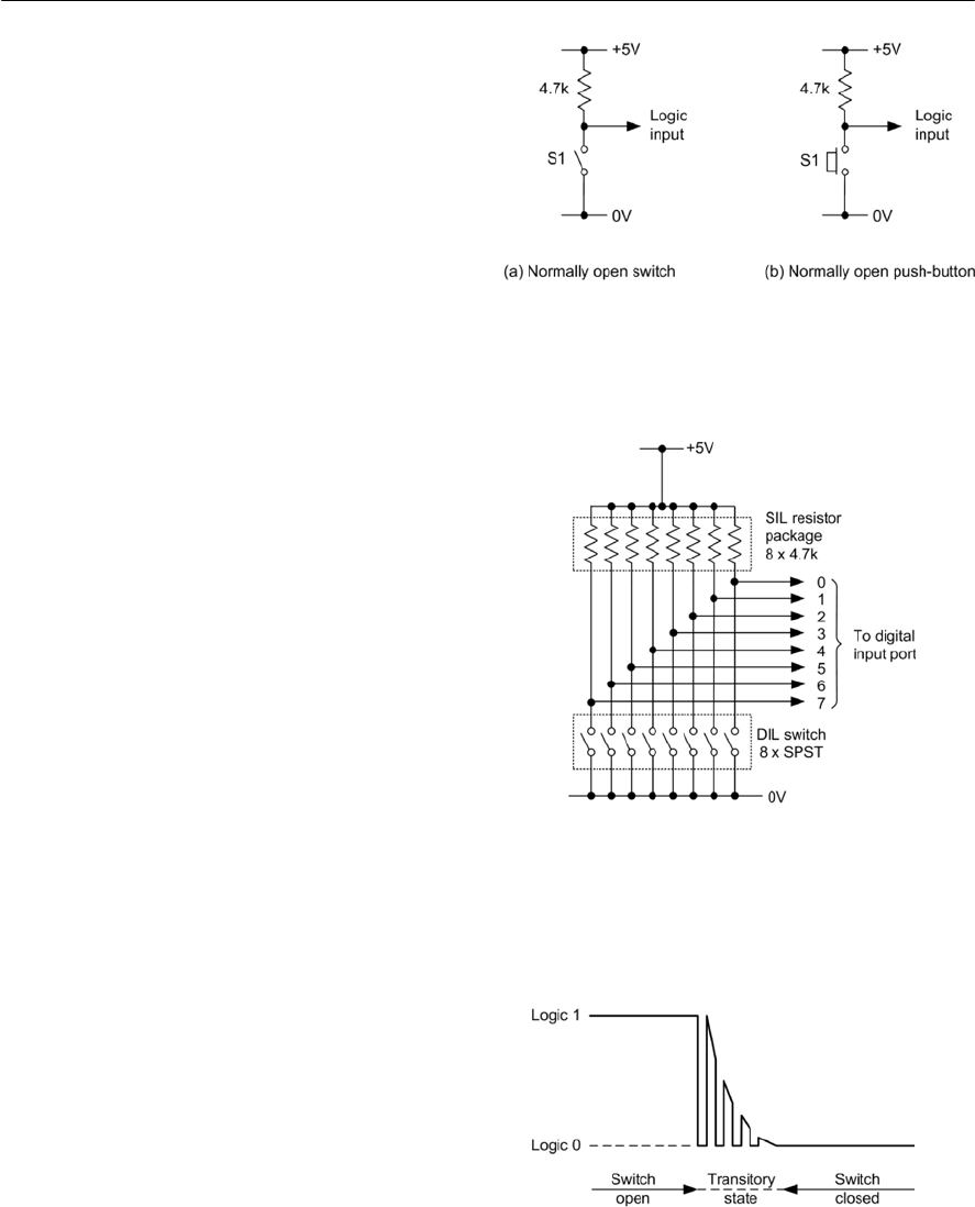
SENSORS AND INTERFACING 293
Switches
Switches can be readily interfaced to electronic
circuits in order to provide manual inputs to the
system. Simple toggle and push-button switches are
generally available with normally open (NO),
normally closed (NC), or changeover contacts. In
the latter case, the switch may be configured as
either an NO or an NC type, depending upon the
connections used.
Toggle, lever, rocker, rotary, slide, and push-
button types are all commonly available in a variety
of styles. Illuminated switches and key switches are
also available for special applications. The choice
of switch type will obviously depend upon the
application and operational environment.
An NO switch or push-button may be interfaced
to a logic circuit using nothing more than a single
pull-up resistor as shown in Fig. 16.11.
The relevant bit of the input will then return 0
when the switch contacts are closed (i.e. when the
switch is operated or where the pushbutton is
depressed). When the switch is inactive, the logic
input will return 1.
Unfortunately, this simple method of interfacing
has a limitation when the state of a switch is being
sensed regularly (e.g. during program execution).
However, a typical application which is unaffected
by this problem is that of using one or more PCB
mounted switches (e.g. a DIL switch package) to
configure a logic system in one of a number of
preset modes. In such cases, the switches would be
set once only and the software would read the state
of the switches and use the values returned to
initially configure the system. Thereafter, the state
of the switches would then only be changed in
order to modify the operational parameters of the
system (e.g. when changing input sensors or output
transducers). A typical DIL switch input interface
to a digital input port is shown in Fig. 16.12.
As mentioned earlier, the simple circuit of Fig.
16.11 is unsuitable for use when the state of the
switch is regularly changing. The reason for this is
that the switching action of most switches is far
from ‘clean’ (i.e. the switch contacts make and
break several times whenever the switch is
operated). This may not be a problem when the
state of a switch remains static during program
execution but it can give rise to serious problems
when dealing with, for example, an operator switch
bank or keypad.
Figure 16.11 Interfacing a normally open switch
or push-button to a digital input port
Figure 16.12 Interfacing a DIL switch input to a
digital input port
Figure 16.13 Typical waveform produced by a
switch closure
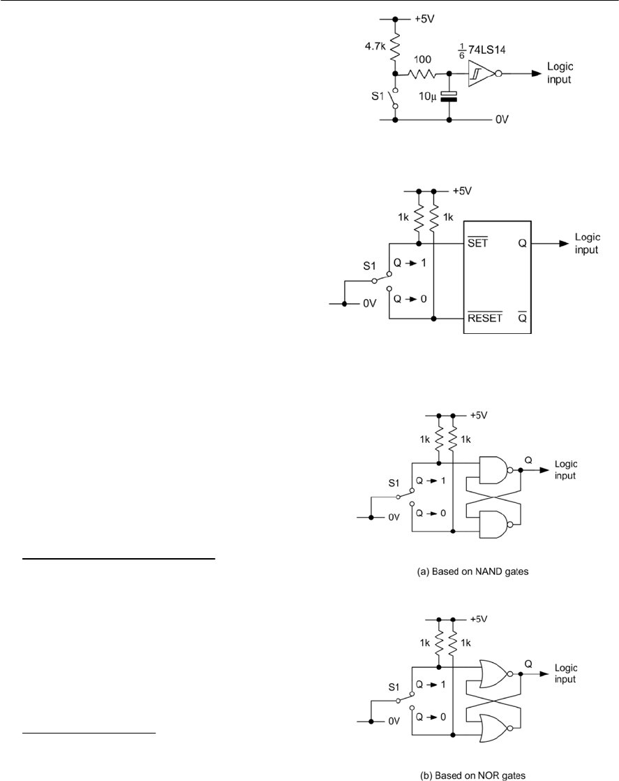
294 ELECTRONIC CIRCUITS: FUNDAMENTALS AND APPLICATIONS
The contact ‘bounce’ that occurs when a switch is
operated results in rapid making and breaking of
the switch until it settles into its new state. Figure
16.13 shows the waveform generated by the simple
switch input circuit of Fig. 16.11 as the contacts
close. The spurious states can cause problems if the
switch is sensed during the period in which the
switch contacts are in motion, and hence steps must
be taken to minimize the effects of bounce. This
may be achieved by using some extra circuitry in
the form of a debounce circuit or by including
appropriate software delays (of typically 4 to 20
ms) so that spurious switching states are ignored.
We shall discuss these two techniques separately.
Immunity to transient switching states is
generally enhanced by the use of active-low inputs
(i.e. a logic 0 state at the input is used to assert the
condition required). The debounce circuit shown in
Fig. 16.14 is adequate for most toggle, slide and
push-button type switches. The value of the 100 D
resistor takes into account the low-state sink current
required by IC1 (normally 1.6 mA for standard
TTL and 400 µA for LS-TTL). This resistor should
not be allowed to exceed approximately 470 Din
order to maintain a valid logic 0 input state. The
values quoted generate an approximate 1 ms delay
(during which the switch contacts will have settled
into their final state). It should be noted that, on
power-up, this circuit generates a logic 1 level for
approximately 1 ms before the output reverts to a
logic 0 in the inactive state. The circuit obeys the
following state table:
Switch condition Logic output
closed 1
open 0
An alternative, but somewhat more complex,
switch de-bouncing arrangement is shown in Fig.
16.15. Here a single-pole double-throw (SPDT)
changeover switch is employed. This arrangement
has the advantage of providing complementary
outputs and it obeys the following state table:
Switch condition Q
QG1 1
QG0 0
Rather than use an integrated circuit R-S bistable in
the configuration of Fig. 16.15 it is often expedient
to make use of ‘spare’ two-input NAND or NOR
Figure 16.16 Alternative switch debounce circuits:
(a) based on NAND gates; (b) based on NOR gates
Figure 16.14 Simple debounce circuit
Figure 16.15 Debounce circuit based on an R-S
bistable
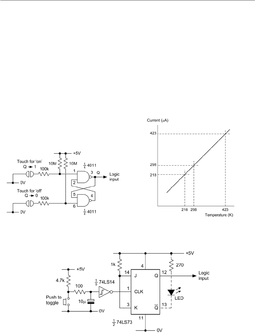
SENSORS AND INTERFACING 295
gates arranged to form bistables using the circuits
shown in Figs 16.16(a) and 16.16(b), respectively.
Figure 16.17 shows a rather neat extension of this
theme in the form of a touch-operated switch. This
arrangement is based on a 4011 CMOS quad two-
input NAND gate (though only two gates of the
package are actually used in this particular
configuration).
Finally, it is some times necessary to generate a
latching action from a normally-open push-button
switch. Figure 16.18 shows an arrangement in
which a 74LS73 JK bistable is clocked from the
output of a debounced switch.
Pressing the switch causes the bistable to change
state. The bistable then remains in that state until
the switch is depressed a second time. If desired,
the complementary outputs provided by the bistable
may be used to good effect by allowing the unused
output to drive an LED. This will become
illuminated whenever the Q output is high.
Semiconductor temperature sensors
Semiconductor temperature sensors are ideal for a
wide range of temperature-sensing applications.
The popular AD590 semiconductor temperature
sensor, for example, produces an output current
which is proportional to absolute temperature and
which increases at the rate of 1 JA/K. The
characteristic of the device is illustrated in Fig.
16.19. The AD590 is laser trimmed to produce a
current of 298.2 JA(±2.5 JA) at a temperature of
298.2°C (i.e. 25°C). A typical interface between the
AD590 and an analogue input is shown in
Fig. 16.20. The Practical investigation (page 301)
makes further use of this device.
Figure 16.17 Touch-operated switch
Figure 16.18 Latching action switch
Figure 16.19 AD590 semiconductor temperature
sensor characteristic
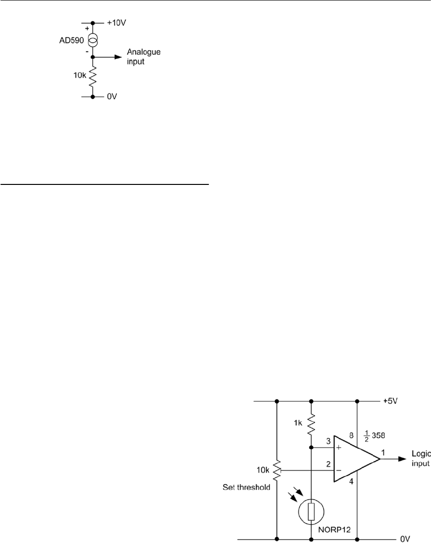
296 ELECTRONIC CIRCUITS: FUNDAMENTALS AND APPLICATIONS
Thermocouples
Thermocouples comprise a junction of dissimilar
metals which generate an e.m.f. proportional to the
temperature differential which exists between the
measuring junction and a reference junction. Since
the measuring junction is usually at a greater
temperature than that of the reference junction, it is
sometimes referred to as the hot junction.
Furthermore, the reference junction (i.e. the cold
junction)is often omitted in which case the
sensing junction is simply terminated at the signal
conditioning board. This board is usually
maintained at, or near, normal room temperatures.
Thermocouples are suitable for use over a very
wide range of temperatures (from -100°C to
+1100°C). Industry standard ‘type K’
thermocouples comprise a positive arm
(conventionally coloured brown) manufactured
from nickel/chromium alloy whilst the negative
arm (conventionally coloured blue) is manufactured
from nickel/aluminium.
The characteristic of a type K thermocouple is
defined in BS 4937 Part 4 of 1973 (International
Thermocouple Reference Tables) and this standard
gives tables of e.m.f. versus temperature over the
range 0°C to +1100°C. In order to minimize errors,
it is usually necessary to connect thermocouples to
appropriate signal conditioning using compensated
cables and matching connectors. Such cables and
connectors are available from a variety of suppliers
and are usually specified for use with type K
thermocouples. A selection of typical thermocouple
probes for high temperature measurement was
shown earlier in Fig. 16.2.
Threshold detection
Analogue sensors are sometimes used in situations
where it is only necessary to respond to a pre-
determined threshold value. In effect, a two-state
digital output is required. In such cases a simple
one-bit analogue-to-digital converter based on a
comparator can be used. Such an arrangement is, of
course, very much simpler and more cost-effective
than making use of a conventional analogue input
port!
Simple threshold detectors for light level and
temperature are shown in Figs 16.21, 16.22 and
16.24. These circuits produce TTL-compatible
outputs suitable for direct connection to a logic
circuit or digital input port.
Figure 16.21 shows a light level threshold
detector based on a comparator and light-dependent
resistor (LDR). This arrangement generates a logic
0input whenever the light level exceeds the
threshold setting, and vice versa. Figure 16.22
shows how light level can be sensed using a
photodiode. This circuit behaves in the same
manner as the LDR equivalent but it is important to
be aware that circuit achieves peak sensitivity in
the near infra-red region. Figure 16.23 shows how
the spectral response of a typical light-dependent
resistor (NORP12) compares with that of a
conventional photodiode (BPX48). Note that the
BPX48 can also be supplied with an integral
daylight filter (BPX48F).
Figure 16.20 Typical input interface for the
AD590 temperature sensor (the output voltage will
increase at the rate of 10 mV per °C)
Figure 16.21 Light-level threshold detector based
on a light-dependent resistor (LDR)
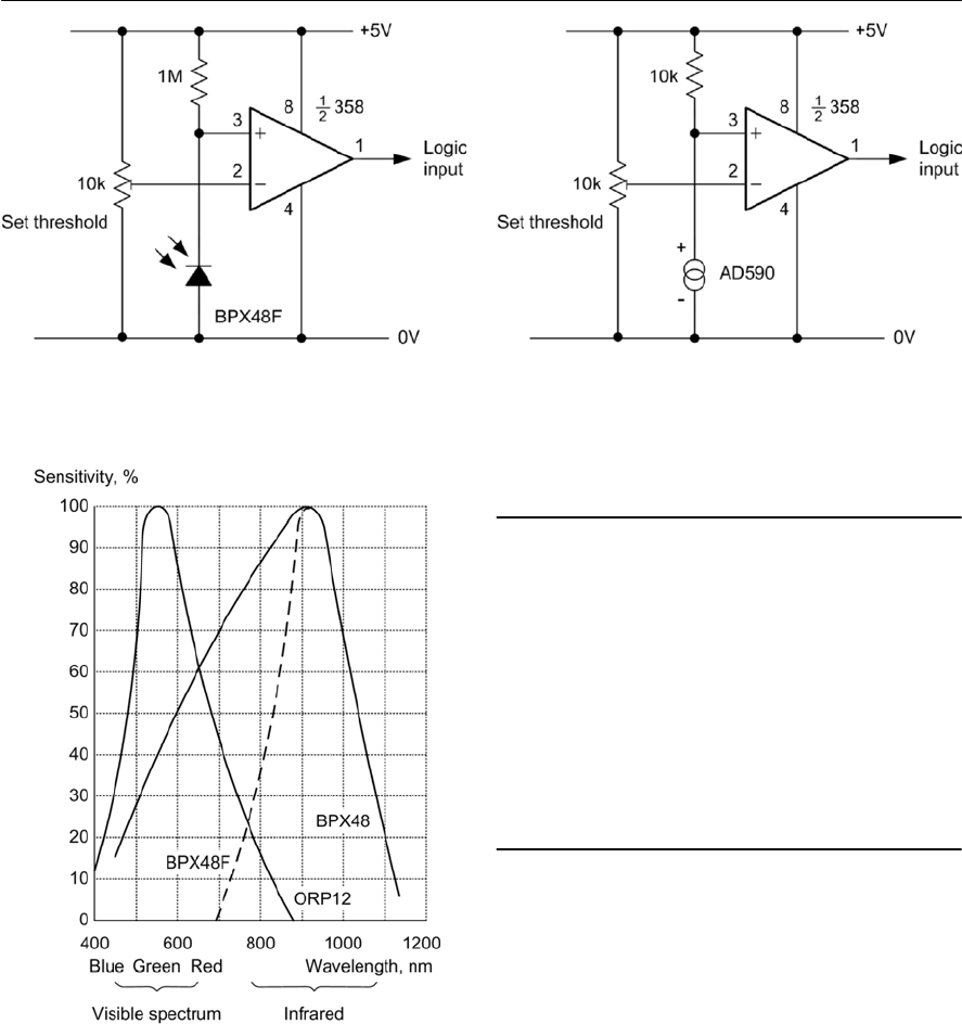
SENSORS AND INTERFACING 297
Figure 16.24 Temperature threshold detector
based on an AD590 semiconductor temperature
sensor
Figure 16.23 Comparison of the spectral response
of an LDR and some common photodiodes
Figure 16.22 Light level threshold detector based
on a photodiode
Figure 16.24 shows how temperature thresholds
can be sensed using the AD590 sensor described
earlier. This arrangement generates a logic 0 input
whenever the temperature level exceeds the
threshold setting, and vice versa.
Outputs
Having dealt at some length with input sensors, we
shall now focus our attention on output devices
(such as relays, loudspeakers and LED indicators)
and the methods used for interfacing them.
Integrated circuit output drivers are available for
more complex devices, such as LCD displays and
stepper motor. Many simple applications will,
however, only require a handful of components in
order to provide an effective interface.
LED indicators
Indicators based on light emitting diodes (LEDs)
are inherently more reliable than small filament
lamps and also consume considerably less power.
They are thus ideal for providing visual status and
warning displays. LEDs are available in a variety of
styles and colours and ‘high brightness’ types can
be employed where high-intensity displays are
required.
Atypical red LED requires a current of around
10 mA to provide a reasonably bright display and
such a device may be directly driven from a
buffered digital output port. Different connections
are used depending upon whether the LED is to be
illuminated for a logic 0 or logic 1 state. Several
possibilities are shown in Fig. 16.25.
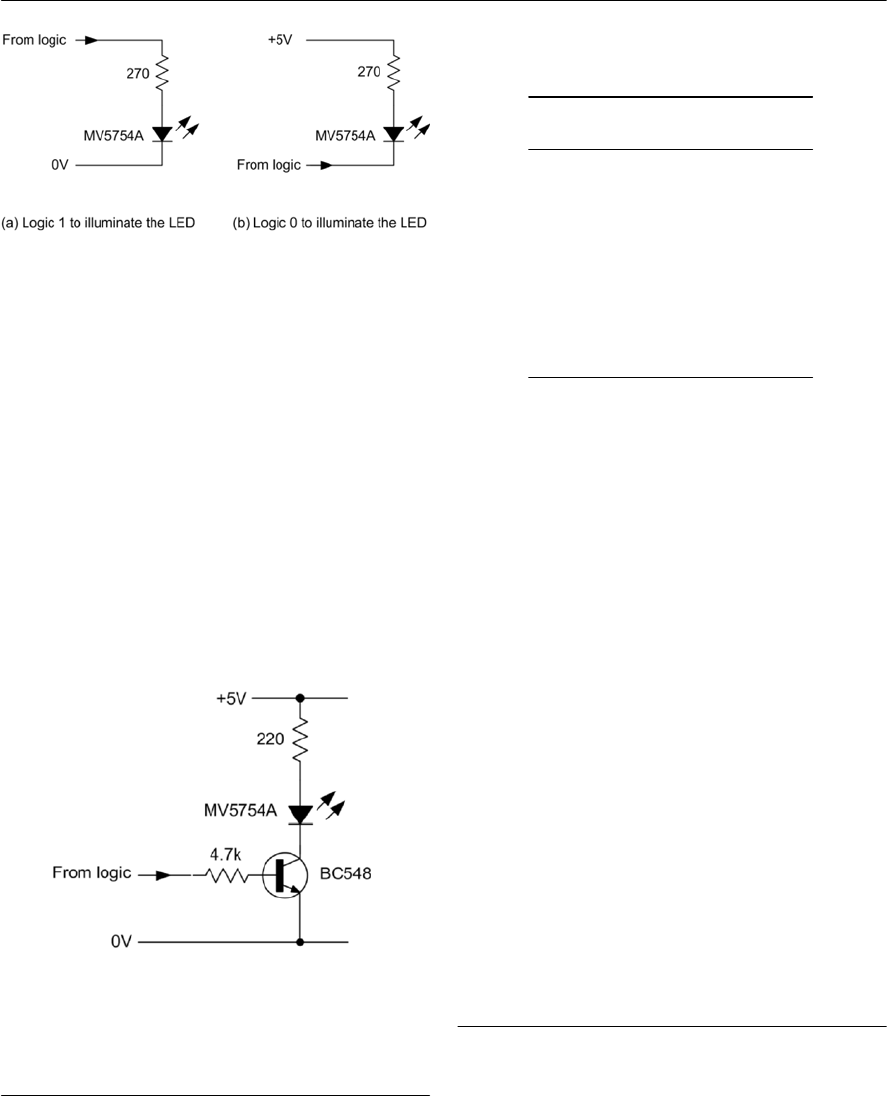
298 ELECTRONIC CIRCUITS: FUNDAMENTALS AND APPLICATIONS
Where drive current is insufficient to operate an
LED, an auxiliary transistor can be used as shown
in Fig. 16.26. The LED will operate when the
output from a logic circuit card is taken to logic 1
and the operating current should be approximately
15 mA (thereby providing a brighter display than
the arrangements previously described). The value
of LED series resistance will be dependent upon
the supply voltage and can be determined from the
equation shown on page 95 or it can be selected
from the data shown in Table 16.4.
Voltage Series resistance
(all 0.25 W)
3V to 4V 100 D
4V to 5V 150 D
5V to 8V 220 D
8V to 12V 470 D
12V to 15V 820 D
15V to 20V 1.2 kD
20V to 28V 1.5 kD
Driving high-current loads
Due to the limited output current and voltage
capability of most standard logic devices and I/O
Figure 16.25 Driving an LED from a buffered
logic gate or digital I/O port
Figure 16.26 Using an auxiliary transistor to drive
an LED where current drive is limited
ports, external circuitry will normally be required
to drive anything other than the most modest of
loads. Figure 16.27 shows some typical
arrangements for operating various types of
medium- and high-current load. Fig. 16.27(a)
shows how an NPN transistor can be used to
operate a low-power relay. Where the relay
requires an appreciable operating current (say, 150
mA, or more) a plastic encapsulated Darlington
power transistor should be used as shown in Figure
16.27(b). Alternatively, a power MOSFET may be
preferred, as shown in Fig. 16.27(c). Such devices
offer very low values of ‘on’ resistance coupled
with a very high ‘off’ resistance. Furthermore,
unlike conventional bipolar transistors, a power
FET will impose a negligible load on an I/O port.
Figure 16.27(d) shows a filament lamp driver based
on a plastic Darlington power transistor. This
circuit will drive lamps rated at up to 24 V, 500
mA. Finally, where visual indication of the state of
arelay is desirable it is a simple matter to add an
LED indicator to the driver stage, as shown in Fig.
16.28.
Audible outputs
Where simple audible warnings are required,
miniature piezoelectric transducers may be used.
Such devices operate at low voltages (typically in
the range 3V to 15V) and can be interfaced with the
aid of a buffer, open-collector logic gate, or
Table 16.4 Typical waveform produced by a
switch closure
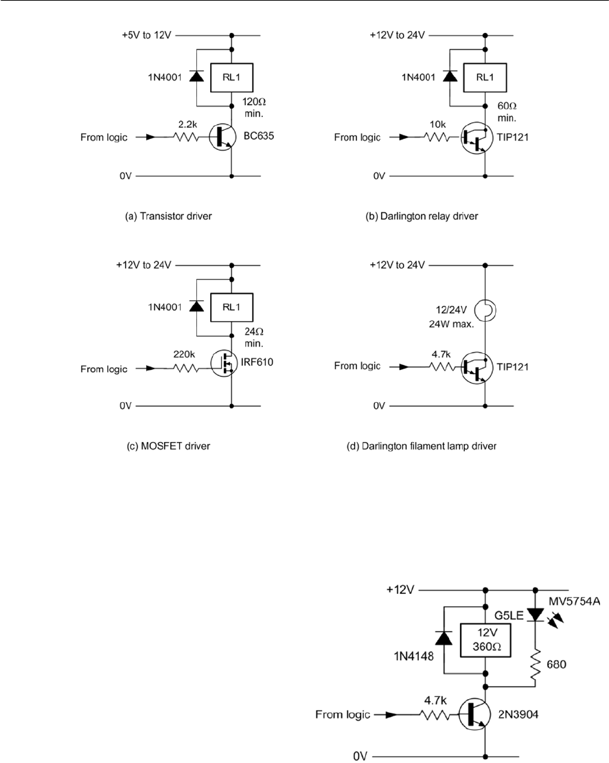
SENSORS AND INTERFACING 299
transistor. Figures 16.29(a)-(c) show typical
interface circuits which produce an audible output
when the port output line is at logic 1.
Where a pulsed rather than continuous audible
alarm is required, a circuit of the type shown in Fig.
16.31 can be employed. This circuit is based on a
standard 555 timer operating in astable mode and
operates at approximately 1 Hz. A logic 1 from the
port output enables the 555 and activates the pulsed
audio output.
Finally, the circuit shown in Fig. 16.32 can be
used where a conventional moving-coil
loudspeaker is to be used in preference to a piezo-
electric transducer. This circuit is again based on
the 555 timer and provides a continuous output at
approximately 1 kHz whenever the port output is at
logic 1.
Figure 16.27 Typical medium- and high-current driver circuits: (a) transistor low-current relay driver; (b)
Darlington medium/high-current relay driver; (c) MOSFET relay driver; (d) Darlington low-voltage filament
lamp driver
Figure 16.28 Showing how an LED indicator can
easily be added to a relay driver
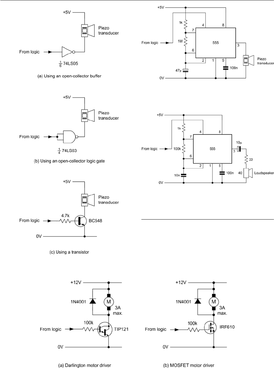
300 ELECTRONIC CIRCUITS: FUNDAMENTALS AND APPLICATIONS
Motors
Circuit arrangements used for driving DC motors
generally follow the same lines as those described
earlier for use with relays. As an example, the
circuits shown in Fig. 16.30 show how a Darlington
Figure 16.30 Motor driver circuits
Figure 16.29 Audible output driver circuits
Figure 16.32 Audible alarm circuit based on a 555
astable oscillator and a 40 Dloudspeaker
Figure 16.31 Audible alarm circuit based on a 555
astable oscillator and a piezoelectric transducer
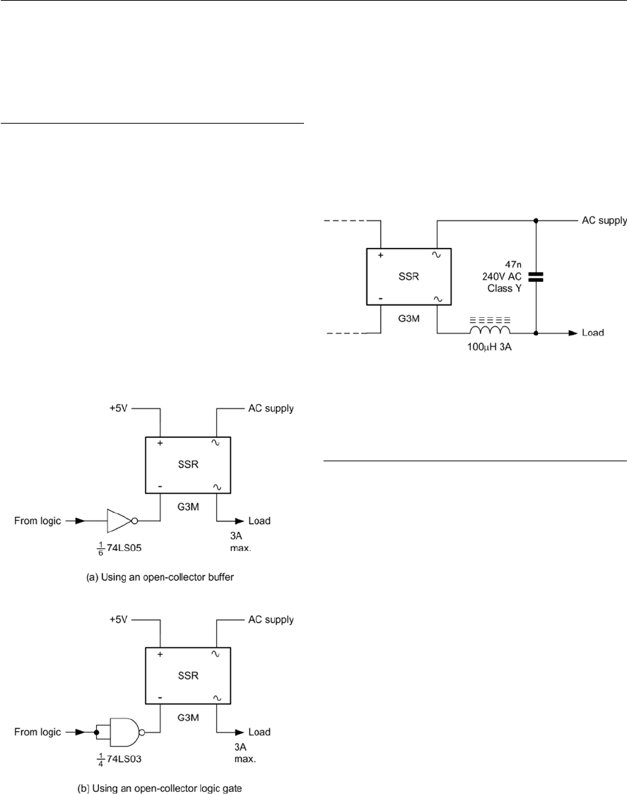
Practical investigation
Objective
To investigate the operation of an AD590
semiconductor temperature sensor and its
interface/signal conditioning circuit.
Components and test equipment
Breadboard, d.c. power supply with ± 5 V output at
100 mA (or more), 10 kDlinear variable resistor
(preferably multi-turn type), fixed resistors of
10 kD(two required) and 100 kD0.25 W 5%,
AD590 temperature sensor, TL081 operational
amplifier, digital multimeter, thermometer, test
leads and probes, small hand-held hair drier.
Procedure
Connect the circuit, set VR1 to mid-position, and
measure the output voltage produced by the circuit.
Adjust VR1 for an output voltage reading of
exactly zero at a temperature of 20°C. Place the
SENSORS AND INTERFACING 301
driver and a power MOSFET can be used to drive a
low-voltage DC motor. These circuits are suitable
for use with DC motors rated at up to l2 V with
stalled currents of up to 3 A. In both cases, a logic
1from the output port will operate the motor.
Driving mains connected loads
Control systems are often used in conjunction with
mains connected loads. Modern solid-state relays
(SSRs) offer superior performance and reliability
when compared with conventional relays in such
applications. SSRs are available in a variety of
encapsulations (including DIL, SIL, flat-pack, and
plug-in octal) and may be rated for RMS currents
between l A and 40 A.
In order to provide a high degree of isolation
between input and output, SSRs are optically
coupled. Such devices require minimal input
currents (typically 5 mA, or so, when driven from 5
V) and they can thus be readily interfaced with an
I/O port that offers sufficient drive current. In other
cases, it may be necessary to drive the SSR from an
unbuffered I/O port using an open-collector logic
gate. Typical arrangements are shown in Fig. 16.33.
Finally, it is important to note that, when an
inductive load is to be controlled, a snubber
network should be fitted, as shown in Fig. 16.34.
Figure 16.33 Interface circuits for driving solid
state relays
Figure 16.34 Using a snubber circuit with an
inductive load
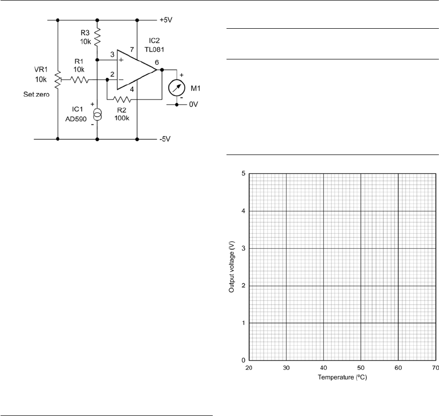
Temperature
(°C)
Output voltage
(V)
20
30
40
50
60
70
Problems
16.1 For each of the automotive applications
listed below, state:
(a) the quantity sensed or measured
(b) the name of the transducer used for
sensing or measurement
(c) the output quantity produced by the
transducer
Applications:
1. Sensing the amount of fuel in a tank
2. Sensing the flow rate of fuel in a fuel
feed pipe
3. Warning a driver that a road surface is
liable to be icy
temperature sensor in close proximity to the
thermometer in the air flow from the hair drier.
Slowly increase the temperature and record the
output voltage for each increase of 10°C indicated
on the thermometer using the table shown in Table
16.5.
Graph and calculations
Plot a graph showing output voltage against
temperature (see Fig. 16.36) and measure the slope
of the graph.
Conclusions
Comment on the shape of the graph. Is this what
you would expect? Suggest an application for the
circuit.
302 ELECTRONIC CIRCUITS: FUNDAMENTALS AND APPLICATIONS
Figure 16.35 Temperature sensor and interface
circuit used in the Practical investigation
Table 16.5 Table of results
4. Warning a driver that a door is open.
16.2 Sketch circuit diagrams to show how the
following devices can be interfaced to a
logic circuit based on conventional LS-
TTL logic:
(a) an LED
(b) a normally-open push button
(c) a relay
(d) a piezoelectric audible transducer.
16.3 With the aid of a circuit diagram, explain
the operation of a threshold light level
sensor. Specify the type of sensor used and
explain how the response might vary with
light of different wavelengths.
Answers to these problems appear on page 376.
Figure 16.36 Graph layout
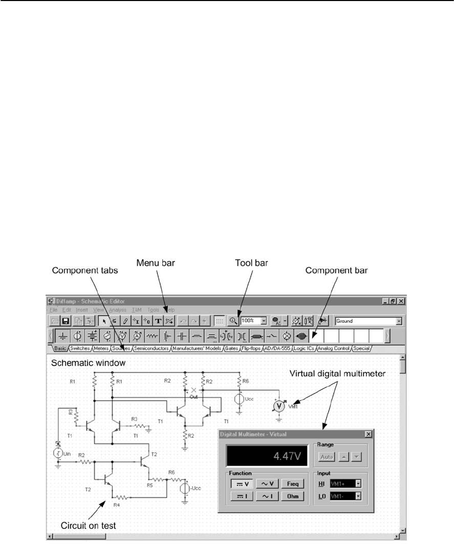
17
Circuit simulation
Computer simulation provides you with a powerful
and cost-effective tool for designing, simulating,
and analysing a wide variety of electronic circuits.
In recent years, the computer software packages
designed for this task have not only become
increasingly sophisticated but also have become
increasingly easy to use. Furthermore, several of
the most powerful and popular packages are now
available at low cost either in evaluation, ‘lite’ or
student versions. In addition, there are several
excellent freeware and shareware packages (see
Appendix 7).
Whereas early electronic simulation software
required that circuits were entered using a complex
netlist that described all of the components and
connections present in a circuit, most modern
packages use an on-screen graphical representation
of the circuit on test. This, in turn, generates a
netlist (or its equivalent) for submission to the
computational engine that actually performs the
circuit analysis using mathematical models and
algorithms.In order to describe the characteristics
and behaviour of components such as diodes and
transistors, manufacturers often provide models in
the form of a standard list of parameters.
Most programs that simulate electronic circuits
use a set of algorithms that describe the behaviour
of electronic components. The most commonly
used algorithm was developed at the Berkeley
Institute in the United States and it is known as
Figure 17.1 Using Tina Pro to construct and test a circuit prior to detailed analysis
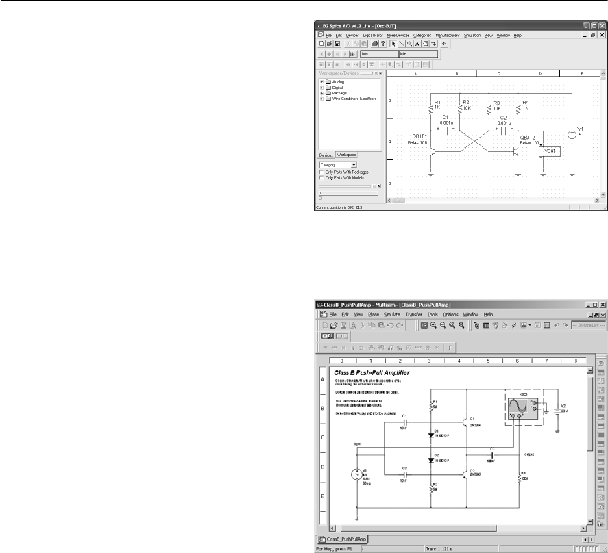
304 ELECTRONIC CIRCUITS: FUNDAMENTALS AND APPLICATIONS
SPICE (Simulation Program with Integrated
Circuit Emphasis).
Results of circuit analysis can be displayed in
various ways, including displays that simulate those
of real test instruments (these are sometimes
referred to as virtual instruments). A further
benefit of using electronic circuit simulation
software is that, when a circuit design has been
finalized, it is usually possible to export a file from
the design/simulation software to a PCB layout
package. It may also be possible to export files for
use in screen printing or CNC drilling. This greatly
reduces the time that it takes to produce a finished
electronic circuit.
Types of analysis
Various types of analysis are available within
modern SPICE-based circuit simulation packages
(see Appendix 7). These usually include:
DC analysis
DC analysis determines the DC operating point of
the circuit under investigation. In this mode any
wound components (e.g. inductors and
transformers) are short-circuited and any capacitors
that may be present are left open-circuit. In order to
determine the initial conditions, a DC analysis is
usually automatically performed prior to a transient
analysis. It is also usually performed prior to an AC
small-signal analysis in order to obtain the
linearized, small-signal models for non-linear
devices. Furthermore, if specified, the DC small-
signal value of a transfer function (ratio of output
variable to input source), input resistance, and
output resistance is also computed as a part of the
DC solution. The DC analysis can also be used to
generate DC transfer curves in which a specified
independent voltage or current source is stepped
over a user-specified range and the DC output
variables are stored for each sequential source
value.
AC small-signal analysis
The AC small-signal analysis feature of SPICE
software computes the AC output variables as a
function of frequency. The program first computes
the DC operating point of the circuit and
determines linearized, small-signal models for all
of the non-linear devices in the circuit (e.g. diodes
and transistors). The resultant linear circuit is then
analysed over a user-specified range of frequencies.
The desired output of an AC small-signal analysis
is usually a transfer function (voltage gain,
transimpedance, etc.). If the circuit has only one
AC input, it is convenient to set that input to unity
and zero phase, so that output variables have the
same value as the transfer function of the output
variable with respect to the input.
Figure 17.2 An astable multivibrator circuit being
simulated using B2 Spice
Figure 17.3 A Class B push-pull amplifier circuit
being simulated by Multisim
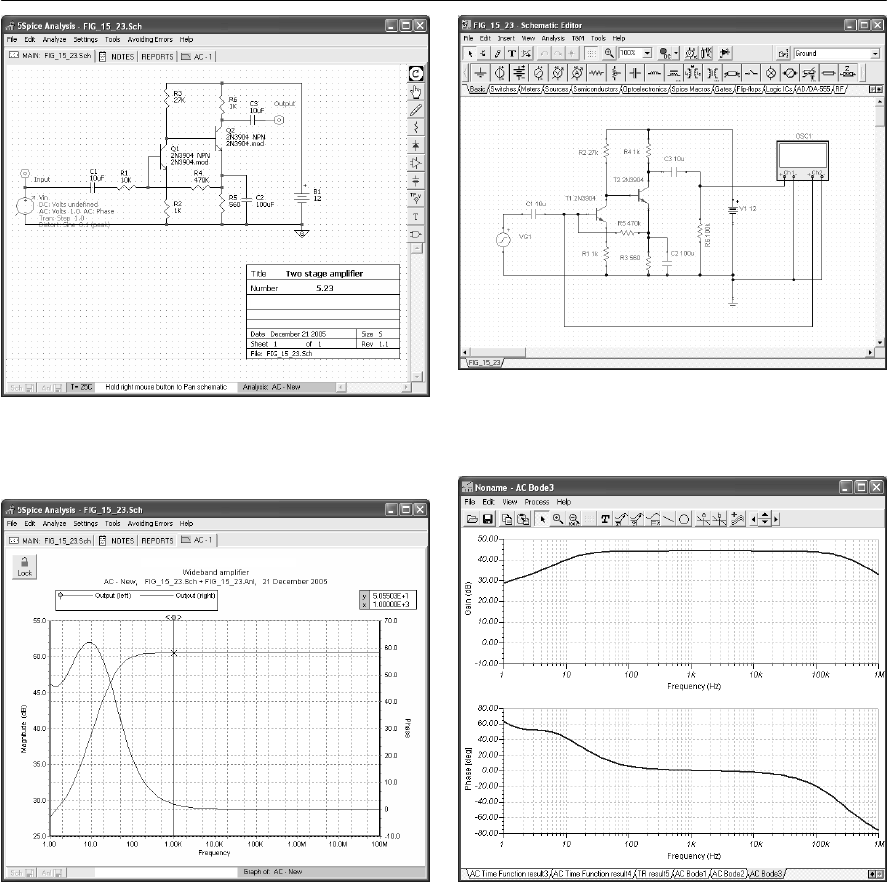
CIRCUIT SIMULATION 305
Transient analysis
The transient analysis feature of a SPICE package
computes the transient output variables as a
function of time over a user-specified time interval.
The initial conditions are automatically determined
by a DC analysis. All sources that are not time
dependent (for example, power supplies) are set to
their DC value.
Pole-zero analysis
The pole-zero analysis facility computes the poles
and/or zeros in the small-signal AC transfer
function. The program first computes the DC
operating point and then determines the linearized,
small-signal models for all the non-linear devices in
the circuit. This circuit is then used to find the
poles and zeros of the transfer function.
Figure 17.5 Gain and phase plotted as a result of
small-signal AC analysis of the circuit in Fig. 17.4
Figure 17.4 High-gain amplifier (Fig. 15.23)
being analysed using the 5Spice Analysis package
Figure 17.6 High-gain amplifier (Fig. 15.23)
being analysed using the Tina Pro package
Figure 17.7 Gain and phase plotted as a result of
small-signal AC analysis of the circuit in Fig. 17.6
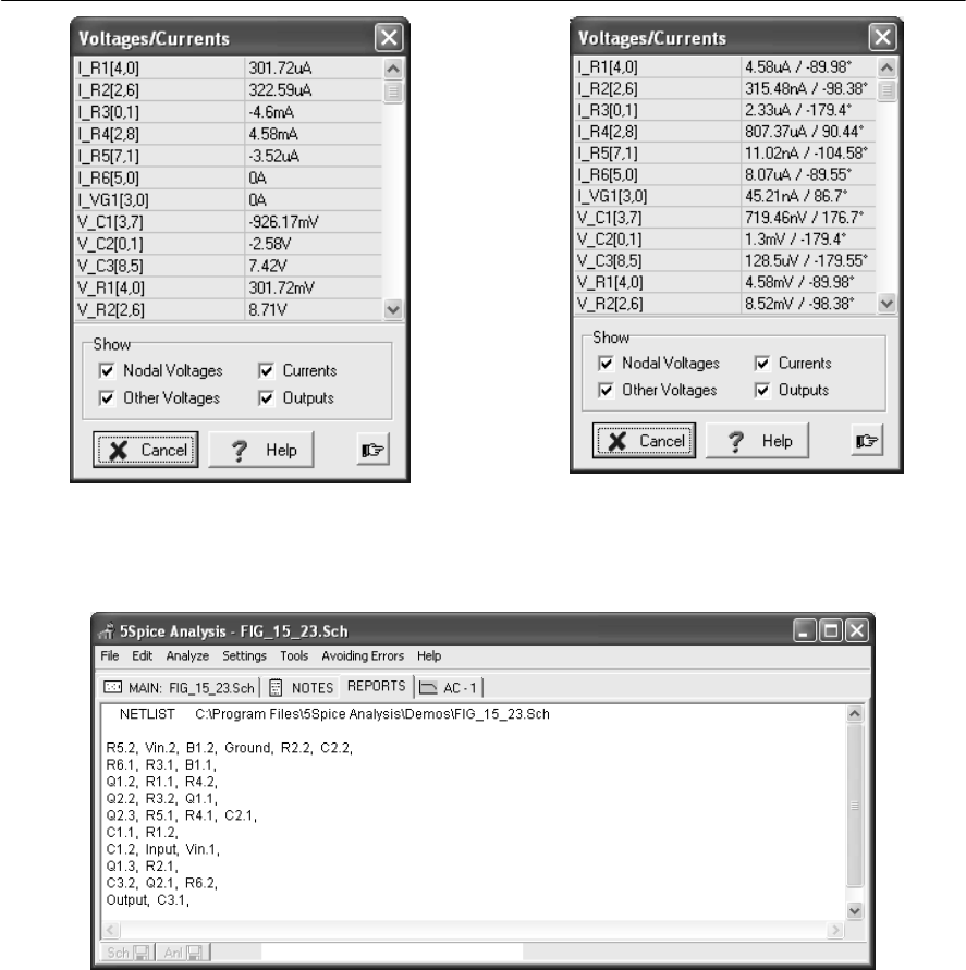
306 ELECTRONIC CIRCUITS: FUNDAMENTALS AND APPLICATIONS
Two types of transfer functions are usually
supported. One of these determines the voltage
transfer function (i.e. output voltage divided by
input voltage) and the other usually computes the
output transimpedance (i.e. output voltage divided
by input current) or transconductance (i.e. output
current divided by input voltage). These two
transfer functions cover all the cases and one can
make it possible to determine the poles/zeros of
functions like impedance ratio (i.e. input
impedance divided by output impedance) and
voltage gain. The input and output ports are
specified as two pairs of nodes. Note that, for
complex circuits it can take some time to carry out
this analysis and the analysis may fail if there is an
excessive number of poles or zeros.
Figure 17.9 Computer generated netlist for the circuit shown in Fig. 17.4.
Figure 17.8 Results of DC analysis of the circuit
shown in Fig. 17.6
Figure 17.10 Results of AC analysis of the circuit
shown in Fig. 17.6
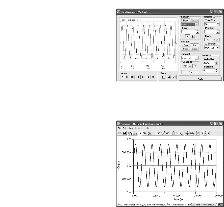
CIRCUIT SIMULATION 307
Small-signal distortion analysis
The distortion analysis facility provided by SPICE-
driven software packages computes steady-state
harmonic and inter-modulation products for small
input signal magnitudes. If signals of a single
frequency are specified as the input to the circuit,
the complex values of the second and third
harmonics are determined at every point in the
circuit. If there are signals of two frequencies input
to the circuit, the analysis finds out the complex
values of the circuit variables at the sum and
difference of the input frequencies, and at the
difference of the smaller frequency from the second
harmonic of the larger frequency.
Sensitivity analysis
Sensitivity analysis allows you to determine either
the DC operating-point sensitivity or the AC small-
signal sensitivity of an output variable with respect
to all circuit variables, including model
parameters. The software calculates the difference
in an output variable (either a node voltage or a
branch current) by perturbing each parameter of
each device independently. Since the method is a
numerical approximation, the results may
demonstrate second order affects in highly sensitive
parameters, or may fail to show very low but non-
zero sensitivity. Further, since each variable is
perturbed by a small fraction of its value, zero-
valued parameters are not analysed (this has the
benefit of reducing what is usually a very large
amount of data).
Noise analysis
The noise analysis feature determines the amount
of noise generated by the components and devices
(e.g. transistors) present in the circuit that is being
analysed. When provided with an input source and
an output port, the analysis calculates the noise
contributions of each device (and each noise
generator within the device) to the output port
voltage. It also calculates the input noise to the
circuit, equivalent to the output noise referred to the
specified input source. This is done for every
frequency point in a specified range. After
calculating the spectral densities, noise analysis
integrates these values over the specified frequency
range to arrive at the total noise voltage/current
(over this frequency range).
Thermal analysis
Many SPICE packages will allow you to determine
the effects of temperature on the performance of a
circuit. Most analyses are performed at normal
ambient temperatures (e.g. 27°C) but it can be
advantageous to look at the effects of reduced or
increased temperatures, particularly where the
circuit is to be used in an environment in which
there is a considerable variation in temperature.
Figure 17.11 Using the virtual oscilloscope in
Tina Pro to display the output voltage waveform
for the circuit shown in Fig. 17.6
Figure 17.12 Alternative waveform plotting
facility provided in Tina Pro
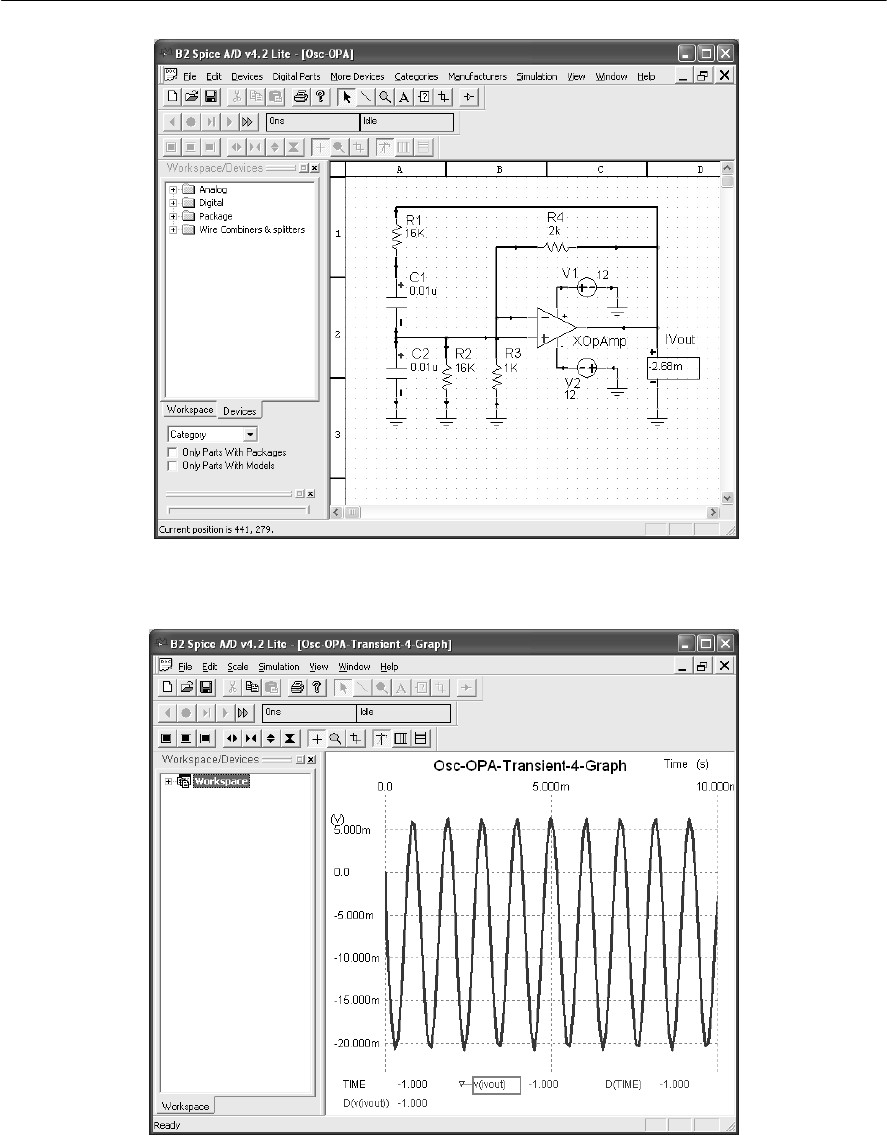
308 ELECTRONIC CIRCUITS: FUNDAMENTALS AND APPLICATIONS
Figure 17.13 Analysis of a Wien Bridge oscillator using B2 Spice.
Figure 17.14 Transient analysis of the circuit in Fig. 17.13 produced the output waveform plot
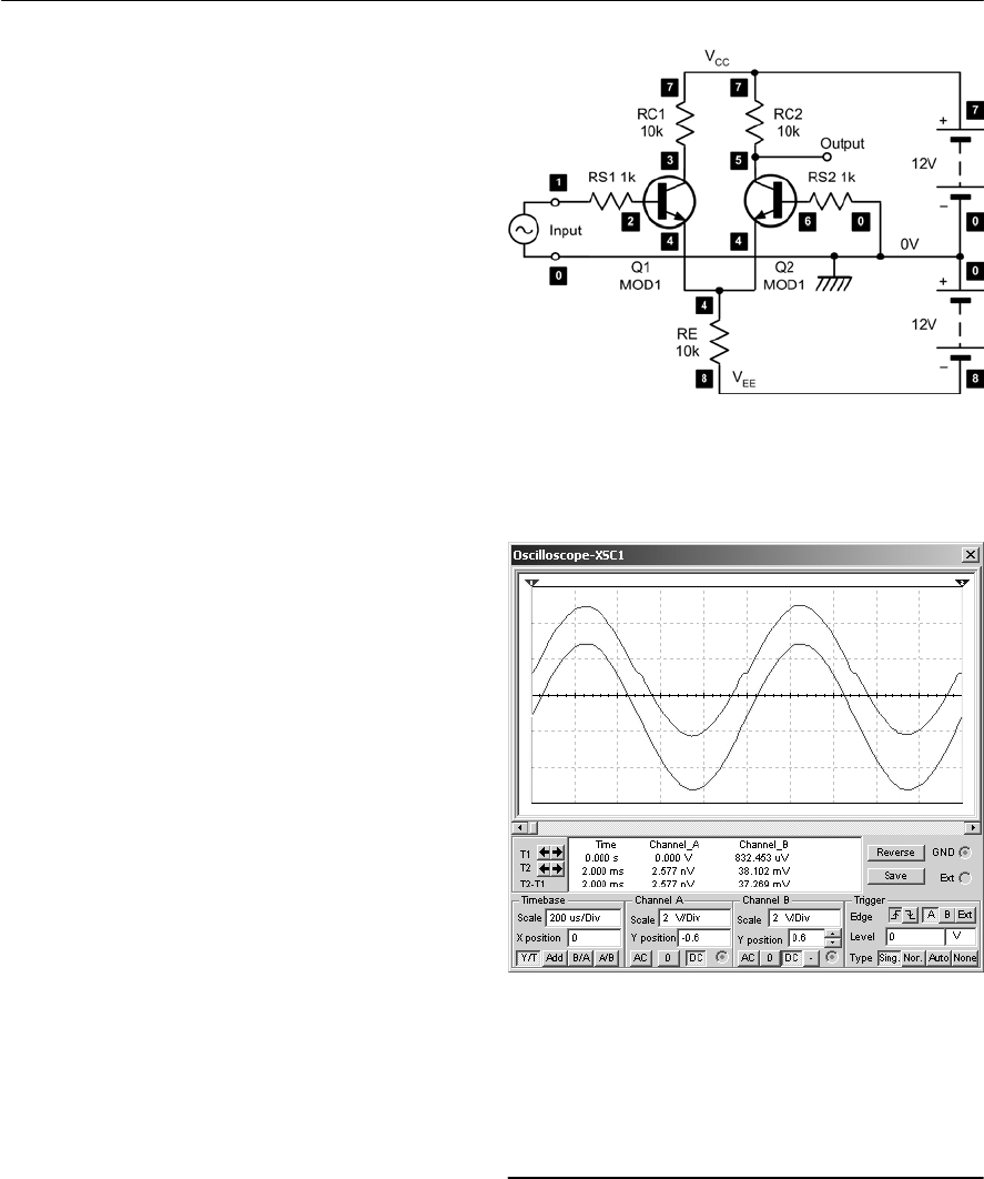
CIRCUIT SIMULATION 309
Netlists and component models
The following is an example of how a netlist for a
simple differential amplifier is constructed (note
that the line numbers have been included solely for
explanatory purposes):
1. SIMPLE DIFFERENTIAL PAIR
2. VCC 7 0 12
3. VEE 8 0 -12
4. VIN 1 0 AC 1
5. RS1 1 2 1K
6. RS2 6 0 1K
7. Q1 3 2 4 MOD1
8. Q2 5 6 4 MOD1
9. RC1 7 3 10K
10. RC2 7 5 10K
11. RE 4 8 10K
12. MODEL MOD1 NPN BF=50 VAF=50
IS=1.E-12 RB=100 CJC=.5PF TF=.6NS
13. .TF V(5) VIN
14. .AC DEC 10 1 100MEG
15. .END
Lines 2 and 3 define the supply voltages. VCC is
+12 V and is connected between node 7 and node 0
(signal ground). VEE is H12 V and is connected
between node 8 and node 0 (signal ground). Line 4
defines the input voltage which is connected
between node 1 and node 0 (ground) whilst lines 5
and 6 define 1 kIresistors (RS1 and RS2)
connected between 1 and 2, and 6 and 0.
Lines 7 and 8 are used to define the connections
of two transistors (Q1 and Q2). The characteristics
of these transistors (both identical) are defined by
MOD1 (see line 12). Lines 9, 10 and 11 define the
connections of three further resistors (RC1, RC2
and RE respectively). Line 12 defines the transistor
model. The device is NPN and has a current gain of
50. The corresponding circuit is shown in Fig.
17.15.
Most semiconductor manufacturers provide
detailed SPICE models for the devices that they
produce. The following is a manufacturer’s SPICE
model for a 2N3904 transistor (see Appendix 8):
NPN (Is=6.734f Xti=3 Eg=1.11 Vaf=74.03
Bf=416.4 Ne=1.259 Ise=6.734 Ikf=66.78m
Xtb=1.5 Br=.7371 Nc=2Isc=0 Ikr=0 Rc=1
Cjc=3.638p Mjc=.3085 Vjc=.75 Fc=.5 Cje=4.493p
Mje=.2593 Vje=.75 Tr=239.5n Tf=301.2pItf=.4
Vtf=4 Xtf=2 Rb=10)
Figure 17.16 Cross-over distortion evident in the
output waveform from the Class B amplifier shown
in Fig. 17.3
Figure 17.15 Differential amplifier with the nodes
marked for generating a netlist
Logic simulation
As well as an ability to carry out small-signal a.c.
and transient analysis of linear circuits (see Fig.
17.3 and 17.16), modern SPICE software packages
usually incorporate facilities that can be used to
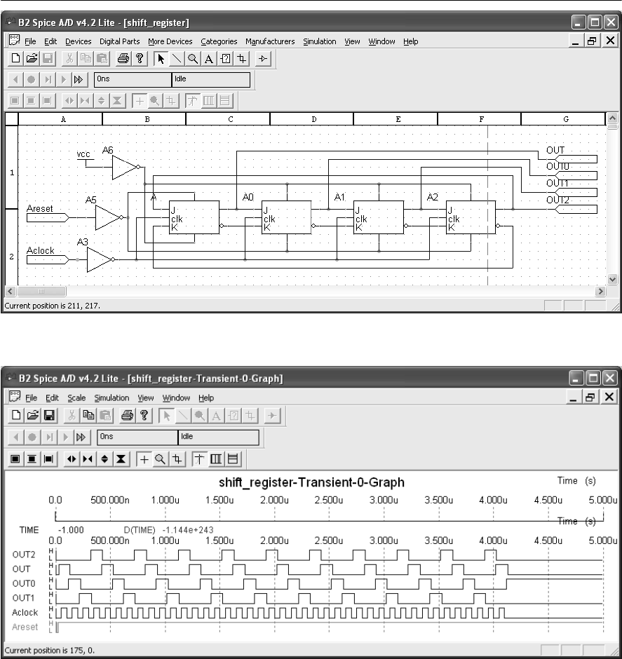
310 ELECTRONIC CIRCUITS: FUNDAMENTALS AND APPLICATIONS
analyse logic and also ‘mixed-mode’ (i.e. analogue
and digital) circuits. Several examples of digital
logic analysis are shown in Figs 17.17, 17.18 and
17.19.
Figure 17.17 shows a four-stage shift register
based on J-K bistables. The result of carrying out
an analysis of this circuit is shown in Fig. 17.18.
Finally, Fig. 17.19 shows how a simple
combinational logic circuit can be rapidly
‘assembled’ and tested and its logical function
checked. This circuit arrangement provides a
solution to Question 10.20 on page 198 and it
shows how the exclusive-OR function can be
realized using only two-input NAND gates.
Figure 17.17 Four-stage circulating shift register simulated using B2 Spice
Figure 17.18 Waveforms for the our stage circulating shift register in Fig. 17.17
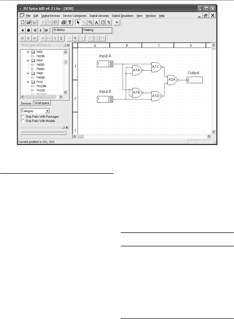
Practical investigation
Objective
To investigate the use of SPICE software to analyse
aDC coupled power amplifier circuit.
Components and test equipment
PC with SPICE software (e.g. Tina Pro, Multisim,
or B2 Spice, see Appendix 9).
Procedure
Construct the circuit shown in Fig. 17.20 using the
screen drawing facilities provided by the SPICE
program. Carry out a DC analysis of the circuit and
record the voltages in Table 17.1. Check that these
are what you would expect.
Use the data from the DC analysis to determine:
(a) the quiescent (no-signal) collector current in
T7 and T8
(b) the output offset voltage (i.e. the output
voltage when the input voltage is zero).
CIRCUIT SIMULATION 311
Figure 17.19 Using B2 Spice to check the function of a simple combinational logic circuit
Transistor Collector Base Emitter
T1
T2
T3
T4
T5
T6
T7
T8
Table 17.1 Table of results
Carry out an AC analysis of the amplifier and
determine the voltage gain of the circuit (this
should be the same as the ratio of R12 to R2).
Check that the voltage gain is what you would have
expected. Also determine the maximum input
voltage before the output voltage becomes clipped.
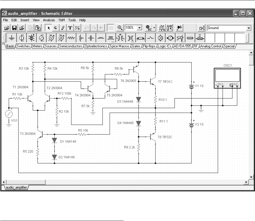
Problems
17.1 In relation to SPICE software explain the
meaning of the following terms:
(a) node
(b) netlist
(c) algorithm
(d) model
(e) mixed-mode.
17.2 Explain why it is usually necessary to carry
out a DC analysis before an AC analysis is
performed.
17.3 Explain the purpose of transient analysis
using SPICE software. How are the results
of this analysis usually displayed?
17.4 Define the terms transimpedance and
transconductance in relation to SPICE
software.
312 ELECTRONIC CIRCUITS: FUNDAMENTALS AND APPLICATIONS
Figure 17.20 DC coupled power amplifier circuit used in the Practical Investigation (Tina Pro)
17.5 The netlist used in a SPICE analysis
program is as follows:
CE AMPLIFIER
VCC 5 0 -5
VIN 1 0 AC 1
R1 1 2 10K
R2 3 5 1K
R3 2 3 1M
Q1 3 2 0 MOD1
MODEL MOD1 PNP BF=75 VAF=50
IS=1.E-12 RB=100 CJC=.5PF TF=.6NS
.TF V(5) VIN
.AC DEC 10 1 10MEG
.END
Sketch the corresponding circuit diagram
and label the nodes.

18
The PIC microcontroller
Earlier in Chapter 11 we introduced the PIC
microcontroller as a device that is normally used in
stand-alone (or embedded)applications to perform
simple logic, timing and input/output control. In
recent years such devices have become increasingly
sophisticated in terms of both the variety of I/O
peripheral facilities provided and the ability to
connect to other devices in bus and networked
configurations. This latter feature makes it possible
to have several microcontrollers working together,
exchanging data and control information, in
distributed systems that can be of virtually any
size.
PIC architecture
PIC microcontrollers first became popular in the
mid-1990s. Since then the range of devices
available has increased dramatically. Nowadays a
PIC device exists for almost any embedded
application, from small 6-pin devices ideal for
simple control applications, through to powerful
high-speed devices packed with I/O features and
large amounts of memory.
PIC are based on RISC (Reduced Instruction Set
Computer) architecture and, as a consequence, they
use a relatively small number of instructions. In
fact, some PIC chips have as few as 33 instructions
compared with some general-purpose
microprocessors (such as the Z80) that may have
several hundred. Because it is only necessary to
remember a relatively small number of commands,
it is relatively easy to learn to program a PIC using
its own assembly language (note, however, that it
may take several instructions to achieve on a PIC
what can be done in a single instruction using a
fully-fledged microprocessor). And, if you don’t
like the idea of having to learn assembly code
programming you can can make use of C, BASIC
or Flowcode (a language based almost entirely on
flowcharts).
Another feature of PIC devices is that they use
Harvard architecture.This means that they
contain completely separate memory and buses for
program instructions and data memory. Program
memory can be ROM, EPROM or Flash, whereas
data memory must be read/write memory
(commonly known as RAM).
Mainstream microprocessors (like the Z80 that
we met in Chapter 11) are categorized in terms of
the number of data bits that they can manipulate
(i.e. the ‘width’ of the data bus). They can be 8-bit,
16-bit, 32-bit and 64-bit and 128-bit devices. PIC
microcontrollers, by contrast, are all based on an 8-
bit data bus and, because of this, they can only
operate on 8-bits of data at a time (despite this, you
will sometimes encounter instructions that
reference more data bits, i.e. 12-bits, 14-bits and
16-bits). Furthermore, although the data memory is
8-bits wide for all PIC microcontrollers, the
program memory varies from 12-bits to 16-bits.
PIC families
In the early 1990s, PIC microcontrollers were
grouped in three families, often referred to as
‘Base-Line’, ‘Mid-Range’, and ‘High-End’. Many
of these devices are incompatible with the latest
development platforms and software tools. Despite
this, it is usually possible to locate a modern device
that is compatible with (and will generally out-
perform) one of these early devices.
The base-line family comprised just four devices,
which all featured 12-bit instructions. The
PIC16C54 and PIC16C56 were both 18-pin devices
having 12 digital I/O lines. The PIC16C54 had 512
×12-bit words of EPROM program memory,
whilst the PIC16C56 had 1K × 12-bit words. Both
of these devices had just 32 bytes of RAM data
memory (ample for most simple control
applications). The larger PIC16C55 and PIC16C57
28-pin devices had 20 digital I/O lines. The
PIC16C55 had 512 × 12-bit words of EPROM
program memory and 32 bytes of RAM data

314 ELECTRONIC CIRCUITS: FUNDAMENTALS AND APPLICATIONS
memory, whilst the PIC16C57 had 2K × 12-bit
words of EPROM program memory and 80 bytes
of RAM data memory. All of these devices also
featured an 8-bit real-time clock/counter and a
watchdog timer.
The mid-range family of PIC devices contained a
number of devices that expanded on the capabilities
of the base-line devices. Of particular note are the
PIC16C71, which added A/D inputs capable of
reading analogue signals, and the popular
PIC16C84, which featured EEPROM program and
data memory. Because of the fact that the
PIC16C84 could be erased electronically (without
the need for the ultraviolet eraser required for
EPROM erasure), it soon became a favourite with
hobbyists and must have been the most popular PIC
for many years.
The high-end device was the PIC17C42. This
device came in a 40-pin package and featured 16-
bit wide instructions. It also allowed for external
memory to be interfaced and supported up to 64K ×
6-bit of addressable program memory space. The
device provided 33 digital I/O pins, EEPROM data
memory, a serial port (USART), three 16-bit
timer/counters and two high-speed pulse width
modulation (PWM) outputs.
There are now more than 200 different PIC chips
available and the ‘Base-Line’, ‘Mid-Range’ and
‘High-End’ classification has now been replaced by
several different ranges of PIC families such as the
PIC-10, PIC-12, PIC-16 and PIC-18. Generally
speaking, the higher the family number, the more
powerful the device in terms of processing
capabilities, memory sizes and I/O features.
Another feature of many of the devices is Flash
program memory.These devices can be erased
and reprogrammed electrically, as with the
previously popular PIC16C84. These Flash
memory devices are signified by a letter ‘F’ in their
part number (e.g. PIC16F877A). Note that Flash
devices are much easier to work with for one-off
prototyping because erasure and reprogramming is
greatly simplified.
Choosing a PIC device
When choosing a PIC device for a particular
project it is important to select a device that is well
supported, both in terms of being a member of one
of the current PIC families but also in terms of the
PIC family Characteristics
PIC10F The PIC10F range features just a few
6/8-pin microcontrollers. These chips
are supplied in DIP packages.
PIC12F The PIC12F devices include the
PIC12F629, PIC12F675 and
PIC12F683. They are all 8-pin devices
featuring six digital I/O lines and differ
in the amount of program and data
memory that they provide. The
PIC12F683 also provides analogue
inputs.
PIC16F The PIC16F family is very large and
includes devices in 14-, 18-, 28- and
40-pin packages. The chips vary in
terms of the amount of memory they
provide and also in their I/O features.
Some devices worth noting include the
PIC16F630, PIC16F676, PIC16F684
and PIC16F688, which are 14-pin
equivalents to the PIC12F devices
mentioned above, the PIC16F84A,
which is the most current equivalent to
the popular PIC16C84, and the
PIC16F877A, which is a powerful 40-
pin device that has become extremely
popular. The PIC16F877A features
8192 × 14-bit Flash program memory,
368 bytes of RAM data memory, 256
bytes of EEPROM data memory, 33
digital I/O lines, eight 10-bit A/D
channels, three counter/timers and a
serial port (USART).
PIC18F The PIC18F devices form the new
high-end range. One feature that they
all share is that their instruction set is
optimized for C compilers. Many
feature large amounts of memory and
special I/O features including Universal
Serial Bus (USB) and Controller Area
Network (CAN) interfaces. One
interesting device is the 40-pin
PIC18F452, which is similar in many
respects and pin-compatible with the
PIC16F877A. It is also worth noting
that some PIC18F devices are supplied
in 80-pin packages and provide more
than 70 digital I/O lines. However,
these are in surface-mount packages
and so are difficult to experiment with!
Table 18.1 Some popular PIC families
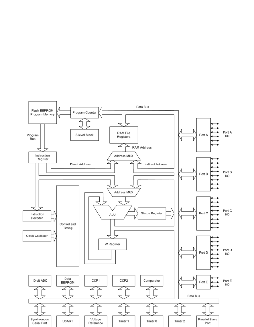
THE PIC MICROCONTROLLER 315
Figure 18.1 Simplified architecture of a 16F877A PIC microcontroller
programming and environment that you intend to
use for software development. It is also important
to ensure that the device incorporates all of the
peripheral I/O facilities that you will need. Such
facilities might include:
•Bus and communication interfaces (such as
RS232/RS485, I2C, CAN, LIN, USB, TCP/IP)
•Display peripheral interfaces (such as LED or
LCD drivers)
•Capture/compare facilities
•Pulse Width Modulators (PWMs)
•Counters/timers
•Watchdog facilities
•Analogue-to-digital (A/D) converters
•Analogue comparators and operational
amplifiers
•Brown-out detectors
•Low-voltage detectors
•Temperature sensors
•Oscillators
•Voltage references
•Digital-to-analogue (D/A) converters
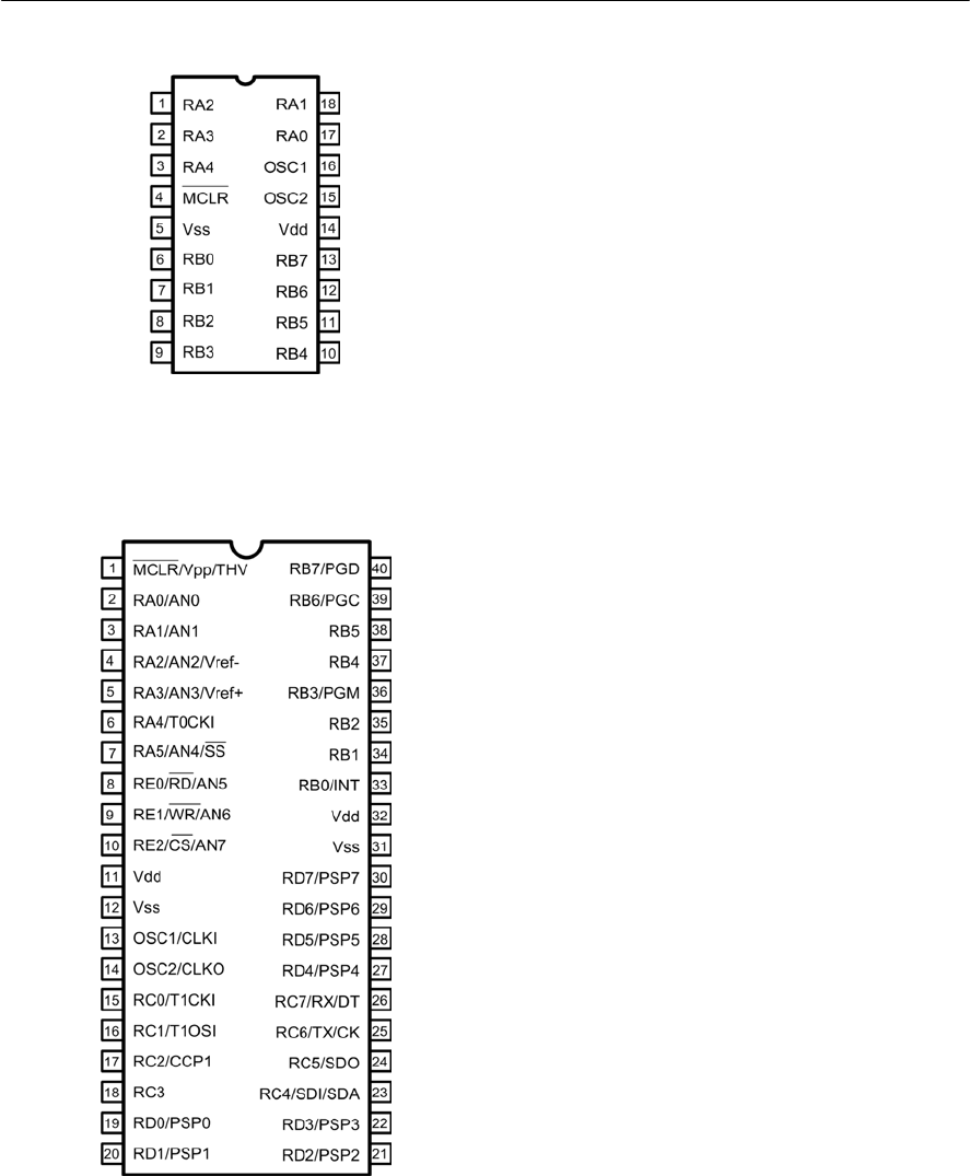
316 ELECTRONIC CIRCUITS: FUNDAMENTALS AND APPLICATIONS
Figure 18.2 Pin connections for the PIC16C84
and PIC16F84 devices
Features of the PIC16F84
The PIC16F84 is an excellent choice for most
simple microcontroller projects. This device is used
in many current PIC designs and it has the
following features:
•35 single-word instructions (see Table 18.3)
•1k × 14-bit EEPROM (Flash) program memory
•68 × 8-bit general purpose SRAM registers
•15 × 8-bit special function hardware registers
•64 × 8-bit EEPROM data memory
•1,000,000 data memory erase/write cycles
(typical)
•Data retention > 40 years
•5data input/output pins, Port A
•8data input/output pins, Port B
•25 mA current sink max. per pin
•20 mA current source per pin
•8-bit timer/counter with prescaler
•Power-on reset (POR)
•Power-up timer (PWRT)
•Oscillator start-up timer (OST)
•Watchdog timer (WDT) with own on-chip RC
oscillator
•Power saving ‘sleep’ function
•Serial in-system programming
•Selectable oscillator options:
RC: low cost RC oscillator
XT: standard crystal resonator (100 kHz to
4 MHz)
HS: high-speed crystal/resonator (4 MHz to
10 MHz - PIC16F84-10 only)
LP: power-saving low-frequency crystal
(32 kHz to 200 kHz)
•Interrupts:
External, RB0/INT pin
TMR0 timer overflow
Port B RB4 to RB7 interrupt on change
Data EEPROM write complete
•Operating voltage range: 2.0 V to 6.0 V
•Power consumption: < 2 mA at 5 V, 4 MHz
•60 µA typical at 2 V, 32 kHz
•< 1 µA typical standby at 2 V (PIC16F84)
Figure 18.2 shows the pin connections for the
PIC16F84 whilst Fig. 18.4 shows how the device
can be used in a simple control application that uses
four switched inputs (S1 to S4) and three relay
outputs (RL1 to RL3).
Figure 18.3 Pin connections for the PIC16F877
device
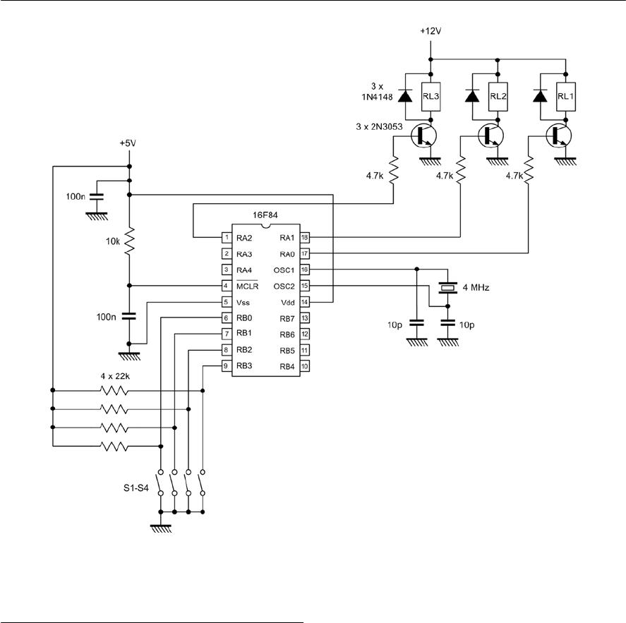
THE PIC MICROCONTROLLER 317
Figure 18.4 Asimple microcontroller application based on the PIC16F84 device which four switch inputs
(S1-S4) to control three relays (RL1-RL3). The program is automatically reset at power-up.
Features of the PIC16F877
The PIC16F877 is used for many current PIC
designs. This chip has the following features:
•35 single-word instructions (see Table 18.3)
•8k x 14-bit EEPROM (Flash)
•368 bytes of general purpose SRAM registers
•256 x 8-bit EEPROM data memory
•1,000,000 data memory erase/write cycles
(typical)
•Data retention >40 years
•6data input/output pins, Port A
•8data input/output pins, Port B
•8data input/output pins, Port C
•8data input/output pins, Port D
•3data input/output pins, Port E
•Two 8-bit and one 16-bit timers
•Two capture and compare PWM modules
•Universal synchronous/asynchronous receiver
transmitter (USART)
•Synchronous serial port (SSP)
•Parallel slave port (PSP)
•Brown-out detection and reset facility
•10-bit, 8-channel ADC
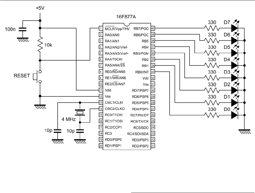
318 ELECTRONIC CIRCUITS: FUNDAMENTALS AND APPLICATIONS
•Two analogue comparators with programmable
on-chip voltage reference, programmable input
multiplexing, and externally accessible
comparator output.
•25mA current sink max. per pin
•20mA current source per pin
•8-bit timer/counter with prescaler
•Power-on reset (POR)
•Power-up timer (PWRT)
•Oscillator start-up timer (OST)
•Watchdog timer (WDT) with own on-chip RC
oscillator
•Power saving ‘sleep’ function
•In-circuit serial programming (via two pins)
•Single supply 5V in-circuit serial programming
•Selectable oscillator options
•Self-programmable under software control
•15 interrupts
•Operating frequency: DC to 20 MHz
•Supply voltage range: 2.0 V to 5.5 V
•Low power consumption.
PIC programming
PIC programming can be carried out using
assembly language, C (see Table 18.2), BASIC,
and Flowcode (see page 324) or a mixture of these
languages. Software and a programmer (see Figs
18.6 and 18.7) will be required to do this. The two
most commonly used methods of programming a
PIC chip are shown in Fig. 18.8. In Fig. 18.8(a) a
dedicated PIC programmer is used whilst in Fig.
18.8(b) the PIC is programmed whilst resident in
the target system. In either case, the programming
software and source code is resident on a PC and
downloaded as hex code into the PIC. The process
of generating the source code, compiling and/or
assembling it into hex, code (see Fig. 18.10) is
invariably performed by software known as an
Integrated Development Environment (IDE), as
shown in Fig. 18.9. Software is also available that
can be used to simulate a PIC (see Figs 18.11 to
18.13) and full development systems are also
available (see Figs 18.14 and 18.15).
Figure 18.5 Asimple microcontroller application based on the 16F877A device. This application uses
eight LED outputs (D0 to D7). Note that the circuit must be manually reset at power-up.

Table 18.2 Switch and LED PIC test routine in C
THE PIC MICROCONTROLLER 319
//Defines for the PIC microcontroller
char PORTC@0x07;
char TRISC@0x87;
char PORTD@0x08;
char TRISD@0x88;
char PORTE@0x09;
char TRISE@0x89;
//PIC Functions
#pragma CLOCK_FREQ 4000000
#define P16F877A
#include <system.h>
#define MX_EE
#define MX_EE_TYPE2
const char MX_EE_SIZE = 256;
#define MX_SPI
#define MX_SPI_C
#define MX_SPI_SDI 4
#define MX_SPI_SDO 5
#define MX_SPI_SCK 3
#define MX_UART
#define MX_UART_C
#define MX_UART_TX 6
#define MX_UART_RX 7
//Macro function declarations
//Variable declarations
char FCV_SWITCHSTATE;
//Macro implementations
void main()
{
//PIC Initialisation
adcon1 = 0x07;
//Interrupt initialisation code
option_reg = 0xC0;
while(1)
{
TRISA = TRISA | 0xff;
FCV_SWITCHSTATE = PORTA;
TRISB = 0x00;
PORTB = FCV_SWITCHSTATE;
if (( FCV_SWITCHSTATE ) == 0)
break;
}
mainendloop: goto mainendloop;
}
Figure 18.7 E-blocks PIC microcontroller/
microprogrammer. This versatile device connects
to a PC via USB and can be used to program most
8-, 14-, 28- and 40-pin PIC chips. The board has
five I/O ports for connection to a wide variety of
external peripheral modules
Figure 18.6 The E-blocks low-cost PIC
microcontroller ‘lite’ programmer. This device is
suitable for programming 18-pin PIC chips and it
connects to a PC via a USB port. The board has
two I/O ports for connecting to a wide variety of
external peripheral modules.

320 ELECTRONIC CIRCUITS: FUNDAMENTALS AND APPLICATIONS
Figure 18.8 Two methods of programming a PIC device
Figure 18.9 The MPLAB Integrated Development Environment (IDE)
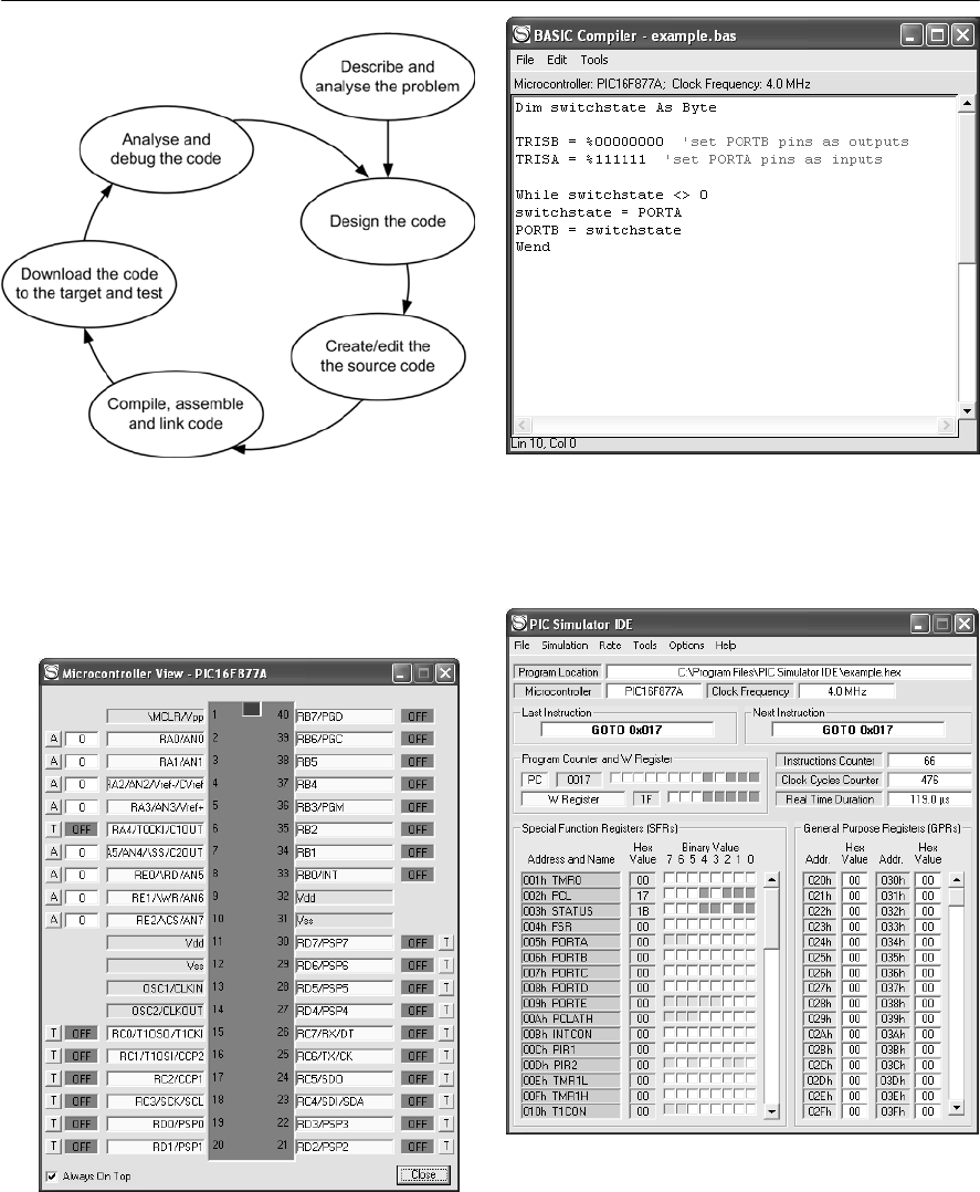
THE PIC MICROCONTROLLER 321
Figure 18.11 The Oshonsoft PIC Simulator
showing the Microcontroller View window in
which the current state of each pin is displayed
Figure 18.10 The PIC software development
cycle
Figure 18.12 The switch and LED test program
using the Oshonsoft PIC Simulator
Figure 18.13 The main Oshonsoft PIC Simulator
screen showing the state of the Special Function
Registers (SFRs) and General Purpose Registers
(GPRs). Note also the contents of the Program
Counter and W Register.

Table 18.3 PIC16C/F84 instruction set
322 ELECTRONIC CIRCUITS: FUNDAMENTALS AND APPLICATIONS
Command Operation Syntax Status register bit(s) affected
ADDLW ADD Literal to W ADDLW K C, DC, Z
ADDWF ADD W to F ADDWF F,D C, DC, Z
ANDLW AND Literal and W ANDLW K Z
ANDWF AND W with F ANDWF F,D Z
BCF Bit Clear F BCF F,B None
BSF Bit Set F BSF F,B None
BTFSC Bit Test, Skip if Clear BTFSC F,B None
BTFSS Bit Test, Skip if Set BTFSC F,B None
CALL Subroutine Call CALL K None
CLRF Clear F CLRF F Z
CLRW Clear W register CLRW Z
CLRWDT Clear Watchdog Timer CLRWDT TO, PD
COMF Complement F COMF F,D Z
DECF Decrement F DECF F,D Z
DECFSZ Decrement F, Skip if 0 DECFSZ F,D None
GOTO Unconditional branch GOTO K None
INCF Increment F INCF F,D Z
INCFSZ Increment F, Skip if 0 INCFSZ F,D None
IORLW Inclusive OR Literal with W IORLW K Z
IORWF Inclusive OR W with F IORWF F,D Z
MOVF Move F MOVF F,D Z
MOVLW Move Literal to W MOVLW K None
MOVWF Move W to F MOVWF F None
NOP No Operation NOP None
RETFIE Return from Interrupt RETFIE None
RETLW Return with Literal in W RETLW K None
RETURN Return from Subroutine RETURN None
RLF Rotate Left through Carry RLF F,D C
RRF Rotate Right through Carry RRF F,D C
SLEEP Power-down SLEEP TO, PD
SUBLW Subtract W from Literal SUBLW K C, DC, Z
SUBLW Subtract W from F SUBWF F,D C, DC, Z
SWAPF Swap F SWAPF F,D None
XORLW Exclusive OR Literal with W XORLW K Z
XORWF Exclusive OR W with F XORWF F,D Z
Abbreviations
C Carry
b Bit address
C Carry
d Destination
DC Digit Carry
f Register File Address
k Literal or label
PD Power-down
TO Time-out
WWorking Register
Z Zero

THE PIC MICROCONTROLLER 323
Figure 18.14 The MicroElektronika EasyPIC3 PIC development system (see Appendix 9). This system
supports the PIC10F, 12F, 16F and 18F families and is connected to a PC via a USB port
Figure 18.15 The E-blocks system (see Appendix 9). The microcontroller system shown here uses a PIC
programmer (left), keypad (bottom), LCD display (top) and serial communications interface (right).
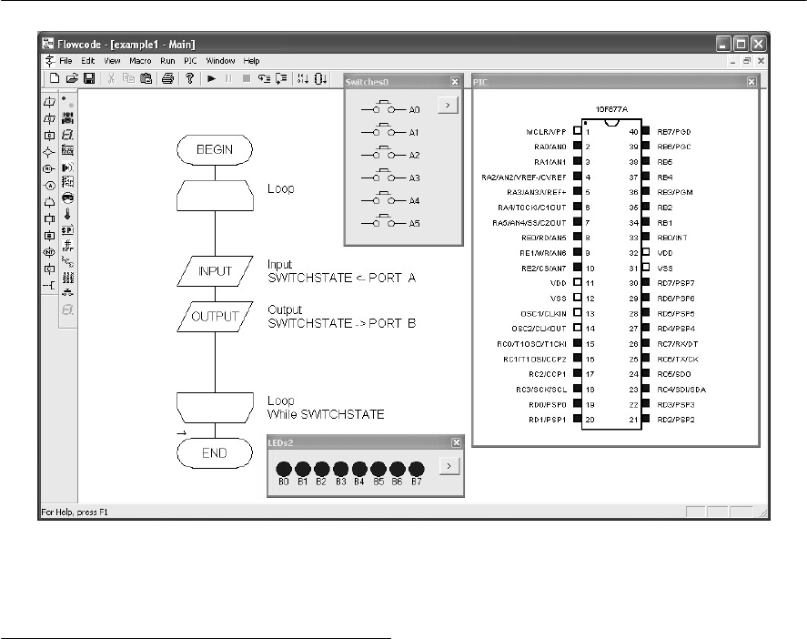
Figure 18.16 The switch and LED test program using Flowcode. Note how the flowchart symbols are sim-
ply dragged and dropped into the main program window from the toolbar on the left.
324 ELECTRONIC CIRCUITS: FUNDAMENTALS AND APPLICATIONS
Flowcode
Flowcode (see Appendix 7) is a novel
programming system that is designed to allow those
new to PIC programming to develop complete
applications with little or no knowledge of any
higher level languages. However it is possible to
embed code written in other languages into
Flowcode programs.
Programs written in C and Assembly code can be
easily embedded in Flowcode. This will allow you
to incorporate more complex and sophisticated
code in applications where this might become
necessary. Note however that the embedded code
cannot be checked or simulated by Flowcode but
instead it will be passed on to the C compiler when
the flowchart is compiled. It is therefore important
to verify that the C code entered is correct, as
syntax errors will cause the compilation of the
whole flowchart to fail.
To access Flowcode variables, macro functions
and connection points, it is necessary to colour the
variable in your C code with the prefixes FCV_,
FCM_ and FCC_MacroName_ respectively. For
example, to use a Flowcode variable called
DELAY in your C code, you must refer to it using
FCV_DELAY. Note that all Flowcode defined
variables must be entered in upper case.
To call a Flowcode macro called TEST in your C
code, you must call FCM_TEST();. To jump to a
connection point called A, defined in a Flowcode
macro called TEST, your C code must be goto
FCC_TEST_A;. Connection points defined in the
main flowchart of a Flowcode file are prefixed
FCC_Main_.
Assembly code (see Table 18.3) can be added
into the code field in a C assembly code wrapper.
For a single line of code you can use the asm
operator in front of each instruction (e.g. asm
movlw 5) or you can enclose several statements
within an asm block. This makes adding assembly
language routines very simple.

Practical investigation
Objective
To investigate the operation of a PIC16F877A
microcontroller using a simulator to run a simple
program.
Components and test equipment
Oshonsoft PIC Simulator or similar virtual
Integrated Development Environment (IDE). The
Oshonsoft IDE can be downloaded from
www.Oshonsoft.com.
System configuration and required operation
The program is to simulate the operation of a
PIC16F877A microcontroller and is to read an
analogue voltage present on the AN0 analog input
and display the 8-bit binary conversion result on
PORTB.
The analogue-to-digital converter (ADC) BASIC
source code used in the Practical investigation
(shown in Table 18.4) is available for downloading
from the companion website (see page 415).
Procedure
Start the PIC Simulator (see Fig. 18.17), click on
Options and then Select Microcontroller. Select the
THE PIC MICROCONTROLLER 325
‘PIC16F877’ from the list and click on the Select
button. Next click on File and Load Program.
Select the file named adc.hex (generated as a result
of compiling the BASIC source code shown in
Table 18.4) and click on Open. This will load the
program into the PIC’s program memory.
Click on Tools and Microcontroller View in
order to open the window shown in Fig. 18.18). If
necessary, reposition the windows on the screen so
that you can see both of them then Select the Rate
and Extremely Fast before clicking on Simulation
and Start. The simulation will start immediately.
To set an analogue input voltage, click on the
analogue (A) button associated with the RA0/AN0
pin then use the slider to change the analogue value
on this pin and click on Accept button to accept the
value. The state of the PORTB pins should
immediately reflect this value. Repeat with several
different analogue input values and at reduced
simulation speeds in order to examine the effect of
each program instruction.
Afurther program
If you have been able to sun the simple ADC
program successfully you might like to try your
hand at entering, compiling and running a program
that will loop continuously reading the state of the
switches on Port A and output the result to Port B
(see Figure 18.12).
Table 18.4 ADC program used in the Practical investigation
Symbol ad_action = ADCON0.GO_DONE 'set new name for A/D conversion start bit
Symbol display = PORTB 'set new name for PORTB used to display the conversion result
TRISB = %00000000 'set PORTB pins as outputs
TRISA = %111111 'set PORTA pins as inputs
ADCON0 = 0xc0 'set A/D conversion clock to internal source
ADCON1 = 0 'set PORTA pins as analog inputs
High ADCON0.ADON 'turn on A/D converter module
main:
Gosub getadresult 'go to conversion routine
display = ADRESH 'display the result of the conversion
Goto main 'repeat forever
End
getadresult: 'conversion routine
High ad_action 'start the conversion
While ad_action 'wait until conversion is completed
Wend
Return
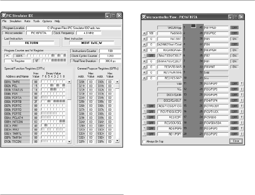
Problems
18.1 In relation to a PIC microcontroller, briefly
explain the meaning of the following terms:
(a) Flash memory
(b) Harvard architecture
(c) RISC
(d) Sleep function
(e) IDE.
18.2 Explain, with the aid of a diagram, how a
PIC can be programmed without having to
remove it from the target system
18.3 Sketch a diagram to show the five stages in
PIC software development cycle. Explain
why it is usually necessary to follow this
process several times before a fully
functional program is obtained.
18.4 Explain how the PIC application circuit
shown in Fig. 18.4 is automatically reset on
power-up (Hint: the MCLR input needs to
be taken low in order to reset the PIC).
18.5 Show how the PIC application shown in
326 ELECTRONIC CIRCUITS: FUNDAMENTALS AND APPLICATIONS
Figure 18.17 PIC Simulator IDE used in the
Practical investigation. This screen shows the state
of the PIC with the Program Counter at 0015.
Fig. 18.5 can be modified to support:
(a) automatic power-on reset.
(b) four switch inputs connected to Port D
(c) an analogue input connected to Port A.
18.6 List FOUR different types of peripheral I/O
device that can be incorporated in a PIC
microcontroller chip. Suggest a typical
application for each device.
18.7 The following fragment of source code
appears in a PIC BASIC program:
Dim inputstate As Byte
TRISA = %111111
TRISB = %00000000
While inputstate <> %111000
Wend
PORTB = %00000000
While inputstate <> %000111
Wend
PORTB = %11111111
Explain the function of the code by adding
appropriate comments to each line.
Answers to these problems appear on page 376.
Figure 18.18 Microcontroller View showing the
state of each of the PIC’s pins during program
execution

19
Circuit construction
This chapter deals with the techniques used to
produce a working circuit from an initial ‘paper
design’ to a working circuit ready for testing and
performance measurement. Various methods are
used for building electronic circuits. The method
that’s actually chosen for a particular application
depends on a number of factors, including the
available resources and the scale of production.
Techniques used for large-scale electronic
manufacture generally involve fully automated
assembly using equipment that can produce
complex circuits quickly and accurately and at very
low cost with minimal human intervention. On the
other extreme, if only one circuit is to be built then
ahand-built prototype is much more appropriate.
It’s also worth noting that, when a circuit is
designed for a commercial application it will
invariably be tested using computer simulation
techniques before a prototype is manufactured (see
Chapter 17). It’s also possible for the computer
simulation to output data that can be used by CNC
equipment to manufacture a printed circuit board
on which the real circuit will be assembled. These
techniques have been instrumental in significantly
reducing the time taken to get a prototype
electronic circuit off the computer screen and into
production.
We begin with a quick introduction to the
different methods of circuit construction before
looking in greater detail at the stages involved in
the layout and manufacture of stripboards and
printed circuit boards. Consideration is also given
to the correct choice of enclosure and connectors as
this is crucial in making the finished equipment
both functional and attractive. The chapter also
deals with soldering and desoldering techniques
and the selection of heatsinks.
Circuit construction methods
There are several different ways of building an
electronic circuit. The method that you choose
depends on a number of factors, including the
resources available to you and whether you are
building a ‘one-off’ prototype or a large number of
identical circuits. The methods that are available to
you include:
Point-to-point wiring
With the advent of miniature components, printed
circuit boards and integrated circuits, point-to-point
wiring construction is a construction technique that
is nowadays considered obsolete. The example
shown in Fig. 19.1 is the underside of a valve
amplifier chassis dating back to the early 1960s.
Unless you are dealing with a very small number of
components or have a particular desire to use tag
strips and group boards,point-to-point wiring is
not a particularly attractive construction method
these days!
Breadboard construction
Breadboard construction is often used for
assembling and testing simple circuit prior to
production of a more permanent circuit using a
stripboard or printed circuit board. The advantage
of this technique is that changes can be quickly and
easily made to a circuit and all of the components
can be re-used. The obvious disadvantages of
breadboard construction are that it is unsuitable for
permanent use and also unsuitable for complex
circuits (i.e. circuits with more than half a dozen, or
so, active devices or integrated circuits). Figure
19.2 shows the simple bistable circuit that you met
in Chapter 10 assembled and ready for testing.
Matrix board construction
Figure 19.3 shows matrix board construction. This
low-cost technique avoids the need for a printed
circuit but is generally only suitable for one-off
prototypes. A matrix board consists of an insulated
board into which a matrix of holes are drilled with
copper tracks arranged as strips on the reverse side
of the board. Component leads are inserted through

328 ELECTRONIC CIRCUITS: FUNDAMENTALS AND APPLICATIONS
the holes and soldered into place. Strips (or tracks)
are linked together with short length of tinned
copper wire (inserted through holes in the board
and soldered into place on the underside of the
board). Tracks can be broken at various points as
appropriate. The advantage of this technique is that
it avoids the need for a printed circuit board (which
may be relatively expensive and may take some
time to design). Disadvantages of matrix board
construction are that it is usually only suitable for
one-off production and the end result is invariably
less compact than a printed circuit board. The
matrix board shown in Fig. 19.3 is a simple
oscilloscope calibrator based on a PIC16F84.
Printed circuit boards
Printed circuit board construction (see Fig. 19.4)
technique is ideal for volume manufacture of
electronic circuits where speed and repeatability of
production are important. Depending on the
complexity of a circuit, various types of printed
circuit board are possible. The most basic form of
printed circuit (and one which is suitable for home
construction) has copper tracks on one side and
components mounted on the other. More complex
printed circuit boards have tracks on both sides
(they are referred to as ‘double-sided’) whilst
boards with up to four layers are used for some of
the most sophisticated and densely packed
electronic equipment (for example, computer
motherboards). The double-sided printed circuit
board shown in Fig. 19.4 is part of an instrument
landing system (ILS) fitted to a passenger aircraft.
A further example of printed circuit construction
is shown in Fig. 19.5. This shows ‘zig-zag’
inductive components fabricated using the copper
track surface together with leadless ‘chip’
capacitors and a leadless transistor which is
soldered directly to the surface of the copper track.
Surface mounting
Figure 19.6 shows an example of surface mounting
construction. This technique is suitable for sub-
miniature leadless components. These are designed
for automated soldering directly to pads on the
surface of a printed circuit board. This technique
makes it possible to pack in the largest number of
components into the smallest space but, since the
components require specialized handling and
soldering equipment, it is not suitable for home
construction nor is it suitable for hand-built
prototypes. The example shown in Fig. 19.6 is part
of the signal processing circuitry used in a
computer monitor.
Using matrix boards and stripboards
Matrix boards and stripboards are ideal for simple
prototype and one-off electronic circuit
construction. The distinction between matrix
boards and stripboards is simply that the former has
no copper tracks and the user has to make extensive
use of press-fit terminal pins which are used for
component connection. Extensive inter-wiring is
then necessary to link terminal pins together. This
may be carried out using sleeved tinned copper
wire (of appropriate gauge) or short lengths of
PVC-insulated ‘hook-up’ or equipment wire.
Like their matrix board counterparts, stripboards
are also pierced with a matrix of holes which,
again, are almost invariably placed on a 0.1 in
pitch. The important difference, however, is that
stripboards have copper strips bounded to one
surface which link together rows of holes along the
complete length of the board. The result, therefore,
is something of a compromise between a ‘naked’
matrix board and a true printed circuit. Compared
with the matrix board, the stripboard has the
advantage that relatively few wire links arc
required and that components can be mounted and
soldered directly to the copper strips without the
need for terminal pins.
Conventional types of stripboard (those with
parallel runs of strips throughout the entire board
surface) are generally unsuitable for relatively
complex circuitry of the type associated with
microprocessor systems. Fortunately, several
manufacturers have responded with special purpose
stripboards. These have strips arranged in groups
which not only permit the mounting of DIL
integrated circuits (including the larger 28-pin and
40-pin types) but are also available in a standard
range of ‘card’ sizes (both single and double-sided
and with and without plated through holes). Board
designed for prototyping using integrated circuits
also tend to have sensibly arranged strips for supply
distribution together with edge connectors (either
direct or indirect types) for use with microprocessor
bus systems.
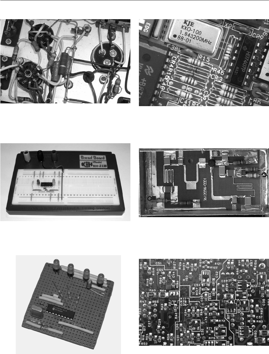
CIRCUIT CONSTRUCTION 329
Figure 19.1 Point-to-point wiring
Figure 19.3 Matrix board construction
Figure 19.2 Breadboard construction
Figure 19.4 Printed circuit construction
Figure 19.5 Printed circuit construction at UHF
Figure 19.6 Surface mounted devices

330 ELECTRONIC CIRCUITS: FUNDAMENTALS AND APPLICATIONS
Stripboard layout techniques
The following steps are required when laying out a
circuit for stripboard construction:
1. Carefully examine a copy of the circuit diagram.
2. Mark all components to be mounted ‘off-board’
and identify (using appropriate letters and/or
numbers, e.g. SK, pin-2) all points at which an
‘off-board’ connection is to be made.
3. Identify any multiple connections required
between integrated circuits or between
integrated circuits and connectors. Arrange such
components in physical proximity and with such
orientation that will effectively minimize the
number of links required.
4. Identify components that require special
attention (such as those which require heatsinks
or have special screening requirements). Ensure
that such components are positioned sensibly
bearing in mind their particular needs.
5. Keep inputs and outputs at opposite ends of the
stripboard. This not only helps maintain a
logical circuit layout (progressing from input to
output) but, in high gain circuits, it may also be
instrumental in preventing instability due to
unwanted feedback.
6. Use standard sizes of stripboard wherever
possible. Where boards have to be cut to size, it
is usually more efficient to align the strips along
the major axis of the board.
7. Consider the means of mounting the stripboard.
If it is to be secured using bolts and threaded
spacers (or equivalent) it will be necessary to
allow adequate clearance around the mounting
holes.
8. Produce a rough layout for the stripboard first
using paper ruled with squares, the corners of
the squares representing the holes in the
stripboard. This process can be carried out
‘actual size’ using 0.1 in. graph paper or
suitably enlarged by means of an appropriate
choice of paper. For preference, it is wise to
choose paper with a feint blue or green grid as
this will subsequently disappear after
photocopying leaving you with a ‘clean’ layout.
9. Identify all conductors that will be handling
high currents (i.e. those in excess of 1 A) and
use adjacent strips connected in parallel at
various points along the length of the board.
10. Identify the strips that will be used to convey
the supply rails: as far as possible these should
be continuous from one end of the board to the
other. It is often convenient to use adjacent
strips for supply and 0 V (or ‘ground’) since
decoupling capacitors can easily be
distributed at strategic points. Ideally, such
capacitors should be positioned in close
proximity to the positive supply input pin to all
integrated circuits which are likely to demand
sudden transient currents (e.g. 555 timers,
comparators, IC power amplifiers).
11. In high-frequency circuits, link all unused strips
to 0 V at regular points. This promotes stability
by ensuring that the 0 V rail is effective as a
common rail.
12. Minimize, as far as possible, the number of
links required. These should be made on (he
upper (component) side of the stripboard. Only
in exceptional cases should links be made on the
underside (foil side) of the board.
13. Experiment with positioning of integrated
circuits (it is good practice, though not essential,
to align them all in the same direction). In some
cases, logic gates may be exchanged from
package to package (or within the same
package) in order to minimize strip usage and
links. (If you have to resort to this dodge, do not
forget to amend the circuit diagram!)
When the stripboard layout is complete, it is
important to carefully check it against the circuit
diagram. Not only can this save considerable
frustration at a later stage but it can be instrumental
in preventing some costly mistakes. In particular,
one should follow the positive supply and 0 V (or
‘ground’) strips and check that all chips and other
devices have supplies. The technique employed by
the author involves the use of coloured pencils that
are used to trace the circuit and stripboard layout;
associating each line in the circuit diagram with a
physical interconnection on the stripboard. Colours
are used as follows:
Positive supply rails Red
Negative supply rails Black
Common 0 V rail Green
Analogue signals Yellow/Pink
Digital signals White/Grey
Off-board connections Orange/Violet
Mains wiring Brown and blue
Assembly of the stripboard is happily a quite
straightforward process. The sequence used for
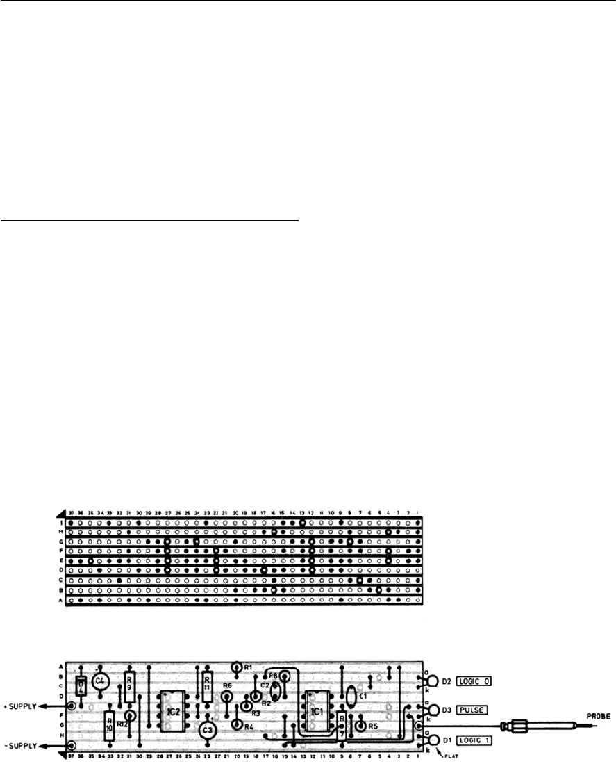
CIRCUIT CONSTRUCTION 331
Figure 19.7 Stripboard layout and component overlay for the logic probe circuit shown in Figure 15.16 on
page 283
stripboard assembly will normally involve
mounting IC sockets first followed by transistors,
diodes, resistors, capacitors and other passive
components. Finally, terminal pins and links should
be fitted before making the track breaks. On
completion, the board should be carefully checked,
paying particular attention to all polarized
components (e.g. diodes, transistors and electrolytic
capacitors). Figure 19.7 shows a typical stripboard
layout together with matching component overlay.
Using printed circuits
Printed circuit boards (PCB) comprise copper
tracks bonded to an epoxy glass or synthetic resin
bonded paper (SRBP) board. The result is a neat
and professional looking circuit that is ideal for
prototype as well as production quantities. Printed
circuits can easily be duplicated or modified from
original master artwork and the production
techniques arc quite simple and should thus not
deter the enthusiast working from home.
The following steps should be followed when
laying out a printed circuit board:
1. Carefully examine a copy of the circuit diagram.
Mark all components which are to be mounted
‘off-board’ and, using appropriate letters and/or
numbers (e.g. SK1, pin-2), identify all points at
which an ‘off-board’ connection is to be made.
2. Identify any multiple connections (e.g. bus
lines) required between integrated circuits or
between integrated circuits and edge connectors.
Arrange such components in physical proximity
and with such orientation that will effectively
minimize the number of links required.
3. Identify components that require special
attention (such as those that require heatsinks or
have special screening requirements). Ensure
that such components are positioned sensibly
bearing in mind their particular needs.
4. Keep inputs and outputs at opposite ends of the
PCB wherever possible. This not only helps
maintain a logical circuit layout (progressing
from input) but, in high gain circuits, it may
also be instrumental in preventing instability
due to unwanted feedback.
5. Use the minimum board area consistent with a
layout which is uncramped. In practice, and to
prevent wastage, you should aim to utilize as
high a proportion of the PCB surface area as

332 ELECTRONIC CIRCUITS: FUNDAMENTALS AND APPLICATIONS
Table 19.1 Current and track width
possible. In the initial stages, however, it is wise
to allow some room for manoeuvre as there will
doubtless be subsequent modifications to the
design.
6. Unless the design makes extensive use of PCB
edge connectors, try to ensure that a common
0 V foil is run all round the periphery of the
PCB. This has a number of advantages not the
least of which is the fact that it will then be
relatively simple to find a route to the 0 V rail
from almost anywhere on the board.
7. Consider the means of mounting the PCB and,
if it is to be secured using bolts and threaded
spacers (or equivalent) you should ascertain the
number and location of the holes required. You
may also wish to ensure that the holes are
coincident with the 0 V foil, alternatively where
the 0 V rail is not to be taken to chassis ground,
it will be necessary to ensure that the PCB
mounting holes occur in an area of the PCB that
is clear of foil.
8. Commence the PCB design in rough first using
paper ruled with squares. This process can be
carried out ‘actual size’ using 0.1 in. graph
paper or suitably enlarged by means of an
appropriate choice of paper. For preference, it is
wise to choose paper with a feint blue or green
grid as this will subsequently disappear after
photocopying leaving you with a ‘clean’ layout.
9. Using the square grid as a guide, try to arrange
all components so that they are mounted on the
standard 0.1 in. matrix. This may complicate
things a little but is important if you should
subsequently wish to convert the design using
computer-aided design (CAD) techniques (see
later).
10. Arrange straight runs of track so that they align
with one dimension of the board or another. Try
to avoid haphazard track layout.
11. Identify all conductors that will be handling
significant current (i.e. in excess of about
500 mA) and ensure that tracks have adequate
widths. Table 19.1 will acts as a rough guide.
Note that, as a general rule, the width of the 0 V
track should be at least twice that used for any
other track.
12. Identify all conductors that will be handling
high voltages (i.e. those in excess of 150 V d.c.
or 100 V r.m.s. a.c.) and ensure that these are
adequately spaced from other tracks. Table 19.2
provides you with a rough guide.
13. Identify the point at which the principal supply
rail is to be connected. Employ extra wide track
widths (for both the 0 V and supply rail) in this
area and check that suitably decoupling
capacitors are placed as close as possible to the
point of supply connection. Check that other
decoupling capacitors are distributed at strategic
points around the board. These should be
positioned in close proximity to the positive
supply input pin to all integrated circuits that are
likely to demand sudden transient currents (e.g.
555 timers, comparators, IC power amplifiers).
Ensure that there is adequate connection to the
0 V rail for each decoupling capacitor that you
use. Additional decoupling may also be
required for high-frequency devices and you
should consult semiconductor manufacturers’
recommendations for specific guidance.
14. Fill unused areas of PCB with ‘land’ (areas of
foil which should be linked to 0 V). This helps
Table 19.2 Voltage and track spacing
Current Minimum track width
Less than 500 mA 0.6 mm
0.5 A to 1.5 A 1.6
1.5 A to 3 A 3
3 A to 6 A 6
6 A to 12 A 10
Voltage Minimum track spacing
Less than 50 V 0.6 mm
50 V to 150 V 1 mm
150 V to 300 V 1.6 mm
300 V to 600 V 3 mm
600 V to 1 kV 5 mm
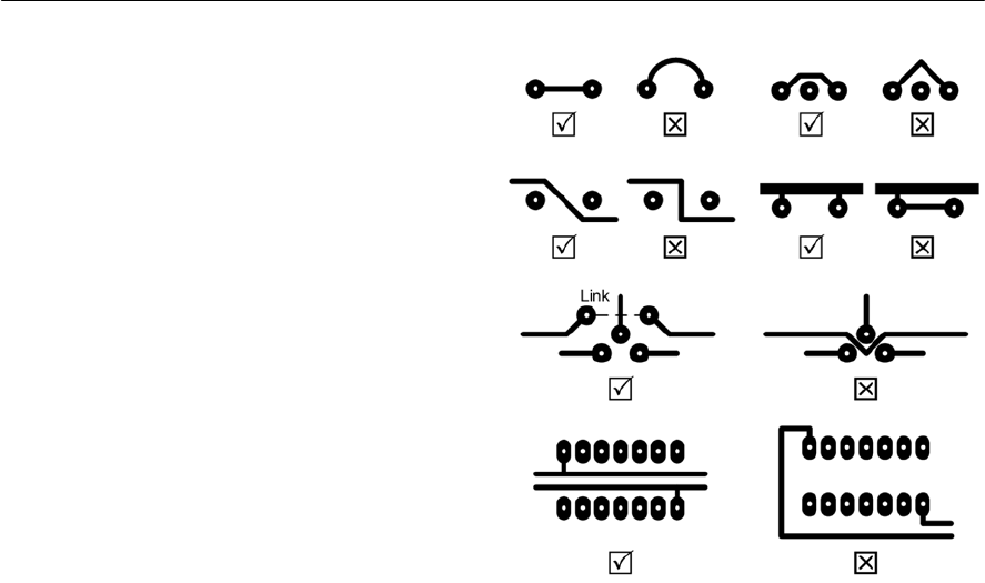
Figure 19.8 Some examples of good and bad
practice in PCB layout
ensure that the 0 V rail is effective as a common
rail, minimizes use of the etchant, helps to
conduct heat away from heat producing
components, and furthermore, is essential in
promoting stability in high-frequency
applications.
15. Lay out the 0 V and positive supply rails first.
Then turn your attention to linking to the pads
or edge connectors used for connecting the off-
board components. Minimize, as far as possible,
the number of links required. Do not use links in
the 0 V rail and avoid using them in the positive
supply rail.
16. Experiment with positioning of integrated
circuits (it is good practice, though not essential,
to align them all in the same direction). In some
cases, logic gates may be exchanged from
package to package (or within the same
package) in order to minimize track runs and
links. (If you have to resort to this dodge, do not
forget to amend the circuit diagram.)
17. Be aware of the pin spacing used by
components and try to keep this consistent
throughout. With the exception of the larger
wirewound resistors (which should be mounted
on ceramic stand-off pillars) axial lead
components should be mounted flat against the
PCB (with their leads bent at right angles).
Axial lead components should not be mounted
vertically.
18. Do not forget that tracks may be conveniently
routed beneath other components. Supply rails
in particular can be routed between opposite
rows of pads of D1L integrated circuits; this
permits very effective supply distribution and
decoupling.
19. Minimize track runs as far as possible and
maintain constant spacing between parallel runs
of track. Corners should be radiused and acute
internal and external angles should be avoided.
In exceptional circumstances, it may be
necessary to run a track between adjacent pads
of a DIL integrated circuit. In such cases, the
track should not be a common 0 V path, neither
should it be a supply rail.
Figure 19.8 shows examples of good and bad
practice associated with PCB layout while Fig. 19.9
shows an example of a PCB layout and matching
component overlay that embodies most of the
techniques and principles discussed.
As with stripboard layouts, it is well worth
devoting some time to checking the final draft PCB
layout before starting on the master artwork. This
can be instrumental in saving much agony and
heartache at a later stage. The same procedure
should be adopted as described on page 330 (i.e.
simultaneously tracing the circuit diagram and PCB
layout).
The next stage depends upon the actual PCB
production. Four methods are commonly used for
prototype and small-scale production. These may
be summarized as follows:
(a) Drawing the track layout directly on the copper
surface of the board using a special pen filled
with etch resist ink. The track layout should, of
course, conform as closely as possible with the
draft layout.
(b) Laying down etch resist transfers of tracks and
pads on to the copper surface of the PCB
following the same layout as the draft but
appropriately scaled.
CIRCUIT CONSTRUCTION 333
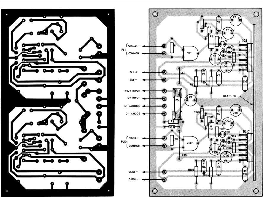
(c) Producing a transparency (using artwork
transfers of tracks and pads) conforming to the
draft layout and then applying photographic
techniques.
(d) Using a PCB layout CAD package (see page
336).
Methods (a) and (b) have the obvious limitation
that they are a strictly one-off process. Method (a)
is also extremely crude and only applicable to very
simple boards. Method (c) is by far the most
superior and allows one to re-use or modify the
master artwork transparency and produce as many
further boards as are required. The disadvantage of
the method is that it is slightly more expensive in
terms of materials (specially coated copper board is
required) and requires some form of ultra-violet
exposure unit. This device normally comprises a
light-tight enclosure into the base of which one or
more ultra-violet tubes are fitted. Smaller units are
available which permit exposure of boards
measuring 250 mm × 150 mm while the larger units
are suitable for boards of up to 500 mm × 350 mm.
The more expensive exposure units are fitted with
timers which can be set to determine the actual
exposure time. Low-cost units do not have such a
facility and the operator has to refer to a clock or
wristwatch in order to determine the exposure time.
In use, the 1:1 master artwork (in the form of
opaque transfers and tape on translucent polyester
drafting film) is placed on the glass screen
immediately in front of the ultra-violet tubes
334 ELECTRONIC CIRCUITS: FUNDAMENTALS AND APPLICATIONS
Figure 19.9 Example of a manually produced PCB layout for an automotive stereo amplifier. The copper
foil layout is shown on the left and the matching component overlay is shown on the right

CIRCUIT CONSTRUCTION 335
Figure 19.10 Exposure frame suitable for photo-
etch PCB production
(taking care to ensure that it is placed so that the
component side is uppermost). The opaque plastic
film is then removed from the photo-resist board
(previously cut roughly to size) and the board is
then placed on top of the film (coated side down).
The lid of the exposure unit is then closed and the
timer set (usually for around four minutes but see
individual manufacturer’s recommendations. The
inside of the lid is lined with foam which exerts an
even pressure over the board such that it is held
firmly in place during the exposure process.
It should be noted that, as with all photographic
materials, sensitized copper board has a finite shelf-
life. Furthermore, boards should ideally be stored in
acool place at a temperature of between 2°C and
10°C. Shelf-life at 20°C will only be around twelve
months and thus boards should be used reasonably
promptly after purchase.
Note that it is not absolutely essential to have
access to an ultra-violet light-box as we all have at
least occasional access to an entirely free source of
ultra-violet light. Provided one is prepared to wait
for a sunny day and prepared to experiment a little,
the exposure process can be carried out in ordinary
sunlight. As a guide, and with the full sun present
overhead, exposure will take around fifteen
minutes. Alternatively, one can make use of a sun-
ray lamp. Again, some experimentation will be
required in order to get the exposure right. With a
lamp placed approximately 300 mm from the sun
ray source (and arranged so that the whole board
surface is evenly illuminated) an exposure time of
around four minutes will be required. Note that, if
you use this technique, it is important to follow the
sun-ray lamp manufacturer’s instructions
concerning eye protection. A pair of goggles or
dark sunglasses can be used to protect the eyes
during the exposure process. However one should
never look directly at the ultra-violet light source
even when it is ‘warming up’.
Finally, one can easily manufacture one’s own
light-box (using low-power ultra-violet tubes) or
make use of a standard ultra-violet bulb (of
between 150 W and 300 W) suspended above the
work area. If this technique is used, the bulb should
be hung approximately 400 mm above the table on
which the sensitized board, artwork and glass sheet
have been placed. A typical exposure time for a
300 W bulb is in the range of ten to fifteen minutes.
Apair of dark sunglasses can again be used to
protect the eyes during the process. Where one is
using an ‘alternative’ technique, a frame should be
constructed along the lines shown in Figure 19.4.
This can be used to hold the transparency in contact
with the coated copper board during the exposure
process.
Whichever method of exposure is used some
experimentation may be required in order to
determine the optimum exposure time. After this
time has elapsed, the board should be removed and
immersed in a solution of sodium hydroxide that
acts as a developer. The solution should be freshly
made and the normal concentration required is
obtained by mixing approximately 500 ml of tap
water (at 20°C) with one tablespoon of sodium
hydroxide crystals. A photographic developing tray
(or similar shallow plastic container) should be
used to hold the developer. Note that care should be
taken when handling the developer solution and the
use of plastic or rubber gloves is strongly
recommended. This process should be carried out
immediately after exposure and care should be
taken not to allow the board to be further exposed
under room lights.
The board should be gently agitated while
immersed in the developer and the ensuing process
of development should be carefully watched. The
board should be left for a sufficiently long period
for the entire surface to be developed correctly but
not so long that the tracks lift. Development times
will depend upon the temperature and
concentration of the developer and on the age of the
sensitized board. Normal development times are in
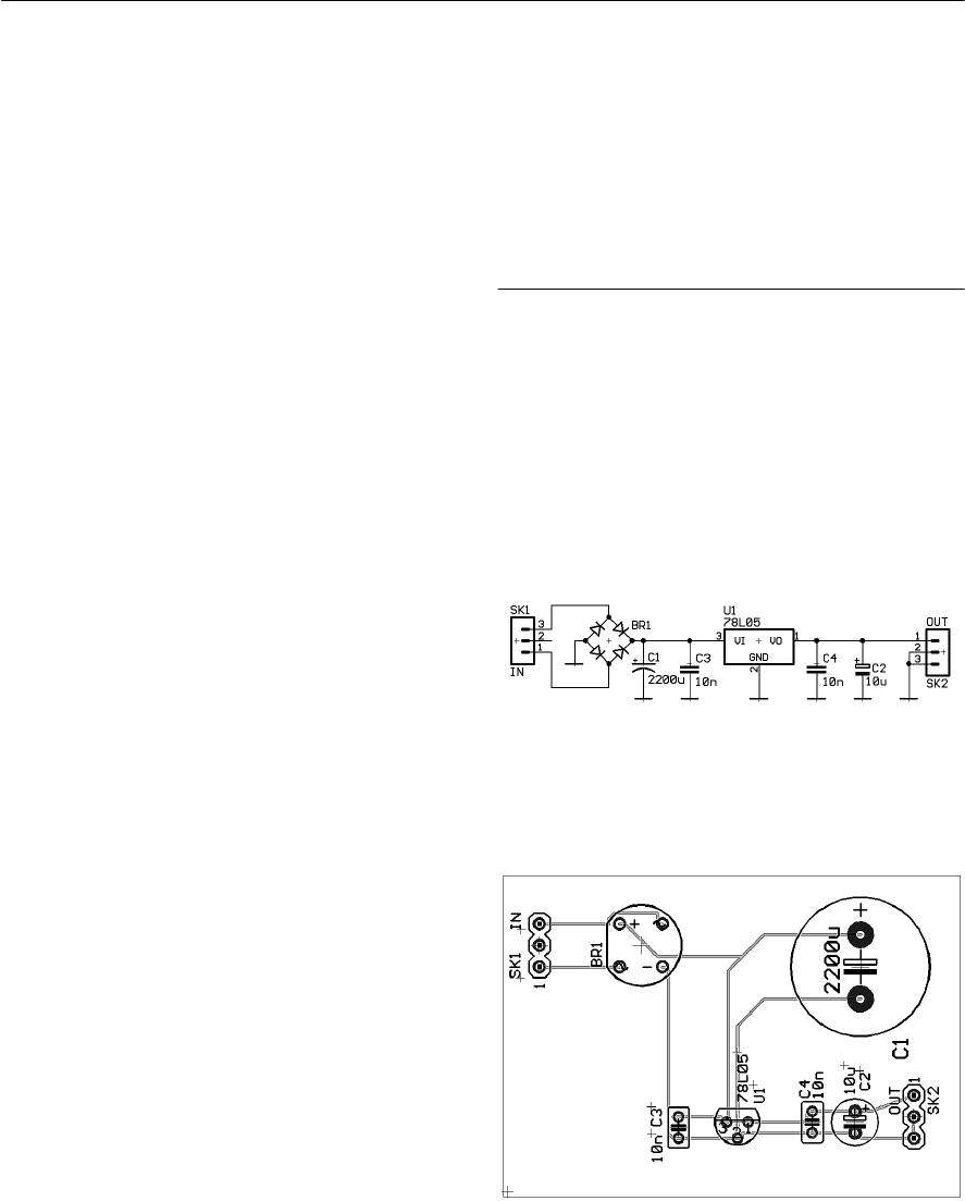
Figure 19.11 Circuit of a simple 5 V regulated
power supply module based on a 78L05 three-
terminal voltage regulator
336 ELECTRONIC CIRCUITS: FUNDAMENTALS AND APPLICATIONS
the region of 30 to 90 seconds and after this period
the developed image of the track layout (an etch-
resist positive) should be seen.
After developing the board it should be carefully
washed under a running tap. It is advisable not to
rub or touch the board (to avoid scratching the
surface) and the jet of water should be sufficient to
remove all traces of the developer. Finally, the
board should be placed in the etchant which is a
ferric chloride solution (FeCl3). For obvious
reasons, ferric chloride is normally provided in
crystalline form (though at least one major supplier
is prepared to supply it on a ‘mail order basis’ in
concentrated liquid form) and should be added to
tap water (at 20°C) following the instructions
provided by the supplier. If no instructions are
given, the normal quantities involved are 750 ml of
water to 500 g of ferric chloride crystals. Etching
times will also be very much dependent upon
temperature and concentration but, for a fresh
solution warmed to around 40°C the time taken
should typically be ten to fifteen minutes. During
this time the board should be regularly agitated and
checked to ascertain the state of etching. The board
should be removed as soon as all areas not
protected by resist have been cleared of copper;
failure to observe this precaution will result in
‘undercutting’ of the resist and consequent thinning
of tracks and pads. Where thermostatically
controlled tanks are used, times of five minutes or
less can be achieved when using fresh solution.
It should go without saying that great care should
be exercised when handling ferric chloride. Plastic
or rubber gloves should be worn and care must be
taken to avoid spills and splashes. After cooling,
the ferric chloride solution may be stored (using a
sealed plastic container) for future use. In general,
750 ml of solution can be used to etch around six to
ten boards of average size; the etching process
taking longer as the solution nears the end of its
working life. Finally, the exhausted solution must
be disposed of with care (it should not be poured
into an ordinary mains drainage system).
Having completed the etching process, the next
stage involves thorough-ly washing, cleaning, and
drying the printed circuit board. After this, the
board will be ready for drilling. Drilling will
normally involve the services of a 0.6 mm or 1 mm
twist drill bit for standard component leads and IC
pins. Larger drill bits may be required for the leads
fitted to some larger components (e.g. power
diodes) and mounting holes. Drilling is greatly
simplified if a special PCB drill and matching stand
can be enlisted. Alternatively, provided it has a
bench stand, a standard electric drill can be used.
Problems sometimes arise when a standard drill or
hand drill is unable to adequately grip a miniature
twist drill bit. In such cases one should make use of
aminiature pin chuck or a drill fitted with an
enlarged shank (usually of 2.4 mm diameter).
PCB CAD packages
The task of laying out a PCB and producing master
artwork (both for the copper foil side of a board
and for the component overlay) is greatly
simplified by the use of a dedicated PCB CAD
package. Some examples of the use of these
packages are shown in Figs 19.11 to 19.14.
Figure 19.12 PCB track layout for the circuit
shown in Fig. 19.5 produced by an autorouting
CAD package (shown prior to optimization)
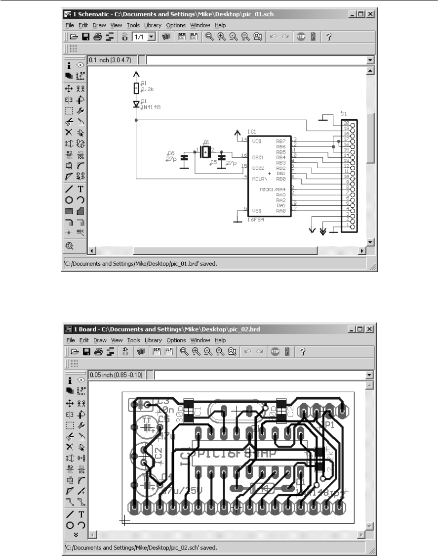
Figure 19.13 Circuit of a PIC16F84-based microcontroller shown in the circuit schematic editor of the
Eagle CAD software (see Appendix 9)
CIRCUIT CONSTRUCTION 337
Figure 19.14 Double-sided PCB layout for the circuit shown in Fig. 19.13 generated by the Eagle CAD
software (shown after optimization)

338 ELECTRONIC CIRCUITS: FUNDAMENTALS AND APPLICATIONS
Connectors
Various forms of connectors may be required in
any particular item of electronic equipment. These
may be categorized in various ways but the
following should serve as a guide:
(a) Mains connectors. These connectors are
intended for use with an a.c. mains supply.
Standard 3-pole IEC types should be employed
wherever possible.
(b) Single-pole connectors. These are available in
ranges having diameters of 4 mm, 3 mm, 2 mm
and 1 mm and are ideal for use with test-leads
(i.e. as input and output connectors in test
equipment) and for low-voltage power
supplies. Plugs and sockets are available in
various colours to permit identification.
(c) Multi-pole connectors. A huge range of multi-
pole connectors is currently available and the
following types are worthy of special note:
(i) DIN standard connectors of the type
commonly used in audio equipment
(ii) DIN 41612 indirect stripboard and PCB
edge connectors with 32, 64, or 96-ways.
(iii) DIN 41617 low-cost indirect edge
connectors
(iv) D-connectors. These are available with 9,
15, 25, and 37-ways and are popularly
used in microcomputer applications
(v) IEEE-488 connectors. These 14, 24, 36
and 50-way connectors are commonly
used with equipment which uses the
popular IEEE-488 instrument bus system.
Note that insulation displacement connector
(IDC) provide a means of terminating multi-
way ribbon cables without the need for
soldering. Simple tools are used to assemble
the connector and strain relief clamp onto the
cable, the insulation of which is pierced by the
tines of the connector pins.)
(d) Coaxial connectors. These connectors are used
for screened test leads and also for r.f.
equipment. The following three types are most
popular:
(i) BNC. These are available in both 50 I
and 75 Iseries and are suitable for
operation at frequencies up to 4 GHz.
(ii) PL259/SO239 (popularly known as UHF).
These 50 Itypes are suitable for use at
frequencies up to 250 MHz.
(iii) Belling-Lee (popularly known as TV).
These low-cost connectors are suitable for
use at frequencies up to 800 MHz with an
impedance of 75 I.
The process of choosing a connector is usually very
straightforward. It will first be necessary to ensure
that an adequate number of ways are catered for
and that the connector is suitably rated as far as
current and voltage are concerned (one should
consult individual manufacturer’s ratings where
any doubt arises). It is advisable to maintain
compatibility with equipment of similar type and
one should avoid using too wide a range of
connectors and cables. In addition, a common pin-
usage convention should be adopted and strictly
adhered to. This will help to avoid problems later
on and will make interwiring of equipment and
exchange of modules a relatively straightforward
process.
Enclosures
An appropriate choice of enclosure is vitally
important to the ‘packaging’ of any electronic
equipment. Not only will the enclosure provide
protection for the equipment but it should also be
attractive and add to the functionality of the
equipment. Enclosures can be divided into five
main types:
(a) Instrument cases. These are ideal for small
items of test gear (e.g. meters and signal
generators) and are available in a wide variety
of styles and sizes. One of the most popular
low-cost ranges of instrument cases is that
manufactured by BICC-Vero and known as
Veroboxes. This enclosure comprises plastic
top and bottom sections with anodized
aluminium front and back panels. Other ranges
of instrument cases feature steel and aluminium
construction and are thus eminently suited for
larger projects or those fitted with larger mains
transformers (such as heavy-duty power
supplies).
(b) Plastic and diecast boxes. These low-cost
enclosures comprise a box with removable lid

CIRCUIT CONSTRUCTION 339
secured by means of four or more screws.
Boxes are available in a range of sizes and the
diecast types (which are ideal for use in
relatively hostile environments) are available
both unpainted and with a textured paint finish.
(c) Rack systems. These are designed to accept
standard cards and are ideal for modular
projects. The outer case comprises an
aluminium framework fitted with covers and a
series of connectors at the rear from which the
modules derive their power and exchange
signals. Individual circuit cards (which may be
stripboard or PCB) are fitted to a small
supporting chassis and anodized aluminium
front panel (available in various widths). The
card assembly slides into the rack using
appropriately positioned clip-in guides. Rack
systems are expensive but inherently flexible.
(d) Desk consoles. These enclosures are ideal for
desktop equipment and generally have sloping
surfaces that are ideal for mounting key-boards
and keypads.
(e) Special purpose enclosures. Apart from the
general-purpose types of enclosure described
earlier, a variety of special purpose enclosures
are also available. These include such items as
clock and calculator housings, enclosures for
hand-held controllers, and cases for in-line
mains power supplies (including types having
integral 13 A plugs).
Having decided upon which of the basic types of
enclosure is required, the following questions
should be borne in mind when making a final
selection of enclosure:
•Is the size adequate?
•Will the enclosure accommodate the stripboard
or PCB circuitry together with the ‘off-board’
components (including, where appropriate, the
mains transformer)?
•Will the enclosure be strong enough?
•Will other equipment be stacked on top of the
enclosure?
•Can the mains transformer be supported
adequately without deforming the case?
•Is the front panel of sufficient size to permit
mounting all of the controls and displays?
•Is any protection (in the form of handles or a
recessed front panel) necessary for the front
panel mounted components?
•Is there any need for ventilation?
•How much heat is likely to be produced within
the equipment?
•Can heat producing components be mounted on
the rear panel?
•Will a cooling fan be required?
•Is the style of the equipment commensurate
with other equipment of its type and within the
same range?
•Is there a need to include screening or filtering
in order to minimize incoming or outgoing
noise or stray electric/magnetic fields?
When laying out the front panel of the equipment,
it is important to bear in mind the basic principles
of ergonomic design. All controls should be
accessible. They should be logically arranged
(grouping related functions together) and clearly
labelled. Consideration should be given to the type
of controls used (e.g. slider versus rotary
potentiometers, push-button versus toggle
switches).
It is also important to wire controls such that
their action follows the expected outcome. Rotary
‘gain’ and ‘volume’ controls, for example, should
produce an increase in output when turned in a
clockwise direction. Indicators should operate with
adequate brightness and should be viewable over an
appropriate angle. Indicators and controls should be
arranged so that it is possible to ascertain the status
of the instrument at a glance. If necessary, a
number of opinions should be sought before
arriving at a final layout for the front panel; one’s
own personal preferences are unlikely to coincide
exactly with those of the ‘end user’.
Solder and soldering technique
Most solders are an alloy of two metals; tin (Sn)
and lead (Pb). The proportion of tin and lead is
usually expressed as a percentage or as a simple
ratio. For example, the term 60/40 solder refers to
an alloy which comprises 60% tin and 40% lead by
weight. The proportion of tin and lead is
instrumental in determining the melting point of the
solder alloy and the proportion of the constituents
is usually clearly stated.
In the past, solder was often categorized by its
intended application and the terms radio solder,
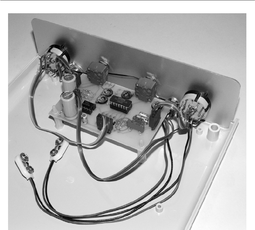
Figure 19.15 Internal wiring of a waveform generator based on PCB headers and coloured ribbon cable
340 ELECTRONIC CIRCUITS: FUNDAMENTALS AND APPLICATIONS
electronic solder,and general-purpose solder and
silver bearing solder. The difference between these
types of solder can be briefly summarized as
follows:
Radio solder
Amedium melting point temperature (typically
230°C) solder used for making joints in point-to-
point wiring as typically found in radios and early
TV receivers. Typical joints would be quite
substantial based on tag strips, group boards, valve
bases, etc., and each joint might involve several
wires or component leads of substantial diameter.
Electronic solder
Alow melting point temperature (typically 185°C)
used for making joints on printed circuit boards. A
joint would normally involve a single component
lead and its associated copper pad and excessive
temperature would have to be avoided in order to
prevent damage both to the component (whose
connecting lead might be of a very short length)
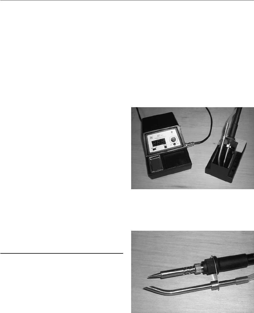
CIRCUIT CONSTRUCTION 341
and the PCB itself (where copper pads and tracks
might lift due to the application of excessive heat).
General-purpose solder
Ahigh melting point temperature (typically 255°C)
designed for general electrical repair work (and
unsuitable for use with electronic equipment).
Silver bearing solders
Silver bearing solders tend to flow more smoothly
and form stronger joints. Unfortunately they
generally require higher soldering and desoldering
temperatures and this can make component
removal and replacement difficult. In particular, the
higher temperatures involved may cause damage to
the bond between copper pads and tracks and the
printed circuit substrate on which they are formed.
In turn, this can result in the lifting of pads and
tracks and permanent damage can result.
Flux
Flux has two roles in soldering. Firstly it helps with
the removal of any oxide coating that may have
formed on the surfaces that are to be soldered and
secondly it helps to prevent the formation of oxides
caused by the heat generated during the soldering
process itself. Flux is available in both paste and
liquid form. However, in the case of solder for
electronic applications, it is also available
incorporated within the solder itself. In this case,
the flux is contained within a number of cores that
permeate through the solder material rather like the
letters that appear on a piece of souvenir seaside
rock.
Safety when soldering
Whilst soldering is not a particularly hazardous
operation, there are a number of essential safety
and other precautions that should be observed.
These are listed below:
Fumes
Solder fumes are an irritant and exposure,
particularly if prolonged, can cause asthma attacks.
Because of this it is essential to avoid the build up
of fumes, particularly so when a soldering iron is in
continuous use. The best way to do this is to use a
proprietary system for fume extraction. In addition,
many professional quality irons can be fitted with
fume extraction facilities which are designed to
clear fumes from the proximity of the soldering
iron bit.
Even when a soldering iron is only used
intermittently it is essential to ensure that the
equipment is used in a well-ventilated area where
fumes cannot accumulate. Fume extraction should
be fitted to all soldering equipment that is in
constant use. Most good quality soldering irons that
Figure 19.16 Amodern temperature-controlled
soldering station with ESD and fume extraction
facilities
Figure 19.17 Fume extraction facility which can
be added to a temperature controlled iron when
necessary
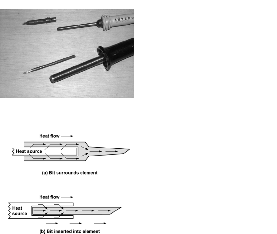
342 ELECTRONIC CIRCUITS: FUNDAMENTALS AND APPLICATIONS
are designed for professional use can be fitted with
fume extraction equipment. Figure 19.1 shows a
modern soldering station equipped with fume
extraction.
Damage to eyes
Molten solder or flux additives can cause
permanent eye damage. Some means of eye
protection is essential. This can take the form of
safety glasses or the use of a bench magnifier.
Ordinary reading or prescription glasses will also
offer a measure of protection and may also be of
benefit when undertaking close work.
Static hazards
Many of today’s electronic devices are susceptible
to damage from electric fields and stray static
charges. Unfortunately, simply earthing the tip of a
soldering iron is not sufficient to completely
eliminate static damage and additional precautions
may be required to avoid any risks of electro-static
damage (ESD). These may involve using a low-
voltage supply to feed the heating element fitted in
the soldering iron, incorporating low/zero-voltage
switching, and the use of conductive (antistatic)
materials in the construction of the soldering iron
body and the soldering station itself.
Burn, melt and fire hazards
The bit of a soldering iron is usually maintained at
atemperature of between 250°C and 350°C. At this
temperature, conventional plastic insulating
materials will melt and many other materials (such
as paper, cotton, etc.) will burn. It should also go
without saying that personal contact should be
avoided at all times and the use of a properly
designed soldering iron stand is essential.
Shock hazards
Mains voltage is present in the supply lead to a
mains operated soldering iron and also in the
supply lead to any soldering station designed for
use with a low-voltage iron. If the soldering iron bit
comes into contact with a mains lead there can be a
danger that the insulation will melt exposing the
live conductors. In such situations, heatproof
insulation is highly recommended both for the
supply to the iron itself and also to any power unit.
Soldering guns
Soldering guns (where the bit is effectively a short-
circuited turn) can become extremely hot and
continuous operation of this type of iron can be
extremely dangerous as the mains transformer
fitted into the handle of the gun can easily become
overheated. This can cause the insulation to reach a
dangerously high temperature which can result in
melting and short-circuits which will cause
permanent damage to the gun. Because of their
rather clumsy nature and high-power, soldering
guns should be avoided for all general electronic
work.
Figure 19.19 Heat transfer in the two types of
soldering iron bit shown in Fig. 19.18
Figure 19.18 Two different types of bit fitted to
small soldering irons
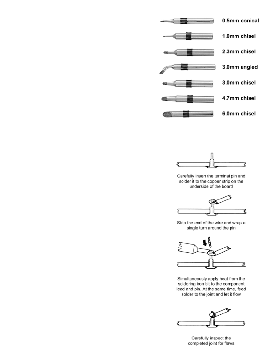
CIRCUIT CONSTRUCTION 343
Soldering and desoldering techniques
Soldered joints effectively provide for both
electrical and mechanical connection of
components with pins, tags, stripboards, and PCB.
Before a soldering operation is carried out, it is
vitally important that all surfaces to be soldered are
clean and completely free of grease and/or oxide
films. It is also important to have an adequately
rated soldering iron fitted with an appropriate bit.
The soldering iron bit is the all-important point of
contact between the soldering iron and the joint and
it should be kept scrupulously clean (using a damp
sponge) and free from oxide. To aid this process,
and promote heat transfer generally, the bit should
be regularly ‘tinned’ (i.e. given a surface coating of
molten solder).
The selection of a soldering bit (see Figs 19.18
and 19.19) depends on the type of work
undertaken. Figure 19.20 shows a number of
popular bit profiles, the smaller bits being suitable
for sub-miniature components and tightly packed
boards. The procedure for making soldered joints to
terminal pins and PCB pads are shown in Figs
19.21 and 19.22, respectively. In the case of
terminal pins, the component lead or wire should be
wrapped tightly around the pin using at least one
turn of wire made using a small pair of long-nosed
pliers. If necessary, the wire should be trimmed
using a small pair of side cutters before soldering.
Next, the pin and wire should then be
simultaneously heated by suitable application of the
soldering iron bit and then sufficient solder should
be fed on to the pin and wire (not via the bit) for it
to flow evenly around the joint thus forming an
airtight ‘seal’. The solder should then be left to cool
(taking care not to disturb the component or wire
during the process). The finished joint should be
carefully inspected and re-made if it suffers from
any of the following faults:
(a) Too little solder. The solder has failed to flow
around the entire joint and some of the wire
turn or pin remains exposed.
(b) Too much solder. The solder has formed into a
large ‘blob’ the majority of which is not in
direct contact with either the wire or the pin.
(c) The joint is ‘dry’. This usually occurs if either
the temperature of the joint was insufficient to
permit the solder to flow adequately or if the
joint was disturbed during cooling.
Figure 19.20 Typical soldering iron bit profiles
Figure 19.21 Procedure for making a soldered
joint to a terminal pin
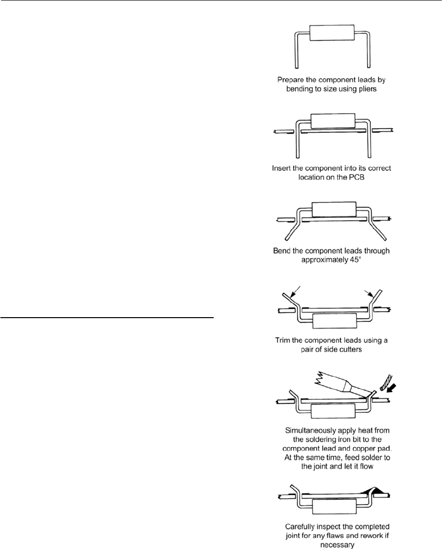
344 ELECTRONIC CIRCUITS: FUNDAMENTALS AND APPLICATIONS
In the case of a joint to be made between a
component and a PCB pad, a slightly different
technique is used (though the requisites for
cleanliness still apply). The component should be
fitted to the PCB (bending its leads appropriately at
right angles if it is an axial lead component) such
that its leads protrude through the PCB to the
copper foil side. The leads should be trimmed to
within a few millimetres of the copper pad then
bent slightly (so that the component does not fall
out when the board is inverted) before soldering in
place. Opinions differ concerning the angles
through which the component leads should be bent.
For easy removal, the leads should not be bent at all
while, for the best mechanical joint, the leads
should be bent through 90°. A good compromise,
and that preferred by the author involves bending
the leads through about 45°. Care should again be
taken to use the minimum of solder consistent with
making a sound electrical and mechanical joint.
Finally, it is important to realize that good
soldering technique usually takes time to develop
and the old adage ‘practice makes perfect’ is very
apt in this respect. Do not despair if your first
efforts fail to match with those of the professional!
Component removal and replacement
Care must be exercised when removing and
replacing printed circuit mounted components (see
Figs 19.23 to 19.28). It is first necessary to
accurately locate the component to be removed on
the upper (component) side of the PCB and then to
correctly identify its solder pads on the underside
of the PCB. Once located, the component pads
should be gently heated using a soldering iron. The
soldering iron bit should be regularly cleaned using
adamp sponge (a small tin containing such an item
is a useful adjunct to any soldering work station).
The power rating of the iron should be the
minimum consistent with effective removal of the
components and should therefore not normally
exceed 20 W for types which do not have
temperature control since excessive heat can not
only damage components but may also destroy the
bond between the copper track and the board itself.
This latter effect causes lifting of pads and tracks
from the surface of the PCB and should be avoided
at all costs. Figure 19.22 Procedure for making a soldered
joint to a PCB pad
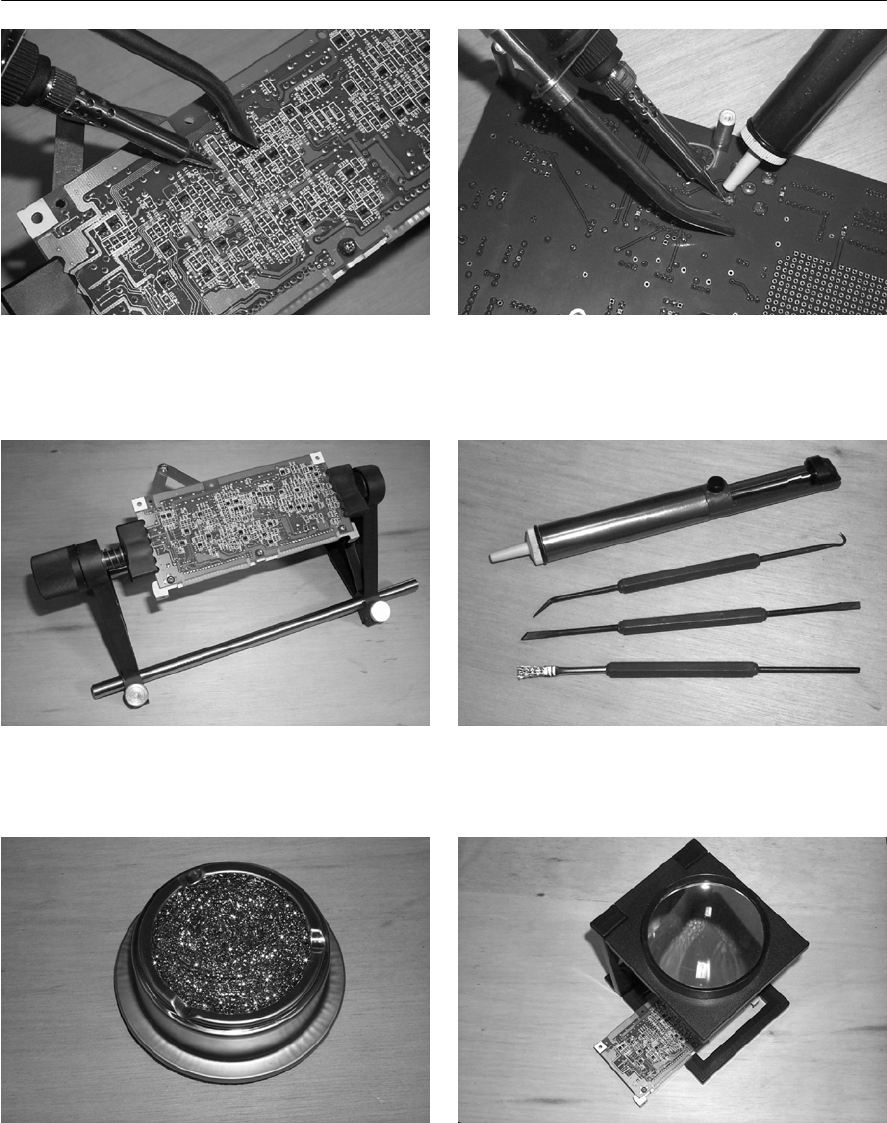
Figure 19.23 Making a soldered joint on a PCB. A
fine point soldering bit is being used
Figure 19.26 Using a desoldering pump to remove
excess solder
Figure 19.24 A PCB holder can be a useful
soldering accessory when working on large boards
Figure 19.27 A variety of desoldering tools
(including desoldering pump and wire brush)
Figure 19.25 A soldering iron bit cleaner. Regular
cleaning is essential to ensure good soldered joints
CIRCUIT CONSTRUCTION 345
Figure 19.28 A PCB bench magnifier is ideal for
inspecting finished work for soldering defects
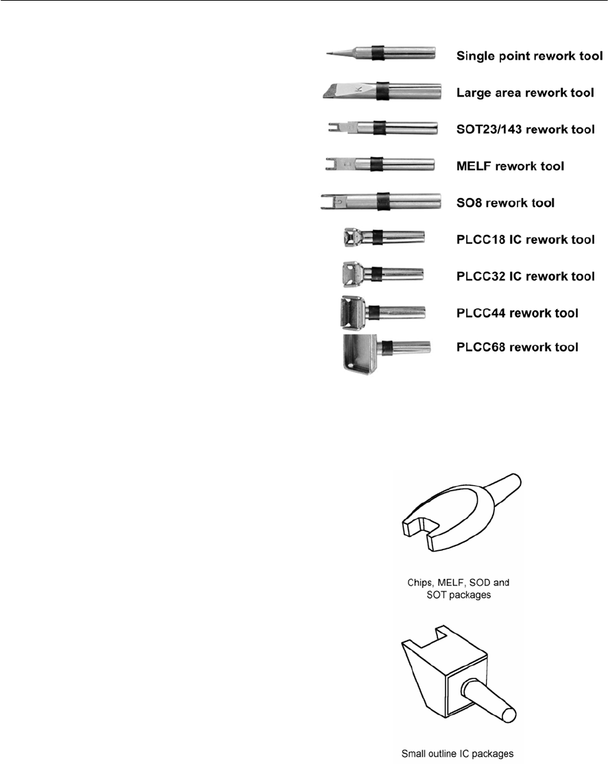
Figure 19.29 Typical desoldering and rework tools
Once the solder in the vicinity of the pad has
become molten (this usually only takes one or two
seconds) and desoldering suction pump should be
used to remove the solder. This will often require
only one operation of the desoldering pump;
however, where a large area of solder is present or
where not all of the solder in the vicinity of the pad
has become molten, a second application of the tool
may be required. If the desoldering tool has to be
repeatedly applied this usually indicates that either
the tool is clogged with solder or that the soldering
iron is not hot enough. With practice only one
application of the soldering iron and soldering
pump should be required. Once cleared of solder,
the component lead should become free and a
similar process should be used for any remaining
leads or pins. Special tools arc available for the
rapid removal of IC and SMD devices and these
permit the simultaneous heating of all pins (see
Figs 19.29 and 19.30).
When desoldering is complete, the component
should be gently withdrawn from the upper
(component) side of the board and the replacement
component should be fitted, taking care to observe
the correct polarity and orientation where
appropriate. The leads should protrude through the
PCB to the copper foil side and should be trimmed
to within a few millimetres of the copper pad then
bent slightly (so that the component do not fall out
when the board is inverted) before soldering in
place. Care should be taken to use the minimum of
solder consistent with making a sound electrical
and mechanical joint. As always, cleanliness of the
soldering iron bit is extremely important if dry
joints arc to be avoided.
Finally, a careful visual examination of the joint
should be carried out. Any solder splashes or
bridges between adjacent tracks should be removed
and, if necessary, a sharp pointed instrument should
be used to remove any surplus solder or flux which
may be present.
In some cases it may be expedient (or essential
when the PCB has been mounted in such a position
that the copper foil side is not readily accessible) to
remove a component by cutting its leads on the
upper (component) side of the board. However,
care should be taken to ensure that sufficient lead is
left to which the replacement component (with its
wires or pins suitably trimmed) may be soldered.
During this operation, extra care must be taken
when the soldering iron bit is placed in close
346 ELECTRONIC CIRCUITS: FUNDAMENTALS AND APPLICATIONS
Figure 19.30 SMD desoldering tools for integrated
circuits
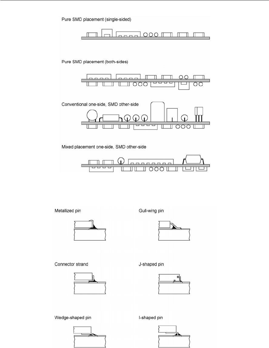
CIRCUIT CONSTRUCTION 347
Figure 19.31 Various PCB layouts involving SMD and conventional components
Figure 19.32 Different pin styles used with SMD devices

348 ELECTRONIC CIRCUITS: FUNDAMENTALS AND APPLICATIONS
proximity to densely packed components on the
upper side of the PCB. Polystyrene capacitors and
other plastic encapsulated components are
particularly vulnerable in this respect. Figures
19.31 and 19.32 show some typical arrangements
used with SMD and conventional components.
Heatsinks
The electronic equipment designer is often faced
with the task of designing circuits that will operate
within a range of temperatures that will ensure safe
and reliable operation. This task is normally carried
out with the aid of a comprehensive set of
manufacturers’ data and a number of simple
formulae. The symbols shown in Table 19.3 are
commonly used in heatsink calculations:
Determining temperature rise
The ability of a heatsink and transistor mounting
arrangement to dissipate heat can be measured in
terms of the amount by which the junction
temperature exceeds the ambient (or surrounding
air) temperature. A perfect heatsink and mounting
arrangement would keep the junction temperature
the same as that of the surrounding air. In practice,
the junction temperature will rise under operational
conditions.
In practice, a rise in junction temperature is
unavoidable. What is important, however, is that
the maximum junction temperature, TJmax,must
never be exceeded. Furthermore, manufacturers
provide a de-rating characteristic that must be used
to determine device rating (percentage of full
power rating at 25°C) when the junction
temperature exceeds its normally specified value
(see Fig. 19.33).
The temperature rise, T,above ambient will be
given by:
(1)
where PTis the total power dissipated by the
semiconductor device(s) and
Tis the total thermal
resistance of the heatsink and mounting
arrangement.
Determining the junction temperature
The temperature rise is simply the difference
between the actual junction temperature and the
surrounding (or ambient) temperature. Ultimately,
the operating junction temperature is vitally
important since exceeding the maximum operating
junction temperature (TJmax)can result in the
destruction of the semiconductor device!
Now MT=TJOTA(2)
Combining equations (1) and (2) gives:
From which:
It is worth using an example to explain the use of
this formula in helping us to determine just how hot
asemiconductor junction actually gets!
(
)
JTTA
TP T
=×+
Symbol Meaning Units
TAAmbient temperature °C
TAmax Maximum ambient temperature °C
TJJunction temperature °C
TJmax Maximum junction temperature °C
TCCase temperature °C
TSHeatsink surface temperature
(note 1)
°C
JA Thermal resistance (from junction
to ambient)
°C/W
CS Thermal resistance (from case to
surface)
°C/W
SA Thermal resistance (from surface to
ambient)
°C/W
TTotal thermal resistance (from junc-
tion to ambient)
°C/W
PTTotal power dissipation (note 2) W
PTmax Maximum total power dissipation
(note 2)
W
Table 19.3 Symbols used in heatsink calculations
Notes:
1. At the point of contact with the semiconductor
device
2. For one or more devices mounted on the
heatsink
TT
TP
=×
JA TT
TT P
=×
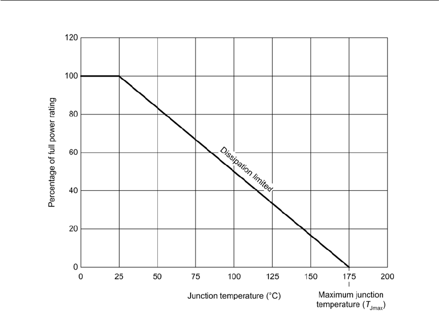
Figure 19.33 A typical semiconductor de-rating characteristic. Note how full power (100%) is available at
temperatures of up to 20°C but above this the percentage must be reduced progressively
CIRCUIT CONSTRUCTION 349
Example 19.1
ATO220 transistor dissipates a total power of 5W.
If the total thermal resistance is 8°C/W and the
ambient temperature is 30°C, determine the
junction temperature.
Applying equation (3) gives:
Determining thermal resistance
Figure 19.34 shows a typical TO3 case style
transistor mounted on a finned heat dissipator (i.e.
heatsink). Heat is conducted away from the
semiconductor junction to the outer case of the
TO3 package and then, via an insulating washer to
the surface of the heatsink. From this point, heat is
conducted to the extremities of the fins where it is
radiated into the surrounding air space.
The total thermal resistance,
T,present in any
heatsink arrangement is actually the sum of several
individual thermal resistances. Consider the case of
atransistor bolted directly to a metal heat radiator
(see Fig. 19.35). The total thermal resistance,
T,is
the sum of the following thermal resistances:
1. The thermal resistance that exists between the
semiconductor junction and the case of the
transistor (i.e. the thermal resistance inside the
transistor package),
JC
2. The thermal resistance between the case of the
transistor and the heat radiator (i.e. the thermal
resistance of an insulating washer, where fitted),
CS
(
)
(
)
JTTA
5 8 30 70 C
TP T
=×+=×+=°
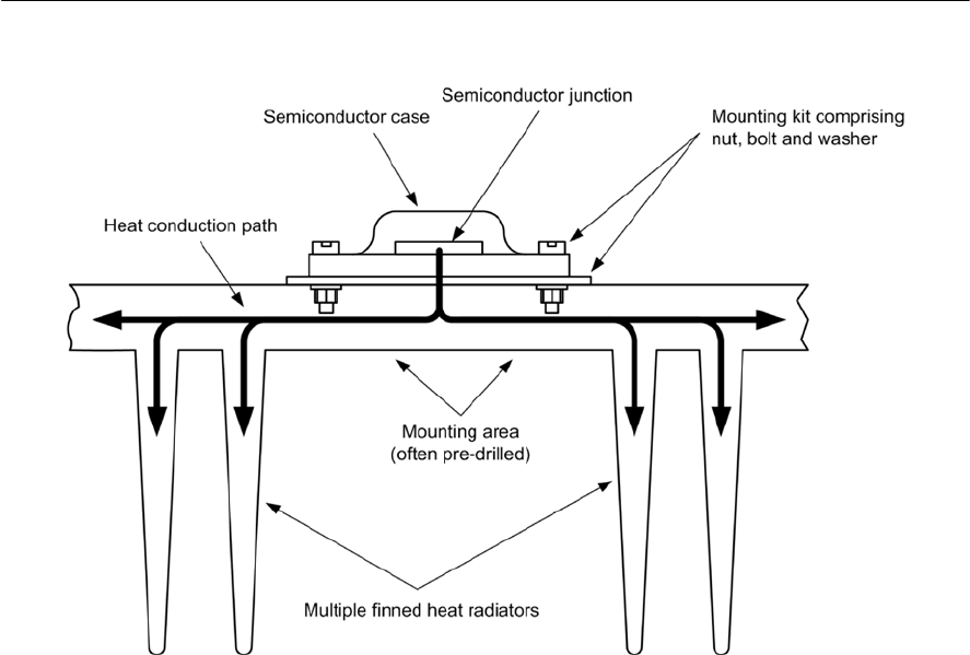
350 ELECTRONIC CIRCUITS: FUNDAMENTALS AND APPLICATIONS
3. The thermal resistance between the surface of the
heat radiator and the space surrounding it (i.e. the
thermal resistance between the surface and
ambient),
SA
Fig. 19.36 shows these three thermal resistances
together with the temperatures that exist at each
point in the arrangement shown in Fig. 19.35. The
three thermal resistances shown in Fig. 19.36
actually appear ‘in series’ and we can use a simple
electrical analogy to represent the thermal ‘circuit’
in electrical terms (see Fig. 19.37).
From Fig. 19.37 we can conclude that the total
thermal resistance,
T,is given by:
T=
JC +
CS +
SA (4)
Note that the total thermal resistance is actually the
same as the thermal resistance between the junction
and ambient.
Thus:
T=
JC +
CS +
SA =
JA (5)
The complete electrical equivalent circuit of the
heatsink arrangement is shown in Fig. 19.37. Note
that the source of power (PTOT)is the
semiconductor device and the ‘potentials’ at the
two extreme ends of the series chain of thermal
resistances are TJ(junction temperature) and TA
(ambient or surrounding air temperature).
Example 19.2
Atransistor has a thermal resistance from junction
to case of 1.5°C/W. If the transistor is fitted with a
washer and mounting kit having a thermal
resistance of 1.75°C/W, and a heatsink of
Figure 19.34 Typical mounting arrangement for a TO3 transistor
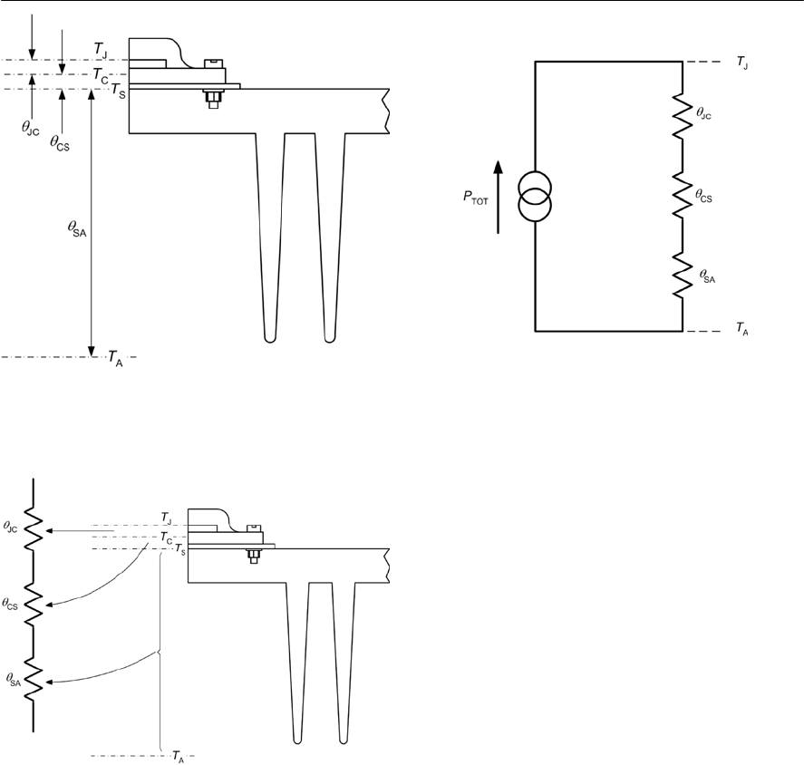
CIRCUIT CONSTRUCTION 351
2.25°C/W, determine the total thermal resistance
that exists between junction and ambient.
Applying equation (5) gives:
JA =
JC +
CS +
SA =1.5 + 1.75 + 2.25 = 5.5°C/W
Worst case conditions
In the design of electronic equipment we often need
to plan for the worst case conditions, ensuring that
the absolute maximum junction temperature, TJmax,
is not exceeded when the total power dissipation
and ambient temperature jointly reach their
maximum working values.
From equation (3) we can infer that, under the
worst case conditions:
Combining this with equation (5) gives:
(6)
Example 19.3
Atransistor has an absolute maximum junction
temperature rating of 150° and a thermal resistance
from junction to case of 1.0°C/W. If the device is
fitted with a washer and mounting kit having a
thermal resistance of 1.25°C/W and a heatsink of
2.75°C/W, determine whether the maximum ratings
are exceeded when the total power dissipation
reaches a maximum of 25 W at a maximum
ambient temperature of 40°C.
Applying equation (6) gives:
Figure 19.35 Typical mounting arrangement for
aTO3 transistor
Figure 19.36 Typical mounting arrangement for
aTO3 transistor
Figure 19.37 Typical mounting arrangement for
aTO3 transistor
(
)
Jmax Tmax T Amax
TP T
=×+
(
)
Jmax Tmax JC CS SA Amax
( + +)TPT
=× +

352 ELECTRONIC CIRCUITS: FUNDAMENTALS AND APPLICATIONS
The absolute maximum junction temperature rating
(150°C) is exceeded and the designer should either
reduce the power dissipation to a safe value or
reduce the thermal resistance present (or both!).
Determining heatsink specifications
The electronic equipment designer often has to
determine the required heatsink specifications
given the absolute maximum junction temperature,
thermal resistance from junction to case, maximum
expected ambient temperature, etc. To do this, we
need to rearrange equation (6) to make
SA the
subject of the equation. Thus:
(7)
The value obtained for
SA will be the minimum
acceptable rating for the required heatsink. In
practice, we would choose a component with a
higher rating to allow for a margin of safety.
Example 19.4
Determine the minimum acceptable thermal
resistance rating for a heatsink for use with a
transistor under the following conditions:
Applying equation (7) gives:
from which:
Example 19.5
Apower FET operates with a maximum continuous
drain current (ID)of 0.5 A at a maximum
continuous drain-source voltage (VDS)of 40 V.
Determine the minimum acceptable thermal
resistance rating for a heatsink for use with the
device under the following conditions:
First we need to determine the maximum total
power dissipation. Since the device is a FET, the
gate dissipation can be neglected. Thus the total
power dissipation will be:
PTmax = VDS ×ID=40 ×0.5 = 20W
Applying equation (7) gives:
All of the previous calculations assume that the
heatsink is subject to natural convection. Increasing
the airflow across the surface of the heatsink can
dramatically increase the amount of radiated and
consequently it will also significantly reduce the
effective thermal resistance of the heatsink.
Practical heatsink arrangements
Having explained some of the theory behind the
design of heat dissipators, we shall move on to
describe some practical heatsink and mounting
arrangements. Typical thermal resistance for
several common case styles are listed in Table 19.4.
A selection of heatsink cross sections is shown in
Fig. 19.41. These range from a simple folded U-
section metal plate with a thermal resistance of
(
)
Jmax
25 (1.0 1.25 2.75 40 165 C
T
=×+ + +=°
()
Jmax Amax
SA JC CS
Tmax
TT
P
=+
Maximum junction temperature:
175°
Thermal resistance of case to surface:
1.25°C/W
Thermal resistance of washer and
mounting kit:
1.75°C/W
Maximum total power dissipation:
75W
Maximum ambient temperature:
45°C
()
SA
175 45
1.25 1.75 10 3 7 C/W
13
=+==°
()
Jmax Amax
SA JC CS
Tmax
TT
P
=+
Maximum junction temperature: 175°
Thermal resistance of case to surface: 1.35°C/W
Thermal resistance of washer and
mounting kit: 1.45°C/W
Maximum ambient temperature: 55°C
()
SA
175 55
1.35 1.45 6 2.8 3.2 C/W
20
=+==°
()
Jmax Amax
SA JC CS
Tmax
TT
P
=+
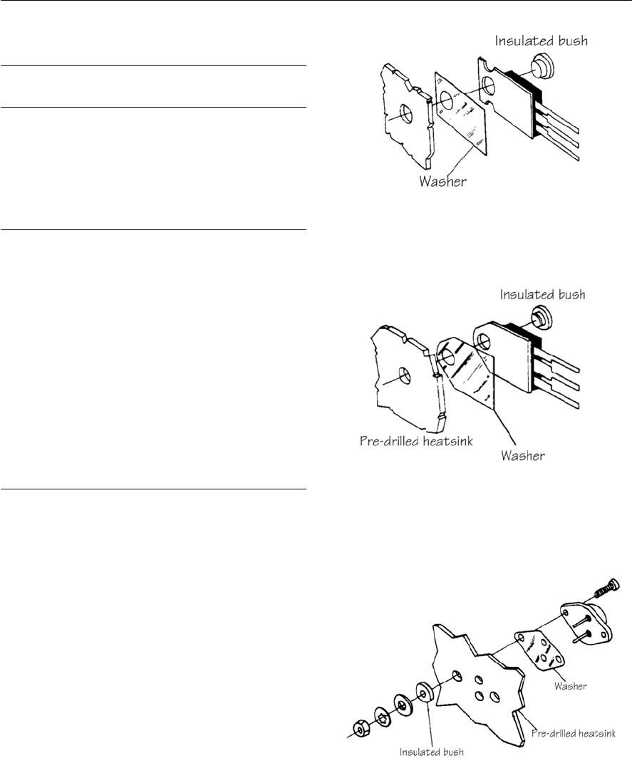
Case style
JA (no heatsink)
(°C/W)
JC
(°C/W)
TO92 200 to 350 40 to 60
TO126 83 to 100 3 to 10
TO220 60 to 70 1.5 to 4
TO202 62 to 75 6 to 13
TO218 30 to 45 1 to 1.56
CIRCUIT CONSTRUCTION 353
Figure 19.39 Typical mounting arrangement for
aTO218 or TAB packaged device
20°C/W to a complex aluminium alloy extrusion
with a thermal resistance of 1.2°C/W. Lower values
of thermal resistance can be obtained with the use
of forced air cooling.
Natural convection airflow can be enhanced by
the proper placement of heatsinks and other heat
producing components. Since warm air rises,
vertical surfaces tend to transmit heat to the air
better than comparable horizontal surfaces. The
hottest devices should be located on the upper side
of a horizontally mounted PCB or close to the
upper edge of a vertically mounted PCB.
Semiconductor mounting arrangements
Atypical mounting arrangement for a TO220
semiconductor package is shown in Fig. 19.38. In
many cases, the tab of the device is connected to
one of three terminals (often the collector or drain)
in which case a mica or thermally conductive
plastic washer must be fitted. Note also that an
insulated bush must be used in order to prevent the
mounting bolt shorting the metal tab to the
heatsink. Figure 19.39 shows a similar mounting
arrangement used for a TO218 packaged device
while Fig. 19.40 shows how a TO3 device is fitted.
The thermal resistance of the mounting kit used
with a semiconductor device can have a major
effect on the efficiency of the heat conduction from
the surface of the case to the heat radiator. Special
thermally impregnated washers have significantly
lower thermal resistance than simple mica washers.
Thermally conductive silicone grease should NOT
be used with this type of washer.
Table 19.4 Typical thermal resistances for various
case styles
Figure 19.38 Typical mounting arrangement for
aTO220 packaged device
Figure 19.40 Typical mounting arrangement for
aTO3 packaged device
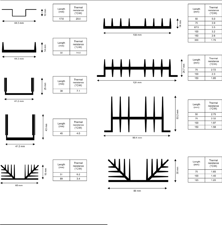
354 ELECTRONIC CIRCUITS: FUNDAMENTALS AND APPLICATIONS
Apractical example
We conclude this chapter with an example of
circuit construction based on a simple bench power
supply. The requirement was for a small adjustable
d.c. power supply that could be used for general-
purpose bench testing of electronic circuits. After
some preliminary investigation the following basic
requirements were established:
1. It should be mechanically and electrically
rugged
2. It should use proven and reliable technology
3. It should be low-cost and easy to maintain
4. It should comply with appropriate European
legislation (e.g. the EMC and low-voltage
directives)
5. It should have one variable (3 V to 15 V) output
and one fixed (+5 V) accessory output and that
both outputs should be protected against a short-
circuit connected to the output.
6. With the exception of the accessory output and
the a.c. mains input, all controls, connectors and
switches should be made available on the front
panel
7. It should have colour coded output terminals
Figure 19.41 Some common heatsink types and their associated thermal resistances

CIRCUIT CONSTRUCTION 355
that will accept standard 4 mm plugs. The
terminals should also allow wires that have not
been fitted with plugs to be clamped directly
using a screw action
8. It should operate from a standard 220 V a.c.
mains supply which should be connected using
astandard 3-pin IEC connector
9. It should be ‘tamper-proof’ (it should not be
possible to remove the knobs or the enclosure
without having to resort to the use of special
tools)
10. It should be lightweight and portable
11. It should have LED indicators to show that the
power supply is switched on and that the
outputs are present.
Design specification
Having determined a need for our product and
obtained a detailed list of requirements, the next
stage was that of firming up the design brief and
producing a detailed specification for the power
supply. This design specification was a detailed
performance specification that included numerical
values for relevant parameters (such as output
voltage and output current). The detailed design
specification was important because we returned
when we needed to confirm that our prototype
power supply met our requirements. We did this by
comparing the measured performance specification
with the original design specification. Taking into
account the requirements listed above, we arrived
at the following design specification:
Fixed output:
•Output voltage adjustable from 3 V to 15 V
•Output current adjustable from 50 mA to
1 A max.
•4mm binding post connectors (red and
black)
Variable output:
•Output voltage fixed at +5V ±5%
•Output current 1 A max.
•4mm binding post connectors (yellow and
black)
Input:
•200 to 240 V a.c. via IEC connector, 1 A
fuse and EMC filter
Prototype manufacture
The next stage in the development of the power
supply was that of examining a range of solutions
before deciding on the particular solution that
formed the basis of a prototype. Since the product
has both electrical/electronic and mechanical
aspects it was possible to consider these separately.
Research was needed to find a suitable electronic
circuit and to identify the components that would
be needed to build it. Various sources of
information were available including books,
magazines, data sheets (see Fig. 19.42) from
manufacturers and suppliers as well as the Web.
After carrying out some initial investigation, a
suitable circuit design was located (see Fig. 19.43).
This circuit was based on two low-cost readily
available integrated circuit devices (see
requirements 2 and 3) and the data sheets were
obtained for each (see Fig. 19.42).
The initial prototype was constructed on
stripboard and tested after fitting into the enclosure
(as shown in Fig. 19.47). A further prototype (see
Fig. 19.48) was developed using a printed circuit
board (PCB), the track layout for which was
designed using a PCB CAD package which had an
autorouting facility.
In order to satisfy requirements 1 and 4, a fully-
screened metal enclosure was used. This was based
on a simple two-part construction (see requirements
3). An internal EMC filter was fitted in order to
comply with the EMC directive (see requirement
4). Before manufacturing the enclosure it was
necessary to produce some general arrangement
and detail drawings showing how the sheet metal
should be drilled, punched, cut and bent. These
drawings had to be accurately dimensioned in order
to accommodate the components used. The
drawings were produced using a simple 2D CAD
package. One drawing was produced to show the
enclosure top and front panel detail (see Fig. 19.44)
whilst a second drawing was used to show the
enclosure bottom and rear panel detail.
The material selected for the enclosure was 1.22
mm (18 SWG) aluminium sheet. The reasons for
the choice of this material were that it was
reasonably lightweight (see requirement 10), low-
cost (see requirement 3), and easy to process. It
could also be attractively paint finished. Figures
19.49 and 19.50 show the assembled prototype.
Testing to specification
Having assembled a working prototype the next
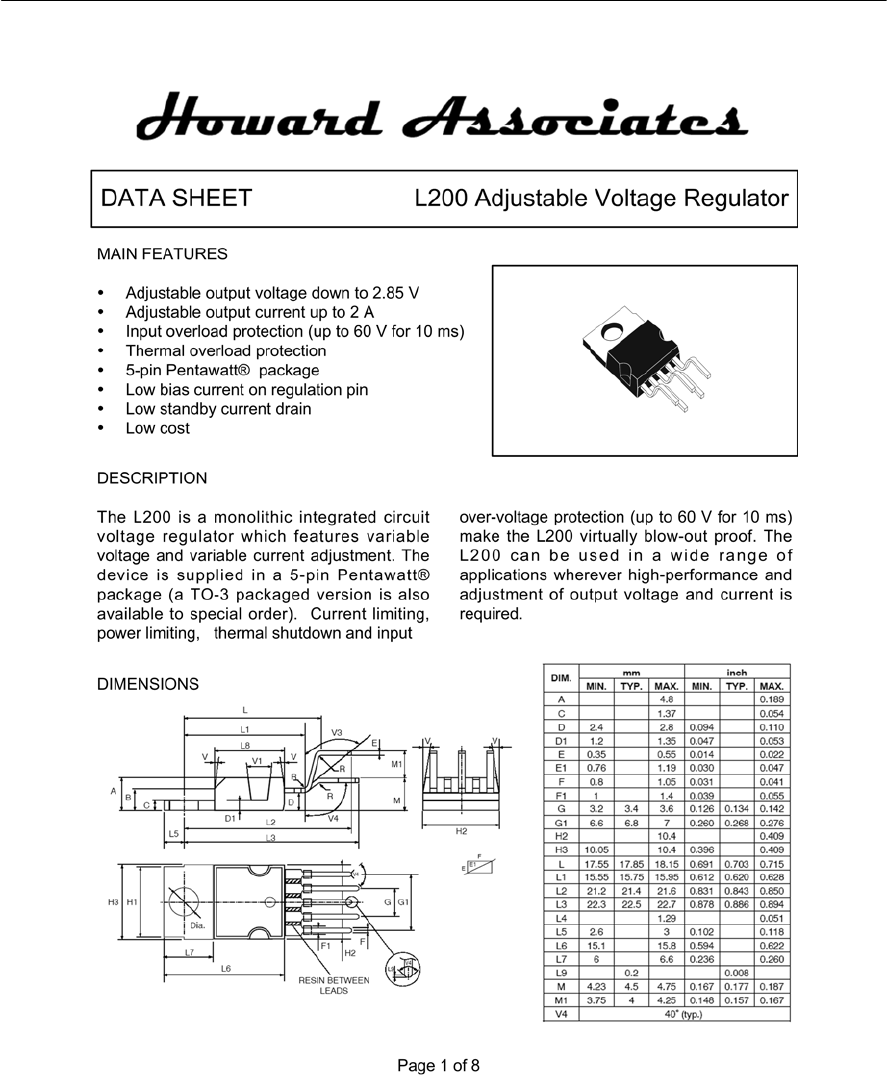
356 ELECTRONIC CIRCUITS: FUNDAMENTALS AND APPLICATIONS
Figure 19.42 Data sheet for the L200 integrated circuit variable voltage regulator. The data sheet provides
all of the essential information required to produce a working circuit design, including maximum ratings,
mounting details, and thermal characteristics
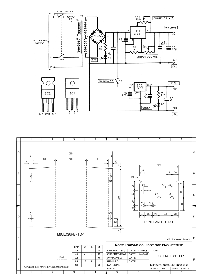
CIRCUIT CONSTRUCTION 357
Figure 19.43 Circuit diagram for the variable bench power supply
Figure 19.44 Mechanical details for the power supply enclosure
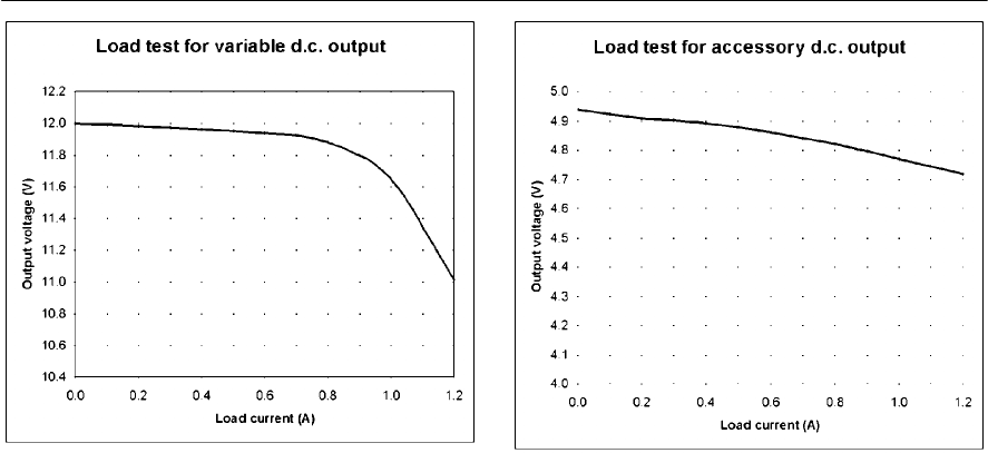
Figure 19.45 Load test graph for the variable d.c.
output. Note how the output voltage begins to fall
rapidly when the load current exceeds 0.9 A
358 ELECTRONIC CIRCUITS: FUNDAMENTALS AND APPLICATIONS
stage was that of measuring its performance in
order to ensure that it fully conformed with the
requirements set down in the design brief.
Prototype testing was carried out by applying a
variable load to the output of the power supply and
measuring corresponding values of output voltage
and output current. To simplify the analysis, the
test data was entered into a spreadsheet and graphs
of each load test were generated (see Figs 19.45
and 19.46).
Performance measurement
The measured performance specifications for the
power supply (obtained from the load tests) were as
follows (figures from the original design
specification are shown in square brackets):
Fixed output
•Minimum output voltage = 2.85V [3 V]
•Maximum output voltage = 15.23 V [15 V]
•Maximum output current = 1.2 A [1 A]
Variable output
•Output voltage (no load) = 4.94 V [5 V]
•Output voltage (1 A load) = 4.77 V [4.75 V]
•Output current = 1.2 A [1 A]
These results provided confirmation that the
prototype conformed closely with the original
design specification.
Evaluation and modification
Having carried detailed testing of the prototype
power supply and having verified that the design
specification had been met, the next stage was that
of finalizing the prototype and carrying out any
modifications prior to passing the design for
production.
Feedback was obtained from a number of ‘test
users’ who were asked to check that each of the
original requirements had been satisfied. Several
recommendations were made as a result of this
feedback including:
•fitting a carrying handle to the enclosure
•fitting calibrated scales to the voltage and
current controls
•relocating the +5 V accessory output switch
to the front panel
•mounting both integrated circuit devices on
the same heatsink (suitably up-rated) to
reduce space and cost
•providing an over-current indicator that will
become illuminated when/if the supply is
overloaded.
Figure 19.46 Load test graph for the fixed
accessory output. Note how the output voltage falls
below 4.75 V at an output current of about 1.1 A
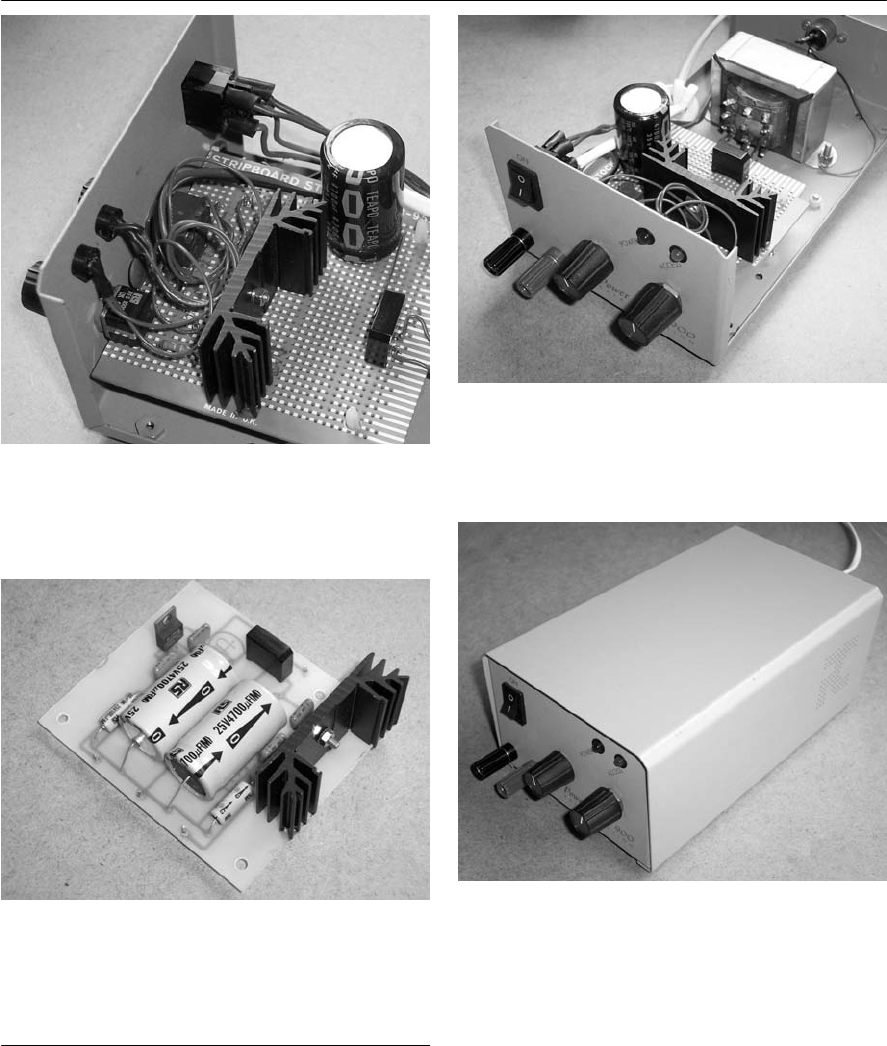
Practical investigation
Objective
To construct a simple circuit using (a) a stripboard
and (b) a printed circuit board.
CIRCUIT CONSTRUCTION 359
Figure 19.48 PCB layout developed for the final
version of the bench power supply
Components and test equipment
Stripboard and photo-resist copper laminate
measuring approximately 6 cm square, 555 timer
and 8-pin low-profile DIL socket (two required),
resistors of 10 kI(four required), 560 kI(two
Figure 19.50 External view of the bench power
supply showing the front panel controls and
enclosure
Figure 19.47 Internal arrangement showing the
prototype stripboard and front panel wiring
Figure 19.49 Interior of the bench power supply
showing transformer and stripboard mounting
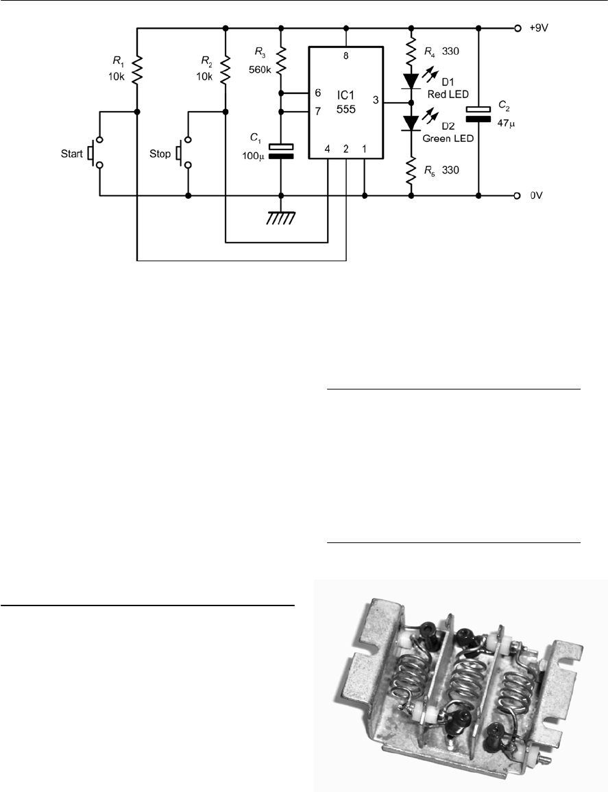
Problems
19.1 Identify the type of circuit construction used
for the low-pass L-C filter shown in Fig.
19.52.
19.2 Explain, with the aid of a diagram, how a
PIC can be programmed without having to
remove it from the target system
19.3 Determine the minimum acceptable thermal
resistance rating for a heatsink for use with a
power transistor operating under the
conditions shown in Table 19.6.
Answers to these problems appear on page 376.
360 ELECTRONIC CIRCUITS: FUNDAMENTALS AND APPLICATIONS
Figure 19.52 See Problem 19.1
Figure 19.51 The one minute timer circuit used in the Practical investigation
required), 470 I(four required) 5% 0.25 W,
capacitors of 100 µF and 47 µF 16 V (two of each
required) , Red and Green LEDs (two of each
required), four normally open (NO) printed circuit
board mounting push-button switches, 9V PP3
battery connectors (two required).
Procedure
Following the procedures described earlier in this
chapter, design and manufacture the one minute
timer circuit using (a) stripboard and (b) printed
circuit board construction techniques. Test each
circuit when complete.
Table 19.5 See Problem 19.3
Maximum junction temperature: 155°
Thermal resistance of case to
surface: 1.4°C/W
Thermal resistance of washer
and mounting kit: 1.75°C/W
Maximum total power
dissipation: 40W
Maximum ambient temperature: 45°C
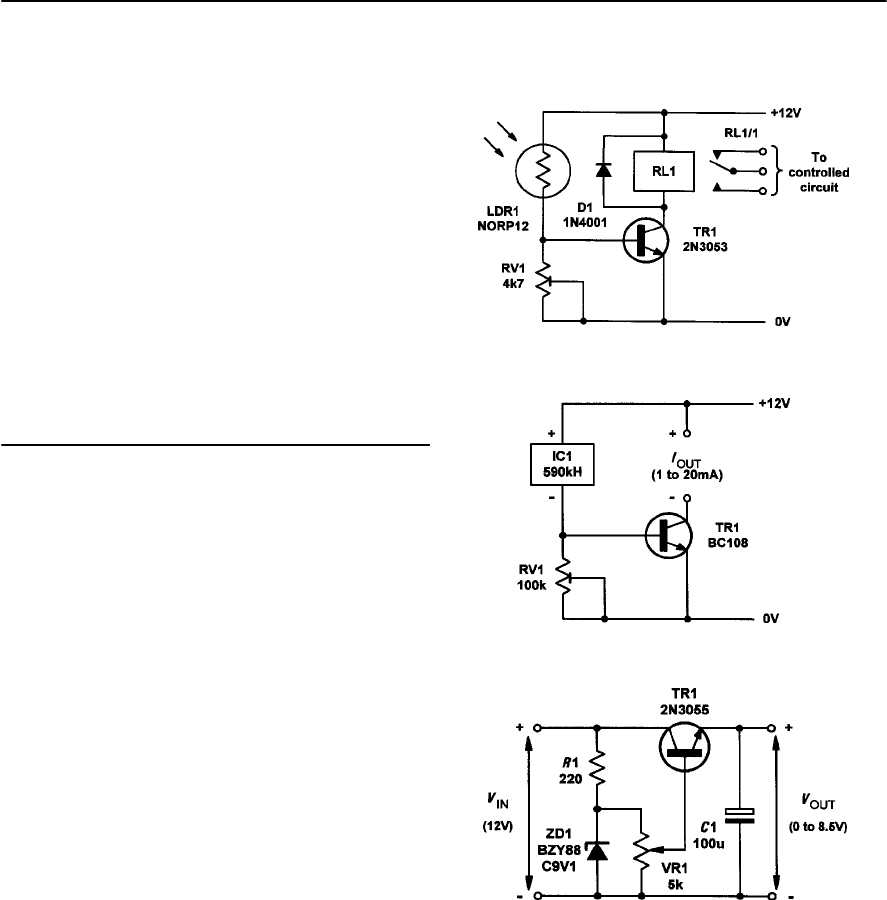
Appendix 1
Student assignments
The student assignments provided here have been
designed to support the topics introduced in this
book. They can also be used to satisfy the
assessment requirements of a taught course. Please
note that the assignments are not exhaustive and
may need modification to meet an individual
awarding body’s requirements as well as the locally
available resources. The first 10 assignments satisfy
the requirements for the level 2 courses while the
remaining 12 are designed to meet the requirements
of level 3 courses. Assignments can normally be
carried out in three to five hours, including
analysis, report writing and evaluation.
Level 2 assignments
Assignment 1 Electronic circuit construction
For each one of five simple electronic circuits
shown in Figs A1.1 to A1.5:
(a) Identify and select the components required to
build the circuit.
(b) Identify an appropriate method of construction
selected from the following list:
•breadboard;
•tag board;
•stripboard;
•printed circuit board;
•wire wrapping.
Assemble and test each circuit according to its
circuit diagram. Note that a different construction
method must be selected for each circuit.
Assignment 2 Electronic circuit testing
For each of the circuits in Figs Al.l to A1.5,
describe the type and nature of the input and output
signals (as appropriate). For each circuit select and
use appropriate measuring instruments (e.g.
multimeter and oscilloscope) to test and check the
operation of each circuit. Write a short report to
summarize your findings.
Assignment 3 Semiconductor investigation
Prepare a report describing the construction of (a) a
junction diode and (b) a bipolar transistor.
Describe, in your own words, the principle of
Figure A1.1 See Assignments 1 and 2
Figure A1.2 See Assignments 1 and 2
Figure A1.3 See Assignments 1 and 2
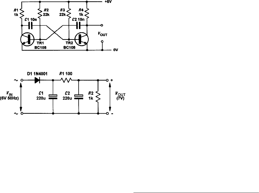
362 ELECTRONIC CIRCUITS: FUNDAMENTALS AND APPLICATIONS
Figure A1.4 See Assignments 1 and 2
Figure A1.5 See Assignments 1 and 2
operation of each device. With the aid of a simple
circuit diagram, describe a typical application for
each type of semiconductor.
Assignment 4 Basic logic functions
Write a report identifying the types and symbols
(both BS3939 and MIL/ANSI) used for all basic
logic gates (AND, OR, NOT, NAND and NOR).
Include in your report a description of the operation
of each logic gate together with a truth table.
Assignment 5 Applications of logic circuits
With the aid of labelled diagrams, describe TWO
applications of logic gates. One application should
be based on combinational logic while the other
should use sequential logic.
Assignment 6 Electronic measuring instruments
Write a report describing the operation and use of
(a) a multimeter and (b) an oscilloscope. Illustrate
your report with records of measurements carried
out on three common electronic components and
two simple electronic circuits.
Assignment 7 Microprocessors
Investigate TWO common types of microprocessor.
Produce an A4-size data sheet for each device
giving a brief specification of the chip, package and
pin-connecting details, clock frequencies, details of
the internal registers, descriptions of bus signals
(including the number of address and address
lines), etc.
Assignment 8 Monostable timer
Design, construct and test a variable timer based on
a555 device connected in monostable mode. The
timer is to be adjustable over the range 10s to 90s
and is to produce an output for driving a low-
voltage relay.
Assignment 9 Square wave generator
Design, construct and test a 5 V 1 kHz square wave
generator based on a 555 timer connected in astable
mode.
Assignment 10 A dipole aerial
Design, construct and test a half-wave dipole aerial
for DAB radio reception. Select a suitable feeder to
connect the aerial to a DAB receiver and
investigate the directional properties of the aerial.
Compare these with what you would expect from
radio theory.
Level 3 assignments
Assignment 11 Power supply investigation
With the aid of an electrical specification and
operating manual for a typical low-voltage d.c.
power supply, write a report explaining the
char-acteristics of the unit. Also explain the
meaning of each of the unit’s specifications. Carry
out a simple load test on the supply, plot a graph to
illustrate your results and comment on your
findings.
Assignment 12 Amplifier circuit investigation
Write a report that describes and explains one
small-signal Class-A discrete amplifier circuit, one
Class-B power amplifier circuit, and one amplifier
circuit based on an operational amplifier. The
report should identify and give typical
specifications for each type of amplifier.
Carry out a simple gain and frequency response
test on one of the amplifier circuits, plot a graph to

APPENDIX 1 STUDENT ASSIGNMENTS 363
illustrate your results and comment on your
findings.
Assignment 13 Small-signal amplifier design and
construction
Design, construct and test a single-stage transistor
amplifier. Write a report describing the model used
for the small-signal amplifier and include a detailed
comparison of the predicted characteristics
compared with the measured performance of the
stage.
Assignment 14 Electronic counter investigation
Prepare a report describing the characteristics of J-
Kbistable elements when compared with D-type
and R-S bistables. Using the data obtained, design,
construct and test a four-stage binary counter.
Modify the design using a standard logic gate to
produce a decade counter. Include in your report
timing diagrams for both the binary and decade
counters.
Assignment 15 Pulse generator investigation
Prepare a report describing one oscillator circuit,
one bistable circuit and one monostable circuit. The
report should include a description of one industrial
application for each of the circuits together with
sample calculations of frequency and pulse rate for
the two oscillator circuits, and pulse width for the
monostable circuit.
Assignment 16 Performance testing
Carry out performance tests on two different
amplifier circuits, two waveform generators and
two digital circuits. Compare the measured
performance of each circuit with the
manufacturer’s specification and present your
findings in a written report. The report should
include details of the calibration and operation of
each test instrument in accordance with the
manufacturer’s handbooks as well as evidence of
the adoption of safe working practice.
Assignment 17 Microprocessor clock
Design, construct and test (using an oscilloscope) a
microprocessor clock based on two Schmitt
inverting logic gates and a quartz crystal. The clock
is to produce a square wave output at a frequency
of between 1 MHz and 6 MHz (depending upon the
quartz crystal used).
Assignment 18 Assembly language programming
Use a simple 8-bit microprocessor system to
develop a simple assembly language program that
will read the state of a set of eight input switches
connected to an input port and illuminate a bank of
eight light emitting diodes connected to an output
port. The state of the input switches is to be
indicated by the light emitting diodes.
Assignment 19 Variable pulse generator
Design, construct and test a variable pulse
generator (along the lines of that shown on page
224). The pulse generator is to provide an output
from 1 Hz to 10 kHz with a pulse width variable
from 50 µs to 500 ms.
Assignment 20 AM radio tuner
Design, construct and test a simple AM radio tuner
based on a diode demodulator and a variable tuned
circuit. The radio tuner is to cover the medium
wave band from 550 kHz to 1.5 MHz and its output
is to be connected to an external audio amplifier.
Investigate the performance of the tuner and
suggest ways in which it could be improved.
Assignment 21 Analogue multimeter
Design, construct and test a simple analogue
multimeter based on a 1 mA moving coil meter.
The multimeter is to have three voltage ranges (10
V, 50 V and 100 V), two current ranges (10 mA
and 50 mA) and one ohms range.
Assignment 22 PIC microcontroller
Design, construct and test a simple PIC
microcontroller-based intruder alarm. The alarm is
to be capable of identifying an intrusion into any
one of four ‘zones’ using an LED panel and is to
produce a master alarm signal using a piezoelectric
transducer whenever any one of the alarm inputs is
triggered. The alarm is to be ‘set’ and ‘reset’ using
two further switch inputs.
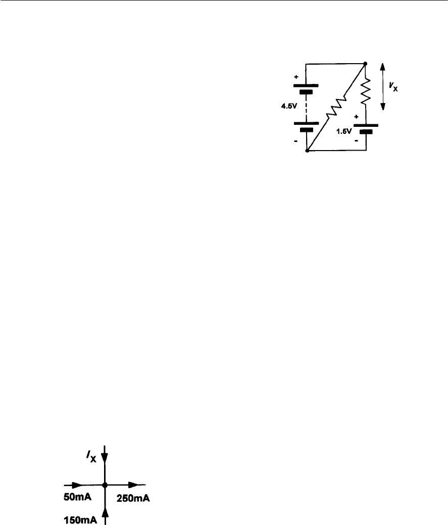
Appendix 2
Revision problems
These problems provide you with a means of
checking your understanding prior to an end-of-
course assessment or formal examination. If you
have difficulty with any of the questions you
should refer to the page numbers indicated.
1. A 120 kGresistor is connected to a 6 V battery.
Determine the current flowing. [Page 6]
2. A current of 45 mA flows in a resistor of 2.7
kG.Determine the voltage dropped across the
resistor. [Page 6]
3. A 24 V d.c. supply delivers a current of 1.5 A.
Determine the power supplied. [Page 8]
4. A 27 Gresistor is rated at 3 W. Determine the
maximum current that can safely be applied to
the resistor. [Page 8]
5. A load resistor is required to dissipate a power
of 50 W from a 12 V supply. Determine the
value of resistance required. [Page 8]
6. An electrical conductor has a resistance of
0.05 Gper metre. Determine the power wasted
in a 175 m length of this conductor when a
current of 8 A is flowing in it. [Page 8]
7. Figure A2.1 shows a node in a circuit.
Determine the value of Ix.[Page 49]
8. Figure A2.2 shows part of a circuit. Determine
the value of Vx.[Page 50]
9. A capacitor of 200 µF is charged to a potential
of 50 V. Determine the amount of charge stored.
[Page 33]
10. A sinusoidal a.c. supply has a frequency of
400 Hz and an r.m.s. value of 120 V. Determine
the periodic time and peak value of the supply.
[Page 70]
11. Four complete cycles of a waveform occur in a
time interval of 20 ms. Determine the frequency
of the waveform. [Page 70]
12. Determine the periodic time, frequency and
amplitude of each of the waveforms shown in
Fig. A2.3. [Page 71]
13. Determine the effective resistance of each
circuit shown in Fig. A2.4. [Page 26]
14. Determine the effective capacitance of each
circuit shown in Fig. A2.5. [Page 36]
15. Determine the effective inductance of each
circuit shown in Fig. A2.6. [Page 42]
16. A quantity of 100 nF capacitors is available,
each rated at 100 V working. Determine how
several of these capacitors can be connected to
produce an equivalent capacitance of: (a) 50 nF
rated at 200 V; (b) 250 nF rated at 100 V; and
(c) 300 nF rated at 100 V. [Page 36]
17. Two 60 mH inductors and two 5mH inductors
are available, each rated at 1 A. Determine how
some or all of these can be connected to produce
an equivalent inductance of: (a) 30 mH rated at
2A; (b) 40 mH rated at 1A; and (c) 125 mH
rated at 1 A. [Page 42]
18. Determine the resistance looking into the
network shown in Fig. A2.7, (a) with C and D
open-circuit and (b) with C and D shorted
together. [Page 26]
Figure A2.1 See Question 7
Figure A2.2 See Question 8
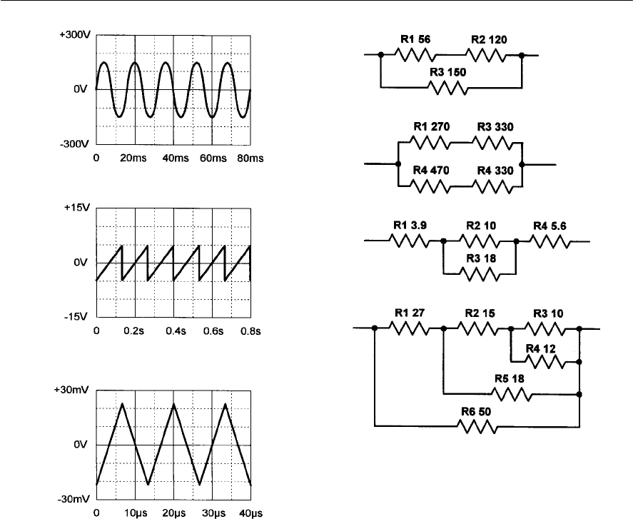
APPENDIX 2 REVISION PROBLEMS 365
19. Determine the current flowing in each resistor
and voltage dropped across each resistor in Fig.
A2.8. [Page 49]
20. Determine the current flowing in the volt-meter
movement shown in Fig. A2.9. [Page 54]
21. Assuming that the capacitor shown in Fig.
A2.10 is initially fully discharged (by switching
to position B), determine the current in R1at the
instant that S1 is switched to position A. Also
determine the capacitor voltage 1 minute after
operating the switch. [Page 58]
22. Determine the time taken for the output voltage
in Fig. A2.11 to reach 4 V after the arrival of
the pulse shown (assume that the capacitor is
initially uncharged). [Page 58]
23. In Fig. A2.12 determine the current supplied to
the inductor 100 ms after pressing the ‘start’
button. [Page 63]
24. Determine the reactance at 2 kHz of (a) a 60
mH inductor and (b) a 47 nF capacitor. [Page
72]
25. A 50 µF capacitor is connected to a 12 V, 50 Hz
a.c. supply. Determine the current flowing.
[Page 72]
26. An inductor of 2 H is connected to a 12 V, 50
Hz a.c. supply. If the inductor has a winding
resistance of 40 G,determine the current
flowing and the phase angle between the supply
voltage and supply current. [Page 74]
27. An inductor of 100 µH is connected in series
with a variable capacitor. If the capacitor is
variable over the range 50 pF to 500 pF,
determine the maximum and minimum values
of resonant frequency for the circuit. [Page 77]
Figure A2.3 See Question 12
Figure A2.4 See Question 13
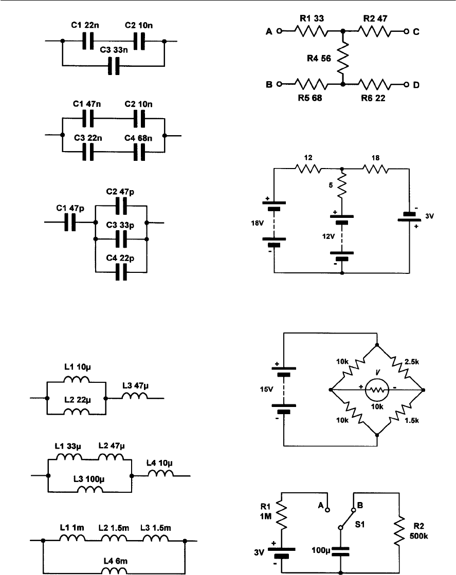
366 ELECTRONIC CIRCUITS: FUNDAMENTALS AND APPLICATIONS
Figure A2.5 See Question 14
Figure A2.6 See Question 15
Figure A2.7 See Question 18
Figure A2.8 See Question 19
Figure A2.9 See Question 20
Figure A2.10 See Question 21
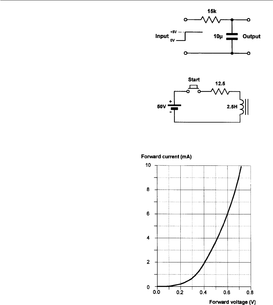
APPENDIX 2 REVISION PROBLEMS 367
28. An audio amplifier delivers an output power of
40 W r.m.s. to an 8 Gresistive load. What r.m.s.
voltage will appear across the load terminals?
[Page 8]
29. A transformer has 400 primary turns and 60
secondary turns. The primary is connected to a
220 V a.c. supply and the secondary is
connected to a load resistance of 20 G.
Assuming that the transformer is perfect,
determine: (a) the secondary voltage; (b) the
secondary current; and (c) the primary current.
[Page 80]
30. Figure A2.13 shows the characteristic of a
diode. Determine the resistance of the diode
when (a) VF= 2 V and (b) IF= 9 mA. [Page 90]
31. A transistor operates with a collector current of
25 mA and a base current of 200 µA.
Determine: (a) the value of emitter current; (b)
the value of common-emitter current gain; and
(c) the new value of collector current if the base
current increases by 50%. [Page 96]
32. A zener diode rated at 5.6 V is connected to a
12 V d.c. supply via a fixed series resistor of 56
G.Determine the current flowing in the resistor,
the power dissipated in the resistor and the
power dissipated in the zener diode. [Page 122]
33. An amplifier has identical input and output
resistances and provides a voltage gain of 26
dB. Determine the output voltage produced if an
input of 50 mV is applied. [Page 388]
34. Figure A2.14 shows the frequency response of
an amplifier. Determine the mid-band voltage
gain and the upper and lower cut-off
frequencies. [Page 135]
35. Figure A2.15 shows the frequency response of
an amplifier. Determine the bandwidth of the
amplifier. [Page 136]
36. The transfer characteristic of a transistor is
shown in Fig. A2.16. Determine (a) the static
value of common-emitter current gain at IC=50
mA and (b) the dynamic (small-signal) value of
common-emitter current gain at IC=50 mA.
[Page 145]
37. The output characteristics of a bipolar transistor
are shown in Fig. A2.17. If the transistor
operates with VCC = 15 V, RL=500 and IB=40
Adetermine (a) the quiescent value of collector-
emitter voltage; (b) the quiescent value of
collector current; (c) the peak-peak output
voltage produced by a base input current of
40 µA. [Page 146]
38. The output characteristics of a field effect
transistor are shown in Fig. A2.18. If the
transistor operates with VDD = 18 V, RL= 3 kG
and VGS = –1.5V determine: (a) the quiescent
value of drain-source voltage; (b) the quiescent
Figure A2.13 See Question 30
Figure A2.12 See Question 23
Figure A2.11 See Question 22
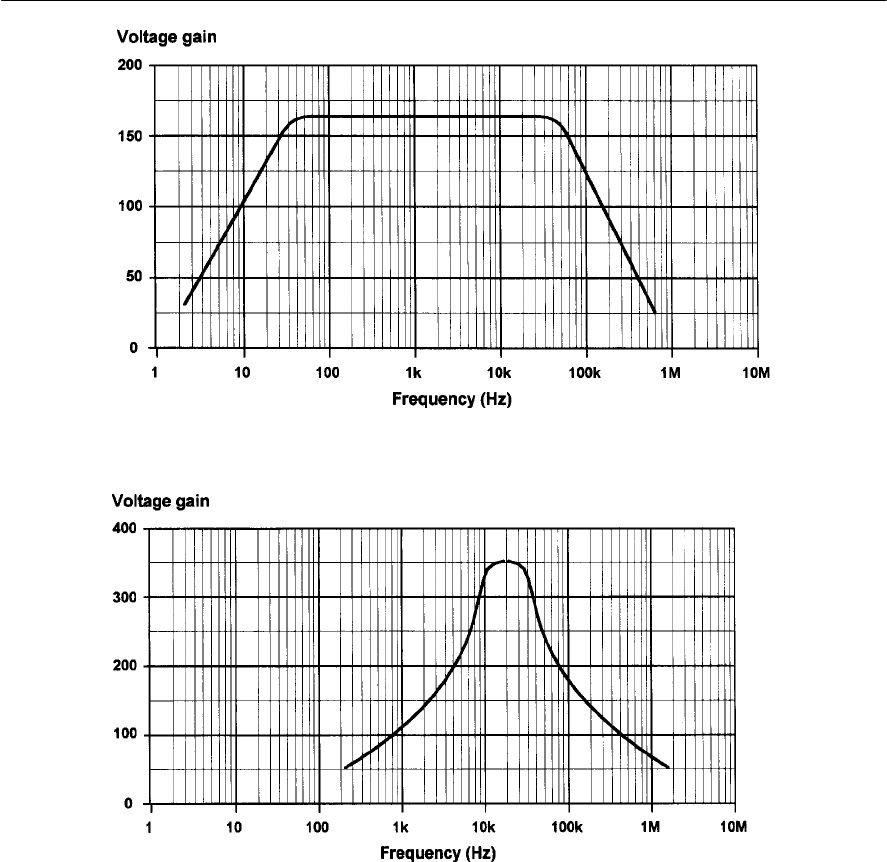
368 ELECTRONIC CIRCUITS: FUNDAMENTALS AND APPLICATIONS
value of drain current; (c) the peak-peak output
voltage produced by a gate input voltage of 1V
pk-pk; (d) the voltage gain of the stage. [Page
146]
39. Figure A2.19 shows the circuit of a common-
emitter amplifier stage. Determine the values of
IB,IC,IEand the voltage at the emitter. [Page
146]
40. A transistor having hie = 2.5 kGand hfe = 220 is
used in a common-emitter amplifier stage with
RL=3.3 kG.Assuming that hoe and hre are both
negligible, determine the voltage gain of the
stage. [Page 143]
41. An astable multivibrator is based on coupling
capacitors Cl = C2=10 nF and timing resistors
R1 = 10 kGand R2 = 4 kG.Determine the
frequency of the output signal. [Page 175]
42. A sine wave oscillator is based on a Wien
bridge with R= 5 kGand C=15 nF. Determine
the frequency of the output signal. [Page 173]
43. The frequency response characteristic of an
operational amplifier is shown in Fig. A2.20. If
Figure A2.14 See Question 34
Figure A2.15 See Question 35
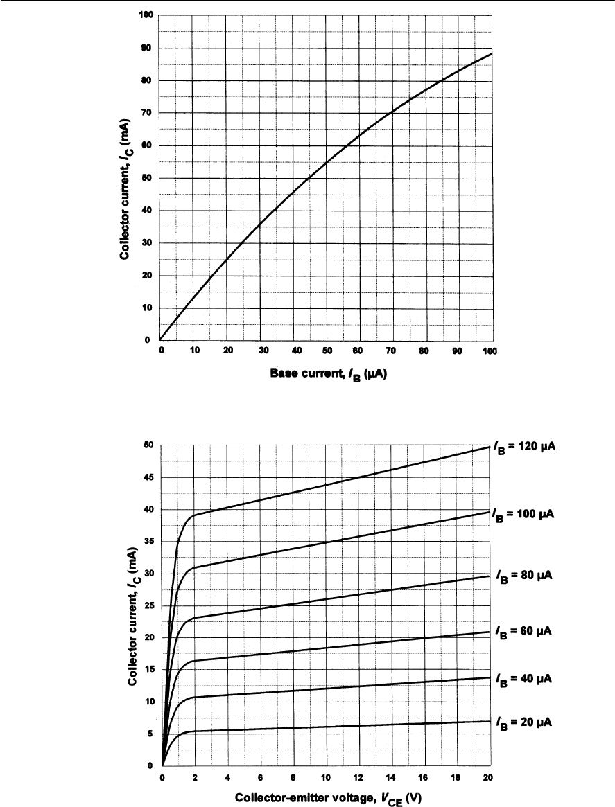
APPENDIX 2 REVISION PROBLEMS 369
Figure A2.16 See Question 36
Figure A2.17 See Question 37
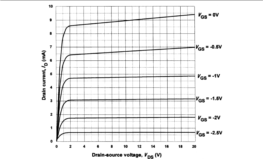
370 ELECTRONIC CIRCUITS: FUNDAMENTALS AND APPLICATIONS
the device is configured for a closed-loop gain
of 200, determine the resulting bandwidth.
[Page 161]
44. Redraw Fig. A2.21 using American (MIL/
ANSI) symbols. [Page 186]
45. Draw the truth table for the logic gate
arrangement shown in Fig. A2.22. [Page 187]
46. Redraw Fig. A2.23 using BS symbols. [Page
186]
47. What single logic gate can be used to replace
the logic circuit shown in Fig. A2.24? [Page
187]
48. What single logic gate can be used to replace
the logic circuit shown in Fig. A2.25? [Page
187]
49. Devise arrangements of logic gates that will
produce the truth tables shown in Fig. A2.26.
Use the minimum number of logic gates in each
case. [Page 187]
50. A 1 kHz square wave clock waveform is applied
to the circuit shown in Fig. A2.27. Sketch the
output waveform against a labelled time axis.
[Page 188]
51. (a) Convert 7B hexadecimal to binary.
(b) Convert 11000011 binary to hexadecimal.
[Page 201]
52. What is the largest value, expressed (a) in
decimal, and (b) in binary, that can appear at
any one time on a 16-bit data bus. [Page 201]
53. Sketch a diagram showing the basic
arrangement of a microprocessor system. Label
your drawing clearly. [Page 200]
54. (a) Explain the function of a microprocessor
clock.
(b) Explain why a quartz crystal is used to
determine the frequency of a microprocessor
clock. [Page 206]
55. Sketch the circuit diagram of a typical
microprocessor clock. Label your drawing
clearly. [Page 206]
56. Explain, briefly, how a microprocessor fetches
and executes instructions. Illustrate your answer
with a timing diagram showing at least one
fetch-execute cycle. [Page 207]
57. Sketch the circuit diagram of a monostable
timer based on a 555 device. Explain, briefly,
Figure A2.18 See Question 38
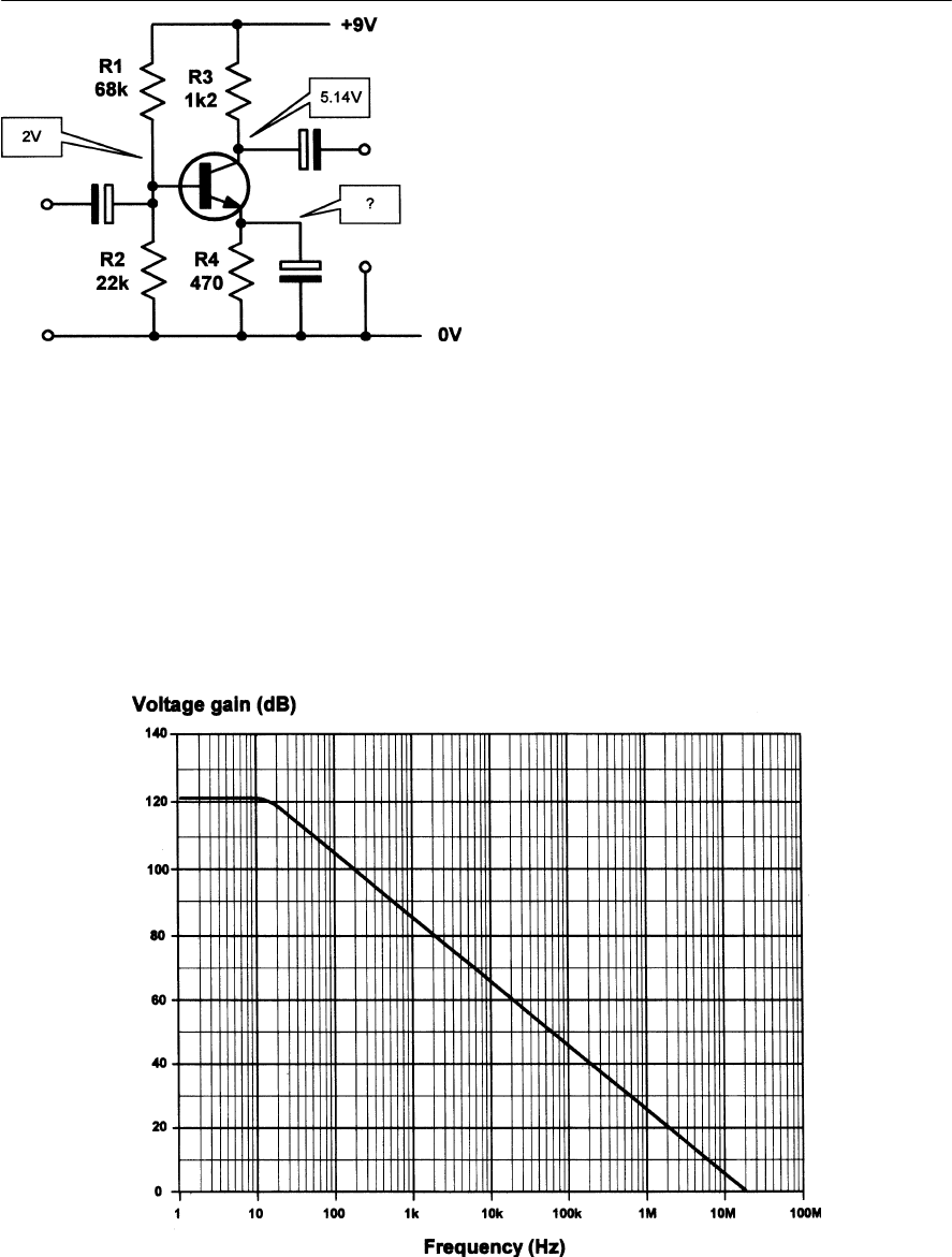
APPENDIX 2 REVISION PROBLEMS 371
how the circuit operates. [Page 219]
58. A 555 timer is connected in monostable mode.
If the values of the timing components used are
C = 100 nF and R = l0 kG,determine the
monostable pulse time. [Page 219]
59. Determine the frequency of a radio signal that
has a wavelength of 1500 m. [Page 229]
60. Determine the wavelength of a radio signal that
has a frequency of 40 MHz. [Page 229]
61. A superhet medium wave broadcast receiver
with an intermediate frequency of 470 kHz is to
cover the frequency range 560 kHz to 1.58
MHz. Over what frequency range should the
local oscillator be tuned? [Page 232]
62. Explain, with the aid of waveforms, the
operation of a simple AM demodulator. [Page
235]
63. Explain, with the aid of a labelled sketch, how
the voltage and current are distributed in a half-
wave dipole aerial. [Page 237]
64. Determine the length of a half-wave dipole for
use at a frequency of 70 MHz. [Page 237]
65. Sketch the block schematic of a simple TRF
radio receiver. Briefly explain the function of
each stage. [Page 233]
66. A moving coil meter has a full-scale deflection
current of 1 mA and a coil resistance of 400 G.
Determine the value of the multiplier resistor if
the meter is to be used as a voltmeter reading 0
to 15 V. [Page 245]
67. A moving coil meter has a full-scale deflection
current of 5 mA and a coil resistance of 120 G.
Determine the value of shunt resistor if the
Figure A2.20 See Question 43
Figure A2.19 See Question 39
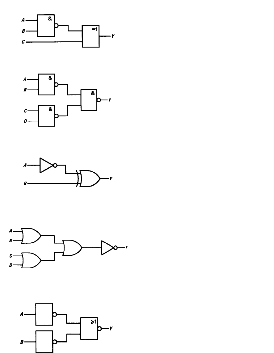
372 ELECTRONIC CIRCUITS: FUNDAMENTALS AND APPLICATIONS
meter is to be used as an ammeter reading 0 to
20 mA. [Page 246]
68. Explain the term ‘ohms-per-volt’ as applied to
an analogue voltmeter. [Page 248]
69. Sketch the circuit of a simple ohmmeter based
on a moving coil meter. [Page 246]
70. Identify each of the forms of distortion shown in
Fig. A2.28. [Page 267]
71. Give TWO reasons why a multimeter is
generally considered to be unsuitable for
checking the operation of logic circuits. [Page
282]
72. Explain how a logic probe can be used to check
the operation of a combinational logic circuit.
[Page 284]
73. Briefly explain the ‘half-split’ method of fault
finding. [Page 274]
74. Define the terms ‘sensor’ and ‘transducer’. Give
one example of each. [Page 288]
75. Identify one type of sensor for use in each of the
following applications:
(a) measuring the surface temperature of an
integrated circuit package; (b) determining the
pressure exerted on the walls of a gas storage
vessel; (c) detecting the minimum level of fuel
in a tank; (d) determining the flow rate of a
liquid in a pipe. [Page 290]
76. Sketch interface circuits to show how a TTL
logic signal can be used to control (a) a 24 V
d.c. relay and (b) an a.c. mains operated motor.
Identify all components used in each circuit.
[Page 299]
77. Sketch the block schematic diagram of an
electronic control system that incorporates
feedback. Label your drawing clearly. [Page
287]
78. Sketch the block schematic diagram of an
electronic instrumentation system that
incorporates analogue input and digital display
facilities. Label your drawing clearly. [Page
287]
79. Explain, with the aid of a circuit diagram, how a
threshold light-level detector can be made with
the aid of a comparator. [Page 296]
80. Explain the advantages of using a PIC
microcontroller in simple control applications
when compared with (a) logic gate
arrangements and (b) conventional
microprocessors. [Page 313]
Figure A2.21 See Question 44
Figure A2.23 See Question 46
Figure A2.22 See Question 45
Figure A2.24 See Question 47
Figure A2.25 See Question 48
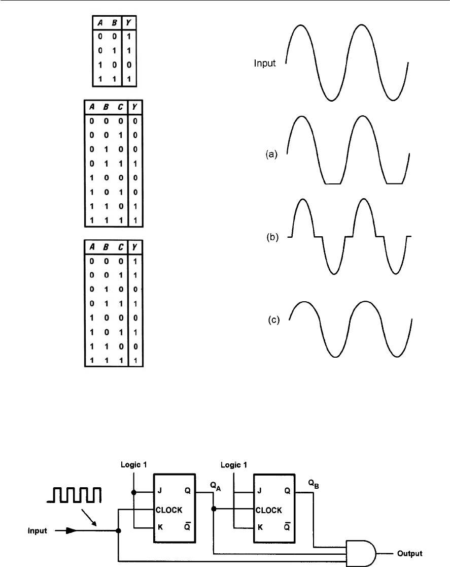
APPENDIX 2 REVISION PROBLEMS 373
Figure A2.27 See Question 50
Figure A2.26 See Question 49 Figure A2.28 See Question 70

Appendix 3
Answers to problems
Chapter 1
1.1 Coulombs, Joules, Hertz
1.2 3.6 MJ
1.3 0.52 radian
1.4 11.46°
1.5 39.57 kG
1.6 0.68 H
1.7 2.45 nF
1.8 0.19 mA
1.9 4.75 × 10R4V
1.10 16.5 × 10⁶G
1.11 4.8 × 106,7.2 × 103, 4 × 103,0.5 × 10R3
1.12 silver
1.13 33.3 mA
1.14 6.72 V
1.15 3.3 kG
1.16 150
1.17 0.436 G
1.18 0.029 W
1.19 0.675 W
1.20 57.7 mA
1.21 0.625 × 10⁶V/m
1.22 12 A
1.23 6 µWb
1.24 1.103 × 10⁵
1.25 0.5 A
1.26 1P 4W
1.27 1 kG, 3 kG,10 kG,30 kG
Chapter 2
2.1 60 G,3.75 W, wirewound
2.2 270 kG5%, 10 G10%, 6.8 MG5%,
0.39 G5%, 2.2 kG2%
2.3 44.65 Gto 49.35 G
2.4 27 Gand 33 Gin series, 27 Gand 33 Gin
parallel, 56 Gand 68 Gin series, 27 G,
33 Gand 56 Gin parallel, 27 G,33 Gand
68 Gin series
2.5 66.67 G
2.6 10 G
2.7 102 G,78.5 G
2.8 407.2 G
2.9 98.7 kG
2.10 3.21 × 10R4
2.11 3.3 µF and 4.7 µF in parallel, 1 µF and
10 µF in parallel, 1 µF, 3.3 µF, 4.7 µF and
10 µF in parallel, 1 µF and 10 µF in series,
3.3 µF and 4.7 µF in series
2.12 60 pF, 360 pF
2.13 50 pF
2.14 20.79 mC
2.15 1.98 nF
2.16 69.4 µF
2.17 0.313 V
2.18 0.136 H
2.19 0.48 J
2.20 10 mH, 22 mH and 60 mH in parallel,
10 mH and 22 mH in parallel, 10 mH and
22 mH in series, 10 mH and 60 mH in
series, 10mH 60mH and 100 mH in series
Chapter 3
3.1 275 mA
3.2 200 G
3.3 1.5 A away from the junction, 215 mA
away from the junction
3.4 1.856 V, 6.6 V
3.5 0.1884 A, 0.1608 A, 0.0276 A, 5.09 V,
0.91V, 2.41V
3.6 1.8 V, 10.2 V
3.7 0.5 A, 1.5 A
3.8 1 V, 2 V, 3 V, 4 V, 5 V
3.9 40.6 ms
3.10 3.54 s
3.11 112.1 µF
3.12 0.128 s
3.13 2.625 V, 5 G
3.14 21 V, 7 G, 3 A, 7 G
3.15 50 mA, 10 V
3.16 50 V, 10 V
Chapter 4
4.1 4 ms, 35.35 V
4.2 59.88 Hz, 3394 V

APPENDIX 3 ANSWERS TO PROBLEMS 375
4.3 50 Hz 30 V pk-pk, 15 Hz 10 V pk-pk,
150 kHz 0.1 Vpk-pk
4.4 19 V, R11.8 V
4.5 10.6 V
4.6 36.19 kG,144.76 G
4.7 3.54 mA
4.8 10.362 G,1.45 kG
4.9 4.71 V
4.10 592.5 G,0.186 A
4.11 0.55, 0.487 A
4.12 157 nF
4.14 1.77 MHz to 7.58 MHz
4.15 7.5 mA, 2.71 V
4.16 281 kHz, 41.5, 6.77 kHz
4.20 18 V
4.21 245 V
4.22 4 turns per volt, 48 turns, 1.7 W, 0.36 A
Chapter 5
5.1 silicon (forward threshold appx. 0.6 V)
5.2 41 G,150 G
5.4 9.1 V zener diode
5.5 250 G
5.6 germanium low-power high-frequency,
silicon low-power low-frequency,
silicon high-power low-frequency,
silicon low-power high-frequency
5.7 2.625 A, 20
5.8 5 mA, 19.6
5.9 16.7
5.10 BC108
5.11 8 µA, 1.1 mA
5.12 47 mA, 94, 75
5.13 12.5mA, 12V, 60 µA
5.14 16 mA
5.16 dual-in-line, single-in-line, quad-in-line,
large-scale integration
5.17 100 V, 500 mW, 50 nA, 0.7 V
5.18 signal or power diode, photo diode, zener
diode, thyristor (or SCR)
5.19 NPN BJT, PNP Darlington BJT, P-channel
enhancement MOSFET, N-channel JFET
5.20 PNP silicon general-purpose transistor,
R40 V, R500 mA, R0.25 V, 625 mW, TO-92
5.21 The maximum power dissipation is not
exceeded
5.22 N-channel JFET RF amplifier, 25 V,
50 mA, 2 nA, 2 mS, 8 pF, 350 mW, TO-92
5.23 9.6 mA, 5 V, 0 V
Chapter 6
6.1 80 mV
6.2 5 mV
6.3 200 G
6.4 12.74 V, 9.1 V, 8.4 V
6.5 36.4 mA, 0.33 W
6.6 0 V, 12.04 V, 0 V
6.7 14.35 V
6.8 0.5 G,8.3 V
6.9 1%, 15.15 V
6.10 step-up (or ‘boost’), pins 5 and 3, pin 7
Chapter 7
7.1 40, 160, 6400, 100 G
7.2 2 V
7.3 56, 560 kHz, 15 Hz
7.4 18.5
7.5 0.0144
7.6 2.25 V
7.7 13 µA, 4.487 mA, 3.39 V, 2.7 V, 4.51 V
7.8 5 V, 7 mA, 8.5 V
7.9 0.6 V, 18 µA, 3.9 V, 2 mA, 0 V, 4.5 V, 9 V
7.10 12.2 V, 6.1 mA, 5.5
7.11 2,500
7.12 40, 0.27 W, 133 mA
7.13 37%, 338 mW
Chapter 8
8.3 200
8.7 R7.5 V
8.8 82 dB
Chapter 9
9.1 4.44, 40
9.2 6.49 kG
9.3 18 kG
9.4 5.63 V pk-pk
9.5 23.32 ms, 42.9 Hz
9.6 14.3 kG,42.9 kG
9.8 1.448 ms, 690 Hz
9.10 15.9 Hz
9.13 R3 = 2R4(minimum gain = 2)
Chapter 10
10.9 Low-power Schottky (LS) TTL, 27th
Month of 1998
10.10 0.6 V

376 ELECTRONIC CIRCUITS: FUNDAMENTALS AND APPLICATIONS
Chapter 11
11.1 00111010
11.2 C2
11.3 (a) 111111, (b) 3F
11.4 (c)
11.5 1,048,576
11.6 1,024
11.7 R32,768
11.8 (a) Input port, FEH; output port, FFH
(b) 01010000
11.10 See page 206
11.12 See page 200
Chapter 12
12.5 (a) VR2
(b) S2
(c) RA
(d) VR1
(e) S1
(f) R2
(g) VR3
(h) R5
(i) C10
(j) C5and R3
12.6 50 G
Chapter 13
13.1 1.58 m
13.2 23.1 MHz
13.3 4 m
13.4 1.02 MHz to 2.07 MHz
13.5 10.7 MHz, 170 kHz, 63
13.6 (a) L1/C2
(b) R1/R2
(c) L2
(d) R4/C5
(e) VR1
(f) C6
(g) C7
(h) C1
13.7 3m
13.8 24 W
Chapter 14
14.1 19.6 kG
14.2 11.11 G
14.3 16.67 kG
14.4 100 kG
14.5 (a) 19.99 V
(b) 10 mV
14.6 25 kG
14.7 60 mA
14.8 35.3 µA
14.9 (a) 3.33 ms, 4 V
(b) 125 ns, 150 mV
14.10 (a) 7.8 µs
(b) 3.4 µs
(c) 4.4 µs
(d) 1.5 µs
(e) 1 µs
(f) 5 V
Chapter 15
15.1 Fault 1: R2open-circuit
Fault 2: TR2 collector-emitter short-circuit
Fault 3: R3open-circuit
Fault 4: TR1 base-collector short-circuit
Fault 5: C2short-circuit
Fault 6: R 5open-circuit
Chapter 16
16.1 1. Volume, float gauge, voltage or current
2. Flow, flow sensor (rotating vane), voltage
or pulse repetition frequency
3. Semiconductor temperature sensor,
threshold comparator, voltage (high or low)
Chapter 18
18.1 Analogue-to-digital converter;
digital-to-analogue converter;
bus interface device (RS-232, USB etc.);
LED or LCD display driver
Chapter 19
19.1 point-to-point wiring
19.3 17.85 °C/W
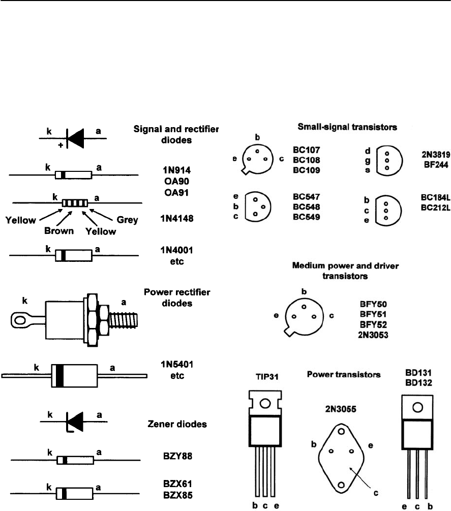
Appendix 4
Semiconductor pin connections
Figure A4.1 Diodes Figure A4.2 Transistors
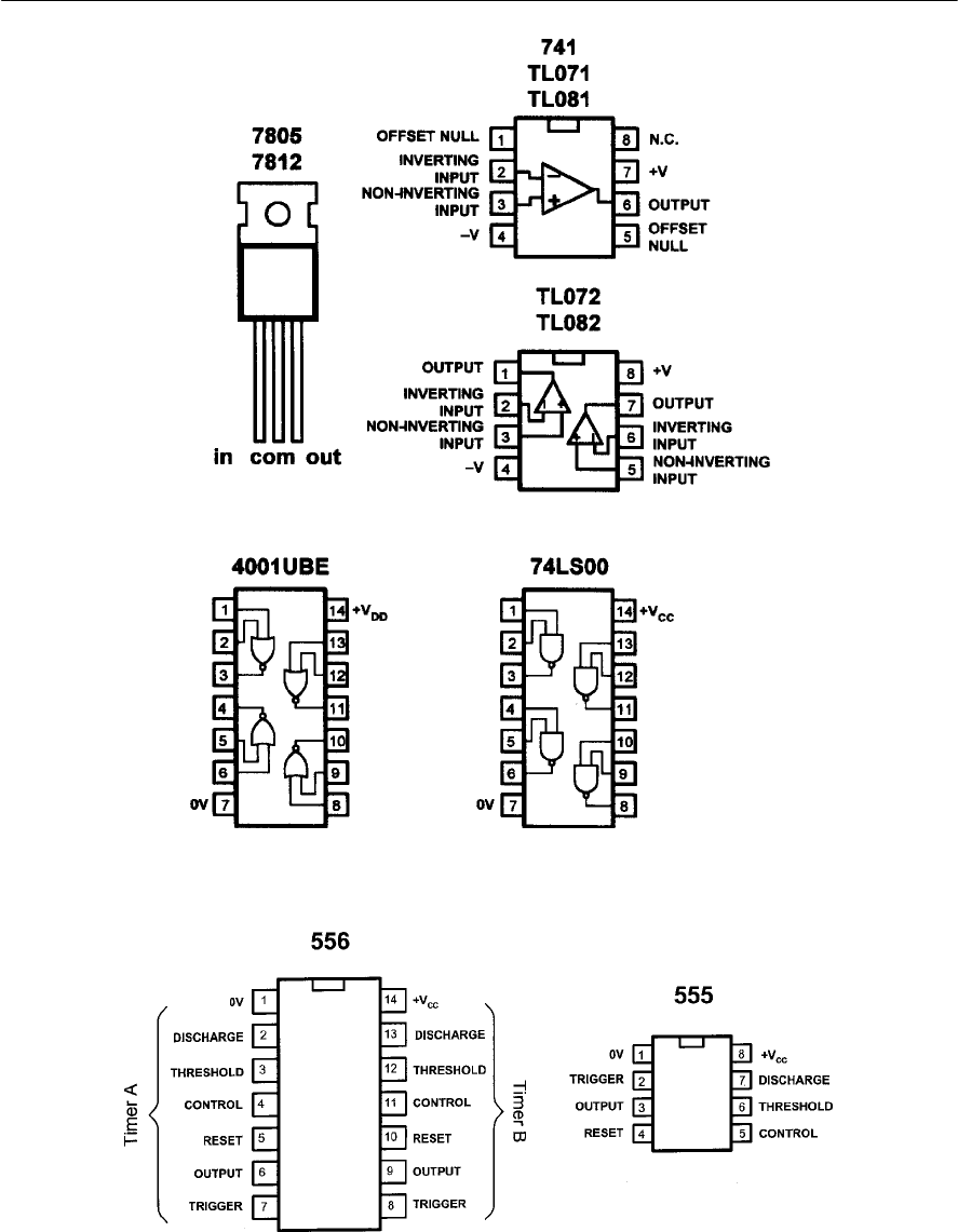
378 ELECTRONIC CIRCUITS: FUNDAMENTALS AND APPLICATIONS
Figure A4.4 Integrated circuit timers
Figure A4.3 Integrated circuits

Appendix 5
1N4148 data sheet
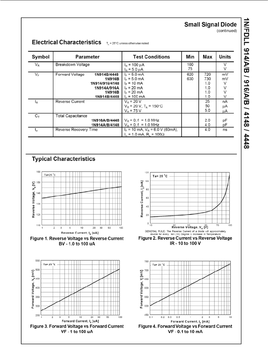
380 ELECTRONIC CIRCUITS: FUNDAMENTALS AND APPLICATIONS
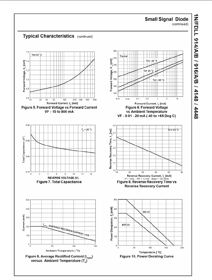
APPENDIX 5 1N4148 DATA SHEET 381
Datasheet reproduced by kind permission of Fairchild Semiconductor

Appendix 6
2N3904 data sheet
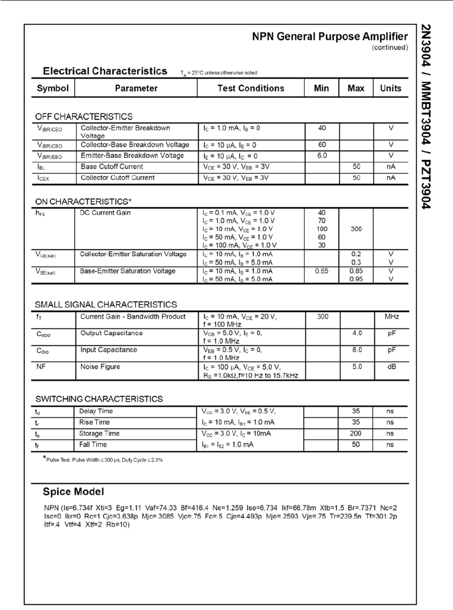
APPENDIX 6 2N3904 DATA SHEET 383
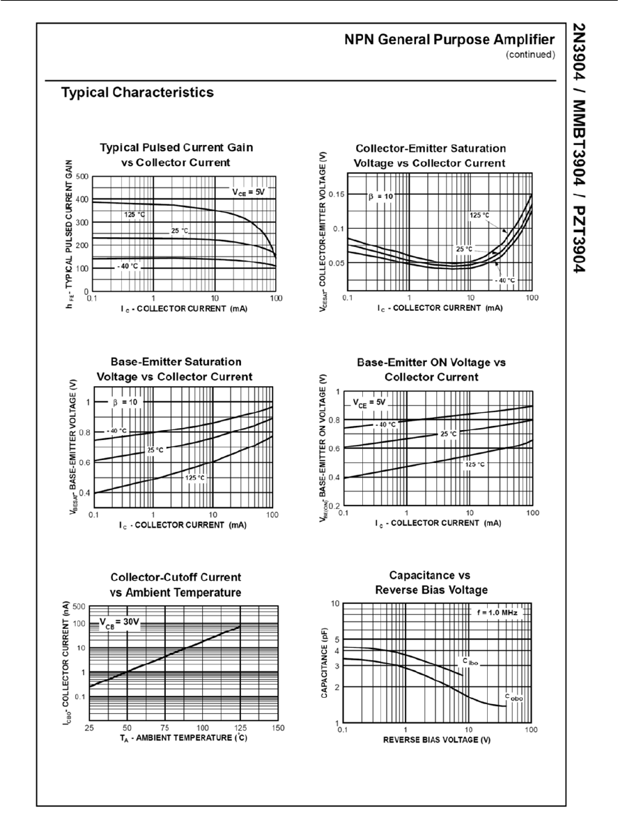
384 ELECTRONIC CIRCUITS: FUNDAMENTALS AND APPLICATIONS
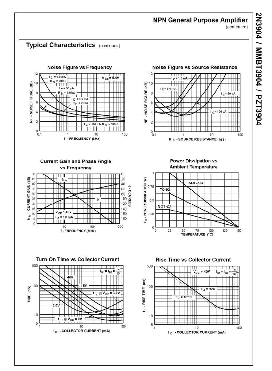
APPENDIX 6 2N3904 DATA SHEET 385
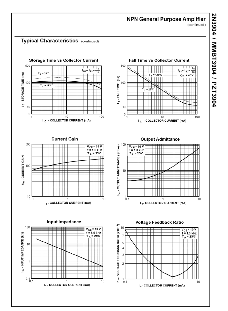
386 ELECTRONIC CIRCUITS: FUNDAMENTALS AND APPLICATIONS
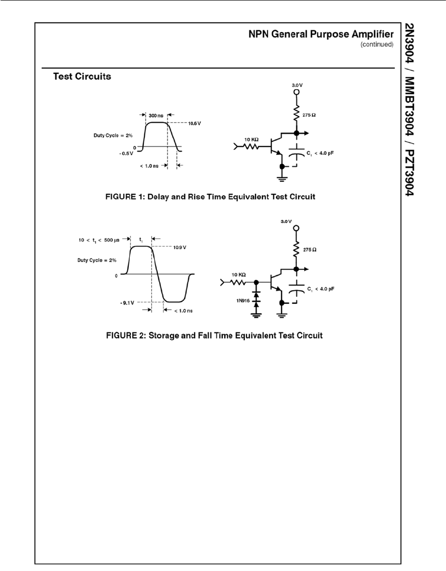
APPENDIX 6 2N3904 DATA SHEET 387
Datasheet reproduced by kind permission of Fairchild Semiconductor

Appendix 7
Decibels
Decibels (dB) are a convenient means of expressing
gain (amplification) and loss (attenuation) in
electronic circuits. In this respect, they are used as a
relative measure (i.e. comparing one voltage with
another, one current with another, or one power
with another). In conjunction with other units,
decibels are sometimes also used as an absolute
measure. Hence dBV are decibels relative to 1V,
dBm are decibels relative to 1 mW, etc.
The decibel is one-tenth of a bel which, in turn,
is defined as the logarithm, to the base 10, of the
ratio of output power (Pout)to input power (Pin).
Gain and loss may be expressed in terms of
power, voltage and current such that:
where Ap,Avor Aiis the power, voltage or current
gain (or loss) expressed as a ratio, Pin and Pout are
the input and output powers, Vin and Vout are the
input and output voltages, and Iin and Iout are the
input and output currents. Note, however, that the
powers, voltages or currents should be expressed in
the same units/multiples (e.g. Pin and Pout should
both be expressed in W, mW, µW or nW).
It is often more convenient to express gain in
decibels (rather than as a simple ratio) using the
following relationships:
Note that a positive result will be obtained
whenever Pout,Vout,or Iout is greater than Pin,Vout,
or Iout,respectively. A negative result will be
obtained whenever Pout,Vout,or Iout is less than Pin,
Vin or Iin. A negative result denotes attenuation
rather than amplification. A negative gain is thus
equivalent to an attenuation (or loss). If desired, the
formulae may be adapted to produce a positive
result for attenuation simply by inverting the ratios,
as shown below:
where Ap,Avor Aiis the power, voltage or current
gain (or loss) expressed in decibels, Pin and Pout are
the input and output powers, Vin and Vout are the
input and output voltages, and Iin and Iout are the
input and output currents. Note, again, that the
powers, voltages or currents should be expressed in
the same units/multiples (e.g. Pin and Pout should
both be expressed in W, mW, µW or nW).
It is worth noting that, for identical decibel
values, the values of voltage and current gain can
be found by taking the square root of the
corresponding value of power gain. As an example,
avoltage gain of 20 dB results from a voltage ratio
of 10 while a power gain of 20 dB corresponds to a
power ratio of 100.
Finally, it is essential to note that the formulae
for voltage and current gain are only meaningful
when the input and output impedances (or
resistances) are identical. Voltage and current gains
expressed in decibels are thus only valid for
matched (constant impedance) systems. Table A7.1
gives some useful decibel values.
Example A7.1
An amplifier with matched input and output
resistances provides an output voltage of 1V for an
input of 25 mV. Express the voltage gain of the
amplifier in decibels.
Solution
The voltage gain can be determined from the
formula:
out out out
pv i
in in in
and
PV I
AA A
PV I
== =
out out
p10 v 10
in in
10log 20log
PV
AA
PV
==
out
i10
in
and 20log I
A
I
=
in in
p10 v 10
out out
10log 20log
PV
AA
PV
==
in
i10
out
and 20log
I
AI
=

APPENDIX 7 DECIBELS 389
Av=20 1og10(Vout/Vin)
where Vin = 25 mV and Vout = 1 V.
Thus:
Av=20 log10(1V/25 mV)
=20 log10(40) = 20 × 1.6 = 32 dB
Example A7.2
Amatched 600 Gattenuator produces an output of
1mV when an input of 20 mV is applied.
Determine the attenuation in decibels.
Solution
The attenuation can be determined by applying the
formula:
Av=20 1og10(Vout/Vin)
where Vin =20 mV and Vout = 1 mV. Thus:
Av=20 log10(20 mV/1 mV)
=20 log10(20) = 20 × 1.3 = 26 dB
Example A7.3
An amplifier provides a power gain of 33 dB. What
output power will be produced if an input of 2 mW
is applied?
Solution
Here we must re-arrange the formula to make Pout
the subject, as follows:
Av=10 log10(Pout/Pin)
thus
Ap/10 = log10(Pout/Pin)
or
antilog10(Ap/10) = Pout/Pin
Hence
Pout = Pin × antilog10(Ap/10)
Now Pin = 2 mW = 20 × 10R3Wand Av=33 dB,
thus:
Pout = 2 × 10R3antilog10(33/10)
= 2 × 10R3×antilog10(3.3)
= 2 × 10R3×1.995 × 10R3=3.99 W
Table A7.1 Decibels and ratios of power, voltage
and current
Decibels
(dB)
Power gain
(ratio)
Voltage gain
(ratio)
Current gain
(ratio)
0 1 1 1
11.26 1.12 1.12
21.58 1.26 1.26
3 2 1.41 1.41
42.51 1.58 1.58
53.16 1.78 1.78
63.98 2 2
75.01 2.24 2.24
86.31 2.51 2.51
97.94 2.82 2.82
10 10 3.16 3.16
13 19.95 3.98 3.98
16 39.81 6.31 6.31
20 100 10 10
30 1,000 31.62 31.62
40 10,000 100 100
50 100,000 316.23 316.23
60 1,000,000 1,000 1,000
70 10,000,000 31,62.3 31,62.3

Appendix 8
Mathematics for electronics
This section introduces the mathematical
techniques that are essential to developing a good
understanding of electronics. The content is divided
into seven sections; notation, algebra, equations,
graphs, trigonometry, Boolean algebra, logarithms
and exponential growth and decay. We have
included a number of examples and typical
calculations.
Notation
The standard notation used in mathematics
provides us with a shorthand that helps to simplify
the writing of mathematical expressions. Notation
is based on the use of symbols that you will already
recognize. These include = (equals), + (addition), -
(subtraction), × (multiplication), and ¸ (division).
Other symbols that you may not be so familiar with
include < (less than), > (greater than), W
(proportional to) and Ö (square root).
Indices
The number 4 is the same as 2 × 2, that is, 2
multiplied by itself. We can write (2 × 2) as 22.In
words, we would call this ‘two raised to the power
two’ or simply ‘two squared’. Thus:
2 × 2 = 22
By similar reasoning we can say that:
2 × 2 × 2 = 23
and
2 × 2 × 2 × 2 = 24
In these examples, the number that we have used
(i.e. 2) is known as the base whilst the number that
we have raised it to is known as an index.Thus, 24
is called ‘two to the power of four’, and it consists
of a base of 2 and an index of 4. Similarly, 53is
called ‘five to the power of 3’ and has a base of 5
and an index of 3. Special names are used when the
indices are 2 and 3, these being called ‘squared’
and ‘cubed’, respectively. Thus 72is called ‘seven
squared’ and 93is called ‘nine cubed’. When no
index is shown, the power is 1, i.e. 21means 2.
Reciprocals
The reciprocal of a number is when the index is –1
and its value is given by 1 divided by the base.
Thus the reciprocal of 2 is 2–1 and its value is ½ or
0.5. Similarly, the reciprocal of 4 is 4–1 which
means ¼ or 0.25.
Square roots
The square root of a number is when the index is
½. The square root of 2 is written as 2½or Ö2. The
value of a square root is the value of the base which
when multiplied by itself gives the number. Since
3 ´ 3 = 9, then Ö9 = 3. However, (-3) ´ (-3) = 9, so
we have a second possibility, i.e. Ö9 = ±3. There
are always two answers when finding the square
root of a number and we can indicate this is by
placing a ± sign in front of the result meaning ‘plus
or minus’. Thus:
and
Variables and constants
Unfortunately, we don’t always know the value of a
particular quantity that we need to use in a
calculation. In some cases the value might actually
change, in which case we refer to it as a variable.
In other cases, the value might be fixed but we
might prefer not to actually quote it’s value. In this
case we refer to the value as a constant.
An example of a variable quantity is the output
voltage produced by a power supply when the load
1
2
44==
±2
1
2
99==
±3

APPENDIX 8 MATHEMATICS FOR ELECTRONICS 391
current is changing. An example of a constant
quantity might be the speed at which radio waves
travel in space.
In either case, we use a symbol to represent the
quantity. The symbol itself (often a single letter) is
aform of shorthand notation. For example, in the
case of the voltage from the power supply we
would probably use vto represent voltage.
Whereas, in the case of the speed of travel of a
radio wave we normally use cto represent the
speed of radio waves in space (i.e. the speed of
light).
We can use letters to represent both variable and
constant quantities in mathematical notation. For
example, the statement:
voltage is equal to current multiplied by resistance
can be written in mathematical notation as follows:
V=I×R
where Vrepresents voltage, Irepresents current,
and Rrepresents resistance.
Similarly, the statement:
resistance is equal to voltage divided by current
can be written in mathematical notation as follows:
where Rrepresents resistance, Vrepresents voltage,
and Irepresents current.
Proportionality
In electronic circuits, when one quantity changes it
normally affects a number of other quantities. For
example, if the output voltage produced by a power
supply increases when the resistance of the load to
which it is connected remains constant, the current
supplied to the load will also increase. If the output
voltage doubles, the current will also double in
value. If, on the other hand, the output voltage falls
by 50% the current will also fall by 50%. To put
this in a mathematical way we can say that
(provided that load resistance remains constant):
load current is directly proportional to output
voltage
Using mathematical notation and symbols to
represent the quantities, we would write this as:
V
R
I
=
where Irepresents load current, Vrepresents output
voltage, and ]means ‘is proportional to’.
In some cases, an increase in one quantity will
produce a reduction in another quantity. For
example, if the frequency of a wavelength of a
radio wave increases its wavelength is reduced. To
put this in a mathematical way we say that
(provided the speed of travel remains constant):
wavelength is inversely proportional frequency
Using mathematical notation and symbols to
represent the quantities, we would write this as
follows:
where Trepresents periodic time and frepresents
frequency.
It’s useful to illustrate these important concepts
using some examples:
Example 1
The power in a loudspeaker is proportional to the
square of the RMS output voltage and inversely
proportional to the impedance of the speaker. Write
down an equation for the power, P,in terms of the
voltage, V,and impedance, Z.Obtain a formula for
Pin terms of Vand Z.
From the information given, we can say that
‘power is proportional to voltage squared’ hence:
(1)
and ‘power is inversely proportional to impedance’
thus:
(2)
We can re-write this expression using a negative
index, as follows:
We can go one stage further and combine these two
relationships to obtain a formula for power that
involves both variables, i.e. Vand Z:
1
T
f
IV
2
PV
1
P
Z
1
PZ

392 ELECTRONIC CIRCUITS: FUNDAMENTALS AND APPLICATIONS
Example 2
In Example 1, determine the power delivered to the
loudspeaker if the RMS voltage, V,is 8 V and the
loudspeaker has an impedance, Z,of 4 W.
Example 3
The equipment manufacturer in Example 2
recommends testing the amplifier at a power of
10 W. Determine the RMS voltage at the output
that corresponds to this power level.
Here we must re-arrange the formula in order to
make Vthe subject. If we multiply both sides of the
equation by Zwe will have Pand Zon one side of
the equation and V2on the other:
from which
or
(1)
Rearranging (1) gives:
(2)
Taking square roots of both sides:
The square root of V2is Vhence:
We need to find Vwhen P=10 W and Z= 4 G:
10 4 40V=×= =
6.32 V
Laws of indices
When simplifying calculations involving indices,
certain basic rules or laws can be applied, called the
laws of indices.These are listed below:
(a) when multiplying two or more numbers
having the same base, the indices are added.
Thus 22× 24= 22+4 = 26.
(b) when a number is divided by a number
having the same base, the indices are
subtracted. Thus 25/22= 25-2 = 23.
(c) when a number which is raised to a power is
raised to a further power, the indices are
multiplied. Thus (25)2= 25×2 = 210.
(d) when a number has an index of 0, its value is
1. Thus 20=1.
(e) when a number is raised to a negative power,
the number is the reciprocal of that number
raised to a positive power. Thus 2-4 = 1/24.
(f) when a number is raised to a fractional power
the denominator of the fraction is the root of
the number and the numerator is the power.
Thus 25½=^251=±5
Standard form
Anumber written with one digit to the left of the
decimal point and multiplied by 10 raised to some
power is said to be written in standard form. Thus:
1234 is written as 1.234 × 10³in standard form, and
0.0456 is written as 4.56 × 10⁻² in standard form.
When a number is written in standard form, the
first factor is called the mantissa and the second
factor is called the exponent.Thus the number 6.8
×103has a mantissa of 6.8 and an exponent of 103.
Numbers having the same exponent can be added
or subtracted in standard form by adding or
subtracting the mantissae and keeping the exponent
the same. Thus:
2.3 × 10⁴+3.7 × 104=(2.3 + 3.7) × 104
=6.0 × 10⁴,
and
5.7 × 10⁻² – 4.6 × 10–2 = (5.7 – 4.6) × 10–2
=1.1 × 10⁻²
When adding or subtracting numbers it is quite
acceptable to express one of the numbers in non-
standard form, so that both numbers have the same
exponent. This makes things much easier as the
1
Z
22
21
88864
444
V
PVZ
Z
×
======
16 W
2
V
PZ Z
Z
×= ×
2
Z
PZ V
Z
=
2
PZ V
=
2
VPZ
=
2
VPZ
=
()
1
2
V PZ PZ
==
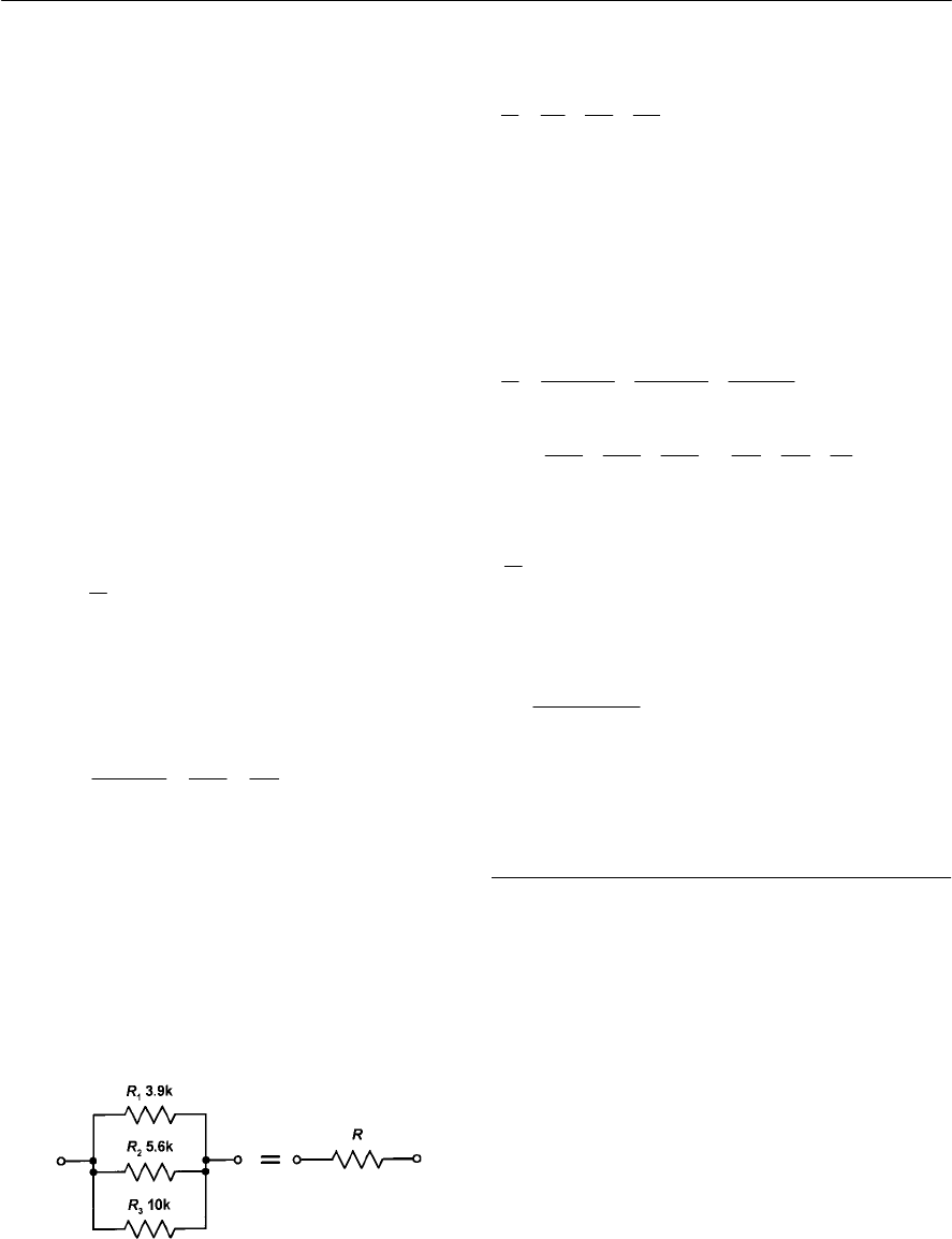
APPENDIX 8 MATHEMATICS FOR ELECTRONICS 393
following example shows:
2.3 × 10⁴+3.7 × 103=2.3 × 10⁴+0.37 × 104
=(2.3 + 0.37) × 104
=2.67 × 10⁴
Alternatively,
2.3 × 10⁴+3.7 × 103=23000 + 3700
=26700 = 2.67 × 10⁴
The laws of indices are used when multiplying or
dividing numbers given in standard form. For
example,
(22.5 × 103) × (5 × 102) = (2.5 × 5) × (103+2)
=12.5 × 10⁵or 1.25 × 10⁶
Example 4
Period, t,is the reciprocal of frequency, f.Thus
Calculate the period of a radio frequency signal
having a frequency of 2.5 MHz.
Now f=2.5 MHz. Expressing this in standard
form gives f=2.5 × 10⁶Hz.
Since
Thus
t=4 × 1027s
Example 5
Resistors of 3.9 kG,5.6 kGand 10 kGare
connected in parallel as shown in Fig. A8.1.
Calculate the effective resistance of the circuit.
1
1
tf
f
==
6
166
6
1101
10 0.4 10
2.5 10 2.5 2.5
tf
== = =× =×
×
The resistance of a parallel circuit is given by the
equation:
Now we know that:
R1 = 3.9 kG=3.9 × 10³G
R2 = 5.6 kG=5.6 × 10³G
R3 = 10 kG= 1 × 10⁴G=10 × 103G
Hence:
Now since we can invert both sides of the equation
so that:
Hence
R=1.87 k4
11 1 1
123
RR R R
=+ +
333
11 1 1
3.9 10 5.6 10 10 10
R
=++
×××
333
3
10 10 10 1 1 1
10
3.9 5.6 10 3.9 5.6 10
=++= ++×
(
)
33
0.256 0.179 0.1 10 0.535 10
=++×=×
Figure A8.1 See Example 5
3
1
0.535 10
R
=×
3
3
1
1.87 10
0.535 10
R
==×
×
Equations
We frequently need to solve equations in order to
find the value of an unknown quantity. Any
arithmetic operation may be applied to an equation
as long as the equality of the equation is
maintained. In other words, the same operation
must be applied to both the left-hand side (LHS)
and the right-hand side (RHS) of the equation.
Example 6
Acurrent of 0.5 A flows in the 56 Gshown in Fig.
A8.2. Given that V=I R determine the voltage that
appears across the resistor.
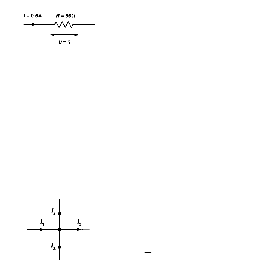
394 ELECTRONIC CIRCUITS: FUNDAMENTALS AND APPLICATIONS
Figure A8.3 See Example 7
It’s a good idea to get into the habit of writing
down what you know before attempting to solve an
equation. In this case:
I=0.5 A
R=56 G
V= ?
Now
V=IR = 0.5 × 56 = 28 V
Example 7
The current present at a junction in a circuit is
shown in Fig. A8.3 where I1=0.1 A, I2=0.25 A
and I3=0.3 A. Determine the value of the unknown
current, Ix.
From Kirchhoff’s Current Law, the algebraic sum
of the current at a junction in a circuit is zero.
Adopting the convention that current flowing
towards the junction is positive and that flowing
away from the junction is negative we can
construct a formula along the following lines:
0 = –Ix+I1–I2–I3
We can rearrange the equation to make Ixthe
subject by adding Ixto both sides:
0 + Ix= –Ix+Ix+ I1–I2–I3
From which:
Ix=I1–I2–I3
Now I1=0.1 A, I2=0.25 A and I3=0.3 A
Thus:
Ix=0.1 – 0.25 – 0.3 = –0.45 A
Hence Ix=0.45 A flowing towards the junction
It is important to note here that our original
‘guess’ as to the direction of Ixas marked on Fig.
A8.3 was incorrect and the current is actually
flowing the other way!
Note that it is always a good idea to check the
solution to an equation by substituting the solution
back into the original equation. The equation
should then balance such that the left hand side
(LHS) can be shown to be equal to the right hand
side (RHS).
In many cases it can be more convenient to
change the subject of a formula before you insert
values. The next few examples show how this is
done:
Example 8
Acopper wire has a length lof 1.5 km, a resistance
Rof 5 Gand a resistivity 5of 17.2 × 10⁻⁶ Gmm.
Find the cross-sectional area, a,of the wire, given
the following relationship:
Once again, it is worth getting into the habit of
summarizing what you know from the question and
what you need to find. Also, don’t forget to include
the units for each one of the quantities that you
know.
R= 5 G
5=17.2 × 10⁻⁶ Gmm
l=1500 × 103mm
a= ?
Figure A8.2 See Example 6
l
R
a
=

APPENDIX 8 MATHEMATICS FOR ELECTRONICS 395
Now since
then
Cross multiplying (i.e. exchanging the ‘5’ for the
‘a’) gives:
Now group the numbers and the powers of 10 as
shown below:
Next simplify as far as possible:
Finally, evaluate the result using your calculator:
a=5160 × 10–3 = 5.16
Don’t forget the units! Since we have been working
in mm, the result, a,will be in mm2.
Hence a=5.16 mm2
It’s worth noting from the previous example that
we have used the laws of indices to simplify the
powers of ten before attempting to use the
calculator to determine the final result. The
alternative to doing this is to make use of the
exponent facility on your calculator. Whichever
technique you use it’s important to be confident
that you are correctly using the exponent notation
since it’s not unknown for students to produce
answers that are incorrect by a factor of 1,000 or
even 1,000,000 and an undetected error of this
magnitude could be totally disastrous!
Before attempting to substitute values into an
equation, it’s important to be clear about what you
know (and what you don’t know) and always make
sure that you have the correct units. The values
marked on components can sometimes be
misleading and it’s always worth checking that you
l
R
a
=
63
(17.2 10 ) (1500 10 )
5
a
××
=
6 3
(17.2 10 ) (1500 10 )
5
a
××
=
63
17.2 1500 10 10
5
a
×××
=
63
17.2 1500
10
5
a
+
×
=×
have interpreted the markings correctly before
wasting time solving an equation that doesn’t
produce the right answer!
Example 9
The reactance, X,of a capacitor is given by the
relationship:
Find the value of capacitance that will exhibit a
reactance of 10 kGat a frequency of 400 Hz.
First, let’s summarize what we know:
X=10 kG
f=400 Hz
7=3.142 (or use the ‘7’button on your calculator)
C= ?
We need to re-arrange the formula to make Cthe
subject. This is done as follows:
Cross multiplying gives:
(note that we have just ‘swapped’ the Cand the X
over).
Next, replacing 7,C,and fby the values that we
know gives:
Finally, it would be sensible to express the answer
in nF (rather than F). To do this, we simply need to
multiply the result by 10
9
,as follows:
C=0.398 × 10
–7
× 10
9
=0.398 × 10
9–7
=0.398 × 10
2
=39.8 nF
1
2
C
fX
=
×
1
2
X
fC
=
1
2
X
fC
=
33
11
2 3.142 400 10 10 25136 10
C==
×××× ×
77
7
11
10 0.398 10 F
2.5136 10 2.5136
==×=×
×
396 ELECTRONIC CIRCUITS: FUNDAMENTALS AND APPLICATIONS
Example 10
The frequency of resonance, f,of a tuned circuit
(see Fig. A8.4) is given by the relationship:
If a tuned circuit is to be resonant at 6.25 MHz and
C=100 pF, determine the value of inductance, L.
1
2
f
LC
=
Figure A8.4 See Example 10
Here we know that:
C=100 pF = 100 × 10–12 F
f=6.25 MHz = 6.25 × 10⁶Hz
7=3.142 (use the ‘7’button on your calculator!)
L= ?
First we will rearrange the formula in order to make
Lthe subject:
Squaring both sides gives:
Re-arranging gives:
We can now replace f,Cand 7by the values that
we know:
()
22
2
22
22
111
4
22
f
LC
LC LC
== =
22
1
4
L
fC
=
More complex equations
More complex equations are solved in essentially
the same way as the simple equations that we have
just met. Note that equations with square (or
higher) laws may have more than one solution.
Here is an example:
Example 11
The impedance of the AC circuit shown in Fig.
A8.5 is given by:
Determine the reactance, X,of the circuit when R=
25 Gand Z=50 G.
1
2
f
LC
=
()
2
26 12
1
H
4 3.142 6.25 10 100 10
L
=
×××××
1212
1
H
39.49 39.06 10 100 10
L
=××××
5
5
111
10
154248 1.54248 10 1.54248
== = ×
×
56
0.648 10 6.48 10 H
=×=× =6.8
µH
22
ZRX
=+
Here we know that:
R=25 G
Z=50 G
X= ?
First we will re-arrange the formula in order to
make Xthe subject:
22
ZRX
=+
Figure A8.5 See Example 11

APPENDIX 8 MATHEMATICS FOR ELECTRONICS 397
Squaring both sides gives:
Re-arranging gives:
X2=Z2–R2
Taking the square root of both sides gives:
We can now replace Zand Rby the values that we
know:
thus
X=43.3 4
In the previous example we arrived at a solution of
43.3 Gfor X.This is not the only solution as we
will now show:
As before, we can check that we have arrived at
the correct answer by substituting values back into
the original equation, as follows:
Thus LHS = RHS.
However, we could also have used –43.3 G(instead
of +43.3 G)for Xand produced the same result:
Once again, LHS = RHS.
The reason for this apparent anomaly is simply that
the result of squaring a negative number will be a
positive number (i.e. (–2)2=(–2) × (–2) = +4).
Hence, a correct answer to the problem in
Example 11 would be:
X=±43.3 4
(
)
2
22222
ZRXRX
=+=+
22
XZR
=
22
50 25 2500 625 1875
X===
Don’t panic if the ambiguity of this answer is
worrying you! Reactance in an AC circuit can be
either positive or negative depending upon whether
the component in question is an inductor or a
capacitor. In this case, the numerical value of the
impedance is the same regardless of whether the
reactance is inductive or capacitive.
2222
50 25 43.3
ZRX==+= +
50 625 1875 2500 50
=+= =
()
2
22 2
50 25 43.3
ZRX==+= +
50 625 1875 2500 50
=+= =
Graphs
Graphs provide us with a visual way of
representing data. They can also be used to show,
in a simple pictorial way, how one variable affects
another variable. Several different types of graph
are used in electronics. We shall start by looking at
the most basic type, the straight line graph.
Straight line graphs
Earlier we introduced the idea of proportionality.
In particular, we showed that the current flowing in
acircuit was directly proportional to the voltage
applied to it. We expressed this using the following
mathematical notation:
where irepresents load current and vrepresents
output voltage.
We can illustrate this relationship using a simple
graph showing current, i,plotted against voltage, v.
Let’s assume that the voltage applied to the circuit
varies over the range 1 V to 6 V and the circuit has
aresistance of 3 W. By taking a set of
measurements of vand i(see Fig. A8.6) we would
obtain the following table of corresponding values
shown below:
The resulting graph is shown in Fig. A8.7. To
obtain the graph, a point is plotted for each pair of
corresponding values for vand i.When all the
points have been drawn they are connected together
by drawing a line. Notice that, in this case, the line
that connects the points together takes the form of a
iv
Voltage, v(V) 1 2 3 4 5 6
Current, i(A) 0.33 0.66 1.0 1.33 1.66 2.0
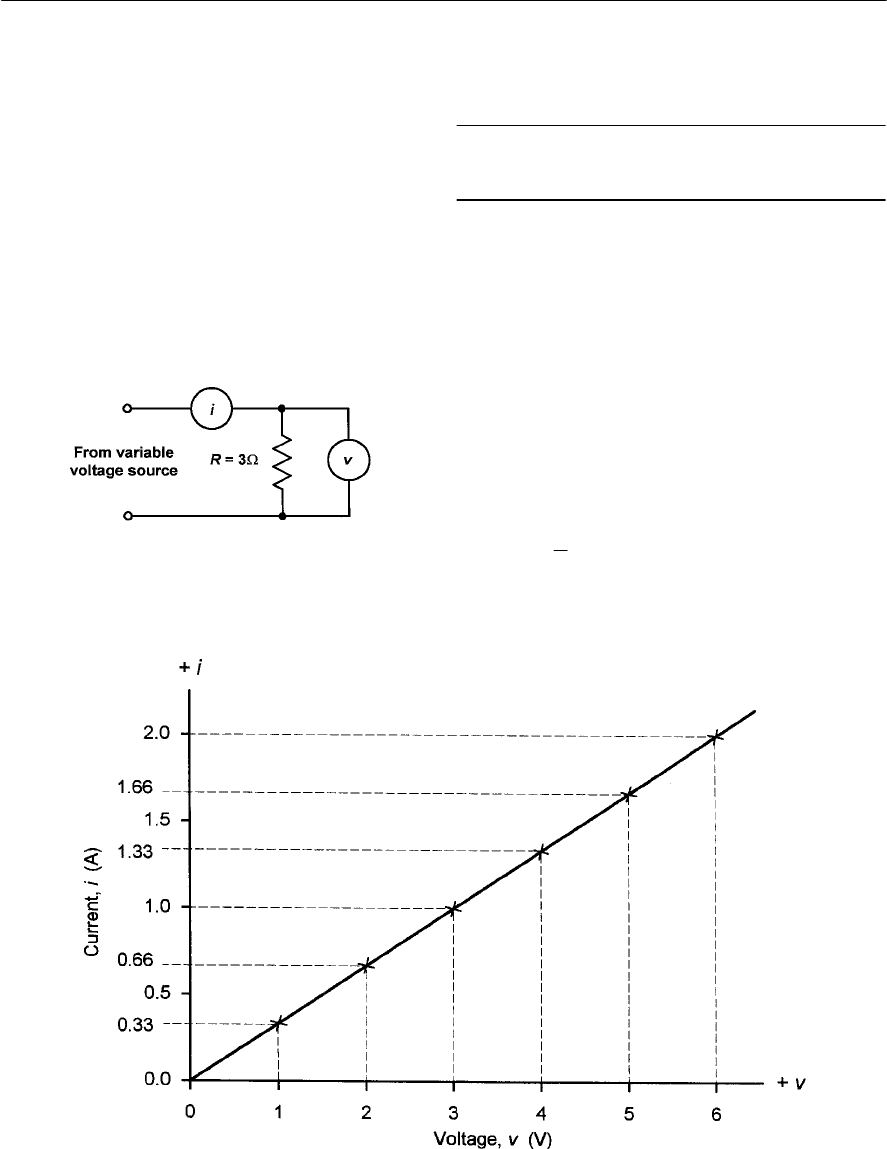
398 ELECTRONIC CIRCUITS: FUNDAMENTALS AND APPLICATIONS
straight line. This is always the case when two
variables are directly proportional to one another.
It is conventional to show the dependent variable
(in this case it is current, i)plotted on the vertical
axis and the independent variable (in this case it is
voltage, v)plotted on the horizontal axis. If you
find these terms a little confusing, just remember
that, what you know is usually plotted on the
horizontal scale whilst what you don’t know (and
may be trying to find) is usually plotted on the
vertical scale. In fact, the graph contains the same
information regardless of which way round it is
drawn!
Now let’s take another example. Assume that the
following measurements are made on an electronic
component:
The results of the experiment are shown plotted in
graphical form in Fig. A8.8. Note that the graph
consists of a straight line but that it does not pass
through the origin of the graph (i.e. the point at
which tand Vare 0°C and 0 V respectively). The
second most important feature to note (after having
noticed that the graph is a straight line) is that,
when t=0°C, R=100 W.
By looking at the graph we could suggest a
relationship (i.e. an equation)that will allow us to
find the resistance, R,of the component at any
given temperature, t.The relationship is simply:
If you need to check that this works, just try
inserting a few pairs of values from those given in
100
2
t
R
=+
Figure A8.6 Corresponding readings of current,
i,and voltage, v,are taken and used to construct the
graph shown in Fig. A8.7
Figure A8.7 Graph of iplotted against v
Temperature, t(°C) 10 20 30 40 50 60
Resistance, R(W) 105 110 115 120 125 130
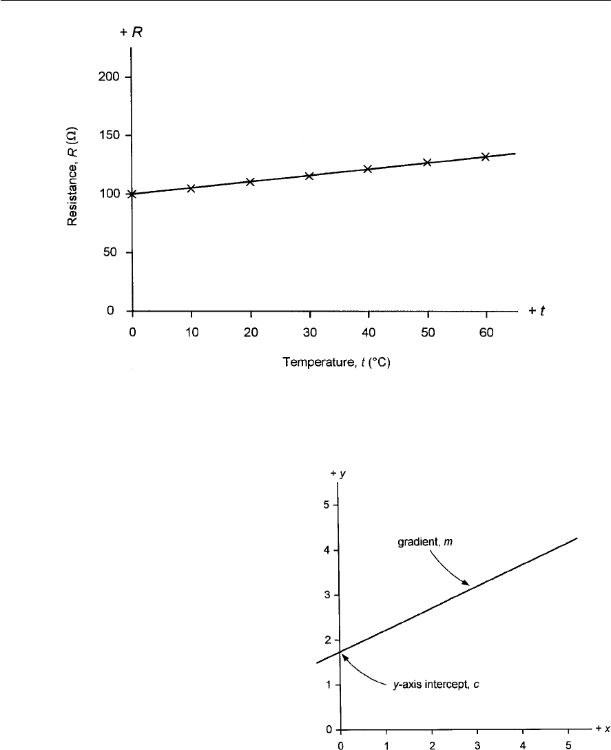
Figure A8.9 Definition of gradient (slope), m,
and y-axis intercept, c
APPENDIX 8 MATHEMATICS FOR ELECTRONICS 399
the table. You should find that the equation
balances every time!
Earlier we looked at equations. The shape of a
graph is dictated by the equation that connects its
two variables. For example, the general equation
for a straight line takes the form:
y=m x +c
where yis the dependent variable (plotted on the
vertical or y-axis), xis the independent variable
(plotted on the horizontal or x-axis), mis the slope
(or gradient)of the graph and cis the intercept on
the y-axis. Fig. A8.9 shows this information plotted
on a graph.
The values of m(the gradient) and c(the y-axis
intercept) are useful when quoting the
specifications for electronic components. In the
previous example, the electronic component (in this
case a thermistor)has:
(a) a resistance of 100 W at 0°C (thus c=100 G)
(a) a characteristic that exhibits an increase in
resistance of 0.5 W per °C (thus m=0.5
W/°C).
Figure A8.8 Graph of resistance, R,plotted against temperature, t,for a thermistor
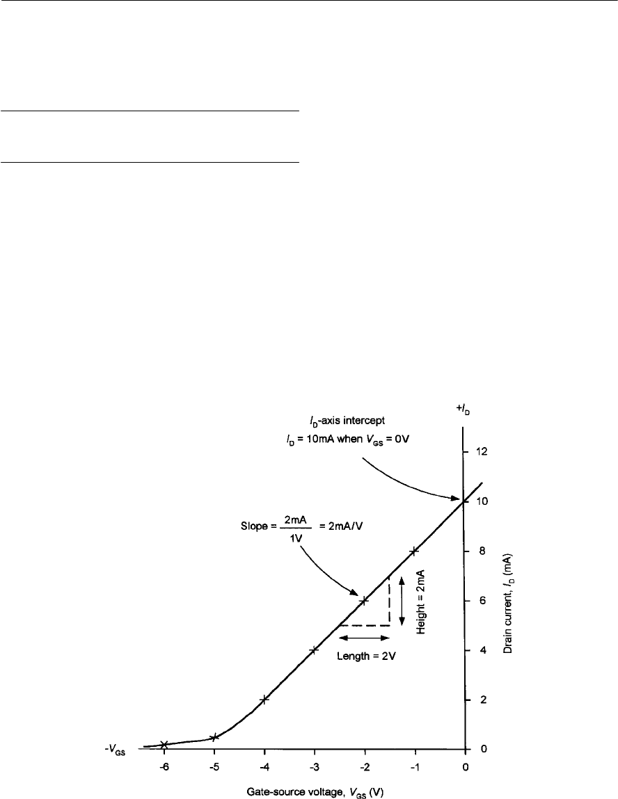
400 ELECTRONIC CIRCUITS: FUNDAMENTALS AND APPLICATIONS
Example 12
The following data was obtained whilst making
measurements on an N-channel field effect
transistor:
Plot a graph showing how drain current (ID)varies
with gate-source voltage (VGS)and use the graph to
determine:
(a) the value of IDwhen VGS = 0 V, and
(b) the slope of the graph (expressed in mA/V)
when VGS = R2V.
The data has been shown plotted in Fig. A8.10.
Note that, since the values of VGS that we have been
given are negative, we have plotted these to the left
of the vertical axis rather than to the right of it.
(a) We can use the graph to determine the
crossing point (the intercept)on the drain
current (ID)axis. This occurs when
ID=10 mA.
(b) The slope (or gradient)of the graph is found
by taking a small change in drain current and
dividing it by a corresponding small change in
gate-source voltage. In order to do this we
have drawn a triangle on the graph at the point
where VGS =R2V. The slope of the graph is
found by dividing the vertical height of the
triangle (expressed in mA) by the horizontal
length of the triangle (expressed in V). From
Fig. A8.10 we can see that the vertical height
of triangle is 2 mA whilst its horizontal
length is 1 V. The slope of the graph is thus
given by 2 mA/1 V = 2mA/V.
Square law graphs
Of course, not all graphs have a straight line shape.
In the previous example we saw a graph that, whilst
VGS (V) R1R2R3R4R5R6
ID(mA) 8 6 4 2 0.4 0.1
Figure A8.10 Drain current, ID,plotted against gate-source voltage, VGS,for a field effect transistor
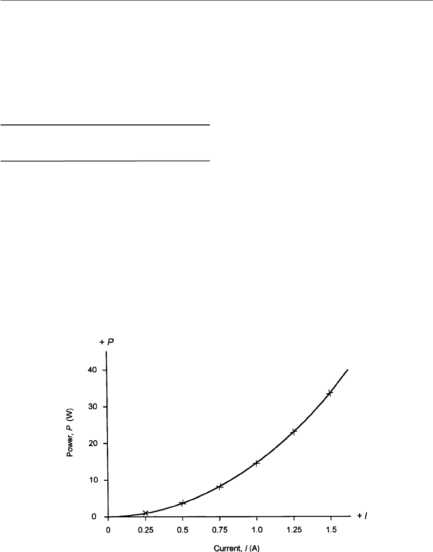
P=I2R
where Prepresents power in Watts, Iis current in
Amps, and Ris resistance in ohms.
Since Rremains constant, we can deduce that:
In words, we would say that ‘power is proportional
to current squared’.
Many other examples of square law relationships
are found in electronics.
More complex graphs
Many more complex graphs exist and Fig. A8.13
shows some of the most common types. Note that
these graphs have all been plotted over the range x
=±4, y=±4. Each graph consists of four quadrants.
These are defined as follows (see Fig. A8.12):
First quadrant Values of x and y are both
positive
Second quadrant Values of x are negative whilst
those for y are positive
Third quadrant Values of x and y are both
negative
Fourth quadrant Values of xare positive whilst
those for yare negative.
APPENDIX 8 MATHEMATICS FOR ELECTRONICS 401
2
PI
substantially linear, became distinctly curved at one
end. Many graphs are curved rather than linear.
One common type of curve is the square law. To
put this into context, consider the relationship
between the power developed in a load resistor and
the current applied to it. Assuming that the load has
aresistance of 15 W we could easily construct a
table showing corresponding values of power and
current, as shown below:
We can plot this information on a graph showing
power, P,on the vertical axis plotted against
current, I,on the horizontal axis. In this case, Pis
the dependent variable and Iis the independent
variable.The graph is shown in Fig. A8.11.
It can be seen that the relationship between Pand
Iin Fig. A8.11 is far from linear. The relationship
is, in fact, a square law relationship.We can
actually deduce this from what we know about the
power dissipated in a circuit and the current
flowing in the circuit. You may recall that:
Current, I(A) 0.25 0.5 0.75 1 1.25 1.5
Power, P(W) 0.94 3.75 8.44 15 23.44 33.75
Figure A8.11 Power, P,plotted against current, I,showing a square law graph
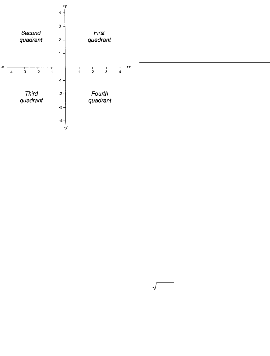
402 ELECTRONIC CIRCUITS: FUNDAMENTALS AND APPLICATIONS
The straight line relationship, y=x,is shown in
Fig. A8.13(a). This graph consists of a straight line
with a gradient of 1 that passes through the origin
(i.e. the point where x= 0 and y=0). The graph has
values in the first and third quadrants.
The relationship y=x2is shown in Fig.
A8.13(b). This graph also passes through the origin
but its gradient changes, becoming steeper for
larger values of x.As you can see, the graph has
values in the first and second quadrants.
The graph of y=x3is shown in Fig. A8.13(c).
This cubic law graph is steeper than the square law
of Fig. A8.13(b) and it has values in the first and
third quadrants.
Figure A8.13(d) shows the graph of y=x4.This
graph is even steeper than those in Figs. A8.13(b)
and A8.13(c). Like the square law graph of Fig.
A8.13(b), this graph has values in the first and
second quadrants.
The graph of y=x5is shown in Fig. A8.13(e).
Like the cubic law graph of Fig. A8.13(c), this
graph has values in the first and third quadrants.
Finally, Fig. A8.13(f) shows the graph of y=1/x
(or y=x-1). Note how the y values are very large
for small values of xand very small for very large
values of x.This graph has values in the first and
third quadrants.
Figure A8.12 The first, second, third and fourth
quadrants of a graph
If you take a careful look at Fig. A8.13 you
should notice that, for odd powers of x(i.e. x1,x3,
x5,and x-1)the graph will have values in the first
and third quadrant whilst for even powers of x(i.e.
x2and x4)the graph will have values in the first and
second quadrants.
Trigonometry
You might be wondering what trigonometry has to
do with electronics. It’s just that a familiarity with
some basic trigonometry is fundamental to
developing an understanding of signal, waveforms
and AC circuits. Indeed, the most fundamental
waveform used in AC circuits is the sine wave and
this wave is a trigonometric function.
Basic trigonometrical ratios
Trigonometrical ratios are to do with the way in
which we measure angles. Take a look at the right-
angled triangle shown in Fig. A8.14. This triangle
has three sides; a,b,and c.The angle that we are
interested in (we have used the Greek symbol 8to
denote this angle) is adjacent to side aand is
opposite to side b.The third side of the triangle (the
hypotenuse)is the longest side of the triangle.
In Fig. A8.14, the theorem of Pythagoras states
that ‘the square on the hypotenuse is equal to the
sum of the squares on the other two sides’. Writing
this as an equation we arrive at:
c2=a2+b2
where cis the hypotenuse and aand bare the other
two sides.
Taking square roots of both sides of the equation
we can see that:
Thus if we know two of the sides (for example, a
and b)of a right-angled triangle we can easily find
the third side (c).
The ratios a/c,b/c,and a/bare known as the
basic trigonometric ratios.They are known as sine
(sin), cosine (cos)and tangent (tan)of angle 8
respectively. Thus:
22
cab
=+
sin
opposite a
hypotenuse c
==
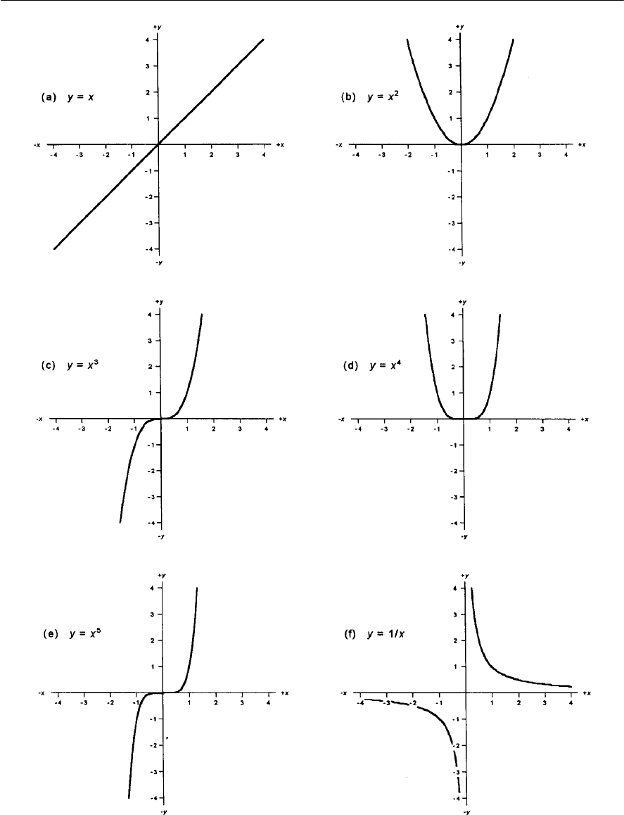
APPENDIX 8 MATHEMATICS FOR ELECTRONICS 403
Figure A8.13 Some complex graphs and their equations
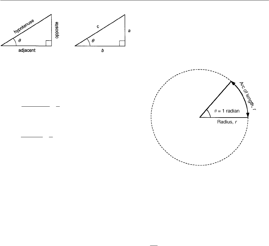
404 ELECTRONIC CIRCUITS: FUNDAMENTALS AND APPLICATIONS
and
and
Trigonometrical equations
Equations that involve trigonometrical expressions
are known as trigonometrical equations.
Fortunately they are not quite so difficult to
understand as they sound! Consider the equation:
sin 8=0.5
This equation can be solved quite easily using a
calculator. However, before doing so, you need to
be sure to select the correct mode for expressing
angles on your calculator. If you are using a
‘scientific calculator’ you will find that you can set
the angular mode to either radian measure or
degrees. A little later we will explain the difference
between these two angular measures but for the
time being we shall use degrees.
If you solve the equation (by keying in 0.5 and
pressing the inverse sine function keys) you should
see the result 30° displayed on your calculator.
Hence we can conclude that:
sin 30° =0.5
Actually, a number of other angles will give the
same result! Try pressing the sine function key and
entering the following angles in turn:
30°, 210°, 390° and 570°
They should all produce the same result, 0.5! This
should suggest to you that the graph of the sine
cos
adjacent b
hypotenuse c
==
tan
opposite a
adjacent b
==
function repeats itself (i.e. the shape of the graph is
periodic). In the next section we shall plot the sine
function but, before we do we shall take a look at
using radian measure to specify angles.
The radian is defined as the angle subtended by
an arc of a circle equal in length to the radius of the
circle. This relationship is illustrated in Fig. A8.15.
Figure A8.14 Right-angled triangles
Figure A8.15 Definition of the radian
The circumference, l,of a circle is related to its
radius, r,according to the formula:
l = 2ar
Thus
Now, since there are 360° in one complete
revolution we can deduce that one radian is the
same as 360°/2a=57.3°. On other words, to
convert:
(a) degrees to radians multiply by 57.3
(b) radians to degrees divide by 57.3
It is important to note that one complete cycle of a
periodic function (i.e. a waveform) occurs in a
time, T.This is known as the periodic time or just
the period.In a time interval equal to T,the angle
will have changed by 360°. The relationship
between time and angle expressed in degrees is
thus:
2
l
r
=
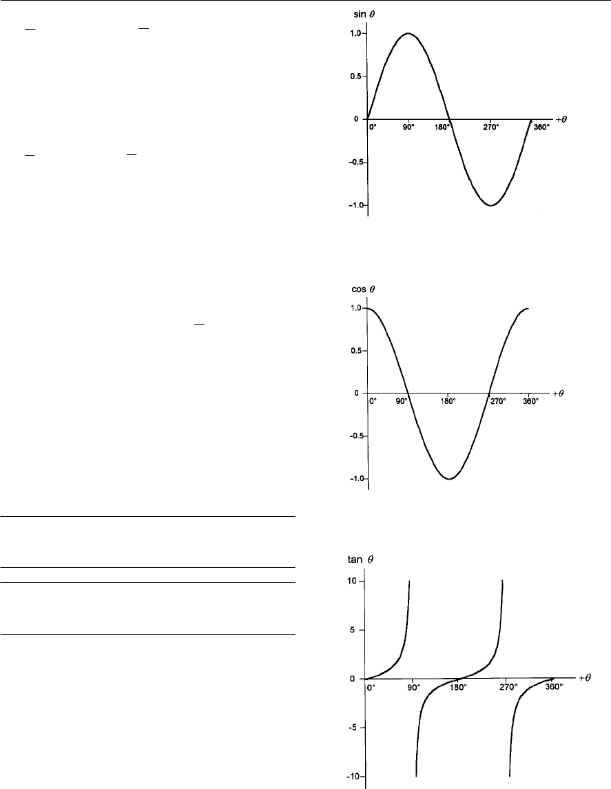
APPENDIX 8 MATHEMATICS FOR ELECTRONICS 405
and
Thus, if one complete cycle (360°) is completed in
0.02 s (i.e. T=20 ms) an angle of 180° will
correspond to a time of 0.01 s (i.e. t=10 ms).
Conversely, if we wish to express angles in
radians:
and
Thus, if one complete cycle (2aradians) is
completed in 0.02 s (i.e. T=20 ms) an angle of p
radians will correspond to a time of 0.01 (i.e. t=
10 ms). It should be apparent from this that, when
considering waveforms, time and angle (whether
expressed in degrees or radians) are
interchangeable. Note that the general equation for
asine wave voltage is:
where Vmax is the maximum value of the voltage
and Tis the periodic time.
Graphs of trigonometrical functions
To plot a graph of y = sin 8we can construct a
table of values of sin 8as 8is varied from 0° to
360° in suitable steps. This exercise (carried out
using a scientific calculator) will produce a table
that looks something like this:
max max
sin(2 ) sin(6.28 )
t
vV ft V
T
==×
360
T
t
=× °
360
T
t
=× °
2
T
t
=×
2
T
t
=×
Plotting a graph of the values in the table reveals
the graph shown in Fig. A8.16. We can use the
same technique to produce graphs of cos 8and tan
8,as shown in Figs A8.17 and A8.18.
Example 13
The voltage applied to a high voltage rectifier is
given by the equation:
Angle, 80° 30° 60° 90° 120° 150°
sin 800.5 0.87 1 0.87 0.5
Angle, 8180° 210° 240° 270° 300° 330°
sin 80R05 R0.87 R1R0.87 R0.5
Figure A8.16
Graph of the sine function (the
equation of the function is y=sin 8)
Figure A8.17
Graph of the cosine function (the
equation of the function is y=cos 8)
Figure A8.18
Graph of the tangent function (the
equation of the function is y=tan 8)
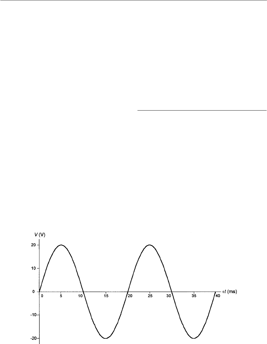
406 ELECTRONIC CIRCUITS: FUNDAMENTALS AND APPLICATIONS
v=800 sin(314 t)
Determine the voltage when:
(a) t= 1 ms
(b) t=15 ms.
We can easily solve this problem by substituting
values into the expression.
In case (a):
v=800 sin(314 × 0.001) = 800 sin(0.314)
=800 × 0.3088 = 247 V
In case (b):
v=800 sin(314 × 0.015) = 800 sin(4.71)
=800 × R1 = 2800 V
Example 14
The voltage appearing at the secondary winding of
atransformer is shown in Fig. A8.19. Determine:
(a) the period of the voltage
(b) the value of the voltage when (i) t= 5 ms and
(ii) t=35 ms
(c) the maximum and minimum values of voltage
(d) the average value of the voltage during the
time interval 0 to 40 ms
(e) the equation for the voltage.
All of the above can be obtained from the graph of
Fig. A8.19, as follows:
(a) period, T=20 ms (this is the time for one
complete cycle of the voltage)
(b) at t= 5 ms, v=20 V; at t=35 ms, v=R20 V
(c) vmax = +20 V and vmin = R20 V
(d) vav. = 0 V (the positive and negative cycles of
the voltage are equal)
(e) v=20 sin 314 t(the maximum value of the
voltage, Vmax,is 20 V and T=0.02 s).
Boolean algebra
Boolean algebra is the algebra that we use to
describe and simplify logic expressions. An
understanding of Boolean algebra can be extremely
useful when troubleshooting any circuit that
employs digital logic. It is, for example, very useful
to be able to predict the output of a logic circuit
when a particular input condition is present.
Boolean notation
Just as with conventional algebra, we use letters to
represent the variables in these expressions. The
Figure A8.19 See Example 14
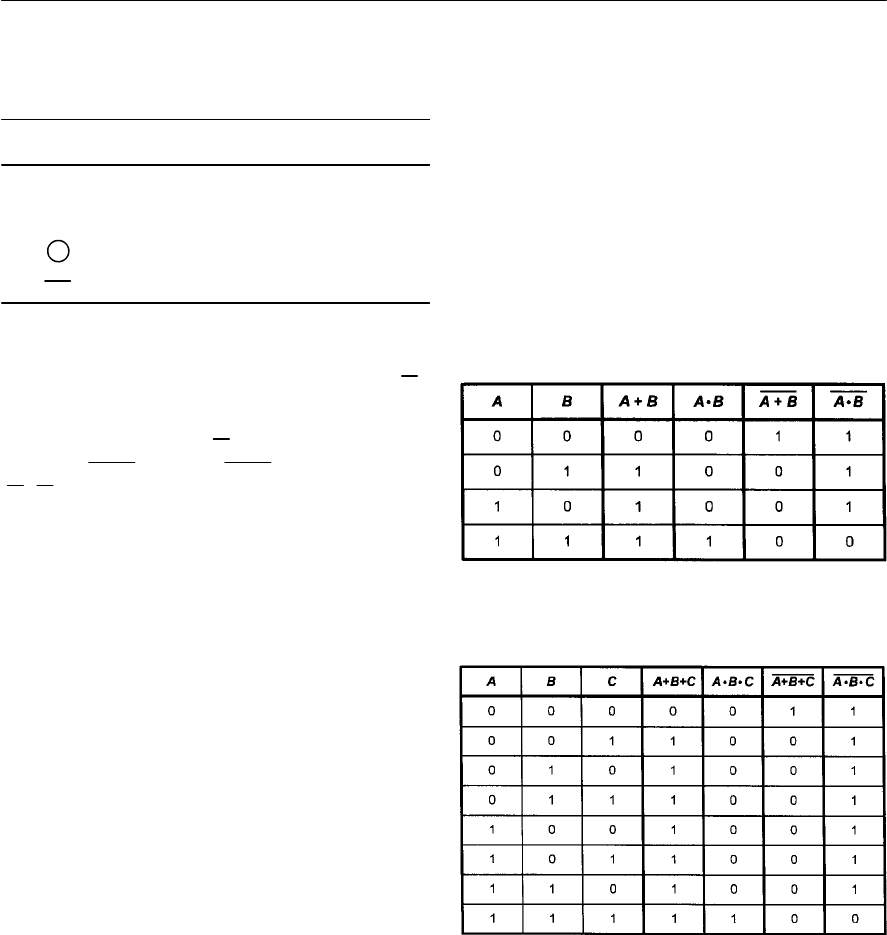
APPENDIX 8 MATHEMATICS FOR ELECTRONICS 407
symbols used in Boolean algebra do not, however,
have the same meanings as they have in
conventional algebra:
In general, a logic function with ninput variables
will have 2ndifferent possible states for those
inputs. Thus, with two input variables there will be
four possible input states, for three input variables
there will be eight possible states, and for four
input variables there will be 16 possible states.
Take a look at Fig. A8.20 and Fig. A8.21 and
compare the output states for AND with those for
NAND as well as OR with those for NOR. In every
case, you should notice that the output states are
complementary—in other words, all of 0’s in the
AND column have been inverted to become 1’s in
the NAND column, and vice versa. The same rule
also applies to the OR and NOR columns.
Symbol Meaning
•Logical AND
+Logical OR
+Logical exclusive-OR
Logical NOT
Thus ‘AAND B’can be written (A•B)whereas
‘AOR B’is written (A+B). The bar symbol, ,
used above a variable (or over a part of an
expression) indicates inversion (the NOT function).
Thus ‘NOT A’is written Aand ‘NOT (AAND B)’
is written A•B.Note that A•Bis not the same as
A•B.
It is important to note that a logic variable (such
as Aor B)can exist in only two states variously
(and interchangeably) described as true or false,
asserted or non-asserted, 1 or 0, etc. The two states
are mutually exclusive and there are no ‘in
between’ conditions.
Truth tables
We often use tables to describe logic functions.
These tables show all possible logical combinations
and they are called truth tables.The columns in a
truth table correspond to the input variables and an
extra column is used to show the resulting output.
The rows of the truth tables show all possible states
of the input variables. Thus, if there are two input
variables (Aand B)there will be four possible input
states, as follows:
A=0, B= 0
A=0, B= 1
A=1, B= 0
A=1, B= 1
Basic logic functions
The basic logic functions are: OR, AND, NOR, and
NAND. We can describe each of these basic logic
functions using truth tables as shown in Fig. A8.20
(for two input variables) and in Fig. A8.21 (for
three input variables).
Venn diagrams
An alternative technique to that of using a truth
table to describe a logic function is that of using a
Venn diagram. This diagram consists of a number
of overlapping areas that represent all of the
possible logic states.
Figure A8.21 Truth tables for the basic logic
functions using three variables: A,Band C
Figure A8.20 Truth tables for the basic logic
functions using two variables: Aand B
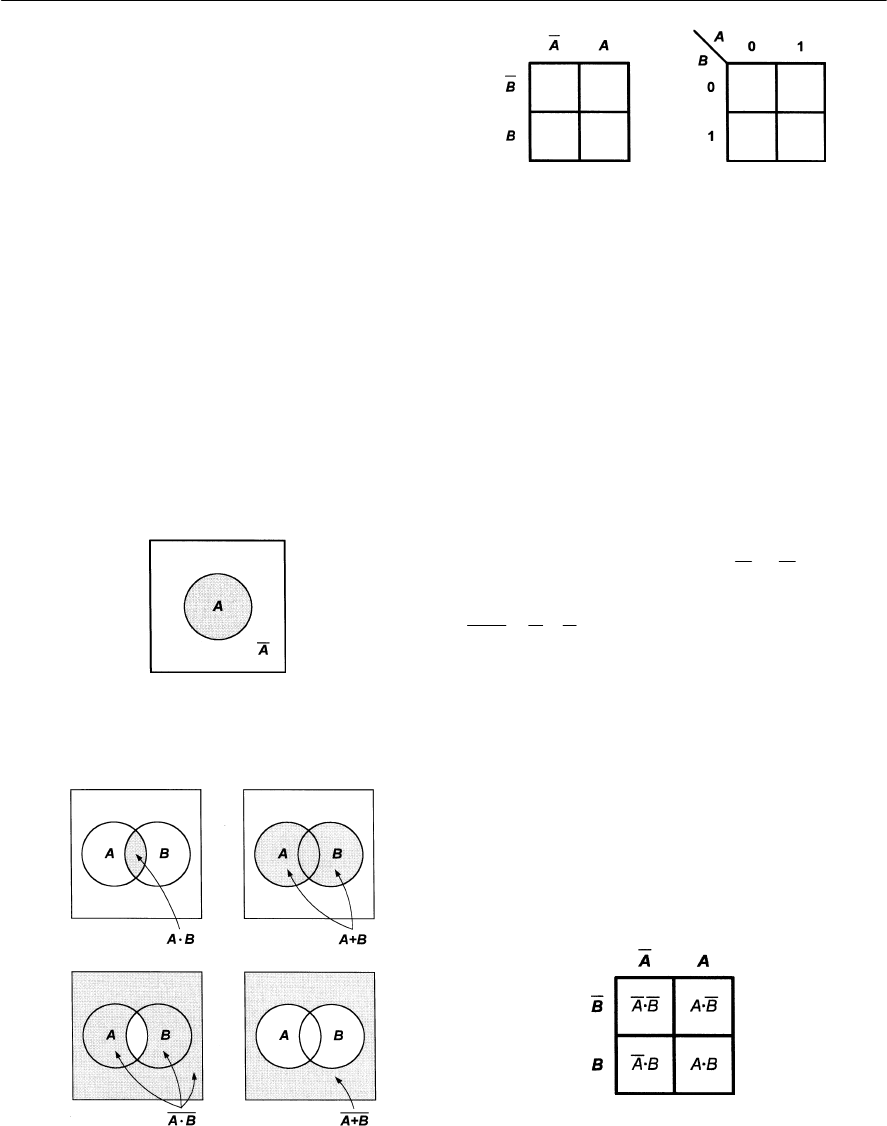
408 ELECTRONIC CIRCUITS: FUNDAMENTALS AND APPLICATIONS
Asimple Venn diagram with only one variable is
shown in Fig. A8.22. The shaded area represents
the condition when variable Ais true (i.e. logic 1).
The non-shaded area represents the condition when
variable Ais false (i.e. logic 0). Obviously, variable
Acannot be both true and false at the same time
hence the shaded and non-shaded areas are
mutually exclusive.
Figure A8.23 shows Venn diagrams for the basic
logic functions; AND, OR, NAND and NOR. You
should note that these diagrams convey exactly the
same information as the truth tables in Fig. A8.20
but presented in a different form.
Karnaugh maps
AKarnaugh map consists of a square or rectangular
array of cells into which 0’s and 1’s may be placed
to indicate false and true respectively. Two
alternative representations of a Karnaugh map for
two variables are shown in Fig. A8.24.
Figure A8.24 Alternative representations for a
Karnaugh map showing two variables
Figure A8.25 Karnaugh map for two variables
showing the Boolean logic expression for each cell
Figure A8.23 Venn diagrams for the basic logic
functions
Figure A8.22 Venn diagram for a single logic
variable, A
The relationship between Boolean logic
expressions for two variables and their Karnaugh
maps is illustrated in Fig. A8.25 whilst Fig. A8.26
shows how the basic logic functions, AND, OR,
NAND and NOR, can be plotted on Karnaugh
maps.
Adjacent cells within a Karnaugh map may be
grouped together in rectangles of two, four, eight,
etc. cells in order to simplify a complex logic
expression. Taking the NAND function, for
example, the two groups of two adjacent cells in
the Karnaugh map correspond to Aor B,as shown
in Fig. A8.27. We thus conclude that:
Once again note how the overscore character is
used to indicate the inverting function.
This important relationship is known as De
Morgan’s theorem.
Karnaugh maps can be drawn showing two,
three, four, or even more variables. The Karnaugh
map shown in Fig. A8.28 is for three variables—
note that there are eight cells and that each cell
corresponds to one of the eight possible
combinations of the three variables; A,Band C.
A B A B= +
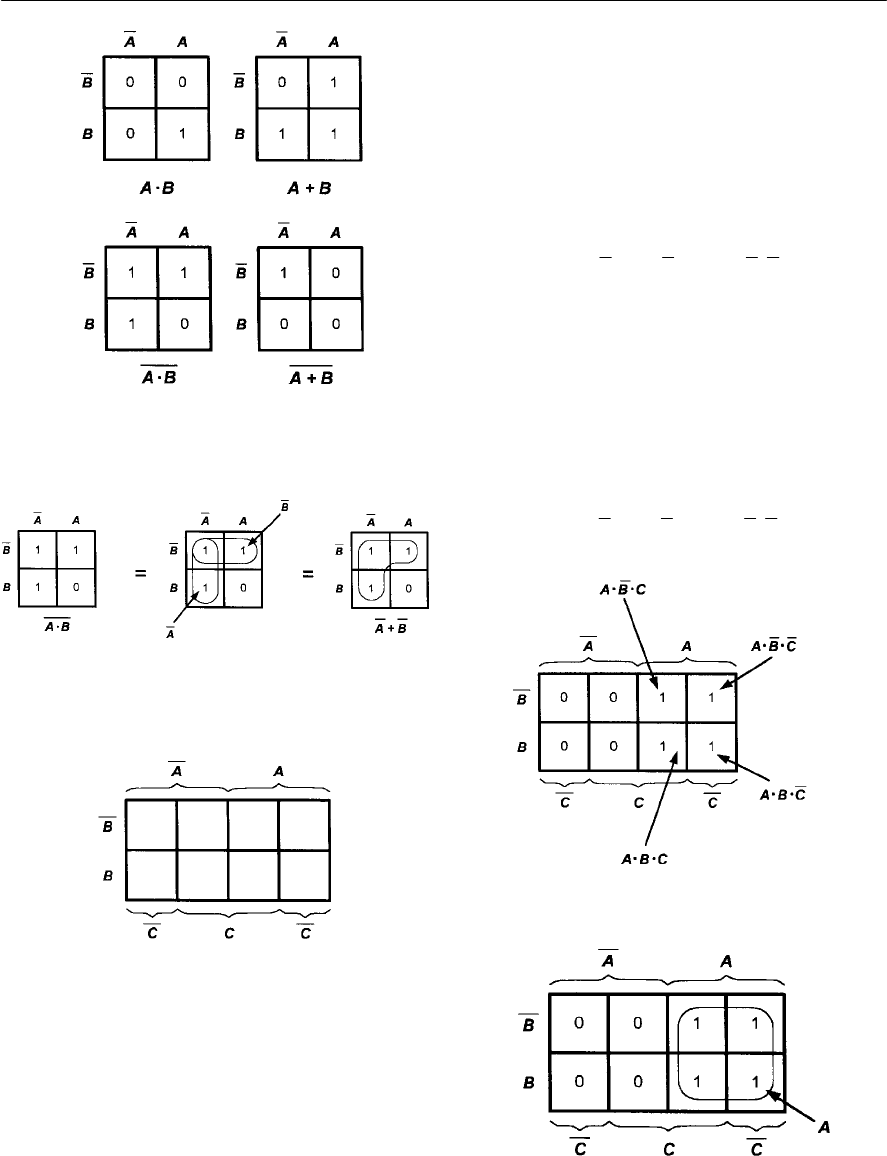
APPENDIX 8 MATHEMATICS FOR ELECTRONICS 409
The technique of grouping cells together is an
extremely powerful one. On a Karnaugh map
showing three variables, if two adjacent cells both
contain 1’s they can be grouped together to produce
an expression containing just two variables.
Similarly, if four adjacent cells can be grouped
together, they reduce to an expression containing
only one variable.
It is also important to note that the map is a
continuous surface which links edge to edge. This
allows cells at opposite extremes of a row or
column to be linked together. The four corner cells
of a four (or more) variable map may likewise be
grouped together (provided they all contain 1’s).
As an example, consider the following Boolean
function:
Figure A8.29 shows how this function is plotted
on the Karnaugh map.
As before, we have placed a 1 in each cell. Then
we can begin to link together adjacent cells—notice
how we have reduced the diagram to a group of
four cells equivalent to the logic variable, A.In
other words, the value of variables Band C,
whether 0 or 1, will have no effect on the logic
function. From Fig. A8.30 we can conclude that:
ABC ABC ABC ABC + + +
b
g
d
i
d
i
d
i
ABC ABC ABC ABC A + + + =
b
g
d
i
d
i
d
i
Figure A8.29 Plotting the logic expression on a
Karnaugh map
Figure A8.26 Karnaugh maps for the basic logic
functions
Figure A8.27 Grouping adjacent cells together to
prove De Morgan’s theorem
Figure A8.28 Karnaugh maps for three variables
Figure A8.30 Grouping adjacent 1 cells together
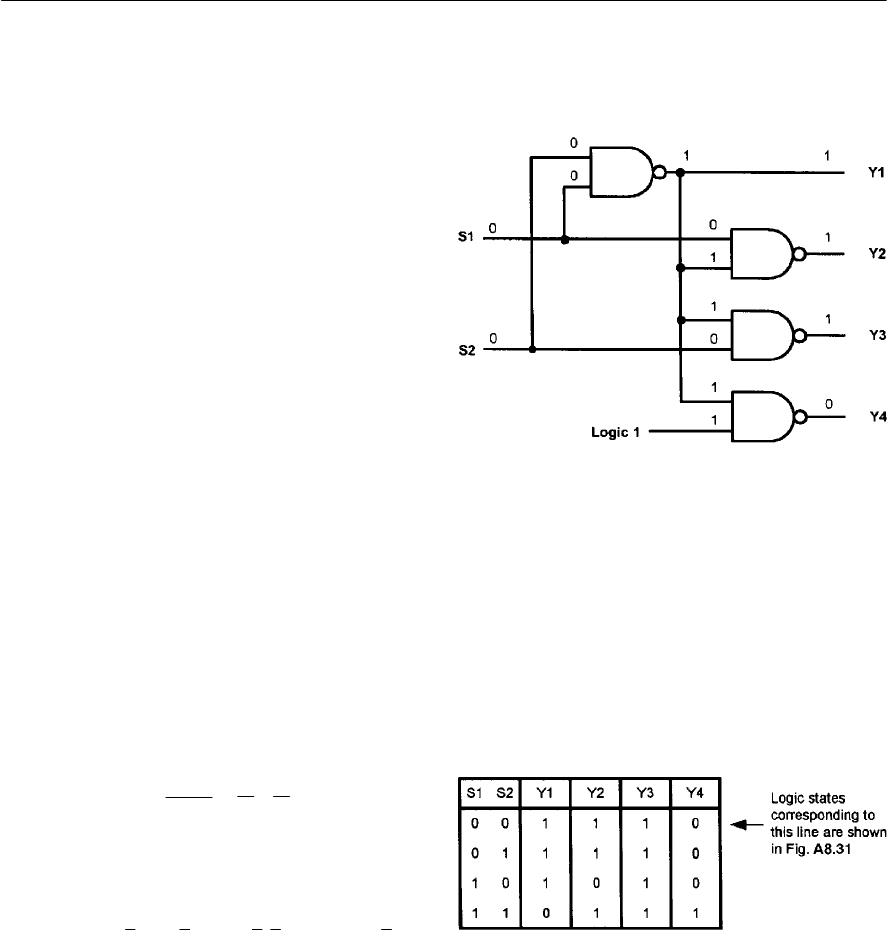
410 ELECTRONIC CIRCUITS: FUNDAMENTALS AND APPLICATIONS
Boolean algebra
The laws of Boolean algebra are quite different
from those of ordinary algebra. For example:
A·0 = 0
A·1 = A
A+0=A
A+ 1 = 1
The Commutative Law shows us that:
A+B=B+A
and also that:
A·B=B·A
The Associative Law shows us that:
A+ (B+C) = (A+B) + C=A+B+C
and also that:
A·(B·C) = (A·B)·C=A·B·C
The Distributive Law shows us that:
A·(B+C) = A·B+B·C
and also that:
A+ (B·C) = (A+B)·(A+C)
All of the above laws can be proved using the
various techniques that we met earlier.
Boolean simplification
Using the laws of Boolean algebra and De
Morgan’s theorem, A·B=A+B(see earlier) we
can reduce complex logical expressions in order to
minimize the number of variables and the number
of terms. For example, the expression that we met
earlier can be simplified as follows:
Here we have eliminated the variable Cfrom the
first and second pair of terms and then eliminated B
from the result. You might like to compare this
with the Karnaugh map that we drew earlier in
Figure A8.30!
Example 15
Part of the control logic for an intruder alarm is
shown in Fig. A8.31. Determine the logic required
ABC ABC ABC ABC AB AB A + + + =+=
b
g
e
j
e
j
e
j
b
g
e
j
to select the Y4 output and verify that the Y3
output is permanently selected and unaffected by
the states of S1 and S2.
Each logic gate shown in Fig. A8.31 is a two
input NAND gate. We can construct the truth table
for the control circuit (see Fig. A8.32) by placing
all four possible combinations of 0 and 1 on the S1
and S2 inputs and tracing the logic states through
the circuit. We have shown the first stage of this
process (the logic conditions that produce the first
line of the truth table) in Fig. A8.32.
Figure A8.31 See Example 15
Figure A8.32 Truth table for Example 15
From Fig. A8.32 it can be seen that the Y4 output
corresponds to the AND logic function:
You can also see from Fig. A8.32 that the Y3
output remains at logic 1 regardless of the states of
S1 and S2.
Y4 S1 S2
=
i

APPENDIX 8 MATHEMATICS FOR ELECTRONICS 411
Logarithms
Many of the numbers that we have to deal with in
electronics are extremely large whilst others can be
extremely small. The problem of coping with a
wide range of numbers is greatly simplified by
using logarithms. Because of this, we frequently
employ logarithmic scales, Bels (B) and decibels
(dB), when comparing values. Note that a decibel
(dB) is simply one tenth of a Bel (B). Hence:
10 dB = 1 B
It is important to note that the Bel is derived from
the logarithm of a ratio—it’s not a unit like the volt
(V) or ampere (A).
The logarithm (to the base 10) of a number is
defined as the power that 10 must be raised to in
order to equal that number. This may sound
difficult but it isn’t, as a few examples will show:
Because 10 = 101,the logarithm (to the base 10) of
10 is 1.
Because 100 = 102,the logarithm (to the base 10)
of 100 is 2.
Because 1,000 = 103,the logarithm (to the base 10)
of 1,000 is 3, and so on.
Writing this as a formula we can say that:
If x=10n,the logarithm (to the base 10) of xis n.
You might like to check that this works using the
examples that we just looked at!
You may be wondering why we keep writing ‘to
the base 10’. Logarithms can be to any base but 10
just happens to be the most obvious and useful.
Logarithmic notation
The notation that we use with logarithms is quite
straightforward:
If x=10nwe say that log10(x) = n.
The subscript that appears after the ‘log’ reminds
us that we are using base 10 rather than any other
(unspecified) number. Re-writing what we said
earlier using our logarithmic notation gives:
log10(10) = log10(101) = 1
log10(100) = log10(102) = 2
log10(1,000) = log10(103) = 3
and so on.
So far we have used values (10, 100 and 1,000)
in our examples that just happen to be exact powers
of 10. So how do we cope with a number that isn’t
an exact power of 10? If you have a scientific
calculator this is quite easy! Simply enter the
number and press the ‘log’ button to find its
logarithm (the instructions provided with your
calculator will tell you how to do this).
You might like to practice with a few values, for
example:
log10(56) = 1.748
log10(1.35) = 0.1303
log10(4,028) = 3.605
log10(195,891) = 5.292
log10(0.3175) = 20.4983
Finally, there’s another advantage of using
logarithmic units (i.e. Bels and decibels) in
electronics. If two values are multiplied together
the result is equivalent to adding their values
expressed in logarithmic units.
To put all of this into context, let’s assume that
the following items are connected in the signal path
of an amplifier (see Fig. A8.33):
Pre-amplifier; input power = 1 mW, output power
=80 mW
Tone control; input power = 80 mW, output power
=20 mW
Power amplifier; input power = 20 mW, output
power = 4 W
The power gain of each component, expressed as
both a ratio and in dB is shown in the table below:
Component Input
power
Output
power
Power gain
(expressed
as a ratio)
Power gain
(expressed
in decibels)
Pre-amplifier 1 mW 80 mW 80 19
Tone control 80 mW 20 mW 0.25 -6
Power
amplifier 20 mW 4 W 200 23
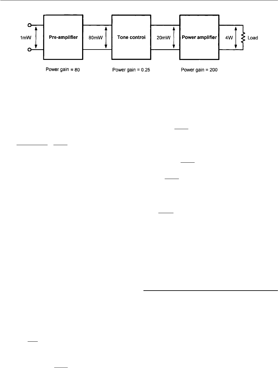
412 ELECTRONIC CIRCUITS: FUNDAMENTALS AND APPLICATIONS
The overall power gain can be calculated from the
following:
Overall power gain (expressed as a ratio)
Converting this gain to decibels gives:
10 log10 (4,000) = 36 dB
Adding the power gains from the right-hand
column gives: 19 R6+23 = 36 dB
Example 16
An amplifier has a power gain of 27,000. Express
this in Bels (B) and decibels (dB).
In Bels, power gain = log10(27,000) = 4.431 B
In decibels, power gain
=10 × log10(27,000) = 10 × 4.431 = 44.31 dB
Example 17
An amplifier has a power gain of 33 dB. What
input power will be required to produce an output
power of 11 W?
Now power gain expressed in decibels will be
given by:
Thus
out
10
in
10log P
P
Dividing both sides by 10 gives:
Taking the antilog of both sides gives:
from which:
Note that the antilog or ‘inverse log’ function can
be found using your calculator. This sometimes
appears as a button marked ‘10x’ or is obtained by
pressing ‘shift’ (to enable the inverse function) and
then ‘log’. In any event, you should refer to your
calculator’s instruction book for more information
on the keystrokes required!
Exponential growth and decay
In electronics we are often concerned with how
quantities grow and decay in response to a sudden
change. In such cases the laws that apply are the
same as those that govern any natural system. The
formula that relates to exponential growth takes
the form:
output power 4 W
4, 000
input power 1 mW
===
Figure A8.33 Amplifier system showing power gains and losses
10
in
11 W
33 10log P
=
10
in
11 W
3.3 log P
=
in
11 W
1, 99 5
P
=
in
11 W
5.5 mW
1, 995
P==
(
)
max
1
x
yY e
=
in
11 W
antilog(3.3)
P
=
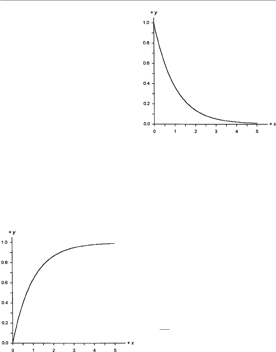
APPENDIX 8 MATHEMATICS FOR ELECTRONICS 413
whilst that which relates to exponential decay takes
the form:
In the case of exponential growth, the value, Ymax,
is simply the maximum value for y.In other words
it is approximately the value that ywill reach after
avery long time (note that, even though ygets very
close in value to it, Ymax is never quite reached).
In the case of exponential decay, the value, Ymax,
is the initial value of y.In other words it is the
value of y before the decay starts. After a very long
period of time, the value of ywill reach
approximately zero (note that, even though ygets
very close in value to zero, it is never quite
reached).
Figure A8.34 shows a graph showing
exponential growth whilst Fig. A8.35 shows a
graph showing exponential decay. In both cases
Ymax has been set to 1.
The name given to the constant, e,is the
exponential constant and it has a value of
approximately 2.713. The value of the constant is
normally accessible from your calculator (in the
same way that the value of ais stored as a constant
in your calculator).
Finally, let’s take a look at a practical example of
the exponential function involving the discharge of
acapacitor.
max
x
yYe
=
Example 18
Acapacitor is charged to a potential of 100 V. It is
then disconnected from its charging source and left
to discharge through a resistor. If it takes 10 s for
the voltage to fall to 50 V, how long will it take to
fall to 10 V?
Here we are dealing with exponential decay. If
we use y to represent the capacitor voltage at any
instant, and since the initial voltage is 100 V, we
can determine the value of x(i.e. x1)when the
voltage reaches 50 V by substituting into the
formula:
hence:
from which:
taking logs (to the base ethis time) of both sides:
max
x
yYe
=
1
50 100
x
e
=
(
)
(
)
1
log log 0.5
x
ee
e=
Figure A8.34 An exponential growth curve
1
50
0.5
100
x
e
==
Figure A8.35 An exponential decay curve
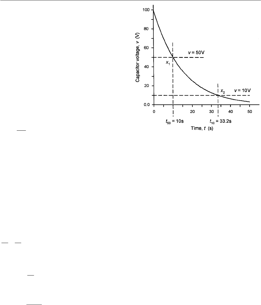
414 ELECTRONIC CIRCUITS: FUNDAMENTALS AND APPLICATIONS
thus:
hence:
x1=0.693
We can use a similar process to find the value of x
(i.e. x2)that corresponds to a capacitor voltage of
10 V:
hence:
from which:
taking logs (again to the base e)of both sides:
thus:
hence:
x2=2.3
We can now apply direct proportionality to
determine the time taken for the voltage to reach
10 V. In other words:
from which:
thus:
Figure A8.36 illustrates this relationship.
1
0.693
x
=
max
x
yYe
=
2
10 100
x
e
=
2
2.3
x
=
2
10 50
1
x
tt
x
=×
10
2.3
10 33.2s
0.693
t=× =
2
10
0.1
100
x
e
==
(
)
(
)
2
log log 0.1
x
ee
e
=
50 10
12
tt
xx
=
Figure A8.36 Capacitor voltage during discharge
—see Example 18

Appendix 9
Useful web addresses
Author’s website and additional resources to support this book
key2electronics http://www.key2electronics.com/
Semiconductor manufacturers
Analog Devices http://www.analog.com/
Dallas Semiconductor http://www.dalsemi.com/
Fujitsu http://www.fujitsu-fme.com/
Harris Semiconductor http://www.harris.com/
Holtek Semiconductor http://www.holtek.com
Intel http://www.intel.com/
International Rectifier http://www.irf.com/
Linear Technology http://www.linear.com/
Maxim http://www.maxim-ic.com/
Microchip Technology http://www.microchip.com/
National Semiconductor http://www.national.com/
Philips http://www.semiconductors.philips.com/
Samsung http://www.samsung.com/
Seiko http://www.sii-ic.com/
SGS-Thompson http://www.st.com/stonline/
Siemens http://www.siemens.de/
Sony http://www.sony.com/
Teridian Semiconductor http://www.tsc.tdk.com/
Texas Instruments http://www.ti.com/
Zilog http://www.zilog.com/
Electronic component suppliers
Farnell Electronic Components http://www.farnell.co.uk/
Greenweld http://www.greenweld.co.uk/
Jaycar Electronics http://www.jaycarelectronics.co.uk/
Magenta http://www.magenta2000.co.uk/
Maplin Electronics http: //www.maplin.co.uk/
Quasar Electronics http://www.quasarelectronics.com/
Rapid Electronics http://www.rapidelectronics.co.uk/
RS Components http://www.rswww.com/

416 ELECTRONIC CIRCUITS: FUNDAMENTALS AND APPLICATIONS
Magazines
Everyday with Practical Electronics (EPE) http://www.epemag.wimborne.co.uk/
EPE Online http://www.epemag.com/
Elektor http://www.elektor-electronics.co.uk/
Clubs and societies
American Radio Relay league http://www.arrl.org/
British Amateur Electronics Club http://members.tripod.com/baec/
Radio Society of Great Britain http://www.rsgb.org.uk/
Miscellaneous
5Spice Analysis http://www.5spice.com/
CadSoft Online (Eagle) http://www.numberonesystems.com/
Electronics Workbench (Multisim) http://www.electronicsworkbench.com/
Labcenter Electronics http://www.labcenter.co.uk/
Matrix Multimedia (E-blocks) http://www.matrixmultimedia.co.uk/
Microchip Technology (MPLab IDE) http://www.microchip.com/
MicroElektronika (EasyPIC3) http://www.breadboarding.co.uk/
Oshonsoft (Z80 and PIC simulators) http://www.oshonsoft.com/
Pico Technology (Picoscope) http://www.picotech.com/
Tina Design Suite http://www.tina.com/
WebEE Electronic Engineering Homepage http://www.web-ee.com/
WinSpice http://www.winspice.com/

Index
3dB point, 135
4000-series, 192
50 Hz square wave generator, 224
60 second timer, 221
74-series, 192
a.c. analysis, 306
a.c. coupled amplifier, 131
ADC, 108, 211, 212
AGC, 234
ALU 203, 205, 207
AM, 231
AM demodulator, 235, 236
AM transmitter, 232, 233
AND gates, 186
AND logic, 104, 184
Absolute permittivity, 11
Acceptor circuit, 77
Accumulator, 203, 208
Active sensor, 288
Address bus, 201, 203, 205
Address bus buffer, 204
Adjustable bias, 150
Adjustable inductor, 43
Aerial, 236
Aerial efficiency, 239
Aerial gain, 239, 240
Air, 11
Air cored inductor, 41, 81
Air cored transformer, 79
Air-spaced variable capacitor, 38
Algorithm, 303
Alternating current, 69
Aluminium, 8
Ambient temperature, 22, 35, 348
Ammeter, 245
Ampere, 2, 3
Amplifier, 131, 132, 135, 138, 144, 145, 146, 149
Amplifier circuit, 148
Amplitude, 71
Amplitude modulation, 231
Analogue multimeter, 247, 249, 250, 251, 252, 253
Analogue sensor, 288
Analogue signal, 69
Analogue-to-digital converter, 211, 212
Analogy, 288
Angle, 2
Angular position, 289, 290
Annealed copper, 8
Anode, 88, 89
Apparent power, 75
Arithmetic logic unit, 203, 205, 207
Astable multivibrator, 174, 175, 178, 304
Astable oscillator, 176, 177, 179
Astable pulse generator, 221
Astigmatism, 262
Atom, 87
Audible alarm, 300
Audible output, 298
Audible output driver, 300
Audible transducer, 289
Audio frequency amplifier, 131, 135
Audio transformer, 79
Automatic gain control, 234
Auto-ranging, 249
Avalanche diode, 92
B–H curve, 15, 16
B2 Spice 308, 311
BFO, 230
BJT, 96, 98, 107
BJT, circuit configurations, 140
BJT go/no-go checks, 279
BNC connector, 338
BS 1852 coding, 25
BS 4937, 296
BS symbols, 186, 187
Back e.m.f., 39
Balance, 54
Band-gap reference, 127
Bandpass filter, 235
Bandwidth, 77, 78, 135, 136, 162, 164
Base, 96, 98
Battery, 17
Battery-backed memory, 202
Beam array, 240
Beamwidth, 241
Beat frequency, 230
Beat frequency oscillator, 230
Belling-Lee connector, 338
418 ELECTRONIC CIRCUITS: FUNDAMENTALS AND APPLICATIONS
Bench magnifier, 345
Bench power supply, 357
Bi-directional aerial, 238
Bi-directional bus, 204
Bi-phase rectifier, 119, 120
Bias, 144
Bias adjustment, 150
Bias point, 133
Bias stabilization, 145, 150
Bias voltage, 98
Bidirectional current, 69
Binary, 201
Binary counter, 190
Binary digit, 183
Binary number, 201
Bipolar junction diode, 96
Bistable, 188
Bistable multivibrator, 174
Bit cleaner, 345
Bit profiles, 343
Bonds, 87
Boolean logic, 185, 186, 187
Boost, 125, 127
Breadboard, 327, 329
Breakdown, 11
Bridge, 54
Bridge rectifier, 91, 121, 122, 124
Buck, 125, 127
Buffers, 185
Bus, 201
Byte, 201, 202
C–R circuit, 58, 59, 60, 62, 75
C–R integrating circuit, 62
C–R ladder network, 172, 173
C–R network, 61
CARRY, 205
CLEAR, 189
CLOCK, 188
CMOS, 192
CMOS RAM, 202
CMOS logic, 193, 194
CMOS microcontroller, 211
CNC, 304, 327
CPU, 199, 200, 203
CPU clock 206
CRT, 260
CW, 229
CW, receiver 229, 230
CW, transmitter 229, 230
Cadmium sulphide, 30
Calibrate, 260
Capacitance, 1, 3, 32, 33, 35
Capacitance measurement, 259
Capacitive proximity switch, 291
Capacitive reactance, 72
Capacitor, 31, 34, 35
Capacitor colour code, 36
Capacitor marking, 35, 36
Capacitors in parallel, 36, 37
Capacitors in series, 36, 37
Carbon film resistor, 22
Carbon potentiometer, 30
Cast iron, 15
Cast steel, 15, 16
Cathode, 88, 89
Cathode ray tube, 260
Centi, 4
Central processing unit, 200, 203
Ceramic, 11
Ceramic capacitor, 35
Ceramic wirewound resistor, 22
Channel, 103
Characteristic of a transistor, 97
Charge, 1, 3, 9, 31, 33
Charge carrier, 88
Charging, 32, 58
Choke, 38, 75, 81
Circuit construction, 327
Circuit diagram, 16, 17
Circuit simulation, 303
Class A, 133, 134, 144, 151
Class AB, 133, 134, 150, 151
Class B, 133, 134, 150, 304
Class C, 134, 232
Class of operation, 132
Clipped waveform, 133
Clock, 200, 206
Clock waveform, 206
Closed-loop, 137
Closed-loop system, 210
Closed-loop voltage gain,158
Coaxial connector, 338
Coil, 38
Cold junction, 296
Collector, 96, 98
Collector characteristic, 99
Collector load, 144
Colour code, 23
Combinational logic, 187
Common, 16
Common rail, 158

INDEX 419
Common-base mode, 138, 140
Common-collector mode, 138, 140
Common-drain mode, 139, 140
Common-emitter amplifier, 141
Common-emitter current gain, 142
Common-emitter h-parameters, 140
Common-emitter mode, 98, 138, 140
Common-gate mode, 139, 140
Common-source mode, 139, 140
Comparator, 127, 166, 167, 296
Complementary metal oxide semiconductor, 192
Complementary output stage, 150, 151
Complex wave, 70
Complex waveform, 69
Component model, 309
Component removal and replacement, 344
Computer simulation, 303
Conductance, 3
Conductivity, 8
Conductor, 6
Conductors, 5
Connectors, 338, 340
Constant current characteristic, 104
Contactless joystick, 292
Continuous wave, 229
Control bus, 201, 203, 205
Control system, 287
Control unit, 204, 205
Conventional flow, 6
Copper, 8
Corrective action, 273
Coulomb, 2, 3
Coulomb’s Law, 9
Counter, 190
Coupling, 149, 168, 235
Coupling capacitor, 144
Covalent bonding, 87
Critically-coupled, 235
Crystal controlled oscillator, 177
Crystal oscillator, 179
Current, 1, 3
Current divider, 53
Current gain, 98, 99, 100, 132, 140, 142
Current gain measurement, 259
Current measurement, 252, 255
Current ratio, 81
Current source, 142
Cut-off, 103, 133, 134, 144
Cut-off frequency, 135, 136, 163, 164
D-connector, 338
D-type bistable, 188, 189
d.c. analysis, 304, 306
d.c. coupled amplifier, 131
d.c. level, 69
DAC, 108, 212
DIL, 108, 157
DIL switch, 293
DIN 41612, 338
DIN 41617, 338
DIN connectors, 338
DPDT switch, 17
Dampen, 78
Darlington relay driver, 299
Darlington transistor, 107
Data bus, 201, 203, 204
Data bus buffer, 204
Data sheet, 355
Data types, 202
Data value, 206
Date code, 193
De-rating characteristic, 349
Debounce circuit, 294
Degrees, 2
Demand, 288
Demodulation, 231
Demodulator, 235, 236
Depletion mode MOSFET 107
Depletion region, 89
Derived units, 1
Design specification, 355
Desoldering pump, 345
Desoldering technique, 343
Desoldering tools, 345, 346, 346
Destination register, 204
Detector, 230, 231
Development cycle, 321
Development system, 320, 323
Diac, 94
Diecast box, 338
Dielectric constant, 11
Dielectric strength, 11
Differential amplifier, 163
Differential pressure vacuum switch, 291
Differentiating circuit, 61, 62
Differentiator, 165, 166
Diffuse scan proximity switch, 290
Digital logic, 183
Digital multimeter, 247, 249, 254, 256, 257, 258
Digital sensor, 288
Digital signal, 69
Digital-to-analogue converter, 212

420 ELECTRONIC CIRCUITS: FUNDAMENTALS AND APPLICATIONS
Diode, 88, 91, 96, 124
Diode characteristic, 90
Diode coding, 96
Diode demodulator, 236
Diode go/no-go checks, 278
Diode test circuit, 90
Diode tester, 280
Diode testing, 277
Dipole, 236
Dipole aerial, 240
Direct coupling, 149
Direct current, 6
Director, 241
Discharging, 32, 60
Display, 247
Distortion, 263, 267
Distortion analysis, 307
Distortion measurement, 263
Distributed systems, 313
Doubler, 125
Drain, 103
Driver stage, 150
Driver transistor, 97
Dual timer, 219
Dual-in-line, 108, 157
Duty cycle, 126
Dynamic microphone, 289
E-blocks, 319, 323
E-field, 227, 228
E.m.f., 6
E12 series, 21, 22
E24 series, 21, 22
E6 series, 21, 22
EMC Directive, 354
EMC filter, 355
ESD, 341, 342
Edge connector, 338
Effective value, 71
Electric circuit, 14
Electric field, 10
Electric field strength, 10
Electrical analogy, 288
Electrical length, 236
Electrical quantities, 1
Electrical units, 3
Electro-static damage, 342
Electrolytic capacitor, 34, 35
Electromagnetic vibration sensor, 291
Electromagnetic wave, 227, 228
Electromagnetism, 11
Electromotive force, 6, 14
Electron, 5, 87
Electronic solder, 340
Electrostatics, 9
Embedded microcontroller, 313
Emitter, 96, 98
Emitter follower, 138, 148, 149
Enclosure, 338, 357
Energy, 1, 3, 8
Energy storage, 33, 40
Enhancement mode MOSFET, 107
Equipment wire, 328
Equivalent circuit, 53, 139, 143, 239
Ergonomic design, 339
Error signal, 288
Etchant, 336
Evaluation, 358
Exclusive-OR gate, 187
Exponent notation, 4
Exponential decay, 58, 60, 61, 64
Exponential growth, 58, 61, 64
Exponents, 4, 5
External clock, 206
FET, 96, 103, 107
FET characteristic, 103
FET parameters, 104
FM, 231
FM transmitter, 232, 233
Fall time, 267
Farad, 3, 32
Fault finding, 273, 274
Feedback, 136, 137, 162
Ferrite core, 38
Ferrite cored inductor, 41, 43, 81
Ferrite cored transformer, 79
Fetch-execute cycle 206, 207
Field, 10, 13
Field effect transistor, 96, 103
Field strength, 10
Filament lamp driver, 299
Flag register, 205, 208
Flash memory, 314
Flatpack, 108
Float switch, 290, 292
Flow sensor, 290, 292
Flowchart, 209, 273
Flowcode, 324
Flux, 3, 13, 14, 39, 80, 341
Flux density, 12, 13, 14
Focus adjustment, 262

INDEX 421
Force, 1
Force between charges, 9
Force between conductors, 12
Forward bias, 89
Forward current gain, 98, 99
Forward current transfer, 140
Forward direction, 88
Forward threshold voltage, 89
Forward transfer conductance, 104
Free electrons, 87
Free space, 11, 229
Frequency, 1, 3, 69
Frequency modulation, 231
Frequency of resonance, 77
Frequency response, 135, 161, 164
Frequency response measurement, 263, 267
Fringing, 14
Full-power bandwidth, 159
Full-scale deflection, 248
Full-wave bridge rectifier, 121
Full-wave control, 94
Full-wave rectifier, 119
Fully charged, 31
Fully discharged, 31
Fume extraction, 341
Fumes, 341
Fundamental, 136
Fundamental mode, 177
Fundamental units, 1
Gain, 132, 137
Gain and bandwidth, 161, 162
Gain block, 157
Ganged control, 30
Gate, 93, 103
General-purpose register, 204
General-purpose solder, 340
Germanium, 96
Germanium diode, 91
Giga, 4
Glass, 11
Go/no-go checks, 278, 279
Graticule, 260, 261
Ground, 16
Group board, 327
H-field, 227, 228
Half-power frequency, 78
Half-wave control, 94
Half-wave dipole, 236, 237
Half-wave rectifier, 116, 117, 118
Hard drawn copper, 8
Harmonic, 136
Harvard architecture, 313
Heat dissipater, 349
Heat flow, 342, 350
Heating element, 289
Heatsink, 348, 352, 353, 354
Helium, 6
Henry, 3
Hertz, 3
Hexadecimal, 201
High time, 267
High-Q, 78
High-brightness, LED 297
High-current load, 298
High-current measurement, 252, 255
High-frequency transistor, 97
High-speed CMOS, 192
High-state, 217, 219
High-voltage transistor, 97
Holes, 88
Hook-up wire, 328
Horizontal dipole, 240
Horizontally polarized aerial, 240
Hot junction, 296
Hybrid parameter equivalent circuit, 143
Hybrid parameter, 98, 99, 102, 139, 140
I/O, 200, 201, 208
IDC connector, 338
IDE, 318, 320
IEC connector, 338
IEEE-488, 338
IF, 232, 234
IF amplifier, 234, 236
IGFET, 103
INTERRUPT, 206
IRQ, 205
Ideal amplifier, 162
Illuminance, 1
Impedance, 74, 75, 238
Impedance triangle, 75
Impurity, 87, 88
Indeterminate range, 193, 194, 281
Index register, 208
Induced e.m.f., 39
Inductance, 1, 3, 39, 40
Inductive proximity switch, 291
Inductive reactance, 73
Inductor, 38, 41
Inductor marking, 41

422 ELECTRONIC CIRCUITS: FUNDAMENTALS AND APPLICATIONS
Inductors in parallel, 42
Inductors in series, 42
Input and output, 208
Input characteristic, 97, 99, 141
Input device, 210
Input impedance, 134
Input offset voltage, 159
Input port, 210, 211
Input resistance, 134, 135, 139, 140, 141, 158
Input transducer, 288
Instruction code, 206
Instruction decoder, 205
Instruction register, 204
Instruction set, 322
Instrument case, 338
Instrumentation system, 287
Insulating bush, 353
Insulating washer, 353
Insulation displacement connector, 338
Insulator, 5, 6
Integrated Development Environment, 318, 320
Integrated circuit, 108
Integrated circuit faults, 277
Integrated circuit logic, 192
Integrated circuit packages, 108
Integrated circuit voltage regulator, 124
Integrating circuit, 61, 62
Integrator, 166
Intensity adjustment, 262
Interface circuits, 212
Intermediate frequency, 232, 234
Internal arrangement, 359
Internal clock, 206
Internal data bus, 204
Internal gain, 137
Internal resistance, 123
Internal wiring, 340
Interrupt, 205, 209
Interrupt vector register, 208
Inverter, 185
Inverting amplifier, 162, 163
Iron cored inductor, 41
Iron cored transformer, 79, 80
Isotropic radiator, 239
J-K bistable, 189, 190, 191
JFET, 103, 104, 157
JFET circuit configurations, 140
JFET oscillator, 178
JFET test circuit, 104
Joule, 2, 3, 8
Joystick, 292
Junction temperature, 348
Keying, 229
Kilo, 4
Kirchhoff’s Current Law, 49
Kirchhoff’s Laws, 49
Kirchhoff’s Voltage Law, 50
L–C circuit, 76
L–C coupling, 149
L–C smoothing filter, 118
L–C–R circuit, 76
L–R circuit, 63, 75
LAN, 200
LCD display, 247, 255
LDR, 30, 290, 296, 297
LED, 94, 95, 297, 298
LED display, 247
LED indicator, 297
LSI, 108, 192
LVDT, 290
Ladder network oscillator, 172, 178
Large scale integration, 108, 192
Large-signal amplifier, 131
Large-signal current gain, 98
Latching action switch, 295
Lattice, 6, 87
Lead, 8
Leakage current, 88
Leakage flux, 14, 80
Length, 1
Light emitting diode, 94, 95
Light level detection, 296, 297
Light level sensor, 290
Light sensor, 292
Light-dependent resistor, 30, 290, 296
Linear law, 30, 31
Linear operation, 133
Linear position sensor, 290, 291
Linear power supply, 125
Linear variable differential transducer, 290
Linearity, 132
Liquid flow sensor, 292
Liquid level sensor, 290, 292
Load, 21
Load cell, 291
Load test, 358
Loaded potential divider, 52
Loading, 52, 247, 248
Local area network, 200

INDEX 423
Local oscillator, 234
Local oscillator frequency, 234
Logarithmic law, 30, 31
Logarithmic scale, 135
Logic, 183
Logic 0, 193, 201
Logic 1, 193, 201
Logic circuit faults, 281
Logic families, 195
Logic function, 183
Logic gates, 185
Logic levels, 193, 194
Logic probe, 282, 284, 285, 331
Logic pulser, 283, 285
Logic simulation, 309
Logic symbols, 186
Loop, 13, 50
Loop gain, 137
Loss resistance, 38, 38, 39
Loudspeaker, 289
Low time, 267
Low-Q, 78
Low-frequency transistor, 97
Low-noise amplifier, 132
Low-noise transistor, 97
Low-power CMOS timer, 218
Low-power Schottky, 192
Low-power timer, 219
Low-state, 217, 219
Low-voltage Directive, 354
Luminous flux, 1
Luminous intensity, 1
M1 cycle, 206, 207
M2 cycle, 207
MIL/ANSI symbols, 186, 187
MOSFET, 107, 126
MOSFET driver, 299, 300
MPLAB, 320
MSI, 192
Machine cycle, 204, 206, 207
Magnetic circuit, 14
Magnetic field, 12, 13
Magnetic flux, 1, 3
Magnetic flux density, 3
Magnetizing force, 15
Magnetomotive force, 14
Main register set, 208
Mains connector, 338
Major lobe, 241
Majority vote circuit, 187
Mark to space ratio, 126
Maskable interrupt, 209
Mass, 1
Matrix board, 327, 328, 329
Maximum reverse repetitive voltage, 90
Medium scale integration, 192
Medium-Q, 78
Mega, 4
Memory cell, 188
Memory refresh register, 208
Mesh, 49, 50
Metal clad resistor, 22
Metal film resistor, 22
Metals, 8
Meter, 245
Meter loading, 247, 248
Mica, 11
Mica capacitor, 35
Micro, 4
Microcontroller, 199, 210, 212, 317, 318, 323
Microcontroller system, 210, 211
Microprocessor, 199, 200, 203, 208
Microprocessor instruction, 209
Microprocessor operation, 206
Microprocessor system, 200
Microprogrammer, 319
Microswitch, 291
Mid-band, 134, 136
Mild steel, 8, 15
Milli, 4
Mixed-mode analysis, 310
Mixer, 234
Modification, 358
Modulation, 230, 231
Monostable multivibrator, 174
Monostable pulse generator, 219
Monostable pulse stretcher, 282
Morse code, 230, 231
Motor driver, 300
Moving coil meter, 53, 245
Multi-plate capacitor, 34
Multi-pole connector, 338
Multi-range meter, 247
Multi-stage amplifier, 149, 168
Multiples, 3, 4
Multiplier, 245
Multivibrator, 174, 175
Mutual characteristic, 103
N-channel, FET 107
N-type material, 88

424 ELECTRONIC CIRCUITS: FUNDAMENTALS AND APPLICATIONS
NAND gate, 186, 194
NAND gate circuit, 193
NC switch, 293
NMI, 205
NO switch, 293
NOR gate, 186, 194
NPN transistor, 96, 97, 98, 100
NTC, 27, 29
Nano, 4
Negative feedback, 136, 137, 145, 168, 288
Negative ramp wave, 70
Negative temperature coefficient, 27, 29
Netlist, 303, 306, 309
Nibble, 201
Nickel, 8
Node, 49, 281
Noise, 22
Noise analysis, 307
Noise filter, 81
Noise margin, 193, 194
Non-electrolytic capacitor, 34
Non-inverting amplifier, 163
Non-linear power supply, 125
Non-maskable interrupt, 205, 209
Non-volatile memory, 202
Normally closed switch, 293
Normally open switch, 293
North pole, 5
Norton equivalent circuit, 57
Norton’s Theorem, 56
Nucleus, 87
OR gate, 186
OR logic, 104, 184, 185
Off-time, 267
Off-tune reactance, 238
Offset voltage, 159
Ohm, 3
Ohm’s Law, 6, 7
Ohmic resistance, 238
Ohmmeter, 246
Ohms-per-volt rating, 248
Omni-directional aerial, 238
On-time, 267
Open-collector buffer, 300, 301
Open-loop voltage gain, 158
Operand, 206
Operating point, 100, 146, 147, 150
Operational amplifier, 157, 158, 161, 163, 165
Operational amplifier circuits, 165
Optical proximity switch, 291
Optical shaft encoder, 290
Oscillation, 172
Oscillator, 171, 173, 176, 178
Oscillator circuits, 178
Oscilloscope, 260, 261, 263, 264, 265, 266, 268
Oscilloscope controls, 262
Output characteristic, 98, 99, 104
Output conductance, 140
Output driver, 298
Output impedance, 134
Output level measurement, 253
Output port, 210, 211
Output resistance, 123, 134, 135, 140, 159
Output stage, 150
Output transducer, 288
Outputs, 297
Over-coupled, 235
Overdriven amplifier, 132
Overtone mode, 177
P-N junction, 89, 96
P-channel FET, 107
P-type material, 88
P.d., 6
P.r.f., 267
PCB, 44, 331, 332
PCB CAD packages, 336
PCB bench magnifier, 345
PCB holder, 345
PCB layout, 304, 331, 332, 333, 347, 359
PCB manufacture, 333, 334, 335
PIC development system, 323
PIC families, 313, 314
PIC microcontroller, 199, 313, 315, 317
PIC programmer, 319, 320
PIC programming, 318
PIC simulator, 321
PIV, 90
PL259/SO239 connector, 338
PLC, 200
PLD, 200
PNP transistor, 96, 97, 98, 101
PRESET, 189
PTC, 27, 29
PWM, 126, 314
Paper, 11
Parallel capacitors, 36, 37
Parallel connection, 26
Parallel inductors, 42
Parallel resistors, 26
Parallel resonant circuit, 76

INDEX 425
Parallel shunt resistor, 53
Parallel-to-serial conversion, 208, 209
Passive component, 21
Passive sensor, 288
Peak inverse voltage, 90
Peak value, 71
Peak-to-peak value, 71
Pentavalent impurity, 88
Performance measurement, 358
Period, 70, 267
Periodic time, 70
Permeability, 12, 15
Permeability of free space, 12
Permittivity, 11, 33
Permittivity of free space, 10
Phase angle, 75
Phase shift, 136, 140, 157
Phasor diagram, 72, 73
Photocell, 290
Photodiode, 290, 297
Phototransistor, 290
Physical length, 237
Pico, 4
Piezo transducer, 300
Piezo-resistive sensor, 291
Piezoelectric effect, 177
Plastic box, 338
Point-to-point wiring, 327, 329
Polarized capacitor, 35
Polarized wave, 228
Pole-zero analysis, 305
Polyester, 11
Polyester capacitor, 35
Polystyrene, 11
Polystyrene capacitor, 35
Polythene, 11
Porcelain, 11
Port, 209
Position sensor, 291
Positive feedback, 137, 168, 171
Positive ramp wave, 70
Positive temperature coefficient, 27, 29
Pot cored inductor, 41
Potential, 1, 3
Potential divider, 52
Potentiometer, 30
Power, 1, 3, 8
Power amplifier, 150
Power factor, 75
Power gain, 132
Power rating, 22
Power supply, 115, 127
Power supply circuit, 123, 124
Power transformer, 79, 80
Power transistor, 97
Powers of ten, 4
Preferred value, 21
Preset resistor, 30, 31
Pressure sensor, 291
Printed circuit, 44
Printed circuit board, 328, 329, 331
Program code, 206, 208, 209
Program counter, 204, 208
Programmable logic controller, 200
Programmable parallel I/O, 208
Programmed logic device, 200
Propagation, 228
Proton, 5, 87
Prototype manufacture, 355
Proximity sensor, 290, 291
Pull-up resistor, 221, 293
Pulsating d.c., 115
Pulse generator, 219, 221
Pulse measurement, 267
Pulse parameters, 268
Pulse repetition frequency, 267
Pulse wave, 70
Pulse waveform, 69
Pulse width modulation, 126
Pyrex glass, 11
Q-factor, 41, 77, 78, 93
Quad-in-line, 108
Quality factor, 77
Quantity of electricity, 33
Quartz crystal, 177, 206
Quiescent point, 147
R–C coupling, 149
R–C smoothing filter, 118
R-S bistable, 188
r.m.s. value, 71
RAM, 199, 200, 201, 202, 204
READ, 205
RESET, 188, 205
RF amplifier, 232, 235, 236
RISC, 313
ROM, 199, 200, 201, 202, 204
Radians, 2
Radiated power, 239
Radiation pattern, 237
Radiation resistance, 238

426 ELECTRONIC CIRCUITS: FUNDAMENTALS AND APPLICATIONS
Radio, 227
Radio frequency amplifier, 131, 135
Radio frequency spectrum, 227, 228
Radio solder, 339
Ramp, 70
Random access memory, 200, 201
Ratio arm, 54
Reactance, 72, 75
Read operation, 204, 206, 207
Read-only memory, 200
Receiver, 233, 234
Rectifier, 91, 116
Reduced Instruction Set Computer, 313
Reed switch, 291
Reference aerial, 239
Reflector, 241
Register, 203
Register set, 208
Regulated d.c., 115
Regulation, 80, 123
Rejector circuit, 77
Relative permeability, 15
Relative permittivity, 11, 33
Relay driver, 299
Reluctance, 14, 15
Research, 355
Reservoir, 116
Reservoir capacitor, 117, 120, 122
Resistance, 1, 3, 6, 7
Resistance measurement, 253, 259
Resistive strain gauge, 291
Resistivity, 7, 8
Resistor, 21, 22, 31
Resistor colour code, 23
Resistor marking, 23, 25
Resistors in parallel, 26
Resistors in series, 26
Resolution, 249
Resonance, 77
Resonant circuit, 76, 78
Resonant frequency, 76
Resonant transformer, 81
Reverse bias, 89
Reverse breakdown voltage, 89
Reverse direction, 88
Reverse voltage transfer, 140
Right-hand rule, 12
Ripple, 117, 120
Ripple filter, 118
Ripple frequency, 120
Rise time, 267
Roll-off, 151
Rotary position sensor, 290
Rotary potentiometer, 289
Rotating vale flow sensor, 290
SET, 188
SI units, 1
SIL, 108
SLSI, 192
SMC, 43, 44
SMD, 347
SMD tools, 346
SMPS, 125
SMT, 43
SPDT switch, 17
SPICE, 304, 309
SPST switch, 17
SRBP, 331
SSI, 192
SSR, 301
Safety, 274, 341
Saturated amplifier, 144
Saturation, 15
Scientific notation, 4
Second, 3
Selectivity, 232, 235
Self-regulating system, 210
Semiconductor junction temperature, 348
Semiconductor mounting, 353
Semi-logarithmic law, 30, 31
Semiconductor, 87, 88
Semiconductor strain sensor, 291
Semiconductor temperature sensor, 291, 295
Sensitivity, 232, 248, 249
Sensitivity analysis, 307
Sensor, 56, 288
Serial-to-parallel conversion, 208, 209
Series capacitors, 36, 37
Series connection, 26
Series inductors, 42
Series loss resistance, 38, 39
Series regulator, 116
Series resistors, 26
Series resonant circuit, 76
Series-pass transistor, 124
Sharpen, 78
Shells, 5
Shift register, 191, 208, 209, 310
Shunt, 245
Shunt resistor, 53
Siemen, 3

INDEX 427
Signal, 69
Signal conditioning, 288
Signed byte, 202
Signed word, 202
Silicon, 96
Silicon controlled rectifier, 93
Silicon diode, 91
Silver, 8
Silver bearing solder, 341
Simulation, 303
Sine wave, 2, 70, 71
Sine wave oscillator, 173, 174, 178
Single-chip microcomputer, 199
Single-in-line, 108
Single-pole connector, 338
Sink current, 217
Skeleton preset, 30
Slew rate, 159, 160
Small-signal amplifier, 131
Small-signal analysis, 304
Small-signal current gain, 99, 100
Small-signal distortion analysis, 307
Smoothing circuit, 117
Smoothing filter, 118
Snubber circuit, 301
Solder, 339
Solder fumes, 341
Soldered joint, 344, 345
Soldering, 44, 339
Soldering iron, 342
Soldering iron bit, 342, 343
Soldering station, 341
Soldering technique, 343
Solenoid, 13
Solid-state relay, 301
Sound, 289
Source, 103
Source current, 217
Source follower mode, 139
Source register, 203
South pole, 5
Special purpose register, 208
Specific resistance, 7
Spectral response, 297
Speed of light, 229
Square wave, 70
Square wave generator, 223, 224
Square wave oscillator, 179
Square-to-pulse converter, 61
Square-to-triangle converter, 61
Stability, 22, 35
Stabilized bias, 150
Stack, 204
Stack pointer, 204, 208
Standard dipole, 239
Step-down regulator, 125
Step-down transformer, 79
Step-up regulator, 125
Step-up transformer, 79
Strain sensor, 291
Stripboard, 328
Stripboard layout, 330
Stripboard mounting, 359
Sub-multiples, 3, 4
Substrate, 103
Summing amplifier, 167
Super large scale integration, 192
Superhet receiver, 234
Supply, 16
Surface mounted components, 44
Surface mounting, 43, 328, 329, 347
Switch, 17
Switch and lamp logic, 183
Switch bounce, 294
Switch input, 293
Switch sensors, 289
Switched mode controller, 126, 127
Switched mode power supply, 125, 127
Switches, 293
Switching diode, 126
Switching transistor, 97
Symbols, 3
Synthetic resin bonded paper, 331
T-state, 206
TAB, 353
THC, 43
THD, 151
TO126, 107
TO18, 107
TO218, 353
TO220, 107, 108, 353
TO3, 107, 108, 350, 353
TO5, 107, 108
TO66, 107
TO72, 108
TO92, 107
TRF receiver, 232, 233
TTL, 192
TTL device coding, 192
TTL logic, 193, 194
TV connector, 338

428 ELECTRONIC CIRCUITS: FUNDAMENTALS AND APPLICATIONS
Tachogenerator, 290
Tag strip, 327
Tapped inductor, 235
Temperature, 1, 289, 291
Temperature coefficient, 8, 22, 26, 28, 29, 35
Temperature rise, 348
Temperature sensor, 292, 295
Temperature threshold detector, 297
Temperature-controlled soldering station, 341
Tera, 4
Tesla, 1, 3, 13
Testing to specification, 355
Thermal analysis, 307
Thermal resistance, 348, 349, 351, 353, 354
Thermistor, 29, 291
Thermocouple, 288, 289, 291, 296
Thevenin equivalent circuit, 55
Thevenin’s Theorem, 54
Three-terminal regulator, 124
Threshold detection, 296
Threshold input, 217
Threshold voltage, 89
Through-hole mounting, 43
Thyristor, 93, 94
Time, 1, 3
Time constant, 58, 60, 63
Timebase, 59
Timer, 217, 218
Timing diagram, 190, 191
Tina Pro, 303, 307
Titanium dioxide, 11
Tolerance, 21, 22, 41
Toothed rotor tachometer, 290
Toroidal transformer, 81
Total harmonic distortion, 151
Touch-operated switch, 295
Track, 328
Track spacing, 332
Track width, 332
Transconductance, 306
Transducer, 287, 288
Transfer characteristic, 98, 99, 133, 142
Transformer, 79
Transformer coupling, 149
Transformer equation, 80
Transformer mounting, 359
Transient analysis, 305, 308
Transimpedance, 306
Transistor, 97, 98, 102, 103
Transistor amplifier, 138
Transistor characteristic, 97, 98, 99, 103
Transistor coding, 107
Transistor current gain measurement, 259
Transistor driver, 299
Transistor faults, 274, 275, 276
Transistor packages, 107
Transistor parameters, 102
Transistor symbols, 98, 107
Transistor test circuit, 100, 104
Transistor tester, 280
Transistor-transistor logic, 192
Transmitter, 232, 233
Tri-state condition, 281
Triac, 94, 95
Triangle wave, 70
Triangle wave generator, 179
Trigger input, 217, 219
Trigger pulse, 93, 174
Triggering, 94
Tripler, 125
Trivalent impurity, 88
True power, 75
Truth table, 104, 185, 186, 187, 189
Tuned circuit, 78
Tuned radio frequency, 232
Tuning capacitor, 38
Turns ratio, 80, 81
Turns-per-volt, 81
Two’s complement, 202
Two-stage amplifier, 149
Type-K thermocouple, 296
UHF circuit construction, 329
USART, 314
USB, 319, 320
Ultra-violet light source, 335
Under-coupled, 235
Unidirectional current, 69
Units, 1, 3
Unsigned byte, 202
Unsigned word, 202
VA rating, 79
VDR, 30
VLS, 199
VLSI, 192, 200
Vacuum, 11
Valence shell, 87
Variable capacitance diode, 93
Variable capacitors, 38
Variable power supply, 357
Variable pulse generator, 224

INDEX 429
Variable reactance, 232
Variable resistor, 30, 31
Varicap, 93
Vertical dipole, 240
Vertically polarized aerial, 240
Very large scale integration, 192, 199
Vibration sensor, 291
Virtual instrument, 304
Vitreous wirewound resistor, 22
Volt, 2, 3
Voltage, 6
Voltage and current distribution, 237
Voltage calibrator, 52
Voltage dependent resistor, 30
Voltage doubler, 125
Voltage follower, 165
Voltage gain, 132, 140, 144, 158
Voltage measurement, 252, 255
Voltage multiplier, 125
Voltage rating, 35
Voltage ratio, 80, 81
Voltage reference, 116, 127
Voltage regulator, 92, 122
Voltage tripler, 125
Voltmeter, 245
WRITE, 205
Watt, 3, 8
Waveform, 69, 70, 166, 167, 267
Waveform measurement, 263
Wavefront, 229
Wavelength, 229
Waveshaping, 61
Weber, 3
Weight sensor, 291
Wheatstone bridge, 54, 55
Wideband amplifier, 131, 135
Wien bridge, 173
Wien bridge oscillator, 173, 174, 178, 308
Wireless telegraphy, 227
Wirewound resistor, 31
Word, 202
Worst case conditions, 351
Write operation, 204, 206, 207
Yagi aerial, 240, 241
ZERO, 205
Zener diode, 91, 92, 122
Zener diode test circuit, 92
Zobel network, 151
Semiconductor devices
1N4001, 91, 124
1N4148, 91, 151, 317
1N5333, 91
1N5349, 124
1N5404, 91
1N914, 91
2N3053, 102, 317
2N3055, 102
2N3702, 101
2N3819, 105, 106, 179
2N3820, 106
2N3866, 102
2N3904, 102, 299
2N4444, 93
2N5457, 106
2N5459, 106
2N5461, 106
2N6075, 95
4001, 193, 194
4011, 295
555, 217, 218, 219, 221, 224, 300
556, 219
741, 161, 179
74LS00, 194
74LS03, 300, 301
74LS05, 301
74LS14, 193, 294
74LS73, 295
7812, 124
78S40, 127
AA103, 95
AA113, 91
AD548, 161
AD590, 295, 297
AD711, 161
AF115, 107
BB115, 95
BC108, 102, 148, 178
BC109, 107, 178
BC142, 151
BC548, 298, 300
BC635, 298

430 ELECTRONIC CIRCUITS: FUNDAMENTALS AND APPLICATIONS
BCY70, 102
BD131, 102, 124, 151
BD132, 102, 151
BD135, 107
BF180, 102
BF244A, 106
BFY51, 107
BPX48, 296, 297
BT106, 93
BT139, 95
BT152, 93
BTY79, 93
BY127, 91
BZX61, 91
BZX79, 124
BZX85, 91
BZY88, 91, 95
BZY93, 91
CA3140, 161
IRF610, 298, 300
J310, 106
LF347, 161
LM301, 161
LM348, 161
LM358, 296, 297
MV1404, 93
MV2103, 93
MV2115, 93
MV5754, 298
OA47, 91
OA91, 91
PIC16C84, 316
PIC16F84, 316, 317
PIC16F877, 317
PIC16F877A, 315, 316, 318
TIC106D, 93
TIC126D, 93
TIC206M, 95
TIC226M, 95
TIP121, 298, 300
TLO71, 161
TLO81, 178, 179
Z80, 199, 200