ALINCO DJ 195 Service Manual
User Manual: Pdf ALINCO--DJ-195-Service-Manual
Open the PDF directly: View PDF ![]() .
.
Page Count: 34

DJ-195
Service Manual
CONTENTS
SPECIFICATIONS
1) GENERAL ................................................................ 2
2) TRANSMITTER ........................................................ 2
3) RECEIVER ............................................................... 2
CIRCUIT DESCRIPTION
1) Receiver System .................................................. 3, 4
2) Transmitter System................................................... 4
3) PLL Synthesizer Circuit ........................................ 4, 5
4) CPU and Peripheral Circuits ................................. 5, 6
5) M3826M8L***GP (XA0644) ................................. 6~8
SEMICONDUCTOR DATA
1) NMJ2070M T1 (XA210) ............................................ 9
2) AT24C16N-10SI-2.7TER (XA0368) .......................... 9
3) M5222FP-600C (XA0385) ...................................... 10
4) TK14521MTL (XA0515).......................................... 11
5) M64082AGP (XA0543) ........................................... 12
6) NJM2904V-TE1 (XA0573) ...................................... 12
7) NJM2902V-TE1 (XA0596) ...................................... 12
8) S-81250SG-QD-T1 (XA0619)................................. 13
9) S-80845ALMP-EA9-T2 (XA0620) ........................... 13
10) Transistor, Diode, and LED Ontline Drawings ......... 14
11) LCD Connection (EL0044) .................................... 14
EXPLODED VIEW
1) Front View ............................................................... 15
2) Rear View ............................................................... 16
PARTS LIST
MAIN Unit ......................................................... 17~19
Mechanical Parts .................................................... 20
Packing Parts ......................................................... 20
ADJUSTMENT
1) Required Test Equipment.................................. 21, 22
2) Adjustment Mode ............................................. 23~26
PC BOARD VIEW
MAIN Unit ............................................................... 27
SCHEMATIC DIAGRAM ............................................ 28
BLOCK DIAGRAM ..................................................... 29
ALINCO,INC.
2
SPECIFICATIONS
1) GENERAL
Frequency coverage T : TX 144 ~ 147.995MHz RX 135 ~ 173.995MHz
E : TX 144 ~ 145.995MHz RX 144 ~ 145.995MHz
EAH : TX 135 ~ 173.995MHz RX 135 ~ 135.995MHz
TFH : TX 150 ~ 173.995MHz RX 135 ~ 173.995MHz
TLH : TX 150 ~ 173.995MHz RX 135 ~ 173.995MHz
Mode F3E (FM)
Channel steps 5,10,12.5,15,20,25, & 30kHz
Memory channels 40 channels+1 CALL channel
Antenna connector BNC (50Ω unbalanced)
Frequency stability ±5 ppm
Microphone input impedance 2kΩ nominal
Power supply requirement 6.0 ~ 16.0V DC (negative ground)
Current drain (at 13.8 V DC) 1.2A (typical) Transmit high at 5W
200mA (typical) Receive at 280mW
50mA (typical) standby
20mA (typical) Battery save on
Usable temperature range -10 ~ +60°C (14 ~ 140°F)
Dimensions 56 (W) × 124 (H) × 40 (D) mm (with EBP-48N)
(Projections not included) 2.2"(W) × 4.88"(H) × 1.57"(D) inches (with EBP-48N)
Weight Approx. 375g (13.2oz) (with EBP-48N)
DTMF 16 Buttons Keypad
Sub audible Tone(CTCSS) encoder/decoder installed (39tones)
Sub audible Tone (DCS) encoder/decoder installed (104codes)
2) TRANSMITTER
Output power Approx. 5W EBP-48N installed
Approx. 5W 13.8V DC
Approx. 0.8W (LOW)
Modulation system Variable reactance frequency modulation
Spurious emissions Less than -60dB
Max. frequency deviation ±5kHz
3) RECEIVER
Receive system Double conversion superheterodyne
Intermediate frequencies 1st 21.7MHz / 2nd 450kHz
Sensitivity(12dB SINAD) Less than -14.0µdB (0.2uV) [144 ~ 147.995MHz]
Less than -12.0µdB (0.25uV) [135 ~ 173.995MHz]
Selectivity -6dB : 12kHz or more
-60dB : 26kHz or less
Audio output power 280mW (typical with an 8Ω load)
200mW (8Ω 10% THD)
3
CIRCUIT DESCRIPTION
1) Receiver System
The receiver system is a double superheterodyne system with a 21.7MHz first IF and a 450kHz second IF.
1. Front End
The received signal at any frequency in the 130.00- to 173.995-MHz range is
passed through thelow-pass filter (L2, L3, L11, C13, C14, C15 and C60) and
tuning circuit (L16 and D15), and amplified by the RF amplifier (Q11). The
signal from Q11 is then passed through the tuning circuit (L17, L18, L19 and
varicaps D13, D14 and D16) and converted into 21.7MHz by the mixer (Q9).
The tuning circuit, which consists of L16, L17, varicaps D15 and D13, L18,
L19, varicaps D14 and D16, is controlled by the tracking voltage form the CPU
so that it is optimized for the reception frequency. The local signal from the VCO
is passed through the buffer (Q13), and supplied to the source of the mixer
(Q9). The radio uses the lower side of the superheterodyne system.
2. IF Circuit
The mixer mixes the received signal with the local signal to obtain the sum of
and difference between them. The crystal filter (XF1, XF2) selects 21.7MHz
frequency from the results and eliminates the signals of the unwanted frequen-
cies. The first IF amplifier (Q10) then amplifies the signal of the selected fre-
quency.
3. Demodulator Circuit
After the signal is amplified by the first IF amplifier (Q10), it is input to pin 16 of
the demodulator IC (IC5). The second local signal of 21.25MHz (shared with
PLL IC reference oscillation), which is oscillated by the internal oscillation cir-
cuit in IC1 and crystal (X1), is input through pin 1 of IC5. Then, these two
signals are mixed by the internal mixer in IC5 and the result is converted into
the second IF signal with a frequency of 450kHz. The second IF signal is output
from pin 3 of IC5 to the ceramic filter (FL1), where the unwanted frequency
band of that signal is eliminated, and the resulting signal is sent back to the IC5
through pins 5.
The second IF signal input via pin 5 is demodulated by the internal limiter
amplifier and quadrature detection circuit in IC5, and output as an audio signal
through pin 10.
4. Audio Circuit
The audio signal from pin 10 of IC5 is compensated to the audio frequency
characteristics in the de-emphasis circuit (R104, R103, C122, C121) and am-
plified by the AF amplifier (Q26). The signal is then input to pin 2 of the elec-
tronic volume (IC4) for volume adjustment, and output from pin 1. The adjusted
signal is sent to the audio power amplifier (IC3) through pin 2 to drive the
speaker.
4
5. Squelch Circuit
The signal except for the noise component in AF signal of IC5 is cut by the
active filter inside IC. The noise component is amplified and rectified, then con-
verted to the DC voltage to output from pin13 of IC5. The voltage is led to pin 2
of CPU and compared with the setting voltage. The squelch will open if the
input voltage is lower than the setting voltage.
2) Transmitter System
1. Modulator Circuit
The audio signal is converted to an electric signal in either the internal or exter-
nal microphone, and input to the microphone amplifier (IC7). IC7 consists of
two operational amplifiers; one amplifier (pins 5, 6, and 7) is composed of pre-
emphasis and IDC circuits and the other (pins 1, 2, and 3) is composed of a
splatter filter. The maximum frequency deviation is obtained by VR202 and
input to the cathode of the varicap of the VCO, to change the electric capacity
in the oscillation circuit. This produces the frequency modulation.
2. Power Amplifier Circuit
The transmitted signal is oscillated by the VCO, amplified by the pre-drive
amplifier (Q4) and drive amplifier (Q3), and input to the final amplifier (Q2). The
signal is then amplified by the final amplifier (Q2) and led to the antenna switch
(D1) and low-pass filter (L5, L4, L3, L2, C16, C15, C14 and C13), where un-
wanted high harmonic waves are reduced as needed, and the resulting signal
is supplied to the antenna.
3. APC Circuit
Part of the transmission power from the low-pass filter is detected by D6, con-
verted to DC, and then amplified by a differential amplifier. The output voltage
controls the bias voltage from the source of Q2 and Q3 to maintain the trans-
mission power constant.
3) PLL Synthesizer Circuit
1. PLL
The dividing ratio is obtained by sending data from the CPU (IC9) to pin 2 and
sending clock pulses to pin 3 of the PLL IC (IC1). The oscillated signal from the
VCO is amplified by the buffer (Q5) and input to pin 6 of IC1. Each program-
mable divider in IC1 divides the frequency of the input signal by N according to
the frequency data, to generate a comparison frequency of 5 or 6.25kHz.
2. Reference Frequency Circuit
The reference frequency appropriate for the channel steps is obtained by divid-
ing the 21.25MHz reference oscillation (X1) by 4250 or 3400, according to the
data from the CPU (IC9). When the resulting frequency is 5kHz, channel steps
of 5, 10, 15, 20, 25, 30, and 50kHz are used. When it is 6.25kHz, the 12.5kHz
channel step is used.
5
3. Phase Comparator Circuit
The PLL (IC1) uses the reference frequency, 5 or 6.25kHz. The phase com-
parator in the IC1 compares the phase of the frequency from the VCO with that
of the comparison frequency, 5 or 6.25kHz, which is obtained by the internal
divider in IC1.
4. PLL Loop Filter Circuit
If a phase difference is found in the phase comparison between the reference
frequency and VCO output frequency, the charge pump output (pin 8) of IC1
generates a pulse signal, which is converted to DC voltage by the PLL loop
filter and input to the varicap of the VCO unit for oscillation frequency control.
5. VCO Circuit
A Colpitts oscillation circuit driven by Q1 directly oscillates the desired fre-
quency. The frequency control voltage determined in the CPU (IC9) and PLL
circuit is input to the varicaps (D32 and D34). This change the oscillation fre-
quency, which is amplified by the VCO buffer (Q5) and output from the VCO
unit.
4) CPU and Peripheral Circuits
1. LCD Display Circuit
The CPU turns ON the LCD via segment and common terminals with 1/4 the
duty and 1/3 the bias, at the frame frequency is 112.5Hz.
2. Display Lamp Circuit
When the LAMP key is pressed, “H” is output form pin 50 of CPU (IC9) to the
bases of Q12. Q12 then turn ON and the LEDs (D12 and D17) light.
3. Reset and Backup
When the power form the DC jack or external battery increases from Circuits 0
V to 2.5 or more, “H” level reset signal is output form the reset IC (IC11) to pin
33 of the CPU (IC9), causing the CPU to reset. The reset signal, however,
waits at 100, and does not enter the CPU untilthe CPU clock (X2) has stabi-
lized.
4. S(Signal) Meter Circuit
The DC potential of pin 8 of IC5 is input to pin 1 of the CPU (IC9), converted
from an analog to a digital signal, and displayed as the S-meter signal on the
LCD.
5. DTMF Encoder
The CPU (IC9) is equipped with an internal DTMF encoder. The DTMF signal
is output from pin 10, through R102 and R158 (for level adjust-ment), and then
through the microphone amplifier (IC7), and is sent to the varicap of the VCO
for modulation. At the same time, the monitor-ing tone passes through the AF
circuit and is output form the speaker.6. CTCSS Encoder The CPU (IC9) is
equipped with an internal tone encoder. The tone signal (67.0 to 250.3 Hz) is
output form pin 9 of the CPU to the varicap (D3) of the VCO for modulation.
6
6. Tone Encoder
The CPU (IC9) is equipped with an internal tone encoder.The tone signal (67.0
to 250.3Hz) is output from pin 9 of the CPU to the varicap (D3) of the VCO for
modulation.
7. DCS Encoder
The CPU (IC9) is equipped with an internal DCS code encoder. The code (023
to 754) is output from pin 9 of the CPU to the varicap (D3) of the PLL reference
oscillator. When DCS is ON, DCS MUTE circuit (Q15-ON, Q18-ON, Q16-OFF)
works. The modulation activates in X1 side only.
8. CTCSS, DCS Decoder
The voice band of the AF output signal from pin 10 of IC5 is cut by sharp active
filter IC8 (VCVS) and amplified, then led to pin 4 of CPU. The input signal is
compared with the programmed tone frequency code in the CPU. The squelch
will open when they match.
9. Clock Shift
In the unlikely event that CPU clock noise is present on a particular operating
frequency programmed into the radio, you can shift the CPU clock frequency to
avoid the CPU clock-noise. The output signal from pin 31 of the CPU turns on
Q30. Then the oscillation frequency of X2 will be shifted about 300 ppm.
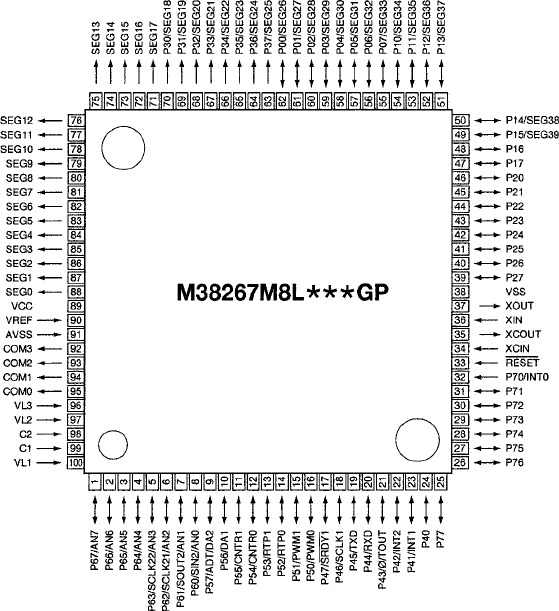
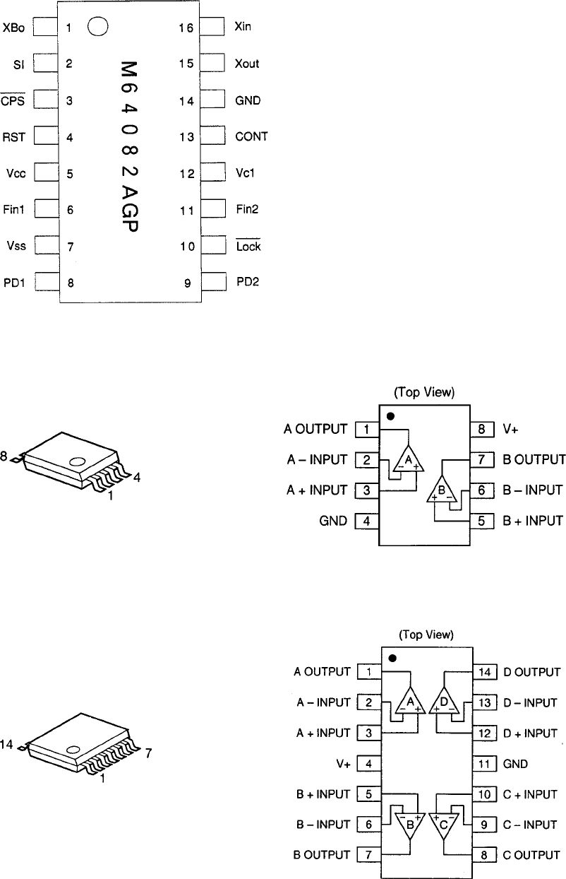
5) M3826M8L***GP (XA0644)
CPU
Terminal Connection
(TOP VIEW)
7
No. Pin Name Function I/O PU Logic Description
1 P67/AN7 SMT I - A/D S-meter input
2 P66/AN6 SQL I - A/D Noise level input for squelch
3 P65/AN5 BAT I - A/D Low battery detection input
4 P64/AN4 TIN I - A/D CTCSS tone input/DSC code input
5 P63/SCLK22/AN3 BP1 I - A/D Band plan 1
6 P62/SCLK21/AN2 BP2 I - A/D Band plan 2
7 P61/SOUT2/AN1 DCSW O - Activ high DCS signal mute
8 P60/SIN2/AN0 F/M/KEY I - A/D Function/Moniter key input
9 P57/ADT/DA2 CTOUT O - D/A CTCSS
tone output/
DCS
tone output/Tuning voltage out
10 P56/DA1 DTOUT O - D/A DTMF output/EVR control output
11 P55/CNTR1 SCL O - Pulse Serial clock for EEPROM
12 P54/CNTR0 TBST I/O Pulse/Activ low Tone burst output/UP input while trunking
13 P53/RTP1 BP4 I - - Band plan 4
14 P52/RTP0 MUTE I/O - Activ high Microphone mute/Bank change input while trunking
15 P51/PWM3 CLK O - Pulse Serial clock output for PLL,CTCSS,and trunking board
16 P50/PWM0 DATA I/O - Pulse
Serial data output for
PLL,CTCSS
, and trunking board/PLL unlock signal input
17 P47/SROY1 STBT I/O - Activ low/Pulse
Trunking board detedtion(when PSW is on)/Storobe signal to trunking board
18 P46/SCLK1 STBP O - Pulse Strobe for PLL IC
19 P45/TXD UTX O - Pulse UART data transmission output
20 P44/RXD RTX I - Pulse UART data reception output
21 P43/ /TOUT BEEP I/O - Pulse/Activ low Beep tone/Band plan 3(when PSW is on)
22 P42I/NT2 RE2 I Avtiv low
23 P41/INT1 RE1 I Avtiv low Rotary encoder input
24 P40 SD O - Avtiv low Signal detection output
25 P77 PTT I - Activ high PTT input
26 P76 SDT I Activ high Trunking signal detection input
27 P75 P5C O - Activ low PLL power ON/OFF output
28 P74 T5C O - Activ low TX power ON/OFF output
29 P73 R5C O - Activ low RX power ON/OFF output
30 P72 AFP O - Activ low AF AMP power ON/OFF output
31 P71 CLSFT O - Activ high CLOCK frequency shift
32 P70/INTO BU I - Activ low Backup signal detection input
33 RESET RESET I - Activ low Reset input
34 Xcin Xcin - - - -
35 Xcout Xcout - - - -
36 Xin Xin - - - Main clock input
37 Xout Xout - - - Main clock output
38 Vss GND - - - CPU GND
39 P27 PSW I - Avtiv low Power switch input
40 P26 SDA O - Pulse Serial data for EEPROM
41 P25 C5C O - Activ high C5V power ON/OFF output
42 P24 LAMP O - Activ high Lamp ON/OFF
43 P23 KI0 I Avtiv low
44 P22 KI1 I Avtiv low
45 P21 KI2 I Avtiv low
46 P20 KI3 I Avtiv low
Key matrix input
47 P17 KO3 O - Avtiv low
48 P16 KO2 O - Avtiv low
49 P15/SEG39 KO1 O - Avtiv low
50 P14/SEG38 KO0 O - Avtiv low
Key matrix output
51 P13/SEG37 H/L O - - Tx power H/L
52 P12/SEG36 DA2 O - - DA converter for output power
53 P11/SEG35 DA1 O - - DA converter for output power
54 P10/SEG34 DA0 O - - DA converter for output power
55 P07/SEG33 SCR I - SCR input

8
No. Pin Name Function I/O PU Logic Description
56 P06/SEG32 AFC O - Activ high AF tone control
57 P05/SEG31 S31 O - -
58 P04/SEG30 S30 O - -
59 P03/SEG29 S29 O - -
60 P02/SEG28 S28 O - -
61 P01/SEG27 S27 O - -
62 P00/SEG26 S26 O - -
63 P37/SEG25 S25 O - -
64 P36/SEG24 S24 O - -
65 P35/SEG23 S23 O - -
66 P34/SEG22 S22 O - -
67 P33/SEG21 S21 O - -
68 P32/SEG20 S20 O - -
69 P31/SEG19 S19 O - -
70 P30/SEG18 S18 O - -
71 SEG17 S17 O - -
72 SEG16 S16 O - -
73 SEG15 S15 O - -
74 SEG14 S14 O - -
75 SEG13 S13 O - -
76 SEG12 S12 O - -
77 SEG11 S11 O - -
78 SEG10 S10 O - -
79 SEG9 S9 O - -
80 SEG8 S8 O - -
81 SEG7 S7 O - -
82 SEG6 S6 O - -
83 SEG5 S5 O - -
84 SEG4 S4 O - -
85 SEG3 S3 O - -
86 SEG2 S2 O - -
87 SEG1 S1 O - -
88 SEG0 S0 O - -
LCD segment signal
89 Vcc VDD - - - CPU power terminal
90 Vref Vref - - - AD converter power supply
91 Avss Avss - - - AD converter GND
92 COM3 COM3 O - - LCD COM3 output
93 COM2 COM2 O - - LCD COM2 output
94 COM1 COM1 O - - LCD COM1 output
95 COM0 COM0 O - - LCD COM0 output
96 VL3 VL3 - - -
97 VL2 VL2 - - - LCD power supply
98 C2 I - - - -
99 C1 C1 - - - -
100 VL1 VL1 I - A/D LCD power supply
9
SEMICONDUCTOR DATA
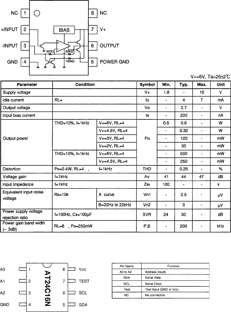
1) NMJ2070M T1 (XA210)
Low Voltage Power Amplifier
Equivalent Circuit
2) AT24C16N-10SI-2.7TER (XA0368)
16K bits CMOS Serial EEPROM
10
3) M5222FP-600C (XA0385)
Electronic Volume
11
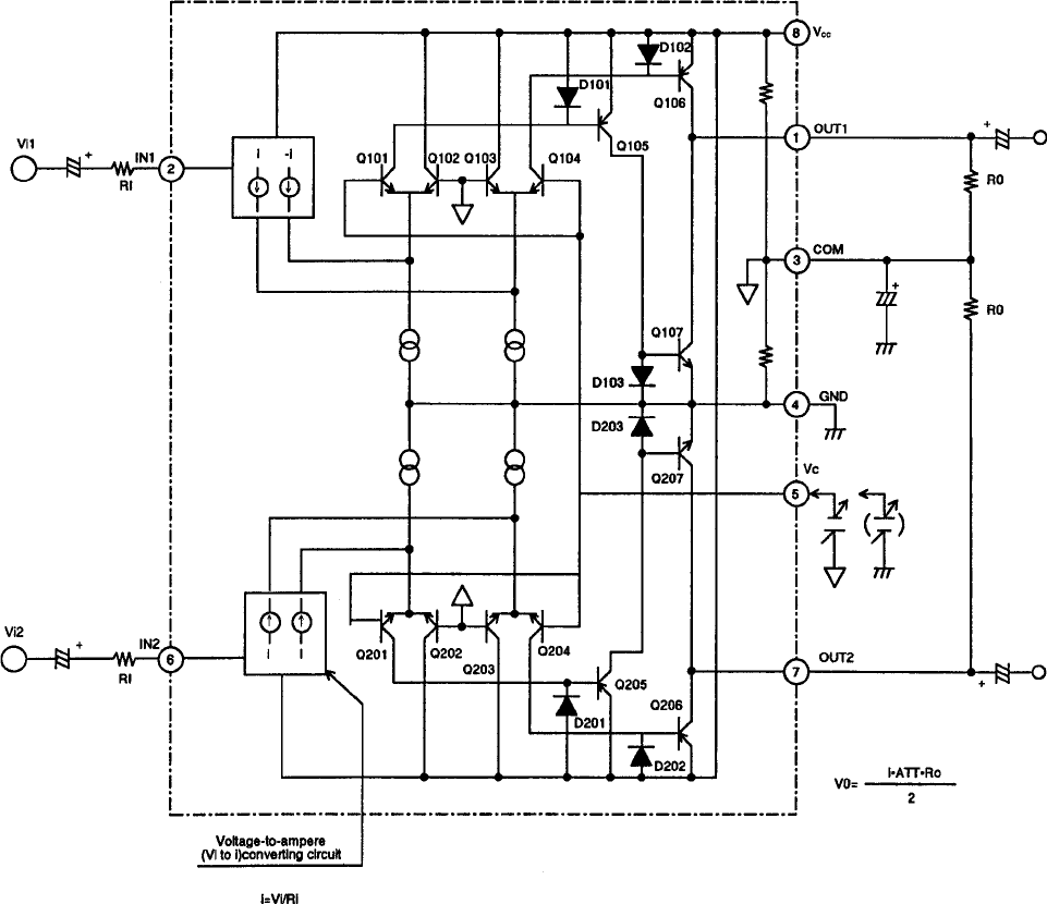
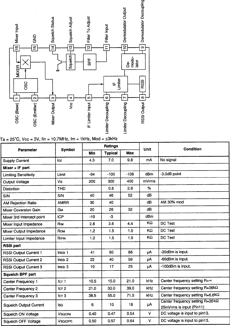
4) TK14521MTL (XA0515)
IF System
12
5) M64082AGP (XA0543)
6) NJM2904V-TE1 (XA0573)
Dual Single Supply Operational Amplifier
7) NJM2902V-TE1 (XA0596)
Quad Single Supply Operational Amplifier
13
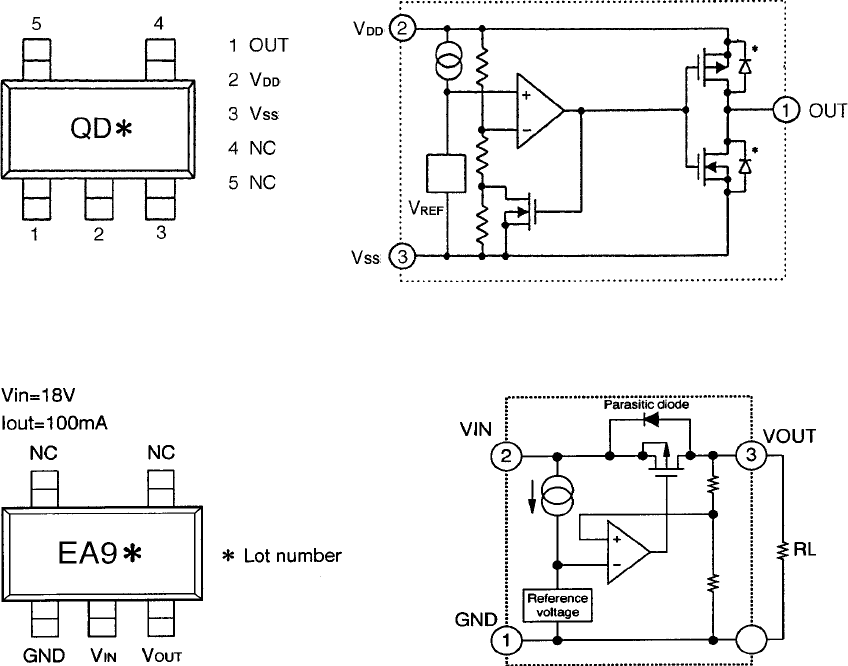
8) S-81250SG-QD-T1 (XA0619)
Top View
9) S-80845ALMP-EA9-T2 (XA0620)
Voltage Regulator
14
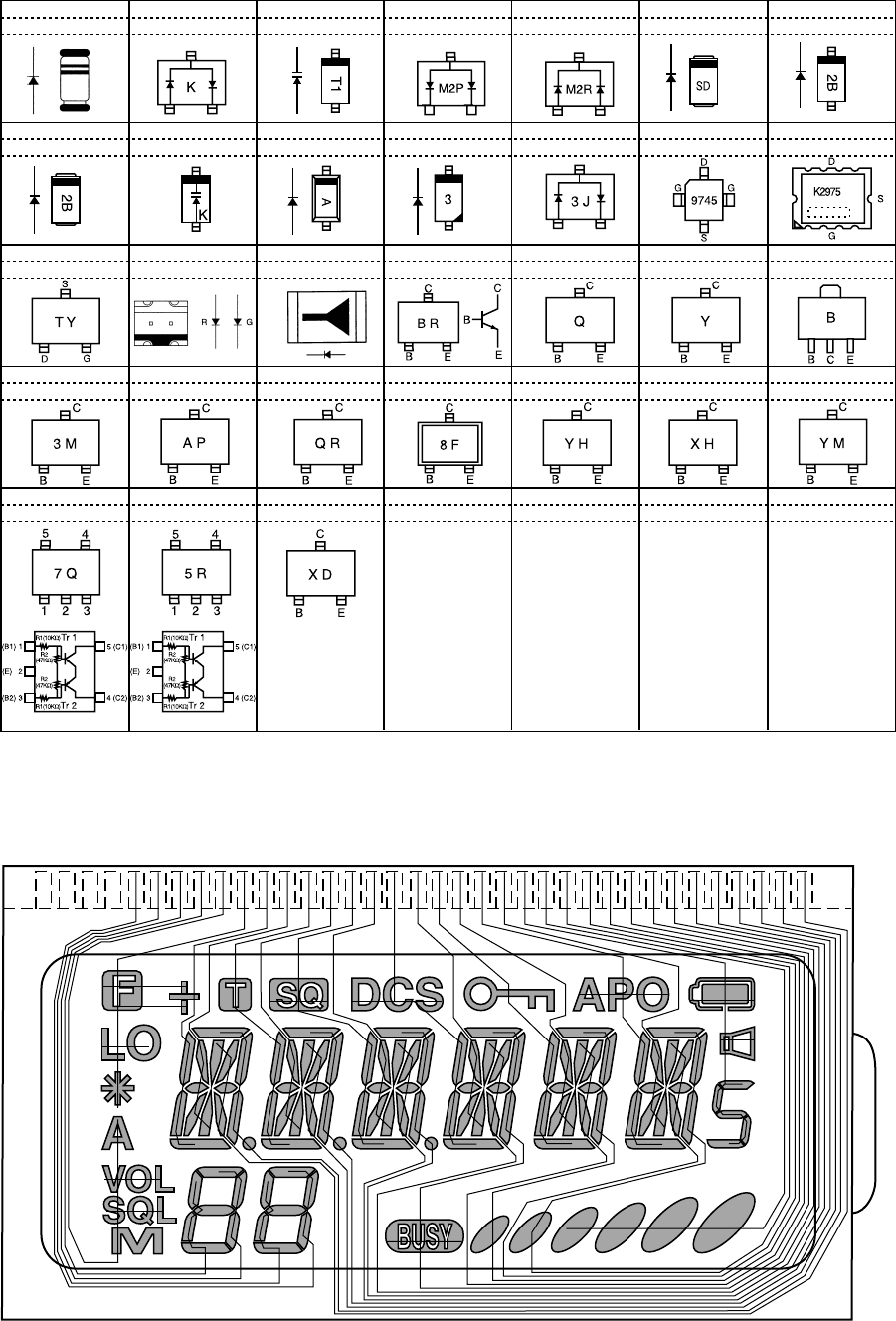
10) Transistor, Diode, and LED Ontline Drawings
Top View
RSL135 TE11
XD0066 S3DG7
XD0261
MA2S111-TX
XD0323 HSU277TRF
XD331 RB706F-40-T106
XD0332
DA204U T106
XD0130 1SV214 TPH4
XD0131 MA729-TX
XD0291
U2FWJ44N (TE12R)
XD0294
MA741WA TX
XD0251 MA741WK
XD0252
MA2S30400L
XD0312 MRF9745T1
XE0034 2SK2975-T11-A
XE0038
2SK882-GR-TE85L
XE0040 SML-310MTT86
XL0036
BRPG1201W TR
XL0028 2SC4081 T106R
XT0095 2SB766A-TX
XT0170
2SC4808-TX. AR
XT0171
2SA1036K T146Q
XT110 2SD2216R-TX
XT0135
2SC2915
XT0178
2SC4618
XT0172 UN9216-R-TX
XU0099
XP1114 (TX)
XU0161 XP1501-TX
XU0172
RN2107 TE85L
XU0192 RN1107 TE85L
XU0193
RN1104 TE85L
XU0195
RN2111 TE85L
XU0194
11) LCD Connection (EL0044)
SEG0
SEG1
SEG2
SEG3
SEG4
SEG5
SEG6
SEG7
SEG8
SEG9
SEG10
SEG11
SEG12
SEG13
SEG14
SEG15
SEG16
SEG17
SEG18
SEG19
SEG20
SEG21
SEG22
SEG23
SEG24
SEG25
SEG26
SEG27
SEG28
SEG29
SEG30
SEG31
15
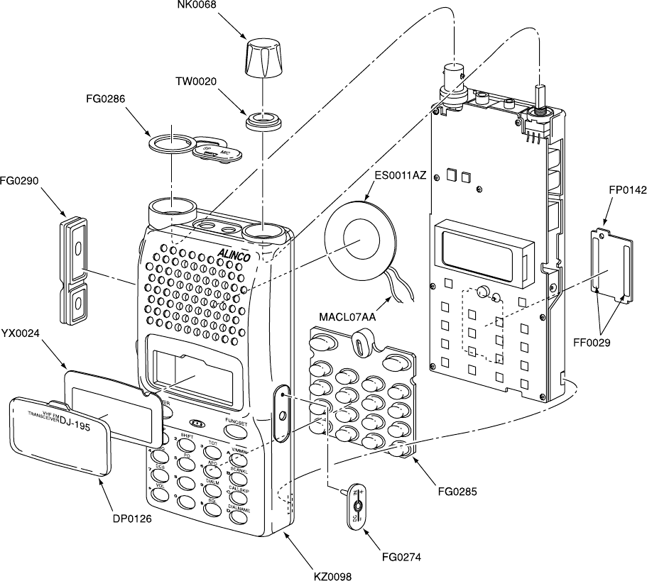
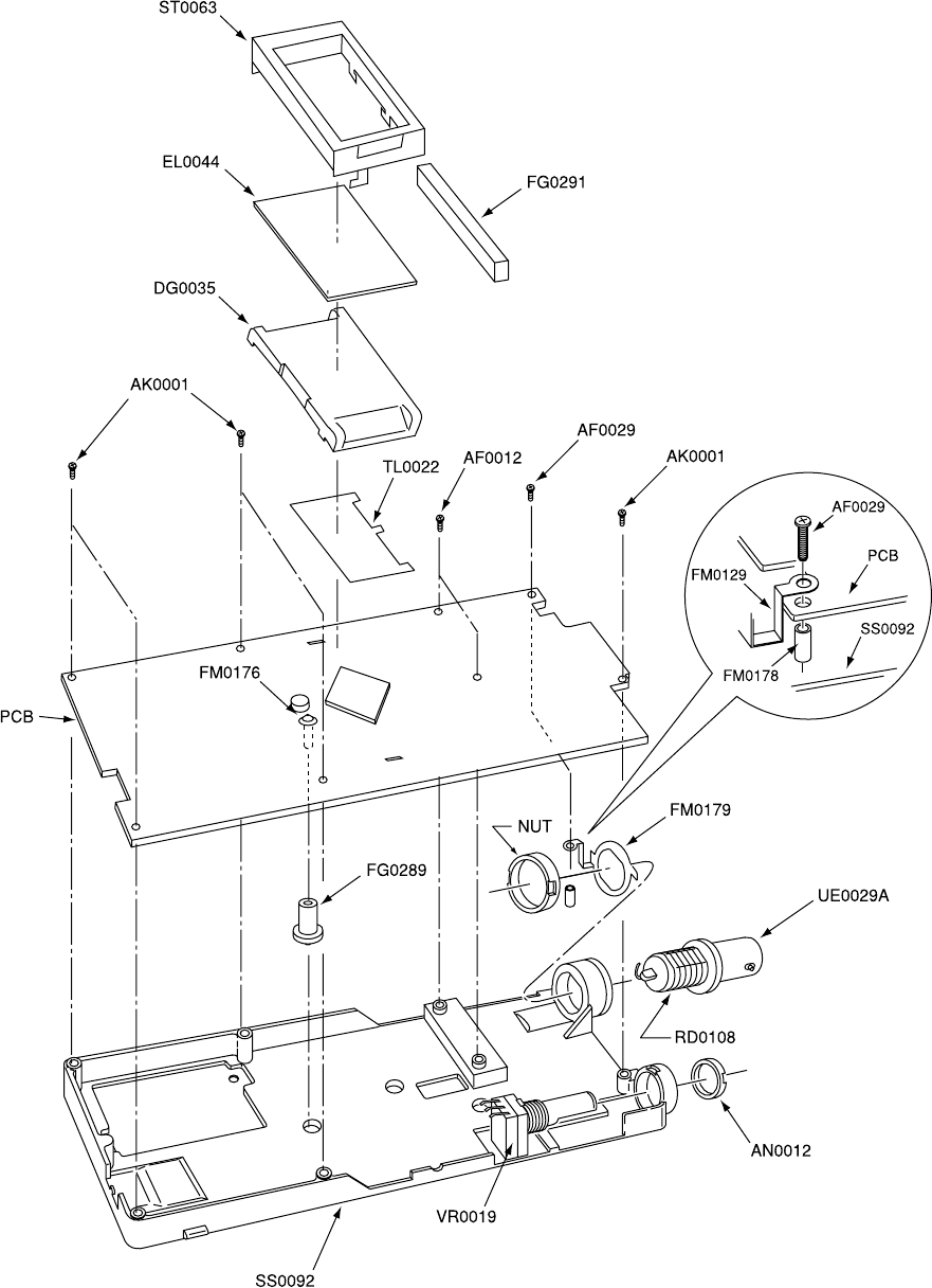
EXPLODED VIEW
1) Front View
16
2) Rear View

17
PARTS LIST
Ref. Ref.
C1 CU3035 Chip C C1608JB1H102KT-AS
C2 CU3035 Chip C C1608JB1H102KT-AS
C3 CS0404 Chip Tantal 6MCM106MATER
C4 CU3012 Chip C C1608CH1H120JT-AS
C5 CU3012 Chip C C1608CH1H120JT-AS
C6 CU3035 Chip C C1608JB1H102KT-AS
C7 CU3035 Chip C C1608JB1H102KT-AS
C8 CU3035 Chip C C1608JB1H102KT-AS
C9 CU3035 Chip C C1608JB1H102KT-AS
C10 CU3035 Chip C C1608JB1H102KT-AS
C11 CU3019 Chip C C1608CH1H470JT-AS
C12 CU3015 Chip C C1608CH1H220JT-AS
C13 CU3011 Chip C C1608CH1H100DT-AS
C14 CU3014 Chip C C1608CH1H180JT-AS
C15 CU3016 Chip C C1608CH1H270JT-AS
C16 CU3085 Chip C C1608CH1H300JT-AS
C17 CU3004 Chip C C1608CH1H030CT-AS
C18 CU3001 Chip C C1608CH1H0R5CT-AS
C19 CU3020 Chip C C1608CH1H560JT-AS
C20 CU3016 Chip C C1608CH1H270JT-AS
C21 CU3003 Chip C C1608CH1H020CT-AS
C22 CU3035 Chip C C1608JB1H102KT-AS
C23 CU3004 Chip C C1608CH1H030CT-AS
C24 CU3002 Chip C C1608CH1H010CT-AS
C25 CU3012 Chip C C1608CH1H120JT-AS
C26 CU3015 Chip C C1608CH1H220JT-AS
C27 CU3002 Chip C C1608CH1H010CT-AS
C28 CU3002 Chip C C1608CH1H010CT-AS
C29 CU3035 Chip C C1608JB1H102KT-AS
C30 CU0108 Chip C LMK212BJ105KG
C31 CU3047 Chip C C1608JB1H103KT-N
C32 CU3035 Chip C C1608JB1H102KT-AS
C33 CU3047 Chip C C1608JB1H103KT-N
C34 CU3035 Chip C C1608JB1H102KT-AS
C35 CU3035 Chip C C1608JB1H102KT-AS
C36 CU0108 Chip C LMK212BJ105KG
C37 CU3035 Chip C C1608JB1H102KT-AS
C38 CU3027 Chip C C1608CH1H221JT-AS
C39 CU3035 Chip C C1608JB1H102KT-AS
C40 CU3002 Chip C C1608CH1H010CT-AS
C41 CU3002 Chip C C1608CH1H010CT-AS
C42 NC
C43 CU3035 Chip C C1608JB1H102KT-AS
C44 CU3035 Chip C C1608JB1H102KT-AS
C45 CU3035 Chip C C1608JB1H102KT-AS
C46 CU0108 Chip C LMK212BJ105KG
C47 CU3035 Chip C C1608JB1H102KT-AS
C48 CU3035 Chip C C1608JB1H102KT-AS
C49 CU3047 Chip C C1608JB1H103KT-N
C50 CU3035 Chip C C1608JB1H102KT-AS
C51 CU3047 Chip C C1608JB1H103KT-N
C52 CS0404 Chip Tantal 6MCM106MATER
C53 CU3014 Chip C C1608CH1H180JT-AS
C54 CU3047 Chip C C1608JB1H103KT-N
C55 CU3035 Chip C C1608JB1H102KT-AS
C56 CU3002 Chip C C1608CH1H010CT-AS
C57 CU3002 Chip C C1608CH1H010CT-AS
C58 CU3015 Chip C C1608CH1H220JT-AS
C59 CU3007 Chip C C1608CH1H060CT-A
C61 CU3047 Chip C C1608JB1H103KT-N
C62 CU3111 Chip C C1608JB1C104KT-N
C63 CS0407 Chip Tantal 35MC104MATER
C64 CU3011 Chip C C1608CH1H100DT-AS
C65 CU3011 Chip C C1608CH1H100DT-AS
C66 CU3035 Chip C C1608JB1H102KT-AS
C67 CU3012 Chip C C1608CH1H120JT-AS
C68 CU3047 Chip C C1608JB1H103KT-N
C69 CU3057 Chip C C1608CH1H130JT-AS
C70 CU3016 Chip C C1608CH1H270JT-AS
C71 CU3035 Chip C C1608JB1H102KT-AS
C72 CS0406 Chip Tantal 35MCM105MATER
C73 CU3017 Chip C C1608CH1H330JT-AS T.E.EAH
C73 CU3085 Chip C C1608CH1H300JT-AS TFH.TLH
C74 CU3019 Chip C C1608CH1H470JT-AS
C75 CU3018 Chip C C1608CH1H390JT-AS
C76 CU3047 Chip C C1608JB1H103KT-N
C77 CU3003 Chip C C1608CH1H020CT-AS
C78 CU3011 Chip C C1608CH1H100JT-AS
C79 CU0108 Chip C LMK212BJ105KG
C80 CU3035 Chip C C1608JB1H102KT-AS
C81 CU3016 Chip C C1608CH1H270JT-AS
C82 CU3035 Chip C C1608JB1H102KT-AS
C83 CU3111 Chip C C1608JB1C104KT-N
C84 CU3035 Chip C C1608JB1H102KT-AS
C85 CU3016 Chip C C1608CH1H270JT-AS
C86 CU3035 Chip C C1608JB1H102KT-AS
C87 CE0392 Electrolytic C 6MV47UW
C88 CU3035 Chip C C1608JB1H102KT-AS
C89 CS0405 Chip Tantal 10MCS475MATER
C90 CU3035 Chip C C1608JB1H102KT-AS
C91 CU3035 Chip C C1608JB1H102KT-AS
C92 CU0108 Chip C LMK212BJ105KG
C93 CU3047 Chip C C1608JB1H103KT-N
C94 CS0404 Chip Tantal 6MCM106MATER
C95 CU3035 Chip C C1608JB1H102KT-AS
C96 CS0408 Chip Tantal 6MCM156MATER
C97 CU3035 Chip C C1608JB1H102KT-AS
C98 CU0108 Chip C LMK212BJ105KG
C99 CS0408 Chip Tantal 6MCM156MATER
C100 CU3035 Chip C C1608JB1H102KT-AS
C101 CU3035 Chip C C1608JB1H102KT-AS
C102 CE0392 Electrolytic C 6MV47UW
C103 CE0373 Electrolytic C 16MV 100UW
C104 CU0108 Chip C LMK212BJ105KG
C105 CU3047 Chip C C1608JB1H103KT-N
C106 CU3035 Chip C C1608JB1H102KT-AS
C107 CS0404 Chip Tantal 6MCM106MATER
C108 CS0404 Chip Tantal 6MCM106MATER
C109 CU3047 Chip C C1608JB1H103KT-N
C110 CU3035 Chip C C1608JB1H102KT-AS
C111 CU3111 Chip C C1608JB1C104KT-N
C112 CU3111 Chip C C1608JB1C104KT-N
C113 CU3035 Chip C C1608JB1H102KT-AS
C114 CE0397 Electrolytic C MVS16VC47MF46
C115 CU3047 Chip C C1608JB1H103KT-N
C116 CU3051 Chip C C1608JB1E223KT-NS
C117 CU3051 Chip C C1608JB1E223KT-NS
C118 CU0108 Chip C LMK212BJ105KG
C119 CU3111 Chip C C1608JB1C104KT-N
C120 CE0396 Electrolytic C MVS6.3VC100MF46
C121 CU3051 Chip C C1608JB1E223KT-NS
C122 CU3111 Chip C C1608JB1C104KT-N
C123 CU3111 Chip C C1608JB1C104KT-N
C124 CS0404 Chip Tantal 6MCM106MATER
C125 CU3035 Chip C C1608JB1H102KT-AS
C126 CU3111 Chip C C1608JB1C104KT-N
C127 CU3025 Chip C C1608CH1H151JT-AS
C128 CU3035 Chip C C1608JB1H102KT-AS
C129 CU3111 Chip C C1608JB1C104KT-N
C130 CU3041 Chip C C1608JB1H332KT-NS
C131 CU0108 Chip C LMK212BJ105KG
C132 CU3111 Chip C C1608JB1C104KT-N
C133 CU3047 Chip C C1608JB1H103KT-N
C134 CU3038 Chip C C1608JB1H182KT-AS
C135 CU3053 Chip C C1608JF1E333ZT-N
C136 CU3111 Chip C C1608JB1C104KT-N
C137 CU3035 Chip C C1608JB1H102KT-AS
C138 CU3111 Chip C C1608JB1C104KT-N
C139 CU3035 Chip C C1608JB1H102KT-AS
C140 CU3035 Chip C C1608JB1H102KT-AS
C141 CU3035 Chip C C1608JB1H102KT-AS
C142 CU0108 Chip C LMK212BJ105KG
C143 CU3051 Chip C C1608JB1E223KT-NS
C144 CU3047 Chip C C1608JB1H103KT-N
C145 CU3021 Chip C C1608CH1H680JT-AS
C146 CU3101 Chip C C1608JB1C473KT-NS
C147 CU3111 Chip C C1608JB1C104KT-N
C148 CU3111 Chip C C1608JB1C104KT-N
C149 CS0404 Chip Tantal 6MCM106MATER
C150 CU3047 Chip C C1608JB1H103KT-N
C151 CU3047 Chip C C1608JB1H103KT-N
C152 CU0108 Chip C LMK212BJ105KG
C153 CU3047 Chip C C1608JB1H103KT-N
C154 CU0108 Chip C LMK212BJ105KG
C155 CS0405 Chip Tantal 10MCS475MATER
C156 CU3014 Chip C C1608CH1H180JT-AS
C157 CU3013 Chip C C1608CH1H150JT-AS
Main Unit
No. Parts No. Description Parts Name Ver No. Parts No. Description Parts Name Ver

18
C158 CU0108 Chip C LMK212BJ105KG
C159 CU3035 Chip C C1608JB1H102KT-AS
C160 CU3047 Chip C C1608JB1H103KT-N
C161 CS0404 Chip Tantal 6MCM106MATER
C162 CU3111 Chip C C1608JB1C104KT-N
C163 CU3111 Chip C C1608JB1C104KT-N
C164 CU3046 Chip C C1608JB1H822KT-NS
C165 CU3111 Chip C C1608JB1C104KT-N
C166 CU3044 Chip C C1608JB1H562KT-NS
C167 CU3040 Chip C C1608JB1H272KT-NS
C168 CU3050 Chip C C1608JB1E183KT-A
C169 CU3035 Chip C C1608JB1H102KT-AS
C170 CU3035 Chip C C1608JB1H102KT-AS
C171 CU3035 Chip C C1608JB1H102KT-AS
C172 CU3101 Chip C C1608JB1C473KT-NS
C173 CU3035 Chip C C1608JB1H102KT-AS
C174 CU3101 Chip C C1608JB1C473KT-NS
C175 NC
C176 NC
C177 NC
C178 NC
C179 CU3049 Chip C C1608JB1E153KT-NS
CN1 UE0350 Connector DF12D(3.5)20DP0.5V81
D1 XD0066 Diode RLS135 TE 11
D2 XD0312 Diode MA2S30400L
D3 XD0131 Diode 1SV214 TPH4
D4 XD0312 Diode MA2S30400L
D5 XD0331 Diode HSU277TRF
D6 XD0251 Diode MA741WA TX
D7 XD0323 Diode MA2S111-TX
D8 XD0261 Diode S3DG7
D9 XD0130 Diode DA204U T106
D10 XD0323 Diode MA2S111-TX
D11 XD0294 Diode U2FWJ44N(TE12R)
D12 XL0036 Chip LED SML-310MTT86
D13 XD0312 Diode MA2S30400L
D14 XD0312 Diode MA2S30400L
D15 XD0312 Diode MA2S30400L
D16 XD0312 Diode MA2S30400L
D17 XL0036 Chip LED SML-310MTT86
D18 XD0131 Diode 1SV214 TPH4
D19 XL0028 Chip LED BRPG1201W TR
D20 XD0291 Diode MA729-TX
D21 XD0332 Diode RB706F-40-T106
D22 XD0323 Diode MA2S111-TX
D23 NC
FL1 XC0060 Filter ALFYM450F=K
IC1 XA0543 IC M64082AGP
IC2 XA0619 IC S-81250SG-QD-T1
IC3 XA0210 IC NJM2070M T1
IC4 XA0385 IC M5222FP-600C
IC5 XA0515 IC TK14521MTL
IC7 XA0573 IC NJM2904V-TE1
IC8 XA0596 IC NJM2902V-TE1
IC9 XA0644 CPU M38267E8L-GP
IC10 XA0368 IC AT24C16N-10SI-2.7TER
IC11 XA0620 IC S-80845ALMP-EA9-T2
JK2 UJ0046 Jack MJ82-1
JK3 UJ0019 Jack HSJ1493-01-010
JK4 UJ0022 Jack HSJ1102-01-540
L1 QC0508 Coil LK16082R2K-T
L2 QKA45A Coil MR1.5 4.5T 0.4
L3 QKA45A Coil MR1.5 4.5T 0.4
L4 QKA65A Coil MR1.5 3.5T 0.4
L5 QKA45A Coil MR1.5 4.5T 0.4
L6 QC0571 Coil LL1608-FH68NJ
L7 QC0566 Coil LL1608-FH27NJ
L8 QC0570 Coil LL1608-FH56NJ
L9 QC0573 Coil LL1608-FHR10J
L10 QKA75A Coil QKA75A
L11 QC0535 Coil LQN21A56NJ04
L12 QC0538 Coil LQN21AR10J04
L13 QC0570 Coil LL1608-FH56NJ
L15 QC0508 Coil LK16082R2K-T
L16 QC0537 Coil LQN21A82NJ04
L17 QC0537 Coil LQN21A82NJ04
L18 QC0537 Coil LQN21A82NJ04
L19 QC0537 Coil LQN21A82NJ04
L20 QC0573 Coil LL1608-FHR10J
L21 QC0089 Coil NL322522T-181JA
LCD1 EL0044 LCD HT-3404
MIC1 EY0017 Microphone OB-27P44
PCB UP0376 PCB DJ195 INTEGRATED
Q1 XT0171 Transistor 2SC4808-TX.AR
Q2 XE0038 FET 2SK2975-T11-A
Q3 XE0034 FET MRF9745T1
Q4 XT0171 Transistor 2SC4808-TX.AR
Q5 XT0171 Transistor 2SC4808-TX.AR
Q6 XU0172 Transistor XP1501-TX
Q7 XT0135 Transistor 2SD2216R-TX
Q8 XT0170 Transistor 2SB766A-TX
Q9 XE0040 FET 2SK882-GR-TE85L
Q10 XT0172 Transistor 2SC4618
Q11 XE0040 FET 2SK882-GR-TE85L
Q12 XU0193 Transistor RN1107 TE85L
Q13 XT0178 Transistor 2SC4915-O TE85L
Q14 XT0170 Transistor 2SB766A-TX
Q15 XU0193 Transistor RN1107 TE85L
Q16 XU0193 Transistor RN1107 TE85L
Q17 XT0170 Transistor 2SB766A-TX
Q18 XU0193 Transistor RN1107 TE85L
Q19 XT0110 Transistor 2SA1036K T146Q
Q20 XU0172 Transistor XP1501-TX
Q21 XU0172 Transistor XP1501-TX
Q22 XU0161 Transistor XP1114(TX)
Q23 XU0192 Transistor RN2107 TE85L
Q24 XT0135 Transistor 2SD2216R-TX
Q25 XU0193 Transistor RN1107 TE85L
Q26 XT0095 Transistor 2SC4081 T106R
Q27 XU0192 Transistor RN2107 TE85L
Q28 XT0135 Transistor 2SD2216R-TX
Q29 XU0195 Transistor RN1104 TE85L
Q30 XU0194 Transistor RN2111 TE85L
Q31 XU0192 Transistor RN2107 TE85L
R1 RK3030 Chip R MCR03EZHJ221
R2 RK3030 Chip R MCR03EZHJ221
R3 RK3034 Chip R MCR03EZHJ471
R4 RK3050 Chip R MCR03EZHJ103
R5 RK3022 Chip R MCR03EZHJ470
R6 RK3042 Chip R MCR03EZHJ222
R7 RK3046 Chip R MCR03EZHJ472
R8 RK3022 Chip R MCR03EZHJ470
R9 RK3030 Chip R MCR03EZHJ221
R10 RK3062 Chip R MCR03EZHJ104
R11 RK3049 Chip R MCR03EZHJ822
R12 RK3062 Chip R MCR03EZHJ104
R13 RK3018 Chip R MCR03EZHJ220
R14 RK3046 Chip R MCR03EZHJ472
R15 RK3044 Chip R MCR03EZHJ332
R16 RK3062 Chip R MCR03EZHJ104
R17 RK3034 Chip R MCR03EZHJ471
R18 RK3026 Chip R MCR03EZHJ101
R19 RK3062 Chip R MCR03EZHJ104
R20 RK3042 Chip R MCR03EZHJ222
R21 RK3037 Chip R MCR03EZHJ821
R22 RK3050 Chip R MCR03EZHJ103
R23 RK3058 Chip R MCR03EZHJ473
R24 RK3058 Chip R MCR03EZHJ473
R25 RK3062 Chip R MCR03EZHJ104
R26 RK3053 Chip R MCR03EZHJ183
R27 RK3054 Chip R MCR03EZHJ223 T.E.EAH
R28 RK3052 Chip R MCR03EZHJ153 TFH.TLH
R28 RK3054 Chip R MCR03EZHJ223 T.E.EAH
R29 RK0002 Chip R ERJ6GEYJ120V
R30 RK3034 Chip R MCR03EZHJ471
R31 RK3042 Chip R MCR03EZHJ222
R32 RK3050 Chip R MCR03EZHJ103
R33 RK3030 Chip R MCR03EZHJ221
R34 RK3050 Chip R MCR03EZHJ103
R35 RK3046 Chip R MCR03EZHJ472
R36 RK3022 Chip R MCR03EZHJ470
R37 RK3050 Chip R MCR03EZHJ103
R38 RK3039 Chip R MCR03EZHJ122
R39 RK3066 Chip R MCR03EZHJ224
R40 RK3050 Chip R MCR03EZHJ103
R41 RK3018 Chip R MCR03EZHJ220
R42 RK3042 Chip R MCR03EZHJ222
R43 RK3038 Chip R MCR03EZHJ102
R44 RK3037 Chip R MCR03EZHJ821
R45 RK3044 Chip R MCR03EZHJ332
R46 RK3062 Chip R MCR03EZHJ104
R47 RK3030 Chip R MCR03EZHJ221
R48 RK3042 Chip R MCR03EZHJ222
R49 RK3037 Chip R MCR03EZHJ821
R50 RK3020 Chip R MCR03EZHJ330
R51 RK3062 Chip R MCR03EZHJ104
R52 RK3038 Chip R MCR03EZHJ102
R53 RK3076 Chip R MCR03EZHJ155
Ref.
No. Parts No. Description Parts Name Ver Ref.
No. Parts No. Description Parts Name Ver

19
R54 RK3074 Chip R MCR03EZHJ105
R55 RK3022 Chip R MCR03EZHJ470
R56 RK3042 Chip R MCR03EZHJ222
R57 RK3074 Chip R MCR03EZHJ105
R58 RK3022 Chip R MCR03EZHJ470
R59 RK3074 Chip R MCR03EZHJ105
R60 RK3074 Chip R MCR03EZHJ105
R61 RK3050 Chip R MCR03EZHJ103
R62 RK3030 Chip R MCR03EZHJ221
R63 RK3050 Chip R MCR03EZHJ103
R64 RK3059 Chip R MCR03EZHJ563
R65 RK3058 Chip R MCR03EZHJ473
R66 RK3058 Chip R MCR03EZHJ473
R67 RK3076 Chip R MCR03EZHJ155
R68 RK3059 Chip R MCR03EZHJ563
R69 RK3074 Chip R MCR03EZHJ105
R70 RK3054 Chip R MCR03EZHJ223
R71 RK3057 Chip R MCR03EZHJ393 T.E.EAH
R71 RK3058 Chip R MCR03EZHJ473 TFH.TLH
R72 RK3054 Chip R MCR03EZHJ223
R73 RK3050 Chip R MCR03EZHJ103
R74 RK3044 Chip R MCR03EZHJ332
R75 RK3058 Chip R MCR03EZHJ473
R76 RK3050 Chip R MCR03EZHJ103
R77 RK3058 Chip R MCR03EZHJ473
R78 RK3054 Chip R MCR03EZHJ223
R79 RK3050 Chip R MCR03EZHJ103
R80 RK3046 Chip R MCR03EZHJ472
R81 RK3062 Chip R MCR03EZHJ104
R82 RK3046 Chip R MCR03EZHJ472
R83 RK3050 Chip R MCR03EZHJ103
R84 RK3036 Chip R MCR03EZHJ681
R85 RK3022 Chip R MCR03EZHJ470
R86 RK3050 Chip R MCR03EZHJ103
R87 RK3038 Chip R MCR03EZHJ102
R88 RK3050 Chip R MCR03EZHJ103
R89 RK3032 Chip R MCR03EZHJ331
R90 RK3044 Chip R MCR03EZHJ332
R91 RK3062 Chip R MCR03EZHJ104
R92 RK3058 Chip R MCR03EZHJ473
R93 RK3032 Chip R MCR03EZHJ331
R94 RK3050 Chip R MCR03EZHJ103
R95 RK3050 Chip R MCR03EZHJ103
R96 RK3058 Chip R MCR03EZHJ473
R97 RK3052 Chip R MCR03EZHJ153
R98 RK3050 Chip R MCR03EZHJ103
R99 RK3041 Chip R MCR03EZHJ182
R100 RK3066 Chip R MCR03EZHJ224
R101 RK3050 Chip R MCR03EZHJ103
R102 RK3066 Chip R MCR03EZHJ224
R103 RK3052 Chip R MCR03EZHJ153
R104 RK3048 Chip R MCR03EZHJ682
R105 RK3054 Chip R MCR03EZHJ223
R106 RK3050 Chip R MCR03EZHJ103
R107 RK3050 Chip R MCR03EZHJ103
R108 RK3014 Chip R MCR03EZHJ100
R109 RK3062 Chip R MCR03EZHJ104
R110 RK3066 Chip R MCR03EZHJ224
R111 RK3038 Chip R MCR03EZHJ102
R112 RK3051 Chip R MCR03EZHJ123
R113 RK3032 Chip R MCR03EZHJ331
R114 RK3062 Chip R MCR03EZHJ104
R115 RK1018 Chip R ERJ8GEYJ101V
R116 RK3074 Chip R MCR03EZHJ105
R117 RK3062 Chip R MCR03EZHJ104
R118 RK3045 Chip R MCR03EZHJ392
R119 RK3057 Chip R MCR03EZHJ393
R120 RK3061 Chip R MCR03EZHJ823
R121 RK3055 Chip R MCR03EZHJ273
R122 RK3062 Chip R MCR03EZHJ104
R123 RK3058 Chip R MCR03EZHJ473
R124 RK3063 Chip R MCR03EZHJ124
R125 RK3072 Chip R MCR03EZHJ684
R126 RK3056 Chip R MCR03EZHJ333
R127 RK3054 Chip R MCR03EZHJ223
R128 RK3056 Chip R MCR03EZHJ333
R129 RK3058 Chip R MCR03EZHJ473
R130 RK3038 Chip R MCR03EZHJ102
R131 RK3022 Chip R MCR03EZHJ470
R132 RK3050 Chip R MCR03EZHJ103
R133 RK3014 Chip R MCR03EZHJ100
R134 RK3058 Chip R MCR03EZHJ473
R135 RK3074 Chip R MCR03EZHJ105
R136 RK3050 Chip R MCR03EZHJ103
R137 RK3062 Chip R MCR03EZHJ104
R138 RK3069 Chip R MCR03EZHJ394
R139 RK3038 Chip R MCR03EZHJ102
R140 RK3065 Chip R MCR03EZHJ184
R141 RK3061 Chip R MCR03EZHJ823
R142 RK3058 Chip R MCR03EZHJ473
R143 RK3050 Chip R MCR03EZHJ103
R144 RK3062 Chip R MCR03EZHJ104
R145 RK3062 Chip R MCR03EZHJ104
R146 RK3040 Chip R MCR03EZHJ152
R147 RK3070 Chip R MCR03EZHJ474
R148 RK3052 Chip R MCR03EZHJ153
R149 RK3046 Chip R MCR03EZHJ472
R150 NC
R151 RK3038 Chip R MCR03EZHJ102
R152 RK3046 Chip R MCR03EZHJ472
R153 RK3038 Chip R MCR03EZHJ102
R154 RK3050 Chip R MCR03EZHJ103
R155 RK3046 Chip R MCR03EZHJ472
R156 RK3048 Chip R MCR03EZHJ682
R157 RK3062 Chip R MCR03EZHJ104
R158 RK3055 Chip R MCR03EZHJ273 TFH.TLH
R158 RK3056 Chip R MCR03EZHJ333 T.E.EAH
R159 RK3038 Chip R MCR03EZHJ102
R160 RK3074 Chip R MCR03EZHJ105
R161 RK3069 Chip R MCR03EZHJ394
R162 RK3060 Chip R MCR03EZHJ683
R163 RK3050 Chip R MCR03EZHJ103
R164 RK3050 Chip R MCR03EZHJ103
R165 RK3048 Chip R MCR03EZHJ682
R166 RK3038 Chip R MCR03EZHJ102
R167 RK3048 Chip R MCR03EZHJ682
R168 RK3038 Chip R MCR03EZHJ102
R169 RK3074 Chip R MCR03EZHJ105
R170 RK3062 Chip R MCR03EZHJ104
R171 RK3062 Chip R MCR03EZHJ104
R172 RK3001 Chip R MCR03EZHJ000
R173 RK3066 Chip R MCR03EZHJ224
R174 RK3066 Chip R MCR03EZHJ224
R175 RK3062 Chip R MCR03EZHJ104
R176 RK3074 Chip R MCR03EZHJ105
R177 RK3066 Chip R MCR03EZHJ224
R178 RK3062 Chip R MCR03EZHJ104
R179 RK3062 Chip R MCR03EZHJ104
R180 RK3046 Chip R MCR03EZHJ472
R181 RK3058 Chip R MCR03EZHJ473
R182 RK3046 Chip R MCR03EZHJ472
R183 NC
R184 RK3054 Chip R MCR03EZHJ223
R185 NC
R186 NC
R187 NC
R188 RK3026 Chip R MCR03EZHJ101
R189 RK3074 Chip R MCR03EZHJ105
R190 RK3058 Chip R MCR03EZHJ473
R191 RK3050 Chip R MCR03EZHJ103
R192 RK3059 Chip R MCR03EZHJ563
R193 RK3063 Chip R MCR03EZHJ124
R194 RK3060 Chip R MCR03EZHJ683
R195 RK3050 Chip R MCR03EZHJ103
R196 RK3067 Chip R MCR03EZHJ274
R197 RK3050 Chip R MCR03EZHJ103
R198 RK3050 Chip R MCR03EZHJ103
R199 RK2042 Chip R MCR18EZHJ152
R200 RK3054 Chip R MCR03EZHJ223
R201 RK3057 Chip R MCR03EZHJ393
R202 RK3045 Chip R MCR03EZHJ392
R203 RK3050 Chip R MCR03EZHJ103
R204 RK3050 Chip R MCR03EZHJ103
R205 RK3050 Chip R MCR03EZHJ103
R206 RK3050 Chip R MCR03EZHJ103
R207 RK3052 Chip R MCR03EZHJ153
R208 NC
SW17 UU0030 Switch EVQPJ005
SW18 UU0030 Switch EVQPJ005
TC1 CT0012 Trimmer CTZ3S-10A-W1-P
VR1 RH0140 Volume MVR22HXBRN472
W1 MACL07AA Wire #30A02-070-02
W2 MACL07AA Wire #30A02-070-02
W3 MACLH2GG Wire #30AH1-025-H1 T.E
X1 XQ0112 Crystal UM-5 21.250MHZ
X2 XQ0077 Crystal 38C 3.686400MHZ
XF1 XF0041 MCF UM5 21.7M 21R15A5
XF2 XF0041 MCF UM5 21.7M 21R15A5
Ref.
No. Parts No. Description Parts Name Ver Ref.
No. Parts No. Description Parts Name Ver

20
AF0012 Screw OPH M2+4 FE/ZN3
AF0029 Screw 0PH 2+9 FE/N 3
AK0001 0PH B2+4 FE/N 3
AN0012 Nut RND N7X0.75 BR/B.ZN
DG0035 LCD LIGHT
DP0126 LCD PANLE DJ195
ES0011AZ Speaker 036M9014
FF0029 Sheet
FG0274 DC CAP
FG0285 16 KEY RUBBER DJ195
FG0286 JACK CAP DJ195
FG0289 TERMINAL RUBBER 195
FG0290 PTT RUBBER DJ195
FG0291 LCD RUBBER CONNECT.
FM0176 PLUS TERMINAL DJ195
FM0177 RADIATIVE PLATE 195
FM0178 DJ195
FM0179 ANTENNA EARTH DJ195
FP0142 BLIND SHEET DJ195
KZ0098 FRONT CASE DJ195
MACLH2GG Wire #30AH1-025-H1
NK0068 DIAL KNOB DJ195
RD0108 J1/6Z
SS0092 CHASSIS DJ195
ST0063 LCD HOLDER DJ195
TG0033 SP HIMELON DJ195
TL0022 REFLECTIVE SHEET 195
TS0142 VCO case XH655
TW0020 W.PROOF A XH720
UE0029A ANT.CONNECT.DJ460
UR0019 Dial RH70N00E20 (RY-6320)
YX0024 LCD TAPE DJ195
EA57 Antenna T.E.EAH
EA58 Antenna TFH.TLH
PR0309 CE label E.EAH
EBP-48N EBP-48N
HK0465 Pacage
HM0189 Carton 10
HU0150 Inner C
HU0151 Inner 5
BH0011 Belt clip
BB0009Y Strap
HP0003 Protection Bag 5*75*110
PR0237 FCC label
DS0388A Spec.sheet
E.EAH.TFH.TLH
DS0411 Spec.sheet DJ195T T
PS0313A Instruction Manual
HH0061 Air cap
EDC93 Wall charger EDC-93 T
EDC94 Wall charger EDC-94
E.EAH.TFH.TLH
PH0009A Warranty T
PT0004A Serial No. Carton
PK0076 Schematic Diagram
PR0421 Serial No. label
DS0388A Spec. sheet with out Serial
E.EAH.TFH.TLH
DS0411
Spec. sheet DJ195 with out Serial
T
Packing Parts
Ref.
No. Parts No. Description Parts Name Ver
Ref.
No. Parts No. Description Parts Name Ver
Mechanical Parts
21
ADJUSTMENT
1) Required Test Equipment
The following items are required to adjust radio parameters:
1. Regulated power supply
Supply voltage: 5-14V DC
Current: 3A or more
2. Digital multimeter
Voltage range: FS = Approx. 20V
Current: 10A or more
Input resistance: High impedance
3. Oscilloscope
Measurable frequency: Audio frequency
4. Audio dummy load
Impedance: 8Ω
Dissipation: 1W or more
Jack: 3.5mmΦ
5. SSG
Output frequency: 200MHz or more
Output level: -20dBu/0.1uV -120dBu/1V
Modulation: FM
6. Spectrum Analyzer
Measuring range: Up to 2GHz or more
7. Power meter
Measurable frequency: Up to 200MHz
Impedance: 50Ω, unbalanced
Measuring range: 0.1W -10W
8. Audio volmeter
Measurable frequency: Up to 100kHz
Sensitivity: 1mV to 10V
9. Audio generator
Output frequency: 67Hz to 10kHz
Output impedance: 600Ω, unbalanced
10.Distortion meter/SINAD meter
Measurable frequency: 1kHz
Input level: Up to 40dB
Distortion: 1% - 100%
11.Frequency counter
Measurable frequency: Up to 200MHz
Measurable stability: Approx. +/-0.1ppm
22
12.Linear detector
Measurable frequency: Up to 200MHz
Characteristics: Flat
CN: 60dB or more
Note
■Standard modulation: 1kHz +/-3.5kHz/DEV
■Reference sensitivity: 12dB SINAD
■Specified audio output leve: 200mW at 8Ω
■Standard audio output level: 50mW at 8Ω
■Use an RF cable (3D2W:1m) for test equipment.
■Attach a fuse to the RF test equipment.
■All SSG outputs are indicated by EMF.
■Supply voltage for the transceiver: 13.8VDC
23
2) Adjustment Mode
The DJ-195 does not require a serviceperson to manipulate the components
on the printed-circuit board, except the trimmer when adjusting reference fre-
quency and deviation.Most of the adjustments for the transceiver are made by
using the keys on it while the unit is in the adjustment mode.Because the ad-
justment mode temporarily uses the channels, frequency must be set on each
channel before adjustments can be made.For instructions on how to program
the channels, see the “DJ-195 INSTRUCTION MANUAL” which came with the
product.In consideration of the radio environment, the frequency on each chan-
nel must be near the value (+/-1MHz) listed in the table below.To enter the
adjustment mode, set key lock and input 490217.Decimal point at 100MHz and
10MHz appears in LCD. (To release the mode, set key-lock and input 490217.)
Channel frequencies used in the adjustment mode
Channel Channel function Frequency
1
2
3
4
5
6
7
8
9
10
11
12
13
14
15
16
17
Reference frequency adjustment
High power adjustment
Low power adjustment
Minimum frequency sensitivity adjustment
Medium frequency sensitivity adjustment
Maximum frequency sensitivity adjustment
S-meter ( 1 ) adjustment
S-meter ( FULL ) adjustment
Deviation
DTMF ( 1 ) test
DTMF ( D ) test
Tone 67 Hz test
Tone 88.5 Hz test
Tone 250.3 Hz test
DCS code 255 test
Tone burst test
Aging ( Not required to use )
145 MHz
145 MHz
145 MHz
130 MHz
145 MHz
174 MHz
145 MHz
145 MHz
145 MHz
145 MHz
145 MHz
145 MHz
145 MHz
145 MHz
145 MHz
145 MHz
145 MHz

24
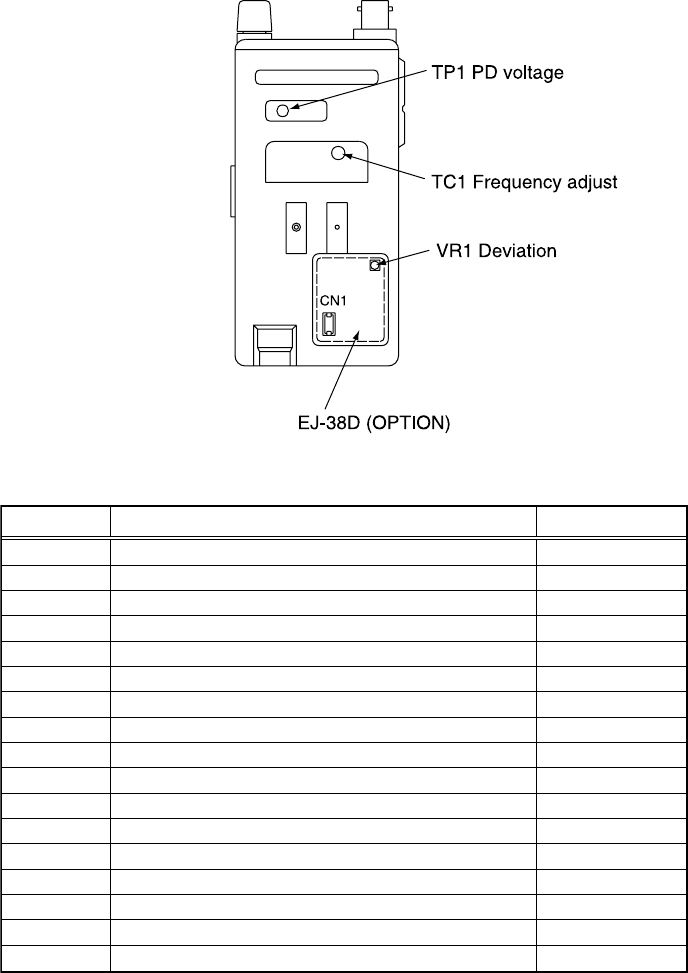
Reference Frequency Adjustment
1. In the adjustment mode, select channel 1 by rotating the main tuning dial.
2. Press the key to start transmission.
3. Rotate TC1 on the Main board until the value on the frequency counter
matches the one displayed on the LCD.
4. On 145.05MHz measure TP1 near the VCO and to obtain 1.2V+0.1V
( If the frequency display is flashing, the PLL is unlocked. )
High Power Adjustment
1. In the adjustment mode, select channel 2 by rotating the main tuning dial.
2. Hold down the key to start transmission.
3. While watching the reading of the TX power meter, set the output power to
the value closest to 5 W by rotating the main tuning dial.
4. When the key is released, the output power at that time will be
stored as the high power setting.
Low Power Adjustment
1. In the adjustment mode, select channel 3 by rotating the main tuning dial.
2. Hold down the key to start transmission.
3. While watching the reading of the TX power meter, set the output power to
the value closest to 0.8 W by rotating the main tuning dial.
4. When the key is released, the output power at that time will be
stored as the low power setting.
Minimum Frequency Sensitivity Adjustment
See “Note on Adjusting the Sensitivity” later in this section.
1. In the adjustment mode, select channel 4 by rotating the main tuning dial.
2. Set the minimum frequency sensitivity rotating the main tuning dial, while F
appears after the key is pressed.
Medium Frequency Sensitivity Adjustment
See “Note on Adjusting the Sensitivity” later in this section.
1. In the adjustment mode, select channel 5 by rotating the main tuning dial.
2. Set the medium frequency sensitivity rotating the main tuning dial, while F
appears after the key is pressed.
Maximum Frequency Sensitivity Adjustment
See “Note on Adjusting the Sensitivity” later in this section.
1. In the adjustment mode, select channel 6 by rotating the main tuning dial.
2. Set the maximum frequency sensitivity rotating the main tuning dial, while F
appears after the key pressed.
25
S-meter (1) Adjustment
1. In the adjustment mode, select channel 7 by rotating the main tuning dial.
The S-meter will show a single circle ( )
2. Enter “0”dBu(EMF) with the transceiver tester (SSG).
3. Press the F key. The transceiver beeps indicating the new setting has been
stored successfully.
S-meter (FULL)
1. In the adjustment mode, select channel 8 by rotating the main tuning dial.
The S-meter will show all six circles ( )
2. Enter “+20”dBu (EMF) with the transceiver tester (SSG).
3. Press the key. The transceiver beeps indicating the new setting has
been stored successfully.
Deviation
1. In the adjustment mode, select channel 9 by rotating the main tuning dial.
2. Input a 50mVrms, 1KMz signal with your transceiver tester through the
external microphone jack.
3. With the tester, put the transceiver in the transmission mode.
4. Rotate the VR1 on the printed-curcuit board of the transceiver until the de-
viation is set to 4.5KHz.
DTMF (1) Test
This function is only for checking the DTMF code, not adjusting it.
1. In the adjustment mode, select channel 10 by rotating the main tuning dial.
2. Press the key. DTMF code “1” is automatically sent and you will
hear the monitoring tone from the speaker.
3. Check the deviation with the transceiver tester.
DTMF (D) Test
1. In the adjustment mode, select channel 11 by rotating the main tuning dial.
2. Press the key. DTMF code “D” is automatically sent and you will
hear the monitoring tone from the speaker.
3. Check the deviation with the transceiver tester.
Tone 67Hz Test
This function is only for checking the tone encoder, not adjusting it.
1. In the adjustment mode, select channel 12 by rotating the main tuning dial.
2. Press the key. A 67Hz tone is automatically sent.
3. Check the deviation with the transceiver tester.
Tone 88.5Hz Test
1. In the adjustment mode, select channel 13 by rotating the main tuning dial.
2. Press the key. An 88.5Hz tone is automatically sent.
3. Check the deviation with the transceiver tester.

26
Tone 250.3Hz Test
1. In the adjustment mode, select channel 14 by rotating the main tuning dial.
2. Press the key. A 250.3Hz tone is automatically sent.
3. Check the deviation with the transceiver tester.
DCS Code 225 Test
1. In the adjustment mode, select channel 15 by rotating the main tuning dial.
2. Press the key. An 255 DCS code is automatically sent.
3. Check the deviation with the transceiver tester.
Tone Burst Test
This function is only for checking the tone burst, not adjusting it.
1. In the adjustment mode, select channel 16 by rotating the main tuning dial.
2. Press the key. A 1750Hz tone burst is automatically sent.
3. Check the deviation with the transceiver tester.
Aging
Perform this aging test only when necessary.
1. In the adjustment mode, select channel 17 by rotating the main tuning dial.
The transceiver automatically repeaters transmission for a minute and re-
ception for another minute.
Note on Adjusting Sensitivity
Sensitivity is adjusted by applying the optimum voltage from the CPU to the
varicap of the tuning circuit.
1. Program any frequency within 145MHz +/- 1MHz on memory channel 5.
2. To enter the adjustment mode, set key lock and input 490217. Decimal point
at 100MHz and 10MHz appears in LCD. (To release the mode, set key lock
and input 490217).
3. Select channel 5 by rotating the main tuning dial.
4. Press the key and, while the F appears, rotate the main tuning
dial. Set the adjustment data to “**” for maximizing the sensitivity (“**”
appears in the channel number area on the LCD).
5. Press the key.
6. In the key lock mode, Input 490217. Decimal point at 100MHz and 10MHz
disappear. Turn the power OFF. The transceiver is in the normal status.
27
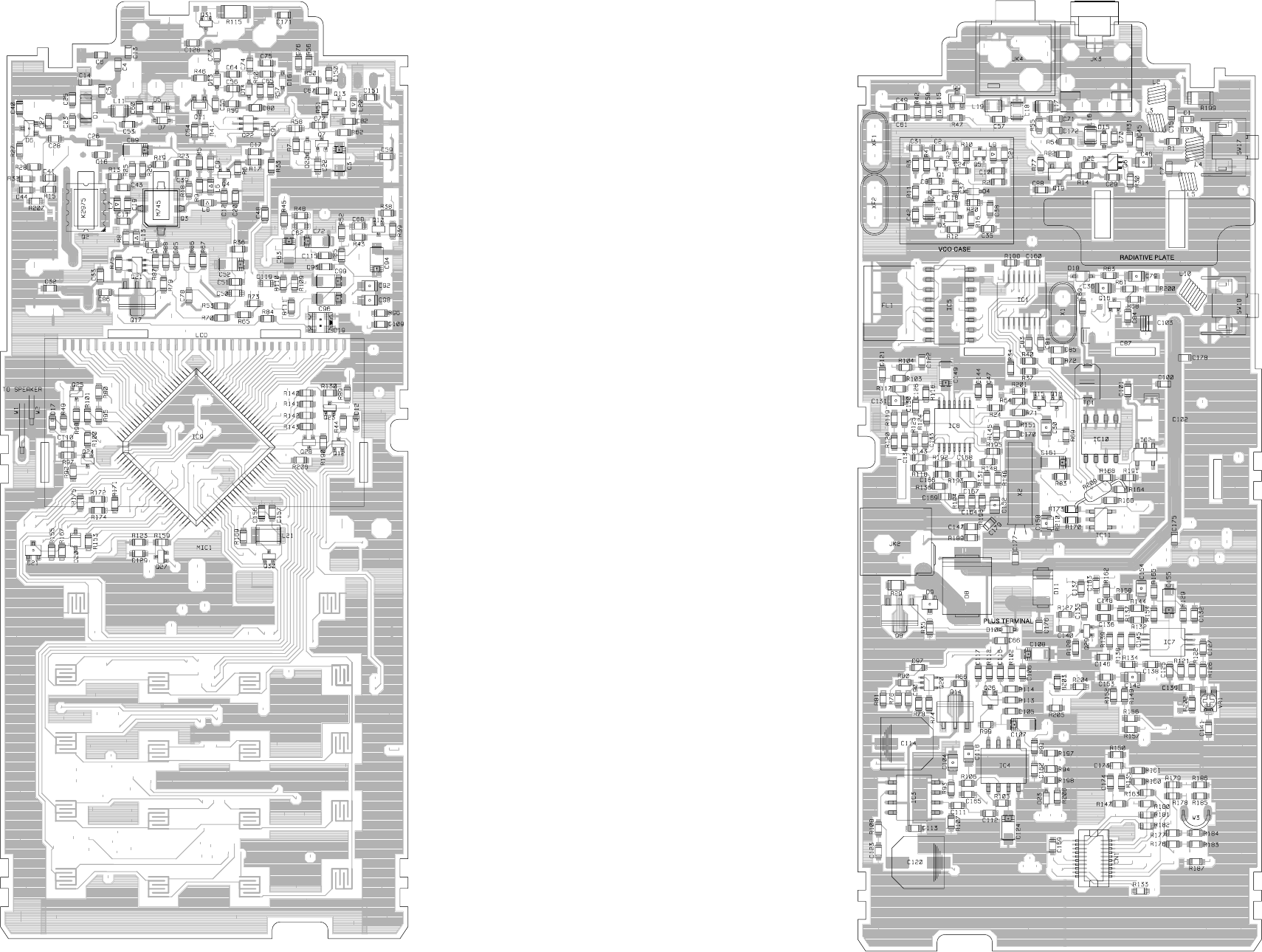
PC BOARD VIEW
MAIN SIDE A MAIN Side B
28
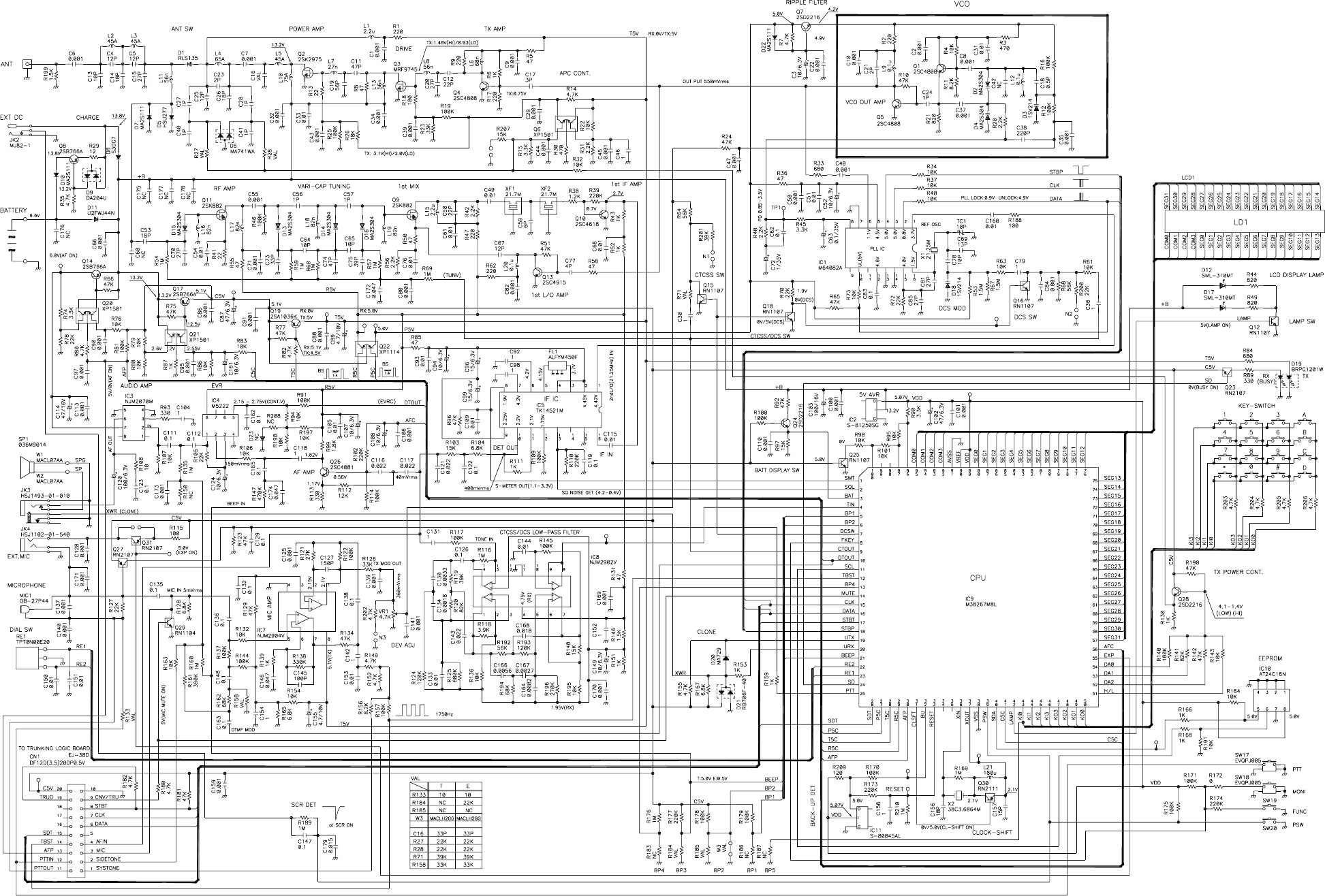
SCHEMATIC DIAGRAM
29
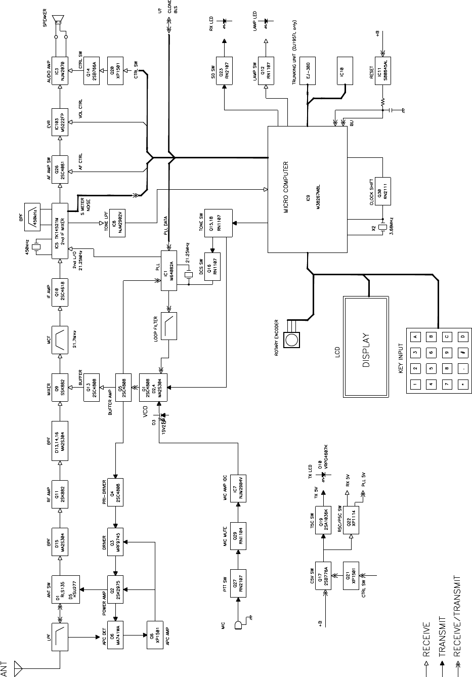
BLOCK DIAGRAM

Dealer/Distributor
DJ-195
Service Manual
ALINCO, INC.
Head Office : “TWIN 21” MID Tower Building 25F
1-61, 2-Chome, Shiromi, Chuo-ku, Osaka 540-8580 Japan
Phone: 06-6946-8150 Fax: 06-6946-8175 Telex: 63086
E-mail: 101243.1446@compuserve.com
U.S.A. : 438 Amapola Ave., Suite 130, Torrance, CA 90501-6201, U.S.A.
Phone: 310-618-8616 Fax: 310-618-8758
http://www.alinco.com/
Germany : Eschborner Landstrasse 55, 60489 Frankfurt am Main, Germany
Phone: 069-786018 Fax: 069-789-60766
Copyright 1999 Alinco, lnc. Osaka Japan
Printed in Japan PM0058
