ARM Architecture Reference Manual ARMv7 A And R Edition V7
User Manual: Pdf
Open the PDF directly: View PDF ![]() .
.
Page Count: 2158 [warning: Documents this large are best viewed by clicking the View PDF Link!]
- ARM Architecture Reference Manual ARMv7-A and ARMv7-R edition
- Contents
- Preface
- Application Level Architecture
- Introduction to the ARM Architecture
- Application Level Programmers’ Model
- A2.1 About the Application level programmers’ model
- A2.2 ARM core data types and arithmetic
- A2.3 ARM core registers
- A2.4 The Application Program Status Register (APSR)
- A2.5 Execution state registers
- A2.6 Advanced SIMD and VFP extensions
- A2.7 Floating-point data types and arithmetic
- A2.7.1 ARM standard floating-point input and output values
- A2.7.2 Advanced SIMD and VFP single-precision format
- A2.7.3 VFP double-precision format
- A2.7.4 Advanced SIMD and VFP half-precision formats
- A2.7.5 Flush-to-zero
- A2.7.6 NaN handling and the Default NaN
- A2.7.7 Floating-point exceptions
- A2.7.8 Pseudocode details of floating-point operations
- Generation of specific floating-point values
- Negation and absolute value
- Floating-point value unpacking
- Floating-point exception and NaN handling
- Floating-point rounding
- Selection of ARM standard floating-point arithmetic
- Comparisons
- Maximum and minimum
- Addition and subtraction
- Multiplication and division
- Reciprocal estimate and step
- Square root
- Reciprocal square root
- Conversions
- A2.8 Polynomial arithmetic over {0,1}
- A2.9 Coprocessor support
- A2.10 Execution environment support
- A2.11 Exceptions, debug events and checks
- Application Level Memory Model
- A3.1 Address space
- A3.2 Alignment support
- A3.3 Endian support
- A3.4 Synchronization and semaphores
- A3.4.1 Exclusive access instructions and Non-shareable memory regions
- A3.4.2 Exclusive access instructions and Shareable memory regions
- A3.4.3 Tagging and the size of the tagged memory block
- A3.4.4 Context switch support
- A3.4.5 Load-Exclusive and Store-Exclusive usage restrictions
- A3.4.6 Semaphores
- A3.4.7 Synchronization primitives and the memory order model
- A3.4.8 Use of WFE and SEV instructions by spin-locks
- A3.5 Memory types and attributes and the memory order model
- A3.6 Access rights
- A3.7 Virtual and physical addressing
- A3.8 Memory access order
- A3.9 Caches and memory hierarchy
- The Instruction Sets
- A4.1 About the instruction sets
- A4.2 Unified Assembler Language
- A4.3 Branch instructions
- A4.4 Data-processing instructions
- A4.5 Status register access instructions
- A4.6 Load/store instructions
- A4.7 Load/store multiple instructions
- A4.8 Miscellaneous instructions
- A4.9 Exception-generating and exception-handling instructions
- A4.10 Coprocessor instructions
- A4.11 Advanced SIMD and VFP load/store instructions
- A4.12 Advanced SIMD and VFP register transfer instructions
- A4.13 Advanced SIMD data-processing operations
- A4.13.1 Advanced SIMD parallel addition and subtraction
- A4.13.2 Bitwise Advanced SIMD data-processing instructions
- A4.13.3 Advanced SIMD comparison instructions
- A4.13.4 Advanced SIMD shift instructions
- A4.13.5 Advanced SIMD multiply instructions
- A4.13.6 Miscellaneous Advanced SIMD data-processing instructions
- A4.14 VFP data-processing instructions
- ARM Instruction Set Encoding
- A5.1 ARM instruction set encoding
- A5.2 Data-processing and miscellaneous instructions
- A5.2.1 Data-processing (register)
- A5.2.2 Data-processing (register-shifted register)
- A5.2.3 Data-processing (immediate)
- A5.2.4 Modified immediate constants in ARM instructions
- A5.2.5 Multiply and multiply-accumulate
- A5.2.6 Saturating addition and subtraction
- A5.2.7 Halfword multiply and multiply-accumulate
- A5.2.8 Extra load/store instructions
- A5.2.9 Extra load/store instructions (unprivileged)
- A5.2.10 Synchronization primitives
- A5.2.11 MSR (immediate), and hints
- A5.2.12 Miscellaneous instructions
- A5.3 Load/store word and unsigned byte
- A5.4 Media instructions
- A5.5 Branch, branch with link, and block data transfer
- A5.6 Supervisor Call, and coprocessor instructions
- A5.7 Unconditional instructions
- Thumb Instruction Set Encoding
- A6.1 Thumb instruction set encoding
- A6.2 16-bit Thumb instruction encoding
- A6.3 32-bit Thumb instruction encoding
- A6.3.1 Data-processing (modified immediate)
- A6.3.2 Modified immediate constants in Thumb instructions
- A6.3.3 Data-processing (plain binary immediate)
- A6.3.4 Branches and miscellaneous control
- A6.3.5 Load/store multiple
- A6.3.6 Load/store dual, load/store exclusive, table branch
- A6.3.7 Load word
- A6.3.8 Load halfword, memory hints
- A6.3.9 Load byte, memory hints
- A6.3.10 Store single data item
- A6.3.11 Data-processing (shifted register)
- A6.3.12 Data-processing (register)
- A6.3.13 Parallel addition and subtraction, signed
- A6.3.14 Parallel addition and subtraction, unsigned
- A6.3.15 Miscellaneous operations
- A6.3.16 Multiply, multiply accumulate, and absolute difference
- A6.3.17 Long multiply, long multiply accumulate, and divide
- A6.3.18 Coprocessor instructions
- Advanced SIMD and VFP Instruction Encoding
- A7.1 Overview
- A7.2 Advanced SIMD and VFP instruction syntax
- A7.3 Register encoding
- A7.4 Advanced SIMD data-processing instructions
- A7.5 VFP data-processing instructions
- A7.6 Extension register load/store instructions
- A7.7 Advanced SIMD element or structure load/store instructions
- A7.8 8, 16, and 32-bit transfer between ARM core and extension registers
- A7.9 64-bit transfers between ARM core and extension registers
- Instruction Details
- A8.1 Format of instruction descriptions
- A8.2 Standard assembler syntax fields
- A8.3 Conditional execution
- A8.4 Shifts applied to a register
- A8.5 Memory accesses
- A8.6 Alphabetical list of instructions
- A8.6.1 ADC (immediate)
- A8.6.2 ADC (register)
- A8.6.3 ADC (register-shifted register)
- A8.6.4 ADD (immediate, Thumb)
- A8.6.5 ADD (immediate, ARM)
- A8.6.6 ADD (register)
- A8.6.7 ADD (register-shifted register)
- A8.6.8 ADD (SP plus immediate)
- A8.6.9 ADD (SP plus register)
- A8.6.10 ADR
- A8.6.11 AND (immediate)
- A8.6.12 AND (register)
- A8.6.13 AND (register-shifted register)
- A8.6.14 ASR (immediate)
- A8.6.15 ASR (register)
- A8.6.16 B
- A8.6.17 BFC
- A8.6.18 BFI
- A8.6.19 BIC (immediate)
- A8.6.20 BIC (register)
- A8.6.21 BIC (register-shifted register)
- A8.6.22 BKPT
- A8.6.23 BL, BLX (immediate)
- A8.6.24 BLX (register)
- A8.6.25 BX
- A8.6.26 BXJ
- A8.6.27 CBNZ, CBZ
- A8.6.28 CDP, CDP2
- A8.6.29 CHKA
- A8.6.30 CLREX
- A8.6.31 CLZ
- A8.6.32 CMN (immediate)
- A8.6.33 CMN (register)
- A8.6.34 CMN (register-shifted register)
- A8.6.35 CMP (immediate)
- A8.6.36 CMP (register)
- A8.6.37 CMP (register-shifted register)
- A8.6.38 CPS
- A8.6.39 CPY
- A8.6.40 DBG
- A8.6.41 DMB
- A8.6.42 DSB
- A8.6.43 ENTERX
- A8.6.44 EOR (immediate)
- A8.6.45 EOR (register)
- A8.6.46 EOR (register-shifted register)
- A8.6.47 F* (former VFP instruction mnemonics)
- A8.6.48 HB, HBL, HBLP, HBP
- A8.6.49 ISB
- A8.6.50 IT
- A8.6.51 LDC, LDC2 (immediate)
- A8.6.52 LDC, LDC2 (literal)
- A8.6.53 LDM / LDMIA / LDMFD
- A8.6.54 LDMDA / LDMFA
- A8.6.55 LDMDB / LDMEA
- A8.6.56 LDMIB / LDMED
- A8.6.57 LDR (immediate, Thumb)
- A8.6.58 LDR (immediate, ARM)
- A8.6.59 LDR (literal)
- A8.6.60 LDR (register)
- A8.6.61 LDRB (immediate, Thumb)
- A8.6.62 LDRB (immediate, ARM)
- A8.6.63 LDRB (literal)
- A8.6.64 LDRB (register)
- A8.6.65 LDRBT
- A8.6.66 LDRD (immediate)
- A8.6.67 LDRD (literal)
- A8.6.68 LDRD (register)
- A8.6.69 LDREX
- A8.6.70 LDREXB
- A8.6.71 LDREXD
- A8.6.72 LDREXH
- A8.6.73 LDRH (immediate, Thumb)
- A8.6.74 LDRH (immediate, ARM)
- A8.6.75 LDRH (literal)
- A8.6.76 LDRH (register)
- A8.6.77 LDRHT
- A8.6.78 LDRSB (immediate)
- A8.6.79 LDRSB (literal)
- A8.6.80 LDRSB (register)
- A8.6.81 LDRSBT
- A8.6.82 LDRSH (immediate)
- A8.6.83 LDRSH (literal)
- A8.6.84 LDRSH (register)
- A8.6.85 LDRSHT
- A8.6.86 LDRT
- A8.6.87 LEAVEX
- A8.6.88 LSL (immediate)
- A8.6.89 LSL (register)
- A8.6.90 LSR (immediate)
- A8.6.91 LSR (register)
- A8.6.92 MCR, MCR2
- A8.6.93 MCRR, MCRR2
- A8.6.94 MLA
- A8.6.95 MLS
- A8.6.96 MOV (immediate)
- A8.6.97 MOV (register)
- A8.6.98 MOV (shifted register)
- A8.6.99 MOVT
- A8.6.100 MRC, MRC2
- A8.6.101 MRRC, MRRC2
- A8.6.102 MRS
- A8.6.103 MSR (immediate)
- A8.6.104 MSR (register)
- A8.6.105 MUL
- A8.6.106 MVN (immediate)
- A8.6.107 MVN (register)
- A8.6.108 MVN (register-shifted register)
- A8.6.109 NEG
- A8.6.110 NOP
- A8.6.111 ORN (immediate)
- A8.6.112 ORN (register)
- A8.6.113 ORR (immediate)
- A8.6.114 ORR (register)
- A8.6.115 ORR (register-shifted register)
- A8.6.116 PKH
- A8.6.117 PLD, PLDW (immediate)
- A8.6.118 PLD (literal)
- A8.6.119 PLD, PLDW (register)
- A8.6.120 PLI (immediate, literal)
- A8.6.121 PLI (register)
- A8.6.122 POP
- A8.6.123 PUSH
- A8.6.124 QADD
- A8.6.125 QADD16
- A8.6.126 QADD8
- A8.6.127 QASX
- A8.6.128 QDADD
- A8.6.129 QDSUB
- A8.6.130 QSAX
- A8.6.131 QSUB
- A8.6.132 QSUB16
- A8.6.133 QSUB8
- A8.6.134 RBIT
- A8.6.135 REV
- A8.6.136 REV16
- A8.6.137 REVSH
- A8.6.138 RFE
- A8.6.139 ROR (immediate)
- A8.6.140 ROR (register)
- A8.6.141 RRX
- A8.6.142 RSB (immediate)
- A8.6.143 RSB (register)
- A8.6.144 RSB (register-shifted register)
- A8.6.145 RSC (immediate)
- A8.6.146 RSC (register)
- A8.6.147 RSC (register-shifted register)
- A8.6.148 SADD16
- A8.6.149 SADD8
- A8.6.150 SASX
- A8.6.151 SBC (immediate)
- A8.6.152 SBC (register)
- A8.6.153 SBC (register-shifted register)
- A8.6.154 SBFX
- A8.6.155 SDIV
- A8.6.156 SEL
- A8.6.157 SETEND
- A8.6.158 SEV
- A8.6.159 SHADD16
- A8.6.160 SHADD8
- A8.6.161 SHASX
- A8.6.162 SHSAX
- A8.6.163 SHSUB16
- A8.6.164 SHSUB8
- A8.6.165 SMC (previously SMI)
- A8.6.166 SMLABB, SMLABT, SMLATB, SMLATT
- A8.6.167 SMLAD
- A8.6.168 SMLAL
- A8.6.169 SMLALBB, SMLALBT, SMLALTB, SMLALTT
- A8.6.170 SMLALD
- A8.6.171 SMLAWB, SMLAWT
- A8.6.172 SMLSD
- A8.6.173 SMLSLD
- A8.6.174 SMMLA
- A8.6.175 SMMLS
- A8.6.176 SMMUL
- A8.6.177 SMUAD
- A8.6.178 SMULBB, SMULBT, SMULTB, SMULTT
- A8.6.179 SMULL
- A8.6.180 SMULWB, SMULWT
- A8.6.181 SMUSD
- A8.6.182 SRS
- A8.6.183 SSAT
- A8.6.184 SSAT16
- A8.6.185 SSAX
- A8.6.186 SSUB16
- A8.6.187 SSUB8
- A8.6.188 STC, STC2
- A8.6.189 STM / STMIA / STMEA
- A8.6.190 STMDA / STMED
- A8.6.191 STMDB / STMFD
- A8.6.192 STMIB / STMFA
- A8.6.193 STR (immediate, Thumb)
- A8.6.194 STR (immediate, ARM)
- A8.6.195 STR (register)
- A8.6.196 STRB (immediate, Thumb)
- A8.6.197 STRB (immediate, ARM)
- A8.6.198 STRB (register)
- A8.6.199 STRBT
- A8.6.200 STRD (immediate)
- A8.6.201 STRD (register)
- A8.6.202 STREX
- A8.6.203 STREXB
- A8.6.204 STREXD
- A8.6.205 STREXH
- A8.6.206 STRH (immediate, Thumb)
- A8.6.207 STRH (immediate, ARM)
- A8.6.208 STRH (register)
- A8.6.209 STRHT
- A8.6.210 STRT
- A8.6.211 SUB (immediate, Thumb)
- A8.6.212 SUB (immediate, ARM)
- A8.6.213 SUB (register)
- A8.6.214 SUB (register-shifted register)
- A8.6.215 SUB (SP minus immediate)
- A8.6.216 SUB (SP minus register)
- A8.6.217 SUBS PC, LR and related instructions
- A8.6.218 SVC (previously SWI)
- A8.6.219 SWP, SWPB
- A8.6.220 SXTAB
- A8.6.221 SXTAB16
- A8.6.222 SXTAH
- A8.6.223 SXTB
- A8.6.224 SXTB16
- A8.6.225 SXTH
- A8.6.226 TBB, TBH
- A8.6.227 TEQ (immediate)
- A8.6.228 TEQ (register)
- A8.6.229 TEQ (register-shifted register)
- A8.6.230 TST (immediate)
- A8.6.231 TST (register)
- A8.6.232 TST (register-shifted register)
- A8.6.233 UADD16
- A8.6.234 UADD8
- A8.6.235 UASX
- A8.6.236 UBFX
- A8.6.237 UDIV
- A8.6.238 UHADD16
- A8.6.239 UHADD8
- A8.6.240 UHASX
- A8.6.241 UHSAX
- A8.6.242 UHSUB16
- A8.6.243 UHSUB8
- A8.6.244 UMAAL
- A8.6.245 UMLAL
- A8.6.246 UMULL
- A8.6.247 UQADD16
- A8.6.248 UQADD8
- A8.6.249 UQASX
- A8.6.250 UQSAX
- A8.6.251 UQSUB16
- A8.6.252 UQSUB8
- A8.6.253 USAD8
- A8.6.254 USADA8
- A8.6.255 USAT
- A8.6.256 USAT16
- A8.6.257 USAX
- A8.6.258 USUB16
- A8.6.259 USUB8
- A8.6.260 UXTAB
- A8.6.261 UXTAB16
- A8.6.262 UXTAH
- A8.6.263 UXTB
- A8.6.264 UXTB16
- A8.6.265 UXTH
- A8.6.266 VABA, VABAL
- A8.6.267 VABD, VABDL (integer)
- A8.6.268 VABD (floating-point)
- A8.6.269 VABS
- A8.6.270 VACGE, VACGT, VACLE,VACLT
- A8.6.271 VADD (integer)
- A8.6.272 VADD (floating-point)
- A8.6.273 VADDHN
- A8.6.274 VADDL, VADDW
- A8.6.275 VAND (immediate)
- A8.6.276 VAND (register)
- A8.6.277 VBIC (immediate)
- A8.6.278 VBIC (register)
- A8.6.279 VBIF, VBIT, VBSL
- A8.6.280 VCEQ (register)
- A8.6.281 VCEQ (immediate #0)
- A8.6.282 VCGE (register)
- A8.6.283 VCGE (immediate #0)
- A8.6.284 VCGT (register)
- A8.6.285 VCGT (immediate #0)
- A8.6.286 VCLE (register)
- A8.6.287 VCLE (immediate #0)
- A8.6.288 VCLS
- A8.6.289 VCLT (register)
- A8.6.290 VCLT (immediate #0)
- A8.6.291 VCLZ
- A8.6.292 VCMP, VCMPE
- A8.6.293 VCNT
- A8.6.294 VCVT (between floating-point and integer, Advanced SIMD)
- A8.6.295 VCVT, VCVTR (between floating-point and integer, VFP)
- A8.6.296 VCVT (between floating-point and fixed-point, Advanced SIMD)
- A8.6.297 VCVT (between floating-point and fixed-point, VFP)
- A8.6.298 VCVT (between double-precision and single-precision)
- A8.6.299 VCVT (between half-precision and single-precision, Advanced SIMD)
- A8.6.300 VCVTB, VCVTT (between half-precision and single-precision, VFP)
- A8.6.301 VDIV
- A8.6.302 VDUP (scalar)
- A8.6.303 VDUP (ARM core register)
- A8.6.304 VEOR
- A8.6.305 VEXT
- A8.6.306 VHADD, VHSUB
- A8.6.307 VLD1 (multiple single elements)
- A8.6.308 VLD1 (single element to one lane)
- A8.6.309 VLD1 (single element to all lanes)
- A8.6.310 VLD2 (multiple 2-element structures)
- A8.6.311 VLD2 (single 2-element structure to one lane)
- A8.6.312 VLD2 (single 2-element structure to all lanes)
- A8.6.313 VLD3 (multiple 3-element structures)
- A8.6.314 VLD3 (single 3-element structure to one lane)
- A8.6.315 VLD3 (single 3-element structure to all lanes)
- A8.6.316 VLD4 (multiple 4-element structures)
- A8.6.317 VLD4 (single 4-element structure to one lane)
- A8.6.318 VLD4 (single 4-element structure to all lanes)
- A8.6.319 VLDM
- A8.6.320 VLDR
- A8.6.321 VMAX, VMIN (integer)
- A8.6.322 VMAX, VMIN (floating-point)
- A8.6.323 VMLA, VMLAL, VMLS, VMLSL (integer)
- A8.6.324 VMLA, VMLS (floating-point)
- A8.6.325 VMLA, VMLAL, VMLS, VMLSL (by scalar)
- A8.6.326 VMOV (immediate)
- A8.6.327 VMOV (register)
- A8.6.328 VMOV (ARM core register to scalar)
- A8.6.329 VMOV (scalar to ARM core register)
- A8.6.330 VMOV (between ARM core register and single-precision register)
- A8.6.331 VMOV (between two ARM core registers and two single-precision registers)
- A8.6.332 VMOV (between two ARM core registers and a doubleword extension register)
- A8.6.333 VMOVL
- A8.6.334 VMOVN
- A8.6.335 VMRS
- A8.6.336 VMSR
- A8.6.337 VMUL, VMULL (integer and polynomial)
- A8.6.338 VMUL (floating-point)
- A8.6.339 VMUL, VMULL (by scalar)
- A8.6.340 VMVN (immediate)
- A8.6.341 VMVN (register)
- A8.6.342 VNEG
- A8.6.343 VNMLA, VNMLS, VNMUL
- A8.6.344 VORN (immediate)
- A8.6.345 VORN (register)
- A8.6.346 VORR (immediate)
- A8.6.347 VORR (register)
- A8.6.348 VPADAL
- A8.6.349 VPADD (integer)
- A8.6.350 VPADD (floating-point)
- A8.6.351 VPADDL
- A8.6.352 VPMAX, VPMIN (integer)
- A8.6.353 VPMAX, VPMIN (floating-point)
- A8.6.354 VPOP
- A8.6.355 VPUSH
- A8.6.356 VQABS
- A8.6.357 VQADD
- A8.6.358 VQDMLAL, VQDMLSL
- A8.6.359 VQDMULH
- A8.6.360 VQDMULL
- A8.6.361 VQMOVN, VQMOVUN
- A8.6.362 VQNEG
- A8.6.363 VQRDMULH
- A8.6.364 VQRSHL
- A8.6.365 VQRSHRN, VQRSHRUN
- A8.6.366 VQSHL (register)
- A8.6.367 VQSHL, VQSHLU (immediate)
- A8.6.368 VQSHRN, VQSHRUN
- A8.6.369 VQSUB
- A8.6.370 VRADDHN
- A8.6.371 VRECPE
- A8.6.372 VRECPS
- A8.6.373 VREV16, VREV32, VREV64
- A8.6.374 VRHADD
- A8.6.375 VRSHL
- A8.6.376 VRSHR
- A8.6.377 VRSHRN
- A8.6.378 VRSQRTE
- A8.6.379 VRSQRTS
- A8.6.380 VRSRA
- A8.6.381 VRSUBHN
- A8.6.382 VSHL (immediate)
- A8.6.383 VSHL (register)
- A8.6.384 VSHLL
- A8.6.385 VSHR
- A8.6.386 VSHRN
- A8.6.387 VSLI
- A8.6.388 VSQRT
- A8.6.389 VSRA
- A8.6.390 VSRI
- A8.6.391 VST1 (multiple single elements)
- A8.6.392 VST1 (single element from one lane)
- A8.6.393 VST2 (multiple 2-element structures)
- A8.6.394 VST2 (single 2-element structure from one lane)
- A8.6.395 VST3 (multiple 3-element structures)
- A8.6.396 VST3 (single 3-element structure from one lane)
- A8.6.397 VST4 (multiple 4-element structures)
- A8.6.398 VST4 (single 4-element structure from one lane)
- A8.6.399 VSTM
- A8.6.400 VSTR
- A8.6.401 VSUB (integer)
- A8.6.402 VSUB (floating-point)
- A8.6.403 VSUBHN
- A8.6.404 VSUBL, VSUBW
- A8.6.405 VSWP
- A8.6.406 VTBL, VTBX
- A8.6.407 VTRN
- A8.6.408 VTST
- A8.6.409 VUZP
- A8.6.410 VZIP
- A8.6.411 WFE
- A8.6.412 WFI
- A8.6.413 YIELD
- ThumbEE
- A9.1 The ThumbEE instruction set
- A9.2 ThumbEE instruction set encoding
- A9.3 Additional instructions in Thumb and ThumbEE instruction sets
- A9.4 ThumbEE instructions with modified behavior
- A9.5 Additional ThumbEE instructions
- System Level Architecture
- The System Level Programmers’ Model
- B1.1 About the system level programmers’ model
- B1.2 System level concepts and terminology
- B1.3 ARM processor modes and core registers
- B1.4 Instruction set states
- B1.5 The Security Extensions
- B1.6 Exceptions
- B1.6.1 Exception vectors and the exception base address
- B1.6.2 Exception priority order
- B1.6.3 Exception entry
- B1.6.4 Exception return
- B1.6.5 Exception-handling instructions
- B1.6.6 Control of exception handling by the Security Extensions
- B1.6.7 Low interrupt latency configuration
- B1.6.8 Wait For Event and Send Event
- B1.6.9 Wait For Interrupt
- B1.6.10 Reset
- B1.6.11 Undefined Instruction exception
- B1.6.12 Supervisor Call (SVC) exception
- B1.6.13 Secure Monitor Call (SMC) exception
- B1.6.14 Prefetch Abort exception
- B1.6.15 Data Abort exception
- B1.6.16 IRQ exception
- B1.6.17 FIQ exception
- B1.7 Coprocessors and system control
- B1.8 Advanced SIMD and floating-point support
- B1.9 Execution environment support
- Common Memory System Architecture Features
- B2.1 About the memory system architecture
- B2.2 Caches
- B2.2.1 Cache identification
- B2.2.2 Cache behavior
- B2.2.3 Cache enabling and disabling
- B2.2.4 Cache maintenance functionality
- B2.2.5 The interaction of cache lockdown with cache maintenance
- B2.2.6 Branch predictors
- B2.2.7 Ordering of cache and branch predictor maintenance operations
- B2.2.8 Multiprocessor effects on cache maintenance operations
- B2.2.9 System-level caches
- B2.3 Implementation defined memory system features
- B2.4 Pseudocode details of general memory system operations
- B2.4.1 Memory data type definitions
- B2.4.2 Basic memory accesses
- B2.4.3 Interfaces to memory system specific pseudocode
- B2.4.4 Aligned memory accesses
- B2.4.5 Unaligned memory accesses
- B2.4.6 Reverse endianness
- B2.4.7 Exclusive monitors operations
- B2.4.8 Access permission checking
- B2.4.9 Default memory access decode
- B2.4.10 Data Abort exception
- Virtual Memory System Architecture (VMSA)
- B3.1 About the VMSA
- B3.2 Memory access sequence
- B3.3 Translation tables
- B3.4 Address mapping restrictions
- B3.5 Secure and Non-secure address spaces
- B3.6 Memory access control
- B3.7 Memory region attributes
- B3.8 VMSA memory aborts
- B3.9 Fault Status and Fault Address registers in a VMSA implementation
- B3.9.1 About the Fault Status and Fault Address registers
- B3.9.2 Data Abort exceptions
- B3.9.3 Prefetch Abort exceptions
- B3.9.4 Fault Status Register encodings for the VMSA
- B3.9.5 Distinguishing read and write accesses on Data Abort exceptions
- B3.9.6 Provision for classification of external aborts
- B3.9.7 The Domain field in the DFSR
- B3.9.8 Auxiliary Fault Status Registers
- B3.10 Translation Lookaside Buffers (TLBs)
- B3.11 Virtual Address to Physical Address translation operations
- B3.12 CP15 registers for a VMSA implementation
- B3.12.1 Organization of the CP15 registers in a VMSA implementation
- B3.12.2 General behavior of CP15 registers
- B3.12.3 Effect of the Security Extensions on the CP15 registers
- B3.12.4 Changes to CP15 registers and the memory order model
- B3.12.5 Meaning of fixed bit values in register diagrams
- B3.12.6 CP15 c0, ID codes registers
- B3.12.7 c0, Main ID Register (MIDR)
- B3.12.8 c0, Cache Type Register (CTR)
- B3.12.9 c0, TCM Type Register (TCMTR)
- B3.12.10 c0, TLB Type Register (TLBTR)
- B3.12.11 c0, Multiprocessor Affinity Register (MPIDR)
- B3.12.12 c0, Cache Size ID Registers (CCSIDR)
- B3.12.13 c0, Cache Level ID Register (CLIDR)
- B3.12.14 c0, Implementation defined Auxiliary ID Register (AIDR)
- B3.12.15 c0, Cache Size Selection Register (CSSELR)
- B3.12.16 CP15 c1, System control registers
- B3.12.17 c1, System Control Register (SCTLR)
- B3.12.18 c1, Implementation defined Auxiliary Control Register (ACTLR)
- B3.12.19 c1, Coprocessor Access Control Register (CPACR)
- B3.12.20 c1, Secure Configuration Register (SCR)
- B3.12.21 c1, Secure Debug Enable Register (SDER)
- B3.12.22 c1, Non-Secure Access Control Register (NSACR)
- B3.12.23 CP15 c2 and c3, Memory protection and control registers
- B3.12.24 CP15 c2, Translation table support registers
- B3.12.25 c3, Domain Access Control Register (DACR)
- B3.12.26 CP15 c4, Not used
- B3.12.27 CP15 c5 and c6, Memory system fault registers
- B3.12.28 CP15 c5, Fault status registers
- B3.12.29 CP15 c6, Fault Address registers
- B3.12.30 CP15 c7, Cache maintenance and other functions
- B3.12.31 CP15 c7, Cache and branch predictor maintenance functions
- B3.12.32 CP15 c7, Virtual Address to Physical Address translation operations
- B3.12.33 CP15 c7, Miscellaneous functions
- B3.12.34 CP15 c8, TLB maintenance operations
- B3.12.35 CP15 c9, Cache and TCM lockdown registers and performance monitors
- B3.12.36 CP15 c10, Memory remapping and TLB control registers
- B3.12.37 CP15 c10, Memory Remap Registers
- B3.12.38 CP15 c11, Reserved for TCM DMA registers
- B3.12.39 CP15 c12, Security Extensions registers
- B3.12.40 c12, Vector Base Address Register (VBAR)
- B3.12.41 c12, Monitor Vector Base Address Register (MVBAR)
- B3.12.42 c12, Interrupt Status Register (ISR)
- B3.12.43 CP15 c13, Process, context and thread ID registers
- B3.12.44 c13, FCSE Process ID Register (FCSEIDR)
- B3.12.45 c13, Context ID Register (CONTEXTIDR)
- B3.12.46 CP15 c13 Software Thread ID registers
- B3.12.47 CP15 c14, Not used
- B3.12.48 CP15 c15, Implementation defined registers
- B3.13 Pseudocode details of VMSA memory system operations
- Protected Memory System Architecture (PMSA)
- B4.1 About the PMSA
- B4.2 Memory access control
- B4.3 Memory region attributes
- B4.4 PMSA memory aborts
- B4.5 Fault Status and Fault Address registers in a PMSA implementation
- B4.5.1 About the Fault Status and Fault Address registers
- B4.5.2 Data Abort exceptions
- B4.5.3 Prefetch Abort exceptions
- B4.5.4 Fault Status Register encodings for the PMSA
- B4.5.5 Distinguishing read and write accesses on Data Abort exceptions
- B4.5.6 Provision for classification of external aborts
- B4.5.7 Auxiliary Fault Status Registers
- B4.6 CP15 registers for a PMSA implementation
- B4.6.1 Organization of the CP15 registers in a PMSA implementation
- B4.6.2 General behavior of CP15 registers
- B4.6.3 Changes to CP15 registers and the memory order model
- B4.6.4 Meaning of fixed bit values in register diagrams
- B4.6.5 CP15 c0, ID codes registers
- B4.6.6 c0, Main ID Register (MIDR)
- B4.6.7 c0, Cache Type Register (CTR)
- B4.6.8 c0, TCM Type Register (TCMTR)
- B4.6.9 c0, MPU Type Register (MPUIR)
- B4.6.10 c0, Multiprocessor Affinity Register (MPIDR)
- B4.6.11 c0, Cache Size ID Registers (CCSIDR)
- B4.6.12 c0, Cache Level ID Register (CLIDR)
- B4.6.13 c0, Implementation defined Auxiliary ID Register (AIDR)
- B4.6.14 c0, Cache Size Selection Register (CSSELR)
- B4.6.15 CP15 c1, System control registers
- B4.6.16 c1, System Control Register (SCTLR)
- B4.6.17 c1, Implementation defined Auxiliary Control Register (ACTLR)
- B4.6.18 c1, Coprocessor Access Control Register (CPACR)
- B4.6.19 CP15 c2 and c3, Not used on a PMSA implementation
- B4.6.20 CP15 c4, Not used
- B4.6.21 CP15 c5 and c6, Memory system fault registers
- B4.6.22 CP15 c5, Fault status registers
- B4.6.23 CP15 c6, Fault Address registers
- B4.6.24 CP15 c6, Memory region programming registers
- c6, Data Region Base Address Register (DRBAR)
- c6, Instruction Region Base Address Register (IRBAR)
- c6, Data Region Size and Enable Register (DRSR)
- c6, Instruction Region Size and Enable Register (IRSR)
- c6, Data Region Access Control Register (DRACR)
- c6, Instruction Region Access Control Register (IRACR)
- c6, MPU Region Number Register (RGNR)
- B4.6.25 CP15 c7, Cache maintenance and other functions
- B4.6.26 CP15 c7, Cache and branch predictor maintenance functions
- B4.6.27 CP15 c7, Miscellaneous functions
- B4.6.28 CP15 c8, Not used on a PMSA implementation
- B4.6.29 CP15 c9, Cache and TCM lockdown registers and performance monitors
- B4.6.30 CP15 c10, Not used on a PMSA implementation
- B4.6.31 CP15 c11, Reserved for TCM DMA registers
- B4.6.32 CP15 c12, Not used on a PMSA implementation
- B4.6.33 CP15 c13, Context and Thread ID registers
- B4.6.34 c13, Context ID Register (CONTEXTIDR)
- B4.6.35 CP15 c13 Software Thread ID registers
- B4.6.36 CP15 c14, Not used
- B4.6.37 CP15 c15, Implementation defined registers
- B4.7 Pseudocode details of PMSA memory system operations
- The CPUID Identification Scheme
- B5.1 Introduction to the CPUID scheme
- B5.2 The CPUID registers
- B5.2.1 CP15 c0, Processor Feature registers
- B5.2.2 c0, Debug Feature Register 0 (ID_DFR0)
- B5.2.3 c0, Auxiliary Feature Register 0 (ID_AFR0)
- B5.2.4 CP15 c0, Memory Model Feature registers
- B5.2.5 CP15 c0, Instruction Set Attribute registers
- Instruction set descriptions in the CPUID scheme
- Summary of Instruction Set Attribute register attributes
- c0, Instruction Set Attribute Register 0 (ID_ISAR0)
- c0, Instruction Set Attribute Register 1 (ID_ISAR1)
- c0, Instruction Set Attribute Register 2 (ID_ISAR2)
- c0, Instruction Set Attribute Register 3 (ID_ISAR3)
- c0, Instruction Set Attribute Register 4 (ID_ISAR4)
- c0, Instruction Set Attribute Register 5 (ID_ISAR5)
- Accessing the Instruction Set Attribute registers
- B5.3 Advanced SIMD and VFP feature identification registers
- System Instructions
- B6.1 Alphabetical list of instructions
- B6.1.1 CPS
- B6.1.2 LDM (exception return)
- B6.1.3 LDM (user registers)
- B6.1.4 LDRBT, LDRHT, LDRSBT, LDRSHT, and LDRT
- B6.1.5 MRS
- B6.1.6 MSR (immediate)
- B6.1.7 MSR (register)
- B6.1.8 RFE
- B6.1.9 SMC (previously SMI)
- B6.1.10 SRS
- B6.1.11 STM (user registers)
- B6.1.12 STRBT, STRHT, and STRT
- B6.1.13 SUBS PC, LR and related instructions
- B6.1.14 VMRS
- B6.1.15 VMSR
- B6.1 Alphabetical list of instructions
- Debug Architecture
- Introduction to the ARM Debug Architecture
- Invasive Debug Authentication
- Debug Events
- C3.1 About debug events
- C3.2 Software debug events
- C3.2.1 Breakpoint debug events
- Generation of Breakpoint debug events
- Debug event generation conditions defined by the DBGBCR
- IVA comparisons for Debug event generation
- IVA comparisons and instruction length
- Context ID comparisons for Debug event generation
- Additional considerations for IVA mismatch breakpoints
- Additional conditions for linked BRPs
- C3.2.2 Watchpoint debug events
- C3.2.3 BKPT Instruction debug events
- C3.2.4 Vector Catch debug events
- C3.2.5 Memory addresses
- C3.2.6 Unpredictable behavior on Software debug events
- C3.2.7 Pseudocode details of Software debug events
- C3.2.1 Breakpoint debug events
- C3.3 Halting debug events
- C3.4 Generation of debug events
- C3.5 Debug event prioritization
- Debug Exceptions
- Debug State
- C5.1 About Debug state
- C5.2 Entering Debug state
- C5.3 Behavior of the PC and CPSR in Debug state
- C5.4 Executing instructions in Debug state
- C5.5 Privilege in Debug state
- C5.6 Behavior of non-invasive debug in Debug state
- C5.7 Exceptions in Debug state
- C5.8 Memory system behavior in Debug state
- C5.9 Leaving Debug state
- Debug Register Interfaces
- C6.1 About the debug register interfaces
- C6.2 Reset and power-down support
- C6.3 Debug register map
- C6.4 Synchronization of debug register updates
- C6.5 Access permissions
- C6.6 The CP14 debug register interfaces
- C6.7 The memory-mapped and recommended external debug interfaces
- Non-invasive Debug Authentication
- Sample-based Profiling
- Performance Monitors
- C9.1 About the performance monitors
- C9.2 Status in the ARM architecture
- C9.3 Accuracy of the performance monitors
- C9.4 Behavior on overflow
- C9.5 Interaction with Security Extensions
- C9.6 Interaction with trace
- C9.7 Interaction with power saving operations
- C9.8 CP15 c9 register map
- C9.9 Access permissions
- C9.10 Event numbers
- Debug Registers Reference
- C10.1 Accessing the debug registers
- C10.2 Debug identification registers
- C10.3 Control and status registers
- C10.3.1 Debug Status and Control Register (DBGDSCR)
- C10.3.2 Watchpoint Fault Address Register (DBGWFAR)
- C10.3.3 Debug Run Control Register (DBGDRCR), v7 Debug only
- C10.3.4 Device Power-down and Reset Control Register (DBGPRCR), v7 Debug only
- C10.3.5 Device Power-down and Reset Status Register (DBGPRSR), v7 Debug only
- C10.3.6 Program Counter Sampling Register (DBGPCSR)
- C10.3.7 Context ID Sampling Register (DBGCIDSR)
- C10.4 Instruction and data transfer registers
- C10.5 Software debug event registers
- C10.6 OS Save and Restore registers, v7 Debug only
- C10.7 Memory system control registers
- C10.8 Management registers, ARMv7 only
- C10.8.1 Processor identification registers
- C10.8.2 Integration Mode Control Register (DBGITCTRL)
- C10.8.3 Claim Tag Set Register (DBGCLAIMSET)
- C10.8.4 Claim Tag Clear Register (DBGCLAIMCLR)
- C10.8.5 Lock Access Register (DBGLAR)
- C10.8.6 Lock Status Register (DBGLSR)
- C10.8.7 Authentication Status Register (DBGAUTHSTATUS)
- C10.8.8 Device Type Register (DBGDEVTYPE)
- C10.8.9 Debug Peripheral Identification Registers (DBGPID0 to DBGPID4)
- C10.8.10 Debug Component Identification Registers (DBGCID0 to DBGCID3)
- C10.9 Performance monitor registers
- C10.9.1 c9, Performance Monitor Control Register (PMCR)
- C10.9.2 c9, Count Enable Set Register (PMCNTENSET)
- C10.9.3 c9, Count Enable Clear Register (PMCNTENCLR)
- C10.9.4 c9, Overflow Flag Status Register (PMOVSR)
- C10.9.5 c9, Software Increment Register (PMSWINC)
- C10.9.6 c9, Event Counter Selection Register (PMSELR)
- C10.9.7 c9, Cycle Count Register (PMCCNTR)
- C10.9.8 c9, Event Type Select Register (PMXEVTYPER)
- C10.9.9 c9, Event Count Register (PMXEVCNTR)
- C10.9.10 c9, User Enable Register (PMUSERENR)
- C10.9.11 c9, Interrupt Enable Set Register (PMINTENSET)
- C10.9.12 c9, Interrupt Enable Clear Register (PMINTENCLR)
- Appendices
- Recommended External Debug Interface
- A.1 System integration signals
- A.2 Recommended debug slave port
- Common VFP Subarchitecture Specification
- B.1 Scope of this appendix
- B.2 Introduction to the Common VFP subarchitecture
- B.3 Exception processing
- B.4 Support code requirements
- B.5 Context switching
- B.6 Subarchitecture additions to the VFP system registers
- B.7 Version 1 of the Common VFP subarchitecture
- B.8 Version 2 of the Common VFP subarchitecture
- Legacy Instruction Mnemonics
- Deprecated and Obsolete Features
- D.1 Deprecated features
- D.1.1 VFP vector mode
- D.1.2 VFP FLDMX and FSTMX instructions
- D.1.3 Fast context switch extension
- D.1.4 Direct manipulation of the Endianness bit
- D.1.5 Strongly-ordered memory accesses and interrupt masks
- D.1.6 Unaligned exception returns
- D.1.7 Use of AP[2] = 1, AP[1:0] = 0b10 in MMU access permissions
- D.1.8 The Domain field in the DFSR
- D.1.9 Watchpoint Fault Address Register in CP15
- D.1.10 CP15 memory barrier operations
- D.1.11 Use of Hivecs exception base address in PMSA implementations
- D.1.12 Use of Secure User halting debug
- D.1.13 Escalation of privilege on CP14 and CP15 accesses in Debug state
- D.1.14 Interrupts or asynchronous aborts in a sequence of memory transactions
- D.1.15 Reading the Debug Program Counter Sampling Registers as register 33
- D.1.16 Old mnemonics for CP15 c8 operations to invalidate entries in a unified TLB
- D.2 Deprecated terminology
- D.3 Obsolete features
- D.4 Semaphore instructions
- D.5 Use of the SP as a general-purpose register
- D.6 Explicit use of the PC in ARM instructions
- D.7 Deprecated Thumb instructions
- D.1 Deprecated features
- Fast Context Switch Extension (FCSE)
- VFP Vector Operation Support
- ARMv6 Differences
- G.1 Introduction to ARMv6
- G.2 Application level register support
- G.3 Application level memory support
- G.4 Instruction set support
- G.5 System level register support
- G.6 System level memory model
- G.7 System Control coprocessor (CP15) support
- G.7.1 Organization of CP15 registers for an ARMv6 VMSA implementation
- G.7.2 Organization of CP15 registers for an ARMv6 PMSA implementation
- G.7.3 c0, ID support
- G.7.4 c1, System control support
- G.7.5 c1, VMSA Security Extensions support
- G.7.6 c2 and c3, VMSA memory protection and control registers
- G.7.7 c5 and c6, VMSA memory system support
- G.7.8 c5 and c6, PMSA memory system support
- G.7.9 c6, Watchpoint Fault Address Register (DBGWFAR)
- G.7.10 c7, Cache operations
- G.7.11 c7, Miscellaneous functions
- G.7.12 c7, VMSA virtual to physical address translation support
- G.7.13 c8, VMSA TLB support
- G.7.14 c9, Cache lockdown support
- G.7.15 c9, TCM support
- G.7.16 c9, VMSA support for the Security Extensions
- G.7.17 c10, VMSA memory remapping support
- G.7.18 c10, VMSA TLB lockdown support
- G.7.19 c11, DMA support
- G.7.20 c12, VMSA support for the Security Extensions
- G.7.21 c13, Context ID support
- G.7.22 c15, implementation defined
- ARMv4 and ARMv5 Differences
- H.1 Introduction to ARMv4 and ARMv5
- H.2 Application level register support
- H.3 Application level memory support
- H.4 Instruction set support
- H.5 System level register support
- H.6 System level memory model
- H.7 System Control coprocessor (CP15) support
- H.7.1 Organization of CP15 registers in an ARMv4 or ARMv5 VMSA implementation
- H.7.2 Organization of CP15 registers in an ARMv4 or ARMv5 PMSA implementation
- H.7.3 c0, ID support
- H.7.4 c1, System control register support
- H.7.5 c2 and c3, VMSA memory protection and control registers
- H.7.6 c5 and c6, VMSA memory system support
- H.7.7 c2, c3, c5, and c6, PMSA support
- H.7.8 c7, Cache operations
- H.7.9 c7, Miscellaneous functions
- H.7.10 c8, VMSA TLB support
- H.7.11 c9, cache lockdown support
- H.7.12 c9, TCM support
- H.7.13 c10, VMSA TLB lockdown support
- H.7.14 c13, VMSA FCSE support
- H.7.15 c15, implementation defined
- Pseudocode Definition
- I.1 Instruction encoding diagrams and pseudocode
- I.2 Limitations of pseudocode
- I.3 Data types
- I.4 Expressions
- I.5 Operators and built-in functions
- I.5.1 Operations on generic types
- I.5.2 Operations on booleans
- I.5.3 Bitstring manipulation
- Bitstring length and most significant bit
- Bitstring concatenation and replication
- Bitstring extraction
- Logical operations on bitstrings
- Bitstring count
- Testing a bitstring for being all zero or all ones
- Lowest and highest set bits of a bitstring
- Zero-extension and sign-extension of bitstrings
- Converting bitstrings to integers
- I.5.4 Arithmetic
- I.6 Statements and program structure
- I.7 Miscellaneous helper procedures and functions
- I.7.1 ArchVersion()
- I.7.2 BadReg()
- I.7.3 Breakpoint()
- I.7.4 CallSupervisor()
- I.7.5 Coproc_Accepted()
- I.7.6 Coproc_DoneLoading()
- I.7.7 Coproc_DoneStoring()
- I.7.8 Coproc_GetOneWord()
- I.7.9 Coproc_GetTwoWords()
- I.7.10 Coproc_GetWordToStore()
- I.7.11 Coproc_InternalOperation()
- I.7.12 Coproc_SendLoadedWord()
- I.7.13 Coproc_SendOneWord()
- I.7.14 Coproc_SendTwoWords()
- I.7.15 EndOfInstruction()
- I.7.16 GenerateAlignmentException()
- I.7.17 GenerateCoprocessorException()
- I.7.18 GenerateIntegerZeroDivide()
- I.7.19 HaveMPExt()
- I.7.20 Hint_Debug()
- I.7.21 Hint_PreloadData()
- I.7.22 Hint_PreloadDataForWrite()
- I.7.23 Hint_PreloadInstr()
- I.7.24 Hint_Yield()
- I.7.25 IntegerZeroDivideTrappingEnabled()
- I.7.26 IsExternalAbort()
- I.7.27 JazelleAcceptsExecution()
- I.7.28 MemorySystemArchitecture()
- I.7.29 ProcessorID()
- I.7.30 RemapRegsHaveResetValues()
- I.7.31 SwitchToJazelleExecution()
- I.7.32 ThisInstr()
- I.7.33 UnalignedSupport()
- Pseudocode Index
- Register Index
- Glossary

Copyright © 1996-1998, 2000, 2004-2008 ARM Limited. All rights reserved.
ARM DDI 0406B
ARM® Architecture
Reference Manual
ARM®v7-A and ARM®v7-R edition

ii Copyright © 1996-1998, 2000, 2004-2008 ARM Limited. All rights reserved. ARM DDI 0406B
ARM Architecture Reference Manual
ARMv7-A and ARMv7-R edition
Copyright © 1996-1998, 2000, 2004-2008 ARM Limited. All rights reserved.
Release Information
The following changes have been made to this document.
From ARMv7, the ARM® architecture defines different architectural profiles and this edition of this manual describes
only the A and R profiles. For details of the documentation of the ARMv7-M profile see Further reading on page xx.
Before ARMv7 there was only a single ARM Architecture Reference Manual, with document number DDI 0100. The first
issue of this was in February 1996, and the final issue, Issue I, was in July 2005. For more information see Further reading
on page xx.
Proprietary Notice
Words and logos marked with ® or ™ are registered trademarks or trademarks of ARM Limited in the EU and other
countries, except as otherwise stated below in this proprietary notice. Other brands and names mentioned herein may be
the trademarks of their respective owners.
Neither the whole nor any part of the information contained in, or the product described in, this document may be adapted
or reproduced in any material form except with the prior written permission of the copyright holder.
The product described in this document is subject to continuous developments and improvements. All particulars of the
product and its use contained in this document are given by ARM in good faith. However, all warranties implied or
expressed, including but not limited to implied warranties of merchantability, or fitness for purpose, are excluded.
1. Subject to the provisions set out below, ARM hereby grants to you a perpetual, non-exclusive, nontransferable, royalty
free, worldwide licence to use this ARM Architecture Reference Manual for the purposes of developing; (i) software
applications or operating systems which are targeted to run on microprocessor cores distributed under licence from ARM;
(ii) tools which are designed to develop software programs which are targeted to run on microprocessor cores distributed
under licence from ARM; (iii) or having developed integrated circuits which incorporate a microprocessor core
manufactured under licence from ARM.
2. Except as expressly licensed in Clause 1 you acquire no right, title or interest in the ARM Architecture Reference
Manual, or any Intellectual Property therein. In no event shall the licences granted in Clause 1, be construed as granting
you expressly or by implication, estoppel or otherwise, licences to any ARM technology other than the ARM Architecture
Reference Manual. The licence grant in Clause 1 expressly excludes any rights for you to use or take into use any ARM
patents. No right is granted to you under the provisions of Clause 1 to; (i) use the ARM Architecture Reference Manual
for the purposes of developing or having developed microprocessor cores or models thereof which are compatible in
whole or part with either or both the instructions or programmers’ models described in this ARM Architecture Reference
Manual; or (ii) develop or have developed models of any microprocessor cores designed by or for ARM; or (iii) distribute
Change History
Date Issue Confidentiality Change
05 April 2007 A Non-Confidential New edition for ARMv7-A and ARMv7-R architecture profiles.
Document number changed from ARM DDI 0100 to ARM DDI 0406 and contents
restructured.
29 April 2008 B Non-Confidential Addition of the VFP Half-precision and Multiprocessing Extensions, and many clarifications
and enhancements.

ARM DDI 0406B Copyright © 1996-1998, 2000, 2004-2008 ARM Limited. All rights reserved. iii
in whole or in part this ARM Architecture Reference Manual to third parties, other than to your subcontractors for the
purposes of having developed products in accordance with the licence grant in Clause 1 without the express written
permission of ARM; or (iv) translate or have translated this ARM Architecture Reference Manual into any other
languages.
3. THE ARM ARCHITECTURE REFERENCE MANUAL IS PROVIDED "AS IS" WITH NO WARRANTIES
EXPRESS, IMPLIED OR STATUTORY, INCLUDING BUT NOT LIMITED TO ANY WARRANTY OF
SATISFACTORY QUALITY, NONINFRINGEMENT OR FITNESS FOR A PARTICULAR PURPOSE.
4. No licence, express, implied or otherwise, is granted to LICENSEE, under the provisions of Clause 1, to use the ARM
tradename, in connection with the use of the ARM Architecture Reference Manual or any products based thereon.
Nothing in Clause 1 shall be construed as authority for you to make any representations on behalf of ARM in respect of
the ARM Architecture Reference Manual or any products based thereon.
Where the term ARM is used to refer to the company it means “ARM or any of its subsidiaries as appropriate”.
Note
The term ARM is also used to refer to versions of the ARM architecture, for example ARMv6 refers to version 6 of the
ARM architecture. The context makes it clear when the term is used in this way.
Copyright © 1996-1998, 2000, 2004-2008 ARM Limited
110 Fulbourn Road Cambridge, England CB1 9NJ
Restricted Rights Legend: Use, duplication or disclosure by the United States Government is subject to the restrictions
set forth in DFARS 252.227-7013 (c)(1)(ii) and FAR 52.227-19.
This document is Non-Confidential. The right to use, copy and disclose this document is subject to the licence set out
above.

iv Copyright © 1996-1998, 2000, 2004-2008 ARM Limited. All rights reserved. ARM DDI 0406B

ARM DDI 0406B Copyright © 1996-1998, 2000, 2004-2008 ARM Limited. All rights reserved. v
Contents
ARM Architecture Reference Manual
ARMv7-A and ARMv7-R edition
Preface
About this manual ............................................................................... xiv
Using this manual ................................................................................ xv
Conventions ....................................................................................... xviii
Further reading .................................................................................... xx
Feedback ............................................................................................ xxi
Part A Application Level Architecture
Chapter A1 Introduction to the ARM Architecture
A1.1 About the ARM architecture ............................................................. A1-2
A1.2 The ARM and Thumb instruction sets .............................................. A1-3
A1.3 Architecture versions, profiles, and variants .................................... A1-4
A1.4 Architecture extensions .................................................................... A1-6
A1.5 The ARM memory model ................................................................. A1-7
A1.6 Debug .............................................................................................. A1-8
Chapter A2 Application Level Programmers’ Model
A2.1 About the Application level programmers’ model ............................. A2-2

Contents
vi Copyright © 1996-1998, 2000, 2004-2008 ARM Limited. All rights reserved. ARM DDI 0406B
A2.2 ARM core data types and arithmetic ................................................ A2-3
A2.3 ARM core registers ........................................................................ A2-11
A2.4 The Application Program Status Register (APSR) ......................... A2-14
A2.5 Execution state registers ................................................................ A2-15
A2.6 Advanced SIMD and VFP extensions ............................................ A2-20
A2.7 Floating-point data types and arithmetic ........................................ A2-32
A2.8 Polynomial arithmetic over {0,1} .................................................... A2-67
A2.9 Coprocessor support ...................................................................... A2-68
A2.10 Execution environment support ..................................................... A2-69
A2.11 Exceptions, debug events and checks ........................................... A2-81
Chapter A3 Application Level Memory Model
A3.1 Address space ................................................................................. A3-2
A3.2 Alignment support ............................................................................ A3-4
A3.3 Endian support ................................................................................. A3-7
A3.4 Synchronization and semaphores .................................................. A3-12
A3.5 Memory types and attributes and the memory order model .......... A3-24
A3.6 Access rights .................................................................................. A3-38
A3.7 Virtual and physical addressing ..................................................... A3-40
A3.8 Memory access order .................................................................... A3-41
A3.9 Caches and memory hierarchy ...................................................... A3-51
Chapter A4 The Instruction Sets
A4.1 About the instruction sets ................................................................. A4-2
A4.2 Unified Assembler Language ........................................................... A4-4
A4.3 Branch instructions .......................................................................... A4-7
A4.4 Data-processing instructions ............................................................ A4-8
A4.5 Status register access instructions ................................................ A4-18
A4.6 Load/store instructions ................................................................... A4-19
A4.7 Load/store multiple instructions ..................................................... A4-22
A4.8 Miscellaneous instructions ............................................................. A4-23
A4.9 Exception-generating and exception-handling instructions ............ A4-24
A4.10 Coprocessor instructions ............................................................... A4-25
A4.11 Advanced SIMD and VFP load/store instructions .......................... A4-26
A4.12 Advanced SIMD and VFP register transfer instructions ................. A4-29
A4.13 Advanced SIMD data-processing operations ................................. A4-30
A4.14 VFP data-processing instructions .................................................. A4-38
Chapter A5 ARM Instruction Set Encoding
A5.1 ARM instruction set encoding .......................................................... A5-2
A5.2 Data-processing and miscellaneous instructions ............................. A5-4
A5.3 Load/store word and unsigned byte ............................................... A5-19
A5.4 Media instructions .......................................................................... A5-21
A5.5 Branch, branch with link, and block data transfer .......................... A5-27
A5.6 Supervisor Call, and coprocessor instructions ............................... A5-28
A5.7 Unconditional instructions .............................................................. A5-30

Contents
ARM DDI 0406B Copyright © 1996-1998, 2000, 2004-2008 ARM Limited. All rights reserved. vii
Chapter A6 Thumb Instruction Set Encoding
A6.1 Thumb instruction set encoding ....................................................... A6-2
A6.2 16-bit Thumb instruction encoding ................................................... A6-6
A6.3 32-bit Thumb instruction encoding ................................................. A6-14
Chapter A7 Advanced SIMD and VFP Instruction Encoding
A7.1 Overview .......................................................................................... A7-2
A7.2 Advanced SIMD and VFP instruction syntax ................................... A7-3
A7.3 Register encoding ............................................................................ A7-8
A7.4 Advanced SIMD data-processing instructions ............................... A7-10
A7.5 VFP data-processing instructions .................................................. A7-24
A7.6 Extension register load/store instructions ...................................... A7-26
A7.7 Advanced SIMD element or structure load/store instructions ........ A7-27
A7.8 8, 16, and 32-bit transfer between ARM core and extension registers .....
A7-31
A7.9 64-bit transfers between ARM core and extension registers ......... A7-32
Chapter A8 Instruction Details
A8.1 Format of instruction descriptions .................................................... A8-2
A8.2 Standard assembler syntax fields .................................................... A8-7
A8.3 Conditional execution ....................................................................... A8-8
A8.4 Shifts applied to a register ............................................................. A8-10
A8.5 Memory accesses .......................................................................... A8-13
A8.6 Alphabetical list of instructions ....................................................... A8-14
Chapter A9 ThumbEE
A9.1 The ThumbEE instruction set ........................................................... A9-2
A9.2 ThumbEE instruction set encoding .................................................. A9-6
A9.3 Additional instructions in Thumb and ThumbEE instruction sets ..... A9-7
A9.4 ThumbEE instructions with modified behavior ................................. A9-8
A9.5 Additional ThumbEE instructions ................................................... A9-14
Part B System Level Architecture
Chapter B1 The System Level Programmers’ Model
B1.1 About the system level programmers’ model ................................... B1-2
B1.2 System level concepts and terminology ........................................... B1-3
B1.3 ARM processor modes and core registers ....................................... B1-6
B1.4 Instruction set states ...................................................................... B1-23
B1.5 The Security Extensions ................................................................ B1-25
B1.6 Exceptions ..................................................................................... B1-30
B1.7 Coprocessors and system control .................................................. B1-62
B1.8 Advanced SIMD and floating-point support .................................... B1-64
B1.9 Execution environment support ..................................................... B1-73

Contents
viii Copyright © 1996-1998, 2000, 2004-2008 ARM Limited. All rights reserved. ARM DDI 0406B
Chapter B2 Common Memory System Architecture Features
B2.1 About the memory system architecture ........................................... B2-2
B2.2 Caches ............................................................................................. B2-3
B2.3 Implementation defined memory system features ......................... B2-27
B2.4 Pseudocode details of general memory system operations .......... B2-29
Chapter B3 Virtual Memory System Architecture (VMSA)
B3.1 About the VMSA .............................................................................. B3-2
B3.2 Memory access sequence ............................................................... B3-4
B3.3 Translation tables ............................................................................. B3-7
B3.4 Address mapping restrictions ......................................................... B3-23
B3.5 Secure and Non-secure address spaces ....................................... B3-26
B3.6 Memory access control .................................................................. B3-28
B3.7 Memory region attributes ............................................................... B3-32
B3.8 VMSA memory aborts .................................................................... B3-40
B3.9 Fault Status and Fault Address registers in a VMSA implementation ......
B3-48
B3.10 Translation Lookaside Buffers (TLBs) ............................................ B3-54
B3.11 Virtual Address to Physical Address translation operations ........... B3-63
B3.12 CP15 registers for a VMSA implementation .................................. B3-64
B3.13 Pseudocode details of VMSA memory system operations .......... B3-156
Chapter B4 Protected Memory System Architecture (PMSA)
B4.1 About the PMSA .............................................................................. B4-2
B4.2 Memory access control .................................................................... B4-9
B4.3 Memory region attributes ............................................................... B4-11
B4.4 PMSA memory aborts .................................................................... B4-13
B4.5 Fault Status and Fault Address registers in a PMSA implementation ......
B4-18
B4.6 CP15 registers for a PMSA implementation .................................. B4-22
B4.7 Pseudocode details of PMSA memory system operations ............ B4-79
Chapter B5 The CPUID Identification Scheme
B5.1 Introduction to the CPUID scheme .................................................. B5-2
B5.2 The CPUID registers ........................................................................ B5-4
B5.3 Advanced SIMD and VFP feature identification registers .............. B5-34
Chapter B6 System Instructions
B6.1 Alphabetical list of instructions ......................................................... B6-2
Part C Debug Architecture
Chapter C1 Introduction to the ARM Debug Architecture
C1.1 Scope of part C of this manual ......................................................... C1-2
C1.2 About the ARM Debug architecture ................................................. C1-3

Contents
ARM DDI 0406B Copyright © 1996-1998, 2000, 2004-2008 ARM Limited. All rights reserved. ix
C1.3 Security Extensions and debug ....................................................... C1-8
C1.4 Register interfaces ........................................................................... C1-9
Chapter C2 Invasive Debug Authentication
C2.1 About invasive debug authentication ............................................... C2-2
Chapter C3 Debug Events
C3.1 About debug events ......................................................................... C3-2
C3.2 Software debug events .................................................................... C3-5
C3.3 Halting debug events ..................................................................... C3-38
C3.4 Generation of debug events ........................................................... C3-40
C3.5 Debug event prioritization .............................................................. C3-43
Chapter C4 Debug Exceptions
C4.1 About debug exceptions .................................................................. C4-2
C4.2 Effects of debug exceptions on CP15 registers and the DBGWFAR ........
C4-4
Chapter C5 Debug State
C5.1 About Debug state ........................................................................... C5-2
C5.2 Entering Debug state ....................................................................... C5-3
C5.3 Behavior of the PC and CPSR in Debug state ................................. C5-7
C5.4 Executing instructions in Debug state .............................................. C5-9
C5.5 Privilege in Debug state ................................................................. C5-13
C5.6 Behavior of non-invasive debug in Debug state ............................. C5-19
C5.7 Exceptions in Debug state ............................................................. C5-20
C5.8 Memory system behavior in Debug state ....................................... C5-24
C5.9 Leaving Debug state ...................................................................... C5-28
Chapter C6 Debug Register Interfaces
C6.1 About the debug register interfaces ................................................. C6-2
C6.2 Reset and power-down support ....................................................... C6-4
C6.3 Debug register map ....................................................................... C6-18
C6.4 Synchronization of debug register updates .................................... C6-24
C6.5 Access permissions ....................................................................... C6-26
C6.6 The CP14 debug register interfaces .............................................. C6-32
C6.7 The memory-mapped and recommended external debug interfaces .......
C6-43
Chapter C7 Non-invasive Debug Authentication
C7.1 About non-invasive debug authentication ........................................ C7-2
C7.2 v7 Debug non-invasive debug authentication .................................. C7-4
C7.3 Effects of non-invasive debug authentication .................................. C7-6
C7.4 ARMv6 non-invasive debug authentication ...................................... C7-8

Contents
xCopyright © 1996-1998, 2000, 2004-2008 ARM Limited. All rights reserved. ARM DDI 0406B
Chapter C8 Sample-based Profiling
C8.1 Program Counter sampling .............................................................. C8-2
Chapter C9 Performance Monitors
C9.1 About the performance monitors ...................................................... C9-2
C9.2 Status in the ARM architecture ........................................................ C9-4
C9.3 Accuracy of the performance monitors ............................................ C9-5
C9.4 Behavior on overflow ....................................................................... C9-6
C9.5 Interaction with Security Extensions ................................................ C9-7
C9.6 Interaction with trace ........................................................................ C9-8
C9.7 Interaction with power saving operations ......................................... C9-9
C9.8 CP15 c9 register map .................................................................... C9-10
C9.9 Access permissions ....................................................................... C9-12
C9.10 Event numbers ............................................................................... C9-13
Chapter C10 Debug Registers Reference
C10.1 Accessing the debug registers ....................................................... C10-2
C10.2 Debug identification registers ......................................................... C10-3
C10.3 Control and status registers ......................................................... C10-10
C10.4 Instruction and data transfer registers ......................................... C10-40
C10.5 Software debug event registers ................................................... C10-48
C10.6 OS Save and Restore registers, v7 Debug only .......................... C10-75
C10.7 Memory system control registers ................................................. C10-80
C10.8 Management registers, ARMv7 only ............................................ C10-88
C10.9 Performance monitor registers ................................................... C10-105
Appendix A Recommended External Debug Interface
A.1 System integration signals ......................................................... AppxA-2
A.2 Recommended debug slave port ............................................. AppxA-13
Appendix B Common VFP Subarchitecture Specification
B.1 Scope of this appendix ............................................................... AppxB-2
B.2 Introduction to the Common VFP subarchitecture ..................... AppxB-3
B.3 Exception processing ................................................................. AppxB-6
B.4 Support code requirements ...................................................... AppxB-11
B.5 Context switching ..................................................................... AppxB-14
B.6 Subarchitecture additions to the VFP system registers ........... AppxB-15
B.7 Version 1 of the Common VFP subarchitecture ....................... AppxB-23
B.8 Version 2 of the Common VFP subarchitecture ....................... AppxB-24
Appendix C Legacy Instruction Mnemonics
C.1 Thumb instruction mnemonics ................................................... AppxC-2
C.2 Pre-UAL pseudo-instruction NOP .............................................. AppxC-3

Contents
ARM DDI 0406B Copyright © 1996-1998, 2000, 2004-2008 ARM Limited. All rights reserved. xi
Appendix D Deprecated and Obsolete Features
D.1 Deprecated features .................................................................. AppxD-2
D.2 Deprecated terminology ............................................................. AppxD-5
D.3 Obsolete features ....................................................................... AppxD-6
D.4 Semaphore instructions ............................................................. AppxD-7
D.5 Use of the SP as a general-purpose register ............................. AppxD-8
D.6 Explicit use of the PC in ARM instructions ................................. AppxD-9
D.7 Deprecated Thumb instructions ............................................... AppxD-10
Appendix E Fast Context Switch Extension (FCSE)
E.1 About the FCSE ......................................................................... AppxE-2
E.2 Modified virtual addresses ......................................................... AppxE-3
E.3 Debug and trace ........................................................................ AppxE-5
Appendix F VFP Vector Operation Support
F.1 About VFP vector mode ............................................................. AppxF-2
F.2 Vector length and stride control ................................................. AppxF-3
F.3 VFP register banks .................................................................... AppxF-5
F.4 VFP instruction type selection .................................................... AppxF-7
Appendix G ARMv6 Differences
G.1 Introduction to ARMv6 .............................................................. AppxG-2
G.2 Application level register support .............................................. AppxG-3
G.3 Application level memory support ............................................. AppxG-6
G.4 Instruction set support ............................................................. AppxG-10
G.5 System level register support .................................................. AppxG-16
G.6 System level memory model ................................................... AppxG-20
G.7 System Control coprocessor (CP15) support .......................... AppxG-29
Appendix H ARMv4 and ARMv5 Differences
H.1 Introduction to ARMv4 and ARMv5 ............................................ AppxH-2
H.2 Application level register support ............................................... AppxH-4
H.3 Application level memory support .............................................. AppxH-6
H.4 Instruction set support .............................................................. AppxH-11
H.5 System level register support ................................................... AppxH-18
H.6 System level memory model .................................................... AppxH-21
H.7 System Control coprocessor (CP15) support ........................... AppxH-31
Appendix I Pseudocode Definition
I.1 Instruction encoding diagrams and pseudocode ......................... AppxI-2
I.2 Limitations of pseudocode .......................................................... AppxI-4
I.3 Data types ................................................................................... AppxI-5
I.4 Expressions ................................................................................ AppxI-9
I.5 Operators and built-in functions ................................................ AppxI-11
I.6 Statements and program structure ............................................ AppxI-17
I.7 Miscellaneous helper procedures and functions ....................... AppxI-22

Contents
xii Copyright © 1996-1998, 2000, 2004-2008 ARM Limited. All rights reserved. ARM DDI 0406B
Appendix J Pseudocode Index
J.1 Pseudocode operators and keywords ........................................ AppxJ-2
J.2 Pseudocode functions and procedures ...................................... AppxJ-6
Appendix K Register Index
K.1 Register index ............................................................................ AppxK-2
Glossary

ARM DDI 0406B Copyright © 1996-1998, 2000, 2004-2008 ARM Limited. All rights reserved. xiii
Preface
This preface summarizes the contents of this manual and lists the conventions it uses. It contains the
following sections:
•About this manual on page xiv
•Using this manual on page xv
•Conventions on page xviii
•Further reading on page xx
•Feedback on page xxi.

Preface
xiv Copyright © 1996-1998, 2000, 2004-2008 ARM Limited. All rights reserved. ARM DDI 0406B
About this manual
This manual describes the ARM®v7 instruction set architecture, including its high code density Thumb®
instruction encoding and the following extensions to it:
• The System Control coprocessor, coprocessor 15 (CP15), used to control memory system
components such as caches, write buffers, Memory Management Units, and Protection Units.
• The optional Advanced SIMD extension, that provides high-performance integer and
single-precision floating-point vector operations.
• The optional VFP extension, that provides high-performance floating-point operations. It can
optionally support double-precision operations.
• The Debug architecture, that provides software access to debug features in ARM processors.
Part A describes the application level view of the architecture. It describes the application level view of the
programmers’ model and the memory model. It also describes the precise effects of each instruction in User
mode (the normal operating mode), including any restrictions on its use. This information is of primary
importance to authors and users of compilers, assemblers, and other programs that generate ARM machine
code.
Part B describes the system level view of the architecture. It gives details of system registers that are not
accessible from User mode, and the system level view of the memory model. It also gives full details of the
effects of instructions in privileged modes (any mode other than User mode), where these are different from
their effects in User mode.
Part C describes the Debug architecture. This is an extension to the ARM architecture that provides
configuration, breakpoint and watchpoint support, and a Debug Communications Channel (DCC) to a debug
host.
Assembler syntax is given for the instructions described in this manual, permitting instructions to be
specified in textual form. However, this manual is not intended as tutorial material for ARM assembler
language, nor does it describe ARM assembler language at anything other than a very basic level. To make
effective use of ARM assembler language, consult the documentation supplied with the assembler being
used.

Preface
ARM DDI 0406B Copyright © 1996-1998, 2000, 2004-2008 ARM Limited. All rights reserved. xv
Using this manual
The information in this manual is organized into four parts, as described below.
Part A, Application Level Architecture
Part A describes the application level view of the architecture. It contains the following chapters:
Chapter A1 Gives a brief overview of the ARM architecture, and the ARM and Thumb instruction sets.
Chapter A2 Describes the application level view of the ARM programmers’ model, including the
application level view of the Advanced SIMD and VFP extensions. It describes the types of
value that ARM instructions operate on, the general-purpose registers that contain those
values, and the Application Program Status Register.
Chapter A3 Describes the application level view of the memory model, including the ARM memory
types and attributes, and memory access control.
Chapter A4 Describes the range of instructions available in the ARM, Thumb, Advanced SIMD, and
VFP instruction sets. It also contains some details of instruction operation, where these are
common to several instructions.
Chapter A5 Gives details of the encoding of the ARM instruction set.
Chapter A6 Gives details of the encoding of the Thumb instruction set.
Chapter A7 Gives details of the encoding of the Advanced SIMD and VFP instruction sets.
Chapter A8 Provides detailed reference information about every instruction available in the Thumb,
ARM, Advanced SIMD, and VFP instruction sets, with the exception of information only
relevant in privileged modes.
Chapter A9 Provides detailed reference information about the ThumbEE (Execution Environment)
variant of the Thumb instruction set.

Preface
xvi Copyright © 1996-1998, 2000, 2004-2008 ARM Limited. All rights reserved. ARM DDI 0406B
Part B, System Level Architecture
Part B describes the system level view of the architecture. It contains the following chapters:
Chapter B1 Describes the system level view of the programmers’ model.
Chapter B2 Describes the system level view of the memory model features that are common to all
memory systems.
Chapter B3 Describes the system level view of the Virtual Memory System Architecture (VMSA) that
is part of all ARMv7-A implementations. This chapter includes descriptions of all of the
CP15 System Control Coprocessor registers in a VMSA implementation.
Chapter B4 Describes the system level view of the Protected Memory System Architecture (PMSA) that
is part of all ARMv7-R implementations. This chapter includes descriptions of all of the
CP15 System Control Coprocessor registers in a PMSA implementation.
Chapter B5 Describes the CPUID scheme.
Chapter B6 Provides detailed reference information about system instructions, and more information
about instructions where they behave differently in privileged modes.
Part C, Debug Architecture
Part C describes the Debug architecture. It contains the following chapters:
Chapter C1 Gives a brief introduction to the Debug architecture.
Chapter C2 Describes the authentication of invasive debug.
Chapter C3 Describes the debug events.
Chapter C4 Describes the debug exceptions.
Chapter C5 Describes Debug state.
Chapter C6 Describes the permitted debug register interfaces.
Chapter C7 Describes the authentication of non-invasive debug.
Chapter C8 Describes sample-based profiling.
Chapter C9 Describes the ARM performance monitors.
Chapter C10 Describes the debug registers.

Preface
ARM DDI 0406B Copyright © 1996-1998, 2000, 2004-2008 ARM Limited. All rights reserved. xvii
Part D, Appendices
This manual contains the following appendices:
Appendix A Describes the recommended external Debug interfaces.
Note
This description is not part of the ARM architecture specification. It is included here only
as supplementary information, for the convenience of developers and users who might
require this information.
Appendix B The Common VFP subarchitecture specification.
Note
This specification is not part of the ARM architecture specification. This sub-architectural
information is included here only as supplementary information, for the convenience of
developers and users who might require this information.
Appendix C Describes the legacy mnemonics.
Appendix D Identifies the deprecated architectural features.
Appendix E Describes the Fast Context Switch Extension (FCSE). From ARMv6, the use of this feature
is deprecated, and in ARMv7 the FCSE is optional.
Appendix F Describes the VFP vector operations. Use of these operations is deprecated in ARMv7.
Appendix G Describes the differences in the ARMv6 architecture.
Appendix H Describes the differences in the ARMv4 and ARMv5 architectures.
Appendix I The formal definition of the pseudocode.
Appendix J Index to definitions of pseudocode operators, keywords, functions, and procedures.
Appendix K Index to register descriptions in the manual.

Preface
xviii Copyright © 1996-1998, 2000, 2004-2008 ARM Limited. All rights reserved. ARM DDI 0406B
Conventions
This manual employs typographic and other conventions intended to improve its ease of use.
General typographic conventions
typewriter
Is used for assembler syntax descriptions, pseudocode descriptions of instructions,
and source code examples. In the cases of assembler syntax descriptions and
pseudocode descriptions, see the additional conventions below.
The
typewriter
style is also used in the main text for instruction mnemonics and for
references to other items appearing in assembler syntax descriptions, pseudocode
descriptions of instructions and source code examples.
italic Highlights important notes, introduces special terminology, and denotes internal
cross-references and citations.
bold Is used for emphasis in descriptive lists and elsewhere, where appropriate.
SMALL CAPITALS Are used for a few terms that have specific technical meanings. Their meanings can
be found in the Glossary.
Signals
In general this specification does not define processor signals, but it does include some signal examples and
recommendations. It uses the following signal conventions:
Signal level The level of an asserted signal depends on whether the signal is active-HIGH or
active-LOW. Asserted means:
• HIGH for active-HIGH signals
• LOW for active-LOW signals.
Lower-case n At the start or end of a signal name denotes an active-LOW signal.
Numbers
Numbers are normally written in decimal. Binary numbers are preceded by 0b, and hexadecimal numbers
by
0x
and written in a
typewriter
font.
Bit values
Values of bits and bitfields are normally given in binary, in single quotes. The quotes are normally omitted
in encoding diagrams and tables.
Pseudocode descriptions
This manual uses a form of pseudocode to provide precise descriptions of the specified functionality. This
pseudocode is written in a
typewriter
font, and is described in Appendix I Pseudocode Definition.

Preface
ARM DDI 0406B Copyright © 1996-1998, 2000, 2004-2008 ARM Limited. All rights reserved. xix
Assembler syntax descriptions
This manual contains numerous syntax descriptions for assembler instructions and for components of
assembler instructions. These are shown in a
typewriter
font, and use the conventions described in
Assembler syntax on page A8-4.

Preface
xx Copyright © 1996-1998, 2000, 2004-2008 ARM Limited. All rights reserved. ARM DDI 0406B
Further reading
This section lists publications from both ARM and third parties that provide more information on the ARM
family of processors.
ARM periodically provides updates and corrections to its documentation. See
http://www.arm.com
for
current errata sheets and addenda, and the ARM Frequently Asked Questions.
ARM publications
•ARM Debug Interface v5 Architecture Specification (ARM IHI 0031)
•ARMv7-M Architecture Reference Manual (ARM DDI 0403)
•CoreSight Architecture Specification (ARM IHI 0029)
•ARM Architecture Reference Manual (ARM DDI 0100I)
Note
— Issue I of the ARM Architecture Reference Manual (DDI 0100I) was issued in July 2005 and
describes the first version of the ARMv6 architecture, and all previous architecture versions.
— Addison-Wesley Professional publish ARM Architecture Reference Manual, Second Edition
(December 27, 2000). The contents of this are identical to Issue E of the ARM Architecture
Reference Manual (DDI 0100E). It describes ARMv5TE and earlier versions of the ARM
architecture, and is superseded by DDI 0100I.
•Embedded Trace Macrocell Architecture Specification (ARM IHI 0014)
•CoreSight Program Flow Trace Architecture Specification (ARM IHI 0035).
External publications
The following books are referred to in this manual, or provide more information:
• IEEE Std 1596.5-1993, IEEE Standard for Shared-Data Formats Optimized for Scalable Coherent
Interface (SCI) Processors, ISBN 1-55937-354-7
• IEEE Std 1149.1-2001, IEEE Standard Test Access Port and Boundary Scan Architecture (JTAG)
• ANSI/IEEE Std 754-1985, IEEE Standard for Binary Floating-Point Arithmetic
• JEP106, Standard Manufacturers Identification Code, JEDEC Solid State Technology Association
•The Java Virtual Machine Specification Second Edition, Tim Lindholm and Frank Yellin, published
by Addison Wesley (ISBN: 0-201-43294-3)
•Memory Consistency Models for Shared Memory-Multiprocessors, Kourosh Gharachorloo, Stanford
University Technical Report CSL-TR-95-685

Preface
ARM DDI 0406B Copyright © 1996-1998, 2000, 2004-2008 ARM Limited. All rights reserved. xxi
Feedback
ARM welcomes feedback on its documentation.
Feedback on this manual
If you notice any errors or omissions in this manual, send e-mail to
errata@arm.com
giving:
• the document title
• the document number
• the page number(s) to which your comments apply
• a concise explanation of the problem.
General suggestions for additions and improvements are also welcome.

Preface
xxii Copyright © 1996-1998, 2000, 2004-2008 ARM Limited. All rights reserved. ARM DDI 0406B
Part A
Application Level Architecture

ARM DDI 0406B Copyright © 1996-1998, 2000, 2004-2008 ARM Limited. All rights reserved. A1-1
Chapter A1
Introduction to the ARM Architecture
This chapter introduces the ARM architecture and contains the following sections:
•About the ARM architecture on page A1-2
•The ARM and Thumb instruction sets on page A1-3
•Architecture versions, profiles, and variants on page A1-4
•Architecture extensions on page A1-6
•The ARM memory model on page A1-7
•Debug on page A1-8.

Introduction to the ARM Architecture
A1-2 Copyright © 1996-1998, 2000, 2004-2008 ARM Limited. All rights reserved. ARM DDI 0406B
A1.1 About the ARM architecture
The ARM architecture supports implementations across a wide range of performance points. It is
established as the dominant architecture in many market segments. The architectural simplicity of ARM
processors leads to very small implementations, and small implementations mean devices can have very low
power consumption. Implementation size, performance, and very low power consumption are key attributes
of the ARM architecture.
The ARM architecture is a Reduced Instruction Set Computer (RISC) architecture, as it incorporates these
typical RISC architecture features:
• a large uniform register file
•a load/store architecture, where data-processing operations only operate on register contents, not
directly on memory contents
• simple addressing modes, with all load/store addresses being determined from register contents and
instruction fields only.
In addition, the ARM architecture provides:
• instructions that combine a shift with an arithmetic or logical operation
• auto-increment and auto-decrement addressing modes to optimize program loops
• Load and Store Multiple instructions to maximize data throughput
• conditional execution of almost all instructions to maximize execution throughput.
These enhancements to a basic RISC architecture enable ARM processors to achieve a good balance of high
performance, small code size, low power consumption, and small silicon area.
Except where the architecture specifies differently, the programmer-visible behavior of an implementation
must be the same as a simple sequential execution of the program. This programmer-visible behavior does
not include the execution time of the program.

Introduction to the ARM Architecture
ARM DDI 0406B Copyright © 1996-1998, 2000, 2004-2008 ARM Limited. All rights reserved. A1-3
A1.2 The ARM and Thumb instruction sets
The ARM instruction set is a set of 32-bit instructions providing comprehensive data-processing and control
functions.
The Thumb instruction set was developed as a 16-bit instruction set with a subset of the functionality of the
ARM instruction set. It provides significantly improved code density, at a cost of some reduction in
performance. A processor executing Thumb instructions can change to executing ARM instructions for
performance critical segments, in particular for handling interrupts.
In ARMv6T2, Thumb-2 technology is introduced. This technology makes it possible to extend the original
Thumb instruction set with many 32-bit instructions. The range of 32-bit Thumb instructions included in
ARMv6T2 permits Thumb code to achieve performance similar to ARM code, with code density better than
that of earlier Thumb code.
From ARMv6T2, the ARM and Thumb instruction sets provide almost identical functionality. For more
information, see Chapter A4 The Instruction Sets.

Introduction to the ARM Architecture
A1-4 Copyright © 1996-1998, 2000, 2004-2008 ARM Limited. All rights reserved. ARM DDI 0406B
A1.3 Architecture versions, profiles, and variants
The ARM and Thumb instruction set architectures have evolved significantly since they were first
developed. They will continue to be developed in the future. Seven major versions of the instruction set have
been defined to date, denoted by the version numbers 1 to 7. Of these, the first three versions are now
obsolete.
ARMv7 provides three profiles:
ARMv7-A Application profile, described in this manual. Implements a traditional ARM architecture
with multiple modes and supporting a Virtual Memory System Architecture (VMSA) based
on an MMU. Supports the ARM and Thumb instruction sets.
ARMv7-R Real-time profile, described in this manual. Implements a traditional ARM architecture with
multiple modes and supporting a Protected Memory System Architecture (PMSA) based on
an MPU. Supports the ARM and Thumb instruction sets.
ARMv7-M Microcontroller profile, described in the ARMv7-M Architecture Reference Manual.
Implements a programmers' model designed for fast interrupt processing, with hardware
stacking of registers and support for writing interrupt handlers in high-level languages.
Implements a variant of the ARMv7 PMSA and supports a variant of the Thumb instruction
set.
Versions can be qualified with variant letters to specify additional instructions and other functionality that
are included as an architecture extension. Extensions are typically included in the base architecture of the
next version number. Provision is also made to exclude variants by prefixing the variant letter with
x
.
Some extensions are described separately instead of using a variant letter. For details of these extensions see
Architecture extensions on page A1-6.
The valid variants of ARMv4, ARMv5, and ARMv6 are as follows:
ARMv4 The earliest architecture variant covered by this manual. It includes only the ARM
instruction set.
ARMv4T Adds the Thumb instruction set.
ARMv5T Improves interworking of ARM and Thumb instructions. Adds count leading zeros (
CLZ
)
and software breakpoint (
BKPT
) instructions.
ARMv5TE Enhances arithmetic support for digital signal processing (DSP) algorithms. Adds preload
data (
PLD
), dual word load (
LDRD
), store (
STRD
), and 64-bit coprocessor register transfers
(
MCRR
,
MRRC
).
ARMv5TEJ Adds the
BXJ
instruction and other support for the Jazelle® architecture extension.
ARMv6 Adds many new instructions to the ARM instruction set. Formalizes and revises the memory
model and the Debug architecture.
ARMv6K Adds instructions to support multi-processing to the ARM instruction set, and some extra
memory model features.

Introduction to the ARM Architecture
ARM DDI 0406B Copyright © 1996-1998, 2000, 2004-2008 ARM Limited. All rights reserved. A1-5
ARMv6T2 Introduces Thumb-2 technology, giving a major development of the Thumb instruction set
to provide a similar level of functionality to the ARM instruction set.
Note
ARMv6KZ or ARMv6Z are sometimes used to describe the ARMv6K architecture with the optional
Security Extensions.
For detailed information about versions of the ARM architecture, see Appendix G ARMv6 Differences and
Appendix H ARMv4 and ARMv5 Differences.
The following architecture variants are now obsolete:
ARMv1, ARMv2, ARMv2a, ARMv3, ARMv3G, ARMv3M, ARMv4xM, ARMv4TxM, ARMv5,
ARMv5xM, ARMv5TxM, and ARMv5TExP.
Contact ARM if you require details of obsolete variants.
Instruction descriptions in this manual specify the architecture versions that support them.

Introduction to the ARM Architecture
A1-6 Copyright © 1996-1998, 2000, 2004-2008 ARM Limited. All rights reserved. ARM DDI 0406B
A1.4 Architecture extensions
This manual describes the following extensions to the ARM and Thumb instruction set architectures:
ThumbEE Is a variant of the Thumb instruction set that is designed as a target for dynamically
generated code. It is:
• a required extension to the ARMv7-A profile
• an optional extension to the ARMv7-R profile.
VFP Is a floating-point coprocessor extension to the instruction set architectures. There
have been three main versions of VFP to date:
• VFPv1 is obsolete. Details are available on request from ARM.
• VFPv2 is an optional extension to:
— the ARM instruction set in the ARMv5TE, ARMv5TEJ, ARMv6, and
ARMv6K architectures
— the ARM and Thumb instruction sets in the ARMv6T2 architecture.
• VFPv3 is an optional extension to the ARM, Thumb and ThumbEE
instruction sets in the ARMv7-A and ARMv7-R profiles.
VFPv3 can be implemented with either thirty-two or sixteen doubleword
registers, as described in Advanced SIMD and VFP extension registers on
page A2-21. Where necessary, the terms VFPv3-D32 and VFPv3-D16 are
used to distinguish between these two implementation options. Where the
term VFPv3 is used it covers both options.
VFPv3 can be extended by the half-precision extensions that provide
conversion functions in both directions between half-precision floating-point
and single-precision floating-point.
Advanced SIMD Is an instruction set extension that provides Single Instruction Multiple Data
(SIMD) functionality. It is an optional extension to the ARMv7-A and ARMv7-R
profiles. When VFPv3 and Advanced SIMD are both implemented, they use a
shared register bank and have some shared instructions.
Advanced SIMD can be extended by the half-precision extensions that provide
conversion functions in both directions between half-precision floating-point and
single-precision floating-point.
Security Extensions Are a set of security features that facilitate the development of secure applications.
They are an optional extension to the ARMv6K architecture and the ARMv7-A
profile.
Jazelle Is the Java bytecode execution extension that extended ARMv5TE to ARMv5TEJ.
From ARMv6 Jazelle is a required part of the architecture, but is still often
described as the Jazelle extension.
Multiprocessing Extensions
Are a set of features that enhance multiprocessing functionality. They are an
optional extension to the ARMv7-A and ARMv7-R profiles.

Introduction to the ARM Architecture
ARM DDI 0406B Copyright © 1996-1998, 2000, 2004-2008 ARM Limited. All rights reserved. A1-7
A1.5 The ARM memory model
The ARM architecture uses a single, flat address space of 232 8-bit bytes. The address space is also regarded
as 230 32-bit words or 231 16-bit halfwords.
The architecture provides facilities for:
• faulting unaligned memory accesses
• restricting access by applications to specified areas of memory
• translating virtual addresses provided by executing instructions into physical addresses
• altering the interpretation of word and halfword data between big-endian and little-endian
• optionally preventing out-of-order access to memory
• controlling caches
• synchronizing access to shared memory by multiple processors.
For more information, see:
• Chapter A3 Application Level Memory Model
• Chapter B2 Common Memory System Architecture Features
• Chapter B3 Virtual Memory System Architecture (VMSA)
• Chapter B4 Protected Memory System Architecture (PMSA).

Introduction to the ARM Architecture
A1-8 Copyright © 1996-1998, 2000, 2004-2008 ARM Limited. All rights reserved. ARM DDI 0406B
A1.6 Debug
ARMv7 processors implement two types of debug support:
Invasive debug Debug permitting modification of the state of the processor. This is intended
primarily for run-control debugging.
Non-invasive debug Debug permitting data and program flow observation, without modifying the state
of the processor or interrupting the flow of execution.
This provides for:
• instruction and data tracing
• program counter sampling
• performance monitors.
For more information, see Chapter C1 Introduction to the ARM Debug Architecture.

ARM DDI 0406B Copyright © 1996-1998, 2000, 2004-2008 ARM Limited. All rights reserved. A2-1
Chapter A2
Application Level Programmers’ Model
This chapter gives an application level view of the ARM programmers’ model. It contains the following
sections:
•About the Application level programmers’ model on page A2-2
•ARM core data types and arithmetic on page A2-3
•ARM core registers on page A2-11
•The Application Program Status Register (APSR) on page A2-14
•Execution state registers on page A2-15
•Advanced SIMD and VFP extensions on page A2-20
•Floating-point data types and arithmetic on page A2-32
•Polynomial arithmetic over {0,1} on page A2-67
•Coprocessor support on page A2-68
•Execution environment support on page A2-69
•Exceptions, debug events and checks on page A2-81.

Application Level Programmers’ Model
A2-2 Copyright © 1996-1998, 2000, 2004-2008 ARM Limited. All rights reserved. ARM DDI 0406B
A2.1 About the Application level programmers’ model
This chapter contains the programmers’ model information required for application development.
The information in this chapter is distinct from the system information required to service and support
application execution under an operating system. However, some knowledge of that system information is
needed to put the Application level programmers' model into context.
System level support requires access to all features and facilities of the architecture, a mode of operation
referred to as privileged operation. System code determines whether an application runs in a privileged or
unprivileged manner. When an operating system supports both privileged and unprivileged operation, an
application usually runs unprivileged. This:
• permits the operating system to allocate system resources to it in a unique or shared manner
• provides a degree of protection from other processes and tasks, and so helps protect the operating
system from malfunctioning applications.
This chapter indicates where some system level understanding is helpful, and where appropriate it:
• gives an overview of the system level information
• gives references to the system level descriptions in Chapter B1 The System Level Programmers’
Model and elsewhere.
The Security Extensions extend the architecture to provide hardware security features that support the
development of secure applications. For more information, see The Security Extensions on page B1-25.

Application Level Programmers’ Model
ARM DDI 0406B Copyright © 1996-1998, 2000, 2004-2008 ARM Limited. All rights reserved. A2-3
A2.2 ARM core data types and arithmetic
All ARMv7-A and ARMv7-R processors support the following data types in memory:
Byte 8 bits
Halfword 16 bits
Word 32 bits
Doubleword 64 bits.
Processor registers are 32 bits in size. The instruction set contains instructions supporting the following data
types held in registers:
• 32-bit pointers
• unsigned or signed 32-bit integers
• unsigned 16-bit or 8-bit integers, held in zero-extended form
• signed 16-bit or 8-bit integers, held in sign-extended form
• two 16-bit integers packed into a register
• four 8-bit integers packed into a register
• unsigned or signed 64-bit integers held in two registers.
Load and store operations can transfer bytes, halfwords, or words to and from memory. Loads of bytes or
halfwords zero-extend or sign-extend the data as it is loaded, as specified in the appropriate load instruction.
The instruction sets include load and store operations that transfer two or more words to and from memory.
You can load and store doublewords using these instructions. The exclusive doubleword load/store
instructions
LDREXD
and
STREXD
specify single-copy atomic doubleword accesses to memory.
When any of the data types is described as unsigned, the N-bit data value represents a non-negative integer
in the range 0 to 2N-1, using normal binary format.
When any of these types is described as signed, the N-bit data value represents an integer in the range -2N-1
to +2N-1-1, using two's complement format.
The instructions that operate on packed halfwords or bytes include some multiply instructions that use just
one of two halfwords, and Single Instruction Multiple Data (SIMD) instructions that operate on all of the
halfwords or bytes in parallel.
Direct instruction support for 64-bit integers is limited, and most 64-bit operations require sequences of two
or more instructions to synthesize them.

Application Level Programmers’ Model
A2-4 Copyright © 1996-1998, 2000, 2004-2008 ARM Limited. All rights reserved. ARM DDI 0406B
A2.2.1 Integer arithmetic
The instruction set provides a wide variety of operations on the values in registers, including bitwise logical
operations, shifts, additions, subtractions, multiplications, and many others. These operations are defined
using the pseudocode described in Appendix I Pseudocode Definition, usually in one of three ways:
• By direct use of the pseudocode operators and built-in functions defined in Operators and built-in
functions on page AppxI-11.
• By use of pseudocode helper functions defined in the main text. These can be located using the table
in Appendix J Pseudocode Index.
• By a sequence of the form:
1. Use of the
SInt()
,
UInt()
, and
Int()
built-in functions defined in Converting bitstrings to
integers on page AppxI-14 to convert the bitstring contents of the instruction operands to the
unbounded integers that they represent as two's complement or unsigned integers.
2. Use of mathematical operators, built-in functions and helper functions on those unbounded
integers to calculate other such integers.
3. Use of either the bitstring extraction operator defined in Bitstring extraction on page AppxI-12
or of the saturation helper functions described in Pseudocode details of saturation on
page A2-9 to convert an unbounded integer result into a bitstring result that can be written to
a register.

Application Level Programmers’ Model
ARM DDI 0406B Copyright © 1996-1998, 2000, 2004-2008 ARM Limited. All rights reserved. A2-5
Shift and rotate operations
The following types of shift and rotate operations are used in instructions:
Logical Shift Left
(
LSL
) moves each bit of a bitstring left by a specified number of bits. Zeros are shifted in at
the right end of the bitstring. Bits that are shifted off the left end of the bitstring are
discarded, except that the last such bit can be produced as a carry output.
Logical Shift Right
(
LSR
) moves each bit of a bitstring right by a specified number of bits. Zeros are shifted in
at the left end of the bitstring. Bits that are shifted off the right end of the bitstring are
discarded, except that the last such bit can be produced as a carry output.
Arithmetic Shift Right
(
ASR
) moves each bit of a bitstring right by a specified number of bits. Copies of the leftmost
bit are shifted in at the left end of the bitstring. Bits that are shifted off the right end of the
bitstring are discarded, except that the last such bit can be produced as a carry output.
Rotate Right (
ROR
) moves each bit of a bitstring right by a specified number of bits. Each bit that is shifted
off the right end of the bitstring is re-introduced at the left end. The last bit shifted off the
right end of the bitstring can be produced as a carry output.
Rotate Right with Extend
(
RRX
) moves each bit of a bitstring right by one bit. The carry input is shifted in at the left
end of the bitstring. The bit shifted off the right end of the bitstring can be produced as a
carry output.
Pseudocode details of shift and rotate operations
These shift and rotate operations are supported in pseudocode by the following functions:
// LSL_C()
// =======
(bits(N), bit) LSL_C(bits(N) x, integer shift)
assert shift > 0;
extended_x = x : Zeros(shift);
result = extended_x<N-1:0>;
carry_out = extended_x<N>;
return (result, carry_out);
// LSL()
// =====
bits(N) LSL(bits(N) x, integer shift)
assert shift >= 0;
if shift == 0 then
result = x;
else

Application Level Programmers’ Model
A2-6 Copyright © 1996-1998, 2000, 2004-2008 ARM Limited. All rights reserved. ARM DDI 0406B
(result, -) = LSL_C(x, shift);
return result;
// LSR_C()
// =======
(bits(N), bit) LSR_C(bits(N) x, integer shift)
assert shift > 0;
extended_x = ZeroExtend(x, shift+N);
result = extended_x<shift+N-1:shift>;
carry_out = extended_x<shift-1>;
return (result, carry_out);
// LSR()
// =====
bits(N) LSR(bits(N) x, integer shift)
assert shift >= 0;
if shift == 0 then
result = x;
else
(result, -) = LSR_C(x, shift);
return result;
// ASR_C()
// =======
(bits(N), bit) ASR_C(bits(N) x, integer shift)
assert shift > 0;
extended_x = SignExtend(x, shift+N);
result = extended_x<shift+N-1:shift>;
carry_out = extended_x<shift-1>;
return (result, carry_out);
// ASR()
// =====
bits(N) ASR(bits(N) x, integer shift)
assert shift >= 0;
if shift == 0 then
result = x;
else
(result, -) = ASR_C(x, shift);
return result;
// ROR_C()
// =======
(bits(N), bit) ROR_C(bits(N) x, integer shift)
assert shift != 0;
m = shift MOD N;
result = LSR(x,m) OR LSL(x,N-m);
carry_out = result<N-1>;
return (result, carry_out);

Application Level Programmers’ Model
ARM DDI 0406B Copyright © 1996-1998, 2000, 2004-2008 ARM Limited. All rights reserved. A2-7
// ROR()
// =====
bits(N) ROR(bits(N) x, integer shift)
if n == 0 then
result = x;
else
(result, -) = ROR_C(x, shift);
return result;
// RRX_C()
// =======
(bits(N), bit) RRX_C(bits(N) x, bit carry_in)
result = carry_in : x<N-1:1>;
carry_out = x<0>;
return (result, carry_out);
// RRX()
// =====
bits(N) RRX(bits(N) x, bit carry_in)
(result, -) = RRX_C(x, shift);
return result;

Application Level Programmers’ Model
A2-8 Copyright © 1996-1998, 2000, 2004-2008 ARM Limited. All rights reserved. ARM DDI 0406B
Pseudocode details of addition and subtraction
In pseudocode, addition and subtraction can be performed on any combination of unbounded integers and
bitstrings, provided that if they are performed on two bitstrings, the bitstrings must be identical in length.
The result is another unbounded integer if both operands are unbounded integers, and a bitstring of the same
length as the bitstring operand(s) otherwise. For the precise definition of these operations, see Addition and
subtraction on page AppxI-15.
The main addition and subtraction instructions can produce status information about both unsigned carry
and signed overflow conditions. This status information can be used to synthesize multi-word additions and
subtractions. In pseudocode the
AddWithCarry()
function provides an addition with a carry input and carry
and overflow outputs:
// AddWithCarry()
// ==============
(bits(N), bit, bit) AddWithCarry(bits(N) x, bits(N) y, bit carry_in)
unsigned_sum = UInt(x) + UInt(y) + UInt(carry_in);
signed_sum = SInt(x) + SInt(y) + UInt(carry_in);
result = unsigned_sum<N-1:0>; // == signed_sum<N-1:0>
carry_out = if UInt(result) == unsigned_sum then ‘0’ else ‘1’;
overflow = if SInt(result) == signed_sum then ‘0’ else ‘1’;
return (result, carry_out, overflow);
An important property of the
AddWithCarry()
function is that if:
(result, carry_out, overflow) = AddWithCarry(x, NOT(y), carry_in)
then:
•if
carry_in == '1'
, then
result == x-y
with:
—
overflow == '1'
if signed overflow occurred during the subtraction
—
carry_out == '1'
if unsigned borrow did not occur during the subtraction, that is, if
x >= y
•if
carry_in == '0'
, then
result == x-y-1
with:
—
overflow == '1'
if signed overflow occurred during the subtraction
—
carry_out == '1'
if unsigned borrow did not occur during the subtraction, that is, if
x > y
.
Together, these mean that the
carry_in
and
carry_out
bits in
AddWithCarry()
calls can act as NOT borrow
flags for subtractions as well as carry flags for additions.

Application Level Programmers’ Model
ARM DDI 0406B Copyright © 1996-1998, 2000, 2004-2008 ARM Limited. All rights reserved. A2-9
Pseudocode details of saturation
Some instructions perform saturating arithmetic, that is, if the result of the arithmetic overflows the
destination signed or unsigned N-bit integer range, the result produced is the largest or smallest value in that
range, rather than wrapping around modulo 2N. This is supported in pseudocode by the
SignedSatQ()
and
UnsignedSatQ()
functions when a boolean result is wanted saying whether saturation occurred, and by the
SignedSat()
and
UnsignedSat()
functions when only the saturated result is wanted:
// SignedSatQ()
// ============
(bits(N), boolean) SignedSatQ(integer i, integer N)
if i > 2^(N-1) - 1 then
result = 2^(N-1) - 1; saturated = TRUE;
elsif i < -(2^(N-1)) then
result = -(2^(N-1)); saturated = TRUE;
else
result = i; saturated = FALSE;
return (result<N-1:0>, saturated);
// UnsignedSatQ()
// ==============
(bits(N), boolean) UnsignedSatQ(integer i, integer N)
if i > 2^N - 1 then
result = 2^N - 1; saturated = TRUE;
elsif i < 0 then
result = 0; saturated = TRUE;
else
result = i; saturated = FALSE;
return (result<N-1:0>, saturated);
// SignedSat()
// ===========
bits(N) SignedSat(integer i, integer N)
(result, -) = SignedSatQ(i, N);
return result;
// UnsignedSat()
// =============
bits(N) UnsignedSat(integer i, integer N)
(result, -) = UnsignedSatQ(i, N);
return result;
SatQ(i, N, unsigned)
returns either
UnsignedSatQ(i,N)
or
SignedSatQ(i, N)
depending on the value of its
third argument, and
Sat(i, N, unsigned)
returns either
UnsignedSat(i, N)
or
SignedSat(i, N)
depending on
the value of its third argument:

Application Level Programmers’ Model
A2-10 Copyright © 1996-1998, 2000, 2004-2008 ARM Limited. All rights reserved. ARM DDI 0406B
// SatQ()
// ======
(bits(N), boolean) SatQ(integer i, integer N, boolean unsigned)
(result, sat) = if unsigned then UnsignedSatQ(i, N) else SignedSatQ(i, N);
return (result, sat);
// Sat()
// =====
bits(N) Sat(integer i, integer N, boolean unsigned)
result = if unsigned then UnsignedSat(i, N) else SignedSat(i, N);
return result;

Application Level Programmers’ Model
ARM DDI 0406B Copyright © 1996-1998, 2000, 2004-2008 ARM Limited. All rights reserved. A2-11
A2.3 ARM core registers
In the application level view, an ARM processor has:
• thirteen general-purpose32-bit registers, R0 to R12
• three 32-bit registers, R13 to R15, that sometimes or always have a special use.
Registers R13 to R15 are usually referred to by names that indicate their special uses:
SP, the Stack Pointer
Register R13 is used as a pointer to the active stack.
In Thumb code, most instructions cannot access SP. The only instructions that can access
SP are those designed to use SP as a stack pointer.
The use of SP for any purpose other than as a stack pointer is deprecated.
Note
Using SP for any purpose other than as a stack pointer is likely to break the requirements of
operating systems, debuggers, and other software systems, causing them to malfunction.
LR, the Link Register
Register R14 is used to store the return address from a subroutine. At other times, LR can
be used for other purposes.
When a
BL
or
BLX
instruction performs a subroutine call, LR is set to the subroutine return
address. To perform a subroutine return, copy LR back to the program counter. This is
typically done in one of two ways, after entering the subroutine with a
BL
or
BLX
instruction:
• Return with a
BX LR
instruction.
• On subroutine entry, store LR to the stack with an instruction of the form:
PUSH {<registers>,LR}
and use a matching instruction to return:
POP {<registers>,PC}
ThumbEE checks and handler calls use LR in a similar way. For details see Chapter A9
ThumbEE.
PC, the Program Counter
Register R15 is the program counter:
• When executing an ARM instruction, PC reads as the address of the current
instruction plus 8.
• When executing a Thumb instruction, PC reads as the address of the current
instruction plus 4.
• Writing an address to PC causes a branch to that address.
In Thumb code, most instructions cannot access PC.
See ARM core registers on page B1-9 for the system level view of SP, LR, and PC.

Application Level Programmers’ Model
A2-12 Copyright © 1996-1998, 2000, 2004-2008 ARM Limited. All rights reserved. ARM DDI 0406B
Note
The names SP, LR and PC are preferred to R13, R14 and R15. However, sometimes it is simpler to use the
R13-R15 names when referring to a group of registers. For example, it is simpler to refer to Registers R8 to
R15, rather than to Registers R8 to R12, the SP, LR and PC. However these two descriptions of the group of
registers have exactly the same meaning.
A2.3.1 Pseudocode details of operations on ARM core registers
In pseudocode, the
R[]
function is used to:
• Read or write R0-R12, SP, and LR, using n == 0-12, 13, and 14 respectively.
• Read the PC, using n == 15.
This function has prototypes:
bits(32) R[integer n]
assert n >= 0 && n <= 15;
R[integer n] = bits(32) value
assert n >= 0 && n <= 14;
The full operation of this function is explained in Pseudocode details of ARM core register operations on
page B1-12.
Descriptions of ARM store instructions that store the PC value use the
PCStoreValue()
pseudocode function
to specify the PC value stored by the instruction:
// PCStoreValue()
// ==============
bits(32) PCStoreValue()
// This function returns the PC value. On architecture versions before ARMv7, it
// is permitted to instead return PC+4, provided it does so consistently. It is
// used only to describe ARM instructions, so it returns the address of the current
// instruction plus 8 (normally) or 12 (when the alternative is permitted).
return PC;
Writing an address to the PC causes either a simple branch to that address or an interworking branch that
also selects the instruction set to execute after the branch. A simple branch is performed by the
BranchWritePC()
function:
// BranchWritePC()
// ===============
BranchWritePC(bits(32) address)
if CurrentInstrSet() == InstrSet_ARM then
if ArchVersion() < 6 && address<1:0> != ‘00’ then UNPREDICTABLE;
BranchTo(address<31:2>:’00’);
else
BranchTo(address<31:1>:’0’);
An interworking branch is performed by the
BXWritePC()
function:

Application Level Programmers’ Model
ARM DDI 0406B Copyright © 1996-1998, 2000, 2004-2008 ARM Limited. All rights reserved. A2-13
// BXWritePC()
// ===========
BXWritePC(bits(32) address)
if CurrentInstrSet() == InstrSet_ThumbEE then
if address<0> == ‘1’ then
BranchTo(address<31:1>:’0’); // Remaining in ThumbEE state
else
UNPREDICTABLE;
else
if address<0> == ‘1’ then
SelectInstrSet(InstrSet_Thumb);
BranchTo(address<31:1>:’0’);
elsif address<1> == ‘0’ then
SelectInstrSet(InstrSet_ARM);
BranchTo(address);
else // address<1:0> == ‘10’
UNPREDICTABLE;
The
LoadWritePC()
and
ALUWritePC()
functions are used for two cases where the behavior was systematically
modified between architecture versions:
// LoadWritePC()
// =============
LoadWritePC(bits(32) address)
if ArchVersion() >= 5 then
BXWritePC(address);
else
BranchWritePC(address);
// ALUWritePC()
// ============
ALUWritePC(bits(32) address)
if ArchVersion() >= 7 && CurrentInstrSet() == InstrSet_ARM then
BXWritePC(address);
else
BranchWritePC(address);
Note
The behavior of the PC writes performed by the
ALUWritePC()
function is different in Debug state, where
there are more UNPREDICTABLE cases. The pseudocode in this section only handles the non-debug cases. For
more information, see Data-processing instructions with the PC as the target in Debug state on page C5-12.

Application Level Programmers’ Model
A2-14 Copyright © 1996-1998, 2000, 2004-2008 ARM Limited. All rights reserved. ARM DDI 0406B
A2.4 The Application Program Status Register (APSR)
Program status is reported in the 32-bit Application Program Status Register (APSR). The format of the
APSR is:
In the APSR, the bits are in the following categories:
• Reserved bits are allocated to system features, or are available for future expansion. Unprivileged
execution ignores writes to privileged fields. However, application level software that writes to the
APSR must treat reserved bits as Do-Not-Modify (DNM) bits. For more information about the
reserved bits, see Format of the CPSR and SPSRs on page B1-16.
• Flags that can be set by many instructions:
N, bit [31] Negative condition code flag. Set to bit [31] of the result of the instruction. If the result
is regarded as a two's complement signed integer, then N == 1 if the result is negative and
N == 0 if it is positive or zero.
Z, bit [30] Zero condition code flag. Set to 1 if the result of the instruction is zero, and to 0 otherwise.
A result of zero often indicates an equal result from a comparison.
C, bit [29] Carry condition code flag. Set to 1 if the instruction results in a carry condition, for
example an unsigned overflow on an addition.
V, bit [28] Overflow condition code flag. Set to 1 if the instruction results in an overflow condition,
for example a signed overflow on an addition.
Q, bit [27] Set to 1 to indicate overflow or saturation occurred in some instructions, normally related
to Digital Signal Processing (DSP). For more information, see Pseudocode details of
saturation on page A2-9.
GE[3:0], bits [19:16]
Greater than or Equal flags. SIMD instructions update these flags to indicate the results
from individual bytes or halfwords of the operation. These flags can control a later
SEL
instruction. For more information, see SEL on page A8-312.
• Bits [26:24] are RAZ/SBZP. Therefore, software can use
MSR
instructions that write the top byte of
the APSR without using a read, modify, write sequence. If it does this, it must write zeros to
bits [26:24].
Instructions can test the N, Z, C, and V condition code flags to determine whether the instruction is to be
executed. In this way, execution of the instruction can be made conditional on the result of a previous
operation. For more information about conditional execution see Conditional execution on page A4-3 and
Conditional execution on page A8-8.
In ARMv7-A and ARMv7-R, the APSR is the same register as the CPSR, but the APSR must be used only
to access the N, Z, C, V, Q, and GE[3:0] bits. For more information, see Program Status Registers (PSRs)
on page B1-14.
31 30 29 28 27 26 24 23 20 19 16 15 0
NZCVQ RAZ/
SBZP Reserved GE[3:0] Reserved

Application Level Programmers’ Model
ARM DDI 0406B Copyright © 1996-1998, 2000, 2004-2008 ARM Limited. All rights reserved. A2-15
A2.5 Execution state registers
The execution state registers modify the execution of instructions. They control:
• Whether instructions are interpreted as Thumb instructions, ARM instructions, ThumbEE
instructions, or Java bytecodes. For more information, see ISETSTATE.
• In Thumb state and ThumbEE state only, what conditions apply to the next four instructions. For
more information, see ITSTATE on page A2-17.
• Whether data is interpreted as big-endian or little-endian. For more information, see ENDIANSTATE
on page A2-19.
In ARMv7-A and ARMv7-R, the execution state registers are part of the Current Program Status Register.
For more information, see Program Status Registers (PSRs) on page B1-14.
There is no direct access to the execution state registers from application level instructions, but they can be
changed by side effects of application level instructions.
A2.5.1 ISETSTATE
The J bit and the T bit determine the instruction set used by the processor. Table A2-1 shows the encoding
of these bits.
ARM state The processor executes the ARM instruction set described in Chapter A5 ARM
Instruction Set Encoding.
Thumb state The processor executes the Thumb instruction set as described in Chapter A6
Thumb Instruction Set Encoding.
Jazelle state The processor executes Java bytecodes as part of a Java Virtual Machine (JVM). For
more information, see Jazelle direct bytecode execution support on page A2-73.
10
JT
Table A2-1 J and T bit encoding in ISETSTATE
J T Instruction set state
00 ARM
0 1 Thumb
10 Jazelle
1 1 ThumbEE

Application Level Programmers’ Model
A2-16 Copyright © 1996-1998, 2000, 2004-2008 ARM Limited. All rights reserved. ARM DDI 0406B
ThumbEE state The processor executes a variation of the Thumb instruction set specifically targeted
for use with dynamic compilation techniques associated with an execution
environment. This can be Java or other execution environments. This feature is
required in ARMv7-A, and optional in ARMv7-R. For more information, see
Thumb Execution Environment on page A2-69.
Pseudocode details of ISETSTATE operations
The following pseudocode functions return the current instruction set and select a new instruction set:
enumeration InstrSet {InstrSet_ARM, InstrSet_Thumb, InstrSet_Jazelle, InstrSet_ThumbEE};
// CurrentInstrSet()
// =================
InstrSet CurrentInstrSet()
case ISETSTATE of
when ‘00’ result = InstrSet_ARM;
when ‘01’ result = InstrSet_Thumb;
when ‘10’ result = InstrSet_Jazelle;
when ‘11’ result = InstrSet_ThumbEE;
return result;
// SelectInstrSet()
// ================
SelectInstrSet(InstrSet iset)
case iset of
when InstrSet_ARM
if CurrentInstrSet() == InstrSet_ThumbEE then
UNPREDICTABLE;
else
ISETSTATE = ‘00’;
when InstrSet_Thumb
ISETSTATE = ‘01’;
when InstrSet_Jazelle
ISETSTATE = ‘10’;
when InstrSet_ThumbEE
ISETSTATE = ‘11’;
return;

Application Level Programmers’ Model
ARM DDI 0406B Copyright © 1996-1998, 2000, 2004-2008 ARM Limited. All rights reserved. A2-17
A2.5.2 ITSTATE
This field holds the If-Then execution state bits for the Thumb
IT
instruction. See IT on page A8-104 for a
description of the
IT
instruction and the associated IT block.
ITSTATE divides into two subfields:
IT[7:5] Holds the base condition for the current IT block. The base condition is the top 3 bits of the
condition specified by the IT instruction.
This subfield is 0b000 when no IT block is active.
IT[4:0] Encodes:
• The size of the IT block. This is the number of instructions that are to be conditionally
executed. The size of the block is implied by the position of the least significant 1 in
this field, as shown in Table A2-2 on page A2-18.
• The value of the least significant bit of the condition code for each instruction in the
block.
Note
Changing the value of the least significant bit of a condition code from 0 to 1 has the
effect of inverting the condition code.
This subfield is 0b00000 when no IT block is active.
When an IT instruction is executed, these bits are set according to the condition in the instruction, and the
Then and Else (T and E) parameters in the instruction. For more information, see IT on page A8-104.
An instruction in an IT block is conditional, see Conditional instructions on page A4-4 and Conditional
execution on page A8-8. The condition used is the current value of IT[7:4]. When an instruction in an IT
block completes its execution normally,
ITSTATE
is advanced to the next line of Table A2-2 on page A2-18.
For details of what happens if such an instruction takes an exception see Exception entry on page B1-34.
Note
Instructions that can complete their normal execution by branching are only permitted in an IT block as its
last instruction, and so always result in
ITSTATE
advancing to normal execution.
Note
ITSTATE
affects instruction execution only in Thumb and ThumbEE states. In ARM and Jazelle states,
ITSTATE
must be '00000000', otherwise behavior is UNPREDICTABLE.
76543210
IT[7:0]

Application Level Programmers’ Model
A2-18 Copyright © 1996-1998, 2000, 2004-2008 ARM Limited. All rights reserved. ARM DDI 0406B
Pseudocode details of ITSTATE operations
ITSTATE
advances after normal execution of an IT block instruction. This is described by the
ITAdvance()
pseudocode function:
// ITAdvance()
// ===========
ITAdvance()
if ITSTATE<2:0> == ‘000’ then
ITSTATE.IT = ‘00000000’;
else
ITSTATE.IT<4:0> = LSL(ITSTATE.IT<4:0>, 1);
The following functions test whether the current instruction is in an IT block, and whether it is the last
instruction of an IT block:
// InITBlock()
// ===========
boolean InITBlock()
return (ITSTATE.IT<3:0> != ‘0000’);
// LastInITBlock()
// ===============
boolean LastInITBlock()
return (ITSTATE.IT<3:0> == ‘1000’);
Table A2-2 Effect of IT execution state bits
IT bits a
a. Combinations of the IT bits not shown in this table are reserved.
Note
[7:5] [4] [3] [2] [1] [0]
cond_base P1 P2 P3 P4 1 Entry point for 4-instruction IT block
cond_base P1 P2 P3 1 0 Entry point for 3-instruction IT block
cond_base P1 P2 1 0 0 Entry point for 2-instruction IT block
cond_base P1 1 0 0 0 Entry point for 1-instruction IT block
000 0 0 0 0 0 Normal execution, not in an IT block

Application Level Programmers’ Model
ARM DDI 0406B Copyright © 1996-1998, 2000, 2004-2008 ARM Limited. All rights reserved. A2-19
A2.5.3 ENDIANSTATE
ARMv7-A and ARMv7-R support configuration between little-endian and big-endian interpretations of
data memory, as shown in Table A2-3. The endianness is controlled by ENDIANSTATE.
The ARM and Thumb instruction sets both include an instruction to manipulate ENDIANSTATE:
SETEND BE
Sets ENDIANSTATE to 1, for big-endian operation
SETEND LE
Sets ENDIANSTATE to 0, for little-endian operation.
The
SETEND
instruction is unconditional. For more information, see SETEND on page A8-314.
Pseudocode details of ENDIANSTATE operations
The
BigEndian()
pseudocode function tests whether big-endian memory accesses are currently selected.
// BigEndian()
// ===========
boolean BigEndian()
return (ENDIANSTATE == ‘1’);
Table A2-3 APSR configuration of endianness
ENDIANSTATE Endian mapping
0 Little-endian
1Big-endian

Application Level Programmers’ Model
A2-20 Copyright © 1996-1998, 2000, 2004-2008 ARM Limited. All rights reserved. ARM DDI 0406B
A2.6 Advanced SIMD and VFP extensions
Advanced SIMD and VFP are two optional extensions to ARMv7.
Advanced SIMD performs packed Single Instruction Multiple Data (SIMD) operations, either integer or
single-precision floating-point. VFP performs single-precision or double-precision floating-point
operations.
Both extensions permit floating-point exceptions, such as overflow or division by zero, to be handled in an
untrapped fashion. When handled in this way, a floating-point exception causes a cumulative status register
bit to be set to 1 and a default result to be produced by the operation.
The ARMv7 VFP implementation is VFPv3. ARMv7 also permits a variant of VFPv3, VFPv3U, that
supports the trapping of floating-point exceptions, see VFPv3U on page A2-31. VFPv2 also supports the
trapping of floating-point exceptions.
For more information about floating-point exceptions see Floating-point exceptions on page A2-42.
Each extension can be implemented at a number of levels. Table A2-4 shows the permitted combinations of
implementations of the two extensions.
The optional half-precision extensions provide conversion functions in both directions between
half-precision floating-point and single-precision floating-point. These extensions can be implemented with
any Advanced SIMD and VFP implementation that supports single-precision floating-point. The
half-precision extensions apply to both VFP and Advanced SIMD if they are both implemented.
For system-level information about the Advanced SIMD and VFP extensions see:
•Advanced SIMD and VFP extension system registers on page B1-66
•Advanced SIMD and floating-point support on page B1-64.
Table A2-4 Permitted combinations of Advanced SIMD and VFP extensions
Advanced SIMD VFP
Not implemented Not implemented
Integer only Not implemented
Integer and single-precision floating-point Single-precision floating-point onlya
a. Must be able to load and store double-precision data.
Integer and single-precision floating-point Single-precision and double-precision floating-point
Not implemented Single-precision floating-point onlya
Not implemented Single-precision and double-precision floating-point

Application Level Programmers’ Model
ARM DDI 0406B Copyright © 1996-1998, 2000, 2004-2008 ARM Limited. All rights reserved. A2-21
Note
Before ARMv7, the VFP extension was called the Vector Floating-point Architecture, and was used for
vector operations. For details of these deprecated operations see Appendix F VFP Vector Operation
Support. From ARMv7:
• ARM recommends that the Advanced SIMD extension is used for single-precision vector
floating-point operations
• an implementation that requires support for vector operations must implement the Advanced SIMD
extension.
A2.6.1 Advanced SIMD and VFP extension registers
Advanced SIMD and VFPv3 use the same register set. This is distinct from the ARM core register set. These
registers are generally referred to as the extension registers.
The extension register set consists of either thirty-two or sixteen doubleword registers, as follows:
• If VFPv2 is implemented, it consists of sixteen doubleword registers.
• If VFPv3 is implemented, it consists of either thirty-two or sixteen doubleword registers. Where
necessary the terms VFPv3-D32 and VFPv3-D16 are used to distinguish between these two
implementation options.
• If Advanced SIMD is implemented, it consists of thirty-two doubleword registers. If both Advanced
SIMD and VFPv3 are implemented, VFPv3 must be implemented in its VFPv3-D32 form.
The Advanced SIMD and VFP views of the extension register set are not identical. They are described in
the following sections.
Figure A2-1 on page A2-22 shows the views of the extension register set, and the way the word,
doubleword, and quadword registers overlap.
Advanced SIMD views of the extension register set
Advanced SIMD can view this register set as:
• Sixteen 128-bit quadword registers,
Q0-Q15
.
• Thirty-two 64-bit doubleword registers,
D0-D31
. This view is also available in VFPv3.
These views can be used simultaneously. For example, a program might hold 64-bit vectors in D0 and D1
and a 128-bit vector in Q1.
Application Level Programmers’ Model
A2-22 Copyright © 1996-1998, 2000, 2004-2008 ARM Limited. All rights reserved. ARM DDI 0406B
VFP views of the extension register set
In VFPv3-D32, the extension register set consists of thirty-two doubleword registers, that VFP can view as:
• Thirty-two 64-bit doubleword registers,
D0-D31
. This view is also available in Advanced SIMD.
• Thirty-two 32-bit single word registers,
S0-S31
. Only half of the set is accessible in this view.
In VFPv3-D16 and VFPv2, the extension register set consists of sixteen doubleword registers, that VFP can
view as:
• Sixteen 64-bit doubleword registers,
D0-D15
.
• Thirty-two 32-bit single word registers,
S0-S31
.
In each case, the two views can be used simultaneously.
Advanced SIMD and VFP register mapping
Figure A2-1 Advanced SIMD and VFP register set
D0
D3
D31
D30
S0
S1
S2
S3
S4
S5
S28
S29
S6
S7
S30
S31
...
D1
D2
D14
D15
D16
D17
...
Q0
Q1
Q7
Q8
Q15
......
...
D0
D3
D1
D2
D14
D15
...
S0-S31
VFP only
D0-D15
VFPv2 or
VFPv3-D16
D0-D31
VFPv3-D32 or
Advanced SIMD
Q0-Q15
Advanced SIMD only

Application Level Programmers’ Model
ARM DDI 0406B Copyright © 1996-1998, 2000, 2004-2008 ARM Limited. All rights reserved. A2-23
The mapping between the registers is as follows:
•
S<2n>
maps to the least significant half of
D<n>
•
S<2n+1>
maps to the most significant half of
D<n>
•
D<2n>
maps to the least significant half of
Q<n>
•
D<2n+1>
maps to the most significant half of
Q<n>
.
For example, you can access the least significant half of the elements of a vector in
Q6
by referring to
D12
,
and the most significant half of the elements by referring to
D13
.
Pseudocode details of Advanced SIMD and VFP extension registers
The pseudocode function
VFPSmallRegisterBank()
returns FALSE if all of the 32 registers D0-D31 can be
accessed, and TRUE if only the 16 registers D0-D15 can be accessed:
boolean VFPSmallRegisterBank()
In more detail,
VFPSmallRegisterBank()
:
• returns TRUE for a VFPv2 or VFPv3-D16 implementation
• for a VFPv3-D32 implementation:
— returns FALSE if CPACR.D32DIS == 0
— returns TRUE if CPACR.D32DIS == 1 and CPACR.ASEDIS == 1
— results in UNPREDICTABLE behavior if CPACR.D32DIS == 1 and CPACR.ASEDIS == 0.
For details of the CPACR register, see:
•c1, Coprocessor Access Control Register (CPACR) on page B3-104 for a VMSA implementation
•c1, Coprocessor Access Control Register (CPACR) on page B4-51 for a PMSA implementation.
The S0-S31, D0-D31, and Q0-Q15 views of the registers are provided by the following functions:
// The 64-bit extension register bank for Advanced SIMD and VFP.
array bits(64) _D[0..31];
// S[] - non-assignment form
// =========================
bits(32) S[integer n]
assert n >= 0 && n <= 31;
if (n MOD 2) == 0 then
result = D[n DIV 2]<31:0>;
else
result = D[n DIV 2]<63:32>;
return result;
// S[] - assignment form
// =====================
S[integer n] = bits(32) value
assert n >= 0 && n <= 31;
if (n MOD 2) == 0 then

Application Level Programmers’ Model
A2-24 Copyright © 1996-1998, 2000, 2004-2008 ARM Limited. All rights reserved. ARM DDI 0406B
D[n DIV 2]<31:0> = value;
else
D[n DIV 2]<63:32> = value;
return;
// D[] - non-assignment form
// =========================
bits(64) D[integer n]
assert n >= 0 && n <= 31;
if n >= 16 && VFPSmallRegisterBank() then UNDEFINED;
return _D[n];
// D[] - assignment form
// =====================
D[integer n] = bits(64) value
assert n >= 0 && n <= 31;
if n >= 16 && VFPSmallRegisterBank() then UNDEFINED;
_D[n] = value;
return;
// Q[] - non-assignment form
// =========================
bits(128) Q[integer n]
assert n >= 0 && n <= 15;
return D[2*n+1]:D[2*n];
// Q[] - assignment form
// =====================
Q[integer n] = bits(128) value
assert n >= 0 && n <= 15;
D[2*n] = value<63:0>;
D[2*n+1] = value<127:64>;
return;

Application Level Programmers’ Model
ARM DDI 0406B Copyright © 1996-1998, 2000, 2004-2008 ARM Limited. All rights reserved. A2-25
A2.6.2 Data types supported by the Advanced SIMD extension
When the Advanced SIMD extension is implemented, it can operate on integer and floating-point data. It
defines a set of data types to represent the different data formats. Table A2-5 shows the available formats.
Each instruction description specifies the data types that the instruction supports.
The polynomial data type is described in Polynomial arithmetic over {0,1} on page A2-67.
The
.F16
data type is the half-precision data type currently selected by the FPSCR.AHP bit, see Advanced
SIMD and VFP system registers on page A2-28. It is supported only when the half-precision extensions are
implemented.
The
.F32
data type is the ARM standard single-precision floating-point data type, see Advanced SIMD and
VFP single-precision format on page A2-34.
The instruction definitions use a data type specifier to define the data types appropriate to the operation.
Figure A2-2 on page A2-26 shows the hierarchy of Advanced SIMD data types.
Table A2-5 Advanced SIMD data types
Data type specifier Meaning
.<size>
Any element of
<size>
bits
.F<size>
Floating-point number of
<size>
bits
.I<size>
Signed or unsigned integer of
<size>
bits
.P<size>
Polynomial over {0,1} of degree less than
<size>
.S<size>
Signed integer of
<size>
bits
.U<size>
Unsigned integer of
<size>
bits

Application Level Programmers’ Model
A2-26 Copyright © 1996-1998, 2000, 2004-2008 ARM Limited. All rights reserved. ARM DDI 0406B
Figure A2-2 Advanced SIMD data type hierarchy
For example, a multiply instruction must distinguish between integer and floating-point data types.
However, some multiply instructions use modulo arithmetic for integer instructions and therefore do not
need to distinguish between signed and unsigned inputs.
A multiply instruction that generates a double-width (long) result must specify the input data types as signed
or unsigned, because for this operation it does make a difference.
A2.6.3 Advanced SIMD vectors
When the Advanced SIMD extension is implemented, a register can hold one or more packed elements, all
of the same size and type. The combination of a register and a data type describes a vector of elements. The
vector is considered to be an array of elements of the data type specified in the instruction. The number of
elements in the vector is implied by the size of the data elements and the size of the register.
Vector indices are in the range 0 to (number of elements – 1). An index of 0 refers to the least significant
end of the vector. Figure A2-3 on page A2-27 shows examples of Advanced SIMD vectors:
.U8
.S16
.S8
.I64
.I32 .U32
.16
.32
.U16
.S32
.8
.I8
.64 .U64
.P16
.P8
.F32
.S64
-
-
-
-
.F16
.I16
Supported only if the half-precision extensions are implemented

Application Level Programmers’ Model
ARM DDI 0406B Copyright © 1996-1998, 2000, 2004-2008 ARM Limited. All rights reserved. A2-27
Figure A2-3 Examples of Advanced SIMD vectors
Pseudocode details of Advanced SIMD vectors
The pseudocode function
Elem[]
is used to access the element of a specified index and size in a vector:
// Elem[] - non-assignment form
// ============================
bits(size) Elem[bits(N) vector, integer e, integer size]
assert e >= 0 && (e+1)*size <= N;
return vector<(e+1)*size-1:e*size>;
// Elem[] - assignment form
// ========================
Elem[bits(N) vector, integer e, integer size] = bits(size) value
assert e >= 0 && (e+1)*size <= N;
vector<(e+1)*size-1:e*size> = value;
return;
Qn
64-bit vector of 32-bit signed integers
[1]
[2]
[3]
[3][7] [6] [5]
64-bit vector of 16-bit unsigned integers
128-bit vector of single-precision
(32-bit) floating-point numbers
128-bit vector of 16-bit signed integers
[2] [0]
[4] [1] [0]
127 0
63 0
.F32 .F32 .F32 .F32
.S16 .S16 .S16 .S16 .S16 .S16 .S16 .S16
Dn
.S32 .S32
[1] [0]
.U16 .U16 .U16 .U16
[2][3] [1] [0]
Application Level Programmers’ Model
A2-28 Copyright © 1996-1998, 2000, 2004-2008 ARM Limited. All rights reserved. ARM DDI 0406B
A2.6.4 Advanced SIMD and VFP system registers
The Advanced SIMD and VFP extensions have a shared register space for system registers. Only one
register in this space is accessible at the application level, see Floating-point Status and Control Register
(FPSCR).
See Advanced SIMD and VFP extension system registers on page B1-66 for the system level description of
the registers.
Floating-point Status and Control Register (FPSCR)
The Floating-point Status and Control Register (FPSCR) is implemented in any system that implements one
or both of:
• the VFP extension
• the Advanced SIMD extension.
The FPSCR provides all necessary User level control of the floating-point system
The FPSCR is a 32-bit read/write system register, accessible in unprivileged and privileged modes.
The format of the FPSCR is:
Bits [31:28] Condition code bits. These are updated on floating-point comparison operations. They are
not updated on SIMD operations, and do not affect SIMD instructions.
N, bit [31] Negative condition code flag.
Z, bit [30] Zero condition code flag.
C, bit [29] Carry condition code flag.
V, bit [28] Overflow condition code flag.
QC, bit [27] Cumulative saturation flag, Advanced SIMD only. This bit is set to 1 to indicate that an
Advanced SIMD integer operation has saturated since 0 was last written to this bit. For
details of saturation, see Pseudocode details of saturation on page A2-9.
The value of this bit is ignored by the VFP extension. If Advanced SIMD is not implemented
this bit is UNK/SBZP.
01231 30292827262524232221201918 161514131211109876543
N Z C V Stride Len UNK/
SBZP
IXC
AHP
QC
DN
FZ
RMode
UNK/SBZP
UFC
OFC
DZC
IOC
IDE
UNK/
SBZP
UFE
OFE
DZE
IOE
IXE
IDC

Application Level Programmers’ Model
ARM DDI 0406B Copyright © 1996-1998, 2000, 2004-2008 ARM Limited. All rights reserved. A2-29
AHP, bit[26] Alternative half-precision control bit:
0 IEEE half-precision format selected.
1 Alternative half-precision format selected.
For more information see Advanced SIMD and VFP half-precision formats on page A2-38.
If the half-precision extensions are not implemented this bit is UNK/SBZP.
Bits [19,14:13,6:5]
Reserved. UNK/SBZP.
DN, bit [25] Default NaN mode control bit:
0 NaN operands propagate through to the output of a floating-point operation.
1 Any operation involving one or more NaNs returns the Default NaN.
For more information, see NaN handling and the Default NaN on page A2-41.
The value of this bit only controls VFP arithmetic. Advanced SIMD arithmetic always uses
the Default NaN setting, regardless of the value of the DN bit.
FZ, bit [24] Flush-to-zero mode control bit:
0 Flush-to-zero mode disabled. Behavior of the floating-point system is fully
compliant with the IEEE 754 standard.
1 Flush-to-zero mode enabled.
For more information, see Flush-to-zero on page A2-39.
The value of this bit only controls VFP arithmetic. Advanced SIMD arithmetic always uses
the Flush-to-zero setting, regardless of the value of the FZ bit.
RMode, bits [23:22]
Rounding Mode control field. The encoding of this field is:
0b00 Round to Nearest (RN) mode
0b01 Round towards Plus Infinity (RP) mode
0b10 Round towards Minus Infinity (RM) mode
0b11 Round towards Zero (RZ) mode.
The specified rounding mode is used by almost all VFP floating-point instructions.
Advanced SIMD arithmetic always uses the Round to Nearest setting, regardless of the
value of the RMode bits.
Stride, bits [21:20] and Len, bits [18:16]
Use of nonzero values of these fields is deprecated in ARMv7. For details of their use in
previous versions of the ARM architecture see Appendix F VFP Vector Operation Support.
The values of these fields are ignored by the Advanced SIMD extension.
Bits [15,12:8] Floating-point exception trap enable bits. These bits are supported only in VFPv2 and
VFPv3U. They are reserved, RAZ/SBZP, on a system that implements VFPv3.

Application Level Programmers’ Model
A2-30 Copyright © 1996-1998, 2000, 2004-2008 ARM Limited. All rights reserved. ARM DDI 0406B
The possible values of each bit are:
0 Untrapped exception handling selected
1 Trapped exception handling selected.
The values of these bits control only VFP arithmetic. Advanced SIMD arithmetic always
uses untrapped exception handling, regardless of the values of these bits.
For more information, see Floating-point exceptions on page A2-42.
IDE, bit [15] Input Denormal exception trap enable.
IXE, bit [12] Inexact exception trap enable.
UFE, bit [11] Underflow exception trap enable.
OFE, bit [10] Overflow exception trap enable.
DZE, bit [9] Division by Zero exception trap enable.
IOE, bit [8] Invalid Operation exception trap enable.
Bits [7,4:0] Cumulative exception flags for floating-point exceptions. Each of these bits is set to 1 to
indicate that the corresponding exception has occurred since 0 was last written to it. How
VFP instructions update these bits depends on the value of the corresponding exception trap
enable bits:
Trap enable bit = 0
If the floating-point exception occurs then the cumulative exception flag is set
to 1.
Trap enable bit = 1
If the floating-point exception occurs the trap handling software can decide
whether to set the cumulative exception flag to 1.
Advanced SIMD instructions set each cumulative exception flag if the corresponding
exception occurs in one or more of the floating-point calculations performed by the
instruction, regardless of the setting of the trap enable bits.
For more information, see Floating-point exceptions on page A2-42.
IDC, bit [7] Input Denormal cumulative exception flag.
IXC, bit [4] Inexact cumulative exception flag.
UFC, bit [3] Underflow cumulative exception flag.
OFC, bit [2] Overflow cumulative exception flag.
DZC, bit [1] Division by Zero cumulative exception flag.
IOC, bit [0] Invalid Operation cumulative exception flag.
If the processor implements the integer-only Advanced SIMD extension and does not implement the VFP
extension, all of these bits except QC are UNK/SBZP.
Writes to the FPSCR can have side-effects on various aspects of processor operation. All of these
side-effects are synchronous to the FPSCR write. This means they are guaranteed not to be visible to earlier
instructions in the execution stream, and they are guaranteed to be visible to later instructions in the
execution stream.

Application Level Programmers’ Model
ARM DDI 0406B Copyright © 1996-1998, 2000, 2004-2008 ARM Limited. All rights reserved. A2-31
Accessing the FPSCR
You read or write the FPSCR using the
VMRS
and
VMSR
instructions. For more information, see VMRS on
page A8-658 and VMSR on page A8-660. For example:
VMRS <Rt>, FPSCR ; Read Floating-point System Control Register
VMSR FPSCR, <Rt> ; Write Floating-point System Control Register
A2.6.5 VFPv3U
VFPv3 does not support the exception trap enable bits in the FPSCR, see Floating-point Status and Control
Register (FPSCR) on page A2-28. All floating-point exceptions are untrapped.
The VFPv3U variant of the VFPv3 architecture implements the exception trap enable bits in the FPSCR,
and provides exception handling as described in VFP support code on page B1-70. There is a separate trap
enable bit for each of the six floating-point exceptions described in Floating-point exceptions on
page A2-42. The VFPv3U architecture is otherwise identical to VFPv3.
Trapped exception handling never causes the corresponding cumulative exception bit of the FPSCR to be
set to 1. If this behavior is desired, the trap handler routine must use a read, modify, write sequence on the
FPSCR to set the cumulative exception bit.
VFPv3U is backwards compatible with VFPv2.

Application Level Programmers’ Model
A2-32 Copyright © 1996-1998, 2000, 2004-2008 ARM Limited. All rights reserved. ARM DDI 0406B
A2.7 Floating-point data types and arithmetic
The VFP extension supports single-precision (32-bit) and double-precision (64-bit) floating-point data
types and arithmetic as defined by the IEEE 754 floating-point standard. It also supports the ARM Standard
modifications to that arithmetic described in Flush-to-zero on page A2-39 and NaN handling and the
Default NaN on page A2-41.
Trapped floating-point exception handling is supported in the VFPv3U variant only (see VFPv3U on
page A2-31).
ARM standard floating-point arithmetic means IEEE 754 floating-point arithmetic with the ARM standard
modifications and:
• the Round to Nearest rounding mode selected
• untrapped exception handling selected for all floating-point exceptions.
The Advanced SIMD extension only supports single-precision ARM standard floating-point arithmetic.
Note
Implementations of the VFP extension require support code to be installed in the system if trapped
floating-point exception handling is required. See VFP support code on page B1-70.
They might also require support code to be installed in the system to support other aspects of their
floating-point arithmetic. It is IMPLEMENTATION DEFINED which aspects of VFP floating-point arithmetic
are supported in a system without support code installed.
Aspects of floating-point arithmetic that are implemented in support code are likely to run much more
slowly than those that are executed in hardware.
ARM recommends that:
• To maximize the chance of getting high floating-point performance, software developers use ARM
standard floating-point arithmetic.
• Software developers check whether their systems have support code installed, and if not, observe the
IMPLEMENTATION DEFINED restrictions on what operations their VFP implementation can handle
without support code.
• VFP implementation developers implement at least ARM standard floating-point arithmetic in
hardware, so that it can be executed without any need for support code.

Application Level Programmers’ Model
ARM DDI 0406B Copyright © 1996-1998, 2000, 2004-2008 ARM Limited. All rights reserved. A2-33
A2.7.1 ARM standard floating-point input and output values
ARM standard floating-point arithmetic supports the following input formats defined by the IEEE 754
floating-point standard:
• Zeros.
• Normalized numbers.
• Denormalized numbers are flushed to 0 before floating-point operations. For details, see
Flush-to-zero on page A2-39.
•NaNs.
• Infinities.
ARM standard floating-point arithmetic supports the Round to Nearest rounding mode defined by the IEEE
754 standard.
ARM standard floating-point arithmetic supports the following output result formats defined by the IEEE
754 standard:
• Zeros.
• Normalized numbers.
• Results that are less than the minimum normalized number are flushed to zero, see Flush-to-zero on
page A2-39.
• NaNs produced in floating-point operations are always the default NaN, see NaN handling and the
Default NaN on page A2-41.
• Infinities.

Application Level Programmers’ Model
A2-34 Copyright © 1996-1998, 2000, 2004-2008 ARM Limited. All rights reserved. ARM DDI 0406B
A2.7.2 Advanced SIMD and VFP single-precision format
The single-precision floating-point format used by the Advanced SIMD and VFP extensions is as defined
by the IEEE 754 standard.
This description includes ARM-specific details that are left open by the standard. It is only intended as an
introduction to the formats and to the values they can contain. For full details, especially of the handling of
infinities, NaNs and signed zeros, see the IEEE 754 standard.
A single-precision value is a 32-bit word, and must be word-aligned when held in memory. It has the format:
The interpretation of the format depends on the value of the exponent field, bits [30:23]:
0 < exponent <
0xFF
The value is a normalized number and is equal to:
–1S × 2(exponent – 127) × (1.fraction)
The minimum positive normalized number is 2–126, or approximately 1.175 ×10–38.
The maximum positive normalized number is (2 – 2–23) × 2127, or approximately
3.403 ×1038.
exponent == 0
The value is either a zero or a denormalized number, depending on the fraction bits:
fraction == 0
The value is a zero. There are two distinct zeros:
+0 when S==0
–0 when S==1.
These usually behave identically. In particular, the result is equal if +0 and –0
are compared as floating-point numbers. However, they yield different results in
some circumstances. For example, the sign of the infinity produced as the result
of dividing by zero depends on the sign of the zero. The two zeros can be
distinguished from each other by performing an integer comparison of the two
words.
fraction != 0
The value is a denormalized number and is equal to:
–1S × 2–126 × (0.fraction)
The minimum positive denormalized number is 2–149, or approximately 1.401 × 10–45.
Denormalized numbers are flushed to zero in the Advanced SIMD extension. They are
optionally flushed to zero in the VFP extension. For details see Flush-to-zero on
page A2-39.
31 30 23 22 0
S exponent fraction

Application Level Programmers’ Model
ARM DDI 0406B Copyright © 1996-1998, 2000, 2004-2008 ARM Limited. All rights reserved. A2-35
exponent ==
0xFF
The value is either an infinity or a Not a Number (NaN), depending on the fraction bits:
fraction == 0
The value is an infinity. There are two distinct infinities:
+∞ When S==0. This represents all positive numbers that are too big to
be represented accurately as a normalized number.
-∞ When S==1. This represents all negative numbers with an absolute
value that is too big to be represented accurately as a normalized
number.
fraction != 0
The value is a NaN, and is either a quiet NaN or a signaling NaN.
In the VFP architecture, the two types of NaN are distinguished on the basis of
their most significant fraction bit, bit [22]:
bit [22] == 0
The NaN is a signaling NaN. The sign bit can take any value, and
the remaining fraction bits can take any value except all zeros.
bit [22] == 1
The NaN is a quiet NaN. The sign bit and remaining fraction bits
can take any value.
For details of the default NaN see NaN handling and the Default NaN on page A2-41.
Note
NaNs with different sign or fraction bits are distinct NaNs, but this does not mean you can use floating-point
comparison instructions to distinguish them. This is because the IEEE 754 standard specifies that a NaN
compares as unordered with everything, including itself. However, you can use integer comparisons to
distinguish different NaNs.

Application Level Programmers’ Model
A2-36 Copyright © 1996-1998, 2000, 2004-2008 ARM Limited. All rights reserved. ARM DDI 0406B
A2.7.3 VFP double-precision format
The double-precision floating-point format used by the VFP extension is as defined by the IEEE 754
standard.
This description includes VFP-specific details that are left open by the standard. It is only intended as an
introduction to the formats and to the values they can contain. For full details, especially of the handling of
infinities, NaNs and signed zeros, see the IEEE 754 standard.
A double-precision value consists of two 32-bit words, with the formats:
Most significant word:
Least significant word:
When held in memory, the two words must appear consecutively and must both be word-aligned. The order
of the two words depends on the endianness of the memory system:
• In a little-endian memory system, the least significant word appears at the lower memory address and
the most significant word at the higher memory address.
• In a big-endian memory system, the most significant word appears at the lower memory address and
the least significant word at the higher memory address.
Double-precision values represent numbers, infinities and NaNs in a similar way to single-precision values,
with the interpretation of the format depending on the value of the exponent:
0 < exponent <
0x7FF
The value is a normalized number and is equal to:
–1S × 2exponent–1023 × (1.fraction)
The minimum positive normalized number is 2–1022, or approximately 2.225 × 10–308.
The maximum positive normalized number is (2 – 2–52) × 21023, or approximately
1.798 × 10308.
exponent == 0
The value is either a zero or a denormalized number, depending on the fraction bits:
fraction == 0
The value is a zero. There are two distinct zeros that behave analogously to the
two single-precision zeros:
+0 when S==0
–0 when S==1.
31 30 20 19 0
S exponent fraction[51:32]
31 0
fraction[31:0]

Application Level Programmers’ Model
ARM DDI 0406B Copyright © 1996-1998, 2000, 2004-2008 ARM Limited. All rights reserved. A2-37
fraction != 0
The value is a denormalized number and is equal to:
1–S × 2–1022 × (0.fraction)
The minimum positive denormalized number is 2–1074, or approximately 4.941 × 10–324.
Optionally, denormalized numbers are flushed to zero in the VFP extension. For details see
Flush-to-zero on page A2-39.
exponent ==
0x7FF
The value is either an infinity or a NaN, depending on the fraction bits:
fraction == 0
the value is an infinity. As for single-precision, there are two infinities:
+∞ Plus infinity, when S==0
-∞ Minus infinity, when S==1.
fraction != 0
The value is a NaN, and is either a quiet NaN or a signaling NaN.
In the VFP architecture, the two types of NaN are distinguished on the basis of
their most significant fraction bit, bit [19] of the most significant word:
bit [19] == 0
The NaN is a signaling NaN. The sign bit can take any value, and
the remaining fraction bits can take any value except all zeros.
bit [19] == 1
The NaN is a quiet NaN. The sign bit and the remaining fraction bits
can take any value.
For details of the default NaN see NaN handling and the Default NaN on page A2-41.
Application Level Programmers’ Model
A2-38 Copyright © 1996-1998, 2000, 2004-2008 ARM Limited. All rights reserved. ARM DDI 0406B
A2.7.4 Advanced SIMD and VFP half-precision formats
Two half-precision floating-point formats are used by the half-precision extensions to Advanced SIMD and
VFP:
• IEEE half-precision, as described in the revised IEEE 754 standard
• Alternative half-precision.
The description of IEEE half-precision includes ARM-specific details that are left open by the standard, and
is only an introduction to the formats and to the values they can contain. For more information, especially
on the handling of infinities, NaNs and signed zeros, see the IEEE 754 standard.
For both half-precision floating-point formats, the layout of the 16-bit number is the same. The format is:
The interpretation of the format depends on the value of the exponent field, bits[14:10] and on which
half-precision format is being used.
0 < exponent <
0x1F
The value is a normalized number and is equal to:
–1S × 2((exponent-15) × (1.fraction)
The minimum positive normalized number is 2–14, or approximately 6.104 ×10⁻⁵.
The maximum positive normalized number is (2 – 2–10) × 215, or 65504.
Larger normalized numbers can be expressed using the alternative format when the
exponent ==
0x1F
.
exponent == 0
The value is either a zero or a denormalized number, depending on the fraction bits:
fraction == 0
The value is a zero. There are two distinct zeros:
+0 when S==0
–0 when S==1.
fraction != 0
The value is a denormalized number and is equal to:
–1S × 2–14 × (0.fraction)
The minimum positive denormalized number is 2–25, or approximately 2.980 × 10⁻⁸.
15 14 10 9 0
SExponent Fraction

Application Level Programmers’ Model
ARM DDI 0406B Copyright © 1996-1998, 2000, 2004-2008 ARM Limited. All rights reserved. A2-39
exponent ==
0x1F
The value depends on which half-precision format is being used:
IEEE Half-precision
The value is either an infinity or a Not a Number (NaN), depending on the
fraction bits:
fraction == 0
The value is an infinity. There are two distinct infinities:
+∞ When S==0. This represents all positive
numbers that are too big to be represented
accurately as a normalized number.
-∞ When S==1. This represents all negative
numbers with an absolute value that is too
big to be represented accurately as a
normalized number.
fraction != 0
The value is a NaN, and is either a quiet NaN or a signaling NaN.
The two types of NaN are distinguished by their most significant
fraction bit, bit [9]:
bit [9] == 0 The NaN is a signaling NaN. The sign bit
can take any value, and the remaining
fraction bits can take any value except all
zeros.
bit [9] == 1 The NaN is a quiet NaN. The sign bit and
remaining fraction bits can take any value.
Alternative Half-precision
The value is a normalized number and is equal to:
-1S x 216 x (1.fraction)
The maximum positive normalized number is (2-2-10) x 216 or 131008.
A2.7.5 Flush-to-zero
The performance of floating-point implementations can be significantly reduced when performing
calculations involving denormalized numbers and Underflow exceptions. In particular this occurs for
implementations that only handle normalized numbers and zeros in hardware, and invoke support code to
handle any other types of value. For an algorithm where a significant number of the operands and
intermediate results are denormalized numbers, this can result in a considerable loss of performance.
In many of these algorithms, this performance can be recovered, without significantly affecting the accuracy
of the final result, by replacing the denormalized operands and intermediate results with zeros. To permit
this optimization, VFP implementations have a special processing mode called Flush-to-zero mode.
Advanced SIMD implementations always use Flush-to-zero mode.

Application Level Programmers’ Model
A2-40 Copyright © 1996-1998, 2000, 2004-2008 ARM Limited. All rights reserved. ARM DDI 0406B
Behavior in Flush-to-zero mode differs from normal IEEE 754 arithmetic in the following ways:
• All inputs to floating-point operations that are double-precision de-normalized numbers or
single-precision de-normalized numbers are treated as though they were zero. This causes an Input
Denormal exception, but does not cause an Inexact exception. The Input Denormal exception occurs
only in Flush-to-zero mode.
The FPSCR contains a cumulative exception bit FPSCR.IDC and trap enable bit FPSCR.IDE
corresponding to the Input Denormal exception. For details of how these are used when processing
the exception see Advanced SIMD and VFP system registers on page A2-28.
The occurrence of all exceptions except Input Denormal is determined using the input values after
flush-to-zero processing has occurred.
• The result of a floating-point operation is flushed to zero if the result of the operation before rounding
satisfies the condition:
0 <
Abs(result)
< MinNorm, where:
—MinNorm ==2
-126 for single-precision
—MinNorm ==2
-1022 for double-precision.
This causes the FPSCR.UFC bit to be set to 1, and prevents any Inexact exception from occurring for
the operation.
Underflow exceptions occur only when a result is flushed to zero.
In a VFPv2 or VFPv3U implementation Underflow exceptions that occur in Flush-to-zero mode are
always treated as untrapped, even when the Underflow trap enable bit, FPSCR.UFE, is set to 1.
• An Inexact exception does not occur if the result is flushed to zero, even though the final result of
zero is not equivalent to the value that would be produced if the operation were performed with
unbounded precision and exponent range.
For information on the FPSCR bits see Floating-point Status and Control Register (FPSCR) on page A2-28.
When an input or a result is flushed to zero the value of the sign bit of the zero is determined as follows:
• In VFPv3 or VFPv3U, it is preserved. That is, the sign bit of the zero matches the sign bit of the input
or result that is being flushed to zero.
• In VFPv2, it is IMPLEMENTATION DEFINED whether it is preserved or always positive. The same
choice must be made for all cases of flushing an input or result to zero.
Flush-to-zero mode has no effect on half-precision numbers that are inputs to floating-point operations, or
results from floating-point operations.

Application Level Programmers’ Model
ARM DDI 0406B Copyright © 1996-1998, 2000, 2004-2008 ARM Limited. All rights reserved. A2-41
Note
Flush-to-zero mode is incompatible with the IEEE 754 standard, and must not be used when IEEE 754
compatibility is a requirement. Flush-to-zero mode must be treated with care. Although it can lead to a major
performance increase on many algorithms, there are significant limitations on its use. These are application
dependent:
• On many algorithms, it has no noticeable effect, because the algorithm does not normally use
denormalized numbers.
• On other algorithms, it can cause exceptions to occur or seriously reduce the accuracy of the results
of the algorithm.
A2.7.6 NaN handling and the Default NaN
The IEEE 754 standard specifies that:
• an operation that produces an Invalid Operation floating-point exception generates a quiet NaN as its
result if that exception is untrapped
• an operation involving a quiet NaN operand, but not a signaling NaN operand, returns an input NaN
as its result.
The VFP behavior when Default NaN mode is disabled adheres to this with the following extra details,
where the first operand means the first argument to the pseudocode function call that describes the
operation:
• If an untrapped Invalid Operation floating-point exception is produced because one of the operands
is a signaling NaN, the quiet NaN result is equal to the signaling NaN with its most significant
fraction bit changed to 1. If both operands are signaling NaNs, the result is produced in this way from
the first operand.
• If an untrapped Invalid Operation floating-point exception is produced for other reasons, the quiet
NaN result is the Default NaN.
• If both operands are quiet NaNs, the result is the first operand.
The VFP behavior when Default NaN mode is enabled, and the Advanced SIMD behavior in all
circumstances, is that the Default NaN is the result of all floating-point operations that:
• generate untrapped Invalid Operation floating-point exceptions
• have one or more quiet NaN inputs.
Table A2-6 on page A2-42 shows the format of the default NaN for ARM floating-point processors.
Default NaN mode is selected for VFP by setting the FPSCR.DN bit to 1, see Floating-point Status and
Control Register (FPSCR) on page A2-28.

Application Level Programmers’ Model
A2-42 Copyright © 1996-1998, 2000, 2004-2008 ARM Limited. All rights reserved. ARM DDI 0406B
Other aspects of the functionality of the Invalid Operation exception are not affected by Default NaN mode.
These are that:
• If untrapped, it causes the FPSCR.IOC bit be set to 1.
• If trapped, it causes a user trap handler to be invoked. This is only possible in VFPv2 and VFPv3U.
A2.7.7 Floating-point exceptions
The Advanced SIMD and VFP extensions record the following floating-point exceptions in the FPSCR
cumulative flags, see Floating-point Status and Control Register (FPSCR) on page A2-28:
IOC Invalid Operation. The flag is set to 1 if the result of an operation has no mathematical value
or cannot be represented. Cases include infinity * 0, +infinity + (–infinity), for example.
These tests are made after flush-to-zero processing. For example, if flush-to-zero mode is
selected, multiplying a denormalized number and an infinity is treated as 0 * infinity and
causes an Invalid Operation floating-point exception.
IOC is also set on any floating-point operation with one or more signaling NaNs as
operands, except for negation and absolute value, as described in Negation and absolute
value on page A2-47.
DZC Division by Zero. The flag is set to 1 if a divide operation has a zero divisor and a dividend
that is not zero, an infinity or a NaN. These tests are made after flush-to-zero processing, so
if flush-to-zero processing is selected, a denormalized dividend is treated as zero and
prevents Division by Zero from occurring, and a denormalized divisor is treated as zero and
causes Division by Zero to occur if the dividend is a normalized number.
For the reciprocal and reciprocal square root estimate functions the dividend is assumed to
be +1.0. This means that a zero or denormalized operand to these functions sets the DZC
flag.
OFC Overflow. The flag is set to 1 if the absolute value of the result of an operation, produced
after rounding, is greater than the maximum positive normalized number for the destination
precision.
UFC Underflow. The flag is set to 1 if the absolute value of the result of an operation, produced
before rounding, is less than the minimum positive normalized number for the destination
precision, and the rounded result is inexact.
Table A2-6 Default NaN encoding
Half-precision, IEEE Format Single-precision Double-precision
Sign bit 0 0a0a
Exponent
0x1F 0xFF 0x7FF
Fraction Bit[9] == 1, bits[8:0] == 0 bit [22] == 1, bits [21:0] == 0 bit [51] == 1, bits [50:0] == 0
a. In VFPv2, the sign bit of the Default NaN is UNKNOWN.

Application Level Programmers’ Model
ARM DDI 0406B Copyright © 1996-1998, 2000, 2004-2008 ARM Limited. All rights reserved. A2-43
The criteria for the Underflow exception to occur are different in Flush-to-zero mode. For
details, see Flush-to-zero on page A2-39.
IXC Inexact. The flag is set to 1 if the result of an operation is not equivalent to the value that
would be produced if the operation were performed with unbounded precision and exponent
range.
The criteria for the Inexact exception to occur are different in Flush-to-zero mode. For
details, see Flush-to-zero on page A2-39.
IDC Input Denormal. The flag is set to 1 if a denormalized input operand is replaced in the
computation by a zero, as described in Flush-to-zero on page A2-39.
With the Advanced SIMD extension and the VFPv3 extension these are non-trapping exceptions and the
data-processing instructions do not generate any trapped exceptions.
With the VFPv2 and VFPv3U extensions:
• These exceptions can be trapped, by setting trap enable flags in the FPSCR, see VFPv3U on
page A2-31. Trapped floating-point exceptions are delivered to user code in an IMPLEMENTATION
DEFINED fashion.
• The definitions of the floating-point exceptions change as follows:
— if the Underflow exception is trapped, it occurs if the absolute value of the result of an
operation, produced before rounding, is less than the minimum positive normalized number
for the destination precision, regardless of whether the rounded result is inexact
— higher priority trapped exceptions can prevent lower priority exceptions from occurring, as
described in Combinations of exceptions on page A2-44.
Table A2-7 shows the default results of the floating-point exceptions:
Table A2-7 Floating-point exception default results
Exception type Default result for positive sign Default result for negative sign
IOC, Invalid Operation Quiet NaN Quiet NaN
DZC, Division by Zero
+
∞
(plus infinity)
–
∞
(minus infinity)
OFC, Overflow RN, RP:
RM, RZ:
+
∞
(plus infinity)
+MaxNorm
RN, RM:
RP, RZ:
–
∞
(minus infinity)
–MaxNorm
UFC, Underflow Normal rounded result Normal rounded result
IXC, Inexact Normal rounded result Normal rounded result
IDC, Input Denormal Normal rounded result Normal rounded result

Application Level Programmers’ Model
A2-44 Copyright © 1996-1998, 2000, 2004-2008 ARM Limited. All rights reserved. ARM DDI 0406B
In Table A2-7 on page A2-43:
MaxNorm The maximum normalized number of the destination precision
RM Round towards Minus Infinity mode, as defined in the IEEE 754 standard
RN Round to Nearest mode, as defined in the IEEE 754 standard
RP Round towards Plus Infinity mode, as defined in the IEEE 754 standard
RZ Round towards Zero mode, as defined in the IEEE 754 standard
• For Invalid Operation exceptions, for details of which quiet NaN is produced as the default result see
NaN handling and the Default NaN on page A2-41.
• For Division by Zero exceptions, the sign bit of the default result is determined normally for a
division. This means it is the exclusive OR of the sign bits of the two operands.
• For Overflow exceptions, the sign bit of the default result is determined normally for the overflowing
operation.
Combinations of exceptions
The following pseudocode functions perform floating-point operations:
FixedToFP()
FPAbs()
FPAdd()
FPCompare()
FPCompareGE()
FPCompareGT()
FPDiv()
FPDoubleToSingle()
FPMax()
FPMin()
FPMul()
FPNeg()
FPRecipEstimate()
FPRecipStep()
FPRSqrtEstimate()
FPRSqrtStep()
FPSingleToDouble()
FPSqrt()
FPSub()
FPToFixed()
All of these operations except
FPAbs()
and
FPNeg()
can generate floating-point exceptions.
More than one exception can occur on the same operation. The only combinations of exceptions that can
occur are:
• Overflow with Inexact
• Underflow with Inexact
• Input Denormal with other exceptions.

Application Level Programmers’ Model
ARM DDI 0406B Copyright © 1996-1998, 2000, 2004-2008 ARM Limited. All rights reserved. A2-45
When none of the exceptions caused by an operation are trapped, any exception that occurs causes the
associated cumulative flag in the FPSCR to be set.
When one or more exceptions caused by an operation are trapped, the behavior of the instruction depends
on the priority of the exceptions. The Inexact exception is treated as lowest priority, and Input Denormal as
highest priority:
• If the higher priority exception is trapped, its trap handler is called. It is IMPLEMENTATION DEFINED
whether the parameters to the trap handler include information about the lower priority exception.
Apart from this, the lower priority exception is ignored in this case.
• If the higher priority exception is untrapped, its cumulative bit is set to 1 and its default result is
evaluated. Then the lower priority exception is handled normally, using this default result.
Some floating-point instructions specify more than one floating-point operation, as indicated by the
pseudocode descriptions of the instruction. In such cases, an exception on one operation is treated as higher
priority than an exception on another operation if the occurrence of the second exception depends on the
result of the first operation. Otherwise, it is UNPREDICTABLE which exception is treated as higher priority.
For example, a
VMLA.F32
instruction specifies a floating-point multiplication followed by a floating-point
addition. The addition can generate Overflow, Underflow and Inexact exceptions, all of which depend on
both operands to the addition and so are treated as lower priority than any exception on the multiplication.
The same applies to Invalid Operation exceptions on the addition caused by adding opposite-signed
infinities.
The addition can also generate an Input Denormal exception, caused by the addend being a denormalized
number while in Flush-to-zero mode. It is UNPREDICTABLE which of an Input Denormal exception on the
addition and an exception on the multiplication is treated as higher priority, because the occurrence of the
Input Denormal exception does not depend on the result of the multiplication. The same applies to an Invalid
Operation exception on the addition caused by the addend being a signaling NaN.
Note
Like other details of VFP instruction execution, these rules about exception handling apply to the overall
results produced by an instruction when the system uses a combination of hardware and support code to
implement it. See VFP support code on page B1-70 for more information.
These principles also apply to the multiple floating-point operations generated by VFP instructions in the
deprecated VFP vector mode of operation. For details of this mode of operation see Appendix F VFP Vector
Operation Support.

Application Level Programmers’ Model
A2-46 Copyright © 1996-1998, 2000, 2004-2008 ARM Limited. All rights reserved. ARM DDI 0406B
A2.7.8 Pseudocode details of floating-point operations
This section contains pseudocode definitions of the floating-point operations used by the architecture.
Generation of specific floating-point values
The following pseudocode functions generate specific floating-point values. The
sign
argument of
FPInfinity()
,
FPMaxNormal()
, and
FPZero()
is
'0'
for the positive version and
'1'
for the negative version.
// FPZero()
// ========
bits(N) FPZero(bit sign, integer N)
assert N == 16 || N == 32 || N == 64;
if N == 16 then
return sign : ‘00000 0000000000’;
elsif N == 32 then
return sign : ‘00000000 00000000000000000000000’;
else
return sign : ‘00000000000 0000000000000000000000000000000000000000000000000000’;
// FPTwo()
// =======
bits(N) FPTwo(integer N)
assert N == 32 || N == 64;
if N == 32 then
return ‘0 10000000 00000000000000000000000’;
else
return ‘0 10000000000 0000000000000000000000000000000000000000000000000000’;
// FPThree()
// =========
bits(N) FPThree(integer N)
assert N == 32 || N == 64;
if N == 32 then
return ‘0 10000000 10000000000000000000000’;
else
return ‘0 10000000000 1000000000000000000000000000000000000000000000000000’;
// FPMaxNormal()
// =============
bits(N) FPMaxNormal(bit sign, integer N)
assert N == 16 || N == 32 || N == 64;
if N == 16 then
return sign : ‘11110 1111111111’;
elsif N == 32 then
return sign : ‘11111110 11111111111111111111111’;
else
return sign : ‘11111111110 1111111111111111111111111111111111111111111111111111’;

Application Level Programmers’ Model
ARM DDI 0406B Copyright © 1996-1998, 2000, 2004-2008 ARM Limited. All rights reserved. A2-47
// FPInfinity()
// ============
bits(N) FPInfinity(bit sign, integer N)
assert N == 16 || N == 32 || N == 64;
if N == 16 then
return sign : ‘11111 0000000000’;
elsif N == 32 then
return sign : ‘11111111 00000000000000000000000’;
else
return sign : ‘11111111111 0000000000000000000000000000000000000000000000000000’;
// FPDefaultNaN()
// ==============
bits(N) FPDefaultNaN(integer N)
assert N == 16 || N == 32 || N == 64;
if N == 16 then
return ‘0 11111 1000000000’;
elsif N == 32 then
return ‘0 11111111 10000000000000000000000’;
else
return ‘0 11111111111 1000000000000000000000000000000000000000000000000000’;
Note
This definition of
FPDefaultNaN()
applies to VFPv3 and VFPv3U. For VFPv2, the sign bit of the result is a
single-bit UNKNOWN value, instead of 0.
Negation and absolute value
The floating-point negation and absolute value operations only affect the sign bit. They do not treat NaN
operands specially, nor denormalized number operands when flush-to-zero is selected.
// FPNeg()
// =======
bits(N) FPNeg(bits(N) operand)
assert N == 32 || N == 64;
return NOT(operand<N-1>) : operand<N-2:0>;
// FPAbs()
// =======
bits(N) FPAbs(bits(N) operand)
assert N == 32 || N == 64;
return ‘0’ : operand<N-2:0>;

Application Level Programmers’ Model
A2-48 Copyright © 1996-1998, 2000, 2004-2008 ARM Limited. All rights reserved. ARM DDI 0406B
Floating-point value unpacking
The
FPUnpack()
function determines the type and numerical value of a floating-point number. It also does
flush-to-zero processing on input operands.
enumeration FPType {FPType_Nonzero, FPType_Zero, FPType_Infinity, FPType_QNaN, FPType_SNaN};
// FPUnpack()
// ==========
//
// Unpack a floating-point number into its type, sign bit and the real number
// that it represents. The real number result has the correct sign for numbers
// and infinities, is very large in magnitude for infinities, and is 0.0 for
// NaNs. (These values are chosen to simplify the description of comparisons
// and conversions.)
//
// The ‘fpscr_val’ argument supplies FPSCR control bits. Status information is
// updated directly in the FPSCR where appropriate.
(FPType, bit, real) FPUnpack(bits(N) fpval, bits(32) fpscr_val)
assert N == 16 || N == 32 || N == 64;
if N == 16 then
sign = fpval<15>;
exp = fpval<14:10>;
frac = fpval<9:0>;
if IsZero(exp) then
// Produce zero if value is zero
if IsZero(frac) then
type = FPType_Zero; value = 0.0;
else
type = FPType_Nonzero; value = 2^-14 * (UInt(frac) * 2^-10);
elsif IsOnes(exp) && fpscr_val<26> == ‘0’ then // Infinity or NaN in IEEE format
if IsZero(frac) then
type = FPType_Infinity; value = 2^1000000;
else
type = if frac<9> == ‘1’ then FPType_QNaN else FPType_SNaN;
value = 0.0;
else
type = FPType_Nonzero; value = 2^(UInt(exp)-15) * (1.0 + UInt(frac) * 2^-10));
elsif N == 32 then
sign = fpval<31>;
exp = fpval<30:23>;
frac = fpval<22:0>;
if IsZero(exp) then
// Produce zero if value is zero or flush-to-zero is selected.
if IsZero(frac) || fpscr_val<24> == ‘1’ then
type = FPType_Zero; value = 0.0;
if !IsZero(frac) then // Denormalized input flushed to zero
FPProcessException(FPExc_InputDenorm, fpscr_val);
else
type = FPType_Nonzero; value = 2^-126 * (UInt(frac) * 2^-23);

Application Level Programmers’ Model
ARM DDI 0406B Copyright © 1996-1998, 2000, 2004-2008 ARM Limited. All rights reserved. A2-49
elsif IsOnes(exp) then
if IsZero(frac) then
type = FPType_Infinity; value = 2^1000000;
else
type = if frac<22> == ‘1’ then FPType_QNaN else FPType_SNaN;
value = 0.0;
else
type = FPType_Nonzero; value = 2^(UInt(exp)-127) * (1.0 + UInt(frac) * 2^-23));
else // N == 64
sign = fpval<63>;
exp = fpval<62:52>;
frac = fpval<51:0>;
if IsZero(exp) then
// Produce zero if value is zero or flush-to-zero is selected.
if IsZero(frac) || fpscr_val<24> == ‘1’ then
type = FPType_Zero; value = 0.0;
if !IsZero(frac) then // Denormalized input flushed to zero
FPProcessException(FPExc_InputDenorm, fpscr_val);
else
type = FPType_Nonzero; value = 2^-1022 * (UInt(frac) * 2^-52);
elsif IsOnes(exp) then
if IsZero(frac) then
type = FPType_Infinity; value = 2^1000000;
else
type = if frac<51> == ‘1’ then FPType_QNaN else FPType_SNaN;
value = 0.0;
else
type = FPType_Nonzero; value = 2^(UInt(exp)-1023) * (1.0 + UInt(frac) * 2^-52));
if sign == ‘1’ then value = -value;
return (type, sign, value);
Floating-point exception and NaN handling
The
FPProcessException()
procedure checks whether a floating-point exception is trapped, and handles it
accordingly:
enumeration FPExc (FPExc_InvalidOp, FPExc_DivideByZero, FPExc_Overflow,
FPExc_Underflow, FPExc_Inexact, FPExc_InputDenorm};
// FPProcessException()
// ====================
//
// The ‘fpscr_val’ argument supplies FPSCR control bits. Status information is
// updated directly in the FPSCR where appropriate.
FPProcessException(FPExc exception, bits(32) fpscr_val)
// Get appropriate FPSCR bit numbers
case exception of
when FPExc_InvalidOp enable = 8; cumul = 0;
when FPExc_DivideByZero enable = 9; cumul = 1;

Application Level Programmers’ Model
A2-50 Copyright © 1996-1998, 2000, 2004-2008 ARM Limited. All rights reserved. ARM DDI 0406B
when FPExc_Overflow enable = 10; cumul = 2;
when FPExc_Underflow enable = 11; cumul = 3;
when FPExc_Inexact enable = 12; cumul = 4;
when FPExc_InputDenorm enable = 15; cumul = 7;
if fpscr_val<enable> then
IMPLEMENTATION_DEFINED floating-point trap handling;
else
FPSCR<cumul> = ‘1’;
return;
The
FPProcessNaN()
function processes a NaN operand, producing the correct result value and generating an
Invalid Operation exception if necessary:
// FPProcessNaN()
// ==============
//
// The ‘fpscr_val’ argument supplies FPSCR control bits. Status information is
// updated directly in the FPSCR where appropriate.
bits(N) FPProcessNaN(FPType type, bits(N) operand, bits(32) fpscr_val)
assert N == 32 || N == 64;
topfrac = if N == 32 then 22 else 51;
result = operand;
if type = FPType_SNaN then
result<topfrac> = ‘1’;
FPProcessException(FPExc_InvalidOp, fpscr_val);
if fpscr_val<25> == ‘1’ then // DefaultNaN requested
result = FPDefaultNaN(N);
return result;
The
FPProcessNaNs()
function performs the standard NaN processing for a two-operand operation:
// FPProcessNaNs()
// ===============
//
// The boolean part of the return value says whether a NaN has been found and
// processed. The bits(N) part is only relevant if it has and supplies the
// result of the operation.
//
// The ‘fpscr_val’ argument supplies FPSCR control bits. Status information is
// updated directly in the FPSCR where appropriate.
(boolean, bits(N)) FPProcessNaNs(FPType type1, FPType type2,
bits(N) op1, bits(N) op2,
bits(32) fpscr_val)
assert N == 32 || N == 64;
if type1 == FPType_SNaN then
done = TRUE; result = FPProcessNaN(type1, op1, fpscr_val);
elsif type2 == FPType_SNaN then
done = TRUE; result = FPProcessNaN(type2, op2, fpscr_val);
elsif type1 == FPType_QNaN then
done = TRUE; result = FPProcessNaN(type1, op1, fpscr_val);
elsif type2 == FPType_QNaN then
done = TRUE; result = FPProcessNaN(type2, op2, fpscr_val);

Application Level Programmers’ Model
ARM DDI 0406B Copyright © 1996-1998, 2000, 2004-2008 ARM Limited. All rights reserved. A2-51
else
done = FALSE; result = Zeros(N); // ‘Don’t care’ result
return (done, result);
Floating-point rounding
The
FPRound()
function rounds and encodes a floating-point result value to a specified destination format.
This includes processing Overflow, Underflow and Inexact floating-point exceptions and performing
flush-to-zero processing on result values.
// FPRound()
// =========
//
// The ‘fpscr_val’ argument supplies FPSCR control bits. Status information is
// updated directly in the FPSCR where appropriate.
bits(N) FPRound(real result, integer N, bits(32) fpscr_val)
assert N == 16 || N == 32 || N == 64;
assert result != 0.0;
// Obtain format parameters - minimum exponent, numbers of exponent and fraction bits.
if N == 16 then
minimum_exp = -14; E = 5; F = 10;
elsif N == 32 then
minimum_exp = -126; E = 8; F = 23;
else // N == 64
minimum_exp = -1022; E = 11; F = 52;
// Split value into sign, unrounded mantissa and exponent.
if result < 0.0 then
sign = ‘1’; mantissa = -result;
else
sign = ‘0’; mantissa = result;
exponent = 0;
while mantissa < 1.0 do
mantissa = mantissa * 2.0; exponent = exponent - 1;
while mantissa >= 2.0 do
mantissa = mantissa / 2.0; exponent = exponent + 1;
// Deal with flush-to-zero.
if fpscr_val<24> == ‘1’ && N != 16 && exponent < minimum_exp then
result = FPZero(sign, N);
FPSCR.UFC = ‘1’; // Flush-to-zero never generates a trapped exception
else
// Start creating the exponent value for the result. Start by biasing the actual exponent
// so that the minimum exponent becomes 1, lower values 0 (indicating possible underflow).
biased_exp = Max(exponent - minimum_exp + 1, 0);
if biased_exp == 0 then mantissa = mantissa / 2^(minimum_exp - exponent);
// Get the unrounded mantissa as an integer, and the “units in last place” rounding error.
int_mant = RoundDown(mantissa * 2^F); // < 2^F if biased_exp == 0, >= 2^F if not
error = mantissa * 2^F - int_mant;

Application Level Programmers’ Model
A2-52 Copyright © 1996-1998, 2000, 2004-2008 ARM Limited. All rights reserved. ARM DDI 0406B
// Underflow occurs if exponent is too small before rounding, and result is inexact or
// the Underflow exception is trapped.
if biased_exp == 0 && (error != 0.0 || fpscr_val<11> == ‘1’) then
FPProcessException(FPExc_Underflow, fpscr_val);
// Round result according to rounding mode.
case fpscr_val<23:22> of
when ‘00’ // Round to Nearest (rounding to even if exactly halfway)
round_up = (error > 0.5 || (error == 0.5 && int_mant<0> == ‘1’));
overflow_to_inf = TRUE;
when ‘01’ // Round towards Plus Infinity
round_up = (error != 0.0 && sign == ‘0’);
overflow_to_inf = (sign == ‘0’);
when ‘10’ // Round towards Minus Infinity
round_up = (error != 0.0 && sign == ‘1’);
overflow_to_inf = (sign == ‘1’);
when ‘11’ // Round towards Zero
round_up = FALSE;
overflow_to_inf = FALSE;
if round_up then
int_mant = int_mant + 1;
if int_mant == 2^F then // Rounded up from denormalized to normalized
biased_exp = 1;
if int_mant == 2^(F+1) then // Rounded up to next exponent
biased_exp = biased_exp + 1; int_mant = int_mant DIV 2;
// Deal with overflow and generate result.
if N != 16 || fpscr_val<26> == ‘0’ then // Single, double or IEEE half precision
if biased_exp >= 2^E - 1 then
result = if overflow_to_inf then FPInfinity(sign, N) else FPMaxNormal(sign, N);
FPProcessException(FPExc_Overflow, fpscr_val);
else
result = sign : biased_exp<E-1:0> : int_mant<F-1:0>;
else // Alternative half precision
if biased_exp >= 2^E then
result = sign : Ones(15);
FPProcessException(FPExc_InvalidOp, fpscr_val);
error = 0.0; // avoid an Inexact exception
else
result = sign : biased_exp<E-1:0> : int_mant<F-1:0>;
// Deal with Inexact exception.
if error != 0 then
FPProcessException(FPExc_Inexact, fpscr_val);
return result;
Selection of ARM standard floating-point arithmetic
StandardFPSCRValue
is an FPSCR value that selects ARM standard floating-point arithmetic. Most of the
arithmetic functions have a boolean
fpscr_controlled
argument that is
TRUE
for VFP operations and
FALSE
for Advanced SIMD operations, and that selects between using the real FPSCR value and this value.

Application Level Programmers’ Model
ARM DDI 0406B Copyright © 1996-1998, 2000, 2004-2008 ARM Limited. All rights reserved. A2-53
// StandardFPSCRValue()
// ====================
bits(32) StandardFPSCRValue()
return ‘00000’ : FPSCR<26> : ‘11000000000000000000000000’;
Comparisons
The
FPCompare()
function compares two floating-point numbers, producing an (N,Z,C,V) flags result as
shown in Table A2-8:
This result is used to define the
VCMP
instruction in the VFP extension. The
VCMP
instruction writes these flag
values in the FPSCR. After using a
VMRS
instruction to transfer them to the APSR, they can be used to control
conditional execution as shown in Table A8-1 on page A8-8.
// FPCompare()
// ===========
(bit, bit, bit, bit) FPCompare(bits(N) op1, bits(N) op2, boolean quiet_nan_exc,
boolean fpscr_controlled)
assert N == 32 || N == 64;
fpscr_val = if fpscr_controlled then FPSCR else StandardFPSCRValue();
(type1,sign1,value1) = FPUnpack(op1, fpscr_val);
(type2,sign2,value2) = FPUnpack(op2, fpscr_val);
if type1==FPType_SNaN || type1==FPType_QNaN || type2==FPType_SNaN || type2==FPType_QNaN then
result = (‘0’,’0’,’1’,’1’);
if type1==FPType_SNaN || type2==FPType_SNaN || quiet_nan_exc then
FPProcessException(FPExc_InvalidOp, fpscr_val);
else
// All non-NaN cases can be evaluated on the values produced by FPUnpack()
if value1 == value2 then
result = (‘0’,’1’,’1’,’0’);
elsif value1 < value2 then
result = (‘1’,’0’,’0’,’0’);
else // value1 > value2
result = (‘0’,’0’,’1’,’0’);
return result;
Table A2-8 VFP comparison flag values
Comparison result N Z C V
Equal 0 1 1 0
Less than 1 0 0 0
Greater than 0 0 1 0
Unordered 0 0 1 1

Application Level Programmers’ Model
A2-54 Copyright © 1996-1998, 2000, 2004-2008 ARM Limited. All rights reserved. ARM DDI 0406B
The
FPCompareEQ()
,
FPCompareGE()
and
FPCompareGT()
functions are used to describe Advanced SIMD
instructions that perform floating-point comparisons.
// FPCompareEQ()
// =============
boolean FPCompareEQ(bits(32) op1, bits(32) op2, boolean fpscr_controlled)
fpscr_val = if fpscr_controlled then FPSCR else StandardFPSCRValue();
(type1,sign1,value1) = FPUnpack(op1, fpscr_val);
(type2,sign2,value2) = FPUnpack(op2, fpscr_val);
if type1==FPType_SNaN || type1==FPType_QNaN || type2==FPType_SNaN || type2==FPType_QNaN then
result = FALSE;
if type1==FPType_SNaN || type2==FPType_SNaN then
FPProcessException(FPExc_InvalidOp, fpscr_val);
else
// All non-NaN cases can be evaluated on the values produced by FPUnpack()
result = (value1 == value2);
return result;
// FPCompareGE()
// =============
boolean FPCompareGE(bits(32) op1, bits(32) op2, boolean fpscr_controlled)
fpscr_val = if fpscr_controlled then FPSCR else StandardFPSCRValue();
(type1,sign1,value1) = FPUnpack(op1, fpscr_val);
(type2,sign2,value2) = FPUnpack(op2, fpscr_val);
if type1==FPType_SNaN || type1==FPType_QNaN || type2==FPType_SNaN || type2==FPType_QNaN then
result = FALSE;
FPProcessException(FPExc_InvalidOp, fpscr_val);
else
// All non-NaN cases can be evaluated on the values produced by FPUnpack()
result = (value1 >= value2);
return result;
// FPCompareGT()
// =============
boolean FPCompareGT(bits(32) op1, bits(32) op2, boolean fpscr_controlled)
fpscr_val = if fpscr_controlled then FPSCR else StandardFPSCRValue();
(type1,sign1,value1) = FPUnpack(op1, fpscr_val);
(type2,sign2,value2) = FPUnpack(op2, fpscr_val);
if type1==FPType_SNaN || type1==FPType_QNaN || type2==FPType_SNaN || type2==FPType_QNaN then
result = FALSE;
FPProcessException(FPExc_InvalidOp, fpscr_val);
else
// All non-NaN cases can be evaluated on the values produced by FPUnpack()
result = (value1 > value2);
return result;

Application Level Programmers’ Model
ARM DDI 0406B Copyright © 1996-1998, 2000, 2004-2008 ARM Limited. All rights reserved. A2-55
Maximum and minimum
// FPMax()
// =======
bits(N) FPMax(bits(N) op1, bits(N) op2, boolean fpscr_controlled)
assert N == 32 || N == 64;
fpscr_val = if fpscr_controlled then FPSCR else StandardFPSCRValue();
(type1,sign1,value1) = FPUnpack(op1, fpscr_val);
(type2,sign2,value2) = FPUnpack(op2, fpscr_val);
(done,result) = FPProcessNaNs(type1, type2, op1, op2, fpscr_val);
if !done then
if type1 == FPType_Zero && type2 == FPType_Zero && sign1 == NOT(sign2) then
// Opposite-signed zeros produce +0.0
result = FPZero(‘0’, N);
else
// All other cases can be evaluated on the values produced by FPUnpack()
result = if value1 > value2 then op1 else op2;
return result;
// FPMin()
// =======
bits(N) FPMin(bits(N) op1, bits(N) op2, boolean fpscr_controlled)
assert N == 32 || N == 64;
fpscr_val = if fpscr_controlled then FPSCR else StandardFPSCRValue();
(type1,sign1,value1) = FPUnpack(op1, fpscr_val);
(type2,sign2,value2) = FPUnpack(op2, fpscr_val);
(done,result) = FPProcessNaNs(type1, type2, op1, op2, fpscr_val);
if !done then
if type1 == FPType_Zero && type2 == FPType_Zero && sign1 == NOT(sign2) then
// Opposite-signed zeros produce -0.0
result = FPZero(‘1’, N);
else
// All other cases can be evaluated on the values produced by FPUnpack()
result = if value1 < value2 then op1 else op2;
return result;
Addition and subtraction
// FPAdd()
// =======
bits(N) FPAdd(bits(N) op1, bits(N) op2, boolean fpscr_controlled)
assert N == 32 || N == 64;
fpscr_val = if fpscr_controlled then FPSCR else StandardFPSCRValue();
(type1,sign1,value1) = FPUnpack(op1, fpscr_val);
(type2,sign2,value2) = FPUnpack(op2, fpscr_val);
(done,result) = FPProcessNaNs(type1, type2, op1, op2, fpscr_val);
if !done then
inf1 = (type1 == FPType_Infinity); inf2 = (type2 == FPType_Infinity);
zero1 = (type1 == FPType_Zero); zero2 = (type2 == FPType_Zero);
if inf1 && inf2 && sign1 == NOT(sign2) then

Application Level Programmers’ Model
A2-56 Copyright © 1996-1998, 2000, 2004-2008 ARM Limited. All rights reserved. ARM DDI 0406B
result = FPDefaultNaN(N);
FPProcessException(FPExc_InvalidOp, fpscr_val);
elsif (inf1 && sign1 == ‘0’) || (inf2 && sign2 == ‘0’) then
result = FPInfinity(‘0’, N);
elsif (inf1 && sign1 == ‘1’) || (inf2 && sign2 == ‘1’) then
result = FPInfinity(‘1’, N);
elsif zero1 && zero2 && sign1 == sign2 then
result = FPZero(sign1, N);
else
result_value = value1 + value2;
if result_value == 0.0 then // Sign of exact zero result depends on rounding mode
result_sign = if fpscr_val<23:22> == ‘10’ then ‘1’ else ‘0’;
result = FPZero(result_sign, N);
else
result = FPRound(result_value, N, fpscr_val);
return result;
// FPSub()
// =======
bits(N) FPSub(bits(N) op1, bits(N) op2, boolean fpscr_controlled)
assert N == 32 || N == 64;
fpscr_val = if fpscr_controlled then FPSCR else StandardFPSCRValue();
(type1,sign1,value1) = FPUnpack(op1, fpscr_val);
(type2,sign2,value2) = FPUnpack(op2, fpscr_val);
(done,result) = FPProcessNaNs(type1, type2, op1, op2, fpscr_val);
if !done then
inf1 = (type1 == FPType_Infinity); inf2 = (type2 == FPType_Infinity);
zero1 = (type1 == FPType_Zero); zero2 = (type2 == FPType_Zero);
if inf1 && inf2 && sign1 == sign2 then
result = FPDefaultNaN(N);
FPProcessException(FPExc_InvalidOp, fpscr_val);
elsif (inf1 && sign1 == ‘0’) || (inf2 && sign2 == ‘1’) then
result = FPInfinity(‘0’, N);
elsif (inf1 && sign1 == ‘1’) || (inf2 && sign2 == ‘0’) then
result = FPInfinity(‘1’, N);
elsif zero1 && zero2 && sign1 == NOT(sign2) then
result = FPZero(sign1, N);
else
result_value = value1 - value2;
if result_value == 0.0 then // Sign of exact zero result depends on rounding mode
result_sign = if fpscr_val<23:22> == ‘10’ then ‘1’ else ‘0’;
result = FPZero(result_sign, N);
else
result = FPRound(result_value, N, fpscr_val);
return result;

Application Level Programmers’ Model
ARM DDI 0406B Copyright © 1996-1998, 2000, 2004-2008 ARM Limited. All rights reserved. A2-57
Multiplication and division
// FPMul()
// =======
bits(N) FPMul(bits(N) op1, bits(N) op2, boolean fpscr_controlled)
assert N == 32 || N == 64;
fpscr_val = if fpscr_controlled then FPSCR else StandardFPSCRValue();
(type1,sign1,value1) = FPUnpack(op1, fpscr_val);
(type2,sign2,value2) = FPUnpack(op2, fpscr_val);
(done,result) = FPProcessNaNs(type1, type2, op1, op2, fpscr_val);
if !done then
inf1 = (type1 == FPType_Infinity); inf2 = (type2 == FPType_Infinity);
zero1 = (type1 == FPType_Zero); zero2 = (type2 == FPType_Zero);
if (inf1 && zero2) || (zero1 && inf2) then
result = FPDefaultNaN(N);
FPProcessException(FPExc_InvalidOp, fpscr_val);
elsif inf1 || inf2 then
result_sign = if sign1 == sign2 then ‘0’ else ‘1’;
result = FPInfinity(result_sign, N);
elsif zero1 || zero2 then
result_sign = if sign1 == sign2 then ‘0’ else ‘1’;
result = FPZero(result_sign, N);
else
result = FPRound(value1*value2, N, fpscr_val);
return result;
// FPDiv()
// =======
bits(N) FPDiv(bits(N) op1, bits(N) op2, boolean fpscr_controlled)
assert N == 32 || N == 64;
fpscr_val = if fpscr_controlled then FPSCR else StandardFPSCRValue();
(type1,sign1,value1) = FPUnpack(op1, fpscr_val);
(type2,sign2,value2) = FPUnpack(op2, fpscr_val);
(done,result) = FPProcessNaNs(type1, type2, op1, op2, fpscr_val);
if !done then
inf1 = (type1 == FPType_Infinity); inf2 = (type2 == FPType_Infinity);
zero1 = (type1 == FPType_Zero); zero2 = (type2 == FPType_Zero);
if (inf1 && inf2) || (zero1 && zero2) then
result = FPDefaultNaN(N);
FPProcessException(FPExc_InvalidOp, fpscr_val);
elsif inf1 || zero2 then
result_sign = if sign1 == sign2 then ‘0’ else ‘1’;
result = FPInfinity(result_sign, N);
if !inf1 then FPProcessException(FPExc_DivideByZero);
elsif zero1 || inf2 then
result_sign = if sign1 == sign2 then ‘0’ else ‘1’;
result = FPZero(result_sign, N);
else
result = FPRound(value1/value2, N, fpscr_val);
return result;

Application Level Programmers’ Model
A2-58 Copyright © 1996-1998, 2000, 2004-2008 ARM Limited. All rights reserved. ARM DDI 0406B
Reciprocal estimate and step
The Advanced SIMD extension includes instructions that support Newton-Raphson calculation of the
reciprocal of a number.
The
VRECPE
instruction produces the initial estimate of the reciprocal. It uses the following pseudocode
functions:
// FPRecipEstimate()
// =================
bits(32) FPRecipEstimate(bits(32) operand)
(type,sign,value) = FPUnpack(operand, StandardFPSCRValue());
if type == FPType_SNaN || type == FPType_QNaN then
result = FPProcessNaN(type, operand, StandardFPSCRValue());
elsif type = FPType_Infinity then
result = FPZero(sign, 32);
elsif type = FPType_Zero then
result = FPInfinity(sign, 32);
FPProcessException(FPExc_DivideByZero, StandardFPSCRValue());
elsif Abs(value) >= 2^126 then // Result underflows to zero of correct sign
result = FPZero(sign, 32);
FPProcessException(FPExc_Underflow, StandardFPSCRValue());;
else
// Operand must be normalized, since denormalized numbers are flushed to zero. Scale to a
// double-precision value in the range 0.5 <= x < 1.0, and calculate result exponent.
// Scaled value has copied sign bit, exponent = 1022 = double-precision biased version of
// -1, fraction = original fraction extended with zeros.
scaled = operand<31> : ‘01111111110’ : operand<22:0> : Zeros(29);
result_exp = 253 - UInt(operand<30:23>); // In range 253-252 = 1 to 253-1 = 252
// Call C function to get reciprocal estimate of scaled value.
estimate = recip_estimate(scaled);
// Result is double-precision and a multiple of 1/256 in the range 1 to 511/256. Convert
// to scaled single-precision result with copied sign bit and high-order fraction bits,
// and exponent calculated above.
result = estimate<63> : result_exp<7:0> : estimate<51:29>;
return result;
// UnsignedRecipEstimate()
// =======================
bits(32) UnsignedRecipEstimate(bits(32) operand)
if operand<31> == ‘0’ then // Operands <= 0x7FFFFFFF produce 0xFFFFFFFF
result = Ones(32);
else
// Generate double-precision value = operand * 2^-32. This has zero sign bit,
// exponent = 1022 = double-precision biased version of -1, fraction taken from
// operand, excluding its most significant bit.
dp_operand = ‘0 01111111110’ : operand<30:0> : Zeros(21);

Application Level Programmers’ Model
ARM DDI 0406B Copyright © 1996-1998, 2000, 2004-2008 ARM Limited. All rights reserved. A2-59
// Call C function to get reciprocal estimate of scaled value.
estimate = recip_estimate(dp_operand);
// Result is double-precision and a multiple of 1/256 in the range 1 to 511/256.
// Multiply by 2^31 and convert to an unsigned integer - this just involves
// concatenating the implicit units bit with the top 31 fraction bits.
result = ‘1’ : estimate<51:21>;
return result;
where
recip_estimate()
is defined by the following C function:
double recip_estimate(double a)
{
int q, s;
double r;
q = (int)(a * 512.0); /* a in units of 1/512 rounded down */
r = 1.0 / (((double)q + 0.5) / 512.0); /* reciprocal r */
s = (int)(256.0 * r + 0.5); /* r in units of 1/256 rounded to nearest */
return (double)s / 256.0;
}
Table A2-9 shows the results where input values are out of range.
The Newton-Raphson iteration:
x
n+1
= x
n
(2-dx
n
)
converges to (
1/d
) if
x
0 is the result of
VRECPE
applied to
d
.
The VRECPS instruction performs a 2 - op1*op2 calculation and can be used with a multiplication to
perform a step of this iteration. The functionality of this instruction is defined by the following pseudocode
function:
// FPRecipStep()
// =============
Table A2-9 VRECPE results for out-of-range inputs
Number type Input Vm[i] Result Vd[i]
Integer <=
0x7FFFFFFF 0xFFFFFFFF
Floating-point NaN Default NaN
Floating-point +/– 0 or denormalized number +/– Infinity a
a. The Division by Zero exception bit in the FPSCR (FPSCR[1]) is set
Floating-point +/– infinity +/– 0
Floating-point Absolute value >= 2126 +/– 0

Application Level Programmers’ Model
A2-60 Copyright © 1996-1998, 2000, 2004-2008 ARM Limited. All rights reserved. ARM DDI 0406B
bits(32) FPRecipStep(bits(32) op1, bits(32) op2)
(type1,sign1,value1) = FPUnpack(op1, StandardFPSCRValue());
(type2,sign2,value2) = FPUnpack(op2, StandardFPSCRValue());
(done,result) = FPProcessNaNs(type1, type2, op1, op2, StandardFPSCRValue());
if !done then
inf1 = (type1 == FPType_Infinity); inf2 = (type2 == FPType_Infinity);
zero1 = (type1 == FPType_Zero); zero2 = (type2 == FPType_Zero);
if (inf1 && zero2) || (zero1 && inf2) then
product = FPZero(‘0’, 32);
else
product = FPMul(op1, op2, FALSE);
result = FPSub(FPTwo(32), product, FALSE);
return result;
Table A2-10 shows the results where input values are out of range.
Square root
// FPSqrt()
// ========
bits(N) FPSqrt(bits(N) operand, boolean fpscr_controlled)
assert N == 32 || N == 64;
fpscr_val = if fpscr_controlled then FPSCR else StandardFPSCRValue();
(type,sign,value) = FPUnpack(operand, fpscr_val);
if type == FPType_SNaN || type == FPType_QNaN then
result = FPProcessNaN(type, operand, fpscr_val);
elsif type == FPType_Zero || (type = FPType_Infinity && sign == ‘0’) then
result = operand;
elsif sign == ‘1’ then
result = FPDefaultNaN(N);
FPProcessException(FPExc_InvalidOp, fpscr_val);
else
result = FPRound(Sqrt(value), N, fpscr_val);
return result;
Table A2-10 VRECPS results for out-of-range inputs
Input Vn[i] Input Vm[i] Result Vd[i]
Any NaN - Default NaN
- Any NaN Default NaN
+/– 0.0 or denormalized number +/– infinity 2.0
+/– infinity +/– 0.0 or denormalized number 2.0

Application Level Programmers’ Model
ARM DDI 0406B Copyright © 1996-1998, 2000, 2004-2008 ARM Limited. All rights reserved. A2-61
Reciprocal square root
The Advanced SIMD extension includes instructions that support Newton-Raphson calculation of the
reciprocal of the square root of a number.
The
VRSQRTE
instruction produces the initial estimate of the reciprocal of the square root. It uses the following
pseudocode functions:
// FPRSqrtEstimate()
// =================
bits(32) FPRSqrtEstimate(bits(32) operand)
(type,sign,value) = FPUnpack(operand, StandardFPSCRValue());
if type == FPType_SNaN || type == FPType_QNaN then
result = FPProcessNaN(type, operand, StandardFPSCRValue());
elsif type = FPType_Zero then
result = FPInfinity(sign, 32);
FPProcessException(FPExc_DivideByZero, StandardFPSCRValue());
elsif sign == ‘1’ then
result = FPDefaultNaN(32);
FPProcessException(FPExc_InvalidOp, StandardFPSCRValue());
elsif type = FPType_Infinity then
result = FPZero(‘0’, 32);
else
// Operand must be normalized, since denormalized numbers are flushed to zero. Scale to a
// double-precision value in the range 0.25 <= x < 1.0, with the evenness or oddness of
// the exponent unchanged, and calculate result exponent. Scaled value has copied sign
// bit, exponent = 1022 or 1021 = double-precision biased version of -1 or -2, fraction
// = original fraction extended with zeros.
if operand<23> == ‘0’ then
scaled = operand<31> : ‘01111111110’ : operand<22:0> : Zeros(29);
else
scaled = operand<31> : ‘01111111101’ : operand<22:0> : Zeros(29);
result_exp = (380 - UInt(operand<30:23>)) DIV 2;
// Call C function to get reciprocal estimate of scaled value.
estimate = recip_sqrt_estimate(scaled);
// Result is double-precision and a multiple of 1/256 in the range 1 to 511/256. Convert
// to scaled single-precision result with copied sign bit and high-order fraction bits,
// and exponent calculated above.
result = estimate<63> : result_exp<7:0> : estimate<51:29>;
return result;
// UnsignedRSqrtEstimate()
// =======================
bits(32) UnsignedRSqrtEstimate(bits(32) operand)
if operand<31:30> == ‘00’ then // Operands <= 0x3FFFFFFF produce 0xFFFFFFFF
result = Ones(32);
else

Application Level Programmers’ Model
A2-62 Copyright © 1996-1998, 2000, 2004-2008 ARM Limited. All rights reserved. ARM DDI 0406B
// Generate double-precision value = operand * 2^-32. This has zero sign bit,
// exponent = 1022 or 1021 = double-precision biased version of -1 or -2,
// fraction taken from operand, excluding its most significant one or two bits.
if operand<31> == ‘1’ then
dp_operand = ‘0 01111111110’ : operand<30:0> : Zeros(21);
else // operand<31:30> == ‘01’
dp_operand = ‘0 01111111101’ : operand<29:0> : Zeros(22);
// Call C function to get reciprocal estimate of scaled value.
estimate = recip_sqrt_estimate(dp_operand);
// Result is double-precision and a multiple of 1/256 in the range 1 to 511/256.
// Multiply by 2^31 and convert to an unsigned integer - this just involves
// concatenating the implicit units bit with the top 31 fraction bits.
result = ‘1’ : estimate<51:21>;
return result;
where
recip_sqrt_estimate()
is defined by the following C function:
double recip_sqrt_estimate(double a)
{
int q0, q1, s;
double r;
if (a < 0.5) /* range 0.25 <= a < 0.5 */
{
q0 = (int)(a * 512.0); /* a in units of 1/512 rounded down */
r = 1.0 / sqrt(((double)q0 + 0.5) / 512.0); /* reciprocal root r */
}
else /* range 0.5 <= a < 1.0 */
{
q1 = (int)(a * 256.0); /* a in units of 1/256 rounded down */
r = 1.0 / sqrt(((double)q1 + 0.5) / 256.0); /* reciprocal root r */
}
s = (int)(256.0 * r + 0.5); /* r in units of 1/256 rounded to nearest */
return (double)s / 256.0;
}
Table A2-11 shows the results where input values are out of range.
Table A2-11 VRSQRTE results for out-of-range inputs
Number type Input Vm[i] Result Vd[i]
Integer <=
0x3FFFFFFF 0xFFFFFFFF
Floating-point NaN, – normalized number, – infinity Default NaN
Floating-point – 0 or – denormalized number – infinity a
Floating-point + 0 or + denormalized number + infinity a
Floating-point + infinity + 0

Application Level Programmers’ Model
ARM DDI 0406B Copyright © 1996-1998, 2000, 2004-2008 ARM Limited. All rights reserved. A2-63
The Newton-Raphson iteration:
x
n+1
= x
n
(3-dx
n2
)/2
converges to (
1/
√
d
) if
x
0 is the result of
VRSQRTE
applied to
d
.
The
VRSQRTS
instruction performs a (3 – op1*op2)/2 calculation and can be used with two multiplications to
perform a step of this iteration. The functionality of this instruction is defined by the following pseudocode
function:
// FPRSqrtStep()
// =============
bits(32) FPRSqrtStep(bits(32) op1, bits(32) op2)
(type1,sign1,value1) = FPUnpack(op1, StandardFPSCRValue());
(type2,sign2,value2) = FPUnpack(op2, StandardFPSCRValue());
(done,result) = FPProcessNaNs(type1, type2, op1, op2, StandardFPSCRValue());
if !done then
inf1 = (type1 == FPType_Infinity); inf2 = (type2 == FPType_Infinity);
zero1 = (type1 == FPType_Zero); zero2 = (type2 == FPType_Zero);
if (inf1 && zero2) || (zero1 && inf2) then
product = FPZero(‘0’, 32);
else
product = FPMul(op1, op2, FALSE);
result = FPDiv(FPSub(FPThree(32), product, FALSE), FPTwo(32), FALSE);
return result;
Table A2-12 shows the results where input values are out of range.
a. The Division by Zero exception bit in the FPSCR (FPSCR[1]) is set.
Table A2-12 VRSQRTS results for out-of-range inputs
Input Vn[i] Input Vm[i] Result Vd[i]
Any NaN - Default NaN
- Any NaN Default NaN
+/– 0.0 or denormalized number +/– infinity 1.5
+/– infinity +/– 0.0 or denormalized number 1.5

Application Level Programmers’ Model
A2-64 Copyright © 1996-1998, 2000, 2004-2008 ARM Limited. All rights reserved. ARM DDI 0406B
Conversions
The following functions perform conversions between half-precision and single-precision floating-point
numbers.
// FPHalfToSingle()
// ================
bits(32) FPHalfToSingle(bits(16) operand, boolean fpscr_controlled)
fpscr_val = if fpscr_controlled then FPSCR else StandardFPSCRValue();
(type,sign,value) = FPUnpack(operand, fpscr_val);
if type == FPType_SNaN || type == FPType_QNaN then
if fpscr_val<25> == ‘1’ then // DN bit set
result = FPDefaultNaN(32);
else
result = sign : ‘11111111 1’ : operand<8:0> : Zeros(13);
if type == FPType_SNaN then
FPProcessException(FPExc_InvalidOp, fpscr_val);
elsif type = FPType_Infinity then
result = FPInfinity(sign, 32);
elsif type = FPType_Zero then
result = FPZero(sign, 32);
else
result = FPRound(value, 32, fpscr_val); // Rounding will be exact
return result;
// FPSingleToHalf()
// ================
bits(16) FPSingleToHalf(bits(32) operand, boolean fpscr_controlled)
fpscr_val = if fpscr_controlled then FPSCR else StandardFPSCRValue();
(type,sign,value) = FPUnpack(operand, fpscr_val);
if type == FPType_SNaN || type == FPType_QNaN then
if fpscr_val<26> == ‘1’ then // AH bit set
result = FPZero(sign, 16);
elsif fpscr_val<25> == ‘1’ then // DN bit set
result = FPDefaultNaN(16);
else
result = sign : ‘11111 1’ : operand<21:13>;
if type == FPType_SNaN || fpscr_val<26> == ‘1’ then
FPProcessException(FPExc_InvalidOp, fpscr_val);
elsif type = FPType_Infinity then
if fpscr_val<26> == ‘1’ then // AH bit set
result = sign : Ones(15);
FPProcessException(FPExc_InvalidOp, fpscr_val);
else
result = FPInfinity(sign, 16);
elsif type = FPType_Zero then
result = FPZero(sign, 16);
else
result = FPRound(value, 16, fpscr_val);
return result;

Application Level Programmers’ Model
ARM DDI 0406B Copyright © 1996-1998, 2000, 2004-2008 ARM Limited. All rights reserved. A2-65
The following functions perform conversions between single-precision and double-precision floating-point
numbers.
// FPSingleToDouble()
// ==================
bits(64) FPSingleToDouble(bits(32) operand, boolean fpscr_controlled)
fpscr_val = if fpscr_controlled then FPSCR else StandardFPSCRValue();
(type,sign,value) = FPUnpack(operand, fpscr_val);
if type == FPType_SNaN || type == FPType_QNaN then
if fpscr_val<25> == ‘1’ then // DN bit set
result = FPDefaultNaN(64);
else
result = sign : ‘11111111111 1’ : operand<21:0> : Zeros(29);
if type == FPType_SNaN then
FPProcessException(FPExc_InvalidOp, fpscr_val);
elsif type = FPType_Infinity then
result = FPInfinity(sign, 64);
elsif type = FPType_Zero then
result = FPZero(sign, 64);
else
result = FPRound(value, 64, fpscr_val); // Rounding will be exact
return result;
// FPDoubleToSingle()
// ==================
bits(32) FPDoubleToSingle(bits(64) operand, boolean fpscr_controlled)
fpscr_val = if fpscr_controlled then FPSCR else StandardFPSCRValue();
(type,sign,value) = FPUnpack(operand, fpscr_val);
if type == FPType_SNaN || type == FPType_QNaN then
if fpscr_val<25> == ‘1’ then // DN bit set
result = FPDefaultNaN(32);
else
result = sign : ‘11111111 1’ : operand<50:29>;
if type == FPType_SNaN then
FPProcessException(FPExc_InvalidOp, fpscr_val);
elsif type = FPType_Infinity then
result = FPInfinity(sign, 32);
elsif type = FPType_Zero then
result = FPZero(sign, 32);
else
result = FPRound(value, 32, fpscr_val);
return result;
The following functions perform conversions between floating-point numbers and integers or fixed-point
numbers:
// FPToFixed()
// ===========
bits(M) FPToFixed(bits(N) operand, integer M, integer fraction_bits, boolean unsigned,
boolean round_towards_zero, boolean fpscr_controlled)
assert N == 32 || N == 64;
fpscr_val = if fpscr_controlled then FPSCR else StandardFPSCRValue();

Application Level Programmers’ Model
A2-66 Copyright © 1996-1998, 2000, 2004-2008 ARM Limited. All rights reserved. ARM DDI 0406B
if round_towards_zero then fpscr_val<23:22> = ‘11’;
(type,sign,value) = FPUnpack(operand, fpscr_val);
// For NaNs and infinities, FPUnpack() has produced a value that will round to the
// required result of the conversion. Also, the value produced for infinities will
// cause the conversion to overflow and signal an Invalid Operation floating-point
// exception as required. NaNs must also generate such a floating-point exception.
if type == FPType_SNaN || type == FPType_QNaN then
FPProcessException(FPExc_InvalidOp, fpscr_val);
// Scale value by specified number of fraction bits, then start rounding to an integer
// and determine the rounding error.
value = value * 2^fraction_bits;
int_result = RoundDown(value);
error = value - int_result;
// Apply the specified rounding mode.
case fpscr_val<23:22> of
when ‘00’ // Round to Nearest (rounding to even if exactly halfway)
round_up = (error > 0.5 || (error == 0.5 && int_result<0> == ‘1’));
when ‘01’ // Round towards Plus Infinity
round_up = (error != 0.0);
when ‘10’ // Round towards Minus Infinity
round_up = FALSE;
when ‘11’ // Round towards Zero
round_up = (error != 0.0 && int_result < 0);
if round_up then int_result = int_result + 1;
// Bitstring result is the integer result saturated to the destination size, with
// saturation indicating overflow of the conversion (signaled as an Invalid
// Operation floating-point exception).
(result, overflow) = SatQ(int_result, M, unsigned);
if overflow then
FPProcessException(FPExc_InvalidOp, fpscr_val);
elsif error != 0 then
FPProcessException(FPExc_Inexact, fpscr_val);
return result;
// FixedToFP()
// ===========
bits(N) FixedToFP(bits(M) operand, integer N, integer fraction_bits, boolean unsigned,
boolean round_to_nearest, boolean fpscr_controlled)
assert N == 32 || N == 64;
fpscr_val = if fpscr_controlled then FPSCR else StandardFPSCRValue();
if round_to_nearest then fpscr_val<23:22> = ‘00’;
int_operand = if unsigned then UInt(operand) else SInt(operand);
real_operand = int_operand / 2^fraction_bits;
if real_operand == 0.0 then
result = FPZero(‘0’, N);
else
result = FPRound(real_operand, N, fpscr_val);
return result;

Application Level Programmers’ Model
ARM DDI 0406B Copyright © 1996-1998, 2000, 2004-2008 ARM Limited. All rights reserved. A2-67
A2.8 Polynomial arithmetic over {0,1}
The polynomial data type represents a polynomial in x of the form bn–1xn–1 + … + b1x + b0 where bk is
bit [k] of the value.
The coefficients 0 and 1 are manipulated using the rules of Boolean arithmetic:
• 0 + 0 = 1 + 1 = 0
• 0 + 1 = 1 + 0 = 1
• 0 * 0 = 0 * 1 = 1 * 0 = 0
• 1 * 1 = 1.
That is:
• adding two polynomials over {0,1} is the same as a bitwise exclusive OR
• multiplying two polynomials over {0,1} is the same as integer multiplication except that partial
products are exclusive-ORed instead of being added.
A2.8.1 Pseudocode details of polynomial multiplication
In pseudocode, polynomial addition is described by the EOR operation on bitstrings.
Polynomial multiplication is described by the
PolynomialMult()
function:
// PolynomialMult()
// ================
bits(M+N) PolynomialMult(bits(M) op1, bits(N) op2)
result = Zeros(M+N);
extended_op2 = Zeros(M) : op2;
for i=0 to M-1
if op1<i> == ‘1’ then
result = result EOR LSL(extended_op2, i);
return result;

Application Level Programmers’ Model
A2-68 Copyright © 1996-1998, 2000, 2004-2008 ARM Limited. All rights reserved. ARM DDI 0406B
A2.9 Coprocessor support
Coprocessor space is used to extend the functionality of an ARM processor. There are sixteen coprocessors
defined in the coprocessor instruction space. These are commonly known as CP0 to CP15. The following
coprocessors are reserved by ARM for specific purposes:
• Coprocessor 15 (CP15) provides system control functionality. This includes architecture and feature
identification, as well as control, status information and configuration support. The following
sections describe CP15:
—CP15 registers for a VMSA implementation on page B3-64
—CP15 registers for a PMSA implementation on page B4-22.
CP15 also provides performance monitor registers, see Chapter C9 Performance Monitors.
• Coprocessor 14 (CP14) supports:
— debug, see Chapter C6 Debug Register Interfaces
— the execution environment features defined by the architecture, see Execution environment
support on page A2-69.
• Coprocessor 11 (CP11) supports double-precision floating-point operations.
• Coprocessor 10 (CP10) supports single-precision floating-point operations and the control and
configuration of both the VFP and the Advanced SIMD architecture extensions.
• Coprocessors 8, 9, 12, and 13 are reserved for future use by ARM.
Note
Any implementation that includes either or both of the Advanced SIMD extension and the VFP extension
must enable access to both CP10 and CP11, see Enabling Advanced SIMD and floating-point support on
page B1-64.
In general, privileged access is required for:
• system control through CP15
• debug control and configuration
• access to the identification registers
• access to any register bits that enable or disable coprocessor features.
For details of the exact split between the privileged and unprivileged coprocessor operations see the relevant
sections of this manual.
All load, store, branch and data operation instructions associated with floating-point, Advanced SIMD and
execution environment support can execute unprivileged.
Coprocessors 0 to 7 can be used to provide vendor specific features.

Application Level Programmers’ Model
ARM DDI 0406B Copyright © 1996-1998, 2000, 2004-2008 ARM Limited. All rights reserved. A2-69
A2.10 Execution environment support
The Jazelle and ThumbEE states, introduced in ISETSTATE on page A2-15, support execution
environments:
• The ThumbEE state is more generic, supporting a variant of the Thumb instruction set that minimizes
the code size overhead generated by a Just-In-Time (JIT) or Ahead-Of-Time (AOT) compiler. JIT and
AOT compilers convert execution environment source code to a native executable. For more
information, see Thumb Execution Environment.
• The Jazelle state is specific to hardware acceleration of Java bytecodes. For more information, see
Jazelle direct bytecode execution support on page A2-73.
A2.10.1 Thumb Execution Environment
Thumb Execution Environment (ThumbEE) is a variant of the Thumb instruction set designed as a target for
dynamically generated code. This is code that is compiled on the device, from a portable bytecode or other
intermediate or native representation, either shortly before or during execution. ThumbEE provides support
for Just-In-Time (JIT), Dynamic Adaptive Compilation (DAC) and Ahead-Of-Time (AOT) compilers, but
cannot interwork freely with the ARM and Thumb instruction sets.
ThumbEE is particularly suited to languages that feature managed pointers and array types.
ThumbEE executes instructions in the ThumbEE instruction set state. For information about instruction set
states see ISETSTATE on page A2-15.
See Thumb Execution Environment on page B1-73 for system level information about ThumbEE.
ThumbEE instructions
In ThumbEE state, the processor executes almost the same instruction set as in Thumb state. However some
instructions behave differently, some are removed, and some ThumbEE instructions are added.
The key differences are:
• additional instructions to change instruction set in both Thumb state and ThumbEE state
• new ThumbEE instructions to branch to handlers
• null pointer checking on load/store instructions executed in ThumbEE state
• an additional instruction in ThumbEE state to check array bounds
• some other modifications to load, store, and control flow instructions.
For more information about the ThumbEE instructions see Chapter A9 ThumbEE.
ThumbEE configuration
ThumbEE introduces two new registers:
• ThumbEE Configuration Register, TEECR. This contains a single bit, the ThumbEE configuration
control bit, XED.

Application Level Programmers’ Model
A2-70 Copyright © 1996-1998, 2000, 2004-2008 ARM Limited. All rights reserved. ARM DDI 0406B
• ThumbEE Handler Base Register. This contains the base address for ThumbEE handlers.
A handler is a short, commonly executed, sequence of instructions. It is typically, but not always,
associated directly with one or more bytecodes or other intermediate language elements.
Changes to these CP14 registers have the same synchronization requirements as changes to the CP15
registers. These are described in:
•Changes to CP15 registers and the memory order model on page B3-77 for a VMSA implementation
•Changes to CP15 registers and the memory order model on page B4-28 for a PMSA implementation.
ThumbEE is an unprivileged, user-level facility, and there are no special provisions for using it securely. For
more information, see ThumbEE and the Security Extensions on page B1-73.
ThumbEE Configuration Register (TEECR)
The ThumbEE Configuration Register (TEECR) controls unprivileged access to the ThumbEE Handler
Base Register.
The TEECR is:
• a CP14 register
• a 32-bit register, with access rights that depend on the current privilege:
— the result of an unprivileged write to the register is UNDEFINED
— unprivileged reads, and privileged reads and writes, are permitted.
• when the Security Extensions are implemented, a Common register.
The format of the TEECR is:
Bits [31:1] UNK/SBZP.
XED, bit [0] Execution Environment Disable bit. Controls unprivileged access to the ThumbEE Handler
Base Register:
0 Unprivileged access permitted.
1 Unprivileged access disabled.
The reset value of this bit is 0.
The effects of a write to this register on ThumbEE configuration are only guaranteed to be visible to
subsequent instructions after the execution of an
ISB
instruction, an exception entry or an exception return.
However, a read of this register always returns the value most recently written to the register.
To access the TEECR, read or write the CP14 registers with an
MRC
or
MCR
instruction with
<opc1>
set to 6,
<CRn>
set to c0,
<CRm>
set to c0, and
<opc2>
set to 0. For example:
MRC p14, 6, <Rt>, c0, c0, 0 ; Read ThumbEE Configuration Register
MCR p14, 6, <Rt>, c0, c0, 0 ; Write ThumbEE Configuration Register
31 10
UNK/SBZP XED

Application Level Programmers’ Model
ARM DDI 0406B Copyright © 1996-1998, 2000, 2004-2008 ARM Limited. All rights reserved. A2-71
ThumbEE Handler Base Register (TEEHBR)
The ThumbEE Handler Base Register (TEEHBR) holds the base address for ThumbEE handlers.
The TEEHBR is:
• a CP14 register
• a 32-bit read/write register, with access rights that depend on the current privilege and the value of
the TEECR.XED bit:
— privileged accesses are always permitted
— when TEECR.XED == 0, unprivileged accesses are permitted
— when TEECR.XED == 1, the result of an unprivileged access is UNDEFINED.
• when the Security Extensions are implemented, a Common register.
The format of the TEEHBR is:
HandlerBase, bits [31:2]
The address of the ThumbEE Handler_00 implementation. This is the address of the first of
the ThumbEE handlers.
The reset value of this field is UNKNOWN.
bits [1:0] Reserved, SBZ.
The effects of a write to this register on ThumbEE handler entry are only guaranteed to be visible to
subsequent instructions after the execution of an
ISB
instruction, an exception entry or an exception return.
However, a read of this register always returns the value most recently written to the register.
To access the TEEHBR, read or write the CP14 registers with an
MRC
or
MCR
instruction with
<opc1>
set to 6,
<CRn>
set to c1,
<CRm>
set to c0, and
<opc2>
set to 0. For example:
MRC p14, 6, <Rt>, c1, c0, 0 ; Read ThumbEE Handler Base Register
MCR p14, 6, <Rt>, c1, c0, 0 ; Write ThumbEE Handler Base Register
31 210
HandlerBase SBZ

Application Level Programmers’ Model
A2-72 Copyright © 1996-1998, 2000, 2004-2008 ARM Limited. All rights reserved. ARM DDI 0406B
Use of HandlerBase
ThumbEE handlers are entered by reference to a HandlerBase address, defined by the TEEHBR. See
ThumbEE Handler Base Register (TEEHBR) on page A2-71. Table A2-13 shows how the handlers are
arranged in relation to the value of HandlerBase:
The IndexCheck occurs when a
CHKA
instruction detects an index out of range. For more information, see
CHKA on page A9-15.
The NullCheck occurs when any memory access instruction is executed with a value of 0 in the base register.
For more information, see Null checking on page A9-3.
Note
Checks are similar to conditional branches, with the added property that they clear the IT bits when taken.
Other handlers are called using explicit handler call instructions. For details see the following sections:
•HB, HBL on page A9-16
•HBLP on page A9-17
•HBP on page A9-18.
Table A2-13 Access to ThumbEE handlers
Offset from HandlerBase Name Value stored
-
0x0008
IndexCheck Branch to IndexCheck handler
-
0x0004
NullCheck Branch to NullCheck handler
+
0x0000
Handler_00 Implementation of Handler_00
+
0x0020
Handler_01 Implementation of Handler_01
... ... ...
+(
0x0000
+ 32n) Handler_<n> Implementation of Handler_<n>
... ... Implementation of additional handlers

Application Level Programmers’ Model
ARM DDI 0406B Copyright © 1996-1998, 2000, 2004-2008 ARM Limited. All rights reserved. A2-73
A2.10.2 Jazelle direct bytecode execution support
From ARMv5TEJ, the architecture requires every system to include an implementation of the Jazelle
extension. The Jazelle extension provides architectural support for hardware acceleration of bytecode
execution by a Java Virtual Machine (JVM).
In the simplest implementations of the Jazelle extension, the processor does not accelerate the execution of
any bytecodes, and the JVM uses software routines to execute all bytecodes. Such an implementation is
called a trivial implementation of the Jazelle extension, and has minimal additional cost compared with not
implementing the Jazelle extension at all. An implementation that provides hardware acceleration of
bytecode execution is a non-trivial Jazelle implementation.
These requirements for the Jazelle extension mean a JVM can be written to both:
• function correctly on all processors that include a Jazelle extension implementation
• automatically take advantage of the accelerated bytecode execution provided by a processor that
includes a non-trivial implementation.
Typically, a non-trivial implementation of the Jazelle extension implements a subset of the bytecodes in
hardware, choosing bytecodes that:
• can have simple hardware implementations
• account for a large percentage of bytecode execution time.
The required features of a non-trivial implementation are:
• provision of the Jazelle state
• a new instruction,
BXJ
, to enter Jazelle state
• system support that enables an operating system to regulate the use of the Jazelle extension hardware
• system support that enables a JVM to configure the Jazelle extension hardware to its specific needs.
The required features of a trivial implementation are:
• Normally, the Jazelle instruction set state is never entered. If an incorrect exception return causes
entry to the Jazelle instruction set state, the next instruction executed is treated as UNDEFINED.
• The
BXJ
instruction behaves as a
BX
instruction.
• Configuration support that maintains the interface to the Jazelle extension is permanently disabled.
For more information about trivial implementations see Trivial implementation of the Jazelle extension on
page B1-81.
A JVM that has been written to take advantage automatically of hardware-accelerated bytecode execution
is known as an Enabled JVM (EJVM).

Application Level Programmers’ Model
A2-74 Copyright © 1996-1998, 2000, 2004-2008 ARM Limited. All rights reserved. ARM DDI 0406B
Subarchitectures
A processor implementation that includes the Jazelle extension expects the general-purpose register values
and other resources of the ARM processor to conform to an interface standard defined by the Jazelle
implementation when Jazelle state is entered and exited. For example, a specific general-purpose register
might be reserved for use as the pointer to the current bytecode.
In order for an EJVM and associated debug support to function correctly, it must be written to comply with
the interface standard defined by the acceleration hardware at Jazelle state execution entry and exit points.
An implementation of the Jazelle extension might define other configuration registers in addition to the
architecturally defined ones.
The interface standard and any additional configuration registers used to communicate with the Jazelle
extension are known collectively as the subarchitecture of the implementation. They are not described in
this manual. Only EJVM implementations and debug or similar software can depend on the subarchitecture.
All other software must rely only on the architectural definition of the Jazelle extension given in this manual.
A particular subarchitecture is identified by reading the JIDR described in Jazelle ID Register (JIDR) on
page A2-76.
Jazelle state
While the processor is in Jazelle state, it executes bytecode programs. A bytecode program is defined as an
executable object that comprises one or more
class
files, or is derived from and functionally equivalent to
one or more
class
files. See Lindholm and Yellin, The Java Virtual Machine Specification 2nd Edition for
the definition of
class
files.
While the processor is in Jazelle state, the PC identifies the next JVM bytecode to be executed. A JVM
bytecode is a bytecode defined in Lindholm and Yellin, or a functionally equivalent transformed version of
a bytecode defined in Lindholm and Yellin.
For the Jazelle extension, the functionality of Native methods, as described in Lindholm and Yellin, must be
specified using only instructions from the ARM, Thumb, and ThumbEE instruction sets.
An implementation of the Jazelle extension must not be documented or promoted as performing any task
while it is in Jazelle state other than the acceleration of bytecode programs in accordance with this section
and The Java Virtual Machine Specification.
Jazelle state entry instruction,
BXJ
ARMv7 includes an ARM instruction similar to
BX
. The
BXJ
instruction has a single register operand that
specifies a target instruction set state, ARM state or Thumb state, and branch target address for use if entry
to Jazelle state is not available. For more information, see BXJ on page A8-64.
Correct entry into Jazelle state involves the EJVM executing the
BXJ
instruction at a time when both:
• the Jazelle extension Control and Configuration registers are initialized correctly, see Application
level configuration and control of the Jazelle extension on page A2-75

Application Level Programmers’ Model
ARM DDI 0406B Copyright © 1996-1998, 2000, 2004-2008 ARM Limited. All rights reserved. A2-75
• application level registers and any additional configuration registers are initialized as required by the
subarchitecture of the implementation.
Executing
BXJ
with Jazelle extension enabled
Executing a
BXJ
instruction when the JMCR.JE bit is 1, see Jazelle Main Configuration Register (JMCR) on
page A2-77, causes the Jazelle hardware to do one of the following:
• enter Jazelle state and start executing bytecodes directly from a SUBARCHITECTURE DEFINED address
•branch to a SUBARCHITECTURE DEFINED handler.
Which of these occurs is SUBARCHITECTURE DEFINED.
The Jazelle subarchitecture can use Application Level registers (but not System Level registers) to transfer
information between the Jazelle extension and the EJVM. There are SUBARCHITECTURE DEFINED
restrictions on what Application Level registers must contain when a BXJ instruction is executed, and
Application Level registers have SUBARCHITECTURE DEFINED values when Jazelle state execution ends and
ARM or Thumb state execution resumes.
Jazelle subarchitectures and implementations must not use any unallocated bits in Application Level
registers such as the CPSR or FPSCR. All such bits are reserved for future expansion of the ARM
architecture.
Executing
BXJ
with Jazelle extension disabled
If a
BXJ
instruction is executed when the JMCR.JE bit is 0, it is executed identically to a
BX
instruction with
the same register operand.
This means that
BXJ
instructions can be executed freely when the JMCR.JE bit is 0. In particular, if an EJVM
determines that it is executing on a processor whose Jazelle extension implementation is trivial or uses an
incompatible subarchitecture, it can set JE == 0 and execute correctly. In this case it executes without the
benefit of any Jazelle hardware acceleration that might be present.
Application level configuration and control of the Jazelle extension
All registers associated with the Jazelle extension are implemented in coprocessor space as part of
coprocessor 14 (CP14). The registers are accessed using the instructions:
•
MCR
, see MCR, MCR2 on page A8-186
•
MRC
, see MRC, MRC2 on page A8-202.
In a non-trivial implementation at least three registers are required. These are described in:
•Jazelle ID Register (JIDR) on page A2-76
•Jazelle Main Configuration Register (JMCR) on page A2-77
•Jazelle OS Control Register (JOSCR) on page B1-77.
Additional configuration registers might be provided and are SUBARCHITECTURE DEFINED.
The following rules apply to all Jazelle extension control and configuration registers:
• All configuration registers are accessed by CP14
MRC
and
MCR
instructions with
<opc1>
set to 7.

Application Level Programmers’ Model
A2-76 Copyright © 1996-1998, 2000, 2004-2008 ARM Limited. All rights reserved. ARM DDI 0406B
• The values contained in configuration registers are changed only by the execution of
MCR
instructions.
In particular, they are never changed by Jazelle state execution of bytecodes.
• The access policy for the required registers is fully defined in their descriptions. With unprivileged
operation:
—all
MCR
accesses to the JIDR are UNDEFINED
—
MRC
and
MCR
accesses that are restricted to privileged modes are UNDEFINED.
The access policy of other configuration registers is SUBARCHITECTURE DEFINED.
• When the Security Extensions are implemented, the registers are common to the Secure and
Non-secure security states. For more information, see Effect of the Security Extensions on the CP15
registers on page B3-71. This section applies to some CP14 registers as well as to the CP15 registers.
• When a configuration register is readable, reading the register returns the last value written to it.
Reading a readable configuration register has no side effects.
When a configuration register is not readable, attempting to read it returns an UNKNOWN value.
• When a configuration register can be written, the effect of writing to it must be idempotent. That is,
the overall effect of writing the same value more than once must not differ from the effect of writing
it once.
Changes to these CP14 registers have the same synchronization requirements as changes to the CP15
registers. These are described in:
•Changes to CP15 registers and the memory order model on page B3-77 for a VMSA implementation
•Changes to CP15 registers and the memory order model on page B4-28 for a PMSA implementation.
For more information, see Jazelle state configuration and control on page B1-77.
Jazelle ID Register (JIDR)
The Jazelle ID Register (JIDR) enables an EJVM to determine the architecture and subarchitecture under
which it is running.
The JIDR is:
• a CP14 register
• a 32-bit read-only register
• accessible during privileged and unprivileged execution
• when the Security Extensions are implemented, a Common register, see Common CP15 registers on
page B3-74.

Application Level Programmers’ Model
ARM DDI 0406B Copyright © 1996-1998, 2000, 2004-2008 ARM Limited. All rights reserved. A2-77
The format of the JIDR is:
Architecture, bits [31:28]
Architecture code. This uses the same Architecture code that appears in the Main ID register
in coprocessor 15, see c0, Main ID Register (MIDR) on page B3-81 (VMSA
implementation) or c0, Main ID Register (MIDR) on page B4-32 (PMSA implementation).
Implementer, bits [27:20]
Implementer code of the designer of the subarchitecture. This uses the same Implementer
code that appears in the Main ID register in coprocessor 15, see c0, Main ID Register
(MIDR) on page B3-81 (VMSA implementation) or c0, Main ID Register (MIDR) on
page B4-32 (PMSA implementation).
If the trivial implementation of the Jazelle extension is used, the Implementer code is
0x00
.
Subarchitecture, bits [19:12]
Contain the subarchitecture code. The following subarchitecture code is defined:
0x00
Jazelle v1 subarchitecture, or trivial implementation of Jazelle extension if
Implementer code is
0x00
.
bits [11:0] Contain additional SUBARCHITECTURE DEFINED information.
To access the JIDR, read the CP14 registers with an
MRC
instruction with
<opc1>
set to 7,
<CRn>
set to c0,
<CRm>
set to c0, and
<opc2>
set to 0. For example:
MRC p14, 7, <Rt>, c0, c0, 0 ; Read Jazelle ID register
Jazelle Main Configuration Register (JMCR)
The Jazelle Main Configuration Register (JMCR) controls the Jazelle extension.
The JMCR is:
• a CP14 register
• a 32-bit register, with access rights that depend on the current privilege:
— for privileged operations the register is read/write
— for unprivileged operations, the register is normally write-only
• when the Security Extensions are implemented, a Common register, see Common CP15 registers on
page B3-74.
For more information about unprivileged access restrictions see Access to Jazelle registers on page A2-78.
31 28 27 20 19 12 11 0
Architecture Implementer Subarchitecture SUBARCHITECTURE DEFINED

Application Level Programmers’ Model
A2-78 Copyright © 1996-1998, 2000, 2004-2008 ARM Limited. All rights reserved. ARM DDI 0406B
The format of the JMCR is:
bit [31:1] SUBARCHITECTURE DEFINED information.
JE, bit [0] Jazelle Enable bit:
0 Jazelle extension disabled. The
BXJ
instruction does not cause Jazelle state
execution.
BXJ
behaves exactly as a
BX
instruction, see Jazelle state entry
instruction, BXJ on page A2-74.
1 Jazelle extension enabled.
The reset value of this bit is 0.
To access the JMCR, read or write the CP14 registers with an
MRC
or
MCR
instruction with
<opc1>
set to 7,
<CRn>
set to c2,
<CRm>
set to c0, and
<opc2>
set to 0. For example:
MRC p14, 7, <Rt>, c2, c0, 0 ; Read Jazelle Main Configuration register
MCR p14, 7, <Rt>, c2, c0, 0 ; Write Jazelle Main Configuration register
Access to Jazelle registers
Table A2-14 shows the access permissions for the Jazelle registers, and how unprivileged access to the
registers depends on the value of the JOSCR.
31 10
SUBARCHITECTURE DEFINED JE
Table A2-14 Access to Jazelle registers
Jazelle register
Unprivileged access
Privileged access
JOSCR.CD == 0aJOSCR.CD == 1a
JIDR
Read access permitted Read and write access
UNDEFINED
Read access permitted
Write access ignored Write access ignored
JMCR
Read access UNDEFINED Read and write access
UNDEFINED Read and write access permitted
Write access permitted
SUBARCHITECTURE
DEFINED configuration
registers
Read access UNDEFINED
Read and write access
UNDEFINED
Read access SUBARCHITECTURE
DEFINED
Write access permitted Write access permitted
a. See Jazelle OS Control Register (JOSCR) on page B1-77.

Application Level Programmers’ Model
ARM DDI 0406B Copyright © 1996-1998, 2000, 2004-2008 ARM Limited. All rights reserved. A2-79
EJVM operation
The following subsections summarize how an EJVM must operate, to meet the requirements of the
architecture:
•Initialization
•Bytecode execution
•Jazelle exception conditions
•Other considerations on page A2-80.
Initialization
During initialization, the EJVM must first check which subarchitecture is present, by checking the
Implementer and Subarchitecture codes in the value read from the JIDR.
If the EJVM is incompatible with the subarchitecture, it must do one of the following:
• write a value with JE == 0 to the JMCR
• if unaccelerated bytecode execution is unacceptable, generate an error.
If the EJVM is compatible with the subarchitecture, it must write its required configuration to the JMCR
and any SUBARCHITECTURE DEFINED configuration registers.
Bytecode execution
The EJVM must contain a handler for each bytecode.
The EJVM initiates bytecode execution by executing a
BXJ
instruction with:
• the register operand specifying the target address of the bytecode handler for the first bytecode of the
program
• the Application Level registers set up in accordance with the SUBARCHITECTURE DEFINED interface
standard.
The bytecode handler:
• performs the data-processing operations required by the bytecode indicated
• determines the address of the next bytecode to be executed
• determines the address of the handler for that bytecode
• performs a
BXJ
to that handler address with the registers again set up to the SUBARCHITECTURE
DEFINED interface standard.
Jazelle exception conditions
During bytecode execution, the EJVM might encounter SUBARCHITECTURE DEFINED Jazelle exception
conditions that must be resolved by a software handler. For example, in the case of a configuration invalid
handler, the handler rewrites the desired configuration to the JMCR and to any SUBARCHITECTURE DEFINED
configuration registers.

Application Level Programmers’ Model
A2-80 Copyright © 1996-1998, 2000, 2004-2008 ARM Limited. All rights reserved. ARM DDI 0406B
On entry to a Jazelle exception condition handler the contents of the Application Level registers are
SUBARCHITECTURE DEFINED. This interface to the Jazelle exception condition handler might differ from the
interface standard for the bytecode handler, in order to supply information about the Jazelle exception
condition.
The Jazelle exception condition handler:
• resolves the Jazelle exception condition
• determines the address of the next bytecode to be executed
• determines the address of the handler for that bytecode
• performs a
BXJ
to that handler address with the registers again set up to the SUBARCHITECTURE
DEFINED interface standard.
Other considerations
To ensure application execution and correct interaction with an operating system, an EJVM must only
perform operations that are permitted in unprivileged operation. In particular, for register accesses they must
only:
• read the JIDR,
• write to the JMCR, and other configuration registers.
An EJVM must not attempt to access the JOSCR.

Application Level Programmers’ Model
ARM DDI 0406B Copyright © 1996-1998, 2000, 2004-2008 ARM Limited. All rights reserved. A2-81
A2.11 Exceptions, debug events and checks
ARMv7 uses the following terms to describe various types of exceptional condition:
Exceptions In the ARM architecture, exceptions cause entry into a privileged mode and execution of a
software handler for the exception.
Note
The terms floating-point exception and Jazelle exception condition do not use this meaning
of exception. These terms are described later in this list.
Exceptions include:
•reset
• interrupts
• memory system aborts
• undefined instructions
• supervisor calls (SVCs).
Most details of exception handling are not visible to application-level code, and are
described in Exceptions on page B1-30. Aspects that are visible to application-level code
are:
• The
SVC
instruction causes an SVC exception. This provides a mechanism for
unprivileged code to make a call to the operating system (or other privileged
component of the software system).
• If the Security Extensions are implemented, the
SMC
instruction causes an SMC
exception, but only if it is executed in a privileged mode. Unprivileged code can only
cause SMC exceptions to occur by methods defined by the operating system (or other
privileged component of the software system).
• The
WFI
instruction provides a hint that nothing needs to be done until an interrupt or
similar exception is taken, see Wait For Interrupt on page B1-47. This permits the
processor to enter a low-power state until that happens.
• The
WFE
instruction provides a hint that nothing needs to be done until either an event
is generated by an
SEV
instruction or an interrupt or similar exception is taken, see
Wait For Event and Send Event on page B1-44. This permits the processor to enter a
low-power state until one of these happens.
• The
YIELD
instruction provides a hint that the current execution thread is of low
importance, see The Yield instruction on page A2-82.
Floating-point exceptions
These relate to exceptional conditions encountered during floating-point arithmetic, such as
division by zero or overflow. For more information see:
•Floating-point exceptions on page A2-42
•Floating-point Status and Control Register (FPSCR) on page A2-28
• ANSI/IEEE Std. 754-1985, IEEE Standard for Binary Floating-Point Arithmetic.

Application Level Programmers’ Model
A2-82 Copyright © 1996-1998, 2000, 2004-2008 ARM Limited. All rights reserved. ARM DDI 0406B
Jazelle exception conditions
These are conditions that cause Jazelle hardware acceleration to exit into a software handler,
as described in Jazelle exception conditions on page A2-79.
Debug events These are conditions that cause a debug system to take action. Most aspects of debug events
are not visible to application-level code, and are described in Chapter C3 Debug Events.
Aspects that are visible to application-level code include:
• The
BKPT
instruction causes a BKPT Instruction debug event to occur, see BKPT
Instruction debug events on page C3-20.
• The
DBG
instruction provides a hint to the debug system.
Checks These are provided in the ThumbEE extension. A check causes an unconditional branch to
a specific handler entry point. The base address of the ThumbEE check handlers is held in
the TEEHBR, see ThumbEE Handler Base Register (TEEHBR) on page A2-71.
A2.11.1 The Yield instruction
In a Symmetric Multi-Threading (SMT) design, a thread can use a Yield instruction to give a hint to the
processor that it is running on. The Yield hint indicates that whatever the thread is currently doing is of low
importance, and so could yield. For example, the thread might be sitting in a spin-lock. Similar behavior
might be used to modify the arbitration priority of the snoop bus in a multiprocessor (MP) system. Defining
such an instruction permits binary compatibility between SMT and SMP systems.
ARMv7 defines a
YIELD
instruction as a specific NOP-hint instruction, see YIELD on page A8-812.
The
YIELD
instruction has no effect in a single-threaded system, but developers of such systems can use the
instruction to flag its intended use on migration to a multiprocessor or multithreading system. Operating
systems can use
YIELD
in places where a yield hint is wanted, knowing that it will be treated as a
NOP
if there
is no implementation benefit.

ARM DDI 0406B Copyright © 1996-1998, 2000, 2004-2008 ARM Limited. All rights reserved. A3-1
Chapter A3
Application Level Memory Model
This chapter gives an application level view of the memory model. It contains the following sections:
•Address space on page A3-2
•Alignment support on page A3-4
•Endian support on page A3-7
•Synchronization and semaphores on page A3-12
•Memory types and attributes and the memory order model on page A3-24
•Access rights on page A3-38
•Virtual and physical addressing on page A3-40
•Memory access order on page A3-41
•Caches and memory hierarchy on page A3-51.

Application Level Memory Model
A3-2 Copyright © 1996-1998, 2000, 2004-2008 ARM Limited. All rights reserved. ARM DDI 0406B
A3.1 Address space
The ARM architecture uses a single, flat address space of 232 8-bit bytes. Byte addresses are treated as
unsigned numbers, running from 0 to 232 - 1. The address space is also regarded as:
•2
30 32-bit words:
— the address of each word is word-aligned, meaning that the address is divisible by 4 and the
last two bits of the address are 0b00
— the word at word-aligned address A consists of the four bytes with addresses A, A+1, A+2 and
A+3.
•2
31 16-bit halfwords:
— the address of each halfword is halfword-aligned, meaning that the address is divisible by 2
and the last bit of the address is 0
— the halfword at halfword-aligned address A consists of the two bytes with addresses A and
A+1.
In some situations the ARM architecture supports accesses to halfwords and words that are not aligned to
the appropriate access size, see Alignment support on page A3-4.
Normally, address calculations are performed using ordinary integer instructions. This means that the
address wraps around if the calculation overflows or underflows the address space. Another way of
describing this is that any address calculation is reduced modulo 232.
A3.1.1 Address incrementing and address space overflow
When a processor performs normal sequential execution of instructions, it effectively calculates:
(address_of_current_instruction) + (size_of_executed_instruction)
after each instruction to determine which instruction to execute next.
Note
The size of the executed instruction depends on the current instruction set, and might depend on the
instruction executed.
If this address calculation overflows the top of the address space, the result is UNPREDICTABLE. In other
words, a program must not rely on sequential execution of the instruction at address
0x00000000
after the
instruction at address:
•
0xFFFFFFFC
, when a 4-byte instruction is executed
•
0xFFFFFFFE
, when a 2-byte instruction is executed
•
0xFFFFFFFF
, when a single byte instruction is executed.

Application Level Memory Model
ARM DDI 0406B Copyright © 1996-1998, 2000, 2004-2008 ARM Limited. All rights reserved. A3-3
This UNPREDICTABLE behavior only applies to instructions that are executed, including those that fail their
condition code check. Most ARM implementations prefetch instructions ahead of the currently-executing
instruction. If this prefetching overflows the top of the address space, it does not cause UNPREDICTABLE
behavior unless a prefetched instruction with an overflowed address is actually executed.
LDC
,
LDM
,
LDRD
,
POP
,
PUSH
,
STC
,
STRD
, and
STM
instructions access a sequence of words at increasing memory
addresses, effectively incrementing the memory address by 4 for each load or store. If this calculation
overflows the top of the address space, the result is UNPREDICTABLE. In other words, programs must not use
these instructions in such a way that they attempt to access the word at address
0x00000000
sequentially after
the word at address
0xFFFFFFFC
.
Note
In some cases instructions that operate on multiple words can decrement the memory address by 4 after each
word access. If this calculation underflows the address space, by decrementing the address
0x00000000
, the
result is UNPREDICTABLE.
The behavior of any unaligned load or store with a calculated address that would access the byte at
0xFFFFFFFF
and the byte at address
0x00000000
as part of the instruction is UNPREDICTABLE.

Application Level Memory Model
A3-4 Copyright © 1996-1998, 2000, 2004-2008 ARM Limited. All rights reserved. ARM DDI 0406B
A3.2 Alignment support
Instructions in the ARM architecture are aligned as follows:
• ARM instructions are word-aligned
• Thumb and ThumbEE instructions are halfword-aligned
• Java bytecodes are byte-aligned.
The data alignment behavior supported by the ARM architecture has changed significantly between ARMv4
and ARMv7. This behavior is indicated by the SCTLR.U bit, see:
•c1, System Control Register (SCTLR) on page B3-96 for a VMSAv7 implementation
•c1, System Control Register (SCTLR) on page B4-45 for a PMSAv7 implementation
•c1, System Control Register (SCTLR) on page AppxG-34 for architecture versions before ARMv7.
This bit defines the alignment behavior of the memory system for data accesses. Table A3-1 shows the
values of SCTLR.U for the different architecture versions.
On an ARMv6 processor, the SCTLR.U bit indicates which of two possible alignment models is selected:
U == 0 The processor implements the legacy alignment model. This is described in Alignment on
page AppxG-6.
Note
The use of U == 0 is deprecated in ARMv6T2, and is obsolete from ARMv7.
U == 1 The processor implements the alignment model described in this section. This model
supports unaligned data accesses.
ARMv7 requires the processor to implement the alignment model described in this section.
Table A3-1 SCTLR.U bit values for different architecture versions
Architecture version SCTLR.U value
Before ARMv6 0
ARMv6 0 or 1
ARMv7 1

Application Level Memory Model
ARM DDI 0406B Copyright © 1996-1998, 2000, 2004-2008 ARM Limited. All rights reserved. A3-5
A3.2.1 Unaligned data access
An ARMv7 implementation must support unaligned data accesses. The SCTLR.U bit is RAO to indicate
this support. The SCTLR.A bit, the strict alignment bit, controls whether strict alignment is required. The
checking of load and store alignment depends on the value of this bit. For more information, see c1, System
Control Register (SCTLR) on page B3-96 for a VMSA implementation, or c1, System Control Register
(SCTLR) on page B4-45 for a PMSA implementation.
Table A3-2 shows how the checking of load and store alignment depends on the instruction type and the
value of SCTLR.A.
Table A3-2 Alignment requirements of load/store instructions
Instructions Alignment
check
Result if check fails when:
SCTLR.A == 0 SCTLR.A == 1
LDRB
,
LDREXB
,
LDRBT
,
LDRSB
,
LDRSBT
,
STRB
,
STREXB
,
STRBT
,
SWPB
,
TBB
None - -
LDRH
,
LDRHT
,
LDRSH
,
LDRSHT
,
STRH
,
STRHT
,
TBH
Halfword Unaligned access Alignment fault
LDREXH
,
STREXH
Halfword Alignment fault Alignment fault
LDR
,
LDRT
,
STR
,
STRT
Word Unaligned access Alignment fault
LDREX
, STREX Word Alignment fault Alignment fault
LDREXD
,
STREXD
Doubleword Alignment fault Alignment fault
All forms of
LDM
,
LDRD
,
PUSH
,
POP
,
RFE
,
SRS
, all forms of
STM
,
STRD
,
SWP
Word Alignment fault Alignment fault
LDC
,
LDC2
,
STC
,
STC2
Word Alignment fault Alignment fault
VLDM
,
VLDR
,
VSTM
,
VSTR
Word Alignment fault Alignment fault
VLD1
,
VLD2
,
VLD3
,
VLD4
,
VST1
,
VST2
,
VST3
,
VST4
, all with
standard alignmenta
Element size Unaligned access Alignment fault
VLD1
,
VLD2
,
VLD3
,
VLD4
,
VST1
,
VST2
,
VST3
,
VST4
, all with
@<align>
specifieda
As specified by
@
<align>
Alignment fault Alignment fault
a. These element and structure load/store instructions are only in the Advanced SIMD extension to the ARMv7 ARM and
Thumb instruction sets. ARMv7 does not support the pre-ARMv6 alignment model, so you cannot use that model with
these instructions.

Application Level Memory Model
A3-6 Copyright © 1996-1998, 2000, 2004-2008 ARM Limited. All rights reserved. ARM DDI 0406B
A3.2.2 Cases where unaligned accesses are UNPREDICTABLE
The following cases cause the resulting unaligned accesses to be UNPREDICTABLE, and overrule any
successful load or store behavior described in Unaligned data access on page A3-5:
• Any load instruction that is not faulted by the alignment restrictions and that loads the PC has
UNPREDICTABLE behavior if it the address it loads from is not word-aligned.
• Any unaligned access that is not faulted by the alignment restrictions and that accesses memory with
the Strongly-ordered or Device attribute has UNPREDICTABLE behavior.
Note
These memory attributes are described in Memory types and attributes and the memory order model
on page A3-24.
A3.2.3 Unaligned data access restrictions in ARMv7 and ARMv6
ARMv7 and ARMv6 have the following restrictions on unaligned data accesses:
• Accesses are not guaranteed to be single-copy atomic, see Atomicity in the ARM architecture on
page A3-26. An access can be synthesized out of a series of aligned operations in a shared memory
system without guaranteeing locked transaction cycles.
• Unaligned accesses typically take a number of additional cycles to complete compared to a naturally
aligned transfer. The real-time implications must be analyzed carefully and key data structures might
need to have their alignment adjusted for optimum performance.
• If an unaligned access occurs across a page boundary, the operation can abort on either or both halves
of the access.
Shared memory schemes must not rely on seeing monotonic updates of non-aligned data of loads and stores
for data items larger than byte wide. For more information, see Atomicity in the ARM architecture on
page A3-26.
Unaligned access operations must not be used for accessing Device memory-mapped registers. They must
only be used with care in shared memory structures that are protected by aligned semaphores or
synchronization variables.

Application Level Memory Model
ARM DDI 0406B Copyright © 1996-1998, 2000, 2004-2008 ARM Limited. All rights reserved. A3-7
A3.3 Endian support
The rules in Address space on page A3-2 require that for a word-aligned address A:
• the word at address A consists of the bytes at addresses A, A+1, A+2 and A+3
• the halfword at address A consists of the bytes at addresses A and A+1
• the halfword at address A+2 consists of the bytes at addresses A+2 and A+3.
• the word at address A therefore consists of the halfwords at addresses A and A+2.
However, this does not specify completely the mappings between words, halfwords, and bytes.
A memory system uses one of the two following mapping schemes. This choice is known as the endianness
of the memory system.
In a little-endian memory system:
• the byte or halfword at a word-aligned address is the least significant byte or halfword in the word at
that address
• the byte at a halfword-aligned address is the least significant byte in the halfword at that address.
In a big-endian memory system:
• the byte or halfword at a word-aligned address is the most significant byte or halfword in the word at
that address
• the byte at a halfword-aligned address is the most significant byte in the halfword at that address.
For a word-aligned address A, Table A3-3 and Table A3-4 on page A3-8 show the relationship between:
• the word at address A
• the halfwords at addresses A and A+2
• the bytes at addresses A, A+1, A+2 and A+3.
Table A3-3 shows this relationship for a big-endian memory system, and Table A3-4 on page A3-8 shows
the relationship for a little-endian memory system.
Table A3-3 Big-endian memory system
MSByte MSByte - 1 LSByte + 1 LSByte
Word at Address A
Halfword at Address A Halfword at Address A+2
Byte at Address A Byte at Address A+1 Byte at Address A+2 Byte at Address A+3

Application Level Memory Model
A3-8 Copyright © 1996-1998, 2000, 2004-2008 ARM Limited. All rights reserved. ARM DDI 0406B
The big-endian and little-endian mapping schemes determine the order in which the bytes of a word or
halfword are interpreted. For example, a load of a word (4 bytes) from address
0x1000
always results in an
access of the bytes at memory locations
0x1000
,
0x1001
,
0x1002
, and
0x1003
. The endianness mapping scheme
determines the significance of these four bytes.
A3.3.1 Control of the endianness mapping scheme in ARMv7
In ARMv7-A, the mapping of instruction memory is always little-endian. In ARMv7-R, instruction
endianness can be controlled at the system level, see Instruction endianness.
For information about data memory endianness control, see ENDIANSTATE on page A2-19.
Note
Versions of the ARM architecture before ARMv7 had a different mechanism to control the endianness, see
Endian configuration and control on page AppxG-20.
A3.3.2 Instruction endianness
Before ARMv7, the ARM architecture included legacy support for an alternative big-endian memory model,
described as BE-32 and controlled by the B bit, bit [7], of the SCTLR, see c1, System Control Register
(SCTLR) on page AppxG-34. ARMv7 does not support BE-32 operation, and bit [7] of the SCTLR is RAZ.
Where legacy object code for ARM processors contains instructions with a big-endian byte order, the
removal of support for BE-32 operation requires the instructions in the object files to have their bytes
reversed for the code to be executed on an ARMv7 processor. This means that:
• each Thumb instruction, whether a 32-bit Thumb instruction or a 16-bit Thumb instruction, must
have the byte order of each halfword of instruction reversed
• each ARM instruction must have the byte order of each word of instruction reversed.
For most situations, this can be handled in the link stage of a tool-flow, provided the object files include
sufficient information to permit this to happen. In practice, this is the situation for all applications with the
ARMv7-A profile.
Table A3-4 Little-endian memory system
MSByte MSByte - 1 LSByte + 1 LSByte
Word at Address A
Halfword at Address A+2 Halfword at Address A
Byte at Address A+3 Byte at Address A+2 Byte at Address A+1 Byte at Address A

Application Level Memory Model
ARM DDI 0406B Copyright © 1996-1998, 2000, 2004-2008 ARM Limited. All rights reserved. A3-9
For applications of the ARMv7-R profile, there are some legacy code situations where the arrangement of
the bytes in the object files cannot be adjusted by the linker. For these object files to be used by an ARMv7-R
processor the byte order of the instructions must be reversed by the processor at runtime. Therefore, the
ARMv7-R profile permits configuration of the instruction endianness.
Instruction endianness static configuration, ARMv7-R only
To provide support for legacy big-endian object code, the ARMv7-R profile supports optional byte order
reversal hardware as a static option from reset. The ARMv7-R profile includes a read-only bit in the CP15
Control Register, SCTLR.IE, bit [31]. For more information, see c1, System Control Register (SCTLR) on
page B4-45.
A3.3.3 Element size and endianness
The effect of the endianness mapping on data transfers depends on the size of the data element or elements
transferred by the load/store instructions. Table A3-5 lists the element sizes of all the load/store instructions,
for all instruction sets.
A3.3.4 Instructions to reverse bytes in a general-purpose register
An application or device driver might have to interface to memory-mapped peripheral registers or shared
memory structures that are not the same endianness as the internal data structures. Similarly, the endianness
of the operating system might not match that of the peripheral registers or shared memory. In these cases,
the processor requires an efficient method to transform explicitly the endianness of the data.
In ARMv7, the ARM and Thumb instruction sets provide this functionality. There are instructions to:
• Reverse word (four bytes) register, for transforming big and little-endian 32-bit representations. See
REV on page A8-272.
Table A3-5 Element size of load/store instructions
Instructions Element size
LDRB
,
LDREXB
,
LDRBT
,
LDRSB
,
LDRSBT
,
STRB
,
STREXB
,
STRBT
,
SWPB
,
TBB
Byte
LDRH
,
LDREXH
,
LDRHT
,
LDRSH
,
LDRSHT
,
STRH
,
STREXH
,
STRHT
,
TBH
Halfword
LDR
,
LDRT
,
LDREX
,
STR
,
STRT
,
STREX
Word
LDRD
,
LDREXD
,
STRD
,
STREXD
Word
All forms of
LDM
,
PUSH
,
POP
,
RFE
,
SRS
, all forms of
STM
,
SWP
Word
LDC
,
LDC2
,
STC
,
STC2
,
VLDM
,
VLDR
,
VSTM
,
VSTR
Word
VLD1
,
VLD2
,
VLD3
,
VLD4
,
VST1
,
VST2
,
VST3
,
VST4
Element size of the Advanced SIMD access
Application Level Memory Model
A3-10 Copyright © 1996-1998, 2000, 2004-2008 ARM Limited. All rights reserved. ARM DDI 0406B
• Reverse halfword and sign-extend, for transforming signed 16-bit representations. See REVSH on
page A8-276.
• Reverse packed halfwords in a register for transforming big- and little-endian 16-bit representations.
See REV16 on page A8-274.
A3.3.5 Endianness in Advanced SIMD
Advanced SIMD element load/store instructions transfer vectors of elements between memory and the
Advanced SIMD register bank. An instruction specifies both the length of the transfer and the size of the
data elements being transferred. This information is used by the processor to load and store data correctly
in both big-endian and little-endian systems.
Consider. for example, the instruction:
VLD1.16 {D0}, [R1]
This loads a 64-bit register with four 16-bit values. The four elements appear in the register in array order,
with the lowest indexed element fetched from the lowest address. The order of bytes in the elements depends
on the endianness configuration, as shown in Figure A3-1. Therefore, the order of the elements in the
registers is the same regardless of the endianness configuration. This means that Advanced SIMD code is
usually independent of endianness.
Figure A3-1 Advanced SIMD byte order example
The Advanced SIMD extension supports Little-Endian (LE) and Big-Endian (BE) models.
For information about the alignment of Advanced SIMD instructions see Unaligned data access on
page A3-5.
VLD1.16 {D0}, [R1]
64-bit register containing four 16-bit elements
Memory system with
Big endian addressing (BE)
D[15:8]
D[7:0]
C[15:8]
C[7:0]
B[7:0]
A[15:8]
A[7:0]1
0
6
7
4
5
2
3
VLD1.16 {D0}, [R1]
B[15:8]
Memory system with
Little endian addressing (LE)
D[15:8]
D[7:0]
C[15:8]
C[7:0]
B[7:0]
A[15:8]
A[7:0]
1
0
6
7
4
5
2
3B[15:8]
D[15:8] D[7:0] C[15:8] C[7:0] B[15:8] B[7:0] A[15:8] A[7:0]

Application Level Memory Model
ARM DDI 0406B Copyright © 1996-1998, 2000, 2004-2008 ARM Limited. All rights reserved. A3-11
Note
Advanced SIMD is an extension to the ARMv7 ARM and Thumb instruction sets. In ARMv7, the SCTLR.B
bit always has the value 0, indicating that ARMv7 does not support the legacy BE-32 endianness model, and
you cannot use this model with Advanced SIMD element and structure load/store instructions.

Application Level Memory Model
A3-12 Copyright © 1996-1998, 2000, 2004-2008 ARM Limited. All rights reserved. ARM DDI 0406B
A3.4 Synchronization and semaphores
In architecture versions before ARMv6, support for the synchronization of shared memory depends on the
SWP
and
SWPB
instructions. These are read-locked-write operations that swap register contents with memory,
and are described in SWP, SWPB on page A8-432. These instructions support basic busy/free semaphore
mechanisms, but do not support mechanisms that require calculation to be performed on the semaphore
between the read and write phases.
ARMv6 introduced a new mechanism to support more comprehensive non-blocking synchronization of
shared memory, using synchronization primitives that scale for multiprocessor system designs. ARMv6
provided a pair of synchronization primitives,
LDREX
and
STREX
. ARMv7 extends the new model by:
• adding byte, halfword and doubleword versions of the synchronization primitives
• adding a Clear-Exclusive instruction,
CLREX
• adding the synchronization primitives to the Thumb instruction set.
Note
From ARMv6, use of the
SWP
and
SWPB
instructions is deprecated. ARM strongly recommends that all
software migrates to using the new synchronization primitives described in this section.
In ARMv7, the synchronization primitives provided in the ARM and Thumb instruction sets are:
• Load-Exclusives:
—
LDREX
, see LDREX on page A8-142
—
LDREXB
, see LDREXB on page A8-144
—
LDREXD
, see LDREXD on page A8-146
—
LDREXH
, see LDREXH on page A8-148
• Store-Exclusives:
—
STREX
, see STREX on page A8-400
—
STREXB
, see STREXB on page A8-402
—
STREXD
, see STREXD on page A8-404
—
STREXH
, see STREXH on page A8-406
•Clear-Exclusive,
CLREX
, see CLREX on page A8-70.
Note
This section describes the operation of a Load-Exclusive/Store-Exclusive pair of synchronization primitives
using, as examples, the
LDREX
and
STREX
instructions. The same description applies to any other pair of
synchronization primitives:
•
LDREXB
used with
STREXB
•
LDREXD
used with
STREXD
•
LDREXH
used with
STREXH
.
Each Load-Exclusive instruction must be used only with the corresponding Store-Exclusive instruction.

Application Level Memory Model
ARM DDI 0406B Copyright © 1996-1998, 2000, 2004-2008 ARM Limited. All rights reserved. A3-13
The model for the use of a Load-Exclusive/Store-Exclusive instruction pair, accessing a non-aborting
memory address x is:
• The Load-Exclusive instruction reads a value from memory address x.
• The corresponding Store-Exclusive instruction succeeds in writing back to memory address x only if
no other observer, process, or thread has performed a more recent store of address x. The
Store-Exclusive operation returns a status bit that indicates whether the memory write succeeded.
A Load-Exclusive instruction tags a small block of memory for exclusive access. The size of the tagged
block is IMPLEMENTATION DEFINED, see Tagging and the size of the tagged memory block on page A3-20.
A Store-Exclusive instruction to the same address clears the tag.
Note
In this section, the term processor includes any observer that can generate a Load-Exclusive or a
Store-Exclusive.
A3.4.1 Exclusive access instructions and Non-shareable memory regions
For memory regions that do not have the Shareable attribute, the exclusive access instructions rely on a local
monitor that tags any address from which the processor executes a Load-Exclusive. Any non-aborted
attempt by the same processor to use a Store-Exclusive to modify any address is guaranteed to clear the tag.
A Load-Exclusive performs a load from memory, and:
• the executing processor tags the physical memory address for exclusive access
• the local monitor of the executing processor transitions to its Exclusive Access state.
A Store-Exclusive performs a conditional store to memory, that depends on the state of the local monitor:
If the local monitor is in its Exclusive Access state
• If the address of the Store-Exclusive is the same as the address that has been tagged
in the monitor by an earlier Load-Exclusive, then the store takes place, otherwise it
is IMPLEMENTATION DEFINED whether the store takes place.
• A status value is returned to a register:
— if the store took place the status value is 0
— otherwise, the status value is 1.
• The local monitor of the executing processor transitions to its Open Access state.
If the local monitor is in its Open Access state
• no store takes place
• a status value of 1 is returned to a register.
• the local monitor remains in its Open Access state.
The Store-Exclusive instruction defines the register to which the status value is returned.
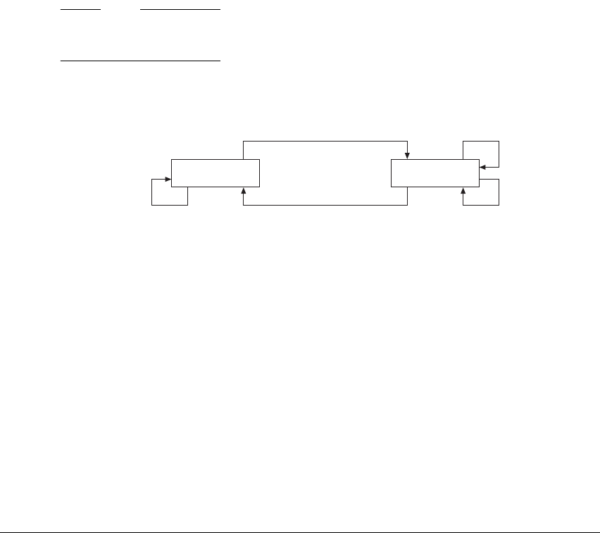
Application Level Memory Model
A3-14 Copyright © 1996-1998, 2000, 2004-2008 ARM Limited. All rights reserved. ARM DDI 0406B
When a processor writes using any instruction other than a Store-Exclusive:
• if the write is to a physical address that is not covered by its local monitor the write does not affect
the state of the local monitor
• if the write is to a physical address that is covered by its local monitor it is IMPLEMENTATION DEFINED
whether the write affects the state of the local monitor.
If the local monitor is in its Exclusive Access state and the processor performs a Store-Exclusive to any
address other than the last one from which it performed a Load-Exclusive, it is IMPLEMENTATION DEFINED
whether the store updates memory, but in all cases the local monitor is reset to its Open Access state. This
mechanism:
• is used on a context switch, see Context switch support on page A3-21
• must be treated as a software programming error in all other cases.
Note
It is UNPREDICTABLE whether a store to a tagged physical address causes a tag in the local monitor to be
cleared if that store is by an observer other than the one that caused the physical address to be tagged.
Figure A3-2 shows the state machine for the local monitor. Table A3-6 on page A3-15 shows the effect of
each of the operations shown in the figure.
Figure A3-2 Local monitor state machine diagram
Operations marked * are possible alternative
IMPLEMENTATION
DEFINED
options.
Any LoadExcl operation updates the tagged address to the most significant bits of the address x used
for the operation. For more information see the section Size of the tagged memory block.
In the diagram: LoadExcl represents any Load-Exclusive instruction
StoreExcl represents any Store-Exclusive instruction
Store represents any other store instruction.
CLREX
StoreExcl(x)
Store(x)
LoadExcl(x) LoadExcl(x)
CLREX
Store(Tagged_address) *
StoreExcl(Tagged_address)
StoreExcl(!Tagged_address)
Open
Access
Store(!Tagged_address)
Store(Tagged_address) *
Exclusive
Access

Application Level Memory Model
ARM DDI 0406B Copyright © 1996-1998, 2000, 2004-2008 ARM Limited. All rights reserved. A3-15
Note
For the local monitor state machine, as shown in Figure A3-2 on page A3-14:
• The IMPLEMENTATION DEFINED options for the local monitor are consistent with the local monitor
being constructed so that it does not hold any physical address, but instead treats any access as
matching the address of the previous
LoadExcl
.
• A local monitor implementation can be unaware of Load-Exclusive and Store-Exclusive operations
from other processors.
•It is UNPREDICTABLE whether the transition from Exclusive Access to Open Access state occurs when
the
Store
or
StoreExcl
is from another observer.
Table A3-6 shows the effect of the operations shown in Figure A3-2 on page A3-14.
Table A3-6 Effect of Exclusive instructions and write operations on local monitor
Initial state OperationaEffect Final state
Open Access
CLREX
No effect Open Access
Open Access
StoreExcl(x)
Does not update memory, returns status 1 Open Access
Open Access
LoadExcl(x)
Loads value from memory, tags address x Exclusive Access
Open Access
Store(x)
Updates memory, no effect on monitor Open Access
Exclusive Access
CLREX
Clears tagged address Open Access
Exclusive Access
StoreExcl(t)
Updates memory, returns status 0 Open Access
Exclusive Access
StoreExcl(!t)
Updates memory, returns status 0b
Open Access
Does not update memory, returns status 1b
Exclusive Access
LoadExcl(x)
Loads value from memory, changes tag to address to x Exclusive Access
Exclusive Access
Store(!t)
Updates memory, no effect on monitor Exclusive Access
Exclusive Access
Store(t)
Updates memory
Exclusive Accessb
Open Accessb
a. In the table:
LoadExcl
represents any Load-Exclusive instruction
StoreExcl
represents any Store-Exclusive instruction
Store
represents any store operation other than a Store-Exclusive operation.
t is the tagged address, bits [31:a] of the address of the last Load-Exclusive instruction. For more information, see
Tagging and the size of the tagged memory block on page A3-20.
b. IMPLEMENTATION DEFINED alternative actions.

Application Level Memory Model
A3-16 Copyright © 1996-1998, 2000, 2004-2008 ARM Limited. All rights reserved. ARM DDI 0406B
A3.4.2 Exclusive access instructions and Shareable memory regions
For memory regions that have the Shareable attribute, exclusive access instructions rely on:
•A local monitor for each processor in the system, that tags any address from which the processor
executes a Load-Exclusive. The local monitor operates as described in Exclusive access instructions
and Non-shareable memory regions on page A3-13, except that for Shareable memory any
Store-Exclusive is then subject to checking by the global monitor if it is described in that section as
doing at least one of:
— updating memory
— returning a status value of 0.
The local monitor can ignore exclusive accesses from other processors in the system.
•A global monitor that tags a physical address as exclusive access for a particular processor. This tag
is used later to determine whether a Store-Exclusive to that address that has not been failed by the
local monitor can occur. Any successful write to the tagged address by any other observer in the
shareability domain of the memory location is guaranteed to clear the tag. For each processor in the
system, the global monitor:
— holds a single tagged address
— maintains a state machine.
The global monitor can either reside in a processor block or exist as a secondary monitor at the memory
interfaces.
Note
An implementation can combine the functionality of the global and local monitors into a single unit.
Operation of the global monitor
Load-Exclusive from Shareable memory performs a load from memory, and causes the physical address of
the access to be tagged as exclusive access for the requesting processor. This access also causes the exclusive
access tag to be removed from any other physical address that has been tagged by the requesting processor.
The global monitor only supports a single outstanding exclusive access to Shareable memory per processor.
Store-Exclusive performs a conditional store to memory:
• The store is guaranteed to succeed only if the physical address accessed is tagged as exclusive access
for the requesting processor and both the local monitor and the global monitor state machines for the
requesting processor are in the Exclusive Access state. In this case:
— a status value of 0 is returned to a register to acknowledge the successful store
— the final state of the global monitor state machine for the requesting processor is
IMPLEMENTATION DEFINED
— if the address accessed is tagged for exclusive access in the global monitor state machine for
any other processor then that state machine transitions to Open Access state.

Application Level Memory Model
ARM DDI 0406B Copyright © 1996-1998, 2000, 2004-2008 ARM Limited. All rights reserved. A3-17
• If no address is tagged as exclusive access for the requesting processor, the store does not succeed:
— a status value of 1 is returned to a register to indicate that the store failed
— the global monitor is not affected and remains in Open Access state for the requesting
processor.
• If a different physical address is tagged as exclusive access for the requesting processor, it is
IMPLEMENTATION DEFINED whether the store succeeds or not:
— if the store succeeds a status value of 0 is returned to a register, otherwise a value of 1 is
returned
— if the global monitor state machine for the processor was in the Exclusive Access state before
the Store-Exclusive it is IMPLEMENTATION DEFINED whether that state machine transitions to
the Open Access state.
The Store-Exclusive instruction defines the register to which the status value is returned.
In a shared memory system, the global monitor implements a separate state machine for each processor in
the system. The state machine for accesses to Shareable memory by processor (n) can respond to all the
Shareable memory accesses visible to it. This means it responds to:
• accesses generated by the associated processor (n)
• accesses generated by the other observers in the shareability domain of the memory location (!n).
In a shared memory system, the global monitor implements a separate state machine for each observer that
can generate a Load-Exclusive or a Store-Exclusive in the system.
Figure A3-3 on page A3-18 shows the state machine for processor(n) in a global monitor. Table A3-7 on
page A3-19 shows the effect of each of the operations shown in the figure.

Application Level Memory Model
A3-18 Copyright © 1996-1998, 2000, 2004-2008 ARM Limited. All rights reserved. ARM DDI 0406B
Figure A3-3 Global monitor state machine diagram for processor(n) in a multiprocessor system
Note
For the global monitor state machine, as shown in Figure A3-3:
• Whether a Store-Exclusive successfully updates memory or not depends on whether the address
accessed matches the tagged Shareable memory address for the processor issuing the Store-Exclusive
instruction. For this reason, Figure A3-3 and Table A3-7 on page A3-19 only show how the (!n)
entries cause state transitions of the state machine for processor(n).
• An Load-Exclusive can only update the tagged Shareable memory address for the processor issuing
the Load-Exclusive instruction.
• The effect of the
CLREX
instruction on the global monitor is IMPLEMENTATION DEFINED.
• It is IMPLEMENTATION DEFINED:
— whether a modification to a non-shareable memory location can cause a global monitor to
transition from Exclusive Access to Open Access state
— whether a Load-Exclusive to a non-shareable memory location can cause a global monitor to
transition from Open Access to Exclusive Access state.
StoreExcl(Tagged_Address,!n) clears the monitor only if the StoreExcl updates memory
Any LoadExcl operation updates the tagged address to the most significant bits of the address x
used for the operation. For more information see the section Size of the tagged memory block.
LoadExcl(x,n)
Open
Access
Exclusive
Access
CLREX(n), CLREX(!n),
LoadExcl(x,!n),
StoreExcl(x,n),
StoreExcl(x,!n),
Store(x,n), Store(x,!n)
StoreExcl(Tagged_address,!n)
Store(Tagged_address,!n)
StoreExcl(Tagged_address,n) *
StoreExcl(!Tagged_address,n) *
Store(Tagged_address,n) *
CLREX(n) *
StoreExcl(Tagged_address,!n)
Store(!Tagged_address,n)
StoreExcl(Tagged_address,n) *
StoreExcl(!Tagged_address,n) *
Store(Tagged_address,n) *
CLREX(n) *
StoreExcl(!Tagged_address,!n)
Store(!Tagged_address,!n)
CLREX(!n)
LoadExcl(x,n)
Operations marked * are possible alternative IMPLEMENTATION DEFINED options.
In the diagram: LoadExcl represents any Load-Exclusive instruction
StoreExcl represents any Store-Exclusive instruction
Store represents any other store instruction.

Application Level Memory Model
ARM DDI 0406B Copyright © 1996-1998, 2000, 2004-2008 ARM Limited. All rights reserved. A3-19
Table A3-7 shows the effect of the operations shown in Figure A3-3 on page A3-18.
Table A3-7 Effect of load/store operations on global monitor for processor(n)
Initial
stateaOperationbEffect Final
statea
Open
CLREX(n)
,
CLREX(!n)
None Open
StoreExcl(x,n)
Does not update memory, returns status 1 Open
LoadExcl(x,!n)
Loads value from memory, no effect on tag address for processor(n) Open
StoreExcl(x,!n)
Depends on state machine and tag address for processor issuing
STREX
c
Open
Store(x,n)
,
Store(x,!n)
Updates memory, no effect on monitor Open
LoadExcl(x,n)
Loads value from memory, tags address x Exclusive
Exclusive
LoadExcl(x,n)
Loads value from memory, tags address x Exclusive
CLREX(n)
None. Effect on the final state is IMPLEMENTATION DEFINED.
Exclusivee
Opene
CLREX(!n)
None Exclusive
StoreExcl(t,!n)
Updates memory, returns status 0cOpen
Does not update memory, returns status 1cExclusive
StoreExcl(t,n)
Updates memory, returns status 0d
Open
Exclusive
StoreExcl(!t,n)
Updates memory, returns status 0e
Open
Exclusive
Does not update memory, returns status 1e
Open
Exclusive
StoreExcl(!t,!n)
Depends on state machine and tag address for processor issuing
STREX
Exclusive

Application Level Memory Model
A3-20 Copyright © 1996-1998, 2000, 2004-2008 ARM Limited. All rights reserved. ARM DDI 0406B
A3.4.3 Tagging and the size of the tagged memory block
As stated in the footnotes to Table A3-6 on page A3-15 and Table A3-7 on page A3-19, when a
Load-Exclusive instruction is executed, the resulting tag address ignores the least significant bits of the
memory address.
Tagged_address = Memory_address[31:a]
The value of
a
in this assignment is IMPLEMENTATION DEFINED, between a minimum value of 3 and a
maximum value of 11. For example, in an implementation where a == 4, a successful
LDREX
of address
0x000341B4
gives a tag value of bits [31:4] of the address, giving
0x000341B
. This means that the four words
of memory from
0x0003 41B0
to
0x000341BF
are tagged for exclusive access.
The size of the tagged memory block called the Exclusives Reservation Granule. The Exclusives
Reservation Granule is IMPLEMENTATION DEFINED between:
• two words, in an implementation with a == 3
• 512 words, in an implementation with a == 11.
In some implementations the CTR identifies the Exclusives Reservation Granule, see:
•c0, Cache Type Register (CTR) on page B3-83 for a VMSA implementation
•c0, Cache Type Register (CTR) on page B4-34 for a PMSA implementation.
Exclusive
Store(t,n)
Updates memory
Exclusivee
Opene
Store(t,!n)
Updates memory Open
Store(!t,n)
,
Store(!t,!n)
Updates memory, no effect on monitor Exclusive
a. Open = Open Access state, Exclusive = Exclusive Access state.
b. In the table:
LoadExcl
represents any Load-Exclusive instruction
StoreExcl
represents any Store-Exclusive instruction
Store
represents any store operation other than a Store-Exclusive operation.
t is the tagged address for processor(n), bits [31:a] of the address of the last Load-Exclusive instruction issued by
processor(n), see Tagging and the size of the tagged memory block.
c. The result of a
STREX(x,!n)
or a
STREX(t,!n)
operation depends on the state machine and tagged address for the processor
issuing the
STREX
instruction. This table shows how each possible outcome affects the state machine for processor(n).
d. After a successful
STREX
to the tagged address, the state of the state machine is IMPLEMENTATION DEFINED. However,
this state has no effect on the subsequent operation of the global monitor.
e. Effect is IMPLEMENTATION DEFINED. The table shows all permitted implementations.
Table A3-7 Effect of load/store operations on global monitor for processor(n) (continued)
Initial
stateaOperationbEffect Final
statea

Application Level Memory Model
ARM DDI 0406B Copyright © 1996-1998, 2000, 2004-2008 ARM Limited. All rights reserved. A3-21
A3.4.4 Context switch support
After a context switch, software must ensure that the local monitor is in the Open Access state. This requires
it to either:
• execute a
CLREX
instruction
• execute a dummy
STREX
to a memory address allocated for this purpose.
Note
• Using a dummy
STREX
for this purpose is backwards-compatible with the ARMv6 implementation of
the exclusive operations. The
CLREX
instruction is introduced in ARMv6K.
• Context switching is not an application level operation. However, this information is included here to
complete the description of the exclusive operations.
The
STREX
or
CLREX
instruction following a context switch might cause a subsequent Store-Exclusive to fail,
requiring a load … store sequence to be replayed. To minimize the possibility of this happening, ARM
recommends that the Store-Exclusive instruction is kept as close as possible to the associated
Load-Exclusive instruction, see Load-Exclusive and Store-Exclusive usage restrictions.
A3.4.5 Load-Exclusive and Store-Exclusive usage restrictions
The Load-Exclusive and Store-Exclusive instructions are intended to work together, as a pair, for example
a
LDREX
/
STREX
pair or a
LDREXB
/
STREXB
pair. As mentioned in Context switch support, ARM recommends that
the Store-Exclusive instruction always follows within a few instructions of its associated Load-Exclusive
instructions. To support different implementations of these functions, software must follow the notes and
restrictions given here.
These notes describe use of an
LDREX
/
STREX
pair, but apply equally to any other
Load-Exclusive/Store-Exclusive pair:
• The exclusives support a single outstanding exclusive access for each processor thread that is
executed. The architecture makes use of this by not requiring an address or size check as part of the
IsExclusiveLocal()
function. If the target address of an
STREX
is different from the preceding
LDREX
in
the same execution thread, behavior can be UNPREDICTABLE. As a result, an
LDREX
/
STREX
pair can only
be relied upon to eventually succeed if they are executed with the same address. Where a context
switch or exception might result in a change of execution thread, a
CLREX
instruction or a dummy
STREX
instruction must be executed to avoid unwanted effects, as described in Context switch support
Using an
STREX
in this way is the only occasion where software can program an
STREX
with a different
address from the previously executed
LDREX
.
• An explicit store to memory can cause the clearing of exclusive monitors associated with other
processors, therefore, performing a store between the
LDREX
and the
STREX
can result in a livelock
situation. As a result, code must avoid placing an explicit store between an
LDREX
and an
STREX
in a
single code sequence.

Application Level Memory Model
A3-22 Copyright © 1996-1998, 2000, 2004-2008 ARM Limited. All rights reserved. ARM DDI 0406B
•If two
STREX
instructions are executed without an intervening
LDREX
the second
STREX
returns a status
value of 1. This means that:
—every
STREX
must have a preceding
LDREX
associated with it in a given thread of execution
— it is not necessary for every
LDREX
to have a subsequent
STREX
.
• An implementation of the Load-Exclusive and Store-Exclusive instructions can require that, in any
thread of execution, the transaction size of a Store-Exclusive is the same as the transaction size of the
preceding Load-Exclusive that was executed in that thread. If the transaction size of a
Store-Exclusive is different from the preceding Load-Exclusive in the same execution thread,
behavior can be UNPREDICTABLE. As a result, an
LDREX
/
STREX
pair can only be relied upon to
eventually succeed only if they have the same size. Where a context switch or exception might result
in a change of execution thread, the software must execute a
CLREX
instruction or a dummy
STREX
instruction to avoid unwanted effects, as described in Context switch support on page A3-21. Using
an
STREX
in this way is the only occasion where software can use a Store-Exclusive instruction with
a different transaction size from the previously executed Load-Exclusive instruction.
• An implementation might clear an exclusive monitor between the
LDREX
and the
STREX
, without any
application-related cause. For example, this might happen because of cache evictions. Code written
for such an implementation must avoid having any explicit memory accesses or cache maintenance
operations between the
LDREX
and
STREX
instructions.
• Implementations can benefit from keeping the
LDREX
and
STREX
operations close together in a single
code sequence. This minimizes the likelihood of the exclusive monitor state being cleared between
the
LDREX
instruction and the
STREX
instruction. Therefore, ARM strongly recommends a limit of 128
bytes between
LDREX
and
STREX
instructions in a single code sequence, for best performance.
• Implementations that implement coherent protocols, or have only a single master, might combine the
local and global monitors for a given processor. The IMPLEMENTATION DEFINED and UNPREDICTABLE
parts of the definitions in Exclusive monitors operations on page B2-35 are provided to cover this
behavior.
• The architecture sets an upper limit of 2048 bytes on the size of a region that can be marked as
exclusive. Therefore, for performance reasons, ARM recommends that software separates objects
that will be accessed by exclusive accesses by at least 2048 bytes. This is a performance guideline
rather than a functional requirement.
•
LDREX
and
STREX
operations must be performed only on memory with the Normal memory attribute.
• The effect of Data Abort exceptions on the state of monitors is UNPREDICTABLE. ARM recommends
that abort handling code performs a
CLREX
instruction or a dummy
STREX
instruction to clear the
monitor state.
• If the memory attributes for the memory being accessed by an
LDREX
/
STREX
pair are changed between
the
LDREX
and the
STREX
, behavior is UNPREDICTABLE.

Application Level Memory Model
ARM DDI 0406B Copyright © 1996-1998, 2000, 2004-2008 ARM Limited. All rights reserved. A3-23
A3.4.6 Semaphores
The Swap (
SWP
) and Swap Byte (
SWPB
) instructions must be used with care to ensure that expected behavior
is observed. Two examples are as follows:
1. A system with multiple bus masters that uses Swap instructions to implement semaphores that control
interactions between different bus masters.
In this case, the semaphores must be placed in an uncached region of memory, where any buffering
of writes occurs at a point common to all bus masters using the mechanism. The Swap instruction
then causes a locked read-write bus transaction.
2. A systems with multiple threads running on a uniprocessor that uses the Swap instructions to
implement semaphores that control interaction of the threads.
In this case, the semaphores can be placed in a cached region of memory, and a locked read-write bus
transaction might or might not occur. The Swap and Swap Byte instructions are likely to have better
performance on such a system than they do on a system with multiple bus masters such as that
described in example 1.
Note
From ARMv6, use of the Swap and Swap Byte instructions is deprecated. All new software should use the
Load-Exclusive and Store-Exclusive synchronization primitives described in Synchronization and
semaphores on page A3-12, for example
LDREX
and
STREX
.
A3.4.7 Synchronization primitives and the memory order model
The synchronization primitives follow the memory order model of the memory type accessed by the
instructions. For this reason:
• Portable code for claiming a spin-lock must include a Data Memory Barrier (DMB) operation,
performed by a
DMB
instruction, between claiming the spin-lock and making any access that makes
use of the spin-lock.
• Portable code for releasing a spin-lock must include a
DMB
instruction before writing to clear the
spin-lock.
This requirement applies to code using:
• the Load-Exclusive/Store-Exclusive instruction pairs, for example
LDREX
/
STREX
• the deprecated synchronization primitives,
SWP
/
SWPB
.
A3.4.8 Use of WFE and SEV instructions by spin-locks
ARMv7 and ARMv6K provide Wait For Event and Send Event instructions,
WFE
and
SEV
, that can assist with
reducing power consumption and bus contention caused by processors repeatedly attempting to obtain a
spin-lock. These instructions can be used at application level, but a complete understanding of what they do
depends on system-level understanding of exceptions. They are described in Wait For Event and Send Event
on page B1-44.

Application Level Memory Model
A3-24 Copyright © 1996-1998, 2000, 2004-2008 ARM Limited. All rights reserved. ARM DDI 0406B
A3.5 Memory types and attributes and the memory order model
ARMv6 defined a set of memory attributes with the characteristics required to support the memory and
devices in the system memory map. In ARMv7 this set of attributes is extended by the addition of the Outer
Shareable attribute for Normal memory.
Note
Whether an ARMv7 implementation supports the Outer Shareable memory attribute is IMPLEMENTATION
DEFINED.
The ordering of accesses for regions of memory, referred to as the memory order model, is defined by the
memory attributes. This model is described in the following sections:
•Memory types
•Summary of ARMv7 memory attributes on page A3-25
•Atomicity in the ARM architecture on page A3-26
•Normal memory on page A3-28
•Device memory on page A3-33
•Strongly-ordered memory on page A3-34
•Memory access restrictions on page A3-35
•Backwards compatibility on page A3-37
•The effect of the Security Extensions on page A3-37.
A3.5.1 Memory types
For each memory region, the most significant memory attribute specifies the memory type. There are three
mutually exclusive memory types:
• Normal
•Device
• Strongly-ordered.
Normal and Device memory regions have additional attributes.
Usually, memory used for program code and for data storage is Normal memory. Examples of Normal
memory technologies are:
• programmed Flash ROM
Note
During programming, Flash memory can be ordered more strictly than Normal memory.
•ROM
•SRAM
• DRAM and DDR memory.

Application Level Memory Model
ARM DDI 0406B Copyright © 1996-1998, 2000, 2004-2008 ARM Limited. All rights reserved. A3-25
System peripherals (I/O) generally conform to different access rules to Normal memory. Examples of I/O
accesses are:
• FIFOs where consecutive accesses
— add queued values on write accesses
— remove queued values on read accesses.
• interrupt controller registers where an access can be used as an interrupt acknowledge, changing the
state of the controller itself
• memory controller configuration registers that are used to set up the timing and correctness of areas
of Normal memory
• memory-mapped peripherals, where accessing a memory location can cause side effects in the
system.
In ARMv7, regions of the memory map for these accesses are defined as Device or Strongly-ordered
memory. To ensure system correctness, access rules for Device and Strongly-ordered memory are more
restrictive than those for Normal memory:
• both read and write accesses can have side effects
• accesses must not be repeated, for example, on return from an exception
• the number, order and sizes of the accesses must be maintained.
In addition, for Strongly-ordered memory, all memory accesses are strictly ordered to correspond to the
program order of the memory access instructions.
A3.5.2 Summary of ARMv7 memory attributes
Table A3-8 summarizes the memory attributes. For more information about theses attributes see:
•Normal memory on page A3-28 and Shareable attribute for Device memory regions on page A3-34,
for the shareability attribute
•Write-Through Cacheable, Write-Back Cacheable and Non-cacheable Normal memory on
page A3-32, for the cacheability attribute.
Table A3-8 Memory attribute summary
Memory type
attribute Shareability Other attributes Description
Strongly-
ordered
- - All memory accesses to
Strongly-ordered memory
occur in program order. All
Strongly-ordered regions are
assumed to be Shareable.

Application Level Memory Model
A3-26 Copyright © 1996-1998, 2000, 2004-2008 ARM Limited. All rights reserved. ARM DDI 0406B
A3.5.3 Atomicity in the ARM architecture
Atomicity is a feature of memory accesses, described as atomic accesses. The ARM architecture description
refers to two types of atomicity, defined in:
•Single-copy atomicity on page A3-27
•Multi-copy atomicity on page A3-28.
Device Shareable - Intended to handle memory-
mapped peripherals that are
shared by several processors.
Non-
shareable
- Intended to handle memory-
mapped peripherals that are
used only by a single processor.
Normal Outer
Shareable
Cacheability, one of: aThe Outer Shareable attribute
qualifies the Shareable attribute
for Normal memory regions
and enables two levels of
Normal memory sharing.b
Non-cacheable
Write-Through Cacheable
Write-Back Write-Allocate Cacheable
Write-Back no Write-Allocate Cacheable
Inner
Shareable
Cacheability, one of: aIntended to handle Normal
memory that is shared between
several processors.
Non-cacheable
Write-Through Cacheable
Write-Back Write-Allocate Cacheable
Write-Back no Write-Allocate Cacheable
Non-
shareable
Cacheability, one of: aIntended to handle Normal
memory that is used by only a
single processor.
Non-cacheable
Write-Through Cacheable
Write-Back Write-Allocate Cacheable
Write-Back no Write-Allocate Cacheable
a. The cacheability attribute is defined independently for inner and outer cache regions.
b. The significance of the Outer Shareable attribute is IMPLEMENTATION DEFINED.
Table A3-8 Memory attribute summary (continued)
Memory type
attribute Shareability Other attributes Description

Application Level Memory Model
ARM DDI 0406B Copyright © 1996-1998, 2000, 2004-2008 ARM Limited. All rights reserved. A3-27
Single-copy atomicity
A read or write operation is single-copy atomic if the following conditions are both true:
• After any number of write operations to an operand, the value of the operand is the value written by
one of the write operations. It is impossible for part of the value of the operand to come from one
write operation and another part of the value to come from a different write operation.
• When a read operation and a write operation are made to the same operand, the value obtained by the
read operation is one of:
— the value of the operand before the write operation
— the value of the operand after the write operation.
It is never the case that the value of the read operation is partly the value of the operand before the
write operation and partly the value of the operand after the write operation.
In ARMv7, the single-copy atomic processor accesses are:
• all byte accesses
• all halfword accesses to halfword-aligned locations
• all word accesses to word-aligned locations
• memory accesses caused by
LDREXD
and
STREXD
instructions to doubleword-aligned locations.
LDM
,
LDC
,
LDC2
,
LDRD
,
STM
,
STC
,
STC2
,
STRD
,
PUSH
,
POP
,
RFE
,
SRS
,
VLDM
,
VLDR
,
VSTM
, and
VSTR
instructions are
executed as a sequence of word-aligned word accesses. Each 32-bit word access is guaranteed to be
single-copy atomic. A subsequence of two or more word accesses from the sequence might not exhibit
single-copy atomicity.
Advanced SIMD element and structure loads and stores are executed as a sequence of accesses of the
element or structure size. The element accesses are single-copy atomic if and only if both:
• the element size is 32 bits, or smaller
• the elements are naturally aligned.
Accesses to 64-bit elements or structures that are at least word-aligned are executed as a sequence of 32-bit
accesses, each of which is single-copy atomic. Subsequences of two or more 32-bit accesses from the
sequence might not be single-copy atomic.
When an access is not single-copy atomic, it is executed as a sequence of smaller accesses, each of which
is single-copy atomic, at least at the byte level.
If an instruction is executed as a sequence of accesses according to these rules, some exceptions can be taken
in the sequence and cause execution of the instruction to be abandoned. These exceptions are:
• synchronous Data Abort exceptions
• if low interrupt latency configuration is selected and the accesses are to Normal memory, see Low
interrupt latency configuration on page B1-43:
— IRQ interrupts
— FIQ interrupts
— asynchronous aborts.

Application Level Memory Model
A3-28 Copyright © 1996-1998, 2000, 2004-2008 ARM Limited. All rights reserved. ARM DDI 0406B
If any of these exceptions are returned from using their preferred exception return, the instruction that
generated the sequence of accesses is re-executed and so any accesses that had already been performed
before the exception was taken are repeated.
Note
The exception behavior for these multiple access instructions means they are not suitable for use for writes
to memory for the purpose of software synchronization.
For implicit accesses:
• Cache linefills and evictions have no effect on the single-copy atomicity of explicit transactions or
instruction fetches.
• Instruction fetches are single-copy atomic for each instruction fetched.
Note
32-bit Thumb instructions are fetched as two 16-bit items.
• Translation table walks are performed as 32-bit accesses aligned to 32 bits, each of which is
single-copy atomic.
Multi-copy atomicity
In a multiprocessing system, writes to a memory location are multi-copy atomic if the following conditions
are both true:
• All writes to the same location are serialized, meaning they are observed in the same order by all
observers, although some observers might not observe all of the writes.
• A read of a location does not return the value of a write until all observers observe that write.
Writes to Normal memory are not multi-copy atomic.
All writes to Device and Strongly-ordered memory that are single-copy atomic are also multi-copy atomic.
All write accesses to the same location are serialized. Write accesses to Normal memory can be repeated up
to the point that another write to the same address is observed.
For Normal memory, serialization of writes does not prohibit the merging of writes.
A3.5.4 Normal memory
Normal memory is idempotent, meaning that it exhibits the following properties:
• read accesses can be repeated with no side effects
• repeated read accesses return the last value written to the resource being read
• read accesses can prefetch additional memory locations with no side effects

Application Level Memory Model
ARM DDI 0406B Copyright © 1996-1998, 2000, 2004-2008 ARM Limited. All rights reserved. A3-29
• write accesses can be repeated with no side effects, provided that the contents of the location are
unchanged between the repeated writes
• unaligned accesses can be supported
• accesses can be merged before accessing the target memory system.
Normal memory can be read/write or read-only, and a Normal memory region is defined as being either
Shareable or Non-shareable. In a VMSA implementation, Shareable Normal memory can be either Inner
Shareable or Outer Shareable. In a PMSA implementation, no distinction is made between Inner Shareable
and Outer Shareable regions.
The Normal memory type attribute applies to most memory used in a system.
Accesses to Normal Memory have a weakly consistent model of memory ordering. See a standard text
describing memory ordering issues for a description of weakly consistent memory models, for example
chapter 2 of Memory Consistency Models for Shared Memory-Multiprocessors, Kourosh Gharachorloo,
Stanford University Technical Report CSL-TR-95-685. In general, for Normal memory, barrier operations
are required where the order of memory accesses observed by other observers must be controlled. This
requirement applies regardless of the cacheablility and shareability attributes of the Normal memory region.
The ordering requirements of accesses described in Ordering requirements for memory accesses on
page A3-45 apply to all explicit accesses.
An instruction that generates a sequence of accesses as described in Atomicity in the ARM architecture on
page A3-26 might be abandoned as a result of an exception being taken during the sequence of accesses. On
return from the exception the instruction is restarted, and therefore one or more of the memory locations
might be accessed multiple times. This can result in repeated write accesses to a location that has been
changed between the write accesses.
The architecture permits speculative accesses to memory locations marked as Normal if the access
permissions and domain permit an access to the locations.
A Normal memory region has shareability attributes that define the data coherency properties of the region.
These attributes do not affect the coherency requirements of:
• instruction fetches, see Instruction coherency issues on page A3-53
• translation table walks, if supported, in the base ARMv7 architecture and in versions of the
architecture before ARMv7, see TLB maintenance operations and the memory order model on
page B3-59.

Application Level Memory Model
A3-30 Copyright © 1996-1998, 2000, 2004-2008 ARM Limited. All rights reserved. ARM DDI 0406B
Non-shareable Normal memory
For a Normal memory region, the Non-shareable attribute identifies Normal memory that is likely to be
accessed only by a single processor.
A region of Normal memory with the Non-shareable attribute does not have any requirement to make data
accesses by different observers coherent, unless the memory is non-cacheable. If other observers share the
memory system, software must use cache maintenance operations if the presence of caches might lead to
coherency issues when communicating between the observers. This cache maintenance requirement is in
addition to the barrier operations that are required to ensure memory ordering.
For Non-shareable Normal memory, the Load-Exclusive and Store-Exclusive synchronization primitives do
not take account of the possibility of accesses by more than one observer.
Shareable, Inner Shareable, and Outer Shareable Normal memory
For Normal memory, the Shareable and Outer Shareable memory attributes describe Normal memory that
is expected to be accessed by multiple processors or other system masters:
• In a VMSA implementation, Normal memory that has the Shareable attribute but not the Outer
Shareable attribute assigned is described as having the Inner Shareable attribute.
• In a PMSA implementation, no distinction is made between Inner Shareable and Outer Shareable
Normal memory, and you cannot assign the Outer Shareable attribute to Normal memory regions.
A region of Normal memory with the Shareable attribute is one for which data accesses to memory by
different observers within the same shareability domain are coherent.
The Outer Shareable attribute is introduced in ARMv7, and can be applied only to a Normal memory region
in a VMSA implementation that has the Shareable attribute assigned. It creates three levels of shareability
for a Normal memory region:
Non-shareable
A Normal memory region that does not have the Shareable attribute assigned.
Inner Shareable
A Normal memory region that has the Shareable attribute assigned, but not the Outer
Shareable attribute.
Outer Shareable
A Normal memory region that has both the Shareable and the Outer Shareable attributes
assigned.
These attributes can be used to define sets of observers for which the shareability attributes make the data
or unified caches transparent for data accesses. The sets of observers that are affected by the shareability
attributes are described as shareability domains. The details of the use of these attributes are
system-specific. Example A3-1 on page A3-31 shows how they might be used:

Application Level Memory Model
ARM DDI 0406B Copyright © 1996-1998, 2000, 2004-2008 ARM Limited. All rights reserved. A3-31
Example A3-1 Use of shareability attributes
In a VMSA implementation, a particular sub-system with two clusters of processors has the requirement
that:
• in each cluster, the data or unified caches of the processors in the cluster are transparent for all data
accesses with the Inner Shareable attribute
• however, between the two clusters, the caches:
— are not transparent for data accesses that have only the Inner Shareable attribute
— are transparent for data accesses that have the Outer Shareable attribute.
In this system, each cluster is in a different shareability domain for the Inner Shareable attribute, but all
components of the sub-system are in the same shareability domain for the Outer Shareable attribute.
A system might implement two such sub-systems. If the data or unified caches of one subsystem are not
transparent to the accesses from the other subsystem, this system has two Outer Shareable shareability
domains.
Having two levels of shareability attribute means you can reduce the performance and power overhead for
shared memory regions that do not need to be part of the Outer Shareable shareability domain.
Whether an ARMv7 implementation supports the Outer Shareable attribute is IMPLEMENTATION DEFINED.
If the Outer Shareable attribute is supported, its significance in the implementation is IMPLEMENTATION
DEFINED.
For Shareable Normal memory, the Load-Exclusive and Store-Exclusive synchronization primitives take
account of the possibility of accesses by more than one observer in the same Shareability domain.
Note
The Shareable concept enables system designers to specify the locations in Normal memory that must have
coherency requirements. However, to facilitate porting of software, software developers must not assume
that specifying a memory region as Non-shareable permits software to make assumptions about the
incoherency of memory locations between different processors in a shared memory system. Such
assumptions are not portable between different multiprocessing implementations that make use of the
Shareable concept. Any multiprocessing implementation might implement caches that, inherently, are
shared between different processing elements.

Application Level Memory Model
A3-32 Copyright © 1996-1998, 2000, 2004-2008 ARM Limited. All rights reserved. ARM DDI 0406B
Write-Through Cacheable, Write-Back Cacheable and Non-cacheable Normal
memory
In addition to being Outer Shareable, Inner Shareable or Non-shareable, each region of Normal memory can
be marked as being one of:
• Write-Through Cacheable
• Write-Back Cacheable, with an additional qualifier that marks it as one of:
— Write-Back, Write-Allocate
— Write-Back, no Write-Allocate
• Non-cacheable.
If the same memory locations are marked as having different cacheability attributes, for example by the use
of aliases in a virtual to physical address mapping, behavior is UNPREDICTABLE.
The cacheability attributes provide a mechanism of coherency control with observers that lie outside the
shareability domain of a region of memory. In some cases, the use of Write-Through Cacheable or
Non-cacheable regions of memory might provide a better mechanism for controlling coherency than the use
of hardware coherency mechanisms or the use of cache maintenance routines. To this end, the architecture
requires the following properties for Non-cacheable or Write-Through Cacheable memory:
• a completed write to a memory location that is Non-cacheable or Write-Through Cacheable for a
level of cache made by an observer accessing the memory system inside the level of cache is visible
to all observers accessing the memory system outside the level of cache without the need of explicit
cache maintenance
• a completed write to a memory location that is Non-cacheable for a level of cache made by an
observer accessing the memory system outside the level of cache is visible to all observers accessing
the memory system inside the level of cache without the need of explicit cache maintenance.
Note
Implementations can also use the cacheability attributes to provide a performance hint regarding the
performance benefit of caching. For example, it might be known to a programmer that a piece of memory
is not going to be accessed again and would be better treated as Non-cacheable. The distinction between
Write-Back Write-Allocate and Write-Back no Write-Allocate memory exists only as a hint for
performance.
The ARM architecture provides independent cacheability attributes for Normal memory for two conceptual
levels of cache, the inner and the outer cache. The relationship between these conceptual levels of cache and
the implemented physical levels of cache is IMPLEMENTATION DEFINED, and can differ from the boundaries
between the Inner and Outer Shareability domains. However:
• inner refers to the innermost caches, and always includes the lowest level of cache
• no cache controlled by the Inner cacheability attributes can lie outside a cache controlled by the Outer
cacheability attributes
• an implementation might not have any outer cache.

Application Level Memory Model
ARM DDI 0406B Copyright © 1996-1998, 2000, 2004-2008 ARM Limited. All rights reserved. A3-33
Example A3-2 to Example A3-4 describe the three possible ways of implementing a system with three
levels of cache, L1 to L3. L1 is the level closest to the processor, see Memory hierarchy on page A3-52.
Example A3-2 Implementation with two inner and one outer cache levels
Implement the three levels of cache in the system, L1 to L3, with:
• the Inner cacheability attribute applied to L1 and L2 cache
• the Outer cacheability attribute applied to L3 cache.
Example A3-3 Implementation with three inner and no outer cache levels
Implement the three levels of cache in the system, L1 to L3, with the Inner cacheability attribute applied to
L1, L2, and L3 cache. Do not use the Outer cacheability attribute.
Example A3-4 Implementation with one inner and two outer cache levels
Implement the three levels of cache in the system, L1 to L3, with:
• the Inner cacheability attribute applied to L1 cache
• the Outer cacheability attribute applied to L2 and L3 cache.
A3.5.5 Device memory
The Device memory type attribute defines memory locations where an access to the location can cause side
effects, or where the value returned for a load can vary depending on the number of loads performed.
Memory-mapped peripherals and I/O locations are examples of memory regions normally marked as being
Device memory.
For explicit accesses from the processor to memory marked as Device:
• all accesses occur at their program size
• the number of accesses is the number specified by the program.
An implementation must not repeat an access to a Device memory location if the program has only one
access to that location. In other words, accesses to Device memory locations are not restartable.
The architecture does not permit speculative accesses to memory marked as Device.
The architecture permits an Advanced SIMD element or structure load instruction to access bytes in Device
memory that are not explicitly accessed by the instruction, provided the bytes accessed are within a 16-byte
window, aligned to 16-bytes, that contains at least one byte that is explicitly accessed by the instruction.
Address locations marked as Device are never held in a cache.

Application Level Memory Model
A3-34 Copyright © 1996-1998, 2000, 2004-2008 ARM Limited. All rights reserved. ARM DDI 0406B
All explicit accesses to Device memory must comply with the ordering requirements of accesses described
in Ordering requirements for memory accesses on page A3-45.
An instruction that generates a sequence of accesses as described in Atomicity in the ARM architecture on
page A3-26 might be abandoned as a result of an exception being taken during the sequence of accesses. On
return from the exception the instruction is restarted, and therefore one or more of the memory locations
might be accessed multiple times. This can result in repeated write accesses to a location that has been
changed between the write accesses.
Note
Do not use an instruction that generates a sequence of accesses to access Device memory if the instruction
might generate an abort on any access other than the first one.
Any unaligned access that is not faulted by the alignment restrictions and accesses Device memory has
UNPREDICTABLE behavior.
Shareable attribute for Device memory regions
Device memory regions can be given the Shareable attribute. This means that a region of Device memory
can be described as either:
• Shareable Device memory
• Non-shareable Device memory.
Non-shareable Device memory is defined as only accessible by a single processor. An example of a system
supporting Shareable and Non-shareable Device memory is an implementation that supports both:
• a local bus for its private peripherals
• system peripherals implemented on the main shared system bus.
Such a system might have more predictable access times for local peripherals such as watchdog timers or
interrupt controllers. In particular, a specific address in a Non-shareable Device memory region might
access a different physical peripheral for each processor.
A3.5.6 Strongly-ordered memory
The Strongly-ordered memory type attribute defines memory locations where an access to the location can
cause side effects, or where the value returned for a load can vary depending on the number of loads
performed. Examples of memory regions normally marked as being Strongly-ordered are memory-mapped
peripherals and I/O locations.
For explicit accesses from the processor to memory marked as Strongly-ordered:
• all accesses occur at their program size
• the number of accesses is the number specified by the program.
An implementation must not repeat an access to a Strongly-ordered memory location if the program has
only one access to that location. In other words, accesses to Strongly-ordered memory locations are not
restartable.

Application Level Memory Model
ARM DDI 0406B Copyright © 1996-1998, 2000, 2004-2008 ARM Limited. All rights reserved. A3-35
The architecture does not permit speculative accesses to memory marked as Strongly-ordered.
The architecture permits an Advanced SIMD element or structure load instruction to access bytes in
Strongly-ordered memory that are not explicitly accessed by the instruction, provided the bytes accessed are
within a 16-byte window, aligned to 16-bytes, that contains at least one byte that is explicitly accessed by
the instruction.
Address locations in Strongly-ordered memory are not held in a cache, and are always treated as Shareable
memory locations.
All explicit accesses to Strongly-ordered memory must correspond to the ordering requirements of accesses
described in Ordering requirements for memory accesses on page A3-45.
An instruction that generates a sequence of accesses as described in Atomicity in the ARM architecture on
page A3-26 might be abandoned as a result of an exception being taken during the sequence of accesses. On
return from the exception the instruction is restarted, and therefore one or more of the memory locations
might be accessed multiple times. This can result in repeated write accesses to a location that has been
changed between the write accesses.
Note
Do not use an instruction that generates a sequence of accesses to access Strongly-ordered memory if the
instruction might generate an abort on any access other than the first one.
Any unaligned access that is not faulted by the alignment restrictions and accesses Strongly-ordered
memory has UNPREDICTABLE behavior.
Note
See Ordering of instructions that change the CPSR interrupt masks on page AppxG-8 for additional
requirements that apply to accesses to Strongly-ordered memory in ARMv6.
A3.5.7 Memory access restrictions
The following restrictions apply to memory accesses:
• For any access X, the bytes accessed by X must all have the same memory type attribute, otherwise
the behavior of the access is UNPREDICTABLE. That is, an unaligned access that spans a boundary
between different memory types is UNPREDICTABLE.
• For any two memory accesses X and Y that are generated by the same instruction, the bytes accessed
by X and Y must all have the same memory type attribute, otherwise the results are UNPREDICTABLE.
For example, an
LDC
,
LDM
,
LDRD
,
STC
,
STM
, or
STRD
that spans a boundary between Normal and Device
memory is UNPREDICTABLE.
• An instruction that generates an unaligned memory access to Device or Strongly-ordered memory is
UNPREDICTABLE.

Application Level Memory Model
A3-36 Copyright © 1996-1998, 2000, 2004-2008 ARM Limited. All rights reserved. ARM DDI 0406B
• To ensure access rules are maintained, an instruction that causes multiple accesses to Device or
Strongly-ordered memory must not cross a 4KB address boundary, otherwise the effect is
UNPREDICTABLE. For this reason, it is important that an access to a volatile memory device is not
made using a single instruction that crosses a 4KB address boundary.
ARM expects this restriction to impose constraints on the placing of volatile memory devices in the
memory map of a system, rather than expecting a compiler to be aware of the alignment of memory
accesses.
• For instructions that generate accesses to Device or Strongly-ordered memory, implementations must
not change the sequence of accesses specified by the pseudocode of the instruction. This includes not
changing:
— how many accesses there are
— the time order of the accesses
— the data sizes and other properties of each access.
In addition, processor implementations expect any attached memory system to be able to identify the
memory type of an accesses, and to obey similar restrictions with regard to the number, time order,
data sizes and other properties of the accesses.
Exceptions to this rule are:
— An implementation of a processor can break this rule, provided that the information it supplies
to the memory system enables the original number, time order, and other details of the accesses
to be reconstructed. In addition, the implementation must place a requirement on attached
memory systems to do this reconstruction when the accesses are to Device or Strongly-ordered
memory.
For example, an implementation with a 64-bit bus might pair the word loads generated by an
LDM
into 64-bit accesses. This is because the instruction semantics ensure that the 64-bit access
is always a word load from the lower address followed by a word load from the higher address.
However the implementation must permit the memory systems to unpack the two word loads
when the access is to Device or Strongly-ordered memory.
— Any implementation technique that produces results that cannot be observed to be different
from those described above is legitimate.
— An Advanced SIMD element or structure load instruction can access bytes in Device or
Strongly-ordered memory that are not explicitly accessed by the instruction, provided the
bytes accessed are within a 16-byte window, aligned to 16-bytes, that contains at least one byte
that is explicitly accessed by the instruction.
• Any multi-access instruction that loads or stores the PC must access only Normal memory. If the
instruction accesses Device or Strongly-ordered memory the result is UNPREDICTABLE. There is one
exception to this restriction. In the VMSA architecture, when the MMU is disabled any multi-access
instruction that loads or stores the PC functions correctly, see Enabling and disabling the MMU on
page B3-5.
• Any instruction fetch must access only Normal memory. If it accesses Device or Strongly-ordered
memory, the result is UNPREDICTABLE. For example, instruction fetches must not be performed to an
area of memory that contains read-sensitive devices, because there is no ordering requirement
between instruction fetches and explicit accesses.

Application Level Memory Model
ARM DDI 0406B Copyright © 1996-1998, 2000, 2004-2008 ARM Limited. All rights reserved. A3-37
•Behavior is UNPREDICTABLE if the same memory location:
— is marked as Shareable Normal and Non-shareable Normal
— is marked as having different memory types (Normal, Device, or Strongly-ordered)
— is marked as having different cacheability attributes
— is marked as being Shareable Device and Non-shareable Device memory.
Such memory marking contradictions can occur, for example, by the use of aliases in a virtual to
physical address mapping.
Before ARMv6, it is IMPLEMENTATION DEFINED whether a low interrupt latency mode is supported. From
ARMv6, low interrupt latency support is controlled by the SCTLR.FI bit. It is IMPLEMENTATION DEFINED
whether multi-access instructions behave correctly in low interrupt latency configurations.
A3.5.8 Backwards compatibility
From ARMv6, the memory attributes are significantly different from those in previous versions of the
architecture. Table A3-9 shows the interpretation of the earlier memory types in the light of this definition.
A3.5.9 The effect of the Security Extensions
The Security Extensions can be included as part of an ARMv7-A implementation, with a VMSA. They
provide two distinct 4GByte virtual memory spaces:
• a Secure virtual memory space
• a Non-secure virtual memory space.
The Secure virtual memory space is accessed by memory accesses in the Secure state, and the Non-secure
virtual memory space is accessed by memory accesses in the Non-secure state.
By providing different virtual memory spaces, the Security Extensions permit memory accesses made from
the Non-secure state to be distinguished from those made from the Secure state.
Table A3-9 Backwards compatibility
Previous architectures ARMv6 and ARMv7 attribute
NCNB (Non-cacheable, Non-bufferable) Strongly-ordered
NCB (Non-cacheable, Bufferable) Shareable Device
Write-Through Cacheable, Bufferable Non-shareable Normal, Write-Through Cacheable
Write-Back Cacheable, Bufferable Non-shareable Normal, Write-Back Cacheable

Application Level Memory Model
A3-38 Copyright © 1996-1998, 2000, 2004-2008 ARM Limited. All rights reserved. ARM DDI 0406B
A3.6 Access rights
ARMv7 includes additional attributes for memory regions, that enable:
• Data accesses to be restricted, based on the privilege of the access. See Privilege level access controls
for data accesses.
• Instruction fetches to be restricted, based on the privilege of the process or thread making the fetch.
See Privilege level access controls for instruction accesses.
• On a system that implements the Security Extensions, accesses to be restricted to memory accesses
with the Secure memory attribute. See Memory region security status on page A3-39.
A3.6.1 Privilege level access controls for data accesses
The memory attributes can define that a memory region is:
• not accessible to any accesses
• accessible only to Privileged accesses
• accessible to Privileged and Unprivileged accesses.
The access privilege level is defined separately for explicit read and explicit write accesses. However, a
system that defines the memory attributes is not required to support all combinations of memory attributes
for read and write accesses.
A Privileged access is an access made during privileged execution, as a result of a load or store operation
other than
LDRT
,
STRT
,
LDRBT
,
STRBT
,
LDRHT
,
STRHT
,
LDRSHT
, or
LDRSBT
.
An Unprivileged access is an access made as a result of load or store operation performed in one of these
cases:
• when the processor is in an unprivileged mode
• when the processor is in any mode and the access is made as a result of a
LDRT
,
STRT
,
LDRBT
,
STRBT
,
LDRHT
,
STRHT
,
LDRSHT
, or
LDRSBT
instruction.
A Data Abort exception is generated if the processor attempts a data access that the access rights do not
permit. For example, a Data Abort exception is generated if the processor is in unprivileged mode and
attempts to access a memory region that is marked as only accessible to Privileged accesses.
A3.6.2 Privilege level access controls for instruction accesses
Memory attributes can define that a memory region is:
• Not accessible for execution
• Accessible for execution by Privileged processes only
• Accessible for execution by Privileged and Unprivileged processes.
To define the instruction access rights to a memory region, the memory attributes describe, separately, for
the region:
• its read access rights, see Privilege level access controls for data accesses

Application Level Memory Model
ARM DDI 0406B Copyright © 1996-1998, 2000, 2004-2008 ARM Limited. All rights reserved. A3-39
• whether it is suitable for execution.
For example, a region that is accessible for execution by Privileged processes only has the memory
attributes:
• accessible only to Privileged read accesses
• suitable for execution.
This means there is some linkage between the memory attributes that define the accessibility of a region to
explicit memory accesses, and those that define that a region can be executed.
A memory fault occurs if a processor attempts to execute code from a memory location with attributes that
do not permit code execution.
A3.6.3 Memory region security status
An additional memory attribute determines whether the memory region is Secure or Non-secure in an
ARMv7-A system that implements the Security Extensions. When the Security Extensions are
implemented, this attribute is checked by the system hardware to ensure that a region of memory that is
designated as Secure by the system hardware is not accessed by memory accesses with the Non-secure
memory attribute. For more information, see Memory region attributes on page B3-32.

Application Level Memory Model
A3-40 Copyright © 1996-1998, 2000, 2004-2008 ARM Limited. All rights reserved. ARM DDI 0406B
A3.7 Virtual and physical addressing
ARMv7 provides three alternative architectural profiles, ARMv7-A, ARMv7-R and ARMv7-M. Each of the
profiles specifies a different memory system. This manual describes two of these profiles:
ARMv7-A profile
The ARMv7-A memory system incorporates a Memory Management Unit (MMU),
controlled by CP15 registers. The memory system supports virtual addressing, with the
MMU performing virtual to physical address translation, in hardware, as part of program
execution.
ARMv7-R profile
The ARMv7-R memory system incorporates a Memory Protection Unit (MPU), controlled
by CP15 registers. The MPU does not support virtual addressing.
At the application level, the difference between the ARMv7-A and ARMv7-R memory systems is
transparent. Regardless of which profile is implemented, an application accesses the memory map described
in Address space on page A3-2, and the implemented memory system makes the features described in this
chapter available to the application.
For a system-level description of the ARMv7-A and ARMv7-R memory models see:
• Chapter B2 Common Memory System Architecture Features
• Chapter B3 Virtual Memory System Architecture (VMSA)
• Chapter B4 Protected Memory System Architecture (PMSA).
Note
This manual does not describe the ARMv7-M profile. For details of this profile see:
•ARMv7-M Architecture Application Level Reference Manual, for an application-level description
•ARMv7-M Architecture Reference Manual, for a full description.

Application Level Memory Model
ARM DDI 0406B Copyright © 1996-1998, 2000, 2004-2008 ARM Limited. All rights reserved. A3-41
A3.8 Memory access order
ARMv7 provides a set of three memory types, Normal, Device, and Strongly-ordered, with well-defined
memory access properties.
The ARMv7 application-level view of the memory attributes is described in:
•Memory types and attributes and the memory order model on page A3-24
•Access rights on page A3-38.
When considering memory access ordering, an important feature of the ARMv6 memory model is the
Shareable memory attribute, that indicates whether a region of memory can be shared between multiple
processors, and therefore requires an appearance of cache transparency in the ordering model.
The key issues with the memory order model depend on the target audience:
• For software programmers, considering the model at the application level, the key factor is that for
accesses to Normal memory barriers are required in some situations where the order of accesses
observed by other observers must be controlled.
• For silicon implementers, considering the model at the system level, the Strongly-ordered and Device
memory attributes place certain restrictions on the system designer in terms of what can be built and
when to indicate completion of an access.
Note
Implementations remain free to choose the mechanisms required to implement the functionality of
the memory model.
More information about the memory order model is given in the following subsections:
•Reads and writes on page A3-42
•Ordering requirements for memory accesses on page A3-45
•Memory barriers on page A3-47.
Additional attributes and behaviors relate to the memory system architecture. These features are defined in
the system level section of this manual:
• Virtual memory systems based on an MMU, described in Chapter B3 Virtual Memory System
Architecture (VMSA).
• Protected memory systems based on an MPU, described in Chapter B4 Protected Memory System
Architecture (PMSA).
• Caches, described in Caches on page B2-3.
Note
In these system level descriptions, some attributes are described in relation to an MMU. In general, these
descriptions can also be applied to an MPU based system.

Application Level Memory Model
A3-42 Copyright © 1996-1998, 2000, 2004-2008 ARM Limited. All rights reserved. ARM DDI 0406B
A3.8.1 Reads and writes
Each memory access is either a read or a write. Explicit memory accesses are the memory accesses required
by the function of an instruction. The following can cause memory accesses that are not explicit:
• instruction fetches
• cache loads and writebacks
• translation table walks.
Except where otherwise stated, the memory ordering requirements only apply to explicit memory accesses.
Reads
Reads are defined as memory operations that have the semantics of a load.
The memory accesses of the following instructions are reads:
•
LDR
,
LDRB
,
LDRH
,
LDRSB
, and
LDRSH
•
LDRT
,
LDRBT
,
LDRHT
,
LDRSBT
, and
LDRSHT
•
LDREX
,
LDREXB
,
LDREXD
, and
LDREXH
•
LDM
,
LDRD
,
POP
, and
RFE
•
LDC
,
LDC2
,
VLDM
,
VLDR
,
VLD1
,
VLD2
,
VLD3
, and
VLD4
• the return of status values by
STREX
,
STREXB
,
STREXD
, and
STREXH
• in the ARM instruction set only,
SWP
and
SWPB
• in the Thumb instruction set only,
TBB
and
TBH
.
Hardware-accelerated opcode execution by the Jazelle extension can cause a number of reads to occur,
according to the state of the operand stack and the implementation of the Jazelle hardware acceleration.
Writes
Writes are defined as memory operations that have the semantics of a store.
The memory accesses of the following instructions are Writes:
•
STR
,
STRB
, and
STRH
•
STRT
,
STRBT
, and
STRHT
•
STREX
,
STREXB
,
STREXD
, and
STREXH
•
STM
,
STRD
, PUSH, and
SRS
•
STC
,
STC2
,
VSTM
,
VSTR
,
VST1
,
VST2
,
VST3
, and
VST4
• in the ARM instruction set only,
SWP
and
SWPB
.
Hardware-accelerated opcode execution by the Jazelle extension can cause a number of writes to occur,
according to the state of the operand stack and the implementation of the Jazelle hardware acceleration.

Application Level Memory Model
ARM DDI 0406B Copyright © 1996-1998, 2000, 2004-2008 ARM Limited. All rights reserved. A3-43
Synchronization primitives
Synchronization primitives must ensure correct operation of system semaphores in the memory order
model. The synchronization primitive instructions are defined as those instructions that are used to ensure
memory synchronization:
•
LDREX
,
STREX
,
LDREXB
,
STREXB
,
LDREXD
,
STREXD
,
LDREXH
,
STREXH
.
•
SWP
,
SWPB
. Use of these instructions is deprecated from ARMv6.
Before ARMv6, support consisted of the
SWP
and
SWPB
instructions. ARMv6 introduced new Load-Exclusive
and Store-Exclusive instructions
LDREX
and
STREX
, and deprecated using the
SWP
and
SWPB
instructions.
ARMv7 introduces:
• additional Load-Exclusive and Store-Exclusive instructions,
LDREXB
,
LDREXD
,
LDREXH
,
STREXB
,
STREXD
,
and
STREXH
• the Clear-Exclusive instruction CLREX
• the Load-Exclusive, Store-Exclusive and Clear-Exclusive instructions in the Thumb instruction set.
For details of the Load-Exclusive, Store-Exclusive and Clear-Exclusive instructions see Synchronization
and semaphores on page A3-12.
The Load-Exclusive and Store-Exclusive instructions are supported to Shareable and Non-shareable
memory. Non-shareable memory can be used to synchronize processes that are running on the same
processor. Shareable memory must be used to synchronize processes that might be running on different
processors.
Observability and completion
An observer is an agent in the system that can access memory. For a processor, the following mechanisms
must be treated as independent observers:
• the mechanism that performs reads or writes to memory
• a mechanism that causes an instruction cache to be filled from memory or that fetches instructions to
be executed directly from memory
• a mechanism that performs translation table walks.
The set of observers that can observe a memory access is defined by the system.
For all memory:
• a write to a location in memory is said to be observed by an observer when a subsequent read of the
location by the same observer will return the value written by the write
• a write to a location in memory is said to be globally observed for a shareability domain when a
subsequent read of the location by any observer in that shareability domain will return the value
written by the write

Application Level Memory Model
A3-44 Copyright © 1996-1998, 2000, 2004-2008 ARM Limited. All rights reserved. ARM DDI 0406B
• a read of a location in memory is said to be observed by an observer when a subsequent write to the
location by the same observer will have no effect on the value returned by the read
• a read of a location in memory is said to be globally observed for a shareability domain when a
subsequent write to the location by any observer in that shareability domain will have no effect on
the value returned by the read.
Additionally, for Strongly-ordered memory:
• A read or write of a memory-mapped location in a peripheral that exhibits side-effects is said to be
observed, and globally observed, only when the read or write:
— meets the general conditions listed
— can begin to affect the state of the memory-mapped peripheral
— can trigger all associated side effects, whether they affect other peripheral devices, processors
or memory.
For all memory, the completion rules are defined as:
• A read or write is complete for a shareability domain when all of the following are true:
— the read or write is globally observed for that shareability domain
— any translation table walks associated with the read or write are complete for that shareability
domain.
• A translation table walk is complete for a shareability domain when the memory accesses associated
with the translation table walk are globally observed for that shareability domain, and the TLB is
updated.
• A cache, branch predictor or TLB maintenance operation is complete for a shareability domain when
the effects of operation are globally observed for that shareability domain and any translation table
walks that arise from the operation are complete for that shareability domain.
The completion of any cache, branch predictor and TLB maintenance operation includes its
completion on all processors that are affected by both the operation and the DSB.
Side effect completion in Strongly-ordered and Device memory
The completion of a memory access in Strongly-ordered or Device memory is not guaranteed to be
sufficient to determine that the side effects of the memory access are visible to all observers. The mechanism
that ensures the visibility of side-effects of a memory accesses is IMPLEMENTATION DEFINED.

Application Level Memory Model
ARM DDI 0406B Copyright © 1996-1998, 2000, 2004-2008 ARM Limited. All rights reserved. A3-45
A3.8.2 Ordering requirements for memory accesses
ARMv7 and ARMv6 define access restrictions in the permitted ordering of memory accesses. These
restrictions depend on the memory attributes of the accesses involved.
Two terms used in describing the memory access ordering requirements are:
Address dependency
An address dependency exists when the value returned by a read access is used to compute
the virtual address of a subsequent read or write access. An address dependency exists even
if the value read by the first read access does not change the virtual address of the second
read or write access. This might be the case if the value returned is masked off before it is
used, or if it has no effect on the predicted address value for the second access.
Control dependency
A control dependency exists when the data value returned by a read access is used to
determine the condition code flags, and the values of the flags are used for condition code
checking to determine the address of a subsequent read access. This address determination
might be through conditional execution, or through the evaluation of a branch.
Figure A3-4 on page A3-46 shows the memory ordering between two explicit accesses A1 and A2, where
A1 occurs before A2 in program order. The symbols used in the figure are as follows:
< Accesses must be observed in program order, that is, A1 must be observed before A2.
- Accesses can be observed in any order, provided that the requirements of uniprocessor
semantics, for example respecting dependencies between instructions in a single processor,
are maintained.
The following additional restrictions apply to the ordering of memory accesses that have this
symbol:
• If there is an address dependency then the two memory accesses are observed in
program order by any observer in the common shareability domain of the two
accesses.
This ordering restriction does not apply if there is only a control dependency between
the two read accesses.
If there is both an address dependency and a control dependency between two read
accesses the ordering requirements of the address dependency apply.
• If the value returned by a read access is used as data written by a subsequent write
access, then the two memory accesses are observed in program order.
• It is impossible for an observer in the shareability domain of a memory location to
observe a write access to that memory location if that location would not be written
to in a sequential execution of a program.
• It is impossible for an observer in the shareability domain of a memory location to
observe a write value written to that memory location if that value would not be
written in a sequential execution of a program.

Application Level Memory Model
A3-46 Copyright © 1996-1998, 2000, 2004-2008 ARM Limited. All rights reserved. ARM DDI 0406B
• It is impossible for an observer in the shareability domain of a memory location to
observe two reads to the same memory location performed by the same observer in
an order that would not occur in a sequential execution of a program.
In Figure A3-4, an access refers to a read or a write access to the specified memory type.
For example, Device access, Non-shareable refers to a read or write access to Non-shareable
Device memory.
Figure A3-4 Memory ordering restrictions
There are no ordering requirements for implicit accesses to any type of memory.
Program order for instruction execution
The program order of instruction execution is the order of the instructions in the control flow trace.
Explicit memory accesses in an execution can be either:
Strictly Ordered
Denoted by <. Must occur strictly in order.
Ordered Denoted by <=. Can occur either in order or simultaneously.
Load/store multiple instructions, such as
LDM
,
LDRD
,
STM
, and
STRD
, generate multiple word accesses, each of
which is a separate access for the purpose of determining ordering.
The rules for determining program order for two accesses A1 and A2 are:
If A1 and A2 are generated by two different instructions:
• A1 < A2 if the instruction that generates A1 occurs before the instruction that generates A2 in
program order
• A2 < A1 if the instruction that generates A2 occurs before the instruction that generates A1 in
program order.
If A1 and A2 are generated by the same instruction:
• If A1 and A2 are the load and store generated by a
SWP
or
SWPB
instruction:
— A1 < A2 if A1 is the load and A2 is the store
— A2 < A1 if A2 is the load and A1 is the store.
A1
Normal access
Device access, Non-shareable
Strongly-
ordered
access
ShareableNon-shareable
Device access
Normal
access
A2
<
Strongly-ordered access
- <<<
Device access, Shareable
-
<
<
<
---
--
--

Application Level Memory Model
ARM DDI 0406B Copyright © 1996-1998, 2000, 2004-2008 ARM Limited. All rights reserved. A3-47
• In these descriptions:
—an LDM-class instruction is any form of
LDM
,
LDMDA
,
LDMDB
,
LDMIB
, or
POP
instruction
—an LDC-class instruction is an
LDC
,
VLDM
, or
VLDR
instruction
—an STM-class instruction is any form of
STM
,
STMDA
,
STMDB
,
STMIB
, or
PUSH
instruction
—an STC-class instruction is an
STC
,
VSTM
, or
VSTR
instruction.
If A1 and A2 are two word loads generated by an LDC-class or LDM-class instruction, or two word
stores generated by an STC-class or STM-class instruction, excluding LDM-class and STM-class
instructions with a register list that includes the PC:
— A1 <= A2 if the address of A1 is less than the address of A2
— A2 <= A1 if the address of A2 is less than the address of A1.
If A1 and A2 are two word loads generated by an LDM-class instruction with a register list that
includes the PC or two word stores generated by an STM-class instruction with a register list that
includes the PC, the program order of the memory accesses is not defined.
• If A1 and A2 are two word loads generated by an
LDRD
instruction or two word stores generated by
an
STRD
instruction, the program order of the memory accesses is not defined.
• If A1 and A2 are load or store accesses generated by Advanced SIMD element or structure load/store
instructions, the program order of the memory accesses is not defined.
• For any instruction or operation not explicitly mentioned in this section, if the single-copy atomicity
rules described in Single-copy atomicity on page A3-27 mean the operation becomes a sequence of
accesses, then the time-ordering of those accesses is not defined.
A3.8.3 Memory barriers
Memory barrier is the general term applied to an instruction, or sequence of instructions, used to force
synchronization events by a processor with respect to retiring load/store instructions. The ARM architecture
defines a number of memory barriers that provide a range of functionality, including:
• ordering of issued load/store instructions to the programmers’ model
• completion of preceding load/store instructions to the programmers’ model
• flushing of any instructions prefetched before the memory barrier operation.
ARMv7 and ARMv6 require three explicit memory barriers to support the memory order model described
in this chapter. In ARMv7 the memory barriers are provided as instructions that are available in the ARM
and Thumb instruction sets, and in ARMv6 the memory barriers are performed by CP15 register writes. The
three memory barriers are:
• Data Memory Barrier, see Data Memory Barrier (DMB) on page A3-48
• Data Synchronization Barrier, see Data Synchronization Barrier (DSB) on page A3-49
• Instruction Synchronization Barrier, see Instruction Synchronization Barrier (ISB) on page A3-49.
Depending on the synchronization needed, a program might use memory barriers on their own, or it might
use them in conjunction with cache and memory management maintenance operations that are only
available in privileged modes.

Application Level Memory Model
A3-48 Copyright © 1996-1998, 2000, 2004-2008 ARM Limited. All rights reserved. ARM DDI 0406B
The DMB and DSB memory barriers affect reads and writes to the memory system generated by load/store
instructions and data or unified cache maintenance operations being executed by the processor. Instruction
fetches or accesses caused by a hardware translation table access are not explicit accesses.
Data Memory Barrier (DMB)
The
DMB
instruction is a data memory barrier. The processor that executes the
DMB
instruction is referred to
as the executing processor, Pe. The
DMB
instruction takes the required shareability domain and required
access types as arguments. If the required shareability is Full system then the operation applies to all
observers within the system.
A DMB creates two groups of memory accesses, Group A and Group B:
Group A Contains:
• All explicit memory accesses of the required access types from observers in the same
required shareability domain as Pe that are observed by Pe before the
DMB
instruction.
These accesses include any accesses of the required access types and required
shareability domain performed by Pe.
• All loads of required access types from observers in the same required shareability
domain as Pe that have been observed by any given observer, Py, in the same required
shareability domain as Pe before Py has performed a memory access that is a member
of Group A.
Group B Contains:
• All explicit memory accesses of the required access types by Pe that occur in program
order after the
DMB
instruction.
• All explicit memory accesses of the required access types by any given observer Px
in the same required shareability domain as Pe that can only occur after Px has
observed a store that is a member of Group B.
Any observer with the same required shareability domain as Pe observes all members of Group A before it
observes any member of Group B to the extent that those group members are required to be observed, as
determined by the shareability and cacheability of the memory locations accessed by the group members.
Where members of Group A and Group B access the same memory-mapped peripheral, all members of
Group A will be visible at the memory-mapped peripheral before any members of Group B are visible at
that peripheral.
Note
• A memory access might be in neither Group A nor Group B. The DMB does not affect the order of
observation of such a memory access.
• The second part of the definition of Group A is recursive. Ultimately, membership of Group A derives
from the observation by Py of a load before Py performs an access that is a member of Group A as a
result of the first part of the definition of Group A.

Application Level Memory Model
ARM DDI 0406B Copyright © 1996-1998, 2000, 2004-2008 ARM Limited. All rights reserved. A3-49
• The second part of the definition of Group B is recursive. Ultimately, membership of Group B derives
from the observation by any observer of an access by Pe that is a member of Group B as a result of
the first part of the definition of Group B.
DMB
only affects memory accesses. It has no effect on the ordering of any other instructions executing on the
processor.
For details of the
DMB
instruction in the Thumb and ARM instruction sets see DMB on page A8-90.
Data Synchronization Barrier (DSB)
The
DSB
instruction is a special memory barrier, that synchronizes the execution stream with memory
accesses. The
DSB
instruction takes the required shareability domain and required access types as arguments.
If the required shareability is Full system then the operation applies to all observers within the system.
A
DSB
behaves as a
DMB
with the same arguments, and also has the additional properties defined here.
A
DSB
completes when both:
• all explicit memory accesses that are observed by Pe before the
DSB
is executed, are of the required
access types, and are from observers in the same required shareability domain as Pe, are complete for
the set of observers in the required shareability domain
• all cache, branch predictor, and TLB maintenance operations issued by Pe before the
DSB
are complete
for the required shareability domain.
In addition, no instruction that appears in program order after the
DSB
instruction can execute until the
DSB
completes.
For details of the
DSB
instruction in the Thumb and ARM instruction sets see DSB on page A8-92.
Note
Historically, this operation was referred to as Drain Write Buffer or Data Write Barrier (DWB). From
ARMv6, these names and the use of DWB were deprecated in favor of the new Data Synchronization Barrier
name and DSB abbreviation. DSB better reflects the functionality provided from ARMv6, because DSB is
architecturally defined to include all cache, TLB and branch prediction maintenance operations as well as
explicit memory operations.
Instruction Synchronization Barrier (ISB)
An
ISB
instruction flushes the pipeline in the processor, so that all instructions that come after the
ISB
instruction in program order are fetched from cache or memory only after the
ISB
instruction has completed.
Using an
ISB
ensures that the effects of context altering operations executed before the
ISB
are visible to the
instructions fetched after the
ISB
instruction. Examples of context altering operations that require the
insertion of an
ISB
instruction to ensure the operations are complete are:
• cache, TLB, and branch predictor maintenance operations
• changes to the CP14 and CP15 registers.

Application Level Memory Model
A3-50 Copyright © 1996-1998, 2000, 2004-2008 ARM Limited. All rights reserved. ARM DDI 0406B
In addition, any branches that appear in program order after the
ISB
instruction are written into the branch
prediction logic with the context that is visible after the
ISB
instruction. This is needed to ensure correct
execution of the instruction stream.
Any context altering operations appearing in program order after the
ISB
instruction only take effect after
the
ISB
has been executed.
For details of the
ISB
instruction in the Thumb and ARM instruction sets see ISB on page A8-102.
Pseudocode details of memory barriers
The following types define the required shareability domains and required access types used as arguments
for
DMB
and
DSB
instructions:
enumeration MBReqDomain {MBReqDomain_FullSystem,
MBReqDomain_OuterShareable,
MBReqDomain_InnerShareable,
MBReqDomain_Nonshareable};
enumeration MBReqTypes {MBReqTypes_All, MBReqTypes_Writes};
The following procedures perform the memory barriers:
DataMemoryBarrier(MBReqDomain domain, MBReqTypes types)
DataSynchronizationBarrier(MBReqDomain domain, MBReqTypes types)
InstructionSynchronizationBarrier()

Application Level Memory Model
ARM DDI 0406B Copyright © 1996-1998, 2000, 2004-2008 ARM Limited. All rights reserved. A3-51
A3.9 Caches and memory hierarchy
The implementation of a memory system depends heavily on the microarchitecture and therefore the details
of the system are IMPLEMENTATION DEFINED. ARMv7 defines the application level interface to the memory
system, and supports a hierarchical memory system with multiple levels of cache. This section provides an
application level view of this system. It contains the subsections:
•Introduction to caches
•Memory hierarchy on page A3-52
•Implication of caches for the application programmer on page A3-52
•Preloading caches on page A3-54.
A3.9.1 Introduction to caches
A cache is a block of high-speed memory that contains a number of entries, each consisting of:
• main memory address information, commonly known as a tag
• the associated data.
Caches are used to increase the average speed of a memory access. Cache operation takes account of two
principles of locality:
Spatial locality
An access to one location is likely to be followed by accesses to adjacent locations.
Examples of this principle are:
• sequential instruction execution
• accessing a data structure.
Temporal locality
An access to an area of memory is likely to be repeated in a short time period. An example
of this principle is the execution of a code loop
To minimize the quantity of control information stored, the spatial locality property is used to group several
locations together under the same tag. This logical block is commonly known as a cache line. When data is
loaded into a cache, access times for subsequent loads and stores are reduced, resulting in overall
performance benefits. An access to information already in a cache is known as a cache hit, and other
accesses are called cache misses.
Normally, caches are self-managing, with the updates occurring automatically. Whenever the processor
wants to access a cacheable location, the cache is checked. If the access is a cache hit, the access occurs in
the cache, otherwise a location is allocated and the cache line loaded from memory. Different cache
topologies and access policies are possible, however, they must comply with the memory coherency model
of the underlying architecture.
Caches introduce a number of potential problems, mainly because of:
• Memory accesses occurring at times other than when the programmer would normally expect them
• There being multiple physical locations where a data item can be held
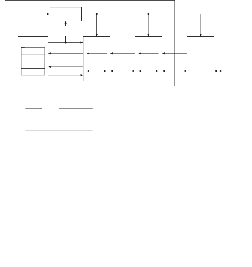
Application Level Memory Model
A3-52 Copyright © 1996-1998, 2000, 2004-2008 ARM Limited. All rights reserved. ARM DDI 0406B
A3.9.2 Memory hierarchy
Memory close to a processor has very low latency, but is limited in size and expensive to implement. Further
from the processor it is easier to implement larger blocks of memory but these have increased latency. To
optimize overall performance, an ARMv7 memory system can include multiple levels of cache in a
hierarchical memory system. Figure A3-5 shows such a system, in an ARMv7-A implementation of a
VMSA, supporting virtual addressing.
Figure A3-5 Multiple levels of cache in a memory hierarchy
Note
In this manual, in a hierarchical memory system, Level 1 refers to the level closest to the processor, as shown
in Figure A3-5.
A3.9.3 Implication of caches for the application programmer
In normal operation, the caches are largely invisible to the application programmer. However they can
become visible when there is a breakdown in the coherency of the caches. Such a breakdown can occur:
• when memory locations are updated by other agents in the system
• when memory updates made from the application code must be made visible to other agents in the
system.
For example:
• In a system with a DMA controller that reads memory locations that are held in the data cache of a
processor, a breakdown of coherency occurs when the processor has written new data in the data
cache, but the DMA controller reads the old data held in memory.
• In a Harvard architecture of caches, where there are separate instruction and data caches, a
breakdown of coherency occurs when new instruction data has been written into the data cache, but
the instruction cache still contains the old instruction data.
Level 4
for example,
CF card, disk
Processor
R15
R0
.
.
.
Address
Translation
Level 1
Cache
Level 2
Cache
Level 3
DRAM
SRAM
Flash
ROM
Instruction
Prefetch
CP15 configuration
and control
Physical address
Virtual
address
Load
Store

Application Level Memory Model
ARM DDI 0406B Copyright © 1996-1998, 2000, 2004-2008 ARM Limited. All rights reserved. A3-53
Data coherency issues
You can ensure the data coherency of caches in the following ways:
• By not using the caches in situations where coherency issues can arise. You can achieve this by:
— using Non-cacheable or, in some cases, Write-Through Cacheable memory for the caches
— not enabling caches in the system.
• By using cache maintenance operations to manage the coherency issues in software, see Cache
maintenance functionality on page B2-9. Many of these operations are only available to system
software.
• By using hardware coherency mechanisms to ensure the coherency of data accesses to memory for
cacheable locations by observers within the different shareability domains, see Non-shareable
Normal memory on page A3-30 and Shareable, Inner Shareable, and Outer Shareable Normal
memory on page A3-30.
The performance of these hardware coherency mechanisms is highly implementation specific. In
some implementations the mechanism suppresses the ability to cache shareable locations. In other
implementations, cache coherency hardware can hold data in caches while managing coherency
between observers within the shareability domains.
Instruction coherency issues
How far ahead of the current point of execution instructions are prefetched from is IMPLEMENTATION
DEFINED. Such prefetching can be either a fixed or a dynamically varying number of instructions, and can
follow any or all possible future execution paths. For all types of memory:
• the processor might have fetched the instructions from memory at any time since the last ISB,
exception entry or exception return executed by that processor
• any instructions fetched in this way might be executed multiple times, if this is required by the
execution of the program, without being refetched from memory
In addition, the ARM architecture does not require the hardware to ensure coherency between instruction
caches and memory, even for regions of memory with Shareable attributes. This means that for cacheable
regions of memory, an instruction cache can hold instructions that were fetched from memory before the
last ISB, exception entry or exception return.
If software requires coherency between instruction execution and memory, it must manage this coherency
using the ISB and DSB memory barriers and cache maintenance operations, see Ordering of cache and
branch predictor maintenance operations on page B2-21. Many of these operations are only available to
system software.

Application Level Memory Model
A3-54 Copyright © 1996-1998, 2000, 2004-2008 ARM Limited. All rights reserved. ARM DDI 0406B
A3.9.4 Preloading caches
The ARM architecture provides memory system hints
PLD
(Preload Data) and
PLI
(Preload Instruction) to
permit software to communicate the expected use of memory locations to the hardware. The memory system
can respond by taking actions that are expected to speed up the memory accesses if and when they do occur.
The effect of these memory system hints is IMPLEMENTATION DEFINED. Typically, implementations will use
this information to bring the data or instruction locations into caches that have faster access times than
normal memory.
The Preload instructions are hints, and so implementations can treat them as NOPs without affecting the
functional behavior of the device. The instructions do not generate synchronous Data Abort exceptions, but
the memory system operations might, under exceptional circumstances, generate asynchronous aborts. For
more information, see Data Abort exception on page B1-55.
Hardware implementations can provide other implementation-specific mechanisms to prefetch memory
locations in the cache. These must comply with the general cache behavior described in Cache behavior on
page B2-5.

ARM DDI 0406B Copyright © 1996-1998, 2000, 2004-2008 ARM Limited. All rights reserved. A4-1
Chapter A4
The Instruction Sets
This chapter describes the ARM and Thumb instruction sets. It contains the following sections:
•About the instruction sets on page A4-2
•Unified Assembler Language on page A4-4
•Branch instructions on page A4-7
•Data-processing instructions on page A4-8
•Status register access instructions on page A4-18
•Load/store instructions on page A4-19
•Load/store multiple instructions on page A4-22
•Miscellaneous instructions on page A4-23
•Exception-generating and exception-handling instructions on page A4-24
•Coprocessor instructions on page A4-25
•Advanced SIMD and VFP load/store instructions on page A4-26
•Advanced SIMD and VFP register transfer instructions on page A4-29
•Advanced SIMD data-processing operations on page A4-30
•VFP data-processing instructions on page A4-38.

The Instruction Sets
A4-2 Copyright © 1996-1998, 2000, 2004-2008 ARM Limited. All rights reserved. ARM DDI 0406B
A4.1 About the instruction sets
ARMv7 contains two main instruction sets, the ARM and Thumb instruction sets. Much of the functionality
available is identical in the two instruction sets. This chapter describes the functionality available in the
instruction sets, and the Unified Assembler Language (UAL) that can be assembled to either instruction set.
The two instruction sets differ in how instructions are encoded:
• Thumb instructions are either 16-bit or 32-bit, and are aligned on a two-byte boundary. 16-bit and
32-bit instructions can be intermixed freely. Many common operations are most efficiently executed
using 16-bit instructions. However:
— Most 16-bit instructions can only access eight of the general-purpose registers, R0-R7. These
are known as the low registers. A small number of 16-bit instructions can access the high
registers, R8-R15.
— Many operations that would require two or more 16-bit instructions can be more efficiently
executed with a single 32-bit instruction.
• ARM instructions are always 32-bit, and are aligned on a four-byte boundary.
The ARM and Thumb instruction sets can interwork freely, that is, different procedures can be compiled or
assembled to different instruction sets, and still be able to call each other efficiently.
ThumbEE is a variant of the Thumb instruction set that is designed as a target for dynamically generated
code. However, it cannot interwork freely with the ARM and Thumb instruction sets.
See:
• Chapter A5 ARM Instruction Set Encoding for encoding details of the ARM instruction set
• Chapter A6 Thumb Instruction Set Encoding for encoding details of the Thumb instruction set
• Chapter A8 Instruction Details for detailed descriptions of the instructions
• Chapter A9 ThumbEE for encoding details of the ThumbEE instruction set.
A4.1.1 Changing between Thumb state and ARM state
A processor in Thumb state (that is, executing Thumb instructions) can enter ARM state (and change to
executing ARM instructions) by executing any of the following instructions:
BX
,
BLX
, or an
LDR
or
LDM
that
loads the PC.
A processor in ARM state (that is, executing ARM instructions) can enter Thumb state (and change to
executing Thumb instructions) by executing any of the same instructions.
In ARMv7, a processor in ARM state can also enter Thumb state (and change to executing Thumb
instructions) by executing an
ADC
,
ADD
,
AND
,
ASR
,
BIC
,
EOR
,
LSL
,
LSR
,
MOV
,
MVN
,
ORR
,
ROR
,
RRX
,
RSB
,
RSC
,
SBC
, or
SUB
instruction that has the PC as destination register and does not set the condition flags.

The Instruction Sets
ARM DDI 0406B Copyright © 1996-1998, 2000, 2004-2008 ARM Limited. All rights reserved. A4-3
Note
This permits calls and returns between ARM code written for ARMv4 processors and Thumb code running
on ARMv7 processors to function correctly. In new code, ARM recommends that you use
BX
or
BLX
instructions instead. In particular, use
BX LR
to return from a procedure, not
MOV PC,LR
.
The target instruction set is either encoded directly in the instruction (for the immediate offset version of
BLX
), or is held as bit [0] of an interworking address. For details, see the description of the
BXWritePC()
function in Pseudocode details of operations on ARM core registers on page A2-12.
Exception entries and returns can also change between ARM and Thumb states. For details see Exceptions
on page B1-30.
A4.1.2 Conditional execution
Most ARM instructions can be conditionally executed. This means that they only have their normal effect
on the programmers’ model operation, memory and coprocessors if the N, Z, C and V flags in the APSR
satisfy a condition specified in the instruction. If the flags do not satisfy this condition, the instruction acts
as a NOP, that is, execution advances to the next instruction as normal, including any relevant checks for
exceptions being taken, but has no other effect.
Most Thumb instructions are unconditional. Conditional execution in Thumb code can be achieved using
any of the following instructions:
• A 16-bit conditional branch instruction, with a branch range of –256 to +254 bytes. For details see B
on page A8-44. Before ARMv6T2, this was the only mechanism for conditional execution in Thumb
code.
• A 32-bit conditional branch instruction, with a branch range of approximately ± 1MB. For details see
B on page A8-44.
• 16-bit Compare and Branch on Zero and Compare and Branch on Nonzero instructions, with a branch
range of +4 to +130 bytes. For details see CBNZ, CBZ on page A8-66.
• A 16-bit If-Then instruction that makes up to four following instructions conditional. For details see
IT on page A8-104. The instructions that are made conditional by an
IT
instruction are called its IT
block. Instructions in an IT block must either all have the same condition, or some can have one
condition, and others can have the inverse condition.
For more information about conditional execution see Conditional execution on page A8-8.

The Instruction Sets
A4-4 Copyright © 1996-1998, 2000, 2004-2008 ARM Limited. All rights reserved. ARM DDI 0406B
A4.2 Unified Assembler Language
This document uses the ARM Unified Assembler Language (UAL). This assembly language syntax
provides a canonical form for all ARM and Thumb instructions.
UAL describes the syntax for the mnemonic and the operands of each instruction. In addition, it assumes
that instructions and data items can be given labels. It does not specify the syntax to be used for labels, nor
what assembler directives and options are available. See your assembler documentation for these details.
Most earlier ARM assembly language mnemonics are still supported as synonyms, as described in the
instruction details.
Note
Most earlier Thumb assembly language mnemonics are not supported. For details see Appendix C Legacy
Instruction Mnemonics.
UAL includes instruction selection rules that specify which instruction encoding is selected when more than
one can provide the required functionality. For example, both 16-bit and 32-bit encodings exist for an
ADD R0,R1,R2
instruction. The most common instruction selection rule is that when both a 16-bit encoding
and a 32-bit encoding are available, the 16-bit encoding is selected, to optimize code density.
Syntax options exist to override the normal instruction selection rules and ensure that a particular encoding
is selected. These are useful when disassembling code, to ensure that subsequent assembly produces the
original code, and in some other situations.
A4.2.1 Conditional instructions
For maximum portability of UAL assembly language between the ARM and Thumb instruction sets, ARM
recommends that:
•
IT
instructions are written before conditional instructions in the correct way for the Thumb
instruction set.
• When assembling to the ARM instruction set, assemblers check that any
IT
instructions are correct,
but do not generate any code for them.
Although other Thumb instructions are unconditional, all instructions that are made conditional by an
IT
instruction must be written with a condition. These conditions must match the conditions imposed by the
IT
instruction. For example, an
ITTEE EQ
instruction imposes the
EQ
condition on the first two following
instructions, and the
NE
condition on the next two. Those four instructions must be written with
EQ
,
EQ
,
NE
and
NE
conditions respectively.
Some instructions cannot be made conditional by an
IT
instruction. Some instructions can be conditional if
they are the last instruction in the IT block, but not otherwise.
The branch instruction encodings that include a condition field cannot be made conditional by an
IT
instruction. If the assembler syntax indicates a conditional branch that correctly matches a preceding
IT
instruction, it is assembled using a branch instruction encoding that does not include a condition field.

The Instruction Sets
ARM DDI 0406B Copyright © 1996-1998, 2000, 2004-2008 ARM Limited. All rights reserved. A4-5
A4.2.2 Use of labels in UAL instruction syntax
The UAL syntax for some instructions includes the label of an instruction or a literal data item that is at a
fixed offset from the instruction being specified. The assembler must:
1. Calculate the
PC
or
Align(PC,4)
value of the instruction. The
PC
value of an instruction is its address
plus 4 for a Thumb instruction, or plus 8 for an ARM instruction. The
Align(PC,4)
value of an
instruction is its
PC
value ANDed with
0xFFFFFFFC
to force it to be word-aligned. There is no
difference between the
PC
and
Align(PC,4)
values for an ARM instruction, but there can be for a
Thumb instruction.
2. Calculate the offset from the
PC
or
Align(PC,4)
value of the instruction to the address of the labelled
instruction or literal data item.
3. Assemble a PC-relative encoding of the instruction, that is, one that reads its
PC
or
Align(PC,4)
value
and adds the calculated offset to form the required address.
Note
For instructions that can encode a subtraction operation, if the instruction cannot encode the
calculated offset but can encode minus the calculated offset, the instruction encoding specifies a
subtraction of minus the calculated offset.
The syntax of the following instructions includes a label:
•
B
,
BL
, and
BLX
(immediate). The assembler syntax for these instructions always specifies the label of
the instruction that they branch to. Their encodings specify a sign-extended immediate offset that is
added to the
PC
value of the instruction to form the target address of the branch.
•
CBNZ
and
CBZ
. The assembler syntax for these instructions always specifies the label of the instruction
that they branch to. Their encodings specify a zero-extended immediate offset that is added to the
PC
value of the instruction to form the target address of the branch. They do not support backward
branches.
•
LDC
,
LDC2
,
LDR
,
LDRB
,
LDRD
,
LDRH
,
LDRSB
,
LDRSH
,
PLD
,
PLDW
,
PLI
, and
VLDR
. The normal assembler syntax of
these load instructions can specify the label of a literal data item that is to be loaded. The encodings
of these instructions specify a zero-extended immediate offset that is either added to or subtracted
from the
Align(PC,4)
value of the instruction to form the address of the data item. A few such
encodings perform a fixed addition or a fixed subtraction and must only be used when that operation
is required, but most contain a bit that specifies whether the offset is to be added or subtracted.
When the assembler calculates an offset of 0 for the normal syntax of these instructions, it must
assemble an encoding that adds 0 to the
Align(PC,4)
value of the instruction. Encodings that subtract
0 from the
Align(PC,4)
value cannot be specified by the normal syntax.
There is an alternative syntax for these instructions that specifies the addition or subtraction and the
immediate offset explicitly. In this syntax, the label is replaced by
[PC, #+/-<imm>]
, where:
+/-
Is
+
or omitted to specify that the immediate offset is to be added to the
Align(PC,4)
value,
or
-
if it is to be subtracted.
<imm>
Is the immediate offset.

The Instruction Sets
A4-6 Copyright © 1996-1998, 2000, 2004-2008 ARM Limited. All rights reserved. ARM DDI 0406B
This alternative syntax makes it possible to assemble the encodings that subtract 0 from the
Align(PC,4)
value, and to disassemble them to a syntax that can be re-assembled correctly.
•
ADR
. The normal assembler syntax for this instruction can specify the label of an instruction or literal
data item whose address is to be calculated. Its encoding specifies a zero-extended immediate offset
that is either added to or subtracted from the
Align(PC,4)
value of the instruction to form the address
of the data item, and some opcode bits that determine whether it is an addition or subtraction.
When the assembler calculates an offset of 0 for the normal syntax of this instruction, it must
assemble the encoding that adds 0 to the
Align(PC,4)
value of the instruction. The encoding that
subtracts 0 from the
Align(PC,4)
value cannot be specified by the normal syntax.
There is an alternative syntax for this instruction that specifies the addition or subtraction and the
immediate value explicitly, by writing them as additions
ADD <Rd>,PC,#<imm>
or subtractions
SUB <Rd>,PC,#<imm>
. This alternative syntax makes it possible to assemble the encoding that subtracts
0 from the
Align(PC,4)
value, and to disassemble it to a syntax that can be re-assembled correctly.
Note
ARM recommends that where possible, you avoid using:
• the alternative syntax for the
ADR
,
LDC
,
LDC2
,
LDR
,
LDRB
,
LDRD
,
LDRH
,
LDRSB
,
LDRSH
,
PLD
,
PLI
,
PLDW
, and
VLDR
instructions
• the encodings of these instructions that subtract 0 from the
Align(PC,4)
value.

The Instruction Sets
ARM DDI 0406B Copyright © 1996-1998, 2000, 2004-2008 ARM Limited. All rights reserved. A4-7
A4.3 Branch instructions
Table A4-1 summarizes the branch instructions in the ARM and Thumb instruction sets. In addition to
providing for changes in the flow of execution, some branch instructions can change instruction set.
Branches to loaded and calculated addresses can be performed by
LDR
,
LDM
and data-processing instructions.
For details see Load/store instructions on page A4-19, Load/store multiple instructions on page A4-22,
Standard data-processing instructions on page A4-8, and Shift instructions on page A4-10.
Table A4-1 Branch instructions
Instruction See Range
(Thumb)
Range
(ARM)
Branch to target address B on page A8-44 +/–16MB +/–32MB
Compare and Branch on Nonzero, Compare
and Branch on Zero
CBNZ, CBZ on page A8-66 0-126B a
Call a subroutine
Call a subroutine, change instruction setb
BL, BLX (immediate) on page A8-58 +/–16MB
+/–16MB
+/–32MB
+/–32MB
Call a subroutine, optionally change instruction
set
BLX (register) on page A8-60 Any Any
Branch to target address, change instruction set BX on page A8-62 Any Any
Change to Jazelle state BXJ on page A8-64 - -
Table Branch (byte offsets)
Table Branch (halfword offsets)
TBB, TBH on page A8-446 0-510B
0-131070B
a
a. These instructions do not exist in the ARM instruction set.
b. The range is determined by the instruction set of the
BLX
instruction, not of the instruction it branches to.

The Instruction Sets
A4-8 Copyright © 1996-1998, 2000, 2004-2008 ARM Limited. All rights reserved. ARM DDI 0406B
A4.4 Data-processing instructions
Core data-processing instructions belong to one of the following groups:
•Standard data-processing instructions. These instructions perform basic data-processing operations,
and share a common format with some variations.
•Shift instructions on page A4-10.
•Saturating instructions on page A4-13.
•Packing and unpacking instructions on page A4-14.
•Miscellaneous data-processing instructions on page A4-15.
•Parallel addition and subtraction instructions on page A4-16.
•Divide instructions on page A4-17.
For extension data-processing instructions, see Advanced SIMD data-processing operations on page A4-30
and VFP data-processing instructions on page A4-38.
A4.4.1 Standard data-processing instructions
These instructions generally have a destination register Rd, a first operand register Rn, and a second
operand. The second operand can be another register Rm, or an immediate constant.
If the second operand is an immediate constant, it can be:
• Encoded directly in the instruction.
•A modified immediate constant that uses 12 bits of the instruction to encode a range of constants.
Thumb and ARM instructions have slightly different ranges of modified immediate constants. For
details see Modified immediate constants in Thumb instructions on page A6-17 and Modified
immediate constants in ARM instructions on page A5-9.
If the second operand is another register, it can optionally be shifted in any of the following ways:
LSL
Logical Shift Left by 1-31 bits.
LSR
Logical Shift Right by 1-32 bits.
ASR
Arithmetic Shift Right by 1-32 bits.
ROR
Rotate Right by 1-31 bits.
RRX
Rotate Right with Extend. For details see Shift and rotate operations on page A2-5.
In Thumb code, the amount to shift by is always a constant encoded in the instruction. In ARM code, the
amount to shift by is either a constant encoded in the instruction, or the value of a register Rs.
For instructions other than
CMN
,
CMP
,
TEQ
, and
TST
, the result of the data-processing operation is placed in the
destination register. In the ARM instruction set, the destination register can be the PC, causing the result to
be treated as an address to branch to. In the Thumb instruction set, this is only permitted for some 16-bit
forms of the
ADD
and
MOV
instructions.

The Instruction Sets
ARM DDI 0406B Copyright © 1996-1998, 2000, 2004-2008 ARM Limited. All rights reserved. A4-9
These instructions can optionally set the condition code flags, according to the result of the operation. If
they do not set the flags, existing flag settings from a previous instruction are preserved.
Table A4-2 summarizes the main data-processing instructions in the Thumb and ARM instruction sets.
Generally, each of these instructions is described in three sections in Chapter A8 Instruction Details, one
section for each of the following:
•
INSTRUCTION
(immediate) where the second operand is a modified immediate constant.
•
INSTRUCTION
(register) where the second operand is a register, or a register shifted by a constant.
•
INSTRUCTION
(register-shifted register) where the second operand is a register shifted by a value
obtained from another register. These are only available in the ARM instruction set.
Table A4-2 Standard data-processing instructions
Instruction Mnemonic Notes
Add with Carry
ADC
-
Add
ADD
Thumb instruction set permits use of a modified immediate
constant or a zero-extended 12-bit immediate constant.
Form PC-relative Address
ADR
First operand is the PC. Second operand is an immediate constant.
Thumb instruction set uses a zero-extended 12-bit immediate
constant. Operation is an addition or a subtraction.
Bitwise AND
AND
-
Bitwise Bit Clear
BIC
-
Compare Negative
CMN
Sets flags. Like
ADD
but with no destination register.
Compare
CMP
Sets flags. Like
SUB
but with no destination register.
Bitwise Exclusive OR
EOR
-
Copy operand to destination
MOV
Has only one operand, with the same options as the second
operand in most of these instructions. If the operand is a shifted
register, the instruction is an
LSL
,
LSR
,
ASR
, or
ROR
instruction
instead. For details see Shift instructions on page A4-10.
The ARM and Thumb instruction sets permit use of a modified
immediate constant or a zero-extended 16-bit immediate constant.
Bitwise NOT
MVN
Has only one operand, with the same options as the second
operand in most of these instructions.
Bitwise OR NOT
ORN
Not available in the ARM instruction set.
Bitwise OR
ORR
-

The Instruction Sets
A4-10 Copyright © 1996-1998, 2000, 2004-2008 ARM Limited. All rights reserved. ARM DDI 0406B
A4.4.2 Shift instructions
Table A4-3 lists the shift instructions in the ARM and Thumb instruction sets.
In the ARM instruction set only, the destination register of these instructions can be the PC, causing the
result to be treated as an address to branch to.
Reverse Subtract
RSB
Subtracts first operand from second operand. This permits
subtraction from constants and shifted registers.
Reverse Subtract with Carry
RSC
Not available in the Thumb instruction set.
Subtract with Carry
SBC
-
Subtract
SUB
Thumb instruction set permits use of a modified immediate
constant or a zero-extended 12-bit immediate constant.
Test Equivalence
TEQ
Sets flags. Like
EOR
but with no destination register.
Test
TST
Sets flags. Like
AND
but with no destination register.
Table A4-2 Standard data-processing instructions (continued)
Instruction Mnemonic Notes
Table A4-3 Shift instructions
Instruction See
Arithmetic Shift Right ASR (immediate) on page A8-40
Arithmetic Shift Right ASR (register) on page A8-42
Logical Shift Left LSL (immediate) on page A8-178
Logical Shift Left LSL (register) on page A8-180
Logical Shift Right LSR (immediate) on page A8-182
Logical Shift Right LSR (register) on page A8-184
Rotate Right ROR (immediate) on page A8-278
Rotate Right ROR (register) on page A8-280
Rotate Right with Extend RRX on page A8-282

The Instruction Sets
ARM DDI 0406B Copyright © 1996-1998, 2000, 2004-2008 ARM Limited. All rights reserved. A4-11
A4.4.3 Multiply instructions
These instructions can operate on signed or unsigned quantities. In some types of operation, the results are
same whether the operands are signed or unsigned.
• Table A4-4 summarizes the multiply instructions where there is no distinction between signed and
unsigned quantities.
The least significant 32 bits of the result are used. More significant bits are discarded.
• Table A4-5 summarizes the signed multiply instructions.
• Table A4-6 on page A4-12 summarizes the unsigned multiply instructions.
Table A4-4 General multiply instructions
Instruction See Operation (number of bits)
Multiply Accumulate MLA on page A8-190 32 = 32 + 32 x 32
Multiply and Subtract MLS on page A8-192 32 = 32 – 32 x 32
Multiply MUL on page A8-212 32 = 32 x 32
Table A4-5 Signed multiply instructions
Instruction See Operation (number of bits)
Signed Multiply Accumulate (halfwords) SMLABB, SMLABT,
SMLATB, SMLATT on
page A8-330
32 = 32 + 16 x 16
Signed Multiply Accumulate Dual SMLAD on page A8-332 32 = 32 + 16 x 16 + 16 x 16
Signed Multiply Accumulate Long SMLAL on page A8-334 64 = 64 + 32 x 32
Signed Multiply Accumulate Long (halfwords) SMLALBB, SMLALBT,
SMLALTB, SMLALTT on
page A8-336
64 = 64 + 16 x 16
Signed Multiply Accumulate Long Dual SMLALD on page A8-338 64 = 64 + 16 x 16 + 16 x 16
Signed Multiply Accumulate (word by
halfword)
SMLAWB, SMLAWT on
page A8-340
32 = 32 + 32 x 16 a
Signed Multiply Subtract Dual SMLSD on page A8-342 32 = 32 + 16 x 16 – 16 x 16
Signed Multiply Subtract Long Dual SMLSLD on page A8-344 64 = 64 + 16 x 16 – 16 x 16
Signed Most Significant Word Multiply
Accumulate
SMMLA on page A8-346 32 = 32 + 32 x 32 b

The Instruction Sets
A4-12 Copyright © 1996-1998, 2000, 2004-2008 ARM Limited. All rights reserved. ARM DDI 0406B
Signed Most Significant Word Multiply
Subtract
SMMLS on page A8-348 32 = 32 – 32 x 32 b
Signed Most Significant Word Multiply SMMUL on page A8-350 32 = 32 x 32 b
Signed Dual Multiply Add SMUAD on page A8-352 32 = 16 x 16 + 16 x 16
Signed Multiply (halfwords) SMULBB, SMULBT,
SMULTB, SMULTT on
page A8-354
32 = 16 x 16
Signed Multiply Long SMULL on page A8-356 64 = 32 x 32
Signed Multiply (word by halfword) SMULWB, SMULWT on
page A8-358
32 = 32 x 16 a
Signed Dual Multiply Subtract SMUSD on page A8-360 32 = 16 x 16 – 16 x 16
a. The most significant 32 bits of the 48-bit product are used. Less significant bits are discarded.
b. The most significant 32 bits of the 64-bit product are used. Less significant bits are discarded.
Table A4-6 Unsigned multiply instructions
Instruction See Operation (number of bits)
Unsigned Multiply Accumulate Accumulate Long UMAAL on page A8-482 64 = 32 + 32 + 32 x 32
Unsigned Multiply Accumulate Long UMLAL on page A8-484 64 = 64 + 32 x 32
Unsigned Multiply Long UMULL on page A8-486 64 = 32 x 32
Table A4-5 Signed multiply instructions (continued)
Instruction See Operation (number of bits)

The Instruction Sets
ARM DDI 0406B Copyright © 1996-1998, 2000, 2004-2008 ARM Limited. All rights reserved. A4-13
A4.4.4 Saturating instructions
Table A4-7 lists the saturating instructions in the ARM and Thumb instruction sets. For more information,
see Pseudocode details of saturation on page A2-9.
Table A4-7 Saturating instructions
Instruction See Operation
Signed Saturate SSAT on page A8-362 Saturates optionally shifted 32-bit value to selected range
Signed Saturate 16 SSAT16 on page A8-364 Saturates two 16-bit values to selected range
Unsigned Saturate USAT on page A8-504 Saturates optionally shifted 32-bit value to selected range
Unsigned Saturate 16 USAT16 on page A8-506 Saturates two 16-bit values to selected range

The Instruction Sets
A4-14 Copyright © 1996-1998, 2000, 2004-2008 ARM Limited. All rights reserved. ARM DDI 0406B
A4.4.5 Packing and unpacking instructions
Table A4-8 lists the packing and unpacking instructions in the ARM and Thumb instruction sets. These are
all available from ARMv6T2 in the Thumb instruction set, and from ARMv6 onwards in the ARM
instruction set.
Table A4-8 Packing and unpacking instructions
Instruction See Operation
Pack Halfword PKH on page A8-234 Combine halfwords
Signed Extend and Add Byte SXTAB on page A8-434 Extend 8 bits to 32 and add
Signed Extend and Add Byte 16 SXTAB16 on page A8-436 Dual extend 8 bits to 16 and add
Signed Extend and Add Halfword SXTAH on page A8-438 Extend 16 bits to 32 and add
Signed Extend Byte SXTB on page A8-440 Extend 8 bits to 32
Signed Extend Byte 16 SXTB16 on page A8-442 Dual extend 8 bits to 16
Signed Extend Halfword SXTH on page A8-444 Extend 16 bits to 32
Unsigned Extend and Add Byte UXTAB on page A8-514 Extend 8 bits to 32 and add
Unsigned Extend and Add Byte 16 UXTAB16 on page A8-516 Dual extend 8 bits to 16 and add
Unsigned Extend and Add Halfword UXTAH on page A8-518 Extend 16 bits to 32 and add
Unsigned Extend Byte UXTB on page A8-520 Extend 8 bits to 32
Unsigned Extend Byte 16 UXTB16 on page A8-522 Dual extend 8 bits to 16
Unsigned Extend Halfword UXTH on page A8-524 Extend 16 bits to 32

The Instruction Sets
ARM DDI 0406B Copyright © 1996-1998, 2000, 2004-2008 ARM Limited. All rights reserved. A4-15
A4.4.6 Miscellaneous data-processing instructions
Table A4-9 lists the miscellaneous data-processing instructions in the ARM and Thumb instruction sets.
Immediate values in these instructions are simple binary numbers.
Table A4-9 Miscellaneous data-processing instructions
Instruction See Notes
Bit Field Clear BFC on page A8-46 -
Bit Field Insert BFI on page A8-48 -
Count Leading Zeros CLZ on page A8-72 -
Move Top MOVT on page A8-200 Moves 16-bit immediate value to top
halfword. Bottom halfword unchanged.
Reverse Bits RBIT on page A8-270 -
Byte-Reverse Word REV on page A8-272 -
Byte-Reverse Packed Halfword REV16 on page A8-274 -
Byte-Reverse Signed Halfword REVSH on page A8-276 -
Signed Bit Field Extract SBFX on page A8-308 -
Select Bytes using GE flags SEL on page A8-312 -
Unsigned Bit Field Extract UBFX on page A8-466 -
Unsigned Sum of Absolute Differences USAD8 on page A8-500 -
Unsigned Sum of Absolute Differences
and Accumulate
USADA8 on page A8-502 -

The Instruction Sets
A4-16 Copyright © 1996-1998, 2000, 2004-2008 ARM Limited. All rights reserved. ARM DDI 0406B
A4.4.7 Parallel addition and subtraction instructions
These instructions perform additions and subtractions on the values of two registers and write the result to
a destination register, treating the register values as sets of two halfwords or four bytes. They are available
in ARMv6 and above.
These instructions consist of a prefix followed by a main instruction mnemonic. The prefixes are as follows:
S
Signed arithmetic modulo 28 or 216.
Q
Signed saturating arithmetic.
SH
Signed arithmetic, halving the results.
U
Unsigned arithmetic modulo 28 or 216.
UQ
Unsigned saturating arithmetic.
UH
Unsigned arithmetic, halving the results.
The main instruction mnemonics are as follows:
ADD16
Adds the top halfwords of two operands to form the top halfword of the result, and the
bottom halfwords of the same two operands to form the bottom halfword of the result.
ASX
Exchanges halfwords of the second operand, and then adds top halfwords and subtracts
bottom halfwords.
SAX
Exchanges halfwords of the second operand, and then subtracts top halfwords and adds
bottom halfwords.
SUB16
Subtracts each halfword of the second operand from the corresponding halfword of the first
operand to form the corresponding halfword of the result.
ADD8
Adds each byte of the second operand to the corresponding byte of the first operand to form
the corresponding byte of the result.
SUB8
Subtracts each byte of the second operand from the corresponding byte of the first operand
to form the corresponding byte of the result.
The instruction set permits all 36 combinations of prefix and main instruction operand.
See also Advanced SIMD parallel addition and subtraction on page A4-31.

The Instruction Sets
ARM DDI 0406B Copyright © 1996-1998, 2000, 2004-2008 ARM Limited. All rights reserved. A4-17
A4.4.8 Divide instructions
In the ARMv7-R profile, the Thumb instruction set includes signed and unsigned integer divide instructions
that are implemented in hardware. For details of the instructions see:
•SDIV on page A8-310
•UDIV on page A8-468.
Note
•
SDIV
and
UDIV
are UNDEFINED in the ARMv7-A profile.
• The ARMv7-M profile also includes the
SDIV
and
UDIV
instructions.
In the ARMv7-R profile, the SCTLR.DZ bit enables divide by zero fault detection, see c1, System Control
Register (SCTLR) on page B4-45:
DZ == 0 Divide-by-zero returns a zero result.
DZ == 1
SDIV
and
UDIV
generate an Undefined Instruction exception on a divide-by-zero.
The SCTLR.DZ bit is cleared to zero on reset.

The Instruction Sets
A4-18 Copyright © 1996-1998, 2000, 2004-2008 ARM Limited. All rights reserved. ARM DDI 0406B
A4.5 Status register access instructions
The
MRS
and
MSR
instructions move the contents of the Application Program Status Register (APSR) to or
from a general-purpose register.
The APSR is described in The Application Program Status Register (APSR) on page A2-14.
The condition flags in the APSR are normally set by executing data-processing instructions, and are
normally used to control the execution of conditional instructions. However, you can set the flags explicitly
using the
MSR
instruction, and you can read the current state of the flags explicitly using the
MRS
instruction.
For details of the system level use of status register access instructions
CPS
,
MRS
, and
MSR
, see Chapter B6
System Instructions.

The Instruction Sets
ARM DDI 0406B Copyright © 1996-1998, 2000, 2004-2008 ARM Limited. All rights reserved. A4-19
A4.6 Load/store instructions
Table A4-10 summarizes the general-purpose register load/store instructions in the ARM and Thumb
instruction sets. See also:
•Load/store multiple instructions on page A4-22
•Advanced SIMD and VFP load/store instructions on page A4-26.
Load/store instructions have several options for addressing memory. For more information, see Addressing
modes on page A4-20.
A4.6.1 Loads to the PC
The
LDR
instruction can be used to load a value into the PC. The value loaded is treated as an interworking
address, as described by the
LoadWritePC()
pseudocode function in Pseudocode details of operations on
ARM core registers on page A2-12.
A4.6.2 Halfword and byte loads and stores
Halfword and byte stores store the least significant halfword or byte from the register, to 16 or 8 bits of
memory respectively. There is no distinction between signed and unsigned stores.
Halfword and byte loads load 16 or 8 bits from memory into the least significant halfword or byte of a
register. Unsigned loads zero-extend the loaded value to 32 bits, and signed loads sign-extend the value to
32 bits.
Table A4-10 Load/store instructions
Data type Load Store Load
unprivileged
Store
unprivileged
Load-
Exclusive
Store-
Exclusive
32-bit word
LDR STR LDRT STRT LDREX STREX
16-bit halfword -
STRH
-
STRHT
-
STREXH
16-bit unsigned halfword
LDRH
-
LDRHT - LDREXH
-
16-bit signed halfword
LDRSH
-
LDRSHT
---
8-bit byte -
STRB
-
STRBT
-
STREXB
8-bit unsigned byte
LDRB - LDRBT
-
LDREXB
-
8-bit signed byte
LDRSB
-
LDRSBT
---
Two 32-bit words
LDRD STRD
-- --
64-bit doubleword - - - -
LDREXD STREXD

The Instruction Sets
A4-20 Copyright © 1996-1998, 2000, 2004-2008 ARM Limited. All rights reserved. ARM DDI 0406B
A4.6.3 Unprivileged loads and stores
In an unprivileged mode, unprivileged loads and stores operate in exactly the same way as the corresponding
ordinary operations. In a privileged mode, unprivileged loads and stores are treated as though they were
executed in an unprivileged mode. For more information, see Privilege level access controls for data
accesses on page A3-38.
A4.6.4 Exclusive loads and stores
Exclusive loads and stores provide for shared memory synchronization. For more information, see
Synchronization and semaphores on page A3-12.
A4.6.5 Addressing modes
The address for a load or store is formed from two parts: a value from a base register, and an offset.
The base register can be any one of the general-purpose registers.
For loads, the base register can be the PC. This permits PC-relative addressing for position-independent
code. Instructions marked (literal) in their title in Chapter A8 Instruction Details are PC-relative loads.
The offset takes one of three formats:
Immediate The offset is an unsigned number that can be added to or subtracted from the base
register value. Immediate offset addressing is useful for accessing data elements that
are a fixed distance from the start of the data object, such as structure fields, stack
offsets and input/output registers.
Register The offset is a value from a general-purpose register. This register cannot be the PC.
The value can be added to, or subtracted from, the base register value. Register
offsets are useful for accessing arrays or blocks of data.
Scaled register The offset is a general-purpose register, other than the PC, shifted by an immediate
value, then added to or subtracted from the base register. This means an array index
can be scaled by the size of each array element.
The offset and base register can be used in three different ways to form the memory address. The addressing
modes are described as follows:
Offset The offset is added to or subtracted from the base register to form the memory
address.
Pre-indexed The offset is added to or subtracted from the base register to form the memory
address. The base register is then updated with this new address, to permit automatic
indexing through an array or memory block.
Post-indexed The value of the base register alone is used as the memory address. The offset is then
added to or subtracted from the base register. The result is stored back in the base
register, to permit automatic indexing through an array or memory block.

The Instruction Sets
ARM DDI 0406B Copyright © 1996-1998, 2000, 2004-2008 ARM Limited. All rights reserved. A4-21
Note
Not every variant is available for every instruction, and the range of permitted immediate values and the
options for scaled registers vary from instruction to instruction. See Chapter A8 Instruction Details for full
details for each instruction.

The Instruction Sets
A4-22 Copyright © 1996-1998, 2000, 2004-2008 ARM Limited. All rights reserved. ARM DDI 0406B
A4.7 Load/store multiple instructions
Load Multiple instructions load a subset, or possibly all, of the general-purpose registers from memory.
Store Multiple instructions store a subset, or possibly all, of the general-purpose registers to memory.
The memory locations are consecutive word-aligned words. The addresses used are obtained from a base
register, and can be either above or below the value in the base register. The base register can optionally be
updated by the total size of the data transferred.
Table A4-11 summarizes the load/store multiple instructions in the ARM and Thumb instruction sets.
System level variants of the
LDM
and
STM
instructions load and store User mode registers from a privileged
mode. Another system level variant of the
LDM
instruction performs an exception return. For details, see
Chapter B6 System Instructions.
A4.7.1 Loads to the PC
The
LDM
,
LDMDA
,
LDMDB
,
LDMIB
, and
POP
instructions can be used to load a value into the PC. The value loaded
is treated as an interworking address, as described by the
LoadWritePC()
pseudocode function in Pseudocode
details of operations on ARM core registers on page A2-12.
Table A4-11 Load/store multiple instructions
Instruction See
Load Multiple, Increment After or Full Descending LDM / LDMIA / LDMFD on page A8-110
Load Multiple, Decrement After or Full Ascending a
a. Not available in the Thumb instruction set.
LDMDA / LDMFA on page A8-112
Load Multiple, Decrement Before or Empty Ascending LDMDB / LDMEA on page A8-114
Load Multiple, Increment Before or Empty Descending aLDMIB / LDMED on page A8-116
Pop multiple registers off the stack b
b. This instruction is equivalent to an
LDM
instruction with the SP as base register, and base register updating.
POP on page A8-246
Push multiple registers onto the stack c
c. This instruction is equivalent to an
STMDB
instruction with the SP as base register, and base register
updating.
PUSH on page A8-248
Store Multiple, Increment After or Empty Ascending STM / STMIA / STMEA on page A8-374
Store Multiple, Decrement After or Empty Descending aSTMDA / STMED on page A8-376
Store Multiple, Decrement Before or Full Descending STMDB / STMFD on page A8-378
Store Multiple, Increment Before or Full Ascending aSTMIB / STMFA on page A8-380

The Instruction Sets
ARM DDI 0406B Copyright © 1996-1998, 2000, 2004-2008 ARM Limited. All rights reserved. A4-23
A4.8 Miscellaneous instructions
Table A4-12 summarizes the miscellaneous instructions in the ARM and Thumb instruction sets.
Table A4-12 Miscellaneous instructions
Instruction See
Clear-Exclusive CLREX on page A8-70
Debug hint DBG on page A8-88
Data Memory Barrier DMB on page A8-90
Data Synchronization Barrier DSB on page A8-92
Instruction Synchronization Barrier ISB on page A8-102
If Then (makes following instructions conditional) IT on page A8-104
No Operation NOP on page A8-222
Preload Data PLD, PLDW (immediate) on page A8-236
PLD (literal) on page A8-238
PLD, PLDW (register) on page A8-240
Preload Instruction PLI (immediate, literal) on page A8-242
PLI (register) on page A8-244
Set Endianness SETEND on page A8-314
Send Event SEV on page A8-316
Supervisor Call SVC (previously SWI) on page A8-430
Swap, Swap Byte. Use deprecated. a
a. Use Load/Store-Exclusive instructions instead, see Load/store instructions on page A4-19.
SWP, SWPB on page A8-432
Wait For Event WFE on page A8-808
Wait For Interrupt WFI on page A8-810
Yield YIELD on page A8-812

The Instruction Sets
A4-24 Copyright © 1996-1998, 2000, 2004-2008 ARM Limited. All rights reserved. ARM DDI 0406B
A4.9 Exception-generating and exception-handling instructions
The following instructions are intended specifically to cause a processor exception to occur:
• The Supervisor Call (
SVC
, previously
SWI
) instruction is used to cause an SVC exception to occur. This
is the main mechanism for User mode code to make calls to privileged operating system code. For
more information, see Supervisor Call (SVC) exception on page B1-52.
• The Breakpoint instruction
BKPT
provides for software breakpoints. For more information, see About
debug events on page C3-2.
• In privileged system level code, the Secure Monitor Call (
SMC
, previously
SMI
) instruction. For more
information, see Secure Monitor Call (SMC) exception on page B1-53.
System level variants of the
SUBS
and
LDM
instructions can be used to return from exceptions. From ARMv6,
the
SRS
instruction can be used near the start of an exception handler to store return information, and the
RFE
instruction can be used to return from an exception using the stored return information. For details of these
instructions, see Chapter B6 System Instructions.

The Instruction Sets
ARM DDI 0406B Copyright © 1996-1998, 2000, 2004-2008 ARM Limited. All rights reserved. A4-25
A4.10 Coprocessor instructions
There are three types of instruction for communicating with coprocessors. These permit the processor to:
• Initiate a coprocessor data-processing operation. For details see CDP, CDP2 on page A8-68.
• Transfer general-purpose registers to and from coprocessor registers. For details, see:
—MCR, MCR2 on page A8-186
—MCRR, MCRR2 on page A8-188
—MRC, MRC2 on page A8-202
—MRRC, MRRC2 on page A8-204.
• Load or store the values of coprocessor registers. For details, see:
—LDC, LDC2 (immediate) on page A8-106
—LDC, LDC2 (literal) on page A8-108
—STC, STC2 on page A8-372.
The instruction set distinguishes up to 16 coprocessors with a 4-bit field in each coprocessor instruction, so
each coprocessor is assigned a particular number.
Note
One coprocessor can use more than one of the 16 numbers if a large coprocessor instruction set is required.
Coprocessors 10 and 11 are used, together, for VFP and some Advanced SIMD functionality. There are
different instructions for accessing these coprocessors, of similar types to the instructions for the other
coprocessors, that is, to:
• Initiate a coprocessor data-processing operation. For details see VFP data-processing instructions on
page A4-38.
• Transfer general-purpose registers to and from coprocessor registers. For details, see Advanced SIMD
and VFP register transfer instructions on page A4-29.
• Load or store the values of coprocessor registers. For details, see Advanced SIMD and VFP load/store
instructions on page A4-26.
Coprocessors execute the same instruction stream as the processor, ignoring non-coprocessor instructions
and coprocessor instructions for other coprocessors. Coprocessor instructions that cannot be executed by
any coprocessor hardware cause an Undefined Instruction exception.
For more information about specific coprocessors see Coprocessor support on page A2-68.

The Instruction Sets
A4-26 Copyright © 1996-1998, 2000, 2004-2008 ARM Limited. All rights reserved. ARM DDI 0406B
A4.11 Advanced SIMD and VFP load/store instructions
Table A4-13 summarizes the extension register load/store instructions in the Advanced SIMD and VFP
instruction sets.
Advanced SIMD also provides instructions for loading and storing multiple elements, or structures of
elements, see Element and structure load/store instructions on page A4-27.
Table A4-13 Extension register load/store instructions
Instruction See Operation
Vector Load Multiple VLDM on page A8-626 Load 1-16 consecutive 64-bit registers (Adv. SIMD and VFP)
Load 1-16 consecutive 32-bit registers (VFP only)
Vector Load Register VLDR on page A8-628 Load one 64-bit register (Adv. SIMD and VFP)
Load one 32-bit register (VFP only)
Vector Store Multiple VSTM on page A8-784 Store 1-16 consecutive 64-bit registers (Adv. SIMD and VFP)
Store 1-16 consecutive 32-bit registers (VFP only)
Vector Store Register VSTR on page A8-786 Store one 64-bit register (Adv. SIMD and VFP)
Store one 32-bit register (VFP only)

The Instruction Sets
ARM DDI 0406B Copyright © 1996-1998, 2000, 2004-2008 ARM Limited. All rights reserved. A4-27
A4.11.1 Element and structure load/store instructions
Table A4-14 shows the element and structure load/store instructions available in the Advanced SIMD
instruction set. Loading and storing structures of more than one element automatically de-interleaves or
interleaves the elements, see Figure A4-1 on page A4-28 for an example of de-interleaving. Interleaving is
the inverse process.
Table A4-14 Element and structure load/store instructions
Instruction See
Load single element
Multiple elements VLD1 (multiple single elements) on page A8-602
To one lane VLD1 (single element to one lane) on page A8-604
To all lanes VLD1 (single element to all lanes) on page A8-606
Load 2-element structure
Multiple structures VLD2 (multiple 2-element structures) on page A8-608
To one lane VLD2 (single 2-element structure to one lane) on page A8-610
To all lanes VLD2 (single 2-element structure to all lanes) on page A8-612
Load 3-element structure
Multiple structures VLD3 (multiple 3-element structures) on page A8-614
To one lane VLD3 (single 3-element structure to one lane) on page A8-616
To all lanes VLD3 (single 3-element structure to all lanes) on page A8-618
Load 4-element structure
Multiple structures VLD4 (multiple 4-element structures) on page A8-620
To one lane VLD4 (single 4-element structure to one lane) on page A8-622
To all lanes VLD4 (single 4-element structure to all lanes) on page A8-624
Store single element
Multiple elements VST1 (multiple single elements) on page A8-768
From one lane VST1 (single element from one lane) on page A8-770
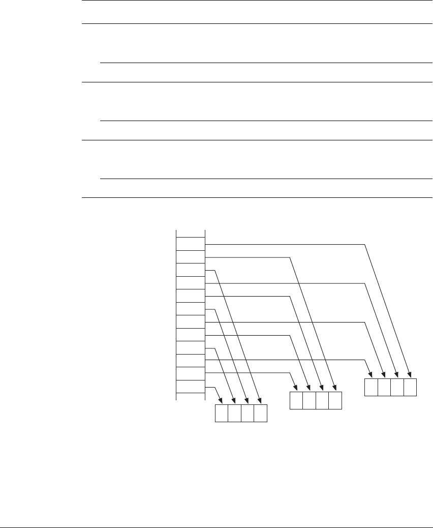
The Instruction Sets
A4-28 Copyright © 1996-1998, 2000, 2004-2008 ARM Limited. All rights reserved. ARM DDI 0406B
Figure A4-1 De-interleaving an array of 3-element structures
Store 2-element structure
Multiple structures VST2 (multiple 2-element structures) on page A8-772
From one lane VST2 (single 2-element structure from one lane) on page A8-774
Store 3-element structure
Multiple structures VST3 (multiple 3-element structures) on page A8-776
From one lane VST3 (single 3-element structure from one lane) on page A8-778
Store 4-element structure
Multiple structures VST4 (multiple 4-element structures) on page A8-780
From one lane VST4 (single 4-element structure from one lane) on page A8-782
Table A4-14 Element and structure load/store instructions (continued)
Instruction See
Z
3
D2
A[3].x
A[3].y
A[3].z
Z
2
Z
1
Z
0
A[2].x
A[2].y
A[2].z
A[1].x
A[1].y
A[1].z
A[0].x
A[0].y
A[0].z
Y
3
D1Y
2
Y
1
Y
0
X
3
D0X
2
X
1
X
0
Memory
Registers

The Instruction Sets
ARM DDI 0406B Copyright © 1996-1998, 2000, 2004-2008 ARM Limited. All rights reserved. A4-29
A4.12 Advanced SIMD and VFP register transfer instructions
Table A4-15 summarizes the extension register transfer instructions in the Advanced SIMD and VFP
instruction sets. These instructions transfer data from ARM core registers to extension registers, or from
extension registers to ARM core registers.
Advanced SIMD vectors, and single-precision and double-precision VFP registers, are all views of the same
extension register set. For details see Advanced SIMD and VFP extension registers on page A2-21.
Table A4-15 Extension register transfer instructions
Instruction See
Copy element from ARM core register to every element of
Advanced SIMD vector
VDUP (ARM core register) on page A8-594
Copy byte, halfword, or word from ARM core register to
extension register
VMOV (ARM core register to scalar) on
page A8-644
Copy byte, halfword, or word from extension register to ARM
core register
VMOV (scalar to ARM core register) on
page A8-646
Copy from single-precision VFP register to ARM core register,
or from ARM core register to single-precision VFP register
VMOV (between ARM core register and
single-precision register) on page A8-648
Copy two words from ARM core registers to consecutive
single-precision VFP registers, or from consecutive
single-precision VFP registers to ARM core registers
VMOV (between two ARM core registers and
two single-precision registers) on page A8-650
Copy two words from ARM core registers to doubleword
extension register, or from doubleword extension register to
ARM core registers
VMOV (between two ARM core registers and a
doubleword extension register) on page A8-652
Copy from Advanced SIMD and VFP extension System Register
to ARM core register
VMRS on page A8-658
VMRS on page B6-27 (system level view)
Copy from ARM core register to Advanced SIMD and VFP
extension System Register
VMSR on page A8-660
VMSR on page B6-29 (system level view)
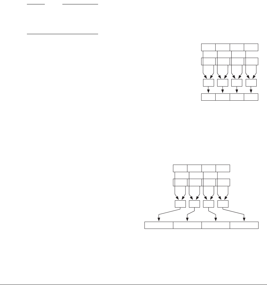
The Instruction Sets
A4-30 Copyright © 1996-1998, 2000, 2004-2008 ARM Limited. All rights reserved. ARM DDI 0406B
A4.13 Advanced SIMD data-processing operations
Advanced SIMD data-processing operations process registers containing vectors of elements of the same
type packed together, enabling the same operation to be performed on multiple items in parallel.
Instructions operate on vectors held in 64-bit or 128-bit registers. Figure A4-2 shows an operation on two
64-bit operand vectors, generating a 64-bit vector result.
Note
Figure A4-2 and other similar figures show 64-bit vectors that consist of four 16-bit elements, and 128-bit
vectors that consist of four 32-bit elements. Other element sizes produce similar figures, but with one, two,
eight, or sixteen operations performed in parallel instead of four.
Figure A4-2 Advanced SIMD instruction operating on 64-bit registers
Many Advanced SIMD instructions have variants that produce vectors of elements double the size of the
inputs. In this case, the number of elements in the result vector is the same as the number of elements in the
operand vectors, but each element, and the whole vector, is double the size.
Figure A4-3 shows an example of an Advanced SIMD instruction operating on 64-bit registers, and
generating a 128-bit result.
Figure A4-3 Advanced SIMD instruction producing wider result
There are also Advanced SIMD instructions that have variants that produce vectors containing elements half
the size of the inputs. Figure A4-4 on page A4-31 shows an example of an Advanced SIMD instruction
operating on one 128-bit register, and generating a 64-bit result.
Op
Dn
Dm
Dd
OpOpOp
Op
Dn
Dm
Qd
OpOpOp
The Instruction Sets
ARM DDI 0406B Copyright © 1996-1998, 2000, 2004-2008 ARM Limited. All rights reserved. A4-31
Figure A4-4 Advanced SIMD instruction producing narrower result
Some Advanced SIMD instructions do not conform to these standard patterns. Their operation patterns are
described in the individual instruction descriptions.
Advanced SIMD instructions that perform floating-point arithmetic use the ARM standard floating-point
arithmetic defined in Floating-point data types and arithmetic on page A2-32.
A4.13.1 Advanced SIMD parallel addition and subtraction
Table A4-16 shows the Advanced SIMD parallel add and subtract instructions.
Op
Qn
Dd
OpOpOp
Table A4-16 Advanced SIMD parallel add and subtract instructions
Instruction See
Vector Add VADD (integer) on page A8-536
VADD (floating-point) on page A8-538
Vector Add and Narrow, returning High Half VADDHN on page A8-540
Vector Add Long, Vector Add Wide VADDL, VADDW on page A8-542
Vector Halving Add, Vector Halving Subtract VHADD, VHSUB on page A8-600
Vector Pairwise Add and Accumulate Long VPADAL on page A8-682
Vector Pairwise Add VPADD (integer) on page A8-684
VPADD (floating-point) on page A8-686
Vector Pairwise Add Long VPADDL on page A8-688
Vector Rounding Add and Narrow, returning High Half VRADDHN on page A8-726
Vector Rounding Halving Add VRHADD on page A8-734
Vector Rounding Subtract and Narrow, returning High Half VRSUBHN on page A8-748
Vector Saturating Add VQADD on page A8-700
Vector Saturating Subtract VQSUB on page A8-724

The Instruction Sets
A4-32 Copyright © 1996-1998, 2000, 2004-2008 ARM Limited. All rights reserved. ARM DDI 0406B
A4.13.2 Bitwise Advanced SIMD data-processing instructions
Table A4-17 shows bitwise Advanced SIMD data-processing instructions. These operate on the doubleword
(64-bit) or quadword (128-bit) extension registers, and there is no division into vector elements.
Vector Subtract VSUB (integer) on page A8-788
VSUB (floating-point) on page A8-790
Vector Subtract and Narrow, returning High Half VSUBHN on page A8-792
Vector Subtract Long, Vector Subtract Wide VSUBL, VSUBW on page A8-794
Table A4-16 Advanced SIMD parallel add and subtract instructions (continued)
Instruction See
Table A4-17 Bitwise Advanced SIMD data-processing instructions
Instruction See
Vector Bitwise AND VAND (register) on page A8-544
Vector Bitwise Bit Clear (AND complement) VBIC (immediate) on page A8-546
VBIC (register) on page A8-548
Vector Bitwise Exclusive OR VEOR on page A8-596
Vector Bitwise Insert if False
VBIF, VBIT, VBSL on page A8-550
Vector Bitwise Insert if True
Vector Bitwise Move VMOV (immediate) on page A8-640
VMOV (register) on page A8-642
Vector Bitwise NOT VMVN (immediate) on page A8-668
VMVN (register) on page A8-670
Vector Bitwise OR VORR (immediate) on page A8-678
VORR (register) on page A8-680
Vector Bitwise OR NOT VORN (register) on page A8-676
Vector Bitwise Select VBIF, VBIT, VBSL on page A8-550

The Instruction Sets
ARM DDI 0406B Copyright © 1996-1998, 2000, 2004-2008 ARM Limited. All rights reserved. A4-33
A4.13.3 Advanced SIMD comparison instructions
Table A4-18 shows Advanced SIMD comparison instructions.
Table A4-18 Advanced SIMD comparison instructions
Instruction See
Vector Absolute Compare VACGE, VACGT, VACLE,VACLT on page A8-534
Vector Compare Equal VCEQ (register) on page A8-552
Vector Compare Equal to Zero VCEQ (immediate #0) on page A8-554
Vector Compare Greater Than or Equal VCGE (register) on page A8-556
Vector Compare Greater Than or Equal to Zero VCGE (immediate #0) on page A8-558
Vector Compare Greater Than VCGT (register) on page A8-560
Vector Compare Greater Than Zero VCGT (immediate #0) on page A8-562
Vector Compare Less Than or Equal to Zero VCLE (immediate #0) on page A8-564
Vector Compare Less Than Zero VCLT (immediate #0) on page A8-568
Vec t or Te st B it s VTST on page A8-802

The Instruction Sets
A4-34 Copyright © 1996-1998, 2000, 2004-2008 ARM Limited. All rights reserved. ARM DDI 0406B
A4.13.4 Advanced SIMD shift instructions
Table A4-19 lists the shift instructions in the Advanced SIMD instruction set.
Table A4-19 Advanced SIMD shift instructions
Instruction See
Vector Saturating Rounding Shift Left VQRSHL on page A8-714
Vector Saturating Rounding Shift Right and Narrow VQRSHRN, VQRSHRUN on page A8-716
Vector Saturating Shift Left VQSHL (register) on page A8-718
VQSHL, VQSHLU (immediate) on page A8-720
Vector Saturating Shift Right and Narrow VQSHRN, VQSHRUN on page A8-722
Vector Rounding Shift Left VRSHL on page A8-736
Vector Rounding Shift Right VRSHR on page A8-738
Vector Rounding Shift Right and Accumulate VRSRA on page A8-746
Vector Rounding Shift Right and Narrow VRSHRN on page A8-740
Vector Shift Left VSHL (immediate) on page A8-750
VSHL (register) on page A8-752
Vector Shift Left Long VSHLL on page A8-754
Vector Shift Right VSHR on page A8-756
Vector Shift Right and Narrow VSHRN on page A8-758
Vector Shift Left and Insert VSLI on page A8-760
Vector Shift Right and Accumulate VSRA on page A8-764
Vector Shift Right and Insert VSRI on page A8-766

The Instruction Sets
ARM DDI 0406B Copyright © 1996-1998, 2000, 2004-2008 ARM Limited. All rights reserved. A4-35
A4.13.5 Advanced SIMD multiply instructions
Table A4-20 summarizes the Advanced SIMD multiply instructions.
Advanced SIMD multiply instructions can operate on vectors of:
• 8-bit, 16-bit, or 32-bit unsigned integers
• 8-bit, 16-bit, or 32-bit signed integers
• 8-bit or 16-bit polynomials over {0,1} (
VMUL
and
VMULL
only)
• single-precision (32-bit) floating-point numbers.
They can also act on one vector and one scalar.
Long instructions have doubleword (64-bit) operands, and produce quadword (128-bit) results. Other
Advanced SIMD multiply instructions can have either doubleword or quadword operands, and produce
results of the same size.
VFP multiply instructions can operate on:
• single-precision (32-bit) floating-point numbers
• double-precision (64-bit) floating-point numbers.
Some VFP implementations do not support double-precision numbers.
Table A4-20 Advanced SIMD multiply instructions
Instruction See
Vector Multiply Accumulate VMLA, VMLAL, VMLS, VMLSL (integer) on
page A8-634
VMLA, VMLS (floating-point) on page A8-636
VMLA, VMLAL, VMLS, VMLSL (by scalar) on
page A8-638
Vector Multiply Accumulate Long
Vector Multiply Subtract
Vector Multiply Subtract Long
Vector Multiply VMUL, VMULL (integer and polynomial) on
page A8-662
VMUL (floating-point) on page A8-664
VMUL, VMULL (by scalar) on page A8-666
Vector Multiply Long
Vector Saturating Doubling Multiply Accumulate Long
VQDMLAL, VQDMLSL on page A8-702
Vector Saturating Doubling Multiply Subtract Long
Vector Saturating Doubling Multiply Returning High Half VQDMULH on page A8-704
Vector Saturating Rounding Doubling Multiply Returning
High Half
VQRDMULH on page A8-712
Vector Saturating Doubling Multiply Long VQDMULL on page A8-706

The Instruction Sets
A4-36 Copyright © 1996-1998, 2000, 2004-2008 ARM Limited. All rights reserved. ARM DDI 0406B
A4.13.6 Miscellaneous Advanced SIMD data-processing instructions
Table A4-21 shows miscellaneous Advanced SIMD data-processing instructions.
Table A4-21 Miscellaneous Advanced SIMD data-processing instructions
Instruction See
Vector Absolute Difference and Accumulate VABA, VABAL on page A8-526
Vector Absolute Difference VABD, VABDL (integer) on page A8-528
VABD (floating-point) on page A8-530
Vec t or A bs ol u te VABS on page A8-532
Vector Convert between floating-point and
fixed point
VCVT (between floating-point and fixed-point, Advanced SIMD) on
page A8-580
Vector Convert between floating-point and
integer
VCVT (between floating-point and integer, Advanced SIMD) on
page A8-576
Vector Convert between half-precision and
single-precision
VCVT (between half-precision and single-precision, Advanced
SIMD) on page A8-586
Vector Count Leading Sign Bits VCLS on page A8-566
Vector Count Leading Zeros VCLZ on page A8-570
Vector Count Set Bits VCNT on page A8-574
Vector Duplicate scalar VDUP (scalar) on page A8-592
Vector Extract VEXT on page A8-598
Vector Move and Narrow VMOVN on page A8-656
Vector Move Long VMOVL on page A8-654
Vector Maximum, Minimum VMAX, VMIN (integer) on page A8-630
VMAX, VMIN (floating-point) on page A8-632
Vec t or N ega t e VNEG on page A8-672
Vector Pairwise Maximum, Minimum VPMAX, VPMIN (integer) on page A8-690
VPMAX, VPMIN (floating-point) on page A8-692
Vector Reciprocal Estimate VRECPE on page A8-728
Vector Reciprocal Step VRECPS on page A8-730
Vector Reciprocal Square Root Estimate VRSQRTE on page A8-742

The Instruction Sets
ARM DDI 0406B Copyright © 1996-1998, 2000, 2004-2008 ARM Limited. All rights reserved. A4-37
Vector Reciprocal Square Root Step VRSQRTS on page A8-744
Ve ct o r R ev er s e VREV16, VREV32, VREV64 on page A8-732
Vector Saturating Absolute VQABS on page A8-698
Vector Saturating Move and Narrow VQMOVN, VQMOVUN on page A8-708
Vector Saturating Negate VQNEG on page A8-710
Ve ct o r S wa p VSWP on page A8-796
Vector Table Lookup VTBL, VTBX on page A8-798
Vector Transpose VTRN on page A8-800
Vector Unzip VUZP on page A8-804
Vector Zip VZIP on page A8-806
Table A4-21 Miscellaneous Advanced SIMD data-processing instructions (continued)
Instruction See

The Instruction Sets
A4-38 Copyright © 1996-1998, 2000, 2004-2008 ARM Limited. All rights reserved. ARM DDI 0406B
A4.14 VFP data-processing instructions
Table A4-22 summarizes the data-processing instructions in the VFP instruction set.
For details of the floating-point arithmetic used by VFP instructions, see Floating-point data types and
arithmetic on page A2-32.
Table A4-22 VFP data-processing instructions
Instruction See
Absolute value VABS on page A8-532
Add VADD (floating-point) on page A8-538
Compare (optionally with exceptions enabled) VCMP, VCMPE on page A8-572
Convert between floating-point and integer VCVT, VCVTR (between floating-point and integer, VFP) on
page A8-578
Convert between floating-point and fixed-point VCVT (between floating-point and fixed-point, VFP) on
page A8-582
Convert between double-precision and
single-precision
VCVT (between double-precision and single-precision) on
page A8-584
Convert between half-precision and single-precision VCVTB, VCVTT (between half-precision and
single-precision, VFP) on page A8-588
Divide VDIV on page A8-590
Multiply Accumulate, Multiply Subtract VMLA, VMLS (floating-point) on page A8-636
Move immediate value to extension register VMOV (immediate) on page A8-640
Copy from one extension register to another VMOV (register) on page A8-642
Multiply VMUL (floating-point) on page A8-664
Negate (invert the sign bit) VNEG on page A8-672
Multiply Accumulate and Negate, Multiply Subtract
and Negate, Multiply and Negate
VNMLA, VNMLS, VNMUL on page A8-674
Square Root VSQRT on page A8-762
Subtract VSUB (floating-point) on page A8-790

ARM DDI 0406B Copyright © 1996-1998, 2000, 2004-2008 ARM Limited. All rights reserved. A5-1
Chapter A5
ARM Instruction Set Encoding
This chapter describes the encoding of the ARM instruction set. It contains the following sections:
•ARM instruction set encoding on page A5-2
•Data-processing and miscellaneous instructions on page A5-4
•Load/store word and unsigned byte on page A5-19
•Media instructions on page A5-21
•Branch, branch with link, and block data transfer on page A5-27
•Supervisor Call, and coprocessor instructions on page A5-28
•Unconditional instructions on page A5-30.
Note
• Architecture variant information in this chapter describes the architecture variant or extension in
which the instruction encoding was introduced into the ARM instruction set. All means that the
instruction encoding was introduced in ARMv4 or earlier, and so is in all variants of the ARM
instruction set covered by this manual.
• In the decode tables in this chapter, an entry of - for a field value means the value of the field does
not affect the decoding.

ARM Instruction Set Encoding
A5-2 Copyright © 1996-1998, 2000, 2004-2008 ARM Limited. All rights reserved. ARM DDI 0406B
A5.1 ARM instruction set encoding
The ARM instruction stream is a sequence of word-aligned words. Each ARM instruction is a single 32-bit
word in that stream.
Table A5-1 shows the major subdivisions of the ARM instruction set, determined by bits [31:25,4].
Most ARM instructions can be conditional, with a condition determined by bits [31:28] of the instruction,
the cond field. For details see The condition field. This applies to all instructions except those with the cond
field equal to 0b1111.
A5.1.1 The condition field
Every conditional instruction contains a 4-bit condition code field in bits 31 to 28:
This field contains one of the values 0b0000-0b1110 described in Table A8-1 on page A8-8. Most
instruction mnemonics can be extended with the letters defined in the mnemonic extension field.
If the always (
AL
) condition is specified, the instruction is executed irrespective of the value of the condition
code flags. The absence of a condition code on an instruction mnemonic implies the
AL
condition code.
313029282726252423222120191817161514131211109876543210
cond op1 op
Table A5-1 ARM instruction encoding
cond op1 op Instruction classes
not 1111 00x - Data-processing and miscellaneous instructions on page A5-4.
010 - Load/store word and unsigned byte on page A5-19.
011 0 Load/store word and unsigned byte on page A5-19.
1Media instructions on page A5-21.
10x - Branch, branch with link, and block data transfer on page A5-27.
11x - Supervisor Call, and coprocessor instructions on page A5-28.
Includes VFP instructions and Advanced SIMD data transfers, see Chapter A7 Advanced
SIMD and VFP Instruction Encoding.
1111 - - If the cond field is 0b1111, the instruction can only be executed unconditionally, see
Unconditional instructions on page A5-30.
Includes Advanced SIMD instructions, see Chapter A7 Advanced SIMD and VFP
Instruction Encoding.
313029282726252423222120191817161514131211109876543210
cond

ARM Instruction Set Encoding
ARM DDI 0406B Copyright © 1996-1998, 2000, 2004-2008 ARM Limited. All rights reserved. A5-3
A5.1.2 UNDEFINED and UNPREDICTABLE instruction set space
An attempt to execute an unallocated instruction results in either:
• Unpredictable behavior. The instruction is described as UNPREDICTABLE.
• An Undefined Instruction exception. The instruction is described as UNDEFINED.
An instruction is UNDEFINED if it is declared as UNDEFINED in an instruction description, or in this chapter.
An instruction is UNPREDICTABLE if:
• it is declared as UNPREDICTABLE in an instruction description or in this chapter
• the pseudocode for that encoding does not indicate that a different special case applies, and a bit
marked (0) or (1) in the encoding diagram of an instruction is not 0 or 1 respectively.
Unless otherwise specified:
• ARM instructions introduced in an architecture variant are UNDEFINED in earlier architecture variants.
• ARM instructions introduced in one or more architecture extensions are UNDEFINED if none of those
extensions are implemented.
A5.1.3 The PC and the use of 0b1111 as a register specifier
In ARM instructions, the use of 0b1111 as a register specifier specifies the PC.
Many instructions are UNPREDICTABLE if they use 0b1111 as a register specifier. This is specified by
pseudocode in the instruction description.
Note
Use of the PC as the base register in any store instruction is deprecated in ARMv7.
A5.1.4 The SP and the use of 0b1101 as a register specifier
In ARM instructions, the use of 0b1101 as a register specifier specifies the SP.
ARM deprecates:
• using SP for any purpose other than as a stack pointer
• using the SP in ARM instructions in ways other that those listed in 32-bit Thumb instruction support
for R13 on page A6-4, except that ARM does not deprecate the use of instructions of the following
form that write a word-aligned address to SP:
SUB SP, <Rd>, #<const>

ARM Instruction Set Encoding
A5-4 Copyright © 1996-1998, 2000, 2004-2008 ARM Limited. All rights reserved. ARM DDI 0406B
A5.2 Data-processing and miscellaneous instructions
Table A5-2 shows the allocation of encodings in this space.
313029282726252423222120191817161514131211109876543210
cond 0 0 op op1 op2
Table A5-2 Data-processing and miscellaneous instructions
op op1 op2 Instruction or instruction class Variant
0 not 10xx0 xxx0 Data-processing (register) on page A5-5 -
0xx1 Data-processing (register-shifted register) on page A5-7 -
10xx0 0xxx Miscellaneous instructions on page A5-18 -
1xx0 Halfword multiply and multiply-accumulate on page A5-13 -
0xxxx 1001 Multiply and multiply-accumulate on page A5-12 -
1xxxx 1001 Synchronization primitives on page A5-16 -
not 0xx1x 1011 Extra load/store instructions on page A5-14 -
11x1 Extra load/store instructions on page A5-14 -
0xx1x 1011 Extra load/store instructions (unprivileged) on page A5-15 -
11x1 Extra load/store instructions (unprivileged) on page A5-15 -
1 not 10xx0 - Data-processing (immediate) on page A5-8 -
10000 - 16-bit immediate load (MOV (immediate) on page A8-194) v6T2
10100 - High halfword 16-bit immediate load (MOVT on page A8-200) v6T2
10x10 - MSR (immediate), and hints on page A5-17 -

ARM Instruction Set Encoding
ARM DDI 0406B Copyright © 1996-1998, 2000, 2004-2008 ARM Limited. All rights reserved. A5-5
A5.2.1 Data-processing (register)
If op1 == 0b10xx0, see Data-processing and miscellaneous instructions on page A5-4.
Table A5-3 shows the allocation of encodings in this space. These encodings are in all architecture variants.
313029282726252423222120191817161514131211109876543210
cond 0 0 0 op1 op2 op3 0
Table A5-3 Data-processing (register) instructions
op1 op2 op3 Instruction See
0000x - - Bitwise AND AND (register) on page A8-36
0001x - - Bitwise Exclusive OR EOR (register) on page A8-96
0010x - - Subtract SUB (register) on page A8-422
0011x - - Reverse Subtract RSB (register) on page A8-286
0100x - - Add ADD (register) on page A8-24
0101x - - Add with Carry ADC (register) on page A8-16
0110x - - Subtract with Carry SBC (register) on page A8-304
0111x - - Reverse Subtract with Carry RSC (register) on page A8-292
10001 - - Test TST (register) on page A8-456
10011 - - Test Equivalence TEQ (register) on page A8-450
10101 - - Compare CMP (register) on page A8-82
10111 - - Compare Negative CMN (register) on page A8-76
1100x - - Bitwise OR ORR (register) on page A8-230
1101x 00000 00 Move MOV (register) on page A8-196
not 00000 00 Logical Shift Left LSL (immediate) on page A8-178
- 01 Logical Shift Right LSR (immediate) on page A8-182
- 10 Arithmetic Shift Right ASR (immediate) on page A8-40
00000 11 Rotate Right with Extend RRX on page A8-282
not 00000 11 Rotate Right ROR (immediate) on page A8-278

ARM Instruction Set Encoding
A5-6 Copyright © 1996-1998, 2000, 2004-2008 ARM Limited. All rights reserved. ARM DDI 0406B
1110x - - Bitwise Bit Clear BIC (register) on page A8-52
1111x - - Bitwise NOT MVN (register) on page A8-216
Table A5-3 Data-processing (register) instructions (continued)
op1 op2 op3 Instruction See

ARM Instruction Set Encoding
ARM DDI 0406B Copyright © 1996-1998, 2000, 2004-2008 ARM Limited. All rights reserved. A5-7
A5.2.2 Data-processing (register-shifted register)
If op1 == 0b10xx0, see Data-processing and miscellaneous instructions on page A5-4.
Table A5-4 shows the allocation of encodings in this space. These encodings are in all architecture variants.
313029282726252423222120191817161514131211109876543210
cond 0 0 0 op1 0 op2 1
Table A5-4 Data-processing (register-shifted register) instructions
op1 op2 Instruction See
0000x - Bitwise AND AND (register-shifted register) on page A8-38
0001x - Bitwise Exclusive OR EOR (register-shifted register) on page A8-98
0010x - Subtract SUB (register-shifted register) on page A8-424
0011x - Reverse Subtract RSB (register-shifted register) on page A8-288
0100x - Add ADD (register-shifted register) on page A8-26
0101x - Add with Carry ADC (register-shifted register) on page A8-18
0110x - Subtract with Carry SBC (register-shifted register) on page A8-306
0111x - Reverse Subtract with Carry RSC (register-shifted register) on page A8-294
10001 - Test TST (register-shifted register) on page A8-458
10011 - Test Equivalence TEQ (register-shifted register) on page A8-452
10101 - Compare CMP (register-shifted register) on page A8-84
10111 - Compare Negative CMN (register-shifted register) on page A8-78
1100x - Bitwise OR ORR (register-shifted register) on page A8-232
1101x 00 Logical Shift Left LSL (register) on page A8-180
01 Logical Shift Right LSR (register) on page A8-184
10 Arithmetic Shift Right ASR (register) on page A8-42
11 Rotate Right ROR (register) on page A8-280
1110x - Bitwise Bit Clear BIC (register-shifted register) on page A8-54
1111x - Bitwise NOT MVN (register-shifted register) on page A8-218

ARM Instruction Set Encoding
A5-8 Copyright © 1996-1998, 2000, 2004-2008 ARM Limited. All rights reserved. ARM DDI 0406B
A5.2.3 Data-processing (immediate)
If op == 0b10xx0, see Data-processing and miscellaneous instructions on page A5-4.
Table A5-5 shows the allocation of encodings in this space. These encodings are in all architecture variants.
These instructions all have modified immediate constants, rather than a simple 12-bit binary number. This
provides a more useful range of values. For details see Modified immediate constants in ARM instructions
on page A5-9.
313029282726252423222120191817161514131211109876543210
cond 0 0 1 op Rn
Table A5-5 Data-processing (immediate) instructions
op Rn Instruction See
0000x - Bitwise AND AND (immediate) on page A8-34
0001x - Bitwise Exclusive OR EOR (immediate) on page A8-94
0010x not 1111 Subtract SUB (immediate, ARM) on page A8-420
1111 Form PC-relative address ADR on page A8-32
0011x - Reverse Subtract RSB (immediate) on page A8-284
0100x not 1111 Add ADD (immediate, ARM) on page A8-22
1111 Form PC-relative address ADR on page A8-32
0101x - Add with Carry ADC (immediate) on page A8-14
0110x - Subtract with Carry SBC (immediate) on page A8-302
0111x - Reverse Subtract with Carry RSC (immediate) on page A8-290
10001 - Test TST (immediate) on page A8-454
10011 - Test Equivalence TEQ (immediate) on page A8-448
10101 - Compare CMP (immediate) on page A8-80
10111 - Compare Negative CMN (immediate) on page A8-74
1100x - Bitwise OR ORR (immediate) on page A8-228
1101x - Move MOV (immediate) on page A8-194
1110x - Bitwise Bit Clear BIC (immediate) on page A8-50
1111x - Bitwise NOT MVN (immediate) on page A8-214

ARM Instruction Set Encoding
ARM DDI 0406B Copyright © 1996-1998, 2000, 2004-2008 ARM Limited. All rights reserved. A5-9
A5.2.4 Modified immediate constants in ARM instructions
Table A5-6 shows the range of modified immediate constants available in ARM data-processing
instructions, and how they are encoded in the a, b, c, d, e, f, g, h, and rotation fields in the instruction.
Note
The range of values available in ARM modified immediate constants is slightly different from the range of
values available in 32-bit Thumb instructions. See Modified immediate constants in Thumb instructions on
page A6-17.
15141312111098765432101514131211109876543210
rotation a b c d e f g h
Table A5-6 Encoding of modified immediates in ARM processing instructions
rotation <const> a
a. In this table, the immediate constant value is shown in binary form, to relate
abcdefgh
to the encoding diagram. In assembly syntax, the immediate value
is specified in the usual way (a decimal number by default).
0000
00000000 00000000 00000000 abcdefgh
0001
gh000000 00000000 00000000 00abcdef
0010
efgh0000 00000000 00000000 0000abcd
0011
cdefgh00 00000000 00000000 000000ab
0100
abcdefgh 00000000 00000000 00000000
..
8-bit values shifted to other even-numbered positions..
..
1001
00000000 00abcdef gh000000 00000000
..
8-bit values shifted to other even-numbered positions..
..
1110
00000000 00000000 0000abcd efgh0000
1111
00000000 00000000 000000ab cdefgh00

ARM Instruction Set Encoding
A5-10 Copyright © 1996-1998, 2000, 2004-2008 ARM Limited. All rights reserved. ARM DDI 0406B
Carry out
A logical instruction with rotation == 0b0000 does not affect APSR.C. Otherwise, a logical instruction that
sets the flags sets APSR.C to the value of bit [31] of the modified immediate constant.
Constants with multiple encodings
Some constant values have multiple possible encodings. In this case, a UAL assembler must select the
encoding with the lowest unsigned value of the rotation field. This is the encoding that appears first in
Table A5-6 on page A5-9. For example, the constant
#3
must be encoded with (rotation, abcdefgh) ==
(
0b0000
,
0b00000011
), not (
0b0001
,
0b00001100
), (
0b0010
,
0b00110000
), or (
0b0011
,
0b11000000
).
In particular, this means that all constants in the range 0-255 are encoded with rotation ==
0b0000
, and
permitted constants outside that range are encoded with rotation !=
0b0000
. A flag-setting logical instruction
with a modified immediate constant therefore leaves APSR.C unchanged if the constant is in the range 0-255
and sets it to the most significant bit of the constant otherwise. This matches the behavior of Thumb
modified immediate constants for all constants that are permitted in both the ARM and Thumb instruction
sets.
An alternative syntax is available for a modified immediate constant that permits the programmer to specify
the encoding directly. In this syntax,
#<const>
is instead written as
#<byte>,#<rot>
, where:
<byte>
is the numeric value of abcdefgh, in the range 0-255
<rot>
is twice the numeric value of rotation, an even number in the range 0-30.
This syntax permits all ARM data-processing instructions with modified immediate constants to be
disassembled to assembler syntax that will assemble to the original instruction.
This syntax also makes it possible to write variants of some flag-setting logical instructions that have
different effects on APSR.C to those obtained with the normal
#<const>
syntax. For example,
ANDS R1,R2,#12,#2
has the same behavior as
ANDS R1,R2,#3
except that it sets APSR.C to 0 instead of leaving
it unchanged. Such variants of flag-setting logical instructions do not have equivalents in the Thumb
instruction set, and their use is deprecated.
Operation
// ARMExpandImm()
// ==============
bits(32) ARMExpandImm(bits(12) imm12)
// APSR.C argument to following function call does not affect the imm32 result.
(imm32, -) = ARMExpandImm_C(imm12, APSR.C);
return imm32;
// ARMExpandImm_C()
// ================
(bits(32), bit) ARMExpandImm_C(bits(12) imm12, bit carry_in)

ARM Instruction Set Encoding
ARM DDI 0406B Copyright © 1996-1998, 2000, 2004-2008 ARM Limited. All rights reserved. A5-11
unrotated_value = ZeroExtend(imm12<7:0>, 32);
(imm32, carry_out) = Shift_C(unrotated_value, SRType_ROR, 2*UInt(imm12<11:8>), carry_in);
return (imm32, carry_out);

ARM Instruction Set Encoding
A5-12 Copyright © 1996-1998, 2000, 2004-2008 ARM Limited. All rights reserved. ARM DDI 0406B
A5.2.5 Multiply and multiply-accumulate
Table A5-7 shows the allocation of encodings in this space.
313029282726252423222120191817161514131211109876543210
cond 0000 op 1001
Table A5-7 Multiply and multiply-accumulate instructions
op Instruction See Variant
000x Multiply MUL on page A8-212 All
001x Multiply Accumulate MLA on page A8-190 All
0100 Unsigned Multiply Accumulate Accumulate Long UMAAL on page A8-482 v6
0101 UNDEFINED --
0110 Multiply and Subtract MLS on page A8-192 v6T2
0111 UNDEFINED --
100x Unsigned Multiply Long UMULL on page A8-486 All
101x Unsigned Multiply Accumulate Long UMLAL on page A8-484 All
110x Signed Multiply Long SMULL on page A8-356 All
111x Signed Multiply Accumulate Long SMLAL on page A8-334 All

ARM Instruction Set Encoding
ARM DDI 0406B Copyright © 1996-1998, 2000, 2004-2008 ARM Limited. All rights reserved. A5-13
A5.2.6 Saturating addition and subtraction
Table A5-8 shows the allocation of encodings in this space. These encodings are all available in ARMv5TE
and above, and are UNDEFINED in earlier variants of the architecture.
A5.2.7 Halfword multiply and multiply-accumulate
Table A5-9 shows the allocation of encodings in this space.
These encodings are signed multiply (
SMUL
) and signed multiply-accumulate (
SMLA
) instructions, operating
on 16-bit values, or mixed 16-bit and 32-bit values. The results and accumulators are 32-bit or 64-bit.
These encodings are all available in ARMv5TE and above, and are UNDEFINED in earlier variants of the
architecture.
313029282726252423222120191817161514131211109876543210
cond 00010 op 0 0101
Table A5-8 Saturating addition and subtraction instructions
op Instruction See
00 Saturating Add QADD on page A8-250
01 Saturating Subtract QSUB on page A8-264
10 Saturating Double and Add QDADD on page A8-258
11 Saturating Double and Subtract QDSUB on page A8-260
313029282726252423222120191817161514131211109876543210
cond 00010 op1 0 1 op0
Table A5-9 Halfword multiply and multiply-accumulate instructions
op1 op Instruction See
00 - Signed 16-bit multiply, 32-bit accumulate SMLABB, SMLABT, SMLATB, SMLATT on
page A8-330
01 0 Signed 16-bit x 32-bit multiply, 32-bit accumulate SMLAWB, SMLAWT on page A8-340
01 1 Signed 16-bit x 32-bit multiply, 32-bit result SMULWB, SMULWT on page A8-358
10 - Signed 16-bit multiply, 64-bit accumulate SMLALBB, SMLALBT, SMLALTB, SMLALTT
on page A8-336
11 - Signed 16-bit multiply, 32-bit result SMULBB, SMULBT, SMULTB, SMULTT on
page A8-354

ARM Instruction Set Encoding
A5-14 Copyright © 1996-1998, 2000, 2004-2008 ARM Limited. All rights reserved. ARM DDI 0406B
A5.2.8 Extra load/store instructions
If op1 == 0b0xx1x or op2 == 0b00, see Data-processing and miscellaneous instructions on page A5-4.
Table A5-10 shows the allocation of encodings in this space.
313029282726252423222120191817161514131211109876543210
cond 0 0 0 op1 Rn 1 op2 1
Table A5-10 Extra load/store instructions
op2 op1 Rn Instruction See Variant
01 xx0x0 - Store Halfword STRH (register) on page A8-412 All
xx0x1 - Load Halfword LDRH (register) on page A8-156 All
xx1x0 - Store Halfword STRH (immediate, ARM) on page A8-410 All
xx1x1 not 1111 Load Halfword LDRH (immediate, ARM) on page A8-152 All
1111 Load Halfword LDRH (literal) on page A8-154 All
10 xx0x0 - Load Dual LDRD (register) on page A8-140 v5TE
xx0x1 - Load Signed Byte LDRSB (register) on page A8-164 All
xx1x0 not 1111 Load Dual LDRD (immediate) on page A8-136 v5TE
1111 Load Dual LDRD (literal) on page A8-138 v5TE
xx1x1 not 1111 Load Signed Byte LDRSB (immediate) on page A8-160 All
1111 Load Signed Byte LDRSB (literal) on page A8-162 All
11 xx0x0 - Store Dual STRD (register) on page A8-398 All
xx0x1 - Load Signed Halfword LDRSH (register) on page A8-172 All
xx1x0 - Store Dual STRD (immediate) on page A8-396 All
xx1x1 not 1111 Load Signed Halfword LDRSH (immediate) on page A8-168 All
1111 Load Signed Halfword LDRSH (literal) on page A8-170 All

ARM Instruction Set Encoding
ARM DDI 0406B Copyright © 1996-1998, 2000, 2004-2008 ARM Limited. All rights reserved. A5-15
A5.2.9 Extra load/store instructions (unprivileged)
If op2 == 0b00, see Data-processing and miscellaneous instructions on page A5-4.
Table A5-11 shows the allocation of encodings in this space. The instruction encodings are all available in
ARMv6T2 and above, and are UNDEFINED in earlier variants of the architecture.
313029282726252423222120191817161514131211109876543210
cond 0 0 0 0 1 op Rt 1 op2 1
Table A5-11 Extra load/store instructions (unprivileged)
op2 op Rt Instruction See
01 0 - Store Halfword Unprivileged STRHT on page A8-414
1 - Load Halfword Unprivileged LDRHT on page A8-158
1x 0 xxx0 UNPREDICTABLE -
xxx1 UNDEFINED -
10 1 - Load Signed Byte Unprivileged LDRSBT on page A8-166
11 1 - Load Signed Halfword Unprivileged LDRSHT on page A8-174

ARM Instruction Set Encoding
A5-16 Copyright © 1996-1998, 2000, 2004-2008 ARM Limited. All rights reserved. ARM DDI 0406B
A5.2.10 Synchronization primitives
Table A5-12 shows the allocation of encodings in this space.
Other encodings in this space are UNDEFINED.
313029282726252423222120191817161514131211109876543210
cond 0001 op 1001
Table A5-12 Synchronization primitives
op Instruction See Variant
0x00 Swap Word, Swap Byte SWP, SWPB on page A8-432 a
a. Use of these instructions is deprecated.
All
1000 Store Register Exclusive STREX on page A8-400 v6
1001 Load Register Exclusive LDREX on page A8-142 v6
1010 Store Register Exclusive Doubleword STREXD on page A8-404 v6K
1011 Load Register Exclusive Doubleword LDREXD on page A8-146 v6K
1100 Store Register Exclusive Byte STREXB on page A8-402 v6K
1101 Load Register Exclusive Byte LDREXB on page A8-144 v6K
1110 Store Register Exclusive Halfword STREXH on page A8-406 v6K
1111 Load Register Exclusive Halfword LDREXH on page A8-148 v6K

ARM Instruction Set Encoding
ARM DDI 0406B Copyright © 1996-1998, 2000, 2004-2008 ARM Limited. All rights reserved. A5-17
A5.2.11 MSR (immediate), and hints
Table A5-13 shows the allocation of encodings in this space.
Other encodings in this space are unallocated hints. They execute as NOPs, but software must not use them.
313029282726252423222120191817161514131211109876543210
cond 0 0 1 1 0 op 1 0 op1 op2
Table A5-13 MSR (immediate), and hints
op op1 op2 Instruction See Variant
0 0000 00000000 No Operation hint NOP on page A8-222 v6K, v6T2
00000001 Yield hint YIELD on page A8-812 v6K
00000010 Wait For Event hint WFE on page A8-808 v6K
00000011 Wait For Interrupt hint WFI on page A8-810 v6K
00000100 Send Event hint SEV on page A8-316 v6K
1111xxxx Debug hint DBG on page A8-88 v7
0100 - Move to Special Register,
application level
MSR (immediate) on page A8-208 All
1x00 -
xx01 - Move to Special Register, system
level
MSR (immediate) on page B6-12 All
xx1x -
1 - - Move to Special Register, system
level
MSR (immediate) on page B6-12 All

ARM Instruction Set Encoding
A5-18 Copyright © 1996-1998, 2000, 2004-2008 ARM Limited. All rights reserved. ARM DDI 0406B
A5.2.12 Miscellaneous instructions
Table A5-14 shows the allocation of encodings in this space.
Other encodings in this space are UNDEFINED.
313029282726252423222120191817161514131211109876543210
cond 00010 op 0 op1 0 op2
Table A5-14 Miscellaneous instructions
op2 op op1 Instruction or instruction class See Variant
000 x0 xxxx Move Special Register to Register MRS on page A8-206
MRS on page B6-10
All
01 xx00 Move to Special Register, application level MSR (register) on page A8-210 All
xx01
xx1x
Move to Special Register, system level MSR (register) on page B6-14 All
11 - Move to Special Register, system level MSR (register) on page B6-14 All
001 01 - Branch and Exchange BX on page A8-62 v4T
11 - Count Leading Zeros CLZ on page A8-72 v6
010 01 - Branch and Exchange Jazelle BXJ on page A8-64 v5TEJ
011 01 - Branch with Link and Exchange BLX (register) on page A8-60 v5T
101 - - Saturating addition and subtraction Saturating addition and
subtraction on page A5-13
-
111 01 - Breakpoint BKPT on page A8-56 v5T
11 - Secure Monitor Call SMC (previously SMI) on
page B6-18
Security
Extensions

ARM Instruction Set Encoding
ARM DDI 0406B Copyright © 1996-1998, 2000, 2004-2008 ARM Limited. All rights reserved. A5-19
A5.3 Load/store word and unsigned byte
These instructions have either A == 0 or B == 0. For instructions with A == 1 and B == 1, see Media
instructions on page A5-21.
Table A5-15 shows the allocation of encodings in this space. These encodings are in all architecture
variants.
313029282726252423222120191817161514131211109876543210
cond 0 1 A op1 Rn B
Table A5-15 Single data transfer instructions
A op1 B Rn Instruction See
0 xx0x0 not 0x010 - - Store Register STR (immediate, ARM) on
page A8-384
1 xx0x0 not 0x010 0 - Store Register STR (register) on page A8-386
0 0x010 - - Store Register Unprivileged STRT on page A8-416
1 0x010 0 -
0 xx0x1 not 0x011 - not 1111 Load Register (immediate) LDR (immediate, ARM) on
page A8-120
xx0x1 not 0x011 - 1111 Load Register (literal) LDR (literal) on page A8-122
1 xx0x1 not 0x011 0 - Load Register LDR (register) on page A8-124
0 0x011 - - Load Register Unprivileged LDRT on page A8-176
1 0x011 0 -
0 xx1x0 not 0x110 - - Store Register Byte (immediate) STRB (immediate, ARM) on
page A8-390
1 xx1x0 not 0x110 0 - Store Register Byte (register) STRB (register) on page A8-392
0 0x110 - - Store Register Byte Unprivileged STRBT on page A8-394
1 0x110 0 -
0 xx1x1 not 0x111 - not 1111 Load Register Byte (immediate) LDRB (immediate, ARM) on
page A8-128
xx1x1 not 0x111 - 1111 Load Register Byte (literal) LDRB (literal) on page A8-130

ARM Instruction Set Encoding
A5-20 Copyright © 1996-1998, 2000, 2004-2008 ARM Limited. All rights reserved. ARM DDI 0406B
1 xx1x1 not 0x111 0 - Load Register Byte (register) LDRB (register) on page A8-132
0 0x111 - - Load Register Byte Unprivileged LDRBT on page A8-134
1 0x111 0 -
Table A5-15 Single data transfer instructions (continued)
A op1 B Rn Instruction See

ARM Instruction Set Encoding
ARM DDI 0406B Copyright © 1996-1998, 2000, 2004-2008 ARM Limited. All rights reserved. A5-21
A5.4 Media instructions
Table A5-16 shows the allocation of encodings in this space.
Other encodings in this space are UNDEFINED.
313029282726252423222120191817161514131211109876543210
cond 0 1 1 op1 Rd op2 1 Rn
Table A5-16 Media instructions
op1 op2 Rd Rn Instructions See Variant
000xx - - - - Parallel addition and
subtraction, signed on
page A5-22
-
001xx - - - - Parallel addition and
subtraction, unsigned on
page A5-23
-
01xxx - - - - Packing, unpacking,
saturation, and reversal on
page A5-24
-
10xxx - - - - Signed multiplies on
page A5-26
-
11000 000 1111 - Unsigned Sum of Absolute
Differences
USAD8 on page A8-500 v6
000 not 1111 - Unsigned Sum of Absolute
Differences and Accumulate
USADA8 on page A8-502 v6
1101x x10 - - Signed Bit Field Extract SBFX on page A8-308 v6T2
1110x x00 - 1111 Bit Field Clear BFC on page A8-46 v6T2
- not 1111 Bit Field Insert BFI on page A8-48 v6T2
1111x x10 - - Unsigned Bit Field Extract UBFX on page A8-466 v6T2
11111 111 - - Permanently UNDEFINED. This space will not be allocated in future.

ARM Instruction Set Encoding
A5-22 Copyright © 1996-1998, 2000, 2004-2008 ARM Limited. All rights reserved. ARM DDI 0406B
A5.4.1 Parallel addition and subtraction, signed
Table A5-17 shows the allocation of encodings in this space. These encodings are all available in ARMv6
and above, and are UNDEFINED in earlier variants of the architecture.
Other encodings in this space are UNDEFINED.
313029282726252423222120191817161514131211109876543210
cond 011000 op1 op2 1
Table A5-17 Signed parallel addition and subtraction instructions
op1 op2 Instruction See
01 000 Add 16-bit SADD16 on page A8-296
01 001 Add and Subtract with Exchange SASX on page A8-300
01 010 Subtract and Add with Exchange SSAX on page A8-366
01 011 Subtract 16-bit SSUB16 on page A8-368
01 100 Add 8-bit SADD8 on page A8-298
01 111 Subtract 8-bit SSUB8 on page A8-370
Saturating instructions
10 000 Saturating Add 16-bit QADD16 on page A8-252
10 001 Saturating Add and Subtract with Exchange QASX on page A8-256
10 010 Saturating Subtract and Add with Exchange QSAX on page A8-262
10 011 Saturating Subtract 16-bit QSUB16 on page A8-266
10 100 Saturating Add 8-bit QADD8 on page A8-254
10 111 Saturating Subtract 8-bit QSUB8 on page A8-268
Halving instructions
11 000 Halving Add 16-bit SHADD16 on page A8-318
11 001 Halving Add and Subtract with Exchange SHASX on page A8-322
11 010 Halving Subtract and Add with Exchange SHSAX on page A8-324
11 011 Halving Subtract 16-bit SHSUB16 on page A8-326
11 100 Halving Add 8-bit SHADD8 on page A8-320
11 111 Halving Subtract 8-bit SHSUB8 on page A8-328

ARM Instruction Set Encoding
ARM DDI 0406B Copyright © 1996-1998, 2000, 2004-2008 ARM Limited. All rights reserved. A5-23
A5.4.2 Parallel addition and subtraction, unsigned
Table A5-18 shows the allocation of encodings in this space. These encodings are all available in ARMv6
and above, and are UNDEFINED in earlier variants of the architecture.
Other encodings in this space are UNDEFINED.
313029282726252423222120191817161514131211109876543210
cond 0 1 1 0 0 1 op1 op2 1
Table A5-18 Unsigned parallel addition and subtractions instructions
op1 op2 Instruction See
01 000 Add 16-bit UADD16 on page A8-460
01 001 Add and Subtract with Exchange UASX on page A8-464
01 010 Subtract and Add with Exchange USAX on page A8-508
01 011 Subtract 16-bit USUB16 on page A8-510
01 100 Add 8-bit UADD8 on page A8-462
01 111 Subtract 8-bit USUB8 on page A8-512
Saturating instructions
10 000 Saturating Add 16-bit UQADD16 on page A8-488
10 001 Saturating Add and Subtract with Exchange UQASX on page A8-492
10 010 Saturating Subtract and Add with Exchange UQSAX on page A8-494
10 011 Saturating Subtract 16-bit UQSUB16 on page A8-496
10 100 Saturating Add 8-bit UQADD8 on page A8-490
10 111 Saturating Subtract 8-bit UQSUB8 on page A8-498
Halving instructions
11 000 Halving Add 16-bit UHADD16 on page A8-470
11 001 Halving Add and Subtract with Exchange UHASX on page A8-474
11 010 Halving Subtract and Add with Exchange UHSAX on page A8-476
11 011 Halving Subtract 16-bit UHSUB16 on page A8-478
11 100 Halving Add 8-bit UHADD8 on page A8-472
11 111 Halving Subtract 8-bit UHSUB8 on page A8-480

ARM Instruction Set Encoding
A5-24 Copyright © 1996-1998, 2000, 2004-2008 ARM Limited. All rights reserved. ARM DDI 0406B
A5.4.3 Packing, unpacking, saturation, and reversal
Table A5-19 shows the allocation of encodings in this space.
Other encodings in this space are UNDEFINED.
313029282726252423222120191817161514131211109876543210
cond 01101 op1 A op2 1
Table A5-19 Packing, unpacking, saturation, and reversal instructions
op1 op2 A Instructions See Variant
000 xx0 - Pack Halfword PKH on page A8-234 v6
01x xx0 - Signed Saturate SSAT on page A8-362 v6
11x xx0 - Unsigned Saturate USAT on page A8-504 v6
000 011 not 1111 Signed Extend and Add Byte 16 SXTAB16 on page A8-436 v6
1111 Signed Extend Byte 16 SXTB16 on page A8-442 v6
101 - Select Bytes SEL on page A8-312 v6
010 001 - Signed Saturate 16 SSAT16 on page A8-364 v6
011 not 1111 Signed Extend and Add Byte SXTAB on page A8-434 v6
1111 Signed Extend Byte SXTB on page A8-440 v6
011 001 - Byte-Reverse Word REV on page A8-272 v6
011 not 1111 Signed Extend and Add Halfword SXTAH on page A8-438 v6
1111 Signed Extend Halfword SXTH on page A8-444 v6
011 101 - Byte-Reverse Packed Halfword REV16 on page A8-274 v6
100 011 not 1111 Unsigned Extend and Add Byte 16 UXTAB16 on page A8-516 v6
1111 Unsigned Extend Byte 16 UXTB16 on page A8-522 v6
110 001 - Unsigned Saturate 16 USAT16 on page A8-506 v6
011 not 1111 Unsigned Extend and Add Byte UXTAB on page A8-514 v6
1111 Unsigned Extend Byte UXTB on page A8-520 v6

ARM Instruction Set Encoding
ARM DDI 0406B Copyright © 1996-1998, 2000, 2004-2008 ARM Limited. All rights reserved. A5-25
111 001 - Reverse Bits RBIT on page A8-270 v6T2
011 not 1111 Unsigned Extend and Add Halfword UXTAH on page A8-518 v6
1111 Unsigned Extend Halfword UXTH on page A8-524 v6
101 - Byte-Reverse Signed Halfword REVSH on page A8-276 v6
Table A5-19 Packing, unpacking, saturation, and reversal instructions (continued)
op1 op2 A Instructions See Variant

ARM Instruction Set Encoding
A5-26 Copyright © 1996-1998, 2000, 2004-2008 ARM Limited. All rights reserved. ARM DDI 0406B
A5.4.4 Signed multiplies
Table A5-20 shows the allocation of encodings in this space. These encodings are all available in ARMv6T2
and above, and are UNDEFINED in earlier variants of the architecture.
Other encodings in this space are UNDEFINED.
313029282726252423222120191817161514131211109876543210
cond 01110 op1 A op2 1
Table A5-20 Signed multiply instructions
op1 op2 A Instruction See
000 00x not 1111 Signed Multiply Accumulate Dual SMLAD on page A8-332
1111 Signed Dual Multiply Add SMUAD on page A8-352
01x not 1111 Signed Multiply Subtract Dual SMLSD on page A8-342
1111 Signed Dual Multiply Subtract SMUSD on page A8-360
100 00x - Signed Multiply Accumulate Long Dual SMLALD on page A8-338
01x - Signed Multiply Subtract Long Dual SMLSLD on page A8-344
101 00x not 1111 Signed Most Significant Word Multiply Accumulate SMMLA on page A8-346
1111 Signed Most Significant Word Multiply SMMUL on page A8-350
11x - Signed Most Significant Word Multiply Subtract SMMLS on page A8-348

ARM Instruction Set Encoding
ARM DDI 0406B Copyright © 1996-1998, 2000, 2004-2008 ARM Limited. All rights reserved. A5-27
A5.5 Branch, branch with link, and block data transfer
Table A5-21 shows the allocation of encodings in this space. These encodings are in all architecture
variants.
313029282726252423222120191817161514131211109876543210
cond 1 0 op R
Table A5-21 Branch, branch with link, and block data transfer instructions
op R Instructions See
0000x0 - Store Multiple Decrement After STMDA / STMED on page A8-376
0000x1 - Load Multiple Decrement After LDMDA / LDMFA on page A8-112
0010x0 - Store Multiple (Increment After) STM / STMIA / STMEA on page A8-374
0010x1 - Load Multiple (Increment After) LDM / LDMIA / LDMFD on page A8-110
0100x0 - Store Multiple Decrement Before STMDB / STMFD on page A8-378
0100x1 - Load Multiple Decrement Before LDMDB / LDMEA on page A8-114
0110x0 - Store Multiple Increment Before STMIB / STMFA on page A8-380
0110x1 - Load Multiple Increment Before LDMIB / LDMED on page A8-116
0xx1x0 - Store Multiple (user registers) STM (user registers) on page B6-22
0xx1x1 0 Load Multiple (user registers) LDM (user registers) on page B6-7
1 Load Multiple (exception return) LDM (exception return) on page B6-5
10xxxx - Branch B on page A8-44
11xxxx - Branch with Link BL, BLX (immediate) on page A8-58

ARM Instruction Set Encoding
A5-28 Copyright © 1996-1998, 2000, 2004-2008 ARM Limited. All rights reserved. ARM DDI 0406B
A5.6 Supervisor Call, and coprocessor instructions
Table A5-22 shows the allocation of encodings in this space.
313029282726252423222120191817161514131211109876543210
cond 1 1 op1 Rn coproc op
Table A5-22 Supervisor Call, and coprocessor instructions
op1 op coproc Rn Instructions See Variant
0xxxxxa- 101x - Advanced SIMD, VFP Extension register load/store
instructions on page A7-26
0xxxx0a- not 101x - Store Coprocessor STC, STC2 on page A8-372 All
0xxxx1a- not 101x not 1111 Load Coprocessor LDC, LDC2 (immediate) on
page A8-106
All
1111 Load Coprocessor LDC, LDC2 (literal) on
page A8-108
All
00000x - - - UNDEFINED --
00010x - 101x - Advanced SIMD, VFP 64-bit transfers between ARM core and
extension registers on page A7-32
000100 - not 101x - Move to Coprocessor from
two ARM core registers
MCRR, MCRR2 on
page A8-188
v5TE
000101 - not 101x - Move to two ARM core
registers from Coprocessor
MRRC, MRRC2 on
page A8-204
v5TE
10xxxx 0 101x - - VFP data-processing instructions on
page A7-24
not 101x - Coprocessor data operations CDP, CDP2 on page A8-68 All
1 101x - Advanced SIMD, VFP 8, 16, and 32-bit transfer between ARM
core and extension registers on
page A7-31
10xxx0 1 not 101x - Move to Coprocessor from
ARM core register
MCR, MCR2 on
page A8-186
All

ARM Instruction Set Encoding
ARM DDI 0406B Copyright © 1996-1998, 2000, 2004-2008 ARM Limited. All rights reserved. A5-29
For more information about specific coprocessors see Coprocessor support on page A2-68.
10xxx1 1 not 101x - Move to ARM core register
from Coprocessor
MRC, MRC2 on
page A8-202
All
11xxxx - - - Supervisor Call SVC (previously SWI) on
page A8-430
All
a. But not 000x0x
Table A5-22 Supervisor Call, and coprocessor instructions (continued)
op1 op coproc Rn Instructions See Variant

ARM Instruction Set Encoding
A5-30 Copyright © 1996-1998, 2000, 2004-2008 ARM Limited. All rights reserved. ARM DDI 0406B
A5.7 Unconditional instructions
Table A5-23 shows the allocation of encodings in this space.
Other encodings in this space are UNDEFINED in ARMv5 and above.
All encodings in this space are UNPREDICTABLE in ARMv4 and ARMv4T.
313029282726252423222120191817161514131211109876543210
1111 op1 Rn op
Table A5-23 Unconditional instructions
op1 op Rn Instruction See Variant
0xxxxxxx - - - Miscellaneous instructions, memory hints, and
Advanced SIMD instructions on page A5-31
100xx1x0 - - Store Return State SRS on page B6-20 v6
100xx0x1 - - Return From Exception RFE on page B6-16 v6
101xxxxx - - Branch with Link and Exchange BL, BLX (immediate) on
page A8-58
v5
11000x11 - not 1111 Load Coprocessor (immediate) LDC, LDC2 (immediate) on
page A8-106
v5
11001xx1 - 1111 Load Coprocessor (literal) LDC, LDC2 (literal) on
page A8-108
v5
1101xxx1 - 1111
11000x10
11001xx0
1101xxx0
- - Store Coprocessor STC, STC2 on page A8-372 v5
11000100 - - Move to Coprocessor from two
ARM core registers
MCRR, MCRR2 on page A8-188 v6
11000101 - - Move to two ARM core registers
from Coprocessor
MRRC, MRRC2 on page A8-204 v6
1110xxxx 0 - Coprocessor data operations CDP, CDP2 on page A8-68 v5
1110xxx0 1 - Move to Coprocessor from
ARM core register
MCR, MCR2 on page A8-186 v5
1110xxx1 1 - Move to ARM core register from
Coprocessor
MRC, MRC2 on page A8-202 v5

ARM Instruction Set Encoding
ARM DDI 0406B Copyright © 1996-1998, 2000, 2004-2008 ARM Limited. All rights reserved. A5-31
A5.7.1 Miscellaneous instructions, memory hints, and Advanced SIMD instructions
Table A5-24 shows the allocation of encodings in this space.
Other encodings in this space are UNDEFINED in ARMv5 and above. All these encodings are
UNPREDICTABLE in ARMv4 and ARMv4T.
313029282726252423222120191817161514131211109876543210
11110 op1 Rn op2
Table A5-24 Hints, and Advanced SIMD instructions
op1 op2 Rn Instruction See Variant
0010000 xx0x xxx0 Change Processor State CPS on page B6-3 v6
0010000 0000 xxx1 Set Endianness SETEND on page A8-314 v6
01xxxxx - - See Advanced SIMD data-processing instructions on page A7-10 v7
100xxx0 - - See Advanced SIMD element or structure load/store instructions on
page A7-27
v7
100x001 - - Unallocated memory hint (treat as NOP) MPa
Extensions
100x101 - - Preload Instruction PLI (immediate, literal) on
page A8-242
v7
101x001 - not 1111 Preload Data with intent to
Write
PLD, PLDW (immediate) on
page A8-236
MPa
Extensions
1111 UNPREDICTABLE --
101x101 - not 1111 Preload Data PLD, PLDW (immediate) on
page A8-236
v5TE
1111 Preload Data PLD (literal) on page A8-238 v5TE
1010111 0001 - Clear-Exclusive CLREX on page A8-70 v6K
0100 - Data Synchronization Barrier DSB on page A8-92 v6T2
0101 - Data Memory Barrier DMB on page A8-90 v7
0110 - Instruction Synchronization
Barrier
ISB on page A8-102 v6T2
10xxx11 - - UNPREDICTABLE except as shown above -

ARM Instruction Set Encoding
A5-32 Copyright © 1996-1998, 2000, 2004-2008 ARM Limited. All rights reserved. ARM DDI 0406B
110x001 xxx0 - Unallocated memory hint (treat as NOP) MPa
Extensions
110x101 xxx0 - Preload Instruction PLI (register) on page A8-244 v7
111x001 xxx0 - Preload Data with intent to
Write
PLD, PLDW (register) on
page A8-240
MPa
Extensions
111x101 xxx0 - Preload Data PLD, PLDW (register) on
page A8-240
v5TE
11xxx11 xxx0 - UNPREDICTABLE --
a. Multiprocessing Extensions.
Table A5-24 Hints, and Advanced SIMD instructions (continued)
op1 op2 Rn Instruction See Variant

ARM DDI 0406B Copyright © 1996-1998, 2000, 2004-2008 ARM Limited. All rights reserved. A6-1
Chapter A6
Thumb Instruction Set Encoding
This chapter introduces the Thumb instruction set and describes how it uses the ARM programmers’ model.
It contains the following sections:
•Thumb instruction set encoding on page A6-2
•16-bit Thumb instruction encoding on page A6-6
•32-bit Thumb instruction encoding on page A6-14.
For details of the differences between the Thumb and ThumbEE instruction sets see Chapter A9 ThumbEE.
Note
• Architecture variant information in this chapter describes the architecture variant or extension in
which the instruction encoding was introduced into the Thumb instruction set.
• In the decode tables in this chapter, an entry of - for a field value means the value of the field does
not affect the decoding.

Thumb Instruction Set Encoding
A6-2 Copyright © 1996-1998, 2000, 2004-2008 ARM Limited. All rights reserved. ARM DDI 0406B
A6.1 Thumb instruction set encoding
The Thumb instruction stream is a sequence of halfword-aligned halfwords. Each Thumb instruction is
either a single 16-bit halfword in that stream, or a 32-bit instruction consisting of two consecutive halfwords
in that stream.
If bits [15:11] of the halfword being decoded take any of the following values, the halfword is the first
halfword of a 32-bit instruction:
• 0b11101
• 0b11110
• 0b11111.
Otherwise, the halfword is a 16-bit instruction.
For details of the encoding of 16-bit Thumb instructions see 16-bit Thumb instruction encoding on
page A6-6.
For details of the encoding of 32-bit Thumb instructions see 32-bit Thumb instruction encoding on
page A6-14.
A6.1.1 UNDEFINED and UNPREDICTABLE instruction set space
An attempt to execute an unallocated instruction results in either:
• Unpredictable behavior. The instruction is described as UNPREDICTABLE.
• An Undefined Instruction exception. The instruction is described as UNDEFINED.
An instruction is UNDEFINED if it is declared as UNDEFINED in an instruction description, or in this chapter.
An instruction is UNPREDICTABLE if:
• a bit marked (0) or (1) in the encoding diagram of an instruction is not 0 or 1 respectively, and the
pseudocode for that encoding does not indicate that a different special case applies
• it is declared as UNPREDICTABLE in an instruction description or in this chapter.
Unless otherwise specified:
• Thumb instructions introduced in an architecture variant are either UNPREDICTABLE or UNDEFINED in
earlier architecture variants.
• A Thumb instruction that is provided by one or more of the architecture extensions is either
UNPREDICTABLE or UNDEFINED in an implementation that does not include any of those extensions.
In both cases, the instruction is UNPREDICTABLE if it is a 32-bit instruction in an architecture variant before
ARMv6T2, and UNDEFINED otherwise.

Thumb Instruction Set Encoding
ARM DDI 0406B Copyright © 1996-1998, 2000, 2004-2008 ARM Limited. All rights reserved. A6-3
A6.1.2 Use of 0b1111 as a register specifier
The use of 0b1111 as a register specifier is not normally permitted in Thumb instructions. When a value of
0b1111 is permitted, a variety of meanings is possible. For register reads, these meanings are:
• Read the PC value, that is, the address of the current instruction + 4. The base register of the table
branch instructions
TBB
and
TBH
can be the PC. This enables branch tables to be placed in memory
immediately after the instruction.
Note
Use of the PC as the base register in the
STC
instruction is deprecated in ARMv7.
• Read the word-aligned PC value, that is, the address of the current instruction + 4, with bits [1:0]
forced to zero. The base register of
LDC
,
LDR
,
LDRB
,
LDRD
(pre-indexed, no writeback),
LDRH
,
LDRSB
, and
LDRSH
instructions can be the word-aligned PC. This enables PC-relative data addressing. In addition,
some encodings of the
ADD
and
SUB
instructions permit their source registers to be 0b1111 for the same
purpose.
• Read zero. This is done in some cases when one instruction is a special case of another, more general
instruction, but with one operand zero. In these cases, the instructions are listed on separate pages,
with a special case in the pseudocode for the more general instruction cross-referencing the other
page.
For register writes, these meanings are:
• The PC can be specified as the destination register of an
LDR
instruction. This is done by encoding Rt
as 0b1111. The loaded value is treated as an address, and the effect of execution is a branch to that
address. bit [0] of the loaded value selects whether to execute ARM or Thumb instructions after the
branch.
Some other instructions write the PC in similar ways, either implicitly (for example branch
instructions) or by using a register mask rather than a register specifier (
LDM
). The address to branch
to can be:
— a loaded value, for example,
RFE
— a register value, for example,
BX
— the result of a calculation, for example,
TBB
or
TBH
.
The method of choosing the instruction set used after the branch can be:
— similar to the
LDR
case, for
LDM
or
BX
— a fixed instruction set other than the one currently being used, for example, the immediate form
of
BLX
— unchanged, for example branch instructions
— set from the (J,T) bits of the SPSR, for
RFE
and
SUBS PC,LR,#imm8
.
• Discard the result of a calculation. This is done in some cases when one instruction is a special case
of another, more general instruction, but with the result discarded. In these cases, the instructions are
listed on separate pages, with a special case in the pseudocode for the more general instruction
cross-referencing the other page.

Thumb Instruction Set Encoding
A6-4 Copyright © 1996-1998, 2000, 2004-2008 ARM Limited. All rights reserved. ARM DDI 0406B
• If the destination register specifier of an
LDRB
,
LDRH
,
LDRSB
, or
LDRSH
instruction is 0b1111, the
instruction is a memory hint instead of a load operation.
• If the destination register specifier of an
MRC
instruction is 0b1111, bits [31:28] of the value
transferred from the coprocessor are written to the N, Z, C, and V flags in the APSR, and bits [27:0]
are discarded.
A6.1.3 Use of 0b1101 as a register specifier
R13 is defined in the Thumb instruction set so that its use is primarily as a stack pointer, and R13 is normally
identified as SP in Thumb instructions. In 32-bit Thumb instructions, if you use R13 as a general-purpose
register beyond the architecturally defined constraints described in this section, the results are
UNPREDICTABLE.
The restrictions applicable to R13 are described in:
•R13[1:0] definition
•32-bit Thumb instruction support for R13.
See also 16-bit Thumb instruction support for R13 on page A6-5.
R13[1:0] definition
Bits [1:0] of R13 are SBZP. Writing a nonzero value to bits [1:0] causes UNPREDICTABLE behavior.
32-bit Thumb instruction support for R13
R13 instruction support is restricted to the following:
• R13 as the source or destination register of a
MOV
instruction. Only register to register transfers without
shifts are supported, with no flag setting:
MOV SP,<Rm>
MOV <Rn>,SP
• Using the following instructions to adjust R13 up or down by a multiple of 4:
ADD{W} SP,SP,#<imm>
SUB{W} SP,SP,#<imm>
ADD SP,SP,<Rm>
ADD SP,SP,<Rm>,LSL #<n> ; For <n> = 1,2,3
SUB SP,SP,<Rm>
SUB SP,SP,<Rm>,LSL #<n> ; For <n> = 1,2,3
• R13 as a base register
<Rn>
of any load/store instruction. This supports SP-based addressing for load,
store, or memory hint instructions, with positive or negative offsets, with and without writeback.
• R13 as the first operand
<Rn>
in any
ADD{S}
,
CMN
,
CMP
, or
SUB{S}
instruction. The add and subtract
instructions support SP-based address generation, with the address going into a general-purpose
register.
CMN
and
CMP
are useful for stack checking in some circumstances.
• R13 as the transferred register
<Rt>
in any
LDR
or
STR
instruction.

Thumb Instruction Set Encoding
ARM DDI 0406B Copyright © 1996-1998, 2000, 2004-2008 ARM Limited. All rights reserved. A6-5
16-bit Thumb instruction support for R13
For 16-bit data-processing instructions that affect high registers, R13 can only be used as described in 32-bit
Thumb instruction support for R13 on page A6-4. Any other use is deprecated. This affects the high register
forms of
CMP
and
ADD
, where the use of R13 as
<Rm>
is deprecated.

Thumb Instruction Set Encoding
A6-6 Copyright © 1996-1998, 2000, 2004-2008 ARM Limited. All rights reserved. ARM DDI 0406B
A6.2 16-bit Thumb instruction encoding
Table A6-1 shows the allocation of 16-bit instruction encodings.
1514131211109876543210
Opcode
Table A6-1 16-bit Thumb instruction encoding
Opcode Instruction or instruction class Variant
00xxxx Shift (immediate), add, subtract, move, and compare on page A6-7 -
010000 Data-processing on page A6-8 -
010001 Special data instructions and branch and exchange on page A6-9 -
01001x Load from Literal Pool, see LDR (literal) on page A8-122 v4T
0101xx Load/store single data item on page A6-10 -
011xxx
100xxx
10100x Generate PC-relative address, see ADR on page A8-32 v4T
10101x Generate SP-relative address, see ADD (SP plus immediate) on page A8-28 v4T
1011xx Miscellaneous 16-bit instructions on page A6-11 -
11000x Store multiple registers, see STM / STMIA / STMEA on page A8-374 a
a. In ThumbEE, 16-bit load/store multiple instructions are not available. This encoding is used for special
ThumbEE instructions. For details see Chapter A9 ThumbEE.
v4T
11001x Load multiple registers, see LDM / LDMIA / LDMFD on page A8-110 av4T
1101xx Conditional branch, and Supervisor Call on page A6-13 -
11100x Unconditional Branch, see B on page A8-44 v4T

Thumb Instruction Set Encoding
ARM DDI 0406B Copyright © 1996-1998, 2000, 2004-2008 ARM Limited. All rights reserved. A6-7
A6.2.1 Shift (immediate), add, subtract, move, and compare
Table A6-2 shows the allocation of encodings in this space.
All these instructions are available since the Thumb instruction set was introduced in ARMv4T.
1514131211109876543210
0 0 Opcode
Table A6-2 16-bit Thumb shift (immediate), add, subtract, move, and compare instructions
Opcode Instruction See
000xx Logical Shift Left LSL (immediate) on page A8-178
001xx Logical Shift Right LSR (immediate) on page A8-182
010xx Arithmetic Shift Right ASR (immediate) on page A8-40
01100 Add register ADD (register) on page A8-24
01101 Subtract register SUB (register) on page A8-422
01110 Add 3-bit immediate ADD (immediate, Thumb) on page A8-20
01111 Subtract 3-bit immediate SUB (immediate, Thumb) on page A8-418
100xx Move MOV (immediate) on page A8-194
101xx Compare CMP (immediate) on page A8-80
110xx Add 8-bit immediate ADD (immediate, Thumb) on page A8-20
111xx Subtract 8-bit immediate SUB (immediate, Thumb) on page A8-418

Thumb Instruction Set Encoding
A6-8 Copyright © 1996-1998, 2000, 2004-2008 ARM Limited. All rights reserved. ARM DDI 0406B
A6.2.2 Data-processing
Table A6-3 shows the allocation of encodings in this space.
All these instructions are available since the Thumb instruction set was introduced in ARMv4T.
1514131211109876543210
010000 Opcode
Table A6-3 16-bit Thumb data-processing instructions
Opcode Instruction See
0000 Bitwise AND AND (register) on page A8-36
0001 Bitwise Exclusive OR EOR (register) on page A8-96
0010 Logical Shift Left LSL (register) on page A8-180
0011 Logical Shift Right LSR (register) on page A8-184
0100 Arithmetic Shift Right ASR (register) on page A8-42
0101 Add with Carry ADC (register) on page A8-16
0110 Subtract with Carry SBC (register) on page A8-304
0111 Rotate Right ROR (register) on page A8-280
1000 Test TST (register) on page A8-456
1001 Reverse Subtract from 0 RSB (immediate) on page A8-284
1010 Compare High Registers CMP (register) on page A8-82
1011 Compare Negative CMN (register) on page A8-76
1100 Bitwise OR ORR (register) on page A8-230
1101 Multiply Two Registers MUL on page A8-212
1110 Bitwise Bit Clear BIC (register) on page A8-52
1111 Bitwise NOT MVN (register) on page A8-216

Thumb Instruction Set Encoding
ARM DDI 0406B Copyright © 1996-1998, 2000, 2004-2008 ARM Limited. All rights reserved. A6-9
A6.2.3 Special data instructions and branch and exchange
Table A6-4 shows the allocation of encodings in this space.
1514131211109876543210
010001 Opcode
Table A6-4 16-bit Thumb special data instructions and branch and exchange
Opcode Instruction See Variant
0000 Add Low Registers ADD (register) on page A8-24 v6T2 a
a. UNPREDICTABLE in earlier variants.
0001
001x
Add High Registers ADD (register) on page A8-24 v4T
0100 UNPREDICTABLE --
0101
011x
Compare High Registers CMP (register) on page A8-82 v4T
1000 Move Low Registers MOV (register) on page A8-196 v6 a
1001
101x
Move High Registers MOV (register) on page A8-196 v4T
110x Branch and Exchange BX on page A8-62 v4T
111x Branch with Link and Exchange BLX (register) on page A8-60 v5T a

Thumb Instruction Set Encoding
A6-10 Copyright © 1996-1998, 2000, 2004-2008 ARM Limited. All rights reserved. ARM DDI 0406B
A6.2.4 Load/store single data item
These instructions have one of the following values in opA:
• 0b0101
• 0b011x
• 0b100x.
Table A6-5 shows the allocation of encodings in this space.
All these instructions are available since the Thumb instruction set was introduced in ARMv4T.
1514131211109876543210
opA opB
Table A6-5 16-bit Thumb Load/store instructions
opA opB Instruction See
0101 000 Store Register STR (register) on page A8-386
001 Store Register Halfword STRH (register) on page A8-412
010 Store Register Byte STRB (register) on page A8-392
011 Load Register Signed Byte LDRSB (register) on page A8-164
100 Load Register LDR (register) on page A8-124
101 Load Register Halfword LDRH (register) on page A8-156
110 Load Register Byte LDRB (register) on page A8-132
111 Load Register Signed Halfword LDRSH (register) on page A8-172
0110 0xx Store Register STR (immediate, Thumb) on page A8-382
1xx Load Register LDR (immediate, Thumb) on page A8-118
0111 0xx Store Register Byte STRB (immediate, Thumb) on page A8-388
1xx Load Register Byte LDRB (immediate, Thumb) on page A8-126
1000 0xx Store Register Halfword STRH (immediate, Thumb) on page A8-408
1xx Load Register Halfword LDRH (immediate, Thumb) on page A8-150
1001 0xx Store Register SP relative STR (immediate, Thumb) on page A8-382
1xx Load Register SP relative LDR (immediate, Thumb) on page A8-118

Thumb Instruction Set Encoding
ARM DDI 0406B Copyright © 1996-1998, 2000, 2004-2008 ARM Limited. All rights reserved. A6-11
A6.2.5 Miscellaneous 16-bit instructions
Table A6-6 shows the allocation of encodings in this space. Other encodings in this space are UNDEFINED.
1514131211109876543210
1 0 1 1 Opcode
Table A6-6 Miscellaneous 16-bit instructions
Opcode Instruction See Variant
0110010 Set Endianness SETEND on page A8-314 v6
0110011 Change Processor State CPS on page B6-3 v6
00000xx Add Immediate to SP ADD (SP plus immediate) on page A8-28 v4T
00001xx Subtract Immediate from SP SUB (SP minus immediate) on page A8-426 v4T
0001xxx Compare and Branch on Zero CBNZ, CBZ on page A8-66 v6T2
001000x Signed Extend Halfword SXTH on page A8-444 v6
001001x Signed Extend Byte SXTB on page A8-440 v6
001010x Unsigned Extend Halfword UXTH on page A8-524 v6
001011x Unsigned Extend Byte UXTB on page A8-520 v6
0011xxx Compare and Branch on Zero CBNZ, CBZ on page A8-66 v6T2
010xxxx Push Multiple Registers PUSH on page A8-248 v4T
1001xxx Compare and Branch on Nonzero CBNZ, CBZ on page A8-66 v6T2
101000x Byte-Reverse Word REV on page A8-272 v6
101001x Byte-Reverse Packed Halfword REV16 on page A8-274 v6
101011x Byte-Reverse Signed Halfword REVSH on page A8-276 v6
1011xxx Compare and Branch on Nonzero CBNZ, CBZ on page A8-66 v6T2
110xxxx Pop Multiple Registers POP on page A8-246 v4T
1110xxx Breakpoint BKPT on page A8-56 v5
1111xxx If-Then, and hints If-Then, and hints on page A6-12 -

Thumb Instruction Set Encoding
A6-12 Copyright © 1996-1998, 2000, 2004-2008 ARM Limited. All rights reserved. ARM DDI 0406B
If-Then, and hints
Table A6-7 shows the allocation of encodings in this space.
Other encodings in this space are unallocated hints. They execute as NOPs, but software must not use them.
1514131211109876543210
10111111 opA opB
Table A6-7 Miscellaneous 16-bit instructions
opA opB Instruction See Variant
- not 0000 If-Then IT on page A8-104 v6T2
0000 0000 No Operation hint NOP on page A8-222 v6T2
0001 0000 Yield hint YIELD on page A8-812 v7
0010 0000 Wait For Event hint WFE on page A8-808 v7
0011 0000 Wait For Interrupt hint WFI on page A8-810 v7
0100 0000 Send Event hint SEV on page A8-316 v7

Thumb Instruction Set Encoding
ARM DDI 0406B Copyright © 1996-1998, 2000, 2004-2008 ARM Limited. All rights reserved. A6-13
A6.2.6 Conditional branch, and Supervisor Call
Table A6-8 shows the allocation of encodings in this space.
All these instructions are available since the Thumb instruction set was introduced in ARMv4T.
1514131211109876543210
1 1 0 1 Opcode
Table A6-8 Conditional branch and Supervisor Call instructions
Opcode Instruction See
not 111x Conditional branch B on page A8-44
1110 Permanently UNDEFINED. This space will not be allocated in future.
1111 Supervisor Call SVC (previously SWI) on page A8-430

Thumb Instruction Set Encoding
A6-14 Copyright © 1996-1998, 2000, 2004-2008 ARM Limited. All rights reserved. ARM DDI 0406B
A6.3 32-bit Thumb instruction encoding
If op1 == 0b00, a 16-bit instruction is encoded, see 16-bit Thumb instruction encoding on page A6-6.
Table A6-9 shows the allocation of encodings in this space.
1514131211109876543210 1514131211109876543210
1 1 1 op1 op2 op
Table A6-9 32-bit Thumb instruction encoding
op1 op2 op Instruction class, see
01 00xx0xx - Load/store multiple on page A6-23
00xx1xx - Load/store dual, load/store exclusive, table branch on page A6-24
01xxxxx - Data-processing (shifted register) on page A6-31
1xxxxxx - Coprocessor instructions on page A6-40
10 x0xxxxx 0 Data-processing (modified immediate) on page A6-15
x1xxxxx 0 Data-processing (plain binary immediate) on page A6-19
-1Branches and miscellaneous control on page A6-20
11 000xxx0 - Store single data item on page A6-30
001xxx0 - Advanced SIMD element or structure load/store instructions on page A7-27
00xx001 - Load byte, memory hints on page A6-28
00xx011 - Load halfword, memory hints on page A6-26
00xx101 - Load word on page A6-25
00xx111 - UNDEFINED
010xxxx - Data-processing (register) on page A6-33
0110xxx - Multiply, multiply accumulate, and absolute difference on page A6-38
0111xxx - Long multiply, long multiply accumulate, and divide on page A6-39
1xxxxxx - Coprocessor instructions on page A6-40

Thumb Instruction Set Encoding
ARM DDI 0406B Copyright © 1996-1998, 2000, 2004-2008 ARM Limited. All rights reserved. A6-15
A6.3.1 Data-processing (modified immediate)
Table A6-10 shows the allocation of encodings in this space. Other encodings in this space are UNDEFINED.
In the Rn, Rd and S columns, - indicates that the field value of the field does affect the decoding.
These encodings are all available in ARMv6T2 and above.
15141312111098765432101514131211109876543210
11110 0 op S Rn 0 Rd
Table A6-10 32-bit modified immediate data-processing instructions
op Rn Rd S Instruction See
0000 - not 1111 x Bitwise AND AND (immediate) on page A8-34
- 1111 0 UNPREDICTABLE -
- 1111 1 Test TST (immediate) on page A8-454
0001 - - - Bitwise Bit Clear BIC (immediate) on page A8-50
0010 not 1111 - - Bitwise OR ORR (immediate) on page A8-228
1111 - - Move MOV (immediate) on page A8-194
0011 not 1111 - - Bitwise OR NOT ORN (immediate) on page A8-224
1111 - - Bitwise NOT MVN (immediate) on page A8-214
0100 - not 1111 x Bitwise Exclusive OR EOR (immediate) on page A8-94
1111 0 UNPREDICTABLE -
1 Test Equivalence TEQ (immediate) on page A8-448
1000 - not 1111 - Add ADD (immediate, Thumb) on page A8-20
1111 0 UNPREDICTABLE -
1 Compare Negative CMN (immediate) on page A8-74
1010 - - - Add with Carry ADC (immediate) on page A8-14
1011 - - - Subtract with Carry SBC (immediate) on page A8-302

Thumb Instruction Set Encoding
A6-16 Copyright © 1996-1998, 2000, 2004-2008 ARM Limited. All rights reserved. ARM DDI 0406B
These instructions all have modified immediate constants, rather than a simple 12-bit binary number. This
provides a more useful range of values. For details see Modified immediate constants in Thumb instructions
on page A6-17.
1101 - not 1111 - Subtract SUB (immediate, Thumb) on page A8-418
1111 0 UNPREDICTABLE -
1 Compare CMP (immediate) on page A8-80
1110 - - - Reverse Subtract RSB (immediate) on page A8-284
Table A6-10 32-bit modified immediate data-processing instructions (continued)
op Rn Rd S Instruction See

Thumb Instruction Set Encoding
ARM DDI 0406B Copyright © 1996-1998, 2000, 2004-2008 ARM Limited. All rights reserved. A6-17
A6.3.2 Modified immediate constants in Thumb instructions
Table A6-11 shows the range of modified immediate constants available in Thumb data-processing
instructions, and how they are encoded in the a, b, c, d, e, f, g, h, i, and imm3 fields in the instruction.
Note
The range of values available in Thumb modified immediate constants is slightly different from the range
of values available in ARM instructions. See Modified immediate constants in ARM instructions on
page A5-9 for the ARM values.
15141312111098765432101514131211109876543210
iimm3abcdefgh
Table A6-11 Encoding of modified immediates in Thumb data-processing instructions
i:imm3:a <const> a
a. In this table, the immediate constant value is shown in binary form, to relate
abcdefgh
to the encoding diagram. In assembly syntax, the immediate value is
specified in the usual way (a decimal number by default).
0000x
00000000 00000000 00000000 abcdefgh
0001x
00000000 abcdefgh 00000000 abcdefgh
b
b. Not available in ARM instructions. UNPREDICTABLE if abcdefgh == 00000000.
0010x
abcdefgh 00000000 abcdefgh 00000000
b
0011x
abcdefgh abcdefgh abcdefgh abcdefgh
b
01000
1bcdefgh 00000000 00000000 00000000
01001
01bcdefg h0000000 00000000 00000000
c
01010
001bcdef gh000000 00000000 00000000
01011
0001bcde fgh00000 00000000 00000000
c
.
.
.
.
.
.
8-bit values shifted to other positions
11101
00000000 00000000 000001bc defgh000
c
11110
00000000 00000000 0000001b cdefgh00
11111
00000000 00000000 00000001 bcdefgh0
c
c. Not available in ARM instructions if
h
== 1.

Thumb Instruction Set Encoding
A6-18 Copyright © 1996-1998, 2000, 2004-2008 ARM Limited. All rights reserved. ARM DDI 0406B
Carry out
A logical instruction with i:imm3:a == ’00xxx’ does not affect the carry flag. Otherwise, a logical
instruction that sets the flags sets the Carry flag to the value of bit [31] of the modified immediate constant.
Operation
// ThumbExpandImm()
// ================
bits(32) ThumbExpandImm(bits(12) imm12)
// APSR.C argument to following function call does not affect the imm32 result.
(imm32, -) = ThumbExpandImm_C(imm12, APSR.C);
return imm32;
// ThumbExpandImm_C()
// ==================
(bits(32), bit) ThumbExpandImm_C(bits(12) imm12, bit carry_in)
if imm12<11:10> == ‘00’ then
case imm12<9:8> of
when ‘00’
imm32 = ZeroExtend(imm12<7:0>, 32);
when ‘01’
if imm12<7:0> == ‘00000000’ then UNPREDICTABLE;
imm32 = ‘00000000’ : imm12<7:0> : ‘00000000’ : imm12<7:0>;
when ‘10’
if imm12<7:0> == ‘00000000’ then UNPREDICTABLE;
imm32 = imm12<7:0> : ‘00000000’ : imm12<7:0> : ‘00000000’;
when ‘11’
if imm12<7:0> == ‘00000000’ then UNPREDICTABLE;
imm32 = imm12<7:0> : imm12<7:0> : imm12<7:0> : imm12<7:0>;
carry_out = carry_in;
else
unrotated_value = ZeroExtend(‘1’:imm12<6:0>, 32);
(imm32, carry_out) = ROR_C(unrotated_value, UInt(imm12<11:7>));
return (imm32, carry_out);

Thumb Instruction Set Encoding
ARM DDI 0406B Copyright © 1996-1998, 2000, 2004-2008 ARM Limited. All rights reserved. A6-19
A6.3.3 Data-processing (plain binary immediate)
Table A6-12 shows the allocation of encodings in this space. Other encodings in this space are UNDEFINED.
These encodings are all available in ARMv6T2 and above.
15141312111098765432101514131211109876543210
11110 1 op Rn 0
Table A6-12 32-bit unmodified immediate data-processing instructions
op Rn Instruction See
00000 not 1111 Add Wide (12-bit) ADD (immediate, Thumb) on page A8-20
1111 Form PC-relative Address ADR on page A8-32
00100 - Move Wide (16-bit) MOV (immediate) on page A8-194
01010 not 1111 Subtract Wide (12-bit) SUB (immediate, Thumb) on page A8-418
1111 Form PC-relative Address ADR on page A8-32
01100 - Move Top (16-bit) MOVT on page A8-200
100x0 a
a. In the second halfword of the instruction, bits [14:12.7:6] != 0b00000.
- Signed Saturate SSAT on page A8-362
10010 b
b. In the second halfword of the instruction, bits [14:12.7:6] == 0b00000.
- Signed Saturate (two 16-bit) SSAT16 on page A8-364
10100 - Signed Bit Field Extract SBFX on page A8-308
10110 not 1111 Bit Field Insert BFI on page A8-48
1111 Bit Field Clear BFC on page A8-46
110x0 a- Unsigned Saturate USAT on page A8-504
11010 b- Unsigned Saturate 16 USAT16 on page A8-506
11100 - Unsigned Bit Field Extract UBFX on page A8-466

Thumb Instruction Set Encoding
A6-20 Copyright © 1996-1998, 2000, 2004-2008 ARM Limited. All rights reserved. ARM DDI 0406B
A6.3.4 Branches and miscellaneous control
Table A6-13 shows the allocation of encodings in this space. Other encodings in this space are UNDEFINED.
15141312111098765432101514131211109876543210
11110 op 1 op1 op2
Table A6-13 Branches and miscellaneous control instructions
op1 op op2 Instruction See Variant
0x0 not x111xxx - Conditional branch B on page A8-44 v6T2
0111000 xx00 Move to Special Register,
application level
MSR (register) on page A8-210 All
xx01 Move to Special Register,
system level
MSR (register) on page B6-14 All
xx1x
0111001 -
0111010 - - Change Processor State, and hints
on page A6-21
-
0111011 - - Miscellaneous control instructions
on page A6-21
-
0111100 - Branch and Exchange Jazelle BXJ on page A8-64 v6T2
0111101 - Exception Return SUBS PC, LR and related
instructions on page B6-25
v6T2
011111x - Move from Special Register MRS on page A8-206 v6T2
000 1111111 - Secure Monitor Call SMC (previously SMI) on
page B6-18
Security
Extensions
010 1111111 - Permanently UNDEFINED. This space will not be allocated in future.
0x1 - - Branch B on page A8-44 v6T2
1x0 - - Branch with Link and
Exchange BL, BLX (immediate) on
page A8-58
v5T a
1x1 - - Branch with Link v4T
a. UNDEFINED in ARMv4T.

Thumb Instruction Set Encoding
ARM DDI 0406B Copyright © 1996-1998, 2000, 2004-2008 ARM Limited. All rights reserved. A6-21
Change Processor State, and hints
Table A6-14 shows the allocation of encodings in this space. Other encodings in this space are unallocated
hints that execute as NOPs. These unallocated hint encodings are reserved and software must not use them.
Miscellaneous control instructions
Table A6-15 shows the allocation of encodings in this space. Other encodings in this space are UNDEFINED
in ARMv7. They are UNPREDICTABLE in ARMv6.
15141312111098765432101514131211109876543210
111100111010 10 0 op1 op2
Table A6-14 Change Processor State, and hint instructions
op1 op2 Instruction See Variant
not 000 - Change Processor State CPS on page B6-3 v6T2
000 00000000 No Operation hint NOP on page A8-222 v6T2
00000001 Yield hint YIELD on page A8-812 v7
00000010 Wait For Event hint WFE on page A8-808 v7
00000011 Wait For Interrupt hint WFI on page A8-810 v7
00000100 Send Event hint SEV on page A8-316 v7
1111xxxx Debug hint DBG on page A8-88 v7
15141312111098765432101514131211109876543210
111100111011 10 0 op
Table A6-15 Miscellaneous control instructions
op Instruction See Variant
0000 Leave ThumbEE state aENTERX, LEAVEX on page A9-7 ThumbEE
0001 Enter ThumbEE state ENTERX, LEAVEX on page A9-7 ThumbEE
0010 Clear-Exclusive CLREX on page A8-70 v7

Thumb Instruction Set Encoding
A6-22 Copyright © 1996-1998, 2000, 2004-2008 ARM Limited. All rights reserved. ARM DDI 0406B
0100 Data Synchronization Barrier DSB on page A8-92 v7
0101 Data Memory Barrier DMB on page A8-90 v7
0110 Instruction Synchronization Barrier ISB on page A8-102 v7
a. This instruction is a NOP in Thumb state.
Table A6-15 Miscellaneous control instructions (continued)
op Instruction See Variant

Thumb Instruction Set Encoding
ARM DDI 0406B Copyright © 1996-1998, 2000, 2004-2008 ARM Limited. All rights reserved. A6-23
A6.3.5 Load/store multiple
Table A6-16 shows the allocation of encodings in this space.
These encodings are all available in ARMv6T2 and above.
15141312111098765432101514131211109876543210
1110100 op 0 L Rn
Table A6-16 Load/store multiple instructions
op L Rn Instruction See
00 0 - Store Return State SRS on page B6-20
1 - Return From Exception RFE on page B6-16
01 0 - Store Multiple (Increment After, Empty Ascending) STM / STMIA / STMEA on
page A8-374
1 not 1101 Load Multiple (Increment After, Full Descending) LDM / LDMIA / LDMFD on
page A8-110
1101 Pop Multiple Registers from the stack POP on page A8-246
10 0 not 1101 Store Multiple (Decrement Before, Full Descending) STMDB / STMFD on
page A8-378
1101 Push Multiple Registers to the stack. PUSH on page A8-248
1 - Load Multiple (Decrement Before, Empty Ascending) LDMDB / LDMEA on
page A8-114
11 0 - Store Return State SRS on page B6-20
1 - Return From Exception RFE on page B6-16

Thumb Instruction Set Encoding
A6-24 Copyright © 1996-1998, 2000, 2004-2008 ARM Limited. All rights reserved. ARM DDI 0406B
A6.3.6 Load/store dual, load/store exclusive, table branch
Table A6-17 shows the allocation of encodings in this space. Other encodings in this space are UNDEFINED.
15141312111098765432101514131211109876543210
1110100 op1 1 op2 Rn op3
Table A6-17 Load/store double or exclusive, table branch
op1 op2 op3 Rn Instruction See Variant
00 00 - - Store Register Exclusive STREX on page A8-400 v6T2
01 - - Load Register Exclusive LDREX on page A8-142 v6T2
0x
1x
10
x0
- - Store Register Dual STRD (immediate) on
page A8-396
v6T2
0x 11 - not 1111 Load Register Dual (immediate) LDRD (immediate) on
page A8-136
v6T2
1x x1 - not 1111
0x 11 - 1111 Load Register Dual (literal) LDRD (literal) on
page A8-138
v6T2
1x x1 - 1111
01 00 0100 - Store Register Exclusive Byte STREXB on page A8-402 v7
0101 - Store Register Exclusive Halfword STREXH on page A8-406 v7
0111 - Store Register Exclusive
Doubleword
STREXD on page A8-404 v7
01 0000 - Table Branch Byte TBB, TBH on page A8-446 v6T2
0001 - Table Branch Halfword TBB, TBH on page A8-446 v6T2
0100 - Load Register Exclusive Byte LDREXB on page A8-144 v7
0101 - Load Register Exclusive Halfword LDREXH on page A8-148 v7
0111 - Load Register Exclusive
Doubleword
LDREXD on page A8-146 v7

Thumb Instruction Set Encoding
ARM DDI 0406B Copyright © 1996-1998, 2000, 2004-2008 ARM Limited. All rights reserved. A6-25
A6.3.7 Load word
Table A6-18 shows the allocation of encodings in this space. Other encodings in this space are UNDEFINED.
These encodings are all available in ARMv6T2 and above.
15141312111098765432101514131211109876543210
1111100 op1 101 Rn op2
Table A6-18 Load word
op1 op2 Rn Instruction See
01 - not 1111 Load Register LDR (immediate, Thumb) on page A8-118
00 1xx1xx not 1111
1100xx not 1111
1110xx not 1111 Load Register Unprivileged LDRT on page A8-176
000000 not 1111 Load Register LDR (register) on page A8-124
0x - 1111 Load Register LDR (literal) on page A8-122

Thumb Instruction Set Encoding
A6-26 Copyright © 1996-1998, 2000, 2004-2008 ARM Limited. All rights reserved. ARM DDI 0406B
A6.3.8 Load halfword, memory hints
Table A6-19 shows the allocation of encodings in this space. Other encodings in this space are UNDEFINED.
Except where otherwise noted, these encodings are available in ARMv6T2 and above.
15141312111098765432101514131211109876543210
1111100 op1 011 Rn Rt op2
Table A6-19 Load halfword, preload
op1 op2 Rn Rt Instruction See
0x - 1111 not 1111 Load Register Halfword LDRH (literal) on page A8-154
01 - not 1111 not 1111 Load Register Halfword LDRH (immediate, Thumb) on
page A8-150
00 1xx1xx not 1111 not 1111
1100xx not 1111 not 1111
1110xx not 1111 not 1111 Load Register Halfword
Unprivileged
LDRHT on page A8-158
000000 not 1111 not 1111 Load Register Halfword LDRH (register) on page A8-156
1x - 1111 not 1111 Load Register Signed
Halfword
LDRSH (literal) on page A8-170
11 - not 1111 not 1111 Load Register Signed
Halfword
LDRSH (immediate) on page A8-168
10 1xx1xx not 1111 not 1111
1100xx not 1111 not 1111
1110xx not 1111 not 1111 Load Register Signed
Halfword Unprivileged
LDRSHT on page A8-174
000000 not 1111 not 1111 Load Register Signed
Halfword
LDRSH (register) on page A8-172
0x - 1111 1111 UNPREDICTABLE -
01 - not 1111 1111 Preload Data with intent to
Writea
PLD, PLDW (immediate) on
page A8-236
00 1100xx not 1111 1111 Preload Data with intent to
Writea
PLD, PLDW (immediate) on
page A8-236
000000 not 1111 1111 Preload Data with intent to
Writea
PLD, PLDW (register) on
page A8-240

Thumb Instruction Set Encoding
ARM DDI 0406B Copyright © 1996-1998, 2000, 2004-2008 ARM Limited. All rights reserved. A6-27
00 1xx1xx not 1111 1111 UNPREDICTABLE -
1110xx not 1111 1111
1x - 1111 1111 Unallocated memory hint (treat as NOP)
10 1100xx not 1111 1111
000000 not 1111 1111
10 1xx1xx not 1111 1111 UNPREDICTABLE -
1110xx not 1111 1111
11 - not 1111 1111 Unallocated memory hint (treat as NOP)
a. Available in ARMv7 with the Multiprocessing Extensions. In the ARMv7 base architecture and in ARMv6T2 these are
unallocated memory hints (treat as NOP).
Table A6-19 Load halfword, preload (continued)
op1 op2 Rn Rt Instruction See

Thumb Instruction Set Encoding
A6-28 Copyright © 1996-1998, 2000, 2004-2008 ARM Limited. All rights reserved. ARM DDI 0406B
A6.3.9 Load byte, memory hints
Table A6-20 shows the allocation of encodings in this space. Other encodings in this space are UNDEFINED.
These encodings are all available in ARMv6T2 and above.
15141312111098765432101514131211109876543210
1111100 op1 001 Rn Rt op2
Table A6-20 Load byte, preload
op1 op2 Rn Rt Instruction See
0x - 1111 not 1111 Load Register Byte LDRB (literal) on page A8-130
01 - not 1111 not 1111 Load Register Byte LDRB (immediate, Thumb) on
page A8-126
00 1xx1xx not 1111 not 1111
1100xx not 1111 not 1111
1110xx not 1111 not 1111 Load Register Byte
Unprivileged
LDRBT on page A8-134
000000 not 1111 not 1111 Load Register Byte LDRB (register) on page A8-132
1x - 1111 not 1111 Load Register Signed Byte LDRSB (literal) on page A8-162
11 - not 1111 not 1111 Load Register Signed Byte LDRSB (immediate) on page A8-160
10 1xx1xx not 1111 not 1111
1100xx not 1111 not 1111
1110xx not 1111 not 1111 Load Register Signed Byte
Unprivileged
LDRSBT on page A8-166
000000 not 1111 not 1111 Load Register Signed Byte LDRSB (register) on page A8-164
0x - 1111 1111 Preload Data PLD (literal) on page A8-238
01 - not 1111 1111 Preload Data PLD, PLDW (immediate) on
page A8-236
00 1100xx not 1111 1111 Preload Data PLD, PLDW (immediate) on
page A8-236
000000 not 1111 1111 Preload Data PLD, PLDW (register) on page A8-240
1xx1xx not 1111 1111 UNPREDICTABLE -
1110xx not 1111 1111

Thumb Instruction Set Encoding
ARM DDI 0406B Copyright © 1996-1998, 2000, 2004-2008 ARM Limited. All rights reserved. A6-29
1x - 1111 1111 Preload Instruction PLI (immediate, literal) on page A8-242
11 - not 1111 1111
10 1100xx not 1111 1111
000000 not 1111 1111 Preload Instruction PLI (register) on page A8-244
1xx1xx not 1111 1111 UNPREDICTABLE -
1110xx not 1111 1111
Table A6-20 Load byte, preload (continued)
op1 op2 Rn Rt Instruction See

Thumb Instruction Set Encoding
A6-30 Copyright © 1996-1998, 2000, 2004-2008 ARM Limited. All rights reserved. ARM DDI 0406B
A6.3.10 Store single data item
Table A6-21 show the allocation of encodings in this space. Other encodings in this space are UNDEFINED.
These encodings are all available in ARMv6T2 and above.
15141312111098765432101514131211109876543210
11111000 op1 0 op2
Table A6-21 Store single data item
op1 op2 Instruction See
100 - Store Register Byte STRB (immediate, Thumb) on page A8-388
000 1xx1xx
1100xx
1110xx Store Register Byte Unprivileged STRBT on page A8-394
0xxxxx Store Register Byte STRB (register) on page A8-392
101 - Store Register Halfword STRH (immediate, Thumb) on page A8-408
001 1xx1xx
1100xx
1110xx Store Register Halfword Unprivileged STRHT on page A8-414
001 0xxxxx Store Register Halfword STRH (register) on page A8-412
110 - Store Register (immediate) STR (immediate, Thumb) on page A8-382
010 1xx1xx
1100xx
1110xx Store Register Unprivileged STRT on page A8-416
0xxxxx Store Register (register) STR (register) on page A8-386

Thumb Instruction Set Encoding
ARM DDI 0406B Copyright © 1996-1998, 2000, 2004-2008 ARM Limited. All rights reserved. A6-31
A6.3.11 Data-processing (shifted register)
Table A6-22 shows the allocation of encodings in this space.
Other encodings in this space are UNDEFINED.
These encodings are all available in ARMv6T2 and above.
15141312111098765432101514131211109876543210
1110101 op S Rn Rd
Table A6-22 Data-processing (shifted register)
op Rn Rd S Instruction See
0000 - not 1111 x Bitwise AND AND (register) on page A8-36
1111 0 UNPREDICTABLE -
1Test TST (register) on page A8-456
0001 - - - Bitwise Bit Clear BIC (register) on page A8-52
0010 not 1111 - - Bitwise OR ORR (register) on page A8-230
1111 - - Move MOV (register) on page A8-196
0011 not 1111 - - Bitwise OR NOT ORN (register) on page A8-226
1111 - - Bitwise NOT MVN (register) on page A8-216
0100 - not 1111 - Bitwise Exclusive OR EOR (register) on page A8-96
1111 0 UNPREDICTABLE -
1 Test Equivalence TEQ (register) on page A8-450
0110 - - - Pack Halfword PKH on page A8-234
1000 - not 1111 - Add ADD (register) on page A8-24
1111 0 UNPREDICTABLE -
1 Compare Negative CMN (register) on page A8-76
1010 - - - Add with Carry ADC (register) on page A8-16
1011 - - - Subtract with Carry SBC (register) on page A8-304

Thumb Instruction Set Encoding
A6-32 Copyright © 1996-1998, 2000, 2004-2008 ARM Limited. All rights reserved. ARM DDI 0406B
1101 - not 1111 - Subtract SUB (register) on page A8-422
1111 0 UNPREDICTABLE -
1 Compare CMP (register) on page A8-82
1110 - - - Reverse Subtract RSB (register) on page A8-286
Table A6-22 Data-processing (shifted register) (continued)
op Rn Rd S Instruction See

Thumb Instruction Set Encoding
ARM DDI 0406B Copyright © 1996-1998, 2000, 2004-2008 ARM Limited. All rights reserved. A6-33
A6.3.12 Data-processing (register)
If, in the second halfword of the instruction, bits [15:12] != 0b1111, the instruction is UNDEFINED.
Table A6-23 shows the allocation of encodings in this space. Other encodings in this space are UNDEFINED.
These encodings are all available in ARMv6T2 and above.
15141312111098765432101514131211109876543210
11111010 op1 Rn 1111 op2
Table A6-23 Data-processing (register)
op1 op2 Rn Instruction See
000x 0000 - Logical Shift Left LSL (register) on page A8-180
001x 0000 - Logical Shift Right LSR (register) on page A8-184
010x 0000 - Arithmetic Shift Right ASR (register) on page A8-42
011x 0000 - Rotate Right ROR (register) on page A8-280
0000 1xxx not 1111 Signed Extend and Add Halfword SXTAH on page A8-438
1111 Signed Extend Halfword SXTH on page A8-444
0001 1xxx not 1111 Unsigned Extend and Add Halfword UXTAH on page A8-518
1111 Unsigned Extend Halfword UXTH on page A8-524
0010 1xxx not 1111 Signed Extend and Add Byte 16 SXTAB16 on page A8-436
1111 Signed Extend Byte 16 SXTB16 on page A8-442
0011 1xxx not 1111 Unsigned Extend and Add Byte 16 UXTAB16 on page A8-516
1111 Unsigned Extend Byte 16 UXTB16 on page A8-522
0100 1xxx not 1111 Signed Extend and Add Byte SXTAB on page A8-434
1111 Signed Extend Byte SXTB on page A8-440
0101 1xxx not 1111 Unsigned Extend and Add Byte UXTAB on page A8-514
1111 Unsigned Extend Byte UXTB on page A8-520

Thumb Instruction Set Encoding
A6-34 Copyright © 1996-1998, 2000, 2004-2008 ARM Limited. All rights reserved. ARM DDI 0406B
1xxx 00xx - - Parallel addition and subtraction, signed on
page A6-35
01xx - - Parallel addition and subtraction, unsigned on
page A6-36
10xx 10xx - - Miscellaneous operations on page A6-37
Table A6-23 Data-processing (register) (continued)
op1 op2 Rn Instruction See

Thumb Instruction Set Encoding
ARM DDI 0406B Copyright © 1996-1998, 2000, 2004-2008 ARM Limited. All rights reserved. A6-35
A6.3.13 Parallel addition and subtraction, signed
If, in the second halfword of the instruction, bits [15:12] != 0b1111, the instruction is UNDEFINED.
Table A6-24 shows the allocation of encodings in this space. Other encodings in this space are UNDEFINED.
These encodings are all available in ARMv6T2 and above.
15141312111098765432101514131211109876543210
111110101 op1 1111 00 op2
Table A6-24 Signed parallel addition and subtraction instructions
op1 op2 Instruction See
001 00 Add 16-bit SADD16 on page A8-296
010 00 Add, Subtract SASX on page A8-300
110 00 Subtract, Add SSAX on page A8-366
101 00 Subtract 16-bit SSUB16 on page A8-368
000 00 Add 8-bit SADD8 on page A8-298
100 00 Subtract 8-bit SSUB8 on page A8-370
Saturating instructions
001 01 Saturating Add 16-bit QADD16 on page A8-252
010 01 Saturating Add, Subtract QASX on page A8-256
110 01 Saturating Subtract, Add QSAX on page A8-262
101 01 Saturating Subtract 16-bit QSUB16 on page A8-266
000 01 Saturating Add 8-bit QADD8 on page A8-254
100 01 Saturating Subtract 8-bit QSUB8 on page A8-268
Halving instructions
001 10 Halving Add 16-bit SHADD16 on page A8-318
010 10 Halving Add, Subtract SHASX on page A8-322
110 10 Halving Subtract, Add SHSAX on page A8-324
101 10 Halving Subtract 16-bit SHSUB16 on page A8-326
000 10 Halving Add 8-bit SHADD8 on page A8-320
100 10 Halving Subtract 8-bit SHSUB8 on page A8-328

Thumb Instruction Set Encoding
A6-36 Copyright © 1996-1998, 2000, 2004-2008 ARM Limited. All rights reserved. ARM DDI 0406B
A6.3.14 Parallel addition and subtraction, unsigned
If, in the second halfword of the instruction, bits [15:12] != 0b1111, the instruction is UNDEFINED.
Table A6-25 shows the allocation of encodings in this space. Other encodings in this space are UNDEFINED.
These encodings are all available in ARMv6T2 and above.
15141312111098765432101514131211109876543210
111110101 op1 1111 01 op2
Table A6-25 Unsigned parallel addition and subtraction instructions
op1 op2 Instruction See
001 00 Add 16-bit UADD16 on page A8-460
010 00 Add, Subtract UASX on page A8-464
110 00 Subtract, Add USAX on page A8-508
101 00 Subtract 16-bit USUB16 on page A8-510
000 00 Add 8-bit UADD8 on page A8-462
100 00 Subtract 8-bit USUB8 on page A8-512
Saturating instructions
001 01 Saturating Add 16-bit UQADD16 on page A8-488
010 01 Saturating Add, Subtract UQASX on page A8-492
110 01 Saturating Subtract, Add UQSAX on page A8-494
101 01 Saturating Subtract 16-bit UQSUB16 on page A8-496
000 01 Saturating Add 8-bit UQADD8 on page A8-490
100 01 Saturating Subtract 8-bit UQSUB8 on page A8-498
Halving instructions
001 10 Halving Add 16-bit UHADD16 on page A8-470
010 10 Halving Add, Subtract UHASX on page A8-474
110 10 Halving Subtract, Add UHSAX on page A8-476
101 10 Halving Subtract 16-bit UHSUB16 on page A8-478
000 10 Halving Add 8-bit UHADD8 on page A8-472
100 10 Halving Subtract 8-bit UHSUB8 on page A8-480

Thumb Instruction Set Encoding
ARM DDI 0406B Copyright © 1996-1998, 2000, 2004-2008 ARM Limited. All rights reserved. A6-37
A6.3.15 Miscellaneous operations
If, in the second halfword of the instruction, bits [15:12] != 0b1111, the instruction is UNDEFINED.
Table A6-26 shows the allocation of encodings in this space. Other encodings in this space are UNDEFINED.
These encodings are all available in ARMv6T2 and above.
15141312111098765432101514131211109876543210
1111101010 op1 1111 10 op2
Table A6-26 Miscellaneous operations
op1 op2 Instruction See
00 00 Saturating Add QADD on page A8-250
01 Saturating Double and Add QDADD on page A8-258
10 Saturating Subtract QSUB on page A8-264
11 Saturating Double and Subtract QDSUB on page A8-260
01 00 Byte-Reverse Word REV on page A8-272
01 Byte-Reverse Packed Halfword REV16 on page A8-274
10 Reverse Bits RBIT on page A8-270
11 Byte-Reverse Signed Halfword REVSH on page A8-276
10 00 Select Bytes SEL on page A8-312
11 00 Count Leading Zeros CLZ on page A8-72

Thumb Instruction Set Encoding
A6-38 Copyright © 1996-1998, 2000, 2004-2008 ARM Limited. All rights reserved. ARM DDI 0406B
A6.3.16 Multiply, multiply accumulate, and absolute difference
If, in the second halfword of the instruction, bits [7:6] != 0b00, the instruction is UNDEFINED.
Table A6-27 shows the allocation of encodings in this space. Other encodings in this space are UNDEFINED.
These encodings are all available in ARMv6T2 and above.
15141312111098765432101514131211109876543210
111110110 op1 Ra 00 op2
Table A6-27 Multiply, multiply accumulate, and absolute difference operations
op1 op2 Ra Instruction See
000 00 not 1111 Multiply Accumulate MLA on page A8-190
1111 Multiply MUL on page A8-212
01 - Multiply and Subtract MLS on page A8-192
001 - not 1111 Signed Multiply Accumulate (Halfwords) SMLABB, SMLABT, SMLATB,
SMLATT on page A8-330
1111 Signed Multiply (Halfwords) SMULBB, SMULBT, SMULTB,
SMULTT on page A8-354
010 0x not 1111 Signed Multiply Accumulate Dual SMLAD on page A8-332
1111 Signed Dual Multiply Add SMUAD on page A8-352
011 0x not 1111 Signed Multiply Accumulate (Word by halfword) SMLAWB, SMLAWT on
page A8-340
1111 Signed Multiply (Word by halfword) SMULWB, SMULWT on
page A8-358
100 0x not 1111 Signed Multiply Subtract Dual SMLSD on page A8-342
1111 Signed Dual Multiply Subtract SMUSD on page A8-360
101 0x not 1111 Signed Most Significant Word Multiply Accumulate SMMLA on page A8-346
1111 Signed Most Significant Word Multiply SMMUL on page A8-350
110 0x - Signed Most Significant Word Multiply Subtract SMMLS on page A8-348
111 00 not 1111 Unsigned Sum of Absolute Differences USAD8 on page A8-500
1111 Unsigned Sum of Absolute Differences, Accumulate USADA8 on page A8-502

Thumb Instruction Set Encoding
ARM DDI 0406B Copyright © 1996-1998, 2000, 2004-2008 ARM Limited. All rights reserved. A6-39
A6.3.17 Long multiply, long multiply accumulate, and divide
Table A6-28 shows the allocation of encodings in this space. Other encodings in this space are UNDEFINED.
15141312111098765432101514131211109876543210
111110111 op1 op2
Table A6-28 Multiply, multiply accumulate, and absolute difference operations
op1 op2 Instruction See Variant
000 0000 Signed Multiply Long SMULL on page A8-356 v6T2
001 1111 Signed Divide SDIV on page A8-310 v7-R a
010 0000 Unsigned Multiply Long UMULL on page A8-486 v6T2
011 1111 Unsigned Divide UDIV on page A8-468 v7-R a
100 0000 Signed Multiply Accumulate Long SMLAL on page A8-334 v6T2
10xx Signed Multiply Accumulate Long
(Halfwords)
SMLALBB, SMLALBT, SMLALTB,
SMLALTT on page A8-336
v6T2
110x Signed Multiply Accumulate Long Dual SMLALD on page A8-338 v6T2
101 110x Signed Multiply Subtract Long Dual SMLSLD on page A8-344 v6T2
110 0000 Unsigned Multiply Accumulate Long UMLAL on page A8-484 v6T2
0110 Unsigned Multiply Accumulate Accumulate
Long
UMAAL on page A8-482 v6T2
a. UNDEFINED in ARMv7-A.

Thumb Instruction Set Encoding
A6-40 Copyright © 1996-1998, 2000, 2004-2008 ARM Limited. All rights reserved. ARM DDI 0406B
A6.3.18 Coprocessor instructions
Table A6-29 shows the allocation of encodings in this space. These encodings are all available in ARMv6T2
and above.
15141312111098765432101514131211109876543210
1 1 1 1 1 op1 Rn coproc op
Table A6-29 Coprocessor instructions
op1 op coproc Rn Instructions See
000x1x
001xxx
01xxxx
- 101x - Advanced SIMD, VFP Extension register load/store
instructions on page A7-26
000x10
001xx0
01xxx0
- not 101x - Store Coprocessor STC, STC2 on page A8-372
000x11
001xx1
01xxx1
- not 101x not 1111 Load Coprocessor (immediate) LDC, LDC2 (immediate) on
page A8-106
000x11
001xx1
01xxx1
- not 101x 1111 Load Coprocessor (literal) LDC, LDC2 (literal) on page A8-108
00000x - - - UNDEFINED -
00010x - 101x - Advanced SIMD, VFP 64-bit transfers between ARM core
and extension registers on page A7-32
000100 - not 101x - Move to Coprocessor from two
ARM core registers
MCRR, MCRR2 on page A8-188
000101 - not 101x - Move to two ARM core
registers from Coprocessor
MRRC, MRRC2 on page A8-204
10xxxx 0 101x - VFP VFP data-processing instructions on
page A7-24
not 101x - Coprocessor data operations CDP, CDP2 on page A8-68

Thumb Instruction Set Encoding
ARM DDI 0406B Copyright © 1996-1998, 2000, 2004-2008 ARM Limited. All rights reserved. A6-41
For more information about specific coprocessors see Coprocessor support on page A2-68.
10xxxx 1 101x - Advanced SIMD, VFP 8, 16, and 32-bit transfer between
ARM core and extension registers on
page A7-31
10xxx0 1 not 101x - Move to Coprocessor from
ARM core register
MCR, MCR2 on page A8-186
10xxx1 1 not 101x - Move to ARM core register
from Coprocessor
MRC, MRC2 on page A8-202
11xxxx - - - Advanced SIMD Advanced SIMD data-processing
instructions on page A7-10
Table A6-29 Coprocessor instructions (continued)
op1 op coproc Rn Instructions See

Thumb Instruction Set Encoding
A6-42 Copyright © 1996-1998, 2000, 2004-2008 ARM Limited. All rights reserved. ARM DDI 0406B

ARM DDI 0406B Copyright © 1996-1998, 2000, 2004-2008 ARM Limited. All rights reserved. A7-1
Chapter A7
Advanced SIMD and VFP
Instruction Encoding
This chapter gives an overview of the Advanced SIMD and VFP instruction sets. It contains the following
sections:
•Overview on page A7-2
•Advanced SIMD and VFP instruction syntax on page A7-3
•Register encoding on page A7-8
•Advanced SIMD data-processing instructions on page A7-10
•VFP data-processing instructions on page A7-24
•Extension register load/store instructions on page A7-26
•Advanced SIMD element or structure load/store instructions on page A7-27
•8, 16, and 32-bit transfer between ARM core and extension registers on page A7-31
•64-bit transfers between ARM core and extension registers on page A7-32.
Note
• The Advanced SIMD architecture extension, its associated implementations, and supporting
software, are commonly referred to as NEON™ technology.
• In the decode tables in this chapter, an entry of - for a field value means the value of the field does
not affect the decoding.

Advanced SIMD and VFP Instruction Encoding
A7-2 Copyright © 1996-1998, 2000, 2004-2008 ARM Limited. All rights reserved. ARM DDI 0406B
A7.1 Overview
All Advanced SIMD and VFP instructions are available in both ARM state and Thumb state.
A7.1.1 Advanced SIMD
The following sections describe the classes of instruction in the Advanced SIMD extension:
•Advanced SIMD data-processing instructions on page A7-10
•Advanced SIMD element or structure load/store instructions on page A7-27
•Extension register load/store instructions on page A7-26
•8, 16, and 32-bit transfer between ARM core and extension registers on page A7-31
•64-bit transfers between ARM core and extension registers on page A7-32.
A7.1.2 VFP
The following sections describe the classes of instruction in the VFP extension:
•Extension register load/store instructions on page A7-26
•8, 16, and 32-bit transfer between ARM core and extension registers on page A7-31
•64-bit transfers between ARM core and extension registers on page A7-32
•VFP data-processing instructions on page A7-24.

Advanced SIMD and VFP Instruction Encoding
ARM DDI 0406B Copyright © 1996-1998, 2000, 2004-2008 ARM Limited. All rights reserved. A7-3
A7.2 Advanced SIMD and VFP instruction syntax
Advanced SIMD and VFP instructions use the general conventions of the ARM instruction set.
Advanced SIMD and VFP data-processing instructions use the following general format:
V{<modifier>}<operation>{<shape>}<c><q>{.<dt>} {<dest>,} <src1>, <src2>
All Advanced SIMD and VFP instructions begin with a
V
. This distinguishes Advanced SIMD vector and
VFP instructions from ARM scalar instructions.
The main operation is specified in the
<operation>
field. It is usually a three letter mnemonic the same as or
similar to the corresponding scalar integer instruction.
The
<c>
and
<q>
fields are standard assembler syntax fields. For details see Standard assembler syntax fields
on page A8-7.
A7.2.1 Advanced SIMD Instruction modifiers
The
<modifier>
field provides additional variants of some instructions. Table A7-1 provides definitions of
the modifiers. Modifiers are not available for every instruction.
Table A7-1 Advanced SIMD instruction modifiers
<modifier> Meaning
Q The operation uses saturating arithmetic.
R The operation performs rounding.
D The operation doubles the result (before accumulation, if any).
H The operation halves the result.

Advanced SIMD and VFP Instruction Encoding
A7-4 Copyright © 1996-1998, 2000, 2004-2008 ARM Limited. All rights reserved. ARM DDI 0406B
A7.2.2 Advanced SIMD Operand shapes
The
<shape>
field provides additional variants of some instructions. Table A7-2 provides definitions of the
shapes. Operand shapes are not available for every instruction.
A7.2.3 Data type specifiers
The
<dt>
field normally contains one data type specifier. This indicates the data type contained in
• the second operand, if any
• the operand, if there is no second operand
• the result, if there are no operand registers.
The data types of the other operand and result are implied by the
<dt>
field combined with the instruction
shape. For information about data type formats see Data types supported by the Advanced SIMD extension
on page A2-25.
In the instruction syntax descriptions in Chapter A8 Instruction Details, the
<dt>
field is usually specified
as a single field. However, where more convenient, it is sometimes specified as a concatenation of two fields,
<type><size>
.
Table A7-2 Advanced SIMD operand shapes
<shape> Meaning Typical register shape
(none) The operands and result are all the same width. Dd, Dn, Dm Qd, Qn, Qm
L Long operation - result is twice the width of both operands Qd, Dn, Dm
N Narrow operation - result is half the width of both operands Dd, Qn, Qm
W Wide operation - result and first operand are twice the width of the
second operand
Qd, Qn, Dm

Advanced SIMD and VFP Instruction Encoding
ARM DDI 0406B Copyright © 1996-1998, 2000, 2004-2008 ARM Limited. All rights reserved. A7-5
Syntax flexibility
There is some flexibility in the data type specifier syntax:
• You can specify three data types, specifying the result and both operand data types. For example:
VSUBW.I16.I16.S8 Q3,Q5,D0
instead of:
VSUBW.S8 Q3,Q5,D0
• You can specify two data types, specifying the data types of the two operands. The data type of the
result is implied by the instruction shape.
• You can specify two data types, specifying the data types of the single operand and the result.
• Where an instruction requires a less specific data type, you can instead specify a more specific type,
as shown in Table A7-3.
• Where an instruction does not require a data type, you can provide one.
• The
F32
data type can be abbreviated to
F
.
• The
F64
data type can be abbreviated to
D
.
In all cases, if you provide additional information, the additional information must match the instruction
shape. Disassembly does not regenerate this additional information.
Table A7-3 Data type specification flexibility
Specified data type Permitted more specific data types
None Any
.I<size>
-
.S<size> .U<size>
--
.8 .I8 .S8 .U8 .P8
-
.16 .I16 .S16 .U16 .P16 .F16
.32 .I32 .S32 .U32
-
.F32
or
.F
.64 .I64 .S64 .U64
-
.F64
or
.D

Advanced SIMD and VFP Instruction Encoding
A7-6 Copyright © 1996-1998, 2000, 2004-2008 ARM Limited. All rights reserved. ARM DDI 0406B
A7.2.4 Register specifiers
The
<dest>
,
<src1>
, and
<src2>
fields contain register specifiers, or in some cases scalar specifiers or register
lists. Table A7-4 shows the register and scalar specifier formats that appear in the instruction descriptions.
If
<dest>
is omitted, it is the same as
<src1>
.
Table A7-4 Advanced SIMD and VFP register specifier formats
<specifier> Usual meaning a
<Qd>
A quadword destination register for the result vector (Advanced SIMD only).
<Qn>
A quadword source register for the first operand vector (Advanced SIMD only).
<Qm>
A quadword source register for the second operand vector (Advanced SIMD only).
<Dd>
A doubleword destination register for the result vector.
<Dn>
A doubleword source register for the first operand vector.
<Dm>
A doubleword source register for the second operand vector.
<Sd>
A singleword destination register for the result vector (VFP only).
<Sn>
A singleword source register for the first operand vector (VFP only).
<Sm>
A singleword source register for the second operand vector (VFP only).
<Dd[x]>
A destination scalar for the result. Element x of vector
<Dd>
. (Advanced SIMD only).
<Dn[x]>
A source scalar for the first operand. Element x of vector
<Dn>
. (Advanced SIMD only).
<Dm[x]>
A source scalar for the second operand. Element x of vector
<Dm>
. (Advanced SIMD only).
<Rd>
An ARM core register. Can be source or destination.
<Rm>
An ARM core register. Can be source or destination.
a. In some instructions the roles of registers are different.

Advanced SIMD and VFP Instruction Encoding
ARM DDI 0406B Copyright © 1996-1998, 2000, 2004-2008 ARM Limited. All rights reserved. A7-7
A7.2.5 Register lists
A register list is a list of register specifiers separated by commas and enclosed in brackets { and }. There are
restrictions on what registers can appear in a register list. These restrictions are described in the individual
instruction descriptions. Table A7-5 shows some register list formats, with examples of actual register lists
corresponding to those formats.
Note
Register lists must not wrap around the end of the register bank.
Syntax flexibility
There is some flexibility in the register list syntax:
• Where a register list contains consecutive registers, they can be specified as a range, instead of listing
every register, for example
{D0-D3}
instead of
{D0,D1,D2,D3}
.
• Where a register list contains an even number of consecutive doubleword registers starting with an
even numbered register, it can be written as a list of quadword registers instead, for example
{Q1,Q2}
instead of
{D2-D5}
.
• Where a register list contains only one register, the enclosing braces can be omitted, for example
VLD1.8 D0,[R0]
instead of
VLD1.8 {D0},[R0]
.
Table A7-5 Example register lists
Format Example Alternative
{<Dd>} {D3} D3
{<Dd>,<Dd+1>,<Dd+2>} {D3,D4,D5} {D3-D5}
{<Dd[x]>,<Dd+2[x]} {D0[3],D2[3]}
-
{<Dd[]>} {D7[]} D7[]

Advanced SIMD and VFP Instruction Encoding
A7-8 Copyright © 1996-1998, 2000, 2004-2008 ARM Limited. All rights reserved. ARM DDI 0406B
A7.3 Register encoding
Advanced SIMD registers are either quadword (128 bits wide) or doubleword (64 bits wide). Some
instructions have options for either doubleword or quadword registers. This is normally encoded in Q
(bit [6]) as Q = 0 for doubleword operations, Q = 1 for quadword operations.
VFP registers are either double-precision (64 bits wide) or single-precision (32 bits wide). This is encoded
in the sz field (bit [8]) as sz = 1 for double-precision operations, or sz = 0 for single-precision operations.
Some instructions use only one or two registers, and use the unused register fields as additional opcode bits.
Table A7-6 shows the encodings for the registers.
Thumb encoding
15141312111098765432101514131211109876543210
DVnVd szNQMVm
ARM encoding
313029282726252423222120191817161514131211109876543210
DVnVd szNQMVm
Table A7-6 Encoding of register numbers
Register
mnemonic Usual usage Register number
encoded in Notes aUsed in
<Qd>
Destination (quadword) D, Vd (bits [22,15:13]) bit [12] == 0 Adv. SIMD
<Qn>
First operand (quadword) N, Vn (bits [7,19:17]) bit [16] == 0 Adv. SIMD
<Qm>
Second operand (quadword) M, Vm (bits [5,3:1]) bit [0] == 0 Adv. SIMD
<Dd>
Destination (doubleword) D, Vd (bits [22,15:12]) - Both
<Dn>
First operand (doubleword) N, Vn (bits [7,19:16]) - Both
<Dm>
Second operand (doubleword) M, Vm (bits [5,3:0]) - Both
<Sd>
Destination (single-precision) Vd, D (bits [15:12,22]) - VFP
<Sn>
First operand (single-precision) Vn, N (bits [19:16,7]) - VFP
<Sm>
Second operand (single-precision) Vm, M (bits [3:0,5]) - VFP
a. If one of these bits is 1, the instruction is UNDEFINED.

Advanced SIMD and VFP Instruction Encoding
ARM DDI 0406B Copyright © 1996-1998, 2000, 2004-2008 ARM Limited. All rights reserved. A7-9
A7.3.1 Advanced SIMD scalars
Advanced SIMD scalars can be 8-bit, 16-bit, 32-bit, or 64-bit. Instructions other than multiply instructions
can access any element in the register set. The instruction syntax refers to the scalars using an index into a
doubleword vector. The descriptions of the individual instructions contain details of the encodings.
Table A7-7 shows the form of encoding for scalars used in multiply instructions. These instructions cannot
access scalars in some registers. The descriptions of the individual instructions contain cross references to
this section where appropriate.
32-bit Advanced SIMD scalars, when used as single-precision floating-point numbers, are equivalent to
VFP single-precision registers. That is,
Dm[x]
in a 32-bit context (0 <=
m
<= 15, 0 <=
x
<=1) is equivalent to
S[2m + x]
.
Table A7-7 Encoding of scalars in multiply instructions
Scalar
mnemonic Usual usage Scalar
size
Register
specifier
Index
specifier
Accessible
registers
<Dm[x]>
Second operand 16-bit Vm[2:0] M, Vm[3] D0-D7
32-bit Vm[3:0] M D0-D15

Advanced SIMD and VFP Instruction Encoding
A7-10 Copyright © 1996-1998, 2000, 2004-2008 ARM Limited. All rights reserved. ARM DDI 0406B
A7.4 Advanced SIMD data-processing instructions
Table A7-8 shows the encoding for Advanced SIMD data-processing instructions. Other encodings in this
space are UNDEFINED.
In these instructions, the U bit is in a different location in ARM and Thumb instructions. This is bit [12] of
the first halfword in the Thumb encoding, and bit [24] in the ARM encoding. Other variable bits are in
identical locations in the two encodings, after adjusting for the fact that the ARM encoding is held in
memory as a single word and the Thumb encoding is held as two consecutive halfwords.
The ARM instructions can only be executed unconditionally. The Thumb instructions can be executed
conditionally by using the
IT
instruction. For details see IT on page A8-104.
Thumb encoding
15141312111098765432101514131211109876543210
111U1111 A B C
ARM encoding
313029282726252423222120191817161514131211109876543210
1111001U A B C
Table A7-8 Data-processing instructions
UA BCSee
- 0xxxx - - Three registers of the same length on page A7-12
1x000 - 0xx1 One register and a modified immediate value on page A7-21
1x001 - 0xx1 Two registers and a shift amount on page A7-17
1x01x - 0xx1
1x1xx - 0xx1
1xxxx - 1xx1
1x0xx - x0x0 Three registers of different lengths on page A7-15
1x10x - x0x0
1x0xx - x1x0 Two registers and a scalar on page A7-16
1x10x - x1x0

Advanced SIMD and VFP Instruction Encoding
ARM DDI 0406B Copyright © 1996-1998, 2000, 2004-2008 ARM Limited. All rights reserved. A7-11
0 1x11x - xxx0 Vector Extract, VEXT on page A8-598
1 1x11x 0xxx xxx0 Two registers, miscellaneous on page A7-19
10xx xxx0 Vector Table Lookup, VTBL, VTBX on page A8-798
1100 0xx0 Vector Duplicate, VDUP (scalar) on page A8-592
Table A7-8 Data-processing instructions (continued)
UA BCSee

Advanced SIMD and VFP Instruction Encoding
A7-12 Copyright © 1996-1998, 2000, 2004-2008 ARM Limited. All rights reserved. ARM DDI 0406B
A7.4.1 Three registers of the same length
Table A7-9 shows the allocation of encodings in this space. Other encodings in this space are UNDEFINED.
Thumb encoding
15141312111098765432101514131211109876543210
111U11110 C A B
ARM encoding
313029282726252423222120191817161514131211109876543210
1111001U0 C A B
Table A7-9 Three registers of the same length
A B U C Instruction See
0000 0 - - Vector Halving Add VHADD, VHSUB on page A8-600
1 - - Vector Saturating Add VQADD on page A8-700
0001 0 - - Vector Rounding Halving Add VRHADD on page A8-734
1 0 00 Vector Bitwise AND VAND (register) on page A8-544
01 Vector Bitwise Bit Clear (AND complement) VBIC (register) on page A8-548
10 Vector Bitwise OR (if source registers differ) VORR (register) on page A8-680
Vector Move (if source registers identical) VMOV (register) on page A8-642
11 Vector Bitwise OR NOT VORN (register) on page A8-676
1 00 Vector Bitwise Exclusive OR VEOR on page A8-596
01 Vector Bitwise Select VBIF, VBIT, VBSL on page A8-550
10 Vector Bitwise Insert if True VBIF, VBIT, VBSL on page A8-550
11 Vector Bitwise Insert if False VBIF, VBIT, VBSL on page A8-550
0010 0 - - Vector Halving Subtract VHADD, VHSUB on page A8-600
1 - - Vector Saturating Subtract VQSUB on page A8-724
0011 0 - - Vector Compare Greater Than VCGT (register) on page A8-560
1 - - Vector Compare Greater Than or Equal VCGE (register) on page A8-556

Advanced SIMD and VFP Instruction Encoding
ARM DDI 0406B Copyright © 1996-1998, 2000, 2004-2008 ARM Limited. All rights reserved. A7-13
0100 0 - - Vector Shift Left VSHL (register) on page A8-752
1 - - Vector Saturating Shift Left VQSHL (register) on page A8-718
0101 0 - - Vector Rounding Shift Left VRSHL on page A8-736
1 - - Vector Saturating Rounding Shift Left VQRSHL on page A8-714
0110 - - - Vector Maximum or Minimum VMAX, VMIN (integer) on page A8-630
0111 0 - - Vector Absolute Difference VABD, VABDL (integer) on page A8-528
1 - - Vector Absolute Difference and Accumulate VABA, VABAL on page A8-526
1000 0 0 - Vector Add VADD (integer) on page A8-536
1 - Vector Subtract VSUB (integer) on page A8-788
10 - Vector Test Bits VTST on page A8-802
1 - Vector Compare Equal VCEQ (register) on page A8-552
1001 0 - - Vector Multiply Accumulate or Subtract VMLA, VMLAL, VMLS, VMLSL (integer)
on page A8-634
1 - - Vector Multiply VMUL, VMULL (integer and polynomial)
on page A8-662
1010 - - - Vector Pairwise Maximum or Minimum VPMAX, VPMIN (integer) on
page A8-690
1011 0 0 - Vector Saturating Doubling Multiply
Returning High Half
VQDMULH on page A8-704
1 - Vector Saturating Rounding Doubling
Multiply Returning High Half
VQRDMULH on page A8-712
1 0 - Vector Pairwise Add VPADD (integer) on page A8-684
Table A7-9 Three registers of the same length (continued)
A B U C Instruction See

Advanced SIMD and VFP Instruction Encoding
A7-14 Copyright © 1996-1998, 2000, 2004-2008 ARM Limited. All rights reserved. ARM DDI 0406B
1101 0 0 0x Vector Add VADD (floating-point) on page A8-538
1x Vector Subtract VSUB (floating-point) on page A8-790
1 0x Vector Pairwise Add VPADD (floating-point) on page A8-686
1x Vector Absolute Difference VABD (floating-point) on page A8-530
1 0 - Vector Multiply Accumulate or Subtract VMLA, VMLS (floating-point) on
page A8-636
1 0x Vector Multiply VMUL (floating-point) on page A8-664
1110 0 0 0x Vector Compare Equal VCEQ (register) on page A8-552
1 0x Vector Compare Greater Than or Equal VCGE (register) on page A8-556
1x Vector Compare Greater Than VCGT (register) on page A8-560
1 1 - Vector Absolute Compare Greater or Less
Than (or Equal)
VACGE, VACGT, VACLE,VACLT on
page A8-534
1111 0 0 - Vector Maximum or Minimum VMAX, VMIN (floating-point) on
page A8-632
1 - Vector Pairwise Maximum or Minimum VPMAX, VPMIN (floating-point) on
page A8-692
1 0 0x Vector Reciprocal Step VRECPS on page A8-730
0 1x Vector Reciprocal Square Root Step VRSQRTS on page A8-744
Table A7-9 Three registers of the same length (continued)
A B U C Instruction See
Advanced SIMD and VFP Instruction Encoding
ARM DDI 0406B Copyright © 1996-1998, 2000, 2004-2008 ARM Limited. All rights reserved. A7-15
A7.4.2 Three registers of different lengths
If B == 0b11, see Advanced SIMD data-processing instructions on page A7-10.
Table A7-10 shows the allocation of encodings in this space. Other encodings in this space are UNDEFINED.
Thumb encoding
15141312111098765432101514131211109876543210
111U11111 B A 0 0
ARM encoding
313029282726252423222120191817161514131211109876543210
1111001U1 B A 0 0
Table A7-10 Data-processing instructions with three registers of different lengths
A U Instruction See
000x - Vector Add Long or Wide VADDL, VADDW on page A8-542
001x - Vector Subtract Long or Wide VSUBL, VSUBW on page A8-794
0100 0 Vector Add and Narrow, returning High Half VADDHN on page A8-540
1 Vector Rounding Add and Narrow, returning High Half VRADDHN on page A8-726
0101 - Vector Absolute Difference and Accumulate VABA, VABAL on page A8-526
0110 0 Vector Subtract and Narrow, returning High Half VSUBHN on page A8-792
1 Vector Rounding Subtract and Narrow, returning High Half VRSUBHN on page A8-748
0111 - Vector Absolute Difference VABD, VABDL (integer) on
page A8-528
10x0 - Vector Multiply Accumulate or Subtract VMLA, VMLAL, VMLS, VMLSL
(integer) on page A8-634
10x1 0 Vector Saturating Doubling Multiply Accumulate or
Subtract Long
VQDMLAL, VQDMLSL on
page A8-702
1100 - Vector Multiply
(integer) VMUL, VMULL (integer and
polynomial) on page A8-662
1101 0 Vector Saturating Doubling Multiply Long VQDMULL on page A8-706
1110 - Vector Multiply (polynomial) VMUL, VMULL (integer and
polynomial) on page A8-662

Advanced SIMD and VFP Instruction Encoding
A7-16 Copyright © 1996-1998, 2000, 2004-2008 ARM Limited. All rights reserved. ARM DDI 0406B
A7.4.3 Two registers and a scalar
If B == 0b11, see Advanced SIMD data-processing instructions on page A7-10.
Table A7-11 shows the allocation of encodings in this space. Other encodings in this space are UNDEFINED.
Thumb encoding
15141312111098765432101514131211109876543210
111U11111 B A 1 0
ARM encoding
313029282726252423222120191817161514131211109876543210
1111001U1 B A 1 0
Table A7-11 Data-processing instructions with two registers and a scalar
A U Instruction See
0x0x - Vector Multiply Accumulate or Subtract VMLA, VMLAL, VMLS, VMLSL (by scalar) on
page A8-638
0x10 - Vector Multiply Accumulate or Subtract Long VMLA, VMLAL, VMLS, VMLSL (by scalar) on
page A8-638
0x11 0 Vector Saturating Doubling Multiply
Accumulate or Subtract Long
VQDMLAL, VQDMLSL on page A8-702
100x - Vector Multiply VMUL, VMULL (by scalar) on page A8-666
1010 - Vector Multiply Long VMUL, VMULL (by scalar) on page A8-666
1011 0 Vector Saturating Doubling Multiply Long VQDMULL on page A8-706
1100 - Vector Saturating Doubling Multiply returning
High Half
VQDMULH on page A8-704
1101 - Vector Saturating Rounding Doubling
Multiply returning High Half
VQRDMULH on page A8-712

Advanced SIMD and VFP Instruction Encoding
ARM DDI 0406B Copyright © 1996-1998, 2000, 2004-2008 ARM Limited. All rights reserved. A7-17
A7.4.4 Two registers and a shift amount
If [L, imm3] == 0b0000, see One register and a modified immediate value on page A7-21.
Table A7-12 shows the allocation of encodings in this space. Other encodings in this space are UNDEFINED.
Thumb encoding
15141312111098765432101514131211109876543210
111U11111 imm3 A LB 1
ARM encoding
313029282726252423222120191817161514131211109876543210
1111001U1 imm3 A LB 1
Table A7-12 Data-processing instructions with two registers and a shift amount
A U B L Instruction See
0000 - - - Vector Shift Right VSHR on page A8-756
0001 - - - Vector Shift Right and Accumulate VSRA on page A8-764
0010 - - - Vector Rounding Shift Right VRSHR on page A8-738
0011 - - - Vector Rounding Shift Right and Accumulate VRSRA on page A8-746
0100 1 - - Vector Shift Right and Insert VSRI on page A8-766
0101 0 - - Vector Shift Left VSHL (immediate) on page A8-750
0101 1 - - Vector Shift Left and Insert VSLI on page A8-760
011x - - - Vector Saturating Shift Left VQSHL, VQSHLU (immediate) on
page A8-720
1000 0 0 0 Vector Shift Right Narrow VSHRN on page A8-758
1 - Vector Rounding Shift Right Narrow VRSHRN on page A8-740
1 0 - Vector Saturating Shift Right, Unsigned Narrow VQSHRN, VQSHRUN on page A8-722
1 - Vector Saturating Shift Right, Rounded
Unsigned Narrow
VQRSHRN, VQRSHRUN on
page A8-716
1001 - 0 - Vector Saturating Shift Right, Narrow VQSHRN, VQSHRUN on page A8-722
1 - Vector Saturating Shift Right, Rounded Narrow VQRSHRN, VQRSHRUN on
page A8-716

Advanced SIMD and VFP Instruction Encoding
A7-18 Copyright © 1996-1998, 2000, 2004-2008 ARM Limited. All rights reserved. ARM DDI 0406B
1010 - 0 - Vector Shift Left Long VSHLL on page A8-754
Vector Move Long VMOVL on page A8-654
111x - - - Vector Convert VCVT (between floating-point and
fixed-point, Advanced SIMD) on
page A8-580
Table A7-12 Data-processing instructions with two registers and a shift amount (continued)
A U B L Instruction See

Advanced SIMD and VFP Instruction Encoding
ARM DDI 0406B Copyright © 1996-1998, 2000, 2004-2008 ARM Limited. All rights reserved. A7-19
A7.4.5 Two registers, miscellaneous
The allocation of encodings in this space is shown in Table A7-13. Other encodings in this space are
UNDEFINED.
Thumb encoding
15141312111098765432101514131211109876543210
111111111 11 A 0 B 0
ARM encoding
313029282726252423222120191817161514131211109876543210
111100111 11 A 0 B 0
Table A7-13 Instructions with two registers, miscellaneous
A B Instruction See
00 0000x Vector Reverse in doublewords VREV16, VREV32, VREV64 on page A8-732
0001x Vector Reverse in words VREV16, VREV32, VREV64 on page A8-732
0010x Vector Reverse in halfwords VREV16, VREV32, VREV64 on page A8-732
010xx Vector Pairwise Add Long VPADDL on page A8-688
1000x Vector Count Leading Sign Bits VCLS on page A8-566
1001x Vector Count Leading Zeros VCLZ on page A8-570
1010x Vector Count VCNT on page A8-574
1011x Vector Bitwise NOT VMVN (register) on page A8-670
110xx Vector Pairwise Add and Accumulate Long VPADAL on page A8-682
1110x Vector Saturating Absolute VQABS on page A8-698
1111x Vector Saturating Negate VQNEG on page A8-710

Advanced SIMD and VFP Instruction Encoding
A7-20 Copyright © 1996-1998, 2000, 2004-2008 ARM Limited. All rights reserved. ARM DDI 0406B
01 x000x Vector Compare Greater Than Zero VCGT (immediate #0) on page A8-562
x001x Vector Compare Greater Than or Equal to Zero VCGE (immediate #0) on page A8-558
x010x Vector Compare Equal to zero VCEQ (immediate #0) on page A8-554
x011x Vector Compare Less Than or Equal to Zero VCLE (immediate #0) on page A8-564
x100x Vector Compare Less Than Zero VCLT (immediate #0) on page A8-568
x110x Vector Absolute VABS on page A8-532
x111x Vector Negate VNEG on page A8-672
0000x Vector Swap VSWP on page A8-796
0001x Vector Transpose VTRN on page A8-800
0010x Vector Unzip VUZP on page A8-804
0011x Vector Zip VZIP on page A8-806
10 01000 Vector Move and Narrow VMOVN on page A8-656
01001 Vector Saturating Move and Unsigned Narrow VQMOVN, VQMOVUN on page A8-708
0101x Vector Saturating Move and Narrow VQMOVN, VQMOVUN on page A8-708
01100 Vector Shift Left Long (maximum shift) VSHLL on page A8-754
11x00 Vector Convert VCVT (between half-precision and
single-precision, Advanced SIMD) on
page A8-586
11 10x0x Vector Reciprocal Estimate VRECPE on page A8-728
10x1x Vector Reciprocal Square Root Estimate VRSQRTE on page A8-742
11xxx Vector Convert VCVT (between floating-point and integer,
Advanced SIMD) on page A8-576
Table A7-13 Instructions with two registers, miscellaneous (continued)
A B Instruction See

Advanced SIMD and VFP Instruction Encoding
ARM DDI 0406B Copyright © 1996-1998, 2000, 2004-2008 ARM Limited. All rights reserved. A7-21
A7.4.6 One register and a modified immediate value
Table A7-14 shows the allocation of encodings in this space.
Table A7-15 on page A7-22 shows the modified immediate constants available with these instructions, and
how they are encoded.
Thumb encoding
15141312111098765432101514131211109876543210
111a11111 000bcd cmode 0 op1e fgh
ARM encoding
313029282726252423222120191817161514131211109876543210
1111001a1 000bcd cmode 0 op1e fgh
Table A7-14 Data-processing instructions with one register and
a modified immediate value
op cmode Instruction See
0 0xx0 Vector Move VMOV (immediate) on page A8-640
0xx1 Vector Bitwise OR VORR (immediate) on page A8-678
10x0 Vector Move VMOV (immediate) on page A8-640
10x1 Vector Bitwise OR VORR (immediate) on page A8-678
11xx Vector Move VMOV (immediate) on page A8-640
1 0xx0 Vector Bitwise NOT VMVN (immediate) on page A8-668
0xx1 Vector Bit Clear VBIC (immediate) on page A8-546
10x0 Vector Bitwise NOT VMVN (immediate) on page A8-668
10x1 Vector Bit Clear VBIC (immediate) on page A8-546
110x Vector Bitwise NOT VMVN (immediate) on page A8-668
1110 Vector Move VMOV (immediate) on page A8-640
1111 UNDEFINED -

Advanced SIMD and VFP Instruction Encoding
A7-22 Copyright © 1996-1998, 2000, 2004-2008 ARM Limited. All rights reserved. ARM DDI 0406B
Table A7-15 Modified immediate values for Advanced SIMD instructions
op cmode Constant a<dt>bNotes
- 000x
00000000 00000000 00000000 abcdefgh 00000000 00000000 00000000 abcdefgh I32
c
001x
00000000 00000000 abcdefgh 00000000 00000000 00000000 abcdefgh 00000000 I32
c, d
010x
00000000 abcdefgh 00000000 00000000 00000000 abcdefgh 00000000 00000000 I32
c, d
011x
abcdefgh 00000000 00000000 00000000 abcdefgh 00000000 00000000 00000000 I32
c, d
100x
00000000 abcdefgh 00000000 abcdefgh 00000000 abcdefgh 00000000 abcdefgh I16
c
101x
abcdefgh 00000000 abcdefgh 00000000 abcdefgh 00000000 abcdefgh 00000000 I16
c, d
1100
00000000 00000000 abcdefgh 11111111 00000000 00000000 abcdefgh 11111111 I32
d, e
1101
00000000 abcdefgh 11111111 11111111 00000000 abcdefgh 11111111 11111111 I32
d, e
0 1110
abcdefgh abcdefgh abcdefgh abcdefgh abcdefgh abcdefgh abcdefgh abcdefgh I8
f
1 1110
aaaaaaaa bbbbbbbb cccccccc dddddddd eeeeeeee ffffffff gggggggg hhhhhhhh I64
f
0 1111
aBbbbbbc defgh000 00000000 00000000 aBbbbbbc defgh000 00000000 00000000 F32
f, g
1 1111 UNDEFINED --
a. In this table, the immediate value is shown in binary form, to relate abcdefgh to the encoding diagram. In assembler
syntax, the constant is specified by a data type and a value of that type. That value is specified in the normal way (a
decimal number by default) and is replicated enough times to fill the 64-bit immediate. For example, a data type of
I32
and a value of 10 specify the 64-bit constant
0x0000000A0000000A
.
b. This specifies the data type used when the instruction is disassembled. On assembly, the data type must be matched in
the table if possible. Other data types are permitted as pseudo-instructions when code is assembled, provided the 64-bit
constant specified by the data type and value is available for the instruction (if it is available in more than one way, the
first entry in this table that can produce it is used). For example,
VMOV.I64 D0,#0x8000000080000000
does not specify a
64-bit constant that is available from the I64 line of the table, but does specify one that is available from the fourth I32
line or the F32 line. It is assembled to the former, and therefore is disassembled as
VMOV.I32 D0,#0x80000000
.
c. This constant is available for the
VBIC
,
VMOV
,
VMVN
, and
VORR
instructions.
d. UNPREDICTABLE if
abcdefgh
== 00000000.
e. This constant is available for the
VMOV
and
VMVN
instructions only.
f. This constant is available for the
VMOV
instruction only.
g. In this entry,
B
=NOT(
b
). The bit pattern represents the floating-point number (–1)S * 2exp * mantissa, where
S=
UInt(a)
, exp =
UInt(NOT(b):c:d)-3
and mantissa =
(16+UInt(e:f:g:h))/16
.

Advanced SIMD and VFP Instruction Encoding
ARM DDI 0406B Copyright © 1996-1998, 2000, 2004-2008 ARM Limited. All rights reserved. A7-23
Operation
// AdvSIMDExpandImm()
// ==================
bits(64) AdvSIMDExpandImm(bit op, bits(4) cmode, bits(8) imm8)
case cmode<3:1> of
when ‘000’
testimm8 = FALSE; imm64 = Replicate(Zeros(24):imm8, 2);
when ‘001’
testimm8 = TRUE; imm64 = Replicate(Zeros(16):imm8:Zeros(8), 2);
when ‘010’
testimm8 = TRUE; imm64 = Replicate(Zeros(8):imm8:Zeros(16), 2);
when ‘011’
testimm8 = TRUE; imm64 = Replicate(imm8:Zeros(24), 2);
when ‘100’
testimm8 = FALSE; imm64 = Replicate(Zeros(8):imm8, 4);
when ‘101’
testimm8 = TRUE; imm64 = Replicate(imm8:Zeros(8), 4);
when ‘110’
testimm8 = TRUE;
if cmode<0> == ‘0’ then
imm64 = Replicate(Zeros(16):imm8:Ones(8), 2);
else
imm64 = Replicate(Zeros(8):imm8:Ones(16), 2);
when ‘111’
testimm8 = FALSE;
if cmode<0> == ‘0’ && op == ‘0’ then
imm64 = Replicate(imm8, 8);
if cmode<0> == ‘0’ && op == ‘1’ then
imm8a = Replicate(imm8<7>, 8); imm8b = Replicate(imm8<6>, 8);
imm8c = Replicate(imm8<5>, 8); imm8d = Replicate(imm8<4>, 8);
imm8e = Replicate(imm8<3>, 8); imm8f = Replicate(imm8<2>, 8);
imm8g = Replicate(imm8<1>, 8); imm8h = Replicate(imm8<0>, 8);
imm64 = imm8a:imm8b:imm8c:imm8d:imm8e:imm8f:imm8g:imm8h;
if cmode<0> == ‘1’ && op == ‘0’ then
imm32 = imm8<7>:NOT(imm8<6>):Replicate(imm8<6>,5):imm8<5:0>:Zeros(19);
imm64 = Replicate(imm32, 2);
if cmode<0> == ‘1’ && op == ‘1’ then
UNDEFINED;
if testimm8 && imm8 == ‘00000000’ then
UNPREDICTABLE;
return imm64;

Advanced SIMD and VFP Instruction Encoding
A7-24 Copyright © 1996-1998, 2000, 2004-2008 ARM Limited. All rights reserved. ARM DDI 0406B
A7.5 VFP data-processing instructions
If
T
== 1 in the Thumb encoding or
cond
== 0b1111 in the ARM encoding, the instruction is UNDEFINED.
Otherwise:
• Table A7-16 shows the encodings for three-register VFP data-processing instructions. Other
encodings in this space are UNDEFINED.
• Table A7-17 on page A7-25 applies only if Table A7-16 indicates that it does. It shows the encodings
for VFP data-processing instructions with two registers or a register and an immediate. Other
encodings in this space are UNDEFINED.
• Table A7-18 on page A7-25 shows the immediate constants available in the
VMOV
(immediate)
instruction.
These instructions are
CDP
instructions for coprocessors 10 and 11.
Thumb encoding
15141312111098765432101514131211109876543210
111T1110 opc1 opc2 101 opc3 0 opc4
ARM encoding
313029282726252423222120191817161514131211109876543210
cond 1110 opc1 opc2 101 opc3 0 opc4
Table A7-16 Three-register VFP data-processing instructions
opc1 opc3 Instruction See
0x00 - Vector Multiply Accumulate or Subtract VMLA, VMLS (floating-point) on
page A8-636
0x01 - Vector Negate Multiply Accumulate or Subtract VNMLA, VNMLS, VNMUL on page A8-674
0x10 x1
x0 Vector Multiply VMUL (floating-point) on page A8-664
0x11 x0 Vector Add VADD (integer) on page A8-536
x1 Vector Subtract VSUB (integer) on page A8-788
1x00 x0 Vector Divide VDIV on page A8-590
1x11 - Other VFP data-processing instructions Table A7-17 on page A7-25

Advanced SIMD and VFP Instruction Encoding
ARM DDI 0406B Copyright © 1996-1998, 2000, 2004-2008 ARM Limited. All rights reserved. A7-25
A7.5.1 Operation
// VFPExpandImm()
// ==============
bits(N) VFPExpandImm(bits(8) imm8, integer N)
assert N == 32 || N == 64;
if N == 32 then
return imm8<7>:NOT(imm8<6>):Replicate(imm8<6>,5):imm8<5:0>:Zeros(19);
else
return imm8<7>:NOT(imm8<6>):Replicate(imm8<6>,8):imm8<5:0>:Zeros(48);
Table A7-17 Other VFP data-processing instructions
opc2 opc3 Instruction See
- x0 Vector Move VMOV (immediate) on page A8-640
0000 01 Vector Move VMOV (register) on page A8-642
11 Vector Absolute VABS on page A8-532
0001 01 Vector Negate VNEG on page A8-672
11 Vector Square Root VSQRT on page A8-762
001x x1 Vector Convert VCVTB, VCVTT (between half-precision and single-precision, VFP) on
page A8-588
010x x1 Vector Compare VCMP, VCMPE on page A8-572
0111 11 Vector Convert VCVT (between double-precision and single-precision) on page A8-584
1000 x1 Vector Convert VCVT, VCVTR (between floating-point and integer, VFP) on page A8-578
101x x1 Vector Convert VCVT (between floating-point and fixed-point, VFP) on page A8-582
110x x1 Vector Convert VCVT, VCVTR (between floating-point and integer, VFP) on page A8-578
111x x1 Vector Convert VCVT (between floating-point and fixed-point, VFP) on page A8-582
Table A7-18 VFP modified immediate constants
Data type opc2 opc4 Constant a
F32
abcd efgh
aBbbbbbc defgh000 00000000 00000000
F64
abcd efgh
aBbbbbbb bbcdefgh 00000000 00000000 00000000 00000000 00000000 00000000
a. In this column,
B
=NOT(
b
). The bit pattern represents the floating-point number (–1)S * 2exp * mantissa, where
S=
UInt(a)
, exp =
UInt(NOT(b):c:d)-3
and mantissa =
(16+UInt(e:f:g:h))/16
.

Advanced SIMD and VFP Instruction Encoding
A7-26 Copyright © 1996-1998, 2000, 2004-2008 ARM Limited. All rights reserved. ARM DDI 0406B
A7.6 Extension register load/store instructions
If
T
== 1 in the Thumb encoding or
cond
== 0b1111 in the ARM encoding, the instruction is UNDEFINED.
Otherwise, the allocation of encodings in this space is shown in Table A7-19. Other encodings in this space
are UNDEFINED.
These instructions are
LDC
and
STC
instructions for coprocessors 10 and 11.
Thumb encoding
15141312111098765432101514131211109876543210
111T110 Opcode Rn 101
ARM encoding
313029282726252423222120191817161514131211109876543210
cond 110 Opcode Rn 101
Table A7-19 Extension register load/store instructions
Opcode Rn Instruction See
0010x - - 64-bit transfers between ARM
core and extension registers on
page A7-32
01x00 - Vector Store Multiple (Increment After, no writeback) VSTM on page A8-784
01x10 - Vector Store Multiple (Increment After, writeback) VSTM on page A8-784
1xx00 - Vector Store Register VSTR on page A8-786
10x10 not 1101 Vector Store Multiple (Decrement Before, writeback) VSTM on page A8-784
1101 Vector Push Registers VPUSH on page A8-696
01x01 - Vector Load Multiple (Increment After, no writeback) VLDM on page A8-626
01x11 not 1101 Vector Load Multiple (Increment After, writeback) VLDM on page A8-626
1101 Vector Pop Registers VPOP on page A8-694
1xx01 - Vector Load Register VLDR on page A8-628
10x11 - Vector Load Multiple (Decrement Before, writeback) VLDM on page A8-626

Advanced SIMD and VFP Instruction Encoding
ARM DDI 0406B Copyright © 1996-1998, 2000, 2004-2008 ARM Limited. All rights reserved. A7-27
A7.7 Advanced SIMD element or structure load/store instructions
The allocation of encodings in this space is shown in:
• Table A7-20 if L == 0, store instructions
• Table A7-21 on page A7-28 if L == 1, load instructions.
Other encodings in this space are UNDEFINED.
The variable bits are in identical locations in the two encodings, after adjusting for the fact that the ARM
encoding is held in memory as a single word and the Thumb encoding is held as two consecutive halfwords.
The ARM instructions can only executed unconditionally. The Thumb instructions can be executed
conditionally by using the
IT
instruction. For details see IT on page A8-104.
Thumb encoding
15141312111098765432101514131211109876543210
11111001A L0 B
ARM encoding
313029282726252423222120191817161514131211109876543210
11110100A L0 B
Table A7-20 Element and structure store instructions (L == 0)
A B Instruction See
0 0010
011x
1010
Vector Store VST1 (multiple single elements) on page A8-768
0011
100x
Vector Store VST2 (multiple 2-element structures) on page A8-772
010x Vector Store VST3 (multiple 3-element structures) on page A8-776
000x Vector Store VST4 (multiple 4-element structures) on page A8-780

Advanced SIMD and VFP Instruction Encoding
A7-28 Copyright © 1996-1998, 2000, 2004-2008 ARM Limited. All rights reserved. ARM DDI 0406B
1 0x00
1000
Vector Store VST1 (single element from one lane) on page A8-770
0x01
1001
Vector Store VST2 (single 2-element structure from one lane) on page A8-774
0x10
1010
Vector Store VST3 (single 3-element structure from one lane) on page A8-778
0x11
1011
Vector Store VST4 (single 4-element structure from one lane) on page A8-782
Table A7-21 Element and structure load instructions (L == 1)
A B Instruction See
0 0010
011x
1010
Ve ct o r L oa d VLD1 (multiple single elements) on page A8-602
0011
100x
Ve ct o r L oa d VLD2 (multiple 2-element structures) on page A8-608
010x Vector Load VLD3 (multiple 3-element structures) on page A8-614
000x Vector Load VLD4 (multiple 4-element structures) on page A8-620
Table A7-20 Element and structure store instructions (L == 0) (continued)
A B Instruction See

Advanced SIMD and VFP Instruction Encoding
ARM DDI 0406B Copyright © 1996-1998, 2000, 2004-2008 ARM Limited. All rights reserved. A7-29
1 0x00
1000
Vector Load VLD1 (single element to one lane) on page A8-604
1100 Vector Load VLD1 (single element to all lanes) on page A8-606
0x01
1001
Vector Load VLD2 (single 2-element structure to one lane) on page A8-610
1101 Vector Load VLD2 (single 2-element structure to all lanes) on page A8-612
0x10
1010
Vector Load VLD3 (single 3-element structure to one lane) on page A8-616
1110 Vector Load VLD3 (single 3-element structure to all lanes) on page A8-618
0x11
1011
Vector Load VLD4 (single 4-element structure to one lane) on page A8-622
1111 Vector Load VLD4 (single 4-element structure to all lanes) on page A8-624
Table A7-21 Element and structure load instructions (L == 1) (continued)
A B Instruction See

Advanced SIMD and VFP Instruction Encoding
A7-30 Copyright © 1996-1998, 2000, 2004-2008 ARM Limited. All rights reserved. ARM DDI 0406B
A7.7.1 Advanced SIMD addressing mode
All the element and structure load/store instructions use this addressing mode. There is a choice of three
formats:
[<Rn>{@<align>}]
The address is contained in ARM core register Rn.
Rn is not updated by this instruction.
Encoded as Rm = 0b1111.
If Rn is encoded as 0b1111, the instruction is UNPREDICTABLE.
[<Rn>{@<align>}]!
The address is contained in ARM core register Rn.
Rn is updated by this instruction:
Rn = Rn + transfer_size
Encoded as Rm = 0b1101.
transfer_size
is the number of bytes transferred by the instruction. This means that,
after the instruction is executed, Rn points to the address in memory immediately
following the last address loaded from or stored to.
If Rn is encoded as 0b1111, the instruction is UNPREDICTABLE.
This addressing mode can also be written as:
[<Rn>{@align}], #<transfer_size>
However, disassembly produces the
[<Rn>{@align}]!
form.
[<Rn>{@<align>}], <Rm>
The address is contained in ARM core register
<Rn>
.
Rn is updated by this instruction:
Rn = Rn + Rm
Encoded as Rm = Rm. Rm must not be encoded as 0b1111 or 0b1101 (the PC or
the SP).
If Rn is encoded as 0b1111, the instruction is UNPREDICTABLE.
In all cases,
<align>
specifies an optional alignment. Details are given in the individual instruction
descriptions.

Advanced SIMD and VFP Instruction Encoding
ARM DDI 0406B Copyright © 1996-1998, 2000, 2004-2008 ARM Limited. All rights reserved. A7-31
A7.8 8, 16, and 32-bit transfer between ARM core and extension registers
If
T
== 1 in the Thumb encoding or
cond
== 0b1111 in the ARM encoding, the instruction is UNDEFINED.
Otherwise, the allocation of encodings in this space is shown in Table A7-22. Other encodings in this space
are UNDEFINED.
These instructions are
MRC
and
MCR
instructions for coprocessors 10 and 11.
Thumb encoding
15141312111098765432101514131211109876543210
111T1110 A L 101C B 1
ARM encoding
313029282726252423222120191817161514131211109876543210
cond 1110 A L 101C B 1
Table A7-22 8-bit, 16-bit and 32-bit data transfer instructions
L C A B Instruction See
0 0 000 - Vector Move VMOV (between ARM core register and
single-precision register) on page A8-648
111 - Move to VFP Special Register from
ARM core register
VMSR on page A8-660
VMSR on page B6-29 (System level view)
0 1 0xx - Vector Move VMOV (ARM core register to scalar) on
page A8-644
1xx 0x Vector Duplicate VDUP (ARM core register) on page A8-594
1 0 000 - Vector Move VMOV (between ARM core register and
single-precision register) on page A8-648
111 - Move to ARM core register from VFP
Special Register
VMRS on page A8-658
VMRS on page B6-27 (System level view)
1 xxx - Vector Move VMOV (scalar to ARM core register) on
page A8-646

Advanced SIMD and VFP Instruction Encoding
A7-32 Copyright © 1996-1998, 2000, 2004-2008 ARM Limited. All rights reserved. ARM DDI 0406B
A7.9 64-bit transfers between ARM core and extension registers
If
T
== 1 in the Thumb encoding or
cond
== 0b1111 in the ARM encoding, the instruction is UNDEFINED.
Otherwise, the allocation of encodings in this space is shown in Table A7-23. Other encodings in this space
are UNDEFINED.
These instructions are
MRRC
and
MCRR
instructions for coprocessors 10 and 11.
Thumb encoding
15141312111098765432101514131211109876543210
111T1100010 101C op
ARM encoding
313029282726252423222120191817161514131211109876543210
cond 1100010 101C op
Table A7-23 8-bit, 16-bit and 32-bit data transfer instructions
C op Instruction
0 00x1 VMOV (between two ARM core registers and two single-precision registers) on page A8-650
1 00x1 VMOV (between two ARM core registers and a doubleword extension register) on page A8-652

ARM DDI 0406B Copyright © 1996-1998, 2000, 2004-2008 ARM Limited. All rights reserved. A8-1
Chapter A8
Instruction Details
This chapter describes each instruction. It contains the following sections:
•Format of instruction descriptions on page A8-2
•Standard assembler syntax fields on page A8-7
•Conditional execution on page A8-8
•Shifts applied to a register on page A8-10
•Memory accesses on page A8-13
•Alphabetical list of instructions on page A8-14.

Instruction Details
A8-2 Copyright © 1996-1998, 2000, 2004-2008 ARM Limited. All rights reserved. ARM DDI 0406B
A8.1 Format of instruction descriptions
The instruction descriptions in Alphabetical list of instructions on page A8-14 normally use the following
format:
• instruction section title
• introduction to the instruction
• instruction encoding(s) with architecture information
• assembler syntax
• pseudocode describing how the instruction operates
• exception information
• notes (where applicable).
Each of these items is described in more detail in the following subsections.
A few instruction descriptions describe alternative mnemonics for other instructions and use an abbreviated
and modified version of this format.
A8.1.1 Instruction section title
The instruction section title gives the base mnemonic for the instructions described in the section. When one
mnemonic has multiple forms described in separate instruction sections, this is followed by a short
description of the form in parentheses. The most common use of this is to distinguish between forms of an
instruction in which one of the operands is an immediate value and forms in which it is a register.
Parenthesized text is also used to document the former mnemonic in some cases where a mnemonic has been
replaced entirely by another mnemonic in the new assembler syntax.
A8.1.2 Introduction to the instruction
The instruction section title is followed by text that briefly describes the main features of the instruction.
This description is not necessarily complete and is not definitive. If there is any conflict between it and the
more detailed information that follows, the latter takes priority.
A8.1.3 Instruction encodings
This is a list of one or more instruction encodings. Each instruction encoding is labelled as:
• T1, T2, T3 … for the first, second, third and any additional Thumb encodings
• A1, A2, A3 … for the first, second, third and any additional ARM encodings
• E1, E2, E3 … for the first, second, third and any additional ThumbEE encodings that are not also
Thumb encodings.
Where Thumb and ARM encodings are very closely related, the two encodings are described together, for
example as encoding T1 / A1.

Instruction Details
ARM DDI 0406B Copyright © 1996-1998, 2000, 2004-2008 ARM Limited. All rights reserved. A8-3
Each instruction encoding description consists of:
• Information about which architecture variants include the particular encoding of the instruction. This
is presented in one of two ways:
— For instruction encodings that are in the main instruction set architecture, as a list of the
architecture variants that include the encoding. See Architecture versions, profiles, and
variants on page A1-4 for a summary of these variants.
— For instruction encodings that are in the architecture extensions, as a list of the architecture
extensions that include the encoding. See Architecture extensions on page A1-6 for a summary
of the architecture extensions and the architecture variants that they can extend.
In architecture variant lists:
— ARMv7 means ARMv7-A and ARMv7-R profiles. The architecture variant information in this
manual does not cover the ARMv7-M profile.
— * is used as a wildcard. For example, ARMv5T* means ARMv5T, ARMv5TE, and
ARMv5TEJ.
• An assembly syntax that ensures that the assembler selects the encoding in preference to any other
encoding. In some cases, multiple syntaxes are given. The correct one to use is sometimes indicated
by annotations to the syntax, such as Inside IT block and Outside IT block. In other cases, the correct
one to use can be determined by looking at the assembler syntax description and using it to determine
which syntax corresponds to the instruction being disassembled.
There is usually more than one syntax that ensures re-assembly to any particular encoding, and the
exact set of syntaxes that do so usually depends on the register numbers, immediate constants and
other operands to the instruction. For example, when assembling to the Thumb instruction set, the
syntax
AND R0,R0,R8
ensures selection of a 32-bit encoding but
AND R0,R0,R1
selects a 16-bit encoding.
The assembly syntax documented for the encoding is chosen to be the simplest one that ensures
selection of that encoding for all operand combinations supported by that encoding. This often means
that it includes elements that are only necessary for a small subset of operand combinations. For
example, the assembler syntax documented for the 32-bit Thumb
AND
(register) encoding includes
the
.W
qualifier to ensure that the 32-bit encoding is selected even for the small proportion of operand
combinations for which the 16-bit encoding is also available.
The assembly syntax given for an encoding is therefore a suitable one for a disassembler to
disassemble that encoding to. However, disassemblers might wish to use simpler syntaxes when they
are suitable for the operand combination, in order to produce more readable disassembled code.
• An encoding diagram, or a Thumb encoding diagram followed by an ARM encoding diagram when
they are being described together. This is half-width for 16-bit Thumb encodings and full-width for
32-bit Thumb and ARM encodings. The 32-bit Thumb encodings use a double vertical line between
the two halfwords of the instruction to distinguish them from ARM encodings and to act as a
reminder that 32-bit Thumb instructions consist of two consecutive halfwords rather than a word.
In particular, if instructions are stored using the standard little-endian instruction endianness, the
encoding diagram for an ARM instruction at address A shows the bytes at addressees A+3, A+2,
A+1, A from left to right, but the encoding diagram for a 32-bit Thumb instruction shows them in the
order A+1, A for the first halfword, followed by A+3, A+2 for the second halfword.

Instruction Details
A8-4 Copyright © 1996-1998, 2000, 2004-2008 ARM Limited. All rights reserved. ARM DDI 0406B
• Encoding-specific pseudocode. This is pseudocode that translates the encoding-specific instruction
fields into inputs to the encoding-independent pseudocode in the later Operation subsection, and that
picks out any special cases in the encoding. For a detailed description of the pseudocode used and of
the relationship between the encoding diagram, the encoding-specific pseudocode and the
encoding-independent pseudocode, see Appendix I Pseudocode Definition.
A8.1.4 Assembler syntax
The Assembly syntax subsection describes the standard UAL syntax for the instruction.
Each syntax description consists of the following elements:
• One or more syntax prototype lines written in a
typewriter
font, using the conventions described in
Assembler syntax prototype line conventions on page A8-5. Each prototype line documents the
mnemonic and (where appropriate) operand parts of a full line of assembler code. When there is more
than one such line, each prototype line is annotated to indicate required results of the
encoding-specific pseudocode. For each instruction encoding, this information can be used to
determine whether any instructions matching that encoding are available when assembling that
syntax, and if so, which ones.
• The line where: followed by descriptions of all of the variable or optional fields of the prototype
syntax line.
Some syntax fields are standardized across all or most instructions. Standard assembler syntax fields
on page A8-7 describes these fields.
By default, syntax fields that specify registers, such as
<Rd>
,
<Rn>
, or
<Rt>
, can be any of R0-R12 or
LR in Thumb instructions, and any of R0-R12, SP or LR in ARM instructions. These require that the
encoding-specific pseudocode set the corresponding integer variable (such as
d
,
n
, or
t
) to the
corresponding register number (0-12 for R0-R12, 13 for SP, 14 for LR). This can normally be done
by setting the corresponding bitfield in the instruction (named Rd, Rn, Rt…) to the binary encoding
of that number. In the case of 16-bit Thumb encodings, this bitfield is normally of length 3 and so the
encoding is only available when one of R0-R7 is specified in the assembler syntax. It is also common
for such encodings to use a bitfield name such as Rdn. This indicates that the encoding is only
available if
<Rd>
and
<Rn>
specify the same register, and that the register number of that register is
encoded in the bitfield if they do.
The description of a syntax field that specifies a register sometimes extends or restricts the permitted
range of registers or documents other differences from the default rules for such fields. Typical
extensions are to permit the use of the SP in Thumb instructions and to permit the use of the PC (using
register number 15).
• Where appropriate, text that briefly describes changes from the pre-UAL ARM assembler syntax.
Where present, this usually consists of an alternative pre-UAL form of the assembler mnemonic. The
pre-UAL ARM assembler syntax does not conflict with UAL, and support for it is a recommended
optional extension to UAL, to enable the assembly of pre-UAL ARM assembler source files.

Instruction Details
ARM DDI 0406B Copyright © 1996-1998, 2000, 2004-2008 ARM Limited. All rights reserved. A8-5
Note
The pre-UAL Thumb assembler syntax is incompatible with UAL and is not documented in the instruction
sections. For details see Appendix C Legacy Instruction Mnemonics.
Assembler syntax prototype line conventions
The following conventions are used in assembler syntax prototype lines and their subfields:
< >
Any item bracketed by
<
and
>
is a short description of a type of value to be supplied by the
user in that position. A longer description of the item is normally supplied by subsequent
text. Such items often correspond to a similarly named field in an encoding diagram for an
instruction. When the correspondence simply requires the binary encoding of an integer
value or register number to be substituted into the instruction encoding, it is not described
explicitly. For example, if the assembler syntax for an ARM instruction contains an item
<Rn>
and the instruction encoding diagram contains a 4-bit field named Rn, the number of
the register specified in the assembler syntax is encoded in binary in the instruction field.
If the correspondence between the assembler syntax item and the instruction encoding is
more complex than simple binary encoding of an integer or register number, the item
description indicates how it is encoded. This is often done by specifying a required output
from the encoding-specific pseudocode, such as
add = TRUE
. The assembler must only use
encodings that produce that output.
{}
Any item bracketed by
{
and
}
is optional. A description of the item and of how its presence
or absence is encoded in the instruction is normally supplied by subsequent text.
Many instructions have an optional destination register. Unless otherwise stated, if such a
destination register is omitted, it is the same as the immediately following source register in
the instruction syntax.
spaces Single spaces are used for clarity, to separate items. When a space is obligatory in the
assembler syntax, two or more consecutive spaces are used.
+/-
This indicates an optional
+
or
-
sign. If neither is coded,
+
is assumed.
All other characters must be encoded precisely as they appear in the assembler syntax. Apart from
{
and
}
,
the special characters described above do not appear in the basic forms of assembler instructions
documented in this manual. The
{
and
}
characters need to be encoded in a few places as part of a variable
item. When this happens, the long description of the variable item indicates how they must be used.
A8.1.5 Pseudocode describing how the instruction operates
The Operation subsection contains encoding-independent pseudocode that describes the main operation of
the instruction. For a detailed description of the pseudocode used and of the relationship between the
encoding diagram, the encoding-specific pseudocode and the encoding-independent pseudocode, see
Appendix I Pseudocode Definition.

Instruction Details
A8-6 Copyright © 1996-1998, 2000, 2004-2008 ARM Limited. All rights reserved. ARM DDI 0406B
A8.1.6 Exception information
The Exceptions subsection contains a list of the exceptional conditions that can be caused by execution of
the instruction.
Processor exceptions are listed as follows:
• Resets and interrupts (both IRQs and FIQs) are not listed. They can occur before or after the
execution of any instruction, and in some cases during the execution of an instruction, but they are
not in general caused by the instruction concerned.
• Prefetch Abort exceptions are normally caused by a memory abort when an instruction is fetched,
followed by an attempt to execute that instruction. This can happen for any instruction, but is caused
by the aborted attempt to fetch the instruction rather than by the instruction itself, and so is not listed.
A special case is the
BKPT
instruction, that is defined as causing a Prefetch Abort exception in some
circumstances.
• Data Abort exceptions are listed for all instructions that perform data memory accesses.
• Undefined Instruction exceptions are listed when they are part of the effects of a defined instruction.
For example, all coprocessor instructions are defined to produce the Undefined Instruction exception
if not accepted by their coprocessor. Undefined Instruction exceptions caused by the execution of an
UNDEFINED instruction are not listed, even when the UNDEFINED instruction is a special case of one
or more of the encodings of the instruction. Such special cases are instead indicated in the
encoding-specific pseudocode for the encoding.
• Supervisor Call and Secure Monitor Call exceptions are listed for the
SVC
and
SMC
instructions
respectively. Supervisor Call exceptions and the
SVC
instruction were previously called Software
Interrupt exceptions and the
SWI
instruction. Secure Monitor Call exceptions and the
SMC
instruction
were previously called Secure Monitor interrupts and the
SMI
instruction.
Floating-point exceptions are listed for instructions that can produce them. Floating-point exceptions on
page A2-42 describes these exceptions. They do not normally result in processor exceptions.
A8.1.7 Notes
Where appropriate, other notes about the instruction appear under additional subheadings.
Note
Information that was documented in notes in previous versions of the ARM Architecture Reference Manual
and its supplements has often been moved elsewhere. For example, operand restrictions on the values of
bitfields in an instruction encoding are now normally documented in the encoding-specific pseudocode for
that encoding.

Instruction Details
ARM DDI 0406B Copyright © 1996-1998, 2000, 2004-2008 ARM Limited. All rights reserved. A8-7
A8.2 Standard assembler syntax fields
The following assembler syntax fields are standard across all or most instructions:
<c>
Is an optional field. It specifies the condition under which the instruction is executed. See
Conditional execution on page A8-8 for the range of available conditions and their
encoding. If
<c>
is omitted, it defaults to always (
AL
).
<q>
Specifies optional assembler qualifiers on the instruction. The following qualifiers are
defined:
.N
Meaning narrow, specifies that the assembler must select a 16-bit encoding for
the instruction. If this is not possible, an assembler error is produced.
.W
Meaning wide, specifies that the assembler must select a 32-bit encoding for the
instruction. If this is not possible, an assembler error is produced.
If neither
.W
nor
.N
is specified, the assembler can select either 16-bit or 32-bit encodings.
If both are available, it must select a 16-bit encoding. In a few cases, more than one encoding
of the same length can be available for an instruction. The rules for selecting between such
encodings are instruction-specific and are part of the instruction description.
Note
When assembling to the ARM instruction set, the
.N
qualifier produces an assembler error
and the
.W
qualifier has no effect.
Although the instruction descriptions throughout this manual show the
<c>
and
<q>
fields without { } around
them, these fields are optional as described in this section.

Instruction Details
A8-8 Copyright © 1996-1998, 2000, 2004-2008 ARM Limited. All rights reserved. ARM DDI 0406B
A8.3 Conditional execution
Most ARM instructions, and most Thumb instructions from ARMv6T2 onwards, can be executed
conditionally, based on the values of the APSR condition flags. Before ARMv6T2, the only conditional
Thumb instruction was the 16-bit conditional branch instruction. Table A8-1 lists the available conditions.
In Thumb instructions, the condition (if it is not
AL
) is normally encoded in a preceding
IT
instruction. For
details see Conditional instructions on page A4-4 and IT on page A8-104. Some conditional branch
instructions do not require a preceding
IT
instruction, and include a condition code in their encoding.
In ARM instructions, bits [31:28] of the instruction contain the condition, or contain 1111 for some ARM
instructions that can only be executed unconditionally.
Table A8-1 Condition codes
cond Mnemonic
extension Meaning (integer) Meaning (floating-point) aCondition flags
0000
EQ
Equal Equal Z == 1
0001
NE
Not equal Not equal, or unordered Z == 0
0010
CS
bCarry set Greater than, equal, or unordered C == 1
0011
CC
cCarry clear Less than C == 0
0100
MI
Minus, negative Less than N == 1
0101
PL
Plus, positive or zero Greater than, equal, or unordered N == 0
0110
VS
Overflow Unordered V == 1
0111
VC
No overflow Not unordered V == 0
1000
HI
Unsigned higher Greater than, or unordered C == 1 and Z == 0
1001
LS
Unsigned lower or same Less than or equal C == 0 or Z == 1
1010
GE
Signed greater than or equal Greater than or equal N == V
1011
LT
Signed less than Less than, or unordered N != V
1100
GT
Signed greater than Greater than Z == 0 and N == V
1101
LE
Signed less than or equal Less than, equal, or unordered Z == 1 or N != V
1110 None (
AL
) dAlways (unconditional) Always (unconditional) Any
a. Unordered means at least one NaN operand.
b.
HS
(unsigned higher or same) is a synonym for
CS
.
c.
LO
(unsigned lower) is a synonym for
CC
.
d.
AL
is an optional mnemonic extension for always, except in
IT
instructions. For details see IT on page A8-104.

Instruction Details
ARM DDI 0406B Copyright © 1996-1998, 2000, 2004-2008 ARM Limited. All rights reserved. A8-9
A8.3.1 Pseudocode details of conditional execution
The
CurrentCond()
pseudocode function has prototype:
bits(4) CurrentCond()
and returns a 4-bit condition specifier as follows:
• For ARM instructions, it returns bits[31:28] of the instruction.
• For the T1 and T3 encodings of the Branch instruction (see B on page A8-44), it returns the 4-bit
'cond' field of the encoding.
• For all other Thumb and ThumbEE instructions, it returns ITSTATE.IT<7:4>. See ITSTATE on
page A2-17.
The
ConditionPassed()
function uses this condition specifier and the APSR condition flags to determine
whether the instruction must be executed:
// ConditionPassed()
// =================
boolean ConditionPassed()
cond = CurrentCond();
// Evaluate base condition.
case cond<3:1> of
when ‘000’ result = (APSR.Z == ‘1’); // EQ or NE
when ‘001’ result = (APSR.C == ‘1’); // CS or CC
when ‘010’ result = (APSR.N == ‘1’); // MI or PL
when ‘011’ result = (APSR.V == ‘1’); // VS or VC
when ‘100’ result = (APSR.C == ‘1’) && (APSR.Z == ‘0’); // HI or LS
when ‘101’ result = (APSR.N == APSR.V); // GE or LT
when ‘110’ result = (APSR.N == APSR.V) && (APSR.Z == ‘0’); // GT or LE
when ‘111’ result = TRUE; // AL
// Condition bits ‘111x’ indicate the instruction is always executed. Otherwise,
// invert condition if necessary.
if cond<0> == ‘1’ && cond != ‘1111’ then
result = !result;
return result;

Instruction Details
A8-10 Copyright © 1996-1998, 2000, 2004-2008 ARM Limited. All rights reserved. ARM DDI 0406B
A8.4 Shifts applied to a register
ARM register offset load/store word and unsigned byte instructions can apply a wide range of different
constant shifts to the offset register. Both Thumb and ARM data-processing instructions can apply the same
range of different constant shifts to the second operand register. For details see Constant shifts.
ARM data-processing instructions can apply a register-controlled shift to the second operand register.
A8.4.1 Constant shifts
These are the same in Thumb and ARM instructions, except that the input bits come from different
positions.
<shift>
is an optional shift to be applied to
<Rm>
. It can be any one of:
(omitted) No shift.
LSL #<n>
Logical shift left
<n>
bits. 1 <=
<n>
<= 31.
LSR #<n>
Logical shift right
<n>
bits. 1 <=
<n>
<= 32.
ASR #<n>
Arithmetic shift right
<n>
bits. 1 <=
<n>
<= 32.
ROR #<n>
Rotate right
<n>
bits. 1 <=
<n>
<= 31.
RRX
Rotate right one bit, with extend. Bit [0] is written to
shifter_carry_out
, bits [31:1] are
shifted right one bit, and the Carry Flag is shifted into bit [31].
Note
Assemblers can permit the use of some or all of
ASR #0
,
LSL #0
,
LSR #0
, and
ROR #0
to specify that no shift is
to be performed. This is not standard UAL, and the encoding selected for Thumb instructions might vary
between UAL assemblers if it is used. To ensure disassembled code assembles to the original instructions,
disassemblers must omit the shift specifier when the instruction specifies no shift.
Similarly, assemblers can permit the use of
#0
in the immediate forms of
ASR
,
LSL
,
LSR
, and
ROR
instructions
to specify that no shift is to be performed, that is, that a
MOV
(register) instruction is wanted. Again, this is
not standard UAL, and the encoding selected for Thumb instructions might vary between UAL assemblers
if it is used. To ensure disassembled code assembles to the original instructions, disassemblers must use the
MOV
(register) syntax when the instruction specifies no shift.

Instruction Details
ARM DDI 0406B Copyright © 1996-1998, 2000, 2004-2008 ARM Limited. All rights reserved. A8-11
Encoding
The assembler encodes
<shift>
into two type bits and five immediate bits, as follows:
(omitted) type = 0b00, immediate = 0.
LSL #<n>
type = 0b00, immediate =
<n>
.
LSR #<n>
type = 0b01.
If
<n>
< 32, immediate =
<n>
.
If
<n>
== 32, immediate = 0.
ASR #<n>
type = 0b10.
If
<n>
< 32, immediate =
<n>
.
If
<n>
== 32, immediate = 0.
ROR #<n>
type = 0b11, immediate =
<n>
.
RRX
type = 0b11, immediate = 0.
A8.4.2 Register controlled shifts
These are only available in ARM instructions.
<type>
is the type of shift to apply to the value read from
<Rm>
. It must be one of:
ASR
Arithmetic shift right, encoded as type = 0b10
LSL
Logical shift left, encoded as type = 0b00
LSR
Logical shift right, encoded as type = 0b01
ROR
Rotate right, encoded as type = 0b11.
The bottom byte of
<Rs>
contains the shift amount.
A8.4.3 Pseudocode details of instruction-specified shifts and rotates
enumeration SRType (SRType_LSL, SRType_LSR, SRType_ASR, SRType_ROR, SRType_RRX);
// DecodeImmShift()
// ================
(SRType, integer) DecodeImmShift(bits(2) type, bits(5) imm5)
case type of
when ‘00’
shift_t = SRType_LSL; shift_n = UInt(imm5);
when ‘01’
shift_t = SRType_LSR; shift_n = if imm5 == ‘00000’ then 32 else UInt(imm5);
when ‘10’
shift_t = SRType_ASR; shift_n = if imm5 == ‘00000’ then 32 else UInt(imm5);
when ‘11’

Instruction Details
A8-12 Copyright © 1996-1998, 2000, 2004-2008 ARM Limited. All rights reserved. ARM DDI 0406B
if imm5 == ‘00000’ then
shift_t = SRType_RRX; shift_n = 1;
else
shift_t = SRType_ROR; shift_n = UInt(imm5);
return (shift_t, shift_n);
// DecodeRegShift()
// ================
SRType DecodeRegShift(bits(2) type)
case type of
when ‘00’ shift_t = SRType_LSL;
when ‘01’ shift_t = SRType_LSR;
when ‘10’ shift_t = SRType_ASR;
when ‘11’ shift_t = SRType_ROR;
return shift_t;
// Shift()
// =======
bits(N) Shift(bits(N) value, SRType type, integer amount, bit carry_in)
(result, -) = Shift_C(value, type, amount, carry_in);
return result;
// Shift_C()
// =========
(bits(N), bit) Shift_C(bits(N) value, SRType type, integer amount, bit carry_in)
assert !(type == SRType_RRX && amount != 1);
if amount == 0 then
(result, carry_out) = (value, carry_in);
else
case type of
when SRType_LSL
(result, carry_out) = LSL_C(value, amount);
when SRType_LSR
(result, carry_out) = LSR_C(value, amount);
when SRType_ASR
(result, carry_out) = ASR_C(value, amount);
when SRType_ROR
(result, carry_out) = ROR_C(value, amount);
when SRType_RRX
(result, carry_out) = RRX_C(value, carry_in);
return (result, carry_out);

Instruction Details
ARM DDI 0406B Copyright © 1996-1998, 2000, 2004-2008 ARM Limited. All rights reserved. A8-13
A8.5 Memory accesses
Commonly, the following addressing modes are permitted for memory access instructions:
Offset addressing
The offset value is applied to an address obtained from the base register. The result is used
as the address for the memory access. The value of the base register is unchanged.
The assembly language syntax for this mode is:
[<Rn>,<offset>]
Pre-indexed addressing
The offset value is applied to an address obtained from the base register. The result is used
as the address for the memory access, and written back into the base register.
The assembly language syntax for this mode is:
[<Rn>,<offset>]!
Post-indexed addressing
The address obtained from the base register is used, unchanged, as the address for the
memory access. The offset value is applied to the address, and written back into the base
register
The assembly language syntax for this mode is:
[<Rn>],<offset>
In each case,
<Rn>
is the base register.
<offset>
can be:
• an immediate constant, such as
<imm8>
or
<imm12>
• an index register,
<Rm>
• a shifted index register, such as
<Rm>, LSL #<shift>
.
For information about unaligned access, endianness, and exclusive access, see:
•Alignment support on page A3-4
•Endian support on page A3-7
•Synchronization and semaphores on page A3-12.

Instruction Details
A8-14 Copyright © 1996-1998, 2000, 2004-2008 ARM Limited. All rights reserved. ARM DDI 0406B
A8.6 Alphabetical list of instructions
Every instruction is listed in this section. For details of the format used see Format of instruction
descriptions on page A8-2.
A8.6.1 ADC (immediate)
Add with Carry (immediate) adds an immediate value and the carry flag value to a register value, and writes
the result to the destination register. It can optionally update the condition flags based on the result.
d = UInt(Rd); n = UInt(Rn); setflags = (S == ‘1’); imm32 = ThumbExpandImm(i:imm3:imm8);
if BadReg(d) || BadReg(n) then UNPREDICTABLE;
if Rd == ‘1111’ && S == ‘1’ then SEE SUBS PC, LR and related instructions;
d = UInt(Rd); n = UInt(Rn); setflags = (S == ‘1’); imm32 = ARMExpandImm(imm12);
Encoding T1 ARMv6T2, ARMv7
ADC{S}<c> <Rd>,<Rn>,#<const>
15141312111098765432101514131211109876543210
11110 i 01010S Rn 0 imm3 Rd imm8
Encoding A1 ARMv4*, ARMv5T*, ARMv6*, ARMv7
ADC{S}<c> <Rd>,<Rn>,#<const>
313029282726252423222120191817161514131211109876543210
cond 0010101S Rn Rd imm12

Instruction Details
ARM DDI 0406B Copyright © 1996-1998, 2000, 2004-2008 ARM Limited. All rights reserved. A8-15
Assembler syntax
ADC{S}<c><q> {<Rd>,} <Rn>, #<const>
where:
S
If S is present, the instruction updates the flags. Otherwise, the flags are not updated.
<c><q>
See Standard assembler syntax fields on page A8-7.
<Rd>
The destination register.
<Rn>
The first operand register.
<const>
The immediate value to be added to the value obtained from
<Rn>
. See Modified immediate
constants in Thumb instructions on page A6-17 or Modified immediate constants in ARM
instructions on page A5-9 for the range of values.
The pre-UAL syntax
ADC<c>S
is equivalent to
ADCS<c>
.
Operation
if ConditionPassed() then
EncodingSpecificOperations();
(result, carry, overflow) = AddWithCarry(R[n], imm32, APSR.C);
if d == 15 then // Can only occur for ARM encoding
ALUWritePC(result); // setflags is always FALSE here
else
R[d] = result;
if setflags then
APSR.N = result<31>;
APSR.Z = IsZeroBit(result);
APSR.C = carry;
APSR.V = overflow;
Exceptions
None.

Instruction Details
A8-16 Copyright © 1996-1998, 2000, 2004-2008 ARM Limited. All rights reserved. ARM DDI 0406B
A8.6.2 ADC (register)
Add with Carry (register) adds a register value, the carry flag value, and an optionally-shifted register value,
and writes the result to the destination register. It can optionally update the condition flags based on the
result.
d = UInt(Rdn); n = UInt(Rdn); m = UInt(Rm); setflags = !InITBlock();
(shift_t, shift_n) = (SRType_LSL, 0);
d = UInt(Rd); n = UInt(Rn); m = UInt(Rm); setflags = (S == ‘1’);
(shift_t, shift_n) = DecodeImmShift(type, imm3:imm2);
if BadReg(d) || BadReg(n) || BadReg(m) then UNPREDICTABLE;
if Rd == ‘1111’ && S == ‘1’ then SEE SUBS PC, LR and related instructions;
d = UInt(Rd); n = UInt(Rn); m = UInt(Rm); setflags = (S == ‘1’);
(shift_t, shift_n) = DecodeImmShift(type, imm5);
Encoding T1 ARMv4T, ARMv5T*, ARMv6*, ARMv7
ADCS <Rdn>,<Rm>
Outside IT block.
ADC<c> <Rdn>,<Rm>
Inside IT block.
1514131211109876543210
0100000101 Rm Rdn
Encoding T2 ARMv6T2, ARMv7
ADC{S}<c>.W <Rd>,<Rn>,<Rm>{,<shift>}
15 14 13 12 11 10 9 8 7 6 5 4 3 2 1 0 15 14 13 12 11 10 9 8 7 6 5 4 3 2 1 0
11101011010S Rn (0) imm3 Rd imm2type Rm
Encoding A1 ARMv4*, ARMv5T*, ARMv6*, ARMv7
ADC{S}<c> <Rd>,<Rn>,<Rm>{,<shift>}
313029282726252423222120191817161514131211109876543210
cond 0000101S Rn Rd imm5 type0 Rm

Instruction Details
ARM DDI 0406B Copyright © 1996-1998, 2000, 2004-2008 ARM Limited. All rights reserved. A8-17
Assembler syntax
ADC{S}<c><q> {<Rd>,} <Rn>, <Rm> {,<shift>}
where:
S
If S is present, the instruction updates the flags. Otherwise, the flags are not updated.
<c><q>
See Standard assembler syntax fields on page A8-7.
<Rd>
The destination register.
<Rn>
The first operand register.
<Rm>
The optionally shifted second operand register.
<shift>
The shift to apply to the value read from
<Rm>
. If present, encoding T1 is not permitted. If
absent, no shift is applied and any encoding is permitted. Shifts applied to a register on
page A8-10 describes the shifts and how they are encoded.
In Thumb assembly:
• outside an IT block, if
ADCS <Rd>,<Rn>,<Rd>
has
<Rd>
and
<Rn>
both in the range R0-R7, it is assembled
using encoding T1 as though
ADCS <Rd>,<Rn>
had been written.
• inside an IT block, if
ADC<c> <Rd>,<Rn>,<Rd>
has
<Rd>
and
<Rn>
both in the range R0-R7, it is
assembled using encoding T1 as though
ADC<c> <Rd>,<Rn>
had been written.
To prevent either of these happening, use the .W qualifier.
The pre-UAL syntax
ADC<c>S
is equivalent to
ADCS<c>
.
Operation
if ConditionPassed() then
EncodingSpecificOperations();
shifted = Shift(R[m], shift_t, shift_n, APSR.C);
(result, carry, overflow) = AddWithCarry(R[n], shifted, APSR.C);
if d == 15 then // Can only occur for ARM encoding
ALUWritePC(result); // setflags is always FALSE here
else
R[d] = result;
if setflags then
APSR.N = result<31>;
APSR.Z = IsZeroBit(result);
APSR.C = carry;
APSR.V = overflow;
Exceptions
None.

Instruction Details
A8-18 Copyright © 1996-1998, 2000, 2004-2008 ARM Limited. All rights reserved. ARM DDI 0406B
A8.6.3 ADC (register-shifted register)
Add with Carry (register-shifted register) adds a register value, the carry flag value, and a register-shifted
register value. It writes the result to the destination register, and can optionally update the condition flags
based on the result.
d = UInt(Rd); n = UInt(Rn); m = UInt(Rm); s = UInt(Rs);
setflags = (S == ‘1’); shift_t = DecodeRegShift(type);
if d == 15 || n == 15 || m == 15 || s == 15 then UNPREDICTABLE;
Encoding A1 ARMv4*, ARMv5T*, ARMv6*, ARMv7
ADC{S}<c> <Rd>,<Rn>,<Rm>,<type> <Rs>
313029282726252423222120191817161514131211109876543210
cond 0000101S Rn Rd Rs 0type1 Rm

Instruction Details
ARM DDI 0406B Copyright © 1996-1998, 2000, 2004-2008 ARM Limited. All rights reserved. A8-19
Assembler syntax
ADC{S}<c><q> {<Rd>,} <Rn>, <Rm>, <type> <Rs>
where:
S
If S is present, the instruction updates the flags. Otherwise, the flags are not updated.
<c><q>
See Standard assembler syntax fields on page A8-7.
<Rd>
The destination register.
<Rn>
The first operand register.
<Rm>
The register that is shifted and used as the second operand.
<type>
The type of shift to apply to the value read from
<Rm>
. It must be one of:
ASR
Arithmetic shift right, encoded as type = 0b10
LSL
Logical shift left, encoded as type = 0b00
LSR
Logical shift right, encoded as type = 0b01
ROR
Rotate right, encoded as type = 0b11.
<Rs>
The register whose bottom byte contains the amount to shift by.
The pre-UAL syntax
ADC<c>S
is equivalent to
ADCS<c>
.
Operation
if ConditionPassed() then
EncodingSpecificOperations();
shift_n = UInt(R[s]<7:0>);
shifted = Shift(R[m], shift_t, shift_n, APSR.C);
(result, carry, overflow) = AddWithCarry(R[n], shifted, APSR.C);
R[d] = result;
if setflags then
APSR.N = result<31>;
APSR.Z = IsZeroBit(result);
APSR.C = carry;
APSR.V = overflow;
Exceptions
None.
Instruction Details
A8-20 Copyright © 1996-1998, 2000, 2004-2008 ARM Limited. All rights reserved. ARM DDI 0406B
A8.6.4 ADD (immediate, Thumb)
This instruction adds an immediate value to a register value, and writes the result to the destination register.
It can optionally update the condition flags based on the result.
d = UInt(Rd); n = UInt(Rn); setflags = !InITBlock(); imm32 = ZeroExtend(imm3, 32);
d = UInt(Rdn); n = UInt(Rdn); setflags = !InITBlock(); imm32 = ZeroExtend(imm8, 32);
if Rd == ‘1111’ && S == ‘1’ then SEE CMN (immediate);
if Rn == ‘1101’ then SEE ADD (SP plus immediate);
d = UInt(Rd); n = UInt(Rn); setflags = (S == ‘1’); imm32 = ThumbExpandImm(i:imm3:imm8);
if BadReg(d) || n == 15 then UNPREDICTABLE;
if Rn == ‘1111’ then SEE ADR;
if Rn == ‘1101’ then SEE ADD (SP plus immediate);
d = UInt(Rd); n = UInt(Rn); setflags = FALSE; imm32 = ZeroExtend(i:imm3:imm8, 32);
if BadReg(d) then UNPREDICTABLE;
Encoding T1 ARMv4T, ARMv5T*, ARMv6*, ARMv7
ADDS <Rd>,<Rn>,#<imm3>
Outside IT block.
ADD<c> <Rd>,<Rn>,#<imm3>
Inside IT block.
1514131211109876543210
0001110 imm3 Rn Rd
Encoding T2 ARMv4T, ARMv5T*, ARMv6*, ARMv7
ADDS <Rdn>,#<imm8>
Outside IT block.
ADD<c> <Rdn>,#<imm8>
Inside IT block.
1514131211109876543210
00110 Rdn imm8
Encoding T3 ARMv6T2, ARMv7
ADD{S}<c>.W <Rd>,<Rn>,#<const>
15141312111098765432101514131211109876543210
11110 i 01000S Rn 0 imm3 Rd imm8
Encoding T4 ARMv6T2, ARMv7
ADDW<c> <Rd>,<Rn>,#<imm12>
15141312111098765432101514131211109876543210
11110i100000 Rn 0 imm3 Rd imm8

Instruction Details
ARM DDI 0406B Copyright © 1996-1998, 2000, 2004-2008 ARM Limited. All rights reserved. A8-21
Assembler syntax
where:
S
If
S
is present, the instruction updates the flags. Otherwise, the flags are not updated.
<c><q>
See Standard assembler syntax fields on page A8-7.
<Rd>
The destination register.
<Rn>
The first operand register. If
<Rn>
is SP, see ADD (SP plus immediate) on page A8-28. If
<Rn>
is PC, see ADR on page A8-32.
<const>
The immediate value to be added to the value obtained from
<Rn>
. The range of values is 0-7
for encoding T1, 0-255 for encoding T2 and 0-4095 for encoding T4. See Modified
immediate constants in Thumb instructions on page A6-17 for the range of values for
encoding T3.
When multiple encodings of the same length are available for an instruction, encoding T3 is preferred to
encoding T4 (if encoding T4 is required, use the
ADDW
syntax). Encoding T1 is preferred to encoding T2 if
<Rd>
is specified and encoding T2 is preferred to encoding T1 if
<Rd>
is omitted.
The pre-UAL syntax
ADD<c>S
is equivalent to
ADDS<c>
.
Operation
if ConditionPassed() then
EncodingSpecificOperations();
(result, carry, overflow) = AddWithCarry(R[n], imm32, ‘0’);
R[d] = result;
if setflags then
APSR.N = result<31>;
APSR.Z = IsZeroBit(result);
APSR.C = carry;
APSR.V = overflow;
Exceptions
None.
ADD{S}<c><q> {<Rd>,} <Rn>, #<const>
All encodings permitted
ADDW<c><q> {<Rd>,} <Rn>, #<const>
Only encoding T4 permitted

Instruction Details
A8-22 Copyright © 1996-1998, 2000, 2004-2008 ARM Limited. All rights reserved. ARM DDI 0406B
A8.6.5 ADD (immediate, ARM)
This instruction adds an immediate value to a register value, and writes the result to the destination register.
It can optionally update the condition flags based on the result.
if Rn == ‘1111’ && S == ‘0’ then SEE ADR;
if Rn == ‘1101’ then SEE ADD (SP plus immediate);
if Rd == ‘1111’ && S == ‘1’ then SEE SUBS PC, LR and related instructions;
d = UInt(Rd); n = UInt(Rn); setflags = (S == ‘1’); imm32 = ARMExpandImm(imm12);
Encoding A1 ARMv4*, ARMv5T*, ARMv6*, ARMv7
ADD{S}<c> <Rd>,<Rn>,#<const>
313029282726252423222120191817161514131211109876543210
cond 0010100S Rn Rd imm12

Instruction Details
ARM DDI 0406B Copyright © 1996-1998, 2000, 2004-2008 ARM Limited. All rights reserved. A8-23
Assembler syntax
where:
S
If
S
is present, the instruction updates the flags. Otherwise, the flags are not updated.
<c><q>
See Standard assembler syntax fields on page A8-7.
<Rd>
The destination register.
<Rn>
The first operand register. If the SP is specified for
<Rn>
, see ADD (SP plus immediate) on
page A8-28. If the PC is specified for
<Rn>
, see ADR on page A8-32.
<const>
The immediate value to be added to the value obtained from
<Rn>
. See Modified immediate
constants in ARM instructions on page A5-9 for the range of values.
The pre-UAL syntax
ADD<c>S
is equivalent to
ADDS<c>
.
Operation
if ConditionPassed() then
EncodingSpecificOperations();
(result, carry, overflow) = AddWithCarry(R[n], imm32, ‘0’);
if d == 15 then
ALUWritePC(result); // setflags is always FALSE here
else
R[d] = result;
if setflags then
APSR.N = result<31>;
APSR.Z = IsZeroBit(result);
APSR.C = carry;
APSR.V = overflow;
Exceptions
None.
ADD{S}<c><q> {<Rd>,} <Rn>, #<const>
Instruction Details
A8-24 Copyright © 1996-1998, 2000, 2004-2008 ARM Limited. All rights reserved. ARM DDI 0406B
A8.6.6 ADD (register)
This instruction adds a register value and an optionally-shifted register value, and writes the result to the
destination register. It can optionally update the condition flags based on the result.
d = UInt(Rd); n = UInt(Rn); m = UInt(Rm); setflags = !InITBlock();
(shift_t, shift_n) = (SRType_LSL, 0);
if (DN:Rdn) == ‘1101’ || Rm == ‘1101’ then SEE ADD (SP plus register);
d = UInt(DN:Rdn); n = d; m = UInt(Rm); setflags = FALSE; (shift_t, shift_n) = (SRType_LSL, 0);
if n == 15 && m == 15 then UNPREDICTABLE;
if d == 15 && InITBlock() && !LastInITBlock() then UNPREDICTABLE;
if Rd == ‘1111’ && S == ‘1’ then SEE CMN (register);
if Rn == ‘1101’ then SEE ADD (SP plus register);
d = UInt(Rd); n = UInt(Rn); m = UInt(Rm); setflags = (S == ‘1’);
(shift_t, shift_n) = DecodeImmShift(type, imm3:imm2);
if BadReg(d) || n == 15 || BadReg(m) then UNPREDICTABLE;
if Rd == ‘1111’ && S == ‘1’ then SEE SUBS PC, LR and related instructions;
if Rn == ‘1101’ then SEE ADD (SP plus register);
d = UInt(Rd); n = UInt(Rn); m = UInt(Rm); setflags = (S == ‘1’);
(shift_t, shift_n) = DecodeImmShift(type, imm5);
Encoding T1 ARMv4T, ARMv5T*, ARMv6*, ARMv7
ADDS <Rd>,<Rn>,<Rm>
Outside IT block.
ADD<c> <Rd>,<Rn>,<Rm>
Inside IT block.
1514131211109876543210
0001100 Rm Rn Rd
Encoding T2 ARMv6T2, ARMv7 if
<Rdn>
and
<Rm>
are both from R0-R7
ARMv4T, ARMv5T*, ARMv6*, ARMv7 otherwise
ADD<c> <Rdn>,<Rm>
If
<Rdn>
is the PC, must be outside or last in IT block.
15 14 13 12 11 10 9 8 7 6 5 4 3 2 1 0
01000100DN Rm Rdn
Encoding T3 ARMv6T2, ARMv7
ADD{S}<c>.W <Rd>,<Rn>,<Rm>{,<shift>}
151413121110987654321015141312111098 7 6 543210
11101011000S Rn (0) imm3 Rd imm2type Rm
Encoding A1 ARMv4*, ARMv5T*, ARMv6*, ARMv7
ADD{S}<c> <Rd>,<Rn>,<Rm>{,<shift>}
313029282726252423222120191817161514131211109876543210
cond 0000100S Rn Rd imm5 type0 Rm

Instruction Details
ARM DDI 0406B Copyright © 1996-1998, 2000, 2004-2008 ARM Limited. All rights reserved. A8-25
Assembler syntax
ADD{S}<c><q> {<Rd>,} <Rn>, <Rm> {,<shift>}
where:
S
If
S
is present, the instruction updates the flags. Otherwise, the flags are not updated.
<c><q>
See Standard assembler syntax fields on page A8-7.
<Rd>
The destination register. If omitted,
<Rd>
is the same as
<Rn>
and encoding T2 is preferred to
encoding T1 inside an IT block. If
<Rd>
is present, encoding T1 is preferred to encoding T2.
<Rn>
The first operand register. If
<Rn>
is SP, see ADD (SP plus register) on page A8-30.
<Rm>
The register that is optionally shifted and used as the second operand.
<shift>
The shift to apply to the value read from
<Rm>
. If present, only encoding T3 or A1 is
permitted. If omitted, no shift is applied and any encoding is permitted. Shifts applied to a
register on page A8-10 describes the shifts and how they are encoded.
In Thumb assembly, inside an IT block, if
ADD<c> <Rd>,<Rn>,<Rd>
cannot be assembled using encoding T1,
it is assembled using encoding T2 as though
ADD<c> <Rd>,<Rn>
had been written.
To prevent this happening, use the
.W
qualifier.
The pre-UAL syntax
ADD<c>S
is equivalent to
ADDS<c>
.
Operation
if ConditionPassed() then
EncodingSpecificOperations();
shifted = Shift(R[m], shift_t, shift_n, APSR.C);
(result, carry, overflow) = AddWithCarry(R[n], shifted, ‘0’);
if d == 15 then
ALUWritePC(result); // setflags is always FALSE here
else
R[d] = result;
if setflags then
APSR.N = result<31>;
APSR.Z = IsZeroBit(result);
APSR.C = carry;
APSR.V = overflow;
Exceptions
None.
Instruction Details
A8-26 Copyright © 1996-1998, 2000, 2004-2008 ARM Limited. All rights reserved. ARM DDI 0406B
A8.6.7 ADD (register-shifted register)
Add (register-shifted register) adds a register value and a register-shifted register value. It writes the result
to the destination register, and can optionally update the condition flags based on the result.
d = UInt(Rd); n = UInt(Rn); m = UInt(Rm); s = UInt(Rs);
setflags = (S == ‘1’); shift_t = DecodeRegShift(type);
if d == 15 || n == 15 || m == 15 || s == 15 then UNPREDICTABLE;
Encoding A1 ARMv4*, ARMv5T*, ARMv6*, ARMv7
ADD{S}<c> <Rd>,<Rn>,<Rm>,<type> <Rs>
313029282726252423222120191817161514131211109876543210
cond 0000100S Rn Rd Rs 0type1 Rm

Instruction Details
ARM DDI 0406B Copyright © 1996-1998, 2000, 2004-2008 ARM Limited. All rights reserved. A8-27
Assembler syntax
ADD{S}<c><q> {<Rd>,} <Rn>, <Rm>, <type> <Rs>
where:
S
If S is present, the instruction updates the flags. Otherwise, the flags are not updated.
<c><q>
See Standard assembler syntax fields on page A8-7.
<Rd>
The destination register.
<Rn>
The first operand register.
<Rm>
The register that is shifted and used as the second operand.
<type>
The type of shift to apply to the value read from
<Rm>
. It must be one of:
ASR
Arithmetic shift right, encoded as type = 0b10
LSL
Logical shift left, encoded as type = 0b00
LSR
Logical shift right, encoded as type = 0b01
ROR
Rotate right, encoded as type = 0b11.
<Rs>
The register whose bottom byte contains the amount to shift by.
The pre-UAL syntax
ADD<c>S
is equivalent to
ADDS<c>
.
Operation
if ConditionPassed() then
EncodingSpecificOperations();
shift_n = UInt(R[s]<7:0>);
shifted = Shift(R[m], shift_t, shift_n, APSR.C);
(result, carry, overflow) = AddWithCarry(R[n], shifted, ‘0’);
R[d] = result;
if setflags then
APSR.N = result<31>;
APSR.Z = IsZeroBit(result);
APSR.C = carry;
APSR.V = overflow;
Exceptions
None.
Instruction Details
A8-28 Copyright © 1996-1998, 2000, 2004-2008 ARM Limited. All rights reserved. ARM DDI 0406B
A8.6.8 ADD (SP plus immediate)
This instruction adds an immediate value to the SP value, and writes the result to the destination register.
d = UInt(Rd); setflags = FALSE; imm32 = ZeroExtend(imm8:’00’, 32);
d = 13; setflags = FALSE; imm32 = ZeroExtend(imm7:’00’, 32);
if Rd == ‘1111’ && S == ‘1’ then SEE CMN (immediate);
d = UInt(Rd); setflags = (S == ‘1’); imm32 = ThumbExpandImm(i:imm3:imm8);
if d == 15 then UNPREDICTABLE;
d = UInt(Rd); setflags = FALSE; imm32 = ZeroExtend(i:imm3:imm8, 32);
if d == 15 then UNPREDICTABLE;
if Rd == ‘1111’ && S == ‘1’ then SEE SUBS PC, LR and related instructions;
d = UInt(Rd); setflags = (S == ‘1’); imm32 = ARMExpandImm(imm12);
Encoding T1 ARMv4T, ARMv5T*, ARMv6*, ARMv7
ADD<c> <Rd>,SP,#<imm>
1514131211109876543210
10101 Rd imm8
Encoding T2 ARMv4T, ARMv5T*, ARMv6*, ARMv7
ADD<c> SP,SP,#<imm>
1514131211109876543210
101100000 imm7
Encoding T3 ARMv6T2, ARMv7
ADD{S}<c>.W <Rd>,SP,#<const>
15141312111098765432101514131211109876543210
11110 i 01000S11010 imm3 Rd imm8
Encoding T4 ARMv6T2, ARMv7
ADDW<c> <Rd>,SP,#<imm12>
15141312111098765432101514131211109876543210
11110 i 10000011010 imm3 Rd imm8
Encoding A1 ARMv4*, ARMv5T*, ARMv6*, ARMv7
ADD{S}<c> <Rd>,SP,#<const>
313029282726252423222120191817161514131211109876543210
cond 0010100S1101 Rd imm12

Instruction Details
ARM DDI 0406B Copyright © 1996-1998, 2000, 2004-2008 ARM Limited. All rights reserved. A8-29
Assembler syntax
where:
S
If
S
is present, the instruction updates the flags. Otherwise, the flags are not updated.
<c><q>
See Standard assembler syntax fields on page A8-7.
<Rd>
The destination register. If omitted,
<Rd>
is SP.
<const>
The immediate value to be added to the value obtained from SP. Values are multiples of 4 in
the range 0-1020 for encoding T1, multiples of 4 in the range 0-508 for encoding T2 and
any value in the range 0-4095 for encoding T4. See Modified immediate constants in Thumb
instructions on page A6-17 or Modified immediate constants in ARM instructions on
page A5-9 for the range of values for encodings T3 and A1.
When both 32-bit encodings are available for an instruction, encoding T3 is preferred to
encoding T4 (if encoding T4 is required, use the
ADDW
syntax).
The pre-UAL syntax
ADD<c>S
is equivalent to
ADDS<c>
.
Operation
if ConditionPassed() then
EncodingSpecificOperations();
(result, carry, overflow) = AddWithCarry(SP, imm32, ‘0’);
if d == 15 then // Can only occur for ARM encoding
ALUWritePC(result); // setflags is always FALSE here
else
R[d] = result;
if setflags then
APSR.N = result<31>;
APSR.Z = IsZeroBit(result);
APSR.C = carry;
APSR.V = overflow;
Exceptions
None.
ADD{S}<c><q> {<Rd>,} SP, #<const>
All encodings permitted
ADDW<c><q> {<Rd>,} SP, #<const>
Only encoding T4 is permitted
Instruction Details
A8-30 Copyright © 1996-1998, 2000, 2004-2008 ARM Limited. All rights reserved. ARM DDI 0406B
A8.6.9 ADD (SP plus register)
This instruction adds an optionally-shifted register value to the SP value, and writes the result to the
destination register.
d = UInt(DM:Rdm); m = UInt(DM:Rdm); setflags = FALSE;
(shift_t, shift_n) = (SRType_LSL, 0);
if Rm == ‘1101’ then SEE encoding T1;
d = 13; m = UInt(Rm); setflags = FALSE;
(shift_t, shift_n) = (SRType_LSL, 0);
d = UInt(Rd); m = UInt(Rm); setflags = (S == ‘1’);
(shift_t, shift_n) = DecodeImmShift(type, imm3:imm2);
if d == 13 && (shift_t != SRType_LSL || shift_n > 3) then UNPREDICTABLE;
if d == 15 || BadReg(m) then UNPREDICTABLE;
if Rd == ‘1111’ && S == ‘1’ then SEE SUBS PC, LR and related instructions;
d = UInt(Rd); m = UInt(Rm); setflags = (S == ‘1’);
(shift_t, shift_n) = DecodeImmShift(type, imm5);
Encoding T1 ARMv4T, ARMv5T*, ARMv6*, ARMv7
ADD<c> <Rdm>, SP, <Rdm>
15141312111098 7 6543210
01000100DM1101 Rdm
Encoding T2 ARMv4T, ARMv5T*, ARMv6*, ARMv7
ADD<c> SP,<Rm>
1514131211109876543210
010001001 Rm 101
Encoding T3 ARMv6T2, ARMv7
ADD{S}<c>.W <Rd>,SP,<Rm>{,<shift>}
15141312111098765432101514131211109876543210
11101011000S11010 imm3 Rd imm2type Rm
Encoding A1 ARMv4*, ARMv5T*, ARMv6*, ARMv7
ADD{S}<c> <Rd>,SP,<Rm>{,<shift>}
313029282726252423222120191817161514131211109876543210
cond 0000100S1101 Rd imm5 type0 Rm

Instruction Details
ARM DDI 0406B Copyright © 1996-1998, 2000, 2004-2008 ARM Limited. All rights reserved. A8-31
Assembler syntax
ADD{S}<c><q> {<Rd>,} SP, <Rm>{, <shift>}
where:
S
If
S
is present, the instruction updates the flags. Otherwise, the flags are not updated.
<c><q>
See Standard assembler syntax fields on page A8-7.
<Rd>
The destination register. This register can be SP. If omitted,
<Rd>
is SP. This register can be
the PC, but if it is, encoding T3 is not permitted. Using the PC is deprecated.
<Rm>
The register that is optionally shifted and used as the second operand. This register can be
the PC, but if it is, encoding T3 is not permitted. Using the PC is deprecated. This register
can be SP in both ARM and Thumb instructions, but:
• the use of SP is deprecated
• when assembling for the Thumb instruction set, only encoding T1 is available and so
the instruction can only be
ADD SP,SP,SP
.
<shift>
The shift to apply to the value read from
<Rm>
. If omitted, no shift is applied and any
encoding is permitted. If present, only encoding T3 or A1 is permitted. Shifts applied to a
register on page A8-10 describes the shifts and how they are encoded.
In the Thumb instruction set, if
<Rd>
is SP or omitted,
<shift>
is only permitted to be
omitted,
LSL #1
,
LSL #2
, or
LSL #3
.
The pre-UAL syntax
ADD<c>S
is equivalent to
ADDS<c>
.
Operation
if ConditionPassed() then
EncodingSpecificOperations();
shifted = Shift(R[m], shift_t, shift_n, APSR.C);
(result, carry, overflow) = AddWithCarry(SP, shifted, ‘0’);
if d == 15 then
ALUWritePC(result); // setflags is always FALSE here
else
R[d] = result;
if setflags then
APSR.N = result<31>;
APSR.Z = IsZeroBit(result);
APSR.C = carry;
APSR.V = overflow;
Exceptions
None.
Instruction Details
A8-32 Copyright © 1996-1998, 2000, 2004-2008 ARM Limited. All rights reserved. ARM DDI 0406B
A8.6.10 ADR
This instruction adds an immediate value to the PC value to form a PC-relative address, and writes the result
to the destination register.
d = UInt(Rd); imm32 = ZeroExtend(imm8:’00’, 32); add = TRUE;
d = UInt(Rd); imm32 = ZeroExtend(i:imm3:imm8, 32); add = FALSE;
if BadReg(d) then UNPREDICTABLE;
d = UInt(Rd); imm32 = ZeroExtend(i:imm3:imm8, 32); add = TRUE;
if BadReg(d) then UNPREDICTABLE;
d = UInt(Rd); imm32 = ARMExpandImm(imm12); add = TRUE;
d = UInt(Rd); imm32 = ARMExpandImm(imm12); add = FALSE;
Encoding T1 ARMv4T, ARMv5T*, ARMv6*, ARMv7
ADR<c> <Rd>,<label>
1514131211109876543210
10100 Rd imm8
Encoding T2 ARMv6T2, ARMv7
ADR<c>.W <Rd>,<label> <label>
before current instruction
SUB <Rd>,PC,#0
Special case for subtraction of zero
15141312111098765432101514131211109876543210
11110 i 10101011110 imm3 Rd imm8
Encoding T3 ARMv6T2, ARMv7
ADR<c>.W <Rd>,<label> <label>
after current instruction
15141312111098765432101514131211109876543210
11110 i 10000011110 imm3 Rd imm8
Encoding A1 ARMv4*, ARMv5T*, ARMv6*, ARMv7
ADR<c> <Rd>,<label> <label>
after current instruction
313029282726252423222120191817161514131211109876543210
cond 001010001111 Rd imm12
Encoding A2 ARMv4*, ARMv5T*, ARMv6*, ARMv7
ADR<c> <Rd>,<label> <label>
before current instruction
SUB <Rd>,PC,#0
Special case for subtraction of zero
313029282726252423222120191817161514131211109876543210
cond 001001001111 Rd imm12

Instruction Details
ARM DDI 0406B Copyright © 1996-1998, 2000, 2004-2008 ARM Limited. All rights reserved. A8-33
Assembler syntax
where:
<c><q>
See Standard assembler syntax fields on page A8-7.
<Rd>
The destination register.
<label>
The label of an instruction or literal data item whose address is to be loaded into
<Rd>
. The
assembler calculates the required value of the offset from the
Align(PC,4)
value of the
ADR
instruction to this label. Permitted values of the offset are:
Encoding T1
multiples of 4 in the range -1020 to 1020
Encodings T2 and T3
any value in the range -4095 to 4095
Encodings A1 and A2
plus or minus any of the constants described in Modified immediate constants
in ARM instructions on page A5-9.
If the offset is zero or positive, encodings T1, T3, and A1 are permitted with
imm32
equal to
the offset.
If the offset is negative, encodings T2 and A2 are permitted with
imm32
equal to minus the
offset.
The alternative syntax permits the addition or subtraction of the offset and the immediate offset to be
specified separately, including permitting a subtraction of 0 that cannot be specified using the normal
syntax. For more information, see Use of labels in UAL instruction syntax on page A4-5.
Operation
if ConditionPassed() then
EncodingSpecificOperations();
result = if add then (Align(PC,4) + imm32) else (Align(PC,4) - imm32);
if d == 15 then // Can only occur for ARM encodings
ALUWritePC(result);
else
R[d] = result;
Exceptions
None.
ADR<c><q> <Rd>, <label>
Normal syntax
ADD<c><q> <Rd>, PC, #<const>
Alternative for encodings T1, T3, A1
SUB<c><q> <Rd>, PC, #<const>
Alternative for encoding T2, A2

Instruction Details
A8-34 Copyright © 1996-1998, 2000, 2004-2008 ARM Limited. All rights reserved. ARM DDI 0406B
A8.6.11 AND (immediate)
This instruction performs a bitwise AND of a register value and an immediate value, and writes the result
to the destination register.
if Rd == ‘1111’ && S == ‘1’ then SEE TST (immediate);
d = UInt(Rd); n = UInt(Rn); setflags = (S == ‘1’);
(imm32, carry) = ThumbExpandImm_C(i:imm3:imm8, APSR.C);
if BadReg(d) || BadReg(n) then UNPREDICTABLE;
if Rd == ‘1111’ && S == ‘1’ then SEE SUBS PC, LR and related instructions;
d = UInt(Rd); n = UInt(Rn); setflags = (S == ‘1’);
(imm32, carry) = ARMExpandImm_C(imm12, APSR.C);
Encoding T1 ARMv6T2, ARMv7
AND{S}<c> <Rd>,<Rn>,#<const>
15141312111098765432101514131211109876543210
11110 i 00000S Rn 0 imm3 Rd imm8
Encoding A1 ARMv4*, ARMv5T*, ARMv6*, ARMv7
AND{S}<c> <Rd>,<Rn>,#<const>
313029282726252423222120191817161514131211109876543210
cond 0010000S Rn Rd imm12

Instruction Details
ARM DDI 0406B Copyright © 1996-1998, 2000, 2004-2008 ARM Limited. All rights reserved. A8-35
Assembler syntax
AND{S}<c><q> {<Rd>,} <Rn>, #<const>
where:
S
If
S
is present, the instruction updates the flags. Otherwise, the flags are not updated.
<c><q>
See Standard assembler syntax fields on page A8-7.
<Rd>
The destination register.
<Rn>
The first operand register.
<const>
The immediate value to be ANDed with the value obtained from
<Rn>
. See Modified
immediate constants in Thumb instructions on page A6-17 or Modified immediate constants
in ARM instructions on page A5-9 for the range of values.
The pre-UAL syntax
AND<c>S
is equivalent to
ANDS<c>
.
Operation
if ConditionPassed() then
EncodingSpecificOperations();
result = R[n] AND imm32;
if d == 15 then // Can only occur for ARM encoding
ALUWritePC(result); // setflags is always FALSE here
else
R[d] = result;
if setflags then
APSR.N = result<31>;
APSR.Z = IsZeroBit(result);
APSR.C = carry;
// APSR.V unchanged
Exceptions
None.
Instruction Details
A8-36 Copyright © 1996-1998, 2000, 2004-2008 ARM Limited. All rights reserved. ARM DDI 0406B
A8.6.12 AND (register)
This instruction performs a bitwise AND of a register value and an optionally-shifted register value, and
writes the result to the destination register. It can optionally update the condition flags based on the result.
d = UInt(Rdn); n = UInt(Rdn); m = UInt(Rm); setflags = !InITBlock();
(shift_t, shift_n) = (SRType_LSL, 0);
if Rd == ‘1111’ && S == ‘1’ then SEE TST (register);
d = UInt(Rd); n = UInt(Rn); m = UInt(Rm); setflags = (S == ‘1’);
(shift_t, shift_n) = DecodeImmShift(type, imm3:imm2);
if BadReg(d) || BadReg(n) || BadReg(m) then UNPREDICTABLE;
if Rd == ‘1111’ && S == ‘1’ then SEE SUBS PC, LR and related instructions;
d = UInt(Rd); n = UInt(Rn); m = UInt(Rm); setflags = (S == ‘1’);
(shift_t, shift_n) = DecodeImmShift(type, imm5);
Encoding T1 ARMv4T, ARMv5T*, ARMv6*, ARMv7
ANDS <Rdn>,<Rm>
Outside IT block.
AND<c> <Rdn>,<Rm>
Inside IT block.
1514131211109876543210
0100000000 Rm Rdn
Encoding T2 ARMv6T2, ARMv7
AND{S}<c>.W <Rd>,<Rn>,<Rm>{,<shift>}
151413121110987654321015141312111098 7 6 543210
11101010000S Rn (0) imm3 Rd imm2type Rm
Encoding A1 ARMv4*, ARMv5T*, ARMv6*, ARMv7
AND{S}<c> <Rd>,<Rn>,<Rm>{,<shift>}
313029282726252423222120191817161514131211109876543210
cond 0000000S Rn Rd imm5 type0 Rm

Instruction Details
ARM DDI 0406B Copyright © 1996-1998, 2000, 2004-2008 ARM Limited. All rights reserved. A8-37
Assembler syntax
AND{S}<c><q> {<Rd>,} <Rn>, <Rm> {,<shift>}
where:
S
If
S
is present, the instruction updates the flags. Otherwise, the flags are not updated.
<c><q>
See Standard assembler syntax fields on page A8-7.
<Rd>
The destination register.
<Rn>
The first operand register.
<Rm>
The register that is optionally shifted and used as the second operand.
<shift>
The shift to apply to the value read from
<Rm>
. If present, encoding T1 is not permitted. If
absent, no shift is applied and all encodings are permitted. Shifts applied to a register on
page A8-10 describes the shifts and how they are encoded.
In Thumb assembly:
• outside an IT block, if
ANDS <Rd>,<Rn>,<Rd>
has
<Rd>
and
<Rn>
both in the range R0-R7, it is assembled
using encoding T1 as though
ANDS <Rd>,<Rn>
had been written
• inside an IT block, if
AND<c> <Rd>,<Rn>,<Rd>
has
<Rd>
and
<Rn>
both in the range R0-R7, it is
assembled using encoding T1 as though
AND<c> <Rd>,<Rn>
had been written.
To prevent either of these happening, use the .W qualifier.
The pre-UAL syntax
AND<c>S
is equivalent to
ANDS<c>
.
Operation
if ConditionPassed() then
EncodingSpecificOperations();
(shifted, carry) = Shift_C(R[m], shift_t, shift_n, APSR.C);
result = R[n] AND shifted;
if d == 15 then // Can only occur for ARM encoding
ALUWritePC(result); // setflags is always FALSE here
else
R[d] = result;
if setflags then
APSR.N = result<31>;
APSR.Z = IsZeroBit(result);
APSR.C = carry;
// APSR.V unchanged
Exceptions
None.

Instruction Details
A8-38 Copyright © 1996-1998, 2000, 2004-2008 ARM Limited. All rights reserved. ARM DDI 0406B
A8.6.13 AND (register-shifted register)
This instruction performs a bitwise AND of a register value and a register-shifted register value. It writes
the result to the destination register, and can optionally update the condition flags based on the result.
d = UInt(Rd); n = UInt(Rn); m = UInt(Rm); s = UInt(Rs);
setflags = (S == ‘1’); shift_t = DecodeRegShift(type);
if d == 15 || n == 15 || m == 15 || s == 15 then UNPREDICTABLE;
Encoding A1 ARMv4*, ARMv5T*, ARMv6*, ARMv7
AND{S}<c> <Rd>,<Rn>,<Rm>,<type> <Rs>
313029282726252423222120191817161514131211109876543210
cond 0000000S Rn Rd Rs 0type1 Rm

Instruction Details
ARM DDI 0406B Copyright © 1996-1998, 2000, 2004-2008 ARM Limited. All rights reserved. A8-39
Assembler syntax
AND{S}<c><q> {<Rd>,} <Rn>, <Rm>, <type> <Rs>
where:
S
If S is present, the instruction updates the flags. Otherwise, the flags are not updated.
<c><q>
See Standard assembler syntax fields on page A8-7.
<Rd>
The destination register.
<Rn>
The first operand register.
<Rm>
The register that is shifted and used as the second operand.
<type>
The type of shift to apply to the value read from
<Rm>
. It must be one of:
ASR
Arithmetic shift right, encoded as type = 0b10
LSL
Logical shift left, encoded as type = 0b00
LSR
Logical shift right, encoded as type = 0b01
ROR
Rotate right, encoded as type = 0b11.
<Rs>
The register whose bottom byte contains the amount to shift by.
The pre-UAL syntax
AND<c>S
is equivalent to
ANDS<c>
.
Operation
if ConditionPassed() then
EncodingSpecificOperations();
shift_n = UInt(R[s]<7:0>);
(shifted, carry) = Shift_C(R[m], shift_t, shift_n, APSR.C);
result = R[n] AND shifted;
R[d] = result;
if setflags then
APSR.N = result<31>;
APSR.Z = IsZeroBit(result);
APSR.C = carry;
// APSR.V unchanged
Exceptions
None.

Instruction Details
A8-40 Copyright © 1996-1998, 2000, 2004-2008 ARM Limited. All rights reserved. ARM DDI 0406B
A8.6.14 ASR (immediate)
Arithmetic Shift Right (immediate) shifts a register value right by an immediate number of bits, shifting in
copies of its sign bit, and writes the result to the destination register. It can optionally update the condition
flags based on the result.
d = UInt(Rd); m = UInt(Rm); setflags = !InITBlock();
(-, shift_n) = DecodeImmShift(‘10’, imm5);
d = UInt(Rd); m = UInt(Rm); setflags = (S == ‘1’);
(-, shift_n) = DecodeImmShift(‘10’, imm3:imm2);
if BadReg(d) || BadReg(m) then UNPREDICTABLE;
d = UInt(Rd); m = UInt(Rm); setflags = (S == ‘1’);
(-, shift_n) = DecodeImmShift(‘10’, imm5);
Encoding T1 ARMv4T, ARMv5T*, ARMv6*, ARMv7
ASRS <Rd>,<Rm>,#<imm>
Outside IT block.
ASR<c> <Rd>,<Rm>,#<imm>
Inside IT block.
1514131211109876543210
00010 imm5 Rm Rd
Encoding T2 ARMv6T2, ARMv7
ASR{S}<c>.W <Rd>,<Rm>,#<imm>
151413121110987654321015141312111098 7 6 543210
11101010010S1111(0) imm3 Rd imm210 Rm
Encoding A1 ARMv4*, ARMv5T*, ARMv6*, ARMv7
ASR{S}<c> <Rd>,<Rm>,#<imm>
313029282726252423222120191817161514131211109876543210
cond 0001101S(0)(0)(0)(0) Rd imm5 100 Rm

Instruction Details
ARM DDI 0406B Copyright © 1996-1998, 2000, 2004-2008 ARM Limited. All rights reserved. A8-41
Assembler syntax
ASR{S}<c><q> {<Rd>,} <Rm>, #<imm>
where:
S
If
S
is present, the instruction updates the flags. Otherwise, the flags are not updated.
<c><q>
See Standard assembler syntax fields on page A8-7.
<Rd>
The destination register.
<Rm>
The first operand register.
<imm>
The shift amount, in the range 1 to 32. See Shifts applied to a register on page A8-10.
Operation
if ConditionPassed() then
EncodingSpecificOperations();
(result, carry) = Shift_C(R[m], SRType_ASR, shift_n, APSR.C);
if d == 15 then // Can only occur for ARM encoding
ALUWritePC(result); // setflags is always FALSE here
else
R[d] = result;
if setflags then
APSR.N = result<31>;
APSR.Z = IsZeroBit(result);
APSR.C = carry;
// APSR.V unchanged
Exceptions
None.

Instruction Details
A8-42 Copyright © 1996-1998, 2000, 2004-2008 ARM Limited. All rights reserved. ARM DDI 0406B
A8.6.15 ASR (register)
Arithmetic Shift Right (register) shifts a register value right by a variable number of bits, shifting in copies
of its sign bit, and writes the result to the destination register. The variable number of bits is read from the
bottom byte of a register. It can optionally update the condition flags based on the result.
d = UInt(Rdn); n = UInt(Rdn); m = UInt(Rm); setflags = !InITBlock();
d = UInt(Rd); n = UInt(Rn); m = UInt(Rm); setflags = (S == ‘1’);
if BadReg(d) || BadReg(n) || BadReg(m) then UNPREDICTABLE;
d = UInt(Rd); n = UInt(Rn); m = UInt(Rm); setflags = (S == ‘1’);
if d == 15 || n == 15 || m == 15 then UNPREDICTABLE;
Encoding T1 ARMv4T, ARMv5T*, ARMv6*, ARMv7
ASRS <Rdn>,<Rm>
Outside IT block.
ASR<c> <Rdn>,<Rm>
Inside IT block.
1514131211109876543210
0100000100 Rm Rdn
Encoding T2 ARMv6T2, ARMv7
ASR{S}<c>.W <Rd>,<Rn>,<Rm>
15141312111098765432101514131211109876543210
11111010010S Rn 1111 Rd 0000 Rm
Encoding A1 ARMv4*, ARMv5T*, ARMv6*, ARMv7
ASR{S}<c> <Rd>,<Rn>,<Rm>
313029282726252423222120191817161514131211109876543210
cond 0001101S(0)(0)(0)(0) Rd Rm 0101 Rn

Instruction Details
ARM DDI 0406B Copyright © 1996-1998, 2000, 2004-2008 ARM Limited. All rights reserved. A8-43
Assembler syntax
ASR{S}<c><q> {<Rd>,} <Rn>, <Rm>
where:
S
If
S
is present, the instruction updates the flags. Otherwise, the flags are not updated.
<c><q>
See Standard assembler syntax fields on page A8-7.
<Rd>
The destination register.
<Rn>
The first operand register.
<Rm>
The register whose bottom byte contains the amount to shift by.
Operation
if ConditionPassed() then
EncodingSpecificOperations();
shift_n = UInt(R[m]<7:0>);
(result, carry) = Shift_C(R[n], SRType_ASR, shift_n, APSR.C);
R[d] = result;
if setflags then
APSR.N = result<31>;
APSR.Z = IsZeroBit(result);
APSR.C = carry;
// APSR.V unchanged
Exceptions
None.
Instruction Details
A8-44 Copyright © 1996-1998, 2000, 2004-2008 ARM Limited. All rights reserved. ARM DDI 0406B
A8.6.16 B
Branch causes a branch to a target address.
if cond == ‘1110’ then UNDEFINED;
if cond == ‘1111’ then SEE SVC;
imm32 = SignExtend(imm8:’0’, 32);
if InITBlock() then UNPREDICTABLE;
imm32 = SignExtend(imm11:’0’, 32);
if InITBlock() && !LastInITBlock() then UNPREDICTABLE;
if cond<3:1> == ‘111’ then SEE “Related encodings”;
imm32 = SignExtend(S:J2:J1:imm6:imm11:’0’, 32);
if InITBlock() then UNPREDICTABLE;
I1 = NOT(J1 EOR S); I2 = NOT(J2 EOR S); imm32 = SignExtend(S:I1:I2:imm10:imm11:’0’, 32);
if InITBlock() && !LastInITBlock() then UNPREDICTABLE;
imm32 = SignExtend(imm24:’00’, 32);
Encoding T1 ARMv4T, ARMv5T*, ARMv6*, ARMv7
B<c> <label>
Not permitted in IT block.
1514131211109876543210
1101 cond imm8
Encoding T2 ARMv4T, ARMv5T*, ARMv6*, ARMv7
B<c> <label>
Outside or last in IT block
1514131211109876543210
11100 imm11
Encoding T3 ARMv6T2, ARMv7
B<c>.W <label>
Not permitted in IT block.
15141312111098765432101514131211109876543210
11110S cond imm6 10J10J2 imm11
Encoding T4 ARMv6T2, ARMv7
B<c>.W <label>
Outside or last in IT block
15141312111098765432101514131211109876543210
11110S imm10 10J11J2 imm11
Encoding A1 ARMv4*, ARMv5T*, ARMv6*, ARMv7
B<c> <label>
313029282726252423222120191817161514131211109876543210
cond 1010 imm24

Instruction Details
ARM DDI 0406B Copyright © 1996-1998, 2000, 2004-2008 ARM Limited. All rights reserved. A8-45
Assembler syntax
B<c><q> <label>
where:
<c><q>
See Standard assembler syntax fields on page A8-7.
Note
Encodings T1 and T3 are conditional in their own right, and do not require an
IT
instruction
to make them conditional.
For encodings T1 and T3,
<c>
must not be
AL
or omitted. The 4-bit encoding of the condition
is placed in the instruction and not in a preceding
IT
instruction, and the instruction must not
be in an IT block. As a result, encodings T1 and T2 are never both available to the assembler,
nor are encodings T3 and T4.
<label>
The label of the instruction that is to be branched to. The assembler calculates the required
value of the offset from the PC value of the
B
instruction to this label, then selects an
encoding that sets
imm32
to that offset.
Permitted offsets are:
Encoding T1 Even numbers in the range –256 to 254
Encoding T2 Even numbers in the range –2048 to 2046
Encoding T3 Even numbers in the range –1048576 to 1048574
Encoding T4 Even numbers in the range –16777216 to 16777214
Encoding A1 Multiples of 4 in the range –33554432 to 33554428.
Operation
if ConditionPassed() then
EncodingSpecificOperations();
BranchWritePC(PC + imm32);
Exceptions
None.
Related encodings See Branches and miscellaneous control on page A6-20
Instruction Details
A8-46 Copyright © 1996-1998, 2000, 2004-2008 ARM Limited. All rights reserved. ARM DDI 0406B
A8.6.17 BFC
Bit Field Clear clears any number of adjacent bits at any position in a register, without affecting the other
bits in the register.
d = UInt(Rd); msbit = UInt(msb); lsbit = UInt(imm3:imm2);
if BadReg(d) then UNPREDICTABLE;
d = UInt(Rd); msbit = UInt(msb); lsbit = UInt(lsb);
if d == 15 then UNPREDICTABLE;
Encoding T1 ARMv6T2, ARMv7
BFC<c> <Rd>,#<lsb>,#<width>
151413121110987654321015141312111098 7 6 543210
11110(0)11011011110 imm3 Rd imm2(0) msb
Encoding A1 ARMv6T2, ARMv7
BFC<c> <Rd>,#<lsb>,#<width>
313029282726252423222120191817161514131211109876543210
cond 0111110 msb Rd lsb 0011111

Instruction Details
ARM DDI 0406B Copyright © 1996-1998, 2000, 2004-2008 ARM Limited. All rights reserved. A8-47
Assembler syntax
BFC<c><q> <Rd>, #<lsb>, #<width>
where:
<c><q>
See Standard assembler syntax fields on page A8-7.
<Rd>
The destination register.
<lsb>
The least significant bit that is to be cleared, in the range 0 to 31. This determines the
required value of
lsbit
.
<width>
The number of bits to be cleared, in the range 1 to 32-
<lsb>
. The required value of
msbit
is
<lsb>+<width>-1
.
Operation
if ConditionPassed() then
EncodingSpecificOperations();
if msbit >= lsbit then
R[d]<msbit:lsbit> = Replicate(‘0’, msbit-lsbit+1);
// Other bits of R[d] are unchanged
else
UNPREDICTABLE;
Exceptions
None.

Instruction Details
A8-48 Copyright © 1996-1998, 2000, 2004-2008 ARM Limited. All rights reserved. ARM DDI 0406B
A8.6.18 BFI
Bit Field Insert copies any number of low order bits from a register into the same number of adjacent bits at
any position in the destination register.
if Rn == ‘1111’ then SEE BFC;
d = UInt(Rd); n = UInt(Rn); msbit = UInt(msb); lsbit = UInt(imm3:imm2);
if BadReg(d) || n == 13 then UNPREDICTABLE;
if Rn == ‘1111’ then SEE BFC;
d = UInt(Rd); n = UInt(Rn); msbit = UInt(msb); lsbit = UInt(lsb);
if d == 15 then UNPREDICTABLE;
Encoding T1 ARMv6T2, ARMv7
BFI<c> <Rd>,<Rn>,#<lsb>,#<width>
151413121110987654321015141312111098 7 6 543210
11110(0)110110 Rn 0 imm3 Rd imm2(0) msb
Encoding A1 ARMv6T2, ARMv7
BFI<c> <Rd>,<Rn>,#<lsb>,#<width>
313029282726252423222120191817161514131211109876543210
cond 0111110 msb Rd 1sb 001 Rn

Instruction Details
ARM DDI 0406B Copyright © 1996-1998, 2000, 2004-2008 ARM Limited. All rights reserved. A8-49
Assembler syntax
BFI<c><q> <Rd>, <Rn>, #<lsb>, #<width>
where:
<c><q>
See Standard assembler syntax fields on page A8-7.
<Rd>
The destination register.
<Rn>
The source register.
<lsb>
The least significant destination bit, in the range 0 to 31. This determines the required value
of
lsbit
.
<width>
The number of bits to be copied, in the range 1 to 32-
<lsb>
. The required value of
msbit
is
<lsb>+<width>-1
.
Operation
if ConditionPassed() then
EncodingSpecificOperations();
if msbit >= lsbit then
R[d]<msbit:lsbit> = R[n]<(msbit-lsbit):0>;
// Other bits of R[d] are unchanged
else
UNPREDICTABLE;
Exceptions
None.
Instruction Details
A8-50 Copyright © 1996-1998, 2000, 2004-2008 ARM Limited. All rights reserved. ARM DDI 0406B
A8.6.19 BIC (immediate)
Bitwise Bit Clear (immediate) performs a bitwise AND of a register value and the complement of an
immediate value, and writes the result to the destination register. It can optionally update the condition flags
based on the result.
d = UInt(Rd); n = UInt(Rn); setflags = (S == ‘1’);
(imm32, carry) = ThumbExpandImm_C(i:imm3:imm8, APSR.C);
if BadReg(d) || BadReg(n) then UNPREDICTABLE;
if Rd == ‘1111’ && S == ‘1’ then SEE SUBS PC, LR and related instructions;
d = UInt(Rd); n = UInt(Rn); setflags = (S == ‘1’);
(imm32, carry) = ARMExpandImm_C(imm12, APSR.C);
Encoding T1 ARMv6T2, ARMv7
BIC{S}<c> <Rd>,<Rn>,#<const>
15141312111098765432101514131211109876543210
11110 i 00001S Rn 0 imm3 Rd imm8
Encoding A1 ARMv4*, ARMv5T*, ARMv6*, ARMv7
BIC{S}<c> <Rd>,<Rn>,#<const>
313029282726252423222120191817161514131211109876543210
cond 0011110S Rn Rd imm12

Instruction Details
ARM DDI 0406B Copyright © 1996-1998, 2000, 2004-2008 ARM Limited. All rights reserved. A8-51
Assembler syntax
BIC{S}<c><q> {<Rd>,} <Rn>, #<const>
where:
S
If
S
is present, the instruction updates the flags. Otherwise, the flags are not updated.
<c><q>
See Standard assembler syntax fields on page A8-7.
<Rd>
The destination register.
<Rn>
The register that contains the operand.
<const>
The immediate value to be bitwise inverted and ANDed with the value obtained from
<Rn>
.
See Modified immediate constants in Thumb instructions on page A6-17 or Modified
immediate constants in ARM instructions on page A5-9 for the range of values.
The pre-UAL syntax
BIC<c>S
is equivalent to
BICS<c>
.
Operation
if ConditionPassed() then
EncodingSpecificOperations();
result = R[n] AND NOT(imm32);
if d == 15 then // Can only occur for ARM encoding
ALUWritePC(result); // setflags is always FALSE here
else
R[d] = result;
if setflags then
APSR.N = result<31>;
APSR.Z = IsZeroBit(result);
APSR.C = carry;
// APSR.V unchanged
Exceptions
None.

Instruction Details
A8-52 Copyright © 1996-1998, 2000, 2004-2008 ARM Limited. All rights reserved. ARM DDI 0406B
A8.6.20 BIC (register)
Bitwise Bit Clear (register) performs a bitwise AND of a register value and the complement of an
optionally-shifted register value, and writes the result to the destination register. It can optionally update the
condition flags based on the result.
d = UInt(Rdn); n = UInt(Rdn); m = UInt(Rm); setflags = !InITBlock();
(shift_t, shift_n) = (SRType_LSL, 0);
d = UInt(Rd); n = UInt(Rn); m = UInt(Rm); setflags = (S == ‘1’);
(shift_t, shift_n) = DecodeImmShift(type, imm3:imm2);
if BadReg(d) || BadReg(n) || BadReg(m) then UNPREDICTABLE;
if Rd == ‘1111’ && S == ‘1’ then SEE SUBS PC, LR and related instructions;
d = UInt(Rd); n = UInt(Rn); m = UInt(Rm); setflags = (S == ‘1’);
(shift_t, shift_n) = DecodeImmShift(type, imm5);
Encoding T1 ARMv4T, ARMv5T*, ARMv6*, ARMv7
BICS <Rdn>,<Rm>
Outside IT block.
BIC<c> <Rdn>,<Rm>
Inside IT block.
1514131211109876543210
0100001110 Rm Rdn
Encoding T2 ARMv6T2, ARMv7
BIC{S}<c>.W <Rd>,<Rn>,<Rm>{,<shift>}
151413121110987654321015141312111098 7 6 543210
11101010001S Rn (0) imm3 Rd imm2type Rm
Encoding A1 ARMv4*, ARMv5T*, ARMv6*, ARMv7
BIC{S}<c> <Rd>,<Rn>,<Rm>{,<shift>}
313029282726252423222120191817161514131211109876543210
cond 0001110S Rn Rd imm5 type0 Rm

Instruction Details
ARM DDI 0406B Copyright © 1996-1998, 2000, 2004-2008 ARM Limited. All rights reserved. A8-53
Assembler syntax
BIC{S}<c><q> {<Rd>,} <Rn>, <Rm> {,<shift>}
where:
S
If
S
is present, the instruction updates the flags. Otherwise, the flags are not updated.
<c><q>
See Standard assembler syntax fields on page A8-7.
<Rd>
The destination register.
<Rn>
The first operand register.
<Rm>
The register that is optionally shifted and used as the second operand.
<shift>
The shift to apply to the value read from
<Rm>
. If present, encoding T1 is not permitted. If
absent, no shift is applied and all encodings are permitted. Shifts applied to a register on
page A8-10 describes the shifts and how they are encoded.
The pre-UAL syntax
BIC<c>S
is equivalent to
BICS<c>
.
Operation
if ConditionPassed() then
EncodingSpecificOperations();
(shifted, carry) = Shift_C(R[m], shift_t, shift_n, APSR.C);
result = R[n] AND NOT(shifted);
if d == 15 then // Can only occur for ARM encoding
ALUWritePC(result); // setflags is always FALSE here
else
R[d] = result;
if setflags then
APSR.N = result<31>;
APSR.Z = IsZeroBit(result);
APSR.C = carry;
// APSR.V unchanged
Exceptions
None.

Instruction Details
A8-54 Copyright © 1996-1998, 2000, 2004-2008 ARM Limited. All rights reserved. ARM DDI 0406B
A8.6.21 BIC (register-shifted register)
Bitwise Bit Clear (register-shifted register) performs a bitwise AND of a register value and the complement
of a register-shifted register value. It writes the result to the destination register, and can optionally update
the condition flags based on the result.
d = UInt(Rd); n = UInt(Rn); m = UInt(Rm); s = UInt(Rs);
setflags = (S == ‘1’); shift_t = DecodeRegShift(type);
if d == 15 || n == 15 || m == 15 || s == 15 then UNPREDICTABLE;
Encoding A1 ARMv4*, ARMv5T*, ARMv6*, ARMv7
BIC{S}<c> <Rd>,<Rn>,<Rm>,<type> <Rs>
313029282726252423222120191817161514131211109876543210
cond 0001110S Rn Rd Rs 0type1 Rm

Instruction Details
ARM DDI 0406B Copyright © 1996-1998, 2000, 2004-2008 ARM Limited. All rights reserved. A8-55
Assembler syntax
BIC{S}<c><q> {<Rd>,} <Rn>, <Rm>, <type> <Rs>
where:
S
If S is present, the instruction updates the flags. Otherwise, the flags are not updated.
<c><q>
See Standard assembler syntax fields on page A8-7.
<Rd>
The destination register.
<Rn>
The first operand register.
<Rm>
The register that is shifted and used as the second operand.
<type>
The type of shift to apply to the value read from
<Rm>
. It must be one of:
ASR
Arithmetic shift right, encoded as type = 0b10
LSL
Logical shift left, encoded as type = 0b00
LSR
Logical shift right, encoded as type = 0b01
ROR
Rotate right, encoded as type = 0b11.
<Rs>
The register whose bottom byte contains the amount to shift by.
The pre-UAL syntax
BIC<c>S
is equivalent to
BICS<c>
.
Operation
if ConditionPassed() then
EncodingSpecificOperations();
shift_n = UInt(R[s]<7:0>);
(shifted, carry) = Shift_C(R[m], shift_t, shift_n, APSR.C);
result = R[n] AND NOT(shifted);
R[d] = result;
if setflags then
APSR.N = result<31>;
APSR.Z = IsZeroBit(result);
APSR.C = carry;
// APSR.V unchanged
Exceptions
None.
Instruction Details
A8-56 Copyright © 1996-1998, 2000, 2004-2008 ARM Limited. All rights reserved. ARM DDI 0406B
A8.6.22 BKPT
Breakpoint causes a software breakpoint to occur.
Breakpoint is always unconditional, even when inside an IT block.
imm32 = ZeroExtend(imm8, 32);
// imm32 is for assembly/disassembly only and is ignored by hardware.
imm32 = ZeroExtend(imm12:imm4, 32);
// imm32 is for assembly/disassembly only and is ignored by hardware.
if cond != ‘1110’ then UNPREDICTABLE; // BKPT must be encoded with AL condition
Encoding T1 ARMv5T*, ARMv6*, ARMv7
BKPT #<imm8>
1514131211109876543210
10111110 imm8
Encoding A1 ARMv5T*, ARMv6*, ARMv7
BKPT #<imm16>
313029282726252423222120191817161514131211109876543210
cond 00010010 imm12 0111 imm4

Instruction Details
ARM DDI 0406B Copyright © 1996-1998, 2000, 2004-2008 ARM Limited. All rights reserved. A8-57
Assembler syntax
BKPT<q> #<imm>
where:
<q>
See Standard assembler syntax fields on page A8-7. A
BKPT
instruction must be
unconditional.
<imm>
Specifies a value that is stored in the instruction, in the range 0-255 for a Thumb instruction
or 0-65535 for an ARM instruction. This value is ignored by the processor, but can be used
by a debugger to store more information about the breakpoint.
Operation
EncodingSpecificOperations();
BKPTInstrDebugEvent();
Exceptions
Prefetch Abort.

Instruction Details
A8-58 Copyright © 1996-1998, 2000, 2004-2008 ARM Limited. All rights reserved. ARM DDI 0406B
A8.6.23 BL, BLX (immediate)
Branch with Link calls a subroutine at a PC-relative address.
Branch with Link and Exchange Instruction Sets (immediate) calls a subroutine at a PC-relative address,
and changes instruction set from ARM to Thumb, or from Thumb to ARM.
I1 = NOT(J1 EOR S); I2 = NOT(J2 EOR S); imm32 = SignExtend(S:I1:I2:imm10:imm11:’0’, 32);
toARM = FALSE;
if InITBlock() && !LastInITBlock() then UNPREDICTABLE;
if CurrentInstrSet() == InstrSet_ThumbEE then UNDEFINED;
I1 = NOT(J1 EOR S); I2 = NOT(J2 EOR S); imm32 = SignExtend(S:I1:I2:imm10H:imm10L:’00’, 32);
toARM = TRUE;
if InITBlock() && !LastInITBlock() then UNPREDICTABLE;
imm32 = SignExtend(imm24:’00’, 32); toARM = TRUE;
imm32 = SignExtend(imm24:H:’0’, 32); toARM = FALSE;
Encoding T1 ARMv4T, ARMv5T*, ARMv6*, ARMv7 if J1 == J2 == 1
ARMv6T2, ARMv7 otherwise
BL<c> <label>
Outside or last in IT block
15141312111098765432101514131211109876543210
11110S imm10 11J11J2 imm11
Encoding T2 ARMv5T*, ARMv6*, ARMv7 if J1 == J2 == 1
ARMv6T2, ARMv7 otherwise
BLX<c> <label>
Outside or last in IT block
15141312111098765432101514131211109876543210
11110S imm10H 11J10J2 imm10L 0
Encoding A1 ARMv4*, ARMv5T*, ARMv6*, ARMv7
BL<c> <label>
313029282726252423222120191817161514131211109876543210
cond 1011 imm24
Encoding A2 ARMv5T*, ARMv6*, ARMv7
BLX <label>
313029282726252423222120191817161514131211109876543210
1111101H imm24

Instruction Details
ARM DDI 0406B Copyright © 1996-1998, 2000, 2004-2008 ARM Limited. All rights reserved. A8-59
Assembler syntax
BL{X}<c><q> <label>
where:
<c><q>
See Standard assembler syntax fields on page A8-7. An ARM
BLX
(immediate) instruction
must be unconditional.
X
If present, specifies a change of instruction set (from ARM to Thumb or from Thumb to
ARM). If X is omitted, the processor remains in the same state. For ThumbEE code,
specifying X is not permitted.
<label>
The label of the instruction that is to be branched to.
For
BL
(encodings T1, A1), the assembler calculates the required value of the offset from the
PC value of the
BL
instruction to this label, then selects an encoding that sets
imm32
to that
offset. Permitted offsets are even numbers in the range –16777216 to 16777214 (Thumb) or
multiples of 4 in the range −33554432 to 33554428 (ARM).
For
BLX
(encodings T2, A2), the assembler calculates the required value of the offset from
the
Align(PC,4)
value of the
BLX
instruction to this label, then selects an encoding that sets
imm32
to that offset. Permitted offsets are multiples of 4 in the range –16777216 to 16777212
(Thumb) or even numbers in the range −33554432 to 33554430 (ARM).
Operation
if ConditionPassed() then
EncodingSpecificOperations();
if CurrentInstrSet == InstrSet_ARM then
next_instr_addr = PC - 4;
LR = next_instr_addr;
else
next_instr_addr = PC;
LR = next_instr_addr<31:1> : ‘1’;
if toARM then
SelectInstrSet(InstrSet_ARM);
BranchWritePC(Align(PC,4) + imm32);
else
SelectInstrSet(InstrSet_Thumb);
BranchWritePC(PC + imm32);
Exceptions
None.
Branch range before ARMv6T2
Before ARMv6T2, J1 and J2 in encodings T1 and T2 were both 1, resulting in a smaller branch range. The
instructions could be executed as two separate 16-bit instructions, as described in BL and BLX (immediate)
instructions, before ARMv6T2 on page AppxG-4.
Instruction Details
A8-60 Copyright © 1996-1998, 2000, 2004-2008 ARM Limited. All rights reserved. ARM DDI 0406B
A8.6.24 BLX (register)
Branch with Link and Exchange (register) calls a subroutine at an address and instruction set specified by a
register.
m = UInt(Rm);
if m == 15 then UNPREDICTABLE;
if InITBlock() && !LastInITBlock() then UNPREDICTABLE;
m = UInt(Rm);
if m == 15 then UNPREDICTABLE;
Encoding T1 ARMv5T*, ARMv6*, ARMv7
BLX<c> <Rm>
Outside or last in IT block
1514131211109876543210
010001111 Rm (0)(0)(0)
Encoding A1 ARMv5T*, ARMv6*, ARMv7
BLX<c> <Rm>
313029282726252423222120191817161514131211109876543210
cond 00010010(1)(1)(1)(1)(1)(1)(1)(1)(1)(1)(1)(1)0011 Rm

Instruction Details
ARM DDI 0406B Copyright © 1996-1998, 2000, 2004-2008 ARM Limited. All rights reserved. A8-61
Assembler syntax
BLX<c><q> <Rm>
where:
<c><q>
See Standard assembler syntax fields on page A8-7.
<Rm>
The register that contains the branch target address and instruction set selection bit.
Operation
if ConditionPassed() then
EncodingSpecificOperations();
if CurrentInstrSet() == InstrSet_ARM then
next_instr_addr = PC - 4;
LR = next_instr_addr;
else
next_instr_addr = PC - 2;
LR = next_instr_addr<31:1> : ‘1’;
BXWritePC(R[m]);
Exceptions
None.
Instruction Details
A8-62 Copyright © 1996-1998, 2000, 2004-2008 ARM Limited. All rights reserved. ARM DDI 0406B
A8.6.25 BX
Branch and Exchange causes a branch to an address and instruction set specified by a register.
m = UInt(Rm);
if InITBlock() && !LastInITBlock() then UNPREDICTABLE;
m = UInt(Rm);
Encoding T1 ARMv4T, ARMv5T*, ARMv6*, ARMv7
BX<c> <Rm>
Outside or last in IT block
1514131211109876543210
010001110 Rm (0)(0)(0)
Encoding A1 ARMv4T, ARMv5T*, ARMv6*, ARMv7
BX<c> Rm
313029282726252423222120191817161514131211109876543210
cond 00010010(1)(1)(1)(1)(1)(1)(1)(1)(1)(1)(1)(1)0001 Rm

Instruction Details
ARM DDI 0406B Copyright © 1996-1998, 2000, 2004-2008 ARM Limited. All rights reserved. A8-63
Assembler syntax
BX<c><q> <Rm>
where:
<c><q>
See Standard assembler syntax fields on page A8-7.
<Rm>
The register that contains the branch target address and instruction set selection bit. The PC
can be used.
Note
If
<Rm>
is the PC in a Thumb instruction at a non word-aligned address, it results in
UNPREDICTABLE behavior because the address passed to the
BXWritePC()
pseudocode
function has bits<1:0> = '10'.
Operation
if ConditionPassed() then
EncodingSpecificOperations();
BXWritePC(R[m]);
Exceptions
None.

Instruction Details
A8-64 Copyright © 1996-1998, 2000, 2004-2008 ARM Limited. All rights reserved. ARM DDI 0406B
A8.6.26 BXJ
Branch and Exchange Jazelle attempts to change to Jazelle state. If the attempt fails, it branches to an
address and instruction set specified by a register as though it were a
BX
instruction.
m = UInt(Rm);
if BadReg(m) then UNPREDICTABLE;
if InITBlock() && !LastInITBlock() then UNPREDICTABLE;
m = UInt(Rm);
if m == 15 then UNPREDICTABLE;
Encoding T1 ARMv6T2, ARMv7
BXJ<c> <Rm>
Outside or last in IT block
15141312111098765432101514131211109876543210
111100111100 Rm 10(0)0(1)(1)(1)(1)(0)(0)(0)(0)(0)(0)(0)(0)
Encoding A1 ARMv5TEJ, ARMv6*, ARMv7
BXJ<c> <Rm>
313029282726252423222120191817161514131211109876543210
cond 00010010(1)(1)(1)(1)(1)(1)(1)(1)(1)(1)(1)(1)0010 Rm

Instruction Details
ARM DDI 0406B Copyright © 1996-1998, 2000, 2004-2008 ARM Limited. All rights reserved. A8-65
Assembler syntax
BXJ<c><q> <Rm>
where:
<c><q>
See Standard assembler syntax fields on page A8-7.
<Rm>
The register that specifies the branch target address and instruction set selection bit to be
used if the attempt to switch to Jazelle state fails.
Operation
if ConditionPassed() then
EncodingSpecificOperations();
if JMCR.JE == ‘0’ || CurrentInstrSet() == InstrSet_ThumbEE then
BXWritePC(R[m]);
else
if JazelleAcceptsExecution() then
SwitchToJazelleExecution();
else
SUBARCHITECTURE_DEFINED handler call;
Exceptions
None.

Instruction Details
A8-66 Copyright © 1996-1998, 2000, 2004-2008 ARM Limited. All rights reserved. ARM DDI 0406B
A8.6.27 CBNZ, CBZ
Compare and Branch on Nonzero and Compare and Branch on Zero compare the value in a register with
zero, and conditionally branch forward a constant value. They do not affect the condition flags.
n = UInt(Rn); imm32 = ZeroExtend(i:imm5:’0’, 32); nonzero = (op == ‘1’);
if InITBlock() then UNPREDICTABLE;
Encoding T1 ARMv6T2, ARMv7
CB{N}Z <Rn>,<label>
Not permitted in IT block.
1514131211109876543210
1011op0 i 1 imm5 Rn

Instruction Details
ARM DDI 0406B Copyright © 1996-1998, 2000, 2004-2008 ARM Limited. All rights reserved. A8-67
Assembler syntax
CB{N}Z<q> <Rn>, <label>
where:
N
If specified, causes the branch to occur when the contents of
<Rn>
are nonzero (encoded as
op = 1). If omitted, causes the branch to occur when the contents of
<Rn>
are zero (encoded
as op = 0).
<q>
See Standard assembler syntax fields on page A8-7. A
CBZ
or
CBNZ
instruction must be
unconditional.
<Rn>
The operand register.
<label>
The label of the instruction that is to be branched to. The assembler calculates the required
value of the offset from the PC value of the
CB{N}Z
instruction to this label, then selects an
encoding that sets
imm32
to that offset. Permitted offsets are even numbers in the range 0 to
126.
Operation
EncodingSpecificOperations();
if nonzero ^ IsZero(R[n]) then
BranchWritePC(PC + imm32);
Exceptions
None.
Instruction Details
A8-68 Copyright © 1996-1998, 2000, 2004-2008 ARM Limited. All rights reserved. ARM DDI 0406B
A8.6.28 CDP, CDP2
Coprocessor Data Processing tells a coprocessor to perform an operation that is independent of ARM core
registers and memory. If no coprocessor can execute the instruction, an Undefined Instruction exception is
generated.
This is a generic coprocessor instruction. Some of the fields have no functionality defined by the architecture
and are free for use by the coprocessor instruction set designer. These fields are the opc1, opc2, CRd, CRn,
and CRm fields.
For more information about the coprocessors see Coprocessor support on page A2-68.
if coproc == ‘101x’ then SEE “VFP instructions”;
cp = UInt(coproc);
cp = UInt(coproc);
Encoding T1 / A1 ARMv6T2, ARMv7 for encoding T1
ARMv4*, ARMv5T*, ARMv6*, ARMv7 for encoding A1
CDP<c> <coproc>,<opc1>,<CRd>,<CRn>,<CRm>,<opc2>
15141312111098765432101514131211109876543210
11101110 opc1 CRn CRd coproc opc2 0 CRm
313029282726252423222120191817161514131211109876543210
cond 1110 opc1 CRn CRd coproc opc2 0 CRm
Encoding T2 / A2 ARMv6T2, ARMv7 for encoding T2
ARMv5T*, ARMv6*, ARMv7 for encodingA2
CDP2<c> <coproc>,<opc1>,<CRd>,<CRn>,<CRm>,<opc2>
15141312111098765432101514131211109876543210
11111110 opc1 CRn CRd coproc opc2 0 CRm
313029282726252423222120191817161514131211109876543210
11111110 opc1 CRn CRd coproc opc2 0 CRm
VFP instructions See VFP data-processing instructions on page A7-24

Instruction Details
ARM DDI 0406B Copyright © 1996-1998, 2000, 2004-2008 ARM Limited. All rights reserved. A8-69
Assembler syntax
CDP{2}<c><q> <coproc>, #<opc1>, <CRd>, <CRn>, <CRm> {,#<opc2>}
where:
2
If specified, selects encoding T2 / A2. If omitted, selects encoding T1 / A1.
<c><q>
See Standard assembler syntax fields on page A8-7. An ARM
CDP2
instruction must be
unconditional.
<coproc>
The name of the coprocessor, and causes the corresponding coprocessor number to be
placed in the cp_num field of the instruction. The standard generic coprocessor names are
p0, p1, …, p15.
<opc1>
Is a coprocessor-specific opcode, in the range 0 to 15.
<CRd>
The destination coprocessor register for the instruction.
<CRn>
The coprocessor register that contains the first operand.
<CRm>
The coprocessor register that contains the second operand.
<opc2>
Is a coprocessor-specific opcode in the range 0 to 7. If it is omitted,
<opc2>
is 0.
Operation
if ConditionPassed() then
EncodingSpecificOperations();
if !Coproc_Accepted(cp, ThisInstr()) then
GenerateCoprocessorException();
else
Coproc_InternalOperation(cp, ThisInstr());
Exceptions
Undefined Instruction.
Instruction Details
A8-70 Copyright © 1996-1998, 2000, 2004-2008 ARM Limited. All rights reserved. ARM DDI 0406B
A8.6.29 CHKA
CHKA
is a ThumbEE instruction. For details see CHKA on page A9-15.
A8.6.30 CLREX
Clear-Exclusive clears the local record of the executing processor that an address has had a request for an
exclusive access.
// No additional decoding required
// No additional decoding required
Encoding T1 ARMv7
CLREX<c>
151413121110987654321 01514131211109876543210
111100111011(1)(1)(1)(1)10(0)0(1)(1)(1)(1)0010(1)(1)(1)(1)
Encoding A1 ARMv6K, ARMv7
CLREX
313029282726252423222120191817161514131211109876543210
111101010111(1)(1)(1)(1)(1)(1)(1)(1)(0)(0)(0)(0)0001(1)(1)(1)(1)

Instruction Details
ARM DDI 0406B Copyright © 1996-1998, 2000, 2004-2008 ARM Limited. All rights reserved. A8-71
Assembler syntax
CLREX<c><q>
where:
<c><q>
See Standard assembler syntax fields on page A8-7. An ARM
CLREX
instruction must be
unconditional.
Operation
if ConditionPassed() then
EncodingSpecificOperations();
ClearExclusiveLocal(ProcessorID());
Exceptions
None.

Instruction Details
A8-72 Copyright © 1996-1998, 2000, 2004-2008 ARM Limited. All rights reserved. ARM DDI 0406B
A8.6.31 CLZ
Count Leading Zeros returns the number of binary zero bits before the first binary one bit in a value.
if !Consistent(Rm) then UNPREDICTABLE;
d = UInt(Rd); m = UInt(Rm);
if BadReg(d) || BadReg(m) then UNPREDICTABLE;
d = UInt(Rd); m = UInt(Rm);
if d == 15 || m == 15 then UNPREDICTABLE;
Encoding T1 ARMv6T2, ARMv7
CLZ<c> <Rd>,<Rm>
15141312111098765432101514131211109876543210
111110101011 Rm 1111 Rd 1000 Rm
Encoding A1 ARMv5T*, ARMv6*, ARMv7
CLZ<c> <Rd>,<Rm>
313029282726252423222120191817161514131211109876543210
cond 00010110(1)(1)(1)(1) Rd (1)(1)(1)(1)0001 Rm

Instruction Details
ARM DDI 0406B Copyright © 1996-1998, 2000, 2004-2008 ARM Limited. All rights reserved. A8-73
Assembler syntax
CLZ<c><q> <Rd>, <Rm>
where:
<c><q>
See Standard assembler syntax fields on page A8-7.
<Rd>
The destination register.
<Rm>
The register that contains the operand. Its number must be encoded twice in encoding T1.
Operation
if ConditionPassed() then
EncodingSpecificOperations();
result = CountLeadingZeroBits(R[m]);
R[d] = result<31:0>;
Exceptions
None.

Instruction Details
A8-74 Copyright © 1996-1998, 2000, 2004-2008 ARM Limited. All rights reserved. ARM DDI 0406B
A8.6.32 CMN (immediate)
Compare Negative (immediate) adds a register value and an immediate value. It updates the condition flags
based on the result, and discards the result.
n = UInt(Rn); imm32 = ThumbExpandImm(i:imm3:imm8);
if n == 15 then UNPREDICTABLE;
n = UInt(Rn); imm32 = ARMExpandImm(imm12);
Encoding T1 ARMv6T2, ARMv7
CMN<c> <Rn>,#<const>
15141312111098765432101514131211109876543210
11110i010001 Rn 0 imm3 1111 imm8
Encoding A1 ARMv4*, ARMv5T*, ARMv6*, ARMv7
CMN<c> <Rn>,#<const>
313029282726252423222120191817161514131211109876543210
cond 0 0 1 1 0 1 1 1 Rn (0) (0) (0) (0) imm12

Instruction Details
ARM DDI 0406B Copyright © 1996-1998, 2000, 2004-2008 ARM Limited. All rights reserved. A8-75
Assembler syntax
CMN<c><q> <Rn>, #<const>
where:
<c><q>
See Standard assembler syntax fields on page A8-7.
<Rn>
The register that contains the operand. SP can be used in Thumb as well as in ARM.
<const>
The immediate value to be added to the value obtained from
<Rn>
. See Modified immediate
constants in Thumb instructions on page A6-17 or Modified immediate constants in ARM
instructions on page A5-9 for the range of values.
Operation
if ConditionPassed() then
EncodingSpecificOperations();
(result, carry, overflow) = AddWithCarry(R[n], imm32, ‘0’);
APSR.N = result<31>;
APSR.Z = IsZeroBit(result);
APSR.C = carry;
APSR.V = overflow;
Exceptions
None.

Instruction Details
A8-76 Copyright © 1996-1998, 2000, 2004-2008 ARM Limited. All rights reserved. ARM DDI 0406B
A8.6.33 CMN (register)
Compare Negative (register) adds a register value and an optionally-shifted register value. It updates the
condition flags based on the result, and discards the result.
n = UInt(Rn); m = UInt(Rm);
(shift_t, shift_n) = (SRType_LSL, 0);
n = UInt(Rn); m = UInt(Rm);
(shift_t, shift_n) = DecodeImmShift(type, imm3:imm2);
if n == 15 || BadReg(m) then UNPREDICTABLE;
n = UInt(Rn); m = UInt(Rm);
(shift_t, shift_n) = DecodeImmShift(type, imm5);
Encoding T1 ARMv4T, ARMv5T*, ARMv6*, ARMv7
CMN<c> <Rn>,<Rm>
1514131211109876543210
0100001011 Rm Rn
Encoding T2 ARMv6T2, ARMv7
CMN<c>.W <Rn>,<Rm>{,<shift>}
151413121110987654321015141312111098 7 6 543210
111010110001 Rn (0) imm3 1111imm2type Rm
Encoding A1 ARMv4*, ARMv5T*, ARMv6*, ARMv7
CMN<c> <Rn>,<Rm>{,<shift>}
313029282726252423222120191817161514131211109876543210
cond 0 0 0 1 0 1 1 1 Rn (0) (0) (0) (0) imm5 type 0 Rm

Instruction Details
ARM DDI 0406B Copyright © 1996-1998, 2000, 2004-2008 ARM Limited. All rights reserved. A8-77
Assembler syntax
CMN<c><q> <Rn>, <Rm> {,<shift>}
where:
<c><q>
See Standard assembler syntax fields on page A8-7.
<Rn>
The first operand register. SP can be used in Thumb (encoding T2) as well as in ARM.
<Rm>
The register that is optionally shifted and used as the second operand.
<shift>
The shift to apply to the value read from
<Rm>
. If present, encoding T1 is not permitted. If
absent, no shift is applied and all encodings are permitted. Shifts applied to a register on
page A8-10 describes the shifts and how they are encoded.
Operation
if ConditionPassed() then
EncodingSpecificOperations();
shifted = Shift(R[m], shift_t, shift_n, APSR.C);
(result, carry, overflow) = AddWithCarry(R[n], shifted, ‘0’);
APSR.N = result<31>;
APSR.Z = IsZeroBit(result);
APSR.C = carry;
APSR.V = overflow;
Exceptions
None.

Instruction Details
A8-78 Copyright © 1996-1998, 2000, 2004-2008 ARM Limited. All rights reserved. ARM DDI 0406B
A8.6.34 CMN (register-shifted register)
Compare Negative (register-shifted register) adds a register value and a register-shifted register value. It
updates the condition flags based on the result, and discards the result.
n = UInt(Rn); m = UInt(Rm); s = UInt(Rs);
shift_t = DecodeRegShift(type);
if n == 15 || m == 15 || s == 15 then UNPREDICTABLE;
Encoding A1 ARMv4*, ARMv5T*, ARMv6*, ARMv7
CMN<c> <Rn>,<Rm>,<type> <Rs>
313029282726252423222120191817161514131211109876543210
cond 0 0 0 1 0 1 1 1 Rn (0) (0) (0) (0) Rs 0 type 1 Rm

Instruction Details
ARM DDI 0406B Copyright © 1996-1998, 2000, 2004-2008 ARM Limited. All rights reserved. A8-79
Assembler syntax
CMN<c><q> <Rn>, <Rm>, <type> <Rs>
where:
<c><q>
See Standard assembler syntax fields on page A8-7.
<Rn>
The first operand register.
<Rm>
The register that is shifted and used as the second operand.
<type>
The type of shift to apply to the value read from
<Rm>
. It must be one of:
ASR
Arithmetic shift right, encoded as type = 0b10
LSL
Logical shift left, encoded as type = 0b00
LSR
Logical shift right, encoded as type = 0b01
ROR
Rotate right, encoded as type = 0b11.
<Rs>
The register whose bottom byte contains the amount to shift by.
Operation
if ConditionPassed() then
EncodingSpecificOperations();
shift_n = UInt(R[s]<7:0>);
shifted = Shift(R[m], shift_t, shift_n, APSR.C);
(result, carry, overflow) = AddWithCarry(R[n], shifted, ‘0’);
APSR.N = result<31>;
APSR.Z = IsZeroBit(result);
APSR.C = carry;
APSR.V = overflow;
Exceptions
None.
Instruction Details
A8-80 Copyright © 1996-1998, 2000, 2004-2008 ARM Limited. All rights reserved. ARM DDI 0406B
A8.6.35 CMP (immediate)
Compare (immediate) subtracts an immediate value from a register value. It updates the condition flags
based on the result, and discards the result.
n = UInt(Rdn); imm32 = ZeroExtend(imm8, 32);
n = UInt(Rn); imm32 = ThumbExpandImm(i:imm3:imm8);
if n == 15 then UNPREDICTABLE;
n = UInt(Rn); imm32 = ARMExpandImm(imm12);
Encoding T1 ARMv4T, ARMv5T*, ARMv6*, ARMv7
CMP<c> <Rn>,#<imm8>
1514131211109876543210
00101 Rn imm8
Encoding T2 ARMv6T2, ARMv7
CMP<c>.W <Rn>,#<const>
15141312111098765432101514131211109876543210
11110i011011 Rn 0 imm3 1111 imm8
Encoding A1 ARMv4*, ARMv5T*, ARMv6*, ARMv7
CMP<c> <Rn>,#<const>
313029282726252423222120191817161514131211109876543210
cond 00110101 Rn (0)(0)(0)(0) imm12

Instruction Details
ARM DDI 0406B Copyright © 1996-1998, 2000, 2004-2008 ARM Limited. All rights reserved. A8-81
Assembler syntax
CMP<c><q> <Rn>, #<const>
where:
<c><q>
See Standard assembler syntax fields on page A8-7.
<Rn>
The first operand register. SP can be used in Thumb (encoding T2) as well as in ARM.
<const>
The immediate value to be compared with the value obtained from
<Rn>
. The range of values
is 0-255 for encoding T1. See Modified immediate constants in Thumb instructions on
page A6-17 or Modified immediate constants in ARM instructions on page A5-9 for the
range of values for encoding T2 and A1.
Operation
if ConditionPassed() then
EncodingSpecificOperations();
(result, carry, overflow) = AddWithCarry(R[n], NOT(imm32), ‘1’);
APSR.N = result<31>;
APSR.Z = IsZeroBit(result);
APSR.C = carry;
APSR.V = overflow;
Exceptions
None.
Instruction Details
A8-82 Copyright © 1996-1998, 2000, 2004-2008 ARM Limited. All rights reserved. ARM DDI 0406B
A8.6.36 CMP (register)
Compare (register) subtracts an optionally-shifted register value from a register value. It updates the
condition flags based on the result, and discards the result.
n = UInt(Rn); m = UInt(Rm);
(shift_t, shift_n) = (SRType_LSL, 0);
n = UInt(N:Rn); m = UInt(Rm);
(shift_t, shift_n) = (SRType_LSL, 0);
if n < 8 && m < 8 then UNPREDICTABLE;
if n == 15 || m == 15 then UNPREDICTABLE;
n = UInt(Rn); m = UInt(Rm);
(shift_t, shift_n) = DecodeImmShift(type, imm3:imm2);
if n == 15 || BadReg(m) then UNPREDICTABLE;
n = UInt(Rn); m = UInt(Rm);
(shift_t, shift_n) = DecodeImmShift(type, imm5);
Encoding T1 ARMv4T, ARMv5T*, ARMv6*, ARMv7
CMP<c> <Rn>,<Rm> <Rn>
and
<Rm>
both from R0-R7
1514131211109876543210
0100001010 Rm Rn
Encoding T2 ARMv4T, ARMv5T*, ARMv6*, ARMv7
CMP<c> <Rn>,<Rm> <Rn>
and
<Rm>
not both from R0-R7
1514131211109876543210
01000101N Rm Rn
Encoding T3 ARMv6T2, ARMv7
CMP<c>.W <Rn>, <Rm> {,<shift>}
151413121110987654321015141312111098 7 6 543210
111010111011 Rn (0) imm3 1111imm2type Rm
Encoding A1 ARMv4*, ARMv5T*, ARMv6*, ARMv7
CMP<c> <Rn>,<Rm>{,<shift>}
313029282726252423222120191817161514131211109876543210
cond 0 0 0 1 0 1 0 1 Rn (0) (0) (0) (0) imm5 type 0 Rm

Instruction Details
ARM DDI 0406B Copyright © 1996-1998, 2000, 2004-2008 ARM Limited. All rights reserved. A8-83
Assembler syntax
CMP<c><q> <Rn>, <Rm> {,<shift>}
where:
<c><q>
See Standard assembler syntax fields on page A8-7.
<Rn>
The first operand register. The SP can be used.
<Rm>
The register that is optionally shifted and used as the second operand. This register can be
SP in both ARM and Thumb instructions, but:
• the use of SP is deprecated
• when assembling for the Thumb instruction set, only encoding T2 is available.
<shift>
The shift to apply to the value read from
<Rm>
. If present, encodings T1 and T2 are not
permitted. If absent, no shift is applied and all encodings are permitted. Shifts applied to a
register on page A8-10 describes the shifts and how they are encoded.
Operation
if ConditionPassed() then
EncodingSpecificOperations();
shifted = Shift(R[m], shift_t, shift_n, APSR.C);
(result, carry, overflow) = AddWithCarry(R[n], NOT(shifted), ‘1’);
APSR.N = result<31>;
APSR.Z = IsZeroBit(result);
APSR.C = carry;
APSR.V = overflow;
Exceptions
None.

Instruction Details
A8-84 Copyright © 1996-1998, 2000, 2004-2008 ARM Limited. All rights reserved. ARM DDI 0406B
A8.6.37 CMP (register-shifted register)
Compare (register-shifted register) subtracts a register-shifted register value from a register value. It updates
the condition flags based on the result, and discards the result.
n = UInt(Rn); m = UInt(Rm); s = UInt(Rs);
shift_t = DecodeRegShift(type);
if n == 15 || m == 15 || s == 15 then UNPREDICTABLE;
Encoding A1 ARMv4*, ARMv5T*, ARMv6*, ARMv7
CMP<c> <Rn>,<Rm>,<type> <Rs>
313029282726252423222120191817161514131211109876543210
cond 0 0 0 1 0 1 0 1 Rn (0) (0) (0) (0) Rs 0 type 1 Rm

Instruction Details
ARM DDI 0406B Copyright © 1996-1998, 2000, 2004-2008 ARM Limited. All rights reserved. A8-85
Assembler syntax
CMP<c><q> <Rn>, <Rm>, <type> <Rs>
where:
<c><q>
See Standard assembler syntax fields on page A8-7.
<Rn>
The first operand register.
<Rm>
The register that is shifted and used as the second operand.
<type>
The type of shift to apply to the value read from
<Rm>
. It must be one of:
ASR
Arithmetic shift right, encoded as type = 0b10
LSL
Logical shift left, encoded as type = 0b00
LSR
Logical shift right, encoded as type = 0b01
ROR
Rotate right, encoded as type = 0b11.
<Rs>
The register whose bottom byte contains the amount to shift by.
Operation
if ConditionPassed() then
EncodingSpecificOperations();
shift_n = UInt(R[s]<7:0>);
shifted = Shift(R[m], shift_t, shift_n, APSR.C);
(result, carry, overflow) = AddWithCarry(R[n], NOT(shifted), ‘1’);
APSR.N = result<31>;
APSR.Z = IsZeroBit(result);
APSR.C = carry;
APSR.V = overflow;
Exceptions
None.


Instruction Details
ARM DDI 0406B Copyright © 1996-1998, 2000, 2004-2008 ARM Limited. All rights reserved. A8-87
Assembler syntax
CPY <Rd>, <Rn>
This is equivalent to:
MOV <Rd>, <Rn>
Exceptions
None.
Instruction Details
A8-88 Copyright © 1996-1998, 2000, 2004-2008 ARM Limited. All rights reserved. ARM DDI 0406B
A8.6.40 DBG
Debug Hint provides a hint to debug and related systems. See their documentation for what use (if any) they
make of this instruction.
// Any decoding of ‘option’ is specified by the debug system
// Any decoding of ‘option’ is specified by the debug system
Encoding T1 ARMv7 (executes as NOP in ARMv6T2)
DBG<c> #<option>
151413121110987654321 01514131211109876543210
111100111010(1)(1)(1)(1)10(0)0(0)0001111 option
Encoding A1 ARMv7 (executes as NOP in ARMv6Kand ARMv6T2)
DBG<c> #<option>
313029282726252423222120191817161514131211109876543210
cond 001100100000(1)(1)(1)(1)(0)(0)(0)(0)1111 option

Instruction Details
ARM DDI 0406B Copyright © 1996-1998, 2000, 2004-2008 ARM Limited. All rights reserved. A8-89
Assembler syntax
DBG<c><q> #<option>
where:
<c><q>
See Standard assembler syntax fields on page A8-7.
<option>
Provides extra information about the hint, and is in the range 0 to 15.
Operation
if ConditionPassed() then
EncodingSpecificOperations();
Hint_Debug(option);
Exceptions
None.
Instruction Details
A8-90 Copyright © 1996-1998, 2000, 2004-2008 ARM Limited. All rights reserved. ARM DDI 0406B
A8.6.41 DMB
Data Memory Barrier is a memory barrier that ensures the ordering of observations of memory accesses, see
Data Memory Barrier (DMB) on page A3-48.
// No additional decoding required
// No additional decoding required
Assembler syntax
DMB<c><q> {<opt>}
where:
<c><q>
See Standard assembler syntax fields on page A8-7. An ARM
DMB
instruction must be
unconditional.
<opt>
Specifies an optional limitation on the DMB operation. Values are:
SY
Full system is the required shareability domain, reads and writes are the
required access types. Can be omitted.
This option is referred to as the full system DMB. Encoded as option == '1111'.
ST
Full system is the required shareability domain, writes are the required access
type.
SYST
is a synonym for
ST
. Encoded as option == '1110'.
ISH
Inner Shareable is the required shareability domain, reads and writes are the
required access types. Encoded as option == '1011'.
ISHST
Inner Shareable is the required shareability domain, writes are the required
access type. Encoded as option == '1010'.
NSH
Non-shareable is the required shareability domain, reads and writes are the
required access types. Encoded as option == '0111'.
NSHST
Non-shareable is the required shareability domain, writes are the required
access type. Encoded as option == '0110'.
Encoding T1 ARMv7
DMB<c> #<option>
151413121110987654321 01514131211109876543210
111100111011(1)(1)(1)(1)10(0)0(1)(1)(1)(1)0101 option
Encoding A1 ARMv7
DMB #<option>
313029282726252423222120191817161514131211109876543210
111101010111(1)(1)(1)(1)(1)(1)(1)(1)(0)(0)(0)(0)0101 option

Instruction Details
ARM DDI 0406B Copyright © 1996-1998, 2000, 2004-2008 ARM Limited. All rights reserved. A8-91
OSH
Outer Shareable is the required shareability domain, reads and writes are the
required access types. Encoded as option == '0011'.
OSHST
Outer Shareable is the required shareability domain, writes are the required
access type. Encoded as option == '0010'.
All other encodings of option are reserved. It is IMPLEMENTATION DEFINED whether options
other than
SY
are implemented. All unsupported and reserved options must execute as a full
system DMB operation, but software must not must rely on this operation.
Note
The following alternative
<opt>
values are supported, but ARM recommends that you do not
use these alternative values:
•
SH
as an alias for
ISH
•
SHST
as an alias for
ISHST
•
UN
as an alias for
NSH
•
UNST
is an alias for
NSHST
.
Operation
if ConditionPassed() then
EncodingSpecificOperations();
case option of
when ‘0010’ domain = MBReqDomain_OuterShareable; types = MBReqTypes_Writes;
when ‘0010’ domain = MBReqDomain_OuterShareable; types = MBReqTypes_All;
when ‘0110’ domain = MBReqDomain_Nonshareable; types = MBReqTypes_Writes;
when ‘0111’ domain = MBReqDomain_Nonshareable; types = MBReqTypes_All;
when ‘1010’ domain = MBReqDomain_InnerShareable; types = MBReqTypes_Writes;
when ‘1011’ domain = MBReqDomain_InnerShareable; types = MBReqTypes_All;
when ‘1110’ domain = MBReqDomain_FullSystem; types = MBReqTypes_Writes;
otherwise domain = MBReqDomain_FullSystem; types = MBReqTypes_All;
DataMemoryBarrier(domain, types);
Exceptions
None.

Instruction Details
A8-92 Copyright © 1996-1998, 2000, 2004-2008 ARM Limited. All rights reserved. ARM DDI 0406B
A8.6.42 DSB
Data Synchronization Barrier is a memory barrier that ensures the completion of memory accesses, see Data
Synchronization Barrier (DSB) on page A3-49.
// No additional decoding required
// No additional decoding required
Assembler syntax
DSB<c><q> {<opt>}
where:
<c><q>
See Standard assembler syntax fields on page A8-7. An ARM
DSB
instruction must be
unconditional.
<opt>
Specifies an optional limitation on the DSB operation. Values are:
SY
Full system is the required shareability domain, reads and writes are the
required access types. Can be omitted.
This option is referred to as the full system DMB. Encoded as option == '1111'.
ST
Full system is the required shareability domain, writes are the required access
type.
SYST
is a synonym for
ST
. Encoded as option == '1110'.
ISH
Inner Shareable is the required shareability domain, reads and writes are the
required access types. Encoded as option == '1011'.
ISHST
Inner Shareable is the required shareability domain, writes are the required
access type. Encoded as option == '1010'.
NSH
Non-shareable is the required shareability domain, reads and writes are the
required access types. Encoded as option == '0111'.
NSHST
Non-shareable is the required shareability domain, writes are the required
access type. Encoded as option == '0110'.
Encoding T1 ARMv7
DSB<c> #<option>
151413121110987654321 01514131211109876543210
111100111011(1)(1)(1)(1)10(0)0(1)(1)(1)(1)0100 option
Encoding A1 ARMv7
DSB #<option>
313029282726252423222120191817161514131211109876543210
111101010111(1)(1)(1)(1)(1)(1)(1)(1)(0)(0)(0)(0)0100 option

Instruction Details
ARM DDI 0406B Copyright © 1996-1998, 2000, 2004-2008 ARM Limited. All rights reserved. A8-93
OSH
Outer Shareable is the required shareability domain, reads and writes are the
required access types. Encoded as option == '0011'.
OSHST
Outer Shareable is the required shareability domain, writes are the required
access type. Encoded as option == '0010'.
All other encodings of option are reserved. It is IMPLEMENTATION DEFINED whether options
other than
SY
are implemented. All unsupported and reserved options must execute as a full
system DSB operation, but software must not must rely on this operation.
Note
The following alternative
<opt>
values are supported, but ARM recommends that you do not
use these alternative values:
•
SH
as an alias for
ISH
•
SHST
as an alias for
ISHST
•
UN
as an alias for
NSH
•
UNST
is an alias for
NSHST
.
Operation
if ConditionPassed() then
EncodingSpecificOperations();
case option of
when ‘0010’ domain = MBReqDomain_OuterShareable; types = MBReqTypes_Writes;
when ‘0010’ domain = MBReqDomain_OuterShareable; types = MBReqTypes_All;
when ‘0110’ domain = MBReqDomain_Nonshareable; types = MBReqTypes_Writes;
when ‘0111’ domain = MBReqDomain_Nonshareable; types = MBReqTypes_All;
when ‘1010’ domain = MBReqDomain_InnerShareable; types = MBReqTypes_Writes;
when ‘1011’ domain = MBReqDomain_InnerShareable; types = MBReqTypes_All;
when ‘1110’ domain = MBReqDomain_FullSystem; types = MBReqTypes_Writes;
otherwise domain = MBReqDomain_FullSystem; types = MBReqTypes_All;
DataSynchronizationBarrier(domain, types);
Exceptions
None.
Instruction Details
A8-94 Copyright © 1996-1998, 2000, 2004-2008 ARM Limited. All rights reserved. ARM DDI 0406B
A8.6.43 ENTERX
ENTERX
causes a change from Thumb state to ThumbEE state, or has no effect in ThumbEE state. For details
see ENTERX, LEAVEX on page A9-7.
A8.6.44 EOR (immediate)
Bitwise Exclusive OR (immediate) performs a bitwise Exclusive OR of a register value and an immediate
value, and writes the result to the destination register. It can optionally update the condition flags based on
the result.
if Rd == ‘1111’ && S == ‘1’ then SEE TEQ (immediate);
d = UInt(Rd); n = UInt(Rn); setflags = (S == ‘1’);
(imm32, carry) = ThumbExpandImm_C(i:imm3:imm8, APSR.C);
if BadReg(d) || BadReg(n) then UNPREDICTABLE;
if Rd == ‘1111’ && S == ‘1’ then SEE SUBS PC, LR and related instructions;
d = UInt(Rd); n = UInt(Rn); setflags = (S == ‘1’);
(imm32, carry) = ARMExpandImm_C(imm12, APSR.C);
Encoding T1 ARMv6T2, ARMv7
EOR{S}<c> <Rd>,<Rn>,#<const>
15141312111098765432101514131211109876543210
11110 i 00100S Rn 0 imm3 Rd imm8
Encoding A1 ARMv4*, ARMv5T*, ARMv6*, ARMv7
EOR{S}<c> <Rd>,<Rn>,#<const>
313029282726252423222120191817161514131211109876543210
cond 0010001S Rn Rd imm12

Instruction Details
ARM DDI 0406B Copyright © 1996-1998, 2000, 2004-2008 ARM Limited. All rights reserved. A8-95
Assembler syntax
EOR{S}<c><q> {<Rd>,} <Rn>, #<const>
where:
S
If
S
is present, the instruction updates the flags. Otherwise, the flags are not updated.
<c><q>
See Standard assembler syntax fields on page A8-7.
<Rd>
The destination register.
<Rn>
The register that contains the operand.
<const>
The immediate value to be exclusive ORed with the value obtained from
<Rn>
. See Modified
immediate constants in Thumb instructions on page A6-17 or Modified immediate constants
in ARM instructions on page A5-9 for the range of values.
The pre-UAL syntax
EOR<c>S
is equivalent to
EORS<c>
.
Operation
if ConditionPassed() then
EncodingSpecificOperations();
result = R[n] EOR imm32;
if d == 15 then // Can only occur for ARM encoding
ALUWritePC(result); // setflags is always FALSE here
else
R[d] = result;
if setflags then
APSR.N = result<31>;
APSR.Z = IsZeroBit(result);
APSR.C = carry;
// APSR.V unchanged
Exceptions
None.

Instruction Details
A8-96 Copyright © 1996-1998, 2000, 2004-2008 ARM Limited. All rights reserved. ARM DDI 0406B
A8.6.45 EOR (register)
Bitwise Exclusive OR (register) performs a bitwise Exclusive OR of a register value and an
optionally-shifted register value, and writes the result to the destination register. It can optionally update the
condition flags based on the result.
d = UInt(Rdn); n = UInt(Rdn); m = UInt(Rm); setflags = !InITBlock();
(shift_t, shift_n) = (SRType_LSL, 0);
if Rd == ‘1111’ && S == ‘1’ then SEE TEQ (register);
d = UInt(Rd); n = UInt(Rn); m = UInt(Rm); setflags = (S == ‘1’);
(shift_t, shift_n) = DecodeImmShift(type, imm3:imm2);
if BadReg(d) || BadReg(n) || BadReg(m) then UNPREDICTABLE;
if Rd == ‘1111’ && S == ‘1’ then SEE SUBS PC, LR and related instructions;
d = UInt(Rd); n = UInt(Rn); m = UInt(Rm); setflags = (S == ‘1’);
(shift_t, shift_n) = DecodeImmShift(type, imm5);
Encoding T1 ARMv4T, ARMv5T*, ARMv6*, ARMv7
EORS <Rdn>,<Rm>
Outside IT block.
EOR<c> <Rdn>,<Rm>
Inside IT block.
1514131211109876543210
0100000001 Rm Rdn
Encoding T2 ARMv6T2, ARMv7
EOR{S}<c>.W <Rd>,<Rn>,<Rm>{,<shift>}
151413121110987654321015141312111098 7 6 543210
11101010100S Rn (0) imm3 Rd imm2type Rm
Encoding A1 ARMv4*, ARMv5T*, ARMv6*, ARMv7
EOR{S}<c> <Rd>,<Rn>,<Rm>{,<shift>}
313029282726252423222120191817161514131211109876543210
cond 0000001S Rn Rd imm5 type0 Rm

Instruction Details
ARM DDI 0406B Copyright © 1996-1998, 2000, 2004-2008 ARM Limited. All rights reserved. A8-97
Assembler syntax
EOR{S}<c><q> {<Rd>,} <Rn>, <Rm> {,<shift>}
where:
S
If
S
is present, the instruction updates the flags. Otherwise, the flags are not updated.
<c><q>
See Standard assembler syntax fields on page A8-7.
<Rd>
The destination register.
<Rn>
The first operand register.
<Rm>
The register that is optionally shifted and used as the second operand.
<shift>
The shift to apply to the value read from
<Rm>
. If present, encoding T1 is not permitted. If
absent, no shift is applied and all encodings are permitted.Shifts applied to a register on
page A8-10 describes the shifts and how they are encoded.
In Thumb assembly:
• outside an IT block, if
EORS <Rd>,<Rn>,<Rd>
has
<Rd>
and
<Rn>
both in the range R0-R7, it is assembled
using encoding T1 as though
EORS <Rd>,<Rn>
had been written
• inside an IT block, if
EOR<c> <Rd>,<Rn>,<Rd>
has
<Rd>
and
<Rn>
both in the range R0-R7, it is
assembled using encoding T1 as though
EOR<c> <Rd>,<Rn>
had been written.
To prevent either of these happening, use the .W qualifier.
The pre-UAL syntax
EOR<c>S
is equivalent to
EORS<c>
.
Operation
if ConditionPassed() then
EncodingSpecificOperations();
(shifted, carry) = Shift_C(R[m], shift_t, shift_n, APSR.C);
result = R[n] EOR shifted;
if d == 15 then // Can only occur for ARM encoding
ALUWritePC(result); // setflags is always FALSE here
else
R[d] = result;
if setflags then
APSR.N = result<31>;
APSR.Z = IsZeroBit(result);
APSR.C = carry;
// APSR.V unchanged
Exceptions
None.

Instruction Details
A8-98 Copyright © 1996-1998, 2000, 2004-2008 ARM Limited. All rights reserved. ARM DDI 0406B
A8.6.46 EOR (register-shifted register)
Bitwise Exclusive OR (register-shifted register) performs a bitwise Exclusive OR of a register value and a
register-shifted register value. It writes the result to the destination register, and can optionally update the
condition flags based on the result.
d = UInt(Rd); n = UInt(Rn); m = UInt(Rm); s = UInt(Rs);
setflags = (S == ‘1’); shift_t = DecodeRegShift(type);
if d == 15 || n == 15 || m == 15 || s == 15 then UNPREDICTABLE;
Encoding A1 ARMv4*, ARMv5T*, ARMv6*, ARMv7
EOR{S}<c> <Rd>,<Rn>,<Rm>,<type> <Rs>
313029282726252423222120191817161514131211109876543210
cond 0000001S Rn Rd Rs 0type1 Rm

Instruction Details
ARM DDI 0406B Copyright © 1996-1998, 2000, 2004-2008 ARM Limited. All rights reserved. A8-99
Assembler syntax
EOR{S}<c><q> {<Rd>,} <Rn>, <Rm>, <type> <Rs>
where:
S
If S is present, the instruction updates the flags. Otherwise, the flags are not updated.
<c><q>
See Standard assembler syntax fields on page A8-7.
<Rd>
The destination register.
<Rn>
The first operand register.
<Rm>
The register that is shifted and used as the second operand.
<type>
The type of shift to apply to the value read from
<Rm>
. It must be one of:
ASR
Arithmetic shift right, encoded as type = 0b10
LSL
Logical shift left, encoded as type = 0b00
LSR
Logical shift right, encoded as type = 0b01
ROR
Rotate right, encoded as type = 0b11.
<Rs>
The register whose bottom byte contains the amount to shift by.
The pre-UAL syntax
EOR<c>S
is equivalent to
EORS<c>
.
Operation
if ConditionPassed() then
EncodingSpecificOperations();
shift_n = UInt(R[s]<7:0>);
(shifted, carry) = Shift_C(R[m], shift_t, shift_n, APSR.C);
result = R[n] EOR shifted;
R[d] = result;
if setflags then
APSR.N = result<31>;
APSR.Z = IsZeroBit(result);
APSR.C = carry;
// APSR.V unchanged
Exceptions
None.

Instruction Details
A8-100 Copyright © 1996-1998, 2000, 2004-2008 ARM Limited. All rights reserved. ARM DDI 0406B
A8.6.47 F* (former VFP instruction mnemonics)
Table A8-2 lists the UAL equivalents of pre-UAL VFP instruction mnemonics.
Table A8-2 VFP instruction mnemonics
Former ARM assembler
mnemonic
UAL
equivalent See
FABSD
,
FABSS VABS
VABS on page A8-532
FADDD
,
FADDS VADD
VADD (floating-point) on page A8-538
FCMP
,
FCMPE
,
FCMPEZ
,
FCMPZ VCMP{E}
VCMP, VCMPE on page A8-572
FCONSTD
,
FCONSTS VMOV
VMOV (immediate) on page A8-640
FCPYD
,
FCPYS VMOV
VMOV (register) on page A8-642
FCVTDS
,
FCVTSD VCVT
VCVT (between double-precision and single-precision) on page A8-584
FDIVD
,
FDIVS VDIV
VDIV on page A8-590
FLDD VLDR
VLDR on page A8-628
FLDMD
,
FLDMS VLDM
,
VPOP
VLDM on page A8-626. VPOP on page A8-694
FLDMX FLDMX
FLDMX, FSTMX on page A8-101
FLDS VLDR
VLDR on page A8-628
FMACD
,
FMACS VMLA
VMLA, VMLS (floating-point) on page A8-636
FMDHR
,
FMDLR VMOV
VMOV (ARM core register to scalar) on page A8-644
FMDRR VMOV
VMOV (between two ARM core registers and a doubleword extension
register) on page A8-652
FMRDH
,
FMRDL VMOV
VMOV (scalar to ARM core register) on page A8-646
FMRRD VMOV
VMOV (between two ARM core registers and a doubleword extension
register) on page A8-652
FMRRS VMOV
VMOV (between two ARM core registers and two single-precision
registers) on page A8-650
FMRS VMOV
VMOV (between ARM core register and single-precision register) on
page A8-648
FMRX VMRS
VMRS on page A8-658
FMSCD
,
FMSCS VNMLS
VNMLA, VNMLS, VNMUL on page A8-674
FMSR VMOV
VMOV (between ARM core register and single-precision register) on
page A8-648
FMSRR VMOV
VMOV (between two ARM core registers and two single-precision
registers) on page A8-650
FMSTAT VMRS
VMRS on page A8-658
FMULD
,
FMULS VMUL
VMUL (floating-point) on page A8-664
FMXR VMSR
VMSR on page A8-660

Instruction Details
ARM DDI 0406B Copyright © 1996-1998, 2000, 2004-2008 ARM Limited. All rights reserved. A8-101
FLDMX, FSTMX
Encodings T1/A1 of the
VLDM
,
VPOP
,
VPUSH
, and
VSTM
instructions contain an imm8 field that is set to twice
the number of doubleword registers to be transferred. Use of these encodings with an odd value in imm8 is
deprecated, and there is no UAL syntax for them.
The pre-UAL mnemonics
FLDMX
and
FSTMX
result in the same instructions as
FLDMD
(
VLDM.64
or
VPOP.64
) and
FSTMD
(
VSTM.64
or
VPUSH.64
) respectively, except that imm8 is equal to twice the number of doubleword
registers plus one. Use of
FLDMX
and
FSTMX
is deprecated from ARMv6, except for disassembly purposes, and
reassembly of disassembled code.
FNEGD
,
FNEGS VNEG
VNEG on page A8-672
FNMACD
,
FNMACS VMLS
VMLA, VMLS (floating-point) on page A8-636
FNMSCD
,
FNMSCS VNMLA
VNMLA, VNMLS, VNMUL on page A8-674
FNMULD
,
FNMULS VNMUL
VNMLA, VNMLS, VNMUL on page A8-674
FSHTOD
,
FSHTOS VCVT
VCVT (between floating-point and fixed-point, VFP) on page A8-582
FSITOD
,
FSITOS VCVT
VCVT, VCVTR (between floating-point and integer, VFP) on
page A8-578
FSLTOD
,
FSLTOS VCVT
VCVT (between floating-point and fixed-point, VFP) on page A8-582
FSQRTD
,
FSQRTS VSQRT
VSQRT on page A8-762
FSTD VSTR
VSTR on page A8-786
FSTMD
,
FSTMS VSTM
,
VPUSH
VSTM on page A8-784, VPUSH on page A8-696
FSTMX FSTMX
FLDMX, FSTMX
FSTS VSTR
VSTR on page A8-786
FSUBD
,
FSUBS VSUB
VSUB (floating-point) on page A8-790
FTOSHD
,
FTOSHS VCVT
VCVT (between floating-point and fixed-point, VFP) on page A8-582
FTOSI{Z}D
,
FTOSI{Z}S VCVT{R}
VCVT, VCVTR (between floating-point and integer, VFP) on
page A8-578
FTOSL
,
FTOUH VCVT
VCVT (between floating-point and fixed-point, VFP) on page A8-582
FTOUI{Z}D
,
FTOUI{Z}S VCVT{R}
VCVT, VCVTR (between floating-point and integer, VFP) on
page A8-578
FTOULD
,
FTOULS
,
FUHTOD
,
FUHTOS VCVT
VCVT (between floating-point and fixed-point, VFP) on page A8-582
FUITOD
,
FUITOS VCVT
VCVT, VCVTR (between floating-point and integer, VFP) on
page A8-578
FULTOD
,
FULTOS VCVT
VCVT (between floating-point and fixed-point, VFP) on page A8-582
Table A8-2 VFP instruction mnemonics (continued)
Former ARM assembler
mnemonic
UAL
equivalent See
Instruction Details
A8-102 Copyright © 1996-1998, 2000, 2004-2008 ARM Limited. All rights reserved. ARM DDI 0406B
A8.6.48 HB, HBL, HBLP, HBP
These are ThumbEE instructions. For details see HB, HBL on page A9-16, HBLP on page A9-17, and HBP
on page A9-18.
A8.6.49 ISB
Instruction Synchronization Barrier flushes the pipeline in the processor, so that all instructions following
the
ISB
are fetched from cache or memory, after the instruction has been completed. It ensures that the effects
of context altering operations, such as changing the ASID, or completed TLB maintenance operations, or
branch predictor maintenance operations, as well as all changes to the CP15 registers, executed before the
ISB
instruction are visible to the instructions fetched after the
ISB
.
In addition, any branches that appear in program order after the ISB instruction are written into the branch
prediction logic with the context that is visible after the
ISB
instruction. This is needed to ensure correct
execution of the instruction stream.
// No additional decoding required
// No additional decoding required
Encoding T1 ARMv7
ISB<c> #<option>
151413121110987654321 01514131211109876543210
111100111011(1)(1)(1)(1)10(0)0(1)(1)(1)(1)0110 option
Encoding A1 ARMv7
ISB #<option>
313029282726252423222120191817161514131211109876543210
111101010111(1)(1)(1)(1)(1)(1)(1)(1)(0)(0)(0)(0)0110 option

Instruction Details
ARM DDI 0406B Copyright © 1996-1998, 2000, 2004-2008 ARM Limited. All rights reserved. A8-103
Assembler syntax
ISB<c><q> {<opt>}
where:
<c><q>
See Standard assembler syntax fields on page A8-7. An ARM
ISB
instruction must be
unconditional.
<opt>
Specifies an optional limitation on the ISB operation. Values are:
SY
Full system ISB operation, encoded as option == '1111'. Can be omitted.
All other encodings of option are reserved. The corresponding instructions execute as full
system ISB operations, but must not be relied upon by software.
Operation
if ConditionPassed() then
EncodingSpecificOperations();
InstructionSynchronizationBarrier();
Exceptions
None.

Instruction Details
A8-104 Copyright © 1996-1998, 2000, 2004-2008 ARM Limited. All rights reserved. ARM DDI 0406B
A8.6.50 IT
If Then makes up to four following instructions (the IT block) conditional. The conditions for the
instructions in the IT block can be the same, or some of them can be the inverse of others.
IT
does not affect the condition code flags. Branches to any instruction in the IT block are not permitted,
apart from those performed by exception returns.
16-bit instructions in the IT block, other than
CMP
,
CMN
and
TST
, do not set the condition code flags. The
AL
condition can be specified to get this changed behavior without conditional execution.
See also ITSTATE on page A2-17, Conditional instructions on page A4-4, and Conditional execution on
page A8-8.
if mask == ‘0000’ then SEE “Related encodings”;
if firstcond == ‘1111’ then UNPREDICTABLE;
if firstcond == ‘1110’ && BitCount(mask) != 1 then UNPREDICTABLE;
if InITBlock() then UNPREDICTABLE;
Assembler syntax
IT{x{y{z}}}<q> <firstcond>
where:
<x>
The condition for the second instruction in the IT block.
<y>
The condition for the third instruction in the IT block.
<z>
The condition for the fourth instruction in the IT block.
<q>
See Standard assembler syntax fields on page A8-7. An
IT
instruction must be
unconditional.
<firstcond>
The condition for the first instruction in the IT block. See Table A8-1 on page A8-8 for the
range of conditions available, and the encodings.
Each of
<x>
,
<y>
, and
<z>
can be either:
T
Then. The condition attached to the instruction is
<firstcond>
.
E
Else. The condition attached to the instruction is the inverse of
<firstcond>
. The condition
code is the same as
<firstcond>
, except that the least significant bit is inverted.
E
must not
be specified if
<firstcond>
is
AL
.
Encoding T1 ARMv6T2, ARMv7
IT{x{y{z}}} <firstcond>
Not permitted in IT block
1514131211109876543210
10111111 firstcond mask
Related encodings See If-Then, and hints on page A6-12

Instruction Details
ARM DDI 0406B Copyright © 1996-1998, 2000, 2004-2008 ARM Limited. All rights reserved. A8-105
Table A8-3 shows how the values of
<x>
,
<y>
, and
<z>
determine the value of the
mask
field.
The conditions specified in an
IT
instruction must match those specified in the syntax of the instructions in
its IT block. When assembling to ARM code, assemblers check
IT
instruction syntax for validity but do not
generate assembled instructions for them. See Conditional instructions on page A4-4.
Operation
EncodingSpecificOperations();
ITSTATE.IT<7:0> = firstcond:mask;
Exceptions
None.
Table A8-3 Determination of maska field
<x> <y> <z> mask[3] mask[2] mask[1] mask[0]
OmittedOmittedOmitted1000
T
Omitted Omitted firstcond[0] 1 0 0
E
Omitted Omitted NOT firstcond[0] 1 0 0
TT
Omitted firstcond[0] firstcond[0] 1 0
ET
Omitted NOT firstcond[0] firstcond[0] 1 0
TE
Omitted firstcond[0] NOT firstcond[0] 1 0
EE
Omitted NOT firstcond[0] NOT firstcond[0] 1 0
TTT
firstcond[0] firstcond[0] firstcond[0] 1
ETT
NOT firstcond[0] firstcond[0] firstcond[0] 1
TET
firstcond[0] NOT firstcond[0] firstcond[0] 1
EET
NOT firstcond[0] NOT firstcond[0] firstcond[0] 1
TTE
firstcond[0] firstcond[0] NOT firstcond[0] 1
ETE
NOT firstcond[0] firstcond[0] NOT firstcond[0] 1
TEE
firstcond[0] NOT firstcond[0] NOT firstcond[0] 1
EEE
NOT firstcond[0] NOT firstcond[0] NOT firstcond[0] 1
a. Note that at least one bit is always 1 in mask.
Instruction Details
A8-106 Copyright © 1996-1998, 2000, 2004-2008 ARM Limited. All rights reserved. ARM DDI 0406B
A8.6.51 LDC, LDC2 (immediate)
Load Coprocessor loads memory data from a sequence of consecutive memory addresses to a coprocessor.
If no coprocessor can execute the instruction, an Undefined Instruction exception is generated.
This is a generic coprocessor instruction. Some of the fields have no functionality defined by the architecture
and are free for use by the coprocessor instruction set designer. These fields are the D bit, the CRd field, and
in the Unindexed addressing mode only, the imm8 field.
For more information about the coprocessors see Coprocessor support on page A2-68.
if Rn == ‘1111’ then SEE LDC (literal);
if P == ‘0’ && U == ‘0’ && D == ‘0’ && W == ‘0’ then UNDEFINED;
if P == ‘0’ && U == ‘0’ && D == ‘1’ && W == ‘0’ then SEE MRRC, MRRC2;
if coproc == ‘101x’ then SEE “Advanced SIMD and VFP”;
n = UInt(Rn); cp = UInt(coproc); imm32 = ZeroExtend(imm8:’00’, 32);
index = (P == ‘1’); add = (U == ‘1’); wback = (W == ‘1’);
if Rn == ‘1111’ then SEE LDC (literal);
if P == ‘0’ && U == ‘0’ && D == ‘0’ && W == ‘0’ then UNDEFINED;
if P == ‘0’ && U == ‘0’ && D == ‘1’ && W == ‘0’ then SEE MRRC, MRRC2;
n = UInt(Rn); cp = UInt(coproc); imm32 = ZeroExtend(imm8:’00’, 32);
index = (P == ‘1’); add = (U == ‘1’); wback = (W == ‘1’);
Encoding T1 / A1 ARMv6T2, ARMv7 for encoding T1
ARMv4*, ARMv5T*, ARMv6*, ARMv7 for encoding A1
LDC{L}<c> <coproc>,<CRd>,[<Rn>,#+/-<imm>]{!}
LDC{L}<c> <coproc>,<CRd>,[<Rn>],#+/-<imm>
LDC{L}<c> <coproc>,<CRd>,[<Rn>],<option>
15141312111098765432101514131211109876543210
1110110PUDW1 Rn CRd coproc imm8
313029282726252423222120191817161514131211109876543210
cond 1 1 0 P U D W 1 Rn CRd coproc imm8
Encoding T2 / A2 ARMv6T2, ARMv7 for encoding T2
ARMv5T*, ARMv6*, ARMv7 for encodingA2
LDC2{L}<c> <coproc>,<CRd>,[<Rn>,#+/-<imm>]{!}
LDC2{L}<c> <coproc>,<CRd>,[<Rn>],#+/-<imm>
LDC2{L}<c> <coproc>,<CRd>,[<Rn>],<option>
15141312111098765432101514131211109876543210
1111110PUDW1 Rn CRd coproc imm8
313029282726252423222120191817161514131211109876543210
1111110PUDW1 Rn CRd coproc imm8
Advanced SIMD and VFP See Extension register load/store instructions on page A7-26

Instruction Details
ARM DDI 0406B Copyright © 1996-1998, 2000, 2004-2008 ARM Limited. All rights reserved. A8-107
Assembler syntax
where:
2
If specified, selects encoding T2 / A2. If omitted, selects encoding T1 / A1.
L
If specified, selects the D == 1 form of the encoding. If omitted, selects the D == 0 form.
<c><q>
See Standard assembler syntax fields on page A8-7. An ARM
LDC2
instruction must be
unconditional.
<coproc>
The name of the coprocessor. The standard generic coprocessor names are p0, p1, …, p15.
<CRd>
The coprocessor destination register.
<Rn>
The base register. The SP can be used. For PC use see LDC, LDC2 (literal) on page A8-108.
+/-
Is + or omitted if the immediate offset is to be added to the base register value (
add == TRUE
),
or – if it is to be subtracted (
add == FALSE
).
#0
and
#-0
generate different instructions.
<imm>
The immediate offset used to form the address. Values are multiples of 4 in the range
0-1020. For the offset addressing syntax,
<imm>
can be omitted, meaning an offset of +0.
<option>
A coprocessor option. An integer in the range 0-255 enclosed in { }. Encoded in imm8.
The pre-UAL syntax
LDC<c>L
is equivalent to
LDCL<c>
.
Operation
if ConditionPassed() then
EncodingSpecificOperations();
if !Coproc_Accepted(cp, ThisInstr()) then
GenerateCoprocessorException();
else
NullCheckIfThumbEE(n);
offset_addr = if add then (R[n] + imm32) else (R[n] - imm32);
address = if index then offset_addr else R[n];
repeat
Coproc_SendLoadedWord(MemA[address,4], cp, ThisInstr()); address = address + 4;
until Coproc_DoneLoading(cp, ThisInstr());
if wback then R[n] = offset_addr;
Exceptions
Undefined Instruction, Data Abort.
LDC{2}{L}<c><q> <coproc>,<CRd>,[<Rn>{,#+/-<imm>}]
Offset. P = 1, W = 0.
LDC{2}{L}<c><q> <coproc>,<CRd>,[<Rn>,#+/-<imm>]!
Pre-indexed. P = 1, W = 1.
LDC{2}{L}<c><q> <coproc>,<CRd>,[<Rn>],#+/-<imm>
Post-indexed. P = 0, W = 1.
LDC{2}{L}<c><q> <coproc>,<CRd>,[<Rn>],<option>
Unindexed. P =0, W =0, U =1.
Instruction Details
A8-108 Copyright © 1996-1998, 2000, 2004-2008 ARM Limited. All rights reserved. ARM DDI 0406B
A8.6.52 LDC, LDC2 (literal)
Load Coprocessor loads memory data from a sequence of consecutive memory addresses to a coprocessor.
If no coprocessor can execute the instruction, an Undefined Instruction exception is generated.
This is a generic coprocessor instruction. The D bit and the CRd field have no functionality defined by the
architecture and are free for use by the coprocessor instruction set designer.
For more information about the coprocessors see Coprocessor support on page A2-68.
if P == ‘0’ && U == ‘0’ && D == ‘0’ && W == ‘0’ then UNDEFINED;
if P == ‘0’ && U == ‘0’ && D == ‘1’ && W == ‘0’ then SEE MRRC, MRRC2;
if coproc == ‘101x’ then SEE “Advanced SIMD and VFP”;
index = (P == ‘1’); add = (U == ‘1’); cp = UInt(coproc); imm32 = ZeroExtend(imm8:’00’, 32);
if W == ‘1’ || (P == ‘0’ && CurrentInstrSet() != InstrSet_ARM) then UNPREDICTABLE;
if P == ‘0’ && U == ‘0’ && D == ‘0’ && W == ‘0’ then UNDEFINED;
if P == ‘0’ && U == ‘0’ && D == ‘1’ && W == ‘0’ then SEE MRRC, MRRC2;
index = (P == ‘1’); add = (U == ‘1’); cp = UInt(coproc); imm32 = ZeroExtend(imm8:’00’, 32);
if W == ‘1’ || (P == ‘0’ && CurrentInstrSet() != InstrSet_ARM) then UNPREDICTABLE;
Encoding T1 / A1 ARMv6T2, ARMv7 for encoding T1
ARMv4*, ARMv5T*, ARMv6*, ARMv7 for encoding A1
LDC{L}<c> <coproc>,<CRd>,<label>
LDC{L}<c> <coproc>,<CRd>,[PC,#-0]
Special case
LDC{L}<c> <coproc>,<CRd>,[PC],<option>
15141312111098765432101514131211109876543210
1110110PUDW11111 CRd coproc imm8
313029282726252423222120191817161514131211109876543210
cond 110PUDW11111 CRd coproc imm8
Encoding T2 / A2 ARMv6T2, ARMv7 for encoding T2
ARMv5T*, ARMv6*, ARMv7 for encodingA2
LDC2{L}<c> <coproc>,<CRd>,<label>
LDC2{L}<c> <coproc>,<CRd>,[PC,#-0]
Special case
LDC2{L}<c> <coproc>,<CRd>,[PC],<option>
15141312111098765432101514131211109876543210
1111110PUDW11111 CRd coproc imm8
313029282726252423222120191817161514131211109876543210
1111110PUDW11111 CRd coproc imm8
Advanced SIMD and VFP See Extension register load/store instructions on page A7-26

Instruction Details
ARM DDI 0406B Copyright © 1996-1998, 2000, 2004-2008 ARM Limited. All rights reserved. A8-109
Assembler syntax
where:
2
If specified, selects encoding T2 / A2. If omitted, selects encoding T1 / A1.
L
If specified, selects the D == 1 form of the encoding. If omitted, selects the D == 0 form.
<c><q>
See Standard assembler syntax fields on page A8-7. An ARM
LDC2
instruction must be
unconditional.
<coproc>
The name of the coprocessor. The standard generic coprocessor names are p0, p1, …, p15.
<CRd>
The coprocessor destination register.
<label>
The label of the literal data item that is to be loaded into
<Rt>
. The assembler calculates the
required value of the offset from the
Align(PC,4)
value of this instruction to the label.
Permitted values of the offset are multiples of 4 in the range -1020 to 1020.
If the offset is zero or positive,
imm32
is equal to the offset and
add == TRUE
.
If the offset is negative,
imm32
is equal to minus the offset and
add == FALSE
.
The alternative syntax permits the addition or subtraction of the offset and the immediate offset to be
specified separately, including permitting a subtraction of 0 that cannot be specified using the normal
syntax. For more information, see Use of labels in UAL instruction syntax on page A4-5.
The unindexed form is permitted for the ARM instruction set only. In it, <option> is a coprocessor option,
written as an integer 0-255 enclosed in { } and encoded in
imm8
.
The pre-UAL syntax
LDC<c>L
is equivalent to
LDCL<c>
.
Operation
if ConditionPassed() then
EncodingSpecificOperations();
if !Coproc_Accepted(cp, ThisInstr()) then
GenerateCoprocessorException();
else
NullCheckIfThumbEE(15);
offset_addr = if add then (Align(PC,4) + imm32) else (Align(PC,4) - imm32);
address = if index then offset_addr else Align(PC,4);
repeat
Coproc_SendLoadedWord(MemA[address,4], cp, ThisInstr()); address = address + 4;
until Coproc_DoneLoading(cp, ThisInstr());
Exceptions
Undefined Instruction, Data Abort.
LDC{2}{L}<c><q> <coproc>, <CRd>, <label>
Normal form with P = 1, W = 0
LDC{2}{L}<c><q> <coproc>, <CRd>, [PC,#+/-<imm>]
Alternative form with P = 1, W = 0
LDC{2}{L}<c><q> <coproc>, <CRd>, [PC], <option>
Unindexed form with P = 0, U = 1, W = 0
Instruction Details
A8-110 Copyright © 1996-1998, 2000, 2004-2008 ARM Limited. All rights reserved. ARM DDI 0406B
A8.6.53 LDM / LDMIA / LDMFD
Load Multiple (Increment After) loads multiple registers from consecutive memory locations using an
address from a base register. The consecutive memory locations start at this address, and the address just
above the highest of those locations can optionally be written back to the base register. The registers loaded
can include the PC, causing a branch to a loaded address. Related system instructions are LDM (user
registers) on page B6-7 and LDM (exception return) on page B6-5.
n = UInt(Rn); registers = ‘00000000’:register_list; wback = (registers<n> == ‘0’);
if BitCount(registers) < 1 then UNPREDICTABLE;
if W == ‘1’ && Rn == ‘1101’ then SEE POP;
n = UInt(Rn); registers = P:M:’0’:register_list; wback = (W == ‘1’);
if n == 15 || BitCount(registers) < 2 || (P == ‘1’ && M == ‘1’) then UNPREDICTABLE;
if registers<15> == ‘1’ && InITBlock() && !LastInITBlock() then UNPREDICTABLE;
if wback && registers<n> == ‘1’ then UNPREDICTABLE;
if W == ‘1’ && Rn == ‘1101’ && BitCount(register_list) >= 2 then SEE POP;
n = UInt(Rn); registers = register_list; wback = (W == ‘1’);
if n == 15 || BitCount(registers) < 1 then UNPREDICTABLE;
if wback && registers<n> == ‘1’ && ArchVersion() >= 7 then UNPREDICTABLE;
Assembler syntax
LDM<c><q> <Rn>{!}, <registers>
where:
<c><q>
See Standard assembler syntax fields on page A8-7.
Encoding T1 ARMv4T, ARMv5T*, ARMv6*, ARMv7 (not in ThumbEE)
LDM<c> <Rn>!,<registers> <Rn>
not included in
<registers>
LDM<c> <Rn>,<registers> <Rn>
included in
<registers>
1514131211109876543210
11001 Rn register_list
Encoding T2 ARMv6T2, ARMv7
LDM<c>.W <Rn>{!},<registers>
15141312111098765432101514131211109876543210
1110100010W1 Rn PM(0) register_list
Encoding A1 ARMv4*, ARMv5T*, ARMv6*, ARMv7
LDM<c> <Rn>{!},<registers>
313029282726252423222120191817161514131211109876543210
cond 100010W1 Rn register_list

Instruction Details
ARM DDI 0406B Copyright © 1996-1998, 2000, 2004-2008 ARM Limited. All rights reserved. A8-111
<Rn>
The base register. SP can be used. If it is the SP and ! is specified, the instruction is treated
as described in POP on page A8-246.
!
Causes the instruction to write a modified value back to
<Rn>
. Encoded as W = 1. If
!
is
omitted, the instruction does not change
<Rn>
in this way. Encoded as W = 0.
<registers>
Is a list of one or more registers to be loaded, separated by commas and surrounded by
{
and
}
. The lowest-numbered register is loaded from the lowest memory address, through
to the highest-numbered register from the highest memory address.
Encoding T2 does not support a list containing only one register. If an
LDMIA
instruction with
just one register
<Rt>
in the list is assembled to Thumb and encoding T1 is not available, it
is assembled to the equivalent
LDR<c><q> <Rt>,[<Rn>]{,#4}
instruction.
The SP can be in the list in ARM code, but not in Thumb code. However, ARM instructions
that include the SP in the list are deprecated.
The PC can be in the list. If it is, the instruction branches to the address loaded to the PC. In
ARMv5T and above, this is an interworking branch, see Pseudocode details of operations
on ARM core registers on page A2-12. In Thumb code, if the PC is in the list:
• the LR must not be in the list
• the instruction must be either outside any IT block, or the last instruction in an IT
block.
ARM instructions that include both the LR and the PC in the list are deprecated.
Instructions with the base register in the list and ! specified are only available in the ARM
instruction set before ARMv7, and the use of such instructions is deprecated. The value of
the base register after such an instruction is UNKNOWN.
LDMIA
and
LDMFD
are pseudo-instructions for
LDM
.
LDMFD
refers to its use for popping data from Full
Descending stacks.
The pre-UAL syntaxes
LDM<c>IA
and
LDM<c>FD
are equivalent to
LDM<c>
.
Operation
if ConditionPassed() then
EncodingSpecificOperations(); NullCheckIfThumbEE(n);
address = R[n];
for i = 0 to 14
if registers<i> == ‘1’ then
R[i] = MemA[address,4]; address = address + 4;
if registers<15> == ‘1’ then
LoadWritePC(MemA[address,4]);
if wback && registers<n> == ‘0’ then R[n] = R[n] + 4*BitCount(registers);
if wback && registers<n> == ‘1’ then R[n] = bits(32) UNKNOWN;
Exceptions
Data Abort.

Instruction Details
A8-112 Copyright © 1996-1998, 2000, 2004-2008 ARM Limited. All rights reserved. ARM DDI 0406B
A8.6.54 LDMDA / LDMFA
Load Multiple Decrement After (Load Multiple Full Ascending) loads multiple registers from consecutive
memory locations using an address from a base register. The consecutive memory locations end at this
address, and the address just below the lowest of those locations can optionally be written back to the base
register. The registers loaded can include the PC, causing a branch to a loaded address.
Related system instructions are LDM (user registers) on page B6-7 and LDM (exception return) on
page B6-5.
n = UInt(Rn); registers = register_list; wback = (W == ‘1’);
if n == 15 || BitCount(registers) < 1 then UNPREDICTABLE;
if wback && registers<n> == ‘1’ && ArchVersion() >= 7 then UNPREDICTABLE;
Encoding A1 ARMv4*, ARMv5T*, ARMv6*, ARMv7
LDMDA<c> <Rn>{!},<registers>
313029282726252423222120191817161514131211109876543210
cond 100000W1 Rn register_list

Instruction Details
ARM DDI 0406B Copyright © 1996-1998, 2000, 2004-2008 ARM Limited. All rights reserved. A8-113
Assembler syntax
LDMDA<c><q> <Rn>{!}, <registers>
where:
<c><q>
See Standard assembler syntax fields on page A8-7.
<Rn>
The base register. SP can be used.
!
Causes the instruction to write a modified value back to
<Rn>
. Encoded as W = 1.
If
!
is omitted, the instruction does not change
<Rn>
in this way. Encoded as W = 0.
<registers>
Is a list of one or more registers to be loaded, separated by commas and surrounded by
{
and
}
. The lowest-numbered register is loaded from the lowest memory address, through
to the highest-numbered register from the highest memory address.
The SP can be in the list. However, instructions that include the SP in the list are deprecated.
The PC can be in the list. If it is, the instruction branches to the address (data) loaded to the
PC. In ARMv5T and above, this branch is an interworking branch, see Pseudocode details
of operations on ARM core registers on page A2-12.
Instructions that include both the LR and the PC in the list are deprecated.
Instructions with the base register in the list and ! specified are only available before
ARMv7, and the use of such instructions is deprecated. The value of the base register after
such an instruction is UNKNOWN.
LDMFA
is a pseudo-instruction for
LDMDA
, referring to its use for popping data from Full Ascending stacks.
The pre-UAL syntaxes
LDM<c>DA
and
LDM<c>FA
are equivalent to
LDMDA<c>
.
Operation
if ConditionPassed() then
EncodingSpecificOperations();
address = R[n] - 4*BitCount(registers) + 4;
for i = 0 to 14
if registers<i> == ‘1’ then
R[i] = MemA[address,4]; address = address + 4;
if registers<15> == ‘1’ then
LoadWritePC(MemA[address,4]);
if wback && registers<n> == ‘0’ then R[n] = R[n] - 4*BitCount(registers);
if wback && registers<n> == ‘1’ then R[n] = bits(32) UNKNOWN;
Exceptions
Data Abort.

Instruction Details
A8-114 Copyright © 1996-1998, 2000, 2004-2008 ARM Limited. All rights reserved. ARM DDI 0406B
A8.6.55 LDMDB / LDMEA
Load Multiple Decrement Before (Load Multiple Empty Ascending) loads multiple registers from
consecutive memory locations using an address from a base register. The consecutive memory locations end
just below this address, and the address of the lowest of those locations can optionally be written back to the
base register. The registers loaded can include the PC, causing a branch to a loaded address.
Related system instructions are LDM (user registers) on page B6-7 and LDM (exception return) on
page B6-5.
n = UInt(Rn); registers = P:M:’0’:register_list; wback = (W == ‘1’);
if n == 15 || BitCount(registers) < 2 || (P == ‘1’ && M == ‘1’) then UNPREDICTABLE;
if registers<15> == ‘1’ && InITBlock() && !LastInITBlock() then UNPREDICTABLE;
if wback && registers<n> == ‘1’ then UNPREDICTABLE;
n = UInt(Rn); registers = register_list; wback = (W == ‘1’);
if n == 15 || BitCount(registers) < 1 then UNPREDICTABLE;
if wback && registers<n> == ‘1’ && ArchVersion() >= 7 then UNPREDICTABLE;
Assembler syntax
LDMDB<c><q> <Rn>{!}, <registers>
where:
<c><q>
See Standard assembler syntax fields on page A8-7.
<Rn>
The base register. The SP can be used.
!
Causes the instruction to write a modified value back to
<Rn>
. Encoded as W = 1.
If
!
is omitted, the instruction does not change
<Rn>
in this way. Encoded as W = 0.
<registers>
Is a list of one or more registers to be loaded, separated by commas and surrounded by
{
and
}
. The lowest-numbered register is loaded from the lowest memory address, through
to the highest-numbered register from the highest memory address.
Encoding T1 does not support a list containing only one register. If an
LDMDB
instruction with
just one register
<Rt>
in the list is assembled to Thumb, it is assembled to the equivalent
LDR<c><q> <Rt>,[<Rn>,#-4]{!}
instruction.
Encoding T1 ARMv6T2, ARMv7
LDMDB<c> <Rn>{!},<registers>
15141312111098765432101514131211109876543210
1110100100W1 Rn PM(0) register_list
Encoding A1 ARMv4*, ARMv5T*, ARMv6*, ARMv7
LDMDB<c> <Rn>{!},<registers>
313029282726252423222120191817161514131211109876543210
cond 100100W1 Rn register_list

Instruction Details
ARM DDI 0406B Copyright © 1996-1998, 2000, 2004-2008 ARM Limited. All rights reserved. A8-115
The SP can be in the list in ARM code, but not in Thumb code. However, ARM instructions
that include the SP in the list are deprecated.
The PC can be in the list. If it is, the instruction branches to the address loaded to the PC. In
ARMv5T and above, this is an interworking branch, see Pseudocode details of operations
on ARM core registers on page A2-12. In Thumb code, if the PC is in the list:
• the LR must not be in the list
• the instruction must be either outside any IT block, or the last instruction in an IT
block.
ARM instructions that include both the LR and the PC in the list are deprecated.
Instructions with the base register in the list and ! specified are only available in the ARM
instruction set before ARMv7, and the use of such instructions is deprecated. The value of
the base register after such an instruction is UNKNOWN.
LDMEA
is a pseudo-instruction for
LDMDB
, referring to its use for popping data from Empty Ascending stacks.
The pre-UAL syntaxes
LDM<c>DB
and
LDM<c>EA
are equivalent to
LDMDB<c>
.
Operation
if ConditionPassed() then
EncodingSpecificOperations(); NullCheckIfThumbEE(n);
address = R[n] - 4*BitCount(registers);
for i = 0 to 14
if registers<i> == ‘1’ then
R[i] = MemA[address,4]; address = address + 4;
if registers<15> == ‘1’ then
LoadWritePC(MemA[address,4]);
if wback && registers<n> == ‘0’ then R[n] = R[n] - 4*BitCount(registers);
if wback && registers<n> == ‘1’ then R[n] = bits(32) UNKNOWN;
Exceptions
Data Abort.

Instruction Details
A8-116 Copyright © 1996-1998, 2000, 2004-2008 ARM Limited. All rights reserved. ARM DDI 0406B
A8.6.56 LDMIB / LDMED
Load Multiple Increment Before loads multiple registers from consecutive memory locations using an
address from a base register. The consecutive memory locations start just above this address, and the address
of the last of those locations can optionally be written back to the base register. The registers loaded can
include the PC, causing a branch to a loaded address.
Related system instructions are LDM (user registers) on page B6-7 and LDM (exception return) on
page B6-5.
n = UInt(Rn); registers = register_list; wback = (W == ‘1’);
if n == 15 || BitCount(registers) < 1 then UNPREDICTABLE;
if wback && registers<n> == ‘1’ && ArchVersion() >= 7 then UNPREDICTABLE;
Encoding A1 ARMv4*, ARMv5T*, ARMv6*, ARMv7
LDMIB<c> <Rn>{!},<registers>
313029282726252423222120191817161514131211109876543210
cond 100110W1 Rn register_list

Instruction Details
ARM DDI 0406B Copyright © 1996-1998, 2000, 2004-2008 ARM Limited. All rights reserved. A8-117
Assembler syntax
LDMIB<c><q> <Rn>{!}, <registers>
where:
<c><q>
See Standard assembler syntax fields on page A8-7.
<Rn>
The base register. The SP can be used.
!
Causes the instruction to write a modified value back to
<Rn>
. Encoded as W = 1.
If
!
is omitted, the instruction does not change
<Rn>
in this way. Encoded as W = 0.
<registers>
Is a list of one or more registers to be loaded, separated by commas and surrounded by
{
and
}
. The lowest-numbered register is loaded from the lowest memory address, through
to the highest-numbered register from the highest memory address.
The SP can be in the list. However, instructions that include the SP in the list are deprecated.
The PC can be in the list. If it is, the instruction branches to the address (data) loaded to the
PC. In ARMv5T and above, this branch is an interworking branch, see Pseudocode details
of operations on ARM core registers on page A2-12.
Instructions that include both the LR and the PC in the list are deprecated.
Instructions with the base register in the list and ! specified are only available before
ARMv7, and the use of such instructions is deprecated. The value of the base register after
such an instruction is UNKNOWN.
LDMED
is a pseudo-instruction for
LDMIB
, referring to its use for popping data from Empty Descending stacks.
The pre-UAL syntaxes
LDM<c>IB
and
LDM<c>ED
are equivalent to
LDMIB<c>
.
Operation
if ConditionPassed() then
EncodingSpecificOperations();
address = R[n] + 4;
for i = 0 to 14
if registers<i> == ‘1’ then
R[i] = MemA[address,4]; address = address + 4;
if registers<15> == ‘1’ then
LoadWritePC(MemA[address,4]);
if wback && registers<n> == ‘0’ then R[n] = R[n] + 4*BitCount(registers);
if wback && registers<n> == ‘1’ then R[n] = bits(32) UNKNOWN;
Exceptions
Data Abort.

Instruction Details
A8-118 Copyright © 1996-1998, 2000, 2004-2008 ARM Limited. All rights reserved. ARM DDI 0406B
A8.6.57 LDR (immediate, Thumb)
Load Register (immediate) calculates an address from a base register value and an immediate offset, loads
a word from memory, and writes it to a register. It can use offset, post-indexed, or pre-indexed addressing.
For information about memory accesses see Memory accesses on page A8-13.
t = UInt(Rt); n = UInt(Rn); imm32 = ZeroExtend(imm5:’00’, 32);
index = TRUE; add = TRUE; wback = FALSE;
t = UInt(Rt); n = 13; imm32 = ZeroExtend(imm8:’00’, 32);
index = TRUE; add = TRUE; wback = FALSE;
if Rn == ‘1111’ then SEE LDR (literal);
t = UInt(Rt); n = UInt(Rn); imm32 = ZeroExtend(imm12, 32);
index = TRUE; add = TRUE; wback = FALSE;
if t == 15 && InITBlock() && !LastInITBlock() then UNPREDICTABLE;
if Rn == ‘1111’ then SEE LDR (literal);
if P == ‘1’ && U == ‘1’ && W == ‘0’ then SEE LDRT;
if Rn == ‘1101’ && P == ‘0’ && U == ‘1’ && W == ‘1’ && imm8 == ‘00000100’ then SEE POP;
if P == ‘0’ && W == ‘0’ then UNDEFINED;
t = UInt(Rt); n = UInt(Rn); imm32 = ZeroExtend(imm8, 32);
index = (P == ‘1’); add = (U == ‘1’); wback = (W == ‘1’);
if (wback && n == t) || (t == 15 && InITBlock() && !LastInITBlock()) then UNPREDICTABLE;
Encoding T1 ARMv4T, ARMv5T*, ARMv6*, ARMv7
LDR<c> <Rt>, [<Rn>{,#<imm>}]
1514131211109876543210
01101 imm5 Rn Rt
Encoding T2 ARMv4T, ARMv5T*, ARMv6*, ARMv7
LDR<c> <Rt>,[SP{,#<imm>}]
1514131211109876543210
10011 Rt imm8
Encoding T3 ARMv6T2, ARMv7
LDR<c>.W <Rt>,[<Rn>{,#<imm12>}]
15141312111098765432101514131211109876543210
111110001101 Rn Rt imm12
Encoding T4 ARMv6T2, ARMv7
LDR<c> <Rt>,[<Rn>,#-<imm8>]
LDR<c> <Rt>,[<Rn>],#+/-<imm8>
LDR<c> <Rt>,[<Rn>,#+/-<imm8>]!
15141312111098765432101514131211109876543210
111110000101 Rn Rt 1PUW imm8

Instruction Details
ARM DDI 0406B Copyright © 1996-1998, 2000, 2004-2008 ARM Limited. All rights reserved. A8-119
Assembler syntax
where:
<c><q>
See Standard assembler syntax fields on page A8-7.
<Rt>
The destination register. The SP can be used. The PC can be used, provided the instruction
is either outside an IT block or the last instruction of an IT block. If the PC is used, the
instruction branches to the address (data) loaded to the PC. In ARMv5T and above, this
branch is an interworking branch, see Pseudocode details of operations on ARM core
registers on page A2-12.
<Rn>
The base register. The SP can be used. For PC use see LDR (literal) on page A8-122.
+/-
Is + or omitted if the immediate offset is to be added to the base register value (
add == TRUE
),
or – if it is to be subtracted (
add == FALSE
).
#0
and
#-0
generate different instructions.
<imm>
The immediate offset used to form the address. For the offset addressing syntax,
<imm>
can
be omitted, meaning an offset of 0. Values are:
Encoding T1 multiples of 4 in the range 0-124
Encoding T2 multiples of 4 in the range 0-1020
Encoding T3 any value in the range 0-4095
Encoding T4 any value in the range 0-255.
Operation
if ConditionPassed() then
EncodingSpecificOperations(); NullCheckIfThumbEE(n);
offset_addr = if add then (R[n] + imm32) else (R[n] - imm32);
address = if index then offset_addr else R[n];
data = MemU[address,4];
if wback then R[n] = offset_addr;
if t == 15 then
if address<1:0> == ‘00’ then LoadWritePC(data); else UNPREDICTABLE;
elsif UnalignedSupport() || address<1:0> = ‘00’ then
R[t] = data;
else R[t] = bits(32) UNKNOWN; // Can only apply before ARMv7
Exceptions
Data Abort.
ThumbEE instruction
ThumbEE has additional
LDR
(immediate) encodings. For details see LDR (immediate) on page A9-19.
LDR<c><q> <Rt>, [<Rn> {, #+/-<imm>}]
Offset:
index==TRUE
,
wback==FALSE
LDR<c><q> <Rt>, [<Rn>, #+/-<imm>]!
Pre-indexed:
index==TRUE
,
wback==TRUE
LDR<c><q> <Rt>, [<Rn>], #+/-<imm>
Post-indexed:
index==FALSE
,
wback==TRUE

Instruction Details
A8-120 Copyright © 1996-1998, 2000, 2004-2008 ARM Limited. All rights reserved. ARM DDI 0406B
A8.6.58 LDR (immediate, ARM)
Load Register (immediate) calculates an address from a base register value and an immediate offset, loads
a word from memory, and writes it to a register. It can use offset, post-indexed, or pre-indexed addressing.
For information about memory accesses see Memory accesses on page A8-13.
if Rn == ‘1111’ then SEE LDR (literal);
if P == ‘0’ && W == ‘1’ then SEE LDRT;
if Rn == ‘1101’ && P == ‘0’ && U == ‘1’ && W == ‘0’ && imm12 == ‘000000000100’ then SEE POP;
t = UInt(Rt); n = UInt(Rn); imm32 = ZeroExtend(imm12, 32);
index = (P == ‘1’); add = (U == ‘1’); wback = (P == ‘0’) || (W == ‘1’);
if wback && n == t then UNPREDICTABLE;
Encoding A1 ARMv4*, ARMv5T*, ARMv6*, ARMv7
LDR<c> <Rt>,[<Rn>{,#+/-<imm12>}]
LDR<c> <Rt>,[<Rn>],#+/-<imm12>
LDR<c> <Rt>,[<Rn>,#+/-<imm12>]!
313029282726252423222120191817161514131211109876543210
cond 0 1 0 P U 0 W 1 Rn Rt imm12

Instruction Details
ARM DDI 0406B Copyright © 1996-1998, 2000, 2004-2008 ARM Limited. All rights reserved. A8-121
Assembler syntax
where:
<c><q>
See Standard assembler syntax fields on page A8-7.
<Rt>
The destination register. The SP or the PC can be used. If the PC is used, the instruction
branches to the address (data) loaded to the PC. In ARMv5T and above, this branch is an
interworking branch, see Pseudocode details of operations on ARM core registers on
page A2-12.
<Rn>
The base register. The SP can be used. For PC use see LDR (literal) on page A8-122.
+/-
Is + or omitted if the immediate offset is to be added to the base register value (
add == TRUE
),
or – if it is to be subtracted (
add == FALSE
).
#0
and
#-0
generate different instructions.
<imm>
The immediate offset used to form the address. For the offset addressing syntax,
<imm>
can
be omitted, meaning an offset of 0. Any value in the range 0-4095 is permitted.
Operation
if ConditionPassed() then
EncodingSpecificOperations();
offset_addr = if add then (R[n] + imm32) else (R[n] - imm32);
address = if index then offset_addr else R[n];
data = MemU[address,4];
if wback then R[n] = offset_addr;
if t == 15 then
if address<1:0> == ‘00’ then LoadWritePC(data); else UNPREDICTABLE;
elsif UnalignedSupport() || address<1:0> = ‘00’ then
R[t] = data;
else // Can only apply before ARMv7
R[t] = ROR(data, 8*UInt(address<1:0>));
Exceptions
Data Abort.
LDR<c><q> <Rt>, [<Rn> {, #+/-<imm>}]
Offset:
index==TRUE
,
wback==FALSE
LDR<c><q> <Rt>, [<Rn>, #+/-<imm>]!
Pre-indexed:
index==TRUE
,
wback==TRUE
LDR<c><q> <Rt>, [<Rn>], #+/-<imm>
Post-indexed:
index==FALSE
,
wback==TRUE
Instruction Details
A8-122 Copyright © 1996-1998, 2000, 2004-2008 ARM Limited. All rights reserved. ARM DDI 0406B
A8.6.59 LDR (literal)
Load Register (literal) calculates an address from the PC value and an immediate offset, loads a word from
memory, and writes it to a register. For information about memory accesses see Memory accesses on
page A8-13.
t = UInt(Rt); imm32 = ZeroExtend(imm8:’00’, 32); add = TRUE;
t = UInt(Rt); imm32 = ZeroExtend(imm12, 32); add = (U == ‘1’);
if t == 15 && InITBlock() && !LastInITBlock() then UNPREDICTABLE;
t = UInt(Rt); imm32 = ZeroExtend(imm12, 32); add = (U == ‘1’);
Assembler syntax
where:
<c><q>
See Standard assembler syntax fields on page A8-7.
<Rt>
The destination register. The SP can be used. The PC can be used, provided the instruction
is either outside an IT block or the last instruction of an IT block. If the PC is used, the
instruction branches to the address (data) loaded to the PC. In ARMv5T and above, this
branch is an interworking branch, see Pseudocode details of operations on ARM core
registers on page A2-12.
Encoding T1 ARMv4T, ARMv5T*, ARMv6*, ARMv7
LDR<c> <Rt>,<label>
1514131211109876543210
01001 Rt imm8
Encoding T2 ARMv6T2, ARMv7
LDR<c>.W <Rt>,<label>
LDR<c>.W <Rt>,[PC,#-0]
Special case
15141312111098765432101514131211109876543210
11111000U1011111 Rt imm12
Encoding A1 ARMv4*, ARMv5T*, ARMv6*, ARMv7
LDR<c> <Rt>,<label>
LDR<c> <Rt>,[PC,#-0]
Special case
313029282726252423222120191817161514131211109876543210
cond 010(1)U0(0)11111 Rt imm12
LDR<c><q> <Rt>, <label>
Normal form
LDR<c><q> <Rt>, [PC, #+/-<imm>]
Alternative form

Instruction Details
ARM DDI 0406B Copyright © 1996-1998, 2000, 2004-2008 ARM Limited. All rights reserved. A8-123
<label>
The label of the literal data item that is to be loaded into
<Rt>
. The assembler calculates the
required value of the offset from the
Align(PC,4)
value of this instruction to the label.
Permitted values of the offset are:
Encoding T1 multiples of four in the range -1020 to 1020
Encoding T2 or A1 any value in the range -4095 to 4095.
If the offset is zero or positive,
imm32
is equal to the offset and
add == TRUE
.
If the offset is negative,
imm32
is equal to minus the offset and
add == FALSE
. Negative offset
is not available in encoding T1.
Note
In code examples in this manual, the syntax
=<value>
is used for the label of a memory word
whose contents are constant and equal to
<value>
. The actual syntax for such a label is
assembler-dependent.
The alternative syntax permits the addition or subtraction of the offset and the immediate offset to be
specified separately, including permitting a subtraction of 0 that cannot be specified using the normal
syntax. For more information, see Use of labels in UAL instruction syntax on page A4-5.
Operation
if ConditionPassed() then
EncodingSpecificOperations(); NullCheckIfThumbEE(15);
base = Align(PC,4);
address = if add then (base + imm32) else (base - imm32);
data = MemU[address,4];
if t == 15 then
if address<1:0> == ‘00’ then LoadWritePC(data); else UNPREDICTABLE;
elsif UnalignedSupport() || address<1:0> = ‘00’ then
R[t] = data;
else // Can only apply before ARMv7
if CurrentInstrSet() == InstrSet_ARM then
R[t] = ROR(data, 8*UInt(address<1:0>));
else
R[t] = bits(32) UNKNOWN;
Exceptions
Data Abort.
Instruction Details
A8-124 Copyright © 1996-1998, 2000, 2004-2008 ARM Limited. All rights reserved. ARM DDI 0406B
A8.6.60 LDR (register)
Load Register (register) calculates an address from a base register value and an offset register value, loads
a word from memory, and writes it to a register. The offset register value can optionally be shifted. For
information about memory accesses, see Memory accesses on page A8-13.
if CurrentInstrSet() == InstrSet_ThumbEE then SEE “Modified operation in ThumbEE”;
t = UInt(Rt); n = UInt(Rn); m = UInt(Rm);
index = TRUE; add = TRUE; wback = FALSE;
(shift_t, shift_n) = (SRType_LSL, 0);
if Rn == ‘1111’ then SEE LDR (literal);
t = UInt(Rt); n = UInt(Rn); m = UInt(Rm);
index = TRUE; add = TRUE; wback = FALSE;
(shift_t, shift_n) = (SRType_LSL, UInt(imm2));
if BadReg(m) then UNPREDICTABLE;
if t == 15 && InITBlock() && !LastInITBlock() then UNPREDICTABLE;
if P == ‘0’ && W == ‘1’ then SEE LDRT;
t = UInt(Rt); n = UInt(Rn); m = UInt(Rm);
index = (P == ‘1’); add = (U == ‘1’); wback = (P == ‘0’) || (W == ‘1’);
(shift_t, shift_n) = DecodeImmShift(type, imm5);
if m == 15 then UNPREDICTABLE;
if wback && (n == 15 || n == t) then UNPREDICTABLE;
if ArchVersion() < 6 && wback && m == n then UNPREDICTABLE;
Encoding T1 ARMv4T, ARMv5T*, ARMv6*, ARMv7
LDR<c> <Rt>,[<Rn>,<Rm>]
1514131211109876543210
0101100 Rm Rn Rt
Encoding T2 ARMv6T2, ARMv7
LDR<c>.W <Rt>,[<Rn>,<Rm>{,LSL #<imm2>}]
15141312111098765432101514131211109876543210
111110000101 Rn Rt 000000imm2 Rm
Encoding A1 ARMv4*, ARMv5T*, ARMv6*, ARMv7
LDR<c> <Rt>,[<Rn>,+/-<Rm>{, <shift>}]{!}
LDR<c> <Rt>,[<Rn>],+/-<Rm>{, <shift>}
313029282726252423222120191817161514131211109876543210
cond 0 1 1 P U 0 W 1 Rn Rt imm5 type 0 Rm
Modified operation in ThumbEE See LDR (register) on page A9-9

Instruction Details
ARM DDI 0406B Copyright © 1996-1998, 2000, 2004-2008 ARM Limited. All rights reserved. A8-125
Assembler syntax
where:
<c><q>
See Standard assembler syntax fields on page A8-7.
<Rt>
The destination register. The SP can be used. The PC can be used, provided the instruction
is either outside an IT block or the last instruction of an IT block. If the PC is used, the
instruction branches to the address (data) loaded to the PC. In ARMv5T and above, this
branch is an interworking branch, see Pseudocode details of operations on ARM core
registers on page A2-12.
<Rn>
The base register. The SP can be used. The PC can be used only in the ARM instruction set.
+/-
Is + or omitted if the optionally shifted value of
<Rm>
is to be added to the base register value
(
add == TRUE
), or – if it is to be subtracted (permitted in ARM code only, add == FALSE).
<Rm>
The offset that is optionally shifted and applied to the value of
<Rn>
to form the address.
<shift>
The shift to apply to the value read from
<Rm>
. If present, encoding T1 is not permitted. If
absent, no shift is applied and all encodings are permitted. For encoding T2,
<shift>
can
only be omitted, encoded as imm2 =
0b00
, or
LSL #<imm>
with
<imm>
= 1, 2, or 3, and
<imm>
encoded in imm2. For encoding A1, see Shifts applied to a register on page A8-10.
Operation
if ConditionPassed() then
EncodingSpecificOperations(); NullCheckIfThumbEE(n);
offset = Shift(R[m], shift_t, shift_n, APSR.C);
offset_addr = if add then (R[n] + offset) else (R[n] - offset);
address = if index then offset_addr else R[n];
data = MemU[address,4];
if wback then R[n] = offset_addr;
if t == 15 then
if address<1:0> == ‘00’ then LoadWritePC(data); else UNPREDICTABLE;
elsif UnalignedSupport() || address<1:0> = ‘00’ then
R[t] = data;
else // Can only apply before ARMv7
if CurrentInstrSet() == InstrSet_ARM then
R[t] = ROR(data, 8*UInt(address<1:0>));
else
R[t] = bits(32) UNKNOWN;
Exceptions
Data Abort.
LDR<c><q> <Rt>, [<Rn>, +/-<Rm>{, <shift>}]
Offset:
index==TRUE
,
wback==FALSE
LDR<c><q> <Rt>, [<Rn>, +/-<Rm>{, <shift>}]!
Pre-indexed:
index==TRUE
,
wback==TRUE
LDR<c><q> <Rt>, [<Rn>], +/-<Rm>{, <shift>}
Post-indexed:
index==FALSE
,
wback==TRUE

Instruction Details
A8-126 Copyright © 1996-1998, 2000, 2004-2008 ARM Limited. All rights reserved. ARM DDI 0406B
A8.6.61 LDRB (immediate, Thumb)
Load Register Byte (immediate) calculates an address from a base register value and an immediate offset,
loads a byte from memory, zero-extends it to form a 32-bit word, and writes it to a register. It can use offset,
post-indexed, or pre-indexed addressing. For information about memory accesses see Memory accesses on
page A8-13.
t = UInt(Rt); n = UInt(Rn); imm32 = ZeroExtend(imm5, 32);
index = TRUE; add = TRUE; wback = FALSE;
if Rt == ‘1111’ then SEE PLD;
if Rn == ‘1111’ then SEE LDRB (literal);
t = UInt(Rt); n = UInt(Rn); imm32 = ZeroExtend(imm12, 32);
index = TRUE; add = TRUE; wback = FALSE;
if t == 13 then UNPREDICTABLE;
if Rt == ‘1111’ && P == ‘1’ && U == ‘0’ && W == ‘0’ then SEE PLD;
if Rn == ‘1111’ then SEE LDRB (literal);
if P == ‘1’ && U == ‘1’ && W == ‘0’ then SEE LDRBT;
if P == ‘0’ && W == ‘0’ then UNDEFINED;
t = UInt(Rt); n = UInt(Rn); imm32 = ZeroExtend(imm8, 32);
index = (P == ‘1’); add = (U == ‘1’); wback = (W == ‘1’);
if BadReg(t) || (wback && n == t) then UNPREDICTABLE;
Encoding T1 ARMv4T, ARMv5T*, ARMv6*, ARMv7
LDRB<c> <Rt>,[<Rn>{,#<imm5>}]
1514131211109876543210
01111 imm5 Rn Rt
Encoding T2 ARMv6T2, ARMv7
LDRB<c>.W <Rt>,[<Rn>{,#<imm12>}]
15141312111098765432101514131211109876543210
111110001001 Rn Rt imm12
Encoding T3 ARMv6T2, ARMv7
LDRB<c> <Rt>,[<Rn>,#-<imm8>]
LDRB<c> <Rt>,[<Rn>],#+/-<imm8>
LDRB<c> <Rt>,[<Rn>,#+/-<imm8>]!
15141312111098765432101514131211109876543210
111110000001 Rn Rt 1PUW imm8

Instruction Details
ARM DDI 0406B Copyright © 1996-1998, 2000, 2004-2008 ARM Limited. All rights reserved. A8-127
Assembler syntax
where:
<c><q>
See Standard assembler syntax fields on page A8-7.
<Rt>
The destination register.
<Rn>
The base register. The SP can be used. For PC use see LDRB (literal) on page A8-130.
+/-
Is + or omitted if the immediate offset is to be added to the base register value (
add == TRUE
),
or – if it is to be subtracted (
add == FALSE
).
#0
and
#-0
generate different instructions.
<imm>
The immediate offset used to form the address. For the offset addressing syntax,
<imm>
can
be omitted, meaning an offset of 0. Values are:
Encoding T1 any value in the range 0-31
Encoding T2 any value in the range 0-4095
Encoding T3 any value in the range 0-255.
The pre-UAL syntax
LDR<c>B
is equivalent to
LDRB<c>
.
Operation
if ConditionPassed() then
EncodingSpecificOperations(); NullCheckIfThumbEE(n);
offset_addr = if add then (R[n] + imm32) else (R[n] - imm32);
address = if index then offset_addr else R[n];
R[t] = ZeroExtend(MemU[address,1], 32);
if wback then R[n] = offset_addr;
Exceptions
Data Abort.
LDRB<c><q> <Rt>, [<Rn> {, #+/-<imm>}]
Offset:
index==TRUE
,
wback==FALSE
LDRB<c><q> <Rt>, [<Rn>, #+/-<imm>]!
Pre-indexed:
index==TRUE
,
wback==TRUE
LDRB<c><q> <Rt>, [<Rn>], #+/-<imm>
Post-indexed:
index==FALSE
,
wback==TRUE

Instruction Details
A8-128 Copyright © 1996-1998, 2000, 2004-2008 ARM Limited. All rights reserved. ARM DDI 0406B
A8.6.62 LDRB (immediate, ARM)
Load Register Byte (immediate) calculates an address from a base register value and an immediate offset,
loads a byte from memory, zero-extends it to form a 32-bit word, and writes it to a register. It can use offset,
post-indexed, or pre-indexed addressing. For information about memory accesses see Memory accesses on
page A8-13.
if Rn == ‘1111’ then SEE LDRB (literal);
if P == ‘0’ && W == ‘1’ then SEE LDRBT;
t = UInt(Rt); n = UInt(Rn); imm32 = ZeroExtend(imm12, 32);
index = (P == ‘1’); add = (U == ‘1’); wback = (P == ‘0’) || (W == ‘1’);
if t == 15 || (wback && n == t) then UNPREDICTABLE;
Encoding A1 ARMv4*, ARMv5T*, ARMv6*, ARMv7
LDRB<c> <Rt>,[<Rn>{,#+/-<imm12>}]
LDRB<c> <Rt>,[<Rn>],#+/-<imm12>
LDRB<c> <Rt>,[<Rn>,#+/-<imm12>]!
313029282726252423222120191817161514131211109876543210
cond 0 1 0 P U 1 W 1 Rn Rt imm12

Instruction Details
ARM DDI 0406B Copyright © 1996-1998, 2000, 2004-2008 ARM Limited. All rights reserved. A8-129
Assembler syntax
where:
<c><q>
See Standard assembler syntax fields on page A8-7.
<Rt>
The destination register.
<Rn>
The base register. The SP can be used. For PC use see LDRB (literal) on page A8-130.
+/-
Is + or omitted if the immediate offset is to be added to the base register value (
add == TRUE
),
or – if it is to be subtracted (
add == FALSE
).
#0
and
#-0
generate different instructions.
<imm>
The immediate offset used to form the address. For the offset addressing syntax,
<imm>
can
be omitted, meaning an offset of 0. Any value in the range 0-4095 is permitted.
The pre-UAL syntax
LDR<c>B
is equivalent to
LDRB<c>
.
Operation
if ConditionPassed() then
EncodingSpecificOperations();
offset_addr = if add then (R[n] + imm32) else (R[n] - imm32);
address = if index then offset_addr else R[n];
R[t] = ZeroExtend(MemU[address,1], 32);
if wback then R[n] = offset_addr;
Exceptions
Data Abort.
LDRB<c><q> <Rt>, [<Rn> {, #+/-<imm>}]
Offset:
index==TRUE
,
wback==FALSE
LDRB<c><q> <Rt>, [<Rn>, #+/-<imm>]!
Pre-indexed:
index==TRUE
,
wback==TRUE
LDRB<c><q> <Rt>, [<Rn>], #+/-<imm>
Post-indexed:
index==FALSE
,
wback==TRUE

Instruction Details
A8-130 Copyright © 1996-1998, 2000, 2004-2008 ARM Limited. All rights reserved. ARM DDI 0406B
A8.6.63 LDRB (literal)
Load Register Byte (literal) calculates an address from the PC value and an immediate offset, loads a byte
from memory, zero-extends it to form a 32-bit word, and writes it to a register. For information about
memory accesses see Memory accesses on page A8-13.
if Rt == ‘1111’ then SEE PLD;
t = UInt(Rt); imm32 = ZeroExtend(imm12, 32); add = (U == ‘1’);
if t == 13 then UNPREDICTABLE;
t = UInt(Rt); imm32 = ZeroExtend(imm12, 32); add = (U == ‘1’);
if t == 15 then UNPREDICTABLE;
Encoding T1 ARMv6T2, ARMv7
LDRB<c> <Rt>,<label>
LDRB<c> <Rt>,[PC,#-0]
Special case
15141312111098765432101514131211109876543210
11111000U0011111 Rt imm12
Encoding A1 ARMv4*, ARMv5T*, ARMv6*, ARMv7
LDRB<c> <Rt>,<label>
LDRB<c> <Rt>,[PC,#-0]
Special case
313029282726252423222120191817161514131211109876543210
cond 010(1)U1(0)11111 Rt imm12

Instruction Details
ARM DDI 0406B Copyright © 1996-1998, 2000, 2004-2008 ARM Limited. All rights reserved. A8-131
Assembler syntax
where:
<c><q>
See Standard assembler syntax fields on page A8-7.
<Rt>
The destination register.
<label>
The label of the literal data item that is to be loaded into
<Rt>
. The assembler calculates the
required value of the offset from the
Align(PC,4)
value of this instruction to the label.
Permitted values of the offset are -4095 to 4095.
If the offset is zero or positive,
imm32
is equal to the offset and
add == TRUE
.
If the offset is negative,
imm32
is equal to minus the offset and
add == FALSE
.
The alternative syntax permits the addition or subtraction of the offset and the immediate offset to be
specified separately, including permitting a subtraction of 0 that cannot be specified using the normal
syntax. For more information, see Use of labels in UAL instruction syntax on page A4-5.
The pre-UAL syntax
LDR<c>B
is equivalent to
LDRB<c>
.
Operation
if ConditionPassed() then
EncodingSpecificOperations(); NullCheckIfThumbEE(15);
base = Align(PC,4);
address = if add then (base + imm32) else (base - imm32);
R[t] = ZeroExtend(MemU[address,1], 32);
Exceptions
Data Abort.
LDRB<c><q> <Rt>, <label>
Normal form
LDRB<c><q> <Rt>, [PC, #+/-<imm>]
Alternative form
Instruction Details
A8-132 Copyright © 1996-1998, 2000, 2004-2008 ARM Limited. All rights reserved. ARM DDI 0406B
A8.6.64 LDRB (register)
Load Register Byte (register) calculates an address from abase register value and an offset register value,
loads a byte from memory, zero-extends it to form a 32-bit word, and writes it to a register. The offset
register value can optionally be shifted. For information about memory accesses see Memory accesses on
page A8-13.
t = UInt(Rt); n = UInt(Rn); m = UInt(Rm);
index = TRUE; add = TRUE; wback = FALSE;
(shift_t, shift_n) = (SRType_LSL, 0);
if Rt == ‘1111’ then SEE PLD;
if Rn == ‘1111’ then SEE LDRB (literal);
t = UInt(Rt); n = UInt(Rn); m = UInt(Rm);
index = TRUE; add = TRUE; wback = FALSE;
(shift_t, shift_n) = (SRType_LSL, UInt(imm2));
if t == 13 || BadReg(m) then UNPREDICTABLE;
if P == ‘0’ && W == ‘1’ then SEE LDRBT;
t = UInt(Rt); n = UInt(Rn); m = UInt(Rm);
index = (P == ‘1’); add = (U == ‘1’); wback = (P == ‘0’) || (W == ‘1’);
(shift_t, shift_n) = DecodeImmShift(type, imm5);
if t == 15 || m == 15 then UNPREDICTABLE;
if wback && (n == 15 || n == t) then UNPREDICTABLE;
if ArchVersion() < 6 && wback && m == n then UNPREDICTABLE;
Encoding T1 ARMv4T, ARMv5T*, ARMv6*, ARMv7
LDRB<c> <Rt>,[<Rn>,<Rm>]
1514131211109876543210
0101110 Rm Rn Rt
Encoding T2 ARMv6T2, ARMv7
LDRB<c>.W <Rt>,[<Rn>,<Rm>{,LSL #<imm2>}]
15141312111098765432101514131211109876543210
111110000001 Rn Rt 000000imm2 Rm
Encoding A1 ARMv4*, ARMv5T*, ARMv6*, ARMv7
LDRB<c> <Rt>,[<Rn>,+/-<Rm>{, <shift>}]{!}
LDRB<c> <Rt>,[<Rn>],+/-<Rm>{, <shift>}
313029282726252423222120191817161514131211109876543210
cond 0 1 1 P U 1 W 1 Rn Rt imm5 type 0 Rm

Instruction Details
ARM DDI 0406B Copyright © 1996-1998, 2000, 2004-2008 ARM Limited. All rights reserved. A8-133
Assembler syntax
where:
<c><q>
See Standard assembler syntax fields on page A8-7.
<Rt>
The destination register.
<Rn>
The base register. The SP can be used. The PC can be used only in the ARM instruction set.
+/-
Is + or omitted if the optionally shifted value of
<Rm>
is to be added to the base register value
(
add == TRUE
), or – if it is to be subtracted (permitted in ARM code only, add == FALSE).
<Rm>
Contains the offset that is optionally shifted and applied to the value of
<Rn>
to form the
address.
<shift>
The shift to apply to the value read from
<Rm>
. If present, encoding T1 is not permitted. If
absent, no shift is applied and all encodings are permitted. For encoding T2,
<shift>
can
only be omitted, encoded as imm2 =
0b00
, or
LSL #<imm>
with
<imm>
= 1, 2, or 3, and
<imm>
encoded in imm2. For encoding A1, see Shifts applied to a register on page A8-10.
The pre-UAL syntax
LDR<c>B
is equivalent to
LDRB<c>
.
Operation
if ConditionPassed() then
EncodingSpecificOperations(); NullCheckIfThumbEE(n);
offset = Shift(R[m], shift_t, shift_n, APSR.C);
offset_addr = if add then (R[n] + offset) else (R[n] - offset);
address = if index then offset_addr else R[n];
R[t] = ZeroExtend(MemU[address,1],32);
if wback then R[n] = offset_addr;
Exceptions
Data Abort.
LDRB<c><q> <Rt>, [<Rn>, +/-<Rm>{, <shift>}]
Offset:
index==TRUE
,
wback==FALSE
LDRB<c><q> <Rt>, [<Rn>, +/-<Rm>{, <shift>}]!
Pre-indexed:
index==TRUE
,
wback==TRUE
LDRB<c><q> <Rt>, [<Rn>], +/-<Rm>{, <shift>}
Post-indexed:
index==FALSE
,
wback==TRUE

Instruction Details
A8-134 Copyright © 1996-1998, 2000, 2004-2008 ARM Limited. All rights reserved. ARM DDI 0406B
A8.6.65 LDRBT
Load Register Byte Unprivileged loads a byte from memory, zero-extends it to form a 32-bit word, and
writes it to a register. For information about memory accesses see Memory accesses on page A8-13.
The memory access is restricted as if the processor were running in User mode. (This makes no difference
if the processor is actually running in User mode.)
The Thumb instruction uses an offset addressing mode, that calculates the address used for the memory
access from a base register value and an immediate offset, and leaves the base register unchanged.
The ARM instruction uses a post-indexed addressing mode, that uses a base register value as the address for
the memory access, and calculates a new address from a base register value and an offset and writes it back
to the base register. The offset can be an immediate value or an optionally-shifted register value.
if Rn == ‘1111’ then SEE LDRB (literal);
t = UInt(Rt); n = UInt(Rn); postindex = FALSE; add = TRUE;
register_form = FALSE; imm32 = ZeroExtend(imm8, 32);
if BadReg(t) then UNPREDICTABLE;
t = UInt(Rt); n = UInt(Rn); postindex = TRUE; add = (U == ‘1’);
register_form = FALSE; imm32 = ZeroExtend(imm12, 32);
if t == 15 || n == 15 || n == t then UNPREDICTABLE;
t = UInt(Rt); n = UInt(Rn); m = UInt(Rm); postindex = TRUE; add = (U == ‘1’);
register_form = TRUE; (shift_t, shift_n) = DecodeImmShift(type, imm5);
if t == 15 || n == 15 || n == t || m == 15 then UNPREDICTABLE;
if ArchVersion() < 6 && m == n then UNPREDICTABLE;
Encoding T1 ARMv6T2, ARMv7
LDRBT<c> <Rt>,[<Rn>,#<imm8>]
15141312111098765432101514131211109876543210
111110000001 Rn Rt 1110 imm8
Encoding A1 ARMv4*, ARMv5T*, ARMv6*, ARMv7
LDRBT<c> <Rt>,[<Rn>],#+/-<imm12>
313029282726252423222120191817161514131211109876543210
cond 0100U111 Rn Rt imm12
Encoding A2 ARMv4*, ARMv5T*, ARMv6*, ARMv7
LDRBT<c> <Rt>,[<Rn>],+/-<Rm>{, <shift>}
313029282726252423222120191817161514131211109876543210
cond 0110U111 Rn Rt imm5 type0 Rm

Instruction Details
ARM DDI 0406B Copyright © 1996-1998, 2000, 2004-2008 ARM Limited. All rights reserved. A8-135
Assembler syntax
where:
<c><q>
See Standard assembler syntax fields on page A8-7.
<Rt>
The destination register.
<Rn>
The base register. The SP can be used.
+/-
Is + or omitted if
<imm>
or the optionally shifted value of
<Rm>
is to be added to the base
register value (
add == TRUE
), or – if it is to be subtracted (permitted in ARM code only,
add == FALSE
).
<imm>
The immediate offset applied to the value of
<Rn>
. Values are 0-255 for encoding T1, and
0-4095 for encoding A1.
<imm>
can be omitted, meaning an offset of 0.
<Rm>
Contains the offset that is optionally shifted and applied to the value of
<Rn>
to form the
address.
<shift>
The shift to apply to the value read from
<Rm>
. If omitted, no shift is applied. Shifts applied
to a register on page A8-10 describes the shifts and how they are encoded.
The pre-UAL syntax
LDR<c>BT
is equivalent to
LDRBT<c>
.
Operation
if ConditionPassed() then
EncodingSpecificOperations(); NullCheckIfThumbEE(n);
offset = if register_form then Shift(R[m], shift_t, shift_n, APSR.C) else imm32;
offset_addr = if add then (R[n] + offset) else (R[n] - offset);
address = if postindex then R[n] else offset_addr;
R[t] = ZeroExtend(MemU_unpriv[address,1],32);
if postindex then R[n] = offset_addr;
Exceptions
Data Abort.
LDRBT<c><q> <Rt>, [<Rn> {, #<imm>}]
Offset: Thumb only
LDRBT<c><q> <Rt>, [<Rn>] {, #+/-<imm>}
Post-indexed: ARM only
LDRBT<c><q> <Rt>, [<Rn>], +/-<Rm> {, <shift>}
Post-indexed: ARM only

Instruction Details
A8-136 Copyright © 1996-1998, 2000, 2004-2008 ARM Limited. All rights reserved. ARM DDI 0406B
A8.6.66 LDRD (immediate)
Load Register Dual (immediate) calculates an address from a base register value and an immediate offset,
loads two words from memory, and writes them to two registers. It can use offset, post-indexed, or
pre-indexed addressing. For information about memory accesses see Memory accesses on page A8-13.
if P == ‘0’ && W == ‘0’ then SEE “Related encodings”;
if Rn == ‘1111’ then SEE LDRD (literal);
t = UInt(Rt); t2 = UInt(Rt2); n = UInt(Rn); imm32 = ZeroExtend(imm8:’00’, 32);
index = (P == ‘1’); add = (U == ‘1’); wback = (W == ‘1’);
if wback && (n == t || n == t2) then UNPREDICTABLE;
if BadReg(t) || BadReg(t2) || t == t2 then UNPREDICTABLE;
if Rn == ‘1111’ then SEE LDRD (literal);
if Rt<0> == ‘1’ then UNDEFINED;
t = UInt(Rt); t2 = t+1; n = UInt(Rn); imm32 = ZeroExtend(imm4H:imm4L, 32);
index = (P == ‘1’); add = (U == ‘1’); wback = (P == ‘0’) || (W == ‘1’);
if P == ‘0’ && W == ‘1’ then UNPREDICTABLE;
if wback && (n == t || n == t2) then UNPREDICTABLE;
if t2 == 15 then UNPREDICTABLE;
Encoding T1 ARMv6T2, ARMv7
LDRD<c> <Rt>,<Rt2>,[<Rn>{,#+/-<imm>}]
LDRD<c> <Rt>,<Rt2>,[<Rn>],#+/-<imm>
LDRD<c> <Rt>,<Rt2>,[<Rn>,#+/-<imm>]!
15141312111098765432101514131211109876543210
1110100PU1W1 Rn Rt Rt2 imm8
Encoding A1 ARMv5TE*, ARMv6*, ARMv7
LDRD<c> <Rt>,<Rt2>,[<Rn>{,#+/-<imm8>}]
LDRD<c> <Rt>,<Rt2>,[<Rn>],#+/-<imm8>
LDRD<c> <Rt>,<Rt2>,[<Rn>,#+/-<imm8>]!
313029282726252423222120191817161514131211109876543210
cond 000PU1W0 Rn Rt imm4H 1101 imm4L
Related encodings See Load/store dual, load/store exclusive, table branch on page A6-24

Instruction Details
ARM DDI 0406B Copyright © 1996-1998, 2000, 2004-2008 ARM Limited. All rights reserved. A8-137
Assembler syntax
where:
<c><q>
See Standard assembler syntax fields on page A8-7.
<Rt>
The first destination register. For an ARM instruction,
<Rt>
must be even-numbered and not
R14.
<Rt2>
The second destination register. For an ARM instruction,
<Rt2>
must be
<R(t+1)>
.
<Rn>
The base register. The SP can be used. For PC use see LDRD (literal) on page A8-138.
+/-
Is + or omitted if the immediate offset is to be added to the base register value (
add == TRUE
),
or – if it is to be subtracted (
add == FALSE
).
#0
and
#-0
generate different instructions.
<imm>
The immediate offset used to form the address. For the offset addressing syntax,
<imm>
can
be omitted, meaning an offset of 0. Values are:
Encoding T1 multiples of 4 in the range 0-1020
Encoding A1 any value in the range 0-255.
The pre-UAL syntax
LDR<c>D
is equivalent to
LDRD<c>
.
Operation
if ConditionPassed() then
EncodingSpecificOperations(); NullCheckIfThumbEE(n);
offset_addr = if add then (R[n] + imm32) else (R[n] - imm32);
address = if index then offset_addr else R[n];
R[t] = MemA[address,4];
R[t2] = MemA[address+4,4];
if wback then R[n] = offset_addr;
Exceptions
Data Abort.
LDRD<c><q> <Rt>, <Rt2>, [<Rn> {, #+/-<imm>}]
Offset:
index==TRUE
,
wback==FALSE
LDRD<c><q> <Rt>, <Rt2>, [<Rn>, #+/-<imm>]!
Pre-indexed:
index==TRUE
,
wback==TRUE
LDRD<c><q> <Rt>, <Rt2>, [<Rn>], #+/-<imm>
Post-indexed:
index==FALSE
,
wback==TRUE
Instruction Details
A8-138 Copyright © 1996-1998, 2000, 2004-2008 ARM Limited. All rights reserved. ARM DDI 0406B
A8.6.67 LDRD (literal)
Load Register Dual (literal) calculates an address from the PC value and an immediate offset, loads two
words from memory, and writes them to two registers. For information about memory accesses see Memory
accesses on page A8-13.
if P == ‘0’ then SEE “Related encodings”;
t = UInt(Rt); t2 = UInt(Rt2);
imm32 = ZeroExtend(imm8:’00’, 32); add = (U == ‘1’);
if BadReg(t) || BadReg(t2) || t == t2 then UNPREDICTABLE;
if Rt<0> == ‘1’ then UNDEFINED;
t = UInt(Rt); t2 = t+1; imm32 = ZeroExtend(imm4H:imm4L, 32); add = (U == ‘1’);
if t2 == 15 then UNPREDICTABLE;
Encoding T1 ARMv6T2, ARMv7
LDRD<c> <Rt>,<Rt2>,<label>
LDRD<c> <Rt>,<Rt2>,[PC,#-0]
Special case
15141312111098765432101514131211109876543210
1110100PU1(0)11111 Rt Rt2 imm8
Encoding A1 ARMv5TE*, ARMv6*, ARMv7
LDRD<c> <Rt>,<Rt2>,<label>
LDRD<c> <Rt>,<Rt2>,[PC,#-0]
Special case
313029282726252423222120191817161514131211109876543210
cond 000(1)U1(0)01111 Rt imm4H 1101 imm4L
Related encodings See Load/store dual, load/store exclusive, table branch on page A6-24

Instruction Details
ARM DDI 0406B Copyright © 1996-1998, 2000, 2004-2008 ARM Limited. All rights reserved. A8-139
Assembler syntax
where:
<c><q>
See Standard assembler syntax fields on page A8-7.
<Rt>
The first destination register. For an ARM instruction,
<Rt>
must be even-numbered and not
R14.
<Rt2>
The second destination register. For an ARM instruction,
<Rt2>
must be
<R(t+1)>
.
<label>
The label of the literal data item that is to be loaded into
<Rt>
. The assembler calculates the
required value of the offset from the
Align(PC,4)
value of this instruction to the label.
Permitted values of the offset are:
Encoding T1 multiples of 4 in the range -1020 to 1020
Encoding A1 any value in the range -255 to 255.
If the offset is zero or positive,
imm32
is equal to the offset and
add == TRUE
.
If the offset is negative,
imm32
is equal to minus the offset and
add == FALSE
.
The alternative syntax permits the addition or subtraction of the offset and the immediate offset to be
specified separately, including permitting a subtraction of 0 that cannot be specified using the normal
syntax. For more information, see Use of labels in UAL instruction syntax on page A4-5.
The pre-UAL syntax
LDR<c>D
is equivalent to
LDRD<c>
.
Operation
if ConditionPassed() then
EncodingSpecificOperations(); NullCheckIfThumbEE(15);
address = if add then (Align(PC,4) + imm32) else (Align(PC,4) - imm32);
R[t] = MemA[address,4];
R[t2] = MemA[address+4,4];
Exceptions
Data Abort.
LDRD<c><q> <Rt>, <Rt2>, <label>
Normal form
LDRD<c><q> <Rt>, <Rt2>, [PC, #+/-<imm>]
Alternative form

Instruction Details
A8-140 Copyright © 1996-1998, 2000, 2004-2008 ARM Limited. All rights reserved. ARM DDI 0406B
A8.6.68 LDRD (register)
Load Register Dual (register) calculates an address from abase register value and a register offset, loads two
words from memory, and writes them to two registers. It can use offset, post-indexed, or pre-indexed
addressing. For information about memory accesses see Memory accesses on page A8-13.
if Rt<0> == ‘1’ then UNDEFINED;
t = UInt(Rt); t2 = t+1; n = UInt(Rn); m = UInt(Rm);
index = (P == ‘1’); add = (U == ‘1’); wback = (P == ‘0’) || (W == ‘1’);
if P == ‘0’ && W == ‘1’ then UNPREDICTABLE;
if t2 == 15 || m == 15 || m == t || m == t2 then UNPREDICTABLE;
if wback && (n == 15 || n == t || n == t2) then UNPREDICTABLE;
if ArchVersion() < 6 && wback && m == n then UNPREDICTABLE;
Encoding A1 ARMv5TE*, ARMv6*, ARMv7
LDRD<c> <Rt>,<Rt2>,[<Rn>,+/-<Rm>]{!}
LDRD<c> <Rt>,<Rt2>,[<Rn>],+/-<Rm>
313029282726252423222120191817161514131211109876543210
cond 000PU0W0 Rn Rt (0)(0)(0)(0)1101 Rm

Instruction Details
ARM DDI 0406B Copyright © 1996-1998, 2000, 2004-2008 ARM Limited. All rights reserved. A8-141
Assembler syntax
where:
<c><q>
See Standard assembler syntax fields on page A8-7.
<Rt>
The first destination register. This register must be even-numbered and not R14.
<Rt2>
The second destination register. This register must be
<R(t+1)>
.
<Rn>
The base register. The SP or the PC can be used.
+/-
Is + or omitted if the value of
<Rm>
is to be added to the base register value (
add == TRUE
), or
– if it is to be subtracted (
add == FALSE
).
<Rm>
Contains the offset that is applied to the value of
<Rn>
to form the address.
The pre-UAL syntax
LDR<c>D
is equivalent to
LDRD<c>
.
Operation
if ConditionPassed() then
EncodingSpecificOperations();
offset_addr = if add then (R[n] + R[m]) else (R[n] - R[m]);
address = if index then offset_addr else R[n];
R[t] = MemA[address,4];
R[t2] = MemA[address+4,4];
if wback then R[n] = offset_addr;
Exceptions
Data Abort.
LDRD<c><q> <Rt>, <Rt2>, [<Rn>, +/-<Rm>]
Offset:
index==TRUE
,
wback==FALSE
LDRD<c><q> <Rt>, <Rt2>, [<Rn>, +/-<Rm>]!
Pre-indexed:
index==TRUE
,
wback==TRUE
LDRD<c><q> <Rt>, <Rt2>, [<Rn>], +/-<Rm>
Post-indexed:
index==FALSE
,
wback==TRUE
Instruction Details
A8-142 Copyright © 1996-1998, 2000, 2004-2008 ARM Limited. All rights reserved. ARM DDI 0406B
A8.6.69 LDREX
Load Register Exclusive calculates an address from a base register value and an immediate offset, loads a
word from memory, writes it to a register and:
• if the address has the Shared Memory attribute, marks the physical address as exclusive access for
the executing processor in a shared monitor
• causes the executing processor to indicate an active exclusive access in the local monitor.
For more information about support for shared memory see Synchronization and semaphores on
page A3-12. For information about memory accesses see Memory accesses on page A8-13.
t = UInt(Rt); n = UInt(Rn); imm32 = ZeroExtend(imm8:’00’, 32);
if BadReg(t) || n == 15 then UNPREDICTABLE;
t = UInt(Rt); n = UInt(Rn); imm32 = Zeros(32); // Zero offset
if t == 15 || n == 15 then UNPREDICTABLE;
Encoding T1 ARMv6T2, ARMv7
LDREX<c> <Rt>,[<Rn>{,#<imm>}]
15141312111098765432101514131211109876543210
111010000101 Rn Rt (1)(1)(1)(1) imm8
Encoding A1 ARMv6*, ARMv7
LDREX<c> <Rt>,[<Rn>]
313029282726252423222120191817161514131211109876543210
cond 00011001 Rn Rt (1)(1)(1)(1)1001(1)(1)(1)(1)

Instruction Details
ARM DDI 0406B Copyright © 1996-1998, 2000, 2004-2008 ARM Limited. All rights reserved. A8-143
Assembler syntax
LDREX<c><q> <Rt>, [<Rn> {,#<imm>}]
where:
<c><q>
See Standard assembler syntax fields on page A8-7.
<Rt>
The destination register.
<Rn>
The base register. The SP can be used.
<imm>
The immediate offset added to the value of
<Rn>
to form the address.
<imm>
can be omitted,
meaning an offset of 0. Values are:
Encoding T1 multiples of 4 in the range 0-1020
Encoding A1 omitted or 0.
Operation
if ConditionPassed() then
EncodingSpecificOperations(); NullCheckIfThumbEE(n);
address = R[n] + imm32;
SetExclusiveMonitors(address,4);
R[t] = MemA[address,4];
Exceptions
Data Abort.

Instruction Details
A8-144 Copyright © 1996-1998, 2000, 2004-2008 ARM Limited. All rights reserved. ARM DDI 0406B
A8.6.70 LDREXB
Load Register Exclusive Byte derives an address from a base register value, loads a byte from memory,
zero-extends it to form a 32-bit word, writes it to a register and:
• if the address has the Shared Memory attribute, marks the physical address as exclusive access for
the executing processor in a shared monitor
• causes the executing processor to indicate an active exclusive access in the local monitor.
For more information about support for shared memory see Synchronization and semaphores on
page A3-12. For information about memory accesses see Memory accesses on page A8-13.
t = UInt(Rt); n = UInt(Rn);
if BadReg(t) || n == 15 then UNPREDICTABLE;
t = UInt(Rt); n = UInt(Rn);
if t == 15 || n == 15 then UNPREDICTABLE;
Encoding T1 ARMv7
LDREXB<c> <Rt>, [<Rn>]
15141312111098765432101514131211109876543210
111010001101 Rn Rt (1)(1)(1)(1)0100(1)(1)(1)(1)
Encoding A1 ARMv6K, ARMv7
LDREXB<c> <Rt>, [<Rn>]
313029282726252423222120191817161514131211109876543210
cond 00011101 Rn Rt (1)(1)(1)(1)1001(1)(1)(1)(1)

Instruction Details
ARM DDI 0406B Copyright © 1996-1998, 2000, 2004-2008 ARM Limited. All rights reserved. A8-145
Assembler syntax
LDREXB<c><q> <Rt>, [<Rn>]
where:
<c><q>
See Standard assembler syntax fields on page A8-7.
<Rt>
The destination register.
<Rn>
The base register. The SP can be used.
Operation
if ConditionPassed() then
EncodingSpecificOperations(); NullCheckIfThumbEE(n);
address = R[n];
SetExclusiveMonitors(address,1);
R[t] = ZeroExtend(MemA[address,1], 32);
Exceptions
Data Abort.

Instruction Details
A8-146 Copyright © 1996-1998, 2000, 2004-2008 ARM Limited. All rights reserved. ARM DDI 0406B
A8.6.71 LDREXD
Load Register Exclusive Doubleword derives an address from a base register value, loads a 64-bit
doubleword from memory, writes it to two registers and:
• if the address has the Shared Memory attribute, marks the physical address as exclusive access for
the executing processor in a shared monitor
• causes the executing processor to indicate an active exclusive access in the local monitor.
For more information about support for shared memory see Synchronization and semaphores on
page A3-12. For information about memory accesses see Memory accesses on page A8-13.
t = UInt(Rt); t2 = UInt(Rt2); n = UInt(Rn);
if BadReg(t) || BadReg(t2) || t == t2 || n == 15 then UNPREDICTABLE;
t = UInt(Rt); t2 = t+1; n = UInt(Rn);
if Rt<0> = ‘1’ || Rt == ‘1110’ || n == 15 then UNPREDICTABLE;
Encoding T1 ARMv7
LDREXD<c> <Rt>,<Rt2>,[<Rn>]
15141312111098765432101514131211109876543210
111010001101 Rn Rt Rt2 0111(1)(1)(1)(1)
Encoding A1 ARMv6K, ARMv7
LDREXD<c> <Rt>,<Rt2>,[<Rn>]
313029282726252423222120191817161514131211109876543210
cond 00011011 Rn Rt (1)(1)(1)(1)1001(1)(1)(1)(1)

Instruction Details
ARM DDI 0406B Copyright © 1996-1998, 2000, 2004-2008 ARM Limited. All rights reserved. A8-147
Assembler syntax
LDREXD<c><q> <Rt>, <Rt2>, [<Rn>]
where:
<c><q>
See Standard assembler syntax fields on page A8-7.
<Rt>
The first destination register. For an ARM instruction,
<Rt>
must be even-numbered and not
R14.
<Rt2>
The second destination register. For an ARM instruction,
<Rt2>
must be
<R(t+1)>
.
<Rn>
The base register. The SP can be used.
Operation
if ConditionPassed() then
EncodingSpecificOperations(); NullCheckIfThumbEE(n);
address = R[n];
SetExclusiveMonitors(address,8);
value = MemA[address,8];
// Extract words from 64-bit loaded value such that R[t] is
// loaded from address and R[t2] from address+4.
R[t] = if BigEndian() then value<63:32> else value<31:0>;
R[t2] = if BigEndian() then value<31:0> else value<63:32>;
Exceptions
Data Abort.

Instruction Details
A8-148 Copyright © 1996-1998, 2000, 2004-2008 ARM Limited. All rights reserved. ARM DDI 0406B
A8.6.72 LDREXH
Load Register Exclusive Halfword derives an address from abase register value, loads a halfword from
memory, zero-extends it to form a 32-bit word, writes it to a register and:
• if the address has the Shared Memory attribute, marks the physical address as exclusive access for
the executing processor in a shared monitor
• causes the executing processor to indicate an active exclusive access in the local monitor.
For more information about support for shared memory see Synchronization and semaphores on
page A3-12. For information about memory accesses see Memory accesses on page A8-13.
t = UInt(Rt); n = UInt(Rn);
if BadReg(t) || n == 15 then UNPREDICTABLE;
t = UInt(Rt); n = UInt(Rn);
if t == 15 || n == 15 then UNPREDICTABLE;
Encoding T1 ARMv7
LDREXH<c> <Rt>, [<Rn>]
15141312111098765432101514131211109876543210
111010001101 Rn Rt (1)(1)(1)(1)0101(1)(1)(1)(1)
Encoding A1 ARMv6K, ARMv7
LDREXH<c> <Rt>, [<Rn>]
313029282726252423222120191817161514131211109876543210
cond 00011111 Rn Rt (1)(1)(1)(1)1001(1)(1)(1)(1)

Instruction Details
ARM DDI 0406B Copyright © 1996-1998, 2000, 2004-2008 ARM Limited. All rights reserved. A8-149
Assembler syntax
LDREXH<c><q> <Rt>, [<Rn>]
where:
<c><q>
See Standard assembler syntax fields on page A8-7.
<Rt>
The destination register.
<Rn>
The base register. The SP can be used.
Operation
if ConditionPassed() then
EncodingSpecificOperations(); NullCheckIfThumbEE(n);
address = R[n];
SetExclusiveMonitors(address,2);
R[t] = ZeroExtend(MemA[address,2], 32);
Exceptions
Data Abort.
Instruction Details
A8-150 Copyright © 1996-1998, 2000, 2004-2008 ARM Limited. All rights reserved. ARM DDI 0406B
A8.6.73 LDRH (immediate, Thumb)
Load Register Halfword (immediate) calculates an address from a base register value and an immediate
offset, loads a halfword from memory, zero-extends it to form a 32-bit word, and writes it to a register. It
can use offset, post-indexed, or pre-indexed addressing. For information about memory accesses see
Memory accesses on page A8-13.
t = UInt(Rt); n = UInt(Rn); imm32 = ZeroExtend(imm5:’0’, 32);
index = TRUE; add = TRUE; wback = FALSE;
if Rt == ‘1111’ then SEE “Unallocated memory hints”;
if Rn == ‘1111’ then SEE LDRH (literal);
t = UInt(Rt); n = UInt(Rn); imm32 = ZeroExtend(imm12, 32);
index = TRUE; add = TRUE; wback = FALSE;
if t == 13 then UNPREDICTABLE;
if Rn == ‘1111’ then SEE LDRH (literal);
if Rt == ‘1111’ && P == ‘1’ && U == ‘0’ && W == ‘0’ then SEE “Unallocated memory hints”;
if P == ‘1’ && U == ‘1’ && W == ‘0’ then SEE LDRHT;
if P == ‘0’ && W == ‘0’ then UNDEFINED;
t = UInt(Rt); n = UInt(Rn); imm32 = ZeroExtend(imm8, 32);
index = (P == ‘1’); add = (U == ‘1’); wback = (W == ‘1’);
if BadReg(t) || (wback && n == t) then UNPREDICTABLE;
Encoding T1 ARMv4T, ARMv5T*, ARMv6*, ARMv7
LDRH<c> <Rt>,[<Rn>{,#<imm>}]
1514131211109876543210
10001 imm5 Rn Rt
Encoding T2 ARMv6T2, ARMv7
LDRH<c>.W <Rt>,[<Rn>{,#<imm12>}]
15141312111098765432101514131211109876543210
111110001011 Rn Rt imm12
Encoding T3 ARMv6T2, ARMv7
LDRH<c> <Rt>,[<Rn>,#-<imm8>]
LDRH<c> <Rt>,[<Rn>],#+/-<imm8>
LDRH<c> <Rt>,[<Rn>,#+/-<imm8>]!
15141312111098765432101514131211109876543210
111110000011 Rn Rt 1PUW imm8
Unallocated memory hints See Load halfword, memory hints on page A6-26

Instruction Details
ARM DDI 0406B Copyright © 1996-1998, 2000, 2004-2008 ARM Limited. All rights reserved. A8-151
Assembler syntax
where:
<c><q>
See Standard assembler syntax fields on page A8-7.
<Rt>
The destination register.
<Rn>
The base register. The SP can be used. For PC use see LDRH (literal) on page A8-154.
+/-
Is + or omitted to indicate that the immediate offset is added to the base register value
(
add == TRUE
), or – to indicate that the offset is to be subtracted (
add == FALSE
). Different
instructions are generated for
#0
and
#-0
.
<imm>
The immediate offset used to form the address. For the offset addressing syntax,
<imm>
can
be omitted, meaning an offset of 0. Values are:
Encoding T1 multiples of 2 in the range 0-62
Encoding T2 any value in the range 0-4095
Encoding T3 any value in the range 0-255.
The pre-UAL syntax
LDR<c>H
is equivalent to
LDRH<c>
.
Operation
if ConditionPassed() then
EncodingSpecificOperations(); NullCheckIfThumbEE(n);
offset_addr = if add then (R[n] + imm32) else (R[n] - imm32);
address = if index then offset_addr else R[n];
data = MemU[address,2];
if wback then R[n] = offset_addr;
if UnalignedSupport() || address<0> = ‘0’ then
R[t] = ZeroExtend(data, 32);
else // Can only apply before ARMv7
R[t] = bits(32) UNKNOWN;
Exceptions
Data Abort.
LDRH<c><q> <Rt>, [<Rn> {, #+/-<imm>}]
Offset:
index==TRUE
,
wback==FALSE
LDRH<c><q> <Rt>, [<Rn>, #+/-<imm>]!
Pre-indexed:
index==TRUE
,
wback==TRUE
LDRH<c><q> <Rt>, [<Rn>], #+/-<imm>
Post-indexed:
index==FALSE
,
wback==TRUE

Instruction Details
A8-152 Copyright © 1996-1998, 2000, 2004-2008 ARM Limited. All rights reserved. ARM DDI 0406B
A8.6.74 LDRH (immediate, ARM)
Load Register Halfword (immediate) calculates an address from a base register value and an immediate
offset, loads a halfword from memory, zero-extends it to form a 32-bit word, and writes it to a register. It
can use offset, post-indexed, or pre-indexed addressing. For information about memory accesses see
Memory accesses on page A8-13.
if Rn == ‘1111’ then SEE LDRH (literal);
if P == ‘0’ && W == ‘1’ then SEE LDRHT;
t = UInt(Rt); n = UInt(Rn); imm32 = ZeroExtend(imm4H:imm4L, 32);
index = (P == ‘1’); add = (U == ‘1’); wback = (P == ‘0’) || (W == ‘1’);
if t == 15 || (wback && n == t) then UNPREDICTABLE;
Encoding A1 ARMv4*, ARMv5T*, ARMv6*, ARMv7
LDRH<c> <Rt>,[<Rn>{,#+/-<imm8>}]
LDRH<c> <Rt>,[<Rn>],#+/-<imm8>
LDRH<c> <Rt>,[<Rn>,#+/-<imm8>]!
313029282726252423222120191817161514131211109876543210
cond 000PU1W1 Rn Rt imm4H 1011 imm4L

Instruction Details
ARM DDI 0406B Copyright © 1996-1998, 2000, 2004-2008 ARM Limited. All rights reserved. A8-153
Assembler syntax
where:
<c><q>
See Standard assembler syntax fields on page A8-7.
<Rt>
The destination register.
<Rn>
The base register. The SP can be used. For PC use see LDRH (literal) on page A8-154.
+/-
Is + or omitted to indicate that the immediate offset is added to the base register value
(
add == TRUE
), or – to indicate that the offset is to be subtracted (
add == FALSE
). Different
instructions are generated for
#0
and
#-0
.
<imm>
The immediate offset used to form the address. For the offset addressing syntax,
<imm>
can
be omitted, meaning an offset of 0. Any value in the range 0-255 is permitted.
The pre-UAL syntax
LDR<c>H
is equivalent to
LDRH<c>
.
Operation
if ConditionPassed() then
EncodingSpecificOperations();
offset_addr = if add then (R[n] + imm32) else (R[n] - imm32);
address = if index then offset_addr else R[n];
data = MemU[address,2];
if wback then R[n] = offset_addr;
if UnalignedSupport() || address<0> = ‘0’ then
R[t] = ZeroExtend(data, 32);
else // Can only apply before ARMv7
R[t] = bits(32) UNKNOWN;
Exceptions
Data Abort.
LDRH<c><q> <Rt>, [<Rn> {, #+/-<imm>}]
Offset:
index==TRUE
,
wback==FALSE
LDRH<c><q> <Rt>, [<Rn>, #+/-<imm>]!
Pre-indexed:
index==TRUE
,
wback==TRUE
LDRH<c><q> <Rt>, [<Rn>], #+/-<imm>
Post-indexed:
index==FALSE
,
wback==TRUE

Instruction Details
A8-154 Copyright © 1996-1998, 2000, 2004-2008 ARM Limited. All rights reserved. ARM DDI 0406B
A8.6.75 LDRH (literal)
Load Register Halfword (literal) calculates an address from the PC value and an immediate offset, loads a
halfword from memory, zero-extends it to form a 32-bit word, and writes it to a register. For information
about memory accesses see Memory accesses on page A8-13.
if Rt == ‘1111’ then SEE “Unallocated memory hints”;
t = UInt(Rt); imm32 = ZeroExtend(imm12, 32); add = (U == ‘1’);
if t == 13 then UNPREDICTABLE;
t = UInt(Rt); imm32 = ZeroExtend(imm4H:imm4L, 32); add = (U == ‘1’);
if t == 15 then UNPREDICTABLE;
Encoding T1 ARMv6T2, ARMv7
LDRH<c> <Rt>,<label>
LDRH<c> <Rt>,[PC,#-0]
Special case
15141312111098765432101514131211109876543210
11111000U0111111 Rt imm12
Encoding A1 ARMv4*, ARMv5T*, ARMv6*, ARMv7
LDRH<c> <Rt>,<label>
LDRH<c> <Rt>,[PC,#-0]
Special case
313029282726252423222120191817161514131211109876543210
cond 000(1)U1(0)11111 Rt imm4H 1011 imm4L
Unallocated memory hints See Load halfword, memory hints on page A6-26

Instruction Details
ARM DDI 0406B Copyright © 1996-1998, 2000, 2004-2008 ARM Limited. All rights reserved. A8-155
Assembler syntax
where:
<c><q>
See Standard assembler syntax fields on page A8-7.
<Rt>
The destination register.
<label>
The label of the literal data item that is to be loaded into
<Rt>
. The assembler calculates the
required value of the offset from the
Align(PC,4)
value of the
ADR
instruction to this label.
Permitted values of the offset are:
Encoding T1 any value in the range -4095 to 4095
Encoding A1 any value in the range -255 to 255.
If the offset is zero or positive,
imm32
is equal to the offset and
add == TRUE
.
If the offset is negative,
imm32
is equal to minus the offset and
add == FALSE
.
The alternative syntax permits the addition or subtraction of the offset and the immediate offset to be
specified separately, including permitting a subtraction of 0 that cannot be specified using the normal
syntax. For more information, see Use of labels in UAL instruction syntax on page A4-5.
The pre-UAL syntax
LDR<c>H
is equivalent to
LDRH<c>
.
Operation
if ConditionPassed() then
EncodingSpecificOperations(); NullCheckIfThumbEE(15);
base = Align(PC,4);
address = if add then (base + imm32) else (base - imm32);
data = MemU[address,2];
if UnalignedSupport() || address<0> = ‘0’ then
R[t] = ZeroExtend(data, 32);
else // Can only apply before ARMv7
R[t] = bits(32) UNKNOWN;
Exceptions
Data Abort.
LDRH<c><q> <Rt>, <label>
Normal form
LDRH<c><q> <Rt>, [PC, #+/-<imm>]
Alternative form

Instruction Details
A8-156 Copyright © 1996-1998, 2000, 2004-2008 ARM Limited. All rights reserved. ARM DDI 0406B
A8.6.76 LDRH (register)
Load Register Halfword (register) calculates an address from a base register value and an offset register
value, loads a halfword from memory, zero-extends it to form a 32-bit word, and writes it to a register. The
offset register value can be shifted left by 0, 1, 2, or 3 bits. For information about memory accesses see
Memory accesses on page A8-13.
if CurrentInstrSet() == InstrSet_ThumbEE then SEE “Modified operation in ThumbEE”;
t = UInt(Rt); n = UInt(Rn); m = UInt(Rm);
index = TRUE; add = TRUE; wback = FALSE;
(shift_t, shift_n) = (SRType_LSL, 0);
if Rn == ‘1111’ then SEE LDRH (literal);
if Rt == ‘1111’ then SEE “Unallocated memory hints”;
t = UInt(Rt); n = UInt(Rn); m = UInt(Rm);
index = TRUE; add = TRUE; wback = FALSE;
(shift_t, shift_n) = (SRType_LSL, UInt(imm2));
if t == 13 || BadReg(m) then UNPREDICTABLE;
if P == ‘0’ && W == ‘1’ then SEE LDRHT;
t = UInt(Rt); n = UInt(Rn); m = UInt(Rm);
index = (P == ‘1’); add = (U == ‘1’); wback = (P == ‘0’) || (W == ‘1’);
(shift_t, shift_n) = (SRType_LSL, 0);
if t == 15 || m == 15 then UNPREDICTABLE;
if wback && (n == 15 || n == t) then UNPREDICTABLE;
if ArchVersion() < 6 && wback && m == n then UNPREDICTABLE;
Encoding T1 ARMv4T, ARMv5T*, ARMv6*, ARMv7
LDRH<c> <Rt>,[<Rn>,<Rm>]
1514131211109876543210
0101101 Rm Rn Rt
Encoding T2 ARMv6T2, ARMv7
LDRH<c>.W <Rt>,[<Rn>,<Rm>{,LSL #<imm2>}]
15141312111098765432101514131211109876543210
111110000011 Rn Rt 000000imm2 Rm
Encoding A1 ARMv4*, ARMv5T*, ARMv6*, ARMv7
LDRH<c> <Rt>,[<Rn>,+/-<Rm>]{!}
LDRH<c> <Rt>,[<Rn>],+/-<Rm>
313029282726252423222120191817161514131211109876543210
cond 000PU0W1 Rn Rt (0)(0)(0)(0)1011 Rm
Unallocated memory hints See Load halfword, memory hints on page A6-26
Modified operation in ThumbEE See LDRH (register) on page A9-10

Instruction Details
ARM DDI 0406B Copyright © 1996-1998, 2000, 2004-2008 ARM Limited. All rights reserved. A8-157
Assembler syntax
where:
<c><q>
See Standard assembler syntax fields on page A8-7.
<Rt>
The destination register.
<Rn>
The base register. The SP can be used. The PC can be used only in the ARM instruction set.
+/-
Is + or omitted if the optionally shifted value of
<Rm>
is to be added to the base register value
(
add == TRUE
), or – if it is to be subtracted (permitted in ARM code only, add == FALSE).
<Rm>
Contains the offset that is optionally left shifted and added to the value of
<Rn>
to form the
address.
<imm>
If present, the size of the left shift to apply to the value from
<Rm>
, in the range 1-3. Only
encoding T2 is permitted, and
<imm>
is encoded in imm2.
If absent, no shift is specified and all encodings are permitted. In encoding T2, imm2 is
encoded as
0b00
.
The pre-UAL syntax
LDR<c>H
is equivalent to
LDRH<c>
.
Operation
if ConditionPassed() then
EncodingSpecificOperations(); NullCheckIfThumbEE(n);
offset = Shift(R[m], shift_t, shift_n, APSR.C);
offset_addr = if add then (R[n] + offset) else (R[n] - offset);
address = if index then offset_addr else R[n];
data = MemU[address,2];
if wback then R[n] = offset_addr;
if UnalignedSupport() || address<0> = ‘0’ then
R[t] = ZeroExtend(data, 32);
else // Can only apply before ARMv7
R[t] = bits(32) UNKNOWN;
Exceptions
Data Abort.
LDRH<c><q> <Rt>, [<Rn>, <Rm>{, LSL #<imm>}]
Offset:
index==TRUE
,
wback==FALSE
LDRH<c><q> <Rt>, [<Rn>, +/-<Rm>]
Offset:
index==TRUE
,
wback==FALSE
LDRH<c><q> <Rt>, [<Rn>, +/-<Rm>]!
Pre-indexed:
index==TRUE
,
wback==TRUE
LDRH<c><q> <Rt>, [<Rn>], +/-<Rm>
Post-indexed:
index==FALSE
,
wback==TRUE
Instruction Details
A8-158 Copyright © 1996-1998, 2000, 2004-2008 ARM Limited. All rights reserved. ARM DDI 0406B
A8.6.77 LDRHT
Load Register Halfword Unprivileged loads a halfword from memory, zero-extends it to form a 32-bit word,
and writes it to a register. For information about memory accesses see Memory accesses on page A8-13.
The memory access is restricted as if the processor were running in User mode. (This makes no difference
if the processor is actually running in User mode.)
The Thumb instruction uses an offset addressing mode, that calculates the address used for the memory
access from a base register value and an immediate offset, and leaves the base register unchanged.
The ARM instruction uses a post-indexed addressing mode, that uses a base register value as the address for
the memory access, and calculates a new address from a base register value and an offset and writes it back
to the base register. The offset can be an immediate value or a register value.
if Rn == ‘1111’ then SEE LDRH (literal);
t = UInt(Rt); n = UInt(Rn); postindex = FALSE; add = TRUE;
register_form = FALSE; imm32 = ZeroExtend(imm8, 32);
if BadReg(t) then UNPREDICTABLE;
t = UInt(Rt); n = UInt(Rn); postindex = TRUE; add = (U == ‘1’);
register_form = FALSE; imm32 = ZeroExtend(imm4H:imm4L, 32);
if t == 15 || n == 15 || n == t then UNPREDICTABLE;
t = UInt(Rt); n = UInt(Rn); m = UInt(Rm); postindex = TRUE; add = (U == ‘1’);
register_form = FALSE;
if t == 15 || n == 15 || n == t || m == 15 then UNPREDICTABLE;
Encoding T1 ARMv6T2, ARMv7
LDRHT<c> <Rt>,[<Rn>,#<imm8>]
15141312111098765432101514131211109876543210
111110000011 Rn Rt 1110 imm8
Encoding A1 ARMv6T2, ARMv7
LDRHT<c> <Rt>, [<Rn>] {, #+/-<imm8>}
313029282726252423222120191817161514131211109876543210
cond 0000U111 Rn Rt imm4H 1011 imm4L
Encoding A2 ARMv6T2, ARMv7
LDRHT<c> <Rt>, [<Rn>], +/-<Rm>
313029282726252423222120191817161514131211109876543210
cond 0000U011 Rn Rt (0)(0)(0)(0)1011 Rm

Instruction Details
ARM DDI 0406B Copyright © 1996-1998, 2000, 2004-2008 ARM Limited. All rights reserved. A8-159
Assembler syntax
where:
<c><q>
See Standard assembler syntax fields on page A8-7.
<Rt>
The destination register.
<Rn>
The base register. The SP can be used.
+/-
Is + or omitted if
<imm>
or the optionally shifted value of
<Rm>
is to be added to the base
register value (
add == TRUE
), or – if it is to be subtracted (permitted in ARM code only,
add == FALSE
).
<imm>
The immediate offset applied to the value of
<Rn>
. Any value in the range 0-255 is permitted.
<imm>
can be omitted, meaning an offset of 0.
<Rm>
Contains the offset that is applied to the value of
<Rn>
to form the address.
Operation
if ConditionPassed() then
EncodingSpecificOperations(); NullCheckIfThumbEE(n);
offset = if register_form then R[m] else imm32;
offset_addr = if add then (R[n] + offset) else (R[n] - offset);
address = if postindex then R[n] else offset_addr;
data = MemU_unpriv[address,2];
if postindex then R[n] = offset_addr;
if UnalignedSupport() || address<0> = ‘0’ then
R[t] = ZeroExtend(data, 32);
else // Can only apply before ARMv7
R[t] = bits(32) UNKNOWN;
Exceptions
Data Abort.
LDRHT<c><q> <Rt>, [<Rn> {, #<imm>}]
Offset: Thumb only
LDRHT<c><q> <Rt>, [<Rn>] {, #+/-<imm>}
Post-indexed: ARM only
LDRHT<c><q> <Rt>, [<Rn>], +/-<Rm>
Post-indexed: ARM only
Instruction Details
A8-160 Copyright © 1996-1998, 2000, 2004-2008 ARM Limited. All rights reserved. ARM DDI 0406B
A8.6.78 LDRSB (immediate)
Load Register Signed Byte (immediate) calculates an address from a base register value and an immediate
offset, loads a byte from memory, sign-extends it to form a 32-bit word, and writes it to a register. It can use
offset, post-indexed, or pre-indexed addressing. For information about memory accesses see Memory
accesses on page A8-13.
if Rt == ‘1111’ then SEE PLI;
if Rn == ‘1111’ then SEE LDRSB (literal);
t = UInt(Rt); n = UInt(Rn); imm32 = ZeroExtend(imm12, 32);
index = TRUE; add = TRUE; wback = FALSE;
if t == 13 then UNPREDICTABLE;
if Rt == ‘1111’ && P == ‘1’ && U == ‘0’ && W == ‘0’ then SEE PLI;
if Rn == ‘1111’ then SEE LDRSB (literal);
if P == ‘1’ && U == ‘1’ && W == ‘0’ then SEE LDRSBT;
if P == ‘0’ && W == ‘0’ then UNDEFINED;
t = UInt(Rt); n = UInt(Rn); imm32 = ZeroExtend(imm8, 32);
index = (P == ‘1’); add = (U == ‘1’); wback = (W == ‘1’);
if BadReg(t) || (wback && n == t) then UNPREDICTABLE;
if Rn == ‘1111’ then SEE LDRSB (literal);
if P == ‘0’ && W == ‘1’ then SEE LDRSBT;
t = UInt(Rt); n = UInt(Rn); imm32 = ZeroExtend(imm4H:imm4L, 32);
index = (P == ‘1’); add = (U == ‘1’); wback = (P == ‘0’) || (W == ‘1’);
if t == 15 || (wback && n == t) then UNPREDICTABLE;
Encoding T1 ARMv6T2, ARMv7
LDRSB<c> <Rt>,[<Rn>,#<imm12>]
15141312111098765432101514131211109876543210
111110011001 Rn Rt imm12
Encoding T2 ARMv6T2, ARMv7
LDRSB<c> <Rt>,[<Rn>,#-<imm8>]
LDRSB<c> <Rt>,[<Rn>],#+/-<imm8>
LDRSB<c> <Rt>,[<Rn>,#+/-<imm8>]!
15141312111098765432101514131211109876543210
111110010001 Rn Rt 1PUW imm8
Encoding A1 ARMv4*, ARMv5T*, ARMv6*, ARMv7
LDRSB<c> <Rt>,[<Rn>{,#+/-<imm8>}]
LDRSB<c> <Rt>,[<Rn>],#+/-<imm8>
LDRSB<c> <Rt>,[<Rn>,#+/-<imm8>]!
313029282726252423222120191817161514131211109876543210
cond 000PU1W1 Rn Rt imm4H 1101 imm4L

Instruction Details
ARM DDI 0406B Copyright © 1996-1998, 2000, 2004-2008 ARM Limited. All rights reserved. A8-161
Assembler syntax
where:
<c><q>
See Standard assembler syntax fields on page A8-7.
<Rt>
The destination register.
<Rn>
The base register. The SP can be used. For PC use see LDRSB (literal) on page A8-162.
+/-
Is + or omitted to indicate that the immediate offset is added to the base register value
(
add == TRUE
), or – to indicate that the offset is to be subtracted (
add == FALSE
). Different
instructions are generated for
#0
and
#-0
.
<imm>
The immediate offset used to form the address. For the offset addressing syntax,
<imm>
can
be omitted, meaning an offset of 0. Values are:
Encoding T1 any value in the range 0-4095
Encoding T2 or A1 any value in the range0-255.
The pre-UAL syntax
LDR<c>SB
is equivalent to
LDRSB<c>
.
Operation
if ConditionPassed() then
EncodingSpecificOperations(); NullCheckIfThumbEE(n);
offset_addr = if add then (R[n] + imm32) else (R[n] - imm32);
address = if index then offset_addr else R[n];
R[t] = SignExtend(MemU[address,1], 32);
if wback then R[n] = offset_addr;
Exceptions
Data Abort.
LDRSB<c><q> <Rt>, [<Rn> {, #+/-<imm>}]
Offset:
index==TRUE
,
wback==FALSE
LDRSB<c><q> <Rt>, [<Rn>, #+/-<imm>]!
Pre-indexed:
index==TRUE
,
wback==TRUE
LDRSB<c><q> <Rt>, [<Rn>], #+/-<imm>
Post-indexed:
index==FALSE
,
wback==TRUE

Instruction Details
A8-162 Copyright © 1996-1998, 2000, 2004-2008 ARM Limited. All rights reserved. ARM DDI 0406B
A8.6.79 LDRSB (literal)
Load Register Signed Byte (literal) calculates an address from the PC value and an immediate offset, loads
a byte from memory, sign-extends it to form a 32-bit word, and writes it to a register. For information about
memory accesses see Memory accesses on page A8-13.
if Rt == ‘1111’ then SEE PLI;
t = UInt(Rt); imm32 = ZeroExtend(imm12, 32); add = (U == ‘1’);
if t == 13 then UNPREDICTABLE;
t = UInt(Rt); imm32 = ZeroExtend(imm4H:imm4L, 32); add = (U == ‘1’);
if t == 15 then UNPREDICTABLE;
Encoding T1 ARMv6T2, ARMv7
LDRSB<c> <Rt>,<label>
LDRSB<c> <Rt>,[PC,#-0]
Special case
15141312111098765432101514131211109876543210
11111001U0011111 Rt imm12
Encoding A1 ARMv4*, ARMv5T*, ARMv6*, ARMv7
LDRSB<c> <Rt>,<label>
LDRSB<c> <Rt>,[PC,#-0]
Special case
313029282726252423222120191817161514131211109876543210
cond 000(1)U1(0)11111 Rt imm4H 1101 imm4L

Instruction Details
ARM DDI 0406B Copyright © 1996-1998, 2000, 2004-2008 ARM Limited. All rights reserved. A8-163
Assembler syntax
where:
<c><q>
See Standard assembler syntax fields on page A8-7.
<Rt>
The destination register.
<label>
The label of the literal data item that is to be loaded into
<Rt>
. The assembler calculates the
required value of the offset from the
Align(PC,4)
value of the
ADR
instruction to this label.
Permitted values of the offset are:
Encoding T1 any value in the range -4095 to 4095
Encoding A1 any value in the range -255 to 255.
If the offset is zero or positive,
imm32
is equal to the offset and
add == TRUE
.
If the offset is negative,
imm32
is equal to minus the offset and
add == FALSE
.
The alternative syntax permits the addition or subtraction of the offset and the immediate offset to be
specified separately, including permitting a subtraction of 0 that cannot be specified using the normal
syntax. For more information, see Use of labels in UAL instruction syntax on page A4-5.
The pre-UAL syntax
LDR<c>SB
is equivalent to
LDRSB<c>
.
Operation
if ConditionPassed() then
EncodingSpecificOperations(); NullCheckIfThumbEE(15);
base = Align(PC,4);
address = if add then (base + imm32) else (base - imm32);
R[t] = SignExtend(MemU[address,1], 32);
Exceptions
Data Abort.
LDRSB<c><q> <Rt>, <label>
Normal form
LDRSB<c><q> <Rt>, [PC, #+/-<imm>]
Alternative form
Instruction Details
A8-164 Copyright © 1996-1998, 2000, 2004-2008 ARM Limited. All rights reserved. ARM DDI 0406B
A8.6.80 LDRSB (register)
Load Register Signed Byte (register) calculates an address from a base register value and an offset register
value, loads a byte from memory, sign-extends it to form a 32-bit word, and writes it to a register. The offset
register value can be shifted left by 0, 1, 2, or 3 bits. For information about memory accesses see Memory
accesses on page A8-13.
t = UInt(Rt); n = UInt(Rn); m = UInt(Rm);
index = TRUE; add = TRUE; wback = FALSE;
(shift_t, shift_n) = (SRType_LSL, 0);
if Rt == ‘1111’ then SEE PLI;
if Rn == ‘1111’ then SEE LDRSB (literal);
t = UInt(Rt); n = UInt(Rn); m = UInt(Rm);
index = TRUE; add = TRUE; wback = FALSE;
(shift_t, shift_n) = (SRType_LSL, UInt(imm2));
if t == 13 || BadReg(m) then UNPREDICTABLE;
if P == ‘0’ && W == ‘1’ then SEE LDRSBT;
t = UInt(Rt); n = UInt(Rn); m = UInt(Rm);
index = (P == ‘1’); add = (U == ‘1’); wback = (P == ‘0’) || (W == ‘1’);
(shift_t, shift_n) = (SRType_LSL, 0);
if t == 15 || m == 15 then UNPREDICTABLE;
if wback && (n == 15 || n == t) then UNPREDICTABLE;
if ArchVersion() < 6 && wback && m == n then UNPREDICTABLE;
Encoding T1 ARMv4T, ARMv5T*, ARMv6*, ARMv7
LDRSB<c> <Rt>,[<Rn>,<Rm>]
1514131211109876543210
0101011 Rm Rn Rt
Encoding T2 ARMv6T2, ARMv7
LDRSB<c>.W <Rt>,[<Rn>,<Rm>{,LSL #<imm2>}]
15141312111098765432101514131211109876543210
111110010001 Rn Rt 000000imm2 Rm
Encoding A1 ARMv4*, ARMv5T*, ARMv6*, ARMv7
LDRSB<c> <Rt>,[<Rn>,+/-<Rm>]{!}
LDRSB<c> <Rt>,[<Rn>],+/-<Rm>
313029282726252423222120191817161514131211109876543210
cond 000PU0W1 Rn Rt (0)(0)(0)(0)1101 Rm

Instruction Details
ARM DDI 0406B Copyright © 1996-1998, 2000, 2004-2008 ARM Limited. All rights reserved. A8-165
Assembler syntax
where:
<c><q>
See Standard assembler syntax fields on page A8-7.
<Rt>
The destination register.
<Rn>
The base register. The SP can be used. The PC can be used only in the ARM instruction set.
+/-
Is + or omitted if the optionally shifted value of
<Rm>
is to be added to the base register value
(
add == TRUE
), or – if it is to be subtracted (permitted in ARM code only, add == FALSE).
<Rm>
Contains the offset that is optionally left shifted and added to the value of
<Rn>
to form the
address.
<imm>
If present, the size of the left shift to apply to the value from
<Rm>
, in the range 1-3. Only
encoding T2 is permitted, and
<imm>
is encoded in imm2.
If absent, no shift is specified and all encodings are permitted. In encoding T2, imm2 is
encoded as
0b00
.
The pre-UAL syntax
LDR<c>SB
is equivalent to
LDRSB<c>
.
Operation
if ConditionPassed() then
EncodingSpecificOperations(); NullCheckIfThumbEE(n);
offset = Shift(R[m], shift_t, shift_n, APSR.C);
offset_addr = if add then (R[n] + offset) else (R[n] - offset);
address = if index then offset_addr else R[n];
R[t] = SignExtend(MemU[address,1], 32);
if wback then R[n] = offset_addr;
Exceptions
Data Abort.
LDRSB<c><q> <Rt>, [<Rn>, <Rm>{, LSL #<imm>}]
Offset:
index==TRUE
,
wback==FALSE
LDRSB<c><q> <Rt>, [<Rn>, +/-<Rm>]
Offset:
index==TRUE
,
wback==FALSE
LDRSB<c><q> <Rt>, [<Rn>, +/-<Rm>]!
Pre-indexed:
index==TRUE
,
wback==TRUE
LDRSB<c><q> <Rt>, [<Rn>], +/-<Rm>
Post-indexed:
index==FALSE
,
wback==TRUE

Instruction Details
A8-166 Copyright © 1996-1998, 2000, 2004-2008 ARM Limited. All rights reserved. ARM DDI 0406B
A8.6.81 LDRSBT
Load Register Signed Byte Unprivileged loads a byte from memory, sign-extends it to form a 32-bit word,
and writes it to a register. For information about memory accesses see Memory accesses on page A8-13.
The memory access is restricted as if the processor were running in User mode. (This makes no difference
if the processor is actually running in User mode.)
The Thumb instruction uses an offset addressing mode, that calculates the address used for the memory
access from a base register value and an immediate offset, and leaves the base register unchanged.
The ARM instruction uses a post-indexed addressing mode, that uses a base register value as the address for
the memory access, and calculates a new address from a base register value and an offset and writes it back
to the base register. The offset can be an immediate value or a register value.
if Rn == ‘1111’ then SEE LDRSB (literal);
t = UInt(Rt); n = UInt(Rn); postindex = FALSE; add = TRUE;
register_form = FALSE; imm32 = ZeroExtend(imm8, 32);
if BadReg(t) then UNPREDICTABLE;
t = UInt(Rt); n = UInt(Rn); postindex = TRUE; add = (U == ‘1’);
register_form = FALSE; imm32 = ZeroExtend(imm4H:imm4L, 32);
if t == 15 || n == 15 || n == t then UNPREDICTABLE;
t = UInt(Rt); n = UInt(Rn); m = UInt(Rm); postindex = TRUE; add = (U == ‘1’);
register_form = TRUE;
if t == 15 || n == 15 || n == t || m == 15 then UNPREDICTABLE;
Encoding T1 ARMv6T2, ARMv7
LDRSBT<c> <Rt>,[<Rn>,#<imm8>]
15141312111098765432101514131211109876543210
111110010001 Rn Rt 1110 imm8
Encoding A1 ARMv6T2, ARMv7
LDRSBT<c> <Rt>, [<Rn>] {, #+/-<imm8>}
313029282726252423222120191817161514131211109876543210
cond 0000U111 Rn Rt imm4H 1101 imm4L
Encoding A2 ARMv6T2, ARMv7
LDRSBT<c> <Rt>, [<Rn>], +/-<Rm>
313029282726252423222120191817161514131211109876543210
cond 0000U011 Rn Rt (0)(0)(0)(0)1101 Rm

Instruction Details
ARM DDI 0406B Copyright © 1996-1998, 2000, 2004-2008 ARM Limited. All rights reserved. A8-167
Assembler syntax
where:
<c><q>
See Standard assembler syntax fields on page A8-7.
<Rt>
The destination register.
<Rn>
The base register. The SP can be used.
+/-
Is + or omitted if
<imm>
or the optionally shifted value of
<Rm>
is to be added to the base
register value (
add == TRUE
), or – if it is to be subtracted (permitted in ARM code only,
add == FALSE
).
<imm>
The immediate offset applied to the value of
<Rn>
. Any value in the range 0-255 is permitted.
<imm>
can be omitted, meaning an offset of 0.
<Rm>
Contains the offset that is applied to the value of
<Rn>
to form the address.
Operation
if ConditionPassed() then
EncodingSpecificOperations(); NullCheckIfThumbEE(n);
offset = if register_form then R[m] else imm32;
offset_addr = if add then (R[n] + offset) else (R[n] - offset);
address = if postindex then R[n] else offset_addr;
R[t] = SignExtend(MemU_unpriv[address,1], 32);
if postindex then R[n] = offset_addr;
Exceptions
Data Abort.
LDRSBT<c><q> <Rt>, [<Rn> {, #<imm>}]
Offset: Thumb only
LDRSBT<c><q> <Rt>, [<Rn>] {, #+/-<imm>}
Post-indexed: ARM only
LDRSBT<c><q> <Rt>, [<Rn>], +/-<Rm>
Post-indexed: ARM only

Instruction Details
A8-168 Copyright © 1996-1998, 2000, 2004-2008 ARM Limited. All rights reserved. ARM DDI 0406B
A8.6.82 LDRSH (immediate)
Load Register Signed Halfword (immediate) calculates an address from a base register value and an
immediate offset, loads a halfword from memory, sign-extends it to form a 32-bit word, and writes it to a
register. It can use offset, post-indexed, or pre-indexed addressing. For information about memory accesses
see Memory accesses on page A8-13.
if Rn == ‘1111’ then SEE LDRSH (literal);
if Rt == ‘1111’ then SEE “Unallocated memory hints”;
t = UInt(Rt); n = UInt(Rn); imm32 = ZeroExtend(imm12, 32);
index = TRUE; add = TRUE; wback = FALSE;
if t == 13 then UNPREDICTABLE;
if Rn == ‘1111’ then SEE LDRSH (literal);
if Rt == ‘1111’ && P == ‘1’ && U == ‘0’ && W == ‘0’ then SEE “Unallocated memory hints”;
if P == ‘1’ && U == ‘1’ && W == ‘0’ then SEE LDRSHT;
if P == ‘0’ && W == ‘0’ then UNDEFINED;
t = UInt(Rt); n = UInt(Rn); imm32 = ZeroExtend(imm8, 32);
index = (P == ‘1’); add = (U == ‘1’); wback = (W == ‘1’);
if BadReg(t) || (wback && n == t) then UNPREDICTABLE;
if Rn == ‘1111’ then SEE LDRSH (literal);
if P == ‘0’ && W == ‘1’ then SEE LDRSHT;
t = UInt(Rt); n = UInt(Rn); imm32 = ZeroExtend(imm4H:imm4L, 32);
index = (P == ‘1’); add = (U == ‘1’); wback = (P == ‘0’) || (W == ‘1’);
if t == 15 || (wback && n == t) then UNPREDICTABLE;
Encoding T1 ARMv6T2, ARMv7
LDRSH<c> <Rt>,[<Rn>,#<imm12>]
15141312111098765432101514131211109876543210
111110011011 Rn Rt imm12
Encoding T2 ARMv6T2, ARMv7
LDRSH<c> <Rt>,[<Rn>,#-<imm8>]
LDRSH<c> <Rt>,[<Rn>],#+/-<imm8>
LDRSH<c> <Rt>,[<Rn>,#+/-<imm8>]!
15141312111098765432101514131211109876543210
111110010011 Rn Rt 1PUW imm8
Encoding A1 ARMv4*, ARMv5T*, ARMv6*, ARMv7
LDRSH<c> <Rt>,[<Rn>{,#+/-<imm8>}]
LDRSH<c> <Rt>,[<Rn>],#+/-<imm8>
LDRSH<c> <Rt>,[<Rn>,#+/-<imm8>]!
313029282726252423222120191817161514131211109876543210
cond 000PU1W1 Rn Rt imm4H 1111 imm4L
Unallocated memory hints See Load halfword, memory hints on page A6-26

Instruction Details
ARM DDI 0406B Copyright © 1996-1998, 2000, 2004-2008 ARM Limited. All rights reserved. A8-169
Assembler syntax
where:
<c><q>
See Standard assembler syntax fields on page A8-7.
<Rt>
The destination register.
<Rn>
The base register. The SP can be used. For PC use see LDRSH (literal) on page A8-170.
+/-
Is + or omitted to indicate that the immediate offset is added to the base register value
(
add == TRUE
), or – to indicate that the offset is to be subtracted (
add == FALSE
). Different
instructions are generated for
#0
and
#-0
.
<imm>
The immediate offset used to form the address, Values are 0-4095 for encoding T1, and
0-255 for encoding T2 or A1. For the offset syntax,
<imm>
can be omitted, meaning an offset
of 0.
The pre-UAL syntax
LDR<c>SH
is equivalent to
LDRSH<c>
.
Operation
if ConditionPassed() then
EncodingSpecificOperations(); NullCheckIfThumbEE(n);
offset_addr = if add then (R[n] + imm32) else (R[n] - imm32);
address = if index then offset_addr else R[n];
data = MemU[address,2];
if wback then R[n] = offset_addr;
if UnalignedSupport() || address<0> = ‘0’ then
R[t] = SignExtend(data, 32);
else // Can only apply before ARMv7
R[t] = bits(32) UNKNOWN;
Exceptions
Data Abort.
LDRSH<c><q> <Rt>, [<Rn> {, #+/-<imm>}]
Offset:
index==TRUE
,
wback==FALSE
LDRSH<c><q> <Rt>, [<Rn>, #+/-<imm>]!
Pre-indexed:
index==TRUE
,
wback==TRUE
LDRSH<c><q> <Rt>, [<Rn>], #+/-<imm>
Post-indexed:
index==FALSE
,
wback==TRUE

Instruction Details
A8-170 Copyright © 1996-1998, 2000, 2004-2008 ARM Limited. All rights reserved. ARM DDI 0406B
A8.6.83 LDRSH (literal)
Load Register Signed Halfword (literal) calculates an address from the PC value and an immediate offset,
loads a halfword from memory, sign-extends it to form a 32-bit word, and writes it to a register. For
information about memory accesses see Memory accesses on page A8-13.
if Rt == ‘1111’ then SEE “Unallocated memory hints”;
t = UInt(Rt); imm32 = ZeroExtend(imm12, 32); add = (U == ‘1’);
if t == 13 then UNPREDICTABLE;
t = UInt(Rt); imm32 = ZeroExtend(imm4H:imm4L, 32); add = (U == ‘1’);
if t == 15 then UNPREDICTABLE;
Encoding T1 ARMv6T2, ARMv7
LDRSH<c> <Rt>,<label>
LDRSH<c> <Rt>,[PC,#-0]
Special case
15141312111098765432101514131211109876543210
11111001U0111111 Rt imm12
Encoding A1 ARMv4*, ARMv5T*, ARMv6*, ARMv7
LDRSH<c> <Rt>,<label>
LDRSH<c> <Rt>,[PC,#-0]
Special case
313029282726252423222120191817161514131211109876543210
cond 000(1)U1(0)11111 Rt imm4H 1111 imm4L
Unallocated memory hints See Load halfword, memory hints on page A6-26

Instruction Details
ARM DDI 0406B Copyright © 1996-1998, 2000, 2004-2008 ARM Limited. All rights reserved. A8-171
Assembler syntax
where:
<c><q>
See Standard assembler syntax fields on page A8-7.
<Rt>
The destination register.
<label>
The label of the literal data item that is to be loaded into
<Rt>
. The assembler calculates the
required value of the offset from the
Align(PC,4)
value of the
ADR
instruction to this label.
Permitted values of the offset are:
Encoding T1 any value in the range -4095 to 4095
Encoding A1 any value in the range -255 to 255.
If the offset is zero or positive,
imm32
is equal to the offset and
add == TRUE
.
If the offset is negative,
imm32
is equal to minus the offset and
add == FALSE
.
The alternative syntax permits the addition or subtraction of the offset and the immediate offset to be
specified separately, including permitting a subtraction of 0 that cannot be specified using the normal
syntax. For more information, see Use of labels in UAL instruction syntax on page A4-5.
The pre-UAL syntax
LDR<c>SH
is equivalent to
LDRSH<c>
.
Operation
if ConditionPassed() then
EncodingSpecificOperations(); NullCheckIfThumbEE(15);
base = Align(PC,4);
address = if add then (base + imm32) else (base - imm32);
data = MemU[address,2];
if UnalignedSupport() || address<0> = ‘0’ then
R[t] = SignExtend(data, 32);
else // Can only apply before ARMv7
R[t] = bits(32) UNKNOWN;
Exceptions
Data Abort.
LDRSH<c><q> <Rt>, <label>
Normal form
LDRSH<c><q> <Rt>, [PC, #+/-<imm>]
Alternative form

Instruction Details
A8-172 Copyright © 1996-1998, 2000, 2004-2008 ARM Limited. All rights reserved. ARM DDI 0406B
A8.6.84 LDRSH (register)
Load Register Signed Halfword (register) calculates an address from a base register value and an offset
register value, loads a halfword from memory, sign-extends it to form a 32-bit word, and writes it to a
register. The offset register value can be shifted left by 0, 1, 2, or 3 bits. For information about memory
accesses see Memory accesses on page A8-13.
if CurrentInstrSet() == InstrSet_ThumbEE then SEE “Modified operation in ThumbEE”;
t = UInt(Rt); n = UInt(Rn); m = UInt(Rm);
index = TRUE; add = TRUE; wback = FALSE;
(shift_t, shift_n) = (SRType_LSL, 0);
if Rn == ‘1111’ then SEE LDRSH (literal);
if Rt == ‘1111’ then SEE “Unallocated memory hints”;
t = UInt(Rt); n = UInt(Rn); m = UInt(Rm);
index = TRUE; add = TRUE; wback = FALSE;
(shift_t, shift_n) = (SRType_LSL, UInt(imm2));
if t == 13 || BadReg(m) then UNPREDICTABLE;
if P == ‘0’ && W == ‘1’ then SEE LDRSHT;
t = UInt(Rt); n = UInt(Rn); m = UInt(Rm);
index = (P == ‘1’); add = (U == ‘1’); wback = (P == ‘0’) || (W == ‘1’);
(shift_t, shift_n) = (SRType_LSL, 0);
if t == 15 || m == 15 then UNPREDICTABLE;
if wback && (n == 15 || n == t) then UNPREDICTABLE;
if ArchVersion() < 6 && wback && m == n then UNPREDICTABLE;
Encoding T1 ARMv4T, ARMv5T*, ARMv6*, ARMv7
LDRSH<c> <Rt>,[<Rn>,<Rm>]
1514131211109876543210
0101111 Rm Rn Rt
Encoding T2 ARMv6T2, ARMv7
LDRSH<c>.W <Rt>,[<Rn>,<Rm>{,LSL #<imm2>}]
15141312111098765432101514131211109876543210
111110010011 Rn Rt 000000imm2 Rm
Encoding A1 ARMv4*, ARMv5T*, ARMv6*, ARMv7
LDRSH<c> <Rt>,[<Rn>,+/-<Rm>]{!}
LDRSH<c> <Rt>,[<Rn>],+/-<Rm>
313029282726252423222120191817161514131211109876543210
cond 000PU0W1 Rn Rt (0)(0)(0)(0)1111 Rm
Unallocated memory hints See Load halfword, memory hints on page A6-26
Modified operation in ThumbEE See LDRSH (register) on page A9-11

Instruction Details
ARM DDI 0406B Copyright © 1996-1998, 2000, 2004-2008 ARM Limited. All rights reserved. A8-173
Assembler syntax
where:
<c><q>
See Standard assembler syntax fields on page A8-7.
<Rt>
The destination register.
<Rn>
The base register. The SP can be used. The PC can be used only in the ARM instruction set.
+/-
Is + or omitted if the optionally shifted value of
<Rm>
is to be added to the base register value
(
add == TRUE
), or – if it is to be subtracted (permitted in ARM code only, add == FALSE).
<Rm>
Contains the offset that is optionally left shifted and added to the value of
<Rn>
to form the
address.
<imm>
If present, the size of the left shift to apply to the value from
<Rm>
, in the range 1-3. Only
encoding T2 is permitted, and
<imm>
is encoded in imm2.
If absent, no shift is specified and all encodings are permitted. In encoding T2, imm2 is
encoded as
0b00
.
The pre-UAL syntax
LDR<c>SH
is equivalent to
LDRSH<c>
.
Operation
if ConditionPassed() then
EncodingSpecificOperations(); NullCheckIfThumbEE(n);
offset = Shift(R[m], shift_t, shift_n, APSR.C);
offset_addr = if add then (R[n] + offset) else (R[n] - offset);
address = if index then offset_addr else R[n];
data = MemU[address,2];
if wback then R[n] = offset_addr;
if UnalignedSupport() || address<0> = ‘0’ then
R[t] = SignExtend(data, 32);
else // Can only apply before ARMv7
R[t] = bits(32) UNKNOWN;
Exceptions
Data Abort.
LDRSH<c><q> <Rt>, [<Rn>, <Rm>{, LSL #<imm>}]
Offset:
index==TRUE
,
wback==FALSE
LDRSH<c><q> <Rt>, [<Rn>, +/-<Rm>]
Offset:
index==TRUE
,
wback==FALSE
LDRSH<c><q> <Rt>, [<Rn>, +/-<Rm>]!
Pre-indexed:
index==TRUE
,
wback==TRUE
LDRSH<c><q> <Rt>, [<Rn>], +/-<Rm>
Post-indexed:
index==FALSE
,
wback==TRUE
Instruction Details
A8-174 Copyright © 1996-1998, 2000, 2004-2008 ARM Limited. All rights reserved. ARM DDI 0406B
A8.6.85 LDRSHT
Load Register Signed Halfword Unprivileged loads a halfword from memory, sign-extends it to form a
32-bit word, and writes it to a register. For information about memory accesses see Memory accesses on
page A8-13.
The memory access is restricted as if the processor were running in User mode. (This makes no difference
if the processor is actually running in User mode.)
The Thumb instruction uses an offset addressing mode, that calculates the address used for the memory
access from a base register value and an immediate offset, and leaves the base register unchanged.
The ARM instruction uses a post-indexed addressing mode, that uses a base register value as the address for
the memory access, and calculates a new address from a base register value and an offset and writes it back
to the base register. The offset can be an immediate value or a register value.
if Rn == ‘1111’ then SEE LDRSH (literal);
t = UInt(Rt); n = UInt(Rn); postindex = FALSE; add = TRUE;
register_form = FALSE; imm32 = ZeroExtend(imm8, 32);
if BadReg(t) then UNPREDICTABLE;
t = UInt(Rt); n = UInt(Rn); postindex = TRUE; add = (U == ‘1’);
register_form = FALSE; imm32 = ZeroExtend(imm4H:imm4L, 32);
if t == 15 || n == 15 || n == t then UNPREDICTABLE;
t = UInt(Rt); n = UInt(Rn); m = UInt(Rm); postindex = TRUE; add = (U == ‘1’);
register_form = TRUE;
if t == 15 || n == 15 || n == t || m == 15 then UNPREDICTABLE;
Encoding T1 ARMv6T2, ARMv7
LDRSHT<c> <Rt>,[<Rn>,#<imm8>]
15141312111098765432101514131211109876543210
111110010011 Rn Rt 1110 imm8
Encoding A1 ARMv6T2, ARMv7
LDRSHT<c> <Rt>, [<Rn>] {, #+/-<imm8>}
313029282726252423222120191817161514131211109876543210
cond 0000U111 Rn Rt imm4H 1111 imm4L
Encoding A2 ARMv6T2, ARMv7
LDRSHT<c> <Rt>, [<Rn>], +/-<Rm>
313029282726252423222120191817161514131211109876543210
cond 0000U011 Rn Rt (0)(0)(0)(0)1111 Rm

Instruction Details
ARM DDI 0406B Copyright © 1996-1998, 2000, 2004-2008 ARM Limited. All rights reserved. A8-175
Assembler syntax
where:
<c><q>
See Standard assembler syntax fields on page A8-7.
<Rt>
The destination register.
<Rn>
The base register. The SP can be used.
+/-
Is + or omitted if
<imm>
or the optionally shifted value of
<Rm>
is to be added to the base
register value (
add == TRUE
), or – if it is to be subtracted (permitted in ARM code only,
add == FALSE
).
<imm>
The immediate offset applied to the value of
<Rn>
. Any value in the range 0-255 is permitted.
<imm>
can be omitted, meaning an offset of 0.
<Rm>
Contains the offset that is applied to the value of
<Rn>
to form the address.
Operation
if ConditionPassed() then
EncodingSpecificOperations(); NullCheckIfThumbEE(n);
offset = if register_form then R[m] else imm32;
offset_addr = if add then (R[n] + offset) else (R[n] - offset);
address = if postindex then R[n] else offset_addr;
data = MemU_unpriv[address,2];
if postindex then R[n] = offset_addr;
if UnalignedSupport() || address<0> = ‘0’ then
R[t] = SignExtend(data, 32);
else // Can only apply before ARMv7
R[t] = bits(32) UNKNOWN;
Exceptions
Data Abort.
LDRSHT<c><q> <Rt>, [<Rn> {, #<imm>}]
Offset: Thumb only
LDRSHT<c><q> <Rt>, [<Rn>] {, #+/-<imm>}
Post-indexed: ARM only
LDRSHT<c><q> <Rt>, [<Rn>], +/-<Rm>
Post-indexed: ARM only

Instruction Details
A8-176 Copyright © 1996-1998, 2000, 2004-2008 ARM Limited. All rights reserved. ARM DDI 0406B
A8.6.86 LDRT
Load Register Unprivileged loads a word from memory, and writes it to a register. For information about
memory accesses see Memory accesses on page A8-13.
The memory access is restricted as if the processor were running in User mode. (This makes no difference
if the processor is actually running in User mode.)
The Thumb instruction uses an offset addressing mode, that calculates the address used for the memory
access from a base register value and an immediate offset, and leaves the base register unchanged.
The ARM instruction uses a post-indexed addressing mode, that uses a base register value as the address for
the memory access, and calculates a new address from a base register value and an offset and writes it back
to the base register. The offset can be an immediate value or an optionally-shifted register value.
if Rn == ‘1111’ then SEE LDR (literal);
t = UInt(Rt); n = UInt(Rn); postindex = FALSE; add = TRUE;
register_form = FALSE; imm32 = ZeroExtend(imm8, 32);
if BadReg(t) then UNPREDICTABLE;
t = UInt(Rt); n = UInt(Rn); postindex = TRUE; add = (U == ‘1’);
register_form = FALSE; imm32 = ZeroExtend(imm12, 32);
if t == 15 || n == 15 || n == t then UNPREDICTABLE;
t = UInt(Rt); n = UInt(Rn); m = UInt(Rm); postindex = TRUE; add = (U == ‘1’);
register_form = TRUE; (shift_t, shift_n) = DecodeImmShift(type, imm5);
if t == 15 || n == 15 || n == t || m == 15 then UNPREDICTABLE;
if ArchVersion() < 6 && m == n then UNPREDICTABLE;
Encoding T1 ARMv6T2, ARMv7
LDRT<c> <Rt>,[<Rn>,#<imm8>]
15141312111098765432101514131211109876543210
111110000101 Rn Rt 1110 imm8
Encoding A1 ARMv4*, ARMv5T*, ARMv6*, ARMv7
LDRT<c> <Rt>, [<Rn>] {, #+/-<imm12>}
313029282726252423222120191817161514131211109876543210
cond 0100U011 Rn Rt imm12
Encoding A2 ARMv4*, ARMv5T*, ARMv6*, ARMv7
LDRT<c> <Rt>,[<Rn>],+/-<Rm>{, <shift>}
313029282726252423222120191817161514131211109876543210
cond 0110U011 Rn Rt imm5 type0 Rm

Instruction Details
ARM DDI 0406B Copyright © 1996-1998, 2000, 2004-2008 ARM Limited. All rights reserved. A8-177
Assembler syntax
where:
<c><q>
See Standard assembler syntax fields on page A8-7.
<Rt>
The destination register.
<Rn>
The base register. The SP can be used.
+/-
Is + or omitted if
<imm>
or the optionally shifted value of
<Rm>
is to be added to the base
register value (
add == TRUE
), or – if it is to be subtracted (permitted in ARM code only,
add == FALSE
).
<imm>
The immediate offset applied to the value of
<Rn>
. Values are 0-255 for encoding T1, and
0-4095 for encoding A1.
<imm>
can be omitted, meaning an offset of 0.
<Rm>
Contains the offset that is optionally shifted and applied to the value of
<Rn>
to form the
address.
<shift>
The shift to apply to the value read from
<Rm>
. If omitted, no shift is applied. Shifts applied
to a register on page A8-10 describes the shifts and how they are encoded.
The pre-UAL syntax
LDR<c>T
is equivalent to
LDRT<c>
.
Operation
if ConditionPassed() then
EncodingSpecificOperations(); NullCheckIfThumbEE(n);
offset = if register_form then Shift(R[m], shift_t, shift_n, APSR.C) else imm32;
offset_addr = if add then (R[n] + offset) else (R[n] - offset);
address = if postindex then R[n] else offset_addr;
data = MemU_unpriv[address,4];
if postindex then R[n] = offset_addr;
if t == 15 then // Only possible for encodings A1 and A2
if address<1:0> == ‘00’ then LoadWritePC(data); else UNPREDICTABLE;
elsif UnalignedSupport() || address<1:0> = ‘00’ then
R[t] = data;
else // Can only apply before ARMv7
if CurrentInstrSet() == InstrSet_ARM then
R[t] = ROR(data, 8*UInt(address<1:0>));
else
R[t] = bits(32) UNKNOWN;
Exceptions
Data Abort.
LDRT<c><q> <Rt>, [<Rn> {, #<imm>}]
Offset: Thumb only
LDRT<c><q> <Rt>, [<Rn>] {, #+/-<imm>}
Post-indexed: ARM only
LDRT<c><q> <Rt>, [<Rn>], +/-<Rm> {, <shift>}
Post-indexed: ARM only

Instruction Details
A8-178 Copyright © 1996-1998, 2000, 2004-2008 ARM Limited. All rights reserved. ARM DDI 0406B
A8.6.87 LEAVEX
LEAVEX
causes a change from ThumbEE to Thumb state, or has no effect in Thumb state. For details see
ENTERX, LEAVEX on page A9-7.
A8.6.88 LSL (immediate)
Logical Shift Left (immediate) shifts a register value left by an immediate number of bits, shifting in zeros,
and writes the result to the destination register. It can optionally update the condition flags based on the
result.
if imm5 == ‘00000’ then SEE MOV (register);
d = UInt(Rd); m = UInt(Rm); setflags = !InITBlock();
(-, shift_n) = DecodeImmShift(‘00’, imm5);
if (imm3:imm2) == ‘00000’ then SEE MOV (register);
d = UInt(Rd); m = UInt(Rm); setflags = (S == ‘1’);
(-, shift_n) = DecodeImmShift(‘00’, imm3:imm2);
if BadReg(d) || BadReg(m) then UNPREDICTABLE;
if imm5 == ‘00000’ then SEE MOV (register);
d = UInt(Rd); m = UInt(Rm); setflags = (S == ‘1’);
(-, shift_n) = DecodeImmShift(‘00’, imm5);
Encoding T1 ARMv4T, ARMv5T*, ARMv6*, ARMv7
LSLS <Rd>,<Rm>,#<imm5>
Outside IT block.
LSL<c> <Rd>,<Rm>,#<imm5>
Inside IT block.
1514131211109876543210
00000 imm5 Rm Rd
Encoding T2 ARMv6T2, ARMv7
LSL{S}<c>.W <Rd>,<Rm>,#<imm5>
151413121110987654321015141312111098 7 6 543210
11101010010S1111(0) imm3 Rd imm200 Rm
Encoding A1 ARMv4*, ARMv5T*, ARMv6*, ARMv7
LSL{S}<c> <Rd>,<Rm>,#<imm5>
313029282726252423222120191817161514131211109876543210
cond 0001101S(0)(0)(0)(0) Rd imm5 000 Rm

Instruction Details
ARM DDI 0406B Copyright © 1996-1998, 2000, 2004-2008 ARM Limited. All rights reserved. A8-179
Assembler syntax
LSL{S}<c><q> {<Rd>,} <Rm>, #<imm5>
where:
S
If
S
is present, the instruction updates the flags. Otherwise, the flags are not updated.
<c><q>
See Standard assembler syntax fields on page A8-7.
<Rd>
The destination register.
<Rm>
The first operand register.
<imm5>
The shift amount, in the range 1 to 31. See Shifts applied to a register on page A8-10.
Operation
if ConditionPassed() then
EncodingSpecificOperations();
(result, carry) = Shift_C(R[m], SRType_LSL, shift_n, APSR.C);
if d == 15 then // Can only occur for ARM encoding
ALUWritePC(result); // setflags is always FALSE here
else
R[d] = result;
if setflags then
APSR.N = result<31>;
APSR.Z = IsZeroBit(result);
APSR.C = carry;
// APSR.V unchanged
Exceptions
None.

Instruction Details
A8-180 Copyright © 1996-1998, 2000, 2004-2008 ARM Limited. All rights reserved. ARM DDI 0406B
A8.6.89 LSL (register)
Logical Shift Left (register) shifts a register value left by a variable number of bits, shifting in zeros, and
writes the result to the destination register. The variable number of bits is read from the bottom byte of a
register. It can optionally update the condition flags based on the result.
d = UInt(Rdn); n = UInt(Rdn); m = UInt(Rm); setflags = !InITBlock();
d = UInt(Rd); n = UInt(Rn); m = UInt(Rm); setflags = (S == ‘1’);
if BadReg(d) || BadReg(n) || BadReg(m) then UNPREDICTABLE;
d = UInt(Rd); n = UInt(Rn); m = UInt(Rm); setflags = (S == ‘1’);
if d == 15 || n == 15 || m == 15 then UNPREDICTABLE;
Encoding T1 ARMv4T, ARMv5T*, ARMv6*, ARMv7
LSLS <Rdn>,<Rm>
Outside IT block.
LSL<c> <Rdn>,<Rm>
Inside IT block.
1514131211109876543210
0100000010 Rm Rdn
Encoding T2 ARMv6T2, ARMv7
LSL{S}<c>.W <Rd>,<Rn>,<Rm>
15141312111098765432101514131211109876543210
11111010000S Rn 1111 Rd 0000 Rm
Encoding A1 ARMv4*, ARMv5T*, ARMv6*, ARMv7
LSL{S}<c> <Rd>,<Rn>,<Rm>
313029282726252423222120191817161514131211109876543210
cond 0001101S(0)(0)(0)(0) Rd Rm 0001 Rn

Instruction Details
ARM DDI 0406B Copyright © 1996-1998, 2000, 2004-2008 ARM Limited. All rights reserved. A8-181
Assembler syntax
LSL{S}<c><q> {<Rd>,} <Rn>, <Rm>
where:
S
If
S
is present, the instruction updates the flags. Otherwise, the flags are not updated.
<c><q>
See Standard assembler syntax fields on page A8-7.
<Rd>
The destination register.
<Rn>
The first operand register.
<Rm>
The register whose bottom byte contains the amount to shift by.
Operation
if ConditionPassed() then
EncodingSpecificOperations();
shift_n = UInt(R[m]<7:0>);
(result, carry) = Shift_C(R[n], SRType_LSL, shift_n, APSR.C);
R[d] = result;
if setflags then
APSR.N = result<31>;
APSR.Z = IsZeroBit(result);
APSR.C = carry;
// APSR.V unchanged
Exceptions
None.

Instruction Details
A8-182 Copyright © 1996-1998, 2000, 2004-2008 ARM Limited. All rights reserved. ARM DDI 0406B
A8.6.90 LSR (immediate)
Logical Shift Right (immediate) shifts a register value right by an immediate number of bits, shifting in
zeros, and writes the result to the destination register. It can optionally update the condition flags based on
the result.
d = UInt(Rd); m = UInt(Rm); setflags = !InITBlock();
(-, shift_n) = DecodeImmShift(‘01’, imm5);
d = UInt(Rd); m = UInt(Rm); setflags = (S == ‘1’);
(-, shift_n) = DecodeImmShift(‘01’, imm3:imm2);
if BadReg(d) || BadReg(m) then UNPREDICTABLE;
d = UInt(Rd); m = UInt(Rm); setflags = (S == ‘1’);
(-, shift_n) = DecodeImmShift(‘01’, imm5);
Encoding T1 ARMv4T, ARMv5T*, ARMv6*, ARMv7
LSRS <Rd>,<Rm>,#<imm>
Outside IT block.
LSR<c> <Rd>,<Rm>,#<imm>
Inside IT block.
1514131211109876543210
00001 imm5 Rm Rd
Encoding T2 ARMv6T2, ARMv7
LSR{S}<c>.W <Rd>,<Rm>,#<imm>
151413121110987654321015141312111098 7 6 543210
11101010010S1111(0) imm3 Rd imm201 Rm
Encoding A1 ARMv4*, ARMv5T*, ARMv6*, ARMv7
LSR{S}<c> <Rd>,<Rm>,#<imm>
313029282726252423222120191817161514131211109876543210
cond 0001101S(0)(0)(0)(0) Rd imm5 010 Rm

Instruction Details
ARM DDI 0406B Copyright © 1996-1998, 2000, 2004-2008 ARM Limited. All rights reserved. A8-183
Assembler syntax
LSR{S}<c><q> {<Rd>,} <Rm>, #<imm>
where:
S
If
S
is present, the instruction updates the flags. Otherwise, the flags are not updated.
<c><q>
See Standard assembler syntax fields on page A8-7.
<Rd>
The destination register.
<Rm>
The first operand register.
<imm>
The shift amount, in the range 1 to 32. See Shifts applied to a register on page A8-10.
Operation
if ConditionPassed() then
EncodingSpecificOperations();
(result, carry) = Shift_C(R[m], SRType_LSR, shift_n, APSR.C);
if d == 15 then // Can only occur for ARM encoding
ALUWritePC(result); // setflags is always FALSE here
else
R[d] = result;
if setflags then
APSR.N = result<31>;
APSR.Z = IsZeroBit(result);
APSR.C = carry;
// APSR.V unchanged
Exceptions
None.

Instruction Details
A8-184 Copyright © 1996-1998, 2000, 2004-2008 ARM Limited. All rights reserved. ARM DDI 0406B
A8.6.91 LSR (register)
Logical Shift Right (register) shifts a register value right by a variable number of bits, shifting in zeros, and
writes the result to the destination register. The variable number of bits is read from the bottom byte of a
register. It can optionally update the condition flags based on the result.
d = UInt(Rdn); n = UInt(Rdn); m = UInt(Rm); setflags = !InITBlock();
d = UInt(Rd); n = UInt(Rn); m = UInt(Rm); setflags = (S == ‘1’);
if BadReg(d) || BadReg(n) || BadReg(m) then UNPREDICTABLE;
d = UInt(Rd); n = UInt(Rn); m = UInt(Rm); setflags = (S == ‘1’);
if d == 15 || n == 15 || m == 15 then UNPREDICTABLE;
Encoding T1 ARMv4T, ARMv5T*, ARMv6*, ARMv7
LSRS <Rdn>,<Rm>
Outside IT block.
LSR<c> <Rdn>,<Rm>
Inside IT block.
1514131211109876543210
0100000011 Rm Rdn
Encoding T2 ARMv6T2, ARMv7
LSR{S}<c>.W <Rd>,<Rn>,<Rm>
15141312111098765432101514131211109876543210
11111010001S Rn 1111 Rd 0000 Rm
Encoding A1 ARMv4*, ARMv5T*, ARMv6*, ARMv7
LSR{S}<c> <Rd>,<Rn>,<Rm>
313029282726252423222120191817161514131211109876543210
cond 0001101S(0)(0)(0)(0) Rd Rm 0011 Rn

Instruction Details
ARM DDI 0406B Copyright © 1996-1998, 2000, 2004-2008 ARM Limited. All rights reserved. A8-185
Assembler syntax
LSR{S}<c><q> {<Rd>,} <Rn>, <Rm>
where:
S
If
S
is present, the instruction updates the flags. Otherwise, the flags are not updated.
<c><q>
See Standard assembler syntax fields on page A8-7.
<Rd>
The destination register.
<Rn>
The first operand register.
<Rm>
The register whose bottom byte contains the amount to shift by.
Operation
if ConditionPassed() then
EncodingSpecificOperations();
shift_n = UInt(R[m]<7:0>);
(result, carry) = Shift_C(R[n], SRType_LSR, shift_n, APSR.C);
R[d] = result;
if setflags then
APSR.N = result<31>;
APSR.Z = IsZeroBit(result);
APSR.C = carry;
// APSR.V unchanged
Exceptions
None.
Instruction Details
A8-186 Copyright © 1996-1998, 2000, 2004-2008 ARM Limited. All rights reserved. ARM DDI 0406B
A8.6.92 MCR, MCR2
Move to Coprocessor from ARM core register passes the value of an ARM core register to a coprocessor.
If no coprocessor can execute the instruction, an Undefined Instruction exception is generated.
This is a generic coprocessor instruction. Some of the fields have no functionality defined by the architecture
and are free for use by the coprocessor instruction set designer. These fields are the opc1, opc2, CRn, and
CRm fields.
For more information about the coprocessors see Coprocessor support on page A2-68.
if coproc == ‘101x’ then SEE “Advanced SIMD and VFP”;
t = UInt(Rt); cp = UInt(coproc);
if t == 15 || (t == 13 && (CurrentInstrSet() != InstrSet_ARM)) then UNPREDICTABLE;
t = UInt(Rt); cp = UInt(coproc);
if t == 15 || (t == 13 && (CurrentInstrSet() != InstrSet_ARM)) then UNPREDICTABLE;
Encoding T1 / A1 ARMv6T2, ARMv7 for encoding T1
ARMv4*, ARMv5T*, ARMv6*, ARMv7 for encoding A1
MCR<c> <coproc>,<opc1>,<Rt>,<CRn>,<CRm>{,<opc2>}
15141312111098765432101514131211109876543210
11101110 opc1 0 CRn Rt coproc opc2 1 CRm
313029282726252423222120191817161514131211109876543210
cond 1110 opc1 0 CRn Rt coproc opc2 1 CRm
Encoding T2 / A2 ARMv6T2, ARMv7 for encoding T2
ARMv5T*, ARMv6*, ARMv7 for encodingA2
MCR2<c> <coproc>,<opc1>,<Rt>,<CRn>,<CRm>{,<opc2>}
15141312111098765432101514131211109876543210
11111110 opc1 0 CRn Rt coproc opc2 1 CRm
313029282726252423222120191817161514131211109876543210
11111110 opc1 0 CRn Rt coproc opc2 1 CRm
Advanced SIMD and VFP See 8, 16, and 32-bit transfer between ARM core and extension registers
on page A7-31

Instruction Details
ARM DDI 0406B Copyright © 1996-1998, 2000, 2004-2008 ARM Limited. All rights reserved. A8-187
Assembler syntax
MCR{2}<c><q> <coproc>, #<opc1>, <Rt>, <CRn>, <CRm>{, #<opc2>}
where:
2
If specified, selects encoding T2 / A2. If omitted, selects encoding T1 / A1.
<c><q>
See Standard assembler syntax fields on page A8-7. An ARM
MCR2
instruction must be
unconditional.
<coproc>
The name of the coprocessor. The standard generic coprocessor names are p0, p1, …, p15.
<opc1>
Is a coprocessor-specific opcode in the range 0 to 7.
<Rt>
Is the ARM core register whose value is transferred to the coprocessor.
<CRn>
Is the destination coprocessor register.
<CRm>
Is an additional destination coprocessor register.
<opc2>
Is a coprocessor-specific opcode in the range 0-7. If omitted,
<opc2>
is assumed to be 0.
Operation
if ConditionPassed() then
EncodingSpecificOperations();
if !Coproc_Accepted(cp, ThisInstr()) then
GenerateCoprocessorException();
else
Coproc_SendOneWord(R[t], cp, ThisInstr());
Exceptions
Undefined Instruction.
Instruction Details
A8-188 Copyright © 1996-1998, 2000, 2004-2008 ARM Limited. All rights reserved. ARM DDI 0406B
A8.6.93 MCRR, MCRR2
Move to Coprocessor from two ARM core registers passes the values of two ARM core registers to a
coprocessor. If no coprocessor can execute the instruction, an Undefined Instruction exception is generated.
This is a generic coprocessor instruction. The opc1 and CRm fields have no functionality defined by the
architecture and are free for use by the coprocessor instruction set designer.
For more information about the coprocessors see Coprocessor support on page A2-68.
if coproc == ‘101x’ then SEE “Advanced SIMD and VFP”;
t = UInt(Rt); t2 = UInt(Rt2); cp = UInt(coproc);
if t == 15 || t2 == 15 then UNPREDICTABLE;
if (t == 13 || t2 == 13) && (CurrentInstrSet() != InstrSet_ARM) then UNPREDICTABLE;
t = UInt(Rt); t2 = UInt(Rt2); cp = UInt(coproc);
if t == 15 || t2 == 15 then UNPREDICTABLE;
if (t == 13 || t2 == 13) && (CurrentInstrSet() != InstrSet_ARM) then UNPREDICTABLE;
Encoding T1 / A1 ARMv6T2, ARMv7 for encoding T1
ARMv5TE*, ARMv6*, ARMv7 for encoding A1
MCRR<c> <coproc>,<opc1>,<Rt>,<Rt2>,<CRm>
15141312111098765432101514131211109876543210
111011000100 Rt2 Rt coproc opc1 CRm
313029282726252423222120191817161514131211109876543210
cond 11000100 Rt2 Rt coproc opc1 CRm
Encoding T2 / A2 ARMv6T2, ARMv7 for encoding T2
ARMv6*, ARMv7 for encoding A2
MCRR2<c> <coproc>,<opc1>,<Rt>,<Rt2>,<CRm>
15141312111098765432101514131211109876543210
111111000100 Rt2 Rt coproc opc1 CRm
313029282726252423222120191817161514131211109876543210
111111000100 Rt2 Rt coproc opc1 CRm
Advanced SIMD and VFP See 64-bit transfers between ARM core and extension registers on
page A7-32

Instruction Details
ARM DDI 0406B Copyright © 1996-1998, 2000, 2004-2008 ARM Limited. All rights reserved. A8-189
Assembler syntax
MCRR{2}<c><q> <coproc>, #<opc1>, <Rt>, <Rt2>, <CRm>
where:
2
If specified, selects encoding T2 / A2. If omitted, selects encoding T1 / A1.
<c><q>
See Standard assembler syntax fields on page A8-7. An ARM
MCRR2
instruction must be
unconditional.
<coproc>
The name of the coprocessor.
The standard generic coprocessor names are p0, p1, …, p15.
<opc1>
Is a coprocessor-specific opcode in the range 0 to 15.
<Rt>
Is the first ARM core register whose value is transferred to the coprocessor.
<Rt2>
Is the second ARM core register whose value is transferred to the coprocessor.
<CRm>
Is the destination coprocessor register.
Operation
if ConditionPassed() then
EncodingSpecificOperations();
if !Coproc_Accepted(cp, ThisInstr()) then
GenerateCoprocessorException();
else
Coproc_SendTwoWords(R[t], R[t2], cp, ThisInstr());
Exceptions
Undefined Instruction.

Instruction Details
A8-190 Copyright © 1996-1998, 2000, 2004-2008 ARM Limited. All rights reserved. ARM DDI 0406B
A8.6.94 MLA
Multiply Accumulate multiplies two register values, and adds a third register value. The least significant 32
bits of the result are written to the destination register. These 32 bits do not depend on whether the source
register values are considered to be signed values or unsigned values.
In ARM code, the condition flags can optionally be updated based on the result. Use of this option adversely
affects performance on many processor implementations.
if Ra == ‘1111’ then SEE MUL;
d = UInt(Rd); n = UInt(Rn); m = UInt(Rm); a = UInt(Ra); setflags = FALSE;
if BadReg(d) || BadReg(n) || BadReg(m) || a == 13 then UNPREDICTABLE;
d = UInt(Rd); n = UInt(Rn); m = UInt(Rm); a = UInt(Ra); setflags = (S == ‘1’);
if d == 15 || n == 15 || m == 15 || a == 15 then UNPREDICTABLE;
if ArchVersion() < 6 && d == n then UNPREDICTABLE;
Encoding T1 ARMv6T2, ARMv7
MLA<c> <Rd>,<Rn>,<Rm>,<Ra>
151413121110987654321 01514131211109876543210
111110110000 Rn Ra Rd 0000 Rm
Encoding A1 ARMv4*, ARMv5T*, ARMv6*, ARMv7
MLA{S}<c> <Rd>,<Rn>,<Rm>,<Ra>
313029282726252423222120191817161514131211109876543210
cond 0000001S Rd Ra Rm 1001 Rn

Instruction Details
ARM DDI 0406B Copyright © 1996-1998, 2000, 2004-2008 ARM Limited. All rights reserved. A8-191
Assembler syntax
MLA{S}<c><q> <Rd>, <Rn>, <Rm>, <Ra>
where:
S
If
S
is present, the instruction updates the flags. Otherwise, the flags are not updated.
S
can be specified only for the ARM instruction set.
<c><q>
See Standard assembler syntax fields on page A8-7.
<Rd>
The destination register.
<Rn>
The first operand register.
<Rm>
The second operand register.
<Ra>
The register containing the accumulate value.
The pre-UAL syntax
MLA<c>S
is equivalent to
MLAS<c>
.
Operation
if ConditionPassed() then
EncodingSpecificOperations();
operand1 = SInt(R[n]); // operand1 = UInt(R[n]) produces the same final results
operand2 = SInt(R[m]); // operand2 = UInt(R[m]) produces the same final results
addend = SInt(R[a]); // addend = UInt(R[a]) produces the same final results
result = operand1 * operand2 + addend;
R[d] = result<31:0>;
if setflags then
APSR.N = result<31>;
APSR.Z = IsZeroBit(result);
if ArchVersion() == 4 then
APSR.C = bit UNKNOWN;
// else APSR.C unchanged
// APSR.V always unchanged
Exceptions
None.
Instruction Details
A8-192 Copyright © 1996-1998, 2000, 2004-2008 ARM Limited. All rights reserved. ARM DDI 0406B
A8.6.95 MLS
Multiply and Subtract multiplies two register values, and subtracts the product from a third register value.
The least significant 32 bits of the result are written to the destination register. These 32 bits do not depend
on whether the source register values are considered to be signed values or unsigned values.
d = UInt(Rd); n = UInt(Rn); m = UInt(Rm); a = UInt(Ra);
if BadReg(d) || BadReg(n) || BadReg(m) || BadReg(a) then UNPREDICTABLE;
d = UInt(Rd); n = UInt(Rn); m = UInt(Rm); a = UInt(Ra);
if d == 15 || n == 15 || m == 15 || a == 15 then UNPREDICTABLE;
Encoding T1 ARMv6T2, ARMv7
MLS<c> <Rd>,<Rn>,<Rm>,<Ra>
151413121110987654321 01514131211109876543210
111110110000 Rn Ra Rd 0001 Rm
Encoding A1 ARMv6T2, ARMv7
MLS<c> <Rd>,<Rn>,<Rm>,<Ra>
313029282726252423222120191817161514131211109876543210
cond 00000110 Rd Ra Rm 1001 Rn

Instruction Details
ARM DDI 0406B Copyright © 1996-1998, 2000, 2004-2008 ARM Limited. All rights reserved. A8-193
Assembler syntax
MLS<c><q> <Rd>, <Rn>, <Rm>, <Ra>
where:
<c><q>
See Standard assembler syntax fields on page A8-7.
<Rd>
The destination register.
<Rn>
The first operand register.
<Rm>
The second operand register.
<Ra>
The register containing the accumulate value.
Operation
if ConditionPassed() then
EncodingSpecificOperations();
operand1 = SInt(R[n]); // operand1 = UInt(R[n]) produces the same final results
operand2 = SInt(R[m]); // operand2 = UInt(R[m]) produces the same final results
addend = SInt(R[a]); // addend = UInt(R[a]) produces the same final results
result = addend - operand1 * operand2;
R[d] = result<31:0>;
Exceptions
None.
Instruction Details
A8-194 Copyright © 1996-1998, 2000, 2004-2008 ARM Limited. All rights reserved. ARM DDI 0406B
A8.6.96 MOV (immediate)
Move (immediate) writes an immediate value to the destination register. It can optionally update the
condition flags based on the value.
d = UInt(Rd); setflags = !InITBlock(); imm32 = ZeroExtend(imm8, 32); carry = APSR.C;
d = UInt(Rd); setflags = (S == ‘1’); (imm32, carry) = ThumbExpandImm_C(i:imm3:imm8, APSR.C);
if BadReg(d) then UNPREDICTABLE;
d = UInt(Rd); setflags = FALSE; imm32 = ZeroExtend(imm4:i:imm3:imm8, 32);
if BadReg(d) then UNPREDICTABLE;
if Rd == ‘1111’ && S == ‘1’ then SEE SUBS PC, LR and related instructions;
d = UInt(Rd); setflags = (S == ‘1’); (imm32, carry) = ARMExpandImm_C(imm12, APSR.C);
d = UInt(Rd); setflags = FALSE; imm32 = ZeroExtend(imm4:imm12, 32);
if d == 15 then UNPREDICTABLE;
Encoding T1 ARMv4T, ARMv5T*, ARMv6*, ARMv7
MOVS <Rd>,#<imm8>
Outside IT block.
MOV<c> <Rd>,#<imm8>
Inside IT block.
1514131211109876543210
00100 Rd imm8
Encoding T2 ARMv6T2, ARMv7
MOV{S}<c>.W <Rd>,#<const>
15141312111098765432101514131211109876543210
11110 i 00010S11110 imm3 Rd imm8
Encoding T3 ARMv6T2, ARMv7
MOVW<c> <Rd>,#<imm16>
15141312111098765432101514131211109876543210
11110 i 100100 imm4 0 imm3 Rd imm8
Encoding A1 ARMv4*, ARMv5T*, ARMv6*, ARMv7
MOV{S}<c> <Rd>,#<const>
313029282726252423222120191817161514131211109876543210
cond 0011101S(0)(0)(0)(0) Rd imm12
Encoding A2 ARMv6T2, ARMv7
MOVW<c> <Rd>,#<imm16>
313029282726252423222120191817161514131211109876543210
cond 00110000 imm4 Rd imm12

Instruction Details
ARM DDI 0406B Copyright © 1996-1998, 2000, 2004-2008 ARM Limited. All rights reserved. A8-195
Assembler syntax
where:
S
If
S
is present, the instruction updates the flags. Otherwise, the flags are not updated.
<c><q>
See Standard assembler syntax fields on page A8-7.
<Rd>
The destination register.
<const>
The immediate value to be placed in
<Rd>
. The range of values is 0-255 for encoding T1 and
0-65535 for encoding T3 or A2. See Modified immediate constants in Thumb instructions
on page A6-17 or Modified immediate constants in ARM instructions on page A5-9 for the
range of values for encoding T2 or A1.
When both 32-bit encodings are available for an instruction, encoding T2 or A1 is preferred
to encoding T3 or A2 (if encoding T3 or A2 is required, use the
MOVW
syntax).
The pre-UAL syntax
MOV<c>S
is equivalent to
MOVS<c>
.
Operation
if ConditionPassed() then
EncodingSpecificOperations();
result = imm32;
if d == 15 then // Can only occur for encoding A1
ALUWritePC(result); // setflags is always FALSE here
else
R[d] = result;
if setflags then
APSR.N = result<31>;
APSR.Z = IsZeroBit(result);
APSR.C = carry;
// APSR.V unchanged
Exceptions
None.
MOV{S}<c><q> <Rd>, #<const>
All encodings permitted
MOVW<c><q> <Rd>, #<const>
Only encoding T3 or A2 permitted
Instruction Details
A8-196 Copyright © 1996-1998, 2000, 2004-2008 ARM Limited. All rights reserved. ARM DDI 0406B
A8.6.97 MOV (register)
Move (register) copies a value from a register to the destination register. It can optionally update the
condition flags based on the value.
d = UInt(D:Rd); m = UInt(Rm); setflags = FALSE;
if d == 15 && InITBlock() && !LastInITBlock() then UNPREDICTABLE;
d = UInt(Rd); m = UInt(Rm); setflags = TRUE;
if InITBlock() then UNPREDICTABLE;
d = UInt(Rd); m = UInt(Rm); setflags = (S == ‘1’);
if (d == 13 || BadReg(m)) && setflags then UNPREDICTABLE;
if (d == 13 && BadReg(m)) || d == 15 then UNPREDICTABLE;
if Rd == ‘1111’ && S == ‘1’ then SEE SUBS PC, LR and related instructions;
d = UInt(Rd); m = UInt(Rm); setflags = (S == ‘1’);
Assembler syntax
MOV{S}<c><q> <Rd>, <Rm>
where:
S
If
S
is present, the instruction updates the flags. Otherwise, the flags are not updated.
Encoding T1 ARMv6*, ARMv7 if
<Rd>
and
<Rm>
both from R0-R7
ARMv4T, ARMv5T*, ARMv6*, ARMv7 otherwise
MOV<c> <Rd>,<Rm>
If
<Rd>
is the PC, must be outside or last in IT block.
1514131211109876543210
01000110D Rm Rd
Encoding T2 ARMv4T, ARMv5T*, ARMv6*, ARMv7
MOVS <Rd>,<Rm>
Not permitted in IT block
1514131211109876543210
0000000000 Rm Rd
Encoding T3 ARMv6T2, ARMv7
MOV{S}<c>.W <Rd>,<Rm>
151413121110987654321015141312111098 7 6 543210
11101010010S1111(0)000 Rd 0 0 00 Rm
Encoding A1 ARMv4*, ARMv5T*, ARMv6*, ARMv7
MOV{S}<c> <Rd>,<Rm>
313029282726252423222120191817161514131211109876543210
cond 0001101S(0)(0)(0)(0) Rd 00000000 Rm

Instruction Details
ARM DDI 0406B Copyright © 1996-1998, 2000, 2004-2008 ARM Limited. All rights reserved. A8-197
<c><q>
See Standard assembler syntax fields on page A8-7.
<Rd>
The destination register. This register can be the SP or PC. If this register is the PC and
S
is
specified, see SUBS PC, LR and related instructions on page B6-25.
If
<Rd>
is the PC:
• the instruction causes a branch to the address moved to the PC
• in the Thumb and ThumbEE instruction sets:
— the instruction must either be outside an IT block or the last instruction of an
IT block
— encoding T3 is not permitted.
In the Thumb and ThumbEE instruction sets,
S
must not be specified if
<Rd>
is the SP. If
<Rd>
is the SP and
<Rm>
is the SP or PC, encoding T3 is not permitted.
<Rm>
The source register. This register can be the SP or PC. In the Thumb and ThumbEE
instruction sets,
S
must not be specified if
<Rm>
is the SP or PC.
Note
The use of the following
MOV
(register) instructions is deprecated:
• ones in which
<Rd>
is the SP or PC and
<Rm>
is also the SP or PC
• ones in which
S
is specified and
<Rd>
is the SP,
<Rm>
is the SP, or
<Rm>
is the PC.
See also Changing between Thumb state and ARM state on page A4-2 about the use of the
MOV PC,LR
instruction.
The pre-UAL syntax
MOV<c>S
is equivalent to
MOVS<c>
.
Operation
if ConditionPassed() then
EncodingSpecificOperations();
result = R[m];
if d == 15 then
ALUWritePC(result); // setflags is always FALSE here
else
R[d] = result;
if setflags then
APSR.N = result<31>;
APSR.Z = IsZeroBit(result);
APSR.C = carry;
// APSR.V unchanged
Exceptions
None.

Instruction Details
A8-198 Copyright © 1996-1998, 2000, 2004-2008 ARM Limited. All rights reserved. ARM DDI 0406B
A8.6.98 MOV (shifted register)
Move (shifted register) is a pseudo-instruction for
ASR
,
LSL
,
LSR
,
ROR
, and
RRX
.
For details see the following sections:
•ASR (immediate) on page A8-40
•ASR (register) on page A8-42
•LSL (immediate) on page A8-178
•LSL (register) on page A8-180
•LSR (immediate) on page A8-182
•LSR (register) on page A8-184
•ROR (immediate) on page A8-278
•ROR (register) on page A8-280
•RRX on page A8-282.

Instruction Details
ARM DDI 0406B Copyright © 1996-1998, 2000, 2004-2008 ARM Limited. All rights reserved. A8-199
Assembler syntax
Table A8-4 shows the equivalences between
MOV
(shifted register) and other instructions.
Disassembly produces the canonical form of the instruction.
Exceptions
None.
Table A8-4 MOV (shifted register) equivalences
MOV instruction Canonical form
MOV{S} <Rd>,<Rm>,ASR #<n> ASR{S} <Rd>,<Rm>,#<n>
MOV{S} <Rd>,<Rm>,LSL #<n> LSL{S} <Rd>,<Rm>,#<n>
MOV{S} <Rd>,<Rm>,LSR #<n> LSR{S} <Rd>,<Rm>,#<n>
MOV{S} <Rd>,<Rm>,ROR #<n> ROR{S} <Rd>,<Rm>,#<n>
MOV{S} <Rd>,<Rm>,ASR <Rs> ASR{S} <Rd>,<Rm>,<Rs>
MOV{S} <Rd>,<Rm>,LSL <Rs> LSL{S} <Rd>,<Rm>,<Rs>
MOV{S} <Rd>,<Rm>,LSR <Rs> LSR{S} <Rd>,<Rm>,<Rs>
MOV{S} <Rd>,<Rm>,ROR <Rs> ROR{S} <Rd>,<Rm>,<Rs>
MOV{S} <Rd>,<Rm>,RRX RRX{S} <Rd>,<Rm>
Instruction Details
A8-200 Copyright © 1996-1998, 2000, 2004-2008 ARM Limited. All rights reserved. ARM DDI 0406B
A8.6.99 MOVT
Move Top writes an immediate value to the top halfword of the destination register. It does not affect the
contents of the bottom halfword.
d = UInt(Rd); imm16 = imm4:i:imm3:imm8;
if BadReg(d) then UNPREDICTABLE;
d = UInt(Rd); imm16 = imm4:imm12;
if d == 15 then UNPREDICTABLE;
Encoding T1 ARMv6T2, ARMv7
MOVT<c> <Rd>,#<imm16>
15141312111098765432101514131211109876543210
11110 i 101100 imm4 0 imm3 Rd imm8
Encoding A1 ARMv6T2, ARMv7
MOVT<c> <Rd>,#<imm16>
313029282726252423222120191817161514131211109876543210
cond 00110100 imm4 Rd imm12

Instruction Details
ARM DDI 0406B Copyright © 1996-1998, 2000, 2004-2008 ARM Limited. All rights reserved. A8-201
Assembler syntax
MOVT<c><q> <Rd>, #<imm16>
where:
<c><q>
See Standard assembler syntax fields on page A8-7.
<Rd>
The destination register.
<imm16>
The immediate value to be written to
<Rd>
. It must be in the range 0-65535.
Operation
if ConditionPassed() then
EncodingSpecificOperations();
R[d]<31:16> = imm16;
// R[d]<15:0> unchanged
Exceptions
None.
Instruction Details
A8-202 Copyright © 1996-1998, 2000, 2004-2008 ARM Limited. All rights reserved. ARM DDI 0406B
A8.6.100 MRC, MRC2
Move to ARM core register from Coprocessor causes a coprocessor to transfer a value to an ARM core
register or to the condition flags. If no coprocessor can execute the instruction, an Undefined Instruction
exception is generated.
This is a generic coprocessor instruction. Some of the fields have no functionality defined by the architecture
and are free for use by the coprocessor instruction set designer. These fields are the opc1, opc2, CRn, and
CRm fields.
For more information about the coprocessors see Coprocessor support on page A2-68.
if coproc == ‘101x’ then SEE “Advanced SIMD and VFP”;
t = UInt(Rt); cp = UInt(coproc);
if t == 13 && (CurrentInstrSet() != InstrSet_ARM) then UNPREDICTABLE;
t = UInt(Rt); cp = UInt(coproc);
if t == 13 && (CurrentInstrSet() != InstrSet_ARM) then UNPREDICTABLE;
Encoding T1 / A1 ARMv6T2, ARMv7 for encoding T1
ARMv4*, ARMv5T*, ARMv6*, ARMv7 for encoding A1
MRC<c> <coproc>,<opc1>,<Rt>,<CRn>,<CRm>{,<opc2>}
15141312111098765432101514131211109876543210
11101110 opc1 1 CRn Rt coproc opc2 1 CRm
313029282726252423222120191817161514131211109876543210
cond 1110 opc1 1 CRn Rt coproc opc2 1 CRm
Encoding T2 / A2 ARMv6T2, ARMv7 for encoding T2
ARMv5T*, ARMv6*, ARMv7 for encodingA2
MRC2<c> <coproc>,<opc1>,<Rt>,<CRn>,<CRm>{,<opc2>}
15141312111098765432101514131211109876543210
11111110 opc1 1 CRn Rt coproc opc2 1 CRm
313029282726252423222120191817161514131211109876543210
11111110 opc1 1 CRn Rt coproc opc2 1 CRm
Advanced SIMD and VFP See 8, 16, and 32-bit transfer between ARM core and extension registers
on page A7-31

Instruction Details
ARM DDI 0406B Copyright © 1996-1998, 2000, 2004-2008 ARM Limited. All rights reserved. A8-203
Assembler syntax
MRC{2}<c><q> <coproc>, #<opc1>, <Rt>, <CRn>, <CRm>{, #<opc2>}
where:
2
If specified, selects encoding T2 / A2. If omitted, selects encoding T1 / A1.
<c><q>
See Standard assembler syntax fields on page A8-7. An ARM
MRC2
instruction must be
unconditional.
<coproc>
The name of the coprocessor. The standard generic coprocessor names are p0, p1, …, p15.
<opc1>
Is a coprocessor-specific opcode in the range 0 to 7.
<Rt>
Is the destination ARM core register. This register can be R0-R14 or APSR_nzcv. The last
form writes bits [31:28] of the transferred value to the N, Z, C and V condition flags and is
specified by setting the Rt field of the encoding to 0b1111. In pre-UAL assembler syntax,
PC was written instead of APSR_nzcv to select this form.
<CRn>
Is the coprocessor register that contains the first operand.
<CRm>
Is an additional source or destination coprocessor register.
<opc2>
Is a coprocessor-specific opcode in the range 0 to 7. If omitted,
<opc2>
is assumed to be 0.
Operation
if ConditionPassed() then
EncodingSpecificOperations();
if !Coproc_Accepted(cp, ThisInstr()) then
GenerateCoprocessorException();
else
value = Coproc_GetOneWord(cp, ThisInstr());
if t != 15 then
R[t] = value;
else
APSR.N = value<31>;
APSR.Z = value<30>;
APSR.C = value<29>;
APSR.V = value<28>;
// value<27:0> are not used.
Exceptions
Undefined Instruction.
Instruction Details
A8-204 Copyright © 1996-1998, 2000, 2004-2008 ARM Limited. All rights reserved. ARM DDI 0406B
A8.6.101 MRRC, MRRC2
Move to two ARM core registers from Coprocessor causes a coprocessor to transfer values to two ARM
core registers. If no coprocessor can execute the instruction, an Undefined Instruction exception is
generated.
This is a generic coprocessor instruction. The opc1 and CRm fields have no functionality defined by the
architecture and are free for use by the coprocessor instruction set designer.
For more information about the coprocessors see Coprocessor support on page A2-68.
if coproc == ‘101x’ then SEE “Advanced SIMD and VFP”;
t = UInt(Rt); t2 = UInt(Rt2); cp = UInt(coproc);
if t == 15 || t2 == 15 || t == t2 then UNPREDICTABLE;
if (t == 13 || t2 == 13) && (CurrentInstrSet() != InstrSet_ARM) then UNPREDICTABLE;
t = UInt(Rt); t2 = UInt(Rt2); cp = UInt(coproc);
if t == 15 || t2 == 15 || t == t2 then UNPREDICTABLE;
if (t == 13 || t2 == 13) && (CurrentInstrSet() != InstrSet_ARM) then UNPREDICTABLE;
Encoding T1 / A1 ARMv6T2, ARMv7 for encoding T1
ARMv5TE*, ARMv6*, ARMv7 for encoding A1
MRRC<c> <coproc>,<opc>,<Rt>,<Rt2>,<CRm>
15141312111098765432101514131211109876543210
111011000101 Rt2 Rt coproc opc1 CRm
313029282726252423222120191817161514131211109876543210
cond 11000101 Rt2 Rt coproc opc1 CRm
Encoding T2 / A2 ARMv6T2, ARMv7 for encoding T2
ARMv6*, ARMv7 for encoding A2
MRRC2<c> <coproc>,<opc>,<Rt>,<Rt2>,<CRm>
15141312111098765432101514131211109876543210
111111000101 Rt2 Rt coproc opc1 CRm
313029282726252423222120191817161514131211109876543210
111111000101 Rt2 Rt coproc opc1 CRm
Advanced SIMD and VFP See 64-bit transfers between ARM core and extension registers on
page A7-32

Instruction Details
ARM DDI 0406B Copyright © 1996-1998, 2000, 2004-2008 ARM Limited. All rights reserved. A8-205
Assembler syntax
MRRC{2}<c><q> <coproc>, #<opc1>, <Rt>, <Rt2>, <CRm>
where:
2
If specified, selects encoding T2 / A2. If omitted, selects encoding T1 / A1.
<c><q>
See Standard assembler syntax fields on page A8-7. An ARM
MRRC2
instruction must be
unconditional.
<coproc>
The name of the coprocessor. The standard generic coprocessor names are p0, p1, …, p15.
<opc1>
Is a coprocessor-specific opcode in the range 0 to 15.
<Rt>
Is the first destination ARM core register.
<Rt2>
Is the second destination ARM core register.
<CRm>
Is the coprocessor register that supplies the data to be transferred.
Operation
if ConditionPassed() then
EncodingSpecificOperations();
if !Coproc_Accepted(cp, ThisInstr()) then
GenerateCoprocessorException();
else
(R[t], R[t2]) = Coproc_GetTwoWords(cp, ThisInstr());
Exceptions
Undefined Instruction.
Instruction Details
A8-206 Copyright © 1996-1998, 2000, 2004-2008 ARM Limited. All rights reserved. ARM DDI 0406B
A8.6.102 MRS
Move to Register from Special Register moves the value from the APSR into a general-purpose register.
For details of system level use of this instruction, see MRS on page B6-10.
d = UInt(Rd);
if BadReg(d) then UNPREDICTABLE;
d = UInt(Rd);
if d == 15 then UNPREDICTABLE;
Encoding T1 ARMv6T2, ARMv7
MRS<c> <Rd>,<spec_reg>
151413121110987654321 01514131211109876543210
111100111110(1)(1)(1)(1)10(0)0 Rd (0)(0)(0)(0)(0)(0)(0)(0)
Encoding A1 ARMv4*, ARMv5T*, ARMv6*, ARMv7
MRS<c> <Rd>,<spec_reg>
313029282726252423222120191817161514131211109876543210
cond 00010000(1)(1)(1)(1) Rd (0)(0)(0)(0)0000(0)(0)(0)(0)

Instruction Details
ARM DDI 0406B Copyright © 1996-1998, 2000, 2004-2008 ARM Limited. All rights reserved. A8-207
Assembler syntax
MRS<c><q> <Rd>, <spec_reg>
where:
<c><q>
See Standard assembler syntax fields on page A8-7.
<Rd>
The destination register.
<spec_reg>
Is one of:
•APSR
• CPSR.
ARM recommends the
APSR
form in application level code. For more information, see The
Application Program Status Register (APSR) on page A2-14.
Operation
if ConditionPassed() then
EncodingSpecificOperations();
R[d] = APSR;
Exceptions
None.
Instruction Details
A8-208 Copyright © 1996-1998, 2000, 2004-2008 ARM Limited. All rights reserved. ARM DDI 0406B
A8.6.103 MSR (immediate)
Move immediate value to Special Register moves selected bits of an immediate value to the corresponding
bits in the APSR.
For details of system level use of this instruction, see MSR (immediate) on page B6-12.
if mask == ‘00’ then SEE “Related encodings”;
imm32 = ARMExpandImm(imm12); write_nzcvq = (mask<1> == ‘1’); write_g = (mask<0> == ‘1’);
if n == 15 then UNPREDICTABLE;
Assembler syntax
MSR<c><q> <spec_reg>, #<imm>
where:
<c><q>
See Standard assembler syntax fields on page A8-7.
<spec_reg>
Is one of:
• APSR_<bits>
• CPSR_<fields>.
ARM recommends the
APSR
forms in application level code. For more information,
see The Application Program Status Register (APSR) on page A2-14.
<imm>
Is the immediate value to be transferred to
<spec_reg>
. See Modified immediate
constants in ARM instructions on page A5-9 for the range of values.
<bits>
Is one of
nzcvq
,
g
, or
nzcvqg
.
In the A and R profiles:
•
APSR_nzcvq
is the same as
CPSR_f
•
APSR_g
is the same as
CPSR_s
•
APSR_nzcvqg
is the same as
CPSR_fs
.
<fields>
Is a sequence of one or more of the following:
s
,
f
.
Encoding A1 ARMv4*, ARMv5T*, ARMv6*, ARMv7
MSR<c> <spec_reg>,#<const>
313029282726252423222120191817161514131211109876543210
cond 00110010mask00(1)(1)(1)(1) imm12

Instruction Details
ARM DDI 0406B Copyright © 1996-1998, 2000, 2004-2008 ARM Limited. All rights reserved. A8-209
Operation
if ConditionPassed() then
EncodingSpecificOperations();
if write_nzcvq then
APSR.N = imm32<31>;
APSR.Z = imm32<30>;
APSR.C = imm32<29>;
APSR.V = imm32<28>;
APSR.Q = imm32<27>;
if write_g then
APSR.GE = imm32<19:16>;
Exceptions
None.
Usage
For details of the APSR see The Application Program Status Register (APSR) on page A2-14. Because of
the Do-Not-Modify nature of its reserved bits, the immediate form of
MSR
is normally only useful at the
Application level for writing to
APSR_nzcvq
(
CPSR_f
).
For the A and R profiles, MSR (immediate) on page B6-12 describes additional functionality that is available
using the reserved bits. This includes some deprecated functionality that is available in unprivileged and
privileged modes and therefore can be used at the Application level.
Instruction Details
A8-210 Copyright © 1996-1998, 2000, 2004-2008 ARM Limited. All rights reserved. ARM DDI 0406B
A8.6.104 MSR (register)
Move to Special Register from ARM core register moves selected bits of a general-purpose register to the
APSR.
For details of system level use of this instruction, see MSR (register) on page B6-14.
n = UInt(Rn); write_nzcvq = (mask<1> == ‘1’); write_g = (mask<0> == ‘1’);
if mask == ‘00’ then UNPREDICTABLE;
if n == 15 then UNPREDICTABLE;
n = UInt(Rn); write_nzcvq = (mask<1> == ‘1’); write_g = (mask<0> == ‘1’);
if mask == ‘00’ then UNPREDICTABLE;
if n == 15 then UNPREDICTABLE;
Assembler syntax
MSR<c><q> <spec_reg>, <Rn>
where:
<c><q>
See Standard assembler syntax fields on page A8-7.
<spec_reg>
Is one of:
• APSR_<bits>
• CPSR_<fields>.
ARM recommends the
APSR
forms in application level code. For more information, see The
Application Program Status Register (APSR) on page A2-14.
<Rn>
Is the general-purpose register to be transferred to
<spec_reg>
.
<bits>
Is one of
nzcvq
,
g
, or
nzcvqg
.
In the A and R profiles:
•
APSR_nzcvq
is the same as
CPSR_f
•
APSR_g
is the same as
CPSR_s
•
APSR_nzcvqg
is the same as
CPSR_fs
.
<fields>
Is a sequence of one or more of the following:
s
,
f
.
Encoding T1 ARMv6T2, ARMv7
MSR<c> <spec_reg>,<Rn>
151413121110987654321 01514131211109876543210
111100111000 Rn 10(0)0mask00(0)(0)(0)(0)(0)(0)(0)(0)
Encoding A1 ARMv4*, ARMv5T*, ARMv6*, ARMv7
MSR<c> <spec_reg>,<Rn>
313029282726252423222120191817161514131211109876543210
cond 00010010mask00(1)(1)(1)(1)(0)(0)(0)(0)0000 Rn

Instruction Details
ARM DDI 0406B Copyright © 1996-1998, 2000, 2004-2008 ARM Limited. All rights reserved. A8-211
Operation
if ConditionPassed() then
EncodingSpecificOperations();
if write_nzcvq then
APSR.N = R[n]<31>;
APSR.Z = R[n]<30>;
APSR.C = R[n]<29>;
APSR.V = R[n]<28>;
APSR.Q = R[n]<27>;
if write_g then
APSR.GE = R[n]<19:16>;
Exceptions
None.
Usage
For details of the APSR see The Application Program Status Register (APSR) on page A2-14. Because of
the Do-Not-Modify nature of its reserved bits, a read / modify / write sequence is normally needed when the
MSR
instruction is being used at Application level and its destination is not
APSR_nzcvq
(
CPSR_f
).
For the A and R profiles, MSR (register) on page B6-14 describes additional functionality that is available
using the reserved bits. This includes some deprecated functionality that is available in unprivileged and
privileged modes and therefore can be used at the Application level.

Instruction Details
A8-212 Copyright © 1996-1998, 2000, 2004-2008 ARM Limited. All rights reserved. ARM DDI 0406B
A8.6.105 MUL
Multiply multiplies two register values. The least significant 32 bits of the result are written to the
destination register. These 32 bits do not depend on whether the source register values are considered to be
signed values or unsigned values.
Optionally, it can update the condition flags based on the result. In the Thumb instruction set, this option is
limited to only a few forms of the instruction. Use of this option adversely affects performance on many
processor implementations.
d = UInt(Rdm); n = UInt(Rn); m = UInt(Rdm); setflags = !InITBlock();
if ArchVersion() < 6 && d == n then UNPREDICTABLE;
d = UInt(Rd); n = UInt(Rn); m = UInt(Rm); setflags = FALSE;
if BadReg(d) || BadReg(n) || BadReg(m) then UNPREDICTABLE;
d = UInt(Rd); n = UInt(Rn); m = UInt(Rm); setflags = (S == ‘1’);
if d == 15 || n == 15 || m == 15 then UNPREDICTABLE;
if ArchVersion() < 6 && d == n then UNPREDICTABLE;
Encoding T1 ARMv4T, ARMv5T*, ARMv6*, ARMv7
MULS <Rdm>,<Rn>,<Rdm>
Outside IT block.
MUL<c> <Rdm>,<Rn>,<Rdm>
Inside IT block.
151413121110987654321 0
0100001101 Rn Rdm
Encoding T2 ARMv6T2, ARMv7
MUL<c> <Rd>,<Rn>,<Rm>
151413121110987654321 01514131211109876543210
111110110000 Rn 1111 Rd 0000 Rm
Encoding A1 ARMv4*, ARMv5T*, ARMv6*, ARMv7
MUL{S}<c> <Rd>,<Rn>,<Rm>
313029282726252423222120191817161514131211109876543210
cond 0000000S Rd (0)(0)(0)(0) Rm 1001 Rn

Instruction Details
ARM DDI 0406B Copyright © 1996-1998, 2000, 2004-2008 ARM Limited. All rights reserved. A8-213
Assembler syntax
MUL{S}<c><q> {<Rd>,} <Rn>, <Rm>
where:
S
If
S
is present, the instruction updates the flags. Otherwise, the flags are not updated.
In the Thumb instruction set,
S
can be specified only if both
<Rn>
and
<Rm>
are R0-R7 and
the instruction is outside an IT block.
<c><q>
See Standard assembler syntax fields on page A8-7.
<Rd>
The destination register.
<Rn>
The first operand register.
<Rm>
The second operand register.
Operation
if ConditionPassed() then
EncodingSpecificOperations();
operand1 = SInt(R[n]); // operand1 = UInt(R[n]) produces the same final results
operand2 = SInt(R[m]); // operand2 = UInt(R[m]) produces the same final results
result = operand1 * operand2;
R[d] = result<31:0>;
if setflags then
APSR.N = result<31>;
APSR.Z = IsZeroBit(result);
if ArchVersion() == 4 then
APSR.C = bit UNKNOWN;
// else APSR.C unchanged
// APSR.V always unchanged
Exceptions
None.
Instruction Details
A8-214 Copyright © 1996-1998, 2000, 2004-2008 ARM Limited. All rights reserved. ARM DDI 0406B
A8.6.106 MVN (immediate)
Bitwise NOT (immediate) writes the bitwise inverse of an immediate value to the destination register. It can
optionally update the condition flags based on the value.
d = UInt(Rd); setflags = (S == ‘1’);
(imm32, carry) = ThumbExpandImm_C(i:imm3:imm8, APSR.C);
if BadReg(d) then UNPREDICTABLE;
if Rd == ‘1111’ && S == ‘1’ then SEE SUBS PC, LR and related instructions;
d = UInt(Rd); setflags = (S == ‘1’);
(imm32, carry) = ARMExpandImm_C(imm12, APSR.C);
Encoding T1 ARMv6T2, ARMv7
MVN{S}<c> <Rd>,#<const>
15141312111098765432101514131211109876543210
11110 i 00011S11110 imm3 Rd imm8
Encoding A1 ARMv4*, ARMv5T*, ARMv6*, ARMv7
MVN{S}<c> <Rd>,#<const>
313029282726252423222120191817161514131211109876543210
cond 0011111S(0)(0)(0)(0) Rd imm12

Instruction Details
ARM DDI 0406B Copyright © 1996-1998, 2000, 2004-2008 ARM Limited. All rights reserved. A8-215
Assembler syntax
MVN{S}<c><q> <Rd>, #<const>
where:
S
If
S
is present, the instruction updates the flags. Otherwise, the flags are not updated.
<c><q>
See Standard assembler syntax fields on page A8-7.
<Rd>
The destination register.
<const>
The immediate value to be bitwise inverted. See Modified immediate constants in Thumb
instructions on page A6-17 or Modified immediate constants in ARM instructions on
page A5-9 for the range of values.
The pre-UAL syntax
MVN<c>S
is equivalent to
MVNS<c>
.
Operation
if ConditionPassed() then
EncodingSpecificOperations();
result = NOT(imm32);
if d == 15 then // Can only occur for ARM encoding
ALUWritePC(result); // setflags is always FALSE here
else
R[d] = result;
if setflags then
APSR.N = result<31>;
APSR.Z = IsZeroBit(result);
APSR.C = carry;
// APSR.V unchanged
Exceptions
None.
Instruction Details
A8-216 Copyright © 1996-1998, 2000, 2004-2008 ARM Limited. All rights reserved. ARM DDI 0406B
A8.6.107 MVN (register)
Bitwise NOT (register) writes the bitwise inverse of a register value to the destination register. It can
optionally update the condition flags based on the result.
d = UInt(Rd); m = UInt(Rm); setflags = !InITBlock();
(shift_t, shift_n) = (SRType_LSL, 0);
d = UInt(Rd); m = UInt(Rm); setflags = (S == ‘1’);
(shift_t, shift_n) = DecodeImmShift(type, imm3:imm2);
if BadReg(d) || BadReg(m) then UNPREDICTABLE;
if Rd == ‘1111’ && S == ‘1’ then SEE SUBS PC, LR and related instructions;
d = UInt(Rd); m = UInt(Rm); setflags = (S == ‘1’);
(shift_t, shift_n) = DecodeImmShift(type, imm5);
Encoding T1 ARMv4T, ARMv5T*, ARMv6*, ARMv7
MVNS <Rd>,<Rm>
Outside IT block.
MVN<c> <Rd>,<Rm>
Inside IT block.
1514131211109876543210
0100001111 Rm Rd
Encoding T2 ARMv6T2, ARMv7
MVN{S}<c>.W <Rd>,<Rm>{,<shift>}
151413121110987654321015141312111098 7 6 543210
11101010011S1111(0) imm3 Rd imm2type Rm
Encoding A1 ARMv4*, ARMv5T*, ARMv6*, ARMv7
MVN{S}<c> <Rd>,<Rm>{,<shift>}
313029282726252423222120191817161514131211109876543210
cond 0001111S(0)(0)(0)(0) Rd imm5 type0 Rm

Instruction Details
ARM DDI 0406B Copyright © 1996-1998, 2000, 2004-2008 ARM Limited. All rights reserved. A8-217
Assembler syntax
MVN{S}<c><q> <Rd>, <Rm> {, <shift>}
where:
S
If
S
is present, the instruction updates the flags. Otherwise, the flags are not updated.
<c><q>
See Standard assembler syntax fields on page A8-7.
<Rd>
The destination register.
<Rm>
The register that is optionally shifted and used as the source register.
<shift>
The shift to apply to the value read from
<Rm>
. If present, encoding T1 is not permitted. If
absent, no shift is applied and all encodings are permitted. Shifts applied to a register on
page A8-10 describes the shifts and how they are encoded.
The pre-UAL syntax
MVN<c>S
is equivalent to
MVNS<c>
.
Operation
if ConditionPassed() then
EncodingSpecificOperations();
(shifted, carry) = Shift_C(R[m], shift_t, shift_n, APSR.C);
result = NOT(shifted);
if d == 15 then // Can only occur for ARM encoding
ALUWritePC(result); // setflags is always FALSE here
else
R[d] = result;
if setflags then
APSR.N = result<31>;
APSR.Z = IsZeroBit(result);
APSR.C = carry;
// APSR.V unchanged
Exceptions
None.

Instruction Details
A8-218 Copyright © 1996-1998, 2000, 2004-2008 ARM Limited. All rights reserved. ARM DDI 0406B
A8.6.108 MVN (register-shifted register)
Bitwise NOT (register-shifted register) writes the bitwise inverse of a register-shifted register value to the
destination register. It can optionally update the condition flags based on the result.
d = UInt(Rd); m = UInt(Rm); s = UInt(Rs);
setflags = (S == ‘1’); shift_t = DecodeRegShift(type);
if d == 15 || m == 15 || s == 15 then UNPREDICTABLE;
Encoding A1 ARMv4*, ARMv5T*, ARMv6*, ARMv7
MVN{S}<c> <Rd>,<Rm>,<type> <Rs>
313029282726252423222120191817161514131211109876543210
cond 0001111S(0)(0)(0)(0) Rd Rs 0type1 Rm

Instruction Details
ARM DDI 0406B Copyright © 1996-1998, 2000, 2004-2008 ARM Limited. All rights reserved. A8-219
Assembler syntax
MVN{S}<c><q> <Rd>, <Rm>, <type> <Rs>
where:
S
If
S
is present, the instruction updates the flags. Otherwise, the flags are not updated.
<c><q>
See Standard assembler syntax fields on page A8-7.
<Rd>
The destination register.
<Rm>
The register that is shifted and used as the operand.
<type>
The type of shift to apply to the value read from
<Rm>
. It must be one of:
ASR
Arithmetic shift right, encoded as type = 0b10
LSL
Logical shift left, encoded as type = 0b00
LSR
Logical shift right, encoded as type = 0b01
ROR
Rotate right, encoded as type = 0b11.
<Rs>
The register whose bottom byte contains the amount to shift by.
The pre-UAL syntax
MVN<c>S
is equivalent to
MVNS<c>
.
Operation
if ConditionPassed() then
EncodingSpecificOperations();
shift_n = UInt(R[s]<7:0>);
(shifted, carry) = Shift_C(R[m], shift_t, shift_n, APSR.C);
result = NOT(shifted);
R[d] = result;
if setflags then
APSR.N = result<31>;
APSR.Z = IsZeroBit(result);
APSR.C = carry;
// APSR.V unchanged
Exceptions
None.


Instruction Details
ARM DDI 0406B Copyright © 1996-1998, 2000, 2004-2008 ARM Limited. All rights reserved. A8-221
Assembler syntax
NEG<c><q> <Rd>, <Rm>
This is equivalent to:
RSBS<c><q> <Rd>, <Rm>, #0
Exceptions
None.

Instruction Details
A8-222 Copyright © 1996-1998, 2000, 2004-2008 ARM Limited. All rights reserved. ARM DDI 0406B
A8.6.110 NOP
No Operation does nothing. This instruction can be used for code alignment purposes.
See Pre-UAL pseudo-instruction NOP on page AppxC-3 for details of
NOP
before the introduction of UAL
and the ARMv6K and ARMv6T2 architecture variants.
Note
The timing effects of including a
NOP
instruction in code are not guaranteed. It can increase execution time,
leave it unchanged, or even reduce it.
NOP
instructions are therefore not suitable for timing loops.
// No additional decoding required
// No additional decoding required
// No additional decoding required
Encoding T1 ARMv6T2, ARMv7
NOP<c>
1514131211109876543210
1011111100000000
Encoding T2 ARMv6T2, ARMv7
NOP<c>.W
151413121110987654321 01514131211109876543210
111100111010(1)(1)(1)(1)10(0)0(0)00000000000
Encoding A1 ARMv6K, ARMv6T2, ARMv7
NOP<c>
313029282726252423222120191817161514131211109876543210
cond 001100100000(1)(1)(1)(1)(0)(0)(0)(0)00000000

Instruction Details
A8-224 Copyright © 1996-1998, 2000, 2004-2008 ARM Limited. All rights reserved. ARM DDI 0406B
A8.6.111 ORN (immediate)
Bitwise OR NOT (immediate) performs a bitwise (inclusive) OR of a register value and the complement of
an immediate value, and writes the result to the destination register. It can optionally update the condition
flags based on the result.
if Rn == ‘1111’ then SEE MVN (immediate);
d = UInt(Rd); n = UInt(Rn); setflags = (S == ‘1’);
(imm32, carry) = ThumbExpandImm_C(i:imm3:imm8, APSR.C);
if BadReg(d) || n == 13 then UNPREDICTABLE;
Encoding T1 ARMv6T2, ARMv7
ORN{S}<c> <Rd>,<Rn>,#<const>
15141312111098765432101514131211109876543210
11110 i 00011S Rn 0 imm3 Rd imm8

Instruction Details
ARM DDI 0406B Copyright © 1996-1998, 2000, 2004-2008 ARM Limited. All rights reserved. A8-225
Assembler syntax
ORN{S}<c><q> {<Rd>,} <Rn>, #<const>
where:
S
If
S
is present, the instruction updates the flags. Otherwise, the flags are not updated.
<c><q>
See Standard assembler syntax fields on page A8-7.
<Rd>
The destination register.
<Rn>
The register that contains the operand.
<const>
The immediate value to be bitwise inverted and ORed with the value obtained from
<Rn>
.
See Modified immediate constants in Thumb instructions on page A6-17 for the range of
values.
Operation
if ConditionPassed() then
EncodingSpecificOperations();
result = R[n] OR NOT(imm32);
R[d] = result;
if setflags then
APSR.N = result<31>;
APSR.Z = IsZeroBit(result);
APSR.C = carry;
// APSR.V unchanged
Exceptions
None.
Instruction Details
A8-226 Copyright © 1996-1998, 2000, 2004-2008 ARM Limited. All rights reserved. ARM DDI 0406B
A8.6.112 ORN (register)
Bitwise OR NOT (register) performs a bitwise (inclusive) OR of a register value and the complement of an
optionally-shifted register value, and writes the result to the destination register. It can optionally update the
condition flags based on the result.
if Rn == ‘1111’ then SEE MVN (register);
d = UInt(Rd); n = UInt(Rn); m = UInt(Rm); setflags = (S == ‘1’);
(shift_t, shift_n) = DecodeImmShift(type, imm3:imm2);
if BadReg(d) || n == 13 || BadReg(m) then UNPREDICTABLE;
Encoding T1 ARMv6T2, ARMv7
ORN{S}<c> <Rd>,<Rn>,<Rm>{,<shift>}
151413121110987654321015141312111098 7 6 543210
11101010011S Rn (0) imm3 Rd imm2type Rm

Instruction Details
ARM DDI 0406B Copyright © 1996-1998, 2000, 2004-2008 ARM Limited. All rights reserved. A8-227
Assembler syntax
ORN{S}<c><q> {<Rd>,} <Rn>, <Rm> {,<shift>}
where:
S
If
S
is present, the instruction updates the flags. Otherwise, the flags are not updated.
<c><q>
See Standard assembler syntax fields on page A8-7.
<Rd>
The destination register.
<Rn>
The first operand register.
<Rm>
The register that is optionally shifted and used as the second operand.
<shift>
The shift to apply to the value read from
<Rm>
. If omitted, no shift is applied. Shifts applied
to a register on page A8-10 describes the shifts and how they are encoded.
Operation
if ConditionPassed() then
EncodingSpecificOperations();
(shifted, carry) = Shift_C(R[m], shift_t, shift_n, APSR.C);
result = R[n] OR NOT(shifted);
R[d] = result;
if setflags then
APSR.N = result<31>;
APSR.Z = IsZeroBit(result);
APSR.C = carry;
// APSR.V unchanged
Exceptions
None.
Instruction Details
A8-228 Copyright © 1996-1998, 2000, 2004-2008 ARM Limited. All rights reserved. ARM DDI 0406B
A8.6.113 ORR (immediate)
Bitwise OR (immediate) performs a bitwise (inclusive) OR of a register value and an immediate value, and
writes the result to the destination register. It can optionally update the condition flags based on the result.
if Rn == ‘1111’ then SEE MOV (immediate);
d = UInt(Rd); n = UInt(Rn); setflags = (S == ‘1’);
(imm32, carry) = ThumbExpandImm_C(i:imm3:imm8, APSR.C);
if BadReg(d) || n == 13 then UNPREDICTABLE;
if Rd == ‘1111’ && S == ‘1’ then SEE SUBS PC, LR and related instructions;
d = UInt(Rd); n = UInt(Rn); setflags = (S == ‘1’);
(imm32, carry) = ARMExpandImm_C(imm12, APSR.C);
Encoding T1 ARMv6T2, ARMv7
ORR{S}<c> <Rd>,<Rn>,#<const>
15141312111098765432101514131211109876543210
11110 i 00010S Rn 0 imm3 Rd imm8
Encoding A1 ARMv4*, ARMv5T*, ARMv6*, ARMv7
ORR{S}<c> <Rd>,<Rn>,#<const>
313029282726252423222120191817161514131211109876543210
cond 0011100S Rn Rd imm12

Instruction Details
ARM DDI 0406B Copyright © 1996-1998, 2000, 2004-2008 ARM Limited. All rights reserved. A8-229
Assembler syntax
ORR{S}<c><q> {<Rd>,} <Rn>, #<const>
where:
S
If
S
is present, the instruction updates the flags. Otherwise, the flags are not updated.
<c><q>
See Standard assembler syntax fields on page A8-7.
<Rd>
The destination register.
<Rn>
The register that contains the operand.
<const>
The immediate value to be bitwise ORed with the value obtained from
<Rn>
. See Modified
immediate constants in Thumb instructions on page A6-17 or Modified immediate constants
in ARM instructions on page A5-9 for the range of values.
The pre-UAL syntax
ORR<c>S
is equivalent to
ORRS<c>
.
Operation
if ConditionPassed() then
EncodingSpecificOperations();
result = R[n] OR imm32;
if d == 15 then // Can only occur for ARM encoding
ALUWritePC(result); // setflags is always FALSE here
else
R[d] = result;
if setflags then
APSR.N = result<31>;
APSR.Z = IsZeroBit(result);
APSR.C = carry;
// APSR.V unchanged
Exceptions
None.

Instruction Details
A8-230 Copyright © 1996-1998, 2000, 2004-2008 ARM Limited. All rights reserved. ARM DDI 0406B
A8.6.114 ORR (register)
Bitwise OR (register) performs a bitwise (inclusive) OR of a register value and an optionally-shifted register
value, and writes the result to the destination register. It can optionally update the condition flags based on
the result.
d = UInt(Rdn); n = UInt(Rdn); m = UInt(Rm); setflags = !InITBlock();
(shift_t, shift_n) = (SRType_LSL, 0);
if Rn == ‘1111’ then SEE MOV (register);
d = UInt(Rd); n = UInt(Rn); m = UInt(Rm); setflags = (S == ‘1’);
(shift_t, shift_n) = DecodeImmShift(type, imm3:imm2);
if BadReg(d) || n == 13 || BadReg(m) then UNPREDICTABLE;
if Rd == ‘1111’ && S == ‘1’ then SEE SUBS PC, LR and related instructions;
d = UInt(Rd); n = UInt(Rn); m = UInt(Rm); setflags = (S == ‘1’);
(shift_t, shift_n) = DecodeImmShift(type, imm5);
Encoding T1 ARMv4T, ARMv5T*, ARMv6*, ARMv7
ORRS <Rdn>,<Rm>
Outside IT block.
ORR<c> <Rdn>,<Rm>
Inside IT block.
1514131211109876543210
0100001100 Rm Rdn
Encoding T2 ARMv6T2, ARMv7
ORR{S}<c>.W <Rd>,<Rn>,<Rm>{,<shift>}
151413121110987654321015141312111098 7 6 543210
11101010010S Rn (0) imm3 Rd imm2type Rm
Encoding A1 ARMv4*, ARMv5T*, ARMv6*, ARMv7
ORR{S}<c> <Rd>,<Rn>,<Rm>{,<shift>}
313029282726252423222120191817161514131211109876543210
cond 0001100S Rn Rd imm5 type0 Rm

Instruction Details
ARM DDI 0406B Copyright © 1996-1998, 2000, 2004-2008 ARM Limited. All rights reserved. A8-231
Assembler syntax
ORR{S}<c><q> {<Rd>,} <Rn>, <Rm> {,<shift>}
where:
S
If
S
is present, the instruction updates the flags. Otherwise, the flags are not updated.
<c><q>
See Standard assembler syntax fields on page A8-7.
<Rd>
The destination register.
<Rn>
The first operand register.
<Rm>
The register that is optionally shifted and used as the second operand.
<shift>
The shift to apply to the value read from
<Rm>
. If present, encoding T1 is not permitted. If
absent, no shift is applied and all encodings are permitted. Shifts applied to a register on
page A8-10 describes the shifts and how they are encoded.
In Thumb assembly:
• outside an IT block, if
ORRS <Rd>,<Rn>,<Rd>
is written with
<Rd>
and
<Rn>
both in the range R0-R7, it
is assembled using encoding T1 as though
ORRS <Rd>,<Rn>
had been written
• inside an IT block, if
ORR<c> <Rd>,<Rn>,<Rd>
is written with
<Rd>
and
<Rn>
both in the range R0-R7,
it is assembled using encoding T1 as though
ORR<c> <Rd>,<Rn>
had been written.
To prevent either of these happening, use the .W qualifier.
The pre-UAL syntax
ORR<c>S
is equivalent to
ORRS<c>
.
Operation
if ConditionPassed() then
EncodingSpecificOperations();
(shifted, carry) = Shift_C(R[m], shift_t, shift_n, APSR.C);
result = R[n] OR shifted;
if d == 15 then // Can only occur for ARM encoding
ALUWritePC(result); // setflags is always FALSE here
else
R[d] = result;
if setflags then
APSR.N = result<31>;
APSR.Z = IsZeroBit(result);
APSR.C = carry;
// APSR.V unchanged
Exceptions
None.

Instruction Details
A8-232 Copyright © 1996-1998, 2000, 2004-2008 ARM Limited. All rights reserved. ARM DDI 0406B
A8.6.115 ORR (register-shifted register)
Bitwise OR (register-shifted register) performs a bitwise (inclusive) OR of a register value and a
register-shifted register value, and writes the result to the destination register. It can optionally update the
condition flags based on the result.
d = UInt(Rd); n = UInt(Rn); m = UInt(Rm); s = UInt(Rs);
setflags = (S == ‘1’); shift_t = DecodeRegShift(type);
if d == 15 || n == 15 || m == 15 || s == 15 then UNPREDICTABLE;
Encoding A1 ARMv4*, ARMv5T*, ARMv6*, ARMv7
ORR{S}<c> <Rd>,<Rn>,<Rm>,<type> <Rs>
313029282726252423222120191817161514131211109876543210
cond 0001100S Rn Rd Rs 0type1 Rm

Instruction Details
ARM DDI 0406B Copyright © 1996-1998, 2000, 2004-2008 ARM Limited. All rights reserved. A8-233
Assembler syntax
ORR{S}<c><q> {<Rd>,} <Rn>, <Rm>, <type> <Rs>
where:
S
If
S
is present, the instruction updates the flags. Otherwise, the flags are not updated.
<c><q>
See Standard assembler syntax fields on page A8-7.
<Rd>
The destination register.
<Rn>
The first operand register.
<Rm>
The register that is shifted and used as the second operand.
<type>
The type of shift to apply to the value read from
<Rm>
. It must be one of:
ASR
Arithmetic shift right, encoded as type = 0b10
LSL
Logical shift left, encoded as type = 0b00
LSR
Logical shift right, encoded as type = 0b01
ROR
Rotate right, encoded as type = 0b11.
<Rs>
The register whose bottom byte contains the amount to shift by.
The pre-UAL syntax
ORR<c>S
is equivalent to
ORRS<c>
.
Operation
if ConditionPassed() then
EncodingSpecificOperations();
shift_n = UInt(R[s]<7:0>);
(shifted, carry) = Shift_C(R[m], shift_t, shift_n, APSR.C);
result = R[n] OR shifted;
R[d] = result;
if setflags then
APSR.N = result<31>;
APSR.Z = IsZeroBit(result);
APSR.C = carry;
// APSR.V unchanged
Exceptions
None.
Instruction Details
A8-234 Copyright © 1996-1998, 2000, 2004-2008 ARM Limited. All rights reserved. ARM DDI 0406B
A8.6.116 PKH
Pack Halfword combines one halfword of its first operand with the other halfword of its shifted second
operand.
d = UInt(Rd); n = UInt(Rn); m = UInt(Rm); tbform = (tb == ‘1’);
(shift_t, shift_n) = DecodeImmShift(tb:’0’, imm3:imm2);
if BadReg(d) || BadReg(n) || BadReg(m) then UNPREDICTABLE;
d = UInt(Rd); n = UInt(Rn); m = UInt(Rm); tbform = (tb == ‘1’);
(shift_t, shift_n) = DecodeImmShift(tb:’0’, imm5);
if d == 15 || n == 15 || m == 15 then UNPREDICTABLE;
Encoding T1 ARMv6T2, ARMv7
PKHBT<c> <Rd>,<Rn>,<Rm>{,LSL #<imm>}
PKHTB<c> <Rd>,<Rn>,<Rm>{,ASR #<imm>}
151413121110987654321015141312111098 7 6 543210
111010101100 Rn (0) imm3 Rd imm2tb0 Rm
Encoding A1 ARMv6*, ARMv7
PKHBT<c> <Rd>,<Rn>,<Rm>{,LSL #<imm>}
PKHTB<c> <Rd>,<Rn>,<Rm>{,ASR #<imm>}
313029282726252423222120191817161514131211109876543210
cond 01101000 Rn Rd imm5 tb01 Rm

Instruction Details
ARM DDI 0406B Copyright © 1996-1998, 2000, 2004-2008 ARM Limited. All rights reserved. A8-235
Assembler syntax
where:
<c><q>
See Standard assembler syntax fields on page A8-7.
<Rd>
The destination register.
<Rn>
The first operand register.
<Rm>
The register that is optionally shifted and used as the second operand.
<imm>
The shift to apply to the value read from
<Rm>
, encoded in imm3:imm2 for encoding T1 and
imm5 for encoding A1.
For
PKHBT
, it is one of:
omitted No shift, encoded as
0b00000
1-31 Left shift by specified number of bits, encoded as a binary number.
For
PKHTB
, it is one of:
omitted Instruction is a pseudo-instruction and is assembled as though
PKHBT<c><q> <Rd>,<Rm>,<Rn>
had been written
1-32 Arithmetic right shift by specified number of bits. A shift by 32 bits is encoded
as
0b00000
. Other shift amounts are encoded as binary numbers.
Note
An assembler can permit
<imm>
= 0 to mean the same thing as omitting the shift, but this is
not standard UAL and must not be used for disassembly.
Operation
if ConditionPassed() then
EncodingSpecificOperations();
operand2 = Shift(R[m], shift_t, shift_n, APSR.C); // APSR.C ignored
R[d]<15:0> = if tbform then operand2<15:0> else R[n]<15:0>;
R[d]<31:16> = if tbform then R[n]<31:16> else operand2<31:16>;
Exceptions
None.
PKHBT<c><q> {<Rd>,} <Rn>, <Rm> {, LSL #<imm>}
tbform == FALSE
PKHTB<c><q> {<Rd>,} <Rn>, <Rm> {, ASR #<imm>}
tbform == TRUE
Instruction Details
A8-236 Copyright © 1996-1998, 2000, 2004-2008 ARM Limited. All rights reserved. ARM DDI 0406B
A8.6.117 PLD, PLDW (immediate)
Preload Data signals the memory system that data memory accesses from a specified address are likely in
the near future. The memory system can respond by taking actions that are expected to speed up the memory
accesses when they do occur, such as pre-loading the cache line containing the specified address into the
data cache. For more information, see Behavior of Preload Data (PLD, PLDW) and Preload Instruction
(PLI) with caches on page B2-7.
On an architecture variant that includes both the
PLD
and
PLDW
instructions, the
PLD
instruction signals that
the likely memory access is a read, and the
PLDW
instruction signals that it is a write.
if Rn == ‘1111’ then SEE PLD (literal);
n = UInt(Rn); imm32 = ZeroExtend(imm12, 32); add = TRUE; is_pldw = (W == ‘1’);
if Rn == ‘1111’ then SEE PLD (literal);
n = UInt(Rn); imm32 = ZeroExtend(imm8, 32); add = FALSE; is_pldw = (W == ‘1’);
if Rn == ‘1111’ then SEE PLD (literal);
n = UInt(Rn); imm32 = ZeroExtend(imm12, 32); add = (U == ‘1’); is_pldw = (R == ‘0’);
Encoding T1 ARMv6T2, ARMv7 for PLD
ARMv7 with MP Extensions for PLDW
PLD{W}<c> [<Rn>,#<imm12>]
15141312111098765432101514131211109876543210
1111100010W1 Rn 1111 imm12
Encoding T2 ARMv6T2, ARMv7 for PLD
ARMv7 with MP Extensions for PLDW
PLD{W}<c> [<Rn>,#-<imm8>]
15141312111098765432101514131211109876543210
1111100000W1 Rn 11111100 imm8
Encoding A1 ARMv5TE*, ARMv6*, ARMv7 for PLD
ARMv7 with MP Extensions for PLDW
PLD{W} [<Rn>,#+/-<imm12>]
313029282726252423222120191817161514131211109876543210
11110101UR01 Rn (1)(1)(1)(1) imm12

Instruction Details
ARM DDI 0406B Copyright © 1996-1998, 2000, 2004-2008 ARM Limited. All rights reserved. A8-237
Assembler syntax
where:
W
If specified, selects PLDW, encoded as W = 1 in Thumb encodings and R = 0 in ARM
encodings. If omitted, selects PLD, encoded as W = 0 in Thumb encodings and R = 1 in
ARM encodings.
<c><q>
See Standard assembler syntax fields on page A8-7. An ARM
PLD
or
PLDW
instruction must
be unconditional.
<Rn>
The base register. The SP can be used. For PC use in the
PLD
instruction, see PLD (literal)
on page A8-238.
+/-
Is + or omitted to indicate that the immediate offset is added to the base register value
(
add == TRUE
), or – to indicate that the offset is to be subtracted (
add == FALSE
). Different
instructions are generated for
#0
and
#-0
.
<imm>
The immediate offset used to form the address. This offset can be omitted, meaning an offset
of 0. Values are:
Encoding T1, A1 any value in the range 0-4095
Encoding T2 any value in the range 0-255.
Operation
if ConditionPassed() then
EncodingSpecificOperations();
address = if add then (R[n] + imm32) else (R[n] - imm32);
if is_pldw then
Hint_PreloadDataForWrite(address);
else
Hint_PreloadData(address);
Exceptions
None.
PLD{W}<c><q> [<Rn> {, #+/-<imm>}]
Instruction Details
A8-238 Copyright © 1996-1998, 2000, 2004-2008 ARM Limited. All rights reserved. ARM DDI 0406B
A8.6.118 PLD (literal)
Preload Data signals the memory system that data memory accesses from a specified address are likely in
the near future. The memory system can respond by taking actions that are expected to speed up the memory
accesses when they do occur, such as pre-loading the cache line containing the specified address into the
data cache. For more information, see Behavior of Preload Data (PLD, PLDW) and Preload Instruction
(PLI) with caches on page B2-7.
imm32 = ZeroExtend(imm12, 32); add = (U == ‘1’);
imm32 = ZeroExtend(imm12, 32); add = (U == ‘1’);
Encoding T1 ARMv6T2, ARMv7
PLD<c> <label>
PLD<c> [PC,#-0]
Special case
15141312111098765432101514131211109876543210
11111000U0(0)111111111 imm12
Encoding A1 ARMv5TE*, ARMv6*, ARMv7
PLD <label>
PLD [PC,#-0]
Special case
313029282726252423222120191817161514131211109876543210
11110101U(1)011111(1)(1)(1)(1) imm12

Instruction Details
ARM DDI 0406B Copyright © 1996-1998, 2000, 2004-2008 ARM Limited. All rights reserved. A8-239
Assembler syntax
where:
<c><q>
See Standard assembler syntax fields on page A8-7. An ARM
PLD
instruction must be
unconditional.
<label>
The label of the literal data item that is likely to be accessed in the near future. The
assembler calculates the required value of the offset from the
Align(PC,4)
value of this
instruction to the label. The offset must be in the range –4095 to 4095.
If the offset is zero or positive,
imm32
is equal to the offset and
add == TRUE
.
If the offset is negative,
imm32
is equal to minus the offset and
add == FALSE
.
+/-
Is + or omitted to indicate that the immediate offset is added to the
Align(PC,4)
value
(
add == TRUE
), or – to indicate that the offset is to be subtracted (
add == FALSE
). Different
instructions are generated for
#0
and
#-0
.
<imm>
The immediate offset used to form the address. Values are in the range 0-4095.
The alternative syntax permits the addition or subtraction of the offset and the immediate offset to be
specified separately, including permitting a subtraction of 0 that cannot be specified using the normal
syntax. For more information, see Use of labels in UAL instruction syntax on page A4-5.
Operation
if ConditionPassed() then
EncodingSpecificOperations();
address = if add then (Align(PC,4) + imm32) else (Align(PC,4) - imm32);
Hint_PreloadData(address);
Exceptions
None.
PLD<c><q> <label>
Normal form
PLD<c><q> [PC, #+/-<imm>]
Alternative form
Instruction Details
A8-240 Copyright © 1996-1998, 2000, 2004-2008 ARM Limited. All rights reserved. ARM DDI 0406B
A8.6.119 PLD, PLDW (register)
Preload Data signals the memory system that data memory accesses from a specified address are likely in
the near future. The memory system can respond by taking actions that are expected to speed up the memory
accesses when they do occur, such as pre-loading the cache line containing the specified address into the
data cache. For more information, see Behavior of Preload Data (PLD, PLDW) and Preload Instruction
(PLI) with caches on page B2-7.
On an architecture variant that includes both the
PLD
and
PLDW
instructions, the
PLD
instruction signals that
the likely memory access is a read, and the
PLDW
instruction signals that it is a write.
if Rn == ‘1111’ then SEE PLD (literal);
n = UInt(Rn); m = UInt(Rm); add = TRUE; is_pldw = (W == ‘1’);
(shift_t, shift_n) = (SRType_LSL, UInt(imm2));
if BadReg(m) then UNPREDICTABLE;
n = UInt(Rn); m = UInt(Rm); add = (U == ‘1’); is_pldw = (R == ‘0’);
(shift_t, shift_n) = DecodeImmShift(type, imm5);
if m == 15 then UNPREDICTABLE;
Encoding T1 ARMv6T2, ARMv7 for PLD
ARMv7 with MP Extensions for PLDW
PLD{W}<c> [<Rn>,<Rm>{,LSL #<imm2>}]
15141312111098765432101514131211109876543210
1111100000W1 Rn 1111000000imm2 Rm
Encoding A1 ARMv5TE*, ARMv6*, ARMv7 for PLD
ARMv7 with MP Extensions for PLDW
PLD{W}<c> [<Rn>,+/-<Rm>{, <shift>}]
313029282726252423222120191817161514131211109876543210
11110111UR01 Rn (1)(1)(1)(1) imm5 type0 Rm

Instruction Details
ARM DDI 0406B Copyright © 1996-1998, 2000, 2004-2008 ARM Limited. All rights reserved. A8-241
Assembler syntax
PLD[W]<c><q> [<Rn>, +/-<Rm> {, <shift>}]
where:
W
If specified, selects PLDW, encoded as W = 1 in Thumb encodings and R = 0 in ARM
encodings. If omitted, selects PLD, encoded as W = 0 in Thumb encodings and R = 1 in
ARM encodings.
<c><q>
See Standard assembler syntax fields on page A8-7. An ARM
PLD
or
PLDW
instruction must
be unconditional.
<Rn>
Is the base register. The SP can be used.
+/-
Is + or omitted if the optionally shifted value of
<Rm>
is to be added to the base register value
(
add == TRUE
), or – if it is to be subtracted (permitted in ARM code only,
add == FALSE
).
<Rm>
Contains the offset that is optionally shifted and applied to the value of
<Rn>
to form the
address.
<shift>
The shift to apply to the value read from
<Rm>
. If absent, no shift is applied. For encoding
T1,
<shift>
can only be omitted, encoded as imm2 =
0b00
, or
LSL #<imm>
with
<imm>
= 1, 2,
or 3, with
<imm>
encoded in imm2. For encoding A1, see Shifts applied to a register on
page A8-10.
Operation
if ConditionPassed() then
EncodingSpecificOperations();
offset = Shift(R[m], shift_t, shift_n, APSR.C);
address = if add then (R[n] + offset) else (R[n] - offset);
if is_pldw then
Hint_PreloadDataForWrite(address);
else
Hint_PreloadData(address);
Exceptions
None.

Instruction Details
A8-242 Copyright © 1996-1998, 2000, 2004-2008 ARM Limited. All rights reserved. ARM DDI 0406B
A8.6.120 PLI (immediate, literal)
Preload Instruction signals the memory system that instruction memory accesses from a specified address
are likely in the near future. The memory system can respond by taking actions that are expected to speed
up the memory accesses when they do occur, such as pre-loading the cache line containing the specified
address into the instruction cache. For more information, see Behavior of Preload Data (PLD, PLDW) and
Preload Instruction (PLI) with caches on page B2-7.
if Rn == ‘1111’ then SEE encoding T3;
n = UInt(Rn); imm32 = ZeroExtend(imm12, 32); add = TRUE;
if Rn == ‘1111’ then SEE encoding T3;
n = UInt(Rn); imm32 = ZeroExtend(imm8, 32); add = FALSE;
n = 15; imm32 = ZeroExtend(imm12, 32); add = (U == ‘1’);
n = UInt(Rn); imm32 = ZeroExtend(imm12, 32); add = (U == ‘1’);
Encoding T1 ARMv7
PLI<c> [<Rn>,#<imm12>]
15141312111098765432101514131211109876543210
111110011001 Rn 1111 imm12
Encoding T2 ARMv7
PLI<c> [<Rn>,#-<imm8>]
15141312111098765432101514131211109876543210
111110010001 Rn 11111100 imm8
Encoding T3 ARMv7
PLI<c> <label>
PLI<c> [PC,#-0]
Special case
15141312111098765432101514131211109876543210
11111001U00111111111 imm12
Encoding A1 ARMv7
PLI [<Rn>,#+/-<imm12>]
PLI <label>
PLI [PC,#-0]
Special case
313029282726252423222120191817161514131211109876543210
11110100U101 Rn (1)(1)(1)(1) imm12

Instruction Details
ARM DDI 0406B Copyright © 1996-1998, 2000, 2004-2008 ARM Limited. All rights reserved. A8-243
Assembler syntax
where:
<c><q>
See Standard assembler syntax fields on page A8-7. An ARM
PLI
instruction must be
unconditional.
<Rn>
Is the base register. The SP can be used.
+/-
Is + or omitted to indicate that the immediate offset is added to the base register value
(
add == TRUE
), or – to indicate that the offset is to be subtracted (
add == FALSE
). Different
instructions are generated for
#0
and
#-0
.
<imm>
The immediate offset used to form the address. For the immediate form of the syntax,
<imm>
can be omitted, in which case the
#0
form of the instruction is assembled. Values are:
Encoding T1, T3, A1 any value in the range 0 to 4095
Encoding T2 any value in the range 0 to 255.
<label>
The label of the instruction that is likely to be accessed in the near future. The assembler
calculates the required value of the offset from the
Align(PC,4)
value of this instruction to
the label. The offset must be in the range –4095 to 4095.
If the offset is zero or positive,
imm32
is equal to the offset and
add == TRUE
.
If the offset is negative,
imm32
is equal to minus the offset and
add == FALSE
.
For the literal forms of the instruction, encoding T3 is used, or Rn is encoded as '1111' in encoding A1, to
indicate that the PC is the base register.
The alternative literal syntax permits the addition or subtraction of the offset and the immediate offset to be
specified separately, including permitting a subtraction of 0 that cannot be specified using the normal
syntax. For more information, see Use of labels in UAL instruction syntax on page A4-5.
Operation
if ConditionPassed() then
EncodingSpecificOperations();
base = if n == 15 then Align(PC,4) else R[n];
address = if add then (base + imm32) else (base - imm32);
Hint_PreloadInstr(address);
Exceptions
None.
PLI<c><q> [<Rn> {, #+/-<imm>}]
Immediate form
PLI<c><q> <label>
Normal literal form
PLI<c><q> [PC, #+/-<imm>]
Alternative literal form

Instruction Details
A8-244 Copyright © 1996-1998, 2000, 2004-2008 ARM Limited. All rights reserved. ARM DDI 0406B
A8.6.121 PLI (register)
Preload Instruction signals the memory system that instruction memory accesses from a specified address
are likely in the near future. The memory system can respond by taking actions that are expected to speed
up the memory accesses when they do occur, such as pre-loading the cache line containing the specified
address into the instruction cache. For more information, see Behavior of Preload Data (PLD, PLDW) and
Preload Instruction (PLI) with caches on page B2-7.
if Rn == ‘1111’ then SEE PLI (immediate, literal);
n = UInt(Rn); m = UInt(Rm); add = TRUE;
(shift_t, shift_n) = (SRType_LSL, UInt(imm2));
if BadReg(m) then UNPREDICTABLE;
n = UInt(Rn); m = UInt(Rm); add = (U == ‘1’);
(shift_t, shift_n) = DecodeImmShift(type, imm5);
if m == 15 then UNPREDICTABLE;
Encoding T1 ARMv7
PLI<c> [<Rn>,<Rm>{,LSL #<imm2>}]
15141312111098765432101514131211109876543210
111110010001 Rn 1111000000imm2 Rm
Encoding A1 ARMv7
PLI [<Rn>,+/-<Rm>{, <shift>}]
313029282726252423222120191817161514131211109876543210
11110110U101 Rn (1)(1)(1)(1) imm5 type0 Rm

Instruction Details
ARM DDI 0406B Copyright © 1996-1998, 2000, 2004-2008 ARM Limited. All rights reserved. A8-245
Assembler syntax
PLI<c><q> [<Rn>, +/-<Rm> {, <shift>}]
where:
<c><q>
See Standard assembler syntax fields on page A8-7. An ARM
PLI
instruction must be
unconditional.
<Rn>
Is the base register. The SP can be used.
+/-
Is + or omitted if the optionally shifted value of
<Rm>
is to be added to the base register value
(
add == TRUE
), or – if it is to be subtracted (permitted in ARM code only, add == FALSE).
<Rm>
Contains the offset that is optionally shifted and applied to the value of
<Rn>
to form the
address.
<shift>
The shift to apply to the value read from
<Rm>
. If absent, no shift is applied. For encoding
T1,
<shift>
can only be omitted, encoded as imm2 =
0b00
, or
LSL #<imm>
with
<imm>
= 1, 2,
or 3, with
<imm>
encoded in imm2. For encoding A1, see Shifts applied to a register on
page A8-10.
Operation
if ConditionPassed() then
EncodingSpecificOperations();
offset = Shift(R[m], shift_t, shift_n, APSR.C);
address = if add then (R[n] + offset) else (R[n] - offset);
Hint_PreloadInstr(address);
Exceptions
None.
Instruction Details
A8-246 Copyright © 1996-1998, 2000, 2004-2008 ARM Limited. All rights reserved. ARM DDI 0406B
A8.6.122 POP
Pop Multiple Registers loads multiple registers from the stack, loading from consecutive memory locations
starting at the address in SP, and updates SP to point just above the loaded data.
registers = P:’0000000’:register_list; if BitCount(registers) < 1 then UNPREDICTABLE;
registers = P:M:’0’:register_list;
if BitCount(registers) < 2 || (P == ‘1’ && M == ‘1’) then UNPREDICTABLE;
if registers<15> == ‘1’ && InITBlock() && !LastInITBlock() then UNPREDICTABLE;
t = UInt(Rt); registers = Zeros(16); registers<t> = ‘1’;
if t == 13 || (t == 15 && InITBlock() && !LastInITBlock()) then UNPREDICTABLE;
if BitCount(register_list) < 2 then SEE LDM / LDMIA / LDMFD;
registers = register_list;
if registers<13> == ‘1’ && ArchVersion() >= 7 then UNPREDICTABLE;
t = UInt(Rt); registers = Zeros(16); registers<t> = ‘1’;
if t == 13 then UNPREDICTABLE;
Encoding T1 ARMv4T, ARMv5T*, ARMv6*, ARMv7
POP<c> <registers>
1514131211109876543210
1011110P register_list
Encoding T2 ARMv6T2, ARMv7
POP<c>.W <registers> <registers>
contains more than one register
15141312111098765432101514131211109876543210
1110100010111101PM(0) register_list
Encoding T3 ARMv6T2, ARMv7
POP<c>.W <registers> <registers>
contains one register,
<Rt>
15141312111098765432101514131211109876543210
1111100001011101 Rt 101100000100
Encoding A1 ARMv4*, ARMv5T*, ARMv6*, ARMv7
POP<c> <registers> <registers>
contains more than one register
313029282726252423222120191817161514131211109876543210
cond 100010111101 register_list
Encoding A2 ARMv4*, ARMv5T*, ARMv6*, ARMv7
POP<c> <registers> <registers>
contains one register,
<Rt>
313029282726252423222120191817161514131211109876543210
cond 010010011101 Rt 000000000100

Instruction Details
ARM DDI 0406B Copyright © 1996-1998, 2000, 2004-2008 ARM Limited. All rights reserved. A8-247
Assembler syntax
where:
<c><q>
See Standard assembler syntax fields on page A8-7.
<registers>
Is a list of one or more registers to be loaded, separated by commas and surrounded by
{
and
}
. The lowest-numbered register is loaded from the lowest memory address, through
to the highest-numbered register from the highest memory address.
If the list contains more than one register, the instruction is assembled to encoding T1, T2,
or A1. If the list contains exactly one register, the instruction is assembled to encoding T1,
T3, or A2.
The SP can only be in the list in ARM code before ARMv7. ARM instructions that include
the SP in the list are deprecated, and the value of the SP after such an instruction is
UNKNOWN.
The PC can be in the list. If it is, the instruction branches to the address loaded to the PC. In
ARMv5T and above, this is an interworking branch, see Pseudocode details of operations
on ARM core registers on page A2-12. In Thumb code, if the PC is in the list:
• the LR must not be in the list
• the instruction must be either outside any IT block, or the last instruction in an IT
block.
ARM instructions that include both the LR and the PC in the list are deprecated.
Operation
if ConditionPassed() then
EncodingSpecificOperations(); NullCheckIfThumbEE(13);
address = SP;
for i = 0 to 14
if registers<i> == ‘1’ then
R[i} = MemA[address,4]; address = address + 4;
if registers<15> == ‘1’ then
LoadWritePC(MemA[address,4]);
if registers<13> == ‘0’ then SP = SP + 4*BitCount(registers);
if registers<13> == ‘1’ then SP = bits(32) UNKNOWN;
Exceptions
Data Abort.
POP<c><q> <registers>
Standard syntax
LDM<c><q> SP!, <registers>
Equivalent
LDM
syntax
Instruction Details
A8-248 Copyright © 1996-1998, 2000, 2004-2008 ARM Limited. All rights reserved. ARM DDI 0406B
A8.6.123 PUSH
Push Multiple Registers stores multiple registers to the stack, storing to consecutive memory locations
ending just below the address in SP, and updates SP to point to the start of the stored data.
registers = ‘0’:M:’000000’:register_list;
if BitCount(registers) < 1 then UNPREDICTABLE;
registers = ‘0’:M:’0’:register_list;
if BitCount(registers) < 2 then UNPREDICTABLE;
t = UInt(Rt); registers = Zeros(16); registers<t> = ‘1’;
if BadReg(t) then UNPREDICTABLE;
if BitCount(register_list) < 2 then SEE STMDB / STMFD;
registers = register_list;
t = UInt(Rt); registers = Zeros(16); registers<t> = ‘1’;
if t == 13 then UNPREDICTABLE;
Encoding T1 ARMv4T, ARMv5T*, ARMv6*, ARMv7
PUSH<c> <registers>
1514131211109876543210
1011010M register_list
Encoding T2 ARMv6T2, ARMv7
PUSH<c>.W <registers> <registers>
contains more than one register
15141312111098765432101514131211109876543210
1110100010101101(0)M(0) register_list
Encoding T3 ARMv6T2, ARMv7
PUSH<c>.W <registers> <registers>
contains one register,
<Rt>
15141312111098765432101514131211109876543210
1111100001001101 Rt 110100000100
Encoding A1 ARMv4*, ARMv5T*, ARMv6*, ARMv7
PUSH<c> <registers> <registers>
contains more than one register
313029282726252423222120191817161514131211109876543210
cond 100100101101 register_list
Encoding A2 ARMv4*, ARMv5T*, ARMv6*, ARMv7
PUSH<c> <registers> <registers>
contains one register,
<Rt>
313029282726252423222120191817161514131211109876543210
cond 010100101101 Rt 000000000100

Instruction Details
ARM DDI 0406B Copyright © 1996-1998, 2000, 2004-2008 ARM Limited. All rights reserved. A8-249
Assembler syntax
where:
<c><q>
See Standard assembler syntax fields on page A8-7.
<registers>
Is a list of one or more registers to be stored, separated by commas and surrounded by
{
and
}
. The lowest-numbered register is stored to the lowest memory address, through to
the highest-numbered register to the highest memory address.
If the list contains more than one register, the instruction is assembled to encoding T1, T2,
or A1. If the list contains exactly one register, the instruction is assembled to encoding T1,
T3, or A2.
The SP and PC can be in the list in ARM code, but not in Thumb code. However, ARM
instructions that include the SP or the PC in the list are deprecated, and if the SP is in the
list, the value the instruction stores for the SP is UNKNOWN.
Operation
if ConditionPassed() then
EncodingSpecificOperations(); NullCheckIfThumbEE(13);
address = SP - 4*BitCount(registers);
for i = 0 to 14
if registers<i> == ‘1’ then
if i == 13 && i != LowestSetBit(registers) then // Only possible for encoding A1
MemA[address,4] = bits(32) UNKNOWN;
else
MemA[address,4] = R[i];
address = address + 4;
if registers<15> == ‘1’ then // Only possible for encoding A1 or A2
MemA[address,4] = PCStoreValue();
SP = SP - 4*BitCount(registers);
Exceptions
Data Abort.
PUSH<c><q> <registers>
Standard syntax
STMDB<c><q> SP!, <registers>
Equivalent
STM
syntax

Instruction Details
A8-250 Copyright © 1996-1998, 2000, 2004-2008 ARM Limited. All rights reserved. ARM DDI 0406B
A8.6.124 QADD
Saturating Add adds two register values, saturates the result to the 32-bit signed integer range
–231 ≤x≤231 – 1, and writes the result to the destination register. If saturation occurs, it sets the Q flag in
the APSR.
d = UInt(Rd); n = UInt(Rn); m = UInt(Rm);
if BadReg(d) || BadReg(n) || BadReg(m) then UNPREDICTABLE;
d = UInt(Rd); n = UInt(Rn); m = UInt(Rm);
if d == 15 || n == 15 || m == 15 then UNPREDICTABLE;
Encoding T1 ARMv6T2, ARMv7
QADD<c> <Rd>,<Rm>,<Rn>
15141312111098765432101514131211109876543210
111110101000 Rn 1111 Rd 1000 Rm
Encoding A1 ARMv5TE*, ARMv6*, ARMv7
QADD<c> <Rd>,<Rm>,<Rn>
313029282726252423222120191817161514131211109876543210
cond 00010000 Rn Rd (0)(0)(0)(0)0101 Rm

Instruction Details
ARM DDI 0406B Copyright © 1996-1998, 2000, 2004-2008 ARM Limited. All rights reserved. A8-251
Assembler syntax
QADD<c><q> {<Rd>,} <Rm>, <Rn>
where:
<c><q>
See Standard assembler syntax fields on page A8-7.
<Rd>
The destination register.
<Rm>
The first operand register.
<Rn>
The second operand register.
Operation
if ConditionPassed() then
EncodingSpecificOperations();
(R[d], sat) = SignedSatQ(SInt(R[m]) + SInt(R[n]), 32);
if sat then
APSR.Q = ‘1’;
Exceptions
None.

Instruction Details
A8-252 Copyright © 1996-1998, 2000, 2004-2008 ARM Limited. All rights reserved. ARM DDI 0406B
A8.6.125 QADD16
Saturating Add 16 performs two 16-bit integer additions, saturates the results to the 16-bit signed integer
range –215 ≤x≤215 – 1, and writes the results to the destination register.
d = UInt(Rd); n = UInt(Rn); m = UInt(Rm);
if BadReg(d) || BadReg(n) || BadReg(m) then UNPREDICTABLE;
d = UInt(Rd); n = UInt(Rn); m = UInt(Rm);
if d == 15 || n == 15 || m == 15 then UNPREDICTABLE;
Encoding T1 ARMv6T2, ARMv7
QADD16<c> <Rd>,<Rn>,<Rm>
15141312111098765432101514131211109876543210
111110101001 Rn 1111 Rd 0001 Rm
Encoding A1 ARMv6*, ARMv7
QADD16<c> <Rd>,<Rn>,<Rm>
313029282726252423222120191817161514131211109876543210
cond 01100010 Rn Rd (1)(1)(1)(1)0001 Rm

Instruction Details
ARM DDI 0406B Copyright © 1996-1998, 2000, 2004-2008 ARM Limited. All rights reserved. A8-253
Assembler syntax
QADD16<c><q> {<Rd>,} <Rn>, <Rm>
where:
<c><q>
See Standard assembler syntax fields on page A8-7.
<Rd>
The destination register.
<Rn>
The first operand register.
<Rm>
The second operand register.
Operation
if ConditionPassed() then
EncodingSpecificOperations();
sum1 = SInt(R[n]<15:0>) + SInt(R[m]<15:0>);
sum2 = SInt(R[n]<31:16>) + SInt(R[m]<31:16>);
R[d]<15:0> = SignedSat(sum1, 16);
R[d]<31:16> = SignedSat(sum2, 16);
Exceptions
None.

Instruction Details
A8-254 Copyright © 1996-1998, 2000, 2004-2008 ARM Limited. All rights reserved. ARM DDI 0406B
A8.6.126 QADD8
Saturating Add 8 performs four 8-bit integer additions, saturates the results to the 8-bit signed integer range
–27≤x≤27– 1, and writes the results to the destination register.
d = UInt(Rd); n = UInt(Rn); m = UInt(Rm);
if BadReg(d) || BadReg(n) || BadReg(m) then UNPREDICTABLE;
d = UInt(Rd); n = UInt(Rn); m = UInt(Rm);
if d == 15 || n == 15 || m == 15 then UNPREDICTABLE;
Encoding T1 ARMv6T2, ARMv7
QADD8<c> <Rd>,<Rn>,<Rm>
15141312111098765432101514131211109876543210
111110101000 Rn 1111 Rd 0001 Rm
Encoding A1 ARMv6*, ARMv7
QADD8<c> <Rd>,<Rn>,<Rm>
313029282726252423222120191817161514131211109876543210
cond 01100010 Rn Rd (1)(1)(1)(1)1001 Rm

Instruction Details
ARM DDI 0406B Copyright © 1996-1998, 2000, 2004-2008 ARM Limited. All rights reserved. A8-255
Assembler syntax
QADD8<c><q> {<Rd>,} <Rn>, <Rm>
where:
<c><q>
See Standard assembler syntax fields on page A8-7.
<Rd>
The destination register.
<Rn>
The first operand register.
<Rm>
The second operand register.
Operation
if ConditionPassed() then
EncodingSpecificOperations();
sum1 = SInt(R[n]<7:0>) + SInt(R[m]<7:0>);
sum2 = SInt(R[n]<15:8>) + SInt(R[m]<15:8>);
sum3 = SInt(R[n]<23:16>) + SInt(R[m]<23:16>);
sum4 = SInt(R[n]<31:24>) + SInt(R[m]<31:24>);
R[d]<7:0> = SignedSat(sum1, 8);
R[d]<15:8> = SignedSat(sum2, 8);
R[d]<23:16> = SignedSat(sum3, 8);
R[d]<31:24> = SignedSat(sum4, 8);
Exceptions
None.

Instruction Details
A8-256 Copyright © 1996-1998, 2000, 2004-2008 ARM Limited. All rights reserved. ARM DDI 0406B
A8.6.127 QASX
Saturating Add and Subtract with Exchange exchanges the two halfwords of the second operand, performs
one 16-bit integer addition and one 16-bit subtraction, saturates the results to the 16-bit signed integer range
–215 ≤x≤215 – 1, and writes the results to the destination register.
d = UInt(Rd); n = UInt(Rn); m = UInt(Rm);
if BadReg(d) || BadReg(n) || BadReg(m) then UNPREDICTABLE;
d = UInt(Rd); n = UInt(Rn); m = UInt(Rm);
if d == 15 || n == 15 || m == 15 then UNPREDICTABLE;
Encoding T1 ARMv6T2, ARMv7
QASX<c> <Rd>,<Rn>,<Rm>
15141312111098765432101514131211109876543210
111110101010 Rn 1111 Rd 0001 Rm
Encoding A1 ARMv6*, ARMv7
QASX<c> <Rd>,<Rn>,<Rm>
313029282726252423222120191817161514131211109876543210
cond 01100010 Rn Rd (1)(1)(1)(1)0011 Rm

Instruction Details
ARM DDI 0406B Copyright © 1996-1998, 2000, 2004-2008 ARM Limited. All rights reserved. A8-257
Assembler syntax
QASX<c><q> {<Rd>,} <Rn>, <Rm>
where:
<c><q>
See Standard assembler syntax fields on page A8-7.
<Rd>
The destination register.
<Rn>
The first operand register.
<Rm>
The second operand register.
The pre-UAL syntax
QADDSUBX<c>
is equivalent to
QASX<c>
.
Operation
if ConditionPassed() then
EncodingSpecificOperations();
diff = SInt(R[n]<15:0>) - SInt(R[m]<31:16>);
sum = SInt(R[n]<31:16>) + SInt(R[m]<15:0>);
R[d]<15:0> = SignedSat(diff, 16);
R[d]<31:16> = SignedSat(sum, 16);
Exceptions
None.

Instruction Details
A8-258 Copyright © 1996-1998, 2000, 2004-2008 ARM Limited. All rights reserved. ARM DDI 0406B
A8.6.128 QDADD
Saturating Double and Add adds a doubled register value to another register value, and writes the result to
the destination register. Both the doubling and the addition have their results saturated to the 32-bit signed
integer range –231 ≤x≤231 – 1. If saturation occurs in either operation, it sets the Q flag in the APSR.
d = UInt(Rd); n = UInt(Rn); m = UInt(Rm);
if BadReg(d) || BadReg(n) || BadReg(m) then UNPREDICTABLE;
d = UInt(Rd); n = UInt(Rn); m = UInt(Rm);
if d == 15 || n == 15 || m == 15 then UNPREDICTABLE;
Encoding T1 ARMv6T2, ARMv7
QDADD<c> <Rd>,<Rm>,<Rn>
15141312111098765432101514131211109876543210
111110101000 Rn 1111 Rd 1001 Rm
Encoding A1 ARMv5TE*, ARMv6*, ARMv7
QDADD<c> <Rd>,<Rm>,<Rn>
313029282726252423222120191817161514131211109876543210
cond 00010100 Rn Rd (0)(0)(0)(0)0101 Rm

Instruction Details
ARM DDI 0406B Copyright © 1996-1998, 2000, 2004-2008 ARM Limited. All rights reserved. A8-259
Assembler syntax
QDADD<c><q> {<Rd>,} <Rm>, <Rn>
where:
<c><q>
See Standard assembler syntax fields on page A8-7.
<Rd>
The destination register.
<Rm>
The first operand register.
<Rn>
The second operand register.
Operation
if ConditionPassed() then
EncodingSpecificOperations();
(doubled, sat1) = SignedSatQ(2 * SInt(R[n]), 32);
(R[d], sat2) = SignedSatQ(SInt(R[m]) + SInt(doubled), 32);
if sat1 || sat2 then
APSR.Q = ‘1’;
Exceptions
None.

Instruction Details
A8-260 Copyright © 1996-1998, 2000, 2004-2008 ARM Limited. All rights reserved. ARM DDI 0406B
A8.6.129 QDSUB
Saturating Double and Subtract subtracts a doubled register value from another register value, and writes
the result to the destination register. Both the doubling and the subtraction have their results saturated to the
32-bit signed integer range –231 ≤x≤231 – 1. If saturation occurs in either operation, it sets the Q flag in
the APSR.
d = UInt(Rd); n = UInt(Rn); m = UInt(Rm);
if BadReg(d) || BadReg(n) || BadReg(m) then UNPREDICTABLE;
d = UInt(Rd); n = UInt(Rn); m = UInt(Rm);
if d == 15 || n == 15 || m == 15 then UNPREDICTABLE;
Encoding T1 ARMv6T2, ARMv7
QDSUB<c> <Rd>,<Rm>,<Rn>
15141312111098765432101514131211109876543210
111110101000 Rn 1111 Rd 1011 Rm
Encoding A1 ARMv5TE*, ARMv6*, ARMv7
QDSUB<c> <Rd>,<Rm>,<Rn>
313029282726252423222120191817161514131211109876543210
cond 00010110 Rn Rd (0)(0)(0)(0)0101 Rm

Instruction Details
ARM DDI 0406B Copyright © 1996-1998, 2000, 2004-2008 ARM Limited. All rights reserved. A8-261
Assembler syntax
QDSUB<c><q> {<Rd>,} <Rm>, <Rn>
where:
<c><q>
See Standard assembler syntax fields on page A8-7.
<Rd>
The destination register.
<Rm>
The first operand register.
<Rn>
The second operand register.
Operation
if ConditionPassed() then
EncodingSpecificOperations();
(doubled, sat1) = SignedSatQ(2 * SInt(R[n]), 32);
(R[d], sat2) = SignedSatQ(SInt(R[m]) - SInt(doubled), 32);
if sat1 || sat2 then
APSR.Q = ‘1’;
Exceptions
None.

Instruction Details
A8-262 Copyright © 1996-1998, 2000, 2004-2008 ARM Limited. All rights reserved. ARM DDI 0406B
A8.6.130 QSAX
Saturating Subtract and Add with Exchange exchanges the two halfwords of the second operand, performs
one 16-bit integer subtraction and one 16-bit addition, saturates the results to the 16-bit signed integer range
–215 ≤x≤215 – 1, and writes the results to the destination register.
d = UInt(Rd); n = UInt(Rn); m = UInt(Rm);
if BadReg(d) || BadReg(n) || BadReg(m) then UNPREDICTABLE;
d = UInt(Rd); n = UInt(Rn); m = UInt(Rm);
if d == 15 || n == 15 || m == 15 then UNPREDICTABLE;
Encoding T1 ARMv6T2, ARMv7
QSAX<c> <Rd>,<Rn>,<Rm>
15141312111098765432101514131211109876543210
111110101110 Rn 1111 Rd 0001 Rm
Encoding A1 ARMv6*, ARMv7
QSAX<c> <Rd>,<Rn>,<Rm>
313029282726252423222120191817161514131211109876543210
cond 01100010 Rn Rd (1)(1)(1)(1)0101 Rm

Instruction Details
ARM DDI 0406B Copyright © 1996-1998, 2000, 2004-2008 ARM Limited. All rights reserved. A8-263
Assembler syntax
QSAX<c><q> {<Rd>,} <Rn>, <Rm>
where:
<c><q>
See Standard assembler syntax fields on page A8-7.
<Rd>
The destination register.
<Rn>
The first operand register.
<Rm>
The second operand register.
The pre-UAL syntax
QSUBADDX<c>
is equivalent to
QSAX<c>
.
Operation
if ConditionPassed() then
EncodingSpecificOperations();
diff = SInt(R[n]<15:0>) - SInt(R[m]<31:16>);
sum = SInt(R[n]<31:16>) + SInt(R[m]<15:0>);
R[d]<15:0> = SignedSat(diff, 16);
R[d]<31:16> = SignedSat(sum, 16);
Exceptions
None.

Instruction Details
A8-264 Copyright © 1996-1998, 2000, 2004-2008 ARM Limited. All rights reserved. ARM DDI 0406B
A8.6.131 QSUB
Saturating Subtract subtracts one register value from another register value, saturates the result to the 32-bit
signed integer range –231 ≤x≤231 – 1, and writes the result to the destination register. If saturation occurs,
it sets the Q flag in the APSR.
d = UInt(Rd); n = UInt(Rn); m = UInt(Rm);
if BadReg(d) || BadReg(n) || BadReg(m) then UNPREDICTABLE;
d = UInt(Rd); n = UInt(Rn); m = UInt(Rm);
if d == 15 || n == 15 || m == 15 then UNPREDICTABLE;
Encoding T1 ARMv6T2, ARMv7
QSUB<c> <Rd>,<Rm>,<Rn>
15141312111098765432101514131211109876543210
111110101000 Rn 1111 Rd 1010 Rm
Encoding A1 ARMv5TE*, ARMv6*, ARMv7
QSUB<c> <Rd>,<Rm>,<Rn>
313029282726252423222120191817161514131211109876543210
cond 00010010 Rn Rd (0)(0)(0)(0)0101 Rm

Instruction Details
ARM DDI 0406B Copyright © 1996-1998, 2000, 2004-2008 ARM Limited. All rights reserved. A8-265
Assembler syntax
QSUB<c><q> {<Rd>,} <Rm>, <Rn>
where:
<c><q>
See Standard assembler syntax fields on page A8-7.
<Rd>
The destination register.
<Rm>
The first operand register.
<Rn>
The second operand register.
Operation
if ConditionPassed() then
EncodingSpecificOperations();
(R[d], sat) = SignedSatQ(SInt(R[m]) - SInt(R[n]), 32);
if sat then
APSR.Q = ‘1’;
Exceptions
None.

Instruction Details
A8-266 Copyright © 1996-1998, 2000, 2004-2008 ARM Limited. All rights reserved. ARM DDI 0406B
A8.6.132 QSUB16
Saturating Subtract 16 performs two 16-bit integer subtractions, saturates the results to the 16-bit signed
integer range –215 ≤x≤215 – 1, and writes the results to the destination register.
d = UInt(Rd); n = UInt(Rn); m = UInt(Rm);
if BadReg(d) || BadReg(n) || BadReg(m) then UNPREDICTABLE;
d = UInt(Rd); n = UInt(Rn); m = UInt(Rm);
if d == 15 || n == 15 || m == 15 then UNPREDICTABLE;
Encoding T1 ARMv6T2, ARMv7
QSUB16<c> <Rd>,<Rn>,<Rm>
15141312111098765432101514131211109876543210
111110101101 Rn 1111 Rd 0001 Rm
Encoding A1 ARMv6*, ARMv7
QSUB16<c> <Rd>,<Rn>,<Rm>
313029282726252423222120191817161514131211109876543210
cond 01100010 Rn Rd (1)(1)(1)(1)0111 Rm

Instruction Details
ARM DDI 0406B Copyright © 1996-1998, 2000, 2004-2008 ARM Limited. All rights reserved. A8-267
Assembler syntax
QSUB16<c><q> {<Rd>,} <Rn>, <Rm>
where:
<c><q>
See Standard assembler syntax fields on page A8-7.
<Rd>
The destination register.
<Rn>
The first operand register.
<Rm>
The second operand register.
Operation
if ConditionPassed() then
EncodingSpecificOperations();
diff1 = SInt(R[n]<15:0>) - SInt(R[m]<15:0>);
diff2 = SInt(R[n]<31:16>) - SInt(R[m]<31:16>);
R[d]<15:0> = SignedSat(diff1, 16);
R[d]<31:16> = SignedSat(diff2, 16);
Exceptions
None.

Instruction Details
A8-268 Copyright © 1996-1998, 2000, 2004-2008 ARM Limited. All rights reserved. ARM DDI 0406B
A8.6.133 QSUB8
Saturating Subtract 8 performs four 8-bit integer subtractions, saturates the results to the 8-bit signed integer
range –27≤x≤27– 1, and writes the results to the destination register.
d = UInt(Rd); n = UInt(Rn); m = UInt(Rm);
if BadReg(d) || BadReg(n) || BadReg(m) then UNPREDICTABLE;
d = UInt(Rd); n = UInt(Rn); m = UInt(Rm);
if d == 15 || n == 15 || m == 15 then UNPREDICTABLE;
Encoding T1 ARMv6T2, ARMv7
QSUB8<c> <Rd>,<Rn>,<Rm>
15141312111098765432101514131211109876543210
111110101100 Rn 1111 Rd 0001 Rm
Encoding A1 ARMv6*, ARMv7
QSUB8<c> <Rd>,<Rn>,<Rm>
313029282726252423222120191817161514131211109876543210
cond 01100010 Rn Rd (1)(1)(1)(1)1111 Rm

Instruction Details
ARM DDI 0406B Copyright © 1996-1998, 2000, 2004-2008 ARM Limited. All rights reserved. A8-269
Assembler syntax
QSUB8<c><q> {<Rd>,} <Rn>, <Rm>
where:
<c><q>
See Standard assembler syntax fields on page A8-7.
<Rd>
The destination register.
<Rn>
The first operand register.
<Rm>
The second operand register.
Operation
if ConditionPassed() then
EncodingSpecificOperations();
diff1 = SInt(R[n]<7:0>) - SInt(R[m]<7:0>);
diff2 = SInt(R[n]<15:8>) - SInt(R[m]<15:8>);
diff3 = SInt(R[n]<23:16>) - SInt(R[m]<23:16>);
diff4 = SInt(R[n]<31:24>) - SInt(R[m]<31:24>);
R[d]<7:0> = SignedSat(diff1, 8);
R[d]<15:8> = SignedSat(diff2, 8);
R[d]<23:16> = SignedSat(diff3, 8);
R[d]<31:24> = SignedSat(diff4, 8);
Exceptions
None.
Instruction Details
A8-270 Copyright © 1996-1998, 2000, 2004-2008 ARM Limited. All rights reserved. ARM DDI 0406B
A8.6.134 RBIT
Reverse Bits reverses the bit order in a 32-bit register.
if !Consistent(Rm) then UNPREDICTABLE;
d = UInt(Rd); m = UInt(Rm);
if BadReg(d) || BadReg(m) then UNPREDICTABLE;
d = UInt(Rd); m = UInt(Rm);
if d == 15 || m == 15 then UNPREDICTABLE;
Encoding T1 ARMv6T2, ARMv7
RBIT<c> <Rd>,<Rm>
15141312111098765432101514131211109876543210
111110101001 Rm 1111 Rd 1010 Rm
Encoding A1 ARMv6T2, ARMv7
RBIT<c> <Rd>,<Rm>
313029282726252423222120191817161514131211109876543210
cond 01101111(1)(1)(1)(1) Rd (1)(1)(1)(1)0011 Rm

Instruction Details
ARM DDI 0406B Copyright © 1996-1998, 2000, 2004-2008 ARM Limited. All rights reserved. A8-271
Assembler syntax
RBIT<c><q> <Rd>, <Rm>
where:
<c><q>
See Standard assembler syntax fields on page A8-7.
<Rd>
The destination register.
<Rm>
The register that contains the operand. In encoding T1, its number must be encoded twice.
Operation
if ConditionPassed() then
EncodingSpecificOperations();
bits(32) result;
for i = 0 to 31 do
result<31-i> = R[m]<i>;
R[d] = result;
Exceptions
None.

Instruction Details
A8-272 Copyright © 1996-1998, 2000, 2004-2008 ARM Limited. All rights reserved. ARM DDI 0406B
A8.6.135 REV
Byte-Reverse Word reverses the byte order in a 32-bit register.
d = UInt(Rd); m = UInt(Rm);
if !Consistent(Rm) then UNPREDICTABLE;
d = UInt(Rd); m = UInt(Rm);
if BadReg(d) || BadReg(m) then UNPREDICTABLE;
d = UInt(Rd); m = UInt(Rm);
if d == 15 || m == 15 then UNPREDICTABLE;
Encoding T1 ARMv6*, ARMv7
REV<c> <Rd>,<Rm>
1514131211109876543210
1011101000 Rm Rd
Encoding T2 ARMv6T2, ARMv7
REV<c>.W <Rd>,<Rm>
15141312111098765432101514131211109876543210
111110101001 Rm 1111 Rd 1000 Rm
Encoding A1 ARMv6*, ARMv7
REV<c> <Rd>,<Rm>
313029282726252423222120191817161514131211109876543210
cond 01101011(1)(1)(1)(1) Rd (1)(1)(1)(1)0011 Rm

Instruction Details
ARM DDI 0406B Copyright © 1996-1998, 2000, 2004-2008 ARM Limited. All rights reserved. A8-273
Assembler syntax
REV<c><q> <Rd>, <Rm>
where:
<c><q>
See Standard assembler syntax fields on page A8-7.
<Rd>
The destination register.
<Rm>
The register that contains the operand. Its number must be encoded twice in encoding T2.
Operation
if ConditionPassed() then
EncodingSpecificOperations();
bits(32) result;
result<31:24> = R[m]<7:0>;
result<23:16> = R[m]<15:8>;
result<15:8> = R[m]<23:16>;
result<7:0> = R[m]<31:24>;
R[d] = result;
Exceptions
None.
Instruction Details
A8-274 Copyright © 1996-1998, 2000, 2004-2008 ARM Limited. All rights reserved. ARM DDI 0406B
A8.6.136 REV16
Byte-Reverse Packed Halfword reverses the byte order in each16-bit halfword of a 32-bit register.
d = UInt(Rd); m = UInt(Rm);
if !Consistent(Rm) then UNPREDICTABLE;
d = UInt(Rd); m = UInt(Rm);
if BadReg(d) || BadReg(m) then UNPREDICTABLE;
d = UInt(Rd); m = UInt(Rm);
if d == 15 || m == 15 then UNPREDICTABLE;
Encoding T1 ARMv6*, ARMv7
REV16<c> <Rd>,<Rm>
1514131211109876543210
1011101001 Rm Rd
Encoding T2 ARMv6T2, ARMv7
REV16<c>.W <Rd>,<Rm>
15141312111098765432101514131211109876543210
111110101001 Rm 1111 Rd 1001 Rm
Encoding A1 ARMv6*, ARMv7
REV16<c> <Rd>,<Rm>
313029282726252423222120191817161514131211109876543210
cond 01101011(1)(1)(1)(1) Rd (1)(1)(1)(1)1011 Rm

Instruction Details
ARM DDI 0406B Copyright © 1996-1998, 2000, 2004-2008 ARM Limited. All rights reserved. A8-275
Assembler syntax
REV16<c><q> <Rd>, <Rm>
where:
<c><q>
See Standard assembler syntax fields on page A8-7.
<Rd>
The destination register.
<Rm>
The register that contains the operand. Its number must be encoded twice in encoding T2.
Operation
if ConditionPassed() then
EncodingSpecificOperations();
bits(32) result;
result<31:24> = R[m]<23:16>;
result<23:16> = R[m]<31:24>;
result<15:8> = R[m]<7:0>;
result<7:0> = R[m]<15:8>;
R[d] = result;
Exceptions
None.
Instruction Details
A8-276 Copyright © 1996-1998, 2000, 2004-2008 ARM Limited. All rights reserved. ARM DDI 0406B
A8.6.137 REVSH
Byte-Reverse Signed Halfword reverses the byte order in the lower 16-bit halfword of a 32-bit register, and
sign-extends the result to 32 bits.
d = UInt(Rd); m = UInt(Rm);
if !Consistent(Rm) then UNPREDICTABLE;
d = UInt(Rd); m = UInt(Rm);
if BadReg(d) || BadReg(m) then UNPREDICTABLE;
d = UInt(Rd); m = UInt(Rm);
if d == 15 || m == 15 then UNPREDICTABLE;
Encoding T1 ARMv6*, ARMv7
REVSH<c> <Rd>,<Rm>
1514131211109876543210
1011101011 Rm Rd
Encoding T2 ARMv6T2, ARMv7
REVSH<c>.W <Rd>,<Rm>
15141312111098765432101514131211109876543210
111110101001 Rm 1111 Rd 1011 Rm
Encoding A1 ARMv6*, ARMv7
REVSH<c> <Rd>,<Rm>
313029282726252423222120191817161514131211109876543210
cond 01101111(1)(1)(1)(1) Rd (1)(1)(1)(1)1011 Rm

Instruction Details
ARM DDI 0406B Copyright © 1996-1998, 2000, 2004-2008 ARM Limited. All rights reserved. A8-277
Assembler syntax
REVSH<c><q> <Rd>, <Rm>
where:
<c><q>
See Standard assembler syntax fields on page A8-7.
<Rd>
The destination register.
<Rm>
The register that contains the operand. Its number must be encoded twice in encoding T2.
Operation
if ConditionPassed() then
EncodingSpecificOperations();
bits(32) result;
result<31:8> = SignExtend(R[m]<7:0>, 24);
result<7:0> = R[m]<15:8>;
R[d] = result;
Exceptions
None.

Instruction Details
A8-278 Copyright © 1996-1998, 2000, 2004-2008 ARM Limited. All rights reserved. ARM DDI 0406B
A8.6.138 RFE
Return From Exception is a system instruction. For details see RFE on page B6-16.
A8.6.139 ROR (immediate)
Rotate Right (immediate) provides the value of the contents of a register rotated by a constant value. The
bits that are rotated off the right end are inserted into the vacated bit positions on the left. It can optionally
update the condition flags based on the result.
if (imm3:imm2) == ‘00000’ then SEE RRX;
d = UInt(Rd); m = UInt(Rm); setflags = (S == ‘1’);
(-, shift_n) = DecodeImmShift(‘11’, imm3:imm2);
if BadReg(d) || BadReg(m) then UNPREDICTABLE;
if imm5 == ‘00000’ then SEE RRX;
d = UInt(Rd); m = UInt(Rm); setflags = (S == ‘1’);
(-, shift_n) = DecodeImmShift(‘11’, imm5);
Encoding T1 ARMv6T2, ARMv7
ROR{S}<c> <Rd>,<Rm>,#<imm>
151413121110987654321015141312111098 7 6 543210
11101010010S1111(0) imm3 Rd imm211 Rm
Encoding A1 ARMv4*, ARMv5T*, ARMv6*, ARMv7
ROR{S}<c> <Rd>,<Rm>,#<imm>
313029282726252423222120191817161514131211109876543210
cond 0001101S(0)(0)(0)(0) Rd imm5 110 Rm

Instruction Details
ARM DDI 0406B Copyright © 1996-1998, 2000, 2004-2008 ARM Limited. All rights reserved. A8-279
Assembler syntax
ROR{S}<c><q> {<Rd>,} <Rm>, #<imm>
where:
S
If
S
is present, the instruction updates the flags. Otherwise, the flags are not updated.
<c><q>
See Standard assembler syntax fields on page A8-7.
<Rd>
The destination register.
<Rm>
The first operand register.
<imm>
The shift amount, in the range 1 to 31. See Shifts applied to a register on page A8-10.
Operation
if ConditionPassed() then
EncodingSpecificOperations();
(result, carry) = Shift_C(R[m], SRType_ROR, shift_n, APSR.C);
if d == 15 then // Can only occur for ARM encoding
ALUWritePC(result); // setflags is always FALSE here
else
R[d] = result;
if setflags then
APSR.N = result<31>;
APSR.Z = IsZeroBit(result);
APSR.C = carry;
// APSR.V unchanged
Exceptions
None.

Instruction Details
A8-280 Copyright © 1996-1998, 2000, 2004-2008 ARM Limited. All rights reserved. ARM DDI 0406B
A8.6.140 ROR (register)
Rotate Right (register) provides the value of the contents of a register rotated by a variable number of bits.
The bits that are rotated off the right end are inserted into the vacated bit positions on the left. The variable
number of bits is read from the bottom byte of a register. It can optionally update the condition flags based
on the result.
d = UInt(Rdn); n = UInt(Rdn); m = UInt(Rm); setflags = !InITBlock();
d = UInt(Rd); n = UInt(Rn); m = UInt(Rm); setflags = (S == ‘1’);
if BadReg(d) || BadReg(n) || BadReg(m) then UNPREDICTABLE;
d = UInt(Rd); n = UInt(Rn); m = UInt(Rm); setflags = (S == ‘1’);
if d == 15 || n == 15 || m == 15 then UNPREDICTABLE;
Encoding T1 ARMv4T, ARMv5T*, ARMv6*, ARMv7
RORS <Rdn>,<Rm>
Outside IT block.
ROR<c> <Rdn>,<Rm>
Inside IT block.
1514131211109876543210
0100000111 Rm Rdn
Encoding T2 ARMv6T2, ARMv7
ROR{S}<c>.W <Rd>,<Rn>,<Rm>
15141312111098765432101514131211109876543210
11111010011S Rn 1111 Rd 0000 Rm
Encoding A1 ARMv4*, ARMv5T*, ARMv6*, ARMv7
ROR{S}<c> <Rd>,<Rn>,<Rm>
313029282726252423222120191817161514131211109876543210
cond 0001101S(0)(0)(0)(0) Rd Rm 0111 Rn

Instruction Details
ARM DDI 0406B Copyright © 1996-1998, 2000, 2004-2008 ARM Limited. All rights reserved. A8-281
Assembler syntax
ROR{S}<c><q> {<Rd>,} <Rn>, <Rm>
where:
S
If
S
is present, the instruction updates the flags. Otherwise, the flags are not updated.
<c><q>
See Standard assembler syntax fields on page A8-7.
<Rd>
The destination register.
<Rn>
The first operand register.
<Rm>
The register whose bottom byte contains the amount to rotate by.
Operation
if ConditionPassed() then
EncodingSpecificOperations();
shift_n = UInt(R[m]<7:0>);
(result, carry) = Shift_C(R[n], SRType_ROR, shift_n, APSR.C);
R[d] = result;
if setflags then
APSR.N = result<31>;
APSR.Z = IsZeroBit(result);
APSR.C = carry;
// APSR.V unchanged
Exceptions
None.

Instruction Details
A8-282 Copyright © 1996-1998, 2000, 2004-2008 ARM Limited. All rights reserved. ARM DDI 0406B
A8.6.141 RRX
Rotate Right with Extend provides the value of the contentsof a register shifted right by one place, with the
carry flag shifted into bit [31].
RRX
can optionally update the condition flags based on the result. In that case, bit [0] is shifted into the carry
flag.
d = UInt(Rd); m = UInt(Rm); setflags = (S == ‘1’);
if BadReg(d) || BadReg(m) then UNPREDICTABLE;
d = UInt(Rd); m = UInt(Rm); setflags = (S == ‘1’);
Encoding T1 ARMv6T2, ARMv7
RRX{S}<c> <Rd>,<Rm>
151413121110987654321015141312111098 7 6 543210
11101010010S1111(0)000 Rd 0 0 11 Rm
Encoding A1 ARMv4*, ARMv5T*, ARMv6*, ARMv7
RRX{S}<c> <Rd>,<Rm>
313029282726252423222120191817161514131211109876543210
cond 0001101S(0)(0)(0)(0) Rd 00000110 Rm

Instruction Details
ARM DDI 0406B Copyright © 1996-1998, 2000, 2004-2008 ARM Limited. All rights reserved. A8-283
Assembler syntax
RRX{S}<c><q> {<Rd>,} <Rm>
where:
S
If
S
is present, the instruction updates the flags. Otherwise, the flags are not updated.
<c><q>
See Standard assembler syntax fields on page A8-7.
<Rd>
The destination register.
<Rm>
The register that contains the operand.
Operation
if ConditionPassed() then
EncodingSpecificOperations();
(result, carry) = Shift_C(R[m], SRType_RRX, 1, APSR.C);
if d == 15 then // Can only occur for ARM encoding
ALUWritePC(result); // setflags is always FALSE here
else
R[d] = result;
if setflags then
APSR.N = result<31>;
APSR.Z = IsZeroBit(result);
APSR.C = carry;
// APSR.V unchanged
Exceptions
None.
Instruction Details
A8-284 Copyright © 1996-1998, 2000, 2004-2008 ARM Limited. All rights reserved. ARM DDI 0406B
A8.6.142 RSB (immediate)
Reverse Subtract (immediate) subtracts a register value from an immediate value, and writes the result to
the destination register. It can optionally update the condition flags based on the result.
d = UInt(Rd); n = UInt(Rn); setflags = !InITBlock(); imm32 = Zeros(32); // immediate = #0
d = UInt(Rd); n = UInt(Rn); setflags = (S == ‘1’); imm32 = ThumbExpandImm(i:imm3:imm8);
if BadReg(d) || BadReg(n) then UNPREDICTABLE;
if Rd == ‘1111’ && S == ‘1’ then SEE SUBS PC, LR and related instructions;
d = UInt(Rd); n = UInt(Rn); setflags = (S == ‘1’); imm32 = ARMExpandImm(imm12);
Encoding T1 ARMv4T, ARMv5T*, ARMv6*, ARMv7
RSBS <Rd>,<Rn>,#0
Outside IT block.
RSB<c> <Rd>,<Rn>,#0
Inside IT block.
1514131211109876543210
0100001001 Rn Rd
Encoding T2 ARMv6T2, ARMv7
RSB{S}<c>.W <Rd>,<Rn>,#<const>
15141312111098765432101514131211109876543210
11110 i 01110S Rn 0 imm3 Rd imm8
Encoding A1 ARMv4*, ARMv5T*, ARMv6*, ARMv7
RSB{S}<c> <Rd>,<Rn>,#<const>
313029282726252423222120191817161514131211109876543210
cond 0010011S Rn Rd imm12

Instruction Details
ARM DDI 0406B Copyright © 1996-1998, 2000, 2004-2008 ARM Limited. All rights reserved. A8-285
Assembler syntax
RSB{S}<c><q> {<Rd>,} <Rn>, #<const>
where:
S
If
S
is present, the instruction updates the flags. Otherwise, the flags are not updated.
<c><q>
See Standard assembler syntax fields on page A8-7.
<Rd>
The destination register.
<Rn>
The first operand register.
<const>
The immediate value to be added to the value obtained from
<Rn>
. The only permitted value
for encoding T1 is 0. See Modified immediate constants in Thumb instructions on
page A6-17 or Modified immediate constants in ARM instructions on page A5-9 for the
range of values for encoding T2 or A1.
The pre-UAL syntax
RSB<c>S
is equivalent to
RSBS<c>
.
Operation
if ConditionPassed() then
EncodingSpecificOperations();
(result, carry, overflow) = AddWithCarry(NOT(R[n]), imm32, ‘1’);
if d == 15 then // Can only occur for ARM encoding
ALUWritePC(result); // setflags is always FALSE here
else
R[d] = result;
if setflags then
APSR.N = result<31>;
APSR.Z = IsZeroBit(result);
APSR.C = carry;
APSR.V = overflow;
Exceptions
None.
Instruction Details
A8-286 Copyright © 1996-1998, 2000, 2004-2008 ARM Limited. All rights reserved. ARM DDI 0406B
A8.6.143 RSB (register)
Reverse Subtract (register) subtracts a register value from an optionally-shifted register value, and writes the
result to the destination register. It can optionally update the condition flags based on the result.
d = UInt(Rd); n = UInt(Rn); m = UInt(Rm); setflags = (S == ‘1’);
(shift_t, shift_n) = DecodeImmShift(type, imm3:imm2);
if BadReg(d) || BadReg(n) || BadReg(m) then UNPREDICTABLE;
if Rd == ‘1111’ && S == ‘1’ then SEE SUBS PC, LR and related instructions;
d = UInt(Rd); n = UInt(Rn); m = UInt(Rm); setflags = (S == ‘1’);
(shift_t, shift_n) = DecodeImmShift(type, imm5);
Encoding T1 ARMv6T2, ARMv7
RSB{S}<c> <Rd>,<Rn>,<Rm>{,<shift>}
151413121110987654321015141312111098 7 6 543210
11101011110S Rn (0) imm3 Rd imm2type Rm
Encoding A1 ARMv4*, ARMv5T*, ARMv6*, ARMv7
RSB{S}<c> <Rd>,<Rn>,<Rm>{,<shift>}
313029282726252423222120191817161514131211109876543210
cond 0000011S Rn Rd imm5 type0 Rm

Instruction Details
ARM DDI 0406B Copyright © 1996-1998, 2000, 2004-2008 ARM Limited. All rights reserved. A8-287
Assembler syntax
RSB{S}<c><q> {<Rd>,} <Rn>, <Rm> {,<shift>}
where:
S
If
S
is present, the instruction updates the flags. Otherwise, the flags are not updated.
<c><q>
See Standard assembler syntax fields on page A8-7.
<Rd>
The destination register.
<Rn>
The first operand register.
<Rm>
The register that is optionally shifted and used as the second operand.
<shift>
The shift to apply to the value read from
<Rm>
. If omitted, no shift is applied. Shifts applied
to a register on page A8-10 describes the shifts and how they are encoded.
The pre-UAL syntax
RSB<c>S
is equivalent to
RSBS<c>
.
Operation
if ConditionPassed() then
EncodingSpecificOperations();
shifted = Shift(R[m], shift_t, shift_n, APSR.C);
(result, carry, overflow) = AddWithCarry(NOT(R[n]), shifted, ‘1’);
if d == 15 then // Can only occur for ARM encoding
ALUWritePC(result); // setflags is always FALSE here
else
R[d] = result;
if setflags then
APSR.N = result<31>;
APSR.Z = IsZeroBit(result);
APSR.C = carry;
APSR.V = overflow;
Exceptions
None.

Instruction Details
A8-288 Copyright © 1996-1998, 2000, 2004-2008 ARM Limited. All rights reserved. ARM DDI 0406B
A8.6.144 RSB (register-shifted register)
Reverse Subtract (register-shifted register) subtracts a register value from a register-shifted register value,
and writes the result to the destination register. It can optionally update the condition flags based on the
result.
d = UInt(Rd); n = UInt(Rn); m = UInt(Rm); s = UInt(Rs);
setflags = (S == ‘1’); shift_t = DecodeRegShift(type);
if d == 15 || n == 15 || m == 15 || s == 15 then UNPREDICTABLE;
Encoding A1 ARMv4*, ARMv5T*, ARMv6*, ARMv7
RSB{S}<c> <Rd>,<Rn>,<Rm>,<type> <Rs>
313029282726252423222120191817161514131211109876543210
cond 0000011S Rn Rd Rs 0type1 Rm

Instruction Details
ARM DDI 0406B Copyright © 1996-1998, 2000, 2004-2008 ARM Limited. All rights reserved. A8-289
Assembler syntax
RSB{S}<c><q> {<Rd>,} <Rn>, <Rm>, <type> <Rs>
where:
S
If
S
is present, the instruction updates the flags. Otherwise, the flags are not updated.
<c><q>
See Standard assembler syntax fields on page A8-7.
<Rd>
The destination register.
<Rn>
The first operand register.
<Rm>
The register that is shifted and used as the second operand.
<type>
The type of shift to apply to the value read from
<Rm>
. It must be one of:
ASR
Arithmetic shift right, encoded as type = 0b10
LSL
Logical shift left, encoded as type = 0b00
LSR
Logical shift right, encoded as type = 0b01
ROR
Rotate right, encoded as type = 0b11.
<Rs>
The register whose bottom byte contains the amount to shift by.
The pre-UAL syntax
RSB<c>S
is equivalent to
RSBS<c>
.
Operation
if ConditionPassed() then
EncodingSpecificOperations();
shift_n = UInt(R[s]<7:0>);
shifted = Shift(R[m], shift_t, shift_n, APSR.C);
(result, carry, overflow) = AddWithCarry(NOT(R[n]), shifted, ‘1’);
R[d] = result;
if setflags then
APSR.N = result<31>;
APSR.Z = IsZeroBit(result);
APSR.C = carry;
APSR.V = overflow;
Exceptions
None.

Instruction Details
A8-290 Copyright © 1996-1998, 2000, 2004-2008 ARM Limited. All rights reserved. ARM DDI 0406B
A8.6.145 RSC (immediate)
Reverse Subtract with Carry (immediate) subtracts a register value and the value of NOT (Carry flag) from
an immediate value, and writes the result to the destination register. It can optionally update the condition
flags based on the result.
if Rd == ‘1111’ && S == ‘1’ then SEE SUBS PC, LR and related instructions;
d = UInt(Rd); n = UInt(Rn); setflags = (S == ‘1’); imm32 = ARMExpandImm(imm12);
Encoding A1 ARMv4*, ARMv5T*, ARMv6*, ARMv7
RSC{S}<c> <Rd>,<Rn>,#<const>
313029282726252423222120191817161514131211109876543210
cond 0010111S Rn Rd imm12

Instruction Details
ARM DDI 0406B Copyright © 1996-1998, 2000, 2004-2008 ARM Limited. All rights reserved. A8-291
Assembler syntax
RSC{S}<c><q> {<Rd>,} <Rn>, #<const>
where:
S
If
S
is present, the instruction updates the flags. Otherwise, the flags are not updated.
<c><q>
See Standard assembler syntax fields on page A8-7.
<Rd>
The destination register.
<Rn>
The first operand register.
<const>
The immediate value that the value obtained from
<Rn>
is to be subtracted from. See
Modified immediate constants in ARM instructions on page A5-9 for the range of values.
The pre-UAL syntax
RSC<c>S
is equivalent to
RSCS<c>
.
Operation
if ConditionPassed() then
EncodingSpecificOperations();
(result, carry, overflow) = AddWithCarry(NOT(R[n]), imm32, APSR.C);
if d == 15 then
ALUWritePC(result); // setflags is always FALSE here
else
R[d] = result;
if setflags then
APSR.N = result<31>;
APSR.Z = IsZeroBit(result);
APSR.C = carry;
APSR.V = overflow;
Exceptions
None.
Instruction Details
A8-292 Copyright © 1996-1998, 2000, 2004-2008 ARM Limited. All rights reserved. ARM DDI 0406B
A8.6.146 RSC (register)
Reverse Subtract with Carry (register) subtracts a register value and the value of NOT (Carry flag) from an
optionally-shifted register value, and writes the result to the destination register. It can optionally update the
condition flags based on the result.
if Rd == ‘1111’ && S == ‘1’ then SEE SUBS PC, LR and related instructions;
d = UInt(Rd); n = UInt(Rn); m = UInt(Rm); setflags = (S == ‘1’);
(shift_t, shift_n) = DecodeImmShift(type, imm5);
Encoding A1 ARMv4*, ARMv5T*, ARMv6*, ARMv7
RSC{S}<c> <Rd>,<Rn>,<Rm>{,<shift>}
313029282726252423222120191817161514131211109876543210
cond 0000111S Rn Rd imm5 type0 Rm

Instruction Details
ARM DDI 0406B Copyright © 1996-1998, 2000, 2004-2008 ARM Limited. All rights reserved. A8-293
Assembler syntax
RSC{S}<c><q> {<Rd>,} <Rn>, <Rm> {,<shift>}
where:
S
If
S
is present, the instruction updates the flags. Otherwise, the flags are not updated.
<c><q>
See Standard assembler syntax fields on page A8-7.
<Rd>
The destination register.
<Rn>
The first operand register.
<Rm>
The register that is optionally shifted and used as the second operand.
<shift>
The shift to apply to the value read from
<Rm>
. If omitted, no shift is applied. Shifts applied
to a register on page A8-10 describes the shifts and how they are encoded.
The pre-UAL syntax
RSC<c>S
is equivalent to
RSCS<c>
.
Operation
if ConditionPassed() then
EncodingSpecificOperations();
shifted = Shift(R[m], shift_t, shift_n, APSR.C);
(result, carry, overflow) = AddWithCarry(NOT(R[n]), shifted, APSR.C);
if d == 15 then
ALUWritePC(result); // setflags is always FALSE here
else
R[d] = result;
if setflags then
APSR.N = result<31>;
APSR.Z = IsZeroBit(result);
APSR.C = carry;
APSR.V = overflow;
Exceptions
None.

Instruction Details
A8-294 Copyright © 1996-1998, 2000, 2004-2008 ARM Limited. All rights reserved. ARM DDI 0406B
A8.6.147 RSC (register-shifted register)
Reverse Subtract (register-shifted register) subtracts a register value and the value of NOT (Carry flag) from
a register-shifted register value, and writes the result to the destination register. It can optionally update the
condition flags based on the result.
d = UInt(Rd); n = UInt(Rn); m = UInt(Rm); s = UInt(Rs);
setflags = (S == ‘1’); shift_t = DecodeRegShift(type);
if d == 15 || n == 15 || m == 15 || s == 15 then UNPREDICTABLE;
Encoding A1 ARMv4*, ARMv5T*, ARMv6*, ARMv7
RSC{S}<c> <Rd>,<Rn>,<Rm>,<type> <Rs>
313029282726252423222120191817161514131211109876543210
cond 0000111S Rn Rd Rs 0type1 Rm

Instruction Details
ARM DDI 0406B Copyright © 1996-1998, 2000, 2004-2008 ARM Limited. All rights reserved. A8-295
Assembler syntax
RSC{S}<c><q> {<Rd>,} <Rn>, <Rm>, <type> <Rs>
where:
S
If
S
is present, the instruction updates the flags. Otherwise, the flags are not updated.
<c><q>
See Standard assembler syntax fields on page A8-7.
<Rd>
The destination register.
<Rn>
The first operand register.
<Rm>
The register that is shifted and used as the second operand.
<type>
The type of shift to apply to the value read from
<Rm>
. It must be one of:
ASR
Arithmetic shift right, encoded as type = 0b10
LSL
Logical shift left, encoded as type = 0b00
LSR
Logical shift right, encoded as type = 0b01
ROR
Rotate right, encoded as type = 0b11.
<Rs>
The register whose bottom byte contains the amount to shift by.
The pre-UAL syntax
RSC<c>S
is equivalent to
RSCS<c>
.
Operation
if ConditionPassed() then
EncodingSpecificOperations();
shift_n = UInt(R[s]<7:0>);
shifted = Shift(R[m], shift_t, shift_n, APSR.C);
(result, carry, overflow) = AddWithCarry(NOT(R[n]), shifted, APSR.C);
R[d] = result;
if setflags then
APSR.N = result<31>;
APSR.Z = IsZeroBit(result);
APSR.C = carry;
APSR.V = overflow;
Exceptions
None.

Instruction Details
A8-296 Copyright © 1996-1998, 2000, 2004-2008 ARM Limited. All rights reserved. ARM DDI 0406B
A8.6.148 SADD16
Signed Add 16 performs two 16-bit signed integer additions, and writes the results to the destination register.
It sets the APSR.GE bits according to the results of the additions.
d = UInt(Rd); n = UInt(Rn); m = UInt(Rm);
if BadReg(d) || BadReg(n) || BadReg(m) then UNPREDICTABLE;
d = UInt(Rd); n = UInt(Rn); m = UInt(Rm);
if d == 15 || n == 15 || m == 15 then UNPREDICTABLE;
Encoding T1 ARMv6T2, ARMv7
SADD16<c> <Rd>,<Rn>,<Rm>
15141312111098765432101514131211109876543210
111110101001 Rn 1111 Rd 0000 Rm
Encoding A1 ARMv6*, ARMv7
SADD16<c> <Rd>,<Rn>,<Rm>
313029282726252423222120191817161514131211109876543210
cond 01100001 Rn Rd (1)(1)(1)(1)0001 Rm

Instruction Details
ARM DDI 0406B Copyright © 1996-1998, 2000, 2004-2008 ARM Limited. All rights reserved. A8-297
Assembler syntax
SADD16<c><q> {<Rd>,} <Rn>, <Rm>
where:
<c><q>
See Standard assembler syntax fields on page A8-7.
<Rd>
The destination register.
<Rn>
The first operand register.
<Rm>
The second operand register.
Operation
if ConditionPassed() then
EncodingSpecificOperations();
sum1 = SInt(R[n]<15:0>) + SInt(R[m]<15:0>);
sum2 = SInt(R[n]<31:16>) + SInt(R[m]<31:16>);
R[d]<15:0> = sum1<15:0>;
R[d]<31:16> = sum2<15:0>;
APSR.GE<1:0> = if sum1 >= 0 then ‘11’ else ‘00’;
APSR.GE<3:2> = if sum2 >= 0 then ‘11’ else ‘00’;
Exceptions
None.

Instruction Details
A8-298 Copyright © 1996-1998, 2000, 2004-2008 ARM Limited. All rights reserved. ARM DDI 0406B
A8.6.149 SADD8
Signed Add 8 performs four 8-bit signed integer additions, and writes the results to the destination register.
It sets the APSR.GE bits according to the results of the additions.
d = UInt(Rd); n = UInt(Rn); m = UInt(Rm);
if BadReg(d) || BadReg(n) || BadReg(m) then UNPREDICTABLE;
d = UInt(Rd); n = UInt(Rn); m = UInt(Rm);
if d == 15 || n == 15 || m == 15 then UNPREDICTABLE;
Encoding T1 ARMv6T2, ARMv7
SADD8<c> <Rd>,<Rn>,<Rm>
15141312111098765432101514131211109876543210
111110101000 Rn 1111 Rd 0000 Rm
Encoding A1 ARMv6*, ARMv7
SADD8<c> <Rd>,<Rn>,<Rm>
313029282726252423222120191817161514131211109876543210
cond 01100001 Rn Rd (1)(1)(1)(1)1001 Rm

Instruction Details
ARM DDI 0406B Copyright © 1996-1998, 2000, 2004-2008 ARM Limited. All rights reserved. A8-299
Assembler syntax
SADD8<c><q> {<Rd>,} <Rn>, <Rm>
where:
<c><q>
See Standard assembler syntax fields on page A8-7.
<Rd>
The destination register.
<Rn>
The first operand register.
<Rm>
The second operand register.
Operation
if ConditionPassed() then
EncodingSpecificOperations();
sum1 = SInt(R[n]<7:0>) + SInt(R[m]<7:0>);
sum2 = SInt(R[n]<15:8>) + SInt(R[m]<15:8>);
sum3 = SInt(R[n]<23:16>) + SInt(R[m]<23:16>);
sum4 = SInt(R[n]<31:24>) + SInt(R[m]<31:24>);
R[d]<7:0> = sum1<7:0>;
R[d]<15:8> = sum2<7:0>;
R[d]<23:16> = sum3<7:0>;
R[d]<31:24> = sum4<7:0>;
APSR.GE<0> = if sum1 >= 0 then ‘1’ else ‘0’;
APSR.GE<1> = if sum2 >= 0 then ‘1’ else ‘0’;
APSR.GE<2> = if sum3 >= 0 then ‘1’ else ‘0’;
APSR.GE<3> = if sum4 >= 0 then ‘1’ else ‘0’;
Exceptions
None.

Instruction Details
A8-300 Copyright © 1996-1998, 2000, 2004-2008 ARM Limited. All rights reserved. ARM DDI 0406B
A8.6.150 SASX
Signed Add and Subtract with Exchange exchanges the two halfwords of the second operand, performs one
16-bit integer addition and one 16-bit subtraction, and writes the results to the destination register. It sets the
APSR.GE bits according to the results.
d = UInt(Rd); n = UInt(Rn); m = UInt(Rm);
if BadReg(d) || BadReg(n) || BadReg(m) then UNPREDICTABLE;
d = UInt(Rd); n = UInt(Rn); m = UInt(Rm);
if d == 15 || n == 15 || m == 15 then UNPREDICTABLE;
Encoding T1 ARMv6T2, ARMv7
SASX<c> <Rd>,<Rn>,<Rm>
15141312111098765432101514131211109876543210
111110101010 Rn 1111 Rd 0000 Rm
Encoding A1 ARMv6*, ARMv7
SASX<c> <Rd>,<Rn>,<Rm>
313029282726252423222120191817161514131211109876543210
cond 01100001 Rn Rd (1)(1)(1)(1)0011 Rm

Instruction Details
ARM DDI 0406B Copyright © 1996-1998, 2000, 2004-2008 ARM Limited. All rights reserved. A8-301
Assembler syntax
SASX<c><q> {<Rd>,} <Rn>, <Rm>
where:
<c><q>
See Standard assembler syntax fields on page A8-7.
<Rd>
The destination register.
<Rn>
The first operand register.
<Rm>
The second operand register.
The pre-UAL syntax
SADDSUBX<c>
is equivalent to
SASX<c>
.
Operation
if ConditionPassed() then
EncodingSpecificOperations();
diff = SInt(R[n]<15:0>) - SInt(R[m]<31:16>);
sum = SInt(R[n]<31:16>) + SInt(R[m]<15:0>);
R[d]<15:0> = diff<15:0>;
R[d]<31:16> = sum<15:0>;
APSR.GE<1:0> = if diff >= 0 then ‘11’ else ‘00’;
APSR.GE<3:2> = if sum >= 0 then ‘11’ else ‘00’;
Exceptions
None.
Instruction Details
A8-302 Copyright © 1996-1998, 2000, 2004-2008 ARM Limited. All rights reserved. ARM DDI 0406B
A8.6.151 SBC (immediate)
Subtract with Carry (immediate) subtracts an immediate value and the value of NOT (Carry flag) from a
register value, and writes the result to the destination register. It can optionally update the condition flags
based on the result.
d = UInt(Rd); n = UInt(Rn); setflags = (S == ‘1’); imm32 = ThumbExpandImm(i:imm3:imm8);
if BadReg(d) || BadReg(n) then UNPREDICTABLE;
if Rd == ‘1111’ && S == ‘1’ then SEE SUBS PC, LR and related instructions;
d = UInt(Rd); n = UInt(Rn); setflags = (S == ‘1’); imm32 = ARMExpandImm(imm12);
Encoding T1 ARMv6T2, ARMv7
SBC{S}<c> <Rd>,<Rn>,#<const>
15141312111098765432101514131211109876543210
11110 i 01011S Rn 0 imm3 Rd imm8
Encoding A1 ARMv4*, ARMv5T*, ARMv6*, ARMv7
SBC{S}<c> <Rd>,<Rn>,#<const>
313029282726252423222120191817161514131211109876543210
cond 0010110S Rn Rd imm12

Instruction Details
ARM DDI 0406B Copyright © 1996-1998, 2000, 2004-2008 ARM Limited. All rights reserved. A8-303
Assembler syntax
SBC{S}<c><q> {<Rd>,} <Rn>, #<const>
where:
S
If
S
is present, the instruction updates the flags. Otherwise, the flags are not updated.
<c><q>
See Standard assembler syntax fields on page A8-7.
<Rd>
The destination register.
<Rn>
The first operand register.
<const>
The immediate value to be subtracted from the value obtained from
<Rn>
. See Modified
immediate constants in Thumb instructions on page A6-17 or Modified immediate constants
in ARM instructions on page A5-9 for the range of values.
The pre-UAL syntax
SBC<c>S
is equivalent to
SBCS<c>
.
Operation
if ConditionPassed() then
EncodingSpecificOperations();
(result, carry, overflow) = AddWithCarry(R[n], NOT(imm32), APSR.C);
if d == 15 then // Can only occur for ARM encoding
ALUWritePC(result); // setflags is always FALSE here
else
R[d] = result;
if setflags then
APSR.N = result<31>;
APSR.Z = IsZeroBit(result);
APSR.C = carry;
APSR.V = overflow;
Exceptions
None.

Instruction Details
A8-304 Copyright © 1996-1998, 2000, 2004-2008 ARM Limited. All rights reserved. ARM DDI 0406B
A8.6.152 SBC (register)
Subtract with Carry (register) subtracts an optionally-shifted register value and the value of NOT (Carry
flag) from a register value, and writes the result to the destination register. It can optionally update the
condition flags based on the result.
d = UInt(Rdn); n = UInt(Rdn); m = UInt(Rm); setflags = !InITBlock();
(shift_t, shift_n) = (SRType_LSL, 0);
d = UInt(Rd); n = UInt(Rn); m = UInt(Rm); setflags = (S == ‘1’);
(shift_t, shift_n) = DecodeImmShift(type, imm3:imm2);
if BadReg(d) || BadReg(n) || BadReg(m) then UNPREDICTABLE;
if Rd == ‘1111’ && S == ‘1’ then SEE SUBS PC, LR and related instructions;
d = UInt(Rd); n = UInt(Rn); m = UInt(Rm); setflags = (S == ‘1’);
(shift_t, shift_n) = DecodeImmShift(type, imm5);
Encoding T1 ARMv4T, ARMv5T*, ARMv6*, ARMv7
SBCS <Rdn>,<Rm>
Outside IT block.
SBC<c> <Rdn>,<Rm>
Inside IT block.
1514131211109876543210
0100000110 Rm Rdn
Encoding T2 ARMv6T2, ARMv7
SBC{S}<c>.W <Rd>,<Rn>,<Rm>{,<shift>}
15 14 13 12 11 10 9 8 7 6 5 4 3 2 1 0 15 14 13 12 11 10 9 8 7 6 5 4 3 2 1 0
11101011011S Rn (0) imm3 Rd imm2type Rm
Encoding A1 ARMv4*, ARMv5T*, ARMv6*, ARMv7
SBC{S}<c> <Rd>,<Rn>,<Rm>{,<shift>}
313029282726252423222120191817161514131211109876543210
cond 0000110S Rn Rd imm5 type0 Rm

Instruction Details
ARM DDI 0406B Copyright © 1996-1998, 2000, 2004-2008 ARM Limited. All rights reserved. A8-305
Assembler syntax
SBC{S}<c><q> {<Rd>,} <Rn>, <Rm> {,<shift>}
where:
S
If
S
is present, the instruction updates the flags. Otherwise, the flags are not updated.
<c><q>
See Standard assembler syntax fields on page A8-7.
<Rd>
The destination register.
<Rn>
The first operand register.
<Rm>
The register that is optionally shifted and used as the second operand.
<shift>
The shift to apply to the value read from
<Rm>
. If present, encoding T1 is not permitted. If
absent, no shift is applied and all encodings are permitted. Shifts applied to a register on
page A8-10 describes the shifts and how they are encoded.
The pre-UAL syntax
SBC<c>S
is equivalent to
SBCS<c>
.
Operation
if ConditionPassed() then
EncodingSpecificOperations();
shifted = Shift(R[m], shift_t, shift_n, APSR.C);
(result, carry, overflow) = AddWithCarry(R[n], NOT(shifted), APSR.C);
if d == 15 then // Can only occur for ARM encoding
ALUWritePC(result); // setflags is always FALSE here
else
R[d] = result;
if setflags then
APSR.N = result<31>;
APSR.Z = IsZeroBit(result);
APSR.C = carry;
APSR.V = overflow;
Exceptions
None.

Instruction Details
A8-306 Copyright © 1996-1998, 2000, 2004-2008 ARM Limited. All rights reserved. ARM DDI 0406B
A8.6.153 SBC (register-shifted register)
Subtract with Carry (register-shifted register) subtracts a register-shifted register value and the value of
NOT (Carry flag) from a register value, and writes the result to the destination register. It can optionally
update the condition flags based on the result.
d = UInt(Rd); n = UInt(Rn); m = UInt(Rm); s = UInt(Rs);
setflags = (S == ‘1’); shift_t = DecodeRegShift(type);
if d == 15 || n == 15 || m == 15 || s == 15 then UNPREDICTABLE;
Encoding A1 ARMv4*, ARMv5T*, ARMv6*, ARMv7
SBC{S}<c> <Rd>,<Rn>,<Rm>,<type> <Rs>
313029282726252423222120191817161514131211109876543210
cond 0000110S Rn Rd Rs 0type1 Rm

Instruction Details
ARM DDI 0406B Copyright © 1996-1998, 2000, 2004-2008 ARM Limited. All rights reserved. A8-307
Assembler syntax
SBC{S}<c><q> {<Rd>,} <Rn>, <Rm>, <type> <Rs>
where:
S
If
S
is present, the instruction updates the flags. Otherwise, the flags are not updated.
<c><q>
See Standard assembler syntax fields on page A8-7.
<Rd>
The destination register.
<Rn>
The first operand register.
<Rm>
The register that is shifted and used as the second operand.
<type>
The type of shift to apply to the value read from
<Rm>
. It must be one of:
ASR
Arithmetic shift right, encoded as type = 0b10
LSL
Logical shift left, encoded as type = 0b00
LSR
Logical shift right, encoded as type = 0b01
ROR
Rotate right, encoded as type = 0b11.
<Rs>
The register whose bottom byte contains the amount to shift by.
The pre-UAL syntax
SBC<c>S
is equivalent to
SBCS<c>
.
Operation
if ConditionPassed() then
EncodingSpecificOperations();
shift_n = UInt(R[s]<7:0>);
shifted = Shift(R[m], shift_t, shift_n, APSR.C);
(result, carry, overflow) = AddWithCarry(R[n], NOT(shifted), APSR.C);
R[d] = result;
if setflags then
APSR.N = result<31>;
APSR.Z = IsZeroBit(result);
APSR.C = carry;
APSR.V = overflow;
Exceptions
None.

Instruction Details
A8-308 Copyright © 1996-1998, 2000, 2004-2008 ARM Limited. All rights reserved. ARM DDI 0406B
A8.6.154 SBFX
Signed Bit Field Extract extracts any number of adjacent bits at any position from a register, sign-extends
them to 32 bits, and writes the result to the destination register.
d = UInt(Rd); n = UInt(Rn);
lsbit = UInt(imm3:imm2); widthminus1 = UInt(widthm1);
if BadReg(d) || BadReg(n) then UNPREDICTABLE;
d = UInt(Rd); n = UInt(Rn);
lsbit = UInt(lsb); widthminus1 = UInt(widthm1);
if d == 15 || n == 15 then UNPREDICTABLE;
Encoding T1 ARMv6T2, ARMv7
SBFX<c> <Rd>,<Rn>,#<lsb>,#<width>
15 14 13 12 11 10 9 8 7 6 5 4 3 2 1 0 15 14 13 12 11 10 9 8 7 6 5 4 3 2 1 0
1 1 1 1 0 (0) 1 1 0 1 0 0 Rn 0 imm3 Rd imm2 (0) widthm1
Encoding A1 ARMv6T2, ARMv7
SBFX<c> <Rd>,<Rn>,#<lsb>,#<width>
313029282726252423222120191817161514131211109876543210
cond 0111101 widthm1 Rd 1sb 101 Rn

Instruction Details
ARM DDI 0406B Copyright © 1996-1998, 2000, 2004-2008 ARM Limited. All rights reserved. A8-309
Assembler syntax
SBFX<c><q> <Rd>, <Rn>, #<lsb>, #<width>
where:
<c><q>
See Standard assembler syntax fields on page A8-7.
<Rd>
The destination register.
<Rn>
The first operand register.
<lsb>
is the bit number of the least significant bit in the bitfield, in the range 0-31. This determines
the required value of
lsbit
.
<width>
is the width of the bitfield, in the range 1 to 32-
<lsb>
. The required value of
widthminus1
is
<width>-1
.
Operation
if ConditionPassed() then
EncodingSpecificOperations();
msbit = lsbit + widthminus1;
if msbit <= 31 then
R[d] = SignExtend(R[n]<msbit:lsbit>, 32);
else
UNPREDICTABLE;
Exceptions
None.

Instruction Details
A8-310 Copyright © 1996-1998, 2000, 2004-2008 ARM Limited. All rights reserved. ARM DDI 0406B
A8.6.155 SDIV
Signed Divide divides a 32-bit signed integer register value by a 32-bit signed integer register value, and
writes the result to the destination register. The condition code flags are not affected.
d = UInt(Rd); n = UInt(Rn); m = UInt(Rm);
if BadReg(d) || BadReg(n) || BadReg(m) then UNPREDICTABLE;
Encoding T1 ARMv7-R
SDIV<c> <Rd>,<Rn>,<Rm>
15141312111098765432101514131211109876543210
111110111001 Rn (1)(1)(1)(1) Rd 1111 Rm

Instruction Details
ARM DDI 0406B Copyright © 1996-1998, 2000, 2004-2008 ARM Limited. All rights reserved. A8-311
Assembler syntax
SDIV<c><q> {<Rd>,} <Rn>, <Rm>
where:
<c><q>
See Standard assembler syntax fields on page A8-7.
<Rd>
The destination register.
<Rn>
The register that contains the dividend.
<Rm>
The register that contains the divisor.
Operation
if ConditionPassed() then
EncodingSpecificOperations();
if SInt(R[m]) == 0 then
if IntegerZeroDivideTrappingEnabled() then
GenerateIntegerZeroDivide();
else
result = 0;
else
result = RoundTowardsZero(SInt(R[n]) / SInt(R[m]));
R[d] = result<31:0>;
Exceptions
Undefined Instruction.
Overflow
If the signed integer division
0x80000000 / 0xFFFFFFFF
is performed, the pseudocode produces the
intermediate integer result +231, that overflows the 32-bit signed integer range. No indication of this
overflow case is produced, and the 32-bit result written to
R[d]
must be the bottom 32 bits of the binary
representation of +231. So the result of the division is
0x80000000
.

Instruction Details
A8-312 Copyright © 1996-1998, 2000, 2004-2008 ARM Limited. All rights reserved. ARM DDI 0406B
A8.6.156 SEL
Select Bytes selects each byte of its result from either its first operand or its second operand, according to
the values of the GE flags.
d = UInt(Rd); n = UInt(Rn); m = UInt(Rm);
if BadReg(d) || BadReg(n) || BadReg(m) then UNPREDICTABLE;
d = UInt(Rd); n = UInt(Rn); m = UInt(Rm);
if d == 15 || n == 15 || m == 15 then UNPREDICTABLE;
Encoding T1 ARMv6T2, ARMv7
SEL<c> <Rd>,<Rn>,<Rm>
15141312111098765432101514131211109876543210
111110101010 Rn 1111 Rd 1000 Rm
Encoding A1 ARMv6*, ARMv7
SEL<c> <Rd>,<Rn>,<Rm>
313029282726252423222120191817161514131211109876543210
cond 01101000 Rn Rd (1)(1)(1)(1)1011 Rm

Instruction Details
ARM DDI 0406B Copyright © 1996-1998, 2000, 2004-2008 ARM Limited. All rights reserved. A8-313
Assembler syntax
SEL<c><q> {<Rd>,} <Rn>, <Rm>
where:
<c><q>
See Standard assembler syntax fields on page A8-7.
<Rd>
The destination register.
<Rn>
The first operand register.
<Rm>
The second operand register.
Operation
if ConditionPassed() then
EncodingSpecificOperations();
R[d]<7:0> = if APSR.GE<0> == ‘1’ then R[n]<7:0> else R[m]<7:0>;
R[d]<15:8> = if APSR.GE<1> == ‘1’ then R[n]<15:8> else R[m]<15:8>;
R[d]<23:16> = if APSR.GE<2> == ‘1’ then R[n]<23:16> else R[m]<23:16>;
R[d]<31:24> = if APSR.GE<3> == ‘1’ then R[n]<31:24> else R[m]<31:24>;
Exceptions
None.
Instruction Details
A8-314 Copyright © 1996-1998, 2000, 2004-2008 ARM Limited. All rights reserved. ARM DDI 0406B
A8.6.157 SETEND
Set Endianness writes a new value to ENDIANSTATE.
set_bigend = (E == ‘1’);
if InITBlock() then UNPREDICTABLE;
set_bigend = (E == ‘1’);
Encoding T1 ARMv6*, ARMv7
SETEND <endian_specifier>
Not permitted in IT block
1514131211109876543210
10110110010(1)E(0)(0)(0)
Encoding A1 ARMv6*, ARMv7
SETEND <endian_specifier>
Cannot be conditional
313029282726252423222120191817161514131211109876543210
111100010000(0)(0)(0)1(0)(0)(0)(0)(0)(0)E(0)0000(0)(0)(0)(0)

Instruction Details
ARM DDI 0406B Copyright © 1996-1998, 2000, 2004-2008 ARM Limited. All rights reserved. A8-315
Assembler syntax
SETEND<q> <endian_specifier>
where:
<q>
See Standard assembler syntax fields on page A8-7. A
SETEND
instruction must be
unconditional.
<endian_specifier>
Is one of:
BE
Sets the E bit in the instruction. This sets ENDIANSTATE.
LE
Clears the E bit in the instruction. This clears ENDIANSTATE.
Operation
EncodingSpecificOperations();
ENDIANSTATE = if set_bigend then ‘1’ else ‘0’;
Exceptions
None.
Instruction Details
A8-316 Copyright © 1996-1998, 2000, 2004-2008 ARM Limited. All rights reserved. ARM DDI 0406B
A8.6.158 SEV
Send Event is a hint instruction. It causes an event to be signaled to all processors in the multiprocessor
system.
// No additional decoding required
// No additional decoding required
// No additional decoding required
Encoding T1 ARMv7 (executes as NOP in ARMv6T2)
SEV<c>
1514131211109876543210
1011111101000000
Encoding T2 ARMv7 (executes as NOP in ARMv6T2)
SEV<c>.W
151413121110987654321 01514131211109876543210
111100111010(1)(1)(1)(1)10(0)0(0)00000000100
Encoding A1 ARMv6K, ARMv7 (executes as NOP in ARMv6T2)
SEV<c>
313029282726252423222120191817161514131211109876543210
cond 001100100000(1)(1)(1)(1)(0)(0)(0)(0)00000100


Instruction Details
A8-318 Copyright © 1996-1998, 2000, 2004-2008 ARM Limited. All rights reserved. ARM DDI 0406B
A8.6.159 SHADD16
Signed Halving Add 16 performs two signed 16-bit integer additions, halves the results, and writes the
results to the destination register.
d = UInt(Rd); n = UInt(Rn); m = UInt(Rm);
if BadReg(d) || BadReg(n) || BadReg(m) then UNPREDICTABLE;
d = UInt(Rd); n = UInt(Rn); m = UInt(Rm);
if d == 15 || n == 15 || m == 15 then UNPREDICTABLE;
Encoding T1 ARMv6T2, ARMv7
SHADD16<c> <Rd>,<Rn>,<Rm>
15141312111098765432101514131211109876543210
111110101001 Rn 1111 Rd 0010 Rm
Encoding A1 ARMv6*, ARMv7
SHADD16<c> <Rd>,<Rn>,<Rm>
313029282726252423222120191817161514131211109876543210
cond 01100011 Rn Rd (1)(1)(1)(1)0001 Rm

Instruction Details
ARM DDI 0406B Copyright © 1996-1998, 2000, 2004-2008 ARM Limited. All rights reserved. A8-319
Assembler syntax
SHADD16<c><q> {<Rd>,} <Rn>, <Rm>
where:
<c><q>
See Standard assembler syntax fields on page A8-7.
<Rd>
The destination register.
<Rn>
The first operand register.
<Rm>
The second operand register.
Operation
if ConditionPassed() then
EncodingSpecificOperations();
sum1 = SInt(R[n]<15:0>) + SInt(R[m]<15:0>);
sum2 = SInt(R[n]<31:16>) + SInt(R[m]<31:16>);
R[d]<15:0> = sum1<16:1>;
R[d]<31:16> = sum2<16:1>;
Exceptions
None.

Instruction Details
A8-320 Copyright © 1996-1998, 2000, 2004-2008 ARM Limited. All rights reserved. ARM DDI 0406B
A8.6.160 SHADD8
Signed Halving Add 8 performs four signed 8-bit integer additions, halves the results, and writes the results
to the destination register.
d = UInt(Rd); n = UInt(Rn); m = UInt(Rm);
if BadReg(d) || BadReg(n) || BadReg(m) then UNPREDICTABLE;
d = UInt(Rd); n = UInt(Rn); m = UInt(Rm);
if d == 15 || n == 15 || m == 15 then UNPREDICTABLE;
Encoding T1 ARMv6T2, ARMv7
SHADD8<c> <Rd>,<Rn>,<Rm>
15141312111098765432101514131211109876543210
111110101000 Rn 1111 Rd 0010 Rm
Encoding A1 ARMv6*, ARMv7
SHADD8<c> <Rd>,<Rn>,<Rm>
313029282726252423222120191817161514131211109876543210
cond 01100011 Rn Rd (1)(1)(1)(1)1001 Rm

Instruction Details
ARM DDI 0406B Copyright © 1996-1998, 2000, 2004-2008 ARM Limited. All rights reserved. A8-321
Assembler syntax
SHADD8<c><q> {<Rd>,} <Rn>, <Rm>
where:
<c><q>
See Standard assembler syntax fields on page A8-7.
<Rd>
The destination register.
<Rn>
The first operand register.
<Rm>
The second operand register.
Operation
if ConditionPassed() then
EncodingSpecificOperations();
sum1 = SInt(R[n]<7:0>) + SInt(R[m]<7:0>);
sum2 = SInt(R[n]<15:8>) + SInt(R[m]<15:8>);
sum3 = SInt(R[n]<23:16>) + SInt(R[m]<23:16>);
sum4 = SInt(R[n]<31:24>) + SInt(R[m]<31:24>);
R[d]<7:0> = sum1<8:1>;
R[d]<15:8> = sum2<8:1>;
R[d]<23:16> = sum3<8:1>;
R[d]<31:24> = sum4<8:1>;
Exceptions
None.

Instruction Details
A8-322 Copyright © 1996-1998, 2000, 2004-2008 ARM Limited. All rights reserved. ARM DDI 0406B
A8.6.161 SHASX
Signed Halving Add and Subtract with Exchange exchanges the two halfwords of the second operand,
performs one signed 16-bit integer addition and one signed 16-bit subtraction, halves the results, and writes
the results to the destination register.
d = UInt(Rd); n = UInt(Rn); m = UInt(Rm);
if BadReg(d) || BadReg(n) || BadReg(m) then UNPREDICTABLE;
d = UInt(Rd); n = UInt(Rn); m = UInt(Rm);
if d == 15 || n == 15 || m == 15 then UNPREDICTABLE;
Encoding T1 ARMv6T2, ARMv7
SHASX<c> <Rd>,<Rn>,<Rm>
15141312111098765432101514131211109876543210
111110101010 Rn 1111 Rd 0010 Rm
Encoding A1 ARMv6*, ARMv7
SHASX<c> <Rd>,<Rn>,<Rm>
313029282726252423222120191817161514131211109876543210
cond 01100011 Rn Rd (1)(1)(1)(1)0011 Rm

Instruction Details
ARM DDI 0406B Copyright © 1996-1998, 2000, 2004-2008 ARM Limited. All rights reserved. A8-323
Assembler syntax
SHASX<c><q> {<Rd>,} <Rn>, <Rm>
where:
<c><q>
See Standard assembler syntax fields on page A8-7.
<Rd>
The destination register.
<Rn>
The first operand register.
<Rm>
The second operand register.
The pre-UAL syntax
SHADDSUBX<c>
is equivalent to
SHASX<c>
.
Operation
if ConditionPassed() then
EncodingSpecificOperations();
diff = SInt(R[n]<15:0>) - SInt(R[m]<31:16>);
sum = SInt(R[n]<31:16>) + SInt(R[m]<15:0>);
R[d]<15:0> = diff<16:1>;
R[d]<31:16> = sum<16:1>;
Exceptions
None.

Instruction Details
A8-324 Copyright © 1996-1998, 2000, 2004-2008 ARM Limited. All rights reserved. ARM DDI 0406B
A8.6.162 SHSAX
Signed Halving Subtract and Add with Exchange exchanges the two halfwords of the second operand,
performs one signed 16-bit integer subtraction and one signed 16-bit addition, halves the results, and writes
the results to the destination register.
d = UInt(Rd); n = UInt(Rn); m = UInt(Rm);
if BadReg(d) || BadReg(n) || BadReg(m) then UNPREDICTABLE;
d = UInt(Rd); n = UInt(Rn); m = UInt(Rm);
if d == 15 || n == 15 || m == 15 then UNPREDICTABLE;
Encoding T1 ARMv6T2, ARMv7
SHSAX<c> <Rd>,<Rn>,<Rm>
15141312111098765432101514131211109876543210
111110101110 Rn 1111 Rd 0010 Rm
Encoding A1 ARMv6*, ARMv7
SHSAX<c> <Rd>,<Rn>,<Rm>
313029282726252423222120191817161514131211109876543210
cond 01100011 Rn Rd (1)(1)(1)(1)0101 Rm

Instruction Details
ARM DDI 0406B Copyright © 1996-1998, 2000, 2004-2008 ARM Limited. All rights reserved. A8-325
Assembler syntax
SHSAX<c><q> {<Rd>,} <Rn>, <Rm>
where:
<c><q>
See Standard assembler syntax fields on page A8-7.
<Rd>
The destination register.
<Rn>
The first operand register.
<Rm>
The second operand register.
The pre-UAL syntax
SHSUBADDX<c>
is equivalent to
SHSAX<c>
.
Operation
if ConditionPassed() then
EncodingSpecificOperations();
sum = SInt(R[n]<15:0>) + SInt(R[m]<31:16>);
diff = SInt(R[n]<31:16>) - SInt(R[m]<15:0>);
R[d]<15:0> = sum<16:1>;
R[d]<31:16> = diff<16:1>;
Exceptions
None.

Instruction Details
A8-326 Copyright © 1996-1998, 2000, 2004-2008 ARM Limited. All rights reserved. ARM DDI 0406B
A8.6.163 SHSUB16
Signed Halving Subtract 16 performs two signed 16-bit integer subtractions, halves the results, and writes
the results to the destination register.
d = UInt(Rd); n = UInt(Rn); m = UInt(Rm);
if BadReg(d) || BadReg(n) || BadReg(m) then UNPREDICTABLE;
d = UInt(Rd); n = UInt(Rn); m = UInt(Rm);
if d == 15 || n == 15 || m == 15 then UNPREDICTABLE;
Encoding T1 ARMv6T2, ARMv7
SHSUB16<c> <Rd>,<Rn>,<Rm>
15141312111098765432101514131211109876543210
111110101101 Rn 1111 Rd 0010 Rm
Encoding A1 ARMv6*, ARMv7
SHSUB16<c> <Rd>,<Rn>,<Rm>
313029282726252423222120191817161514131211109876543210
cond 01100011 Rn Rd (1)(1)(1)(1)0111 Rm

Instruction Details
ARM DDI 0406B Copyright © 1996-1998, 2000, 2004-2008 ARM Limited. All rights reserved. A8-327
Assembler syntax
SHSUB16<c><q> {<Rd>,} <Rn>, <Rm>
where:
<c><q>
See Standard assembler syntax fields on page A8-7.
<Rd>
The destination register.
<Rn>
The first operand register.
<Rm>
The second operand register.
Operation
if ConditionPassed() then
EncodingSpecificOperations();
diff1 = SInt(R[n]<15:0>) - SInt(R[m]<15:0>);
diff2 = SInt(R[n]<31:16>) - SInt(R[m]<31:16>);
R[d]<15:0> = diff1<16:1>;
R[d]<31:16> = diff2<16:1>;
Exceptions
None.

Instruction Details
A8-328 Copyright © 1996-1998, 2000, 2004-2008 ARM Limited. All rights reserved. ARM DDI 0406B
A8.6.164 SHSUB8
Signed Halving Subtract 8 performs four signed 8-bit integer subtractions, halves the results, and writes the
results to the destination register.
d = UInt(Rd); n = UInt(Rn); m = UInt(Rm);
if BadReg(d) || BadReg(n) || BadReg(m) then UNPREDICTABLE;
d = UInt(Rd); n = UInt(Rn); m = UInt(Rm);
if d == 15 || n == 15 || m == 15 then UNPREDICTABLE;
Encoding T1 ARMv6T2, ARMv7
SHSUB8<c> <Rd>,<Rn>,<Rm>
15141312111098765432101514131211109876543210
111110101100 Rn 1111 Rd 0010 Rm
Encoding A1 ARMv6*, ARMv7
SHSUB8<c> <Rd>,<Rn>,<Rm>
313029282726252423222120191817161514131211109876543210
cond 01100011 Rn Rd (1)(1)(1)(1)1111 Rm

Instruction Details
ARM DDI 0406B Copyright © 1996-1998, 2000, 2004-2008 ARM Limited. All rights reserved. A8-329
Assembler syntax
SHSUB8<c><q> {<Rd>,} <Rn>, <Rm>
where:
<c><q>
See Standard assembler syntax fields on page A8-7.
<Rd>
The destination register.
<Rn>
The first operand register.
<Rm>
The second operand register.
Operation
if ConditionPassed() then
EncodingSpecificOperations();
diff1 = SInt(R[n]<7:0>) - SInt(R[m]<7:0>);
diff2 = SInt(R[n]<15:8>) - SInt(R[m]<15:8>);
diff3 = SInt(R[n]<23:16>) - SInt(R[m]<23:16>);
diff4 = SInt(R[n]<31:24>) - SInt(R[m]<31:24>);
R[d]<7:0> = diff1<8:1>;
R[d]<15:8> = diff2<8:1>;
R[d]<23:16> = diff3<8:1>;
R[d]<31:24> = diff4<8:1>;
Exceptions
None.
Instruction Details
A8-330 Copyright © 1996-1998, 2000, 2004-2008 ARM Limited. All rights reserved. ARM DDI 0406B
A8.6.165 SMC (previously SMI)
Secure Monitor Call is a system instruction. For details see SMC (previously SMI) on page B6-18.
A8.6.166 SMLABB, SMLABT, SMLATB, SMLATT
Signed Multiply Accumulate (halfwords) performs a signed multiply-accumulate operation. The multiply
acts on two signed 16-bit quantities, taken from either the bottom or the top half of their respective source
registers. The other halves of these source registers are ignored. The 32-bit product is added to a 32-bit
accumulate value and the result is written to the destination register.
If overflow occurs during the addition of the accumulate value, the instruction sets the Q flag in the APSR.
It is not possible for overflow to occur during the multiplication.
if Ra == ‘1111’ then SEE SMULBB, SMULBT, SMULTB, SMULTT;
d = UInt(Rd); n = UInt(Rn); m = UInt(Rm); a = UInt(Ra);
n_high = (N == ‘1’); m_high = (M == ‘1’);
if BadReg(d) || BadReg(n) || BadReg(m) || a == 13 then UNPREDICTABLE;
d = UInt(Rd); n = UInt(Rn); m = UInt(Rm); a = UInt(Ra);
n_high = (N == ‘1’); m_high = (M == ‘1’);
if d == 15 || n == 15 || m == 15 || a == 15 then UNPREDICTABLE;
Encoding T1 ARMv6T2, ARMv7
SMLA<x><y><c> <Rd>,<Rn>,<Rm>,<Ra>
15141312111098765432101514131211109876543210
111110110001 Rn Ra Rd 00NM Rm
Encoding A1 ARMv5TE*, ARMv6*, ARMv7
SMLA<x><y><c> <Rd>,<Rn>,<Rm>,<Ra>
313029282726252423222120191817161514131211109876543210
cond 00010000 Rd Ra Rm 1MN0 Rn

Instruction Details
ARM DDI 0406B Copyright © 1996-1998, 2000, 2004-2008 ARM Limited. All rights reserved. A8-331
Assembler syntax
SMLA<x><y><c><q> <Rd>, <Rn>, <Rm>, <Ra>
where:
<x>
Specifies which half of the source register
<Rn>
is used as the first multiply operand. If
<x>
is
B
, then the bottom half (bits [15:0]) of
<Rn>
is used. If
<x>
is
T
, then the top half
(bits [31:16]) of
<Rn>
is used.
<y>
Specifies which half of the source register
<Rm>
is used as the second multiply operand. If
<y>
is
B
, then the bottom half (bits [15:0]) of
<Rm>
is used. If
<y>
is
T
, then the top half
(bits [31:16]) of
<Rm>
is used.
<c><q>
See Standard assembler syntax fields on page A8-7.
<Rd>
The destination register.
<Rn>
The source register whose bottom or top half (selected by
<x>
) is the first multiply operand.
<Rm>
The source register whose bottom or top half (selected by
<y>
) is the second multiply
operand.
<Ra>
The register that contains the accumulate value.
Operation
if ConditionPassed() then
EncodingSpecificOperations();
operand1 = if n_high then R[n]<31:16> else R[n]<15:0>;
operand2 = if m_high then R[m]<31:16> else R[m]<15:0>;
result = SInt(operand1) * SInt(operand2) + SInt(R[a]);
R[d] = result<31:0>;
if result != SInt(result<31:0>) then // Signed overflow
APSR.Q = ‘1’;
Exceptions
None.

Instruction Details
A8-332 Copyright © 1996-1998, 2000, 2004-2008 ARM Limited. All rights reserved. ARM DDI 0406B
A8.6.167 SMLAD
Signed Multiply Accumulate Dual performs two signed 16 x 16-bit multiplications. It adds the products to
a 32-bit accumulate operand.
Optionally, you can exchange the halfwords of the second operand before performing the arithmetic. This
produces top × bottom and bottom × top multiplication.
This instruction sets the Q flag if the accumulate operation overflows. Overflow cannot occur during the
multiplications.
if Ra == ‘1111’ then SEE SMUAD;
d = UInt(Rd); n = UInt(Rn); m = UInt(Rm); a = UInt(Ra);
m_swap = (M == ‘1’);
if BadReg(d) || BadReg(n) || BadReg(m) || a == 13 then UNPREDICTABLE;
if Ra == ‘1111’ then SEE SMUAD;
d = UInt(Rd); n = UInt(Rn); m = UInt(Rm); a = UInt(Ra);
m_swap = (M == ‘1’);
if d == 15 || n == 15 || m == 15 then UNPREDICTABLE;
Encoding T1 ARMv6T2, ARMv7
SMLAD{X}<c> <Rd>,<Rn>,<Rm>,<Ra>
15141312111098765432101514131211109876543210
111110110010 Rn Ra Rd 000M Rm
Encoding A1 ARMv6*, ARMv7
SMLAD{X}<c> <Rd>,<Rn>,<Rm>,<Ra>
313029282726252423222120191817161514131211109876543210
cond 01110000 Rd Ra Rm 00M1 Rn

Instruction Details
ARM DDI 0406B Copyright © 1996-1998, 2000, 2004-2008 ARM Limited. All rights reserved. A8-333
Assembler syntax
SMLAD{X}<c><q> <Rd>, <Rn>, <Rm>, <Ra>
where:
X
If X is present (encoded as M == 1), the multiplications are bottom × top and top × bottom.
If the X is omitted (encoded as M == 0), the multiplications are bottom × bottom and
top ×top.
<c><q>
See Standard assembler syntax fields on page A8-7.
<Rd>
The destination register.
<Rn>
The first operand register.
<Rm>
The second operand register.
<Ra>
The register that contains the accumulate value.
Operation
if ConditionPassed() then
EncodingSpecificOperations();
operand2 = if m_swap then ROR(R[m],16) else R[m];
product1 = SInt(R[n]<15:0>) * SInt(operand2<15:0>);
product2 = SInt(R[n]<31:16>) * SInt(operand2<31:16>);
result = product1 + product2 + SInt(R[a]);
R[d] = result<31:0>;
if result != SInt(result<31:0>) then // Signed overflow
APSR.Q = ‘1’;
Exceptions
None.

Instruction Details
A8-334 Copyright © 1996-1998, 2000, 2004-2008 ARM Limited. All rights reserved. ARM DDI 0406B
A8.6.168 SMLAL
Signed Multiply Accumulate Long multiplies two signed 32-bit values to produce a 64-bit value, and
accumulates this with a 64-bit value.
In ARM code, the condition flags can optionally be updated based on the result. Use of this option adversely
affects performance on many processor implementations.
dLo = UInt(RdLo); dHi = UInt(RdHi); n = UInt(Rn); m = UInt(Rm); setflags = FALSE;
if BadReg(dLo) || BadReg(dHi) || BadReg(n) || BadReg(m) then UNPREDICTABLE;
if dHi == dLo then UNPREDICTABLE;
dLo = UInt(RdLo); dHi = UInt(RdHi); n = UInt(Rn); m = UInt(Rm); setflags = (S == ‘1’);
if dLo == 15 || dHi == 15 || n == 15 || m == 15 then UNPREDICTABLE;
if dHi == dLo then UNPREDICTABLE;
if ArchVersion() < 6 && (dHi == n || dLo == n) then UNPREDICTABLE;
Encoding T1 ARMv6T2, ARMv7
SMLAL<c> <RdLo>,<RdHi>,<Rn>,<Rm>
15141312111098765432101514131211109876543210
111110111100 Rn RdLo RdHi 0000 Rm
Encoding A1 ARMv4*, ARMv5T*, ARMv6*, ARMv7
SMLAL{S}<c> <RdLo>,<RdHi>,<Rn>,<Rm>
313029282726252423222120191817161514131211109876543210
cond 0000111S RdHi RdLo Rm 1001 Rn

Instruction Details
ARM DDI 0406B Copyright © 1996-1998, 2000, 2004-2008 ARM Limited. All rights reserved. A8-335
Assembler syntax
SMLAL{S}<c><q> <RdLo>, <RdHi>, <Rn>, <Rm>
where:
S
If
S
is present, the instruction updates the flags. Otherwise, the flags are not updated.
S
can be specified only for the ARM instruction set.
<c><q>
See Standard assembler syntax fields on page A8-7.
<RdLo>
Supplies the lower 32 bits of the accumulate value, and is the destination register for the
lower 32 bits of the result.
<RdHi>
Supplies the upper 32 bits of the accumulate value, and is the destination register for the
upper 32 bits of the result.
<Rn>
The first operand register.
<Rm>
The second operand register.
The pre-UAL syntax
SMLAL<c>S
is equivalent to
SMLALS<c>
.
Operation
if ConditionPassed() then
EncodingSpecificOperations();
result = SInt(R[n]) * SInt(R[m]) + SInt(R[dHi]:R[dLo]);
R[dHi] = result<63:32>;
R[dLo] = result<31:0>;
if setflags then
APSR.N = result<63>;
APSR.Z = IsZeroBit(result<63:0>);
if ArchVersion() == 4 then
APSR.C = bit UNKNOWN;
APSR.V = bit UNKNOWN;
// else APSR.C, APSR.V unchanged
Exceptions
None.
Instruction Details
A8-336 Copyright © 1996-1998, 2000, 2004-2008 ARM Limited. All rights reserved. ARM DDI 0406B
A8.6.169 SMLALBB, SMLALBT, SMLALTB, SMLALTT
Signed Multiply Accumulate Long (halfwords) multiplies two signed 16-bit values to produce a 32-bit
value, and accumulates this with a 64-bit value. The multiply acts on two signed 16-bit quantities, taken
from either the bottom or the top half of their respective source registers. The other halves of these source
registers are ignored. The 32-bit product is sign-extended and accumulated with a 64-bit accumulate value.
Overflow is possible during this instruction, but only as a result of the 64-bit addition. This overflow is not
detected if it occurs. Instead, the result wraps around modulo 264.
dLo = UInt(RdLo); dHi = UInt(RdHi); n = UInt(Rn); m = UInt(Rm);
n_high = (N == ‘1’); m_high = (M == ‘1’);
if BadReg(dLo) || BadReg(dHi) || BadReg(n) || BadReg(m) then UNPREDICTABLE;
if dHi == dLo then UNPREDICTABLE;
dLo = UInt(RdLo); dHi = UInt(RdHi); n = UInt(Rn); m = UInt(Rm);
n_high = (N == ‘1’); m_high = (M == ‘1’);
if dLo == 15 || dHi == 15 || n == 15 || m == 15 then UNPREDICTABLE;
if dHi == dLo then UNPREDICTABLE;
Encoding T1 ARMv6T2, ARMv7
SMLAL<x><y><c> <RdLo>,<RdHi>,<Rn>,<Rm>
15141312111098765432101514131211109876543210
111110111100 Rn RdLo RdHi 10NM Rm
Encoding A1 ARMv5TE*, ARMv6*, ARMv7
SMLAL<x><y><c> <RdLo>,<RdHi>,<Rn>,<Rm>
313029282726252423222120191817161514131211109876543210
cond 00010100 RdHi RdLo Rm 1MN0 Rn

Instruction Details
ARM DDI 0406B Copyright © 1996-1998, 2000, 2004-2008 ARM Limited. All rights reserved. A8-337
Assembler syntax
SMLAL<x><y><c><q> <RdLo>, <RdHi>, <Rn>, <Rm>
where:
<x>
Specifies which half of the source register
<Rn>
is used as the first multiply operand. If
<x>
is
B
, then the bottom half (bits [15:0]) of
<Rn>
is used. If
<x>
is
T
, then the top half
(bits [31:16]) of
<Rn>
is used.
<y>
Specifies which half of the source register
<Rm>
is used as the second multiply operand. If
<y>
is
B
, then the bottom half (bits [15:0]) of
<Rm>
is used. If
<y>
is
T
, then the top half
(bits [31:16]) of
<Rm>
is used.
<c><q>
See Standard assembler syntax fields on page A8-7.
<RdLo>
Supplies the lower 32 bits of the accumulate value, and is the destination register for the
lower 32 bits of the result.
<RdHi>
Supplies the upper 32 bits of the accumulate value, and is the destination register for the
upper 32 bits of the result.
<Rn>
The source register whose bottom or top half (selected by
<x>
) is the first multiply operand.
<Rm>
The source register whose bottom or top half (selected by
<y>
) is the second multiply
operand.
Operation
if ConditionPassed() then
EncodingSpecificOperations();
operand1 = if n_high then R[n]<31:16> else R[n]<15:0>;
operand2 = if m_high then R[m]<31:16> else R[m]<15:0>;
result = SInt(operand1) * SInt(operand2) + SInt(R[dHi]:R[dLo]);
R[dHi] = result<63:32>;
R[dLo] = result<31:0>;
Exceptions
None.

Instruction Details
A8-338 Copyright © 1996-1998, 2000, 2004-2008 ARM Limited. All rights reserved. ARM DDI 0406B
A8.6.170 SMLALD
Signed Multiply Accumulate Long Dual performs two signed 16 × 16-bit multiplications. It adds the
products to a 64-bit accumulate operand.
Optionally, you can exchange the halfwords of the second operand before performing the arithmetic. This
produces top × bottom and bottom × top multiplication.
Overflow is possible during this instruction, but only as a result of the 64-bit addition. This overflow is not
detected if it occurs. Instead, the result wraps around modulo 264.
dLo = UInt(RdLo); dHi = UInt(RdHi); n = UInt(Rn); m = UInt(Rm); m_swap = (M == ‘1’);
if BadReg(dLo) || BadReg(dHi) || BadReg(n) || BadReg(m) then UNPREDICTABLE;
if dHi == dLo then UNPREDICTABLE;
dLo = UInt(RdLo); dHi = UInt(RdHi); n = UInt(Rn); m = UInt(Rm); m_swap = (M == ‘1’);
if dLo == 15 || dHi == 15 || n == 15 || m == 15 then UNPREDICTABLE;
if dHi == dLo then UNPREDICTABLE;
Encoding T1 ARMv6T2, ARMv7
SMLALD{X}<c> <RdLo>,<RdHi>,<Rn>,<Rm>
15141312111098765432101514131211109876543210
111110111100 Rn RdLo RdHi 110M Rm
Encoding A1 ARMv6*, ARMv7
SMLALD{X}<c> <RdLo>,<RdHi>,<Rn>,<Rm>
313029282726252423222120191817161514131211109876543210
cond 01110100 RdHi RdLo Rm 00M1 Rn

Instruction Details
ARM DDI 0406B Copyright © 1996-1998, 2000, 2004-2008 ARM Limited. All rights reserved. A8-339
Assembler syntax
SMLALD{X}<c><q> <RdLo>, <RdHi>, <Rn>, <Rm>
where:
X
If X is present, the multiplications are bottom × top and top × bottom.
If the X is omitted, the multiplications are bottom × bottom and top × top.
<c><q>
See Standard assembler syntax fields on page A8-7.
<RdLo>
Supplies the lower 32 bits of the accumulate value, and is the destination register for the
lower 32 bits of the result.
<RdHi>
Supplies the upper 32 bits of the accumulate value, and is the destination register for the
upper 32 bits of the result.
<Rn>
The first operand register.
<Rm>
The second operand register.
Operation
if ConditionPassed() then
EncodingSpecificOperations();
operand2 = if m_swap then ROR(R[m],16) else R[m];
product1 = SInt(R[n]<15:0>) * SInt(operand2<15:0>);
product2 = SInt(R[n]<31:16>) * SInt(operand2<31:16>);
result = product1 + product2 + SInt(R[dHi]:R[dLo]);
R[dHi] = result<63:32>;
R[dLo] = result<31:0>;
Exceptions
None.
Instruction Details
A8-340 Copyright © 1996-1998, 2000, 2004-2008 ARM Limited. All rights reserved. ARM DDI 0406B
A8.6.171 SMLAWB, SMLAWT
Signed Multiply Accumulate (word by halfword) performs a signed multiply-accumulate operation. The
multiply acts on a signed 32-bit quantity and a signed 16-bit quantity. The signed 16-bit quantity is taken
from either the bottom or the top half of its source register. The other half of the second source register is
ignored. The top 32 bits of the 48-bit product are added to a 32-bit accumulate value and the result is written
to the destination register. The bottom 16 bits of the 48-bit product are ignored.
If overflow occurs during the addition of the accumulate value, the instruction sets the Q flag in the APSR.
No overflow can occur during the multiplication.
if Ra == ‘1111’ then SEE SMULWB, SMULWT;
d = UInt(Rd); n = UInt(Rn); m = UInt(Rm); a = UInt(Ra); m_high = (M == ‘1’);
if BadReg(d) || BadReg(n) || BadReg(m) || a == 13 then UNPREDICTABLE;
d = UInt(Rd); n = UInt(Rn); m = UInt(Rm); a = UInt(Ra); m_high = (M == ‘1’);
if d == 15 || n == 15 || m == 15 || a == 15 then UNPREDICTABLE;
Encoding T1 ARMv6T2, ARMv7
SMLAW<y><c> <Rd>,<Rn>,<Rm>,<Ra>
15141312111098765432101514131211109876543210
111110110011 Rn Ra Rd 000M Rm
Encoding A1 ARMv5TE*, ARMv6*, ARMv7
SMLAW<y><c> <Rd>,<Rn>,<Rm>,<Ra>
313029282726252423222120191817161514131211109876543210
cond 00010010 Rd Ra Rm 1M00 Rn

Instruction Details
ARM DDI 0406B Copyright © 1996-1998, 2000, 2004-2008 ARM Limited. All rights reserved. A8-341
Assembler syntax
SMLAW<y><c><q> <Rd>, <Rn>, <Rm>, <Ra>
where:
<y>
Specifies which half of the source register
<Rm>
is used as the second multiply operand. If
<y>
is
B
, then the bottom half (bits [15:0]) of
<Rm>
is used. If
<y>
is
T
, then the top half
(bits [31:16]) of
<Rm>
is used.
<c><q>
See Standard assembler syntax fields on page A8-7.
<Rd>
The destination register.
<Rn>
The first operand register.
<Rm>
The source register whose bottom or top half (selected by
<y>
) is the second multiply
operand.
<Ra>
The register that contains the accumulate value.
Operation
if ConditionPassed() then
EncodingSpecificOperations();
operand2 = if m_high then R[m]<31:16> else R[m]<15:0>;
result = SInt(R[n]) * SInt(operand2) + (SInt(R[a]) << 16);
R[d] = result<47:16>;
if (result >> 16) != SInt(R[d]) then // Signed overflow
APSR.Q = ‘1’;
Exceptions
None.

Instruction Details
A8-342 Copyright © 1996-1998, 2000, 2004-2008 ARM Limited. All rights reserved. ARM DDI 0406B
A8.6.172 SMLSD
Signed Multiply Subtract Dual performs two signed 16 × 16-bit multiplications. It adds the difference of the
products to a 32-bit accumulate operand.
Optionally, you can exchange the halfwords of the second operand before performing the arithmetic. This
produces top × bottom and bottom × top multiplication.
This instruction sets the Q flag if the accumulate operation overflows. Overflow cannot occur during the
multiplications or subtraction.
if Ra == ‘1111’ then SEE SMUSD;
d = UInt(Rd); n = UInt(Rn); m = UInt(Rm); a = UInt(Ra); m_swap = (M == ‘1’);
if BadReg(d) || BadReg(n) || BadReg(m) || a == 13 then UNPREDICTABLE;
if Ra == ‘1111’ then SEE SMUSD;
d = UInt(Rd); n = UInt(Rn); m = UInt(Rm); a = UInt(Ra); m_swap = (M == ‘1’);
if d == 15 || n == 15 || m == 15 then UNPREDICTABLE;
Encoding T1 ARMv6T2, ARMv7
SMLSD{X}<c> <Rd>,<Rn>,<Rm>,<Ra>
15141312111098765432101514131211109876543210
111110110100 Rn Ra Rd 000M Rm
Encoding A1 ARMv6*, ARMv7
SMLSD{X}<c> <Rd>,<Rn>,<Rm>,<Ra>
313029282726252423222120191817161514131211109876543210
cond 01110000 Rd Ra Rm 01M1 Rn

Instruction Details
ARM DDI 0406B Copyright © 1996-1998, 2000, 2004-2008 ARM Limited. All rights reserved. A8-343
Assembler syntax
SMLSD{X}<c><q> <Rd>, <Rn>, <Rm>, <Ra>
where:
X
If X is present, the multiplications are bottom × top and top × bottom.
If the X is omitted, the multiplications are bottom × bottom and top × top.
<c><q>
See Standard assembler syntax fields on page A8-7.
<Rd>
The destination register.
<Rn>
The first operand register.
<Rm>
The second operand register.
<Ra>
The register that contains the accumulate value.
Operation
if ConditionPassed() then
EncodingSpecificOperations();
operand2 = if m_swap then ROR(R[m],16) else R[m];
product1 = SInt(R[n]<15:0>) * SInt(operand2<15:0>);
product2 = SInt(R[n]<31:16>) * SInt(operand2<31:16>);
result = product1 - product2 + SInt(R[a]);
R[d] = result<31:0>;
if result != SInt(result<31:0>) then // Signed overflow
APSR.Q = ‘1’;
Exceptions
None.

Instruction Details
A8-344 Copyright © 1996-1998, 2000, 2004-2008 ARM Limited. All rights reserved. ARM DDI 0406B
A8.6.173 SMLSLD
Signed Multiply Subtract Long Dual performs two signed 16 × 16-bit multiplications. It adds the difference
of the products to a 64-bit accumulate operand.
Optionally, you can exchange the halfwords of the second operand before performing the arithmetic. This
produces top × bottom and bottom × top multiplication.
Overflow is possible during this instruction, but only as a result of the 64-bit addition. This overflow is not
detected if it occurs. Instead, the result wraps around modulo 264.
dLo = UInt(RdLo); dHi = UInt(RdHi); n = UInt(Rn); m = UInt(Rm); m_swap = (M == ‘1’);
if BadReg(dLo) || BadReg(dHi) || BadReg(n) || BadReg(m) then UNPREDICTABLE;
if dHi == dLo then UNPREDICTABLE;
dLo = UInt(RdLo); dHi = UInt(RdHi); n = UInt(Rn); m = UInt(Rm); m_swap = (M == ‘1’);
if dLo == 15 || dHi == 15 || n == 15 || m == 15 then UNPREDICTABLE;
if dHi == dLo then UNPREDICTABLE;
Encoding T1 ARMv6T2, ARMv7
SMLSLD{X}<c> <RdLo>,<RdHi>,<Rn>,<Rm>
15141312111098765432101514131211109876543210
111110111101 Rn RdLo RdHi 110M Rm
Encoding A1 ARMv6*, ARMv7
SMLSLD{X}<c> <RdLo>,<RdHi>,<Rn>,<Rm>
313029282726252423222120191817161514131211109876543210
cond 01110100 RdHi RdLo Rm 01M1 Rn

Instruction Details
ARM DDI 0406B Copyright © 1996-1998, 2000, 2004-2008 ARM Limited. All rights reserved. A8-345
Assembler syntax
SMLSLD{X}<c><q> <RdLo>, <RdHi>, <Rn>, <Rm>
where:
X
If X is present, the multiplications are bottom × top and top × bottom.
If the X is omitted, the multiplications are bottom × bottom and top × top.
<c><q>
See Standard assembler syntax fields on page A8-7.
<RdLo>
Supplies the lower 32 bits of the accumulate value, and is the destination register for the
lower 32 bits of the result.
<RdHi>
Supplies the upper 32 bits of the accumulate value, and is the destination register for the
upper 32 bits of the result.
<Rn>
The first operand register.
<Rm>
The second operand register.
Operation
if ConditionPassed() then
EncodingSpecificOperations();
operand2 = if m_swap then ROR(R[m],16) else R[m];
product1 = SInt(R[n]<15:0>) * SInt(operand2<15:0>);
product2 = SInt(R[n]<31:16>) * SInt(operand2<31:16>);
result = product1 - product2 + SInt(R[dHi]:R[dLo]);
R[dHi] = result<63:32>;
R[dLo] = result<31:0>;
Exceptions
None.

Instruction Details
A8-346 Copyright © 1996-1998, 2000, 2004-2008 ARM Limited. All rights reserved. ARM DDI 0406B
A8.6.174 SMMLA
Signed Most Significant Word Multiply Accumulate multiplies two signed 32-bit values, extracts the most
significant 32 bits of the result, and adds an accumulate value.
Optionally, you can specify that the result is rounded instead of being truncated. In this case, the constant
0x80000000
is added to the product before the high word is extracted.
if Ra == ‘1111’ then SEE SMMUL;
d = UInt(Rd); n = UInt(Rn); m = UInt(Rm); a = UInt(Ra); round = (R == ‘1’);
if BadReg(d) || BadReg(n) || BadReg(m) || a == 13 then UNPREDICTABLE;
if Ra == ‘1111’ then SEE SMMUL;
d = UInt(Rd); n = UInt(Rn); m = UInt(Rm); a = UInt(Ra); round = (R == ‘1’);
if d == 15 || n == 15 || m == 15 then UNPREDICTABLE;
Encoding T1 ARMv6T2, ARMv7
SMMLA{R}<c> <Rd>,<Rn>,<Rm>,<Ra>
15141312111098765432101514131211109876543210
111110110101 Rn Ra Rd 000R Rm
Encoding A1 ARMv6*, ARMv7
SMMLA{R}<c> <Rd>,<Rn>,<Rm>,<Ra>
313029282726252423222120191817161514131211109876543210
cond 01110101 Rd Ra Rm 00R1 Rn

Instruction Details
ARM DDI 0406B Copyright © 1996-1998, 2000, 2004-2008 ARM Limited. All rights reserved. A8-347
Assembler syntax
SMMLA{R}<c><q> <Rd>, <Rn>, <Rm>, <Ra>
where:
R
If R is present, the multiplication is rounded.
If the R is omitted, the multiplication is truncated.
<c><q>
See Standard assembler syntax fields on page A8-7.
<Rd>
The destination register.
<Rn>
The register that contains the first multiply operand.
<Rm>
The register that contains the second multiply operand.
<Ra>
The register that contains the accumulate value.
Operation
if ConditionPassed() then
EncodingSpecificOperations();
result = (SInt(R[a]) << 32) + SInt(R[n]) * SInt(R[m]);
if round then result = result + 0x80000000;
R[d] = result<63:32>;
Exceptions
None.

Instruction Details
A8-348 Copyright © 1996-1998, 2000, 2004-2008 ARM Limited. All rights reserved. ARM DDI 0406B
A8.6.175 SMMLS
Signed Most Significant Word Multiply Subtract multiplies two signed 32-bit values, extracts the most
significant 32 bits of the result, and subtracts it from an accumulate value.
Optionally, you can specify that the result is rounded instead of being truncated. In this case, the constant
0x80000000
is added to the product before the high word is extracted.
d = UInt(Rd); n = UInt(Rn); m = UInt(Rm); a = UInt(Ra); round = (R == ‘1’);
if BadReg(d) || BadReg(n) || BadReg(m) || BadReg(a) then UNPREDICTABLE;
d = UInt(Rd); n = UInt(Rn); m = UInt(Rm); a = UInt(Ra); round = (R == ‘1’);
if d == 15 || n == 15 || m == 15 || a == 15 then UNPREDICTABLE;
Encoding T1 ARMv6T2, ARMv7
SMMLS{R}<c> <Rd>,<Rn>,<Rm>,<Ra>
15141312111098765432101514131211109876543210
111110110110 Rn Ra Rd 000R Rm
Encoding A1 ARMv6*, ARMv7
SMMLS{R}<c> <Rd>,<Rn>,<Rm>,<Ra>
313029282726252423222120191817161514131211109876543210
cond 01110101 Rd Ra Rm 11R1 Rn

Instruction Details
ARM DDI 0406B Copyright © 1996-1998, 2000, 2004-2008 ARM Limited. All rights reserved. A8-349
Assembler syntax
SMMLS{R}<c><q> <Rd>, <Rn>, <Rm>, <Ra>
where:
R
If R is present, the multiplication is rounded.
If the R is omitted, the multiplication is truncated.
<c><q>
See Standard assembler syntax fields on page A8-7.
<Rd>
The destination register.
<Rn>
The register that contains the first multiply operand.
<Rm>
The register that contains the second multiply operand.
<Ra>
The register that contains the accumulate value.
Operation
if ConditionPassed() then
EncodingSpecificOperations();
result = (SInt(R[a]) << 32) - SInt(R[n]) * SInt(R[m]);
if round then result = result + 0x80000000;
R[d] = result<63:32>;
Exceptions
None.

Instruction Details
A8-350 Copyright © 1996-1998, 2000, 2004-2008 ARM Limited. All rights reserved. ARM DDI 0406B
A8.6.176 SMMUL
Signed Most Significant Word Multiply multiplies two signed 32-bit values, extracts the most significant
32 bits of the result, and writes those bits to the destination register.
Optionally, you can specify that the result is rounded instead of being truncated. In this case, the constant
0x80000000
is added to the product before the high word is extracted.
d = UInt(Rd); n = UInt(Rn); m = UInt(Rm); round = (R == ‘1’);
if BadReg(d) || BadReg(n) || BadReg(m) then UNPREDICTABLE;
d = UInt(Rd); n = UInt(Rn); m = UInt(Rm); round = (R == ‘1’);
if d == 15 || n == 15 || m == 15 then UNPREDICTABLE;
Encoding T1 ARMv6T2, ARMv7
SMMUL{R}<c> <Rd>,<Rn>,<Rm>
15141312111098765432101514131211109876543210
111110110101 Rn 1111 Rd 000R Rm
Encoding A1 ARMv6*, ARMv7
SMMUL{R}<c> <Rd>,<Rn>,<Rm>
313029282726252423222120191817161514131211109876543210
cond 01110101 Rd 1111 Rm 00R1 Rn

Instruction Details
ARM DDI 0406B Copyright © 1996-1998, 2000, 2004-2008 ARM Limited. All rights reserved. A8-351
Assembler syntax
SMMUL{R}<c><q> {<Rd>,} <Rn>, <Rm>
where:
R
If R is present, the multiplication is rounded.
If the R is omitted, the multiplication is truncated.
<c><q>
See Standard assembler syntax fields on page A8-7.
<Rd>
The destination register.
<Rn>
The first operand register.
<Rm>
The second operand register.
Operation
if ConditionPassed() then
EncodingSpecificOperations();
result = SInt(R[n]) * SInt(R[m]);
if round then result = result + 0x80000000;
R[d] = result<63:32>;
Exceptions
None.
Instruction Details
A8-352 Copyright © 1996-1998, 2000, 2004-2008 ARM Limited. All rights reserved. ARM DDI 0406B
A8.6.177 SMUAD
Signed Dual Multiply Add performs two signed 16 × 16-bit multiplications. It adds the products together,
and writes the result to the destination register.
Optionally, you can exchange the halfwords of the second operand before performing the arithmetic. This
produces top × bottom and bottom × top multiplication.
This instruction sets the Q flag if the addition overflows. The multiplications cannot overflow.
d = UInt(Rd); n = UInt(Rn); m = UInt(Rm); m_swap = (M == ‘1’);
if BadReg(d) || BadReg(n) || BadReg(m) then UNPREDICTABLE;
d = UInt(Rd); n = UInt(Rn); m = UInt(Rm); m_swap = (M == ‘1’);
if d == 15 || n == 15 || m == 15 then UNPREDICTABLE;
Encoding T1 ARMv6T2, ARMv7
SMUAD{X}<c> <Rd>,<Rn>,<Rm>
15141312111098765432101514131211109876543210
111110110010 Rn 1111 Rd 000M Rm
Encoding A1 ARMv6*, ARMv7
SMUAD{X}<c> <Rd>,<Rn>,<Rm>
313029282726252423222120191817161514131211109876543210
cond 01110000 Rd 1111 Rm 00M1 Rn

Instruction Details
ARM DDI 0406B Copyright © 1996-1998, 2000, 2004-2008 ARM Limited. All rights reserved. A8-353
Assembler syntax
SMUAD{x}<c><q> {<Rd>,} <Rn>, <Rm>
where:
X
If X is present, the multiplications are bottom × top and top × bottom.
If the X is omitted, the multiplications are bottom × bottom and top × top.
<c><q>
See Standard assembler syntax fields on page A8-7.
<Rd>
The destination register.
<Rn>
The first operand register.
<Rm>
The second operand register.
Operation
if ConditionPassed() then
EncodingSpecificOperations();
operand2 = if m_swap then ROR(R[m],16) else R[m];
product1 = SInt(R[n]<15:0>) * SInt(operand2<15:0>);
product2 = SInt(R[n]<31:16>) * SInt(operand2<31:16>);
result = product1 + product2;
R[d] = result<31:0>;
if result != SInt(result<31:0>) then // Signed overflow
APSR.Q = ‘1’;
Exceptions
None.
Instruction Details
A8-354 Copyright © 1996-1998, 2000, 2004-2008 ARM Limited. All rights reserved. ARM DDI 0406B
A8.6.178 SMULBB, SMULBT, SMULTB, SMULTT
Signed Multiply (halfwords) multiplies two signed 16-bit quantities, taken from either the bottom or the top
half of their respective source registers. The other halves of these source registers are ignored. The 32-bit
product is written to the destination register. No overflow is possible during this instruction.
d = UInt(Rd); n = UInt(Rn); m = UInt(Rm);
n_high = (N == ‘1’); m_high = (M == ‘1’);
if BadReg(d) || BadReg(n) || BadReg(m) then UNPREDICTABLE;
d = UInt(Rd); n = UInt(Rn); m = UInt(Rm);
n_high = (N == ‘1’); m_high = (M == ‘1’);
if d == 15 || n == 15 || m == 15 then UNPREDICTABLE;
Encoding T1 ARMv6T2, ARMv7
SMUL<x><y><c> <Rd>,<Rn>,<Rm>
15141312111098765432101514131211109876543210
111110110001 Rn 1111 Rd 00NM Rm
Encoding A1 ARMv5TE*, ARMv6*, ARMv7
SMUL<x><y><c> <Rd>,<Rn>,<Rm>
313029282726252423222120191817161514131211109876543210
cond 00010110 Rd SBZ Rm 1MN0 Rn

Instruction Details
ARM DDI 0406B Copyright © 1996-1998, 2000, 2004-2008 ARM Limited. All rights reserved. A8-355
Assembler syntax
SMUL<x><y><c><q> {<Rd>,} <Rn>, <Rm>
where:
<x>
Specifies which half of the source register
<Rn>
is used as the first multiply operand. If
<x>
is
B
, then the bottom half (bits [15:0]) of
<Rn>
is used. If
<x>
is
T
, then the top half
(bits [31:16]) of
<Rn>
is used.
<y>
Specifies which half of the source register
<Rm>
is used as the second multiply operand. If
<y>
is
B
, then the bottom half (bits [15:0]) of
<Rm>
is used. If
<y>
is
T
, then the top half
(bits [31:16]) of
<Rm>
is used.
<c><q>
See Standard assembler syntax fields on page A8-7.
<Rd>
The destination register.
<Rn>
The source register whose bottom or top half (selected by
<x>
) is the first multiply operand.
<Rm>
The source register whose bottom or top half (selected by
<y>
) is the second multiply
operand.
Operation
if ConditionPassed() then
EncodingSpecificOperations();
operand1 = if n_high then R[n]<31:16> else R[n]<15:0>;
operand2 = if m_high then R[m]<31:16> else R[m]<15:0>;
result = SInt(operand1) * SInt(operand2);
R[d] = result<31:0>;
// Signed overflow cannot occur
Exceptions
None.
Instruction Details
A8-356 Copyright © 1996-1998, 2000, 2004-2008 ARM Limited. All rights reserved. ARM DDI 0406B
A8.6.179 SMULL
Signed Multiply Long multiplies two 32-bit signed values to produce a 64-bit result.
In ARM code, the condition flags can optionally be updated based on the result. Use of this option adversely
affects performance on many processor implementations.
dLo = UInt(RdLo); dHi = UInt(RdHi); n = UInt(Rn); m = UInt(Rm); setflags = FALSE;
if BadReg(dLo) || BadReg(dHi) || BadReg(n) || BadReg(m) then UNPREDICTABLE;
if dHi == dLo then UNPREDICTABLE;
dLo = UInt(RdLo); dHi = UInt(RdHi); n = UInt(Rn); m = UInt(Rm); setflags = (S == ‘1’);
if dLo == 15 || dHi == 15 || n == 15 || m == 15 then UNPREDICTABLE;
if dHi == dLo then UNPREDICTABLE;
if ArchVersion() < 6 && (dHi == n || dLo == n) then UNPREDICTABLE;
Encoding T1 ARMv6T2, ARMv7
SMULL<c> <RdLo>,<RdHi>,<Rn>,<Rm>
15141312111098765432101514131211109876543210
111110111000 Rn RdLo RdHi 0000 Rm
Encoding A1 ARMv4*, ARMv5T*, ARMv6*, ARMv7
SMULL{S}<c> <RdLo>,<RdHi>,<Rn>,<Rm>
313029282726252423222120191817161514131211109876543210
cond 0000110S RdHi RdLo Rm 1001 Rn

Instruction Details
ARM DDI 0406B Copyright © 1996-1998, 2000, 2004-2008 ARM Limited. All rights reserved. A8-357
Assembler syntax
SMULL{S}<c><q> <RdLo>, <RdHi>, <Rn>, <Rm>
where:
S
If
S
is present, the instruction updates the flags. Otherwise, the flags are not updated.
S
can be specified only for the ARM instruction set.
<c><q>
See Standard assembler syntax fields on page A8-7.
<RdLo>
Stores the lower 32 bits of the result.
<RdHi>
Stores the upper 32 bits of the result.
<Rn>
The first operand register.
<Rm>
The second operand register.
The pre-UAL syntax
SMULL<c>S
is equivalent to
SMULLS<c>
.
Operation
if ConditionPassed() then
EncodingSpecificOperations();
result = SInt(R[n]) * SInt(R[m]);
R[dHi] = result<63:32>;
R[dLo] = result<31:0>;
if setflags then
APSR.N = result<63>;
APSR.Z = IsZeroBit(result<63:0>);
if ArchVersion() == 4 then
APSR.C = bit UNKNOWN;
APSR.V = bit UNKNOWN;
// else APSR.C, APSR.V unchanged
Exceptions
None.
Instruction Details
A8-358 Copyright © 1996-1998, 2000, 2004-2008 ARM Limited. All rights reserved. ARM DDI 0406B
A8.6.180 SMULWB, SMULWT
Signed Multiply (word by halfword) multiplies a signed 32-bit quantity and a signed 16-bit quantity. The
signed 16-bit quantity is taken from either the bottom or the top half of its source register. The other half of
the second source register is ignored. The top 32 bits of the 48-bit product are written to the destination
register. The bottom 16 bits of the 48-bit product are ignored. No overflow is possible during this instruction.
d = UInt(Rd); n = UInt(Rn); m = UInt(Rm); m_high = (M == ‘1’);
if BadReg(d) || BadReg(n) || BadReg(m) then UNPREDICTABLE;
d = UInt(Rd); n = UInt(Rn); m = UInt(Rm); m_high = (M == ‘1’);
if d == 15 || n == 15 || m == 15 then UNPREDICTABLE;
Encoding T1 ARMv6T2, ARMv7
SMULW<y><c> <Rd>,<Rn>,<Rm>
15141312111098765432101514131211109876543210
111110110011 Rn 1111 Rd 000M Rm
Encoding A1 ARMv5TE*, ARMv6*, ARMv7
SMULW<y><c> <Rd>,<Rn>,<Rm>
313029282726252423222120191817161514131211109876543210
cond 00010010 Rd SBZ Rm 1M10 Rn

Instruction Details
ARM DDI 0406B Copyright © 1996-1998, 2000, 2004-2008 ARM Limited. All rights reserved. A8-359
Assembler syntax
SMULW<y><c><q> {<Rd>,} <Rn>, <Rm>
where:
<y>
Specifies which half of the source register
<Rm>
is used as the second multiply operand. If
<y>
is
B
, then the bottom half (bits [15:0]) of
<Rm>
is used. If
<y>
is
T
, then the top half
(bits [31:16]) of
<Rm>
is used.
<c><q>
See Standard assembler syntax fields on page A8-7.
<Rd>
The destination register.
<Rn>
The first operand register.
<Rm>
The source register whose bottom or top half (selected by
<y>
) is the second multiply
operand.
Operation
if ConditionPassed() then
EncodingSpecificOperations();
operand2 = if m_high then R[m]<31:16> else R[m]<15:0>;
product = SInt(R[n]) * SInt(operand2);
R[d] = product<47:16>;
// Signed overflow cannot occur
Exceptions
None.

Instruction Details
A8-360 Copyright © 1996-1998, 2000, 2004-2008 ARM Limited. All rights reserved. ARM DDI 0406B
A8.6.181 SMUSD
Signed Dual Multiply Subtract performs two signed 16 × 16-bit multiplications. It subtracts one of the
products from the other, and writes the result to the destination register.
Optionally, you can exchange the halfwords of the second operand before performing the arithmetic. This
produces top × bottom and bottom × top multiplication.
Overflow cannot occur.
d = UInt(Rd); n = UInt(Rn); m = UInt(Rm); m_swap = (M == ‘1’);
if BadReg(d) || BadReg(n) || BadReg(m) then UNPREDICTABLE;
d = UInt(Rd); n = UInt(Rn); m = UInt(Rm); m_swap = (M == ‘1’);
if d == 15 || n == 15 || m == 15 then UNPREDICTABLE;
Encoding T1 ARMv6T2, ARMv7
SMUSD{X}<c> <Rd>,<Rn>,<Rm>
15141312111098765432101514131211109876543210
111110110100 Rn 1111 Rd 000M Rm
Encoding A1 ARMv6*, ARMv7
SMUSD{X}<c> <Rd>,<Rn>,<Rm>
313029282726252423222120191817161514131211109876543210
cond 01110000 Rd 1111 Rm 01M1 Rn

Instruction Details
ARM DDI 0406B Copyright © 1996-1998, 2000, 2004-2008 ARM Limited. All rights reserved. A8-361
Assembler syntax
SMUSD{X}<c><q> {<Rd>,} <Rn>, <Rm>
where:
X
If X is present, the multiplications are bottom × top and top × bottom.
If the X is omitted, the multiplications are bottom × bottom and top × top.
<c><q>
See Standard assembler syntax fields on page A8-7.
<Rd>
The destination register.
<Rn>
The first operand register.
<Rm>
The second operand register.
Operation
if ConditionPassed() then
EncodingSpecificOperations();
operand2 = if m_swap then ROR(R[m],16) else R[m];
product1 = SInt(R[n]<15:0>) * SInt(operand2<15:0>);
product2 = SInt(R[n]<31:16>) * SInt(operand2<31:16>);
result = product1 - product2;
R[d] = result<31:0>;
// Signed overflow cannot occur
Exceptions
None.

Instruction Details
A8-362 Copyright © 1996-1998, 2000, 2004-2008 ARM Limited. All rights reserved. ARM DDI 0406B
A8.6.182 SRS
Store Return State is a system instruction. For details see SRS on page B6-20.
A8.6.183 SSAT
Signed Saturate saturates an optionally-shifted signed value to a selectable signed range.
The Q flag is set if the operation saturates.
if sh == ‘1’ && (imm3:imm2) == ‘00000’ then SEE SSAT16;
d = UInt(Rd); n = UInt(Rn); saturate_to = UInt(sat_imm)+1;
(shift_t, shift_n) = DecodeImmShift(sh:’0’, imm3:imm2);
if BadReg(d) || BadReg(n) then UNPREDICTABLE;
d = UInt(Rd); n = UInt(Rn); saturate_to = UInt(sat_imm)+1;
(shift_t, shift_n) = DecodeImmShift(sh:’0’, imm5);
if d == 15 || n == 15 then UNPREDICTABLE;
Encoding T1 ARMv6T2, ARMv7
SSAT<c> <Rd>,#<imm>,<Rn>{,<shift>}
15141312111098765432101514131211109876543210
11110(0)1100sh0 Rn 0 imm3 Rd imm2(0) sat_imm
Encoding A1 ARMv6*, ARMv7
SSAT<c> <Rd>,#<imm>,<Rn>{,<shift>}
313029282726252423222120191817161514131211109876543210
cond 0110101 sat_imm Rd imm5 sh01 Rn

Instruction Details
ARM DDI 0406B Copyright © 1996-1998, 2000, 2004-2008 ARM Limited. All rights reserved. A8-363
Assembler syntax
SSAT<c><q> <Rd>, #<imm>, <Rn> {,<shift>}
where:
<c><q>
See Standard assembler syntax fields on page A8-7.
<Rd>
The destination register.
<imm>
The bit position for saturation, in the range 1 to 32.
<Rn>
The register that contains the value to be saturated.
<shift>
The optional shift, encoded in the sh bit and five bits in imm3:imm2 for encoding T1 and
imm5 for encoding A1. It must be one of:
omitted No shift. Encoded as sh = 0, five bits =
0b00000
LSL #<n>
Left shift by
<n>
bits, with
<n>
in the range 1-31.
Encoded as sh = 0, five bits =
<n>
.
ASR #<n>
Arithmetic right shift by
<n>
bits, with
<n>
in the range 1-31.
Encoded as sh = 1, five bits =
<n>
.
ASR #32
Arithmetic right shift by 32 bits, permitted only for encoding A1.
Encoded as sh = 1, imm5 =
0b00000
.
Note
An assembler can permit
ASR #0
or
LSL #0
to mean the same thing as omitting the shift, but
this is not standard UAL and must not be used for disassembly.
Operation
if ConditionPassed() then
EncodingSpecificOperations();
operand = Shift(R[n], shift_t, shift_n, APSR.C); // APSR.C ignored
(result, sat) = SignedSatQ(SInt(operand), saturate_to);
R[d] = SignExtend(result, 32);
if sat then
APSR.Q = ‘1’;
Exceptions
None.
Instruction Details
A8-364 Copyright © 1996-1998, 2000, 2004-2008 ARM Limited. All rights reserved. ARM DDI 0406B
A8.6.184 SSAT16
Signed Saturate 16 saturates two signed 16-bit values to a selected signed range.
The Q flag is set if the operation saturates.
d = UInt(Rd); n = UInt(Rn); saturate_to = UInt(sat_imm)+1;
if BadReg(d) || BadReg(n) then UNPREDICTABLE;
d = UInt(Rd); n = UInt(Rn); saturate_to = UInt(sat_imm)+1;
if d == 15 || n == 15 then UNPREDICTABLE;
Encoding T1 ARMv6T2, ARMv7
SSAT16<c> <Rd>,#<imm>,<Rn>
15141312111098765432101514131211109876543210
11110(0)110010 Rn 0000 Rd 00(0)(0) sat_imm
Encoding A1 ARMv6*, ARMv7
SSAT16<c> <Rd>,#<imm>,<Rn>
313029282726252423222120191817161514131211109876543210
cond 01101010 sat_imm Rd (1)(1)(1)(1)0011 Rn

Instruction Details
ARM DDI 0406B Copyright © 1996-1998, 2000, 2004-2008 ARM Limited. All rights reserved. A8-365
Assembler syntax
SSAT16<c><q> <Rd>, #<imm>, <Rn>
where:
<c><q>
See Standard assembler syntax fields on page A8-7.
<Rd>
The destination register.
<imm>
The bit position for saturation, in the range 1 to 16.
<Rn>
The register that contains the values to be saturated.
Operation
if ConditionPassed() then
EncodingSpecificOperations();
(result1, sat1) = SignedSatQ(SInt(R[n]<15:0>), saturate_to);
(result2, sat2) = SignedSatQ(SInt(R[n]<31:16>), saturate_to);
R[d]<15:0> = SignExtend(result1, 16);
R[d]<31:16> = SignExtend(result2, 16);
if sat1 || sat2 then
APSR.Q = ‘1’;
Exceptions
None.

Instruction Details
A8-366 Copyright © 1996-1998, 2000, 2004-2008 ARM Limited. All rights reserved. ARM DDI 0406B
A8.6.185 SSAX
Signed Subtract and Add with Exchange exchanges the two halfwords of the second operand, performs one
16-bit integer subtraction and one 16-bit addition, and writes the results to the destination register. It sets the
APSR.GE bits according to the results.
d = UInt(Rd); n = UInt(Rn); m = UInt(Rm);
if BadReg(d) || BadReg(n) || BadReg(m) then UNPREDICTABLE;
d = UInt(Rd); n = UInt(Rn); m = UInt(Rm);
if d == 15 || n == 15 || m == 15 then UNPREDICTABLE;
Encoding T1 ARMv6T2, ARMv7
SSAX<c> <Rd>,<Rn>,<Rm>
15141312111098765432101514131211109876543210
111110101110 Rn 1111 Rd 0000 Rm
Encoding A1 ARMv6*, ARMv7
SSAX<c> <Rd>,<Rn>,<Rm>
313029282726252423222120191817161514131211109876543210
cond 01100001 Rn Rd (1)(1)(1)(1)0101 Rm

Instruction Details
ARM DDI 0406B Copyright © 1996-1998, 2000, 2004-2008 ARM Limited. All rights reserved. A8-367
Assembler syntax
SSAX<c><q> {<Rd>,} <Rn>, <Rm>
where:
<c><q>
See Standard assembler syntax fields on page A8-7.
<Rd>
The destination register.
<Rn>
The first operand register.
<Rm>
The second operand register.
The pre-UAL syntax
SSUBADDX<c>
is equivalent to
SSAX<c>
.
Operation
if ConditionPassed() then
EncodingSpecificOperations();
sum = SInt(R[n]<15:0>) + SInt(R[m]<31:16>);
diff = SInt(R[n]<31:16>) - SInt(R[m]<15:0>);
R[d]<15:0> = sum<15:0>;
R[d]<31:16> = diff<15:0>;
APSR.GE<1:0> = if sum >= 0 then ‘11’ else ‘00’;
APSR.GE<3:2> = if diff >= 0 then ‘11’ else ‘00’;
Exceptions
None.

Instruction Details
A8-368 Copyright © 1996-1998, 2000, 2004-2008 ARM Limited. All rights reserved. ARM DDI 0406B
A8.6.186 SSUB16
Signed Subtract 16 performs two 16-bit signed integer subtractions, and writes the results to the destination
register. It sets the APSR.GE bits according to the results of the subtractions.
d = UInt(Rd); n = UInt(Rn); m = UInt(Rm);
if BadReg(d) || BadReg(n) || BadReg(m) then UNPREDICTABLE;
d = UInt(Rd); n = UInt(Rn); m = UInt(Rm);
if d == 15 || n == 15 || m == 15 then UNPREDICTABLE;
Encoding T1 ARMv6T2, ARMv7
SSUB16<c> <Rd>,<Rn>,<Rm>
15141312111098765432101514131211109876543210
111110101101 Rn 1111 Rd 0000 Rm
Encoding A1 ARMv6*, ARMv7
SSUB16<c> <Rd>,<Rn>,<Rm>
313029282726252423222120191817161514131211109876543210
cond 01100001 Rn Rd (1)(1)(1)(1)0111 Rm

Instruction Details
ARM DDI 0406B Copyright © 1996-1998, 2000, 2004-2008 ARM Limited. All rights reserved. A8-369
Assembler syntax
SSUB16<c><q> {<Rd>,} <Rn>, <Rm>
where:
<c><q>
See Standard assembler syntax fields on page A8-7.
<Rd>
The destination register.
<Rn>
The first operand register.
<Rm>
The second operand register.
Operation
if ConditionPassed() then
EncodingSpecificOperations();
diff1 = SInt(R[n]<15:0>) - SInt(R[m]<15:0>);
diff2 = SInt(R[n]<31:16>) - SInt(R[m]<31:16>);
R[d]<15:0> = diff1<15:0>;
R[d]<31:16> = diff2<15:0>;
APSR.GE<1:0> = if diff1 >= 0 then ‘11’ else ‘00’;
APSR.GE<3:2> = if diff2 >= 0 then ‘11’ else ‘00’;
Exceptions
None.

Instruction Details
A8-370 Copyright © 1996-1998, 2000, 2004-2008 ARM Limited. All rights reserved. ARM DDI 0406B
A8.6.187 SSUB8
Signed Subtract 8 performs four 8-bit signed integer subtractions, and writes the results to the destination
register. It sets the APSR.GE bits according to the results of the subtractions.
d = UInt(Rd); n = UInt(Rn); m = UInt(Rm);
if BadReg(d) || BadReg(n) || BadReg(m) then UNPREDICTABLE;
d = UInt(Rd); n = UInt(Rn); m = UInt(Rm);
if d == 15 || n == 15 || m == 15 then UNPREDICTABLE;
Encoding T1 ARMv6T2, ARMv7
SSUB8<c> <Rd>,<Rn>,<Rm>
15141312111098765432101514131211109876543210
111110101100 Rn 1111 Rd 0000 Rm
Encoding A1 ARMv6*, ARMv7
SSUB8<c> <Rd>,<Rn>,<Rm>
313029282726252423222120191817161514131211109876543210
cond 01100001 Rn Rd (1)(1)(1)(1)1111 Rm

Instruction Details
ARM DDI 0406B Copyright © 1996-1998, 2000, 2004-2008 ARM Limited. All rights reserved. A8-371
Assembler syntax
SSUB8<c><q> {<Rd>,} <Rn>, <Rm>
where:
<c><q>
See Standard assembler syntax fields on page A8-7.
<Rd>
The destination register.
<Rn>
The first operand register.
<Rm>
The second operand register.
Operation
if ConditionPassed() then
EncodingSpecificOperations();
diff1 = SInt(R[n]<7:0>) - SInt(R[m]<7:0>);
diff2 = SInt(R[n]<15:8>) - SInt(R[m]<15:8>);
diff3 = SInt(R[n]<23:16>) - SInt(R[m]<23:16>);
diff4 = SInt(R[n]<31:24>) - SInt(R[m]<31:24>);
R[d]<7:0> = diff1<7:0>;
R[d]<15:8> = diff2<7:0>;
R[d]<23:16> = diff3<7:0>;
R[d]<31:24> = diff4<7:0>;
APSR.GE<0> = if diff1 >= 0 then ‘1’ else ‘0’;
APSR.GE<1> = if diff2 >= 0 then ‘1’ else ‘0’;
APSR.GE<2> = if diff3 >= 0 then ‘1’ else ‘0’;
APSR.GE<3> = if diff4 >= 0 then ‘1’ else ‘0’;
Exceptions
None.

Instruction Details
A8-372 Copyright © 1996-1998, 2000, 2004-2008 ARM Limited. All rights reserved. ARM DDI 0406B
A8.6.188 STC, STC2
Store Coprocessor stores data from a coprocessor to a sequence of consecutive memory addresses. If no
coprocessor can execute the instruction, an Undefined Instruction exception is generated.
This is a generic coprocessor instruction. Some of the fields have no functionality defined by the architecture
and are free for use by the coprocessor instruction set designer. These fields are the D bit, the CRd field, and
in the Unindexed addressing mode only, the imm8 field.
For more information about the coprocessors see Coprocessor support on page A2-68.
if P == ‘0’ && U == ‘0’ && D == ‘0’ && W == ‘0’ then UNDEFINED;
if P == ‘0’ && U == ‘0’ && D == ‘1’ && W == ‘0’ then SEE MCRR, MCRR2;
if coproc == ‘101x’ then SEE “Advanced SIMD and VFP”;
n = UInt(Rn); cp = UInt(coproc); imm32 = ZeroExtend(imm8:’00’, 32);
index = (P == ‘1’); add = (U == ‘1’); wback = (W == ‘1’);
if n == 15 && (wback || CurrentInstrSet() != InstrSet_ARM) then UNPREDICTABLE;
if P == ‘0’ && U == ‘0’ && D == ‘0’ && W == ‘0’ then UNDEFINED;
if P == ‘0’ && U == ‘0’ && D == ‘1’ && W == ‘0’ then SEE MCRR, MCRR2;
n = UInt(Rn); cp = UInt(coproc); imm32 = ZeroExtend(imm8:’00’, 32);
index = (P == ‘1’); add = (U == ‘1’); wback = (W == ‘1’);
if n == 15 && (wback || CurrentInstrSet() != InstrSet_ARM) then UNPREDICTABLE;
Encoding T1 / A1 ARMv6T2, ARMv7 for encoding T1
ARMv4*, ARMv5T*, ARMv6*, ARMv7 for encoding A1
STC{L}<c> <coproc>,<CRd>,[<Rn>,#+/-<imm>]{!}
STC{L}<c> <coproc>,<CRd>,[<Rn>],#+/-<imm>
STC{L}<c> <coproc>,<CRd>,[<Rn>],<option>
15141312111098765432101514131211109876543210
1110110PUDW0 Rn CRd coproc imm8
313029282726252423222120191817161514131211109876543210
cond 1 1 0 P U D W 0 Rn CRd coproc imm8
Encoding T2 / A2 ARMv6T2, ARMv7 for encoding T2
ARMv5T*, ARMv6*, ARMv7 for encodingA2
STC2{L}<c> <coproc>,<CRd>,[<Rn>,#+/-<imm>]{!}
STC2{L}<c> <coproc>,<CRd>,[<Rn>],#+/-<imm>
STC2{L}<c> <coproc>,<CRd>,[<Rn>],<option>
15141312111098765432101514131211109876543210
1111110PUDW0 Rn CRd coproc imm8
313029282726252423222120191817161514131211109876543210
1111110PUDW0 Rn CRd coproc imm8
Advanced SIMD and VFP See Extension register load/store instructions on page A7-26

Instruction Details
ARM DDI 0406B Copyright © 1996-1998, 2000, 2004-2008 ARM Limited. All rights reserved. A8-373
Assembler syntax
where:
2
If specified, selects encoding T2 / A2. If omitted, selects encoding T1 / A1.
L
If specified, selects the D == 1 form of the encoding. If omitted, selects the D == 0 form.
<c><q>
See Standard assembler syntax fields on page A8-7. An ARM
STC2
instruction must be
unconditional.
<coproc>
The name of the coprocessor. The standard generic coprocessor names are p0, p1, …, p15.
<CRd>
The coprocessor source register.
<Rn>
The base register. The SP can be used. In the ARM instruction set, for offset and unindexed
addressing only, the PC can be used. However, use of the PC is deprecated.
+/-
Is + or omitted if the immediate offset is to be added to the base register value (
add == TRUE
),
or – if it is to be subtracted (
add == FALSE
).
#0
and
#-0
generate different instructions.
<imm>
The immediate offset used to form the address. Values are multiples of 4 in the range
0-1020. For the offset addressing syntax,
<imm>
can be omitted, meaning an offset of +0.
<option>
A coprocessor option. An integer in the range 0-255 enclosed in { }. Encoded in imm8.
The pre-UAL syntax
STC<c>L
is equivalent to
STCL<c>
.
Operation
if ConditionPassed() then
EncodingSpecificOperations();
if !Coproc_Accepted(cp, ThisInstr()) then
GenerateCoprocessorException();
else
NullCheckIfThumbEE(n);
offset_addr = if add then (R[n] + imm32) else (R[n] - imm32);
address = if index then offset_addr else R[n];
repeat
MemA[address,4] = Coproc_GetWordToStore(cp, ThisInstr()); address = address + 4;
until Coproc_DoneStoring(cp, ThisInstr());
if wback then R[n] = offset_addr;
Exceptions
Undefined Instruction, Data Abort.
STC{2}{L}<c><q> <coproc>,<CRd>,[<Rn>{,#+/-<imm>}]
Offset. P = 1, W = 0.
STC{2}{L}<c><q> <coproc>,<CRd>,[<Rn>,#+/-<imm>]!
Pre-indexed. P = 1, W = 1.
STC{2}{L}<c><q> <coproc>,<CRd>,[<Rn>],#+/-<imm>
Post-indexed. P = 0, W = 1.
STC{2}{L}<c><q> <coproc>,<CRd>,[<Rn>],<option>
Unindexed. P =0, W =0, U =1.
Instruction Details
A8-374 Copyright © 1996-1998, 2000, 2004-2008 ARM Limited. All rights reserved. ARM DDI 0406B
A8.6.189 STM / STMIA / STMEA
Store Multiple Increment After (Store Multiple Empty Ascending) stores multiple registers to consecutive
memory locations using an address from a base register. The consecutive memory locations start at this
address, and the address just above the last of those locations can optionally be written back to the base
register.
For details of related system instructions see STM (user registers) on page B6-22.
n = UInt(Rn); registers = ‘00000000’:register_list; wback = TRUE;
if BitCount(registers) < 1 then UNPREDICTABLE;
n = UInt(Rn); registers = ‘0’:M:’0’:register_list; wback = (W == ‘1’);
if n == 15 || BitCount(registers) < 2 then UNPREDICTABLE;
if wback && registers<n> == ‘1’ then UNPREDICTABLE;
n = UInt(Rn); registers = register_list; wback = (W == ‘1’);
if n == 15 || BitCount(registers) < 1 then UNPREDICTABLE;
Assembler syntax
STM<c><q> <Rn>{!}, <registers>
where:
<c><q>
See Standard assembler syntax fields on page A8-7.
<Rn>
The base register. The SP can be used.
!
Causes the instruction to write a modified value back to
<Rn>
. Encoded as W = 1.
If
!
is omitted, the instruction does not change
<Rn>
in this way. Encoded as W = 0.
Encoding T1 ARMv4T, ARMv5T*, ARMv6*, ARMv7 (not in ThumbEE)
STM<c> <Rn>!,<registers>
1514131211109876543210
11000 Rn register_list
Encoding T2 ARMv6T2, ARMv7
STM<c>.W <Rn>{!},<registers>
15141312111098765432101514131211109876543210
1110100010W0 Rn (0)M(0) register_list
Encoding A1 ARMv4*, ARMv5T*, ARMv6*, ARMv7
STM<c> <Rn>{!},<registers>
313029282726252423222120191817161514131211109876543210
cond 100010W0 Rn register_list

Instruction Details
ARM DDI 0406B Copyright © 1996-1998, 2000, 2004-2008 ARM Limited. All rights reserved. A8-375
<registers>
Is a list of one or more registers to be stored, separated by commas and surrounded by
{
and
}
. The lowest-numbered register is stored to the lowest memory address, through to
the highest-numbered register to the highest memory address.
Encoding T2 does not support a list containing only one register. If an
STM
instruction with
just one register
<Rt>
in the list is assembled to Thumb and encoding T1 is not available, it
is assembled to the equivalent
STR<c><q> <Rt>,[<Rn>]{,#4}
instruction.
The SP and PC can be in the list in ARM code, but not in Thumb code. However, ARM
instructions that include the SP or the PC in the list are deprecated.
Encoding T2 is not available for instructions with the base register in the list and ! specified,
and the use of such instructions is deprecated. If the base register is not the lowest-numbered
register in the list, such an instruction stores an UNKNOWN value for the base register.
STMEA
and
STMIA
are pseudo-instructions for
STM
.
STMEA
refers to its use for pushing data onto Empty
Ascending stacks.
The pre-UAL syntaxes
STM<c>IA
and
STM<c>EA
are equivalent to
STM<c>
.
Operation
if ConditionPassed() then
EncodingSpecificOperations(); NullCheckIfThumbEE(n);
address = R[n];
for i = 0 to 14
if registers<i> == ‘1’ then
if i == n && wback && i != LowestSetBit(registers) then
MemA[address,4] = bits(32) UNKNOWN; // Only possible for encodings T1 and A1
else
MemA[address,4] = R[i];
address = address + 4;
if registers<15> == ‘1’ then // Only possible for encoding A1
MemA[address,4] = PCStoreValue();
if wback then R[n] = R[n] + 4*BitCount(registers);
Exceptions
Data Abort.

Instruction Details
A8-376 Copyright © 1996-1998, 2000, 2004-2008 ARM Limited. All rights reserved. ARM DDI 0406B
A8.6.190 STMDA / STMED
Store Multiple Decrement After (Store Multiple Empty Descending) stores multiple registers to consecutive
memory locations using an address from a base register. The consecutive memory locations end at this
address, and the address just below the lowest of those locations can optionally be written back to the base
register.
For details of related system instructions see STM (user registers) on page B6-22.
n = UInt(Rn); registers = register_list; wback = (W == ‘1’);
if n == 15 || BitCount(registers) < 1 then UNPREDICTABLE;
Encoding A1 ARMv4*, ARMv5T*, ARMv6*, ARMv7
STMDA<c> <Rn>{!},<registers>
313029282726252423222120191817161514131211109876543210
cond 100000W0 Rn register_list

Instruction Details
ARM DDI 0406B Copyright © 1996-1998, 2000, 2004-2008 ARM Limited. All rights reserved. A8-377
Assembler syntax
STMDA<c><q> <Rn>{!}, <registers>
where:
<c><q>
See Standard assembler syntax fields on page A8-7.
<Rn>
The base register. The SP can be used.
!
Causes the instruction to write a modified value back to
<Rn>
. Encoded as W = 1.
If
!
is omitted, the instruction does not change
<Rn>
in this way. Encoded as W = 0.
<registers>
Is a list of one or more registers to be stored, separated by commas and surrounded by
{
and
}
. The lowest-numbered register is stored to the lowest memory address, through to
the highest-numbered register to the highest memory address.
The SP and PC can be in the list. However, instructions that include the SP or the PC in the
list are deprecated.
The use of instructions with the base register in the list and ! specified is deprecated. If the
base register is not the lowest-numbered register in the list, such an instruction stores an
UNKNOWN value for the base register.
STMED
is s pseudo-instruction for
STMDA
, referring to its use for pushing data onto Empty Descending stacks.
The pre-UAL syntaxes
STM<c>DA
and
STM<c>ED
are equivalent to
STMDA<c>
.
Operation
if ConditionPassed() then
EncodingSpecificOperations();
address = R[n] - 4*BitCount(registers) + 4;
for i = 0 to 14
if registers<i> == ‘1’ then
if i == n && wback && i != LowestSetBit(registers) then
MemA[address,4] = bits(32) UNKNOWN;
else
MemA[address,4] = R[i];
address = address + 4;
if registers<15> == ‘1’ then
MemA[address,4] = PCStoreValue();
if wback then R[n] = R[n] - 4*BitCount(registers);
Exceptions
Data Abort.

Instruction Details
A8-378 Copyright © 1996-1998, 2000, 2004-2008 ARM Limited. All rights reserved. ARM DDI 0406B
A8.6.191 STMDB / STMFD
Store Multiple Decrement Before (Store Multiple Full Descending) stores multiple registers to consecutive
memory locations using an address from a base register. The consecutive memory locations end just below
this address, and the address of the first of those locations can optionally be written back to the base register.
For details of related system instructions see STM (user registers) on page B6-22.
if W == ‘1’ && Rn == ‘1101’ then SEE PUSH;
n = UInt(Rn); registers = ‘0’:M:’0’:register_list; wback = (W == ‘1’);
if n == 15 || BitCount(registers) < 2 then UNPREDICTABLE;
if wback && registers<n> == ‘1’ then UNPREDICTABLE;
if W == ‘1’ && Rn == ‘1101’ && BitCount(register_list) >= 2 then SEE PUSH;
n = UInt(Rn); registers = register_list; wback = (W == ‘1’);
if n == 15 || BitCount(registers) < 1 then UNPREDICTABLE;
Assembler syntax
STMDB<c><q> <Rn>{!}, <registers>
where:
<c><q>
See Standard assembler syntax fields on page A8-7.
<Rn>
The base register. The SP can be used. If it is the SP and ! is specified, it is treated as
described in PUSH on page A8-248.
!
Causes the instruction to write a modified value back to
<Rn>
. Encoded as W = 1.
If
!
is omitted, the instruction does not change
<Rn>
in this way. Encoded as W = 0.
<registers>
Is a list of one or more registers to be stored, separated by commas and surrounded by
{
and
}
. The lowest-numbered register is stored to the lowest memory address, through to
the highest-numbered register to the highest memory address.
Encoding T1 does not support a list containing only one register. If an
STMDB
instruction with
just one register
<Rt>
in the list is assembled to Thumb, it is assembled to the equivalent
STR<c><q> <Rt>,[<Rn>,#-4]{!}
instruction.
Encoding T1 ARMv6T2, ARMv7
STMDB<c> <Rn>{!},<registers>
15141312111098765432101514131211109876543210
1110100100W0 Rn (0)M(0) register_list
Encoding A1 ARMv4*, ARMv5T*, ARMv6*, ARMv7
STMDB<c> <Rn>{!},<registers>
313029282726252423222120191817161514131211109876543210
cond 100100W0 Rn register_list

Instruction Details
ARM DDI 0406B Copyright © 1996-1998, 2000, 2004-2008 ARM Limited. All rights reserved. A8-379
The SP and PC can be in the list in ARM code, but not in Thumb code. However, ARM
instructions that include the SP or the PC in the list are deprecated.
Instructions with the base register in the list and ! specified are only available in the ARM
instruction set, and the use of such instructions is deprecated. If the base register is not the
lowest-numbered register in the list, such an instruction stores an UNKNOWN value for the
base register.
STMFD
is a pseudo-instruction for
STMDB
, referring to its use for pushing data onto Full Descending stacks.
The pre-UAL syntaxes
STM<c>DB
and
STM<c>FD
are equivalent to
STMDB<c>
.
Operation
if ConditionPassed() then
EncodingSpecificOperations(); NullCheckIfThumbEE(n);
address = R[n] - 4*BitCount(registers);
for i = 0 to 14
if registers<i> == ‘1’ then
if i == n && wback && i != LowestSetBit(registers) then
MemA[address,4] = bits(32) UNKNOWN; // Only possible for encoding A1
else
MemA[address,4] = R[i];
address = address + 4;
if registers<15> == ‘1’ then // Only possible for encoding A1
MemA[address,4] = PCStoreValue();
if wback then R[n] = R[n] - 4*BitCount(registers);
Exceptions
Data Abort.

Instruction Details
A8-380 Copyright © 1996-1998, 2000, 2004-2008 ARM Limited. All rights reserved. ARM DDI 0406B
A8.6.192 STMIB / STMFA
Store Multiple Increment Before (Store Multiple Full Ascending) stores multiple registers to consecutive
memory locations using an address from a base register. The consecutive memory locations start just above
this address, and the address of the last of those locations can optionally be written back to the base register.
For details of related system instructions see STM (user registers) on page B6-22.
n = UInt(Rn); registers = register_list; wback = (W == ‘1’);
if n == 15 || BitCount(registers) < 1 then UNPREDICTABLE;
Encoding A1 ARMv4*, ARMv5T*, ARMv6*, ARMv7
STMIB<c> <Rn>{!},<registers>
313029282726252423222120191817161514131211109876543210
cond 100110W0 Rn register_list

Instruction Details
ARM DDI 0406B Copyright © 1996-1998, 2000, 2004-2008 ARM Limited. All rights reserved. A8-381
Assembler syntax
STMIB<c><q> <Rn>{!}, <registers>
where:
<c><q>
See Standard assembler syntax fields on page A8-7.
<Rn>
The base register. The SP can be used.
!
Causes the instruction to write a modified value back to
<Rn>
. Encoded as W = 1.
If
!
is omitted, the instruction does not change
<Rn>
in this way. Encoded as W = 0.
<registers>
Is a list of one or more registers to be stored, separated by commas and surrounded by
{
and
}
. The lowest-numbered register is stored to the lowest memory address, through to
the highest-numbered register to the highest memory address.
The SP and PC can be in the list. However, instructions that include the SP or the PC in the
list are deprecated.
The use of instructions with the base register in the list and ! specified is deprecated. If the
base register is not the lowest-numbered register in the list, such an instruction stores an
UNKNOWN value for the base register.
STMFA
is a pseudo-instruction for
STMIB
, referring to its use for pushing data onto Full Ascending stacks.
The pre-UAL syntax
STM<c>IB
and
STM<c>FA
are equivalent to
STMIB<c>
.
Operation
if ConditionPassed() then
EncodingSpecificOperations();
address = R[n] + 4;
for i = 0 to 14
if registers<i> == ‘1’ then
if i == n && wback && i != LowestSetBit(registers) then
MemA[address,4] = bits(32) UNKNOWN;
else
MemA[address,4] = R[i];
address = address + 4;
if registers<15> == ‘1’ then
MemA[address,4] = PCStoreValue();
if wback then R[n] = R[n] + 4*BitCount(registers);
Exceptions
Data Abort.
Instruction Details
A8-382 Copyright © 1996-1998, 2000, 2004-2008 ARM Limited. All rights reserved. ARM DDI 0406B
A8.6.193 STR (immediate, Thumb)
Store Register (immediate) calculates an address from a base register value and an immediate offset, and
stores a word from a register to memory. It can use offset, post-indexed, or pre-indexed addressing. For
information about memory accesses see Memory accesses on page A8-13.
t = UInt(Rt); n = UInt(Rn); imm32 = ZeroExtend(imm5:’00’, 32);
index = TRUE; add = TRUE; wback = FALSE;
t = UInt(Rt); n = 13; imm32 = ZeroExtend(imm8:’00’, 32);
index = TRUE; add = TRUE; wback = FALSE;
if Rn == ‘1111’ then UNDEFINED;
t = UInt(Rt); n = UInt(Rn); imm32 = ZeroExtend(imm12, 32);
index = TRUE; add = TRUE; wback = FALSE;
if t == 15 then UNPREDICTABLE;
if P == ‘1’ && U == ‘1’ && W == ‘0’ then SEE STRT;
if Rn == ‘1101’ && P == ‘1’ && U == ‘0’ && W == ‘1’ && imm8 == ‘00000100’ then SEE PUSH;
if Rn == ‘1111’ || (P == ‘0’ && W == ‘0’) then UNDEFINED;
t = UInt(Rt); n = UInt(Rn); imm32 = ZeroExtend(imm8, 32);
index = (P == ‘1’); add = (U == ‘1’); wback = (W == ‘1’);
if t == 15 || (wback && n == t) then UNPREDICTABLE;
Encoding T1 ARMv4T, ARMv5T*, ARMv6*, ARMv7
STR<c> <Rt>, [<Rn>{,#<imm>}]
1514131211109876543210
01100 imm5 Rn Rt
Encoding T2 ARMv4T, ARMv5T*, ARMv6*, ARMv7
STR<c> <Rt>,[SP,#<imm>]
1514131211109876543210
10010 Rt imm8
Encoding T3 ARMv6T2, ARMv7
STR<c>.W <Rt>,[<Rn>,#<imm12>]
15141312111098765432101514131211109876543210
111110001100 Rn Rt imm12
Encoding T4 ARMv6T2, ARMv7
STR<c> <Rt>,[<Rn>,#-<imm8>]
STR<c> <Rt>,[<Rn>],#+/-<imm8>
STR<c> <Rt>,[<Rn>,#+/-<imm8>]!
15141312111098765432101514131211109876543210
111110000100 Rn Rt 1PUW imm8

Instruction Details
ARM DDI 0406B Copyright © 1996-1998, 2000, 2004-2008 ARM Limited. All rights reserved. A8-383
Assembler syntax
where:
<c><q>
See Standard assembler syntax fields on page A8-7.
<Rt>
The source register. The SP can be used.
<Rn>
The base register. The SP can be used.
+/-
Is + or omitted if the immediate offset is to be added to the base register value (
add == TRUE
),
or – if it is to be subtracted (
add == FALSE
).
#0
and
#-0
generate different instructions.
<imm>
The immediate offset used to form the address. Values are:
Encoding T1 multiples of 4 in the range 0-124
Encoding T2 multiples of 4 in the range 0-1020
Encoding T3 any value in the range 0-4095
Encoding T4 any value in the range 0-255.
For the offset addressing syntax,
<imm>
can be omitted, meaning an offset of 0.
Operation
if ConditionPassed() then
EncodingSpecificOperations(); NullCheckIfThumbEE(n);
offset_addr = if add then (R[n] + imm32) else (R[n] - imm32);
address = if index then offset_addr else R[n];
if UnalignedSupport() || address<1:0> == ‘00’ then
MemU[address,4] = R[t];
else // Can only occur before ARMv7
MemU[address,4] = bits(32) UNKNOWN;
if wback then R[n] = offset_addr;
Exceptions
Data Abort.
ThumbEE instruction
ThumbEE has an additional
STR
(immediate) encoding. For details see STR (immediate) on page A9-21.
STR<c><q> <Rt>, [<Rn> {, #+/-<imm>}]
Offset:
index==TRUE
,
wback==FALSE
STR<c><q> <Rt>, [<Rn>, #+/-<imm>]!
Pre-indexed:
index==TRUE
,
wback==TRUE
STR<c><q> <Rt>, [<Rn>], #+/-<imm>
Post-indexed:
index==FALSE
,
wback==TRUE

Instruction Details
A8-384 Copyright © 1996-1998, 2000, 2004-2008 ARM Limited. All rights reserved. ARM DDI 0406B
A8.6.194 STR (immediate, ARM)
Store Register (immediate) calculates an address from a base register value and an immediate offset, and
stores a word from a register to memory. It can use offset, post-indexed, or pre-indexed addressing. For
information about memory accesses see Memory accesses on page A8-13.
if P == ‘0’ && W == ‘1’ then SEE STRT;
if Rn == ‘1101’ && P == ‘1’ && U == ‘0’ && W == ‘1’ && imm12 == ‘000000000100’ then SEE PUSH;
t = UInt(Rt); n = UInt(Rn); imm32 = ZeroExtend(imm12, 32);
index = (P == ‘1’); add = (U == ‘1’); wback = (P == ‘0’) || (W == ‘1’);
if wback && (n == 15 || n == t) then UNPREDICTABLE;
Encoding A1 ARMv4*, ARMv5T*, ARMv6*, ARMv7
STR<c> <Rt>,[<Rn>{,#+/-<imm12>}]
STR<c> <Rt>,[<Rn>],#+/-<imm12>
STR<c> <Rt>,[<Rn>,#+/-<imm12>]!
313029282726252423222120191817161514131211109876543210
cond 0 1 0 P U 0 W 0 Rn Rt imm12

Instruction Details
ARM DDI 0406B Copyright © 1996-1998, 2000, 2004-2008 ARM Limited. All rights reserved. A8-385
Assembler syntax
where:
<c><q>
See Standard assembler syntax fields on page A8-7.
<Rt>
The source register. The SP or the PC can be used. However, use of the PC is deprecated.
<Rn>
The base register. The SP can be used. For offset addressing only, the PC can be used.
However, use of the PC is deprecated.
+/-
Is + or omitted if the immediate offset is to be added to the base register value (
add == TRUE
),
or – if it is to be subtracted (
add == FALSE
).
#0
and
#-0
generate different instructions.
<imm>
The immediate offset used to form the address. Any value in the range 0-4095 is permitted.
For the offset addressing syntax,
<imm>
can be omitted, meaning an offset of 0.
Operation
if ConditionPassed() then
EncodingSpecificOperations();
offset_addr = if add then (R[n] + imm32) else (R[n] - imm32);
address = if index then offset_addr else R[n];
MemU[address,4] = if t == 15 then PCStoreValue() else R[t];
if wback then R[n] = offset_addr;
Exceptions
Data Abort.
STR<c><q> <Rt>, [<Rn> {, #+/-<imm>}]
Offset:
index==TRUE
,
wback==FALSE
STR<c><q> <Rt>, [<Rn>, #+/-<imm>]!
Pre-indexed:
index==TRUE
,
wback==TRUE
STR<c><q> <Rt>, [<Rn>], #+/-<imm>
Post-indexed:
index==FALSE
,
wback==TRUE
Instruction Details
A8-386 Copyright © 1996-1998, 2000, 2004-2008 ARM Limited. All rights reserved. ARM DDI 0406B
A8.6.195 STR (register)
Store Register (register) calculates an address from a base register value and an offset register value, stores
a word from a register to memory. The offset register value can optionally be shifted. For information about
memory accesses see Memory accesses on page A8-13.
if CurrentInstrSet() == InstrSet_ThumbEE then SEE “Modified operation in ThumbEE”;
t = UInt(Rt); n = UInt(Rn); m = UInt(Rm);
index = TRUE; add = TRUE; wback = FALSE;
(shift_t, shift_n) = (SRType_LSL, 0);
if Rn == ‘1111’ then UNDEFINED;
t = UInt(Rt); n = UInt(Rn); m = UInt(Rm);
index = TRUE; add = TRUE; wback = FALSE;
(shift_t, shift_n) = (SRType_LSL, UInt(imm2));
if t == 15 || BadReg(m) then UNPREDICTABLE;
if P == ‘0’ && W == ‘1’ then SEE STRT;
t = UInt(Rt); n = UInt(Rn); m = UInt(Rm);
index = (P == ‘1’); add = (U == ‘1’); wback = (P == ‘0’) || (W == ‘1’);
(shift_t, shift_n) = DecodeImmShift(type, imm5);
if m == 15 then UNPREDICTABLE;
if wback && (n == 15 || n == t) then UNPREDICTABLE;
if ArchVersion() < 6 && wback && m == n then UNPREDICTABLE;
Encoding T1 ARMv4T, ARMv5T*, ARMv6*, ARMv7
STR<c> <Rt>,[<Rn>,<Rm>]
1514131211109876543210
0101000 Rm Rn Rt
Encoding T2 ARMv6T2, ARMv7
STR<c>.W <Rt>,[<Rn>,<Rm>{,LSL #<imm2>}]
15141312111098765432101514131211109876543210
111110000100 Rn Rt 000000imm2 Rm
Encoding A1 ARMv4*, ARMv5T*, ARMv6*, ARMv7
STR<c> <Rt>,[<Rn>,+/-<Rm>{, <shift>}]{!}
STR<c> <Rt>,[<Rn>],+/-<Rm>{, <shift>}
313029282726252423222120191817161514131211109876543210
cond 0 1 1 P U 0 W 0 Rn Rt imm5 type 0 Rm
Modified operation in ThumbEE See STR (register) on page A9-12

Instruction Details
ARM DDI 0406B Copyright © 1996-1998, 2000, 2004-2008 ARM Limited. All rights reserved. A8-387
Assembler syntax
where:
<c><q>
See Standard assembler syntax fields on page A8-7.
<Rt>
The source register. The SP can be used. In the ARM instruction set, the PC can be used.
However, use of the PC is deprecated.
<Rn>
The base register. The SP can be used. In the ARM instruction set, for offset addressing only,
the PC can be used. However, use of the PC is deprecated.
+/-
Is + or omitted if the optionally shifted value of
<Rm>
is to be added to the base register value
(
add == TRUE
), or – if it is to be subtracted (permitted in ARM code only, add == FALSE).
<Rm>
Contains the offset that is optionally shifted and added to the value of
<Rn>
to form the
address.
<shift>
The shift to apply to the value read from
<Rm>
. If present, encoding T1 is not permitted. If
absent, no shift is applied and all encodings are permitted. For encoding T2,
<shift>
can
only be omitted, encoded as imm2 =
0b00
, or
LSL #<imm>
with
<imm>
= 1, 2, or 3, and
<imm>
encoded in imm2. For encoding A1, see Shifts applied to a register on page A8-10.
Operation
if ConditionPassed() then
EncodingSpecificOperations(); NullCheckIfThumbEE(n);
offset = Shift(R[m], shift_t, shift_n, APSR.C);
offset_addr = if add then (R[n] + offset) else (R[n] - offset);
address = if index then offset_addr else R[n];
if t == 15 then // Only possible for encoding A1
data = PCStoreValue();
else
data = R[t];
if UnalignedSupport() || address<1:0> == ‘00’ || CurrentInstrSet() == InstrSet_ARM then
MemU[address,4] = data;
else // Can only occur before ARMv7
MemU[address,4] = bits(32) UNKNOWN;
if wback then R[n] = offset_addr;
Exceptions
Data Abort.
STR<c><q> <Rt>, [<Rn>, <Rm>{, <shift>}]
Offset:
index==TRUE
,
wback==FALSE
STR<c><q> <Rt>, [<Rn>, <Rm>{, <shift>}]!
Pre-indexed:
index==TRUE
,
wback==TRUE
STR<c><q> <Rt>, [<Rn>], <Rm>{, <shift>}
Post-indexed:
index==FALSE
,
wback==TRUE
Instruction Details
A8-388 Copyright © 1996-1998, 2000, 2004-2008 ARM Limited. All rights reserved. ARM DDI 0406B
A8.6.196 STRB (immediate, Thumb)
Store Register Byte (immediate) calculates an address from a base register value and an immediate offset,
and stores a byte from a register to memory. It can use offset, post-indexed, or pre-indexed addressing. For
information about memory accesses see Memory accesses on page A8-13.
t = UInt(Rt); n = UInt(Rn); imm32 = ZeroExtend(imm5, 32);
index = TRUE; add = TRUE; wback = FALSE;
if Rn == ‘1111’ then UNDEFINED;
t = UInt(Rt); n = UInt(Rn); imm32 = ZeroExtend(imm12, 32);
index = TRUE; add = TRUE; wback = FALSE;
if BadReg(t) then UNPREDICTABLE;
if P == ‘1’ && U == ‘1’ && W == ‘0’ then SEE STRBT;
if Rn == ‘1111’ || (P == ‘0’ && W == ‘0’) then UNDEFINED;
t = UInt(Rt); n = UInt(Rn); imm32 = ZeroExtend(imm8, 32);
index = (P == ‘1’); add = (U == ‘1’); wback = (W == ‘1’);
if BadReg(t) || (wback && n == t) then UNPREDICTABLE;
Encoding T1 ARMv4T, ARMv5T*, ARMv6*, ARMv7
STRB<c> <Rt>,[<Rn>,#<imm5>]
1514131211109876543210
01110 imm5 Rn Rt
Encoding T2 ARMv6T2, ARMv7
STRB<c>.W <Rt>,[<Rn>,#<imm12>]
15141312111098765432101514131211109876543210
111110001000 Rn Rt imm12
Encoding T3 ARMv6T2, ARMv7
STRB<c> <Rt>,[<Rn>,#-<imm8>]
STRB<c> <Rt>,[<Rn>],#+/-<imm8>
STRB<c> <Rt>,[<Rn>,#+/-<imm8>]!
15141312111098765432101514131211109876543210
111110000000 Rn Rt 1PUW imm8

Instruction Details
ARM DDI 0406B Copyright © 1996-1998, 2000, 2004-2008 ARM Limited. All rights reserved. A8-389
Assembler syntax
where:
<c><q>
See Standard assembler syntax fields on page A8-7.
<Rt>
The source register.
<Rn>
The base register. The SP can be used.
+/-
Is + or omitted if the immediate offset is to be added to the base register value (
add == TRUE
),
or – if it is to be subtracted (
add == FALSE
).
#0
and
#-0
generate different instructions.
<imm>
The immediate offset used to form the address. Values are:
Encoding T1 any value in the range 0-31
Encoding T2 any value in the range 0-4095
Encoding T3 any value in the range 0-255.
For the offset addressing syntax,
<imm>
can be omitted, meaning an offset of 0.
The pre-UAL syntax
STR<c>B
is equivalent to
STRB<c>
.
Operation
if ConditionPassed() then
EncodingSpecificOperations(); NullCheckIfThumbEE(n);
offset_addr = if add then (R[n] + imm32) else (R[n] - imm32);
address = if index then offset_addr else R[n];
MemU[address,1] = R[t]<7:0>;
if wback then R[n] = offset_addr;
Exceptions
Data Abort.
STRB<c><q> <Rt>, [<Rn> {, #+/-<imm>}]
Offset:
index==TRUE
,
wback==FALSE
STRB<c><q> <Rt>, [<Rn>, #+/-<imm>]!
Pre-indexed:
index==TRUE
,
wback==TRUE
STRB<c><q> <Rt>, [<Rn>], #+/-<imm>
Post-indexed:
index==FALSE
,
wback==TRUE

Instruction Details
A8-390 Copyright © 1996-1998, 2000, 2004-2008 ARM Limited. All rights reserved. ARM DDI 0406B
A8.6.197 STRB (immediate, ARM)
Store Register Byte (immediate) calculates an address from a base register value and an immediate offset,
and stores a byte from a register to memory. It can use offset, post-indexed, or pre-indexed addressing. For
information about memory accesses see Memory accesses on page A8-13.
if P == ‘0’ && W == ‘1’ then SEE STRBT;
t = UInt(Rt); n = UInt(Rn); imm32 = ZeroExtend(imm12, 32);
index = (P == ‘1’); add = (U == ‘1’); wback = (P == ‘0’) || (W == ‘1’);
if t == 15 then UNPREDICTABLE;
if wback && (n == 15 || n == t) then UNPREDICTABLE;
Encoding A1 ARMv4*, ARMv5T*, ARMv6*, ARMv7
STRB<c> <Rt>,[<Rn>{,#+/-<imm12>}]
STRB<c> <Rt>,[<Rn>],#+/-<imm12>
STRB<c> <Rt>,[<Rn>,#+/-<imm12>]!
313029282726252423222120191817161514131211109876543210
cond 0 1 0 P U 1 W 0 Rn Rt imm12

Instruction Details
ARM DDI 0406B Copyright © 1996-1998, 2000, 2004-2008 ARM Limited. All rights reserved. A8-391
Assembler syntax
where:
<c><q>
See Standard assembler syntax fields on page A8-7.
<Rt>
The source register.
<Rn>
The base register. The SP can be used. For offset addressing only, the PC can be used.
However, use of the PC is deprecated.
+/-
Is + or omitted if the immediate offset is to be added to the base register value (
add == TRUE
),
or – if it is to be subtracted (
add == FALSE
).
#0
and
#-0
generate different instructions.
<imm>
The immediate offset used to form the address. Values are 0-4095. For the offset addressing
syntax,
<imm>
can be omitted, meaning an offset of 0.
The pre-UAL syntax
STR<c>B
is equivalent to
STRB<c>
.
Operation
if ConditionPassed() then
EncodingSpecificOperations();
offset_addr = if add then (R[n] + imm32) else (R[n] - imm32);
address = if index then offset_addr else R[n];
MemU[address,1] = R[t]<7:0>;
if wback then R[n] = offset_addr;
Exceptions
Data Abort.
STRB<c><q> <Rt>, [<Rn> {, #+/-<imm>}]
Offset:
index==TRUE
,
wback==FALSE
STRB<c><q> <Rt>, [<Rn>, #+/-<imm>]!
Pre-indexed:
index==TRUE
,
wback==TRUE
STRB<c><q> <Rt>, [<Rn>], #+/-<imm>
Post-indexed:
index==FALSE
,
wback==TRUE
Instruction Details
A8-392 Copyright © 1996-1998, 2000, 2004-2008 ARM Limited. All rights reserved. ARM DDI 0406B
A8.6.198 STRB (register)
Store Register Byte (register) calculates an address from a base register value and an offset register value,
and stores a byte from a register to memory. The offset register value can optionally be shifted. For
information about memory accesses see Memory accesses on page A8-13.
t = UInt(Rt); n = UInt(Rn); m = UInt(Rm);
index = TRUE; add = TRUE; wback = FALSE;
(shift_t, shift_n) = (SRType_LSL, 0);
if Rn == ‘1111’ then UNDEFINED;
t = UInt(Rt); n = UInt(Rn); m = UInt(Rm);
index = TRUE; add = TRUE; wback = FALSE;
(shift_t, shift_n) = (SRType_LSL, UInt(imm2));
if BadReg(t) || BadReg(m) then UNPREDICTABLE;
if P == ‘0’ && W == ‘1’ then SEE STRBT;
t = UInt(Rt); n = UInt(Rn); m = UInt(Rm);
index = (P == ‘1’); add = (U == ‘1’); wback = (P == ‘0’) || (W == ‘1’);
(shift_t, shift_n) = DecodeImmShift(type, imm5);
if t == 15 || m == 15 then UNPREDICTABLE;
if wback && (n == 15 || n == t) then UNPREDICTABLE;
if ArchVersion() < 6 && wback && m == n then UNPREDICTABLE;
Encoding T1 ARMv4T, ARMv5T*, ARMv6*, ARMv7
STRB<c> <Rt>,[<Rn>,<Rm>]
1514131211109876543210
0101010 Rm Rn Rt
Encoding T2 ARMv6T2, ARMv7
STRB<c>.W <Rt>,[<Rn>,<Rm>{,LSL #<imm2>}]
15141312111098765432101514131211109876543210
111110000000 Rn Rt 000000imm2 Rm
Encoding A1 ARMv4*, ARMv5T*, ARMv6*, ARMv7
STRB<c> <Rt>,[<Rn>,+/-<Rm>{, <shift>}]{!}
STRB<c> <Rt>,[<Rn>],+/-<Rm>{, <shift>}
313029282726252423222120191817161514131211109876543210
cond 0 1 1 P U 1 W 0 Rn Rt imm5 type 0 Rm

Instruction Details
ARM DDI 0406B Copyright © 1996-1998, 2000, 2004-2008 ARM Limited. All rights reserved. A8-393
Assembler syntax
where:
<c><q>
See Standard assembler syntax fields on page A8-7.
<Rt>
The source register.
<Rn>
The base register. The SP can be used. In the ARM instruction set, for offset addressing only,
the PC can be used. However, use of the PC is deprecated.
+/-
Is + or omitted if the optionally shifted value of
<Rm>
is to be added to the base register value
(
add == TRUE
), or – if it is to be subtracted (permitted in ARM code only, add == FALSE).
<Rm>
Contains the offset that is optionally shifted and added to the value of
<Rn>
to form the
address.
<shift>
The shift to apply to the value read from
<Rm>
. If present, encoding T1 is not permitted. If
absent, no shift is applied and all encodings are permitted. For encoding T2,
<shift>
can
only be omitted, encoded as imm2 =
0b00
, or
LSL #<imm>
with
<imm>
= 1, 2, or 3, and
<imm>
encoded in imm2. For encoding A1, see Shifts applied to a register on page A8-10.
The pre-UAL syntax
STR<c>B
is equivalent to
STRB<c>
.
Operation
if ConditionPassed() then
EncodingSpecificOperations(); NullCheckIfThumbEE(n);
offset = Shift(R[m], shift_t, shift_n, APSR.C);
offset_addr = if add then (R[n] + offset) else (R[n] - offset);
address = if index then offset_addr else R[n];
MemU[address,1] = R[t]<7:0>;
if wback then R[n] = offset_addr;
Exceptions
Data Abort.
STRB<c><q> <Rt>, [<Rn>, <Rm>{, <shift>}]
Offset:
index==TRUE
,
wback==FALSE
STRB<c><q> <Rt>, [<Rn>, <Rm>{, <shift>}]!
Pre-indexed:
index==TRUE
,
wback==TRUE
STRB<c><q> <Rt>, [<Rn>], <Rm>{, <shift>}
Post-indexed:
index==FALSE
,
wback==TRUE

Instruction Details
A8-394 Copyright © 1996-1998, 2000, 2004-2008 ARM Limited. All rights reserved. ARM DDI 0406B
A8.6.199 STRBT
Store Register Byte Unprivileged and stores a byte from a register to memory. For information about
memory accesses see Memory accesses on page A8-13.
The memory access is restricted as if the processor were running in User mode. (This makes no difference
if the processor is actually running in User mode.)
The Thumb instruction uses an offset addressing mode, that calculates the address used for the memory
access from a base register value and an immediate offset, and leaves the base register unchanged.
The ARM instruction uses a post-indexed addressing mode, that uses a base register value as the address for
the memory access, and calculates a new address from a base register value and an offset and writes it back
to the base register. The offset can be an immediate value or an optionally-shifted register value.
if Rn == ‘1111’ then UNDEFINED;
t = UInt(Rt); n = UInt(Rn); postindex = FALSE; add = TRUE;
register_form = FALSE; imm32 = ZeroExtend(imm8, 32);
if BadReg(t) then UNPREDICTABLE;
t = UInt(Rt); n = UInt(Rn); postindex = TRUE; add = (U == ‘1’);
register_form = FALSE; imm32 = ZeroExtend(imm12, 32);
if t == 15 || n == 15 || n == t then UNPREDICTABLE;
t = UInt(Rt); n = UInt(Rn); m = UInt(Rm); postindex = TRUE; add = (U == ‘1’);
register_form = TRUE; (shift_t, shift_n) = DecodeImmShift(type, imm5);
if t == 15 || n == 15 || n == t || m == 15 then UNPREDICTABLE;
if ArchVersion() < 6 && m == n then UNPREDICTABLE;
Encoding T1 ARMv6T2, ARMv7
STRBT<c> <Rt>,[<Rn>,#<imm8>]
15141312111098765432101514131211109876543210
111110000000 Rn Rt 1110 imm8
Encoding A1 ARMv4*, ARMv5T*, ARMv6*, ARMv7
STRBT<c> <Rt>,[<Rn>],#+/-<imm12>
313029282726252423222120191817161514131211109876543210
cond 0100U110 Rn Rt imm12
Encoding A2 ARMv4*, ARMv5T*, ARMv6*, ARMv7
STRBT<c> <Rt>,[<Rn>],+/-<Rm>{, <shift>}
313029282726252423222120191817161514131211109876543210
cond 0110U110 Rn Rt imm5 type0 Rm

Instruction Details
ARM DDI 0406B Copyright © 1996-1998, 2000, 2004-2008 ARM Limited. All rights reserved. A8-395
Assembler syntax
where:
<c><q>
See Standard assembler syntax fields on page A8-7.
<Rt>
The source register.
<Rn>
The base register. The SP can be used.
+/-
Is + or omitted if
<imm>
or the optionally shifted value of
<Rm>
is to be added to the base
register value (
add == TRUE
), or – if it is to be subtracted (permitted in ARM code only,
add == FALSE
).
<imm>
The immediate offset applied to the value of
<Rn>
. Values are 0-255 for encoding T1, and
0-4095 for encoding A1.
<imm>
can be omitted, meaning an offset of 0.
<Rm>
Contains the offset that is optionally shifted and added to the value of
<Rn>
to form the
address.
<shift>
The shift to apply to the value read from
<Rm>
. If omitted, no shift is applied. Shifts applied
to a register on page A8-10 describes the shifts and how they are encoded.
The pre-UAL syntax
STR<c>BT
is equivalent to
STRBT<c>
.
Operation
if ConditionPassed() then
EncodingSpecificOperations(); NullCheckIfThumbEE(n);
offset = if register_form then Shift(R[m], shift_t, shift_n, APSR.C) else imm32;
offset_addr = if add then (R[n] + offset) else (R[n] - offset);
address = if postindex then R[n] else offset_addr;
MemU_unpriv[address,1] = R[t]<7:0>;
if postindex then R[n] = offset_addr;
Exceptions
Data Abort.
STRBT<c><q> <Rt>, [<Rn> {, #<imm>}]
Offset: Thumb only
STRBT<c><q> <Rt>, [<Rn>] {, #<imm>}
Post-indexed: ARM only
STRBT<c><q> <Rt>, [<Rn>], +/-<Rm> {, <shift>}
Post-indexed: ARM only
Instruction Details
A8-396 Copyright © 1996-1998, 2000, 2004-2008 ARM Limited. All rights reserved. ARM DDI 0406B
A8.6.200 STRD (immediate)
Store Register Dual (immediate) calculates an address from a base register value and an immediate offset,
and stores two words from two registers to memory. It can use offset, post-indexed, or pre-indexed
addressing. For information about memory accesses see Memory accesses on page A8-13.
if P == ‘0’ && W == ‘0’ then SEE “Related encodings”;
t = UInt(Rt); t2 = UInt(Rt2); n = UInt(Rn); imm32 = ZeroExtend(imm8:’00’, 32);
index = (P == ‘1’); add = (U == ‘1’); wback = (W == ‘1’);
if wback && (n == t || n == t2) then UNPREDICTABLE;
if n == 15 || BadReg(t) || BadReg(t2) then UNPREDICTABLE;
if Rt<0> == ‘1’ then UNDEFINED;
t = UInt(Rt); t2 = t+1; n = UInt(Rn); imm32 = ZeroExtend(imm4H:imm4L, 32);
index = (P == ‘1’); add = (U == ‘1’); wback = (P == ‘0’) || (W == ‘1’);
if P == ‘0’ && W == ‘1’ then UNPREDICTABLE;
if wback && (n == 15 || n == t || n == t2) then UNPREDICTABLE;
if t2 == 15 then UNPREDICTABLE;
Encoding T1 ARMv6T2, ARMv7
STRD<c> <Rt>,<Rt2>,[<Rn>{,#+/-<imm>}]
STRD<c> <Rt>,<Rt2>,[<Rn>],#+/-<imm>
STRD<c> <Rt>,<Rt2>,[<Rn>,#+/-<imm>]!
15141312111098765432101514131211109876543210
1110100PU1W0 Rn Rt Rt2 imm8
Encoding A1 ARMv5TE*, ARMv6*, ARMv7
STRD<c> <Rt>,<Rt2>,[<Rn>{,#+/-<imm8>}]
STRD<c> <Rt>,<Rt2>,[<Rn>],#+/-<imm8>
STRD<c> <Rt>,<Rt2>,[<Rn>,#+/-<imm8>]!
313029282726252423222120191817161514131211109876543210
cond 000PU1W0 Rn Rt imm4H 1111 imm4L
Related encodings See Load/store dual, load/store exclusive, table branch on page A6-24

Instruction Details
ARM DDI 0406B Copyright © 1996-1998, 2000, 2004-2008 ARM Limited. All rights reserved. A8-397
Assembler syntax
where:
<c><q>
See Standard assembler syntax fields on page A8-7.
<Rt>
The first source register. For an ARM instruction,
<Rt>
must be even-numbered and not R14.
<Rt2>
The second source register. For an ARM instruction,
<Rt2>
must be
<R(t+1)>
.
<Rn>
The base register. The SP can be used. In the ARM instruction set, for offset addressing only,
the PC can be used. However, use of the PC is deprecated.
+/-
Is + or omitted if the immediate offset is to be added to the base register value (
add == TRUE
),
or – if it is to be subtracted (
add == FALSE
).
#0
and
#-0
generate different instructions.
<imm>
The immediate offset used to form the address. Values are multiples of 4 in the range 0-1020
for encoding T1, and any value in the range 0-255 for encoding A1. For the offset addressing
syntax,
<imm>
can be omitted, meaning an offset of 0.
The pre-UAL syntax
STR<c>D
is equivalent to
STRD<c>
.
Operation
if ConditionPassed() then
EncodingSpecificOperations(); NullCheckIfThumbEE(n);
offset_addr = if add then (R[n] + imm32) else (R[n] - imm32);
address = if index then offset_addr else R[n];
MemA[address,4] = R[t];
MemA[address+4,4] = R[t2];
if wback then R[n] = offset_addr;
Exceptions
Data Abort.
STRD<c><q> <Rt>, <Rt2>, [<Rn> {, #+/-<imm>}]
Offset:
index==TRUE
,
wback==FALSE
STRD<c><q> <Rt>, <Rt2>, [<Rn>, #+/-<imm>]!
Pre-indexed:
index==TRUE
,
wback==TRUE
STRD<c><q> <Rt>, <Rt2>, [<Rn>], #+/-<imm>
Post-indexed:
index==FALSE
,
wback==TRUE

Instruction Details
A8-398 Copyright © 1996-1998, 2000, 2004-2008 ARM Limited. All rights reserved. ARM DDI 0406B
A8.6.201 STRD (register)
Store Register Dual (register) calculates an address from a base register value and a register offset, and stores
two words from two registers to memory. It can use offset, post-indexed, or pre-indexed addressing. For
information about memory accesses see Memory accesses on page A8-13.
if Rt<0> == ‘1’ then UNDEFINED;
t = UInt(Rt); t2 = t+1; n = UInt(Rn); m = UInt(Rm);
index = (P == ‘1’); add = (U == ‘1’); wback = (P == ‘0’) || (W == ‘1’);
if P == ‘0’ && W == ‘1’ then UNPREDICTABLE;
if t2 == 15 || m == 15 then UNPREDICTABLE;
if wback && (n == 15 || n == t || n == t2) then UNPREDICTABLE;
if ArchVersion() < 6 && wback && m == n then UNPREDICTABLE;
Encoding A1 ARMv5TE*, ARMv6*, ARMv7
STRD<c> <Rt>,<Rt2>,[<Rn>,+/-<Rm>]{!}
STRD<c> <Rt>,<Rt2>,[<Rn>],+/-<Rm>
313029282726252423222120191817161514131211109876543210
cond 000PU0W0 Rn Rt (0)(0)(0)(0)1111 Rm

Instruction Details
ARM DDI 0406B Copyright © 1996-1998, 2000, 2004-2008 ARM Limited. All rights reserved. A8-399
Assembler syntax
where:
<c><q>
See Standard assembler syntax fields on page A8-7.
<Rt>
The first source register. This register must be even-numbered and not R14.
<Rt2>
The second source register. This register must be
<R(t+1)>
.
<Rn>
The base register. The SP can be used. For offset addressing only, the PC can be used.
However, use of the PC is deprecated.
+/-
Is + or omitted if the immediate offset is to be added to the base register value (
add == TRUE
),
or – if it is to be subtracted (
add == FALSE
).
<Rm>
Contains the offset that is added to the value of
<Rn>
to form the address.
The pre-UAL syntax
STR<c>D
is equivalent to
STRD<c>
.
Operation
if ConditionPassed() then
EncodingSpecificOperations();
offset_addr = if add then (R[n] + R[m]) else (R[n] - R[m]);
address = if index then offset_addr else R[n];
MemA[address,4] = R[t];
MemA[address+4,4] = R[t2];
if wback then R[n] = offset_addr;
Exceptions
Data Abort.
STRD<c><q> <Rt>, <Rt2>, [<Rn>, +/-<Rm>]
Offset:
index==TRUE
,
wback==FALSE
STRD<c><q> <Rt>, <Rt2>, [<Rn>, +/-<Rm>]!
Pre-indexed:
index==TRUE
,
wback==TRUE
STRD<c><q> <Rt>, <Rt2>, [<Rn>], +/-<Rm>
Post-indexed:
index==FALSE
,
wback==TRUE

Instruction Details
A8-400 Copyright © 1996-1998, 2000, 2004-2008 ARM Limited. All rights reserved. ARM DDI 0406B
A8.6.202 STREX
Store Register Exclusive calculates an address from a base register value and an immediate offset, and stores
a word from a register to memory if the executing processor has exclusive access to the memory addressed.
For more information about support for shared memory see Synchronization and semaphores on
page A3-12. For information about memory accesses see Memory accesses on page A8-13.
d = UInt(Rd); t = UInt(Rt); n = UInt(Rn); imm32 = ZeroExtend(imm8:’00’, 32);
if BadReg(d) || BadReg(t) || n == 15 then UNPREDICTABLE;
if d == n || d == t then UNPREDICTABLE;
d = UInt(Rd); t = UInt(Rt); n = UInt(Rn); imm32 = Zeros(32); // Zero offset
if d == 15 || t == 15 || n == 15 then UNPREDICTABLE;
if d == n || d == t then UNPREDICTABLE;
Encoding T1 ARMv6T2, ARMv7
STREX<c> <Rd>,<Rt>,[<Rn>{,#<imm>}]
15141312111098765432101514131211109876543210
111010000100 Rn Rt Rd imm8
Encoding A1 ARMv6*, ARMv7
STREX<c> <Rd>,<Rt>,[<Rn>]
313029282726252423222120191817161514131211109876543210
cond 00011000 Rn Rd (1)(1)(1)(1)1001 Rt

Instruction Details
ARM DDI 0406B Copyright © 1996-1998, 2000, 2004-2008 ARM Limited. All rights reserved. A8-401
Assembler syntax
STREX<c><q> <Rd>, <Rt>, [<Rn> {,#<imm>}]
where:
<c><q>
See Standard assembler syntax fields on page A8-7.
<Rd>
The destination register for the returned status value. The value returned is:
0
if the operation updates memory
1
if the operation fails to update memory.
<Rt>
The source register.
<Rn>
The base register. The SP can be used.
<imm>
The immediate offset added to the value of
<Rn>
to form the address. Values are multiples of
4 in the range 0-1020 for encoding T1, and 0 for encoding A1.
<imm>
can be omitted,
meaning an offset of 0.
Operation
if ConditionPassed() then
EncodingSpecificOperations(); NullCheckIfThumbEE(n);
address = R[n] + imm32;
if ExclusiveMonitorsPass(address,4) then
MemA[address,4] = R[t];
R[d] = 0;
else
R[d] = 1;
Exceptions
Data Abort.
Aborts and alignment
If a synchronous Data Abort exception is generated by the execution of this instruction:
• memory is not updated
•
<Rd>
is not updated.
If
ExclusiveMonitorsPass()
returns
FALSE
and the memory address would generate a synchronous Data
Abort exception if accessed, it is IMPLEMENTATION DEFINED whether the exception is generated.
If SCTLR.A and SCTLR.U are both 0, a non word-aligned memory address causes UNPREDICTABLE
behavior. Otherwise, a non word-aligned memory address causes a Data Abort exception with type
Alignment fault to be generated according to the following rules:
•if
ExclusiveMonitorsPass()
returns
TRUE
, the exception is generated
• otherwise, it is IMPLEMENTATION DEFINED whether the exception is generated.

Instruction Details
A8-402 Copyright © 1996-1998, 2000, 2004-2008 ARM Limited. All rights reserved. ARM DDI 0406B
A8.6.203 STREXB
Store Register Exclusive Byte derives an address from a base register value, and stores a byte from a register
to memory if the executing processor has exclusive access to the memory addressed.
For more information about support for shared memory see Synchronization and semaphores on
page A3-12. For information about memory accesses see Memory accesses on page A8-13.
d = UInt(Rd); t = UInt(Rt); n = UInt(Rn);
if BadReg(d) || BadReg(t) || n == 15 then UNPREDICTABLE;
if d == n || d == t then UNPREDICTABLE;
d = UInt(Rd); t = UInt(Rt); n = UInt(Rn);
if d == 15 || t == 15 || n == 15 then UNPREDICTABLE;
if d == n || d == t then UNPREDICTABLE;
Encoding T1 ARMv7
STREXB<c> <Rd>,<Rt>,[<Rn>]
15141312111098765432101514131211109876543210
111010001100 Rn Rt (1)(1)(1)(1)0100 Rd
Encoding A1 ARMv6K, ARMv7
STREXB<c> <Rd>,<Rt>,[<Rn>]
313029282726252423222120191817161514131211109876543210
cond 00011100 Rn Rd (1)(1)(1)(1)1001 Rt

Instruction Details
ARM DDI 0406B Copyright © 1996-1998, 2000, 2004-2008 ARM Limited. All rights reserved. A8-403
Assembler syntax
STREXB<c><q> <Rd>, <Rt>, [<Rn>]
where:
<c><q>
See Standard assembler syntax fields on page A8-7.
<Rd>
The destination register for the returned status value. The value returned is:
0
if the operation updates memory
1
if the operation fails to update memory.
<Rt>
The source register.
<Rn>
The base register. The SP can be used.
Operation
if ConditionPassed() then
EncodingSpecificOperations(); NullCheckIfThumbEE(n);
address = R[n];
if ExclusiveMonitorsPass(address,1) then
MemA[address,1] = R[t];
R[d] = 0;
else
R[d] = 1;
Exceptions
Data Abort.
Aborts
If a synchronous Data Abort exception is generated by the execution of this instruction:
• memory is not updated
•
<Rd>
is not updated.
If
ExclusiveMonitorsPass()
returns
FALSE
and the memory address would generate a synchronous Data
Abort exception if accessed, it is IMPLEMENTATION DEFINED whether the exception is generated.

Instruction Details
A8-404 Copyright © 1996-1998, 2000, 2004-2008 ARM Limited. All rights reserved. ARM DDI 0406B
A8.6.204 STREXD
Store Register Exclusive Doubleword derives an address from a base register value, and stores a 64-bit
doubleword from two registers to memory if the executing processor has exclusive access to the memory
addressed.
For more information about support for shared memory see Synchronization and semaphores on
page A3-12. For information about memory accesses see Memory accesses on page A8-13.
d = UInt(Rd); t = UInt(Rt); t2 = UInt(Rt2); n = UInt(Rn);
if BadReg(d) || BadReg(t) || BadReg(t2) || n == 15 then UNPREDICTABLE;
if d == n || d == t || d == t2 then UNPREDICTABLE;
d = UInt(Rd); t = UInt(Rt); t2 = t+1; n = UInt(Rn);
if d == 15 || Rt<0> = ‘1’ || Rt == ‘1110’ || n == 15 then UNPREDICTABLE;
if d == n || d == t || d == t2 then UNPREDICTABLE;
Encoding T1 ARMv7
STREXD<c> <Rd>,<Rt>,<Rt2>,[<Rn>]
15141312111098765432101514131211109876543210
111010001100 Rn Rt Rt2 0111 Rd
Encoding A1 ARMv6K, ARMv7
STREXD<c> <Rd>,<Rt>,<Rt2>,[<Rn>]
313029282726252423222120191817161514131211109876543210
cond 00011010 Rn Rd (1)(1)(1)(1)1001 Rt

Instruction Details
ARM DDI 0406B Copyright © 1996-1998, 2000, 2004-2008 ARM Limited. All rights reserved. A8-405
Assembler syntax
STREXD<c><q> <Rd>, <Rt>, <Rt2>, [<Rn>]
where:
<c><q>
See Standard assembler syntax fields on page A8-7.
<Rd>
The destination register for the returned status value. The value returned is:
0
if the operation updates memory
1
if the operation fails to update memory.
<Rt>
The first source register.
<Rt2>
The second source register.
<Rn>
The base register. The SP can be used.
Operation
if ConditionPassed() then
EncodingSpecificOperations(); NullCheckIfThumbEE(n);
address = R[n];
// Create doubleword to store such that R[t] will be stored at address and R[t2] at address+4.
value = if BigEndian() then R[t]:R[t2] else R[t2]:R[t];
if ExclusiveMonitorsPass(address,8) then
MemA[address,8] = value; R[d] = 0;
else
R[d] = 1;
Exceptions
Data Abort.
Aborts and alignment
If a synchronous Data Abort exception is generated by the execution of this instruction:
• memory is not updated
•
<Rd>
is not updated.
If
ExclusiveMonitorsPass()
returns
FALSE
and the memory address would generate a synchronous Data
Abort exception if accessed, it is IMPLEMENTATION DEFINED whether the exception is generated.
If SCTLR.A and SCTLR.U are both 0, a non doubleword-aligned memory address causes UNPREDICTABLE
behavior. Otherwise, a non doubleword-aligned memory address causes a Data Abort exception with type
Alignment fault to be generated according to the following rules:
•if
ExclusiveMonitorsPass()
returns
TRUE
, the exception is generated
• otherwise, it is IMPLEMENTATION DEFINED whether the exception is generated.

Instruction Details
A8-406 Copyright © 1996-1998, 2000, 2004-2008 ARM Limited. All rights reserved. ARM DDI 0406B
A8.6.205 STREXH
Store Register Exclusive Halfword derives an address from a base register value, and stores a halfword from
a register to memory if the executing processor has exclusive access to the memory addressed.
For more information about support for shared memory see Synchronization and semaphores on
page A3-12. For information about memory accesses see Memory accesses on page A8-13.
d = UInt(Rd); t = UInt(Rt); n = UInt(Rn);
if BadReg(d) || BadReg(t) || n == 15 then UNPREDICTABLE;
if d == n || d == t then UNPREDICTABLE;
d = UInt(Rd); t = UInt(Rt); n = UInt(Rn);
if d == 15 || t == 15 || n == 15 then UNPREDICTABLE;
if d == n || d == t then UNPREDICTABLE;
Encoding T1 ARMv7
STREXH<c> <Rd>,<Rt>,[<Rn>]
15141312111098765432101514131211109876543210
111010001100 Rn Rt (1)(1)(1)(1)0101 Rd
Encoding A1 ARMv6K, ARMv7
STREXH<c> <Rd>,<Rt>,[<Rn>]
313029282726252423222120191817161514131211109876543210
cond 00011110 Rn Rd (1)(1)(1)(1)1001 Rt

Instruction Details
ARM DDI 0406B Copyright © 1996-1998, 2000, 2004-2008 ARM Limited. All rights reserved. A8-407
Assembler syntax
STREXH<c><q> <Rd>, <Rt>, [<Rn>]
where:
<c><q>
See Standard assembler syntax fields on page A8-7.
<Rd>
The destination register for the returned status value. The value returned is:
0
if the operation updates memory
1
if the operation fails to update memory.
<Rt>
The source register.
<Rn>
The base register. The SP can be used.
Operation
if ConditionPassed() then
EncodingSpecificOperations(); NullCheckIfThumbEE(n);
address = R[n];
if ExclusiveMonitorsPass(address,2) then
MemA[address,2] = R[t];
R[d] = 0;
else
R[d] = 1;
Exceptions
Data Abort.
Aborts and alignment
If a synchronous Data Abort exception is generated by the execution of this instruction:
• memory is not updated
•
<Rd>
is not updated.
If
ExclusiveMonitorsPass()
returns
FALSE
and the memory address would generate a synchronous Data
Abort exception if accessed, it is IMPLEMENTATION DEFINED whether the exception is generated.
If SCTLR.A and SCTLR.U are both 0, a non halfword-aligned memory address causes UNPREDICTABLE
behavior. Otherwise, a non halfword-aligned memory address causes a Data Abort exception with type
Alignment fault to be generated according to the following rules:
•if
ExclusiveMonitorsPass()
returns
TRUE
, the exception is generated
• otherwise, it is IMPLEMENTATION DEFINED whether the exception is generated.

Instruction Details
A8-408 Copyright © 1996-1998, 2000, 2004-2008 ARM Limited. All rights reserved. ARM DDI 0406B
A8.6.206 STRH (immediate, Thumb)
Store Register Halfword (immediate) calculates an address from a base register value and an immediate
offset, and stores a halfword from a register to memory. It can use offset, post-indexed, or pre-indexed
addressing. For information about memory accesses see Memory accesses on page A8-13.
t = UInt(Rt); n = UInt(Rn); imm32 = ZeroExtend(imm5:’0’, 32);
index = TRUE; add = TRUE; wback = FALSE;
if Rn == ‘1111’ then UNDEFINED;
t = UInt(Rt); n = UInt(Rn); imm32 = ZeroExtend(imm12, 32);
index = TRUE; add = TRUE; wback = FALSE;
if BadReg(t) then UNPREDICTABLE;
if P == ‘1’ && U == ‘1’ && W == ‘0’ then SEE STRHT;
if Rn == ‘1111’ || (P == ‘0’ && W == ‘0’) then UNDEFINED;
t = UInt(Rt); n = UInt(Rn); imm32 = ZeroExtend(imm8, 32);
index = (P == ‘1’); add = (U == ‘1’); wback = (W == ‘1’);
if BadReg(t) || (wback && n == t) then UNPREDICTABLE;
Encoding T1 ARMv4T, ARMv5T*, ARMv6*, ARMv7
STRH<c> <Rt>,[<Rn>{,#<imm>}]
1514131211109876543210
10000 imm5 Rn Rt
Encoding T2 ARMv6T2, ARMv7
STRH<c>.W <Rt>,[<Rn>{,#<imm12>}]
15141312111098765432101514131211109876543210
111110001010 Rn Rt imm12
Encoding T3 ARMv6T2, ARMv7
STRH<c> <Rt>,[<Rn>,#-<imm8>]
STRH<c> <Rt>,[<Rn>],#+/-<imm8>
STRH<c> <Rt>,[<Rn>,#+/-<imm8>]!
15141312111098765432101514131211109876543210
111110000010 Rn Rt 1PUW imm8

Instruction Details
ARM DDI 0406B Copyright © 1996-1998, 2000, 2004-2008 ARM Limited. All rights reserved. A8-409
Assembler syntax
where:
<c><q>
See Standard assembler syntax fields on page A8-7.
<Rt>
The source register.
<Rn>
The base register. The SP can be used.
+/-
Is + or omitted if the immediate offset is to be added to the base register value (
add == TRUE
),
or – if it is to be subtracted (
add == FALSE
).
#0
and
#-0
generate different instructions.
<imm>
The immediate offset used to form the address. Values are:
Encoding T1 multiples of 2 in the range 0-62
Encoding T2 any value in the range 0-4095
Encoding T3 any value in the range 0-255.
For the offset addressing syntax,
<imm>
can be omitted, meaning an offset of 0.
The pre-UAL syntax
STR<c>H
is equivalent to
STRH<c>
.
Operation
if ConditionPassed() then
EncodingSpecificOperations(); NullCheckIfThumbEE(n);
offset_addr = if add then (R[n] + imm32) else (R[n] - imm32);
address = if index then offset_addr else R[n];
if UnalignedSupport() || address<0> == ‘0’ then
MemU[address,2] = R[t]<15:0>;
else // Can only occur before ARMv7
MemU[address,2] = bits(16) UNKNOWN;
if wback then R[n] = offset_addr;
Exceptions
Data Abort.
STRH<c><q> <Rt>, [<Rn> {, #+/-<imm>}]
Offset:
index==TRUE
,
wback==FALSE
STRH<c><q> <Rt>, [<Rn>, #+/-<imm>]!
Pre-indexed:
index==TRUE
,
wback==TRUE
STRH<c><q> <Rt>, [<Rn>], #+/-<imm>
Post-indexed:
index==FALSE
,
wback==TRUE

Instruction Details
A8-410 Copyright © 1996-1998, 2000, 2004-2008 ARM Limited. All rights reserved. ARM DDI 0406B
A8.6.207 STRH (immediate, ARM)
Store Register Halfword (immediate) calculates an address from a base register value and an immediate
offset, and stores a halfword from a register to memory. It can use offset, post-indexed, or pre-indexed
addressing. For information about memory accesses see Memory accesses on page A8-13.
if P == ‘0’ && W == ‘1’ then SEE STRHT;
t = UInt(Rt); n = UInt(Rn); imm32 = ZeroExtend(imm4H:imm4L, 32);
index = (P == ‘1’); add = (U == ‘1’); wback = (P == ‘0’) || (W == ‘1’);
if t == 15 then UNPREDICTABLE;
if wback && (n == 15 || n == t) then UNPREDICTABLE;
Encoding A1 ARMv4*, ARMv5T*, ARMv6*, ARMv7
STRH<c> <Rt>,[<Rn>{,#+/-<imm8>}]
STRH<c> <Rt>,[<Rn>],#+/-<imm8>
STRH<c> <Rt>,[<Rn>,#+/-<imm8>]!
313029282726252423222120191817161514131211109876543210
cond 000PU1W0 Rn Rt imm4H 1011 imm4L

Instruction Details
ARM DDI 0406B Copyright © 1996-1998, 2000, 2004-2008 ARM Limited. All rights reserved. A8-411
Assembler syntax
where:
<c><q>
See Standard assembler syntax fields on page A8-7.
<Rt>
The source register.
<Rn>
The base register. The SP can be used. For offset addressing only, the PC can be used.
However, use of the PC is deprecated.
+/-
Is + or omitted if the immediate offset is to be added to the base register value (
add == TRUE
),
or – if it is to be subtracted (
add == FALSE
).
#0
and
#-0
generate different instructions.
<imm>
The immediate offset used to form the address. Values are 0-255. For the offset addressing
syntax,
<imm>
can be omitted, meaning an offset of 0.
The pre-UAL syntax
STR<c>H
is equivalent to
STRH<c>
.
Operation
if ConditionPassed() then
EncodingSpecificOperations();
offset_addr = if add then (R[n] + imm32) else (R[n] - imm32);
address = if index then offset_addr else R[n];
if UnalignedSupport() || address<0> == ‘0’ then
MemU[address,2] = R[t]<15:0>;
else // Can only occur before ARMv7
MemU[address,2] = bits(16) UNKNOWN;
if wback then R[n] = offset_addr;
Exceptions
Data Abort.
STRH<c><q> <Rt>, [<Rn> {, #+/-<imm>}]
Offset:
index==TRUE
,
wback==FALSE
STRH<c><q> <Rt>, [<Rn>, #+/-<imm>]!
Pre-indexed:
index==TRUE
,
wback==TRUE
STRH<c><q> <Rt>, [<Rn>], #+/-<imm>
Post-indexed:
index==FALSE
,
wback==TRUE
Instruction Details
A8-412 Copyright © 1996-1998, 2000, 2004-2008 ARM Limited. All rights reserved. ARM DDI 0406B
A8.6.208 STRH (register)
Store Register Halfword (register) calculates an address from a base register value and an offset register
value, and stores a halfword from a register to memory. The offset register value can be shifted left by 0, 1,
2, or 3 bits. For information about memory accesses see Memory accesses on page A8-13.
if CurrentInstrSet() == InstrSet_ThumbEE then SEE “Modified operation in ThumbEE”;
t = UInt(Rt); n = UInt(Rn); m = UInt(Rm);
index = TRUE; add = TRUE; wback = FALSE;
(shift_t, shift_n) = (SRType_LSL, 0);
if Rn == ‘1111’ then UNDEFINED;
t = UInt(Rt); n = UInt(Rn); m = UInt(Rm);
index = TRUE; add = TRUE; wback = FALSE;
(shift_t, shift_n) = (SRType_LSL, UInt(imm2));
if BadReg(t) || BadReg(m) then UNPREDICTABLE;
if P == ‘0’ && W == ‘1’ then SEE STRHT;
t = UInt(Rt); n = UInt(Rn); m = UInt(Rm);
index = (P == ‘1’); add = (U == ‘1’); wback = (P == ‘0’) || (W == ‘1’);
(shift_t, shift_n) = (SRType_LSL, 0);
if t == 15 || m == 15 then UNPREDICTABLE;
if wback && (n == 15 || n == t) then UNPREDICTABLE;
if ArchVersion() < 6 && wback && m == n then UNPREDICTABLE;
Encoding T1 ARMv4T, ARMv5T*, ARMv6*, ARMv7
STRH<c> <Rt>,[<Rn>,<Rm>]
1514131211109876543210
0101001 Rm Rn Rt
Encoding T2 ARMv6T2, ARMv7
STRH<c>.W <Rt>,[<Rn>,<Rm>{,LSL #<imm2>}]
15141312111098765432101514131211109876543210
111110000010 Rn Rt 000000imm2 Rm
Encoding A1 ARMv4*, ARMv5T*, ARMv6*, ARMv7
STRH<c> <Rt>,[<Rn>,+/-<Rm>]{!}
STRH<c> <Rt>,[<Rn>],+/-<Rm>
313029282726252423222120191817161514131211109876543210
cond 000PU0W0 Rn Rt (0)(0)(0)(0)1011 Rm
Modified operation in ThumbEE See STRH (register) on page A9-13

Instruction Details
ARM DDI 0406B Copyright © 1996-1998, 2000, 2004-2008 ARM Limited. All rights reserved. A8-413
Assembler syntax
where:
<c><q>
See Standard assembler syntax fields on page A8-7.
<Rt>
The source register.
<Rn>
The base register. The SP can be used. In the ARM instruction set, for offset addressing only,
the PC can be used. However, use of the PC is deprecated.
+/-
Is + or omitted if the optionally shifted value of
<Rm>
is to be added to the base register value
(
add == TRUE
), or – if it is to be subtracted (permitted in ARM code only, add == FALSE).
<Rm>
Contains the offset that is optionally left shifted and added to the value of
<Rn>
to form the
address.
<imm>
If present, the size of the left shift to apply to the value from
<Rm>
, in the range 1-3. Only
encoding T2 is permitted, and
<imm>
is encoded in imm2.
If absent, no shift is specified and all encodings are permitted. In encoding T2, imm2 is
encoded as
0b00
.
The pre-UAL syntax
STR<c>H
is equivalent to
STRH<c>
.
Operation
if ConditionPassed() then
EncodingSpecificOperations(); NullCheckIfThumbEE(n);
offset = Shift(R[m], shift_t, shift_n, APSR.C);
offset_addr = if add then (R[n] + offset) else (R[n] - offset);
address = if index then offset_addr else R[n];
if UnalignedSupport() || address<0> == ‘0’ then
MemU[address,2] = R[t]<15:0>;
else // Can only occur before ARMv7
MemU[address,2] = bits(16) UNKNOWN;
if wback then R[n] = offset_addr;
Exceptions
Data Abort.
STRH<c><q> <Rt>, [<Rn>, +/-<Rm>{, LSL #<imm>}]
Offset:
index==TRUE
,
wback==FALSE
STRH<c><q> <Rt>, [<Rn>, +/-<Rm>]!
Pre-indexed:
index==TRUE
,
wback==TRUE
STRH<c><q> <Rt>, [<Rn>], +/-<Rm>
Post-indexed:
index==FALSE
,
wback==TRUE

Instruction Details
A8-414 Copyright © 1996-1998, 2000, 2004-2008 ARM Limited. All rights reserved. ARM DDI 0406B
A8.6.209 STRHT
Store Register Halfword Unprivileged and stores a halfword from a register to memory. For information
about memory accesses see Memory accesses on page A8-13.
The memory access is restricted as if the processor were running in User mode. (This makes no difference
if the processor is actually running in User mode.)
The Thumb instruction uses an offset addressing mode, that calculates the address used for the memory
access from a base register value and an immediate offset, and leaves the base register unchanged.
The ARM instruction uses a post-indexed addressing mode, that uses a base register value as the address for
the memory access, and calculates a new address from a base register value and an offset and writes it back
to the base register. The offset can be an immediate value or a register value.
if Rn == ‘1111’ then UNDEFINED;
t = UInt(Rt); n = UInt(Rn); postindex = FALSE; add = TRUE;
register_form = FALSE; imm32 = ZeroExtend(imm8, 32);
if BadReg(t) then UNPREDICTABLE;
t = UInt(Rt); n = UInt(Rn); postindex = TRUE; add = (U == ‘1’);
register_form = FALSE; imm32 = ZeroExtend(imm4H:imm4L, 32);
if t == 15 || n == 15 || n == t then UNPREDICTABLE;
t = UInt(Rt); n = UInt(Rn); m = UInt(Rm); postindex = TRUE; add = (U == ‘1’);
register_form = TRUE;
if t == 15 || n == 15 || n == t || m == 15 then UNPREDICTABLE;
Encoding T1 ARMv6T2, ARMv7
STRHT<c> <Rt>,[<Rn>,#<imm8>]
15141312111098765432101514131211109876543210
111110000010 Rn Rt 1110 imm8
Encoding A1 ARMv6T2, ARMv7
STRHT<c> <Rt>, [<Rn>] {, #+/-<imm8>}
313029282726252423222120191817161514131211109876543210
cond 0000U110 Rn Rt imm4H 1011 imm4L
Encoding A2 ARMv6T2, ARMv7
STRHT<c> <Rt>, [<Rn>], +/-<Rm>
313029282726252423222120191817161514131211109876543210
cond 0000U010 Rn Rt (0)(0)(0)(0)1011 Rm

Instruction Details
ARM DDI 0406B Copyright © 1996-1998, 2000, 2004-2008 ARM Limited. All rights reserved. A8-415
Assembler syntax
where:
<c><q>
See Standard assembler syntax fields on page A8-7.
<Rt>
The source register.
<Rn>
The base register. The SP can be used.
+/-
Is + or omitted if
<imm>
or the optionally shifted value of
<Rm>
is to be added to the base
register value (
add == TRUE
), or – if it is to be subtracted (permitted in ARM code only,
add == FALSE
).
<imm>
The immediate offset applied to the value of
<Rn>
. Any value in the range 0-255 is permitted.
<imm>
can be omitted, meaning an offset of 0.
<Rm>
Contains the offset that is applied to the value of
<Rn>
to form the address.
Operation
if ConditionPassed() then
EncodingSpecificOperations(); NullCheckIfThumbEE(n);
offset = if register_form then R[m] else imm32;
offset_addr = if add then (R[n] + offset) else (R[n] - offset);
address = if postindex then R[n] else offset_addr;
if UnalignedSupport() || address<0> == ‘0’ then
MemU_unpriv[address,2] = R[t]<15:0>;
else // Can only occur before ARMv7
MemU_unpriv[address,2] = bits(16) UNKNOWN;
if postindex then R[n] = offset_addr;
Exceptions
Data Abort.
STRHT<c><q> <Rt>, [<Rn> {, #<imm>}]
Offset: Thumb only
STRHT<c><q> <Rt>, [<Rn>] {, #+/-<imm>}
Post-indexed: ARM only
STRHT<c><q> <Rt>, [<Rn>], +/-<Rm>
Post-indexed: ARM only
Instruction Details
A8-416 Copyright © 1996-1998, 2000, 2004-2008 ARM Limited. All rights reserved. ARM DDI 0406B
A8.6.210 STRT
Store Register Unprivileged and stores a word from a register to memory. For information about memory
accesses see Memory accesses on page A8-13.
The memory access is restricted as if the processor were running in User mode. (This makes no difference
if the processor is actually running in User mode.)
The Thumb instruction uses an offset addressing mode, that calculates the address used for the memory
access from a base register value and an immediate offset, and leaves the base register unchanged.
The ARM instruction uses a post-indexed addressing mode, that uses a base register value as the address for
the memory access, and calculates a new address from a base register value and an offset and writes it back
to the base register. The offset can be an immediate value or an optionally-shifted register value.
if Rn == ‘1111’ then UNDEFINED;
t = UInt(Rt); n = UInt(Rn); postindex = FALSE; add = TRUE;
register_form = FALSE; imm32 = ZeroExtend(imm8, 32);
if BadReg(t) then UNPREDICTABLE;
t = UInt(Rt); n = UInt(Rn); postindex = TRUE; add = (U == ‘1’);
register_form = FALSE; imm32 = ZeroExtend(imm12, 32);
if n == 15 || n == t then UNPREDICTABLE;
t = UInt(Rt); n = UInt(Rn); m = UInt(Rm); postindex = TRUE; add = (U == ‘1’);
register_form = TRUE; (shift_t, shift_n) = DecodeImmShift(type, imm5);
if n == 15 || n == t || m == 15 then UNPREDICTABLE;
if ArchVersion() < 6 && m == n then UNPREDICTABLE;
Encoding T1 ARMv6T2, ARMv7
STRT<c> <Rt>,[<Rn>,#<imm8>]
15141312111098765432101514131211109876543210
111110000100 Rn Rt 1110 imm8
Encoding A1 ARMv4*, ARMv5T*, ARMv6*, ARMv7
STRT<c> <Rt>, [<Rn>] {, +/-<imm12>}
313029282726252423222120191817161514131211109876543210
cond 0100U010 Rn Rt imm12
Encoding A2 ARMv4*, ARMv5T*, ARMv6*, ARMv7
STRT<c> <Rt>,[<Rn>],+/-<Rm>{, <shift>}
313029282726252423222120191817161514131211109876543210
cond 0110U010 Rn Rt imm5 type0 Rm

Instruction Details
ARM DDI 0406B Copyright © 1996-1998, 2000, 2004-2008 ARM Limited. All rights reserved. A8-417
Assembler syntax
where:
<c><q>
See Standard assembler syntax fields on page A8-7.
<Rt>
The source register. In the ARM instruction set, the PC can be used. However, use of the PC
is deprecated.
<Rn>
The base register. The SP can be used.
+/-
Is + or omitted if
<imm>
or the optionally shifted value of
<Rm>
is to be added to the base
register value (
add == TRUE
), or – if it is to be subtracted (permitted in ARM code only,
add == FALSE
).
<imm>
The immediate offset applied to the value of
<Rn>
. Values are 0-255 for encoding T1, and
0-4095 for encoding A1.
<imm>
can be omitted, meaning an offset of 0.
<Rm>
Contains the offset that is optionally shifted and added to the value of
<Rn>
to form the
address.
<shift>
The shift to apply to the value read from
<Rm>
. If omitted, no shift is applied. Shifts applied
to a register on page A8-10 describes the shifts and how they are encoded.
The pre-UAL syntax
STR<c>T
is equivalent to
STRT<c>
.
Operation
if ConditionPassed() then
EncodingSpecificOperations(); NullCheckIfThumbEE(n);
offset = if register_form then Shift(R[m], shift_t, shift_n, APSR.C) else imm32;
offset_addr = if add then (R[n] + offset) else (R[n] - offset);
address = if postindex then R[n] else offset_addr;
if t == 15 then // Only possible for encodings A1 and A2
data = PCStoreValue();
else
data = R[t];
if UnalignedSupport() || address<1:0> == ‘00’ || CurrentInstrSet() == InstrSet_ARM then
MemU_unpriv[address,4] = data;
else // Can only occur before ARMv7
MemU_unpriv[address,4] = bits(32) UNKNOWN;
if postindex then R[n] = offset_addr;
Exceptions
Data Abort.
STRT<c><q> <Rt>, [<Rn> {, #<imm>}]
Offset: Thumb only
STRT<c><q> <Rt>, [<Rn>] {, #+/-<imm>}
Post-indexed: ARM only
STRT<c><q> <Rt>, [<Rn>], +/-<Rm> {, <shift>}
Post-indexed: ARM only

Instruction Details
A8-418 Copyright © 1996-1998, 2000, 2004-2008 ARM Limited. All rights reserved. ARM DDI 0406B
A8.6.211 SUB (immediate, Thumb)
This instruction subtracts an immediate value from a register value, and writes the result to the destination
register. It can optionally update the condition flags based on the result.
d = UInt(Rd); n = UInt(Rn); setflags = !InITBlock(); imm32 = ZeroExtend(imm3, 32);
d = UInt(Rdn); n = UInt(Rdn); setflags = !InITBlock(); imm32 = ZeroExtend(imm8, 32);
if Rd == ‘1111’ && setflags then SEE CMP (immediate);
if Rn == ‘1101’ then SEE SUB (SP minus immediate);
d = UInt(Rd); n = UInt(Rn); setflags = (S == ‘1’); imm32 = ThumbExpandImm(i:imm3:imm8);
if BadReg(d) || n == 15 then UNPREDICTABLE;
if Rn == ‘1111’ then SEE ADR;
if Rn == ‘1101’ then SEE SUB (SP minus immediate);
d = UInt(Rd); n = UInt(Rn); setflags = FALSE; imm32 = ZeroExtend(i:imm3:imm8, 32);
if BadReg(d) then UNPREDICTABLE;
Encoding T1 ARMv4T, ARMv5T*, ARMv6*, ARMv7
SUBS <Rd>,<Rn>,#<imm3>
Outside IT block.
SUB<c> <Rd>,<Rn>,#<imm3>
Inside IT block.
1514131211109876543210
0001111 imm3 Rn Rd
Encoding T2 ARMv4T, ARMv5T*, ARMv6*, ARMv7
SUBS <Rdn>,#<imm8>
Outside IT block.
SUB<c> <Rdn>,#<imm8>
Inside IT block.
1514131211109876543210
00111 Rdn imm8
Encoding T3 ARMv6T2, ARMv7
SUB{S}<c>.W <Rd>,<Rn>,#<const>
15141312111098765432101514131211109876543210
11110 i 01101S Rn 0 imm3 Rd imm8
Encoding T4 ARMv6T2, ARMv7
SUBW<c> <Rd>,<Rn>,#<imm12>
15141312111098765432101514131211109876543210
11110i101010 Rn 0 imm3 Rd imm8

Instruction Details
ARM DDI 0406B Copyright © 1996-1998, 2000, 2004-2008 ARM Limited. All rights reserved. A8-419
Assembler syntax
where:
S
If
S
is present, the instruction updates the flags. Otherwise, the flags are not updated.
<c><q>
See Standard assembler syntax fields on page A8-7.
<Rd>
The destination register.
<Rn>
The first operand register. If the SP is specified for
<Rn>
, see SUB (SP minus immediate) on
page A8-426. If the PC is specified for
<Rn>
, see ADR on page A8-32.
<const>
The immediate value to be subtracted from the value obtained from
<Rn>
. The range of
values is 0-7 for encoding T1, 0-255 for encoding T2 and 0-4095 for encoding T4. See
Modified immediate constants in Thumb instructions on page A6-17 for the range of values
for encoding T3.
When multiple encodings of the same length are available for an instruction, encoding T3
is preferred to encoding T4 (if encoding T4 is required, use the
SUBW
syntax). Encoding T1
is preferred to encoding T2 if
<Rd>
is specified and encoding T2 is preferred to encoding T1
if
<Rd>
is omitted.
The pre-UAL syntax
SUB<c>S
is equivalent to
SUBS<c>
.
Operation
if ConditionPassed() then
EncodingSpecificOperations();
(result, carry, overflow) = AddWithCarry(R[n], NOT(imm32), ‘1’);
R[d] = result;
if setflags then
APSR.N = result<31>;
APSR.Z = IsZeroBit(result);
APSR.C = carry;
APSR.V = overflow;
Exceptions
None.
SUB{S}<c><q> {<Rd>,} <Rn>, #<const>
All encodings permitted
SUBW<c><q> {<Rd>,} <Rn>, #<const>
Only encoding T4 permitted
Instruction Details
A8-420 Copyright © 1996-1998, 2000, 2004-2008 ARM Limited. All rights reserved. ARM DDI 0406B
A8.6.212 SUB (immediate, ARM)
This instruction subtracts an immediate value from a register value, and writes the result to the destination
register. It can optionally update the condition flags based on the result.
if Rn == ‘1111’ && S == ‘0’ then SEE ADR;
if Rn == ‘1101’ then SEE SUB (SP minus immediate);
if Rd == ‘1111’ && S == ‘1’ then SEE SUBS PC, LR and related instructions;
d = UInt(Rd); n = UInt(Rn); setflags = (S == ‘1’); imm32 = ARMExpandImm(imm12);
Encoding A1 ARMv4*, ARMv5T*, ARMv6*, ARMv7
SUB{S}<c> <Rd>,<Rn>,#<const>
313029282726252423222120191817161514131211109876543210
cond 0010010S Rn Rd imm12

Instruction Details
ARM DDI 0406B Copyright © 1996-1998, 2000, 2004-2008 ARM Limited. All rights reserved. A8-421
Assembler syntax
where:
S
If
S
is present, the instruction updates the flags. Otherwise, the flags are not updated.
<c><q>
See Standard assembler syntax fields on page A8-7.
<Rd>
The destination register.
<Rn>
The first operand register. If the SP is specified for
<Rn>
, see SUB (SP minus immediate) on
page A8-426. If the PC is specified for
<Rn>
, see ADR on page A8-32.
<const>
The immediate value to be subtracted from the value obtained from
<Rn>
. See Modified
immediate constants in ARM instructions on page A5-9 for the range of values.
The pre-UAL syntax
SUB<c>S
is equivalent to
SUBS<c>
.
Operation
if ConditionPassed() then
EncodingSpecificOperations();
(result, carry, overflow) = AddWithCarry(R[n], NOT(imm32), ‘1’);
if d == 15 then
ALUWritePC(result); // setflags is always FALSE here
else
R[d] = result;
if setflags then
APSR.N = result<31>;
APSR.Z = IsZeroBit(result);
APSR.C = carry;
APSR.V = overflow;
Exceptions
None.
SUB{S}<c><q> {<Rd>,} <Rn>, #<const>
Instruction Details
A8-422 Copyright © 1996-1998, 2000, 2004-2008 ARM Limited. All rights reserved. ARM DDI 0406B
A8.6.213 SUB (register)
This instruction subtracts an optionally-shifted register value from a register value, and writes the result to
the destination register. It can optionally update the condition flags based on the result.
d = UInt(Rd); n = UInt(Rn); m = UInt(Rm); setflags = !InITBlock();
(shift_t, shift_n) = (SRType_LSL, 0);
if Rd == ‘1111’ && S == ‘1’ then SEE CMP (register);
if Rn == ‘1101’ then SEE SUB (SP minus register);
d = UInt(Rd); n = UInt(Rn); m = UInt(Rm); setflags = (S == ‘1’);
(shift_t, shift_n) = DecodeImmShift(type, imm3:imm2);
if BadReg(d) || n == 15 || BadReg(m) then UNPREDICTABLE;
if Rd == ‘1111’ && S == ‘1’ then SEE SUBS PC, LR and related instructions;
if Rn == ‘1101’ then SEE SUB (SP minus register);
d = UInt(Rd); n = UInt(Rn); m = UInt(Rm); setflags = (S == ‘1’);
(shift_t, shift_n) = DecodeImmShift(type, imm5);
Encoding T1 ARMv4T, ARMv5T*, ARMv6*, ARMv7
SUBS <Rd>,<Rn>,<Rm>
Outside IT block.
SUB<c> <Rd>,<Rn>,<Rm>
Inside IT block.
1514131211109876543210
0001101 Rm Rn Rd
Encoding T2 ARMv6T2, ARMv7
SUB{S}<c>.W <Rd>,<Rn>,<Rm>{,<shift>}
151413121110987654321015141312111098 7 6 543210
11101011101S Rn (0) imm3 Rd imm2type Rm
Encoding A1 ARMv4*, ARMv5T*, ARMv6*, ARMv7
SUB{S}<c> <Rd>,<Rn>,<Rm>{,<shift>}
313029282726252423222120191817161514131211109876543210
cond 0000010S Rn Rd imm5 type0 Rm

Instruction Details
ARM DDI 0406B Copyright © 1996-1998, 2000, 2004-2008 ARM Limited. All rights reserved. A8-423
Assembler syntax
SUB{S}<c><q> {<Rd>,} <Rn>, <Rm> {,<shift>}
where:
S
If
S
is present, the instruction updates the flags. Otherwise, the flags are not updated.
<c><q>
See Standard assembler syntax fields on page A8-7.
<Rd>
The destination register.
<Rn>
The first operand register. If the SP is specified for
<Rn>
, see SUB (SP minus register) on
page A8-428.
<Rm>
The register that is optionally shifted and used as the second operand.
<shift>
The shift to apply to the value read from
<Rm>
. If present, encoding T1 is not permitted. If
absent, no shift is applied and all encodings are permitted. Shifts applied to a register on
page A8-10 describes the shifts and how they are encoded.
The pre-UAL syntax
SUB<c>S
is equivalent to
SUBS<c>
.
Operation
if ConditionPassed() then
EncodingSpecificOperations();
shifted = Shift(R[m], shift_t, shift_n, APSR.C);
(result, carry, overflow) = AddWithCarry(R[n], NOT(shifted), ‘1’);
if d == 15 then // Can only occur for ARM encoding
ALUWritePC(result); // setflags is always FALSE here
else
R[d] = result;
if setflags then
APSR.N = result<31>;
APSR.Z = IsZeroBit(result);
APSR.C = carry;
APSR.V = overflow;
Exceptions
None.

Instruction Details
A8-424 Copyright © 1996-1998, 2000, 2004-2008 ARM Limited. All rights reserved. ARM DDI 0406B
A8.6.214 SUB (register-shifted register)
This instruction subtracts a register-shifted register value from a register value, and writes the result to the
destination register. It can optionally update the condition flags based on the result.
d = UInt(Rd); n = UInt(Rn); m = UInt(Rm); s = UInt(Rs);
setflags = (S == ‘1’); shift_t = DecodeRegShift(type);
if d == 15 || n == 15 || m == 15 || s == 15 then UNPREDICTABLE;
Encoding A1 ARMv4*, ARMv5T*, ARMv6*, ARMv7
SUB{S}<c> <Rd>,<Rn>,<Rm>,<type> <Rs>
313029282726252423222120191817161514131211109876543210
cond 0000010S Rn Rd Rs 0type1 Rm

Instruction Details
ARM DDI 0406B Copyright © 1996-1998, 2000, 2004-2008 ARM Limited. All rights reserved. A8-425
Assembler syntax
SUB{S}<c><q> {<Rd>,} <Rn>, <Rm>, <type> <Rs>
where:
S
If
S
is present, the instruction updates the flags. Otherwise, the flags are not updated.
<c><q>
See Standard assembler syntax fields on page A8-7.
<Rd>
The destination register.
<Rn>
The first operand register.
<Rm>
The register that is shifted and used as the second operand.
<type>
The type of shift to apply to the value read from
<Rm>
. It must be one of:
ASR
Arithmetic shift right, encoded as type = 0b10
LSL
Logical shift left, encoded as type = 0b00
LSR
Logical shift right, encoded as type = 0b01
ROR
Rotate right, encoded as type = 0b11.
<Rs>
The register whose bottom byte contains the amount to shift by.
The pre-UAL syntax
SUB<c>S
is equivalent to
SUBS<c>
.
Operation
if ConditionPassed() then
EncodingSpecificOperations();
shift_n = UInt(R[s]<7:0>);
shifted = Shift(R[m], shift_t, shift_n, APSR.C);
(result, carry, overflow) = AddWithCarry(R[n], NOT(shifted), ‘1’);
R[d] = result;
if setflags then
APSR.N = result<31>;
APSR.Z = IsZeroBit(result);
APSR.C = carry;
APSR.V = overflow;
Exceptions
None.
Instruction Details
A8-426 Copyright © 1996-1998, 2000, 2004-2008 ARM Limited. All rights reserved. ARM DDI 0406B
A8.6.215 SUB (SP minus immediate)
This instruction subtracts an immediate value from the SP value, and writes the result to the destination
register.
d = 13; setflags = FALSE; imm32 = ZeroExtend(imm7:’00’, 32);
if Rd == ‘1111’ && S == ‘1’ then SEE CMP (immediate);
d = UInt(Rd); setflags = (S == ‘1’); imm32 = ThumbExpandImm(i:imm3:imm8);
if d == 15 then UNPREDICTABLE;
d = UInt(Rd); setflags = FALSE; imm32 = ZeroExtend(i:imm3:imm8, 32);
if d == 15 then UNPREDICTABLE;
if Rd == ‘1111’ && S == ‘1’ then SEE SUBS PC, LR and related instructions;
d = UInt(Rd); setflags = (S == ‘1’); imm32 = ARMExpandImm(imm12);
Encoding T1 ARMv4T, ARMv5T*, ARMv6*, ARMv7
SUB<c> SP,SP,#<imm>
1514131211109876543210
101100001 imm7
Encoding T2 ARMv6T2, ARMv7
SUB{S}<c>.W <Rd>,SP,#<const>
15141312111098765432101514131211109876543210
11110 i 01101S11010 imm3 Rd imm8
Encoding T3 ARMv6T2, ARMv7
SUBW<c> <Rd>,SP,#<imm12>
15141312111098765432101514131211109876543210
11110 i 10101011010 imm3 Rd imm8
Encoding A1 ARMv4*, ARMv5T*, ARMv6*, ARMv7
SUB{S}<c> <Rd>,SP,#<const>
313029282726252423222120191817161514131211109876543210
cond 0010010S1101 Rd imm12

Instruction Details
ARM DDI 0406B Copyright © 1996-1998, 2000, 2004-2008 ARM Limited. All rights reserved. A8-427
Assembler syntax
where:
S
If
S
is present, the instruction updates the flags. Otherwise, the flags are not updated.
<c><q>
See Standard assembler syntax fields on page A8-7.
<Rd>
The destination register. If omitted,
<Rd>
is SP.
<const>
The immediate value to be subtracted from the value obtained from SP. Values are multiples
of 4 in the range 0-508 for encoding T1 and any value in the range 0-4095 for encoding T3.
See Modified immediate constants in Thumb instructions on page A6-17 or Modified
immediate constants in ARM instructions on page A5-9 for the range of values for
encodings T2 and A1.
When both 32-bit encodings are available for an instruction, encoding T2 is preferred to
encoding T3 (if encoding T3 is required, use the
SUBW
syntax).
The pre-UAL syntax
SUB<c>S
is equivalent to
SUBS<c>
.
Operation
if ConditionPassed() then
EncodingSpecificOperations();
(result, carry, overflow) = AddWithCarry(SP, NOT(imm32), ‘1’);
if d == 15 then // Can only occur for ARM encoding
ALUWritePC(result); // setflags is always FALSE here
else
R[d] = result;
if setflags then
APSR.N = result<31>;
APSR.Z = IsZeroBit(result);
APSR.C = carry;
APSR.V = overflow;
Exceptions
None.
SUB{S}<c><q> {<Rd>,} SP, #<const>
All encodings permitted
SUBW<c><q> {<Rd>,} SP, #<const>
Only encoding T3 permitted
Instruction Details
A8-428 Copyright © 1996-1998, 2000, 2004-2008 ARM Limited. All rights reserved. ARM DDI 0406B
A8.6.216 SUB (SP minus register)
This instruction subtracts an optionally-shifted register value from the SP value, and writes the result to the
destination register.
d = UInt(Rd); m = UInt(Rm); setflags = (S == ‘1’);
(shift_t, shift_n) = DecodeImmShift(type, imm3:imm2);
if d == 13 && (shift_t != SRType_LSL || shift_n > 3) then UNPREDICTABLE;
if d == 15 || BadReg(m) then UNPREDICTABLE;
if Rd == ‘1111’ && S == ‘1’ then SEE SUBS PC, LR and related instructions;
d = UInt(Rd); m = UInt(Rm); setflags = (S == ‘1’);
(shift_t, shift_n) = DecodeImmShift(type, imm5);
Encoding T1 ARMv6T2, ARMv7
SUB{S}<c> <Rd>,SP,<Rm>{,<shift>}
15141312111098765432101514131211109876543210
11101011101S1101(0) imm3 Rd imm2type Rm
Encoding A1 ARMv4*, ARMv5T*, ARMv6*, ARMv7
SUB{S}<c> <Rd>,SP,<Rm>{,<shift>}
313029282726252423222120191817161514131211109876543210
cond 0000010S1101 Rd imm5 type0 Rm

Instruction Details
ARM DDI 0406B Copyright © 1996-1998, 2000, 2004-2008 ARM Limited. All rights reserved. A8-429
Assembler syntax
SUB{S}<c><q> {<Rd>,} SP, <Rm> {,<shift>}
where:
S
If
S
is present, the instruction updates the flags. Otherwise, the flags are not updated.
<c><q>
See Standard assembler syntax fields on page A8-7.
<Rd>
The destination register. If omitted,
<Rd>
is SP.
<Rm>
The register that is optionally shifted and used as the second operand.
<shift>
The shift to apply to the value read from
<Rm>
. If omitted, no shift is applied. Shifts applied
to a register on page A8-10 describes the shifts and how they are encoded.
In the Thumb instruction set, if
<Rd>
is SP or omitted,
<shift>
is only permitted to be
omitted,
LSL #1
,
LSL #2
, or
LSL #3
.
The pre-UAL syntax
SUB<c>S
is equivalent to
SUBS<c>
.
Operation
if ConditionPassed() then
EncodingSpecificOperations();
shifted = Shift(R[m], shift_t, shift_n, APSR.C);
(result, carry, overflow) = AddWithCarry(SP, NOT(shifted), ‘1’);
if d == 15 then // Can only occur for ARM encoding
ALUWritePC(result); // setflags is always FALSE here
else
R[d] = result;
if setflags then
APSR.N = result<31>;
APSR.Z = IsZeroBit(result);
APSR.C = carry;
APSR.V = overflow;
Exceptions
None.
Instruction Details
A8-430 Copyright © 1996-1998, 2000, 2004-2008 ARM Limited. All rights reserved. ARM DDI 0406B
A8.6.217 SUBS PC, LR and related instructions
These instructions are for system level use only. See SUBS PC, LR and related instructions on page B6-25.
A8.6.218 SVC (previously SWI)
Supervisor Call, previously called a Software Interrupt. For more information, see Exceptions on
page B1-30, and in particular Supervisor Call (SVC) exception on page B1-52.
You can use this instruction as a call to an operating system to provide a service.
imm32 = ZeroExtend(imm8, 32);
// imm32 is for assembly/disassembly, and is ignored by hardware. SVC handlers in some
// systems interpret imm8 in software, for example to determine the required service.
imm32 = ZeroExtend(imm24, 32);
// imm32 is for assembly/disassembly, and is ignored by hardware. SVC handlers in some
// systems interpret imm24 in software, for example to determine the required service.
Encoding T1 ARMv4T, ARMv5T*, ARMv6*, ARMv7
SVC<c> #<imm8>
1514131211109876543210
11011111 imm8
Encoding A1 ARMv4*, ARMv5T*, ARMv6*, ARMv7
SVC<c> #<imm24>
313029282726252423222120191817161514131211109876543210
cond 1111 imm24

Instruction Details
ARM DDI 0406B Copyright © 1996-1998, 2000, 2004-2008 ARM Limited. All rights reserved. A8-431
Assembler syntax
SVC<c><q> #<imm>
where:
<c><q>
See Standard assembler syntax fields on page A8-7.
<imm>
Specifies an immediate constant, 8-bit in Thumb code, or 24-bit in ARM code.
The pre-UAL syntax
SWI<c>
is equivalent to
SVC<c>
.
Operation
if ConditionPassed() then
EncodingSpecificOperations();
CallSupervisor();
Exceptions
Supervisor Call.

Instruction Details
A8-432 Copyright © 1996-1998, 2000, 2004-2008 ARM Limited. All rights reserved. ARM DDI 0406B
A8.6.219 SWP, SWPB
SWP
(Swap) swaps a word between registers and memory.
SWP
loads a word from the memory address given
by the value of register
<Rn>
. The value of register
<Rt2>
is then stored to the memory address given by the
value of
<Rn>
, and the original loaded value is written to register
<Rt>
. If the same register is specified for
<Rt>
and
<Rt2>
, this instruction swaps the value of the register and the value at the memory address.
SWPB
(Swap Byte) swaps a byte between registers and memory.
SWPB
loads a byte from the memory address
given by the value of register
<Rn>
. The value of the least significant byte of register
<Rt2>
is stored to the
memory address given by
<Rn>
, the original loaded value is zero-extended to a 32-bit word, and the word is
written to register
<Rt>
. If the same register is specified for
<Rt>
and
<Rt2>
, this instruction swaps the value
of the least significant byte of the register and the byte value at the memory address, and clears the most
significant three bytes of the register.
For both instructions, the memory system ensures that no other memory access can occur to the memory
location between the load access and the store access.
Note
• The
SWP
and
SWPB
instructions rely on the properties of the system beyond the processor to ensure that
no stores from other observers can occur between the load access and the store access, and this might
not be implemented for all regions of memory on some system implementations. In all cases,
SWP
and
SWPB
do ensure that no stores from the processor that executed the
SWP
or
SWPB
instruction can occur
between the load access and the store access of the
SWP
or
SWPB
.
• The use of
SWP
is deprecated, and new code should use
LDREX
/
STREX
in preference to using
SWP
.
• The use of
SWPB
is deprecated, and new code should use
LDREXB
/
STREXB
in preference to using
SWPB
.
t = UInt(Rt); t2 = UInt(Rt2); n = UInt(Rn); size = if B == ‘1’ then 1 else 4;
if t == 15 || t2 == 15 || n == 15 || n == t || n == t2 then UNPREDICTABLE;
Encoding A1 ARMv4*, ARMv5T*, ARMv6* (deprecated), ARMv7 (deprecated)
SWP{B}<c> <Rt>,<Rt2>,[<Rn>]
313029282726252423222120191817161514131211109876543210
cond 00010B00 Rn Rt (0)(0)(0)(0)1001 Rt2

Instruction Details
ARM DDI 0406B Copyright © 1996-1998, 2000, 2004-2008 ARM Limited. All rights reserved. A8-433
Assembler syntax
SWP{B}<c><q> <Rt>, <Rt2>, [<Rn>]
where:
<c><q>
See Standard assembler syntax fields on page A8-7.
<Rt>
The destination register.
<Rt2>
Contains the value that is stored to memory.
<Rn>
Contains the memory address to load from.
Operation
if ConditionPassed() then
EncodingSpecificOperations();
// The MemA[] accesses in the next two statements are locked together, that is, the memory
// system must ensure that no other access to the same location can occur between them.
data = MemA[R[n], size];
MemA[R[n], size] = R[t2]<8*size-1:0>;
if size == 1 then // SWPB
R[t] = ZeroExtend(data, 32);
else // SWP
// Rotation in the following will always be by zero in ARMv7, due to alignment checks,
// but can be nonzero in legacy configurations.
R[t] = ROR(data, 8*UInt(address<1:0>));
Exceptions
Data Abort.

Instruction Details
A8-434 Copyright © 1996-1998, 2000, 2004-2008 ARM Limited. All rights reserved. ARM DDI 0406B
A8.6.220 SXTAB
Signed Extend and Add Byte extracts an 8-bit value from a register, sign-extends it to 32 bits, adds the result
to the value in another register, and writes the final result to the destination register. You can specify a
rotation by 0, 8, 16, or 24 bits before extracting the 8-bit value.
if Rn == ‘1111’ then SEE SXTB;
d = UInt(Rd); n = UInt(Rn); m = UInt(Rm); rotation = UInt(rotate:’000’);
if BadReg(d) || n == 13 || BadReg(m) then UNPREDICTABLE;
if Rn == ‘1111’ then SEE SXTB;
d = UInt(Rd); n = UInt(Rn); m = UInt(Rm); rotation = UInt(rotate:’000’);
if d == 15 || m == 15 then UNPREDICTABLE;
Encoding T1 ARMv6T2, ARMv7
SXTAB<c> <Rd>,<Rn>,<Rm>{,<rotation>}
15141312111098765432101514131211109876543210
111110100100 Rn 1111 Rd 1(0)rotate Rm
Encoding A1 ARMv6*, ARMv7
SXTAB<c> <Rd>,<Rn>,<Rm>{,<rotation>}
313029282726252423222120191817161514131211109876543210
cond 01101010 Rn Rd rotate(0)(0)0111 Rm

Instruction Details
ARM DDI 0406B Copyright © 1996-1998, 2000, 2004-2008 ARM Limited. All rights reserved. A8-435
Assembler syntax
SXTAB<c><q> {<Rd>,} <Rn>, <Rm> {, <rotation>}
where:
<c><q>
See Standard assembler syntax fields on page A8-7.
<Rd>
The destination register.
<Rn>
The first operand register.
<Rm>
The second operand register.
<rotation>
This can be any one of:
omitted encoded as rotate = ’00’
ROR #8
encoded as rotate = ’01’
ROR #16
encoded as rotate = ’10’
ROR #24
encoded as rotate = ’11’.
Note
An assembler can permit
ROR #0
to mean the same thing as omitting the rotation, possibly
with restrictions on the permitted encodings, but this is not standard UAL and must not be
used for disassembly.
Operation
if ConditionPassed() then
EncodingSpecificOperations();
rotated = ROR(R[m], rotation);
R[d] = R[n] + SignExtend(rotated<7:0>, 32);
Exceptions
None.
Instruction Details
A8-436 Copyright © 1996-1998, 2000, 2004-2008 ARM Limited. All rights reserved. ARM DDI 0406B
A8.6.221 SXTAB16
Signed Extend and Add Byte 16 extracts two 8-bit values from a register, sign-extends them to 16 bits each,
adds the results to two 16-bit values from another register, and writes the final results to the destination
register. You can specify a rotation by 0, 8, 16, or 24 bits before extracting the 8-bit values.
if Rn == ‘1111’ then SEE SXTB16;
d = UInt(Rd); n = UInt(Rn); m = UInt(Rm); rotation = UInt(rotate:’000’);
if BadReg(d) || n == 13 || BadReg(m) then UNPREDICTABLE;
if Rn == ‘1111’ then SEE SXTB16;
d = UInt(Rd); n = UInt(Rn); m = UInt(Rm); rotation = UInt(rotate:’000’);
if d == 15 || m == 15 then UNPREDICTABLE;
Encoding T1 ARMv6T2, ARMv7
SXTAB16<c> <Rd>,<Rn>,<Rm>{,<rotation>}
15141312111098765432101514131211109876543210
111110100010 Rn 1111 Rd 1(0)rotate Rm
Encoding A1 ARMv6*, ARMv7
SXTAB16<c> <Rd>,<Rn>,<Rm>{,<rotation>}
313029282726252423222120191817161514131211109876543210
cond 01101000 Rn Rd rotate(0)(0)0111 Rm

Instruction Details
ARM DDI 0406B Copyright © 1996-1998, 2000, 2004-2008 ARM Limited. All rights reserved. A8-437
Assembler syntax
SXTAB16<c><q> {<Rd>,} <Rn>, <Rm> {, <rotation>}
where:
<c><q>
See Standard assembler syntax fields on page A8-7.
<Rd>
The destination register.
<Rn>
The first operand register.
<Rm>
The second operand register.
<rotation>
This can be any one of:
omitted encoded as rotate = ’00’
ROR #8
encoded as rotate = ’01’
ROR #16
encoded as rotate = ’10’
ROR #24
encoded as rotate = ’11’.
Note
An assembler can permit
ROR #0
to mean the same thing as omitting the rotation, possibly
with restrictions on the permitted encodings, but this is not standard UAL and must not be
used for disassembly.
Operation
if ConditionPassed() then
EncodingSpecificOperations();
rotated = ROR(R[m], rotation);
R[d]<15:0> = R[n]<15:0> + SignExtend(rotated<7:0>, 16);
R[d]<31:16> = R[n]<31:16> + SignExtend(rotated<23:16>, 16);
Exceptions
None.

Instruction Details
A8-438 Copyright © 1996-1998, 2000, 2004-2008 ARM Limited. All rights reserved. ARM DDI 0406B
A8.6.222 SXTAH
Signed Extend and Add Halfword extracts a 16-bit value from a register, sign-extends it to 32 bits, adds the
result to a value from another register, and writes the final result to the destination register. You can specify
a rotation by 0, 8, 16, or 24 bits before extracting the 16-bit value.
if Rn == ‘1111’ then SEE SXTH;
d = UInt(Rd); n = UInt(Rn); m = UInt(Rm); rotation = UInt(rotate:’000’);
if BadReg(d) || n == 13 || BadReg(m) then UNPREDICTABLE;
if Rn == ‘1111’ then SEE SXTH;
d = UInt(Rd); n = UInt(Rn); m = UInt(Rm); rotation = UInt(rotate:’000’);
if d == 15 || m == 15 then UNPREDICTABLE;
Encoding T1 ARMv6T2, ARMv7
SXTAH<c> <Rd>,<Rn>,<Rm>{,<rotation>}
15141312111098765432101514131211109876543210
111110100000 Rn 1111 Rd 1(0)rotate Rm
Encoding A1 ARMv6*, ARMv7
SXTAH<c> <Rd>,<Rn>,<Rm>{,<rotation>}
313029282726252423222120191817161514131211109876543210
cond 01101011 Rn Rd rotate(0)(0)0111 Rm

Instruction Details
ARM DDI 0406B Copyright © 1996-1998, 2000, 2004-2008 ARM Limited. All rights reserved. A8-439
Assembler syntax
SXTAH<c><q> {<Rd>,} <Rn>, <Rm> {, <rotation>}
where:
<c><q>
See Standard assembler syntax fields on page A8-7.
<Rd>
The destination register.
<Rn>
The first operand register.
<Rm>
The second operand register.
<rotation>
This can be any one of:
omitted encoded as rotate = ’00’
ROR #8
encoded as rotate = ’01’
ROR #16
encoded as rotate = ’10’
ROR #24
encoded as rotate = ’11’.
Note
An assembler can permit
ROR #0
to mean the same thing as omitting the rotation, possibly
with restrictions on the permitted encodings, but this is not standard UAL and must not be
used for disassembly.
Operation
if ConditionPassed() then
EncodingSpecificOperations();
rotated = ROR(R[m], rotation);
R[d] = R[n] + SignExtend(rotated<15:0>, 32);
Exceptions
None.

Instruction Details
A8-440 Copyright © 1996-1998, 2000, 2004-2008 ARM Limited. All rights reserved. ARM DDI 0406B
A8.6.223 SXTB
Signed Extend Byte extracts an 8-bit value from a register, sign-extends it to 32 bits, and writes the result to
the destination register. You can specify a rotation by 0, 8, 16, or 24 bits before extracting the 8-bit value.
d = UInt(Rd); m = UInt(Rm); rotation = 0;
d = UInt(Rd); m = UInt(Rm); rotation = UInt(rotate:’000’);
if BadReg(d) || BadReg(m) then UNPREDICTABLE;
d = UInt(Rd); m = UInt(Rm); rotation = UInt(rotate:’000’);
if d == 15 || m == 15 then UNPREDICTABLE;
Encoding T1 ARMv6*, ARMv7
SXTB<c> <Rd>,<Rm>
1514131211109876543210
1011001001 Rm Rd
Encoding T2 ARMv6T2, ARMv7
SXTB<c>.W <Rd>,<Rm>{,<rotation>}
15141312111098765432101514131211109876543210
11111010010011111111 Rd 1(0)rotate Rm
Encoding A1 ARMv6*, ARMv7
SXTB<c> <Rd>,<Rm>{,<rotation>}
313029282726252423222120191817161514131211109876543210
cond 011010101111 Rd rotate(0)(0)0111 Rm

Instruction Details
ARM DDI 0406B Copyright © 1996-1998, 2000, 2004-2008 ARM Limited. All rights reserved. A8-441
Assembler syntax
SXTB<c><q> {<Rd>,} <Rm> {, <rotation>}
where:
<c><q>
See Standard assembler syntax fields on page A8-7.
<Rd>
The destination register.
<Rm>
The register that contains the operand.
<rotation>
This can be any one of:
omitted any encoding, with rotate = ’00’ in encoding T2 or A1
ROR #8
encoding T2 or A1, rotate = ’01’
ROR #16
encoding T2 or A1, rotate = ’10’
ROR #24
encoding T2 or A1, rotate = ’11’.
Note
An assembler can permit
ROR #0
to mean the same thing as omitting the rotation, possibly
with restrictions on the permitted encodings, but this is not standard UAL and must not be
used for disassembly.
Operation
if ConditionPassed() then
EncodingSpecificOperations();
rotated = ROR(R[m], rotation);
R[d] = SignExtend(rotated<7:0>, 32);
Exceptions
None.
Instruction Details
A8-442 Copyright © 1996-1998, 2000, 2004-2008 ARM Limited. All rights reserved. ARM DDI 0406B
A8.6.224 SXTB16
Signed Extend Byte 16 extracts two 8-bit values from a register, sign-extends them to 16 bits each, and
writes the results to the destination register. You can specify a rotation by 0, 8, 16, or 24 bits before
extracting the 8-bit values.
d = UInt(Rd); m = UInt(Rm); rotation = UInt(rotate:’000’);
if BadReg(d) || BadReg(m) then UNPREDICTABLE;
d = UInt(Rd); m = UInt(Rm); rotation = UInt(rotate:’000’);
if d == 15 || m == 15 then UNPREDICTABLE;
Encoding T1 ARMv6T2, ARMv7
SXTB16<c> <Rd>,<Rm>{,<rotation>}
15141312111098765432101514131211109876543210
11111010001011111111 Rd 1(0)rotate Rm
Encoding A1 ARMv6*, ARMv7
SXTB16<c> <Rd>,<Rm>{,<rotation>}
313029282726252423222120191817161514131211109876543210
cond 011010001111 Rd rotate(0)(0)0111 Rm

Instruction Details
ARM DDI 0406B Copyright © 1996-1998, 2000, 2004-2008 ARM Limited. All rights reserved. A8-443
Assembler syntax
SXTB16<c><q> {<Rd>,} <Rm> {, <rotation>}
where:
<c><q>
See Standard assembler syntax fields on page A8-7.
<Rd>
The destination register.
<Rm>
The register that contains the operand.
<rotation>
This can be any one of:
omitted encoded as rotate = ’00’
ROR #8
encoded as rotate = ’01’
ROR #16
encoded as rotate = ’10’
ROR #24
encoded as rotate = ’11’.
Note
An assembler can permit
ROR #0
to mean the same thing as omitting the rotation, possibly
with restrictions on the permitted encodings, but this is not standard UAL and must not be
used for disassembly.
Operation
if ConditionPassed() then
EncodingSpecificOperations();
rotated = ROR(R[m], rotation);
R[d]<15:0> = SignExtend(rotated<7:0>, 16);
R[d]<31:16> = SignExtend(rotated<23:16>, 16);
Exceptions
None.

Instruction Details
A8-444 Copyright © 1996-1998, 2000, 2004-2008 ARM Limited. All rights reserved. ARM DDI 0406B
A8.6.225 SXTH
Signed Extend Halfword extracts a 16-bit value from a register, sign-extends it to 32 bits, and writes the
result to the destination register. You can specify a rotation by 0, 8, 16, or 24 bits before extracting the 16-bit
value.
d = UInt(Rd); m = UInt(Rm); rotation = 0;
d = UInt(Rd); m = UInt(Rm); rotation = UInt(rotate:’000’);
if BadReg(d) || BadReg(m) then UNPREDICTABLE;
d = UInt(Rd); m = UInt(Rm); rotation = UInt(rotate:’000’);
if d == 15 || m == 15 then UNPREDICTABLE;
Encoding T1 ARMv6*, ARMv7
SXTH<c> <Rd>,<Rm>
1514131211109876543210
1011001000 Rm Rd
Encoding T2 ARMv6T2, ARMv7
SXTH<c>.W <Rd>,<Rm>{,<rotation>}
15141312111098765432101514131211109876543210
11111010000011111111 Rd 1(0)rotate Rm
Encoding A1 ARMv6*, ARMv7
SXTH<c> <Rd>,<Rm>{,<rotation>}
313029282726252423222120191817161514131211109876543210
cond 011010111111 Rd rotate(0)(0)0111 Rm

Instruction Details
ARM DDI 0406B Copyright © 1996-1998, 2000, 2004-2008 ARM Limited. All rights reserved. A8-445
Assembler syntax
SXTH<c><q> {<Rd>,} <Rm> {, <rotation>}
where:
<c><q>
See Standard assembler syntax fields on page A8-7.
<Rd>
The destination register.
<Rm>
The register that contains the operand.
<rotation>
This can be any one of:
omitted any encoding, with rotate = '00' in encoding T2 or A1
ROR #8
encoding T2 or A1, rotate = ’01’
ROR #16
encoding T2 or A1, rotate = ’10’
ROR #24
encoding T2 or A1, rotate = ’11’.
Note
An assembler can permit
ROR #0
to mean the same thing as omitting the rotation, possibly
with restrictions on the permitted encodings, but this is not standard UAL and must not be
used for disassembly.
Operation
if ConditionPassed() then
EncodingSpecificOperations();
rotated = ROR(R[m], rotation);
R[d] = SignExtend(rotated<15:0>, 32);
Exceptions
None.
Instruction Details
A8-446 Copyright © 1996-1998, 2000, 2004-2008 ARM Limited. All rights reserved. ARM DDI 0406B
A8.6.226 TBB, TBH
Table Branch Byte causes a PC-relative forward branch using a table of single byte offsets. A base register
provides a pointer to the table, and a second register supplies an index into the table. The branch length is
twice the value of the byte returned from the table.
Table Branch Halfword causes a PC-relative forward branch using a table of single halfword offsets. A base
register provides a pointer to the table, and a second register supplies an index into the table. The branch
length is twice the value of the halfword returned from the table.
n = UInt(Rn); m = UInt(Rm); is_tbh = (H == ‘1’);
if n == 13 || BadReg(m) then UNPREDICTABLE;
if InITBlock() && !LastInITBlock() then UNPREDICTABLE;
Encoding T1 ARMv6T2, ARMv7
TBB<c> [<Rn>,<Rm>]
Outside or last in IT block
TBH<c> [<Rn>,<Rm>,LSL #1]
Outside or last in IT block
15141312111098765432101514131211109876543210
111010001101 Rn (1)(1)(1)(1)(0)(0)(0)(0)000H Rm

Instruction Details
ARM DDI 0406B Copyright © 1996-1998, 2000, 2004-2008 ARM Limited. All rights reserved. A8-447
Assembler syntax
TBB<c><q> [<Rn>, <Rm>]
TBH<c><q> [<Rn>, <Rm>, LSL #1]
where:
<c><q>
See Standard assembler syntax fields on page A8-7.
<Rn>
The base register. This contains the address of the table of branch lengths. The PC can be
used. If it is, the table immediately follows this instruction.
<Rm>
The index register.
For
TBB
, this contains an integer pointing to a single byte in the table. The offset in the table
is the value of the index.
For
TBH
, this contains an integer pointing to a halfword in the table. The offset in the table is
twice the value of the index.
Operation
if ConditionPassed() then
EncodingSpecificOperations(); NullCheckIfThumbEE(n);
if is_tbh then
halfwords = UInt(MemU[R[n]+LSL(R[m],1), 2]);
else
halfwords = UInt(MemU[R[n]+R[m], 1]);
BranchWritePC(PC + 2*halfwords);
Exceptions
Data Abort.

Instruction Details
A8-448 Copyright © 1996-1998, 2000, 2004-2008 ARM Limited. All rights reserved. ARM DDI 0406B
A8.6.227 TEQ (immediate)
Test Equivalence (immediate) performs a bitwise exclusive OR operation on a register value and an
immediate value. It updates the condition flags based on the result, and discards the result.
n = UInt(Rn);
(imm32, carry) = ThumbExpandImm_C(i:imm3:imm8, APSR.C);
if BadReg(n) then UNPREDICTABLE;
n = UInt(Rn);
(imm32, carry) = ARMExpandImm_C(imm12, APSR.C);
Encoding T1 ARMv6T2, ARMv7
TEQ<c> <Rn>,#<const>
15141312111098765432101514131211109876543210
11110i001001 Rn 0 imm3 1111 imm8
Encoding A1 ARMv4*, ARMv5T*, ARMv6*, ARMv7
TEQ<c> <Rn>,#<const>
313029282726252423222120191817161514131211109876543210
cond 0 0 1 1 0 0 1 1 Rn (0) (0) (0) (0) imm12

Instruction Details
ARM DDI 0406B Copyright © 1996-1998, 2000, 2004-2008 ARM Limited. All rights reserved. A8-449
Assembler syntax
TEQ<c><q> <Rn>, #<const>
where:
<c><q>
See Standard assembler syntax fields on page A8-7.
<Rn>
The operand register.
<const>
The immediate value to be tested against the value obtained from
<Rn>
. See Modified
immediate constants in Thumb instructions on page A6-17 or Modified immediate constants
in ARM instructions on page A5-9 for the range of values.
Operation
if ConditionPassed() then
EncodingSpecificOperations();
result = R[n] EOR imm32;
APSR.N = result<31>;
APSR.Z = IsZeroBit(result);
APSR.C = carry;
// APSR.V unchanged
Exceptions
None.

Instruction Details
A8-450 Copyright © 1996-1998, 2000, 2004-2008 ARM Limited. All rights reserved. ARM DDI 0406B
A8.6.228 TEQ (register)
Test Equivalence (register) performs a bitwise exclusive OR operation on a register value and an
optionally-shifted register value. It updates the condition flags based on the result, and discards the result.
n = UInt(Rn); m = UInt(Rm);
(shift_t, shift_n) = DecodeImmShift(type, imm3:imm2);
if BadReg(n) || BadReg(m) then UNPREDICTABLE;
n = UInt(Rn); m = UInt(Rm);
(shift_t, shift_n) = DecodeImmShift(type, imm5);
Encoding T1 ARMv6T2, ARMv7
TEQ<c> <Rn>,<Rm>{,<shift>}
151413121110987654321015141312111098 7 6 543210
111010101001 Rn (0) imm3 1111imm2type Rm
Encoding A1 ARMv4*, ARMv5T*, ARMv6*, ARMv7
TEQ<c> <Rn>,<Rm>{,<shift>}
313029282726252423222120191817161514131211109876543210
cond 0 0 0 1 0 0 1 1 Rn (0) (0) (0) (0) imm5 type 0 Rm

Instruction Details
ARM DDI 0406B Copyright © 1996-1998, 2000, 2004-2008 ARM Limited. All rights reserved. A8-451
Assembler syntax
TEQ<c><q> <Rn>, <Rm> {,<shift>}
where:
<c><q>
See Standard assembler syntax fields on page A8-7.
<Rn>
The first operand register.
<Rm>
The register that is optionally shifted and used as the second operand.
<shift>
The shift to apply to the value read from
<Rm>
. If omitted, no shift is applied. Shifts applied
to a register on page A8-10 describes the shifts and how they are encoded.
Operation
if ConditionPassed() then
EncodingSpecificOperations();
(shifted, carry) = Shift_C(R[m], shift_t, shift_n, APSR.C);
result = R[n] EOR shifted;
APSR.N = result<31>;
APSR.Z = IsZeroBit(result);
APSR.C = carry;
// APSR.V unchanged
Exceptions
None.

Instruction Details
A8-452 Copyright © 1996-1998, 2000, 2004-2008 ARM Limited. All rights reserved. ARM DDI 0406B
A8.6.229 TEQ (register-shifted register)
Test Equivalence (register-shifted register) performs a bitwise exclusive OR operation on a register value
and a register-shifted register value. It updates the condition flags based on the result, and discards the result.
n = UInt(Rn); m = UInt(Rm); s = UInt(Rs);
shift_t = DecodeRegShift(type);
if n == 15 || m == 15 || s == 15 then UNPREDICTABLE;
Encoding A1 ARMv4*, ARMv5T*, ARMv6*, ARMv7
TEQ<c> <Rn>,<Rm>,<type> <Rs>
313029282726252423222120191817161514131211109876543210
cond 0 0 0 1 0 0 1 1 Rn (0) (0) (0) (0) Rs 0 type 1 Rm

Instruction Details
ARM DDI 0406B Copyright © 1996-1998, 2000, 2004-2008 ARM Limited. All rights reserved. A8-453
Assembler syntax
TEQ<c><q> <Rn>, <Rm>, <type> <Rs>
where:
<c><q>
See Standard assembler syntax fields on page A8-7.
<Rn>
The first operand register.
<Rm>
The register that is shifted and used as the second operand.
<type>
The type of shift to apply to the value read from
<Rm>
. It must be one of:
ASR
Arithmetic shift right, encoded as type = 0b10
LSL
Logical shift left, encoded as type = 0b00
LSR
Logical shift right, encoded as type = 0b01
ROR
Rotate right, encoded as type = 0b11.
<Rs>
The register whose bottom byte contains the amount to shift by.
Operation
if ConditionPassed() then
EncodingSpecificOperations();
shift_n = UInt(R[s]<7:0>);
(shifted, carry) = Shift_C(R[m], shift_t, shift_n, APSR.C);
result = R[n] EOR shifted;
APSR.N = result<31>;
APSR.Z = IsZeroBit(result);
APSR.C = carry;
// APSR.V unchanged
Exceptions
None.

Instruction Details
A8-454 Copyright © 1996-1998, 2000, 2004-2008 ARM Limited. All rights reserved. ARM DDI 0406B
A8.6.230 TST (immediate)
Test (immediate) performs a bitwise AND operation on a register value and an immediate value. It updates
the condition flags based on the result, and discards the result.
n = UInt(Rn);
(imm32, carry) = ThumbExpandImm_C(i:imm3:imm8, APSR.C);
if BadReg(n) then UNPREDICTABLE;
n = UInt(Rn);
(imm32, carry) = ARMExpandImm_C(imm12, APSR.C);
Encoding T1 ARMv6T2, ARMv7
TST<c> <Rn>,#<const>
15141312111098765432101514131211109876543210
11110i000001 Rn 0 imm3 1111 imm8
Encoding A1 ARMv4*, ARMv5T*, ARMv6*, ARMv7
TST<c> <Rn>,#<const>
313029282726252423222120191817161514131211109876543210
cond 0 0 1 1 0 0 0 1 Rn (0) (0) (0) (0) imm12

Instruction Details
ARM DDI 0406B Copyright © 1996-1998, 2000, 2004-2008 ARM Limited. All rights reserved. A8-455
Assembler syntax
TST<c><q> <Rn>, #<const>
where:
<c><q>
See Standard assembler syntax fields on page A8-7.
<Rn>
The operand register.
<const>
The immediate value to be tested against the value obtained from
<Rn>
. See Modified
immediate constants in Thumb instructions on page A6-17 or Modified immediate constants
in ARM instructions on page A5-9 for the range of values.
Operation
if ConditionPassed() then
EncodingSpecificOperations();
result = R[n] AND imm32;
APSR.N = result<31>;
APSR.Z = IsZeroBit(result);
APSR.C = carry;
// APSR.V unchanged
Exceptions
None.
Instruction Details
A8-456 Copyright © 1996-1998, 2000, 2004-2008 ARM Limited. All rights reserved. ARM DDI 0406B
A8.6.231 TST (register)
Test (register) performs a bitwise AND operation on a register value and an optionally-shifted register value.
It updates the condition flags based on the result, and discards the result.
n = UInt(Rdn); m = UInt(Rm);
(shift_t, shift_n) = (SRType_LSL, 0);
n = UInt(Rn); m = UInt(Rm);
(shift_t, shift_n) = DecodeImmShift(type, imm3:imm2);
if BadReg(n) || BadReg(m) then UNPREDICTABLE;
n = UInt(Rn); m = UInt(Rm);
(shift_t, shift_n) = DecodeImmShift(type, imm5);
Encoding T1 ARMv4T, ARMv5T*, ARMv6*, ARMv7
TST<c> <Rn>,<Rm>
1514131211109876543210
0100001000 Rm Rn
Encoding T2 ARMv6T2, ARMv7
TST<c>.W <Rn>,<Rm>{,<shift>}
151413121110987654321015141312111098 7 6 543210
111010100001 Rn (0) imm3 1111imm2type Rm
Encoding A1 ARMv4*, ARMv5T*, ARMv6*, ARMv7
TST<c> <Rn>,<Rm>{,<shift>}
313029282726252423222120191817161514131211109876543210
cond 0 0 0 1 0 0 0 1 Rn (0) (0) (0) (0) imm5 type 0 Rm

Instruction Details
ARM DDI 0406B Copyright © 1996-1998, 2000, 2004-2008 ARM Limited. All rights reserved. A8-457
Assembler syntax
TST<c><q> <Rn>, <Rm> {,<shift>}
where:
<c><q>
See Standard assembler syntax fields on page A8-7.
<Rn>
The first operand register.
<Rm>
The register that is optionally shifted and used as the second operand.
<shift>
The shift to apply to the value read from
<Rm>
. If present, encoding T1 is not permitted. If
absent, no shift is applied and all encodings are permitted. Shifts applied to a register on
page A8-10 describes the shifts and how they are encoded.
Operation
if ConditionPassed() then
EncodingSpecificOperations();
(shifted, carry) = Shift_C(R[m], shift_t, shift_n, APSR.C);
result = R[n] AND shifted;
APSR.N = result<31>;
APSR.Z = IsZeroBit(result);
APSR.C = carry;
// APSR.V unchanged
Exceptions
None.

Instruction Details
A8-458 Copyright © 1996-1998, 2000, 2004-2008 ARM Limited. All rights reserved. ARM DDI 0406B
A8.6.232 TST (register-shifted register)
Test (register-shifted register) performs a bitwise AND operation on a register value and a register-shifted
register value. It updates the condition flags based on the result, and discards the result.
n = UInt(Rn); m = UInt(Rm); s = UInt(Rs);
shift_t = DecodeRegShift(type);
if n == 15 || m == 15 || s == 15 then UNPREDICTABLE;
Encoding A1 ARMv4*, ARMv5T*, ARMv6*, ARMv7
TST<c> <Rn>,<Rm>,<type> <Rs>
313029282726252423222120191817161514131211109876543210
cond 0 0 0 1 0 0 0 1 Rn (0) (0) (0) (0) Rs 0 type 1 Rm

Instruction Details
ARM DDI 0406B Copyright © 1996-1998, 2000, 2004-2008 ARM Limited. All rights reserved. A8-459
Assembler syntax
TST<c><q> <Rn>, <Rm>, <type> <Rs>
where:
<c><q>
See Standard assembler syntax fields on page A8-7.
<Rn>
The first operand register.
<Rm>
The register that is shifted and used as the second operand.
<type>
The type of shift to apply to the value read from
<Rm>
. It must be one of:
ASR
Arithmetic shift right, encoded as type = 0b10
LSL
Logical shift left, encoded as type = 0b00
LSR
Logical shift right, encoded as type = 0b01
ROR
Rotate right, encoded as type = 0b11.
<Rs>
The register whose bottom byte contains the amount to shift by.
Operation
if ConditionPassed() then
EncodingSpecificOperations();
shift_n = UInt(R[s]<7:0>);
(shifted, carry) = Shift_C(R[m], shift_t, shift_n, APSR.C);
result = R[n] AND shifted;
APSR.N = result<31>;
APSR.Z = IsZeroBit(result);
APSR.C = carry;
// APSR.V unchanged
Exceptions
None.

Instruction Details
A8-460 Copyright © 1996-1998, 2000, 2004-2008 ARM Limited. All rights reserved. ARM DDI 0406B
A8.6.233 UADD16
Unsigned Add 16 performs two 16-bit unsigned integer additions, and writes the results to the destination
register. It sets the APSR.GE bits according to the results of the additions.
d = UInt(Rd); n = UInt(Rn); m = UInt(Rm);
if BadReg(d) || BadReg(n) || BadReg(m) then UNPREDICTABLE;
d = UInt(Rd); n = UInt(Rn); m = UInt(Rm);
if d == 15 || n == 15 || m == 15 then UNPREDICTABLE;
Encoding T1 ARMv6T2, ARMv7
UADD16<c> <Rd>,<Rn>,<Rm>
15141312111098765432101514131211109876543210
111110101001 Rn 1111 Rd 0100 Rm
Encoding A1 ARMv6*, ARMv7
UADD16<c> <Rd>,<Rn>,<Rm>
313029282726252423222120191817161514131211109876543210
cond 01100101 Rn Rd (1)(1)(1)(1)0001 Rm

Instruction Details
ARM DDI 0406B Copyright © 1996-1998, 2000, 2004-2008 ARM Limited. All rights reserved. A8-461
Assembler syntax
UADD16<c><q> {<Rd>,} <Rn>, <Rm>
where:
<c><q>
See Standard assembler syntax fields on page A8-7.
<Rd>
The destination register.
<Rn>
The first operand register.
<Rm>
The second operand register.
Operation
if ConditionPassed() then
EncodingSpecificOperations();
sum1 = UInt(R[n]<15:0>) + UInt(R[m]<15:0>);
sum2 = UInt(R[n]<31:16>) + UInt(R[m]<31:16>);
R[d]<15:0> = sum1<15:0>;
R[d]<31:16> = sum2<15:0>;
APSR.GE<1:0> = if sum1 >= 0x10000 then ‘11’ else ‘00’;
APSR.GE<3:2> = if sum2 >= 0x10000 then ‘11’ else ‘00’;
Exceptions
None.

Instruction Details
A8-462 Copyright © 1996-1998, 2000, 2004-2008 ARM Limited. All rights reserved. ARM DDI 0406B
A8.6.234 UADD8
Unsigned Add 8 performs four unsigned 8-bit integer additions, and writes the results to the destination
register. It sets the APSR.GE bits according to the results of the additions.
d = UInt(Rd); n = UInt(Rn); m = UInt(Rm);
if BadReg(d) || BadReg(n) || BadReg(m) then UNPREDICTABLE;
d = UInt(Rd); n = UInt(Rn); m = UInt(Rm);
if d == 15 || n == 15 || m == 15 then UNPREDICTABLE;
Encoding T1 ARMv6T2, ARMv7
UADD8<c> <Rd>,<Rn>,<Rm>
15141312111098765432101514131211109876543210
111110101000 Rn 1111 Rd 0100 Rm
Encoding A1 ARMv6*, ARMv7
UADD8<c> <Rd>,<Rn>,<Rm>
313029282726252423222120191817161514131211109876543210
cond 01100101 Rn Rd (1)(1)(1)(1)1001 Rm

Instruction Details
ARM DDI 0406B Copyright © 1996-1998, 2000, 2004-2008 ARM Limited. All rights reserved. A8-463
Assembler syntax
UADD8<c><q> {<Rd>,} <Rn>, <Rm>
where:
<c><q>
See Standard assembler syntax fields on page A8-7.
<Rd>
The destination register.
<Rn>
The first operand register.
<Rm>
The second operand register.
Operation
if ConditionPassed() then
EncodingSpecificOperations();
sum1 = UInt(R[n]<7:0>) + UInt(R[m]<7:0>);
sum2 = UInt(R[n]<15:8>) + UInt(R[m]<15:8>);
sum3 = UInt(R[n]<23:16>) + UInt(R[m]<23:16>);
sum4 = UInt(R[n]<31:24>) + UInt(R[m]<31:24>);
R[d]<7:0> = sum1<7:0>;
R[d]<15:8> = sum2<7:0>;
R[d]<23:16> = sum3<7:0>;
R[d]<31:24> = sum4<7:0>;
APSR.GE<0> = if sum1 >= 0x100 then ‘1’ else ‘0’;
APSR.GE<1> = if sum2 >= 0x100 then ‘1’ else ‘0’;
APSR.GE<2> = if sum3 >= 0x100 then ‘1’ else ‘0’;
APSR.GE<3> = if sum4 >= 0x100 then ‘1’ else ‘0’;
Exceptions
None.

Instruction Details
A8-464 Copyright © 1996-1998, 2000, 2004-2008 ARM Limited. All rights reserved. ARM DDI 0406B
A8.6.235 UASX
Unsigned Add and Subtract with Exchange exchanges the two halfwords of the second operand, performs
one unsigned 16-bit integer addition and one unsigned 16-bit subtraction, and writes the results to the
destination register. It sets the APSR.GE bits according to the results.
d = UInt(Rd); n = UInt(Rn); m = UInt(Rm);
if BadReg(d) || BadReg(n) || BadReg(m) then UNPREDICTABLE;
d = UInt(Rd); n = UInt(Rn); m = UInt(Rm);
if d == 15 || n == 15 || m == 15 then UNPREDICTABLE;
Encoding T1 ARMv6T2, ARMv7
UASX<c> <Rd>,<Rn>,<Rm>
15141312111098765432101514131211109876543210
111110101010 Rn 1111 Rd 0100 Rm
Encoding A1 ARMv6*, ARMv7
UASX<c> <Rd>,<Rn>,<Rm>
313029282726252423222120191817161514131211109876543210
cond 01100101 Rn Rd (1)(1)(1)(1)0011 Rm

Instruction Details
ARM DDI 0406B Copyright © 1996-1998, 2000, 2004-2008 ARM Limited. All rights reserved. A8-465
Assembler syntax
UASX<c><q> {<Rd>,} <Rn>, <Rm>
where:
<c><q>
See Standard assembler syntax fields on page A8-7.
<Rd>
The destination register.
<Rn>
The first operand register.
<Rm>
The second operand register.
The pre-UAL syntax
UADDSUBX<c>
is equivalent to
UASX<c>
.
Operation
if ConditionPassed() then
EncodingSpecificOperations();
diff = UInt(R[n]<15:0>) - UInt(R[m]<31:16>);
sum = UInt(R[n]<31:16>) + UInt(R[m]<15:0>);
R[d]<15:0> = diff<15:0>;
R[d]<31:16> = sum<15:0>;
APSR.GE<1:0> = if diff >= 0 then ‘11’ else ‘00’;
APSR.GE<3:2> = if sum >= 0x10000 then ‘11’ else ‘00’;
Exceptions
None.

Instruction Details
A8-466 Copyright © 1996-1998, 2000, 2004-2008 ARM Limited. All rights reserved. ARM DDI 0406B
A8.6.236 UBFX
Unsigned Bit Field Extract extracts any number of adjacent bits at any position from a register, zero-extends
them to 32 bits, and writes the result to the destination register.
d = UInt(Rd); n = UInt(Rn);
lsbit = UInt(imm3:imm2); widthminus1 = UInt(widthm1);
if BadReg(d) || BadReg(n) then UNPREDICTABLE;
d = UInt(Rd); n = UInt(Rn);
lsbit = UInt(lsb); widthminus1 = UInt(widthm1);
if d == 15 || n == 15 then UNPREDICTABLE;
Encoding T1 ARMv6T2, ARMv7
UBFX<c> <Rd>,<Rn>,#<lsb>,#<width>
15 14 13 12 11 10 9 8 7 6 5 4 3 2 1 0 15 14 13 12 11 10 9 8 7 6 5 4 3 2 1 0
1 1 1 1 0 (0) 1 1 1 1 0 0 Rn 0 imm3 Rd imm2 (0) widthm1
Encoding A1 ARMv6T2, ARMv7
UBFX<c> <Rd>,<Rn>,#<lsb>,#<width>
313029282726252423222120191817161514131211109876543210
cond 0111111 widthm1 Rd 1sb 101 Rn

Instruction Details
ARM DDI 0406B Copyright © 1996-1998, 2000, 2004-2008 ARM Limited. All rights reserved. A8-467
Assembler syntax
UBFX<c><q> <Rd>, <Rn>, #<lsb>, #<width>
where:
<c><q>
See Standard assembler syntax fields on page A8-7.
<Rd>
The destination register.
<Rn>
The first operand register.
<lsb>
is the bit number of the least significant bit in the bitfield, in the range 0-31. This determines
the required value of
lsbit
.
<width>
is the width of the bitfield, in the range 1 to 32-
<lsb>
. The required value of
widthminus1
is
<width>-1
.
Operation
if ConditionPassed() then
EncodingSpecificOperations();
msbit = lsbit + widthminus1;
if msbit <= 31 then
R[d] = ZeroExtend(R[n]<msbit:lsbit>, 32);
else
UNPREDICTABLE;
Exceptions
None.

Instruction Details
A8-468 Copyright © 1996-1998, 2000, 2004-2008 ARM Limited. All rights reserved. ARM DDI 0406B
A8.6.237 UDIV
Unsigned Divide divides a 32-bit unsigned integer register value by a 32-bit unsigned integer register value,
and writes the result to the destination register. The condition code flags are not affected.
d = UInt(Rd); n = UInt(Rn); m = UInt(Rm);
if BadReg(d) || BadReg(n) || BadReg(m) then UNPREDICTABLE;
Encoding T1 ARMv7-R
UDIV<c> <Rd>,<Rn>,<Rm>
15141312111098765432101514131211109876543210
111110111011 Rn (1)(1)(1)(1) Rd 1111 Rm

Instruction Details
ARM DDI 0406B Copyright © 1996-1998, 2000, 2004-2008 ARM Limited. All rights reserved. A8-469
Assembler syntax
UDIV<c><q> {<Rd>,} <Rn>, <Rm>
where:
<c><q>
See Standard assembler syntax fields on page A8-7.
<Rd>
The destination register.
<Rn>
The register that contains the dividend.
<Rm>
The register that contains the divisor.
Operation
if ConditionPassed() then
EncodingSpecificOperations();
if UInt(R[m]) == 0 then
if IntegerZeroDivideTrappingEnabled() then
GenerateIntegerZeroDivide();
else
result = 0;
else
result = RoundTowardsZero(UInt(R[n]) / UInt(R[m]));
R[d] = result<31:0>;
Exceptions
Undefined Instruction.

Instruction Details
A8-470 Copyright © 1996-1998, 2000, 2004-2008 ARM Limited. All rights reserved. ARM DDI 0406B
A8.6.238 UHADD16
Unsigned Halving Add 16 performs two unsigned 16-bit integer additions, halves the results, and writes the
results to the destination register.
d = UInt(Rd); n = UInt(Rn); m = UInt(Rm);
if BadReg(d) || BadReg(n) || BadReg(m) then UNPREDICTABLE;
d = UInt(Rd); n = UInt(Rn); m = UInt(Rm);
if d == 15 || n == 15 || m == 15 then UNPREDICTABLE;
Encoding T1 ARMv6T2, ARMv7
UHADD16<c> <Rd>,<Rn>,<Rm>
15141312111098765432101514131211109876543210
111110101001 Rn 1111 Rd 0110 Rm
Encoding A1 ARMv6*, ARMv7
UHADD16<c> <Rd>,<Rn>,<Rm>
313029282726252423222120191817161514131211109876543210
cond 01100111 Rn Rd (1)(1)(1)(1)0001 Rm

Instruction Details
ARM DDI 0406B Copyright © 1996-1998, 2000, 2004-2008 ARM Limited. All rights reserved. A8-471
Assembler syntax
UHADD16<c><q> {<Rd>,} <Rn>, <Rm>
where:
<c><q>
See Standard assembler syntax fields on page A8-7.
<Rd>
The destination register.
<Rn>
The first operand register.
<Rm>
The second operand register.
Operation
if ConditionPassed() then
EncodingSpecificOperations();
sum1 = UInt(R[n]<15:0>) + UInt(R[m]<15:0>);
sum2 = UInt(R[n]<31:16>) + UInt(R[m]<31:16>);
R[d]<15:0> = sum1<16:1>;
R[d]<31:16> = sum2<16:1>;
Exceptions
None.

Instruction Details
A8-472 Copyright © 1996-1998, 2000, 2004-2008 ARM Limited. All rights reserved. ARM DDI 0406B
A8.6.239 UHADD8
Unsigned Halving Add 8 performs four unsigned 8-bit integer additions, halves the results, and writes the
results to the destination register.
d = UInt(Rd); n = UInt(Rn); m = UInt(Rm);
if BadReg(d) || BadReg(n) || BadReg(m) then UNPREDICTABLE;
d = UInt(Rd); n = UInt(Rn); m = UInt(Rm);
if d == 15 || n == 15 || m == 15 then UNPREDICTABLE;
Encoding T1 ARMv6T2, ARMv7
UHADD8<c> <Rd>,<Rn>,<Rm>
15141312111098765432101514131211109876543210
111110101000 Rn 1111 Rd 0110 Rm
Encoding A1 ARMv6*, ARMv7
UHADD8<c> <Rd>,<Rn>,<Rm>
313029282726252423222120191817161514131211109876543210
cond 01100111 Rn Rd (1)(1)(1)(1)1001 Rm

Instruction Details
ARM DDI 0406B Copyright © 1996-1998, 2000, 2004-2008 ARM Limited. All rights reserved. A8-473
Assembler syntax
UHADD8<c><q> {<Rd>,} <Rn>, <Rm>
where:
<c><q>
See Standard assembler syntax fields on page A8-7.
<Rd>
The destination register.
<Rn>
The first operand register.
<Rm>
The second operand register.
Operation
if ConditionPassed() then
EncodingSpecificOperations();
sum1 = UInt(R[n]<7:0>) + UInt(R[m]<7:0>);
sum2 = UInt(R[n]<15:8>) + UInt(R[m]<15:8>);
sum3 = UInt(R[n]<23:16>) + UInt(R[m]<23:16>);
sum4 = UInt(R[n]<31:24>) + UInt(R[m]<31:24>);
R[d]<7:0> = sum1<8:1>;
R[d]<15:8> = sum2<8:1>;
R[d]<23:16> = sum3<8:1>;
R[d]<31:24> = sum4<8:1>;
Exceptions
None.

Instruction Details
A8-474 Copyright © 1996-1998, 2000, 2004-2008 ARM Limited. All rights reserved. ARM DDI 0406B
A8.6.240 UHASX
Unsigned Halving Add and Subtract with Exchange exchanges the two halfwords of the second operand,
performs one unsigned 16-bit integer addition and one unsigned 16-bit subtraction, halves the results, and
writes the results to the destination register.
d = UInt(Rd); n = UInt(Rn); m = UInt(Rm);
if BadReg(d) || BadReg(n) || BadReg(m) then UNPREDICTABLE;
d = UInt(Rd); n = UInt(Rn); m = UInt(Rm);
if d == 15 || n == 15 || m == 15 then UNPREDICTABLE;
Encoding T1 ARMv6T2, ARMv7
UHASX<c> <Rd>,<Rn>,<Rm>
15141312111098765432101514131211109876543210
111110101010 Rn 1111 Rd 0110 Rm
Encoding A1 ARMv6*, ARMv7
UHASX<c> <Rd>,<Rn>,<Rm>
313029282726252423222120191817161514131211109876543210
cond 01100111 Rn Rd (1)(1)(1)(1)0011 Rm

Instruction Details
ARM DDI 0406B Copyright © 1996-1998, 2000, 2004-2008 ARM Limited. All rights reserved. A8-475
Assembler syntax
UHASX<c><q> {<Rd>,} <Rn>, <Rm>
where:
<c><q>
See Standard assembler syntax fields on page A8-7.
<Rd>
The destination register.
<Rn>
The first operand register.
<Rm>
The second operand register.
The pre-UAL syntax
UHADDSUBX<c>
is equivalent to
UHASX<c>
.
Operation
if ConditionPassed() then
EncodingSpecificOperations();
diff = UInt(R[n]<15:0>) - UInt(R[m]<31:16>);
sum = UInt(R[n]<31:16>) + UInt(R[m]<15:0>);
R[d]<15:0> = diff<16:1>;
R[d]<31:16> = sum<16:1>;
Exceptions
None.

Instruction Details
A8-476 Copyright © 1996-1998, 2000, 2004-2008 ARM Limited. All rights reserved. ARM DDI 0406B
A8.6.241 UHSAX
Unsigned Halving Subtract and Add with Exchange exchanges the two halfwords of the second operand,
performs one unsigned 16-bit integer subtraction and one unsigned 16-bit addition, halves the results, and
writes the results to the destination register.
d = UInt(Rd); n = UInt(Rn); m = UInt(Rm);
if BadReg(d) || BadReg(n) || BadReg(m) then UNPREDICTABLE;
d = UInt(Rd); n = UInt(Rn); m = UInt(Rm);
if d == 15 || n == 15 || m == 15 then UNPREDICTABLE;
Encoding T1 ARMv6T2, ARMv7
UHSAX<c> <Rd>,<Rn>,<Rm>
15141312111098765432101514131211109876543210
111110101110 Rn 1111 Rd 0110 Rm
Encoding A1 ARMv6*, ARMv7
UHSAX<c> <Rd>,<Rn>,<Rm>
313029282726252423222120191817161514131211109876543210
cond 01100111 Rn Rd (1)(1)(1)(1)0101 Rm

Instruction Details
ARM DDI 0406B Copyright © 1996-1998, 2000, 2004-2008 ARM Limited. All rights reserved. A8-477
Assembler syntax
UHSAX<c><q> {<Rd>,} <Rn>, <Rm>
where:
<c><q>
See Standard assembler syntax fields on page A8-7.
<Rd>
The destination register.
<Rn>
The first operand register.
<Rm>
The second operand register.
The pre-UAL syntax
UHSUBADDX<c>
is equivalent to
UHSAX<c>
.
Operation
if ConditionPassed() then
EncodingSpecificOperations();
sum = UInt(R[n]<15:0>) + UInt(R[m]<31:16>);
diff = UInt(R[n]<31:16>) - UInt(R[m]<15:0>);
R[d]<15:0> = sum<16:1>;
R[d]<31:16> = diff<16:1>;
Exceptions
None.

Instruction Details
A8-478 Copyright © 1996-1998, 2000, 2004-2008 ARM Limited. All rights reserved. ARM DDI 0406B
A8.6.242 UHSUB16
Unsigned Halving Subtract 16 performs two unsigned 16-bit integer subtractions, halves the results, and
writes the results to the destination register.
d = UInt(Rd); n = UInt(Rn); m = UInt(Rm);
if BadReg(d) || BadReg(n) || BadReg(m) then UNPREDICTABLE;
d = UInt(Rd); n = UInt(Rn); m = UInt(Rm);
if d == 15 || n == 15 || m == 15 then UNPREDICTABLE;
Encoding T1 ARMv6T2, ARMv7
UHSUB16<c> <Rd>,<Rn>,<Rm>
15141312111098765432101514131211109876543210
111110101101 Rn 1111 Rd 0110 Rm
Encoding A1 ARMv6*, ARMv7
UHSUB16<c> <Rd>,<Rn>,<Rm>
313029282726252423222120191817161514131211109876543210
cond 01100111 Rn Rd (1)(1)(1)(1)0111 Rm

Instruction Details
ARM DDI 0406B Copyright © 1996-1998, 2000, 2004-2008 ARM Limited. All rights reserved. A8-479
Assembler syntax
UHSUB16<c><q> {<Rd>,} <Rn>, <Rm>
where:
<c><q>
See Standard assembler syntax fields on page A8-7.
<Rd>
The destination register.
<Rn>
The first operand register.
<Rm>
The second operand register.
Operation
if ConditionPassed() then
EncodingSpecificOperations();
diff1 = UInt(R[n]<15:0>) - UInt(R[m]<15:0>);
diff2 = UInt(R[n]<31:16>) - UInt(R[m]<31:16>);
R[d]<15:0> = diff1<16:1>;
R[d]<31:16> = diff2<16:1>;
Exceptions
None.

Instruction Details
A8-480 Copyright © 1996-1998, 2000, 2004-2008 ARM Limited. All rights reserved. ARM DDI 0406B
A8.6.243 UHSUB8
Unsigned Halving Subtract 8 performs four unsigned 8-bit integer subtractions, halves the results, and
writes the results to the destination register.
d = UInt(Rd); n = UInt(Rn); m = UInt(Rm);
if BadReg(d) || BadReg(n) || BadReg(m) then UNPREDICTABLE;
d = UInt(Rd); n = UInt(Rn); m = UInt(Rm);
if d == 15 || n == 15 || m == 15 then UNPREDICTABLE;
Encoding T1 ARMv6T2, ARMv7
UHSUB8<c> <Rd>,<Rn>,<Rm>
15141312111098765432101514131211109876543210
111110101100 Rn 1111 Rd 0110 Rm
Encoding A1 ARMv6*, ARMv7
UHSUB8<c> <Rd>,<Rn>,<Rm>
313029282726252423222120191817161514131211109876543210
cond 01100111 Rn Rd (1)(1)(1)(1)1111 Rm

Instruction Details
ARM DDI 0406B Copyright © 1996-1998, 2000, 2004-2008 ARM Limited. All rights reserved. A8-481
Assembler syntax
UHSUB8<c><q> {<Rd>,} <Rn>, <Rm>
where:
<c><q>
See Standard assembler syntax fields on page A8-7.
<Rd>
The destination register.
<Rn>
The first operand register.
<Rm>
The second operand register.
Operation
if ConditionPassed() then
EncodingSpecificOperations();
diff1 = UInt(R[n]<7:0>) - UInt(R[m]<7:0>);
diff2 = UInt(R[n]<15:8>) - UInt(R[m]<15:8>);
diff3 = UInt(R[n]<23:16>) - UInt(R[m]<23:16>);
diff4 = UInt(R[n]<31:24>) - UInt(R[m]<31:24>);
R[d]<7:0> = diff1<8:1>;
R[d]<15:8> = diff2<8:1>;
R[d]<23:16> = diff3<8:1>;
R[d]<31:24> = diff4<8:1>;
Exceptions
None.

Instruction Details
A8-482 Copyright © 1996-1998, 2000, 2004-2008 ARM Limited. All rights reserved. ARM DDI 0406B
A8.6.244 UMAAL
Unsigned Multiply Accumulate Accumulate Long multiplies two unsigned 32-bit values to produce a 64-bit
value, adds two unsigned 32-bit values, and writes the 64-bit result to two registers.
dLo = UInt(RdLo); dHi = UInt(RdHi); n = UInt(Rn); m = UInt(Rm);
if BadReg(dLo) || BadReg(dHi) || BadReg(n) || BadReg(m) then UNPREDICTABLE;
if dHi == dLo then UNPREDICTABLE;
dLo = UInt(RdLo); dHi = UInt(RdHi); n = UInt(Rn); m = UInt(Rm);
if dLo == 15 || dHi == 15 || n == 15 || m == 15 then UNPREDICTABLE;
if dHi == dLo then UNPREDICTABLE;
Encoding T1 ARMv6T2, ARMv7
UMAAL<c> <RdLo>,<RdHi>,<Rn>,<Rm>
15141312111098765432101514131211109876543210
111110111110 Rn RdLo RdHi 0110 Rm
Encoding A1 ARMv6*, ARMv7
UMAAL<c> <RdLo>,<RdHi>,<Rn>,<Rm>
313029282726252423222120191817161514131211109876543210
cond 00000100 RdHi RdLo Rm 1001 Rn

Instruction Details
ARM DDI 0406B Copyright © 1996-1998, 2000, 2004-2008 ARM Limited. All rights reserved. A8-483
Assembler syntax
UMAAL<c><q> <RdLo>, <RdHi>, <Rn>, <Rm>
where:
<c><q>
See Standard assembler syntax fields on page A8-7.
<RdLo>
Supplies one of the 32 bit values to be added, and is the destination register for the lower
32 bits of the result.
<RdHi>
Supplies the other of the 32 bit values to be added, and is the destination register for the
upper 32 bits of the result.
<Rn>
The register that contains the first multiply operand.
<Rm>
The register that contains the second multiply operand.
Operation
if ConditionPassed() then
EncodingSpecificOperations();
result = UInt(R[n]) * UInt(R[m]) + UInt(R[dHi]) + UInt(R[dLo]);
R[dHi] = result<63:32>;
R[dLo] = result<31:0>;
Exceptions
None.

Instruction Details
A8-484 Copyright © 1996-1998, 2000, 2004-2008 ARM Limited. All rights reserved. ARM DDI 0406B
A8.6.245 UMLAL
Unsigned Multiply Accumulate Long multiplies two unsigned32-bit values to produce a 64-bit value, and
accumulates this with a 64-bit value.
In ARM code, the condition flags can optionally be updated based on the result. Use of this option adversely
affects performance on many processor implementations.
dLo = UInt(RdLo); dHi = UInt(RdHi); n = UInt(Rn); m = UInt(Rm); setflags = FALSE;
if BadReg(dLo) || BadReg(dHi) || BadReg(n) || BadReg(m) then UNPREDICTABLE;
if dHi == dLo then UNPREDICTABLE;
dLo = UInt(RdLo); dHi = UInt(RdHi); n = UInt(Rn); m = UInt(Rm); setflags = (S == ‘1’);
if dLo == 15 || dHi == 15 || n == 15 || m == 15 then UNPREDICTABLE;
if dHi == dLo then UNPREDICTABLE;
if ArchVersion() < 6 && (dHi == n || dLo == n) then UNPREDICTABLE;
Encoding T1 ARMv6T2, ARMv7
UMLAL<c> <RdLo>,<RdHi>,<Rn>,<Rm>
15141312111098765432101514131211109876543210
111110111110 Rn RdLo RdHi 0000 Rm
Encoding A1 ARMv4*, ARMv5T*, ARMv6*, ARMv7
UMLAL{S}<c> <RdLo>,<RdHi>,<Rn>,<Rm>
313029282726252423222120191817161514131211109876543210
cond 0000101S RdHi RdLo Rm 1001 Rn

Instruction Details
ARM DDI 0406B Copyright © 1996-1998, 2000, 2004-2008 ARM Limited. All rights reserved. A8-485
Assembler syntax
UMLAL{S}<c><q> <RdLo>, <RdHi>, <Rn>, <Rm>
where:
S
If
S
is present, the instruction updates the flags. Otherwise, the flags are not updated.
S
can be specified only for the ARM instruction set.
<c><q>
See Standard assembler syntax fields on page A8-7.
<RdLo>
Supplies the lower 32 bits of the accumulate value, and is the destination register for the
lower 32 bits of the result.
<RdHi>
Supplies the upper 32 bits of the accumulate value, and is the destination register for the
upper 32 bits of the result.
<Rn>
The first operand register.
<Rm>
The second operand register.
The pre-UAL syntax
UMLAL<c>S
is equivalent to
UMLALS<c>
.
Operation
if ConditionPassed() then
EncodingSpecificOperations();
result = UInt(R[n]) * UInt(R[m]) + UInt(R[dHi]:R[dLo]);
R[dHi] = result<63:32>;
R[dLo] = result<31:0>;
if setflags then
APSR.N = result<63>;
APSR.Z = IsZeroBit(result<63:0>);
if ArchVersion() == 4 then
APSR.C = bit UNKNOWN;
APSR.V = bit UNKNOWN;
// else APSR.C, APSR.V unchanged
Exceptions
None.

Instruction Details
A8-486 Copyright © 1996-1998, 2000, 2004-2008 ARM Limited. All rights reserved. ARM DDI 0406B
A8.6.246 UMULL
Unsigned Multiply Long multiplies two 32-bit unsigned values to produce a 64-bit result.
In ARM code, the condition flags can optionally be updated based on the result. Use of this option adversely
affects performance on many processor implementations.
dLo = UInt(RdLo); dHi = UInt(RdHi); n = UInt(Rn); m = UInt(Rm); setflags = FALSE;
if BadReg(dLo) || BadReg(dHi) || BadReg(n) || BadReg(m) then UNPREDICTABLE;
if dHi == dLo then UNPREDICTABLE;
dLo = UInt(RdLo); dHi = UInt(RdHi); n = UInt(Rn); m = UInt(Rm); setflags = (S == ‘1’);
if dLo == 15 || dHi == 15 || n == 15 || m == 15 then UNPREDICTABLE;
if dHi == dLo then UNPREDICTABLE;
if ArchVersion() < 6 && (dHi == n || dLo == n) then UNPREDICTABLE;
Encoding T1 ARMv6T2, ARMv7
UMULL<c> <RdLo>,<RdHi>,<Rn>,<Rm>
15141312111098765432101514131211109876543210
111110111010 Rn RdLo RdHi 0000 Rm
Encoding A1 ARMv4*, ARMv5T*, ARMv6*, ARMv7
UMULL{S}<c> <RdLo>,<RdHi>,<Rn>,<Rm>
313029282726252423222120191817161514131211109876543210
cond 0000100S RdHi RdLo Rm 1001 Rn

Instruction Details
ARM DDI 0406B Copyright © 1996-1998, 2000, 2004-2008 ARM Limited. All rights reserved. A8-487
Assembler syntax
UMULL{S}<c><q> <RdLo>, <RdHi>, <Rn>, <Rm>
where:
S
If
S
is present, the instruction updates the flags. Otherwise, the flags are not updated.
S
can be specified only for the ARM instruction set.
<c><q>
See Standard assembler syntax fields on page A8-7.
<RdLo>
Stores the lower 32 bits of the result.
<RdHi>
Stores the upper 32 bits of the result.
<Rn>
The first operand register.
<Rm>
The second operand register.
The pre-UAL syntax
UMULL<c>S
is equivalent to
UMULLS<c>
.
Operation
if ConditionPassed() then
EncodingSpecificOperations();
result = UInt(R[n]) * UInt(R[m]);
R[dHi] = result<63:32>;
R[dLo] = result<31:0>;
if setflags then
APSR.N = result<63>;
APSR.Z = IsZeroBit(result<63:0>);
if ArchVersion() == 4 then
APSR.C = bit UNKNOWN;
APSR.V = bit UNKNOWN;
// else APSR.C, APSR.V unchanged
Exceptions
None.
Instruction Details
A8-488 Copyright © 1996-1998, 2000, 2004-2008 ARM Limited. All rights reserved. ARM DDI 0406B
A8.6.247 UQADD16
Unsigned Saturating Add 16 performs two unsigned 16-bit integer additions, saturates the results to the
16-bit unsigned integer range 0 ≤x≤216 – 1, and writes the results to the destination register.
d = UInt(Rd); n = UInt(Rn); m = UInt(Rm);
if BadReg(d) || BadReg(n) || BadReg(m) then UNPREDICTABLE;
d = UInt(Rd); n = UInt(Rn); m = UInt(Rm);
if d == 15 || n == 15 || m == 15 then UNPREDICTABLE;
Encoding T1 ARMv6T2, ARMv7
UQADD16<c> <Rd>,<Rn>,<Rm>
15141312111098765432101514131211109876543210
111110101001 Rn 1111 Rd 0101 Rm
Encoding A1 ARMv6*, ARMv7
UQADD16<c> <Rd>,<Rn>,<Rm>
313029282726252423222120191817161514131211109876543210
cond 01100110 Rn Rd (1)(1)(1)(1)0001 Rm

Instruction Details
ARM DDI 0406B Copyright © 1996-1998, 2000, 2004-2008 ARM Limited. All rights reserved. A8-489
Assembler syntax
UQADD16<c><q> {<Rd>,} <Rn>, <Rm>
where:
<c><q>
See Standard assembler syntax fields on page A8-7.
<Rd>
The destination register.
<Rn>
The first operand register.
<Rm>
The second operand register.
Operation
if ConditionPassed() then
EncodingSpecificOperations();
sum1 = UInt(R[n]<15:0>) + UInt(R[m]<15:0>);
sum2 = UInt(R[n]<31:16>) + UInt(R[m]<31:16>);
R[d]<15:0> = UnsignedSat(sum1, 16);
R[d]<31:16> = UnsignedSat(sum2, 16);
Exceptions
None.

Instruction Details
A8-490 Copyright © 1996-1998, 2000, 2004-2008 ARM Limited. All rights reserved. ARM DDI 0406B
A8.6.248 UQADD8
Unsigned Saturating Add 8 performs four unsigned 8-bit integer additions, saturates the results to the 8-bit
unsigned integer range 0 ≤x≤28– 1, and writes the results to the destination register.
d = UInt(Rd); n = UInt(Rn); m = UInt(Rm);
if BadReg(d) || BadReg(n) || BadReg(m) then UNPREDICTABLE;
d = UInt(Rd); n = UInt(Rn); m = UInt(Rm);
if d == 15 || n == 15 || m == 15 then UNPREDICTABLE;
Encoding T1 ARMv6T2, ARMv7
UQADD8<c> <Rd>,<Rn>,<Rm>
15141312111098765432101514131211109876543210
111110101000 Rn 1111 Rd 0101 Rm
Encoding A1 ARMv6*, ARMv7
UQADD8<c> <Rd>,<Rn>,<Rm>
313029282726252423222120191817161514131211109876543210
cond 01100110 Rn Rd (1)(1)(1)(1)1001 Rm

Instruction Details
ARM DDI 0406B Copyright © 1996-1998, 2000, 2004-2008 ARM Limited. All rights reserved. A8-491
Assembler syntax
UQADD8<c><q> {<Rd>,} <Rn>, <Rm>
where:
<c><q>
See Standard assembler syntax fields on page A8-7.
<Rd>
The destination register.
<Rn>
The first operand register.
<Rm>
The second operand register.
Operation
if ConditionPassed() then
EncodingSpecificOperations();
sum1 = UInt(R[n]<7:0>) + UInt(R[m]<7:0>);
sum2 = UInt(R[n]<15:8>) + UInt(R[m]<15:8>);
sum3 = UInt(R[n]<23:16>) + UInt(R[m]<23:16>);
sum4 = UInt(R[n]<31:24>) + UInt(R[m]<31:24>);
R[d]<7:0> = UnsignedSat(sum1, 8);
R[d]<15:8> = UnsignedSat(sum2, 8);
R[d]<23:16> = UnsignedSat(sum3, 8);
R[d]<31:24> = UnsignedSat(sum4, 8);
Exceptions
None.

Instruction Details
A8-492 Copyright © 1996-1998, 2000, 2004-2008 ARM Limited. All rights reserved. ARM DDI 0406B
A8.6.249 UQASX
Unsigned Saturating Add and Subtract with Exchange exchanges the two halfwords of the second operand,
performs one unsigned 16-bit integer addition and one unsigned 16-bit subtraction, saturates the results to
the 16-bit unsigned integer range 0 ≤x≤216 – 1, and writes the results to the destination register.
d = UInt(Rd); n = UInt(Rn); m = UInt(Rm);
if BadReg(d) || BadReg(n) || BadReg(m) then UNPREDICTABLE;
d = UInt(Rd); n = UInt(Rn); m = UInt(Rm);
if d == 15 || n == 15 || m == 15 then UNPREDICTABLE;
Encoding T1 ARMv6T2, ARMv7
UQASX<c> <Rd>,<Rn>,<Rm>
15141312111098765432101514131211109876543210
111110101010 Rn 1111 Rd 0101 Rm
Encoding A1 ARMv6*, ARMv7
UQASX<c> <Rd>,<Rn>,<Rm>
313029282726252423222120191817161514131211109876543210
cond 01100110 Rn Rd (1)(1)(1)(1)0011 Rm

Instruction Details
ARM DDI 0406B Copyright © 1996-1998, 2000, 2004-2008 ARM Limited. All rights reserved. A8-493
Assembler syntax
UQASX<c><q> {<Rd>,} <Rn>, <Rm>
where:
<c><q>
See Standard assembler syntax fields on page A8-7.
<Rd>
The destination register.
<Rn>
The first operand register.
<Rm>
The second operand register.
The pre-UAL syntax
UQADDSUBX<c>
is equivalent to
UQASX<c>
.
Operation
if ConditionPassed() then
EncodingSpecificOperations();
diff = UInt(R[n]<15:0>) - UInt(R[m]<31:16>);
sum = UInt(R[n]<31:16>) + UInt(R[m]<15:0>);
R[d]<15:0> = UnsignedSat(diff, 16);
R[d]<31:16> = UnsignedSat(sum, 16);
Exceptions
None.

Instruction Details
A8-494 Copyright © 1996-1998, 2000, 2004-2008 ARM Limited. All rights reserved. ARM DDI 0406B
A8.6.250 UQSAX
Unsigned Saturating Subtract and Add with Exchange exchanges the two halfwords of the second operand,
performs one unsigned 16-bit integer subtraction and one unsigned 16-bit addition, saturates the results to
the 16-bit unsigned integer range 0 ≤x≤216 – 1, and writes the results to the destination register.
d = UInt(Rd); n = UInt(Rn); m = UInt(Rm);
if BadReg(d) || BadReg(n) || BadReg(m) then UNPREDICTABLE;
d = UInt(Rd); n = UInt(Rn); m = UInt(Rm);
if d == 15 || n == 15 || m == 15 then UNPREDICTABLE;
Encoding T1 ARMv6T2, ARMv7
UQSAX<c> <Rd>,<Rn>,<Rm>
15141312111098765432101514131211109876543210
111110101110 Rn 1111 Rd 0101 Rm
Encoding A1 ARMv6*, ARMv7
UQSAX<c> <Rd>,<Rn>,<Rm>
313029282726252423222120191817161514131211109876543210
cond 01100110 Rn Rd (1)(1)(1)(1)0101 Rm

Instruction Details
ARM DDI 0406B Copyright © 1996-1998, 2000, 2004-2008 ARM Limited. All rights reserved. A8-495
Assembler syntax
UQSAX<c><q> {<Rd>,} <Rn>, <Rm>
where:
<c><q>
See Standard assembler syntax fields on page A8-7.
<Rd>
The destination register.
<Rn>
The first operand register.
<Rm>
The second operand register.
The pre-UAL syntax
UQSUBADDX<c>
is equivalent to
UQSAX<c>
.
Operation
if ConditionPassed() then
EncodingSpecificOperations();
sum = UInt(R[n]<15:0>) + UInt(R[m]<31:16>);
diff = UInt(R[n]<31:16>) - UInt(R[m]<15:0>);
R[d]<15:0> = UnsignedSat(sum, 16);
R[d]<31:16> = UnsignedSat(diff, 16);
Exceptions
None.

Instruction Details
A8-496 Copyright © 1996-1998, 2000, 2004-2008 ARM Limited. All rights reserved. ARM DDI 0406B
A8.6.251 UQSUB16
Unsigned Saturating Subtract 16 performs two unsigned 16-bit integer subtractions, saturates the results to
the 16-bit unsigned integer range 0 ≤x≤216 – 1, and writes the results to the destination register.
d = UInt(Rd); n = UInt(Rn); m = UInt(Rm);
if BadReg(d) || BadReg(n) || BadReg(m) then UNPREDICTABLE;
d = UInt(Rd); n = UInt(Rn); m = UInt(Rm);
if d == 15 || n == 15 || m == 15 then UNPREDICTABLE;
Encoding T1 ARMv6T2, ARMv7
UQSUB16<c> <Rd>,<Rn>,<Rm>
15141312111098765432101514131211109876543210
111110101101 Rn 1111 Rd 0101 Rm
Encoding A1 ARMv6*, ARMv7
UQSUB16<c> <Rd>,<Rn>,<Rm>
313029282726252423222120191817161514131211109876543210
cond 01100110 Rn Rd (1)(1)(1)(1)0111 Rm

Instruction Details
ARM DDI 0406B Copyright © 1996-1998, 2000, 2004-2008 ARM Limited. All rights reserved. A8-497
Assembler syntax
UQSUB16<c><q> {<Rd>,} <Rn>, <Rm>
where:
<c><q>
See Standard assembler syntax fields on page A8-7.
<Rd>
The destination register.
<Rn>
The first operand register.
<Rm>
The second operand register.
Operation
if ConditionPassed() then
EncodingSpecificOperations();
diff1 = UInt(R[n]<15:0>) - UInt(R[m]<15:0>);
diff2 = UInt(R[n]<31:16>) - UInt(R[m]<31:16>);
R[d]<15:0> = UnsignedSat(diff1, 16);
R[d]<31:16> = UnsignedSat(diff2, 16);
Exceptions
None.

Instruction Details
A8-498 Copyright © 1996-1998, 2000, 2004-2008 ARM Limited. All rights reserved. ARM DDI 0406B
A8.6.252 UQSUB8
Unsigned Saturating Subtract 8 performs four unsigned 8-bit integer subtractions, saturates the results to the
8-bit unsigned integer range 0 ≤x≤28– 1, and writes the results to the destination register.
d = UInt(Rd); n = UInt(Rn); m = UInt(Rm);
if BadReg(d) || BadReg(n) || BadReg(m) then UNPREDICTABLE;
d = UInt(Rd); n = UInt(Rn); m = UInt(Rm);
if d == 15 || n == 15 || m == 15 then UNPREDICTABLE;
Encoding T1 ARMv6T2, ARMv7
UQSUB8<c> <Rd>,<Rn>,<Rm>
15141312111098765432101514131211109876543210
111110101100 Rn 1111 Rd 0101 Rm
Encoding A1 ARMv6*, ARMv7
UQSUB8<c> <Rd>,<Rn>,<Rm>
313029282726252423222120191817161514131211109876543210
cond 01100110 Rn Rd (1)(1)(1)(1)1111 Rm

Instruction Details
ARM DDI 0406B Copyright © 1996-1998, 2000, 2004-2008 ARM Limited. All rights reserved. A8-499
Assembler syntax
UQSUB8<c><q> {<Rd>,} <Rn>, <Rm>
where:
<c><q>
See Standard assembler syntax fields on page A8-7.
<Rd>
The destination register.
<Rn>
The first operand register.
<Rm>
The second operand register.
Operation
if ConditionPassed() then
EncodingSpecificOperations();
diff1 = UInt(R[n]<7:0>) - UInt(R[m]<7:0>);
diff2 = UInt(R[n]<15:8>) - UInt(R[m]<15:8>);
diff3 = UInt(R[n]<23:16>) - UInt(R[m]<23:16>);
diff4 = UInt(R[n]<31:24>) - UInt(R[m]<31:24>);
R[d]<7:0> = UnsignedSat(diff1, 8);
R[d]<15:8> = UnsignedSat(diff2, 8);
R[d]<23:16> = UnsignedSat(diff3, 8);
R[d]<31:24> = UnsignedSat(diff4, 8);
Exceptions
None.
Instruction Details
A8-500 Copyright © 1996-1998, 2000, 2004-2008 ARM Limited. All rights reserved. ARM DDI 0406B
A8.6.253 USAD8
Unsigned Sum of Absolute Differences performs four unsigned 8-bit subtractions, and adds the absolute
values of the differences together.
d = UInt(Rd); n = UInt(Rn); m = UInt(Rm);
if BadReg(d) || BadReg(n) || BadReg(m) then UNPREDICTABLE;
d = UInt(Rd); n = UInt(Rn); m = UInt(Rm);
if d == 15 || n == 15 || m == 15 then UNPREDICTABLE;
Encoding T1 ARMv6T2, ARMv7
USAD8<c> <Rd>,<Rn>,<Rm>
15141312111098765432101514131211109876543210
111110110111 Rn 1111 Rd 0000 Rm
Encoding A1 ARMv6*, ARMv7
USAD8<c> <Rd>,<Rn>,<Rm>
313029282726252423222120191817161514131211109876543210
cond 01111000 Rd 1111 Rm 0001 Rn

Instruction Details
ARM DDI 0406B Copyright © 1996-1998, 2000, 2004-2008 ARM Limited. All rights reserved. A8-501
Assembler syntax
USAD8<c><q> {<Rd>,} <Rn>, <Rm>
where:
<c><q>
See Standard assembler syntax fields on page A8-7.
<Rd>
The destination register.
<Rn>
The first operand register.
<Rm>
The second operand register.
Operation
if ConditionPassed() then
EncodingSpecificOperations();
absdiff1 = Abs(UInt(R[n]<7:0>) - UInt(R[m]<7:0>));
absdiff2 = Abs(UInt(R[n]<15:8>) - UInt(R[m]<15:8>));
absdiff3 = Abs(UInt(R[n]<23:16>) - UInt(R[m]<23:16>));
absdiff4 = Abs(UInt(R[n]<31:24>) - UInt(R[m]<31:24>));
result = absdiff1 + absdiff2 + absdiff3 + absdiff4;
R[d] = result<31:0>;
Exceptions
None.

Instruction Details
A8-502 Copyright © 1996-1998, 2000, 2004-2008 ARM Limited. All rights reserved. ARM DDI 0406B
A8.6.254 USADA8
Unsigned Sum of Absolute Differences and Accumulate performs four unsigned 8-bit subtractions, and
adds the absolute values of the differences to a 32-bit accumulate operand.
if Ra == ‘1111’ then SEE USAD8;
d = UInt(Rd); n = UInt(Rn); m = UInt(Rm); a == UInt(Ra);
if BadReg(d) || BadReg(n) || BadReg(m) || BadReg(a) then UNPREDICTABLE;
if Ra == ‘1111’ then SEE USAD8;
d = UInt(Rd); n = UInt(Rn); m = UInt(Rm); a == UInt(Ra);
if d == 15 || n == 15 || m == 15 || a == 15 then UNPREDICTABLE;
Encoding T1 ARMv6T2, ARMv7
USADA8<c> <Rd>,<Rn>,<Rm>,<Ra>
15141312111098765432101514131211109876543210
111110110111 Rn Ra Rd 0000 Rm
Encoding A1 ARMv6*, ARMv7
USADA8<c> <Rd>,<Rn>,<Rm>,<Ra>
313029282726252423222120191817161514131211109876543210
cond 01111000 Rd Ra Rm 0001 Rn

Instruction Details
ARM DDI 0406B Copyright © 1996-1998, 2000, 2004-2008 ARM Limited. All rights reserved. A8-503
Assembler syntax
USADA8<c><q> <Rd>, <Rn>, <Rm>, <Ra>
where:
<c><q>
See Standard assembler syntax fields on page A8-7.
<Rd>
The destination register.
<Rn>
The first operand register.
<Rm>
The second operand register.
<Ra>
The register that contains the accumulation value.
Operation
if ConditionPassed() then
EncodingSpecificOperations();
absdiff1 = Abs(UInt(R[n]<7:0>) - UInt(R[m]<7:0>));
absdiff2 = Abs(UInt(R[n]<15:8>) - UInt(R[m]<15:8>));
absdiff3 = Abs(UInt(R[n]<23:16>) - UInt(R[m]<23:16>));
absdiff4 = Abs(UInt(R[n]<31:24>) - UInt(R[m]<31:24>));
result = UInt(R[a]) + absdiff1 + absdiff2 + absdiff3 + absdiff4;
R[d] = result<31:0>;
Exceptions
None.
Instruction Details
A8-504 Copyright © 1996-1998, 2000, 2004-2008 ARM Limited. All rights reserved. ARM DDI 0406B
A8.6.255 USAT
Unsigned Saturate saturates an optionally-shifted signed value to a selected unsigned range.
The Q flag is set if the operation saturates.
if sh == ‘1’ && (imm3:imm2) == ‘00000’ then SEE USAT16;
d = UInt(Rd); n = UInt(Rn); saturate_to = UInt(sat_imm);
(shift_t, shift_n) = DecodeImmShift(sh:’0’, imm3:imm2);
if BadReg(d) || BadReg(n) then UNPREDICTABLE;
d = UInt(Rd); n = UInt(Rn); saturate_to = UInt(sat_imm);
(shift_t, shift_n) = DecodeImmShift(sh:’0’, imm5);
if d == 15 || n == 15 then UNPREDICTABLE;
Encoding T1 ARMv6T2, ARMv7
USAT<c> <Rd>,#<imm5>,<Rn>{,<shift>}
15141312111098765432101514131211109876543210
11110(0)1110sh0 Rn 0 imm3 Rd imm2(0) sat_imm
Encoding A1 ARMv6*, ARMv7
USAT<c> <Rd>,#<imm5>,<Rn>{,<shift>}
313029282726252423222120191817161514131211109876543210
cond 0110111 sat_imm Rd imm5 sh01 Rn

Instruction Details
ARM DDI 0406B Copyright © 1996-1998, 2000, 2004-2008 ARM Limited. All rights reserved. A8-505
Assembler syntax
USAT<c><q> <Rd>, #<imm>, <Rn> {,<shift>}
where:
<c><q>
See Standard assembler syntax fields on page A8-7.
<Rd>
The destination register.
<imm>
The bit position for saturation, in the range 0 to 31.
<Rn>
The register that contains the value to be saturated.
<shift>
The optional shift, encoded in the sh bit and five bits in imm3:imm2 for encoding T1 and
imm5 for encoding A1. It must be one of:
omitted No shift. Encoded as sh = 0, five bits =
0b00000
LSL #<n>
Left shift by
<n>
bits, with
<n>
in the range 1-31.
Encoded as sh = 0, five bits =
<n>
.
ASR #<n>
Arithmetic right shift by
<n>
bits, with
<n>
in the range 1-31.
Encoded as sh = 1, five bits =
<n>
.
ASR #32
Arithmetic right shift by 32 bits, permitted only for encoding A1.
Encoded as sh = 1, imm5 =
0b00000
.
Note
An assembler can permit
ASR #0
or
LSL #0
to mean the same thing as omitting the shift, but
this is not standard UAL and must not be used for disassembly.
Operation
if ConditionPassed() then
EncodingSpecificOperations();
operand = Shift(R[n], shift_t, shift_n, APSR.C); // APSR.C ignored
(result, sat) = UnsignedSatQ(SInt(operand), saturate_to);
R[d] = ZeroExtend(result, 32);
if sat then
APSR.Q = ‘1’;
Exceptions
None.

Instruction Details
A8-506 Copyright © 1996-1998, 2000, 2004-2008 ARM Limited. All rights reserved. ARM DDI 0406B
A8.6.256 USAT16
Unsigned Saturate 16 saturates two signed 16-bit values to a selected unsigned range.
The Q flag is set if the operation saturates.
d = UInt(Rd); n = UInt(Rn); saturate_to = UInt(sat_imm);
if BadReg(d) || BadReg(n) then UNPREDICTABLE;
d = UInt(Rd); n = UInt(Rn); saturate_to = UInt(sat_imm);
if d == 15 || n == 15 then UNPREDICTABLE;
Encoding T1 ARMv6T2, ARMv7
USAT16<c> <Rd>,#<imm4>,<Rn>
15141312111098765432101514131211109876543210
11110(0)111010 Rn 0000 Rd 00(0)(0) sat_imm
Encoding A1 ARMv6*, ARMv7
USAT16<c> <Rd>,#<imm4>,<Rn>
313029282726252423222120191817161514131211109876543210
cond 01101110 sat_imm Rd (1)(1)(1)(1)0011 Rn

Instruction Details
ARM DDI 0406B Copyright © 1996-1998, 2000, 2004-2008 ARM Limited. All rights reserved. A8-507
Assembler syntax
USAT16<c><q> <Rd>, #<imm>, <Rn>
where:
<c><q>
See Standard assembler syntax fields on page A8-7.
<Rd>
The destination register.
<imm>
The bit position for saturation, in the range 0 to 15.
<Rn>
The register that contains the values to be saturated.
Operation
if ConditionPassed() then
EncodingSpecificOperations();
(result1, sat1) = UnsignedSatQ(SInt(R[n]<15:0>), saturate_to);
(result2, sat2) = UnsignedSatQ(SInt(R[n]<31:16>), saturate_to);
R[d]<15:0> = ZeroExtend(result1, 16);
R[d]<31:16> = ZeroExtend(result2, 16);
if sat1 || sat2 then
APSR.Q = ‘1’;
Exceptions
None.

Instruction Details
A8-508 Copyright © 1996-1998, 2000, 2004-2008 ARM Limited. All rights reserved. ARM DDI 0406B
A8.6.257 USAX
Unsigned Subtract and Add with Exchange exchanges the two halfwords of the second operand, performs
one unsigned 16-bit integer subtraction and one unsigned 16-bit addition, and writes the results to the
destination register. It sets the APSR.GE bits according to the results.
d = UInt(Rd); n = UInt(Rn); m = UInt(Rm);
if BadReg(d) || BadReg(n) || BadReg(m) then UNPREDICTABLE;
d = UInt(Rd); n = UInt(Rn); m = UInt(Rm);
if d == 15 || n == 15 || m == 15 then UNPREDICTABLE;
Encoding T1 ARMv6T2, ARMv7
USAX<c> <Rd>,<Rn>,<Rm>
15141312111098765432101514131211109876543210
111110101110 Rn 1111 Rd 0100 Rm
Encoding A1 ARMv6*, ARMv7
USAX<c> <Rd>,<Rn>,<Rm>
313029282726252423222120191817161514131211109876543210
cond 01100101 Rn Rd (1)(1)(1)(1)0101 Rm

Instruction Details
ARM DDI 0406B Copyright © 1996-1998, 2000, 2004-2008 ARM Limited. All rights reserved. A8-509
Assembler syntax
USAX<c><q> {<Rd>,} <Rn>, <Rm>
where:
<c><q>
See Standard assembler syntax fields on page A8-7.
<Rd>
The destination register.
<Rn>
The first operand register.
<Rm>
The second operand register.
The pre-UAL syntax
USUBADDX<c>
is equivalent to
USAX<c>
.
Operation
if ConditionPassed() then
EncodingSpecificOperations();
sum = UInt(R[n]<15:0>) + UInt(R[m]<31:16>);
diff = UInt(R[n]<31:16>) - UInt(R[m]<15:0>);
R[d]<15:0> = sum<15:0>;
R[d]<31:16> = diff<15:0>;
APSR.GE<1:0> = if sum >= 0x10000 then ‘11’ else ‘00’;
APSR.GE<3:2> = if diff >= 0 then ‘11’ else ‘00’;
Exceptions
None.

Instruction Details
A8-510 Copyright © 1996-1998, 2000, 2004-2008 ARM Limited. All rights reserved. ARM DDI 0406B
A8.6.258 USUB16
Unsigned Subtract 16 performs two 16-bit unsigned integer subtractions, and writes the results to the
destination register. It sets the APSR.GE bits according to the results of the subtractions.
d = UInt(Rd); n = UInt(Rn); m = UInt(Rm);
if BadReg(d) || BadReg(n) || BadReg(m) then UNPREDICTABLE;
d = UInt(Rd); n = UInt(Rn); m = UInt(Rm);
if d == 15 || n == 15 || m == 15 then UNPREDICTABLE;
Encoding T1 ARMv6T2, ARMv7
USUB16<c> <Rd>,<Rn>,<Rm>
15141312111098765432101514131211109876543210
111110101101 Rn 1111 Rd 0100 Rm
Encoding A1 ARMv6*, ARMv7
USUB16<c> <Rd>,<Rn>,<Rm>
313029282726252423222120191817161514131211109876543210
cond 01100101 Rn Rd (1)(1)(1)(1)0111 Rm

Instruction Details
ARM DDI 0406B Copyright © 1996-1998, 2000, 2004-2008 ARM Limited. All rights reserved. A8-511
Assembler syntax
USUB16<c><q> {<Rd>,} <Rn>, <Rm>
where:
<c><q>
See Standard assembler syntax fields on page A8-7.
<Rd>
The destination register.
<Rn>
The first operand register.
<Rm>
The second operand register.
Operation
if ConditionPassed() then
EncodingSpecificOperations();
diff1 = UInt(R[n]<15:0>) - UInt(R[m]<15:0>);
diff2 = UInt(R[n]<31:16>) - UInt(R[m]<31:16>);
R[d]<15:0> = diff1<15:0>;
R[d]<31:16> = diff2<15:0>;
APSR.GE<1:0> = if diff1 >= 0 then ‘11’ else ‘00’;
APSR.GE<3:2> = if diff2 >= 0 then ‘11’ else ‘00’;
Exceptions
None.

Instruction Details
A8-512 Copyright © 1996-1998, 2000, 2004-2008 ARM Limited. All rights reserved. ARM DDI 0406B
A8.6.259 USUB8
Unsigned Subtract 8 performs four 8-bit unsigned integer subtractions, and writes the results to the
destination register. It sets the APSR.GE bits according to the results of the subtractions.
d = UInt(Rd); n = UInt(Rn); m = UInt(Rm);
if BadReg(d) || BadReg(n) || BadReg(m) then UNPREDICTABLE;
d = UInt(Rd); n = UInt(Rn); m = UInt(Rm);
if d == 15 || n == 15 || m == 15 then UNPREDICTABLE;
Encoding T1 ARMv6T2, ARMv7
USUB8<c> <Rd>,<Rn>,<Rm>
15141312111098765432101514131211109876543210
111110101100 Rn 1111 Rd 0100 Rm
Encoding A1 ARMv6*, ARMv7
USUB8<c> <Rd>,<Rn>,<Rm>
313029282726252423222120191817161514131211109876543210
cond 01100101 Rn Rd (1)(1)(1)(1)1111 Rm

Instruction Details
ARM DDI 0406B Copyright © 1996-1998, 2000, 2004-2008 ARM Limited. All rights reserved. A8-513
Assembler syntax
USUB8<c><q> {<Rd>,} <Rn>, <Rm>
where:
<c><q>
See Standard assembler syntax fields on page A8-7.
<Rd>
The destination register.
<Rn>
The first operand register.
<Rm>
The second operand register.
Operation
if ConditionPassed() then
EncodingSpecificOperations();
diff1 = UInt(R[n]<7:0>) - UInt(R[m]<7:0>);
diff2 = UInt(R[n]<15:8>) - UInt(R[m]<15:8>);
diff3 = UInt(R[n]<23:16>) - UInt(R[m]<23:16>);
diff4 = UInt(R[n]<31:24>) - UInt(R[m]<31:24>);
R[d]<7:0> = diff1<7:0>;
R[d]<15:8> = diff2<7:0>;
R[d]<23:16> = diff3<7:0>;
R[d]<31:24> = diff4<7:0>;
APSR.GE<0> = if diff1 >= 0 then ‘1’ else ‘0’;
APSR.GE<1> = if diff2 >= 0 then ‘1’ else ‘0’;
APSR.GE<2> = if diff3 >= 0 then ‘1’ else ‘0’;
APSR.GE<3> = if diff4 >= 0 then ‘1’ else ‘0’;
Exceptions
None.

Instruction Details
A8-514 Copyright © 1996-1998, 2000, 2004-2008 ARM Limited. All rights reserved. ARM DDI 0406B
A8.6.260 UXTAB
Unsigned Extend and Add Byte extracts an 8-bit value from a register, zero-extends it to 32 bits, adds the
result to the value in another register, and writes the final result to the destination register. You can specify
a rotation by 0, 8, 16, or 24 bits before extracting the 8-bit value.
if Rn == ‘1111’ then SEE UXTB;
d = UInt(Rd); n = UInt(Rn); m = UInt(Rm); rotation = UInt(rotate:’000’);
if BadReg(d) || n == 13 || BadReg(m) then UNPREDICTABLE;
if Rn == ‘1111’ then SEE UXTB;
d = UInt(Rd); n = UInt(Rn); m = UInt(Rm); rotation = UInt(rotate:’000’);
if d == 15 || m == 15 then UNPREDICTABLE;
Encoding T1 ARMv6T2, ARMv7
UXTAB<c> <Rd>,<Rn>,<Rm>{,<rotation>}
15141312111098765432101514131211109876543210
111110100101 Rn 1111 Rd 1(0)rotate Rm
Encoding A1 ARMv6*, ARMv7
UXTAB<c> <Rd>,<Rn>,<Rm>{,<rotation>}
313029282726252423222120191817161514131211109876543210
cond 01101110 Rn Rd rotate(0)(0)0111 Rm

Instruction Details
ARM DDI 0406B Copyright © 1996-1998, 2000, 2004-2008 ARM Limited. All rights reserved. A8-515
Assembler syntax
UXTAB<c><q> {<Rd>,} <Rn>, <Rm> {, <rotation>}
where:
<c><q>
See Standard assembler syntax fields on page A8-7.
<Rd>
The destination register.
<Rn>
The first operand register.
<Rm>
The second operand register.
<rotation>
This can be any one of:
omitted encoded as rotate = ’00’
ROR #8
encoded as rotate = ’01’
ROR #16
encoded as rotate = ’10’
ROR #24
encoded as rotate = ’11’.
Note
An assembler can permit
ROR #0
to mean the same thing as omitting the rotation, possibly
with restrictions on the permitted encodings, but this is not standard UAL and must not be
used for disassembly.
Operation
if ConditionPassed() then
EncodingSpecificOperations();
rotated = ROR(R[m], rotation);
R[d] = R[n] + ZeroExtend(rotated<7:0>, 32);
Exceptions
None.

Instruction Details
A8-516 Copyright © 1996-1998, 2000, 2004-2008 ARM Limited. All rights reserved. ARM DDI 0406B
A8.6.261 UXTAB16
Unsigned Extend and Add Byte 16 extracts two 8-bit values from a register, zero-extends them to 16 bits
each, adds the results to two 16-bit values from another register, and writes the final results to the destination
register. You can specify a rotation by 0, 8, 16, or 24 bits before extracting the 8-bit values.
if Rn == ‘1111’ then SEE UXTB16;
d = UInt(Rd); n = UInt(Rn); m = UInt(Rm); rotation = UInt(rotate:’000’);
if BadReg(d) || n == 13 || BadReg(m) then UNPREDICTABLE;
if Rn == ‘1111’ then SEE UXTB16;
d = UInt(Rd); n = UInt(Rn); m = UInt(Rm); rotation = UInt(rotate:’000’);
if d == 15 || m == 15 then UNPREDICTABLE;
Encoding T1 ARMv6T2, ARMv7
UXTAB16<c> <Rd>,<Rn>,<Rm>{,<rotation>}
15141312111098765432101514131211109876543210
111110100011 Rn 1111 Rd 1(0)rotate Rm
Encoding A1 ARMv6*, ARMv7
UXTAB16<c> <Rd>,<Rn>,<Rm>{,<rotation>}
313029282726252423222120191817161514131211109876543210
cond 01101100 Rn Rd rotate(0)(0)0111 Rm

Instruction Details
ARM DDI 0406B Copyright © 1996-1998, 2000, 2004-2008 ARM Limited. All rights reserved. A8-517
Assembler syntax
UXTAB16<c><q> {<Rd>,} <Rn>, <Rm> {, <rotation>}
where:
<c><q>
See Standard assembler syntax fields on page A8-7.
<Rd>
The destination register.
<Rn>
The first operand register.
<Rm>
The second operand register.
<rotation>
This can be any one of:
omitted encoded as rotate = ’00’
ROR #8
encoded as rotate = ’01’
ROR #16
encoded as rotate = ’10’
ROR #24
encoded as rotate = ’11’.
Note
An assembler can permit
ROR #0
to mean the same thing as omitting the rotation, possibly
with restrictions on the permitted encodings, but this is not standard UAL and must not be
used for disassembly.
Operation
if ConditionPassed() then
EncodingSpecificOperations();
rotated = ROR(R[m], rotation);
R[d]<15:0> = R[n]<15:0> + ZeroExtend(rotated<7:0>, 16);
R[d]<31:16> = R[n]<31:16> + ZeroExtend(rotated<23:16>, 16);
Exceptions
None.

Instruction Details
A8-518 Copyright © 1996-1998, 2000, 2004-2008 ARM Limited. All rights reserved. ARM DDI 0406B
A8.6.262 UXTAH
Unsigned Extend and Add Halfword extracts a 16-bit value from a register, zero-extends it to 32 bits, adds
the result to a value from another register, and writes the final result to the destination register. You can
specify a rotation by 0, 8, 16, or 24 bits before extracting the 16-bit value.
if Rn == ‘1111’ then SEE UXTH;
d = UInt(Rd); n = UInt(Rn); m = UInt(Rm); rotation = UInt(rotate:’000’);
if BadReg(d) || n == 13 || BadReg(m) then UNPREDICTABLE;
if Rn == ‘1111’ then SEE UXTH;
d = UInt(Rd); n = UInt(Rn); m = UInt(Rm); rotation = UInt(rotate:’000’);
if d == 15 || m == 15 then UNPREDICTABLE;
Encoding T1 ARMv6T2, ARMv7
UXTAH<c> <Rd>,<Rn>,<Rm>{,<rotation>}
15141312111098765432101514131211109876543210
111110100001 Rn 1111 Rd 1(0)rotate Rm
Encoding A1 ARMv6*, ARMv7
UXTAH<c> <Rd>,<Rn>,<Rm>{,<rotation>}
313029282726252423222120191817161514131211109876543210
cond 01101111 Rn Rd rotate(0)(0)0111 Rm

Instruction Details
ARM DDI 0406B Copyright © 1996-1998, 2000, 2004-2008 ARM Limited. All rights reserved. A8-519
Assembler syntax
UXTAH<c><q> {<Rd>,} <Rn>, <Rm> {, <rotation>}
where:
<c><q>
See Standard assembler syntax fields on page A8-7.
<Rd>
The destination register.
<Rn>
The first operand register.
<Rm>
The second operand register.
<rotation>
This can be any one of:
omitted encoded as rotate = ’00’
ROR #8
encoded as rotate = ’01’
ROR #16
encoded as rotate = ’10’
ROR #24
encoded as rotate = ’11’.
Note
An assembler can permit
ROR #0
to mean the same thing as omitting the rotation, possibly
with restrictions on the permitted encodings, but this is not standard UAL and must not be
used for disassembly.
Operation
if ConditionPassed() then
EncodingSpecificOperations();
rotated = ROR(R[m], rotation);
R[d] = R[n] + ZeroExtend(rotated<15:0>, 32);
Exceptions
None.
Instruction Details
A8-520 Copyright © 1996-1998, 2000, 2004-2008 ARM Limited. All rights reserved. ARM DDI 0406B
A8.6.263 UXTB
Unsigned Extend Byte extracts an 8-bit value from a register, zero-extends it to 32 bits, and writes the result
to the destination register. You can specify a rotation by 0, 8, 16, or 24 bits before extracting the 8-bit value.
d = UInt(Rd); m = UInt(Rm); rotation = 0;
d = UInt(Rd); m = UInt(Rm); rotation = UInt(rotate:’000’);
if BadReg(d) || BadReg(m) then UNPREDICTABLE;
d = UInt(Rd); m = UInt(Rm); rotation = UInt(rotate:’000’);
if d == 15 || m == 15 then UNPREDICTABLE;
Encoding T1 ARMv6*, ARMv7
UXTB<c> <Rd>,<Rm>
1514131211109876543210
1011001011 Rm Rd
Encoding T2 ARMv6T2, ARMv7
UXTB<c>.W <Rd>,<Rm>{,<rotation>}
15141312111098765432101514131211109876543210
11111010010111111111 Rd 1(0)rotate Rm
Encoding A1 ARMv6*, ARMv7
UXTB<c> <Rd>,<Rm>{,<rotation>}
313029282726252423222120191817161514131211109876543210
cond 011011101111 Rd rotate(0)(0)0111 Rm

Instruction Details
ARM DDI 0406B Copyright © 1996-1998, 2000, 2004-2008 ARM Limited. All rights reserved. A8-521
Assembler syntax
UXTB<c><q> {<Rd>,} <Rm> {, <rotation>}
where:
<c><q>
See Standard assembler syntax fields on page A8-7.
<Rd>
The destination register.
<Rm>
The second operand register.
<rotation>
This can be any one of:
omitted any encoding, with rotate = ’00’ in encoding T2 or A1
ROR #8
encoding T2 or A1, rotate = ’01’
ROR #16
encoding T2 or A1, rotate = ’10’
ROR #24
encoding T2 or A1, rotate = ’11’.
Note
An assembler can permit
ROR #0
to mean the same thing as omitting the rotation, possibly
with restrictions on the permitted encodings, but this is not standard UAL and must not be
used for disassembly.
Operation
if ConditionPassed() then
EncodingSpecificOperations();
rotated = ROR(R[m], rotation);
R[d] = ZeroExtend(rotated<7:0>, 32);
Exceptions
None.

Instruction Details
A8-522 Copyright © 1996-1998, 2000, 2004-2008 ARM Limited. All rights reserved. ARM DDI 0406B
A8.6.264 UXTB16
Unsigned Extend Byte 16 extracts two 8-bit values from a register, zero-extends them to 16 bits each, and
writes the results to the destination register. You can specify a rotation by 0, 8, 16, or 24 bits before
extracting the 8-bit values.
d = UInt(Rd); m = UInt(Rm); rotation = UInt(rotate:’000’);
if BadReg(d) || BadReg(m) then UNPREDICTABLE;
d = UInt(Rd); m = UInt(Rm); rotation = UInt(rotate:’000’);
if d == 15 || m == 15 then UNPREDICTABLE;
Encoding T1 ARMv6T2, ARMv7
UXTB16<c> <Rd>,<Rm>{,<rotation>}
15141312111098765432101514131211109876543210
11111010001111111111 Rd 1(0)rotate Rm
Encoding A1 ARMv6*, ARMv7
UXTB16<c> <Rd>,<Rm>{,<rotation>}
313029282726252423222120191817161514131211109876543210
cond 011011001111 Rd rotate(0)(0)0111 Rm

Instruction Details
ARM DDI 0406B Copyright © 1996-1998, 2000, 2004-2008 ARM Limited. All rights reserved. A8-523
Assembler syntax
UXTB16<c><q> {<Rd>,} <Rm> {, <rotation>}
where:
<c><q>
See Standard assembler syntax fields on page A8-7.
<Rd>
The destination register.
<Rm>
The second operand register.
<rotation>
This can be any one of:
omitted encoded as rotate = ’00’
ROR #8
encoded as rotate = ’01’
ROR #16
encoded as rotate = ’10’
ROR #24
encoded as rotate = ’11’.
Note
An assembler can permit
ROR #0
to mean the same thing as omitting the rotation, possibly
with restrictions on the permitted encodings, but this is not standard UAL and must not be
used for disassembly.
Operation
if ConditionPassed() then
EncodingSpecificOperations();
rotated = ROR(R[m], rotation);
R[d]<15:0> = ZeroExtend(rotated<7:0>, 16);
R[d]<31:16> = ZeroExtend(rotated<23:16>, 16);
Exceptions
None.
Instruction Details
A8-524 Copyright © 1996-1998, 2000, 2004-2008 ARM Limited. All rights reserved. ARM DDI 0406B
A8.6.265 UXTH
Unsigned Extend Halfword extracts a 16-bit value from a register, zero-extends it to 32 bits, and writes the
result to the destination register. You can specify a rotation by 0, 8, 16, or 24 bits before extracting the 16-bit
value.
d = UInt(Rd); m = UInt(Rm); rotation = 0;
d = UInt(Rd); m = UInt(Rm); rotation = UInt(rotate:’000’);
if BadReg(d) || BadReg(m) then UNPREDICTABLE;
d = UInt(Rd); m = UInt(Rm); rotation = UInt(rotate:’000’);
if d == 15 || m == 15 then UNPREDICTABLE;
Encoding T1 ARMv6*, ARMv7
UXTH<c> <Rd>,<Rm>
1514131211109876543210
1011001010 Rm Rd
Encoding T2 ARMv6T2, ARMv7
UXTH<c>.W <Rd>,<Rm>{,<rotation>}
15141312111098765432101514131211109876543210
11111010000111111111 Rd 1(0)rotate Rm
Encoding A1 ARMv6*, ARMv7
UXTH<c> <Rd>,<Rm>{,<rotation>}
313029282726252423222120191817161514131211109876543210
cond 011011111111 Rd rotate(0)(0)0111 Rm

Instruction Details
ARM DDI 0406B Copyright © 1996-1998, 2000, 2004-2008 ARM Limited. All rights reserved. A8-525
Assembler syntax
UXTH<c><q> {<Rd>,} <Rm> {, <rotation>}
where:
<c><q>
See Standard assembler syntax fields on page A8-7.
<Rd>
The destination register.
<Rm>
The second operand register.
<rotation>
This can be any one of:
omitted any encoding, with rotate = ’00’ in encoding T2 or A1
ROR #8
encoding T2 or A1, rotate = ’01’
ROR #16
encoding T2 or A1, rotate = ’10’
ROR #24
encoding T2 or A1, rotate = ’11’.
Note
An assembler can permit
ROR #0
to mean the same thing as omitting the rotation, possibly
with restrictions on the permitted encodings, but this is not standard UAL and must not be
used for disassembly.
Operation
if ConditionPassed() then
EncodingSpecificOperations();
rotated = ROR(R[m], rotation);
R[d] = ZeroExtend(rotated<15:0>, 32);
Exceptions
None.

Instruction Details
A8-526 Copyright © 1996-1998, 2000, 2004-2008 ARM Limited. All rights reserved. ARM DDI 0406B
A8.6.266 VABA, VABAL
Vector Absolute Difference and Accumulate {Long} subtracts the elements of one vector from the
corresponding elements of another vector, and accumulates the absolute values of the results into the
elements of the destination vector.
Operand and result elements are either all integers of the same length, or optionally the results can be double
the length of the operands.
if size == ‘11’ then UNDEFINED;
if Q == ‘1’ && (Vd<0> == ‘1’ || Vn<0> == ‘1’ || Vm<0> == ‘1’) then UNDEFINED;
unsigned = (U == ‘1’); long_destination = FALSE;
esize = 8 << UInt(size); elements = 64 DIV esize;
d = UInt(D:Vd); n = UInt(N:Vn); m = UInt(M:Vm); regs = if Q == ‘0’ then 1 else 2;
if size == ‘11’ then SEE “Related encodings”;
if Vd<0> == ‘1’ then UNDEFINED;
unsigned = (U == ‘1’); long_destination = TRUE;
esize = 8 << UInt(size); elements = 64 DIV esize;
d = UInt(D:Vd); n = UInt(N:Vn); m = UInt(M:Vm); regs = 1;
Encoding T1 / A1 Advanced SIMD
VABA<c>.<dt> <Qd>, <Qn>, <Qm>
VABA<c>.<dt> <Dd>, <Dn>, <Dm>
15141312111098765432101514131211109876543210
111U11110Dsize Vn Vd 0111NQM1 Vm
313029282726252423222120191817161514131211109876543210
1111001U0Dsize Vn Vd 0111NQM1 Vm
Encoding T2 / A2 Advanced SIMD
VABAL<c>.<dt> <Qd>, <Dn>, <Dm>
15141312111098765432101514131211109876543210
111U11111Dsize Vn Vd 0101N0M0 Vm
313029282726252423222120191817161514131211109876543210
1111001U1Dsize Vn Vd 0101N0M0 Vm
Related encodings See Advanced SIMD data-processing instructions on page A7-10

Instruction Details
ARM DDI 0406B Copyright © 1996-1998, 2000, 2004-2008 ARM Limited. All rights reserved. A8-527
Assembler syntax
where:
<c><q>
See Standard assembler syntax fields on page A8-7. An ARM
VABA
or
VABAL
instruction must be unconditional.
<dt>
The data type for the elements of the operands. It must be one of:
S8
encoded as size = 0b00, U = 0
S16
encoded as size = 0b01, U = 0
S32
encoded as size = 0b10, U = 0
U8
encoded as size = 0b00, U = 1
U16
encoded as size = 0b01, U = 1
U32
encoded as size = 0b10, U = 1.
<Qd>, <Qn>, <Qm>
The destination vector and the operand vectors, for a quadword operation.
<Dd>, <Dn>, <Dm>
The destination vector and the operand vectors, for a doubleword operation.
<Qd>, <Dn>, <Dm>
The destination vector and the operand vectors, for a long operation.
Operation
if ConditionPassed() then
EncodingSpecificOperations(); CheckAdvSIMDEnabled();
for r = 0 to regs-1
for e = 0 to elements-1
op1 = Elem[D[n+r],e,esize];
op2 = Elem[D[m+r],e,esize];
absdiff = Abs(Int(op1,unsigned) - Int(op2,unsigned));
if long_destination then
Elem[Q[d>>1],e,2*esize] = Elem[Q[d>>1],e,2*esize] + absdiff;
else
Elem[D[d+r],e,esize] = Elem[D[d+r],e,esize] + absdiff;
Exceptions
Undefined Instruction.
VABA<c><q>.<dt> <Qd>, <Qn>, <Qm>
Encoding T1 / A1, Q = 1
VABA<c><q>.<dt> <Dd>, <Dn>, <Dm>
Encoding T1 / A1, Q = 0
VABAL<c><q>.<dt> <Qd>, <Dn>, <Dm>
Encoding T2 / A2
Instruction Details
A8-528 Copyright © 1996-1998, 2000, 2004-2008 ARM Limited. All rights reserved. ARM DDI 0406B
A8.6.267 VABD, VABDL (integer)
Vector Absolute Difference {Long} (integer) subtracts the elements of one vector from the corresponding
elements of another vector, and places the absolute values of the results in the elements of the destination
vector.
Operand and result elements are either all integers of the same length, or optionally the results can be double
the length of the operands.
if size == ‘11’ then UNDEFINED;
if Q == ‘1’ && (Vd<0> == ‘1’ || Vn<0> == ‘1’ || Vm<0> == ‘1’) then UNDEFINED;
unsigned = (U == ‘1’); long_destination = FALSE;
esize = 8 << UInt(size); elements = 64 DIV esize;
d = UInt(D:Vd); n = UInt(N:Vn); m = UInt(M:Vm); regs = if Q == ‘0’ then 1 else 2;
if size == ‘11’ then SEE “Related encodings”;
if Vd<0> == ‘1’ then UNDEFINED;
unsigned = (U == ‘1’); long_destination = TRUE;
esize = 8 << UInt(size); elements = 64 DIV esize;
d = UInt(D:Vd); n = UInt(N:Vn); m = UInt(M:Vm); regs = 1;
Encoding T1 / A1 Advanced SIMD
VABD<c>.<dt> <Qd>, <Qn>, <Qm>
VABD<c>.<dt> <Dd>, <Dn>, <Dm>
15141312111098765432101514131211109876543210
111U11110Dsize Vn Vd 0111NQM0 Vm
313029282726252423222120191817161514131211109876543210
1111001U0Dsize Vn Vd 0111NQM0 Vm
Encoding T2 / A2 Advanced SIMD
VABDL<c>.<dt> <Qd>, <Dn>, <Dm>
15141312111098765432101514131211109876543210
111U11111Dsize Vn Vd 0111N0M0 Vm
313029282726252423222120191817161514131211109876543210
1111001U1Dsize Vn Vd 0111N0M0 Vm
Related encodings See Advanced SIMD data-processing instructions on page A7-10

Instruction Details
ARM DDI 0406B Copyright © 1996-1998, 2000, 2004-2008 ARM Limited. All rights reserved. A8-529
Assembler syntax
where:
<c><q>
See Standard assembler syntax fields on page A8-7. An ARM
VABD
or
VABDL
instruction must be unconditional.
<dt>
The data type for the elements of the operands. It must be one of:
S8
encoded as size = 0b00, U = 0
S16
encoded as size = 0b01, U = 0
S32
encoded as size = 0b10, U = 0
U8
encoded as size = 0b00, U = 1
U16
encoded as size = 0b01, U = 1
U32
encoded as size = 0b10, U = 1.
<Qd>, <Qn>, <Qm>
The destination vector and the operand vectors, for a quadword operation.
<Dd>, <Dn>, <Dm>
The destination vector and the operand vectors, for a doubleword operation.
<Qd>, <Dn>, <Dm>
The destination vector and the operand vectors, for a long operation.
Operation
if ConditionPassed() then
EncodingSpecificOperations(); CheckAdvSIMDEnabled();
for r = 0 to regs-1
for e = 0 to elements-1
op1 = Elem[D[n+r],e,esize];
op2 = Elem[D[m+r],e,esize];
absdiff = Abs(Int(op1,unsigned) - Int(op2,unsigned));
if long_destination then
Elem[Q[d>>1],e,2*esize] = absdiff<2*esize-1:0>;
else
Elem[D[d+r],e,esize] = absdiff<esize-1:0>;
Exceptions
Undefined Instruction.
VABD<c><q>.<dt> <Qd>, <Qn>, <Qm>
Encoding T1 / A1, Q = 1
VABD<c><q>.<dt> <Dd>, <Dn>, <Dm>
Encoding T1 / A1, Q = 0
VABDL<c><q>.<dt> <Qd>, <Dn>, <Dm>
Encoding T2 / A2

Instruction Details
A8-530 Copyright © 1996-1998, 2000, 2004-2008 ARM Limited. All rights reserved. ARM DDI 0406B
A8.6.268 VABD (floating-point)
Vector Absolute Difference (floating-point) subtracts the elements of one vector from the corresponding
elements of another vector, and places the absolute values of the results in the elements of the destination
vector.
Operand and result elements are all single-precision floating-point numbers.
if Q == ‘1’ && (Vd<0> == ‘1’ || Vn<0> == ‘1’ || Vm<0> == ‘1’) then UNDEFINED;
if sz == ‘1’ then UNDEFINED;
esize = 32; elements = 2;
d = UInt(D:Vd); n = UInt(N:Vn); m = UInt(M:Vm); regs = if Q == ‘0’ then 1 else 2;
Encoding T1 / A1 Advanced SIMD (UNDEFINED in integer-only variant)
VABD<c>.F32 <Qd>, <Qn>, <Qm>
VABD<c>.F32 <Dd>, <Dn>, <Dm>
15141312111098765432101514131211109876543210
111111110D1sz Vn Vd 1101NQM0 Vm
313029282726252423222120191817161514131211109876543210
111100110D1sz Vn Vd 1101NQM0 Vm

Instruction Details
ARM DDI 0406B Copyright © 1996-1998, 2000, 2004-2008 ARM Limited. All rights reserved. A8-531
Assembler syntax
where:
<c><q>
See Standard assembler syntax fields on page A8-7. An ARM
VABD
instruction must
be unconditional.
<Qd>, <Qn>, <Qm>
The destination vector and the operand vectors, for a quadword operation.
<Dd>, <Dn>, <Dm>
The destination vector and the operand vectors, for a doubleword operation.
Operation
if ConditionPassed() then
EncodingSpecificOperations(); CheckAdvSIMDEnabled();
for r = 0 to regs-1
for e = 0 to elements-1
op1 = Elem[D[n+r],e,esize]; op2 = Elem[D[m+r],e,esize];
Elem[D[d+r],e,esize] = FPAbs(FPSub(op1,op2,FALSE));
Exceptions
Undefined Instruction.
Floating-point exceptions: Input Denormal, Invalid Operation, Overflow, Underflow, and Inexact.
VABD<c><q>.F32 <Qd>, <Qn>, <Qm>
Encoded as Q = 1, sz = 0
VABD<c><q>.F32 <Dd>, <Dn>, <Dm>
Encoded as Q = 0, sz = 0

Instruction Details
A8-532 Copyright © 1996-1998, 2000, 2004-2008 ARM Limited. All rights reserved. ARM DDI 0406B
A8.6.269 VABS
Vector Absolute takes the absolute value of each element in a vector, and places the results in a second
vector. The floating-point version only clears the sign bit.
if size == ‘11’ || (F == ‘1’ && size != ‘10’) then UNDEFINED;
if Q == ‘1’ && (Vd<0> == ‘1’ || Vm<0> == ‘1’) then UNDEFINED;
advsimd = TRUE; floating_point = (F == ‘1’);
esize = 8 << UInt(size); elements = 64 DIV esize;
d = UInt(D:Vd); m = UInt(M:Vm); regs = if Q == ‘0’ then 1 else 2;
if FPSCR.LEN != ‘000’ || FPSCR.STRIDE != ‘00’ then SEE “VFP vectors”;
advsimd = FALSE; dp_operation = (sz == ‘1’);
d = if dp_operation then UInt(D:Vd) else UInt(Vd:D);
m = if dp_operation then UInt(M:Vm) else UInt(Vm:M);
Encoding T1 / A1 Advanced SIMD (F = 1 UNDEFINED in integer-only variants)
VABS<c>.<dt> <Qd>, <Qm>
VABS<c>.<dt> <Dd>, <Dm>
15141312111098765432101514131211109876543210
111111111D11 size 01 Vd 0F110QM0 Vm
313029282726252423222120191817161514131211109876543210
111100111D11 size 01 Vd 0F110QM0 Vm
Encoding T2 / A2 VFPv2, VFPv3 (sz = 1 UNDEFINED in single-precision only variants)
VABS<c>.F64 <Dd>, <Dm>
VABS<c>.F32 <Sd>, <Sm>
15141312111098765432101514131211109876543210
111011101D110000 Vd 101sz11M0 Vm
313029282726252423222120191817161514131211109876543210
cond 11101D110000 Vd 101sz11M0 Vm
VFP vectors Encoding T2 / A2 can operate on VFP vectors under control of the FPSCR.LEN and
FPSCR.STRIDE bits. For details see Appendix F VFP Vector Operation Support.

Instruction Details
ARM DDI 0406B Copyright © 1996-1998, 2000, 2004-2008 ARM Limited. All rights reserved. A8-533
Assembler syntax
where:
<c><q>
See Standard assembler syntax fields on page A8-7. An ARM Advanced SIMD
VABS
instruction must be unconditional.
<dt>
The data type for the elements of the vectors. It must be one of:
S8
encoding T1 / A1, size = 0b00, F = 0
S16
encoding T1 / A1, size = 0b01, F = 0
S32
encoding T1 / A1, size = 0b10, F = 0
F32
encoding T1 / A1, size = 0b10, F = 1
F64
encoding T2 / A2, sz = 1.
<Qd>, <Qm>
The destination vector and the operand vector, for a quadword operation.
<Dd>, <Dm>
The destination vector and the operand vector, for a doubleword operation.
<Sd>, <Sm>
The destination vector and the operand vector, for a singleword operation.
Operation
if ConditionPassed() then
EncodingSpecificOperations(); CheckAdvSIMDOrVFPEnabled(TRUE, advsimd);
if advsimd then // Advanced SIMD instruction
for r = 0 to regs-1
for e = 0 to elements-1
if floating_point then
Elem[D[d+r],e,esize] = FPAbs(Elem[D[m+r],e,esize]);
else
result = Abs(SInt(Elem[D[m+r],e,esize]));
Elem[D[d+r],e,esize] = result<esize-1:0>;
else // VFP instruction
if dp_operation then
D[d] = FPAbs(D[m]);
else
S[d] = FPAbs(S[m]);
Exceptions
Undefined Instruction.
VABS<c><q>.<dt> <Qd>, <Qm> <dt>
!=
F64
VABS<c><q>.<dt> <Dd>, <Dm>
VABS<c><q>.F32 <Sd>, <Sm>
VFP only. Encoding T2/A2, sz = 0
Instruction Details
A8-534 Copyright © 1996-1998, 2000, 2004-2008 ARM Limited. All rights reserved. ARM DDI 0406B
A8.6.270 VACGE, VACGT, VACLE,VACLT
VACGE
(Vector Absolute Compare Greater Than or Equal) and
VACGT
(Vector Absolute Compare Greater
Than) take the absolute value of each element in a vector, and compare it with the absolute value of the
corresponding element of a second vector. If the condition is true, the corresponding element in the
destination vector is set to all ones. Otherwise, it is set to all zeros.
VACLE
(Vector Absolute Compare Less Than or Equal) is a pseudo-instruction, equivalent to a
VACGE
instruction with the operands reversed. Disassembly produces the
VACGE
instruction.
VACLT
(Vector Absolute Compare Less Than) is a pseudo-instruction, equivalent to a
VACGT
instruction with
the operands reversed. Disassembly produces the
VACGT
instruction.
The operands and result can be quadword or doubleword vectors. They must all be the same size.
The operand vector elements must be 32-bit floating-point numbers.
The result vector elements are 32-bit bitfields.
if Q == ‘1’ && (Vd<0> == ‘1’ || Vn<0> == ‘1’ || Vm<0> == ‘1’) then UNDEFINED;
if sz == ‘1’ then UNDEFINED;
or_equal = (op == ‘0’); esize = 32; elements = 2;
d = UInt(D:Vd); n = UInt(N:Vn); m = UInt(M:Vm); regs = if Q == ‘0’ then 1 else 2;
Encoding T1 / A1 Advanced SIMD (UNDEFINED in integer-only variant)
V<op><c>.F32 <Qd>, <Qn>, <Qm>
V<op><c>.F32 <Dd>, <Dn>, <Dm>
15141312111098765432101514131211109876543210
111111110Dopsz Vn Vd 1110NQM1 Vm
313029282726252423222120191817161514131211109876543210
111100110Dopsz Vn Vd 1110NQM1 Vm

Instruction Details
ARM DDI 0406B Copyright © 1996-1998, 2000, 2004-2008 ARM Limited. All rights reserved. A8-535
Assembler syntax
where:
<op>
The operation.
<op>
must be one of:
ACGE
Absolute Compare Greater than or Equal, encoded as op = 0
ACGT
Absolute Compare Greater Than, encoded as op = 1.
<c><q>
See Standard assembler syntax fields on page A8-7. An ARM
VACGE
,
VACGT
,
VACLE
,
or
VACLT
instruction must be unconditional.
<Qd>, <Qn>, <Qm>
The destination vector and the operand vectors, for a quadword operation.
<Dd>, <Dn>, <Dm>
The destination vector and the operand vectors, for a doubleword operation.
Operation
if ConditionPassed() then
EncodingSpecificOperations(); CheckAdvSIMDEnabled();
for r = 0 to regs-1
for e = 0 to elements-1
op1 = FPAbs(Elem[D[n+r],e,esize]); op2 = FPAbs(Elem[D[m+r],e,esize]);
if or_equal then
test_passed = FPCompareGE(op1, op2, FALSE);
else
test_passed = FPCompareGT(op1, op2, FALSE);
Elem[D[d+r],e,esize] = if test_passed then Ones(esize) else Zeros(esize);
Exceptions
Undefined Instruction.
Floating-point exceptions: Input Denormal and Invalid Operation.
V<op><c><q>.F32 {<Qd>,} <Qn>, <Qm>
Encoded as Q = 1
V<op><c><q>.F32 {<Dd>,} <Dn>, <Dm>
Encoded as Q = 0
Instruction Details
A8-536 Copyright © 1996-1998, 2000, 2004-2008 ARM Limited. All rights reserved. ARM DDI 0406B
A8.6.271 VADD (integer)
Vector Add adds corresponding elements in two vectors, and places the results in the destination vector.
if Q == ‘1’ && (Vd<0> == ‘1’ || Vn<0> == ‘1’ || Vm<0> == ‘1’) then UNDEFINED;
esize = 8 << UInt(size); elements = 64 DIV esize;
d = UInt(D:Vd); n = UInt(N:Vn); m = UInt(M:Vm); regs = if Q == ‘0’ then 1 else 2;
Encoding T1 / A1 Advanced SIMD
VADD<c>.<dt> <Qd>, <Qn>, <Qm>
VADD<c>.<dt> <Dd>, <Dn>, <Dm>
15141312111098765432101514131211109876543210
111011110Dsize Vn Vd 1000NQM0 Vm
313029282726252423222120191817161514131211109876543210
111100100Dsize Vn Vd 1000NQM0 Vm

Instruction Details
ARM DDI 0406B Copyright © 1996-1998, 2000, 2004-2008 ARM Limited. All rights reserved. A8-537
Assembler syntax
where:
<c><q>
See Standard assembler syntax fields on page A8-7. An ARM Advanced SIMD
VADD
instruction must be unconditional.
<dt>
The data type for the elements of the vectors. It must be one of:
I8
size = 0b00
I16
size = 0b01
I32
size = 0b10
I64
size = 0b11.
<Qd>, <Qn>, <Qm>
The destination vector and the operand vectors, for a quadword operation.
<Dd>, <Dn>, <Dm>
The destination vector and the operand vectors, for a doubleword operation.
Operation
if ConditionPassed() then
EncodingSpecificOperations(); CheckAdvSIMDEnabled();
for r = 0 to regs-1
for e = 0 to elements-1
Elem[D[d+r],e,esize] = Elem[D[n+r],e,esize] + Elem[D[m+r],e,esize];
Exceptions
Undefined Instruction.
VADD<c><q>.<dt> {<Qd>,} <Qn>, <Qm>
VADD<c><q>.<dt> {<Dd>,} <Dn>, <Dm>

Instruction Details
A8-538 Copyright © 1996-1998, 2000, 2004-2008 ARM Limited. All rights reserved. ARM DDI 0406B
A8.6.272 VADD (floating-point)
Vector Add adds corresponding elements in two vectors, and places the results in the destination vector.
if Q == ‘1’ && (Vd<0> == ‘1’ || Vn<0> == ‘1’ || Vm<0> == ‘1’) then UNDEFINED;
if sz == ‘1’ then UNDEFINED;
advsimd = TRUE; esize = 32; elements = 2;
d = UInt(D:Vd); n = UInt(N:Vn); m = UInt(M:Vm); regs = if Q == ‘0’ then 1 else 2;
if FPSCR.LEN != ‘000’ || FPSCR.STRIDE != ‘00’ then SEE “VFP vectors”;
advsimd = FALSE; dp_operation = (sz == ‘1’);
d = if dp_operation then UInt(D:Vd) else UInt(Vd:D);
n = if dp_operation then UInt(N:Vn) else UInt(Vn:N);
m = if dp_operation then UInt(M:Vm) else UInt(Vm:M);
Encoding T1 / A1 Advanced SIMD (UNDEFINED in integer-only variant)
VADD<c>.F32 <Qd>, <Qn>, <Qm>
VADD<c>.F32 <Dd>, <Dn>, <Dm>
15141312111098765432101514131211109876543210
111011110D0sz Vn Vd 1101NQM0 Vm
313029282726252423222120191817161514131211109876543210
111100100D0sz Vn Vd 1101NQM0 Vm
Encoding T2 / A2 VFPv2, VFPv3 (sz = 1 UNDEFINED in single-precision only variants)
VADD<c>.F64 <Dd>, <Dn>, <Dm>
VADD<c>.F32 <Sd>, <Sn>, <Sm>
15141312111098765432101514131211109876543210
111011100D11 Vn Vd 101szN0M0 Vm
313029282726252423222120191817161514131211109876543210
cond 11100D11 Vn Vd 101szN0M0 Vm
VFP vectors Encoding T2 / A2 can operate on VFP vectors under control of the FPSCR.LEN and
FPSCR.STRIDE bits. For details see Appendix F VFP Vector Operation Support.

Instruction Details
ARM DDI 0406B Copyright © 1996-1998, 2000, 2004-2008 ARM Limited. All rights reserved. A8-539
Assembler syntax
where:
<c><q>
See Standard assembler syntax fields on page A8-7. An ARM Advanced SIMD
VADD
instruction must be unconditional.
<Qd>, <Qn>, <Qm>
The destination vector and the operand vectors, for a quadword operation.
<Dd>, <Dn>, <Dm>
The destination vector and the operand vectors, for a doubleword operation.
<Sd>, <Sn>, <Sm>
The destination vector and the operand vectors, for a singleword operation.
Operation
if ConditionPassed() then
EncodingSpecificOperations(); CheckAdvSIMDOrVFPEnabled(TRUE, advsimd);
if advsimd then // Advanced SIMD instruction
for r = 0 to regs-1
for e = 0 to elements-1
Elem[D[d+r],e,esize] = FPAdd(Elem[D[n+r],e,esize], Elem[D[m+r],e,esize], FALSE);
else // VFP instruction
if dp_operation then
D[d] = FPAdd(D[n], D[m], TRUE);
else
S[d] = FPAdd(S[n], S[m], TRUE);
Exceptions
Undefined Instruction.
Floating-point exceptions: Input Denormal, Invalid Operation, Overflow, Underflow, and Inexact.
VADD<c><q>.F32 {<Qd>,} <Qn>, <Qm>
Encoding T1 / A1, Q = 1, sz = 0
VADD<c><q>.F32 {<Dd>,} <Dn>, <Dm>
Encoding T1 / A1, Q = 0, sz = 0
VADD<c><q>.F64 {<Dd>,} <Dn>, <Dm>
Encoding T2 / A2, sz = 1
VADD<c><q>.F32 {<Sd>,} <Sn>, <Sm>
Encoding T2 / A2, sz = 0

Instruction Details
A8-540 Copyright © 1996-1998, 2000, 2004-2008 ARM Limited. All rights reserved. ARM DDI 0406B
A8.6.273 VADDHN
Vector Add and Narrow, returning High Half adds corresponding elements in two quadword vectors, and
places the most significant half of each result in a doubleword vector. The results are truncated. (For rounded
results, see VRADDHN on page A8-726).
The operand elements can be 16-bit, 32-bit, or 64-bit integers. There is no distinction between signed and
unsigned integers.
if size == ‘11’ then SEE “Related encodings”;
if Vn<0> == ‘1’ || Vm<0> == ‘1’ then UNDEFINED;
esize = 8 << UInt(size); elements = 64 DIV esize;
d = UInt(D:Vd); n = UInt(N:Vn); m = UInt(M:Vm);
Encoding T1 / A1 Advanced SIMD
VADDHN<c>.<dt> <Dd>, <Qn>, <Qm>
15141312111098765432101514131211109876543210
111011111Dsize Vn Vd 0100N0M0 Vm
313029282726252423222120191817161514131211109876543210
111100101Dsize Vn Vd 0100N0M0 Vm
Related encodings See Advanced SIMD data-processing instructions on page A7-10

Instruction Details
ARM DDI 0406B Copyright © 1996-1998, 2000, 2004-2008 ARM Limited. All rights reserved. A8-541
Assembler syntax
where:
<c><q>
See Standard assembler syntax fields on page A8-7. An ARM
VADDHN
instruction
must be unconditional.
<dt>
The data type for the elements of the operands. It must be one of:
I16
size = 0b00
I32
size = 0b01
I64
size = 0b10.
<Dd>, <Qn>, <Qm>
The destination vector, the first operand vector, and the second operand vector.
Operation
if ConditionPassed() then
EncodingSpecificOperations(); CheckAdvSIMDEnabled();
for e = 0 to elements-1
result = Elem[Q[n>>1],e,2*esize] + Elem[Q[m>>1],e,2*esize];
Elem[D[d],e,esize] = result<2*esize-1:esize>;
Exceptions
Undefined Instruction.
VADDHN<c><q>.<dt> <Dd>, <Qn>, <Qm>

Instruction Details
A8-542 Copyright © 1996-1998, 2000, 2004-2008 ARM Limited. All rights reserved. ARM DDI 0406B
A8.6.274 VADDL, VADDW
VADDL
(Vector Add Long) adds corresponding elements in two doubleword vectors, and places the results in
a quadword vector. Before adding, it sign-extends or zero-extends the elements of both operands.
VADDW
(Vector Add Wide) adds corresponding elements in one quadword and one doubleword vector, and
places the results in a quadword vector. Before adding, it sign-extends or zero-extends the elements of the
doubleword operand.
if size == ‘11’ then SEE “Related encodings”;
if Vd<0> == ‘1’ || (op == ‘1’ && Vn<0> == ‘1’) then UNDEFINED;
esize = 8 << UInt(size); elements = 64 DIV esize; is_vaddw == (op == ‘1’);
d = UInt(D:Vd); n = UInt(N:Vn); m = UInt(M:Vm);
Encoding T1 / A1 Advanced SIMD
VADDL<c>.<dt> <Qd>, <Dn>, <Dm>
VADDW<c>.<dt> <Qd>, <Qn>, <Dm>
15141312111098765432101514131211109876543210
111U11111Dsize Vn Vd 000opN0M0 Vm
313029282726252423222120191817161514131211109876543210
1111001U1Dsize Vn Vd 000opN0M0 Vm
Related encodings See Advanced SIMD data-processing instructions on page A7-10

Instruction Details
ARM DDI 0406B Copyright © 1996-1998, 2000, 2004-2008 ARM Limited. All rights reserved. A8-543
Assembler syntax
where:
<c><q>
See Standard assembler syntax fields on page A8-7. An ARM
VADDL
or
VADDW
instruction
must be unconditional.
<dt>
The data type for the elements of the second operand vector. It must be one of:
S8
encoded as size = 0b00, U = 0
S16
encoded as size = 0b01, U = 0
S32
encoded as size = 0b10, U = 0
U8
encoded as size = 0b00, U = 1
U16
encoded as size = 0b01, U = 1
U32
encoded as size = 0b10, U = 1.
<Qd>
The destination register. If this register is omitted in a
VADDW
instruction, it is the same
register as
<Qn>
.
<Qn>, <Dm>
The first and second operand registers for a
VADDW
instruction.
<Dn>, <Dm>
The first and second operand registers for a
VADDL
instruction.
Operation
if ConditionPassed() then
EncodingSpecificOperations(); CheckAdvSIMDEnabled();
for e = 0 to elements-1
if is_vaddw then
op1 = Int(Elem[Q[n>>1],e,2*esize], unsigned);
else
op1 = Int(Elem[D[n],e,esize], unsigned);
result = op1 + Int(Elem[D[m],e,esize],unsigned);
Elem[Q[d>>1],e,2*esize] = result<2*esize-1:0>;
Exceptions
Undefined Instruction.
VADDL<c><q>.<dt> <Qd>, <Dn>, <Dm>
Encoded as op = 0
VADDW<c><q>.<dt> {<Qd>,} <Qn>, <Dm>
Encoded as op = 1

Instruction Details
A8-544 Copyright © 1996-1998, 2000, 2004-2008 ARM Limited. All rights reserved. ARM DDI 0406B
A8.6.275 VAND (immediate)
This is a pseudo-instruction, equivalent to a
VBIC
(immediate) instruction with the immediate value bitwise
inverted. For details see VBIC (immediate) on page A8-546.
A8.6.276 VAND (register)
This instruction performs a bitwise AND operation between two registers, and places the result in the
destination register.
if Q == ‘1’ && (Vd<0> == ‘1’ || Vn<0> == ‘1’ || Vm<0> == ‘1’) then UNDEFINED;
d = UInt(D:Vd); n = UInt(N:Vn); m = UInt(M:Vm); regs = if Q == ‘0’ then 1 else 2;
Encoding T1 / A1 Advanced SIMD
VAND<c> <Qd>, <Qn>, <Qm>
VAND<c> <Dd>, <Dn>, <Dm>
15141312111098765432101514131211109876543210
111011110D00 Vn Vd 0001NQM1 Vm
313029282726252423222120191817161514131211109876543210
111100100D00 Vn Vd 0001NQM1 Vm

Instruction Details
ARM DDI 0406B Copyright © 1996-1998, 2000, 2004-2008 ARM Limited. All rights reserved. A8-545
Assembler syntax
where:
<c><q>
See Standard assembler syntax fields on page A8-7. An ARM
VAND
instruction must
be unconditional.
<dt>
An optional data type. It is ignored by assemblers, and does not affect the encoding.
<Qd>, <Qn>, <Qm>
The destination vector and the operand vectors, for a quadword operation.
<Dd>, <Dn>, <Dm>
The destination vector and the operand vectors, for a doubleword operation.
Operation
if ConditionPassed() then
EncodingSpecificOperations(); CheckAdvSIMDEnabled();
for r = 0 to regs-1
D[d+r] = D[n+r] AND D[m+r];
Exceptions
Undefined Instruction.
VAND<c><q>{.<dt>} {<Qd>,} <Qn>, <Qm>
Encoded as Q = 1
VAND<c><q>{.<dt>} {<Dd>,} <Dn>, <Dm>
Encoded as Q = 0

Instruction Details
A8-546 Copyright © 1996-1998, 2000, 2004-2008 ARM Limited. All rights reserved. ARM DDI 0406B
A8.6.277 VBIC (immediate)
Vector Bitwise Bit Clear (immediate) performs a bitwise AND between a register value and the complement
of an immediate value, and returns the result into the destination vector. For the range of constants available,
see One register and a modified immediate value on page A7-21.
if cmode<0> == ‘0’ || cmode<3:2> == ‘11’ then SEE “Related encodings”;
if Q == ‘1’ && Vd<0> == ‘1’ then UNDEFINED;
imm64 = AdvSIMDExpandImm(‘1’, cmode, i:imm3:imm4);
d = UInt(D:Vd); regs = if Q == ‘0’ then 1 else 2;
Encoding T1 / A1 Advanced SIMD
VBIC<c>.<dt> <Qd>, #<imm>
VBIC<c>.<dt> <Dd>, #<imm>
15141312111098765432101514131211109876543210
111 i 11111D000 imm3 Vd cmode 0Q11 imm4
313029282726252423222120191817161514131211109876543210
1111001 i 1D000 imm3 Vd cmode 0Q11 imm4
Related encodings See One register and a modified immediate value on page A7-21

Instruction Details
ARM DDI 0406B Copyright © 1996-1998, 2000, 2004-2008 ARM Limited. All rights reserved. A8-547
Assembler syntax
where:
<c><q>
See Standard assembler syntax fields on page A8-7. An ARM
VBIC
instruction must be
unconditional.
<dt>
The data type used for
<imm>
. It can be either
I16
or
I32
.
I8
,
I64
, and
F32
are also permitted, but the resulting syntax is a pseudo-instruction.
<Qd>
The destination vector for a quadword operation.
<Dd>
The destination vector for a doubleword operation.
<imm>
A constant of the type specified by
<dt>
. This constant is replicated enough times to fill the
destination register. For example,
VBIC.I32 D0,#10
ANDs the complement of
0x0000000A0000000A
with D0, and puts the result into D0.
For details of the range of constants available and the encoding of
<dt>
and
<imm>
, see One register and a
modified immediate value on page A7-21.
Operation
if ConditionPassed() then
EncodingSpecificOperations(); CheckAdvSIMDEnabled();
for r = 0 to regs-1
D[d+r] = D[d+r] AND NOT(imm64);
Exceptions
Undefined Instruction.
Pseudo-instructions
VAND
can be used with a range of constants that are the bitwise inverse of the available constants for
VBIC
.
This is assembled as the equivalent
VBIC
instruction. Disassembly produces the
VBIC
form.
One register and a modified immediate value on page A7-21 describes pseudo-instructions with a
combination of
<dt>
and
<imm>
that is not supported by hardware, but that generates the same destination
register value as a different combination that is supported by hardware.
VBIC<c><q>.<dt> {<Qd>,} <Qd>, #<imm>
Encoded as Q = 1
VBIC<c><q>.<dt> {<Dd>,} <Dd>, #<imm>>
Encoded as Q = 0

Instruction Details
A8-548 Copyright © 1996-1998, 2000, 2004-2008 ARM Limited. All rights reserved. ARM DDI 0406B
A8.6.278 VBIC (register)
Vector Bitwise Bit Clear (register) performs a bitwise AND between a register value and the complement
of a register value, and places the result in the destination register.
if Q == ‘1’ && (Vd<0> == ‘1’ || Vn<0> == ‘1’ || Vm<0> == ‘1’) then UNDEFINED;
d = UInt(D:Vd); n = UInt(N:Vn); m = UInt(M:Vm); regs = if Q == ‘0’ then 1 else 2;
Encoding T1 / A1 Advanced SIMD
VBIC<c> <Qd>, <Qn>, <Qm>
VBIC<c> <Dd>, <Dn>, <Dm>
15141312111098765432101514131211109876543210
111011110D01 Vn Vd 0001NQM1 Vm
313029282726252423222120191817161514131211109876543210
111100100D01 Vn Vd 0001NQM1 Vm

Instruction Details
ARM DDI 0406B Copyright © 1996-1998, 2000, 2004-2008 ARM Limited. All rights reserved. A8-549
Assembler syntax
where:
<c><q>
See Standard assembler syntax fields on page A8-7. An ARM
VBIC
instruction must
be unconditional.
<dt>
An optional data type. It is ignored by assemblers, and does not affect the encoding.
<Qd>, <Qn>, <Qm>
The destination vector and the operand vectors, for a quadword operation.
<Dd>, <Dn>, <Dm>
The destination vector and the operand vectors, for a doubleword operation.
Operation
if ConditionPassed() then
EncodingSpecificOperations(); CheckAdvSIMDEnabled();
for r = 0 to regs-1
D[d+r] = D[n+r] AND NOT(D[m+r]);
Exceptions
Undefined Instruction.
VBIC<c><q>{.<dt>} {<Qd>,} <Qn>, <Qm>
Encoded as Q = 1
VBIC<c><q>{.<dt>} {<Dd>,} <Dn>, <Dm>
Encoded as Q = 0

Instruction Details
A8-550 Copyright © 1996-1998, 2000, 2004-2008 ARM Limited. All rights reserved. ARM DDI 0406B
A8.6.279 VBIF, VBIT, VBSL
VBIF
(Vector Bitwise Insert if False),
VBIT
(Vector Bitwise Insert if True), and
VBSL
(Vector Bitwise Select)
perform bitwise selection under the control of a mask, and place the results in the destination register. The
registers can be either quadword or doubleword, and must all be the same size.
if Q == ‘1’ && (Vd<0> == ‘1’ || Vn<0> == ‘1’ || Vm<0> == ‘1’) then UNDEFINED;
if op == ‘00’ then SEE VEOR;
if op == ‘01’ then operation = VBitOps_VBSL;
if op == ‘10’ then operation = VBitOps_VBIT;
if op == ‘11’ then operation = VBitOps_VBIF;
d = UInt(D:Vd); n = UInt(N:Vn); m = UInt(M:Vm); regs = if Q == ‘0’ then 1 else 2;
Encoding T1 / A1 Advanced SIMD
V<op><c> <Qd>, <Qn>, <Qm>
V<op><c> <Dd>, <Dn>, <Dm>
15141312111098765432101514131211109876543210
111111110D op Vn Vd 0001NQM1 Vm
313029282726252423222120191817161514131211109876543210
111100110D op Vn Vd 0001NQM1 Vm

Instruction Details
ARM DDI 0406B Copyright © 1996-1998, 2000, 2004-2008 ARM Limited. All rights reserved. A8-551
Assembler syntax
where:
<op>
The operation. It must be one of:
BIF
Bitwise Insert if False, encoded as op = 0b11. Inserts each bit from Vn
into Vd if the corresponding bit of Vm is 0, otherwise leaves the Vd bit
unchanged.
BIT
Bitwise Insert if True, encoded as op = 0b10. Inserts each bit from Vn
into Vd if the corresponding bit of Vm is 1, otherwise leaves the Vd bit
unchanged.
BSL
Bitwise Select, encoded as op = 0b01. Selects each bit from Vn into Vd
if the corresponding bit of Vd is 1, otherwise selects the bit from Vm.
<c><q>
See Standard assembler syntax fields on page A8-7. An ARM
VBIF
,
VBIT
, or
VBSL
instruction must be unconditional.
<dt>
An optional data type. It is ignored by assemblers, and does not affect the encoding.
<Qd>, <Qn>, <Qm>
The destination vector and the operand vectors, for a quadword operation.
<Dd>, <Dn>, <Dm>
The destination vector and the operand vectors, for a doubleword operation.
Operation
enumeration VBitOps {VBitOps_VBIF, VBitOps_VBIT, VBitOps_VBSL};
if ConditionPassed() then
EncodingSpecificOperations(); CheckAdvSIMDEnabled();
for r = 0 to regs-1
case operation of
when VBitOps_VBIF D[d+r] = (D[d+r] AND D[m+r]) OR (D[n+r] AND NOT(D[m+r]);
when VBitOps_VBIT D[d+r] = (D[n+r] AND D[m+r]) OR (D[d+r] AND NOT(D[m+r]);
when VBitOps_VBSL D[d+r] = (D[n+r] AND D[d+r]) OR (D[m+r] AND NOT(D[d+r]);
Exceptions
Undefined Instruction.
V<op><c><q>{.<dt>} {<Qd>,} <Qn>, <Qm>
Encoded as Q = 1
V<op><c><q>{.<dt>} {<Dd>,} <Dn>, <Dm>
Encoded as Q = 0
Instruction Details
A8-552 Copyright © 1996-1998, 2000, 2004-2008 ARM Limited. All rights reserved. ARM DDI 0406B
A8.6.280 VCEQ (register)
VCEQ
(Vector Compare Equal) takes each element in a vector, and compares it with the corresponding
element of a second vector. If they are equal, the corresponding element in the destination vector is set to all
ones. Otherwise, it is set to all zeros.
The operand vector elements can be any one of:
• 8-bit, 16-bit, or 32-bit integers. There is no distinction between signed and unsigned integers.
• 32-bit floating-point numbers.
The result vector elements are bitfields the same size as the operand vector elements.
if Q == ‘1’ && (Vd<0> == ‘1’ || Vn<0> == ‘1’ || Vm<0> == ‘1’) then UNDEFINED;
if size == ‘11’ then UNDEFINED;
int_operation = TRUE; esize = 8 << UInt(size); elements = 64 DIV esize;
d = UInt(D:Vd); n = UInt(N:Vn); m = UInt(M:Vm); regs = if Q == ‘0’ then 1 else 2;
if Q == ‘1’ && (Vd<0> == ‘1’ || Vn<0> == ‘1’ || Vm<0> == ‘1’) then UNDEFINED;
if sz == ‘1’ then UNDEFINED;
int_operation = FALSE; esize = 32; elements = 2;
d = UInt(D:Vd); n = UInt(N:Vn); m = UInt(M:Vm); regs = if Q == ‘0’ then 1 else 2;
Encoding T1 / A1 Advanced SIMD
VCEQ<c>.<dt> <Qd>, <Qn>, <Qm> <dt>
an integer type
VCEQ<c>.<dt> <Dd>, <Dn>, <Dm> <dt>
an integer type
15141312111098765432101514131211109876543210
111111110Dsize Vn Vd 1000NQM1 Vm
313029282726252423222120191817161514131211109876543210
111100110Dsize Vn Vd 1000NQM1 Vm
Encoding T2 / A2 Advanced SIMD (UNDEFINED in integer-only variant)
VCEQ<c>.F32 <Qd>, <Qn>, <Qm>
VCEQ<c>.F32 <Dd>, <Dn>, <Dm>
15141312111098765432101514131211109876543210
111011110D0sz Vn Vd 1110NQM0 Vm
313029282726252423222120191817161514131211109876543210
111100100D0sz Vn Vd 1110NQM0 Vm

Instruction Details
ARM DDI 0406B Copyright © 1996-1998, 2000, 2004-2008 ARM Limited. All rights reserved. A8-553
Assembler syntax
where:
<c><q>
See Standard assembler syntax fields on page A8-7. An ARM
VCEQ
instruction must
be unconditional.
<dt>
The data types for the elements of the operands. It must be one of:
I8
encoding T1 / A1, size = 0b00
I16
encoding T1 / A1, size = 0b01
I32
encoding T1 / A1, size = 0b10
F32
encoding T2 / A2, sz = 0.
<Qd>, <Qn>, <Qm>
The destination vector and the operand vectors, for a quadword operation.
<Dd>, <Dn>, <Dm>
The destination vector and the operand vectors, for a doubleword operation.
Operation
if ConditionPassed() then
EncodingSpecificOperations(); CheckAdvSIMDEnabled();
for r = 0 to regs-1
for e = 0 to elements-1
op1 = Elem[D[n+r],e,esize]; op2 = Elem[D[m+r],e,esize];
if int_operation then
test_passed = (op1 == op2);
else
test_passed = FPCompareEQ(op1, op2, FALSE);
Elem[D[d+r],e,esize] = if test_passed then Ones(esize) else Zeros(esize);
Exceptions
Undefined Instruction.
Floating-point exceptions: Input Denormal and Invalid Operation.
VCEQ<c><q>.<dt> {<Qd>,} <Qn>, <Qm>
Encoded as Q = 1
VCEQ<c><q>.<dt> {<Dd>,} <Dn>, <Dm>
Encoded as Q = 0

Instruction Details
A8-554 Copyright © 1996-1998, 2000, 2004-2008 ARM Limited. All rights reserved. ARM DDI 0406B
A8.6.281 VCEQ (immediate #0)
VCEQ #0
(Vector Compare Equal to zero) takes each element in a vector, and compares it with zero. If it is
equal to zero, the corresponding element in the destination vector is set to all ones. Otherwise, it is set to all
zeros.
The operand vector elements can be any one of:
• 8-bit, 16-bit, or 32-bit integers. There is no distinction between signed and unsigned integers.
• 32-bit floating-point numbers.
The result vector elements are bitfields the same size as the operand vector elements.
if size == ‘11’ || (F == ‘1’ && size != ‘10’) then UNDEFINED;
if Q == ‘1’ && (Vd<0> == ‘1’ || Vm<0> == ‘1’) then UNDEFINED;
floating_point = (F == ‘1’);
esize = 8 << UInt(size); elements = 64 DIV esize;
d = UInt(D:Vd); m = UInt(M:Vm); regs = if Q == ‘0’ then 1 else 2;
Encoding T1 / A1 Advanced SIMD (F = 1 UNDEFINED in integer-only variants)
VCEQ<c>.<dt> <Qd>, <Qm>, #0
VCEQ<c>.<dt> <Dd>, <Dm>, #0
15141312111098765432101514131211109876543210
111111111D11 size 01 Vd 0F010QM0 Vm
313029282726252423222120191817161514131211109876543210
111100111D11 size 01 Vd 0F010QM0 Vm

Instruction Details
ARM DDI 0406B Copyright © 1996-1998, 2000, 2004-2008 ARM Limited. All rights reserved. A8-555
Assembler syntax
where:
<c><q>
See Standard assembler syntax fields on page A8-7. An ARM
VCEQ
instruction must be
unconditional.
<dt>
The data types for the elements of the operands. It must be one of:
I8
encoded as size = 0b00, F = 0
I16
encoded as size = 0b01, F = 0
I32
encoded as size = 0b10, F = 0
F32
encoded as size = 0b10, F = 1.
<Qd>, <Qm>
The destination vector and the operand vector, for a quadword operation.
<Dd>, <Dm>
The destination vector and the operand vector, for a doubleword operation.
Operation
if ConditionPassed() then
EncodingSpecificOperations(); CheckAdvSIMDEnabled();
for r = 0 to regs-1
for e = 0 to elements-1
if floating_point then
test_passed = FPCompareEQ(Elem[D[m+r],e,esize], FPZero(‘0’,esize), FALSE);
else
test_passed = (Elem[D[m+r],e,esize] == Zeros(esize));
Elem[D[d+r],e,esize] = if test_passed then Ones(esize) else Zeros(esize);
Exceptions
Undefined Instruction.
Floating-point exceptions: Input Denormal and Invalid Operation.
VCEQ<c><q>.<dt> {<Qd>,} <Qm>, #0
Encoded as Q = 1
VCEQ<c><q>.<dt> {<Dd>,} <Dm>, #0
Encoded as Q = 0
Instruction Details
A8-556 Copyright © 1996-1998, 2000, 2004-2008 ARM Limited. All rights reserved. ARM DDI 0406B
A8.6.282 VCGE (register)
VCGE
(Vector Compare Greater Than or Equal) takes each element in a vector, and compares it with the
corresponding element of a second vector. If the first is greater than or equal to the second, the
corresponding element in the destination vector is set to all ones. Otherwise, it is set to all zeros.
The operand vector elements can be any one of:
• 8-bit, 16-bit, or 32-bit signed integers
• 8-bit, 16-bit, or 32-bit unsigned integers
• 32-bit floating-point numbers.
The result vector elements are bitfields the same size as the operand vector elements.
if Q == ‘1’ && (Vd<0> == ‘1’ || Vn<0> == ‘1’ || Vm<0> == ‘1’) then UNDEFINED;
if size == ‘11’ then UNDEFINED;
type = if U == ‘1’ then VCGEtype_unsigned else VCGEtype_signed;
esize = 8 << UInt(size); elements = 64 DIV esize;
d = UInt(D:Vd); n = UInt(N:Vn); m = UInt(M:Vm); regs = if Q == ‘0’ then 1 else 2;
if Q == ‘1’ && (Vd<0> == ‘1’ || Vn<0> == ‘1’ || Vm<0> == ‘1’) then UNDEFINED;
if sz == ‘1’ then UNDEFINED;
type = VCGEtype_fp; esize = 32; elements = 2;
d = UInt(D:Vd); n = UInt(N:Vn); m = UInt(M:Vm); regs = if Q == ‘0’ then 1 else 2;
Encoding T1 / A1 Advanced SIMD
VCGE<c>.<dt> <Qd>, <Qn>, <Qm> <dt>
an integer type
VCGE<c>.<dt> <Dd>, <Dn>, <Dm> <dt>
an integer type
15141312111098765432101514131211109876543210
111U11110Dsize Vn Vd 0011NQM1 Vm
313029282726252423222120191817161514131211109876543210
1111001U0Dsize Vn Vd 0011NQM1 Vm
Encoding T2 / A2 Advanced SIMD (UNDEFINED in integer-only variant)
VCGE<c>.F32 <Qd>, <Qn>, <Qm>
VCGE<c>.F32 <Dd>, <Dn>, <Dm>
15141312111098765432101514131211109876543210
111111110D0sz Vn Vd 1110NQM0 Vm
313029282726252423222120191817161514131211109876543210
111100110D0sz Vn Vd 1110NQM0 Vm

Instruction Details
ARM DDI 0406B Copyright © 1996-1998, 2000, 2004-2008 ARM Limited. All rights reserved. A8-557
Assembler syntax
where:
<c><q>
See Standard assembler syntax fields on page A8-7. An ARM
VCGE
instruction must
be unconditional.
<dt>
The data types for the elements of the operands. It must be one of:
S8
encoding T1 / A1, size = 0b00, U = 0
S16
encoding T1 / A1, size = 0b01, U = 0
S32
encoding T1 / A1, size = 0b10, U = 0
U8
encoding T1 / A1, size = 0b00, U = 1
U16
encoding T1 / A1, size = 0b01, U = 1
U32
encoding T1 / A1, size = 0b10, U = 1
F32
encoding T2 / A2, sz = 0.
<Qd>, <Qn>, <Qm>
The destination vector and the operand vectors, for a quadword operation.
<Dd>, <Dn>, <Dm>
The destination vector and the operand vectors, for a doubleword operation.
Operation
enumeration VCGEtype {VCGEtype_signed, VCGEtype_unsigned, VCGEtype_fp};
if ConditionPassed() then
EncodingSpecificOperations(); CheckAdvSIMDEnabled();
for r = 0 to regs-1
for e = 0 to elements-1
op1 = Elem[D[n+r],e,esize]; op2 = Elem[D[m+r],e,esize];
case type of
when VCGEtype_signed test_passed = (SInt(op1) >= SInt(op2));
when VCGEtype_unsigned test_passed = (UInt(op1) >= UInt(op2));
when VCGEtype_fp test_passed = FPCompareGE(op1, op2, FALSE);
Elem[D[d+r],e,esize] = if test_passed then Ones(esize) else Zeros(esize);
Exceptions
Undefined Instruction.
Floating-point exceptions: Input Denormal and Invalid Operation.
VCGE<c><q>.<dt> {<Qd>,} <Qn>, <Qm>
Encoded as Q = 1
VCGE<c><q>.<dt> {<Dd>,} <Dn>, <Dm>
Encoded as Q = 0

Instruction Details
A8-558 Copyright © 1996-1998, 2000, 2004-2008 ARM Limited. All rights reserved. ARM DDI 0406B
A8.6.283 VCGE (immediate #0)
VCGE #0
(Vector Compare Greater Than or Equal to Zero) take each element in a vector, and compares it with
zero. If it is greater than or equal to zero, the corresponding element in the destination vector is set to all
ones. Otherwise, it is set to all zeros.
The operand vector elements can be any one of:
• 8-bit, 16-bit, or 32-bit signed integers
• 32-bit floating-point numbers.
The result vector elements are bitfields the same size as the operand vector elements.
if size == ‘11’ || (F == ‘1’ && size != ‘10’) then UNDEFINED;
if Q == ‘1’ && (Vd<0> == ‘1’ || Vm<0> == ‘1’) then UNDEFINED;
floating_point = (F == ‘1’);
esize = 8 << UInt(size); elements = 64 DIV esize;
d = UInt(D:Vd); m = UInt(M:Vm); regs = if Q == ‘0’ then 1 else 2;
Encoding T1 / A1 Advanced SIMD (F = 1 UNDEFINED in integer-only variants)
VCGE<c>.<dt> <Qd>, <Qm>, #0
VCGE<c>.<dt> <Dd>, <Dm>, #0
15141312111098765432101514131211109876543210
111111111D11 size 01 Vd 0F001QM0 Vm
313029282726252423222120191817161514131211109876543210
111100111D11 size 01 Vd 0F001QM0 Vm

Instruction Details
ARM DDI 0406B Copyright © 1996-1998, 2000, 2004-2008 ARM Limited. All rights reserved. A8-559
Assembler syntax
where:
<c><q>
See Standard assembler syntax fields on page A8-7. An ARM
VCGE
instruction must be
unconditional.
<dt>
The data types for the elements of the operands. It must be one of:
S8
encoded as size = 0b00, F = 0
S16
encoded as size = 0b01, F = 0
S32
encoded as size = 0b10, F = 0
F32
encoded as size = 0b10, F = 1.
<Qd>, <Qm>
The destination vector and the operand vector, for a quadword operation.
<Dd>, <Dm>
The destination vector and the operand vector, for a doubleword operation.
Operation
if ConditionPassed() then
EncodingSpecificOperations(); CheckAdvSIMDEnabled();
for r = 0 to regs-1
for e = 0 to elements-1
if floating_point then
test_passed = FPCompareGE(Elem[D[m+r],e,esize], FPZero(‘0’,esize), FALSE);
else
test_passed = (SInt(Elem[D[m+r],e,esize]) >= 0);
Elem[D[d+r],e,esize] = if test_passed then Ones(esize) else Zeros(esize);
Exceptions
Undefined Instruction.
Floating-point exceptions: Input Denormal and Invalid Operation.
VCGE<c><q>.<dt> {<Qd>,} <Qm>, #0
Encoded as Q = 1
VCGE<c><q>.<dt> {<Dd>,} <Dm>, #0
Encoded as Q = 0

Instruction Details
A8-560 Copyright © 1996-1998, 2000, 2004-2008 ARM Limited. All rights reserved. ARM DDI 0406B
A8.6.284 VCGT (register)
VCGT
(Vector Compare Greater Than) takes each element in a vector, and compares it with the corresponding
element of a second vector. If the first is greater than the second, the corresponding element in the
destination vector is set to all ones. Otherwise, it is set to all zeros.
The operand vector elements can be any one of:
• 8-bit, 16-bit, or 32-bit signed integers
• 8-bit, 16-bit, or 32-bit unsigned integers
• 32-bit floating-point numbers.
The result vector elements are bitfields the same size as the operand vector elements.
if Q == ‘1’ && (Vd<0> == ‘1’ || Vn<0> == ‘1’ || Vm<0> == ‘1’) then UNDEFINED;
if size == ‘11’ then UNDEFINED;
type = if U == ‘1’ then VCGTtype_unsigned else VCGTtype_signed;
esize = 8 << UInt(size); elements = 64 DIV esize;
d = UInt(D:Vd); n = UInt(N:Vn); m = UInt(M:Vm); regs = if Q == ‘0’ then 1 else 2;
if Q == ‘1’ && (Vd<0> == ‘1’ || Vn<0> == ‘1’ || Vm<0> == ‘1’) then UNDEFINED;
if sz == ‘1’ then UNDEFINED;
type = VCGTtype_fp; esize = 32; elements = 2;
d = UInt(D:Vd); n = UInt(N:Vn); m = UInt(M:Vm); regs = if Q == ‘0’ then 1 else 2;
Encoding T1 / A1 Advanced SIMD
VCGT<c>.<dt> <Qd>, <Qn>, <Qm> <dt>
an integer type
VCGT<c>.<dt> <Dd>, <Dn>, <Dm> <dt>
an integer type
15141312111098765432101514131211109876543210
111U11110Dsize Vn Vd 0011NQM0 Vm
313029282726252423222120191817161514131211109876543210
1111001U0Dsize Vn Vd 0011NQM0 Vm
Encoding T2 / A2 Advanced SIMD (UNDEFINED in integer-only variant)
VCGT<c>.F32 <Qd>, <Qn>, <Qm>
VCGT<c>.F32 <Dd>, <Dn>, <Dm>
15141312111098765432101514131211109876543210
111111110D1sz Vn Vd 1110NQM0 Vm
313029282726252423222120191817161514131211109876543210
111100110D1sz Vn Vd 1110NQM0 Vm

Instruction Details
ARM DDI 0406B Copyright © 1996-1998, 2000, 2004-2008 ARM Limited. All rights reserved. A8-561
Assembler syntax
where:
<c><q>
See Standard assembler syntax fields on page A8-7. An ARM
VCGT
instruction must
be unconditional.
<dt>
The data types for the elements of the operands. It must be one of:
S8
encoding T1 / A1, size = 0b00, U = 0
S16
encoding T1 / A1, size = 0b01, U = 0
S32
encoding T1 / A1, size = 0b10, U = 0
U8
encoding T1 / A1, size = 0b00, U = 1
U16
encoding T1 / A1, size = 0b01, U = 1
U32
encoding T1 / A1, size = 0b10, U = 1
F32
encoding T2 / A2, sz = 0.
<Qd>, <Qn>, <Qm>
The destination vector and the operand vectors, for a quadword operation.
<Dd>, <Dn>, <Dm>
The destination vector and the operand vectors, for a doubleword operation.
Operation
enumeration VCGTtype {VCGTtype_signed, VCGTtype_unsigned, VCGTtype_fp};
if ConditionPassed() then
EncodingSpecificOperations(); CheckAdvSIMDEnabled();
for r = 0 to regs-1
for e = 0 to elements-1
op1 = Elem[D[n+r],e,esize]; op2 = Elem[D[m+r],e,esize];
case type of
when VCGTtype_signed test_passed = (SInt(op1) > SInt(op2));
when VCGTtype_unsigned test_passed = (UInt(op1) > UInt(op2));
when VCGTtype_fp test_passed = FPCompareGT(op1, op2, FALSE);
Elem[D[d+r],e,esize] = if test_passed then Ones(esize) else Zeros(esize);
Exceptions
Undefined Instruction.
Floating-point exceptions: Input Denormal and Invalid Operation.
VCGT<c><q>.<dt> {<Qd>,} <Qn>, <Qm>
Encoded as Q = 1
VCGT<c><q>.<dt> {<Dd>,} <Dn>, <Dm>
Encoded as Q = 0

Instruction Details
A8-562 Copyright © 1996-1998, 2000, 2004-2008 ARM Limited. All rights reserved. ARM DDI 0406B
A8.6.285 VCGT (immediate #0)
VCGT #0
(Vector Compare Greater Than Zero) take each element in a vector, and compares it with zero. If it
is greater than zero, the corresponding element in the destination vector is set to all ones. Otherwise, it is set
to all zeros.
The operand vector elements can be any one of:
• 8-bit, 16-bit, or 32-bit signed integers
• 32-bit floating-point numbers.
The result vector elements are bitfields the same size as the operand vector elements.
if size == ‘11’ || (F == ‘1’ && size != ‘10’) then UNDEFINED;
if Q == ‘1’ && (Vd<0> == ‘1’ || Vm<0> == ‘1’) then UNDEFINED;
floating_point = (F == ‘1’);
esize = 8 << UInt(size); elements = 64 DIV esize;
d = UInt(D:Vd); m = UInt(M:Vm); regs = if Q == ‘0’ then 1 else 2;
Encoding T1 / A1 Advanced SIMD (F = 1 UNDEFINED in integer-only variants)
VCGT<c>.<dt> <Qd>, <Qm>, #0
VCGT<c>.<dt> <Dd>, <Dm>, #0
15141312111098765432101514131211109876543210
111111111D11 size 01 Vd 0F000QM0 Vm
313029282726252423222120191817161514131211109876543210
111100111D11 size 01 Vd 0F000QM0 Vm

Instruction Details
ARM DDI 0406B Copyright © 1996-1998, 2000, 2004-2008 ARM Limited. All rights reserved. A8-563
Assembler syntax
where:
<c><q>
See Standard assembler syntax fields on page A8-7. An ARM
VCGT
instruction must be
unconditional.
<dt>
The data types for the elements of the operands. It must be one of:
S8
encoded as size = 0b00, F = 0
S16
encoded as size = 0b01, F = 0
S32
encoded as size = 0b10, F = 0
F32
encoded as size = 0b10, F = 1.
<Qd>, <Qm>
The destination vector and the operand vector, for a quadword operation.
<Dd>, <Dm>
The destination vector and the operand vector, for a doubleword operation.
Operation
if ConditionPassed() then
EncodingSpecificOperations(); CheckAdvSIMDEnabled();
for r = 0 to regs-1
for e = 0 to elements-1
if floating_point then
test_passed = FPCompareGT(Elem[D[m+r],e,esize], FPZero(‘0’,esize), FALSE);
else
test_passed = (SInt(Elem[D[m+r],e,esize]) > 0);
Elem[D[d+r],e,esize] = if test_passed then Ones(esize) else Zeros(esize);
Exceptions
Undefined Instruction.
Floating-point exceptions: Input Denormal and Invalid Operation.
VCGT<c><q>.<dt> {<Qd>,} <Qm>, #0
Encoded as Q = 1
VCGT<c><q>.<dt> {<Dd>,} <Dm>, #0
Encoded as Q = 0
Instruction Details
A8-564 Copyright © 1996-1998, 2000, 2004-2008 ARM Limited. All rights reserved. ARM DDI 0406B
A8.6.286 VCLE (register)
VCLE
is a pseudo-instruction, equivalent to a
VCGE
instruction with the operands reversed. For details see
VCGE (register) on page A8-556.
A8.6.287 VCLE (immediate #0)
VCLE #0
(Vector Compare Less Than or Equal to Zero) take each element in a vector, and compares it with
zero. If it is less than or equal to zero, the corresponding element in the destination vector is set to all ones.
Otherwise, it is set to all zeros.
The operand vector elements can be any one of:
• 8-bit, 16-bit, or 32-bit signed integers
• 32-bit floating-point numbers.
The result vector elements are bitfields the same size as the operand vector elements.
if size == ‘11’ || (F == ‘1’ && size != ‘10’) then UNDEFINED;
if Q == ‘1’ && (Vd<0> == ‘1’ || Vm<0> == ‘1’) then UNDEFINED;
floating_point = (F == ‘1’);
esize = 8 << UInt(size); elements = 64 DIV esize;
d = UInt(D:Vd); m = UInt(M:Vm); regs = if Q == ‘0’ then 1 else 2;
Encoding T1 / A1 Advanced SIMD (F = 1 UNDEFINED in integer-only variants)
VCLE<c>.<dt> <Qd>, <Qm>, #0
VCLE<c>.<dt> <Dd>, <Dm>, #0
15141312111098765432101514131211109876543210
111111111D11 size 01 Vd 0F011QM0 Vm
313029282726252423222120191817161514131211109876543210
111100111D11 size 01 Vd 0F011QM0 Vm

Instruction Details
ARM DDI 0406B Copyright © 1996-1998, 2000, 2004-2008 ARM Limited. All rights reserved. A8-565
Assembler syntax
where:
<c><q>
See Standard assembler syntax fields on page A8-7. An ARM
VCLE
instruction must
be unconditional.
<dt>
The data types for the elements of the operands. It must be one of:
S8
encoded as size = 0b00, F = 0
S16
encoded as size = 0b01, F = 0
S32
encoded as size = 0b10, F = 0
F32
encoded as size = 0b10, F = 1.
<Qd>, <Qm>
The destination vector and the operand vector, for a quadword operation.
<Dd>, <Dm>
The destination vector and the operand vector, for a doubleword operation.
Operation
if ConditionPassed() then
EncodingSpecificOperations(); CheckAdvSIMDEnabled();
for r = 0 to regs-1
for e = 0 to elements-1
if floating_point then
test_passed = FPCompareGE(FPZero(‘0’,esize), Elem[D[m+r],e,esize], FALSE);
else
test_passed = (SInt(Elem[D[m+r],e,esize]) <= 0);
Elem[D[d+r],e,esize] = if test_passed then Ones(esize) else Zeros(esize);
Exceptions
Undefined Instruction.
Floating-point exceptions: Input Denormal and Invalid Operation.
VCLE<c><q>.<dt> {<Qd>,} <Qm>, #0
Encoded as Q = 1
VCLE<c><q>.<dt> {<Dd>,} <Dm>, #0
Encoded as Q = 0

Instruction Details
A8-566 Copyright © 1996-1998, 2000, 2004-2008 ARM Limited. All rights reserved. ARM DDI 0406B
A8.6.288 VCLS
Vector Count Leading Sign Bits counts the number of consecutive bits following the topmost bit, that are
the same as the topmost bit, in each element in a vector, and places the results in a second vector. The count
does not include the topmost bit itself.
The operand vector elements can be any one of 8-bit, 16-bit, or 32-bit signed integers.
The result vector elements are the same data type as the operand vector elements.
if size == ‘11’ then UNDEFINED;
if Q == ‘1’ && (Vd<0> == ‘1’ || Vm<0> == ‘1’) then UNDEFINED;
esize = 8 << UInt(size); elements = 64 DIV esize;
d = UInt(D:Vd); m = UInt(M:Vm); regs = if Q == ‘0’ then 1 else 2;
Encoding T1 / A1 Advanced SIMD
VCLS<c>.<dt> <Qd>, <Qm>
VCLS<c>.<dt> <Dd>, <Dm>
15141312111098765432101514131211109876543210
111111111D11 size 00 Vd 01000QM0 Vm
313029282726252423222120191817161514131211109876543210
111100111D11 size 00 Vd 01000QM0 Vm

Instruction Details
ARM DDI 0406B Copyright © 1996-1998, 2000, 2004-2008 ARM Limited. All rights reserved. A8-567
Assembler syntax
where:
<c><q>
See Standard assembler syntax fields on page A8-7. An ARM
VCLS
instruction must be
unconditional.
<dt>
The data size for the elements of the operands. It must be one of:
S8
encoded as size = 0b00
S16
encoded as size = 0b01
S32
encoded as size = 0b10.
<Qd>, <Qm>
The destination vector and the operand vector, for a quadword operation.
<Dd>, <Dm>
The destination vector and the operand vector, for a doubleword operation.
Operation
if ConditionPassed() then
EncodingSpecificOperations(); CheckAdvSIMDEnabled();
for r = 0 to regs-1
for e = 0 to elements-1
Elem[D[d+r],e,esize] = CountLeadingSignBits(Elem[D[m+r],e,esize]);
Exceptions
Undefined Instruction.
VCLS<c><q>.<dt> <Qd>, <Qm>
Encoded as Q = 1
VCLS<c><q>.<dt> <Dd>, <Dm>
Encoded as Q = 0

Instruction Details
A8-568 Copyright © 1996-1998, 2000, 2004-2008 ARM Limited. All rights reserved. ARM DDI 0406B
A8.6.289 VCLT (register)
VCLT
is a pseudo-instruction, equivalent to a
VCGT
instruction with the operands reversed. For details see
VCGT (register) on page A8-560.
A8.6.290 VCLT (immediate #0)
VCLT #0
(Vector Compare Less Than Zero) take each element in a vector, and compares it with zero. If it is
less than zero, the corresponding element in the destination vector is set to all ones. Otherwise, it is set to
all zeros.
The operand vector elements can be any one of:
• 8-bit, 16-bit, or 32-bit signed integers
• 32-bit floating-point numbers.
The result vector elements are bitfields the same size as the operand vector elements.
if size == ‘11’ || (F == ‘1’ && size != ‘10’) then UNDEFINED;
if Q == ‘1’ && (Vd<0> == ‘1’ || Vm<0> == ‘1’) then UNDEFINED;
floating_point = (F == ‘1’);
esize = 8 << UInt(size); elements = 64 DIV esize;
d = UInt(D:Vd); m = UInt(M:Vm); regs = if Q == ‘0’ then 1 else 2;
Encoding T1 / A1 Advanced SIMD (F = 1 UNDEFINED in integer-only variants)
VCLT<c>.<dt> <Qd>, <Qm>, #0
VCLT<c>.<dt> <Dd>, <Dm>, #0
15141312111098765432101514131211109876543210
111111111D11 size 01 Vd 0F100QM0 Vm
313029282726252423222120191817161514131211109876543210
111100111D11 size 01 Vd 0F100QM0 Vm

Instruction Details
ARM DDI 0406B Copyright © 1996-1998, 2000, 2004-2008 ARM Limited. All rights reserved. A8-569
Assembler syntax
where:
<c><q>
See Standard assembler syntax fields on page A8-7. An ARM
VCLT
instruction must
be unconditional.
<dt>
The data types for the elements of the operands. It must be one of:
S8
encoded as size = 0b00, F = 0
S16
encoded as size = 0b01, F = 0
S32
encoded as size = 0b10, F = 0
F32
encoded as size = 0b10, F = 1.
<Qd>, <Qm>
The destination vector and the operand vector, for a quadword operation.
<Dd>, <Dm>
The destination vector and the operand vector, for a doubleword operation.
Operation
if ConditionPassed() then
EncodingSpecificOperations(); CheckAdvSIMDEnabled();
for r = 0 to regs-1
for e = 0 to elements-1
if floating_point then
test_passed = FPCompareGT(FPZero(‘0’,esize), Elem[D[m+r],e,esize], FALSE);
else
test_passed = (SInt(Elem[D[m+r],e,esize]) < 0);
Elem[D[d+r],e,esize] = if test_passed then Ones(esize) else Zeros(esize);
Exceptions
Undefined Instruction.
Floating-point exceptions: Input Denormal and Invalid Operation.
VCLT<c><q>.<dt> {<Qd>,} <Qm>, #0
Encoded as Q = 1
VCLT<c><q>.<dt> {<Dd>,} <Dm>, #0
Encoded as Q = 0

Instruction Details
A8-570 Copyright © 1996-1998, 2000, 2004-2008 ARM Limited. All rights reserved. ARM DDI 0406B
A8.6.291 VCLZ
Vector Count Leading Zeros counts the number of consecutive zeros, starting from the most significant bit,
in each element in a vector, and places the results in a second vector.
The operand vector elements can be any one of 8-bit, 16-bit, or 32-bit integers. There is no distinction
between signed and unsigned integers.
The result vector elements are the same data type as the operand vector elements.
if size == ‘11’ then UNDEFINED;
if Q == ‘1’ && (Vd<0> == ‘1’ || Vm<0> == ‘1’) then UNDEFINED;
esize = 8 << UInt(size); elements = 64 DIV esize;
d = UInt(D:Vd); m = UInt(M:Vm); regs = if Q == ‘0’ then 1 else 2;
Encoding T1 / A1 Advanced SIMD
VCLZ<c>.<dt> <Qd>, <Qm>
VCLZ<c>.<dt> <Dd>, <Dm>
15141312111098765432101514131211109876543210
111111111D11 size 00 Vd 01001QM0 Vm
313029282726252423222120191817161514131211109876543210
111100111D11 size 00 Vd 01001QM0 Vm

Instruction Details
ARM DDI 0406B Copyright © 1996-1998, 2000, 2004-2008 ARM Limited. All rights reserved. A8-571
Assembler syntax
where:
<c><q>
See Standard assembler syntax fields on page A8-7. An ARM
VCLZ
instruction must be
unconditional.
<dt>
The data size for the elements of the operands. It must be one of:
I8
encoded as size = 0b00
I16
encoded as size = 0b01
I32
encoded as size = 0b10.
<Qd>, <Qm>
The destination vector and the operand vector, for a quadword operation.
<Dd>, <Dm>
The destination vector and the operand vector, for a doubleword operation.
Operation
if ConditionPassed() then
EncodingSpecificOperations(); CheckAdvSIMDEnabled();
for r = 0 to regs-1
for e = 0 to elements-1
Elem[D[d+r],e,esize] = CountLeadingZeroBits(Elem[D[m+r],e,esize]);
Exceptions
Undefined Instruction.
VCLZ<c><q>.<dt> <Qd>, <Qm>
Encoded as Q = 1
VCLZ<c><q>.<dt> <Dd>, <Dm>
Encoded as Q = 0

Instruction Details
A8-572 Copyright © 1996-1998, 2000, 2004-2008 ARM Limited. All rights reserved. ARM DDI 0406B
A8.6.292 VCMP, VCMPE
This instruction compares two floating-point registers, or one floating-point register and zero. It writes the
result to the FPSCR flags. These are normally transferred to the ARM flags by a subsequent
VMRS
instruction.
It can optionally raise an Invalid Operation exception if either operand is any type of NaN. It always raises
an Invalid Operation exception if either operand is a signaling NaN.
dp_operation = (sz == ‘1’); quiet_nan_exc = (E == ‘1’); with_zero = FALSE;
d = if dp_operation then UInt(D:Vd) else UInt(Vd:D);
m = if dp_operation then UInt(M:Vm) else UInt(Vm:M);
dp_operation = (sz == ‘1’); quiet_nan_exc = (E == ‘1’); with_zero = TRUE;
d = if dp_operation then UInt(D:Vd) else UInt(Vd:D);
Encoding T1 / A1 VFPv2, VFPv3 (sz = 1 UNDEFINED in single-precision only variants)
VCMP{E}<c>.F64 <Dd>, <Dm>
VCMP{E}<c>.F32 <Sd>, <Sm>
15141312111098765432101514131211109876543210
111011101D110100 Vd 101szE1M0 Vm
313029282726252423222120191817161514131211109876543210
cond 11101D110100 Vd 101szE1M0 Vm
Encoding T2 / A2 VFPv2, VFPv3 (sz = 1 UNDEFINED in single-precision only variants)
VCMP{E}<c>.F64 <Dd>, #0.0
VCMP{E}<c>.F32 <Sd>, #0.0
15141312111098765432101514131211109876543210
111011101D110101 Vd 101szE1(0)0(0)(0)(0)(0)
313029282726252423222120191817161514131211109876543210
cond 11101D110101 Vd 101szE1(0)0(0)(0)(0)(0)

Instruction Details
ARM DDI 0406B Copyright © 1996-1998, 2000, 2004-2008 ARM Limited. All rights reserved. A8-573
Assembler syntax
where:
E
If present, any NaN operand causes an Invalid Operation exception. Encoded as E = 1.
Otherwise, only a signaling NaN causes the exception. Encoded as E = 0.
<c><q>
See Standard assembler syntax fields on page A8-7.
<Dd>, <Dm>
The operand vectors, for a doubleword operation.
<Sd>, <Sm>
The operand vectors, for a singleword operation.
Operation
if ConditionPassed() then
EncodingSpecificOperations(); CheckVFPEnabled(TRUE);
if dp_operation then
op2 = if with_zero then FPZero(‘0’,64) else D[m];
(FPSCR.N, FPSCR.Z, FPSCR.C, FPSCR.V) = FPCompare(D[d], op2, quiet_nan_exc, TRUE);
else
op2 = if with_zero then FPZero(‘0’,32) else S[m];
(FPSCR.N, FPSCR.Z, FPSCR.C, FPSCR.V) = FPCompare(S[d], op2, quiet_nan_exc, TRUE);
Exceptions
Undefined Instruction.
Floating-point exceptions: Invalid Operation, Input Denormal.
NaNs
The IEEE 754 standard specifies that the result of a comparison is precisely one of
<, ==
,
>
or unordered. If
either or both of the operands are NaNs, they are unordered, and all three of (Operand1 < Operand2),
(Operand1 == Operand2) and (Operand1 > Operand2) are false. This results in the FPSCR flags being set
as N=0, Z=0, C=1 and V=1.
VCMPE
raises an Invalid Operation exception if either operand is any type of NaN, and is suitable for testing
for
<
,
<=
,
>
,
>=
, and other predicates that raise an exception when the operands are unordered.
VCMP{E}<c><q>.F64 <Dd>, <Dm>
Encoding T1 / A1, sz = 1
VCMP{E}<c><q>.F32 <Sd>, <Sm>
Encoding T1 / A1, sz = 0
VCMP{E}<c><q>.F64 <Dd>, #0.0
Encoding T2 / A2, sz = 1
VCMP{E}<c><q>.F32 <Sd>, #0.0
Encoding T2 / A2, sz = 0
Instruction Details
A8-574 Copyright © 1996-1998, 2000, 2004-2008 ARM Limited. All rights reserved. ARM DDI 0406B
A8.6.293 VCNT
This instruction counts the number of bits that are one in each element in a vector, and places the results in
a second vector.
The operand vector elements must be 8-bit bitfields.
The result vector elements are 8-bit integers.
if size != ‘00’ then UNDEFINED;
if Q == ‘1’ && (Vd<0> == ‘1’ || Vm<0> == ‘1’) then UNDEFINED;
esize = 8; elements = 8;
d = UInt(D:Vd); m = UInt(M:Vm); regs = if Q == ‘0’ then 1 else 2;
Encoding T1 / A1 Advanced SIMD
VCNT<c>.8 <Qd>, <Qm>
VCNT<c>.8 <Dd>, <Dm>
15141312111098765432101514131211109876543210
111111111D11 size 00 Vd 01010QM0 Vm
313029282726252423222120191817161514131211109876543210
111100111D11 size 00 Vd 01010QM0 Vm

Instruction Details
ARM DDI 0406B Copyright © 1996-1998, 2000, 2004-2008 ARM Limited. All rights reserved. A8-575
Assembler syntax
where:
<c><q>
See Standard assembler syntax fields on page A8-7. An ARM
VCNT
instruction must
be unconditional.
<Qd>, <Qm>
The destination vector and the operand vector, for a quadword operation.
<Dd>, <Dm>
The destination vector and the operand vector, for a doubleword operation.
Operation
if ConditionPassed() then
EncodingSpecificOperations(); CheckAdvSIMDEnabled();
for r = 0 to regs-1
for e = 0 to elements-1
Elem[D[d+r],e,esize] = BitCount(Elem[D[m+r],e,esize]);
Exceptions
Undefined Instruction.
VCNT<c><q>.8 <Qd>, <Qm>
Encoded as Q = 1
VCNT<c><q>.8 <Dd>, <Dm>
Encoded as Q = 0

Instruction Details
A8-576 Copyright © 1996-1998, 2000, 2004-2008 ARM Limited. All rights reserved. ARM DDI 0406B
A8.6.294 VCVT (between floating-point and integer, Advanced SIMD)
This instruction converts each element in a vector from floating-point to integer, or from integer to
floating-point, and places the results in a second vector.
The vector elements must be 32-bit floating-point numbers, or 32-bit integers. Signed and unsigned integers
are distinct.
The floating-point to integer operation uses the Round towards Zero rounding mode. The integer to
floating-point operation uses the Round to Nearest rounding mode.
if Q == ‘1’ && (Vd<0> == ‘1’ || Vm<0> == ‘1’) then UNDEFINED;
if size != ‘10’ then UNDEFINED;
to_integer = (op<1> == ‘1’); unsigned = (op<0> == ‘1’); esize = 32; elements = 2;
if to_integer then
round_zero = TRUE; // Variable name indicates purpose of FPToFixed() argument
else
round_nearest = TRUE; // Variable name indicates purpose of FixedToFP() argument
d = UInt(D:Vd); m = UInt(M:Vm); regs = if Q == ‘0’ then 1 else 2;
Encoding T1 / A1 Advanced SIMD (UNDEFINED in integer-only variant)
VCVT<c>.<Td>.<Tm> <Qd>, <Qm>
VCVT<c>.<Td>.<Tm> <Dd>, <Dm>
15141312111098765432101514131211109876543210
111111111D11 size 11 Vd 011 op QM0 Vm
313029282726252423222120191817161514131211109876543210
111100111D11 size 11 Vd 011 op QM0 Vm

Instruction Details
ARM DDI 0406B Copyright © 1996-1998, 2000, 2004-2008 ARM Limited. All rights reserved. A8-577
Assembler syntax
where:
<c><q>
See Standard assembler syntax fields on page A8-7. An ARM Advanced SIMD
VCVT
instruction must be unconditional.
.<Td>.<Tm>
The data types for the elements of the vectors. They must be one of:
.S32.F32
encoded as op = 0b10, size = 0b10
.U32.F32
encoded as op = 0b11, size = 0b10
.F32.S32
encoded as op = 0b00, size = 0b10
.F32.U32
encoded as op = 0b01, size = 0b10.
<Qd>, <Qm>
The destination vector and the operand vector, for a quadword operation.
<Dd>, <Dm>
The destination vector and the operand vector, for a doubleword operation.
Operation
if ConditionPassed() then
EncodingSpecificOperations(); CheckAdvSIMDEnabled();
for r = 0 to regs-1
for e = 0 to elements-1
op = Elem[D[m+r],e,esize];
if to_integer then
result = FPToFixed(op, esize, 0, unsigned, round_zero, FALSE);
else
result = FixedToFP(op, esize, 0, unsigned, round_nearest, FALSE);
Elem[D[d+r],e,esize] = result;
Exceptions
Undefined Instruction.
Floating-point exceptions: Input Denormal, Invalid Operation, and Inexact.
VCVT<c><q>.<Td>.<Tm> <Qd>, <Qm>
Encoded as Q = 1
VCVT<c><q>.<Td>.<Tm> <Dd>, <Dm>
Encoded as Q = 0
Instruction Details
A8-578 Copyright © 1996-1998, 2000, 2004-2008 ARM Limited. All rights reserved. ARM DDI 0406B
A8.6.295 VCVT, VCVTR (between floating-point and integer, VFP)
These instructions convert a value in a register from floating-point to a 32-bit integer, or from a 32-bit integer
to floating-point, and place the result in a second register.
The floating-point to integer operation normally uses the Round towards Zero rounding mode, but can
optionally use the rounding mode specified by the FPSCR. The integer to floating-point operation uses the
rounding mode specified by the FPSCR.
VCVT (between floating-point and fixed-point, VFP) on page A8-582 describes conversions between
floating-point and 16-bit integers.
if opc2 != ‘000’ && opc2 != ‘10x’ then SEE “Related encodings”;
to_integer = (opc2<2> == ‘1’); dp_operation = (sz == 1);
if to_integer then
unsigned = (opc2<0> == ‘0’); round_zero = (op == ‘1’);
d = UInt(Vd:D); m = if dp_operation then UInt(M:Vm) else UInt(Vm:M);
else
unsigned = (op == ‘0’); round_fpscr = FALSE; // FALSE selects FPSCR rounding
m = UInt(Vm:M); d = if dp_operation then UInt(D:Vd) else UInt(Vd:D);
Encoding T1 / A1 VFPv2, VFPv3 (sz = 1 UNDEFINED in single-precision only variants)
VCVT{R}<c>.S32.F64 <Sd>, <Dm>
VCVT{R}<c>.S32.F32 <Sd>, <Sm>
VCVT{R}<c>.U32.F64 <Sd>, <Dm>
VCVT{R}<c>.U32.F32 <Sd>, <Sm>
VCVT<c>.F64.<Tm> <Dd>, <Sm>
VCVT<c>.F32.<Tm> <Sd>, <Sm>
15141312111098765432101514131211109876543210
111011101D111 opc2 Vd 101szop1M0 Vm
313029282726252423222120191817161514131211109876543210
cond 11101D111 opc2 Vd 101szop1M0 Vm
Related encodings See VFP data-processing instructions on page A7-24

Instruction Details
ARM DDI 0406B Copyright © 1996-1998, 2000, 2004-2008 ARM Limited. All rights reserved. A8-579
Assembler syntax
where:
R
If
R
is specified, the operation uses the rounding mode specified by the FPSCR. Encoded as
op = 0.
If
R
is omitted. the operation uses the Round towards Zero rounding mode. For syntaxes in
which
R
is optional, op is encoded as 1 if
R
is omitted.
<c><q>
See Standard assembler syntax fields on page A8-7.
<Tm>
The data type for the operand. It must be one of:
S32
encoded as op = 1
U32
encoded as op = 0.
<Sd>, <Dm>
The destination register and the operand register, for a double-precision operand.
<Dd>, <Sm>
The destination register and the operand register, for a double-precision result.
<Sd>, <Sm>
The destination register and the operand register, for a single-precision operand or result.
Operation
if ConditionPassed() then
EncodingSpecificOperations(); CheckVFPEnabled(TRUE);
if to_integer then
if dp_operation then
S[d] = FPToFixed(D[m], 32, 0, unsigned, round_zero, TRUE);
else
S[d] = FPToFixed(S[m], 32, 0, unsigned, round_zero, TRUE);
else
if dp_operation then
D[d] = FixedToFP(S[m], 64, 0, unsigned, round_fpscr, TRUE);
else
S[d] = FixedToFP(S[m], 32, 0, unsigned, round_fpscr, TRUE);
Exceptions
Undefined Instruction.
Floating-point exceptions: Input Denormal, Invalid Operation, and Inexact.
VCVT{R}<c><q>.S32.F64 <Sd>, <Dm>
opc2 = ’101’, sz = 1
VCVT{R}<c><q>.S32.F32 <Sd>, <Sm>
opc2 = ’101’, sz = 0
VCVT{R}<c><q>.U32.F64 <Sd>, <Dm>
opc2 = ’100’, sz = 1
VCVT{R}<c><q>.U32.F32 <Sd>, <Sm>
opc2 = ’100’, sz = 0
VCVT<c><q>.F64.<Tm> <Dd>, <Sm>
opc2 = ’000’, sz = 1
VCVT<c><q>.F32.<Tm> <Sd>, <Sm>
opc2 = ’000’, sz = 0

Instruction Details
A8-580 Copyright © 1996-1998, 2000, 2004-2008 ARM Limited. All rights reserved. ARM DDI 0406B
A8.6.296 VCVT (between floating-point and fixed-point, Advanced SIMD)
This instruction converts each element in a vector from floating-point to fixed-point, or from fixed-point to
floating-point, and places the results in a second vector.
The vector elements must be 32-bit floating-point numbers, or 32-bit integers. Signed and unsigned integers
are distinct.
The floating-point to fixed-point operation uses the Round towards Zero rounding mode. The fixed-point to
floating-point operation uses the Round to Nearest rounding mode.
if imm6 == ‘000xxx’ then SEE “Related encodings”;
if imm6 == ‘0xxxxx’ then UNDEFINED;
if Q == ‘1’ && (Vd<0> == ‘1’ || Vm<0> == ‘1’) then UNDEFINED;
to_fixed = (op == ‘1’); unsigned = (U == ‘1’);
if to_fixed then
round_zero = TRUE; // Variable name indicates purpose of FPToFixed() argument
else
round_nearest = TRUE; // Variable name indicates purpose of FixedToFP() argument
esize = 32; frac_bits = 64 - UInt(imm6);
d = UInt(D:Vd); m = UInt(M:Vm); regs = if Q == ‘0’ then 1 else 2;
Encoding T1 / A1 Advanced SIMD (UNDEFINED in integer-only variant)
VCVT<c>.<Td>.<Tm> <Qd>, <Qm>, #<fbits>
VCVT<c>.<Td>.<Tm> <Dd>, <Dm>, #<fbits>
15141312111098765432101514131211109876543210
111U11111D imm6 Vd 111op0QM1 Vm
313029282726252423222120191817161514131211109876543210
1111001U1D imm6 Vd 111op0QM1 Vm
Related encodings See One register and a modified immediate value on page A7-21

Instruction Details
ARM DDI 0406B Copyright © 1996-1998, 2000, 2004-2008 ARM Limited. All rights reserved. A8-581
Assembler syntax
where:
<c><q>
See Standard assembler syntax fields on page A8-7. An ARM Advanced SIMD
VCVT
instruction must be unconditional.
.<Td>.<Tm>
The data types for the elements of the vectors. They must be one of:
.S32.F32
encoded as op = 1, U = 0
.U32.F32
encoded as op = 1, U = 1
.F32.S32
encoded as op = 0, U = 0
.F32.U32
encoded as op = 0, U = 1.
<Qd>, <Qm>
The destination vector and the operand vector, for a quadword operation.
<Dd>, <Dm>
The destination vector and the operand vector, for a doubleword operation.
<fbits>
The number of fraction bits in the fixed point number, in the range 1 to 32:
•(64 -
<fbits>
) is encoded in imm6.
An assembler can permit an
<fbits>
value of 0. This is encoded as floating-point to integer
or integer to floating-point instruction, see VCVT (between floating-point and integer,
Advanced SIMD) on page A8-576.
Operation
if ConditionPassed() then
EncodingSpecificOperations(); CheckAdvSIMDEnabled();
for r = 0 to regs-1
for e = 0 to elements-1
op = Elem[D[m+r],e,esize];
if to_fixed then
result = FPToFixed(op, esize, frac_bits, unsigned, round_zero, FALSE);
else
result = FixedToFP(op, esize, frac_bits, unsigned, round_nearest, FALSE);
Elem[D[d+r],e,esize] = result;
Exceptions
Undefined Instruction.
Floating-point exceptions: Input Denormal, Invalid Operation, and Inexact.
VCVT<c><q>.<Td>.<Tm> <Qd>, <Qm>, #<fbits>
Encoded as Q = 1
VCVT<c><q>.<Td>.<Tm> <Dd>, <Dm>, #<fbits>
Encoded as Q = 0
Instruction Details
A8-582 Copyright © 1996-1998, 2000, 2004-2008 ARM Limited. All rights reserved. ARM DDI 0406B
A8.6.297 VCVT (between floating-point and fixed-point, VFP)
This instruction converts a value in a register from floating-point to fixed-point, or from fixed-point to
floating-point, and places the result in a second register. You can specify the fixed-point value as either
signed or unsigned.
The floating-point value can be single-precision or double-precision.
The fixed-point value can be 16-bit or 32-bit. Conversions from fixed-point values take their operand from
the low-order bits of the source register and ignore any remaining bits. Signed conversions to fixed-point
values sign-extend the result value to the destination register width. Unsigned conversions to fixed-point
values zero-extend the result value to the destination register width.
The floating-point to fixed-point operation uses the Round towards Zero rounding mode. The fixed-point to
floating-point operation uses the Round to Nearest rounding mode.
to_fixed = (op == ‘1’); dp_operation = (sf == ‘1’); unsigned = (U == ‘1’);
size = if sx == ‘0’ then 16 else 32;
frac_bits = size - UInt(imm4:i);
if to_fixed then
round_zero = TRUE;
else
round_nearest = TRUE;
d = if dp_operation then UInt(D:Vd) else UInt(Vd:D);
if frac_bits < 0 then UNPREDICTABLE;
Encoding T1 / A1 VFPv3 (sf = 1 UNDEFINED in single-precision only variants)
VCVT<c>.<Td>.F64 <Dd>, <Dd>, #<fbits>
VCVT<c>.<Td>.F32 <Sd>, <Sd>, #<fbits>
VCVT<c>.F64.<Td> <Dd>, <Dd>, #<fbits>
VCVT<c>.F32.<Td> <Sd>, <Sd>, #<fbits>
15141312111098765432101514131211109876543210
111011101D111op1U Vd 101sfsx1 i 0 imm4
313029282726252423222120191817161514131211109876543210
cond 11101D111op1U Vd 101sfsx1 i 0 imm4

Instruction Details
ARM DDI 0406B Copyright © 1996-1998, 2000, 2004-2008 ARM Limited. All rights reserved. A8-583
Assembler syntax
where:
<c><q>
See Standard assembler syntax fields on page A8-7.
<Td>
The data type for the fixed-point number. It must be one of:
S16
encoded as U = 0, sx = 0
U16
encoded as U = 1, sx = 0
S32
encoded as U = 0, sx = 1
U32
encoded as U = 1, sx = 1.
<Dd>
The destination and operand register, for a double-precision operand.
<Sd>
The destination and operand register, for a single-precision operand.
<fbits>
The number of fraction bits in the fixed-point number:
• If
<Td>
is
S16
or
U16
,
<fbits>
must be in the range 0-16. (16 -
<fbits>
) is encoded in
[imm4,i]
•I f
<Td>
is
S32
or
U32
,
<fbits>
must be in the range 1-32. (32 -
<fbits>
) is encoded in
[imm4,i].
Operation
if ConditionPassed() then
EncodingSpecificOperations(); CheckVFPEnabled(TRUE);
if to_fixed then
if dp_operation then
result = FPToFixed(D[d], size, frac_bits, unsigned, round_zero, TRUE);
D[d] = if unsigned then ZeroExtend(result, 64) else SignExtend(result, 64);
else
result = FPToFixed(S[m], size, frac_bits, unsigned, round_zero, TRUE);
S[d] = if unsigned then ZeroExtend(result, 32) else SignExtend(result, 32);
else
if dp_operation then
D[d] = FixedToFP(D[d]<size-1:0>, 64, frac_bits, unsigned, round_nearest, TRUE);
else
S[d] = FixedToFP(S[d]<size-1:0>, 32, frac_bits, unsigned, round_nearest, TRUE);
Exceptions
Undefined Instruction.
Floating-point exceptions: Input Denormal, Invalid Operation, and Inexact.
VCVT<c><q>.<Td>.F64 <Dd>, <Dd>,#<fbits>
op =1, sf =1
VCVT<c><q>.<Td>.F32 <Sd>, <Sd>, #<fbits>
op =1, sf =0
VCVT<c><q>.F64.<Td> <Dd>, <Dd>, #<fbits>
op =0, sf =1
VCVT<c><q>.F32.<Td> <Sd>, <Sd>, #<fbits>
op =0, sf =0

Instruction Details
A8-584 Copyright © 1996-1998, 2000, 2004-2008 ARM Limited. All rights reserved. ARM DDI 0406B
A8.6.298 VCVT (between double-precision and single-precision)
This instruction does one of the following:
• converts the value in a double-precision register to single-precision and writes the result to a
single-precision register
• converts the value in a single-precision register to double-precision and writes the result to a
double-precision register.
double_to_single = (sz == ‘1’);
d = if double_to_single then UInt(Vd:D) else UInt(D:Vd);
m = if double_to_single then UInt(M:Vm) else UInt(Vm:M);
Encoding T1 / A1 VFPv2, VFPv3 (UNDEFINED in single-precision only variants)
VCVT<c>.F64.F32 <Dd>, <Sm>
VCVT<c>.F32.F64 <Sd>, <Dm>
15141312111098765432101514131211109876543210
111011101D110111 Vd 101sz11M0 Vm
313029282726252423222120191817161514131211109876543210
cond 11101D110111 Vd 101sz11M0 Vm

Instruction Details
ARM DDI 0406B Copyright © 1996-1998, 2000, 2004-2008 ARM Limited. All rights reserved. A8-585
Assembler syntax
where:
<c><q>
See Standard assembler syntax fields on page A8-7.
<Dd>, <Sm>
The destination register and the operand register, for a single-precision operand.
<Sd>, <Dm>
The destination register and the operand register, for a double-precision operand.
Operation
if ConditionPassed() then
EncodingSpecificOperations(); CheckVFPEnabled(TRUE);
if double_to_single then
S[d] = FPDoubleToSingle(D[m], TRUE);
else
D[d] = FPSingleToDouble(S[m], TRUE);
Exceptions
Undefined Instruction.
Floating-point exceptions: Invalid Operation, Input Denormal, Overflow, Underflow, and Inexact.
VCVT<c><q>.F64.F32 <Dd>, <Sm>
Encoded as sz = 0
VCVT<c><q>.F32.F64 <Sd>, <Dm>
Encoded as sz = 1

Instruction Details
A8-586 Copyright © 1996-1998, 2000, 2004-2008 ARM Limited. All rights reserved. ARM DDI 0406B
A8.6.299 VCVT (between half-precision and single-precision, Advanced SIMD)
This instruction converts each element in a vector from single-precision to half-precision floating-point or
from half-precision to single-precision, and places the results in a second vector.
The vector elements must be 32-bit floating-point numbers, or 16-bit floating-point numbers.
half_to_single = (op == ‘1’);
if size != ‘01’ then UNDEFINED;
if half_to_single && Vd<0> == ‘1’ then UNDEFINED;
if !half_to_single && Vm<0> == ‘1’ then UNDEFINED;
esize = 16; elements = 4;
m = UInt(M:Vm); d = UInt(D:Vd);
Encoding T1 / A1 Advanced SIMD with half-precision extensions (UNDEFINED in integer-only variant)
VCVT<c>.F32.F16 <Qd>, <Dm>
VCVT<c>.F16.F32 <Dd>, <Qm>
15141312111098765432101514131211109876543210
111111111D11 size 10 Vd 011op00M0 Vm
313029282726252423222120191817161514131211109876543210
111100111D11 size 10 Vd 011op00M0 Vm

Instruction Details
ARM DDI 0406B Copyright © 1996-1998, 2000, 2004-2008 ARM Limited. All rights reserved. A8-587
Assembler syntax
where:
<c><q>
See Standard assembler syntax fields on page A8-7.
<Qd>, <Dm>
The destination vector and the operand vector for a half-precision to single-precision
operation.
<Dd>, <Qm>
The destination vector and the operand vectors for a single-precision to half-precision
operation.
Operation
if ConditionPassed() then
EncodingSpecificOperations(); CheckAdvSIMDEnabled();
for e = 0 to elements-1
if half_to_single then
Elem[Q[d>>1],e,2*esize] = FPHalfToSingle(Elem[D[m],e,esize], FALSE);
else
Elem[D[d],e,esize] = FPSingleToHalf(Elem[Q[m>>1],e,2*esize], FALSE);
Exceptions
Undefined Instruction.
Floating-point exceptions: Invalid Operation, Input Denormal, Overflow, Underflow, and Inexact.
VCVT<c><q>.F32.F16 <Qd>, <Dm>
Encoded as op = 1
VCVT<c><q>.F16.F32 <Dd>, <Qm>
Encoded as op = 0
Instruction Details
A8-588 Copyright © 1996-1998, 2000, 2004-2008 ARM Limited. All rights reserved. ARM DDI 0406B
A8.6.300 VCVTB, VCVTT (between half-precision and single-precision, VFP)
This instruction does one of the following:
• converts the half-precision value in the top or bottom half of a single-precision register to
single-precision and writes the result to a single-precision register
• converts the value in a single-precision register to half-precision and writes the result into the top or
bottom half of a single-precision register, preserving the other half of the target register.
half_to_single = (op == ‘0’);
lowbit = if T == ‘1’ then 16 else 0;
m = UInt(Vm:M); d = UInt(Vd:D);
Encoding T1 / A1 VFPv3 half-precision extensions
VCVT<y><c>.F32.F16 <Sd>, <Sm>
VCVT<y><c>.F16.F32 <Sd>, <Sm>
15141312111098765432101514131211109876543210
111011101D11001op Vd 1010T1M0 Vm
313029282726252423222120191817161514131211109876543210
cond 11101D11001op Vd 1010T1M0 Vm

Instruction Details
ARM DDI 0406B Copyright © 1996-1998, 2000, 2004-2008 ARM Limited. All rights reserved. A8-589
Assembler syntax
where:
<y>
Specifies which half of the operand register
<Sm>
or destination register
<Sd>
is used for the
operand or destination. If
<y>
is B, then the T bit is encoded as 0 and the bottom half (bits
[15:0]) of
<Sm>
or
<Sd>
is used. If
<y>
is T, then the T bit is encoded as 1 and the top half (bits
[31:16]) of
<Sm>
or
<Sd>
is used
<c><q>
See Standard assembler syntax fields on page A8-7.
<Sd>
The destination register.
<Sm>
The operand register.
Operation
if ConditionPassed() then
EncodingSpecificOperations(); CheckVFPEnabled(TRUE);
if half_to_single then
S[d] = FPHalfToSingle(S[m]<lowbit+15:lowbit>, TRUE);
else
S[d]<lowbit+15:lowbit> = FPSingleToHalf(S[m], TRUE);
Exceptions
Undefined Instruction.
Floating-point exceptions: Invalid Operation, Input Denormal, Overflow, Underflow, and Inexact.
VCVT<y><c><q>.F32.F16 <Sd>, <Sm>
Encoded as op = 0
VCVT<y><c><q>.F16.F32 <Sd>, <Sm>
Encoded as op = 1

Instruction Details
A8-590 Copyright © 1996-1998, 2000, 2004-2008 ARM Limited. All rights reserved. ARM DDI 0406B
A8.6.301 VDIV
This instruction divides one floating-point value by another floating-point value and writes the result to a
third floating-point register.
if FPSCR.LEN != ‘000’ || FPSCR.STRIDE != ‘00’ then SEE “VFP vectors”;
dp_operation = (sz == ‘1’);
d = if dp_operation then UInt(D:Vd) else UInt(Vd:D);
n = if dp_operation then UInt(N:Vn) else UInt(Vn:N);
m = if dp_operation then UInt(M:Vm) else UInt(Vm:M);
Encoding T1 / A1 VFPv2, VFPv3 (sz = 1 UNDEFINED in single-precision only variants)
VDIV<c>.F64 <Dd>, <Dn>, <Dm>
VDIV<c>.F32 <Sd>, <Sn>, <Sm>
15141312111098765432101514131211109876543210
111011101D00 Vn Vd 101szN0M0 Vm
313029282726252423222120191817161514131211109876543210
cond 11101D00 Vn Vd 101szN0M0 Vm
VFP vectors This instruction can operate on VFP vectors under control of the FPSCR.LEN and
FPSCR.STRIDE bits. For details see Appendix F VFP Vector Operation Support.

Instruction Details
ARM DDI 0406B Copyright © 1996-1998, 2000, 2004-2008 ARM Limited. All rights reserved. A8-591
Assembler syntax
where:
<c><q>
See Standard assembler syntax fields on page A8-7.
<Dd>, <Dn>, <Dm>
The destination register and the operand registers, for a double-precision operation.
<Sd>, <Sn>, <Sm>
The destination register and the operand registers, for a single-precision operation.
Operation
if ConditionPassed() then
EncodingSpecificOperations(); CheckVFPEnabled(TRUE);
if dp_operation then
D[d] = FPDiv(D[n], D[m], TRUE);
else
S[d] = FPDiv(S[n], S[m], TRUE);
Exceptions
Undefined Instruction.
Floating-point exceptions: Invalid Operation, Division by Zero, Overflow, Underflow, Inexact, Input
Denormal.
VDIV<c><q>.F64 {<Dd>,} <Dn>, <Dm>
Encoded as sz = 1
VDIV<c><q>.F32 {<Sd>,} <Sn>, <Sm>
Encoded as sz = 0
Instruction Details
A8-592 Copyright © 1996-1998, 2000, 2004-2008 ARM Limited. All rights reserved. ARM DDI 0406B
A8.6.302 VDUP (scalar)
Vector Duplicate duplicates a scalar into every element of the destination vector.
The scalar, and the destination vector elements, can be any one of 8-bit, 16-bit, or 32-bit bitfields. There is
no distinction between data types.
For more information about scalars see Advanced SIMD scalars on page A7-9.
if imm4 == ‘x000’ then UNDEFINED;
if Q == ‘1’ && Vd<0> == ‘1’ then UNDEFINED;
case imm4 of
when ‘xxx1’ esize = 8; elements = 8; index = UInt(imm4<3:1>);
when ‘xx10’ esize = 16; elements = 4; index = UInt(imm4<3:2>);
when ‘x100’ esize = 32; elements = 2; index = UInt(imm4<3>);
d = UInt(D:Vd); regs = if U == ‘0’ then 1 else 2;
Encoding T1 / A1 Advanced SIMD
VDUP<c>.<size> <Qd>, <Dm[x]>
VDUP<c>.<size> <Dd>, <Dm[x]>
15141312111098765432101514131211109876543210
111111111D11 imm4 Vd 11000QM0 Vm
313029282726252423222120191817161514131211109876543210
111100111D11 imm4 Vd 11000QM0 Vm

Instruction Details
ARM DDI 0406B Copyright © 1996-1998, 2000, 2004-2008 ARM Limited. All rights reserved. A8-593
Assembler syntax
where:
<c><q>
See Standard assembler syntax fields on page A8-7. An ARM
VDUP
instruction must be
unconditional.
<size>
The data size. It must be one of:
8
Encoded as imm4<0> = '1'. imm4<3:1> encodes the index
[x]
of the scalar.
16
Encoded as imm4<1:0> = '10'. imm4<3:2> encodes the index
[x]
of the scalar.
32
Encoded as imm4<2:0> = '100'. imm4<3> encodes the index
[x]
of the scalar.
<Qd>
The destination vector for a quadword operation.
<Dd>
The destination vector for a doubleword operation.
<Dm[x]>
The scalar. For details of how
[x]
is encoded, see the description of
<size>
.
Operation
if ConditionPassed() then
EncodingSpecificOperations(); CheckAdvSIMDEnabled();
scalar = Elem[D[m],index,esize];
for r = 0 to regs-1
for e = 0 to elements-1
Elem[D[d+r],e,esize] = scalar;
Exceptions
Undefined Instruction.
VDUP<c><q>.<size> <Qd>, <Dm[x]>
Encoded as Q = 1
VDUP<c><q>.<size> <Dd>, <Dm[x]>
Encoded as Q = 0
Instruction Details
A8-594 Copyright © 1996-1998, 2000, 2004-2008 ARM Limited. All rights reserved. ARM DDI 0406B
A8.6.303 VDUP (ARM core register)
This instruction duplicates an element from an ARM core register into every element of the destination
vector.
The destination vector elements can be 8-bit, 16-bit, or 32-bit bitfields. The source element is the least
significant 8, 16, or 32 bits of the ARM core register. There is no distinction between data types.
if Q == ‘1’ && Vd<0> == ‘1’ then UNDEFINED;
d = UInt(D:Vd); t = UInt(Rt); regs = if Q == ‘0’ then 1 else 2;
case b:e of
when ‘00’ esize = 32; elements = 2;
when ‘01’ esize = 16; elements = 4;
when ‘10’ esize = 8; elements = 8;
when ‘11’ UNDEFINED;
if t == 15 || (CurrentInstrSet() != InstrSet_ARM && t == 13) then UNPREDICTABLE;
Encoding T1 / A1 Advanced SIMD
VDUP<c>.<size> <Qd>, <Rt>
VDUP<c>.<size> <Dd>, <Rt>
15141312111098765432101514131211109876543210
111011101bQ0 Vd Rt 1011D0e1(0)(0)(0)(0)
313029282726252423222120191817161514131211109876543210
cond 11101bQ0 Vd Rt 1011D0e1(0)(0)(0)(0)

Instruction Details
ARM DDI 0406B Copyright © 1996-1998, 2000, 2004-2008 ARM Limited. All rights reserved. A8-595
Assembler syntax
where:
<c><q>
See Standard assembler syntax fields on page A8-7. An ARM
VDUP
instruction must be
unconditional.
<size>
The data size for the elements of the destination vector. It must be one of:
8
encoded as [b,e] = 0b10
16
encoded as [b,e] = 0b01
32
encoded as [b,e] = 0b00.
<Qd>
The destination vector for a quadword operation.
<Dd>
The destination vector for a doubleword operation.
<Rt>
The ARM source register.
Operation
if ConditionPassed() then
EncodingSpecificOperations(); CheckAdvSIMDEnabled();
scalar = R[t]<esize-1:0>;
for r = 0 to regs-1
for e = 0 to elements-1
Elem[D[d+r],e,esize] = scalar;
Exceptions
Undefined Instruction.
VDUP<c><q>.<size> <Qd>, <Rt>
Encoded as Q = 1
VDUP<c><q>.<size> <Dd>, <Rt>
Encoded as Q = 0

Instruction Details
A8-596 Copyright © 1996-1998, 2000, 2004-2008 ARM Limited. All rights reserved. ARM DDI 0406B
A8.6.304 VEOR
Vector Bitwise Exclusive OR performs a bitwise Exclusive OR operation between two registers, and places
the result in the destination register. The operand and result registers can be quadword or doubleword. They
must all be the same size.
if Q == ‘1’ && (Vd<0> == ‘1’ || Vn<0> == ‘1’ || Vm<0> == ‘1’) then UNDEFINED;
d = UInt(D:Vd); n = UInt(N:Vn); m = UInt(M:Vm); regs = if Q == ‘0’ then 1 else 2;
Encoding T1 / A1 Advanced SIMD
VEOR<c> <Qd>, <Qn>, <Qm>
VEOR<c> <Dd>, <Dn>, <Dm>
15141312111098765432101514131211109876543210
111111110D00 Vn Vd 0001NQM1 Vm
313029282726252423222120191817161514131211109876543210
111100110D00 Vn Vd 0001NQM1 Vm

Instruction Details
ARM DDI 0406B Copyright © 1996-1998, 2000, 2004-2008 ARM Limited. All rights reserved. A8-597
Assembler syntax
where:
<c><q>
See Standard assembler syntax fields on page A8-7. An ARM
VEOR
instruction must
be unconditional.
<dt>
An optional data type. It is ignored by assemblers, and does not affect the encoding.
<Qd>, <Qn>, <Qm>
The destination vector and the operand vectors, for a quadword operation.
<Dd>, <Dn>, <Dm>
The destination vector and the operand vectors, for a doubleword operation.
Operation
if ConditionPassed() then
EncodingSpecificOperations(); CheckAdvSIMDEnabled();
for r = 0 to regs-1
D[d+r] = D[n+r] EOR D[m+r];
Exceptions
Undefined Instruction.
VEOR<c><q>{.<dt>} {<Qd>,} <Qn>, <Qm>
Encoded as Q = 1
VEOR<c><q>{.<dt>} {<Dd>,} <Dn>, <Dm>
Encoded as Q = 0
Instruction Details
A8-598 Copyright © 1996-1998, 2000, 2004-2008 ARM Limited. All rights reserved. ARM DDI 0406B
A8.6.305 VEXT
Vector Extract extracts elements from the bottom end of the second operand vector and the top end of the
first, concatenates them and places the result in the destination vector. See Figure A8-1 for an example.
The elements of the vectors are treated as being 8-bit bitfields. There is no distinction between data types.
Figure A8-1 Operation of doubleword VEXT for imm = 3
if Q == ‘1’ && (Vd<0> == ‘1’ || Vn<0> == ‘1’ || Vm<0> == ‘1’) then UNDEFINED;
if Q == ‘0’ && imm4<3> == ‘1’ then UNDEFINED;
quadword_operation = (Q == ‘1’); position = 8 * UInt(imm4);
d = UInt(D:Vd); n = UInt(N:Vn); m = UInt(M:Vm);
Encoding T1 / A1 Advanced SIMD
VEXT<c>.8 <Qd>, <Qn>, <Qm>, #<imm>
VEXT<c>.8 <Dd>, <Dn>, <Dm>, #<imm>
15141312111098765432101514131211109876543210
111011111D11 Vn Vd imm4 NQM0 Vm
313029282726252423222120191817161514131211109876543210
111100101D11 Vn Vd imm4 NQM0 Vm
Vd
VnVm
0123456701234567

Instruction Details
ARM DDI 0406B Copyright © 1996-1998, 2000, 2004-2008 ARM Limited. All rights reserved. A8-599
Assembler syntax
where:
<c><q>
See Standard assembler syntax fields on page A8-7. An ARM
VEXT
instruction must
be unconditional.
<size>
Size of the operation. The value can be:
• 8, 16, or 32 for doubleword operations
• 8, 16, 32, or 64 for quadword operations.
If the value is 16, 32, or 64, the syntax is a pseudo-instruction for a
VEXT
instruction
specifying the equivalent number of bytes. The following examples show how an
assembler treats values greater than 8:
VEXT.16 D0,D1,#x
is treated as
VEXT.8 D0,D1,#(x*2)
VEXT.32 D0,D1,#x
is treated as
VEXT.8 D0,D1,#(x*4)
VEXT.64 Q0,Q1,#x
is treated as
VEXT.8 Q0,Q1,#(x*8)
.
<Qd>, <Qn>, <Qm>
The destination vector and the operand vectors, for a quadword operation.
<Dd>, <Dn>, <Dm>
The destination vector and the operand vectors, for a doubleword operation.
<imm>
The location of the extracted result in the concatenation of the operands, as a
number of bytes from the least significant end, in the range 0-7 for a doubleword
operation or 0-15 for a quadword operation.
Operation
if ConditionPassed() then
EncodingSpecificOperations(); CheckAdvSIMDEnabled();
if quadword_operation then
Q[d] = (Q[m]:Q[n])<position+127:position>;
else
D[d] = (D[m]:D[n])<position+63:position>;
Exceptions
Undefined Instruction.
VEXT<c><q>.<size> {<Qd>,} <Qn>, <Qm>, #<imm>
Encoded as Q = 1
VEXT<c><q>.<size> {<Dd>,} <Dn>, <Dm>, #<imm>
Encoded as Q = 0
Instruction Details
A8-600 Copyright © 1996-1998, 2000, 2004-2008 ARM Limited. All rights reserved. ARM DDI 0406B
A8.6.306 VHADD, VHSUB
Vector Halving Add adds corresponding elements in two vectors of integers, shifts each result right one bit,
and places the final results in the destination vector. The results of the halving operations are truncated (for
rounded results see VRHADD on page A8-734).
Vector Halving Subtract subtracts the elements of the second operand from the corresponding elements of
the first operand, shifts each result right one bit, and places the final results in the destination vector. The
results of the halving operations are truncated (there is no rounding version).
The operand and result elements are all the same type, and can be any one of:
• 8-bit, 16-bit, or 32-bit signed integers
• 8-bit, 16-bit, or 32-bit unsigned integers.
if Q == ‘1’ && (Vd<0> == ‘1’ || Vn<0> == ‘1’ || Vm<0> == ‘1’) then UNDEFINED;
if size == ‘11’ then UNDEFINED;
add = (op == ‘0’); unsigned = (U == ‘1’);
esize = 8 << UInt(size); elements = 64 DIV esize;
d = UInt(D:Vd); n = UInt(N:Vn); m = UInt(M:Vm); regs = if Q == ‘0’ then 1 else 2;
Encoding T1 / A1 Advanced SIMD
VH<op><c> <Qd>, <Qn>, <Qm>
VH<op><c> <Dd>, <Dn>, <Dm>
15141312111098765432101514131211109876543210
111U11110Dsize Vn Vd 00op0NQM0 Vm
313029282726252423222120191817161514131211109876543210
1111001U0Dsize Vn Vd 00op0NQM0 Vm

Instruction Details
ARM DDI 0406B Copyright © 1996-1998, 2000, 2004-2008 ARM Limited. All rights reserved. A8-601
Assembler syntax
where:
<op>
Must be one of:
ADD
encoded as op = 0
SUB
encoded as op = 1.
<c><q>
See Standard assembler syntax fields on page A8-7. An ARM
VHADD
or
VHSUB
instruction must be unconditional.
<dt>
The data type for the elements of the vectors. It must be one of:
S8
encoded as size = 0b00, U = 0
S16
encoded as size = 0b01, U = 0
S32
encoded as size = 0b10, U = 0
U8
encoded as size = 0b00, U = 1
U16
encoded as size = 0b01, U = 1
U32
encoded as size = 0b10, U = 1.
<Qd>, <Qn>, <Qm>
The destination vector and the operand vectors, for a quadword operation.
<Dd>, <Dn>, <Dm>
The destination vector and the operand vectors, for a doubleword operation.
Operation
if ConditionPassed() then
EncodingSpecificOperations(); CheckAdvSIMDEnabled();
for r = 0 to regs-1
for e = 0 to elements-1
op1 = Int(Elem[D[n+r],e,esize], unsigned);
op2 = Int(Elem[D[m+r],e,esize], unsigned);
result = if add then op1+op2 else op1-op2;
Elem[D[d+r],e,esize] = result<esize:1>;
Exceptions
Undefined Instruction.
VH<op><c><q>.<dt> {<Qd>,} <Qn>, <Qm>
Encoded as Q = 1
VH<op><c><q>.<dt> {<Dd>,} <Dn>, <Dm>
Encoded as Q = 0

Instruction Details
A8-602 Copyright © 1996-1998, 2000, 2004-2008 ARM Limited. All rights reserved. ARM DDI 0406B
A8.6.307 VLD1 (multiple single elements)
This instruction loads elements from memory into one, two, three, or four registers, without de-interleaving.
Every element of each register is loaded. For details of the addressing mode see Advanced SIMD addressing
mode on page A7-30.
case type of
when ‘0111’
regs = 1; if align<1> == ‘1’ then UNDEFINED;
when ‘1010’
regs = 2; if align == ‘11’ then UNDEFINED;
when ‘0110’
regs = 3; if align<1> == ‘1’ then UNDEFINED;
when ‘0010’
regs = 4;
otherwise
SEE “Related encodings”;
alignment = if align == ‘00’ then 1 else 4 << UInt(align);
ebytes = 1 << UInt(size); esize = 8 * ebytes; elements = 8 DIV ebytes;
d = UInt(D:Vd); n = UInt(Rn); m = UInt(Rm);
wback = (m != 15); register_index = (m != 15 && m != 13);
if d+regs > 32 then UNPREDICTABLE;
Assembler syntax
where:
<c><q>
See Standard assembler syntax fields on page A8-7. An ARM
VLD1
instruction must be
unconditional.
<size>
The data size. It must be one of:
8
encoded as size = 0b00
16
encoded as size = 0b01
Encoding T1 / A1 Advanced SIMD
VLD1<c>.<size> <list>, [<Rn>{@<align>}]{!}
VLD1<c>.<size> <list>, [<Rn>{@<align>}], <Rm>
15141312111098765432101514131211109876543210
111110010D10 Rn Vd type sizealign Rm
313029282726252423222120191817161514131211109876543210
111101000D10 Rn Vd type sizealign Rm
Related encodings See Advanced SIMD element or structure load/store instructions on page A7-27
VLD1<c><q>.<size> <list>,[<Rn>{@<align>}]
Rm = ’1111’
VLD1<c><q>.<size> <list>, [<Rn>{@<align>}]!
Rm = ’1101’
VLD1<c><q>.<size> <list>, [<Rn>{@<align>}], <Rm>
Rm = other values

Instruction Details
ARM DDI 0406B Copyright © 1996-1998, 2000, 2004-2008 ARM Limited. All rights reserved. A8-603
32
encoded as size = 0b10
64
encoded as size = 0b11.
<list>
The list of registers to load. It must be one of:
{<Dd>}
encoded as D:Vd =
<Dd>
, type = 0b0111
{<Dd>, <Dd+1>}
encoded as D:Vd =
<Dd>
, type = 0b1010
{<Dd>, <Dd+1>, <Dd+2>}
encoded as D:Vd =
<Dd>
, type = 0b0110
{<Dd>, <Dd+1>, <Dd+2>, <Dd+3>}
encoded as D:Vd =
<Dd>
, type = 0b0010.
<Rn>
Contains the base address for the access.
<align>
The alignment. It can be one of:
64
8-byte alignment, encoded as align = 0b01.
128
16-byte alignment, available only if
<list>
contains two or four registers,
encoded as align = 0b10.
256
32-byte alignment, available only if
<list>
contains four registers, encoded as
align = 0b11.
omitted Standard alignment, see Unaligned data access on page A3-5. Encoded as align
= 0b00.
!
If present, specifies writeback.
<Rm>
Contains an address offset applied after the access.
For more information about
<Rn>
,
!
, and
<Rm>
, see Advanced SIMD addressing mode on page A7-30.
Operation
if ConditionPassed() then
EncodingSpecificOperations(); CheckAdvSIMDEnabled(); NullCheckIfThumbEE(n);
address = R[n]; if (address MOD alignment) != 0 then GenerateAlignmentException();
if wback then R[n] = R[n] + (if register_index then R[m] else 8*regs);
for r = 0 to regs-1
for e = 0 to elements-1
Elem[D[d+r],e,esize] = MemU[address,ebytes];
address = address + ebytes;
Exceptions
Undefined Instruction, Data Abort.

Instruction Details
A8-604 Copyright © 1996-1998, 2000, 2004-2008 ARM Limited. All rights reserved. ARM DDI 0406B
A8.6.308 VLD1 (single element to one lane)
This instruction loads one element from memory into one element of a register. Elements of the register that
are not loaded are unchanged. For details of the addressing mode see Advanced SIMD addressing mode on
page A7-30.
if size == ‘11’ then SEE VLD1 (single element to all lanes);
case size of
when ‘00’
if index_align<0> != ‘0’ then UNDEFINED;
ebytes = 1; esize = 8; index = UInt(index_align<3:1>); alignment = 1;
when ‘01’
if index_align<1> != ‘0’ then UNDEFINED;
ebytes = 2; esize = 16; index = UInt(index_align<3:2>);
alignment = if index_align<0> == ‘0’ then 1 else 2;
when ‘10’
if index_align<2> != ‘0’ then UNDEFINED;
if index_align<1:0> != ‘00’ && index_align<1:0> != ‘11’ then UNDEFINED;
ebytes = 4; esize = 32; index = UInt(index_align<3>);
alignment = if index_align<1:0> == ‘00’ then 1 else 4;
d = UInt(D:Vd); n = UInt(Rn); m = UInt(Rm);
wback = (m != 15); register_index = (m != 15 && m != 13);
Assembler syntax
where:
<c><q>
See Standard assembler syntax fields on page A8-7. An ARM
VLD1
instruction must be
unconditional.
<size>
The data size. It must be one of:
8
encoded as size = 0b00
16
encoded as size = 0b01
32
encoded as size = 0b10.
Encoding T1 / A1 Advanced SIMD
VLD1<c>.<size> <list>, [<Rn>{@<align>}]{!}
VLD1<c>.<size> <list>, [<Rn>{@<align>}], <Rm>
15141312111098765432101514131211109876543210
111110011D10 Rn Vd size 00index_align Rm
313029282726252423222120191817161514131211109876543210
111101001D10 Rn Vd size 00index_align Rm
VLD1<c><q>.<size> <list>, [<Rn>{@<align>}]
Rm = ’1111’
VLD1<c><q>.<size> <list>, [<Rn>{@<align>}]!
Rm = ’1101’
VLD1<c><q>.<size> <list>, [<Rn>{@<align>}], <Rm>
Rm = other values

Instruction Details
ARM DDI 0406B Copyright © 1996-1998, 2000, 2004-2008 ARM Limited. All rights reserved. A8-605
<list>
The register containing the element to load. It must be
{<Dd[x]>}
. The register
<Dd>
is
encoded in
D:Vd
.
<Rn>
Contains the base address for the access.
<align>
The alignment. It can be one of:
16
2-byte alignment, available only if
<size>
is 16
32
4-byte alignment, available only if
<size>
is 32
omitted Standard alignment, see Unaligned data access on page A3-5.
!
If present, specifies writeback.
<Rm>
Contains an address offset applied after the access.
For more information about
<Rn>
,
!
, and
<Rm>
, see Advanced SIMD addressing mode on page A7-30.
Table A8-5 shows the encoding of index and alignment for the different
<size>
values.
Operation
if ConditionPassed() then
EncodingSpecificOperations(); CheckAdvSIMDEnabled(); NullCheckIfThumbEE(n);
address = R[n]; if (address MOD alignment) != 0 then GenerateAlignmentException();
if wback then R[n] = R[n] + (if register_index then R[m] else ebytes);
Elem[D[d],index,esize] = MemU[address,ebytes];
Exceptions
Undefined Instruction, Data Abort.
Table A8-5 Encoding of index and alignment
<size>
== 8
<size>
== 16
<size>
== 32
Index index_align[3:1] = x index_align[3:2] = x index_align[3] = x
<align>
omitted index_align[0] = 0 index_align[1:0] = ’00’ index_align[2:0] = ’000’
<align>
== 16 - index_align[1:0] = ’01’ -
<align>
== 32 - - index_align[2:0] = ’011’

Instruction Details
A8-606 Copyright © 1996-1998, 2000, 2004-2008 ARM Limited. All rights reserved. ARM DDI 0406B
A8.6.309 VLD1 (single element to all lanes)
This instruction loads one element from memory into every element of one or two vectors. For details of the
addressing mode see Advanced SIMD addressing mode on page A7-30.
if size == ‘11’ || (size == ‘00’ && a == ‘1’) then UNDEFINED;
ebytes = 1 << UInt(size); elements = 8 DIV ebytes; regs = if T == ‘0’ then 1 else 2;
alignment = if a == ‘0’ then 1 else ebytes;
d = UInt(D:Vd); n = UInt(Rn); m = UInt(Rm);
wback = (m != 15); register_index = (m != 15 && m != 13);
if d+regs > 32 then UNPREDICTABLE;
Encoding T1 / A1 Advanced SIMD
VLD1<c>.<size> <list>, [<Rn>{@<align>}]{!}
VLD1<c>.<size> <list>, [<Rn>{@<align>}], <Rm>
15141312111098765432101514131211109876543210
111110011D10 Rn Vd 1100 sizeTa Rm
313029282726252423222120191817161514131211109876543210
111101001D10 Rn Vd 1100 sizeTa Rm

Instruction Details
ARM DDI 0406B Copyright © 1996-1998, 2000, 2004-2008 ARM Limited. All rights reserved. A8-607
Assembler syntax
where:
<c><q>
See Standard assembler syntax fields on page A8-7. An ARM
VLD1
instruction must be
unconditional.
<size>
The data size. It must be one of:
8
encoded as size = 0b00
16
encoded as size = 0b01
32
encoded as size = 0b10.
<list>
The list of registers to load. It must be one of:
{<Dd[]>}
encoded as D:Vd =
<Dd>
, T = 0
{<Dd[]>, <Dd+1[]>}
encoded as D:Vd =
<Dd>
, T = 1.
<Rn>
Contains the base address for the access.
<align>
The alignment. It can be one of:
16
2-byte alignment, available only if
<size>
is 16, encoded as a = 1.
32
4-byte alignment, available only if
<size>
is 32, encoded as a = 1.
omitted Standard alignment, see Unaligned data access on page A3-5. Encoded as a = 0.
!
If present, specifies writeback.
<Rm>
Contains an address offset applied after the access.
For more information about
<Rn>
,
!
, and
<Rm>
, see Advanced SIMD addressing mode on page A7-30.
Operation
if ConditionPassed() then
EncodingSpecificOperations(); CheckAdvSIMDEnabled(); NullCheckIfThumbEE(n);
address = R[n]; if (address MOD alignment) != 0 then GenerateAlignmentException();
if wback then R[n] = R[n] + (if register_index then R[m] else ebytes);
replicated_element = Replicate(MemU[address,ebytes], elements);
for r = 0 to regs-1
D[d+r] = replicated_element;
Exceptions
Undefined Instruction, Data Abort.
VLD1<c><q>.<size> <list>, [<Rn>{@<align>}]
Rm = ’1111’
VLD1<c><q>.<size> <list>, [<Rn>{@<align>}]!
Rm = ’1101’
VLD1<c><q>.<size> <list>, [<Rn>{@<align>}], <Rm>
Rm = other values
Instruction Details
A8-608 Copyright © 1996-1998, 2000, 2004-2008 ARM Limited. All rights reserved. ARM DDI 0406B
A8.6.310 VLD2 (multiple 2-element structures)
This instruction loads multiple 2-element structures from memory into two or four registers, with
de-interleaving. For more information, see Element and structure load/store instructions on page A4-27.
Every element of each register is loaded. For details of the addressing mode see Advanced SIMD addressing
mode on page A7-30.
if size == ‘11’ then UNDEFINED;
case type of
when ‘1000’
regs = 1; inc = 1; if align == ‘11’ then UNDEFINED;
when ‘1001’
regs = 1; inc = 2; if align == ‘11’ then UNDEFINED;
when ‘0011’
regs = 2; inc = 2;
otherwise
SEE “Related encodings”;
alignment = if align == ‘00’ then 1 else 4 << UInt(align);
ebytes = 1 << UInt(size); esize = 8 * ebytes; elements = 8 DIV ebytes;
d = UInt(D:Vd); d2 = d + inc; n = UInt(Rn); m = UInt(Rm);
wback = (m != 15); register_index = (m != 15 && m != 13);
if d2+regs > 32 then UNPREDICTABLE;
Assembler syntax
where:
<c><q>
See Standard assembler syntax fields on page A8-7. An ARM
VLD2
instruction must be
unconditional.
<size>
The data size. It must be one of:
8
encoded as size = 0b00
16
encoded as size = 0b01
Encoding T1 / A1 Advanced SIMD
VLD2<c>.<size> <list>, [<Rn>{@<align>}]{!}
VLD2<c>.<size> <list>, [<Rn>{@<align>}], <Rm>
15141312111098765432101514131211109876543210
111110010D10 Rn Vd type sizealign Rm
313029282726252423222120191817161514131211109876543210
111101000D10 Rn Vd type sizealign Rm
Related encodings See Advanced SIMD element or structure load/store instructions on page A7-27
VLD2<c><q>.<size> <list>, [<Rn>{@<align>}]
Rm = ’1111’
VLD2<c><q>.<size> <list>, [<Rn>{@<align>}]!
Rm = ’1101’
VLD2<c><q>.<size> <list>, [<Rn>{@<align>}], <Rm>
Rm = other values

Instruction Details
ARM DDI 0406B Copyright © 1996-1998, 2000, 2004-2008 ARM Limited. All rights reserved. A8-609
32
encoded as size = 0b10.
<list>
The list of registers to load. It must be one of:
{<Dd>, <Dd+1>}
encoded as D:Vd =
<Dd>
, type = 0b1000
{<Dd>, <Dd+2>}
encoded as D:Vd =
<Dd>
, type = 0b1001
{<Dd>, <Dd+1>, <Dd+2>, <Dd+3>}
encoded as D:Vd =
<Dd>
, type = 0b0011.
<Rn>
Contains the base address for the access.
<align>
The alignment. It can be one of:
64
8-byte alignment, encoded as align = 0b01.
128
16-byte alignment, encoded as align = 0b10.
256
32-byte alignment, available only if
<list>
contains four registers. Encoded as
align = 0b11
omitted Standard alignment, see Unaligned data access on page A3-5. Encoded as
align = 0b00.
!
If present, specifies writeback.
<Rm>
Contains an address offset applied after the access.
For more information about
<Rn>
,
!
, and
<Rm>
, see Advanced SIMD addressing mode on page A7-30.
Operation
if ConditionPassed() then
EncodingSpecificOperations(); CheckAdvSIMDEnabled(); NullCheckIfThumbEE(n);
address = R[n]; if (address MOD alignment) != 0 then GenerateAlignmentException();
if wback then R[n] = R[n] + (if register_index then R[m] else 16*regs);
for r = 0 to regs-1
for e = 0 to elements-1
Elem[D[d+r],e,esize] = MemU[address,ebytes];
Elem[D[d2+r],e,esize] = MemU[address+ebytes,ebytes];
address = address + 2*ebytes;
Exceptions
Undefined Instruction, Data Abort.

Instruction Details
A8-610 Copyright © 1996-1998, 2000, 2004-2008 ARM Limited. All rights reserved. ARM DDI 0406B
A8.6.311 VLD2 (single 2-element structure to one lane)
This instruction loads one 2-element structure from memory into corresponding elements of two registers.
Elements of the registers that are not loaded are unchanged. For details of the addressing mode see Advanced
SIMD addressing mode on page A7-30.
if size == ‘11’ then SEE VLD2 (single 2-element structure to all lanes);
case size of
when ‘00’
ebytes = 1; esize = 8; index = UInt(index_align<3:1>); inc = 1;
alignment = if index_align<0> == ‘0’ then 1 else 2;
when ‘01’
ebytes = 2; esize = 16; index = UInt(index_align<3:2>);
inc = if index_align<1> == ‘0’ then 1 else 2;
alignment = if index_align<0> == ‘0’ then 1 else 4;
when ‘10’
if index_align<1> != ‘0’ then UNDEFINED;
ebytes = 4; esize = 32; index = UInt(index_align<3>);
inc = if index_align<2> == ‘0’ then 1 else 2;
alignment = if index_align<0> == ‘0’ then 1 else 8;
d = UInt(D:Vd); d2 = d + inc; n = UInt(Rn); m = UInt(Rm);
wback = (m != 15); register_index = (m != 15 && m != 13);
if d2 > 31 then UNPREDICTABLE;
Assembler syntax
where:
<c><q>
See Standard assembler syntax fields on page A8-7. An ARM
VLD2
instruction must be
unconditional.
<size>
The data size. It must be one of:
8
encoded as size = 0b00
16
encoded as size = 0b01
32
encoded as size = 0b10.
Encoding T1 / A1 Advanced SIMD
VLD2<c>.<size> <list>, [<Rn>{@<align>}]{!}
VLD2<c>.<size> <list>, [<Rn>{@<align>}], <Rm>
15141312111098765432101514131211109876543210
111110011D10 Rn Vd size 01index_align Rm
313029282726252423222120191817161514131211109876543210
111101001D10 Rn Vd size 01index_align Rm
VLD2<c><q>.<size> <list>, [<Rn>{@<align>}]
Rm = ’1111’
VLD2<c><q>.<size> <list>, [<Rn>{@<align>}]!
Rm = ’1101’
VLD2<c><q>.<size> <list>, [<Rn>{@<align>}], <Rm>
Rm = other values

Instruction Details
ARM DDI 0406B Copyright © 1996-1998, 2000, 2004-2008 ARM Limited. All rights reserved. A8-611
<list>
The registers containing the structure. Encoded with D:Vd =
<Dd>
. It must be one of:
{<Dd[x]>, <Dd+1[x]>}
Single-spaced registers, see Table A8-6.
{<Dd[x]>, <Dd+2[x]>}
Double-spaced registers, see Table A8-6.
This is not available if
<size>
== 8.
<Rn>
Contains the base address for the access.
<align>
The alignment. It can be one of:
16
2-byte alignment, available only if
<size>
is 8
32
4-byte alignment, available only if
<size>
is 16
64
8-byte alignment, available only if
<size>
is 32
omitted Standard alignment, see Unaligned data access on page A3-5.
!
If present, specifies writeback.
<Rm>
Contains an address offset applied after the access.
For more information about
<Rn>
,
!
, and
<Rm>
see Advanced SIMD addressing mode on page A7-30.
Operation
if ConditionPassed() then
EncodingSpecificOperations(); CheckAdvSIMDEnabled(); NullCheckIfThumbEE(n);
address = R[n]; if (address MOD alignment) != 0 then GenerateAlignmentException();
if wback then R[n] = R[n] + (if register_index then R[m] else 2*ebytes);
Elem[D[d],index,esize] = MemU[address,ebytes];
Elem[D[d2],index,esize] = MemU[address+ebytes,ebytes];
Exceptions
Undefined Instruction, Data Abort.
Table A8-6 Encoding of index, alignment, and register spacing
<size>
== 8
<size>
== 16
<size>
== 32
Index index_align[3:1] = x index_align[3:2] = x index_align[3] = x
Single-spacing - index_align[1] = 0 index_align[2] = 0
Double-spacing - index_align[1] = 1 index_align[2] = 1
<align>
omitted index_align[0] = 0 index_align[0] = 0 index_align[1:0] = ’00’
<align>
== 16 index_align[0] = 1 - -
<align>
== 32 - index_align[0] = 1 -
<align>
== 64 - - index_align[1:0] = ’01’
Instruction Details
A8-612 Copyright © 1996-1998, 2000, 2004-2008 ARM Limited. All rights reserved. ARM DDI 0406B
A8.6.312 VLD2 (single 2-element structure to all lanes)
This instruction loads one 2-element structure from memory into all lanes of two registers. For details of the
addressing mode see Advanced SIMD addressing mode on page A7-30.
if size == ‘11’ then UNDEFINED;
ebytes = 1 << UInt(size); elements = 8 DIV ebytes;
alignment = if a == ‘0’ then 1 else 2*ebytes;
inc = if T == ‘0’ then 1 else 2;
d = UInt(D:Vd); d2 = d + inc; n = UInt(Rn); m = UInt(Rm);
wback = (m != 15); register_index = (m != 15 && m != 13);
if d2 > 31 then UNPREDICTABLE;
Assembler syntax
where:
<c><q>
See Standard assembler syntax fields on page A8-7. An ARM
VLD2
instruction must be
unconditional.
<size>
The data size. It must be one of:
8
encoded as size = 0b00
16
encoded as size = 0b01
32
encoded as size = 0b10.
<list>
The registers containing the structure. It must be one of:
{<Dd[]>, <Dd+1[]>}
single-spaced register transfer, encoded as D:Vd =
<Dd>
, T = 0
{<Dd[]>, <Dd+2[]>}
double-spaced register transfer, encoded as D:Vd =
<Dd>
, T = 1.
<Rn>
Contains the base address for the access.
<align>
The alignment. It can be one of:
16
2-byte alignment, available only if
<size>
is 8, encoded as a = 1
32
4-byte alignment, available only if
<size>
is 16, encoded as a = 1
Encoding T1 / A1 Advanced SIMD
VLD2<c>.<size> <list>, [<Rn>{@<align>}]{!}
VLD2<c>.<size> <list>, [<Rn>{@<align>}], <Rm>
15141312111098765432101514131211109876543210
111110011D10 Rn Vd 1101 sizeTa Rm
313029282726252423222120191817161514131211109876543210
111101001D10 Rn Vd 1101 sizeTa Rm
VLD2<c><q>.<size> <list>, [<Rn>{@<align>}]
Rm = ’1111’
VLD2<c><q>.<size> <list>, [<Rn>{@<align>}]!
Rm = ’1101’
VLD2<c><q>.<size> <list>, [<Rn>{@<align>}], <Rm>
Rm = other values

Instruction Details
ARM DDI 0406B Copyright © 1996-1998, 2000, 2004-2008 ARM Limited. All rights reserved. A8-613
64
8-byte alignment, available only if
<size>
is 32, encoded as a = 1
omitted Standard alignment, see Unaligned data access on page A3-5. Encoded as a = 0.
!
If present, specifies writeback.
<Rm>
Contains an address offset applied after the access.
For more information about
<Rn>
,
!
, and
<Rm>
, see Advanced SIMD addressing mode on page A7-30.
Operation
if ConditionPassed() then
EncodingSpecificOperations(); CheckAdvSIMDEnabled(); NullCheckIfThumbEE(n);
address = R[n]; if (address MOD alignment) != 0 then GenerateAlignmentException();
if wback then R[n] = R[n] + (if register_index then R[m] else 2*ebytes);
D[d] = Replicate(MemU[address,ebytes], elements);
D[d2] = Replicate(MemU[address+ebytes,ebytes], elements);
Exceptions
Undefined Instruction, Data Abort.

Instruction Details
A8-614 Copyright © 1996-1998, 2000, 2004-2008 ARM Limited. All rights reserved. ARM DDI 0406B
A8.6.313 VLD3 (multiple 3-element structures)
This instruction loads multiple 3-element structures from memory into three registers, with de-interleaving.
For more information, see Element and structure load/store instructions on page A4-27. Every element of
each register is loaded. For details of the addressing mode see Advanced SIMD addressing mode on
page A7-30.
if size == ‘11’ || align<1> == ‘1’ then UNDEFINED;
case type of
when ‘0100’
inc = 1;
when ‘0101’
inc = 2;
otherwise
SEE “Related encodings”;
alignment = if align<0> == ‘0’ then 1 else 8;
ebytes = 1 << UInt(size); esize = 8 * ebytes; elements = 8 DIV ebytes;
d = UInt(D:Vd); d2 = d + inc; d3 = d2 + inc; n = UInt(Rn); m = UInt(Rm);
wback = (m != 15); register_index = (m != 15 && m != 13);
if d3 > 31 then UNPREDICTABLE;
Assembler syntax
where:
<c><q>
See Standard assembler syntax fields on page A8-7. An ARM
VLD3
instruction must be
unconditional.
<size>
The data size. It must be one of:
8
encoded as size = 0b00
16
encoded as size = 0b01
32
encoded as size = 0b10.
Encoding T1 / A1 Advanced SIMD
VLD3<c>.<size> <list>, [<Rn>{@<align>}]{!}
VLD3<c>.<size> <list>, [<Rn>{@<align>}], <Rm>
15141312111098765432101514131211109876543210
111110010D10 Rn Vd type sizealign Rm
313029282726252423222120191817161514131211109876543210
111101000D10 Rn Vd type sizealign Rm
Related encodings See Advanced SIMD element or structure load/store instructions on page A7-27
VLD3<c><q>.<size> <list>, [<Rn>{@<align>}]
Rm = ’1111’
VLD3<c><q>.<size> <list>, [<Rn>{@<align>}]!
Rm = ’1101’
VLD3<c><q>.<size> <list>, [<Rn>{@<align>}], <Rm>
Rm = other values

Instruction Details
ARM DDI 0406B Copyright © 1996-1998, 2000, 2004-2008 ARM Limited. All rights reserved. A8-615
<list>
The list of registers to load. It must be one of:
{<Dd>, <Dd+1>, <Dd+2>}
encoded as D:Vd =
<Dd>
, type = 0b0100
{<Dd>, <Dd+2>, <Dd+4>}
encoded as D:Vd =
<Dd>
, type = 0b0101.
<Rn>
Contains the base address for the access.
<align>
The alignment. It can be:
64
8-byte alignment, encoded as align = 0b01.
omitted Standard alignment, see Unaligned data access on page A3-5. Encoded as
align = 0b00.
!
If present, specifies writeback.
<Rm>
Contains an address offset applied after the access.
For more information about
<Rn>
,
!
, and
<Rm>
, see Advanced SIMD addressing mode on page A7-30.
Operation
if ConditionPassed() then
EncodingSpecificOperations(); CheckAdvSIMDEnabled(); NullCheckIfThumbEE(n);
address = R[n]; if (address MOD alignment) != 0 then GenerateAlignmentException();
if wback then R[n] = R[n] + (if register_index then R[m] else 24);
for e = 0 to elements-1
Elem[D[d],e,esize] = MemU[address,ebytes];
Elem[D[d2],e,esize] = MemU[address+ebytes,ebytes];
Elem[D[d3],e,esize] = MemU[address+2*ebytes,ebytes];
address = address + 3*ebytes;
Exceptions
Undefined Instruction, Data Abort.
Instruction Details
A8-616 Copyright © 1996-1998, 2000, 2004-2008 ARM Limited. All rights reserved. ARM DDI 0406B
A8.6.314 VLD3 (single 3-element structure to one lane)
This instruction loads one 3-element structure from memory into corresponding elements of three registers.
Elements of the registers that are not loaded are unchanged. For details of the addressing mode see Advanced
SIMD addressing mode on page A7-30.
if size == ‘11’ then SEE VLD3 (single 3-element structure to all lanes);
case size of
when ‘00’
if index_align<0> != ‘0’ then UNDEFINED;
ebytes = 1; esize = 8; index = UInt(index_align<3:1>); inc = 1;
when ‘01’
if index_align<0> != ‘0’ then UNDEFINED;
ebytes = 2; esize = 16; index = UInt(index_align<3:2>);
inc = if index_align<1> == ‘0’ then 1 else 2;
when ‘10’
if index_align<1:0> != ‘00’ then UNDEFINED;
ebytes = 4; esize = 32; index = UInt(index_align<3>);
inc = if index_align<2> == ‘0’ then 1 else 2;
d = UInt(D:Vd); d2 = d + inc; d3 = d2 + inc; n = UInt(Rn); m = UInt(Rm);
wback = (m != 15); register_index = (m != 15 && m != 13);
if d3 > 31 then UNPREDICTABLE;
Assembler syntax
where:
<c><q>
See Standard assembler syntax fields on page A8-7. An ARM
VLD3
instruction must be
unconditional.
<size>
The data size. It must be one of:
8
encoded as size = 0b00
16
encoded as size = 0b01
32
encoded as size = 0b10.
Encoding T1 / A1 Advanced SIMD
VLD3<c>.<size> <list>, [<Rn>]{!}
VLD3<c>.<size> <list>, [<Rn>], <Rm>
15141312111098765432101514131211109876543210
111110011D10 Rn Vd size 10index_align Rm
313029282726252423222120191817161514131211109876543210
111101001D10 Rn Vd size 10index_align Rm
VLD3<c><q>.<size> <list>, [<Rn>]
Rm = ’1111’
VLD3<c><q>.<size> <list>, [<Rn>]!
Rm = ’1101’
VLD3<c><q>.<size> <list>, [<Rn>], <Rm>
Rm = other values

Instruction Details
ARM DDI 0406B Copyright © 1996-1998, 2000, 2004-2008 ARM Limited. All rights reserved. A8-617
<list>
The registers containing the structure. Encoded with D:Vd =
<Dd>
. It must be one of:
{<Dd[x]>, <Dd+1[x]>, <Dd+2[x]>}
Single-spaced registers, see Table A8-7.
{<Dd[x]>, <Dd+2[x]>, <Dd+4[x]>}
Double-spaced registers, see Table A8-7. This is not available if
<size>
== 8.
<Rn>
Contains the base address for the access.
!
If present, specifies writeback.
<Rm>
Contains an address offset applied after the access.
For more information about
<Rn>
,
!
, and
<Rm>
, see Advanced SIMD addressing mode on page A7-30.
Alignment
Standard alignment rules apply, see Unaligned data access on page A3-5.
Operation
if ConditionPassed() then
EncodingSpecificOperations(); CheckAdvSIMDEnabled(); NullCheckIfThumbEE(n);
address = R[n];
if wback then R[n] = R[n] + (if register_index then R[m] else 3*ebytes);
Elem[D[d],index,esize] = MemU[address,ebytes];
Elem[D[d2],index,esize] = MemU[address+ebytes,ebytes];
Elem[D[d3],index,esize] = MemU[address+2*ebytes,ebytes];
Exceptions
Undefined Instruction, Data Abort.
Table A8-7 Encoding of index and register spacing
<size>
== 8
<size>
== 16
<size>
== 32
Index index_align[3:1] = x index_align[3:2] = x index_align[3] = x
Single-spacing index_align[0] = 0 index_align[1:0] = '00' index_align[2:0] = '000'
Double-spacing - index_align[1:0] = '10' index_align[2:0] = '100'

Instruction Details
A8-618 Copyright © 1996-1998, 2000, 2004-2008 ARM Limited. All rights reserved. ARM DDI 0406B
A8.6.315 VLD3 (single 3-element structure to all lanes)
This instruction loads one 3-element structure from memory into all lanes of three registers. For details of
the addressing mode see Advanced SIMD addressing mode on page A7-30.
if size == ‘11’ || a == ‘1’ then UNDEFINED;
ebytes = 1 << UInt(size); elements = 8 DIV ebytes;
inc = if T == ‘0’ then 1 else 2;
d = UInt(D:Vd); d2 = d + inc; d3 = d2 + inc; n = UInt(Rn); m = UInt(Rm);
wback = (m != 15); register_index = (m != 15 && m != 13);
if d3 > 31 then UNPREDICTABLE;
Assembler syntax
where:
<c><q>
See Standard assembler syntax fields on page A8-7. An ARM
VLD3
instruction must be
unconditional.
<size>
The data size. It must be one of:
8
encoded as size = 0b00
16
encoded as size = 0b01
32
encoded as size = 0b10.
<list>
The registers containing the structures. It must be one of:
{<Dd[]>, <Dd+1[]>, <Dd+2[]>}
Single-spaced register transfer, encoded as D:Vd =
<Dd>
, T = 0.
{<Dd[]>, <Dd+2[]>, <Dd+4[]>}
Double-spaced register transfer, encoded as D:Vd =
<Dd>
, T = 1.
<Rn>
Contains the base address for the access.
!
If present, specifies writeback.
Encoding T1 / A1 Advanced SIMD
VLD3<c>.<size> <list>, [<Rn>]{!}
VLD3<c>.<size> <list>, [<Rn>], <Rm>
15141312111098765432101514131211109876543210
111110011D10 Rn Vd 1110 sizeTa Rm
313029282726252423222120191817161514131211109876543210
111101001D10 Rn Vd 1110 sizeTa Rm
VLD3<c><q>.<size> <list>, [<Rn>]
Rm = ’1111’
VLD3<c><q>.<size> <list>, [<Rn>]!
Rm = ’1101’
VLD3<c><q>.<size> <list>, [<Rn>], <Rm>
Rm = other values

Instruction Details
ARM DDI 0406B Copyright © 1996-1998, 2000, 2004-2008 ARM Limited. All rights reserved. A8-619
<Rm>
Contains an address offset applied after the access.
For more information about
<Rn>
,
!
, and
<Rm>
, see Advanced SIMD addressing mode on page A7-30.
Alignment
Standard alignment rules apply, see Unaligned data access on page A3-5.
The a bit must be encoded as 0.
Operation
if ConditionPassed() then
EncodingSpecificOperations(); CheckAdvSIMDEnabled(); NullCheckIfThumbEE(n);
address = R[n];
if wback then R[n] = R[n] + (if register_index then R[m] else 3*ebytes);
D[d] = Replicate(MemU[address,ebytes], elements);
D[d2] = Replicate(MemU[address+ebytes,ebytes], elements);
D[d3] = Replicate(MemU[address+2*ebytes,ebytes], elements);
Exceptions
Undefined Instruction, Data Abort.

Instruction Details
A8-620 Copyright © 1996-1998, 2000, 2004-2008 ARM Limited. All rights reserved. ARM DDI 0406B
A8.6.316 VLD4 (multiple 4-element structures)
This instruction loads multiple 4-element structures from memory into four registers, with de-interleaving.
For more information, see Element and structure load/store instructions on page A4-27. Every element of
each register is loaded. For details of the addressing mode see Advanced SIMD addressing mode on
page A7-30.
if size == ‘11’ then UNDEFINED;
case type of
when ‘0000’
inc = 1;
when ‘0001’
inc = 2;
otherwise
SEE “Related encodings”;
alignment = if align == ‘00’ then 1 else 4 << UInt(align);
ebytes = 1 << UInt(size); esize = 8 * ebytes; elements = 8 DIV ebytes;
d = UInt(D:Vd); d2 = d + inc; d3 = d2 + inc; d4 = d3 + inc; n = UInt(Rn); m = UInt(Rm);
wback = (m != 15); register_index = (m != 15 && m != 13);
if d4 > 31 then UNPREDICTABLE;
Assembler syntax
where:
<c><q>
See Standard assembler syntax fields on page A8-7. An ARM
VLD4
instruction must be
unconditional.
<size>
The data size. It must be one of:
8
encoded as size = 0b00
16
encoded as size = 0b01
32
encoded as size = 0b10.
Encoding T1 / A1 Advanced SIMD
VLD4<c>.<size> <list>, [<Rn>{@<align>}]{!}
VLD4<c>.<size> <list>, [<Rn>{@<align>}], <Rm>
15141312111098765432101514131211109876543210
111110010D10 Rn Vd type sizealign Rm
313029282726252423222120191817161514131211109876543210
111101000D10 Rn Vd type sizealign Rm
Related encodings See Advanced SIMD element or structure load/store instructions on page A7-27
VLD4<c><q>.<size> <list>, [<Rn>{@<align>}]
Rm = ’1111’
VLD4<c><q>.<size> <list>, [<Rn>{@<align>}]!
Rm = ’1101’
VLD4<c><q>.<size> <list>, [<Rn>{@<align>}], <Rm>
Rm = other values

Instruction Details
ARM DDI 0406B Copyright © 1996-1998, 2000, 2004-2008 ARM Limited. All rights reserved. A8-621
<list>
The list of registers to load. It must be one of:
{<Dd>, <Dd+1>, <Dd+2>, <Dd+3>}
encoded as D:Vd =
<Dd>
, type = 0b0000
{<Dd>, <Dd+2>, <Dd+4>, <Dd+6>}
encoded as D:Vd =
<Dd>
, type = 0b0001.
<Rn>
Contains the base address for the access.
<align>
The alignment. It can be one of:
64
8-byte alignment, encoded as align = 0b01.
128
16-byte alignment, encoded as align = 0b10.
256
32-byte alignment, encoded as align = 0b11.
omitted Standard alignment, see Unaligned data access on page A3-5. Encoded as
align = 0b00.
!
If present, specifies writeback.
<Rm>
Contains an address offset applied after the access.
For more information about
<Rn>
,
!
, and
<Rm>
, see Advanced SIMD addressing mode on page A7-30.
Operation
if ConditionPassed() then
EncodingSpecificOperations(); CheckAdvSIMDEnabled(); NullCheckIfThumbEE(n);
address = R[n]; if (address MOD alignment) != 0 then GenerateAlignmentException();
if wback then R[n] = R[n] + (if register_index then R[m] else 32);
for e = 0 to elements-1
Elem[D[d],e,esize] = MemU[address,ebytes];
Elem[D[d2],e,esize] = MemU[address+ebytes,ebytes];
Elem[D[d3],e,esize] = MemU[address+2*ebytes,ebytes];
Elem[D[d4],e,esize] = MemU[address+3*ebytes,ebytes];
address = address + 4*ebytes;
Exceptions
Undefined Instruction, Data Abort.

Instruction Details
A8-622 Copyright © 1996-1998, 2000, 2004-2008 ARM Limited. All rights reserved. ARM DDI 0406B
A8.6.317 VLD4 (single 4-element structure to one lane)
This instruction loads one 4-element structure from memory into corresponding elements of four registers.
Elements of the registers that are not loaded are unchanged. For details of the addressing mode see Advanced
SIMD addressing mode on page A7-30.
if size == ‘11’ then SEE VLD4 (single 4-element structure to all lanes);
case size of
when ‘00’
ebytes = 1; esize = 8; index = UInt(index_align<3:1>); inc = 1;
alignment = if index_align<0> == ‘0’ then 1 else 4;
when ‘01’
ebytes = 2; esize = 16; index = UInt(index_align<3:2>);
inc = if index_align<1> == ‘0’ then 1 else 2;
alignment = if index_align<0> == ‘0’ then 1 else 8;
when ‘10’
if index_align<1:0> == ‘11’ then UNDEFINED;
ebytes = 4; esize = 32; index = UInt(index_align<3>);
inc = if index_align<2> == ‘0’ then 1 else 2;
alignment = if index_align<1:0> == ‘00’ then 1 else 4 << UInt(index_align<1:0>);
d = UInt(D:Vd); d2 = d + inc; d3 = d2 + inc; d4 = d3 + inc; n = UInt(Rn); m = UInt(Rm);
wback = (m != 15); register_index = (m != 15 && m != 13);
if d4 > 31 then UNPREDICTABLE;
Assembler syntax
where:
<c><q>
See Standard assembler syntax fields on page A8-7. An ARM
VLD4
instruction must be
unconditional.
<size>
The data size. It must be one of:
8
encoded as size = 0b00
16
encoded as size = 0b01
32
encoded as size = 0b10.
Encoding T1 / A1 Advanced SIMD
VLD4<c>.<size> <list>, [<Rn>{@<align>}]{!}
VLD4<c>.<size> <list>, [<Rn>{@<align>}], <Rm>
15141312111098765432101514131211109876543210
111110011D10 Rn Vd size 11index_align Rm
313029282726252423222120191817161514131211109876543210
111101001D10 Rn Vd size 11index_align Rm
VLD4<c><q>.<size> <list>, [<Rn>{@<align>}]
Rm = ’1111’
VLD4<c><q>.<size> <list>, [<Rn>{@<align>}]!
Rm = ’1101’
VLD4<c><q>.<size> <list>, [<Rn>{@<align>}], <Rm>
Rm = other values

Instruction Details
ARM DDI 0406B Copyright © 1996-1998, 2000, 2004-2008 ARM Limited. All rights reserved. A8-623
<list>
The registers containing the structure. Encoded with D:Vd =
<Dd>
. It must be one of:
{<Dd[x]>, <Dd+1[x]>, <Dd+2[x]>, <Dd+3[x]>}
single-spaced registers, see Table A8-8.
{<Dd[x]>, <Dd+2[x]>, <Dd+4[x]>, <Dd+6[x]>}
double-spaced registers, see Table A8-8.
Not available if
<size>
== 8.
<Rn>
The base address for the access.
<align>
The alignment. It can be:
32
4-byte alignment, available only if
<size>
is 8.
64
8-byte alignment, available only if
<size>
is 16 or 32.
128
16-byte alignment, available only if
<size>
is 32.
omitted Standard alignment, see Unaligned data access on page A3-5.
!
If present, specifies writeback.
<Rm>
Contains an address offset applied after the access.
For more information about
<Rn>
,
!
, and
<Rm>
see Advanced SIMD addressing mode on page A7-30.
Operation
if ConditionPassed() then
EncodingSpecificOperations(); CheckAdvSIMDEnabled(); NullCheckIfThumbEE(n);
address = R[n]; if (address MOD alignment) != 0 then GenerateAlignmentException();
if wback then R[n] = R[n] + (if register_index then R[m] else 4*ebytes);
Elem[D[d],index,esize] = MemU[address,ebytes];
Elem[D[d2],index,esize] = MemU[address+ebytes,ebytes];
Elem[D[d3],index,esize] = MemU[address+2*ebytes,ebytes];
Elem[D[d4],index,esize] = MemU[address+3*ebytes,ebytes];
Exceptions
Undefined Instruction, Data Abort.
Table A8-8 Encoding of index, alignment, and register spacing
<size>
== 8
<size>
== 16
<size>
== 32
Index index_align[3:1] = x index_align[3:2] = x index_align[3] = x
Single-spacing - index_align[1] = 0 index_align[2] = 0
Double-spacing - index_align[1] = 1 index_align[2] = 1
<align>
omitted index_align[0] = 0 index_align[0] = 0 index_align[1:0] = ’00’
<align>
== 32 index_align[0] = 1 - -
<align>
== 64 - index_align[0] = 1 index_align[1:0] = ’01’
<align>
== 128 - - index_align[1:0] = ’10’

Instruction Details
A8-624 Copyright © 1996-1998, 2000, 2004-2008 ARM Limited. All rights reserved. ARM DDI 0406B
A8.6.318 VLD4 (single 4-element structure to all lanes)
This instruction loads one 4-element structure from memory into all lanes of four registers. For details of
the addressing mode see Advanced SIMD addressing mode on page A7-30.
if size == ‘11’ && a == ‘0’ then UNDEFINED;
if size == ‘11’ then
ebytes = 4; elements = 2; alignment = 16;
else
ebytes = 1 << UInt(size); elements = 8 DIV ebytes;
if size == ‘10’ then
alignment = if a == ‘0’ then 1 else 8;
else
alignment = if a == ‘0’ then 1 else 4*ebytes;
inc = if T == ‘0’ then 1 else 2;
d = UInt(D:Vd); d2 = d + inc; d3 = d2 + inc; d4 = d3 + inc; n = UInt(Rn); m = UInt(Rm);
wback = (m != 15); register_index = (m != 15 && m != 13);
if d4 > 31 then UNPREDICTABLE;
Assembler syntax
where:
<c><q>
See Standard assembler syntax fields on page A8-7. An ARM
VLD4
instruction must be
unconditional.
<size>
The data size. It must be one of:
8
encoded as size = 0b00
16
encoded as size = 0b01
32
encoded as size = 0b10 (or 0b11 for 16-byte alignment).
<list>
The registers containing the structures. It must be one of:
{<Dd[]>, <Dd+1[]>, <Dd+2[]>, <Dd+3[]>}
single-spaced registers, encoded as D:Vd =
<Dd>
, T = 0
Encoding T1 / A1 Advanced SIMD
VLD4<c>.<size> <list>, [<Rn>{ @<align>}]{!}
VLD4<c>.<size> <list>, [<Rn>{ @<align>}], <Rm>
15141312111098765432101514131211109876543210
111110011D10 Rn Vd 1111 sizeTa Rm
313029282726252423222120191817161514131211109876543210
111101001D10 Rn Vd 1111 sizeTa Rm
VLD4<c><q>.<size> <list>, [<Rn>{ @<align>}]
Rm = ’1111’
VLD4<c><q>.<size> <list>, [<Rn>{ @<align>}]!
Rm = ’1101’
VLD4<c><q>.<size> <list>, [<Rn>{ @<align>}], <Rm>
Rm = other values

Instruction Details
ARM DDI 0406B Copyright © 1996-1998, 2000, 2004-2008 ARM Limited. All rights reserved. A8-625
{<Dd[]>, <Dd+2[]>, <Dd+4[]>, <Dd+6[]>}
double-spaced register transfer, encoded as D:Vd =
<Dd>
, T = 1.
<Rn>
The base address for the access.
<align>
The alignment. It can be one of:
32
4-byte alignment, available only if
<size>
is 8, encoded as a = 1.
64
8-byte alignment, available only if
<size>
is 16 or 32, encoded as a = 1.
128
16-byte alignment, available only if
<size>
is 32, encoded as a = 1, size = 0b11.
omitted Standard alignment, see Unaligned data access on page A3-5. Encoded as a = 0.
!
If present, specifies writeback.
<Rm>
Contains an address offset applied after the access.
For more information about
<Rn>
,
!
, and
<Rm>
, see Advanced SIMD addressing mode on page A7-30.
Operation
if ConditionPassed() then
EncodingSpecificOperations(); CheckAdvSIMDEnabled(); NullCheckIfThumbEE(n);
address = R[n]; if (address MOD alignment) != 0 then GenerateAlignmentException();
if wback then R[n] = R[n] + (if register_index then R[m] else 4*ebytes);
D[d] = Replicate(MemU[address,ebytes], elements);
D[d2] = Replicate(MemU[address+ebytes,ebytes], elements);
D[d3] = Replicate(MemU[address+2*ebytes,ebytes], elements);
D[d4] = Replicate(MemU[address+3*ebytes,ebytes], elements);
Exceptions
Undefined Instruction, Data Abort.
Instruction Details
A8-626 Copyright © 1996-1998, 2000, 2004-2008 ARM Limited. All rights reserved. ARM DDI 0406B
A8.6.319 VLDM
Vector Load Multiple loads multiple extension registers from consecutive memory locations using an
address from an ARM core register.
if P == ‘0’ && U == ‘0’ && W == ‘0’ then SEE “Related encodings”;
if P == ‘0’ && U == ‘1’ && W == ‘1’ && Rn == ‘1101’ then SEE VPOP;
if P == ‘1’ && W == ‘0’ then SEE VLDR;
if P == U && W == ‘1’ then UNDEFINED;
// Remaining combinations are PUW = 010 (IA without !), 011 (IA with !), 101 (DB with !)
single_regs = FALSE; add = (U == ‘1’); wback = (W == ‘1’);
d = UInt(D:Vd); n = UInt(Rn); imm32 = ZeroExtend(imm8:’00’, 32);
regs = UInt(imm8) DIV 2; // If UInt(imm8) is odd, see “FLDMX”.
if n == 15 && (wback || CurrentInstrSet() != InstrSet_ARM) then UNPREDICTABLE;
if regs == 0 || regs > 16 || (d+regs) > 32 then UNPREDICTABLE;
if P == ‘0’ && U == ‘0’ && W == ‘0’ then SEE “Related encodings”;
if P == ‘0’ && U == ‘1’ && W == ‘1’ && Rn == ‘1101’ then SEE VPOP;
if P == ‘1’ && W == ‘0’ then SEE VLDR;
if P == U && W == ‘1’ then UNDEFINED;
// Remaining combinations are PUW = 010 (IA without !), 011 (IA with !), 101 (DB with !)
single_regs = TRUE; add = (U == ‘1’); wback = (W == ‘1’); d = UInt(Vd:D); n = UInt(Rn);
imm32 = ZeroExtend(imm8:’00’, 32); regs = UInt(imm8);
if n == 15 && (wback || CurrentInstrSet() != InstrSet_ARM) then UNPREDICTABLE;
if regs == 0 || (d+regs) > 32 then UNPREDICTABLE;
Encoding T1 / A1 VFPv2, VFPv3, Advanced SIMD
VLDM{mode}<c> <Rn>{!}, <list> <list>
is consecutive 64-bit registers
15141312111098765432101514131211109876543210
1110110PUDW1 Rn Vd 1011 imm8
313029282726252423222120191817161514131211109876543210
cond 110PUDW1 Rn Vd 1011 imm8
Encoding T2 / A2 VFPv2, VFPv3
VLDM{mode}<c> <Rn>{!}, <list> <list>
is consecutive 32-bit registers
15141312111098765432101514131211109876543210
1110110PUDW1 Rn Vd 1010 imm8
313029282726252423222120191817161514131211109876543210
cond 110PUDW1 Rn Vd 1010 imm8
Related encodings See 64-bit transfers between ARM core and extension registers on page A7-32
FLDMX Encoding T1/A1 behaves as described by the pseudocode if imm8 is odd.
However, there is no UAL syntax for such encodings and their use is deprecated.
For more information, see FLDMX, FSTMX on page A8-101.

Instruction Details
ARM DDI 0406B Copyright © 1996-1998, 2000, 2004-2008 ARM Limited. All rights reserved. A8-627
Assembler syntax
VLDM{<mode>}<c><q>{.<size>} <Rn>{!}, <list>
where:
<mode>
The addressing mode:
IA
Increment After. The consecutive addresses start at the address specified in
<Rn>
.
This is the default and can be omitted. Encoded as P = 0, U = 1.
DB
Decrement Before. The consecutive addresses end just before the address
specified in
<Rn>
. Encoded as P = 1, U = 0.
<c><q>
See Standard assembler syntax fields on page A8-7.
<size>
An optional data size specifier. If present, it must be equal to the size in bits, 32 or 64, of the
registers in
<list>
.
<Rn>
The base register. The SP can be used. In the ARM instruction set, if
!
is not specified the
PC can be used.
!
Causes the instruction to write a modified value back to
<Rn>
. This is required if
<mode>
==
DB
, and is optional if
<mode>
==
IA
. Encoded as W = 1.
If
!
is omitted, the instruction does not change
<Rn>
in this way. Encoded as W = 0.
<list>
The extension registers to be loaded, as a list of consecutively numbered doubleword
(encoding T1 / A1) or singleword (encoding T2 / A2) registers, separated by commas and
surrounded by brackets. It is encoded in the instruction by setting D and Vd to specify the
first register in the list, and imm8 to twice the number of registers in the list (encoding
T1 / A1) or the number of registers in the list (encoding T2 / A2).
<list>
must contain at
least one register. If it contains doubleword registers it must not contain more than 16
registers.
Operation
if ConditionPassed() then
EncodingSpecificOperations(); CheckVFPEnabled(TRUE); NullCheckIfThumbEE(n);
address = if add then R[n] else R[n]-imm32;
if wback then R[n] = if add then R[n}+imm32 else R[n]-imm32;
for r = 0 to regs-1
if single_regs then
S[d+r] = MemA[address,4]; address = address+4;
else
word1 = MemA[address,4]; word2 = MemA[address+4,4]; address = address+8;
// Combine the word-aligned words in the correct order for current endianness.
D[d+r] = if BigEndian() then word1:word2 else word2:word1;
Exceptions
Undefined Instruction, Data Abort.
Instruction Details
A8-628 Copyright © 1996-1998, 2000, 2004-2008 ARM Limited. All rights reserved. ARM DDI 0406B
A8.6.320 VLDR
This instruction loads a single extension register from memory, using an address from an ARM core register,
with an optional offset.
single_reg = FALSE; add = (U == ‘1’); imm32 = ZeroExtend(imm8:’00’, 32);
d = UInt(D:Vd); n = UInt(Rn);
single_reg = TRUE; add = (U == ‘1’); imm32 = ZeroExtend(imm8:’00’, 32);
d = UInt(Vd:D); n = UInt(Rn);
Assembler syntax
where:
<c><q>
See Standard assembler syntax fields on page A8-7.
.32, .64
Optional data size specifiers.
Encoding T1 / A1 VFPv2, VFPv3, Advanced SIMD
VLDR<c> <Dd>, [<Rn>{, #+/-<imm>}]
VLDR<c> <Dd>, <label>
VLDR<c> <Dd>, [PC,#-0]
Special case
15141312111098765432101514131211109876543210
11101101UD01 Rn Vd 1011 imm8
313029282726252423222120191817161514131211109876543210
cond 1101UD01 Rn Vd 1011 imm8
Encoding T2 / A2 VFPv2, VFPv3
VLDR<c> <Sd>, [<Rn>{, #+/-<imm>}]
VLDR<c> <Sd>, <label>
VLDR<c> <Sd>, [PC,#-0]
Special case
15141312111098765432101514131211109876543210
11101101UD01 Rn Vd 1010 imm8
313029282726252423222120191817161514131211109876543210
cond 1101UD01 Rn Vd 1010 imm8
VLDR<c><q>{.64} <Dd>, [<Rn> {, #+/-<imm>}]
Encoding T1 / A1, immediate form
VLDR<c><q>{.64} <Dd>, <label>
Encoding T1 / A1, normal literal form
VLDR<c><q>{.64} <Dd>, [PC, #+/-<imm>]
Encoding T1 / A1, alternative literal form
VLDR<c><q>{.32} <Sd>, [<Rn> {, #+/-<imm>}]
Encoding T2 / A2, immediate form
VLDR<c><q>{.32} <Sd>, <label>
Encoding T2 / A2, normal literal form
VLDR<c><q>{.32} <Sd>, [PC, #+/-<imm>]
Encoding T2 / A2, alternative literal form

Instruction Details
ARM DDI 0406B Copyright © 1996-1998, 2000, 2004-2008 ARM Limited. All rights reserved. A8-629
<Dd>
The destination register for a doubleword load.
<Sd>
The destination register for a singleword load.
<Rn>
The base register. The SP can be used.
+/-
Is + or omitted if the immediate offset is to be added to the base register value (
add == TRUE
),
or – if it is to be subtracted (
add == FALSE
).
#0
and
#-0
generate different instructions.
<imm>
The immediate offset used to form the address. For the immediate forms of the syntax,
<imm>
can be omitted, in which case the #0 form of the instruction is assembled. Permitted values
are multiples of 4 in the range 0 to 1020.
<label>
The label of the literal data item to be loaded. The assembler calculates the required value
of the offset from the
Align(PC,4)
value of this instruction to the label. Permitted values are
multiples of 4 in the range -1020 to 1020.
If the offset is zero or positive,
imm32
is equal to the offset and
add == TRUE
.
If the offset is negative,
imm32
is equal to minus the offset and
add == FALSE
.
For the literal forms of the instruction, the base register is encoded as '1111' to indicate that the PC is the
base register.
The alternative syntax permits the addition or subtraction of the offset and the immediate offset to be
specified separately, including permitting a subtraction of 0 that cannot be specified using the normal
syntax. For more information, see Use of labels in UAL instruction syntax on page A4-5.
Operation
if ConditionPassed() then
EncodingSpecificOperations(); CheckVFPEnabled(TRUE); NullCheckIfThumbEE(n);
base = if n == 15 then Align(PC,4) else R[n];
address = if add then (base + imm32) else (base - imm32);
if single_reg then
S[d] = MemA[address,4];
else
word1 = MemA[address,4]; word2 = MemA[address+4,4];
// Combine the word-aligned words in the correct order for current endianness.
D[d] = if BigEndian() then word1:word2 else word2:word1;
Exceptions
Undefined Instruction, Data Abort.

Instruction Details
A8-630 Copyright © 1996-1998, 2000, 2004-2008 ARM Limited. All rights reserved. ARM DDI 0406B
A8.6.321 VMAX, VMIN (integer)
Vector Maximum compares corresponding elements in two vectors, and copies the larger of each pair into
the corresponding element in the destination vector.
Vector Minimum compares corresponding elements in two vectors, and copies the smaller of each pair into
the corresponding element in the destination vector.
The operand vector elements can be any one of:
• 8-bit, 16-bit, or 32-bit signed integers
• 8-bit, 16-bit, or 32-bit unsigned integers.
The result vector elements are the same size as the operand vector elements.
if Q == ‘1’ && (Vd<0> == ‘1’ || Vn<0> == ‘1’ || Vm<0> == ‘1’) then UNDEFINED;
if size == ‘11’ then UNDEFINED;
maximum = (op == ‘0’); unsigned = (U == ‘1’);
esize = 8 << UInt(size); elements = 64 DIV esize;
d = UInt(D:Vd); n = UInt(N:Vn); m = UInt(M:Vm); regs = if Q == ‘0’ then 1 else 2;
Encoding T1 / A1 Advanced SIMD
V<op><c>.<dt> <Qd>, <Qn>, <Qm>
V<op><c>.<dt> <Dd>, <Dn>, <Dm>
15141312111098765432101514131211109876543210
111U11110Dsize Vn Vd 0110NQMop Vm
313029282726252423222120191817161514131211109876543210
1111001U0Dsize Vn Vd 0110NQMop Vm

Instruction Details
ARM DDI 0406B Copyright © 1996-1998, 2000, 2004-2008 ARM Limited. All rights reserved. A8-631
Assembler syntax
where:
<op>
Must be one of:
MAX
encoded as op = 0
MIN
encoded as op = 1.
<c><q>
See Standard assembler syntax fields on page A8-7. An ARM
VMAX
or
VMIN
instruction must be unconditional.
<dt>
The data types for the elements of the vectors. It must be one of:
S8
size = 0b00, U = 0
S16
size = 0b01, U = 0
S32
size = 0b10, U = 0
U8
size = 0b00, U = 1
U16
size = 0b01, U = 1
U32
size = 0b10, U = 1.
<Qd>, <Qn>, <Qm>
The destination vector and the operand vectors, for a quadword operation.
<Dd>, <Dn>, <Dm>
The destination vector and the operand vectors, for a doubleword operation.
Operation
if ConditionPassed() then
EncodingSpecificOperations(); CheckAdvSIMDEnabled();
for r = 0 to regs-1
for e = 0 to elements-1
op1 = Int(Elem[D[n+r],e,esize], unsigned);
op2 = Int(Elem[D[m+r],e,esize], unsigned);
result = if maximum then Max(op1,op2) else Min(op1,op2);
Elem[D[d+r],e,esize] = result<esize-1:0>;
Exceptions
Undefined Instruction.
V<op><c><q>.<dt> {<Qd>,} <Qn>, <Qm>
Encoded as Q = 1
V<op><c><q>.<dt> {<Dd>,} <Dn>, <Dm>
Encoded as Q = 0

Instruction Details
A8-632 Copyright © 1996-1998, 2000, 2004-2008 ARM Limited. All rights reserved. ARM DDI 0406B
A8.6.322 VMAX, VMIN (floating-point)
Vector Maximum compares corresponding elements in two vectors, and copies the larger of each pair into
the corresponding element in the destination vector.
Vector Minimum compares corresponding elements in two vectors, and copies the smaller of each pair into
the corresponding element in the destination vector.
The operand vector elements are 32-bit floating-point numbers.
if Q == ‘1’ && (Vd<0> == ‘1’ || Vn<0> == ‘1’ || Vm<0> == ‘1’) then UNDEFINED;
if sz == ‘1’ then UNDEFINED;
maximum = (op == ‘0’); esize = 32; elements = 2;
d = UInt(D:Vd); n = UInt(N:Vn); m = UInt(M:Vm); regs = if Q == ‘0’ then 1 else 2;
Encoding T1 / A1 Advanced SIMD (UNDEFINED in integer-only variant)
V<op><c>.F32 <Qd>, <Qn>, <Qm>
V<op><c>.F32 <Dd>, <Dn>, <Dm>
15141312111098765432101514131211109876543210
111011110Dopsz Vn Vd 1111NQM0 Vm
313029282726252423222120191817161514131211109876543210
111100100Dopsz Vn Vd 1111NQM0 Vm

Instruction Details
ARM DDI 0406B Copyright © 1996-1998, 2000, 2004-2008 ARM Limited. All rights reserved. A8-633
Assembler syntax
where:
<op>
Must be one of:
MAX
encoded as op = 0
MIN
encoded as op = 1.
<c><q>
See Standard assembler syntax fields on page A8-7. An ARM
VMAX
or
VMIN
instruction must be unconditional.
<Qd>, <Qn>, <Qm>
The destination vector and the operand vectors, for a quadword operation.
<Dd>, <Dn>, <Dm>
The destination vector and the operand vectors, for a doubleword operation.
Operation
if ConditionPassed() then
EncodingSpecificOperations(); CheckAdvSIMDEnabled();
for r = 0 to regs-1
for e = 0 to elements-1
op1 = Elem[D[n+r],e,esize]; op2 = Elem[D[m+r],e,esize];
Elem[D[d+r],e,esize] = if maximum then FPMax(op1,op2,FALSE) else FPMin(op1,op2,FALSE);
Exceptions
Undefined Instruction.
Floating-point maximum and minimum
• max(+0.0, –0.0) = +0.0
• min(+0.0, –0.0) = –0.0
• If any input is a NaN, the corresponding result element is the default NaN.
V<op><c><q>.F32 {<Qd>,} <Qn>, <Qm>
Encoded as Q = 1
V<op><c><q>.F32 {<Dd>,} <Dn>, <Dm>
Encoded as Q = 0

Instruction Details
A8-634 Copyright © 1996-1998, 2000, 2004-2008 ARM Limited. All rights reserved. ARM DDI 0406B
A8.6.323 VMLA, VMLAL, VMLS, VMLSL (integer)
Vector Multiply Accumulate and Vector Multiply Subtract multiply corresponding elements in two vectors,
and either add the products to, or subtract them from, the corresponding elements of the destination vector.
Vector Multiply Accumulate Long and Vector Multiply Subtract Long do the same thing, but with
destination vector elements that are twice as long as the elements that are multiplied.
if size == ‘11’ then UNDEFINED;
if Q == ‘1’ && (Vd<0> == ‘1’ || Vn<0> == ‘1’ || Vm<0> == ‘1’) then UNDEFINED;
add = (op == ‘0’); long_destination = FALSE;
unsigned = FALSE; // “Don’t care” value: TRUE produces same functionality
esize = 8 << UInt(size); elements = 64 DIV esize;
d = UInt(D:Vd); n = UInt(N:Vn); m = UInt(M:Vm); regs = if Q == ‘0’ then 1 else 2;
if size == ‘11’ then SEE “Related encodings”;
if Vd<0> == ‘1’ then UNDEFINED;
add = (op == ‘0’); long_destination = TRUE; unsigned = (U == ‘1’);
esize = 8 << UInt(size); elements = 64 DIV esize;
d = UInt(D:Vd); n = UInt(N:Vn); m = UInt(M:Vm); regs = 1;
Encoding T1 / A1 Advanced SIMD
V<op><c>.<dt> <Qd>, <Qn>, <Qm>
V<op><c>.<dt> <Dd>, <Dn>, <Dm>
15141312111098765432101514131211109876543210
111op11110Dsize Vn Vd 1001NQM0 Vm
313029282726252423222120191817161514131211109876543210
1111001op0Dsize Vn Vd 1001NQM0 Vm
Encoding T2 / A2 Advanced SIMD
V<op>L<c>.<dt> <Qd>, <Dn>, <Dm>
15141312111098765432101514131211109876543210
111U11111Dsize Vn Vd 10op0N0M0 Vm
313029282726252423222120191817161514131211109876543210
1111001U1Dsize Vn Vd 10op0N0M0 Vm
Related encodings See Advanced SIMD data-processing instructions on page A7-10

Instruction Details
ARM DDI 0406B Copyright © 1996-1998, 2000, 2004-2008 ARM Limited. All rights reserved. A8-635
Assembler syntax
where:
<op>
Must be either
MLA
(op = 0) or
MLS
(op = 1).
<c><q>
See Standard assembler syntax fields on page A8-7. An ARM Advanced SIMD
VMLA
,
VMLAL
,
VMLS
, or
VMLSL
instruction must be unconditional.
<type>
The data type for the elements of the operands. It must be one of:
S
Optional in encoding T1 / A1. U = 0 in encoding T2 / A2.
U
Optional in encoding T1 / A1. U = 1 in encoding T2 / A2.
I
Available only in encoding T1 / A1.
<size>
The data size for the elements of the operands. It must be one of:
8
encoded as size = 0b00
16
encoded as size = 0b01
32
encoded as size = 0b10.
<Qd>, <Qn>, <Qm>
The destination vector and the operand vectors, for a quadword operation.
<Dd>, <Dn>, <Dm>
The destination vector and the operand vectors, for a doubleword operation.
<Qd>, <Dn>, <Dm>
The destination vector and the operand vectors, for a long operation.
Operation
if ConditionPassed() then
EncodingSpecificOperations(); CheckAdvSIMDEnabled();
for r = 0 to regs-1
for e = 0 to elements-1
product = Int(Elem[D[n+r],e,esize],unsigned) * Int(Elem[D[m+r],e,esize],unsigned);
addend = if add then product else -product;
if long_destination then
Elem[Q[d>>1],e,2*esize] = Elem[Q[d>>1],e,2*esize] + addend;
else
Elem[D[d+r],e,esize] = Elem[D[d+r],e,esize] + addend;
Exceptions
Undefined Instruction.
V<op><c><q>.<type><size> <Qd>, <Qn>, <Qm>
Encoding T1 / A1, Q = 1
V<op><c><q>.<type><size> <Dd>, <Dn>, <Dm>
Encoding T1 / A1, Q = 0
V<op>L<c><q>.<type><size> <Qd>, <Dn>, <Dm>
Encoding T2 / A2
Instruction Details
A8-636 Copyright © 1996-1998, 2000, 2004-2008 ARM Limited. All rights reserved. ARM DDI 0406B
A8.6.324 VMLA, VMLS (floating-point)
Vector Multiply Accumulate multiplies corresponding elements in two vectors, and accumulates the results
into the elements of the destination vector.
Vector Multiply Subtract multiplies corresponding elements in two vectors, subtracts the products from
corresponding elements of the destination vector, and places the results in the destination vector.
if Q == ‘1’ && (Vd<0> == ‘1’ || Vn<0> == ‘1’ || Vm<0> == ‘1’) then UNDEFINED;
if sz == ‘1’ then UNDEFINED;
advsimd = TRUE; add = (op == ‘0’); esize = 32; elements = 2;
d = UInt(D:Vd); n = UInt(N:Vn); m = UInt(M:Vm); regs = if Q == ‘0’ then 1 else 2;
if FPSCR.LEN != ‘000’ || FPSCR.STRIDE != ‘00’ then SEE “VFP vectors”;
advsimd = FALSE; dp_operation = (sz == ‘1’); add = (op == ‘0’);
d = if dp_operation then UInt(D:Vd) else UInt(Vd:D);
n = if dp_operation then UInt(N:Vn) else UInt(Vn:N);
m = if dp_operation then UInt(M:Vm) else UInt(Vm:M);
Encoding T1 / A1 Advanced SIMD (UNDEFINED in integer-only variant)
V<op><c>.F32 <Qd>, <Qn>, <Qm>
V<op><c>.F32 <Dd>, <Dn>, <Dm>
15141312111098765432101514131211109876543210
111011110Dopsz Vn Vd 1101NQM1 Vm
313029282726252423222120191817161514131211109876543210
111100100Dopsz Vn Vd 1101NQM1 Vm
Encoding T2 / A2 VFPv2, VFPv3 (sz = 1 UNDEFINED in single-precision only variants)
V<op><c>.F64 <Dd>, <Dn>, <Dm>
V<op><c>.F32 <Sd>, <Sn>, <Sm>
15141312111098765432101514131211109876543210
111011100D00 Vn Vd 101szNopM0 Vm
313029282726252423222120191817161514131211109876543210
cond 11100D00 Vn Vd 101szNopM0 Vm
VFP vectors Encoding T2 / A2 can operate on VFP vectors under control of the FPSCR.LEN and
FPSCR.STRIDE bits. For details see Appendix F VFP Vector Operation Support.

Instruction Details
ARM DDI 0406B Copyright © 1996-1998, 2000, 2004-2008 ARM Limited. All rights reserved. A8-637
Assembler syntax
where:
<op>
Must be either
MLA
(op = 0) or
MLS
(op = 1).
<c><q>
See Standard assembler syntax fields on page A8-7. An ARM Advanced SIMD
VMLA
or
VMLS
instruction must be unconditional.
<Qd>, <Qn>, <Qm>
The destination vector and the operand vectors, for a quadword operation.
<Dd>, <Dn>, <Dm>
The destination vector and the operand vectors, for a doubleword operation.
<Sd>, <Sn>, <Sm>
The destination vector and the operand vectors, for a singleword operation.
Operation
if ConditionPassed() then
EncodingSpecificOperations(); CheckAdvSIMDOrVFPEnabled(TRUE, advsimd);
if advsimd then // Advanced SIMD instruction
for r = 0 to regs-1
for e = 0 to elements-1
product = FPMul(Elem[D[n+r],e,esize], Elem[D[m+r],e,esize], FALSE);
addend = if add then product else FPNeg(product);
Elem[D[d+r],e,esize] = FPAdd(Elem[D[d+r],e,esize], addend, FALSE);
else // VFP instruction
if dp_operation then
addend = if add then FPMul(D[n], D[m], TRUE) else FPNeg(FPMul(D[n], D[m], TRUE));
D[d] = FPAdd(D[d], addend, TRUE);
else
addend = if add then FPMul(S[n], S[m], TRUE) else FPNeg(FPMul(S[n], S[m], TRUE));
S[d] = FPAdd(S[d], addend, TRUE);
Exceptions
Undefined Instruction.
Floating-point exceptions: Input Denormal, Invalid Operation, Overflow, Underflow, and Inexact.
V<op><c><q>.F32 <Qd>, <Qn>, <Qm>
Encoding T1 / A1, Q = 1, sz = 0
V<op><c><q>.F32 <Dd>, <Dn>, <Dm>
Encoding T1 / A1, Q = 0, sz = 0
V<op><c><q>.F64 <Dd>, <Dn>, <Dm>
Encoding T2 / A2, sz = 1
V<op><c><q>.F32 <Sd>, <Sn>, <Sm>
Encoding T2 / A2, sz = 0
Instruction Details
A8-638 Copyright © 1996-1998, 2000, 2004-2008 ARM Limited. All rights reserved. ARM DDI 0406B
A8.6.325 VMLA, VMLAL, VMLS, VMLSL (by scalar)
Vector Multiply Accumulate and Vector Multiply Subtract multiply elements of a vector by a scalar, and
either add the products to, or subtract them from, corresponding elements of the destination vector. Vector
Multiply Accumulate Long and Vector Multiply Subtract Long do the same thing, but with destination
vector elements that are twice as long as the elements that are multiplied.
For more information about scalars see Advanced SIMD scalars on page A7-9.
if size == ‘11’ then SEE “Related encodings”;
if size == ‘00’ || (F == ‘1’ && size == ‘01’) then UNDEFINED;
if Q == ‘1’ && (Vd<0> == ‘1’ || Vn<0> == ‘1’) then UNDEFINED;
unsigned = FALSE; // “Don’t care” value: TRUE produces same functionality
add = (op == ‘0’); floating_point = (F == ‘1’); long_destination = FALSE;
d = UInt(D:Vd); n = UInt(N:Vn); regs = if Q == ‘0’ then 1 else 2;
if size == ‘01’ then esize = 16; elements = 4; m = UInt(Vm<2:0>); index = UInt(M:Vm<3>);
if size == ‘10’ then esize = 32; elements = 2; m = UInt(Vm); index = UInt(M);
if size == ‘11’ then SEE “Related encodings”;
if size == ‘00’ || Vd<0> == ‘1’ then UNDEFINED;
unsigned = (U == ‘1’); add = (op == ‘0’); floating_point = FALSE; long_destination = TRUE;
d = UInt(D:Vd); n = UInt(N:Vn); regs = 1;
if size == ‘01’ then esize = 16; elements = 4; m = UInt(Vm<2:0>); index = UInt(M:Vm<3>);
if size == ‘10’ then esize = 32; elements = 2; m = UInt(Vm); index = UInt(M);
Encoding T1 / A1 Advanced SIMD (F = 1 UNDEFINED in integer-only variants)
V<op><c>.<dt> <Qd>, <Qn>, <Dm[x]>
V<op><c>.<dt> <Dd>, <Dn>, <Dm[x]>
15141312111098765432101514131211109876543210
111Q11111Dsize Vn Vd 0op0FN1M0 Vm
313029282726252423222120191817161514131211109876543210
1111001Q1Dsize Vn Vd 0op0FN1M0 Vm
Encoding T2 / A2 Advanced SIMD
V<op>L<c>.<dt> <Qd>, <Dn>, <Dm[x]>
15141312111098765432101514131211109876543210
111U11111Dsize Vn Vd 0op10N1M0 Vm
313029282726252423222120191817161514131211109876543210
1111001U1Dsize Vn Vd 0op10N1M0 Vm
Related encodings See Advanced SIMD data-processing instructions on page A7-10

Instruction Details
ARM DDI 0406B Copyright © 1996-1998, 2000, 2004-2008 ARM Limited. All rights reserved. A8-639
Assembler syntax
where:
<op>
Must be either
MLA
(encoded as op = 0) or
MLS
(encoded as op = 1).
<c><q>
See Standard assembler syntax fields on page A8-7. An ARM Advanced SIMD
VMLA
,
VMLAL
,
VMLS
, or
VMLSL
instruction must be unconditional.
<type>
The data type for the elements of the operands. It must be one of:
S
encoding T2 / A2, U = ’0’.
U
encoding T2 / A2, U = ’1’.
I
encoding T1 / A1, F = ’0’.
F
encoding T1 / A1, F = ’1’.
<size>
must be 32.
<size>
The operand element data size. It can be 16 (size = ’01’) or 32 (size = ’10’).
<Qd>, <Qn>
The accumulate vector, and the operand vector, for a quadword operation.
<Dd>, <Dn>
The accumulate vector, and the operand vector, for a doubleword operation.
<Qd>, <Dn>
The accumulate vector, and the operand vector, for a long operation.
<Dm[x]>
The scalar.
Dm
is restricted to D0-D7 if
<size>
is 16, or D0-D15 otherwise.
Operation
if ConditionPassed() then
EncodingSpecificOperations(); CheckAdvSIMDEnabled();
op2 = Elem[D[m],index,esize]; op2val = Int(op2, unsigned);
for r = 0 to regs-1
for e = 0 to elements-1
op1 = Elem[D[n+r],e,esize]; op1val = Int(op1, unsigned);
if floating_point then
fp_addend = if add then FPMul(op1,op2,FALSE) else FPNeg(FPMul(op1,op2,FALSE));
Elem[D[d+r],e,esize] = FPAdd(Elem[D[d+r],e,esize], fp_addend, FALSE);
else
addend = if add then op1val*op2val else -op1val*op2val;
if long_destination then
Elem[Q[d>>1],e,2*esize] = Elem[Q[d>>1],e,2*esize] + addend;
else
Elem[D[d+r],e,esize] = Elem[D[d+r],e,esize] + addend;
Exceptions
Undefined Instruction. Floating-point exceptions: Input Denormal, Invalid Operation, Overflow,
Underflow, and Inexact.
V<op><c><q>.<type><size> <Qd>, <Qn>, <Dm[x]>
Encoding T1 / A1, Q = 1
V<op><c><q>.<type><size> <Dd>, <Dn>, <Dm[x]>
Encoding T1 / A1, Q = 0
V<op>L<c><q>.<type><size> <Qd>, <Dn>, <Dm[x]>
Encoding T2 / A2
Instruction Details
A8-640 Copyright © 1996-1998, 2000, 2004-2008 ARM Limited. All rights reserved. ARM DDI 0406B
A8.6.326 VMOV (immediate)
This instruction places an immediate constant into every element of the destination register.
if op == ‘0’ && cmode<0> == ‘1’ && cmode<3:2> != ‘11’ then SEE VORR (immediate);
if op == ‘1’ && cmode != ‘1110’ then SEE “Related encodings”;
if Q == ‘1’ && Vd<0> == ‘1’ then UNDEFINED;
single_register = FALSE; advsimd = TRUE; imm64 = AdvSIMDExpandImm(op, cmode, i:imm3:imm4);
d = UInt(D:Vd); regs = if Q == ‘0’ then 1 else 2;
if FPSCR.LEN != ‘000’ || FPSCR.STRIDE != ‘00’ then SEE “VFP vectors”;
single_register = (sz == ‘0’); advsimd = FALSE;
if single_register then
d = UInt(Vd:D); imm32 = VFPExpandImm(imm4H:imm4L, 32);
else
d = UInt(D:Vd); imm64 = VFPExpandImm(imm4H:imm4L, 64); regs = 1;
Encoding T1 / A1 Advanced SIMD
VMOV<c>.<dt> <Qd>, #<imm>
VMOV<c>.<dt> <Dd>, #<imm>
15141312111098765432101514131211109876543210
111 i 11111D000 imm3 Vd cmode 0Qop1 imm4
313029282726252423222120191817161514131211109876543210
1111001 i 1D000 imm3 Vd cmode 0Qop1 imm4
Encoding T2 / A2 VFPv3 (sz = 1 UNDEFINED in single-precision only variants)
VMOV<c>.F64 <Dd>, #<imm>
VMOV<c>.F32 <Sd>, #<imm>
15141312111098765432101514131211109876543210
111011101D11 imm4H Vd 101sz(0)0(0)0 imm4L
313029282726252423222120191817161514131211109876543210
cond 11101D11 imm4H Vd 101sz(0)0(0)0 imm4L
Related encodings See One register and a modified immediate value on page A7-21
VFP vectors Encoding T2 / A2 can operate on VFP vectors under control of the FPSCR.LEN
and FPSCR.STRIDE bits. For details see Appendix F VFP Vector Operation
Support.

Instruction Details
ARM DDI 0406B Copyright © 1996-1998, 2000, 2004-2008 ARM Limited. All rights reserved. A8-641
Assembler syntax
where:
<c><q>
See Standard assembler syntax fields on page A8-7. An ARM Advanced SIMD
VMOV
(immediate) instruction must be unconditional.
<dt>
The data type. It must be one of
I8
,
I16
,
I32
,
I64
, or
F32
.
<Qd>
The destination register for a quadword operation.
<Dd>
The destination register for a doubleword operation.
<Sd>
The destination register for a singleword operation.
<imm>
A constant of the type specified by
<dt>
. This constant is replicated enough times to fill the
destination register. For example,
VMOV.I32 D0,#10
writes
0x0000000A0000000A
to D0.
For the range of constants available, and the encoding of
<dt>
and
<imm>
, see:
•One register and a modified immediate value on page A7-21 for encoding T1 / A1
•VFP data-processing instructions on page A7-24 for encoding T2 / A2.
Operation
if ConditionPassed() then
EncodingSpecificOperations(); CheckAdvSIMDOrVFPEnabled(TRUE, advsimd);
if single_register then
S[d] = imm32;
else
for r = 0 to regs-1
D[d+r] = imm64;
Exceptions
Undefined Instruction.
Pseudo-instructions
One register and a modified immediate value on page A7-21 describes pseudo-instructions with a
combination of
<dt>
and
<imm>
that is not supported by hardware, but that generates the same destination
register value as a different combination that is supported by hardware.
VMOV<c><q>.<dt> <Qd>, #<imm>
Encoding T1 / A1, Q = 1
VMOV<c><q>.<dt> <Dd>, #<imm>
Encoding T1 / A1, Q = 0
VMOV<c>.F64 <Dd>, #<imm>
Encoding T2 / A2, sz = 1
VMOV<c>.F32 <Sd>, #<imm>
Encoding T2 / A2, sz = 0
Instruction Details
A8-642 Copyright © 1996-1998, 2000, 2004-2008 ARM Limited. All rights reserved. ARM DDI 0406B
A8.6.327 VMOV (register)
This instruction copies the contents of one register to another.
if !Consistent(M) || !Consistent(Vm) then SEE VORR (register);
if Q == ‘1’ && (Vd<0> == ‘1’ || Vm<0> == ‘1’) then UNDEFINED;
single_register = FALSE; advsimd = TRUE;
d = UInt(D:Vd); m = UInt(M:Vm); regs = if Q == ‘0’ then 1 else 2;
if FPSCR.LEN != ‘000’ || FPSCR.STRIDE != ‘00’ then SEE “VFP vectors”;
single_register = (sz == ‘0’); advsimd = FALSE;
if single_register then
d = UInt(Vd:D); m = UInt(Vm:M);
else
d = UInt(D:Vd); m = UInt(M:Vm); regs = 1;
Encoding T1 / A1 Advanced SIMD
VMOV<c> <Qd>, <Qm>
VMOV<c> <Dd>, <Dm>
15141312111098765432101514131211109876543210
111011110D10 Vm Vd 0001MQM1 Vm
313029282726252423222120191817161514131211109876543210
111100100D10 Vm Vd 0001MQM1 Vm
Encoding T2 / A2 VFPv2, VFPv3 (sz = 1 UNDEFINED in single-precision only variants)
VMOV<c>.F64 <Dd>, <Dm>
VMOV<c>.F32 <Sd>, <Sm>
15141312111098765432101514131211109876543210
111011101D110000 Vd 101sz01M0 Vm
313029282726252423222120191817161514131211109876543210
cond 11101D110000 Vd 101sz01M0 Vm
VFP vectors Encoding T2 / A2 can operate on VFP vectors under control of the FPSCR.LEN and
FPSCR.STRIDE bits. For details see Appendix F VFP Vector Operation Support.

Instruction Details
ARM DDI 0406B Copyright © 1996-1998, 2000, 2004-2008 ARM Limited. All rights reserved. A8-643
Assembler syntax
where:
<c><q>
See Standard assembler syntax fields on page A8-7. An ARM Advanced SIMD
VMOV
(register) instruction must be unconditional.
<dt>
An optional data type.
<dt>
must not be
F64
, but it is otherwise ignored.
<Qd>, <Qm>
The destination register and the source register, for a quadword operation.
<Dd>, <Dm>
The destination register and the source register, for a doubleword operation.
<Sd>, <Sm>
The destination register and the source register, for a singleword operation.
Operation
if ConditionPassed() then
EncodingSpecificOperations(); CheckAdvSIMDOrVFPEnabled(TRUE, advsimd);
if single_register then
S[d] = S[m];
else
for r = 0 to regs-1
D[d+r] = D[m+r];
Exceptions
Undefined Instruction.
VMOV<c><q>{.<dt>} <Qd>, <Qm>
Encoding T1 / A1, Q = 1
VMOV<c><q>{.<dt>} <Dd>, <Dm>
Encoding T1 / A1, Q = 0
VMOV<c><q>.F64 <Dd>, <Dm>
Encoding T2 / A2, sz = 1
VMOV<c><q>.F32 <Sd>, <Sm>
Encoding T2 / A2, sz = 0

Instruction Details
A8-644 Copyright © 1996-1998, 2000, 2004-2008 ARM Limited. All rights reserved. ARM DDI 0406B
A8.6.328 VMOV (ARM core register to scalar)
This instruction copies a byte, halfword, or word from an ARM core register into an Advanced SIMD scalar.
On a VFP-only system, this instruction transfers one word to the upper or lower half of a double-precision
floating-point register from an ARM core register. This is an identical operation to the Advanced SIMD
single word transfer.
For more information about scalars see Advanced SIMD scalars on page A7-9.
case opc1:opc2 of
when ‘1xxx’ advsimd = TRUE; esize = 8; index = UInt(opc1<0>:opc2);
when ‘0xx1’ advsimd = TRUE; esize = 16; index = UInt(opc1<0>:opc2<1>);
when ‘0x00’ advsimd = FALSE; esize = 32; index = UInt(opc1<0>);
when ‘0x10’ UNDEFINED;
d = UInt(D:Vd); t = UInt(Rt);
if t == 15 || (CurrentInstrSet() != InstrSet_ARM && t == 13) then UNPREDICTABLE;
Encoding T1 / A1 VFPv2, VFPv3, Advanced SIMD if
opc1 == ’0x’ && opc2 == '00'
Advanced SIMD otherwise
VMOV<c>.<size> <Dd[x]>, <Rt>
15141312111098765432101514131211109876543210
111011100opc10 Vd Rt 1011Dopc21(0)(0)(0)(0)
313029282726252423222120191817161514131211109876543210
cond 11100opc10 Vd Rt 1011Dopc21(0)(0)(0)(0)

Instruction Details
ARM DDI 0406B Copyright © 1996-1998, 2000, 2004-2008 ARM Limited. All rights reserved. A8-645
Assembler syntax
where:
<c><q>
See Standard assembler syntax fields on page A8-7.
<size>
The data size. It must be one of:
8
Encoded as opc1<1> = 1.
[x]
is encoded in opc1<0>, opc2.
16
Encoded as opc1<1>, opc2<0> = 0b01.
[x]
is encoded in opc1<0>, opc2<1>.
32
Encoded as opc1<1>, opc2 = 0b000.
[x]
is encoded in opc1<0>.
omitted equivalent to
32.
<Dd[x]>
The scalar. The register
<Dd>
is encoded in D:Vd. For details of how
[x]
is encoded, see the
description of
<size>
.
<Rt>
The source ARM core register.
Operation
if ConditionPassed() then
EncodingSpecificOperations(); CheckAdvSIMDOrVFPEnabled(TRUE, advsimd);
Elem[D[d+r],index,esize] = R[t]<esize-1:0>;
Exceptions
Undefined Instruction.
VMOV<c>{.<size>} <Dd[x]>, <Rt>

Instruction Details
A8-646 Copyright © 1996-1998, 2000, 2004-2008 ARM Limited. All rights reserved. ARM DDI 0406B
A8.6.329 VMOV (scalar to ARM core register)
This instruction copies a byte, halfword, or word from an Advanced SIMD scalar to an ARM core register.
Bytes and halfwords can be either zero-extended or sign-extended.
On a VFP-only system, this instruction transfers one word from the upper or lower half of a double-precision
floating-point register to an ARM core register. This is an identical operation to the Advanced SIMD single
word transfer.
For more information about scalars see Advanced SIMD scalars on page A7-9.
case U:opc1:opc2 of
when ‘x1xxx’ advsimd = TRUE; esize = 8; index = UInt(opc1<0>:opc2);
when ‘x0xx1’ advsimd = TRUE; esize = 16; index = UInt(opc1<0>:opc2<1>);
when ‘00x00’ advsimd = FALSE; esize = 32; index = UInt(opc1<0>);
when ‘10x00’ UNDEFINED;
when ‘x0x10’ UNDEFINED;
t = UInt(Rt); n = UInt(N:Vn); unsigned = (U == ‘1’);
if t == 15 || (CurrentInstrSet() != InstrSet_ARM && t == 13) then UNPREDICTABLE;
Encoding T1 / A1 VFPv2, VFPv3, Advanced SIMD if
opc1 == ’0x’ && opc2 == '00'
Advanced SIMD otherwise
VMOV<c>.<dt> <Rt>, <Dn[x]>
15141312111098765432101514131211109876543210
11101110Uopc11 Vn Rt 1011Nopc21(0)(0)(0)(0)
313029282726252423222120191817161514131211109876543210
cond 1110Uopc11 Vn Rt 1011Nopc21(0)(0)(0)(0)

Instruction Details
ARM DDI 0406B Copyright © 1996-1998, 2000, 2004-2008 ARM Limited. All rights reserved. A8-647
Assembler syntax
where:
<c><q>
See Standard assembler syntax fields on page A8-7.
<dt>
The data type. It must be one of:
S8
Encoded as opc1<2:1> = ’01’.
[x]
is encoded in opc1<0>, opc2.
S16
Encoded as opc1<2:1>, opc2<0> = ’001’.
[x]
is encoded in opc1<0>, opc2<1>.
U8
Encoded as opc1<2:1> = ’11’.
[x]
is encoded in opc1<0>, opc2.
U16
Encoded as opc1<2:1>, opc2<0> = ’101.’
[x]
is encoded in opc1<0>, opc2<1>.
32
Encoded as opc1<2:1>, opc2<1:0> = ’0000’.
[x]
is encoded in opc1<0>.
omitted equivalent to
32
.
<Dm[x]>
The scalar. For details of how
[x]
is encoded see the description of
<dt>
.
<Rt>
The destination ARM core register.
Operation
if ConditionPassed() then
EncodingSpecificOperations(); CheckAdvSIMDOrVFPEnabled(TRUE, advsimd);
if unsigned then
R[t] = ZeroExtend(Elem[D[n+r],index,esize]);
else
R[t] = SignExtend(Elem[D[n+r],index,esize]);
Exceptions
Undefined Instruction.
VMOV<c>{.<dt>} <Rt>, <Dn[x]>
Instruction Details
A8-648 Copyright © 1996-1998, 2000, 2004-2008 ARM Limited. All rights reserved. ARM DDI 0406B
A8.6.330 VMOV (between ARM core register and single-precision register)
This instruction transfers the contents of a single-precision VFP register to an ARM core register, or the
contents of an ARM core register to a single-precision VFP register.
to_arm_register = (op == ‘1’); t = UInt(Rt); n = UInt(Vn:N);
if t == 15 || (CurrentInstrSet() != InstrSet_ARM && t == 13) then UNPREDICTABLE;
Encoding T1 / A1 VFPv2, VFPv3
VMOV<c> <Sn>, <Rt>
VMOV<c> <Rt>, <Sn>
15141312111098765432101514131211109876543210
11101110000op Vn Rt 1010N(0)(0)1(0)(0)(0)(0)
313029282726252423222120191817161514131211109876543210
cond 1110000op Vn Rt 1010N(0)(0)1(0)(0)(0)(0)

Instruction Details
ARM DDI 0406B Copyright © 1996-1998, 2000, 2004-2008 ARM Limited. All rights reserved. A8-649
Assembler syntax
where:
<c><q>
See Standard assembler syntax fields on page A8-7.
<Sn>
The single-precision VFP register.
<Rt>
The ARM core register.
Operation
if ConditionPassed() then
EncodingSpecificOperations(); CheckVFPEnabled(TRUE);
if to_arm_register then
R[t] = S[n];
else
S[n] = R[t];
Exceptions
Undefined Instruction.
VMOV<c><q> <Sn>, <Rt>
Encoded as op = 0
VMOV<c><q> <Rt>, <Sn>
Encoded as op = 1
Instruction Details
A8-650 Copyright © 1996-1998, 2000, 2004-2008 ARM Limited. All rights reserved. ARM DDI 0406B
A8.6.331 VMOV (between two ARM core registers and two single-precision registers)
This instruction transfers the contents of two consecutively numbered single-precision VFP registers to two
ARM core registers, or the contents of two ARM core registers to a pair of single-precision VFP registers.
The ARM core registers do not have to be contiguous.
to_arm_registers = (op == ‘1’); t = UInt(Rt); t2 = UInt(Rt2); m = UInt(Vm:M);
if t == 15 || t2 == 15 || m == 31 then UNPREDICTABLE;
if CurrentInstrSet() != InstrSet_ARM && (t == 13 || t2 == 13) then UNPREDICTABLE;
if to_arm_registers && t == t2 then UNPREDICTABLE;
Encoding T1 / A1 VFPv2, VFPv3
VMOV<c> <Sm>, <Sm1>, <Rt>, <Rt2>
VMOV<c> <Rt>, <Rt2>, <Sm>, <Sm1>
15141312111098765432101514131211109876543210
11101100010op Rt2 Rt 101000M1 Vm
313029282726252423222120191817161514131211109876543210
cond 1100010op Rt2 Rt 101000M1 Vm

Instruction Details
ARM DDI 0406B Copyright © 1996-1998, 2000, 2004-2008 ARM Limited. All rights reserved. A8-651
Assembler syntax
where:
<c><q>
See Standard assembler syntax fields on page A8-7.
<Sm>
The first single-precision VFP register.
<Sm1>
The second single-precision VFP register. This is the next single-precision VFP register
after
<Sm>
.
<Rt>
The ARM core register that
<Sm>
is transferred to or from.
<Rt2>
The ARM core register that
<Sm1>
is transferred to or from.
Operation
if ConditionPassed() then
EncodingSpecificOperations(); CheckVFPEnabled(TRUE);
if to_arm_registers then
R[t] = S[m];
R[t2] = S[m+1];
else
S[m] = R[t];
S[m+1] = R[t2];
Exceptions
Undefined Instruction.
VMOV<c><q> <Sm>, <Sm1>, <Rt>, <Rt2>
Encoded as op = 0
VMOV<c><q> <Rt>, <Rt2>, <Sm>, <Sm1>
Encoded as op = 1
Instruction Details
A8-652 Copyright © 1996-1998, 2000, 2004-2008 ARM Limited. All rights reserved. ARM DDI 0406B
A8.6.332 VMOV (between two ARM core registers and a doubleword extension register)
This instruction copies two words from two ARM core registers into a doubleword extension register, or
from a doubleword extension register to two ARM core registers.
to_arm_registers = (op == ‘1’); t = UInt(Rd); t2 = UInt(Rt2); m = UInt(M:Vm);
if t == 15 || t2 == 15 then UNPREDICTABLE;
if CurrentInstrSet() != InstrSet_ARM && (t == 13 || t2 == 13) then UNPREDICTABLE;
if to_arm_registers && t == t2 then UNPREDICTABLE;
Encoding T1 / A1 VFPv2, VFPv3, Advanced SIMD
VMOV<c> <Dm>, <Rt>, <Rt2>
VMOV<c> <Rt>, <Rt2>, <Dm>
15141312111098765432101514131211109876543210
11101100010op Rt2 Rt 101100M1 Vm
313029282726252423222120191817161514131211109876543210
cond 1100010op Rt2 Rt 101100M1 Vm

Instruction Details
ARM DDI 0406B Copyright © 1996-1998, 2000, 2004-2008 ARM Limited. All rights reserved. A8-653
Assembler syntax
where:
<c><q>
See Standard assembler syntax fields on page A8-7.
<Dm>
The doubleword extension register.
<Rt>, <Rt2>
The two ARM core registers.
Operation
if ConditionPassed() then
EncodingSpecificOperations(); CheckVFPEnabled(TRUE);
if to_arm_registers then
R[t] = D[m]<31:0>;
R[t2] = D[m]<63:32>;
else
D[m]<31:0> = R[t];
D[m]<63:32> = R[t2];
Exceptions
Undefined Instruction.
VMOV<c><q> <Dm>, <Rt>, <Rt2>
Encoded as op = 0
VMOV<c><q> <Rt>, <Rt2>, <Dm>
Encoded as op = 1
Instruction Details
A8-654 Copyright © 1996-1998, 2000, 2004-2008 ARM Limited. All rights reserved. ARM DDI 0406B
A8.6.333 VMOVL
Vector Move Long takes each element in a doubleword vector, sign or zero-extends them to twice their
original length, and places the results in a quadword vector.
if imm3 == ‘000’ then SEE “Related encodings”;
if imm3 != ‘001’ && imm3 != ‘010’ && imm3 != ‘100’ then SEE VSHLL;
if Vd<0> == ‘1’ then UNDEFINED;
esize = 8 * UInt(imm3);
unsigned = (U == ‘1’); elements = 64 DIV esize;
d = UInt(D:Vd); m = UInt(M:Vm);
Encoding T1 / A1 Advanced SIMD
VMOVL<c>.<dt> <Qd>, <Dm>
15141312111098765432101514131211109876543210
111U11111D imm3 000 Vd 101000M1 Vm
313029282726252423222120191817161514131211109876543210
1111001U1D imm3 000 Vd 101000M1 Vm
Related encodings See One register and a modified immediate value on page A7-21

Instruction Details
ARM DDI 0406B Copyright © 1996-1998, 2000, 2004-2008 ARM Limited. All rights reserved. A8-655
Assembler syntax
where:
<c><q>
See Standard assembler syntax fields on page A8-7. An ARM
VMOVL
instruction must be
unconditional.
<dt>
The data type for the elements of the operand. It must be one of:
S8
encoded as U = 0, imm3 = ’001’
S16
encoded as U = 0, imm3 = ’010’
S32
encoded as U = 0, imm3 = ’100’
U8
encoded as U = 1, imm3 = ’001’
U16
encoded as U = 1, imm3 = ’010’
U32
encoded as U = 1, imm3 = ’100’.
<Qd>, <Dm>
The destination vector and the operand vector.
Operation
if ConditionPassed() then
EncodingSpecificOperations(); CheckAdvSIMDEnabled();
for e = 0 to elements-1
result = Int(Elem[D[m],e,esize], unsigned);
Elem[Q[d>>1],e,2*esize] = result<2*esize-1:0>;
Exceptions
Undefined Instruction.
VMOVL<c><q>.dt> <Qd>, <Dm>
Instruction Details
A8-656 Copyright © 1996-1998, 2000, 2004-2008 ARM Limited. All rights reserved. ARM DDI 0406B
A8.6.334 VMOVN
Vector Move and Narrow copies the least significant half of each element of a quadword vector into the
corresponding elements of a doubleword vector.
The operand vector elements can be any one of 16-bit, 32-bit, or 64-bit integers. There is no distinction
between signed and unsigned integers.
if size == ‘11’ then UNDEFINED;
if Vm<0> == ‘1’ then UNDEFINED;
esize = 8 << UInt(size); elements = 64 DIV esize;
d = UInt(D:Vd); m = UInt(M:Vm);
Encoding T1 / A1 Advanced SIMD
VMOVN<c>.<dt> <Dd>, <Qm>
15141312111098765432101514131211109876543210
111111111D11 size 10 Vd 001000M0 Vm
313029282726252423222120191817161514131211109876543210
111100111D11 size 10 Vd 001000M0 Vm

Instruction Details
ARM DDI 0406B Copyright © 1996-1998, 2000, 2004-2008 ARM Limited. All rights reserved. A8-657
Assembler syntax
where:
<c><q>
See Standard assembler syntax fields on page A8-7. An ARM
VMOVN
instruction must be
unconditional.
<dt>
The data type for the elements of the operand. It must be one of:
I16
encoded as size = 0b00
I32
encoded as size = 0b01
I64
encoded as size = 0b10.
<Dd>, <Qm>
The destination vector and the operand vector.
Operation
if ConditionPassed() then
EncodingSpecificOperations(); CheckAdvSIMDEnabled();
for e = 0 to elements-1
Elem[D[d],e,esize] = Elem[Q[m>>1],e,2*esize]<esize-1:0>;
Exceptions
Undefined Instruction.
VMOVN<c><q>.<dt> <Dd>, <Qm>
Instruction Details
A8-658 Copyright © 1996-1998, 2000, 2004-2008 ARM Limited. All rights reserved. ARM DDI 0406B
A8.6.335 VMRS
Move to ARM core register from Advanced SIMD and VFP extension System Register moves the value of
the FPSCR to a general-purpose register.
For details of system level use of this instruction, see VMRS on page B6-27.
t = UInt(Rt);
if t == 13 && CurrentInstrSet() != InstrSet_ARM then UNPREDICTABLE;
Encoding T1 / A1 VFPv2, VFPv3, Advanced SIMD
VMRS<c> <Rt>, FPSCR
15141312111098765432101514131211109876543210
1110111011110001 Rt 10100(0)(0)1(0)(0)(0)(0)
313029282726252423222120191817161514131211109876543210
cond 111011110001 Rt 10100(0)(0)1(0)(0)(0)(0)

Instruction Details
ARM DDI 0406B Copyright © 1996-1998, 2000, 2004-2008 ARM Limited. All rights reserved. A8-659
Assembler syntax
VMRS<c><q> <Rt>, FPSCR
where:
<c><q>
See Standard assembler syntax fields on page A8-7.
<Rt>
The destination ARM core register. This register can be R0-R14 or APSR_nzcv.
APSR_nzcv is encoded as Rt = ’1111’, and the instruction transfers the FPSCR N, Z, C, and
V flags to the APSR N, Z, C, and V flags.
The pre-UAL instruction
FMSTAT
is equivalent to
VMRS APSR_nzcv, FPSCR
.
Operation
if ConditionPassed() then
EncodingSpecificOperations(); CheckVFPEnabled(TRUE);
SerializeVFP(); VFPExcBarrier();
if t != 15 then
R[t] = FPSCR;
else
APSR.N = FPSCR.N;
APSR.Z = FPSCR.Z;
APSR.C = FPSCR.C;
APSR.V = FPSCR.V;
Exceptions
Undefined Instruction.

Instruction Details
A8-660 Copyright © 1996-1998, 2000, 2004-2008 ARM Limited. All rights reserved. ARM DDI 0406B
A8.6.336 VMSR
Move to Advanced SIMD and VFP extension System Register from ARM core register moves the value of
a general-purpose register to the FPSCR.
For details of system level use of this instruction, see VMSR on page B6-29.
t = UInt(Rt);
if t == 15 || (t == 13 && CurrentInstrSet() != InstrSet_ARM) then UNPREDICTABLE;
Encoding T1 / A1 VFPv2, VFPv3, Advanced SIMD
VMSR<c> FPSCR, <Rt>
15141312111098765432101514131211109876543210
1110111011100001 Rt 10100(0)(0)1(0)(0)(0)(0)
313029282726252423222120191817161514131211109876543210
cond 111011100001 Rt 10100(0)(0)1(0)(0)(0)(0)

Instruction Details
ARM DDI 0406B Copyright © 1996-1998, 2000, 2004-2008 ARM Limited. All rights reserved. A8-661
Assembler syntax
VMSR<c><q> FPSCR, <Rt>
where:
<c><q>
See Standard assembler syntax fields on page A8-7.
<Rt>
The general-purpose register to be transferred to the FPSCR.
Operation
if ConditionPassed() then
EncodingSpecificOperations(); CheckVFPEnabled(TRUE);
SerializeVFP(); VFPExcBarrier();
FPSCR = R[t];
Exceptions
Undefined Instruction.
Instruction Details
A8-662 Copyright © 1996-1998, 2000, 2004-2008 ARM Limited. All rights reserved. ARM DDI 0406B
A8.6.337 VMUL, VMULL (integer and polynomial)
Vector Multiply multiplies corresponding elements in two vectors. Vector Multiply Long does the same
thing, but with destination vector elements that are twice as long as the elements that are multiplied.
For information about multiplying polynomials see Polynomial arithmetic over {0,1} on page A2-67.
if size == ‘11’ || (op == ‘1’ && size != ‘00’) then UNDEFINED;
if Q == ‘1’ && (Vd<0> == ‘1’ || Vn<0> == ‘1’ || Vm<0> == ‘1’) then UNDEFINED;
polynomial = (op == ‘1’); long_destination = FALSE;
unsigned = FALSE; // “Don’t care” value: TRUE produces same functionality
esize = 8 << UInt(size); elements = 64 DIV esize;
d = UInt(D:Vd); n = UInt(N:Vn); m = UInt(M:Vm); regs = if Q == ‘0’ then 1 else 2;
if size == ‘11’ then SEE “Related encodings”;
if op == ‘1’ && (U != ‘0’ || size != ‘00’) then UNDEFINED;
if Vd<0> == ‘1’ then UNDEFINED;
polynomial = (op == ‘1’); long_destination = TRUE; unsigned = (U == ‘1’);
esize = 8 << UInt(size); elements = 64 DIV esize;
d = UInt(D:Vd); n = UInt(N:Vn); m = UInt(M:Vm); regs = 1;
Encoding T1 / A1 Advanced SIMD
VMUL<c>.<dt> <Qd>, <Qn>, <Qm>
VMUL<c>.<dt> <Dd>, <Dn>, <Dm>
15141312111098765432101514131211109876543210
111op11110Dsize Vn Vd 1001NQM1 Vm
313029282726252423222120191817161514131211109876543210
1111001op0Dsize Vn Vd 1001NQM1 Vm
Encoding T2 / A2 Advanced SIMD
VMULL<c>.<dt> <Qd>, <Dn>, <Dm>
15141312111098765432101514131211109876543210
111U11111Dsize Vn Vd 11op0N0M0 Vm
313029282726252423222120191817161514131211109876543210
1111001U1Dsize Vn Vd 11op0N0M0 Vm
Related encodings See Advanced SIMD data-processing instructions on page A7-10

Instruction Details
ARM DDI 0406B Copyright © 1996-1998, 2000, 2004-2008 ARM Limited. All rights reserved. A8-663
Assembler syntax
where:
<c><q>
See Standard assembler syntax fields on page A8-7. An ARM Advanced SIMD
VMUL
or
VMULL
instruction must be unconditional.
<type>
The data type for the elements of the operands. It must be one of:
S
op = 0 in both encodings. U = 0 in encoding T2 / A2
U
op = 0 in both encodings. U = 1 in encoding T2 / A2
I
op = 0 in encoding T1 / A1, not available in encoding T2 / A2
P
op = 1 in both encodings. U= 0 in encoding T2 / A2.
When
<type>
is
P
,
<size>
must be
8
.
<size>
The data size for the elements of the operands. It must be one of:
8
encoded as size = 0b00
16
encoded as size = 0b01
32
encoded as size = 0b10.
<Qd>, <Qn>, <Qm>
The destination vector and the operand vectors, for a quadword operation.
<Dd>, <Dn>, <Dm>
The destination vector and the operand vectors, for a doubleword operation.
<Qd>, <Dn>, <Dm>
The destination vector and the operand vectors, for a long operation.
Operation
if ConditionPassed() then
EncodingSpecificOperations(); CheckAdvSIMDEnabled();
for r = 0 to regs-1
for e = 0 to elements-1
op1 = Elem[D[n+r],e,esize]; op1val = Int(op1, unsigned);
op2 = Elem[D[m+r],e,esize]; op2val = Int(op2, unsigned);
if polynomial then
product = PolynomialMult(op1,op2);
else
product = (op1val*op2val)<2*esize-1:0>;
if long_destination then
Elem[Q[d>>1],e,2*esize] = product;
else
Elem[D[d+r],e,esize] = product<esize-1:0>;
Exceptions
Undefined Instruction.
VMUL<c><q>.<type><size> {<Qd>,} <Qn>, <Qm>
Encoding T1 / A1. Q = 1
VMUL<c><q>.<type><size> {<Dd>,} <Dn>, <Dm>
Encoding T1 / A1. Q = 0
VMULL<c><q>.<type><size> <Qd>, <Dn>, <Dm>
Encoding T2 / A2
Instruction Details
A8-664 Copyright © 1996-1998, 2000, 2004-2008 ARM Limited. All rights reserved. ARM DDI 0406B
A8.6.338 VMUL (floating-point)
Vector Multiply multiplies corresponding elements in two vectors, and places the results in the destination
vector. Vector Multiply Long does the same thing, but with destination vector elements that are twice as long
as the elements that are multiplied.
if Q == ‘1’ && (Vd<0> == ‘1’ || Vn<0> == ‘1’ || Vm<0> == ‘1’) then UNDEFINED;
if sz == ‘1’ then UNDEFINED;
advsimd = TRUE; esize = 32; elements = 2;
d = UInt(D:Vd); n = UInt(N:Vn); m = UInt(M:Vm); regs = if Q == ‘0’ then 1 else 2;
if FPSCR.LEN != ‘000’ || FPSCR.STRIDE != ‘00’ then SEE “VFP vectors”;
advsimd = FALSE; dp_operation = (sz == ‘1’);
d = if dp_operation then UInt(D:Vd) else UInt(Vd:D);
n = if dp_operation then UInt(N:Vn) else UInt(Vn:N);
m = if dp_operation then UInt(M:Vm) else UInt(Vm:M);
Encoding T1 / A1 Advanced SIMD (UNDEFINED in integer-only variant)
VMUL<c>.F32 <Qd>, <Qn>, <Qm>
VMUL<c>.F32 <Dd>, <Dn>, <Dm>
15141312111098765432101514131211109876543210
111111110D0sz Vn Vd 1101NQM1 Vm
313029282726252423222120191817161514131211109876543210
111100110D0sz Vn Vd 1101NQM1 Vm
Encoding T2 / A2 VFPv2, VFPv3 (sz = 1 UNDEFINED in single-precision only variants)
VMUL<c>.F64 <Dd>, <Dn>, <Dm>
VMUL<c>.F32 <Sd>, <Sn>, <Sm>
15141312111098765432101514131211109876543210
111011100D10 Vn Vd 101szN0M0 Vm
313029282726252423222120191817161514131211109876543210
cond 11100D10 Vn Vd 101szN0M0 Vm
VFP vectors Encoding T2 / A2 can operate on VFP vectors under control of the FPSCR.LEN and
FPSCR.STRIDE bits. For details see Appendix F VFP Vector Operation Support.

Instruction Details
ARM DDI 0406B Copyright © 1996-1998, 2000, 2004-2008 ARM Limited. All rights reserved. A8-665
Assembler syntax
where:
<c><q>
See Standard assembler syntax fields on page A8-7. An ARM Advanced SIMD
VMUL
instruction must be unconditional.
<Qd>, <Qn>, <Qm>
The destination vector and the operand vectors, for a quadword operation.
<Dd>, <Dn>, <Dm>
The destination vector and the operand vectors, for a doubleword operation.
<Sd>, <Sn>, <Sm>
The destination vector and the operand vectors, for a singleword operation.
Operation
if ConditionPassed() then
EncodingSpecificOperations(); CheckAdvSIMDOrVFPEnabled(TRUE, advsimd);
if advsimd then // Advanced SIMD instruction
for r = 0 to regs-1
for e = 0 to elements-1
Elem[D[d+r],e,esize] = FPMul(Elem[D[n+r],e,esize], Elem[D[m+r],e,esize], FALSE);
else // VFP instruction
if dp_operation then
D[d] = FPMul(D[n], D[m], TRUE);
else
S[d] = FPMul(S[n], S[m], TRUE);
Exceptions
Undefined Instruction.
Floating-point exceptions: Input Denormal, Invalid Operation, Overflow, Underflow, and Inexact.
VMUL<c><q>.F32 {<Qd>,} <Qn>, <Qm>
Encoding T1 / A1, Q = 1, sz = 0
VMUL<c><q>.F32 {<Dd>,} <Dn>, <Dm>
Encoding T1 / A1, Q = 0, sz = 0
VMUL<c><q>.F64 {<Dd>,} <Dn>, <Dm>
Encoding T2 / A2, sz = 1
VMUL<c><q>.F32 {<Sd>,} <Sn>, <Sm>
Encoding T2 / A2, sz = 0
Instruction Details
A8-666 Copyright © 1996-1998, 2000, 2004-2008 ARM Limited. All rights reserved. ARM DDI 0406B
A8.6.339 VMUL, VMULL (by scalar)
Vector Multiply multiplies each element in a vector by a scalar, and places the results in a second vector.
Vector Multiply Long does the same thing, but with destination vector elements that are twice as long as the
elements that are multiplied.
For more information about scalars see Advanced SIMD scalars on page A7-9.
if size == ‘11’ then SEE “Related encodings”;
if size == ‘00’ || (F == ‘1’ && size == ‘01’) then UNDEFINED;
if Q == ‘1’ && (Vd<0> == ‘1’ || Vn<0> == ‘1’) then UNDEFINED;
unsigned = FALSE; // “Don’t care” value: TRUE produces same functionality
floating_point = (F == ‘1’); long_destination = FALSE;
d = UInt(D:Vd); n = UInt(N:Vn); regs = if Q == ‘0’ then 1 else 2;
if size == ‘01’ then esize = 16; elements = 4; m = UInt(Vm<2:0>); index = UInt(M:Vm<3>);
if size == ‘10’ then esize = 32; elements = 2; m = UInt(Vm); index = UInt(M);
if size == ‘11’ then SEE “Related encodings”;
if size == ‘00’ || Vd<0> == ‘1’ then UNDEFINED;
unsigned = (U == ‘1’); long_destination = TRUE; floating_point = FALSE;
d = UInt(D:Vd); n = UInt(N:Vn); regs = 1;
if size == ‘01’ then esize = 16; elements = 4; m = UInt(Vm<2:0>); index = UInt(M:Vm<3>);
if size == ‘10’ then esize = 32; elements = 2; m = UInt(Vm); index = UInt(M);
Encoding T1 / A1 Advanced SIMD (F = 1 UNDEFINED in integer-only variants)
VMUL<c>.<dt> <Qd>, <Qn>, <Dm[x]>
VMUL<c>.<dt> <Dd>, <Dn>, <Dm[x]>
15141312111098765432101514131211109876543210
111Q11111Dsize Vn Vd 100FN1M0 Vm
313029282726252423222120191817161514131211109876543210
1111001Q1Dsize Vn Vd 100FN1M0 Vm
Encoding T2 / A2 Advanced SIMD
VMULL<c>.<dt> <Qd>, <Dn>, <Dm[x]>
15141312111098765432101514131211109876543210
111U11111Dsize Vn Vd 1010N1M0 Vm
313029282726252423222120191817161514131211109876543210
1111001U1Dsize Vn Vd 1010N1M0 Vm
Related encodings See Advanced SIMD data-processing instructions on page A7-10

Instruction Details
ARM DDI 0406B Copyright © 1996-1998, 2000, 2004-2008 ARM Limited. All rights reserved. A8-667
Assembler syntax
where:
<c><q>
See Standard assembler syntax fields on page A8-7. An ARM Advanced SIMD
VMUL
or
VMULL
instruction must be unconditional.
<dt>
The data type for the scalar, and the elements of the operand vector. It must be one of:
I16
encoding T1 / A1, size = 0b01, F = 0
I32
encoding T1 / A1, size = 0b10, F = 0
F32
encoding T1 / A1, size = 0b10, F = 1
S16
encoding T2 / A2, size = 0b01, U = 0
S32
encoding T2 / A2, size = 0b10, U = 0
U16
encoding T2 / A2, size = 0b01, U = 1
U32
encoding T2 / A2, size = 0b10, U = 1.
<Qd>, <Qn>
The destination vector, and the operand vector, for a quadword operation.
<Dd>, <Dn>
The destination vector, and the operand vector, for a doubleword operation.
<Qd>, <Dn>
The destination vector, and the operand vector, for a long operation.
<Dm[x]>
The scalar.
Dm
is restricted to D0-D7 if
<dt>
is
I16
,
S16
, or
U16
, or D0-D15 otherwise.
Operation
if ConditionPassed() then
EncodingSpecificOperations(); CheckAdvSIMDEnabled();
op2 = Elem[D[m],index,esize]; op2val = Int(op2, unsigned);
for r = 0 to regs-1
for e = 0 to elements-1
op1 = Elem[D[n+r],e,esize]; op1val = Int(op1, unsigned);
if floating_point then
Elem[D[d+r],e,esize] = FPMul(op1, op2, FALSE);
else
if long_destination then
Elem[Q[d>>1],e,2*esize] = (op1val*op2val)<2*esize-1:0>;
else
Elem[D[d+r],e,esize] = (op1val*op2val)<esize-1:0>;
Exceptions
Undefined Instruction.
Floating-point exceptions: Input Denormal, Invalid Operation, Overflow, Underflow, and Inexact.
VMUL<c><q>.<dt> {<Qd>,} <Qn>, <Dm[x]>
Encoding T1 / A1, Q = 1
VMUL<c><q>.<dt> {<Dd>,} <Dn>, <Dm[x]>
Encoding T1 / A1, Q = 0
VMULL<c><q>.<dt> <Qd>, <Dn>, <Dm[x]>
Encoding T2 / A2

Instruction Details
A8-668 Copyright © 1996-1998, 2000, 2004-2008 ARM Limited. All rights reserved. ARM DDI 0406B
A8.6.340 VMVN (immediate)
Vector Bitwise NOT (immediate) places the bitwise inverse of an immediate integer constant into every
element of the destination register. For the range of constants available, see One register and a modified
immediate value on page A7-21.
if (cmode<0> == ‘1’ && cmode<3:2> != ‘11’) || cmode<3:1> == ‘111’ then SEE “Related encodings”;
if Q == ‘1’ && Vd<0> == ‘1’ then UNDEFINED;
imm64 = AdvSIMDExpandImm(‘1’, cmode, i:imm3:imm4);
d = UInt(D:Vd); regs = if Q == ‘0’ then 1 else 2;
Encoding T1 / A1 Advanced SIMD
VMVN<c>.<dt> <Qd>, #<imm>
VMVN<c>.<dt> <Dd>, #<imm>
15141312111098765432101514131211109876543210
111 i 11111D000 imm3 Vd cmode 0Q11 imm4
313029282726252423222120191817161514131211109876543210
1111001 i 1D000 imm3 Vd cmode 0Q11 imm4
Related encodings See One register and a modified immediate value on page A7-21

Instruction Details
ARM DDI 0406B Copyright © 1996-1998, 2000, 2004-2008 ARM Limited. All rights reserved. A8-669
Assembler syntax
where:
<c><q>
See Standard assembler syntax fields on page A8-7. An ARM
VMVN
instruction must be
unconditional.
<dt>
The data type. It must be either
I16
or
I32
.
<Qd>
The destination register for a quadword operation.
<Dd>
The destination register for a doubleword operation.
<imm>
A constant of the specified type.
See One register and a modified immediate value on page A7-21 for the range of constants available, and
the encoding of
<dt>
and
<imm>
.
Operation
if ConditionPassed() then
EncodingSpecificOperations(); CheckAdvSIMDEnabled();
for r = 0 to regs-1
D[d+r] = NOT(imm64);
Exceptions
Undefined Instruction.
Pseudo-instructions
One register and a modified immediate value on page A7-21 describes pseudo-instructions with a
combination of
<dt>
and
<imm>
that is not supported by hardware, but that generates the same destination
register value as a different combination that is supported by hardware.
VMVN<c><q>.dt> <Qd>, #<imm>
Encoding T1 / A1, Q = 1
VMVN<c><q>.dt> <Dd>, #<imm>
Encoding T1 / A1, Q = 0
Instruction Details
A8-670 Copyright © 1996-1998, 2000, 2004-2008 ARM Limited. All rights reserved. ARM DDI 0406B
A8.6.341 VMVN (register)
Vector Bitwise NOT (register) takes a value from a register, inverts the value of each bit, and places the result
in the destination register. The registers can be either doubleword or quadword.
if size != ‘00’ then UNDEFINED;
if Q == ‘1’ && (Vd<0> == ‘1’ || Vm<0> == ‘1’) then UNDEFINED;
d = UInt(D:Vd); m = UInt(M:Vm); regs = if Q == ‘0’ then 1 else 2;
Encoding T1 / A1 Advanced SIMD
VMVN<c> <Qd>, <Qm>
VMVN<c> <Dd>, <Dm>
15141312111098765432101514131211109876543210
111111111D11 size 00 Vd 01011QM0 Vm
313029282726252423222120191817161514131211109876543210
111100111D11 size 00 Vd 01011QM0 Vm

Instruction Details
ARM DDI 0406B Copyright © 1996-1998, 2000, 2004-2008 ARM Limited. All rights reserved. A8-671
Assembler syntax
where:
<c><q>
See Standard assembler syntax fields on page A8-7. An ARM
VMVN
instruction must be
unconditional.
<dt>
An optional data type. It is ignored by assemblers, and does not affect the encoding.
<Qd>, <Qm>
The destination vector and the operand vector, for a quadword operation.
<Dd>, <Dm>
The destination vector and the operand vector, for a doubleword operation.
Operation
if ConditionPassed() then
EncodingSpecificOperations(); CheckAdvSIMDEnabled();
for r = 0 to regs-1
D[d+r] = NOT(D[m+r]);
Exceptions
Undefined Instruction.
VMVN<c><q>{.<dt>} <Qd>, <Qm>
VMVN<c><q>{.<dt>} <Dd>, <Dm>
Instruction Details
A8-672 Copyright © 1996-1998, 2000, 2004-2008 ARM Limited. All rights reserved. ARM DDI 0406B
A8.6.342 VNEG
Vector Negate negates each element in a vector, and places the results in a second vector. The floating-point
version only inverts the sign bit.
if size == ‘11’ || (F == ‘1’ && size != ‘10’) then UNDEFINED;
if Q == ‘1’ && (Vd<0> == ‘1’ || Vm<0> == ‘1’) then UNDEFINED;
advsimd = TRUE; floating_point = (F == ‘1’);
esize = 8 << UInt(size); elements = 64 DIV esize;
d = UInt(D:Vd); m = UInt(M:Vm); regs = if Q == ‘0’ then 1 else 2;
if FPSCR.LEN != ‘000’ || FPSCR.STRIDE != ‘00’ then SEE “VFP vectors”;
advsimd = FALSE; dp_operation = (sz == ‘1’);
d = if dp_operation then UInt(D:Vd) else UInt(Vd:D);
m = if dp_operation then UInt(M:Vm) else UInt(Vm:M);
Encoding T1 / A1 Advanced SIMD (F = 1 UNDEFINED in integer-only variants)
VNEG<c>.<dt> <Qd>, <Qm>
VNEG<c>.<dt> <Dd>, <Dm>
15141312111098765432101514131211109876543210
111111111D11 size 01 Vd 0F111QM0 Vm
313029282726252423222120191817161514131211109876543210
111100111D11 size 01 Vd 0F111QM0 Vm
Encoding T2 / A2 VFPv2, VFPv3 (sz = 1 UNDEFINED in single-precision only variants)
VNEG<c>.F64 <Dd>, <Dm>
VNEG<c>.F32 <Sd>, <Sm>
15141312111098765432101514131211109876543210
111011101D110001 Vd 101sz01M0 Vm
313029282726252423222120191817161514131211109876543210
cond 11101D110001 Vd 101sz01M0 Vm
VFP vectors Encoding T2 / A2 can operate on VFP vectors under control of the FPSCR.LEN and
FPSCR.STRIDE bits. For details see Appendix F VFP Vector Operation Support.

Instruction Details
ARM DDI 0406B Copyright © 1996-1998, 2000, 2004-2008 ARM Limited. All rights reserved. A8-673
Assembler syntax
where:
<c><q>
See Standard assembler syntax fields on page A8-7. An ARM Advanced SIMD
VNEG
instruction must be unconditional.
<dt>
The data type for the elements of the vectors. It must be one of:
S8
encoding T1 / A1, size = 0b00, F = 0
S16
encoding T1 / A1, size = 0b01, F = 0
S32
encoding T1 / A1, size = 0b10, F = 0
F32
encoding T1 / A1, size = 0b10, F = 1
F64
encoding T2 / A2, sz = 1.
<Qd>, <Qm>
The destination vector and the operand vector, for a quadword operation.
<Dd>, <Dm>
The destination vector and the operand vector, for a doubleword operation.
<Sd>, <Sm>
The destination vector and the operand vector, for a singleword operation.
Operation
if ConditionPassed() then
EncodingSpecificOperations(); CheckAdvSIMDOrVFPEnabled(TRUE, advsimd);
if advsimd then // Advanced SIMD instruction
for r = 0 to regs-1
for e = 0 to elements-1
if floating_point then
Elem[D[d+r],e,esize] = FPNeg(Elem[D[m+r],e,esize]);
else
result = -SInt(Elem[D[m+r],e,esize]);
Elem[D[d+r],e,esize] = result<esize-1:0>;
else // VFP instruction
if dp_operation then
D[d] = FPNeg(D[m]);
else
S[d] = FPNeg(S[m]);
Exceptions
Undefined Instruction.
VNEG<c><q>.<dt> <Qd>, <Qm> <dt>
!=
F64
VNEG<c><q>.<dt> <Dd>, <Dm>
VNEG<c><q>.F32 <Sd>, <Sm>
VFP only, encoding T2/A2, sz = 0
Instruction Details
A8-674 Copyright © 1996-1998, 2000, 2004-2008 ARM Limited. All rights reserved. ARM DDI 0406B
A8.6.343 VNMLA, VNMLS, VNMUL
VNMLA
multiplies together two floating-point register values, adds the negation of the floating-point value in
the destination register to the negation of the product, and writes the result back to the destination register.
VNMLS
multiplies together two floating-point register values, adds the negation of the floating-point value in
the destination register to the product, and writes the result back to the destination register.
VNMUL
multiplies together two floating-point register values, and writes the negation of the result to the
destination register.
if FPSCR.LEN != ‘000’ || FPSCR.STRIDE != ‘00’ then SEE “VFP vectors”;
type = if op == ‘1’ then VFPNegMul_VNMLA else VFPNegMul_VNMLS;
dp_operation = (sz == ‘1’);
d = if dp_operation then UInt(D:Vd) else UInt(Vd:D);
n = if dp_operation then UInt(N:Vn) else UInt(Vn:N);
m = if dp_operation then UInt(M:Vm) else UInt(Vm:M);
if FPSCR.LEN != ‘000’ || FPSCR.STRIDE != ‘00’ then SEE “VFP vectors”;
type = VFPNegMul_VNMUL;
dp_operation = (sz == ‘1’);
d = if dp_operation then UInt(D:Vd) else UInt(Vd:D);
n = if dp_operation then UInt(N:Vn) else UInt(Vn:N);
m = if dp_operation then UInt(M:Vm) else UInt(Vm:M);
Encoding T1 / A1 VFPv2, VFPv3 (sz = 1 UNDEFINED in single-precision only variants)
VNMLA<c>.F64 <Dd>, <Dn>, <Dm>
VNMLA<c>.F32 <Sd>, <Sn>, <Sm>
VNMLS<c>.F64 <Dd>, <Dn>, <Dm>
VNMLS<c>.F32 <Sd>, <Sn>, <Sm>
15141312111098765432101514131211109876543210
111011100D01 Vn Vd 101szNopM0 Vm
313029282726252423222120191817161514131211109876543210
cond 11100D01 Vn Vd 101szNopM0 Vm
Encoding T2 / A2 VFPv2, VFPv3 (sz = 1 UNDEFINED in single-precision only variants)
VNMUL<c>.F64 <Dd>, <Dn>, <Dm>
VNMUL<c>.F32 <Sd>, <Sn>, <Sm>
15141312111098765432101514131211109876543210
111011100D10 Vn Vd 101szN1M0 Vm
313029282726252423222120191817161514131211109876543210
cond 11100D10 Vn Vd 101szN1M0 Vm
VFP vectors These instructions can operate on VFP vectors under control of the FPSCR.LEN and
FPSCR.STRIDE bits. For details see Appendix F VFP Vector Operation Support.

Instruction Details
ARM DDI 0406B Copyright © 1996-1998, 2000, 2004-2008 ARM Limited. All rights reserved. A8-675
Assembler syntax
where:
<c><q>
See Standard assembler syntax fields on page A8-7.
<op>
Must be one of:
MLA
op = 1
MLS
op = 0.
<Dd>, <Dn>, <Dm>
The destination register and the operand registers, for a double-precision operation.
<Sd>, <Sn>, <Sm>
The destination register and the operand registers, for a single-precision operation.
Operation
enumeration VFPNegMul {VFPNegMul_VNMLA, VFPNegMul_VNMLS, VFPNegMul_VNMUL};
if ConditionPassed() then
EncodingSpecificOperations(); CheckVFPEnabled(TRUE);
if dp_operation then
product = FPMul(D[n], D[m], TRUE);
case type of
when VFPNegMul_VNMLA D[d] = FPAdd(FPNeg(D[d]), FPNeg(product), TRUE);
when VFPNegMul_VNMLS D[d] = FPAdd(FPNeg(D[d]), product, TRUE);
when VFPNegMul_VNMUL D[d] = FPNeg(product);
else
product = FPMul(S[n], S[m], TRUE);
case type of
when VFPNegMul_VNMLA S[d] = FPAdd(FPNeg(S[d]), FPNeg(product), TRUE);
when VFPNegMul_VNMLS S[d] = FPAdd(FPNeg(S[d]), product, TRUE);
when VFPNegMul_VNMUL S[d] = FPNeg(product);
Exceptions
Undefined Instruction.
Floating-point exceptions: Invalid Operation, Overflow, Underflow, Inexact, Input Denormal.
VN<op><c><q>.F64 <Dd>, <Dn>, <Dm>
Encoding T1 / A1 with sz = 1
VN<op><c><q>.F32 <Sd>, <Sn>, <Sm>
Encoding T1 / A1 with sz = 0
VNMUL<c><q>.F64 {<Dd>,} <Dn>, <Dm>
Encoding T2 / A2 with sz = 1
VNMUL<c><q>.F32 {<Sd>,} <Sn>, <Sm>
Encoding T2 / A2 with sz = 0

Instruction Details
A8-676 Copyright © 1996-1998, 2000, 2004-2008 ARM Limited. All rights reserved. ARM DDI 0406B
A8.6.344 VORN (immediate)
VORN
(immediate) is a pseudo-instruction, equivalent to a
VORR
(immediate) instruction with the immediate
value bitwise inverted. For details see VORR (immediate) on page A8-678.
A8.6.345 VORN (register)
This instruction performs a bitwise OR NOT operation between two registers, and places the result in the
destination register. The operand and result registers can be quadword or doubleword. They must all be the
same size.
if Q == ‘1’ && (Vd<0> == ‘1’ || Vn<0> == ‘1’ || Vm<0> == ‘1’) then UNDEFINED;
d = UInt(D:Vd); n = UInt(N:Vn); m = UInt(M:Vm); regs = if Q == ‘0’ then 1 else 2;
Encoding T1 / A1 Advanced SIMD
VORN<c> <Qd>, <Qn>, <Qm>
VORN<c> <Dd>, <Dn>, <Dm>
15141312111098765432101514131211109876543210
111011110D11 Vn Vd 0001NQM1 Vm
313029282726252423222120191817161514131211109876543210
111100100D11 Vn Vd 0001NQM1 Vm

Instruction Details
ARM DDI 0406B Copyright © 1996-1998, 2000, 2004-2008 ARM Limited. All rights reserved. A8-677
Assembler syntax
where:
<c><q>
See Standard assembler syntax fields on page A8-7. An ARM
VORN
instruction must
be unconditional.
<dt>
An optional data type. It is ignored by assemblers, and does not affect the encoding.
<Qd>, <Qn>, <Qm>
The destination vector and the operand vectors, for a quadword operation.
<Dd>, <Dn>, <Dm>
The destination vector and the operand vectors, for a doubleword operation.
Operation
if ConditionPassed() then
EncodingSpecificOperations(); CheckAdvSIMDEnabled();
for r = 0 to regs-1
D[d+r] = D[n+r] OR NOT(D[m+r]);
Exceptions
Undefined Instruction.
VORN<c><q>{.<dt>} {<Qd>,} <Qn>, <Qm>
Encoded as Q = 1
VORN<c><q>{.<dt>} {<Dd>,} <Dn>, <Dm>
Encoded as Q = 0
Instruction Details
A8-678 Copyright © 1996-1998, 2000, 2004-2008 ARM Limited. All rights reserved. ARM DDI 0406B
A8.6.346 VORR (immediate)
This instruction takes the contents of the destination vector, performs a bitwise OR with an immediate
constant, and returns the result into the destination vector. For the range of constants available, see One
register and a modified immediate value on page A7-21.
if cmode<0> == ‘0’ || cmode<3:2> == ‘11’ then SEE VMOV (immediate);
if Q == ‘1’ && Vd<0> == ‘1’ then UNDEFINED;
imm64 = AdvSIMDExpandImm(‘0’, cmode, i:imm3:imm4);
d = UInt(D:Vd); regs = if Q == ‘0’ then 1 else 2;
Encoding T1 / A1 Advanced SIMD
VORR<c>.<dt> <Qd>, #<imm>
VORR<c>.<dt> <Dd>, #<imm>
15141312111098765432101514131211109876543210
111 i 11111D000 imm3 Vd cmode 0Q01 imm4
313029282726252423222120191817161514131211109876543210
1111001 i 1D000 imm3 Vd cmode 0Q01 imm4

Instruction Details
ARM DDI 0406B Copyright © 1996-1998, 2000, 2004-2008 ARM Limited. All rights reserved. A8-679
Assembler syntax
where:
<c><q>
See Standard assembler syntax fields on page A8-7. An ARM
VORR
instruction must be
unconditional.
<dt>
The data type used for
<imm>
. It can be either
I16
or
I32
.
I8
,
I64
, and
F32
are also permitted, but the resulting syntax is a pseudo-instruction.
<Qd>
The destination vector for a quadword operation.
<Dd>
The destination vector for a doubleword operation.
<imm>
A constant of the type specified by
<dt>
. This constant is replicated enough times to fill the
destination register. For example,
VORR.I32 D0,#10
ORs
0x0000000A0000000A
into D0.
For details of the range of constants available, and the encoding of
<dt>
and
<imm>
, see One register and a
modified immediate value on page A7-21.
Operation
if ConditionPassed() then
EncodingSpecificOperations(); CheckAdvSIMDEnabled();
for r = 0 to regs-1
D[d+r] = D[d+r] OR imm64;
Exceptions
Undefined Instruction.
Pseudo-instructions
VORN
can be used, with a range of constants that are the bitwise inverse of the available constants for
VORR
.
This is assembled as the equivalent
VORR
instruction. Disassembly produces the
VORR
form.
One register and a modified immediate value on page A7-21 describes pseudo-instructions with a
combination of
<dt>
and
<imm>
that is not supported by hardware, but that generates the same destination
register value as a different combination that is supported by hardware.
VORR<c><q>.<dt> {<Qd>,} <Qd>, #<imm>
Encoded as Q = 1
VORR<c><q>.<dt> {<Dd>,} <Dd>, #<imm>>
Encoded as Q = 0
Instruction Details
A8-680 Copyright © 1996-1998, 2000, 2004-2008 ARM Limited. All rights reserved. ARM DDI 0406B
A8.6.347 VORR (register)
This instruction performs a bitwise OR operation between two registers, and places the result in the
destination register. The operand and result registers can be quadword or doubleword. They must all be the
same size.
if N == M && Vn == Vm then SEE VMOV (register);
if Q == ‘1’ && (Vd<0> == ‘1’ || Vn<0> == ‘1’ || Vm<0> == ‘1’) then UNDEFINED;
d = UInt(D:Vd); n = UInt(N:Vn); m = UInt(M:Vm); regs = if Q == ‘0’ then 1 else 2;
Encoding T1 / A1 Advanced SIMD
VORR<c> <Qd>, <Qn>, <Qm>
VORR<c> <Dd>, <Dn>, <Dm>
15141312111098765432101514131211109876543210
111011110D10 Vn Vd 0001NQM1 Vm
313029282726252423222120191817161514131211109876543210
111100100D10 Vn Vd 0001NQM1 Vm

Instruction Details
ARM DDI 0406B Copyright © 1996-1998, 2000, 2004-2008 ARM Limited. All rights reserved. A8-681
Assembler syntax
where:
<c><q>
See Standard assembler syntax fields on page A8-7. An ARM
VORR
instruction must
be unconditional.
<dt>
An optional data type. It is ignored by assemblers, and does not affect the encoding.
<Qd>, <Qn>, <Qm>
The destination vector and the operand vectors, for a quadword operation.
<Dd>, <Dn>, <Dm>
The destination vector and the operand vectors, for a doubleword operation.
Operation
if ConditionPassed() then
EncodingSpecificOperations(); CheckAdvSIMDEnabled();
for r = 0 to regs-1
D[d+r] = D[n+r] OR D[m+r];
Exceptions
Undefined Instruction.
VORR<c><q>{.<dt>} {<Qd>,} <Qn>, <Qm>
Encoded as Q = 1
VORR<c><q>{.<dt>} {<Dd>,} <Dn>, <Dm>
Encoded as Q = 0
Instruction Details
A8-682 Copyright © 1996-1998, 2000, 2004-2008 ARM Limited. All rights reserved. ARM DDI 0406B
A8.6.348 VPADAL
Vector Pairwise Add and Accumulate Long adds adjacent pairs of elements of a vector, and accumulates the
absolute values of the results into the elements of the destination vector.
The vectors can be doubleword or quadword. The operand elements can be 8-bit, 16-bit, or 32-bit integers.
The result elements are twice the length of the operand elements.
Figure A8-2 shows an example of the operation of
VPADAL
.
if size == ‘11’ then UNDEFINED;
if Q == ‘1’ && (Vd<0> == ‘1’ || Vm<0> == ‘1’) then UNDEFINED;
unsigned = (op == ‘1’);
esize = 8 << UInt(size); elements = 64 DIV esize;
d = UInt(D:Vd); m = UInt(M:Vm); regs = if Q == ‘0’ then 1 else 2;
Figure A8-2 Operation of doubleword VPADAL for data type
S16
Encoding T1 / A1 Advanced SIMD
VPADAL<c>.<dt> <Qd>, <Qm>
VPADAL<c>.<dt> <Dd>, <Dm>
15141312111098765432101514131211109876543210
111111111D11 size 00 Vd 0110opQM0 Vm
313029282726252423222120191817161514131211109876543210
111100111D11 size 00 Vd 0110opQM0 Vm
Dd
Dm
+ +

Instruction Details
ARM DDI 0406B Copyright © 1996-1998, 2000, 2004-2008 ARM Limited. All rights reserved. A8-683
Assembler syntax
where:
<c><q>
See Standard assembler syntax fields on page A8-7. An ARM
VPADAL
instruction must be
unconditional.
<dt>
The data type for the elements of the vectors. It must be one of:
S8
encoded as size = 0b00, op = 0
S16
encoded as size = 0b01, op = 0
S32
encoded as size = 0b10, op = 0
U8
encoded as size = 0b00, op = 1
U16
encoded as size = 0b01, op = 1
U32
encoded as size = 0b10, op = 1.
<Qd>, <Qm>
The destination vector and the operand vector, for a quadword operation.
<Dd>, <Dm>
The destination vector and the operand vector, for a doubleword operation.
Operation
if ConditionPassed() then
EncodingSpecificOperations(); CheckAdvSIMDEnabled();
h = elements/2;
for r = 0 to regs-1
for e = 0 to h-1
op1 = Elem[D[m+r],2*e,esize]; op2 = Elem[D[m+r],2*e+1,esize];
result = Int(op1, unsigned) + Int(op2, unsigned);
Elem[D[d+r],e,2*esize] = Elem[D[d+r],e,2*esize] + result;
Exceptions
Undefined Instruction.
VPADAL<c><q>.<dt> <Qd>, <Qm>
Encoded as Q = 1
VPADAL<c><q>.<dt> <Dd>, <Dm>
Encoded as Q = 0
Instruction Details
A8-684 Copyright © 1996-1998, 2000, 2004-2008 ARM Limited. All rights reserved. ARM DDI 0406B
A8.6.349 VPADD (integer)
Vector Pairwise Add (integer) adds adjacent pairs of elements of two vectors, and places the results in the
destination vector.
The operands and result are doubleword vectors.
The operand and result elements must all be the same type, and can be 8-bit, 16-bit, or 32-bit integers. There
is no distinction between signed and unsigned integers.
Figure A8-3 shows an example of the operation of
VPADD
.
if size == ‘11’ || Q == ‘1’ then UNDEFINED;
esize = 8 << UInt(size); elements = 64 DIV esize;
d = UInt(D:Vd); n = UInt(N:Vn); m = UInt(M:Vm);
Figure A8-3 Operation of VPADD for data type
I16
Encoding T1 / A1 Advanced SIMD
VPADD<c>.<dt> <Dd>, <Dn>, <Dm>
15141312111098765432101514131211109876543210
111011110Dsize Vn Vd 1011NQM1 Vm
313029282726252423222120191817161514131211109876543210
111100100Dsize Vn Vd 1011NQM1 Vm
Dd
DnDm
+ + ++

Instruction Details
ARM DDI 0406B Copyright © 1996-1998, 2000, 2004-2008 ARM Limited. All rights reserved. A8-685
Assembler syntax
where:
<c><q>
See Standard assembler syntax fields on page A8-7. An ARM
VPADD
instruction
must be unconditional.
<dt>
The data type for the elements of the vectors. It must be one of:
I8
encoding T1 / A1, size = 0b00
I16
encoding T1 / A1, size = 0b01
I32
encoding T1 / A1, size = 0b10.
<Dd>, <Dn>, <Dm>
The destination vector, the first operand vector, and the second operand vector.
Operation
if ConditionPassed() then
EncodingSpecificOperations(); CheckAdvSIMDEnabled();
bits(64) dest;
h = elements/2;
for e = 0 to h-1
Elem[dest,e,esize] = Elem[D[n],2*e,esize] + Elem[D[n],2*e+1,esize];
Elem[dest,e+h,esize] = Elem[D[m],2*e,esize] + Elem[D[m],2*e+1,esize];
D[d] = dest;
Exceptions
Undefined Instruction.
VPADD<c><q>.<dt> {<Dd>,} <Dn>, <Dm>
Encoded as Q = 0

Instruction Details
A8-686 Copyright © 1996-1998, 2000, 2004-2008 ARM Limited. All rights reserved. ARM DDI 0406B
A8.6.350 VPADD (floating-point)
Vector Pairwise Add (floating-point) adds adjacent pairs of elements of two vectors, and places the results
in the destination vector.
The operands and result are doubleword vectors.
The operand and result elements are 32-bit floating-point numbers.
Figure A8-3 on page A8-684 shows an example of the operation of
VPADD
.
if sz == ‘1’ || Q == ‘1’ then UNDEFINED;
esize = 32; elements = 2;
d = UInt(D:Vd); n = UInt(N:Vn); m = UInt(M:Vm);
Encoding T1 / A1 Advanced SIMD (UNDEFINED in integer-only variant)
VPADD<c>.F32 <Dd>, <Dn>, <Dm>
15141312111098765432101514131211109876543210
111111110D0sz Vn Vd 1101NQM0 Vm
313029282726252423222120191817161514131211109876543210
111100110D0sz Vn Vd 1101NQM0 Vm

Instruction Details
ARM DDI 0406B Copyright © 1996-1998, 2000, 2004-2008 ARM Limited. All rights reserved. A8-687
Assembler syntax
where:
<c><q>
See Standard assembler syntax fields on page A8-7. An ARM
VPADD
instruction
must be unconditional.
<Dd>, <Dn>, <Dm>
The destination vector, the first operand vector, and the second operand vector.
Operation
if ConditionPassed() then
EncodingSpecificOperations(); CheckAdvSIMDEnabled();
bits(64) dest;
h = elements/2;
for e = 0 to h-1
Elem[dest,e,esize] = FPAdd(Elem[D[n],2*e,esize], Elem[D[n],2*e+1,esize], FALSE);
Elem[dest,e+h,esize] = FPAdd(Elem[D[m],2*e,esize], Elem[D[m],2*e+1,esize], FALSE);
D[d] = dest;
Exceptions
Undefined Instruction.
Floating-point exceptions: Input Denormal, Invalid Operation, Overflow, Underflow, and Inexact.
VPADD<c><q>.F32 {<Dd>,} <Dn>, <Dm>
Encoded as Q = 0, sz = 0
Instruction Details
A8-688 Copyright © 1996-1998, 2000, 2004-2008 ARM Limited. All rights reserved. ARM DDI 0406B
A8.6.351 VPADDL
Vector Pairwise Add Long adds adjacent pairs of elements of two vectors, and places the results in the
destination vector.
The vectors can be doubleword or quadword. The operand elements can be 8-bit, 16-bit, or 32-bit integers.
The result elements are twice the length of the operand elements.
Figure A8-4 shows an example of the operation of
VPADDL
.
if size == ‘11’ then UNDEFINED;
if Q == ‘1’ && (Vd<0> == ‘1’ || Vm<0> == ‘1’) then UNDEFINED;
unsigned = (op == ‘1’);
esize = 8 << UInt(size); elements = 64 DIV esize;
d = UInt(D:Vd); m = UInt(M:Vm); regs = if Q == ‘0’ then 1 else 2;
Figure A8-4 Operation of doubleword VPADDL for data type
S16
Encoding T1 / A1 Advanced SIMD
VPADDL<c>.<dt> <Qd>, <Qm>
VPADDL<c>.<dt> <Dd>, <Dm>
15141312111098765432101514131211109876543210
111111111D11 size 00 Vd 0010opQM0 Vm
313029282726252423222120191817161514131211109876543210
111100111D11 size 00 Vd 0010opQM0 Vm
Dd
Dm
+ +

Instruction Details
ARM DDI 0406B Copyright © 1996-1998, 2000, 2004-2008 ARM Limited. All rights reserved. A8-689
Assembler syntax
where:
<c><q>
See Standard assembler syntax fields on page A8-7. An ARM
VPADDL
instruction must be
unconditional.
<dt>
The data type for the elements of the vectors. It must be one of:
S8
encoded as size = 0b00, op = 0
S16
encoded as size = 0b01, op = 0
S32
encoded as size = 0b10, op = 0
U8
encoded as size = 0b00, op = 1
U16
encoded as size = 0b01, op = 1
U32
encoded as size = 0b10, op = 1.
<Qd>, <Qm>
The destination vector and the operand vector, for a quadword operation.
<Dd>, <Dm>
The destination vector and the operand vector, for a doubleword operation.
Operation
if ConditionPassed() then
EncodingSpecificOperations(); CheckAdvSIMDEnabled();
h = elements/2;
for r = 0 to regs-1
for e = 0 to h-1
op1 = Elem[D[m+r],2*e,esize]; op2 = Elem[D[m+r],2*e+1,esize];
result = Int(op1, unsigned) + Int(op2, unsigned);
Elem[D[d+r],e,2*esize] = result<2*esize-1:0>;
Exceptions
Undefined Instruction.
VPADDL<c><q>.<dt> <Qd>, <Qm>
Encoded as Q = 1
VPADDL<c><q>.<dt> <Dd>, <Dm>
Encoded as Q = 0
Instruction Details
A8-690 Copyright © 1996-1998, 2000, 2004-2008 ARM Limited. All rights reserved. ARM DDI 0406B
A8.6.352 VPMAX, VPMIN (integer)
Vector Pairwise Maximum compares adjacent pairs of elements in two doubleword vectors, and copies the
larger of each pair into the corresponding element in the destination doubleword vector.
Vector Pairwise Minimum compares adjacent pairs of elements in two doubleword vectors, and copies the
smaller of each pair into the corresponding element in the destination doubleword vector.
Figure A8-5 shows an example of the operation of
VPMAX
.
if size == ‘11’ || Q == ‘1’ then UNDEFINED;
maximum = (op == ‘0’); unsigned = (U == ‘1’);
esize = 8 << UInt(size); elements = 64 DIV esize;
d = UInt(D:Vd); n = UInt(N:Vn); m = UInt(M:Vm);
Figure A8-5 Operation of VPMAX for data type
S16
or
U16
Encoding T1 / A1 Advanced SIMD
VP<op><c>.<dt> <Dd>, <Dn>, <Dm>
15141312111098765432101514131211109876543210
111U11110Dsize Vn Vd 1010NQMop Vm
313029282726252423222120191817161514131211109876543210
1111001U0Dsize Vn Vd 1010NQMop Vm
Dd
DnDm
max max maxmax

Instruction Details
ARM DDI 0406B Copyright © 1996-1998, 2000, 2004-2008 ARM Limited. All rights reserved. A8-691
Assembler syntax
where:
<op>
Must be one of:
MAX
encoded as op = 0
MIN
encoded as op = 1.
<c><q>
See Standard assembler syntax fields on page A8-7. An ARM
VPMAX
or
VPMIN
instruction must be unconditional.
<dt>
The data type for the elements of the vectors. It must be one of:
S8
encoding T1 / A1, size = 0b00, U = 0
S16
encoding T1 / A1, size = 0b01, U = 0
S32
encoding T1 / A1, size = 0b10, U = 0
U8
encoding T1 / A1, size = 0b00, U = 1
U16
encoding T1 / A1, size = 0b01, U = 1
U32
encoding T1 / A1, size = 0b10, U = 1.
<Dd>, <Dn>, <Dm>
The destination vector and the operand vectors.
Operation
if ConditionPassed() then
EncodingSpecificOperations(); CheckAdvSIMDEnabled();
bits(64) dest;
h = elements/2;
for e = 0 to h-1
op1 = Int(Elem[D[n],2*e,esize], unsigned);
op2 = Int(Elem[D[n],2*e+1,esize], unsigned);
result = if maximum then Max(op1,op2) else Min(op1,op2);
Elem[dest,e,esize] = result<esize-1:0>;
op1 = Int(Elem[D[m],2*e,esize], unsigned);
op2 = Int(Elem[D[m],2*e+1,esize], unsigned);
result = if maximum then Max(op1,op2) else Min(op1,op2);
Elem[dest,e+h,esize] = result<esize-1:0>;
D[d] = dest;
Exceptions
Undefined Instruction.
VP<op><c><q>.<dt> {<Dd>,} <Dn>, <Dm>
Encoded as Q = 0

Instruction Details
A8-692 Copyright © 1996-1998, 2000, 2004-2008 ARM Limited. All rights reserved. ARM DDI 0406B
A8.6.353 VPMAX, VPMIN (floating-point)
Vector Pairwise Maximum compares adjacent pairs of elements in two doubleword vectors, and copies the
larger of each pair into the corresponding element in the destination doubleword vector.
Vector Pairwise Minimum compares adjacent pairs of elements in two doubleword vectors, and copies the
smaller of each pair into the corresponding element in the destination doubleword vector.
Figure A8-5 on page A8-690 shows an example of the operation of
VPMAX
.
if sz == ‘1’ || Q == ‘1’ then UNDEFINED;
maximum = (op == ‘0’); esize = 32; elements = 2;
d = UInt(D:Vd); n = UInt(N:Vn); m = UInt(M:Vm);
Encoding T1 / A1 Advanced SIMD (UNDEFINED in integer-only variant)
VP<op><c>.F32 <Dd>, <Dn>, <Dm>
15141312111098765432101514131211109876543210
111111110Dopsz Vn Vd 1111NQM0 Vm
313029282726252423222120191817161514131211109876543210
111100110Dopsz Vn Vd 1111NQM0 Vm

Instruction Details
ARM DDI 0406B Copyright © 1996-1998, 2000, 2004-2008 ARM Limited. All rights reserved. A8-693
Assembler syntax
where:
<op>
Must be one of:
MAX
encoded as op = 0
MIN
encoded as op = 1.
<c><q>
See Standard assembler syntax fields on page A8-7. An ARM
VPMAX
or
VPMIN
instruction must be unconditional.
<Dd>, <Dn>, <Dm>
The destination vector and the operand vectors.
Operation
if ConditionPassed() then
EncodingSpecificOperations(); CheckAdvSIMDEnabled();
bits(64) dest;
h = elements/2;
for e = 0 to h-1
op1 = Elem[D[n],2*e,esize]; op2 = Elem[D[n],2*e+1,esize];
Elem[dest,e,esize] = if maximum then FPMax(op1,op2,FALSE) else FPMin(op1,op2,FALSE);
op1 = Elem[D[m],2*e,esize]; op2 = Elem[D[m],2*e+1,esize];
Elem[dest,e+h,esize] = if maximum then FPMax(op1,op2,FALSE) else FPMin(op1,op2,FALSE);
D[d] = dest;
Exceptions
Undefined Instruction.
VP<op><c><q>.F32 {<Dd>,} <Dn>, <Dm>
Encoded as Q = 0, sz = 0

Instruction Details
A8-694 Copyright © 1996-1998, 2000, 2004-2008 ARM Limited. All rights reserved. ARM DDI 0406B
A8.6.354 VPOP
Vector Pop loads multiple consecutive extension registers from the stack.
single_regs = FALSE; d = UInt(D:Vd); imm32 = ZeroExtend(imm8:’00’, 32);
regs = UInt(imm8) DIV 2; // If UInt(imm8) is odd, see “FLDMX”.
if regs == 0 || regs > 16 || (d+regs) > 32 then UNPREDICTABLE;
single_regs = TRUE; d = UInt(Vd:D);
imm32 = ZeroExtend(imm8:’00’, 32); regs = UInt(imm8);
if regs == 0 || regs > 16 || (d+regs) > 32 then UNPREDICTABLE;
Encoding T1 / A1 VFPv2, VFPv3, Advanced SIMD
VPOP <list> <list>
is consecutive 64-bit registers
15141312111098765432101514131211109876543210
111011001D111101 Vd 1011 imm8
313029282726252423222120191817161514131211109876543210
cond 11001D111101 Vd 1011 imm8
Encoding T2 / A2 VFPv2, VFPv3
VPOP <list> <list>
is consecutive 32-bit registers
15141312111098765432101514131211109876543210
111011001D111101 Vd 1010 imm8
313029282726252423222120191817161514131211109876543210
cond 11001D111101 Vd 1010 imm8
FLDMX Encoding T1/A1 behaves as described by the pseudocode if imm8 is odd.
However, there is no UAL syntax for such encodings and their use is deprecated.
For more information, see FLDMX, FSTMX on page A8-101.

Instruction Details
ARM DDI 0406B Copyright © 1996-1998, 2000, 2004-2008 ARM Limited. All rights reserved. A8-695
Assembler syntax
VPOP<c><q>{.<size>} <list>
where:
<c><q>
See Standard assembler syntax fields on page A8-7.
<size>
An optional data size specifier. If present, it must be equal to the size in bits, 32 or 64, of the
registers in
<list>
.
<list>
The extension registers to be loaded, as a list of consecutively numbered doubleword
(encoding T1 / A1) or singleword (encoding T2 / A2) registers, separated by commas and
surrounded by brackets. It is encoded in the instruction by setting D and Vd to specify the
first register in the list, and imm8 to twice the number of registers in the list (encoding
T1 / A1) or the number of registers in the list (encoding T2 / A2).
<list>
must contain at
least one register, and not more than sixteen.
Operation
if ConditionPassed() then
EncodingSpecificOperations(); CheckVFPEnabled(TRUE); NullCheckIfThumbEE(13);
address = SP;
SP = SP + imm32;
if single_regs then
for r = 0 to regs-1
S[d+r] = MemA[address,4]; address = address+4;
else
for r = 0 to regs-1
word1 = MemA[address,4]; word2 = MemA[address+4,4]; address = address+8;
// Combine the word-aligned words in the correct order for current endianness.
D[d+r] = if BigEndian() then word1:word2 else word2:word1;
Exceptions
Undefined Instruction, Data Abort.
Instruction Details
A8-696 Copyright © 1996-1998, 2000, 2004-2008 ARM Limited. All rights reserved. ARM DDI 0406B
A8.6.355 VPUSH
Vector Push stores multiple consecutive extension registers to the stack.
single_regs = FALSE; d = UInt(D:Vd); imm32 = ZeroExtend(imm8:’00’, 32);
regs = UInt(imm8) DIV 2; // If UInt(imm8) is odd, see “FSTMX”.
if regs == 0 || regs > 16 || (d+regs) > 32 then UNPREDICTABLE;
single_regs = TRUE; d = UInt(Vd:D);
imm32 = ZeroExtend(imm8:’00’, 32); regs = UInt(imm8);
if regs == 0 || regs > 16 || (d+regs) > 32 then UNPREDICTABLE;
Encoding T1 / A1 VFPv2, VFPv3, Advanced SIMD
VPUSH<c> <list> <list>
is consecutive 64-bit registers
15141312111098765432101514131211109876543210
111011010D101101 Vd 1011 imm8
313029282726252423222120191817161514131211109876543210
cond 11010D101101 Vd 1011 imm8
Encoding T2 / A2 VFPv2, VFPv3
VPUSH<c> <list> <list>
is consecutive 32-bit registers
15141312111098765432101514131211109876543210
111011010D101101 Vd 1010 imm8
313029282726252423222120191817161514131211109876543210
cond 11010D101101 Vd 1010 imm8
FSTMX Encoding T1/A1 behaves as described by the pseudocode if imm8 is odd.
However, there is no UAL syntax for such encodings and their use is deprecated.
For more information, see FLDMX, FSTMX on page A8-101.

Instruction Details
ARM DDI 0406B Copyright © 1996-1998, 2000, 2004-2008 ARM Limited. All rights reserved. A8-697
Assembler syntax
VPUSH<c><q>{.<size>} <list>
where:
<c><q>
See Standard assembler syntax fields on page A8-7.
<size>
An optional data size specifier. If present, it must be equal to the size in bits, 32 or 64, of the
registers in
<list>
.
<list>
The extension registers to be stored, as a list of consecutively numbered doubleword
(encoding T1 / A1) or singleword (encoding T2 / A2) registers, separated by commas and
surrounded by brackets. It is encoded in the instruction by setting D and Vd to specify the
first register in the list, and imm8 to twice the number of registers in the list (encoding
T1 / A1), or the number of registers in the list (encoding T2 / A2).
<list>
must contain at
least one register, and not more than sixteen.
Operation
if ConditionPassed() then
EncodingSpecificOperations(); CheckVFPEnabled(TRUE); NullCheckIfThumbEE(13);
address = SP - imm32;
SP = SP - imm32;
if single_regs then
for r = 0 to regs-1
MemA[address,4] = S[d+r]; address = address+4;
else
for r = 0 to regs-1
// Store as two word-aligned words in the correct order for current endianness.
MemA[address,4] = if BigEndian() then D[d+r]<63:32> else D[d+r]<31:0>;
MemA[address+4,4] = if BigEndian() then D[d+r]<31:0> else D[d+r]<63:32>;
address = address+8;
Exceptions
Undefined Instruction, Data Abort.
Instruction Details
A8-698 Copyright © 1996-1998, 2000, 2004-2008 ARM Limited. All rights reserved. ARM DDI 0406B
A8.6.356 VQABS
Vector Saturating Absolute takes the absolute value of each element in a vector, and places the results in the
destination vector.
If any of the results overflow, they are saturated. The cumulative saturation flag, QC, is set if saturation
occurs. For details see Pseudocode details of saturation on page A2-9.
if size == ‘11’ then UNDEFINED;
if Q == ‘1’ && (Vd<0> == ‘1’ || Vm<0> == ‘1’) then UNDEFINED;
esize = 8 << UInt(size); elements = 64 DIV esize;
d = UInt(D:Vd); m = UInt(M:Vm); regs = if Q == ‘0’ then 1 else 2;
Encoding T1 / A1 Advanced SIMD
VQABS<c>.<dt> <Qd>,<Qm>
VQABS<c>.<dt> <Dd>,<Dm>
15141312111098765432101514131211109876543210
111111111D11 size 00 Vd 01110QM0 Vm
313029282726252423222120191817161514131211109876543210
111100111D11 size 00 Vd 01110QM0 Vm

Instruction Details
ARM DDI 0406B Copyright © 1996-1998, 2000, 2004-2008 ARM Limited. All rights reserved. A8-699
Assembler syntax
where:
<c><q>
See Standard assembler syntax fields on page A8-7. An ARM
VQABS
instruction must be
unconditional.
<dt>
The data type for the elements of the vectors. It must be one of:
S8
encoded as size = 0b00
S16
encoded as size = 0b01
S32
encoded as size = 0b10.
<Qd>, <Qm>
The destination vector and the operand vector, for a quadword operation.
<Dd>, <Dm>
The destination vector and the operand vector, for a doubleword operation.
Operation
if ConditionPassed() then
EncodingSpecificOperations(); CheckAdvSIMDEnabled();
for r = 0 to regs-1
for e = 0 to elements-1
result = Abs(SInt(Elem[D[m+r],e,esize]));
(Elem[D[d+r],e,esize], sat) = SignedSatQ(result, esize);
if sat then FPSCR.QC = ‘1’;
Exceptions
Undefined Instruction.
VQABS<c><q>.<dt> <Qd>, <Qm>
Encoded as Q = 1
VQABS<c><q>.<dt> <Dd>, <Dm>
Encoded as Q = 0
Instruction Details
A8-700 Copyright © 1996-1998, 2000, 2004-2008 ARM Limited. All rights reserved. ARM DDI 0406B
A8.6.357 VQADD
Vector Saturating Add adds the values of corresponding elements of two vectors, and places the results in
the destination vector.
If any of the results overflow, they are saturated. The cumulative saturation flag, QC, is set if saturation
occurs. For details see Pseudocode details of saturation on page A2-9.
if Q == ‘1’ && (Vd<0> == ‘1’ || Vn<0> == ‘1’ || Vm<0> == ‘1’) then UNDEFINED;
unsigned = (U == ‘1’);
esize = 8 << UInt(size); elements = 64 DIV esize;
d = UInt(D:Vd); n = UInt(N:Vn); m = UInt(M:Vm); regs = if Q == ‘0’ then 1 else 2;
Encoding T1 / A1 Advanced SIMD
VQADD<c>.<dt> <Qd>,<Qn>,<Qm>
VQADD<c>.<dt> <Dd>,<Dn>,<Dm>
15141312111098765432101514131211109876543210
111U11110Dsize Vn Vd 0000NQM1 Vm
313029282726252423222120191817161514131211109876543210
1111001U0Dsize Vn Vd 0000NQM1 Vm

Instruction Details
ARM DDI 0406B Copyright © 1996-1998, 2000, 2004-2008 ARM Limited. All rights reserved. A8-701
Assembler syntax
where:
<c><q>
See Standard assembler syntax fields on page A8-7. An ARM
VQADD
instruction
must be unconditional.
<type>
The data type for the elements of the vectors. It must be one of:
S
signed, encoded as U = 0
U
unsigned, encoded as U = 1.
<size>
The data size for the elements of the vectors. It must be one of:
8
encoded as size = 0b00
16
encoded as size = 0b01
32
encoded as size = 0b10
64
encoded as size = 0b11.
<Qd>, <Qn>, <Qm>
The destination vector and the operand vectors, for a quadword operation.
<Dd>, <Dn>, <Dm>
The destination vector and the operand vectors, for a doubleword operation.
Operation
if ConditionPassed() then
EncodingSpecificOperations(); CheckAdvSIMDEnabled();
for r = 0 to regs-1
for e = 0 to elements-1
sum = Int(Elem[D[n+r],e,esize], unsigned) + Int(Elem[D[m+r],e,esize], unsigned);
(Elem[D[d+r],e,esize], sat) = SatQ(sum, esize, unsigned);
if sat then FPSCR.QC = ‘1’;
Exceptions
Undefined Instruction.
VQADD<c><q>.<type><size> {<Qd>,} <Qn>, <Qm>
Encoded as Q = 1
VQADD<c><q>.<type><size> {<Dd>,} <Dn>, <Dm>
Encoded as Q = 0

Instruction Details
A8-702 Copyright © 1996-1998, 2000, 2004-2008 ARM Limited. All rights reserved. ARM DDI 0406B
A8.6.358 VQDMLAL, VQDMLSL
Vector Saturating Doubling Multiply Accumulate Long multiplies corresponding elements in two
doubleword vectors, doubles the products, and accumulates the results into the elements of a quadword
vector.
Vector Saturating Doubling Multiply Subtract Long multiplies corresponding elements in two doubleword
vectors, subtracts double the products from corresponding elements of a quadword vector, and places the
results in the same quadword vector.
In both instructions, the second operand can be a scalar instead of a vector. For more information about
scalars see Advanced SIMD scalars on page A7-9.
If any of the results overflow, they are saturated. The cumulative saturation flag, QC, is set if saturation
occurs. For details see Pseudocode details of saturation on page A2-9.
if size == ‘11’ then SEE “Related encodings”;
if size == ‘00’ || Vd<0> == ‘1’ then UNDEFINED;
add = (op == ‘0’);
scalar_form = FALSE; d = UInt(D:Vd); n = UInt(N:Vn); m = UInt(M:Vm);
esize = 8 << UInt(size); elements = 64 DIV esize;
if size == ‘11’ then SEE “Related encodings”;
if size == ‘00’ || Vd<0> == ‘1’ then UNDEFINED;
add = (op == ‘0’);
scalar_form = TRUE; d = UInt(D:Vd); n = UInt(N:Vn);
if size == ‘01’ then esize = 16; elements = 4; m = UInt(Vm<2:0>); index = UInt(M:Vm<3>);
if size == ‘10’ then esize = 32; elements = 2; m = UInt(Vm); index = UInt(M);
Encoding T1 / A1 Advanced SIMD
VQD<op><c>.<dt> <Qd>,<Dn>,<Dm>
15141312111098765432101514131211109876543210
111011111Dsize Vn Vd 10op1N0M0 Vm
313029282726252423222120191817161514131211109876543210
111100101Dsize Vn Vd 10op1N0M0 Vm
Encoding T2 / A2 Advanced SIMD
VQD<op><c>.<dt> <Qd>,<Dn>,<Dm[x]>
15141312111098765432101514131211109876543210
111011111Dsize Vn Vd 0op11N1M0 Vm
313029282726252423222120191817161514131211109876543210
111100101Dsize Vn Vd 0op11N1M0 Vm
Related encodings See Advanced SIMD data-processing instructions on page A7-10

Instruction Details
ARM DDI 0406B Copyright © 1996-1998, 2000, 2004-2008 ARM Limited. All rights reserved. A8-703
Assembler syntax
where:
<op>
Must be one of:
MLAL
encoded as op = 0
MLSL
encoded as op = 1.
<c><q>
See Standard assembler syntax fields on page A8-7. An ARM
VQDMLAL
or
VQDMLSL
instruction
must be unconditional.
<dt>
The data type for the elements of the operands. It must be one of:
S16
encoded as size = 0b01
S32
encoded as size = 0b10.
<Qd>, <Dn>
The destination vector and the first operand vector.
<Dm>
The second operand vector, for an all vector operation.
<Dm[x]>
The scalar for a scalar operation. If
<dt>
is
S16
,
Dm
is restricted to D0-D7. If
<dt>
is
S32
,
Dm
is
restricted to D0-D15.
Operation
if ConditionPassed() then
EncodingSpecificOperations(); CheckAdvSIMDEnabled();
if scalar_form then op2 = SInt(Elem[D[m],index,esize]);
for e = 0 to elements-1
if !scalar_form then op2 = SInt(Elem[D[m],e,esize]);
op1 = SInt(Elem[D[n],e,esize]);
// The following only saturates if both op1 and op2 equal -(2^(esize-1))
(product, sat1) = SignedSatQ(2*op1*op2, 2*esize);
if add then
result = SInt(Elem[Q[d>>1],e,2*esize]) + SInt(product);
else
result = SInt(Elem[Q[d>>1],e,2*esize]) - SInt(product);
(Elem[Q[d>>1],e,2*esize], sat2) = SignedSatQ(result, 2*esize);
if sat1 || sat2 then FPSCR.QC = ‘1’;
Exceptions
Undefined Instruction.
VQD<op><c><q>.<dt> <Qd>, <Dn>, <Dm>
VQD<op><c><q>.<dt> <Qd>, <Dn>, <Dm[x]>
Instruction Details
A8-704 Copyright © 1996-1998, 2000, 2004-2008 ARM Limited. All rights reserved. ARM DDI 0406B
A8.6.359 VQDMULH
Vector Saturating Doubling Multiply Returning High Half multiplies corresponding elements in two
vectors, doubles the results, and places the most significant half of the final results in the destination vector.
The results are truncated (for rounded results see VQRDMULH on page A8-712).
The second operand can be a scalar instead of a vector. For more information about scalars see Advanced
SIMD scalars on page A7-9.
If any of the results overflow, they are saturated. The cumulative saturation flag, QC, is set if saturation
occurs. For details see Pseudocode details of saturation on page A2-9.
if Q == ‘1’ && (Vd<0> == ‘1’ || Vn<0> == ‘1’ || Vm<0> == ‘1’) then UNDEFINED;
if size == ‘00’ || size == ‘11’ then UNDEFINED;
scalar_form = FALSE; esize = 8 << UInt(size); elements = 64 DIV esize;
d = UInt(D:Vd); n = UInt(N:Vn); m = UInt(M:Vm); regs = if Q == ‘0’ then 1 else 2;
if Q == ‘1’ && (Vd<0> == ‘1’ || Vn<0> == ‘1’) then UNDEFINED;
if size == ‘00’ || size == ‘11’ then UNDEFINED;
scalar_form = TRUE; d = UInt(D:Vd); n = UInt(N:Vn); regs = if Q == ‘0’ then 1 else 2;
if size == ‘01’ then esize = 16; elements = 4; m = UInt(Vm<2:0>); index = UInt(M:Vm<3>);
if size == ‘10’ then esize = 32; elements = 2; m = UInt(Vm); index = UInt(M);
Encoding T1 / A1 Advanced SIMD
VQDMULH<c>.<dt> <Qd>,<Qn>,<Qm>
VQDMULH<c>.<dt> <Dd>,<Dn>,<Dm>
15141312111098765432101514131211109876543210
111011110Dsize Vn Vd 1011NQM0 Vm
313029282726252423222120191817161514131211109876543210
111100100Dsize Vn Vd 1011NQM0 Vm
Encoding T2 / A2 Advanced SIMD
VQDMULH<c>.<dt> <Qd>,<Qn>,<Dm[x]>
VQDMULH<c>.<dt> <Dd>,<Dn>,<Dm[x]>
15141312111098765432101514131211109876543210
111Q11111Dsize Vn Vd 1100N1M0 Vm
313029282726252423222120191817161514131211109876543210
1111001Q1Dsize Vn Vd 1100N1M0 Vm
Related encodings See Advanced SIMD data-processing instructions on page A7-10

Instruction Details
ARM DDI 0406B Copyright © 1996-1998, 2000, 2004-2008 ARM Limited. All rights reserved. A8-705
Assembler syntax
where:
<c><q>
See Standard assembler syntax fields on page A8-7. An ARM
VQDMULH
instruction
must be unconditional.
<dt>
The data type for the elements of the operands. It must be one of:
S16
encoded as size = 0b01
S32
encoded as size = 0b10.
<Qd>, <Qn>
The destination vector and the first operand vector, for a quadword operation.
<Dd>, <Dn>
The destination vector and the first operand vector, for a doubleword operation.
<Qm>
The second operand vector, for a quadword all vector operation.
<Dm>
The second operand vector, for a doubleword all vector operation.
<Dm[x]>
The scalar for either a quadword or a doubleword scalar operation. If
<dt>
is
S16
,
Dm
is restricted to D0-D7. If
<dt>
is
S32
,
Dm
is restricted to D0-D15.
Operation
if ConditionPassed() then
EncodingSpecificOperations(); CheckAdvSIMDEnabled();
if scalar_form then op2 = SInt(Elem[D[m],index,esize]);
for r = 0 to regs-1
for e = 0 to elements-1
if !scalar_form then op2 = SInt(Elem[D[m+r],e,esize]);
op1 = SInt(Elem[D[n+r],e,esize]);
// The following only saturates if both op1 and op2 equal -(2^(esize-1))
(result, sat) = SignedSatQ((2*op1*op2) >> esize, esize);
Elem[D[d+r],e,esize] = result;
if sat then FPSCR.QC = ‘1’;
Exceptions
Undefined Instruction.
VQDMULH<c><q>.<dt> {<Qd>,} <Qn>, <Qm>
Encoding T1 / A1, Q = 1
VQDMULH<c><q>.<dt> {<Dd>,} <Dn>, <Dm>
Encoding T1 / A1, Q = 0
VQDMULH<c><q>.<dt> {<Qd>,} <Qn>, <Dm[x]>
Encoding T2 / A2, U = 1
VQDMULH<c><q>.<dt> {<Dd>,} <Dn>, <Dm[x]>
Encoding T2 / A2, U = 0

Instruction Details
A8-706 Copyright © 1996-1998, 2000, 2004-2008 ARM Limited. All rights reserved. ARM DDI 0406B
A8.6.360 VQDMULL
Vector Saturating Doubling Multiply Long multiplies corresponding elements in two doubleword vectors,
doubles the products, and places the results in a quadword vector.
The second operand can be a scalar instead of a vector. For more information about scalars see Advanced
SIMD scalars on page A7-9.
If any of the results overflow, they are saturated. The cumulative saturation flag, QC, is set if saturation
occurs. For details see Pseudocode details of saturation on page A2-9.
if size == ‘11’ then SEE “Related encodings”;
if size == ‘00’ || Vd<0> == ‘1’ then UNDEFINED;
scalar_form = FALSE; d = UInt(D:Vd); n = UInt(N:Vn); m = UInt(M:Vm);
esize = 8 << UInt(size); elements = 64 DIV esize;
if size == ‘11’ then SEE “Related encodings”;
if size == ‘00’ || Vd<0> == ‘1’ then UNDEFINED;
scalar_form = TRUE; d = UInt(D:Vd); n = UInt(N:Vn);
if size == ‘01’ then esize = 16; elements = 4; m = UInt(Vm<2:0>); index = UInt(M:Vm<3>);
if size == ‘10’ then esize = 32; elements = 2; m = UInt(Vm); index = UInt(M);
Encoding T1 / A1 Advanced SIMD
VQDMULL<c>.<dt> <Qd>,<Dn>,<Dm>
15141312111098765432101514131211109876543210
111011111Dsize Vn Vd 1101N0M0 Vm
313029282726252423222120191817161514131211109876543210
111100101Dsize Vn Vd 1101N0M0 Vm
Encoding T2 / A2 Advanced SIMD
VQDMULL<c>.<dt> <Qd>,<Dn>,<Dm[x]>
15141312111098765432101514131211109876543210
111011111Dsize Vn Vd 1011N1M0 Vm
313029282726252423222120191817161514131211109876543210
111100101Dsize Vn Vd 1011N1M0 Vm
Related encodings See Advanced SIMD data-processing instructions on page A7-10

Instruction Details
ARM DDI 0406B Copyright © 1996-1998, 2000, 2004-2008 ARM Limited. All rights reserved. A8-707
Assembler syntax
where:
<c><q>
See Standard assembler syntax fields on page A8-7. An ARM
VQDMULL
instruction must be
unconditional.
<dt>
The data type for the elements of the operands. It must be one of:
S16
encoded as size = 0b01
S32
encoded as size = 0b10.
<Qd>, <Dn>
The destination vector and the first operand vector.
<Dm>
The second operand vector, for an all vector operation.
<Dm[x]>
The scalar for a scalar operation. If
<dt>
is
S16
,
Dm
is restricted to D0-D7. If
<dt>
is
S32
,
Dm
is
restricted to D0-D15.
Operation
if ConditionPassed() then
EncodingSpecificOperations(); CheckAdvSIMDEnabled();
if scalar_form then op2 = SInt(Elem[D[m],index,esize]);
for e = 0 to elements-1
if !scalar_form then op2 = SInt(Elem[D[m],e,esize]);
op1 = SInt(Elem[D[n],e,esize]);
// The following only saturates if both op1 and op2 equal -(2^(esize-1))
(product, sat) = SignedSatQ(2*op1*op2, 2*esize);
Elem[Q[d>>1],e,2*esize] = product;
if sat then FPSCR.QC = ‘1’;
Exceptions
Undefined Instruction.
VQDMULL<c><q>.<dt> <Qd>, <Dn>, <Dm>
VQDMULL<c><q>.<dt> <Qd>, <Dn>, <Dm[x]>

Instruction Details
A8-708 Copyright © 1996-1998, 2000, 2004-2008 ARM Limited. All rights reserved. ARM DDI 0406B
A8.6.361 VQMOVN, VQMOVUN
Vector Saturating Move and Narrow copies each element of the operand vector to the corresponding element
of the destination vector.
The operand is a quadword vector. The elements can be any one of:
• 16-bit, 32-bit, or 64-bit signed integers
• 16-bit, 32-bit, or 64-bit unsigned integers.
The result is a doubleword vector. The elements are half the length of the operand vector elements. If the
operand is unsigned, the results are unsigned. If the operand is signed, the results can be signed or unsigned.
If any of the results overflow, they are saturated. The cumulative saturation flag, QC, is set if saturation
occurs. For details see Pseudocode details of saturation on page A2-9.
if op == ‘00’ then SEE VMOVN;
if size == ‘11’ || Vm<0> == ‘1’ then UNDEFINED;
source_unsigned = (op == ‘11’); dest_unsigned = (op<0> == ‘1’);
esize = 8 << UInt(size); elements = 64 DIV esize;
d = UInt(D:Vd); m = UInt(M:Vm);
Encoding T1 / A1 Advanced SIMD
VQMOV{U}N<c>.<type><size> <Dd>, <Qm>
15141312111098765432101514131211109876543210
111111111D11 size 10 Vd 0010 op M0 Vm
313029282726252423222120191817161514131211109876543210
111100111D11 size 10 Vd 0010 op M0 Vm

Instruction Details
ARM DDI 0406B Copyright © 1996-1998, 2000, 2004-2008 ARM Limited. All rights reserved. A8-709
Assembler syntax
where:
U
If present, specifies that the operation produces unsigned results, even though the operands
are signed. Encoded as op = 0b01.
<c><q>
See Standard assembler syntax fields on page A8-7. An ARM
VQMOVN
or
VQMOVUN
instruction
must be unconditional.
<type>
The data type for the elements of the operand. It must be one of:
S
encoded as:
• op = 0b10 for
VQMOVN
• op = 0b01 for
VQMOVUN
.
U
encoded as op = 0b11. Not available for
VQMOVUN
.
<size>
The data size for the elements of the operand. It must be one of:
16
encoded as size = 0b00
32
encoded as size = 0b01
64
encoded as size = 0b10.
<Dd>, <Qm>
The destination vector and the operand vector.
Operation
if ConditionPassed() then
EncodingSpecificOperations(); CheckAdvSIMDEnabled();
for e = 0 to elements-1
operand = Int(Elem[Q[m>>1],e,2*esize], src_unsigned);
(Elem[D[d],e,esize], sat) = SatQ(operand, esize, dest_unsigned);
if sat then FPSCR.QC = ‘1’;
Exceptions
Undefined Instruction.
VQMOV{U}N<c><q>.<type><size> <Dd>, <Qm>
Instruction Details
A8-710 Copyright © 1996-1998, 2000, 2004-2008 ARM Limited. All rights reserved. ARM DDI 0406B
A8.6.362 VQNEG
Vector Saturating Negate negates each element in a vector, and places the results in the destination vector.
If any of the results overflow, they are saturated. The cumulative saturation flag, QC, is set if saturation
occurs. For details see Pseudocode details of saturation on page A2-9.
if size == ‘11’ then UNDEFINED;
if Q == ‘1’ && (Vd<0> == ‘1’ || Vm<0> == ‘1’) then UNDEFINED;
esize = 8 << UInt(size); elements = 64 DIV esize;
d = UInt(D:Vd); m = UInt(M:Vm); regs = if Q == ‘0’ then 1 else 2;
Encoding T1 / A1 Advanced SIMD
VQNEG<c>.<dt> <Qd>,<Qm>
VQNEG<c>.<dt> <Dd>,<Dm>
15141312111098765432101514131211109876543210
111111111D11 size 00 Vd 01111QM0 Vm
313029282726252423222120191817161514131211109876543210
111100111D11 size 00 Vd 01111QM0 Vm

Instruction Details
ARM DDI 0406B Copyright © 1996-1998, 2000, 2004-2008 ARM Limited. All rights reserved. A8-711
Assembler syntax
where:
<c><q>
See Standard assembler syntax fields on page A8-7. An ARM
VQNEG
instruction must be
unconditional.
<dt>
The data type for the elements of the vectors. It must be one of:
S8
encoded as size = 0b00
S16
encoded as size = 0b01
S32
encoded as size = 0b10.
<Qd>, <Qm>
The destination vector and the operand vector, for a quadword operation.
<Dd>, <Dm>
The destination vector and the operand vector, for a doubleword operation.
Operation
if ConditionPassed() then
EncodingSpecificOperations(); CheckAdvSIMDEnabled();
for r = 0 to regs-1
for e = 0 to elements-1
result = -SInt(Elem[D[m+r],e,esize]);
(Elem[D[d+r],e,esize], sat) = SignedSatQ(result, esize);
if sat then FPSCR.QC = ‘1’;
Exceptions
Undefined Instruction.
VQNEG<c><q>.<dt> <Qd>, <Qm>
Encoded as Q = 1
VQNEG<c><q>.<dt> <Dd>, <Dm>
Encoded as Q = 0

Instruction Details
A8-712 Copyright © 1996-1998, 2000, 2004-2008 ARM Limited. All rights reserved. ARM DDI 0406B
A8.6.363 VQRDMULH
Vector Saturating Rounding Doubling Multiply Returning High Half multiplies corresponding elements in
two vectors, doubles the results, and places the most significant half of the final results in the destination
vector. The results are rounded (for truncated results see VQDMULH on page A8-704).
The second operand can be a scalar instead of a vector. For more information about scalars see Advanced
SIMD scalars on page A7-9.
If any of the results overflow, they are saturated. The cumulative saturation flag, QC, is set if saturation
occurs. For details see Pseudocode details of saturation on page A2-9.
if Q == ‘1’ && (Vd<0> == ‘1’ || Vn<0> == ‘1’ || Vm<0> == ‘1’) then UNDEFINED;
if size == ‘00’ || size == ‘11’ then UNDEFINED;
scalar_form = FALSE; esize = 8 << UInt(size); elements = 64 DIV esize;
d = UInt(D:Vd); n = UInt(N:Vn); m = UInt(M:Vm); regs = if Q == ‘0’ then 1 else 2;
if Q == ‘1’ && (Vd<0> == ‘1’ || Vn<0> == ‘1’) then UNDEFINED;
if size == ‘00’ || size == ‘11’ then UNDEFINED;
scalar_form = TRUE; d = UInt(D:Vd); n = UInt(N:Vn); regs = if Q == ‘0’ then 1 else 2;
if size == ‘01’ then esize = 16; elements = 4; m = UInt(Vm<2:0>); index = UInt(M:Vm<3>);
if size == ‘10’ then esize = 32; elements = 2; m = UInt(Vm); index = UInt(M);
Encoding T1 / A1 Advanced SIMD
VQRDMULH<c>.<dt> <Qd>,<Qn>,<Qm>
VQRDMULH<c>.<dt> <Dd>,<Dn>,<Dm>
15141312111098765432101514131211109876543210
111111110Dsize Vn Vd 1011NQM0 Vm
313029282726252423222120191817161514131211109876543210
111100110Dsize Vn Vd 1011NQM0 Vm
Encoding T2 / A2 Advanced SIMD
VQRDMULH<c>.<dt> <Qd>,<Qn>,<Dm[x]>
VQRDMULH<c>.<dt> <Dd>,<Dn>,<Dm[x]>
15141312111098765432101514131211109876543210
111Q11111Dsize Vn Vd 1101N1M0 Vm
313029282726252423222120191817161514131211109876543210
1111001Q1Dsize Vn Vd 1101N1M0 Vm
Related encodings See Advanced SIMD data-processing instructions on page A7-10

Instruction Details
ARM DDI 0406B Copyright © 1996-1998, 2000, 2004-2008 ARM Limited. All rights reserved. A8-713
Assembler syntax
where:
<c><q>
See Standard assembler syntax fields on page A8-7. An ARM
VQRDMULH
instruction
must be unconditional.
<dt>
The data type for the elements of the operands. It must be one of:
S16
encoded as size = 0b01
S32
encoded as size = 0b10.
<Qd>, <Qn>
The destination vector and the first operand vector, for a quadword operation.
<Dd>, <Dn>
The destination vector and the first operand vector, for a doubleword operation.
<Qm>
The second operand vector, for a quadword all vector operation.
<Dm>
The second operand vector, for a doubleword all vector operation.
<Dm[x]>
The scalar for either a quadword or a doubleword scalar operation. If
<dt>
is
S16
,
Dm
is restricted to D0-D7. If
<dt>
is
S32
,
Dm
is restricted to D0-D15.
Operation
if ConditionPassed() then
EncodingSpecificOperations(); CheckAdvSIMDEnabled();
round_const = 1 << (esize-1);
if scalar_form then op2 = SInt(Elem[D[m],index,esize]);
for r = 0 to regs-1
for e = 0 to elements-1
op1 = SInt(Elem[D[n+r],e,esize]);
if !scalar_form then op2 = SInt(Elem[D[m+r],e,esize]);
(result, sat) = SignedSatQ((2*op1*op2 + round_const) >> esize, esize);
Elem[D[d+r],e,esize] = result;
if sat then FPSCR.QC = ‘1’;
Exceptions
Undefined Instruction.
VQRDMULH<c><q>.<dt> {<Qd>,} <Qn>, <Qm>
Encoding T1 / A1, Q = 1
VQRDMULH<c><q>.<dt> {<Dd>,} <Dn>, <Dm>
Encoding T1 / A1, Q = 0
VQRDMULH<c><q>.<dt> {<Qd>,} <Qn>, <Dm[x]>
Encoding T2 / A2, Q = 1
VQRDMULH<c><q>.<dt> {<Dd>,} <Dn>, <Dm[x]>
Encoding T2 / A2, Q = 0

Instruction Details
A8-714 Copyright © 1996-1998, 2000, 2004-2008 ARM Limited. All rights reserved. ARM DDI 0406B
A8.6.364 VQRSHL
Vector Saturating Rounding Shift Left takes each element in a vector, shifts them by a value from the least
significant byte of the corresponding element of a second vector, and places the results in the destination
vector. If the shift value is positive, the operation is a left shift. Otherwise, it is a right shift.
For truncated results see VQSHL (register) on page A8-718.
The first operand and result elements are the same data type, and can be any one of:
• 8-bit, 16-bit, 32-bit, or 64-bit signed integers
• 8-bit, 16-bit, 32-bit, or 64-bit unsigned integers.
The second operand is a signed integer of the same size.
If any of the results overflow, they are saturated. The cumulative saturation flag, QC, is set if saturation
occurs. For details see Pseudocode details of saturation on page A2-9.
if Q == ‘1’ && (Vd<0> == ‘1’ || Vm<0> == ‘1’ || Vn<0> == ‘1’) then UNDEFINED;
unsigned = (U == ‘1’);
esize = 8 << UInt(size); elements = 64 DIV esize;
d = UInt(D:Vd); m = UInt(M:Vm); n = UInt(N:Vn); regs = if Q == ‘0’ then 1 else 2;
Encoding T1 / A1 Advanced SIMD
VQRSHL<c>.<type><size> <Qd>,<Qm>,<Qn>
VQRSHL<c>.<type><size> <Dd>,<Dm>,<Dn>
15141312111098765432101514131211109876543210
111U11110Dsize Vn Vd 0101NQM1 Vm
313029282726252423222120191817161514131211109876543210
1111001U0Dsize Vn Vd 0101NQM1 Vm

Instruction Details
ARM DDI 0406B Copyright © 1996-1998, 2000, 2004-2008 ARM Limited. All rights reserved. A8-715
Assembler syntax
where:
<c><q>
See Standard assembler syntax fields on page A8-7. An ARM
VQRSHL
instruction
must be unconditional.
<type>
The data type for the elements of the vectors. It must be one of:
S
signed, encoded as U = 0
U
unsigned, encoded as U = 1.
<size>
The data size for the elements of the vectors. It must be one of:
8
encoded as size = 0b00
16
encoded as size = 0b01
32
encoded as size = 0b10
64
encoded as size = 0b11.
<Qd>, <Qm>, <Qn>
The destination vector and the operand vectors, for a quadword operation.
<Dd>, <Dm>, <Dn>
The destination vector and the operand vectors, for a doubleword operation.
Operation
if ConditionPassed() then
EncodingSpecificOperations(); CheckAdvSIMDEnabled();
for r = 0 to regs-1
for e = 0 to elements-1
shift = SInt(Elem[D[n+r],e,esize]<7:0>);
round_const = 1 << (-1-shift); // 0 for left shift, 2^(n-1) for right shift
operand = Int(Elem[D[m+r],e,esize], unsigned);
(result, sat) = SatQ((operand + round_const) << shift, esize, unsigned);
Elem[D[d+r],e,esize] = result;
if sat then FPSCR.QC = ‘1’;
Exceptions
Undefined Instruction.
VQRSHL<c><q>.<type><size> {<Qd>,} <Qm>, <Qn>
Encoded as Q = 1
VQRSHL<c><q>.<type><size> {<Dd>,} <Dm>, <Dn>
Encoded as Q = 0

Instruction Details
A8-716 Copyright © 1996-1998, 2000, 2004-2008 ARM Limited. All rights reserved. ARM DDI 0406B
A8.6.365 VQRSHRN, VQRSHRUN
Vector Saturating Rounding Shift Right, Narrow takes each element in a quadword vector of integers, right
shifts them by an immediate value, and places the rounded results in a doubleword vector.
For truncated results, see VQSHRN, VQSHRUN on page A8-722.
The operand elements must all be the same size, and can be any one of:
• 16-bit, 32-bit, or 64-bit signed integers
• 16-bit, 32-bit, or 64-bit unsigned integers.
The result elements are half the width of the operand elements. If the operand elements are signed, the
results can be either signed or unsigned. If the operand elements are unsigned, the result elements must also
be unsigned.
If any of the results overflow, they are saturated. The cumulative saturation flag, QC, is set if saturation
occurs. For details see Pseudocode details of saturation on page A2-9.
if imm6 == ‘000xxx’ then SEE “Related encodings”;
if U == ‘0’ && op == ‘0’ then SEE VRSHRN;
if Vm<0> == ‘1’ then UNDEFINED;
case imm6 of
when ‘001xxx’ esize = 8; elements = 8; shift_amount = 16 - UInt(imm6);
when ‘01xxxx’ esize = 16; elements = 4; shift_amount = 32 - UInt(imm6);
when ‘1xxxxx’ esize = 32; elements = 2; shift_amount = 64 - UInt(imm6);
src_unsigned = (U == ‘1’ && op == ‘1’); dest_unsigned = (U == ‘1’);
d = UInt(D:Vd); m = UInt(M:Vm);
Encoding T1 / A1 Advanced SIMD
VQRSHR{U}N<c>.<type><size> <Dd>,<Qm>,#<imm>
15141312111098765432101514131211109876543210
111U11111D imm6 Vd 100op01M1 Vm
313029282726252423222120191817161514131211109876543210
1111001U1D imm6 Vd 100op01M1 Vm
Related encodings See One register and a modified immediate value on page A7-21

Instruction Details
ARM DDI 0406B Copyright © 1996-1998, 2000, 2004-2008 ARM Limited. All rights reserved. A8-717
Assembler syntax
where:
U
If present, specifies that the results are unsigned, although the operands are signed.
<c><q>
See Standard assembler syntax fields on page A8-7. An ARM
VQRSHRN
or
VQRSHRUN
instruction must be unconditional.
<type>
The data type for the elements of the vectors. It must be one of:
S
encoded as:
U = 0, op = 1, if U is absent
U = 1, op = 0, if U is present
U
encoded as U = 1, op = 1. Not available for
VQRSHRUN
.
<size>
The data size for the elements of the vectors. It must be one of:
16
Encoded as L = ’0’, imm6<5:3> = ’001’. (8–
<imm>
) is encoded in imm6<2:0>.
32
Encoded as L = ’0’, imm6<5:4> = ’01’. (16 –
<imm>
) is encoded in imm6<3:0>.
64
Encoded as L = ’0’, imm6<5> = ’1’. (32 –
<imm>
) is encoded in imm6<4:0>.
<Dd>, <Qm>
The destination vector and the operand vector.
<imm>
The immediate value, in the range 1 to
<size>
/2. See the description of
<size>
for how
<imm>
is encoded.
Operation
if ConditionPassed() then
EncodingSpecificOperations(); CheckAdvSIMDEnabled();
round_const = 1 << (shift_amount - 1);
for e = 0 to elements-1
operand = Int(Elem[Q[m>>1],e,2*esize], src_unsigned);
(result, sat) = SatQ((operand + round_const) >> shift_amount, esize, dest_unsigned);
Elem[D[d],e,esize] = result;
if sat then FPSCR.QC = ‘1’;
Exceptions
Undefined Instruction.
Pseudo-instructions
VQRSHR{U}N<c><q>.<type><size> <Dd>, <Qm>, #<imm>
VQRSHRN.I<size> <Dd>, <Qm>, #0
is a synonym for
VQMOVN.I<size> <Dd>, <Qm>
VQRSHRUN.I<size> <Dd>, <Qm>, #0
is a synonym for
VQMOVUN.I<size> <Dd>, <Qm>
Instruction Details
A8-718 Copyright © 1996-1998, 2000, 2004-2008 ARM Limited. All rights reserved. ARM DDI 0406B
A8.6.366 VQSHL (register)
Vector Saturating Shift Left (register) takes each element in a vector, shifts them by a value from the least
significant byte of the corresponding element of a second vector, and places the results in the destination
vector. If the shift value is positive, the operation is a left shift. Otherwise, it is a right shift.
The results are truncated. For rounded results, see VQRSHL on page A8-714.
The first operand and result elements are the same data type, and can be any one of:
• 8-bit, 16-bit, 32-bit, or 64-bit signed integers
• 8-bit, 16-bit, 32-bit, or 64-bit unsigned integers.
The second operand is a signed integer of the same size.
If any of the results overflow, they are saturated. The cumulative saturation flag, QC, is set if saturation
occurs. For details see Pseudocode details of saturation on page A2-9.
if Q == ‘1’ && (Vd<0> == ‘1’ || Vm<0> == ‘1’ || Vn<0> == ‘1’) then UNDEFINED;
unsigned = (U == ‘1’);
esize = 8 << UInt(size); elements = 64 DIV esize;
d = UInt(D:Vd); m = UInt(M:Vm); n = UInt(N:Vn); regs = if Q == ‘0’ then 1 else 2;
Encoding T1 / A1 Advanced SIMD
VQSHL<c>.<type><size> <Qd>,<Qm>,<Qn>
VQSHL<c>.<type><size> <Dd>,<Dm>,<Dn>
15141312111098765432101514131211109876543210
111U11110Dsize Vn Vd 0100NQM1 Vm
313029282726252423222120191817161514131211109876543210
1111001U0Dsize Vn Vd 0100NQM1 Vm

Instruction Details
ARM DDI 0406B Copyright © 1996-1998, 2000, 2004-2008 ARM Limited. All rights reserved. A8-719
Assembler syntax
where:
<c><q>
See Standard assembler syntax fields on page A8-7. An ARM
VQSHL
instruction
must be unconditional.
<type>
The data type for the elements of the vectors. It must be one of:
S
signed, encoded as U = 0
U
unsigned, encoded as U = 1.
<size>
The data size for the elements of the vectors. It must be one of:
8
encoded as size = 0b00
16
encoded as size = 0b01
32
encoded as size = 0b10
64
encoded as size = 0b11.
<Qd>, <Qm>, <Qn>
The destination vector and the operand vectors, for a quadword operation.
<Dd>, <Dm>, <Dn>
The destination vector and the operand vectors, for a doubleword operation.
Operation
if ConditionPassed() then
EncodingSpecificOperations(); CheckAdvSIMDEnabled();
for r = 0 to regs-1
for e = 0 to elements-1
shift = SInt(Elem[D[n+r],e,esize]<7:0>);
operand = Int(Elem[D[m+r],e,esize], unsigned);
(result,sat) = SatQ(operand << shift, esize, unsigned);
Elem[D[d+r],e,esize] = result;
if sat then FPSCR.QC = ‘1’;
Exceptions
Undefined Instruction.
VQSHL<c><q>.<type><size> {<Qd>,} <Qm>, <Qn>
Encoded as Q = 1
VQSHL<c><q>.<type><size> {<Dd>,} <Dm>, <Dn>
Encoded as Q = 0
Instruction Details
A8-720 Copyright © 1996-1998, 2000, 2004-2008 ARM Limited. All rights reserved. ARM DDI 0406B
A8.6.367 VQSHL, VQSHLU (immediate)
Vector Saturating Shift Left (immediate) takes each element in a vector of integers, left shifts them by an
immediate value, and places the results in a second vector.
The operand elements must all be the same size, and can be any one of:
• 8-bit, 16-bit, 32-bit, or 64-bit signed integers
• 8-bit, 16-bit, 32-bit, or 64-bit unsigned integers.
The result elements are the same size as the operand elements. If the operand elements are signed, the results
can be either signed or unsigned. If the operand elements are unsigned, the result elements must also be
unsigned.
If any of the results overflow, they are saturated. The cumulative saturation flag, QC, is set if saturation
occurs. For details see Pseudocode details of saturation on page A2-9.
if L:imm6 == ‘0000xxx’ then SEE “Related encodings”;
if U == ‘0’ && op == ‘0’ then UNDEFINED;
if Q == ‘1’ && (Vd<0> == ‘1’ || Vm<0> == ‘1’) then UNDEFINED;
case L:imm6 of
when ‘0001xxx’ esize = 8; elements = 8; shift_amount = UInt(imm6) - 8;
when ‘001xxxx’ esize = 16; elements = 4; shift_amount = UInt(imm6) - 16;
when ‘01xxxxx’ esize = 32; elements = 2; shift_amount = UInt(imm6) - 32;
when ‘1xxxxxx’ esize = 64; elements = 1; shift_amount = UInt(imm6);
src_unsigned = (U == ‘1’ && op == ‘1’); dest_unsigned = (U == ‘1’);
d = UInt(D:Vd); m = UInt(M:Vm); regs = if Q == ‘0’ then 1 else 2;
Encoding T1 / A1 Advanced SIMD
VQSHL{U}<c>.<type><size> <Qd>,<Qm>,#<imm>
VQSHL{U}<c>.<type><size> <Dd>,<Dm>,#<imm>
15141312111098765432101514131211109876543210
111U11111D imm6 Vd 011opLQM1 Vm
313029282726252423222120191817161514131211109876543210
1111001U1D imm6 Vd 011opLQM1 Vm
Related encodings See One register and a modified immediate value on page A7-21

Instruction Details
ARM DDI 0406B Copyright © 1996-1998, 2000, 2004-2008 ARM Limited. All rights reserved. A8-721
Assembler syntax
where:
U
If present, specifies that the results are unsigned, although the operands are signed.
<c><q>
See Standard assembler syntax fields on page A8-7. An ARM
VQSHL
or
VQSHLU
instruction
must be unconditional.
<type>
The data type for the elements of the vectors. It must be one of:
S
encoded as:
U = 0, op = 1, if U is absent
U = 1, op = 0, if U is present
U
encoded as U = 1, op = 1. Not available for
VQSHLU
.
<size>
The data size for the elements of the vectors. It must be one of:
8
Encoded as L = ’0’, imm6<5:3> = ’001’.
<imm>
is encoded in imm6<2:0>.
16
Encoded as L = ’0’, imm6<5:4> = ’01’.
<imm>
is encoded in imm6<3:0>.
32
Encoded as L = ’0’, imm6<5> = ’1’.
<imm>
is encoded in imm6<4:0>.
64
Encoded as L = ’1’.
<imm>
is encoded in imm6<5:0>.
<Qd>, <Qm>
The destination vector, and the operand vector, for a quadword operation.
<Dd>, <Dm>
The destination vector, and the operand vector, for a doubleword operation.
<imm>
The immediate value, in the range 0 to
<size>
-1. See the description of
<size>
for how
<imm>
is encoded.
Operation
if ConditionPassed() then
EncodingSpecificOperations(); CheckAdvSIMDEnabled();
for r = 0 to regs-1
for e = 0 to elements-1
operand = Int(Elem[D[m+r],e,esize], src_unsigned);
(result, sat) = SatQ(operand << shift_amount, esize, dest_unsigned);
Elem[D[d+r],e,esize] = result;
if sat then FPSCR.QC = ‘1’;
Exceptions
Undefined Instruction.
VQSHL{U}<c><q>.<type><size> {<Qd>,} <Qm>, #<imm>
Encoded as Q = 1
VQSHL{U}<c><q>.<type><size> {<Dd>,} <Dm>, #<imm>
Encoded as Q = 0

Instruction Details
A8-722 Copyright © 1996-1998, 2000, 2004-2008 ARM Limited. All rights reserved. ARM DDI 0406B
A8.6.368 VQSHRN, VQSHRUN
Vector Saturating Shift Right, Narrow takes each element in a quadword vector of integers, right shifts them
by an immediate value, and places the truncated results in a doubleword vector.
For rounded results, see VQRSHRN, VQRSHRUN on page A8-716.
The operand elements must all be the same size, and can be any one of:
• 16-bit, 32-bit, or 64-bit signed integers
• 16-bit, 32-bit, or 64-bit unsigned integers.
The result elements are half the width of the operand elements. If the operand elements are signed, the
results can be either signed or unsigned. If the operand elements are unsigned, the result elements must also
be unsigned.
If any of the results overflow, they are saturated. The cumulative saturation flag, QC, is set if saturation
occurs. For details see Pseudocode details of saturation on page A2-9.
if imm6 == ‘000xxx’ then SEE “Related encodings”;
if U == ‘0’ && op == ‘0’ then SEE VSHRN;
if Vm<0> == ‘1’ then UNDEFINED;
case imm6 of
when ‘001xxx’ esize = 8; elements = 8; shift_amount = 16 - UInt(imm6);
when ‘01xxxx’ esize = 16; elements = 4; shift_amount = 32 - UInt(imm6);
when ‘1xxxxx’ esize = 32; elements = 2; shift_amount = 64 - UInt(imm6);
src_unsigned = (U == ‘1’ && op == ‘1’); dest_unsigned = (U == ‘1’);
d = UInt(D:Vd); m = UInt(M:Vm);
Encoding T1 / A1 Advanced SIMD
VQSHR{U}N<c>.<type><size> <Dd>,<Qm>,#<imm>
15141312111098765432101514131211109876543210
111U11111D imm6 Vd 100op00M1 Vm
313029282726252423222120191817161514131211109876543210
1111001U1D imm6 Vd 100op00M1 Vm
Related encodings See One register and a modified immediate value on page A7-21

Instruction Details
ARM DDI 0406B Copyright © 1996-1998, 2000, 2004-2008 ARM Limited. All rights reserved. A8-723
Assembler syntax
where:
U
If present, specifies that the results are unsigned, although the operands are signed.
<c><q>
See Standard assembler syntax fields on page A8-7. An ARM
VQSHRN
or
VQSHRUN
instruction
must be unconditional.
<type>
The data type for the elements of the vectors. It must be one of:
S
encoded as:
U = 0, op = 1, if U is absent
U = 1, op = 0, if U is present
U
encoded as U = 1, op = 1. Not available for
VQSHRUN
.
<size>
The data size for the elements of the vectors. It must be one of:
16
Encoded as imm6<5:3> = ’001’. (8 –
<imm>
) is encoded in imm6<2:0>.
32
Encoded as imm6<5:4> = ’01’. (16 –
<imm>
) is encoded in imm6<3:0>.
64
Encoded as imm6<5> = ’1’. (32 –
<imm>
) is encoded in imm6<4:0>.
<Dd>, <Qm>
The destination vector, and the operand vector.
<imm>
The immediate value, in the range 1 to
<size>
/2. See the description of
<size>
for how
<imm>
is encoded.
Operation
if ConditionPassed() then
EncodingSpecificOperations(); CheckAdvSIMDEnabled();
for e = 0 to elements-1
operand = Int(Elem[Q[m>>1],e,2*esize], src_unsigned);
(result, sat) = SatQ(operand >> shift_amount, esize, dest_unsigned);
Elem[D[d],e,esize] = result;
if sat then FPSCR.QC = ‘1’;
Exceptions
Undefined Instruction.
Pseudo-instructions
VQSHR{U}N<c><q>.<type><size> <Dd>, <Qm>, #<imm>
VQSHRN.I<size> <Dd>, <Qm>, #0
is a synonym for
VQMOVN.I<size> <Dd>, <Qm>
VQSHRUN.I<size> <Dd>, <Qm>, #0
is a synonym for
VQMOVUN.I<size> <Dd>, <Qm>

Instruction Details
A8-724 Copyright © 1996-1998, 2000, 2004-2008 ARM Limited. All rights reserved. ARM DDI 0406B
A8.6.369 VQSUB
Vector Saturating Subtract subtracts the elements of the second operand vector from the corresponding
elements of the first operand vector, and places the results in the destination vector. Signed and unsigned
operations are distinct.
The operand and result elements must all be the same type, and can be any one of:
• 8-bit, 16-bit, 32-bit, or 64-bit signed integers
• 8-bit, 16-bit, 32-bit, or 64-bit unsigned integers.
If any of the results overflow, they are saturated. The cumulative saturation flag, QC, is set if saturation
occurs. For details see Pseudocode details of saturation on page A2-9.
if Q == ‘1’ && (Vd<0> == ‘1’ || Vn<0> == ‘1’ || Vm<0> == ‘1’) then UNDEFINED;
unsigned = (U == ‘1’);
esize = 8 << UInt(size); elements = 64 DIV esize;
d = UInt(D:Vd); n = UInt(N:Vn); m = UInt(M:Vm); regs = if Q == ‘0’ then 1 else 2;
Encoding T1 / A1 Advanced SIMD
VQSUB<c>.<type><size> <Qd>, <Qn>, <Qm>
VQSUB<c>.<type><size> <Dd>, <Dn>, <Dm>
15141312111098765432101514131211109876543210
111U11110Dsize Vn Vd 0010NQM1 Vm
313029282726252423222120191817161514131211109876543210
1111001U0Dsize Vn Vd 0010NQM1 Vm

Instruction Details
ARM DDI 0406B Copyright © 1996-1998, 2000, 2004-2008 ARM Limited. All rights reserved. A8-725
Assembler syntax
where:
<c><q>
See Standard assembler syntax fields on page A8-7. An ARM
VQSUB
instruction
must be unconditional.
<type>
The data type for the elements of the vectors. It must be one of:
S
signed, encoded as U = 0
U
unsigned, encoded as U = 1.
<size>
The data size for the elements of the vectors. It must be one of:
8
encoded as size = 0b00
16
encoded as size = 0b01
32
encoded as size = 0b10
64
encoded as size = 0b11.
<Qd>, <Qn>, <Qm>
The destination vector and the operand vectors, for a quadword operation.
<Dd>, <Dn>, <Dm>
The destination vector and the operand vectors, for a doubleword operation.
Operation
if ConditionPassed() then
EncodingSpecificOperations(); CheckAdvSIMDEnabled();
for r = 0 to regs-1
for e = 0 to elements-1
diff = Int(Elem[D[n+r],e,esize], unsigned) - Int(Elem[D[m+r],e,esize], unsigned);
(Elem[D[d+r],e,esize], sat) = SatQ(diff, esize, unsigned);
if sat then FPSCR.QC = ‘1’;
Exceptions
Undefined Instruction.
VQSUB<c><q>.<type><size> {<Qd>,} <Qn>, <Qm>
Encoded as Q = 1
VQSUB<c><q>.<type><size> {<Dd>,} <Dn>, <Dm>
Encoded as Q = 0

Instruction Details
A8-726 Copyright © 1996-1998, 2000, 2004-2008 ARM Limited. All rights reserved. ARM DDI 0406B
A8.6.370 VRADDHN
Vector Rounding Add and Narrow, returning High Half adds corresponding elements in two quadword
vectors, and places the most significant half of each result in a doubleword vector. The results are rounded.
(For truncated results, see VADDHN on page A8-540.)
The operand elements can be 16-bit, 32-bit, or 64-bit integers. There is no distinction between signed and
unsigned integers.
if size == ‘11’ then SEE “Related encodings”;
if Vn<0> == ‘1’ || Vm<0> == ‘1’ then UNDEFINED;
esize = 8 << UInt(size); elements = 64 DIV esize;
d = UInt(D:Vd); n = UInt(N:Vn); m = UInt(M:Vm);
Encoding T1 / A1 Advanced SIMD
VRADDHN<c>.<dt> <Dd>, <Qn>, <Qm>
15141312111098765432101514131211109876543210
111111111Dsize Vn Vd 0100N0M0 Vm
313029282726252423222120191817161514131211109876543210
111100111Dsize Vn Vd 0100N0M0 Vm
Related encodings See Advanced SIMD data-processing instructions on page A7-10

Instruction Details
ARM DDI 0406B Copyright © 1996-1998, 2000, 2004-2008 ARM Limited. All rights reserved. A8-727
Assembler syntax
where:
<c><q>
See Standard assembler syntax fields on page A8-7. An ARM
VRADDHN
instruction
must be unconditional.
<dt>
The data type for the elements of the operands. It must be one of:
I16
size = 0b00
I32
size = 0b01
I64
size = 0b10.
<Dd>, <Qn>, <Qm>
The destination vector and the operand vectors.
Operation
if ConditionPassed() then
EncodingSpecificOperations(); CheckAdvSIMDEnabled();
round_const = 1 << (esize-1);
for e = 0 to elements-1
result = Elem[Q[n>>1],e,2*esize] + Elem[Q[m>>1],e,2*esize] + round_const;
Elem[D[d],e,esize] = result<2*esize-1:esize>;
Exceptions
Undefined Instruction.
VRADDHN<c><q>.<dt> <Dd>, <Qn>, <Qm>

Instruction Details
A8-728 Copyright © 1996-1998, 2000, 2004-2008 ARM Limited. All rights reserved. ARM DDI 0406B
A8.6.371 VRECPE
Vector Reciprocal Estimate finds an approximate reciprocal of each element in the operand vector, and
places the results in the destination vector.
The operand and result elements are the same type, and can be 32-bit floating-point numbers, or 32-bit
unsigned integers.
For details of the operation performed by this instruction see Reciprocal estimate and step on page A2-58.
if Q == ‘1’ && (Vd<0> == ‘1’ || Vm<0> == ‘1’) then UNDEFINED;
if size != ‘10’ then UNDEFINED;
floating_point = (F == ‘1’); esize = 32; elements = 2;
d = UInt(D:Vd); m = UInt(M:Vm); regs = if Q == ‘0’ then 1 else 2;
Encoding T1 / A1 Advanced SIMD (F = 1 UNDEFINED in integer-only variants)
VRECPE<c>.<dt> <Qd>, <Qm>
VRECPE<c>.<dt> <Dd>, <Dm>
15141312111098765432101514131211109876543210
111111111D11 size 11 Vd 010F0QM0 Vm
313029282726252423222120191817161514131211109876543210
111100111D11 size 11 Vd 010F0QM0 Vm

Instruction Details
ARM DDI 0406B Copyright © 1996-1998, 2000, 2004-2008 ARM Limited. All rights reserved. A8-729
Assembler syntax
where:
<c><q>
See Standard assembler syntax fields on page A8-7. An ARM
VRECPE
instruction must be
unconditional.
<dt>
The data types for the elements of the vectors. It must be one of:
U32
encoded as F = 0, size = 0b10
F32
encoded as F = 1, size = 0b10.
<Qd>, <Qm>
The destination vector and the operand vector, for a quadword operation.
<Dd>, <Dm>
The destination vector and the operand vector, for a doubleword operation.
Operation
if ConditionPassed() then
EncodingSpecificOperations(); CheckAdvSIMDEnabled();
for r = 0 to regs-1
for e = 0 to elements-1
if floating_point then
Elem[D[d+r],e,esize] = FPRecipEstimate(Elem[D[m+r],e,esize]);
else
Elem[D[d+r],e,esize] = UnsignedRecipEstimate(Elem[D[m+r],e,esize]);
Exceptions
Undefined Instruction.
Floating-point exceptions: Input Denormal, Invalid Operation, Underflow, and Division by Zero.
Newton-Raphson iteration
For details of the operation performed and how it can be used in a Newton-Raphson iteration to calculate
the reciprocal of a number, see Reciprocal estimate and step on page A2-58.
VRECPE<c><q>.<dt> <Qd>, <Qm>
Encoded as Q = 1
VRECPE<c><q>.<dt> <Dd>, <Dm>
Encoded as Q = 0

Instruction Details
A8-730 Copyright © 1996-1998, 2000, 2004-2008 ARM Limited. All rights reserved. ARM DDI 0406B
A8.6.372 VRECPS
Vector Reciprocal Step multiplies the elements of one vector by the corresponding elements of another
vector, subtracts each of the products from 2.0, and places the results into the elements of the destination
vector.
The operand and result elements are 32-bit floating-point numbers.
For details of the operation performed by this instruction see Reciprocal estimate and step on page A2-58.
if Q == ‘1’ && (Vd<0> == ‘1’ || Vn<0> == ‘1’ || Vm<0> == ‘1’) then UNDEFINED;
if sz == ‘1’ then UNDEFINED;
esize = 32; elements = 2;
d = UInt(D:Vd); n = UInt(N:Vn); m = UInt(M:Vm); regs = if Q == ‘0’ then 1 else 2;
Encoding T1 / A1 Advanced SIMD (UNDEFINED in integer-only variant)
VRECPS<c>.F32 <Qd>, <Qn>, <Qm>
VRECPS<c>.F32 <Dd>, <Dn>, <Dm>
15141312111098765432101514131211109876543210
111011110D0sz Vn Vd 1111NQM1 Vm
313029282726252423222120191817161514131211109876543210
111100100D0sz Vn Vd 1111NQM1 Vm

Instruction Details
ARM DDI 0406B Copyright © 1996-1998, 2000, 2004-2008 ARM Limited. All rights reserved. A8-731
Assembler syntax
where:
<c><q>
See Standard assembler syntax fields on page A8-7. An ARM
VRECPS
instruction
must be unconditional.
<Qd>, <Qn>, <Qm>
The destination vector and the operand vectors for a quadword operation.
<Dd>, <Dn>, <Dm>
The destination vector and the operand vectors for a doubleword operation.
Operation
if ConditionPassed() then
EncodingSpecificOperations(); CheckAdvSIMDEnabled();
for r = 0 to regs-1
for e = 0 to elements-1
Elem[D[d+r],e,esize] = FPRecipStep(Elem[D[n+r],e,esize], Elem[D[m+r],e,esize]);
Exceptions
Undefined Instruction.
Floating-point exceptions: Input Denormal, Invalid Operation, Overflow, Underflow, and Inexact.
Newton-Raphson iteration
For details of the operation performed and how it can be used in a Newton-Raphson iteration to calculate
the reciprocal of a number, see Reciprocal estimate and step on page A2-58.
VRECPS<c><q>.F32 {<Qd>,} <Qn>, <Qm>
Encoded as Q = 1
VRECPS<c><q>.F32 {<Dd>,} <Dn>, <Dm>
Encoded as Q = 0
Instruction Details
A8-732 Copyright © 1996-1998, 2000, 2004-2008 ARM Limited. All rights reserved. ARM DDI 0406B
A8.6.373 VREV16, VREV32, VREV64
VREV16
(Vector Reverse in halfwords) reverses the order of 8-bit elements in each halfword of the vector, and
places the result in the corresponding destination vector.
VREV32
(Vector Reverse in words) reverses the order of 8-bit or 16-bit elements in each word of the vector,
and places the result in the corresponding destination vector.
VREV64
(Vector Reverse in doublewords) reverses the order of 8-bit, 16-bit, or 32-bit elements in each
doubleword of the vector, and places the result in the corresponding destination vector.
There is no distinction between data types, other than size.
if UInt(op)+UInt(size) >= 3 then UNDEFINED;
if Q == ‘1’ && (Vd<0> == ‘1’ || Vm<0> == ‘1’) then UNDEFINED;
esize = 8 << UInt(size); elements = 64 DIV esize;
groupsize = (1 << (3-UInt(op)-UInt(size)); // elements per reversing group: 2, 4 or 8
reverse_mask = (groupsize-1)<esize-1:0>; // EORing mask used for index calculations
d = UInt(D:Vd); m = UInt(M:Vm); regs = if Q == ‘0’ then 1 else 2;
Figure A8-6 shows two examples of the operation of
VREV
.
Figure A8-6 Examples of operation
Encoding T1 / A1 Advanced SIMD
VREV<n><c>.<size> <Qd>, <Qm>
VREV<n><c>.<size> <Dd>, <Dm>
15141312111098765432101514131211109876543210
111111111D11 size 00 Vd 000 op QM0 Vm
313029282726252423222120191817161514131211109876543210
111100111D11 size 00 Vd 000 op QM0 Vm
Qd
Qm
VREV64.32, quadword
Dd
Dm
VREV64.8, doubleword

Instruction Details
ARM DDI 0406B Copyright © 1996-1998, 2000, 2004-2008 ARM Limited. All rights reserved. A8-733
Assembler syntax
where:
<n>
The size of the regions in which the vector elements are reversed. It must be one of:
16
encoded as op = 0b10
32
encoded as op = 0b01
64
encoded as op = 0b00.
<c><q>
See Standard assembler syntax fields on page A8-7. An ARM
VREV
instruction must be
unconditional.
<size>
The size of the vector elements. It must be one of:
8
encoded as size = 0b00
16
encoded as size = 0b01
32
encoded as size = 0b10.
<size>
must specify a smaller size than
<n>
.
<Qd>, <Qm>
The destination vector and the operand vector, for a quadword operation.
<Dd>, <Dm>
The destination vector and the operand vector, for a doubleword operation.
If op + size >= 3, the instruction is reserved.
Operation
if ConditionPassed() then
EncodingSpecificOperations(); CheckAdvSIMDEnabled();
bits(64) dest;
for r = 0 to regs-1
for e = 0 to elements-1
// Calculate destination element index by bitwise EOR on source element index:
e_bits = e<esize-1:0>; d_bits = e_bits EOR reverse_mask; d = UInt(d_bits);
Elem[dest,d,esize] = Elem[D[m+r],e,esize];
D[d+r] = dest;
Exceptions
Undefined Instruction.
VREV<n><c><q>.<size> <Qd>, <Qm>
Encoded as Q = 1
VREV<n><c><q>.<size> <Dd>, <Dm>
Encoded as Q = 0
Instruction Details
A8-734 Copyright © 1996-1998, 2000, 2004-2008 ARM Limited. All rights reserved. ARM DDI 0406B
A8.6.374 VRHADD
Vector Rounding Halving Add adds corresponding elements in two vectors of integers, shifts each result
right one bit, and places the final results in the destination vector.
The operand and result elements are all the same type, and can be any one of:
• 8-bit, 16-bit, or 32-bit signed integers
• 8-bit, 16-bit, or 32-bit unsigned integers.
The results of the halving operations are rounded (for truncated results see VHADD, VHSUB on
page A8-600).
if Q == ‘1’ && (Vd<0> == ‘1’ || Vn<0> == ‘1’ || Vm<0> == ‘1’) then UNDEFINED;
if size == ‘11’ then UNDEFINED;
unsigned = (U == ‘1’);
esize = 8 << UInt(size); elements = 64 DIV esize;
d = UInt(D:Vd); n = UInt(N:Vn); m = UInt(M:Vm); regs = if Q == ‘0’ then 1 else 2;
Encoding T1 / A1 Advanced SIMD
VRHADD<c> <Qd>, <Qn>, <Qm>
VRHADD<c> <Dd>, <Dn>, <Dm>
15141312111098765432101514131211109876543210
111U11110Dsize Vn Vd 0001NQM0 Vm
313029282726252423222120191817161514131211109876543210
1111001U0Dsize Vn Vd 0001NQM0 Vm

Instruction Details
ARM DDI 0406B Copyright © 1996-1998, 2000, 2004-2008 ARM Limited. All rights reserved. A8-735
Assembler syntax
where:
<c><q>
See Standard assembler syntax fields on page A8-7. An ARM
VRHADD
instruction
must be unconditional.
<dt>
The data type for the elements of the vectors. It must be one of:
S8
encoded as size = 0b00, U = 0
S16
encoded as size = 0b01, U = 0
S32
encoded as size = 0b10, U = 0
U8
encoded as size = 0b00, U = 1
U16
encoded as size = 0b01, U = 1
U32
encoded as size = 0b10, U = 1.
<Qd>, <Qn>, <Qm>
The destination vector and the operand vectors, for a quadword operation.
<Dd>, <Dn>, <Dm>
The destination vector and the operand vectors, for a doubleword operation.
Operation
if ConditionPassed() then
EncodingSpecificOperations(); CheckAdvSIMDEnabled();
for r = 0 to regs-1
for e = 0 to elements-1
op1 = Int(Elem[D[n+r],e,esize], unsigned);
op2 = Int(Elem[D[m+r],e,esize], unsigned);
result = op1 + op2 + 1;
Elem[D[d+r],e,esize] = result<esize:1>;
Exceptions
Undefined Instruction.
VRHADD<c><q>.<dt> {<Qd>,} <Qn>, <Qm>
Encoded as Q = 1
VRHADD<c><q>.<dt> {<Dd>,} <Dn>, <Dm>
Encoded as Q = 0

Instruction Details
A8-736 Copyright © 1996-1998, 2000, 2004-2008 ARM Limited. All rights reserved. ARM DDI 0406B
A8.6.375 VRSHL
Vector Rounding Shift Left takes each element in a vector, shifts them by a value from the least significant
byte of the corresponding element of a second vector, and places the results in the destination vector. If the
shift value is positive, the operation is a left shift. If the shift value is negative, it is a rounding right shift.
(For a truncating shift, see VSHL (register) on page A8-752).
The first operand and result elements are the same data type, and can be any one of:
• 8-bit, 16-bit, 32-bit, or 64-bit signed integers
• 8-bit, 16-bit, 32-bit, or 64-bit unsigned integers.
The second operand is always a signed integer of the same size.
if Q == ‘1’ && (Vd<0> == ‘1’ || Vm<0> == ‘1’ || Vn<0> == ‘1’) then UNDEFINED;
unsigned = (U == ‘1’);
esize = 8 << UInt(size); elements = 64 DIV esize;
d = UInt(D:Vd); m = UInt(M:Vm); n = UInt(N:Vn); regs = if Q == ‘0’ then 1 else 2;
Encoding T1 / A1 Advanced SIMD
VRSHL<c>.<type><size> <Qd>, <Qm>, <Qn>
VRSHL<c>.<type><size> <Dd>, <Dm>, <Dn>
15141312111098765432101514131211109876543210
111U11110Dsize Vn Vd 0101NQM0 Vm
313029282726252423222120191817161514131211109876543210
1111001U0Dsize Vn Vd 0101NQM0 Vm

Instruction Details
ARM DDI 0406B Copyright © 1996-1998, 2000, 2004-2008 ARM Limited. All rights reserved. A8-737
Assembler syntax
where:
<c><q>
See Standard assembler syntax fields on page A8-7. An ARM
VRSHL
instruction
must be unconditional.
<type>
The data type for the elements of the vectors. It must be one of:
S
signed, encoded as U = 0
U
unsigned, encoded as U = 1.
<size>
The data size for the elements of the vectors. It must be one of:
8
encoded as size = 0b00
16
encoded as size = 0b01
32
encoded as size = 0b10
64
encoded as size = 0b11.
<Qd>, <Qm>, <Qn>
The destination vector and the operand vectors, for a quadword operation.
<Dd>, <Dm>, <Dn>
The destination vector and the operand vectors, for a doubleword operation.
Operation
if ConditionPassed() then
EncodingSpecificOperations(); CheckAdvSIMDEnabled();
for r = 0 to regs-1
for e = 0 to elements-1
shift = SInt(Elem[D[n+r],e,esize]<7:0>);
round_const = 1 << (-shift-1); // 0 for left shift, 2^(n-1) for right shift
result = (Int(Elem[D[m+r],e,esize], unsigned) + round_const) << shift;
Elem[D[d+r],e,esize] = result<esize-1:0>;
Exceptions
Undefined Instruction.
VRSHL<c><q>.<type><size> {<Qd>,} <Qm>, <Qn>
Encoded as Q = 1
VRSHL<c><q>.<type><size> {<Dd>,} <Dm>, <Dn>
Encoded as Q = 0

Instruction Details
A8-738 Copyright © 1996-1998, 2000, 2004-2008 ARM Limited. All rights reserved. ARM DDI 0406B
A8.6.376 VRSHR
Vector Rounding Shift Right takes each element in a vector, right shifts them by an immediate value, and
places the rounded results in the destination vector. For truncated results, see VSHR on page A8-756.
The operand and result elements must be the same size, and can be any one of:
• 8-bit, 16-bit, 32-bit, or 64-bit signed integers.
• 8-bit, 16-bit, 32-bit, or 64-bit unsigned integers.
if L:imm6 == ‘0000xxx’ then SEE “Related encodings”;
if Q == ‘1’ && (Vd<0> == ‘1’ || Vm<0> == ‘1’) then UNDEFINED;
case L:imm6 of
when ‘0001xxx’ esize = 8; elements = 8; shift_amount = 16 - UInt(imm6);
when ‘001xxxx’ esize = 16; elements = 4; shift_amount = 32 - UInt(imm6);
when ‘01xxxxx’ esize = 32; elements = 2; shift_amount = 64 - UInt(imm6);
when ‘1xxxxxx’ esize = 64; elements = 1; shift_amount = 64 - UInt(imm6);
unsigned = (U == ‘1’); d = UInt(D:Vd); m = UInt(M:Vm); regs = if Q == ‘0’ then 1 else 2;
Encoding T1 / A1 Advanced SIMD
VRSHR<c>.<type><size> <Qd>, <Qm>, #<imm>
VRSHR<c>.<type><size> <Dd>, <Dm>, #<imm>
15141312111098765432101514131211109876543210
111U11111D imm6 Vd 0010LQM1 Vm
313029282726252423222120191817161514131211109876543210
1111001U1D imm6 Vd 0010LQM1 Vm
Related encodings See One register and a modified immediate value on page A7-21

Instruction Details
ARM DDI 0406B Copyright © 1996-1998, 2000, 2004-2008 ARM Limited. All rights reserved. A8-739
Assembler syntax
where:
<c><q>
See Standard assembler syntax fields on page A8-7. An ARM
VRSHR
instruction must be
unconditional.
<type>
The data type for the elements of the vectors. It must be one of:
S
signed, encoded as U = 0
U
unsigned, encoded as U = 1.
<size>
The data size for the elements of the vectors. It must be one of:
8
Encoded as L = ’0’, imm6<5:3> = ’001’. (8–
<imm>
) is encoded in imm6<2:0>.
16
Encoded as L = ’0’, imm6<5:4> = ’01’. (16 –
<imm>
) is encoded in imm6<3:0>.
32
Encoded as L = ’0’, imm6<5> = ’1’. (32 –
<imm>
) is encoded in imm6<4:0>.
64
Encoded as L = ’1’. (64 –
<imm>
) is encoded in imm6<5:0>.
<Qd>, <Qm>
The destination vector, and the operand vector, for a quadword operation.
<Dd>, <Dm>
The destination vector, and the operand vector, for a doubleword operation.
<imm>
The immediate value, in the range 1 to
<size>
. See the description of
<size>
for how
<imm>
is encoded.
Operation
if ConditionPassed() then
EncodingSpecificOperations(); CheckAdvSIMDEnabled();
round_const = 1 << (shift_amount - 1);
for r = 0 to regs-1
for e = 0 to elements-1
result = (Int(Elem[D[m+r],e,esize], unsigned) + round_const) >> shift_amount;
Elem[D[d+r],e,esize] = result<esize-1:0>;
Exceptions
Undefined Instruction.
Pseudo-instructions
For details see VMOV (register) on page A8-642.
VRSHR<c><q>.<type><size> {<Qd>,} <Qm>, #<imm>
Encoded as Q = 1
VRSHR<c><q>.<type><size> {<Dd>,} <Dm>, #<imm>
Encoded as Q = 0
VRSHR.<type><size> <Qd>, <Qm>, #0
is a synonym for
VMOV <Qd>, <Qm>
VRSHR.<type><size> <Dd>, <Dm>, #0
is a synonym for
VMOV <Dd>, <Dm>

Instruction Details
A8-740 Copyright © 1996-1998, 2000, 2004-2008 ARM Limited. All rights reserved. ARM DDI 0406B
A8.6.377 VRSHRN
Vector Rounding Shift Right and Narrow takes each element in a vector, right shifts them by an immediate
value, and places the rounded results in the destination vector. For truncated results, see VSHRN on
page A8-758.
The operand elements can be 16-bit, 32-bit, or 64-bit integers. There is no distinction between signed and
unsigned integers. The destination elements are half the size of the source elements.
if imm6 == ‘000xxx’ then SEE “Related encodings”;
if Vm<0> == ‘1’ then UNDEFINED;
case imm6 of
when ‘001xxx’ then esize = 8; elements = 8; shift_amount = 16 - UInt(imm6);
when ‘01xxxx’ then esize = 16; elements = 4; shift_amount = 32 - UInt(imm6);
when ‘1xxxxx’ then esize = 32; elements = 2; shift_amount = 64 - UInt(imm6);
d = UInt(D:Vd); m = UInt(M:Vm);
Encoding T1 / A1 Advanced SIMD
VRSHRN<c>.I<size> <Dd>, <Qm>, #<imm>
15141312111098765432101514131211109876543210
111011111D imm6 Vd 100001M1 Vm
313029282726252423222120191817161514131211109876543210
111100101D imm6 Vd 100001M1 Vm
Related encodings See One register and a modified immediate value on page A7-21

Instruction Details
ARM DDI 0406B Copyright © 1996-1998, 2000, 2004-2008 ARM Limited. All rights reserved. A8-741
Assembler syntax
where:
<c><q>
See Standard assembler syntax fields on page A8-7. An ARM
VRSHRN
instruction must be
unconditional.
<size>
The data size for the elements of the vectors. It must be one of:
16
Encoded as imm6<5:3> = ’001’. (8 –
<imm>
) is encoded in imm6<2:0>.
32
Encoded as imm6<5:4> = ’01’. (16 –
<imm>
) is encoded in imm6<3:0>.
64
Encoded as imm6<5> = ’1’. (32 –
<imm>
) is encoded in imm6<4:0>.
<Dd>, <Qm>
The destination vector, and the operand vector.
<imm>
The immediate value, in the range 1 to
<size>
/2. See the description of
<size>
for how
<imm>
is encoded.
Operation
if ConditionPassed() then
EncodingSpecificOperations(); CheckAdvSIMDEnabled();
round_const = 1 << (shift_amount-1);
for e = 0 to elements-1
result = LSR(Elem[Q[m>>1],e,2*esize] + round_const, shift_amount);
Elem[D[d],e,esize] = result<esize-1:0>;
Exceptions
Undefined Instruction.
Pseudo-instructions
For details see VMOVN on page A8-656.
VRSHRN<c><q>.I<size> <Dd>, <Qm>, #<imm>
VRSHRN.I<size> <Dd>, <Qm>, #0
is a synonym for
VMOVN.I<size> <Dd>, <Qm>

Instruction Details
A8-742 Copyright © 1996-1998, 2000, 2004-2008 ARM Limited. All rights reserved. ARM DDI 0406B
A8.6.378 VRSQRTE
Vector Reciprocal Square Root Estimate finds an approximate reciprocal square root of each element in a
vector, and places the results in a second vector.
The operand and result elements are the same type, and can be 32-bit floating-point numbers, or 32-bit
unsigned integers.
For details of the operation performed by this instruction see Reciprocal square root on page A2-61.
if Q == ‘1’ && (Vd<0> == ‘1’ || Vm<0> == ‘1’) then UNDEFINED;
if size != ‘10’ then UNDEFINED;
floating_point = (F == ‘1’); esize = 32; elements = 2;
d = UInt(D:Vd); m = UInt(M:Vm); regs = if Q == ‘0’ then 1 else 2;
Encoding T1 / A1 Advanced SIMD (F = 1 UNDEFINED in integer-only variants)
VRSQRTE<c>.<dt> <Qd>, <Qm>
VRSQRTE<c>.<dt> <Dd>, <Dm>
15141312111098765432101514131211109876543210
111111111D11 size 11 Vd 010F1QM0 Vm
313029282726252423222120191817161514131211109876543210
111100111D11 size 11 Vd 010F1QM0 Vm

Instruction Details
ARM DDI 0406B Copyright © 1996-1998, 2000, 2004-2008 ARM Limited. All rights reserved. A8-743
Assembler syntax
where:
<c><q>
See Standard assembler syntax fields on page A8-7. An ARM
VRSQRTE
instruction must be
unconditional.
<dt>
The data types for the elements of the vectors. It must be one of:
U32
encoded as F = 0, size = 0b10
F32
encoded as F = 1, size = 0b10.
<Qd>, <Qm>
The destination vector and the operand vector, for a quadword operation.
<Dd>, <Dm>
The destination vector and the operand vector, for a doubleword operation.
Operation
if ConditionPassed() then
EncodingSpecificOperations(); CheckAdvSIMDEnabled();
for r = 0 to regs-1
for e = 0 to elements-1
if floating_point then
Elem[D[d+r],e,esize] = FPRSqrtEstimate(Elem[D[m+r],e,esize]);
else
Elem[D[d+r],e,esize] = UnsignedRSqrtEstimate(Elem[D[m+r],e,esize]);
Exceptions
Undefined Instruction.
Floating-point exceptions: Input Denormal, Invalid Operation, and Division by Zero.
Newton-Raphson iteration
For details of the operation performed and how it can be used in a Newton-Raphson iteration to calculate
the reciprocal of the square root of a number, see Reciprocal square root on page A2-61.
VRSQRTE<c><q>.<dt> <Qd>, <Qm>
Encoded as Q = 1
VRSQRTE<c><q>.<dt> <Dd>, <Dm>
Encoded as Q = 0

Instruction Details
A8-744 Copyright © 1996-1998, 2000, 2004-2008 ARM Limited. All rights reserved. ARM DDI 0406B
A8.6.379 VRSQRTS
Vector Reciprocal Square Root Step multiplies the elements of one vector by the corresponding elements of
another vector, subtracts each of the products from 3.0, divides these results by 2.0, and places the results
into the elements of the destination vector.
The operand and result elements are 32-bit floating-point numbers.
For details of the operation performed by this instruction see Reciprocal square root on page A2-61.
if Q == ‘1’ && (Vd<0> == ‘1’ || Vn<0> == ‘1’ || Vm<0> == ‘1’) then UNDEFINED;
if sz == ‘1’ then UNDEFINED;
esize = 32; elements = 2;
d = UInt(D:Vd); n = UInt(N:Vn); m = UInt(M:Vm); regs = if Q == ‘0’ then 1 else 2;
Encoding T1 / A1 Advanced SIMD (UNDEFINED in integer-only variant)
VRSQRTS<c>.F32 <Qd>, <Qn>, <Qm>
VRSQRTS<c>.F32 <Dd>, <Dn>, <Dm>
15141312111098765432101514131211109876543210
111011110D1sz Vn Vd 1111NQM1 Vm
313029282726252423222120191817161514131211109876543210
111100100D1sz Vn Vd 1111NQM1 Vm

Instruction Details
ARM DDI 0406B Copyright © 1996-1998, 2000, 2004-2008 ARM Limited. All rights reserved. A8-745
Assembler syntax
where:
<c><q>
See Standard assembler syntax fields on page A8-7. An ARM
VRSQRTS
instruction
must be unconditional.
<Qd>, <Qn>, <Qm>
The destination vector and the operand vectors for a quadword operation.
<Dd>, <Dn>, <Dm>
The destination vector and the operand vectors for a doubleword operation.
Operation
if ConditionPassed() then
EncodingSpecificOperations(); CheckAdvSIMDEnabled();
for r = 0 to regs-1
for e = 0 to elements-1
Elem[D[d+r],e,esize] = FPRSqrtStep(Elem[D[n+r],e,esize], Elem[D[m+r],e,esize]);
Exceptions
Undefined Instruction.
Floating-point exceptions: Input Denormal, Invalid Operation, Overflow, Underflow, and Inexact.
Newton-Raphson iteration
For details of the operation performed and how it can be used in a Newton-Raphson iteration to calculate
the reciprocal of the square root of a number, see Reciprocal square root on page A2-61.
VRSQRTS<c><q>.F32 {<Qd>,} <Qn>, <Qm>
Encoded as Q = 1, sz = 0
VRSQRTS<c><q>.F32 {<Dd>,} <Dn>, <Dm>
Encoded as Q = 0, sz = 0
Instruction Details
A8-746 Copyright © 1996-1998, 2000, 2004-2008 ARM Limited. All rights reserved. ARM DDI 0406B
A8.6.380 VRSRA
Vector Rounding Shift Right and Accumulate takes each element in a vector, right shifts them by an
immediate value, and accumulates the rounded results into the destination vector. (For truncated results, see
VSRA on page A8-764.)
The operand and result elements must all be the same type, and can be any one of:
• 8-bit, 16-bit, 32-bit, or 64-bit signed integers.
• 8-bit, 16-bit, 32-bit, or 64-bit unsigned integers.
if L:imm6 == ‘0000xxx’ then SEE “Related encodings”;
if Q == ‘1’ && (Vd<0> == ‘1’ || Vm<0> == ‘1’) then UNDEFINED;
case L:imm6 of
when ‘0001xxx’ esize = 8; elements = 8; shift_amount = 16 - UInt(imm6);
when ‘001xxxx’ esize = 16; elements = 4; shift_amount = 32 - UInt(imm6);
when ‘01xxxxx’ esize = 32; elements = 2; shift_amount = 64 - UInt(imm6);
when ‘1xxxxxx’ esize = 64; elements = 1; shift_amount = 64 - UInt(imm6);
unsigned = (U == ‘1’); d = UInt(D:Vd); m = UInt(M:Vm); regs = if Q == ‘0’ then 1 else 2;
Encoding T1 / A1 Advanced SIMD
VRSRA<c>.<type><size> <Qd>, <Qm>, #<imm>
VRSRA<c>.<type><size> <Dd>, <Dm>, #<imm>
15141312111098765432101514131211109876543210
111U11111D imm6 Vd 0011LQM1 Vm
313029282726252423222120191817161514131211109876543210
1111001U1D imm6 Vd 0011LQM1 Vm
Related encodings See One register and a modified immediate value on page A7-21

Instruction Details
ARM DDI 0406B Copyright © 1996-1998, 2000, 2004-2008 ARM Limited. All rights reserved. A8-747
Assembler syntax
where:
<c><q>
See Standard assembler syntax fields on page A8-7. An ARM
VRSRA
instruction must be
unconditional.
<type>
The data type for the elements of the vectors. It must be one of:
S
signed, encoded as U = 0
U
unsigned, encoded as U = 1.
<size>
The data size for the elements of the vectors. It must be one of:
8
Encoded as L = ’0’, imm6<5:3> = ’001’. (8–
<imm>
) is encoded in imm6<2:0>.
16
Encoded as L = ’0’, imm6<5:4> = ’01’. (16 –
<imm>
) is encoded in imm6<3:0>.
32
Encoded as L = ’0’, imm6<5> = ’1’. (32 –
<imm>
) is encoded in imm6<4:0>.
64
Encoded as L = ’1’. (64 –
<imm>
) is encoded in imm6<5:0>.
<Qd>, <Qm>
The destination vector, and the operand vector, for a quadword operation.
<Dd>, <Dm>
The destination vector, and the operand vector, for a doubleword operation.
<imm>
The immediate value, in the range 1 to
<size>
. See the description of
<size>
for how
<imm>
is encoded.
Operation
if ConditionPassed() then
EncodingSpecificOperations(); CheckAdvSIMDEnabled();
round_const = 1 << (shift_amount - 1);
for r = 0 to regs-1
for e = 0 to elements-1
result = (Int(Elem[D[m+r],e,esize], unsigned) + round_const) >> shift_amount;
Elem[D[d+r],e,esize] = Elem[D[d+r],e,esize] + result;
Exceptions
Undefined Instruction.
VRSRA<c><q>.<type><size> {<Qd>,} <Qm>, #<imm>
Encoded as Q = 1
VRSRA<c><q>.<type><size> {<Dd>,} <Dm>, #<imm>
Encoded as Q = 0

Instruction Details
A8-748 Copyright © 1996-1998, 2000, 2004-2008 ARM Limited. All rights reserved. ARM DDI 0406B
A8.6.381 VRSUBHN
Vector Rounding Subtract and Narrow, returning High Half subtracts the elements of one quadword vector
from the corresponding elements of another quadword vector takes the most significant half of each result,
and places the final results in a doubleword vector. The results are rounded. (For truncated results, see
VSUBHN on page A8-792.)
The operand elements can be 16-bit, 32-bit, or 64-bit integers. There is no distinction between signed and
unsigned integers.
if size == ‘11’ then SEE “Related encodings”;
if Vn<0> == ‘1’ || Vm<0> == ‘1’ then UNDEFINED;
esize = 8 << UInt(size); elements = 64 DIV esize;
d = UInt(D:Vd); n = UInt(N:Vn); m = UInt(M:Vm);
Encoding T1 / A1 Advanced SIMD
VRSUBHN<c>.<dt> <Dd>, <Qn>, <Qm>
15141312111098765432101514131211109876543210
111111111Dsize Vn Vd 0110N0M0 Vm
313029282726252423222120191817161514131211109876543210
111100111Dsize Vn Vd 0110N0M0 Vm
Related encodings See Advanced SIMD data-processing instructions on page A7-10

Instruction Details
ARM DDI 0406B Copyright © 1996-1998, 2000, 2004-2008 ARM Limited. All rights reserved. A8-749
Assembler syntax
where:
<c><q>
See Standard assembler syntax fields on page A8-7. An ARM
VRSUBHN
instruction
must be unconditional.
<dt>
The data type for the elements of the operands. It must be one of:
I16
size = 0b00
I32
size = 0b01
I64
size = 0b10.
<Dd>, <Qn>, <Qm>
The destination vector and the operand vectors.
Operation
if ConditionPassed() then
EncodingSpecificOperations(); CheckAdvSIMDEnabled();
round_const = 1 << (esize-1);
for e = 0 to elements-1
result = Elem[Q[n>>1],e,2*esize] - Elem[Q[m>>1],e,2*esize] + round_const;
Elem[D[d],e,esize] = result<2*esize-1:esize>;
Exceptions
Undefined Instruction.
VRSUBHN<c><q>.<dt> <Dd>, <Qn>, <Qm>

Instruction Details
A8-750 Copyright © 1996-1998, 2000, 2004-2008 ARM Limited. All rights reserved. ARM DDI 0406B
A8.6.382 VSHL (immediate)
Vector Shift Left (immediate) takes each element in a vector of integers, left shifts them by an immediate
value, and places the results in the destination vector.
Bits shifted out of the left of each element are lost.
The elements must all be the same size, and can be 8-bit, 16-bit, 32-bit, or 64-bit integers. There is no
distinction between signed and unsigned integers.
if L:imm6 == ‘0000xxx’ then SEE “Related encodings”;
if Q == ‘1’ && (Vd<0> == ‘1’ || Vm<0> == ‘1’) then UNDEFINED;
case L:imm6 of
when ‘0001xxx’ esize = 8; elements = 8; shift_amount = UInt(imm6) - 8;
when ‘001xxxx’ esize = 16; elements = 4; shift_amount = UInt(imm6) - 16;
when ‘01xxxxx’ esize = 32; elements = 2; shift_amount = UInt(imm6) - 32;
when ‘1xxxxxx’ esize = 64; elements = 1; shift_amount = UInt(imm6);
d = UInt(D:Vd); m = UInt(M:Vm); regs = if Q == ‘0’ then 1 else 2;
Encoding T1 / A1 Advanced SIMD
VSHL<c>.I<size> <Qd>, <Qm>, #<imm>
VSHL<c>.I<size> <Dd>, <Dm>, #<imm>
15141312111098765432101514131211109876543210
111011111D imm6 Vd 0101LQM1 Vm
313029282726252423222120191817161514131211109876543210
111100101D imm6 Vd 0101LQM1 Vm
Related encodings See One register and a modified immediate value on page A7-21

Instruction Details
ARM DDI 0406B Copyright © 1996-1998, 2000, 2004-2008 ARM Limited. All rights reserved. A8-751
Assembler syntax
where:
<c><q>
See Standard assembler syntax fields on page A8-7. An ARM
VSHL
instruction must be
unconditional.
<size>
The data size for the elements of the vectors. It must be one of:
8
Encoded as L = ’0’, imm6<5:3> = ’001’.
<imm>
is encoded in imm6<2:0>.
16
Encoded as L = ’0’, imm6<5:4> = ’01’.
<imm>
is encoded in imm6<3:0>.
32
Encoded as L = ’0’, imm6<5> = ’1’.
<imm>
is encoded in imm6<4:0>.
64
Encoded as L = ’1’.
<imm>
is encoded in imm6<5:0>.
<Qd>, <Qm>
The destination vector, and the operand vector, for a quadword operation.
<Dd>, <Dm>
The destination vector, and the operand vector, for a doubleword operation.
<imm>
The immediate value, in the range 0 to
<size>
-1. See the description of
<size>
for how
<imm>
is encoded.
Operation
if ConditionPassed() then
EncodingSpecificOperations(); CheckAdvSIMDEnabled();
for r = 0 to regs-1
for e = 0 to elements-1
Elem[D[d+r],e,esize] = LSL(Elem[D[m+r],e,esize], shift_amount);
Exceptions
Undefined Instruction.
VSHL<c><q>.I<size> {<Qd>,} <Qm>, #<imm>
Encoded as Q = 1
VSHL<c><q>.I<size> {<Dd>,} <Dm>, #<imm>
Encoded as Q = 0

Instruction Details
A8-752 Copyright © 1996-1998, 2000, 2004-2008 ARM Limited. All rights reserved. ARM DDI 0406B
A8.6.383 VSHL (register)
Vector Shift Left (register) takes each element in a vector, shifts them by a value from the least significant
byte of the corresponding element of a second vector, and places the results in the destination vector. If the
shift value is positive, the operation is a left shift. If the shift value is negative, it is a truncating right shift.
(For a rounding shift, see VRSHL on page A8-736).
The first operand and result elements are the same data type, and can be any one of:
• 8-bit, 16-bit, 32-bit, or 64-bit signed integers
• 8-bit, 16-bit, 32-bit, or 64-bit unsigned integers.
The second operand is always a signed integer of the same size.
if Q == ‘1’ && (Vd<0> == ‘1’ || Vm<0> == ‘1’ || Vn<0> == ‘1’) then UNDEFINED;
unsigned = (U == ‘1’);
esize = 8 << UInt(size); elements = 64 DIV esize;
d = UInt(D:Vd); m = UInt(M:Vm); n = UInt(N:Vn); regs = if Q == ‘0’ then 1 else 2;
Encoding T1 / A1 Advanced SIMD
VSHL<c>.I<size> <Qd>, <Qm>, <Qn>
VSHL<c>.I<size> <Dd>, <Dm>, <Dn>
15141312111098765432101514131211109876543210
111U11110Dsize Vn Vd 0100NQM0 Vm
313029282726252423222120191817161514131211109876543210
1111001U0Dsize Vn Vd 0100NQM0 Vm

Instruction Details
ARM DDI 0406B Copyright © 1996-1998, 2000, 2004-2008 ARM Limited. All rights reserved. A8-753
Assembler syntax
where:
<c><q>
See Standard assembler syntax fields on page A8-7. An ARM
VSHL
instruction must
be unconditional.
<type>
The data type for the elements of the vectors. It must be one of:
S
signed, encoded as U = 0
U
unsigned, encoded as U = 1.
<size>
The data size for the elements of the vectors. It must be one of:
8
encoded as size = 0b00
16
encoded as size = 0b01
32
encoded as size = 0b10
64
encoded as size = 0b11.
<Qd>, <Qm>, <Qn>
The destination vector and the operand vectors, for a quadword operation.
<Dd>, <Dm>, <Dn>
The destination vector and the operand vectors, for a doubleword operation.
Operation
if ConditionPassed() then
EncodingSpecificOperations(); CheckAdvSIMDEnabled();
for r = 0 to regs-1
for e = 0 to elements-1
shift = SInt(Elem[D[n+r],e,esize]<7:0>);
result = Int(Elem[D[m+r],e,esize], unsigned) << shift;
Elem[D[d+r],e,esize] = result<esize-1:0>;
Exceptions
Undefined Instruction.
VSHL<c><q>.<type><size> {<Qd>,} <Qm>, <Qn>
Encoded as Q = 1
VSHL<c><q>.<type><size> {<Dd>,} <Dm>, <Dn>
Encoded as Q = 0
Instruction Details
A8-754 Copyright © 1996-1998, 2000, 2004-2008 ARM Limited. All rights reserved. ARM DDI 0406B
A8.6.384 VSHLL
Vector Shift Left Long takes each element in a doubleword vector, left shifts them by an immediate value,
and places the results in a quadword vector.
The operand elements can be:
• 8-bit, 16-bit, or 32-bit signed integers
• 8-bit, 16-bit, or 32-bit unsigned integers
• 8-bit, 16-bit, or 32-bit untyped integers (maximum shift only).
The result elements are twice the length of the operand elements.
if imm6 == ‘000xxx’ then SEE “Related encodings”;
if Vd<0> == ‘1’ then UNDEFINED;
case imm6 of
when ‘001xxx’ esize = 8; elements = 8; shift_amount = UInt(imm6) - 8;
when ‘01xxxx’ esize = 16; elements = 4; shift_amount = UInt(imm6) - 16;
when ‘1xxxxx’ esize = 32; elements = 2; shift_amount = UInt(imm6) - 32;
if shift_amount == 0 then SEE VMOVL;
unsigned = (U == ‘1’); d = UInt(D:Vd); m = UInt(M:Vm);
if size == ‘11’ || Vd<0> == ‘1’ then UNDEFINED;
esize = 8 << UInt(size); shift_amount = esize;
unsigned = FALSE; // Or TRUE without change of functionality
d = UInt(D:Vd); m = UInt(M:Vm);
Encoding T1 / A1 Advanced SIMD
VSHLL<c>.<type><size> <Qd>, <Dm>, #<imm>
(0 <
<imm>
<
<size>
)
15141312111098765432101514131211109876543210
111U11111D imm6 Vd 101000M1 Vm
313029282726252423222120191817161514131211109876543210
1111001U1D imm6 Vd 101000M1 Vm
Encoding T2 / A2 Advanced SIMD
VSHLL<c>.<type><size> <Qd>, <Dm>, #<imm>
(
<imm>
==
<size>
)
15141312111098765432101514131211109876543210
111111111D11 size 10 Vd 001100M0 Vm
313029282726252423222120191817161514131211109876543210
111100111D11 size 10 Vd 001100M0 Vm
Related encodings See One register and a modified immediate value on page A7-21

Instruction Details
ARM DDI 0406B Copyright © 1996-1998, 2000, 2004-2008 ARM Limited. All rights reserved. A8-755
Assembler syntax
where:
<c><q>
See Standard assembler syntax fields on page A8-7. An ARM
VSHLL
instruction must be
unconditional.
<type>
The data type for the elements of the operand. It must be one of:
S
encoded as U = 0 in encoding T1 / A1
U
encoded as U = 1 in encoding T1 / A1
I
available only in encoding T2 / A2.
<size>
The data size for the elements of the operand. It must be one of:
8
encoded as imm6<5:3> = ’001’ or size = ’00’
16
encoded as imm6<5:4> = ’01’ or size = ’01’
32
encoded as imm6<5> = ’1’ or size = ’10’.
<Qd>, <Dm>
The destination vector and the operand vector.
<imm>
The immediate value.
<imm>
must lie in the range 1 to
<size>
:
•if
<size>
=
<imm>
, encoding is T2 / A2
•if
<size>
=8,
<imm>
is encoded in imm6<2:0>
•if
<size>
= 16,
<imm>
is encoded in imm6<3:0>
•if
<size>
= 32,
<imm>
is encoded in imm6<4:0>.
Operation
if ConditionPassed() then
EncodingSpecificOperations(); CheckAdvSIMDEnabled();
for e = 0 to elements-1
result = Int(Elem[D[m],e,esize], unsigned) << shift_amount;
Elem[Q[d>>1],e,2*esize] = result<2*esize-1:0>;
Exceptions
Undefined Instruction.
VSHLL<c><q>.<type><size> <Qd>, <Dm>, #<imm>

Instruction Details
A8-756 Copyright © 1996-1998, 2000, 2004-2008 ARM Limited. All rights reserved. ARM DDI 0406B
A8.6.385 VSHR
Vector Shift Right takes each element in a vector, right shifts them by an immediate value, and places the
truncated results in the destination vector. For rounded results, see VRSHR on page A8-738.
The operand and result elements must be the same size, and can be any one of:
• 8-bit, 16-bit, 32-bit, or 64-bit signed integers.
• 8-bit, 16-bit, 32-bit, or 64-bit unsigned integers.
if L:imm6 == ‘0000xxx’ then SEE “Related encodings”;
if Q == ‘1’ && (Vd<0> == ‘1’ || Vm<0> == ‘1’) then UNDEFINED;
case L:imm6 of
when ‘0001xxx’ esize = 8; elements = 8; shift_amount = 16 - UInt(imm6);
when ‘001xxxx’ esize = 16; elements = 4; shift_amount = 32 - UInt(imm6);
when ‘01xxxxx’ esize = 32; elements = 2; shift_amount = 64 - UInt(imm6);
when ‘1xxxxxx’ esize = 64; elements = 1; shift_amount = 64 - UInt(imm6);
unsigned = (U == ‘1’); d = UInt(D:Vd); m = UInt(M:Vm); regs = if Q == ‘0’ then 1 else 2;
Encoding T1 / A1 Advanced SIMD
VSHR<c>.<type><size> <Qd>, <Qm>, #<imm>
VSHR<c>.<type><size> <Dd>, <Dm>, #<imm>
15141312111098765432101514131211109876543210
111U11111D imm6 Vd 0000LQM1 Vm
313029282726252423222120191817161514131211109876543210
1111001U1D imm6 Vd 0000LQM1 Vm
Related encodings See One register and a modified immediate value on page A7-21

Instruction Details
ARM DDI 0406B Copyright © 1996-1998, 2000, 2004-2008 ARM Limited. All rights reserved. A8-757
Assembler syntax
where:
<c><q>
See Standard assembler syntax fields on page A8-7. An ARM
VSHR
instruction must be
unconditional.
<type>
The data type for the elements of the vectors. It must be one of:
S
signed, encoded as U = 0
U
unsigned, encoded as U = 1.
<size>
The data size for the elements of the vectors. It must be one of:
8
Encoded as L = ’0’, imm6<5:3> = ’001’. (8–
<imm>
) is encoded in imm6<2:0>.
16
Encoded as L = ’0’, imm6<5:4> = ’01’. (16 –
<imm>
) is encoded in imm6<3:0>.
32
Encoded as L = ’0’, imm6<5> = ’1’. (32 –
<imm>
) is encoded in imm6<4:0>.
64
Encoded as L = ’1’. (64 –
<imm>
) is encoded in imm6<5:0>.
<Qd>, <Qm>
The destination vector, and the operand vector, for a quadword operation.
<Dd>, <Dm>
The destination vector, and the operand vector, for a doubleword operation.
<imm>
The immediate value, in the range 1 to
<size>
. See the description of
<size>
for how
<imm>
is encoded.
Operation
if ConditionPassed() then
EncodingSpecificOperations(); CheckAdvSIMDEnabled();
for r = 0 to regs-1
for e = 0 to elements-1
result = Int(Elem[D[m+r],e,esize], unsigned) >> shift_amount;
Elem[D[d+r],e,esize] = result<esize-1:0>;
Exceptions
Undefined Instruction.
Pseudo-instructions
VSHR<c><q>.<type><size> {<Qd>,} <Qm>, #<imm>
Encoded as Q = 1
VSHR<c><q>.<type><size> {<Dd>,} <Dm>, #<imm>
Encoded as Q = 0
VSHR.<type><size> <Qd>, <Qm>, #0
is a synonym for
VMOV <Qd>, <Qm>
VSHR.<type><size> <Dd>, <Dm>, #0
is a synonym for
VMOV <Dd>, <Dm>
Instruction Details
A8-758 Copyright © 1996-1998, 2000, 2004-2008 ARM Limited. All rights reserved. ARM DDI 0406B
A8.6.386 VSHRN
Vector Shift Right Narrow takes each element in a vector, right shifts them by an immediate value, and
places the truncated results in the destination vector. For rounded results, see VRSHRN on page A8-740.
The operand elements can be 16-bit, 32-bit, or 64-bit integers. There is no distinction between signed and
unsigned integers. The destination elements are half the size of the source elements.
if imm6 == ‘000xxx’ then SEE “Related encodings”;
if Vm<0> == ‘1’ then UNDEFINED;
case imm6 of
when ‘001xxx’ esize = 8; elements = 8; shift_amount = 16 - UInt(imm6);
when ‘01xxxx’ esize = 16; elements = 4; shift_amount = 32 - UInt(imm6);
when ‘1xxxxx’ esize = 32; elements = 2; shift_amount = 64 - UInt(imm6);
d = UInt(D:Vd); m = UInt(M:Vm);
Encoding T1 / A1 Advanced SIMD
VSHRN<c>.I<size> <Dd>, <Qm>, #<imm>
15141312111098765432101514131211109876543210
111011111D imm6 Vd 100000M1 Vm
313029282726252423222120191817161514131211109876543210
111100101D imm6 Vd 100000M1 Vm
Related encodings See One register and a modified immediate value on page A7-21

Instruction Details
ARM DDI 0406B Copyright © 1996-1998, 2000, 2004-2008 ARM Limited. All rights reserved. A8-759
Assembler syntax
where:
<c><q>
See Standard assembler syntax fields on page A8-7. An ARM
VSHRN
instruction must be
unconditional.
<size>
The data size for the elements of the vectors. It must be one of:
16
Encoded as imm6<5:3> = ’001’. (8 –
<imm>
) is encoded in imm6<2:0>.
32
Encoded as imm6<5:4> = ’01’. (16 –
<imm>
) is encoded in imm6<3:0>.
64
Encoded as imm6<5> = ’1’. (32 –
<imm>
) is encoded in imm6<4:0>.
<Dd>, <Qm>
The destination vector, and the operand vector.
<imm>
The immediate value, in the range 1 to
<size>
/2. See the description of
<size>
for how
<imm>
is encoded.
Operation
if ConditionPassed() then
EncodingSpecificOperations(); CheckAdvSIMDEnabled();
for e = 0 to elements-1
result = LSR(Elem[Q[m>>1],e,2*esize], shift_amount);
Elem[D[d],e,esize] = result<esize-1:0>;
Exceptions
Undefined Instruction.
Pseudo-instructions
For details see VMOVN on page A8-656.
VSHRN<c><q>.I<size> <Dd>, <Qm>, #<imm>
VSHRN.I<size> <Dd>, <Qm>, #0
is a synonym for
VMOVN.I<size> <Dd>, <Qm>
Instruction Details
A8-760 Copyright © 1996-1998, 2000, 2004-2008 ARM Limited. All rights reserved. ARM DDI 0406B
A8.6.387 VSLI
Vector Shift Left and Insert takes each element in the operand vector, left shifts them by an immediate value,
and inserts the results in the destination vector. Bits shifted out of the left of each element are lost.
The elements must all be the same size, and can be 8-bit, 16-bit, 32-bit, or 64-bit. There is no distinction
between data types.
if L:imm6 == ‘0000xxx’ then SEE “Related encodings”;
if Q == ‘1’ && (Vd<0> == ‘1’ || Vm<0> == ‘1’) then UNDEFINED;
case L:imm6 of
when ‘0001xxx’ esize = 8; elements = 8; shift_amount = UInt(imm6) - 8;
when ‘001xxxx’ esize = 16; elements = 4; shift_amount = UInt(imm6) - 16;
when ‘01xxxxx’ esize = 32; elements = 2; shift_amount = UInt(imm6) - 32;
when ‘1xxxxxx’ esize = 64; elements = 1; shift_amount = UInt(imm6);
d = UInt(D:Vd); m = UInt(M:Vm); regs = if Q == ‘0’ then 1 else 2;
Encoding T1 / A1 Advanced SIMD
VSLI<c>.<size> <Qd>, <Qm>, #<imm>
VSLI<c>.<size> <Dd>, <Dm>, #<imm>
15141312111098765432101514131211109876543210
111111111D imm6 Vd 0101LQM1 Vm
313029282726252423222120191817161514131211109876543210
111100111D imm6 Vd 0101LQM1 Vm
Related encodings See One register and a modified immediate value on page A7-21

Instruction Details
ARM DDI 0406B Copyright © 1996-1998, 2000, 2004-2008 ARM Limited. All rights reserved. A8-761
Assembler syntax
where:
<c><q>
See Standard assembler syntax fields on page A8-7. An ARM
VSLI
instruction must be
unconditional.
<size>
The data size for the elements of the vectors. It must be one of:
8
Encoded as L = ’0’, imm6<5:3> = ’001’.
<imm>
is encoded in imm6<2:0>.
16
Encoded as L = ’0’, imm6<5:4> = ’01’.
<imm>
is encoded in imm6<3:0>.
32
Encoded as L = ’0’, imm6<5> = ’1’.
<imm>
is encoded in imm6<4:0>.
64
Encoded as L = ’1’.
<imm>
is encoded in imm6<5:0>.
<Qd>, <Qm>
The destination vector, and the operand vector, for a quadword operation.
<Dd>, <Dm>
The destination vector, and the operand vector, for a doubleword operation.
<imm>
The immediate value, in the range 0 to
<size>
-1. See the description of
<size>
for how
<imm>
is encoded.
Operation
if ConditionPassed() then
EncodingSpecificOperations(); CheckAdvSIMDEnabled();
mask = LSL(Ones(esize), shift_amount);
for r = 0 to regs-1
for e = 0 to elements-1
shifted_op = LSL(Elem[D[m+r],e,esize], shift_amount);
Elem[D[d+r],e,esize] = (Elem[D[d+r],e,esize] AND NOT(mask)) OR shifted_op;
Exceptions
Undefined Instruction.
VSLI<c><q>.<size> {<Qd>,} <Qm>, #<imm>
Encoded as Q = 1
VSLI<c><q>.<size> {<Dd>,} <Dm>, #<imm>
Encoded as Q = 0
Instruction Details
A8-762 Copyright © 1996-1998, 2000, 2004-2008 ARM Limited. All rights reserved. ARM DDI 0406B
A8.6.388 VSQRT
This instruction calculates the square root of the value in a floating-point register and writes the result to
another floating-point register.
if FPSCR.LEN != ‘000’ || FPSCR.STRIDE != ‘00’ then SEE “VFP vectors”;
dp_operation = (sz == ‘1’);
d = if dp_operation then UInt(D:Vd) else UInt(Vd:D);
m = if dp_operation then UInt(M:Vm) else UInt(Vm:M);
Encoding T1 / A1 VFPv2, VFPv3 (sz = 1 UNDEFINED in single-precision only variants)
VSQRT<c>.F64 <Dd>, <Dm>
VSQRT<c>.F32 <Sd>, <Sm>
15141312111098765432101514131211109876543210
111011101D110001 Vd 101sz11M0 Vm
313029282726252423222120191817161514131211109876543210
cond 11101D110001 Vd 101sz11M0 Vm
VFP vectors This instruction can operate on VFP vectors under control of the FPSCR.LEN and
FPSCR.STRIDE bits. For details see Appendix F VFP Vector Operation Support.

Instruction Details
ARM DDI 0406B Copyright © 1996-1998, 2000, 2004-2008 ARM Limited. All rights reserved. A8-763
Assembler syntax
where:
<c><q>
See Standard assembler syntax fields on page A8-7.
<Dd>, <Dm>
The destination vector and the operand vector, for a double-precision operation.
<Sd>, <Sm>
The destination vector and the operand vector, for a single-precision operation.
Operation
if ConditionPassed() then
EncodingSpecificOperations(); CheckVFPEnabled(TRUE);
if dp_operation then
D[d] = FPSqrt(D[m]);
else
S[d] = FPSqrt(S[m]);
Exceptions
Undefined Instruction.
Floating-point exceptions: Invalid Operation, Inexact, Input Denormal.
VSQRT<c><q>.F64 <Dd>, <Dm>
Encoded as sz = 1
VSQRT<c><q>.F32 <Sd>, <Sm>
Encoded as sz = 0

Instruction Details
A8-764 Copyright © 1996-1998, 2000, 2004-2008 ARM Limited. All rights reserved. ARM DDI 0406B
A8.6.389 VSRA
Vector Shift Right and Accumulate takes each element in a vector, right shifts them by an immediate value,
and accumulates the truncated results into the destination vector. (For rounded results, see VRSRA on
page A8-746.)
The operand and result elements must all be the same type, and can be any one of:
• 8-bit, 16-bit, 32-bit, or 64-bit signed integers.
• 8-bit, 16-bit, 32-bit, or 64-bit unsigned integers.
if L:imm6 == ‘0000xxx’ then SEE “Related encodings”;
if Q == ‘1’ && (Vd<0> == ‘1’ || Vm<0> == ‘1’) then UNDEFINED;
case L:imm6 of
when ‘0001xxx’ esize = 8; elements = 8; shift_amount = 16 - UInt(imm6);
when ‘001xxxx’ esize = 16; elements = 4; shift_amount = 32 - UInt(imm6);
when ‘01xxxxx’ esize = 32; elements = 2; shift_amount = 64 - UInt(imm6);
when ‘1xxxxxx’ esize = 64; elements = 1; shift_amount = 64 - UInt(imm6);
unsigned = (U == ‘1’); d = UInt(D:Vd); m = UInt(M:Vm); regs = if Q == ‘0’ then 1 else 2;
Encoding T1 / A1 Advanced SIMD
VSRA<c>.<type><size> <Qd>, <Qm>, #<imm>
VSRA<c>.<type><size> <Dd>, <Dm>, #<imm>
15141312111098765432101514131211109876543210
111U11111D imm6 Vd 0001LQM1 Vm
313029282726252423222120191817161514131211109876543210
1111001U1D imm6 Vd 0001LQM1 Vm
Related encodings See One register and a modified immediate value on page A7-21

Instruction Details
ARM DDI 0406B Copyright © 1996-1998, 2000, 2004-2008 ARM Limited. All rights reserved. A8-765
Assembler syntax
where:
<c><q>
See Standard assembler syntax fields on page A8-7. An ARM
VSRA
instruction must be
unconditional.
<type>
The data type for the elements of the vectors. It must be one of:
S
signed, encoded as U = 0
U
unsigned, encoded as U = 1.
<size>
The data size for the elements of the vectors. It must be one of:
8
Encoded as L = ’0’, imm6<5:3> = ’001’. (8–
<imm>
) is encoded in imm6<2:0>.
16
Encoded as L = ’0’, imm6<5:4> = ’01’. (16 –
<imm>
) is encoded in imm6<3:0>.
32
Encoded as L = ’0’, imm6<5> = ’1’. (32 –
<imm>
) is encoded in imm6<4:0>.
64
Encoded as L = ’1’. (64 –
<imm>
) is encoded in imm6<5:0>.
<Qd>, <Qm>
The destination vector, and the operand vector, for a quadword operation.
<Dd>, <Dm>
The destination vector, and the operand vector, for a doubleword operation.
<imm>
The immediate value, in the range 1 to
<size>
. See the description of
<size>
for how
<imm>
is encoded.
Operation
if ConditionPassed() then
EncodingSpecificOperations(); CheckAdvSIMDEnabled();
for r = 0 to regs-1
for e = 0 to elements-1
result = Int(Elem[D[m+r],e,esize], unsigned) >> shift_amount;
Elem[D[d+r],e,esize] = Elem[D[d+r],e,esize] + result;
Exceptions
Undefined Instruction.
VSRA<c><q>.<type><size> {<Qd>,} <Qm>, #<imm>
Encoded as Q = 1
VSRA<c><q>.<type><size> {<Dd>,} <Dm>, #<imm>
Encoded as Q = 0

Instruction Details
A8-766 Copyright © 1996-1998, 2000, 2004-2008 ARM Limited. All rights reserved. ARM DDI 0406B
A8.6.390 VSRI
Vector Shift Right and Insert takes each element in the operand vector, right shifts them by an immediate
value, and inserts the results in the destination vector. Bits shifted out of the right of each element are lost.
The elements must all be the same size, and can be 8-bit, 16-bit, 32-bit, or 64-bit. There is no distinction
between data types.
if L:imm6 == ‘0000xxx’ then SEE “Related encodings”;
if Q == ‘1’ && (Vd<0> == ‘1’ || Vm<0> == ‘1’) then UNDEFINED;
case L:imm6 of
when ‘0001xxx’ esize = 8; elements = 8; shift_amount = 16 - UInt(imm6);
when ‘001xxxx’ esize = 16; elements = 4; shift_amount = 32 - UInt(imm6);
when ‘01xxxxx’ esize = 32; elements = 2; shift_amount = 64 - UInt(imm6);
when ‘1xxxxxx’ esize = 64; elements = 1; shift_amount = 64 - UInt(imm6);
d = UInt(D:Vd); m = UInt(M:Vm); regs = if Q == ‘0’ then 1 else 2;
Encoding T1 / A1 Advanced SIMD
VSRI<c>.<size> <Qd>, <Qm>, #<imm>
VSRI<c>.<size> <Dd>, <Dm>, #<imm>
15141312111098765432101514131211109876543210
111111111D imm6 Vd 0100LQM1 Vm
313029282726252423222120191817161514131211109876543210
111100111D imm6 Vd 0100LQM1 Vm
Related encodings See One register and a modified immediate value on page A7-21

Instruction Details
ARM DDI 0406B Copyright © 1996-1998, 2000, 2004-2008 ARM Limited. All rights reserved. A8-767
Assembler syntax
where:
<c><q>
See Standard assembler syntax fields on page A8-7. An ARM
VSRI
instruction must be
unconditional.
<size>
The data size for the elements of the vectors. It must be one of:
8
Encoded as L = ’0’, imm6<5:3> = ’001’. (8–
<imm>
) is encoded in imm6<2:0>.
16
Encoded as L = ’0’, imm6<5:4> = ’01’. (16 –
<imm>
) is encoded in imm6<3:0>.
32
Encoded as L = ’0’, imm6<5> = ’1’. (32 –
<imm>
) is encoded in imm6<4:0>.
64
Encoded as L = ’1’. (64 –
<imm>
) is encoded in imm6<5:0>.
<Qd>, <Qm>
The destination vector, and the operand vector, for a quadword operation.
<Dd>, <Dm>
The destination vector, and the operand vector, for a doubleword operation.
<imm>
The immediate value, in the range 1 to
<size>
. See the description of
<size>
for how
<imm>
is encoded.
Operation
if ConditionPassed() then
EncodingSpecificOperations(); CheckAdvSIMDEnabled();
mask = LSR(Ones(esize), shift_amount);
for r = 0 to regs-1
for e = 0 to elements-1
shifted_op = LSR(Elem[D[m+r],e,esize], shift_amount);
Elem[D[d+r],e,esize] = (Elem[D[d+r],e,esize] AND NOT(mask)) OR shifted_op;
Exceptions
Undefined Instruction.
VSRI<c><q>.<size> {<Qd>,} <Qm>, #<imm>
Encoded as Q = 1
VSRI<c><q>.<size> {<Dd>,} <Dm>, #<imm>
Encoded as Q = 0

Instruction Details
A8-768 Copyright © 1996-1998, 2000, 2004-2008 ARM Limited. All rights reserved. ARM DDI 0406B
A8.6.391 VST1 (multiple single elements)
Vector Store (multiple single elements) stores elements to memory from one, two, three, or four registers,
without interleaving. Every element of each register is stored. For details of the addressing mode see
Advanced SIMD addressing mode on page A7-30.
case type of
when ‘0111’
regs = 1; if align<1> == ‘1’ then UNDEFINED;
when ‘1010’
regs = 2; if align == ‘11’ then UNDEFINED;
when ‘0110’
regs = 3; if align<1> == ‘1’ then UNDEFINED;
when ‘0010’
regs = 4;
otherwise
SEE “Related encodings”;
alignment = if align == ‘00’ then 1 else 4 << UInt(align);
ebytes = 1 << UInt(size); esize = 8 * ebytes; elements = 8 DIV ebytes;
d = UInt(D:Vd); n = UInt(Rn); m = UInt(Rm);
wback = (m != 15); register_index = (m != 15 && m != 13);
if d+regs > 32 then UNPREDICTABLE;
Assembler syntax
where:
<c><q>
See Standard assembler syntax fields on page A8-7. An ARM
VST1
instruction must be
unconditional.
<size>
The data size. It must be one of:
8
encoded as size = 0b00
16
encoded as size = 0b01
Encoding T1 / A1 Advanced SIMD
VST1<c>.<size> <list>, [<Rn>{@<align>}]{!}
VST1<c>.<size> <list>, [<Rn>{@<align>}], <Rm>
15141312111098765432101514131211109876543210
111110010D00 Rn Vd type sizealign Rm
313029282726252423222120191817161514131211109876543210
111101000D00 Rn Vd type sizealign Rm
Related encodings See Advanced SIMD element or structure load/store instructions on page A7-27
VST1<c><q>.<size> <list>, [<Rn>{@<align>}]
Rm = ’1111’
VST1<c><q>.<size> <list>, [<Rn>{@<align>}]!
Rm = ’1101’
VST1<c><q>.<size> <list>, [<Rn>{@<align>}], <Rm>
Rm = other values

Instruction Details
ARM DDI 0406B Copyright © 1996-1998, 2000, 2004-2008 ARM Limited. All rights reserved. A8-769
32
encoded as size = 0b10
64
encoded as size = 0b11.
<list>
The list of registers to store. It must be one of:
{<Dd>}
encoded as D:Vd =
<Dd>
, type = 0b0111
{<Dd>, <Dd+1>}
encoded as D:Vd =
<Dd>
, type = 0b1010
{<Dd>, <Dd+1>, <Dd+2>}
encoded as D:Vd =
<Dd>
, type = 0b0110
{<Dd>, <Dd+1>, <Dd+2>, <Dd+3>}
encoded as D:Vd =
<Dd>
, type = 0b0010.
<Rn>
Contains the base address for the access.
<align>
The alignment. It can be one of:
64
8-byte alignment, encoded as align = 0b01.
128
16-byte alignment, available only if
<list>
contains two or four registers,
encoded as align = 0b10.
256
32-byte alignment, available only if
<list>
contains four registers, encoded as
align = 0b11.
omitted Standard alignment, see Unaligned data access on page A3-5. Encoded as align
= 0b00.
!
If present, specifies writeback.
<Rm>
Contains an address offset applied after the access.
For more information about
<Rn>
,
!
, and
<Rm>
, see Advanced SIMD addressing mode on page A7-30.
Operation
if ConditionPassed() then
EncodingSpecificOperations(); CheckAdvSIMDEnabled(); NullCheckIfThumbEE(n);
address = R[n]; if (address MOD alignment) != 0 then GenerateAlignmentException();
if wback then R[n] = R[n] + (if register_index then R[m] else 8*regs);
for r = 0 to regs-1
for e = 0 to elements-1
MemU[address,ebytes] = Elem[D[d+r],e,esize];
address = address + ebytes;
Exceptions
Undefined Instruction, Data Abort.
Instruction Details
A8-770 Copyright © 1996-1998, 2000, 2004-2008 ARM Limited. All rights reserved. ARM DDI 0406B
A8.6.392 VST1 (single element from one lane)
This instruction stores one element to memory from one element of a register. For details of the addressing
mode see Advanced SIMD addressing mode on page A7-30.
if size == ‘11’ then UNDEFINED;
case size of
when ‘00’
if index_align<0> != ‘0’ then UNDEFINED;
ebytes = 1; esize = 8; index = UInt(index_align<3:1>); alignment = 1;
when ‘01’
if index_align<1> != ‘0’ then UNDEFINED;
ebytes = 2; esize = 16; index = UInt(index_align<3:2>);
alignment = if index_align<0> == ‘0’ then 1 else 2;
when ‘10’
if index_align<2> != ‘0’ then UNDEFINED;
if index_align<1:0> != ‘00’ && index_align<1:0> != ‘11’ then UNDEFINED;
ebytes = 4; esize = 32; index = UInt(index_align<3>);
alignment = if index_align<1:0> == ‘00’ then 1 else 4;
d = UInt(D:Vd); n = UInt(Rn); m = UInt(Rm);
wback = (m != 15); register_index = (m != 15 && m != 13);
Assembler syntax
where:
<c><q>
See Standard assembler syntax fields on page A8-7. An ARM
VST1
instruction must be
unconditional.
<size>
The data size. It must be one of:
8
encoded as size = 0b00
16
encoded as size = 0b01
32
encoded as size = 0b10.
Encoding T1 / A1 Advanced SIMD
VST1<c>.<size> <list>, [<Rn>{@<align>}]{!}
VST1<c>.<size> <list>, [<Rn>{@<align>}], <Rm>
15141312111098765432101514131211109876543210
111110011D00 Rn Vd size 00index_align Rm
313029282726252423222120191817161514131211109876543210
111101001D00 Rn Vd size 00index_align Rm
VST1<c><q>.<size> <list>, [<Rn>{@<align>}]
Rm = ’1111’
VST1<c><q>.<size> <list>, [<Rn>{@<align>}]!
Rm = ’1101’
VST1<c><q>.<size> <list>, [<Rn>{@<align>}], <Rm>
Rm = other values

Instruction Details
ARM DDI 0406B Copyright © 1996-1998, 2000, 2004-2008 ARM Limited. All rights reserved. A8-771
<list>
The register containing the element to store. It must be
{<Dd[x]>}
. The register
Dd
is encoded
in D:Vd
<Rn>
Contains the base address for the access.
<align>
The alignment. It can be one of:
16
2-byte alignment, available only if
<size>
is 16
32
4-byte alignment, available only if
<size>
is 32
omitted Standard alignment, see Unaligned data access on page A3-5.
!
If present, specifies writeback.
<Rm>
Contains an address offset applied after the access.
For more information about
<Rn>
,
!
, and
<Rm>
, see Advanced SIMD addressing mode on page A7-30.
Table A8-9 shows the encoding of index and alignment for different
<size>
values.
Operation
if ConditionPassed() then
EncodingSpecificOperations(); CheckAdvSIMDEnabled(); NullCheckIfThumbEE(n);
address = R[n]; if (address MOD alignment) != 0 then GenerateAlignmentException();
if wback then R[n] = R[n] + (if register_index then R[m] else ebytes);
MemU[address,ebytes] = Elem[D[d],index,esize];
Exceptions
Undefined Instruction, Data Abort.
Table A8-9 Encoding of index and alignment
<size>
== 8
<size>
== 16
<size>
== 32
Index index_align[3:1] = x index_align[3:2] = x index_align[3] = x
<align>
omitted index_align[0] = 0 index_align[1:0] = ’00’ index_align[2:0] = ’000’
<align>
== 16 - index_align[1:0] = ’01’ -
<align>
== 32 - - index_align[2:0] = ’011’

Instruction Details
A8-772 Copyright © 1996-1998, 2000, 2004-2008 ARM Limited. All rights reserved. ARM DDI 0406B
A8.6.393 VST2 (multiple 2-element structures)
This instruction stores multiple 2-element structures from two or four registers to memory, with
interleaving. For more information, see Element and structure load/store instructions on page A4-27. Every
element of each register is saved. For details of the addressing mode see Advanced SIMD addressing mode
on page A7-30.
if size == ‘11’ then UNDEFINED;
case type of
when ‘1000’
regs = 1; inc = 1; if align == ‘11’ then UNDEFINED;
when ‘1001’
regs = 1; inc = 2; if align == ‘11’ then UNDEFINED;
when ‘0011’
regs = 2; inc = 2;
otherwise
SEE “Related encodings”;
alignment = if align == ‘00’ then 1 else 4 << UInt(align);
ebytes = 1 << UInt(size); esize = 8 * ebytes; elements = 8 DIV ebytes;
d = UInt(D:Vd); d2 = d + inc; n = UInt(Rn); m = UInt(Rm);
wback = (m != 15); register_index = (m != 15 && m != 13);
if d2+regs > 32 then UNPREDICTABLE;
Assembler syntax
where:
<c><q>
See Standard assembler syntax fields on page A8-7. An ARM
VST2
instruction must be
unconditional.
<size>
The data size. It must be one of:
8
encoded as size = 0b00
16
encoded as size = 0b01
Encoding T1 / A1 Advanced SIMD
VST2<c>.<size> <list>, [<Rn>{@<align>}]{!}
VST2<c>.<size> <list>, [<Rn>{@<align>}], <Rm>
15141312111098765432101514131211109876543210
111110010D00 Rn Vd type sizealign Rm
313029282726252423222120191817161514131211109876543210
111101000D00 Rn Vd type sizealign Rm
Related encodings See Advanced SIMD element or structure load/store instructions on page A7-27
VST2<c><q>.<size> <list>, [<Rn>{@<align>}]
Rm = ’1111’
VST2<c><q>.<size> <list>, [<Rn>{@<align>}]!
Rm = ’1101’
VST2<c><q>.<size> <list>, [<Rn>{@<align>}], <Rm>
Rm = other values

Instruction Details
ARM DDI 0406B Copyright © 1996-1998, 2000, 2004-2008 ARM Limited. All rights reserved. A8-773
32
encoded as size = 0b10.
<list>
The list of registers to store. It must be one of:
{<Dd>, <Dd+1>}
encoded as D:Vd =
<Dd>
, type = 0b1000
{<Dd>, <Dd+2>}
encoded as D:Vd =
<Dd>
, type = 0b1001
{<Dd>, <Dd+1>, <Dd+2>, <Dd+3>}
encoded as D:Vd =
<Dd>
, type = 0b0011.
<Rn>
Contains the base address for the access.
<align>
The alignment. It can be one of:
64
8-byte alignment, encoded as align = 0b01.
128
16-byte alignment, encoded as align = 0b10.
256
32-byte alignment, available only if
<list>
contains four registers, encoded as
align = 0b11
omitted Standard alignment, see Unaligned data access on page A3-5. Encoded as align
= 0b00.
!
If present, specifies writeback.
<Rm>
Contains an address offset applied after the access.
For more information about
<Rn>
,
!
, and
<Rm>
, see Advanced SIMD addressing mode on page A7-30.
Operation
if ConditionPassed() then
EncodingSpecificOperations(); CheckAdvSIMDEnabled(); NullCheckIfThumbEE(n);
address = R[n]; if (address MOD alignment) != 0 then GenerateAlignmentException();
if wback then R[n] = R[n] + (if register_index then R[m] else 16*regs);
for r = 0 to regs-1
for e = 0 to elements-1
MemU[address,ebytes] = Elem[D[d+r],e,esize];
MemU[address+ebytes,ebytes] = Elem[D[d2+r],e,esize];
address = address + 2*ebytes;
Exceptions
Undefined Instruction, Data Abort.

Instruction Details
A8-774 Copyright © 1996-1998, 2000, 2004-2008 ARM Limited. All rights reserved. ARM DDI 0406B
A8.6.394 VST2 (single 2-element structure from one lane)
This instruction stores one 2-element structure to memory from corresponding elements of two registers.
For details of the addressing mode see Advanced SIMD addressing mode on page A7-30.
if size == ‘11’ then UNDEFINED;
case size of
when ‘00’
ebytes = 1; esize = 8; index = UInt(index_align<3:1>); inc = 1;
alignment = if index_align<0> == ‘0’ then 1 else 2;
when ‘01’
ebytes = 2; esize = 16; index = UInt(index_align<3:2>);
inc = if index_align<1> == ‘0’ then 1 else 2;
alignment = if index_align<0> == ‘0’ then 1 else 4;
when ‘10’
if index_align<1> != ‘0’ then UNDEFINED;
ebytes = 4; esize = 32; index = UInt(index_align<3>);
inc = if index_align<2> == ‘0’ then 1 else 2;
alignment = if index_align<0> == ‘0’ then 1 else 8;
d = UInt(D:Vd); d2 = d + inc; n = UInt(Rn); m = UInt(Rm);
wback = (m != 15); register_index = (m != 15 && m != 13);
if d2 > 31 then UNPREDICTABLE;
Assembler syntax
where:
<c><q>
See Standard assembler syntax fields on page A8-7. An ARM
VST2
instruction must be
unconditional.
<size>
The data size. It must be one of:
8
encoded as size = 0b00
16
encoded as size = 0b01
32
encoded as size = 0b10.
Encoding T1 / A1 Advanced SIMD
VST2<c>.<size> <list>, [<Rn>{@<align>}]{!}
VST2<c>.<size> <list>, [<Rn>{@<align>}], <Rm>
15141312111098765432101514131211109876543210
111110011D00 Rn Vd size 01index_align Rm
313029282726252423222120191817161514131211109876543210
111101001D00 Rn Vd size 01index_align Rm
VST2<c><q>.<size> <list>, [<Rn>{@<align>}]
Rm = ’1111’
VST2<c><q>.<size> <list>, [<Rn>{@<align>}]!
Rm = ’1101’
VST2<c><q>.<size> <list>, [<Rn>{@<align>}], <Rm>
Rm = other values

Instruction Details
ARM DDI 0406B Copyright © 1996-1998, 2000, 2004-2008 ARM Limited. All rights reserved. A8-775
<list>
The registers containing the structure. Encoded with D:Vd =
<Dd>
. It must be one of:
{<Dd[x]>, <Dd+1[x]>}
Single-spaced registers, see Table A8-10.
{<Dd[x]>, <Dd+2[x]>}
Double-spaced registers, see Table A8-10.
This is not available if
<size>
== 8.
<Rn>
Contains the base address for the access.
<align>
The alignment. It can be one of:
16
2-byte alignment, available only if
<size>
is 8
32
4-byte alignment, available only if
<size>
is 16
64
8-byte alignment, available only if
<size>
is 32
omitted Standard alignment, see Unaligned data access on page A3-5.
!
If present, specifies writeback.
<Rm>
Contains an address offset applied after the access.
For more information about
<Rn>
,
!
, and
<Rm>
, see Advanced SIMD addressing mode on page A7-30.
Operation
if ConditionPassed() then
EncodingSpecificOperations(); CheckAdvSIMDEnabled(); NullCheckIfThumbEE(n);
address = R[n]; if (address MOD alignment) != 0 then GenerateAlignmentException();
if wback then R[n] = R[n] + (if register_index then R[m] else 2*ebytes);
MemU[address,ebytes] = Elem[D[d],index,esize];
MemU[address+ebytes,ebytes] = Elem[D[d2],index,esize];
Exceptions
Undefined Instruction, Data Abort.
Table A8-10 Encoding of index, alignment, and register spacing
<size>
== 8
<size>
== 16
<size>
== 32
Index index_align[3:1] = x index_align[3:2] = x index_align[3] = x
Single-spacing - index_align[1] = 0 index_align[2] = 0
Double-spacing - index_align[1] = 1 index_align[2] = 1
<align>
omitted index_align[0] = 0 index_align[0] = 0 index_align[1:0] = ’00’
<align>
== 16 index_align[0] = 1 - -
<align>
== 32 - index_align[0] = 1 -
<align>
== 64 - - index_align[1:0] = ’01’

Instruction Details
A8-776 Copyright © 1996-1998, 2000, 2004-2008 ARM Limited. All rights reserved. ARM DDI 0406B
A8.6.395 VST3 (multiple 3-element structures)
This instruction stores multiple 3-element structures to memory from three registers, with interleaving. For
more information, see Element and structure load/store instructions on page A4-27. Every element of each
register is saved. For details of the addressing mode see Advanced SIMD addressing mode on page A7-30.
if size == ‘11’ || align<1> == ‘1’ then UNDEFINED;
case type of
when ‘0100’
inc = 1;
when ‘0101’
inc = 2;
otherwise
SEE “Related encodings”;
alignment = if align<0> == ‘0’ then 1 else 8;
ebytes = 1 << UInt(size); esize = 8 * ebytes; elements = 8 DIV ebytes;
d = UInt(D:Vd); d2 = d + inc; d3 = d2 + inc; n = UInt(Rn); m = UInt(Rm);
wback = (m != 15); register_index = (m != 15 && m != 13);
if d3 > 31 then UNPREDICTABLE;
Assembler syntax
where:
<c><q>
See Standard assembler syntax fields on page A8-7. An ARM
VST3
instruction must be
unconditional.
<size>
The data size. It must be one of:
8
encoded as size = 0b00
16
encoded as size = 0b01
32
encoded as size = 0b10.
Encoding T1 / A1 Advanced SIMD
VST3<c>.<size> <list>, [<Rn>{@<align>}]{!}
VST3<c>.<size> <list>, [<Rn>{@<align>}], <Rm>
15141312111098765432101514131211109876543210
111110010D00 Rn Vd type sizealign Rm
313029282726252423222120191817161514131211109876543210
111101000D00 Rn Vd type sizealign Rm
Related encodings See Advanced SIMD element or structure load/store instructions on page A7-27
VST3<c><q>.<size> <list>, [<Rn>{@<align>}]
Rm = ’1111’
VST3<c><q>.<size> <list>, [<Rn>{@<align>}]!
Rm = ’1101’
VST3<c><q>.<size> <list>, [<Rn>{@<align>}], <Rm>
Rm = other values

Instruction Details
ARM DDI 0406B Copyright © 1996-1998, 2000, 2004-2008 ARM Limited. All rights reserved. A8-777
<list>
The list of registers to store. It must be one of:
{<Dd>, <Dd+1>, <Dd+2>}
encoded as D:Vd =
<Dd>
, type = 0b0100
{<Dd>, <Dd+2>, <Dd+4>}
encoded as D:Vd =
<Dd>
, type = 0b0101.
<Rn>
Contains the base address for the access.
<align>
The alignment. It can be:
64
8-byte alignment, encoded as align = 0b01.
omitted Standard alignment, see Unaligned data access on page A3-5. Encoded as
align = 0b00.
!
If present, specifies writeback.
<Rm>
Contains an address offset applied after the access.
For more information about
<Rn>
,
!
, and
<Rm>
, see Advanced SIMD addressing mode on page A7-30.
Operation
if ConditionPassed() then
EncodingSpecificOperations(); CheckAdvSIMDEnabled(); NullCheckIfThumbEE(n);
address = R[n]; if (address MOD alignment) != 0 then GenerateAlignmentException();
if wback then R[n] = R[n] + (if register_index then R[m] else 24);
for e = 0 to elements-1
MemU[address,ebytes] = Elem[D[d],e,esize];
MemU[address+ebytes,ebytes] = Elem[D[d2],e,esize];
MemU[address+2*ebytes,ebytes] = Elem[D[d3],e,esize];
address = address + 3*ebytes;
Exceptions
Undefined Instruction, Data Abort.

Instruction Details
A8-778 Copyright © 1996-1998, 2000, 2004-2008 ARM Limited. All rights reserved. ARM DDI 0406B
A8.6.396 VST3 (single 3-element structure from one lane)
This instruction stores one 3-element structure to memory from corresponding elements of three registers.
For details of the addressing mode see Advanced SIMD addressing mode on page A7-30.
if size == ‘11’ then UNDEFINED;
case size of
when ‘00’
if index_align<0> != ‘0’ then UNDEFINED;
ebytes = 1; esize = 8; index = UInt(index_align<3:1>); inc = 1;
when ‘01’
if index_align<0> != ‘0’ then UNDEFINED;
ebytes = 2; esize = 16; index = UInt(index_align<3:2>);
inc = if index_align<1> == ‘0’ then 1 else 2;
when ‘10’
if index_align<1:0> != ‘00’ then UNDEFINED;
ebytes = 4; esize = 32; index = UInt(index_align<3>);
inc = if index_align<2> == ‘0’ then 1 else 2;
d = UInt(D:Vd); d2 = d + inc; d3 = d2 + inc; n = UInt(Rn); m = UInt(Rm);
wback = (m != 15); register_index = (m != 15 && m != 13);
if d3 > 31 then UNPREDICTABLE;
Assembler syntax
where:
<c><q>
See Standard assembler syntax fields on page A8-7. An ARM
VST3
instruction must be
unconditional.
<size>
The data size. It must be one of:
8
encoded as size = 0b00
16
encoded as size = 0b01
32
encoded as size = 0b10.
Encoding T1 / A1 Advanced SIMD
VST3<c>.<size> <list>, [<Rn>]{!}
VST3<c>.<size> <list>, [<Rn>], <Rm>
15141312111098765432101514131211109876543210
111110011D00 Rn Vd size 10index_align Rm
313029282726252423222120191817161514131211109876543210
111101001D00 Rn Vd size 10index_align Rm
VST3<c><q>.<size> <list>, [<Rn>]
Rm = ’1111’
VST3<c><q>.<size> <list>, [<Rn>]!
Rm = ’1101’
VST3<c><q>.<size> <list>, [<Rn>], <Rm>
Rm = other values

Instruction Details
ARM DDI 0406B Copyright © 1996-1998, 2000, 2004-2008 ARM Limited. All rights reserved. A8-779
<list>
The registers containing the structure. Encoded with D:Vd =
<Dd>
. It must be one of:
{<Dd[x]>, <Dd+1[x]>, <Dd+2[x]>}
Single-spaced registers, see Table A8-11.
{<Dd[x]>, <Dd+2[x]>, <Dd+4[x]>}
Double-spaced registers, see Table A8-11. This is not available if
<size>
== 8.
<Rn>
Contains the base address for the access.
!
If present, specifies writeback.
<Rm>
Contains an address offset applied after the access.
For more information about
<Rn>
,
!
, and
<Rm>
, see Advanced SIMD addressing mode on page A7-30.
Alignment
Standard alignment rules apply, see Unaligned data access on page A3-5.
Operation
if ConditionPassed() then
EncodingSpecificOperations(); CheckAdvSIMDEnabled(); NullCheckIfThumbEE(n);
address = R[n];
if wback then R[n] = R[n] + (if register_index then R[m] else 3*ebytes);
MemU[address,ebytes] = Elem[D[d],index,esize];
MemU[address+ebytes,ebytes] = Elem[D[d2],index,esize];
MemU[address+2*ebytes,ebytes] = Elem[D[d3],index,esize];
Exceptions
Undefined Instruction, Data Abort.
Table A8-11 Encoding of index and register spacing
<size>
== 8
<size>
== 16
<size>
== 32
Index index_align[3:1] = x index_align[3:2] = x index_align[3] = x
Single-spacing index_align[0] = 0 index_align[1:0] = ’00’ index_align[2:0] = ’000’
Double-spacing - index_align[1:0] = ’10’ index_align[2:0] = ’100’

Instruction Details
A8-780 Copyright © 1996-1998, 2000, 2004-2008 ARM Limited. All rights reserved. ARM DDI 0406B
A8.6.397 VST4 (multiple 4-element structures)
This instruction stores multiple 4-element structures to memory from four registers, with interleaving. For
more information, see Element and structure load/store instructions on page A4-27. Every element of each
register is saved. For details of the addressing mode see Advanced SIMD addressing mode on page A7-30.
if size == ‘11’ then UNDEFINED;
case type of
when ‘0000’
inc = 1;
when ‘0001’
inc = 2;
otherwise
SEE “Related encodings”;
alignment = if align == ‘00’ then 1 else 4 << UInt(align);
ebytes = 1 << UInt(size); esize = 8 * ebytes; elements = 8 DIV ebytes;
d = UInt(D:Vd); d2 = d + inc; d3 = d2 + inc; d4 = d3 + inc; n = UInt(Rn); m = UInt(Rm);
wback = (m != 15); register_index = (m != 15 && m != 13);
if d4 > 31 then UNPREDICTABLE;
Assembler syntax
where:
<c><q>
See Standard assembler syntax fields on page A8-7. An ARM
VST4
instruction must be
unconditional.
<size>
The data size. It must be one of:
8
encoded as size = 0b00
16
encoded as size = 0b01
32
encoded as size = 0b10.
Encoding T1 / A1 Advanced SIMD
VST4<c>.<size> <list>, [<Rn>{@<align>}]{!}
VST4<c>.<size> <list>, [<Rn>{@<align>}], <Rm>
15141312111098765432101514131211109876543210
111110010D00 Rn Vd type sizealign Rm
313029282726252423222120191817161514131211109876543210
111101000D00 Rn Vd type sizealign Rm
Related encodings See Advanced SIMD element or structure load/store instructions on page A7-27
VST4<c><q>.<size> <list>, [<Rn>{@<align>}]
Rm = ’1111’
VST4<c><q>.<size> <list>, [<Rn>{@<align>}]!
Rm = ’1101’
VST4<c><q>.<size> <list>, [<Rn>{@<align>}], <Rm>
Rm = other values

Instruction Details
ARM DDI 0406B Copyright © 1996-1998, 2000, 2004-2008 ARM Limited. All rights reserved. A8-781
<list>
The list of registers to store. It must be one of:
{<Dd>, <Dd+1>, <Dd+2>, <Dd+3>}
encoded as D:Vd =
<Dd>
, type = 0b0000
{<Dd>, <Dd+2>, <Dd+4>, <Dd+6>}
encoded as D:Vd =
<Dd>
, type = 0b0001.
<Rn>
Contains the base address for the access.
<align>
The alignment. It can be one of:
64
8-byte alignment, encoded as align = 0b01.
128
16-byte alignment, encoded as align = 0b10.
256
32-byte alignment, encoded as align = 0b11.
omitted Standard alignment, see Unaligned data access on page A3-5. Encoded as align
= 0b00.
!
If present, specifies writeback.
<Rm>
Contains an address offset applied after the access.
For more information about
<Rn>
,
!
, and
<Rm>
, see Advanced SIMD addressing mode on page A7-30.
Operation
if ConditionPassed() then
EncodingSpecificOperations(); CheckAdvSIMDEnabled(); NullCheckIfThumbEE(n);
address = R[n]; if (address MOD alignment) != 0 then GenerateAlignmentException();
if wback then R[n] = R[n] + (if register_index then R[m] else 32);
for e = 0 to elements-1
MemU[address,ebytes] = Elem[D[d],e,esize];
MemU[address+ebytes,ebytes] = Elem[D[d2],e,esize];
MemU[address+2*ebytes,ebytes] = Elem[D[d3],e,esize];
MemU[address+3*ebytes,ebytes] = Elem[D[d4],e,esize];
address = address + 4*ebytes;
Exceptions
Undefined Instruction, Data Abort.

Instruction Details
A8-782 Copyright © 1996-1998, 2000, 2004-2008 ARM Limited. All rights reserved. ARM DDI 0406B
A8.6.398 VST4 (single 4-element structure from one lane)
This instruction stores one 4-element structure to memory from corresponding elements of four registers.
For details of the addressing mode see Advanced SIMD addressing mode on page A7-30.
if size == ‘11’ then UNDEFINED;
case size of
when ‘00’
ebytes = 1; esize = 8; index = UInt(index_align<3:1>); inc = 1;
alignment = if index_align<0> == ‘0’ then 1 else 4;
when ‘01’
ebytes = 2; esize = 16; index = UInt(index_align<3:2>);
inc = if index_align<1> == ‘0’ then 1 else 2;
alignment = if index_align<0> == ‘0’ then 1 else 8;
when ‘10’
if index_align<1:0> == ‘11’ then UNDEFINED;
ebytes = 4; esize = 32; index = UInt(index_align<3>);
inc = if index_align<2> == ‘0’ then 1 else 2;
alignment = if index_align<1:0> == ‘00’ then 1 else 4 << UInt(index_align<1:0>);
d = UInt(D:Vd); d2 = d + inc; d3 = d2 + inc; d4 = d3 + inc; n = UInt(Rn); m = UInt(Rm);
wback = (m != 15); register_index = (m != 15 && m != 13);
if d4 > 31 then UNPREDICTABLE;
Assembler syntax
where:
<c><q>
See Standard assembler syntax fields on page A8-7. An ARM
VST4
instruction must be
unconditional.
<size>
The data size. It must be one of:
8
encoded as size = 0b00
16
encoded as size = 0b01
32
encoded as size = 0b10.
Encoding T1 / A1 Advanced SIMD
VST4<c>.<size> <list>, [<Rn>{@<align>}]{!}
VST4<c>.<size> <list>, [<Rn>{@<align>}], <Rm>
15141312111098765432101514131211109876543210
111110011D00 Rn Vd size 11index_align Rm
313029282726252423222120191817161514131211109876543210
111101001D00 Rn Vd size 11index_align Rm
VST4<c><q>.<size> <list>, [<Rn>{@<align>}]
Rm = ’1111’
VST4<c><q>.<size> <list>, [<Rn>{@<align>}]!
Rm = ’1101’
VST4<c><q>.<size> <list>, [<Rn>{@<align>}], <Rm>
Rm = other values

Instruction Details
ARM DDI 0406B Copyright © 1996-1998, 2000, 2004-2008 ARM Limited. All rights reserved. A8-783
<list>
The registers containing the structure. Encoded with D:Vd =
<Dd>
. It must be one of:
{<Dd[x]>, <Dd+1[x]>, <Dd+2[x]>, <Dd+3[x]>}
Single-spaced registers, see Table A8-12.
{<Dd[x]>, <Dd+2[x]>, <Dd+4[x]>, <Dd+6[x]>}
Double-spaced registers, see Table A8-12. This is not available if
<size>
== 8.
<Rn>
The base address for the access.
<align>
The alignment. It can be:
32
4-byte alignment, available only if
<size>
is 8.
64
8-byte alignment, available only if
<size>
is 16 or 32.
128
16-byte alignment, available only if
<size>
is 32.
omitted Standard alignment, see Unaligned data access on page A3-5.
!
If present, specifies writeback.
<Rm>
Contains an address offset applied after the access.
For more information about
<Rn>
,
!
, and
<Rm>
, see Advanced SIMD addressing mode on page A7-30.
Operation
if ConditionPassed() then
EncodingSpecificOperations(); CheckAdvSIMDEnabled(); NullCheckIfThumbEE(n);
address = R[n]; if (address MOD alignment) != 0 then GenerateAlignmentException();
if wback then R[n] = R[n] + (if register_index then R[m] else 4*ebytes);
MemU[address,ebytes] = Elem[D[d],index,esize];
MemU[address+ebytes,ebytes] = Elem[D[d2],index,esize];
MemU[address+2*ebytes,ebytes] = Elem[D[d3],index,esize];
MemU[address+3*ebytes,ebytes] = Elem[D[d4],index,esize];
Exceptions
Undefined Instruction, Data Abort.
Table A8-12 Encoding of index, alignment, and register spacing
<size>
== 8
<size>
== 16
<size>
== 32
Index index_align[3:1] = x index_align[3:2] = x index_align[3] = x
Single-spacing - index_align[1] = 0 index_align[2] = 0
Double-spacing - index_align[1] = 1 index_align[2] = 1
<align>
omitted index_align[0] = 0 index_align[0] = 0 index_align[1:0] = ’00’
<align>
== 32 index_align[0] = 1 - -
<align>
== 64 - index_align[0] = 1 index_align[1:0] = ’01’
<align>
== 128 - - index_align[1:0] = ’10’

Instruction Details
A8-784 Copyright © 1996-1998, 2000, 2004-2008 ARM Limited. All rights reserved. ARM DDI 0406B
A8.6.399 VSTM
Vector Store Multiple stores multiple extension registers to consecutive memory locations using an address
from an ARM core register.
if P == ‘0’ && U == ‘0’ && W == ‘0’ then SEE “Related encodings”;
if P == ‘1’ && U == ‘0’ && W == ‘1’ && Rn == ‘1101’ then SEE VPUSH;
if P == ‘1’ && W == ‘0’ then SEE VSTR;
if P == U && W == ‘1’ then UNDEFINED;
// Remaining combinations are PUW = 010 (IA without !), 011 (IA with !), 101 (DB with !)
single_regs = FALSE; add = (U == ‘1’); wback = (W == ‘1’);
d = UInt(D:Vd); n = UInt(Rn); imm32 = ZeroExtend(imm8:’00’, 32);
regs = UInt(imm8) DIV 2; // If UInt(imm8) is odd, see “FSTMX”.
if n == 15 && (wback || CurrentInstrSet() != InstrSet_ARM) then UNPREDICTABLE;
if regs == 0 || regs > 16 || (d+regs) > 32 then UNPREDICTABLE;
if P == ‘0’ && U == ‘0’ && W == ‘0’ then SEE “Related encodings”;
if P == ‘1’ && U == ‘0’ && W == ‘1’ && Rn == ‘1101’ then SEE VPUSH;
if P == ‘1’ && W == ‘0’ then SEE VSTR;
if P == U && W == ‘1’ then UNDEFINED;
// Remaining combinations are PUW = 010 (IA without !), 011 (IA with !), 101 (DB with !)
single_regs = TRUE; add = (U == ‘1’); wback = (W == ‘1’); d = UInt(Vd:D); n = UInt(Rn);
imm32 = ZeroExtend(imm8:’00’, 32); regs = UInt(imm8);
if n == 15 && (wback || CurrentInstrSet() != InstrSet_ARM) then UNPREDICTABLE;
if regs == 0 || (d+regs) > 32 then UNPREDICTABLE;
Encoding T1 / A1 VFPv2, VFPv3, Advanced SIMD
VSTM{mode}<c> <Rn>{!}, <list> <list>
is consecutive 64-bit registers
15141312111098765432101514131211109876543210
1110110PUDW0 Rn Vd 1011 imm8
313029282726252423222120191817161514131211109876543210
cond 110PUDW0 Rn Vd 1011 imm8
Encoding T2 / A2 VFPv2, VFPv3
VSTM{mode}<c> <Rn>{!}, <list> <list>
is consecutive 32-bit registers
15141312111098765432101514131211109876543210
1110110PUDW0 Rn Vd 1010 imm8
313029282726252423222120191817161514131211109876543210
cond 110PUDW0 Rn Vd 1010 imm8
Related encodings See 64-bit transfers between ARM core and extension registers on page A7-32
FSTMX Encoding T1/A1 behaves as described by the pseudocode if imm8 is odd.
However, there is no UAL syntax for such encodings and their use is deprecated.
For more information, see FLDMX, FSTMX on page A8-101.

Instruction Details
ARM DDI 0406B Copyright © 1996-1998, 2000, 2004-2008 ARM Limited. All rights reserved. A8-785
Assembler syntax
VSTM{<mode>}<c><q>{.<size>} <Rn>{!}, <list>
where:
<mode>
The addressing mode:
IA
Increment After. The consecutive addresses start at the address specified in
<Rn>
.
This is the default and can be omitted. Encoded as P = 0, U = 1.
DB
Decrement Before. The consecutive addresses end just before the address
specified in
<Rn>
. Encoded as P = 1, U = 0.
<c><q>
See Standard assembler syntax fields on page A8-7.
<size>
An optional data size specifier. If present, it must be equal to the size in bits, 32 or 64, of the
registers in
<list>
.
<Rn>
The base register. The SP can be used. In the ARM instruction set, if
!
is not specified the
PC can be used. However, use of the PC is deprecated.
!
Causes the instruction to write a modified value back to
<Rn>
. Required if <mode> ==
DB
.
Encoded as W = 1.
If
!
is omitted, the instruction does not change
<Rn>
in this way. Encoded as W = 0.
<list>
The extension registers to be stored, as a list of consecutively numbered doubleword
(encoding T1 / A1) or singleword (encoding T2 / A2) registers, separated by commas and
surrounded by brackets. It is encoded in the instruction by setting D and Vd to specify the
first register in the list, and imm8 to twice the number of registers in the list (encoding
T1 / A1) or the number of registers (encoding T2 / A2).
<list>
must contain at least one
register. If it contains doubleword registers it must not contain more than 16 registers.
Operation
if ConditionPassed() then
EncodingSpecificOperations(); CheckVFPEnabled(TRUE); NullCheckIfThumbEE(n);
address = if add then R[n] else R[n]-imm32;
if wback then R[n] = if add then R[n}+imm32 else R[n]-imm32;
for r = 0 to regs-1
if single_regs then
MemA[address,4] = S[d+r]; address = address+4;
else
// Store as two word-aligned words in the correct order for current endianness.
MemA[address,4] = if BigEndian() then D[d+r]<63:32> else D[d+r]<31:0>;
MemA[address+4,4] = if BigEndian() then D[d+r]<31:0> else D[d+r]<63:32>;
address = address+8;
Exceptions
Undefined Instruction, Data Abort.
Instruction Details
A8-786 Copyright © 1996-1998, 2000, 2004-2008 ARM Limited. All rights reserved. ARM DDI 0406B
A8.6.400 VSTR
This instruction stores a single extension register to memory, using an address from an ARM core register,
with an optional offset.
single_reg = FALSE; add = (U == ‘1’); imm32 = ZeroExtend(imm8:’00’, 32);
d = UInt(D:Vd); n = UInt(Rn);
if n == 15 && CurrentInstrSet() != InstrSet_ARM then UNPREDICTABLE;
single_reg = TRUE; add = (U == ‘1’); imm32 = ZeroExtend(imm8:’00’, 32);
d = UInt(Vd:D); n = UInt(Rn);
if n == 15 && CurrentInstrSet() != InstrSet_ARM then UNPREDICTABLE;
Encoding T1 / A1 VFPv2, VFPv3, Advanced SIMD
VSTR<c> <Dd>, [<Rn>{, #+/-<imm>}]
15141312111098765432101514131211109876543210
11101101UD00 Rn Vd 1011 imm8
313029282726252423222120191817161514131211109876543210
cond 1101UD00 Rn Vd 1011 imm8
Encoding T2 / A2 VFPv2, VFPv3
VSTR<c> <Sd>, [<Rn>{, #+/-<imm>}]
15141312111098765432101514131211109876543210
11101101UD00 Rn Vd 1010 imm8
313029282726252423222120191817161514131211109876543210
cond 1101UD00 Rn Vd 1010 imm8

Instruction Details
ARM DDI 0406B Copyright © 1996-1998, 2000, 2004-2008 ARM Limited. All rights reserved. A8-787
Assembler syntax
where:
<c><q>
See Standard assembler syntax fields on page A8-7.
.32, .64
Optional data size specifiers.
<Dd>
The source register for a doubleword store.
<Sd>
The source register for a singleword store.
<Rn>
The base register. The SP can be used. In the ARM instruction set the PC can be used.
However, use of the PC is deprecated.
+/-
Is + or omitted if the immediate offset is to be added to the base register value (
add == TRUE
),
or – if it is to be subtracted (
add == FALSE
).
#0
and
#-0
generate different instructions.
<imm>
The immediate offset used to form the address. Values are multiples of 4 in the range
0-1020.
<imm>
can be omitted, meaning an offset of +0.
Operation
if ConditionPassed() then
EncodingSpecificOperations(); CheckVFPEnabled(TRUE); NullCheckIfThumbEE(n);
address = if add then (R[n] + imm32) else (R[n] - imm32);
if single_reg then
MemA[address,4] = S[d];
else
// Store as two word-aligned words in the correct order for current endianness.
MemA[address,4] = if BigEndian() then D[d]<63:32> else D[d]<31:0>;
MemA[address+4,4] = if BigEndian() then D[d]<31:0> else D[d]<63:32>;
Exceptions
Undefined Instruction, Data Abort.
VSTR<c><q>{.64} <Dd>, [<Rn>{, #+/-<imm>}]
Encoding T1 / A1
VSTR<c><q>{.32} <Sd>, [<Rn>{, #+/-<imm>}]
Encoding T2 / A2

Instruction Details
A8-788 Copyright © 1996-1998, 2000, 2004-2008 ARM Limited. All rights reserved. ARM DDI 0406B
A8.6.401 VSUB (integer)
Vector Subtract subtracts the elements of one vector from the corresponding elements of another vector, and
places the results in the destination vector.
if Q == ‘1’ && (Vd<0> == ‘1’ || Vn<0> == ‘1’ || Vm<0> == ‘1’) then UNDEFINED;
esize = 8 << UInt(size); elements = 64 DIV esize;
d = UInt(D:Vd); n = UInt(N:Vn); m = UInt(M:Vm); regs = if Q == ‘0’ then 1 else 2;
Encoding T1 / A1 Advanced SIMD
VSUB<c>.<dt> <Qd>, <Qn>, <Qm>
VSUB<c>.<dt> <Dd>, <Dn>, <Dm>
15141312111098765432101514131211109876543210
111111110Dsize Vn Vd 1000NQM0 Vm
313029282726252423222120191817161514131211109876543210
111100110Dsize Vn Vd 1000NQM0 Vm

Instruction Details
ARM DDI 0406B Copyright © 1996-1998, 2000, 2004-2008 ARM Limited. All rights reserved. A8-789
Assembler syntax
where:
<c><q>
See Standard assembler syntax fields on page A8-7. An ARM Advanced SIMD
VSUB
instruction must be unconditional.
<dt>
The data type for the elements of the vectors. It must be one of:
I8
size = 0b00
I16
size = 0b01
I32
size = 0b10
I64
size = 0b11.
<Qd>, <Qn>, <Qm>
The destination vector and the operand vectors, for a quadword operation.
<Dd>, <Dn>, <Dm>
The destination vector and the operand vectors, for a doubleword operation.
Operation
if ConditionPassed() then
EncodingSpecificOperations(); CheckAdvSIMDEnabled();
for r = 0 to regs-1
for e = 0 to elements-1
Elem[D[d+r],e,esize] = Elem[D[n+r],e,esize] - Elem[D[m+r],e,esize];
Exceptions
Undefined Instruction.
VSUB<c><q>.<dt> {<Qd>,} <Qn>, <Qm>
VSUB<c><q>.<dt> {<Dd>,} <Dn>, <Dm>
Instruction Details
A8-790 Copyright © 1996-1998, 2000, 2004-2008 ARM Limited. All rights reserved. ARM DDI 0406B
A8.6.402 VSUB (floating-point)
Vector Subtract subtracts the elements of one vector from the corresponding elements of another vector, and
places the results in the destination vector.
if Q == ‘1’ && (Vd<0> == ‘1’ || Vn<0> == ‘1’ || Vm<0> == ‘1’) then UNDEFINED;
if sz == ‘1’ then UNDEFINED;
advsimd = TRUE; esize = 32; elements = 2;
d = UInt(D:Vd); n = UInt(N:Vn); m = UInt(M:Vm); regs = if Q == ‘0’ then 1 else 2;
if FPSCR.LEN != ‘000’ || FPSCR.STRIDE != ‘00’ then SEE “VFP vectors”;
advsimd = FALSE; dp_operation = (sz == ‘1’);
d = if dp_operation then UInt(D:Vd) else UInt(Vd:D);
n = if dp_operation then UInt(N:Vn) else UInt(Vn:N);
m = if dp_operation then UInt(M:Vm) else UInt(Vm:M);
Encoding T1 / A1 Advanced SIMD (UNDEFINED in integer-only variant)
VSUB<c>.F32 <Qd>, <Qn>, <Qm>
VSUB<c>.F32 <Dd>, <Dn>, <Dm>
15141312111098765432101514131211109876543210
111011110D1sz Vn Vd 1101NQM0 Vm
313029282726252423222120191817161514131211109876543210
111100100D1sz Vn Vd 1101NQM0 Vm
Encoding T2 / A2 VFPv2, VFPv3 (sz = 1 UNDEFINED in single-precision only variants)
VSUB<c>.F64 <Dd>, <Dn>, <Dm>
VSUB<c>.F32 <Sd>, <Sn>, <Sm>
15141312111098765432101514131211109876543210
111011100D11 Vn Vd 101szN1M0 Vm
313029282726252423222120191817161514131211109876543210
cond 11100D11 Vn Vd 101szN1M0 Vm
VFP vectors Encoding T2 / A2 can operate on VFP vectors under control of the FPSCR.LEN and
FPSCR.STRIDE bits. For details see Appendix F VFP Vector Operation Support.

Instruction Details
ARM DDI 0406B Copyright © 1996-1998, 2000, 2004-2008 ARM Limited. All rights reserved. A8-791
Assembler syntax
where:
<c><q>
See Standard assembler syntax fields on page A8-7. An ARM Advanced SIMD
VSUB
instruction must be unconditional.
<Qd>, <Qn>, <Qm>
The destination vector and the operand vectors, for a quadword operation.
<Dd>, <Dn>, <Dm>
The destination vector and the operand vectors, for a doubleword operation.
<Sd>, <Sn>, <Sm>
The destination vector and the operand vectors, for a singleword operation.
Operation
if ConditionPassed() then
EncodingSpecificOperations(); CheckAdvSIMDOrVFPEnabled(TRUE, advsimd);
if advsimd then // Advanced SIMD instruction
for r = 0 to regs-1
for e = 0 to elements-1
Elem[D[d+r],e,esize] = FPSub(Elem[D[n+r],e,esize], Elem[D[m+r],e,esize], FALSE);
else // VFP instruction
if dp_operation then
D[d] = FPSub(D[n], D[m], TRUE);
else
S[d] = FPSub(S[n], S[m], TRUE);
Exceptions
Undefined Instruction.
Floating-point exceptions: Input Denormal, Invalid Operation, Overflow, Underflow, and Inexact.
VSUB<c><q>.F32 {<Qd>,} <Qn>, <Qm>
Encoding T1 / A1, Q = 1, sz = 0
VSUB<c><q>.F32 {<Dd>,} <Dn>, <Dm>
Encoding T1 / A1, Q = 0, sz = 0
VSUB<c><q>.F64 {<Dd>,} <Dn>, <Dm>
Encoding T2 / A2, sz = 1
VSUB<c><q>.F32 {<Sd>,} <Sn>, <Sm>
Encoding T2 / A2, sz = 0

Instruction Details
A8-792 Copyright © 1996-1998, 2000, 2004-2008 ARM Limited. All rights reserved. ARM DDI 0406B
A8.6.403 VSUBHN
Vector Subtract and Narrow, returning High Half subtracts the elements of one quadword vector from the
corresponding elements of another quadword vector takes the most significant half of each result, and places
the final results in a doubleword vector. The results are truncated. (For rounded results, see VRSUBHN on
page A8-748.
There is no distinction between signed and unsigned integers.
if size == ‘11’ then SEE “Related encodings”;
if Vn<0> == ‘1’ || Vm<0> == ‘1’ then UNDEFINED;
esize = 8 << UInt(size); elements = 64 DIV esize;
d = UInt(D:Vd); n = UInt(N:Vn); m = UInt(M:Vm);
Encoding T1 / A1 Advanced SIMD
VSUBHN<c>.<dt> <Dd>, <Qn>, <Qm>
15141312111098765432101514131211109876543210
111011111Dsize Vn Vd 0110N0M0 Vm
313029282726252423222120191817161514131211109876543210
111100101Dsize Vn Vd 0110N0M0 Vm
Related encodings See Advanced SIMD data-processing instructions on page A7-10

Instruction Details
ARM DDI 0406B Copyright © 1996-1998, 2000, 2004-2008 ARM Limited. All rights reserved. A8-793
Assembler syntax
where:
<c><q>
See Standard assembler syntax fields on page A8-7. An ARM
VSUBHN
instruction
must be unconditional.
<dt>
The data type for the elements of the operands. It must be one of:
I16
size = 0b00
I32
size = 0b01
I64
size = 0b10.
<Dd>, <Qn>, <Qm>
The destination vector, the first operand vector, and the second operand vector.
Operation
if ConditionPassed() then
EncodingSpecificOperations(); CheckAdvSIMDEnabled();
for e = 0 to elements-1
result = Elem[Q[n>>1],e,2*esize] - Elem[Q[m>>1],e,2*esize];
Elem[D[d],e,esize] = result<2*esize-1:esize>;
Exceptions
Undefined Instruction.
VSUBHN<c><q>.<dt> <Dd>, <Qn>, <Qm>

Instruction Details
A8-794 Copyright © 1996-1998, 2000, 2004-2008 ARM Limited. All rights reserved. ARM DDI 0406B
A8.6.404 VSUBL, VSUBW
Vector Subtract Long subtracts the elements of one doubleword vector from the corresponding elements of
another doubleword vector, and places the results in a quadword vector. Before subtracting, it sign-extends
or zero-extends the elements of both operands.
Vector Subtract Wide subtracts the elements of a doubleword vector from the corresponding elements of a
quadword vector, and places the results in another quadword vector. Before subtracting, it sign-extends or
zero-extends the elements of the doubleword operand.
if size == ‘11’ then SEE “Related encodings”;
if Vd<0> == ‘1’ || (op == ‘1’ && Vn<0> == ‘1’) then UNDEFINED;
esize = 8 << UInt(size); elements = 64 DIV esize; is_vsubw == (op == ‘1’);
d = UInt(D:Vd); n = UInt(N:Vn); m = UInt(M:Vm);
Encoding T1 / A1 Advanced SIMD
VSUBL<c>.<dt> <Qd>, <Dn>, <Dm>
VSUBW<c>.<dt> {<Qd>,} <Qn>, <Dm>
15141312111098765432101514131211109876543210
111U11111Dsize Vn Vd 001opN0M0 Vm
313029282726252423222120191817161514131211109876543210
1111001U1Dsize Vn Vd 001opN0M0 Vm
Related encodings See Advanced SIMD data-processing instructions on page A7-10

Instruction Details
ARM DDI 0406B Copyright © 1996-1998, 2000, 2004-2008 ARM Limited. All rights reserved. A8-795
Assembler syntax
where:
<c><q>
See Standard assembler syntax fields on page A8-7. An ARM
VSUBL
or
VSUBW
instruction
must be unconditional.
<dt>
The data type for the elements of the second operand. It must be one of:
S8
encoded as size = 0b00, U = 0
S16
encoded as size = 0b01, U = 0
S32
encoded as size = 0b10, U = 0
U8
encoded as size = 0b00, U = 1
U16
encoded as size = 0b01, U = 1
U32
encoded as size = 0b10, U = 1.
<Qd>
The destination register.
<Qn>, <Dm>
The first and second operand registers for a
VSUBW
instruction.
<Dn>, <Dm>
The first and second operand registers for a
VSUBL
instruction.
Operation
if ConditionPassed() then
EncodingSpecificOperations(); CheckAdvSIMDEnabled();
for e = 0 to elements-1
if is_vsubw then
op1 = Int(Elem[Q[n>>1],e,2*esize], unsigned);
else
op1 = Int(Elem[D[n],e,esize], unsigned);
result = op1 - Int(Elem[D[m],e,esize], unsigned);
Elem[Q[d>>1],e,2*esize] = result<2*esize-1:0>;
Exceptions
Undefined Instruction.
VSUBL<c><q>.<dt> <Qd>, <Dn>, <Dm>
Encoded as op = 0
VSUBW<c><q>.<dt> {<Qd>,} <Qn>, <Dm>
Encoded as op = 1

Instruction Details
A8-796 Copyright © 1996-1998, 2000, 2004-2008 ARM Limited. All rights reserved. ARM DDI 0406B
A8.6.405 VSWP
VSWP
(Vector Swap) exchanges the contents of two vectors. The vectors can be either doubleword or
quadword. There is no distinction between data types.
if size != ‘00’ then UNDEFINED;
if Q == ‘1’ && (Vd<0> == ‘1’ || Vm<0> == ‘1’) then UNDEFINED;
d = UInt(D:Vd); m = UInt(M:Vm); regs = if Q == ‘0’ then 1 else 2;
Encoding T1 / A1 Advanced SIMD
VSWP<c> <Qd>, <Qm>
VSWP<c> <Dd>, <Dm>
15141312111098765432101514131211109876543210
111111111D11 size 10 Vd 00000QM0 Vm
313029282726252423222120191817161514131211109876543210
111100111D11 size 10 Vd 00000QM0 Vm

Instruction Details
ARM DDI 0406B Copyright © 1996-1998, 2000, 2004-2008 ARM Limited. All rights reserved. A8-797
Assembler syntax
where:
<c><q>
See Standard assembler syntax fields on page A8-7. An ARM
VSWP
instruction must be
unconditional.
<dt>
An optional data type. It is ignored by assemblers, and does not affect the encoding.
<Qd>, <Qm>
The vectors for a quadword operation.
<Dd>, <Dm>
The vectors for a doubleword operation.
Operation
if ConditionPassed() then
EncodingSpecificOperations(); CheckAdvSIMDEnabled();
for r = 0 to regs-1
if d == m then
D[d+r] = bits(64) UNKNOWN;
else
tmp = D[d+r];
D[d+r] = D[m+r];
D[m+r] = tmp;
Exceptions
Undefined Instruction.
VSWP<c><q>{.<dt>} <Qd>, <Qm>
Encoded as Q = 1, size = ’00’
VSWP<c><q>{.<dt>} <Dd>, <Dm>
Encoded as Q = 0, size = ’00’

Instruction Details
A8-798 Copyright © 1996-1998, 2000, 2004-2008 ARM Limited. All rights reserved. ARM DDI 0406B
A8.6.406 VTBL, VTBX
Vector Table Lookup uses byte indexes in a control vector to look up byte values in a table and generate a
new vector. Indexes out of range return 0.
Vector Table Extension works in the same way, except that indexes out of range leave the destination
element unchanged.
is_vtbl = (op == ‘0’); length = UInt(len)+1;
d = UInt(D:Vd); n = UInt(N:Vn); m = UInt(M:Vm);
if n+length > 32 then UNPREDICTABLE;
Encoding T1 / A1 Advanced SIMD
V<op><c>.8 <Dd>, <list>, <Dm>
15141312111098765432101514131211109876543210
111111111D11 Vn Vd 10 len NopM0 Vm
313029282726252423222120191817161514131211109876543210
111100111D11 Vn Vd 10 len NopM0 Vm

Instruction Details
ARM DDI 0406B Copyright © 1996-1998, 2000, 2004-2008 ARM Limited. All rights reserved. A8-799
Assembler syntax
where:
<op>
Specifies the operation. It must be one of:
TBL
encoded as op = 0
TBX
encoded as op = 1
<c><q>
See Standard assembler syntax fields on page A8-7. An ARM
VTBL
or
VTBX
instruction must
be unconditional.
<Dd>
The destination vector.
<list>
The vectors containing the table. It must be one of:
{<Dn>}
encoded as len = 0b00
{<Dn>,<Dn+1>}
encoded as len = 0b01
{<Dn>,<Dn+1>,<Dn+2>}
encoded as len = 0b10
{<Dn>,<Dn+1>,<Dn+2>,<Dn+3>}
encoded as len = 0b11
<Dm>
The index vector.
Operation
if ConditionPassed() then
EncodingSpecificOperations(); CheckAdvSIMDEnabled();
// Create 256-bit = 32-byte table variable, with zeros in entries that will not be used.
table3 = if length == 4 then D[n+3] else Zeros(64);
table2 = if length >= 3 then D[n+2] else Zeros(64);
table1 = if length >= 2 then D[n+1] else Zeros(64);
table = table3 : table2 : table1 : D[n];
for i = 0 to 7
index = UInt(Elem[D[m],i,8]);
if index < 8*length then
Elem[D[d],i,8] = Elem[table,index,8];
else
if is_vtbl then
Elem[D[d],i,8] = Zeros(8);
// else Elem[D[d],i,8] unchanged
Exceptions
Undefined Instruction.
V<op><c><q>.8 <Dd>, <list>, <Dm>
Instruction Details
A8-800 Copyright © 1996-1998, 2000, 2004-2008 ARM Limited. All rights reserved. ARM DDI 0406B
A8.6.407 VTRN
Vector Transpose treats the elements of its operand vectors as elements of 2 × 2 matrices, and transposes the
matrices.
The elements of the vectors can be 8-bit, 16-bit, or 32-bit. There is no distinction between data types.
if size == ‘11’ then UNDEFINED;
if Q == ‘1’ && (Vd<0> == ‘1’ || Vm<0> == ‘1’) then UNDEFINED;
esize = 8 << UInt(size); elements = 64 DIV esize;
d = UInt(D:Vd); m = UInt(M:Vm); regs = if Q == ‘0’ then 1 else 2;
Figure A8-7 shows the operation of doubleword
VTRN
. Quadword
VTRN
performs the same operation as
doubleword
VTRN
twice, once on the upper halves of the quadword vectors, and once on the lower halves
Figure A8-7 Operation of doubleword VTRN
Encoding T1 / A1 Advanced SIMD
VTRN<c>.<size> <Qd>, <Qm>
VTRN<c>.<size> <Dd>, <Dm>
15141312111098765432101514131211109876543210
111111111D11 size 10 Vd 00001QM0 Vm
313029282726252423222120191817161514131211109876543210
111100111D11 size 10 Vd 00001QM0 Vm
Dd
0132
Dd
01765432
Dd
01
VTRN.32 VTRN.16 VTRN.8
Dm DmDm

Instruction Details
ARM DDI 0406B Copyright © 1996-1998, 2000, 2004-2008 ARM Limited. All rights reserved. A8-801
Assembler syntax
where:
<c><q>
See Standard assembler syntax fields on page A8-7. An ARM
VTRN
instruction must be
unconditional.
<size>
The data size for the elements of the vectors. It must be one of:
8
encoded as size = 0b00
16
encoded as size = 0b01
32
encoded as size = 0b10.
<Qd>, <Qm>
The destination vector, and the operand vector, for a quadword operation.
<Dd>, <Dm>
The destination vector, and the operand vector, for a doubleword operation.
Operation
if ConditionPassed() then
EncodingSpecificOperations(); CheckAdvSIMDEnabled();
h = elements/2;
for r = 0 to regs-1
if d == m then
D[d+r] = bits(64) UNKNOWN;
else
for e = 0 to h-1
tmp = Elem[D[d+r],2*e+1,esize];
Elem[D[d+r],2*e+1,esize] = Elem[D[m+r],2*e,esize];
Elem[D[m+r],2*e,esize] = tmp;
Exceptions
Undefined Instruction.
VTRN<c><q>.<size> <Qd>, <Qm>
Encoded as Q = 1
VTRN<c><q>.<size> <Dd>, <Dm>
Encoded as Q = 0

Instruction Details
A8-802 Copyright © 1996-1998, 2000, 2004-2008 ARM Limited. All rights reserved. ARM DDI 0406B
A8.6.408 VTST
Vector Test Bits takes each element in a vector, and bitwise ANDs it with the corresponding element of a
second vector. If the result is not zero, the corresponding element in the destination vector is set to all ones.
Otherwise, it is set to all zeros.
The operand vector elements can be any one of:
• 8-bit, 16-bit, or 32-bit fields.
The result vector elements are bitfields the same size as the operand vector elements.
if Q == ‘1’ && (Vd<0> == ‘1’ || Vn<0> == ‘1’ || Vm<0> == ‘1’) then UNDEFINED;
if size == ‘11’ then UNDEFINED;
esize = 8 << UInt(size); elements = 64 DIV esize;
d = UInt(D:Vd); n = UInt(N:Vn); m = UInt(M:Vm); regs = if Q == ‘0’ then 1 else 2;
Encoding T1 / A1 Advanced SIMD
VTST<c>.<size> <Qd>, <Qn>, <Qm>
VTST<c>.<size> <Dd>, <Dn>, <Dm>
15141312111098765432101514131211109876543210
111011110Dsize Vn Vd 1000NQM1 Vm
313029282726252423222120191817161514131211109876543210
111100100Dsize Vn Vd 1000NQM1 Vm

Instruction Details
ARM DDI 0406B Copyright © 1996-1998, 2000, 2004-2008 ARM Limited. All rights reserved. A8-803
Assembler syntax
where:
<c><q>
See Standard assembler syntax fields on page A8-7. An ARM
VTST
instruction must
be unconditional.
<size>
The data size for the elements of the operands. It must be one of:
8
encoded as size = 0b00
16
encoded as size = 0b01
32
encoded as size = 0b10.
<Qd>, <Qn>, <Qm>
The destination vector and the operand vectors, for a quadword operation.
<Dd>, <Dn>, <Dm>
The destination vector and the operand vectors, for a doubleword operation.
Operation
if ConditionPassed() then
EncodingSpecificOperations(); CheckAdvSIMDEnabled();
for r = 0 to regs-1
for e = 0 to elements-1
if !IsZero(Elem[D[n+r],e,esize] AND Elem[D[m+r],e,esize]) then
Elem[D[d+r],e,esize] = Ones(esize);
else
Elem[D[d+r],e,esize] = Zeros(esize);
Exceptions
Undefined Instruction.
VTST<c><q>.<size> {<Qd>,} <Qn>, <Qm>
Encoded as Q = 1
VTST<c><q>.<size> {<Dd>,} <Dn>, <Dm>
Encoded as Q = 0

Instruction Details
A8-804 Copyright © 1996-1998, 2000, 2004-2008 ARM Limited. All rights reserved. ARM DDI 0406B
A8.6.409 VUZP
Vector Unzip de-interleaves the elements of two vectors. See Table A8-13 and Table A8-14 for examples of
the operation.
The elements of the vectors can be 8-bit, 16-bit, or 32-bit. There is no distinction between data types.
if size == ‘11’ || (Q == ‘0’ && size == ‘10’) then UNDEFINED;
if Q == ‘1’ && (Vd<0> == ‘1’ || Vm<0> == ‘1’) then UNDEFINED;
quadword_operation = (Q == ‘1’); esize = 8 << UInt(size);
d = UInt(D:Vd); m = UInt(M:Vm);
Encoding T1 / A1 Advanced SIMD
VUZP<c>.<size> <Qd>, <Qm>
VUZP<c>.<size> <Dd>, <Dm>
15141312111098765432101514131211109876543210
111111111D11 size 10 Vd 00010QM0 Vm
313029282726252423222120191817161514131211109876543210
111100111D11 size 10 Vd 00010QM0 Vm
Table A8-13 Operation of doubleword VUZP.8
Register state before operation Register state after operation
Dd A7A6A5A4A3A2A1A0B6B4B2B0A6A4A2A0
Dm B7B6B5B4B3B2B1B0B7B5B3B1A7A5A3A1
Table A8-14 Operation of quadword VUZP.32
Register state before operation Register state after operation
Qd A3A2A1A0B2B0A2A0
Qm B3B2B1B0B3B1A3A1

Instruction Details
ARM DDI 0406B Copyright © 1996-1998, 2000, 2004-2008 ARM Limited. All rights reserved. A8-805
Assembler syntax
where:
<c><q>
See Standard assembler syntax fields on page A8-7. An ARM
VUZP
instruction must be
unconditional.
<size>
The data size for the elements of the vectors. It must be one of:
8
encoded as size = 0b00.
16
encoded as size = 0b01.
32
encoded as size = 0b10 for a quadword operation.
Doubleword operation with
<size>
= 32 is a pseudo-instruction.
<Qd>, <Qm>
The vectors for a quadword operation.
<Dd>, <Dm>
The vectors for a doubleword operation.
Operation
if ConditionPassed() then
EncodingSpecificOperations(); CheckAdvSIMDEnabled();
if quadword_operation then
if d == m then
Q[d>>1] = bits(128) UNKNOWN; Q[m>>1] = bits(128) UNKNOWN;
else
zipped_q = Q[m>>1]:Q[d>>1];
for e = 0 to (128 DIV esize) - 1
Elem[Q[d>>1],e,esize] = Elem[zipped_q,2*e,esize];
Elem[Q[m>>1],e,esize] = Elem[zipped_q,2*e+1,esize];
else
if d == m then
D[d] = bits(64) UNKNOWN; D[m] = bits(64) UNKNOWN;
else
zipped_d = D[m]:D[d];
for e = 0 to (64 DIV esize) - 1
Elem[D[d],e,esize] = Elem[zipped_d,2*e,esize];
Elem[D[m],e,esize] = Elem[zipped_d,2*e+1,esize];
Exceptions
Undefined Instruction.
Pseudo-instruction
VUZP.32 <Dd>, <Dm>
is a synonym for
VTRN.32 <Dd>, <Dm>
.
For details see VTRN on page A8-800.
VUZP<c><q>.<size> <Qd>, <Qm>
Encoded as Q = 1
VUZP<c><q>.<size> <Dd>, <Dm>
Encoded as Q = 0
Instruction Details
A8-806 Copyright © 1996-1998, 2000, 2004-2008 ARM Limited. All rights reserved. ARM DDI 0406B
A8.6.410 VZIP
Vector Zip interleaves the elements of two vectors. See Table A8-15 and Table A8-16 for examples of the
operation.
The elements of the vectors can be 8-bit, 16-bit, or 32-bit. There is no distinction between data types.
if size == ‘11’ || (Q == ‘0’ && size == ‘10’) then UNDEFINED;
if Q == ‘1’ && (Vd<0> == ‘1’ || Vm<0> == ‘1’) then UNDEFINED;
quadword_operation = (Q == ‘1’); esize = 8 << UInt(size);
d = UInt(D:Vd); m = UInt(M:Vm);
Encoding T1 / A1 Advanced SIMD
VZIP<c>.<size> <Qd>, <Qm>
VZIP<c>.<size> <Dd>, <Dm>
15141312111098765432101514131211109876543210
111111111D11 size 10 Vd 00011QM0 Vm
313029282726252423222120191817161514131211109876543210
111100111D11 size 10 Vd 00011QM0 Vm
Table A8-15 Operation of doubleword VZIP.8
Register state before operation Register state after operation
Dd A7A6A5A4A3A2A1A0B3A3B2A2B1A1B0A0
Dm B7B6B5B4B3B2B1B0B7A7B6A6B5A5B4A4
Table A8-16 Operation of quadword VZIP.32
Register state before operation Register state after operation
Qd A3A2A1A0B1A1B0A0
Qm B3B2B1B0B3A3B2A2

Instruction Details
ARM DDI 0406B Copyright © 1996-1998, 2000, 2004-2008 ARM Limited. All rights reserved. A8-807
Assembler syntax
where:
<c><q>
See Standard assembler syntax fields on page A8-7. An ARM
VZIP
instruction must be
unconditional.
<size>
The data size for the elements of the vectors. It must be one of:
8
encoded as size = 0b00.
16
encoded as size = 0b01.
32
encoded as size = 0b10 for a quadword operation.
Doubleword operation with
<size>
= 32 is a pseudo-instruction.
<Qd>, <Qm>
The vectors for a quadword operation.
<Dd>, <Dm>
The vectors for a doubleword operation.
Operation
if ConditionPassed() then
EncodingSpecificOperations(); CheckAdvSIMDEnabled();
if quadword_operation then
if d == m then
Q[d>>1] = bits(128) UNKNOWN; Q[m>>1] = bits(128) UNKNOWN;
else
bits(256) zipped_q;
for e = 0 to (128 DIV esize) - 1
Elem[zipped_q,2*e,esize] = Elem[Q[d>>1],e,esize];
Elem[zipped_q,2*e+1,esize] = Elem[Q[m>>1],e,esize];
Q[d>>1] = zipped_q<127:0>; Q[m>>1] = zipped_q<255:128>;
else
if d == m then
D[d] = bits(64) UNKNOWN; D[m] = bits(64) UNKNOWN;
else
bits(128) zipped_d;
for e = 0 to (64 DIV esize) - 1
Elem[zipped_d,2*e,esize] = Elem[D[d],e,esize];
Elem[zipped_d,2*e+1,esize] = Elem[D[m],e,esize];
D[d] = zipped_d<63:0>; D[m] = zipped_d<127:64>;
Exceptions
Undefined Instruction.
Pseudo-instructions
VZIP.32 <Dd>, <Dm>
is a synonym for
VTRN.32 <Dd>, <Dm>
.
For details see VTRN on page A8-800.
VZIP<c><q>.<size> <Qd>, <Qm>
Encoded as Q = 1
VZIP<c><q>.<size> <Dd>, <Dm>
Encoded as Q = 0

Instruction Details
A8-808 Copyright © 1996-1998, 2000, 2004-2008 ARM Limited. All rights reserved. ARM DDI 0406B
A8.6.411 WFE
Wait For Event is a hint instruction that permits the processor to enter a low-power state until one of a
number of events occurs, including events signaled by executing the
SEV
instruction on any processor in the
multiprocessor system. For more information, see Wait For Event and Send Event on page B1-44.
// No additional decoding required
// No additional decoding required
// No additional decoding required
Encoding T1 ARMv7 (executes as NOP in ARMv6T2)
WFE<c>
1514131211109876543210
1011111100100000
Encoding T2 ARMv7 (executes as NOP in ARMv6T2)
WFE<c>.W
151413121110987654321 01514131211109876543210
111100111010(1)(1)(1)(1)10(0)0(0)00000000010
Encoding A1 ARMv6K, ARMv7 (executes as NOP in ARMv6T2)
WFE<c>
313029282726252423222120191817161514131211109876543210
cond 001100100000(1)(1)(1)(1)(0)(0)(0)(0)00000010

Instruction Details
ARM DDI 0406B Copyright © 1996-1998, 2000, 2004-2008 ARM Limited. All rights reserved. A8-809
Assembler syntax
WFE<c><q>
where:
<c><q>
See Standard assembler syntax fields on page A8-7.
Operation
if ConditionPassed() then
EncodingSpecificOperations();
if EventRegistered() then
ClearEventRegister();
else
WaitForEvent();
Exceptions
None.
Instruction Details
A8-810 Copyright © 1996-1998, 2000, 2004-2008 ARM Limited. All rights reserved. ARM DDI 0406B
A8.6.412 WFI
Wait For Interrupt is a hint instruction that permits the processor to enter a low-power state until one of a
number of asynchronous events occurs. For details, see Wait For Interrupt on page B1-47.
// No additional decoding required
// No additional decoding required
// No additional decoding required
Encoding T1 ARMv7 (executes as NOP in ARMv6T2)
WFI<c>
1514131211109876543210
1011111100110000
Encoding T2 ARMv7 (executes as NOP in ARMv6T2)
WFI<c>.W
151413121110987654321 01514131211109876543210
111100111010(1)(1)(1)(1)10(0)0(0)00000000011
Encoding A1 ARMv6K, ARMv7 (executes as NOP in ARMv6T2)
WFI<c>
313029282726252423222120191817161514131211109876543210
cond 001100100000(1)(1)(1)(1)(0)(0)(0)(0)00000011

Instruction Details
A8-812 Copyright © 1996-1998, 2000, 2004-2008 ARM Limited. All rights reserved. ARM DDI 0406B
A8.6.413 YIELD
YIELD
is a hint instruction. It enables software with a multithreading capability to indicate to the hardware
that it is performing a task, for example a spin-lock, that could be swapped out to improve overall system
performance. Hardware can use this hint to suspend and resume multiple code threads if it supports the
capability.
// No additional decoding required
// No additional decoding required
// No additional decoding required
Encoding T1 ARMv7 (executes as NOP in ARMv6T2)
YIELD<c>
1514131211109876543210
1011111100010000
Encoding T2 ARMv7 (executes as NOP in ARMv6T2)
YIELD<c>.W
151413121110987654321 01514131211109876543210
111100111010(1)(1)(1)(1)10(0)0(0)00000000001
Encoding A1 ARMv6K, ARMv7 (executes as NOP in ARMv6T2)
YIELD<c>
313029282726252423222120191817161514131211109876543210
cond 001100100000(1)(1)(1)(1)(0)(0)(0)(0)00000001


Instruction Details
A8-814 Copyright © 1996-1998, 2000, 2004-2008 ARM Limited. All rights reserved. ARM DDI 0406B

ARM DDI 0406B Copyright © 1996-1998, 2000, 2004-2008 ARM Limited. All rights reserved. A9-1
Chapter A9
ThumbEE
This chapter contains detailed reference material on ThumbEE.
It contains the following sections:
•The ThumbEE instruction set on page A9-2
•ThumbEE instruction set encoding on page A9-6
•Additional instructions in Thumb and ThumbEE instruction sets on page A9-7
•ThumbEE instructions with modified behavior on page A9-8
•Additional ThumbEE instructions on page A9-14.

ThumbEE
A9-2 Copyright © 1996-1998, 2000, 2004-2008 ARM Limited. All rights reserved. ARM DDI 0406B
A9.1 The ThumbEE instruction set
In general, instructions in ThumbEE are identical to Thumb instructions, with the following exceptions:
• A small number of instructions are affected by modifications to transitions from ThumbEE state. For
more information, see ThumbEE state transitions.
• A substantial number of instructions have a null check on the base register before any other operation
takes place, but are identical (or almost identical) in all other respects. For more information, see Null
checking on page A9-3.
• A small number of instructions are modified in additional ways. See Instructions with modifications
on page A9-4.
• Three Thumb instructions,
BLX
(immediate), 16-bit
LDM
, and 16-bit
STM
, are removed in ThumbEE
state.
The encoding corresponding to
BLX
(immediate) in Thumb is UNDEFINED in ThumbEE state.
16-bit
LDM
and
STM
are replaced by new instructions, for details see Additional ThumbEE instructions
on page A9-14.
• Two new 32-bit instructions,
ENTERX
and
LEAVEX
, are introduced in both the Thumb instruction set and
the ThumbEE instruction set. See Additional instructions in Thumb and ThumbEE instruction sets on
page A9-7. These instructions use previously UNDEFINED encodings.
A9.1.1 ThumbEE state transitions
Instruction set state transitions to ThumbEE state can occur implicitly as part of a return from exception, or
explicitly on execution of an
ENTERX
instruction.
Instruction set state transitions from ThumbEE state can only occur due to an exception, or due to a
transition to Thumb state using the
LEAVEX
instruction. Return from exception instructions (
RFE
and
SUBS PC,
LR, #imm
) are UNPREDICTABLE in ThumbEE state.
Any other Thumb instructions that can update the PC in ThumbEE state are UNPREDICTABLE if they attempt
to change to ARM state. Interworking of ARM and Thumb instructions is not supported in ThumbEE state.
The instructions affected are:
•
LDR
,
LDM
, and
POP
instructions that write to the PC, if bit [0] of the value loaded to the PC is 0
•
BLX
(register),
BX
, and
BXJ
, where Rm bit [0] == 0.
Note
SVC
,
BKPT
, and UNDEFINED instructions cause an exception to occur.
If a
BXJ <Rm>
instruction is executed in ThumbEE state, with Rm bit[0] == 1, it does not enter Jazelle state.
Instead, it behaves like the corresponding
BX <Rm>
instruction and remains in ThumbEE state.
Debug state is a special case. For the rules governing changes to CPSR state bits and Debug state, see
Executing instructions in Debug state on page C5-9.

ThumbEE
ARM DDI 0406B Copyright © 1996-1998, 2000, 2004-2008 ARM Limited. All rights reserved. A9-3
A9.1.2 Null checking
A null check is performed for all load/store instructions when they are executed in ThumbEE state. If the
value in the base register is zero, execution branches to the NullCheck handler at HandlerBase – 4.
For most load/store instructions, this is the only difference from normal Thumb operation. Exceptions to
this rule are described in this chapter.
Note
• The null check examines the value in the base register, not any calculated value offset from the base
register.
• If the base register is the SP or the PC, a zero value in the base register results in UNPREDICTABLE
behavior.
The instructions affected by null checking are:
• all instructions whose mnemonic starts with
LD
,
ST
,
VLD
or
VST
•
POP
,
PUSH
,
TBB
,
TBH
,
VPOP
, and
VPUSH
.
For each of these instructions, the pseudocode shown in the Operation section uses the following function:
// NullCheckIfThumbEE()
// ====================
NullCheckIfThumbEE(integer n)
if CurrentInstrSet() == InstrSet_ThumbEE then
if n == 15 then
if IsZero(Align(PC,4)) then UNPREDICTABLE;
elsif n == 13 then
if IsZero(SP) then UNPREDICTABLE;
else
if IsZero(R[n]) then
LR = PC<31:1> : ‘1’; // PC holds this instruction’s address plus 4
BranchWritePC(TEEHBR - 4);
EndOfInstruction();
return;

ThumbEE
A9-4 Copyright © 1996-1998, 2000, 2004-2008 ARM Limited. All rights reserved. ARM DDI 0406B
A9.1.3 Instructions with modifications
In addition to the instructions described in ThumbEE state transitions on page A9-2 and Null checking on
page A9-3, Table A9-1 shows other instructions that are modified in ThumbEE state. The pseudocode,
including the null check if any, is given in ThumbEE instructions with modified behavior on page A9-8.
Table A9-1 Modified instructions
Instructions Rbase Modification
LDR
(register) Rn Rm multiplied by 4, null check
LDRH
(register) Rn Rm multiplied by 2, null check
LDRSH
(register) Rn Rm multiplied by 2, null check
STR
(register) Rn Rm multiplied by 4, null check
STRH
(register) Rn Rm multiplied by 2, null check

ThumbEE
ARM DDI 0406B Copyright © 1996-1998, 2000, 2004-2008 ARM Limited. All rights reserved. A9-5
A9.1.4 IT block and check handlers
CHKA
, stores, and permitted loads (loads to the PC are only permitted as the last instruction) can occur
anywhere in an IT block. If one of these instructions results in a branch to the null pointer or array index
handlers, the IT state bits in ITSTATE are cleared. This enables unconditional execution from the start of
the handler.
The original IT state bits are not preserved.

ThumbEE
A9-6 Copyright © 1996-1998, 2000, 2004-2008 ARM Limited. All rights reserved. ARM DDI 0406B
A9.2 ThumbEE instruction set encoding
In general, instructions in the ThumbEE instruction set are encoded in exactly the same way as Thumb
instructions described in Chapter A6 Thumb Instruction Set Encoding. The differences are as follows:
• There are no 16-bit
LDM
or
STM
instructions in the ThumbEE instruction set.
• The 16-bit encodings used for
LDM
and
STM
in the Thumb instruction set are used for different 16-bit
instructions in the ThumbEE instruction set. For details, see 16-bit ThumbEE instructions.
• There are two new 32-bit instructions in both Thumb state and ThumbEE state. For details, see
Additional instructions in Thumb and ThumbEE instruction sets on page A9-7.
A9.2.1 16-bit ThumbEE instructions
Table A9-2 shows the allocation of encodings in this space. Other encodings in this space are UNDEFINED.
1514131211109876543210
1100 Opcode
Table A9-2 16-bit ThumbEE instructions
Opcode Instruction See
0000 Handler Branch with Parameter HBP on page A9-18
0001 UNDEFINED
001x Handler Branch, Handler Branch with Link HB, HBL on page A9-16
01xx Handler Branch with Link and Parameter HBLP on page A9-17
100x Load Register from a frame LDR (immediate) on page A9-19
1010 Check Array CHKA on page A9-15
1011 Load Register from a literal pool LDR (immediate) on page A9-19
110x Load Register (array operations) LDR (immediate) on page A9-19
111x Store Register to a frame STR (immediate) on page A9-21
ThumbEE
ARM DDI 0406B Copyright © 1996-1998, 2000, 2004-2008 ARM Limited. All rights reserved. A9-7
A9.3 Additional instructions in Thumb and ThumbEE instruction sets
On a processor with the ThumbEE extension, there are two additional 32-bit instructions,
ENTERX
and
LEAVEX
.
These are available in both Thumb state and ThumbEE state.
A9.3.1 ENTERX, LEAVEX
ENTERX
causes a change from Thumb state to ThumbEE state, or has no effect in ThumbEE state.
LEAVEX
causes a change from ThumbEE state to Thumb state, or has no effect in Thumb state.
is_enterx = (J == ‘1’);
Assembler syntax
where:
<q>
See Standard assembler syntax fields on page A8-7. An
ENTERX
or
LEAVEX
instruction must
be unconditional.
Operation
if is_enterx then
SelectInstrSet(InstrSet_ThumbEE);
else
SelectInstrSet(InstrSet_Thumb);
Exceptions
None.
Encoding T1 ThumbEE
ENTERX
Not permitted in IT block.
LEAVEX
Not permitted in IT block.
151413121110987654321 01514131211109876543210
111100111011(1)(1)(1)(1)10(0)0(1)(1)(1)(1)000J(1)(1)(1)(1)
ENTERX<q>
Encoded as J = 1
LEAVEX<q>
Encoded as J = 0

ThumbEE
A9-8 Copyright © 1996-1998, 2000, 2004-2008 ARM Limited. All rights reserved. ARM DDI 0406B
A9.4 ThumbEE instructions with modified behavior
The 16-bit encodings of the following Thumb instructions have changed functionality in ThumbEE:
•LDR (register) on page A9-9
•LDRH (register) on page A9-10
•LDRSH (register) on page A9-11
•STR (register) on page A9-12
•STRH (register) on page A9-13.
In ThumbEE state there are the following changes in the behavior of instructions:
• All load/store instructions perform null checks on their base register values, as described in Null
checking on page A9-3. The pseudocode for these instructions in Chapter A8 Instruction Details
describes this by calling the
NullCheckIfThumbEE()
pseudocode procedure.
• Instructions that attempt to enter ARM state are UNPREDICTABLE, as described in ThumbEE state
transitions on page A9-2. The pseudocode for these instructions in Chapter A8 Instruction Details
describes this by calling the
SelectInstrSet()
or
BXWritePC()
pseudocode procedure.
• The
BXJ
instruction behaves like the
BX
instruction, as described in ThumbEE state transitions on
page A9-2. The pseudocode for the instruction, in BXJ on page A8-64, describes this directly.

ThumbEE
ARM DDI 0406B Copyright © 1996-1998, 2000, 2004-2008 ARM Limited. All rights reserved. A9-9
A9.4.1 LDR (register)
Load Register (register) calculates an address from a base register value and an offset register value, loads
a word from memory, and writes it to a register. The offset register value is shifted left by 2 bits. For
information about memory accesses see Memory accesses on page A8-13.
The similar Thumb instruction does not have a left shift.
t = UInt(Rt); n = UInt(Rn); m = UInt(Rm);
Assembler syntax
LDR<c><q> <Rt>, [<Rn>, <Rm>, LSL #2]
where:
<c><q>
See Standard assembler syntax fields on page A8-7.
<Rt>
The destination register.
<Rn>
The base register.
<Rm>
Contains the offset that is shifted and applied to the value of
<Rn>
to form the address.
Operation
if ConditionPassed() then
EncodingSpecificOperations(); NullCheckIfThumbEE(n);
address = R[n] + LSL(R[m],2);
R[t] = MemU[address,4];
Exceptions and checks
Data Abort, NullCheck.
Encoding T1 ThumbEE
LDR<c> <Rt>,[<Rn>,<Rm>, LSL #2]
1514131211109876543210
0101100 Rm Rn Rt

ThumbEE
A9-10 Copyright © 1996-1998, 2000, 2004-2008 ARM Limited. All rights reserved. ARM DDI 0406B
A9.4.2 LDRH (register)
Load Register Halfword (register) calculates an address from a base register value and an offset register
value, loads a halfword from memory, zero-extends it to form a 32-bit word, and writes it to a register. The
offset register value is shifted left by 1 bit. For information about memory accesses see Memory accesses
on page A8-13.
The similar Thumb instruction does not have a left shift.
t = UInt(Rt); n = UInt(Rn); m = UInt(Rm);
Assembler syntax
LDRH<c><q> <Rt>, [<Rn>, <Rm>, LSL #1]
where:
<c><q>
See Standard assembler syntax fields on page A8-7.
<Rt>
The destination register.
<Rn>
The base register.
<Rm>
Contains the offset that is shifted and applied to the value of
<Rn>
to form the address.
Operation
if ConditionPassed() then
EncodingSpecificOperations(); NullCheckIfThumbEE(n);
address = R[n] + LSL(R[m],1);
R[t] = ZeroExtend(MemU[address,2], 32);
Exceptions and checks
Data Abort, NullCheck.
Encoding T1 ThumbEE
LDRH<c> <Rt>,[<Rn>,<Rm>, LSL #1]
1514131211109876543210
0101101 Rm Rn Rt

ThumbEE
ARM DDI 0406B Copyright © 1996-1998, 2000, 2004-2008 ARM Limited. All rights reserved. A9-11
A9.4.3 LDRSH (register)
Load Register Signed Halfword (register) calculates an address from a base register value and an offset
register value, loads a halfword from memory, sign-extends it to form a 32-bit word, and writes it to a
register. The offset register value is shifted left by 1 bit. For information about memory accesses see Memory
accesses on page A8-13.
The similar Thumb instruction does not have a left shift.
t = UInt(Rt); n = UInt(Rn); m = UInt(Rm);
Assembler syntax
LDRSH<c><q> <Rt>, [<Rn>, <Rm>, LSL #1]
where:
<c><q>
See Standard assembler syntax fields on page A8-7.
<Rt>
The destination register.
<Rn>
The base register.
<Rm>
Contains the offset that is shifted and applied to the value of
<Rn>
to form the address.
Operation
if ConditionPassed() then
EncodingSpecificOperations(); NullCheckIfThumbEE(n);
address = R[n] + LSL(R[m],1);
R[t] = SignExtend(MemU[address,2], 32);
Exceptions and checks
Data Abort, NullCheck.
Encoding T1 ThumbEE
LDRSH<c> <Rt>,[<Rn>,<Rm>, LSL #1]
1514131211109876543210
0101111 Rm Rn Rt

ThumbEE
A9-12 Copyright © 1996-1998, 2000, 2004-2008 ARM Limited. All rights reserved. ARM DDI 0406B
A9.4.4 STR (register)
Store Register (register) calculates an address from a base register value and an offset register value, and
stores a word from a register to memory. The offset register value is shifted left by 2 bits. For information
about memory accesses see Memory accesses on page A8-13.
The similar Thumb instruction does not have a left shift.
t = UInt(Rt); n = UInt(Rn); m = UInt(Rm);
Assembler syntax
STR<c><q> <Rt>, [<Rn>, <Rm>, LSL #2]
where:
<c><q>
See Standard assembler syntax fields on page A8-7.
<Rt>
The source register.
<Rn>
The base register.
<Rm>
Contains the offset that is shifted and applied to the value of
<Rn>
to form the address.
Operation
if ConditionPassed() then
EncodingSpecificOperations(); NullCheckIfThumbEE(n);
address = R[n] + LSL(R[m],2);
MemU[address,4] = R[t];
Exceptions and checks
Data Abort, NullCheck.
Encoding T1 ThumbEE
STR<c> <Rt>,[<Rn>,<Rm>, LSL #2]
1514131211109876543210
0101000 Rm Rn Rt

ThumbEE
ARM DDI 0406B Copyright © 1996-1998, 2000, 2004-2008 ARM Limited. All rights reserved. A9-13
A9.4.5 STRH (register)
Store Register Halfword (register) calculates an address from a base register value and an offset register
value, and stores a halfword from a register to memory. The offset register value is shifted left by 1 bit. For
information about memory accesses see Memory accesses on page A8-13.
The similar Thumb instruction does not have a left shift.
t = UInt(Rt); n = UInt(Rn); m = UInt(Rm);
Assembler syntax
STRH<c><q> <Rt>, [<Rn>, <Rm>, LSL #1]
where:
<c><q>
See Standard assembler syntax fields on page A8-7.
<Rt>
The source register.
<Rn>
The base register.
<Rm>
Contains the offset that is shifted and applied to the value of
<Rn>
to form the address.
Operation
if ConditionPassed() then
EncodingSpecificOperations(); NullCheckIfThumbEE(n);
address = R[n] + LSL(R[m],1);
MemU[address,2] = R[t]<15:0>;
Exceptions and checks
Data Abort, NullCheck.
Encoding T1 ThumbEE
STRH<c> <Rt>,[<Rn>,<Rm>, LSL #1]
1514131211109876543210
0101001 Rm Rn Rt

ThumbEE
A9-14 Copyright © 1996-1998, 2000, 2004-2008 ARM Limited. All rights reserved. ARM DDI 0406B
A9.5 Additional ThumbEE instructions
The following instructions are available in ThumbEE state, but not in Thumb state:
•CHKA on page A9-15
•HB, HBL on page A9-16
•HBLP on page A9-17
•HBP on page A9-18
•LDR (immediate) on page A9-19
•STR (immediate) on page A9-21.
These are 16-bit instructions. They occupy the instruction encoding space that
STMIA
and
LDMIA
occupy in
Thumb state.

ThumbEE
ARM DDI 0406B Copyright © 1996-1998, 2000, 2004-2008 ARM Limited. All rights reserved. A9-15
A9.5.1 CHKA
CHKA
(Check Array) compares the unsigned values in two registers. If the first is lower than, or the same as,
the second, it copies the PC to the LR, and causes a branch to the IndexCheck handler.
n = UInt(N:Rn); m = UInt(Rm);
if n == 15 || BadReg(m) then UNPREDICTABLE;
Assembler syntax
CHKA<c><q> <Rn>, <Rm>
where:
<c><q>
See Standard assembler syntax fields on page A8-7.
<Rn>
The first operand register. This contains the array size. Use of the SP is permitted.
<Rm>
The second operand register. This contains the array index.
Operation
if ConditionPassed() then
EncodingSpecificOperations();
if UInt(R[n]) <= UInt(R[m]) then
LR = PC<31:1> : ‘1’; // PC holds this instruction’s address + 4
BranchWritePC(TEEHBR - 8);
Exceptions and checks
IndexCheck.
Usage
Use
CHKA
to check that an array index is in bounds.
CHKA
does not modify the APSR condition code flags.
Encoding E1 ThumbEE
CHKA<c> <Rn>,<Rm>
1514131211109876543210
11001010N Rm Rn
ThumbEE
A9-16 Copyright © 1996-1998, 2000, 2004-2008 ARM Limited. All rights reserved. ARM DDI 0406B
A9.5.2 HB, HBL
Handler Branch branches to a specified handler.
Handler Branch with Link saves a return address to the LR, and then branches to a specified handler.
generate_link = (L == ‘1’); handler_offset = ZeroExtend(handler:’00000’, 32);
Assembler syntax
where:
<c><q>
See Standard assembler syntax fields on page A8-7.
<HandlerID>
The index number of the handler to be called, in the range 0-255.
Operation
if ConditionPassed() then
EncodingSpecificOperations();
if generate_link then
next_instr_addr = PC - 2;
LR = next_instr_addr<31:1> : ‘1’;
BranchWritePC(TEEHBR + handler_offset);
Exceptions
None.
Usage
HB{L}
makes a large number of handlers available.
Encoding E1 ThumbEE
HB{L}<c> #<HandlerID>
1514131211109876543210
1100001L handler
HB<c><q> #<HandlerID>
Encoded as L = 0
HBL<c><q> #<HandlerID>
Encoded as L = 1
ThumbEE
ARM DDI 0406B Copyright © 1996-1998, 2000, 2004-2008 ARM Limited. All rights reserved. A9-17
A9.5.3 HBLP
HBLP
(Handler Branch with Link and Parameter) saves a return address to the LR, and then branches to a
specified handler. It passes a 5-bit parameter to the handler in R8.
imm32 = ZeroExtend(imm5, 32); handler_offset = ZeroExtend(handler:’00000’, 32);
Assembler syntax
HBLP<c><q> #<imm>, #<HandlerID>
where:
<c><q>
See Standard assembler syntax fields on page A8-7.
<imm>
The parameter to pass to the handler, in the range 0-31.
<HandlerID>
The index number of the handler to be called, in the range 0-31.
Operation
if ConditionPassed() then
EncodingSpecificOperations();
R[8] = imm32;
next_instr_addr = PC - 2;
LR = next_instr_addr<31:1> : ‘1’;
BranchWritePC(TEEHBR + handler_offset);
Exceptions
None.
Encoding E1 ThumbEE
HBLP<c> #<imm>, #<HandlerID>
1514131211109876543210
110001 imm5 handler

ThumbEE
A9-18 Copyright © 1996-1998, 2000, 2004-2008 ARM Limited. All rights reserved. ARM DDI 0406B
A9.5.4 HBP
HBP
(Handler Branch with Parameter) causes a branch to a specified handler. It passes a 3-bit parameter to
the handler in R8.
imm32 = ZeroExtend(imm3, 32); handler_offset = ZeroExtend(handler:’00000’, 32);
Assembler syntax
HBP<c><q> #<imm>, #<HandlerID>
where:
<c><q>
See Standard assembler syntax fields on page A8-7.
<imm>
The parameter to pass to the handler, in the range 0-7.
<HandlerID>
The index number of the handler to be called, in the range 0-31.
Operation
if ConditionPassed() then
EncodingSpecificOperations();
R[8] = imm32;
BranchWritePC(TEEHBR + handler_offset);
Exceptions
None.
Encoding E1 ThumbEE
HBP<c> #<imm>, #<HandlerID>
1514131211109876543210
11000000 imm3 handler

ThumbEE
ARM DDI 0406B Copyright © 1996-1998, 2000, 2004-2008 ARM Limited. All rights reserved. A9-19
A9.5.5 LDR (immediate)
Load Register (immediate) provides 16-bit instructions to load words using:
• R9 as base register, with a positive offset of up to 63 words, for loading from a frame
• R10 as base register, with a positive offset of up to 31 words, for loading from a literal pool
• R0-R7 as base register, with a negative offset of up to 7 words, for array operations.
t = UInt(Rt); n = 9; imm32 = ZeroExtend(imm6:’00’, 32); add = TRUE;
t = UInt(Rt); n = 10; imm32 = ZeroExtend(imm5:’00’, 32); add = TRUE;
t = UInt(Rt); n = UInt(Rn); imm32 = ZeroExtend(imm3:’00’, 32); add = FALSE;
Encoding E1 ThumbEE
LDR<c> <Rt>,[R9{, #<imm>}]
1514131211109876543210
1100110 imm6 Rt
Encoding E2 ThumbEE
LDR<c> <Rt>,[R10{, #<imm>}]
1514131211109876543210
11001011 imm5 Rt
Encoding E3 ThumbEE
LDR<c> <Rt>,[<Rn>{, #-<imm>}]
1514131211109876543210
1100100 imm3 Rn Rt

ThumbEE
A9-20 Copyright © 1996-1998, 2000, 2004-2008 ARM Limited. All rights reserved. ARM DDI 0406B
Assembler syntax
LDR<c><q> <Rt>, [<Rn>{, #<imm>}]
where:
<c><q>
See Standard assembler syntax fields on page A8-7.
<Rt>
The destination register.
<Rn>
The base register. This register is:
• R9 for encoding E1
• R10 for encoding E2
• any of R0-R7 for encoding E3.
<imm>
The immediate offset used to form the address. Values are multiples of 4 in the range:
0-252
encoding E1
0-124
encoding E2
–28-0
encoding E3.
<imm>
can be omitted, meaning an offset of 0.
Operation
if ConditionPassed() then
EncodingSpecificOperations(); NullCheckIfThumbEE(n);
address = if add then (R[n] + imm32) else (R[n] - imm32);
R[t] = MemU[address,4];
Exceptions and checks
Data Abort, NullCheck.
ThumbEE
ARM DDI 0406B Copyright © 1996-1998, 2000, 2004-2008 ARM Limited. All rights reserved. A9-21
A9.5.6 STR (immediate)
Store Register (immediate) provides a 16-bit word store instruction using R9 as base register, with a positive
offset of up to 63 words, for storing to a frame.
t = UInt(Rt); imm32 = ZeroExtend(imm6:’00’, 32);
Assembler syntax
STR<c><q> <Rt>, [R9, #<imm>]
where:
<c><q>
See Standard assembler syntax fields on page A8-7.
<Rt>
The source register.
<imm>
The immediate offset applied to the value of R9 to form the address. Values are multiples of
4 in the range 0-252.
<imm>
can be omitted, meaning an offset of 0.
Operation
if ConditionPassed() then
EncodingSpecificOperations(); NullCheckIfThumbEE(9);
address = R[9] + imm32;
MemU[address,4] = R[t];
Exceptions and checks
Data Abort, NullCheck.
Encoding E1 ThumbEE
STR<c> <Rt>, [R9, #<imm>]
1514131211109876543210
1100111 imm6 Rt

ThumbEE
A9-22 Copyright © 1996-1998, 2000, 2004-2008 ARM Limited. All rights reserved. ARM DDI 0406B
Part B
System Level Architecture

ARM DDI 0406B Copyright © 1996-1998, 2000, 2004-2008 ARM Limited. All rights reserved. B1-1
Chapter B1
The System Level Programmers’ Model
This chapter provides a system-level view of the programmers’ model. It contains the following sections:
•About the system level programmers’ model on page B1-2
•System level concepts and terminology on page B1-3
•ARM processor modes and core registers on page B1-6
•Instruction set states on page B1-23
•The Security Extensions on page B1-25
•Exceptions on page B1-30
•Coprocessors and system control on page B1-62
•Advanced SIMD and floating-point support on page B1-64
•Execution environment support on page B1-73.

The System Level Programmers’ Model
B1-2 Copyright © 1996-1998, 2000, 2004-2008 ARM Limited. All rights reserved. ARM DDI 0406B
B1.1 About the system level programmers’ model
An application programmer has only a restricted view of the system. The system level programmers’ model
supports this application level view of the system, and includes features required for an operating system
(OS) to provide the programming environment seen by an application.
The system level programmers’ model includes all of the system features required to support operating
systems and to handle hardware events.
System level concepts and terminology on page B1-3 gives a system level introduction to the basic concepts
of the ARM architecture, and the terminology used to describe the architecture. The rest of this chapter
describes the system level programmers’ model.
The other chapters in this part describe:
• The memory system architectures:
— Chapter B2 Common Memory System Architecture Features describes common features of the
memory system architectures
— Chapter B3 Virtual Memory System Architecture (VMSA) describes the Virtual Memory
System Architecture (VMSA) used in the ARMv7-A profile
— Chapter B4 Protected Memory System Architecture (PMSA) describes the Protected Memory
System Architecture (PMSA) used in the ARMv7-R profile.
• The CPUID mechanism, that enables an OS to determine the capabilities of the processor it is running
on. See Chapter B5 The CPUID Identification Scheme.
• The instructions that provide system-level functionality, such as returning from an exception. See
Chapter B6 System Instructions.

The System Level Programmers’ Model
ARM DDI 0406B Copyright © 1996-1998, 2000, 2004-2008 ARM Limited. All rights reserved. B1-3
B1.2 System level concepts and terminology
A number of concepts are critical to understanding the system level architecture support. These are
introduced in the following sections:
•Privilege, mode, and state
•Exceptions on page B1-4
B1.2.1 Privilege, mode, and state
Privilege, mode, and state are key concepts in the ARM architecture.
Privilege
Software can execute as privileged or unprivileged:
• Unprivileged execution limits or excludes access to some resources in the current security state.
• Privileged execution gives access to all resources in the current security state.
Mode
The ARM architecture provides a set of modes that support normal software execution and handle
exceptions. The current mode determines the set of registers that are available and the privilege of the
executing software. For more information, see ARM processor modes and core registers on page B1-6.
State
In the ARM architecture, state is used to describe the following distinct concepts:
Instruction set state
ARMv7 provides four instruction set states. The instruction set state determines the
instruction set that is being executed, and is one of ARM state, Thumb state, Jazelle state,
or ThumbEE state. ISETSTATE on page A2-15 gives more information about these states.
Execution state
The execution state consists of the instruction set state and some control bits that modify
how the instruction stream is decoded. For details, see Execution state registers on
page A2-15 and Program Status Registers (PSRs) on page B1-14.
Security state In the ARM architecture, the number of security states depends on whether the Security
Extensions are implemented:
• When the Security Extensions are implemented, the ARM architecture provides two
security states, Secure state and Non-secure state. Each security state has its own
system registers and memory address space.

The System Level Programmers’ Model
B1-4 Copyright © 1996-1998, 2000, 2004-2008 ARM Limited. All rights reserved. ARM DDI 0406B
The security state is largely independent of the processor mode. The only exception
to this independence of security state and processor mode is Monitor mode. Monitor
mode exists only in the Secure state, and supports transitions between Secure and
Non-secure state.
Some system control resources are only accessible from the Secure state.
For more information, see The Security Extensions on page B1-25.
Note
In some documentation, the Secure state is described as the Secure world, and the
Non-secure state is described as the Non-secure world.
• When the Security Extensions are not implemented, the ARM architecture provides
only a single security state.
Debug state Debug state refers to the processor being halted for debug purposes, because a debug event
has occurred when the processor is configured to Halting debug-mode. See Invasive debug
on page C1-3.
When the processor is not in Debug state it is in Non-debug state.
Except where explicitly stated otherwise, parts A and B of this manual describe processor
behavior and instruction execution in Non-debug state. Chapter C5 Debug State describes
the differences in Debug state.
B1.2.2 Exceptions
An exception is a condition that changes the normal flow of control in a program. The change of flow
switches execution to an exception handler, and the state of the system at the point where the exception
occurred is presented to the exception handler. A key component of the state presented to the handler is the
return address, that indicates the point in the instruction stream where the exception was taken.
The ARM architecture provides a number of different exceptions as described in Exceptions on page B1-30.
Terminology for describing exceptions
In this manual, a number of terms have specific meanings when used to describe exceptions:
• An exception is generated in one of the following ways:
— Directly as a result of the execution or attempted execution of the instruction stream. For
example, an exception is generated as a result of an UNDEFINED instruction.
— Less directly, as a result of something in the state of the system. For example, an exception is
generated as a result of an interrupt signaled by a peripheral.
• An exception is taken by a processor at the point where it causes a change to the normal flow of
control in the program.

The System Level Programmers’ Model
ARM DDI 0406B Copyright © 1996-1998, 2000, 2004-2008 ARM Limited. All rights reserved. B1-5
• An exception is described as synchronous if both of the following apply:
— the exception is generated as a result of direct execution or attempted execution of the
instruction stream
— the return address presented to the exception handler is guaranteed to indicate the instruction
that caused the exception.
• An exception is described as asynchronous if either of the following applies:
— the exception is not generated as a result of direct execution or attempted execution of the
instruction stream
— the return address presented to the exception handler is not guaranteed to indicate the
instruction that caused the exception.
Asynchronous exceptions are of two types:
•a precise asynchronous exception guarantees that the state presented to the exception handler is
consistent with the state at an identifiable instruction boundary in the execution stream from which
the exception was taken.
•an imprecise asynchronous exception is one where the state presented to the exception handler is not
guaranteed to be consistent with any point in the execution stream from which the exception was
taken.

The System Level Programmers’ Model
B1-6 Copyright © 1996-1998, 2000, 2004-2008 ARM Limited. All rights reserved. ARM DDI 0406B
B1.3 ARM processor modes and core registers
The following sections describe the ARM processor modes and the core registers:
•ARM processor modes
•ARM core registers on page B1-9
•Program Status Registers (PSRs) on page B1-14.
B1.3.1 ARM processor modes
The ARM architecture defines eight modes, shown in Table B1-1:
Mode changes can be made under software control, or can be caused by an external or internal exception.
Table B1-1 ARM processor modes
Processor
modea
Mode
encodingbPrivilege Description
User usr 10000 Unprivileged Suitable for most application code.
FIQ fiq 10001 Privileged Entered as a result of a fast interrupt. c
IRQ irq 10010 Privileged Entered as a result of a normal interrupt.c
Supervisor svc 10011 Privileged Suitable for running most kernel code.
Entered on Reset, and on execution of a Supervisor Call (
SVC
)
instruction.
Monitordmon 10110 Privileged A Secure mode that enables change between Secure and
Non-secure states, and can also be used to handle any of
FIQs, IRQs and external aborts. c
Entered on execution of a Secure Monitor Call (
SMC
)
instruction.
Abort abt 10111 Privileged Entered as a result of a Data Abort exception or Prefetch
Abort exception.c
Undefined und 11011 Privileged Entered as a result of an instruction-related error.
System sys 11111 Privileged Suitable for application code that requires privileged access.
a. Processor mode names and abbreviations.
b. CPSR.M. All other values are reserved. When the Security Extensions are not implemented the Monitor mode encoding,
0b10110, is reserved.
c. Bits in the Secure Configuration Register can be set so that one or more of FIQs, IRQs and external aborts are handled
in Monitor mode, see c1, Secure Configuration Register (SCR) on page B3-106.
d. Only supported when the Security Extensions are implemented.

The System Level Programmers’ Model
ARM DDI 0406B Copyright © 1996-1998, 2000, 2004-2008 ARM Limited. All rights reserved. B1-7
Notes on the ARM processor modes
User mode User mode enables the operating system to restrict the use of system resources. Application
programs normally execute in User mode. In User mode, the program being executed:
• cannot access protected system resources
• cannot change mode except by causing an exception, see Exceptions on page B1-30.
Privileged modes
The modes other than User mode are known as privileged modes. In their security state they
have full access to system resources and can change mode freely.
Exception modes
The exception modes are:
• FIQ mode
• IRQ mode
• Supervisor mode
• Abort mode
• Undefined mode
• Monitor mode.
Each of these modes normally handles the corresponding exceptions, as shown in
Table B1-1 on page B1-6.
Each exception mode has some banked registers to avoid corrupting the registers of the
mode in use when the exception is taken, see ARM core registers on page B1-9.
System mode System mode has the same registers available as User mode, and is not entered by any
exception.
System mode is intended for use by operating system tasks that must access system
resources, but do not want to use the exception entry mechanism and the associated
additional registers. Also, it is used when the operating system has to access the User mode
registers.
Monitor mode
Monitor mode is only implemented as part of the Security Extensions, and is always in the
Secure state, regardless of the value of the SCR.NS bit. For more information, see The
Security Extensions on page B1-25.
Code running in Monitor mode has access to both the Secure and Non-secure copies of
system registers. This means Monitor mode provides the normal method of changing
between the Secure and Non-secure security states.

The System Level Programmers’ Model
B1-8 Copyright © 1996-1998, 2000, 2004-2008 ARM Limited. All rights reserved. ARM DDI 0406B
Secure and Non-secure modes
In a processor that implements the Security Extensions, a mode description can be qualified
as Secure or Non-secure, to indicate whether the processor is also in Secure state or
Non-secure state. For example:
• if a processor is in a privileged mode and Secure state, it is in a Secure privileged
mode
• if a processor is in User mode and Non-secure state, it is in Non-secure User mode.
Pseudocode details of mode operations
The
BadMode()
function tests whether a 5-bit mode number corresponds to one of the permitted modes:
// BadMode()
// =========
boolean BadMode(bits(5) mode)
case mode of
when ‘10000’ result = FALSE; // User mode
when ‘10001’ result = FALSE; // FIQ mode
when ‘10010’ result = FALSE; // IRQ mode
when ‘10011’ result = FALSE; // Supervisor mode
when ‘10110’ result = !HaveSecurityExt(); // Monitor mode
when ‘10111’ result = FALSE; // Abort mode
when ‘11011’ result = FALSE; // Undefined mode
when ‘11111’ result = FALSE; // System mode
otherwise result = TRUE;
return result;
The following pseudocode functions provide information about the current mode:
// CurrentModeIsPrivileged()
// =========================
boolean CurrentModeIsPrivileged()
if BadMode(CPSR.M) then UNPREDICTABLE;
if CPSR.M == ‘10000’ then return FALSE; // User mode
return TRUE; // Other modes
// CurrentModeIsUserOrSystem()
// ===========================
boolean CurrentModeIsUserOrSystem()
if BadMode(CPSR.M) then UNPREDICTABLE;
if CPSR.M == ‘10000’ then return TRUE; // User mode
if CPSR.M == ‘11111’ then return TRUE; // System mode
return FALSE; // Other modes
The System Level Programmers’ Model
ARM DDI 0406B Copyright © 1996-1998, 2000, 2004-2008 ARM Limited. All rights reserved. B1-9
B1.3.2 ARM core registers
ARM core registers on page A2-11 describes the application level view of the ARM register file. This view
provides 16 ARM core registers, R0 to R15, that include the Stack Pointer (SP), Link Register (LR), and
Program Counter (PC). These registers are selected from a total set of either 31 or 33 registers, depending
on whether or not the Security Extensions are implemented. The current execution mode determines the
selected set of registers, as shown in Figure B1-1. This shows that the arrangement of the registers provides
duplicate copies of some registers, with the current register selected by the execution mode. This
arrangement is described as banking of the registers, and the duplicated copies of registers are referred to as
banked registers:
Figure B1-1 Organization of general-purpose registers and Program Status Registers
Figure B1-1 includes the views of the Current Program Status Register (CPSR) and of the banked Saved
Program Status Register (SPSR), see Program Status Registers (PSRs) on page B1-14.
Abort
mode
IRQ
mode
FIQ
mode
Monitor
mode
Exception modes
PC
R0_usr
R1_usr
R2_usr
R3_usr
R4_usr
R5_usr
R6_usr
R7_usr
R8_usr
R9_usr
R10_usr
R11_usr
R12_usr
SP_usr
LR_usr
CPSR
SPSR_abt SPSR_und SPSR_irq SPSR_fiq
R8_fiq
R9_fiq
R10_fiq
R11_fiq
R12_fiq
SP_fiq
LR_fiqLR_svc LR_mon LR_abt LR_und LR_irq
SP_svc SP_mon SP_abt SP_und SP_irq
Privileged modes
System level views
Undefined
mode
SPSR_mon SPSR_svc
Supervisor
mode
System
mode
User
mode
PC
R0
R1
R2
R3
R4
R5
R6
R7
R8
R9
R10
R11
R12
SP
LR
APSR
Application
level view
Monitor mode, and the associated banked registers, are implemented only as part of the Security Extensions

The System Level Programmers’ Model
B1-10 Copyright © 1996-1998, 2000, 2004-2008 ARM Limited. All rights reserved. ARM DDI 0406B
Note
• System level register names, such as R0_usr, R8_usr, and R8_fiq, are used when it is necessary to
identify a specific register. The Application level names refer to the registers for the current mode,
and usually are sufficient to identify a register.
• In ARMv7, the Security Extensions can be implemented only as part of an ARMv7-A
implementation.
Each of the exception modes selects a different copy of the banked SP and LR, because these registers have
special functions on exception entry:
SP This enables the exception handler to use a different stack to the one in use when the
exception occurred. For example, it can use a stack in privileged memory rather than one in
unprivileged memory.
LR The exception return address is placed in the banked LR of the exception mode. This means
the use of the LR by the application is not corrupted. The address placed in the banked LR
is at an exception-dependent offset from the next instruction to be executed in the code in
which the exception occurred. This address enables the exception handler to return to that
code, so the processor can resume execution of the code. Table B1-4 on page B1-34 shows
the LR value saved on entry to each of the exception modes.
In addition:
• FIQ mode provides its own mappings for the general-purpose registers R8 to R12. These enable very
fast processing of interrupts that are simple enough to be processed using only registers R8 to R12,
SP, LR, and PC, without affecting the corresponding registers of the mode in which the interrupt was
taken.
• In an exception mode the processor can access the SPSR for that mode. There is no SPSR for User
mode and System mode.
In all ARMv7-A and ARMv7-R implementations:
• Every mode except User mode is privileged.
• User mode and System mode share the same register file. The only difference between System and
User modes is that System mode runs with privileged access.
For more information about the application level view of the SP, LR, and the Program Counter (PC), and
the alternative descriptions of them as R13, R14 and R15, see ARM core registers on page A2-11.

The System Level Programmers’ Model
ARM DDI 0406B Copyright © 1996-1998, 2000, 2004-2008 ARM Limited. All rights reserved. B1-11
Writing to the PC
In ARMv7, instruction writes to the PC are handled as follows:
• Exception return instructions write both the PC and the CPSR. The value written to the CPSR
determines the new instruction set state, and the value written to the PC determines the address that
is branched to. For full details, including which instructions are exception return instructions and how
incorrectly aligned PC values are handled, see Exception return on page B1-38.
• The following two 16-bit Thumb instruction encodings remain in Thumb state and branch to a value
written to the PC:
— encoding T2 of ADD (register) on page A8-24
— encoding T1 of MOV (register) on page A8-196.
The value written to the PC is forced to be halfword-aligned by ignoring its least significant bit,
instead treating that bit as being 0.
• The following instructions remain in the same instruction set state and branch to a value written to
the PC:
—
B
,
BL
,
CBNZ
,
CBZ
,
CHKA
,
HB
,
HBL
,
HBLP
,
HBP
,
TBB
, and
TBH
— in ThumbEE state, load/store instructions that fail their null check.
The definition of each of these instructions ensures that the value written to the PC is correctly
aligned for the current instruction set state.
• The
BLX
(immediate) instruction switches between ARM and Thumb states and branches to a value
written to the PC. Its definition ensures that the value written to the PC is correctly aligned for the
new instruction set state.
• The following instructions write a value to the PC, treating that value as an interworking address with
low-order bits that determine the new instruction set state and an address to branch to:
—
BLX
(register),
BX
, and
BXJ
—
LDR
, and
LDRT
instructions with <Rt> equal to the PC
—
POP
and all forms of
LDM
except
LDM
(exception return), when the register list includes the PC
— in ARM state only,
ADC
,
ADD
,
ADR
,
AND
,
ASR
(immediate),
BIC
,
EOR
,
LSL
(immediate),
LSR
(immediate),
MOV
,
MVN
,
ORR
,
ROR
(immediate),
RRX
,
RSB
,
RSC
,
SBC
, and
SUB
instructions with
<Rd>
equal to the PC and without flag setting specified.
For details of how an interworking address specifies the new instruction set state and instruction
address, see Pseudocode details of operations on ARM core registers on page A2-12.
Note
— The
LDR
,
LDRT
,
POP
, and
LDM
instructions first have this behavior in ARMv5T.
— The instructions listed as having this behavior in ARM state only first have this behavior in
ARMv7.

The System Level Programmers’ Model
B1-12 Copyright © 1996-1998, 2000, 2004-2008 ARM Limited. All rights reserved. ARM DDI 0406B
In both cases, the behavior in earlier architecture versions is a branch that remains in the same
instruction set state. For more information, see:
—Interworking on page AppxG-4, for ARMv6
—Interworking on page AppxH-5, for ARMv5 and ARMv4.
Pseudocode details of ARM core register operations
The following pseudocode gives access to the general-purpose registers:
// The names of the banked core registers.
enumeration RName {RName_0usr, RName_1usr, RName_2usr, RName_3usr, RName_4usr, RName_5usr,
RName_6usr, RName_7usr, RName_8usr, RName_8fiq, RName_9usr, RName_9fiq,
RName_10usr, RName_10fiq, RName_11usr, RName_11fiq, RName_12usr, RName_12fiq,
RName_SPusr, RName_SPfiq, RName_SPirq, RName_SPsvc,
RName_SPabt, RName_SPund, RName_SPmon,
RName_LRusr, RName_LRfiq, RName_LRirq, RName_LRsvc,
RName_LRabt, RName_LRund, RName_LRmon,
RName_PC};
// The physical array of banked core registers.
//
// _R[RName_PC] is defined to be the address of the current instruction. The
// offset of 4 or 8 bytes is applied to it by the register access functions.
array bits(32) _R[RName];
// RBankSelect()
// =============
RName RBankSelect(bits(5) mode, RName usr, RName fiq, RName irq,
RName svc, RName abt, RName und, RName mon)
if BadMode(mode) then
UNPREDICTABLE;
else
case mode of
when ‘10000’ result = usr; // User mode
when ‘10001’ result = fiq; // FIQ mode
when ‘10010’ result = irq; // IRQ mode
when ‘10011’ result = svc; // Supervisor mode
when ‘10110’ result = mon; // Monitor mode
when ‘10111’ result = abt; // Abort mode
when ‘11011’ result = und; // Undefined mode
when ‘11111’ result = usr; // System mode uses User mode registers
return result;
// RfiqBankSelect()
// ================
RName RfiqBankSelect(bits(5) mode, RName usr, RName fiq)
return RBankSelect(mode, usr, fiq, usr, usr, usr, usr, usr);

The System Level Programmers’ Model
ARM DDI 0406B Copyright © 1996-1998, 2000, 2004-2008 ARM Limited. All rights reserved. B1-13
// LookUpRName()
// =============
RName LookUpRName(integer n, bits(5) mode)
assert n >= 0 && n <= 14;
case n of
when 0 result = RName_0usr;
when 1 result = RName_1usr;
when 2 result = RName_2usr;
when 3 result = RName_3usr;
when 4 result = RName_4usr;
when 5 result = RName_5usr;
when 6 result = RName_6usr;
when 7 result = RName_7usr;
when 8 result = RfiqBankSelect(mode, RName_8usr, RName_8fiq);
when 9 result = RfiqBankSelect(mode, RName_9usr, RName_9fiq);
when 10 result = RfiqBankSelect(mode, RName_10usr, RName_10fiq);
when 11 result = RfiqBankSelect(mode, RName_11usr, RName_11fiq);
when 12 result = RfiqBankSelect(mode, RName_12usr, RName_12fiq);
when 13 result = RBankSelect(mode, RName_SPusr, RName_SPfiq, RName_SPirq,
RName_SPsvc, RName_SPabt, RName_SPund, RName_SPmon);
when 14 result = RBankSelect(mode, RName_LRusr, RName_LRfiq, RName_LRirq,
RName_LRsvc, RName_LRabt, RName_LRund, RName_LRmon);
return result;
// Rmode[] - non-assignment form
// =============================
bits(32) Rmode[integer n, bits(5) mode]
assert n >= 0 && n <= 14;
// In Non-secure state, check for attempted use of Monitor mode (‘10110’), or of FIQ
// mode (‘10001’) when the Security Extensions are reserving the FIQ registers. The
// definition of UNPREDICTABLE does not permit this to be a security hole.
if !IsSecure() && mode == ‘10110’ then UNPREDICTABLE;
if !IsSecure() && mode == ‘10001’ && NSACR.RFR == ‘1’ then UNPREDICTABLE;
return _R[LookUpRName(n,mode)];
// Rmode[] - assignment form
// =========================
Rmode[integer n, bits(5) mode] = bits(32) value
assert n >= 0 && n <= 14;
// In Non-secure state, check for attempted use of Monitor mode (‘10110’), or of FIQ
// mode (‘10001’) when the Security Extensions are reserving the FIQ registers. The
// definition of UNPREDICTABLE does not permit this to be a security hole.
if !IsSecure() && mode == ‘10110’ then UNPREDICTABLE;
if !IsSecure() && mode == ‘10001’ && NSACR.RFR == ‘1’ then UNPREDICTABLE;
// Writes of non word-aligned values to SP are only permitted in ARM state.
if n == 13 && value<1:0> != ‘00’ && CurrentInstrSet() != InstrSet_ARM then UNPREDICTABLE;

The System Level Programmers’ Model
B1-14 Copyright © 1996-1998, 2000, 2004-2008 ARM Limited. All rights reserved. ARM DDI 0406B
_R[LookUpRName(n,mode)] = value;
return;
// R[] - non-assignment form
// =========================
bits(32) R[integer n]
assert n >= 0 && n <= 15;
if n == 15 then
offset = if CurrentInstrSet() == InstrSet_ARM then 8 else 4;
result = _R[RName_PC] + offset;
else
result = Rmode[n, CPSR.M];
return result;
// R[] - assignment form
// =====================
R[integer n] = bits(32) value
assert n >= 0 && n <= 14;
Rmode[n, CPSR.M] = value;
return;
// BranchTo()
// ==========
BranchTo(bits(32) address)
_R[RName_PC] = address;
return;
B1.3.3 Program Status Registers (PSRs)
The application level programmers’ model provides the Application Program Status Register, see The
Application Program Status Register (APSR) on page A2-14. This is an application level alias for the
Current Program Status Register (CPSR). The system level view of the CPSR extends the register, adding
system level information.
Each of the exception modes has its own saved copy of the CPSR, the Saved Program Status Register
(SPSR), as shown in Figure B1-1 on page B1-9. For example, the SPSR for Monitor mode is called
SPSR_mon.
The Current Program Status Register (CPSR)
The Current Program Status Register (CPSR) holds processor status and control information:
• the APSR, see The Application Program Status Register (APSR) on page A2-14
• the current instruction set state, see ISETSTATE on page A2-15
• the execution state bits for the Thumb If-Then instruction, see ITSTATE on page A2-17
• the current endianness, see ENDIANSTATE on page A2-19
• the current processor mode

The System Level Programmers’ Model
ARM DDI 0406B Copyright © 1996-1998, 2000, 2004-2008 ARM Limited. All rights reserved. B1-15
• interrupt and asynchronous abort disable bits.
The non-APSR bits of the CPSR have defined reset values. These are shown in the
TakeReset()
pseudocode
function, see Reset on page B1-48.
Writes to the CPSR have side-effects on various aspects of processor operation. All of these side-effects,
except for those on memory accesses caused by fetching instructions, are synchronous to the CPSR write.
This means they are guaranteed not to be visible to earlier instructions in the execution stream, and they are
guaranteed to be visible to later instructions in the execution stream.
Fetching an instruction causes an instruction fetch memory access. In addition, in a Virtual Memory System
Architecture (VMSA) implementation, fetching an instruction can cause a translation table walk. The
privilege of these memory accesses can be affected by changes to the mode field of the CPSR. Also, if the
Security Extensions are implemented the virtual memory space of these accesses can be affected by changes
to the mode field. Those mode changes take effect on the memory accesses as follows:
• A mode change by an exception entry is synchronous to the exception entry. This applies to all
exception entries, including the exception entry for a synchronous exception generated directly by an
instruction.
• A mode change by an exception return instruction is synchronous to the instruction.
• A mode change by an instruction other than an exception return and that is not the result of a
synchronous exception generated directly by the instruction. Such a mode change can be the result
of a
CPS
or
MSR
instructions, and:
— is guaranteed not to be visible to memory accesses caused by fetching earlier instructions in
the execution stream
— is guaranteed to be visible to memory accesses caused by fetching instructions after the next
exception entry, exception return instruction, or
ISB
instruction in the execution stream
— might or might not affect memory accesses caused by fetching instructions between the mode
change instruction and the point where mode changes are guaranteed to be visible.
See Exception return on page B1-38 for the definition of exception return instructions.
The Saved Program Status Registers (SPSRs)
The purpose of an SPSR is to record the pre-exception value of the CPSR. When taking an exception, the
processor copies the CPSR to the SPSR of the exception mode it is about to enter. Saving this value means
the exception handler can:
• on exception return, restore the CPSR to the value it had when the exception was taken
• examine the value the CPSR had when the exception was taken, for example to determine the
instruction set state in which the instruction that caused an Undefined Instruction exception was
executed.
The SPSRs do not have defined reset values.

The System Level Programmers’ Model
B1-16 Copyright © 1996-1998, 2000, 2004-2008 ARM Limited. All rights reserved. ARM DDI 0406B
Format of the CPSR and SPSRs
The format of the CPSR and SPSRs is:
Condition code flags, bits [31:28]
Set on the result of instruction execution. The flags are:
N, bit [31] Negative condition code flag
Z, bit [30] Zero condition code flag
C, bit [29] Carry condition code flag
V, bit [28] Overflow condition code flag.
The condition code flags can be read or written in any mode, and are described in The
Application Program Status Register (APSR) on page A2-14.
Q, bit [27] Cumulative saturation flag. This flag can be read or written in any mode, and is described
in The Application Program Status Register (APSR) on page A2-14.
IT[7:0], bits [15:10,26:25]
If-Then execution state bits for the Thumb
IT
(If-Then) instruction. ITSTATE on page A2-17
describes the encoding of these bits. CPSR.IT[7:0] are the IT[7:0] bits described there. For
more information, see IT on page A8-104.
For details of how these bits can be accessed see Accessing the execution state bits on
page B1-18.
J, bit [24] Jazelle bit, see the description of the T bit, bit [5].
Bits [23:20] Reserved. RAZ/SBZP.
GE[3:0], bits [19:16]
Greater than or Equal flags, for SIMD instructions.
The GE[3:0] field can be read or written in any mode, and is described in The Application
Program Status Register (APSR) on page A2-14.
E, bit [9] Endianness execution state bit. Controls the load and store endianness for data accesses:
0 Little endian operation
1 Big endian operation.
This bit is ignored by instruction fetches.
ENDIANSTATE on page A2-19 describes the encoding of this bit. CPSR.E is the
ENDIANSTATE bit described there.
For details of how this bit can be accessed see Accessing the execution state bits on
page B1-18.
31 30 29 28 27 26 25 24 23 20 19 16 15 10 9 8 7 6 5 4 0
NZCVQ IT
[1:0] J Reserved GE[3:0] IT[7:2] E A I F T M[4:0]

The System Level Programmers’ Model
ARM DDI 0406B Copyright © 1996-1998, 2000, 2004-2008 ARM Limited. All rights reserved. B1-17
Mask bits, bits [8:6]
The mask bits disable some asynchronous exceptions. The three mask bits are:
A, bit [8] Asynchronous abort disable bit. Used to mask asynchronous aborts.
I, bit [7] Interrupt disable bit. Used to mask IRQ interrupts.
F, bit [6] Fast interrupt disable bit. Used to mask FIQ interrupts.
The possible values of each bit are:
0 Exception enabled
1 Exception disabled.
The mask bits can be written only in privileged modes. Their values can be read in any
mode, but use of their values and attempts to change them by User mode code are
deprecated.
Updates to the F bit are restricted if Non-maskable Fast Interrupts (NMFIs) are supported,
see Non-maskable fast interrupts on page B1-18.
If implemented, the Security Extensions can restrict updates to the A and F bits from the
Non-secure state, see Use of the A, F, and Mode bits by the Security Extensions on
page B1-19.
T, bit [5] Thumb execution state bit. This bit and the J execution state bit, bit [24], determine the
instruction set state of the processor, ARM, Thumb, Jazelle, or ThumbEE. ISETSTATE on
page A2-15 describes the encoding of these bits. CPSR.J and CPSR.T are the same bits as
ISETSTATE.J and ISETSTATE.T respectively. For more information, see Instruction set
states on page B1-23.
For details of how these bits can be accessed see Accessing the execution state bits on
page B1-18.
M[4:0], bits [4:0]
Mode field. This field determines the current mode of the processor. The permitted values
of this field are listed in Table B1-1 on page B1-6. All other values of M[4:0] are reserved.
The effect of setting M[4:0] to a reserved value is UNPREDICTABLE.
For more information about the processor modes see ARM processor modes on page B1-6.
Figure B1-1 on page B1-9 shows the registers that can be accessed in each mode.
This field can be written only in privileged modes. Its value can be read in any mode, but
use of its value and attempts to change it by User mode code are deprecated.
If implemented, the Security Extensions restrict use of the mode field to enter Monitor and
FIQ modes, see Use of the A, F, and Mode bits by the Security Extensions on page B1-19.

The System Level Programmers’ Model
B1-18 Copyright © 1996-1998, 2000, 2004-2008 ARM Limited. All rights reserved. ARM DDI 0406B
Accessing the execution state bits
The execution state bits are the IT[7:0], J, E, and T bits. In exception modes you can read or write these bits
in the current SPSR.
In the CPSR, unless the processor is in Debug state:
• The execution state bits, other than the E bit, are RAZ when read by an
MRS
instruction.
• Writes to the execution state bits, other than the E bit, by an
MSR
instruction are:
— For ARMv7 and ARMv6T2, ignored in all modes.
— For architecture variants before ARMv6T2, ignored in User mode and required to write zeros
in privileged modes. If a nonzero value is written in a privileged mode, behavior is
UNPREDICTABLE.
Instructions other than
MRS
and
MSR
that access the execution state bits can read and write them in any mode.
Unlike the other execution state bits in the CPSR, CPSR.E can be read by an
MRS
instruction and written by
an
MSR
instruction. However, using the CPSR.E value read by an
MRS
instruction is deprecated, and using an
MSR
instruction to change the value of CPSR.E is deprecated.
Note
•Use the
SETEND
instruction to change the current endianness.
• To determine the current endianness, use an
LDR
instruction to load a word of memory whose value is
known and will differ if the endianness is reversed. For example, use an
LDR
(literal) instruction to
load a word whose four bytes are
0x01
,
0x00
,
0x00
, and
0x00
in ascending order of memory address.
The
LDR
instruction loads the destination register with:
—
0x00000001
if the current endianness is little-endian
—
0x01000000
if the current endianness is big-endian.
For more information about the behavior of these bits in Debug state see Behavior of the PC and CPSR in
Debug state on page C5-7.
Non-maskable fast interrupts
Exceptions, debug events and checks on page A2-81 introduces the two levels of external interrupts to an
ARM processor, Interrupt Requests or IRQs and higher priority Fast Interrupt Requests or FIQs. Both IRQs
and FIQs can be masked by bits in the CPSR, see Program Status Registers (PSRs) on page B1-14:
• when the CPSR.I bit is set to 1, IRQ interrupts are masked
• when the CPSR.F bit is set to 1, FIQ interrupts are masked.
ARMv7 supports an operating mode where FIQs are not maskable by software. This Non-maskable Fast
Interrupt (NMFI) operation is controlled by a configuration input signal to the processor, that is asserted
HIGH to enable NMFI operation. There is no software control of NMFI operation.
Software can detect whether FIQs are maskable by reading the SCTLR.NMFI bit:
NMFI == 0 Software can mask FIQs by setting the CPSR.F bit to 1
NMFI == 1 Software cannot mask FIQs.

The System Level Programmers’ Model
ARM DDI 0406B Copyright © 1996-1998, 2000, 2004-2008 ARM Limited. All rights reserved. B1-19
For more information see:
•c1, System Control Register (SCTLR) on page B3-96 for a VMSA implementation
•c1, System Control Register (SCTLR) on page B4-45 for a PMSA implementation.
It is IMPLEMENTATION DEFINED whether an ARMv7 processor supports NMFIs. The SCTLR.NMFI bit is
RAO only if the processor supports NMFIs and the configuration input signal is asserted HIGH, otherwise
it is RAZ.
When the SCTLR.NMFI bit is 1:
• an instruction writing 0 to the CPSR.F bit clears it to 0, but an instruction attempting to write 1 to it
leaves it unchanged.
• CPSR.F can be set to 1 only by exception entries, as described in CPSR M field and A, I, and F mask
bit values on exception entry on page B1-36.
Use of the A, F, and Mode bits by the Security Extensions
When the Security Extensions are implemented and the processor is in the Non-secure state:
• the CPSR.F bit cannot be changed if the SCR.FW bit is set to 0
• the CPSR.A bit cannot be changed if the SCR.AW bit is set to 0
• the effect of setting CPSR.M to 0b10110, Monitor mode, is UNPREDICTABLE
• the effect of setting CPSR.M to 0b10001, FIQ mode, is UNPREDICTABLE if NSACR.RFR is set to 1.
Note
• When the Security Extensions are implemented and the processor is in the Non-secure state the
SPSR.F and SPSR.A bits can be changed even if the corresponding bits in the SCR are set to 0.
However, when the SPSR is copied to the CPSR the CPSR.F and CPSR.A bits are not updated if the
corresponding bits in the SCR are set to 0.
•UNPREDICTABLE behavior must not be a security hole. Therefore, every implementation must ensure
that:
— If NSACR.RFR is 0, setting CPSR.M to 0b10110 when in Non-secure state cannot cause entry
to either Monitor mode or Secure state
— If NSACR.RFR is 1, setting CPSR.M to 0b10001 or 0b10110 when in Non-secure state cannot
cause entry to Monitor mode, FIQ mode or Secure state.
For more information about the access controls provided by the Security Extensions see c1, Secure
Configuration Register (SCR) on page B3-106.

The System Level Programmers’ Model
B1-20 Copyright © 1996-1998, 2000, 2004-2008 ARM Limited. All rights reserved. ARM DDI 0406B
Software running in Non-secure state might not be able to set the CPSR.F bit to 1 to mask FIQs, as described
in Use of the A, F, and Mode bits by the Security Extensions on page B1-19. Table B1-2 shows how the
SCTLR.NMFI bit interacts with the SCR.FW bit to control access to the CPSR.F bit, in the Secure and
Non-secure security states.
Note
The SCTLR.NMFI bit is common to the Secure and Non-secure versions of the SCTLR, because it is a
read-only bit that reflects the value of a configuration input signal.
Pseudocode details of PSR operations
The following pseudocode gives access to the PSRs:
bits(32) CPSR, SPSR_fiq, SPSR_irq, SPSR_svc, SPSR_mon, SPSR_abt, SPSR_und;
// SPSR[] - non-assignment form
// ============================
bits(32) SPSR[]
if BadMode(CPSR.M) then
UNPREDICTABLE;
else
case CPSR.M of
when ‘10001’ result = SPSR_fiq; // FIQ mode
when ‘10010’ result = SPSR_irq; // IRQ mode
when ‘10011’ result = SPSR_svc; // Supervisor mode
when ‘10110’ result = SPSR_mon; // Monitor mode
when ‘10111’ result = SPSR_abt; // Abort mode
when ‘11011’ result = SPSR_und; // Undefined mode
otherwise UNPREDICTABLE;
return result;
// SPSR[] - assignment form
// ========================
Table B1-2 Summary of NMFI behavior when Security Extensions are implemented
Security state SCR.FW bit SCTLR.NMFI bit CPSR.F bit properties
Secure x 0 F bit can be written to 0 or 1
1 F bit can be written to 0 but not to 1
Non-secure 0 x F bit cannot be written
1 0 F bit can be written to 0 or 1
1 F bit can be written to 0 but not to 1

The System Level Programmers’ Model
ARM DDI 0406B Copyright © 1996-1998, 2000, 2004-2008 ARM Limited. All rights reserved. B1-21
SPSR[] = bits(32) value
if BadMode(CPSR.M) then
UNPREDICTABLE;
else
case CPSR.M of
when ‘10001’ SPSR_fiq = value; // FIQ mode
when ‘10010’ SPSR_irq = value; // IRQ mode
when ‘10011’ SPSR_svc = value; // Supervisor mode
when ‘10110’ SPSR_mon = value; // Monitor mode
when ‘10111’ SPSR_abt = value; // Abort mode
when ‘11011’ SPSR_und = value; // Undefined mode
otherwise UNPREDICTABLE;
return;
// CPSRWriteByInstr()
// ==================
CPSRWriteByInstr(bits(32) value, bits(4) bytemask, boolean affect_execstate)
privileged = CurrentModeIsPrivileged();
nmfi = (SCTLR.NMFI == ‘1’);
if bytemask<3> == ‘1’ then
CPSR<31:27> = value<31:27>; // N,Z,C,V,Q flags
if affect_execstate then
CPSR<26:24> = value<26:24>; // IT<1:0>,J execution state bits
if bytemask<2> == ‘1’ then
// bits <23:20> are reserved SBZP bits
CPSR<19:16> = value<19:16>; // GE<3:0> flags
if bytemask<1> == ‘1’ then
if affect_execstate then
CPSR<15:10> = value<15:10>; // IT<7:2> execution state bits
CPSR<9> = value<9>; // E bit is user-writable
if privileged && (IsSecure() || SCR.AW == ‘1’) then
CPSR<8> = value<8>; // A interrupt mask
if bytemask<0> == ‘1’ then
if privileged then
CPSR<7> = value<7>; // I interrupt mask
if privileged && (IsSecure() || SCR.FW == ‘1’) && (!nmfi || value<6> == ‘0’) then
CPSR<6> = value<6>; // F interrupt mask
if affect_execstate then
CPSR<5> = value<5>; // T execution state bit
if privileged then
if BadMode(value<4:0>) then
UNPREDICTABLE;
else
// Check for attempts to enter modes only permitted in Secure state from
// Non-secure state. These are Monitor mode (‘10110’), and FIQ mode (‘10001’)
// if the Security Extensions have reserved it. The definition of UNPREDICTABLE
// does not permit the resulting behavior to be a security hole.
if !IsSecure() && value<4:0> == ‘10110’ then UNPREDICTABLE;

The System Level Programmers’ Model
B1-22 Copyright © 1996-1998, 2000, 2004-2008 ARM Limited. All rights reserved. ARM DDI 0406B
if !IsSecure() && value<4:0> == ‘10001’ && NSACR.RFR == ‘1’ then UNPREDICTABLE;
CPSR<4:0> = value<4:0>; // M<4:0> mode bits
return;
// SPSRWriteByInstr()
// ==================
SPSRWriteByInstr(bits(32) value, bits(4) bytemask)
if CurrentModeIsUserOrSystem() then UNPREDICTABLE;
if bytemask<3> == ‘1’ then
SPSR[]<31:24> = value<31:24>; // N,Z,C,V,Q flags, IT<1:0>,J execution state bits
if bytemask<2> == ‘1’ then
// bits <23:20> are reserved SBZP bits
SPSR[]<19:16> = value<19:16>; // GE<3:0> flags
if bytemask<1> == ‘1’ then
SPSR[]<15:8> = value<15:8>; // IT<7:2> execution state bits, E bit, A interrupt mask
if bytemask<0> == ‘1’ then
SPSR[]<7:5> = value<7:5>; // I,F interrupt masks, T execution state bit
if BadMode(value<4:0>) then // Mode bits
UNPREDICTABLE;
else
SPSR[]<4:0> = value<4:0>;
return;

The System Level Programmers’ Model
ARM DDI 0406B Copyright © 1996-1998, 2000, 2004-2008 ARM Limited. All rights reserved. B1-23
B1.4 Instruction set states
The instruction set states are described in Chapter A2 Application Level Programmers’ Model and
application level operations on them are described there. This section supplies more information about how
they interact with system level functionality, in the sections:
•Exceptions and instruction set state.
•Unimplemented instruction sets.
B1.4.1 Exceptions and instruction set state
An exception is handled in the appropriate exception mode. The SCTLR.TE bit determines the processor
instruction set state that handles exceptions. If necessary, the processor changes to this instruction set state
on exception entry. For more information see:
•c1, System Control Register (SCTLR) on page B3-96 for a VMSA implementation
•c1, System Control Register (SCTLR) on page B4-45 for a PMSA implementation.
When an exception is taken, the value of the CPSR before the exception is written to the SPSR for the
exception mode.
On returning from the exception:
• the CPSR is restored:
— from a memory location if the
RFE
instruction is used
— otherwise, from the SPSR for the exception mode
• the processor instruction set state is determined by the restored CPSR.J and CPSR.T values.
Note
The Reset exception is a special case and behaves differently, see Reset on page B1-48.
B1.4.2 Unimplemented instruction sets
The CPSR.J and CPSR.T bits define the current instruction set state, see ISETSTATE on page A2-15. The
Jazelle state is optional, and the ThumbEE state is optional in the ARMv7-R architecture. Some system
instructions permit an attempt to set CPSR.J and CPSR.T to values that select an unimplemented instruction
set option, for example to set CPSR.J = 1, CPSR.T = 0 on an processor that does not implement the Jazelle
state. If such values are written to CPSR.J and CPSR.T, the implementation behaves in one of these ways:
• Sets CPSR.J and CPSR.T to the requested values and causes the next instruction to be UNDEFINED.
Entry to the Undefined Instruction handler forces the processor into the state indicated by the
SCTLR.TE bit. The handler can detect the cause of the exception because CPSR.J and CPSR.T are
set to the unimplemented combination in SPSR_und. Table B1-4 on page B1-34 shows the value in
LR_und on exception entry.
For the description of the SCTLR see:
—c1, System Control Register (SCTLR) on page B3-96 for a VMSA implementation
—c1, System Control Register (SCTLR) on page B4-45 for a PMSA implementation.

The System Level Programmers’ Model
B1-24 Copyright © 1996-1998, 2000, 2004-2008 ARM Limited. All rights reserved. ARM DDI 0406B
• Does not set CPSR.J and CPSR.T to the requested values. The processor might change the value of
one or both of the bits in such a way that the new values correspond to an implemented instruction
set state. If this is done then the instruction set state changes to this new state. The detailed behavior
of the attempt to change to an unimplemented state is IMPLEMENTATION DEFINED.

The System Level Programmers’ Model
ARM DDI 0406B Copyright © 1996-1998, 2000, 2004-2008 ARM Limited. All rights reserved. B1-25
B1.5 The Security Extensions
It is IMPLEMENTATION DEFINED whether an ARMv7-A system includes the Security Extensions. When
implemented, the Security Extensions integrate hardware security features into the architecture, to facilitate
the development of secure applications. Many features of the architecture are extended to integrate with the
Security Extensions, and because of this integration of the Security Extensions into the architecture, features
of the Security Extensions are described in many sections of this manual.
Note
The Security Extensions are also permitted as an extension to the ARMv6K architecture. The resulting
combination is sometimes known as the ARMv6Z or ARMv6KZ architecture.
General information about the Security Extensions is given in:
•Security states
•Impact of the Security Extensions on the modes and exception model on page B1-28
•Effect of the Security Extensions on the CP15 registers on page B3-71.
B1.5.1 Security states
The Security Extensions define two security states, Secure state and Non-secure state. All code execution
takes place either in Secure state or in Non-secure state:
• each security state operates in its own virtual memory address space
• many system controls can be set independently in each of the security states
• all of the processor modes that are available in a system that does not implement the Security
Extensions are available in each of the security states.
The Security Extensions also define an additional processor mode, Monitor mode, that provides a bridge
between code running in Non-secure state and code running in Secure state.
The following features mean the two security states can provide more security than is typically provided by
systems using the split between privileged and unprivileged code:
• the memory system provides mechanisms that prevent the Non-secure state accessing regions of the
physical memory designated as Secure
• system controls that apply to the Secure state are not accessible from the Non-secure state
• entry to the Secure state from the Non-secure state is provided only by a small number of exceptions
• exit from the Secure state to the Non-secure state is provided only by a small number of mechanisms
• many operating system exceptions can be handled without changing security state.

The System Level Programmers’ Model
B1-26 Copyright © 1996-1998, 2000, 2004-2008 ARM Limited. All rights reserved. ARM DDI 0406B
The fundamental mechanism that determines the security state is the SCR.NS bit, see c1, Secure
Configuration Register (SCR) on page B3-106:
• for all modes other than Monitor mode, the SCR.NS bit determines the security state for code
execution
• code executing in Monitor mode is executed in the Secure state regardless of the value of the SCR.NS
bit.
Code can change the SCR only if it is executing in the Secure state.
The general-purpose registers and the processor status registers are not banked between the Secure and the
Non-secure states. When execution switches between the Non-secure and Secure security states, ARM
expects that the values of these registers are switched by a kernel running mostly in Monitor mode.
Many of the system registers described in Coprocessors and system control on page B1-62 are banked
between the Secure and Non-secure security states. A banked copy of a register applies only to execution in
the appropriate security state. A small number of system registers are not banked but apply to both the
Secure and Non-secure security states. Typically the registers that are not banked relate to global system
configuration options that ARM expects to be common to the two security states.
Figure B1-2 on page B1-27 shows the normal transfers of control between different modes and security
states.
Note
In Figure B1-2 on page B1-27, the route labelled as
MCR
is for an
MCR
instruction writing to the SCR, that sets
SCR.NS to 1 (Non-secure) at a time when SCR.NS == 0 (Secure) and the processor is not in Monitor mode.
This is a possible transfer, but ARM recommends that the value of SCR.NS is changed only by code
executing in Monitor mode, see Changing from Secure to Non-secure state on page B1-27.
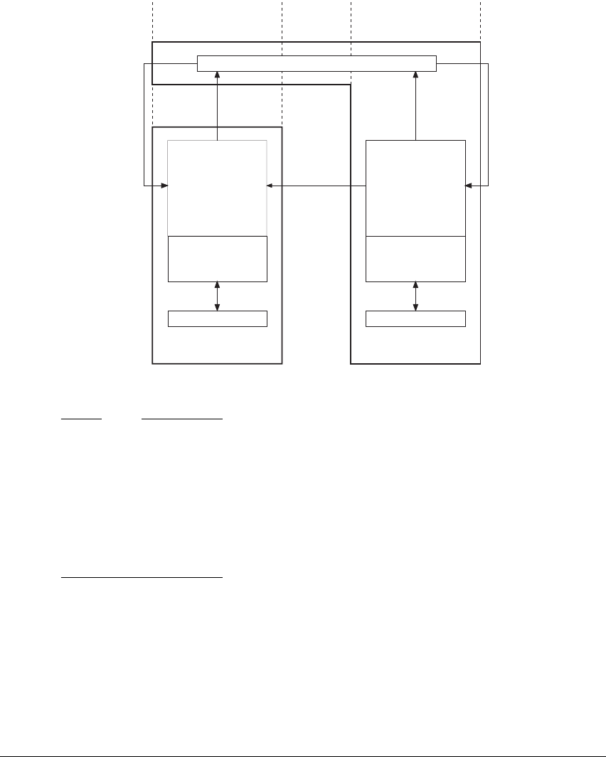
The System Level Programmers’ Model
ARM DDI 0406B Copyright © 1996-1998, 2000, 2004-2008 ARM Limited. All rights reserved. B1-27
Figure B1-2 Security state, Monitor mode, and the SCR.NS bit
Note
It is important to distinguish between:
Monitor mode This is a processor mode that is only available when the Security Extensions are
implemented. It is used in normal operation, as a mechanism to transfer between Secure and
Non-secure state, as described in this section.
Monitor debug-mode
This is a debug mode and is available regardless of whether the Security Extensions are
implemented. For more information, see About the ARM Debug architecture on page C1-3.
Changing from Secure to Non-secure state
The security state is controlled by the SCR.NS bit, and ARM recommends that the SCR is modified only in
Monitor mode. Monitor mode is responsible for switching between Secure and Non-secure states.
To return to Non-secure state, set the SCR.NS bit to 1 and then perform an exception return.
MCR
SMC
Secure
state
Non-secure
state
FIQ
Supervisor
Undef
Abort
System
IRQ
FIQ
Supervisor
Undef
Abort
System
IRQ
User User
SMC
CP15SCR.NS = 1
(Non-secure)
Non-secure
privileged modes
or other mode
changing method
CP15SCR.NS = 0
(Secure)
Secure privileged
modes other than
Monitor mode
Monitor

The System Level Programmers’ Model
B1-28 Copyright © 1996-1998, 2000, 2004-2008 ARM Limited. All rights reserved. ARM DDI 0406B
Note
To avoid security holes, ARM strongly recommends that:
• you do not change from Secure to Non-secure state by using an
MSR
or
CPS
instruction to switch from
Monitor mode to some other mode while SCR.NS is 1
• you do not use an
MCR
instruction that writes SCR.NS to change from Secure to Non-secure state. This
means you should not alter the SCR.NS bit in any mode except Monitor mode.
The usual mechanism for changing from Secure to Non-secure state is an exception return.
Pseudocode details of Secure state operations
The
HaveSecurityExt()
function returns TRUE if the Security Extensions are implemented, and FALSE
otherwise.
The following function returns TRUE if the Security Extensions are not implemented or the processor is in
Secure state, and FALSE otherwise.
// IsSecure()
// ==========
boolean IsSecure()
return !HaveSecurityExt() || SCR.NS == ‘0’ || CPSR.M == ‘10110’; // Monitor mode
B1.5.2 Impact of the Security Extensions on the modes and exception model
This section summarizes the effect of the Security Extensions on the modes and exception model, to give a
overview of the Security Extensions. When the Security Extensions are implemented:
• An additional mode, Monitor mode, is implemented. For more information, see ARM processor
modes on page B1-6 and Security states on page B1-25.
• An additional exception, the Secure Monitor Call (SMC) exception, is implemented. This is
generated by the
SMC
instruction. For more information, see Secure Monitor Call (SMC) exception on
page B1-53 and SMC (previously SMI) on page B6-18.
• Because the SCTLR is banked between the Secure and Non-secure states, the V and VE bits are
defined independently for the Secure and Non-secure states. For each state:
— the SCTLR.V bit controls whether the normal or the high exception vectors are used
— the SCTLR.VE bit controls whether the IRQ and FIQ vectors are IMPLEMENTATION DEFINED.
For more information, see Exception vectors and the exception base address on page B1-30.
• The base address for the normal exception vectors is held in a CP15 register that is banked between
the two security states. This register defines the base address used for exceptions handled in modes
other than Monitor mode. Another CP15 register holds the base address for exceptions handled in
Monitor mode. For more information, see Exception vectors and the exception base address on
page B1-30.

The System Level Programmers’ Model
ARM DDI 0406B Copyright © 1996-1998, 2000, 2004-2008 ARM Limited. All rights reserved. B1-29
• If an exception is taken in Monitor mode in Non-debug state, the SCR.NS bit is set to zero, see c1,
Secure Configuration Register (SCR) on page B3-106. This forces Secure state entry for all
exceptions. However, if an exception is taken in Monitor mode in Debug state, the SCR.NS bit is not
set to zero.
Note
Many uses of the Security Extensions can be simplified if the system is designed so that exceptions
cannot be taken in Monitor mode.
• Setting bits in the Secure Configuration Register causes one or more of external aborts, IRQs and
FIQs to be handled in Monitor mode and to use the Monitor exception base address:
— setting the SCR.EA bit to 1 means external aborts are handled in Monitor mode, instead of
Abort mode
— setting the SCR.FIQ bit to 1 means FIQs are handled in Monitor mode, instead of FIQ mode
— setting the SCR.IRQ bit to 1 means IRQs are handled in Monitor mode, instead of IRQ mode.
For more information see:
—Control of exception handling by the Security Extensions on page B1-41
—c1, Secure Configuration Register (SCR) on page B3-106.
• Setting bits in the Secure Configuration Register prevents code executing in Non-secure state from
being able to mask one or both of asynchronous aborts and FIQs:
— Setting the SCR.AW bit to 1 prevents Non-secure setting of CPSR.A to 1.
— Setting the SCR.FW bit to 1 prevents Non-secure setting of CPSR.F to 1. For details of how
this setting interacts with NMFIs see Non-maskable fast interrupts on page B1-18.

The System Level Programmers’ Model
B1-30 Copyright © 1996-1998, 2000, 2004-2008 ARM Limited. All rights reserved. ARM DDI 0406B
B1.6 Exceptions
An exception causes the processor to suspend program execution to handle an event, such as an externally
generated interrupt or an attempt to execute an undefined instruction. Exceptions can be generated by
internal and external sources.
Normally, when an exception is taken the processor state is preserved immediately, before handling the
exception. This means that, when the event has been handled, the original state can be restored and program
execution resumed from the point where the exception was taken.
More than one exception might be generated at the same time, and a new exception can be generated while
the processor is handling an exception.
The following sections describe exception handling in general:
•Exception vectors and the exception base address
•Exception priority order on page B1-33
•Exception entry on page B1-34
•Exception return on page B1-38
•Exception-handling instructions on page B1-41
•Control of exception handling by the Security Extensions on page B1-41
•Low interrupt latency configuration on page B1-43.
•Wait For Event and Send Event on page B1-44
•Wait For Interrupt on page B1-47.
The following sections give details of each exception:
•Reset on page B1-48
•Undefined Instruction exception on page B1-49
•Supervisor Call (SVC) exception on page B1-52
•Secure Monitor Call (SMC) exception on page B1-53
•Prefetch Abort exception on page B1-54
•Data Abort exception on page B1-55
•IRQ exception on page B1-58
•FIQ exception on page B1-60.
B1.6.1 Exception vectors and the exception base address
When an exception is taken, processor execution is forced to an address that corresponds to the type of
exception. These addresses are called the exception vectors.
By default, the exception vectors are eight consecutive word-aligned memory addresses, starting at an
exception base address. Table B1-3 on page B1-31 shows the assignment of the exceptions to the eight
memory addresses.

The System Level Programmers’ Model
ARM DDI 0406B Copyright © 1996-1998, 2000, 2004-2008 ARM Limited. All rights reserved. B1-31
The default exception vectors for the IRQ and FIQ exceptions can be changed by setting the SCTLR.VE bit
to 1, as described in Vectored interrupt support on page B1-32.
If the Security Extensions are not implemented there is a single exception base address. This is controlled
by the SCTLR.V bit:
V==0 Exception base address =
0x00000000
. This setting is referred to as normal vectors, or as low
vectors.
V==1 Exception base address =
0xFFFF0000
. This setting is referred to as high vectors, or Hivecs.
Note
Use of the Hivecs setting, V == 1, is deprecated in ARMv7-R. ARM recommends that Hivecs is used only
in ARMv7-A implementations.
If the Security Extensions are implemented there are three exception base addresses:
• the Non-secure exception base address is used for all exceptions that are processed in Non-secure
state
• the Secure exception base address is used for all exceptions that are processed in Secure state but not
in Monitor mode
• the Monitor exception base address is used for all exceptions that are processed in Monitor mode.
Table B1-3 Offsets from exception base addresses
Exception
offset
Exception that is vectored at that offset from:
Monitor exception base addressa
a. This column applies only if the Security Extensions are implemented.
Base address for all other exceptions
0x00
Not used Reset
0x04
Not used Undefined Instruction
0x08
Secure Monitor Call (SMC) Supervisor Call (SVC)
0x0C
Prefetch Abort Prefetch Abort
0x10
Data Abort Data Abort
0x14
Not used Not used
0x18
IRQ (interrupt) IRQ (interrupt)
0x1C
FIQ (fast interrupt) FIQ (fast interrupt)

The System Level Programmers’ Model
B1-32 Copyright © 1996-1998, 2000, 2004-2008 ARM Limited. All rights reserved. ARM DDI 0406B
See CPSR M field and A, I, and F mask bit values on exception entry on page B1-36 to determine the mode
in which an exception is processed. If that mode is Monitor mode then the exception is processed in Secure
state, otherwise the exception is processed in the current security state, determined at the time when the
exception is taken.
The Non-secure exception base address is controlled by the SCTLR.V bit in the Non-secure SCTLR:
V==0 The exception base address is the value of the Non-secure Vector Base Address Register
(VBAR), see c12, Vector Base Address Register (VBAR) on page B3-148.
V==1 Exception base address =
0xFFFF0000
. This setting is often referred to as Hivecs.
The Secure exception base address is controlled similarly, by the Secure SCTLR.V bit and the Secure
VBAR.
The Monitor exception base address is always the value of the Monitor Vector Base Address Register
(MVBAR), see c12, Monitor Vector Base Address Register (MVBAR) on page B3-149.
Vectored interrupt support
By default, the IRQ and FIQ exception vectors are at fixed offsets from the exception base address that is
being used. This is consistent with previous versions of the ARM architecture. With this default
configuration, each of the FIQ and IRQ handlers typically starts with an instruction sequence that
determines the cause of the interrupt and then branches to an appropriate routine to handle it.
Support for vectored interrupts means an interrupt controller can prioritize interrupts and provide the
address of the required interrupt handler directly to the processor, for use as the interrupt vector. Vectored
interrupt behavior is enabled by setting the SCTLR.VE bit to 1, see:
•c1, System Control Register (SCTLR) on page B3-96 for a VMSA implementation
•c1, System Control Register (SCTLR) on page B4-45 for a PMSA implementation.
The hardware that supports vectored interrupts is IMPLEMENTATION DEFINED.
For backwards compatibility, the vectored interrupt mechanism is disabled on reset.
When the Security Extensions are implemented:
• The SCTLR.VE bit is banked between Secure and Non-secure states to provide independent control
of whether vectored interrupt support is enabled.
• Interrupts can be trapped to Monitor mode, by setting either or both of the SCR.IRQ and SCR.FIQ
bits to 1. When an interrupt is trapped to Monitor mode it uses the vector in the vector table addressed
by the Monitor exception base address held in MVBAR, regardless of the value of either banked copy
of the SCTLR.VE bit.

The System Level Programmers’ Model
ARM DDI 0406B Copyright © 1996-1998, 2000, 2004-2008 ARM Limited. All rights reserved. B1-33
Operation
In pseudocode, the current exception base address for exceptions processed in Monitor mode is determined
by reading MVBAR, and for other exceptions by the following function:
// ExcVectorBase()
// ===============
bits(32) ExcVectorBase()
if SCTLR.V == ‘1’ then // Hivecs selected, base = 0xFFFF0000
return Ones(16):Zeros(16);
elsif HaveSecurityExt() then
return VBAR;
else
return Zeros(32);
B1.6.2 Exception priority order
In principle a number of different synchronous exceptions can be generated by a single instruction. The
following principles determine which synchronous exception is taken:
• No instruction is valid if it has a synchronous Prefetch Abort exception associated with it. Therefore,
other synchronous exceptions are not taken in this case.
• An instruction that generates an Undefined Instruction exception cannot cause any memory access,
and therefore cannot cause a Data Abort exception.
• All other synchronous exceptions are mutually exclusive and are derived from a decode of the
instruction.
The ARM architecture does not define when asynchronous exceptions are taken. Therefore the prioritization
of asynchronous exceptions relative to other exceptions, both synchronous and asynchronous, depends on
the implementation.
The CPSR includes a mask bit for each type of asynchronous exception. Setting one of these bits to 1
prevents the corresponding asynchronous exception from being taken. Taking an exception sets an
exception-dependent subset of these mask bits.
Note
• The subset of the CPSR mask bits that is set on taking an exception prioritizes the execution of FIQ
handlers over that of IRQ and asynchronous abort handlers.
• A special requirement applies to asynchronous watchpoints - see Debug event prioritization on
page C3-43.

The System Level Programmers’ Model
B1-34 Copyright © 1996-1998, 2000, 2004-2008 ARM Limited. All rights reserved. ARM DDI 0406B
B1.6.3 Exception entry
On taking an exception:
1. The value of the CPSR is saved in the SPSR for the exception mode that is handling the exception.
2. The value of (PC + exception-dependent offset) is saved in the LR for the exception mode that is
handling the exception, see Table B1-4.
3. The CPSR and PC are updated with information for the exception handler:
• The CPSR is updated with new context information. This includes:
— Setting CPSR.M to the processor mode in which the exception is to be handled.
— Disabling appropriate classes of interrupt, to prevent uncontrolled nesting of exception
handlers. For more information, see Table B1-6 on page B1-36, Table B1-7 on
page B1-37, and Table B1-8 on page B1-37.
— Setting the instruction set state to the instruction set chosen for exception entry, see
Instruction set state on exception entry on page B1-35.
— Setting the endianness to the value chosen for exception entry, see CPSR.E bit value on
exception entry on page B1-38.
— Clearing the IT[7:0] bits to 0.
For more information, see CPSR M field and A, I, and F mask bit values on exception entry on
page B1-36.
• The appropriate exception vector is loaded to the PC, see Exception vectors and the exception
base address on page B1-30.
4. Execution continues from the address held in the PC.
At step 2 of the exception entry, the address saved in the LR depends on:
• the Exception type
• the instruction set state in which the processor is executing when the exception occurs.
Table B1-4 shows the LR value saved for all cases:
Table B1-4 Link Register value saved on exception entry
Exception Base LR value a
Offset, for processor state of:a
ARM Thumb or ThumbEE Jazelle
Reset UNKNOWN -- -
Undefined Instruction Address of the undefined instruction + 4 +2 +2 or +4b
SVC Address of
SVC
instruction + 4 +2 -c
SMC Address of
SMC
instruction + 4 +4 -c

The System Level Programmers’ Model
ARM DDI 0406B Copyright © 1996-1998, 2000, 2004-2008 ARM Limited. All rights reserved. B1-35
Instruction set state on exception entry
Exception handlers always execute in either Thumb state or ARM state. Which state they execute in is
determined by the Thumb Exception enable bit, SCTLR.TE, see:
•c1, System Control Register (SCTLR) on page B3-96 for a VMSA implementation
•c1, System Control Register (SCTLR) on page B4-45 for a PMSA implementation.
On exception entry, the CPSR.T and CPSR.J bits are set to values that depend on the SCTLR.TE value, as
shown in Table B1-5:
When the Security Extensions are implemented, the SCTLR is banked for Secure and Non-secure states,
and therefore the TE bit value might be different for Secure and Non-secure states. The SCTLR.TE bit for
the security state in which the exception is handled determines the instruction set state for the exception
handler. This means the exception handlers might run in different instruction set states, depending on the
security state.
Prefetch Abort Address of aborted instruction fetch + 4 +4 + 4
Data Abort Address of instruction that generated
the abort
+ 8 +8 + 8
IRQ or FIQ Address of next instruction to execute + 4 +4 + 4
a. Except for the Reset exception, the value saved in the LR is the base LR value plus the offset value for the processor
state immediately before the exception entry.
b. In Jazelle state, Undefined Instruction exceptions can only happen on a processor that includes a trivial implementation
of Jazelle state. On such a processor, if an exception return instruction writes {CPSR.J, CPSR.T} to 0b10, the processor
takes an Undefined Instruction exception when it next attempts to execute an instruction. It is IMPLEMENTATION
DEFINED whether the processor uses an offset of +2 or +4 in these circumstances, but it must always use the same offset.
c. SVC and SMC exceptions cannot occur in Jazelle state.
Table B1-4 Link Register value saved on exception entry (continued)
Exception Base LR value a
Offset, for processor state of:a
ARM Thumb or ThumbEE Jazelle
Table B1-5 CPSR.J and CPSR.T bit values on exception entry
SCTLR.TE CPSR.J CPSR.T Exception handler state
000ARM
1 0 1 Thumb

The System Level Programmers’ Model
B1-36 Copyright © 1996-1998, 2000, 2004-2008 ARM Limited. All rights reserved. ARM DDI 0406B
CPSR M field and A, I, and F mask bit values on exception entry
On exception entry, the processor mode is set to one of the exception modes and the CPSR[A,I,F] interrupt
disable (mask) bits are set to new values:
• the CPSR.I bit is always set to 1, to disable IRQs
• the CPSR.M (mode), CPSR.A (asynchronous abort disable), and CPSR.F (FIQ disable) bits are set
to values that depend:
— on the exception type
— if the Security Extensions are implemented, on the security state and some bits of the SCR, see
c1, Secure Configuration Register (SCR) on page B3-106.
The new values are shown in:
• Table B1-6, for an implementation that does not include the Security Extensions
• Table B1-7 on page B1-37, for an implementation that includes the Security Extensions, when the
security state is Secure (NS == 0).
• Table B1-8 on page B1-37, for an implementation that includes the Security Extensions, when the
security state is Non-secure (NS == 1).
In these tables, Unchanged indicates that the bit value is unchanged from its value when the exception was
taken.
Table B1-6 A and F bit values on exception entry, without Security Extensions
Exception Exception mode CPSR.A CPSR.F
Reset Supervisor 1 1
Undefined Instruction Undefined Unchanged Unchanged
Supervisor Call (SVC) Supervisor Unchanged Unchanged
All aborts Abort 1 Unchanged
IRQ IRQ 1 Unchanged
FIQ FIQ 1 1

The System Level Programmers’ Model
ARM DDI 0406B Copyright © 1996-1998, 2000, 2004-2008 ARM Limited. All rights reserved. B1-37
Table B1-7 A and F bit values on exception entry, with Security Extensions and NS == 0
Exception
SCR bits
Exception mode
NS == 0, Secure
EA IRQ FIQ CPSR.A CPSR.F
Reset x x x Supervisor 1 1
Undefined Instruction x x x Undefined Unchanged Unchanged
Supervisor Call (SVC) x x x Supervisor Unchanged Unchanged
Secure Monitor Call (SMC) x x x Monitor 1 1
All external aborts
0 x x Abort 1 Unchanged
1xxMonitor 1 1
All internal aborts x x x Abort 1 Unchanged
IRQ
x 0 x IRQ 1 Unchanged
x1xMonitor 1 1
FIQ
xx0FIQ 1 1
xx1Monitor 1 1
Table B1-8 A and F bit values on exception entry, with Security Extensions and NS == 1
Exception
SCR bits Exception
mode
NS == 1, Non-secure
EA IRQ FIQ AW FW CPSR.A CPSR.F
Reset xxxxxSupervisor1 1
Undefined Instruction x x x x x Undefined Unchanged Unchanged
Supervisor Call (SVC) xxxxxSupervisor Unchanged Unchanged
Secure Monitor Call (SMC) x x x x x Monitor 1 1
All external aborts
0 x x 0 x Abort Unchanged Unchanged
0 x x 1 x Abort 1 Unchanged
1xxxxMonitor 1 1

The System Level Programmers’ Model
B1-38 Copyright © 1996-1998, 2000, 2004-2008 ARM Limited. All rights reserved. ARM DDI 0406B
CPSR.E bit value on exception entry
On exception entry, the CPSR.E bit is set to the value of the SCTLR.EE bit. This bit of the CPSR controls
the load and store endianness for data handling by the exception handler, see the bit description in Format
of the CPSR and SPSRs on page B1-16. For the description of the SCTLR see:
•c1, System Control Register (SCTLR) on page B3-96 for a VMSA implementation
•c1, System Control Register (SCTLR) on page B4-45 for a PMSA implementation.
B1.6.4 Exception return
In the ARM architecture, exception return requires the simultaneous restoration of the PC and CPSR to
values that are consistent with the desired state of execution on returning from the exception. Normally, this
is the state of execution just before the exception was taken, but it can be different in some circumstances,
for example if the exception handler performed instruction emulation.
Typically, this involves returning to one of:
• the instruction boundary at which an asynchronous exception was taken
• the instruction following an
SVC
or
SMC
instruction, for an exception generated by one of those
instructions
• the instruction that caused the exception, after the reason for the exception has been removed
All internal aborts
xxx0xAbort UnchangedUnchanged
xxx1xAbort 1 Unchanged
IRQ
x0x0xIRQ UnchangedUnchanged
x0x1xIRQ 1 Unchanged
x1xxxMonitor 1 1
FIQ
xx000FIQ UnchangedUnchanged
xx001FIQ Unchanged1
xx010FIQ 1 Unchanged
xx011FIQ 1 1
xx1xxMonitor 1 1
Table B1-8 A and F bit values on exception entry, with Security Extensions and NS == 1 (continued)
Exception
SCR bits Exception
mode
NS == 1, Non-secure
EA IRQ FIQ AW FW CPSR.A CPSR.F

The System Level Programmers’ Model
ARM DDI 0406B Copyright © 1996-1998, 2000, 2004-2008 ARM Limited. All rights reserved. B1-39
• the subsequent instruction, if the instruction that caused the exception has been emulated in the
exception handler.
The ARM architecture makes no requirement that exception return must be to any particular place in the
execution stream. However, the architecture does have a preferred exception return for each exception other
than Reset. The values of the SPSR.IT[7:0] bits generated on exception entry are always correct for the
preferred exception return, but might require adjustment by software if returning elsewhere.
In some cases, the value of the LR set on taking the exception, as shown in Table B1-4 on page B1-34,
makes it necessary to perform a subtraction to calculate the appropriate return address. The value that must
be subtracted for the preferred exception return, and other details of the preferred exception return, are given
in the description of each of the exceptions.
The ARM architecture provides the following exception return instructions:
• Data-processing instructions with the S bit set and the PC as a destination, see SUBS PC, LR and
related instructions on page B6-25.
Typically,
SUBS
is used when a subtraction is required, and
SUBS
with an operand of 0 or
MOVS
is used
otherwise.
• From ARMv6, the
RFE
instruction, see RFE on page B6-16. If a subtraction is required, typically it is
performed before saving the LR value to memory.
• In ARM state, a form of the
LDM
instruction, see LDM (exception return) on page B6-5. If a
subtraction is required, typically it is performed before saving the LR value to memory.
Alignment of exception returns
An unaligned exception return is one where the address transferred to the PC on an exception return is not
aligned to the size of instructions in the target instruction set. The target instruction set is controlled by the
[J,T] bits of the value transferred to the CPSR for the exception return. The behavior of the hardware for
exception returns for different values of the [J,T] bits is as follows:
[J,T] == 00 The target instruction set state is ARM state. Bits [1:0] of the address transferred to the PC
are ignored by the hardware.
[J,T] == 01 The target instruction set state is Thumb state:
• bit [0] of the address transferred to the PC is ignored by the hardware
• bit [1] of the address transferred to the PC is part of the instruction address.
[J,T] == 10 The target instruction set state is Jazelle state. In a non-trivial implementation of the Jazelle
extension, bits [1:0] of the address transferred to the PC are part of the instruction address.
In a trivial implementation of the Jazelle extension, behavior is UNPREDICTABLE, see
Exception return to an unsupported instruction set state on page B1-40. For details of the
trivial implementation of Jazelle state see Trivial implementation of the Jazelle extension on
page B1-81.

The System Level Programmers’ Model
B1-40 Copyright © 1996-1998, 2000, 2004-2008 ARM Limited. All rights reserved. ARM DDI 0406B
[J,T] == 11 The target instruction set state is ThumbEE state:
• bit [0] of the address transferred to the PC is ignored by the hardware
• bit [1] of the address transferred to the PC is part of the instruction address.
ARM deprecates any dependence on the requirements that the hardware ignores bits of the address. ARM
recommends that the address transferred to the PC for an exception return is correctly aligned for the target
instruction set.
After an exception entry other than Reset, the LR value has the correct alignment for the instruction set
indicated by the SPSR.[J,T] bits. This means that if exception return instructions are used with the LR and
SPSR values produced by such an exception entry, the only precaution software needs to take to ensure
correct alignment is that any subtraction is of a multiple of four if returning to ARM state, or a multiple of
two if returning to Thumb state or to ThumbEE state.
Exception return to an unsupported instruction set state
An implementation that does not support one or both of Jazelle and ThumbEE states does not normally get
into an unsupported instruction set state, because:
• on a trivial Jazelle implementation, the
BXJ
instruction acts as a
BX
instruction
• on an implementation that does not include ThumbEE support, the
ENTERX
instruction is UNDEFINED
• normal exception entry and return preserves the instruction set state.
However, it is possible for an exception return instruction to set CPSR.J and CPSR.T to the values
corresponding to an unsupported instruction set state. This is most likely to happen because a faulty
exception handler restores the wrong value to the CPSR.
If the processor attempts to execute an instruction while the CPSR.J and CPSR.T bits indicate an
unsupported instruction set state:
• If the unsupported instruction set state is Jazelle state, behavior is UNPREDICTABLE.
• If the unsupported instruction set state is ThumbEE state, the processor takes an Undefined
Instruction exception.
The Undefined Instruction handler can detect the cause of this exception because on entry to the
handler the SPSR.J and SPSR.T bits indicate the ThumbEE state. If the Undefined Instruction handler
wants to return, avoiding a return to ThumbEE state, it can change the values its exception return
instruction writes to the CPSR.J and CPSR.T bits.
If an exception return writes CPSR.J = 1 and CPSR.T = 1, corresponding to ThumbEE state, and also
writes the address of an aborting memory location to the PC, it is IMPLEMENTATION DEFINED whether:
— the instruction is fetched and a Prefetch Abort exception is taken because the memory access
aborts
— an Undefined Instruction exception is taken, without the instruction being fetched.
An implementation that supports neither of the Jazelle and ThumbEE states can implement the J bits of the
PSRs as RAZ/WI. On such an implementation, a return to an unsupported instruction set state cannot occur.

The System Level Programmers’ Model
ARM DDI 0406B Copyright © 1996-1998, 2000, 2004-2008 ARM Limited. All rights reserved. B1-41
B1.6.5 Exception-handling instructions
From ARMv6, the instruction sets include the following exception-handling instructions, in addition to the
exception return instructions described in Exception return on page B1-38:
•a
CPS
(Change Processor State) instruction to simplify changes of processor mode and the disabling
and enabling of interrupts, see CPS on page B6-3
•an
SRS
(Store Return State) instruction, to reduce the processing cost of handling exceptions in a
different mode to the exception entry mode, by removing any need to use the stack of the original
mode, see SRS on page B6-20.
As an example of where these instructions might be used, an IRQ routine might want to execute in System
or Supervisor mode, so that it can both re-enable IRQs and use
BL
instructions. This is not possible in IRQ
mode, because a nested IRQ could corrupt the return link of a
BL
at any time.
With the
CPS
and
SRS
instructions, the system can use the following instruction sequence at the start of its
exception handler:
SUB LR,LR,#4 ; IRQ requires subtraction from LR
SRSFD SP!, #<mode> ; <mode> = 19 for Supervisor, 31 for System
CPSIE i,#<mode>
This:
• stores the return state held in the LR and SPSR_irq to the stack for Supervisor mode or for User and
System mode
• switches to Supervisor or System mode and re-enables IRQs.
This is done efficiently, without making any use of SP_irq or the IRQ stack.
At the end of the exception handler, an
RFEFD SP!
instruction pops the return state off the stack and returns
from the exception.
B1.6.6 Control of exception handling by the Security Extensions
The Security Exceptions provide additional controls of the handling of:
• aborts, see Control of aborts by the Security Extensions
•FIQs, see Control of FIQs by the Security Extensions on page B1-42
• IRQs, see Control of IRQs by the Security Extensions on page B1-43.
Control of aborts by the Security Extensions
The CPSR.A bit can be used to disable asynchronous aborts. When the Security Extensions are
implemented:
• the SCR.AW bit controls whether the CPSR.A bit can be modified in Non-secure state
• the SCR.EA bit controls whether external aborts are handled in Abort mode or Monitor mode.
For details of these bits see c1, Secure Configuration Register (SCR) on page B3-106.

The System Level Programmers’ Model
B1-42 Copyright © 1996-1998, 2000, 2004-2008 ARM Limited. All rights reserved. ARM DDI 0406B
Table B1-9 shows the possible values for the SCR.AW and SCR.EA bits, and the abort handling that results
in each case:
When the SCR.EA bit is set to 1, and an external abort causes entry to Monitor mode, fault information is
written to the Secure copies of the Fault Status and Fault Address registers.
Control of FIQs by the Security Extensions
The CPSR.F bit can be used to disable FIQs. When the Security Extensions are implemented:
• the SCR.FW bit controls whether the CPSR.F bit can be modified in Non-secure state
• the SCR.FIQ bit controls whether FIQs are handled in FIQ mode or Monitor mode.
For details of these bits see c1, Secure Configuration Register (SCR) on page B3-106.
Table B1-10 on page B1-43 shows the effect of these bits on FIQ handling:
Table B1-9 Effect of the SCR.AW and SCR.EA bits on abort handling
SCR bits
Effect on abort handling
AW EA
0 0 All aborts are handled locally using Abort mode. Asynchronous aborts are maskable only in Secure
state.
This is the reset state and supports legacy systems.
0 1 All external aborts, synchronous and asynchronous, are handled in Monitor mode. Asynchronous
aborts are maskable only in Secure state.
All security aborts from peripherals can be treated in a safe manner in Monitor mode.
1 0 All aborts are handled locally, using Abort mode. Asynchronous aborts are maskable in both Secure
and Non-secure states.
1 1 All external aborts are trapped to Monitor mode. Non-secure state can hide asynchronous external
aborts from the Monitor, by changing the CPSR.A bit.

The System Level Programmers’ Model
ARM DDI 0406B Copyright © 1996-1998, 2000, 2004-2008 ARM Limited. All rights reserved. B1-43
Note
• The configuration with SCR.FW == 1 and SCR.FIQ == 1 permits Non-secure state to deny service
by changing the CPSR.F bit. ARM recommends that this configuration is not used.
• Interrupts driven by Secure peripherals are called Secure interrupts. When SCR.FW = 0 and
SCR.FIQ = 1, FIQ exceptions can be used as Secure interrupts. These enter Secure state in a
deterministic way.
Control of IRQs by the Security Extensions
When the Security Extensions are implemented, the SCR.IRQ bit controls whether IRQs are handled in IRQ
mode or Monitor mode. For details of this bit see c1, Secure Configuration Register (SCR) on page B3-106.
B1.6.7 Low interrupt latency configuration
The SCTLR.FI bit is set to 1 to enable the low interrupt latency configuration of an implementation. This
configuration can reduce the interrupt latency of the processor. The mechanisms implemented to achieve
low interrupt latency are IMPLEMENTATION DEFINED. For the description of the SCTLR see:
•c1, System Control Register (SCTLR) on page B3-96 for a VMSA implementation
•c1, System Control Register (SCTLR) on page B4-45 for a PMSA implementation.
To ensure that a change between normal and low interrupt latency configurations is synchronized correctly,
the SCTLR.FI bit must be changed only in IMPLEMENTATION DEFINED circumstances. The FI bit can be
changed shortly after reset and before enabling the MMU, MPU, or caches, when interrupts are disabled,
using the following sequence:
Table B1-10 Effect of the SCR.AW and SCR.EA bits on FIQ handling
SCR bits
Effect on FIQ handling
FW FIQ
0 0 FIQs are handled locally using FIQ mode. FIQs are maskable only in Secure state.
This is the reset state and supports legacy systems.
0 1 FIQs are handled in Monitor mode. FIQs are maskable only in Secure state.
This setting gives Secure FIQs.
1 0 FIQs are handled locally in FIQ mode. FIQs can be masked, in both Secure and Non-secure states.
1 1 All FIQs are trapped to Monitor mode. Non-secure state can hide FIQs from the Monitor, by changing
the CPSR.F bit.

The System Level Programmers’ Model
B1-44 Copyright © 1996-1998, 2000, 2004-2008 ARM Limited. All rights reserved. ARM DDI 0406B
DSB
ISB
MCR p15, 0, Rx, c1, c0, c0 ; change FI bit in the SCTLR
DSB
ISB
Implementation can define other sequences and circumstances that permit the SCTLR.FI bit to be changed.
When interrupt latency is reduced, this can result in reduced performance overall. Examples of methods that
might be used to reduce interrupt latency are:
• disabling Hit-Under-Miss functionality in a processor
• the abandoning of restartable external accesses.
These choices permit the processor to react to a pending interrupt faster than would otherwise be the case.
A low interrupt latency configuration permits interrupts and asynchronous aborts to be taken during a
sequence of memory transactions generated by a load/store instruction. For details of what these sequences
are and the consequences of taking interrupts and asynchronous aborts in this way see Single-copy atomicity
on page A3-27.
ARM deprecates any software reliance on the behavior that an interrupt or asynchronous abort cannot occur
in a sequence of memory transactions generated by a single load/store instruction to Normal memory.
Note
A particular case that has shown this reliance is load multiples that load the stack pointer from memory. In
an implementation where an interrupt is taken during the
LDM
, this can result in corruption of the stack
pointer.
B1.6.8 Wait For Event and Send Event
A multiprocessor operating system requires locking mechanisms to protect data structures from being
accessed simultaneously by multiple processors. These mechanisms prevent the data structures becoming
inconsistent or corrupted if different processors try to make conflicting changes. If a lock is busy, because
a data structure is being used by one processor, it might not be practical for another processor to do anything
except wait for the lock to be released. For example, if a processor is handling an interrupt from a device it
might need to add data received from the device to a queue. If another processor is removing data from the
queue, it will have locked the memory area that holds the queue. The first processor cannot add the new data
until the queue is in a consistent state and the lock has been released. It cannot return from the interrupt
handler until the data has been added to the queue, so it must wait.
Typically, a spin-lock mechanism is provided for these circumstances:
• A processor requiring access to the protected data attempts to obtain the lock using single-copy
atomic synchronization primitives such as the ARM Load-Exclusive and Store-Exclusive operations
described in Synchronization and semaphores on page A3-12.
• If the processor obtains the lock it performs its memory operation and releases the lock.

The System Level Programmers’ Model
ARM DDI 0406B Copyright © 1996-1998, 2000, 2004-2008 ARM Limited. All rights reserved. B1-45
• If the processor cannot obtain the lock, it reads the lock value repeatedly in a tight loop until the lock
becomes available. At this point it again attempts to obtain the lock.
However, this spin-lock mechanism is not ideal for all situations:
• in a low-power system the tight read loop is undesirable because it uses energy to no effect
• in a multi-threaded processor the execution of spin-locks by waiting threads can significantly degrade
overall performance.
Therefore, ARMv7 provides an alternative locking mechanism based on events. The Wait For Event lock
mechanism permits a processor that has failed to obtain a lock to enter a low-power state. When the
processor that currently holds the required lock releases the lock it sends an event that causes any waiting
processors to wake up and attempt to gain the lock again.
Note
Although a complex operating system can contain thousands of distinct locks, the event sent by this
mechanism does not indicate which lock has been released. If the event relates to a different lock, or if
another processor acquires the lock more quickly, the processor fails to acquire the lock and can re-enter the
low-power state waiting for the next event.
The Wait For Event system relies on hardware and software working together to achieve energy saving:
• the hardware provides the mechanism to enter the Wait For Event low-power state
• the operating system software is responsible for issuing:
— a Wait For Event instruction when waiting for a spin-lock, to enter the low-power state
— a Send Event instructions when releasing a spin-lock.
The mechanism depends on the interaction of:
• WFE wake-up events, see WFE wake-up events
• the Event Register, see The Event Register on page B1-46
• the Send Event instruction, see The Send Event instruction on page B1-46
• the Wait For Event instruction, see The Wait For Event instruction on page B1-46.
WFE wake-up events
The following events are WFE wake-up events:
• the execution of an
SEV
instruction on any processor in the multiprocessor system
• an IRQ interrupt, unless masked by the CPSR.I bit
• an FIQ interrupt, unless masked by the CPSR.F bit
• an asynchronous abort, unless masked by the CPSR.A bit
• a debug event, if invasive debug is enabled and the debug event is permitted.
For details of the masking bits in the CPSR see Format of the CPSR and SPSRs on page B1-16. This
masking is an important consideration with this mechanism, because lock mechanisms can be required
when interrupts are disabled.

The System Level Programmers’ Model
B1-46 Copyright © 1996-1998, 2000, 2004-2008 ARM Limited. All rights reserved. ARM DDI 0406B
The Event Register
The Event Register is a single bit register for each processor. When set, an event register indicates that an
event has occurred, since the register was last cleared, that might prevent the processor needing to suspend
operation on issuing a
WFE
instruction.
The value of the Event Register at reset is UNKNOWN.
The Event Register is set by any WFE wake-up event or by the execution of an exception return instruction.
For the definition of exception return instructions see Exception return on page B1-38.
The Event Register is cleared only by a Wait For Event instruction.
You cannot read or write the value of the Event Register directly.
The Send Event instruction
The Send Event instruction causes an event to be signaled to all processors in the multiprocessor system.
The mechanism used to signal the event to the processors is IMPLEMENTATION DEFINED. The Send Event
instruction sets the Event Register.
The Send Event instruction,
SEV
, is available to both unprivileged and privileged code, see SEV on
page A8-316.
The Wait For Event instruction
The action of the Wait For Event instruction depends on the state of the Event Register:
• If the Event Register is set, the instruction clears the register and returns immediately. Normally, if
this happens the processor makes another attempt to claim the lock.
• If the Event Register is clear the processor can suspend execution and enter a low-power state. It can
remain in that state until the processor detects a WFE wake-up event or a reset. When the processor
detects a WFE wake-up event, or earlier if the implementation chooses, the
WFE
instruction completes.
The Wait For Event instruction,
WFE
, is available to both unprivileged and privileged code, see WFE on
page A8-808.
The code using the Wait For Event mechanism must be tolerant to spurious wake-up events, including
multiple wake ups.
Pseudocode details of the Wait For Event lock mechanism
The
ClearEventRegister()
pseudocode procedure clears the Event Register of the current processor.
The
EventRegistered()
pseudocode function returns TRUE if the Event Register of the current processor is
set and FALSE if it is clear:
boolean EventRegistered()

The System Level Programmers’ Model
ARM DDI 0406B Copyright © 1996-1998, 2000, 2004-2008 ARM Limited. All rights reserved. B1-47
The
WaitForEvent()
pseudocode procedure optionally suspends execution until a WFE wake-up event or
reset occurs, or until some earlier time if the implementation chooses. It is IMPLEMENTATION DEFINED
whether restarting execution after the period of suspension causes a
ClearEventRegister()
to occur.
The
SendEvent()
pseudocode procedure sets the Event Register of every processor in the multiprocessor
system.
B1.6.9 Wait For Interrupt
Previous versions of the ARM architecture have included a Wait For Interrupt concept, and Wait For
Interrupt is a required feature of the architecture from ARMv6. In ARMv7, Wait For Interrupt is supported
only through an instruction,
WFI
, that is provided in the ARM and Thumb instruction sets. For more
information, see WFI on page A8-810.
Note
In ARMv7 the CP15 c7 encoding previously used for WFI is redefined as a NOP, see CP15 c7, No
Operation (NOP) on page B3-138 and CP15 c7, Miscellaneous functions on page B4-72.
When a processor issues a
WFI
instruction it can suspend execution and enter a low-power state. It can remain
in that state until the processor detects a reset or one of the following WFI wake-up events:
• an IRQ interrupt, regardless of the value of the CPSR.I bit
• an FIQ interrupt, regardless of the value of the CPSR.F bit
• an asynchronous abort, regardless of the value of the CPSR.A bit
• a debug event, when invasive debug is enabled and the debug event is permitted.
When the hardware detects a WFI wake-up event, or earlier if the implementation chooses, the
WFI
instruction completes.
WFI wake-up events cannot be masked by the mask bits in the CPSR.
Note
• Because debug entry is one of the WFI wake-up events, ARM strongly recommends that Wait For
Interrupt is used as part of an idle loop rather than waiting for a single specific interrupt event to occur
and then moving forward. This ensures the intervention of debug while waiting does not significantly
change the function of the program being debugged.
• In some previous implementations of Wait For Interrupt, the idle loop is followed by exit functions
that must be executed before the interrupt is taken. The operation of Wait For Interrupt remains
consistent with this model, and therefore differs from the operation of Wait For Event.
• Some implementations of Wait For Interrupt drain down any pending memory activity before
suspending execution. This increases the power saving, by increasing the area over which clocks can
be stopped. This operation is not required by the ARM architecture, and code must not rely on Wait
For Interrupt operating in this way.

The System Level Programmers’ Model
B1-48 Copyright © 1996-1998, 2000, 2004-2008 ARM Limited. All rights reserved. ARM DDI 0406B
Using WFI to indicate an idle state on bus interfaces
A common implementation practice is to complete any entry into power-down routines with a
WFI
instruction. Typically, the
WFI
instruction:
1. forces the suspension of execution, and of all associated bus activity
2. ceases to execute instructions from processor.
The control logic required to do this typically tracks the activity of the bus interfaces of the processor. This
means it can signal to an external power controller that there is no ongoing bus activity.
The exact nature of this interface is IMPLEMENTATION DEFINED, but the use of Wait For Interrupt as the only
architecturally-defined mechanism that completely suspends execution makes it very suitable as the
preferred power-down entry mechanism for future implementations.
Pseudocode details of Wait For Interrupt
The
WaitForInterrupt()
pseudocode procedure optionally suspends execution until a WFI wake-up event or
reset occurs, or until some earlier time if the implementation chooses.
B1.6.10 Reset
On an ARM processor, when the Reset input is asserted the processor immediately stops execution of the
current instruction. When Reset is de-asserted, the actions described in Exception entry on page B1-34 are
performed, for the Reset exception. The processor then starts executing code, in Supervisor mode with
interrupts disabled. Execution starts from the normal or high reset vector address,
0x00000000
or
0xFFFF0000
,
as determined by the reset value of the SCTLR.V bit. This reset value can be determined by an
IMPLEMENTATION DEFINED configuration input signal.
Note
• The ARM architecture does not distinguish between multiple levels of reset. A system can provide
multiple distinct levels of reset that reset different parts of the system. These all correspond to this
single reset exception.
• The reset value of the SCTLR.EE bit can be defined by a configuration input signal. If this is done,
that value also applies to the CPSR.E bit on reset. For more information see:
—c1, System Control Register (SCTLR) on page B3-96 for a VMSA implementation
—c1, System Control Register (SCTLR) on page B4-45 for a PMSA implementation.
The following pseudocode describes how this exception is taken:
// TakeReset()
// ===========
TakeReset()
// Enter Supervisor mode and (if relevant) Secure state, and reset CP15. This affects
// the banked versions and values of various registers accessed later in the code.
// Also reset other system components.
CPSR.M = ‘10011’; // Supervisor mode

The System Level Programmers’ Model
ARM DDI 0406B Copyright © 1996-1998, 2000, 2004-2008 ARM Limited. All rights reserved. B1-49
if HaveSecurityExt() then SCR.NS = ‘0’;
ResetCP15Registers();
ResetDebugRegisters();
if HaveAdvSIMDorVFP() then FPEXC.EN = ‘0’; SUBARCHITECTURE_DEFINED further resetting;
if HaveThumbEE() then TEECR.XED = ‘0’;
if HaveJazelle() then JMCR.JE = ‘0’; SUBARCHITECTURE_DEFINED further resetting;
// Further CPSR changes: all interrupts disabled, IT state reset, instruction set
// and endianness according to the SCTLR values produced by the above call to
// ResetCP15Registers().
CPSR.I = ‘1’; CPSR.F = ‘1’; CPSR.A = ‘1’;
CPSR.IT = ‘00000000’;
CPSR.J = ‘0’; CPSR.T = SCTLR.TE; // TE=0: ARM, TE=1: Thumb
CPSR.E = SCTLR.EE; // EE=0: little-endian, EE=1: big-endian
// All registers, bits and fields not reset by the above pseudocode or by the
// BranchTo() call below are UNKNOWN bitstrings after reset. In particular, the
// return information registers R14_svc and SPSR_svc have UNKNOWN values, so that
// it is impossible to return from a reset in an architecturally defined way.
// Branch to Reset vector.
BranchTo(ExcVectorBase() + 0);
The ARM architecture does not define any way of returning from a reset.
B1.6.11 Undefined Instruction exception
An Undefined Instruction exception might be caused by:
• a coprocessor instruction that is not accessible because of the settings in one or both of:
— the Coprocessor Access Control Register, see c1, Coprocessor Access Control Register
(CPACR) on page B3-104 for a VMSA implementation, or c1, Coprocessor Access Control
Register (CPACR) on page B4-51 for a PMSA implementation
— in an implementation that includes the Security Extensions, the Non-Secure Access Control
Register, see c1, Non-Secure Access Control Register (NSACR) on page B3-110
• a coprocessor instruction that is not implemented
• an instruction that is UNDEFINED
• an attempt to execute an instruction in an unsupported instruction set state, see Exception return to
an unsupported instruction set state on page B1-40
• division by zero in an
SDIV
or
UDIV
instruction in the ARMv7-R profile when the SCTLR.DZ bit is set
to 1, see c1, System Control Register (SCTLR) on page B4-45.
The Undefined Instruction exception can be used for:
• software emulation of a coprocessor in a system that does not have the physical coprocessor hardware
•lazy context switching of coprocessor registers
• general-purpose instruction set extension by software emulation

The System Level Programmers’ Model
B1-50 Copyright © 1996-1998, 2000, 2004-2008 ARM Limited. All rights reserved. ARM DDI 0406B
• signaling an illegal instruction execution
• division by zero errors.
In some coprocessor designs, an internal exceptional condition caused by one coprocessor instruction is
signaled asynchronously by refusing to respond to a later coprocessor instruction that belongs to the same
coprocessor. In these circumstances, the Undefined Instruction handler must take whatever action is needed
to clear the exceptional condition, and then return to the second coprocessor instruction.
Note
The only mechanism to determine the cause of an Undefined Instruction exception is analysis of the
instruction indicated by the return link in the LR on exception entry. Therefore it is important that a
coprocessor only reports exceptional conditions by generating Undefined Instruction exceptions on its own
coprocessor instructions.
The following pseudocode describes how this exception is taken:
// TakeUndefInstrException()
// =========================
TakeUndefInstrException()
// Determine return information. SPSR is to be the current CPSR, and LR is to be the
// current PC minus 2 for Thumb or 4 for ARM, to change the PC offsets of 4 or 8
// respectively from the address of the current instruction into the required return
// address offsets of 2 or 4 respectively.
new_lr_value = if CPSR.T == ‘1’ then PC-2 else PC-4;
new_spsr_value = CPSR;
// Enter Undefined (‘11011’) mode, and ensure Secure state if initially in Monitor
// (‘10110’) mode. This affects the banked versions of various registers accessed later
// in the code.
if CPSR.M == ‘10110’ then SCR.NS = ‘0’;
CPSR.M = ‘11011’;
// Write return information to registers, and make further CPSR changes: IRQs disabled,
// IT state reset, instruction set and endianness to SCTLR-configured values.
SPSR[] = new_spsr_value;
R[14] = new_lr_value;
CPSR.I = ‘1’;
CPSR.IT = ‘00000000’;
CPSR.J = ‘0’; CPSR.T = SCTLR.TE; // TE=0: ARM, TE=1: Thumb
CPSR.E = SCTLR.EE; // EE=0: little-endian, EE=1: big-endian
// Branch to Undefined Instruction vector.
BranchTo(ExcVectorBase() + 4);
The preferred exception return from an Undefined Instruction exception is a return to the instruction that
generated the exception. Use the LR and SPSR values generated by the exception entry to produce this
return as follows:
• If SPSR.J and SPSR.T are both 0, indicating that the exception occurred in ARM state, use an
exception return instruction with a subtraction of 4

The System Level Programmers’ Model
ARM DDI 0406B Copyright © 1996-1998, 2000, 2004-2008 ARM Limited. All rights reserved. B1-51
• If SPSR.J and SPSR.T are not both 0, indicating that the exception occurred in Thumb state or
ThumbEE state, use an exception return instruction with a subtraction of 2.
For more information, see Exception return on page B1-38.
Note
• Undefined Instruction exceptions cannot occur in Jazelle state
• If handling the Undefined Instruction exception requires instruction emulation, followed by return to
the next instruction after the instruction that caused the exception, the instruction emulator must use
the instruction length to calculate the correct return address, and to calculate the updated values of
the IT bits if necessary.
Conditional execution of undefined instructions
The conditional execution rules described in Conditional execution on page A8-8 apply to all instructions.
This includes UNDEFINED instructions and other instructions that would cause entry to the Undefined
Instruction exception.
If such an instruction fails its condition check, the behavior depends on the architecture profile and the
potential cause of entry to the Undefined Instruction exception, as follows:
• In the ARMv7-A profile:
— If the potential cause is the execution of the instruction itself and depends on data values the
instruction reads, the instruction executes as a NOP and does not cause an Undefined
Instruction exception.
— If the potential cause is the execution of an earlier coprocessor instruction, or the execution of
the instruction itself but does not depend on data values the instruction reads, it is
IMPLEMENTATION DEFINED whether the instruction executes as a NOP or causes an Undefined
Instruction exception.
An implementation must handle all such cases in the same way.
• In the ARMv7-R profile, the instruction executes as a
NOP
and does not cause an Undefined
Instruction exception.
Note
Before ARMv7, all implementations executed any instruction that failed its condition check as a
NOP
, even
if it would otherwise have caused an Undefined Instruction exception. Undefined Instruction handlers
written for these implementations might assume without checking that the undefined instruction passed its
condition check. Such Undefined Instruction handlers are likely to need rewriting, to check the condition is
passed, before they function correctly on all ARMv7-A implementations.

The System Level Programmers’ Model
B1-52 Copyright © 1996-1998, 2000, 2004-2008 ARM Limited. All rights reserved. ARM DDI 0406B
B1.6.12 Supervisor Call (SVC) exception
The Supervisor Call instruction
SVC
enters Supervisor mode and requests a supervisor function. Typically,
the
SVC
instruction is used to request an operating system function. For more information, see SVC
(previously SWI) on page A8-430.
Note
In previous versions of the ARM architecture, the
SVC
instruction was called
SWI
, Software Interrupt.
The following pseudocode describes how this exception is taken:
// TakeSVCException()
// ==================
TakeSVCException()
// Determine return information. SPSR is to be the current CPSR, after changing the IT[]
// bits to give them the correct values for the following instruction, and LR is to be
// the current PC minus 2 for Thumb or 4 for ARM, to change the PC offsets of 4 or 8
// respectively from the address of the current instruction into the required address of
// the next instruction (the SVC instruction having size 2 or 4 bytes respectively).
ITAdvance();
new_lr_value = if CPSR.T == ‘1’ then PC-2 else PC-4;
new_spsr_value = CPSR;
// Enter Supervisor (‘10011’) mode, and ensure Secure state if initially in Monitor
// (‘10110’) mode. This affects the banked versions of various registers accessed later
// in the code.
if CPSR.M == ‘10110’ then SCR.NS = ‘0’;
CPSR.M = ‘10011’;
// Write return information to registers, and make further CPSR changes: IRQs disabled,
// IT state reset, instruction set and endianness to SCTLR-configured values.
SPSR[] = new_spsr_value;
R[14] = new_lr_value;
CPSR.I = ‘1’;
CPSR.IT = ‘00000000’;
CPSR.J = ‘0’; CPSR.T = SCTLR.TE; // TE=0: ARM, TE=1: Thumb
CPSR.E = SCTLR.EE; // EE=0: little-endian, EE=1: big-endian
// Branch to SVC vector.
BranchTo(ExcVectorBase() + 8);
The preferred exception return from an SVC exception is a return to the next instruction after the
SVC
instruction. Use the LR and SPSR values generated by the exception entry to produce this return by using
an exception return instruction without a subtraction.
For more information, see Exception return on page B1-38.

The System Level Programmers’ Model
ARM DDI 0406B Copyright © 1996-1998, 2000, 2004-2008 ARM Limited. All rights reserved. B1-53
B1.6.13 Secure Monitor Call (SMC) exception
The Secure Monitor Call instruction
SMC
enters Monitor mode and requests a Monitor function. For more
information, see SMC (previously SMI) on page B6-18.
Note
In previous versions of the ARM architecture, the
SMC
instruction was called
SMI
, Software Monitor
Interrupt.
The following pseudocode describes how this exception is taken:
// TakeSMCException()
// ==================
TakeSMCException()
// Determine return information. SPSR is to be the current CPSR, after changing the IT[]
// bits to give them the correct values for the following instruction, and LR is to be
// the current PC minus 0 for Thumb or 4 for ARM, to change the PC offsets of 4 or 8
// respectively from the address of the current instruction into the required address of
// the next instruction (with the SMC instruction always being 4 bytes in length).
ITAdvance();
new_lr_value = if CPSR.T == ‘1’ then PC else PC-4;
new_spsr_value = CPSR;
// Enter Monitor (‘10110’) mode, and ensure Secure state if initially in Monitor mode.
// This affects the banked versions of various registers accessed later in the code.
if CPSR.M == ‘10110’ then SCR.NS = ‘0’;
CPSR.M = ‘10110’;
// Write return information to registers, and make further CPSR changes: interrupts
// disabled, IT state reset, instruction set and endianness to SCTLR-configured values.
SPSR[] = new_spsr_value;
R[14] = new_lr_value;
CPSR.I = ‘1’; CPSR.F = ‘1’; CPSR.A = ‘1’;
CPSR.IT = ‘00000000’;
CPSR.J = ‘0’; CPSR.T = SCTLR.TE; // TE=0: ARM, TE=1: Thumb
CPSR.E = SCTLR.EE; // EE=0: little-endian, EE=1: big-endian
// Branch to SMC vector.
BranchTo(MVBAR + 8);
The preferred exception return from an SMC exception is a return to the next instruction after the
SMC
instruction. Use the LR and SPSR values generated by the exception entry to produce this return by using
an exception return instruction without a subtraction.
For more information, see Exception return on page B1-38.

The System Level Programmers’ Model
B1-54 Copyright © 1996-1998, 2000, 2004-2008 ARM Limited. All rights reserved. ARM DDI 0406B
Note
You can return to the
SMC
instruction itself by returning using a subtraction of 4, without any adjustment to
the SPSR.IT[7:0] bits. The result is that the return occurs, then interrupts or external aborts might occur and
be handled, then the
SMC
instruction is re-executed and another SMC exception occurs.
This relies on:
• the SMC instruction being used correctly, either outside an IT block or as the last instruction in an IT
block, so that the SPSR.IT[7:0] bits indicate unconditional execution
• the SMC handler not changing the result of the original conditional execution test for the
SMC
instruction.
B1.6.14 Prefetch Abort exception
A Prefetch Abort exception can be generated by:
• A synchronous memory abort on an instruction fetch.
Note
Asynchronous aborts on instruction fetches are reported using the Data Abort exception, see Data
Abort exception on page B1-55.
Prefetch Abort exception entry is synchronous to the instruction whose instruction fetch aborted. If
an implementation prefetches instructions, it must handle a synchronous abort on an instruction
prefetch by:
— generating a Prefetch Abort exception if and when the instruction is about to execute
— ignoring the abort if the instruction does not reach the point of being about to execute, for
example, if a branch misprediction or exception entry occurs before the instruction is reached.
For more information about memory aborts see:
—VMSA memory aborts on page B3-40
—PMSA memory aborts on page B4-13.
• A Breakpoint, Vector Catch or BKPT Instruction debug event, see Debug exception on Breakpoint,
BKPT Instruction or Vector Catch debug events on page C4-2.
The following pseudocode describes how this exception is taken:
// TakePrefetchAbortException()
// ============================
TakePrefetchAbortException()
// Determine return information. SPSR is to be the current CPSR, and LR is to be the
// current PC minus 0 for Thumb or 4 for ARM, to change the PC offsets of 4 or 8
// respectively from the address of the current instruction into the required address
// of the current instruction plus 4.
new_lr_value = if CPSR.T == ‘1’ then PC else PC-4;

The System Level Programmers’ Model
ARM DDI 0406B Copyright © 1996-1998, 2000, 2004-2008 ARM Limited. All rights reserved. B1-55
new_spsr_value = CPSR;
// Determine whether this is an external abort to be trapped to Monitor mode.
trap_to_monitor = HaveSecurityExt() && SCR.EA == ‘1’ && IsExternalAbort();
// Enter Abort (‘10111’) or Monitor (‘10110’) mode, and ensure Secure state if
// initially in Monitor mode. This affects the banked versions of various registers
// accessed later in the code.
if CPSR.M == ‘10110’ then SCR.NS = ‘0’;
CPSR.M = if trap_to_monitor then ‘10110’ else ‘10111’;
// Write return information to registers, and make further CPSR changes: IRQs disabled,
// other interrupts disabled if appropriate, IT state reset, instruction set and
// endianness to SCTLR-configured values.
SPSR[] = new_spsr_value;
R[14] = new_lr_value;
CPSR.I = ‘1’;
if trap_to_monitor then
CPSR.F = ‘1’; CPSR.A = ‘1’;
else
if !HaveSecurityExt() || SCR.NS == ‘0’ || SCR.AW == ‘1’ then CPSR.A = ‘1’;
CPSR.IT = ‘00000000’;
CPSR.J = ‘0’; CPSR.T = SCTLR.TE; // TE=0: ARM, TE=1: Thumb
CPSR.E = SCTLR.EE; // EE=0: little-endian, EE=1: big-endian
// Branch to correct Prefetch Abort vector.
if trap_to_monitor then
BranchTo(MVBAR + 12);
else
BranchTo(ExcVectorBase() + 12);
The preferred exception return from a Prefetch Abort exception is a return to the aborted instruction. Use
the LR and SPSR values generated by the exception entry to produce this return by using an exception return
instruction with a subtraction of 4.
For more information, see Exception return on page B1-38.
B1.6.15 Data Abort exception
A Data Abort exception can be generated by:
• A synchronous abort on a data read or write memory access. Exception entry is synchronous to the
instruction that generated the memory access.
• An asynchronous abort. The memory access that caused the abort can be any of:
— a data read or write access
— an instruction fetch or prefetch
— in a VMSA memory system, a translation table access.
Exception entry occurs asynchronously. It is similar to an interrupt, but uses either Abort mode or
Monitor mode, and the associated banked registers. Setting the CPSR.A bit prevents asynchronous
aborts from occurring.

The System Level Programmers’ Model
B1-56 Copyright © 1996-1998, 2000, 2004-2008 ARM Limited. All rights reserved. ARM DDI 0406B
Note
There are no asynchronous internal aborts in ARMv7 and earlier architecture versions, so
asynchronous aborts are always asynchronous external aborts.
• A Watchpoint debug event, see Debug exception on Watchpoint debug event on page C4-3.
Note
A Data Abort exception generated by a Watchpoint debug event can be either asynchronous or
synchronous, but is not an abort. This means that if it is asynchronous, it is an asynchronous Data
Abort exception but not an asynchronous abort.
For more information about memory aborts see:
•VMSA memory aborts on page B3-40
•PMSA memory aborts on page B4-13.
The following pseudocode describes how this exception is taken:
// TakeDataAbortException()
// ========================
TakeDataAbortException()
// Determine return information. SPSR is to be the current CPSR, and LR is to be the
// current PC plus 4 for Thumb or 0 for ARM, to change the PC offsets of 4 or 8
// respectively from the address of the current instruction into the required address
// of the current instruction plus 8. For an asynchronous abort, the PC and CPSR are
// considered to have already moved on to their values for the instruction following
// the instruction boundary at which the exception occurred.
new_lr_value = if CPSR.T == ‘1’ then PC+4 else PC;
new_spsr_value = CPSR;
// Determine whether this is an external abort to be trapped to Monitor mode.
trap_to_monitor = HaveSecurityExt() && SCR.EA == ‘1’ && IsExternalAbort();
// Enter Abort (‘10111’) or Monitor (‘10110’) mode, and ensure Secure state if
// initially in Monitor mode. This affects the banked versions of various registers
// accessed later in the code.
if CPSR.M == ‘10110’ then SCR.NS = ‘0’;
CPSR.M = if trap_to_monitor then ‘10110’ else ‘10111’;
// Write return information to registers, and make further CPSR changes: IRQs disabled,
// other interrupts disabled if appropriate, IT state reset, instruction set and
// endianness to SCTLR-configured values.
SPSR[] = new_spsr_value;
R[14] = new_lr_value;
CPSR.I = ‘1’;
if trap_to_monitor then
CPSR.F = ‘1’; CPSR.A = ‘1’;
else
if !HaveSecurityExt() || SCR.NS == ‘0’ || SCR.AW == ‘1’ then CPSR.A = ‘1’;
CPSR.IT = ‘00000000’;

The System Level Programmers’ Model
ARM DDI 0406B Copyright © 1996-1998, 2000, 2004-2008 ARM Limited. All rights reserved. B1-57
CPSR.J = ‘0’; CPSR.T = SCTLR.TE; // TE=0: ARM, TE=1: Thumb
CPSR.E = SCTLR.EE; // EE=0: little-endian, EE=1: big-endian
// Branch to correct Data Abort vector.
if trap_to_monitor then
BranchTo(MVBAR + 16);
else
BranchTo(ExcVectorBase() + 16);
The preferred exception return from a Data Abort exception is a return to the instruction that generated the
aborting memory access, or to the instruction following the instruction boundary at which an asynchronous
Data Abort exception occurred. Use the LR and SPSR values generated by the exception entry to produce
this return by using an exception return instruction with a subtraction of 8.
For more information, see Exception return on page B1-38.
Effects of data-aborted instructions
Instructions that access data memory can modify memory by storing one or more values. If a Data Abort
exception is generated by executing such an instruction, the value of each memory location that the
instruction stores to is:
• unchanged if the memory system does not permit write access to the memory location
•UNKNOWN otherwise.
Instructions that access data memory can modify registers in the following ways:
• By loading values into one or more of the general-purpose registers. The registers loaded can include
the PC.
• By specifying base register write-back, in which the base register used in the address calculation has
a modified value written to it. All instructions that support base register write-back have
UNPREDICTABLE results if this is specified with the PC as the base register. Only general-purpose
registers other than the PC can be modified reliably in this way.
• By loading values into coprocessor registers.
• By modifying the CPSR.
If a synchronous Data Abort exception is generated by executing such an instruction, the following rules
determine the values left in these registers:
1. On entry to the Data Abort handler:
• the PC value is the Data Abort vector address, see Exception vectors and the exception base
address on page B1-30
• the LR_abt value is determined from the address of the aborted instruction.
Neither value is affected in any way by the results of any load specified by the instruction.
2. The base register is restored to its original value if either:
• the aborted instruction is a load that includes the base register in the list to be loaded

The System Level Programmers’ Model
B1-58 Copyright © 1996-1998, 2000, 2004-2008 ARM Limited. All rights reserved. ARM DDI 0406B
• the base register is being written back.
3. If the instruction only loads one general-purpose register, the value in that register is unchanged.
4. If the instruction loads more than one general-purpose register, UNKNOWN values are left in
destination registers other than the PC and the base register of the instruction.
5. If the instruction loads coprocessor registers, UNKNOWN values are left in the destination coprocessor
registers.
6. CPSR bits that are not defined as updated on exception entry retain their current value.
7. If a synchronous Data Abort exception is generated by execution of a
STREX
,
STREXB
,
STREXH
, or
STREXD
instruction:
• memory is not updated
•
<Rd>
is not updated
•it is UNPREDICTABLE whether the monitor changes from the Exclusive state to the Open state.
The ARM abort model
The abort model used by an ARM processor implementation is described as a Base Restored Abort Model.
This means that if a synchronous Data Abort exception is generated by executing an instruction that
specifies base register write-back, the value in the base register is unchanged.
Note
In versions of the ARM architecture before ARMv6, it is IMPLEMENTATION DEFINED whether the abort
model used is the Base Restored Abort Model or the Base Updated Abort Model. For more information, see
The ARM abort model on page AppxH-20.
The abort model applies uniformly across all instructions.
B1.6.16 IRQ exception
The IRQ exception is generated by IMPLEMENTATION DEFINED means. Typically this is by asserting an IRQ
interrupt request input to the processor.
Whether and how an IRQ exception is taken depends on the CPSR.I and SCTLR.FI bits:
• If CPSR.I == 1, IRQ exceptions are disabled and are not taken.
• If CPSR.I == 0 and SCTLR.FI == 0, IRQ exceptions can be taken. In this case IRQ exception entry
is precise to an instruction boundary.

The System Level Programmers’ Model
ARM DDI 0406B Copyright © 1996-1998, 2000, 2004-2008 ARM Limited. All rights reserved. B1-59
• If CPSR.I == 0 and SCTLR.FI == 1, IRQ exceptions can be taken. In this case IRQ exception entry
is precise to an instruction boundary, except that some of the effects of the instruction that follows
that boundary might have occurred. These effects are restricted to those that can be repeated
idempotently and without breaking the rules in Single-copy atomicity on page A3-27. Examples of
such effects are:
— changing the value of a register that the instruction writes but does not read
— performing an access to Normal memory.
Note
This relaxation of the normal definition of a precise asynchronous exception permits interrupts to
occur during the execution of instructions that change register or memory values, while only
requiring the implementation to restore those register values that are needed to correctly re-execute
the instruction after the preferred exception return.
LDM
and
STM
are examples of such instructions.
The following pseudocode describes how this exception is taken:
// TakeIRQException()
// ==================
TakeIRQException()
// Determine return information. SPSR is to be the current CPSR, and LR is to be the
// current PC minus 0 for Thumb or 4 for ARM, to change the PC offsets of 4 or 8
// respectively from the address of the current instruction into the required address
// of the instruction boundary at which the interrupt occurred plus 4. For this
// purpose, the PC and CPSR are considered to have already moved on to their values
// for the instruction following that boundary.
new_lr_value = if CPSR.T == ‘1’ then PC else PC-4;
new_spsr_value = CPSR;
// Determine whether IRQs are trapped to Monitor mode.
trap_to_monitor = HaveSecurityExt() && SCR.IRQ == ‘1’;
// Enter IRQ (‘10010’) or Monitor (‘10110’) mode, and ensure Secure state if initially
// in Monitor mode. This affects the banked versions of various registers accessed
// later in the code.
if CPSR.M == ‘10110’ then SCR.NS = ‘0’;
CPSR.M = if trap_to_monitor then ‘10110’ else ‘10010’;
// Write return information to registers, and make further CPSR changes: IRQs disabled,
// other interrupts disabled if appropriate, IT state reset, instruction set and
// endianness to SCTLR-configured values.
SPSR[] = new_spsr_value;
R[14] = new_lr_value;
CPSR.I = ‘1’;
if trap_to_monitor then
CPSR.F = ‘1’; CPSR.A = ‘1’;
else
if !HaveSecurityExt() || SCR.NS == ‘0’ || SCR.AW == ‘1’ then CPSR.A = ‘1’;
CPSR.IT = ‘00000000’;
CPSR.J = ‘0’; CPSR.T = SCTLR.TE; // TE=0: ARM, TE=1: Thumb
CPSR.E = SCTLR.EE; // EE=0: little-endian, EE=1: big-endian

The System Level Programmers’ Model
B1-60 Copyright © 1996-1998, 2000, 2004-2008 ARM Limited. All rights reserved. ARM DDI 0406B
// Branch to correct IRQ vector.
if trap_to_monitor then
BranchTo(MVBAR + 24);
elsif SCTLR.VE == ‘1’ then
IMPLEMENTATION_DEFINED branch to an IRQ vector;
else
BranchTo(ExcVectorBase() + 24);
The preferred exception return from an IRQ interrupt is a return to the instruction following the instruction
boundary at which the interrupt occurred. Use the LR and SPSR values generated by the exception entry to
produce this return by using an exception return instruction with a subtraction of 4.
For more information, see Exception return on page B1-38.
B1.6.17 FIQ exception
The FIQ exception is generated by IMPLEMENTATION DEFINED means. Typically this is by asserting an FIQ
interrupt request input to the processor.
Whether and how an FIQ exception is taken depends on the CPSR.F and SCTLR.FI bits:
• If CPSR.F == 1, FIQ exceptions are disabled and are not taken.
• If CPSR.F == 0 and SCTLR.FI == 0, FIQ exceptions can be taken. In this case FIQ exception entry
is precise to an instruction boundary.
• If CPSR.F == 0 and SCTLR.FI == 1, FIQ exceptions can be taken. In this case FIQ exception entry
is precise to an instruction boundary, except that some of the effects of the instruction that follows
that boundary might have occurred. These effects are restricted to those that can be repeated
idempotently and without breaking the rules in Single-copy atomicity on page A3-27. Examples of
such effects are:
— changing the value of a register that the instruction writes but does not read
— performing an access to Normal memory.
Note
This relaxation of the normal definition of a precise asynchronous exception permits interrupts to
occur during the execution of instructions that change register or memory values, while only
requiring the implementation to restore those register values that are needed to correctly re-execute
the instruction after the preferred exception return.
LDM
and
STM
are examples of such instructions.
The FIQ vector is the last vector in the vector table. This means the FIQ exception handler can be placed
directly at the FIQ vector address, see Exception vectors and the exception base address on page B1-30. For
example, if High vectors are enabled and VE == 0 the FIQ exception handler software can be placed at
0xFFFF001C
. This avoids a branch instruction from the vector.
The following pseudocode describes how this exception is taken:
// TakeFIQException()
// ==================

The System Level Programmers’ Model
ARM DDI 0406B Copyright © 1996-1998, 2000, 2004-2008 ARM Limited. All rights reserved. B1-61
TakeFIQException()
// Determine return information. SPSR is to be the current CPSR, and LR is to be the
// current PC minus 0 for Thumb or 4 for ARM, to change the PC offsets of 4 or 8
// respectively from the address of the current instruction into the required address
// of the instruction boundary at which the interrupt occurred plus 4. For this
// purpose, the PC and CPSR are considered to have already moved on to their values
// for the instruction following that boundary.
new_lr_value = if CPSR.T == ‘1’ then PC else PC-4;
new_spsr_value = CPSR;
// Determine whether FIQs are trapped to Monitor mode.
trap_to_monitor = HaveSecurityExt() && SCR.FIQ == ‘1’;
// Enter FIQ (‘10001’) or Monitor (‘10110’) mode, and ensure Secure state if initially
// in Monitor mode. This affects the banked versions of various registers accessed
// later in the code.
if CPSR.M == ‘10110’ then SCR.NS = ‘0’;
CPSR.M = if trap_to_monitor then ‘10110’ else ‘10001’;
// Write return information to registers, and make further CPSR changes: IRQs disabled,
// other interrupts disabled if appropriate, IT state reset, instruction set and
// endianness to SCTLR-configured values.
SPSR[] = new_spsr_value;
R[14] = new_lr_value;
CPSR.I = ‘1’;
if trap_to_monitor then
CPSR.F = ‘1’; CPSR.A = ‘1’;
else
if !HaveSecurityExt() || SCR.NS == ‘0’ || SCR.FW == ‘1’ then CPSR.F = ‘1’;
if !HaveSecurityExt() || SCR.NS == ‘0’ || SCR.AW == ‘1’ then CPSR.A = ‘1’;
CPSR.IT = ‘00000000’;
CPSR.J = ‘0’; CPSR.T = SCTLR.TE; // TE=0: ARM, TE=1: Thumb
CPSR.E = SCTLR.EE; // EE=0: little-endian, EE=1: big-endian
// Branch to correct FIQ vector.
if trap_to_monitor then
BranchTo(MVBAR + 28);
elsif SCTLR.VE == ‘1’ then
IMPLEMENTATION_DEFINED branch to an FIQ vector;
else
BranchTo(ExcVectorBase() + 28);
The preferred exception return from an FIQ interrupt is a return to the instruction following the instruction
boundary at which the interrupt occurred. Use the LR and SPSR values generated by the exception entry to
produce this return by using an exception return instruction with a subtraction of 4.
For more information, see Exception return on page B1-38.

The System Level Programmers’ Model
B1-62 Copyright © 1996-1998, 2000, 2004-2008 ARM Limited. All rights reserved. ARM DDI 0406B
B1.7 Coprocessors and system control
The ARM architecture supports sixteen coprocessors, usually referred to as CP0 to CP15. These
coprocessors are introduced in Coprocessor support on page A2-68. The architecture reserves two of these
coprocessors, CP14 and CP15, for configuration and control related to the architecture:
• CP14 is reserved for the configuration and control of:
— debug features, see The CP14 debug register interfaces on page C6-32
— execution environment features, see Execution environment support on page B1-73.
• CP15 is called the System Control coprocessor, and is reserved for the control and configuration of
the ARM processor system, including architecture and feature identification.
This section gives:
• general information about the CP15 registers, in CP15 System Control coprocessor registers
• information about access controls for coprocessors CP0 to CP13, in Access controls on CP0 to CP13
on page B1-63.
B1.7.1 CP15 System Control coprocessor registers
The implementation of the CP15 registers depends heavily on whether the ARMv7 implementation is:
• an ARMv7-A implementation with a Virtual Memory System Architecture (VMSA)
• an ARMv7-R implementation with a Protected Memory System Architecture (PMSA).
Therefore, detailed descriptions of the CP15 registers are given in:
•CP15 registers for a VMSA implementation on page B3-64
•CP15 registers for a PMSA implementation on page B4-22.
Registers that are common to VMSA and PMSA implementations are described in both of these sections.
Some registers are implemented differently in VMSA and PMSA implementations.
Those descriptions do not include the registers that implement the processor identification scheme, CPUID.
The CPUID registers are described in Chapter B5 The CPUID Identification Scheme.
CP15, the System Control coprocessor, can contain up to 16 primary registers, each of which is 32 bits long.
The CP15 register access instructions define the required primary register. Additional fields in the
instruction are used to refine the access, and increase the number of physical 32-bit registers in CP15. In
descriptions of the System Control coprocessor the 4-bit primary register number is used as a top level
register identifier, because it is the primary factor determining the function of the register. The 16 primary
registers in CP15 are identified as c0 to c15.
For details of register access rights and restrictions see the descriptions of the individual registers. In
ARMv7-A implementations, see also Effect of the Security Extensions on the CP15 registers on page B3-71.
The CP15 register access instructions are:
•
MCR
, to write an ARM core register to a CP15 register, see MCR, MCR2 on page A8-186
•
MRC
, to read the value of a CP15 register into an ARM core register, see MRC, MRC2 on page A8-202.

The System Level Programmers’ Model
ARM DDI 0406B Copyright © 1996-1998, 2000, 2004-2008 ARM Limited. All rights reserved. B1-63
All CP15
CDP
,
CDP2
,
LDC
,
LDC2
,
MCR2
,
MCRR
,
MCRR2
,
MRC2
,
MRRC
,
MRRC2
,
STC
, and
STC2
instructions are UNDEFINED.
B1.7.2 Access controls on CP0 to CP13
Coprocessors CP0 to CP13 might be required for optional features of the ARMv7 implementation. In
particular, CP10 and CP11 are used to support floating-point operations through the VFP and Advanced
SIMD extensions to the architecture, see Advanced SIMD and floating-point support on page B1-64.
Coprocessors CP0 to CP7 can be used to provide IMPLEMENTATION DEFINED vendor specific features.
Access to the coprocessors CP0 to CP13 is controlled by the Coprocessor Access Control Register, see:
•c1, Coprocessor Access Control Register (CPACR) on page B3-104 for a VMSA implementation
•c1, Coprocessor Access Control Register (CPACR) on page B4-51 for a PMSA implementation.
Initially on power up or reset, access to coprocessors CP0 to CP13 is disabled.
When the Security Extensions are implemented, the Non-Secure Access Control Register determines which
of the CP0 to CP13 coprocessors can be accessed from the Non-secure state, see c1, Non-Secure Access
Control Register (NSACR) on page B3-110.
Note
• When an implementation includes either or both of the VFP and Advanced SIMD extensions, the
access settings for CP10 and CP11 must be identical. If these settings are not identical the behavior
of the extensions is UNPREDICTABLE.
• To check which coprocessors are implemented:
1. If required, read the Coprocessor Access Control Register and save the value.
2. Write the value
0x0FFFFFFF
to the register, to write 0b11 to the access field for each of the
coprocessors CP13 to CP0.
3. Read the Coprocessor Access Control Register again and check the access field for each
coprocessor:
• if the access field value is 0b00 the coprocessor is not implemented
• if the access field value is 0b11 the coprocessor is implemented.
4. If required, write the value from stage 1 back to the register to restore the original value.

The System Level Programmers’ Model
B1-64 Copyright © 1996-1998, 2000, 2004-2008 ARM Limited. All rights reserved. ARM DDI 0406B
B1.8 Advanced SIMD and floating-point support
Advanced SIMD and VFP extensions on page A2-20 introduces:
• the VFP extension, used for scalar floating-point operations
• the Advanced SIMD extension, used for integer and floating-point vector operations
• the Advanced SIMD and VFP extension registers D0 - D31 and their alternative views as S0 - S31
and Q0 - Q15
• the Floating-Point Status and Control Register (FPSCR).
For more information about the system registers for the Advanced SIMD and VFP extensions see Advanced
SIMD and VFP extension system registers on page B1-66.
Software can interrogate the registers described in Advanced SIMD and VFP feature identification registers
on page B5-34 to discover the Advanced SIMD and floating-point support implemented in a system.
This section gives more information about the Advanced SIMD and VFP extensions, in the subsections:
•Enabling Advanced SIMD and floating-point support
•Advanced SIMD and VFP extension system registers on page B1-66
•The Floating-Point Exception Register (FPEXC) on page B1-68
•Context switching with the Advanced SIMD and VFP extensions on page B1-69
•VFP support code on page B1-70
•VFP subarchitecture support on page B1-72.
B1.8.1 Enabling Advanced SIMD and floating-point support
If an ARMv7 implementation includes support for any Advanced SIMD or VFP features then the boot
software for any system that uses that implementation must ensure that:
• access to CP10 and CP11 is enabled in the Coprocessor Access Control Register, see:
—c1, Coprocessor Access Control Register (CPACR) on page B3-104 for a VMSA
implementation
—c1, Coprocessor Access Control Register (CPACR) on page B4-51 for a PMSA
implementation.
• if the Security Extensions are implemented and Non-secure access to the Advanced SIMD or VFP
features is required, the access flags for CP10 and CP11 in the NSACR must be set to 1, see c1,
Non-Secure Access Control Register (NSACR) on page B3-110.
If this is not done, operation of Advanced SIMD and VFP features is UNDEFINED.
If the access control bits are programmed differently for CP10 and CP11, operation of Advanced SIMD and
VFP features is UNPREDICTABLE.
In addition, software must set the FPEXC.EN bit to 1 to enable most Advanced SIMD and VFP operations,
see The Floating-Point Exception Register (FPEXC) on page B1-68.

The System Level Programmers’ Model
ARM DDI 0406B Copyright © 1996-1998, 2000, 2004-2008 ARM Limited. All rights reserved. B1-65
When floating-point operation is disabled because FPEXC.EN is 0, all Advanced SIMD and VFP
instructions are treated as Undefined Instructions except for:
•a
VMSR
to the FPEXC or FPSID register
•a
VMRS
from the FPEXC, FPSID, MVFR0, or MVFR1 register.
These instructions can be executed only in privileged modes.
Note
• When FPEXC.EN == 0, these operations are treated as Undefined Instructions:
—a
VMSR
to the FPSCR
—a
VMRS
from the FPSCR
• If a VFP implementation contains system registers additional to the FPSID, FPSCR, FPEXC,
MVFR0, and MVFR1 registers, the behavior of
VMSR
instructions to them and
VMRS
instructions from
them is SUBARCHITECTURE DEFINED.
Pseudocode details of enabling the Advanced SIMD and VFP extensions
The following pseudocode takes appropriate action if an Advanced SIMD or VFP instruction is used when
the extensions are not enabled:
// CheckAdvSIMDOrVFPEnabled()
// ==========================
CheckAdvSIMDOrVFPEnabled(boolean include_fpexc_check, boolean advsimd)
if HaveSecurityExt() then
// Check Non-secure Access Control Register for permission to use CP10/11.
if NSACR.cp10 != NSACR.cp11 then UNPREDICTABLE;
if SCR.NS == ‘1’ && NSACR.cp10 == ‘0’ then UNDEFINED;
// Check Coprocessor Access Control Register for permission to use CP10/11.
if CPACR.cp10 != CPACR.cp11 then UNPREDICTABLE;
case CPACR.cp10 of
when ‘00’ UNDEFINED;
when ‘01’ if !CurrentModeIsPrivileged() then UNDEFINED; // else CPACR permits access
when ‘10’ UNPREDICTABLE;
when ‘11’ // CPACR permits access
// If the Advanced SIMD extension is specified, check whether it is disabled.
if advsimd && CPACR.ASEDIS == ‘1’ then UNDEFINED;
// If required, check FPEXC enabled bit.
if include_fpexc_check && FPEXC.EN == ‘0’ then UNDEFINED;
return;
// CheckAdvSIMDEnabled()
// =====================
CheckAdvSIMDEnabled()

The System Level Programmers’ Model
B1-66 Copyright © 1996-1998, 2000, 2004-2008 ARM Limited. All rights reserved. ARM DDI 0406B
return CheckAdvSIMDOrVFPEnabled(TRUE, TRUE);
// CheckVFPEnabled()
// =================
CheckVFPEnabled(boolean include_fpexc_check)
return CheckAdvSIMDOrVFPEnabled(include_fpexc_check, FALSE);
B1.8.2 Advanced SIMD and VFP extension system registers
The Advanced SIMD and VFP extensions share a common set of special-purpose registers. Any ARMv7
implementation that includes either or both of these extensions must implement these registers. This section
gives general information about this set of registers, and indicates where each register is described in detail.
It contains the following subsections:
•Register map of the Advanced SIMD and VFP extension system registers
•Accessing the Advanced SIMD and VFP extension system registers on page B1-67.
Register map of the Advanced SIMD and VFP extension system registers
Table B1-11 shows the register map of the Advanced SIMD and VFP registers. When the Security
Extensions are implemented, the Advanced SIMD and VFP registers are not banked.
Table B1-11 Advanced SIMD and VFP common register block
System register Name Description
0b0000 FPSID See Floating-point System ID Register (FPSID) on page B5-34
0b0001 FPSCR See Floating-point Status and Control Register (FPSCR) on
page A2-28
0b0010- 0b0101 Reserved All accesses are UNPREDICTABLE
0b0110 MVFR1 Media and VFP Feature Registers 1 and 0, see Media and VFP Feature
registers on page B5-36
0b0111 MVFR0
0b1000 FPEXC See The Floating-Point Exception Register (FPEXC) on page B1-68
0b1001-0b1111 SUBARCHITECTURE
DEFINED
-

The System Level Programmers’ Model
ARM DDI 0406B Copyright © 1996-1998, 2000, 2004-2008 ARM Limited. All rights reserved. B1-67
Note
• Appendix B Common VFP Subarchitecture Specification includes examples of how a VFP
subarchitecture might define additional registers, in the SUBARCHITECTURE DEFINED register space
using addresses in the 0b1001 to 0b1111 range.
• Appendix B is not part of the ARMv7 architecture. It is included as an example of how a VFP
subarchitecture might be defined.
Accessing the Advanced SIMD and VFP extension system registers
You access the Advanced SIMD and VFP extension system registers using the
VMRS
and
VMSR
instructions,
see:
•VMRS on page A8-658
•VMSR on page A8-660.
For example:
VMRS <Rt>, FPSID ; Read Floating-Point System ID Register
VMRS <Rt>, MVFR1 ; Read Media and VFP Feature Register 1
VMSR FPSCR, <Rt> ; Write Floating-Point System Control Register
You must enable access to CP10 and CP11 in the Coprocessor Access Control register before you can access
any of the Advanced SIMD and VFP extension system registers, see Enabling Advanced SIMD and
floating-point support on page B1-64.
To enable access to the FPSCR you must also set the EN flag in the FPEXC Register to 1, see The
Floating-Point Exception Register (FPEXC) on page B1-68.
Table B1-12 shows the permitted accesses to the Advanced SIMD and VFP extension system registers when
the access rights to CP10 and CP11 are sufficient.
Table B1-12 Access to Advanced SIMD and VFP system registers
Register Register
access
Privileged accesses User accesses
EN == 0 a
a. In the FPEXC Register, see The Floating-Point Exception Register (FPEXC) on page B1-68.
EN == 1 aEN == 0 aEN == 1 a
FPSID Read-only Permitted Permitted Not permitted Not permitted
FPSCR Read/write Not permitted Permitted Not permitted Permitted
MVFR1, MVFR0 Read-only Permitted Permitted Not permitted Not permitted
FPEXC Read/write Permitted Permitted Not permitted Not permitted

The System Level Programmers’ Model
B1-68 Copyright © 1996-1998, 2000, 2004-2008 ARM Limited. All rights reserved. ARM DDI 0406B
Note
All hardware ID information can be accessed only from privileged modes.
The FPSID is privileged access only.
This is a change in VFPv3. In VFPv2 implementations the FPSID register can be accessed
in all modes.
The MVFR registers are privileged access only.
User code must issue a system call to determine what features are supported.
B1.8.3 The Floating-Point Exception Register (FPEXC)
The Floating-Point Exception Register (FPEXC) provides global enable and disable control of the
Advanced SIMD and VFP extensions, and to indicate how the state of these extensions is recorded.
The FPEXC:
• Is in the CP10 and CP11 register space.
• Is present only when at least one of the VFP and Advanced SIMD extensions is implemented.
• Is a 32-bit read/write register, that can have different access rights for different bits.
• If the Security Extensions are implemented, is a Configurable access register. The FPEXC is only
accessible in the Non-secure state if the CP10 and CP11 bits in the NSACR are set to 1, see c1,
Non-Secure Access Control Register (NSACR) on page B3-110
• Is accessible only in privileged modes, and only if access to coprocessors CP10 and CP11 is enabled
in the Coprocessor Access Control Register, see:
—c1, Coprocessor Access Control Register (CPACR) on page B3-104 for a VMSA
implementation
—c1, Coprocessor Access Control Register (CPACR) on page B4-51 for a PMSA
implementation.
• Has a reset value of 0 for bit [30], FPEXC.EN.
The format of the FPEXC is:
EX, bit [31] Exception bit. A status bit that specifies how much information must be saved to record the
state of the Advanced SIMD and VFP system:
0 The only significant state is the contents of the registers:
• D0 - D15
• D16 - D31, if implemented
31 30 29 0
EXEN SUBARCHITECTURE DEFINED

The System Level Programmers’ Model
ARM DDI 0406B Copyright © 1996-1998, 2000, 2004-2008 ARM Limited. All rights reserved. B1-69
• FPSCR
•FPEXC.
A context switch can be performed by saving and restoring the values of these
registers.
1 There is additional state that must be handled by any context switch system.
The behavior of the EX bit on writes is SUBARCHITECTURE DEFINED, except that in any
implementation a write of 0 to this bit must be a valid operation, and must return a value of
0 if read back immediately.
EN, bit [30] Enable bit. A global enable for the Advanced SIMD and VFP extensions:
0 The Advanced SIMD and VFP extensions are disabled. For details of how the
system operates when EN == 0 see Enabling Advanced SIMD and
floating-point support on page B1-64.
1 The Advanced SIMD and VFP extensions are enabled and operate normally.
This bit is always a normal read/write bit. It has a reset value of 0.
Bits [29:0] SUBARCHITECTURE DEFINED. An implementation can use these bits to communicate
exception information between the floating-point hardware and the support code. The
subarchitectural definition of these bits includes their read/write access. This can be defined
on a bit by bit basis.
A constraint on these bits is that if EX == 0 it must be possible to save and restore all
significant state for the floating-point system by saving and restoring only the two Advanced
SIMD and VFP extension registers FPSCR and FPEXC.
Writes to the FPEXC can have side-effects on various aspects of processor operation. All of these
side-effects are synchronous to the FPEXC write. This means they are guaranteed not to be visible to earlier
instructions in the execution stream, and they are guaranteed to be visible to later instructions in the
execution stream.
See Advanced SIMD and VFP extension system registers on page B1-66 for an overview of the common set
of system registers for the Advanced SIMD and VFP extensions.
B1.8.4 Context switching with the Advanced SIMD and VFP extensions
In an implementation that includes one or both of the Advanced SIMD and VFP extensions, if the VFP
registers are used by only a subset of processes, the operating system might implement lazy context
switching of the extension registers and extension system registers.
In the simplest lazy context switch implementation, the primary context switch code simply disables the
VFP and Advanced SIMD extensions, by disabling access to coprocessors CP10 and CP11 in the
Coprocessor Access Control Register, see Enabling Advanced SIMD and floating-point support on
page B1-64. Subsequently, when a process or thread attempts to use an Advanced SIMD or VFP instruction,
it triggers an Undefined Instruction exception. The operating system responds by saving and restoring the
extension registers and extension system registers.

The System Level Programmers’ Model
B1-70 Copyright © 1996-1998, 2000, 2004-2008 ARM Limited. All rights reserved. ARM DDI 0406B
B1.8.5 VFP support code
A complete VFP implementation might require a software component, known as the support code. For
example, if VFPv3U is implemented support code must handle the trapped floating-point exceptions.
Typically, the support code is entered through the ARM Undefined Instruction vector, when the extension
hardware does not respond to a VFP instruction. This software entry is known as a bounce.
When VFPv3U is implemented, the bounce mechanism is used to support trapped floating-point exceptions.
Trapped floating-point exceptions, known as traps, are floating-point exceptions that an implementation
passes back to application software to resolve, see Floating-point exceptions on page A2-42. The support
code must catch a trapped exception and convert it into a trap handler call.
The support code can perform other tasks, as determined by the implementation. It might be used for rare
conditions, such as operations that are difficult to implement in hardware, or operations that are gate
intensive in hardware. This permits consistent software behavior with varying degrees of hardware support.
The division of labor between the hardware and software components of an implementation, and details of
the interface between the support code and hardware are SUBARCHITECTURE DEFINED.
Asynchronous bounces, serialization, and VFP exception barriers
A VFP implementation can produce an asynchronous bounce, in which a VFP instruction takes the
Undefined Instruction exception because support code processing is required for an earlier VFP instruction.
The mechanism by which the nature of the required processing is communicated to the support code is
SUBARCHITECTURE DEFINED. Typically, it involves:
• using the SUBARCHITECTURE DEFINED bits of the FPEXC, see The Floating-Point Exception Register
(FPEXC) on page B1-68
• using the SUBARCHITECTURE DEFINED extension system registers, see Advanced SIMD and VFP
extension system registers on page B1-66
• setting FPEXC.EX == 1, to indicate that the SUBARCHITECTURE DEFINED extension system registers
must be saved on a context switch.
An asynchronous bounce might not relate to the last VFP instruction executed before the one that took the
Undefined Instruction exception. It is possible that another VFP instruction has been issued and retired
before the asynchronous bounce occurs. This is possible only if this intervening instruction has no register
dependencies on the VFP instruction that requires support code processing. In addition. it is possible that
there are SUBARCHITECTURE DEFINED mechanisms for handling an intervening VFP instruction that has
issued but not retired.
However,
VMRS
and
VMSR
instructions that access the FPSID, FPSCR, or FPEXC registers are serializing
instructions. This means they ensure that any exceptional condition in any preceding VFP instruction that
requires support code processing has been detected and reflected in the extension system registers before
they perform the register transfer. A
VMSR
instruction to the read-only FPSID register is a serializing NOP.

The System Level Programmers’ Model
ARM DDI 0406B Copyright © 1996-1998, 2000, 2004-2008 ARM Limited. All rights reserved. B1-71
In addition:
•A
VMRS
or
VMSR
instruction that accesses the FPSCR acts as a VFP exception barrier. This means it
ensures that any outstanding exceptional conditions in preceding VFP instructions have been detected
and processed by the support code before it performs the register transfer. If necessary, the
VMRS
or
VMSR
instruction takes an asynchronous bounce to force the processing of outstanding exceptional
conditions.
•
VMRS
and
VMSR
instructions that access the FPSID or FPEXC do not take asynchronous bounces.
VFP serialization and the VFP exception barriers are described in pseudocode by the
SerializeVFP()
and
VFPExcBarrier()
functions respectively:
SerializeVFP()
VFPExcBarrier()
Interactions with the ARM architecture
ARM recommends that a VFP extension uses the Undefined Instruction mechanism to invoke its support
code, see Undefined Instruction exceptions on page B1-76. To do this:
1. Before enabling the extension hardware, install the support code on the Undefined Instruction vector.
2. If the extension hardware requires assistance from the support code, it does not respond to a VFP
instruction.
3. This causes an Undefined Instruction exception, that causes the support code to be executed.
VFP load/store instructions can generate Data Abort exceptions, and therefore implementations must be
able to cope with a Data Abort exception on any memory access caused by such instructions.
Interrupts
Taking the Undefined Instruction exception causes IRQs to be disabled, see Undefined Instruction exception
on page B1-49. Normally, IRQs are not re-enabled until the exception handler returns. This means that
normal use of a VFP extension that requires support code in a system can increases worst case IRQ latency
considerably.
You can reduce this IRQ latency penalty considerably by explicitly re-enabling interrupts soon after entry
to the Undefined Instruction handler. This requires careful integration of the Undefined Instruction handler
into the rest of the operating system. How this might be done is highly system-specific and beyond the scope
of this manual.
A system where the IRQ handler itself might use the VFP coprocessor has a second potential cause of
increased IRQ latency. This increase occurs if a long latency VFP operation is initiated by the interrupted
application program, denying the use of the extension hardware to the IRQ handler for a significant number
of cycles.

The System Level Programmers’ Model
B1-72 Copyright © 1996-1998, 2000, 2004-2008 ARM Limited. All rights reserved. ARM DDI 0406B
Therefore, if a system contains IRQ handlers that require both low interrupt latency and the use of VFP
instructions, ARM recommends that the use of the highest latency Advanced SIMD or VFP instructions is
avoided.
Note
FIQs are not disabled by entry to the Undefined Instruction handler, and so FIQ latency is not affected by
the use of the Undefined Instruction exception described here. However, because they are not disabled, an
FIQ can occur at any point during support code execution, including during the entry and exit sequences of
the Undefined Instruction handler. If an FIQ handler can make any change to the state of the Advanced
SIMD or VFP implementation, you must take great care to ensure that it handles every case correctly.
Usually, this requirement is incompatible with the requirement that FIQs provide fast interrupt processing.
Therefore ARM recommends that FIQ handlers do not use the Advanced SIMD or VFP extension.
B1.8.6 VFP subarchitecture support
In the ARMv7 specification of the VFP extension, some features are identified as SUBARCHITECTURE
DEFINED. ARMv7 is fully compatible with the ARM Common VFP subarchitecture, that ARM has used for
several VFP implementations. However, ARMv7 does not require or specifically recommend the use of the
ARM Common VFP subarchitecture.
Appendix B Common VFP Subarchitecture Specification is the specification of the ARM Common VFP
subarchitecture. The subarchitecture is not part of the ARMv7 architecture specification. For details of the
status of the subarchitecture specification see the Note on the cover page of Appendix B.

The System Level Programmers’ Model
ARM DDI 0406B Copyright © 1996-1998, 2000, 2004-2008 ARM Limited. All rights reserved. B1-73
B1.9 Execution environment support
Support code for an execution environment can execute in two of the processor states described in
Instruction set states on page B1-23:
• ThumbEE state supports the Thumb Execution Environment. For more information, see Thumb
Execution Environment.
• Jazelle state supports direct bytecode execution. For more information, see Jazelle direct bytecode
execution on page B1-74.
B1.9.1 Thumb Execution Environment
See Thumb Execution Environment on page A2-69 for an introduction to the Thumb Execution Environment
(ThumbEE), including an application level view of the execution environment, and a definition of its CP14
registers. This section describes the system level programmers’ model for ThumbEE. For more information
about ThumbEE see Chapter A9 ThumbEE.
The ThumbEE Configuration Register can be read in User mode, but can be written only in privileged
modes, see ThumbEE Configuration Register (TEECR) on page A2-70.
Access to the ThumbEE Handler Base Register depends on the value held in the TEECR and the current
privilege level, see ThumbEE Handler Base Register (TEEHBR) on page A2-71.
The processor executes ThumbEE instructions when it is in ThumbEE state.
The processor instruction set state is indicated by the CPSR.J and CPSR.T bits, see Program Status
Registers (PSRs) on page B1-14. (J,T) == 0b11 when the processor is in ThumbEE state.
During normal execution, not involving exception entries and returns:
• ThumbEE state can only be entered from Thumb state, using the
ENTERX
instruction
• exit from ThumbEE state always occurs using the
LEAVEX
instruction and returns execution to Thumb
state.
For details of these instructions see ENTERX, LEAVEX on page A9-7.
When an exception occurs in ThumbEE state, exception entry goes to either ARM state or Thumb state as
usual, depending on the value of SCTLR.TE. When the exception handler returns, the exception return
instruction restores CPSR.J and CPSR.T as usual, causing a return to ThumbEE state.
In ThumbEE state, execution of the exception return instructions described in Exception return on
page B1-38 is UNPREDICTABLE.
ThumbEE and the Security Extensions
When an implementation that supports ThumbEE includes the Security Extensions, the ThumbEE registers
are not banked. If ThumbEE support is required in both Secure and Non-secure states, the monitor must save
and restore the register contents accordingly.

The System Level Programmers’ Model
B1-74 Copyright © 1996-1998, 2000, 2004-2008 ARM Limited. All rights reserved. ARM DDI 0406B
Aborts, exceptions, and checks
Aborts and exceptions are unchanged in ThumbEE. A null check takes priority over an abort or watchpoint
on the same memory access. For more information, see Null checking on page A9-3.
The IT state bits in the CPSR are always cleared on entry to a NullCheck or IndexCheck handler. For more
information, see IT block and check handlers on page A9-5.
B1.9.2 Jazelle direct bytecode execution
In Jazelle state the processor executes bytecode programs, as described in Jazelle state on page A2-74.
The processor instruction set state is indicated by the CPSR.J and CPSR.T bits, see Program Status
Registers (PSRs) on page B1-14. (J,T) == 0b10 when the processor is in Jazelle state. For more information
about entering and leaving Jazelle state see Jazelle state on page B1-81.
Extension of the PC to 32 bits
To enable the PC to point to an arbitrary bytecode instruction, in a non-trivial Jazelle implementation all 32
bits of the PC are defined. In the PC, bit [0] always reads as zero when in ARM, Thumb, or ThumbEE state.
The existence of bit [0] in the PC is only visible in ARM, Thumb, or ThumbEE states when an exception
occurs in Jazelle state and the exception return address is odd-byte aligned.
The main architectural implication of this is that an exception handler must ensure that it restores all 32 bits
of the PC. The recommended ways of handling exception returns behave correctly.
Exception handling in the Jazelle extension
Exceptions on page B1-30 describes how exception entry occurs if an exception occurs while the processor
is executing in Jazelle state. This section gives more information about how exceptions in Jazelle state are
taken and handled.
Interrupts and Fast interrupts, IRQ and FIQ
To enable the standard mechanism for handling interrupts to work correctly, a Jazelle hardware
implementation must ensure that one of the following applies at the point where execution of a bytecode
instruction might be interrupted by an IRQ or FIQ:
• Execution has reached a bytecode instruction boundary. That is:
— all operations required to implement one bytecode instruction have completed
— no operations required to implement the next bytecode instruction has completed.
The LR value on entry to the interrupt handler must be (address of the next bytecode instruction) + 4.
• The sequence of operations performed from the start of execution of the current bytecode instruction,
up to the point where the interrupt occurs, is idempotent. This means that the sequence can be
repeated from its start without changing the overall result of executing the bytecode instruction.

The System Level Programmers’ Model
ARM DDI 0406B Copyright © 1996-1998, 2000, 2004-2008 ARM Limited. All rights reserved. B1-75
The LR value on entry to the interrupt handler must be (address of the current bytecode
instruction) + 4.
• Corrective action is taken either:
— directly by the Jazelle extension hardware
— indirectly, by calling a SUBARCHITECTURE DEFINED handler in the EJVM.
The corrective action must re-create a situation where the bytecode instruction can be re-executed
from its start.
The LR value on entry to the interrupt handler must be (address of the interrupted bytecode
instruction) + 4.
Data Abort exceptions
On taking a Data Abort exception, the value saved in LR_abt must ensure that the Data Abort handler can:
• read the CP15 Fault Status and Fault Address registers
• fix the reason for the abort
• return using
SUBS PC,LR,#8
or its equivalent.
The abort handler must be able to do this without looking at the instruction that caused the abort or which
instruction set state it was executed in. On an ARMv7-A implementation, the abort handler must take
account of the virtual memory system.
Note
• This assumes that the intention is to return to and retry the bytecode instruction that caused the Data
Abort exception. If the intention is instead to return to the bytecode instruction after the one that
caused the abort, then the return address must be modified by the length of the bytecode instruction
that caused the abort.
• For details of the CP15 Fault Status and Fault Address:
— for a VMSA implementation, see CP15 c5, Fault status registers on page B3-121 and CP15
c6, Fault Address registers on page B3-124
— for a PMSA implementation, see CP15 c5, Fault status registers on page B4-54 and CP15 c6,
Fault Address registers on page B4-57.
To enable the standard mechanism for handling Data Abort exceptions to work correctly, a Jazelle hardware
implementation must ensure that one of the following applies at any point where a bytecode instruction can
generate a Data Abort exception:
• The sequence of operations performed from the start of execution of the bytecode instruction, up to
the point where the Data Abort exception is generated, is idempotent. This means that the sequence
can be repeated from its start without changing the overall result of executing the bytecode
instruction.
• If the Data Abort exception is generated during execution of a bytecode instruction, corrective action
is taken either:
— directly by the Jazelle extension hardware

The System Level Programmers’ Model
B1-76 Copyright © 1996-1998, 2000, 2004-2008 ARM Limited. All rights reserved. ARM DDI 0406B
— indirectly, by calling a SUBARCHITECTURE DEFINED handler in the EJVM.
The corrective action must re-create a situation where the bytecode instruction can be re-executed
from its start.
Note
From ARMv6, the ARM architecture does not support the Base Updated Abort Model. This removes a
potential obstacle to the first of these solutions. For information about the Base Updated Abort Model in
earlier versions of the ARM architecture see The ARM abort model on page AppxH-20.
Prefetch Abort exceptions
On taking a Prefetch Abort exception, the value saved in LR_abt must ensure that the Prefetch Abort handler
can locate the start of the instruction that caused the abort simply and without looking at the instruction set
state in which its execution was attempted. The start of this instruction is always at address (LR_abt – 4).
On an ARMv7-A implementation, the abort handler must take account of the virtual memory system.
A multi-byte bytecode instruction can cross a page boundary. In this case the Prefetch Abort handler cannot
use LR_abt to determine which of the two pages caused the abort. How this situation is handled is
SUBARCHITECTURE DEFINED, but if it is handled by taking a Prefetch Abort exception, the architecture
requires that (LR_abt – 4) must point to the first byte of the bytecode instruction that caused the abort.
To ensure subarchitecture-independence, OS designers must write Prefetch Abort handlers in such a way
that they can handle a Prefetch Abort exception generated in either of the two pages spanned by a multi-byte
bytecode instruction that crosses a page boundary. In an implementation that has an Instruction Fault
Address Register (IFAR), the IFAR can be used to determine the faulting page. Otherwise, a simple
technique is:
IF the page pointed to by (LR_abt – 4) is not mapped
THEN map the page
ELSE map the page following the page including (LR_abt – 4)
ENDIF
retry the instruction
SVC and SMC exceptions
SVC and SMC exceptions must not be taken during Jazelle state execution. To cause either of these
exceptions to be taken, a Jazelle implementation must exit to a software handler that executes an
SVC
or
SMC
instruction.
Undefined Instruction exceptions
The Undefined Instruction exception must not be taken during Jazelle state execution, except on a trivial
implementation of Jazelle state as described in Exception return to an unsupported instruction set state on
page B1-40.
When executing in Jazelle state, the Jazelle extension hardware might use a coprocessor extension such as
the VFP extension to execute some operations. If it does so, it must avoid taking Undefined Instruction
exceptions while in Jazelle state, even if an exceptional condition occurs that would normally cause the
coprocessor extension to generate an Undefined Instruction exception.

The System Level Programmers’ Model
ARM DDI 0406B Copyright © 1996-1998, 2000, 2004-2008 ARM Limited. All rights reserved. B1-77
Jazelle state configuration and control
For details of the configuration and control of Jazelle state from the application level, see Application level
configuration and control of the Jazelle extension on page A2-75. That section includes descriptions of the
Jazelle extension registers that can be accessed from User mode:
•Jazelle ID Register (JIDR) on page A2-76
•Jazelle Main Configuration Register (JMCR) on page A2-77.
The other Jazelle extension register is accessible only from privileged modes, see Jazelle OS Control
Register (JOSCR). This register controls access to the Jazelle extension.
When the Security Extensions are implemented, the Jazelle registers are common to the Secure and
Non-secure security states. Each register has the same access permissions in both security states. For more
information, see the register descriptions.
Changes to the Jazelle CP14 registers have the same synchronization requirements as changes to the CP15
registers. These are described in:
•Changes to CP15 registers and the memory order model on page B3-77 for a VMSA implementation
•Changes to CP15 registers and the memory order model on page B4-28 for a PMSA implementation.
Note
• Normally, an EJVM never accesses the JOSCR.
• An EJVM that runs in User mode must not attempt to access the JOSCR.
Jazelle OS Control Register (JOSCR)
The Jazelle OS Control Register (JOSCR) provides operating system control of the use of the Jazelle
extension by processes and threads.
The JOSCR is:
• a CP14 register
• a 32-bit read/write register
• accessible only from privileged modes
• when the Security Extensions are implemented, a Common register.
The format of the JOSCR is:
Bits [31:2] Reserved, RAZ. These bits are reserved for future expansion.
CV, bit [1] Configuration Valid bit. This bit is used by an operating system to signal to the EJVM that
it must re-write its configuration to the configuration registers. The possible values are:
0 Configuration not valid. The EJVM must re-write its configuration to the
configuration registers before it executes another bytecode instruction.
31 210
Reserved, RAZ C
V
C
D

The System Level Programmers’ Model
B1-78 Copyright © 1996-1998, 2000, 2004-2008 ARM Limited. All rights reserved. ARM DDI 0406B
1 Configuration valid. The EJVM does not need to update the configuration
registers.
When the JMCR.JE bit is set to 1, the CV bit also controls entry to Jazelle state, see
Controlling entry to Jazelle state on page B1-79.
CD, bit [0] Configuration Disabled bit. This bit is used by an operating system to disable User mode
access to the JIDR and configuration registers:
0 Configuration enabled. Access to the Jazelle registers, including User mode
accesses, operate normally. For more information, see the register descriptions
in Application level configuration and control of the Jazelle extension on
page A2-75.
1 Configuration disabled in User mode. User mode access to the Jazelle registers
are UNDEFINED, and all User mode accesses to the Jazelle registers cause an
Undefined Instruction exception.
For more information about the use of this bit see Monitoring and controlling User mode
access to the Jazelle extension on page B1-80.
The JOSCR provides a control mechanism that is independent of the subarchitecture of the Jazelle
extension. An operating system can use this mechanism to control access to the Jazelle extension. Normally,
this register is used in conjunction with the JMCR.JE bit, see Jazelle Main Configuration Register (JMCR)
on page A2-77.
The JOSCR.CV and JOSCR.CD bits are both set to 0 on reset. This ensures that, subject to some conditions,
an EJVM can operate under an OS that does not support the Jazelle extension. The main condition required
to ensure an EJVM can operate under an OS that does not support the Jazelle extension it that the operating
system never swaps between two EJVM processes that require different settings of the Jazelle configuration
registers.
Two examples of how this condition can be met in a system are:
• if there is only ever one process or thread using the EJVM
• if all of the processes or threads that use the EJVM use the same static settings of the configuration
registers.
Accessing the JOSCR
To access the JOSCR you read or write the CP14 registers with
<opc1>
set to 7,
<CRn>
set to c1,
<CRm>
set to
c0, and
<opc2>
set to 0. For example:
MRC p14, 7, <Rt>, c1, c0, 0 ; Read Jazelle OS Control Register
MCR p14, 7, <Rt>, c1, c0, 0 ; Write Jazelle OS Control Register
Note
For maximum compatibility with any future enhancements to the Jazelle extension, ARM strongly
recommends that a read, modify, write sequence is used to update the JOSCR. Updating the register in this
way preserves the value of any of bits [31:2] that might be used by a future expansion.

The System Level Programmers’ Model
ARM DDI 0406B Copyright © 1996-1998, 2000, 2004-2008 ARM Limited. All rights reserved. B1-79
Controlling entry to Jazelle state
The normal method of entering Jazelle state is using the
BXJ
instruction, see Jazelle state entry instruction,
BXJ on page A2-74. The operation of this instruction depends on both:
• the value of the JMCR.JE bit, see Jazelle Main Configuration Register (JMCR) on page A2-77
• the value of the JOSCR.CV bit.
When the JMCR.JE bit is 0, the JOSCR has no effect on the execution of
BXJ
instructions. They always
execute as
BX
instructions, and there is no attempt to enter Jazelle state.
When the JMCR.JE bit is 1, the JOSCR.CV bit controls the operation of
BXJ
instructions:
If CV == 1 The Jazelle extension hardware configuration is valid and enabled. A
BXJ
instruction causes
the processor to enter Jazelle state in SUBARCHITECTURE DEFINED circumstances, and
execute bytecode instructions as described in Executing BXJ with Jazelle extension enabled
on page A2-75.
If CV == 0 The Jazelle extension hardware configuration is not valid and therefore entry to Jazelle state
is disabled.
In all SUBARCHITECTURE DEFINED circumstances where, if CV had been 1 the
BXJ
instruction would have caused the Jazelle extension hardware to enter Jazelle state, it
instead:
• enters a Configuration Invalid handler
•sets CV to 1.
A Configuration Invalid handler is a sequence of instructions that:
• includes
MCR
instructions to write the configuration required by the EJVM
• ends with a
BXJ
instruction to re-attempt execution of the required bytecode
instruction.
The following are SUBARCHITECTURE DEFINED:
• how the address of the Configuration Invalid handler is determined
• the entry and exit conditions of the Configuration Invalid handler.
In circumstances in which the Jazelle extension hardware would not have entered Jazelle
state if CV had been 1, it is IMPLEMENTATION DEFINED whether:
• the Configuration Invalid handler is entered
•a
SUBARCHITECTURE DEFINED handler is entered, as described in Executing BXJ with
Jazelle extension enabled on page A2-75.
In ARMv7, the JOSCVR.CV bit is set to 0 on exception entry for all implementations other than a trivial
implementation of the Jazelle extension.
The intended use of the JOSCR.CV bit is:
1. When a context switch occurs, JOSCR.CV is set to 0. This is done by the operating system or, in
ARMv7, as the result of an exception.

The System Level Programmers’ Model
B1-80 Copyright © 1996-1998, 2000, 2004-2008 ARM Limited. All rights reserved. ARM DDI 0406B
2. When the new process or thread performs a
BXJ
instruction to start executing bytecode instructions,
the Configuration Invalid handler is entered and JOSCR.CV becomes 1.
3. The Configuration Invalid handler:
• writes the configuration required by the EJVM to the Jazelle configuration registers
• retries the
BXJ
instruction to execute the bytecode instruction.
This ensures that the Jazelle extension configuration registers are set up correctly for the EJVM concerned
before any bytecode instructions are executed. It successfully handles cases where a context switch occurs
during execution of the Configuration Invalid handler.
Monitoring and controlling User mode access to the Jazelle extension
The system can use the JOSCR.CD bit in different ways to monitor and control User mode access to the
Jazelle extension hardware. Possible uses include:
• An OS can set JOSCR.CD == 1 and JMCR.JE == 0, to prevent all User mode access to the Jazelle
extension hardware. With these settings any use of the
BXJ
instruction has the same result as a
BX
instruction, and any attempt to configure the hardware, including any attempt to set the JMCR.JE bit
to 1, results in an Undefined Instruction exception.
• A simple mechanism for the OS to provide User mode access to the Jazelle extension hardware, while
protecting EJVMs from conflicting use of the hardware by other processes, is:
— Set the JOSCR.CD bit to 0.
— Preserve and restore the JMCR on context switches, initializing its value to 0 for new
processes.
— The JOSCR.CV bit is set to 0 on each context switch, either by the operating system or, in
ARMv7, as the result of an exception. This ensures that EJVMs reconfigure the Jazelle
extension hardware to match their requirements when necessary.
The context switch mechanism is described in Controlling entry to Jazelle state on page B1-79.
EJVM operation
EJVM operation on page A2-79 described the architectural requirements for an EJVM at the application
level. Because the EJVM is provided for use by applications, the system level description of the architecture
does not require significant additional information about the EJVM.
Initialization on page A2-79 stated that, if the EJVM is compatible with the subarchitecture, the EJVM must
write its required configuration to the JMCR and any other configuration registers. The EJVM must not omit
this step on the assumption that the JOSCR.CV bit is 0. In other words, the EJVM must not assume that
JOSCR.CV == 0, and that this will trigger entry to the Configuration Invalid handler before any bytecode
instruction is executed by the Jazelle extension hardware.

The System Level Programmers’ Model
ARM DDI 0406B Copyright © 1996-1998, 2000, 2004-2008 ARM Limited. All rights reserved. B1-81
Trivial implementation of the Jazelle extension
Jazelle direct bytecode execution support on page A2-73 introduced the possible trivial implementation of
the Jazelle extension, and summarized the application level requirements of a trivial implementation. This
section gives the system level description of a trivial implementation of the Jazelle extension.
A trivial implementation of the Jazelle extension must:
• Implement the JIDR with the implementer and subarchitecture fields set to zero. The register can be
implemented so that the whole register is RAZ.
• Implement the JMCR as RAZ/WI.
• Implement the JOSCR either:
— so that it can be read and written, but its effects are ignored
—as RAZ/WI.
This enables operating systems that support an EJVM to execute correctly.
• Implement the
BXJ
instruction to behave identically to the
BX
instruction in all circumstances, as
required by the fact that the JMCR.JE bit is always zero. This means that Jazelle state can never be
entered normally on a trivial implementation.
• Treat Jazelle state as an unsupported instruction set state, as described in Exception return to an
unsupported instruction set state on page B1-40.
A trivial implementation does not have to extend the PC to 32 bits, that is, it can implement PC[0] as
RAZ/WI. This is because the only way that PC[0] is visible in ARM or Thumb state is as a result of a
processor exception occurring during Jazelle state execution, and Jazelle state execution cannot occur on a
trivial implementation.
Jazelle state
All processor configuration information that can be modified by Jazelle state execution must be kept in the
Application Level registers described in ARM processor modes and core registers on page B1-6. This
ensures that the processor configuration information is preserved and restored correctly when processor
exceptions and context switches occur. Configuration information can be kept either in Application Level
registers or in configuration registers. In this context, configuration information is information that affects
Jazelle state execution but is not modified by it.
An Enabled Java Virtual Machine (EJVM) implementation must check whether the implemented Jazelle
extension is compatible with its use of the Application Level registers. If the implementation is compatible,
the EJVM sets JE == 1 in the JMCR, see Jazelle Main Configuration Register (JMCR) on page A2-77. If
the implementation is not compatible, the EJVM sets JE == 0 and executes without hardware acceleration.

The System Level Programmers’ Model
B1-82 Copyright © 1996-1998, 2000, 2004-2008 ARM Limited. All rights reserved. ARM DDI 0406B
Jazelle state exit
The processor exits Jazelle state in IMPLEMENTATION DEFINED circumstances. Typically, this is due to
attempted execution of a bytecode instruction that the implementation cannot handle in hardware, or that
generates one of the Java exceptions described in Lindholm and Yellin, The Java Virtual Machine
Specification 2nd Edition. On exit from Jazelle state, various processor registers contain SUBARCHITECTURE
DEFINED values, enabling the EJVM to resume software execution of the bytecode program correctly.
The processor also exits Jazelle state when a processor exception occurs. The CPSR is copied to the banked
SPSR for the exception mode, so the banked SPSR contains J == 1 and T == 0, and Jazelle state is restored
on return from the exception when the SPSR is copied back into the CPSR. With the restriction that Jazelle
state execution can modify only Application Level registers, this ensures that all registers are correctly
preserved and can be restored by the exception handlers. Configuration and control registers can be modified
in the exception handler itself as described in Jazelle state configuration and control on page B1-77 and
Jazelle OS Control Register (JOSCR) on page B1-77.
Specific considerations apply to processor exceptions, see Exception handling in the Jazelle extension on
page B1-74.
It is IMPLEMENTATION DEFINED whether Jazelle extension hardware contains state that is both:
• modified during Jazelle state execution
• held outside the Application Level registers during Jazelle state execution.
If such state exists, the implementation must:
• Initialize the state from one or more of the Application Level registers whenever Jazelle state is
entered, whether as the result of:
— the execution of a
BXJ
instruction
— returning from a processor exception.
• Write the state into one or more of the Application Level registers whenever Jazelle state is exited,
whether as a result of taking a processor exception or of IMPLEMENTATION DEFINED circumstances.
• Ensure that the mechanism for writing the state into Application Level registers on taking a processor
exception, and initializing the state from Application Level registers on returning from that exception,
ensures that the state is correctly preserved and restored over the exception.
Additional Jazelle state restrictions
The Jazelle extension hardware must obey the following restrictions:
• It must not change processor mode other than by taking one of the standard ARM processor
exceptions.
• It must not access banked versions of registers other than the ones belonging to the processor mode
in which it is entered.
• It must not do anything that is illegal for an UNPREDICTABLE instruction. That is, it must not:
— generate a security loophole
— halt or hang the processor or any other part of the system.

The System Level Programmers’ Model
ARM DDI 0406B Copyright © 1996-1998, 2000, 2004-2008 ARM Limited. All rights reserved. B1-83
As a result of these requirements, Jazelle state can be entered from User mode without risking a breach of
OS security.
In addition, Jazelle state execution is UNPREDICTABLE in FIQ mode.

The System Level Programmers’ Model
B1-84 Copyright © 1996-1998, 2000, 2004-2008 ARM Limited. All rights reserved. ARM DDI 0406B

ARM DDI 0406B Copyright © 1996-1998, 2000, 2004-2008 ARM Limited. All rights reserved. B2-1
Chapter B2
Common Memory System Architecture
Features
This chapter provides a system-level view of the general features of the memory system. It contains the
following sections:
•About the memory system architecture on page B2-2
•Caches on page B2-3
•Implementation defined memory system features on page B2-27
•Pseudocode details of general memory system operations on page B2-29.

Common Memory System Architecture Features
B2-2 Copyright © 1996-1998, 2000, 2004-2008 ARM Limited. All rights reserved. ARM DDI 0406B
B2.1 About the memory system architecture
The ARM architecture supports different implementation choices for the memory system microarchitecture
and memory hierarchy, depending on the requirements of the system being implemented. In this respect, the
memory system architecture describes a design space in which an implementation is made. The architecture
does not prescribe a particular form for the memory systems. Key concepts are abstracted in a way that
enables implementation choices to be made while enabling the development of common software routines
that do not have to be specific to a particular microarchitectural form of the memory system. For more
information about the concept of a hierarchical memory system see Memory hierarchy on page A3-52.
B2.1.1 Form of the memory system architecture
ARMv7 supports different forms of the memory system architecture, that map onto the different architecture
profiles. Two of these are described in this manual:
• ARMv7-A, the A profile, requires the inclusion of a Virtual Memory System Architecture (VMSA),
as described in Chapter B3 Virtual Memory System Architecture (VMSA).
• ARMv7-R, the R profile, requires the inclusion of a Protected Memory System Architecture (PMSA),
as described in Chapter B4 Protected Memory System Architecture (PMSA).
Both of these memory system architectures provide mechanisms to split memory into different regions.
Each region has specific memory types and attributes. The two memory system architectures have different
capabilities and programmers’ models.
The memory system architecture model required by ARMv7-M, the M profile, is outside the scope of this
manual. It is described in the ARMv7-M Architecture Reference Manual.
B2.1.2 Memory attributes
Summary of ARMv7 memory attributes on page A3-25 summarizes the memory attributes, including how
different memory types have different attributes. Each region of memory has a set of memory attributes:
• in a PMSA implementation the attributes are part of each MPU memory region definition
• in a VMSA implementation the translation table entry that defines a virtual memory region also
defines the attributes for that region.
B2.1.3 Levels of cache
From ARMv7, the architecturally-defined cache control mechanism covers multiple levels of cache, as
described in Caches on page B2-3. Also, it permits levels of cache beyond the scope of these cache control
mechanisms, see System-level caches on page B2-26.
Note
Before ARMv7, the architecturally-defined cache control mechanism covers only a single level of cache,
and any support for other levels of cache is IMPLEMENTATION DEFINED.

Common Memory System Architecture Features
ARM DDI 0406B Copyright © 1996-1998, 2000, 2004-2008 ARM Limited. All rights reserved. B2-3
B2.2 Caches
The concept of caches is described in Caches and memory hierarchy on page A3-51. This section describes
the cache identification and control mechanisms in ARMv7. These are described in the following sections:
•Cache identification
•Cache behavior on page B2-5
•Cache enabling and disabling on page B2-8
•Cache maintenance functionality on page B2-9
•The interaction of cache lockdown with cache maintenance on page B2-18
•Branch predictors on page B2-19
•Ordering of cache and branch predictor maintenance operations on page B2-21
•Multiprocessor effects on cache maintenance operations on page B2-23
•System-level caches on page B2-26.
Note
The cache identification and control mechanisms for previous versions of the ARM architecture are
described in:
•Cache support on page AppxG-21, for ARMv6
•Cache support on page AppxH-21, for the ARMv4 and ARMv5 architectures.
B2.2.1 Cache identification
The ARMv7 cache identification consists of a set of registers that describe the implemented caches that are
under the control of the processor:
• A single Cache Type Register defines:
— the minimum line length of any of the instruction caches
— the minimum line length of any of the data or unified caches
— the cache indexing and tagging policy of the Level 1 instruction cache.
For more information, see:
—c0, Cache Type Register (CTR) on page B3-83, for a VMSA implementation
—c0, Cache Type Register (CTR) on page B4-34, for a PMSA implementation.
• A single Cache Level ID Register defines:
— the type of cache implemented at a each cache level, up to the maximum of seven levels
— the Level of Coherence for the caches
— the Level of Unification for the caches.
For more information, see:
—c0, Cache Level ID Register (CLIDR) on page B3-92, for a VMSA implementation
—c0, Cache Level ID Register (CLIDR) on page B4-41, for a PMSA implementation.

Common Memory System Architecture Features
B2-4 Copyright © 1996-1998, 2000, 2004-2008 ARM Limited. All rights reserved. ARM DDI 0406B
• A single Cache Size Selection Register selects the cache level and cache type of the current Cache
Size Identification Register, see:
—c0, Cache Size Selection Register (CSSELR) on page B3-95, for a VMSA implementation
—c0, Cache Size Selection Register (CSSELR) on page B4-43, for a PMSA implementation.
• For each implemented cache, across all the levels of caching, a Cache Size Identification Register
defines:
— whether the cache supports Write-Through, Write-Back, Read-Allocate and Write-Allocate
— the number of sets, associativity and line size of the cache.
For more information, see:
—c0, Cache Size ID Registers (CCSIDR) on page B3-91, for a VMSA implementation
—c0, Cache Size ID Registers (CCSIDR) on page B4-40, for a PMSA implementation.
Identifying the cache resources in ARMv7
From ARMv7 the architecture defines support for multiple levels of cache, up to a maximum of seven levels.
This means the process of identifying the cache resources available to the processor in an ARMv7
implementation is more complicated. To obtain this information:
1. Read the Cache Type Register to find the indexing and tagging policy used for the Level 1 instruction
cache. This register also provides the size of the smallest cache lines used for the instruction caches,
and for the data and unified caches. These values are used in cache maintenance operations.
2. Read the Cache Level ID Register to find what caches are implemented. The register includes seven
Cache type fields, for cache levels 1 to 8. Scanning these fields, starting from Level 1, identifies the
instruction, data or unified caches implemented at each level. This scan ends when it reaches a level
at which no caches are defined. The Cache Level ID Register also provides the Level of Unification
and the Level of Coherency for the cache implementation.
3. For each cache identified at stage 2:
• Write to the Cache Size Selection Register to select the required cache. A cache is identified
by its level, and whether it is:
— an instruction cache
— a data or unified cache.
• Read the Cache Size ID Register to find details of the cache.
Note
In ARMv6, only the Level 1 caches are architecturally defined, and the Cache Type Register holds details
of the caches. For more information, see Cache support on page AppxG-21.

Common Memory System Architecture Features
ARM DDI 0406B Copyright © 1996-1998, 2000, 2004-2008 ARM Limited. All rights reserved. B2-5
B2.2.2 Cache behavior
The behavior of caches in an ARMv7 implementation is summarized in the following subsections:
•General behavior of the caches
•Behavior of the caches at reset on page B2-6
•Behavior of Preload Data (PLD, PLDW) and Preload Instruction (PLI) with caches on page B2-7.
General behavior of the caches
When a memory location is marked with a Normal Cacheable memory attribute, determining whether a
copy of the memory location is held in a cache still depends on many aspects of the implementation.
Typically, the following non-exhaustive list of factors might be involved:
• the size, line-length, and associativity of the cache
• the cache allocation algorithm
• activity by other elements of the system that can access the memory
• instruction prefetching algorithms
• data prefetching algorithms
• interrupt behaviors.
Given this range of factors, and the large variety of cache systems that might be implemented, the
architecture cannot guarantee whether:
• a memory location present in the cache remains in the cache
• a memory location not present in the cache is brought into the cache.
Instead, the following principles apply to the behavior of caches:
• The architecture has a concept of an entry locked down in the cache. How lockdown is achieved is
IMPLEMENTATION DEFINED, and lockdown might not be supported by:
— a particular implementation
— some memory attributes.
• An unlocked entry in the cache cannot be relied upon to remain in the cache. If an unlocked entry
does remain in the cache, it cannot be relied upon to remain incoherent with the rest of memory. In
other words, software must not assume that an unlocked item that remains in the cache remains dirty.
• A locked entry in the cache can be relied upon to remain in the cache. A locked entry in the cache
cannot be relied upon to remain incoherent with the rest of memory, that is, it cannot be relied on to
remain dirty.
Note
For more information, see The interaction of cache lockdown with cache maintenance on
page B2-18.
• If a memory location is marked as Cacheable there is no mechanism by which it can be guaranteed
not to be allocated to an enabled cache at any time. Any application must assume that any Cacheable
memory location can be allocated to any enabled cache at any time.

Common Memory System Architecture Features
B2-6 Copyright © 1996-1998, 2000, 2004-2008 ARM Limited. All rights reserved. ARM DDI 0406B
• If the cache is disabled, it is guaranteed that no new allocation of memory locations into the cache
will occur.
• If the cache is enabled, it is guaranteed that no memory location that does not have a Cacheable
attribute is allocated into the cache.
• If the cache is enabled, it is guaranteed that no memory location is allocated to the cache if its
translation table attributes or region attributes prevent privileged read access.
• Any memory location that is marked as Normal Shareable is guaranteed to be coherent with all
masters in that shareability domain for data accesses.
• Any memory location is not guaranteed to remain incoherent with the rest of memory.
• The eviction of a cache entry from a cache level can overwrite memory that has been written by
another observer only if the entry contains a memory location that has been written to by a processor
that controls that cache. The maximum size of the memory that can be overwritten is called the Cache
Writeback Granule. In some implementations the CTR identifies the Cache Writeback Granule, see:
—c0, Cache Type Register (CTR) on page B3-83 for a VMSA implementation
—c0, Cache Type Register (CTR) on page B4-34 for a PMSA implementation.
• The allocation of a memory location into a cache cannot cause the most recent value of that memory
location to become invisible to an observer, if it had previously been visible to that observer.
For the purpose of these principles, a cache entry covers at least 16 bytes and no more than 2KB of
contiguous address space, aligned to its size.
In addition, in ARMv7, in the following situations it is UNPREDICTABLE whether the location is returned
from cache or from memory:
• The location is not marked as Cacheable but is contained in the cache. This situation can occur if a
location is marked as Non-cacheable after it has been allocated into the cache.
• The location is marked as Cacheable and might be contained in the cache, but the cache is disabled.
Behavior of the caches at reset
In ARMv7:
• All caches are disabled at reset.
• An implementation can require the use of a specific cache initialization routine to invalidate its
storage array before it is enabled. The exact form of any required initialization routine is
IMPLEMENTATION DEFINED, but the routine must be documented clearly as part of the documentation
of the device.
• It is IMPLEMENTATION DEFINED whether an access can generate a cache hit when the cache is
disabled. If an implementation permits cache hits when the cache is disabled the cache initialization
routine must:
— provide a mechanism to ensure the correct initialization of the caches
— be documented clearly as part of the documentation of the device.

Common Memory System Architecture Features
ARM DDI 0406B Copyright © 1996-1998, 2000, 2004-2008 ARM Limited. All rights reserved. B2-7
In particular, if an implementation permits cache hits when the cache is disabled and the cache
contents are not invalidated at reset, the initialization routine must avoid any possibility of running
from an uninitialized cache. It is acceptable for an initialization routine to require a fixed instruction
sequence to be placed in a restricted range of memory.
• ARM recommends that whenever an invalidation routine is required, it is based on the ARMv7 cache
maintenance operations.
When they are enabled the state of the caches is UNPREDICTABLE if the appropriate initialization routine has
not been performed.
Similar rules apply:
• to branch predictor behavior, see Behavior of the branch predictors at reset on page B2-21
• on an ARMv7-A implementation, to TLB behavior, see TLB behavior at reset on page B3-55.
Note
Before ARMv7, caches are invalidated by the assertion of reset, see Cache behavior at reset on
page AppxG-23.
Behavior of Preload Data (PLD, PLDW) and Preload Instruction (PLI) with caches
Preload Data and Preload Instruction operations are provided by the
PLD
and
PLI
instructions. These are
implemented in the ARM and Thumb instruction sets. The Multiprocessing Extensions add the
PLDW
instruction.
PLD
,
PLDW
and
PLI
act as hints to the memory system, and as such their operation does not cause a precise
abort to occur. However, a memory operation performed as a result of one of these memory system hints
might trigger an asynchronous event, so influencing the execution of the processor. Examples of the
asynchronous events that might be triggered are asynchronous aborts and interrupts.
A
PLD
or
PLDW
instruction is guaranteed not to cause any effect to the caches, or TLB, or memory other than
the effects that, for permission or other reasons, the equivalent load from the same location with the same
context and at the same privilege level can cause.
A
PLD
or
PLDW
instruction is guaranteed not to access Strongly-ordered or Device memory.
A
PLI
instruction is guaranteed not to cause any effect to the caches, or TLB, or memory other than the
effects that, for permission or other reasons, the fetch resulting from changing the PC to the location
specified by the
PLI
instruction with the same context and at the same privilege level can cause.
A
PLI
instruction is guaranteed not to access Strongly-ordered or Device memory. In a VMSA
implementation, a
PLI
instruction must not perform any accesses when the MMU is disabled.
Note
In ARMv6, an instruction prefetch is provided by the optional Prefetch instruction cache line operation in
CP15 c7, with encoding
<opc1>
== 0,
<CRm>
== c13,
<opc2>
== 1, see c7, Cache operations on
page AppxG-38.

Common Memory System Architecture Features
B2-8 Copyright © 1996-1998, 2000, 2004-2008 ARM Limited. All rights reserved. ARM DDI 0406B
Cache lockdown
Cache lockdown requirements can conflict with the management of hardware coherency. For this reason,
ARMv7 introduces significant changes in this area, compared to previous versions of the ARM architecture.
These changes recognize that, in many systems, cache lockdown is inappropriate.
For an ARMv7 implementation:
• There is no requirement to support cache lockdown.
• If cache lockdown is supported, the lockdown mechanism is IMPLEMENTATION DEFINED. However
key properties of the interaction of lockdown with the architecture must be described in the
implementation documentation.
• The Cache Type Register does not hold information about lockdown. This is a change from ARMv6.
However some CP15 c9 encodings are available for IMPLEMENTATION DEFINED, cache lockdown
features, see Implementation defined memory system features on page B2-27.
Note
For details of cache lockdown in ARMv6 see c9, Cache lockdown support on page AppxG-45.
B2.2.3 Cache enabling and disabling
Levels of cache on page B2-2 indicates that:
• from ARMv7 the architecture defines the control of multiple levels of cache
• before ARMv7 the architecture defines the control of only one level of cache.
This means the mechanism for cache enabling and disabling caches changes in ARMv7. In both cases,
enabling and disabling of caches is controlled by the SCTLR.C and SCTLR.I bits, see:
•c1, System Control Register (SCTLR) on page B3-96, for a VMSA implementation
•c1, System Control Register (SCTLR) on page B4-45, for a PMSA implementation.
In ARMv7:
• The SCTLR.C bit enables or disables all data and unified caches, across all levels of cache visible to
the processor.
• The SCTLR.I bit enables or disables all instruction caches, across all levels of cache visible to the
processor.
• If an implementation requires finer-grained control of cache enabling it can implement control bits
in the Auxiliary Control Register for this purpose. For example, an implementation might define
control bits to enable and disable the caches at a particular level. For more information about the
Auxiliary Control Register see:
—c1, Implementation defined Auxiliary Control Register (ACTLR) on page B3-103, for a VMSA
implementation
—c1, Implementation defined Auxiliary Control Register (ACTLR) on page B4-50, for a PMSA
implementation.

Common Memory System Architecture Features
ARM DDI 0406B Copyright © 1996-1998, 2000, 2004-2008 ARM Limited. All rights reserved. B2-9
Note
In ARMv6, the SCTLR I, C, and W bits provide separate enables for the level 1 instruction cache (if
implemented), the level 1 data or unified cache, and write buffering. For more information, see c1, System
Control Register (SCTLR) on page AppxG-34.
When a cache is disabled:
• it is IMPLEMENTATION DEFINED whether a cache hit occurs if a location that is held in the cache is
accessed
• any location that is not held in the cache is not brought into the cache as a result of a memory access.
The SCTLR.C and SCTLR.I bits describe the enabling of the caches, and do not affect the memory attributes
generated by an enabled MMU or MPU.
If the MMU or MPU is disabled, the effects of the SCTLR.C and SCTLR.I bits on the memory attributes
are described in:
•Enabling and disabling the MMU on page B3-5 for the MMU
•Behavior when the MPU is disabled on page B4-5 for the MPU.
B2.2.4 Cache maintenance functionality
ARMv7 redefines the required CP15 cache maintenance operations. The two main features of this change
are:
• improved support for multiple levels of cache, including abstracting how many levels of cache are
implemented.
• reducing the architecturally-defined set of operations to the minimum set required for operating
systems
This section only describes cache maintenance for ARMv7. For details of cache maintenance in previous
versions of the ARM architecture see:
•c7, Cache operations on page AppxG-38 for ARMv6
•c7, Cache operations on page AppxH-49 for the ARMv4 and ARMv5 architectures.
Terms used in describing cache operations on page B2-10 describes the terms used in this section. Then the
following subsections describe the ARMv7 cache maintenance functionality:
•ARMv7 cache maintenance operations on page B2-13
•The ARMv7 abstraction of the cache hierarchy on page B2-15.

Common Memory System Architecture Features
B2-10 Copyright © 1996-1998, 2000, 2004-2008 ARM Limited. All rights reserved. ARM DDI 0406B
Terms used in describing cache operations
This section describes particular terms used in the descriptions of cache maintenance operations.
Cache maintenance operations are defined to act on particular memory locations. Operations can be defined:
• by the address of the memory location to be maintained, referred to as by MVA
• by a mechanism that describes the location in the hardware of the cache, referred to as by set/way.
In addition, the instruction cache invalidate operation has an option that invalidates all entries in the
instruction caches.
The following subsections define the terms used to describe the cache operations:
•Operations by MVA
•Operations by set/way
•Clean, Invalidate, and Clean and Invalidate on page B2-11.
Operations by MVA
For cache operations by MVA, these terms relate to memory addressing, and in particular the relation
between:
•Modified Virtual Address (MVA)
•Virtual Address (VA)
•Physical Address (PA).
The term Modified Virtual Address relates to the Fast Context Switch Extension (FCSE) mechanism,
described in Appendix E Fast Context Switch Extension (FCSE). Use of the FCSE is deprecated in ARMv6
and the FCSE is optional in ARMv7. When the FCSE is absent or disabled, the MVA and VA have the same
value. However the term MVA is used throughout this section, and elsewhere in this manual, for cache and
TLB operations. This is consistent with previous issues of the ARM Architecture Reference Manual.
Virtual addresses only exist in systems with a MMU. When no MMU is implemented or the MMU is
disabled, the MVA and VA are identical to the PA.
In the cache operations, any operation described as operating by MVA includes as part of any required MVA
to PA translation:
• the current system Application Space IDentifier (ASID)
• the current security state, if the Security Extensions are implemented.
Operations by set/way
Cache maintenance operations by set/way refer to the particular structures in a cache. Three parameters
describe the location in a cache hierarchy that an operation works on. These parameters are:
Level The cache level of the hierarchy. The number of levels of cache is IMPLEMENTATION
DEFINED, and can be determined from the Cache Level ID Register, see:
•c0, Cache Level ID Register (CLIDR) on page B3-92 for a VMSA implementation
•c0, Cache Level ID Register (CLIDR) on page B4-41 for a PMSA implementation.

Common Memory System Architecture Features
ARM DDI 0406B Copyright © 1996-1998, 2000, 2004-2008 ARM Limited. All rights reserved. B2-11
In the ARM architecture, the lower numbered levels are those closest to the processor, see
Memory hierarchy on page A3-52.
Set Each level of a cache is split up into a number of sets. Each set is a set of locations in a cache
level that an address can be assigned to. Usually, the set number is an IMPLEMENTATION
DEFINED function of an address.
In the ARM architecture, sets are numbered from 0.
Way The Associativity of a cache defines the number of locations in a set that an address can be
assigned to. The way number specifies a location in a set. In the ARM architecture, ways are
numbered from 0.
Cache maintenance operations that work by set/way use the level, set and way values to determine the
location acted on by the operation. The address in memory that corresponds to this cache location is
determined by the cache.
Note
Because the allocation of a memory address to a cache location is entirely IMPLEMENTATION DEFINED, ARM
expects that most portable code will use only the set/way operations as single steps in a routine to perform
maintenance on the entire cache.
Clean, Invalidate, and Clean and Invalidate
Caches introduce coherency problems in two possible directions:
1. An update to a memory location by a processor that accesses a cache might not be visible to other
observers that can access memory. This can occur because new updates are still in the cache and are
not visible yet to the other observers that do not access that cache.
2. Updates to memory locations by other observers that can access memory might not be visible to a
processor that accesses a cache. This can occur when the cache contains an old, or stale, copy of the
memory location that has been updated.
The Clean and Invalidate operations address these two issues. The definitions of these operations are:
Clean A cache clean operation ensures that updates made by an observer that controls the cache
are made visible to other observers that can access memory at the point to which the
operation is performed. Once the Clean has completed, the new memory values are
guaranteed to be visible to the point to which the operation is performed, for example to the
point of unification.
The cleaning of a cache entry from a cache can overwrite memory that has been written by
another observer only if the entry contains a location that has been written to by a processor
that controls that cache.
Invalidate A cache invalidate operation ensures that updates made visible by observers that access
memory at the point to which the invalidate is defined are made visible to an observer that
controls the cache. This might result in the loss of updates to the locations affected by the
invalidate operation that have been written by observers that access the cache.

Common Memory System Architecture Features
B2-12 Copyright © 1996-1998, 2000, 2004-2008 ARM Limited. All rights reserved. ARM DDI 0406B
If the address of an entry on which the invalidate operates does not have a Normal Cacheable
attribute, or if the cache is disabled, then an invalidate operation also ensures that this
address is not present in the cache.
Note
Entries for addresses with a Normal Cacheable attribute can be allocated to an enabled cache
at any time, and so the cache invalidate operation cannot ensure that the address is not
present in the cache.
Clean and Invalidate
A cache clean and invalidate operation behaves as the execution of a clean operation
followed immediately by an invalidate operation. Both operations are performed to the same
location.
The points to which a cache maintenance operation can be defined differ depending on whether the
operation is by MVA or by set/way:
• For set/way operations, and for All (entire cache) operations, the point is defined to be to the next
level of caching.
• For MVA operations, two conceptual points are defined:
Point of coherency (POC)
For a particular MVA, the POC is the point at which all agents that can access memory
are guaranteed to see the same copy of a memory location. In many cases, this is
effectively the main system memory, although the architecture does not prohibit the
implementation of caches beyond the POC that have no effect on the coherence between
memory system agents.
Point of unification (POU)
The PoU for a processor is the point by which the instruction and data caches and the
translation table walks of that processor are guaranteed to see the same copy of a memory
location. In many cases, the point of unification is the point in a uniprocessor memory
system by which the instruction and data caches and the translation table walks have
merged.
The PoU for an Inner Shareable shareability domain is the point by which the instruction
and data caches and the translation table walks of all the processors in that Inner
Shareable shareability domain are guaranteed to see the same copy of a memory location.
Defining this point permits self-modifying code to ensure future instruction fetches are
associated with the modified version of the code by using the standard correctness policy
of:
1. clean data cache entry by address
2. invalidate instruction cache entry by address.
The PoU also enables a uniprocessor system which does not implement the
Multiprocessing Extensions to use the clean data cache entry operation to ensure that all
writes to the translation tables are visible to the translation table walk hardware.

Common Memory System Architecture Features
ARM DDI 0406B Copyright © 1996-1998, 2000, 2004-2008 ARM Limited. All rights reserved. B2-13
Three field definitions in the Cache Level ID Register relate to these conceptual points:
Level of Coherence
The level of coherence field defines the first level of cache that does not have to be
cleaned or invalidated when cleaning or invalidating to the point of coherency. The value
in the register is one less than the cache level, so a value of 0 indicates level 1 cache. For
example, if the level of coherence field contains the value 3:
• level 4 cache is the first level that does not have to be cleaned or invalidated
• therefore, a clean to the point of coherency operation requires the level 1, level 2
and level 3 caches to be cleaned.
The specified level of coherence can be a level that is not implemented, indicating that all
implemented caches are before the point of coherency.
Level of Unification Uniprocessor
The Level of Unification Uniprocessor field defines the first level of cache that does not
have to be cleaned or invalidated when cleaning or invalidating to the point of unification
for the processor. As with the Level of Coherence, the value in the register is one less than
the cache level, so a value of 0 indicates Level 1 cache.
The specified Level of Unification Uniprocessor can be a level that is not implemented,
indicating that all implemented caches are before the point of unification.
Level of Unification Inner Shareable
The Level of Unification Inner Shareable field defines the first level of cache that does
not have to be cleaned or invalidated when cleaning or invalidating to the point of
unification for the Inner Shareable shareability domain. As with the Level of Coherence,
the value in the register is one less than the cache level, that means a value of 0 indicates
Level 1 cache.
The specified Level of Unification Inner Shareable can be a level that is not implemented,
indicating that all implemented caches are before the point of unification.
The Level of Unification Inner Shareable field is RAZ in implementations that do not
implement the Multiprocessing Extensions.
For more information, see:
—c0, Cache Level ID Register (CLIDR) on page B3-92 for a VMSA implementation
—c0, Cache Level ID Register (CLIDR) on page B4-41 for a PMSA implementation.
ARMv7 cache maintenance operations
Cache maintenance operations are performed using accesses to CP15 c7. The operations are described in:
•CP15 c7, Cache and branch predictor maintenance functions on page B3-126, for a VMSA
implementation
•CP15 c7, Cache and branch predictor maintenance functions on page B4-68, for a PMSA
implementation.

Common Memory System Architecture Features
B2-14 Copyright © 1996-1998, 2000, 2004-2008 ARM Limited. All rights reserved. ARM DDI 0406B
This operations required by ARMv7 are:
Data cache and unified cache line operations
Any of these operations can be applied to
• any data cache
• any unified cache.
The supported operations are:
Invalidate by MVA
Performs an invalidate of a data or unified cache line based on the address it
contains.
Invalidate by set/way
Performs an invalidate of a data or unified cache line based on its location in the
cache hierarchy.
Clean by MVA
Performs a clean of a data or unified cache line based on the address it contains.
Clean by set/way
Performs a clean of a data or unified cache line based on its location in the cache
hierarchy.
Clean and Invalidate by MVA
Performs a clean and invalidate of a data or unified cache line based on the
address it contains.
Clean and Invalidate by set/way
Performs a clean and invalidate of a data or unified cache line based on its
location in the cache hierarchy.
Instruction cache operations
Invalidate by MVA
Performs an invalidate of an instruction cache line based on the address it
contains.
Invalidate All
Performs an invalidate of the entire instruction cache or caches, and of all
Branch Prediction caches.
Note
Other cache maintenance operations specified in ARMv6 are not supported in ARMv7. Their associated
encodings in CP15 c7 are UNPREDICTABLE.
An ARMv7 implementation can add additional IMPLEMENTATION DEFINED cache maintenance functionality
using CP15 c15 operations, if this is required.

Common Memory System Architecture Features
ARM DDI 0406B Copyright © 1996-1998, 2000, 2004-2008 ARM Limited. All rights reserved. B2-15
The ARMv7 specification of the cache maintenance operation describe what they are guaranteed to do in a
system. It does not limit other behaviors that might occur, provided they are consistent with the requirements
for cache behavior described in Cache behavior on page B2-5.
This means that as a side-effect of a cache maintenance operation:
• any location in the cache might be cleaned
• any unlocked location in the cache might be cleaned and invalidated.
Note
ARM recommends that, for best performance, such side-effects are kept to a minimum. In particular, when
the Security Extensions are implemented ARM strongly recommends that the side-effects of operations
performed in Non-secure state do not have a significant performance impact on execution in Secure state.
Effect of the Security Extensions on the cache maintenance operations
When the Security Extensions are implemented, each security state has its own physical address space. For
details of how this affects the cache maintenance operations see The effect of the Security Extensions on the
cache operations on page B3-27.
The ARMv7 abstraction of the cache hierarchy
The following subsections describe the ARMv7 abstraction of the cache hierarchy:
•Cache hierarchy abstraction for address-based operations
•Cache hierarchy abstraction for set/way-based operations on page B2-16.
Example code for cache maintenance operations on page B2-16 gives an example of cache maintenance
code, that can be adapted for other cache operations, and Boundary conditions for cache maintenance
operations on page B2-17 gives more information about the cache operations.
Cache hierarchy abstraction for address-based operations
The addressed-based cache operations are described as operating by MVA. Each of these operations is
always qualified as being one of:
• performed to the point of coherency
• performed to the point of unification.
See Terms used in describing cache operations on page B2-10 for definitions of point of coherency and
point of unification, and more information about possible meanings of MVA.
This means that the full list of possible address-based cache operations is:
• Invalidate data cache or unified cache line by MVA to the point of coherency
• Clean data cache or unified cache line by MVA to the point of coherency
• Clean data cache or unified cache line by MVA to the point of unification
• Clean and invalidate data cache or unified cache line by MVA to the point of coherency
• Invalidate instruction cache line by MVA to the point of unification.

Common Memory System Architecture Features
B2-16 Copyright © 1996-1998, 2000, 2004-2008 ARM Limited. All rights reserved. ARM DDI 0406B
The Cache Type Register holds minimum line length values for:
• the instruction caches
• the data and unified caches.
These values enable a range of addresses to be invalidated in an efficient manner. For details of the register
see:
•c0, Cache Type Register (CTR) on page B3-83 for a VMSA implementation
•c0, Cache Type Register (CTR) on page B4-34 for a PMSA implementation.
For details of the CP15 c7 encodings for all cache maintenance operations see:
•CP15 c7, Cache and branch predictor maintenance functions on page B3-126 for a VMSA
implementation
•CP15 c7, Cache and branch predictor maintenance functions on page B4-68 for a PMSA
implementation.
Cache hierarchy abstraction for set/way-based operations
The set/way-based cache maintenance operations are:
• Invalidate data cache or unified cache line by set/way
• Clean data cache or unified cache line by set/way
• Clean and invalidate data cache or unified cache line by set/way
The CP15 c7 encodings of these operations include a field that must be used to specify the cache level for
the operation:
• a clean operation cleans from the level of cache specified through to at least the next level of cache,
moving further from the processor
• an invalidate operation invalidates only at the level specified.
In addition to these set/way operations, a cache operation is provided for instruction cache maintenance, to
Invalidate all instruction cache lines to the point of unification.
For details of the CP15 c7 encodings for all cache maintenance operations see:
•CP15 c7, Cache and branch predictor maintenance functions on page B3-126 for a VMSA
implementation
•CP15 c7, Cache and branch predictor maintenance functions on page B4-68 for a PMSA
implementation.
Example code for cache maintenance operations
This code sequence illustrates a generic mechanism for cleaning the entire data or unified cache to the point
of coherency:
MRC p15, 1, R0, c0, c0, 1 ; Read CLIDR
ANDS R3, R0, #&7000000
MOV R3, R3, LSR #23 ; Cache level value (naturally aligned)
BEQ Finished
MOV R10, #0

Common Memory System Architecture Features
ARM DDI 0406B Copyright © 1996-1998, 2000, 2004-2008 ARM Limited. All rights reserved. B2-17
Loop1 ADD R2, R10, R10, LSR #1 ; Work out 3xcachelevel
MOV R1, R0, LSR R2 ; bottom 3 bits are the Cache type for this level
AND R1, R1, #7 ; get those 3 bits alone
CMP R1, #2
BLT Skip ; no cache or only instruction cache at this level
MCR p15, 2, R10, c0, c0, 0 ; write the Cache Size selection register
ISB ; ISB to sync the change to the CacheSizeID reg
MRC p15, 1, R1, c0, c0, 0 ; reads current Cache Size ID register
AND R2, R1, #&7 ; extract the line length field
ADD R2, R2, #4 ; add 4 for the line length offset (log2 16 bytes)
LDR R4, =0x3FF
ANDS R4, R4, R1, LSR #3 ; R4 is the max number on the way size (right aligned)
CLZ R5, R4 ; R5 is the bit position of the way size increment
LDR R7, =0x00007FFF
ANDS R7, R7, R1, LSR #13 ; R7 is the max number of the index size (right aligned)
Loop2 MOV R9, R4 ; R9 working copy of the max way size (right aligned)
Loop3 ORR R11, R10, R9, LSL R5 ; factor in the way number and cache number into R11
ORR R11, R11, R7, LSL R2 ; factor in the index number
MCR p15, 0, R11, c7, c10, 2 ; clean by set/way
SUBS R9, R9, #1 ; decrement the way number
BGE Loop3
SUBS R7, R7, #1 ; decrement the index
BGE Loop2
Skip ADD R10, R10, #2 ; increment the cache number
CMP R3, R10
BGT Loop1
Finished
Similar approaches can be used for all cache maintenance operations.
Boundary conditions for cache maintenance operations
Cache maintenance operations operate on the caches when the caches are enabled or when they are disabled.
For the address-based cache maintenance operations, the operations operate on the caches regardless of the
memory type and cacheability attributes marked for the memory address in the VMSA translation table
entries or in the PMSA section attributes. This means that the cache operations take no account of:
• whether the address accessed:
— is Strongly-ordered, Device or Normal memory
— has a Cacheable attribute or the Non-cacheable attribute
• the domain control of the address accessed
• the access permissions for the address accessed.
Therefore, software can:
• ensure there are no more allocations to the caches of a range of addresses because of prefetching
effects or interrupts
• at the same time, continue to perform cache maintenance operations on these addresses.
In a VMSA implementation, some cache maintenance operations can generate an MMU fault, see MMU
faults on page B3-40.

Common Memory System Architecture Features
B2-18 Copyright © 1996-1998, 2000, 2004-2008 ARM Limited. All rights reserved. ARM DDI 0406B
B2.2.5 The interaction of cache lockdown with cache maintenance
The interaction of cache lockdown and cache maintenance operations is IMPLEMENTATION DEFINED.
However, an architecturally-defined cache maintenance operation on a locked cache line must comply with
the following general rules:
• The effect of these operations on locked cache entries is IMPLEMENTATION DEFINED:
— cache clean by set/way
— cache invalidate by set/way
— cache clean and invalidate by set/way
— instruction cache invalidate all.
However, one of the following approaches must be adopted in all these cases:
1. If the operation specified an invalidation a locked entry is not invalidated from the cache. If the
operation specified a clean it is IMPLEMENTATION DEFINED whether locked entries are cleaned.
2. If an entry is locked down, or could be locked down, an IMPLEMENTATION DEFINED Data Abort
exception is generated, using the fault status code defined for this purpose in CP15 c5, see
either:
•Fault Status and Fault Address registers in a VMSA implementation on page B3-48
•Fault Status and Fault Address registers in a PMSA implementation on page B4-18.
This permits a typical usage model for cache invalidate routines to operate on a large range of
addresses by performing the required operation on the entire cache, without having to consider
whether any cache entries are locked. The operation performed is either an invalidate, or a clean and
invalidate.
• The effect of these operations is IMPLEMENTATION DEFINED:
— cache clean by MVA
— cache invalidate by MVA
— cache clean and invalidate by MVA.
However, one of the following approaches must be adopted in all these cases:
1. If the operation specified an invalidation a locked entry is invalidated from the cache. For the
clean and invalidate operation, the entry must be cleaned before it is invalidated.
2. If the operation specified an invalidation a locked entry is not invalidated from the cache. If the
operation specified a clean it is IMPLEMENTATION DEFINED whether locked entries are cleaned
3. If an entry is locked down, or could be locked down, an IMPLEMENTATION DEFINED Data Abort
exception is generated, using the fault status code defined for this purpose in CP15 c5, see
either:
•Fault Status and Fault Address registers in a VMSA implementation on page B3-48
•Fault Status and Fault Address registers in a PMSA implementation on page B4-18.
An implementation that uses the abort mechanisms for entries that could be locked must:
• document IMPLEMENTATION DEFINED code sequences that then perform the required operation on
entries that are not locked down

Common Memory System Architecture Features
ARM DDI 0406B Copyright © 1996-1998, 2000, 2004-2008 ARM Limited. All rights reserved. B2-19
• implement one of the other permitted alternatives for the locked entries.
ARM recommends that, where possible, architecturally-defined operations are used in such code sequences.
This minimizes the number of customized operations required.
In addition, any implementation that uses aborts for handling cache maintenance operations on entries that
might be locked must provide a mechanism that can be used to ensures that no entries are locked in the
cache. The reset setting of the cache must be that no cache entries are locked.
On an ARMv7-A implementation, similar rules apply to TLB lockdown, see The interaction of TLB
maintenance operations with TLB lockdown on page B3-57.
Additional cache functions for the implementation of lockdown
An implementation can add additional cache maintenance functions for the handling of lockdown in the
IMPLEMENTATION DEFINED spaces reserved for Cache Lockdown. Examples of possible functions are:
• Operations that unlock all cache entries.
• Operations that preload into specific levels of cache. These operations might be provided for
instruction caches, data caches, or both.
An implementation can add other functions as required.
B2.2.6 Branch predictors
Branch predictor hardware typically uses a form of cache to hold branch information. The ARM architecture
permits this branch predictor hardware to be visible to the functional behavior of software, and so the branch
predictor is not architecturally invisible. This means that under some circumstances software must perform
branch predictor maintenance to avoid incorrect execution caused by out of date entries in the branch
predictor.
Branch prediction maintenance operations
In some implementations, to ensure correct operation it might be necessary to invalidate branch prediction
entries on a change of instruction or instruction address mapping. For more information, see Branch
predictor maintenance operations and the memory order model on page B2-20.
Two CP15 c7 operations apply to branch prediction hardware, these two functions are:
MCR p15, 0, Rt, c7, c5, 6: Invalidate entire branch predictor array
MCR p15, 0, Rt, c7, c5, 7: Invalidate MVA from branch predictor array
In ARMv7, these functions can perform a NOP if the operation of Branch Prediction hardware is not visible
architecturally.
The invalidate entire branch predictor array operation ensures that any location held in the branch predictor
has no functional effect on execution.

Common Memory System Architecture Features
B2-20 Copyright © 1996-1998, 2000, 2004-2008 ARM Limited. All rights reserved. ARM DDI 0406B
The invalidate MVA from branch predictor array operation operates on the address of the branch instruction.
It includes the current system ASID and the security state when determining which line is affected as part
of any required VA to PA translation. Security state checking is performed only if the Security Extensions
are implemented. The invalidate by MVA operation can affect other branch predictor entries.
Note
The architecture does not make visible the range of addresses in a branch predictor to which the invalidate
operation applies. This means the address used in the invalidate MVA instruction must be the address of the
branch to be invalidated.
If the correct functioning of a system requires invalidation of the branch predictor when there are changes
to the instructions in memory, the invalidate entire instruction cache operation also causes an invalidate
entire branch predictor array operation.
Branch predictor maintenance operations and the memory order model
The following rule describes the effect of the memory order model on the branch predictor maintenance
operations:
• Any invalidation of the branch predictor is guaranteed to take effect only after one of the following:
— execution of a
ISB
instruction
— taking an exception
— return from an exception.
Therefore, if a branch instruction appears between an invalidate branch prediction instruction and an ISB
operation, exception entry or exception return, it is UNPREDICTABLE whether the branch instruction is
affected by the invalidate. Software must avoid this ordering of instructions, because it might lead to
UNPREDICTABLE behavior.
The branch predictor maintenance operations must be used to invalidate entries in the branch predictor after
any of the following events:
• enabling or disabling the MMU
• writing new data to instruction locations
• writing new mappings to the translation tables
• changes to the TTBR0, TTBR1, or TTBCR registers, unless accompanied by a change to the
ContextID or the FCSE ProcessID.
Failure to invalidate entries might give UNPREDICTABLE results, caused by the execution of old branches.

Common Memory System Architecture Features
ARM DDI 0406B Copyright © 1996-1998, 2000, 2004-2008 ARM Limited. All rights reserved. B2-21
In ARMv7, there is no requirement to use the branch predictor maintenance operations to invalidate the
branch predictor after:
• changing the ContextID or FCSE ProcessID.
• a cache operation that is identified as also flushing the branch target cache, see either:
—CP15 c7, Cache and branch predictor maintenance functions on page B3-126 for a VMSA
implementation
—CP15 c7, Cache and branch predictor maintenance functions on page B4-68 for a PMSA
implementation.
Note
In ARMv6, the branch predictor must be invalidated after a change to the ContextID or FCSE ProcessID,
see c13, Context ID support on page AppxG-54.
Behavior of the branch predictors at reset
In ARMv7:
• If branch predictors are not architecturally invisible the branch prediction logic is disabled at reset.
• An implementation can require the use of a specific branch predictor initialization routine to
invalidate its storage array before it is enabled. The exact form of any required initialization routine
is IMPLEMENTATION DEFINED, but the routine must be documented clearly as part of the
documentation of the device.
• ARM recommends that whenever an invalidation routine is required, it is based on the ARMv7
branch predictor maintenance operations.
When it is enabled the state of the branch predictor logic is UNPREDICTABLE if the appropriate initialization
routine has not been performed.
Similar rules apply:
• to cache behavior, see Behavior of the caches at reset on page B2-6
• on an ARMv7-A implementation, to TLB behavior, see TLB behavior at reset on page B3-55.
B2.2.7 Ordering of cache and branch predictor maintenance operations
The following rules describe the effect of the memory order model on the cache and branch predictor
maintenance operations:
• All cache and branch predictor maintenance operations are executed, relative to each other, in
program order.
• On an ARMv7-A implementation, where a cache or branch predictor maintenance operation appears
in program order before a change to the translation tables, the cache or branch predictor maintenance
operation is guaranteed to take place before the change to the translation tables is visible.

Common Memory System Architecture Features
B2-22 Copyright © 1996-1998, 2000, 2004-2008 ARM Limited. All rights reserved. ARM DDI 0406B
• On an ARMv7-A implementation, where a change of the translation tables appears in program order
before a cache or branch predictor maintenance operation, that change is guaranteed to be visible only
after the sequence outlined in TLB maintenance operations and the memory order model on
page B3-59 is executed.
•A
DMB
instruction causes the effect of all data cache or unified cache maintenance operations
appearing in program order before the
DMB
to be visible to all explicit load and store operations
appearing in program order after the
DMB
.
It also ensures that the effects of any data cache or unified cache maintenance operations appearing
in program order before the
DMB
are observable by any observer in the same required shareability
domain before any data cache or unified cache maintenance or explicit memory operations appearing
in program order after the
DMB
are observed by the same observer. Completion of the
DMB
does not
guarantee the visibility of all data to other observers. For example, all data might not be visible to a
translation table walk, or to instruction fetches.
•A
DSB
causes the completion of all cache maintenance operations appearing in program order before
the
DSB
instruction.
•An
ISB
instruction or an exception entry or a return from exception causes the effect of all branch
predictor maintenance operations appearing in program order before the
ISB
instruction, exception
entry or exception return to be visible to all instructions after the
ISB
instruction, exception entry or
exception return.
• Any data cache or unified cache maintenance operation by MVA must be executed in program order
relative to any explicit load or store on the same processor to an address covered by the MVA of the
cache operation. The order of memory accesses that result from the cache maintenance operation,
relative to any other memory accesses, are subject to the memory ordering rules. For more
information, see Ordering requirements for memory accesses on page A3-45.
• There is no restriction on the ordering of data cache or unified cache maintenance operations by MVA
relative to any explicit load or store on the same processor where the address of the explicit load or
store is not covered by the MVA of the cache operation. Where the ordering must be restricted, a
DMB
instruction must be inserted to enforce ordering.
• There is no restriction on the ordering of a data cache or unified cache maintenance operation by
set/way relative to any explicit load or store on the same processor. Where the ordering must be
restricted, a
DMB
instruction must be inserted to enforce ordering.
• The execution of a data cache or unified cache maintenance operation by set/way might not be visible
to other observers in the system until after a
DSB
instruction is executed.
• The execution of an instruction cache maintenance operation is guaranteed to be complete only after
the execution of a
DSB
instruction.
• The completion of an instruction cache maintenance operation is guaranteed to be visible to the
instruction fetch only after the execution of an
ISB
instruction or an exception entry or return from
exception.
The last two points mean that the sequence of cache cleaning operations for a line of self-modifying code
on a uniprocessor system is:

Common Memory System Architecture Features
ARM DDI 0406B Copyright © 1996-1998, 2000, 2004-2008 ARM Limited. All rights reserved. B2-23
; Enter this code with <Rx> containing the new 32-bit instruction. Use STRH in the first
; line instead of STR for a 16-bit instruction.
STR <Rx>, [instruction location]
Clean data cache by MVA to point of unification [instruction location]
DSB ; Ensures visibility of the data cleaned from the data cache
Invalidate instruction cache by MVA [instruction location]
Invalidate BTC entry by MVA [instruction location]
DSB ; Ensures completion of the instruction cache invalidation
ISB
B2.2.8 Multiprocessor effects on cache maintenance operations
This section describes the multiprocessor effects on cache maintenance operations for the base ARMv7
architecture and the base ARMv7 architecture with Multiprocessing Extensions.
Base ARMv7 architecture
The base ARMv7 architecture defines that all cache maintenance operations apply only to the caches
directly attached to the processor on which the operation is executed. There is no requirement that cache
maintenance operations influence all processors with which the data can be shared.
In porting an architecturally portable multiprocessor operating system to ARMv7, when a cache
maintenance operation is performed, Inter-Processor Interrupts (IPIs) must be used to inform other
processors in a multiprocessor configuration that they must perform the equivalent operation.
Multiprocessing Extensions
To improve the implementation of multiprocessor systems, a set of extensions to ARMv7, called the
Multiprocessing Extensions, has been introduced. These expand the role of cache and branch predictor
maintenance operations in the multiprocessing system. For the VMSA architecture, the Multiprocessing
Extensions also extend the role of TLB operations. For more information see Multiprocessor effects on TLB
maintenance operations on page B3-62.
The extensions can be implemented in a uniprocessor system with no hardware support for cache coherency.
In such a system, the Inner Shareable and Outer Shareable domains would be limited to being the single
processor, and all instructions defined to apply to the Inner Shareable domains behave as aliases of the local
operations.
Data and Unified cache operations to the point of coherency
The following instructions have an effect on data and unified caches to the point of coherency, and must
affect the caches of other processors in the shareability domain described by the shareability attributes of
the MVA passed with the instruction:
• invalidate data, or unified, cache line by MVA to the point of coherency (DCIMVAC)
• clean data, or unified, cache line by MVA to the point of coherency (DCCMVAC)
• clean and invalidate data (or unified) cache line by MVA to the point of coherency (DCCIMVAC).

Common Memory System Architecture Features
B2-24 Copyright © 1996-1998, 2000, 2004-2008 ARM Limited. All rights reserved. ARM DDI 0406B
Table B2-1 shows, for these instructions, the minimum set of processors that they affect, and the earliest
point that the operations occur to depends upon the shareability attribute of the address being used.
Address based cache maintenance operations not to the point of coherency
The following operations are redefined in the Multiprocessing Extensions:
• Clean data, or unified, cache line by MVA to the point of unification (DCCMVAU)
• Invalidate instruction cache line by MVA to point of unification (ICIMVAU)
• Invalidate MVA from branch predictor array (BPIMVA)
Table B2-2 shows, for these instructions, the minimum set of processors that they effect, and the earliest
point that the operations occur to depends upon the shareability attribute of the address being used.
Table B2-1 Processors affected by Data and Unified cache operations
Shareability Processors affected Point that the operations occur to
Non-shareable The processor executing the instruction Point of coherency of the entire system
Inner Shareable All processors in the same Inner Shareable
shareability domain as the processor executing the
instruction
Point of coherency of the entire system
Outer Shareable All processors in the same Outer shareable
shareability domain as the processor executing the
instruction
Point of coherency of the entire system
Table B2-2 Processors affected byAddress based cache maintenance operations
Shareability of the Address Processors affected Point that the operations occur to
Non-Shareable The processor executing the
instruction
To the point of unification of instruction
cache fills, data cache fills and writebacks,
and translation table walks on the processor
executing the instruction
Inner Shareable or Outer
shareable
All processors in the same Inner
Shareable shareability domain
as the processor executing the
instruction
To the point of unification of instruction
cache fills, data cache fills and writebacks,
and translation table walks of all processors
in the same Inner Shareable shareability
domain as the processor executing the
instruction

Common Memory System Architecture Features
ARM DDI 0406B Copyright © 1996-1998, 2000, 2004-2008 ARM Limited. All rights reserved. B2-25
Note
The set of processors that is guaranteed to be affected is never greater than the Inner Shareable shareability
domain containing the executing processor.
Entire and set/way based cache maintenance operations
This section describes the Local and Inner Shareable instructions for entire and set/way based cache
maintenance operations:
Local instructions The following instructions are only guaranteed to apply to the caches of the
processor that the instructions are run on:
• Invalidate entire instruction cache (ICIALLU)
• Invalidate entire branch predictor array (BPIALL)
• Clean and Invalidate data or unified cache line by set/way (DCCISW)
• Clean data or unified cache line by set/way (DCCSW)
• Invalidate data or unified cache line by set/way (DCISW).
These operations have an effect on the processor executing the instruction.
These operations are functionally unchanged from the base architecture.
Inner Shareable instructions
The following instructions can be applied to the caches of all processors in the same
Inner Shareable shareability domain as the processor executing the instruction:
• Invalidate entire branch predictor array Inner Shareable (BPIALLIS)
• Invalidate entire instruction cache Inner Shareable (ICIALLUIS).
ICIALLUIS automatically performs the BPIALLIS function, in the same way as
ICIALLU automatically performs the BPIALL function.
These operations have an effect to the point of unification of instruction cache fills,
data cache fills and writebacks, and translation table walks of all processors in the
same Inner Shareable shareability domain.
These instructions complement the ICIALLU and BPIALL instructions defined in
the base ARMv7 architecture, and extend them to the same Inner Shareable
shareability domain.
Inner Shareable instructions encodings:
• ICIALLUIS is encoded as
MCR p15, 0, <Rt>, c7, c1, 0
• BPIALLIS is encoded as
MCR p15, 0, <Rt>, c7, c1, 6

Common Memory System Architecture Features
B2-26 Copyright © 1996-1998, 2000, 2004-2008 ARM Limited. All rights reserved. ARM DDI 0406B
B2.2.9 System-level caches
The system-level architecture might define further aspects of the software view of caches and the memory
model that are not defined by the ARMv7 processor architecture. These aspects of the system-level
architecture can affect the requirements for software management of caches and coherency. For example, a
system design might introduce additional levels of caching that cannot be managed using the CP15
maintenance operations defined by the ARMv7 architecture. Typically, such caches are referred to as system
caches and are managed through the use of memory-mapped operations. The ARMv7 architecture does not
forbid the presence of system caches that are outside the scope of the architecture, but ARM strongly
recommends the following for any such cache:
• Physical, rather than virtual, addresses are used for address-based cache maintenance operations.
•Any IMPLEMENTATION DEFINED system cache maintenance operations include as a minimum the set
of functions defined by ARMv7 cache maintenance operations on page B2-13, with the number of
levels of system cache operated on by these cache maintenance operations being IMPLEMENTATION
DEFINED.
• Where possible, such system caches are included in the caches affected by the architecturally-defined
CP15 cache maintenance operations, so that the architecturally-defined software sequences for
managing the memory model and coherency are sufficient for managing all caches in the system.

Common Memory System Architecture Features
ARM DDI 0406B Copyright © 1996-1998, 2000, 2004-2008 ARM Limited. All rights reserved. B2-27
B2.3 IMPLEMENTATION DEFINED memory system features
ARMv7 reserves space in the SCTLR for use with IMPLEMENTATION DEFINED features of the cache, and
other IMPLEMENTATION DEFINED features of the memory system architecture.
In particular, in ARMv7 the following memory system features are IMPLEMENTATION DEFINED:
• Cache lockdown, see Cache lockdown on page B2-8.
• In VMSAv7, TLB lockdown, see TLB lockdown on page B3-56.
•Tightly Coupled Memory (TCM) support, including any associated DMA scheme. The TCM Type
Register, TCMTR is required in all implementations, and if no TCMs are implemented this must be
indicated by the value of this register.
Note
For details of the optional TCMs and associated DMA scheme in ARMv6 see Tightly Coupled
Memory (TCM) support on page AppxG-23.
B2.3.1 ARMv7 CP15 register support for IMPLEMENTATION DEFINED features
The ARMv7 CP15 registers implementation includes the following support for IMPLEMENTATION DEFINED
features of the memory system:
• The TCM Type Register, TCMTR, in CP15 c0, must be implemented. The following conditions
apply to this register:
— If no TCMs are implemented, the TCMTR indicates zero-size TCMs. For more information
see c0, TCM Type Register (TCMTR) on page B3-85 (for a VMSA implementation) or c0,
TCM Type Register (TCMTR) on page B4-35 (for a PMSA implementation).
— If bits [31:29] are 0b100, the format of the rest of the register format is IMPLEMENTATION
DEFINED. This value indicates that the implementation includes TCMs that do not follow the
ARMv6 usage model. Other fields in the register might give more information about the
TCMs.
For more information, see:
—c0, TCM Type Register (TCMTR) on page B3-85, for a VMSA implementation
—c0, TCM Type Register (TCMTR) on page B4-35, for a PMSA implementation.
• The CP15 c9 encoding space with
<CRm>
= {0-2,5-7} is IMPLEMENTATION DEFINED for all values of
<opc2>
and
<opc1>
. This space is reserved for branch predictor, cache and TCM functionality, for
example maintenance, override behaviors and lockdown. It permits:
— ARMv6 backwards compatible schemes
— alternative schemes.
For more information, see:
—CP15 c9, Cache and TCM lockdown registers and performance monitors on page B3-141, for
a VMSA implementation
—CP15 c9, Cache and TCM lockdown registers and performance monitors on page B4-74, for
a PMSA implementation.

Common Memory System Architecture Features
B2-28 Copyright © 1996-1998, 2000, 2004-2008 ARM Limited. All rights reserved. ARM DDI 0406B
• In a VMSAv7 implementation, part of the CP15 c10 encoding space is IMPLEMENTATION DEFINED
and reserved for TLB functionality, see TLB lockdown on page B3-56.
• The CP15 c11 encoding space with
<CRm>
= {0-8,15} is IMPLEMENTATION DEFINED for all values of
<opc2>
and
<opc1>
. This space is reserved for DMA operations to and from the TCMs It permits:
— an ARMv6 backwards compatible scheme
— an alternative scheme.
For more information, see:
—CP15 c11, Reserved for TCM DMA registers on page B3-147, for a VMSA implementation
—CP15 c11, Reserved for TCM DMA registers on page B4-75, for a PMSA implementation.

Common Memory System Architecture Features
ARM DDI 0406B Copyright © 1996-1998, 2000, 2004-2008 ARM Limited. All rights reserved. B2-29
B2.4 Pseudocode details of general memory system operations
This section contains pseudocode describing general memory operations, in the subsections:
•Memory data type definitions.
•Basic memory accesses on page B2-30.
•Interfaces to memory system specific pseudocode on page B2-30.
•Aligned memory accesses on page B2-31
•Unaligned memory accesses on page B2-32
•Reverse endianness on page B2-34
•Exclusive monitors operations on page B2-35
•Access permission checking on page B2-37
•Default memory access decode on page B2-37
•Data Abort exception on page B2-39.
The pseudocode in this section applies to both VMSA and PMSA implementations. Additional pseudocode
for memory operations is given in:
•Pseudocode details of VMSA memory system operations on page B3-156
•Pseudocode details of PMSA memory system operations on page B4-79.
B2.4.1 Memory data type definitions
The following data type definitions are used by the memory system pseudocode functions:
// Types of memory
enumeration MemType {MemType_Normal, MemType_Device, MemType_StronglyOrdered};
// Memory attributes descriptor
type MemoryAttributes is (
MemType type,
bits(2) innerattrs, // ‘00’ = Non-cacheable; ‘01’ = WBWA; ‘10’ = WT; ‘11’ = WBnWA
bits(2) outerattrs, // ‘00’ = Non-cacheable; ‘01’ = WBWA; ‘10’ = WT; ‘11’ = WBnWA
boolean shareable,
boolean outershareable
)
// Physical address type, with extra bits used by some VMSA features
type FullAddress is (
bits(32) physicaladdress,
bits(8) physicaladdressext,
bit NS // ‘0’ = Secure, ‘1’ = Non-secure
)
// Descriptor used to access the underlying memory array
type AddressDescriptor is (
MemoryAttributes memattrs,

Common Memory System Architecture Features
B2-30 Copyright © 1996-1998, 2000, 2004-2008 ARM Limited. All rights reserved. ARM DDI 0406B
FullAddress paddress
)
// Access permissions descriptor
type Permissions is (
bits(3) ap, // Access Permission bits
bit xn // Execute Never bit
)
B2.4.2 Basic memory accesses
The
_Mem[]
function performs single-copy atomic, aligned, little-endian memory accesses to the underlying
physical memory array of bytes:
bits(8*size) _Mem[AddressDescriptor memaddrdesc, integer size]
assert size == 1 || size == 2 || size == 4 || size == 8;
_Mem[AddressDescriptor memaddrdesc, integer size] = bits(8*size) value
assert size == 1 || size == 2 || size == 4 || size == 8;
This function addresses the array using
memaddrdesc.paddress
,that supplies:
• A 32-bit physical address.
• An 8-bit physical address extension, that is treated as additional high-order bits of the physical
address. This extension is always 0b00000000 in the PMSA.
• A single NS bit to select between Secure and Non-secure parts of the array. This bit is always 0 if the
Security Extensions are not implemented.
The actual implemented array of memory might be smaller than the 241 bytes implied. In this case, the
scheme for aliasing is IMPLEMENTATION DEFINED, or some parts of the address space might give rise to
external aborts. For more information, see:
•External aborts on page B3-45 for a VMSA implementation
•External aborts on page B4-15 for a PMSA implementation.
The attributes in
memaddrdesc.memattrs
are used by the memory system to determine caching and ordering
behaviors as described in Memory types and attributes and the memory order model on page A3-24.
B2.4.3 Interfaces to memory system specific pseudocode
The following functions call the VMSA-specific or PMSA-specific functions to handle Alignment faults
and perform address translation.
// AlignmentFault()
// ================
AlignmentFault(bits(32) address, boolean iswrite)
case MemorySystemArchitecture() of
when MemArch_VMSA AlignmentFaultV(address, iswrite);

Common Memory System Architecture Features
ARM DDI 0406B Copyright © 1996-1998, 2000, 2004-2008 ARM Limited. All rights reserved. B2-31
when MemArch_PMSA AlignmentFaultP(address, iswrite);
// TranslateAddress()
// ==================
AddressDescriptor TranslateAddress(bits(32) VA, boolean ispriv, boolean iswrite)
case MemorySystemArchitecture() of
when MemArch_VMSA return TranslateAddressV(VA, ispriv, iswrite);
when MemArch_PMSA return TranslateAddressP(VA, ispriv, iswrite);
B2.4.4 Aligned memory accesses
The
MemA[]
function performs a memory access at the current privilege level, and the
MemA_unpriv[]
function
performs an access that is always unprivileged. In both cases the architecture requires the access to be
aligned, and in ARMv7 the function generates an Alignment fault if it is not.
Note
In versions of the architecture before ARMv7, if the SCTLR.A and SCTLR.U bits are both 0, an unaligned
access is forced to be aligned by replacing the low-order address bits with zeros.
// MemA[]
// ======
bits(8*size) MemA[bits(32) address, integer size]
return MemA_with_priv[address, size, CurrentModeIsPrivileged()];
MemA[bits(32) address, integer size] = bits(8*size) value
MemA_with_priv[address, size, CurrentModeIsPrivileged()] = value;
return;
// MemA_unpriv[]
// =============
bits(8*size) MemA_unpriv[bits(32) address, integer size]
return MemA_with_priv[address, size, FALSE];
MemA_unpriv[bits(32) address, integer size] = bits(8*size) value
MemA_with_priv[address, size, FALSE] = value;
return;
// MemA_with_priv[]
// ================
// Non-assignment form
bits(8*size) MemA_with_priv[bits(32) address, integer size, boolean privileged]
// Sort out alignment
if address == Align(address, size) then
VA = address;
elsif SCTLR.A == ‘1’ || SCTLR.U == ‘1’ then

Common Memory System Architecture Features
B2-32 Copyright © 1996-1998, 2000, 2004-2008 ARM Limited. All rights reserved. ARM DDI 0406B
AlignmentFault(address, FALSE);
else // if legacy non alignment-checking configuration
VA = Align(address, size);
// MMU or MPU
memaddrdesc = TranslateAddress(VA, privileged, FALSE);
// Memory array access, and sort out endianness
value = _Mem[memaddrdesc, size];
if CPSR.E == ‘1’ then
value = BigEndianReverse(value, size);
return value;
// Assignment form
MemA_with_priv[bits(32) address, integer size, boolean privileged] = bits(8*size) value
// Sort out alignment
if address == Align(address, size) then
VA = address;
elsif SCTLR.A == ‘1’ || SCTLR.U == ‘1’ then
AlignmentFault(address, FALSE);
else // if legacy non alignment-checking configuration
VA = Align(address, size);
// MMU or MPU
memaddrdesc = TranslateAddress(VA, privileged, TRUE);
// Effect on exclusives
if memaddrdesc.memattrs.shareable then
ClearExclusiveByAddress(memaddrdesc.physicaladdress, ProcessorID(), size);
// Sort out endianness, then memory array access
if CPSR.E == ‘1’ then
value = BigEndianReverse(value, size);
_Mem[memaddrdesc,size] = value;
return;
B2.4.5 Unaligned memory accesses
The
MemU[]
function performs a memory access at the current privilege level, and the
MemU_unpriv[]
function
performs an access that is always unprivileged.
In both cases:
• if the SCTLR.A bit is 0, unaligned accesses are supported
• if the SCTLR.A bit is 1, unaligned accesses produce Alignment faults.

Common Memory System Architecture Features
ARM DDI 0406B Copyright © 1996-1998, 2000, 2004-2008 ARM Limited. All rights reserved. B2-33
Note
In versions of the architecture before ARMv7, if the SCTLR.A and SCTLR.U bits are both 0, an unaligned
access is forced to be aligned by replacing the low-order address bits with zeros.
// MemU[]
// ======
bits(8*size) MemU[bits(32) address, integer size]
return MemU_with_priv[address, size, CurrentModeIsPrivileged()];
MemU[bits(32) address, integer size] = bits(8*size) value
MemU_with_priv[address, size, CurrentModeIsPrivileged()] = value;
return;
// MemU_unpriv[]
// =============
bits(8*size) MemU_unpriv[bits(32) address, integer size]
return MemU_with_priv[address, size, FALSE];
MemU_unpriv[bits(32) address, integer size] = bits(8*size) value
MemU_with_priv[address, size, FALSE] = value;
return;
// MemU_with_priv[]
// ================
//
// Due to single-copy atomicity constraints, the aligned accesses are distinguished from
// the unaligned accesses:
// * aligned accesses are performed at their size
// * unaligned accesses are expressed as a set of bytes.
// Non-assignment form
bits(8*size) MemU_with_priv[bits(32) address, integer size, boolean privileged]
bits(8*size) value;
// Legacy non alignment-checking configuration forces access to be aligned
if SCTLR.A == ‘0’ && SCTLR.U == ‘0’ then address = Align(address, size);
// Do aligned access, take alignment fault, or do sequence of bytes
if address == Align(address, size) then
value = MemA_with_priv[address, size, privileged];
elsif SCTLR.A == ‘1’ then
AlignmentFault(address, FALSE);
else // if unaligned access, SCTLR.A == ‘0’, and SCTLR.U == ‘1’
for i = 0 to size-1
value<8*i+7:8*i> = MemA_with_priv[address+i, 1, privileged];
if CPSR.E == ‘1’ then
value = BigEndianReverse(value, size);

Common Memory System Architecture Features
B2-34 Copyright © 1996-1998, 2000, 2004-2008 ARM Limited. All rights reserved. ARM DDI 0406B
return value;
// Assignment form
MemU_with_priv[bits(32) address, integer size, boolean privileged] = bits(8*size) value
// Legacy non alignment-checking configuration forces access to be aligned
if SCTLR.A == ‘0’ && SCTLR.U == ‘0’ then address = Align(address, size);
// Do aligned access, take alignment fault, or do sequence of bytes
if address == Align(address, size) then
MemA_with_priv[address, value, privileged] = value;
elsif SCTLR.A == ‘1’ then
AlignmentFault(address, TRUE);
else // if unaligned access, SCTLR.A == ‘0’, and SCTLR.U == ‘1’
if CPSR.E == ‘1’ then
value = BigEndianReverse(value, size);
for i = 0 to size-1
MemA_with_priv[address+i, 1, privileged] = value<8*i+7:8*i>;
return;
B2.4.6 Reverse endianness
The following pseudocode describes the operation to reverse endianness:
// BigEndianReverse()
// ==================
bits(8*N) BigEndianReverse (bits(8*N) value, integer N)
assert N == 1 || N == 2 || N == 4 || N == 8;
bits(8*N) result;
case N of
when 1
result<7:0> = value<7:0>;
when 2
result<15:8> = value<7:0>;
result<7:0> = value<15:8>;
when 4
result<31:24> = value<7:0>;
result<23:16> = value<15:8>;
result<15:8> = value<23:16>;
result<7:0> = value<31:24>;
when 8
result<63:56> = value<7:0>;
result<55:48> = value<15:8>
result<47:40> = value<23:16>;
result<39:32> = value<31:24>;
result<31:24> = value<39:32>;
result<23:16> = value<47:40>;
result<15:8> = value<55:48>;
result<7:0> = value<63:56>;
return result;

Common Memory System Architecture Features
ARM DDI 0406B Copyright © 1996-1998, 2000, 2004-2008 ARM Limited. All rights reserved. B2-35
B2.4.7 Exclusive monitors operations
The
SetExclusiveMonitors()
function sets the exclusive monitors for a Load-Exclusive instruction. The
ExclusiveMonitorsPass()
function checks whether a Store-Exclusive instruction still has possession of the
exclusive monitors and therefore completes successfully.
// SetExclusiveMonitors()
// ======================
SetExclusiveMonitors(bits(32) address, integer size)
memaddrdesc = TranslateAddress(address, CurrentModeIsPrivileged(), FALSE);
if memaddrdesc.memattrs.shareable then
MarkExclusiveGlobal(memaddrdesc.physicaladdress, ProcessorID(), size);
MarkExclusiveLocal(memaddrdesc.physicaladdress, ProcessorID(), size);
// ExclusiveMonitorsPass()
// =======================
boolean ExclusiveMonitorsPass(bits(32) address, integer size)
// It is IMPLEMENTATION DEFINED whether the detection of memory aborts happens
// before or after the check on the local Exclusive Monitor. As a result a failure
// of the local monitor can occur on some implementations even if the memory
// access would give an memory abort.
if address != Align(address, size) then
AlignmentFault(address, TRUE);
else
memaddrdesc = TranslateAddress(address, CurrentModeIsPrivileged(), TRUE);
passed = IsExclusiveLocal(memaddrdesc.paddress, ProcessorID(), size);
if memaddrdesc.memattrs.shareable then
passed = passed && IsExclusiveGlobal(memaddrdesc.paddress, ProcessorID(), size);
if passed then
ClearExclusiveLocal(ProcessorID());
return passed;
The
MarkExclusiveGlobal()
procedure takes as arguments a FullAddress
paddress
, the processor identifier
processorid
and the size of the transfer. The procedure records that processor
processorid
has requested
exclusive access covering at least
size
bytes from address
paddress
. The size of region marked as exclusive
is IMPLEMENTATION DEFINED, up to a limit of 2KB, and no smaller than two words, and aligned in the
address space to the size of the region. It is UNPREDICTABLE whether this causes any previous request for
exclusive access to any other address by the same processor to be cleared.
MarkExclusiveGlobal(FullAddress paddress, integer processorid, integer size)

Common Memory System Architecture Features
B2-36 Copyright © 1996-1998, 2000, 2004-2008 ARM Limited. All rights reserved. ARM DDI 0406B
The
MarkExclusiveLocal()
procedure takes as arguments a FullAddress
paddress
, the processor identifier
processorid
and the size of the transfer. The procedure records in a local record that processor
processorid
has requested exclusive access to an address covering at least
size
bytes from address paddress. The size of
the region marked as exclusive is IMPLEMENTATION DEFINED, and can at its largest cover the whole of
memory, but is no smaller than two words, and is aligned in the address space to the size of the region. It is
IMPLEMENTATION DEFINED whether this procedure also performs a
MarkExclusiveGlobal()
using the same
parameters.
MarkExclusiveLocal(FullAddress paddress, integer processorid, integer size)
The
IsExclusiveGlobal()
function takes as arguments a FullAddress
paddress
, the processor identifier
processorid
and the size of the transfer. The function returns TRUE if the processor
processorid
has marked
in a global record an address range as exclusive access requested that covers at least the
size
bytes from
address
paddress
. It is IMPLEMENTATION DEFINED whether it returns TRUE or FALSE if a global record has
marked a different address as exclusive access requested. If no address is marked in a global record as
exclusive access,
IsExclusiveGlobal()
returns FALSE.
boolean IsExclusiveGlobal(FullAddress paddress, integer processorid, integer size)
The
IsExclusiveLocal()
function takes as arguments a FullAddress
paddress
, the processor identifier
processorid
and the size of the transfer. The function returns TRUE if the processor
processorid
has marked
an address range as exclusive access requested that covers at least the
size
bytes from address
paddress
. It
is IMPLEMENTATION DEFINED whether this function returns TRUE or FALSE if the address marked as
exclusive access requested does not cover all of the
size
bytes from address
paddress
. If no address is
marked as exclusive access requested, then this function returns FALSE. It is IMPLEMENTATION DEFINED
whether this result is ANDed with the result of
IsExclusiveGlobal()
with the same parameters.
boolean IsExclusiveLocal(FullAddress paddress, integer processorid, integer size)
The
ClearExclusiveByAddress()
procedure takes as arguments a FullAddress
paddress
, the processor
identifier
processorid
and the size of the transfer. The procedure clears the global records of all processors,
other than
processorid
, for which an address region including any of the
size
bytes starting from
paddress
has had a request for an exclusive access. It is IMPLEMENTATION DEFINED whether the equivalent global
record of the processor
processorid
is also cleared if any of the
size
bytes starting from
paddress
has had a
request for an exclusive access, or if any other address has had a request for an exclusive access.
ClearExclusiveByAddress(FullAddress paddress, integer processorid, integer size)
The
ClearExclusiveLocal()
procedure takes as arguments the processor identifier
processorid
. The
procedure clears the local record of processor
processorid
for which an address has had a request for an
exclusive access. It is IMPLEMENTATION DEFINED whether this operation also clears the global record of
processor
processorid
that an address has had a request for an exclusive access.
ClearExclusiveLocal(integer processorid)

Common Memory System Architecture Features
ARM DDI 0406B Copyright © 1996-1998, 2000, 2004-2008 ARM Limited. All rights reserved. B2-37
B2.4.8 Access permission checking
The function
CheckPermission()
is used by both the VMSA and PMSA architectures to perform access
permission checking based on attributes derived from the translation tables or region descriptors. The
domain
and
sectionnotpage
arguments are only relevant for the VMSA architecture.
The interpretation of the access permissions is shown in:
•Access permissions on page B3-28, for a VMSA implementation
•Access permissions on page B4-9, for a PMSA implementation.
The following pseudocode describes the checking of the access permission:
// CheckPermission()
// =================
CheckPermission(Permissions perms, bits(32) mva,
boolean sectionnotpage, bits(4) domain, boolean iswrite, boolean ispriv)
if SCTLR.AFE == ‘0’ then
perms.ap<0> = ‘1’;
case perms.ap of
when ‘000’ abort = TRUE;
when ‘001’ abort = !ispriv;
when ‘010’ abort = !ispriv && iswrite;
when ‘011’ abort = FALSE;
when ‘100’ UNPREDICTABLE;
when ‘101’ abort = !ispriv || iswrite;
when ‘110’ abort = iswrite;
when ‘111’
if MemorySystemArchitecture() == MemArch_VMSA then
abort = iswrite
else
UNPREDICTABLE;
if abort then
DataAbort(mva, domain, sectionnotpage, iswrite, DAbort_Permission);
return;
B2.4.9 Default memory access decode
The function
DefaultTEXDecode()
is used by both the VMSA and PMSA architectures to decode the
texcb
and
S
attributes derived from the translation tables or region descriptors.
The interpretation of the arguments is shown in:
•C, B, and TEX[2:0] encodings without TEX remap on page B3-33, for a VMSA implementation
•C, B, and TEX[2:0] encodings on page B4-11, for a PMSA implementation.
The following pseudocode describes the default memory access decoding, when memory region remapping
is not implemented:

Common Memory System Architecture Features
B2-38 Copyright © 1996-1998, 2000, 2004-2008 ARM Limited. All rights reserved. ARM DDI 0406B
// DefaultTEXDecode()
// ==================
MemoryAttributes DefaultTEXDecode(bits(5) texcb, bit S)
MemoryAttributes memattrs;
case texcb of
when ‘00000’
memattrs.type = MemType_StronglyOrdered;
memattrs.innerattrs = ‘00’; // Non-cacheable
memattrs.outerattrs = ‘00’; // Non-cacheable
memattrs.shareable = TRUE;
when ‘00001’
memattrs.type = MemType_Device;
memattrs.innerattrs = ‘00’; // Non-cacheable
memattrs.outerattrs = ‘00’; // Non-cacheable
memattrs.shareable = TRUE;
when ‘0001x’, ‘00100’
memattrs.type = MemType_Normal;
memattrs.innerattrs = texcb<1:0>;
memattrs.outerattrs = texcb<1:0>;
memattrs.shareable = (S == ‘1’);
when ‘00110’
IMPLEMENTATION_DEFINED setting of memattrs;
when ‘00111’
memattrs.type = MemType_Normal;
memattrs.innerattrs = ‘01’; // Write-back write-allocate cacheable
memattrs.outerattrs = ‘01’; // Write-back write-allocate cacheable
memattrs.shareable = (S == ‘1’);
when ‘01000’
memattrs.type = MemType_Device;
memattrs.innerattrs = ‘00’; // Non-cacheable
memattrs.outerattrs = ‘00’; // Non-cacheable
memattrs.shareable = FALSE;
when ‘1xxxx’
memattrs.type = MemType_Normal;
memattrs.innerattrs = texcb<1:0>;
memattrs.outerattrs = texcb<3:2>;
memattrs.shareable = (S == ‘1’);
otherwise
UNPREDICTABLE;
memattrs.outershareable = memattrs.shareable;
return memattrs;

Common Memory System Architecture Features
ARM DDI 0406B Copyright © 1996-1998, 2000, 2004-2008 ARM Limited. All rights reserved. B2-39
B2.4.10 Data Abort exception
The
DataAbort()
function generates a Data Abort exception and is used by both the VMSA and PMSA
architectures. It sets the DFSR to indicate:
• the type of the abort, including the distinction between section and page on a VMSA implementation
• on a VMSA implementation, the domain, if appropriate
• whether the access was a read or write.
For a synchronous abort it also sets the DFAR to the MVA of the abort.
For details of the FSR encoding values see:
•Fault Status Register encodings for the VMSA on page B3-50, for a VMSA implementation
•Fault Status Register encodings for the PMSA on page B4-19, for a PMSA implementation.
An implementation might also set the IMPLEMENTATION DEFINED ADFSR.
// Data abort types.
enumeration DAbort {DAbort_AccessFlag,
DAbort_Alignment,
DAbort_Background,
DAbort_Domain,
DAbort_Permission,
DAbort_Translation};
DataAbort(bits(32) address, bits(4) domain, boolean sectionnotpage, boolean iswrite, DAbort type)

Common Memory System Architecture Features
B2-40 Copyright © 1996-1998, 2000, 2004-2008 ARM Limited. All rights reserved. ARM DDI 0406B

ARM DDI 0406B Copyright © 1996-1998, 2000, 2004-2008 ARM Limited. All rights reserved. B3-1
Chapter B3
Virtual Memory System Architecture (VMSA)
This chapter provides a system-level view of the Virtual Memory System Architecture (VMSA), the
memory system architecture of an ARMv7-A implementation. It contains the following sections:
•About the VMSA on page B3-2
•Memory access sequence on page B3-4
•Translation tables on page B3-7
•Address mapping restrictions on page B3-23
•Secure and Non-secure address spaces on page B3-26
•Memory access control on page B3-28
•Memory region attributes on page B3-32
•VMSA memory aborts on page B3-40
•Fault Status and Fault Address registers in a VMSA implementation on page B3-48
•Translation Lookaside Buffers (TLBs) on page B3-54
•Virtual Address to Physical Address translation operations on page B3-63
•CP15 registers for a VMSA implementation on page B3-64
•Pseudocode details of VMSA memory system operations on page B3-156.
Note
For an ARMv7-A implementation, this chapter must be read with Chapter B2 Common Memory System
Architecture Features.

Virtual Memory System Architecture (VMSA)
B3-2 Copyright © 1996-1998, 2000, 2004-2008 ARM Limited. All rights reserved. ARM DDI 0406B
B3.1 About the VMSA
Complex operating systems typically use a virtual memory system to provide separate, protected address
spaces for different processes. The ARMv7 VMSA is referred to as VMSAv7. For details of the differences
in previous versions of the ARM architecture see:
•Virtual memory support on page AppxH-21 for the ARMv4 and ARMv5 architectures
•Virtual memory support on page AppxG-24 for ARMv6.
In a VMSA, a Memory Management Unit (MMU) provides facilities that enable an operating system to
dynamically allocate memory and other memory-mapped system resources to the processes. The MMU
provides fine-grained control of a memory system through a set of virtual to physical address mappings and
associated memory properties held in memory-mapped tables known as translation tables.
The translation properties associated with each translation table entry include:
Memory access permission control
This controls whether a program has access to a memory area. The possible settings are no
access, read-only access, or read/write access. In addition, there is control of whether code
can be executed from the memory area.
If a processor attempts an access that is not permitted, a memory abort is signaled to the
processor.
The permitted level of access can be affected by:
• whether the program is running in User mode or a privileged mode
• the use of domains.
Memory region attributes
These describe the properties of a memory region. The top-level attribute, the Memory type,
is one of Strongly-ordered, Device, or Normal. Device and Normal memory regions have
additional attributes, see Summary of ARMv7 memory attributes on page A3-25.
Virtual-to-physical address mapping
The VMSA regards the address of an explicit data access or an instruction fetch as a Virtual
Address (VA). The MMU maps this address onto the required Physical Address (PA).
VA to PA address mapping can be used to manage the allocation of physical memory in
many ways. For example:
• to allocate memory to different processes with potentially conflicting address maps
• to enable an application with a sparse address map to use a contiguous region of
physical memory.
A full translation table lookup is called a translation table walk. It is performed automatically by hardware,
and has a significant cost in execution time, requiring at least one main memory access, and often two.
Translation Lookaside Buffers (TLBs) reduce the average cost of a memory access by caching the results of
translation table walks. TLBs behave as caches of the translation table information, and the VMSA provides
TLB maintenance operations to manage TLB contents in software.

Virtual Memory System Architecture (VMSA)
ARM DDI 0406B Copyright © 1996-1998, 2000, 2004-2008 ARM Limited. All rights reserved. B3-3
To reduce the software overhead of TLB maintenance, the VMSA distinguishes between Global pages and
Process specific pages. The Address Space Identifier (ASID) identifies pages associated with a specific
process and provides a mechanism for changing process specific tables without having to perform
maintenance on the TLB structures.
System Control coprocessor (CP15) registers control the VMSA, including defining the location of the
translation tables. They include registers that contain memory fault status and address information. See
CP15 registers for a VMSA implementation on page B3-64. When the Security Extensions are implemented,
many of the CP15 registers are banked between the Secure and Non-secure security states. This means
separate system control software can be used in the different security states.
VMSAv7 supports physical addresses of up to 40 bits, though implementations are permitted to support only
32 bits of physical address. Where implementations support more than 32 bits of physical address,
generating physical addresses with PA[39:32] != 0b00000000 requires the use of Supersections, see
Translation tables on page B3-7.

Virtual Memory System Architecture (VMSA)
B3-4 Copyright © 1996-1998, 2000, 2004-2008 ARM Limited. All rights reserved. ARM DDI 0406B
B3.2 Memory access sequence
Explicit data accesses and instruction fetches generate memory accesses using VAs. The VA for an access
is subject to two stages of address translation:
1. A translation from VA to Modified Virtual Address (MVA) by the FCSE, if it is implemented, see
FCSE translation
2. A translation from MVA to PA using the translation tables, see Translation from MVA to PA using the
translation tables.
B3.2.1 FCSE translation
The FCSE translation is a linear remapping of the bottom 32MBytes of the Virtual Address map, to a
32MByte address block determined by the FCSEIDR, see c13, FCSE Process ID Register (FCSEIDR) on
page B3-152. Therefore, the translation is that shown by the pseudo-function
FCSETranslate
, see FCSE
translation on page B3-156.
Note
• The FCSE translation has no effect if bits FCSEIDR[31:25] are 0b0000000, see c13, FCSE Process
ID Register (FCSEIDR) on page B3-152.
• From VMSAv6, use of FCSE translation is deprecated.
• In VMSAv7, the FCSE is optional and might not be implemented. If it is not implemented the VMSA
behavior is that MVA = VA, and the FCSEIDR register is RAZ/WI.
B3.2.2 Translation from MVA to PA using the translation tables
The MMU translates the MVA to the PA. Typically, this translation attempts to find the translation table
entry held in a TLB that either:
• is a global entry
• was brought into the TLB with the ASID that matches the current value held in the CONTEXTIDR,
see c13, Context ID Register (CONTEXTIDR) on page B3-153.
If no matching entry is found in a TLB, then the hardware locates the appropriate entry in the translation
tables held in memory.
When the translation table entry is located, in the TLB or in memory, either:
• It is not a valid translation, and therefore causes a Translation fault.
• The contents of the entry contain the PA, the memory permission attributes and the memory type
attributes for the required access. Using the entry might cause an abort, for variety of reasons.
For more information about MMU faults see MMU faults on page B3-40.

Virtual Memory System Architecture (VMSA)
ARM DDI 0406B Copyright © 1996-1998, 2000, 2004-2008 ARM Limited. All rights reserved. B3-5
B3.2.3 Enabling and disabling the MMU
The MMU can be enabled and disabled by writing to the SCTLR.M bit, see c1, System Control Register
(SCTLR) on page B3-96. On reset, this bit is cleared to 0, disabling the MMU.
When the MMU is disabled, memory accesses are treated as follows:
• All data accesses are treated as Non-cacheable and Strongly-ordered. Unexpected data cache hit
behavior is IMPLEMENTATION DEFINED.
• The treatment of instruction accesses depends on the value of the SCTLR.I bit:
When I == 0
All instruction accesses are Non-cacheable.
When I == 1
All instruction accesses are Cacheable:
• Inner Write-Through no Write-Allocate
• Outer Write-Through no Write-Allocate.
In both cases all instruction accesses are Non-shareable, Normal memory.
Note
On some implementations, if the SCTLR.TRE bit is set to 0 then this behavior can be changed by the
remap settings in the memory remap registers, see CP15 c10, Memory Remap Registers on
page B3-143. The details of TEX remapping when SCTLR.TRE is set to 0 are IMPLEMENTATION
DEFINED, see SCTLR.TRE, SCTLR.M, and the effect of the MMU remap registers on page B3-38.
• No memory access permission checks are performed, and no aborts are generated by the MMU.
• For every access the PA is equal to the MVA. This is known as a flat address mapping.
• If the FCSE is implemented, the FCSE PID is SBZ when the MMU is disabled. This is the reset value
for the FCSE PID. Behavior is UNPREDICTABLE if the FCSE PID is not zero when the MMU is
disabled.
When the FCSE is implemented software must clear the FCSE PID before disabling the MMU.
• CP15 cache maintenance operations act on the target cache whether the MMU is enabled or not, and
regardless of the values of the memory attributes. However, if the MMU is disabled, they use the flat
address mapping, and all mappings are considered global.
CP15 TLB invalidate operations act on the target TLB whether the MMU is enabled or not.
All relevant CP15 registers must be programmed before the MMU is enabled. This includes setting up
suitable translation tables in memory.
When the MMU is disabled, an instruction can be fetched if one of the following conditions is met:
• The instruction is in the same 4KB block of memory (aligned to 4KB) as an instruction that is
required by a simple sequential execution of the program, or is in the 4KB block of memory
immediately following such a block.

Virtual Memory System Architecture (VMSA)
B3-6 Copyright © 1996-1998, 2000, 2004-2008 ARM Limited. All rights reserved. ARM DDI 0406B
• The instruction is in the same 4KB block of memory (aligned to 4KB) from which an instruction has
previously been required by a simple sequential execution of the program with the MMU disabled,
or is in the 4KB block immediately following such a block.
Note
• Software must ensure that instructions that will be executed when the MMU is disabled are located
within 4KB blocks of the address space that contain only memory which is tolerant to prefetching
and speculative accesses, and that the following 4KB blocks of the address space also contain only
memory which is tolerant to prefetching and speculative accesses.
• Enabling or disabling the MMU effectively changes the translation tables that are in use. The
synchronization requirements that apply on changing translation tables also apply to enabling or
disabling the MMU. For more information, see Changing translation table attributes on page B3-21.
See also Requirements for instruction caches on page B3-23.
In addition, if the physical address of the code that enables or disables the MMU differs from its
MVA, instruction prefetching can cause complications. Therefore, ARM strongly recommends that
any code that enables or disables the MMU has identical virtual and physical addresses.

Virtual Memory System Architecture (VMSA)
ARM DDI 0406B Copyright © 1996-1998, 2000, 2004-2008 ARM Limited. All rights reserved. B3-7
B3.3 Translation tables
The MMU supports memory accesses based on memory sections or pages:
Supersections Consist of 16MB blocks of memory. Support for Supersections is optional.
Sections Consist of 1MB blocks of memory.
Large pages Consist of 64KB blocks of memory.
Small pages Consist of 4KB blocks of memory.
Support for Supersections, Sections and Large pages enables a large region of memory to be mapped using
only a single entry in the TLB.
The translation tables held in memory have two levels:
First-level table
Holds first-level descriptors that contain the base address and
• translation properties for Sections and Supersections
• translation properties and pointers to a second level table for Large pages and Small
pages
Second-level tables
Hold second-level descriptors, each containing the base address and translation properties
for a Small pages or a Large page. Second-level tables are also referred to as Page tables.
The translation tables are described in the following sections:
•Translation table entry formats
•Translation table base registers on page B3-11
•Translation table walks on page B3-13
•Changing translation table attributes on page B3-21
•The access flag on page B3-21.
B3.3.1 Translation table entry formats
The formats of the first-level and second-level translation table descriptor entries in the translation tables are
described in:
•First-level descriptors on page B3-8
•Second-level descriptors on page B3-10.
For more information about second-level translation tables see Additional requirements for translation
tables on page B3-11.
Note
In previous versions of the ARM Architecture Reference Manual and in some other documentation, the
AP[2] bit in the translation table entries is described as the APX bit.
Virtual Memory System Architecture (VMSA)
B3-8 Copyright © 1996-1998, 2000, 2004-2008 ARM Limited. All rights reserved. ARM DDI 0406B
First-level descriptors
Each entry in the first-level table is a descriptor of how the associated 1MB MVA range is mapped.
Table B3-1 shows the possible first-level descriptor formats, where the value of bits [1:0] of the descriptor
identifies the descriptor type:
0b00 Invalid or fault entry. The associated MVA is unmapped, and attempting to access it
generates a Translation fault, see VMSA memory aborts on page B3-40. Software can use
bits [31:2] of an invalid descriptor for its own purposes, because these bits are ignored by
the hardware.
0b01 Page table descriptor. The descriptor gives the physical address of a second-level translation
table, that specifies how the associated 1MByte MVA range is mapped. A second level
translation table requires 1KByte of memory and can map Large pages and Small pages, see
Second-level descriptors on page B3-10.
0b10 Section or Supersection descriptor for the associated MVA. Bit [18] determines whether the
descriptor is of a Section or a Supersection. For details of how the descriptor is interpreted
see The full translation flow for Sections, Supersections, Small pages and Large pages on
page B3-15.
0b11 Reserved. In VMSAv7, descriptors with bits [1:0] == 0b11 generate Translation faults, and
must not be used.
The address information in the first-level descriptors is:
Page table Bits [31:10] of the descriptor are bits [31:10] of the physical address of a Page table.
Section Bits [31:20] of the descriptor are bits [31:20] of the physical address of the Section.
Supersection Bits [31:24] of the descriptor are bits [31:24] of the physical address of the Supersection.
Optionally, bits [8:5,23:20] of the descriptor are bits [39:32] of the extended Supersection
address.
Table B3-1 VMSAv7 first-level descriptor formats
31 24 23 20 19 18 17 16 15 14 12 11 10 9 8 5 4 3 2 1 0
Fault IGNORE 0 0
Page table Page table base address, bits [31:10]
I
M
P
Domain
S
B
Z
N
S
S
B
Z
01
Section Section base address, PA[31:20] N
S0n
GS
A
P
[2]
TEX
[2:0]
AP
[1:0]
I
M
P
Domain X
NCB1 0
Supersection Supersection base address
PA[31:24]
Extended
base address
PA[35:32]
N
S1n
GS
A
P
[2]
TEX
[2:0]
AP
[1:0]
I
M
P
Extended
base address
PA[39:36]
X
NCB1 0
Reserved Reserved 1 1

Virtual Memory System Architecture (VMSA)
ARM DDI 0406B Copyright © 1996-1998, 2000, 2004-2008 ARM Limited. All rights reserved. B3-9
The other fields in the descriptors are:
TEX[2:0], C, B
Memory region attribute bits, see Memory region attributes on page B3-32.
These bits are not present in a Page table entry.
XN bit The execute-never bit. Determines whether the region is executable, see The Execute Never
(XN) attribute and instruction prefetching on page B3-30.
This bit is not present in a Page table entry.
NS bit Non-secure bit. When the Security Extensions are implemented this bit specifies whether
the translated PA targets Secure or Non-secure memory, see Secure and Non-secure address
spaces on page B3-26.
Domain Domain field, see Domains on page B3-31.
This field is not present in a Supersection entry. Memory described by Supersections is in
domain 0.
IMP bit The meaning of this bit is IMPLEMENTATION DEFINED.
AP[2], AP[1:0]
Access Permissions bits, see Memory access control on page B3-28.
AP[0] can be configured as the access flag, see The access flag on page B3-21.
These bits are not present in a Page table entry.
S bit The Shareable bit. Determines whether the translation is for Shareable memory, see Memory
region attributes on page B3-32.
This bit is not present in a Page table entry.
nG bit The not global bit. Determines how the translation is marked in the TLB, see Global and
non-global regions in the virtual memory map on page B3-54.
This bit is not present in a Page table entry.
Bit [18], when bits [1:0] == 0b10
0 Descriptor is for a Section
1 Descriptor is for a Supersection.
Virtual Memory System Architecture (VMSA)
B3-10 Copyright © 1996-1998, 2000, 2004-2008 ARM Limited. All rights reserved. ARM DDI 0406B
Second-level descriptors
Table B3-2 shows the possible formats of a second-level descriptor, where bits [1:0] of the descriptor
identify the descriptor type:
0b00 Invalid or fault entry. The associated MVA is unmapped, and attempting to access it
generates a Translation fault. Software can use bits [31:2] of an invalid descriptor for its own
purposes, because these bits are ignored by the hardware.
0b01 Large page descriptor. Bits [31:16] of the descriptor are the base address of the Large page.
0b1X Small page descriptor. Bits [31:12] of the descriptor are the base address of the Small page.
In this descriptor format, bit [0] of the descriptor is the XN bit.
The address information in the second-level descriptors is:
Large page Bits [31:16] of the descriptor are bits [31:16] of the physical address of the Large page.
Small page Bits [31:12] of the descriptor are bits [31:12] of the physical address of the Small page.
The other fields in the descriptors are:
XN bit The execute-never bit. Determines whether the region is executable, see The Execute Never
(XN) attribute and instruction prefetching on page B3-30.
TEX[2:0], C, B
Memory region attribute bits, see Memory region attributes on page B3-32.
AP[2], AP[1:0]
Access Permissions bits, see Memory access control on page B3-28.
AP[0] can be configured as the access flag, see The access flag on page B3-21.
S bit The Shareable bit. Determines whether the translation is for Shareable memory, see Memory
region attributes on page B3-32.
nG bit The not global bit. Used in the TLB matching process, see Global and non-global regions
in the virtual memory map on page B3-54.
Table B3-2 VMSAv7 second-level descriptor formats
31 161514 1211109876543210
Fault IGNORE 0 0
Large page Large page base address, PA[31:16] X
N
TEX
[2:0]
n
GS
A
P
[2]
SBZ AP
[1:0] CB0 1
Small page Small page base address, PA[31:12] n
GS
A
P
[2]
TEX
[2:0]
AP
[1:0] CB1X
N

Virtual Memory System Architecture (VMSA)
ARM DDI 0406B Copyright © 1996-1998, 2000, 2004-2008 ARM Limited. All rights reserved. B3-11
Additional requirements for translation tables
Additional requirements for the entries in a translation table apply:
• to first-level translation tables when Supersection descriptors are used
• to second-level translation tables when Large page descriptors are used.
These requirements exist because the top four bits of the Supersection or Large page index region of the
MVA overlap with the bottom four bits of the table index. Translation table walks on page B3-13 gives more
information, and these two cases are shown in:
• Figure B3-5 on page B3-18 for the first-level translation table Supersection entry
• Figure B3-7 on page B3-20 for the second-level translation table Large page table entry.
Considering the case of using Large page table descriptors in a second-level translation table, this overlap
means that for any specific Large page, the bottom four bits of the second-level translation table entry might
take any value from 0b0000 to 0b1111. Therefore, each of these sixteen index values must point to a separate
copy of the same descriptor. This means that, in a second-level translation table, each Large page descriptor
must:
• occur first on a sixteen-word boundary
• be repeated in 16 consecutive memory locations.
For similar reasons, in a first-level translation table, each Supersection descriptor must also:
• occur first on a sixteen-word boundary
• be repeated in 16 consecutive memory locations.
Second-level translation tables are 1KB in size, and must be aligned on a 1KB boundary. Each 32-bit entry
in a table provides translation information for 4KB of memory. VMSAv7 supports two page sizes:
• Large pages are 64KByte in size
• Small pages are 4KByte in size.
The required replication of Large page descriptors preserves this 4KB per entry relationship:
(4KBytes per entry) x (16 replicated entries) = 64KBytes = Large page size
B3.3.2 Translation table base registers
Three translation table registers describe the translation tables that are held in memory. For descriptions of
the registers, see:
•c2, Translation Table Base Register 0 (TTBR0) on page B3-113
•c2, Translation Table Base Register 1 (TTBR1) on page B3-116
•c2, Translation Table Base Control Register (TTBCR) on page B3-117.
On a translation table walk, the most significant bits of the MVA and the value of TTBCR.N determine
whether TTBR0 or TTBR1 is used as the translation table base register. The value of TTBCR.N indicates a
number of most significant bits of the MVA and:
• if either TTBCR.N is zero or the indicated bits of the MVA are zero, TTBR0 is used
• otherwise TTBR1 is used.

Virtual Memory System Architecture (VMSA)
B3-12 Copyright © 1996-1998, 2000, 2004-2008 ARM Limited. All rights reserved. ARM DDI 0406B
For more information, see Determining which TTBR to use, and the TTBR0 translation table size on
page B3-118.
The normal use of the two TTBRs is:
TTBR0 Typically used for process-specific addresses. This table ranges in size from 128bytes to
16Kbyte, depending on the value of TTBCR.N.
Each process maintains a separate first-level translation table. On a context switch:
• TTBR0 is updated to point to the first-level translation table for the new context
• TTBCR is updated if this change changes the size of the translation table
• the CONTEXTIDR is updated.
When the TTBCR is programmed to zero, all translations use TTBR0 in a manner
compatible with earlier versions of the architecture, that is, with versions before ARMv6.
TTBR1 Typically used for operating system and I/O addresses, that do not change on a context
switch. The size of this table is always 16KByte.
In the selected TTBR. the following bits define the memory region attributes for the translation table walk:
• the RGN, S and C bits, in the ARMv7-A base architecture
• the RGN, S, and IRGN[1:0] bits, when the Multiprocessing Extensions are implemented.
When the Security Extensions are implemented, two bits in the TTBCR for the current security state control
whether a translation table walk is performed on a TLB miss:
• PD0, bit [4], controls whether translation table walks based on TTBR0 are performed
• PD1, bit [5], controls whether translation table walks based on TTBR1 are performed.
For more information about the TTBCR see c2, Translation Table Base Control Register (TTBCR) on
page B3-117.
The effect of these bits is:
PDx == 0 When a TLB miss occurs based on TTBRx, a translation table walk is performed. The
privilege of the memory access, Secure or Non-secure, corresponds to the current security
state.
PDx == 1 If a TLB miss occurs based on TTBRx, a Section Translation fault is returned. No
translation table walk is performed.
Note
When the Security Extensions are implemented, setting PD0 ==1 or PD1==1 can result in recursive entry
into the abort handler. This effectively deadlocks the system if the mapping for the abort vectors is not
guaranteed to be present in the TLB. TLB lockdown might be used to guarantee that the mapping for the
abort vectors is present in the TLB.

Virtual Memory System Architecture (VMSA)
ARM DDI 0406B Copyright © 1996-1998, 2000, 2004-2008 ARM Limited. All rights reserved. B3-13
B3.3.3 Translation table walks
A translation table walk occurs as the result of a TLB miss, and starts with a read of the appropriate
first-level translation table:
• a section-mapped access only requires a read of the first-level translation table
• a page-mapped access also requires a read of the second-level translation table.
The value of the SCTLR.EE bit determines the endianness of the translation table look ups. The physical
address of the base of the first-level translation table is determined from the appropriate Translation Table
Base Register (TTBR), see Translation table base registers on page B3-11.
In the base ARMv7 architecture, and in versions of the architecture before ARMv7, it is IMPLEMENTATION
DEFINED whether a hardware translation table walk can cause a read from the L1 unified or data cache. If an
implementation does not support translation table accesses from L1 then software must ensure coherency
between translation table walks and data updates.
Typically this involves one of:
• storing translation tables in Inner Write-Through Cacheable Normal memory
• storing translation tables in Inner Write-Back Cacheable Normal memory and ensure the appropriate
cache entries are cleaned after modification
• storing translation tables in Non-cacheable memory.
For more information, see TLB maintenance operations and the memory order model on page B3-59.
In the Multiprocessing Extensions, translation table walks are required to access data or unified caches, or
data and unified caches, of other agents participating in the coherency protocol, according to the shareability
attributes described in the translation table base register. The shareability attributes described in the
translation table base register must be consistent with the shareability attributes for the translation tables
themselves.
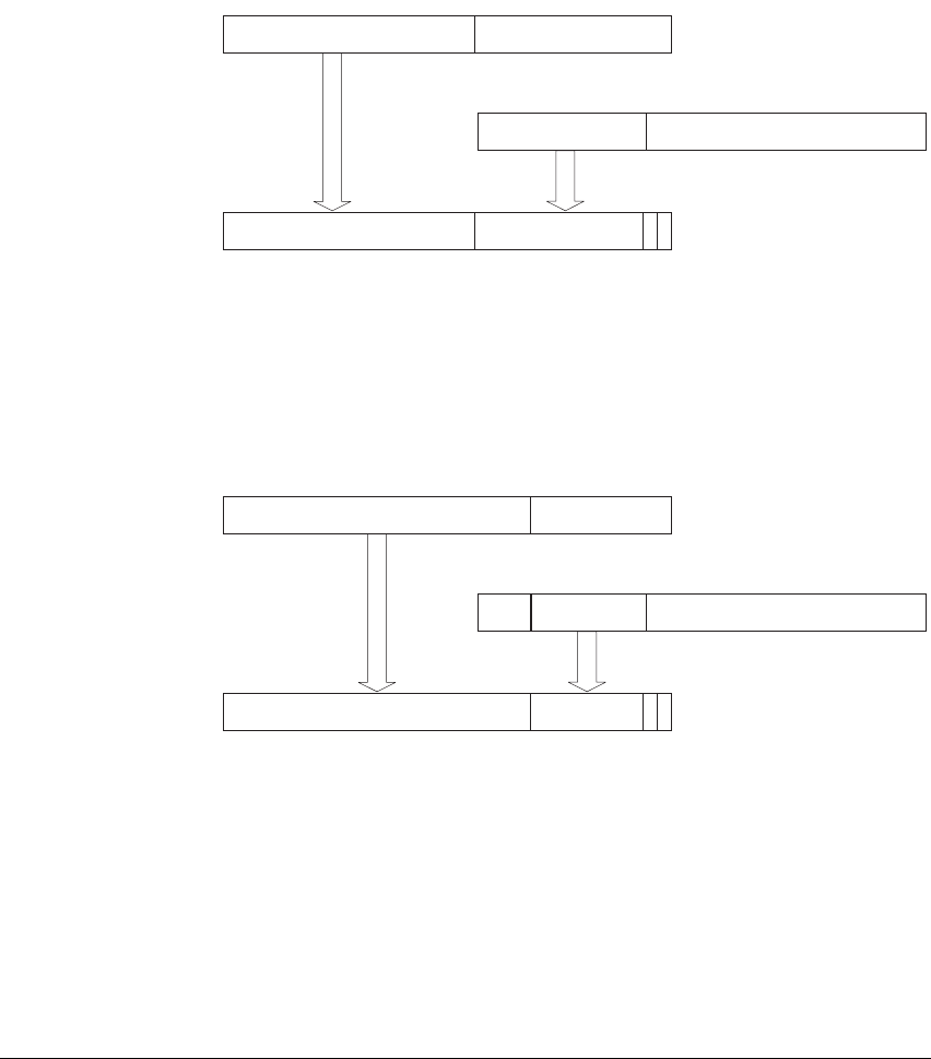
Virtual Memory System Architecture (VMSA)
B3-14 Copyright © 1996-1998, 2000, 2004-2008 ARM Limited. All rights reserved. ARM DDI 0406B
Reading a first-level translation table
To perform a fetch based on TTBR1, Bits TTBR1[31:14] are concatenated with bits [31:20] of the MVA and
two zero bits to produce a 32-bit physical address, as shown in Figure B3-1.
Figure B3-1 Accessing the translation table first-level descriptors based on TTBR1
When performing a fetch based on TTBR0:
• the address bits taken from TTBR0 vary between bits [31:14] and bits [31:7]
• the address bits taken from the MVA vary between bits [31:20] and bits [24:20].
The width of the TTBR0 and MVA fields depend on the value of TTBCR.N, as shown in Figure B3-2.
Figure B3-2 Accessing the translation table first-level descriptors based on TTBR0
31 14 13
31 20 19
31 14 13 2 1
Translation base SBZ
Translation base Table index
Table index
0 0
0
0
0
TTBR1
MVA
PA[31:0] of
first level descriptor
PA[39:32] = 0x00
31 14-N 13-N
31 20 19
31 14-N 13-N 2 1
Translation base SBZ
Translation base Table index
Table index
0 0
0
0
0
TTBR0
MVA
PA[31:0] of
first level descriptor
31-N32-N
PA[39:32] = 0x00
N is the value of TTBCR.N
This field is absent if N==0
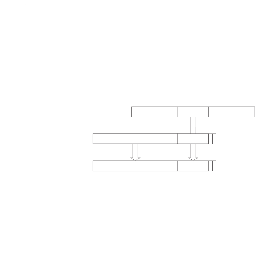
Virtual Memory System Architecture (VMSA)
ARM DDI 0406B Copyright © 1996-1998, 2000, 2004-2008 ARM Limited. All rights reserved. B3-15
Regardless of which register is used as the base for the fetch, the resulting physical address selects a
four-byte translation table entry that is one of:
• A first-level descriptor for a Section or Supersection.
•A Page table pointer to a second-level translation table. In this case a second fetch is performed to
retrieve a second-level descriptor, see Reading a second-level translation table.
• A faulting entry.
Note
Comparing Figure B3-1 on page B3-14 with Figure B3-2 on page B3-14, you can see that when using
TTBR0 with N == 0 the construction of the PA becomes identical to that for TTBR1. Other diagrams in this
section show the PA formation from TTBR0, but also represent PA formation from TTBR1, for which case
N=0.
Reading a second-level translation table
Figure B3-3 shows how the address of a second-level descriptor is obtained by combining:
• the result of the first-level fetch
• the second-level table index value held in bits [19:12] of the MVA.
See Table B3-1 on page B3-8 for the format of the Access control fields of the first-level descriptor.
Figure B3-3 Accessing second-level Page table descriptors
The full translation flow for Sections, Supersections, Small pages and Large
pages
This section summarizes how each of the memory section and page options is described in the translation
tables, and has a subsection summarizing the full translation flow for each of the options.
First-level
descriptor
31 21
0 0
0
10 9
Page table base address Second-level
table index
31 21
0 1
0
10 9
Page table base address Access
control fields
PA[31:0] of
second-level descriptor
31 20 19 0
MVA
12 11
Second-level
table index
PA[39:32] = 0x00

Virtual Memory System Architecture (VMSA)
B3-16 Copyright © 1996-1998, 2000, 2004-2008 ARM Limited. All rights reserved. ARM DDI 0406B
The four options are:
Section A 1MB memory region, described by a first-level translation table descriptor with bits
[18,1:0] == 0b010.
See Translation flow for a Section on page B3-17.
Supersection A 16MB memory region, described by a first-level translation table entry with bits
[18,1:0] == 0b110.
See Translation flow for a Supersection on page B3-18.
Small page A 4KB memory region, described by:
• a first-level translation table entry with bits [1:0] == 0b01, giving a second-level Page
table address.
• a second-level descriptor with bit [1] == 1.
See Translation flow for a Small page on page B3-19.
Large page A 64KB memory region, described by:
• a first-level translation table entry with bits [1:0] == 0b01, giving a second-level Page
table address.
• a second-level descriptor with bits [1:0] == 0b01.
See Translation flow for a Large page on page B3-20.
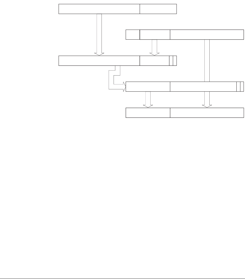
Virtual Memory System Architecture (VMSA)
ARM DDI 0406B Copyright © 1996-1998, 2000, 2004-2008 ARM Limited. All rights reserved. B3-17
Translation flow for a Section
Figure B3-4 shows the virtual to physical addresses translation for a Section. For details of the access
control fields in the first-level descriptor see the Section entry in Table B3-1 on page B3-8.
Figure B3-4 Section address translation
31 14-N 13-N
31 20 19
31 14-N 13-N 2 1
Translation base SBZ
Translation base Table index
Table index
0 0
0
0
0
MVA
PA[31:0] of
first-level descriptor
31-N32-N
31 20 19
Section
base address
21
1 0
0
First-level
read
31 20 19
Section
base address
0
Section index
Section index
Access control fields
First-level
Section descriptor
PA[31:0]
Translation Table
Base Register
PA[39:32] = 0x00
PA[39:32] = 0x00
For a translation based on TTBR0, N is the value of TTBCR.N
For a translation based on TTBR1, N is 0
This field is absent if N==0
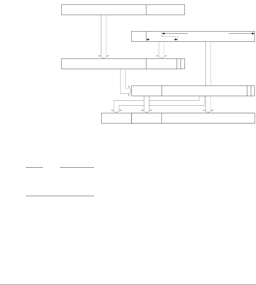
Virtual Memory System Architecture (VMSA)
B3-18 Copyright © 1996-1998, 2000, 2004-2008 ARM Limited. All rights reserved. ARM DDI 0406B
Translation flow for a Supersection
Figure B3-5 shows the virtual to physical addresses translation for a Supersection. For details of the
extended Supersection address and access control fields in the first-level descriptor see the Supersection
entry in Table B3-1 on page B3-8.
Figure B3-5 Supersection address translation
Note
Figure B3-5 shows how, when the MVA addresses a Supersection, the top four bits of the Supersection index
bits of the MVA overlap the bottom four bits of the Table index bits. For more information, see Additional
requirements for translation tables on page B3-11.
31 14-N 13-N
31 20 19
31 14-N 13-N 2 1
Translation base SBZ
Translation base Table index 0 0
0
0
0
MVA
PA31:0] of
first-level descriptor
31-N32-N
31
Supersection
base address
21
1 0
0
First-level
read
31 23
Extended
base address
0
Supersection index
Extended Supersection base address
and Access control fields
First-level
Supersection descriptor
PA[39:0]
Translation Table
Base Register
24 23
Supersection
base address
243239
24 23
Table index
Supersection index
PA[39:32] = 0x00
For a translation based on TTBR0, N is the value of TTBCR.N
For a translation based on TTBR1, N is 0
This field is absent if N==0
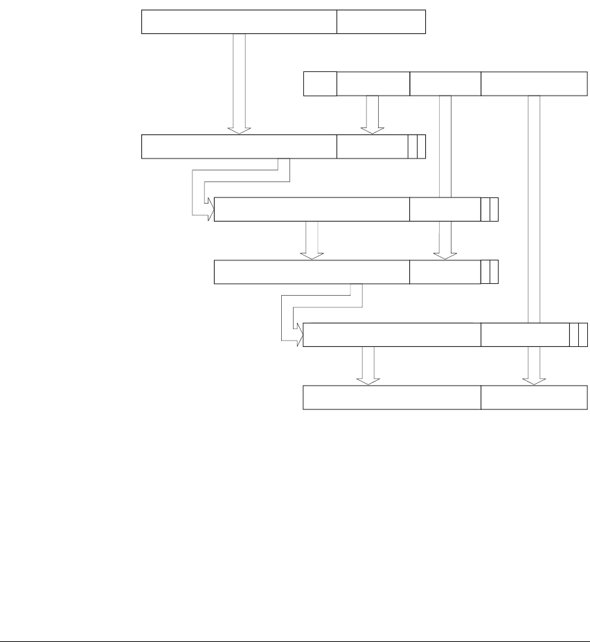
Virtual Memory System Architecture (VMSA)
ARM DDI 0406B Copyright © 1996-1998, 2000, 2004-2008 ARM Limited. All rights reserved. B3-19
Translation flow for a Small page
Figure B3-6 shows the virtual to physical addresses translation for a Small page. For details of the access
control fields in the first-level descriptor see the Page table entry in Table B3-1 on page B3-8. For details of
the access control fields in the second-level descriptor see the Small page entry in Table B3-2 on
page B3-10.
Figure B3-6 Small page address translation
31 14-N 13-N
31 20 19
31 14-N 13-N 2 1
Translation base SBZ
Translation base
First-level
table index
0 0
0
0
0
MVA
PA[31:0] of
first-level descriptor
31-N32-N
First-level
read
First-level
descriptor
Translation Table
Base Register
12 11
Second-level
table index
First-level
table index
31 21
0 0
0
10 9
Page table base address Second-level
table index
31 21
0 1
0
10 9
Page table base address Access
control fields
PA[31:0] of
second-level descriptor
Page index
Second-level
read
Second-level
descriptor 1
21 0
12 1131
0
12 1131
PA[31:0]
Access
control fields
Small page base address
Small page base address Page index
PA[39:32] = 0x00
PA[39:32] = 0x00
PA[39:32] = 0x00
For a translation based on TTBR0, N is the value of TTBCR.N
For a translation based on TTBR1, N is 0
This field is absent if N==0
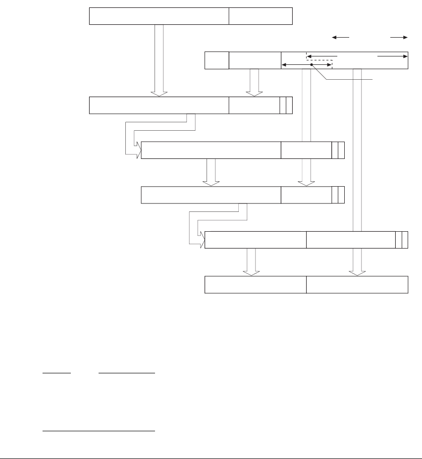
Virtual Memory System Architecture (VMSA)
B3-20 Copyright © 1996-1998, 2000, 2004-2008 ARM Limited. All rights reserved. ARM DDI 0406B
Translation flow for a Large page
Figure B3-7 shows the virtual to physical addresses translation for a Large page. For details of the access
control fields in the first-level descriptor see the Page table entry in Table B3-1 on page B3-8. For details of
the access control fields in the second-level descriptor see the Large page entry in Table B3-2 on
page B3-10.
Figure B3-7 Large page address translation
Note
Figure B3-7 shows how, when the MVA addresses a Large page, the top four bits of the page index bits of
the MVA overlap the bottom four bits of the First-level table index bits. For more information, see
Additional requirements for translation tables on page B3-11. This diagram also shows the width of the
page index bits when addressing a Small page, to show that there is no overlap in this case.
31 14-N 13-N
31 20 19
31 14-N 13-N 2 1
Translation base SBZ
Translation base
First-level
table index
0 0
0
0
0
MVA
PA[31:0]
of first-level descriptor
31-N32-N
First-level
read
First-level
descriptor
12 11
Second-level
table index
First-level
table index
31 21
0 0
0
10 9
Page table base address Second-level
table index
31 21
0 1
0
10 9
Page table base address Access
control fields
PA[31:0] of
second-level descriptor
Page index
16 15
Small page
index range
Second-level
read
Second-level
descriptor 0 1
21 0
16 1531
0
16 1531
PA[31:0]
Access control fieldsLarge page base address
Large page base address Page index
PA[39:32] = 0x00
PA[39:32] = 0x00
PA[39:32] = 0x00
Translation Table
Base Register
For a translation based on TTBR0, N is the value of TTBCR.N
For a translation based on TTBR1, N is 0
This field is absent if N==0

Virtual Memory System Architecture (VMSA)
ARM DDI 0406B Copyright © 1996-1998, 2000, 2004-2008 ARM Limited. All rights reserved. B3-21
B3.3.4 Changing translation table attributes
When changing translation table attributes, you must avoid situations where caching or pipelining effects
mean that overlapping entries or aliases with different attributes might be visible to the processor at the same
time. To avoid these situations, ARM recommends that you invalidate old translation table entries, and
synchronize the effects of those invalidations, before you create new translation table entries that might
overlap or create aliases with different attributes. This approach is sometimes called break before make.
For information about the procedure for synchronizing a change to the translation tables see TLB
maintenance operations and the memory order model on page B3-59.
Translation table entries that create Translation faults are not held in the TLB, see Translation fault on
page B3-43. Therefore TLB and branch predictor invalidation is not required for the synchronization of a
change from a translation table entry that causes a Translation fault to one that does not.
B3.3.5 The access flag
From VMSAv7, the AP[0] bit in the translation table descriptors can be redefined as an access flag. This is
done by setting SCTLR.AFE to 1, see c1, System Control Register (SCTLR) on page B3-96. When this bit
is set, the access permissions information in the translation table descriptors is limited to the AP[2:1] bits,
as described in Simplified access permissions model on page B3-29.
The access flag is used to indicate when a page or section of memory is accessed for the first time since the
access flag was set to 0.
It is IMPLEMENTATION DEFINED whether the access flag is managed by software or by hardware. The two
options are described in the subsections:
•Software management of the access flag
•Hardware management of the access flag.
The access flag mechanism expects that, when an Access Flag fault occurs, software sets the access flag to
1 in the translation table entry that caused the fault. This prevents the fault occurring the next time the
memory is accessed. Software does not have to flush the entry from the TLB after setting the flag.
Software management of the access flag
With an implementation that requires software to manage the access flag, an Access Flag fault is generated
when both:
• the SCTLR.AFE bit is set to 1
• a translation table entry with the access flag set to 0 is read into the TLB.
Hardware management of the access flag
An implementation can choose to provide hardware management of the access flag. In this case, when the
SCTLR.AFE bit is set to 1 and a translation table entry with the access flag set to 0 is read into the TLB, the
hardware must write 1 to the access flag bit of the translation table entry in memory.

Virtual Memory System Architecture (VMSA)
B3-22 Copyright © 1996-1998, 2000, 2004-2008 ARM Limited. All rights reserved. ARM DDI 0406B
Any implementation of hardware management of the access flag must ensure that any software changes to
the translation table are not lost. The architecture does not require software that performs translation table
changes to use interlocked operations. The hardware management mechanisms for the access flag must
prevent any loss of data written to translation table entries that might occur when, for example, a write by
another processor occurs between the read and write phases of a translation table walk that updates the
access flag.
An implementation that provides hardware management of the access flag:
• does not generate Access Flag faults when the access flag is enabled
• uses the HW access flag field, ID_MMFR2[31:28], to indicate this implementation choice, see c0,
Memory Model Feature Register 2 (ID_MMFR2) on page B5-14.
Architecturally, an operating system that makes use of the access flag must support the software faulting
option that uses the Access Flag fault. This provides compatibility between systems that include a hardware
implementation of the access flag and those systems that do not implement this feature.
When an implementation provides hardware management of the access flag it must also implement the
SCTLR.HA bit, that can be used to enable or disable the access flag mechanism. See c1, System Control
Register (SCTLR) on page B3-96.
Changing the access flag enable
It is UNPREDICTABLE whether the TLB caches the effect of the SCTLR.AFE bit on translation tables. This
means that, after changing the SCTLR.AFE bit software must invalidate the TLB before it relies on the
effect of the new value of the SCTLR.AFE bit.

Virtual Memory System Architecture (VMSA)
ARM DDI 0406B Copyright © 1996-1998, 2000, 2004-2008 ARM Limited. All rights reserved. B3-23
B3.4 Address mapping restrictions
ARMv6 supported a page coloring restriction that, when implemented, required all Virtual Address aliases
of a given Physical Address to have the same value for address bits [13:12]. This page coloring restriction
was required to support Virtually Index Physically Tagged (VIPT) caches with a cache way size larger than
4KBytes. For details of the page coloring restriction see Virtual to physical translation mapping restrictions
on page AppxG-26.
ARMv7 does not support page coloring, and requires that all data and unified caches behave as Physically
Indexed Physically Tagged (PIPT) caches.
Note
An ARMv7 implementation might use techniques such as hardware alias avoidance to make a VIPT cache
behave as a PIPT cache, and might improve performance by avoiding accesses to frequently alternating
aliases to a physical address. Such approaches give good results, but ARM recommends migration to the
use of true PIPT caches for all data and unified caches.
In an ARMv7 implementation, any data or unified cache maintenance operation that operates on a virtual
address must take account of the fact that the cache behaves as a PIPT cache. This means that the
implementation must perform the appropriate action on the physical address that corresponds to the MVA
targeted by the operation.
The ARMv7 requirements for instruction caches are described in Requirements for instruction caches.
B3.4.1 Requirements for instruction caches
In a base VMSAv7 implementation, the following conditions require cache maintenance of an instruction
cache:
• writing new data to an instruction address
• writing new address mappings to the translation table
• changing one or more of the TTBR0, TTBR1 and TTBCR registers without changing the ASID
• enabling or disabling the MMU, by writing to the SCTLR.
Note
These conditions are consistent with the maintenance required for an ASID-tagged Virtually Indexed
Virtually Tagged (VIVT) instruction cache that also includes a security status bit for each cache entry.
VMSAv7 can be implemented with an optional extension, the IVIPT extension (Instruction cache Virtually
Indexed Physically Tagged extension). The effect of this extension is to reduce the instruction cache
maintenance requirement to a single condition:
• writing new data to an instruction address.

Virtual Memory System Architecture (VMSA)
B3-24 Copyright © 1996-1998, 2000, 2004-2008 ARM Limited. All rights reserved. ARM DDI 0406B
Note
This condition is consistent with the maintenance required for a Virtually Indexed Physically Tagged (VIPT)
instruction cache.
Software can read the Cache Type Register to determine whether the IVIPT extension is implemented, see
c0, Cache Type Register (CTR) on page B3-83.
Functionally, the relationship between cache type and the software management requirement depends on
whether the operating system uses ASIDs to distinguish processes that use different translation tables:
• when ASIDs are used, management is similar for a VIPT and an ASID-tagged VIVT cache
• when ASIDs are not used, management is similar for a VIVT and an ASID-tagged VIVT cache.
A remapping policy that supports ASID changes means that translation tables can be swapped simply by
updates to the TTBR0, TTBR1 and TTBCR registers, with an appropriate change of the ASID held in the
CONTEXTIDR, see Synchronization of changes of ASID and TTBR on page B3-60. Such changes are
transparent to an ASID-tagged VIVT instruction cache until an ASID value is reused. In contrast, a VIVT
instruction cache that is not ASID-tagged must be invalidated whenever the virtual to physical address
mappings change. Therefore, such a cache must be invalidated on an ASID change.
Software written to rely on a VIPT instruction cache must only be used with processors that implement the
IVIPT. For maximum compatibility across processors, ARM recommends that operating systems target the
ARMv7 base architecture that uses ASID-tagged VIVT instruction caches, and do not assume the presence
of the IVIPT extension. Software that relies on the IVIPT extension might fail in an UNPREDICTABLE way
on an ARMv7 implementation that does not include the IVIPT extension.
With an instruction cache, the distinction between a VIPT cache and a PIPT cache is much less visible to
the programmer than it is for a data cache, because normally the contents of an instruction cache are not
changed by writing to the cached memory. However, there are situations where a program must distinguish
between the different cache tagging strategies. Example B3-1 describes such a situation.
Example B3-1 A situation where software must be aware of the
Instruction cache tagging strategy
Two processes, P1 and P2, share some code and have separate virtual mappings to the same region of
instruction memory. P1 changes this region, for example as a result of a
JIT
, or some other self-modifying
code operation. P2 needs to see the modified code.
As part of its self-modifying code operation, P1 must invalidate the changed locations from the instruction
cache. For more information, see Ordering of cache and branch predictor maintenance operations on
page B2-21. If this invalidation is performed by MVA, and the instruction cache is a VIPT cache, then P2
might continue to see the old code.
In this situation, if the instruction cache is a VIPT cache, after the code modification the entire instruction
cache must be invalidated to ensure P2 observes the new version of the code.

Virtual Memory System Architecture (VMSA)
ARM DDI 0406B Copyright © 1996-1998, 2000, 2004-2008 ARM Limited. All rights reserved. B3-25
Note
Software can read the Cache Type Register to determine whether the instruction cache is PIPT, VIPT, or
ASID-tagged VIVT, see c0, Cache Type Register (CTR) on page B3-83.
B3.4.2 Instruction cache maintenance operations by MVA
On a cache maintenance operation by MVA, the generation of Data Abort exceptions can depend on the
tagging strategy of the instruction cache:
• With an ASID-tagged VIVT instruction cache, it is IMPLEMENTATION DEFINED whether the TLB is
checked to see whether a valid translation table mapping exists for the VA used by a cache
maintenance operation. Therefore, it is IMPLEMENTATION DEFINED whether cache maintenance
operations by MVA can generate Data Abort exceptions.
• With a VIPT or PIPT instruction cache, the TLB must be checked and an abort is generated on a
Translation fault or an Access Flag fault. No abort is generated on a Domain or Permission fault.
For maximum portability, ARM recommends that operating systems always provide an abort handler to
process Data Abort exceptions on instruction cache maintenance operations by MVA, even though some
ARMv7 implementations might not be capable of generating these aborts.
The effect of an instruction cache maintenance operation by MVA can depend on the tagging strategy of the
instruction cache:
• For an ASID -tagged VIVT instruction cache or a VIPT instruction cache, the effect of the operation
is only guaranteed to apply to the modified virtual address supplied to the instruction. It is not
guaranteed to apply to any other alias of that modified virtual address.
• For a PIPT instruction cache, the effect of the operation applies to all aliases of the modified virtual
address supplied to the instruction.

Virtual Memory System Architecture (VMSA)
B3-26 Copyright © 1996-1998, 2000, 2004-2008 ARM Limited. All rights reserved. ARM DDI 0406B
B3.5 Secure and Non-secure address spaces
When implemented, the Security Extensions provide two physical address spaces, a Secure physical address
space and a Non-secure physical address space.
The translation table base registers, TTBR0, TTBR1 and TTBCR are banked between Secure and
Non-secure versions, and the security state of a memory access selects the corresponding version of the
registers. Therefore, the translation tables are separated between Secure and Non-secure versions.
Translation table walks are made to the physical address space corresponding to the security state of the
translation tables.
The Non-secure translation table entries can only translate a virtual address to a physical address in the
Non-secure physical address space. Secure translation table entries can translate a virtual address to a
physical addresses in either the Secure or the Non-secure address space. Selection of which physical address
space to use is managed by the NS field in the first-level descriptors, see First-level descriptors on
page B3-8:
• for Non-secure translation table entries, the NS field is ignored
• for Secure translation table entries, the NS field determines which physical address space is accessed:
NS == 0 Secure physical address space is accessed.
NS == 1 Non-secure physical address space is accessed.
Because the NS field is defined only in the first level translation tables, the granularity of the Secure and
Non-secure memory spaces is 1MB. However, in these memory regions you can define physical memory
regions with a granularity of 4KB. For more information, see Translation tables on page B3-7.
Note
A system implementation can alias parts of the Secure physical address space to the Non-secure physical
address space in implementation-specific ways. As with any other aliasing of physical memory, the use of
aliases in this way can require the use of cache maintenance operations to ensure that changes to memory
made using one alias of the physical memory are visible to accesses to the other alias of the physical
memory.

Virtual Memory System Architecture (VMSA)
ARM DDI 0406B Copyright © 1996-1998, 2000, 2004-2008 ARM Limited. All rights reserved. B3-27
B3.5.1 The effect of the Security Extensions on the cache operations
When the Security Extensions are implemented and each security state has its own physical address space,
Table B3-3 shows the effect of the security state on the cache operations.
For locked entries and entries that might be locked, the behavior of cache maintenance operations described
in The interaction of cache lockdown with cache maintenance on page B2-18 applies. This behavior is not
affected by the Security Extensions.
With an implementation that generates aborts if entries are locked or might be locked in the cache, if the use
of lockdown aborts is enabled then these aborts can occur on any cache maintenance operation regardless
of the Security Extensions.
Table B3-3 Effect of the security state on the cache operations
Cache operation Security
state Targeted entry
Instruction cache operations
Invalidate All Non-
secure
All instruction cache lines that contain entries that can be accessed
from the Non-secure security state
Invalidate All Secure All instruction cache lines
Invalidate by MVA Either Base Architecture:
All Lines that match the specified MVA and the current ASID and
come from the same virtual address space as the current security
state
IVIPT extension:a
All Lines that match the specified MVA and the current ASID and
come from the same physical address space as described in the
translation tables
Data or unified cache operations
Invalidate, Clean, Clean
and Invalidate by set/way
Non-
secure
Line specified by set/way provided that the entry comes from the
Non-secure physical address space
Invalidate, Clean, Clean
and Invalidate by set/way
Secure Line specified by set/way regardless of the physical address space that
the entry has come from
Invalidate, Clean, Clean
and Invalidate by MVA
Either All Lines that match the specified MVA and the current ASID and
come from the same physical address space, as described in the
translation tables
a. For more information about the IVIPT extension see Requirements for instruction caches on page B3-23.

Virtual Memory System Architecture (VMSA)
B3-28 Copyright © 1996-1998, 2000, 2004-2008 ARM Limited. All rights reserved. ARM DDI 0406B
B3.6 Memory access control
Access to a memory region is controlled by the access permission bits and the domain field in the TLB entry.
These form part of the translation table entry formats described in Translation tables on page B3-7. The bits
and fields are summarized in First-level descriptors on page B3-8 and Second-level descriptors on
page B3-10.
The TLB memory access controls are described in:
•Access permissions
•The Execute Never (XN) attribute and instruction prefetching on page B3-30
•Domains on page B3-31.
B3.6.1 Access permissions
The access permission bits control access to the corresponding memory region. If an access is made to an
area of memory without the required permissions, a Permission fault is generated if the domain is set to
Client. The access permissions are determined by the AP[2:0] bits in the translation table entry. The XN bit
in the translation table entry provides an additional permission bit for instruction fetches.
Note
• Before VMSAv7, the SCTLR.S and SCTLR.R bits also affect the access permissions. For more
information, see Translation attributes on page AppxH-22.
• From VMSAv7, the full set of access permissions shown in Table B3-4 are only supported when the
SCTLR.AFE bit is set to 0. When SCTLR.AFE = 1, the only supported access permissions are those
described in Simplified access permissions model on page B3-29.
• In previous issues of the ARM Architecture Reference Manual and in some other documentation, the
AP[2] bit in the translation table entries is described as the APX bit.
Table B3-4 shows the encoding of the access permissions:
Table B3-4 VMSAv7 MMU access permissions
AP[2] AP[1:0] Privileged
permissions
User
permissions Description
0 00 No access No access All accesses generate Permission faults
0 01 Read/write No access Privileged access only
0 10 Read/write Read-only Writes in User mode generate Permission faults
0 11 Read/write Read/write Full access
1 00 - - Reserved

Virtual Memory System Architecture (VMSA)
ARM DDI 0406B Copyright © 1996-1998, 2000, 2004-2008 ARM Limited. All rights reserved. B3-29
Each memory region can be tagged as not containing executable code. If the Execute-never (XN) bit is set
to 1 and the region is in a Client domain, any attempt to execute an instruction in that region results in a
Permission fault. If the XN bit is 0 and there is valid read permission, code can execute from that memory
region, provided that no other Prefetch Abort condition exists.
Note
The XN bit is ignored on accesses to Manager domains.
Simplified access permissions model
Some memory management require a simple access permissions model where:
• one flag selects between read-only and read/write access
• a second flag selects between User and Kernel control.
In the ARM architecture, this model permits four access combinations:
• read-only by both privileged and unprivileged code
• read/write by both privileged and unprivileged code
• read-only by privileged code, no access by unprivileged code
• read/write by privileged code, no access by unprivileged code.
With the VMSAv7 MMU access permissions shown in Table B3-4 on page B3-28, this model is
implemented by:
• Setting the AP[0] bit to 1, unless the SCTLR.AFE bit is set to 1, see c1, System Control Register
(SCTLR) on page B3-96.
• Using the AP[2:1] bits to control access, as shown in Table B3-5 on page B3-30.
1 01 Read-only No access Privileged read-only
1 10 Read-only Read-only Privileged and User read-only, deprecated in VMSAv7a
1 11 Read-only Read-only Privileged and User read-onlyb
a. From VMSAv7, ARM strongly recommends that the 0b11 encoding is used for Privileged and User read-only.
b. This mapping is introduced in VMSAv7, and is reserved in VMSAv6. For more information, see Simplified access
permissions model.
Table B3-4 VMSAv7 MMU access permissions (continued)
AP[2] AP[1:0] Privileged
permissions
User
permissions Description

Virtual Memory System Architecture (VMSA)
B3-30 Copyright © 1996-1998, 2000, 2004-2008 ARM Limited. All rights reserved. ARM DDI 0406B
Note
This model depends on the definition of the AP[2] == 1, AP[1:0] == 0b11 encoding shown in Table B3-4
on page B3-28. This encoding is introduced in VMSAv7, and therefore the simplified access permissions
model cannot be supported in VMSAv6.
When the SCTLR.AFE bit is set to 1 the AP[0] bit becomes an access flag, see The access flag on
page B3-21. In this case, this simplified access permissions model becomes the only supported access
permissions model.
B3.6.2 The Execute Never (XN) attribute and instruction prefetching
An implementation must not fetch instructions from any memory location that is marked as Execute Never.
A location is marked as Execute Never when it has its XN attribute set to 1 in a Client domain. When the
MMU is enabled, instructions can only be fetched or prefetched from memory locations in Client domains
where:
• XN is set to 0
• valid read permissions exist
• no other Prefetch Abort condition exists.
Any region of memory that is read-sensitive must be marked as Execute Never, to avoid the possibility of a
speculative prefetch accessing the memory region. For example, any memory region that corresponds to a
read-sensitive peripheral must be marked as Execute Never.
The XN attribute is not checked for domains marked as Manager. Read-sensitive memory must not be
included in domains marked as Manager, because the XN bit does not prevent prefetches in these cases.
The XN attribute is not checked when the MMU is disabled. All VMSAv7 implementations must ensure
that, when the MMU is disabled, prefetching down non-sequential paths cannot cause unwanted accesses to
read-sensitive devices.
Table B3-5 VMSAv7 simple access control model
AP[2] AP[1] Accessa
a. Kernel access corresponds to access by privileged code
only.
0 0 Kernel, read/write
0 1 User, read/write
1 0 Kernel, read-only
1 1 User, read-only

Virtual Memory System Architecture (VMSA)
ARM DDI 0406B Copyright © 1996-1998, 2000, 2004-2008 ARM Limited. All rights reserved. B3-31
B3.6.3 Domains
A domain is a collection of memory regions. The ARM VMSA architecture supports 16 domains, and each
VMSA memory region is assigned to a domain:
• First-level translation table entries for Page tables and Sections include a domain field.
• Translation table entries for Supersections do not include a domain field. Supersections are defined
as being in domain 0.
• Second-level translation table entries inherit a domain setting from the parent first-level Page table
entry.
• Each TLB entry includes a domain field.
A domain field specifies which domain the entry is in. Access to each domain is controlled by a two-bit field
in the Domain Access Control Register, see c3, Domain Access Control Register (DACR) on page B3-119.
Each field enables the access to an entire domain to be enabled and disabled very quickly, so that whole
memory areas can be swapped in and out of virtual memory very efficiently. The VMSA supports two kinds
of domain access:
Clients Users of domains, guarded by the access permissions of the TLB entries for that domain.
Clients execute programs and access data held in the domain.
Managers Control the behavior of the domain, and are not guarded by the access permissions for TLB
entries in that domain. The domain behavior controlled by a Manager covers:
• the sections and pages currently in the domain
• the current access permissions for the domain.
A single program might:
• be a Client of some domains
• be a Manager of some other domains
• have no access to the remaining domains.
This permits very flexible memory protection for programs that access different memory resources.
Table B3-6 shows the encoding of the bits in the DACR.
Table B3-6 Domain access values
Value Access types Description
00 No access Any access generates a Domain fault
01 Client Accesses are checked against the access permission bits in the TLB entry
10 Reserved Using this value has UNPREDICTABLE results
11 Manager Accesses are not checked against the access permission bits in the TLB
entry, so a Permission fault cannot be generated

Virtual Memory System Architecture (VMSA)
B3-32 Copyright © 1996-1998, 2000, 2004-2008 ARM Limited. All rights reserved. ARM DDI 0406B
B3.7 Memory region attributes
Each TLB entry has an associated set of memory region attributes. These control accesses to the caches,
how the write buffer is used, and if the memory region is Shareable and therefore must be kept coherent.
From VMSAv6:
• Most of the memory attributes are controlled by the C and B bits and the TEX[2:0] field of the
translation table entries. More information about these attributes is given in the sections:
—The alternative descriptions of the Memory region attributes
—C, B, and TEX[2:0] encodings without TEX remap on page B3-33
—Memory region attribute descriptions when TEX remap is enabled on page B3-34.
• When the Security Extensions are implemented, the NS bit provides an additional memory attribute,
see Secure and Non-secure address spaces on page B3-26.
Note
The Bufferable (B), Cacheable (C), and Type Extension (TEX) bit names are inherited from earlier versions
of the architecture. These names no longer adequately describe the function of the B, C, and TEX bits.
The translation table entries also include an S bit. This bit:
• Is ignored if the entry refers to Device or Strongly-ordered memory.
• For Normal memory, determines whether the memory region is Shareable or Non-shareable:
S==0 Normal memory region is Non-shareable
S==1 Normal memory region is Shareable.
B3.7.1 The alternative descriptions of the Memory region attributes
From VMSAv7, there are two alternative schemes for describing the memory region attributes, and the
current scheme is selected by the SCTLR.TRE (TEX Remap Enable) bit, see c1, System Control Register
(SCTLR) on page B3-96. The two schemes are:
TRE == 0 TEX Remap disabled. TEX[2:0] are used, with the C and B bits, to describe the memory
region attributes.
This is the scheme used in VMSAv6, and it is described in C, B, and TEX[2:0] encodings
without TEX remap on page B3-33.
TRE == 1 TEX Remap enabled. TEX[2:1] are reassigned for use as flags managed by the operating
system. The TEX[0], C and B bits are used to describe the memory region attributes, with
the MMU remap registers:
• the Primary Region Remap Register, PRRR
• the Normal Memory Remap Register, NMRR.
This scheme is described in Memory region attribute descriptions when TEX remap is
enabled on page B3-34.

Virtual Memory System Architecture (VMSA)
ARM DDI 0406B Copyright © 1996-1998, 2000, 2004-2008 ARM Limited. All rights reserved. B3-33
When the Security Extensions are implemented, the SCTLR.TRE bit is banked between the Secure and
Non-secure states.
B3.7.2 C, B, and TEX[2:0] encodings without TEX remap
Table B3-7 shows the C, B, and TEX[2:0] encodings when TEX remap is disabled (TRE == 0).
See Memory types and attributes and the memory order model on page A3-24 for an explanation of Normal,
Strongly-ordered and Device memory types and of the Shareable attribute.
Table B3-7 TEX, C, and B encodings when TRE == 0
TEX[2:0] C B Description Memory type Page Shareable
000 0 0 Strongly-ordered Strongly-ordered Shareable
000 0 1 Shareable Device Device Shareable
000 1 0 Outer and Inner Write-Through, no
Write-Allocate
Normal S bita
000 1 1 Outer and Inner Write-Back, no Write-Allocate Normal S bita
001 0 0 Outer and Inner Non-cacheable Normal S bita
001 0 1 Reserved - -
001 1 0 IMPLEMENTATION DEFINED IMPLEMENTATION
DEFINED
IMPLEMENTATION
DEFINED
001 1 1 Outer and Inner Write-Back, Write-Allocate Normal S bita
010 0 0 Non-shareable Device Device Non-shareable
010 0 1 Reserved - -
010 1 X Reserved - -
011 X X Reserved - -
1BB A A Cacheable memory: AA = Inner attributeb
BB = Outer attribute
Normal S bita
a. Whether the memory is Shareable depends on the value of the S bit, see description in Memory region attributes on
page B3-32.
b. For more information, see Cacheable memory attributes on page B3-34.

Virtual Memory System Architecture (VMSA)
B3-34 Copyright © 1996-1998, 2000, 2004-2008 ARM Limited. All rights reserved. ARM DDI 0406B
Cacheable memory attributes
When TEX[2] == 1, the translation table entry describes Cacheable memory, and the rest of the encoding
defines the Inner and Outer cache attributes:
TEX[1:0] defines the Outer cache attribute
C,B defines the Inner cache attribute
The same encoding is used for the Outer and Inner cache attributes. Table B3-8 shows the encoding.
B3.7.3 Memory region attribute descriptions when TEX remap is enabled
The VMSAv6 scheme for describing the memory region attributes, described in C, B, and TEX[2:0]
encodings without TEX remap on page B3-33, uses the TEX[2:0], C and B bits to describe all of the options
for Inner and Outer cacheability. However, many system software implementations do not need to use all of
these options simultaneously. Instead a smaller subset of attributes can be enabled. This alternative
functionality is called TEX remap, and permits software to hold software-interpreted values in the
translation tables. When TEX remap is enabled:
• only the TEX[0], C and B bits are used to describe the memory region attributes
• fewer attribute options are available at any time
• the available options are configurable using the PRRR and NMRR registers
• TEX[2:1] are not updated by hardware, see The OS managed translation table bits on page B3-38.
When TEX remap is enabled:
• For seven of the eight possible combinations of the TEX[0], C and B bits:
— a field in the PRRR defines the corresponding memory region as being Normal, Device or
Strongly-ordered memory
— a field in the NMRR defines the Inner cache attributes that apply if the PRRR field identifies
the region as Normal memory
— a second field in the NMRR defines the Outer cache attributes that apply if the PRRR field
identifies the region as Normal memory.
• The meaning of the eighth combination for the TEX[0], C and B bits is IMPLEMENTATION DEFINED
Table B3-8 Inner and Outer cache attribute encoding
Encoding Cache attribute
0 0 Non-cacheable
0 1 Write-Back, Write-Allocate
1 0 Write-Through, no Write-Allocate
1 1 Write-Back, no Write-Allocate

Virtual Memory System Architecture (VMSA)
ARM DDI 0406B Copyright © 1996-1998, 2000, 2004-2008 ARM Limited. All rights reserved. B3-35
• Four bits in the PRRR permit mapping of the Shareable attribute by defining, for the translation table
S bit:
— the meaning of S == 0 if the region is identified as Device memory
— the meaning of S == 1 if the region is identified as Device memory
— the meaning of S == 0 if the region is identified as Normal memory
— the meaning of S == 1 if the region is identified as Normal memory.
In each case, the meaning of the Shareable bit value is that the memory region is one of:
—Shareable
— Non-shareable.
For each of the possible encodings of the TEX[0], C and B bits in a translation table entry, Table B3-9 shows
which fields of the PRRR and NMRR registers describe the memory region attributes.
To find the meaning of the value of the S bit in a translation table entry you must:
• use Table B3-9 to find the memory type of the region described by the entry
• if the memory type is Strongly-ordered then the region is Shareable
• if the memory type is not Strongly-ordered then look up the memory type and value of the S bit in
Table B3-10 on page B3-36 to find which bit of the PRRR defines the Shareable attribute of the
region.
Table B3-9 TEX, C, and B encodings when TRE == 1
Encoding
Memory typea
Cache attributesa, b:Outer Shareable
attributeb
TEX[0] C B Inner cache Outer cache
0 0 0 PRRR[1:0] NMRR[1:0] NMRR[17:16] NOT(PRRR[24])
0 0 1 PRRR[3:2] NMRR[3:2] NMRR[19:18] NOT(PRRR[25])
0 1 0 PRRR[5:4] NMRR[5:4] NMRR[21:20] NOT(PRRR[26])
0 1 1 PRRR[7:6] NMRR[7:6] NMRR[23:22] NOT(PRRR[27])
1 0 0 PRRR[9:8] NMRR[9:8] NMRR[25:24] NOT(PRRR[28])
1 0 1 PRRR[11:10] NMRR[11:10] NMRR[27:26] NOT(PRRR[29])
110
IMPLEMENTATION
DEFINED
IMPLEMENTATION
DEFINED
IMPLEMENTATION
DEFINED
IMPLEMENTATION
DEFINED
1 1 1 PRRR[15:14] NMRR[15:14] NMRR[31:30] NOT(PRRR[31])
a. For details of the memory type field encodings see c10, Primary Region Remap Register (PRRR) on page B3-143. For
details of the cache attribute encodings see Table B3-8 on page B3-34.
b. Only applies if the memory type for the region is mapped as Normal memory and the location is Shareable.

Virtual Memory System Architecture (VMSA)
B3-36 Copyright © 1996-1998, 2000, 2004-2008 ARM Limited. All rights reserved. ARM DDI 0406B
• The appropriate bit of the PRRR indicates whether the region is Shareable or Non-shareable.
Note
When TEX remapping is enabled, it is possible for a translation table entry with S = 0 to be mapped
as Shareable memory.
For full descriptions of the TEX remap registers see:
•c10, Primary Region Remap Register (PRRR) on page B3-143
•c10, Normal Memory Remap Register (NMRR) on page B3-146.
When the Security Extensions are implemented, the TEX remap registers and the SCTLR.TRE bit are
banked between the Secure and Non-secure security states. For more information, see The effect of the
Security Extensions on TEX remapping on page B3-39.
When TEX remap is enabled, the mappings specified by the PRRR and NMRR determine the mapping of
the TEX[0], C and B bits in the translation tables to memory type and cacheability attributes:
1. The primary mapping, indicated by a field in the PRRR as shown in the Memory region column of
Table B3-9 on page B3-35, takes precedence.
2. Any region that is mapped as Normal memory can have the Inner and Outer Cacheable attributes
determined by the NMRR.
3. If it is supported, the Outer Shareable mapping adds a third level of attribute, see Interpretation of the
NOSn fields in the PRRR on page B3-37.
The TEX remap registers must be static during normal operation. In particular, when the remap registers are
changed:
• it is IMPLEMENTATION DEFINED when the changes take effect
• it is UNPREDICTABLE whether the TLB caches the effect of the TEX remap on translation tables.
Table B3-10 Remapping of the S bit
Memory type
Remapping of Shareable attribute when
S = 0 S = 1
Strongly-ordered Shareablea
a. No remapping, Strongly-ordered memory is always Shareable.
Shareablea
Device PRRR[16] PRRR[17]
Normal PRRR[18] PRRR[19]

Virtual Memory System Architecture (VMSA)
ARM DDI 0406B Copyright © 1996-1998, 2000, 2004-2008 ARM Limited. All rights reserved. B3-37
The sequence to ensure the synchronization of changes to the TEX remap registers is:
1. Perform a DSB. This ensures any memory accesses using the old mapping have completed.
2. Write the TEX remap registers or SCTLR.TRE bit.
3. Perform an ISB. This ensures synchronization of the register updates.
4. Invalidate the entire TLB.
5. Perform a DSB. This ensures completion of the entire TLB operation.
6. Clean and invalidate all caches. This removes any cached information associated with the old
mapping.
7. Perform a DSB. This ensures completion of the cache maintenance.
8. Perform an ISB. This ensures instruction synchronization.
This extends the standard rules for the synchronization of changes to CP15 registers described in Changes
to CP15 registers and the memory order model on page B3-77, and provides implementation freedom as to
whether or not the effect of the TEX remap is cached.
Interpretation of the NOSn fields in the PRRR
When all of the following apply, the NOSn fields in the PRRR distinguish between Inner Shareable and
Outer Shareable memory regions:
• the SCTLR.TRE bit is set to 1
• the region is mapped as Normal memory
• the Normal memory remapping of the S bit value for the entry makes the region Shareable
• the implementation supports the distinction between Inner Shareable and Outer Shareable.
If the SCTLR.TRE bit is set to 0, an implementation can provide an IMPLEMENTATION DEFINED mechanism
to interpret the NOSn fields in the PRRR, see SCTLR.TRE, SCTLR.M, and the effect of the MMU remap
registers on page B3-38.
The values of the NOSn fields in the PRRR have no effect if any of the following apply:
• the SCTLR.TRE bit is set to 0 and the IMPLEMENTATION DEFINED mechanism has not been invoked
• the region is not mapped as Normal memory
• the Normal memory remapping of the S bit value for the entry makes the region Non-shareable.
The NOSn fields in the PRRR are RAZ/WI if the implementation does not support the distinction between
Inner Shareable and Outer Shareable memory regions.

Virtual Memory System Architecture (VMSA)
B3-38 Copyright © 1996-1998, 2000, 2004-2008 ARM Limited. All rights reserved. ARM DDI 0406B
SCTLR.TRE, SCTLR.M, and the effect of the MMU remap registers
When TEX remap is disabled, because the SCTLR.TRE bit is set to 0:
• the effect of the MMU remap registers can be IMPLEMENTATION DEFINED
• the interpretation of the fields of the PRRR and NMRR registers can differ from the description given
in this section.
VMSAv7 requires that the effect of these registers is limited to remapping the attributes of memory
locations. These registers must not change whether any cache or MMU hardware is enabled. The
mechanism by which the MMU remap registers have an effect when the SCTLR.TRE bit is set to 0 is
IMPLEMENTATION DEFINED. The ARMv7 architecture requires that from reset, if the IMPLEMENTATION
DEFINED mechanism has not been invoked:
• If the MMU is enabled, the architecturally-defined behavior of the TEX[2:0], C, and B bits must
apply, without reference to the TEX remap functionality. In other words, memory attribute
assignment must comply with the scheme described in C, B, and TEX[2:0] encodings without TEX
remap on page B3-33.
• If the MMU is disabled, then the architecturally-defined behavior of the VMSA with the MMU
disabled must apply, without reference to the TEX remap functionality. See Enabling and disabling
the MMU on page B3-5.
Typical mechanisms for enabling the IMPLEMENTATION DEFINED effect of the TEX Remap registers when
SCTLR.TRE bit is set to 0 include:
• a control bit in the ACTLR, or in a CP15 c15 register
• changing the behavior when the PRRR and NMRR registers are changed from their
IMPLEMENTATION DEFINED reset values.
In addition, if the MMU is disabled and the SCTLR.TRE bit is set to 1, the architecturally-defined behavior
of the VMSA with the MMU disabled must apply without reference to the TEX remap functionality.
When the Security Extensions are implemented, the IMPLEMENTATION DEFINED effect of these registers
must only take effect in the security domain of the registers.
The OS managed translation table bits
When TEX remap is enabled, the TEX[2:1] bits in the translation table descriptors are available as two flags
that can be managed by the operating system. In VMSAv7, as long as the SCTLR.TRE bit is set to 1, the
values of the TEX[2:1] bits are ignored by the memory management hardware. You can write any value to
these bits in the translation tables. In a system that implements access flag updates in hardware, a hardware
access flag update never changes these bits.

Virtual Memory System Architecture (VMSA)
ARM DDI 0406B Copyright © 1996-1998, 2000, 2004-2008 ARM Limited. All rights reserved. B3-39
B3.7.4 The effect of the Security Extensions on TEX remapping
When the Security Extensions are implemented, the MMU remap registers are banked in the Secure and
Non-secure security states. The register versions for the current security state apply to all TLB lookups. The
SCTLR.TRE bit is banked in the Secure and Non-secure copies of the register, and the appropriate version
of this bit determines whether TEX remapping is applied to TLB lookups in the current security state.
When the Security Extensions are implemented, the translation table descriptors include an NS bit. For
security reasons, the NS bit is not accessible through the MMU remap registers.
Write accesses to the Secure copies of the MMU remap registers are disabled when the CP15SDISABLE
input is asserted HIGH, and the
MCR
operations to access these registers become UNDEFINED. For more
information, see The CP15SDISABLE input on page B3-76.

Virtual Memory System Architecture (VMSA)
B3-40 Copyright © 1996-1998, 2000, 2004-2008 ARM Limited. All rights reserved. ARM DDI 0406B
B3.8 VMSA memory aborts
The mechanisms that cause the ARM processor to take an exception because of a failed memory access are:
MMU fault The MMU detects an access restriction and signals the processor.
External abort A memory system component other than the MMU signals an illegal or faulting
memory access.
The exception taken is a Prefetch Abort exception if either of these occurs synchronously on an instruction
fetch, and a Data Abort exception otherwise.
Collectively, these mechanisms are called aborts. The different abort mechanisms are described in:
•MMU faults
•External aborts on page B3-45.
An access that causes an abort is said to be aborted, and uses the Fault Address Registers (FARs) and Fault
Status Registers (FSRs) to record context information. The FARs and FSRs are described in Fault Status
and Fault Address registers in a VMSA implementation on page B3-48.
Also, a debug exception can cause the processor to take a Prefetch Abort exception or a Data Abort
exception, and to update the FARs and FSRs. For details see Chapter C4 Debug Exceptions and Debug event
prioritization on page C3-43.
B3.8.1 MMU faults
The MMU checks the memory accesses required for instruction fetches and for explicit memory accesses:
• if an instruction fetch faults it generates a Prefetch Abort exception
• if an explicit memory access faults it generates a Data Abort exception.
For more information about Prefetch Abort exceptions and Data Abort exceptions see Exceptions on
page B1-30.
MMU faults are always synchronous. For more information, see Terminology for describing exceptions on
page B1-4.
When the MMU generates an abort for a region of memory, no memory access is made if that region is or
could be marked as Strongly-ordered or Device.
Fault-checking sequence
The sequence used by the MMU to check for access faults is slightly different for sections and pages. For
both sections and pages:
• Figure B3-8 on page B3-41 shows the checking sequence
• Figure B3-9 on page B3-42 shows the descriptor fetch and check performed during the checking
sequence.
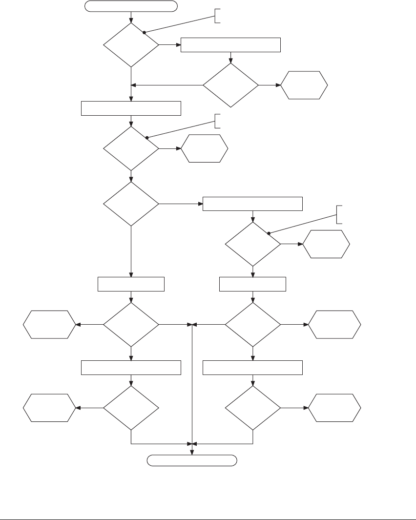
Virtual Memory System Architecture (VMSA)
ARM DDI 0406B Copyright © 1996-1998, 2000, 2004-2008 ARM Limited. All rights reserved. B3-41
Figure B3-8 VMSA fault checking sequence
Page
Section
Get second-level descriptor
Check domainCheck domain
Access
type?
Client
Manager
No
access
No
Physical Address
Check access permissions
Violation
?
No
Yes
Section
permission
fault
Yes Page
permission
fault
Check access permissions
Violation
?
No
Client
Access
type?
Manager
No
access
Section
domain
fault
Page
domain
fault
Got valid
descriptor
?
Abort
Section
or Page
?
Get first-level descriptor
No
Got valid
descriptor
?
Abort
See Descriptor fetch
and check flowchart
Check address alignment
Misaligned
?
Alignment
fault
Yes
No
No
Yes
Alignment
check?
Modified Virtual Address
See Descriptor fetch and check flowchart
Is the access subject to an alignment check?
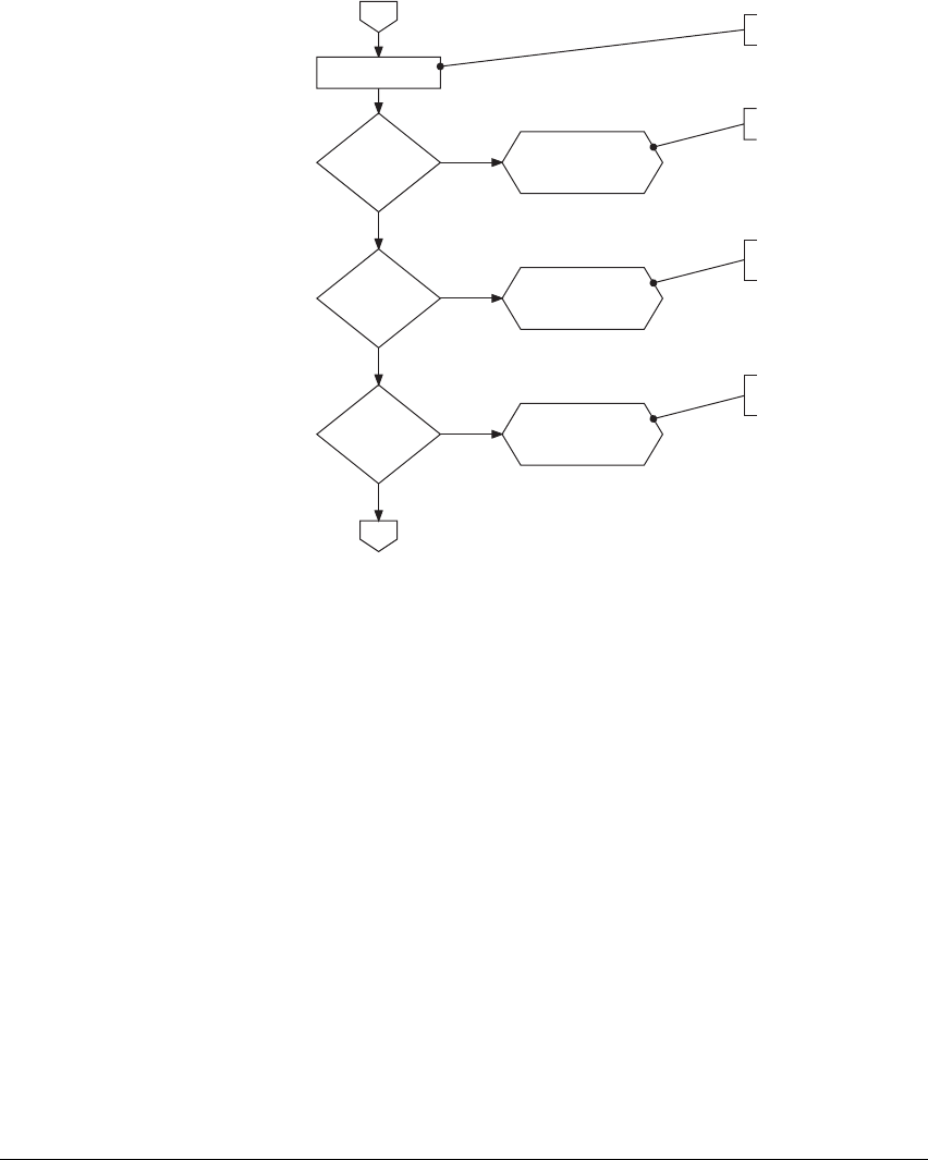
Virtual Memory System Architecture (VMSA)
B3-42 Copyright © 1996-1998, 2000, 2004-2008 ARM Limited. All rights reserved. ARM DDI 0406B
Figure B3-9 Descriptor fetch and check in the fault checking sequence
The faults that might be detected during the fault checking sequence are described in the following
subsections:
•Alignment fault
•External abort on a translation table walk
•Translation fault on page B3-43
•Access Flag fault on page B3-43
•Domain fault on page B3-44
•Permission fault on page B3-44.
Alignment fault
The ARMv7 memory architecture requires support for strict alignment checking. This checking is
controlled by the SCTLR.A bit, see c1, System Control Register (SCTLR) on page B3-96. For details of
when Alignment faults are generated see Unaligned data access on page A3-5.
External abort on a translation table walk
This is described in the section External aborts on page B3-45, see External abort on a translation table
walk on page B3-46.
External
abort?
No
Descriptor
fault ?
Access flag
fault
?
Yes
Out
Translation
external abort
Section or Page
Descriptor
fault
Section or Page
Access flag
fault
No
Yes
No
Yes
In
Get descriptor
At first or second level
Section at first level
Page at second level
Section at first level
Page at second level
First or second level

Virtual Memory System Architecture (VMSA)
ARM DDI 0406B Copyright © 1996-1998, 2000, 2004-2008 ARM Limited. All rights reserved. B3-43
Translation fault
There are two types of Translation fault:
Section This is generated if the first-level descriptor is marked as invalid. This happens if bits [1:0]
of the descriptor are:
• 0b00, the fault encoding
• 0b11, the reserved encoding.
For more information, see First-level descriptors on page B3-8.
Page This is generated if the second-level descriptor is marked as invalid. This happens if
bits [1:0] of the descriptor are 0b00, the fault encoding. For more information, see
Second-level descriptors on page B3-10.
Translation table entries that result in Translation faults are guaranteed not to be cached, meaning the TLB
is not updated. Therefore, when a Translation fault occurs, it is not necessary to perform any TLB
maintenance operations to remove the faulting entries.
Translation faults can be generated by data and unified cache maintenance operations by MVA. It is
IMPLEMENTATION DEFINED whether Translation faults can be generated by instruction cache invalidate by
MVA operations, see Instruction cache maintenance operations by MVA on page B3-25.
It is IMPLEMENTATION DEFINED whether Translation faults can be generated by branch predictor
maintenance operations.
Access Flag fault
There are two types of Access Flag fault:
Section This can be generated when a section with AF == 0 is accessed.
Page This can be generated when a page with AF == 0 is accessed.
Access Flag faults only occur on a VMSAv7 implementation that provides software management of the
access flag, and are only generated when the AFE flag is set to 1 in the SCTLR, see c1, System Control
Register (SCTLR) on page B3-96.
Translation table entries that result in Access Flag faults are guaranteed not to be cached, meaning the TLB
is not updated. Therefore, when an Access Flag fault occurs, it is not necessary to perform any TLB
maintenance operations to remove the faulting entries.
It is IMPLEMENTATION DEFINED whether Access Flag faults can be generated by any cache maintenance
operations by MVA.
It is IMPLEMENTATION DEFINED whether Access Flag faults can be generated by branch predictor invalidate
by MVA operations.
For more information, see The access flag on page B3-21.

Virtual Memory System Architecture (VMSA)
B3-44 Copyright © 1996-1998, 2000, 2004-2008 ARM Limited. All rights reserved. ARM DDI 0406B
Domain fault
There are two types of Domain fault:
Section When a first-level descriptor fetch returns a valid Section first-level descriptor, the MMU
checks the domain field of that descriptor against the Domain Access Control Register, and
generates a Section Domain fault if this check fails.
Page When a second-level descriptor fetch returns a valid second-level descriptor, the MMU
checks the domain field of the first-level descriptor that required the second-level fetch
against the Domain Access Control Register, and generates a Page Domain fault if this
check fails.
Domain faults cannot occur on cache or branch predictor maintenance operations.
For more information, see Domains on page B3-31.
Where a Domain fault results in an update to the associated translation tables, the appropriate TLB entry
must be flushed to ensure correctness. For more information, see the translation table entry update example
in TLB maintenance operations and the memory order model on page B3-59.
Changes to the Domain Access Control register must be synchronized by one of:
• performing a ISB operation
• an exception
• exception return.
For details see Changes to CP15 registers and the memory order model on page B3-77.
Permission fault
When a memory access is to a Client domain, the MMU checks the access permission field in the translation
table entry. As with other MMU faults, there are two types of Permission fault:
Section This can be generated when a section in a Client domain is accessed.
Page This can be generated when a page in a Client domain is accessed.
For details of conditions that cause a Permission fault see Access permissions on page B3-28.
Where a Permission fault results in an update to the associated translation tables, the appropriate TLB entry
must be flushed to ensure correctness. For more information, see the translation table entry update example
in TLB maintenance operations and the memory order model on page B3-59.
Permission faults cannot occur on cache or branch predictor maintenance operations.

Virtual Memory System Architecture (VMSA)
ARM DDI 0406B Copyright © 1996-1998, 2000, 2004-2008 ARM Limited. All rights reserved. B3-45
B3.8.2 External aborts
External aborts are defined as errors that occur in the memory system other than those that are detected by
the MMU or Debug hardware. They include parity errors detected by the caches or other parts of the
memory system. An external abort is one of:
• synchronous
• precise asynchronous
• imprecise asynchronous.
For more information, see Terminology for describing exceptions on page B1-4.
The ARM architecture does not provide a method to distinguish between precise asynchronous and
imprecise asynchronous aborts.
The ARM architecture handles asynchronous aborts in a similar way to interrupts, except that they are
reported to the processor using the Data Abort exception. Setting the CPSR.A bit to 1 masks asynchronous
aborts, see Program Status Registers (PSRs) on page B1-14.
Normally, external aborts are rare. An imprecise asynchronous external abort is likely to be fatal to the
process that is running. An example of an event that might cause an external abort is an uncorrectable parity
or ECC failure on a Level 2 Memory structure.
It is IMPLEMENTATION DEFINED which external aborts, if any, are supported.
VMSAv7 permits external aborts on data accesses, translation table walks, and instruction fetches to be
either synchronous or asynchronous. The DFSR indicates whether the external abort is synchronous or
asynchronous, see c5, Data Fault Status Register (DFSR) on page B3-121.
Note
Because imprecise external aborts are normally fatal to the process that caused them, ARM recommends
that implementations make external aborts precise wherever possible.
More information about possible external aborts is given in the subsections:
•External abort on instruction fetch on page B3-46
•External abort on data read or write on page B3-46
•External abort on a translation table walk on page B3-46
•Behavior of external aborts on a translation table walk caused by a VA to PA translation on
page B3-46
•Parity error reporting on page B3-46.
For details of how external aborts are reported see Fault Status and Fault Address registers in a VMSA
implementation on page B3-48.

Virtual Memory System Architecture (VMSA)
B3-46 Copyright © 1996-1998, 2000, 2004-2008 ARM Limited. All rights reserved. ARM DDI 0406B
External abort on instruction fetch
An external abort on an instruction fetch can be either synchronous or asynchronous. A synchronous
external abort on an instruction fetch is taken precisely.
An implementation can report the external abort asynchronously from the instruction that it applies to. In
such an implementation these aborts behave essentially as interrupts. They are masked by the CPSR.A bit
when it is set to 1, otherwise they are reported using the Data Abort exception.
External abort on data read or write
Externally generated errors during a data read or write can be either synchronous or asynchronous.
An implementation can report the external abort asynchronously from the instruction that generated the
access. In such an implementation these aborts behave essentially as interrupts. They are masked by the
CPSR.A bit when it is set to 1, otherwise they are reported using the Data Abort exception.
External abort on a translation table walk
An external abort on a translation table walk can be either synchronous or asynchronous. If the external
abort is synchronous then the result is:
• a synchronous Prefetch Abort exception if the translation table walk is for an instruction fetch
• a synchronous Data Abort exception if the translation table walk is for a data access.
An implementation can report the error in the translation table walk asynchronously from executing the
instruction whose instruction fetch or memory access caused the translation table walk. In such an
implementation these aborts behave essentially as interrupts. They are masked by the CPSR.A bit when it
is set to 1, otherwise they are reported using the Data Abort exception.
Behavior of external aborts on a translation table walk caused by a VA to PA
translation
The VA to PA translation operations described in CP15 c7, Virtual Address to Physical Address translation
operations on page B3-130 require translation table walks. An external abort can occur in the translation
table walk, as described in External abort on a translation table walk. The abort generates a Data Abort
exception, and can be synchronous or asynchronous.
Parity error reporting
The ARM architecture supports the reporting of both synchronous and asynchronous parity errors from the
cache systems. It is IMPLEMENTATION DEFINED what parity errors in the cache systems, if any, result in
synchronous or asynchronous parity errors.
A fault status code is defined for reporting parity errors, see Fault Status and Fault Address registers in a
VMSA implementation on page B3-48. However when parity error reporting is implemented it is
IMPLEMENTATION DEFINED whether the assigned fault status code or another appropriate encoding is used
to report parity errors.

Virtual Memory System Architecture (VMSA)
ARM DDI 0406B Copyright © 1996-1998, 2000, 2004-2008 ARM Limited. All rights reserved. B3-47
For all purposes other than the fault status encoding, parity errors are treated as external aborts.
B3.8.3 Prioritization of aborts
For synchronous aborts, Debug event prioritization on page C3-43 describes the relationship between debug
events, MMU faults and external aborts.
In general, the ARM architecture does not define when asynchronous events are taken, and therefore the
prioritization of asynchronous events is IMPLEMENTATION DEFINED.
Note
A special requirement applies to asynchronous watchpoints, see Debug event prioritization on page C3-43.

Virtual Memory System Architecture (VMSA)
B3-48 Copyright © 1996-1998, 2000, 2004-2008 ARM Limited. All rights reserved. ARM DDI 0406B
B3.9 Fault Status and Fault Address registers in a VMSA implementation
This section describes the Fault Status and Fault Address registers, and how they report information about
VMSA aborts. It contains the following subsections:
•About the Fault Status and Fault Address registers
•Data Abort exceptions on page B3-49
•Prefetch Abort exceptions on page B3-49
•Fault Status Register encodings for the VMSA on page B3-50
•Distinguishing read and write accesses on Data Abort exceptions on page B3-52
•Provision for classification of external aborts on page B3-52
•The Domain field in the DFSR on page B3-52
•Auxiliary Fault Status Registers on page B3-53.
Also, these registers are used to report information about debug exceptions. For details see Effects of debug
exceptions on CP15 registers and the DBGWFAR on page C4-4.
B3.9.1 About the Fault Status and Fault Address registers
VMSAv7 provides four registers for reporting fault address and status information:
• The Data Fault Status Register, see c5, Data Fault Status Register (DFSR) on page B3-121. The
DFSR is updated on taking a Data Abort exception.
• The Instruction Fault Status Register, see c5, Instruction Fault Status Register (IFSR) on
page B3-122. The IFSR is updated on taking a Prefetch Abort exception.
• The Data Fault Address Register, see c6, Data Fault Address Register (DFAR) on page B3-124. In
some cases, on taking a synchronous Data Abort exception the DFAR is updated with the faulting
address. See Terminology for describing exceptions on page B1-4 for a description of synchronous
exceptions.
• The Instruction Fault Address Register, see c6, Instruction Fault Address Register (IFAR) on
page B3-125. The IFAR is updated with the faulting address on taking a Prefetch Abort exception.
In addition, the architecture provides encodings for two IMPLEMENTATION DEFINED Auxiliary Fault Status
Registers, see Auxiliary Fault Status Registers on page B3-53.
Note
• On a Data Abort exception that is generated by an instruction cache maintenance operation, the IFSR
is also updated.
• Before ARMv7, the Data Fault Address Register (DFAR) was called the Fault Address Register
(FAR).

Virtual Memory System Architecture (VMSA)
ARM DDI 0406B Copyright © 1996-1998, 2000, 2004-2008 ARM Limited. All rights reserved. B3-49
On a Watchpoint debug exception, the Watchpoint Fault Address Register (DBGWFAR) is used to hold fault
information. On a watchpoint access the DBGWFAR is updated with the address of the instruction that
generated the Data Abort exception. For more information, see Watchpoint Fault Address Register
(DBGWFAR) on page C10-28.
B3.9.2 Data Abort exceptions
On taking a Data Abort exception the processor:
• updates the DFSR with a fault status code
• if the Data Abort exception is synchronous:
— updates the DFSR with whether the faulted access was a read or a write, and the domain
number of the access, if applicable
— if the Data Abort exception was not caused by a Watchpoint debug event, updates the DFAR
with the MVA that caused the Data Abort exception
— if the Data Abort exception was caused by a Watchpoint debug event, the DFAR becomes
UNKNOWN
• if the Data Abort exception is asynchronous, the DFAR becomes UNKNOWN.
When the Security Extensions are implemented, the security state of the processor immediately after taking
the Data Abort exception determines whether the Secure or Non-secure DFSR and DFAR are updated.
If the Data Abort exception is generated by an instruction cache or branch predictor invalidation by MVA,
the DFSR indicates an Instruction Cache Maintenance Operation Fault and the IFSR indicates a Translation
or Access Flag fault.
On an access that might have multiple aborts, the MMU fault checking sequence and the prioritization of
aborts determine which abort occurs. For more information, see Fault-checking sequence on page B3-40
and Prioritization of aborts on page B3-47.
B3.9.3 Prefetch Abort exceptions
A Prefetch Abort exception is taken synchronously with the instruction that an abort is reported on. This
means:
• If the instruction is executed a Prefetch Abort exception is generated.
• If the instruction fetch is issued but the processor does not attempt to execute the instruction no
Prefetch Abort exception is generated for that instruction. For example, if the processor branches
round the instruction no Prefetch Abort exception is generated.
On taking a Prefetch Abort exception the processor:
• updates the IFSR with a fault status code
• updates the IFAR with the MVA that caused the Prefetch Abort exception.
When the Security Extensions are implemented, the security state of the processor immediately after taking
the Prefetch Abort exception determines whether the Secure or Non-secure DFSR and DFAR are updated.

Virtual Memory System Architecture (VMSA)
B3-50 Copyright © 1996-1998, 2000, 2004-2008 ARM Limited. All rights reserved. ARM DDI 0406B
B3.9.4 Fault Status Register encodings for the VMSA
For the fault status encodings for a VMSA implementation see:
• Table B3-11 for the Instruction Fault Status Register (IFSR) encodings
• Table B3-12 on page B3-51 for the Data Fault Status Register (DFSR) encodings.
Note
In previous ARM documentation, the terms precise and imprecise were used instead of synchronous and
asynchronous. For details of the more exact terminology introduced in this manual see Terminology for
describing exceptions on page B1-4.
Table B3-11 VMSAv7 IFSR encodings
IFSR
[10,3:0]aSource IFAR Notes
01100
01110
Translation table walk
synchronous external abort
1st level
2nd level
Va l i d -
11100
11110
Translation table walk
synchronous parity error
1st level
2nd level
Va l i d -
00101
00111 Translation fault Section
Page
Va l i d MMU fault
00011b
00110 Access Flag fault Section
Page
Va l i d MMU fault
01001
01011 Domain fault Section
Page
Va l i d MMU fault
01101
01111 Permission fault Section
Page
Va l i d MMU fault
00010 Debug event UNKNOWN See Software debug events on
page C3-5
01000 Synchronous external abort Valid -
10100 IMPLEMENTATION DEFINED Valid Lockdown
11010 IMPLEMENTATION DEFINED Valid Coprocessor abort
11001 Memory access synchronous parity error Valid -
a. All IFSR[10,3:0] values not listed in this table are reserved.
b. Previously, this encoding was a deprecated encoding for Alignment fault. The extensive changes in the memory model
in ARMv7 and VMSAv7 mean there should be no possibility of confusing these two uses.

Virtual Memory System Architecture (VMSA)
ARM DDI 0406B Copyright © 1996-1998, 2000, 2004-2008 ARM Limited. All rights reserved. B3-51
Table B3-12 VMSAv7 DFSR encodings
DFSR
[10,3:0]aSource DFAR Domain Notes
00001 Alignment fault Valid UNKNOWN MMU fault
00100 Instruction cache maintenance fault Valid UNKNOWN -
01100
01110
Translation table walk
synchronous external abort
1st level
2nd level
Va l i d
Va l i d
UNKNOWN
Valid -
11100
11110
Translation table walk
synchronous parity error
1st level
2nd level
Va l i d
Va l i d
UNKNOWN
Valid -
00101
00111 Translation fault Section
Page
Va l i d
Va l i d
UNKNOWN
Valid MMU fault
00011b
00110 Access Flag fault Section
Page
Va l i d
Va l i d
UNKNOWN
Valid MMU fault
01001
01011 Domain fault Section
Page
Va l i d
Va l i d
Valid
Valid MMU fault
01101
01111 Permission fault Section
Page
Va l i d
Va l i d
Valid
Valid MMU fault
00010 Debug event UNKNOWN UNKNOWN See Software debug
events on page C3-5
01000 Synchronous external abort Valid UNKNOWN -
10100 IMPLEMENTATION DEFINED - - Lockdown
11010 IMPLEMENTATION DEFINED - - Coprocessor abort
11001 Memory access synchronous parity error Valid UNKNOWN -
10110 Asynchronous external abortcUNKNOWN UNKNOWN -
11000 Memory access asynchronous parity error UNKNOWN UNKNOWN Including on translation
table walk
a. All DFSR[10,3:0] values not listed in this table are reserved.
b. Previously, this encoding was a deprecated encoding for Alignment fault. The extensive changes in the memory model
in ARMv7 and VMSAv7 mean there should be no possibility of confusing these two uses.
c. Including asynchronous data external abort on translation table walk or instruction fetch.

Virtual Memory System Architecture (VMSA)
B3-52 Copyright © 1996-1998, 2000, 2004-2008 ARM Limited. All rights reserved. ARM DDI 0406B
Reserved encodings in the IFSR and DFSR encodings tables
A single encoding is reserved for cache and TLB lockdown faults. The details of these faults and any
associated subsidiary registers are IMPLEMENTATION DEFINED.
A single encoding is reserved for aborts associated with coprocessors. The details of these faults are
IMPLEMENTATION DEFINED.
B3.9.5 Distinguishing read and write accesses on Data Abort exceptions
On a synchronous Data Abort exception, the DFSR.WnR bit, bit [11] of the register, indicates whether the
abort occurred on a read access or on a write access. However, for a fault on a CP15 cache maintenance
operation, including a fault on a VA to PA translation operation, this bit always indicates a write access fault.
For a fault generated by an
SWP
or
SWPB
instruction, the WnR bit is 0 if a read to the location would have
generated a fault, otherwise it is 1.
B3.9.6 Provision for classification of external aborts
An implementation can use the DFSR.ExT and IFSR.ExT bits to provide more information about external
aborts:
• DFSR.ExT can provide an IMPLEMENTATION DEFINED classification of external aborts on data
accesses
• IFSR.ExT can provide an IMPLEMENTATION DEFINED classification of external aborts on instruction
accesses
For all aborts other than external aborts these bits return a value of 0.
B3.9.7 The Domain field in the DFSR
The DFSR includes a domain field. This has been inherited from previous versions of the VMSA. There is
no domain field in the IFSR. The domain field of the DFSR is not valid on watchpoints.
From ARMv7, use of the domain field in the DFSR is deprecated. This field might not be supported in future
versions of the ARM architecture. ARM strongly recommends that new software does not use this field.
For both Data Abort exceptions and Prefetch Abort exceptions, software can find the domain information
by performing a translation table read for the faulting address and extracting the domain field from the
translation table entry.

Virtual Memory System Architecture (VMSA)
ARM DDI 0406B Copyright © 1996-1998, 2000, 2004-2008 ARM Limited. All rights reserved. B3-53
B3.9.8 Auxiliary Fault Status Registers
ARMv7 architects two Auxiliary Fault Status Registers:
• the Auxiliary Data Fault Status Register (ADFSR)
• the Auxiliary Instruction Fault Status Register (AIFSR).
These registers enable additional fault status information to be returned:
• The position of these registers is architecturally-defined, but the content and use of the registers is
IMPLEMENTATION DEFINED.
• An implementation that does not need to report additional fault information must implement these
registers as UNK/SBZ. This ensures that a privileged attempt to access these registers does not cause
an Undefined Instruction exception.
An example use of these registers would be to return more information for diagnosing parity errors.
See c5, Auxiliary Data and Instruction Fault Status Registers (ADFSR and AIFSR) on page B3-123 for the
architectural details of these registers.

Virtual Memory System Architecture (VMSA)
B3-54 Copyright © 1996-1998, 2000, 2004-2008 ARM Limited. All rights reserved. ARM DDI 0406B
B3.10 Translation Lookaside Buffers (TLBs)
Translation Lookaside Buffers (TLBs) are an implementation technique that caches translations or
translation table entries. TLBs avoid the requirement for every memory access to perform a translation table
lookup. The ARM architecture does not specify the exact form of the TLB structures for any design. In a
similar way to the requirements for caches, the architecture only defines certain principles for TLBs:
• The architecture has a concept of an entry locked down in the TLB. The method by which lockdown
is achieved is IMPLEMENTATION DEFINED, and an implementation might not support lockdown.
• An unlocked entry in the TLB is not guaranteed to remain in the TLB.
• A locked entry in the TLB is guaranteed to remain in the TLB. However, a locked entry in a TLB
might be updated by subsequent updates to the translation tables. Therefore it is not guaranteed to
remain incoherent with an entry in the translation table if a change is made to the translation tables.
• A translation table entry that returns a Translation fault or an Access fault is guaranteed not to be held
in the TLB. However a translation table entry that returns a Domain fault or a Permission fault might
be held in the TLB.
• Any translation table entry that does not return a Translation or Access fault might be allocated to an
enabled TLB at any time. The only translation table entries guaranteed not to be held in the TLB are
those that return a Translation or Access fault.
• Software can rely on the fact that between disabling and re-enabling the MMU, entries in the TLB
have not have been corrupted to give incorrect translations.
B3.10.1 Global and non-global regions in the virtual memory map
The VMSA permits the virtual memory map to be divided into global and non-global regions, distinguished
by the nG bit in the translation table descriptors:
nG == 0 The translation is global.
nG == 1 The translation is process specific, meaning it relates to the current ASID, as defined by the
CONTEXTIDR.
Each non-global region has an associated Address Space Identifier (ASID). These identifiers enable
different translation table mappings to co-exist in a caching structure such as a TLB. This means that a new
mapping of a non-global memory region can be created without removing previous mappings.
For a symmetric multiprocessor cluster where a single operating system is running on the set of processing
elements, ARMv7 requires all ASID values to be assigned uniquely. In other words, each ASID value must
have the same meaning to all processing elements in the system.
The use of non-global pages when FCSEIDR[31:25] is not 0b0000000 is UNPREDICTABLE.

Virtual Memory System Architecture (VMSA)
ARM DDI 0406B Copyright © 1996-1998, 2000, 2004-2008 ARM Limited. All rights reserved. B3-55
B3.10.2 TLB matching
A TLB is a hardware caching structure for translation table information. Like other hardware caching
structures, it is mostly invisible to software. However, there are some situations where it can become visible.
These are associated with coherency problems caused by an update to the translation table that has not been
reflected in the TLB. The TLB maintenance operations, described in TLB maintenance on page B3-56,
enable software to prevent any TLB incoherency becoming a problem.
A particular case where the presence of the TLB can become visible is if the translation table entries that
are in use under a particular ASID are changed without suitable invalidation of the TLB. This is an issue
regardless of whether or not the translation table entries are global. In some cases, the TLB can hold two
mappings for the same address, and this can lead to UNPREDICTABLE behavior
TLB block size
When the TLB is scanned, address matching is performed on bits [31:N] of the MVA, where N is log2 of the
page size, or block size, for the TLB entry. In VMSAv7, a TLB can store entries based on the following
block sizes:
Supersections consist of 16MB blocks of memory, N =24
Sections consist of 1MB blocks of memory, N =20
Large pages consist of 64KB blocks of memory, N =16
Small pages consist of 4KB blocks of memory, N=12.
Supersections, Sections and Large pages are supported to permit mapping of a large region of memory while
using only a single entry in a TLB.
B3.10.3 TLB behavior at reset
In ARMv7, there is no requirement that a reset invalidates the TLBs. ARMv7 recognizes that an
implementation might require caches, including TLBs, to maintain context over a system reset. Possible
reasons for doing so include power management and debug requirements.
For ARMv7:
• All TLBs are disabled at reset.
• An implementation can require the use of a specific TLB invalidation routine, to invalidate the TLB
arrays before they are enabled after a reset. The exact form of this routine is IMPLEMENTATION
DEFINED, but if an invalidation routine is required it must be documented clearly as part of the
documentation of the device.
ARM recommends that if an invalidation routine is required for this purpose, the routine is based on
the ARMv7 TLB maintenance operations described in CP15 c8, TLB maintenance operations on
page B3-138.
• When TLBs that have not been invalidated by some mechanism since reset are enabled, the state of
those TLBs is UNPREDICTABLE.

Virtual Memory System Architecture (VMSA)
B3-56 Copyright © 1996-1998, 2000, 2004-2008 ARM Limited. All rights reserved. ARM DDI 0406B
Similar rules apply:
• to cache behavior, see Behavior of the caches at reset on page B2-6
• to branch predictor behavior, see Behavior of the branch predictors at reset on page B2-21.
B3.10.4 TLB lockdown
ARMv7 recognizes that any TLB lockdown scheme is heavily dependent on the microarchitecture, making
it inappropriate to define a common mechanism across all implementations. This means that:
• ARMv7 does not require TLB lockdown support.
• If TLB lockdown support is implemented, the lockdown mechanism is IMPLEMENTATION DEFINED.
However, key properties of the interaction of lockdown with the architecture must be documented as
part of the implementation documentation.
This means that:
• In ARMv7, the TLB Type Register TLBTR does not define the lockdown scheme in use. This is a
change from previous versions of the architecture.
• A region of the CP15 c10 encodings is reserved for IMPLEMENTATION DEFINED TLB functions, such
as TLB lockdown functions. The reserved encodings are those with:
—
<CRm>
= {0, 1, 4, 8}
— all values of
<opc2>
and
<opc1>
.
See also The implementation defined TLB control operations on page B3-143.
An implementation might use some of the CP15 c10 encodings that are reserved for IMPLEMENTATION
DEFINED TLB functions to implement additional TLB control functions. These functions might include:
• Unlock all locked TLB entries.
• Preload into a specific level of TLB. This is beyond the scope of the
PLI
and
PLD
hint instructions.
B3.10.5 TLB maintenance
TLB maintenance operations provide a mechanism to invalidate entries from a TLB.
Any TLB operation might affect other TLB entries that are not locked down.
TLB maintenance operations are provided by CP15 c8 functions. The following operations are supported:
• invalidate all unlocked entries in the TLB
• invalidate a single TLB entry, by MVA, or MVA and ASID for a non-global entry
• invalidate all TLB entries that match a specified ASID.
The Multiprocessing Extensions add the following operations:
• invalidate all TLB entries that match a specified by MVA, regardless of the ASID
• operations that apply across multiprocessors in the same Inner Shareable domain, see Multiprocessor
effects on TLB maintenance operations on page B3-62.

Virtual Memory System Architecture (VMSA)
ARM DDI 0406B Copyright © 1996-1998, 2000, 2004-2008 ARM Limited. All rights reserved. B3-57
In the TLB operations:
• An operation that depends on an MVA value includes a field for the ASID to be used as part of the
translation. For a translation table entry that refers to a non-global region, the ASID must be
specified.
• If the Security Extensions are implemented, operations include the current security state as part of
the VA to PA address translation required for the TLB operation.
A single register function can apply one of these operations:
• when separate Instruction and Data TLBs are implemented, to:
— only the Instruction TLB
— only the Data TLB
— both the Instruction TLB and the Data TLB
• the Unified TLB, when a Unified TLB is implemented.
The distinction between the Instruction TLB and Data TLB in TLB maintenance operations is historical and
is not supported in newer instructions. The distinction is deprecated in ARMv7. Developers must not rely
on this distinction being maintained in future versions of the ARM architecture.
The ARM architecture does not dictate the form in which the TLB stores translation table entries. However,
for TLB invalidate operations, the size of the table entry that must be removed from the TLB must be at least
the size that appears in the translation table entry.
These operations are described in CP15 c8, TLB maintenance operations on page B3-138.
The interaction of TLB maintenance operations with TLB lockdown
The precise interaction of TLB lockdown with the TLB maintenance operations is IMPLEMENTATION
DEFINED. However, the architecturally-defined TLB maintenance operations must comply with these rules:
• The effect on locked entries of the TLB invalidate all unlocked entries and TLB invalidate by MVA
all ASID operations is IMPLEMENTATION DEFINED. However, these operations must implement one
of the following options:
— Have no effect on entries that are locked down.
— Generate an IMPLEMENTATION DEFINED Data Abort exception if an entry is locked down, or
might be locked down. A fault status code is provided in the CP15 c5 fault status registers for
cache and TLB lockdown faults, see Table B3-11 on page B3-50 and Table B3-12 on
page B3-51.
This permits a typical usage model for TLB invalidate routines, where the routine invalidates a large
range of addresses, without considering whether any entries are locked in the TLB.
• The effect on locked entries of the TLB invalidate by MVA and invalidate by ASID match operations
is IMPLEMENTATION DEFINED. However, these operations must implement one of these options:
— A locked entry is invalidated in the TLB.
— The operation has no effect on a locked entry in the TLB. In the case of the Invalidate single
entry by MVA, this means the operation is treated as a NOP.

Virtual Memory System Architecture (VMSA)
B3-58 Copyright © 1996-1998, 2000, 2004-2008 ARM Limited. All rights reserved. ARM DDI 0406B
— The operation generates an IMPLEMENTATION DEFINED Data Abort exception if it operates on
an entry that is locked down, or might be locked down. A fault status code is provided in the
CP15 c5 fault status registers for cache and TLB lockdown faults, see Table B3-11 on
page B3-50 and Table B3-12 on page B3-51.
Any implementation that uses an abort mechanism for entries that might be locked must:
• document the IMPLEMENTATION DEFINED code sequences that then performs the required operations
on entries that are not locked down
• implement one of the other specified alternatives for the locked entries.
ARM recommends that architecturally-defined operations are used wherever possible in such sequences, to
minimize the number of customized operations required.
In addition, if an implementation uses an abort mechanisms for entries that might be locked it must also must
provide a mechanism that ensures that no TLB entries are locked.
Similar rules apply to cache lockdown, see The interaction of cache lockdown with cache maintenance on
page B2-18.
An unlocked entry in the TLB is not guaranteed to remain in the TLB. This means that, as a side effect of a
TLB maintenance operation, any unlocked entry in the TLB might be invalidated.
The effect of the Security Extensions on the TLB maintenance operations
If an implementation includes the Security Extensions, the TLB maintenance operations must take account
of the current security state. Table B3-13 summarizes how the Security Extensions affect these operations.
Table B3-13 TLB maintenance operations when the Security Extensions are implemented
TLB maintenance operation TLB entries guaranteed to be invalidated
Invalidate all entries All TLB entries accessible in the current security state.
Invalidate single entry by MVA Targeted TLB entry, only if all of these apply:
• the MVA value matches
• the ASID value matches, for a non-global entry
• the entry applies to the current security state.
Invalidate entries by ASID match All non-global TLB entries for which both:
• the ASID value matches
• the entry applies to the current security state.
Invalidate entries by MVA, all ASID All targeted TLB entries for which both:
• the MVA value matches
• the entry applies to the current security state.

Virtual Memory System Architecture (VMSA)
ARM DDI 0406B Copyright © 1996-1998, 2000, 2004-2008 ARM Limited. All rights reserved. B3-59
The Security Extensions do not change the possible effects of TLB maintenance operations on entries that
are locked or might be locked, as described in The interaction of TLB maintenance operations with TLB
lockdown on page B3-57. If an implementation has TLB maintenance operations that generate aborts on
entries that are locked or might be locked then those aborts can occur on any maintenance operation,
regardless of the Security Extensions. However aborts must not be generated as a result of entries from the
other security state.
TLB maintenance operations and the memory order model
The following rules describe the relations between the memory order model and the TLB maintenance
operations:
• A TLB invalidate operation is complete when all memory accesses using the TLB entries that have
been invalidated have been observed by all observers to the extent that those accesses are required to
be observed, as determined by the shareability and cacheability of the memory locations accessed by
the accesses. In addition, once the TLB invalidate operation is complete, no new memory accesses
that can be observed by those observers using those TLB entries will be performed.
• A TLB maintenance operation is only guaranteed to be complete after the execution of a
DSB
instruction.
•An
ISB
instruction, or a return from an exception, causes the effect of all completed TLB maintenance
operations that appear in program order before the
ISB
or return from exception to be visible to all
subsequent instructions, including the instruction fetches for those instructions.
• An exception causes all completed TLB maintenance operations that appear in the instruction stream
before the point where the exception was taken to be visible to all subsequent instructions, including
the instruction fetches for those instructions.
• All TLB Maintenance operations are executed in program order relative to each other.
• The execution of a Data or Unified TLB maintenance operation is guaranteed not to affect any
explicit memory access of any instruction that appears in program order before the TLB maintenance
operation. This means no memory barrier instruction is required. This ordering is guaranteed by the
hardware implementation.
• The execution of a Data or Unified TLB maintenance operation is only guaranteed to be visible to a
subsequent explicit load or store operation after both:
— the execution of a
DSB
instruction to ensure the completion of the TLB operation
— a subsequent
ISB
instruction, or taking an exception, or returning from an exception.
• The execution of an Instruction or Unified TLB maintenance operation is only guaranteed to be
visible to a subsequent instruction fetch after both:
— the execution of a
DSB
instruction to ensure the completion of the TLB operation
— a subsequent
ISB
instruction, or taking an exception, or returning from an exception.
The following rules apply when writing translation table entries. They ensure that the updated entries are
visible to subsequent accesses and cache maintenance operations.

Virtual Memory System Architecture (VMSA)
B3-60 Copyright © 1996-1998, 2000, 2004-2008 ARM Limited. All rights reserved. ARM DDI 0406B
For TLB maintenance, the translation table walk is treated as a separate observer:
• A write to the translation tables, after it has been cleaned from the cache if appropriate, is only
guaranteed to be seen by a translation table walk caused by an explicit load or store after the execution
of both a
DSB
and an
ISB
.
However, it is guaranteed that any writes to the translation tables are not seen by any explicit memory
access that occurs in program order before the write to the translation tables.
• For the base ARMv7 architecture and versions of the architecture before ARMv7, if the translation
tables are held in Write-Back Cacheable memory, the caches must be cleaned to the point of
unification after writing to the translation tables and before the
DSB
instruction. This ensures that the
updated translation table are visible to a hardware translation table walk.
• A write to the translation tables, after it has been cleaned from the cache if appropriate, is only
guaranteed to be seen by a translation table walk caused by the instruction fetch of an instruction that
follows the write to the translation tables after both a
DSB
and an
ISB
.
Therefore, typical code for writing a translation table entry, covering changes to the instruction or data
mappings in a uniprocessor system is:
STR rx, [Translation table entry] ; write new entry to the translation table
Clean cache line [Translation table entry] : This operation is not required with the
; Multiprocessing Extensions.
DSB ; ensures visibility of the data cleaned from the D Cache
Invalidate TLB entry by MVA (and ASID if non-global) [page address]
Invalidate BTC
DSB ; ensure completion of the Invalidate TLB operation
ISB ; ensure table changes visible to instruction fetch
Synchronization of changes of ASID and TTBR
A common virtual memory management requirement is to change the ContextID and Translation Table Base
Registers together to associate the new ContextID with different translation tables. However, such a change
is complicated by:
• the depth of prefetch being IMPLEMENTATION DEFINED
• the use of branch prediction.
The virtual memory management operations must ensure the synchronization of changes of the ContextID
and the translation table registers. For example, some or all of the TLBs, BTCs (Branch Target Caches) and
other caching of ASID and translation information might become corrupt with invalid translations.
Synchronization is necessary to avoid either:
• the old ASID being associated with translation table walks from the new translation tables
• the new ASID being associated with translation table walks from the old translation tables.
There are a number of possible solutions to this problem, and the most appropriate approach depends on the
system. Example B3-2 on page B3-61 and Example B3-3 on page B3-61, and Example B3-4 on page B3-62
describe three possible approaches.

Virtual Memory System Architecture (VMSA)
ARM DDI 0406B Copyright © 1996-1998, 2000, 2004-2008 ARM Limited. All rights reserved. B3-61
Note
Another instance of the synchronization problem occurs if a branch is encountered between changing the
ASID and performing the synchronization. In this case the value in the branch predictor might be associated
with the incorrect ASID. This possibility can be addressed by any of these approaches, but might be
addressed by avoiding such branches.
Example B3-2 Using a reserved ASID to synchronize ASID and TTBR changes
In this approach, a particular ASID value is reserved for use by the operating system, and is used only for
the synchronization of the ASID and Translation Table Base Register. This example uses the value of 0 for
this purpose, but any value could be used.
This approach can be used only when the size of the mapping for any given virtual address is the same in
the old and new translation tables.
The following sequence is followed, and must be executed from memory marked as being global:
Change ASID to 0
ISB
Change Translation Table Base Register
ISB
Change ASID to new value
This approach ensures that any non-global pages prefetched at a time when it is uncertain whether the old
or new translation tables are being accessed are associated with the unused ASID value of 0. Since the ASID
value of 0 is not used for any normal operations these entries cannot cause corruption of execution.
Example B3-3 Using translation tables that contain only global mappings
when changing the ASID
A second approach involves switching the translation tables to a set of translation tables that only contain
global mappings while switching the ASID.
The following sequence is followed, and must be executed from memory marked as being global:
Change Translation Table Base Register to the global-only mappings
ISB
Change ASID to new value
ISB
Change Translation Table Base Register to new value
This approach ensures that no non-global pages can be prefetched at a time when it is uncertain whether the
old or new ASID value will be used.

Virtual Memory System Architecture (VMSA)
B3-62 Copyright © 1996-1998, 2000, 2004-2008 ARM Limited. All rights reserved. ARM DDI 0406B
Example B3-4 Disabling non-global mappings when changing the ASID
In systems where the only non-global mappings are held in TTBR0, you can use the TTBCR.PD0 field to
disable use of the TTBR0 register during the change of ASID. This means you do not require a set of
global-only mappings.
The following sequence is followed, and must be executed from a memory region with a translation that is
accessed from the base address in the TTBR1 register, and is marked as global:
Set TTBCR.PD0 = 1
ISB
Change ASID to new value
Change Translation Table Base Register to new value
ISB
Set TTBCR.PD0 = 0
This approach ensures that no non-global pages can be prefetched at a time when it is uncertain whether the
old or new ASID value will be used.
Multiprocessor effects on TLB maintenance operations
The base ARMv7 architecture defines that the TLB maintenance operations apply only to the TLB directly
attached to the processor on which the operation is executed.
To improve the implementation of multiprocessor systems, a set of extensions to ARMv7, called the
Multiprocessing Extensions, has been introduced. These introduce some new TLB maintenance operations
to apply to the TLBs of processors in the same Inner Shareable domain.
The extensions can be implemented in a uniprocessor system with no hardware support for cache coherency.
In such a system, the Inner Shareable domain would be limited to being the single processor, and all
instructions defined to apply to the Inner Shareable domain behave as aliases of the local operations.

Virtual Memory System Architecture (VMSA)
ARM DDI 0406B Copyright © 1996-1998, 2000, 2004-2008 ARM Limited. All rights reserved. B3-63
B3.11 Virtual Address to Physical Address translation operations
CP15 c7 includes operations for Virtual Address (VA) to Physical Address (PA) translation. For more
information, see CP15 c7, Virtual Address to Physical Address translation operations on page B3-130. The
details of these operations depend on whether the Security Extensions are implemented.
All VA to PA translations take account of the TEX remapping when this remapping is enabled, see The
alternative descriptions of the Memory region attributes on page B3-32.
A VA to PA translation operation might require a translation table walk, and an external abort might occur
on this walk. For more information, see Behavior of external aborts on a translation table walk caused by
a VA to PA translation on page B3-46. If an external abort occurs on this walk:
• The Physical Address Register, PAR:
— is not updated if the abort is synchronous
—is
UNPREDICTABLE if the abort is asynchronous.
• if the Security Extensions are implemented, fault status and fault address register updates occur only
in the security state in which the abort is handled. Fault address and fault status registers in the other
security state are not changed.

Virtual Memory System Architecture (VMSA)
B3-64 Copyright © 1996-1998, 2000, 2004-2008 ARM Limited. All rights reserved. ARM DDI 0406B
B3.12 CP15 registers for a VMSA implementation
This section gives a full description of the registers implemented in the CP15 System Control Coprocessor
in an ARMv7 implementation that includes the VMSA memory system. Therefore, this is the description
of the CP15 registers for an ARMv7-A implementation.
Some of the registers described in this section are also included in an ARMv7 implementation with a PMSA.
The section CP15 registers for a PMSA implementation on page B4-22 also includes descriptions of these
registers.
See Coprocessors and system control on page B1-62 for general information about the System Control
Coprocessor, CP15 and the register access instructions
MRC
and
MCR
.
Information in this section is organized as follows:
• general information is given in:
—Organization of the CP15 registers in a VMSA implementation
—General behavior of CP15 registers on page B3-68
—Effect of the Security Extensions on the CP15 registers on page B3-71
—Changes to CP15 registers and the memory order model on page B3-77
—Meaning of fixed bit values in register diagrams on page B3-78.
• this is followed by, for each of the primary CP15 registers c0 to c15:
— a general description of the organization of the primary CP15 register
— detailed descriptions of all the registers in that primary register.
Note
The detailed descriptions of the registers that implement the processor identification scheme, CPUID,
are given in Chapter B5 The CPUID Identification Scheme, and not in this section.
Table B3-14 on page B3-66 lists all of the CP15 registers in a VMSA implementation, and is an index to the
detailed description of each register.
B3.12.1 Organization of the CP15 registers in a VMSA implementation
Figure B3-10 on page B3-65 summarizes the ARMv7 CP15 registers when the VMSA is implemented.
Table B3-14 on page B3-66 lists all of these registers.
Note
ARMv7 introduces significant changes to the memory system registers, especially in relation to caches. For
details of:
• the CP15 register implementation in VMSAv6, see Organization of CP15 registers for an ARMv6
VMSA implementation on page AppxG-29
• how the ARMv7 registers must be used to discover what caches can be accessed by the processor, see
Identifying the cache resources in ARMv7 on page B2-4.
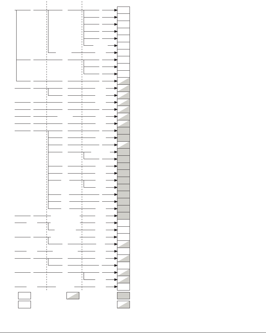
Virtual Memory System Architecture (VMSA)
ARM DDI 0406B Copyright © 1996-1998, 2000, 2004-2008 ARM Limited. All rights reserved. B3-65
Figure B3-10 CP15 registers in a VMSA implementation
c2 0 c0 {0-2} Translation Table Base Registers
DACR, Domain Access Control Register
c3 0 c0 0
Fault Address Registers
c6 0 c0 {0,2}
c5 0 {c0,c1} {0,1} Fault Status Registers
Security Extensions registers, if implemented
CRn opc1 CRm opc2
System Control registersc1 0 c0 {0-2}
CSSELR, Cache Size Selection Register
1
2 c0 0
CTR, Cache Type Register
c0
TLBTR, TLB Type Register
0 c0
1
3
CLIDR, Cache Level ID Register
CCSIDR, Cache Size ID Registers
1 c0 0
TCMTR, TCM Type Register, IMPLEMENTATION DEFINED2
MIDR, Main ID Register
MPIDR, Multiprocessor Affinity Register
Aliases of Main ID Register
CPUID registers
0
5
{4,6,7}
{c1-c7} {0-7}
AIDR, Auxiliary ID Register, IMPLEMENTATION DEFINED7
c1 {0-2}
c7 0 c0 NOP4
Cache and branch predictor maintenance operations
PAR, Physical Address Register
c5 {0,1,6,7}
c4 0
VA to PA translation operations{0-7}c8
c10 {1,2}
{4,5}
DCCMVAU, Cache barrier operation1c11
c6
Data barrier operations
{1,2} Cache maintenance operations
Cache management operations
CP15ISB, Instruction barrier operation4
c14 {1,2} Cache maintenance operations
c8 0 {c3,c5,c6,c7} {0-3} TLB maintenance operations *
Reserved for Branch Predictor, Cache and TCM operationsc9 {0-7} {c0-c2,c5-c8} {0-7}
{0-7} Reserved for Performance monitors{c12-c15}
Reserved for DMA operations for TCM accessc11 {0-7} {c0-c8,c15} {0-7}
TEX Remap Registers (PRRR, NMRR)
Reserved for TLB Lockdown operations
c10 0
c2 {0,1}
{c0,c1,c4,c8} {0-7}
ISR, Security Extensions register, if implemented
c12 0 c0 {0,1}
c1 0
Security Extensions registers, if implemented
c13 0 c0 0
{1-4}
FCSEIDR, FCSE PID Register
Software Thread and Context ID registers
c13 1 NOP
Bold text = Accessible in User modeRead/WriteRead-only Write-only
Read-only if FCSE
not implemented
Access depends on the operation
IMPLEMENTATION DEFINED Registersc15 {0-7} {c0-c15} {0-7}
Cache maintenance operations, Multiprocessing Extensions
c1 {0,6}
* Some encodings are only in the
Multiprocessing Extensions

Virtual Memory System Architecture (VMSA)
B3-66 Copyright © 1996-1998, 2000, 2004-2008 ARM Limited. All rights reserved. ARM DDI 0406B
For information about the CP15 encodings not shown in Figure B3-10 on page B3-65 see Unpredictable
and undefined behavior for CP15 accesses on page B3-68.
Summary of CP15 register descriptions in a VMSA implementation
Table B3-14 shows the CP15 registers in a VMSA implementation. The table also includes links to the
descriptions of each of the primary CP15 registers, c0 to c15.
Table B3-14 Summary of VMSA CP15 register descriptions
Register and description
CP15 c0, ID codes registers on page B3-79
c0, Main ID Register (MIDR) on page B3-81
c0, Cache Type Register (CTR) on page B3-83
c0, TCM Type Register (TCMTR) on page B3-85
c0, TLB Type Register (TLBTR) on page B3-86
c0, Multiprocessor Affinity Register (MPIDR) on page B3-87
CP15 c0, Processor Feature registers on page B5-4
c0, Debug Feature Register 0 (ID_DFR0) on page B5-6
c0, Auxiliary Feature Register 0 (ID_AFR0) on page B5-8
CP15 c0, Memory Model Feature registers on page B5-9
CP15 c0, Instruction Set Attribute registers on page B5-19
c0, Cache Size ID Registers (CCSIDR) on page B3-91
c0, Cache Level ID Register (CLIDR) on page B3-92
c0, Implementation defined Auxiliary ID Register (AIDR) on page B3-94
c0, Cache Size Selection Register (CSSELR) on page B3-95
CP15 c1, System control registers on page B3-96
c1, System Control Register (SCTLR) on page B3-96
c1, Implementation defined Auxiliary Control Register (ACTLR) on page B3-103
c1, Coprocessor Access Control Register (CPACR) on page B3-104
c1, Secure Configuration Register (SCR) on page B3-106

Virtual Memory System Architecture (VMSA)
ARM DDI 0406B Copyright © 1996-1998, 2000, 2004-2008 ARM Limited. All rights reserved. B3-67
c1, Secure Debug Enable Register (SDER) on page B3-108
c1, Non-Secure Access Control Register (NSACR) on page B3-110
CP15 c2 and c3, Memory protection and control registers on page B3-113
c2, Translation Table Base Register 0 (TTBR0) on page B3-113
c2, Translation Table Base Register 1 (TTBR1) on page B3-116
c2, Translation Table Base Control Register (TTBCR) on page B3-117
c3, Domain Access Control Register (DACR) on page B3-119
CP15 c4, Not used on page B3-120
CP15 c5 and c6, Memory system fault registers on page B3-120
c5, Data Fault Status Register (DFSR) on page B3-121
c5, Instruction Fault Status Register (IFSR) on page B3-122
c5, Auxiliary Data and Instruction Fault Status Registers (ADFSR and AIFSR) on page B3-123
c6, Data Fault Address Register (DFAR) on page B3-124
c6, Instruction Fault Address Register (IFAR) on page B3-125
CP15 c7, Cache maintenance and other functions on page B3-126
CP15 c7, Cache and branch predictor maintenance functions on page B3-126
CP15 c7, Virtual Address to Physical Address translation operations on page B3-130
CP15 c7, Data and Instruction Barrier operations on page B3-137
CP15 c7, No Operation (NOP) on page B3-138
CP15 c8, TLB maintenance operations on page B3-138
CP15 c9, Cache and TCM lockdown registers and performance monitors on page B3-141
CP15 c10, Memory remapping and TLB control registers on page B3-142
c10, Primary Region Remap Register (PRRR) on page B3-143
c10, Normal Memory Remap Register (NMRR) on page B3-146
CP15 c11, Reserved for TCM DMA registers on page B3-147
Table B3-14 Summary of VMSA CP15 register descriptions (continued)
Register and description

Virtual Memory System Architecture (VMSA)
B3-68 Copyright © 1996-1998, 2000, 2004-2008 ARM Limited. All rights reserved. ARM DDI 0406B
B3.12.2 General behavior of CP15 registers
The following sections give information about the general behavior of CP15 registers:
•Read-only bits in read/write registers
•Unpredictable and undefined behavior for CP15 accesses
•Reset behavior of CP15 registers on page B3-70
See also Meaning of fixed bit values in register diagrams on page B3-78.
Read-only bits in read/write registers
Some read/write registers include bits that are read-only. These bits ignore writes.
An example of this is the SCTLR.NMFI bit, bit [27], see c1, System Control Register (SCTLR) on
page B3-96.
UNPREDICTABLE and UNDEFINED behavior for CP15 accesses
In ARMv7 the following operations are UNDEFINED:
•all
CDP
,
MCRR
,
MRRC
,
LDC
and
STC
operations to CP15
•all
CDP2
,
MCR2
,
MRC2
,
MCRR2
,
MRRC2
,
LDC2
and
STC2
operations to CP15.
Unless otherwise indicated in the individual register descriptions:
• reserved fields in registers are UNK/SBZP
• reserved values of fields can have UNPREDICTABLE effects.
CP15 c12, Security Extensions registers on page B3-148
c12, Vector Base Address Register (VBAR) on page B3-148
c12, Monitor Vector Base Address Register (MVBAR) on page B3-149
c12, Interrupt Status Register (ISR) on page B3-150
CP15 c13, Process, context and thread ID registers on page B3-151
c13, FCSE Process ID Register (FCSEIDR) on page B3-152
c13, Context ID Register (CONTEXTIDR) on page B3-153
CP15 c13 Software Thread ID registers on page B3-154
CP15 c14 is not used, see Unallocated CP15 encodings on page B3-69
CP15 c15, Implementation defined registers on page B3-155
Table B3-14 Summary of VMSA CP15 register descriptions (continued)
Register and description

Virtual Memory System Architecture (VMSA)
ARM DDI 0406B Copyright © 1996-1998, 2000, 2004-2008 ARM Limited. All rights reserved. B3-69
The following subsections give more information about UNPREDICTABLE and UNDEFINED behavior for
CP15:
•Unallocated CP15 encodings
•Rules for MCR and MRC accesses to CP15 registers
•Effects of the Security Extensions on page B3-70.
Unallocated CP15 encodings
When
MCR
and
MRC
instructions perform CP15 operations, the CRn value for the instruction is the major
register specifier for the CP15 space. Accesses to unallocated major registers are UNDEFINED. For the
ARMv7-A Architecture, this means that:
• for an implementation that includes the Security Extensions, accesses with
<CRn>
= {c4, c14} are
UNDEFINED
• for an implementation that does not include the Security Extensions, accesses with
<CRn>
= {c4, c12, c14} are UNDEFINED
In an allocated CP15 major register specifier,
MCR
and
MRC
accesses to all unallocated encodings are
UNPREDICTABLE for privileged accesses. For the ARMv7-A architecture this means that:
• if the Security Extensions are implemented, any privileged
MCR
or
MRC
access with
<CRn>
!= {c4, c14}
and a combination of
<opc1>
,
<CRm>
and
<opc2>
values not shown in Figure B3-10 on page B3-65 is
UNPREDICTABLE.
• if the Security Extensions are not implemented, any privileged
MCR
or
MRC
access with
<CRn>
!= {c4, c12, c14} and a combination of
<opc1>
,
<CRm>
and
<opc2>
values not shown in
Figure B3-10 on page B3-65 is UNPREDICTABLE.
Note
As shown in Figure B3-10 on page B3-65, accesses to unallocated principal ID registers map onto MIDR.
These are accesses with
<CRn>
= c0,
<opc1>
=0,
<CRm>
= c0, and
<opc2>
= {4, 6, 7}.
Rules for MCR and MRC accesses to CP15 registers
All
MCR
operations from the PC are UNPREDICTABLE for all coprocessors, including for CP15.
All
MRC
operations to APSR_nzcv are UNPREDICTABLE for CP15.
The following accesses are UNPREDICTABLE:
•an
MCR
access to an encoding for which no write behavior is defined in any circumstances
•an
MRC
access to an encoding for which no read behavior is defined in any circumstances.
Except for CP15 encoding that are accessible in User mode, all
MCR
and
MRC
accesses from User mode are
UNDEFINED. This applies to all User mode accesses to unallocated CP15 encodings. Individual register
descriptions, and the summaries of the CP15 major registers, show the CP15 encodings that are accessible
in User mode.

Virtual Memory System Architecture (VMSA)
B3-70 Copyright © 1996-1998, 2000, 2004-2008 ARM Limited. All rights reserved. ARM DDI 0406B
Some individual registers can be made inaccessible by setting configuration bits, possibly including
IMPLEMENTATION DEFINED configuration bits, to disable access to the register. The effects of the
architecturally-defined configuration bits are defined individually in this manual. Typically, setting a
configuration bit to disable access to a register results in the register becoming UNDEFINED for
MRC
and
MCR
accesses.
Effects of the Security Extensions
In Non-secure state, any User or privileged access to a CP15 register is UNDEFINED if either:
• There are no circumstances in which all bits and fields in the register can be accessed from
Non-secure privileged modes.
• Settings in the NSACR mean that there are no circumstances in which all bits and fields in the register
can be accessed from Non-secure privileged modes.
Note
The ARMv7-A architecture does not define any registers of this type. However an ARMv7-A
implementation might include one or more IMPLEMENTATION DEFINED registers of this type.
When Non-secure access to a field of a CP15 register is controlled by an access control bit in the NSACR,
and that access control bit is set to 0, then the controlled register field is RAZ/WI when accessed from a
privileged mode in Non-secure state. If the register can be accessed from User mode then the field is also
RAZ/WI when accessed from User mode.
If write access to a register is disabled by the CP15SDISABLE signal then any
MCR
access to that register
is UNDEFINED.
Reset behavior of CP15 registers
After a reset, only a limited subset of the processor state is guaranteed to be set to defined values. On reset,
the VMSAv7 architecture requires that the following CP15 registers are set to defined values.
Note
When the Security Extensions are implemented, only the Secure copy of a banked register is reset to the
defined value.
•The SCTLR, see c1, System Control Register (SCTLR) on page B3-96.
• The CPACR, see c1, Coprocessor Access Control Register (CPACR) on page B3-104.
• The SCR, when the Security Extensions are implemented, see c1, Secure Configuration Register
(SCR) on page B3-106.
• The TTBCR, see c2, Translation Table Base Control Register (TTBCR) on page B3-117.
• The Secure version of the VBAR, when the Security Extensions are implemented, see c12, Vector
Base Address Register (VBAR) on page B3-148.

Virtual Memory System Architecture (VMSA)
ARM DDI 0406B Copyright © 1996-1998, 2000, 2004-2008 ARM Limited. All rights reserved. B3-71
• The FCSEIDR, if the Fast Context Switch Extension (FCSE) is implemented, see c13, FCSE Process
ID Register (FCSEIDR) on page B3-152. This register is RAZ/WI when the FCSE is not
implemented.
For details of the reset values of these registers see the register descriptions. If the introductory description
of a register does not include its reset value then the architecture does not require that register to be reset to
a defined value.
The values of all other registers at reset are architecturally UNKNOWN. An implementation can assign an
IMPLEMENTATION DEFINED reset value to a register whose reset value is architecturally UNKNOWN. After a
reset, software must not rely on the value of any read/write register that does not have either an
architecturally-defined reset value or an IMPLEMENTATION DEFINED reset value.
B3.12.3 Effect of the Security Extensions on the CP15 registers
When the Security Extensions are implemented, they integrate with many features of the architecture.
Therefore, the descriptions of the individual CP15 registers include information about how the Security
Extensions affect the register. This section:
• summarizes how the Security Extensions affect the implementation of the CP15 registers
• summarizes how the Security Extensions control access to the CP15 registers
• describes a Security Extensions signal that can control access to some CP15 registers.
It contains the following subsections:
•Banked CP15 registers on page B3-72
•Restricted access CP15 registers on page B3-73
•Configurable access CP15 registers on page B3-74
•Common CP15 registers on page B3-74
•The CP15SDISABLE input on page B3-76
•Access to registers in Monitor mode on page B3-77.
Note
• This section describes the effect of the Security Extensions on all of CP15 registers that are present
in an implementation that includes the Security Extensions.
• When the Security Extensions are implemented, the register classifications of Banked, Restricted
access, Configurable, or Common can apply to some coprocessor registers in addition to the CP15
registers.
It is IMPLEMENTATION DEFINED whether each IMPLEMENTATION DEFINED register is Banked, Restricted
access, Configurable, or Common.

Virtual Memory System Architecture (VMSA)
B3-72 Copyright © 1996-1998, 2000, 2004-2008 ARM Limited. All rights reserved. ARM DDI 0406B
Banked CP15 registers
When the Security Extensions are implemented, some CP15 registers are banked. Banked CP15 registers
have two copies, one Secure and one Non-secure. The SCR.NS bit selects the Secure or Non-secure register,
see c1, Secure Configuration Register (SCR) on page B3-106. Table B3-15 shows which registers are
banked, and the permitted access to each register.
Table B3-15 Banked CP15 registers
CP15
register Banked register Permitted accessesa
c0 CSSELR, Cache Size Selection Register Read/write in privileged modes only
c1 SCTLR, System Control RegisterbRead/write in privileged modes only
ACTLR, Auxiliary Control RegistercRead/write in privileged modes only
c2 TTBR0, Translation Table Base 0 Read/write in privileged modes only
TTBR1, Translation Table Base 1 Read/write in privileged modes only
TTBCR, Translation Table Base Control Read/write in privileged modes only
c3 DACR, Domain Access Control Register Read/write in privileged modes only
c5 DFSR, Data Fault Status Register Read/write in privileged modes only
IFSR, Instruction Fault Status Register Read/write in privileged modes only
ADFSR, Auxiliary Data Fault Status Register cRead/write in privileged modes only
AIFSR, Auxiliary Instruction Fault Status RegistercRead/write in privileged modes only
c6 DFAR, Data Fault Address Register Read/write in privileged modes only
IFAR, Instruction Fault Address Register Read/write in privileged modes only
c7 PAR, Physical Address Register (VA to PA translation) Read/write in privileged modes only
c10 PRRR, Primary Region Remap Register Read/write in privileged modes only
NMRR, Normal Memory Remap Register Read/write in privileged modes only
c12 VBAR, Vector Base Address Register Read/write in privileged modes only

Virtual Memory System Architecture (VMSA)
ARM DDI 0406B Copyright © 1996-1998, 2000, 2004-2008 ARM Limited. All rights reserved. B3-73
A Banked CP15 register can contain a mixture of:
• fields that are banked
• fields that are read-only in Non-secure privileged modes but read/write in the Secure state.
The System Control Register SCTLR is an example of a register of that contains this mixture of fields.
The Secure copies of the Banked CP15 registers are sometimes referred to as the Secure Banked CP15
registers. The Non-secure copies of the Banked CP15 registers are sometimes referred to as the Non-secure
Banked CP15 registers.
Restricted access CP15 registers
When the Security Extensions are implemented, some CP15 registers are present only in the Secure security
state. These are called Restricted access registers, and their read/write access permissions are:
• Restricted access CP15 registers cannot be modified in Non-secure state.
• The NSACR can be read in Non-secure privileged modes, but not in Non-secure User mode. This
enables software running in a Non-secure privileged mode to read the access permissions for CP15
registers that have configurable access.
• Apart from the NSACR, Restricted access CP15 registers cannot be read in Non-secure state.
Table B3-16 on page B3-74 shows the Restricted access CP15 registers when the Security Extensions are
implemented:
c13 FCSEIDR, FCSE PID RegisterdRead/write in privileged modes only
CONTEXTIDR, Context ID Register Read/write in privileged modes only
TPIDRURW, User Read/Write Thread ID Read/write in unprivileged and privileged
modes
TPIDRURO, User Read-only Thread ID Read-only in User mode
Read/write in privileged modes
TPIDRPRW, Privileged Only Thread ID Read/write in privileged modes only
a. Any attempt to execute an access that is not permitted results in an Undefined Instruction exception.
b. Some bits are common to the Secure and the Non-secure register, see c1, System Control Register (SCTLR) on
page B3-96.
c. Register is IMPLEMENTATION DEFINED.
d. Banked only if the FCSE is implemented. The FCSE PID Register is RAZ/WI if the FCSE is not implemented.
Table B3-15 Banked CP15 registers (continued)
CP15
register Banked register Permitted accessesa

Virtual Memory System Architecture (VMSA)
B3-74 Copyright © 1996-1998, 2000, 2004-2008 ARM Limited. All rights reserved. ARM DDI 0406B
Configurable access CP15 registers
Access to some CP15 registers is configurable. These registers can be:
• accessible from Secure states only
• accessible from both Secure and Non-secure states.
Access is controlled by bits in the NSACR, see c1, Non-Secure Access Control Register (NSACR) on
page B3-110.
In ARMv7-A, the only required Configurable access CP15 register is:
• CPACR, Coprocessor Access Control Register.
Common CP15 registers
Some CP15 registers and operations are common to the Secure and Non-secure security states. These are
described as the Common access CP15 registers, or simply as the Common CP15 registers. These registers
are:
• Read-only registers that hold configuration information.
• Register encodings used for various memory system operations, rather than to access registers.
• The Interrupt Status Register (ISR).
Table B3-16 Restricted access CP15 registers
CP15 register Secure register Permitted accessesa
c1 NSACR, Non-Secure Access Control Read/write in Secure privileged modes
Read-only in Non-secure privileged modes
SCR, Secure Configuration Read/write in Secure privileged modes
SDER, Secure Debug Enable Read/write in Secure privileged modes
c12 MVBAR, Monitor Vector Base Address Read/write in Secure privileged modes
a. Any attempt to execute an access that is not permitted results in an Undefined Instruction exception.

Virtual Memory System Architecture (VMSA)
ARM DDI 0406B Copyright © 1996-1998, 2000, 2004-2008 ARM Limited. All rights reserved. B3-75
Table B3-17 shows the registers that are present in an ARMv7-A implementation that are not affected by
the Security Extensions. When the Security Extensions are implemented these registers are sometimes
described as the common registers.
Table B3-17 Common CP15 registers
CP15
register Register Permitted accessesa
c0 MIDR, Main ID Register Read-only in privileged modes only
CTR, Cache Type Register Read-only in privileged modes only
TCMTR, TCM Type RegisterbRead-only in privileged modes only
TLBTR, TLB Type RegisterbRead-only in privileged modes only
MPIDR, Multiprocessor Affinity Register Read-only in privileged modes only
ID_PFRx, Processor Feature Registers Read-only in privileged modes only
ID_DFR0, Debug Feature Register 0 Read-only in privileged modes only
ID_AFR0, Auxiliary Feature Register 0 Read-only in privileged modes only
ID_MMFRx, Memory Model Feature Registers Read-only in privileged modes only
ID_ISARx, Instruction Set Attribute Registers Read-only in privileged modes only
CCSIDR, Cache Size ID Register Read-only in privileged modes only
CLIDR, Cache Level ID Register Read-only in privileged modes only
AIDR, Auxiliary ID RegisterbRead-only in privileged modes only
c7 NOP Write-only in privileged modes only
Cache maintenance operations See CP15 c7, Cache and branch predictor
maintenance functions on page B3-126
VA to PA Translation operations See CP15 c7, Virtual Address to Physical Address
translation operations on page B3-130
Data Barrier Operations Write-only in unprivileged and privileged modes
c8 TLB maintenance operations Write-only in privileged modes only
c9 Performance monitors See Access permissions on page C9-12
c12 ISR, Interrupt Status Register Read-only in privileged modes only
a. Any attempt to execute an access that is not permitted results in an Undefined Instruction exception.
b. Register or operation details are IMPLEMENTATION DEFINED.

Virtual Memory System Architecture (VMSA)
B3-76 Copyright © 1996-1998, 2000, 2004-2008 ARM Limited. All rights reserved. ARM DDI 0406B
Secure CP15 registers
The Secure CP15 registers comprise:
• The Secure copies of the Banked CP15 registers
• Restricted access CP15 registers
• Configurable access CP15 registers that are configured to be accessible only from Secure state.
The CP15SDISABLE input
The Security Extensions include an input signal, CP15SDISABLE, that disables write access to some of
the Secure registers when asserted HIGH.
Note
The interaction between CP15SDISABLE and any IMPLEMENTATION DEFINED register is IMPLEMENTATION
DEFINED.
Table B3-18 shows the registers and operations affected.
On a reset by the external system, the CP15SDISABLE input signal must be taken LOW. This permits the
Reset code to set up the configuration of the Security Extensions. When the input is asserted HIGH, any
attempt to write to the Secure registers shown in Table B3-18 results in an Undefined Instruction exception.
Table B3-18 Secure registers affected by CP15SDISABLE
CP15
register Register name Affected operation
c1 SCTLR, System Control Register
MCR p15, 0, <Rt>, c1, c0, 0
c2 TTBR0, Translation Table Base Register 0
MCR p15, 0, <Rt>, c2, c0, 0
TTBCR, Translation Table Base Control Register
MCR p15, 0, <Rt>, c2, c0, 2
c3 DACR, Domain Access Control Register
MCR p15, 0, <Rt>, c3, c0, 0
c10 PRRR. Primary Region Remap Register
MCR p15, 0, <Rt>, c10, c2, 0
NMRR, Normal Memory Remap Register
MCR p15, 0, <Rt>, c10, c2, 1
c12 VBAR, Vector Base Address Register
MCR p15, 0, <Rt>, c12, c0, 0
MVBAR, Monitor Vector Base Address Register
MCR p15, 0, <Rt>, c12, c0, 1
c13 FCSEIDR, FCSE PID Register a
a. If the FCSE is implemented. The FCSE PID Register is RAZ/WI if the FCSE is not implemented.
MCR p15, 0, <Rt>, c13, c0, 0

Virtual Memory System Architecture (VMSA)
ARM DDI 0406B Copyright © 1996-1998, 2000, 2004-2008 ARM Limited. All rights reserved. B3-77
The CP15SDISABLE input does not affect reading Secure registers, or reading or writing Non-secure
registers. It is IMPLEMENTATION DEFINED how the input is changed and when changes to this input are
reflected in the processor. However, changes must be reflected as quickly as possible. The change must
occur before completion of a Instruction Synchronization Barrier operation, issued after the change, is
visible to the processor with respect to instruction execution boundaries. Software must perform a
Instruction Synchronization Barrier operation meeting the above conditions to ensure all subsequent
instructions are affected by the change to CP15SDISABLE.
The assertion of CP15SDISABLE enables key Secure privileged features to be locked in a known good
state, providing an additional level of overall system security. ARM expects control of this input to reside
in the system, in a system block dedicated to security.
Access to registers in Monitor mode
When the processor is in Monitor mode, the processor is in Secure state regardless of the value of the
SCR.NS bit. In Monitor mode, the SCR.NS bit determines whether the Secure Banked CP15 registers or
Non-secure Banked CP15 registers are read or written using
MRC
or
MCR
instructions. That is:
NS = 0 Common, Restricted access, and Secure Banked registers are accessed by CP15
MRC
and
MCR
instructions.
CP15 operations use the security state to determine all resources used, that is, all CP15
based operations are performed in Secure state.
NS = 1 Common, Restricted access and Non-secure Banked registers are accessed by CP15
MRC
and
MCR
instructions.
CP15 operations use the security state to determine all resources used, that is, all CP15
based operations are performed in Secure state.
The security state determines whether the Secure or Non-secure Banked registers are used to determine the
control state.
B3.12.4 Changes to CP15 registers and the memory order model
All changes to CP15 registers that appear in program order after any explicit memory operations are
guaranteed not to affect those memory operations.
Any change to CP15 registers is guaranteed to be visible to subsequent instructions only after one of:
• the execution of an
ISB
instruction
• the taking of an exception
• the return from an exception.
To guarantee the visibility of changes to some CP15 registers, additional operations might be required, on
a case by case basis, before the
ISB
instruction, exception or return from exception. These cases are
identified specifically in the definition of the registers.
However, for CP15 register accesses, all
MRC
and
MCR
instructions to the same register using the same register
number appear to occur in program order relative to each other without context synchronization.

Virtual Memory System Architecture (VMSA)
B3-78 Copyright © 1996-1998, 2000, 2004-2008 ARM Limited. All rights reserved. ARM DDI 0406B
Where a change to the CP15 registers that is not yet guaranteed to be visible has an effect on exception
processing, the following rule applies:
• When it is determined that an exception must be taken, any change of state held in CP15 registers
involved in the triggering of the exception and that affects the processing of the exception is
guaranteed to take effect before the exception is taken.
Therefore, in the following example, where initially A=1 and V=0, the
LDR
might or might not take a Data
Abort exception due to the unaligned access, but if an exception occurs the vector used is affected by the
Vbit:
MCR p15, R0, c1, c0, 0 ; clears the A bit and sets the V bit
LDR R2, [R3] ; unaligned load.
B3.12.5 Meaning of fixed bit values in register diagrams
In register diagrams, fixed bits are indicated by one of following:
0 In any implementation:
• the bit must read as 0
• writes to the bit must be ignored.
Software:
• can rely on the bit reading as 0
• must use an SBZP policy to write to the bit.
(0) In any implementation:
• the bit must read as 0
• writes to the bit must be ignored.
Software:
• must not rely on the bit reading as 0
• must use an SBZP policy to write to the bit.
1 In any implementation:
• the bit must read as 1
• writes to the bit must be ignored.
Software:
• can rely on the bit reading as 1
• must use an SBOP policy to write to the bit.
(1) In any implementation:
• the bit must read as 1
• writes to the bit must be ignored.
Software:
• must not rely on the bit reading as 1
• must use an SBOP policy to write to the bit.
Fields that are more than 1 bit wide are sometimes described as UNK/SBZP, instead of having each bit
marked as (0).
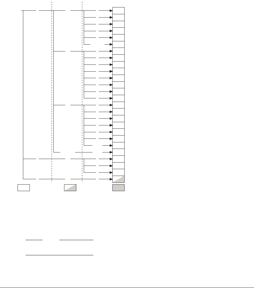
Virtual Memory System Architecture (VMSA)
ARM DDI 0406B Copyright © 1996-1998, 2000, 2004-2008 ARM Limited. All rights reserved. B3-79
B3.12.6 CP15 c0, ID codes registers
The CP15 c0 registers are used for processor and feature identification. Figure B3-11 shows the CP15 c0
registers.
Figure B3-11 CP15 c0 registers in a VMSA implementation
CP15 c0 register encodings not shown in Figure B3-11 are UNPREDICTABLE, see Unallocated CP15
encodings on page B3-69.
Note
Chapter B5 The CPUID Identification Scheme describes the CPUID registers shown in Figure B3-11.
CRn opc1 CRm
CLIDR, Cache Level ID Register
CCSIDR, Cache Size ID Registers
CSSELR, Cache Size Selection Register0
c0
opc2
01
c2
MPIDR, Multiprocessor Affinity Register
Aliases of Main ID Register
5
{4,6,7}
0c1 ID_PFR0, Processor Feature Register 0
ID_PFR1, Processor Feature Register 1
ID_DFR0, Debug Feature Register 0
ID_AFR0, Auxiliary Feature Register 0
ID_MMFR0, Memory Model Feature Register 0
ID_MMFR1, Memory Model Feature Register 1
ID_MMFR2, Memory Model Feature Register 2
ID_MMFR3, Memory Model Feature Register 3
7
0
1
3
2
4
5
6
Read-As-Zero
ID_ISAR0, ISA Feature Register 0
ID_ISAR1, ISA Feature Register 1
ID_ISAR1, ISA Feature Register 2
ID_ISAR1, ISA Feature Register 3
ID_ISAR4, ISA Feature Register 4
ID_ISAR5, ISA Feature Register 5
1
3
2
4
5
{6,7}
Read-As-Zero
{c3-c7} {0-7}
AIDR, Auxiliary ID Register
IMPLEMENTATION
DEFINED
c02
Read/WriteRead-only Write-only
1
7
CPUID registers
CTR, Cache Type Register
c0
TLBTR, TLB Type Register, details
IMPLEMENTATION
DEFINED
0 c0
TCMTR, TCM Type Register, details
IMPLEMENTATION
DEFINED
MIDR, Main ID Register
1
3
2
0

Virtual Memory System Architecture (VMSA)
B3-80 Copyright © 1996-1998, 2000, 2004-2008 ARM Limited. All rights reserved. ARM DDI 0406B
Table B3-19 lists the CP15 c0 registers and shows where each register is described in full. The table does
not include the reserved and aliased registers that are shown in Figure B3-11 on page B3-79.
Note
The CPUID scheme described in Chapter B5 The CPUID Identification Scheme includes information about
the implementation of the optional VFP and Advanced SIMD architecture extensions. See Advanced SIMD
and VFP extensions on page A2-20 for a summary of the implementation options for these features.
Table B3-19 Index to CP15 c0 register descriptions
opc1 CRm opc2 Register and description
0c00c0, Main ID Register (MIDR) on page B3-81
1c0, Cache Type Register (CTR) on page B3-83
2c0, TCM Type Register (TCMTR) on page B3-85
3c0, TLB Type Register (TLBTR) on page B3-86
5c0, Multiprocessor Affinity Register (MPIDR) on page B3-87
4, 6, 7 c0, Main ID Register (MIDR) on page B3-81
c1 0, 1 CP15 c0, Processor Feature registers on page B5-4
2c0, Debug Feature Register 0 (ID_DFR0) on page B5-6
3c0, Auxiliary Feature Register 0 (ID_AFR0) on page B5-8
4-7 CP15 c0, Memory Model Feature registers on page B5-9
c2 0-5 CP15 c0, Instruction Set Attribute registers on page B5-19
1c00c0, Cache Size ID Registers (CCSIDR) on page B3-91
1c0, Cache Level ID Register (CLIDR) on page B3-92
7c0, Implementation defined Auxiliary ID Register (AIDR) on page B3-94
2c00c0, Cache Size Selection Register (CSSELR) on page B3-95

Virtual Memory System Architecture (VMSA)
ARM DDI 0406B Copyright © 1996-1998, 2000, 2004-2008 ARM Limited. All rights reserved. B3-81
B3.12.7 c0, Main ID Register (MIDR)
The Main ID Register, MIDR, provides identification information for the processor, including an
implementer code for the device and a device ID number.
The MIDR is:
• a 32-bit read-only register
• accessible only in privileged modes
• when the Security Extensions are implemented, a Common register.
Some fields of the MIDR are IMPLEMENTATION DEFINED. For details of the values of these fields for a
particular ARMv7 implementation, and any implementation-specific significance of these values, see the
product documentation.
The format of the MIDR is:
Implementer, bits [31:24]
The Implementer code. Table B3-20 shows the permitted values for this field:
All other values are reserved by ARM and must not be used.
Variant, bits [23:20]
An IMPLEMENTATION DEFINED variant number. Typically, this field is used to distinguish
between different product variants, or major revisions of a product.
31 24 23 20 19 16 15 4 3 0
Implementer Variant Architecture Primary part number Revision
Table B3-20 Implementer codes
Bits [31:24] ASCII character Implementer
0x41
A ARM Limited
0x44
D Digital Equipment Corporation
0x4D
M Motorola, Freescale Semiconductor Inc.
0x51
QQUALCOMM Inc.
0x56
V Marvell Semiconductor Inc.
0x69
i Intel Corporation

Virtual Memory System Architecture (VMSA)
B3-82 Copyright © 1996-1998, 2000, 2004-2008 ARM Limited. All rights reserved. ARM DDI 0406B
Architecture, bits [19:16]
Table B3-21 shows the permitted values for this field:
All other values are reserved by ARM and must not be used.
Primary part number, bits [15:4]
An IMPLEMENTATION DEFINED primary part number for the device.
Note
On processors implemented by ARM, if the top four bits of the primary part number are
0x0
or
0x7
, the variant and architecture are encoded differently, see c0, Main ID Register (MIDR)
on page AppxH-34. Processors implemented by ARM have an Implementer code of
0x41
.
Revision, bits [3:0]
An IMPLEMENTATION DEFINED revision number for the device.
ARMv7 requires all implementations to use the CPUID scheme, described in Chapter B5 The CPUID
Identification Scheme, and an implementation is described by the MIDR with the CPUID registers.
Note
For an ARMv7 implementation by ARM, the MIDR is interpreted as:
Bits [31:24] Implementer code, must be
0x41
.
Bits [23:20] Major revision number, rX.
Bits [19:16] Architecture code, must be
0xF
.
Bits [15:4] ARM part number.
Bits [3:0] Minor revision number, pY.
Table B3-21 Architecture codes
Bits [19:16] Architecture
0x1
ARMv4
0x2
ARMv4T
0x3
ARMv5 (obsolete)
0x4
ARMv5T
0x5
ARMv5TE
0x6
ARMv5TEJ
0x7
ARMv6
0xF
Defined by CPUID scheme
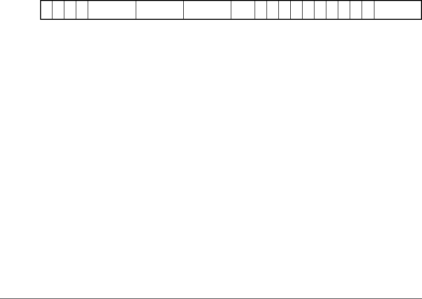
Virtual Memory System Architecture (VMSA)
ARM DDI 0406B Copyright © 1996-1998, 2000, 2004-2008 ARM Limited. All rights reserved. B3-83
Accessing the MIDR
To access the MIDR you read the CP15 registers with
<opc1>
set to 0,
<CRn>
set to c0,
<CRm>
set to c0, and
<opc2>
set to 0. For example:
MRC p15,0,<Rt>,c0,c0,0 ; Read CP15 Main ID Register
B3.12.8 c0, Cache Type Register (CTR)
The Cache Type Register, CTR, provides information about the architecture of the caches.
The CTR is:
• a 32-bit read-only register
• accessible only in privileged modes
• when the Security Extensions are implemented, a Common register.
The format of the CTR is changed in ARMv7. The new format of the register is indicated by Bit [31:29]
being set to 0b100. For details of the format of the Cache Type Register in versions of the ARM architecture
before ARMv7 see c0, Cache Type Register (CTR) on page AppxH-35.
In ARMv7, the format of the CTR is:
Bits [31:29] Set to 0b100 for the ARMv7 register format. Set to 0b000 for the format used in ARMv6
and earlier.
Bit [28] RAZ.
CWG, bits [27:24]
Cache Writeback Granule. Log2 of the number of words of the maximum size of memory
that can be overwritten as a result of the eviction of a cache entry that has had a memory
location in it modified.
A value of 0b0000 indicates that the CTR does not provide Cache Writeback Granule
information and either:
• the architectural maximum of 512 words (2Kbytes) must be assumed
• the Cache Writeback Granule can be determined from maximum cache line size
encoded in the Cache Size ID Registers.
Values greater than 0b1001 are reserved.
ERG, bits [27:24]
Exclusives Reservation Granule. Log2 of the number of words of the maximum size of the
reservation granule that has been implemented for the Load-Exclusive and Store-Exclusive
instructions. For more information, see Tagging and the size of the tagged memory block on
page A3-20.
31 29 28 27 24 23 20 19 16 15 14 13 4 3 0
1000 CWG ERG DminLine L1Ip0000000000 IminLine

Virtual Memory System Architecture (VMSA)
B3-84 Copyright © 1996-1998, 2000, 2004-2008 ARM Limited. All rights reserved. ARM DDI 0406B
A value of 0b0000 indicates that the CTR does not provide Exclusives Reservation Granule
information and the architectural maximum of 512 words (2Kbytes) must be assumed.
Values greater than 0b1001 are reserved.
DminLine, bits [19:16]
Log2 of the number of words in the smallest cache line of all the data caches and unified
caches that are controlled by the processor.
L1Ip, bits [15:14]
Level 1 instruction cache policy. Indicates the indexing and tagging policy for the
L1 instruction cache. Table B3-22 shows the possible values for this field.
Bits [13:4] RAZ.
IminLine, bits [3:0]
Log2 of the number of words in the smallest cache line of all the instruction caches that are
controlled by the processor.
Accessing the CTR
To access the CTR you read the CP15 registers with
<opc1>
set to 0,
<CRn>
set to c0,
<CRm>
set to c0, and
<opc2>
set to 1. For example
MRC p15,0,<Rt>,c0,c0,1 ; Read CP15 Cache Type Register
Table B3-22 Level 1 instruction cache policy field values
L1Ip bits L1 instruction cache indexing and tagging policy
00 Reserved
01 ASID-tagged Virtual Index, Virtual Tag (AIVIVT)
10 Virtual Index, Physical Tag (VIPT)
11 Physical Index, Physical Tag (PIPT)

Virtual Memory System Architecture (VMSA)
ARM DDI 0406B Copyright © 1996-1998, 2000, 2004-2008 ARM Limited. All rights reserved. B3-85
B3.12.9 c0, TCM Type Register (TCMTR)
The TCM Type Register, TCMTR, provides information about the implementation of the TCM.
The TCMTR is:
• a 32-bit read-only register
• accessible only in privileged modes.
• when the Security Extensions are implemented, a Common register.
From ARMv7:
• TCMTR must be implemented
• when the ARMv7 format is used, the meaning of register bits [28:0] is IMPLEMENTATION DEFINED
• the ARMv6 format of the TCM Type Register remains a valid usage model
• if no TCMs are implemented the ARMv6 format must be used to indicate zero-sized TCMs.
The ARMv7 format of the TCMTR is:
Bits [31:29] Set to 0b100 for the ARMv7 register format.
Note
This field is set to 0b000 for the format used in ARMv6 and earlier.
Bits [28:0] IMPLEMENTATION DEFINED in the ARMv7 register format.
If no TCMs are implemented, the TCMTR must be implemented with this ARMv6 format:
For details of the ARMv6 optional implementation of the TCM Type Register see c0, TCM Type Register
(TCMTR) on page AppxG-33.
Accessing the TCMTR
To access the TCMTR you read the CP15 registers with
<opc1>
set to 0,
<CRn>
set to c0,
<CRm>
set to c0, and
<opc2>
set to 2. For example:
MRC p15,0,<Rt>,c0,c0,2 ; Read CP15 TCM Type Register
31 29 28 0
100 IMPLEMENTATION DEFINED
31 29 28 19 18 16 15 3 2 0
000 UNKNOWN 000 UNKNOWN 000

Virtual Memory System Architecture (VMSA)
B3-86 Copyright © 1996-1998, 2000, 2004-2008 ARM Limited. All rights reserved. ARM DDI 0406B
B3.12.10 c0, TLB Type Register (TLBTR)
The TLB Type Register, TLBTR, provides information about the TLB implementation. The register must
define whether the implementation provides separate instruction and data TLBs, or a unified TLB.
Normally, the IMPLEMENTATION DEFINED information in this register includes the number of lockable
entries in the TLB.
The TLBTR is:
• a 32-bit read-only register
• accessible only in privileged modes
• implemented only when the VMSA is implemented
• when the Security Extensions are implemented, a Common register.
The format of the TLBTR is:
Bits [31:1] IMPLEMENTATION DEFINED.
nU, bit [0] Not Unified TLB. Indicates whether the implementation has a unified TLB:
nU == 0 Unified TLB.
nU == 1 Separate Instruction and Data TLBs.
Note
From ARMv7, the TLB lockdown mechanism is IMPLEMENTATION DEFINED, and therefore the details of
bits [31:1] of the TLB Type Register are IMPLEMENTATION DEFINED.
Accessing the TLBTR
To access the TLBTR you read the CP15 registers with
<opc1>
set to 0,
<CRn>
set to c0,
<CRm>
set to c0, and
<opc2>
set to 3. For example:
MRC p15,0,<Rt>,c0,c0,3 ; Read CP15 TLB Type Register
31 10
IMPLEMENTATION DEFINED nU
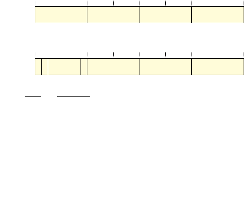
Virtual Memory System Architecture (VMSA)
ARM DDI 0406B Copyright © 1996-1998, 2000, 2004-2008 ARM Limited. All rights reserved. B3-87
B3.12.11 c0, Multiprocessor Affinity Register (MPIDR)
The Multiprocessor Affinity Register, MPIDR, provides an additional processor identification mechanism
for scheduling purposes in a multiprocessor system. In a uniprocessor system ARM recommends that this
register returns a value of 0.
The MPIDR is:
• a 32-bit read-only register
• accessible only in privileged modes
• when the Security Extensions are implemented, a Common register
• introduced in ARMv7.
In the ARMv7 base architecture the format of the MPIDR is:
When the Multiprocessing Extensions are implemented the format of the MPIDR is:
Note
In the MIDR bit definitions, a processor in the system can be a physical processor or a virtual CPU.
Bits [31:24], ARMv7 base architecture
Reserved, RAZ.
Bits [31], Multiprocessing Extensions
RAO. Indicates that the processor implements the Multiprocessing Extensions register
format.
U bit, bit [30], Multiprocessing Extensions
Indicates a Uniprocessor system, as distinct from processor 0 in a multiprocessor system.
The possible values of this bit are:
0 Processor is part of a multiprocessor system.
1 Processor is part of a uniprocessor system
0
31 24 23 16 15 8 7 0
0 0 0 0 0 0 0 Affinity Level 2 Affinity Level 1 Affinity Level 0
1
31 30 29 25 24 23 16 15 8 7 0
U (0) (0) (0) (0) (0) Affinity Level 2 Affinity Level 1 Affinity Level 0
MT

Virtual Memory System Architecture (VMSA)
B3-88 Copyright © 1996-1998, 2000, 2004-2008 ARM Limited. All rights reserved. ARM DDI 0406B
Bits [29:25], Multiprocessing Extensions
Reserved, UNK.
MT bit, bit [24], Multiprocessing Extensions
Indicates whether the lowest level of affinity consists of logical processors that are
implemented using a multi-threading type approach. The possible values of this bit are:
0 Performance of processors at the lowest affinity level is largely independent.
1 Performance of processors at the lowest affinity level is very interdependent
For more information about the meaning of this bit see Multi-threading approach to lowest
affinity levels, Multiprocessing Extensions on page B3-89.
Affinity level 2, bits [23:16]
The least significant affinity level field, for this processor in the system.
Affinity level 1, bits [15:8]
The intermediate affinity level field, for this processor in the system.
Affinity level 0, bits [7:0]
The most significant level field, for this processor in the system.
In the system as a whole, for each of the affinity level fields, the assigned values must start at 0 and increase
monotonically.
Increasing monotonically means that:
• There must not be any gaps in the sequence of numbers used.
• A higher value of the field includes any properties indicated by all lower values of the field.
When matching against an affinity level field, scheduler software checks for a value equal to or greater than
a required value.
Recommended use of the MPIDR on page B3-89 includes a description of an example multiprocessor
system and the affinity level field values it might use.
The interpretation of these fields is IMPLEMENTATION DEFINED, and must be documented as part of the
documentation of the multiprocessor system. ARM recommends that this register might be used as
described in the next subsection.
The software mechanism to discover the total number of affinity numbers used at each level is
IMPLEMENTATION DEFINED, and is part of the general system identification task.

Virtual Memory System Architecture (VMSA)
ARM DDI 0406B Copyright © 1996-1998, 2000, 2004-2008 ARM Limited. All rights reserved. B3-89
Multi-threading approach to lowest affinity levels, Multiprocessing Extensions
When the Multiprocessing Extensions are implemented, if the MPIDR.MT bit is set to 1, this indicates that
the processors at affinity level 0 are logical processors, implemented using a multi-threading type approach.
In such an approach, there can be a significant performance impact if a new thread is assigned the processor
with:
• the same Affinity Level 0 value as some other thread, referred to as the original thread
• a pair of values for Affinity Levels 2 and 3 that are different to the pair of values of the original thread.
In this situation, the performance of the original thread might be significantly reduced.
Note
In this description, thread always refers to a thread or a process.
Recommended use of the MPIDR
In a multiprocessor system the register might provide two important functions:
• Identifying special functionality of a particular processor in the system. In general, the actual
meaning of the affinity level fields is not important. In a small number of situations, an affinity level
field value might have a special IMPLEMENTATION DEFINED significance. Possible examples include
booting from reset and power-down events.
• Providing affinity information for the scheduling software, to help the scheduler run an individual
thread or process on either:
— the same processor, or as similar a processor as possible, as the processor it was running on
previously
— a processor on which a related thread or process was run.
Note
A monotonically increasing single number ID mechanism provides a convenient index into software arrays
and for accessing the interrupt controller. This might be:
• performed as part of the boot sequence
• stored as part of the local storage of threads.
MPIDR provides a mechanism with up to three levels of affinity information, but the meaning of those levels
of affinity is entirely IMPLEMENTATION DEFINED. The levels of affinity provided can have different
meanings. Table B3-23 on page B3-90 shows two possible implementations:

Virtual Memory System Architecture (VMSA)
B3-90 Copyright © 1996-1998, 2000, 2004-2008 ARM Limited. All rights reserved. ARM DDI 0406B
The scheduler maintains affinity level information for all threads and processes. When it has to reschedule
a thread or process the scheduler:
• looks for an available processor that matches at all three affinity levels
• if this fails, it might look for a processor that matches at levels 2 and 3 only
• if it still cannot find an available processor it might look for a match at level 3 only.
A multiprocessor system corresponding to Example system 1 in Table B3-23 might implement affinity
values as shown in Table B3-24:
Accessing the MPIDR
To access MPIDR you read the CP15 registers with
<opc1>
set to 0,
<CRn>
set to c0,
<CRm>
set to c0, and
<opc2>
set to 5. For example:
MRC p15,0,<Rt>,c0,c0,5 ; Read Multiprocessor Affinity Register
Table B3-23 Possible implementations of the affinity levels
Affinity Level Example system 1 Example system 2
0 Virtual CPUs in a multi-threaded processor Processors in an SMP cluster
1 Processors in an Symmetric Multi Processor (SMP) cluster Clusters with a system
2 Clusters in a system No meaning, fixed as 0.
Table B3-24 Example of possible affinity values at different affinity levels
Affinity level 2
Cluster level
Affinity level 1
Processor level
Affinity level 0
Virtual CPU level
0 0 0, 1
0 1 0, 1
0 2 0, 1
0 3 0, 1
1 0 0, 1
1 1 0, 1
1 2 0, 1
1 3 0, 1

Virtual Memory System Architecture (VMSA)
ARM DDI 0406B Copyright © 1996-1998, 2000, 2004-2008 ARM Limited. All rights reserved. B3-91
B3.12.12 c0, Cache Size ID Registers (CCSIDR)
The Cache Size ID Registers, CCSIDR, provide information about the architecture of the caches.
The CCSIDR registers are:
• 32-bit read-only registers
• accessible only in privileged modes
• when the Security Extensions are implemented, Common registers
• introduced in ARMv7.
One CCSIDR is implemented for each cache that can be accessed by the processor. CSSELR selects which
Cache Size ID Register is accessible, see c0, Cache Size Selection Register (CSSELR) on page B3-95.
The format of a CCSIDR is:
WT, bit [31] Indicates whether the cache level supports Write-Through, see Table B3-25.
WB, bit [30] Indicates whether the cache level supports Write-Back, see Table B3-25.
RA, bit [29] Indicates whether the cache level supports Read-Allocation, see Table B3-25.
WA, bit [28] Indicates whether the cache level supports Write-Allocation, see Table B3-25.
NumSets, bits [27:13]
(Number of sets in cache) - 1, therefore a value of 0 indicates 1 set in the cache. The number
of sets does not have to be a power of 2.
Associativity, bits [12:3]
(Associativity of cache) - 1, therefore a value of 0 indicates an associativity of 1. The
associativity does not have to be a power of 2.
LineSize, bits [2:0]
(Log2(Number of words in cache line)) -2. For example:
• For a line length of 4 words: Log2(4) = 2, LineSize entry = 0.
31 30 29 28 27 13 12 3 2 0
W
T
W
BRA W
ANumSets Associativity LineSize
Table B3-25 WT, WB, RA and WA bit values
WT, WB, RA or WA bit value Meaning
0 Feature not supported
1 Feature supported

Virtual Memory System Architecture (VMSA)
B3-92 Copyright © 1996-1998, 2000, 2004-2008 ARM Limited. All rights reserved. ARM DDI 0406B
This is the minimum line length.
• For a line length of 8 words: Log2(8) = 3, LineSize entry = 1.
Accessing the currently selected CCSIDR
The CSSELR selects a CCSIDR, see c0, Cache Size Selection Register (CSSELR) on page B3-95. To access
the currently-selected CCSIDR you read the CP15 registers with
<opc1>
set to 1,
<CRn>
set to c0,
<CRm>
set
to c0, and
<opc2>
set to 0. For example:
MRC p15,1,<Rt>,c0,c0,0 ; Read current CP15 Cache Size ID Register
Accessing the CCSIDR when the value in CSSELR corresponds to a cache that is not implemented returns
an UNKNOWN value.
B3.12.13 c0, Cache Level ID Register (CLIDR)
The Cache Level ID Register, CLIDR:
• identifies the type of cache, or caches, implemented at each level, up to a maximum of eight levels
• identifies the Level of Coherency and Level of Unification for the cache hierarchy.
The CLIDR is:
• a 32-bit read-only register
• accessible only in privileged modes
• when the Security Extensions are implemented, a Common register
• introduced in ARMv7.
The format of the CLIDR is:
Bits [31:30] RAZ.
LoUU, bits [29:27]
Level of Unification Uniprocessor for the cache hierarchy, see Clean, Invalidate, and Clean
and Invalidate on page B2-11.
LoC, bits [26:24]
Level of Coherency for the cache hierarchy, see Clean, Invalidate, and Clean and Invalidate
on page B2-11.
LoUIS, bits [23:21]
Level of Unification Inner Shareable for the cache hierarchy, see Clean, Invalidate, and
Clean and Invalidate on page B2-11. This field is RAZ in implementations that do not
implement the Multiprocessing Extensions.
31 30 29 27 26 24 23 21 20 18 17 15 14 12 11 9 8 6 5 3 2 0
0 0 LoUU LoC LoUIS Ctype7 Ctype6 Ctype5 Ctype4 Ctype3 Ctype2 Ctype1

Virtual Memory System Architecture (VMSA)
ARM DDI 0406B Copyright © 1996-1998, 2000, 2004-2008 ARM Limited. All rights reserved. B3-93
CtypeX, bits [3(x - 1) + 2:3(x - 1)], for x = 1 to 7
Cache Type fields. Indicate the type of cache implemented at each level, from Level 1 up to
a maximum of seven levels of cache hierarchy. The Level 1 cache field, Ctype1, is bits [2:0],
see register diagram. Table B3-26 shows the possible values for each CtypeX field.
If you read the Cache Type fields from Ctype1 upwards, once you have seen a value of
0b000, no caches exist at further out levels of the hierarchy. So, for example, if Ctype3 is
the first Cache Type field with a value of 0b000, the values of Ctype4 to Ctype7 must be
ignored.
The CLIDR describes only the caches that are under the control of the processor.
Accessing the CLIDR
To access the CLIDR you read the CP15 registers with
<opc1>
set to 1,
<CRn>
set to c0,
<CRm>
set to c0, and
<opc2>
set to 1. For example:
MRC p15,1,<Rt>,c0,c0,1 ; Read CP15 Cache Level ID Register
Table B3-26 Ctype bit values
CtypeX value Meaning, cache implemented at this level
000 No cache
001 Instruction cache only
010 Data cache only
011 Separate instruction and data caches
100 Unified cache
101, 11X Reserved

Virtual Memory System Architecture (VMSA)
B3-94 Copyright © 1996-1998, 2000, 2004-2008 ARM Limited. All rights reserved. ARM DDI 0406B
B3.12.14 c0, IMPLEMENTATION DEFINED Auxiliary ID Register (AIDR)
The IMPLEMENTATION DEFINED Auxiliary ID Register, AIDR, provides implementation-specific ID
information. The value of this register must be used in conjunction with the value of MIDR.
The IMPLEMENTATION DEFINED AIDR is:
• a 32-bit read-only register
• accessible only in privileged modes
• when the Security Extensions are implemented, a Common register
• introduced in ARMv7.
The format of the AIDR is IMPLEMENTATION DEFINED.
Accessing the AIDR
To access the AIDR you read the CP15 registers with
<opc1>
set to 1,
<CRn>
set to c0,
<CRm>
set to c0, and
<opc2>
set to 7. For example:
MRC p15,1,<Rt>,c0,c0,7 ; Read IMPLEMENTATION DEFINED Auxiliary ID Register

Virtual Memory System Architecture (VMSA)
ARM DDI 0406B Copyright © 1996-1998, 2000, 2004-2008 ARM Limited. All rights reserved. B3-95
B3.12.15 c0, Cache Size Selection Register (CSSELR)
The Cache Size Selection Register, CSSELR, selects the current CCSIDR. An ARMv7 implementation
must include a CCSIDR for every implemented cache that is under the control of the processor. The
CSSELR identifies which CP1CSID register can be accessed, by specifying, for the required cache:
• the cache level
• the cache type, either:
— instruction cache.
— Data cache. The data cache argument is also used for a unified cache.
The CSSELR is:
• a 32-bit read/write register
• accessible only in privileged modes
• when the Security Extensions are implemented, a Banked register
• introduced in ARMv7.
The format of the CSSELR is:
Bits [31:4] UNK/SBZP.
Level, bits [3:1]
Cache level of required cache. Permitted values are from 0b000, indicating Level 1 cache,
to 0b110 indicating Level 7 cache.
InD, bit [0]
Instruction not Data bit. Permitted values are:
0 Data or unified cache
1 Instruction cache.
If CSSELR is set to indicate a cache that is not implemented, the result of reading CCSIDR is
UNPREDICTABLE.
Accessing CSSELR
To access CSSELR you read or write the CP15 registers with
<opc1>
set to 2,
<CRn>
set to c0,
<CRm>
set to c0,
and
<opc2>
set to 0. For example:
MRC p15,2,<Rt>,c0,c0,0 ; Read Cache Size Selection Register
MCR p15,2,<Rt>,c0,c0,0 ; Write Cache Size Selection Register
0
LevelUNK/SBZP
InD
31 413
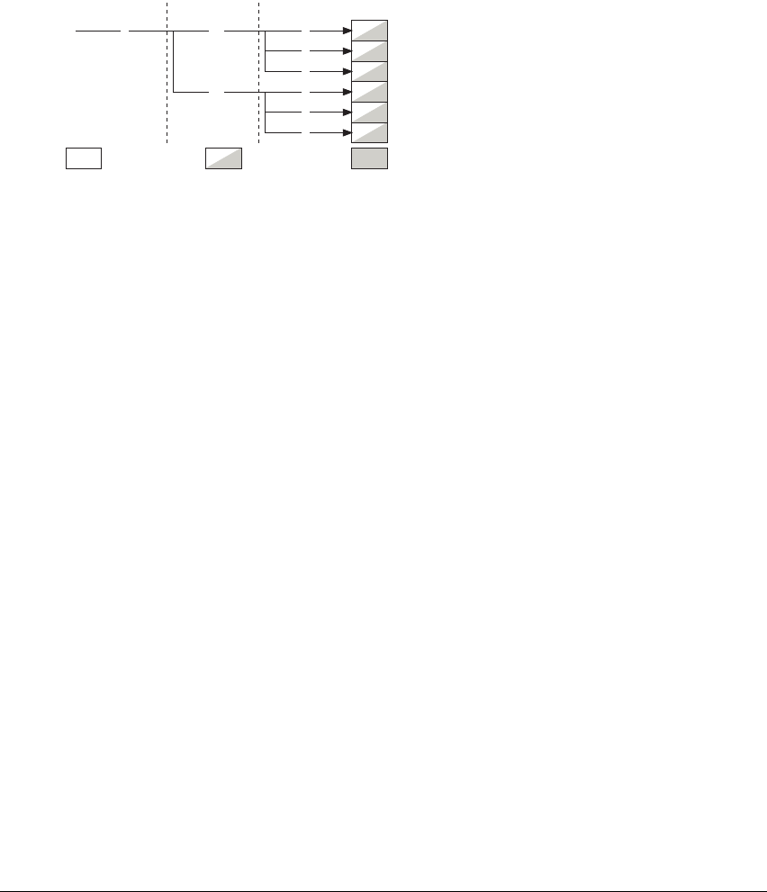
Virtual Memory System Architecture (VMSA)
B3-96 Copyright © 1996-1998, 2000, 2004-2008 ARM Limited. All rights reserved. ARM DDI 0406B
B3.12.16 CP15 c1, System control registers
The CP15 c1 registers are used for system control. Figure B3-12 shows the CP15 c1 registers.
Figure B3-12 CP15 c1 registers in a VMSA implementation
CP15 c1 register encodings not shown in Figure B3-12 are UNPREDICTABLE. When the Security Extensions
are not implemented all encodings with CRm == c1 are UNPREDICTABLE. For more information, see
Unallocated CP15 encodings on page B3-69.
The following sections describe the CP15 c1 registers:
•c1, System Control Register (SCTLR)
•c1, Implementation defined Auxiliary Control Register (ACTLR) on page B3-103
•c1, Coprocessor Access Control Register (CPACR) on page B3-104
•c1, Secure Configuration Register (SCR) on page B3-106
•c1, Secure Debug Enable Register (SDER) on page B3-108
•c1, Non-Secure Access Control Register (NSACR) on page B3-110.
B3.12.17 c1, System Control Register (SCTLR)
The System Control Register, SCTLR, provides the top level control of the system, including its memory
system.
The SCTLR:
• Is a 32-bit read/write register, with different access rights for some bits of the register.
In ARMv7, some bits in the register are read-only. These bits relate to non-configurable features of
an ARMv7 implementation, and are provided for compatibility with previous versions of the
architecture.
• Is accessible only in privileged modes.
• Has a defined reset value. The reset value is IMPLEMENTATION DEFINED, see Reset value of the SCTLR
on page B3-102. When the Security Extensions are implemented the defined reset value applies only
to the Secure copy of the SCTLR, and software must program the non-banked read/write bits of the
Non-secure copy of the register with the required values.
CRn opc1 CRm
c1 0 c0 0
2
SCTLR, Control Register
* SCR, Secure Configuration Register
opc2
1
c1 0
1
2
Read/WriteRead-only Write-only
* Only present if the Security Extensions are implemented.
ACTLR, Auxiliary Control Register, IMPLEMENTATION DEFINED
CPACR, Coprocessor Access Control Register
* SDER, Secure Debug Enable Register
* NSACR, Non-secure Access Control Register

Virtual Memory System Architecture (VMSA)
ARM DDI 0406B Copyright © 1996-1998, 2000, 2004-2008 ARM Limited. All rights reserved. B3-97
• When the Security Extensions are implemented:
— is a Banked register, with some bits common to the Secure and Non-secure copies of the
register
— has write access to the Secure copy of the register disabled when the CP15SDISABLE signal
is asserted HIGH.
For more information, see Effect of the Security Extensions on the CP15 registers on page B3-71.
Control bits in the SCTLR that are not applicable to a VMSA implementation read as the value that most
closely reflects that implementation, and ignore writes.
In an ARMv7-A implementation the format of the SCTLR is:
Bit [31] UNK/SBZP.
TE, bit [30] Thumb Exception enable. This bit controls whether exceptions are taken in ARM or Thumb
state:
0 Exceptions, including reset, handled in ARM state
1 Exceptions, including reset, handled in Thumb state.
When the Security Extensions are implemented, this bit is banked between the Secure and
Non-secure versions of the register.
An implementation can include a configuration input signal that determines the reset value
of the TE bit. If there is no configuration input signal to determine the reset value of this bit
then it resets to 0 in an ARMv7-A implementation.
For more information about the use of this bit see Instruction set state on exception entry on
page B1-35.
AFE, bit [29] Access Flag Enable bit. This bit enables use of the AP[0] bit in the translation table
descriptors as an access flag. It also restricts access permissions in the translation table
descriptors to the simplified model described in Simplified access permissions model on
page B3-29. The possible values of this bit are:
0 In the translation table descriptors, AP[0] is an access permissions bit. The full
range of access permissions is supported. No access flag is implemented.
1 In the translation table descriptors, AP[0] is an access flag. Only the simplified
model for access permissions is supported.
When the Security Extensions are implemented, this bit is banked between the Secure and
Non-secure versions of the register.
31 30 029 28 27 26 25 24 23 22 21 20 19 18 17 16 15 14 13 12 11 10 7 6 3 2 1
CAMZ 0001111IV10100
RR
HA
FI
11
VE
EE
0
NMFI
TRE
AFE
TE
0
8
BU
954
SW

Virtual Memory System Architecture (VMSA)
B3-98 Copyright © 1996-1998, 2000, 2004-2008 ARM Limited. All rights reserved. ARM DDI 0406B
TRE, bit [28] TEX Remap Enable bit. This bit enables remapping of the TEX[2:1] bits for use as two
translation table bits that can be managed by the operating system. Enabling this remapping
also changes the scheme used to describe the memory region attributes in the VMSA. The
possible values of this bit are:
0 TEX Remap disabled. TEX[2:0] are used, with the C and B bits, to describe the
memory region attributes.
1 TEX Remap enabled. TEX[2:1] are reassigned for use as flags managed by the
operating system. The TEX[0], C and B bits are used to describe the memory
region attributes, with the MMU remap registers.
When the Security Extensions are implemented, this bit is banked between the Secure and
Non-secure versions of the register.
For more information, see The alternative descriptions of the Memory region attributes on
page B3-32.
NMFI, bit [27]
Non-maskable Fast Interrupts enable:
0 Fast interrupts (FIQs) can be masked in the CPSR
1 Fast interrupts are non-maskable.
When the Security Extensions are implemented this bit is common to the Secure and
Non-secure versions of the register.
This bit is read-only. It is IMPLEMENTATION DEFINED whether an implementation supports
Non-Maskable Fast Interrupts (NMFIs):
• If NMFIs are not supported then this bit must be RAZ.
• If NMFIs are supported then this bit is controlled by a configuration input signal.
For more information, see Non-maskable fast interrupts on page B1-18.
Bit [26] RAZ/SBZP.
EE, bit [25] Exception Endianness bit. The value of this bit defines the value of the CPSR.E bit on entry
to an exception vector, including reset. This value also indicates the endianness of the
translation table data for translation table lookups. The permitted values of this bit are:
0 Little endian
1 Big endian.
When the Security Extensions are implemented, this bit is banked between the Secure and
Non-secure versions of the register.
This is a read/write bit. An implementation can include a configuration input signal that
determines the reset value of the EE bit. If there is no configuration input signal to determine
the reset value of this bit then it resets to 0.
VE, bit [24] Interrupt Vectors Enable bit. This bit controls the vectors used for the FIQ and IRQ
interrupts. The permitted values of this bit are:
0 Use the FIQ and IRQ vectors from the vector table, see the V bit entry
1 Use the IMPLEMENTATION DEFINED values for the FIQ and IRQ vectors.

Virtual Memory System Architecture (VMSA)
ARM DDI 0406B Copyright © 1996-1998, 2000, 2004-2008 ARM Limited. All rights reserved. B3-99
When the Security Extensions are implemented, this bit is banked between the Secure and
Non-secure versions of the register.
For more information, see Vectored interrupt support on page B1-32.
If the implementation does not support IMPLEMENTATION DEFINED FIQ and IRQ vectors
then this bit is RAZ/WI.
Bit [23] RAO/SBOP.
U, bit [22] In ARMv7 this bit is RAO/SBOP, indicating use of the alignment model described in
Alignment support on page A3-4.
For details of this bit in earlier versions of the architecture see Alignment on page AppxG-6.
FI, bit [21] Fast Interrupts configuration enable bit. This bit can be used to reduce interrupt latency in
an implementation by disabling IMPLEMENTATION DEFINED performance features. The
permitted values of this bit are:
0 All performance features enabled.
1 Low interrupt latency configuration. Some performance features disabled.
When the Security Extensions are implemented, this bit is common to the Secure and
Non-secure versions of the register.
This bit is:
• a read/write bit if the Security Extensions are not implemented
• if the Security Extensions are implemented:
— a read/write bit if the processor is in Secure state
— a read-only bit if the processor is in Non-secure state.
For more information, see Low interrupt latency configuration on page B1-43.
If the implementation does not support a mechanism for selecting a low interrupt latency
configuration this bit is RAZ/WI.
Bit [20:19] RAZ/SBZP.
Bit [18] RAO/SBOP.
HA, bit [17] Hardware Access Flag Enable bit. If the implementation provides hardware management of
the access flag this bit enables the access flag management:
0 Hardware management of access flag disabled
1 Hardware management of access flag enabled.
If the Security Extensions are implemented then this bit is banked between the Secure and
Non-secure versions of the register.
If the implementation does not provide hardware management of the access flag then this
bit is RAZ/WI.
For more information, see Hardware management of the access flag on page B3-21.
Bit [16] RAO/SBOP.

Virtual Memory System Architecture (VMSA)
B3-100 Copyright © 1996-1998, 2000, 2004-2008 ARM Limited. All rights reserved. ARM DDI 0406B
Bit [15] RAZ/SBZP.
RR, bit [14] Round Robin bit. If the cache implementation supports the use of an alternative replacement
strategy that has a more easily predictable worst-case performance, this bit selects it:
0 Normal replacement strategy, for example, random replacement
1 Predictable strategy, for example, round-robin replacement.
When the Security Extensions are implemented, this bit is common to the Secure and
Non-secure versions of the register.
This bit is:
• a read/write bit if the Security Extensions are not implemented
• if the Security Extensions are implemented:
— a read/write bit if the processor is in Secure state
— a read-only bit if the processor is in Non-secure state.
The replacement strategy associated with each value of the RR bit is IMPLEMENTATION
DEFINED.
If the implementation does not support multiple IMPLEMENTATION DEFINED replacement
strategies this bit is RAZ/WI.
V, bit [13] Vectors bit. This bit selects the base address of the exception vectors:
0 Normal exception vectors, base address
0x00000000
.
When the Security Extensions are implemented this base address can be
re-mapped.
1 High exception vectors (Hivecs), base address
0xFFFF0000
.
This base address is never remapped.
When the Security Extensions are implemented, this bit is banked between the Secure and
Non-secure versions of the register.
An implementation can include a configuration input signal that determines the reset value
of the V bit. If there is no configuration input signal to determine the reset value of this bit
then it resets to 0.
For more information, see Exception vectors and the exception base address on page B1-30.
I, bit [12] Instruction cache enable bit: This is a global enable bit for instruction caches:
0 Instruction caches disabled
1 Instruction caches enabled.
When the Security Extensions are implemented, this bit is banked between the Secure and
Non-secure versions of the register.
If the system does not implement any instruction caches that can be accessed by the
processor, at any level of the memory hierarchy, this bit is RAZ/WI.
If the system implements any instruction caches that can be accessed by the processor then
it must be possible to disable them by setting this bit to 0.
Cache enabling and disabling on page B2-8 describes the effect of enabling the caches.

Virtual Memory System Architecture (VMSA)
ARM DDI 0406B Copyright © 1996-1998, 2000, 2004-2008 ARM Limited. All rights reserved. B3-101
Z, bit [11] Branch prediction enable bit. This bit is used to enable branch prediction, also called
program flow prediction:
0 Program flow prediction disabled
1 Program flow prediction enabled.
When the Security Extensions are implemented, this bit is banked between the Secure and
Non-secure versions of the register.
If program flow prediction cannot be disabled, this bit is RAO/WI. Program flow prediction
includes all possible forms of speculative change of instruction stream prediction. Examples
include static prediction, dynamic prediction, and return stacks.
If the implementation does not support program flow prediction this bit is RAZ/WI.
SW, bit[10] SWP/SWPB Enable bit. This bit enables the use of
SWP
and
SWPB
instructions:
0
SWP
and
SWPB
are UNDEFINED
1
SWP
and
SWPB
perform as described in SWP, SWPB on page A8-432.
When the Security Extensions are implemented, this bit is banked between the Secure and
Non-secure versions of the register. The bit is reset to 0.
This is part of the Multiprocessing Extensions. In implementations that do not implement
the Multiprocessing Extensions this bit is RAZ and
SWP
and
SWPB
instructions perform as
described in SWP, SWPB on page A8-432.
Note
At reset, this bit disables
SWP
and
SWPB
. This means that operating systems have to choose to
use
SWP
or
SWPB
.
Bits [9:8] RAZ/SBZP.
B, bit [7] In ARMv7 this bit is RAZ/SBZP, indicating use of the endianness model described in
Endian support on page A3-7.
For details of this bit in earlier versions of the architecture see Endian support on
page AppxG-7 and Endian support on page AppxH-7.
Bits [6:3] RAO/SBOP.
C, bit [2] Cache enable bit: This is a global enable bit for data and unified caches:
0 Data and unified caches disabled
1 Data and unified caches enabled.
When the Security Extensions are implemented, this bit is banked between the Secure and
Non-secure versions of the register.
If the system does not implement any data or unified caches that can be accessed by the
processor, at any level of the memory hierarchy, this bit is RAZ/WI.
If the system implements any data or unified caches that can be accessed by the processor
then it must be possible to disable them by setting this bit to 0.
Cache enabling and disabling on page B2-8 describes the effect of enabling the caches.

Virtual Memory System Architecture (VMSA)
B3-102 Copyright © 1996-1998, 2000, 2004-2008 ARM Limited. All rights reserved. ARM DDI 0406B
A, bit [1] Alignment bit. This is the enable bit for Alignment fault checking:
0 Alignment fault checking disabled
1 Alignment fault checking enabled.
When the Security Extensions are implemented, this bit is banked between the Secure and
Non-secure versions of the register.
For more information, see Alignment fault on page B3-42, for a VMSA implementation.
M, bit [0] MMU enable bit. This is a global enable bit for the MMU:
0 MMU disabled
1 MMU enabled.
When the Security Extensions are implemented, this bit is banked between the Secure and
Non-secure versions of the register.
For more information, see Enabling and disabling the MMU on page B3-5.
Reset value of the SCTLR
The SCTLR has a defined reset value that is IMPLEMENTATION DEFINED. There are different types of bit in
the SCTLR:
• Some bits are defined as RAZ or RAO, and have the same value in all VMSAv7 implementations.
Figure B3-13 on page B3-103 shows the values of these bits.
• Some bits are read-only and either:
— have an IMPLEMENTATION DEFINED value
— have a value that is determined by a configuration input signal.
• Some bits are read/write and either:
— reset to zero
— reset to an IMPLEMENTATION DEFINED value
— reset to a value that is determined by a configuration input signal.
Figure B3-13 on page B3-103 shows the reset value, or how the reset value is defined, for each bit of the
SCTLR. It also shows the possible values of each half byte of the register.

Virtual Memory System Architecture (VMSA)
ARM DDI 0406B Copyright © 1996-1998, 2000, 2004-2008 ARM Limited. All rights reserved. B3-103
Figure B3-13 Reset value of the SCTLR, ARMv7-A (VMSAv7)
Accessing the SCTLR
To access the SCTLR you read or write the CP15 registers with
<opc1>
set to 0,
<CRn>
set to c1,
<CRm>
set to
c0, and
<opc2>
set to 0. For example:
MRC p15,0,<Rt>,c1,c0,0 ; Read CP15 System Control Register
MCR p15,0,<Rt>,c1,c0,0 ; Write CP15 System Control Register
Note
Additional configuration and control bits might be added to the SCTLR in future versions of the ARM
architecture. ARM strongly recommends that software always uses a read, modify, write sequence to update
the SCTLR. This prevents software modifying any bit that is currently unallocated, and minimizes the
chance of the register update having undesired side effects.
B3.12.18 c1, IMPLEMENTATION DEFINED Auxiliary Control Register (ACTLR)
The Auxiliary Control Register, ACTLR, provides implementation-specific configuration and control
options.
The ACTLR is:
• A 32-bit read/write register.
• Accessible only in privileged modes.
• When the Security Extensions are implemented, a Banked register. However, some bits might define
global configuration settings, and be common to the Secure and Non-secure copies of the register.
The contents of this register are IMPLEMENTATION DEFINED. ARMv7 requires this register to be privileged
read/write accessible, even if an implementation has not created any control bits in this register.
31 30 029 28 27 26 25 24 23 22 21 20 19 18 17 16 15 14 13 12 11 10 7 6 3 2 1
CAM
0
Z
0001111
IV
10100
RRHA
FI
11
VE
0
TRE
AFE
TE
0*
EE
NMFI
**************** (0)
98 54
0000 00
(*)
(*)
00
(*)
00
0x80x70x8 or 0x00x2 or 0x00x50xC
0xA, 0x8,
0x2 or 0x00x4 or 0x0
()
U B
Read-only bits, including RAZ and RAO bits.*
Can be RAZ. Otherwise read/write, resets to 0.
(*)
()Can be read-only, with IMPLEMENTATION DEFINED value. Otherwise resets to 0.
Value or reset value can depend on configuration input. Otherwise RAZ or resets to 0.
SW
(*)
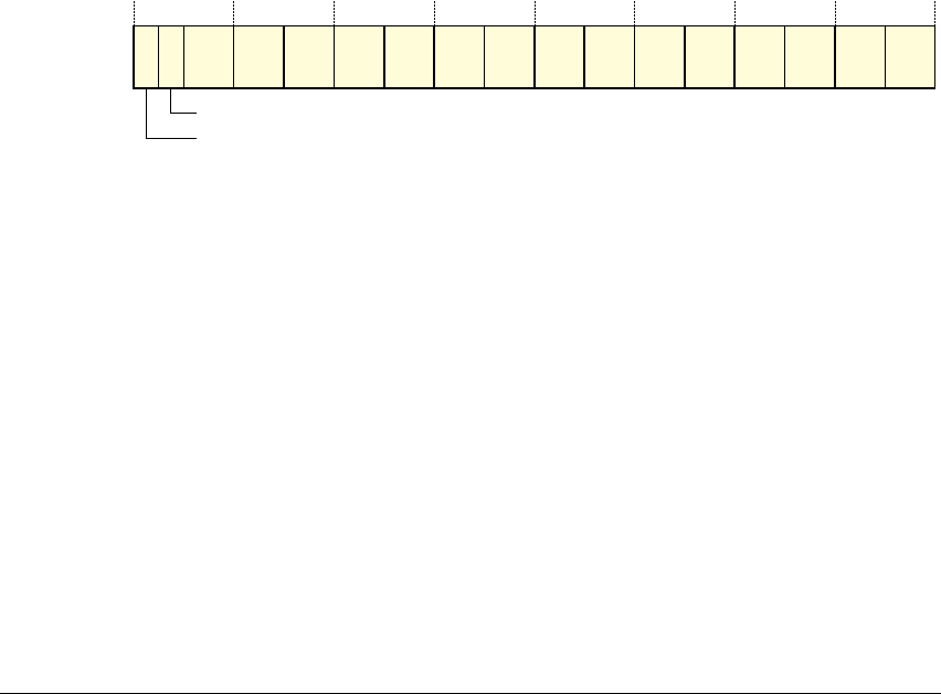
Virtual Memory System Architecture (VMSA)
B3-104 Copyright © 1996-1998, 2000, 2004-2008 ARM Limited. All rights reserved. ARM DDI 0406B
Accessing the ACTLR
To access the ACTLR you read or write the CP15 registers with
<opc1>
set to 0,
<CRn>
set to c1,
<CRm>
set to
c0, and
<opc2>
set to 1. For example:
MRC p15,0,<Rt>,c1,c0,1 ; Read CP15 Auxiliary Control Register
MCR p15,0,<Rt>,c1,c0,1 ; Write CP15 Auxiliary Control Register
B3.12.19 c1, Coprocessor Access Control Register (CPACR)
The Coprocessor Access Control Register, CPACR, controls access to all coprocessors other than CP14 and
CP15. It also enables software to check for the presence of coprocessors CP0 to CP13.
The CPACR:
• is a 32-bit read/write register
• is accessible only in privileged modes
• has a defined reset value of 0
• when the Security Extensions are implemented, is a Configurable access register.
The format of the CPACR is:
ASEDIS, bit[31]
Disable Advanced SIMD Functionality:
0 This bit does not cause any instructions to be UNDEFINED.
1 All instruction encodings identified in the Alphabetical list of instructions on
page A8-14 as being part of Advanced SIMD, but that are not VFPv3
instructions, are UNDEFINED.
On an implementation that:
• Implements VFP and does not implement Advanced SIMD, this bit is RAO/WI.
• Does not implement VFP or Advanced SIMD, this bit is UNK/SBZP.
• Implements both VFP and Advanced SIMD, it is IMPLEMENTATION DEFINED whether
this bit is supported. If it is not supported it is RAZ/WI.
This bit resets to 0 if it is supported.
D32DIS, bit[30]
Disable use of D16-D31 of the VFP register file:
0 This bit does not cause any instructions to be UNDEFINED.
cp13 cp0
31 30 29 26 25 24 23 22 21 20 19 18 17 16 15 14 13 12 11 10 9 8 7 6 5 4 3 2 1 0
(0) (0) cp12 cp11 cp10 cp9 cp8 cp7 cp6 cp5 cp4 cp3 cp2 cp1
D32DIS
ASEDIS
28 27

Virtual Memory System Architecture (VMSA)
ARM DDI 0406B Copyright © 1996-1998, 2000, 2004-2008 ARM Limited. All rights reserved. B3-105
1 All instruction encodings identified in the Alphabetical list of instructions on
page A8-14 as being VFPv3 instructions are UNDEFINED if they access any of
registers D16-D31.
If this bit is 1 when CPACR.ASEDIS == 0, the result is UNPREDICTABLE.
On an implementation that:
• Does not implement VFP, this bit is UNK/SBZP.
• Implements VFP and does not implement D16-D31, this bit is RAO/WI.
• Implements VFP and implements D16-D31, it is IMPLEMENTATION DEFINED whether
this bit is supported. If it is not, then this bit is RAZ/WI.
This bit resets to 0 if it is supported.
Bits [29:28] Reserved. UNK/SBZP.
cp<n>, bits [2n+1, 2n], for n = 0 to 13
Defines the access rights for coprocessor n. The possible values of the field are:
0b00 Access denied. Any attempt to access the coprocessor generates an Undefined
Instruction exception.
0b01 Privileged access only. Any attempt to access the coprocessor in User mode
generates an Undefined Instruction exception.
0b10 Reserved. The effect of this value is UNPREDICTABLE.
0b11 Full access. The meaning of full access is defined by the appropriate
coprocessor.
The value for a coprocessor that is not implemented is 0b00, access denied.
When the Security Extensions are implemented, the NSACR controls whether each coprocessor can be
accessed from the Non-secure state, see c1, Non-Secure Access Control Register (NSACR) on page B3-110.
When the NSACR permits Non-secure access to a coprocessor the level of access permitted is determined
by the CPACR. Because the CPACR is not banked, the options for Non-secure state access to a coprocessor
are:
• no access
• identical access rights to the Secure state.
If more than one coprocessor is used to provide a set of functionality then having different values for the
CPACR fields for those coprocessors can lead to UNPREDICTABLE behavior. An example where this must be
considered is with the VFP extension. This uses CP10 and CP11.
Typically, an operating system uses this register to control coprocessor resource sharing among applications:
• Initially all applications are denied access to the shared coprocessor-based resources.
• When an application attempts to use a resource it results in an Undefined Instruction exception.
• The Undefined Instruction handler can then grant access to the resource by setting the appropriate
field in the CPACR.
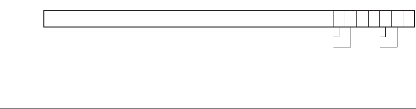
Virtual Memory System Architecture (VMSA)
B3-106 Copyright © 1996-1998, 2000, 2004-2008 ARM Limited. All rights reserved. ARM DDI 0406B
For details of how this register can be used to check for implemented coprocessors see Access controls on
CP0 to CP13 on page B1-63.
Sharing resources among applications requires a state saving mechanism. Two possibilities are:
• during a context switch, if the last executing process or thread had access rights to a coprocessor then
the operating system saves the state of that coprocessor
• on receiving a request for access to a coprocessor, the operating system saves the old state for that
coprocessor with the last process or thread that accessed it.
Accessing the CPACR
To access the CPACR you read or write the CP15 registers with
<opc1>
set to 0,
<CRn>
set to c1,
<CRm>
set to
c0, and
<opc2>
set to 2. For example:
MRC p15,0,<Rt>,c1,c0,2 ; Read CP15 Coprocessor Access Control Register
MCR p15,0,<Rt>,c1,c0,2 ; Write CP15 Coprocessor Access Control Register
Normally, software uses a read, modify, write sequence to update the CPACR, to avoid unwanted changes
to the access settings for other coprocessors.
B3.12.20 c1, Secure Configuration Register (SCR)
The Secure Configuration Register, SCR, is part of the Security Extensions.
The SCR defines the configuration of the current security state. It specifies:
• the security state of the processor, Secure or Non-secure
• what mode the processor branches to if an IRQ, FIQ or external abort occurs
• whether the CPSR.F and CPSR.A bits can be modified when SCR.NS = 1.
The SCR:
• is present only when the Security Extensions are implemented
• is a 32-bit read/write register
• is accessible in Secure privileged modes only
• has a defined reset value of 0
• is a Restricted access register, meaning it exists only in the Secure state.
The format of the SCR is:
Bits [31:7] Reserved. UNK/SBZP.
0
NS
UNK/SBZP
FIQ
41365 231 7
EAFW
IRQ
nET
AW

Virtual Memory System Architecture (VMSA)
ARM DDI 0406B Copyright © 1996-1998, 2000, 2004-2008 ARM Limited. All rights reserved. B3-107
nET, bit [6] Not Early Termination. This bit disables early termination:
0 Early termination permitted. Execution time of data operations can depend on
the data values.
1 Disable early termination. The number of cycles required for data operations is
forced to be independent of the data values.
This IMPLEMENTATION DEFINED mechanism can be used to disable data dependent timing
optimizations from multiplies and data operations. It can provide system support against
information leakage that might be exploited by timing correlation types of attack.
On implementations that do not have early termination, this bit is UNK/SBZP.
AW, bit [5] A bit writable. This bit controls whether the A bit in the CPSR can be modified in
Non-secure state:
0 the CPSR.A bit can be modified only in Secure state.
1 the CPSR.A bit can be modified in any security state.
For more information, see Control of aborts by the Security Extensions on page B1-41.
FW, bit [4] F bit writable. This bit controls whether the F bit in the CPSR can be modified in Non-secure
state:
0 the CPSR.F bit can be modified only in Secure state
1 the CPSR.F bit can be modified in any security state.
For more information, see Control of FIQs by the Security Extensions on page B1-42.
EA, bit [3] External Abort handler. This bit controls which mode handles external aborts:
0 Abort mode handles external aborts
1 Monitor mode handles external aborts.
For more information, see Control of aborts by the Security Extensions on page B1-41.
FIQ, bit [2] FIQ handler. This bit controls which mode the processor enters when a Fast Interrupt (FIQ)
is taken:
0 FIQ mode entered when FIQ is taken
1 Monitor mode entered when FIQ is taken.
For more information, see Control of FIQs by the Security Extensions on page B1-42.
IRQ, bit [1] IRQ handler. This bit controls which mode the processor enters when an Interrupt (IRQ)
is taken:
0 IRQ mode entered when IRQ is taken
1 Monitor mode entered when IRQ is taken.

Virtual Memory System Architecture (VMSA)
B3-108 Copyright © 1996-1998, 2000, 2004-2008 ARM Limited. All rights reserved. ARM DDI 0406B
NS, bit [0] Non Secure bit. Except when the processor is in Monitor mode, this bit determines the
security state of the processor. Table B3-27 shows the security settings:
For more information, see Changing from Secure to Non-secure state on page B1-27.
The value of the NS bit also affects the accessibility of the Banked CP15 registers in Monitor
mode, see Access to registers in Monitor mode on page B3-77.
Unless the processor is in Debug state, when an exception occurs in Monitor mode the
hardware sets the NS bit to 0.
Whenever the processor changes security state, the monitor code can change the value of the EA, FIQ and
IQ bits. This means that the behavior of IRQ, FIQ and External Abort exceptions can be different in each
security state.
Accessing the SCR
To access the SCR you read or write the CP15 registers with
<opc1>
set to 0,
<CRn>
set to c1,
<CRm>
set to c1,
and
<opc2>
set to 0. For example:
MRC p15,0,<Rt>,c1,c1,0 ; Read CP15 Secure Configuration Register
MCR p15,0,<Rt>,c1,c1,0 ; Write CP15 Secure Configuration Register
B3.12.21 c1, Secure Debug Enable Register (SDER)
The Secure Debug Enable Register, SDER, is part of the Security Extensions.
The SDER controls invasive and non-invasive debug in Secure User mode.
The SDER is:
• present only when the Security Extensions are implemented
• a 32-bit read/write register
• a Restricted access register, meaning it exists only in the Secure state
• accessible in Secure privileged modes only.
Table B3-27 Processor security state
SCR.NS
Processor mode, from CPSR.M bits
Monitor mode All modes except Monitor mode
0 Secure state Secure state
1 Secure state Non-secure state

Virtual Memory System Architecture (VMSA)
ARM DDI 0406B Copyright © 1996-1998, 2000, 2004-2008 ARM Limited. All rights reserved. B3-109
The format of the SDER is:
Bits [31:2] Reserved. UNK/SBZP.
SUNIDEN, bit [1]
Secure User Non-Invasive Debug ENable:
0 non-invasive debug not permitted in Secure User mode
1 non-invasive debug permitted in Secure User mode.
SUIDEN, bit [0]
Secure User Invasive Debug ENable:
0 invasive debug not permitted in Secure User mode
1 invasive debug permitted in Secure User mode.
For more information about the use of the SUNIDEN and SUIDEN bits see:
• Chapter C2 Invasive Debug Authentication
• Chapter C7 Non-invasive Debug Authentication.
Note
Invasive and non-invasive debug in Secure privileged modes is controlled by hardware only. For more
information, see Chapter C2 Invasive Debug Authentication and Chapter C7 Non-invasive Debug
Authentication.
Accessing the SDER
To access the SDER you read or write the CP15 registers with
<opc1>
set to 0,
<CRn>
set to c1,
<CRm>
set to
c1, and
<opc2>
set to 1. For example:
MRC p15,0,<Rt>,c1,c1,1 ; Read CP15 Secure Debug Enable Register
MCR p15,0,<Rt>,c1,c1,1 ; Write CP15 Secure Debug Enable Register
01
UNK/SBZP
SUNIDEN
SUIDEN
231
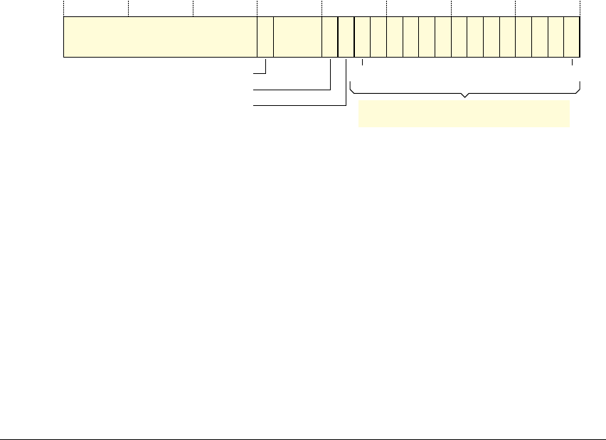
Virtual Memory System Architecture (VMSA)
B3-110 Copyright © 1996-1998, 2000, 2004-2008 ARM Limited. All rights reserved. ARM DDI 0406B
B3.12.22 c1, Non-Secure Access Control Register (NSACR)
The Non-Secure Access Control Register, NSACR, is part of the Security Extensions.
The NSACR defines the Non-secure access permissions to the coprocessors CP0 to CP13. Additional
IMPLEMENTATION DEFINED bits in the register can be used to define Non-secure access permissions for
IMPLEMENTATION DEFINED functionality.
The NSACR is:
• Present only when the Security Extensions are implemented.
• A 32-bit register
• A Restricted access register. NSACR exists only in the Secure state, but can be read from Non-secure
state.
• Accessible only in privileged modes, with access rights that depend on the mode and security state:
— the NSACR is read/write in Secure privileged modes
— the NSACR is read-only in Non-secure privileged modes.
The format of the NSACR is:
Bits [31:20]
Reserved. UNK/SBZP.
RFR, bit [19] Reserve FIQ Registers:
0 FIQ mode and the FIQ banked registers are accessible in Secure and Non-secure
security states.
1 FIQ mode and the FIQ banked registers are accessible in the Secure security
state only. Any attempt to access any FIQ Banked register or to enter an FIQ
mode when in the Non-secure security states is UNPREDICTABLE.
This bit resets to 0. On some implementations this bit cannot be set to 1.
If NSACR.RFR == 1 when SCR.FIQ == 0, instruction execution is UNPREDICTABLE in
Non-secure security state.
Bits [18:16] IMPLEMENTATION DEFINED.
These bits can be used to define the Non-secure access to IMPLEMENTATION DEFINED
features.
UNK/SBZP
31 20 19 18 16 15 14 13 12 11 10 9 8 7 6 5 4 3 2 1 0
IMP
RFR
NSASEDIS
NSD32DIS Coprocessor Non-secure access enables,
cp13 to cp0, see text
---cp13 cp0

Virtual Memory System Architecture (VMSA)
ARM DDI 0406B Copyright © 1996-1998, 2000, 2004-2008 ARM Limited. All rights reserved. B3-111
NSASEDIS, bit[15]
Disable Non-secure Advanced SIMD functionality:
0 This bit has no effect on the ability to write CPACR.ASEDIS.
1 When executing in Non-secure state the CPACR.ASEDIS bit has a fixed value
of 1 and writes to it are ignored.
On an implementation that:
• Implements VFP and does not implement Advanced SIMD, this bit is RAO/WI.
• Does not implement VFP or Advanced SIMD, this bit is UNK/SBZP.
• Implements both VFP and Advanced SIMD, it is IMPLEMENTATION DEFINED whether
this bit is supported. If it is not supported it is RAZ/WI.
This bit resets to 0 if it is supported.
NSD32DIS, bit[14]
Disable Non-secure use of D16-D31 of the VFP register file:
0 This bit has no effect on the ability to write CPACR.D32DIS.
1 When executing in Non-secure state, the CPACR.D32DIS bit has a fixed value
of 1 and writes to it are ignored.
If this bit is 1 when NSACR.NSASEDIS == 0, the result is UNPREDICTABLE.
On an implementation that:
• Does not implement VFP, this bit is UNK/SBZP.
• Implements VFP and does not implement D16-D31, this bit is RAO/WI.
• Implements VFP and implements D16-D31, it is IMPLEMENTATION DEFINED whether
this bit is supported. If it is not supported it is RAZ/WI.
This bit resets to 0 if it is supported.
cp<n>, bit [n], for n = 0 to 13
Non-secure access to coprocessor <n> enable. Each bit enables access to the corresponding
coprocessor from Non-secure state:
0 Coprocessor <n> can be accessed only from Secure state. Any attempt to access
coprocessor <n> in Non-secure state results in an Undefined Instruction
exception.
If the processor is in Non-secure state it cannot write the corresponding bits in
the CPACR, and reads them as 0b00, access denied.
1 Coprocessor <n> can be accessed from any security state.
If Non-secure access to a coprocessor is enabled, the CPACR must be checked to determine
the level of access that is permitted, see c1, Coprocessor Access Control Register (CPACR)
on page B3-104.

Virtual Memory System Architecture (VMSA)
B3-112 Copyright © 1996-1998, 2000, 2004-2008 ARM Limited. All rights reserved. ARM DDI 0406B
If multiple coprocessors are used to control a feature then the Non-secure access enable bits
for those coprocessors must be set to the same value, otherwise behavior is UNPREDICTABLE.
For example, when the VFP extension is implemented it is controlled by coprocessors 10
and 11, and bits [10,11] of the NSACR must be set to the same value.
For bits that correspond to coprocessors that are not implemented, it is IMPLEMENTATION
DEFINED whether the bits:
• behave as RAZ/WI
• can be written by Secure privileged modes.
Accessing the NSACR
To access the NSACR you read or write the CP15 registers with
<opc1>
set to 0,
<CRn>
set to c1,
<CRm>
set to
c1, and
<opc2>
set to 2. For example:
MRC p15,0,<Rt>,c1,c1,2 ; Read CP15 Non-Secure Access Control Register
MCR p15,0,<Rt>,c1,c1,2 ; Write CP15 Non-Secure Access Control Register
You can write to the NSACR only in Secure privileged modes.
You can read the register in any privileged mode.

Virtual Memory System Architecture (VMSA)
ARM DDI 0406B Copyright © 1996-1998, 2000, 2004-2008 ARM Limited. All rights reserved. B3-113
B3.12.23 CP15 c2 and c3, Memory protection and control registers
On an ARMv7-A implementation, the CP15 c2 and c3 registers are used for memory protection and control.
Figure B3-14 shows these registers.
Figure B3-14 CP15 c2 and c3 registers
CP15 c2 and c3 register encodings not shown in Figure B3-14 are UNPREDICTABLE, see Unallocated CP15
encodings on page B3-69.
B3.12.24 CP15 c2, Translation table support registers
When the VMSA is implemented, three translation table support registers are implemented in CP15 c2.
Table B3-28 summarizes these registers.
The description of the TTBCR describes the use of this set of registers, see c2, Translation Table Base
Control Register (TTBCR) on page B3-117.
c2, Translation Table Base Register 0 (TTBR0)
The Translation Table Base Register 0, TTBR0, holds the base address of translation table 0, and
information about the memory it occupies.
The TTBR0 register:
• is a 32-bit read/write register
• is accessible only in privileged modes
• when the Security Extensions are implemented:
— is a Banked register.
— has write access to the Secure copy of the register disabled when the CP15SDISABLE signal
is asserted HIGH.
CRn opc1 CRm opc2
TTBR0, Translation Table Base Register 0
c2 0 c0
TTBCR, Translation Table Base Control Register
0
2
1 TTBR1, Translation Table Base Register 1
DACR, Domain Access Control Register
c3 0 c0 0
Read/WriteRead-only Write-only
Table B3-28 VMSA translation table support registers
Register name Description
Translation Table Base 0 c2, Translation Table Base Register 0 (TTBR0)
Translation Table Base 1 c2, Translation Table Base Register 1 (TTBR1) on page B3-116
Translation Table Base Control c2, Translation Table Base Control Register (TTBCR) on page B3-117
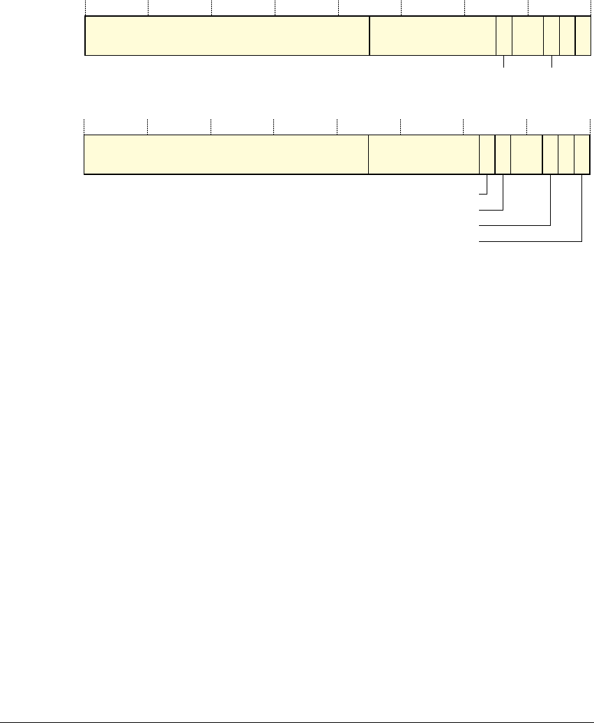
Virtual Memory System Architecture (VMSA)
B3-114 Copyright © 1996-1998, 2000, 2004-2008 ARM Limited. All rights reserved. ARM DDI 0406B
When the Multiprocessing Extensions are not implemented, the format of the TTBR0 register is:
When the Multiprocessing Extensions are implemented, the format of the TTBR0 register is:
Bits [31:14-N] Translation table base 0 address, bits [31:14-N].
The value of N determines the required alignment of the translation table, which must be
aligned to 214-N bytes.
Bits [13-N:6], ARMv7-A base architecture
UNK/SBZP.
Bits [13-N:7], when the Multiprocessing Extensions are implemented
UNK/SBZP.
IRGN[0], bit [6], when the Multiprocessing Extensions are implemented
See the description of bit [0] when the Multiprocessing Extensions are implemented.
NOS, bit [5] Not Outer Shareable bit. Indicates the Outer Shareable attribute for the memory associated
with a translation table walk that has the Shareable attribute, indicated by TTBR0.S == 1:
0 Outer Shareable
1 Inner Shareable.
This bit is ignored when TTBR0.S == 0.
This bit is only implemented from ARMv7.
RGN, bits [4:3]
Region bits. Indicates the Outer Cacheability attributes for the memory associated with the
translation table walks:
0b00 Normal memory, Outer Non-cacheable
0b01 Normal memory, Outer Write-Back Write-Allocate Cacheable
C
31 14-N 13-N 6 5 4 3 2 1 0
Translation table base 0 address UNK/SBZP RGN S
NOS IMP
31 14-N 13-N 6 5 4 3 2 1 0
Translation table base 0 address UNK/SBZP RGN S
NOS
7
IRGN[0]
IRGN[1]
IMP

Virtual Memory System Architecture (VMSA)
ARM DDI 0406B Copyright © 1996-1998, 2000, 2004-2008 ARM Limited. All rights reserved. B3-115
0b10 Normal memory, Outer Write-Through Cacheable
0b11 Normal memory, Outer Write-Back no Write-Allocate Cacheable.
IMP, bit [2] The effect of this bit is IMPLEMENTATION DEFINED. If the translation table implementation
does not include any IMPLEMENTATION DEFINED features this bit is SBZ.
S, bit [1] Shareable bit. Indicates the Shareable attribute for the memory associated with the
translation table walks:
0 Non-shareable
1 Shareable.
C, bit [0], ARMv7-A base architecture
Cacheable bit. Indicates whether the translation table walk is to Inner Cacheable memory.
0 Inner Non-cacheable
1 Inner Cacheable.
For regions marked as Inner Cacheable, it is IMPLEMENTATION DEFINED whether the read
has the Write-Through, Write-Back no Write-Allocate, or Write-Back Write-Allocate
attribute.
IRGN, bits [6,0], when the Multiprocessing Extensions are implemented
Inner region bits. Indicates the Inner Cacheability attributes for the memory associated with
the translation table walks. The possible values of IRGN[1:0] are:
0b00 Normal memory, Inner Non-cacheable
0b01 Normal memory, Inner Write-Back Write-Allocate Cacheable
0b10 Normal memory, Inner Write-Through Cacheable
0b11 Normal memory, Inner Write-Back no Write-Allocate Cacheable.
Note
The encoding of the IRGN bits is counter-intuitive, with register bit [6] being IRGN[0] and
register bit [0] being IRGN[1]. This encoding is chosen to give a consistent encoding of
memory region types and to ensure that software written for the ARMv7 base architecture
can run unmodified on an implementation that includes the Multiprocessing Extensions.
Accessing the TTBR0 register
To access the TTBR0 register you read or write the CP15 registers with
<opc1>
set to 0,
<CRn>
set to c2,
<CRm>
set to c0, and
<opc2>
set to 0. For example:
MRC p15,0,<Rt>,c2,c0,0 ; Read CP15 Translation Table Base Register 0
MCR p15,0,<Rt>,c2,c0,0 ; Write CP15 Translation Table Base Register 0
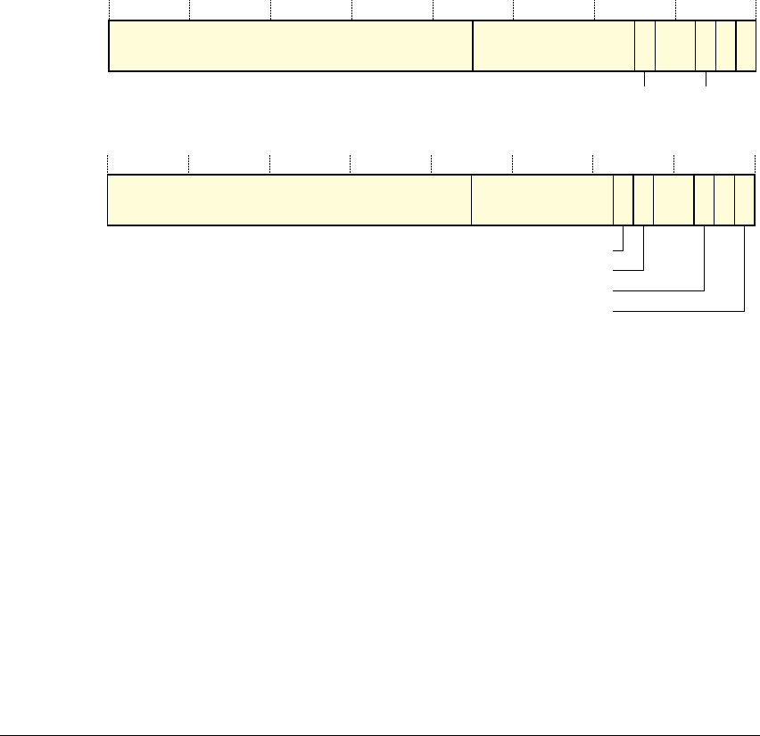
Virtual Memory System Architecture (VMSA)
B3-116 Copyright © 1996-1998, 2000, 2004-2008 ARM Limited. All rights reserved. ARM DDI 0406B
c2, Translation Table Base Register 1 (TTBR1)
The Translation Table Base Register 1, TTBR1, holds the base address of translation table 1, and
information about the memory it occupies.
The TTBR1 register is:
• a 32-bit read/write register
• accessible only in privileged modes
• when the Security Extensions are implemented, a Banked register.
When the Multiprocessing Extensions are not implemented, the format of the TTBR1 register is:
When the Multiprocessing Extensions are implemented, the format of the TTBR1 register is:
Bits [31:14] Translation table base 1 address, bits [31:14]. The translation table must be aligned on a
16KByte boundary.
Bits [13:6], ARMv7-A base architecture
UNK/SBZP.
Bits [13:7], when the Multiprocessing Extensions are implemented
UNK/SBZP.
IRGN[0:1], bits [6,0], when the Multiprocessing Extensions are implemented
See the definition given for the TTBR0 in c2, Translation Table Base Register 0 (TTBR0)
on page B3-113.
NOS, RGN, IMP, S, bits [5:1]
See the definitions given for the TTBR0 in c2, Translation Table Base Register 0 (TTBR0)
on page B3-113.
C
31 14 13 6 5 4 3 2 1 0
Translation table base 1 address UNK/SBZP RGN S
NOS IMP
31 14 13 6 5 4 3 2 1 0
Translation table base 1 address UNK/SBZP RGN S
NOS
7
IRGN[0]
IMP
IRGN[1]
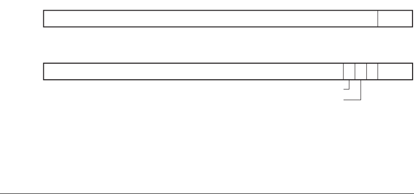
Virtual Memory System Architecture (VMSA)
ARM DDI 0406B Copyright © 1996-1998, 2000, 2004-2008 ARM Limited. All rights reserved. B3-117
C, bit [0], ARMv7-A base architecture
See the definition given for the TTBR0 in c2, Translation Table Base Register 0 (TTBR0)
on page B3-113.
Accessing the TTBR1 register
To access the TTBR1 register you read or write the CP15 registers with
<opc1>
set to 0,
<CRn>
set to c2,
<CRm>
set to c0, and
<opc2>
set to 1. For example:
MRC p15,0,<Rt>,c2,c0,1 ; Read CP15 Translation Table Base Register 1
MCR p15,0,<Rt>,c2,c0,1 ; Write CP15 Translation Table Base Register 1
c2, Translation Table Base Control Register (TTBCR)
The Translation Table Base Control Register, TTBCR, determines which of the Translation Table Base
Registers, TTBR0 or TTBR1, defines the base address for the translation table walk that is required when
an MVA is not found in the TLB.
The TTBCR:
• Is a 32-bit read/write register.
• Is accessible only in privileged modes
• Has a defined reset value of 0. When the Security Extensions are implemented, this reset value
applies only to the Secure copy of the register, and software must program the Non-secure copy of
the register with the required value.
• When the Security Extensions are implemented:
— is a Banked register.
— has write access to the Secure copy of the register disabled when the CP15SDISABLE signal
is asserted HIGH.
When the Security Extensions are not implemented, the format of the TTBCR is:
When the Security Extensions are implemented, the format of the TTBCR is:
Bits [31:6, 3] UNK/SBZP.
PD1, bit [5], when Security Extensions are implemented
Translation table walk Disable bit for TTBR1. This bit controls whether a translation table
walk is performed on a TLB miss when TTBR1 is used:
0 If a TLB miss occurs when TTBR1 is used a translation table walk is performed.
3
NUNK/SBZP
31 02
543
N(0)UNK/SBZP
31 602
PD0
PD1

Virtual Memory System Architecture (VMSA)
B3-118 Copyright © 1996-1998, 2000, 2004-2008 ARM Limited. All rights reserved. ARM DDI 0406B
1 If a TLB miss occurs when TTBR1 is used no translation table walk is
performed and a Section Translation fault is returned.
PD0, bit [4], when Security Extensions are implemented
Translation table walk Disable bit for TTBR0. This bit controls whether a translation table
walk is performed on a TLB miss when TTBR0 is used. The meanings of the possible values
of this bit are equivalent to those for the PD1 bit.
Bits [5:4], when Security Extensions are not implemented
UNK/SBZP.
N, bits [2:0] Indicate the width of the base address held in TTBR0. In TTBR0, the base address field is
bits [31:14-N]. The value of N also determines:
• whether TTBR0 or TTBR1 is used as the base address for translation table walks.
• the size of the translation table pointed to by TTBR0.
N can take any value from 0 to 7, that is, from 0b000 to 0b111.
When N has its reset value of 0, the translation table base is compatible with ARMv5 and
ARMv6.
Determining which TTBR to use, and the TTBR0 translation table size
When an MVA is not found in the TLB, the value of TTBCR.N determines whether TTBR0 or TTBR1 is
used as the base address for the translation table walk in memory:
• if N == 0 then always use TTBR0
• if N > 0 then:
— if bits [31:32-N] of the MVA are all zero then use TTBR0
— otherwise use TTBR1.
The size of the first-level translation tables accessed by TTBR0 depends on the value of TTBCR.N as shown
in Table B3-29:
Table B3-29 Value of N field and the size of the TTBR0 translation table
TTBCR.N Size of TTBR0 translation table
0b000 16KB
0b001 8KB
0b010 4KB
0b011 2KB
0b100 1KB

Virtual Memory System Architecture (VMSA)
ARM DDI 0406B Copyright © 1996-1998, 2000, 2004-2008 ARM Limited. All rights reserved. B3-119
Accessing the TTBCR
To access the TTBCR you read or write the CP15 registers with
<opc1>
set to 0,
<CRn>
set to c2,
<CRm>
set to
c0, and
<opc2>
set to 2. For example:
MRC p15,0,<Rt>,c2,c0,2 ; Read CP15 Translation Table Base Control Register
MCR p15,0,<Rt>,c2,c0,2 ; Write CP15 Translation Table Base Control Register
B3.12.25 c3, Domain Access Control Register (DACR)
The Domain Access Control Register, DACR, defines the access permission for each of the sixteen memory
domains.
The DACR:
• is a 32-bit read/write register
• is accessible only in privileged modes
• when the Security Extensions are implemented:
— is a Banked register.
— has write access to the Secure copy of the register disabled when the CP15SDISABLE signal
is asserted HIGH.
The format of the DACR is:
Dn, bits [(2n+1):2n]
Domain n access permission, where n = 0 to 15. Permitted values are:
0b00 No access. Any access to the domain generates a Domain fault.
0b01 Client. Accesses are checked against the permission bits in the translation
tables.
0b10 Reserved, effect is UNPREDICTABLE
0b11 Manager. Accesses are not checked against the permission bits in the translation
tables.
For more information, see Domains on page B3-31.
0b101 512 bytes
0b110 256 bytes
0b111 128 bytes
Table B3-29 Value of N field and the size of the TTBR0 translation table (continued)
TTBCR.N Size of TTBR0 translation table
31 30 29 28 27 26 25 24 23 22 21 20 19 18 17 16 15 14 13 12 11 10 9 8 7 6 5 4 3 2 1 0
D15 D14 D13 D12 D11 D10 D9 D8 D7 D6 D5 D4 D3 D2 D1 D0
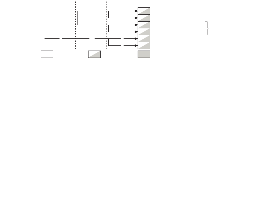
Virtual Memory System Architecture (VMSA)
B3-120 Copyright © 1996-1998, 2000, 2004-2008 ARM Limited. All rights reserved. ARM DDI 0406B
Accessing the DACR
To access the DACR you read or write the CP15 registers with
<opc1>
set to 0,
<CRn>
set to c3,
<CRm>
set to
c0, and
<opc2>
set to 0. For example:
MRC p15,0,<Rt>,c3,c0,0 ; Read CP15 Domain Access Control Register
MCR p15,0,<Rt>,c3,c0,0 ; Write CP15 Domain Access Control Register
B3.12.26 CP15 c4, Not used
CP15 c4 is not used on any ARMv7 implementation, see Unallocated CP15 encodings on page B3-69.
B3.12.27 CP15 c5 and c6, Memory system fault registers
The CP15 c5 and c6 registers are used for memory system fault reporting. Figure B3-15 shows the CP15 c5
and c6 registers.
Figure B3-15 CP15 c5 and c6 registers in a VMSA implementation
CP15 c5 and c6 register encodings not shown in Figure B3-15 are UNPREDICTABLE, see Unallocated CP15
encodings on page B3-69.
The CP15 c5 and c6 registers are described in:
•CP15 c5, Fault status registers on page B3-121
•CP15 c6, Fault Address registers on page B3-124.
Also, these registers are used to report information about debug exceptions. For details see Effects of debug
exceptions on CP15 registers and the DBGWFAR on page C4-4.
c5 0 c0 0 DFSR, Data Fault Status Register
IFSR, Instruction Fault Status Register
DFAR, Data Fault Address Register
IFAR, Instruction Fault Address Register
1
c6 0 c0 0
2
Details are
IMPLEMENTATION DEFINED
ADFSR, Auxiliary DFSR
AIFSR, Auxiliary IFSR
c1 0
1
CRn opc1 CRm opc2
Read/WriteRead-only Write-only
Virtual Memory System Architecture (VMSA)
ARM DDI 0406B Copyright © 1996-1998, 2000, 2004-2008 ARM Limited. All rights reserved. B3-121
B3.12.28 CP15 c5, Fault status registers
There are two fault status registers, in CP15 c5, and the architecture provides encodings for two additional
IMPLEMENTATION DEFINED registers. Table B3-30 summarizes these registers.
Fault information is returned using the fault status registers and the fault address registers described in CP15
c6, Fault Address registers on page B3-124. For details of how these registers are used see Fault Status and
Fault Address registers in a VMSA implementation on page B3-48.
c5, Data Fault Status Register (DFSR)
The Data Fault Status Register, DFSR, holds status information about the last data fault.
The DFSR is:
• a 32-bit read/write register
• accessible only in privileged modes
• when the Security Extensions are implemented, a Banked register.
The format of the DFSR is:
Bits [31:13,9:8]
UNK/SBZP.
ExT, bit [12] External abort type. This bit can be used to provide an IMPLEMENTATION DEFINED
classification of external aborts.
For aborts other than external aborts this bit always returns 0.
Table B3-30 Fault status registers
Register name Description
Data Fault Status Register (DFSR) c5, Data Fault Status Register (DFSR)
Instruction Fault Status Register (IFSR) c5, Instruction Fault Status Register (IFSR) on page B3-122
Auxiliary Data Fault Status Register (ADFSR) c5, Auxiliary Data and Instruction Fault Status Registers
(ADFSR and AIFSR) on page B3-123
Auxiliary Instruction Fault Status Register (AIFSR)
43
FS[3:0]
(0)UNK/SBZP
012 11 10 9 8 7
ExT
WnR
Domain
FS[4]
(0)
31 13

Virtual Memory System Architecture (VMSA)
B3-122 Copyright © 1996-1998, 2000, 2004-2008 ARM Limited. All rights reserved. ARM DDI 0406B
WnR, bit [11] Write not Read bit. Indicates whether the abort was caused by a write or a read access:
0 Abort caused by a read access
1 Abort caused by a write access.
For faults on CP15 cache maintenance operations, including the VA to PA translation
operations, this bit always returns a value of 1.
FS, bits [10,3:0]
Fault status bits. For the valid encodings of these bits in an ARMv7-A implementation with
a VMSA, see Table B3-12 on page B3-51.
All encodings not shown in the table are reserved.
Domain, bits [7:4]
The domain of the fault address.
From ARMv7 use of this field is deprecated, see The Domain field in the DFSR on
page B3-52.
For information about using the DFSR see Fault Status and Fault Address registers in a VMSA
implementation on page B3-48.
Accessing the DFSR
To access the DFSR you read or write the CP15 registers with
<opc1>
set to 0,
<CRn>
set to c5,
<CRm>
set to
c0, and
<opc2>
set to 0. For example:
MRC p15,0,<Rt>,c5,c0,0 ; Read CP15 Data Fault Status Register
MCR p15,0,<Rt>,c5,c0,0 ; Write CP15 Data Fault Status Register
c5, Instruction Fault Status Register (IFSR)
The Instruction Fault Status Register, IFSR, holds status information about the last instruction fault.
The IFSR is:
• a 32-bit read/write register
• accessible only in privileged modes
• when the Security Extensions are implemented, a Banked register.
The format of the IFSR is:
Bits [31:13,11,9:4]
UNK/SBZP.
43
FS[3:0]
UNK/SBZP
012 11 10 9
ExT
FS[4]
31 13
UNK/SBZP(0)

Virtual Memory System Architecture (VMSA)
ARM DDI 0406B Copyright © 1996-1998, 2000, 2004-2008 ARM Limited. All rights reserved. B3-123
ExT, bit [12] External abort type. This bit can be used to provide an IMPLEMENTATION DEFINED
classification of external aborts.
For aborts other than external aborts this bit always returns 0.
FS, bits [10,3:0]
Fault status bits. For the valid encodings of these bits in an ARMv7-A implementation with
a VMSA, see Table B3-11 on page B3-50.
All encodings not shown in the table are reserved.
For information about using the IFSR see Fault Status and Fault Address registers in a VMSA
implementation on page B3-48.
Accessing the IFSR
To access the IFSR you read or write the CP15 registers with
<opc1>
set to 0,
<CRn>
set to c5,
<CRm>
set to c0,
and
<opc2>
set to 1. For example:
MRC p15,0,<Rt>,c5,c0,1 ; Read CP15 Instruction Fault Status Register
MCR p15,0,<Rt>,c5,c0,1 ; Write CP15 Instruction Fault Status Register
c5, Auxiliary Data and Instruction Fault Status Registers (ADFSR and AIFSR)
The Auxiliary Data Fault Status Register (ADFSR) and the Auxiliary Instruction Fault Status Register
(AIFSR) enable the system to return additional IMPLEMENTATION DEFINED fault status information, see
Auxiliary Fault Status Registers on page B3-53.
The ADFSR and AIFSR are:
• 32-bit read/write registers
• accessible only in privileged modes
• when the Security Extensions are implemented, Banked registers
• introduced in ARMv7.
The formats of the ADFSR and AIFSR are IMPLEMENTATION DEFINED.
Accessing the ADFSR and AIFSR
To access the ADFSR or AIFSR you read or write the CP15 registers with
<opc1>
set to 0,
<CRn>
set to c5,
<CRm>
set to c1, and
<opc2>
set to:
• 0 for the ADFSR
• 1 for the AIFSR.
For example:
MRC p15,0,<Rt>,c5,c1,0 ; Read CP15 Auxiliary Data Fault Status Register
MCR p15,0,<Rt>,c5,c1,0 ; Write CP15 Auxiliary Data Fault Status Register
MRC p15,0,<Rt>,c5,c1,1 ; Read CP15 Auxiliary Instruction Fault Status Register
MCR p15,0,<Rt>,c5,c1,1 ; Write CP15 Auxiliary Instruction Fault Status Register

Virtual Memory System Architecture (VMSA)
B3-124 Copyright © 1996-1998, 2000, 2004-2008 ARM Limited. All rights reserved. ARM DDI 0406B
B3.12.29 CP15 c6, Fault Address registers
There are two Fault Address registers, in CP15 c6, as shown in Figure B3-15 on page B3-120s. The two
Fault Address registers complement the Fault Status registers, and are shown in Table B3-31.
Note
Before ARMv7:
• The DFAR was called the Fault Address Register (FAR).
• The Watchpoint Fault Address Register (DBGWFAR) was implemented in CP15 c6, with
<opc2>
=1.
From ARMv7, the DBGWFAR is only implemented as a CP14 debug register, see Watchpoint Fault
Address Register (DBGWFAR) on page C10-28.
Fault information is returned using the fault address registers and the fault status registers described in CP15
c5, Fault status registers on page B3-121. For details of how these registers are used, and when the value in
the IFAR is valid, see Fault Status and Fault Address registers in a VMSA implementation on page B3-48.
c6, Data Fault Address Register (DFAR)
The Data Fault Address Register, DFAR, holds the MVA of the faulting address that caused a synchronous
Data Abort exception.
The DFAR is:
• a 32-bit read/write register
• accessible only in privileged modes
• when the Security Extensions are implemented, a Banked register.
The format of the DFAR is:
For information about using the DFAR, and when the value in the DFAR is valid, see Fault Status and Fault
Address registers in a VMSA implementation on page B3-48.
A debugger can write to the DFAR to restore its value.
Table B3-31 Fault Address registers
Register name Description
Data Fault Address Register (DFAR) c6, Data Fault Address Register (DFAR)
Instruction Fault Address Register (IFAR) c6, Instruction Fault Address Register (IFAR) on page B3-125
31 0
MVA of faulting address of synchronous Data Abort exception

Virtual Memory System Architecture (VMSA)
ARM DDI 0406B Copyright © 1996-1998, 2000, 2004-2008 ARM Limited. All rights reserved. B3-125
Accessing the DFAR
To access the DFAR you read or write the CP15 registers with
<opc1>
set to 0,
<CRn>
set to c6,
<CRm>
set to
c0, and
<opc2>
set to 0. For example:
MRC p15,0,<Rt>,c6,c0,0 ; Read CP15 Data Fault Address Register
MCR p15,0,<Rt>,c6,c0,0 ; Write CP15 Data Fault Address Register
c6, Instruction Fault Address Register (IFAR)
The Instruction Fault Address Register, IFAR, holds the MVA of the faulting access that caused a
synchronous Prefetch Abort exception.
The IFAR is:
• a 32-bit read/write register
• accessible only in privileged modes
• when the Security Extensions are implemented, a Banked register.
The format of the IFAR is:
For information about using the IFAR see Fault Status and Fault Address registers in a VMSA
implementation on page B3-48.
A debugger can write to the IFAR to restore its value.
Accessing the IFAR
To access the IFAR you read or write the CP15 registers with
<opc1>
set to 0,
<CRn>
set to c6,
<CRm>
set to c0,
and
<opc2>
set to 2. For example:
MRC p15,0,<Rt>,c6,c0,2 ; Read CP15 Instruction Fault Address Register
MCR p15,0,<Rt>,c6,c0,2 ; Write CP15 Instruction Fault Address Register
31 0
MVA of faulting address of synchronous Prefetch Abort exception
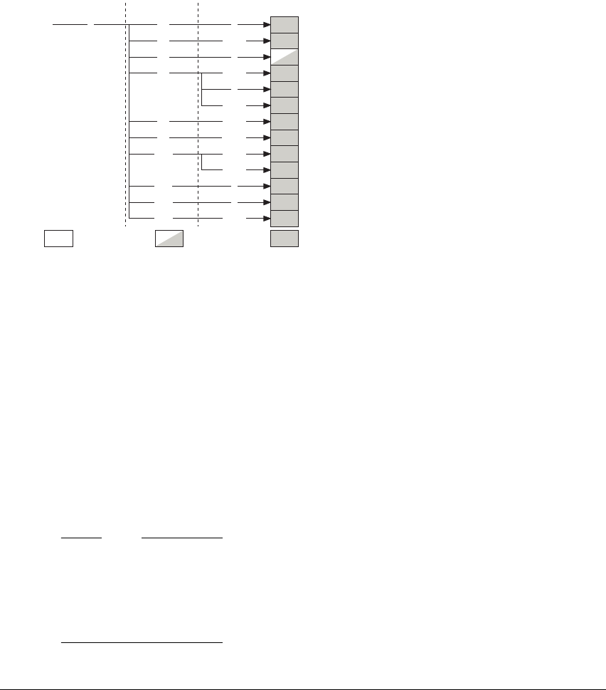
Virtual Memory System Architecture (VMSA)
B3-126 Copyright © 1996-1998, 2000, 2004-2008 ARM Limited. All rights reserved. ARM DDI 0406B
B3.12.30 CP15 c7, Cache maintenance and other functions
The CP15 c7 registers are used for cache maintenance operations. They also provide barrier operations, and
VA to PA address translation functions. Figure B3-16 shows the CP15 c7 registers.
Figure B3-16 CP15 c7 registers in a VMSA implementation
CP15 c7 register encodings not shown in Figure B3-16 are UNPREDICTABLE, see Unallocated CP15
encodings on page B3-69.
The CP15 c7 registers are described in:
•CP15 c7, Cache and branch predictor maintenance functions
•CP15 c7, Virtual Address to Physical Address translation operations on page B3-130
•CP15 c7, Miscellaneous functions on page B3-136.
B3.12.31 CP15 c7, Cache and branch predictor maintenance functions
CP15 c7 provides a number of functions. This section describes only the CP15 c7 cache and branch
predictor maintenance operations. Branch predictor operations are included in this section because they
operate in a similar way to the cache maintenance operations.
Note
ARMv7 introduces significant changes in the CP c7 operations. Most of these changes are because, from
ARMv7, the architecture covers multiple levels of cache. This section only describes the ARMv7
requirements for these operations. For details of these operations in previous versions of the architecture see:
•c7, Cache operations on page AppxG-38 for ARMv6
•c7, Cache operations on page AppxH-49 for ARMv4 and ARMv5.
Cache maintenance operations
PAR, PA result from VA to PA translation
c5
c4 0
VA to PA translation operations{0-7}c8
c10 {1,2}
{4,5}
DCCMVAU, cache maintenance operation1c11
c6
Data barrier operations
Cache maintenance operations
Cache maintenance operations
CP15ISB, Instruction Synchronization Barrier operation
Branch predictor maintenance operations
{0,1}
{6,7}
4
{1,2}
Bold text = Accessible in User mode
Read/WriteRead-only
c14 {1,2}
c13 1 NOP
Write-only
Cache maintenance operations
Cache maintenance operations
c1 {0,6}
Part of the Multiprocessing Extensions
c7 0 c0 NOP4
CRn opc1 CRm opc2

Virtual Memory System Architecture (VMSA)
ARM DDI 0406B Copyright © 1996-1998, 2000, 2004-2008 ARM Limited. All rights reserved. B3-127
Figure B3-17 shows the CP15 c7 cache and branch predictor maintenance operations.
Figure B3-17 CP15 c7 Cache and branch predictor maintenance operations
The CP15 c7 cache and branch predictor maintenance operations are all write-only operations that can be
executed only in privileged modes. They are listed in Table B3-32.
For more information about the terms used in this section see Terms used in describing cache operations on
page B2-10. The Multiprocessing Extensions changes the set of caches affected by these operations,
Multiprocessor effects on cache maintenance operations on page B2-23.
In Table B3-32, the Rt data column specifies what data is required in the register Rt specified by the
MCR
instruction used to perform the operation. For more information about the possible data formats, see Data
formats for the cache and branch predictor operations on page B3-128.
c7 0
ICIALLU, Invalidate all instruction caches to PoU
DCIMVAC, Invalidate data cache line by MVA to PoCc6 1
1
6
7
ICIMVAU, Invalidate instruction caches by MVA to PoU
BPIALL, Invalidate entire branch predictor array
BPIMVA, Invalidate MVA from branch predictor array
2DCISW, Invalidate data cache line by set/way
c10 1 DCCMVAC, Clean data cache line by MVA to PoC
DCCSW, Clean data cache line by set/way2
1c11
c14 1
PoU: Point of Unification
PoC: Point of Coherency
DCCIMVAC, Clean and invalidate data cache line by MVA to PoC
DCCISW, Clean and invalidate data cache line by set/way
2
DCCMVAU, Clean data cache line by MVA to PoU
Read-only Read/Write data or unified
CRn opc1 CRm opc2
ICIALLUIS, Invalidate all instruction caches to PoU Inner Shareable
BPIALLIS, Invalidate entire branch predictor array Inner Shareable
Part of the Multiprocessing Extensions
c1 0
6
c5 0
Write-only
Table B3-32 CP15 c7 cache and branch predictor maintenance operations
CRm opc2 Mnemonic FunctionaRt data
c1 0 ICIALLUISbInvalidate all instruction caches Inner Shareable to PoU. Also
flushes branch target cache.c
Ignored
c1 6 BPIALLISbInvalidate entire branch predictor array Inner Shareable. Ignored
c5 0 ICIALLU Invalidate all instruction caches to PoU. Also flushes branch target
cache.c
Ignored
c5 1 ICIMVAU Invalidate instruction cache line by MVA to PoU.cMVA
c5 6 BPIALL Invalidate entire branch predictor array. Ignored

Virtual Memory System Architecture (VMSA)
B3-128 Copyright © 1996-1998, 2000, 2004-2008 ARM Limited. All rights reserved. ARM DDI 0406B
Data formats for the cache and branch predictor operations
Table B3-32 on page B3-127 shows three possibilities for the data in the register Rt specified by the
MCR
instruction. These are described in the following subsections:
•Ignored
•MVA
•Set/way on page B3-129.
Ignored
The value in the register specified by the
MCR
instruction is ignored. You do not have to write a value to the
register before issuing the
MCR
instruction.
MVA
For more information about the possible meaning when the table shows that an MVA is required see Terms
used in describing cache operations on page B2-10. When the data is stated to be an MVA, it does not have
to be cache line aligned.
c5 7 BPIMVA Invalidate MVA from branch predictor array. MVA
c6 1 DCIMVAC Invalidate data or unified cache line by MVA to PoC. MVA
c6 2 DCISW Invalidate data or unified cache line by set/way. Set/way
c10 1 DCCMVAC Clean data or unified cache line by MVA to PoC. MVA
c10 2 DCCSW Clean data or unified cache line by set/way. Set/way
c11 1 DCCMVAU Clean data or unified cache line by MVA to PoU. MVA
c14 1 DCCIMVAC Clean and Invalidate data or unified cache line by MVA to PoC. MVA
c14 2 DCCISW Clean and Invalidate data or unified cache line by set/way. Set/way
a. Modified Virtual Address (MVA), point of coherency (PoC) and point of unification (PoU) are described in Terms use d
in describing cache operations on page B2-10.
b. Part of the Multiprocessing Extensions, See Multiprocessor effects on cache maintenance operations on page B2-23.
c. Only applies to separate instruction caches, does not apply to unified caches.
Table B3-32 CP15 c7 cache and branch predictor maintenance operations (continued)
CRm opc2 Mnemonic FunctionaRt data

Virtual Memory System Architecture (VMSA)
ARM DDI 0406B Copyright © 1996-1998, 2000, 2004-2008 ARM Limited. All rights reserved. B3-129
Set/way
For an operation by set/way, the data identifies the cache line that the operation is to be applied to by
specifying:
• the cache set the line belongs to
• the way number of the line in the set
• the cache level.
The format of the register data for a set/way operation is:
Where:
A =Log
2(ASSOCIATIVITY)
B =(L+S)
L =Log
2(LINELEN)
S =Log
2(NSETS)
ASSOCIATIVITY, LINELEN (Line Length) and NSETS (number of sets) have their usual
meanings and are the values for the cache level being operated on.
The values of A and S are rounded up to the next integer.
Level ((Cache level to operate on) -1)
For example, this field is 0 for operations on L 1 cache, or 1 for operations on L 2 cache.
Set The number of the set to operate on.
Way The number of the way to operate on.
Note
• If L = 4 then there is no SBZ field between the set and level fields in the register.
• If A = 0 there is no way field in the register, and register bits [31:B] are SBZ.
• If the level, set or way field in the register is larger than the size implemented in the cache then the
effect of the operation is UNPREDICTABLE.
Accessing the CP15 c7 cache and branch predictor maintenance operations
To perform one of the cache maintenance operations you write the CP15 registers with
<opc1>
set to 0,
<CRn>
set to c7, and
<CRm>
and
<opc2>
set to the values shown in Table B3-32 on page B3-127.
That is:
MCR p15,0,<Rt>,c7,<CRm>,<opc2>
For example:
MCR p15,0,<Rt>,c7,c5,0 ; Invalidate all instruction caches to point of unification
MCR p15,0,<Rt>,c7,c10,2 ; Clean data or unified cache line by set/way
31 32-A 31-A B B-1 L L-1 4 3 1 0
Way SBZ Set SBZ Level 0
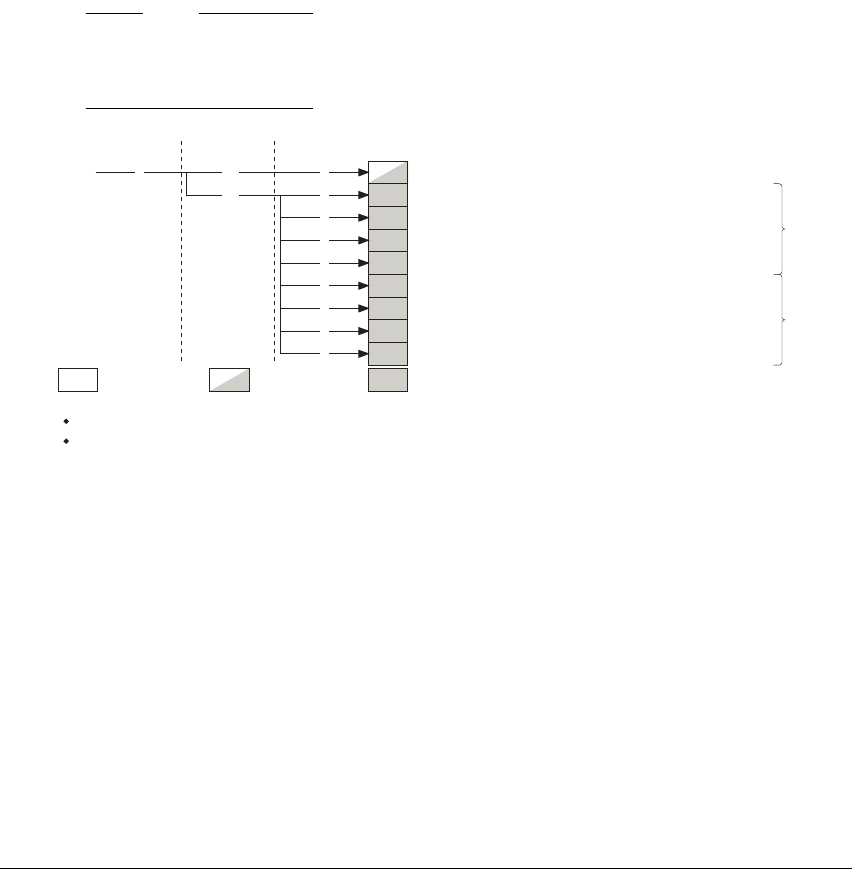
Virtual Memory System Architecture (VMSA)
B3-130 Copyright © 1996-1998, 2000, 2004-2008 ARM Limited. All rights reserved. ARM DDI 0406B
B3.12.32 CP15 c7, Virtual Address to Physical Address translation operations
CP15 c7 provides a number of functions, summarized in Figure B3-10 on page B3-65. This section
describes only the CP15 c7 operations that provide Virtual Address (VA) to Physical Address (PA)
translation on implementations that include the VMSA, and the register that returns the result of the
operation.
Figure B3-18 shows all of the CP15 c7 VA to PA translation operations. It does not show the other CP15 c7
operations.
Note
As explained in this section, the CP15 c7 encodings for VA to PA translation with
<opc2>
== {4-7} are
available only when the Security Extensions are implemented. These encodings are reserved and
UNPREDICTABLE when the Security Extensions are not implemented.
Figure B3-18 CP15 c7 VA to PA translation operations
This set of registers comprises:
• A single Physical Address Register, PAR, that returns the result of the VA to PA translation. For more
information about this register see c7, Physical Address Register (PAR) and VA to PA translations on
page B3-133.
• A set of VA to PA translation operations. These are:
— 32-bit write-only operations
— accessible only in privileged modes.
c7 0 PAR, Physical Address Register (Translation result)c4 0
c8 V2PCWPR, Privileged Read VA to PA translation0
1
2
3
5
6
7
4
V2PCWPW, Privileged Write VA to PA translation
V2PCWUR, User Read VA to PA translation
V2PCWUW, User Write VA to PA translation
V2POWPR, Privileged Read VA to PA translation
V2POWPW, Privileged Write VA to PA translation
V2POWUR, User Read VA to PA translation
V2POWUW, User Write VA to PA translation
Other
security
state
Current
security
state
CRn opc1 CRm opc2
Shown with Security Extensions implemented. When they are not implemented:
the concepts of Current security state and Other security state are not defined
encodings marked are reserved and
UNPREDICTABLE
.
Read-only Read/Write Write-only

Virtual Memory System Architecture (VMSA)
ARM DDI 0406B Copyright © 1996-1998, 2000, 2004-2008 ARM Limited. All rights reserved. B3-131
When the Security Extensions are not implemented, there are four VA to PA translation operations,
listed in Table B3-33.
When the Security Extensions are implemented, there are eight VA to PA translation operations. Four of
these are common to the Secure and Non-secure security states, and four are only available in the Secure
state. Table B3-34 lists these operations, and shows the security states in which each is available.
Table B3-33 VA to PA translation when Security Extensions are not implemented
CRm opc2 Mnemonic Register or operation
c4 0 - PAR, Physical Address Register
c8 0 V2PCWPR Privileged read VA to PA translation
c8 1 V2PCWPW Privileged write VA to PA translation
c8 2 V2PCWUR User read VA to PA translation
c8 3 V2PCWUW User write VA to PA translation
Table B3-34 VA to PA translation when Security Extensions are implemented
Register or operation:
CRm opc2 Mnemonic Common Non-secure
state Secure state
c4 0 - - PAR PAR
c8 0 V2PCWPR Current security state
privileged reada
--
c8 1 V2PCWPW Current security state
privileged writea
--
c8 2 V2PCWUR Current security state
User reada
--
c8 3 V2PCWUW Current security state
User writea
--
c8 4 V2POWPR - - Other security state privileged reada

Virtual Memory System Architecture (VMSA)
B3-132 Copyright © 1996-1998, 2000, 2004-2008 ARM Limited. All rights reserved. ARM DDI 0406B
Writing a VA to a VA to PA translation operation encoding translates the VA to the corresponding PA. The
PA value is returned in the PAR. These operations are accessible only in privileged modes. The available
VA to PA translations depend on:
• whether the Security Extensions are implemented
• if the Security Extensions are implemented, whether the processor is in the Secure or Non-secure
state.
In more detail:
Security Extensions not implemented
Four VA to PA translation operations are available, as shown in Table B3-33 on
page B3-131. These operations provide VA to PA translation for privileged read or write,
and for User read or write.
Security Extensions implemented, processor in Non-secure state
Only the four current security state VA to PA translation operations are available, as shown
in Table B3-33 on page B3-131. These operations provide VA to PA translation for
privileged read or write, and for User read or write, in the Non-secure security state.
It is not possible to perform VA to PA translations for the Secure security state. Attempting
to access an Other security state VA to PA translation operation encoding generates an
Undefined Instruction exception.
Security Extensions implemented, processor in Secure security state
Eight VA to PA Translation operations are available, as shown in Table B3-34 on
page B3-131:
• The four current security state VA to PA translation operations provide address
translation for privileged read or write, and for User read or write, in the Secure
security state.
• The four other security state VA to PA translation operations provide address
translation for privileged read or write, and for User read or write, in the Non-secure
security state.
c8 5 V2POWPW - - Other security state privileged writea
c8 6 V2POWUR - - Other security state User reada
c8 7 V2POWUW - - Other security state User writea
a. VA to PA Translation operations.
Table B3-34 VA to PA translation when Security Extensions are implemented (continued)
Register or operation:
CRm opc2 Mnemonic Common Non-secure
state Secure state
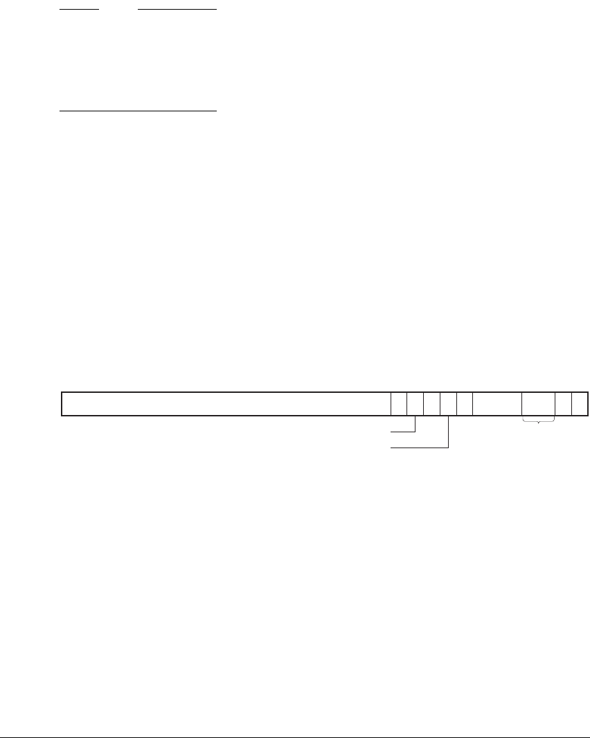
Virtual Memory System Architecture (VMSA)
ARM DDI 0406B Copyright © 1996-1998, 2000, 2004-2008 ARM Limited. All rights reserved. B3-133
Note
In all cases:
• If the FCSE is implemented the VA required is the VA before any modification by the FCSE, not the
MVA.
• For information about translations when the MMU is disabled see VA to PA translation when the
MMU is disabled on page B3-136.
c7, Physical Address Register (PAR) and VA to PA translations
The Physical Address Register, PAR, of the current security state receives the PA during any VA to PA
translation.
The PAR is:
• a 32-bit read/write register
• accessible only in privileged modes
• when the Security Extensions are implemented, a Banked register.
Write access to the register means its contents can be context switched.
The PAR format depends on the value of bit [0]. Bit [0] indicates whether the address translation operation
completed successfully.
If the translation completed successfully, the format of the PAR is:
PA, bits [31:12]
Physical Address. The physical address corresponding to the supplied virtual address.
Address bits [31:12] are returned.
Bit [11] Reserved. UNK/SBZP.
Bits [10:1] Return information from the translation table entry used for the translation:
NOS, bit [10]
Not Outer Shareable attribute. Indicates whether the physical memory is Outer
Shareable:
0 Memory is Outer Shareable
1 Memory is not Outer Shareable.
On an implementation that do not support Outer Shareable, this bit is
UNK/SBZP.
NS, bit [9] Non-secure. The NS bit from the translation table entry.
SS
PA
011 10 9
Inner[2:0](0)
87 1
FNS SH
Outer[1:0]
32461231
IMPLEMENTATION DEFINED
NOS

Virtual Memory System Architecture (VMSA)
B3-134 Copyright © 1996-1998, 2000, 2004-2008 ARM Limited. All rights reserved. ARM DDI 0406B
Bit [8] IMPLEMENTATION DEFINED.
SH, bit [7]
Shareable attribute. Indicates whether the physical memory is Shareable:
0 Memory is Non-shareable
1 Memory is Shareable.
Inner[2:0], bits [6:4]
Inner memory attributes from the translation table entry. Permitted values are:
0b111 Write-Back, no Write-Allocate
0b110 Write-Through
0b101 Write-Back, Write-Allocate
0b011 Device
0b001 Strongly-ordered
0b000 Non-cacheable.
Other encodings for Inner[2:0] are reserved.
Outer[1:0], bits [3:2]
Outer memory attributes from the translation table. Possible values are:
0b11 Write-Back, no Write-Allocate.
0b10 Write-Through, no Write-Allocate.
0b01 Write-Back, Write-Allocate.
0b00 Non-cacheable.
SS, bit [1] SuperSection. Used to indicate if the result is a Supersection:
0 Page is not a Supersection, that is, PAR[31:12] contains PA[31:12],
regardless of the page size.
1 Page is part of a Supersection
• PAR[31:24] contains PA[31:24]
• PAR[23:16] contains PA[39:32]
• PAR[15:12] contains 0b0000.
If an implementation supports less than 40 bits of physical address,
the bits in the PAR field that correspond to physical address bits that
are not implemented are UNKNOWN.
Note
PA[23:12] is the same as VA[23:12] for Supersections
F, bit [0] F bit is 0 if the conversion completed successfully.
In the Inner[2:0] and Outer[1:0] fields, an implementation that does not support all of the attributes can
report the memory type behavior that the cache does support, rather than the value held in the translation
table entry.

Virtual Memory System Architecture (VMSA)
ARM DDI 0406B Copyright © 1996-1998, 2000, 2004-2008 ARM Limited. All rights reserved. B3-135
If the translation fails without generating an abort, the format of the PAR is:
Bits [31:7] UNK/SBZP.
FS, bits [6:1] Fault status bits. Bits [12,10,3:0] from the Data Fault Status Register, indicate the source of
the abort. For more information, see c5, Data Fault Status Register (DFSR) on page B3-121.
F, bit [0] F bit is 1 if the conversion aborted.
The VA to PA translation only generates an abort if the translation fails because an external abort occurred
on a translation table walk request. In this case:
• If the external abort is synchronous, the DFSR and DFAR of the security state in which the abort is
handled are updated. The DFSR indicates the appropriate external abort on Translation fault, and the
DFAR indicates the MVA that caused the translation. PAR is UNKNOWN.
• If the external abort is asynchronous, the DFSR of the security state in which the abort is handled is
updated when the abort is taken. The DFSR indicates the asynchronous external abort. The DFAR is
not updated. PAR is UNKNOWN.
For all other cases where the VA to PA translation fails:
• No abort is generated, and the DFSR and DFAR are unchanged
• the PAR [6:1] field is updated with an FSR encoding that indicates the fault
• the PAR bit [0] is set to 1.
Implementations that do not support all attributes can report the behavior for those memory types that the
cache does support.
Accessing the PAR and the VA to PA translation operations
To access one of the VA to PA translation operations you write the CP15 registers with
<opc1>
set to 0,
<CRn>
set to c7,
<CRm>
set to c8, and
<opc2>
set to the value shown in Table B3-33 on page B3-131 or Table B3-34
on page B3-131.
With register
Rt
containing the original VA this gives:
MCR p15,0,<Rt>,c7,c8,<opc2>
To read the PAR you read the CP15 registers with
<opc1>
set to 0,
<CRn>
set to c7,
<CRm>
set to c4, and
<opc2>
set to 0. To return the translated PA in register Rt this gives:
MRC p15,0,<Rt>,c7,c4,0
The PAR is a read/write register, and you can write to the CP15 registers with the same settings to write to
the register. There is no translation operation that requires writing to this register, but the write operation
might be required to restore the value of the PAR after a context switch.
An example of a VA to PA translation when the Security Extensions are not implemented is:
31 76 10
UNK/SBZP FS F
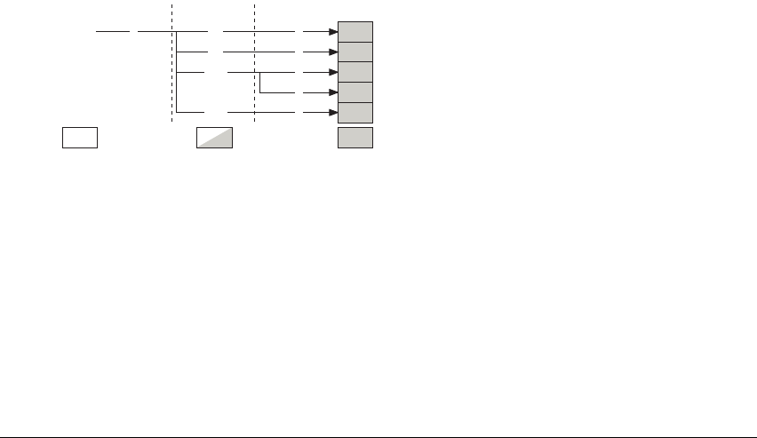
Virtual Memory System Architecture (VMSA)
B3-136 Copyright © 1996-1998, 2000, 2004-2008 ARM Limited. All rights reserved. ARM DDI 0406B
MCR p15,0,<Rt>,c7,c8,2 ; Write CP15 VA to User Read VA to PA Translation Register
MRC p15,0,<Rt>,c7,c4,0 ; Read CP15 PA from Physical Address Register
An example of a VA to PA translation when the Security Extensions are implemented and the processor is
in the Secure state is:
MCR p15,0,<Rt>,c7,c8,5 ; Write VA to Other State Privileged Write VA to PA Translation Register
; Performs VA to PA translation for Non-secure security state
MRC p15,0,<Rt>,c7,c4,0 ; Read PA from Physical Address Register
VA to PA translation when the MMU is disabled
The VA to PA translation operations occur even when the MMU is disabled. The operations report the flat
address mapping and the MMU-disabled value of the attributes and permissions for the data side accesses.
These include any MMU-disabled re-mapping specified by the TEX-remap facilities. The SuperSection bit
is 0 when the MMU is disabled. For more information about the address and attributes returned when the
MMU is disabled see Enabling and disabling the MMU on page B3-5.
When the Security Extensions are implemented, this information applies when the MMU is disabled in the
security state for which the VA to PA translation is performed.
B3.12.33 CP15 c7, Miscellaneous functions
CP15 c7 provides a number of functions, summarized in Figure B3-10 on page B3-65. This section
describes only the CP15 c7 miscellaneous operations.
Figure B3-19 shows the CP15 c7 miscellaneous operations. It does not show the other CP15 c7 operations.
Figure B3-19 CP15 c7 Miscellaneous operations
The CP15 c7 miscellaneous operations are described in:
•CP15 c7, Data and Instruction Barrier operations on page B3-137
•CP15 c7, No Operation (NOP) on page B3-138.
c7 0 NOP, was Wait For Interrupt (CP15WFI) in ARMv6
CP15DSB, Data Synchronization Barrier operation
CP15DMB, Data Memory Barrier operation
CP15ISB, Instruction Synchronization Barrier operation
CRn opc1 CRm opc2
c0 4
c10 4
5
c5 4
Bold text = Accessible in User mode
Read/Write
Read-only Write-only
c13 1 NOP, was Prefetch instruction by MVA in ARMv6

Virtual Memory System Architecture (VMSA)
ARM DDI 0406B Copyright © 1996-1998, 2000, 2004-2008 ARM Limited. All rights reserved. B3-137
CP15 c7, Data and Instruction Barrier operations
ARMv6 includes two CP15 c7 operations to perform Data Barrier operations, and another operation to
perform an Instruction Barrier operation. In ARMv7:
• The ARM and Thumb instruction sets include instructions to perform the barrier operations, that can
be executed in all modes, see Memory barriers on page A3-47.
• The CP15 c7 operations are defined as write-only operations, that can be executed in all modes. The
three operations are described in:
—Instruction Synchronization Barrier operation
—Data Synchronization Barrier operation
—Data Memory Barrier operation.
The value in the register Rt specified by the
MCR
instruction used to perform one of these operations
is ignored. You do not have to write a value to the register before issuing the
MCR
instruction.
In ARMv7 using these CP15 c7 operations is deprecated. Use the
ISB
,
DSB
, and
DMB
instructions
instead.
Note
• In ARMv6 and earlier documentation, the Instruction Synchronization Barrier operation is referred
to as a Prefetch Flush (PFF).
• In versions of the ARM architecture before ARMv6 the Data Synchronization Barrier operation is
described as a Data Write Barrier (DWB).
Instruction Synchronization Barrier operation
In ARMv7, the
ISB
instruction is used to perform an Instruction Synchronization Barrier, see ISB on
page A8-102.
The deprecated CP15 c7 encoding for an Instruction Synchronization Barrier is
<opc1>
set to 0,
<CRn>
set to
c7,
<CRm>
set to c5, and
<opc2>
set to 4.
Data Synchronization Barrier operation
In ARMv7, the
DSB
instruction is used to perform a Data Synchronization Barrier, see DSB on page A8-92.
The deprecated CP15 c7 encoding for a Data Synchronization Barrier is
<opc1>
set to 0,
<CRn>
set to c7,
<CRm>
set to c10, and
<opc2>
set to 4. This operation performs the full system barrier performed by the
DSB
instruction.
Data Memory Barrier operation
In ARMv7, the
DMB
instruction is used to perform a Data Memory Barrier, see DMB on page A8-90.
The deprecated CP15 c7 encoding for a Data Memory Barrier is
<opc1>
set to 0,
<CRn>
set to c7,
<CRm>
set to
c10, and
<opc2>
set to 5. This operation performs the full system barrier performed by the
DMB
instruction.
Virtual Memory System Architecture (VMSA)
B3-138 Copyright © 1996-1998, 2000, 2004-2008 ARM Limited. All rights reserved. ARM DDI 0406B
CP15 c7, No Operation (NOP)
ARMv6 includes two CP15 c7 operations that are not supported in ARMv7, with encodings that become
No Operation (NOP) in ARMv7. These are:
• The Wait For Interrupt (CP15WFI) operation. In ARMv7 this operation is performed by the
WFI
instruction, that is available in the ARM and Thumb instruction sets. For more information, see WFI
on page A8-810.
• The prefetch instruction by MVA operation. In ARMv7 this operation is replaced by the
PLI
instruction, that is available in the ARM and Thumb instruction sets. For more information, see PLI
(immediate, literal) on page A8-242 and PLI (register) on page A8-244.
In ARMv7, the CP15 c7 encodings that were used for these operations must be valid write-only operations
that perform a NOP. These encodings are:
• for the ARMv6 CP15WFI operation:
—
<opc1>
set to 0,
<CRn>
set to c7,
<CRm>
set to c0, and
<opc2>
set to 4
• for the ARMv6 prefetch instruction by MVA operation:
—
<opc1>
set to 0,
<CRn>
set to c7,
<CRm>
set to c13, and
<opc2>
set to 1.
B3.12.34 CP15 c8, TLB maintenance operations
On ARMv7-A implementations, CP15 c8 operations are used for TLB maintenance functions. Figure B3-20
shows the CP15 c8 encodings.
Figure B3-20 CP15 c8 operations
CP15 c8 encodings not shown in Figure B3-20 are UNPREDICTABLE, see Unallocated CP15 encodings on
page B3-69.
c8 0
c6
c7
ITLBIALL, invalidate instruction TLB
1
2
0
1
2
0
1
2
ITLBIMVA, invalidate instruction TLB entry by MVA
ITLBIASID, invalidate instruction TLB by ASID match
DTLBIALL, invalidate data TLB
DTLBIMVA, invalidate data TLB entry by MVA
DTLBIASID, invalidate data TLB by ASID match
TLBIALL*, invalidate unified TLB
TLBIMVA*, invalidate unified TLB entry by MVA
TLBIASID*, invalidate unified TLB by ASID match
c3 0
c5 0
1
2
3
Read/WriteRead-only Write-only
3
TLBIALLIS, Invalidate entire TLB Inner Shareable
TLBIMVAIS, Invalidate unified TLB entry by MVA Inner Shareable
TLBIASIDIS, Invalidate unified TLB by ASID match Inner Shareable
TLBIMVAAIS, Invalidate unified TLB entry by MVA all ASID Inner Shareable
TLBIMVAA, Invalidate unified TLB entries by MVA all ASID
CRn opc1 CRm opc2
Part of the Multiprocessing Extensions* See text for more information about these mnemonics

Virtual Memory System Architecture (VMSA)
ARM DDI 0406B Copyright © 1996-1998, 2000, 2004-2008 ARM Limited. All rights reserved. B3-139
The CP15 c8 TLB maintenance functions:
• are write-only operations
• can be executed only in privileged modes.
Table B3-35 summarizes the TLB maintenance operations.
For more information about the Inner Shareable operations see Multiprocessor effects on TLB maintenance
operations on page B3-62.
For information about the effect of these operations on locked TLB entries see The interaction of TLB
maintenance operations with TLB lockdown on page B3-57.
Table B3-35 CP15 c8 TLB maintenance operations
CRm opc2 Mnemonic Function Rt data
c3 0 TLBIALLIS Invalidate entire unified TLBd Inner ShareableaIgnored
1 TLBIMVAIS Invalidate unified TLBd entry by MVA Inner ShareableaMVA
2TLBIASIDIS
Invalidate unified TLBd by ASID match Inner ShareableaASID
3TLBIMVAAIS
Invalidate unified TLBd entry by MVA all ASID Inner
Shareablea
MVA
c5 0 ITLBIALL Invalidate entire instruction TLBbIgnored
1ITLBIMVA
Invalidate instruction TLBb entry by MVA MVA
2ITLBIASID
Invalidate instruction TLBb by ASID match ASID
c6 0 DTLBIALL Invalidate entire data TLBbIgnored
1DTLBIMVA
Invalidate data TLBb entry by MVA MVA
2DTLBIASID
Invalidate data TLBb by ASID match ASID
c7 0 TLBIALLcInvalidate entire unified TLBdIgnore
1TLBIMVAcInvalidate unified TLBd entry by MVA MVA
2TLBIASIDcInvalidate unified TLBd by ASID match ASID
3TLBIMVAA
Invalidate unified TLBd entries by MVA all ASIDaMVA
a. Implemented only as part of the Multiprocessing Extensions.
b. If these operations are performed on an implementation that has a unified TLB they operate on the unified TLB.
c. The mnemonics for the operations with CRm==c7, opc2=={0,1,2} were previously UTLBIALL, UTLBIMVA and
UTLBIMASID.
d. When separate instruction and data TLBs are implemented, these operations are performed on both TLBs.

Virtual Memory System Architecture (VMSA)
B3-140 Copyright © 1996-1998, 2000, 2004-2008 ARM Limited. All rights reserved. ARM DDI 0406B
About the TLB maintenance operations
For more information about TLBs and their maintenance see Translation Lookaside Buffers (TLBs) on
page B3-54, and in particular TLB maintenance on page B3-56. The following subsections give more
information about the TLB maintenance operations:
•Invalidate entire TLB
•Invalidate single TLB entry by MVA
•Invalidate TLB entries by ASID match
•Invalidate TLB entries by MVA all ASID on page B3-141.
As stated in the footnotes to Table B3-35 on page B3-139:
• If an Instruction TLB or Data TLB operation is used on a system that implements a Unified TLB then
the operation is performed on the Unified TLB
• If a Unified TLB operation is used on a system that implements separate Instruction and Data TLBs
then the operation is performed on both the Instruction TLB and the Data TLB.
• The mnemonics for the operations to invalidate a unified TLB that are defined in the ARM v7 base
architecture were previously UTLBIALL, UTLBIMV, and UTLBIASID. These remain synonyms for
these operations, but ARM deprecates the use of the older names. These are the operations with
CRm==c7, opc2=={0,1,2}.
For information about the synchronization of the TLB maintenance operations see TLB maintenance
operations and the memory order model on page B3-59.
Invalidate entire TLB
The Invalidate entire TLB operations invalidate all unlocked entries in the TLB. The value in the register Rt
specified by the
MCR
instruction used to perform the operation is ignored. You do not have to write a value
to the register before issuing the
MCR
instruction.
Invalidate single TLB entry by MVA
The Invalidate Single Entry operations invalidate a TLB entry that matches the MVA and ASID values
provided as an argument to the operation. The register format required is:
With global entries in the TLB, the supplied ASID value is not checked.
Invalidate TLB entries by ASID match
The Invalidate on ASID Match operations invalidate all TLB entries for non-global pages that match the
ASID value provided as an argument to the operation. The register format required is:
31 12 11 8 7 0
MVA SBZ ASID
31 87 0
SBZ ASID
Virtual Memory System Architecture (VMSA)
ARM DDI 0406B Copyright © 1996-1998, 2000, 2004-2008 ARM Limited. All rights reserved. B3-141
Invalidate TLB entries by MVA all ASID
The Invalidate TLB entries by MVA all ASID operations invalidate all TLB entries that matches the MVA
provided as an argument to the operation regardless of the ASID. The register format required is:
Accessing the CP15 c8 TLB maintenance operations
To perform one of the TLB maintenance operations you write the CP15 registers with
<opc1> == 0
,
<CRn>==c8
, and
<CRm>
and
<opc2>
set to the values shown in Table B3-35 on page B3-139. That is:
MCR p15,0,<Rt>,c8,<CRm>,<opc2>
For example:
MCR p15,0,<Rt>,c8,c5,0 ; Invalidate all unlocked entries in Instruction TLB
MCR p15,0,<Rt>,c8,c6,2 ; Invalidate Data TLB entries on ASID match
B3.12.35 CP15 c9, Cache and TCM lockdown registers and performance monitors
Some CP15 c9 encodings are reserved for IMPLEMENTATION DEFINED memory system functions, in
particular:
• cache control, including lockdown
• TCM control, including lockdown
• branch predictor control.
Additional CP15 c9 encodings are reserved for performance monitors. These encodings fall into two groups:
• the optional performance monitors, described in Chapter C9 Performance Monitors
• additional IMPLEMENTATION DEFINED performance monitors.
The reserved encodings permit implementations that are compatible with previous versions of the ARM
architecture, in particular with the ARMv6 requirements. Figure B3-21 shows the permitted CP15 c9
register encodings.
Figure B3-21 Permitted CP15 c9 encodings
31 12 11 0
MVA SBZ
Reserved for Branch Predictor, Cache and TCM operationsc9 {0-7} {c0-c2} {0-7}
Reserved for Branch Predictor, Cache and TCM operations
{c5-c8} {0-7}
Reserved for ARM-recommended Performance Monitors
c15 {0-7}
CRn opc1 CRm opc2
Reserved for IMPLEMENTATION DEFINED Performance Monitors
{c12-c14} {0-7}
Read/WriteRead-only Write-only
Access depends on the operation
Virtual Memory System Architecture (VMSA)
B3-142 Copyright © 1996-1998, 2000, 2004-2008 ARM Limited. All rights reserved. ARM DDI 0406B
CP15 c9 encodings not shown in Figure B3-21 on page B3-141 are UNPREDICTABLE, see Unallocated CP15
encodings on page B3-69.
In ARMv6, CP15 c9 provides cache lockdown functions. With the ARMv7 abstraction of the hierarchical
memory model, for CP15 c9:
• All encodings with CRm = {c0-c2, c5-c8} are reserved for IMPLEMENTATION DEFINED cache, branch
predictor and TCM operations.
This reservation enables the implementation of a scheme that is backwards compatible with ARMv6.
For details of the ARMv6 implementation see c9, Cache lockdown support on page AppxG-45.
Note
In an ARMv6 implementation that implements the Security Extensions, a Cache Behavior Override
Register is required in CP15 c9, with CRm = 8, see c9, Cache Behavior Override Register (CBOR)
on page AppxG-49. This register is not architecturally-defined in ARMv7, and therefore the CP15 c9
encoding with CRm = 8 is IMPLEMENTATION DEFINED. However, an ARMv7 implementation can
include the CBOR, in which case ARM recommends that this encoding is used for it.
• All encodings with CRm = {c12-c14} are reserved for the optional performance monitors that are
defined in Chapter C9 Performance Monitors.
• All encodings with CRm = c15 are reserved for IMPLEMENTATION DEFINED performance monitoring
features.
B3.12.36 CP15 c10, Memory remapping and TLB control registers
On ARMv7-A implementations, CP15 c10 is used for memory remapping registers. In addition, some
encodings are reserved for IMPLEMENTATION DEFINED TLB control functions, in particular TLB lockdown.
The reserved encodings permit implementations that are compatible with previous versions of the ARM
architecture, in particular with the ARMv6 requirements.
Figure B3-22 shows the CP15 c10 registers and reserved encodings.
Figure B3-22 CP15 c10 registers
CP15 c10 encodings not shown in Figure B3-22 are UNPREDICTABLE, see Unallocated CP15 encodings on
page B3-69.
The CP15 c10 memory remap registers are described in CP15 c10, Memory Remap Registers on
page B3-143.
PRRR, Primary Region Remap Register
Reserved for TLB Lockdown operations
c10 0
c2 0
{c0,c1,c4,c8} {0-7}
NMRR, Normal Memory Remap Register
Read/WriteRead-only Write-only
Access depends on the operation
CRn opc1 CRm opc2
1

Virtual Memory System Architecture (VMSA)
ARM DDI 0406B Copyright © 1996-1998, 2000, 2004-2008 ARM Limited. All rights reserved. B3-143
The IMPLEMENTATION DEFINED TLB control operations
In VMSAv6, CP15 c10 provides TLB lockdown functions. In VMSAv7, the TLB lockdown mechanism is
IMPLEMENTATION DEFINED and some CP15 c10 encodings are reserved for IMPLEMENTATION DEFINED TLB
control operations. These are the encodings with
<CRn>
== c10,
<opc1>
== 0,
<CRm>
== {c0, c1, c4, c8}, and
<opc2>
== {0-7}.
B3.12.37 CP15 c10, Memory Remap Registers
CP15 c10 includes two Memory Remap Registers, described in the subsections:
•c10, Primary Region Remap Register (PRRR)
•c10, Normal Memory Remap Register (NMRR) on page B3-146.
In addition:
• The significance and use of these registers is described in Memory region attribute descriptions when
TEX remap is enabled on page B3-34.
• The function of these registers is architecturally defined only when the
— SCTLR.TRE bit is set to 1
— SCTLR.TRE bit is set to 0 and no IMPLEMENTATION DEFINED mechanism using MMU remap
has been invoked.
Otherwise their behavior is IMPLEMENTATION DEFINED, see SCTLR.TRE, SCTLR.M, and the effect of
the MMU remap registers on page B3-38.
c10, Primary Region Remap Register (PRRR)
The Primary Region Remap Register, PRRR, can in some cases control the top level mapping of the TEX[0],
C, and B memory region attributes.
The PRRR:
• is a 32-bit read/write register
• is accessible only in privileged modes
• when the Security Extensions are implemented:
— is a Banked register
— has write access to the Secure copy of the register disabled when the CP15SDISABLE signal
is asserted HIGH.
Virtual Memory System Architecture (VMSA)
B3-144 Copyright © 1996-1998, 2000, 2004-2008 ARM Limited. All rights reserved. ARM DDI 0406B
The format of the PRRR is:
The reset value of the PRRR is IMPLEMENTATION DEFINED.
NOSn, bit [24+n], for values of n from 0 to 7
Outer Shareable property mapping for memory attributes n, if the region is mapped as
Normal Memory that is Shareable. n is the value of the TEX[0], C and B bits, see
Table B3-36 on page B3-145. The possible values of each NOSn bit are:
0 Shareable Normal memory region is Outer Shareable
1 Shareable Normal Memory region is Inner Shareable.
The value of this bit is ignored if the region is not Shareable Normal memory.
The meaning of the field with n =6 is IMPLEMENTATION DEFINED and might differ from the
meaning given here. This is because the meaning of the attribute combination
{TEX[0] = 1, C = 1, B = 0} is IMPLEMENTATION DEFINED.
If the implementation does not support the Outer Shareable memory attribute then these bits
are reserved, RAZ/SBZP.
Bits [23:20] Reserved. UNK/SBZP.
NS1, bit [19] Mapping of S = 1 attribute for Normal memory. This bit gives the mapped Shareable
attribute for a region of memory that:
• is mapped as Normal memory
• has the S bit set to 1.
The possible values of the bit are:
0 Region is not Shareable
1 Region is Shareable.
NS0, bit [18] Mapping of S = 0 attribute for Normal memory. This bit gives the mapped Shareable
attribute for a region of memory that:
• is mapped as Normal memory
• has the S bit set to 0.
The possible values of the bit are the same as those given for the NS1 bit, bit [19].
31 30 29 28 27 26 25 24 23 20 19 18 17 16 15 14 13 12 11 10 9 8 7 6 5 4 3 2 1 0
UNK/SBZP TR7 TR6 TR5 TR4 TR3 TR2 TR1 TR0
DS0
DS1
NS1
NS0
NOS0
NOS1
NOS2
NOS3
NOS7
NOS6
NOS5
NOS4

Virtual Memory System Architecture (VMSA)
ARM DDI 0406B Copyright © 1996-1998, 2000, 2004-2008 ARM Limited. All rights reserved. B3-145
DS1, bit [17] Mapping of S = 1 attribute for Device memory. This bit gives the mapped Shareable
attribute for a region of memory that:
• is mapped as Device memory
• has the S bit set to 1.
The possible values of the bit are the same as those given for the NS1 bit, bit [19].
DS0, bit [16] Mapping of S = 0 attribute for Device memory. This bit gives the mapped Shareable
attribute for a region of memory that:
• is mapped as Device memory
• has the S bit set to 0.
The possible values of the bit are the same as those given for the NS1 bit, bit [19].
TRn, bits [2n+1:2n] for values of n from 0 to 7
Primary TEX mapping for memory attributes n. n is the value of the TEX[0], C and B bits,
see Table B3-36. This field defines the mapped memory type for a region with attributes n.
The possible values of the field are:
00 Strongly-ordered
01 Device
10 Normal Memory
11 Reserved, effect is UNPREDICTABLE.
The meaning of the field with n =6 is IMPLEMENTATION DEFINED and might differ from the
meaning given here. This is because the meaning of the attribute combination
{TEX[0] = 1, C = 1, B = 0} is IMPLEMENTATION DEFINED.
Table B3-36 shows the mapping between the memory region attributes and the n value used in the
PRRR.nOSn and PRRR.TRn field descriptions.
Table B3-36 Memory attributes and the n value for the PRRR field descriptions
Attributes
n value
TEX[0] C B
0000
0011
0102
0113
1004
1015

Virtual Memory System Architecture (VMSA)
B3-146 Copyright © 1996-1998, 2000, 2004-2008 ARM Limited. All rights reserved. ARM DDI 0406B
For more information about the PRRR see Memory region attribute descriptions when TEX remap is
enabled on page B3-34.
Accessing the PRRR
To access the PRRR you read or write the CP15 registers with
<opc1>
set to 0,
<CRn>
set to c10,
<CRm>
set to
c2, and
<opc2>
set to 0. For example:
MRC p15,0,<Rt>,c10,c2,0 ; Read CP15 Primary Region Remap Register
MCR p15,0,<Rt>,c10,c2,0 ; Write CP15 Primary Region Remap Register
c10, Normal Memory Remap Register (NMRR)
The Normal Memory Remap Register, NMRR, can in some cases provide additional mapping controls for
memory regions that are mapped as Normal memory by their entry in the PRRR.
The NMRR:
• is a 32-bit read/write register
• is accessible only in privileged modes
• when the Security Extensions are implemented:
— is a Banked register
— has write access to the Secure copy of the register disabled when the CP15SDISABLE signal
is asserted HIGH.
The format of the NMRR is:
The reset value of the NMRR is IMPLEMENTATION DEFINED.
ORn, bits [2n+17:2n+16], for values of n from 0 to 7
Outer Cacheable property mapping for memory attributes n, if the region is mapped as
Normal Memory by the TRn entry in the PRRR, see c10, Primary Region Remap Register
(PRRR) on page B3-143. n is the value of the TEX[0], C and B bits, see Table B3-36 on
page B3-145. The possible values of this field are:
00 Region is Non-cacheable
01 Region is Write-Back, WriteAllocate
1106
1117
313029282726252423222120191817161514131211109876543210
OR7 OR6 OR5 OR4 OR3 OR2 OR1 OR0 IR7 IR6 IR5 IR4 IR3 IR2 IR1 IR0
Table B3-36 Memory attributes and the n value for the PRRR field descriptions (continued)
Attributes
n value
TEX[0] C B
Virtual Memory System Architecture (VMSA)
ARM DDI 0406B Copyright © 1996-1998, 2000, 2004-2008 ARM Limited. All rights reserved. B3-147
10 Region is WriteThrough, Non-WriteAllocate
11 Region is Write-Back, Non-WriteAllocate.
The meaning of the field with n = 6 is IMPLEMENTATION DEFINED and might differ from the
meaning given here. This is because the meaning of the attribute combination
{TEX[0] = 1, C = 1, B = 0} is IMPLEMENTATION DEFINED.
IRn, bits [2n+1:2n], for values of n from 0 to 7
Inner Cacheable property mapping for memory attributes n, if the region is mapped as
Normal Memory by the TRn entry in the PRRR, see c10, Primary Region Remap Register
(PRRR) on page B3-143. n is the value of the TEX[0], C and B bits, see Table B3-36 on
page B3-145. The possible values of this field are the same as those given for the ORn field.
The meaning of the field with n = 6 is IMPLEMENTATION DEFINED and might differ from the
meaning given here. This is because the meaning of the attribute combination
{TEX[0] = 1, C = 1, B = 0} is IMPLEMENTATION DEFINED.
For more information about the NMRR see Memory region attribute descriptions when TEX remap is
enabled on page B3-34.
Accessing the NMRR
To access the NMRR you read or write the CP15 registers with
<opc1>
set to 0,
<CRn>
set to c10,
<CRm>
set to
c2, and
<opc2>
set to 1. For example:
MRC p15,0,<Rt>,c10,c2,1 ; Read CP15 Normal Memory Remap Register
MCR p15,0,<Rt>,c10,c2,1 ; Write CP15 Normal Memory Remap Register
B3.12.38 CP15 c11, Reserved for TCM DMA registers
Some CP15 c11 register encodings are reserved for IMPLEMENTATION DEFINED DMA operations to and
from TCM, see Figure B3-23:
Figure B3-23 Permitted CP15 c11 encodings
CP15 c11 encodings not shown in Figure B3-23 are UNPREDICTABLE, see Unallocated CP15 encodings on
page B3-69.
Reserved for DMA operations for TCM access
Reserved for DMA operations for TCM access
c11 {0-7} {c0-c8} {0-7}
c15 {0-7}
Read/WriteRead-only Write-only
CRn opc1 CRm opc2
Access depends on the operation

Virtual Memory System Architecture (VMSA)
B3-148 Copyright © 1996-1998, 2000, 2004-2008 ARM Limited. All rights reserved. ARM DDI 0406B
B3.12.39 CP15 c12, Security Extensions registers
When the Security Extensions are implemented, CP15 c12 is used for the Vector base address registers and
an Interrupt status register. Figure B3-24 shows the CP15 c12 Security Extensions registers:
Figure B3-24 Security Extensions CP15 c12 registers
When the Security Extensions are implemented, CP15 c12 encodings not shown in Figure B3-24 are
UNPREDICTABLE. On an implementation that does not include the Security Extensions all CP15 c12
encodings are UNDEFINED. For more information, see Unallocated CP15 encodings on page B3-69.
The CP15 c12 registers are described in the subsections:
•c12, Vector Base Address Register (VBAR)
•c12, Monitor Vector Base Address Register (MVBAR) on page B3-149
•c12, Interrupt Status Register (ISR) on page B3-150.
B3.12.40 c12, Vector Base Address Register (VBAR)
When the Security Extensions are implemented and high exception vectors are not selected, the Vector Base
Address Register, VBAR, provides the exception base address for exceptions that are not handled in Monitor
mode, see Exception vectors and the exception base address on page B1-30. The high exception vectors
always have the base address
0xFFFF0000
and are not affected by the value of VBAR.
The VBAR:
• Is present only when the Security Extensions are implemented.
• Is a 32-bit read/write register.
• Is accessible only in privileged modes.
• Has a defined reset value, for the Secure copy of the register, of 0. This reset value does not apply to
the Non-secure copy of the register, and software must program the Non-secure copy of the register
with the required value, as part of the processor boot sequence.
• Is a Banked register.
• Has write access to the Secure copy of the register disabled when the CP15SDISABLE signal is
asserted HIGH.
* MVBAR, Monitor Vector Base Address Register
* VBAR, Vector Base Address Register
c12 0
c1
c0 0
* ISR, Interrupt Status Register
Read/WriteRead-only Write-only
* Implemented only when the Security Extensions are implemented
CRn opc1 CRm opc2
0
1

Virtual Memory System Architecture (VMSA)
ARM DDI 0406B Copyright © 1996-1998, 2000, 2004-2008 ARM Limited. All rights reserved. B3-149
The format of the VBAR is:
The Secure copy of the VBAR holds the vector base address for the Secure state, described as the Secure
exception base address
The Non-secure copy of the VBAR holds the vector base address for the Non-secure state, described as the
Non-secure exception base address.
Vector_Base_Address, bits [31:5]
Bits [31:5] of the base address of the normal exception vectors. Bits [4:0] of an exception
vector is the exception offset, see Table B1-3 on page B1-31.
Bits [4:0] Reserved, UNK/SBZP.
For details of how the VBAR registers are used to determine the exception addresses see Exception vectors
and the exception base address on page B1-30.
Accessing the VBAR
To access the VBAR you read or write the CP15 registers with
<opc1>
set to 0,
<CRn>
set to c12,
<CRm>
set to
c0, and
<opc2>
set to 0. For example:
MRC p15,0,<Rt>,c12,c0,0 ; Read CP15 Vector Base Address Register
MCR p15,0,<Rt>,c12,c0,0 ; Write CP15 Vector Base Address Register
B3.12.41 c12, Monitor Vector Base Address Register (MVBAR)
The Monitor Vector Base Address Register, MVBAR, provides the exception base address for all exceptions
that are handled in Monitor mode, see Exception vectors and the exception base address on page B1-30.
The MVBAR is:
• present only when the Security Extensions are implemented
• a 32-bit read/write register
• accessible in Secure privileged modes only
• a Restricted access register, meaning it exists only in the Secure state.
The format of the MVBAR is:
31 54 0
Vector_Base_Address (0) (0) (0) (0) (0)
31 54 0
Monitor_Vector_Base_Address (0) (0) (0) (0) (0)
Virtual Memory System Architecture (VMSA)
B3-150 Copyright © 1996-1998, 2000, 2004-2008 ARM Limited. All rights reserved. ARM DDI 0406B
The reset value of the MVBAR is UNKNOWN. The MVBAR must be programmed as part of the boot
sequence.
Monitor_Vector_Base_Address, bits [31:5]
Bits [31:5] of the base address of the exception vectors for exceptions that are handled in
Monitor mode. Bits [4:0] of an exception vector is the exception offset, see Table B1-3 on
page B1-31.
Bits [4:0] Reserved, UNK/SBZP.
For details of how the MVBAR is used to determine the exception addresses see Exception vectors and the
exception base address on page B1-30.
Accessing the MVBAR
To access the MVBAR you read or write the CP15 registers with
<opc1>
set to 0,
<CRn>
set to c12,
<CRm>
set
to c0, and
<opc2>
set to 1. For example:
MRC p15,0,<Rt>,c12,c0,1 ; Read CP15 Monitor Vector Base Address Register
MCR p15,0,<Rt>,c12,c0,1 ; Write CP15 Monitor Vector Base Address Register
B3.12.42 c12, Interrupt Status Register (ISR)
The Interrupt Status Register, ISR, shows whether an IRQ, FIQ or external abort is pending.
The ISR is:
• present only when the Security Extensions are implemented
• a 32-bit read-only register
• accessible only in privileged modes.
• a Common register, meaning it is available in the Secure and Non-secure states.
The format of the ISR is:
Bits [31:9] Reserved, UNK.
A, bit [8] External abort pending flag:
0 no pending external abort
1 an external abort is pending.
I, bit [7] Interrupt pending flag. Indicates whether an IRQ interrupt is pending:
0 no pending IRQ
1 an IRQ interrupt is pending.
31 98765 0
UNK A I F (0) (0) (0) (0) (0) (0)

Virtual Memory System Architecture (VMSA)
ARM DDI 0406B Copyright © 1996-1998, 2000, 2004-2008 ARM Limited. All rights reserved. B3-151
F, bit [7] Fast interrupt pending flag. Indicates whether an FIQ fast interrupt is pending:
0 no pending FIQ
1 an FIQ fast interrupt is pending.
Bits [5:0] Reserved, UNK/SBZP.
The bit positions of the A, I and F flags in the ISR match the A, I and F flag bits in the CPSR, see Program
Status Registers (PSRs) on page B1-14. This means the same masks can be used to extract the flags from
the register value.
Note
• The ISR.F and ISR.I bits directly reflect the state of the FIQ and IRQ inputs.
• the ISR.A bit is set when an asynchronous abort is generated and is cleared automatically when the
abort is taken.
Accessing the ISR
To access the ISR you read the CP15 registers with
<opc1>
set to 0,
<CRn>
set to c12,
<CRm>
set to c1, and
<opc2>
set to 0. For example:
MRC p15,0,<Rt>,c12,c1,0 ; Read Interrupt Status Register
B3.12.43 CP15 c13, Process, context and thread ID registers
The CP15 c13 registers are used for:
• a Context ID register
• three software Thread ID registers
• an FCSE Process ID Register.
Note
From ARMv6, use of the FCSE is a deprecated, and in ARMv7 the FCSE is an optional component of a
VMSA implementation. ARM expects the FCSE will become obsolete during the lifetime of ARMv7.
However, every ARMv7-A implementation must include the FCSE Process ID Register.
Figure B3-25 on page B3-152 shows the CP15 c13 registers:

Virtual Memory System Architecture (VMSA)
B3-152 Copyright © 1996-1998, 2000, 2004-2008 ARM Limited. All rights reserved. ARM DDI 0406B
Figure B3-25 CP15 c13 registers in a VMSA implementation
CP15 c13 encodings not shown in Figure B3-25 are UNPREDICTABLE, see Unallocated CP15 encodings on
page B3-69.
The CP15 c13 registers are described in:
•c13, FCSE Process ID Register (FCSEIDR)
•c13, Context ID Register (CONTEXTIDR) on page B3-153
•CP15 c13 Software Thread ID registers on page B3-154.
B3.12.44 c13, FCSE Process ID Register (FCSEIDR)
The FCSE Process ID Register, FCSEIDR, identifies the current Process ID (PID) for the Fast Context
Switch Extension (FCSE). In ARMv7, the FCSE is optional. However, the FCSEIDR must be implemented
regardless of whether the FCSE is implemented. Software can access this register to determine whether the
FCSE is implemented.
The FCSEIDR:
• Is a 32-bit register, with access that depends on whether the FCSE is implemented:
FCSE implemented: . the register is read/write
FCSE not implemented: . the register is RAZ/WI.
• Is accessible only in privileged modes.
• When implemented as a read/write register, has a defined reset value of 0. When the Security
Extensions are implemented, this reset value applies only to the Secure copy of the register, and
software must program the Non-secure copy of the register with the required value.
• When the Security Extensions are implemented, is a Banked register.
When the Security Extensions are implemented and the FCSE is implemented, write access to the
Secure copy of the FCSEIDR is disabled when the CP15SDISABLE signal is asserted HIGH.
Software Thread ID
Registers
c13 0 c0
Read/WriteRead-only Write-only
FCSEIDR, FCSE PID Register
CONTEXTIDR, Context ID Register
TPIDRURO, User Read Only
TPIDRPRW, Privileged Only
CRn opc1 CRm opc2
Access depends whether FCSE is implemented
0
4
3
1
2TPIDRURW, User Read/Write

Virtual Memory System Architecture (VMSA)
ARM DDI 0406B Copyright © 1996-1998, 2000, 2004-2008 ARM Limited. All rights reserved. B3-153
The format of the FCSEIDR is:
PID, bits [31:25]
The current Process ID, for the FCSE. If the FCSE is not implemented this field is RAZ/WI.
Bits [24:0] Reserved. If the FCSE is not implemented this field is RAZ/WI.
If the FCSE is implemented, the value of this field is UNKNOWN on reads and
Should-Be-Zero-or-Preserved on writes.
Note
• When the PID is written, the overall virtual-to-physical address mapping changes. Because of this,
you must ensure that instructions that might have been prefetched already are not affected by the
address mapping change.
• From ARMv6, use of the FCSE is deprecated, and in ARMv7 the FCSE is optional.
Accessing the FCSEIDR
To access the FCSEIDR you read or write the CP15 registers with
<opc1>
set to 0,
<CRn>
set to c13,
<CRm>
set
to c0, and
<opc2>
set to 0. For example:
MRC p15,0,<Rt>,c13,c0,0 ; Read CP15 FCSE PID Register
MCR p15,0,<Rt>,c13,c0,0 ; Write CP15 FCSE PID Register
B3.12.45 c13, Context ID Register (CONTEXTIDR)
The Context ID Register, CONTEXTIDR, identifies the current:
•Process Identifier (PROCID)
•Address Space Identifier (ASID).
The value of the whole of this register is called the Context ID and is used by:
• the debug logic, for Linked and Unlinked Context ID matching, see Breakpoint debug events on
page C3-5 and Watchpoint debug events on page C3-15.
• the trace logic, to identify the current process.
The ASID field value is used by many memory management functions.
The CONTEXTIDR is:
• a 32-bit read/write register
• accessible only in privileged modes
• when the Security Extensions are implemented, a Banked register.
31 25 24 0
PID UNK/SBZP

Virtual Memory System Architecture (VMSA)
B3-154 Copyright © 1996-1998, 2000, 2004-2008 ARM Limited. All rights reserved. ARM DDI 0406B
The format of the CONTEXTIDR is:
PROCID, bits [31:8]
Process Identifier. This field must be programmed with a unique value that identifies the
current process. It is used by the trace logic and the debug logic to identify the process that
is running currently.
ASID, bits [7:0]
Address Space Identifier. This field is programmed with the value of the current ASID.
Using the CONTEXTIDR
For information about the synchronization of changes to the CONTEXTIDR see Changes to CP15 registers
and the memory order model on page B3-77. There are particular synchronization requirements when
changing the ASID and Translation Table Base Registers, see Synchronization of changes of ASID and
TTBR on page B3-60.
Accessing the CONTEXTIDR
To access the CONTEXTIDR you read or write the CP15 registers with
<opc1>
set to 0,
<CRn>
set to c13,
<CRm>
set to c0, and
<opc2>
set to 1. For example:
MRC p15,0,<Rt>,c13,c0,1 ; Read CP15 Context ID Register
MCR p15,0,<Rt>,c13,c0,1 ; Write CP15 Context ID Register
B3.12.46 CP15 c13 Software Thread ID registers
The Software Thread ID registers provide locations where software can store thread identifying information,
for OS management purposes. These registers are never updated by the hardware.
The Software Thread ID registers are:
• three 32-bit register read/write registers:
— User Read/Write Thread ID Register, TPIDRURW
— User Read-only Thread ID Register, TPIDRURO
— Privileged Only Thread ID Register, TPIDRPRW.
• accessible in different modes:
— the User Read/Write Thread ID Register is read/write in unprivileged and privileged modes
— the User Read-only Thread ID Register is read-only in User mode, and read/write in privileged
modes
— the Privileged Only Thread ID Register is only accessible in privileged modes, and is
read/write.
• when the Security Extensions are implemented, Banked registers
• introduced in ARMv7.
31 87 0
PROCID ASID

Virtual Memory System Architecture (VMSA)
ARM DDI 0406B Copyright © 1996-1998, 2000, 2004-2008 ARM Limited. All rights reserved. B3-155
Accessing the Software Thread ID registers
To access the Software Thread ID registers you read or write the CP15 registers with
<opc1>
set to 0,
<CRn>
set to c13,
<CRm>
set to c0, and
<opc2>
set to:
• 2 for the User Read/Write Thread ID Register, TPIDRURW
• 3 for the User Read-only Thread ID Register, TPIDRURO
• 4 for the Privileged Only Thread ID Register, TPIDRPRW.
For example:
MRC p15, 0, <Rt>, c13, c0, 2 ; Read CP15 User Read/Write Thread ID Register
MCR p15, 0, <Rt>, c13, c0, 2 ; Write CP15 User Read/Write Thread ID Register
MRC p15, 0, <Rt>, c13, c0, 3 ; Read CP15 User Read-only Thread ID Register
MCR p15, 0, <Rt>, c13, c0, 3 ; Write CP15 User Read-only Thread ID Register
MRC p15, 0, <Rt>, c13, c0, 4 ; Read CP15 Privileged Only Thread ID Register
MCR p15, 0, <Rt>, c13, c0, 4 ; Write CP15 Privileged Only Thread ID Register
B3.12.47 CP15 c14, Not used
CP15 c14 is not used on any ARMv7 implementation, see Unallocated CP15 encodings on page B3-69.
B3.12.48 CP15 c15, IMPLEMENTATION DEFINED registers
CP15 c15 is reserved for IMPLEMENTATION DEFINED purposes. ARMv7 does not impose any restrictions on
the use of the CP15 c15 encodings. The documentation of the ARMv7 implementation must describe fully
any registers implemented in CP15 c15. Normally, for processor implementations by ARM, this information
is included in the Technical Reference Manual for the processor.
Typically, CP15 c15 is used to provide test features, and any required configuration options that are not
covered by this manual.

Virtual Memory System Architecture (VMSA)
B3-156 Copyright © 1996-1998, 2000, 2004-2008 ARM Limited. All rights reserved. ARM DDI 0406B
B3.13 Pseudocode details of VMSA memory system operations
This section contains pseudocode describing VMSA memory operations. The following subsections
describe the pseudocode functions:
•Alignment fault
•FCSE translation
•Address translation on page B3-157
•Domain checking on page B3-157
•TLB operations on page B3-158
•Translation table walk on page B3-158.
See also the pseudocode for general memory system operations in Pseudocode details of general memory
system operations on page B2-29.
B3.13.1 Alignment fault
The following pseudocode describes the generation of an Alignment fault Data Abort exception:
// AlignmentFaultV()
// =================
AlignmentFaultV(bits(32) address, boolean iswrite)
mva = FCSETranslate(address);
DataAbort(mva, bits(4) UNKNOWN, boolean UNKNOWN, iswrite, DAbort_Alignment);
B3.13.2 FCSE translation
The following pseudocode describes the FCSE translation:
// FCSETranslate()
// ===============
bits(32) FCSETranslate(bits(32) va)
if va<31:25> == ‘0000000’ then
mva = FCSEIDR.PID : va<24:0>;
else
mva = va;
return mva;

Virtual Memory System Architecture (VMSA)
ARM DDI 0406B Copyright © 1996-1998, 2000, 2004-2008 ARM Limited. All rights reserved. B3-157
B3.13.3 Address translation
The following pseudocode describes address translation in a VMSA implementation:
// TranslateAddressV()
// ===================
AddressDescriptor TranslateAddressV(bits(32) va, boolean ispriv, boolean iswrite)
mva = FCSETranslate(va);
if SCTLR.M == ‘1’ then // MMU is enabled
(tlbhit, tlbrecord) = CheckTLB(CONTEXTIDR.ASID, mva);
if !tlbhit then
tlbrecord = TranslationTableWalk(mva, iswrite);
if CheckDomain(tlbrecord.domain, mva, tlbrecord.sectionnotpage, iswrite) then
CheckPermission(tlbrecord.perms, mva, tlbrecord.sectionnotpage, iswrite, ispriv);
else
tlbrecord = TranslationTableWalk(mva, iswrite);
return tlbrecord.addrdesc;
B3.13.4 Domain checking
The following pseudocode describes domain checking:
// CheckDomain()
// =============
boolean CheckDomain(bits(4) domain, bits(32) mva, boolean sectionnotpage, boolean iswrite)
bitpos = 2*UInt(domain);
case DACR<bitpos+1:bitpos> of
when ‘00’ DataAbort(mva, domain, sectionnotpage, iswrite, DAbort_Domain);
when ‘01’ permissioncheck = TRUE;
when ‘10’ UNPREDICTABLE;
when ‘11’ permissioncheck = FALSE;
return permissioncheck;

Virtual Memory System Architecture (VMSA)
B3-158 Copyright © 1996-1998, 2000, 2004-2008 ARM Limited. All rights reserved. ARM DDI 0406B
B3.13.5 TLB operations
The
TLBRecord
type represents the contentsof a TLB entry:
// Types of TLB entry
enumeration TLBRecType = { TLBRecType_SmallPage,
TLBRecType_LargePage,
TLBRecType_Section,
TLBRecType_Supersection,
TLBRecType_MMUDisabled
};
type TLBRecord is (
Permissions perms,
bit nG, // ‘0’ = Global, ‘1’ = not Global
bits(4) domain,
boolean sectionnotpage,
TLBRecType type,
AddressDescriptor addrdesc
)
The
CheckTLB()
function checks whether the TLB contains an entry that matches an ASID and address, and
returns TRUE and the matching
TLBRecord
if so. Otherwise, it returns FALSE and an UNKNOWN
TLBRecord
.
(boolean, TLBRecord) CheckTLB(bits(8) asid, bits(32) address)
The
AssignToTLB()
procedure supplies an ASID and new
TLBRecord
to the TLB, for possible allocation to a
TLB entry. It is IMPLEMENTATION DEFINED under what circumstances this allocation takes place, and TLB
entries might also be allocated at other times.
AssignToTLB(bits(8) asid, bits(32) mva, TLBRecord entry)
B3.13.6 Translation table walk
The following pseudocode describes the translation table walk operation:
// TranslationTableWalk()
// ======================
//
// Returns a result of a translation table walk in TLBRecord form.
TLBRecord TranslationTableWalk(bits(32) mva, boolean is_write)
TLBRecord result;
AddressDescriptor l1descaddr;
AddressDescriptor l2descaddr;
if SCTLR.M == ‘1’ then // MMU is enabled
domain = bits(4) UNKNOWN; // For Data Abort exceptions found before a domain is known
// Determine correct Translation Table Base Register to use.
n = UInt(TTBCR.N);

Virtual Memory System Architecture (VMSA)
ARM DDI 0406B Copyright © 1996-1998, 2000, 2004-2008 ARM Limited. All rights reserved. B3-159
if n == 0 || IsZero(mva<31:(32-n)>) then
ttbr = TTBR0;
disabled = (TTBCR.PD0 == ‘1’);
else
ttbr = TTBR1;
disabled = (TTBCR.PD1 == ‘1’);
n = 0; // TTBR1 translation always works like N=0 TTBR0 translation
// Check this Translation Table Base Register is not disabled.
if HaveSecurityExt() && disabled == ‘1’ then
DataAbort(mva, domain, TRUE, is_write, DAbort_Translation);
// Obtain level 1 descriptor.
l1descaddr.paddress.physicaladdress = ttbr<31:(14-n)> : mva<(31-n):20> : ‘00’;
l1descaddr.paddress.physicaladdressext = ‘00000000’;
l1descaddr.paddress.NS = if IsSecure() then ‘0’ else ‘1’;
l1descaddr.memattrs.type = MemType_Normal;
l1descaddr.memattrs.shareable = (ttbr<1> == ‘1’);
l1descaddr.memattrs.outershareable = (ttbr<5> == ‘0’) && (ttbr<1> == ‘1’);
l1descaddr.memattrs.outerattrs = ttbr<4:3>;
if HaveMPExt() then
1descaddr.memattrs.innerattrs = ttbr<0>:ttbr<6>;
else
if ttbr<0> == ‘0’ then
l1descaddr.memattrs.innerattrs = ‘00’;
else
IMPLEMENTATION_DEFINED set l1descaddr.memattrs.innerattrs to one of
‘01’,’10’,’11’;
l1desc = _Mem[l1descaddr,4];
// Process level 1 descriptor.
case l1desc<1:0> of
when ‘00’, ‘11’ // Fault, Reserved
DataAbort(mva, domain, TRUE, is_write, DAbort_Translation);
when ‘01’ // Section or Supersection
texcb = l1desc<14:12,3,2>;
S = l1desc<16>;
ap = l1desc<15,11:10>;
xn = l1desc<4>;
nG = l1desc<17>;
sectionnotpage = TRUE;
NS = l1desc<19>;
if SCTLR.AFE == ‘1’ && l1desc<10> == ‘0’ then
if SCTLR.HA == ‘0’ then
DataAbort(mva, domain, sectionnotpage, is_write, DAbort_AccessFlag);
else // Hardware-managed access flag must be set in memory
_Mem[l1descaddr,4]<10> = ‘1’;
if l1desc<18> == ‘0’ then // Section
domain = l1desc<8:5>;
type = TLBRecType_Section;

Virtual Memory System Architecture (VMSA)
B3-160 Copyright © 1996-1998, 2000, 2004-2008 ARM Limited. All rights reserved. ARM DDI 0406B
physicaladdressext = ‘00000000’;
physicaladdress = l1desc<31:20> : mva<19:0>;
else // Supersection
domain = ‘0000’;
type = TLBRecType_Supersection;
physicaladdressext = l1desc<8:5,23:20>;
physicaladdress = l1desc<31:24> : mva<23:0>;
when ‘10’ // Large page or Small page
domain = l1desc<8:5>;
sectionnotpage = FALSE;
NS = l1desc<3>;
// Obtain level 2 descriptor.
l2descaddr.paddress.physicaladdress = l1desc<31:10> : mva<19:12> : ‘00’;
l2descaddr.paddress.physicaladdressext = ‘00000000’;
l2descaddr.paddress.NS = if IsSecure() then ‘0’ else ‘1’;
l2descaddr.memattrs = l1descaddr.memattrs;
l2desc = _Mem[l2descaddr,4];
// Process level 2 descriptor.
if l2desc<1:0> == ‘00’ then
DataAbort(mva, domain, sectionnotpage, is_write, DAbort_Translation);
S = l2desc<10>;
ap = l2desc<9,5:4>;
nG = l2desc<11>;
if SCTLR.AFE == ‘1’ && l2desc<4> == ‘0’ then
if SCTLR.HA == ‘0’ then
DataAbort(mva, domain, sectionnotpage, is_write, DAbort_AccessFlag);
else // Hardware-managed access flag must be set in memory
_Mem[l2descaddr,4]<4> = ‘1’;
if l2desc<1> == ‘0’ then // Large page
texcb = l2desc<14:12,3,2>
xn = l2desc<15>;
type = TLBRecType_LargePage;
physicaladdressext = ‘00000000’;
physicaladdress = l2desc<31:16> : mva<15:0>;
else // Small page
texcb = l2desc<8:6,3,2>;
xn = l2desc<0>;
type = TLBRecType_SmallPage;
physicaladdressext = ‘00000000’;
physicaladdress = l2desc<31:12> : mva<11:0>;
else // MMU is disabled
texcb = ‘00000’;
S = ‘1’;
ap = bits(3) UNKNOWN;
xn = bit UNKNOWN;
nG = bit UNKNOWN;

Virtual Memory System Architecture (VMSA)
ARM DDI 0406B Copyright © 1996-1998, 2000, 2004-2008 ARM Limited. All rights reserved. B3-161
domain = bits(4) UNKNOWN;
sectionnotpage = boolean UNKNOWN;
type = TLBRecType_MMUDisabled;
physicaladdress = mva;
physicaladdressext = ‘00000000’;
NS = if IsSecure() then ‘0’ else ‘1’;
// Decode the TEX, C, B and S bits to produce the TLBRecord’s memory attributes.
if SCTLR.TRE == ‘0’ then
if RemapRegsHaveResetValues() then
result.addrdesc.memattrs = DefaultTEXDecode(texcb, S);
else
IMPLEMENTATION_DEFINED setting of result.addrdesc.memattrs;
else
if SCTLR.M == ‘0’ then
result.addrdesc.memattrs = DefaultTEXDecode(texcb, S);
else
result.addrdesc.memattrs = RemappedTEXDecode(texcb, S);
// Set the rest of the TLBRecord, try to add it to the TLB, and return it.
result.perms.ap = ap;
result.perms.xn = xn;
result.nG = nG;
result.domain = domain;
result.sectionnotpage = sectionnotpage;
result.type = type;
result.addrdesc.paddress.physicaladdress = physicaladdress;
result.addrdesc.paddress.physicaladdressext = physicaladdressext;
result.addrdesc.paddress.NS = NS;
AssignToTLB(CONTEXTIDR.ASID, mva, result);
return result;

Virtual Memory System Architecture (VMSA)
B3-162 Copyright © 1996-1998, 2000, 2004-2008 ARM Limited. All rights reserved. ARM DDI 0406B

ARM DDI 0406B Copyright © 1996-1998, 2000, 2004-2008 ARM Limited. All rights reserved. B4-1
Chapter B4
Protected Memory System Architecture
(PMSA)
This chapter provides a system-level view of the memory system. It contains the following sections:
•About the PMSA on page B4-2
•Memory access control on page B4-9
•Memory region attributes on page B4-11
•PMSA memory aborts on page B4-13
•Fault Status and Fault Address registers in a PMSA implementation on page B4-18
•CP15 registers for a PMSA implementation on page B4-22
•Pseudocode details of PMSA memory system operations on page B4-79.
Note
For an ARMv7-R implementation, this chapter must be read with Chapter B2 Common Memory System
Architecture Features.

Protected Memory System Architecture (PMSA)
B4-2 Copyright © 1996-1998, 2000, 2004-2008 ARM Limited. All rights reserved. ARM DDI 0406B
B4.1 About the PMSA
The PMSA is based on a Memory Protection Unit (MPU). The PMSA provides a much simpler memory
protection scheme than the MMU based VMSA described in Chapter B3 Virtual Memory System
Architecture (VMSA). The simplification applies to both the hardware and the software. A PMSAv7
processor is identified by the presence of the MPU Type Register, see c0, MPU Type Register (MPUIR) on
page B4-36.
The main simplification is that the MPU does not use translation tables. Instead, System Control
Coprocessor (CP15) registers are used to define protection regions. The protection regions eliminate the
need for:
• hardware to perform translation table walks
• software to set up and maintain the translation tables.
The use of protection regions has the benefit of making the memory checking fully deterministic. However,
the level of control is region based rather than page based, meaning the control is considerably less
fine-grained than in the VMSA.
A second simplification is that the PMSA does not support virtual to physical address mapping other than
flat address mapping. The physical memory address accessed is the same as the virtual address generated
by the processor.
B4.1.1 Protection regions
In a PMSA implementation, you can use CP15 registers to define protection regions in the physical memory
map. When describing a PMSA implementation, protection regions are often referred to as regions.
This means the PMSA has the following features:
• For each defined region, CP15 registers specify:
— the region size
— the base address
— the memory attributes, for example, memory type and access permissions.
Regions of 256 bytes or larger can be split into 8 sub-regions for improved granularity of memory
access control.
The minimum region size supported is IMPLEMENTATION DEFINED.
• Memory region control, requiring read and write access to the region configuration registers, is
possible only from privileged modes.
• Regions can overlap. If an address is defined in multiple regions, a fixed priority scheme is used to
define the properties of the address being accessed. This scheme gives priority to the region with the
highest region number.
• The PMSA can be configured so that an access to an address that is not defined in any region either:
— causes a memory abort
— if it is a privileged access, uses the default memory map.

Protected Memory System Architecture (PMSA)
ARM DDI 0406B Copyright © 1996-1998, 2000, 2004-2008 ARM Limited. All rights reserved. B4-3
• All addresses are physical addresses, address translation is not supported.
• Instruction and data address spaces can be either:
— unified, so a single region descriptor applies to both instruction and data accesses
— separated between different instruction region descriptors and data region descriptors.
When the processor generates a memory access, the MPU compares the memory address with the
programmed memory regions:
• If a matching memory region is not found, then:
— the access can be mapped onto a background region, see Using the default memory map as a
background region on page B4-5
— otherwise, a Background Fault memory abort is signaled to the processor.
• If a matching memory region is found:
— The access permission bits are used to determine whether the access is permitted. If the access
is not permitted, the MPU signals a Permissions Fault memory abort. Otherwise, the access
proceeds. See Memory access control on page B4-9 for a description of the access permission
bits.
— The memory region attributes are used to determine the memory type, as described in Memory
region attributes on page B4-11.
B4.1.2 Subregions
A region of the PMSA memory map can be split into eight equal sized, non-overlapping subregions:
• any region size between 256bytes and 4Gbytes supports 8 sub-regions
• region sizes below 256 bytes do not support sub-regions
In the Region Size Register for each region, there is a Subregion disable bit for each subregion. This means
that each subregion is either:
• part of the region, if its Subregion disable bit is 0
• not part of the region, if its Subregion disable bit is 1.
If the region size is smaller than 256 bytes then all eight of the Subregion bits are UNK/SBZ.
If a subregion is part of the region then the protection and memory type attributes of the region apply to the
subregion. If a subregion is not part of the region then the addresses covered by the subregion do not match
as part of the region.
Subregions are not available in versions of the PMSA before PMSAv7.
B4.1.3 Overlapping regions
The MPU can be programmed with two or more overlapping regions. When memory regions overlap, a fixed
priority scheme determines the region whose attributes are applied to the memory access. The higher the
region number the higher the priority. Therefore, for example, in an implementation that supports eight
memory regions, the attributes for region 7 have highest priority and those for region 0 have lowest priority.

Protected Memory System Architecture (PMSA)
B4-4 Copyright © 1996-1998, 2000, 2004-2008 ARM Limited. All rights reserved. ARM DDI 0406B
Figure B4-1 shows a case where the MPU is programmed with overlapping memory regions.
Figure B4-1 Overlapping memory regions in the MPU
In this example:
• Data region 2 is programmed to be 4KB in size, starting from address
0x3000
with AP[2:0} == 0b010,
giving privileged mode full access, User mode read-only access.
• Data region 1 is programmed to be 16KB in size, starting from address
0x0
with AP[2:0} == 0b001,
giving privileged mode access only.
If the processor performs a data load from address
0x3010
while in User mode, the address is in both region 1
and region 2. Region 2 has the higher priority, therefore the region 2 attributes apply to the access. This
means the load does not abort.
B4.1.4 The background region
Background region refers to a region that matches the entire 4GB physical address map, and has a lower
priority than any other region. Therefore, a background region provides the memory attributes for any
memory access that does not match any of the defined memory regions.
When the SCTLR.BR bit is set to 0, the MPU behaves as if there is a background region that generates a
Background Fault memory abort on any access. This means that any memory access that does not match
any of the programmed memory regions generates a Background Fault memory abort. This is the same as
the behavior in PMSAv6.
If you want a background region with a different set of memory attributes, you can program region 0 as a
4GB region with the attributes you require. Because region 0 has the lowest priority this region then acts as
a background region.
0x4000
0x3000
0x3010 Region 2
Region 1
0x0000

Protected Memory System Architecture (PMSA)
ARM DDI 0406B Copyright © 1996-1998, 2000, 2004-2008 ARM Limited. All rights reserved. B4-5
Using the default memory map as a background region
The default memory map is defined in The default memory map on page B4-6. Before PMSAv7, the default
memory map is used only to define the behavior of memory accesses when the MPU is disabled or not
implemented. From PMSAv7, when the SCTLR.BR bit is set to 1, and the MPU is present and enabled:
• the default memory map defines the background region for privileged memory accesses, meaning
that a privileged access that does not match any of the programmed memory regions takes the
properties defined for that address in the default memory map
• an unprivileged memory access that does not match any of the defined memory regions generates a
Background Fault memory abort.
Using the default memory map as the background region means that all of the programmable memory region
definitions can be used to define protection regions in the 4GB memory address space.
B4.1.5 Enabling and disabling the MPU
The SCTLR.M bit is used to enable and disable the MPU, see c1, System Control Register (SCTLR) on
page B4-45. On reset, this bit is cleared to 0, meaning the MPU is disabled after a reset.
Software must program all relevant CP15 registers before enabling the MPU. This includes at least one of:
• setting up at least one memory region
• setting the SCTLR.BR bit to 1, to use the default memory map as a background region, see Using the
default memory map as a background region.
Synchronization of changes to the CP15 registers is discussed in Changes to CP15 registers and the memory
order model on page B4-28. These considerations apply to any change that enables or disables the MPU or
the caches.
Behavior when the MPU is disabled
When the MPU is disabled:
• Instruction accesses use the default memory map and attributes shown in Table B4-1 on page B4-6.
An access to a memory region with the Execute Never attribute generates a Permission fault, see The
Execute Never (XN) attribute and instruction prefetching on page B4-10. No other permission checks
are performed. Additional control of the cacheability is made by:
— the SCTLR.I bit if separate instruction and data caches are implemented
— the SCTLR.C bit if unified caches are implemented.
• Data accesses use the default memory map and attributes shown in Table B4-2 on page B4-7. No
memory access permission checks are performed, and no aborts can be generated.
• Program flow prediction functions as normal, controlled by the value of the SCTLR.Z bit, see c1,
System Control Register (SCTLR) on page B4-45.
• All of the CP15 cache operations work as normal.

Protected Memory System Architecture (PMSA)
B4-6 Copyright © 1996-1998, 2000, 2004-2008 ARM Limited. All rights reserved. ARM DDI 0406B
• Instruction and data prefetch operations work as normal, based on the default memory map:
— Data prefetch operations have no effect if the data cache is disabled
— Instruction prefetch operations have no effect if the instruction cache is disabled.
• The Outer memory attributes are the same as those for the Inner memory system.
The default memory map
The PMSAv7 default memory map is fixed and not configurable, and is shown in:
• Table B4-1 for the instruction access attributes
• Table B4-2 on page B4-7 for the data access attributes.
The regions of the default memory map are identical in both tables. The information about the memory map
is split into two tables only to improve the presentation of the information.
Table B4-1 Default memory map, showing instruction access attributes
Address
range HIVECS
Instruction memory type
Execute Never, XN
Caching enabledaCaching disableda
0xFFFFFFFF
-
0xF0000000
0 Not applicable Not applicable Execute Never
0xFFFFFFFF
-
0xF0000000
1bNormal, Non-cacheable Normal, Non-cacheable Execution permitted
0xEFFFFFFF
-
0xC0000000
X Not applicable Not applicable Execute Never
0xBFFFFFFF
-
0xA0000000
X Not applicable Not applicable Execute Never
0x9FFFFFFF
-
0x80000000
X Not applicable Not applicable Execute Never
0x7FFFFFFF
-
0x60000000
XNormal, Non-shareable,
Write-Through Cacheable
Normal, Non-shareable,
Non-cacheable Execution permitted
0x5FFFFFFF
-
0x40000000
XNormal, Non-shareable,
Write-Through Cacheable
Normal, Non-shareable,
Non-cacheable Execution permitted
0x3FFFFFFF
-
0x00000000
XNormal, Non-shareable,
Write-Through Cacheable
Normal, Non-shareable,
Non-cacheable Execution permitted
a. When separate instruction and data caches are implemented, caching is enabled for instruction accesses if the
instruction caches are enabled. When unified caches are implemented caching is enabled if the data or unified caches
are enabled. See the descriptions of the C and I bits in c1, System Control Register (SCTLR) on page B4-45.
b. Use of HIVECS == 1 is deprecated in PMSAv7, see Exception vectors and the exception base address on page B1-30.

Protected Memory System Architecture (PMSA)
ARM DDI 0406B Copyright © 1996-1998, 2000, 2004-2008 ARM Limited. All rights reserved. B4-7
Behavior of an implementation that does not include an MPU
If a PMSAv7 implementation does not include an MPU, it must adopt the default memory map behavior
described in Behavior when the MPU is disabled on page B4-5.
A PMSAv7 implementation that does not include an MPU is identified by an MPU Type Register entry that
shows a Unified MPU with zero Data or Unified regions, see c0, MPU Type Register (MPUIR) on
page B4-36.
B4.1.6 Finding the minimum supported region size
You can use the DRBAR to find the minimum region size supported by an implementation, by following
this procedure:
1. Write a valid memory region number to the RGNR. Normally you use region number 0, because this
is always a valid region number.
2. Write the value
0xFFFFFFFC
to the DRBAR. This value sets all valid bits in the register to 1.
3. Read back the value of the DRBAR. In the returned value the least significant bit set indicates the
resolution of the selected region. If the least significant bit set is bit M the resolution of the region is
2M bytes.
If the MPU implements separate data and instruction regions this process gives the minimum size for data
regions. To find the minimum size for instruction regions, use the same procedure with the IRBAR.
Table B4-2 Default memory map, showing data access attributes
Address range
Data memory type
Caching enabledaCaching disabled
0xFFFFFFFF
-
0xC0000000
Strongly-ordered Strongly-ordered
0xBFFFFFFF
-
0xA0000000
Shareable Device Shareable Device
0x9FFFFFFF
-
0x80000000
Non-shareable Device Non-shareable Device
0x7FFFFFFF
-
0x60000000
Normal, Shareable, Non-cacheable Normal, Shareable, Non-cacheable
0x5FFFFFFF
-
0x40000000
Normal, Non-shareable, Write-Through
Cacheable
Normal, Shareable, Non-cacheable
0x3FFFFFFF
-
0x00000000
Normal, Non-shareable, Write-Back,
Write-Allocate Cacheable
Normal, Shareable, Non-cacheable
a. Caching is enabled for data accesses if the data or unified caches are enabled. See the description of the C bit in
c1, System Control Register (SCTLR) on page B4-45.

Protected Memory System Architecture (PMSA)
B4-8 Copyright © 1996-1998, 2000, 2004-2008 ARM Limited. All rights reserved. ARM DDI 0406B
For more information about the registers used see:
•c6, MPU Region Number Register (RGNR) on page B4-66
•c6, Data Region Base Address Register (DRBAR) on page B4-60
•c6, Instruction Region Base Address Register (IRBAR) on page B4-61.

Protected Memory System Architecture (PMSA)
ARM DDI 0406B Copyright © 1996-1998, 2000, 2004-2008 ARM Limited. All rights reserved. B4-9
B4.2 Memory access control
Access to a memory region is controlled by the access permission bits for each region, held in the DRACR
and IRACR. For descriptions of the registers see:
•c6, Data Region Access Control Register (DRACR) on page B4-64
•c6, Instruction Region Access Control Register (IRACR) on page B4-65.
B4.2.1 Access permissions
Access permission bits control access to the corresponding memory region. If an access is made to an area
of memory without the required permissions, a Permission fault is generated. In the appropriate Region
Access Control Register:
• the AP bits determine the access permissions
• the XN bit provides an additional permission bit for instruction fetches.
The access permissions are a three-bit field, DRACR.AP[2:0] or IRACR.AP[2:0]. Table B4-3 shows the
possible values of this field.
Table B4-3 Access permissions
AP[2:0] Privileged
permissions
User
permissions Description
000 No access No access All accesses generate a Permission fault
001 Read/Write No access All User mode accesses generate Permission faults
010 Read/Write Read-only User mode write accesses generate Permission faults
011 Read/Write Read/Write Full access
100 UNPREDICTABLE UNPREDICTABLE Reserved
101 Read-only No Access Privileged read-only, all other accesses generate
Permission faults
110 Read-only Read-only All write accesses generate Permission faults.
111 UNPREDICTABLE UNPREDICTABLE Reserved

Protected Memory System Architecture (PMSA)
B4-10 Copyright © 1996-1998, 2000, 2004-2008 ARM Limited. All rights reserved. ARM DDI 0406B
The Execute Never (XN) attribute and instruction prefetching
Each memory region can be tagged as not containing executable code. If the Execute never (XN) bit is set
to 1, any attempt to execute an instruction in that region results in a Permission fault, and the implementation
must not access the region to prefetch instructions speculatively. If the XN bit is 0, code can execute from
that memory region.
Note
The XN bit acts as an additional permission check. The address must also have a valid read access
permission.
In ARMv7, all regions of memory that contain read-sensitive peripherals must be marked as XN to avoid
the possibility of a speculative prefetch accessing the locations.

Protected Memory System Architecture (PMSA)
ARM DDI 0406B Copyright © 1996-1998, 2000, 2004-2008 ARM Limited. All rights reserved. B4-11
B4.3 Memory region attributes
Each memory region has an associated set of memory region attributes. These control accesses to the caches,
how the write buffer is used, and whether the memory region is Shareable and therefore is guaranteed by
hardware to be coherent. These attributes are encoded in the C, B, TEX[2:0] and S bits of the appropriate
Region Access Control Register.
Note
The Bufferable (B), Cacheable (C), and Type Extension (TEX) bit names are inherited from earlier versions
of the architecture. These names no longer adequately describe the function of the B, C, and TEX bits.
B4.3.1 C, B, and TEX[2:0] encodings
The TEX[2:0] field must be considered with the C and B bits to give a five bit encoding of the access
attributes for an MPU memory region. Table B4-4 shows these encodings.
For Normal memory regions, the S (Shareable) bit gives more information about whether the region is
Shareable. A Shareable region can be shared by multiple processors. A Normal memory region is Shareable
if the S bit for the region is set to 1. For other memory types, the value of the S bit is ignored.
Table B4-4 C, B and TEX[2:0] encodings
TEX[2:0] C B Description Memory type Shareable?
000 0 0 Strongly-ordered. Strongly-ordered Shareable
000 0 1 Shareable Device. Device Shareable
000 1 0 Outer and Inner Write-Through, no Write-Allocate. Normal S bita
000 1 1 Outer and Inner Write-Back, no Write-Allocate. Normal S bita
001 0 0 Outer and Inner Non-cacheable. Normal S bita
001 0 1 Reserved. - -
001 1 0 IMPLEMENTATION DEFINED.IMP. DEF.bIMP. DEF.b
001 1 1 Outer and Inner Write-Back, Write-Allocate. Normal S bita
010 0 0 Non-shareable Device. Device Non-shareable
010 0 1 Reserved. - -
010 1 X Reserved. - -

Protected Memory System Architecture (PMSA)
B4-12 Copyright © 1996-1998, 2000, 2004-2008 ARM Limited. All rights reserved. ARM DDI 0406B
For an explanation of Normal, Strongly-ordered and Device memory types, and the Shareable attribute, see
Memory types and attributes and the memory order model on page A3-24.
Cacheable memory attributes
When TEX[2] == 1, the memory region is Cacheable memory, and the rest of the encoding defines the Inner
and Outer cache attributes:
TEX[1:0] defines the Outer cache attribute
C,B defines the Inner cache attribute
The same encoding is used for the Outer and Inner cache attributes. Table B4-5 shows the encoding.
011 X X Reserved. - -
1BB A A Cacheable memory: AA = Inner attributec
BB = Outer policy
Normal S bita
a. Region is Shareable if S == 1, and Non-shareable if S == 0.
b. IMP. DEF. = IMPLEMENTATION DEFINED.
c. For more information see Cacheable memory attributes.
Table B4-4 C, B and TEX[2:0] encodings (continued)
TEX[2:0] C B Description Memory type Shareable?
Table B4-5 Inner and Outer cache attribute encoding
Memory attribute encoding Cache attribute
00 Non-cacheable
01 Write-Back, Write-Allocate
10 Write-Through, no Write-Allocate
11 Write-Back, no Write-Allocate

Protected Memory System Architecture (PMSA)
ARM DDI 0406B Copyright © 1996-1998, 2000, 2004-2008 ARM Limited. All rights reserved. B4-13
B4.4 PMSA memory aborts
The mechanisms that cause the ARM processor to take an exception because of a memory access are:
MPU fault The MPU detects an access restriction and signals the processor.
External abort A memory system component other than the MPU signals an illegal or faulting
external memory access.
The exception taken is a Prefetch Abort exception if either of these occurs synchronously on an instruction
fetch, and a Data Abort exception otherwise.
Collectively these mechanisms are called aborts. The different abort mechanisms are described in:
•MPU faults
•External aborts on page B4-15.
An access that causes an abort is said to be aborted, and uses the Fault Address Registers (FARs) and Fault
Status Registers (FSRs) to record context information. The FARs and FSRs are described in Fault Status
and Fault Address registers in a PMSA implementation on page B4-18.
Also, a debug exception can cause the processor to take a Prefetch Abort exception or a Data Abort
exception, and to update the FARs and FSRs. For details see Chapter C4 Debug Exceptions and Debug event
prioritization on page C3-43.
B4.4.1 MPU faults
The MPU checks the memory accesses required for instruction fetches and for explicit memory accesses:
• if an instruction fetch faults it generates a Prefetch Abort exception
• if an explicit memory access faults it generates a Data Abort exception.
For more information about Prefetch Abort exceptions and Data Abort exceptions see Exceptions on
page B1-30.
MPU faults are always synchronous. For more information, see Terminology for describing exceptions on
page B1-4.
When the MPU generates an abort for a region of memory, no memory access is made if that region is or
could be marked as Strongly-ordered or Device.
The MPU can generate three types of fault, described in the subsections:
•Alignment fault on page B4-14
•Background fault on page B4-14
•Permission fault on page B4-14.
The MPU fault checking sequence on page B4-15 describes the fault checking sequence.

Protected Memory System Architecture (PMSA)
B4-14 Copyright © 1996-1998, 2000, 2004-2008 ARM Limited. All rights reserved. ARM DDI 0406B
Alignment fault
The ARMv7 memory architecture requires support for strict alignment checking. This checking is
controlled by the SCTLR.A bit, see c1, System Control Register (SCTLR) on page B4-45. For details of
when Alignment faults are generated see Unaligned data access on page A3-5.
Background fault
If the memory access address does not match one of the programmed MPU memory regions, and the default
memory map is not being used, a Background Fault memory abort is generated.
Background faults cannot occur on any cache or branch predictor maintenance operation.
Permission fault
The access permissions, defined in Memory access control on page B4-9, are checked against the processor
memory access. If the access is not permitted, a Permission Fault memory abort is generated.
Permission faults cannot occur on cache or branch predictor maintenance operation.
Protected Memory System Architecture (PMSA)
ARM DDI 0406B Copyright © 1996-1998, 2000, 2004-2008 ARM Limited. All rights reserved. B4-15
The MPU fault checking sequence
Figure B4-2 shows the MPU fault checking sequence, when the MPU is enabled.
Figure B4-2 MPU fault checking sequence
B4.4.2 External aborts
External memory errors are defined as errors that occur in the memory system other than those that are
detected by the MPU or Debug hardware. They include parity errors detected by the caches or other parts
of the memory system. An external abort is one of:
• synchronous
• precise asynchronous
• imprecise asynchronous.
Memory address
Alignment
check? Check address alignmentYes
Does the access require
an alignment check?
No
Check address is in a
defined memory region
No
Address
in a region
?
No
Is use of default memory map as
a Background region enabled?
Permission
fault
Valid
permissions
?
No No Execution
permitted
?
Misaligned
?
Alignment
fault
Yes
Background
region
?
Privileged
access
?
Yes
Background
fault
No
No
Yes
Yes
Yes
Access memory
Yes
Is access to an XN area in
the Background region?
Check access permissions

Protected Memory System Architecture (PMSA)
B4-16 Copyright © 1996-1998, 2000, 2004-2008 ARM Limited. All rights reserved. ARM DDI 0406B
For more information, see Terminology for describing exceptions on page B1-4.
The ARM architecture does not provide a method to distinguish between precise asynchronous and
imprecise asynchronous aborts.
The ARM architecture handles asynchronous aborts in a similar way to interrupts, except that they are
reported to the processor using the Data Abort exception. Setting the CPSR.A bit to 1 masks asynchronous
aborts, see Program Status Registers (PSRs) on page B1-14.
Normally, external aborts are rare. An imprecise asynchronous external abort is likely to be fatal to the
process that is running. An example of an event that might cause an external abort is an uncorrectable parity
or ECC failure on a Level 2 memory structure.
It is IMPLEMENTATION DEFINED which external aborts, if any, are supported.
PMSAv7 permits external aborts on data accesses and instruction fetches to be either synchronous or
asynchronous. The DFSR indicates whether the external abort is synchronous or asynchronous, see c5, Data
Fault Status Register (DFSR) on page B4-55.
Note
Because imprecise external aborts are normally fatal to the process that caused them, ARM recommends
that implementations make external aborts precise wherever possible.
More information about possible external aborts is given in the subsections:
•External abort on instruction fetch
•External abort on data read or write
•Parity error reporting on page B4-17.
For information about how external aborts are reported see Fault Status and Fault Address registers in a
PMSA implementation on page B4-18.
External abort on instruction fetch
An external abort on an instruction fetch can be either synchronous or asynchronous. A synchronous
external abort on an instruction fetch is taken precisely.
An implementation can report the external abort asynchronously from the instruction that it applies to. In
such an implementation these aborts behave essentially as interrupts. They are masked by the CPSR.A bit
when it is set to 1, otherwise they are reported using the Data Abort exception.
External abort on data read or write
Externally generated errors during a data read or write can be either synchronous or asynchronous.
An implementation can report the external abort asynchronously from the instruction that generated the
access. In such an implementation these aborts behave essentially as interrupts. They are masked by the
CPSR.A bit when it is set to 1, otherwise they are reported using the Data Abort exception.

Protected Memory System Architecture (PMSA)
ARM DDI 0406B Copyright © 1996-1998, 2000, 2004-2008 ARM Limited. All rights reserved. B4-17
Parity error reporting
The ARM architecture supports the reporting of both synchronous and asynchronous parity errors from the
cache systems. It is IMPLEMENTATION DEFINED what parity errors in the cache systems, if any, result in
synchronous or asynchronous parity errors.
A fault status code is defined for reporting parity errors, see Fault Status and Fault Address registers in a
PMSA implementation on page B4-18. However when parity error reporting is implemented it is
IMPLEMENTATION DEFINED whether the assigned fault status code or another appropriate encoding is used
to report parity errors.
For all purposes other than the fault status encoding, parity errors are treated as external aborts.
B4.4.3 Prioritization of aborts
For synchronous aborts, Debug event prioritization on page C3-43 describes the relationship between debug
events, MPU faults and external aborts.
In general, the ARM architecture does not define when asynchronous events are taken, and therefore the
prioritization of asynchronous events is IMPLEMENTATION DEFINED.
Note
A special requirement applies to asynchronous watchpoints, see Debug event prioritization on page C3-43.

Protected Memory System Architecture (PMSA)
B4-18 Copyright © 1996-1998, 2000, 2004-2008 ARM Limited. All rights reserved. ARM DDI 0406B
B4.5 Fault Status and Fault Address registers in a PMSA implementation
This section describes the Fault Status and Fault Address registers, and how they report information about
PMSA aborts. It contains the following subsections:
•About the Fault Status and Fault Address registers
•Data Abort exceptions on page B4-19
•Prefetch Abort exceptions on page B4-19
•Fault Status Register encodings for the PMSA on page B4-19
•Distinguishing read and write accesses on Data Abort exceptions on page B4-21
•Provision for classification of external aborts on page B4-21
•Auxiliary Fault Status Registers on page B4-21.
Also, these registers are used to report information about debug exceptions. For details see Effects of debug
exceptions on CP15 registers and the DBGWFAR on page C4-4.
B4.5.1 About the Fault Status and Fault Address registers
PMSAv7 provides four registers for reporting fault address and status information:
• The Data Fault Status Register, see c5, Data Fault Status Register (DFSR) on page B4-55. The DFSR
is updated on taking a Data Abort exception.
• The Instruction Fault Status Register, see c5, Instruction Fault Status Register (IFSR) on page B4-56.
The IFSR is updated on taking a Prefetch Abort exception.
• The Data Fault Address Register, see c6, Data Fault Address Register (DFAR) on page B4-57. In
some cases, on taking a synchronous Data Abort exception the DFAR is updated with the faulting
address. See Terminology for describing exceptions on page B1-4 for a description of synchronous
exceptions.
• The Instruction Fault Address Register, see c6, Instruction Fault Address Register (IFAR) on
page B4-58. The IFAR is updated with the faulting address on taking a Prefetch Abort exception.
In addition, the architecture provides encodings for two IMPLEMENTATION DEFINED Auxiliary Fault Status
Registers, see Auxiliary Fault Status Registers on page B4-21.
Note
• On a Data Abort exception that is generated by an instruction cache maintenance operation, the IFSR
is also updated.
• Before ARMv7, the Data Fault Address Register (DFAR) was called the Fault Address Register
(FAR).
On a Watchpoint debug exception, the Watchpoint Fault Address Register (DBGWFAR) is used to hold fault
information. On a watchpoint access the DBGWFAR is updated with the address of the instruction that
generated the Data Abort exception. For more information, see Watchpoint Fault Address Register
(DBGWFAR) on page C10-28.

Protected Memory System Architecture (PMSA)
ARM DDI 0406B Copyright © 1996-1998, 2000, 2004-2008 ARM Limited. All rights reserved. B4-19
B4.5.2 Data Abort exceptions
On taking a Data Abort exception the processor:
• updates the DFSR with a fault status code
• if the Data Abort exception is synchronous:
— updates the DFSR with whether the faulted access was a read or a write
— if the Data Abort exception was not caused by a Watchpoint debug event, updates the DFAR
with the address that caused the Data Abort exception
— if the Data Abort exception was caused by a Watchpoint debug event, the DFAR becomes
UNKNOWN
• if the Data Abort exception is asynchronous, the DFAR becomes UNKNOWN.
On an access that might have multiple aborts, the MPU fault checking sequence and the prioritization of
aborts determine which abort occurs. For more information, see The MPU fault checking sequence on
page B4-15 and Prioritization of aborts on page B4-17.
B4.5.3 Prefetch Abort exceptions
A Prefetch Abort exception can be generated on an instruction fetch. The Prefetch Abort exception is taken
synchronously with the instruction that the abort is reported on. This means:
• If the instruction is executed a Prefetch Abort exception is generated.
• If the instruction fetch is issued but the processor does not attempt to execute the instruction no
Prefetch Abort exception is generated. For example, if the processor branches round the instruction
no Prefetch Abort exception is generated.
On taking a Prefetch Abort exception the processor:
• updates the IFSR with a fault status code
• updates the IFAR with the address that caused the Prefetch Abort exception.
B4.5.4 Fault Status Register encodings for the PMSA
For the PMSA fault status encodings in priority order see:
• Table B4-6 for the Instruction Fault Status Register (IFSR) encodings
• Table B4-7 on page B4-20 for the Data Fault Status Register (DFSR) encodings.
Table B4-6 PMSAv7 IFSR encodings
IFSR
[10,3:0]aSources IFAR Notes
00001 Alignment fault Valid MPU fault
00000 Background fault Valid MPU fault
01101 Permission fault Valid MPU fault

Protected Memory System Architecture (PMSA)
B4-20 Copyright © 1996-1998, 2000, 2004-2008 ARM Limited. All rights reserved. ARM DDI 0406B
Note
In previous ARM documentation, the terms precise and imprecise were used instead of synchronous and
asynchronous. For details of the more exact terminology introduced in this manual see Terminology for
describing exceptions on page B1-4.
00010 Debug event UNKNOWN See Software debug events on page C3-5
01000 Synchronous external abort Valid -
10100 IMPLEMENTATION DEFINED - Lockdown
11010 IMPLEMENTATION DEFINED - Coprocessor abort
11001 Memory access synchronous parity error Valid -
a. All IFSR[10,3:0] values not listed in this table are reserved.
Table B4-7 PMSAv7 DFSR encodings
DFSR
[10,3:0]aSources DFAR Notes
00001 Alignment fault Valid MPU fault
00000 Background fault Valid MPU fault
01101 Permission fault Valid MPU fault
00010 Debug event UNKNOWN See Software debug events on page C3-5
01000 Synchronous external abort Valid -
10100 IMPLEMENTATION DEFINED - Lockdown
11010 IMPLEMENTATION DEFINED - Coprocessor abort
11001 Memory access synchronous parity error b-
10110 Asynchronous external abort UNKNOWN -
11000 Memory access asynchronous parity error UNKNOWN -
a. All DFSR[10,3:0] values not listed in this table are reserved.
b. It is IMPLEMENTATION DEFINED whether the DFAR is updated for a synchronous parity error.
Table B4-6 PMSAv7 IFSR encodings (continued)
IFSR
[10,3:0]aSources IFAR Notes

Protected Memory System Architecture (PMSA)
ARM DDI 0406B Copyright © 1996-1998, 2000, 2004-2008 ARM Limited. All rights reserved. B4-21
Reserved encodings in the IFSR and DFSR encodings tables
A single encoding is reserved for cache lockdown faults. The details of these faults and any associated
subsidiary registers are IMPLEMENTATION DEFINED.
A single encoding is reserved for aborts associated with coprocessors. The details of these faults are
IMPLEMENTATION DEFINED.
B4.5.5 Distinguishing read and write accesses on Data Abort exceptions
On a Data Abort exception, the DFSR.WnR bit, bit [11] of the register, indicates whether the abort occurred
on a read access or on a write access. However, for a fault on a CP15 cache maintenance operation this bit
always indicates a write access fault.
For a fault generated by a
SWP
or
SWPB
instruction, the WnR bit is 0 if a read to the location would have
generated a fault, otherwise it is 1.
B4.5.6 Provision for classification of external aborts
An implementation can use the DFSR.ExT and IFSR.ExT bits to provide more information about external
aborts:
• DFSR.ExT can provide an IMPLEMENTATION DEFINED classification of external aborts on data
accesses
• IFSR.ExT can provide an IMPLEMENTATION DEFINED classification of external aborts on instruction
accesses
For all aborts other than external aborts these bits return a value of 0.
B4.5.7 Auxiliary Fault Status Registers
ARMv7 architects two Auxiliary Fault Status Registers:
• the Auxiliary Data Fault Status Register (ADFSR)
• the Auxiliary Instruction Fault Status Register (AIFSR).
These registers enable additional fault status information to be returned:
• The position of these registers is architecturally-defined, but the content and use of the registers is
IMPLEMENTATION DEFINED.
• An implementation that does not need to report additional fault information must implement these
registers as UNK/SBZ. This ensures that a privileged attempt to access these registers is not faulted.
An example use of these registers would be to return more information for diagnosing parity errors.
See c5, Auxiliary Data and Instruction Fault Status Registers (ADFSR and AIFSR) on page B4-56 for the
architectural details of these registers.

Protected Memory System Architecture (PMSA)
B4-22 Copyright © 1996-1998, 2000, 2004-2008 ARM Limited. All rights reserved. ARM DDI 0406B
B4.6 CP15 registers for a PMSA implementation
This section gives a full description of the registers implemented in the CP15 System Control Coprocessor
in an ARMv7 implementation that includes the PMSA memory system. Therefore, this is the description of
the CP15 registers for an ARMv7-R implementation.
Some of the registers described in this section are also included in an ARMv7 implementation with a
VMSA. The section CP15 registers for a VMSA implementation on page B3-64 also includes descriptions
of these registers.
See Coprocessors and system control on page B1-62 for general information about the System Control
Coprocessor, CP15 and the register access instructions
MRC
and
MCR
.
Information in this section is organized as follows:
• general information is given in:
—Organization of the CP15 registers in a PMSA implementation
—General behavior of CP15 registers on page B4-26
—Changes to CP15 registers and the memory order model on page B4-28
—Meaning of fixed bit values in register diagrams on page B4-29.
• this is followed by, for each of the primary CP15 registers c0 to c15:
— a general description of the organization of the primary CP15 register
— detailed descriptions of all the registers in that primary register.
Note
The detailed descriptions of the registers that implement the processor identification scheme, CPUID,
are given in Chapter B5 The CPUID Identification Scheme, and not in this section.
Table B4-8 on page B4-24 lists all of the CP15 registers in a PMSA implementation, and is an index to the
detailed description of each register.
B4.6.1 Organization of the CP15 registers in a PMSA implementation
Figure B4-3 on page B4-23 summarizes the ARMv7 CP15 registers when the PMSA is implemented.
Table B4-8 on page B4-24 lists all of these registers.
Note
ARMv7 introduces significant changes to the memory system registers, especially in relation to caches. For
details of:
• the CP15 register implementation in PMSAv6, see Organization of CP15 registers for an ARMv6
PMSA implementation on page AppxG-31.
• how the ARMv7 registers must be used to discover what caches can be accessed by the processor, see
Identifying the cache resources in ARMv7 on page B2-4.
Protected Memory System Architecture (PMSA)
ARM DDI 0406B Copyright © 1996-1998, 2000, 2004-2008 ARM Limited. All rights reserved. B4-23
Figure B4-3 CP15 registers in a PMSA implementation
Cache maintenance operationsc5 {0,1}
CP15ISB, Instruction barrier operation
Branch predictor maintenance operations
4
{6,7}
c10 {4,5}
{c6,c10}
Data barrier operations
{1,2} Cache maintenance operations
DCCMVAU, Cache barrier operation
1c11
Bold text = Accessible in User modeRead/WriteRead-only Write-only
Access depends on the operation
c14 {1,2}
Reserved for Branch Predictor, Cache and TCM operationsc9 {0-7} {c0-c2,c5-c8} {0-7}
Reserved for DMA operations for TCM accessc11 {0-7} {c0-c8,c15} {0-7}
Cache maintenance operations
Reserved for Performance monitors
{c12-c15} {0-7}
c13 0 c0 1 CONTEXTIDR, Context ID Register
Software Thread Registers{2-4}
IMPLEMENTATION DEFINED Registersc15 {0-7} {c0-c15} {0-7}
NOP
1c13
Cache maintenance operations, Multiprocessing Extensionsc1 {0,6}
CRn opc1 CRm opc2
c7 0 c0 NOP
c5 0 c0 {0,1} Fault Status Registers
Fault Address Registers
c6 0 c0 {0,2}
c1
c2
0
1
0
2
3
4
5
Auxiliary Fault Status Registers, IMPLEMENTATION DEFINEDc1 {0,1}
ACTLR, Auxiliary Control Register, IMPLEMENTATION DEFINED
CTR, Cache Type Register
c0
MPUIR, MPU Type Register
0 c0
1
SCTLR, Control Registerc1 0 c0 0
CLIDR, Cache Level ID Register
CCSIDR, Cache Size ID Registers
CSSELR, Cache Size Selection Register
1 c0 0
1
2 c0 0
TCMTR, TCM Type Register, IMPLEMENTATION DEFINED2
4
1
MIDR, Main ID Register0
MPIDR, Multiprocessor Affinity Register
5
{3,6,7} Aliases of Main ID Register
CPUID registers
{0-7}{c1-c7}
AIDR, Auxiliary ID Register, IMPLEMENTATION DEFINED7
2 CPACR, Coprocessor Access Control Register
DRBAR, Data Region Base Address Register
IRBAR, Instruction Region Base Address Register
DRSR, Data Region Size and Enable Register
IRSR, Instruction Region Size and Enable Register
DRACR, Data Region Access Control Register
IRACR, Instruction Region Access Control Register
RGNR, MPU Region Number Register
4

Protected Memory System Architecture (PMSA)
B4-24 Copyright © 1996-1998, 2000, 2004-2008 ARM Limited. All rights reserved. ARM DDI 0406B
For information about the CP15 encodings not shown in Figure B4-3 on page B4-23 see Unpredictable and
undefined behavior for CP15 accesses on page B4-26.
Summary of CP15 register descriptions in a PMSA implementation
Table B4-8 shows the CP15 registers in a PMSA implementation. The table also includes links to the
descriptions of each of the primary CP15 registers, c0 to c15.
Table B4-8 Summary of CP15 registers in a PMSA implementation
Register and description
CP15 c0, ID codes registers on page B4-30
c0, Main ID Register (MIDR) on page B4-32
c0, Cache Type Register (CTR) on page B4-34
c0, TCM Type Register (TCMTR) on page B4-35
c0, MPU Type Register (MPUIR) on page B4-36
c0, Multiprocessor Affinity Register (MPIDR) on page B4-37
CP15 c0, Processor Feature registers on page B5-4
c0, Debug Feature Register 0 (ID_DFR0) on page B5-6
c0, Auxiliary Feature Register 0 (ID_AFR0) on page B5-8
CP15 c0, Memory Model Feature registers on page B5-9
CP15 c0, Instruction Set Attribute registers on page B5-19
c0, Cache Size ID Registers (CCSIDR) on page B4-40
c0, Cache Level ID Register (CLIDR) on page B4-41
c0, Implementation defined Auxiliary ID Register (AIDR) on page B4-43
c0, Cache Size Selection Register (CSSELR) on page B4-43
CP15 c1, System control registers on page B4-44
c1, System Control Register (SCTLR) on page B4-45
c1, Implementation defined Auxiliary Control Register (ACTLR) on page B4-50
c1, Coprocessor Access Control Register (CPACR) on page B4-51
CP15 registers c2, c3, and c4 are not used on a PMSA implementation, see Unallocated CP15
encodings on page B4-27

Protected Memory System Architecture (PMSA)
ARM DDI 0406B Copyright © 1996-1998, 2000, 2004-2008 ARM Limited. All rights reserved. B4-25
CP15 c5 and c6, Memory system fault registers on page B4-53
c5, Data Fault Status Register (DFSR) on page B4-55
c5, Instruction Fault Status Register (IFSR) on page B4-56
c5, Auxiliary Data and Instruction Fault Status Registers (ADFSR and AIFSR) on page B4-56
c6, Data Fault Address Register (DFAR) on page B4-57
c6, Instruction Fault Address Register (IFAR) on page B4-58
c6, Data Region Base Address Register (DRBAR) on page B4-60
c6, Instruction Region Base Address Register (IRBAR) on page B4-61
c6, Data Region Size and Enable Register (DRSR) on page B4-62
c6, Instruction Region Size and Enable Register (IRSR) on page B4-63
c6, Data Region Access Control Register (DRACR) on page B4-64
c6, Instruction Region Access Control Register (IRACR) on page B4-65
c6, MPU Region Number Register (RGNR) on page B4-66
CP15 c7, Cache maintenance and other functions on page B4-68
CP15 c7, Cache and branch predictor maintenance functions on page B4-68
CP15 c7, Data and Instruction Barrier operations on page B4-72
CP15 c7, No Operation (NOP) on page B4-73
CP15 c8 is not used on a PMSA implementation, see Unallocated CP15 encodings on page B4-27
CP15 c9, Cache and TCM lockdown registers and performance monitors on page B4-74
CP15 c10 is not used on a PMSA implementation, see Unallocated CP15 encodings on page B4-27
CP15 c11, Reserved for TCM DMA registers on page B4-75
CP15 c12 is not used on a PMSA implementation, see Unallocated CP15 encodings on page B4-27
Table B4-8 Summary of CP15 registers in a PMSA implementation (continued)
Register and description

Protected Memory System Architecture (PMSA)
B4-26 Copyright © 1996-1998, 2000, 2004-2008 ARM Limited. All rights reserved. ARM DDI 0406B
B4.6.2 General behavior of CP15 registers
The following sections give information about the general behavior of CP15 registers:
•Unpredictable and undefined behavior for CP15 accesses
•Reset behavior of CP15 registers on page B4-27
See also Meaning of fixed bit values in register diagrams on page B4-29.
Read-only bits in read/write registers
Some read/write registers include bits that are read-only. These bits ignore writes.
An example of this is the SCTLR.NMFI bit, bit [27], see c1, System Control Register (SCTLR) on
page B4-45.
UNPREDICTABLE and UNDEFINED behavior for CP15 accesses
In ARMv7 the following operations are UNDEFINED:
•all
CDP
,
MCRR
,
MRRC
,
LDC
and
STC
operations to CP15
•all
CDP2
,
MCR2
,
MRC2
,
MCRR2
,
MRRC2
,
LDC2
and
STC2
operations to CP15.
Unless otherwise indicated in the individual register descriptions:
• reserved fields in registers are UNK/SBZP
• reserved values of fields can have UNPREDICTABLE effects.
The following subsections give more information about UNPREDICTABLE and UNDEFINED behavior for
CP15:
•Unallocated CP15 encodings on page B4-27
•Rules for MCR and MRC accesses to CP15 registers on page B4-27.
CP15 c13, Context and Thread ID registers on page B4-75
c13, Context ID Register (CONTEXTIDR) on page B4-76
CP15 c13 Software Thread ID registers on page B4-77
CP15 c14 is not used on a PMSA implementation, see Unallocated CP15 encodings on page B4-27
CP15 c15, Implementation defined registers on page B4-78
Table B4-8 Summary of CP15 registers in a PMSA implementation (continued)
Register and description

Protected Memory System Architecture (PMSA)
ARM DDI 0406B Copyright © 1996-1998, 2000, 2004-2008 ARM Limited. All rights reserved. B4-27
Unallocated CP15 encodings
When
MCR
and
MRC
instructions perform CP15 operations, the
<CRn>
value for the instruction is the major
register specifier for the CP15 space. Accesses to unallocated major registers are UNDEFINED. For the
ARMv7-R Architecture, this means that accesses with
<CRn>
= {c2-c4, c8, c10, c12, c14} are UNDEFINED.
In an allocated CP15 major register specifier,
MCR
and
MRC
accesses to all unallocated encodings are
UNPREDICTABLE for privileged accesses. For the ARMv7-A architecture this means that privileged
MCR
and
MRC
accesses with
<CRn>
!= {c2-c4, c8, c10, c12, c14} but with an unallocated combination of
<opc1>
,
<CRm>
and
<opc2>
values, are UNPREDICTABLE. For
<CRn>
!= {c2-c4, c8, c10, c12, c14}, Figure B4-3 on page B4-23
shows all allocated allocations of
<opc1>
,
<CRm>
and
<opc2>
. A privileged access using any combination not
show in the figure is UNPREDICTABLE.
Note
As shown in Figure B4-3 on page B4-23, accesses to unallocated principal ID registers map onto the Main
ID Register. These are accesses with
<CRn>
= c0,
<opc1>
=0,
<CRm>
= c0, and
<opc2>
= {4, 6, 7}.
Rules for MCR and MRC accesses to CP15 registers
All
MCR
operations from the PC are UNPREDICTABLE for all coprocessors, including for CP15.
All
MRC
operations to APSR_nzcv are UNPREDICTABLE for CP15.
The following accesses are UNPREDICTABLE:
•an
MCR
access to an encoding for which no write behavior is defined in any circumstances
•an
MRC
access to an encoding for which no read behavior is defined in any circumstances.
Except for CP15 encoding that are accessible in User mode, all
MCR
and
MRC
accesses from User mode are
UNDEFINED. This applies to all User mode accesses to unallocated CP15 encodings. Individual register
descriptions, and the summaries of the CP15 major registers, show the CP15 encodings that are accessible
in User mode.
Some individual registers can be made inaccessible by setting configuration bits, possibly including
IMPLEMENTATION DEFINED configuration bits, to disable access to the register. The effects of the
architecturally-defined configuration bits are defined individually in this manual. Typically, setting a
configuration bit to disable access to a register results in the register becoming UNDEFINED for
MRC
and
MCR
accesses.
Reset behavior of CP15 registers
After a reset, only a limited subset of the processor state is guaranteed to be set to defined values. On reset,
the PMSAv7 architecture requires that the following CP15 registers are set to defined values:
•the SCTLR, see c1, System Control Register (SCTLR) on page B4-45
• the CPACR, see c1, Coprocessor Access Control Register (CPACR) on page B4-51
• the DRSR, see c6, Data Region Size and Enable Register (DRSR) on page B4-62
• the IRSR, if implemented, see c6, Instruction Region Size and Enable Register (IRSR) on page B4-63.

Protected Memory System Architecture (PMSA)
B4-28 Copyright © 1996-1998, 2000, 2004-2008 ARM Limited. All rights reserved. ARM DDI 0406B
For details of the reset values of these registers see the register descriptions.
After a reset, software must not rely on the value of any read/write register not included in this list.
B4.6.3 Changes to CP15 registers and the memory order model
All changes to CP15 registers that appear in program order after any explicit memory operations are
guaranteed not to affect those memory operations.
Any change to CP15 registers is guaranteed to be visible to subsequent instructions only after one of:
• the execution of an
ISB
instruction
• the taking of an exception
• the return from an exception.
To guarantee the visibility of changes to some CP15 registers, additional operations might be required, on
a case by case basis, before the
ISB
instruction, exception or return from exception. These cases are
identified specifically in the definition of the registers.
However, for CP15 register accesses, all
MRC
and
MCR
instructions to the same register using the same register
number appear to occur in program order relative to each other without context synchronization.
Where a change to the CP15 registers that is not yet guaranteed to be visible has an effect on exception
processing, the following rule applies:
• When it is determined that an exception must be taken, any change of state held in CP15 registers
involved in the triggering of the exception and that affects the processing of the exception is
guaranteed to take effect before the exception is taken.
Therefore, in the following example, where initially A=1 and V=0, the
LDR
might or might not take a Data
Abort exception due to the unaligned access, but if an exception occurs, the vector used is affected by the V
bit:
MCR p15, R0, c1, c0, 0 ; clears the A bit and sets the V bit
LDR R2, [R3] ; unaligned load.

Protected Memory System Architecture (PMSA)
ARM DDI 0406B Copyright © 1996-1998, 2000, 2004-2008 ARM Limited. All rights reserved. B4-29
B4.6.4 Meaning of fixed bit values in register diagrams
In register diagrams, fixed bits are indicated by one of following:
0 In any implementation:
• the bit must read as 0
• writes to the bit must be ignored.
Software:
• can rely on the bit reading as 0
• must use an SBZP policy to write to the bit.
(0) In any implementation:
• the bit must read as 0
• writes to the bit must be ignored.
Software:
• must not rely on the bit reading as 0
• must use an SBZP policy to write to the bit.
1 In any implementation:
• the bit must read as 1
• writes to the bit must be ignored.
Software:
• can rely on the bit reading as 1
• must use an SBOP policy to write to the bit.
(1) In any implementation:
• the bit must read as 1
• writes to the bit must be ignored.
Software:
• must not rely on the bit reading as 1
• must use an SBOP policy to write to the bit.
Fields that are more than 1 bit wide are sometimes described as UNK/SBZP, instead of having each bit
marked as (0).
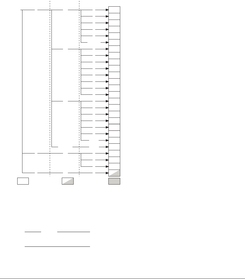
Protected Memory System Architecture (PMSA)
B4-30 Copyright © 1996-1998, 2000, 2004-2008 ARM Limited. All rights reserved. ARM DDI 0406B
B4.6.5 CP15 c0, ID codes registers
The CP15 c0 registers are used for processor and feature identification. Figure B4-4 shows the CP15 c0
registers.
Figure B4-4 CP15 c0 registers in a PMSA implementation
All CP15 c0 register encodings not shown in Figure B4-4 are UNPREDICTABLE, see Unallocated CP15
encodings on page B4-27.
Note
Chapter B5 The CPUID Identification Scheme describes the CPUID registers shown in Figure B4-4.
CRn opc1 CRm
CLIDR, Cache Level ID Register
CCSIDR, Cache Size ID Registers
CSSELR, Cache Size Selection Register0
c0
opc2
01
c2
MPUIR, MPU Type Register
MPIDR, Multiprocessor Affinity Register
Aliases of Main ID Register
4
5
{3,6,7}
0c1 ID_PFR0, Processor Feature Register 0
ID_PFR1, Processor Feature Register 1
ID_DFR0, Debug Feature Register 0
ID_AFR0, Auxiliary Feature Register 0
ID_MMFR0, Memory Model Feature Register 0
ID_MMFR1, Memory Model Feature Register 1
ID_MMFR2, Memory Model Feature Register 2
ID_MMFR3, Memory Model Feature Register 3
7
0
1
3
2
4
5
6
Read-As-Zero
ID_ISAR0, ISA Feature Register 0
ID_ISAR1, ISA Feature Register 1
ID_ISAR2, ISA Feature Register 2
ID_ISAR3, ISA Feature Register 3
ID_ISAR4, ISA Feature Register 4
ID_ISAR5, ISA Feature Register 5
1
3
2
4
5
{6,7}
Read-As-Zero
{c3-c7} {0-7}
AIDR, Auxiliary ID Register,
IMPLEMENTATION
DEFINED
c02
Read/WriteRead-only Write-only
1
7
CPUID registers
CTR, Cache Type Register
c0 0 c0
TCMTR, TCM Type Register, details
IMPLEMENTATION
DEFINED
MIDR, Main ID Register
1
2
0

Protected Memory System Architecture (PMSA)
ARM DDI 0406B Copyright © 1996-1998, 2000, 2004-2008 ARM Limited. All rights reserved. B4-31
Table B4-9 lists the CP15 c0 registers and shows where each register is described in full. The table does not
include the reserved and aliased registers that are shown in Figure B4-4 on page B4-30.
Note
The CPUID scheme described in Chapter B5 The CPUID Identification Scheme includes information about
the implementation of the optional Floating-Point and Advanced SIMD architecture extensions. See
Advanced SIMD and VFP extensions on page A2-20 for a summary of the implementation options for these
features.
Table B4-9 Index to CP15 c0 register descriptions
opc1 CRm opc2 Register and description
0c00c0, Main ID Register (MIDR) on page B4-32
1c0, Cache Type Register (CTR) on page B4-34
2c0, TCM Type Register (TCMTR) on page B4-35
4c0, MPU Type Register (MPUIR) on page B4-36
5c0, Multiprocessor Affinity Register (MPIDR) on page B4-37
3, 6, 7 c0, Main ID Register (MIDR) on page B4-32
c1 0, 1 CP15 c0, Processor Feature registers on page B5-4
2c0, Debug Feature Register 0 (ID_DFR0) on page B5-6
3c0, Auxiliary Feature Register 0 (ID_AFR0) on page B5-8
4-7 CP15 c0, Memory Model Feature registers on page B5-9
c2 0-5 CP15 c0, Instruction Set Attribute registers on page B5-19
1c00c0, Cache Size ID Registers (CCSIDR) on page B4-40
1c0, Cache Level ID Register (CLIDR) on page B4-41
7c0, Implementation defined Auxiliary ID Register (AIDR) on page B4-43
2c00c0, Cache Size Selection Register (CSSELR) on page B4-43

Protected Memory System Architecture (PMSA)
B4-32 Copyright © 1996-1998, 2000, 2004-2008 ARM Limited. All rights reserved. ARM DDI 0406B
B4.6.6 c0, Main ID Register (MIDR)
The Main ID Register, MIDR, provides identification information for the processor, including an
implementer code for the device and a device ID number.
The MIDR is:
• a 32-bit read-only register
• accessible only in privileged modes.
Some fields of the MIDR are IMPLEMENTATION DEFINED. For details of the values of these fields for a
particular ARMv7 implementation, and any implementation-specific significance of these values, see the
product documentation.
The format of the MIDR is:
Implementer, bits [31:24]
The Implementer code. Table B4-10 shows the permitted values for this field:
All other values are reserved by ARM and must not be used.
Variant, bits [23:20]
An IMPLEMENTATION DEFINED variant number. Typically, this field is used to distinguish
between different product variants, for example implementations of the same product with
different cache sizes.
31 24 23 20 19 16 15 4 3 0
Implementer Variant Architecture Primary part number Revision
Table B4-10 Implementer codes
Bits [31:24] ASCII character Implementer
0x41
A ARM Limited
0x44
D Digital Equipment Corporation
0x4D
M Motorola, Freescale Semiconductor Inc.
0x51
Q QUALCOMM Inc.
0x56
V Marvell Semiconductor Inc.
0x69
i Intel Corporation

Protected Memory System Architecture (PMSA)
ARM DDI 0406B Copyright © 1996-1998, 2000, 2004-2008 ARM Limited. All rights reserved. B4-33
Architecture, bits [19:16]
Table B4-11 shows the permitted values for this field:
All other values are reserved by ARM and must not be used.
Primary part number, bits [15:4]
An IMPLEMENTATION DEFINED primary part number for the device.
Note
On processors implemented by ARM, if the top four bits of the primary part number are
0x0
or
0x7
, the variant and architecture are encoded differently, see c0, Main ID Register (MIDR)
on page AppxH-34. Processors implemented by ARM have an Implementer code of
0x41
.
Revision, bits [3:0]
An IMPLEMENTATION DEFINED revision number for the device.
ARMv7 requires all implementations to use the CPUID scheme, described in Chapter B5 The CPUID
Identification Scheme, and an implementation is described by the MIDR and the CPUID registers.
Note
For an ARMv7 implementation by ARM, the MIDR is interpreted as:
Bits [31:24] Implementer code, must be
0x41
.
Bits [23:20] Major revision number, rX.
Bits [19:16] Architecture code, must be
0xF
.
Bits [15:4] ARM part number.
Bits [3:0] Minor revision number, pY.
Table B4-11 Architecture codes
Bits [19:16] Architecture
0x1
ARMv4
0x2
ARMv4T
0x3
ARMv5 (obsolete)
0x4
ARMv5T
0x5
ARMv5TE
0x6
ARMv5TEJ
0x7
ARMv6
0xF
Defined by CPUID scheme
Protected Memory System Architecture (PMSA)
B4-34 Copyright © 1996-1998, 2000, 2004-2008 ARM Limited. All rights reserved. ARM DDI 0406B
Accessing the MIDR
To access the MIDR you read the CP15 registers with
<opc1>
set to 0,
<CRn>
set to c0,
<CRm>
set to c0, and
<opc2>
set to 0. For example:
MRC p15,0,<Rt>,c0,c0,0 ; Read CP15 Main ID Register
B4.6.7 c0, Cache Type Register (CTR)
The Cache Type Register, CTR, provides information about the architecture of the caches.
The CTR is:
• a 32-bit read-only register
• accessible only in privileged modes.
The format of the CTR is changed from ARMv7. The ARMv7 format of the register is indicated by bits
[31:29] being set to 0b100. For details of the format of the Cache Type Register in versions of the ARM
architecture before ARMv7 see c0, Cache Type Register (CTR) on page AppxH-35.
In ARMv7, the format of the CTR is:
Bits [31:29] Set to 0b100 for the ARMv7 register format. Set to 0b000 for the format used in ARMv6
and earlier.
Bit [28] RAZ.
CWG, bits [27:24]
Cache Writeback Granule. Log2 of the number of words of the maximum size of memory
that can be overwritten as a result of the eviction of a cache entry that has had a memory
location in it modified.
A value of 0b0000 indicates that the CTR does not provide Cache Writeback Granule
information and either:
• the architectural maximum of 512 words (2Kbytes) must be assumed
• the Cache Writeback Granule can be determined from maximum cache line size
encoded in the Cache Size ID Registers.
Values greater than 0b1001 are reserved.
ERG, bits [27:24]
Exclusives Reservation Granule. Log2 of the number of words of the maximum size of the
reservation granule that has been implemented for the Load-Exclusive and Store-Exclusive
instructions. For more information, see Tagging and the size of the tagged memory block on
page A3-20.
A value of 0b0000 indicates that the CTR does not provide Exclusives Reservation Granule
information and the architectural maximum of 512 words (2Kbytes) must be assumed.
31 29 28 27 24 23 20 19 16 15 4 3 0
1000 CWG ERG DminLine 100000000000 IminLine

Protected Memory System Architecture (PMSA)
ARM DDI 0406B Copyright © 1996-1998, 2000, 2004-2008 ARM Limited. All rights reserved. B4-35
Values greater than 0b1001 are reserved.
DminLine, bits [19:16]
Log2 of the number of words in the smallest cache line of all the data caches and unified
caches that are controlled by the processor.
Bit [15] RAO.
Bits [14:4] RAZ.
IminLine, bits [3:0]
Log2 of the number of words in the smallest cache line of all the instruction caches that are
controlled by the processor.
Accessing the CTR
To access the CTR you read the CP15 registers with
<opc1>
set to 0,
<CRn>
set to c0,
<CRm>
set to c0, and
<opc2>
set to 1. For example
MRC p15,0,<Rt>,c0,c0,1 ; Read CP15 Cache Type Register
B4.6.8 c0, TCM Type Register (TCMTR)
The TCM Type Register, TCMTR, provides information about the implementation of the TCM.
The TCMTR is:
• a 32-bit read-only register
• accessible only in privileged modes.
From ARMv7:the
• TCMTR must be implemented
• when the ARMv7 format is used, the meaning of register bits [28:0] is IMPLEMENTATION DEFINED
• the ARMv6 format of the TCM Type Register remains a valid usage model
• if no TCMs are implemented the ARMv6 format must be used to indicate zero-sized TCMs.
The ARMv7 format of the TCMTR is:
Bits [31:29] Set to 0b100 for the ARMv7 register format. Set to 0b000 for the format used in ARMv6
and earlier.
Bits [28:0] IMPLEMENTATION DEFINED in the ARMv7 register format.
31 29 28 0
100 IMPLEMENTATION DEFINED

Protected Memory System Architecture (PMSA)
B4-36 Copyright © 1996-1998, 2000, 2004-2008 ARM Limited. All rights reserved. ARM DDI 0406B
If no TCMs are implemented, the TCMTR must be implemented with this ARMv6 format:
For details of the ARMv6 optional implementation of the TCM Type Register see c0, TCM Type Register
(TCMTR) on page AppxG-33.
Accessing the TCMTR
To access the TCMTR you read the CP15 registers with
<opc1>
set to 0,
<CRn>
set to c0,
<CRm>
set to c0, and
<opc2>
set to 2. For example:
MRC p15,0,<Rt>,c0,c0,2 ; Read CP15 TCM Type Register
B4.6.9 c0, MPU Type Register (MPUIR)
The MPU Type Register, MPUIR, identifies the features of the MPU implementation. In particular it
identifies:
• whether the MPU implements:
— a Unified address map, also referred to as a von Neumann architecture
— separate Instruction and Data address maps, also referred to as a Harvard architecture.
• the number of memory regions implemented by the MPU.
The MPUIR is:
• a 32-bit read-only register
• accessible only in privileged modes
• implemented only when the PMSA is implemented.
The format of the MPUIR is:
Bits [31:24] UNKNOWN.
IRegion, bits [23:16]
Specifies the number of Instruction regions implemented by the MPU.
If the MPU implements a Unified memory map this field is UNK/SBZ.
DRegion, bits [15:8]
Specifies the number of Data or Unified regions implemented by the MPU.
If this field is zero, no MPU is implemented, and the default memory map is in use.
Bits [7:1] UNKNOWN.
31 29 28 19 18 16 15 3 2 0
000 UNKNOWN 000 UNKNOWN 000
31 24 23 16 15 8 7 1 0
UNKNOWN IRegion DRegion UNKNOWN nU

Protected Memory System Architecture (PMSA)
ARM DDI 0406B Copyright © 1996-1998, 2000, 2004-2008 ARM Limited. All rights reserved. B4-37
nU, bit [0] Not Unified MPU. Indicates whether the MPU implements a unified memory map:
nU == 0 Unified memory map. Bits [23:16] of the register are zero.
nU == 1 Separate Instruction and Data memory maps.
Accessing the MPUIR
To access the MPUIR you read the CP15 registers with
<opc1>
set to 0,
<CRn>
set to c0,
<CRm>
set to c0, and
<opc2>
set to 4. For example:
MRC p15,0,<Rt>,c0,c0,4 ; Read CP15 MPU Type Register
B4.6.10 c0, Multiprocessor Affinity Register (MPIDR)
The Multiprocessor Affinity Register, MPIDR, provides an additional processor identification mechanism
for scheduling purposes in a multiprocessor system. In a uniprocessor system ARM recommends that this
register returns a value of 0.
The MPIDR is:
• a 32-bit read-only register
• accessible only in privileged modes
• introduced in ARMv7.
The format of the MPIDR is:
Note
In the MIDR bit definitions, a processor in the system can be a physical processor or a virtual processor.
Bits [31:24] Reserved, RAZ.
Affinity level 2, bits [23:16]
The least significant affinity level field, for this processor in the system.
Affinity level 1, bits [15:8]
The intermediate affinity level field, for this processor in the system.
Affinity level 0, bits [7:0]
The most significant level field, for this processor in the system.
In the system as a whole, for each of the affinity level fields, the assigned values must start at 0 and increase
monotonically.
31 24 23 16 15 8 7 0
0 0 0 0 0 0 0 0 Affinity level 2 Affinity level 1 Affinity level 0

Protected Memory System Architecture (PMSA)
B4-38 Copyright © 1996-1998, 2000, 2004-2008 ARM Limited. All rights reserved. ARM DDI 0406B
Increasing monotonically means that:
• There must not be any gaps in the sequence of numbers used.
• A higher value of the field includes any properties indicated by all lower values of the field.
When matching against an affinity level field, scheduler software checks for a value equal to or greater than
a required value.
Recommended use of the MPIDR includes a description of an example multiprocessor system and the
affinity level field values it might use.
The interpretation of these fields is IMPLEMENTATION DEFINED, and must be documented as part of the
documentation of the multiprocessor system. ARM recommends that this register might be used as
described in the next subsection.
The software mechanism to discover the total number of affinity numbers used at each level is
IMPLEMENTATION DEFINED, and is part of the general system identification task.
Recommended use of the MPIDR
In a multiprocessor system the register might provide two important functions:
• Identifying special functionality of a particular processor in the system. In general, the actual
meaning of the affinity level fields is not important. In a small number of situations, an affinity level
field value might have a special IMPLEMENTATION DEFINED significance. Possible examples include
booting from reset and power-down events.
• Providing affinity information for the scheduling software, to help the scheduler run an individual
thread or process on either:
— the same processor, or as similar a processor as possible, as the processor it was running on
previously
— a processor on which a related thread or process was run.
Note
A monotonically increasing single number ID mechanism provides a convenient index into software arrays
and for accessing the interrupt controller. This might be:
• performed as part of the boot sequence
• stored as part of the local storage of threads.

Protected Memory System Architecture (PMSA)
ARM DDI 0406B Copyright © 1996-1998, 2000, 2004-2008 ARM Limited. All rights reserved. B4-39
MPIDR provides a mechanism with up to three levels of affinity information, but the meaning of those levels
of affinity is entirely IMPLEMENTATION DEFINED. The levels of affinity provided can have different
meanings. Table B4-12 shows two possible implementations:
The scheduler maintains affinity level information for all threads and processes. When it has to reschedule
a thread or process the scheduler:
• looks for an available processor that matches at all three affinity levels
• if this fails, it might look for a processor that matches at levels 2 and 3 only
• if it still cannot find an available processor it might look for a match at level 3 only.
A multiprocessor system corresponding to Example system 1 in Table B4-12 might implement affinity
values as shown in Table B4-13:
Accessing the MPIDR
To access the MPIDR you read the CP15 registers with
<opc1>
set to 0,
<CRn>
set to c0,
<CRm>
set to c0, and
<opc2>
set to 5. For example:
MRC p15,0,<Rt>,c0,c0,5 ; Read Multiprocessor Affinity Register
Table B4-12 Possible implementations of the affinity levels
Affinity Level Example system 1 Example system 2
0 Virtual CPUs in a in a multi-threaded processor Processors in an SMP cluster
1 Processors in an Symmetric Multi Processor (SMP) cluster Clusters with a system
2 Clusters in a system No meaning, fixed as 0.
Table B4-13 Example of possible affinity values at different affinity levels
Affinity level 2, Cluster level Affinity level 1, Processor level Affinity level 0, Virtual CPU level
0 0 0, 1
0 1 0, 1
0 2 0, 1
0 3 0, 1
1 0 0, 1
1 1 0, 1
1 2 0, 1
1 3 0, 1

Protected Memory System Architecture (PMSA)
B4-40 Copyright © 1996-1998, 2000, 2004-2008 ARM Limited. All rights reserved. ARM DDI 0406B
B4.6.11 c0, Cache Size ID Registers (CCSIDR)
The Cache Size ID Registers, CCSIDR, provide information about the architecture of the caches.
The CCSIDR registers are:
• 32-bit read-only registers
• accessible only in privileged modes
• introduced in ARMv7.
One CCSIDR is implemented for each cache that can be accessed by the processor. CSSELR selects which
Cache Size ID register is accessible, see c0, Cache Size Selection Register (CSSELR) on page B4-43.
The format of a CCSIDR is:
WT, bit [31] Indicates whether the cache level supports Write-Through, see Table B4-14.
WB, bit [30] Indicates whether the cache level supports Write-Back, see Table B4-14.
RA, bit [29] Indicates whether the cache level supports Read-Allocation, see Table B4-14.
WA, bit [28] Indicates whether the cache level supports Write-Allocation, see Table B4-14.
NumSets, bits [27:13]
(Number of sets in cache) - 1, therefore a value of 0 indicates 1 set in the cache. The number
of sets does not have to be a power of 2.
Associativity, bits [12:3]
(Associativity of cache) - 1, therefore a value of 0 indicates an associativity of 1. The
associativity does not have to be a power of 2.
31 30 29 28 27 13 12 3 2 0
W
T
W
B
R
A
W
ANumSets Associativity LineSize
Table B4-14 WT, WB, RA and WA bit values
WT, WB, RA or WA bit value Meaning
0 Feature not supported
1 Feature supported

Protected Memory System Architecture (PMSA)
ARM DDI 0406B Copyright © 1996-1998, 2000, 2004-2008 ARM Limited. All rights reserved. B4-41
LineSize, bits [2:0]
(Log2(Number of words in cache line)) -2. For example:
• For a line length of 4 words: Log2(4) = 2, LineSize entry = 0.
This is the minimum line length.
• For a line length of 8 words: Log2(8) = 3, LineSize entry = 1.
Accessing the currently selected CCSIDR
The CSSELR selects a CCSIDR, see c0, Cache Size Selection Register (CSSELR) on page B4-43. To access
the currently-selected CCSIDR you read the CP15 registers with
<opc1>
set to 1,
<CRn>
set to c0,
<CRm>
set
to c0, and
<opc2>
set to 0. For example:
MRC p15,1,<Rt>,c0,c0,0 ; Read current CP15 Cache Size ID Register
Accessing the CCSIDR when the value in CSSELR corresponds to a cache that is not implemented returns
an UNKNOWN value.
B4.6.12 c0, Cache Level ID Register (CLIDR)
The Cache Level ID Register, CLIDR:
• identifies the type of cache, or caches, implemented at each level, up to a maximum of eight levels
• identifies the Level of Coherency and Level of Unification for the cache hierarchy.
The CLIDR is:
• a 32-bit read-only register
• accessible only in privileged modes
• introduced in ARMv7.
The format of the CLIDR is:
Bits [31:30] RAZ.
LoUU, bits [29:27]
Level of Unification Uniprocessor for the cache hierarchy, see Clean, Invalidate, and Clean
and Invalidate on page B2-11.
LoC, bits [26:24]
Level of Coherency for the cache hierarchy, see Clean, Invalidate, and Clean and Invalidate
on page B2-11.
31 30 29 27 26 24 23 21 20 18 17 15 14 12 11 9 8 6 5 3 2 0
0 0 LoUU LoC LoUIS Ctype7 Ctype6 Ctype5 Ctype4 Ctype3 Ctype2 Ctype1

Protected Memory System Architecture (PMSA)
B4-42 Copyright © 1996-1998, 2000, 2004-2008 ARM Limited. All rights reserved. ARM DDI 0406B
LoUIS, bits [23:21]
Level of Unification Inner Shareable for the cache hierarchy, see Clean, Invalidate, and
Clean and Invalidate on page B2-11. This field is RAZ in implementations that do not
implement the Multiprocessing extension.
CtypeX, bits [3(x - 1) + 2:3(x - 1)], for x = 1 to 7
Cache type fields. Indicate the type of cache implemented at each level, from Level 1 up to
a maximum of seven levels of cache hierarchy. The Level 1 cache type field, Ctype1, is bits
[2:0], see register diagram. Table B4-15 shows the possible values for each CtypeX field.
If you read the Cache type fields from Ctype1 upwards, once you have seen a value of
0b000, no caches exist at further out levels of the hierarchy. So, for example, if Ctype3 is
the first Cache type field with a value of 0b000, the values of Ctype4 to Ctype7 must be
ignored.
The CLIDR describes only the caches that are under the control of the processor.
Accessing the CLIDR
To access the CLIDR you read the CP15 registers with
<opc1>
set to 1,
<CRn>
set to c0,
<CRm>
set to c0, and
<opc2>
set to 1. For example:
MRC p15,1,<Rt>,c0,c0,1 ; Read CP15 Cache Level ID Register
Table B4-15 Ctype bit values
CtypeX bits Meaning, cache implemented at this level
000 No cache
001 Instruction cache only
010 Data cache only
011 Separate instruction and data caches
100 Unified cache
101, 11X Reserved

Protected Memory System Architecture (PMSA)
ARM DDI 0406B Copyright © 1996-1998, 2000, 2004-2008 ARM Limited. All rights reserved. B4-43
B4.6.13 c0, IMPLEMENTATION DEFINED Auxiliary ID Register (AIDR)
The IMPLEMENTATION DEFINED Auxiliary ID Register, AIDR, provides implementation-specific ID
information. The value of this register must be used in conjunction with the value of the MIDR.
The IMPLEMENTATION DEFINED AIDR is:
• a 32-bit read-only register
• accessible only in privileged modes
• introduced in ARMv7.
The format of the AIDR is IMPLEMENTATION DEFINED.
Accessing the AIDR
To access the AIDR you read the CP15 registers with
<opc1>
set to 1,
<CRn>
set to c0,
<CRm>
set to c0, and
<opc2>
set to 7. For example:
MRC p15,1,<Rt>,c0,c0,7 ; Read IMPLEMENTATION DEFINED Auxiliary ID Register
B4.6.14 c0, Cache Size Selection Register (CSSELR)
The Cache Size Selection Register, CSSELR, selects the current CCSIDR. An ARMv7 implementation
must include a CCSIDR for every implemented cache that is under the control of the processor. The
CSSELR identifies which CCSIDR can be accessed, by specifying, for the required cache:
• the cache level
• the cache type, either:
— instruction cache.
— Data cache. The data cache argument is also used for a unified cache.
CSSELR is:
• a 32-bit read/write register
• accessible only in privileged modes
• introduced in ARMv7.
The format of the CSSELR is:
Bits [31:4] UNK/SBZP.
Level, bits [3:1]
Cache level of required cache. Permitted values are from 0b000, indicating Level 1 cache,
to 0b110 indicating Level 7 cache.
0
LevelUNK/SBZP
InD
31 413
Protected Memory System Architecture (PMSA)
B4-44 Copyright © 1996-1998, 2000, 2004-2008 ARM Limited. All rights reserved. ARM DDI 0406B
InD, bit [0]
Instruction not data bit. Permitted values are:
0 Data or unified cache
1 Instruction cache.
If CSSELR is set to indicate a cache that is not implemented, the result of reading the current CCSIDR is
UNPREDICTABLE.
Accessing CSSELR
To access CSSELR you read or write the CP15 registers with
<opc1>
set to 2,
<CRn>
set to c0,
<CRm>
set to
c0, and
<opc2>
set to 0. For example:
MRC p15,2,<Rt>,c0,c0,0 ; Read Cache Size Selection Register
MCR p15,2,<Rt>,c0,c0,0 ; Write Cache Size Selection Register
B4.6.15 CP15 c1, System control registers
The CP15 c1 registers are used for system control. Figure B4-5 shows the CP15 c1 registers.
Figure B4-5 CP15 c1 registers in a PMSA implementation
All CP15 c1 register encodings not shown in Figure B4-5 are UNPREDICTABLE, see Unallocated CP15
encodings on page B4-27.
CRn opc1 CRm
c1 0 c0 0
2
SCTLR, Control Register
opc2
1 ACTLR, Auxiliary Control Register,
IMPLEMENTATION
DEFINED
CPACR, Coprocessor Access Control Register
Read/WriteRead-only Write-only

Protected Memory System Architecture (PMSA)
ARM DDI 0406B Copyright © 1996-1998, 2000, 2004-2008 ARM Limited. All rights reserved. B4-45
B4.6.16 c1, System Control Register (SCTLR)
The System Control Register, SCTLR, provides the top level control of the system, including its memory
system.
The SCTLR:
• Is a 32-bit read/write register, with different access rights for some bits of the register.
In ARMv7, some bits in the register are read-only. These bits relate to non-configurable features of
an ARMv7 implementation, and are provided for compatibility with previous versions of the
architecture.
• Is accessible only in privileged modes.
• Has a defined reset value. The reset value is IMPLEMENTATION DEFINED, see Reset value of the SCTLR
on page B4-49.
Control bits in the SCTLR that are not applicable to a PMSA implementation read as the value that most
closely reflects that implementation, and ignore writes.
In an ARMv7-R implementation the format of the SCTLR is:
IE, bit [31] Instruction Endianness. This bit indicates the endianness of the instructions issued to the
processor:
0 Little-endian byte ordering in the instructions
1 Big-endian byte ordering in the instructions.
When set, this bit causes the byte order of instructions to be reversed at runtime.
This bit is read-only. It is IMPLEMENTATION DEFINED which instruction endianness is used
by an ARMv7-R implementation, and this bit must indicate the implemented endianness.
If IE == 1 and EE == 0, behavior is UNPREDICTABLE.
TE, bit [30] Thumb Exception enable. This bit controls whether exceptions are taken in ARM or Thumb
state:
0 Exceptions, including reset, handled in ARM state
1 Exceptions, including reset, handled in Thumb state.
An implementation can include a configuration input signal that determines the reset value
of the TE bit. If the implementation does not include a configuration signal for this purpose
then this bit resets to zero in an ARMv7-R implementation.
For more information about the use of this bit see Instruction set state on exception entry on
page B1-35.
Bits [29:28] RAZ/SBZP.
31 30 029 28 27 26 25 24 23 22 21 20 19 18 17 16 15 14 13 12 11 10 7 6 3 2 1
CAMZ 0001111IV1010
RR
BR
FI
11
VE
EE
0
NMFI
TE
IE
00
DZ
U B
8954
SW

Protected Memory System Architecture (PMSA)
B4-46 Copyright © 1996-1998, 2000, 2004-2008 ARM Limited. All rights reserved. ARM DDI 0406B
NMFI, bit [27]
Non-Maskable Fast Interrupts enable:
0 Fast interrupts (FIQs) can be masked in the CPSR
1 Fast interrupts are non-maskable.
This bit is read-only. It is IMPLEMENTATION DEFINED whether an implementation supports
Non-Maskable Fast Interrupts (NMFIs):
• If NMFIs are not supported then this bit is RAZ/WI.
• If NMFIs are supported then this bit is determined a configuration input signal.
For more information, see Non-maskable fast interrupts on page B1-18.
Bit [26] RAZ/SBZP.
EE, bit [25] Exception Endianness bit. The value of this bit defines the value of the CPSR.E bit on entry
to an exception vector, including reset. The permitted values of this bit are:
0 Little endian
1 Big endian.
This is a read/write bit. An implementation can include a configuration input signal that
determines the reset value of the EE bit. If the implementation does not include a
configuration signal for this purpose then this bit resets to zero.
If IE == 1 and EE == 0, behavior is UNPREDICTABLE.
VE, bit [24] Interrupt Vectors Enable bit. This bit controls the vectors used for the FIQ and IRQ
interrupts. The permitted values of this bit are:
0 Use the FIQ and IRQ vectors from the vector table, see the V bit entry
1 Use the IMPLEMENTATION DEFINED values for the FIQ and IRQ vectors.
For more information, see Vectored interrupt support on page B1-32.
If the implementation does not support IMPLEMENTATION DEFINED FIQ and IRQ vectors
then this bit is RAZ/WI.
Bit [23] RAO/SBOP.
U, bit [22] In ARMv7 this bit is RAO/SBOP, indicating use of the alignment model described in
Alignment support on page A3-4.
For details of this bit in earlier versions of the architecture see Alignment on page AppxG-6.
FI, bit [21] Fast Interrupts configuration enable bit. This bit can be used to reduce interrupt latency in
an implementation by disabling IMPLEMENTATION DEFINED performance features. The
permitted values of this bit are:
0 All performance features enabled.
1 Low interrupt latency configuration. Some performance features disabled.
If the implementation does not support a mechanism for selecting a low interrupt latency
configuration this bit is RAZ/WI.
For more information, see Low interrupt latency configuration on page B1-43.

Protected Memory System Architecture (PMSA)
ARM DDI 0406B Copyright © 1996-1998, 2000, 2004-2008 ARM Limited. All rights reserved. B4-47
Bit [20] RAZ/SBZP.
DZ, bit [19] Divide by Zero fault enable bit. Any ARMv7-R implementation includes instructions to
perform unsigned and signed division, see SDIV on page A8-310 and UDIV on
page A8-468. This bit controls whether an integer divide by zero causes an Undefined
Instruction exception:
0 Divide by zero returns the result zero, and no exception is taken
1 Attempting a divide by zero causes an Undefined Instruction exception on the
SDIV
or
UDIV
instruction.
Bit [18] RAO/SBOP.
BR, bit [17] Background Region bit. When the MPU is enabled this bit controls how an access that does
not map to any MPU memory region is handled:
0 Any access to an address that is not mapped to an MPU region generates a
Background Fault memory abort. This is the PMSAv6 behavior.
1 The default memory map is used as a background region:
• A privileged access to an address that does not map to an MPU region
takes the properties defined for that address in the default memory map.
• An unprivileged access to an address that does not map to an MPU region
generates a Background Fault memory abort.
For more information, see Using the default memory map as a background region on
page B4-5.
Bit [16] RAO/SBOP.
Bit [15] RAZ/SBZP.
RR, bit [14] Round Robin bit. If the cache implementation supports the use of an alternative replacement
strategy that has a more easily predictable worst-case performance, this bit selects it:
0 Normal replacement strategy, for example, random replacement
1 Predictable strategy, for example, round-robin replacement.
The RR bit must reset to 0.
The replacement strategy associated with each value of the RR bit is IMPLEMENTATION
DEFINED.
If the implementation does not support multiple IMPLEMENTATION DEFINED replacement
strategies this bit is RAZ/WI.
V, bit [13] Vectors bit. This bit selects the base address of the exception vectors:
0 Normal exception vectors, base address
0x00000000
.
1 High exception vectors (Hivecs), base address
0xFFFF0000
.
For more information, see Exception vectors and the exception base address on page B1-30.

Protected Memory System Architecture (PMSA)
B4-48 Copyright © 1996-1998, 2000, 2004-2008 ARM Limited. All rights reserved. ARM DDI 0406B
Note
Use of the Hivecs setting, V == 1, is deprecated in an ARMv7-R implementation.
An implementation can include a configuration input signal that determines the reset value
of the V bit. If the implementation does not include a configuration signal for this purpose
then this bit resets to zero.
I, bit [12] Instruction cache enable bit: This is a global enable bit for instruction caches:
0 Instruction caches disabled
1 Instruction caches enabled.
If the system does not implement any instruction caches that can be accessed by the
processor, at any level of the memory hierarchy, this bit is RAZ/WI.
If the system implements any instruction caches that can be accessed by the processor then
it must be possible to disable them by setting this bit to 0.
Cache enabling and disabling on page B2-8 describes the effect of enabling the caches.
Z, bit [11] Branch prediction enable bit. This bit is used to enable branch prediction, also called
program flow prediction:
0 Program flow prediction disabled
1 Program flow prediction enabled.
If program flow prediction cannot be disabled, this bit is RAO/WI.
If the implementation does not support program flow prediction then this bit is RAZ/WI.
SW, bit[10] SWP/SWPB enable bit. This bit enables the use of
SWP
and
SWPB
instructions:
0
SWP
and
SWPB
are UNDEFINED
1
SWP
and
SWPB
perform as described in section SWP, SWPB on page A8-432.
This bit is added as part of the Multiprocessing Extensions.
Note
At reset, this bit disables
SWP
and
SWPB
. This means that operating systems have to choose to
use
SWP
and
SWPB
.
Bits [9:8] RAZ/SBZP.
B, bit [7] In ARMv7 this bit is RAZ/SBZP, indicating use of the endianness model described in
Endian support on page A3-7.
For details of this bit in earlier versions of the architecture see Endian support on
page AppxG-7 and Endian support on page AppxH-7.
Bits [6:3] RAO/SBOP.

Protected Memory System Architecture (PMSA)
ARM DDI 0406B Copyright © 1996-1998, 2000, 2004-2008 ARM Limited. All rights reserved. B4-49
C, bit [2] Cache enable bit: This is a global enable bit for data and unified caches:
0 Data and unified caches disabled
1 Data and unified caches enabled.
If the system does not implement any data or unified caches that can be accessed by the
processor, at any level of the memory hierarchy, this bit is RAZ/WI.
If the system implements any data or unified caches that can be accessed by the processor
then it must be possible to disable them by setting this bit to 0.
Cache enabling and disabling on page B2-8 describes the effect of enabling the caches.
A, bit [1] Alignment bit. This is the enable bit for Alignment fault checking:
0 Alignment fault checking disabled
1 Alignment fault checking enabled.
For more information, see Alignment fault on page B4-14.
M, bit [0] MPU enable bit. This is a global enable bit for the MPU:
0 MPU disabled
1 MPU enabled.
For more information, see Enabling and disabling the MPU on page B4-5.
Reset value of the SCTLR
The SCTLR has a defined reset value that is IMPLEMENTATION DEFINED. There are different types of bit in
the SCTLR:
• Some bits are defined as RAZ or RAO, and have the same value in all PMSAv7 implementations.
Figure B4-6 on page B4-50 shows the values of these bits.
• Some bits are read-only and either:
— have an IMPLEMENTATION DEFINED value
— have a value that is determined by a configuration input signal.
• Some bits are read/write and either:
— reset to zero
— reset to an IMPLEMENTATION DEFINED value
— reset to a value that is determined by a configuration input signal.
Figure B4-6 on page B4-50 shows the reset value, or how the reset value is defined, for each bit of the
SCTLR. It also shows the possible values of each half byte of the register.

Protected Memory System Architecture (PMSA)
B4-50 Copyright © 1996-1998, 2000, 2004-2008 ARM Limited. All rights reserved. ARM DDI 0406B
Figure B4-6 Reset value of the SCTLR, ARMv7-R (PMSAv7)
Accessing the SCTLR
To access SCTLR you read or write the CP15 registers with
<opc1>
set to 0,
<CRn>
set to c1,
<CRm>
set to c0,
and
<opc2>
set to 0. For example:
MRC p15,0,<Rt>,c1,c0,0 ; Read CP15 System Control Register
MCR p15,0,<Rt>,c1,c0,0 ; Write CP15 System Control Register
Note
Additional configuration and control bits might be added to the SCTLR in future versions of the ARM
architecture. ARM strongly recommends that software always uses a read, modify, write sequence to update
the SCTLR. This prevents software modifying any bit that is currently unallocated, and minimizes the
chance of the register update having undesired side effects.
B4.6.17 c1, IMPLEMENTATION DEFINED Auxiliary Control Register (ACTLR)
The Auxiliary Control Register, ACTLR, provides implementation-specific configuration and control
options.
The ACTLR is:
• A 32-bit read/write register.
• Accessible only in privileged modes.
The contents of this register are IMPLEMENTATION DEFINED. ARMv7 requires this register to be privileged
read/write accessible, even if an implementation has not created any control bits in this register.
31 30 029 28 27 26 25 24 23 22 21 20 19 18 17 16 15 14 13 12 11 10 7 6 3 2 1
CAM
0
Z
0001111
IV
10100
RRBR
FI
11
VE
0
TE
*
EENMFI
*************** (0)
98 54
0000 00
(*)
00
(*)
00
0x80x70x8 or 0x00x2 or 0x00x50xC
0xA, 0x8,
0x2 or 0x0
IE
DZ
** ()
0xC, 0x8,
0x4 or 0x0
UB
Read-only bits, including RAZ and RAO bits.*
Can be RAZ. Otherwise read/write, resets to 0.
(*)
Value is IMPLEMENTATION DEFINED.
Can be read-only, with IMPLEMENTATION DEFINED value. Otherwise resets to 0.
Value or reset value can depend on configuration input. Otherwise RAZ or resets to 0.
()
SW
(*)

Protected Memory System Architecture (PMSA)
ARM DDI 0406B Copyright © 1996-1998, 2000, 2004-2008 ARM Limited. All rights reserved. B4-51
Accessing the ACTLR
To access the ACTLR you read or write the CP15 registers with
<opc1>
set to 0,
<CRn>
set to c1,
<CRm>
set to
c0, and
<opc2>
set to 1. For example:
MRC p15,0,<Rt>,c1,c0,1 ; Read CP15 Auxiliary Control Register
MCR p15,0,<Rt>,c1,c0,1 ; Write CP15 Auxiliary Control Register
B4.6.18 c1, Coprocessor Access Control Register (CPACR)
The Coprocessor Access Control Register, CPACR, controls access to all coprocessors other than CP14 and
CP15. It also enables software to check for the presence of coprocessors CP0 to CP13.
The CPACR:
• is a 32-bit read/write register
• is accessible only in privileged modes.
• has a defined reset value of 0.
The format of the CPACR is:
ASEDIS, bit[31]
Disable Advanced SIMD functionality:
0 This bit does not cause any instructions to be UNDEFINED.
1 All instruction encodings identified in the Alphabetical list of instructions on
page A8-14 as being part of Advanced SIMD, but that are not VFPv3
instructions, are UNDEFINED.
On an implementation that:
• Implements VFP and does not implement Advanced SIMD, this bit is RAO/WI.
• Does not implement VFP or Advanced SIMD, this bit is UNK/SBZP.
• Implements both VFP and Advanced SIMD, it is IMPLEMENTATION DEFINED whether
this bit is supported. If it is not supported it is RAZ/WI.
This bit resets to 0 if it is supported.
cp13 cp0
31 30 29 26 25 24 23 22 21 20 19 18 17 16 15 14 13 12 11 10 9 8 7 6 5 4 3 2 1 0
(0) (0) cp12 cp11 cp10 cp9 cp8 cp7 cp6 cp5 cp4 cp3 cp2 cp1
D32DIS
ASEDIS
28 27

Protected Memory System Architecture (PMSA)
B4-52 Copyright © 1996-1998, 2000, 2004-2008 ARM Limited. All rights reserved. ARM DDI 0406B
D32DIS, bit[30]
Disable use of D16-D31 of the VFP register file:
0 This bit does not cause any instructions to be UNDEFINED.
1 All instruction encodings identified in the Alphabetical list of instructions on
page A8-14 as being VFPv3 instructions are UNDEFINED if they access any of
registers D16-D31.
If this bit is 1 when CPACR.ASEDIS == 0, the result is UNPREDICTABLE.
On an implementation that:
• Does not implement VFP, this bit is UNK/SBZP.
• Implements VFP and does not implement D16-D31, this bit is RAO/WI.
• Implements VFP and implements D16-D31, it is IMPLEMENTATION DEFINED whether
this bit is supported. If it is not supported it is RAZ/WI.
This bit resets to 0 if it is supported.
Bits [29:28] Reserved. UNK/SBZP.
cp<n>, bits [2n+1, 2n], for n = 0 to 13
Defines the access rights for coprocessor n. The possible values of the field are:
00 Access denied. Any attempt to access the coprocessor generates an Undefined
Instruction exception.
01 Privileged access only. Any attempt to access the coprocessor in User mode
generates an Undefined Instruction exception.
10 Reserved. The effect of this value is UNPREDICTABLE.
11 Full access. The meaning of full access is defined by the appropriate
coprocessor.
The value for a coprocessor that is not implemented is 00, access denied.
If more than one coprocessor is used to provide a set of functionality then having different values for the
CPACR fields for those coprocessors can lead to UNPREDICTABLE behavior. An example where this must be
considered is with the VFP extension, that uses CP10 and CP11.
Typically, an operating system uses this register to control coprocessor resource sharing among applications:
• Initially all applications are denied access to the shared coprocessor-based resources.
• When an application attempts to use a resource it results in an Undefined Instruction exception.
• The Undefined Instruction handler can then grant access to the resource by setting the appropriate
field in the CPACR.
For details of how this register can be used to check for implemented coprocessors see Access controls on
CP0 to CP13 on page B1-63.

Protected Memory System Architecture (PMSA)
ARM DDI 0406B Copyright © 1996-1998, 2000, 2004-2008 ARM Limited. All rights reserved. B4-53
Sharing resources among applications requires a state saving mechanism. Two possibilities are:
• during a context switch, if the last executing process or thread had access rights to a coprocessor then
the operating system saves the state of that coprocessor
• on receiving a request for access to a coprocessor, the operating system saves the old state for that
coprocessor with the last process or thread that accessed it.
Accessing the CPACR
To access the CPACR you read or write the CP15 registers with
<opc1>
set to 0,
<CRn>
set to c1,
<CRm>
set to
c0, and
<opc2>
set to 2. For example:
MRC p15,0,<Rt>,c1,c0,2 ; Read CP15 Coprocessor Access Control Register
MCR p15,0,<Rt>,c1,c0,2 ; Write CP15 Coprocessor Access Control Register
Normally, software uses a read, modify, write sequence to update the CPACR, to avoid unwanted changes
to the access settings for other coprocessors.
B4.6.19 CP15 c2 and c3, Not used on a PMSA implementation
The CP15 c2 and c3 register encodings are not used on an ARMv7-R implementation, see Unallocated
CP15 encodings on page B4-27.
B4.6.20 CP15 c4, Not used
The CP15 c4 register encodings are not used on an ARMv7 implementation, see Unallocated CP15
encodings on page B4-27.
B4.6.21 CP15 c5 and c6, Memory system fault registers
The CP15 c5 and c6 registers are used for memory system fault reporting. In addition, c6 provides the MPU
Region registers. Figure B4-7 on page B4-54 shows the CP15 c5 and c6 registers.
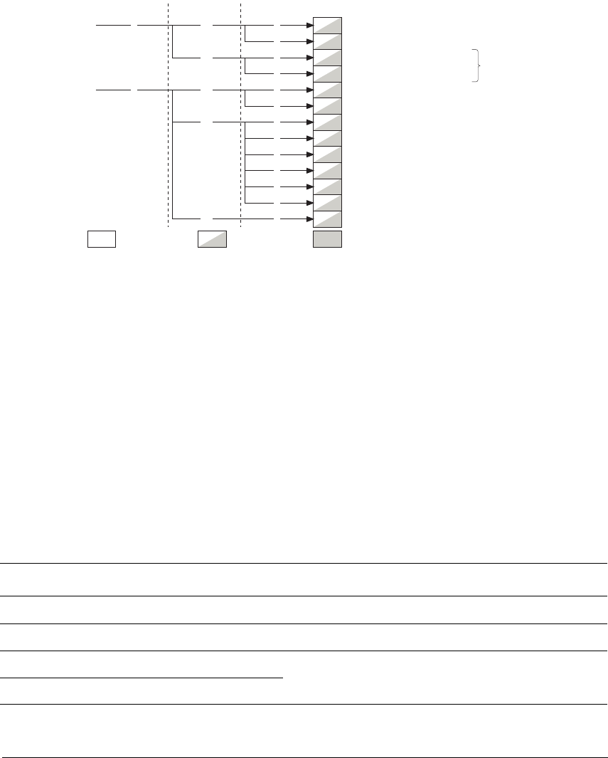
Protected Memory System Architecture (PMSA)
B4-54 Copyright © 1996-1998, 2000, 2004-2008 ARM Limited. All rights reserved. ARM DDI 0406B
Figure B4-7 CP15 c5 and c6 registers in a PMSA implementation
All CP15 c5 and c6 register encodings not shown in Figure B4-7 are UNPREDICTABLE, see Unallocated
CP15 encodings on page B4-27.
The CP15 c5 and c6 registers are described in:
•CP15 c5, Fault status registers
•CP15 c6, Fault Address registers on page B4-57
•CP15 c6, Memory region programming registers on page B4-59.
Also, these registers are used to report information about debug exceptions. For details see Effects of debug
exceptions on CP15 registers and the DBGWFAR on page C4-4.
B4.6.22 CP15 c5, Fault status registers
There are two fault status registers, in CP15 c5, and the architecture provides encodings for two additional
IMPLEMENTATION DEFINED registers. Table B4-16 summarizes these registers.
c5 0 c0 0 DFSR, Data Fault Status Register
IFSR, Instruction Fault Status Register
DFAR, Data Fault Address Register
IFAR, Instruction Fault Address Register
1
c6 0 c0 0
2
c1 DRBAR, Data Region Base Address Register
IRBAR, Instruction Region Base Address Register
DRSR, Data Region Size and Enable Register
IRSR, Instruction Region Size and Enable Register
DRACR, Data Region Access Control Register
IRACR, Instruction Region Access Control Register
RGNR, MPU Region Number Register
c2
0
1
0
2
3
4
5
Details are
IMPLEMENTATION DEFINED
ADFSR, Auxiliary DFSR
AIFSR, Auxiliary IFSR
c1 0
1
CRn opc1 CRm opc2
Read/WriteRead-only Write-only
Table B4-16 Fault status registers
Register name Description
Data Fault Status Register (DFSR) c5, Data Fault Status Register (DFSR) on page B4-55
Instruction Fault Status Register (IFSR) c5, Instruction Fault Status Register (IFSR) on page B4-56
Auxiliary Data Fault Status Register (ADFSR) c5, Auxiliary Data and Instruction Fault Status Registers
(ADFSR and AIFSR) on page B4-56
Auxiliary Instruction Fault Status Register (AIFSR)
Protected Memory System Architecture (PMSA)
ARM DDI 0406B Copyright © 1996-1998, 2000, 2004-2008 ARM Limited. All rights reserved. B4-55
Fault information is returned using the fault status registers and the fault address registers described in CP15
c6, Fault Address registers on page B4-57. For details of how these registers are used see Fault Status and
Fault Address registers in a PMSA implementation on page B4-18.
c5, Data Fault Status Register (DFSR)
The Data Fault Status Register, DFSR, holds status information about the last data fault.
The DFSR is:
• a 32-bit read/write register
• accessible only in privileged modes.
The format of the DFSR is:
Bits [31:13,9:4]
UNK/SBZP.
ExT, bit [12] External abort type. This bit can be used to provide an IMPLEMENTATION DEFINED
classification of external aborts.
For aborts other than external aborts this bit always returns 0.
WnR, bit [11] Write not Read bit. Indicates whether the abort was caused by a write or a read access:
0 Abort caused by a read access
1 Abort caused by a write access.
For faults on CP15 cache maintenance operations this bit always returns a value of 1.
FS, bits [10,3:0]
Fault status bits. For the valid encodings of these bits in an ARMv7-R implementation with
a PMSA, see Table B4-7 on page B4-20.
All encodings not shown in the table are reserved.
For information about using the DFSR see Fault Status and Fault Address registers in a PMSA
implementation on page B4-18.
Accessing the DFSR
To access the DFSR you read or write the CP15 registers with
<opc1>
set to 0,
<CRn>
set to c5,
<CRm>
set to
c0, and
<opc2>
set to 0. For example:
MRC p15,0,<Rt>,c5,c0,0 ; Read CP15 Data Fault Status Register
MCR p15,0,<Rt>,c5,c0,0 ; Write CP15 Data Fault Status Register
43
FS[3:0]
UNK/SBZP
012 11 10 9
ExT
WnR
FS[4]
31 13
UNK/SBZP
Protected Memory System Architecture (PMSA)
B4-56 Copyright © 1996-1998, 2000, 2004-2008 ARM Limited. All rights reserved. ARM DDI 0406B
c5, Instruction Fault Status Register (IFSR)
The Instruction Fault Status Register, IFSR, holds status information about the last instruction fault.
The IFSR is:
• a 32-bit read/write register
• accessible only in privileged modes.
The format of the IFSR is:
Bits [31:13,11,9:4]
UNK/SBZP.
ExT, bit [12] External abort type. This bit can be used to provide an IMPLEMENTATION DEFINED
classification of external aborts.
For aborts other than external aborts this bit always returns 0.
FS, bits [10,3:0]
Fault status bits.
See Table B4-7 on page B4-20 for the valid encodings of these bits. All encodings not
shown in the table are reserved.
For information about using the IFSR see Fault Status and Fault Address registers in a PMSA
implementation on page B4-18.
Accessing the IFSR
To access the IFSR you read or write the CP15 registers with
<opc1>
set to 0,
<CRn>
set to c5,
<CRm>
set to c0,
and
<opc2>
set to 1. For example:
MRC p15,0,<Rt>,c5,c0,1 ; Read CP15 Instruction Fault Status Register
MCR p15,0,<Rt>,c5,c0,1 ; Write CP15 Instruction Fault Status Register
c5, Auxiliary Data and Instruction Fault Status Registers (ADFSR and AIFSR)
The Auxiliary Data Fault Status Register (ADFSR) and the Auxiliary Instruction Fault Status Register
(AIFSR) enable the system to return additional IMPLEMENTATION DEFINED fault status information, see
Auxiliary Fault Status Registers on page B4-21.
The ADFSR and AIFSR are:
• 32-bit read/write registers
• accessible only in privileged modes
• introduced in ARMv7.
43
FS[3:0]
UNK/SBZP
012 11 10 9
ExT
FS[4]
31 13
UNK/SBZP(0)

Protected Memory System Architecture (PMSA)
ARM DDI 0406B Copyright © 1996-1998, 2000, 2004-2008 ARM Limited. All rights reserved. B4-57
The formats of the ADFSR and AIFSR are IMPLEMENTATION DEFINED.
Accessing the ADFSR and AIFSR
To access the ADFSR or AIFSR you read or write the CP15 registers with
<opc1>
set to 0,
<CRn>
set to c5,
<CRm>
set to c1, and
<opc2>
set to:
• 0 for the ADFSR
• 1 for the AIFSR.
For example:
MRC p15,0,<Rt>,c5,c1,0 ; Read CP15 Auxiliary Data Fault Status Register
MCR p15,0,<Rt>,c5,c1,0 ; Write CP15 Auxiliary Data Fault Status Register
MRC p15,0,<Rt>,c5,c1,1 ; Read CP15 Auxiliary Instruction Fault Status Register
MCR p15,0,<Rt>,c5,c1,1 ; Write CP15 Auxiliary Instruction Fault Status Register
B4.6.23 CP15 c6, Fault Address registers
There are two Fault Address registers, in CP15 c6, as shown in Figure B4-7 on page B4-54. The two Fault
Address registers complement the Fault Status registers, and are shown in Table B4-17.
Note
Before ARMv7:
• The DFAR was called the Fault Address Register (FAR).
• The Watchpoint Fault Address Register (DBGWFAR) was implemented in CP15 c6 with
<opc2>
==1.
From ARMv7, the DBGWFAR is only implemented as a CP14 debug register, see Watchpoint Fault
Address Register (DBGWFAR) on page C10-28.
Fault information is returned using the fault address registers and the fault status registers described in CP15
c5, Fault status registers on page B4-54. For details of how these registers are used see Fault Status and
Fault Address registers in a PMSA implementation on page B4-18.
c6, Data Fault Address Register (DFAR)
The Data Fault Address Register, DFAR, holds the faulting address that caused a synchronous Data Abort
exception.
Table B4-17 Fault address registers
Register name Description
Data Fault Address Register (DFAR) c6, Data Fault Address Register (DFAR)
Instruction Fault Address Register (IFAR) c6, Instruction Fault Address Register (IFAR) on page B4-58

Protected Memory System Architecture (PMSA)
B4-58 Copyright © 1996-1998, 2000, 2004-2008 ARM Limited. All rights reserved. ARM DDI 0406B
The DFAR is:
• a 32-bit read/write register
• accessible only in privileged modes.
The format of the DFAR is:
For information about using the DFAR, including when the value in the DFAR is valid, see Fault Status and
Fault Address registers in a PMSA implementation on page B4-18.
A debugger can write to the DFAR to restore its value.
Accessing the DFAR
To access the DFAR you read or write the CP15 registers with
<opc1>
set to 0,
<CRn>
set to c6,
<CRm>
set to
c0, and
<opc2>
set to 0. For example:
MRC p15,0,<Rt>,c6,c0,0 ; Read CP15 Data Fault Address Register
MCR p15,0,<Rt>,c6,c0,0 ; Write CP15 Data Fault Address Register
c6, Instruction Fault Address Register (IFAR)
The Instruction Fault Address Register, IFAR, holds the address of the faulting access that caused a
synchronous Prefetch Abort exception.
The IFAR is:
• a 32-bit read/write register
• accessible only in privileged modes.
The format of the IFAR is:
For information about using the IFAR, including when the value in the IFAR is valid, see Fault Status and
Fault Address registers in a PMSA implementation on page B4-18.
A debugger can write to the IFAR to restore its value.
Accessing the IFAR
To access the IFAR you read or write the CP15 registers with
<opc1>
set to 0,
<CRn>
set to c6,
<CRm>
set to c0,
and
<opc2>
set to 2. For example:
MRC p15,0,<Rt>,c6,c0,2 ; Read CP15 Instruction Fault Address Register
MCR p15,0,<Rt>,c6,c0,2 ; Write CP15 Instruction Fault Address Register
31 0
Faulting address of synchronous Data Abort exception
31 0
Faulting address of synchronous Prefetch Abort exception

Protected Memory System Architecture (PMSA)
ARM DDI 0406B Copyright © 1996-1998, 2000, 2004-2008 ARM Limited. All rights reserved. B4-59
B4.6.24 CP15 c6, Memory region programming registers
When the PMSA is implemented, a number of registers in CP15 c6 are used to configure the MPU memory
regions. There are three registers for each memory region supported by the MPU:
• A Base Address Register, that defined the start address of the region in the memory map.
• A Region Size and Enable Register, that:
— has a single enable bit for the region
— defines the size of the region
— has a disable bit for each of the eight subregions in the region.
• A Region Access Control Register that defines the memory access attributes for the region.
The multiple copies of these registers are mapped onto three or six registers in CP15 c6, and another register
is used to select the current memory region. The mapping of the region registers onto the CP15 registers
depends on whether the MPU implements a unified memory map, or separate Instruction and Data memory
maps:
Separate Instruction and Data memory maps
The multiple copies of the registers that describe each memory region map onto six CP15
registers.
For the memory regions in the Instruction memory map:
• the multiple Region Base Address Registers map onto the Instruction Region Base
Address Register, IRBAR
• the multiple Region Size and Enable Registers map onto the Instruction Region Size
and Enable Register, IRSR
• the multiple Region Access Control Registers map onto the Instruction Region
Access Control Register, IRACR.
For the memory regions in the Data memory map:
• the multiple Region Base Address Registers map onto the Data Region Base Address
Register, DRBAR
• the multiple Region Size and Enable Registers map onto the Data Region Size and
Enable Register, DRSR
• the multiple Region Access Control Registers map onto the Data Region Access
Control Register, DRACR.
The value in the RGNR is the index value for both the instruction region and the data region
registers, see c6, MPU Region Number Register (RGNR) on page B4-66. The RGNR value
indicates the current memory region for both the instruction and the data memory maps.
However, a particular value might not be valid for both memory maps.
Unified memory maps
The multiple copies of the registers that describe each memory region map onto three CP15
registers:
• the multiple Region Base Address Registers map onto the Data Region Base Address
Register, DRBAR

Protected Memory System Architecture (PMSA)
B4-60 Copyright © 1996-1998, 2000, 2004-2008 ARM Limited. All rights reserved. ARM DDI 0406B
• the multiple Region Size and Enable Registers map onto the Data Region Size and
Enable Register, DRSR
• the multiple Region Access Control Registers map onto the Data Region Access
Control Register, DRACR.
The IRBAR, IRSR, and IRACR are not implemented.
The value in the RGNR is the index value for the data region registers, see c6, MPU Region
Number Register (RGNR) on page B4-66. Its value indicates the current memory region in
the unified memory map.
The read-only MPUIR indicates:
• whether the MPU implements separate Instruction and Data address maps, or a Unified address map
• the number of Data or Unified regions the MPU supports
• if separate Instruction and Data address maps are implemented, the number of Instruction regions the
MPU supports.
For more information, see c0, MPU Type Register (MPUIR) on page B4-36.
Table B4-18 summarizes the CP15 registers that are used to program the MPU memory regions, and gives
references to the full descriptions of these registers.
c6, Data Region Base Address Register (DRBAR)
The Data Region Base Address Register, DRBAR, indicates the base address of the current memory region
in the data or unified address map. The base address must be aligned to the region size. The current memory
region is selected by the value held in the RGNR, see c6, MPU Region Number Register (RGNR) on
page B4-66.
Table B4-18 MPU Memory Region Programming Registers
Register name Description
Data or Unified Region Base Address c6, Data Region Base Address Register (DRBAR)
Instruction Region Base Addressac6, Instruction Region Base Address Register (IRBAR) on page B4-61a
Data or Unified Region Size and Enable c6, Data Region Size and Enable Register (DRSR) on page B4-62
Instruction Region Size and Enableac6, Instruction Region Size and Enable Register (IRSR) on page B4-63a
Data or Unified Region Access Control c6, Data Region Access Control Register (DRACR) on page B4-64
Instruction Region Access Controlac6, Instruction Region Access Control Register (IRACR) on page B4-65a
MPU Region Number c6, MPU Region Number Register (RGNR) on page B4-66
a. These registers are implemented only if the MPU implements separate Instruction and Data memory maps.

Protected Memory System Architecture (PMSA)
ARM DDI 0406B Copyright © 1996-1998, 2000, 2004-2008 ARM Limited. All rights reserved. B4-61
The DRBAR is:
• a 32-bit read/write register
• accessible only in privileged modes.
The format of the DRBAR is:
Region Base Address, bits [31:2]
The Base Address for the region, in the Data or Unified address map. The region referenced
is selected by the RGNR
Bit [1:0] UNK/SBZP.
The DRBAR can be used to find the size of the supported physical address space for the Data or Unified
memory map, see Finding the minimum supported region size on page B4-7.
Accessing the DRBAR
To access the DRBAR you read or write the CP15 registers with
<opc1>
set to 0,
<CRn>
set to c6,
<CRm>
set to
c1, and
<opc2>
set to 0. For example:
MRC p15,0,<Rt>,c6,c1,0 ; Read CP15 Data Region Base Address Register
MCR p15,0,<Rt>,c6,c1,0 ; Write CP15 Data Region Base Address Register
c6, Instruction Region Base Address Register (IRBAR)
The Instruction Region Base Address Register, IRBAR, indicates the base address of the current memory
region in the Instruction address map. The base address must be aligned to the region size. The current
memory region is selected by the value held in the RGNR, see c6, MPU Region Number Register (RGNR)
on page B4-66.
The IRBAR is:
• a 32-bit read/write register
• accessible only in privileged modes.
• implemented only when the PMSA implements separate instruction and data memory maps.
The format of the IRBAR is identical to the DRBAR, see c6, Data Region Base Address Register (DRBAR)
on page B4-60.
The IRBAR can be used to find the minimum region size supported by the implementation, see Finding the
minimum supported region size on page B4-7.
31 210
Region Base Address (0) (0)

Protected Memory System Architecture (PMSA)
B4-62 Copyright © 1996-1998, 2000, 2004-2008 ARM Limited. All rights reserved. ARM DDI 0406B
Accessing the IRBAR
To access the IRBAR you read or write the CP15 registers with
<opc1>
set to 0,
<CRn>
set to c6,
<CRm>
set to
c1, and
<opc2>
set to 1. For example:
MRC p15,0,<Rt>,c6,c1,1 ; Read CP15 Instruction Region Base Address Register
MCR p15,0,<Rt>,c6,c1,1 ; Write CP15 Instruction Region Base Address Register
c6, Data Region Size and Enable Register (DRSR)
The Data Region Size and Enable Register, DRSR, indicates the size of the current memory region in the
data or unified address map, and can be used to enable or disable:
• the entire region
• each of the eight subregions, if the region is enabled.
The current memory region is selected by the value held in the RGNR see c6, MPU Region Number Register
(RGNR) on page B4-66.
The DRSR:
• is a 32-bit read/write register
• is accessible only in privileged modes.
• has a defined reset value of 0.
The format of the DRSR is:
Bit [31:16,7:6]
UNK/SBZP.
SnD, bit [n+8], for values of n from 0 to 7
Subregion disable bit for region n. Indicates whether the subregion is part of this region:
0 Subregion is part of this region
1 Subregion disabled. The subregion is not part of this region.
The region is divided into exactly eight equal sized subregions. Subregion 0 is the subregion
at the least significant address. For more information, see Subregions on page B4-3.
If the size of this region, indicated by the RSize field, is less than 256 bytes then the SnD
fields are not defined, and register bits [15:8] are UNK/SBZP.
UNK/SBZP
0111098761215 14 13
(0) RSize En
31 16 5 1
(0)
S0D
S1D
S2D
S3D
S7D
S6D
S5D
S4D

Protected Memory System Architecture (PMSA)
ARM DDI 0406B Copyright © 1996-1998, 2000, 2004-2008 ARM Limited. All rights reserved. B4-63
RSize, bits [5:1]
Region Size field. Indicates the size of the current memory region:
• A value of 0 is not permitted, this value is reserved and UNPREDICTABLE.
• If N is the value in this field, the region size is 2N+1 bytes.
En, bit [0] Enable bit for the region:
0 Region is disabled
1 Region is enabled.
Because this register resets to zero, all memory regions are disabled on reset.
All memory regions must be enabled before they are used.
The minimum region size supported is IMPLEMENTATION DEFINED, but if the memory system
implementation includes a cache, ARM strongly recommends that the minimum region size is a multiple of
the cache line length. This prevents cache attributes changing mid-way through a cache line.
Behavior is UNPREDICTABLE if you:
• write a region size that is outside the range supported by the implementation
• access this register when the RGNR does not point to a valid region in the MPU Data or Unified
address map.
Accessing the DRSR
To access the DRSR you read or write the CP15 registers with
<opc1>
set to 0,
<CRn>
set to c6,
<CRm>
set to
c1, and
<opc2>
set to 2. For example:
MRC p15,0,<Rt>,c6,c1,2 ; Read CP15 Data Region Size and Enable Register
MCR p15,0,<Rt>,c6,c1,2 ; Write CP15 Data Region Size and Enable Register
c6, Instruction Region Size and Enable Register (IRSR)
The Instruction Region Size and Enable Register, IRSR, indicates the size of the current memory region in
the instruction address map, and to enable or disable:
• the entire region
• each of the eight subregions, if the region is enabled.
The current memory region is selected by the value held in the RGNR, see c6, MPU Region Number
Register (RGNR) on page B4-66.
The IRSR:
• is a 32-bit read/write register
• is accessible only in privileged modes
• has a defined reset value of 0.
• is implemented only when the PMSA implements separate instruction and data memory maps.

Protected Memory System Architecture (PMSA)
B4-64 Copyright © 1996-1998, 2000, 2004-2008 ARM Limited. All rights reserved. ARM DDI 0406B
The format of the IRSR is identical to the DRSR, see c6, Data Region Size and Enable Register (DRSR) on
page B4-62.
All memory regions must be enabled before they are used.
The minimum region size supported is IMPLEMENTATION DEFINED, but if the memory system
implementation includes an instruction cache, ARM strongly recommends that the minimum region size is
a multiple of the instruction cache line length. This prevents cache attributes changing mid-way through a
cache line.
Behavior is UNPREDICTABLE if you:
• write a region size that is outside the range supported by the implementation
• access this register when the RGNR does not point to a valid region in the MPU instruction address
map.
Accessing the IRSR
To access the IRSR you read or write the CP15 registers with
<opc1>
set to 0,
<CRn>
set to c6,
<CRm>
set to c1,
and
<opc2>
set to 3. For example:
MRC p15,0,<Rt>,c6,c1,3 ; Read CP15 Instruction Region Size and Enable Register
MCR p15,0,<Rt>,c6,c1,3 ; Write CP15 Instruction Region Size and Enable Register
c6, Data Region Access Control Register (DRACR)
The Data Region Access Control Register, DRACR, defines the memory attributes for the current memory
region in the data or unified address map.
The current memory region is selected by the value held in the RGNR, see c6, MPU Region Number
Register (RGNR) on page B4-66.
The DRACR is:
• a 32-bit read/write register
• accessible only in privileged modes.
The format of the DRACR is:
Bit [31:13,11,7:6]
UNK/SBZP.
XN, bit [12] Execute Never bit. Indicates whether instructions can be fetched from this region:
0 region can contain executable code
1 region is an Execute never region, and any attempt to execute an instruction
from the region results in a Permission fault.
31 13121110 8765 3210
UNK/SBZP X
N(0) AP [2:0] (0) (0) TEX
[2:0] SCB

Protected Memory System Architecture (PMSA)
ARM DDI 0406B Copyright © 1996-1998, 2000, 2004-2008 ARM Limited. All rights reserved. B4-65
If the MPU implements separate Instruction and Data memory maps this bit is UNK/SBZ
For more information, see The Execute Never (XN) attribute and instruction prefetching on
page B4-10.
AP[2:0], bits [10:8]
Access Permissions field. Indicates the read and write access permissions for unprivileged
and privileged accesses to the memory region.
For more information, see Access permissions on page B4-9.
TEX[2:0], C, B, bits [5:3,1:0]
Memory access attributes. For more information, see C, B, and TEX[2:0] encodings on
page B4-11.
S, bit [2] Shareable bit, for Normal memory regions:
0 If region is Normal memory, memory is Non-shareable
1 If region is Normal memory, memory is Shareable.
The value of this bit is ignored if the region is not Normal memory.
If you access this register when the RGNR does not point to a valid region in the MPU data or unified
address map, the result is UNPREDICTABLE.
Accessing the DRACR
To access the DRACR you read or write the CP15 registers with
<opc1>
set to 0,
<CRn>
set to c6,
<CRm>
set to
c1, and
<opc2>
set to 4. For example:
MRC p15,0,<Rt>,c6,c1,4 ; Read CP15 Data Region Access Control Register
MCR p15,0,<Rt>,c6,c1,4 ; Write CP15 Data Region Access Control Register
c6, Instruction Region Access Control Register (IRACR)
The Instruction Region Access Control Register, IRACR, defines the memory attributes for the current
memory region in the instruction address map, when the MPU implements separate data and instruction
address maps.
The current memory region is selected by the value held in the RGNR, see c6, MPU Region Number
Register (RGNR) on page B4-66.
The IRACR is:
• a 32-bit read/write register
• accessible only in privileged modes
• implemented only when the PMSA implements separate instruction and data memory maps.
The format of the IRACR is identical to the DRACR, see c6, Data Region Access Control Register (DRACR)
on page B4-64.

Protected Memory System Architecture (PMSA)
B4-66 Copyright © 1996-1998, 2000, 2004-2008 ARM Limited. All rights reserved. ARM DDI 0406B
Note
The XN bit, bit [12], is always valid in the IRACR.
If you access this register when the RGNR does not point to a valid region in the MPU instruction address
map, the result is UNPREDICTABLE.
Accessing the IRACR
To access the IRACR you read or write the CP15 registers with
<opc1>
set to 0,
<CRn>
set to c6,
<CRm>
set to
c1, and
<opc2>
set to 5. For example:
MRC p15,0,<Rt>,c6,c1,5 ; Read CP15 Instruction Region Access Control Register
MCR p15,0,<Rt>,c6,c1,5 ; Write CP15 Instruction Region Access Control Register
c6, MPU Region Number Register (RGNR)
The MPU Region Number Register, RGNR, defines the current memory region in:
• the MPU data or unified address map
• the MPU instruction address map, if the MPU implements separate data and instruction address
maps.
The value in the RGNR identifies the memory region description accessed by the Region Base Address, Size
and Enable, and Access Control Registers.
Note
There is only a single MPU Region Number Register. When the MPU implements separate data and
instruction address maps, the current region number is always identical for both address maps. This might
mean that the current region number is valid for one address map but invalid for the other map.
The RGNR is:
• a 32-bit read/write register
• accessible only in privileged modes.
The format of the RGNR is:
Bit [31:N] UNK/SBZP.
Region, bits [N-1:0]
The number of the current region in the Data or Unified address map, and in the Instruction
address map if the MPU implements separate Data and Instruction address maps.
The value of N is Log2(Number of regions supported) rounded up to an integer.
31 NN-1 0
UNK/SBZP Region

Protected Memory System Architecture (PMSA)
ARM DDI 0406B Copyright © 1996-1998, 2000, 2004-2008 ARM Limited. All rights reserved. B4-67
Memory region numbering starts at 0 and goes up to one less than the number of regions
supported.
Writing a value to this register that is greater than or equal to the number of memory regions supported has
UNPREDICTABLE results.
In the context of the RGNR description, when the MPU implements separate Data and Instruction address
maps the Number of memory regions supported is the greater of:
• number of Data memory regions supported
• number of Instruction memory regions supported.
Accessing the RGNR
To access the RGNR you read or write the CP15 registers with
<opc1>
set to 0,
<CRn>
set to c6,
<CRm>
set to
c2, and
<opc2>
set to 0. For example:
MRC p15,0,<Rt>,c6,c2,0 ; Read CP15 MPU Region Number Register
MCR p15,0,<Rt>,c6,c2,0 ; Write CP15 MPU Region Number Register
Protected Memory System Architecture (PMSA)
B4-68 Copyright © 1996-1998, 2000, 2004-2008 ARM Limited. All rights reserved. ARM DDI 0406B
B4.6.25 CP15 c7, Cache maintenance and other functions
The CP15 c7 registers are used for cache maintenance operations, and also provide barrier operations.
Figure B4-8 shows the CP15 c7 registers.
Figure B4-8 CP15 c7 registers in a PMSA implementation
All CP15 c7 encodings not shown in Figure B4-8 are UNPREDICTABLE, see Unallocated CP15 encodings on
page B4-27.
The CP15 c7 operations are described in:
•CP15 c7, Cache and branch predictor maintenance functions
•CP15 c7, Miscellaneous functions on page B4-72.
B4.6.26 CP15 c7, Cache and branch predictor maintenance functions
CP15 c7 provides a number of functions. This section describes only the CP15 c7 cache and branch
predictor maintenance operations. Branch predictor operations are included in this section, because they
operate in a similar way to the cache maintenance operations.
Note
ARMv7 introduces significant changes in the CP15 c7 operations. Most of these changes are because, from
ARMv7, the architecture covers multiple levels of cache. This section only describes the ARMv7
requirements for these operations. For details of these operations in previous versions of the architecture see:
•c7, Cache operations on page AppxG-38 for ARMv6
•c7, Cache operations on page AppxH-49 for ARMv4 and ARMv5.
Cache maintenance operationsc5
c10 {1,2}
{4,5}
DCCMVAU, cache maintenance operation
1c11
c6
Data barrier operations
{1,2} Cache maintenance operations
Cache maintenance operations
CP15ISB, Instruction Synchronization Barrier operation
Branch predictor maintenance operations
{0,1}
4
{6,7}
Bold text = Accessible in User mode
Read/WriteRead-only Write-only
c14 {1,2} Cache maintenance operations
c13 1 NOP
Cache maintenance operations
c1 {0,6}
Part of the Multiprocessing Extensions
CRn opc1 CRm opc2
c7 0 c0 NOP4
Protected Memory System Architecture (PMSA)
ARM DDI 0406B Copyright © 1996-1998, 2000, 2004-2008 ARM Limited. All rights reserved. B4-69
Figure B4-9 shows the CP15 c7 cache and branch predictor maintenance operations.
Figure B4-9 CP15 c7 Cache and branch predictor maintenance operations
The CP15 c7 cache and branch predictor maintenance operations are all write-only operations that can be
executed only in privileged modes. They are listed in Table B4-19.
For more information about the terms used in this section see Terms used in describing cache operations on
page B2-10. The Multiprocessing Extensions changes the set of caches affected by these operations, see
Multiprocessor effects on cache maintenance operations on page B2-23.
In Table B4-19, the Rt data column specifies what data is required in the register Rt specified by the
MCR
instruction used to perform the operation. For more information about the possible data formats see Data
formats for the cache and branch predictor operations on page B4-70.
c7 0
ICIALLU, Invalidate all instruction caches to PoU
DCIMVAC, Invalidate data cache line by MVA to PoCc6 1
1
6
7
ICIMVAU, Invalidate instruction caches by MVA to PoU
BPIALL, Invalidate entire branch predictor array
BPIMVA, Invalidate MVA from branch predictor array
2DCISW, Invalidate data cache line by set/way
c10 1 DCCMVAC, Clean data cache line by MVA to PoC
DCCSW, Clean data cache line by set/way2
1c11
c14 1
PoU: Point of Unification
PoC: Point of Coherency
DCCIMVAC, Clean and invalidate data cache line by MVA to PoC
DCCISW, Clean and invalidate data cache line by set/way
2
DCCMVAU, Clean data cache line by MVA to PoU
Read-only Read/Write data or unified
CRn opc1 CRm opc2
ICIALLUIS, Invalidate all instruction caches to PoU Inner Shareable
BPIALLIS, Invalidate entire branch predictor array Inner Shareable
Part of the Multiprocessing Extensions
c1 0
6
c5 0
Write-only
Table B4-19 CP15 c7 cache and branch predictor maintenance operations
CRm opc2 Mnemonic FunctionaRt data
c1 0 ICIALLUIS Invalidate all instruction caches to PoU Inner Shareable. Also
flushes branch target cache.b
Ignored
c1 1 BPIALLIS Invalidate entire branch predictor array Inner Shareable. Ignored
c5 0 ICIALLU Invalidate all instruction caches to PoU. Also flushes branch target
cache.c
Ignored
c5 1 ICIMVAU Invalidate instruction cache line by address to PoU.b, d Address
c5 6 BPIALL Invalidate entire branch predictor array. Ignored

Protected Memory System Architecture (PMSA)
B4-70 Copyright © 1996-1998, 2000, 2004-2008 ARM Limited. All rights reserved. ARM DDI 0406B
Data formats for the cache and branch predictor operations
Table B4-19 on page B4-69 shows three possibilities for the data in the register Rt specified by the
MCR
instruction. These are described in the following subsections:
•Ignored
•Address
•Set/way on page B4-71
Ignored
The value in the register specified by the
MCR
instruction is ignored. You do not have to write a value to the
register before issuing the
MCR
instruction.
Address
In general descriptions of the maintenance operations, operations that require a memory address are
described as operating by MVA. For more information, see Terms used in describing cache operations on
page B2-10. In a PMSA implementation, these operations require the physical address in the memory map.
When the data is stated to be an address, it does not have to be cache line aligned.
c5 7 BPIMVA Invalidate address from branch predictor array in the inner
shareable domain.d
Address
c6 1 DCIMVAC Invalidate data or unified cache line by address to PoU.dAddress
c6 2 DCISW Invalidate data or unified cache line by set/way. Set/way
c10 1 DCCMVAC Clean data or unified cache line by address to PoC.dAddress
c10 2 DCCSW Clean data or unified cache line by set/way. Set/way
c11 1 DCCMVAU Clean data or unified cache line by address to PoU.dAddress
c14 1 DCCIMVAC Clean and invalidate data or unified cache line by address to PoC.dAddress
c14 2 DCCISW Clean and invalidate data or unified cache line by set/way. Set/way
a. Address, point of coherency (PoC) and point of unification (PoU) are described in Terms used in describing cache
operations on page B2-10.
b. Only applies to separate instruction caches, does not apply to unified caches.
c. Only applies to separate instruction caches, does not apply to unified caches.
d. In general descriptions of the cache operations, these functions are described as operating by MVA
(Modified Virtual Address). In a PMSA implementation the MVA and the PA have the same value, and so
the functions operate using a physical address in the memory map.
Table B4-19 CP15 c7 cache and branch predictor maintenance operations (continued)
CRm opc2 Mnemonic FunctionaRt data

Protected Memory System Architecture (PMSA)
ARM DDI 0406B Copyright © 1996-1998, 2000, 2004-2008 ARM Limited. All rights reserved. B4-71
Set/way
For an operation by set/way, the data identifies the cache line that the operation is to be applied to by
specifying:
• the cache set the line belongs to
• the way number of the line in the set
• the cache level.
The format of the register data for a set/way operation is:
Where:
A =Log
2(ASSOCIATIVITY)
B =(L+S)
L =Log
2(LINELEN)
S =Log
2(NSETS)
ASSOCIATIVITY, LINELEN (Line Length) and NSETS (number of sets) have their usual
meanings and are the values for the cache level being operated on.
The values of A and S are rounded up to the next integer.
Level ((Cache level to operate on) -1)
For example, this field is 0 for operations on L 1 cache, or 1 for operations on L 2 cache.
Set The number of the set to operate on.
Way The number of the way to operate on.
Note
• If L = 4 then there is no SBZ field between the set and level fields in the register.
• If A = 0 there is no way field in the register, and register bits [31:B] are SBZ.
• If the level, set or way field in the register is larger than the size implemented in the cache then the
effect of the operation is UNPREDICTABLE.
Accessing the CP15 c7 cache maintenance operations
To perform one of the cache maintenance operations you write the CP15 registers with
<opc1>
set to 0,
<CRn>
set to c7, and
<CRm>
and
<opc2>
set to the values shown in Table B4-19 on page B4-69.
That is:
MCR p15,0,<Rt>,c7,<CRm>,<opc2>
For example:
MCR p15,0,<Rt>,c7,c5,0 ; Invalidate all instruction caches to point of unification
MCR p15,0,<Rt>,c7,c10,2 ; Clean data or unified cache line by set/way
31 32-A 31-A B B-1 L L-1 4 3 1 0
Way SBZ Set SBZ Level 0
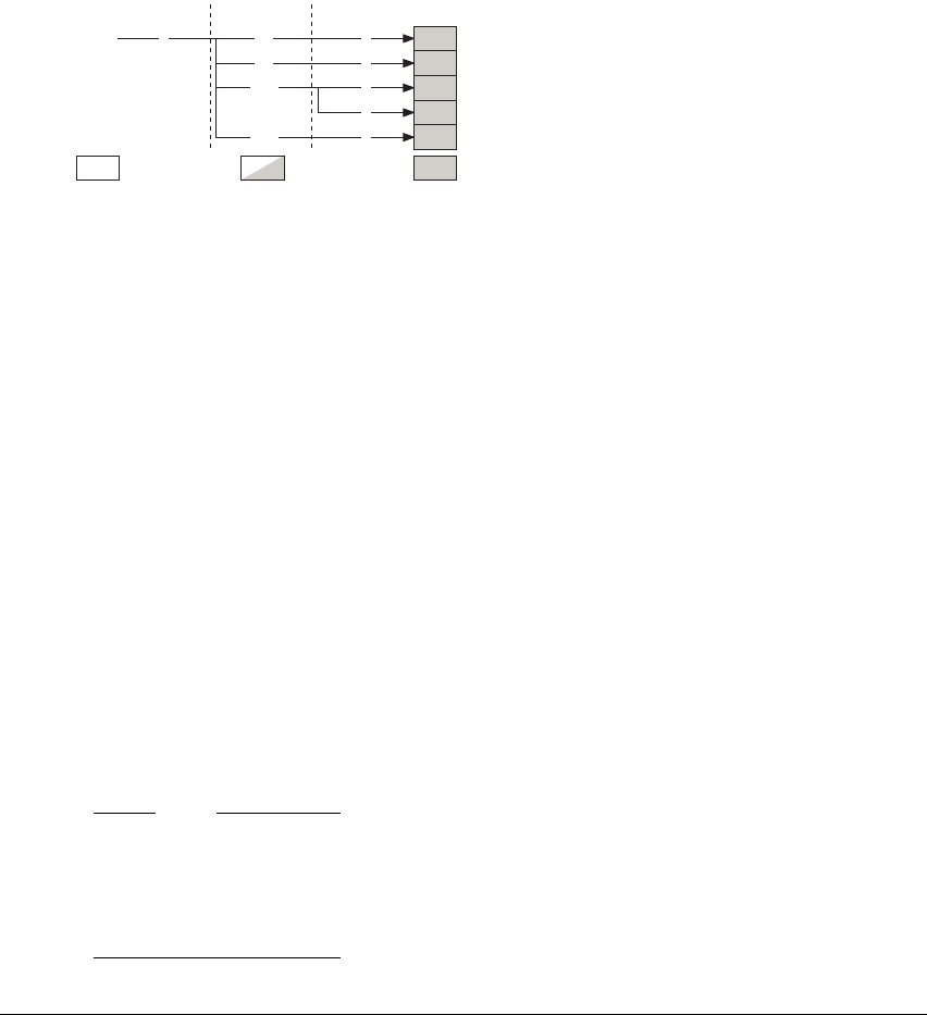
Protected Memory System Architecture (PMSA)
B4-72 Copyright © 1996-1998, 2000, 2004-2008 ARM Limited. All rights reserved. ARM DDI 0406B
B4.6.27 CP15 c7, Miscellaneous functions
CP15 c7 provides a number of functions, summarized in Figure B4-8 on page B4-68. This section describes
only the CP15 c7 miscellaneous operations.
Figure B4-10 shows the CP15 c7 miscellaneous operations. It does not show the other CP15 c7 operations.
Figure B4-10 CP15 c7 Miscellaneous operations
The CP15 c7 miscellaneous operations are described in:
•CP15 c7, Data and Instruction Barrier operations
•CP15 c7, No Operation (NOP) on page B4-73.
CP15 c7, Data and Instruction Barrier operations
ARMv6 includes two CP15 c7 operations to perform Data Barrier operations, and another operation to
perform an Instruction Barrier operation. In ARMv7:
• The ARM and Thumb instruction sets include instructions to perform the barrier operations, that can
be executed in unprivileged and privileged modes, see Memory barriers on page A3-47.
• The CP15 c7 operations are defined as write-only operations, that can be executed in unprivileged
and privileged modes, but using these operations is deprecated. The three operations are described in:
—Instruction Synchronization Barrier operation on page B4-73
—Data Synchronization Barrier operation on page B4-73
—Data Memory Barrier operation on page B4-73.
The value in the register Rt specified by the
MCR
instruction used to perform one of these operations
is ignored. You do not have to write a value to the register before issuing the
MCR
instruction.
In ARMv7 using these CP15 c7 operations is deprecated. Use the
ISB
,
DSB
, and
DMB
instructions
instead.
Note
• In ARMv6 and earlier documentation, the Instruction Synchronization Barrier operation is referred
to as a Prefetch Flush.
• In versions of the ARM architecture before ARMv6 the Data Synchronization Barrier operation is
described as a Data Write Barrier (DWB).
c7 0 NOP, was Wait For Interrupt (CP15WFI) in ARMv6
CP15DSB, Data Synchronization Barrier operation
CP15DMB, Data Memory Barrier operation
CP15ISB, Instruction Synchronization Barrier operation
CRn opc1 CRm opc2
c0 4
c10 4
5
c5 4
Bold text = Accessible in User mode
Read/Write
Read-only Write-only
c13 1 NOP, was Prefetch instruction by MVA in ARMv6

Protected Memory System Architecture (PMSA)
ARM DDI 0406B Copyright © 1996-1998, 2000, 2004-2008 ARM Limited. All rights reserved. B4-73
Instruction Synchronization Barrier operation
In ARMv7, the
ISB
instruction is used to perform an Instruction Synchronization Barrier, see ISB on
page A8-102.
The deprecated CP15 c7 encoding for an Instruction Synchronization Barrier is
<opc1>
set to 0,
<CRn>
set to
c7,
<CRm>
set to c5, and
<opc2>
set to 4.
Data Synchronization Barrier operation
In ARMv7, the
DSB
instruction is used to perform a Data Synchronization Barrier, see DSB on page A8-92.
The deprecated CP15 c7 encoding for a Data Synchronization Barrier is
<opc1>
set to 0,
<CRn>
set to c7,
<CRm>
set to c10, and
<opc2>
set to 4. This operation performs the full system barrier performed by the
DSB
instruction.
Data Memory Barrier operation
In ARMv7, the
DMB
instruction is used to perform a Data Memory Barrier, see DMB on page A8-90.
The deprecated CP15 c7 encoding for a Data Memory Barrier is
<opc1>
set to 0,
<CRn>
set to c7,
<CRm>
set to
c10, and
<opc2>
set to 5. This operation performs the full system barrier performed by the
DMB
instruction.
CP15 c7, No Operation (NOP)
ARMv6 includes two CP15 c7 operations that are not supported in ARMv7, with encodings that become
No Operation (NOP) in ARMv7. These are:
• The Wait For Interrupt (CP15WFI) operation. In ARMv7 this operation is performed by the
WFI
instruction, that is available in the ARM and Thumb instruction sets. For more information, see WFI
on page A8-810.
• The prefetch instruction by MVA operation. In ARMv7 this operation is replaced by the
PLI
instruction, that is available in the ARM and Thumb instruction sets. For more information, see PLI
(immediate, literal) on page A8-242, and PLI (register) on page A8-244.
In ARMv7, the CP15 c7 encodings that were used for these operations must be valid write-only operations
that perform a NOP. These encodings are:
• for the ARMv6 CP15WFI operation:
—
<opc1>
set to 0,
<CRn>
set to c7,
<CRm>
set to c0, and
<opc2>
set to 4
• for the ARMv6 prefetch instruction by MVA operation:
—
<opc1>
set to 0,
<CRn>
set to c7,
<CRm>
set to c13, and
<opc2>
set to 1.
B4.6.28 CP15 c8, Not used on a PMSA implementation
CP15 c8 is not used on an ARMv7-R implementation, see Unallocated CP15 encodings on page B4-27.
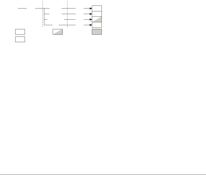
Protected Memory System Architecture (PMSA)
B4-74 Copyright © 1996-1998, 2000, 2004-2008 ARM Limited. All rights reserved. ARM DDI 0406B
B4.6.29 CP15 c9, Cache and TCM lockdown registers and performance monitors
Some CP15 c9 register encodings are reserved for IMPLEMENTATION DEFINED memory system functions, in
particular:
• cache control, including lockdown
• TCM control, including lockdown
• branch predictor control.
Additional CP15 c9 encodings are reserved for performance monitors. These encodings fall into two groups:
• the optional performance monitors described in Chapter C9 Performance Monitors
• additional IMPLEMENTATION DEFINED performance monitors.
The reserved encodings permit implementations that are compatible with previous versions of the ARM
architecture, in particular with the ARMv6 requirements. Figure B4-11 shows the permitted CP15 c9
register encodings.
Figure B4-11 Permitted CP15 c9 register encodings
All CP15 c9 encodings not shown in Figure B4-11 are UNPREDICTABLE, see Unallocated CP15 encodings
on page B4-27.
In ARMv6, CP15 c9 provides cache lockdown functions. With the ARMv7 abstraction of the hierarchical
memory model, for CP15 c9:
• All encodings with CRm = {c0-c2, c5-c8} are reserved for IMPLEMENTATION DEFINED cache, branch
predictor and TCM operations.
This reservation enables the implementation of a scheme that is backwards compatible with ARMv6.
For details of the ARMv6 implementation see c9, Cache lockdown support on page AppxG-45.
• All encodings with CRm = {c12-c14} are reserved for the optional performance monitors that are
defined in Chapter C9 Performance Monitors.
• All encodings with CRm = c15 are reserved for IMPLEMENTATION DEFINED performance monitoring
features.
B4.6.30 CP15 c10, Not used on a PMSA implementation
CP15 c10 is not used on an ARMv7-R implementation, see Unallocated CP15 encodings on page B4-27.
Reserved for Branch Predictor, Cache and TCM operationsc9 {0-7} {c0-c2} {0-7}
Reserved for Branch Predictor, Cache and TCM operations
{c5-c8} {0-7}
Reserved for ARM-recommended Performance Monitors
c15 {0-7}
CRn opc1 CRm opc2
Reserved for IMPLEMENTATION DEFINED Performance Monitors
{c12-c14} {0-7}
Read/WriteRead-only Write-only
Access depends on the operation
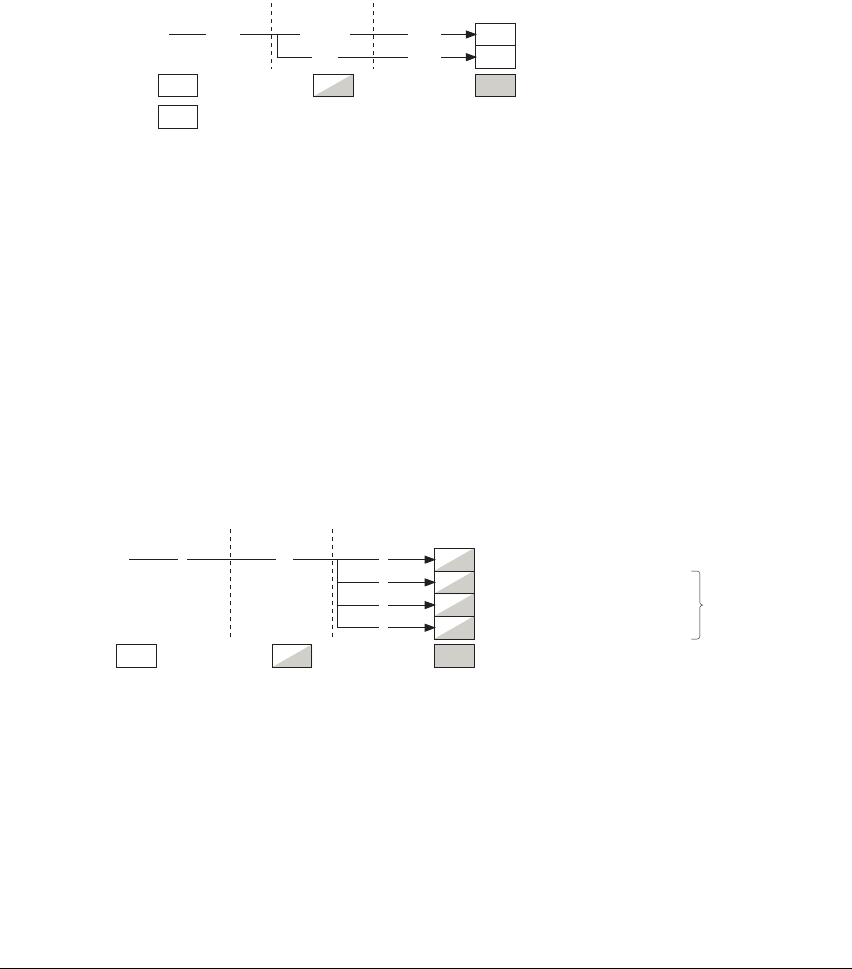
Protected Memory System Architecture (PMSA)
ARM DDI 0406B Copyright © 1996-1998, 2000, 2004-2008 ARM Limited. All rights reserved. B4-75
B4.6.31 CP15 c11, Reserved for TCM DMA registers
Some CP15 c11 register encodings are reserved for IMPLEMENTATION DEFINED DMA operations to and
from TCM, see Figure B4-12.
Figure B4-12 Permitted CP15 c11 register encodings
All CP15 c11 encodings not shown in Figure B4-12 are UNPREDICTABLE, see Unallocated CP15 encodings
on page B4-27.
B4.6.32 CP15 c12, Not used on a PMSA implementation
CP15 c12 is not used on an ARMv7-R implementation, see Unallocated CP15 encodings on page B4-27.
B4.6.33 CP15 c13, Context and Thread ID registers
The CP15 c13 registers are used for:
• a Context ID register
• three software Thread ID registers.
Figure B4-13 shows the CP15 c13 registers:
Figure B4-13 CP15 c13 registers in a PMSA implementation
All CP15 c13 encodings not shown in Figure B4-13 are UNPREDICTABLE, see Unallocated CP15 encodings
on page B4-27.
The CP15 c13 registers are described in:
•c13, Context ID Register (CONTEXTIDR) on page B4-76
•CP15 c13 Software Thread ID registers on page B4-77.
Reserved for DMA operations for TCM access
Reserved for DMA operations for TCM access
c11 {0-7} {c0-c8} {0-7}
c15 {0-7}
Read/WriteRead-only Write-only
CRn opc1 CRm opc2
Access depends on the operation
c13 0 c0 1
CRn opc1 CRm opc2
4
3
CONTEXTIDR, Context ID Register
2
Read/WriteRead-only Write-only
Software Thread ID
Registers
TPIDRURO, User Read Only
TPIDRPRW, Privileged Only
TPIDRURW, User Read/Write

Protected Memory System Architecture (PMSA)
B4-76 Copyright © 1996-1998, 2000, 2004-2008 ARM Limited. All rights reserved. ARM DDI 0406B
B4.6.34 c13, Context ID Register (CONTEXTIDR)
The Context ID Register, CONTEXTIDR, identifies the current context by means of a Context Identifier
(Context ID).
Note
Previously, on PMSA implementations, this Context ID has been described as a Process Identifier
(PROCID), and this CP15 c13 register has been called the Process ID Register. The new naming makes the
register naming consistent for PMSA and VMSA implementations.
The whole of this register is used by:
• the debug logic, for Linked and Unlinked Context ID matching, see Breakpoint debug events on
page C3-5 and Watchpoint debug events on page C3-15.
• the trace logic, to identify the current process.
The CONTEXTIDR is:
• a 32-bit read/write register
• accessible only in privileged modes.
The format of the CONTEXTIDR is:
ContextID, bits [31:0]
Context Identifier. This field must be programmed with a unique context identifier value that
identifies the current process. It is used by the trace logic and the debug logic to identify the
process that is running currently.
Accessing the CONTEXTIDR
To access the CONTEXTIDR you read or write the CP15 registers with
<opc1>
set to 0,
<CRn>
set to c13,
<CRm>
set to c0, and
<opc2>
set to 1. For example:
MRC p15,0,<Rt>,c13,c0,1 ; Read CP15 Context ID Register
MCR p15,0,<Rt>,c13,c0,1 ; Write CP15 Context ID Register
31 0
ContextID

Protected Memory System Architecture (PMSA)
ARM DDI 0406B Copyright © 1996-1998, 2000, 2004-2008 ARM Limited. All rights reserved. B4-77
B4.6.35 CP15 c13 Software Thread ID registers
The Software Thread ID registers provide locations where software can store thread identifying information,
for OS management purposes. These registers are never updated by the hardware.
The Software Thread ID registers are:
• three 32-bit register read/write registers:
— User Read/Write Thread ID Register, TPIDRURW
— User Read-only Thread ID Register, TPIDRURO
— Privileged Only Thread ID Register, TPIDRPRW.
• accessible in different modes:
— the User Read/Write Thread ID Register is read/write in unprivileged and privileged modes
— the User Read-only Thread ID Register is read-only in User mode, and read/write in privileged
modes
— the Privileged Only Thread ID Register is only accessible in privileged modes, and is
read/write
• introduced in ARMv7.
Accessing the Software Thread ID registers
To access the Software Thread ID registers you read or write the CP15 registers with
<opc1>
set to 0,
<CRn>
set to c13,
<CRm>
set to c0, and
<opc2>
set to:
• 2 for the User Read/Write Thread ID Register, TPIDRURW
• 3 for the User Read-only Thread ID Register, TPIDRURO
• 4 for the Privileged Only Thread ID Register, TPIDRPRW.
For example:
MRC p15, 0, <Rt>, c13, c0, 2 ; Read CP15 User Read/Write Thread ID Register
MCR p15, 0, <Rt>, c13, c0, 2 ; Write CP15 User Read/Write Thread ID Register
MRC p15, 0, <Rt>, c13, c0, 3 ; Read CP15 User Read-only Thread ID Register
MCR p15, 0, <Rt>, c13, c0, 3 ; Write CP15 User Read-only Thread ID Register
MRC p15, 0, <Rt>, c13, c0, 4 ; Read CP15 Privileged Only Thread ID Register
MCR p15, 0, <Rt>, c13, c0, 4 ; Write CP15 Privileged Only Thread ID Register
B4.6.36 CP15 c14, Not used
CP15 c14 is not used on any ARMv7 implementation, see Unallocated CP15 encodings on page B4-27.

Protected Memory System Architecture (PMSA)
B4-78 Copyright © 1996-1998, 2000, 2004-2008 ARM Limited. All rights reserved. ARM DDI 0406B
B4.6.37 CP15 c15, IMPLEMENTATION DEFINED registers
CP15 c15 is reserved for IMPLEMENTATION DEFINED purposes. ARMv7 does not impose any restrictions on
the use of the CP15 c15 encodings. The documentation of the ARMv7 implementation must describe fully
any registers implemented in CP15 c15. Normally, for processor implementations by ARM, this information
is included in the Technical Reference Manual for the processor.
Typically, CP15 c15 is used to provide test features, and any required configuration options that are not
covered by this manual.

Protected Memory System Architecture (PMSA)
ARM DDI 0406B Copyright © 1996-1998, 2000, 2004-2008 ARM Limited. All rights reserved. B4-79
B4.7 Pseudocode details of PMSA memory system operations
This section contains pseudocode describing PMSA-specific memory operations. The following
subsections describe the pseudocode functions:
•Alignment fault
•Address translation
•Default memory map attributes on page B4-81.
See also the pseudocode for general memory system operations in Pseudocode details of general memory
system operations on page B2-29.
B4.7.1 Alignment fault
The following pseudocode describes the Alignment fault in a PMSA implementation:
// AlignmentFaultP()
// =================
AlignmentFaultP(bits(32) address, boolean iswrite)
DataAbort(address, bits(4) UNKNOWN, boolean UNKNOWN, iswrite, DAbort_Alignment);
B4.7.2 Address translation
The following pseudocode describes address translation in a PMSA implementation:
// TranslateAddressP()
// ===================
AddressDescriptor TranslateAddressP(bits(32) va, boolean ispriv, boolean iswrite)
AddressDescriptor result;
Permissions perms;
// PMSA only does flat mapping and security domain is effectively IMPLEMENTATION DEFINED.
result.paddress.physicaladdress = va;
result.paddress.physicaladdressext = ‘00000000’;
IMPLEMENTATION_DEFINED setting of result.paddress.NS;
if SCTLR.M == 0 then // MPU is disabled
result.memAttrs = DefaultMemoryAttributes(va);
else // MPU is enabled
// Scan through regions looking for matching ones. If found, the last
// one matched is used.
region_found = FALSE;
for r=0 to MPUIR.DRegion-1
size_enable = DRSR[r];

Protected Memory System Architecture (PMSA)
B4-80 Copyright © 1996-1998, 2000, 2004-2008 ARM Limited. All rights reserved. ARM DDI 0406B
base_address = DRBAR[r];
access_control = DRACR[r];
if size_enable<0> == ‘1’ then // Region is enabled
lsbit = UInt(size_enable<5:1>) + 1;
if lsbit < 2 then UNPREDICTABLE;
if lsbit == 32 || va<31:lsbit> == base_address<31:lsbit> then
if lsbit >= 8 then // can have subregions
subregion = UInt(va<lsbit-1:lsbit-3>);
hit = (size_enable<subregion+8> == ‘0’);
else
hit = TRUE;
if hit then
texcb = access_control<5:3,1:0>;
S = access_control<2>;
perms.ap = access_control<10:8>;
perms.xn = access_control<12>;
region_found = TRUE;
// Generate the memory attributes, and also the permissions if no region found.
if region_found then
result.memattrs = DefaultTEXDecode(texcb, S);
else
if SCTLR.BR == ‘0’ || NOT(ispriv) then
DataAbort(address, bits(4) UNKNOWN, boolean UNKNOWN, iswrite, DAbort_Background);
else
result.memattrs = DefaultMemoryAttributes(va);
perms.ap = ‘011’;
perms.xn = if va<31:28> == ‘1111’ then NOT(SCTLR.V) else va<31>;
// Check the permissions.
CheckPermission(perms, VA, boolean UNKNOWN, bits(4) UNKNOWN, iswrite, ispriv);
return result;

Protected Memory System Architecture (PMSA)
ARM DDI 0406B Copyright © 1996-1998, 2000, 2004-2008 ARM Limited. All rights reserved. B4-81
B4.7.3 Default memory map attributes
The following pseudocode describes the default memory map attributes in a PMSA implementation:
// DefaultMemoryAttributes()
// =========================
MemoryAttributes DefaultMemoryAttributes(bits(32) va)
MemoryAttributes memattrs;
case va<31:30> of
when ‘00’
if SCTLR.C == ‘0’ then
memattrs.type = MemType_Normal;
memattrs.innerattrs = ‘00’; // Non-cacheable
memattrs.shareable = TRUE;
else
memattrs.type = MemType_Normal;
memattrs.innerattrs = ‘01’; // Write-back write-allocate cacheable
memattrs.shareable = FALSE;
when ‘01’
if SCTLR.C == ‘0’ || va<29> == ‘1’ then
memattrs.type = MemType_Normal;
memattrs.innerattrs = ‘00’; // Non-cacheable
memattrs.shareable = TRUE;
else
memattrs.type = MemType_Normal;
memattrs.innerattrs = ‘10’; // Write-through cacheable
memattrs.shareable = FALSE;
when ‘10’
memattrs.type = MemType_Device;
memattrs.innerattrs = ‘00’; // Non-cacheable
memattrs.shareable = (va<29> == ‘1’);
when ‘11’
memattrs.type = MemType_StronglyOrdered;
memattrs.innerattrs = ‘00’; // Non-cacheable
memattrs.shareable = TRUE;
// Outer attributes are the same as the inner attributes in all cases.
memattrs.outerattrs = memattrs.innerattrs;
memattrs.outershareable = memattrs.shareable;
return memattrs;

Protected Memory System Architecture (PMSA)
B4-82 Copyright © 1996-1998, 2000, 2004-2008 ARM Limited. All rights reserved. ARM DDI 0406B

ARM DDI 0406B Copyright © 1996-1998, 2000, 2004-2008 ARM Limited. All rights reserved. B5-1
Chapter B5
The CPUID Identification Scheme
This chapter describes the CPUID scheme introduced as a requirement in ARMv7. This scheme provides
registers that identify the architecture version and many features of the processor implementation. This
chapter also describes the registers that identify the implemented Advanced SIMD and VFP features, if any.
This chapter contains the following sections:
•Introduction to the CPUID scheme on page B5-2
•The CPUID registers on page B5-4
•Advanced SIMD and VFP feature identification registers on page B5-34.
Note
The other chapters of this manual describe the permitted combinations of architectural features for the
ARMv7-A and ARMv7-R architecture profiles, and some of the appendices give this information for
previous versions of the architecture. Typically, permitted features are associated with a named architecture
version, or version and profile, such as ARMv7-A or ARMv6.
The CPUID scheme is a mechanism for describing these permitted combinations in a way that enables
software to determine the capabilities of the hardware it is running on.
The CPUID scheme does not extend the permitted combinations of architectural features beyond those
associated with named architecture versions and profiles. The fact that the CPUID scheme can describe
other combinations does not imply that those combinations are permitted ARM architecture variants.

The CPUID Identification Scheme
B5-2 Copyright © 1996-1998, 2000, 2004-2008 ARM Limited. All rights reserved. ARM DDI 0406B
B5.1 Introduction to the CPUID scheme
In ARM architecture versions before ARMv7, the architecture version is indicated by the Architecture field
in the Main ID Register, see:
•c0, Main ID Register (MIDR) on page B3-81, for a VMSA implementation
•c0, Main ID Register (MIDR) on page B4-32, for a PMSA implementation.
From ARMv7, the architecture implements an extended processor identification scheme, using a number of
registers in CP15 c0. ARMv7 requires the use of this scheme, and use of the scheme is indicated by a value
of
0xF
in the Architecture field of the Main ID Register.
Note
Some ARMv6 processors implemented the scheme before its formal adoption in the architecture.
The CPUID scheme provides information about the implemented:
• processor features
• debug features
• auxiliary features, in particular IMPLEMENTATION DEFINED features
• memory model features
• instruction set features.
The following sections give more information about the CPUID registers:
•Organization of the CPUID registers
•General features of the CPUID registers on page B5-3.
The CPUID registers on page B5-4 gives detailed descriptions of the registers.
This chapter also describes the identification registers for any Advanced SIMD or VFP implementation.
These are registers in the shared register space for the Advanced SIMD and VFP extensions, in CP 10 and
CP 11. Advanced SIMD and VFP feature identification registers on page B5-34 describes these registers.
B5.1.1 Organization of the CPUID registers
Figure B5-1 on page B5-3 shows the CPUID registers and their encodings in CP15. Two of the encodings
shown, with
<CRm>
== c2 and
<opc2>
== {6,7}, are reserved for future expansion of the CPUID scheme. In
addition, all CP15 c0 encodings with
<CRm>
== {c3-c7} and
<opc2>
== {0-7} are reserved for future
expansion of the scheme. These reserved encodings must be RAZ.
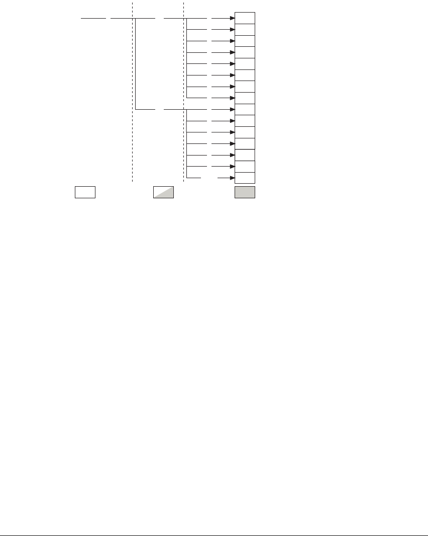
The CPUID Identification Scheme
ARM DDI 0406B Copyright © 1996-1998, 2000, 2004-2008 ARM Limited. All rights reserved. B5-3
Figure B5-1 The CPUID register encodings
B5.1.2 General features of the CPUID registers
All of the CPUID registers are:
• 32-bit read-only registers
• accessible only in privileged modes
• when the Security Extensions are implemented, Common registers, see Common CP15 registers on
page B3-74.
Each register is divided into eight 4-bit fields, and the possible field values are defined individually for each
field. Some registers do not use all of these fields.
CRn opc1 CRm
c0 0 c0
opc2
c2
00c1 ID_PFR0, Processor Feature Register 0
ID_PFR1, Processor Feature Register 1
ID_DFR0, Debug Feature Register 0
ID_AFR0, Auxiliary Feature Register 0
ID_MMFR0, Memory Model Feature Register 0
ID_MMFR1, Memory Model Feature Register 1
ID_MMFR2, Memory Model Feature Register 2
ID_MMFR3, Memory Model Feature Register 3
7
0
1
3
2
4
5
6
Reserved
ID_ISAR0, ISA Feature Register 0
ID_ISAR1, ISA Feature Register 1
ID_ISAR2, ISA Feature Register 2
ID_ISAR3, ISA Feature Register 3
ID_ISAR4, ISA Feature Register 4
ID_ISAR5, ISA Feature Register 5
1
3
2
4
5
{6-7}
Read/WriteRead-only Write-only

The CPUID Identification Scheme
B5-4 Copyright © 1996-1998, 2000, 2004-2008 ARM Limited. All rights reserved. ARM DDI 0406B
B5.2 The CPUID registers
The CPUID registers are described in detail in the following sections:
•CP15 c0, Processor Feature registers
•c0, Debug Feature Register 0 (ID_DFR0) on page B5-6
•c0, Auxiliary Feature Register 0 (ID_AFR0) on page B5-8
•CP15 c0, Memory Model Feature registers on page B5-9
•CP15 c0, Instruction Set Attribute registers on page B5-19.
See also General features of the CPUID registers on page B5-3.
B5.2.1 CP15 c0, Processor Feature registers
The Processor Feature registers, ID_PFR0 and ID_PFR1, provide information about the instruction set state
support and programmers’ model for the processor. There are two Processor Feature registers, described in:
•c0, Processor Feature Register 0 (ID_PFR0)
•c0, Processor Feature Register 1 (ID_PFR1) on page B5-5
•Accessing the Processor Feature registers on page B5-6.
c0, Processor Feature Register 0 (ID_PFR0)
The format of ID_PFR0 is:
Bits [31:16] Reserved, RAZ.
State3, bits [15:12]
ThumbEE instruction set support. Permitted values are:
0b0000 Not supported.
0b0001 ThumbEE instruction set supported.
The value of 0b0001 is only permitted when State1 == 0b0011.
State2, bits [11:8]
Jazelle extension support. Permitted values are:
0b0000 Not supported.
0b0001 Support for Jazelle extension, without clearing of JOSCR.CV on exception
entry.
0b0010 Support for Jazelle extension, with clearing of JOSCR.CV on exception entry.
Reserved, RAZ
31 16 15 12 11 8 7 4 3 0
State3 State2 State1 State0
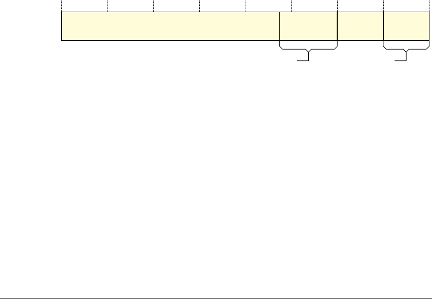
The CPUID Identification Scheme
ARM DDI 0406B Copyright © 1996-1998, 2000, 2004-2008 ARM Limited. All rights reserved. B5-5
State1, bits [7:4]
Thumb instruction set support. Permitted values are:
0b0000 No support for Thumb instruction set.
0b0001 Support for Thumb encoding before the introduction of Thumb-2 technology:
• all instructions are 16-bit
•a
BL
or
BLX
is a pair of 16-bit instructions
• 32-bit instructions other than
BL
and
BLX
cannot be encoded.
0b0010 Reserved.
0b0011 Support for Thumb encoding after the introduction of Thumb-2 technology, and
for all 16-bit and 32-bit Thumb basic instructions.
State0, bits [3:0]
ARM instruction set support. Permitted values are:
0b0000 No support for ARM instruction set.
0b0001 Support for ARM instruction set.
c0, Processor Feature Register 1 (ID_PFR1)
The format of ID_PFR1 is:
Bits [31:12] Reserved, RAZ.
M profile programmers’ model, bits [11:8]
Permitted values are:
0b0000 Not supported.
0b0010 Support for two-stack programmers’ model.
The value of 0b0001 is reserved.
Security Extensions, bits [7:4]
Permitted values are:
0b0000 Not supported.
0b0001 Support for the Security Extensions.
This includes support for Monitor mode and the
SMC
instruction.
0b0010 As for 0b0001, and adds the ability to set the NSACR.RFR bit.
Reserved, RAZ
31 13 12 8 7 4 3 0
Security
Extensions
Programmers’ modelM profile programmers’ model
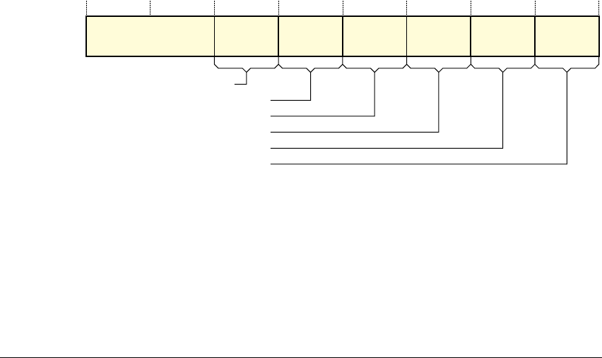
The CPUID Identification Scheme
B5-6 Copyright © 1996-1998, 2000, 2004-2008 ARM Limited. All rights reserved. ARM DDI 0406B
Programmers’ model, bits [3:0]
Support for the standard programmers’ model for ARMv4 and later. Model must support
User, FIQ, IRQ, Supervisor, Abort, Undefined and System modes. Permitted values are:
0b0000 Not supported.
0b0001 Supported.
Accessing the Processor Feature registers
To access the Processor Feature Registers you read the CP15 registers with
<opc1>
set to 0,
<CRn>
set to c0,
<CRm>
set to c1, and
<opc2>
set to:
• 0 for ID_PFR0
• 1 for ID_PFR1.
For example:
MRC p15, 0, <Rt>, c0, c1, 0 ; Read Processor Feature Register 0
B5.2.2 c0, Debug Feature Register 0 (ID_DFR0)
The Debug Feature Register 0, ID_DFR0, provides top level information about the debug system for the
processor. You can obtain more information from the debug infrastructure, see Debug identification
registers on page C10-3.
The format of the ID_DFR0 is:
Bits [31:24] Reserved, RAZ.
Debug model, M profile, bits [23:20]
Support for memory-mapped debug model for M profile processors. Permitted values are:
0b0000 Not supported.
0b0001 Support for M profile Debug architecture, with memory-mapped access.
31 24 23 20 19 16 15 12 11 8 7 4 3 0
Reserved, RAZ
Debug model, M profile
Memory-mapped trace model
Coprocessor trace model
Memory-mapped debug model, A and R profiles
Coprocessor Secure debug model, A profile only
Coprocessor debug model, A and R profiles

The CPUID Identification Scheme
ARM DDI 0406B Copyright © 1996-1998, 2000, 2004-2008 ARM Limited. All rights reserved. B5-7
Memory-mapped trace model, bits [19:16]
Support for memory-mapped trace model. Permitted values are:
0b0000 Not supported.
0b0001 Support for ARM trace architecture, with memory-mapped access.
The ID register, register
0x079
, gives more information about the
implementation. See also Trace on page C1-5.
Coprocessor trace model, bits [15:12]
Support for coprocessor-based trace model. Permitted values are:
0b0000 Not supported.
0b0001 Support for ARM trace architecture, with CP14 access.
The ID register, register
0x079
, gives more information about the
implementation. See also Trace on page C1-5.
Memory-mapped debug model, A and R profiles, bits [11:8]
Support for memory-mapped debug model, for A and R profile processors. Permitted values
are:
0b0000 Not supported, or pre-ARMv6 implementation.
0b0100 Support for v7 Debug architecture, with memory-mapped access.
Values 0b0001, 0b0010, and 0b0011 are reserved.
Coprocessor Secure debug model, bits [7:4]
Support for coprocessor-based Secure debug model, for an A profile processor that includes
the Security Extensions. Permitted values are:
0b0000 Not supported.
0b0011 Support for v6.1 Debug architecture, with CP14 access.
0b0100 Support for v7 Debug architecture, with CP14 access.
Values 0b0001 and 0b0010 are reserved.
Coprocessor debug model, bits [3:0]
Support for coprocessor based debug model, for A and R profile processors. Permitted
values are:
0b0000 Not supported.
0b0010 Support for v6 Debug architecture, with CP14 access.
0b0011 Support for v6.1 Debug architecture, with CP14 access.
0b0100 Support for v7 Debug architecture, with CP14 access.
Value 0b0001 is reserved.

The CPUID Identification Scheme
B5-8 Copyright © 1996-1998, 2000, 2004-2008 ARM Limited. All rights reserved. ARM DDI 0406B
Accessing the ID_DFR0
To access the ID_DFR0 you read the CP15 registers with
<opc1>
set to 0,
<CRn>
set to c0,
<CRm>
set to c1, and
<opc2>
set to 2. For example:
MRC p15, 0, <Rt>, c0, c1, 2 ; Read Debug Feature Register 0
B5.2.3 c0, Auxiliary Feature Register 0 (ID_AFR0)
The Auxiliary Feature Register 0, ID_AFR0, provides information about the IMPLEMENTATION DEFINED
features of the processor.
The format of the ID_AFR0 is:
Bits [31:16] Reserved, RAZ.
IMPLEMENTATION DEFINED, bits [15:12]
IMPLEMENTATION DEFINED, bits [11:8]
IMPLEMENTATION DEFINED, bits [7:4]
IMPLEMENTATION DEFINED, bits [3:0]
The Auxiliary Feature Register 0 has four 4-bit IMPLEMENTATION FIELDS. These fields are defined by the
implementer of the design. The implementer is identified by the Implementer field of the Main ID Register,
see:
•c0, Main ID Register (MIDR) on page B3-81, for a VMSA implementation
•c0, Main ID Register (MIDR) on page B4-32, for a PMSA implementation.
The Auxiliary Feature Register 0 enables implementers to include additional design features in the CPUID
scheme. Field definitions for the Auxiliary Feature Register 0 might:
• differ between different implementers
• be subject to change
• migrate over time, for example if they are incorporated into the main architecture.
Accessing the ID_AFR0
To access the ID_AFR0 you read the CP15 registers with
<opc1>
set to 0,
<CRn>
set to c0,
<CRm>
set to c1, and
<opc2>
set to 3. For example:
MRC p15, 0, <Rt>, c0, c1, 3 ; Read Auxiliary Feature Register 0
Reserved, RAZ
31 16 15 12 11 8 7 4 3 0
IMP IMP IMP IMP

The CPUID Identification Scheme
ARM DDI 0406B Copyright © 1996-1998, 2000, 2004-2008 ARM Limited. All rights reserved. B5-9
B5.2.4 CP15 c0, Memory Model Feature registers
The Memory Model Feature registers, ID_MMF0 to ID_MMFR3, provide general information about the
implemented memory model and memory management support, including the supported cache and TLB
operations. There are four Memory Model Feature registers, described in:
•c0, Memory Model Feature Register 0 (ID_MMFR0)
•c0, Memory Model Feature Register 1 (ID_MMFR1) on page B5-11
•c0, Memory Model Feature Register 2 (ID_MMFR2) on page B5-14
•c0, Memory Model Feature Register 3 (ID_MMFR3) on page B5-17
•Accessing the Memory Model Feature registers on page B5-19.
c0, Memory Model Feature Register 0 (ID_MMFR0)
The format of the ID_MMFR0 is:
Innermost shareability, bits [31:28]
Indicates the innermost shareability domain implemented. Permitted values are:
0b0000 Implemented as Non-cacheable.
0b0001 Implemented with hardware coherency support.
0b1111 Shareability ignored.
This field is valid only if more than one level of shareability is implemented, as indicated by
the value of the Shareability levels field, bits [15:12].
When the Shareability level field is zero, this field is UNK.
FCSE support, bits [27:24]
Indicates whether the implementation includes the FCSE. Permitted values are:
0b0000 Not supported.
0b0001 Support for FCSE.
The value of 0b0001 is only permitted when the VMSA_support field has a value greater
than 0b0010.
Auxiliary registers, bits [23:20]
Indicates support for Auxiliary registers. Permitted values are:
0b0000 None supported.
0b0001 Support for Auxiliary Control Register only.
0b0010 Support for Auxiliary Fault Status Registers (AIFSR and ADFSR) and
Auxiliary Control Register.
Innermost
shareability
FCSE
support
Auxiliary
registers
TCM
support
31 16 15 12 11 8 7 4 3 0
Shareability
levels
Outermost
shareability
PMSA
support
VMSA
support
28 27 24 23 20 19

The CPUID Identification Scheme
B5-10 Copyright © 1996-1998, 2000, 2004-2008 ARM Limited. All rights reserved. ARM DDI 0406B
TCM support, bits [19:16]
Indicates support for TCMs and associated DMAs. Permitted values are:
0b0000 Not supported.
0b0001 Support is IMPLEMENTATION DEFINED. ARMv7 requires this setting.
0b0010 Support for TCM only, ARMv6 implementation.
0b0011 Support for TCM and DMA, ARMv6 implementation.
Note
An ARMv7 implementation might include an ARMv6 model for TCM support. However,
in ARMv7 this is an IMPLEMENTATION DEFINED option, and therefore it must be represented
by the 0b0001 encoding in this field.
Shareability levels, bits [15:12]
Indicates the number of shareability levels implemented. Permitted values are:
0b0000 One level of shareability implemented.
0b0001 Two levels of shareability implemented.
Outermost shareability, bits [11:8]
Indicates the outermost shareability domain implemented. Permitted values are:
0b0000 Implemented as Non-cacheable.
0b0001 Implemented with hardware coherency support.
0b1111 Shareability ignored.
PMSA support, bits [7:4]
Indicates support for a PMSA. Permitted values are:
0b0000 Not supported.
0b0001 Support for IMPLEMENTATION DEFINED PMSA.
0b0010 Support for PMSAv6, with a Cache Type Register implemented.
0b0011 Support for PMSAv7, with support for memory subsections. ARMv7-R profile.
When the PMSA support field is set to a value other than 0b0000 the VMSA support field
must be set to 0b0000.
VMSA support, bits [3:0]
Indicates support for a VMSA. Permitted values are:
0b0000 Not supported.
0b0001 Support for IMPLEMENTATION DEFINED VMSA.
0b0010 Support for VMSAv6, with Cache and TLB Type Registers implemented.
0b0011 Support for VMSAv7, with support for remapping and the access flag.
ARMv7-A profile.
When the VMSA support field is set to a value other than 0b0000 the PMSA support field
must be set to 0b0000.

The CPUID Identification Scheme
ARM DDI 0406B Copyright © 1996-1998, 2000, 2004-2008 ARM Limited. All rights reserved. B5-11
c0, Memory Model Feature Register 1 (ID_MMFR1)
The format of the ID_MMFR1 is:
Branch predictor, bits [31:28]
Indicates branch predictor management requirements. Permitted values are:
0b0000 No branch predictor, or no MMU present. Implies a fixed MPU configuration.
0b0001 Branch predictor requires flushing on:
• enabling or disabling the MMU
• writing new data to instruction locations
• writing new mappings to the translation tables
• any change to the TTBR0, TTBR1, or TTBCR registers
• changes of FCSE ProcessID or ContextID.
0b0010 Branch predictor requires flushing on:
• enabling or disabling the MMU
• writing new data to instruction locations
• writing new mappings to the translation tables
• any change to the TTBR0, TTBR1, or TTBCR registers without a
corresponding change to the FCSE ProcessID or ContextID.
0b0011 Branch predictor requires flushing only on:
• writing new data to instruction locations.
0b0100 For execution correctness, branch predictor requires no flushing at any time.
Note
The branch predictor is described in some documentation as the Branch Target Buffer.
L1 cache Test and Clean, bits [27:24]
Indicates the supported Level 1 data cache test and clean operations, for Harvard or unified
cache implementations. Permitted values are:
0b0000 None supported. This is the required setting for ARMv7.
0b0001 Supported Level 1 data cache test and clean operations are:
• Test and clean data cache.
0b0010 As for 0b0001, and adds:
• Test, clean, and invalidate data cache.
L1 cache
Test and
Clean
L1 Harvard
cache VA
31 24 23 20 19 16 15 12 11 8 7 4 3 0
Branch
Predictor
L1 unified
cache
L1 Harvard
cache
L1 unified
cache s/w
L1 Harvard
cache s/w
L1 unified
cache VA
28 27

The CPUID Identification Scheme
B5-12 Copyright © 1996-1998, 2000, 2004-2008 ARM Limited. All rights reserved. ARM DDI 0406B
L1 unified cache, bits [23:20]
Indicates the supported entire Level 1 cache maintenance operations, for a unified cache
implementation. Permitted values are:
0b0000 None supported. This is the required setting for ARMv7, because ARMv7
requires a hierarchical cache implementation.
0b0001 Supported entire Level 1 cache operations are:
• Invalidate cache, including branch predictor if appropriate
• Invalidate branch predictor, if appropriate.
0b0010 As for 0b0001, and adds:
• Clean cache. Uses a recursive model, using the cache dirty status bit.
• Clean and invalidate cache. Uses a recursive model, using the cache dirty
status bit.
If this field is set to a value other than 0b0000 then the L1 Harvard cache field, bits [19:16],
must be set to 0b0000.
L1 Harvard cache, bits [19:16]
Indicates the supported entire Level 1 cache maintenance operations, for a Harvard cache
implementation. Permitted values are:
0b0000 None supported. This is the required setting for ARMv7, because ARMv7
requires a hierarchical cache implementation.
0b0001 Supported entire Level 1 cache operations are:
• Invalidate instruction cache, including branch predictor if appropriate
• Invalidate branch predictor, if appropriate.
0b0010 As for 0b0001, and adds:
• Invalidate data cache
• Invalidate data cache and instruction cache, including branch predictor if
appropriate.
0b0011 As for 0b0010, and adds:
• Clean data cache. Uses a recursive model, using the cache dirty status bit.
• Clean and invalidate data cache. Uses a recursive model, using the cache
dirty status bit.
If this field is set to a value other than 0b0000 then the L1 unified cache field, bits [23:20],
must be set to 0b0000.
L1 unified cache s/w, bits [15:12]
Indicates the supported Level 1 cache line maintenance operations by set/way, for a unified
cache implementation. Permitted values are:
0b0000 None supported. This is the required setting for ARMv7, because ARMv7
requires a hierarchical cache implementation.
0b0001 Supported Level 1 unified cache line maintenance operations by set/way are:
• Clean cache line by set/way.

The CPUID Identification Scheme
ARM DDI 0406B Copyright © 1996-1998, 2000, 2004-2008 ARM Limited. All rights reserved. B5-13
0b0010 As for 0b0001, and adds:
• Clean and invalidate cache line by set/way.
0b0011 As for 0b0010, and adds:
• Invalidate cache line by set/way.
If this field is set to a value other than 0b0000 then the L1 Harvard cache s/w field,
bits [11:8], must be set to 0b0000.
L1 Harvard cache s/w, bits [11:8]
Indicates the supported Level 1 cache line maintenance operations by set/way, for a Harvard
cache implementation. Permitted values are:
0b0000 None supported. This is the required setting for ARMv7, because ARMv7
requires a hierarchical cache implementation.
0b0001 Supported Level 1 Harvard cache line maintenance operations by set/way are:
• Clean data cache line by set/way
• Clean and invalidate data cache line by set/way.
0b0010 As for 0b0001, and adds:
• Invalidate data cache line by set/way.
0b0011 As for 0b0010, and adds:
• Invalidate instruction cache line by set/way.
If this field is set to a value other than 0b0000 then the L1 unified cache s/w field,
bits [15:12], must be set to 0b0000.
L1 unified cache VA, bits [7:4]
Indicates the supported Level 1 cache line maintenance operations by MVA, for a unified
cache implementation. Permitted values are:
0b0000 None supported. This is the required setting for ARMv7, because ARMv7
requires a hierarchical cache implementation.
0b0001 Supported Level 1 unified cache line maintenance operations by MVA are:
• Clean cache line by MVA
• Invalidate cache line by MVA
• Clean and invalidate cache line by MVA.
0b0010 As for 0b0001, and adds:
• Invalidate branch predictor by MVA, if branch predictor is implemented.
If this field is set to a value other than 0b0000 then the L1 Harvard cache VA field, bits [3:0],
must be set to 0b0000.
L1 Harvard cache VA, bits [3:0]
Indicates the supported Level 1 cache line maintenance operations by MVA, for a Harvard
cache implementation. Permitted values are:
0b0000 None supported. This is the required setting for ARMv7, because ARMv7
requires a hierarchical cache implementation.

The CPUID Identification Scheme
B5-14 Copyright © 1996-1998, 2000, 2004-2008 ARM Limited. All rights reserved. ARM DDI 0406B
0b0001 Supported Level 1 Harvard cache line maintenance operations by MVA are:
• Clean data cache line by MVA
• Invalidate data cache line by MVA
• Clean and invalidate data cache line by MVA
• Clean instruction cache line by MVA.
0b0010 As for 0b0001, and adds:
• Invalidate branch predictor by MVA, if branch predictor is implemented.
If this field is set to a value other than 0b0000 then the L1 unified cache VA field, bits [7:4],
must be set to 0b0000.
c0, Memory Model Feature Register 2 (ID_MMFR2)
The format of the ID_MMFR2 is:
HW access flag, bits [31:28]
Indicates support for a Hardware access flag, as part of the VMSAv7 implementation.
Permitted values are:
0b0000 Not supported.
0b0001 Support for VMSAv7 access flag, updated in hardware.
On an ARMv7-R implementation this field must be 0b0000.
WFI stall, bits [27:24]
Indicates the support for Wait For Interrupt (WFI) stalling. Permitted values are:
0b0000 Not supported.
0b0001 Support for WFI stalling.
Mem barrier, bits [23:20]
Indicates the supported CP15 memory barrier operations:
0b0000 None supported.
0b0001 Supported CP15 Memory barrier operations are:
• Data Synchronization Barrier (DSB). In previous versions of the ARM
architecture, DSB was named Data Write Barrier (DWB).
0b0010 As for 0b0001, and adds:
• Instruction Synchronization Barrier (ISB). In previous versions of the
ARM architecture, the ISB operation was called Prefetch Flush.
• Data Memory Barrier (DMB).
HW
access flag
WFI
stall
Mem
barrier
Unified
TLB
31 16 15 12 11 8 7 4 3 0
Harvard
TLB
L1 Harvard
range
L1 Harvard
bg prefetch
L1 Harvard
fg prefetch
28 27 24 23 20 19

The CPUID Identification Scheme
ARM DDI 0406B Copyright © 1996-1998, 2000, 2004-2008 ARM Limited. All rights reserved. B5-15
Unified TLB, bits [19:16]
Indicates the supported TLB maintenance operations, for a unified TLB implementation.
Permitted values are:
0b0000 Not supported.
0b0001 Supported unified TLB maintenance operations are:
• Invalidate all entries in the TLB
• Invalidate TLB entry by MVA.
0b0010 As for 0b0001, and adds:
• Invalidate TLB entries by ASID match.
0b0011 As for 0b0010 and adds:
• Invalidate TLB entries by MVA All ASID.
If this field is set to a value other than 0b0000 then the Harvard TLB field, bits [15:12], must
be set to 0b0000.
Harvard TLB, bits [15:12]
Indicates the supported TLB maintenance operations, for a Harvard TLB implementation.
Permitted values are:
0b0000 Not supported.
0b0001 Supported Harvard TLB maintenance operations are:
• Invalidate all entries in the ITLB and the DTLB.
This is a shared unified TLB operation.
• Invalidate all ITLB entries.
• Invalidate all DTLB entries.
• Invalidate ITLB entry by MVA.
• Invalidate DTLB entry by MVA.
0b0010 As for 0b0001, and adds:
• Invalidate ITLB and DTLB entries by ASID match.
This is a shared unified TLB operation.
• Invalidate ITLB entries by ASID match
• Invalidate DTLB entries by ASID match.
If this field is set to a value other than 0b0000 then the Unified TLB field, bits [19:16], must
be set to 0b0000.

The CPUID Identification Scheme
B5-16 Copyright © 1996-1998, 2000, 2004-2008 ARM Limited. All rights reserved. ARM DDI 0406B
L1 Harvard range, bits [11:8]
Indicates the supported Level 1 cache maintenance range operations, for a Harvard cache
implementation. Permitted values are:
0b0000 Not supported.
0b0001 Supported Level 1 Harvard cache maintenance range operations are:
• Invalidate data cache range by VA
• Invalidate instruction cache range by VA
• Clean data cache range by VA
• Clean and invalidate data cache range by VA.
L1 Harvard bg prefetch, bits [7:4]
Indicates the supported Level 1 cache background prefetch operations, for a Harvard cache
implementation. When supported, background prefetch operations are non-blocking
operations. Permitted values are:
0b0000 Not supported.
0b0001 Supported Level 1 Harvard cache foreground prefetch operations are:
• Prefetch instruction cache range by VA
• Prefetch data cache range by VA.
L1 Harvard fg prefetch, bits [3:0]
Indicates the supported Level 1 cache foreground prefetch operations, for a Harvard cache
implementation. When supported, foreground prefetch operations are blocking operations.
Permitted values are:
0b0000 Not supported.
0b0001 Supported Level 1 Harvard cache foreground prefetch operations are:
• Prefetch instruction cache range by VA
• Prefetch data cache range by VA.
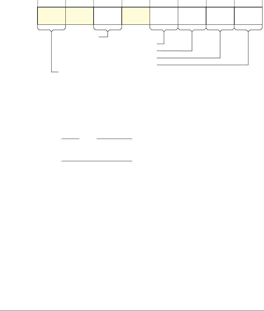
The CPUID Identification Scheme
ARM DDI 0406B Copyright © 1996-1998, 2000, 2004-2008 ARM Limited. All rights reserved. B5-17
c0, Memory Model Feature Register 3 (ID_MMFR3)
The format of the ID_MMFR3 is:
Supersection support, bits [31:28]
On a VMSA implementation, indicates whether Supersections are supported. Permitted
values are:
0b0000 Supersections supported.
0b1111 Supersections not supported.
All other values are reserved.
Note
The sense of this identification is reversed from the normal usage in the CPUID mechanism,
with the value of zero indicating that the feature is supported.
Bits [27:24] Reserved, RAZ.
Coherent walk, bits [23:20]
Indicates whether Translation table updates require a clean to the point of unification.
Permitted values are:
0b0000 Updates to the translation tables require a clean to the point of unification to
ensure visibility by subsequent translation table walks.
0b0001 Updates to the translation tables do not require a clean to the point of unification
to ensure visibility by subsequent translation table walks.
Bits [19:16] Reserved, RAZ.
Maintenance broadcast, bits [15:12]
Indicates whether Cache, TLB and branch predictor operations are broadcast. Permitted
values are:
0b0000 Cache, TLB and branch predictor operations only affect local structures.
0b0001 Cache and branch predictor operations affect structures according to
shareability and defined behavior of instructions. TLB operations only affect
local structures.
31 28 27 16 15 12 11 8 7 4 3 0
Reserved,
RAZ
Supersection support
BP maintain
Cache maintainence s/w
Cache maintainence MVA
Maintenance broadcast
1920
Reserved,
RAZ
2324
Coherent walk

The CPUID Identification Scheme
B5-18 Copyright © 1996-1998, 2000, 2004-2008 ARM Limited. All rights reserved. ARM DDI 0406B
0b0010 Cache, TLB and branch predictor operations affect structures according to
shareability an defined behavior of instructions.
BP maintain, bits [11:8]
Indicates the supported branch predictor maintenance operations in an implementation with
hierarchical cache maintenance operations. Permitted values are:
0b0000 None supported.
0b0001 Supported branch predictor maintenance operations are:
• Invalidate entire branch predictor array
0b0010 As for 0b0001, and adds:
• Invalidate branch predictor by MVA.
Cache maintain s/w, bits [7:4]
Indicates the supported cache maintenance operations by set/way, in an implementation
with hierarchical caches. Permitted values are:
0b0000 None supported.
0b0001 Supported hierarchical cache maintenance operations by set/way are:
• Invalidate data cache by set/way
• Clean data cache by set/way
• Clean and invalidate data cache by set/way.
In a unified cache implementation, the data cache operations apply to the unified caches.
Cache maintain MVA, bits [3:0]
Indicates the supported cache maintenance operations by MVA, in an implementation with
hierarchical caches. Permitted values are:
0b0000 None supported.
0b0001 Supported hierarchical cache maintenance operations by MVA are:
• Invalidate data cache by MVA
• Clean data cache by MVA
• Clean and invalidate data cache by MVA
• Invalidate instruction cache by MVA
• Invalidate all instruction cache entries.
In a unified cache implementation, the data cache operations apply to the unified caches, and
the instruction cache operations are not implemented.

The CPUID Identification Scheme
ARM DDI 0406B Copyright © 1996-1998, 2000, 2004-2008 ARM Limited. All rights reserved. B5-19
Accessing the Memory Model Feature registers
To access the Memory Model Feature Registers you read the CP15 registers with
<opc1>
set to 0,
<CRn>
set
to c0,
<CRm>
set to c1, and
<opc2>
set to:
• 4 for the ID_MMFR0
• 5 for the ID_MMFR1
• 6 for the ID_MMFR2
• 7 for the ID_MMFR3.
For example:
MRC p15, 0, <Rt>, c0, c1, 6 ; Read Memory Model Feature Register 2
B5.2.5 CP15 c0, Instruction Set Attribute registers
The Instruction Set Attribute registers, ID_ISAR0 to ID_ISAR5, provide information about the instruction
set supported by the processor. The instruction set is divided into:
• The basic instructions, for the ARM, Thumb, and ThumbEE instruction sets. If the Processor Feature
Register 0 indicates support for one of these instruction sets then all basic instructions that have
encodings in the corresponding instruction set must be implemented.
• The non-basic instructions. The Instruction Set Attribute registers indicate which of these instructions
are implemented.
Instruction set descriptions in the CPUID scheme on page B5-20 describes the division of the instruction
set into basic and non-basic instructions.
Summary of Instruction Set Attribute register attributes on page B5-22 lists all of the attributes and shows
which register holds each attribute.
ARMv7 implements six Instruction Set Attribute registers, described in:
•c0, Instruction Set Attribute Register 0 (ID_ISAR0) on page B5-24
•c0, Instruction Set Attribute Register 1 (ID_ISAR1) on page B5-25
•c0, Instruction Set Attribute Register 2 (ID_ISAR2) on page B5-27
•c0, Instruction Set Attribute Register 3 (ID_ISAR3) on page B5-29
•c0, Instruction Set Attribute Register 4 (ID_ISAR4) on page B5-31
•c0, Instruction Set Attribute Register 5 (ID_ISAR5) on page B5-33
•Accessing the Instruction Set Attribute registers on page B5-33.

The CPUID Identification Scheme
B5-20 Copyright © 1996-1998, 2000, 2004-2008 ARM Limited. All rights reserved. ARM DDI 0406B
Instruction set descriptions in the CPUID scheme
The following subsections describe how the CPUID scheme describes the instruction set, and how
instructions are classified as either basic or non-basic:
•General rules for instruction classification
•Data-processing instructions
•Multiply instructions on page B5-21
•Branches on page B5-21
•Load or Store single word instructions on page B5-21
•Load or Store multiple word instructions on page B5-21
•Q flag support in the PSRs on page B5-21.
General rules for instruction classification
Two general rules apply to the description of instruction classification given in this section:
1. The rules about an instruction being basic do not guarantee that it is available in any particular
instruction set. For example, the rules given in this section classify
MOV R0, #123456789
as a basic
instruction, but this instruction is not available in any existing ARM instruction set.
2. Whether an instruction is conditional or unconditional never makes any difference to whether it is a
basic instruction.
Data-processing instructions
The data-processing instructions are:
ADC ADD AND ASR BIC CMN CMP EOR LSL LSR MOV MVN
NEG ORN ORR ROR RRX RSB RSC SBC SUB TEQ TST
An instruction from this group is a basic instruction if these conditions both apply:
• The second source operand, or the only source operand of a
MOV
or
MVN
instruction, is an immediate
or an unshifted register.
Note
A
MOV
instruction with a shifted register source operand must be treated as the equivalent
ASR
,
LSL
,
LSR
,
ROR
, or
RRX
instruction, see MOV (shifted register) on page A8-198.
• The instruction is not one of the exception return instructions described in SUBS PC, LR and related
instructions on page B6-25.
If either of these conditions does not apply then the instruction is a non-basic instruction. One or both of
these attributes in the Instruction Set Attribute registers shows the support for non-basic data-processing
instructions:
• PSR_instrs
• WithShifts_instrs.

The CPUID Identification Scheme
ARM DDI 0406B Copyright © 1996-1998, 2000, 2004-2008 ARM Limited. All rights reserved. B5-21
Multiply instructions
The classification of multiply instructions is:
•
MUL
instructions are always basic instructions
• all other multiply instructions, and all multiply-accumulate instructions, are non-basic instructions.
Branches
All
B
and
BL
instructions are basic instructions.
Load or Store single word instructions
The instructions in this group are:
LDR LDRB LDRH LDRSB LDRSH STR STRB STRH
An instruction in this group is a basic instruction if its addressing mode is one of these forms:
•
[Rn, #immediate]
•
[Rn, #-immediate]
•
[Rn, Rm]
•
[Rn, -Rm]
.
A Load or Store single word instruction with any other addressing mode is a non-basic instruction. One or
more of these attributes in the Instruction Set Attribute registers shows the support for these instructions:
• WithShifts_instrs
• Writeback_instrs
• Unpriv_instrs.
Load or Store multiple word instructions
The Load or Store multiple word instructions are:
LDM<mode> STM<mode> PUSH POP
A limited number of variants of these instructions are non-basic. The Except_instrs attribute in the
Instruction Set Attribute registers shows the support for these instructions. For details of these non-basic
instructions see c0, Instruction Set Attribute Register 1 (ID_ISAR1) on page B5-25.
All other forms of these instructions are always basic instructions.
Q flag support in the PSRs
The Q flag is present in the CPSR and SPSRs when one or more of these conditions apply to the Instruction
Set Attribute register attributes:
• MultS_instrs ≥2
• Saturate_instrs ≥1
• SIMD_instrs ≥1.

The CPUID Identification Scheme
B5-22 Copyright © 1996-1998, 2000, 2004-2008 ARM Limited. All rights reserved. ARM DDI 0406B
Summary of Instruction Set Attribute register attributes
The Instruction Set Attribute registers use a set of attributes to indicate the non-basic instructions supported
by the processor. The descriptions of the non-basic instructions in Instruction set descriptions in the CPUID
scheme on page B5-20 include the attribute or attributes used to indicate support for each category of
non-basic instructions. Table B5-1 lists all of these attributes in alphabetical order, and shows which
Instruction Set Attribute register holds each attribute.
Table B5-1 Alphabetic list of Instruction Set Attribute registers attributes
Attribute Register
Barrier_instrs c0, Instruction Set Attribute Register 4 (ID_ISAR4) on page B5-31
BitCount_instrs c0, Instruction Set Attribute Register 0 (ID_ISAR0) on page B5-24
Bitfield_instrs c0, Instruction Set Attribute Register 0 (ID_ISAR0) on page B5-24
CmpBranch_instrs c0, Instruction Set Attribute Register 0 (ID_ISAR0) on page B5-24
Coproc_instrs c0, Instruction Set Attribute Register 0 (ID_ISAR0) on page B5-24
Debug_instrs c0, Instruction Set Attribute Register 0 (ID_ISAR0) on page B5-24
Divide_instrs c0, Instruction Set Attribute Register 0 (ID_ISAR0) on page B5-24
Endian_instrs c0, Instruction Set Attribute Register 1 (ID_ISAR1) on page B5-25
Except_AR_instrs c0, Instruction Set Attribute Register 1 (ID_ISAR1) on page B5-25
Except_instrs c0, Instruction Set Attribute Register 1 (ID_ISAR1) on page B5-25
Extend_instrs c0, Instruction Set Attribute Register 1 (ID_ISAR1) on page B5-25
IfThen_instrs c0, Instruction Set Attribute Register 1 (ID_ISAR1) on page B5-25
Immediate_instrs c0, Instruction Set Attribute Register 1 (ID_ISAR1) on page B5-25
Interwork_instrs c0, Instruction Set Attribute Register 1 (ID_ISAR1) on page B5-25
Jazelle_instrs c0, Instruction Set Attribute Register 1 (ID_ISAR1) on page B5-25
LoadStore_instrs c0, Instruction Set Attribute Register 2 (ID_ISAR2) on page B5-27
MemHint_instrs c0, Instruction Set Attribute Register 2 (ID_ISAR2) on page B5-27
Mult_instrs c0, Instruction Set Attribute Register 2 (ID_ISAR2) on page B5-27
MultiAccessInt_instrs c0, Instruction Set Attribute Register 2 (ID_ISAR2) on page B5-27
MultS_instrs c0, Instruction Set Attribute Register 2 (ID_ISAR2) on page B5-27
MultU_instrs c0, Instruction Set Attribute Register 2 (ID_ISAR2) on page B5-27

The CPUID Identification Scheme
ARM DDI 0406B Copyright © 1996-1998, 2000, 2004-2008 ARM Limited. All rights reserved. B5-23
PSR_AR_instrs c0, Instruction Set Attribute Register 2 (ID_ISAR2) on page B5-27
PSR_M_instrs c0, Instruction Set Attribute Register 4 (ID_ISAR4) on page B5-31
Reversal_instrs c0, Instruction Set Attribute Register 2 (ID_ISAR2) on page B5-27
Saturate_instrs c0, Instruction Set Attribute Register 3 (ID_ISAR3) on page B5-29
SIMD_instrs c0, Instruction Set Attribute Register 3 (ID_ISAR3) on page B5-29
SMC_instrs c0, Instruction Set Attribute Register 4 (ID_ISAR4) on page B5-31
SVC_instrs c0, Instruction Set Attribute Register 3 (ID_ISAR3) on page B5-29
Swap_instrs c0, Instruction Set Attribute Register 0 (ID_ISAR0) on page B5-24
SynchPrim_instrs c0, Instruction Set Attribute Register 3 (ID_ISAR3) on page B5-29
SynchPrim_instrs_frac c0, Instruction Set Attribute Register 4 (ID_ISAR4) on page B5-31
TabBranch_instrs c0, Instruction Set Attribute Register 3 (ID_ISAR3) on page B5-29
ThumbCopy_instrs c0, Instruction Set Attribute Register 3 (ID_ISAR3) on page B5-29
ThumbEE_extn_instrs c0, Instruction Set Attribute Register 3 (ID_ISAR3) on page B5-29
TrueNOP_instrs c0, Instruction Set Attribute Register 3 (ID_ISAR3) on page B5-29
Unpriv_instrs c0, Instruction Set Attribute Register 4 (ID_ISAR4) on page B5-31
WithShifts_instrs c0, Instruction Set Attribute Register 4 (ID_ISAR4) on page B5-31
Writeback_instrs c0, Instruction Set Attribute Register 4 (ID_ISAR4) on page B5-31
Table B5-1 Alphabetic list of Instruction Set Attribute registers attributes (continued)
Attribute Register

The CPUID Identification Scheme
B5-24 Copyright © 1996-1998, 2000, 2004-2008 ARM Limited. All rights reserved. ARM DDI 0406B
c0, Instruction Set Attribute Register 0 (ID_ISAR0)
The format of the ID_ISAR0 is:
Bits [31:28] Reserved, RAZ.
Divide_instrs, bits [27:24]
Indicates the supported Divide instructions. Permitted values are:
0b0000 . None supported.
0b0001 . Adds support for
SDIV
and
UDIV
.
Debug_instrs, bits [23:20]
Indicates the supported Debug instructions. Permitted values are:
0b0000 None supported.
0b0001 Adds support for
BKPT
.
Coproc_instrs, bits [19:16]
Indicates the supported Coprocessor instructions. Permitted values are:
0b0000 None supported, except for separately attributed architectures including CP15,
CP14, and Advanced SIMD and VFP.
0b0001 Adds support for generic
CDP
,
LDC
,
MCR
,
MRC
, and
STC
.
0b0010 As for 0b0001, and adds generic
CDP2
,
LDC2
,
MCR2
,
MRC2
, and
STC2
.
0b0011 As for 0b0010, and adds generic
MCRR
and
MRRC
.
0b0100 As for 0b0011, and adds generic
MCRR2
and
MRRC2
.
CmpBranch_instrs, bits [15:12]
Indicates the supported combined Compare and Branch instructions in the Thumb
instruction set. Permitted values are:
0b0000 None supported.
0b0001 Adds support for
CBNZ
and
CBZ
.
Bitfield_instrs, bits [11:8]
Indicates the supported BitField instructions. Permitted values are:
0b0000 None supported.
0b0001 Adds support for
BFC
,
BFI
,
SBFX
, and
UBFX
.
BitCount_instrs, bits [7:4]
Indicates the supported Bit Counting instructions. Permitted values are:
0b0000 None supported.
0b0001 Adds support for
CLZ
.
Reserved,
RAZ
Divide
_instrs
Debug
_instrs
Coproc
_instrs
31 16 15 12 11 8 7 4 3 0
CmpBranch
_instrs
Bitfield
_instrs
BitCount
_instrs
Swap
_instrs
28 27 24 23 20 19

The CPUID Identification Scheme
ARM DDI 0406B Copyright © 1996-1998, 2000, 2004-2008 ARM Limited. All rights reserved. B5-25
Swap_instrs, bits [3:0]
Indicates the supported Swap instructions in the ARM instruction set. Permitted values are:
0b0000 None supported.
0b0001 Adds support for
SWP
and
SWPB
.
c0, Instruction Set Attribute Register 1 (ID_ISAR1)
The format of the IID_ISAR1 is:
Jazelle_instrs, bits [31:28]
Indicates the supported Jazelle extension instructions. Permitted values are:
0b0000 No support for Jazelle.
0b0001 Adds support for
BXJ
instruction, and the J bit in the PSR.
This setting might indicate a trivial implementation of Jazelle support.
Interwork_instrs, bits [27:24]
Indicates the supported Interworking instructions. Permitted values are:
0b0000 None supported.
0b0001 Adds support for
BX
instruction, and the T bit in the PSR.
0b0010 As for 0b0001, and adds support for
BLX
instruction. PC loads have
BX
-like
behavior.
0b0011 As for 0b0010, but guarantees that data-processing instructions in the ARM
instruction set with the PC as the destination and the S bit clear have
BX
-like
behavior.
Note
A value of 0b0000, 0b0001, or 0b0010 in this field does not guarantee that an ARM
data-processing instruction with the PC as the destination and the S bit clear behaves like an
old
MOV PC
instruction, ignoring bits [1:0] of the result. With these values of this field:
• if bits [1:0] of the result value are 0b00 then the processor remains in ARM state
• if bits [1:0] are 0b01, 0b10 or 0b11, the result must be treated as UNPREDICTABLE.
Immediate_instrs, bits [23:20]
Indicates the support for data-processing instructions with long immediates. Permitted
values are:
0b0000 None supported.
Jazelle
_instrs
Interwork
_instrs
Immediate
_instrs
IfThen
_instrs
31 16 15 12 11 8 7 4 3 0
Extend
_instrs
Except_AR
_instrs
Except
_instrs
Endian
_instrs
28 27 24 23 20 19

The CPUID Identification Scheme
B5-26 Copyright © 1996-1998, 2000, 2004-2008 ARM Limited. All rights reserved. ARM DDI 0406B
0b0001 Adds support for:
• the
MOVT
instruction
• the
MOV
instruction encodings with zero-extended 16-bit immediates
• the Thumb
ADD
and
SUB
instruction encodings with zero-extended 12-bit
immediates, and the other
ADD
,
ADR
and
SUB
encodings cross-referenced by
the pseudocode for those encodings.
IfThen_instrs, bits [19:16]
Indicates the supported IfThen instructions in the Thumb instruction set. Permitted values
are:
0b0000 None supported.
0b0001 Adds support for the
IT
instructions, and for the IT bits in the PSRs.
Extend_instrs, bits [15:12]
Indicates the supported Extend instructions. Permitted values are:
0b0000 No scalar sign-extend or zero-extend instructions are supported, where scalar
instructions means non-Advanced SIMD instructions.
0b0001 Adds support for the
SXTB
,
SXTH
,
UXTB
, and
UXTH
instructions.
0b0010 As for 0b0001, and adds support for the
SXTB16
,
SXTAB
,
SXTAB16
,
SXTAH
,
UXTB16
,
UXTAB
,
UXTAB16
, and
UXTAH
instructions.
Note
In addition:
• the shift options on these instructions are available only if the WithShifts_instrs
attribute is 0b0011 or greater
• the
SXTAB16
,
SXTB16
,
UXTAB16
, and
UXTB16
instructions are available only if both:
— the Extend_instrs attribute is 0b0010 or greater
— the SIMD_instrs attribute is 0b0011 or greater.
Except_AR_instrs, bits [11:8]
Indicates the supported A and R profile exception-handling instructions. Permitted values
are:
0b0000 None supported.
0b0001 Adds support for the
SRS
and
RFE
instructions, and the A and R profile forms of
the
CPS
instruction.
Except_instrs, bits [7:4]
Indicates the supported exception-handling instructions in the ARM instruction set.
Permitted values are:
0b0000 Not supported. This indicates that the User bank and Exception return forms of
the LDM and STM instructions are not supported.
0b0001 Adds support for the
LDM
(exception return),
LDM
(user registers) and
STM
(user
registers) instruction versions.

The CPUID Identification Scheme
ARM DDI 0406B Copyright © 1996-1998, 2000, 2004-2008 ARM Limited. All rights reserved. B5-27
Endian_instrs, bits [3:0]
Indicates the supported Endian instructions. Permitted values are:
0b0000 None supported.
0b0001 Adds support for the
SETEND
instruction, and the E bit in the PSRs.
c0, Instruction Set Attribute Register 2 (ID_ISAR2)
The format of the ID_ISAR2 is:
Reversal_instrs, bits [31:28]
Indicates the supported Reversal instructions. Permitted values are:
0b0000 None supported.
0b0001 Adds support for the
REV
,
REV16
, and
REVSH
instructions.
0b0010 As for 0b0001, and adds support for the
RBIT
instruction.
PSR_AR_instrs, bits [27:24]
Indicates the supported A and R profile instructions to manipulate the PSR. Permitted values
are:
0b0000 None supported.
0b0001 Adds support for the
MRS
and
MSR
instructions, and the exception return forms of
data-processing instructions described in SUBS PC, LR and related instructions
on page B6-25.
Note
The exception return forms of the data-processing instructions are:
• In the ARM instruction set, data-processing instructions with the PC as the
destination and the S bit set. These instructions might be affected by the WithShifts
attribute.
• In the Thumb instruction set, the
SUBS PC,LR,#N
instruction.
MultU_instrs, bits [23:20]
Indicates the supported advanced unsigned Multiply instructions. Permitted values are:
0b0000 None supported.
0b0001 Adds support for the
UMULL
and
UMLAL
instructions.
0b0010 As for 0b0001, and adds support for the
UMAAL
instruction.
Reversal
_instrs
PSR_AR
_instrs
MultU
_instrs
MultS
_instrs
31 16 15 12 11 8 7 4 3 0
Mult
_instrs
MultiAccess
Int_instrs
MemHint
_instrs
LoadStore
_instrs
28 27 24 23 20 19

The CPUID Identification Scheme
B5-28 Copyright © 1996-1998, 2000, 2004-2008 ARM Limited. All rights reserved. ARM DDI 0406B
MultS_instrs, bits [19:16]
Indicates the supported advanced signed Multiply instructions. Permitted values are:
0b0000 None supported.
0b0001 Adds support for the
SMULL
and
SMLAL
instructions.
0b0010 As for 0b0001, and adds support for the
SMLABB
,
SMLABT
,
SMLALBB
,
SMLALBT
,
SMLALTB
,
SMLALTT
,
SMLATB
,
SMLATT
,
SMLAWB
,
SMLAWT
,
SMULBB
,
SMULBT
,
SMULTB
,
SMULTT
,
SMULWB
, and
SMULWT
instructions.
Also adds support for the Q bit in the PSRs.
0b0011 As for 0b0010, and adds support for the
SMLAD
,
SMLADX
,
SMLALD
,
SMLALDX
,
SMLSD
,
SMLSDX
,
SMLSLD
,
SMLSLDX
,
SMMLA
,
SMMLAR
,
SMMLS
,
SMMLSR
,
SMMUL
,
SMMULR
,
SMUAD
,
SMUADX
,
SMUSD
, and
SMUSDX
instructions.
Mult_instrs, bits [15:12]
Indicates the supported additional Multiply instructions. Permitted values are:
0b0000 No additional instructions supported. This means only
MUL
is supported.
0b0001 Adds support for the
MLA
instruction.
0b0010 As for 0b0001, and adds support for the
MLS
instruction.
MultiAccessInt_instrs, bits [11:8]
Indicates the support for multi-access interruptible instructions. Permitted values are:
0b0000 None supported. This means the
LDM
and
STM
instructions are not interruptible.
0b0001
LDM
and
STM
instructions are restartable.
0b0010
LDM
and
STM
instructions are continuable.
MemHint_instrs, bits [7:4]
Indicates the supported Memory Hint instructions. Permitted values are:
0b0000 None supported.
0b0001 Adds support for the
PLD
instruction.
0b0010 Adds support for the
PLD
instruction.
In the MemHint_instrs field, entries of 0b0001 and 0b0010 have identical
meanings.
0b0011 As for 0b0001 (or 0b0010), and adds support for the
PLI
instruction.
0b0100 As for 0b0011, and adds support for the
PLDW
instruction.
LoadStore_instrs, bits [3:0]
Indicates the supported additional load/store instructions. Permitted values are:
0b0000 None supported.
0b0001 Adds support for the
LDRD
and
STRD
instructions.

The CPUID Identification Scheme
ARM DDI 0406B Copyright © 1996-1998, 2000, 2004-2008 ARM Limited. All rights reserved. B5-29
c0, Instruction Set Attribute Register 3 (ID_ISAR3)
The format of the ID_ISAR3 is:
ThumbEE_extn_instrs, bits [31:28]
Indicates the supported Thumb Execution Environment (ThumbEE) extension instructions.
Permitted values are:
0b0000 None supported.
0b0001 Adds support for the
ENTERX
and
LEAVEX
instructions, and modifies the load
behavior to include null checking.
Note
This field can only have a value other than 0b0000 when the PFR0 register State3 field has
a value of 0b0001, see c0, Processor Feature Register 0 (ID_PFR0) on page B5-4.
TrueNOP_instrs, bits [27:24]
Indicates the support for True NOP instructions. Permitted values are:
0b0000 None supported. This means there are no
NOP
instructions that do not have any
register dependencies.
0b0001 Adds true
NOP
instructions in both the Thumb and ARM instruction sets. Also
permits additional NOP-compatible hints.
ThumbCopy_instrs, bits [23:20]
Indicates the supported Thumb non flag-setting
MOV
instructions. Permitted values are:
0b0000 Not supported. This means that in the Thumb instruction set, encoding T1 of the
MOV
(register) instruction does not support a copy from a low register to a low
register.
0b0001 Adds support for Thumb instruction set encoding T1 of the
MOV
(register)
instruction, copying from a low register to a low register.
TabBranch_instrs, bits [19:16]
Indicates the supported Table Branch instructions in the Thumb instruction set. Permitted
values are:
0b0000 None supported.
0b0001 Adds support for the
TBB
and
TBH
instructions.
ThumbEE_
extn_instrs
TrueNOP
_instrs
TabBranch
_instrs
31 16 15 12 11 8 7 4 3 0
SynchPrim
_instrs
SVC
_instrs
SIMD
_instrs
Saturate
_instrs
28 27 24 23 20 19
ThumbCopy
_instrs

The CPUID Identification Scheme
B5-30 Copyright © 1996-1998, 2000, 2004-2008 ARM Limited. All rights reserved. ARM DDI 0406B
SynchPrim_instrs, bits [15:12]
This field is used with the SynchPrim_instrs_frac field of ID_ISAR4 to indicate the
supported Synchronization Primitive instructions. Table B5-2 shows the permitted values of
these fields:
All combinations of SynchPrim_instrs and SynchPrim_instrs_frac not shown in Table B5-2
are reserved.
SVC_instrs, bits [11:8]
Indicates the supported SVC instructions. Permitted values are:
0b0000 Not supported.
0b0001 Adds support for the
SVC
instruction.
Note
The
SVC
instruction was called the
SWI
instruction in previous versions of the ARM
architecture.
SIMD_instrs, bits [7:4]
Indicates the supported SIMD instructions. Permitted values are:
0b0000 None supported.
0b0001 Adds support for the
SSAT
and
USAT
instructions, and for the Q bit in the PSRs.
0b0011 As for 0b0001, and adds support for the
PKHBT
,
PKHTB
,
QADD16
,
QADD8
,
QASX
,
QSUB16
,
QSUB8
,
QSAX
,
SADD16
,
SADD8
,
SASX
,
SEL
,
SHADD16
,
SHADD8
,
SHASX
,
SHSUB16
,
SHSUB8
,
SHSAX
,
SSAT16
,
SSUB16
,
SSUB8
,
SSAX
,
SXTAB16
,
SXTB16
,
UADD16
,
UADD8
,
UASX
,
UHADD16
,
UHADD8
,
UHASX
,
UHSUB16
,
UHSUB8
,
UHSAX
,
UQADD16
,
UQADD8
,
UQASX
,
UQSUB16
,
UQSUB8
,
UQSAX
,
USAD8
,
USADA8
,
USAT16
,
USUB16
,
USUB8
,
USAX
,
UXTAB16
, and
UXTB16
instructions.
Also adds support for the GE[3:0] bits in the PSRs.
Table B5-2 Synchronization Primitives support
SynchPrim_instrs SynchPrim_instrs_frac Supported Synchronization Primitives
0000 0000 None supported
0001 0000 Adds support for the
LDREX
and
STREX
instructions.
0001 0011 As for [0001,0000], and adds support for the
CLREX
,
LDREXB
,
LDREXH
,
STREXB
, and
STREXH
instructions.
0010 0000 As for [0001,0011], and adds support for the
LDREXD
and
STREXD
instructions.

The CPUID Identification Scheme
ARM DDI 0406B Copyright © 1996-1998, 2000, 2004-2008 ARM Limited. All rights reserved. B5-31
Note
• in the SIMD_instrs field, the value of 0b0010 is reserved
• the
SXTAB16
,
SXTB16
,
UXTAB16
, and
UXTB16
instructions are available only if both:
— the Extend_instrs attribute is 0b0010 or greater
— the SIMD_instrs attribute is 0b0011 or greater.
Saturate_instrs, bits [3:0]
Indicates the supported Saturate instructions. Permitted values are:
0b0000 None supported. This means no non-Advanced SIMD saturate instructions are
supported.
0b0001 Adds support for the
QADD
,
QDADD
,
QDSUB
, and
QSUB
instructions, and for the Q bit
in the PSRs.
c0, Instruction Set Attribute Register 4 (ID_ISAR4)
The format of the ID_ISAR4 is:
SWP_frac, bits [31:28]
Indicates support for the memory system locking the bus for
SWP
or
SWPB
instructions.
Permitted values are:
0b0000
SWP
or
SWPB
not supported.
0b0001
SWP
or
SWPB
supported but only in a uniprocessor context.
SWP
and
SWPB
do not
guarantee whether memory accesses from other masters can come between the
load memory access and the store memory access of the
SWP
or
SWPB
.
This field is valid only if the Swap_instrs field in ID_ISAR0 is zero.
PSR_M_instrs, bits [27:24]
Indicates the supported M profile instructions to modify the PSRs. Permitted values are:
0b0000 None supported.
0b0001 Adds support for the M profile forms of the
CPS
,
MRS
and
MSR
instructions.
SynchPrim_instrs_frac, bits [23:20]
This field is used with the SynchPrim_instrs field of ID_ISAR3 to indicate the supported
Synchronization Primitive instructions. Table B5-2 on page B5-30 shows the permitted
values of these fields.
All combinations of SynchPrim_instrs and SynchPrim_instrs_frac not shown in Table B5-2
on page B5-30 are reserved.
SWP_frac PSR_M
_instrs
SynchPrim
_instrs_frac
Barrier
_instrs
31 16 15 12 11 8 7 4 3 0
SMC
_instrs
Writeback
_instrs
WithShifts
_instrs
Unpriv
_instrs
28 27 24 23 20 19

The CPUID Identification Scheme
B5-32 Copyright © 1996-1998, 2000, 2004-2008 ARM Limited. All rights reserved. ARM DDI 0406B
Barrier_instrs, bits [19:16]
Indicates the supported Barrier instructions in the ARM and Thumb instruction sets.
Permitted values are:
0b0000 None supported. Barrier operations are provided only as CP15 operations.
0b0001 Adds support for the
DMB
,
DSB
, and
ISB
barrier instructions.
If this field is set to a value other than 0b0000 then the L1 unified cache field, bits [23:20],
must be set to 0b0000.
SMC_instrs, bits [15:12]
Indicates the supported SMC instructions. Permitted values are:
0b0000 Not supported.
0b0001 Adds support for the
SMC
instruction.
Note
The
SMC
instruction was called the
SMI
instruction in previous versions of the ARM
architecture.
Writeback_instrs, bits [11:8]
Indicates the support for Writeback addressing modes. Permitted values are:
0b0000 Basic support. Only the
LDM
,
STM
,
PUSH
,
POP
,
SRS
, and
RFE
instructions support
writeback addressing modes. These instructions support all of their writeback
addressing modes.
0b0001 Adds support for all of the writeback addressing modes defined in ARMv7.
WithShifts_instrs, bits [7:4]
Indicates the support for instructions with shifts. Permitted values are:
0b0000 Nonzero shifts supported only in
MOV
and shift instructions.
0b0001 Adds support for shifts of loads and stores over the range LSL 0-3.
0b0011 As for 0b0001, and adds support for other constant shift options, both on
load/store and other instructions.
0b0100 As for 0b0011, and adds support for register-controlled shift options.
Note
• In this field, the value of 0b0010 is reserved.
• Additions to the basic support indicated by the 0b0000 field value only apply when
the encoding supports them. In particular, in the Thumb instruction set there is no
difference between the 0b0011 and 0b0100 levels of support.
•
MOV
instructions with shift options are treated as
ASR
,
LSL
,
LSR
,
ROR
or
RRX
instructions,
as described in Data-processing instructions on page B5-20.

The CPUID Identification Scheme
ARM DDI 0406B Copyright © 1996-1998, 2000, 2004-2008 ARM Limited. All rights reserved. B5-33
Unpriv_instrs, bits [3:0]
Indicates the supported Unprivileged instructions. Permitted values are:
0b0000 None supported. No
T
variant instructions are implemented.
0b0001 Adds support for
LDRBT
,
LDRT
,
STRBT
, and
STRT
instructions.
0b0010 As for 0b0001, and adds support for
LDRHT
,
LDRSBT
,
LDRSHT
, and
STRHT
instructions.
c0, Instruction Set Attribute Register 5 (ID_ISAR5)
The format of the ID_ISAR5 is:
Bits [31:0] Reserved, RAZ.
Accessing the Instruction Set Attribute registers
To access the Instruction Set Attribute Registers you read the CP15 registers with
<opc1>
set to 0,
<CRn>
set
to c0,
<CRm>
set to c2, and
<opc2>
set to:
• 0 for the ID_ISAR0
• 1 for the ID_ISAR1
• 2 for the ID_ISAR2
• 3 for the ID_ISAR3
• 4 for the ID_ISAR4
• 5 for the ID_ISAR5.
For example:
MRC p15, 0, <Rt>, c0, c2, 3 ; Read Instruction Set Attribute Register 3
Reserved, RAZ
31 0
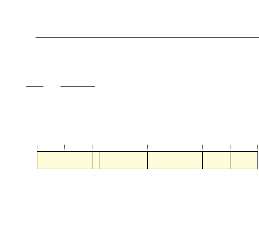
The CPUID Identification Scheme
B5-34 Copyright © 1996-1998, 2000, 2004-2008 ARM Limited. All rights reserved. ARM DDI 0406B
B5.3 Advanced SIMD and VFP feature identification registers
When an implementation includes one or both of the optional Advanced SIMD and VFP extensions, the
feature identification registers for the extensions are implemented in a common register block. The
extensions reside in the coprocessor space for coprocessors CP10 and CP11, and the registers are accessed
using the
VMRS
and
VMSR
instructions. For more information, see Register map of the Advanced SIMD and
VFP extension system registers on page B1-66.
Table B5-3 lists the feature identification registers for the Advanced SIMD and VFP extensions. These are
described in the remainder of this section.
When the Security Extensions are implemented, these registers are Common registers.
B5.3.1 Floating-point System ID Register (FPSID)
In ARMv7, the FPSID Register provides top-level information about the floating-point implementation.
Note
• In an ARMv7 implementation that includes one or both of the Advanced SIMD and VFP extensions
the Media and VFP Feature registers provide details of the implemented VFP architecture.
• The FPSID can be implemented in a system that provides only software emulation of the ARM
floating-point instructions.
The ARMv7 format of the FPSID is:
Implementer, bits [31:24]
Implementer codes are the same as those used for the Main ID Register, see:
•c0, Main ID Register (MIDR) on page B3-81, for a VMSA implementation
•c0, Main ID Register (MIDR) on page B4-32, for a PMSA implementation.
For an implementation by ARM this field is
0x41
, the ASCII code for A.
Table B5-3 Advanced SIMD and VFP feature identification registers
System register Name Description
0b0000 FPSID See Floating-point System ID Register (FPSID)
0b0110 MVFR1 See Media and VFP Feature Register 1 (MVFR1) on page B5-38
0b0111 MVFR0 See Media and VFP Feature Register 0 (MVFR0) on page B5-36
Implementer
31 24 23 22 16 15 8 7 4 3 0
Subarchitecture Part number Variant Revision
SW

The CPUID Identification Scheme
ARM DDI 0406B Copyright © 1996-1998, 2000, 2004-2008 ARM Limited. All rights reserved. B5-35
SW, bit [23] Software flag. This bit is used to indicate that a system provides only software emulation of
the VFP floating-point instructions:
0 The system includes hardware support for VFP floating-point operations.
1 The system provides only software emulation of the VFP floating-point
instructions.
Subarchitecture, bits [22:16]
Subarchitecture version number. For an implementation by ARM, permitted values are:
0b0000000
VFPv1 architecture with an IMPLEMENTATION DEFINED subarchitecture.
Not permitted in an ARMv7 implementation.
0b0000001
VFPv2 architecture with Common VFP subarchitecture v1.
Not permitted in an ARMv7 implementation.
0b0000010
VFP architecture v3 or later with Common VFP subarchitecture v2. The VFP
architecture version is indicated by the MVFR0 and MVFR1 registers.
0b0000011
VFP architecture v3 or later with Null subarchitecture. The entire floating-point
implementation is in hardware, and no software support code is required. The
VFP architecture version is indicated by the MVFR0 and MVFR1 registers.
This value can be used only by an implementation that does not support the trap
enable bits in the FPSCR, see Floating-point Status and Control Register
(FPSCR) on page A2-28.
0b0000100
VFP architecture v3 or later with Common VFP subarchitecture v3. The VFP
architecture version is indicated by the MVFR0 and MVFR1 registers.
For a subarchitecture designed by ARM the most significant bit of this field, register
bit [22], is 0. Values with a most significant bit of 0 that are not listed here are reserved.
When the subarchitecture designer is not ARM, the most significant bit of this field, register
bit [22], must be 1. Each implementer must maintain its own list of subarchitectures it has
designed, starting at subarchitecture version number
0x40
.
Part number, bits [15:8]
An IMPLEMENTATION DEFINED part number for the floating-point implementation, assigned
by the implementer.
Variant, bits [7:4]
An IMPLEMENTATION DEFINED variant number. Typically, this field is used to distinguish
between different production variants of a single product.

The CPUID Identification Scheme
B5-36 Copyright © 1996-1998, 2000, 2004-2008 ARM Limited. All rights reserved. ARM DDI 0406B
Revision, bits [3:0]
An IMPLEMENTATION DEFINED revision number for the floating-point implementation.
B5.3.2 Media and VFP Feature registers
The Media and VFP Feature registers describe the features provided by the Advanced SIMD and VFP
extensions, when an implementation includes either or both of these extensions. For details of the
implementation options for these extensions see Advanced SIMD and VFP extensions on page A2-20.
In VFPv2, it is IMPLEMENTATION DEFINED whether the Media and VFP Feature registers are implemented.
Note
Often, the complete implementation of a VFP architecture uses support code to provide some VFP
functionality. In such an implementation, only the support code can provide full details of the supported
features. In this case the Media and VFP Feature registers are not used directly.
The Media and VFP Feature registers are described in:
•Media and VFP Feature Register 0 (MVFR0)
•Media and VFP Feature Register 1 (MVFR1) on page B5-38.
Media and VFP Feature Register 0 (MVFR0)
The format of the MVFR0 register is:
VFP rounding modes, bits [31:28]
Indicates the rounding modes supported by the VFP floating-point hardware. Permitted
values are:
0b0000 Only Round to Nearest mode supported, except that Round towards Zero mode
is supported for VCVT instructions that always use that rounding mode
regardless of the FPSCR setting.
0b0001 All rounding modes supported.
Short vectors, bits [27:24]
Indicates the hardware support for VFP short vectors. Permitted values are:
0b0000 Not supported.
0b0001 Short vector operation supported.
VFP
rounding
modes
Short
vectors
Square
root Divide
31 16 15 12 11 8 7 4 3 0
VFP
exception
trapping
Double-
precision
Single-
precision
A_SIMD
registers
28 27 24 23 20 19

The CPUID Identification Scheme
ARM DDI 0406B Copyright © 1996-1998, 2000, 2004-2008 ARM Limited. All rights reserved. B5-37
Square root, bits [23:20]
Indicates the hardware support for VFP square root operations. Permitted values are:
0b0000 Not supported in hardware.
0b0001 Supported.
Note
• the
FSQRTS
instruction also requires the single-precision VFP attribute, bits [7:4]
• the
FSQRTD
instruction also requires the double-precision VFP attribute, bits [11:8].
Divide, bits [19:16]
Indicates the hardware support for VFP divide operations. Permitted values are:
0b0000 Not supported in hardware.
0b0001 Supported.
Note
• the
FDIVS
instruction also requires the single-precision VFP attribute, bits [7:4]
• the
FDIVD
instruction also requires the double-precision VFP attribute, bits [11:8].
VFP exception trapping, bits [15:12]
Indicates whether the VFP hardware implementation supports exception trapping.
Permitted values are:
0b0000 Not supported. This is the value for VFPv3.
0b0001 Supported by the hardware. This is the value for VFPv3U, and for VFPv2.
When exception trapping is supported, support code is needed to handle the
trapped exceptions.
Note
This value does not indicate that trapped exception handling is available.
Because trapped exception handling requires support code, only the support
code can provide this information.
Double-precision, bits [11:8]
Indicates the hardware support for VFP double-precision operations. Permitted values are:
0b0000 Not supported in hardware.
0b0001 Supported, VFPv2.
0b0010 Supported, VFPv3.
VFPv3 adds an instruction to load a double-precision floating-point constant,
and conversions between double-precision and fixed-point values.

The CPUID Identification Scheme
B5-38 Copyright © 1996-1998, 2000, 2004-2008 ARM Limited. All rights reserved. ARM DDI 0406B
A value of 0b0001 or 0b0010 indicates support for all VFP double-precision instructions in
the supported version of VFP, except that, in addition to this field being nonzero:
•
FSQRTD
is only available if the Square root field is 0b0001
•
FDIVD
is only available if the Divide field is 0b0001
• conversion between double-precision and single-precision is only available if the
single-precision field is nonzero.
Single-precision, bits [7:4]
Indicates the hardware support for VFP single-precision operations. Permitted values are:
0b0000 Not supported in hardware.
0b0001 Supported, VFPv2.
0b0010 Supported, VFPv3.
VFPv3 adds an instruction to load a single-precision floating-point constant,
and conversions between single-precision and fixed-point values.
A value of 0b0001 or 0b0010 indicates support for all VFP single-precision instructions in
the supported version of VFP, except that, in addition to this field being nonzero:
•
FSQRTS
is only available if the Square root field is 0b0001
•
FDIVS
is only available if the Divide field is 0b0001
• conversion between double-precision and single-precision is only available if the
double-precision field is nonzero.
A_SIMD registers, bits [3:0]
Indicates support for the Advanced SIMD register bank. Permitted values are:
0b0000 Not supported.
0b0001 Supported, 16 x 64-bit registers.
0b0010 Supported, 32 x 64-bit registers.
If this field is nonzero:
• all VFP
LDC
,
STC
,
MCR
, and
MRC
instructions are supported
• if the CPUID register shows that the
MCRR
and
MRRC
instructions are supported then the
corresponding VFP instructions are supported.
Media and VFP Feature Register 1 (MVFR1)
The format of the MVFR1 register is:
Bits [31:28] Reserved, RAZ.
Reserved,
RAZ
VFP
HPFP
A_SIMD
HPFP
A_SIMD
SPFP
31 16 15 12 11 8 7 4 3 0
A_SIMD
integer
A_SIMD
load/store
D_NaN
mode
FtZ
mode
28 27 24 23 20 19

The CPUID Identification Scheme
ARM DDI 0406B Copyright © 1996-1998, 2000, 2004-2008 ARM Limited. All rights reserved. B5-39
VFP HPFP, bits[27:24]
Indicates whether the VFP supports half-precision floating-point conversion operations.
Permitted values are:
0b0000 Not supported.
0b0001 Supported.
A_SIMD HPFP, bits[23:20]
Indicates whether Advanced SIMD supports half-precision floating-point conversion
operations. Permitted values are:
0b0000 Not supported.
0b0001 Supported. This value is only permitted if the A_SIMD SPFP field is 0b0001.
A_SIMD SPFP, bits [19:16]
Indicates whether the Advanced SIMD extension supports single-precision floating-point
operations. Permitted values are:
0b0000 Not supported.
0b0001 Supported. This value is only permitted if the A_SIMD integer field is 0b0001.
A_SIMD integer, bits [15:12]
Indicates whether the Advanced SIMD extension supports integer operations. Permitted
values are:
0b0000 Not supported.
0b0001 Supported.
A_SIMD load/store, bits [11:8]
Indicates whether the Advanced SIMD extension supports load/store instructions. Permitted
values are:
0b0000 Not supported.
0b0001 Supported.
D_NaN mode, bits [7:4]
Indicates whether the VFP hardware implementation supports only the Default NaN mode.
Permitted values are:
0b0000 Hardware supports only the Default NaN mode. If a VFP subarchitecture is
implemented its support code might include support for propagation of NaN
values.
0b0001 Hardware supports propagation of NaN values.

The CPUID Identification Scheme
B5-40 Copyright © 1996-1998, 2000, 2004-2008 ARM Limited. All rights reserved. ARM DDI 0406B
FtZ mode, bits [7:4]
Indicates whether the VFP hardware implementation supports only the Flush-to-Zero mode
of operation. Permitted values are:
0b0000 Hardware supports only the Flush-to-Zero mode of operation. If a VFP
subarchitecture is implemented its support code might include support for full
denormalized number arithmetic.
0b0001 Hardware supports full denormalized number arithmetic.
B5.3.3 Accessing the Advanced SIMD and VFP feature identification registers
You access the Advanced SIMD and VFP feature identification registers using the
VMRS
instruction, see
VMRS on page A8-658.
For example:
VMRS <Rt>, FPSID ; Read Floating-Point System ID Register
VMRS <Rt>, MVFR1 ; Read Media and VFP Feature Register 1

ARM DDI 0406B Copyright © 1996-1998, 2000, 2004-2008 ARM Limited. All rights reserved. B6-1
Chapter B6
System Instructions
This chapter describes the instructions that are only available, or that behave differently, in privileged
modes. It contains the following section:
•Alphabetical list of instructions on page B6-2.

System Instructions
B6-2 Copyright © 1996-1998, 2000, 2004-2008 ARM Limited. All rights reserved. ARM DDI 0406B
B6.1 Alphabetical list of instructions
This section lists every instruction that behaves differently in privileged modes, or that is only available in
privileged modes. For information about privileged modes see ARM processor modes and core registers on
page B1-6.
System Instructions
ARM DDI 0406B Copyright © 1996-1998, 2000, 2004-2008 ARM Limited. All rights reserved. B6-3
B6.1.1 CPS
Change Processor State is available only in privileged modes. It changes one or more of the A, I, and F
interrupt disable bits and the mode bits of the CPSR, without changing the other CPSR bits.
enable = (im == ‘0’); disable = (im == ‘1’); changemode = FALSE;
affectA = (A == ‘1’); affectI = (I == ‘1’); affectF = (F == ‘1’);
if InITBlock() then UNPREDICTABLE;
if imod == ‘00’ && M == ‘0’ then SEE “Hint instructions”;
enable = (imod == ‘10’); disable = (imod == ‘11’); changemode = (M == ‘1’);
affectA = (A == ‘1’); affectI = (I == ‘1’); affectF = (F == ‘1’);
if imod == ‘01’ || InITBlock() then UNPREDICTABLE;
enable = (imod == ‘10’); disable = (imod == ‘11’); changemode = (M == ‘1’);
affectA = (A == ‘1’); affectI = (I == ‘1’); affectF = (F == ‘1’);
if (imod == ‘00’ && M == ‘0’) || imod == ‘01’ then UNPREDICTABLE;
Assembler syntax
CPS<effect><q> <iflags> {, #<mode>}
CPS<q> #<mode>
where:
<effect>
The effect required on the A, I, and F bits in the CPSR. This is one of:
IE
Interrupt Enable. This sets the specified bits to 0.
ID
Interrupt Disable. This sets the specified bits to 1.
Encoding T1 ARMv6*, ARMv7
CPS<effect> <iflags>
Not permitted in IT block.
1514131211109876543210
10110110011im(0)AIF
Encoding T2 ARMv6T2, ARMv7
CPS<effect>.W <iflags>{,#<mode>}
Not permitted in IT block.
CPS #<mode>
Not permitted in IT block.
151413121110987654321 01514131211109876543210
111100111010(1)(1)(1)(1)10(0)0(0)imodMAIF mode
Encoding A1 ARMv6*, ARMv7
CPS<effect> <iflags>{,#<mode>}
CPS #<mode>
313029282726252423222120191817161514131211109876543210
111100010000imodM0(0)(0)(0)(0)(0)(0)(0)AIF0 mode

System Instructions
B6-4 Copyright © 1996-1998, 2000, 2004-2008 ARM Limited. All rights reserved. ARM DDI 0406B
If
<effect>
is specified, the bits to be affected are specified by
<iflags>
. The mode can
optionally be changed by specifying a mode number as
<mode>
.
If
<effect>
is not specified, then:
•
<iflags>
is not specified and interrupt settings are not changed
•
<mode>
specifies the new mode number.
<q>
See Standard assembler syntax fields on page A8-7. A CPS instruction must be
unconditional.
<iflags>
Is a sequence of one or more of the following, specifying which interrupt disable flags are
affected:
a
Sets the A bit in the instruction, causing the specified effect on the CPSR.A
(asynchronous abort) bit.
i
Sets the I bit in the instruction, causing the specified effect on the CPSR.I (IRQ
interrupt) bit.
f
Sets the F bit in the instruction, causing the specified effect on the CPSR.F (FIQ
interrupt) bit.
<mode>
The number of the mode to change to. If this option is omitted, no mode change occurs.
Operation
EncodingSpecificOperations();
if CurrentModeIsPrivileged() then
cpsr_val = CPSR;
if enable then
if affectA then cpsr_val<8> = ‘0’;
if affectI then cpsr_val<7> = ‘0’;
if affectF then cpsr_val<6> = ‘0’;
if disable then
if affectA then cpsr_val<8> = ‘1’;
if affectI then cpsr_val<7> = ‘1’;
if affectF then cpsr_val<6> = ‘1’;
if changemode then
cpsr_val<4:0> = mode;
CPSRWriteByInstr(cpsr_val, ‘1111’, TRUE);
Exceptions
None.
Hint instructions
If the imod field and the M bit in encoding T2 are '00' and'0' respectively, a hint instruction is encoded. To
determine which hint instruction, see Change Processor State, and hints on page A6-21.

System Instructions
ARM DDI 0406B Copyright © 1996-1998, 2000, 2004-2008 ARM Limited. All rights reserved. B6-5
B6.1.2 LDM (exception return)
Load Multiple (exception return) loads multiple registers from consecutive memory locations using an
address from a base register. The SPSR of the current mode is copied to the CPSR. An address adjusted by
the size of the data loaded can optionally be written back to the base register.
The registers loaded include the PC. The word loaded for the PC is treated as an address and a branch occurs
to that address.
n = UInt(Rn); registers = register_list;
wback = (W == ‘1’); increment = (U == ‘1’); wordhigher = (P == U);
if n == 15 then UNPREDICTABLE;
if wback && registers<n> == ‘1’ && ArchVersion() >= 7 then UNPREDICTABLE;
Assembler syntax
LDM{<amode>}<c><q> <Rn>{!}, <registers_with_pc>^
where:
<c><q>
See Standard assembler syntax fields on page A8-7.
<amode>
is one of:
DA
Decrement After. The consecutive memory addresses end at the address in the
base register. For this instruction,
FA
, meaning Full Ascending, is equivalent to
DA
. Encoded as P = 0, U = 0.
DB
Decrement Before. The consecutive memory addresses end one word below the
address in the base register. For this instruction,
EA
, meaning Empty Ascending,
is equivalent to
DB
. Encoded as P = 1, U = 0.
IA
Increment After. The consecutive memory addresses start at the address in the
base register. This is the default, and is normally omitted. For this instruction,
FD
, meaning Full Descending, is equivalent to
IA
. Encoded as P = 0, U = 1.
IB
Increment Before. The consecutive memory addresses start one word above the
address in the base register. For this instruction,
ED
, meaning Empty
Descending, is equivalent to
IB
. Encoded as P =1, U =1.
<Rn>
The base register. This register can be the SP.
!
Causes the instruction to write a modified value back to
<Rn>
. Encoded as W = 1.
If
!
is omitted, the instruction does not change
<Rn>
in this way. Encoded as W = 0.
Encoding A1 ARMv4*, ARMv5T*, ARMv6*, ARMv7
LDM{<amode>}<c> <Rn>{!},<registers_with_pc>^
313029282726252423222120191817161514131211109876543210
cond 1 0 0 P U 1 W 1 Rn 1 register_list

System Instructions
B6-6 Copyright © 1996-1998, 2000, 2004-2008 ARM Limited. All rights reserved. ARM DDI 0406B
<registers_with_pc>
Is a list of one or more registers, separated by commas and surrounded by
{
and
}
. It
specifies the set of registers to be loaded. The registers are loaded with the lowest-numbered
register from the lowest memory address, through to the highest-numbered register from the
highest memory address. The PC must be specified in the register list, and the instruction
causes a branch to the address (data) loaded into the PC.
The pre-UAL syntax
LDM<c>{<amode>}
is equivalent to
LDM{<amode>}<c>
.
Note
Instructions with similar syntax but without the PC included in
<registers>
are described in LDM (user
registers) on page B6-7.
Operation
if ConditionPassed() then
EncodingSpecificOperations();
if CurrentModeIsUserOrSystem() then UNPREDICTABLE;
length = 4*BitCount(registers) + 4;
address = if increment then R[n] else R[n]-length;
if wordhigher then address = address+4;
for i = 0 to 14
if registers<i> == ‘1’ then
R[i] = MemA[address,4]; address = address + 4;
new_pc_value = MemA[address,4];
if wback && registers<n> == ‘0’ then R[n] = if increment then R[n]+length else R[n]-length;
if wback && registers<n> == ‘1’ then R[n] = bits(32) UNKNOWN;
CPSRWriteByInstr(SPSR[], ‘1111’, TRUE);
BranchWritePC(new_pc_value);
Exceptions
Data Abort.

System Instructions
ARM DDI 0406B Copyright © 1996-1998, 2000, 2004-2008 ARM Limited. All rights reserved. B6-7
B6.1.3 LDM (user registers)
Load Multiple (user registers) is UNPREDICTABLE in User or System modes. In exception modes, it loads
multiple User mode registers from consecutive memory locations using an address from a banked base
register. Writeback to the base register is not available with this instruction.
The registers loaded cannot include the PC.
n = UInt(Rn); registers = register_list; increment = (U == ‘1’); wordhigher = (P == U);
if n == 15 || BitCount(registers) < 1 then UNPREDICTABLE;
Assembler syntax
LDM{<amode>}<c><q> <Rn>, <registers_without_pc>^
where:
<c><q>
See Standard assembler syntax fields on page A8-7.
<amode>
is one of:
DA
Decrement After. The consecutive memory addresses end at the address in the
base register. For this instruction,
FA
, meaning Full Ascending, is equivalent to
DA
. Encoded as P = 0, U = 0.
DB
Decrement Before. The consecutive memory addresses end one word below the
address in the base register. For this instruction,
EA
, meaning Empty Ascending,
is equivalent to
DB
. Encoded as P = 1, U = 0.
IA
Increment After. The consecutive memory addresses start at the address in the
base register. This is the default, and is normally omitted. For this instruction,
FD
, meaning Full Descending, is equivalent to
IA
. Encoded as P = 0, U = 1.
IB
Increment Before. The consecutive memory addresses start one word above the
address in the base register. For this instruction,
ED
, meaning Empty
Descending, is equivalent to
IB
. Encoded as P =1, U =1.
<Rn>
The base register. This register can be the SP.
<registers_without_pc>
Is a list of one or more registers, separated by commas and surrounded by
{
and
}
. It
specifies the set of registers to be loaded by the
LDM
instruction. The registers are loaded with
the lowest-numbered register from the lowest memory address, through to the
highest-numbered register from the highest memory address. The PC must not be in the
register list.
Encoding A1 ARMv4*, ARMv5T*, ARMv6*, ARMv7
LDM{<amode>}<c> <Rn>,<registers_without_pc>^
313029282726252423222120191817161514131211109876543210
cond 1 0 0 P U 1 (0) 1 Rn 0 register_list

System Instructions
B6-8 Copyright © 1996-1998, 2000, 2004-2008 ARM Limited. All rights reserved. ARM DDI 0406B
The pre-UAL syntax
LDM<c>{<amode>}
is equivalent to
LDM{<amode>}<c>
.
Note
Instructions with similar syntax but with the PC included in
<registers>
are described in LDM (exception
return) on page B6-5.
Operation
if ConditionPassed() then
EncodingSpecificOperations();
if CurrentModeIsUserOrSystem() then UNPREDICTABLE;
length = 4*BitCount(registers);
address = if increment then R[n] else R[n]-length;
if wordhigher then address = address+4;
for i = 0 to 14
if registers<i> == ‘1’ then // Load User mode (‘10000’) register
Rmode[i, ‘10000’] = MemA[address,4]; address = address + 4;
Exceptions
Data Abort.

System Instructions
ARM DDI 0406B Copyright © 1996-1998, 2000, 2004-2008 ARM Limited. All rights reserved. B6-9
B6.1.4 LDRBT, LDRHT, LDRSBT, LDRSHT, and LDRT
Even in privileged modes, loads from memory by these instructions are restricted in the same way as loads
from memory in User mode. This is encapsulated in the
MemA_unpriv[]
and
MemU_unpriv[]
pseudocode
functions. For details see Aligned memory accesses on page B2-31 and Unaligned memory accesses on
page B2-32.
For details of the instructions see:
•LDRBT on page A8-134
•LDRHT on page A8-158
•LDRSBT on page A8-166
•LDRSHT on page A8-174
•LDRT on page A8-176.
System Instructions
B6-10 Copyright © 1996-1998, 2000, 2004-2008 ARM Limited. All rights reserved. ARM DDI 0406B
B6.1.5 MRS
Move to Register from Special Register moves the value from the CPSR or SPSR of the current mode into
a general-purpose register.
d = UInt(Rd); read_spsr = (R == ‘1’);
if BadReg(d) then UNPREDICTABLE;
d = UInt(Rd); read_spsr = (R == ‘1’);
if d == 15 then UNPREDICTABLE;
Encoding T1 ARMv6T2, ARMv7
MRS<c> <Rd>,<spec_reg>
151413121110987654321 01514131211109876543210
11110011111R(1)(1)(1)(1)10(0)0 Rd (0)(0)(0)(0)(0)(0)(0)(0)
Encoding A1 ARMv4*, ARMv5T*, ARMv6*, ARMv7
MRS<c> <Rd>,<spec_reg>
313029282726252423222120191817161514131211109876543210
cond 00010R00(1)(1)(1)(1) Rd (0)(0)(0)(0)0000(0)(0)(0)(0)

System Instructions
ARM DDI 0406B Copyright © 1996-1998, 2000, 2004-2008 ARM Limited. All rights reserved. B6-11
Assembler syntax
MRS<c><q> <Rd>, <spec_reg>
where:
<c><q>
See Standard assembler syntax fields on page A8-7.
<Rd>
The destination register.
<spec_reg>
Is one of:
•APSR
•CPSR
• SPSR.
ARM recommends the
APSR
form when only the N, Z, C, V, Q, or GE[3:0] bits of the read
value are going to be used (see The Application Program Status Register (APSR) on
page A2-14).
Operation
if ConditionPassed() then
EncodingSpecificOperations();
if read_spsr then
if CurrentModeIsUserOrSystem() then
UNPREDICTABLE;
else
R[d] = SPSR[];
else
// CPSR is read with execution state bits other than E masked out.
R[d] = CPSR AND ‘11111000 11111111 00000011 11011111’;
Exceptions
None.
System Instructions
B6-12 Copyright © 1996-1998, 2000, 2004-2008 ARM Limited. All rights reserved. ARM DDI 0406B
B6.1.6 MSR (immediate)
Move immediate value to Special Register moves selected bits of an immediate value to the CPSR or the
SPSR of the current mode.
if mask == ‘0000’ && R == ‘0’ then SEE “Related encodings”;
imm32 = ARMExpandImm(imm12); write_spsr = (R == ‘1’);
if mask == ‘0000’ then UNPREDICTABLE;
if n == 15 then UNPREDICTABLE;
Assembler syntax
MSR<c><q> <spec_reg>, #<const>
where:
<c><q>
See Standard assembler syntax fields on page A8-7.
<spec_reg>
Is one of:
• APSR_<bits>
• CPSR_<fields>
• SPSR_<fields>.
ARM recommends the
APSR
forms when only the N, Z, C, V, Q, and GE[3:0] bits are being
written. For more information, see The Application Program Status Register (APSR) on
page A2-14.
<const>
The immediate value to be transferred to
<spec_reg>
. See Modified immediate constants in
ARM instructions on page A5-9 for the range of values.
<bits>
Is one of
nzcvq
,
g
, or
nzcvqg
.
In the A and R profiles:
•
APSR_nzcvq
is the same as
CPSR_f
(mask == ’1000’)
•
APSR_g
is the same as
CPSR_s
(mask == ’0100’)
•
APSR_nzcvqg
is the same as
CPSR_fs
(mask == ’1100’).
<fields>
Is a sequence of one or more of the following:
c
mask<0> = '1' to enable writing of bits<7:0> of the destination PSR
x
mask<1> = '1' to enable writing of bits<15:8> of the destination PSR
s
mask<2> = '1' to enable writing of bits<23:16> of the destination PSR
f
mask<3> = '1' to enable writing of bits<31:24> of the destination PSR.
Encoding A1 ARMv4*, ARMv5T*, ARMv6*, ARMv7
MSR<c> <spec_reg>,#<const>
313029282726252423222120191817161514131211109876543210
cond 00110R10 mask (1)(1)(1)(1) imm12

System Instructions
ARM DDI 0406B Copyright © 1996-1998, 2000, 2004-2008 ARM Limited. All rights reserved. B6-13
Operation
if ConditionPassed() then
EncodingSpecificOperations();
if write_spsr then
SPSRWriteByInstr(imm32, mask);
else
CPSRWriteByInstr(imm32, mask, FALSE); // Does not affect execution state bits
// other than E
Exceptions
None.
E bit
The CPSR.E bit is writable from any mode using an
MSR
instruction. Use of this to change its value is
deprecated. Use the
SETEND
instruction instead.
System Instructions
B6-14 Copyright © 1996-1998, 2000, 2004-2008 ARM Limited. All rights reserved. ARM DDI 0406B
B6.1.7 MSR (register)
Move to Special Register from ARM core register moves the value of a general-purpose register to the
CPSR or the SPSR of the current mode.
n = UInt(Rn); write_spsr = (R == ‘1’);
if mask == ‘0000’ then UNPREDICTABLE;
if BadReg(n) then UNPREDICTABLE;
n = UInt(Rn); write_spsr = (R == ‘1’);
if mask == ‘0000’ then UNPREDICTABLE;
if n == 15 then UNPREDICTABLE;
Assembler syntax
MSR<c><q> <spec_reg>, <Rn>
where:
<c><q>
See Standard assembler syntax fields on page A8-7.
<spec_reg>
Is one of:
• APSR_<bits>
• CPSR_<fields>
• SPSR_<fields>.
ARM recommends the
APSR
forms when only the N, Z, C, V, Q, and GE[3:0] bits are being
written. For more information, see The Application Program Status Register (APSR) on
page A2-14.
<Rn>
Is the general-purpose register to be transferred to
<spec_reg>
.
<bits>
Is one of
nzcvq
,
g
, or
nzcvqg
.
In the A and R profiles:
•
APSR_nzcvq
is the same as
CPSR_f
(mask == ’1000’)
•
APSR_g
is the same as
CPSR_s
(mask == ’0100’)
•
APSR_nzcvqg
is the same as
CPSR_fs
(mask == ’1100’).
Encoding T1 ARMv6T2, ARMv7
MSR<c> <spec_reg>,<Rn>
151413121110987654321 01514131211109876543210
11110011100R Rn 10(0)0 mask (0)(0)(0)(0)(0)(0)(0)(0)
Encoding A1 ARMv4*, ARMv5T*, ARMv6*, ARMv7
MSR<c> <spec_reg>,<Rn>
313029282726252423222120191817161514131211109876543210
cond 00010R10 mask (1)(1)(1)(1)(0)(0)(0)(0)0000 Rn

System Instructions
ARM DDI 0406B Copyright © 1996-1998, 2000, 2004-2008 ARM Limited. All rights reserved. B6-15
<fields>
Is a sequence of one or more of the following:
c
mask<0> = '1' to enable writing of bits<7:0> of the destination PSR
x
mask<1> = '1' to enable writing of bits<15:8> of the destination PSR
s
mask<2> = '1' to enable writing of bits<23:16> of the destination PSR
f
mask<3> = '1' to enable writing of bits<31:24> of the destination PSR.
Operation
if ConditionPassed() then
EncodingSpecificOperations();
if write_spsr then
SPSRWriteByInstr(R[n], mask);
else
CPSRWriteByInstr(R[n], mask, FALSE); // Does not affect execution state bits
// other than E
Exceptions
None.
E bit
The CPSR.E bit is writable from any mode using an
MSR
instruction. Use of this to change its value is
deprecated. Use the
SETEND
instruction instead.
System Instructions
B6-16 Copyright © 1996-1998, 2000, 2004-2008 ARM Limited. All rights reserved. ARM DDI 0406B
B6.1.8 RFE
Return From Exception loads the PC and the CPSR from the word at the specified address and the following
word respectively. For information about memory accesses see Memory accesses on page A8-13.
n = UInt(Rn); wback = (W == ‘1’); increment = FALSE; wordhigher = FALSE;
if n == 15 then UNPREDICTABLE;
if InITBlock() && !LastInITBlock() then UNPREDICTABLE;
n = UInt(Rn); wback = (W == ‘1’); increment = TRUE; wordhigher = FALSE;
if n == 15 then UNPREDICTABLE;
if InITBlock() && !LastInITBlock() then UNPREDICTABLE;
n = UInt(Rn);
wback = (W == ‘1’); inc = (U == ‘1’); wordhigher = (P == U);
if n == 15 then UNPREDICTABLE;
Encoding T1 ARMv6T2, ARMv7
RFEDB<c> <Rn>{!}
Outside or last in IT block
15141312111098765432101514131211109876543210
1110100000W1 Rn (1)(1)(0)(0)(0)(0)(0)(0)(0)(0)(0)(0)(0)(0)(0)(0)
Encoding T2 ARMv6T2, ARMv7
RFE{IA}<c> <Rn>{!}
Outside or last in IT block
15141312111098765432101514131211109876543210
1110100110W1 Rn (1)(1)(0)(0)(0)(0)(0)(0)(0)(0)(0)(0)(0)(0)(0)(0)
Encoding A1 ARMv6*, ARMv7
RFE{<amode>} <Rn>{!}
313029282726252423222120191817161514131211109876543210
1111100PU0W1 Rn (0)(0)(0)(0)(1)(0)(1)(0)(0)(0)(0)(0)(0)(0)(0)(0)

System Instructions
ARM DDI 0406B Copyright © 1996-1998, 2000, 2004-2008 ARM Limited. All rights reserved. B6-17
Assembler syntax
RFE{<amode>}<c><q> <Rn>{!}
where:
<amode>
is one of:
DA
Decrement After. ARM code only. The consecutive memory addresses end at
the address in the base register. Encoded as P = 0, U = 0 in encoding A1.
DB
Decrement Before. The consecutive memory addresses end one word below the
address in the base register. Encoding T1, or encoding A1 with P = 1, U = 0.
IA
Increment After. The consecutive memory addresses start at the address in the
base register. This is the default, and is normally omitted. Encoding T2, or
encoding A1 with P = 0, U = 1.
IB
Increment Before. ARM code only. The consecutive memory addresses start
one word above the address in the base register. Encoded as P = 1, U = 1 in
encoding A1.
<c><q>
See Standard assembler syntax fields on page A8-7. An ARM
RFE
instruction must be
unconditional.
<Rn>
The base register.
!
Causes the instruction to write a modified value back to
<Rn>
. If
!
is omitted, the instruction
does not change
<Rn>
.
RFEFA
,
RFEEA
,
RFEFD
, and
RFEED
are pseudo-instructions for
RFEDA
,
RFEDB
,
RFEIA
, and
RFEIB
respectively,
referring to their use for popping data from Full Ascending, Empty Ascending, Full Descending, and Empty
Descending stacks.
Operation
if ConditionPassed() then
EncodingSpecificOperations();
if !CurrentModeIsPrivileged() || CurrentInstrSet() == InstrSet_ThumbEE then
UNPREDICTABLE;
else
address = if increment then R[n] else R[n]-8;
if wordhigher then address = address+4;
CPSRWriteByInstr(MemA[address+4,4], ‘1111’, TRUE);
BranchWritePC(MemA[address,4]);
if wback then R[n] = if increment then R[n]+8 else R[n]-8;
Exceptions
Data Abort.

System Instructions
B6-18 Copyright © 1996-1998, 2000, 2004-2008 ARM Limited. All rights reserved. ARM DDI 0406B
B6.1.9 SMC (previously SMI)
Secure Monitor Call causes a Secure Monitor exception. It is available only in privileged modes. An attempt
to execute this instruction in User mode causes an Undefined Instruction exception.
For details of the effects of a Secure Monitor exception see Secure Monitor Call (SMC) exception on
page B1-53.
imm32 = ZeroExtend(imm4, 32);
// imm32 is for assembly/disassembly only and is ignored by hardware
if InITBlock() && !LastInITBlock() then UNPREDICTABLE;
imm32 = ZeroExtend(imm4, 32);
// imm32 is for assembly/disassembly only and is ignored by hardware
Encoding T1 Security Extensions (not in ARMv6K)
SMC<c> #<imm4>
15141312111098765432101514131211109876543210
111101111111 imm4 1000(0)(0)(0)(0)(0)(0)(0)(0)(0)(0)(0)(0)
Encoding A1 Security Extensions
SMC<c> #<imm4>
313029282726252423222120191817161514131211109876543210
cond 00010110(0)(0)(0)(0)(0)(0)(0)(0)(0)(0)(0)(0)0111 imm4

System Instructions
ARM DDI 0406B Copyright © 1996-1998, 2000, 2004-2008 ARM Limited. All rights reserved. B6-19
Assembler syntax
SMC<c><q> #<imm4>
where:
<c><q>
See Standard assembler syntax fields on page A8-7.
<imm4>
Is a 4-bit immediate value. This is ignored by the ARM processor. It can be used by the SMC
exception handler (Secure Monitor code) to determine what service is being requested, but
this is not recommended.
The pre-UAL syntax
SMI<c>
is equivalent to
SMC<c>
.
Operation
if ConditionPassed() then
EncodingSpecificOperations();
if HaveSecurityExt() && CurrentModeIsPrivileged() then
TakeSMCException(); // Secure Monitor Call if privileged
else
UNDEFINED;
Exceptions
Secure Monitor Call.
System Instructions
B6-20 Copyright © 1996-1998, 2000, 2004-2008 ARM Limited. All rights reserved. ARM DDI 0406B
B6.1.10 SRS
Store Return State stores the LR and SPSR of the current mode to the stack of a specified mode. For
information about memory accesses see Memory accesses on page A8-13.
wback = (W == ‘1’); increment = FALSE; wordhigher = FALSE;
// In Non-secure state, check for attempts to access Monitor mode (‘10110’), or FIQ
// mode (‘10001’) when the Security Extensions are reserving the FIQ registers. The
// definition of UNPREDICTABLE does not permit this to be a security hole.
if !IsSecure() && mode == ‘10110’ then UNPREDICTABLE;
if !IsSecure() && mode == ‘10001’ && NSACR.RFR == ‘1’ then UNPREDICTABLE;
wback = (W == ‘1’); increment = TRUE; wordhigher = FALSE;
// In Non-secure state, check for attempts to access Monitor mode (‘10110’), or FIQ
// mode (‘10001’) when the Security Extensions are reserving the FIQ registers. The
// definition of UNPREDICTABLE does not permit this to be a security hole.
if !IsSecure() && mode == ‘10110’ then UNPREDICTABLE;
if !IsSecure() && mode == ‘10001’ && NSACR.RFR == ‘1’ then UNPREDICTABLE;
wback = (W == ‘1’); inc = (U == ‘1’); wordhigher = (P == U);
// In Non-secure state, check for attempts to access Monitor mode (‘10110’), or FIQ
// mode (‘10001’) when the Security Extensions are reserving the FIQ registers. The
// definition of UNPREDICTABLE does not permit this to be a security hole.
if !IsSecure() && mode == ‘10110’ then UNPREDICTABLE;
if !IsSecure() && mode == ‘10001’ && NSACR.RFR == ‘1’ then UNPREDICTABLE;
Encoding T1 ARMv6T2, ARMv7
SRSDB<c> SP{!},#<mode>
151413121110987654321 01514131211109876543210
1110100000W0(1)(1)(0)(1)(1)(1)(0)(0)(0)(0)(0)(0)(0)(0)(0) mode
Encoding T2 ARMv6T2, ARMv7
SRS{IA}<c> SP{!},#<mode>
151413121110987654321 0 1514131211109876543210
1 1 1 0 1 0 0 1 1 0 W 0 (1) (1) (0) (1) (1) (1) (0) (0) (0) (0) (0) (0) (0) (0) (0) mode
Encoding A1 ARMv6*, ARMv7
SRS{<amode>} SP{!},#<mode>
313029282726252423222120191817161514131211109876543210
1111100PU1W0(1)(1)(0)(1)(0)(0)(0)(0)(0)(1)(0)(1)(0)(0)(0) mode

System Instructions
ARM DDI 0406B Copyright © 1996-1998, 2000, 2004-2008 ARM Limited. All rights reserved. B6-21
Assembler syntax
SRS{<amode>}<c><q> SP{!}, #<mode>
where:
<amode>
is one of:
DA
Decrement After. ARM code only. The consecutive memory addresses end at
the address in the base register. Encoded as P = 0, U = 0 in encoding A1.
DB
Decrement Before. The consecutive memory addresses end one word below the
address in the base register. Encoding T1, or encoding A1 with P = 1, U = 0.
IA
Increment After. The consecutive memory addresses start at the address in the
base register. This is the default, and is normally omitted. Encoding T2, or
encoding A1 with P = 0, U = 1.
IB
Increment Before. ARM code only. The consecutive memory addresses start
one word above the address in the base register. Encoded as P = 1, U = 1 in
encoding A1.
<c><q>
See Standard assembler syntax fields on page A8-7. An ARM
SRS
instruction must be
unconditional.
!
Causes the instruction to write a modified value back to the base register (encoded as W
=1). If
!
is omitted, the instruction does not change the base register (encoded as W = 0).
<mode>
The number of the mode whose banked SP is used as the base register. For details of
processor modes and their numbers see ARM processor modes on page B1-6.
SRSFA
,
SRSEA
,
SRSFD
, and
SRSED
are pseudo-instructions for
SRSIB
,
SRSIA
,
SRSDB
, and
SRSDA
respectively,
referring to their use for pushing data onto Full Ascending, Empty Ascending, Full Descending, and Empty
Descending stacks.
Operation
if ConditionPassed() then
EncodingSpecificOperations();
if CurrentModeIsUserOrSystem() || CurrentInstrSet() == InstrSet_ThumbEE then
UNPREDICTABLE;
else
base = Rmode[13,mode];
address = if increment then base else base-8;
if wordhigher then address = address+4;
MemA[address,4] = LR;
MemA[address+4,4] = SPSR[];
if wback then Rmode[13] = if increment then base+8 else base-8;
Exceptions
Data Abort.

System Instructions
B6-22 Copyright © 1996-1998, 2000, 2004-2008 ARM Limited. All rights reserved. ARM DDI 0406B
B6.1.11 STM (user registers)
Store Multiple (user registers) is UNPREDICTABLE in User or System modes. In exception modes, it stores
multiple User mode registers to consecutive memory locations using an address from a banked base register.
Writeback to the base register is not available with this instruction.
n = UInt(Rn); registers = register_list; increment = (U == ‘1’); wordhigher = (P == U);
if n == 15 || BitCount(registers) < 1 then UNPREDICTABLE;
Assembler syntax
STM{amode}<c><q> <Rn>, <registers>^
where:
<c><q>
See Standard assembler syntax fields on page A8-7.
amode
is one of:
DA
Decrement After. The consecutive memory addresses end at the address in the
base register. For this instruction,
ED
, meaning Empty Descending, is equivalent
to
DA
. Encoded as P = 0, U = 0.
DB
Decrement Before. The consecutive memory addresses end one word below the
address in the base register. For this instruction,
FD
, meaning Full Descending,
is equivalent to
DB
. Encoded as P = 1, U = 0.
IA
Increment After. The consecutive memory addresses start at the address in the
base register. This is the default, and is normally omitted. For this instruction,
EA
, meaning Empty Ascending, is equivalent to
IA
. Encoded as P = 0, U = 1.
IB
Increment Before. The consecutive memory addresses start one word above the
address in the base register. For this instruction,
FA
, meaning Full Ascending, is
equivalent to
IB
. Encoded as P = 1, U = 1.
<Rn>
The base register. This register can be the SP.
<registers>
Is a list of one or more registers, separated by commas and surrounded by
{
and
}
. It
specifies the set of registers to be stored by the
STM
instruction. The registers are stored with
the lowest-numbered register to the lowest memory address, through to the
highest-numbered register to the highest memory address.
The pre-UAL syntax
STM<c>{amode}
is equivalent to
STM{amode}<c>
.
Encoding A1 ARMv4*, ARMv5T*, ARMv6*, ARMv7
STM{amode}<c> <Rn>,<registers>^
313029282726252423222120191817161514131211109876543210
cond 1 0 0 P U 1 (0) 0 Rn register_list

System Instructions
ARM DDI 0406B Copyright © 1996-1998, 2000, 2004-2008 ARM Limited. All rights reserved. B6-23
Operation
if ConditionPassed() then
EncodingSpecificOperations();
if CurrentModeIsUserOrSystem() then UNPREDICTABLE;
length = 4*BitCount(registers);
address = if increment then R[n] else R[n]-length;
if wordhigher then address = address+4;
for i = 0 to 14
if registers<i> == ‘1’ then / Store User mode (‘10000’) register
MemA[address,4] = Rmode[i, ‘10000’];
address = address + 4;
if registers<15> == ‘1’ then
MemA[address,4] = PCStoreValue();
Exceptions
Data Abort.

System Instructions
B6-24 Copyright © 1996-1998, 2000, 2004-2008 ARM Limited. All rights reserved. ARM DDI 0406B
B6.1.12 STRBT, STRHT, and STRT
Even in privileged modes, stores to memory by these instructions are restricted in the same way as stores to
memory in User mode. This is encapsulated in the
MemA_unpriv[]
and
MemU_unpriv[]
pseudocode functions.
For details see Aligned memory accesses on page B2-31 and Unaligned memory accesses on page B2-32.
For details of the instructions see:
•STRBT on page A8-394
•STRHT on page A8-414
•STRT on page A8-416.

System Instructions
ARM DDI 0406B Copyright © 1996-1998, 2000, 2004-2008 ARM Limited. All rights reserved. B6-25
B6.1.13 SUBS PC, LR and related instructions
The
SUBS PC, LR, #<const>
instruction provides an exception return without the use of the stack. It subtracts
the immediate constant from LR, branches to the resulting address, and also copies the SPSR to the CPSR.
The ARM instruction set contains similar instructions based on other data-processing operations, with a
wider range of operands, or both. The use of these other instructions is deprecated, except for
MOVS PC, LR
.
n = 14; imm32 = ZeroExtend(imm8, 32); register_form = FALSE; opcode = ‘0010’; // = SUB
if InITBlock() && !LastInITBlock() then UNPREDICTABLE;
n = UInt(Rn); imm32 = ARMExpandImm(imm12); register_form = FALSE;
n = UInt(Rn); m = UInt(Rm); register_form = TRUE;
(shift_t, shift_n) = DecodeImmShift(type, imm5);
Assembler syntax
where:
<c><q>
See Standard assembler syntax fields on page A8-7.
Encoding T1 ARMv6T2, ARMv7
SUBS<c> PC,LR,#<imm8>
Outside or last in IT block
151413121110987654321 01514131211109876543210
111100111101(1)(1)(1)(0)10(0)0(1)(1)(1)(1) imm8
Encoding A1 ARMv4*, ARMv5T*, ARMv6*, ARMv7
<opc1>S<c> PC,<Rn>,#<const>
<opc2>S<c> PC,#<const>
313029282726252423222120191817161514131211109876543210
cond 0 0 1 opcode 1 Rn 1 1 1 1 imm12
Encoding A2 ARMv4*, ARMv5T*, ARMv6*, ARMv7
<opc1>S<c> PC,<Rn>,<Rm>{,<shift>}
<opc2>S<c> PC,<Rm>{,<shift>}
313029282726252423222120191817161514131211109876543210
cond 0 0 0 opcode 1 Rn 1 1 1 1 imm5 type 0 Rm
SUBS<c><q> PC, LR, #<const>
Encodings T1, A1
<opc1>S<c><q> PC, <Rn>, #<const>
Encoding A1
<opc1>S<c><q> PC, <Rn>, <Rm> {,<shift>}
Encoding A2, deprecated
<opc2>S<c><q> PC, #<const>
Encoding A1, deprecated
<opc2>S<c><q> PC, <Rm> {,<shift>}
Encoding A2

System Instructions
B6-26 Copyright © 1996-1998, 2000, 2004-2008 ARM Limited. All rights reserved. ARM DDI 0406B
<opc1>
The operation.
<opc1>
is one of
ADC
,
ADD
,
AND
,
BIC
,
EOR
,
ORR
,
RSB
,
RSC
,
SBC
, and
SUB
. Use of all
of these operations except
SUB
is deprecated.
<opc2>
The operation.
<opc2>
is
MOV
or
MVN
. Use of
MVN
is deprecated.
<Rn>
The first operand register. Use of any register except
LR
is deprecated.
<const>
The immediate constant. For encoding T1,
<const>
is in the range 0-255. See Modified
immediate constants in ARM instructions on page A5-9 for the range of available values in
encoding A1.
<Rm>
The optionally shifted second or only operand register. Use of any register except LR is
deprecated.
<shift>
The shift to apply to the value read from
<Rm>
. If absent, no shift is applied. The shifts and
how they are encoded are described in Shifts applied to a register on page A8-10. Use of
<shift>
is deprecated.
The value of the operation
<opc1>
or
<opc2>
is encoded in the opcode field of the instruction. For the opcode
values for different operations see Operation on page B6-6.
In Thumb code,
MOVS<c><q> PC,LR
is a pseudo-instruction for
SUBS<c><q> PC,LR,#0
.
The pre-UAL syntax
<opc1><c>S
is equivalent to
<opc1>S<c>
. The pre-UAL syntax
<opc2><c>S
is equivalent
to
<opc2>S<c>
.
Operation
if ConditionPassed() then
EncodingSpecificOperations();
if CurrentInstrSet() == InstrSet_ThumbEE then
UNPREDICTABLE;
operand2 = if register_form then Shift(R[m], shift_t, shift_n, APSR.C) else imm32;
case opcode of
when ‘0000’ result = R[n] AND operand2; // AND
when ‘0001’ result = R[n] EOR operand2; // EOR
when ‘0010’ (result, -, -) = AddWithCarry(R[n], NOT(operand2), ‘1’); // SUB
when ‘0011’ (result, -, -) = AddWithCarry(NOT(R[n]), operand2, ‘1’); // RSB
when ‘0100’ (result, -, -) = AddWithCarry(R[n], operand2, ‘0’); // ADD
when ‘0101’ (result, -, -) = AddWithCarry(R[n], operand2, APSR.c); // ADC
when ‘0110’ (result, -, -) = AddWithCarry(R[n], NOT(operand2), APSR.C); // SBC
when ‘0111’ (result, -, -) = AddWithCarry(NOT(R[n]), operand2, APSR.C); // RSC
when ‘1100’ result = R[n] OR operand2; // ORR
when ‘1101’ result = operand2; // MOV
when ‘1110’ result = R[n] AND NOT(operand2); // BIC
when ‘1111’ result = NOT(operand2); // MVN
CPSRWriteByInstr(SPSR[], ‘1111’, TRUE);
BranchWritePC(result);
Exceptions
None.
System Instructions
ARM DDI 0406B Copyright © 1996-1998, 2000, 2004-2008 ARM Limited. All rights reserved. B6-27
B6.1.14 VMRS
Move to ARM core register from Advanced SIMD and VFP extension System Register moves the value of
an extension system register to a general-purpose register.
t = UInt(Rt);
if t == 13 && CurrentInstrSet() != InstrSet_ARM then UNPREDICTABLE;
if t == 15 && reg != ‘0001’ then UNPREDICTABLE;
Encoding T1 / A1 VFPv2, VFPv3, Advanced SIMD
VMRS<c> <Rt>,<spec_reg>
15141312111098765432101514131211109876543210
111011101111 reg Rt 1010(0)(0)(0)1(0)(0)(0)(0)
313029282726252423222120191817161514131211109876543210
cond 11101111 reg Rt 1010(0)(0)(0)1(0)(0)(0)(0)

System Instructions
B6-28 Copyright © 1996-1998, 2000, 2004-2008 ARM Limited. All rights reserved. ARM DDI 0406B
Assembler syntax
VMRS<c><q> <Rt>, <spec_reg>
where:
<c><q>
See Standard assembler syntax fields on page A8-7.
<Rt>
The destination ARM core register. This register can be R0-R14.
If
<spec_reg>
is
FPSCR
, it is also permitted to be
APSR_nzcv
, encoded as Rt = ’1111’. This
instruction transfers the FPSCR N, Z, C, and V flags to the APSR N, Z, C, and V flags.
<spec_reg>
Is one of:
FPSID
reg = ’0000’
FPSCR
reg = ’0001’
MVFR1
reg = ’0110’
MVFR0
reg = ’0111’
FPEXC
reg = ’1000’.
If the Common VFP subarchitecture is implemented, see Subarchitecture additions to the
VFP system registers on page AppxB-15 for additional values of
<spec_reg>
.
The pre-UAL instruction
FMSTAT
is equivalent to
VMRS APSR_nzcv, FPSCR
.
Operation
if ConditionPassed() then
EncodingSpecificOperations();
if reg == ‘0001’ then // FPSCR
CheckVFPEnabled(TRUE); SerializeVFP(); VFPExcBarrier();
if t == 15 then
APSR.N = FPSCR.N; APSR.Z = FPSCR.Z; APSR.C = FPSCR.C; APSR.V = FPSCR.V;
else
R[t] = FPSCR;
else // Non-FPSCR registers are privileged-only and not affected by FPEXC.EN
CheckVFPEnabled(FALSE);
if !CurrentModeIsPrivileged() then UNDEFINED;
case reg of
when ‘0000’ SerializeVFP(); R[t] = FPSID;
// ‘0001’ already dealt with above
when ‘001x’ UNPREDICTABLE;
when ‘010x’ UNPREDICTABLE;
when ‘0110’ SerializeVFP(); R[t] = MVFR1;
when ‘0111’ SerializeVFP(); R[t] = MVFR0;
when ‘1000’ SerializeVFP(); R[t] = FPEXC;
otherwise SUBARCHITECTURE_DEFINED register access;
Exceptions
Undefined Instruction.

System Instructions
ARM DDI 0406B Copyright © 1996-1998, 2000, 2004-2008 ARM Limited. All rights reserved. B6-29
B6.1.15 VMSR
Move to Advanced SIMD and VFP extension System Register from ARM core register moves the value of
a general-purpose register to a VFP system register.
t = UInt(Rt);
if t == 15 || (t == 13 && CurrentInstrSet() != InstrSet_ARM) then UNPREDICTABLE;
Encoding T1 / A1 VFPv2, VFPv3, Advanced SIMD
VMSR<c> <spec_reg>,<Rt>
15141312111098765432101514131211109876543210
111011101110 reg Rt 1010(0)(0)(0)1(0)(0)(0)(0)
313029282726252423222120191817161514131211109876543210
cond 11101110 reg Rt 1010(0)(0)(0)1(0)(0)(0)(0)

System Instructions
B6-30 Copyright © 1996-1998, 2000, 2004-2008 ARM Limited. All rights reserved. ARM DDI 0406B
Assembler syntax
VMSR<c><q> <spec_reg>, <Rt>
where:
<c><q>
See Standard assembler syntax fields on page A8-7.
<spec_reg>
Is one of:
FPSID
reg = ’0000’
FPSCR
reg = ’0001’
FPEXC
reg = ’1000’.
If the Common VFP subarchitecture is implemented, see Subarchitecture additions to the
VFP system registers on page AppxB-15 for additional values of
<spec_reg>
.
<Rt>
The general-purpose register to be transferred to
<spec_reg>
.
Operation
if ConditionPassed() then
EncodingSpecificOperations();
if reg == ‘0001’ then // FPSCR
CheckVFPEnabled(TRUE); SerializeVFP(); VFPExcBarrier();
FPSCR = R[t];
else // Non-FPSCR registers are privileged-only and not affected by FPEXC.EN
CheckVFPEnabled(FALSE);
if !CurrentModeIsPrivileged() then UNDEFINED;
case reg of
when ‘0000’ SerializeVFP();
// ‘0001’ already dealt with above
when ‘001x’ UNPREDICTABLE;
when ‘01xx’ UNPREDICTABLE;
when ‘1000’ SerializeVFP(); FPEXC = R[t];
otherwise SUBARCHITECTURE_DEFINED register access;
Exceptions
Undefined Instruction.
Part C
Debug Architecture

ARM DDI 0406B Copyright © 1996-1998, 2000, 2004-2008 ARM Limited. All rights reserved. C1-1
Chapter C1
Introduction to the ARM Debug Architecture
This chapter introduces part C of this manual, and the ARM Debug architecture. It contains the following
sections:
•Scope of part C of this manual on page C1-2
•About the ARM Debug architecture on page C1-3
•Security Extensions and debug on page C1-8
•Register interfaces on page C1-9.

Introduction to the ARM Debug Architecture
C1-2 Copyright © 1996-1998, 2000, 2004-2008 ARM Limited. All rights reserved. ARM DDI 0406B
C1.1 Scope of part C of this manual
Part C of this manual defines the debug features of ARMv7. However, ARM recognizes that many
debuggers require compatibility with previous versions of the ARM Debug architecture. Therefore, this part
includes information about three versions of the ARM Debug architecture:
•v7Debug
• v6.1 Debug
•v6Debug
These three versions of the Debug architecture are introduced in Major differences between the ARMv6 and
ARMv7 Debug architectures on page C1-7.
In part C of this manual:
• ARMv6 is used sometimes to refer to an implementation that includes either v6.1 Debug or
v6 Debug.
• ARMv7 is used sometimes to refer to an implementation that includes v7 Debug.
Note
• v6.1 Debug and v6 Debug are two different versions of the Debug architecture for the ARMv6
architecture. They might be described as:
— ARMv6, v6.1 Debug
— ARMv6, v6 Debug.
Throughout this part the descriptions v6.1 Debug and v6 Debug are used, for brevity.
• Any processor that implements the ARMv7 architecture must implement v7 Debug. Information
about v6.1 Debug and v6 Debug is given:
— to enable developers to produce debuggers that are backwards compatible with these Debug
architecture versions
— as reference material for processors that implement the ARMv6 architecture.

Introduction to the ARM Debug Architecture
ARM DDI 0406B Copyright © 1996-1998, 2000, 2004-2008 ARM Limited. All rights reserved. C1-3
C1.2 About the ARM Debug architecture
ARM processors implement two types of debug support:
Invasive debug All debug features that permit modification of processor state. For more
information, see Invasive debug.
Non-invasive debug All debug features that permit data and program flow observation, especially trace
support. For more information, see Non-invasive debug on page C1-5.
The following sections introduce invasive and non-invasive debug. Summary of the ARM debug component
descriptions on page C1-7 gives a quick reference summary of the rest of this part of this manual.
C1.2.1 Invasive debug
The invasive debug component of the ARM Debug architecture is intended primarily for run-control
debugging.
Note
In this part of this manual, invasive debug is often referred to simply as debug. For example, debug events,
debug exceptions, and Debug state are all part of the invasive debug implementation.
The programmers’ model can be used to manage and control debug events. Watchpoints and breakpoints are
two examples of debug events. Debug events are described in Chapter C3 Debug Events.
You can configure the processor through the DBGDSCR into one of two debug-modes:
Monitor debug-mode
In Monitor debug-mode, a debug event causes a debug exception to occur:
• a debug exception that relates to instruction execution generates a Prefetch Abort
exception
• a debug exception that relates to a data access generates a Data Abort exception.
Debug exceptions are described in Chapter C4 Debug Exceptions.
Halting debug-mode
In Halting debug-mode, a debug event causes the processor to enter a special Debug state.
When the processor is in Debug state, the processor ceases to execute instructions from the
program counter location, but is instead controlled through the external debug interface, in
particular the Instruction Transfer Register (DBGITR). This enables an external agent, such
as a debugger, to interrogate processor context, and control all subsequent instruction
execution. Because the processor is stopped, it ignores the system and cannot service
interrupts.
Debug state is described in Chapter C5 Debug State.

Introduction to the ARM Debug Architecture
C1-4 Copyright © 1996-1998, 2000, 2004-2008 ARM Limited. All rights reserved. ARM DDI 0406B
A debug solution can use a mixture of the two methods, for example to support an OS or RTOS with both:
•Running System Debug (RSD) using Monitor debug-mode
• Halting debug-mode support available as a fallback for system failure and boot time debug.
The architecture supports the ability to switch between these two debug-modes.
When no debug-mode is selected, debug is restricted to simple monitor solutions. These are usually ROM
or Flash-based. Such a monitor might use standard system features, such as a UART or Ethernet connection,
to communicate with a debug host. Alternatively, it might use the Debug Communications Channel (DCC)
as an out-of-band communications channel to the host. This minimizes the debug requirement on system
resources.
All versions of the Debug architecture provide a software interface that includes:
•a Debug Identification Register (DBGDIDR)
• status and control registers, including the Debug Status and Control Register (DBGDSCR)
• hardware breakpoint and watchpoint support
• the DCC.
In addition, the v7 Debug software interface includes reset, power-down and operating system debug
support features.
The Debug architecture requires an external debug interface that supports access to the programmers’
model.
This forms the basis of the Debug Programmers' Model (DPM) for ARMv6 and ARMv7.
Description of invasive debug features
The following chapters describe the invasive debug implementation:
• Chapter C2 Invasive Debug Authentication
• Chapter C3 Debug Events
• Chapter C4 Debug Exceptions
• Chapter C5 Debug State.
In addition, see:
• Chapter C6 Debug Register Interfaces for a description of the register interfaces to the debug
components
• Chapter C10 Debug Registers Reference for descriptions of the registers used to configure and
control debug operations
• Appendix A Recommended External Debug Interface for a description of the recommended external
interface to the debug components.

Introduction to the ARM Debug Architecture
ARM DDI 0406B Copyright © 1996-1998, 2000, 2004-2008 ARM Limited. All rights reserved. C1-5
C1.2.2 Non-invasive debug
Non-invasive debug includes all debug features that permit data and program flow to be observed, but that
do not permit modification of the main processor state.
The v7 Debug architecture defines three areas of non-invasive debug:
• Instruction trace and, in some implementations, data trace. Trace support is an architecture extension
typically implemented using a trace macrocell, see Trace.
• Sample-based profiling, see Sample-based profiling on page C1-6.
• Performance monitors, see Performance monitors on page C1-6.
A processor implementation might include other forms of non-invasive debug.
Chapter C7 Non-invasive Debug Authentication describes the authentication of non-invasive debug
operations.
Trace
Trace support is an architecture extension. This manual describes such an extension as a trace macrocell. A
trace macrocell constructs a real-time trace stream corresponding to the operation of the processor. It is
IMPLEMENTATION DEFINED whether the trace stream is:
• stored locally in an Embedded Trace Buffer (ETB) for independent download and analysis
• exported directly through a trace port to a Trace Port Analyzer (TPA) and its associated host based
trace debug tools.
Typically, use of a trace macrocell is non-invasive. Development tools can connect to the trace macrocell,
configure it, capture trace and download the trace without affecting the operation of the processor in any
way. A trace macrocell provides an enhanced level of runtime system observation and debug granularity. It
is particularly useful in cases where:
• Stopping the processor affects the behavior of the system.
• There is insufficient state visible in a system by the time a problem is detected to be able to determine
its cause. Trace provides a mechanism for system logging and back tracing of faults.
Trace might also be used to perform analysis of code running on the processor, such as performance analysis
or code coverage analysis.
Typically, a trace architecture defines:
• the trace macrocell programmers’ model
• permitted trace protocol formats
• the physical trace port connector.
The following documents define the ARM trace architectures:
•Embedded Trace Macrocell Architecture Specification
•CoreSight Program Flow Trace Architecture Specification.

Introduction to the ARM Debug Architecture
C1-6 Copyright © 1996-1998, 2000, 2004-2008 ARM Limited. All rights reserved. ARM DDI 0406B
The ARM trace architectures have a common identification mechanism. This means development tools can
detect which architecture is implemented.
Sample-based profiling
Sample-based profiling is an optional non-invasive component of the Debug architecture, that enables debug
software to profile a program. For more information, see Chapter C8 Sample-based Profiling.
Performance monitors
Performance monitors were implemented in several processors before ARMv7, but before ARMv7 they did
not form part of the architecture. The ARMv7 form of the monitors, described here, follows those
implementations with minor modifications to enable future expansion.
The basic form of the performance monitors is:
• A cycle counter, with the ability to count every cycle or every sixty-fourth cycle.
• A number of event counters. The event counted by each counter is programmable:
— Previous implementations provided up to four counters
— In ARMv7, space is provided for up to 31 counters. The actual number of counters is
IMPLEMENTATION DEFINED, and an identification mechanism is provided.
• Controls for
— enabling and resetting counters
— flagging overflows
— enabling interrupts on overflow.
The cycle counter can be enabled independently from the event counters.
The set of events that can be monitored is divided into:
• events that are likely to be consistent across many microarchitectures
• other events, that are likely to be implementation specific.
As a result, the architecture defines a common set of events to be used across many microarchitectures, and
a large space reserved for IMPLEMENTATION DEFINED events. The full set of events for any given
implementation is IMPLEMENTATION DEFINED. There is no requirement to implement any of the common set
of events, but the numbers allocated for the common set of events must not be used except as defined.
Chapter C9 Performance Monitors describes the performance monitors.

Introduction to the ARM Debug Architecture
ARM DDI 0406B Copyright © 1996-1998, 2000, 2004-2008 ARM Limited. All rights reserved. C1-7
C1.2.3 Major differences between the ARMv6 and ARMv7 Debug architectures
ARMv6 is the first version of the ARM architecture to include debug. The introduction of the ARM
architecture Security Extensions extended the ARMv6 Debug architecture:
• ARMv6 processors without the Security Extensions implement v6 Debug
• ARMv6 processors with the Security Extensions implement v6.1 Debug.
ARMv7 introduces additional extensions to support developments in the debug environment.
The main change in the Debug architecture is the specification of new forms of external debug interface.
ARMv6 Debug does not require a particular debug interface, but can be implemented with access from a
JTAG interface as defined in IEEE Standard Test Access Port and Boundary Scan Architecture (JTAG).
However, systems such as the ARM CoreSight™ architecture require changes in the debug interface. For
more information about the CoreSight architecture see the CoreSight Architecture Specification.
ARMv7 Debug addresses some of the aims of the CoreSight architecture, such as a more system-centric
view of debug, and improved debug of powered-down systems.
v7 Debug also introduces an architecture extension to provide performance monitors.
C1.2.4 Summary of the ARM debug component descriptions
Table C1-1 shows the main components of v7 Debug, and where they are described.
For more information, see:
• Chapter C10 Debug Registers Reference
• Appendix A Recommended External Debug Interface.
Table C1-1 v7 Debug subarchitectures
Component Status Type Reference
Run-control Debug Required Invasive Chapter C2 Invasive Debug Authentication
Chapter C3 Debug Events
Chapter C4 Debug Exceptions
Chapter C5 Debug State
Chapter C6 Debug Register Interfaces
Trace Optional Non-invasiveaTrace on page C1-5
Sample-based profiling Optional Non-invasiveaChapter C8 Sample-based Profiling
Performance monitors Optional Non-invasiveaChapter C9 Performance Monitors
a. For information about authentication of these components see Chapter C7 Non-invasive Debug Authentication.

Introduction to the ARM Debug Architecture
C1-8 Copyright © 1996-1998, 2000, 2004-2008 ARM Limited. All rights reserved. ARM DDI 0406B
C1.3 Security Extensions and debug
Security Extensions debug enables you to not permit invasive debug events and non-invasive debug
operations independently in either:
• In all processor modes in Secure state.
• In Secure privileged modes but not in Secure User mode. In v7 Debug, for invasive debug events that
cause entry to Debug state:
— support for not permitting these events is optional
— if an implementation does support not permitting these events the use of them is deprecated.
This is controlled by two control bits in the Secure Debug Enable Register and, in the recommended external
debug interface, four input signals:
• the Secure User Invasive Debug Enable bit, SDER.SUIDEN
• the Secure User Non-invasive Debug Enable bit, SDER.SUNIDEN
• in the recommended external debug interface:
— the Debug Enable signal, DBGEN
— the Non-Invasive Debug Enable signal, NIDEN
— the Secure Privileged Invasive Debug Enable signal, SPIDEN
— the Secure Privileged Non-Invasive Debug Enable signal, SPNIDEN.
For more information, see:
• Chapter C2 Invasive Debug Authentication
• Chapter C7 Non-invasive Debug Authentication
•c1, Secure Debug Enable Register (SDER) on page B3-108 for details of the SUIDEN and SUNIDEN
control bits
•Authentication signals on page AppxA-3 for details of the DBGEN, NIDEN, SPIDEN and
SPNIDEN signals.

Introduction to the ARM Debug Architecture
ARM DDI 0406B Copyright © 1996-1998, 2000, 2004-2008 ARM Limited. All rights reserved. C1-9
C1.4 Register interfaces
This section gives a brief description of the different debug register interfaces defined by v7 Debug. The
most important distinction is between:
• the external debug interface, that defines how an external debugger can access the v7 Debug
resources
• the processor interface, that describes how an ARMv7 processor can access its own debug resources.
For v7 Debug, ARM recommends an external debug interface based on the ARM Debug Interface v5
Architecture Specification (ADIv5). The most significant difference between ADIv5 and the interface
recommended by v6 Debug and v6.1 Debug is that ADIv5 supports debug over power-down of the
processor.
Although the ADIv5 interface is not required for compliance with ARMv7, the ARM RealView® tools
require this interface to be implemented.
ADIv5 supports both a JTAG wire interface and a low pin-count Serial Wire (SW) interface. The RealView
tools support either wire interface.
An ADIv5 interface enables a debug object, such as an ARMv7 processor, to abstract a set of resources as
a memory-mapped peripheral. Accesses to debug resources are made as 32-bit read/write transfers.
Power-down debug is supported by introducing the abstraction that accesses to certain resources can return
an error response when they are unavailable, just as a memory-mapped peripheral can return a
slave-generated error response in exceptional circumstances.
v7 Debug requires software executing on the processor to be able to access all debug registers. To provide
access to a particular basic subset of debug registers, v7 Debug requires implementation of the Baseline
Coprocessor 14 (CP14) Interface, see The Baseline CP14 debug register interface on page C6-32. To
provide access to the rest of the debug registers v7 Debug permits one of two options:
• An Extended CP14 interface. This is similar to the requirement of v6 Debug and v6.1 Debug.
• A memory-mapped interface.
An implementation can include both of these options.
ARMv7 does not permit all combinations of debug, trace, and performance monitor register interfaces.
There are three options for ARMv7 implementations, shown in Table C1-2 on page C1-10. In a number of
cases an optional memory-mapped interface is permitted, indicated by brackets. ARM recommends that if
the optional memory-mapped interface is implemented for either the debug interface or the trace interface
then it is implemented for both of these interfaces.

Introduction to the ARM Debug Architecture
C1-10 Copyright © 1996-1998, 2000, 2004-2008 ARM Limited. All rights reserved. ARM DDI 0406B
Table C1-2 Options for interfacing to debug in ARMv7
Processor interface to debug registers Processor interface
to trace registers
Processor interface to
performance monitor
Baseline CP14 + Memory-mapped (Memory-mapped)aCP15
Baseline CP14 + Extended CP14 (+ Memory-mapped)aMemory-mapped)aCP15
Baseline CP14 + Extended CP14 (+ Memory-mapped)aCP14
(+ Memory-mapped)a
CP15
a. Interfaces shown in brackets are optional, see text for more information.

ARM DDI 0406B Copyright © 1996-1998, 2000, 2004-2008 ARM Limited. All rights reserved. C2-1
Chapter C2
Invasive Debug Authentication
This chapter describes the authentication controls on invasive debug operations. It contains the following
section:
•About invasive debug authentication on page C2-2.
Note
The recommended external debug interface provides an authentication interface that controls both invasive
debug and non-invasive debug, as described in Authentication signals on page AppxA-3. This chapter
describes how you can use this interface to control invasive debug. For information about using the interface
to control non-invasive debug see Chapter C7 Non-invasive Debug Authentication.

Invasive Debug Authentication
C2-2 Copyright © 1996-1998, 2000, 2004-2008 ARM Limited. All rights reserved. ARM DDI 0406B
C2.1 About invasive debug authentication
Invasive debug can be enabled or disabled. If it is disabled the processor ignores all debug events except
BKPT Instruction. This means that debug events other than the BKPT Instruction debug event do not cause
the processor to enter Debug state or to take a debug exception.
In addition, if a processor implements the Security Extensions, invasive debug can be permitted or not
permitted. When invasive debug is not permitted, all debug events are not permitted. When a debug event is
not permitted:
• if the debug event is not a BKPT Instruction debug event then it is ignored
• if the debug event is a BKPT Instruction debug event then it causes a debug exception.
Note
The BKPT Instruction debug event is never ignored.
The difference between enabled and permitted is that whether a debug event is permitted depends on both
the security state and the operating mode of the processor.
For debug events that cause entry to Debug state, Secure User halting debug refers to permitting these events
in Secure User mode when invasive debug is not permitted in Secure privileged modes. The debug events
that cause entry to Debug state are:
• Halting debug events
• if Halting debug-mode is selected, Software debug events.
Support for Secure User halting debug is required in v6.1 Debug. In v7 Debug it is IMPLEMENTATION
DEFINED whether Secure User halting debug is supported. On an implementation that does not support
Secure User halting debug the DBGDIDR.nSUHD_imp bit is RAO, see Debug ID Register (DBGDIDR) on
page C10-3. ARM deprecates the use of Secure User halting debug.
If the Security Extensions are implemented, when invasive debug is not permitted in Secure privileged
modes it must be possible to permit, in Secure User mode, the debug events that do not cause entry to Debug
state. The debug events that do not cause entry to Debug state are Software debug events when Monitor
debug-mode is selected.
Note
When the Security Extensions are implemented, the Debug architecture distinguishes between permitting
invasive halting debug and permitting invasive non-halting debug. However, in Non-secure state and in
Secure privileged modes whether a debug event is permitted does not depend on whether the event would
cause entry to Debug state. Therefore, the distinction between permitting invasive halting debug and
invasive non-halting debug applies only in Secure User mode.
When Secure User halting debug is supported, the processor can be configured so that both invasive halting
debug and invasive non-halting debug are permitted in Secure User mode when invasive debug is not
permitted in Secure privileged modes. Therefore, the alternatives for when a debug event is permitted are:
• in all processor modes, in both Secure and Non-secure security states
• only in Non-secure state

Invasive Debug Authentication
ARM DDI 0406B Copyright © 1996-1998, 2000, 2004-2008 ARM Limited. All rights reserved. C2-3
• in Non-secure state and also in Secure User mode.
When Secure User halting debug is not supported, the processor can be configured only so that invasive
non-halting debug is permitted in Secure User mode when invasive debug is not permitted in Secure
privileged modes. Any debug event that would cause entry to Debug state is ignored, unless it is a BKPT
Instruction debug event. Therefore, the alternatives for when a debug event is permitted are:
• in all processor modes, in both Secure and Non-secure security states
• only in Non-secure state
• in Non-secure state and also, if it will not cause entry to Debug state, in Secure User mode.
In v6.1 Debug and v7 Debug, invasive debug authentication can be controlled dynamically, meaning that
whether a debug event is permitted can change while the processor is running, or while the processor is in
Debug state. For more information, see Generation of debug events on page C3-40.
In v6 Debug, invasive debug authentication can be changed only while the processor is in reset.
In the recommended external debug interface, the signals that control the enabling and permitting of debug
events are DBGEN and SPIDEN. SPIDEN is only implemented on processors that implement Security
Extensions. See Authentication signals on page AppxA-3.
Part C of this manual assumes that the recommended external debug interface is implemented.
Note
• DBGEN and SPIDEN also control non-invasive debug, see About non-invasive debug authentication
on page C7-2.
• For more information about use of the authentication signals see Changing the authentication signals
on page AppxA-4.
If DBGEN is LOW, all invasive debug is disabled.
On processors that do not implement Security Extensions, if DBGEN is HIGH, invasive debug is enabled
and permitted in all modes, see Table C2-1:
On processors that implement the Security Extensions, if both DBGEN and SPIDEN are HIGH, invasive
debug is enabled and all debug events are permitted in all modes and in both Secure and Non-secure security
states.
Table C2-1 Invasive debug authentication, Security Extensions not implemented
DBGEN Modes in which invasive debug is permitted
LOW None. Invasive debug is disabled.
HIGH All modes.

Invasive Debug Authentication
C2-4 Copyright © 1996-1998, 2000, 2004-2008 ARM Limited. All rights reserved. ARM DDI 0406B
If DBGEN is HIGH and SPIDEN is LOW:
• invasive debug is enabled
• all debug events are permitted in the Non-secure state
• no debug events are permitted in Secure privileged modes.
• whether invasive debug is permitted in Secure User mode depends on:
— the value of the SDER.SUIDEN bit, see c1, Secure Debug Enable Register (SDER) on
page B3-108.
— if Secure User halting debug is not supported, whether the debug event would cause entry to
Debug state.
This is shown in Table C2-2.
Note
Invasive and non-invasive debug authentication enable you to protect Secure processing from direct
observation or invasion by an untrusted debugger. If you are designing a system you must be aware that
security attacks can be aided by the invasive and non-invasive debug facilities. For example, Debug state or
the DBGDSCR.INTdis register bit might be used for a denial of service attack, and the Non-secure
performance monitors might be used to measure the side-effects of Secure processing on Non-secure code.
ARM recommends that where you are concerned about such attacks you disable invasive and non-invasive
debug in all modes. However you must be aware of the limitations on the protection that debug
authentication can provide, because similar attacks can be made by running malicious code on the processor
in Non-secure state.
Table C2-2 Invasive debug authentication, Security Extensions implemented
DBGENaSPIDENaSUIDENbMode Security state Invasive debug
LOW X X Any Either Disabled
HIGH LOW 0 Any Non-secure Enabled and permitted
Secure Enabled but not permitted
HIGH LOW 1 Any Non-secure Enabled and permitted
User Secure See note c
Privileged Secure Enabled but not permitted
HIGH HIGH X Any Either Enabled and permitted
a. Authentication signals, see Authentication signals on page AppxA-3.
b. SDER.SUIDEN bit, see c1, Secure Debug Enable Register (SDER) on page B3-108.
c. Invasive non-halting debug is permitted.
If Secure User halting debug is not supported then invasive halting debug is enabled but not permitted. Otherwise,
invasive halting debug is enabled and permitted.

ARM DDI 0406B Copyright © 1996-1998, 2000, 2004-2008 ARM Limited. All rights reserved. C3-1
Chapter C3
Debug Events
This chapter describes debug events. Debug events trigger invasive debug operations. It contains the
following sections:
•About debug events on page C3-2
•Software debug events on page C3-5
•Halting debug events on page C3-38
•Generation of debug events on page C3-40
•Debug event prioritization on page C3-43.

Debug Events
C3-2 Copyright © 1996-1998, 2000, 2004-2008 ARM Limited. All rights reserved. ARM DDI 0406B
C3.1 About debug events
A debug event can be either:
• A Software debug event, see Software debug events on page C3-5
• A Halting debug event, see Halting debug events on page C3-38.
A processor responds to a debug event in one of the following ways:
• ignores the debug event
• takes a debug exception, see Chapter C4 Debug Exceptions
• enters Debug state, see Chapter C5 Debug State.
The response depends on the configuration. This is shown in Table C3-1 and in:
• Figure C3-1 on page C3-3 for v7 Debug
• Figure C3-2 on page C3-4 for v6 Debug and v6.1 Debug.
Table C3-1 Processor behavior on debug events
Configuration Behavior, for specified debug event
Debug-mode
selected and
enabled
Enabled
and
permitteda
DBGDSCR
[15:14]b
BKPT
Instruction
debug event
Other Software
debug event
Halting debug
event
No xx cDebug
exception d
Ignore IgnoreeDisabled or
not permitted
Yes 00 Debug
exception d
Ignore Debug state entryfNone
Yes x1 Debug state
entry
Debug state entry Debug state entry Halting
Yes 10 Debug
exception
Debug exception or
UNPREDICTABLE g
Debug state entryfMonitor
a. Invasive debug is enabled and the debug event is permitted. Whether a debug event is permitted might depend on the
type of debug event as well as the configuration of the processor, see Chapter C2 Invasive Debug Authentication.
b. See Debug Status and Control Register (DBGDSCR) on page C10-10.
c. The value of DBGSCR[15:14] is ignored when invasive debug is disabled or the debug event is not permitted. If debug
is disabled these bits are RAZ.
d. When debug is disabled or the debug event is not permitted, the
BKPT
instruction generates a debug exception rather than
being ignored. The DBGDSCR, IFSR and IFAR are set as if a BKPT Instruction debug exception occurred. See Effects
of debug exceptions on CP15 registers and the DBGWFAR on page C4-4.
e. The processor might enter Debug state later, see Halting debug events on page C3-38.
f. In v6 Debug, it is IMPLEMENTATION DEFINED whether the processor enters Debug state or ignores the event.
g. Be careful when programming debug events when Monitor debug-mode is selected and enabled, because certain
conditions can lead to UNPREDICTABLE behavior, see Unpredictable behavior on Software debug events on page C3-24.
In v6 Debug and v6.1 Debug, some events are ignored in this state.
Debug Events
ARM DDI 0406B Copyright © 1996-1998, 2000, 2004-2008 ARM Limited. All rights reserved. C3-3
Figure C3-1 Processor behavior on debug events, for v7 Debug
External Debug
Request
BKPT Instruction
Breakpoint
Vector Catch
Watchpoint
Halt Request
Software Debug Events
Halting Debug Events
Debug disabled or debug event not permitted Debug-mode: none
Debug-mode: Halting Debug-mode: Monitor
External Debug
Request
BKPT Instruction
Breakpoint
Vector Catch
Watchpoint
Halt Request
Software Debug Events
Halting Debug Events
External Debug
Request
BKPT Instruction
Breakpoint
Vector Catch
Watchpoint
Halt Request
OS Unlock Catch
Debug State
Entry
Software Debug Events
Halting Debug Events
External Debug
Request
BKPT Instruction
Breakpoint
Vector Catch
Watchpoint
Halt Request
OS Unlock Catch
Debug Exception
(Prefetch Abort)
Debug State
Entry
Software Debug Events
Halting Debug Events
Debug Exception
(Data Abort)
UNPREDICTABLE
Ignored
Debug Exception
(Prefetch Abort)
Debug Exception
(Data Abort)
UNPREDICTABLE
Ignored
Debug Exception
(Prefetch Abort)
Debug Exception
(Data Abort)
UNPREDICTABLE
Ignored
Debug Exception
(Prefetch Abort)
Debug Exception
(Data Abort)
UNPREDICTABLE
Ignored
Some cases are UNPREDICTABLE, see text.
OS Unlock Catch
Debug State
Entry
OS Unlock Catch
Debug State
Entry
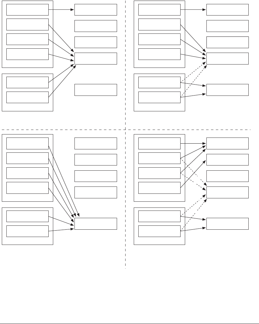
Debug Events
C3-4 Copyright © 1996-1998, 2000, 2004-2008 ARM Limited. All rights reserved. ARM DDI 0406B
Figure C3-2 Processor behavior on debug events, for v6 Debug and v6.1 Debug
Debug disabled or debug event not permitted
Debug-mode: Halting Debug-mode: Monitor
External Debug
Request
BKPT Instruction
Breakpoint
Vector Catch
Watchpoint
Halt Request
Debug State
Entry
Software Debug Events
Halting Debug Events
External Debug
Request
BKPT Instruction
Breakpoint
Vector Catch
Watchpoint
Halt Request
Debug Exception
(Prefetch Abort)
Debug State
Entry
Software Debug Events
Halting Debug Events
Debug Exception
(Data Abort)
UNPREDICTABLE
Ignored
Debug Exception
(Prefetch Abort)
Debug Exception
(Data Abort)
UNPREDICTABLE
Ignored
IMPLEMENTATION DEFINED altenative behavior for v6 Debug
Some cases are ignored, see text
Debug-mode: none
External Debug
Request
BKPT Instruction
Breakpoint
Vector Catch
Watchpoint
Software Debug Events
Halting Debug Events
Debug Exception
(Prefetch Abort)
Debug Exception
(Data Abort)
Ignored
UNPREDICTABLE
Halt Request
Debug State
Entry
IMPLEMENTATION DEFINED altenative behavior for v6 Debug
BKPT Instruction
Breakpoint
Vector Catch
Watchpoint
Software Debug Events
Halting Debug Events
Debug Exception
(Prefetch Abort)
Debug Exception
(Data Abort)
UNPREDICTABLE
Ignored
External Debug
Request
Halt Request
Debug State
Entry

Debug Events
ARM DDI 0406B Copyright © 1996-1998, 2000, 2004-2008 ARM Limited. All rights reserved. C3-5
C3.2 Software debug events
A Software debug event can be any of the following:
• A Breakpoint debug event, see Breakpoint debug events
• A Watchpoint debug event, see Watchpoint debug events on page C3-15
• A BKPT Instruction debug event, see BKPT Instruction debug events on page C3-20
• A Vector Catch debug event, see Vector Catch debug events on page C3-20.
Memory addresses on page C3-23 describes the addresses used for generating Software debug events in
different memory system implementations.
If Monitor debug-mode is selected and enabled, the behavior of certain types of Software debug event is
UNPREDICTABLE. For more information, see Unpredictable behavior on Software debug events on
page C3-24.
Pseudocode details of Software debug events on page C3-27 gives pseudocode for the operation of the
Software debug events.
C3.2.1 Breakpoint debug events
A Breakpoint debug event is defined by a pair of registers described to as a Breakpoint Register Pair (BRP),
comprising a Breakpoint Control Register (DBGBCR) and a Breakpoint Value Register (DBGBVR). BRPs,
DBGBCRs, and DBGBVRs number upwards from 0, with BRPn comprising DBGBCRn and DBGBVRn.
For details of the breakpoint registers see:
•Breakpoint Control Registers (DBGBCR) on page C10-49
•Breakpoint Value Registers (DBGBVR) on page C10-48.
The DBGDIDR.BRPs field specifies the number of BRPs implemented, see Debug ID Register
(DBGDIDR) on page C10-3. The maximum number of BRPs is 16.
You can define a Breakpoint debug event:
• Based on comparison of an Instruction Virtual Address (IVA) with the value held in a DBGBVR. See
Memory addresses on page C3-23 for the definition of an IVA.
• Based on comparison of the Context ID with the value held in a DBGBVR. Some BRPs might not
support Context ID comparison. The DBGDIDR.CTX_CMPs field specifies the number of BRPs
that support Context ID comparison, see Debug ID Register (DBGDIDR) on page C10-3.
• By linking a BRP to a second BRP, to define a single Breakpoint debug event. One pair includes an
IVA for comparison, and the second pair includes a Context ID value.
In all cases, the DBGBCR defines some additional conditions that must be met for the BRP to generate a
Breakpoint debug event, including whether the BRP is enabled.
The terms hit and miss are used to describe whether the conditions defined in the BRP are met:
• a hit occurs when the conditions are met
• a miss occurs when a condition is not met, meaning the processor does not generate a debug event.

Debug Events
C3-6 Copyright © 1996-1998, 2000, 2004-2008 ARM Limited. All rights reserved. ARM DDI 0406B
The following sections describe Breakpoint debug events:
•Generation of Breakpoint debug events
•Debug event generation conditions defined by the DBGBCR on page C3-7
•IVA comparisons for Debug event generation on page C3-8
•IVA comparisons and instruction length on page C3-10
•Context ID comparisons for Debug event generation on page C3-13
•Additional considerations for IVA mismatch breakpoints on page C3-13
•Additional conditions for linked BRPs on page C3-15.
Generation of Breakpoint debug events
For each instruction in the program flow, the debug logic tests all the BRPs. For each BRP, the debug logic
generates a Breakpoint debug event only if all of the following apply:
• When the BRP is tested, the conditions specified in the DBGBCR are met, see Debug event
generation conditions defined by the DBGBCR on page C3-7.
• The comparison with the value in the DBGBVR is successful. When two BRPs are linked to define
a single Breakpoint debug event, both comparisons must succeed. For more information see:
—IVA comparisons for Debug event generation on page C3-8
—Context ID comparisons for Debug event generation on page C3-13.
• The instruction is committed for execution.
Note
The processor must test for any possible Breakpoint debug events before it executes the instruction.
The debug logic might test the BRPs when an instruction is prefetched. However, it must not generate
a Breakpoint debug event if the instruction is not committed for execution.
If all of these conditions are met, the debug logic generates the Breakpoint debug event regardless of
whether the instruction passes its condition code test.
In ARMv6 and the ARMv7-A and ARMv7-R architecture profiles, the debug logic generates the debug
event regardless of the type of instruction.
Breakpoint debug events are synchronous. That is, the debug event acts like an exception that cancels the
breakpointed instruction.
When invasive debug is enabled and Monitor debug-mode is selected, if Breakpoint debug events are
permitted a Breakpoint debug event generates a Prefetch Abort exception.

Debug Events
ARM DDI 0406B Copyright © 1996-1998, 2000, 2004-2008 ARM Limited. All rights reserved. C3-7
Debug event generation conditions defined by the DBGBCR
For each BRP, the DBGBCR defines some conditions for generating a Breakpoint debug event, using the
following register fields:
Breakpoint enable
Controls whether this BRP is enabled.
Privileged mode control
Controls whether this BRP defines a Breakpoint debug event that can occur:
• only in User mode
• only in a privileged mode
• only in User, System or Supervisor modes
• in any mode.
Security state control
If the processor implements the Security Extensions, this field controls whether this BRP
defines a Breakpoint debug event that can occur only in Secure state, only in Non-secure
state, or in either security state.
For more information, including the differences in different versions of the Debug architecture, see
Breakpoint Control Registers (DBGBCR) on page C10-49.
When two BRPs are linked to define a single Breakpoint debug event, the BRP that defines the IVA
comparison also defines the privileged mode control and security state control, see Additional conditions
for linked BRPs on page C3-15 for more information.
Other information in the DBGBCR
In addition to defining these conditions for generating a Breakpoint debug event, the DBGBCR controls the
following:
• The DBGBVR meaning field defines the breakpoint type. The following sections describe all of the
breakpoint types:
—IVA comparisons for Debug event generation on page C3-8
—Context ID comparisons for Debug event generation on page C3-13.
• The Linked BRP number field specifies whether the BRP is linked to another BRP. If this BRP is
linked, this field gives the number of the linked BRP. For more information see Additional conditions
for linked BRPs on page C3-15.
• For an IVA comparison, the DBGBVR defines a word-aligned address, and the Byte address select
field specifies the bytes in that word that comprise the breakpointed instruction, see IVA comparisons
for Debug event generation on page C3-8.
• For an IVA comparison in v7 Debug, the Address range mask field optionally specifies a bitmask that
defines the low-order bits of the IVA and DBGBVR values that are excluded from the comparison,
see IVA comparisons for Debug event generation on page C3-8.

Debug Events
C3-8 Copyright © 1996-1998, 2000, 2004-2008 ARM Limited. All rights reserved. ARM DDI 0406B
Note
For IVA comparison in v7 Debug, you must use either byte address selection or address range
masking to restrict the comparison made. However, you cannot use both at the same time.
IVA comparisons for Debug event generation
The result of an IVA comparison depends on the value in the DBGBVR either matching or mismatching the
IVA value. In each case, you can link the BRP to a second BRP that defines a Context ID comparison. This
means that the breakpoint types that depend on an IVA comparison are:
• Unlinked IVA match
• Unlinked IVA mismatch
• Linked IVA match
• Linked IVA mismatch.
When the DBGBCR is programmed for one of these breakpoint types, the debug logic generates a
Breakpoint debug event only if all the other conditions for the breakpoint are met, and the IVA comparison
is successful. That is, all other conditions are met and, taking account of any masking:
• for an IVA match, the IVA value equals the value in the DBGBVR
• for an IVA mismatch, the IVA value does not equal the value in the DBGBVR.
In the linked cases, the debug logic generates a Breakpoint debug event only if all the other conditions for
the breakpoint are met, the IVA comparison is successful, and the Context ID comparison in the linked BRP
is successful, see Context ID comparisons for Debug event generation on page C3-13. See Additional
conditions for linked BRPs on page C3-15 for more information.
All versions of the Debug architecture support byte address selection, to specify which bytes of the word
addressed by DBGBVR comprise the breakpointed instruction. v7 Debug supports an alternative bit
masking scheme referred to as address range masking. The following subsections give more information
about the IVA comparisons:
•Condition for breakpoint generation on IVA match, without address range masking on page C3-9
•Condition for breakpoint generation on IVA mismatch, without address range masking on page C3-9
•Breakpoint address range masking behavior, v7 Debug on page C3-9.
DBGBVR values must be word-aligned, and DBGBVR[1:0] are never used for IVA comparison. ARM
instructions are always word-aligned, and therefore a DBGBVR value can specify exactly the IVA of an
ARM instruction. See IVA comparisons and instruction length on page C3-10 for more information about
how the instruction length affects how you must define a breakpoint.
Note
• v6 Debug does not support IVA mismatch.
• If it is supported, you can use IVA mismatch to generate a Breakpoint debug event when the processor
executes an instruction other than the instruction indicated by the DBGBVR. You can use this for
single-stepping, or for breakpointing all instructions outside a range of instruction addresses.

Debug Events
ARM DDI 0406B Copyright © 1996-1998, 2000, 2004-2008 ARM Limited. All rights reserved. C3-9
Condition for breakpoint generation on IVA match, without address range masking
When BRPn is programmed for IVA match, without address range masking, and all other conditions for
generating a breakpoint are met, a Breakpoint debug event is generated only if both:
• bits [31:2] of the IVA are equal to the value of bits [31:2] of DBGBVRn
• the Byte address select field, bits [8:5], of DBGBCRn is programmed for an IVA match for the
current Instruction set state and IVA[1:0] value, see Byte address selection behavior on IVA match or
mismatch on page C10-55.
Note
In v7 Debug, to perform IVA comparison without address range masking you must set DBGBCR[28:24],
the Address range mask field, to zero.
Condition for breakpoint generation on IVA mismatch, without address range masking
When BRPn is programmed for IVA mismatch, without address range masking, and all other conditions for
generating a breakpoint are met, a Breakpoint debug event is generated only if either:
• bits [31:2] of the IVA are not equal to the value of bits [31:2] of DBGBVRn
• the Byte address select field, bits [8:5], of DBGBCRn is programmed for an IVA mismatch for the
current Instruction set state and IVA[1:0] value, see Byte address selection behavior on IVA match or
mismatch on page C10-55.
Note
In v7 Debug, to perform IVA comparison without address range masking you must set DBGBCR[28:24],
the Address range mask field, to zero.
Breakpoint address range masking behavior, v7 Debug
When BRPn is programmed for IVA matching, the comparison is masked using the value held in the
Address range mask field, DBGBCRn[28:24].
You can use the Address range mask field when programming the BRP for IVA mismatch, that is, when
DBGBCR[28:24] != 0b00000 and DBGBCR[22] == 1. In this case, the address comparison portion of
breakpoint generation hits for all addresses outside the masked address region.
If an implementation does not support breakpoint address range masking, the Address range mask field is
RAZ.

Debug Events
C3-10 Copyright © 1996-1998, 2000, 2004-2008 ARM Limited. All rights reserved. ARM DDI 0406B
Note
There is no encoding for a full 32-bit mask. This mask would have the effect of setting a breakpoint that hits
on every address comparison, and you can achieve this by setting:
• DBGBCR[22] to 1 to select an IVA mismatch
• DBGBCR[8:5] to 0b0000.
To use address range masking, you must also set DBGBCR[8:5], the Byte address field, to 0b1111.
IVA comparisons and instruction length
An instruction set is fixed-length if all of its instructions have the same length, and variable-length
otherwise. In a variable-length instruction set a single instruction comprises one or more units of memory.
The ARM instruction set is an example of a fixed-length instruction set. In the ARM instruction set the size
of each instruction is one word, and ARM instructions are always word aligned.
The following are examples of variable-length instruction sets:
• The ThumbEE instruction set, and the Thumb instruction set from ARMv6T2 onwards. In these
instruction sets an instruction comprises one or two halfwords.
• Java bytecodes. A single Java bytecode comprises one or more bytes.
Before ARMv6T2, an implementation can treat the Thumb instruction set as a fixed-length 16-bit
instruction set, as described in BL and BLX (immediate) instructions, before ARMv6T2 on page AppxG-4.
An implementation that does this can permit an exception to be taken between the two halfwords of a
BL
or
BLX
(immediate) instruction.
In a variable-length instruction set, for an instruction consisting of more than one unit of memory, the first
unit of the instruction is defined as the unit of the instruction with the lowest address in memory.
In a fixed-length instruction set, an instruction consists of a single unit of memory. This unit is also the first
unit of the instruction.
Instruction length considerations depend on the Debug architecture version, as described in the following
subsections:
•Effect of instruction length in v7 Debug
•Effect of instruction length in v6 Debug and v6.1 Debug on page C3-11.
IVA comparison programming examples on page C3-12 gives examples of Breakpoint programming, taking
account of possible instruction length effects, for all versions of the Debug architecture.
Effect of instruction length in v7 Debug
In v7 Debug there are four types of IVA breakpoint:
• IVA match with no address range mask, described as a regular IVA breakpoint
• IVA mismatch with no address range mask, described as a step-off IVA breakpoint
• IVA match with an address range mask, described as an included range IVA breakpoint

Debug Events
ARM DDI 0406B Copyright © 1996-1998, 2000, 2004-2008 ARM Limited. All rights reserved. C3-11
• IVA mismatch with an address range mask, described as an excluded range IVA breakpoint
Note
Support for address range masks on breakpoints is IMPLEMENTATION DEFINED.
For all types of IVA breakpoint, if the conditions in the DBGBCR are met, and the instruction is committed
for execution, the BRP generates a Breakpoint debug event if the required DBGBVR comparison, taking
account of the byte address selection and any address range masking, hits for the first unit of the instruction.
Table C3-2 shows the conditions for Breakpoint debug event generation by an instruction that comprises
more than one unit of memory, assuming that the conditions in the DBGBCR are met and that the instruction
is committed for execution.
Effect of instruction length in v6 Debug and v6.1 Debug
If the conditions in the DBGBCR are met, and the instruction is committed for execution, the BRP generates
a Breakpoint debug event if the required DBGBVR comparison, taking account of the byte address
selection, hits for the first unit of the instruction.
In v6 Debug and v6.1 Debug, it is IMPLEMENTATION DEFINED whether an IVA comparison on an instruction
memory unit other than the first unit, following a breakpoint miss on the first unit of the instruction, can
cause a Breakpoint debug event.
For Java bytecodes, v6 Debug and v6.1 Debug specify that a BRP comparison on an operand does not
generate a Breakpoint debug event. A Breakpoint debug is generated only if the BRP hits on the opcode.
For Java bytecodes the instruction memory unit is a byte, and the opcode is always the first byte of the
instruction.
Table C3-2 Breakpoint debug event generation for instructions of more than one unit of memory
DBGBVR comparison resulta:
IVA breakpoint type Breakpoint debug
event generated?
First unitbAny subsequent unitb
Hit - Any Yes
Miss Hit Regular, included range, or excluded range UNPREDICTABLE
Step-off No
Miss Miss Any No
a. Taking account of the byte address selection and any address range masking.
b. Of the instruction whose IVA is being compared.

Debug Events
C3-12 Copyright © 1996-1998, 2000, 2004-2008 ARM Limited. All rights reserved. ARM DDI 0406B
Note
• v6 Debug does not support IVA mismatch breakpoints.
• v6.1 Debug and v6 Debug do not support address range masks on breakpoints.
IVA comparison programming examples
In all Debug architecture versions, a debugger must configure the BRP so that it matches on all bytes of the
first unit of the instruction, otherwise the generation of Breakpoint debug events is UNPREDICTABLE.
Before ARMv6T2, on a processor that implements the Thumb instruction set and can take an exception
between the two halfwords of a Thumb
BL
or
BLX
(immediate) instruction, a debugger must treat the two
halfwords as separate instructions, and set breakpoints on both halfwords. This might require two BRPs.
Note
• To ensure compatibility across ARMv6 implementations, a debugger can always treat
BL
or
BLX
(immediate) as two instructions when debugging code on an ARMv6 processor before ARMv6T2.
• The examples that follow include setting breakpoints on ThumbEE instructions. These are supported
only in ARMv7.
For example, if BRPn and BRPm are two breakpoint register pairs, then:
• On any ARMv6 or ARMv7 processor:
— To breakpoint on a Java bytecode at address
0x8001
, the debugger must set DBGBVRn to
0x8000
and DBGBCRn[8:5] to 0b0010.
— To breakpoint on a 16-bit Thumb or ThumbEE instruction starting at address
0x8002
, a
debugger must set DBGBVRn to
0x8000
and DBGBCRn[8:5] to 0b1100.
— To breakpoint on an ARM instruction starting at address
0x8004
, a debugger must set
DBGBVRn to
0x8004
and DBGBCRn[8:5] to 0b1111.
• On an ARMv7 or ARMv6T2 processor, a debugger sets breakpoints on a 32-bit Thumb instruction,
or on a 16-bit or a 32-bit ThumbEE instruction, in exactly the same way as on a 16-bit Thumb
instruction. For example:
— To breakpoint on a 16-bit or a 32-bit Thumb or ThumbEE instruction starting at address
0x8000
, the debugger must set DBGBVRn to
0x8000
and DBGBCRn[8:5] to 0b0011. These are
the settings for breakpointing on any Thumb or ThumbEE instruction, including
BL
and
BLX
(immediate).
• On an ARMv6 or ARMv6K processor:
— To breakpoint on a Thumb
BL
or
BLX
instruction at address
0x8000
, a debugger must set
DBGBVRn to
0x8000
, and DBGBCRn[8:5] to 0b1111.
— To breakpoint on a Thumb
BL
or
BLX
instruction at address
0x8002
, a debugger must set
DBGBVRn to
0x8000
, DBGBVRm to
0x8004
, DBGBCRn[8:5] to 0b1100, and
DBGBCRm[8:5] to 0b0011.

Debug Events
ARM DDI 0406B Copyright © 1996-1998, 2000, 2004-2008 ARM Limited. All rights reserved. C3-13
Note
When programming DBGBVR for IVA match or mismatch, the debugger must program DBGBVR[1:0] to
0b00, otherwise Breakpoint debug event generation is UNPREDICTABLE.
Context ID comparisons for Debug event generation
A Context ID comparison depends on the value in the DBGBVR matching the Context ID, held in the
Context ID Register, when the instruction is committed for execution. The breakpoint types that depend on
a Context ID comparison are:
• Unlinked Context ID match
• Linked Context ID match.
When the DBGBCR is programmed for one of these debug types, the debug logic generates a Breakpoint
debug event only if all the other conditions for the breakpoint are met, and the Context ID equals the value
in the DBGBVR.
In the linked case, the BRP that is programmed for a Context ID match is linked to at least one of:
• a BRP programmed for Linked IVA match or mismatch
• a Watchpoint Register Pair (WRP) programmed for linked Data Virtual Address (DVA) match.
In the linked IVA cases, the debug logic generates a Breakpoint debug event only if all the other conditions
for the breakpoint are met, the Context ID comparison is successful, and the IVA comparison in the linked
BRP is successful, see IVA comparisons for Debug event generation on page C3-8. See Additional
conditions for linked BRPs on page C3-15 for more information.
In the linked DVA case, the debug logic generates a Watchpoint debug event only if all the other conditions
for the watchpoint are met, the Context ID comparison is successful, and the DVA comparison in the linked
WRP is successful, See Watchpoint debug events on page C3-15 for more information.
Note
• You cannot define a Breakpoint debug event based on a Context ID mismatch.
• You can link a BRP programmed for linked Context ID match to any number of:
— BRPs programmed for Linked IVA match or mismatch
— WRPs programmed for Linked DVA match.
This means you can use a single BRP to define the Context ID match for multiple breakpoints and
watchpoints.
Additional considerations for IVA mismatch breakpoints
The following subsections describe additional considerations for IVA mismatch breakpoints:
•Interaction of IVA mismatch breakpoints with other breakpoints and Vector Catch on page C3-14
•Generation of IVA mismatch breakpoints on branch to self instructions on page C3-14.

Debug Events
C3-14 Copyright © 1996-1998, 2000, 2004-2008 ARM Limited. All rights reserved. ARM DDI 0406B
Interaction of IVA mismatch breakpoints with other breakpoints and Vector Catch
When a BRPn is programmed for IVA mismatch and does not generate a Breakpoint debug event because
the general conditions specified in DBGBCRn are not met, this does not affect the generation of:
• Breakpoint debug events by other BRPs
• Vector Catch debug events.
Note
In this context, the general conditions specified in DBGBCR not being met means that at least one of the
following applies:
• the BRP is not enabled
• the Privileged mode control bits of the DBGBCR do not match the mode of the processor
• DBGBCR is configured for linked Context ID matching but the linked BRP either is not enabled or
does not match the current Context ID
• the Security Extensions are implemented, and the Security state control field of DBGBCR does not
match the security state of the processor.
However, if the general conditions specified in DBGBCRn are met, and BRPn does not generate a
Breakpoint debug event only because the IVA fails the comparison required for an IVA mismatch, then the
failure of this comparison can affect the generation of other debug events:
• if any other BRP, BRPm, hits on its required comparison with the IVA and meets the general
conditions specified in DBGBCRm, it is UNPREDICTABLE whether BRPm generates a Breakpoint
debug event
• if the Vector Catch Register defines a Vector Catch that matches the IVA, it is UNPREDICTABLE
whether a Vector Catch debug event is generated.
Generation of IVA mismatch breakpoints on branch to self instructions
This section describes the generation of Breakpoint debug events when the IVA of an instruction that
branches to itself misses a BRP programmed for IVA mismatch, and all the general conditions specified in
the DBGBCR are met. See the IVA mismatch column of Table C10-11 on page C10-56 for details of when
an IVA mismatch comparison misses. In this case:
1. The first time the instruction is committed for execution the BRP does not generate a Breakpoint
debug event.
2. Because the instruction branches to itself, if no exception is generated, the instruction is committed
for execution again. On this and any subsequent execution, it is UNPREDICTABLE whether the BRP
generates a Breakpoint debug event.

Debug Events
ARM DDI 0406B Copyright © 1996-1998, 2000, 2004-2008 ARM Limited. All rights reserved. C3-15
Note
Instructions that branch to themselves include:
• a branch instruction that specifies itself as the branch destination
• a load instruction that loads the PC from a memory location that holds the address of that load
instruction.
Additional conditions for linked BRPs
When you link two BRPs to define a single Linked IVA match or mismatch breakpoint, if BRPn defines the
IVA match or mismatch and BRPm defines the Context ID match:
• for the DBGBCR fields described in Debug event generation conditions defined by the DBGBCR on
page C3-7, you must program DBGBCRn and DBGBCRm as follows:
— in DBGBCRn, program the Security state control and Privileged mode control fields to define
the required conditions for Debug event generation
— in DBGBCRm, program the Security state control field to 0b00, and the Privileged mode
control field to 0b11
• you must program the Linked BRP number field:
— of DBGBCRn with the value of m
— of DBGBCRm to zero
• you must program the DBGBVR meaning field:
— of DBGBCRn for Linked IVA match or mismatch
— of DBGBCRm for Linked Context ID match
• BRPm must support Context ID comparisons.
Breakpoint debug event generation is UNPREDICTABLE if you do not meet all these conditions.
You must also set the Breakpoint enable bits in DBGBCRn and DBGBCRm to 1, to enable both BRPs.
Note
If you fail to enable either or both of the BRPs, BRPn never generates any Breakpoint debug events.
For more information see Linked comparisons on page C10-59
C3.2.2 Watchpoint debug events
A Watchpoint debug event is defined by a pair of registers described as a Watchpoint Register Pair (WRP),
comprising a Watchpoint Control Register (DBGWCR) and a Watchpoint Value Register (DBGWVR).
WRPs, DBGWCRs, and DBGWVRs number upwards from 0, with WRPn comprising DBGWCRn and
DBGWVRn. For details of the Watchpoint registers see:
•Watchpoint Control Registers (DBGWCR) on page C10-61

Debug Events
C3-16 Copyright © 1996-1998, 2000, 2004-2008 ARM Limited. All rights reserved. ARM DDI 0406B
•Watchpoint Value Registers (DBGWVR) on page C10-60.
The DBGDIDR.WRPs field specifies the number of WRPs implemented, see Debug ID Register
(DBGDIDR) on page C10-3.
A WRP can be linked to a BRP, to define a single watchpoint event. The WRP holds a virtual address for
comparison, and the BRP holds a Context ID value. For more information, see Linked comparisons on
page C10-59.
A Watchpoint debug event is defined based on comparisons of a Data Virtual Address (DVA) with the value
held in a WVR. See Memory addresses on page C3-23 for the definition of a DVA.
For a given Watchpoint Register Pair, WRPn, a Watchpoint debug event occurs when all of the following
are true:
• The watchpoint is enabled, in DBGWCRn.
• The DVA matches the value in DBGWVRn.
• When the processor tests the WRP, all the conditions of DBGWCRn are met.
• If linking is enabled in DBGWCRn, when the processor tests the WRP, the Linked Context ID
matching BRP, BRPm, meets the following conditions:
— the BRP is enabled, in DBGBCRm
— the value held in the DBGBVRm matches the Context ID held in the CONTEXTIDR.
For more information about BRPs see Breakpoint debug events on page C3-5.
• The instruction that initiated the memory access is committed for execution. A Watchpoint debug
event is generated only if the instruction passes its condition code check.
Note
A watchpoint match does not require the access to match exactly the watched address. A match is generated
on any access to any watched byte or bytes. For example, a match is generated on an unaligned word access
that includes a byte that is being watched, even when the watched byte is not in the same word as the start
address of the unaligned word.
All instructions that are defined as memory access instructions can generate Watchpoint debug events. For
information about which instructions are memory accesses see Alphabetical list of instructions on
page A8-14. Watchpoint debug event generation can be conditional on whether the memory access is a load
access or a store access.
For a Store-Exclusive instruction, if the target address of the instruction would generate a Watchpoint debug
event, but the check of whether the Store-Exclusive operation has control of the exclusive monitors returns
FALSE, then it is IMPLEMENTATION DEFINED whether the processor generates the Watchpoint debug event.

Debug Events
ARM DDI 0406B Copyright © 1996-1998, 2000, 2004-2008 ARM Limited. All rights reserved. C3-17
For each of the memory hint instructions,
PLD
and
PLI
, it is IMPLEMENTATION DEFINED whether the
instruction generates Watchpoint debug events. If either or both of the
PLD
and
PLI
instructions normally
generates Watchpoint debug events, the behavior must be:
•For the
PLI
instruction:
— no watchpoint is generated in a situation where, if the instruction was a real fetch rather than
a hint, the real fetch would generate a Prefetch Abort exception
— in all other situations a Watchpoint debug event is generated.
•For the
PLD
instruction:
— no watchpoint is generated in a situation where, if the instruction was a real memory access
rather than a hint, the real memory access would generate a Data Abort exception
— in all other situations a Watchpoint debug event is generated.
• When watchpoint generation is conditional on the type of memory access, a memory hint instruction
is treated as generating a load access.
It is IMPLEMENTATION DEFINED whether the following cache maintenance operations generate Watchpoint
debug events:
• Clean data or unified cache line by MVA to PoU, DCCMVAU
• Clean data or unified cache line by MVA to PoC, DCCMVAC
• Invalidate data or unified cache line by MVA to PoC, DCIMVAC
• Invalidate instruction cache line by MVA to PoU, ICIMVAU
• Clean and Invalidate data or unified cache line by MVA to PoC, DCCIMVAC.
When Watchpoint debug event generation by these cache maintenance operations is implemented, the
behavior must be:
• the cache maintenance operation must generate a Watchpoint debug event on a DVA match,
regardless of whether the data is stored in any cache
• when watchpoint generation is conditional on the type of memory access, a cache maintenance
operation is treated as generating a store access.
For regular data accesses, the size of the access is considered when determining whether a watched byte is
being accessed. The size of the access is IMPLEMENTATION DEFINED for:
• memory hint instructions,
PLD
and
PLI
• cache maintenance operations.
Watchpoint debug events are precise and can be synchronous or asynchronous:
• a synchronous Watchpoint debug event acts like a synchronous abort exception on the memory access
instruction itself
• an asynchronous Watchpoint debug event acts like a precise asynchronous abort exception that
cancels a later instruction.
For more information, see Synchronous and Asynchronous Watchpoint debug events on page C3-18.

Debug Events
C3-18 Copyright © 1996-1998, 2000, 2004-2008 ARM Limited. All rights reserved. ARM DDI 0406B
For the ordering of debug events, ARMv7 requires that:
• Regardless of the actual ordering of memory accesses, Watchpoint debug events must be taken in
program order. See Debug event prioritization on page C3-43.
• Watchpoint debug events must behave as if the processor tested for any possible Watchpoint debug
event before the memory access was observed, regardless of whether the Watchpoint debug event is
synchronous or asynchronous. See Generation of debug events on page C3-40.
Synchronous and Asynchronous Watchpoint debug events
ARMv7 permits watchpoints to be either synchronous or asynchronous. An implementation can implement
synchronous watchpoints, asynchronous watchpoints, or both. It is IMPLEMENTATION DEFINED under what
circumstances a watchpoint is synchronous or asynchronous.
ARMv6 only permits asynchronous watchpoints.
Synchronous Watchpoint debug events
A synchronous Watchpoint debug event acts like a synchronous abort:
• The debug event occurs before any following instructions or exceptions have altered the state of the
processor.
• The value in the base register for the memory access is not updated.
Note
The Base Updated Abort Model is not permitted in ARMv7.
• If the instruction was a register load, the data returned is marked as invalid and:
— if the instruction was a single register load, the destination is not updated
— if the instruction loaded multiple registers, the values in the destination registers, other than
the PC and base register, are UNKNOWN.
• If the instruction is a coprocessor load, the values left in the coprocessor registers are UNKNOWN.
• If the instruction is a store, the content of the memory location written to is unchanged.
When invasive debug is enabled and Monitor debug-mode is selected, if Watchpoint debug events are
permitted a synchronous Watchpoint debug event generates a synchronous Data Abort exception. On a
synchronous Watchpoint debug event, the DBGDSCR.MOE field is set to Synchronous Watchpoint
occurred.
When an instruction that causes multiple memory operations is addressing Device or Strongly-ordered
memory, if a synchronous Watchpoint debug event is signaled by a memory operation other than the first
operation of the instruction, the memory access rules might not be maintained. Examples of instructions that
cause multiple memory operations are the
LDM
and
LDC
instructions.

Debug Events
ARM DDI 0406B Copyright © 1996-1998, 2000, 2004-2008 ARM Limited. All rights reserved. C3-19
For example, if the second memory operation of an
STM
instruction signals a synchronous Watchpoint debug
event, then when the instruction is re-tried following processing of the debug event, the first memory
operation is repeated. This behavior is not normally permitted for accesses to Device or Strongly-ordered
memory.
To avoid this circumstance, debuggers must not set watchpoints on addresses in regions of Device or
Strongly-ordered memory that might be accessed in this way. The address range masking features of
watchpoints can be used to set a watchpoint on an entire region, ensuring the synchronous Watchpoint debug
event is taken on the first operation of such an instruction.
Asynchronous Watchpoint debug events
An asynchronous Watchpoint debug event acts like a precise asynchronous abort. Its behavior is:
• The watchpointed instruction must have completed, and other instructions that followed it, in
program order, might have completed. For more information, see Recognizing asynchronous
Watchpoint debug events.
• The watchpoint must be taken before any exceptions that occur in program order after the watchpoint
is triggered.
• All the registers written by the watchpointed instruction are updated.
• Any memory accessed by the watchpointed instruction is updated.
When invasive debug is enabled and Monitor debug-mode is selected, if Watchpoint debug events are
permitted an asynchronous Watchpoint debug event generates a precise asynchronous Data Abort exception.
An asynchronous Watchpoint debug event is not an abort and is not affected by architectural rules about
aborts, including the rules about external aborts and asynchronous aborts. An asynchronous Watchpoint
debug event:
• is not affected by the SCR.EA bit
• is not ignored when the CPSR.A bit is set to 1.
On an asynchronous Watchpoint debug event, the DBGDSCR.MOE field is set to Asynchronous
Watchpoint occurred.
Recognizing asynchronous Watchpoint debug events
When an instruction that consists of multiple memory operations is accessing Device or Strongly-ordered
memory, and an asynchronous Watchpoint debug event is signaled by a memory operation other than the
first operation of the instruction, the debug event must not cause Debug state entry or a debug exception until
all the operations have completed. This ensures the memory access rules for Device and Strongly-ordered
memory are preserved.
Examples of instructions that cause multiple memory operations are the
LDM
and
LDC
instructions.

Debug Events
C3-20 Copyright © 1996-1998, 2000, 2004-2008 ARM Limited. All rights reserved. ARM DDI 0406B
Note
To understand why the architecture does not permit the asynchronous Watchpoint debug event to be taken
before the watchpointed instruction completes, consider an
LDM
instruction accessing Device or
Strongly-ordered memory, with an asynchronous Watchpoint debug event signaled after the first word of
memory is accessed. If the debug event was taken immediately, the
LDM
would be re-executed on return from
the event handler. This would cause a new access to the first word of memory, breaking the rule that, for
Device or Strongly-ordered memory, each memory operation of an instruction is issued precisely once.
C3.2.3 BKPT Instruction debug events
A BKPT Instruction debug event occurs when a
BKPT
instruction is committed for execution.
BKPT
is an
unconditional instruction.
BKPT Instruction debug events are synchronous. That is, the debug event acts like an exception that cancels
the
BKPT
instruction.
For details of the
BKPT
instruction and its encodings in the ARM and Thumb instruction sets see BKPT on
page A8-56.
C3.2.4 Vector Catch debug events
The Vector Catch Register (DBGVCR) controls Vector Catch debug events, see Vector Catch Register
(DBGVCR) on page C10-67.
A Vector Catch debug event occurs when:
• The IVA of an instruction matches a vector address for the current security state.
See Memory addresses on page C3-23 for a definition of the IVA.
• When the processor tests for the possible vector catch, the corresponding bit of the DBGVCR is set
to 1, indicating that vector catch is enabled.
• The instruction is committed for execution. The debug event is generated whether the instruction
passes or fails its condition code check.
If all the conditions for a Vector Catch debug event are met, the processor generates the event regardless of
the mode in which it is executing.
The processor must test for any possible Vector Catch debug events before it executes the instruction.
If the Security Extensions are not implemented the debug logic uses only one set of vector addresses to
generate Vector Catch debug events, and these are called the Local vector addresses.
If the Security Extensions are implemented, the debug logic uses three sets of vector addresses to generate
Vector Catch debug events:
• One set for exceptions taken in the Non-secure exception modes. These are called the Non-secure
Local vector addresses.

Debug Events
ARM DDI 0406B Copyright © 1996-1998, 2000, 2004-2008 ARM Limited. All rights reserved. C3-21
• One set for exceptions taken in the Secure exception modes other than Monitor mode. These are
called the Secure Local vector addresses.
• One set for exceptions taken in Monitor mode. These are called the Monitor vector addresses.
You enable vector catch independently for each of these vector addresses, by setting a bit in the DBGVCR
to 1, see Vector Catch Register (DBGVCR) on page C10-67.
If the Security Extensions are not implemented, the debug logic determines whether to generate a Vector
Catch debug event by comparing every instruction fetch with the Local vector addresses.
If the Security Extensions are implemented, the debug logic determines whether to generate a Vector Catch
debug event by comparing every Secure instruction fetch with the Secure Local and Monitor vector
addresses, and by comparing every Non-secure instruction fetch with the Non-secure Local vector
addresses.
Note
Any instruction fetched from an exception vector address and committed for execution triggers a Vector
Catch debug event if the appropriate bit in the DBGVCR is set to 1. Testing for possible Vector Catch debug
events does not check whether the instruction is executed as a result of an exception entry.
Whether a Vector Catch debug event is generated for an instruction is UNPREDICTABLE if either:
• The exception vector address is word-aligned and one of the following applies:
— the first unit of the instruction is in the word at the exception vector address but is not at the
exception vector address
— the first unit of the instruction is not in the word at the exception vector address but another
unit of the instruction is in that word.
This can occur when the processor is executing a variable-length instruction set, that is, in Thumb,
ThumbEE or Jazelle state.
• The exception vector address is not word-aligned but is halfword-aligned and one of the following
applies:
— The first unit of the instruction is in the halfword at the exception vector address but is not at
the exception vector address. This can occur only in Jazelle state, where instructions consist
of one or more byte-sized units.
— The first unit of the instruction includes the halfword at the exception vector address but is not
at the exception vector address. This can occur only in ARM state, where all instructions are
a single word and are word-aligned.
— The first unit of the instruction is not in the halfword at the exception vector address but
another unit of the instruction is in that halfword. This can occur in variable-length instruction
set states, that is, in Thumb, ThumbEE or Jazelle state.

Debug Events
C3-22 Copyright © 1996-1998, 2000, 2004-2008 ARM Limited. All rights reserved. ARM DDI 0406B
Note
Normally, exception vector addresses must be word-aligned. However, when SCTLR.VE == 1, enabling
vectored interrupt support, the exception vector address for one or both of the IRQ and FIQ vectors might
not be word-aligned. Support for exception vector addresses that are not word-aligned is IMPLEMENTATION
DEFINED, see Vectored interrupt support on page B1-32.
If Monitor debug-mode is selected and enabled, and the vector is either the Prefetch Abort vector or the Data
Abort vector, the debug event is:
•UNPREDICTABLE in v7 Debug
• ignored in v6 Debug and v6.1 Debug.
Vector Catch debug events are synchronous. That is, the debug event acts like an exception that cancels the
instruction at the caught vector. When invasive debug is enabled and Monitor debug-mode is selected, if
Vector Catch debug events are permitted a Vector Catch debug event generates a Prefetch Abort exception.
For more information, see Generation of debug events on page C3-40.
Note
A Vector Catch debug event is taken only when the instruction is committed for execution and therefore
might not be taken if another exception occurs, see Debug event prioritization on page C3-43.
For more information, see Vector Catch Register (DBGVCR) on page C10-67.
Vector catch debug events and vectored interrupt support
The ARM architecture provides support for vectored interrupts, where an interrupt controller provides the
interrupt vector address directly to the processor. The mechanism for defining the vectors is
IMPLEMENTATION DEFINED. You enable the use of vectored interrupts by setting the SCTLR.VE bit to 1. For
more information see Vectored interrupt support on page B1-32.
Vectored interrupt support affects Vector Catch debug event generation for the IRQ and FIQ exception
vectors. These two vectors are described as the interrupt vectors. The details of Vector Catch debug event
generation on the interrupt vectors depend on whether the Security Extensions are implemented:
If the Security Extensions are not implemented
• If the SCTRL.VE bit is set to 0, then the Local vector addresses for IRQ and FIQ
vector catch are determined by the exception base address.
• If the SCTRL.VE bit is set to 1, then the Local vector address for an IRQ or FIQ
vector catch is the interrupt vector address supplied by the interrupt controller on
taking the interrupt.

Debug Events
ARM DDI 0406B Copyright © 1996-1998, 2000, 2004-2008 ARM Limited. All rights reserved. C3-23
If the Security Extensions are implemented
The Secure Local and Non-secure Local vector addresses for IRQ and FIQ vector catch are
determined by the appropriate banked copy of the SCTRL.VE bit:
• If the SCTRL.VE bit is set to 0, then the corresponding Local vector addresses for
IRQ and FIQ vector catch are determined by the banked exception base address.
• If the SCTRL.VE bit is set to 1, then for each of IRQ and FIQ vector catch:
— if the interrupt is taken in Secure or Non-Secure IRQ mode or FIQ mode, then
the corresponding Local vector address is the interrupt vector address supplied
by the interrupt controller on taking the interrupt.
— if the interrupt is taken in Monitor mode, then it is IMPLEMENTATION DEFINED
whether the IRQ and FIQ Vector Catch debug events generated from the Local
vector addresses can occur, and if they can occur the Secure and Non-secure
Local vector addresses for the vector catches are IMPLEMENTATION DEFINED.
The Monitor vector addresses for IRQ and FIQ vector catch are determined by the Monitor
exception base address.
When the Vector Catch debug logic uses addresses supplied by the interrupt controller, then:
• if the interrupt controller has not supplied an interrupt address to the processor since vectored
interrupt support was enabled then no Vector Catch debug events using Local vector addresses are
generated
• if Vector Catch debug events were not enabled when the interrupt controller supplied a vector address
to the processor, but have been enabled since, an implementation must consistently either:
— generate a Vector Catch debug event if the IVA of an instruction matches the Local vector
address
— not generate Vector Catch debug events using any Local vector address.
C3.2.5 Memory addresses
On processors that implement the Virtual Memory System Architecture (VMSA), and also implement the
Fast Context Switch Extension (FCSE):
• It is IMPLEMENTATION DEFINED whether the Instruction Virtual Address (IVA) used in generating
Breakpoint debug events is the Modified Virtual Address (MVA) or Virtual Address (VA) of the
instruction.
• It is IMPLEMENTATION DEFINED whether the Data Virtual Address (DVA) used in generating
Watchpoint debug events is the MVA or VA of the data access.
• The IVA used in generating Vector Catch debug events is always the VA of the instruction.
• The Watchpoint Fault Address Register (DBGWFAR) reads a VA plus an offset that depends on the
processor instruction set state.
• The Program Counter Sampling Register (DBGPCSR), if implemented, reads a VA plus an offset that
depends on the processor instruction set state.

Debug Events
C3-24 Copyright © 1996-1998, 2000, 2004-2008 ARM Limited. All rights reserved. ARM DDI 0406B
Note
The FCSE is optional in ARMv7, and ARM deprecates use of the FCSE.
On processors that implement the VMSA, and do not implement the FCSE:
• The IVA used in generating Breakpoint debug events is the VA of the instruction.
• The DVA used in generating Watchpoint debug events is the VA of the data access.
• The IVA used in generating Vector Catch debug events is the VA of the instruction.
• The DBGWFAR reads a VA plus an offset that depends on the processor instruction set state.
• The DBGPCSR reads a VA plus an offset that depends on the processor instruction set state.
On processors that implement the Protected Memory System Architecture (PMSA), the Virtual Address is
identical to the Physical Address (PA) and therefore:
• The IVA used in generating Breakpoint debug events is the PA of the instruction.
• The DVA used in generating Watchpoint debug events is the PA of the data access.
• The IVA used in generating Vector Catch debug events is the PA of the instruction.
• The DBGWFAR reads a PA plus an offset that depends on the processor instruction set state.
• The DBGPCSR reads a PA plus an offset that depends on the processor instruction set state.
For more information about the DBGWFAR, see:
•Effects of debug exceptions on CP15 registers and the DBGWFAR on page C4-4
•Effect of entering Debug state on CP15 registers and the DBGWFAR on page C5-4
•Watchpoint Fault Address Register (DBGWFAR) on page C10-28.
For more information about the DBGPCSR, see Program Counter sampling on page C8-2 and Program
Counter Sampling Register (DBGPCSR) on page C10-38.
C3.2.6 UNPREDICTABLE behavior on Software debug events
In ARMv6 the following events are ignored if Monitor debug-mode is configured, because they could lead
to an unrecoverable state:
• Vector Catch debug events on the Prefetch Abort and Data Abort vectors
• Unlinked Context ID Breakpoint debug events, if the processor is running in a privileged mode
• Linked or Unlinked Instruction Virtual Address mismatch Breakpoint debug events, if the processor
is running in a privileged mode.
In ARMv7, if Monitor debug-mode is configured the generation of the following events is UNPREDICTABLE
and can lead to an unrecoverable state:
• Vector Catch debug events on the Prefetch Abort and Data Abort vectors
• Unlinked Context ID Breakpoint debug events that are configured to be generated in any mode, or to
be generated only in privileged modes
• Linked or Unlinked Instruction Virtual Address mismatch Breakpoint debug events that are
configured to be generated in any mode, or to be generated only in privileged modes.

Debug Events
ARM DDI 0406B Copyright © 1996-1998, 2000, 2004-2008 ARM Limited. All rights reserved. C3-25
When Monitor debug-mode is configured, debuggers must avoid these cases by restricting the programming
of the debug event control registers:
• DBGVCR[28,27,12,11,4,3] must be programmed as zero, see Vector Catch Register (DBGVCR) on
page C10-67.
• The permitted values of the Privileged Mode control bits, DBGBCR[2:1], must be restricted in the
following cases:
— if DBGBCR[22:20] is set to 0b010, selecting an Unlinked Context ID breakpoint
— If DBGBCR[22:20] is set to 0b100 or 0b101, selecting an IVA mismatch breakpoint.
For these cases, DBGBCR[2:1] must be programmed to one of:
— 0b00, selecting match only in User, Supervisor or System mode
— 0b10, selecting match only in User mode.
See Debug exceptions in abort handlers for additional points that must be considered before using
the 0b00 setting.
For details of programming the DBGBCR see Breakpoint Control Registers (DBGBCR) on
page C10-49.
If these restrictions are not followed, processor behavior on a resulting debug event is UNPREDICTABLE.
When the Security Extensions are implemented Vector Catch debug events on the Secure Monitor Call
vector are not ignored and are not UNPREDICTABLE. However, normally DBGVCR[10] is also programmed
as zero, see Monitor debug-mode vector catch on Secure Monitor Call on page C3-26.
Debug exceptions in abort handlers
The previous section indicated that, in ARMv7, a debugger might set DBGBCR[2:1] to 0b00, match in User,
Supervisor and System modes, to avoid the possibility of reaching an unrecoverable state in the Unlinked
Context ID and IVA mismatch breakpoint cases when Monitor debug-mode is selected. However,
DBGBCR[2:1] must only be programmed to 0b00 if you are confident that the abort handler will not switch
to one of these modes before saving context that might be corrupted by an additional debug event. The
context that might be corrupted by such an event includes LR_abt, SPSR_abt, IFAR, DFAR, and DFSR.
It is unlikely that an abort handler would switch to User mode to process an abort before saving these
registers, so setting DBGBCR[2:1] to 0b10, match only in User mode, is safer.
Also, take care when setting a Breakpoint or BKPT Instruction debug event inside a Prefetch Abort or Data
Abort handler, or when setting a Watchpoint debug event on a data address that might be accessed by any
of these handlers.
In general, a user must only set Breakpoint or BKPT Instruction debug events inside an abort handler at a
point after the context that would be corrupted by a debug event has been saved. Breakpoint debug events
in code that might be run by an abort handler can be avoided by setting DBGBCR[2:1] to 0b00 or 0b01, as
appropriate.
Watchpoint debug events in abort handlers can be avoided by setting DBGWCR[2:1] for the watchpoint to
0b10, match only unprivileged accesses, if the code being debugged is not running in a privileged mode.

Debug Events
C3-26 Copyright © 1996-1998, 2000, 2004-2008 ARM Limited. All rights reserved. ARM DDI 0406B
If these guidelines are not followed, a debug event might occur before the handler has saved the context of
the abort, causing the context to be overwritten. This loss of context results in UNPREDICTABLE software
behavior. The context that might be corrupted by such an event includes LR_abt, SPSR_abt, IFAR, DFAR,
and DFSR.
Debug events in the debug monitor
Because debug exceptions generate Data Abort or Prefetch Abort exceptions, the precautions outlined in the
section Debug exceptions in abort handlers on page C3-25 also apply to debug monitors. The suggested
settings for breakpoints and watchpoints that can avoid taking debug exceptions in a Data Abort handler can
be used to avoid taking debug exceptions in the debug monitor.
In addition, particularly on ARMv7 processors that do not implement the Extended CP14 interface, and
particularly those that implement synchronous Watchpoint debug events, when Monitor debug-mode is
enabled debuggers must avoid:
• setting Watchpoint debug events on the addresses of debug registers
• setting Breakpoint and Vector Catch debug events on the addresses of instructions in the debug
monitor.
In particular, it is unwise to set a watchpoint on the address of the Watchpoint Control Register (DBGWCR)
for that watchpoint, or to set a breakpoint on the address of an instruction that disables the breakpoint.
The section Generation of debug events on page C3-40 identifies two problem cases:
• A write to the DBGWCR for a watchpoint set on the address of that DBGWCR, to disable that
watchpoint, triggers the watchpoint.
In this case:
— if watchpoints are asynchronous, the write to the DBGWCR still takes place and the
watchpoint is disabled. The debug software must then deal with the re-entrant debug
exception.
— if watchpoints are synchronous the value in the DBGWCR after the watchpoint is signaled is
unchanged, and the debug event is left enabled.
• an instruction that disables a breakpoint on that instruction triggers the breakpoint.
In this case, the debug exception is taken before the debug event is disabled.
In both of these cases it might be impossible to recover.
Monitor debug-mode vector catch on Secure Monitor Call
Debuggers must be cautious about programming a Vector Catch debug event on the Secure Monitor Call
(SMC) vector when Monitor debug-mode is configured. If such an event is programmed, the following
sequence can occur:
1. Non-secure code executes an
SMC
instruction.

Debug Events
ARM DDI 0406B Copyright © 1996-1998, 2000, 2004-2008 ARM Limited. All rights reserved. C3-27
2. The processor takes the
SMC
exception, branching to the Monitor vector in Monitor mode. The
SCR.NS bit is set to 1, indicating the
SMC
originated in the Non-secure state.
3. The Vector Catch debug event is taken. Although SCR.NS is set to 1, the processor is in the Secure
state because it is in Monitor mode.
4. The processor jumps to the Secure Prefetch Abort vector, and sets SCR.NS to 0.
Note
Aborts taken in Secure state cause SCR.NS to be set to 0.
5. The abort handler at the Secure Prefetch Abort handler can tell a Vector Catch debug event occurred,
and can determine the address of the
SMC
instruction from LR_mon. However, it cannot determine
whether that is a Secure or Non-secure address.
Therefore, ARM recommends that you do not program a Vector Catch debug event on the SMC vector when
Monitor debug-mode is enabled.
Note
This is not a security issue, because the sequence given here can only occur if SPIDEN is HIGH.
Possible effect of the Security Extensions on FIQ vector catch
When the Security Extensions are implemented, a debugger might need to consider the implications of the
SCR on a Vector Catch event set on the FIQ vector, when the SCR is configured with both:
• the SCR.FW bit set to 0, so the CPSR.F bit cannot be modified in Non-secure state
• the SCR.FIQ bit set to 0, so that FIQs are handled in FIQ mode.
With this configuration, if an FIQ occurs in Non-secure state, the processor does not set CPSR.F to disable
FIQs, and so the processor repeatedly takes the FIQ exception.
It might not be possible to debug this situation using the vector catch on FIQ because the instruction at the
FIQ exception vector is never committed for execution and therefore the debug event never occurs.
C3.2.7 Pseudocode details of Software debug events
The following subsections give pseudocode details of Software debug events:
•Debug events
•Breakpoints and Vector Catches on page C3-28
•Watchpoints on page C3-35.
Debug events
The following functions cause the corresponding debug events to occur:
BKPTInstrDebugEvent()

Debug Events
C3-28 Copyright © 1996-1998, 2000, 2004-2008 ARM Limited. All rights reserved. ARM DDI 0406B
BreakpointDebugEvent()
VectorCatchDebugEvent()
WatchpointDebugEvent()
If the debug event is not permitted, it is ignored by the processor.
Breakpoints and Vector Catches
If invasive debug is enabled, on each instruction the
Debug_CheckInstruction()
function checks for BRP and
DBGVCR matches. If a match is found the function calls
BreakpointDebugEvent()
or
VectorCatchDebugEvent()
. If the debug event is not permitted, it is ignored by the processor.
On a simple sequential execution model, the
Debug_CheckInstruction()
call for an instruction occurs just
before the Operation pseudocode for the instruction is executed, and any call it generates to
BreakpointDebugEvent()
or
VectorCatchDebugEvent()
must happen at that time. However, the architecture
does not define when the checks for BRP and DBGVCR matches are made, other than that they must be
made at or before that time. Therefore an implementation can perform the checks much earlier in an
instruction pipeline, marking the instruction as breakpointed, and cause a marked instruction to call
BreakpointDebugEvent()
or
VectorCatchDebugEvent()
if and when it is about to execute.
The
BRPMatch()
function checks an individual BRP match, calling the
BRPLinkMatch()
function if necessary
to check whether a linked BRP matches.
The
VCRMatch()
function checks for a Vector Catch debug event. When vectored interrupt support is enabled,
it uses variables to hold the IRQ and FIQ interrupt vector addresses supplied to the processor by the interrupt
controller on taking an interrupt in IRQ mode or FIQ mode. These variables are updated by the
VCR_OnTakingInterrupt()
function, that is called each time the processor takes an IRQ or FIQ interrupt.
For all of these functions, between a context changing operation and an exception entry, exception return or
explicit Instruction Synchronization Barrier (ISB) operation, it is UNPREDICTABLE whether the values of
CurrentModeIsPrivileged()
, CPSR.M,
CurrentInstrSet()
,
FindSecure()
, and the CONTEXTIDR used by
BRPMatch()
,
BRPLinkMatch()
, and
VCRMatch()
are the old or the new values.
// Debug_CheckInstruction()
// ========================
Debug_CheckInstruction(bits(32) address, integer length)
// Do nothing if debug disabled.
if DBGDSCR<15:14> == ‘00’ then return;
case CurrentInstrSet() of
when InstrSet_ARM
step = 4;
when InstrSet_Thumb, InstrSet_ThumbEE
step = 2;
when InstrSet_Jazelle
step = 1;
length = length / step;
vcr_match = FALSE;
brp_match = FALSE;

Debug Events
ARM DDI 0406B Copyright © 1996-1998, 2000, 2004-2008 ARM Limited. All rights reserved. C3-29
// Each unit of the instruction is checked against the VCR and the BRPs. VCRMatch()
// and BRPMatch() might return UNKNOWN for units other than the first unit of the
// instruction, as in some cases the generation of Debug events is UNPREDICTABLE.
for W = 0 to length-1
vcr_match = VCRMatch(address, W == 0) || vcr_match;
// This code does not take into account the case where a mismatch breakpoint
// does not match the address of an instruction but another breakpoint or
// vector catch does match the instruction. In that situation, generation of
// the Debug event is UNPREDICTABLE.
for N = 0 to UInt(DBGDIDR.BRPs)
brp_match = BRPMatch(N, address, W == 0) || brp_match;
address = address + step;
// A suitable debug event occurs if there has been a BRP match or a VCR match. If
// both have occurred, just one debug event occurs, and its type is IMPLEMENTATION
// DEFINED.
if vcr_match || brp_match then
if !vcr_match then BreakpointDebugEvent();
elsif !brp_match then VectorCatchDebugEvent();
else IMPLEMENTATION_DEFINED either BreakpointDebugEvent() or VectorCatchDebugEvent();
return;
// BRPMatch()
// ==========
boolean BRPMatch(integer N, bits(32) address, boolean first)
assert N <= UInt(DBGDIDR.BRPs);
// If this breakpoint is not enabled, return immediately.
if DBGBCR[N]<0> == ‘0’ return FALSE;
unk_match = FALSE;
// Mode control match
case DBGBCR[N]<2:1> of
when ‘00’
if UInt(DBGDIDR.Version) < 3 then
UNPREDICTABLE;
else
case CPSR.M of
when ‘10000’ mode_control_match = TRUE; // User mode
when ‘10011’ mode_control_match = TRUE; // Supervisor mode
when ‘11111’ mode_control_match = TRUE; // System mode
otherwise mode_control_match = FALSE; // Any other mode
when ‘01’ mode_control_match = CurrentModeIsPrivileged(); // Privileged mode
when ‘10’ mode_control_match = !CurrentModeIsPrivileged(); // Unprivileged mode
when ‘11’ mode_control_match = TRUE; // Any mode
// Byte lane select
case CurrentInstrSet() of

Debug Events
C3-30 Copyright © 1996-1998, 2000, 2004-2008 ARM Limited. All rights reserved. ARM DDI 0406B
when InstrSet_ARM
byte_select_match = (DBGBCR[N]<8:5> != ‘0000’);
when InstrSet_Thumb, InstrSet_ThumbEE
case address<1> of
when ‘0’ byte_select_match = (DBGBCR[N]<6:5> != ‘00’);
when ‘1’ byte_select_match = (DBGBCR[N]<8:7> != ‘00’);
when InstrSet_Jazelle
case address<1:0> of
when ‘00’ byte_select_match = (DBGBCR[N]<5> == ‘1’);
when ‘01’ byte_select_match = (DBGBCR[N]<6> == ‘1’);
when ‘10’ byte_select_match = (DBGBCR[N]<7> == ‘1’);
when ‘11’ byte_select_match = (DBGBCR[N]<8> == ‘1’);
// Address mask
case DBGBCR[N]<28:24> of
when ‘00000’
// This implies no mask, but the byte address is always dealt with by
// byte_select_match, so the mask always has the bottom two bits set.
mask = ZeroExtend(‘11’, 32);
when ‘00001’, ‘00010’
UNPREDICTABLE;
otherwise
mask = ZeroExtend(Ones(UInt(DBGBCR[N]<28:24>)), 32);
if DBGBCR[N]<8:5> != ‘1111’ then unk_match = TRUE;
// Meaning of BVR
case DBGBCR[N]<22:20> of
when ‘000’ // Unlinked IVA match
cmp_in = address; linked = FALSE; mismatch = FALSE; mon_debug_ok = TRUE;
when ‘001’ // Linked IVA match
cmp_in = address; linked = TRUE; mismatch = FALSE; mon_debug_ok = TRUE;
when ‘010’ // Unlinked context ID match
if N < UInt(DBGDIDR.BRPs) - UInt(DBGDIDR.CTX_CMPs) then UNPREDICTABLE;
if DBGBCR[N]<8:5> != ‘1111’ || DBGBCR[N]<28:24> != ‘00000’ then unk_match = TRUE;
mask = Zeros(32);
cmp_in = CONTEXTIDR; linked = FALSE; mismatch = FALSE; mon_debug_ok = FALSE;
when ‘011’ // Linked context ID match (does not match directly, only via link)
return FALSE;
when ‘100’ // Unlinked IVA mismatch
if UInt(DBGDIDR.Version) < 2 then UNPREDICTABLE;
cmp_in = address; linked = FALSE; mismatch = TRUE; mon_debug_ok = FALSE;
when ‘101’ // Linked IVA mismatch
if UInt(DBGDIDR.Version) < 2 then UNPREDICTABLE;
cmp_in = address; linked = TRUE; mismatch = TRUE; mon_debug_ok = FALSE;
otherwise // Reserved
unk_match = TRUE;
if !IsZero(DBGBVR[N] AND mask) then unk_match = TRUE;

Debug Events
ARM DDI 0406B Copyright © 1996-1998, 2000, 2004-2008 ARM Limited. All rights reserved. C3-31
BVR_match = byte_select_match && (cmp_in AND NOT(mask)) == DBGBVR[N];
if mismatch then BVR_match = !BVR_match;
// If this is not the first unit of the instruction and there is an address match, then
// the breakpoint match is UNPREDICTABLE, except in the “single-step” case where it is a
// mismatch breakpoint without a range set. If there is a match on the first unit of the
// instruction, that will override the UNKNOWN case here. In the single-step case, matches
// on the subsequent units of the instruction are ignored.
if BVR_match && !first then
if mismatch && DBGBCR[N]<28:24> == ‘00000’ then // Single-step case
BVR_match = FALSE;
else
BVR_match = boolean UNKNOWN;
// Security state
case DBGBCR[N]<15:14> of
when ‘00’ secure_state_match = TRUE; // Any state (or no Security Extensions)
when ‘01’ secure_state_match = !IsSecure(); // Non-secure only
when ‘10’ secure_state_match = IsSecure(); // Secure only
when ‘11’ UNPREDICTABLE; // Reserved
match = mode_control_match && BVR_match && secure_state_match;
// If linked, check the linked BRP.
if linked then match = match && BRPLinkMatch(UInt(DBGBCR[N]<19:16>));
elsif DBGBCR[N]<19:16> != ‘0000’ then unk_match = TRUE;
// When Monitor debug-mode is configured:
// * some types of event are ignored in v6 Debug and v6.1 Debug in privileged modes
// * some types of event are UNPREDICTABLE in v7 Debug.
if !mon_debug_ok && DBGDSCR<15:14> == ‘10’ then
if UInt(DBGDIDR.Version) < 3 then
if CurrentModeIsPrivileged() then return FALSE;
else
if DBGBCR[N]<2:1> == ‘01’ || DBGBCR[N]<2:1> == ‘11’ then UNPREDICTABLE;
if unk_match then
return boolean UNKNOWN;
else
return match;
// BRPLinkMatch()
// ==============
boolean BRPLinkMatch(integer M)
assert M <= UInt(DBGDIDR.BRPs);
if M < UInt(DBGDIDR.BRPs) - UInt(DBGDIDR.CTX_CMPs) then UNPREDICTABLE;
// If this breakpoint is not enabled, return immediately.
if DBGBCR[M]<0> == ‘0’ return FALSE;
unk_match = FALSE;

Debug Events
C3-32 Copyright © 1996-1998, 2000, 2004-2008 ARM Limited. All rights reserved. ARM DDI 0406B
if DBGBCR[M]<2:1> != ‘11’ then unk_match = TRUE;
if DBGBCR[M]<8:5> != ‘1111’ then unk_match = TRUE;
if DBGBCR[M]<15:14> != ‘00’ then unk_match = TRUE;
if DBGBCR[M]<19:16> != ‘0000’ then unk_match = TRUE;
if DBGBCR[M]<22:20> != ‘011’ then unk_match = TRUE;
if DBGBCR[M]<28:24> != ‘00000’ then unk_match = TRUE;
if unk_match then
return boolean UNKNOWN;
else
return (CONTEXTIDR == DBGBVR[M]);
// Variables used to record most recent interrupts of various types.
bits(32) VCR_Recent_IRQ_S;
bits(32) VCR_Recent_IRQ_NS;
bits(32) VCR_Recent_FIQ_S;
bits(32) VCR_Recent_FIQ_NS;
boolean VCR_Recent_IRQ_S_Valid;
boolean VCR_Recent_IRQ_NS_Valid;
boolean VCR_Recent_FIQ_S_Valid;
boolean VCR_Recent_FIQ_NS_Valid;
// VCR_OnTakingInterrupt()
// =======================
VCR_OnTakingInterrupt(bits(32) vector, boolean FIQnIRQ)
if SCTLR.VE == ‘1’ then
if FIQnIRQ then
if IsSecure() then
if DBGVCR<7> == ‘0’ || (HaveSecurityExt() && SCR.FIQ == ‘1’) then
IMPLEMENTATION_DEFINED whether the variables are updated;
else
VCR_Recent_FIQ_S = vector;
VCR_Recent_FIQ_S_Valid = TRUE;
else
if DBGVCR<31> == ‘0’ || (HaveSecurityExt() && SCR.FIQ == ‘1’) then
IMPLEMENTATION_DEFINED whether the variables are updated;
else
VCR_Recent_FIQ_NS = vector;
VCR_Recent_FIQ_NS_Valid = TRUE;
else
if IsSecure() then
if DBGVCR<6> == ‘0’ || (HaveSecurityExt() && SCR.IRQ == ‘1’) then
IMPLEMENTATION_DEFINED whether the variables are updated;
else
VCR_Recent_IRQ_S = vector;
VCR_Recent_IRQ_S_Valid = TRUE;
else
if DBGVCR<30> == ‘0’ || (HaveSecurityExt() && SCR.IRQ == ‘1’) then
IMPLEMENTATION_DEFINED whether the variables are updated;
else
VCR_Recent_IRQ_NS = vector;

Debug Events
ARM DDI 0406B Copyright © 1996-1998, 2000, 2004-2008 ARM Limited. All rights reserved. C3-33
VCR_Recent_IRQ_NS_Valid = TRUE;
return;
// VCRVectorMatch()
// ================
//
// The result of this function says whether iaddr and eaddr match for vector catch purposes:
// TRUE if they definitely match
// boolean UNKNOWN if it is UNPREDICTABLE whether they match
// FALSE if they definitely do not match
boolean VCRVectorMatch(bits(32) iaddr, boolean first, bits(32) eaddr)
match = FALSE;
unpred = FALSE;
if eaddr<31:2> == iaddr<31:2> then
if eaddr<1:0> == iaddr<1:0> then
// Exact address match is a definite match if on the first unit of the instruction,
// otherwise an UNPREDICTABLE match.
if first then match = TRUE; else unpred = TRUE;
else
// Check for other cases of UNPREDICTABLE matches.
case CurrentInstrSet() of
when InstrSet_ARM
unpred = TRUE;
when InstrSet_Thumb, InstrSet_ThumbEE
if iaddr<1> == eaddr<1> then unpred = TRUE;
if iaddr<1:0> == ‘10’ && eaddr<1:0> == ‘00’ then unpred = TRUE;
when InstrSet_Jazelle
if eaddr<1:0> == ‘00’ then unpred = TRUE;
if eaddr<1:0> == ‘10’ && iaddr<1:0> == ‘11’ then unpred = TRUE;
if match then
return TRUE;
elsif unpred then
return boolean UNKNOWN;
else
return FALSE;
// VCRMatch()
// ==========
boolean VCRMatch(bits(32) address, boolean first)
// Determine addresses for IRQ and FIQ comparisons.
if SCTLR.VE == ‘0’ then
VCR_Recent_IRQ_S_Valid = FALSE; VCR_Recent_IRQ_NS_Valid = FALSE;
VCR_Recent_FIQ_S_Valid = FALSE; VCR_Recent_FIQ_NS_Valid = FALSE;
irq_addr = ExcVectorBase() + 24; irq_addr_v = TRUE;
fiq_addr = ExcVectorBase() + 28; fiq_addr_v = TRUE;

Debug Events
C3-34 Copyright © 1996-1998, 2000, 2004-2008 ARM Limited. All rights reserved. ARM DDI 0406B
else
if IsSecure() then
irq_addr = VCR_Recent_IRQ_S; irq_addr_v = VCR_Recent_IRQ_S_Valid;
fiq_addr = VCR_Recent_FIQ_S; fiq_addr_v = VCR_Recent_FIQ_S_Valid;
else
irq_addr = VCR_Recent_IRQ_NS; irq_addr_v = VCR_Recent_IRQ_NS_Valid;
fiq_addr = VCR_Recent_FIQ_NS; fiq_addr_v = VCR_Recent_FIQ_NS_Valid;
a_match = FALSE; // Boolean for a match on an abort vector
match = FALSE; // Boolean for a match on any other vector
// Check for non-monitor, non-reset matches, using DBGVCR<7:1> if no Security
// Extensions or in Secure state, or DBGVCR<31:25> if in Non-secure state.
start = if IsSecure() then 0 else 24;
if DBGVCR<start+1> == ‘1’ then
match = match || VCRVectorMatch(address, first, ExcVectorBase()+4);
if DBGVCR<start+2> == ‘1’ then
match = match || VCRVectorMatch(address, first, ExcVectorBase()+8);
if DBGVCR<start+3> == ‘1’ then
a_match = a_match || VCRVectorMatch(address, first, ExcVectorBase()+12);
if DBGVCR<start+4> == ‘1’ then
a_match = a_match || VCRVectorMatch(address, first, ExcVectorBase()+16);
if DBGVCR<start+6> == ‘1’ then
if HaveSecurityExt() && SCR.IRQ == ‘1’ && SCTLR.VE == ‘1’ then
IMPLEMENTATION_DEFINED what test is made, if any;
else if irq_addr_v then
match = match || VCRVectorMatch(address, first, irq_addr);
if DBGVCR<start+7> == ‘1’ then
if HaveSecurityExt() && SCR.FIQ == ‘1’ && SCTLR.VE == ‘1’ then
IMPLEMENTATION_DEFINED what test is made, if any;
else if fiq_addr_v then
match = match || VCRVectorMatch(address, first, fiq_addr);
// If we have the Security Extensions and are in Secure state, check for monitor matches.
if HaveSecurityExt() && IsSecure() then
if DBGVCR<10> == ‘1’ then
match = match || VCRVectorMatch(address, first, MVBAR+8);
if DBGVCR<11> == ‘1’ then
a_match = a_match || VCRVectorMatch(address, first, MVBAR+12);
if DBGVCR<12> == ‘1’ then
a_match = a_match || VCRVectorMatch(address, first, MVBAR+16);
if DBGVCR<14> == ‘1’ then
match = match || VCRVectorMatch(address, first, MVBAR+24);
if DBGVCR<15> == ‘1’ then
match = match || VCRVectorMatch(address, first, MVBAR+28);
// Check for reset matches.
// In v7 Debug this check is made regardless of the security state.
// In v6 Debug and v6.1 Debug this check is only made in Secure state.
vector = if SCTLR.V == ‘1’ then Ones(16):Zeros(16) else Zeros(32);
if DBGVCR<0> == ‘1’ && (UInt(DBGDIDR.Version) >= 3 || IsSecure()) then
match = match || VCRVectorMatch(address, first, vector);

Debug Events
ARM DDI 0406B Copyright © 1996-1998, 2000, 2004-2008 ARM Limited. All rights reserved. C3-35
// When Monitor debug-mode is configured, abort vector catches are ignored in v6 Debug
// and v6.1 Debug, but UNPREDICTABLE in v7 Debug.
if a_match && DBGDSCR<15:14> == ‘10’ then
if UInt(DBGDIDR.Version) < 3 then
a_match = FALSE;
else
UNPREDICTABLE;
return match || a_match;
Watchpoints
If invasive debug is enabled, the
Debug_CheckDataAccess()
function checks WRP matches for each data
access. If the implementation includes IMPLEMENTATION DEFINED support for watchpoint generation on
memory hint operations, or on cache maintenance operations, the function also checks for WRP matches on
the appropriate operations. If a match is found the function calls
WatchpointDebugEvent()
. If the debug event
is not permitted, it is ignored by the processor.
On a simple sequential execution model:
• for a synchronous watchpoint, the
Debug_CheckDataAccess()
test is made before the data access
• for an asynchronous watchpoint, the
Debug_CheckDataAccess()
test is made after the data access.
For more information see Synchronous and Asynchronous Watchpoint debug events on page C3-18.
The
WRPMatch()
function checks an individual WRP match. In ARMv7, it is IMPLEMENTATION DEFINED
whether WRP matches use eight byte lanes or four. The
WRPUsesEightByteLanes()
function returns TRUE if
they use eight byte lanes and FALSE if they use four. Using eight byte lanes is permitted only in ARMv7.
boolean WRPUsesEightByteLanes()
For these functions the parameters
read
,
write
,
privileged
and
secure
are determined at the point the access
is made, and not from the state of the processor at the point where
WRPMatch()
is executed. For swaps,
read
=
write
=TRUE.
// Debug_CheckDataAccess()
// =======================
boolean Debug_CheckDataAccess(bits(32) address, integer size, boolean read,
boolean write, boolean privileged, boolean secure)
// Do nothing if debug disabled;
if DBGDSCR<15:14> == ‘00’ then return;
match = FALSE;
// Each byte accessed by the data access is checked
for byte = address to address + size - 1
for N = 0 to UInt(DBGDIDR.WRPs)
if WRPMatch(N, byte, read, write, privileged, secure) then match = TRUE;
if match then WatchpointDebugEvent();
return;

Debug Events
C3-36 Copyright © 1996-1998, 2000, 2004-2008 ARM Limited. All rights reserved. ARM DDI 0406B
// WRPMatch()
// ==========
boolean WRPMatch(integer N, bits(32) address, boolean read, boolean write,
boolean privileged, boolean secure)
assert N <= UInt(DBGDIDR.WRPs);
// If watchpoint is not enabled, return immediately.
if DBGWCR[N]<0> == ‘0’ return FALSE;
// Access privilege match
case DBGWCR[N]<2:1> of
when ‘00’ UNPREDICTABLE; // Reserved
when ‘01’ privilege_match = privileged; // Only privileged accesses
when ‘10’ privilege_match = !privileged; // Only unprivileged accesses
when ‘11’ privilege_match = TRUE; // Any access
// Load/Store access control match
case DBGWCR[N]<4:3> of
when ‘00’ UNPREDICTABLE; // Reserved
when ‘01’ load_store_match = read; // Only load, load exclusive or swap
when ‘10’ load_store_match = write; // Only store, store exclusive or swap
when ‘11’ load_store_match = TRUE; // All accesses
// Address match
case DBGWCR[N]<28:24> of
when ‘00000’ // No mask
// If implementation uses 8 byte lanes, DBGWVR[N]<2> == ‘1’ selects 4 byte lane
// behavior.
if DBGWVR[N]<2> == ‘1’ then
bits = 2;
if DBGWCR[N]<12:9> != ‘0000’ then UNPREDICTABLE;
else
bits = if WRPUsesEightByteLanes() then 3 else 2;
mask = ZeroExtend(Ones(bits), 32);
if !IsZero(DBGWVR[N]<1:0>) then UNPREDICTABLE;
byte = UInt(address<bits-1:0>);
WVR_match = ((address AND NOT(mask)) == DBGWVR[N]) && (DBGWCR[N]<5+byte> == ‘1’);
when ‘00001’, ‘00010’ // Reserved
UNPREDICTABLE;
otherwise // Masked address check
mask = ZeroExtend(Ones(UInt(DBGWCR[N]<28:24>)), 32);
if !IsZero(DBGWVR[N] AND mask) then UNPREDICTABLE;
if DBGWCR[N]<8:5> != ‘1111’ then UNPREDICTABLE;
if WRPUsesEightByteLanes() && (DBGWCR[N]<12:9> != ‘1111’) then UNPREDICTABLE;
WVR_match = ((address AND NOT(mask)) == DBGWVR[N]);
// Security state
case DBGWCR[N]<15:14> of
when ‘00’ secure_state_match = TRUE; // Any access (or no Security Extensions)
when ‘01’ secure_state_match = !secure; // Only non-secure accesses

Debug Events
ARM DDI 0406B Copyright © 1996-1998, 2000, 2004-2008 ARM Limited. All rights reserved. C3-37
when ‘10’ secure_state_match = secure; // Only secure accesses
when ‘11’ UNPREDICTABLE; // Reserved
match = privilege_match && load_store_match && WVR_match && secure_state_match;
// Check for linking
linked = (DBGWCR[N]<22> == ‘1’);
if linked then match = match && BRPLinkMatch(UInt(DBGWCR[N]<19:16>));
elsif DBGWCR[N]<19:16> != ‘0000’ then UNPREDICTABLE;
return match;

Debug Events
C3-38 Copyright © 1996-1998, 2000, 2004-2008 ARM Limited. All rights reserved. ARM DDI 0406B
C3.3 Halting debug events
A Halting debug event is one of the following:
• An External Debug Request debug event. This is a request from the system for the processor to enter
Debug state.
The method of generating an External Debug Request is IMPLEMENTATION DEFINED. Typically it is
by asserting an External Debug Request input to the processor.
• A Halt Request debug event. This occurs when the debug logic receives a Halt request command.
In v7 Debug, a debugger generates a Halt request command by writing 1 to the DBGDRCR Halt
request bit, see Debug Run Control Register (DBGDRCR), v7 Debug only on page C10-29.
• An OS Unlock Catch debug event. This occurs when both of the following are true:
— the OS Unlock Catch is enabled in the Event Catch Register
— the OS Lock transitions from the locked to the unlocked condition.
For details see Event Catch Register (DBGECR) on page C10-78 and OS Lock Access Register
(DBGOSLAR) on page C10-75.
If invasive debug is disabled when one of these events is detected, the request is ignored and no Halting
debug event occurs. Invasive debug is disabled when the external debug interface signal DBGEN is LOW.
If DBGEN is HIGH, meaning that invasive debug is enabled, and a Halting debug event occurs when it is
not permitted, the Halting debug event is pended. This means that the processor enters Debug state when it
transitions to a security state or processor mode where the Halting debug event is permitted.
However, if DBGEN goes LOW before the processor enters the security state or processor mode where the
Halting debug event is permitted, it is UNPREDICTABLE whether the event remains pended. If the debug logic
is reset before the processor enters the permitted security state or processor mode, the processor must
remove pending Halt Request and OS Unlock catch debug events. Whether a pending External Debug
Request debug event is removed is IMPLEMENTATION DEFINED.
Note
The IMPLEMENTATION DEFINED details of External Debug Request might specify that it is pended externally
by the peripheral that is driving it until the processor acknowledges the request by entering Debug state. In
such a system the pending request is typically held over a debug logic reset.
If a Halting debug event occurs when debug is enabled and the event is permitted, or the Halting debug event
becomes permitted while it is pending, it is guaranteed that Debug state is entered by the end of the next
Instruction Synchronization Barrier (ISB) operation, exception entry, or exception return.
See Run-control and cross-triggering signals on page AppxA-5 for details of the recommended external
debug interface.

Debug Events
ARM DDI 0406B Copyright © 1996-1998, 2000, 2004-2008 ARM Limited. All rights reserved. C3-39
In v6 Debug and v6.1 Debug:
• if the processor implements the recommended ARM Debug Interface v4, the Halt request command
is issued through the JTAG interface, by placing the HALT instruction in the IR and taking the Debug
Test Access Port State Machine (Debug TAP State Machine) through the Run-Test/Idle state
• the OS Unlock Catch debug event is not supported.
In v6 Debug it is IMPLEMENTATION DEFINED whether Halting debug events cause entry to Debug state when
Halting debug-mode is not configured and enabled.

Debug Events
C3-40 Copyright © 1996-1998, 2000, 2004-2008 ARM Limited. All rights reserved. ARM DDI 0406B
C3.4 Generation of debug events
The generation of Breakpoint and Watchpoint debug events can be dependent on the context of the
processor, including:
• the current processor mode
• the contents of the CONTEXTIDR
• the Secure security state setting, if the processor implements Security Extensions.
The generation of debug events is also dependent on the state of the debug event generation logic:
• Breakpoint debug events are dependent on the contents of the relevant Breakpoint Register Pair
(BRP)
• Watchpoint debug events are dependent on the contents of the relevant Watchpoint Register Pair
(WRP)
• Linked Breakpoint or Watchpoint debug events are dependent on the settings of a second BRP
• Vector Catch debug events are dependent on the settings in the Vector Catch Register (DBGVCR)
• OS Unlock Catch debug events are dependent on the setting of the Event Catch Register (DBGECR).
In addition, as shown in Table C3-1 on page C3-2, the generation of debug events is dependent on:
• the invasive debug authentication settings, see Chapter C2 Invasive Debug Authentication
• the values of the DBGDSCR.HDBGen and DBGDSCR.MDBGen bits, see Debug Status and Control
Register (DBGDSCR) on page C10-10.
The following events are guaranteed to take effect on the debug event generation logic by the end of the next
ISB operation, exception entry, or exception return:
• Context changing operations, including:
— mode changes
— writes to the CONTEXTIDR
— security state changes.
• Operations that change the state of the debug event generation logic, including:
— writes to BRP registers, for Breakpoint debug events, or Linked Breakpoint or Watchpoint
debug events
— writes to WRP registers, for Watchpoint debug events
— writes to the DBGVCR, for Vector Catch debug events
— writes to the DBGECR, for OS Unlock Catch debug events
— changes to the authentication signals
— writes to the DBGDSCR.

Debug Events
ARM DDI 0406B Copyright © 1996-1998, 2000, 2004-2008 ARM Limited. All rights reserved. C3-41
Usually, exception return sequences are also context changing operations, and hence the context change
operation is guaranteed to take effect on the breakpoint matching logic by the end of that exception return
sequence.
To ensure a change in the debug event generation logic has completed before a particular event or piece of
code is debugged you must include an ISB, exception entry or exception return after the change in the Debug
settings. In the absence of an ISB, exception entry or exception return, it is UNPREDICTABLE when the
changes take place.
Between a context change operation and the end of the next ISB, exception entry or exception return it is
UNPREDICTABLE whether the processing of a debug event depends on the old or the new context.
Between operations that change the state of the debug event generation logic and the end of the next ISB,
exception entry or exception return, it is UNPREDICTABLE whether debug event generation depends on the
old or the new settings. Example C3-1 describes such a case.
Example C3-1 Unpredictability in debug event generation
A breakpoint is set at an address programmed in its Breakpoint Value Register (DBGBVR) and is configured
through its Breakpoint Control Register (DBGBCR). In this example:
• DBGBCR is programmed to only match in User, Supervisor or System modes
• the address in the DBGBVR is the address of an instruction in an abort handler routine normally
entered from the Prefetch Abort exception vector in Abort mode, but located after that handler
switches from Abort mode to Supervisor mode using a
CPS
instruction.
If there is no ISB, exception entry or exception return between the
CPS
instruction and the instruction at the
breakpoint address, it is UNPREDICTABLE whether the breakpoint matches, even though the instruction is
executed in Supervisor mode.
Such an ISB, exception entry or exception return is usually not required to ensure correct operation of the
program. In this example because the program is switching between two privileged modes it is not required
to ensure correct operation of the memory system.
ARMv7 does not require that such changes take effect on instruction fetches from the memory system, or
on memory accesses made by the processor, at the same point as they take effect on the debug logic. The
only architectural requirement is that such a change executed before an ISB operation must be visible to both
the memory system and the debug logic for all instructions executed after the ISB operation. This
requirement is described earlier in this section.
The processor must test for any possible:
• Watchpoint debug event before a memory access operation is observed.
• Breakpoint or Vector Catch debug event before the instruction is executed, that is, before the
instruction has any effect on the architectural state of the processor.

Debug Events
C3-42 Copyright © 1996-1998, 2000, 2004-2008 ARM Limited. All rights reserved. ARM DDI 0406B
As a result, for an instruction that modifies the context in which the processor tests for debug events, the
processor must test for all possible debug event in terms of the context before the memory access operation
is observed or the instruction executes. For example:
• In a v7 Debug implementation that uses the memory-mapped interface, a write to the DBGWCR to
enable a watchpoint on a Data Virtual Address (DVA) of the DBGWCR itself must not trigger the
watchpoint.
Conversely, a write to the DBGWCR to disable the same watchpoint must trigger the watchpoint. For
more information, see Debug events in the debug monitor on page C3-26.
• An instruction that writes to a Breakpoint Control Register (DBGBCR) or Vector Catch Register
(DBGVCR) to enable a debug event on the Instruction Virtual Address (IVA) of the instruction itself
must not trigger the debug event.
Conversely, a write to the DBGBCR or DBGVCR to disable the same debug event must trigger the
debug event.

Debug Events
ARM DDI 0406B Copyright © 1996-1998, 2000, 2004-2008 ARM Limited. All rights reserved. C3-43
C3.5 Debug event prioritization
Debug events can be synchronous or asynchronous:
• Breakpoint, Vector Catch, BKPT Instruction, and synchronous Watchpoint debug events are all
synchronous debug events
• asynchronous Watchpoints and all Halting debug events are all asynchronous debug events.
A single instruction can generate a number of synchronous debug events. It can also generate a number of
synchronous exceptions. The principles given in Exception priority order on page B1-33 apply to those
exceptions and debug events, in addition to the following:
• An instruction fetch that generates an MMU fault, MPU fault, or external abort does not generate a
Breakpoint or Vector Catch debug event.
• Breakpoint and Vector Catch debug events are associated with the instruction and are taken before
the instruction executes. Therefore, when a Breakpoint or Vector Catch debug event occurs no other
synchronous exception or debug event that would have occurred as a result of executing the
instruction is generated.
• If a single instruction has more than one of the following debug events associated with it, it is
UNPREDICTABLE which is taken:
— Breakpoint
—Vector Catch.
• No instruction is valid if it has a Prefetch Abort exception associated with it. Therefore, if an
instruction causes a Prefetch Abort exception no other synchronous exception or debug event that
would have occurred as a result of executing the instruction is generated.
• An instruction that generates an Undefined Instruction exception does not cause any memory access,
and therefore cannot cause a Data Abort exception or a Watchpoint debug event.
• A memory access that generates an MMU fault or an MPU fault must not generate a Watchpoint
debug event.
• A memory access that generates an MMU fault, an MPU fault, or a synchronous Watchpoint debug
event must not generate an external abort.
• All other synchronous exceptions and synchronous debug events are mutually exclusive, and are
derived from a decode of the instruction.
The ARM architecture does not define when asynchronous debug events other than asynchronous
Watchpoint debug events are taken. Therefore the prioritization of asynchronous debug events other than
asynchronous Watchpoint debug events is IMPLEMENTATION DEFINED.

Debug Events
C3-44 Copyright © 1996-1998, 2000, 2004-2008 ARM Limited. All rights reserved. ARM DDI 0406B
Debug events must be taken in the execution order of the sequential execution model. This means that if an
instruction causes a debug event then that event must be taken before any debug event on any instruction
that would execute after that instruction, in the sequential execution model. In particular, if the execution of
an instruction generates an asynchronous Watchpoint debug event:
• the asynchronous Watchpoint debug event must not be taken if the instruction also generates any
synchronous debug event
• if the instruction does not generate any synchronous debug event, then the asynchronous Watchpoint
debug event must be taken before any subsequent:
— synchronous or asynchronous debug event
— synchronous or asynchronous precise exception.

ARM DDI 0406B Copyright © 1996-1998, 2000, 2004-2008 ARM Limited. All rights reserved. C4-1
Chapter C4
Debug Exceptions
This chapter describes debug exceptions, that are used to handle debug events when the processor is
configured for Monitor debug-mode. It contains the following sections:
•About debug exceptions on page C4-2
•Effects of debug exceptions on CP15 registers and the DBGWFAR on page C4-4.

Debug Exceptions
C4-2 Copyright © 1996-1998, 2000, 2004-2008 ARM Limited. All rights reserved. ARM DDI 0406B
C4.1 About debug exceptions
A debug exception is taken when:
• a permitted Software debug event occurs when invasive debug is enabled and Monitor debug-mode
is selected
•a
BKPT
instruction is executed when one of:
— invasive debug is disabled
— the debug event is not permitted
— no debug-mode is selected.
For more information, see Table C3-1 on page C3-2. You must be careful when programming certain events
because you might leave the processor in an unrecoverable state. See Unpredictable behavior on Software
debug events on page C3-24.
How the processor handles the debug exception depends on the cause of the exception, and is described in:
•Debug exception on Breakpoint, BKPT Instruction or Vector Catch debug events
•Debug exception on Watchpoint debug event on page C4-3.
Halting debug events never cause a debug exception. The Halting debug events are:
• External Debug Request debug event
• Halt Request debug event
• OS Unlock Catch debug event.
C4.1.1 Debug exception on Breakpoint, BKPT Instruction or Vector Catch debug events
If the cause of the debug exception is a Breakpoint, BKPT Instruction, or a Vector Catch debug event, the
processor performs the following actions:
• Sets the DBGDSCR.MOE bits according to Table C10-3 on page C10-26.
• Sets the IFSR and IFAR as described in Effects of debug exceptions on CP15 registers and the
DBGWFAR on page C4-4.
• Generates a Prefetch Abort exception, see Prefetch Abort exception on page B1-54
The Prefetch Abort handler is responsible for checking the IFSR bits to find out whether the exception entry
was caused by a debug exception. If it was, typically the handler branches to the debug monitor.

Debug Exceptions
ARM DDI 0406B Copyright © 1996-1998, 2000, 2004-2008 ARM Limited. All rights reserved. C4-3
C4.1.2 Debug exception on Watchpoint debug event
If the cause of the debug exception is a Watchpoint debug event, the processor performs the following
actions:
• Sets the DBGDSCR.MOE bits either to Asynchronous Watchpoint Occurred or to Synchronous
Watchpoint Occurred.
• Sets the DFSR, DFAR, and DBGWFAR as described in Effects of debug exceptions on CP15 registers
and the DBGWFAR on page C4-4.
• Generates a precise Data Abort exception, see Data Abort exception on page B1-55.
For more information, see Synchronous and Asynchronous Watchpoint debug events on page C3-18.
The Data Abort handler is responsible for checking the DFSR bits to find out whether the exception entry
was caused by a debug exception. If it was, typically the handler branches to the debug monitor:
• The DBGWFAR indicates the address of the instruction that caused the Watchpoint debug event. see
Watchpoint Fault Address Register (DBGWFAR) on page C10-28.
• LR_abt holds the address of (instruction to restart at + 8). If the watchpoint is synchronous, the
instruction to restart at is the instruction that triggered the watchpoint.

Debug Exceptions
C4-4 Copyright © 1996-1998, 2000, 2004-2008 ARM Limited. All rights reserved. ARM DDI 0406B
C4.2 Effects of debug exceptions on CP15 registers and the DBGWFAR
There are four CP15 registers that are used to record abort information:
DFAR Data Fault Address Register, see:
•c6, Data Fault Address Register (DFAR) on page B3-124 for a VMSA
implementation
•c6, Data Fault Address Register (DFAR) on page B4-57 for a PMSA implementation.
IFAR Instruction Fault Address Register, see:
•c6, Instruction Fault Address Register (IFAR) on page B3-125 for a VMSA
implementation
•c6, Instruction Fault Address Register (IFAR) on page B4-58 for a PMSA
implementation.
DFSR Data Fault Status Register, see:
•c5, Data Fault Status Register (DFSR) on page B3-121 for a VMSA implementation
•c5, Data Fault Status Register (DFSR) on page B4-55 for a PMSA implementation.
IFSR Instruction Fault Status Register, see:
•c5, Instruction Fault Status Register (IFSR) on page B3-122 for a VMSA
implementation
•c5, Instruction Fault Status Register (IFSR) on page B4-56 for a PMSA
implementation.
Their usage model for normal operation is described in:
•Fault Status and Fault Address registers in a VMSA implementation on page B3-48 for a VMSA
implementation
•Fault Status and Fault Address registers in a PMSA implementation on page B4-18 for a PMSA
implementation.
Additional registers might be used to return additional IMPLEMENTATION DEFINED fault status information,
see:
•c5, Auxiliary Data and Instruction Fault Status Registers (ADFSR and AIFSR) on page B3-123 for a
VMSA implementation
•c5, Auxiliary Data and Instruction Fault Status Registers (ADFSR and AIFSR) on page B4-56 for a
PMSA implementation.
Also, information can be returned in the Watchpoint Fault Address Register (DBGWFAR). The
implementation of the DBGWFAR depends on the Debug architecture version:
• In v6 Debug it is implemented as a register in CP15 c6.
• In v6.1 Debug it is implemented in CP14, and use of the CP15 alias is deprecated.
• In v7 Debug it can be implemented in the Extended CP14 interface, and has no alias in CP15.
For more information, see Watchpoint Fault Address Register (DBGWFAR) on page C10-28.

Debug Exceptions
ARM DDI 0406B Copyright © 1996-1998, 2000, 2004-2008 ARM Limited. All rights reserved. C4-5
In Monitor debug-mode the behavior on the exception generated as a result of a Breakpoint, BKPT
Instruction, or Vector Catch debug events is as follows:
• the IFSR is updated with the encoding for a debug event, IFSR[10,3:0] = 0b00010
•the IFAR is UNKNOWN following these debug exceptions
• the DFSR, DFAR and DBGWFAR are unchanged.
In Monitor debug-mode the behavior on the exception generated as a result of a Watchpoint debug event is
as follows:
• the IFSR and IFAR are unchanged.
• the DFSR is updated with the encoding for a debug event, DFSR[10,3:0] = 0b00010.
• the Domain and Write fields in the DFSR, DFSR[11,7:4], are UNKNOWN. However, an ARMv6
watchpoint sets the Domain field.
•the DFAR is UNKNOWN.
• the DBGWFAR is updated with the Instruction Virtual Address (IVA) of the instruction that accessed
the watchpointed address, plus an offset that depends on the instruction set state of the processor for
that instruction:
— 8 in ARM state
— 4 in Thumb and ThumbEE states
—IMPLEMENTATION DEFINED in Jazelle state.
See Memory addresses on page C3-23 for a definition of the IVA used to update the DBGWFAR.

Debug Exceptions
C4-6 Copyright © 1996-1998, 2000, 2004-2008 ARM Limited. All rights reserved. ARM DDI 0406B

ARM DDI 0406B Copyright © 1996-1998, 2000, 2004-2008 ARM Limited. All rights reserved. C5-1
Chapter C5
Debug State
This chapter describes Debug state, that is entered if a debug event occurs when the processor is configured
for Halting debug-mode. It contains the following sections:
•About Debug state on page C5-2
•Entering Debug state on page C5-3
•Behavior of the PC and CPSR in Debug state on page C5-7
•Executing instructions in Debug state on page C5-9
•Privilege in Debug state on page C5-13
•Behavior of non-invasive debug in Debug state on page C5-19
•Exceptions in Debug state on page C5-20
•Memory system behavior in Debug state on page C5-24
•Leaving Debug state on page C5-28.

Debug State
C5-2 Copyright © 1996-1998, 2000, 2004-2008 ARM Limited. All rights reserved. ARM DDI 0406B
C5.1 About Debug state
When invasive debug is enabled, the processor switches to a special state called Debug state if one of:
• a permitted Software debug event occurs and Halting debug-mode is selected
• a permitted Halting debug event occurs
• a Halting debug event becomes permitted while it is pending.
For more information, see State on page B1-3. In Debug state, control passes to an external agent.
Note
The external agent is usually a debugger. However it might be some other agent connecting to the debug
port of the processor. This could be another processor in the same System on Chip (SoC) device. In part C
of this manual this agent is often referred to as a debugger.
In v6 Debug, when debug is enabled and Halting debug-mode is not selected it is IMPLEMENTATION DEFINED
whether a Halting debug event causes entry to Debug state. For more information, see Table C3-1 on
page C3-2.
Halting debug-mode is configured by setting DBGDSCR[14] to 1, see Debug Status and Control Register
(DBGDSCR) on page C10-10.
Parts A and B of this manual describe how an ARMv7 processor behaves when it is not in Debug state, that
is, when it is in Non-debug state. In Debug state, the processor behavior changes as follows:
• The PC and CPSR behave as described in Behavior of the PC and CPSR in Debug state on page C5-7.
• Instructions are prefetched from the Instruction Transfer Register (DBGITR), see Executing
instructions in Debug state on page C5-9.
• The processor can execute only instructions from the ARM instruction set.
• The rules about modes and privileges are different to those in Non-debug state, see Privilege in Debug
state on page C5-13.
• Non-invasive debug features are disabled, see Behavior of non-invasive debug in Debug state on
page C5-19.
• Exceptions are treated as described in Exceptions in Debug state on page C5-20. Other software and
Halting debug events and interrupts are ignored.
• If the processor implements a DMA engine, its behavior is IMPLEMENTATION DEFINED.
• If the processor implements a cache or other local memory that it keeps coherent with other memories
in the system during normal operation, it must continue to service coherency requests from the other
memories.
Leaving Debug state on page C5-28 describes how to leave Debug state.

Debug State
ARM DDI 0406B Copyright © 1996-1998, 2000, 2004-2008 ARM Limited. All rights reserved. C5-3
C5.2 Entering Debug state
When invasive debug is enabled, the processor switches to a special state called Debug state if one of:
• a permitted Software debug event occurs and Halting debug-mode is selected
• a permitted Halting debug event occurs
• a Halting debug event becomes permitted while it is pending.
In v6 Debug, when debug is enabled and Halting debug-mode is not selected it is IMPLEMENTATION DEFINED
whether a Halting debug event causes entry to Debug state. For more information, see Table C3-1 on
page C3-2.
Note
Entering Debug state does not ensure that the effect of any context altering operation performed before
Debug state entry is visible to instructions executed in Debug state.
On entering Debug state the processor follows this sequence:
1. The processor signals to the system that it is entering Debug state. Details of the signalling method,
including whether it is implemented, are IMPLEMENTATION DEFINED.
2. Processing is halted, meaning:
• The instruction pipeline is flushed and no more instructions are prefetched from memory.
• The values of the following are not changed on entering Debug state:
— the PC and CPSR
— all general-purpose and program status registers, including SPSR_abt and LR_abt.
• The values of the PC and CPSR remain unchanged while the processor is in Debug state.
• Instructions can be executed in Debug state, see Executing instructions in Debug state on
page C5-9, but when the instruction is executed in this way the normal effects of incrementing
the PC and updating the CPSR are masked.
• The effect of Debug state entry on CP15 registers and debug registers is described in Effect of
entering Debug state on CP15 registers and the DBGWFAR on page C5-4.
• The processor signals to the system that it is in Debug state. Details of this signalling method,
including whether it is implemented, are IMPLEMENTATION DEFINED.
• The processor might:
— ensure that all Non-debug state memory operations complete and signal this to the
system
— set the DBGDSCR.ADAdiscard bit to 1.
However, processor behavior regarding memory accesses outstanding at Debug state entry is
IMPLEMENTATION DEFINED, see Asynchronous aborts and entry to Debug state on page C5-5.
Details of the method used to signal to the system that Non-debug state memory operations are
complete, including whether any such method is implemented, are IMPLEMENTATION DEFINED.

Debug State
C5-4 Copyright © 1996-1998, 2000, 2004-2008 ARM Limited. All rights reserved. ARM DDI 0406B
3. The processor signals that it has entered Debug state and is ready for an external agent to take control:
• the DBGDSCR.HALTED bit is set to 1
• the DBGDSCR.MOE field is set according to Table C10-3 on page C10-26.
For details of the recommended external debug interface, see Run-control and cross-triggering signals on
page AppxA-5 and DBGACK and DBGCPUDONE on page AppxA-7.
C5.2.1 Effect of entering Debug state on CP15 registers and the DBGWFAR
The actions taken on entering Debug state depend on what caused the Debug state entry:
• If Debug state was entered following a Watchpoint debug event, then the DBGWFAR is updated with
the Instruction Virtual Address (IVA) of the instruction that accessed the watchpointed address, plus
an offset that depends on the instruction set state of the processor when the debug event was
generated:
— 8 in ARM state
— 4 in Thumb and ThumbEE states
—IMPLEMENTATION DEFINED in Jazelle state.
See Memory addresses on page C3-23 for a definition of the IVA used to update the DBGWFAR.
• Otherwise, the DBGWFAR is unchanged on entry to Debug state.
Note
• The implementation of the DBGWFAR depends on the Debug architecture version:
— In v6 Debug it is implemented as a register in CP15 c6.
— In v6.1 Debug it is implemented in CP14, and use of the CP15 alias is deprecated.
— In v7 Debug it can be implemented in the Extended CP14 interface, and has no alias in CP15.
For more information, see Watchpoint Fault Address Register (DBGWFAR) on page C10-28.
• In all cases, on Debug state entry the DBGWFAR is set as described in this section.
In ARMv7, all CP15 registers are unchanged on entry to Debug state. In ARMv6, all CP15 registers except
for the DBGWFAR are unchanged on entry to Debug state. The unchanged registers include the IFSR,
DFSR, DFAR, and IFAR.
On a processor that implements the Security Extensions, the SCR.NS bit is not changed on entry to Debug
state.

Debug State
ARM DDI 0406B Copyright © 1996-1998, 2000, 2004-2008 ARM Limited. All rights reserved. C5-5
C5.2.2 Asynchronous aborts and entry to Debug state
On entry to Debug state, it is IMPLEMENTATION DEFINED whether a processor ensures that all memory
operations complete and that all possible outstanding asynchronous aborts have been recognized before it
signals that it has entered Debug state.
Behavior in ARMv7
In ARMv7 the behavior on entry to Debug state is signaled by the value of the DBGDSCR.ADAdiscard bit:
If DBGDSCR.ADAdiscard == 1
The processor has already ensured that all possible outstanding asynchronous aborts have
been recognized, and the debugger has no additional action to take.
If the processor logic always automatically sets DBGDSCR.ADAdiscard to 1 on entry to
Debug state, then DBGDSCR.ADAdiscard is implemented as a read-only bit.
If DBGDSCR.ADAdiscard == 0
The following sequence must occur:
1. The debugger must execute an IMPLEMENTATION DEFINED sequence to determine
whether all possible outstanding asynchronous aborts have been recognized.
An asynchronous abort recognized as a result of this sequence is not acted on
immediately. Instead, the processor latches the abort event and its type. The
asynchronous abort is acted on when the processor leaves Debug state.
2. DBGDSCR.ADAdiscard is set to 1.
There are two ways this requirement can be implemented:
• The processor automatically sets this bit to 1 on detecting the execution of the
IMPLEMENTATION DEFINED sequence. In this case, DBGDSCR.ADAdiscard is
implemented as a read-only bit.
• The IMPLEMENTATION DEFINED sequence sets DBGDSCR.ADAdiscard to 1,
using the processor interface to the debug resources. In this case,
DBGDSCR.ADAdiscard is implemented as a read/write bit.
When the processor has completed all Non-debug state memory operations it signals this to the system. It
is IMPLEMENTATION DEFINED whether the processor ensures that all Non-debug state memory operations are
complete on entry to Debug state. If not, the processor does not signal the system until all Non-debug state
memory operations are complete. This might be linked to the debugger executing the IMPLEMENTATION
DEFINED sequence to determine whether all possible outstanding asynchronous aborts have been
recognized.
Details of the method used to signal to the system that Non-debug state memory operations are complete,
including whether any such method is implemented, are IMPLEMENTATION DEFINED.
While the processor is in Debug state and DBGDSCR.ADAdiscard is 1, any memory access that causes an
asynchronous abort has the effect of setting DBGDSCR.ADABORT_l, the Sticky Asynchronous Data
Abort bit, to 1, but has no other effect on the state of the processor. The cause and type of the abort are not
recorded. Because the abort is not pended, if the asynchronous abort is an external asynchronous abort and

Debug State
C5-6 Copyright © 1996-1998, 2000, 2004-2008 ARM Limited. All rights reserved. ARM DDI 0406B
the Interrupt Status Register (ISR) is implemented, the ISR.A bit is not updated. For more information, see
c12, Interrupt Status Register (ISR) on page B3-150. The ISR is implemented only on processors that
include the Security Extensions.
Any asynchronous abort that is latched before or during the entry to Debug state sequence is not overwritten
by any new asynchronous abort. This means the latched abort is not discarded if the processor detects
another asynchronous abort while DBGDSCR.ADAdiscard is set to 1. The processor acts on the latched
abort on exit from Debug state. If the asynchronous abort is an external asynchronous abort and the ISR is
implemented, the ISR.A bit reads as 1 indicating that an external abort is pending.
If the debugger has executed any memory access instructions, before exiting Debug state it must issue an
IMPLEMENTATION DEFINED sequence of operations to ensure that any asynchronous aborts have been
recognized and discarded.
On exit from Debug state, the processor automatically clears DBGDSCR.ADAdiscard to 0.
If an asynchronous abort is signalled to the processor before entry to Debug state or between entry to Debug
state and DBGDSCR.ADAdiscard transitioning from 0 to 1, then the processor acts on the asynchronous
abort on exit from Debug state:
• if the CPSR.A bit is 1, the abort is pended, and is taken when the A bit is cleared to 0
• if the CPSR.A bit is 0, the abort is taken by the processor.
For details of the recommended external debug interface, see Run-control and cross-triggering signals on
page AppxA-5 and DBGACK and DBGCPUDONE on page AppxA-7.
Behavior in ARMv6
The behavior of asynchronous aborts on entry to Debug state differs between v6 Debug and v6.1 Debug:
v6 Debug DBGDSCR.ADAdiscard bit is not defined. A debugger must always perform a
Data Synchronization Barrier (DSB) following entry to Debug state.
If the CPSR.A bit is 0 and an asynchronous abort is signalled, the processor takes a Data
Abort exception as described in Undefined Instruction and Data Abort exceptions in Debug
state in v6 Debug on page C5-23. A subsequent read of the processor state by the debugger
returns the updated values of CPSR, LR_abt and SPSR_abt.
The value of DBGDSCR.ADABORT_l is UNKNOWN when in Non-debug state.
v6.1 Debug A debugger must always perform a DSB following entry to Debug state. This DSB causes
DBGDSCR.ADAdiscard to be set to 1.
DBGDSCR.ADABORT_l is set to 1 on any asynchronous abort detected while the
processor is in Debug state, regardless of the setting of DBGDSCR.ADAdiscard.

Debug State
ARM DDI 0406B Copyright © 1996-1998, 2000, 2004-2008 ARM Limited. All rights reserved. C5-7
C5.3 Behavior of the PC and CPSR in Debug state
Processing is halted on entry to Debug state, see Entering Debug state on page C5-3. After the processor
has entered Debug state, a read of the PC returns a return address plus an offset. The return address depends
on the type of debug event, and the offset depends on the instruction set state of the processor when Debug
state was entered. Table C5-1 shows the values returned by a read of the PC.
On entry to Debug state, the value of the CPSR is the value that the instruction at the return address would
have been executed with, if it had not been cancelled by the debug event.
Table C5-1 PC value while in Debug state
Debug event
PC value, for instruction set state on Debug entry
Meaning of return address
(RA)a obtained from PC read
ARM Thumb or
ThumbEE Jazelleb
Breakpoint RA + 8 RA + 4 RA + Offset Breakpointed instruction address
Synchronous
Watchpoint
RA + 8 RA + 4 RA + Offset Address of the instruction that
triggered the watchpointc
Asynchronous
Watchpoint
RA + 8 RA + 4 RA + Offset Address of the instruction for the
execution to resumed
BKPT
instruction
RA + 8 RA + 4 RA + Offset
BKPT
instruction address
Vector Catch RA + 8 RA + 4 RA + Offset Vector address
External Debug
Request
RA + 8 RA + 4 RA + Offset Address of the instruction for the
execution to resume
Halt Request RA + 8 RA + 4 RA + Offset Address of the instruction for the
execution to resume
OS Unlock
Catch
RA + 8 RA + 4 RA + Offset Address of the instruction for the
execution to resume
a. Return address (RA) is the address of the first instruction that the processor must execute on exit from Debug state. This
enables program execution to continue from where it stopped.
b. Offset is an IMPLEMENTATION DEFINED value that is constant and documented.
c. Returning to RA has the effect of retrying the instruction. This can have implications under the memory order model.
See Synchronous and Asynchronous Watchpoint debug events on page C3-18.
d. RA is not the address of the instruction that triggered the watchpoint, but one that was executed some number of
instructions later. The address of the instruction that triggered the watchpoint can be discovered from the value in the
DBGWFAR. See Watchpoint Fault Address Register (DBGWFAR) on page C10-28.

Debug State
C5-8 Copyright © 1996-1998, 2000, 2004-2008 ARM Limited. All rights reserved. ARM DDI 0406B
Note
This rule also applies to the CPSR.IT bits. On entry to Debug state these bits apply to the instruction at the
return address.
The behavior of the PC and CPSR registers in Debug state is:
• The PC does not increment on instruction execution.
• The CPSR.IT status bits do not change on instruction execution.
• Predictable instructions that explicitly modify the PC or CPSR operate normally, updating the PC or
CPSR.
• After the processor has entered Debug state, if 0b1111 (the PC) is specified as a source operand for
an instruction it returns a value as described in Table C5-1 on page C5-7. The value read from the PC
is aligned according to the rules of the instruction set state indicated by the CPSR.J and CPSR.T
execution state bits, regardless of the fact that the processor only executes the ARM instruction set in
Debug state. For more information, see Executing instructions in Debug state on page C5-9.
• If an instruction sequence for writing a particular value to the PC is executed while in Debug state,
and the processor is later forced to restart without any additional write to the PC or CPSR, the
execution starts at the address corresponding to the written value.
• If the CPSR is written to while in Debug state, subsequent reads of the PC return an UNKNOWN value,
and if the processor is later forced to restart without having performed a write to the PC, the restart
address is UNKNOWN. However, the CPSR can be read correctly while in Debug state.
Note
In v6 Debug, the CPSR and PC can be written in a single instruction, for example,
MOVS pc,lr
. In this
case, the behavior is as if the CPSR is written first, followed by the PC. That is, if the processor is
later forced to restart the restart address is predictable. This does not apply to v6.1 Debug or
v7 Debug because in these versions of the Debug architecture such instructions are themselves
UNPREDICTABLE in Debug state.
• If the processor is forced to restart without having performed a write to the PC, the restart address is
UNKNOWN.
• If the PC is written to while in Debug state, later reads of the PC return an UNKNOWN value.
See also Executing instructions in Debug state on page C5-9, for more restrictions on instructions that might
be executed in Debug state, including those that access the PC and CPSR.

Debug State
ARM DDI 0406B Copyright © 1996-1998, 2000, 2004-2008 ARM Limited. All rights reserved. C5-9
C5.4 Executing instructions in Debug state
In Debug state the processor executes instructions issued through the Instruction Transfer Register, see
Instruction Transfer Register (DBGITR) on page C10-46. This mechanism is enabled through
DBGDSCR[13], see Debug Status and Control Register (DBGDSCR) on page C10-10.
The following rules and restrictions apply to instructions that can be executed in this manner in Debug state:
• The processor instruction set state always corresponds to the state indicated by the CPSR.J and
CPSR.T execution state bits. However, the processor always interprets the instructions issued through
the DBGITR as ARM instruction set opcodes, regardless of the setting of the CPSR.J and CPSR.T
execution state bits.
Some ARM instructions are UNPREDICTABLE if executed in Debug state. These instructions are
either:
— identified as UNPREDICTABLE in this list
— shown as UNPREDICTABLE in Table C5-2 on page C5-10.
Otherwise, except for the value read from the PC, instructions executed in Debug state operate as
specified for ARM state. Behavior of the PC and CPSR in Debug state on page C5-7 specifies the
value read from the PC.
• The CPSR.IT execution state bits are ignored. This means that instructions issued through the
DBGITR do not fail their condition tests unexpectedly. However, the condition code field in an ARM
instruction is honored.
The CPSR.IT execution state bits are preserved and do not change when instructions are executed,
unless an instruction that modifies those bits explicitly is executed.
• The branch instructions
B
,
BL
,
BLX
(immediate), and
BLX
(register) are UNPREDICTABLE in Debug state.
• The hint instructions
WFI
,
WFE
and
YIELD
are UNPREDICTABLE in Debug state.
• All memory read and memory write instructions with the PC as the base address register read an
UNKNOWN value for the base address.
• Certain instructions that normally update the CPSR can be UNPREDICTABLE in Debug state, see
Writing to the CPSR in Debug state on page C5-10.
• Instructions that load a value from memory into the PC are UNPREDICTABLE in Debug state.
• Conditional instructions that write explicitly to the PC are UNPREDICTABLE in Debug state.
• There are additional restrictions on data-processing instructions that write to the PC. See
Data-processing instructions with the PC as the target in Debug state on page C5-12.
• The exception-generating instructions
SVC
,
SMC
and
BKPT
are UNPREDICTABLE in Debug state.

Debug State
C5-10 Copyright © 1996-1998, 2000, 2004-2008 ARM Limited. All rights reserved. ARM DDI 0406B
• A coprocessor can impose additional constraints or usage guidelines for executing coprocessor
instructions in Debug state. For example a coprocessor that signals internal exception conditions
asynchronously using the Undefined Instruction exception, as described in Undefined Instruction
exception on page B1-49, might require particular sequences of instructions to avoid the corruption
of coprocessor state associated with the exception condition.
In the case of the VFP coprocessors, these sequences are defined by the VFP subarchitecture. Other
coprocessors must define any sequences that they require.
Note
The definition of UNPREDICTABLE implies that an UNPREDICTABLE instruction executed in Debug state must
not put the processor into a state or mode in which debug is not permitted, or change the state of any register
that cannot be accessed from the current state and mode.
C5.4.1 Writing to the CPSR in Debug state
Table C5-2 lists all the instructions that normally update the CPSR, and shows their behavior in Debug state.
Which instructions are permitted in Debug state depends on the version of the Debug architecture.
Table C5-2 Instructions that modify the CPSR, and their behavior in Debug state
Instruction v6 Debug v6.1 Debug, v7 Debug
BX
UNPREDICTABLE if CPSR.J is 1. Can be used
to set or clear the CPSR.T bit.
UNPREDICTABLE.
BXJ
UNPREDICTABLE if either CPSR.J or CPSR.T
is 1. Can be used to set CPSR.J to 1.
UNPREDICTABLE.
SETEND
UNPREDICTABLE.UNPREDICTABLE.
CPS
UNPREDICTABLE.UNPREDICTABLE.
<op>S PC,<Rn>,<Rm>
aCan be used to set the CPSR to any value by
copying it from the SPSR of the current mode.
UNPREDICTABLE.
<op> PC,<Rn>,<Rm>
aDo not update the CPSR. See Data-processing instructions
with the PC as the target in Debug
state on page C5-12.
MSR CPSR_fsxc
Use for setting the CPSR bits other than the
execution state bits.
Use for setting the CPSR to any
value.
MSR CPSR_<not fsxc>
Use for setting the CPSR bits other than the
execution state bits.
UNPREDICTABLE.
LDM
(exception return),
RFE
UNPREDICTABLE.UNPREDICTABLE.
a.
<op>
is one of
ADC
,
ADD
,
AND
,
ASR
,
BIC
,
EOR
,
LSL
,
LSR
,
MOV
,
MVN
,
ORR
,
ROR
,
RRX
,
RSB
,
RSC
,
SBC
, or
SUB
.

Debug State
ARM DDI 0406B Copyright © 1996-1998, 2000, 2004-2008 ARM Limited. All rights reserved. C5-11
Note
Table C5-2 on page C5-10 does not:
• Include instructions that only update the CPSR bits that are available in the APSR, that is the N, Z,
C, V, Q, and GE[3:0] bits. These instructions have their normal behavior when executed in Debug
state.
• Include instructions that cause exceptions, such as
SVC
,
SMC
, and memory access instructions that
cause aborts. The behavior of these instructions is described in Exceptions in Debug state on
page C5-20.
• Show what values can be written to the CPSR. For more information, see Altering CPSR privileged
bits in Debug state on page C5-14.
MRS and MSR instructions in Debug state, in v6.1 Debug and v7 Debug
In v6.1 Debug and v7 Debug, if the debugger has to update bits in the CPSR that are not available in the
APSR then it must use the
MSR
instruction to do so, writing to CPSR_fsxc. The behavior of the CPSR forms
of the
MSR
and
MRS
instructions in Debug state differs from their behavior in Non-debug state. In the CPSR:
• in Non-debug state:
— the execution state bits, other than the E bit, are RAZ when read by an
MRS
instruction
— writes to the execution state bits, other than the E bit, by an
MSR
instruction are ignored
• in Debug state:
— the execution state bits return their correct values when read by an
MRS
instruction
— writes to the execution state bits by an
MSR
instruction update the execution state bits.
MRS
and
MSR
instructions that read and write an SPSR behave as they do in Non-debug state.
In addition, in Debug state in v6.1 Debug and v7 Debug:
• if you use an
MSR
instruction to directly modify the execution state bits of the CPSR, you must then
perform an Instruction Synchronization Barrier (ISB) operation
•an
MSR
instruction that does not write to all fields of the CPSR is UNPREDICTABLE
•if an
MRS
instruction reads the CPSR after an
MSR
writes the execution state bits, and before an ISB,
the value returned is UNKNOWN
• if the processor leaves Debug state after an
MSR
writes the execution state bits, and before an ISB, the
behavior of the processor is UNPREDICTABLE.

Debug State
C5-12 Copyright © 1996-1998, 2000, 2004-2008 ARM Limited. All rights reserved. ARM DDI 0406B
C5.4.2 Data-processing instructions with the PC as the target in Debug state
The ARM encodings of the instructions
ADC
,
ADD
,
AND
,
ASR
,
BIC
,
EOR
,
LSL
,
LSR
,
MOV
,
MVN
,
ORR
,
ROR
,
RRX
,
RSB
,
RSC
,
SBC
, and
SUB
write to the PC if their Rd field is 0b1111.
When in Non-debug state, these ARM instruction encodings can be executed only in the ARM instruction
set state, and their behavior is described in:
•SUBS PC, LR and related instructions on page B6-25, if the S bit of the instruction is 1.
• Chapter A8 Instruction Details, if the S bit of the instruction is 0. These ARM instructions cause
interworking branches in ARMv7, and simple branches in earlier versions of the architecture. The
ALUWritePC()
pseudocode function describes this operation, see Pseudocode details of operations on
ARM core registers on page A2-12.
In Debug state, these ARM instruction encodings can be executed in any instruction set state, and the
following additional restrictions apply:
• If the S bit of the instruction is 1:
— in v7 Debug and v6.1 Debug, behavior is UNPREDICTABLE
— in v6 Debug, behavior is as in Non-debug state.
• If the S bit of the instruction is 0, the behavior is always either a simple branch without changing
instruction set state or UNPREDICTABLE. Table C5-3 shows how this behavior depends on the
instruction set state, the value
alu<1:0>
written to the PC, and the architecture version.
Table C5-3 Debug state rules for data-processing instructions that write to the PC
CPSR.J CPSR.T Instruction
set state Architecture version alu<1:0> Operationa
00ARMARMv7 00
BranchTo(alu<31:2>:'00')
x1 UNPREDICTABLEb
10 UNPREDICTABLE
ARMv6 xx
BranchTo(alu<31:2>:'00')
X 1 Thumb or
ThumbEE
ARMv7 x0 UNPREDICTABLEb
x1
BranchTo(alu<31:1>:'0')
ARMv6 xx
BranchTo(alu<31:1>:'0')
1 0 Jazelle ARMv7 or ARMv6 xx
BranchTo(alu<31:0>)
a. Pseudocode description of behavior, when the behavior is not UNPREDICTABLE.
b. This behavior is changed from the behavior in Non-debug state. In all other rows, the behavior described is
unchanged from the behavior in Non-debug state.

Debug State
ARM DDI 0406B Copyright © 1996-1998, 2000, 2004-2008 ARM Limited. All rights reserved. C5-13
C5.5 Privilege in Debug state
In Debug state, instructions issued to the processor have the privileges to access and modify processor
registers, memory and coprocessor registers that they would have if issued in the same mode and security
state in Non-debug state.
In User mode and Debug state, instructions have additional privileges to access or modify some registers
and fields that cannot be accessed in User mode in Non-debug state. However, on processors that implement
the Security Extensions and support Secure User halting debug, these additional privileges are restricted
when all the following conditions are true:
• the processor is in Debug state
• the processor is in Secure User mode
• invasive debug is not permitted in Secure privileged modes, because either DBGEN or SPIDEN is
LOW, see Chapter C2 Invasive Debug Authentication.
The following sections describe the instruction privileges, and the restrictions on them when these
conditions are all true:
•Accessing registers and memory in Debug state
•Altering CPSR privileged bits in Debug state on page C5-14
•Changing the SCR.NS bit in Debug state on page C5-15
•Coprocessor and Advanced SIMD instructions in Debug state on page C5-16.
C5.5.1 Accessing registers and memory in Debug state
The rules for accessing ARM core registers and memory are the same in Debug state as in Non-debug state.
For example, if the CPSR mode bits indicate the processor is in Supervisor mode:
• reads of ARM core registers return the Supervisor mode registers
• normal load and store operations make privileged accesses to memory
• a load or store with User mode privilege operation, for example
LDRT
, makes a User mode privilege
access.

Debug State
C5-14 Copyright © 1996-1998, 2000, 2004-2008 ARM Limited. All rights reserved. ARM DDI 0406B
C5.5.2 Altering CPSR privileged bits in Debug state
On processors that implement the Security Extensions, the processor:
• prevents attempts to set the CPSR.M field to a value that would place the processor in a mode or
security state where debug is not permitted
• prevents updates to the Privileged bits of the CPSR in cases where Secure User halting debug is
supported, the processor is in Secure User mode, and invasive debug is not permitted in Secure
privileged modes
• prevents attempts to set the CPSR.M field to 0b10001, FIQ mode, if NSACR.RFR == 1 and the
processor is in Non-secure state.
On processors that do not implement the Security Extensions, all CPSR updates that are permitted in a
privileged mode when in Non-debug state, are permitted in Debug state.
Table C5-4 defines the behavior on writes to the CPSR in Debug state.
Table C5-4 Permitted updates to the CPSR in Debug state
Mode Secure state
Logical
(DBGEN AND
SPIDEN)
SU halting
debuga
supported
Update privileged
CPSR bitsb
Modify CPSR.M to
Monitor mode
User Yes 0 Yes Update ignored UNPREDICTABLEc
No PermitteddPermitted
Privileged Yes 0 X PermitteddPermitted
Any No 0 X PermitteddUNPREDICTABLE e
Any X 1 X PermitteddPermitted
a. Secure User halting debug support.
b. This column does not apply to changing CPSR.M to Monitor mode. Apart from this, the CPSR bits are defined in
Program Status Registers (PSRs) on page B1-14, and this column does apply to changing CPSR.M to any other value.
c. The definition of UNPREDICTABLE implies the processor must not enter a privileged mode.
d. Except that, regardless of the state of SPIDEN:
The SCR.AW, SCR.FW and SCTLR.NMFI bits have the same effects on writes to CPSR.A and CPSR.F as they do
in Non-debug state, see Control of exception handling by the Security Extensions on page B1-41 and
Non-maskable fast interrupts on page B1-18.
The NSACR.RFR bit has the same effect on writes to CPSR.M as it does in Non-debug state, see
c1, Non-Secure Access Control Register (NSACR) on page B3-110.
e. The definition of UNPREDICTABLE implies the processor must not enter Monitor mode, and must not enter FIQ mode
when NSACR.RFR == 1.

Debug State
ARM DDI 0406B Copyright © 1996-1998, 2000, 2004-2008 ARM Limited. All rights reserved. C5-15
Being in Debug state when invasive halting debug is not permitted
A processor can be in a Secure privileged mode with SPIDEN LOW, see Generation of debug events on
page C3-40 and Changing the authentication signals on page AppxA-4. More generally, it is possible to be
in Debug state when the current mode, security state or debug authentication signals indicate that, in
Non-debug state, debug events would be ignored. There are two situations where this can occur:
• Between a change in the debug authentication signals and the end of the next Instruction
Synchronization Barrier operation, exception entry, or exception return. At this point it is it is
UNPREDICTABLE whether the behavior of debug events that are generated follows the old or the new
authentication signal settings.
• Because it is possible to change the authentication signals while in Debug state.
For example, the following sequence of events can occur:
1. The processor is in a Secure privileged mode. SPIDEN and DBGEN are both HIGH.
2. An instruction is prefetched that matches all the conditions for a breakpoint to occur.
3. That instruction is committed for execution.
4. At the same time, an external device writes to the peripheral that controls SPIDEN and DBGEN,
causing SPIDEN to be deasserted to LOW.
5. SPIDEN changes, but the processor is already committed to entering Debug state.
6. The processor enters Debug state and is in a Secure privileged mode, even though SPIDEN is LOW.
If this series of events occurs, the processor can change to other Secure privileged modes, including Monitor
mode, and update privileged bits in the CPSR, because it is in a privileged mode. However, if the processor
leaves Secure state or moves to Secure User mode, it might not be able to return to a Secure privileged mode.
C5.5.3 Changing the SCR.NS bit in Debug state
SCR.NS is the Non-secure state bit, see c1, Secure Configuration Register (SCR) on page B3-106. Because
this bit is part of a coprocessor register, the rules for executing coprocessor instructions in Debug state apply,
see Coprocessor and Advanced SIMD instructions in Debug state on page C5-16.
In Debug state, the SCR can be written to:
• when Secure User halting debug is supported:
— in any Secure privileged mode, including Monitor mode, regardless of the state of DBGEN
and SPIDEN
— in Secure User mode only if DBGEN and SPIDEN are both HIGH
• when Secure User halting debug is not supported, in any Secure mode, including Monitor mode,
regardless of the state of DBGEN and SPIDEN.
A write to the SCR in any other case is treated as an Undefined Instruction exception. For details of how
Undefined Instruction exceptions are handled in Debug state see Exceptions in Debug state on page C5-20.

Debug State
C5-16 Copyright © 1996-1998, 2000, 2004-2008 ARM Limited. All rights reserved. ARM DDI 0406B
This is a particular case of the rules for accessing CP15 registers described in Coprocessor and Advanced
SIMD instructions in Debug state.
Note
Normally, in Monitor mode, any exception automatically clears the SCR.NS bit to 0. However an exception
while in Debug state in Monitor mode does not have any effect on the value of the SCR.NS bit.
C5.5.4 Coprocessor and Advanced SIMD instructions in Debug state
The following sections describe the coprocessor and Advanced SIMD instructions in Debug state:
•Instructions for CP0 to CP13, and Advanced SIMD instructions
•Instructions for CP14 and CP15 on page C5-17.
Instructions for CP0 to CP13, and Advanced SIMD instructions
This subsection describes:
• Coprocessor instructions for CP0 to CP13. These include the VFP instructions.
• If the Advanced SIMD extension is implemented, the instruction encodings described in Advanced
SIMD data-processing instructions on page A7-10 and Advanced SIMD element or structure
load/store instructions on page A7-27.
Access controls for these instructions are determined:
• by the CPACR, see:
—c1, Coprocessor Access Control Register (CPACR) on page B3-104, for a VMSA
implementation
—c1, Coprocessor Access Control Register (CPACR) on page B4-51, for a PMSA
implementation.
• additionally, if the Security Extensions are implemented, by the NSACR, see c1, Non-Secure Access
Control Register (NSACR) on page B3-110.
In v6.1 Debug and v7 Debug, in Debug state the current mode and security state define the privilege and
access controls for these instructions.
In v6 Debug, in Debug state it is IMPLEMENTATION DEFINED whether these instructions are executed using
the privilege and access controls for the current mode and security state, or using the privilege and access
controls for a privileged mode in the current security state.

Debug State
ARM DDI 0406B Copyright © 1996-1998, 2000, 2004-2008 ARM Limited. All rights reserved. C5-17
Instructions for CP14 and CP15
This subsection describes the coprocessor instructions for the internal coprocessors CP14 and CP15.
The two groups of registers provided by CP14 are:
• The CP14 debug registers, accessed by
MCR
and
MRC
instructions with
<opc1>
== 0b000. Some of these
registers can also be accessed by CP14
LDC
and
STC
instructions.
• The CP14 non-debug registers, accessed by
MCR
and
MRC
instructions with
<opc1>
!= 0b000. These
include the trace registers.
Accesses to CP14 and CP15 are as follows:
• Instructions that access CP14 or CP15 registers that are permitted (not UNDEFINED) in User mode
when in Non-debug state, are always permitted in Debug state.
• Instructions that access CP14 debug registers that are permitted (not UNDEFINED) in privileged modes
when in Non-debug state are permitted in Debug state, regardless of the debug authentication and the
processor mode and security state.
• If Secure User halting debug is supported, ARM recommends that certain CP15 instructions that a
debugger requires to maintain memory coherency are permitted in Debug state regardless of debug
permissions and the processor mode, see Access to specific cache management functions in Debug
state on page C5-25.
• If the processor is in a privileged mode or the debugger can write to the CPSR.M bits to change to a
privileged mode, then instructions that access CP14 or CP15 registers that are permitted (not
UNDEFINED) in privileged modes when in Non-debug state are permitted in Debug state. If the
processor is in User mode there is no requirement to change to a privileged mode first.
Note
— Two particular cases are where Security Extensions are not implemented and where Secure
User halting debug is not supported. In these cases the CPSR.M bits can always be changed to
a privileged mode and, therefore, the debugger is able to access all CP14 and CP15 registers
at all times.
— Except for accesses to the Baseline CP14 debug registers, ARM deprecates accessing any
CP14 or CP15 register from User mode in Debug state if that register cannot be accessed from
User mode in Non-debug state.
• In every case, permissions to access CP14 and CP15 registers while in Debug state are never greater
than the permissions granted to any privileged mode when in Non-debug state in the current security
state.
• If the processor is in Secure User mode and the debugger cannot write to the CPSR.M bits to change
to a privileged mode, then any instruction that accesses a CP14 non-debug register or a CP15 register
is not permitted (UNDEFINED) in Debug state if it is not permitted in Secure User mode in Non-debug
state.

Debug State
C5-18 Copyright © 1996-1998, 2000, 2004-2008 ARM Limited. All rights reserved. ARM DDI 0406B
• Any CP14 or CP15 register access that is not permitted generates an Undefined Instruction exception.
For details of how Undefined Instruction exceptions are handled in Debug state see Exceptions in
Debug state on page C5-20.
• If the processor is in a privileged mode or the debugger can write to the CPSR.M bits to change to a
privileged mode, then any CP14 or CP15 instruction is UNPREDICTABLE in Debug state if that
instruction is UNPREDICTABLE in Non-debug state.
• On processors that implement the Security Extensions, any access to a Banked CP15 register accesses
the copy for the current security state. If the processor is in Monitor mode, the Non-debug state rules
for accessing CP15 registers in Monitor mode apply.
This means that, for example:
• If the processor is stopped in Non-secure state and invasive debug is not permitted in Secure
privileged modes then the debugger has access only to those CP15 registers accessible in Non-secure
state in Non-debug mode.
• If the processor is stopped with invasive debug permitted in Secure privileged modes then the
debugger has access to all CP15 registers. If the processor is in Non-secure state, the debugger can
switch the processor to Monitor mode to access the SCR.NS bit, to give access to all CP15 registers.
Invasive debug is permitted in Secure privileged modes when both SPIDEN and DBGEN are HIGH.
In Debug state. the CP15SDISABLE input to the processor operates in exactly the same way as in
Non-debug state, see The CP15SDISABLE input on page B3-76:
•if CP15SDISABLE is HIGH, any operation affected by CP15SDISABLE in Non-debug state
results in an Undefined Instruction exception in Debug state
•if CP15SDISABLE is LOW, it has no effect on any register access.

Debug State
ARM DDI 0406B Copyright © 1996-1998, 2000, 2004-2008 ARM Limited. All rights reserved. C5-19
C5.6 Behavior of non-invasive debug in Debug state
If any non-invasive debug features exist, their behavior in Debug state is broadly the same as when
non-invasive debug is not permitted. For details see About non-invasive debug authentication on page C7-2.
Note
When the DBGDSCR.DBGack bit, Force Debug Acknowledge, is set to 1 and the processor is in Non-debug
state, the behavior of non-invasive debug features is IMPLEMENTATION DEFINED. However, in this case
non-invasive debug features must behave either as if in Debug state or as if Non-debug state.

Debug State
C5-20 Copyright © 1996-1998, 2000, 2004-2008 ARM Limited. All rights reserved. ARM DDI 0406B
C5.7 Exceptions in Debug state
This section describes how exceptions are handled when the processor is in Debug state:
• exception handling is the same in Debug state in v7 Debug and v6.1 Debug, except for some slight
differences in when asynchronous aborts are recognized
• there are some differences in exception handling in Debug state in v6 Debug, and these are indicated.
Exceptions are handled as follows when the processor is in Debug state:
Reset On a Reset exception, the processor leaves Debug state. The reset handler runs in
Non-debug state, see Reset on page B1-48.
Note
This only applies to a reset that in Non-debug state would cause a Reset exception. It does
not apply to a debug logic reset. For more information on debug logic reset, see
Recommended reset scheme for v7 Debug on page C6-16.
Prefetch Abort
A Prefetch Abort exception cannot be generated because no instructions are prefetched in
Debug state.
SVC The
SVC
instruction is UNPREDICTABLE.
SMC The
SMC
instruction is UNPREDICTABLE.
BKPT The
BKPT
instruction is UNPREDICTABLE.
Debug events Debug events are ignored in Debug state.
Interrupts IRQ and FIQ exceptions are disabled and not taken in Debug state.
Note
This behavior does not depend on the values of the I and F bits in the CPSR, and the value
of these bits are not changed on entering Debug state.
However, if the Interrupt Status Register (ISR) is implemented, the ISR.I and ISR.F
bits continue to reflect the values of the IRQ and FIQ inputs to the processor. For more
information, see c12, Interrupt Status Register (ISR) on page B3-150.

Debug State
ARM DDI 0406B Copyright © 1996-1998, 2000, 2004-2008 ARM Limited. All rights reserved. C5-21
Undefined Instruction
Undefined Instruction exceptions are generated for the same reasons in Debug state as in
Non-debug state.
The behavior depends on the Debug architecture version:
v6.1 Debug, v7 Debug
When an Undefined Instruction exception is generated in Debug state, the
processor takes the exception as follows:
• PC, CPSR, SPSR_und, LR_und, SCR.NS, and DBGDSCR.MOE are
unchanged.
• The processor remains in Debug state.
• DBGDSCR.UND_l, the Sticky Undefined Instruction bit, is set to 1.
For more information, see the description of the UND_l bit in Debug Status and
Control Register (DBGDSCR) on page C10-10.
v6 Debug See Undefined Instruction and Data Abort exceptions in Debug state in
v6 Debug on page C5-23.
Synchronous data abort
Data Abort exceptions are generated by synchronous data aborts in Debug state. The
behavior depends on the Debug architecture version:
v6.1 Debug, v7 Debug
When a Data Abort exception is generated by a synchronous data abort in
Debug state, the processor takes the exception as follows:
• PC, CPSR, SPSR_abt, LR_abt, SCR.NS, and DBGDSCR.MOE are
unchanged.
• The processor remains in Debug state.
• DBGDSCR.SDABORT_l, the Sticky Synchronous Data Abort bit, is set
to 1.
• The DFSR and DFAR are updated if any of:
— Secure User halting debug is not supported
— the processor is not in Secure User mode
— invasive debug is permitted in Secure privileged modes.
Otherwise it is IMPLEMENTATION DEFINED whether the DFSR and DFAR
are updated.
• If the ISR is implemented, the ISR.A bit is not changed, because no abort
is pended.
See also the description of the SDABORT_l bit in Debug Status and Control
Register (DBGDSCR) on page C10-10.
v6 Debug See Undefined Instruction and Data Abort exceptions in Debug state in
v6 Debug on page C5-23.

Debug State
C5-22 Copyright © 1996-1998, 2000, 2004-2008 ARM Limited. All rights reserved. ARM DDI 0406B
Asynchronous abort
The behavior depends on the Debug architecture version:
v6.1 Debug, v7 Debug
When an asynchronous abort is signalled in Debug state, no Data Abort
exception is generated and the processor behaves as follows:
• The setting of the CPSR.A bit is ignored.
• PC, CPSR, SPSR_abt, LR_abt, SCR.NS, and DBGDSCR.MOE are
unchanged.
• The processor remains in Debug state.
• The DFSR is unchanged.
• If DBGDSCR.ADAdiscard is 1:
— DBGDSCR.ADABORT_l, the Sticky Asynchronous Data Abort
bit, is set to 1.
— On exit from Debug state, this asynchronous abort is not acted on.
— If the ISR is implemented, the ISR.A bit is not changed, because
no abort is pended.
• If DBGDSCR.ADAdiscard is 0:
— In v7 Debug, DBGDSCR.ADABORT_l is unchanged.
— In v6.1 Debug, DBGDSCR.ADABORT_l is set to 1.
— On exit from Debug state, this asynchronous abort is acted on.
— If the asynchronous abort is an external asynchronous abort, and
the ISR is implemented, the ISR.A bit is set to 1 indicating that an
external abort is pending.
See also:
•Asynchronous aborts and entry to Debug state on page C5-5.
• the descriptions of the ADABORT_l and ADAdiscard bits in Debug
Status and Control Register (DBGDSCR) on page C10-10.
v6 Debug When an asynchronous abort is signalled in Debug state, then:
• if the CPSR.A bit is 0, the abort is generated when the CPSR.A bit is
cleared to 0
• if the CPSR.A bit is 1, a Data Abort exception is generated, see
Undefined Instruction and Data Abort exceptions in Debug state in
v6 Debug on page C5-23.

Debug State
ARM DDI 0406B Copyright © 1996-1998, 2000, 2004-2008 ARM Limited. All rights reserved. C5-23
C5.7.1 Undefined Instruction and Data Abort exceptions in Debug state in v6 Debug
In v6 Debug, if an Undefined Instruction exception is generated when the processor is in Jazelle state and
Debug state, the result is UNPREDICTABLE.
Otherwise, in v6 Debug, Undefined Instruction and Data Abort exceptions generated in Debug state are
taken by the processor as follows:
• The PC, CPSR, and SPSR_<exception_mode> are set in the same way as in a normal Non-debug
state exception entry. In addition:
— if the exception is an asynchronous abort, and the PC has not yet been written, LR_abt is set
as for exception entry in Non-debug state
— in all other cases, LR_<exception_mode> is set to an UNKNOWN value.
• The processor remains in Debug state, and does not prefetch the exception vector.
In addition, for a Data Abort exception:
• The DFSR and DFAR are set in the same way as in a normal Non-debug state exception entry. The
DBGWFAR is set to an UNKNOWN value. The IFSR is not modified.
• DBGDSCR.ADABORT_l or DBGDSCR.SDABORT_l is set to 1.
• The DBGDSCR.MOE bits are set to 0b0110, D-side abort occurred.
For more information about asynchronous aborts in ARMv6 see Behavior in ARMv6 on page C5-6.
Debuggers must take care when processing a debug event that occurred when the processor was executing
an exception handler. The debugger must save the values of SPSR_und and LR_und before performing any
operation that might result in an Undefined Instruction exception being generated in Debug state. The
debugger must also save the values of SPSR_abt and LR_abt, and of the DFSR, DFAR and DBGWFAR
before performing an operation that might generate a Data Abort exception when in Debug state. If this is
not done, register values might be overwritten, resulting in UNPREDICTABLE software behavior.

Debug State
C5-24 Copyright © 1996-1998, 2000, 2004-2008 ARM Limited. All rights reserved. ARM DDI 0406B
C5.8 Memory system behavior in Debug state
The Debug architecture places requirements on the memory system. There are two general guidelines:
• Memory coherency has to be maintained during debugging.
• It is best if debugging is non-intrusive. This requires a way to preserve, for example, the contents of
memory caches and translation lookaside buffers (TLBs), so the state of the target application is not
altered.
In Debug state, it is strongly recommended that the caches and TLBs, where implemented, behave as
described here. For preservation purposes it is strongly recommended that it is possible to:
• disable cache evictions and linefills, so that cache accesses, on read or write, do not cause the contents
of caches to change.
• disable TLB evictions and replacements, so that translations do not cause the contents of TLBs to
change.
The mechanisms for disabling these operations:
• must be accessible by the external debugger
• are only required when in Debug state.
In v6.1 Debug and v7 Debug, the Debug State Cache Control Register (DBGDSCCR) and the Debug State
MMU Control Register (DBGDSMCR) are used for this purpose.
While the processor is in Debug state, no instruction fetches occur and therefore:
• if the system implements separate instruction and data caches then there might be no instruction
cache evictions or replacements
• if the system implements separate instruction and data TLBs then there might be no instruction TLB
evictions or replacements.
In Debug state, reads must behave as in Non-debug state:
• cache reads return data from the cache
• cache misses fetch from external memory.
A debugger must be able to maintain coherency between instruction and data memory, and maintain
coherency in a multiprocessor system. This means that in Debug state a debugger must be able to force all
writes to update all levels of memory to the point of coherency.
It must be possible to reset the memory system of the processor to a known safe and coherent state. Also, it
must be possible to reset any caches of meta-information, such as branch predictor arrays, to a safe and
coherent state.
For debugging purposes ARM recommends that TLBs can be disabled so that all TLB accesses are read
from the main translation tables, and not from the TLB. This enables a debugger to access memory without
using any virtual to physical memory mapping that is implemented for the application.

Debug State
ARM DDI 0406B Copyright © 1996-1998, 2000, 2004-2008 ARM Limited. All rights reserved. C5-25
C5.8.1 Access to specific cache management functions in Debug state
If a processor includes the Security Extensions and supports Secure User halting debug, it must implement
mechanisms that enable memory system requirements to be met when debugging in Secure User mode when
invasive debug is not permitted in Secure privileged modes. This is a situation where executing the CP15
cache and TLB control operations would otherwise be prohibited.
To meet these requirements, ARM recommends that, on a processor that implements the Security
Extensions and supports Secure User halting debug, when the processor is in Debug state:
• the rules for accessing CP15 registers do not apply for a certain set of register access operations
• the set of operations depends on the Debug architecture version, as shown in Table C5-5.
These instructions must be executable in Debug state regardless of any processor setting. However, use of
an operation can generate an abort if instruction cache lockdown is in use.
For more information about debug access to coprocessor instructions, see Coprocessor and Advanced SIMD
instructions in Debug state on page C5-16.
Table C5-5 CP15 operations permitted from User mode in Debug state
Versions Operation Description
v7 Debug
MCR p15,0,<Rt>,c7,c5,0
Invalidate entire instruction cache and flush branch predictor arrays a
MCR p15,0,<Rt>,c7,c5,1
Invalidate instruction cache by MVAa
MCR p15,0,<Rt>,c7,c5,7
Invalidate MVA from branch predictor array
MCR p15,0,<Rt>,c7,c10,1
Clean data or unified cache line by MVA to point of coherencyb
MCR p15,0,<Rt>,c7,c10,2
Clean data or unified cache line by set/wayb
MCR p15,0,<Rt>,c7,c11,1
Clean data or unified cache line by MVA to point of unificationb
MCR p15,0,<Rt>,c7,c1,0
Invalidate entire instruction cache Inner Shareablec
MCR p15,0,<Rt>,c7,c1,6
Invalidate entire branch predictor array Inner Shareablec
v6.1 Debug
MCRR p15,0,<Rt>,<Rn>,c5
Invalidate instruction cache by VA range
v6.1 Debug,
v7 Debug
MCR p15,0,<Rt>,c7,c5,6
Flush entire branch predictor array
a. See also v7 Debug restrictions on instruction cache invalidation in Secure User debug on page C5-26.
b. A debugger does not have to perform cache cleaning operations if DBGDSCCR.nWT is implemented and is set to 0,
see Debug State Cache Control Register (DBGDSCCR) on page C10-81. This is because when nWT is set to 0, writes
do not leave dirty data in the cache that is not coherent with outer levels of memory. However, the I-cache is not updated,
so I-cache invalidate operations are required.
c. These instructions are part of the Multiprocessing Extensions. See Multiprocessor effects on cache maintenance
operations on page B2-23.

Debug State
C5-26 Copyright © 1996-1998, 2000, 2004-2008 ARM Limited. All rights reserved. ARM DDI 0406B
For more information about the ARMv7 cache maintenance operations, see:
•CP15 c7, Cache and branch predictor maintenance functions on page B3-126 for a VMSA
implementation
•CP15 c7, Cache and branch predictor maintenance functions on page B4-68 for a PMSA
implementation.
In v6 Debug and on any processor that does not implement Security Extensions, or when debugging in a
state and mode where privileged CP15 operations can be executed, the debugger can use any CP15
operations. These include, but are not limited to, those operations listed in Table C5-5 on page C5-25.
v7 Debug restrictions on instruction cache invalidation in Secure User debug
An ARMv7 implementation that includes the Security Extensions and supports Secure User halting debug
must support Secure User debug access to at least one of these instruction cache invalidation operations:
• Invalidate entire instruction cache, and flush branch predictor arrays,
MCR p15,0,<Rt>,c7,c5,0
• Invalidate instruction cache by MVA,
MCR p15,0,<Rt>,c7,c5,1
.
An implementation might support both of these operations.
If the DSCCR.nWT bit is not implemented, the implementation must also support Secure User debug access
to at least the operation to Clean data or unified cache line by MVA to point of coherency.
A debugger requires access to an instruction cache invalidation operations so that it can maintain coherency
between instruction memory and data memory, and between processors in a multiprocessor system.
However, the architecture imposes restrictions on the operation of these instructions in Debug state, that are
not required when the instructions are used in normal operation. In Secure User mode in Debug state when
invasive debug is not permitted in Secure privileged modes:
•If the Invalidate all instruction caches operation is supported it must:
— invalidate all unlocked lines in the cache
— leave any locked lines in the cache unchanged.
If there are locked lines in the cache the instruction can abort, but only after it has invalidated all
unlocked lines. However, there is no requirement for the operation to abort if there are locked lines.
•If the Invalidate instruction caches by MVA operation is supported, this operation must not invalidate
a locked line. If an instruction attempts to invalidate a locked line in Secure User mode debug the
implementation must either:
— ignore the instruction
— abort the instruction.
These requirements mean that these instructions might operate differently in Debug state to how they
operate in Non-debug state.
Note
In ARMv7, it is IMPLEMENTATION DEFINED whether instruction cache locking is supported.

Debug State
ARM DDI 0406B Copyright © 1996-1998, 2000, 2004-2008 ARM Limited. All rights reserved. C5-27
C5.8.2 Debug state Cache and MMU Control Registers
In v6 Debug, the Debug state MMU Control Register (DBGDSMCR) and Debug state Cache Control
Register (DBGDSCCR) are not defined.
In v6.1 Debug, ARM recommends the debug registers DBGDSMCR and DBGDSCCR.
v7 Debug requires DBGDSMCR and DBGDSCCR, but there can be IMPLEMENTATION DEFINED limits on
their behavior.
For descriptions of these registers, see Memory system control registers on page C10-80.
In all debug implementations there can be IMPLEMENTATION DEFINED support for cache behavior override
and, on a VMSA implementation, for TLB debug control.

Debug State
C5-28 Copyright © 1996-1998, 2000, 2004-2008 ARM Limited. All rights reserved. ARM DDI 0406B
C5.9 Leaving Debug state
The processor leaves Debug state when a restart request command is received. A restart request can be one
of the following:
• An External Restart request. This is a request from the system for the processor to leave Debug state.
The External Restart request enables multiple processors to be restarted synchronously.
The External Restart request is generated by IMPLEMENTATION DEFINED means. Typically this is by
asserting an External Restart request input to the processor.
• A restart request command.
In v7 Debug, the restart request command is made by a debugger writing 1 to the DBGDRCR Restart
request bit, see Debug Run Control Register (DBGDRCR), v7 Debug only on page C10-29
A number of flags in the Debug Status and Control Register (DBGDSCR) must be set correctly before
leaving Debug state, see Debug Status and Control Register (DBGDSCR) on page C10-10. The flags that
must be set are:
• the sticky exception flags, DBGDSCR[8:6], must be set to 0b000
• the Execute ARM Instruction Enable bit, DBGDSCR.ITRen, must be set to 0
• the Latched Instruction Complete flag, DBGDSCR.InstrCompl_l, must be set to 1.
In v7 Debug the sticky exception flags are cleared to 0 by writing 1 to the Clear Sticky Exceptions bit of the
DBGDRCR. This operation can be combined with the restart request command. For more information see
Debug Run Control Register (DBGDRCR), v7 Debug only on page C10-29.
If the processor is signaled to leave Debug state without all of these flags set to the correct values the results
are UNPREDICTABLE.
On receipt of a restart request, the processor performs a sequence of operations to leave Debug state.
If DBGDSCR is read during the restart sequence, DBGDSCR.RESTARTED must read as 0 and
DBGDSCR.HALTED must read as 1. At all other times DBGDSCR.RESTARTED must read as 1.
On completion of the restart sequence, the processor leaves Debug state:
• DBGDSCR.HALTED is set to 0.
• The processor stops ignoring debug events and starts executing instructions from the address held in
the PC, in the mode and instruction set state indicated by the current value of the CPSR. The
execution state bits of the CPSR are honored, and the IT bits state machine is restarted, with the
current value applying to the first instruction executed.
• Unless the DBGDSCR.DBGack bit is set to 1, the processor signals to the system that it is in
Non-debug state. Details of this signalling method, including whether it is implemented, are
IMPLEMENTATION DEFINED.

Debug State
ARM DDI 0406B Copyright © 1996-1998, 2000, 2004-2008 ARM Limited. All rights reserved. C5-29
Note
Leaving Debug state is not a memory barrier operation. This means that:
• If a debugger executes any context altering operations in Debug state, it must issue an Instruction
Synchronization Barrier (
ISB
) instruction before leaving Debug state
• If the debugger executes any memory access instructions in Debug state, it must execute a Data
Synchronization Barrier (
DSB
) instruction before leaving Debug state, to ensure those accesses are
complete. This
DSB
might form part of the IMPLEMENTATION DEFINED sequence of instructions
required to ensure that the processor has recognized any asynchronous aborts, as described in
Asynchronous aborts and entry to Debug state on page C5-5.
For details of the recommended external debug interface, see Run-control and cross-triggering signals on
page AppxA-5 and DBGACK and DBGCPUDONE on page AppxA-7.
In v6 Debug and v6.1 Debug:
• the DBGDRCR and External Restart request are not supported
• if the processor implements the recommended ARM Debug Interface v4, the restart request
command is issued through the JTAG interface by placing the RESTART instruction in the IR and
taking the Debug TAP State Machine through the Run-Test/Idle state. Connecting multiple JTAG
interfaces in series enables multiple processors to be restarted synchronously.

Debug State
C5-30 Copyright © 1996-1998, 2000, 2004-2008 ARM Limited. All rights reserved. ARM DDI 0406B

ARM DDI 0406B Copyright © 1996-1998, 2000, 2004-2008 ARM Limited. All rights reserved. C6-1
Chapter C6
Debug Register Interfaces
This chapter describes the debug register interfaces. It contains the following sections:
•About the debug register interfaces on page C6-2
•Reset and power-down support on page C6-4
•Debug register map on page C6-18
•Synchronization of debug register updates on page C6-24
•Access permissions on page C6-26
•The CP14 debug register interfaces on page C6-32
•The memory-mapped and recommended external debug interfaces on page C6-43.

Debug Register Interfaces
C6-2 Copyright © 1996-1998, 2000, 2004-2008 ARM Limited. All rights reserved. ARM DDI 0406B
C6.1 About the debug register interfaces
The Debug architecture defines a set of debug registers. The debug register interfaces provide access to these
registers. This chapter describes the different ways of implementing the debug register interfaces.
The debug register interfaces provide access to the debug registers from:
• software running on the processor, see Processor interface to the debug registers
• an external debugger, see External interface to the debug registers.
The debug register interfaces always include the Debug Communications Channel, see The Debug
Communications Channel (DCC) on page C6-3.
C6.1.1 Processor interface to the debug registers
Table C6-4 on page C6-32 lists the set of CP14 debug instructions for accessing the debug registers that
must be implemented.
The possible interfaces between the software running on the processor and the debug registers are:
• The Baseline CP14 interface. This provides access to a small set of the debug registers through a set
of coprocessor instructions. It must be implemented by all processors.
• The Extended CP14 interface. This provides access to the remaining debug registers through a
coprocessor interface. It is required in v6 Debug and v6.1 Debug, and is optional in v7 Debug.
• The memory-mapped interface. This provides memory-mapped access to the debug registers. It is
introduced in v7 Debug, and is an optional interface. When it is implemented:
— some of the registers that are accessed through the Baseline CP14 interface are not available
through the memory-mapped interface
— it is IMPLEMENTATION DEFINED whether the memory-mapped interface is visible only to the
processor in which the debug registers are implemented, or is also visible to other processors
in the system.
An ARMv7 implementation must include the Baseline CP14 interface and at least one of:
• the Extended CP14 interface
• the memory-mapped interface.
C6.1.2 External interface to the debug registers
Every ARMv6 and ARMv7 implementation must include an external debug interface. This interface
provides access to the debug registers from an external debugger through a Debug Access Port (DAP). This
interface is IMPLEMENTATION DEFINED. For details of the interface recommended by ARM:
• for an ARMv7 implementation, see the ARM Debug Interface v5 Architecture Specification
• for an ARMv6 implementation, contact ARM.

Debug Register Interfaces
ARM DDI 0406B Copyright © 1996-1998, 2000, 2004-2008 ARM Limited. All rights reserved. C6-3
The Debug architecture does not require implementation of the recommended interface. However:
• the ARM RealView tools require the recommended interface
• ARM recommends this interface for compatibility with other tool chains.
C6.1.3 The Debug Communications Channel (DCC)
The debug register interface includes the Debug Communications Channel (DCC). This is accessed through
two physical registers:
• DBGDTRTX, for data transfers from the processor to an external debugger
• DBGDTRRX, for data transfers from the external debugger to the processor.
In addition, there are four DCC status flags in the DBGDSCR:
• TXfull and TXfull_l, indicating the DBGDTRTX status
• RXfull and RXfull_l, indicating the DBGDTRRX status.
There are separate internal and external views of the DBGDSCR, and of the DBGDTRTX and DBGDTRRX
Registers:
• DBGDTRTXint, DBGDTRRXint and DBGDSCRint provide the internal view
• DBGDTRTXext, DBGDTRRXext and DBGDSCRext provide the external view.
For more information, see Internal and external views of the DBGDSCR and the DCC registers on
page C6-21.
Note
In previous descriptions of the DCC, the term DTR (Data Transfer Register) is used to describe the DCC
data registers. In those descriptions, the DBGDTRTX Register is named wDTR, and the DBGDTRRX
Register is named rDTR.

Debug Register Interfaces
C6-4 Copyright © 1996-1998, 2000, 2004-2008 ARM Limited. All rights reserved. ARM DDI 0406B
C6.2 Reset and power-down support
This section contains the following subsections:
•Debug guidelines for systems with energy management capability
•Power domains and debug on page C6-5
•The OS Save and Restore mechanism on page C6-8
•Recommended reset scheme for v7 Debug on page C6-16.
C6.2.1 Debug guidelines for systems with energy management capability
ARMv7 processors can be built with energy management capabilities. This section describes how to use the
v7 Debug features to debug software running on these systems.
v7 Debug only permits debugging software that is running on a system where:
• energy-saving measures are taken only when the processor is in an idle state
• it is a function of the operating system, or other supervisor code, to take any implemented
energy-saving measures.
The measures that the OS can take to save energy during an idle state can be split in two groups:
Standby The OS takes some measures, including using IMPLEMENTATION DEFINED features, to
reduce energy consumption. The processor preserves the processor state, including the
debug logic state. Changing from standby to normal operation does not involve a reset of
the processor.
Power-down The OS takes some measures to reduce energy consumption. These measures mean the
processor cannot preserve the processor state, and therefore the measures taken must
include the OS saving any processor state it requires not to be lost. Changing from
power-down to normal operation must include:
• a reset of the processor, after the power level has been restored
• reinstallation of the processor state by the OS.
Standby is the least invasive OS energy saving state. It implies only that the processor is unavailable, and
does not clear any of the debug settings. For standby, v7 Debug prescribes only the following:
• If the processor is in standby and a Halting debug event is triggered the processor must leave standby
to handle the debug event. If the processor executed a
WFI
or
WFE
instruction to enter standby then that
instruction is retired.
• If the processor is in standby and the external debug or memory-mapped interface is accessed, the
processor must automatically:
— leave standby
— respond to the debug transaction
— go back to standby.
This is possible because the external debug and memory-mapped interface can insert wait states, for
example by holding PREADYDBG LOW, until the processor has left standby.

Debug Register Interfaces
ARM DDI 0406B Copyright © 1996-1998, 2000, 2004-2008 ARM Limited. All rights reserved. C6-5
The protocol for communicating between the debug logic and the power controller, enabling the
processor to leave and return to standby automatically, is IMPLEMENTATION DEFINED.
v7 Debug includes features that can aid software debugging in a system that dynamically powers down the
processor. These techniques are described in greater detail in the following sections.
C6.2.2 Power domains and debug
This section does not apply to v6 Debug and v6.1 Debug, which support only a single power domain.
This section discusses how, in v7 Debug, some registers can be split between different power domains to
implement support for debug over power-down and re-powering of the processor.
In v7 Debug, it is IMPLEMENTATION DEFINED whether a processor supports debug over power-down:
• debug over power-down can be supported only if the processor implements the features summarized
in this section
• when a processor implements the features required for debug over power-down, it is
IMPLEMENTATION DEFINED whether a system that includes that processor supports debug over
power-down
• usually, a system that does not support debug over power-down implements a single power domain.
An ARMv7 processor with a single power domain cannot support debug over power-down.
This means that the number of power domains supported by an ARMv7 processor is IMPLEMENTATION
DEFINED. However, ARM recommends that at least two are implemented, to provide support for debug over
power-down. The two power domains required for this are:
• a debug power domain
• a core power domain.
The debug power domain contains the external debug interface control logic and a subset of the debug
resources. This subset is determined by physical placement constraints and other considerations that are
explained later in this chapter. Figure C6-1 on page C6-7 shows an example of such a system.
For example, this arrangement is useful for debugging systems where several processors are connected to
the same debug bus and where one or more of the processors can power-down at any time. It has two
advantages:
• The debug bus is not made unavailable by the core power domain powering down:
— if the debugger tries to access the processor with the core power domain powered-down, the
external debug interface can return a slave-generated error response instead of locking the
system
— if the debugger tries to access another processor, it can proceed normally.
The debug bus might be, for example, an APBv3 or internal debug bus.
• Some debug registers are unaffected by power-down. This means that a debugger can, for example,
identify the processor while the core power domain is powered-down.

Debug Register Interfaces
C6-6 Copyright © 1996-1998, 2000, 2004-2008 ARM Limited. All rights reserved. ARM DDI 0406B
To have full debug support for power-down and re-powering of the processor, the following registers and
individual bits need to be in the debug power domain:
DBGECR This enables the debugger to set the OS Unlock Catch bit to 1 any time and still break on
completion of the power-up sequence. If this register was in the core power domain, the
power-down event would clear this catch bit to 0. For more information, see Event Catch
Register (DBGECR) on page C10-78.
DBGDRCR[0] Halt request bit
This enables the debugger to request a Debug state entry even if the processor is powered
down. Also, if the debugger makes this request before powering-down but the request
cannot be satisfied, for example because the processor is in Secure state but
(DBGEN AND SPIDEN) = 0, the request remains pending through power-down.
Note
The processor has to be powered up to respond to a pending DBGDRCR[0] Halt request or
External Debug request.
OS Lock Access Register
This enables the lock that the OS sets before saving the debug registers to remain set through
power-down. For details see OS Lock Access Register (DBGOSLAR) on page C10-75.
Device Power-down and Reset registers
These registers must be in the debug power domain because some of their functions are used
for debugging power-down events. See Device Power-down and Reset Control Register
(DBGPRCR), v7 Debug only on page C10-31, Device Power-down and Reset Status
Register (DBGPRSR), v7 Debug only on page C10-34.
Lock Access Register, if implemented
If implemented, this register must be in the debug power domain because it is used to enable
certain accesses by external debug interface, and this functionality is required when
debugging power-down events.
Identification registers and the DBGDIDR
The identification registers are at addresses
0xD00
-
0xDFC
, and
0xFD0
-
0xFEC
. For details of
these registers see Management registers, ARMv7 only on page C10-88.
Debugger operation only requires the above registers and bits to be in the debug power domain. However,
to rationalize the split between the debug and core power domains in the register map, ARMv7 requires an
implementation that supports debug over power-down to have all bits of the following registers in the debug
power domain:
DBGDIDR, DBGECR, and DBGDRCR
No error response is returned on read or write accesses when the core power domain is
powered down.
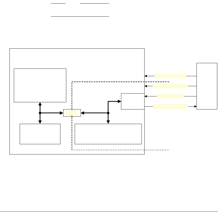
Debug Register Interfaces
ARM DDI 0406B Copyright © 1996-1998, 2000, 2004-2008 ARM Limited. All rights reserved. C6-7
OS Save and Restore registers, and Device Power-down and Reset registers
No error response returned on read or write accesses when the core power domain is
powered down. However, accesses to the OS Lock Access Register (DBGOSLAR) and OS
Save and Restore Register (DBGOSSRR) are UNPREDICTABLE when the core power domain
is powered-down.
All of the management registers, except for the IMPLEMENTATION DEFINED integration registers
The management registers are registers 823 - 1023, in the address range
0xD00
-
0xFFC
.
Requiring all these registers to be in the debug power domain simplifies the decoding of
register addresses for the registers in the debug power domain.
Note
The CP15 c0 registers (
0xD00
-
0xDFC
) are included in this category.
For all other registers, including any IMPLEMENTATION DEFINED registers, it is IMPLEMENTATION DEFINED
whether the register is implemented in the core or the debug power domain.
Figure C6-1 shows the recommended power domain split.
Figure C6-1 Recommended power domain split between core and debug power domains
The signals DBGNOPWRDWN and DBGPWRDUP shown in Figure C6-1 above form an interface
between the power controller and the processor debug logic that is in the debug power domain. With this
interface:
• the external debugger can request the power controller to emulate power-down, simplifying the
requirements on software by sacrificing entirely realistic behavior
Processor
External
debug
interface
All other
Debug registers
DBGDIDR, DBGECR, DBGDRCR,
OS Save and Restore registers,
DBGPRCR, DBGPRSR, and
Management registers
Power
controller
Core domain Vdd
Debug domain Vdd
DBGPWRDUP
DBGNOPWRDWN
Remainder of
processor logic
Power domain boundary
Debug
power domain
Core
power domain
Bridge

Debug Register Interfaces
C6-8 Copyright © 1996-1998, 2000, 2004-2008 ARM Limited. All rights reserved. ARM DDI 0406B
• the external debug interface knows when the core power domain is powered down, and can
communicate this information to the external debugger.
For details of these signals see DBGNOPWRDWN on page AppxA-9 and DBGPWRDUP on
page AppxA-10.
If the core power domain is not being powered down at the same time as the debug power domain then the
authentication signal DBGEN must be pulled LOW before power is removed from the debug power domain.
The behavior of the debug logic, and in particular the generation of debug events, is UNPREDICTABLE when
the debug power domain is not powered if DBGEN is not LOW. Pulling DBGEN LOW ensures that debug
events are ignored by the processor. For more information, see Changing the authentication signals on
page AppxA-4.
Reads and writes of debug registers when the debug logic is powered down are UNPREDICTABLE.
The performance monitors must be implemented in the core power domain, and must continue to operate
when debug power is removed.
The rest of this part of this manual assumes that two power domains are implemented as described in this
section, and that therefore the implementation supports debug over power-down. Features that are not
required for an ARMv7 implementation with a single power domain are identified as SinglePower, with a
description of the differences in behavior. A SinglePower implementation cannot support debug over
power-down.
C6.2.3 The OS Save and Restore mechanism
The OS Save and Restore mechanism enables an operating system to save the debug registers before
power-down and restore them when power is restored. This extends the support for debug over power-down,
and permits debug tools to work at a higher level of abstraction when there are no power-down events.
In v7 Debug:
• If an implementation supports debug over power-down, then it must implement the OS Save and
Restore mechanism.
• On a SinglePower implementation, and on any other implementation that does not support debug over
power-down, it is IMPLEMENTATION DEFINED whether the OS Save and Restore mechanism is
implemented.
• If the OS Save and Restore mechanism is not implemented, the DBGOSLSR must be implemented
as RAZ, and the other OS Save and Restore mechanism register encodings must be RAZ/WI.
In v6 Debug and v6.1 Debug, these registers are not defined.
Two of the requirements for an implementation that supports debug over power-down are:
• An operating system must be able to save and restore the much of the debug logic state over a
power-down. This requirement is met by the OS Save and Restore mechanism.
• A debugger must be able to detect that a processor has powered-down. For more information, see
Permissions in relation to power-down on page C6-28.

Debug Register Interfaces
ARM DDI 0406B Copyright © 1996-1998, 2000, 2004-2008 ARM Limited. All rights reserved. C6-9
The OS Save and Restore mechanism is provided by the following registers:
• OS Save and Restore Register (DBGOSSRR), see OS Save and Restore Register (DBGOSSRR) on
page C10-77
• OS Lock Access Register (DBGOSLAR), see OS Lock Access Register (DBGOSLAR) on
page C10-75
• OS Lock Status Register (DBGOSLSR), see OS Lock Status Register (DBGOSLSR) on page C10-76
• The Event Catch Register (DBGECR), see Event Catch Register (DBGECR) on page C10-78.
You can read the DBGOSLSR to detect whether the OS Save and Restore mechanism is implemented. If it
is not implemented the read of the DBGOSLSR returns zero.
The DBGOSSRR works in conjunction with an internal sequence counter, so that a series of reads or writes
of this register saves or restores the complete debug logic state of the processor that would be lost when the
processor is powered down. The internal sequence counter is reset to the start of the sequence by writing the
key,
0xC5ACCE55
, to the DBGOSLAR.
The number of accesses required, and the order and interpretation of the data are IMPLEMENTATION
DEFINED.
The first access to the DBGOSSRR following the reset of the internal sequence counter must be a read:
• when performing an OS Save sequence this read returns the number of reads from the DBGOSSRR
that are needed to save the entire debug logic state
• when performing an OS Restore sequence the value returned by this read is UNKNOWN.
The result of issuing a write to the DBGOSSRR following a reset of the internal sequence counter is
UNPREDICTABLE.
Note
• If the OS Save and Restore mechanism is not implemented, this first read returns zero, correctly
indicating to software that no registers are to be saved.
• An implementation that includes the OS Save and Restore mechanism might not provide access to
the DBGOSSRR through the external debug interface. In this case:
— the DBGOSLSR, DBGOSLAR, and DBGECR are accessible through the external debug
interface
— through the external debug interface, the DBGOSSRR is RAZ/WI
— because the first read of the DBGOSSRR through the external debug interface returns zero,
this indicates that the OS registers cannot be saved or restored through the external debug
interface.

Debug Register Interfaces
C6-10 Copyright © 1996-1998, 2000, 2004-2008 ARM Limited. All rights reserved. ARM DDI 0406B
The subsequent accesses to the DBGOSSRR must be either all reads or all writes. UNPREDICTABLE behavior
results if:
• reads and writes are mixed
• more accesses are performed than the number of registers to be saved or restored, as returned by the
first read in the OS Save sequence.
• the subsequent accesses are writes, but the OS Lock is cleared with fewer writes performed than the
number of registers to be restored.
The debug logic state of the processor is unchanged if the OS Lock is cleared during or following an OS
Save sequence. The sequence is restarted the next time the OS Lock is set.
When the core power domain is powered down or when the OS Lock is not locked, reads of DBGOSSRR
return an UNKNOWN value and writes are UNPREDICTABLE.
See Example OS Save and Restore sequences on page C6-12 for software examples of the OS Save and
Restore processes.
The debug logic state preserved by the OS Save and Restore mechanism
If debug over power-down is supported, the OS Save and Restore mechanism permits the following debug
logic state to be preserved:
• The registers that must be in the debug power domain, see Power domains and debug on page C6-5.
• The DBGWFAR.
• The DBGBVRs, DBGBCRs, DBGWVRs, DBGWCRs, and DBGVCR.
• The DBGDSCCR and DBGDSMCR.
• The data transfer registers DBGDTRTX and DBGDTRRX, subject to the values of
DBGDSCR.TXfull and DBGDSCR.RXfull when the OS Save sequence is performed:
— If DBGDSCR.TXfull is set to 1 then the value of DBGDTRTX is guaranteed to be saved and
restored.
— If DBGDSCR.RXfull is set to 1 then the value of DBGDTRRX is guaranteed to be saved and
restored.
— If either of these flags is not set to 1 when the OS Save sequence is performed then the value
of the corresponding register is UNKNOWN after the OS Restore sequence.
Note
The OS Save and Restore sequences must not stall reading the values of DBGDTRTX and
DBGDTRRX, and must not cause any instructions to be issued, regardless of the settings of the
DBGDSCR.ExtDCCmode access mode bits.

Debug Register Interfaces
ARM DDI 0406B Copyright © 1996-1998, 2000, 2004-2008 ARM Limited. All rights reserved. C6-11
• The DCC status flags themselves:
— DBGDSCR.TXfull, bit [29]
— DBGDSCR.TXfull_l, bit [26]
— DBGDSCR.RXfull, bit [30]
— DBGDSCR.RXfull_l, bit [27].
Note
Reading DBGDSCR through the DBGOSSRR has no side-effects, that is, the values of TXfull_l and
RXfull_l are unchanged.
• All other writable flags in the DBGDSCR:
— Method of Debug Entry bits, MOE, bits [5:2]
— Force Debug Acknowledge bit, DBGack, bit [10]
— Interrupts Disable bit, INTdis, bit [11]
— User mode Access to Communication Channel Enable bit, UDCCdis, bit [12]
— Execute ARM Instruction Enable bit, ITRen, bit [13]
— Halting debug-mode Enable bit, HDBGen, bit [14]
— Monitor debug-mode Enable bit, MDBGen, bit [15]
— External DCC access mode field, ExtDCCmode, bits [21:20].
• If vectored interrupt support is implemented and enabled, all state required to ensure the correct
generation of Vector Catch debug events. For more information, see Vector catch debug events and
vectored interrupt support on page C3-22.
The OS Save sequence must preserve at least all of this debug logic state that is lost when the core power
domain is powered down. The OS Save sequence does not have to preserve any debug logic state that is not
lost when the core power domain is powered down. That is, it does not have to preserve any debug logic
state that is in the debug power domain.
The OS Save and Restore mechanism does not preserve:
• The sticky exception flags in the DBGDSCR, and the contents of the DBGITR.
• The read-only processor status flags in the DBGDSCR:
— HALTED, bit [0]
— RESTARTED, bit [1]
— SPIDdis, bit [16]
— SPNIDdis, bit [17]
— NS, bit [18]
— ADAdiscard, bit [19]
— InstrCompl_l, bit [24]
— PipeAdv, bit [25].

Debug Register Interfaces
C6-12 Copyright © 1996-1998, 2000, 2004-2008 ARM Limited. All rights reserved. ARM DDI 0406B
• The performance monitor registers described in Chapter C9 Performance Monitors.
• The trace registers.
The OS Restore sequence always overwrites the debug registers with the values that were saved. In
particular, the values of the DBGDTRTX and DBGDTRRX Registers, and of the DCC status flags TXfull,
TXfull_l, RXfull, and RXfull_l after the OS Restore sequence are the saved values.
If there were valid values in the DBGDTRTX or DBGDTRRX Registers immediately before the OS Restore
sequence then those values are lost.
Example OS Save and Restore sequences
Example OS Save and Restore sequences are described in:
•Example OS Save and Restore sequences using the memory-mapped interface
•Example OS Save and Restore sequences using the Extended CP14 interface on page C6-14.
Example OS Save and Restore sequences using the memory-mapped interface
On an implementation that includes the OS Save and Restore mechanism and a memory-mapped interface:
• Example C6-1 shows the correct sequence for saving the debug logic state, using the
memory-mapped interface, before powering down
• Example C6-2 on page C6-13 shows the correct sequence for restoring the debug logic state, using
the memory-mapped interface, when the system is powered on again.
When the debug logic state is restored, if the OS Unlock Catch bit in the Event Catch Register is set to 1 a
debug event is triggered when the DBGOSLAR is cleared. This event might be used by an external debugger
to restart a debugging session. See Event Catch Register (DBGECR) on page C10-78.
Example C6-1 OS debug register save sequence, memory-mapped interface
; On entry, R0 points to a block to save the debug registers in.
SaveDebugRegisters
PUSH {R4, LR}
MOV R4, R0 ; Save pointer
; (1) Set OS Lock Access Register (DBGOSLAR). The architecture requires that DBGOSLAR
; and the other debug registers have at least the Device memory attribute.
BL GetDebugRegisterBase ; Returns base in R0
LDR R1, =0xC5ACCE55
STR R1, [R0, #0x300] ; Write DBGOSLAR
; (2) Get the number of words to save.
LDR R1, [R0, #0x308] ; DBGOSSRR returns size
STR R1, [R4], #4 ; Push on to the save stack
; (3) Loop reading words from the DBGOSSRR.

Debug Register Interfaces
ARM DDI 0406B Copyright © 1996-1998, 2000, 2004-2008 ARM Limited. All rights reserved. C6-13
CMP R1, #0 ; Check for zero
SaveDebugRegisters_Loop
ITTT NE
LDRNE R2, [R0, #0x308] ; Load a word of data
STRNE R2, [R4], #4 ; Push on to the save stack
SUBSNE R1, R1, #1
BNE SaveDebugRegisters_Loop
; (4) Return the pointer to first word not written to. Leave DBGOSLAR set, because
; from now on we do not want any changes.
MOV R0, R4
POP {R4, PC}
Example C6-2 OS debug register restore sequence, memory-mapped interface
; On entry, R0 points to a block of saved debug registers.
RestoreDebugRegisters
PUSH {R4, LR}
MOV R4, R0 ; Save pointer
; (1) Set the OS Lock Access Register (DBGOSLAR) and reset pointer. The lock
; will already be set, but this write is needed to reset the pointer. The
; architecture requires that DBGOSLAR and the other debug registers have at
; least the Device memory attribute.
BL GetDebugRegisterBase ; Returns base in R0
LDR R1, =0xC5ACCE55
STR R1, [R0, #0x300] ; Write DBGOSLAR
; (2) Clear the Sticky Power-down Status bit.
LDR R1, [R0, #0x314] ; Read DBGPRSR to clear StickyPD
; (3) Get the number of words saved.
LDR R1, [R0, #0x308] ; Dummy read of DBGOSSRR
LDR R1, [R4], #4 ; Get register count from the save stack
; (4) Loop writing words from the DBGOSSRR.
CMP R1, #0 ; Check for zero
RestoreDebugRegisters_Loop
ITTT NE
LDRNE R2, [R4], #4 ; Load a word from the save stack
STRNE R2, [R0, #0x308] ; Store a word of data
SUBSNE R1, R1, #1
BNE RestoreDebugRegisters_Loop
; (5) Clear the DBGOSLAR. Writing any non-key value clears the lock, so use the
; zero value in R1.
STR R1, [R0, #0x300] ; Write DBGOSLAR
; (6) A final DSB ensures the restore is complete and an ISB ensures
; the restored register values are visible to subsequent instructions.

Debug Register Interfaces
C6-14 Copyright © 1996-1998, 2000, 2004-2008 ARM Limited. All rights reserved. ARM DDI 0406B
DSB
ISB
; (7) Return the pointer to first word not read.
MOV R0, R4
POP {R4, PC}
Example OS Save and Restore sequences using the Extended CP14 interface
On an implementation that includes the OS Save and Restore mechanism and the Extended CP14 interface:
• Example C6-3 shows the correct sequence for saving the debug logic state, using the Extended CP14
interface, before powering down
• Example C6-4 on page C6-15 shows the correct sequence, using the Extended CP14 interface, for
restoring the debug logic state when the system is powered on again.
When the debug logic state is restored, if the OS Unlock Catch bit in the Event Catch Register is set to 1 a
debug event is triggered when the DBGOSLAR is cleared. This event might be used by an external debugger
to restart a debugging session. See Event Catch Register (DBGECR) on page C10-78.
Example C6-3 OS debug register save sequence, Extended CP14 interface
; On entry, R0 points to a block to save the debug registers in.
SaveDebugRegisters
; (1) Set OS Lock Access Register (DBGOSLAR).
LDR R1, =0xC5ACCE55
MCR p14, 0, R1, c1, c0, 4 ; Write DBGOSLAR
ISB
; (2) Get the number of words to save.
MRC p14, 0, R1, c1, c2, 4 ; DBGOSSRR returns size
STR R1, [R0], #4 ; Push on to the save stack
; (3) Loop reading words from the DBGOSSRR.
CMP R1, #0 ; Check for zero
SaveDebugRegisters_Loop
ITTT NE
MRCNE p14, 0, R2, c1, c2, 4 ; Load a word of data
STRNE R2, [R0], #4 ; Push on to the save stack
SUBSNE R1, R1, #1
BNE SaveDebugRegisters_Loop
; (4) Return the pointer to first word not written to. This pointer is already in R0, so
; all that is needed is to return from this function.
;
; Leave DBGOSLAR set, because from now on we do not want any changes.
BX LR

Debug Register Interfaces
ARM DDI 0406B Copyright © 1996-1998, 2000, 2004-2008 ARM Limited. All rights reserved. C6-15
Example C6-4 OS debug register restore sequence, Extended CP14 interface
; On entry, R0 points to a block of saved debug registers.
RestoreDebugRegisters
; (1) Set OS Lock Access Register (DBGOSLAR) and reset pointer. The lock
; will already be set, but this write is needed to reset the pointer.
LDR R1, =0xC5ACCE55
MCR p14, 0, R1, c1, c0, 4 ; Write DBGOSLAR
ISB
; (2) Clear the Sticky Power-down Status bit.
MRC p14, 0, R1, c1, c5, 4 ; Read DBGPRSR to clear StickyPD
ISB
; (3) Get the number of words saved.
MRC p14, 0, R1, c1, c2, 4 ; Dummy read of DBGOSSRR
LDR R1, [R0], #4 ; Load size from the save stack
; (4) Loop writing words from the DBGOSSRR.
CMP R1, #0 ; Check for zero
RestoreDebugRegisters_Loop
ITTT NE
LDRNE R2, [R0], #4 ; Load a word from the save stack
MCRNE p14, 0, R2, c1, c2, 4 ; Store a word of data
SUBSNE R1, R1, #1
BNE RestoreDebugRegisters_Loop
; (5) Clear the OS Lock Access Register (DBGOSLAR). Writing any non-key value
; clears the lock, so use the zero value in R1.
ISB
MCR p14, 0, R1, c1, c0, 4 ; Write DBGOSLAR
; (6) A final ISB guarantees the restored register values are visible to subsequent
; instructions.
ISB
; (7) Return the pointer to first word not read. This pointer is already in R0, so
; all that is needed is to return from this function.
BX LR

Debug Register Interfaces
C6-16 Copyright © 1996-1998, 2000, 2004-2008 ARM Limited. All rights reserved. ARM DDI 0406B
C6.2.4 Recommended reset scheme for v7 Debug
The processor reset scheme is IMPLEMENTATION DEFINED. The ARM architecture, described in parts A and
B of this manual, does not distinguish different levels of reset. However, in a typical system, there are a
number of reasons why multiple levels of reset might exist. In particular, for debug:
• It is desirable to be able to debug the reset sequence. This requires support for:
— setting the debug register values before performing a processor reset
— a processor reset not resetting the debug register values.
• Providing separate power domains means you might need to reset the debug logic independently from
the logic in the core power domain.
For these reasons, v7 Debug introduces a distinction between debug logic reset and non-debug logic reset.
These resets can be applied independently. The reset descriptions in parts A and B of this manual describe
the non-debug logic reset. Part C describes the debug logic reset and its interaction with the non-debug logic
reset. The non-debug logic reset is sometimes referred to as a core logic reset.
ARM recommends use of the following reset signals for an implementation that supports these independent
resets:
nSYSPORESET This signal must be driven LOW on power-up of both the core and debug power
domains. It sets parts of the processor logic, including debug logic, to a known state.
nCOREPORESET If the core power domain is powered down while the system is still powered up, this
signal must be driven LOW when the core power domain is powered back up. It sets
parts of the processor logic in the core power domain to a known state. Also, this
reset initializes the debug registers that are in the core power domain.
nRESET This signal is driven LOW to generate a warm reset, that is, when the system wants
to set the processor to a known state but the reset has nothing to do with any
power-down, for example a watchdog reset. It sets parts of the non-debug processor
logic to a known state. A debug session must be unaffected by this reset.
PRESETDBGn The debugger drives this signal LOW to set parts of the debug logic to a known state.
This signal must be driven LOW on power-up of the debug logic.
v6 Debug and v6.1 Debug systems do not support multiple power domains and therefore ARM recommends
a less flexible reset scheme, consisting of only nSYSPORESET and nRESET. The debug logic is reset
only on nSYSPORESET and has no independent reset signal.
In the v7 Debug recommended reset scheme, a separate PRESETDBGn reset signal can be asserted at any
time, not just at power-up. This new signal has similar effects to nSYSPORESET, that is, it clears all debug
registers, unless otherwise noted by the register definition. For more information, see Appendix A
Recommended External Debug Interface.
Asynchronously asserting PRESETDBGn can lead to UNPREDICTABLE behavior. For example, the reset
might change the values of debug registers that are in use or will be used by software.
For more information about this reset scheme, contact ARM.

Debug Register Interfaces
ARM DDI 0406B Copyright © 1996-1998, 2000, 2004-2008 ARM Limited. All rights reserved. C6-17
Table C6-1 summarizes the v7 Debug recommended reset scheme.
For ARMv7 SinglePower systems, ARM recommends only nSYSPORESET, nRESET, and
PRESETDBGn.
Debug behavior when the processor is in debug logic reset
The implementation of separate debug and core power domains with a separate debug logic reset signal
means that a processor can access debug registers and the DCC while in the debug logic reset state. When
in debug logic reset:
• The behavior of the DCC is UNPREDICTABLE. In particular, the values of the DBGDSCR.RXfull and
DBGDSCR.TXfull flags are UNKNOWN.
•It is UNPREDICTABLE whether a debug event that would have been generated by the state of the debug
logic immediately before the debug logic reset is generated.
• The debug logic must not generate any debug event that would not have been generated if the system
was not in debug logic reset.
• Accesses to the debug registers through the Extended CP14, memory-mapped and external debug
interfaces are UNPREDICTABLE.
Table C6-1 Recommended reset scheme, v7 Debug
Debug power domain Core power domain
Signal Debug logic Debug logic Non-debug logic
nSYSPORESET Reset Reseta
a. If the core power domain is not powered, or the Sticky Power-down status bit
DBGPRSR[1] is set to 1, it is UNPREDICTABLE whether the registers are reset. If power is
not applied to the core power domain, nCOREPORESET must be driven LOW when
power is restored to the core power domain. This resets these registers.
Reset
nCOREPORESET Not reset ResetaReset
nRESET Not reset Not reset Reset
PRESETDBGn Reset ResetaNot reset

Debug Register Interfaces
C6-18 Copyright © 1996-1998, 2000, 2004-2008 ARM Limited. All rights reserved. ARM DDI 0406B
C6.3 Debug register map
Table C6-2 lists all of the debug registers. Full details of each register can be found in the referenced section.
The number of DBGBVR/DBGBCR and DBGWVR/DBGWCR pairs is IMPLEMENTATION DEFINED, see the
BRPs and WRPs fields of the Debug ID Register (DBGDIDR) on page C10-3. An implementation can have
up to 16 of each.
The interpretation of the information in the Access column depends on whether the coprocessor or
memory-mapped interface is used to access the register.
Collectively, registers 832-1023 are known as the management registers.
Table C6-2 Debug register map
Register
number Offset AccessaVersions bName and reference to description
0
0x000
Read-only All Debug ID Register (DBGDIDR) on page C10-3.
Not applicablec- Read-only v7 only Debug ROM Address Register (DBGDRAR) on
page C10-7.
Not applicablec- Read-only v7 only Debug Self Address Offset Register (DBGDSAR) on
page C10-8.
1-5 - - - Reserved.
6
0x018
Read/write v7 dWatchpoint Fault Address Register (DBGWFAR) on
page C10-28.
7
0x01C
Read/write All Vector Catch Register (DBGVCR) on page C10-67.
8---Reserved.
9
0x024
Read/write v7 only Event Catch Register (DBGECR) on page C10-78.
10
0x028
Read/write v6.1, v7 Debug State Cache Control Register (DBGDSCCR) on
page C10-81.
11
0x02C
Read/write v6.1, v7 Debug State MMU Control Register (DBGDSMCR) on
page C10-84.
12-31 - - - Reserved.
32
0x080
Read/write v7 eDBGDTRRX external viewf. See Host to Target Data
Transfer Register (DBGDTRRX) on page C10-40.

Debug Register Interfaces
ARM DDI 0406B Copyright © 1996-1998, 2000, 2004-2008 ARM Limited. All rights reserved. C6-19
33
0x084
Write-only v7 eInstruction Transfer Register (DBGITR) on
page C10-46.
Read-only v7 eProgram Counter Sampling Register (DBGPCSR) on
page C10-38.
34
0x088
Read/write v7 eDBGDSCR external viewf. See Debug Status and
Control Register (DBGDSCR) on page C10-10.
35
0x08C
Read/write v7 eDBGDTRTX external viewf. See Target to Host Data
Transfer Register (DBGDTRTX) on page C10-43.
36
0x090
Write-only v7 only Debug Run Control Register (DBGDRCR), v7 Debug
only on page C10-29.
37-39 - - - Reserved.
40
0x0A0
Read-only v7 only Program Counter Sampling Register (DBGPCSR) on
page C10-38
41
0x0A4
Read-only v7 only Context ID Sampling Register (DBGCIDSR) on
page C10-39
42-63 - - - Reserved.
64-79
0x100
-
0x13C
Read/write
or -
All Breakpoint Value Registers (DBGBVR) on page C10-48
or Reserved.
80-95
0x140
-
0x17C
Read/write
or -
All Breakpoint Control Registers (DBGBCR) on
page C10-49 or Reserved.
96-111
0x180
-
0x1BC
Read/write
or -
All Watchpoint Value Registers (DBGWVR) on
page C10-60 or Reserved.
112-127
0x1C0
-
0x1FC
Read/write
or -
All Watchpoint Control Registers (DBGWCR) on
page C10-61 or Reserved.
128-191 - - - Reserved.
192
0x300
Write-only v7 only OS Lock Access Register (DBGOSLAR) on
page C10-75.
193
0x304
Read-only v7 only OS Lock Status Register (DBGOSLSR) on page C10-76.
194
0x308
Read/write v7 only OS Save and Restore Register (DBGOSSRR) on
page C10-77.
Table C6-2 Debug register map (continued)
Register
number Offset AccessaVersions bName and reference to description

Debug Register Interfaces
C6-20 Copyright © 1996-1998, 2000, 2004-2008 ARM Limited. All rights reserved. ARM DDI 0406B
195 - - - Reserved.
196
0x310
Read/write v7 only Device Power-down and Reset Control Register
(DBGPRCR), v7 Debug only on page C10-31.
197
0x314
Read-only v7 only Device Power-down and Reset Status Register
(DBGPRSR), v7 Debug only on page C10-34.
198-511 - - - Reserved.
512-575
0x800
-
0x8FC
- v7 only IMPLEMENTATION DEFINED.
576-831 - - - Reserved.
832-895
0xD00
-
0xDFC
Read-only v7 only Processor identification registers on page C10-88.
896-927 - - - Reserved.
928-959
0xE80
-
0xEFC
- v7 only IMPLEMENTATION DEFINED integration registers. See the
CoreSight Architecture Specification.
960
0xF00
Read/write v7 only Integration Mode Control Register (DBGITCTRL) on
page C10-91.
961-999
0xF04
-
0xF9C
- v7 only Reserved for management registers expansion.
1000
0xFA0
Read/write v7 only Claim Tag Set Register (DBGCLAIMSET) on
page C10-92.
1001
0xFA4
Read/write v7 only Claim Tag Clear Register (DBGCLAIMCLR) on
page C10-93.
1002-1003 - - - Reserved.
1004
0xFB0
Write-only v7 only Lock Access Register (DBGLAR) on page C10-94.
1005
0xFB4
Read-only v7 only Lock Status Register (DBGLSR) on page C10-95.
1006
0xFB8
Read-only v7 only Authentication Status Register (DBGAUTHSTATUS) on
page C10-96.
1007-1009 - - - Reserved.
Table C6-2 Debug register map (continued)
Register
number Offset AccessaVersions bName and reference to description

Debug Register Interfaces
ARM DDI 0406B Copyright © 1996-1998, 2000, 2004-2008 ARM Limited. All rights reserved. C6-21
C6.3.1 Internal and external views of the DBGDSCR and the DCC registers
For each of the three registers DBGDSCR, DBGDTRTX and DBGDTRRX there are two views, denoted by
int and ext suffixes. The differences between these aliases relate to the handling of the Debug
Communications Channel (DCC), and in particular the TXfull and RXfull status flags. The nomenclature
internal and external derives from the intended usage model.
Accesses to DBGDSCRint, DBGDTRRXint or DBGDTRTXint are always made through the Baseline
CP14 interface described in The Baseline CP14 debug register interface on page C6-32. DBGDSCRint is
read-only in v7 Debug.
Accesses to DBGDSCRext, DBGDTRRXext or DBGDTRTXext can be made through:
• the Extended CP14 interface, if implemented
• the memory-mapped interface, if implemented
• the external debug interface.
However, if at any given time you attempt to access the DBGDSCRext, DBGDTRRXext and
DBGDTRTXext registers through more than one interface the behavior is UNPREDICTABLE. If an
implementation provides a single port to handle external debug interface and the memory-mapped interface
1010
0xFC8
Read-only v7 only Debug Device ID Register (DBGDEVID) on
page C10-6.
1011
0xFCC
Read-only v7 only Device Type Register (DBGDEVTYPE) on
page C10-98.
1012-1019
0xFD0
-
0xFEC
Read-only v7 only Debug Peripheral Identification Registers (DBGPID0 to
DBGPID4) on page C10-98.
1020-1023
0xFF0
-
0xFFC
Read-only v7 only Debug Component Identification Registers (DBGCID0
to DBGCID3) on page C10-102.
a. For more information, see CP14 debug registers access permissions on page C6-36 and Permission summaries for
memory-mapped and external debug interfaces on page C6-45.
b. An entry of All in the Ve r s i o n s column indicates that the register is implemented in v6 Debug, v6.1 Debug, and
v7 Debug.
c. These registers are only implemented through the Baseline CP14 interface and do not have register numbers or offsets.
d. The method of accessing the DBGWFAR is different in v6 Debug, v6.1 Debug and v7 Debug. For details see
Watchpoint Fault Address Register (DBGWFAR) on page C10-28.
e. In v6 Debug and v6.1 Debug, ARM recommends these registers as part of the external debug interface, and are not
implemented through the Extended CP14 interface. In v7 Debug these registers are required.
f. Internal views of the DBGDTRRX, DBGDTRTX, and DBGDSCR are implemented through the Baseline CP14
interface. This is explained in Internal and external views of the DBGDSCR and the DCC registers.
Table C6-2 Debug register map (continued)
Register
number Offset AccessaVersions bName and reference to description
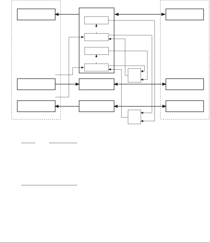
Debug Register Interfaces
C6-22 Copyright © 1996-1998, 2000, 2004-2008 ARM Limited. All rights reserved. ARM DDI 0406B
accesses, that port might serialize accesses to the registers from the two interfaces. However, the effects of
reads and writes to these registers are such that the behavior observed from either interface appears as
UNPREDICTABLE.
Figure C6-2 v7 Debug Internal (int) and External (ext) views of the DCC registers
Note
• DBGDSCRint and DBGDSCRext only provide different views onto the underlying DBGDSCR
• DBGDTRRXint and DBGDTRRXext only provide different views onto the underlying
DBGDTRRX Register
• DBGDTRTXint and DBGDTRTXext only provide different views onto the underlying DBGDTRTX
Register.
See also:
•Debug Status and Control Register (DBGDSCR) on page C10-10
•Host to Target Data Transfer Register (DBGDTRRX) on page C10-40
•Target to Host Data Transfer Register (DBGDTRTX) on page C10-43.
DBGDTRTXext
(Read/write)
DBGDSCRext
(Read/write)
DBGDTRTX
DBGDTRRX
DBGDSCR
TXfull
RXfull
RXfull_l
TXfull_l
DBGDTRRXext
(Read/write)
Internal view External view
0 (on reads)
TX
Read
Logic
RX
Write
Logic
1 (on writes)
DBGDTRTXint
(Write-only)
DBGDTRRXint
(Read-only)
Copied on reads
DBGDSCRint
(Read-only)
Copied on reads

Debug Register Interfaces
ARM DDI 0406B Copyright © 1996-1998, 2000, 2004-2008 ARM Limited. All rights reserved. C6-23
C6.3.2 Effect of the Security Extensions on the debug registers
When the Security Extensions are implemented, all debug register are Common registers, meaning they are
common to the Secure and Non-secure states. For more information, see Common CP15 registers on
page B3-74.

Debug Register Interfaces
C6-24 Copyright © 1996-1998, 2000, 2004-2008 ARM Limited. All rights reserved. ARM DDI 0406B
C6.4 Synchronization of debug register updates
Software running on the processor can program the debug registers through at least one of:
• a CP14 coprocessor interface
• the memory-mapped interface, if it is implemented.
It is IMPLEMENTATION DEFINED which interfaces are implemented.
For the CP14 coprocessor interface, the following synchronization rules apply:
• All changes to CP14 debug registers that appear in program order after any explicit memory
operations are guaranteed not to affect those memory operations.
• Any change to CP14 debug registers is guaranteed to be visible to subsequent instructions only after
one of:
— performing an ISB operation
— taking an exception
— returning from an exception.
However, for CP14 coprocessor register accesses, all
MRC
and
MCR
instructions to the same register
using the same register number appear to occur in program order relative to each other without
context synchronization.
For the memory-mapped interface, the following synchronization rules apply:
• All memory-mapped debug registers must be mapped to Strongly-ordered or Device memory,
otherwise the effect of any access to the memory-mapped debug registers is
UNPREDICTABLE
.
• Changes to memory-mapped debug registers that appear in program order after an explicit memory
operation are guaranteed not to affect that previous memory operation only if the order is guaranteed
by the memory order model or by the use of a DMB or DSB operation between the memory operation
and the register change.
• A DSB operation causes all writes to memory-mapped debug registers appearing in program order
before the DSB to be completed.
• With respect to other accesses by the same processor to the memory-mapped debug registers, all
accesses to memory-mapped debug registers have their effect in the order in which the accesses
occur, as governed by the memory order model and the use of DSB and DMB operations.
• All accesses to memory-mapped debug registers that are completed are only guaranteed to affect
subsequent instructions after one of:
— performing an ISB operation
— taking an exception
— returning from an exception.
Some memory-mapped debug registers are not idempotent for reads or writes. Therefore, the region of
memory occupied by the debug registers must not be marked as Normal memory, because the memory order
model permits accesses to Normal memory locations that are not appropriate for such registers.

Debug Register Interfaces
ARM DDI 0406B Copyright © 1996-1998, 2000, 2004-2008 ARM Limited. All rights reserved. C6-25
Synchronization between register updates made through the external debug interface and updates made by
software running on the processor is IMPLEMENTATION DEFINED. However, if the external debug interface is
implemented through the same port as the memory-mapped interface, then updates made through the
external debug interface have the same properties as updates made through the memory-mapped interface.

Debug Register Interfaces
C6-26 Copyright © 1996-1998, 2000, 2004-2008 ARM Limited. All rights reserved. ARM DDI 0406B
C6.5 Access permissions
This section describes the basic concepts of the access permissions model for debug registers on ARMv7
processors. The actual rules for each interface, and for ARMv6 implementations, are given in the section
describing the register interface:
•CP14 debug registers access permissions on page C6-36
•Permission summaries for memory-mapped and external debug interfaces on page C6-45.
The restrictions for accessing the registers can be divided into three categories:
Privilege of the access
Accesses from processors in the system to the memory-mapped registers, and accesses to
coprocessor registers, can be required to be privileged.
Locks Can be used to lock out different parts of the register map so they cannot be accessed.
Power-down Access to registers in the core power domain is not possible when that domain is powered
down.
When permission to access a register is not granted, an error is returned. The nature of this error depends on
the interface:
• For coprocessor interfaces, the error is an Undefined Instruction exception
• For the memory-mapped interface, the error is a slave-generated error response, for example
PSLVERRDBG. The error is normally signaled to the processor as an external abort.
• For the external debug interface, the error is signaled to the debugger by the Debug Access Port.
Holding the processor in warm reset, whether by using an external warm reset signal or by using the Device
Power-down and Reset Control Register (DBGPRCR), does not affect the behavior of the memory-mapped
or external debug interface.
The Hold non-debug reset control bit of the DBGPRCR enables an external debugger to keep the processor
in warm reset while programming other debug registers. For details see Device Power-down and Reset
Control Register (DBGPRCR), v7 Debug only on page C10-31.
C6.5.1 Permissions in relation to the privilege of the access
The majority of debug registers can only be accessed by privileged code. The exception to this general
requirement is a small subset of the registers, defined in The Baseline CP14 debug register interface on
page C6-32. Using the coprocessor interface, privileged code can disable User mode access to this subset of
registers.
For the memory-mapped interface, it is IMPLEMENTATION DEFINED whether restricting debug register access
to privileged code is implemented by the processor or must be implemented by the system designer at the
system level. The behavior of an access that is not permitted is IMPLEMENTATION DEFINED, however it must
either be ignored or aborted.

Debug Register Interfaces
ARM DDI 0406B Copyright © 1996-1998, 2000, 2004-2008 ARM Limited. All rights reserved. C6-27
Note
• The recommended memory-mapped interface port is based on the AMBA® Advanced Peripheral Bus
(APBv3), that does not support signaling of access privileges. Therefore in this case the system must
prevent the access.
• This access restriction applies to the privilege of the initiator of the access, not the current mode of
the processor being accessed. The privilege of accesses made by a Debug Access Port is
IMPLEMENTATION DEFINED.
The system designer can impose additional restrictions. However, ARM strongly recommends that
designers do not impose restrictions such as only permitting Secure privileged accesses, and does not
support such restrictions in its debug tools.
C6.5.2 Permissions in relation to locks
The registers can be locked by a debugger or by an operating system so that access to debug registers is
restricted.
There are three locks, although some of these locks only apply to certain interfaces:
Software Lock
The Software Lock only applies to accesses made through the memory-mapped interface.
By default, software is locked out so the debug registers settings cannot be modified. A
debug monitor must leave this lock set when not accessing the debug registers, to reduce the
chance of erratic code modifying debug settings. When this lock is set, writes to the debug
registers from the memory-mapped interface are ignored. For more information about this
lock, see Lock Access Register (DBGLAR) on page C10-94 and Lock Status Register
(DBGLSR) on page C10-95.
OS Lock An OS must set this lock on the debug registers before starting an OS Save or Restore
sequence, so that the debug registers cannot be read or written during the sequence. When
this lock is set, accesses to some registers return errors. Only the OS Save and Restore
mechanism registers can be accessed safely.
Note
An external debugger can clear this lock at any time, even if an OS Save or Restore operation
is in progress.
For more information about this lock, see OS Lock Access Register (DBGOSLAR) on
page C10-75 and OS Lock Status Register (DBGOSLSR) on page C10-76.

Debug Register Interfaces
C6-28 Copyright © 1996-1998, 2000, 2004-2008 ARM Limited. All rights reserved. ARM DDI 0406B
Debug Software Enable
An external debugger can use the Debug Software Enable function to prevent modification
of the debug registers by a debug monitor or other software running on the system. The
Debug Software Enable is a required function of the Debug Access Port, and is implemented
as part of the ARM Debug Interface v5. For more information see the ARM Debug Interface
v5 Architecture Specification.
See also DBGSWENABLE on page AppxA-11.
Note
• The states of the Software Lock and the OS Lock are held in the debug power domain, and the Debug
Software Enable is in the Debug Access Port. Therefore, these locks are unaffected by the core power
domain powering down. Also, all of these locks are set to their reset values only on reset of the debug
power domain, that is. on a PRESETDBGn or nSYSPORESET reset.
• On SinglePower systems, the Software Lock and OS Lock are lost over a power-down. It is
IMPLEMENTATION DEFINED whether the single processor power-domain also includes the Debug
Access Port, and therefore also whether the Debug Software Enable is lost over a power-down.
C6.5.3 Permissions in relation to power-down
Accesses cannot be made through the coprocessor interface when the core power domain is powered down.
Access to registers in the core power domain is not possible when the domain is powered down, and accesses
return an error response.
Note
Returning this error response, rather than simply ignoring writes, means that the debugger and the debug
monitor detect the debug session interruption as soon as it occurs. This makes re-starting the session, after
power-up, considerably easier.
When the core power domain powers down, the Sticky Power-down status bit, bit [1] of the Device
Power-down and Reset Status Register, is set to 1. This bit remains set to 1 until it is cleared to 0 by a read
of this register after the core power domain has powered up. If the register is read while the core power
domain is still powered down, the bit remains set to 1. When this bit is 1 the behavior is as if the core power
domain is powered down, meaning the processor ignores accesses to registers inside the core power domain
and the system returns an error. This applies whether the register is accessed through the Extended CP14
interface, the memory-mapped interface, or the external debug interface.
This behavior is useful because when the external debugger tries to access a register whose contents might
have been lost by a power-down, it gets the same response regardless of whether the core power domain is
currently powered down or has powered back up. This means that, if the external debugger does not access
the external debug interface during the window where the core power domain is powered down, the
processor still reports the occurrence of the power-down event.

Debug Register Interfaces
ARM DDI 0406B Copyright © 1996-1998, 2000, 2004-2008 ARM Limited. All rights reserved. C6-29
Access to all debug registers is not possible if the debug logic is powered down. In this situation:
• the system must respond to any access made through the memory-mapped or external debug interface
when the debug power domain is powered down, and ARM recommends that the system generates
an error response
• accesses through the coprocessor interface are UNPREDICTABLE.
The debug logic is powered down:
• when the debug power domain is powered down, in an implementation with separate debug and core
power domains
• when the processor is powered down, in a SinglePower implementation.
C6.5.4 Access to IMPLEMENTATION DEFINED and reserved registers
The following subsections describe the responses to accesses to IMPLEMENTATION DEFINED and reserved
registers:
•Access to implementation defined registers
•Access to reserved registers on page C6-30.
Note
There are no IMPLEMENTATION DEFINED or reserved registers in the Baseline CP14 interface and therefore
these sections do not say anything about accesses through the Baseline CP14 interface.
Any unused registers in the spaces for IMPLEMENTATION DEFINED registers must behave as reserved
registers. These spaces are register numbers 512-575 and 928-959.
Access to IMPLEMENTATION DEFINED registers
When the Debug Software Enable function, described in Permissions in relation to locks on page C6-27, is
disabling software access to the debug registers, Table C6-3 shows how the response to an accesses to an
IMPLEMENTATION DEFINED register depends on the debug interface used for the access.
Table C6-3 Accesses to IMPLEMENTATION DEFINED registers when
Debug Software Enable disables access
Debug interlace used for accessa
a. There are no IMPLEMENTATION DEFINED registers in the Baseline CP14
interface.
Response
Memory-mapped interface Error response
Extended CP14 interface Undefined Instruction exception
External debug interface IMPLEMENTATION DEFINED

Debug Register Interfaces
C6-30 Copyright © 1996-1998, 2000, 2004-2008 ARM Limited. All rights reserved. ARM DDI 0406B
It the Debug Software Enable function is not disabling software access to the debug registers, the response
to any access to an IMPLEMENTATION DEFINED register is IMPLEMENTATION DEFINED. This means the
response is IMPLEMENTATION DEFINED if any of the following apply:
• the core power domain is powered-down
• the Sticky Powered-down Status bit is set to 1
• the OS Lock is implemented and is locked
• the attempted access is using the memory-mapped interface and the Software Lock is locked.
Note
The IMPLEMENTATION DEFINED registers include the IMPLEMENTATION DEFINED integration registers,
register numbers 928-959.
Access to reserved registers
The response to an access to a reserved register depends on the interface you are using to attempt the access,
as follows:
Memory-mapped interface
When the Debug Software Enable function, described in Permissions in relation to locks on
page C6-27, is disabling software access to the debug registers, any access to a reserved
register through the memory-mapped interface returns an error response. This includes
accesses to reserved registers in the management registers space, register numbers
832-1023.
When the Debug Software Enable function is not disabling software access to the debug
registers:
• Reserved registers in the management registers space, except for reserved registers in
the IMPLEMENTATION DEFINED integration registers space, are UNK/SBZP.
• For all other reserved registers, it is UNPREDICTABLE whether a register access returns
an error response if any of the following applies:
— the core power domain is powered-down
— the Sticky Powered-Down Status bit is set to 1
— the OS Lock is implemented and is locked
— the Software Lock is locked.
If none of these applies then these reserved registers are UNK/SBZP.
Extended CP14 interface
In v6 Debug and v6.1 Debug, any attempt to access a reserved register causes an Undefined
Instruction exception.
In v7 Debug:
• When the Debug Software Enable function is disabling software access to the debug
registers, any attempt to access a reserved register causes an Undefined Instruction
exception.

Debug Register Interfaces
ARM DDI 0406B Copyright © 1996-1998, 2000, 2004-2008 ARM Limited. All rights reserved. C6-31
• When the Debug Software Enable function enables software access to the debug
registers, any attempt to access a reserved register:
— causes an Undefined Instruction exception if the access is from User mode
—is
UNPREDICTABLE if the access is from a privileged mode.
External debug interface
Reserved registers in the management registers space, except for reserved registers in the
IMPLEMENTATION DEFINED integration registers space, are UNK/SBZP.
For all other reserved registers:
•It is UNPREDICTABLE whether a register access returns an error response if any of the
following applies:
— the core power domain is powered-down
— the Sticky Powered-Down Status bit is set to 1
— the OS Lock is implemented and is locked.
• If none of these applies then these reserved registers are UNK/SBZP.
Note
• There are no reserved registers in the Baseline CP14 interface.
• Unimplemented breakpoint and watchpoint registers are reserved registers.

Debug Register Interfaces
C6-32 Copyright © 1996-1998, 2000, 2004-2008 ARM Limited. All rights reserved. ARM DDI 0406B
C6.6 The CP14 debug register interfaces
This section contains the following subsections:
•The Baseline CP14 debug register interface
•Extended CP14 interface on page C6-33
•CP14 debug registers access permissions on page C6-36.
C6.6.1 The Baseline CP14 debug register interface
Table C6-4 lists the set of CP14 debug instructions for accessing the debug registers that must be
implemented.
All
MRC
and
MCR
instructions with
<coproc>
= 0b1110 and
<opc1>
= 0b000 are debug instructions:
• Some of these instructions are defined in Table C6-4.
• Additional instructions are defined in Extended CP14 interface on page C6-33
• All other instructions are reserved for use by the Debug architecture. The behavior of reserved
instructions is defined in CP14 debug registers access permissions on page C6-36.
All
MRC
and
MCR
instructions with
<coproc>
= 0b1110 and
<opc1>
= 0b001 are used by the trace extension.
Other values of
<opc1>
are not used by the Debug architecture.
All
LDC
and
STC
instructions with
<coproc>
= 0b1110 that are not listed below are reserved for use by the
Debug architecture and are currently UNDEFINED. All
CDP
,
MRC2
,
MCR2
,
LDC2
,
STC2
,
LDCL
,
STCL
,
LDC2L
, and
STC2L
instructions with
<coproc>
= 0b1110 are UNDEFINED.
Instructions that access registers that are only available in v7 Debug are UNDEFINED in earlier versions of
the Debug architecture. For example, the read from DBGDRAR performed by
MRC p14,0,<Rt>,c1,c0,0
is
UNDEFINED in v6 Debug and v6.1 Debug, but is permitted in v7 Debug.
<Rt>
refers to any of the general-purpose registers R0-R14. Use of APSR_nzcv is UNPREDICTABLE except
where stated. Use of R13 is UNPREDICTABLE in Thumb and ThumbEE state, and is deprecated in ARM state.
Table C6-4 Baseline CP14 debug instructions
Instruction Mnemonic Version Name and reference to description
MRC p14,0,<Rt>,c0,c0,0
DBGDIDR All Debug ID Register (DBGDIDR) on page C10-3
MRC p14,0,<Rt>,c1,c0,0
DBGDRAR v7 only Debug ROM Address Register (DBGDRAR) on
page C10-7
MRC p14,0,<Rt>,c2,c0,0
DBGDSAR v7 only Debug Self Address Offset Register (DBGDSAR)
on page C10-8

Debug Register Interfaces
ARM DDI 0406B Copyright © 1996-1998, 2000, 2004-2008 ARM Limited. All rights reserved. C6-33
C6.6.2 Extended CP14 interface
The architectural requirements for the Extended CP14 interface depend on the Debug architecture version:
v6 Debug and v6.1 Debug
All debug registers can be accessed through CP14, and implementations must provide an
external access mechanism for debuggers. The details of this mechanism are not covered by
the architecture specification. See Features specific to v6 Debug and v6.1 Debug on
page C6-35.
v7 Debug The Extended CP14 interface to the debug registers is optional.
The Baseline CP14 interface is sufficient to boot-strap access to the register file, and enables
software to distinguish between the Extended CP14 and memory-mapped interfaces.
See Features specific to v7 Debug on page C6-34.
If the Extended CP14 interface is not implemented, the memory-mapped interface must be
implemented. See section The memory-mapped and recommended external debug
interfaces on page C6-43.
Note
This section does not apply to a v7 Debug implementation that does not implement the Extended CP14
interface.
The full list of debug registers is given in Table C6-2 on page C6-18 and is not repeated here.
MRC p14,0,<Rt>,c0,c5,0
STC p14,c5,<addr_mode>
DBGDTRRXint AllaDBGDTRRX internal view. See Host to Target
Data Transfer Register (DBGDTRRX) on
page C10-40
MCR p14,0,<Rt>,c0,c5,0
LDC p14,c5,<addr_mode>
DBGDTRTXint AllaDBGDTRTX internal view. See Target to Host
Data Transfer Register (DBGDTRTX) on
page C10-43
MRC p14,0,<Rt>,c0,c1,0
MRC p14,0,APSR_nzcv,c0,c1,0
b
DBGDSCRint AllaDBGDSCR internal view. See Debug Status and
Control Register (DBGDSCR) on page C10-10
a. For more information, see the register description.
b. DBGDSCR[31:28] are transferred to the N, Z, C and V condition flags. For more information, see Program Status
Registers (PSRs) on page B1-14.
Table C6-4 Baseline CP14 debug instructions (continued)
Instruction Mnemonic Version Name and reference to description
Debug Register Interfaces
C6-34 Copyright © 1996-1998, 2000, 2004-2008 ARM Limited. All rights reserved. ARM DDI 0406B
With some exceptions, listed in Features specific to v7 Debug and Features specific to v6 Debug and v6.1
Debug on page C6-35, all the debug registers, including those in the IMPLEMENTATION DEFINED space, are
accessed by the following coprocessor instructions, with
<CRn>
<= 0b0111 and the mapping shown in
Figure C6-3:
•
MRC p14,0,<Rt>,<CRn>,<CRm>,<opc2> ; Read
•
MCR p14,0,<Rt>,<CRn>,<CRm>,<opc2> ; Write
Figure C6-3 Mapping from register number to CP14 instruction
For example, the instruction:
MRC p14,0,<Rt>,c0,c0,5
reads the value of DBGBCR0, that is register 80, 0b0001010000.
Features specific to v7 Debug
Table C6-5 lists the exceptions, in the v7 Debug Extended CP14 interface, to the standard mapping. In the
v7 Debug Extended CP14 interface, all the instructions are UNDEFINED in User mode and UNPREDICTABLE
in privileged modes.
Bit
Value
Field
Register number[9:0] (0-1023)
CRn[3:0] CRm[3:0]op2[2:0]
10 9 012345678
0
Table C6-5 Exceptions to the standard mapping, v7 Debug with Extended CP14 interface
Register number Name Access Standard mapping
33 Program Counter Sampling Register Read-only
MRC p14,0,<Rt>,c0,c1,2
Instruction Transfer Register Write-only
MCR p14,0,<Rt>,c0,c1,2
40 Program Counter Sampling Register Read-only
MRC p14,0,<Rt>,c0,c8,2
41 Context ID Sampling Register Read-only
MRC p14,0,<Rt>,c0,c9,2
832-895 Processor identification registers Read-only
MRC p14,0,<Rt>,c6,c0,4
to
MRC p14,0,<Rt>,c6,c15,7
1004 Lock Access Register Write-only
MCR p14,0,<Rt>,c7,c12,6
1005 Lock Status Register Read-only
MRC p14,0,<Rt>,c7,c13,6

Debug Register Interfaces
ARM DDI 0406B Copyright © 1996-1998, 2000, 2004-2008 ARM Limited. All rights reserved. C6-35
Accesses to the external views DBGDSCRext, DBGDTRRXext and DBGDTRTXext can be made through
the standard mapping of these registers, in addition to the instructions to access the internal views
DBGDSCRint, DBGDTRRXint and DBGDTRTXint provided in the Baseline CP14 interface. See Internal
and external views of the DBGDSCR and the DCC registers on page C6-21.
Features specific to v6 Debug and v6.1 Debug
Table C6-6 lists the exceptions, in the Extended CP14 interface in v6 Debug and v6.1 Debug, to the standard
mapping. All the instructions listed are UNDEFINED in ARMv6.
See also footnote e on Table C6-2 on page C6-18, regarding registers 32, 33, 34, and 35.
In v6 Debug and v6.1 Debug, no debug registers map to CP14 instructions with
<CRn>
!= 0b0000. All
instruction encodings with
<CRn>
!= 0b0000 and
<opc1>
=0 are UNDEFINED in User mode and
UNPREDICTABLE in privileged modes. All reserved encodings with
<CRn>
= 0b0000 are UNDEFINED in all
modes.
Table C6-7 defines an additional ARMv6 instruction for making an internal access write to the DBGDSCR.
Table C6-6 Exceptions to the standard mapping, v6 Debug and v6.1 Debug
Register number Name Access Standard mapping, all UNDEFINED
32 Host to Target Data Transfer
Register
Read/write
MRC p14,0,<Rt>,c0,c0,2
MCR p14,0,<Rt>,c0,c0,2
33 Program Counter Sampling
Register
Read-only
MRC p14,0,<Rt>,c0,c1,2
Instruction Transfer Register Write-only
MCR p14,0,<Rt>,c0,c1,2
34 Debug Status and Control Register Read/write
MRC p14,0,<Rt>,c0,c2,2
MCR p14,0,<Rt>,c0,c2,2
35 Target to Host Data Transfer
Register
Read/write
MRC p14,0,<Rt>,c0,c3,2
MCR p14,0,<Rt>,c0,c3,2
Table C6-7 Additional ARMv6 CP14 debug instruction
Instruction Mnemonic Name
MCR p14,0,<Rt>,c0,c1,0
DBGDSCRint Debug Status and Control Register (DBGDSCR) on page C10-10

Debug Register Interfaces
C6-36 Copyright © 1996-1998, 2000, 2004-2008 ARM Limited. All rights reserved. ARM DDI 0406B
C6.6.3 CP14 debug registers access permissions
By default, certain CP14 debug registers can be accessed from User mode. However, the processor can be
programmed to prevent User mode access to these CP14 debug registers. For more information, see the
description of the UDCCdis bit in Debug Status and Control Register (DBGDSCR) on page C10-10.
All CP14 debug registers can be accessed if the processor is in Debug state.
Note
When the Software Lock (DBGLAR) is implemented for a memory-mapped interface, it does not affect the
behavior of CP14 instructions.
Baseline CP14 debug registers access permissions
Access to the Baseline CP14 debug registers is governed by the processor mode, Debug state and the value
of DBGDSCR.UDCCdis. In addition, when the OS Lock is set accesses to the baseline registers are
UNPREDICTABLE.
Note
OS Lock is implemented only in v7 Debug.
These access permissions are shown:
• in Table C6-8 for v6 Debug and v6.1 Debug
• in Table C6-9 on page C6-37 for v7 Debug
Table C6-8 Access to Baseline CP14 debug registers in v6 Debug and v6.1 Debug
Conditions Baseline CP14
instructionsa
DBGDSCRint
writes
Debug state Processor mode DBGDSCR.UDCCdisb
Yes X X Proceed Proceed
No User 0 Proceed UNDEFINED
No User 1 UNDEFINED UNDEFINED
No Privileged X Proceed Proceed
a. Read DBGDIDR, DBGDSCRint, DBGDTRRXint, or write DBGDTRTXint.
Attempting to use an
MCR
instruction to access the DBGDIDR always causes an Undefined Instruction exception.
b. DCC User mode accesses disable bit, see Debug Status and Control Register (DBGDSCR) on page C10-10.

Debug Register Interfaces
ARM DDI 0406B Copyright © 1996-1998, 2000, 2004-2008 ARM Limited. All rights reserved. C6-37
Note
The Baseline CP14 instructions are not affected by:
• the recommended Debug Software Enable control in the Debug Access Port, see Permissions in
relation to locks on page C6-27
• the Sticky Power-down status bit in the Device Power-down and Reset Status Register (DBGPRSR),
see Device Power-down and Reset Status Register (DBGPRSR), v7 Debug only on page C10-34.
For more information on access permissions and restrictions see Access permissions on page C6-26.
In addition:
• if the debug power domain is powered down, instructions that access the debug registers are
UNPREDICTABLE
• when the processor is in debug logic reset, reads of the debug registers return UNKNOWN values.
Table C6-9 Access to Baseline CP14 debug registers in v7 Debug
Conditions Baseline CP14
instructionsa
a. Read DBGDIDR, DBGDSAR, DBGDRAR, DBGDSCRint, DBGDTRRXint, or write DBGDTRTXint.
Attempting to use an
MCR
instruction to read DBGDIDR, DBGDSAR, DBGDRAR, or DBGDSCRint is
UNPREDICTABLE, except in the case shown by footnote d.
Debug state Processor mode DBGDSCR.UDCCdisb
b. DCC user accesses disable bit, see Debug Status and Control Register (DBGDSCR) on page C10-10.
OS Lock
Yes X X 0 Proceed
Yes X X 1 UNPREDICTABLEc
c. Apart from reads of DBGDIDR, which proceed.
No User 0 0 Proceed
No User 0 1 UNPREDICTABLEc
No User 1 X UNDEFINEDd
d. Under these conditions, attempting to use an
MCR
instruction to read DBGDIDR, DBGDSAR,
DBGDRAR, or DBGDSCRint always causes an Undefined Instruction exception.
No Privileged X 0 Proceed
No Privileged X 1 UNPREDICTABLEc

Debug Register Interfaces
C6-38 Copyright © 1996-1998, 2000, 2004-2008 ARM Limited. All rights reserved. ARM DDI 0406B
v7 Debug CP14 debug registers access permissions, Extended CP14 interface not
implemented
Table C6-10 summarizes the complete set of CP14 instructions if the Extended CP14 interface is not
implemented. In this situation, only the Baseline CP14 interface is implemented.
Table C6-10 Access to unallocated CP14 debug registers, v7 Debug with no Extended CP14
interface
Conditions CP14 debug MCR and MRC instructions,
other than Baseline CP14 instructions
Debug state Processor mode
Yes X UNPREDICTABLE
No User UNDEFINED
No Privileged UNPREDICTABLE

Debug Register Interfaces
ARM DDI 0406B Copyright © 1996-1998, 2000, 2004-2008 ARM Limited. All rights reserved. C6-39
v7 Debug CP14 debug registers access permissions, Extended CP14 interface
implemented
If the Extended CP14 interface is implemented, the Debug Software Enable function can be used to prevent
access to registers other than the DBGDIDR, DBGDSCR, DBGDTRRX, DBGDTRTX, DBGDSAR,
DBGDRAR, DBGOSLAR, DBGOSLSR and DBGOSSRR. For more information, see Permissions in
relation to locks on page C6-27.
For a v7 Debug implementation with the Extended CP14 interface:
• Table C6-9 on page C6-37 shows the access permissions for the Baseline CP14 debug registers
• Table C6-11 summarizes the access permissions for the other CP14 debug registers
• Table C6-12 on page C6-40 gives more information about access to the Extended CP14 interface
debug registers.
Table C6-11 Access to CP14 debug registers, v7 Debug with Extended CP14 interface
ConditionsaOther CP14 debug instructionsb
Debug state Processor mode EnablecCRn <= 0b0111 dCRn >= 0b1000
Yes X 0 UNDEFINED eUNPREDICTABLE
Yes X 1 See Table C6-12 on page C6-40fUNPREDICTABLE
No User X UNDEFINED UNDEFINED
No Privileged 0 UNDEFINED eUNPREDICTABLE
No Privileged 1 See Table C6-12 on page C6-40 UNPREDICTABLE
a. The accesses in this table are not affected by the value of the DBGDSCR.UDCCdis bit.
b. All
MRC
and
MCR
instructions with
<coproc>
== 0b1110 and
<opc1>
== 0b000 except for read accesses to DBGDIDR,
DBGDSAR, DBGDRAR, DBGDSCRint, and DBGDTRRXint, and write accesses to DBGDTRTXint.
c. Debug Software Enable function is enabled.
d. Where indicated in this column, see Table C6-12 on page C6-40 for a more detailed description of access permissions
to the other registers defined by the Debug architecture. In addition, there is more information about access to reserved
and IMPLEMENTATION DEFINED registers in Access to implementation defined and reserved registers on page C6-29.
e. Except for the OS Save and Restore mechanism registers DBGOSLAR, DBGOSLSR, and DBGOSSRR, and the
DBGPRSR. The state of the Debug Software Enable function does not affect access to these registers. Access to these
registers must always be provided, even on implementations that do not support debug over power-down. If the
implementation does not support debug over power-down the DBGOSLAR, DBGOSLSR, and DBGOSSRR are
RAZ/WI.
f. ARM deprecates the use of these instructions from User mode in Debug state.

Debug Register Interfaces
C6-40 Copyright © 1996-1998, 2000, 2004-2008 ARM Limited. All rights reserved. ARM DDI 0406B
In v7 Debug the behavior of Extended CP14 interface
MRC
and
MCR
instructions also depends on the access
type of the register, as shown in Table C6-2 on page C6-18. Table C6-13 summarizes the behavior of these
instructions, for:
• read accesses, using
MRC p14,0,<Rt>,<CRn>,<CRm>,<opc2>
• write accesses, using
MCR p14,0,<Rt>,<CRn>,<CRm>,<opc2>
.
Some read/write registers include bits that are read-only. These bits ignore writes.
Table C6-12 Access to Extended CP14 interface debug registers
Conditions Registers:
Sticky
Power- down
set
OS Lock
set
DBGECR,
DBGDRCR,
DBGOSLARa,
DBGOSLSRa,
DBGPRCR,
DBGPRSR
DBGOSSRRaOther
debugbAll reservedcOther
mgmtd
No No OK UNPREDICTABLE OK UNPREDICTABLE OK
No Yes OK OK UNDEFINED UNPREDICTABLE OK
Yes X O K UNPREDICTABLE UNDEFINED UNPREDICTABLE OK
a. If the OS Save and Restore mechanism is not implemented, these registers addresses behave as reserved locations.
b. Debug register numbers 0 to 127, except for the DBGECR, DBGDRCR, the registers defined as baseline registers, and
reserved registers. For details of the baseline registers see Table C6-4 on page C6-32.
c. See also Access to implementation defined and reserved registers on page C6-29.
d. Other management registers. This means debug register numbers 832 to 1023, except for the IMPLEMENTATION DEFINED
locations, see Access to implementation defined and reserved registers on page C6-29.
Table C6-13 Behavior of CP14 MRC and MCR instructions, v7 Debug
with Extended CP14 interface
Access typea
a. Register access type, as shown in Table C6-2 on page C6-18.
Read accessb
b. In a privileged mode, or in Debug state.
Write accessb
- (Reserved) UNPREDICTABLE UNPREDICTABLE
Read-only Returns register value in Rt UNPREDICTABLE
Write-only UNPREDICTABLE Writes value in Rt to register
Read/write Returns register value in Rt Writes value in Rt to register

Debug Register Interfaces
ARM DDI 0406B Copyright © 1996-1998, 2000, 2004-2008 ARM Limited. All rights reserved. C6-41
When the processor is in Non-debug state, all User mode accesses to the Extended CP14 interface registers
are UNDEFINED.
For example, in privileged modes the following instruction reads the value of DBGWVR7, register 103, if
at least 8 watchpoints are implemented, and is UNPREDICTABLE otherwise:
MRC p14,0,<Rt>,c0,c7,6
Note
The access permissions in Table C6-11 on page C6-39 and Table C6-12 on page C6-40 have precedence
over the behavior in Table C6-13 on page C6-40. For example, even if at least 8 watchpoints are
implemented, the following instruction is UNDEFINED in all processor modes when the Debug Software
Enable function is disabled:
MRC p14,0,<Rt>,c0,c7,6
v6 Debug and v6.1 Debug CP14 debug registers access permissions
In v6 Debug and v6.1 Debug, access to registers other than the DBGDIDR, DBGDSCR, DBGDTRRX, and
DBGDTRTX is not permitted if Halting debug-mode is selected. The Debug Software Enable function, the
Sticky Power-down status bit and the OS Lock are not implemented, and there are fewer CP14 debug
registers than in the v7 Debug Extended CP14 interface.
For v6 Debug and v6.1 Debug:
• Table C6-8 on page C6-36 shows the access permissions for the Baseline CP14 debug registers
• Table C6-14 shows the access permissions for the other CP14 debug registers.
Table C6-14 Access to CP14 debug registers, v6 Debug and v6.1 Debug
Conditionsa
a. The accesses in this table are not affected by the value of the DBGDSCR.UDCCdis bit.
Other CP14 debug
instructionsb
b. All instructions with
<opc1>
== 0b000 and
<CRn>
== 0b0000, except for read accesses to DBGDIDR,
DBGDSAR, DBGDRAR, DBGDSCRint, and DBGDTRRXint, and write accesses to DBGDSCRint
and DBGDTRTXint. See also Table C6-15 on page C6-42.
Debug state Processor mode DBGDSCR[15:14]c
c. MDBGen and HDBGen bits, debug-mode enable and select bits.
Yes X X X Pr ocee d
No User XX UNDEFINED
No Privileged 00 (None) UNDEFINED
No Privileged X1 (Halting) UNDEFINED
No Privileged 10 (Monitor) Proceed

Debug Register Interfaces
C6-42 Copyright © 1996-1998, 2000, 2004-2008 ARM Limited. All rights reserved. ARM DDI 0406B
In v6 Debug and v6.1 Debug the behavior of CP14
MRC
and
MCR
instructions also depends on access type of
the register, as shown in Table C6-2 on page C6-18. Table C6-15 summarizes the behavior, for:
• read accesses, using
MRC p14,0,<Rt>,<CRn>,<CRm>,<opc2>
• write accesses, using
MCR p14,0,<Rt>,<CRn>,<CRm>,<opc2>
.
Some read/write registers include bits that are read-only. These bits ignore writes.
For example, the following instruction reads the value of DBGWVR7, register 103, if at least 8 watchpoints
are implemented, and is UNDEFINED otherwise:
MRC p14,0,<Rt>,c0,c7,6
Note
The access permissions in Table C6-14 on page C6-41 have precedence over those in Table C6-15. For
example, even if at least 8 watchpoints are implemented, the following instruction is UNDEFINED in User
mode, and is also UNDEFINED in privileged modes when Halting debug-mode is enabled:
MRC p14,0,<Rt>,c0,c7,6
Table C6-15 Behavior of CP14 MRC and MCR instructions in v6 Debug and v6.1 Debug
Access typea
a. Register access type, as shown in Table C6-2 on page C6-18.
Read access Write access
- (Reserved) UNDEFINED UNDEFINED
Read-only (DBGDIDR b)
b. The DBGDIDR is the only read-only register in v6 Debug and v6.1 Debug.
Returns register value in Rt UNDEFINED
Write-onlyc
c. There are no write-only registers in v6 Debug and v6.1 Debug.
--
Read/write Returns register value in Rt Writes value in Rt to register

Debug Register Interfaces
ARM DDI 0406B Copyright © 1996-1998, 2000, 2004-2008 ARM Limited. All rights reserved. C6-43
C6.7 The memory-mapped and recommended external debug interfaces
The external debug interface is IMPLEMENTATION DEFINED in all versions of the ARM Debug architecture.
This manual describes only the v7 Debug recommendations for this interface. For details of the external
debug interface recommendations for v6 Debug and v6.1 Debug, contact ARM.
The memory-mapped interface to the debug registers is optional in v7 Debug.
The Baseline CP14 interface is sufficient to boot-strap access to the register file, and permits software to
distinguish between the Extended CP14 and memory-mapped interfaces.
Both the memory-mapped interface and the recommended external debug interface are defined in terms of
an addressable register file mapped onto a region of memory.
This section describes:
• the view of the debug registers from the processor through the memory-mapped interface
• the recommended external debug interface.
If the memory-mapped interface is not implemented, the Extended CP14 interface must be implemented,
see Extended CP14 interface on page C6-33.
C6.7.1 Register map
The register map occupies 4KB of physical address space. The base address is IMPLEMENTATION DEFINED
and must be aligned to a 4KB boundary.
Note
All memory-mapped debug registers must be mapped to Strongly-ordered or Device memory, see
Synchronization of debug register updates on page C6-24. In systems with the ARMv7 PMSA this
requirement applies even when the MPU is disabled.
Each register is mapped at an offset that is the register number multiplied by 4, the size of a word. For
example, DBGWVR7, register 103, is mapped at offset
0x19C
(412).
The complete list of registers is defined in Debug register map on page C6-18, and is not repeated here.
C6.7.2 Shared interface port for the memory-mapped and external debug interfaces
What components in a system can access the memory-mapped interface is IMPLEMENTATION DEFINED.
Typically, the processor itself and other processors in the system can access this interface. An external
debugger might be able to access the debug registers through the memory-mapped interface, as well as
through the external debug interface.
Because the memory-mapped interface and external debug interface share the same memory map and many
of the same properties, both interfaces can be implemented as a single physical interface port to the
processor.

Debug Register Interfaces
C6-44 Copyright © 1996-1998, 2000, 2004-2008 ARM Limited. All rights reserved. ARM DDI 0406B
If the memory-mapped interface and external debug interface are implemented as a single physical interface
port, external debugger accesses must be distinguishable from those of software running on a processor,
including the ARM processor itself, in the target system. For example, accesses by an external debugger are
not affected by the Software Lock. For the recommended memory-mapped or external debug interface this
is achieved using the PADDRDBG[31] signal, see PADDRDBG on page AppxA-15.
C6.7.3 Endianness
The recommended memory-mapped and external debug interface port, referred to as the debug port, only
supports word accesses. The data presented or returned on the interface is always 32 bits and is in a fixed
byte order:
• bits [7:0] of the debug register are mapped to bits [7:0] of the connected data bus
• bits [15:8] of the debug register are mapped to bits [15:8] of the connected data bus
• bits [23:16] of the debug register are mapped to bits [23:16] of the connected data bus
• bits [31:24] of the debug register are mapped to bits [31:24] of the connected data bus.
The debug port ignores bits [1:0] of the address. These signals are not present in the debug port interface.
The Debug Access Port (DAP) and the interface between it and the debug port together form part of the
external debug interface, and must support word accesses from the external debugger to these registers. The
recommended ARM Debug Interface v5 (ADIv5) supports word accesses, see the ARM Debug Interface v5
Architecture Specification for more information. Where this interface is used the implementation must
ensure that a 32-bit access by the debugger through the Debug Access Port has the same 32-bit value, in the
same bit order, as the corresponding access to the debug registers. This is a requirement for tools support
using ADIv5.
If a memory-mapped interface is implemented, the debug port connects to the system interconnect fabric
either directly or through some form of bridge component. Such system interconnect fabrics normally
support byte accesses. The system must support word-sized accesses to the debug registers. When accessing
the debug registers, the behavior of an access that is smaller than word-sized is UNPREDICTABLE.
The detailed behavior of this bridge and of the system interconnect is outside the scope of the architecture.
Accesses to registers made through the debug port are not affected by the endianness configuration of the
processor in which the registers reside. However, they are affected by the endianness configuration of the
bus master making the access, and by the nature and configuration of the fabric that connects the two.
In an ARMv7 processor, the CPSR.E bit controls the endianness. With some assumptions, described later
in this section, the operation of the CPSR.E bit is:
CPSR.E bit set to 0, for little-endian operation
If the processor reads its own DBGDIDR with an
LDR
instruction, the system ensures that
the value returned in the destination register is in the same bit order as the DBGDIDR itself.
CPSR.E bit set to 1, for big-endian operation
If the processor reads its own DBGDIDR with an
LDR
instruction, the system ensures that:
• bits [7:0] of DBGDIDR are read into bits [31:24] of the destination register
• bits [15:8] of DBGDIDR are read into bits [23:16] of the destination register

Debug Register Interfaces
ARM DDI 0406B Copyright © 1996-1998, 2000, 2004-2008 ARM Limited. All rights reserved. C6-45
• bits [23:16] of DBGDIDR are read into bits [15:8] of the destination register
• bits [31:24] of DBGDIDR are read into bits [7:0] of the destination register.
Similarly the bytes of a data value written to a debug register, for example the DBGDSCR,
are reversed in big-endian configuration.
If an ARMv7 processor, with the E bit set for little-endian operation, reads the DBGDIDR of a second
ARMv7 processor with an
LDR
instruction, then bits [7:0] of the DBGDIDR of the second processor are read
into bits [7:0] of the destination register of the
LDR
, on the first processor. Similarly, the other bytes of the
DBGDIDR are copied to the corresponding bytes of the destination register. However, if the E bit of the first
processor is set for big-endian operation the bytes are reversed during the
LDR
operation, with bits [31:24]
of the DBGDIDR of the second processor being read to bits [7:0] of the destination register of the
LDR
.
Note
The ordering of the bytes in the destination register on the first processor is not affected in any way by the
setting of the CPSR.E bit of the second processor.
These examples assume that no additional manipulation of the data occurs in the interconnect fabric of the
system. For example, an interconnect might perform byte transposition for accesses made across a boundary
between a little-endian subsystem and a big-endian subsystem. Such transformations are beyond the scope
of the architecture.
C6.7.4 Permission summaries for memory-mapped and external debug interfaces
This section gives summaries of the permission controls and their effects for different implementations of
v7 Debug systems. The following subsections describe the access permissions for the two interfaces:
•Access permissions for the external debug interface on page C6-47
•Access permissions for the memory-mapped interface on page C6-48.
Note
For more information about access permissions in an implementation that includes the OS Save and Restore
mechanism but does not provide access to the DBGOSSRR through the external debug interface, see the
Note in The OS Save and Restore mechanism on page C6-8.
The remaining subsections apply to both interfaces:
•Meanings of terms and abbreviations used in this section on page C6-46
•Permissions summary for separate debug and core power domains on page C6-48
•Permissions summary for SinglePower (debug and core in single power domain) on page C6-50.

Debug Register Interfaces
C6-46 Copyright © 1996-1998, 2000, 2004-2008 ARM Limited. All rights reserved. ARM DDI 0406B
Meanings of terms and abbreviations used in this section
The following terms and abbreviations are used in the tables that summarize the access permissions:
X Don't care. The outcome does not depend on this condition.
0 The condition is false.
1 The condition is true. For more information, see Table C6-16.
IG/ABT The access is ignored or aborted.
Note
The IG/ABT response might be implemented outside the processor, for example, by the
system or DAP.
Proceed The access must not be ignored, but the processor or system might return an error response.
For more information about the response returned, see:
•Permissions summary for separate debug and core power domains on page C6-48
•Permissions summary for SinglePower (debug and core in single power domain) on
page C6-50.
Not possible When the debug logic is powered down, accessing the debug registers is not possible. The
system must respond to the access, and the response is IMPLEMENTATION DEFINED. ARM
recommends that the system returns an error response.
Error Error response. Writes are ignored and reads return an UNKNOWN value.
OK Read or write access succeeds. Writes to read-only locations are ignored. Reads from RAZ
or write-only locations return zero.
Some read/write registers include bits that are read-only. Unless otherwise stated in the bit
description, these bits ignore writes.
UNP The access has UNPREDICTABLE results. Reads return UNKNOWN value.
DBGLAR Lock Access Register, see Lock Access Register (DBGLAR) on page C10-94. This is one of
the management registers.
Table C6-16 lists the control conditions used in this section, and tells you where you can find more
information about each of these controls. These conditions can be given an argument of X, 0 or 1, as defined
at the start of this section. The table gives more information about the meaning when the argument is 1 for
each condition.
Table C6-16 Meaning of (Argument = 1) for the control condition
Control condition Meaning of (Argument = 1) For details see
Debug logic powered The debug power domain is powered upaPermissions in relation to power-down on
page C6-28
Core logic powered The core power domain is powered upa
Processor powered The single power domain is powered upa
Sticky power-down DBGPRSR[1] = 1

Debug Register Interfaces
ARM DDI 0406B Copyright © 1996-1998, 2000, 2004-2008 ARM Limited. All rights reserved. C6-47
Access permissions for the external debug interface
Table C6-17 summarizes the access permissions for the external debug interface.
When the debug logic is not powered, external debug accesses must be prohibited. An implementation can
either ignore or abort these accesses.
OS Lock DBGOSLSR[1] = 1 Permissions in relation to locks on
page C6-27
Software Lock DBGLSR[1] = 1
Debug Software
Enable
The recommended function of the DAP is
enabled
a. On a SinglePower system, the Processor powered control condition is equivalent to having both Debug logic powered
and Core logic powered on a system with the recommended separate debug and core power domains.
Table C6-16 Meaning of (Argument = 1) for the control condition (continued)
Control condition Meaning of (Argument = 1) For details see
Table C6-17 Register access permissions for the external debug interfacea
a. See Meanings of terms and abbreviations used in this section on page C6-46 when
using this table.
Debug logic powered?b
b. Or Processor powered, on a SinglePower system.
Response Writes or has other side-effects?
No Not possible -
Yes Proceed Yes

Debug Register Interfaces
C6-48 Copyright © 1996-1998, 2000, 2004-2008 ARM Limited. All rights reserved. ARM DDI 0406B
Access permissions for the memory-mapped interface
Table C6-17 on page C6-47 summarizes the access permissions for the memory-mapped interface.
At the system level, certain memory-mapped accesses must be prohibited. An implementation can either
ignore or abort these accesses.
Note
If an implementation permits an external debugger to access the memory-mapped interface, it is
IMPLEMENTATION DEFINED whether those accesses are controlled by the Debug Software Enable control in
the debug access port.
Permissions summary for separate debug and core power domains
For implementations with separate debug and core power domains, the following tables show the effects of
permissions on access to memory-mapped debug registers:
• Table C6-19 on page C6-49 for access to debug and management registers
• Table C6-20 on page C6-49 for access to the OS Save and Restore and Power-down registers.
For more information about the conditions that control access to these registers, see Table C6-16 on
page C6-46.
Table C6-18 Register access permissions for the memory-mapped interfacea
a. See Meanings of terms and abbreviations used in this section on page C6-46 when using this table.
Conditions:
Response
Writes or has
other
side-effects?
Debug logic
powered?b
b. Or Processor powered, on a SinglePower system.
Debug Software
Enable
Access
privilege
Software
Lock
No X X X Not possible -
Yes 0 XXI
G/ABT -
Yes X User X IG/ABT -
Yes 1 Privileged 0 Proceed Yes
Yes 1 Privileged 1 Proceed DBGLAR only c
c. Writes are ignored and reads, such as reads of DBGDSCRext, have no side-effects. Writes to the
DBGLAR are permitted.

Debug Register Interfaces
ARM DDI 0406B Copyright © 1996-1998, 2000, 2004-2008 ARM Limited. All rights reserved. C6-49
Table C6-19 Debug and management register access for separate debug and core power domainsa
Conditions Registers:
Core logic
powered?
Sticky
power-down
OS
Lock
DBGDIDR,
DBGECR,
DBGDRCR
Other
debugb, d Managementc, d Reservedd
No X X OK Error OK UNP
Yes 0 0 OK OK OK OK
Yes 0 1 OK Error OK UNP
Yes 1 X OK Error OK UNP
a. See Meanings of terms and abbreviations used in this section on page C6-46 when using this table.
b. Registers in the memory region
0x000
-
0x1FC
, except for the DBGDIDR, DBGECR, and DBGDRCR, and reserved
locations.
c. Registers in the memory region
0xD00
-
0xFFC
, except for IMPLEMENTATION DEFINED registers.
d. For details of the behavior of accesses to reserved and IMPLEMENTATION DEFINED registers see Access to
implementation defined and reserved registers on page C6-29.
Table C6-20 OS Save and Restore and Power-down register access for separate debug and
core power domainsa
Conditions Registers:
Core logic
powered?
Sticky
power-down OS Lock
DBGOSLSRb
DBGPRCR,
DBGPRSR
DBGOSLARbDBGOSSRRb
No X X OK UNP UNP
Yes 0 0 OK OK U NP
Yes 0 1 OK OK O K
Yes 1 X O K O K U NP
a. See Meanings of terms and abbreviations used in this section on page C6-46 when using this table.
b. If the OS Save and Restore mechanism is not implemented, these registers behave as reserved locations.
For details of the behavior of accesses to reserved and IMPLEMENTATION DEFINED registers see Access
to implementation defined and reserved registers on page C6-29.

Debug Register Interfaces
C6-50 Copyright © 1996-1998, 2000, 2004-2008 ARM Limited. All rights reserved. ARM DDI 0406B
Permissions summary for SinglePower (debug and core in single power domain)
For implementations with a single debug and core power domain, when the processor is powered down the
system response is IMPLEMENTATION DEFINED. ARM recommends that the system returns an error response,
but the processor cannot generate any response. The Sticky Power-down status bit is RAZ.
Table C6-21 and Table C6-22 show the effects of permissions on access to memory-mapped debug registers.
For more information about the conditions that control access to these registers, see Table C6-16 on
page C6-46.
Table C6-21 Register accesses for single debug and core power domain, part 1a
Conditions Registers:
Processor powered? OS Lock
DBGDIDR, DBGECR,
DBGDRCR, DBGOSLSR b,
DBGPRCR, DBGPRSR
DBGOSLARbDBGOSSRRb
No X Not possible Not possible Not possible
Yes 0 OK OK UNP
Yes 1 OK OK OK
a. See Meanings of terms and abbreviations used in this section on page C6-46 when using this table.
b. If the OS Save and Restore mechanism is not implemented, these registers behave as reserved locations.
Table C6-22 Register accesses for single debug and core power domain, part 2a
Conditions Registers:
Processor powered? OS Lock Other debugb, d Managementc, d Reservedd
No X Not possible Not possible Not possible
Yes 0 OK OK OK
Yes 1 Error OK UNP
a. See Meanings of terms and abbreviations used in this section on page C6-46 when using this table.
b. Registers in the memory region
0x000
-
0x1FC
, except for the DBGDIDR, DBGECR, and DBGDRCR,
and reserved locations.
c. Management registers, that is, registers in the memory region
0xD00
-
0xFFC
, except for
IMPLEMENTATION DEFINED registers.
d. For details of the behavior of accesses to reserved and IMPLEMENTATION DEFINED registers see
Access to implementation defined and reserved registers on page C6-29.

Debug Register Interfaces
ARM DDI 0406B Copyright © 1996-1998, 2000, 2004-2008 ARM Limited. All rights reserved. C6-51
C6.7.5 Registers not implemented in the memory-mapped or external debug interface
In any Debug architecture version, the following registers are not implemented through the
memory-mapped or external debug interfaces:
DBGDRAR Debug ROM Address Register (DBGDRAR) on page C10-7
DBGDSAR Debug Self Address Offset Register (DBGDSAR) on page C10-8.
These registers are not required by an external debugger.
In addition, there is no interface to access to DBGDSCRint, DBGDTRRXint or DBGDTRTXint through
the memory-mapped or external debug interface. These operations are only available through the Baseline
CP14 interface.

Debug Register Interfaces
C6-52 Copyright © 1996-1998, 2000, 2004-2008 ARM Limited. All rights reserved. ARM DDI 0406B

ARM DDI 0406B Copyright © 1996-1998, 2000, 2004-2008 ARM Limited. All rights reserved. C7-1
Chapter C7
Non-invasive Debug Authentication
This chapter describes the authentication controls on non-invasive debug operations. It contains the
following sections:
•About non-invasive debug authentication on page C7-2
•v7 Debug non-invasive debug authentication on page C7-4
•Effects of non-invasive debug authentication on page C7-6
•ARMv6 non-invasive debug authentication on page C7-8.
Note
The recommended external debug interface provides an authentication interface that controls both invasive
debug and non-invasive debug, as described in Authentication signals on page AppxA-3. This chapter
describes how you can use this interface to control non-invasive debug. For information about using the
interface to control invasive debug see Chapter C2 Invasive Debug Authentication.

Non-invasive Debug Authentication
C7-2 Copyright © 1996-1998, 2000, 2004-2008 ARM Limited. All rights reserved. ARM DDI 0406B
C7.1 About non-invasive debug authentication
Non-invasive debug can be enabled or disabled though the external debug interface. In addition, if a
processor implements the Security Extensions, non-invasive debug operations can be permitted or not
permitted.
The difference between enabled and permitted is that the permitted non-invasive debug operations depend
on both the security state and the operating mode of the processor. The alternatives for when non-invasive
debug is permitted are:
• in all processor modes, in both Secure and Non-secure security states
• only in Non-secure state
• in Non-secure state and in Secure User mode.
Whether non-invasive debug operations are permitted in Secure User mode depends on the value of the
SDER.SUNIDEN bit, see c1, Secure Debug Enable Register (SDER) on page B3-108.
In v6.1 Debug and v7 Debug, non-invasive debug authentication can be controlled dynamically, meaning
that whether non-invasive debug is permitted can change while the processor is running, or while the
processor is in Debug state. However, for more information, see Generation of debug events on page C3-40.
In v6 Debug, non-invasive debug authentication can be changed only while the processor is in reset.
In the recommended external debug interface, the signals that control the enabling and permitting of
non-invasive debug are DBGEN, SPIDEN, NIDEN and SPNIDEN, see Authentication signals on
page AppxA-3.
Part C of this manual assumes that the recommended external debug interface is implemented.
SPIDEN and SPNIDEN are only implemented on processors that implement Security Extensions. NIDEN
is an optional signal in v6 Debug and v6.1 Debug.
Note
• DBGEN and SPIDEN also control invasive debug, see About invasive debug authentication on
page C2-2.
• In v6 Debug and v6.1 Debug, NIDEN might be implemented on some non-invasive debug
components and not on others. For example, the performance monitoring unit for a processor might
implement NIDEN when the trace macrocell for the same processor does not.
• For more information about use of the authentication signals see Changing the authentication signals
on page AppxA-4.
• For more information about ARMv6 non-invasive debug see ARMv6 non-invasive debug
authentication on page C7-8.
If both DBGEN and NIDEN are LOW, no non-invasive debug is permitted.
Non-invasive debug authentication in v7 Debug is described in the section v7 Debug non-invasive debug
authentication on page C7-4.

Non-invasive Debug Authentication
ARM DDI 0406B Copyright © 1996-1998, 2000, 2004-2008 ARM Limited. All rights reserved. C7-3
The behavior of the non-invasive debug components when non-invasive debug is not enabled or not
permitted is described in the following sections. These sections also describe the behavior when the
processor is in Debug state:
•Performance monitors on page C7-6
•Trace on page C7-7
•Reads of the Program Counter sampling registers on page C8-3.
ARMv6 non-invasive debug authentication on page C7-8 describes the architectural requirements for an
v6 Debug or v6.1 Debug implementation.
Note
Invasive and non-invasive debug authentication enable you to protect Secure processing from direct
observation or invasion by a debugger that you do not trust. If you are designing a system you must be aware
that security attacks can be aided by the invasive and non-invasive debug facilities. For example, Debug state
or the DBGDSCR.INTdis bit might be used for a denial of service attack, and the Non-secure performance
monitors might be used to measure the side-effects of Secure processing on Non-secure code. ARM
recommends that where you are concerned about such attacks you disable invasive and non-invasive debug
in all modes. However you must be aware of the limitations on the protection that debug authentication can
provide, because similar attacks can be made by running malicious code on the processor in Non-secure
state.

Non-invasive Debug Authentication
C7-4 Copyright © 1996-1998, 2000, 2004-2008 ARM Limited. All rights reserved. ARM DDI 0406B
C7.2 v7 Debug non-invasive debug authentication
On processors that do not implement Security Extensions, if NIDEN is asserted HIGH, non-invasive debug
is enabled and permitted in all modes.
If DBGEN is asserted HIGH the system behaves as if NIDEN is asserted HIGH, regardless of the actual
state of the NIDEN signal.
Table C7-1 shows the required behavior in v7 Debug when the Security Extensions are not implemented.
On a processor that implements the Security Extensions:
• If both NIDEN and SPNIDEN are asserted HIGH, non-invasive debug is enabled and permitted in
all modes and security states.
•If NIDEN is HIGH and SPNIDEN is LOW:
— non-invasive debug is enabled and permitted in Non-secure state
— non-invasive debug is not permitted in Secure privileged modes
— whether non-invasive debug is permitted in Secure User mode depends on the value of the
SDER.SUNIDEN bit.
If DBGEN is HIGH, the system behaves as if NIDEN is HIGH, regardless of the actual state of the NIDEN
signal
If SPIDEN is HIGH, the system behaves as if SPNIDEN is HIGH, regardless of the actual state of the
SPNIDEN signal.
Table C7-1 v7 Debug non-invasive debug authentication, Security Extensions not
implemented
DBGEN NIDEN Modes in which non-invasive debug is permitted
LOW LOW None. Non-invasive debug is disabled.
x HIGH All modes.
HIGH LOW All modes.

Non-invasive Debug Authentication
ARM DDI 0406B Copyright © 1996-1998, 2000, 2004-2008 ARM Limited. All rights reserved. C7-5
Table C7-2 shows the non-invasive debug authentication for ARMv7 processors that implement the Security
Extensions.
Note
The value of the SDER.SUIDEN bit does not have any effect on non-invasive debug.
Table C7-2 v7 Debug non-invasive debug authentication, Security Extensions implemented
Signals SDER.
SUNIDEN
Modes in which non-invasive
debug is permitted
DBGEN NIDEN SPIDEN SPNIDEN
LOW LOW x x x None. Non-invasive debug is disabled.
LOW HIGH LOW LOW 0 All modes in Non-secure state
LOW HIGH LOW LOW 1 All modes in Non-secure state,
Secure User mode.
LOW HIGH LOW HIGH x All modes in both security states.
LOW HIGH HIGH x x All modes in both security states.
HIGH x LOW LOW 0 All modes in Non-secure state.
HIGH x LOW LOW 1 All modes in Non-secure state,
Secure User mode.
HIGH x LOW HIGH x All modes in both security states.
HIGH x HIGH x x All modes in both security states.

Non-invasive Debug Authentication
C7-6 Copyright © 1996-1998, 2000, 2004-2008 ARM Limited. All rights reserved. ARM DDI 0406B
C7.3 Effects of non-invasive debug authentication
The following sections describe the effects of the non-invasive debug authentication on the non-invasive
debug components:
•Performance monitors
•Trace on page C7-7
•Reads of the Program Counter sampling registers on page C8-3.
C7.3.1 Performance monitors
Performance monitors provide a non-invasive debug feature, and are controlled by the non-invasive debug
authentication signals. For more information, see Chapter C9 Performance Monitors.
The cycle counter, PMCCNTR, is not controlled by the non-invasive debug authentication signals. However,
setting the PMCR.DP flag to 1 disables PMCCNTR counting in regions of code where the event counters
are disabled. For details see c9, Performance Monitor Control Register (PMCR) on page C10-105.
Table C7-3 describes the behavior of the performance monitors when non-invasive debug is disabled or not
permitted, and in Debug state.
The performance monitors are not intended to be completely accurate, see Accuracy of the performance
monitors on page C9-5. In particular, some inaccuracy is permitted at the point of changing security state.
However, to avoid the leaking of information from the Secure state, the permitted inaccuracy is that
non-prohibited transactions can be uncounted. Prohibited transactions must not be counted.
Entry to and exit from Debug state can also disturb the normal running of the processor, causing additional
inaccuracy in the performance monitors. Disabling the counters while in Debug state limits the extent of this
inaccuracy. Implementations can limit this inaccuracy to a greater extent, for example by disabling the
counters as soon as possible during the Debug state entry sequence.
Table C7-3 Behavior of performance monitors when non-invasive debug not permitted
Debug
state
Non-invasive debug
permitted and enabled PMCR.DPa
a. See c9, Performance Monitor Control Register (PMCR) on page C10-105.
Event counters enabled
and events exported a, b
b. The events are exported only if the PMCR.X bit is set to 1.
PMCCNTR
enabled
Yes x x N o No
No Yes x Yes Yes
No No 0 No Yes
No No 1 No No

Non-invasive Debug Authentication
ARM DDI 0406B Copyright © 1996-1998, 2000, 2004-2008 ARM Limited. All rights reserved. C7-7
C7.3.2 Trace
All instructions and data transfers are ignored by the trace device when:
• non-invasive debug is disabled
• the processor is in a mode or state where non-invasive debug is not permitted
• the processor is in Debug state.

Non-invasive Debug Authentication
C7-8 Copyright © 1996-1998, 2000, 2004-2008 ARM Limited. All rights reserved. ARM DDI 0406B
C7.4 ARMv6 non-invasive debug authentication
An ARMv6 processor might implement the v7 Debug non-invasive debug authentication signaling
described in v7 Debug non-invasive debug authentication on page C7-4.
In general, non-invasive debug authentication in ARMv6 Debug is IMPLEMENTATION DEFINED. For details
of the implemented authentication scheme you must see the appropriate product documentation. In
particular:
• it is IMPLEMENTATION DEFINED whether the NIDEN signal is implemented
• the exact roles of the following signals are IMPLEMENTATION DEFINED:
—DBGEN, SPIDEN, and SPNIDEN
—NIDEN, if it is implemented.
However, an ARMv6 non-invasive debug authentication scheme must obey the following rules:
•If NIDEN is implemented then tying NIDEN and DBGEN both LOW guarantees that non-invasive
debug is disabled.
•if NIDEN is not implemented then the mechanism for disabling non-invasive debug is
IMPLEMENTATION DEFINED. An implementation might not support any mechanism for disabling
non-invasive debug.
• When the Security Extensions are implemented, tying SPIDEN and SPNIDEN both LOW
guarantees that non-invasive debug is not permitted in Secure privileged modes.
In addition, if SPIDEN and SPNIDEN are both LOW then setting SDER.SUNIDEN to 0 guarantees
that non-invasive debug is not permitted in Secure User mode.
If non-invasive debug is enabled then if SDER.SUNIDEN is 1, non-invasive debug is permitted in
Secure User mode.
•If NIDEN is implemented then tying NIDEN and SPNIDEN both HIGH is guaranteed to enable and
permit non-invasive debug in all modes in both security states.
If NIDEN is not implemented then tying SPNIDEN HIGH is guaranteed to enable and permit
non-invasive debug in all modes in both security states.
Table C7-4 shows the architectural requirements for non-invasive debug behavior in an ARMv6 Debug
implementation that does not include the Security Extensions.
Table C7-4 ARMv6 non-invasive debug authentication requirements, Security Extensions
not implemented
NIDEN DBGEN Non-invasive debug behavior
Implemented and LOW LOW Disabled.
Implemented and HIGH x Enabled.

Non-invasive Debug Authentication
ARM DDI 0406B Copyright © 1996-1998, 2000, 2004-2008 ARM Limited. All rights reserved. C7-9
Table C7-5 shows the architectural requirements for non-invasive debug behavior in an ARMv6 Debug
implementation that includes the Security Extensions.
An ARMv6 Debug implementation that includes the Security Extensions might have other signal
combinations that permit non-invasive debug in Secure privileged modes. You must take care to avoid
unknowingly permitting non-invasive debug.
There is no mechanism that a debugger can use to determine the implemented mechanism for controlling
non-invasive debug on an ARMv6 processor. You must see the product documentation for this information.
Table C7-5 ARMv6 non-invasive debug authentication requirements, Security Extensions
implemented
Signals SDER.
SUNIDEN Non-invasive debug behavior
NIDEN DBGEN SPIDEN SPNIDEN
Implemented
and LOW
LOW x x x Disabled.
x x LOW LOW 0 Not permitted in all modes in Secure state.
x x LOW LOW 1 Not permitted in Secure privileged modes.
Permitted in Secure User mode if enabled.
Implemented
and HIGH
x x x x Permitted in all modes in Non-secure state.
Might also be permitted in Secure state.
Implemented
and HIGH
x x HIGH x Permitted in all modes and security states.
Not
implemented
x x HIGH x Permitted in all modes and security states.

Non-invasive Debug Authentication
C7-10 Copyright © 1996-1998, 2000, 2004-2008 ARM Limited. All rights reserved. ARM DDI 0406B

ARM DDI 0406B Copyright © 1996-1998, 2000, 2004-2008 ARM Limited. All rights reserved. C8-1
Chapter C8
Sample-based Profiling
This chapter describes sample-based profiling. Sample-based profiling is an optional non-invasive debug
component. It contains the following section:
•Program Counter sampling on page C8-2.

Sample-based Profiling
C8-2 Copyright © 1996-1998, 2000, 2004-2008 ARM Limited. All rights reserved. ARM DDI 0406B
C8.1 Program Counter sampling
In ARMv6, the Program Counter Sampling Register (DBGPCSR) is an optional part of the recommended
external debug interface. It is not defined by the architecture.
In v7 Debug, Program Counter sampling is an optional feature defined by the architecture. The following
sections describe this feature:
•Implemented Program Counter sampling registers
•Reads of the Program Counter sampling registers on page C8-3
C8.1.1 Implemented Program Counter sampling registers
In v7 Debug, it is IMPLEMENTATION DEFINED whether the DBGPCSR is implemented. It is an optional
extension to the Debug architecture, that provides a mechanism for coarse-grained profiling of code
executing on the processor without changing the behavior of that code. For details see Program Counter
Sampling Register (DBGPCSR) on page C10-38.
If the DBGPCSR is implemented, it is IMPLEMENTATION DEFINED whether a second sampling register is also
implemented. This register is the Context ID Sampling Register (DBGCIDSR) and is described in Context
ID Sampling Register (DBGCIDSR) on page C10-39.
If a processor does not implement DBGPCSR it does not implement DBGCIDSR.
If a processor implements only DBGPCSR, it is IMPLEMENTATION DEFINED whether it is implemented as
register 33, as register 40, or as both register 33 and register 40.
If a processor implements both DBGPCSR and DBGCIDSR:
• it must implement:
— DBGPCSR as register 40
— DBGCIDSR as register 41
• it is IMPLEMENTATION DEFINED whether it also implements DBGPCSR as register 33.
If a processor implements DBGPCSR as both register 33 and register 40, the two register numbers are
aliases of a single register. ARM deprecates reading DBGPCSR as register 33 on an implementation that
also implements it as register 40.
To determine which, if any, of the Program Counter sampling registers are implemented, and the register
numbers used for any implemented registers, read:
• the DEVID_imp and PCSR_imp bits of the DBGDIDR, see Debug ID Register (DBGDIDR) on
page C10-3
• the DBGDEVID.PCsample field, see Debug Device ID Register (DBGDEVID) on page C10-6.

Sample-based Profiling
ARM DDI 0406B Copyright © 1996-1998, 2000, 2004-2008 ARM Limited. All rights reserved. C8-3
Note
ARM recommends that an implementation that supports sample-based profiling:
• implements both DBGPCSR and DBGCIDSR
• implements DBGPCSR as register 40
• also implements DBGPCSR as register 33, for backwards compatibility with implementations that
implement it only as register 33.
C8.1.2 Reads of the Program Counter sampling registers
A read of the DBGPCSR:
• Normally:
— returns the address of an instruction recently executed by the processor
— sets the DBGCIDSR, if implemented, to the current value of the CONTEXTIDR.
For more information about the CONTEXTIDR, see:
—c13, Context ID Register (CONTEXTIDR) on page B3-153, for a VMSA implementation
—c13, Context ID Register (CONTEXTIDR) on page B4-76, for a PMSA implementation.
• Alternatively, when any of the following is true, returns
0xFFFFFFFF
and sets the DBGCIDSR, if
implemented, to an UNKNOWN value:
— non-invasive debug is disabled
— the processor is in a mode or state where non-invasive debug is not permitted
— the processor is in Debug state.
If the DBGCIDSR is implemented, reading it returns the last value to which it was set.
Note
The ARM architecture does not define recently executed. The delay between an instruction being executed
by the processor and its address appearing in the DBGPCSR is not defined. For example, if a piece of code
reads the DBGPCSR of the processor it is running on, there is no guaranteed relationship between the
program counter for that piece of code and the value read. The DBGPCSR is intended only for use by an
external agent to provide statistical information for code profiling.
The value in the DBGPCSR always references a committed instruction. An implementation must not sample
values that reference instructions that are fetched but not committed for execution.
If DBGPCSR is implemented, it must be possible to sample references to branch targets. It is
IMPLEMENTATION DEFINED whether references to other instructions can be sampled. ARM recommends that
a reference to any instruction can be sampled.
The branch target for a conditional branch instruction that fails its condition code check is the instruction
that follows the conditional branch instruction. The branch target for an exception is the exception vector
address.

Sample-based Profiling
C8-4 Copyright © 1996-1998, 2000, 2004-2008 ARM Limited. All rights reserved. ARM DDI 0406B
If an instruction writes to the CONTEXTIDR, it is UNPREDICTABLE whether the DBGCIDSR is set to the
original or new value of CONTEXTIDR when a read of the DBGPCSR samples a subsequent instruction
that occurs before the earliest of:
• the execution of an
ISB
instruction or an ISB operation
• the taking of an exception
• the execution of an exception return instruction.

ARM DDI 0406B Copyright © 1996-1998, 2000, 2004-2008 ARM Limited. All rights reserved. C9-1
Chapter C9
Performance Monitors
This chapter describes the performance monitors, that are a non-invasive debug component. It contains the
following sections:
•About the performance monitors on page C9-2
•Status in the ARM architecture on page C9-4
•Accuracy of the performance monitors on page C9-5
•Behavior on overflow on page C9-6
•Interaction with Security Extensions on page C9-7
•Interaction with trace on page C9-8
•Interaction with power saving operations on page C9-9
•CP15 c9 register map on page C9-10
•Access permissions on page C9-12
•Event numbers on page C9-13.

Performance Monitors
C9-2 Copyright © 1996-1998, 2000, 2004-2008 ARM Limited. All rights reserved. ARM DDI 0406B
C9.1 About the performance monitors
The basic organization of the performance monitors is:
• A cycle counter. This can be programmed to increment either on every cycle, or once every 64 cycles.
• A number of event counters. Each counter is configured to select the event that increments the
counter. Space is provided in the architecture for up to 31 counters. The actual number of counters is
IMPLEMENTATION DEFINED, and there is an identification mechanism for the counters.
• Controls for enabling the counters, resetting the counters, flagging overflows, and enabling interrupts
on counter overflow.
The cycle counter can be enabled independently of the event counters.
The counters are held in a set of registers that can be accessed in coprocessor space. This means the counters
can be accessed from the operating system running on the processor, enabling a number of uses, including:
• dynamic compilation techniques
• energy management.
In addition, you can provide access to the counters from application code, if required. This enables
applications to monitor their own performance with fine grain control without requiring operating system
support. For example, an application might implement per-function performance monitoring.
There are many situations where performance monitoring features integrated into the processor are valuable
for applications and for application development. When an operating system does not use the performance
monitors itself, ARM recommends that it enables application code access to the performance monitors.
However an implementation can choose not to implement any performance monitors.
To enable interaction with external monitoring, an implementation might consider additional enhancements,
including:
• Providing a set of events, from which a selection can be exported onto a bus for use as external events.
For very high frequency operation, this might introduce unacceptable timing requirements, but the
bus could be interfaced to the trace macrocell or another closely coupled resource.
• Providing the ability to count external events. Here, again, there are clock frequency issues between
the processor and the system. A suitable approach might be to edge-detect changes in the signals and
to use those changes to increment a counter.
This enhancement requires the processor to implement a set of external event input pins.
• Providing memory-mapped and external debug access to the performance monitor registers, to enable
the counter resources to be used for system monitoring in systems where they are not used by the
software running on the processor.
Such access is not described in this manual. Contact ARM if you require more information about this
option.

Performance Monitors
ARM DDI 0406B Copyright © 1996-1998, 2000, 2004-2008 ARM Limited. All rights reserved. C9-3
The set of events that might be monitored splits into:
• events that are likely to be consistent across many microarchitectures
• implementation specific events.
Therefore, this architecture defines a common set of events to be used across many microarchitectures, and
a large space reserved for IMPLEMENTATION DEFINED events.
The full set of events for any given implementation is IMPLEMENTATION DEFINED, and there is no
requirement to implement any of the common set of events. ARM recommends that ARMv7 processors
implement as many of the events as are feasible given the architecture profile and microarchitecture of the
implementation.
The event numbers of the common set of events are reserved for the specified events. In this set, a particular
event number must either:
• be used for its assigned event
• not be used.
When an ARMv7 processor supports monitoring of an event that is assigned a number in the range allocated
to the common set of events range, if possible it must use that number for the event. However, ARM might
introduce additional event definitions in this range in future editions of this manual. Therefore software
might encounter implementations where an event assigned a number in this range is monitored using an
event number from the IMPLEMENTATION DEFINED range.

Performance Monitors
C9-4 Copyright © 1996-1998, 2000, 2004-2008 ARM Limited. All rights reserved. ARM DDI 0406B
C9.2 Status in the ARM architecture
The status of the architecturally-defined performance monitors block is that it is an IMPLEMENTATION
DEFINED space for ARMv7, but ARM recommends implementers to use the approach described here to
implement the performance monitors.

Performance Monitors
ARM DDI 0406B Copyright © 1996-1998, 2000, 2004-2008 ARM Limited. All rights reserved. C9-5
C9.3 Accuracy of the performance monitors
The performance monitors provide approximately accurate performance count information. To keep the
implementation and validation cost low, a reasonable degree of inaccuracy in the counts is acceptable. There
is no exact definition of reasonable degree of inaccuracy, but ARM recommends the following guidelines:
• Under normal operating conditions, the counters must present an accurate value of the count.
• In exceptional circumstances, such as changes in security state or other boundary conditions, it is
acceptable for the count to be inaccurate.
• Under very unusual non-repeating pathological cases counts can be inaccurate. These cases are likely
to occur as a result of asynchronous exceptions, such as interrupts, where the chance of a systematic
error in the count is vanishingly unlikely.
Note
An implementation must not introduce inaccuracies that can be triggered systematically by normal pieces
of code that are running. For example, dropping a branch count in a loop due to the structure of the loop
gives a systematic error that makes the count of branch behavior very inaccurate, and this is not reasonable.
However, the dropping of a single branch count as the result of a rare interaction with an interrupt is
acceptable.
The permitted inaccuracy limits the possible uses of the performance monitors. In particular, the point in a
pipeline where the event counter is incremented is not defined relative to the point where a read of the event
counters is made. This means that pipelining effects can cause some imprecision. An implementation must
document any particular scenarios where significant inaccuracies are expected.

Performance Monitors
C9-6 Copyright © 1996-1998, 2000, 2004-2008 ARM Limited. All rights reserved. ARM DDI 0406B
C9.4 Behavior on overflow
On counter overflow:
• An overflow status flag is set to 1. See c9, Overflow Flag Status Register (PMOVSR) on
page C10-110.
• An interrupt request is generated if the processor is configured to generate counter overflow
interrupts. For details see c9, Interrupt Enable Set Register (PMINTENSET) on page C10-118 and
c9, Interrupt Enable Clear Register (PMINTENCLR) on page C10-119.
• The counter wraps to zero and continues counting events. Counting continues as long as the counters
are enabled, regardless of any overflows.
The counter always resets to zero and overflows after 32 bits of increment. To enable a more frequent
generation of interrupt requests, the counters can be written to. For example, an interrupt handler might reset
the overflowed counter to
0xFFFF0000
to generate another overflow interrupt after 16 bits of increment.
Note
The mechanism by which an interrupt request from the performance monitors generates an FIQ or IRQ
exception is IMPLEMENTATION DEFINED.
The interrupt handler for the counter interrupt must cancel the interrupt by clearing the overflow flag.

Performance Monitors
ARM DDI 0406B Copyright © 1996-1998, 2000, 2004-2008 ARM Limited. All rights reserved. C9-7
C9.5 Interaction with Security Extensions
The performance monitors provide a non-invasive debug feature, and therefore are controlled by the
non-invasive debug authentication signals. About non-invasive debug authentication on page C7-2 describes
how non-invasive debug interacts with Security Extensions.
Performance monitors on page C7-6 describes the behavior of the performance monitors when:
• non-invasive debug is disabled
• the processor is in a mode or state where non-invasive debug is not permitted
• the processor is in Debug state.
Note
Additional controls in the PMCR can also disable the event counters and the PMCCNTR. Disabling the
event counters and the PMCCNTR in the PMCR takes precedence over the authentication controls.
The performance monitor registers are Common registers, see Common CP15 registers on page B3-74.
They are always accessible regardless of the values of the authentication signals and SUNIDEN.
Authentication controls whether the counters count events, not to control access to the performance monitor
registers.

Performance Monitors
C9-8 Copyright © 1996-1998, 2000, 2004-2008 ARM Limited. All rights reserved. ARM DDI 0406B
C9.6 Interaction with trace
It is IMPLEMENTATION DEFINED whether counter events are exported to a trace macrocell or other external
monitoring agents to provide triggering information. The form of the exporting is also IMPLEMENTATION
DEFINED. If implemented, this exporting might be enabled as part of the performance monitoring control
functionality.
Similarly, ARM recommends system designers to include a mechanism for importing a set of external
events to be counted, but such a feature is IMPLEMENTATION DEFINED. When implemented, this feature
enables the trace module to pass in events to be counted.

Performance Monitors
ARM DDI 0406B Copyright © 1996-1998, 2000, 2004-2008 ARM Limited. All rights reserved. C9-9
C9.7 Interaction with power saving operations
All counters are subject to any changes in clock frequency, including clock stopping caused by the
WFI
and
WFE
instructions.
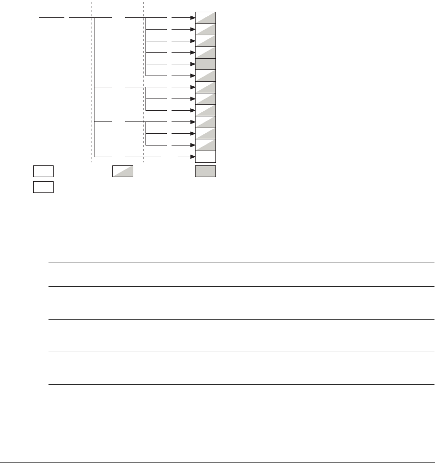
Performance Monitors
C9-10 Copyright © 1996-1998, 2000, 2004-2008 ARM Limited. All rights reserved. ARM DDI 0406B
C9.8 CP15 c9 register map
The performance monitor registers are mapped into part of the CP15 register map. The registers are
described in Performance monitor registers on page C10-105.
Figure C9-1 shows the CP15 c9 encodings for the recommended performance monitor registers, and the
reserved encodings for IMPLEMENTATION DEFINED performance monitors:
Figure C9-1 Recommended CP15 performance monitor registers
Table C9-1 lists the instructions used to access the recommended performance monitor registers.
c9 0 c12 0
CRn opc1 CRm opc2
PMCR, Performance Monitor Control Register
PMCNTENSET, Count Enable Set Register
PMCNTENCLR, Count Enable Clear Register
PMOVSR, Overflow Flag Status Register
PMSWINC, Software Increment Register
PMSELR, Event Counter Selection Register
1
2
3
4
5
PMCCNTR, Cycle Count Register
PMXEVTYPER, Event Type Select Register
PMXEVCNTR, Event Count Register
c13 0
1
2
Read/WriteRead-only Write-only
Access depends on the operation
PMINTENSET, Interrupt Enable Set Register
PMINTENCLR, Interrupt Enable Clear Register
c14
2
PMUSERENR, User Enable Register0
1
c15 {0-7} Reserved for IMPLEMENTATION DEFINED performance monitors
Table C9-1 Recommended performance monitor registers
InstructionaDescription or notes
MRC p15,0,<Rt>,c9,c12,0
MCR p15,0,<Rt>,c9,c12,0
c9, Performance Monitor Control Register (PMCR) on page C10-105.
MRC p15,0,<Rt>,c9,c12,1
MCR p15,0,<Rt>,c9,c12,1
c9, Count Enable Set Register (PMCNTENSET) on page C10-108.
MRC p15,0,<Rt>,c9,c12,2
MCR p15,0,<Rt>,c9,c12,2
c9, Count Enable Clear Register (PMCNTENCLR) on page C10-109.
MRC p15,0,<Rt>,c9,c12,3
MCR p15,0,<Rt>,c9,c12,3
c9, Overflow Flag Status Register (PMOVSR) on page C10-110.

Performance Monitors
ARM DDI 0406B Copyright © 1996-1998, 2000, 2004-2008 ARM Limited. All rights reserved. C9-11
C9.8.1 Power domains and performance monitor registers reset
For ARMv7 implementations, ARM recommends that performance monitors are implemented as part of the
core power domain, not as part of a separate debug power domain. There is no interface to access the
performance monitor registers when the core power domain is powered down.
The performance monitor registers must be set to their reset values on a processor reset by
nSYSPORESET, nCOREPORESET or nRESET. Performance monitor registers are not changed by a
debug logic reset by PRESETDBGn.
For more information about the reset scheme recommended for a v7 Debug implementation see
Recommended reset scheme for v7 Debug on page C6-16.
MRC p15,0,<Rt>,c9,c12,4
UNPREDICTABLE. PMSWINC is a write-only register.
MCR p15,0,<Rt>,c9,c12,4
c9, Software Increment Register (PMSWINC) on page C10-112.
MRC p15,0,<Rt>,c9,c12,5
MCR p15,0,<Rt>,c9,c12,5
c9, Event Counter Selection Register (PMSELR) on page C10-113.
MRC p15,0,<Rt>,c9,c13,0
MCR p15,0,<Rt>,c9,c13,0
c9, Cycle Count Register (PMCCNTR) on page C10-114.
MRC p15,0,<Rt>,c9,c13,1
MCR p15,0,<Rt>,c9,c13,1
c9, Event Type Select Register (PMXEVTYPER) on page C10-115.
MRC p15,0,<Rt>,c9,c13,2
MCR p15,0,<Rt>,c9,c13,2
c9, Event Count Register (PMXEVCNTR) on page C10-116.
MRC p15,0,<Rt>,c9,c14,0
MCR p15,0,<Rt>,c9,c14,0
c9, User Enable Register (PMUSERENR) on page C10-117.
MRC p15,0,<Rt>,c9,c14,1
MCR p15,0,<Rt>,c9,c14,1
c9, Interrupt Enable Set Register (PMINTENSET) on page C10-118.
MRC p15,0,<Rt>,c9,c14,2
MCR p15,0,<Rt>,c9,c14,2
c9, Interrupt Enable Clear Register (PMINTENCLR) on page C10-119.
a. CP15 c9 encodings with CRm == {c12-c14} not listed in the table are reserved. For details of the
behavior of accesses to these encodings see Unallocated CP15 encodings on page B3-69.
Table C9-1 Recommended performance monitor registers (continued)
InstructionaDescription or notes

Performance Monitors
C9-12 Copyright © 1996-1998, 2000, 2004-2008 ARM Limited. All rights reserved. ARM DDI 0406B
C9.9 Access permissions
Normally the performance monitor registers are accessible from privileged modes only. Setting the
PMUSERENR.EN flag to 1 permits access from User mode code, for example for instrumentation and
profiling purposes, see c9, User Enable Register (PMUSERENR) on page C10-117. However, the
PMUSERENR does not provide access to the registers that control interrupt generation.
Table C9-2 Performance monitor access permissions
Register Operation Access from a
privileged mode
Access from User modea
PMUSERENR.EN == 0 PMUSERENR.EN == 1
PMCR
MRC
or
MCR
Proceed UNDEFINED Proceed
PMCNTENSET
MRC
or
MCR
Proceed UNDEFINED Proceed
PMCNTENCLR
MRC
or
MCR
Proceed UNDEFINED Proceed
PMOVSR
MRC
or
MCR
Proceed UNDEFINED Proceed
PMSWINC
MRC
UNPREDICTABLE UNDEFINED UNPREDICTABLE
MCR
Proceed UNDEFINED Proceed
PMSELR
MRC
or
MCR
Proceed UNDEFINED Proceed
PMCCNTR
MRC
or
MCR
Proceed UNDEFINED Proceed
PMXEVTYPER
MRC
or
MCR
Proceed UNDEFINED Proceed
PMXEVCNTR
MRC
or
MCR
Proceed UNDEFINED Proceed
PMUSERENRa
MRC
Proceed Proceed Proceed
MCR
Proceed UNDEFINED UNDEFINED
PMINTENSET
MRC
or
MCR
Proceed UNDEFINED UNDEFINED
PMINTENCLR
MRC
or
MCR
Proceed UNDEFINED UNDEFINED
Reservedb
MRC
or
MCR
UNPREDICTABLE UNDEFINED UNDEFINED
a. For details of the EN flag see c9, User Enable Register (PMUSERENR) on page C10-117.
b. All the registers marked as reserved in Table C9-1 on page C9-10.

Performance Monitors
ARM DDI 0406B Copyright © 1996-1998, 2000, 2004-2008 ARM Limited. All rights reserved. C9-13
C9.10 Event numbers
The event numbers are described in the following subsections:
•Common feature event numbers
•Implementation defined feature event numbers on page C9-16.
C9.10.1 Common feature event numbers
For the common features, normally the counters must increment only once for each event. Exceptions to this
rule are stated in the individual definitions.
In these definitions, the term architecturally executed means that the instruction flow is such that the counted
instruction would have been executed in a simple sequential execution model.
Note
An instruction is architecturally executed if the behavior of the program on the processor is consistent with
the instruction having been executed on a simple execution model of the architecture. Therefore an
instruction that has been executed and retired is defined to be architecturally executed. In processors that
perform speculative execution, an instruction is not architecturally executed if the results of the speculative
execution are discarded. Where an instruction has no visible effect, for example, a
NOP
, the point where the
instruction is retired is IMPLEMENTATION DEFINED.
The common feature event number assignments are:
0x00
Software increment. The register is incremented only on writes to the Software Increment
Register. For details see c9, Software Increment Register (PMSWINC) on page C10-112.
0x01
Instruction fetch that causes a refill of at least the level of instruction or unified cache closest
to the processor. Each instruction fetch that causes a refill from outside the cache is counted.
Accesses that do not cause a new cache refill, but are satisfied from refilling data of a
previous miss, are not counted. Where an instruction fetch fetches multiple instructions, the
fetch counts a single event.
CP15 cache maintenance operations do not count as events.
This counter increments on speculative instruction fetches as well as on fetches of
instructions that reach execution.
0x02
Instruction fetch that causes a TLB refill of at least the level of TLB closest to the processor.
Each instruction fetch that causes an access to a level of memory system due to a translation
table walk or an access to another level of TLB caching is counted.
CP15 TLB maintenance operations do not count as events.
This counter increments on speculative instruction fetches as well as on fetches of
instructions that reach execution.
0x03
Memory Read or Write operation that causes a refill of at least the level of data or unified
cache closest to the processor. Each memory read from or write to that causes a refill from
outside the cache is counted. Accesses that do not cause a new cache refill, but are satisfied

Performance Monitors
C9-14 Copyright © 1996-1998, 2000, 2004-2008 ARM Limited. All rights reserved. ARM DDI 0406B
from refilling data of a previous miss are not counted. Each access to a cache line that causes
a new linefill is counted, including the multiple accesses of load or store multiples, including
PUSH
and
POP
. Write-Through writes that hit in the cache do not cause a linefill and so are not
counted.
CP15 cache maintenance operations do not count as events.
This counter increments on speculative memory accesses as well as for memory accesses
that are explicitly made by instructions.
0x04
Memory Read or Write operation that causes a cache access to at least the level of data or
unified cache closest to the processor. Each access to a cache line is counted including the
multiple accesses of instructions such as
LDM
or
STM
.
CP15 cache maintenance operations do not count as events.
This counter increments on speculative memory accesses as well as for memory accesses
that are explicitly made by instructions.
0x05
Memory Read or Write operation that causes a TLB refill of at least the level of TLB closest
to the processor. Each memory read or write operation that causes a translation table walk
or an access to another level of TLB caching is counted.
CP15 TLB maintenance operations do not count as events.
This counter increments on speculative memory accesses as well as for memory accesses
that are explicitly made by instructions.
0x06
Memory-reading instruction architecturally executed. This counter increments for every
instruction that explicitly read data, including
SWP
.
This counter does not increment for a conditional instruction that fails its condition code
check.
0x07
Memory-writing instruction architecturally executed. The counter increments for every
instruction that explicitly wrote data, including
SWP
.
This counter does not increment for a Store-Exclusive instruction that fails, or for a
conditional instruction that fails its condition code check.
0x08
Instruction architecturally executed. This counter counts for all instructions, including
conditional instructions that fail their condition code check.
0x09
Exception taken. This counts for each exception taken.
Note
This event number counts the processor exceptions described in Exceptions on page B1-30.
It does not count floating-point exceptions or ThumbEE null and index checks.
0x0A
Exception return architecturally executed. This counts the exception return instructions
described in Exception return on page B1-38.
This counter does not increment for a conditional instruction that fails its condition code
check.

Performance Monitors
ARM DDI 0406B Copyright © 1996-1998, 2000, 2004-2008 ARM Limited. All rights reserved. C9-15
0x0B
Instruction that writes to the CONTEXTIDR architecturally executed.
This counter does not increment for a conditional instruction that fails its condition code
check.
0x0C
Software change of PC, except by an exception, architecturally executed.
This counter does not increment for a conditional instruction that fails its condition code
check.
0x0D
Immediate branch architecturally executed:
•
B{L} <label>
•
BLX <label>
•
CB{N}Z <Rn>,<label>
•
HB{L} #HandlerId
(ThumbEE state only)
•
HB{L}P #<imm>, #HandlerId
(ThumbEE state only).
This counter counts for all immediate branch instructions that are architecturally executed,
including conditional instructions that fail their condition code check.
0x0E
Procedure return, other than exception return, architecturally executed:
•
BX R14
•
MOV PC,LR
•
POP {…,PC}
•
LDR PC,[SP],#offset
•
LDMIA R9!,{…,PC}
(ThumbEE state only)
•
LDR PC,[R9],#offset
(ThumbEE state only).
This counter does not increment for a conditional instruction that fails its condition code
check.
Note
Only these instructions are counted as procedure returns. For example, the following are not
counted as procedure return instructions:
•
BX R0
(Rm != R14)
•
MOV PC,R0
(Rm != R14)
•
LDM SP,{…,PC}
(writeback not specified)
•
LDR PC,[SP,#offset]
(wrong addressing mode).
0x0F
Unaligned access architecturally executed. This counts each instruction that is an access to
an unaligned address. That is, the instruction either triggered an unaligned fault, or would
have done so if the CPSR.A bit had been 1.
This counter does not increment for a conditional instruction that fails its condition code
check.

Performance Monitors
C9-16 Copyright © 1996-1998, 2000, 2004-2008 ARM Limited. All rights reserved. ARM DDI 0406B
0x10
Branch mispredicted or not predicted. This counts for each correction to the predicted
program flow that occurs because of a misprediction from, or no prediction from, the
program flow prediction resources and that relates to instructions that the program flow
prediction resources are capable of predicting.
0x11
Cycle count. The register is incremented on every cycle.
Note
Unlike PMCCNTR, this count is not affected by PMCR.DP, PMCR.D or PMCR.C:
• The counter is not incremented in prohibited regions, so is not affected by PMCR.DP.
• The counter increments on every cycle, regardless of the setting of PMCR.D.
• The counter is reset when event counters are reset by PMCR.P, never by PMCR.C.
0x12
Branch or other change in program flow that could have been predicted by the branch
prediction resources of the processor.
0x13
-
0x3F
Reserved.
C9.10.2 IMPLEMENTATION DEFINED feature event numbers
For IMPLEMENTATION DEFINED feature numbers, the counters are defined to either:
• increment only once for each event
• count the duration for which an event occurs
This property is defined individually for each feature.
ARM recommends implementers to establish house styles for the IMPLEMENTATION DEFINED events, with
common definitions, and common count numbers, applied to all the processors they implement. In general,
the recommended approach is for standardization across implementations with common features. However,
ARM recognizes that attempting to standardize the encoding of microarchitectural features across too wide
a range of implementations is not productive.
ARM strongly recommends that at least the following classes of event are identified in the IMPLEMENTATION
DEFINED events:
• Cumulative duration of stalls due to the holes in the instruction availability, separating out counts for
key buffering points that might exist.
• Cumulative duration of stalls due to data dependent stalling, separating out counts for key
dependency classes that might exist.
• Cumulative duration of stalls due to unavailability of execution resources (including write buffers, for
example), separating out counts for key resources that might exist.
• Missed superscalar issue opportunities, if relevant, separating out counts for key classes of issue that
might exist.
• Miss rates for different levels of caches and TLB.

Performance Monitors
ARM DDI 0406B Copyright © 1996-1998, 2000, 2004-2008 ARM Limited. All rights reserved. C9-17
• Transaction counts on external buses.
• External events passed into the processor via an IMPLEMENTATION DEFINED mechanism. Typically
this involves counting the number of cycles for which the signal is asserted using the duration count
option.
• Cumulative duration for which the CPSR.I and CPSR.F interrupt mask bits are set to 1.
• Any other microarchitectural features that the implementer considers it valuable to count.
IMPLEMENTATION DEFINED feature numbers are
0x40
to
0xFF
.

Performance Monitors
C9-18 Copyright © 1996-1998, 2000, 2004-2008 ARM Limited. All rights reserved. ARM DDI 0406B

ARM DDI 0406B Copyright © 1996-1998, 2000, 2004-2008 ARM Limited. All rights reserved. C10-1
Chapter C10
Debug Registers Reference
This chapter gives a reference description of the debug registers. See Debug register map on page C6-18 for
a list of all the debug registers.
This chapter contains the following sections:
•Accessing the debug registers on page C10-2
•Debug identification registers on page C10-3
•Control and status registers on page C10-10
•Instruction and data transfer registers on page C10-40
•Software debug event registers on page C10-48
•OS Save and Restore registers, v7 Debug only on page C10-75
•Memory system control registers on page C10-80
•Management registers, ARMv7 only on page C10-88
•Performance monitor registers on page C10-105.

Debug Registers Reference
C10-2 Copyright © 1996-1998, 2000, 2004-2008 ARM Limited. All rights reserved. ARM DDI 0406B
C10.1 Accessing the debug registers
In this chapter:
• The debug registers are numbered sequentially from 0 to 1023.
• The register offsets refer to the offsets in the v7 Debug memory-mapped or external debug interface.
The locations of these registers in the ARMv6 external debug interface might differ.
There is a standard mapping from debug register number to coprocessor instructions in the Extended CP14
interface, see Extended CP14 interface on page C6-33. The register numbers and offsets for the DBGDSCR,
DBGDTRRX, and DBGDTRTX Registers apply only to the external view of that register. For more
information, see Internal and external views of the DBGDSCR and the DCC registers on page C6-21.
Note
• The recommended v7 Debug external debug interface is described in ARM Debug Interface v5
Architecture Specification.
• Contact ARM if you require details of the ARMv6 recommended external debug interface.
Debug Registers Reference
ARM DDI 0406B Copyright © 1996-1998, 2000, 2004-2008 ARM Limited. All rights reserved. C10-3
C10.2 Debug identification registers
This section contains the following subsections:
•Debug ID Register (DBGDIDR)
•Debug Device ID Register (DBGDEVID) on page C10-6
•Debug ROM Address Register (DBGDRAR) on page C10-7
•Debug Self Address Offset Register (DBGDSAR) on page C10-8.
C10.2.1 Debug ID Register (DBGDIDR)
The Debug ID Register, DBGDIDR, specifies:
• which version of the Debug architecture is implemented
• some features of the debug implementation.
The DBGDIDR is:
• debug register 0, at offset
0x000
• a read-only register
• required on all versions of the Debug architecture from v6 Debug onwards
• when the Security Extensions are implemented, a Common register.
The format of the DBGDIDR is:
WRPs, bits [31:28]
The number of Watchpoint Register Pairs (WRPs) implemented. The meanings of the values
of this field are:
0b0000 1 WRP implemented
0b0001 2 WRPs implemented
0b0010 3 WRPs implemented
. .
. .
. .
0b1111 16 WRPs implemented.
The minimum number of WRPs is 1.
13 12
WRPs
31 28
BRPs
27 24
CTX_CMPs
23 20
Version
19 16 15 14
RAZ
11 8
Variant
74
Revision
03
nSUHD_imp
SE_imp
PCSR_imp
DEVID_imp

Debug Registers Reference
C10-4 Copyright © 1996-1998, 2000, 2004-2008 ARM Limited. All rights reserved. ARM DDI 0406B
BRPs, bits [27:24]
The number of Breakpoint Register Pairs (BRPs) implemented. The meanings of the values
of this field are:
0b0000 Reserved
0b0001 2 BRPs implemented
0b0010 3 BRPs implemented
. .
. .
. .
0b1111 16 BRPs implemented.
The minimum number of BRPs is 2.
CTX_CMPs, bits [23:20]
The number of BRPs that can be used for Context ID comparison. The meanings of the
values of this field are:
0b0000 1 BRP can be used for Context ID comparison
0b0001 2 BRPs can be used for Context ID comparison
0b0010 3 BRPs can be used for Context ID comparison
. .
. .
. .
0b1111 16 BRPs can be used for Context ID comparison.
The minimum number of BRPs with Context ID comparison capability is 1. The value in
this field cannot be greater than the value in the BRPs field, bits [27:24].
The breakpoint comparators with Context ID comparison capability must be the highest
addressed comparators. For example, if six comparators are implemented and two have
Context ID comparison capability, the comparators with Context ID comparison capability
must be comparators 4 and 5.
Version, bits [19:16]
The Debug architecture version. The permitted values of this field are:
0b0001 ARMv6, v6 Debug architecture
0b0010 ARMv6, v6.1 Debug architecture
0b0011 ARMv7 Debug architecture - Extended CP14 interface implemented
0b0100 ARMv7 Debug architecture - No Extended CP14 interface implemented.
All other values are reserved.
DEVID_imp, bit [15]
Debug Device ID Register, DBGDEVID, implemented bit. The meanings of the values of
this bit are:
0 DBGDEVID is not implemented. Debug register 1010 is reserved.

Debug Registers Reference
ARM DDI 0406B Copyright © 1996-1998, 2000, 2004-2008 ARM Limited. All rights reserved. C10-5
1 DBGDEVID is implemented, see Debug Device ID Register (DBGDEVID) on
page C10-6.
This bit is always RAZ in ARMv6.
nSUHD_imp, bit [14]
Secure User halting debug not implemented bit. When the Security Extensions are
implemented, the meanings of the values of this bit are:
0 Secure User halting debug is implemented
1 Secure User halting debug is not implemented.
If the Security Extensions are not implemented:
• Secure User halting debug cannot be implemented
• this bit is RAZ.
A v6.1 Debug processor that implements the Security Extensions must support Secure User
halting debug. In v6.1 Debug this bit is always RAZ.
See also Chapter C2 Invasive Debug Authentication.
PCSR_imp, bit [13]
Program Counter Sampling Register (DBGPCSR) implemented as register 33 bit. The
meanings of the values of this bit are:
0 DBGPCSR is not implemented as register 33
1 DBGPCSR is implemented as register 33.
Note
In v7 Debug, the DBGPCSR can be implemented as register 33, as register 40, or as both
register 33 and register 40, as described in Implemented Program Counter sampling
registers on page C8-2. The PCSR_imp bit only indicates whether it is implemented as
register 33. For details of how to determine whether it is implemented as register 40 see
Debug Device ID Register (DBGDEVID) on page C10-6.
In ARMv6, the Program Counter Sampling Register is an IMPLEMENTATION DEFINED
feature of the external debug interface and is not indicated in the DBGDIDR. This bit is
always RAZ in ARMv6.
See also Program Counter Sampling Register (DBGPCSR) on page C10-38.
SE_imp, bit [12]
Security Extensions implemented bit. The meanings of the values of this bit are:
0 Security Extensions are not implemented
1 Security Extensions are implemented.
v6 Debug is not a permitted option for an implementation that includes the Security
Extensions. This bit is RAZ on a v6 Debug implementation.
Bits [11:8] Reserved, RAZ.

Debug Registers Reference
C10-6 Copyright © 1996-1998, 2000, 2004-2008 ARM Limited. All rights reserved. ARM DDI 0406B
Variant, bits [7:4]
This field holds an IMPLEMENTATION DEFINED variant number. This number is incremented
on functional changes. The value must match bits [23:20] of the CP15 Main ID Register.
Revision, bits [3:0]
This field holds an IMPLEMENTATION DEFINED revision number. This number is incremented
on functional changes. The value must match bits [3:0] of the CP15 Main ID Register.
For details of the CP15 Main ID Register see:
•c0, Main ID Register (MIDR) on page B3-81, for a VMSA implementation
•c0, Main ID Register (MIDR) on page B4-32, for a PMSA implementation.
C10.2.2 Debug Device ID Register (DBGDEVID)
The Debug Device ID Register, DBGDEVID, extends the DBGDIDR by describing other features of the
debug implementation.
The DBGDEVID register is:
• debug register 1010, at offset
0xFC8
• a read-only register
• an optional register, that can be implemented only in v7 Debug
• when the Security Extensions are implemented, a Common register.
The DBGDIDR.DEVID_imp bit indicates whether the DBGDEVID register is implemented, see Debug ID
Register (DBGDIDR) on page C10-3.
If the DBGDEVID register is not implemented:
• the Program Counter Sampling Register (DBGPCSR) is not implemented as register 40
• the Context ID Sampling Register (DBGCIDSR) is not implemented.
The format of the DBGDEVID register is:
Bits [31:4] Reserved, RAZ.
PCsample, bits [3:0]
This field indicates the level of Program Counter sampling support using debug registers 40
and 41. The permitted values of this field are:
0b0000 Program Counter Sampling Register (DBGPCSR) is not implemented as
register 40, and Context ID Sampling Register (DBGCIDSR) is not
implemented.
0b0001 DBGPCSR is implemented as register 40, and DBGCIDSR is not implemented.
031
PCsampleReserved, RAZ
43

Debug Registers Reference
ARM DDI 0406B Copyright © 1996-1998, 2000, 2004-2008 ARM Limited. All rights reserved. C10-7
0b0010 DBGPCSR is implemented as register 40, and DBGCIDSR is implemented as
register 41.
Other values are reserved.
Note
The DBGPCSR can be implemented as register 33, as register 40, or as both register 33 and
register 40, as described in Implemented Program Counter sampling registers on page C8-2.
The PCsample field only indicates whether it is implemented as register 40. For details of
how to determine whether it is implemented as register 33 see Debug ID Register
(DBGDIDR) on page C10-3.
C10.2.3 Debug ROM Address Register (DBGDRAR)
The Debug ROM Address Register, DBGDRAR, defines the base address of a ROM Table, that locates and
describes the debug components in the system.
The DBGDRAR is:
• Only implemented through the Baseline CP14 interface, and therefore does not have a register
number and offset. For more information, see The CP14 debug register interfaces on page C6-32.
• A read-only register.
• Implemented as follows:
ARMv6 This register is not defined in ARMv6.
v7 Debug If no Memory-mapped debug components, including this processor, are implemented,
this register is RAZ.
Otherwise, the register defines the physical address in memory of a ROM Table.
• When the Security Extensions are implemented, a Common register.
It is IMPLEMENTATION DEFINED how the processor determines the value that is returned as the ROM Table
address. If the processor cannot determine the value, the Valid field in the register must be RAZ.
One implementation scheme is to provide inputs DBGROMADDR[31:12] and DBGROMADDRV that a
system designer must tie-off to the correct value. DBGROMADDRV must be tied HIGH only if
DBGROMADDR[31:12] is tied off to a valid value, otherwise DBGROMADDR[31:12] and
DBGROMADDRV must be tied LOW.
The format of the DBGDRAR is:
DBGROMADDR[31:12]
0131 12
Valid
211
Reserved, RAZ

Debug Registers Reference
C10-8 Copyright © 1996-1998, 2000, 2004-2008 ARM Limited. All rights reserved. ARM DDI 0406B
This register format applies regardless of the implementation scheme for identifying the ROM Table
address.
DBGROMADDR[31:12], bits [31:12]
Bits [31:12] of the ROM Table physical address. Bits [11:0] of the address are zero.
If the Valid field, bits [1:0], is zero the value of this field is UNKNOWN.
Bits [11:2] Reserved, RAZ.
Valid, bits [1:0]
This field indicates whether the ROM Table address is valid. In the recommended
implementation it reflects the value of the DBGROMADDRV signal, and the permitted
values of this field are:
0b00 DBGROMADDRV is LOW, ROM Table address is not valid
0b11 DBGROMADDRV is HIGH, ROM Table address is valid.
Other values are reserved.
The ROM Table contains a zero-terminated list of signed 32-bit offsets from the ROM Table base to other
Memory-mapped debug components in the system. All the debug components pointed to must contain a set
of debug component identification registers compatible with the format in Debug Component Identification
Registers (DBGCID0 to DBGCID3) on page C10-102. For more information, see the ARM Debug Interface
v5 Architecture Specification.
C10.2.4 Debug Self Address Offset Register (DBGDSAR)
The Debug Self Address Offset Register, DBGDSAR, defines the offset from the ROM Table physical
address to the physical address of the debug registers for the processor.
The DBGDSAR is:
• Only implemented through the Baseline CP14 interface, and therefore does not have a register
number and offset. For more information, see The CP14 debug register interfaces on page C6-32.
• A read-only register.
• Implemented as follows:
ARMv6 This register is not defined in ARMv6.
v7 Debug If no memory-mapped interface is provided, this register is RAZ.
Otherwise, the register gives the offset from the ROM Table physical address to the
physical address of the debug registers for the processor.
• When the Security Extensions are implemented, a Common register.
It is IMPLEMENTATION DEFINED how the processor determines the value that is returned as the debug self
address offset. If the processor cannot determine the value, the Valid field in the register must be RAZ.

Debug Registers Reference
ARM DDI 0406B Copyright © 1996-1998, 2000, 2004-2008 ARM Limited. All rights reserved. C10-9
One implementation scheme is to provide inputs DBGSELFADDR[31:12] and DBGSELFADDRV that a
system designer must tie-off to the correct value. DBGSELFADDRV must be tied HIGH only if
DBGSELFADDR[31:12] is tied off to a valid value, otherwise DBGSELFADDR[31:12] and
DBGSELFADDRV must be tied LOW.
The format of the DBGDSAR is:
This register format applies regardless of the implementation scheme for identifying the debug self address
offset.
DBGSELFADDR [31:12], bits [31:12]
Bits [31:12] of the two’s complement offset from the ROM Table physical address to the
physical address where the debug registers are mapped. Bits [11:0] of the address are zero.
If the Valid field, bits [1:0], is zero the value of this field is UNKNOWN.
Bits [11:2] Reserved, RAZ.
Valid, bits [1:0]
This field indicates whether the debug self address offset is valid. In the recommended
implementation it reflects the value of the DBGSELFADDRV signal, and the permitted
values of this field are:
0b00 DBGSELFADDRV is LOW, offset is not valid
0b11 DBGSELFADDRV is HIGH, offset is valid.
Other values are reserved.
DBGSELFADDR[31:12]
01
Valid
21131 12
Reserved, RAZ

Debug Registers Reference
C10-10 Copyright © 1996-1998, 2000, 2004-2008 ARM Limited. All rights reserved. ARM DDI 0406B
C10.3 Control and status registers
This section contains the following subsections:
•Debug Status and Control Register (DBGDSCR)
•Watchpoint Fault Address Register (DBGWFAR) on page C10-28
•Debug Run Control Register (DBGDRCR), v7 Debug only on page C10-29
•Device Power-down and Reset Control Register (DBGPRCR), v7 Debug only on page C10-31
•Device Power-down and Reset Status Register (DBGPRSR), v7 Debug only on page C10-34
•Program Counter Sampling Register (DBGPCSR) on page C10-38
•Context ID Sampling Register (DBGCIDSR) on page C10-39.
C10.3.1 Debug Status and Control Register (DBGDSCR)
The Debug Status and Control Register, DBGDSCR, provides the main control register for the debug
facilities in the ARM architecture. All debug implementations provide both internal and external views of
the DBGDSCR, and it is the external view that provides control of the debug facilities. These views are
referred to as:
DBGDSCRint the internal view
DBGDSCRext the external view.
For more information, see Internal and external views of the DBGDSCR and the DCC registers on
page C6-21.
The DBGDSCR:
• In its external view:
— is debug register 34 at offset
0x088
.
— is a read/write register, with more restricted access to some bits.
• Has the following differences in different versions of the Debug architecture:
— v6.1 Debug and v7 Debug define additional bits in the register.
— DBGDSCR bit [9] is defined only in v6 Debug and v6.1 Debug. It is reserved in v7 Debug.
— Access to the register depends on the version of the Debug architecture, see Access to the
DBGDSCR on page C10-27.
— The behavior of RXfull and TXfull on reads of DBGDSCR through the internal and external
views is different, see Access controls on the external view of the DCC registers and DBGITR,
v7 Debug only on page C10-21.
• When the Security Extensions are implemented, is a Common register.
Debug Registers Reference
ARM DDI 0406B Copyright © 1996-1998, 2000, 2004-2008 ARM Limited. All rights reserved. C10-11
In v7 Debug, the format of the DBGDSCR is:
Bits [31,28,23:22]
Reserved, UNK/SBZP.
RXfull, bit [30]
The DBGDTRRX Register full bit. The possible values of this bit are:
0 DBGDTRRX Register empty
1 DBGDTRRX Register full.
Normally, RXfull is:
• set to 1 on writes to DBGDTRRXext
• cleared to 0 on reads of DBGDTRRXint.
For more information about the behavior of RXfull and the DBGDTRRX Register see Host
to Target Data Transfer Register (DBGDTRRX) on page C10-40.
TXfull, bit [29]
The DBGDTRTX Register full bit. The possible values of this bit are:
0 DBGDTRTX Register empty
1 DBGDTRTX Register full.
Normally, TXfull is:
• cleared to 0 on reads of DBGDTRTXext
• set to 1 on writes to DBGDTRTXint.
For more information about the behavior of TXfull and the DBGDTRTX Register see Targe t
to Host Data Transfer Register (DBGDTRTX) on page C10-43.
0121131 12
RXfull
TXfull
Reserved, UNK/SBZP
30 29 28 27 26 25 24 23 22 21 20 19 18 17 16 15 14 13
(0)
1098765
MOE
Res.
RXfull_l
TXfull_l
PipeAdv
InstrCompl_l
NS
ADAdiscard
ExtDCCmode
SPNIDdis
SPIDdis
MDBGen
HDBGen
SDABORT_l
ADABORT_l
UND_l
ITRen
UDCCdis
INTdis
DBGack
RESTARTED
HALTED
(0)(0)(0)
In ARMv6, bit [9] can
be DBGnoPWRDWN

Debug Registers Reference
C10-12 Copyright © 1996-1998, 2000, 2004-2008 ARM Limited. All rights reserved. ARM DDI 0406B
RXfull_l, bit [27], v7 Debug only
The latched RXfull bit. This is a copy of the RXfull bit taken as a side-effect of a read of
DBGDSCRext. This means that RXfull_l holds the last value of RXfull read from
DBGDSCRext:
• On a read of DBGDSCRext that is permitted to have side-effects, the value of
RXfull_l is the same as the value of RXfull.
• On a read of DBGDSCRint, the value of RXfull_l is UNKNOWN.
Normally, RXfull_l is set to 1 on writes to DBGDTRRXext.
The RXfull_l bit controls the behavior of the processor on writes to DBGDTRRXext. For
more information about the behavior of RXfull_l and the DBGDTRRX Register, see Host
to Target Data Transfer Register (DBGDTRRX) on page C10-40.
TXfull_l, bit [26], v7 Debug only
The latched TXfull bit. This is a copy of the TXfull bit taken as a side-effect of a read of
DBGDSCRext. This means that TXfull_l holds the last value of TXfull read from
DBGDSCRext:
• On a read of DBGDSCRext that is permitted to have side-effects, the value of
TXfull_l is the same as the value of TXfull.
• On a read of DBGDSCRint, the value of TXfull_l is UNKNOWN.
Normally, TXfull_l is cleared to 0 on reads of DBGDTRTXext.
The TXfull_l bit controls the behavior of the processor on reads of DBGDTRTXext. For
more information about the behavior of TXfull_l and the DBGDTRTX Register see Targe t
to Host Data Transfer Register (DBGDTRTX) on page C10-43.
PipeAdv, bit [25], v7 Debug only
Sticky Pipeline Advance bit. This bit is set to 1 every time the processor pipeline retires one
instruction. It is cleared to 0 by a write to DBGDRCR[3], see Debug Run Control Register
(DBGDRCR), v7 Debug only on page C10-29.
This flag enables a debugger to detect that the processor is idle. In some situations this might
indicate that the processor is deadlocked.
InstrCompl_l, bit [24], v7 Debug only
The latched Instruction Complete bit. This is a copy of the Instruction Complete internal
flag, taken on each read of DBGDSCRext. InstrCompl signals whether the processor has
completed execution of an instruction issued through the Instruction Transfer Register
(DBGITR), see Instruction Transfer Register (DBGITR) on page C10-46. InstrCompl is not
visible directly in any register.

Debug Registers Reference
ARM DDI 0406B Copyright © 1996-1998, 2000, 2004-2008 ARM Limited. All rights reserved. C10-13
On a read of DBGDSCRext, InstrCompl_l always returns the current value of InstrCompl.
The meanings of the values of InstrCompl_l are:
0 an instruction previously issued through the DBGITR has not completed its
changes to the architectural state of the processor
1 all instructions previously issued through the DBGITR have completed their
changes to the architectural state of the processor.
Normally, InstrCompl:
• is cleared to 0 following issue of an instruction through DBGITR
• becomes 1 once the instruction completes.
The taking of an exception marks the completion of the instruction. InstrCompl is set to 1 if
an instruction generates an Undefined Instruction or Data Abort exception.
InstrCompl is set to 1 on entry to Debug state. For more information about the behavior of
InstrCompl, InstrCompl_l and the DBGITR, see:
•Instruction Transfer Register (DBGITR) on page C10-46
•Host to Target Data Transfer Register (DBGDTRRX) on page C10-40
•Target to Host Data Transfer Register (DBGDTRTX) on page C10-43.
Bits [27:24], v6 Debug and v6.1 Debug only
Reserved, UNK/SBZP.
ExtDCCmode, bits [21:20], v7 Debug only
The External DCC access mode field. This field controls the access mode for the external
views of the DCC registers and the Instruction Transfer Register (DBGITR). Possible values
are:
0b00 Non-blocking mode
0b01 Stall mode
0b10 Fast mode.
The values of 0b11 is reserved.
For details of the external DCC access modes see Access controls on the external view of the
DCC registers and DBGITR, v7 Debug only on page C10-21.
Bits [21:20], v6 Debug and v6.1 Debug only
Reserved, UNK/SBZP.
ADAdiscard, bit [19], v6.1 Debug and v7 Debug
Asynchronous Data Aborts Discarded bit. The possible values of this bit are:
0 Asynchronous aborts handled normally
1 On an asynchronous abort, the processor sets the Sticky Asynchronous Data
Abort bit, ADABORT_l, to 1 but otherwise discards the abort.

Debug Registers Reference
C10-14 Copyright © 1996-1998, 2000, 2004-2008 ARM Limited. All rights reserved. ARM DDI 0406B
Note
The conditions for setting ADABORT_l to 1 are different in v7 Debug and
v6.1 Debug. For more information, see the description of the ADABORT_l bit,
bit [7].
It is IMPLEMENTATION DEFINED whether the hardware automatically sets this bit to 1 on
entry to Debug state, see Asynchronous aborts and entry to Debug state on page C5-5.
The processor clears this bit to 0 on exit from Debug state.
NS, bit [18], v6.1 Debug and v7 Debug
Non-secure state status bit. If the processor implements Security Extensions, this bit
indicates whether the processor is in the Secure state. The possible values of this bit are:
0 the processor is in the Secure state
1 the processor is in the Non-secure state.
If the processor does not implement Security Extensions, this bit is RAZ.
SPNIDdis, bit [17], v6.1 Debug and v7 Debug
Secure Privileged Non-Invasive Debug Disabled bit. The behavior of this bit depends on the
version of the Debug architecture:
v6.1 Debug
If the processor implements Security Extensions, this bit takes the value of the
inverse of the SPNIDEN input. Otherwise it is RAZ.
v7 Debug This bit is the inverse of bit [6] of the Authentication Status Register, see
Authentication Status Register (DBGAUTHSTATUS) on page C10-96.
SPIDdis, bit [16], v6.1 Debug and v7 Debug
Secure Privileged Invasive Debug Disabled bit. The behavior of this bit depends on the
version of the Debug architecture:
v6.1 Debug
If the processor implements Security Extensions, this bit takes the value of the
inverse of the SPIDEN input. Otherwise it is RAZ.
v7 Debug This bit is the inverse of bit [4] of the Authentication Status Register, see
Authentication Status Register (DBGAUTHSTATUS) on page C10-96.
Bits [19:16], v6 Debug only
Reserved, UNK/SBZP.
MDBGen, bit [15]
Monitor debug-mode enable bit. The possible values of this bit are:
0 Monitor debug-mode disabled
1 Monitor debug-mode enabled.

Debug Registers Reference
ARM DDI 0406B Copyright © 1996-1998, 2000, 2004-2008 ARM Limited. All rights reserved. C10-15
If the external interface input DBGEN is LOW, the MDBGen bit reads as 0. The
programmed value is masked until DBGEN is taken HIGH. When DBGEN goes HIGH, the
value read and the behavior of the processor correspond to the programmed value.
Note
• If Halting debug-mode is enabled, by setting the HDBGen bit to 1, then the Monitor
debug-mode setting is disabled regardless of the setting of the MDBGen bit.
• It is the programmed value of the MDBGen bit, not the value returned by reads of the
DBGDSCR, that is saved by the OS Save and Restore Register in a power-down
sequence. For more information, see The OS Save and Restore mechanism on
page C6-8.
HDBGen, bit [14]
Halting debug-mode enable bit. The possible values of this bit are:
0 Halting debug-mode disabled
1 Halting debug-mode enabled.
If the external interface input DBGEN is LOW, the HDBGen bit reads as 0. The
programmed value is masked until DBGEN is taken HIGH. When DBGEN goes HIGH, the
value read and the behavior of the processor correspond to the programmed value.
Note
It is the programmed value of the HDBGen bit, not the value returned by reads of the
DBGDSCR, that is saved by the OS Save and Restore Register in a power-down sequence.
For more information, see The OS Save and Restore mechanism on page C6-8.
ITRen, bit [13]
Execute ARM instruction enable bit. This bit enables the execution of ARM instructions
through the DBGITR, see Instruction Transfer Register (DBGITR) on page C10-46. The
possible values of this bit are:
0 ITR mechanism disabled
1 The ITR mechanism for forcing the processor to execute instructions in Debug
state via the external debug interface is enabled.
Setting this bit to 1 when the processor is in Non-debug state causes UNPREDICTABLE
behavior. The effect of writing to DBGITR when this bit is set to 0 is UNPREDICTABLE.
The implementation of this bit can depend on the Debug architecture version:
ARMv6 If the external debug interface does not have a mechanism for forcing the
processor to execute instructions in Debug state via the external debug interface,
this bit is RAZ/WI.
v7 Debug This bit, and the DBGITR, are required.

Debug Registers Reference
C10-16 Copyright © 1996-1998, 2000, 2004-2008 ARM Limited. All rights reserved. ARM DDI 0406B
UDCCdis, bit [12]
User mode access to Communications Channel disable bit. The possible values of this bit
are:
0 User mode access to Communication Channel enabled
1 User mode access to Communication Channel disabled.
When this bit is set to 1, if a User mode process tries to access the DBGDIDR,
DBGDSCRint, DBGDTRRXint, or DBGDTRTXint through CP14 operations, the
Undefined Instruction exception is taken. Setting this bit to 1 prevents User mode access to
any CP14 debug register.
INTdis, bit [11]
Interrupts Disable bit. This bit can be used to mask the taking of IRQs and FIQs. The
possible values of this bit are:
0 interrupts enabled
1 interrupts disabled.
If the external debugger needs to execute a piece of code in Non-debug state as part of the
debugging process, but that code must not be interrupted, the external debugger sets this bit
to 1.
For example, when single stepping code in a system with a periodic timer interrupt, the
period of the interrupt is likely to be more frequent than the stepping frequency of the
debugger. In this situation, if the debugger steps the target without setting the INTdis bit to 1
for the duration of the step, the interrupt is pending. This means that, if interrupts are
enabled in the CPSR, the interrupt is taken as soon as the processor leaves Debug state.
The INTdis bit is ignored when either:
• DBGDSCR[15:14] == 0b00
•DBGEN is LOW.
For more information about the debug authentication signals see Chapter C2 Invasive
Debug Authentication.
Note
If implemented, the ISR always reflects the status of the IRQ and FIQ signals, regardless of
the value of the INTdis bit. For more information, see c12, Interrupt Status Register (ISR)
on page B3-150.
DBGack, bit [10]
Force Debug Acknowledge bit. A debugger can use this bit to force any implemented debug
acknowledge output signals to be asserted. The possible values of this bit are:
0 Debug acknowledge signals under normal processor control
1 Debug acknowledge signals asserted, regardless of the processor state.
For details of the recommended external debug interface, see Run-control and
cross-triggering signals on page AppxA-5 and DBGACK and DBGCPUDONE on
page AppxA-7.

Debug Registers Reference
ARM DDI 0406B Copyright © 1996-1998, 2000, 2004-2008 ARM Limited. All rights reserved. C10-17
If a debugger sets this bit to 1, it can then cause the processor to execute instructions in
Non-debug state, while the rest of the system behaves as if the processor is in Debug state.
Note
The effect of setting DBGack to 1 takes no account of the DBGEN and SPIDEN signals.
This means it asserts the debug acknowledge signals regardless of the invasive debug
authentication settings.
Bit [9], v7 Debug
Reserved, UNK/SBZP.
DBGnoPWRDWN, bit [9], v6 Debug and v6.1 Debug only
Debug no power-down bit. This bit can be used to drive a debug no power-down output
signal, DBGNOPWRDWN. The possible values of this bit are:
0 DBGNOPWRDWN driven LOW
1 DBGNOPWRDWN driven HIGH.
Note
• In v6 Debug and v6.1 Debug, this bit is not defined, but many implementations
define DBGDSCR[9] as the DBGnoPWRDWN bit. If this bit is not implemented,
DBGDSCR[9] is UNK/SBZP.
• In v7 Debug this use of this bit is replaced by the DBGnoPWRDWN bit in the
DBGPRCR, see Device Power-down and Reset Control Register (DBGPRCR),
v7 Debug only on page C10-31.
UND_l, bit [8], v6.1 Debug and v7 Debug
Sticky Undefined Instruction bit. This flag is set to 1 by any Undefined Instruction
exceptions generated by instructions issued to the processor while in Debug state. The
possible values of this bit are:
0 No Undefined Instruction exception has been generated since the last time this
bit was cleared to 0
1 An Undefined Instruction exception has been generated since the last time this
bit was cleared to 0.
The method of clearing this flag to 0, and the behavior of the flag, depends on the version
of the Debug architecture:
v6.1 Debug
This flag is cleared to 0 when the external debugger reads the DBGDSCR.
v7 Debug This flag is cleared to 0 only by writing to bit [2] of the DBGDRCR, see Debug
Run Control Register (DBGDRCR), v7 Debug only on page C10-29.
Leaving Debug state with this flag set to 1 causes UNPREDICTABLE behavior.
When the processor is in Non-debug state, this flag is not set to 1 by an Undefined
Instruction exception.

Debug Registers Reference
C10-18 Copyright © 1996-1998, 2000, 2004-2008 ARM Limited. All rights reserved. ARM DDI 0406B
For more information, see Exceptions in Debug state on page C5-20.
Bit [8], v6 Debug only
Reserved, UNK/SBZP.
ADABORT_l, bit [7], v7 Debug
Sticky Asynchronous Data Abort bit. This flag is set to 1 by any asynchronous abort that
occurs when the processor is in Debug state and is discarded because the ADAdiscard bit,
bit [19], is set to 1. The possible values of this bit are:
0 No asynchronous abort has been discarded since the last time this bit was
cleared to 0
1 An asynchronous abort has been discarded since the last time this bit was
cleared to 0.
This flag is cleared to 0 only by writing to bit [2] of the DBGDRCR, see Debug Run Control
Register (DBGDRCR), v7 Debug only on page C10-29.
Leaving Debug state with this flag set to 1 causes UNPREDICTABLE behavior.
When the processor is in Non-debug state this flag is never set to 1 when an asynchronous
abort occurs.
For more information, see Asynchronous aborts and entry to Debug state on page C5-5 and
Exceptions in Debug state on page C5-20.
ADABORT_l, bit [7], v6 Debug and v6.1 Debug
Sticky Asynchronous Data Abort bit. This flag is set to 1 by any asynchronous abort that
occurs when the processor is in Debug state. The possible values of this bit are:
0 No asynchronous abort has occurred since the last time this bit was cleared to 0
1 An asynchronous abort has occurred since the last time this bit was cleared to 0.
This flag is cleared to 0 when the external debugger reads the DBGDSCR.
Some aspects of the behavior of this flag depend on the version of the Debug architecture:
v6.1 Debug
If the processor is in Non-debug state this flag is not set to 1 on an asynchronous
abort.
v6 Debug The value of this flag is UNKNOWN when either the processor is in Non-debug
state, or the ITRen bit, bit [13], is not set to 1.
For more information, see Asynchronous aborts and entry to Debug state on page C5-5 and
Exceptions in Debug state on page C5-20.

Debug Registers Reference
ARM DDI 0406B Copyright © 1996-1998, 2000, 2004-2008 ARM Limited. All rights reserved. C10-19
SDABORT_l, bit [6]
Sticky Synchronous Data Abort bit. This flag is set to 1 by any Data Abort exception that is
generated by a synchronous data abort when the processor is in Debug state. The possible
values of this bit are:
0 No Data Abort exception has been generated by a synchronous data abort since
the last time this bit was cleared to 0
1 A Data Abort exception has been generated by a synchronous data abort since
the last time this bit was cleared to 0.
The behavior of the DBGITR depends on the value of the SDABORT_l bit, see Instruction
Transfer Register (DBGITR) on page C10-46.
The method of clearing this flag to 0 depends on the version of the Debug architecture:
v7 Debug This flag is cleared to 0 only by writing to bit [2] of the DBGDRCR, see Debug
Run Control Register (DBGDRCR), v7 Debug only on page C10-29.
ARMv6 This flag is cleared to 0 when the external debugger reads the DBGDSCR.
Some aspects of the behavior of this flag depend on the version of the Debug architecture:
v7 Debug If the processor is in Non-debug state this flag is not set to 1 on a synchronous
Data Abort exception.
Leaving Debug state with this flag set to 1 causes UNPREDICTABLE behavior.
v6.1 Debug
If the processor is in Non-debug state this flag is not set to 1 on a synchronous
Data Abort exception.
v6 Debug If the processor is in Non-debug state, the value of this flag is UNKNOWN.
For more information, see Exceptions in Debug state on page C5-20.
MOE, bits [5:2]
Method of Debug Entry field. The permitted values of this field depend on the Debug
architecture. For details of this field see Method of Debug entry on page C10-26.
RESTARTED, bit [1]
Processor Restarted bit. The possible values of this bit are:
0 The processor is exiting Debug state. This bit only reads as 0 between receiving
a restart request, and restarting Non-debug state operation.
1 The processor has exited Debug state. This bit remains set to 1 if the processor
re-enters Debug state.
After making a restart request, the debugger can poll this bit until it is set to 1. At that point
it knows that the restart request has taken effect and the processor has exited Debug state.
Note
Polling the HALTED bit until it is set to 0 is not safe because the processor could re-enter
Debug state as a result of another debug event before the debugger samples the DBGDSCR.
See Chapter C5 Debug State for a definition of Debug state.

Debug Registers Reference
C10-20 Copyright © 1996-1998, 2000, 2004-2008 ARM Limited. All rights reserved. ARM DDI 0406B
HALTED, bit [0]
Processor Halted bit. The possible values of this bit are:
0 The processor is in Non-debug state.
1 The processor is in Debug state.
Note
Between receiving a restart request and restarting Non-debug state operation,
the processor is in Debug state and this bit reads as 1
After programming a debug event, the external debugger can poll this bit until it is set to 1.
At that point it knows that the processor has entered Debug state.
See Chapter C5 Debug State for a definition of Debug state.
Table C10-1 shows the access to each field of the DBGDSCR, and the reset value of each field. It also shows
the Debug architecture versions in which each field is defined.
Table C10-1 DBGDSCR bit access and reset values
Bits Field name Version AccessaReset valueb
[31] - - UNK/SBZP -
[30] RXfull All Read-only 0
[29] TXfull All Read-only 0
[28] - - UNK/SBZP -
[27] RXfull_l v7 Debug Read-only 0
[26] TXfull_l v7 Debug Read-only 0
[25] PipeAdv v7 Debug Read-only UNKNOWN
[24] InstrCompl_l v7 Debug Read-only UNKNOWN
[23:22] - - UNK/SBZP -
[21:20] ExtDCCmode v7 Debug Read/write 00
[19] ADAdiscard v6.1 Debug, v7 Debug Read-only or
Read/writec
0
[18] NS v6.1 Debug, v7 Debug Read-only f
[17] SPNIDdis v6.1 Debug, v7 Debug Read-only f
[16] SPIDdis v6.1 Debug, v7 Debug Read-only f
[15] MDBGen All RWInt 0

Debug Registers Reference
ARM DDI 0406B Copyright © 1996-1998, 2000, 2004-2008 ARM Limited. All rights reserved. C10-21
Access controls on the external view of the DCC registers and DBGITR,
v7 Debug only
In v7 Debug, the DBGDSCR.ExtDCCmode field determines the external DCC access mode. This access
mode, operating with flags in the DBGDSCR, controls all accesses made to DBGDTRRXext and
DBGDTRTXext, and also controls some accesses to the Instruction Transfer Register DBGITR.
The DBGDSCR includes a ready flag and a latched ready flag for each of the registers DBGDTRRXext and
DBGDTRTXext, and a latched ready flag for the DBGITR:
• RXfull and RXfull_l are the ready and latched ready flags for the DBGDTRRXext register
• TXfull and TXfull_l are the ready and latched ready flags for the DBGDTRTXext register
• InstrCompl_l is the latched ready flag for the DBGITR.
[14] HDBGen All RWExt 0
[13] ITRen All RWExt 0
[12] UDCCdis All RWInt 0
[11] INTdis All RWExt 0
[10] DBGack All RWExt 0
[9] DBGnoPWRDWN v6 Debug, v6.1 DebugdRWExt 0
[8] UND_l v6.1 Debug, v7 Debug Read-only e0
[7] ADABORT_l All Read-only e0
[6] SDABORT_l All Read-only e0
[5:2] MOE All RWInt 0
[1] RESTARTED All Read-only f
[0] HALTED All Read-only f
a. For more information, including the meaning of RWInt and RWExt, see Access to the DBGDSCR on
page C10-27.
b. Debug logic reset value, the value after a debug logic reset.
c. The ADAdiscard bit can be read/write. This is IMPLEMENTATION DEFINED, see Asynchronous aborts and
entry to Debug state on page C5-5.
d. For more information, see the v6 Debug and v6.1 Debug description of this field.
e. For details of how these bits are cleared to 0 see the descriptions of the bits. The method depends on the
Debug architecture version.
f. These are read-only status bits that reflect the current state of the processor.
Table C10-1 DBGDSCR bit access and reset values (continued)
Bits Field name Version AccessaReset valueb

Debug Registers Reference
C10-22 Copyright © 1996-1998, 2000, 2004-2008 ARM Limited. All rights reserved. ARM DDI 0406B
The ready flag for the DBGITR, InstrCompl, is an internal flag that cannot be accessed through any
register.
For details of the ready state of each flag, and details of when the latched flags are updated, see the
descriptions of the DBGDSCR flag bits.
Different external DCC access modes require the debugger to execute different sequences of accesses to the
DBGDTRRXext and DBGDTRTXext registers, and to the DBGITR. This can affect the total number of
accesses required.
Table C10-2 shows the three external DCC access modes:
Note
• Non-blocking mode is the default setting because improper use of the other modes can result in the
external debug interface becoming deadlocked.
• For information that applies to all access modes see Restrictions on accesses to DBGITR,
DBGDTRRXext and DBGDTRTXext on page C10-25.
See Instruction and data transfer registers on page C10-40. The external DCC access mode field has no
effect on accesses to DBGDTRRXint and DBGDTRTXint.
Non-blocking mode
When Non-blocking mode is selected, reads from DBGDTRTXext and writes to DBGDTRRXext and
DBGITR are ignored when the appropriate latched ready flag is not in the ready state:
• if RXfull_l is set to 1, writes to DBGDTRRXext are ignored
• if InstrCompl_l is set to 0, writes to DBGITR are ignored
• if TXfull_l is set to 0, reads from DBGDTRTXext are ignored and return an UNKNOWN value.
Following a successful write to DBGDTRRXext, RXfull and RXfull_l are set to 1.
Following a successful read from DBGDTRTXext, TXfull and TXfull_l are cleared to 0.
Following a successful write to DBGITR, InstrCompl and InstrCompl_l are cleared to 0.
Table C10-2 Meaning of the external DCC access mode values
DBGDSCR.ExtDCCmode External DCC access mode Description
0b00 Non-blocking mode Non-blocking mode
0b01 Stall mode Stall mode on page C10-23
0b10 Fast mode Fast mode on page C10-23

Debug Registers Reference
ARM DDI 0406B Copyright © 1996-1998, 2000, 2004-2008 ARM Limited. All rights reserved. C10-23
Debuggers accessing these registers must first read DBGDSCRext. This has the side-effect of copying
RXfull and TXfull to RXfull_l and TXfull_l, and setting InstrCompl_l. The debugger can then use the
returned value to determine whether a subsequent access to these registers will be ignored.
Stall mode
When Stall mode is selected, accesses to DBGDTRRXext, DBGDTRTXext, and DBGITR are modified
such that each access stalls under the following conditions:
• writes to DBGDTRRXext are not completed until RXfull is 0
• writes to DBGITR are not completed until InstrCompl is 1
• reads from DBGDTRTXext are not completed until TXfull is 1.
If an access is stalled in this way you cannot access any of the debug registers until the stalled
DBGDTRRXext, DBGDTRTXext, or DBGITR access completes. For more information about stalled
accesses see Stalling of accesses to the DCC registers on page C10-25.
Following a write to DBGDTRRXext or DBGITR, or a read from DBGDTRTXext, the flags InstrCompl,
InstrCompl_l, RXfull, RXfull_l, TXfull, and TXfull_l are set as in Non-blocking mode on page C10-22.
Note
The rules used in Non-blocking mode for ignoring accesses based on the values of the latched flags
InstrCompl_l, RXfull_l and TXfull_l do not apply in Stall mode.
Stall mode can be selected when the processor is in Non-debug state. However, because Stall mode blocks
the interface to the debug registers until the processor issues the correct
MCR
or
MRC
instruction to unblock the
access, ARM recommends that you do not use Stall mode in cases where the external debugger does not
have complete control over the instructions executing on the processor.
Accesses to DBGDTRRXext and DBGDTRTXext through the Extended CP14 interface are
UNPREDICTABLE when Stall mode is selected.
Fast mode
If Fast mode is selected and the DBGDSCR.ITRen bit is 0, or the processor is in Non-debug state, the results
are UNPREDICTABLE.
When Fast mode is selected, a write to the DBGITR does not trigger an instruction for execution. Instead,
the instruction is latched. The latched value is retained until either a new value is written to the DBGITR,
or the access mode is changed.
For accesses through the external debug interface or the memory-mapped interface:
• when an instruction is latched, any read of DBGDTRTXext or write to DBGDTRRXext causes the
processor to execute the latched instruction
• when no instruction is latched, any access to DBGDTRRXext or DBGDTRTXext is UNPREDICTABLE.
Any access to DBGDTRRXext or DBGDTRTXext through the Extended CP14 interface is
UNPREDICTABLE.

Debug Registers Reference
C10-24 Copyright © 1996-1998, 2000, 2004-2008 ARM Limited. All rights reserved. ARM DDI 0406B
Fast mode enables a single instruction to be executed repeatedly, without reloading the DBGITR.
In Fast mode:
• Writes to DBGITR do not trigger an instruction to be executed. If a previously issued instruction is
executing, it must not be affected by the write to the DBGITR. Implementations can choose to stall
the write until InstrCompl is set to 1 to achieve this requirement.
• Writes to DBGDTRRXext:
— are not completed until InstrCompl is set to 1
— write the data to the DBGDTRRX Register
— issue the instruction last written to DBGITR. If the issued instruction reads from
DBGDTRRXint, the instruction reads the value written to DBGDTRRXext by this write.
If RXfull is set to 1 before the write, then after the write the values of DBGDTRRX and the RXfull
and RXfull_l flags in the DBGDSCR are UNKNOWN.
• Reads from DBGDTRTXext:
— Are not completed until InstrCompl is set to 1.
— Return the data from the DBGDTRTX.
— Issue the instruction last written to the DBGITR. If the issued instruction writes to
DBGDTRTXint, the instruction does not affect the value returned from this read of
DBGDTRTXext. That is, this instruction can write the next DBGDTRTXext value to be read.
If TXfull is set to 0 before the read, then after the read the values of DBGDTRTX and the TXfull and
TXfull_l flags in the DBGDSCR are UNKNOWN.
If a Fast mode access is stalled you cannot access any of the debug registers until the stalled
DBGDTRRXext, DBGDTRTXext, or DBGITR access completes. For more information about stalled
accesses see Stalling of accesses to the DCC registers on page C10-25.
Note
The rules used in Non-blocking mode for ignoring accesses based on the values of the latched flags
InstrCompl_l, RXfull_l and TXfull_l do not apply in Fast mode.
If the DBGDSCR.SDABORT_l bit is set to 1, reads of DBGDTRTXext and writes to DBGDTRTXext do
not cause the latched instruction to be executed by the processor, and the access completes immediately. In
these cases:
• reading DBGDTRTXext returns an UNKNOWN value, and the values of DBGDTRTX and the TXfull
and TXfull_l flags become UNKNOWN
• if you write to DBGDTRRXext, the values of DBGDTRRX and the RXfull and RXfull_l flags in the
DBGDSCR become UNKNOWN.
Otherwise, following a write to DBGDTRRXext or DBGITR, or a read from DBGDTRTXext, the flags
InstrCompl, InstrCompl_l, RXfull, RXfull_l, TXfull, and TXfull_l are set as in Non-blocking mode on
page C10-22.

Debug Registers Reference
ARM DDI 0406B Copyright © 1996-1998, 2000, 2004-2008 ARM Limited. All rights reserved. C10-25
Stalling of accesses to the DCC registers
In Stall mode and Fast mode, accesses to the DCC registers can stall:
• The mechanism by which an access is stalled by the external debug interface must be defined by the
external debug interface. For details of how accesses are stalled by the recommended ARM Debug
Interface v5, see the ARM Debug Interface v5 Architecture Specification.
• The mechanism by which an access is stalled by the memory-mapped interface must be defined by
the memory-mapped interface.
• A stall is a side-effect of an access. If the debug logic is in a state where an access has no side-effects,
the access does not stall. For more information about debug logic states in which accesses have no
side effects see Permission summaries for memory-mapped and external debug interfaces on
page C6-45.
Note
When the selected DCC access mode is Stall mode or Fast mode, all accesses through the Extended CP14
interface are UNPREDICTABLE.
Restrictions on accesses to DBGITR, DBGDTRRXext and DBGDTRTXext
If an access is made when the OS Lock is set or when the Sticky Power-down status bit is set to 1, then:
• the access generates an error response
• register reads have no side-effects
• register writes are ignored
• the flags remain unchanged.
This applies both to accesses through the external debug interface and to accesses through the
memory-mapped interface.
If an access is made through the memory-mapped interface when the Software Lock is set then:
• register reads have no side-effects
• register writes are ignored
• the flags remain unchanged.
For more information, see Permission summaries for memory-mapped and external debug interfaces on
page C6-45.

Debug Registers Reference
C10-26 Copyright © 1996-1998, 2000, 2004-2008 ARM Limited. All rights reserved. ARM DDI 0406B
Method of Debug entry
The Method of Debug Entry is indicated by the DBGDSCR.MOE field. Table C10-3 shows the meanings
of the possible values of the DBGDSCR.MOE field, and also shows:
• the versions of the Debug architecture for which each value is permitted
• the section where the corresponding method of entry is described.
A Prefetch Abort or Data Abort handler can determine whether a debug event occurred by checking the
value of the relevant Fault Status Register, IFSR or DFSR. It then uses the DBGDSCR.MOE bits to
determine the specific debug event.
In v6 Debug, the DBGDSCR can be checked first to determine whether an abort has occurred, and hence
whether the abort handler jumps to the debug monitor or not. In v6.1 Debug and v7 Debug the D-side abort
occurred and I-side abort occurred encodings are reserved. Therefore, an abort handler must always check
the IFSR or DFSR first.
Table C10-3 Meaning of Method of Debug Entry values
MOE
bits
Debug
versions Debug entry caused by: Section, notes
0000 All Halt Request debug event Halting debug events on page C3-38.
0001 All Breakpoint debug event. Breakpoint debug events on page C3-5.
0010 All Asynchronous Watchpoint debug event. Watchpoint debug events on page C3-15.
0011 All BKPT Instruction debug event. BKPT Instruction debug events on page C3-20.
0100 All External Debug Request debug event. Halting debug events on page C3-38.
0101 All Vector Catch debug event. Vector Catch debug events on page C3-20.
0110 v6 only D-side abort. This MOE value is reserved in v6.1 and v7.
0111 v6 only I-side abort. This MOE value is reserved in v6.1 and v7.
1000 v7 OS Unlock Catch debug event. Halting debug events on page C3-38.
This MOE value is reserved in v6 and v6.1.
1001 All Reserved. -
1010 v7 Synchronous Watchpoint debug event. Watchpoint debug events on page C3-15
This MOE value is reserved in v6 and v6.1.
1011-
1111
All Reserved. -

Debug Registers Reference
ARM DDI 0406B Copyright © 1996-1998, 2000, 2004-2008 ARM Limited. All rights reserved. C10-27
When debug is disabled, and when debug events are not permitted, the
BKPT
instruction generates a debug
exception rather than being ignored. The DBGDSCR, IFSR, and IFAR are set as if a BKPT Instruction
debug exception occurred. See Effects of debug exceptions on CP15 registers and the DBGWFAR on
page C4-4. For security reasons, monitor software might need to check that debug was enabled and that the
debug event was permitted before communicating with an external debugger.
In v7 Debug support for synchronous watchpoint events is added, see Synchronous and Asynchronous
Watchpoint debug events on page C3-18.
Access to the DBGDSCR
In the Access column of Table C10-1 on page C10-20, read/write bits in the DBGDSCR are indicated by
either RWInt or RWExt.
In v6 Debug and v6.1 Debug:
• the meanings of the RWInt and RWExt indications are:
RWInt The bit is read/write in the internal view of the register, and read-only in the external view.
RWExt The bit is read/write in the external view of the register, and read-only in the internal view.
• the internal view, DBGDSCRint, is accessed using coprocessor instructions
• the external view, DBGDSCRext, is accessed through the external debug interface.
In v7 Debug:
• all read/write bits, whether indicated by RWInt or RWExt, are read/write in DBGDSCRext
• DBGDSCRext can be accessed through the Extended CP14 interface, the memory-mapped interface,
and the external debug interface
• DBGDSCRint is read-only, and is accessed using coprocessor instructions.

Debug Registers Reference
C10-28 Copyright © 1996-1998, 2000, 2004-2008 ARM Limited. All rights reserved. ARM DDI 0406B
C10.3.2 Watchpoint Fault Address Register (DBGWFAR)
The Watchpoint Fault Address Register, DBGWFAR, returns information about the address of the
instruction that accessed a watchpointed address.
The DBGWFAR:
• is debug register 6 at offset
0x018
• is a read/write register
• is implemented differently in different versions of the Debug architecture:
v6 Debug In v6 Debug, the DBGWFAR can be accessed only through CP15.
v6.1 Debug
In v6.1 Debug, the DBGWFAR can be accessed through the debug register interfaces,
and using the CP15 access is deprecated.
v7 Debug In v7 Debug, the CP15 encoding used for the DBGWFAR in v6 Debug is UNDEFINED in
User mode and UNPREDICTABLE in privileged modes. The DBGWFAR can be accessed
only through the debug register interfaces.
The format of the DBGWFAR is:
(Instruction address) + offset, bits [31:0]
When Watchpoint debug events are permitted, on every Watchpoint debug event the
DBGWFAR is updated with the address of the instruction that accessed the watchpointed
address plus an offset that depends on the processor instruction set state when the instruction
was executed:
• 8 if the processor was in ARM state
• 4 if the processor was in Thumb or ThumbEE state
•an
IMPLEMENTATION DEFINED offset if the processor was in Jazelle state.
See Memory addresses on page C3-23 for a definition of the Instruction Virtual Address
(IVA) used to update the DBGWFAR.
The debug logic reset value of the DBGWFAR is UNKNOWN.
A processor with a trivial implementation of the Jazelle extension can implement DBGWFAR[0] as
RAZ/WI, see Trivial implementation of the Jazelle extension on page B1-81 for more information. In such
an implementation, software must use a SBZP policy when writing to DBGWFAR[0].
31 0
(Instruction address) + offset
Debug Registers Reference
ARM DDI 0406B Copyright © 1996-1998, 2000, 2004-2008 ARM Limited. All rights reserved. C10-29
C10.3.3 Debug Run Control Register (DBGDRCR), v7 Debug only
The Debug Run Control Register, DBGDRCR, requests the processor to enter or leave Debug state. It is also
used to clear to 0 the sticky exception bits in the DBGDSCR.
The DBGDRCR is:
• debug register 36, at offset
0x090
• a write-only register
• implemented only in v7 Debug
• when the Security Extensions are implemented, a Common register.
In v6 Debug and v6.1 Debug, register 36 is not defined.
The format of the DBGDRCR is:
Bits [31:5] Reserved, SBZ.
Cancel BIU Requests, bit [4]
Cancel Bus Interface Unit Requests bit. The actions on writing to this bit are:
0 no action
1 cancel pending accesses.
See Cancel Bus Interface Unit (BIU) Requests on page C10-30. It is IMPLEMENTATION
DEFINED whether this feature is supported. If this feature is not implemented, writes to this
bit are ignored.
It is UNPREDICTABLE whether a write of 1 to this bit has any effect when the processor is
powered-down.
Clear Sticky Pipeline Advance flag, bit [3]
This bit is used to clear the DBGDSCR.PipeAdv bit, the Sticky Pipeline Advance bit, to 0.
The actions on writing to this bit are:
0 no action
1 clear the DBGDSCR.PipeAdv bit to 0.
When the processor is powered down, it is UNPREDICTABLE whether a write of 1 to this bit
clears DBGDSCR.PipeAdv to 0.
31 543210
Reserved, SBZ
Cancel BIU Requests
Clear Sticky Pipeline Advance flag
Clear Sticky Exceptions flags
Restart request
Halt request

Debug Registers Reference
C10-30 Copyright © 1996-1998, 2000, 2004-2008 ARM Limited. All rights reserved. ARM DDI 0406B
Clear Sticky Exceptions flags, bit [2]
This bit is used to clear the sticky exceptions flags in the DBGDSCR to 0. The actions on
writing to this bit are:
0 no action
1 clear DBGDSCR[8:6] to 0b000.
Writing 1 to this bit clears the DBGDSCR.UND_l, DBGDSCR.ADABORT_l, and
DBGDSCR.SDABORT_l sticky exceptions flags, DBGDSCR[8:6], to 0b000.
When the processor is in Non-debug state, it is UNPREDICTABLE whether a write of 1 to this
bit clears DBGDSCR[8:6] to 0b000.
When the processor is in Debug state, it can leave Debug state by performing a a single write
to DBGDRCR with DBGDRCR[2:1] = 0b11. This:
• clears DBGDSCR[8:6] to 0b000
• requests exit from Debug state.
Restart request, bit [1]
Restart request bit. The actions on writing to this bit are:
0 no action
1 request exit from Debug state.
Writing 1 to this bit requests that the processor leaves Debug state. This request is held until
the processor exits Debug state.
Once the request has been made, the debugger can poll the DBGDSCR.RESTARTED bit
until it reads 1.
Writes to this bit are ignored if the processor is in Non-debug state.
Halt request, bit [0]
Halt request bit. The actions on writing to the this bit are:
0 no action
1 request entry to Debug state.
Writing 1 to this bit requests that the processor enters Debug state. This request is held until
the processor enters Debug state, see Halting debug events on page C3-38.
Once the request has been made, the debugger can poll the DBGDSCR.HALTED bit until
it reads 1.
Writes to this bit are ignored if the processor is already in Debug state.
Cancel Bus Interface Unit (BIU) Requests
When support for Cancel BIU Requests is implemented, if 1 is written to the Cancel BIU Requests bit, the
processor cancels any pending Bus Interface Unit Request accesses until Debug state is entered. This means
it cancels any pending accesses to the system bus. When this request is made an implementation must
abandon all data load and store accesses. It is IMPLEMENTATION DEFINED whether other accesses, including
instruction fetches and cache operations, are also abandoned.

Debug Registers Reference
ARM DDI 0406B Copyright © 1996-1998, 2000, 2004-2008 ARM Limited. All rights reserved. C10-31
Debug state entry is the acknowledge event that clears this request.
Abandoned accesses have the following behavior:
• an abandoned data store writes an UNKNOWN value to the target address
• an abandoned data load returns an UNKNOWN value to the register bank
• an abandoned instruction fetch returns an UNKNOWN instruction for execution
• an abandoned cache operation leaves the memory system in an UNPREDICTABLE state.
However, an abandoned access does not cause any exception.
Additional BIU requests, after Debug state has been entered, have UNPREDICTABLE behavior.
The number of ports on the processor and their protocols are implementation specific and, therefore, the
detailed behavior of this bit is IMPLEMENTATION DEFINED. It is also IMPLEMENTATION DEFINED whether this
behavior is supported on all ports of a processor. For example, an implementation can choose not to
implement this behavior on instruction fetches.
This control bit enables the debugger to release a deadlock on the system bus so Debug state can be entered.
This Debug state entry is imprecise, because the debugger only wants to know what the state of the processor
was at the time the deadlock occurred. At the point where the deadlock is released, one of the following must
be pending:
• a Halt request, made by also writing 1 to the Halt request bit of the DBGDRCR
• an External Debug request.
It might not be easy to infer the cause of the deadlock by reading the PC value after entering Debug state if,
for example, either:
• the processor has a non-blocking cache design or a write buffer
• the deadlocked access corresponded to a load to the PC.
The effect of this bit depends on the state of the external debug interface signals:
• If the processor implements Security Extensions, a write to this bit is ignored unless DBGEN and
SPIDEN are both HIGH, meaning that invasive debug is permitted in all processor states and modes.
• If the processor does not implement Security Extensions, a write to this bit is ignored unless DBGEN
is HIGH.
For details of invasive debug authentication see Chapter C2 Invasive Debug Authentication.
C10.3.4 Device Power-down and Reset Control Register (DBGPRCR), v7 Debug only
The Device Power-down and Reset Control Register, DBGPRCR, controls processor functionality related
to reset and power-down.
The DBGPRCR is:
• debug register 196, at offset
0x310
• a read/write register, with more restricted access to some bits
• implemented only in v7 Debug
• when the Security Extensions are implemented, a Common register.

Debug Registers Reference
C10-32 Copyright © 1996-1998, 2000, 2004-2008 ARM Limited. All rights reserved. ARM DDI 0406B
In v6 Debug and v6.1 Debug, register 196 is not defined.
The format of the DBGPRCR is:
Bits [31:3] Reserved, UNK/SBZP.
Hold non-debug logic reset, bit [2]
The effects of the possible values of this bit are:
0 Do not hold the non-debug logic reset on power-up or warm reset.
1 Hold the non-debug logic of the processor in reset on power-up or warm reset.
The processor is held in this state until this flag is cleared to 0.
Hold non-debug logic reset is an IMPLEMENTATION DEFINED feature. If it is implemented
writing 1 to this bit means the non-debug logic of the processor is held in reset after a
power-up or warm reset.
Note
This bit never affects system power-up, because when implemented it resets to 0.
An external debugger can use this bit to prevent the processor running again before the
debugger has had the chance to detect a power-down occurrence and restore the state of the
debug registers inside the core power domain. Also, this bit can be used in conjunction with
an external reset controller to take the processor into reset and hold it there while the rest of
the system comes out of reset. This means a debugger can hold the processor in reset while
programming other debug registers.
The effect of this bit depends on the state of the external debug interface signals:
• If the processor implements the Security Extensions, the value of this bit is ignored
unless both the external debug interface signals DBGEN and SPIDEN are HIGH,
meaning that invasive debug is permitted in all processor states and modes.
• If the processor does not implement the Security Extensions, the value of this bit is
ignored unless DBGEN is HIGH.
For details of invasive debug authentication see Chapter C2 Invasive Debug Authentication.
If both features are supported, the bit can be written at the same time as the Warm reset
request bit to force the processor into reset and hold it there, for example while
programming other debug registers such as setting the Halt request bit of the DBGDRCR to
take the processor into Debug state on leaving Reset. For more information, see Debug Run
Control Register (DBGDRCR), v7 Debug only on page C10-29.
012
Reserved, UNK/SBZP
331
DBGnoPWRDWN
Hold non-debug logic reset
Warm reset request

Debug Registers Reference
ARM DDI 0406B Copyright © 1996-1998, 2000, 2004-2008 ARM Limited. All rights reserved. C10-33
Note
When this bit is set to 1 the processor is not held in Debug state, and cannot enter Debug
state until released from reset. While the processor is held in reset it must not accept
instructions issued via the Instruction Transfer Register (DBGITR).
If Hold non-debug logic reset is not implemented this bit is RAZ/WI.
Warm reset request, bit [1]
The actions on writing to the Warm reset request bit are:
0 no action
1 request internal reset.
Warm reset request is an IMPLEMENTATION DEFINED feature. If it is implemented writing 1
to this bit issues a request for a warm reset. Typically the request is passed to an external
reset controller. This means that even when a processor implements Warm reset request,
whether a request causes a reset might be an IMPLEMENTATION DEFINED feature of the
system that contains the processor.
Note
• This bit is always RAZ. Software must read the Sticky Reset status bit in the
DBGPRSR to determine the current reset status of the processor, see Device
Power-down and Reset Status Register (DBGPRSR), v7 Debug only on page C10-34.
• Warm reset request does not request the reset of any registers that are only reset on a
debug logic reset.
The external debugger can use this bit to force the processor into reset if it does not have
access to the nRESET input. The reset behavior is the same as warm reset driven by the
nRESET signal. A warm reset does not cause power-down.
The effect of this bit depends on the state of the external debug interface signals:
• If the processor implements the Security Extensions, a write to this bit is ignored
unless both the external debug interface signals DBGEN and SPIDEN are HIGH,
meaning that invasive debug is permitted in all processor states and modes.
• If the processor does not implement the Security Extensions, a write to this bit is
ignored unless DBGEN is HIGH.
For details of invasive debug authentication see Chapter C2 Invasive Debug Authentication.
Unless Hold non-debug logic reset, bit [2], is set to 1, the reset must be held only for long
enough to reset the processor. The processor then leaves the reset state.
Note
If an implementation supports both features, both the Warm reset request and Hold
non-debug logic reset bits can be set to 1 in a single write to the DBGPRCR. In this case the
processor enters reset and is held there.
If Warm reset request is not implemented this bit is RAZ/WI.
Debug Registers Reference
C10-34 Copyright © 1996-1998, 2000, 2004-2008 ARM Limited. All rights reserved. ARM DDI 0406B
DBGnoPWRDWN, bit [0]
No power-down bit, DBGnoPWRDWN. This bit controls the DBGNOPWRDWN signal,
if it is implemented. The possible values of this bit are:
0 drive DBGNOPWRDWN LOW
1 drive DBGNOPWRDWN HIGH.
DBGNOPWRDWN is an IMPLEMENTATION DEFINED feature. If it is implemented, setting
this bit drives the DBGNOPWRDWN signal HIGH, requesting the power controller to
work in an emulation mode where the processor is not actually powered down when
requested. For more information, see DBGNOPWRDWN on page AppxA-9.
If the DBGNOPWRDWN signal is not implemented this bit is RAZ/WI.
C10.3.5 Device Power-down and Reset Status Register (DBGPRSR), v7 Debug only
The Device Power-down and Reset Status Register, DBGPRSR, holds information about the reset and
power-down state of the processor.
The DBGPRSR is:
• debug register 197, at offset
0x314
• a read-only register, with reads of the register also resetting some register bits
• implemented only in v7 Debug
• when the Security Extensions are implemented, a Common register.
In v6 Debug and v6.1 Debug, register 197 is not defined.
The format of the DBGPRSR is:
Bits [31:4] Reserved, UNK.
Sticky Reset status, bit [3]
The meanings of the Sticky Reset status bit values are:
0 the non-debug logic of the processor has not been reset since the last time this
register was read
1 the non-debug logic of the processor has been reset since the last time this
register was read.
This bit is cleared to 0 on a read of the DBGPRSR when the non-debug logic of the
processor is not in reset state.
012
Reserved, UNK
331 4
Sticky Power-down status
Sticky Reset status
Reset status
Power-up status

Debug Registers Reference
ARM DDI 0406B Copyright © 1996-1998, 2000, 2004-2008 ARM Limited. All rights reserved. C10-35
When the non-debug logic of the processor is in reset state, the Sticky Reset status bit is set
to 1.
Reads of DBGPRSR made when the non-debug logic of the processor is in reset state return
1 for Sticky Reset status and do not change the value of Sticky Reset status.
Reads of DBGPRSR made when the non-debug logic of the processor is not in reset state
return the current value of Sticky Reset status, and then clear Sticky Reset status to 0.
Note
•Reset state is defined in Reset state on page C10-37.
• On a read access, the Sticky Reset status bit can be cleared only as a side effect of the
read. When a read is made through the memory-mapped interface with the Software
Lock set, side-effects are not permitted, and therefore the bit is not cleared. For more
information, see Permission summaries for memory-mapped and external debug
interfaces on page C6-45.
• Bits [3:2] of DBGPRSR never read as 0b01.
The debug logic reset value for the Sticky Reset status bit is UNKNOWN.
Reset status, bit [2]
The meanings of the Reset status bit values are:
0 the non-debug logic of the processor is not currently held in reset state
1 the non-debug logic of the processor is currently held in reset state.
Note
Reset state is defined in Reset state on page C10-37.
Reads of the DBGPRSR made when the non-debug logic of the processor is in reset state
return 1 for the Reset status.
Reads of the DBGPRSR made when the non-debug logic of the processor is not in reset state
return 0 for the Reset status.
Sticky Power-down status, bit [1]
The meanings of the Sticky Power-down status bit values are:
0 the processor has not powered down since the last time this register was read
1 the processor has powered down since the last time this register was read.
This bit is cleared to 0 on a read of the DBGPRSR when the processor is in the powered-up
state.
Note
If the implementation supports separate core and debug power domains, the Sticky
Power-down status bit reflects the state of the core power domain. Powered-up and
powered-down are defined in Powered-up state on page C10-37.

Debug Registers Reference
C10-36 Copyright © 1996-1998, 2000, 2004-2008 ARM Limited. All rights reserved. ARM DDI 0406B
When the processor is in the powered-down state, the Sticky Power-down status bit is set
to 1.
Reads of DBGPRSR made when the processor is in the powered down state return 1 for
Sticky Power-down status and do not change the value of Sticky Power-down status.
Reads of DBGPRSR made when the processor is in the powered-up state return the current
value of Sticky Power-down status, and then clear Sticky Power-down status to 0.
Note
• The value 0b00 for DBGPRSR[1:0], indicating certain of the debug registers cannot
be accessed but have not lost their value, is not permitted in v7 Debug.
• On a read access, the Sticky Power-down status bit can be cleared only as a side effect
of the read. When a read is made through the memory-mapped interface with the
Software Lock set, side-effects are not permitted, and therefore the bit is not cleared.
For more information, see Permission summaries for memory-mapped and external
debug interfaces on page C6-45.
If this bit is set to 1, accesses to certain registers return an error response. For more
information, see Permissions in relation to power-down on page C6-28.
The debug logic reset value for the Sticky Power-down status bit is UNKNOWN.
Power-up status, bit [0]
The meanings of the Power-up status bit values are:
0 The processor is powered-down. Certain debug registers cannot be accessed.
1 The processor is powered-up. All debug registers can be accessed.
Note
If the implementation supports separate core and debug power domains, the Power-up status
bit reflects the state of the core power domain. Powered-up and powered-down are defined
in Powered-up state on page C10-37.
The Power-up status bit reads the value of the DBGPWRDUP input on the external debug
interface. For details of the DBGPWRDUP input see DBGPWRDUP on page AppxA-10.
Reads of DBGPRSR made when the processor is in the powered up state return 1 for
Power-up status.
Reads of DBGPRSR made when the processor is in the powered down state return 0 for
Power-up status.
For more information, see Power domains and debug on page C6-5.
Note
If only a single power-domain is implemented:
• bit [0] of the DBGPRSR is RAO
• bit [1] of the DBGPRSR can be implemented as RAZ.

Debug Registers Reference
ARM DDI 0406B Copyright © 1996-1998, 2000, 2004-2008 ARM Limited. All rights reserved. C10-37
Reset state
In the reset scheme described in Recommended reset scheme for v7 Debug on page C6-16, the non-debug
logic of the processor enters reset state following the assertion of at least one of:
• the internal or warm reset input, nRESET
• The power-up reset inputs, nCOREPORESET and nSYSPORESET.
All of these reset signals are asserted LOW.
Also, writing 1 to the Warm reset request bit of the DBGPRCR might cause the non-debug logic of the
processor to enter reset state, see Device Power-down and Reset Control Register (DBGPRCR), v7 Debug
only on page C10-31.
The processor stops executing instructions before it enters reset state.
The non-debug logic of the processor remains in reset state until:
• all of the reset signals nRESET, nCOREPORESET, and nSYSPORESET, are deasserted HIGH
• the Hold warm reset bit in the Device Power-down and Reset Control Register (DBGPRCR) is 0.
Note
One effect of asserting nSYSPORESET LOW is to place the debug logic into a reset state. In this state the
DBGPRSR is not accessible.
The processor then resumes execution of instructions with the Reset exception.
Powered-up state
The processor is in the powered-up state when DBGPWRDUP is HIGH, and is in the powered-down state
when DBGPWRDUP is LOW. Changing from powered-down state to powered-up state requires a reset of
the processor.
If the implementation supports separate core and debug power domains, powered-up and powered-down
state refer to the state of the core power domain.
Powered-up status is not affected by the reset state of the processor, whether that reset is:
• a power-up reset, nCOREPORESET or nSYSPORESET
• a warm reset, nRESET
• a reset occurring because the Hold non-debug logic reset bit in the Device Power-down and Reset
Control Register (DBGPRCR) is set to 1.
For more information, see Reset and power-down support on page C6-4.
Debug Registers Reference
C10-38 Copyright © 1996-1998, 2000, 2004-2008 ARM Limited. All rights reserved. ARM DDI 0406B
C10.3.6 Program Counter Sampling Register (DBGPCSR)
The Program Counter Sampling Register, DBGPCSR, enables a debugger to sample the Program Counter
(PC).
DBGPCSR is defined only in the v7 Debug architecture. However, an ARMv6 implementation might
implement DBGPCSR as part of the external debug interface.
In v7 Debug:
• It is IMPLEMENTATION DEFINED whether DBGPCSR is:
— not implemented
— implemented as debug register 33, at offset
0x084
— implemented as debug register 40, at offset
0x0A0
— implemented both as debug register 33 and as debug register 40.
• When DBGPCSR is implemented both as debug register 33 and as debug register 40, the two register
numbers are aliases of each other.
• You can determine whether, or how, DBGPCSR is implemented as follows:
— If DBGDIDR.PCSR_imp is 1, DBGPCSR is implemented as debug register 33. Otherwise,
reads of register 33 return an UNKNOWN value.
— If DBGDIDR.DEVID_imp is 1 and DBGDEVID.PCsample is non-zero, DBGPCSR is
implemented as debug register 40. Otherwise, debug register 40 is reserved.
When implemented, the DBGPCSR is:
• a read-only register
• when the Security Extensions are implemented, a Common register.
Any read through the Extended CP14 interface of a CP14 register that maps to the DBGPCSR is UNDEFINED
in User mode and UNPREDICTABLE in privileged modes.
ARM deprecates reading a PC sample through register 33 when the DBGPCSR is also implemented as
register 40.
The format of the DBGPCSR is:
Program Counter Sample value, bits [31:2]
The sampled value of bits [31:2] of the PC. The sampled value is an instruction address plus
an offset that depends on the processor instruction set state. See Memory addresses on
page C3-23 for a definition of the Instruction Virtual Address (IVA) read through the
DBGPCSR.
01
Program Counter Sample value
231
Meaning of PC Sample Value
Debug Registers Reference
ARM DDI 0406B Copyright © 1996-1998, 2000, 2004-2008 ARM Limited. All rights reserved. C10-39
Meaning of PC Sample Value, bits [1:0]
The permitted values of this field are:
0b00 ((DBGPCSR[31:2] << 2) - 8) references an ARM state instruction
0bx1 ((DBGPCSR[31:1] << 1) - 4) references a Thumb or ThumbEE state instruction
0b10 IMPLEMENTATION DEFINED.
This field encodes the processor instruction set state, so that the profiling tool can calculate
the true instruction address by subtracting the appropriate offset from the value sampled in
bits [31:2] of the register.
For more information about Program Counter sampling, see Program Counter sampling on page C8-2.
C10.3.7 Context ID Sampling Register (DBGCIDSR)
The Context ID Sampling Register, DBGCIDSR, samples the CONTEXTIDR whenever the Program
Counter Sampling Register, DBGPCSR, samples the Program Counter. This enables a debugger to associate
a Program Counter sample with the process running on the processor.
DBGCIDSR is defined only in the v7 Debug architecture. However, an ARMv6 implementation might
implement DBGCIDSR as part of the external debug interface.
In v7 Debug:
• It is IMPLEMENTATION DEFINED whether DBGCIDSR is implemented.
• If DBGDIDR.DEVID_imp is 1 and DBGDEVID.PCsample is 0b0010, DBGCIDSR is implemented
as debug register 41. Otherwise, debug register 41 is reserved.
When implemented, the DBGCIDSR is:
• debug register 41, at offset
0x0A4
• a read-only register
• when the Security Extensions are implemented, a Common register.
Any read through the Extended CP14 interface of the CP14 register that maps to the DBGCIDSR is
UNDEFINED in User mode and UNPREDICTABLE in privileged modes.
The format of the DBGCIDSR is:
CONTEXTIDR sample value, bits [31:0]
The value of the Context ID Register, CONTEXTIDR, associated with the last PC sample
read from DBGPCSR.
The core logic reset value of the DBGCIDSR is UNKNOWN.
For more information about Program Counter sampling, see Program Counter sampling on page C8-2.
CONTEXTIDR sample value
031

Debug Registers Reference
C10-40 Copyright © 1996-1998, 2000, 2004-2008 ARM Limited. All rights reserved. ARM DDI 0406B
C10.4 Instruction and data transfer registers
This section describes the registers that are used to transfer data between an external debugger and the ARM
processor. It contains the following subsections:
•Host to Target Data Transfer Register (DBGDTRRX)
•Target to Host Data Transfer Register (DBGDTRTX) on page C10-43
•Instruction Transfer Register (DBGITR) on page C10-46.
The following registers and flags form the Debug Communications Channel:
• the DBGDTRRX Register, see Host to Target Data Transfer Register (DBGDTRRX)
• the DBGDTRTX Register, see Target to Host Data Transfer Register (DBGDTRTX) on page C10-43
• the RXfull, TXfull, TXfull_l, and RXfull_l flags in the DBGDSCR, see:
— the flag descriptions in Debug Status and Control Register (DBGDSCR) on page C10-10
—Access controls on the external view of the DCC registers and DBGITR, v7 Debug only on
page C10-21.
C10.4.1 Host to Target Data Transfer Register (DBGDTRRX)
The Host to Target Data Transfer Register, DBGDTRRX, is used by an external host to transfer data to the
ARM processor. For example it is used by a debugger transferring commands and data to a debug target.
The DBGDTRRX Register is:
• Debug register 32, at offset
0x080
.
• A component of the Debug Communication Channel (DCC).
• Accessed through two views:
— DBGDTRRXint, the internal view
— DBGDTRRXext, the external view.
See Internal and external views of the DBGDSCR and the DCC registers on page C6-21 for
definitions of the internal and external views.
• When the Security Extensions are implemented, a Common register.
The behavior of accesses to the DBGDTRRX Register depends on:
• which view is being accessed
• the values of flags in the DCC.
For more information, see Access to the DBGDTRRX Register on page C10-41.
The architectural status of the DBGDTRRX Register depends on the Debug architecture version:
ARMv6 DBGDTRRX was previously named rDTR. DBGDTRRXext is not defined in ARMv6.
However, the DBGDTRRXext functionality must be implemented as part of the external
debug interface.

Debug Registers Reference
ARM DDI 0406B Copyright © 1996-1998, 2000, 2004-2008 ARM Limited. All rights reserved. C10-41
v7 Debug The Extended CP14 interface instructions that access DBGDTRRXext, if implemented, are
UNPREDICTABLE in Debug state. For more information, see Internal and external views of
the DBGDSCR and the DCC registers on page C6-21 and Extended CP14 interface on
page C6-33.
The format of the DBGDTRRX Register is:
Host to target data, bits [31:0]
One word of data for transfer from the debug host to the debug target.
The debug logic reset value of the DBGDTRRX Register is UNKNOWN.
Access to the DBGDTRRX Register
The behavior on various accesses to the DBGDTRRX Register is described in the following tables:
• Table C10-4 shows the behavior of accesses to DBGDTRRXint
• Table C10-5 on page C10-42 shows the behavior of read accesses to DBGDTRRXext
• Table C10-6 on page C10-42 shows the behavior of write accesses to DBGDTRRXext.
To access the DBGDTRRXint Register you read the CP14 registers using either:
•an
MRC
instruction with
<opc1>
set to 0,
<CRn>
set to c0,
<CRm>
set to c5, and
<opc2>
set to 0
•an
STC
instruction with
<CRd>
set to c5.
Both instructions read only one word from the DBGDTRRXint Register. For example:
MCR p14,0,<Rd>,c0,c5,0 ; Read DBGDTRRXint Register
STC p14,c5,[<Rn>],#4 ; Read a word from the DBGDTRRXint Register and write it to memory
Note
• If the
STC
instruction that reads DBGDTRRXint aborts, the contents of DBGDTRRX and the value
of the RXfull flag are UNKNOWN.
• The behavior on accesses to DBGDTRRXint does not depend on the value of RXfull_l,
31 0
Host to target data
Table C10-4 Behavior of accesses to DBGDTRRXint
Access RXfull Action New RXfull
Read 0 Returns an UNKNOWN value. Unchanged
1 Returns DBGDTRRX contents 0
Write X Not possible. There is no operation that writes to DBGDTRRXint -

Debug Registers Reference
C10-42 Copyright © 1996-1998, 2000, 2004-2008 ARM Limited. All rights reserved. ARM DDI 0406B
• Accesses to DBGDTRRXint do not update the value of RXfull_l.
Accesses to DBGDTRRXext can be made through:
• the Extended CP14 interface, if implemented
• the memory-mapped interface, if implemented
• the external debug interface.
Table C10-5 Behavior of read accesses to DBGDTRRXext
Access modeaFlagbFlag
value Action New RXfull New RXfull_l
X RXfull 0 Returns an UNKNOWN value Unchanged Unchanged
1 Returns DBGDTRRX contents Unchanged Unchanged
a. For more information, see Access controls on the external view of the DCC registers and DBGITR,
v7 Debug only on page C10-21.
b. This column indicates which of the RXfull, RXfull_l and InstrCompl flags are used to control the access. The
access does not depend on the value of any other flags.
Table C10-6 Behavior of write accesses to DBGDTRRXext
Access
modeaFlagbFlag
value Action New
RXfull
New
RXfull_l
Non-
blocking
RXfull_l 0 Writes to DBGDTRRXc1c1c
1 Write is ignored. Unchanged Unchanged
Stall RXfull 0 Writes to DBGDTRRXc1c1c
1Stallsc until (RXfull = 0) --
Fast InstrCompl 0 Stallsc until (InstrCompl = 1) --
1Writes to DBGDTRRXc, d and issues the
instruction from the DBGITRc, e
1c, d, e 1c, d, e
a. For more information, see Access controls on the external view of the DCC registers and DBGITR, v7 Debug only on
page C10-21.
b. This column indicates which of the RXfull, RXfull_l and InstrCompl flags are used to control the access. The access
does not depend on the value of any other flags.
c. If the write is made through the memory-mapped interface and the Software Lock is set, the registers are read-only and
accesses have no side-effects. This means that:
DBGDTRRX, RXfull, RXfull_l, InstrCompl and InstrCompl_l are unchanged
the access completes immediately
in Fast mode no instruction is issued.
For more information, see Permission summaries for memory-mapped and external debug interfaces on page C6-45.

Debug Registers Reference
ARM DDI 0406B Copyright © 1996-1998, 2000, 2004-2008 ARM Limited. All rights reserved. C10-43
C10.4.2 Target to Host Data Transfer Register (DBGDTRTX)
The Target to Host Data Transfer Register, DBGDTRTX, is used by the ARM processor to transfer data to
an external host. For example it is used by a debug target to transfer data to the debugger.
The DBGDTRTX Register is:
• Debug register 35, at offset
0x08C
.
• A component of the Debug Communication Channel (DCC).
• Accessed through two views:
— DBGDTRTXint, the internal view
— DBGDTRTXext, the external view.
See Internal and external views of the DBGDSCR and the DCC registers on page C6-21 for
definitions of the internal and external views.
• When the Security Extensions are implemented, a Common register.
The behavior of accesses to the DBGDTRTX Register depends on:
• which view is being accessed
• the values of flags in the DCC.
For more information, see Access to the DBGDTRTX Register on page C10-44.
The architectural status of the DBGDTRRX Register depends on the Debug architecture version:
ARMv6 DBGDTRTX was previously named wDTR. DBGDTRTXext is not defined in ARMv6.
However, the DBGDTRTXext functionality must be implemented as part of the external
debug interface.
v7 Debug If implemented, the Extended CP14 interface instructions that access DBGDTRTXext are
UNPREDICTABLE in Debug state. For more information, see Internal and external views of
the DBGDSCR and the DCC registers on page C6-21 and Extended CP14 interface on
page C6-33.
The format of the DBGDTRTX Register is:
Target to host data, bits [31:0]
One word of data for transfer from the debug target to the debug host.
The debug logic reset value of the DBGDTRTX Register is UNKNOWN.
d. If RXfull is 1, the values of DBGDTRRX, RXfull, and RXfull_l become UNKNOWN.
e. If DBGDSCR.SDABORT_l, the Sticky Synchronous Data Abort bit, is set to 1, the instruction is not issued:
InstrCompl and InstrCompl_l are unchanged
the values of DBGDTRRX, RXfull and RXfull_l become UNKNOWN.
For a description of the DBGDSCR.SDABORT_l bit, see Debug Status and Control Register (DBGDSCR) on
page C10-10.
Otherwise, the instruction is issued and InstrCompl and InstrCompl_l are cleared to 0.
31 0
Target to host data

Debug Registers Reference
C10-44 Copyright © 1996-1998, 2000, 2004-2008 ARM Limited. All rights reserved. ARM DDI 0406B
Access to the DBGDTRTX Register
The behavior on various accesses to the DBGDTRTX Register is described in the following tables:
• Table C10-7 shows the behavior of accesses to DBGDTRTXint
• Table C10-8 on page C10-45 shows the behavior of write accesses to DBGDTRTXext
• Table C10-9 on page C10-45 shows the behavior of read accesses to DBGDTRTXext.
To access the DBGDTRTXint Register you write the CP14 registers using either:
•an
MCR
instruction with
<opc1>
set to 0,
<CRn
> set to c0,
<CRm>
set to c5, and
<opc2>
set to 0
•an
LDC
instruction with
<CRd>
set to c5.
Both instructions write only one word to the DBGDTRTXint Register. For example:
MCR p14,0,<Rd>,c0,c5,0 ; Write DBGDTRTXint Register
LDC p14,c5,[<Rn>],#4 ; Read a word from memory and write it to the DBGDTRTXint Register
Note
•If the
LDC
instruction that writes to DBGDTRTXint aborts, the contents of DBGDTRTX and the value
of the TXfull flag are UNKNOWN.
• The behavior on accesses to DBGDTRTXint does not depend on the value of TXfull_l
• Accesses to DBGDTRTXint do not update the value of TXfull_l.
Accesses to DBGDTRTXext can be made through:
• the Extended CP14 interface, if implemented
• the memory-mapped interface, if implemented
• the external debug interface.
Table C10-8 on page C10-45 shows the behavior of write accesses to DBGDTRTXext, and Table C10-9 on
page C10-45 shows the behavior of read accesses to DBGDTRTXext.
Table C10-7 Behavior of accesses to DBGDTRTXint
Access TXfull Action New TXfull
Read X Not possible. There is no operation that reads from DBGDTRTXint. -
Write 0 Writes value to DBGDTRTX. 1
1UNPREDICTABLE.-

Debug Registers Reference
ARM DDI 0406B Copyright © 1996-1998, 2000, 2004-2008 ARM Limited. All rights reserved. C10-45
Table C10-8 Behavior of write accesses to DBGDTRTXext
Access modeaFlagbFlag value Action New TXfull and TXfull_l
XXX
Updates DBGDTRTX valuecUnchanged
a. For more information, see Access controls on the external view of the DCC registers and DBGITR,
v7 Debug only on page C10-21.
b. This column indicates which of the TXfull, TXfull_l and InstrCompl flags are used to control the access. The
access does not depend on the value of any other flags.
c. In the event of a race condition with writes to both DBGDTRTXint and DBGDTRTXext occurring, the result
is UNPREDICTABLE. Writes to DBGDTRTXext must only be performed under controlled circumstances, for
example when the processor is in Debug state.
Table C10-9 Behavior of read accesses to DBGDTRTXext
Access
modeaFlagbFlag
value Action New
TXfull
New
TXfull_l
Non-blocking TXfull_l 0 Returns an UNKNOWN value. Unchanged Unchanged
1 Returns DBGDTRTX contents 0c0c
Stall TXfull 0 Stallscuntil (TXfull = 1) --
1 Returns DBGDTRTX contents 0c0c
Fast InstrCompl 0 Stallsc until (InstrCompl = 1) --
1Returns DBGDTRTX contentsd and
issues the instruction in the DBGITRc, e
0c, d, e 0c, d, e
a. For more information, see Access controls on the external view of the DCC registers and DBGITR, v7 Debug only on
page C10-21.
b. This column indicates which of the TXfull, TXfull_l and InstrCompl flags are used to control the access. The access
does not depend on the value of any other flags.
c. If the read is made through the memory-mapped interface and the Software Lock is set, the registers are read-only and
accesses have no side effects. This means that:
TXfull, TXfull_l, InstrCompl, and InstrCompl_l remain unchanged
the access completes immediately
if TXfull==1, the access returns the contents of DBGDTRTX, otherwise it returns an UNKNOWN value
in Fast mode no instruction is issued.
For more information, see Permission summaries for memory-mapped and external debug interfaces on page C6-45.
d. If TXfull is 0, this returns an UNKNOWN value and the values of DBGDTRTX, TXfull and TXfull_l become UNKNOWN.
e. The value returned is the value of DBGDTRTX before the instruction issued modifies the state of the processor.
If DBGDSCR.SDABORT_l, the Sticky Synchronous Data Abort bit, is set to 1, the instruction is not issued,
InstrCompl and InstrCompl_l remain unchanged, and the values of TXfull and TXfull_l become UNKNOWN. For a
description of the DBGDSCR.SDABORT_l bit, see Debug Status and Control Register (DBGDSCR) on page C10-10.
Otherwise, the instruction is issued and InstrCompl and InstrCompl_l are cleared to 0.

Debug Registers Reference
C10-46 Copyright © 1996-1998, 2000, 2004-2008 ARM Limited. All rights reserved. ARM DDI 0406B
C10.4.3 Instruction Transfer Register (DBGITR)
The Instruction Transfer Register, DBGITR, enables external debugger to transfer ARM instructions to the
processor for execution when the processor is in Debug state.
The DBGITR is:
• Debug register 33, at offset
0x084
.
• A write-only register. However, accesses to the DBGITR also depend on:
— the processor state
— the values of the DBGDSCR.ExtDCCmode and DBGDSCR.ITRen fields, see Debug Status
and Control Register (DBGDSCR) on page C10-10
— the values of the DCC and InstrCompl_l flags.
For more information, see Accesses to the DBGITR.
• When the Security Extensions are implemented, a Common register.
The architectural status of the DBGITR depends on the Debug architecture version:
ARMv6 DBGITR is not defined in ARMv6. However, it might form part of the external debug
interface.
v7 Debug Writes through the Extended CP14 interface of the CP14 register that maps to the DBGITR
are UNDEFINED in User mode and UNPREDICTABLE in privileged modes.
The format of the DBGITR is:
ARM instruction to execute on the processor, bits [31:0]
The 32-bit encoding of an ARM instruction to execute on the processor.
The debug logic reset value of the DBGITR is UNKNOWN.
Accesses to the DBGITR
Writes to the DBGITR are UNPREDICTABLE when:
• the processor is in Non-debug state
• DBGDSCR.ITRen is set to 0.
Table C10-10 on page C10-47 shows the behavior of writes to the DBGITR when in Debug state with the
DBGDSCR.ITRen flag is set to 1.
31 0
ARM instruction to execute on the processor

Debug Registers Reference
ARM DDI 0406B Copyright © 1996-1998, 2000, 2004-2008 ARM Limited. All rights reserved. C10-47
If the write is made through the memory-mapped interface and the Software Lock is set to 1, writes to the
DBGITR are ignored and have no other side-effects. This means that:
• the DBGITR, and the InstrCompl and InstrCompl_l flags, remain unchanged
• no instruction is issued.
For more information, see Permission summaries for memory-mapped and external debug interfaces on
page C6-45.
Table C10-10 Behavior of write accesses to DBGITR
Access
modeaFlagbFlag
value Action New
InstrCompl
New
InstrCompl_l
Non-
blocking
InstrCompl_l 0 Write is ignored Unchanged Unchanged
1Issue instructionc0c0c
Stall InstrCompl 0 Stall until (InstrCompl = 0) - -
1Issue instructionc0c0c
Fast Not applicable - Save instruction in DBGITRd--
a. For more information, see Access controls on the external view of the DCC registers and DBGITR, v7 Debug only
on page C10-21.
b. This column indicates which flag controls the access. The access does not depend on the value of any other flag.
c. If DBGDSCR.SDABORT_l, the Sticky Synchronous Data Abort bit, is set to 1, the instruction is not issued and
InstrCompl remains unchanged. For a description of the DBGDSCR.SDABORT_l bit, see Debug Status and
Control Register (DBGDSCR) on page C10-10.
d. The instruction is saved in the DBGITR and is issued on a read of DBGDTRTXext or a write of DBGDTRRXext.
For more information, see Access controls on the external view of the DCC registers and DBGITR, v7 Debug only
on page C10-21.

Debug Registers Reference
C10-48 Copyright © 1996-1998, 2000, 2004-2008 ARM Limited. All rights reserved. ARM DDI 0406B
C10.5 Software debug event registers
This section contains the following subsections:
•Breakpoint Value Registers (DBGBVR)
•Breakpoint Control Registers (DBGBCR) on page C10-49
•Watchpoint Value Registers (DBGWVR) on page C10-60
•Watchpoint Control Registers (DBGWCR) on page C10-61
•Vector Catch Register (DBGVCR) on page C10-67.
In addition, when the OS Save and Restore mechanism is implemented, the Event Catch Register can be
used to enable generation of a debug event when the OS Lock is unlocked, see Event Catch Register
(DBGECR) on page C10-78.
C10.5.1 Breakpoint Value Registers (DBGBVR)
A Breakpoint Value Register, DBGBVR, holds a value for use in breakpoint matching. The value is either
an Instruction Virtual Address (IVA) or a Context ID. Each DBGBVR is associated with a DBGBCR to form
a Breakpoint Register Pair (BRP). DBGBVRn is associated with DBGBCRn to form BRPn, where n takes
the values from 0 to 15. A debug event is generated when an instruction that matches the BRP is committed
for execution. For more information, see Breakpoint debug events on page C3-5.
A breakpoint can be set on any one of:
• an IVA match or mismatch
• a Context ID match
• an IVA match or mismatch occurring with a Context ID match.
For the third case:
• two BRPs must be linked, see Breakpoint Control Registers (DBGBCR) on page C10-49.
• a debug event is generated when, on the same instruction, both:
— the IVA matches or mismatches, as required
— the Context ID matches.
See Memory addresses on page C3-23 for a definition of the IVA used to program a DBGBVR.
Note
Some BRPs might not support Context ID comparison. For more information, see the description of the
DBGDIDR.CTX_CMPs field in Debug ID Register (DBGDIDR) on page C10-3.
The DBGBVRs are:
• debug registers 64-79, at offsets
0x100-0x13C
• read/write registers
• when the Security Extensions are implemented, Common registers.
Debug Registers Reference
ARM DDI 0406B Copyright © 1996-1998, 2000, 2004-2008 ARM Limited. All rights reserved. C10-49
When used for IVA comparison the format of a DBGBVR is:
When used for Context ID comparison the format of a DBGBVR is:
Bits [31:2] Bits [31:2] of the value for comparison. Either IVA[31:2] or ContextID[31:2].
Bits [1:0], when register used for IVA comparison
Must be written as 0b00, otherwise the generation of Breakpoint debug events is
UNPREDICTABLE
Bits [1:0], when register used for Context ID comparison
Bits [1:0] of the value for comparison, ContextID[1:0].
If the BRP does not support Context ID comparison then bits [1:0] are UNK/SBZP.
The debug logic reset values of all bits of a DBGBVR are UNKNOWN.
C10.5.2 Breakpoint Control Registers (DBGBCR)
A Breakpoint Control Register, DBGBCR, holds control information for a breakpoint. Each DBGBCR is
associated with a DBGBVR to form a Breakpoint Register Pair (BRP). For more information about BRPs
and the possible breakpoints, see Breakpoint Value Registers (DBGBVR) on page C10-48.
The DBGBCRs are:
• debug registers 80-95, at offsets
0x140-0x17C
• read/write registers
• when the Security Extensions are implemented, Common registers.
The format of a DBGBCR, in v7 Debug, is:
See the bit descriptions for the differences in other Debug architecture versions.
Bits [31:29,23,13:9,4:3]
Reserved, UNK/SBZP.
31 210
Breakpoint address[31:2] 0 0
31 0
Context ID[31:0]
023
Address
range mask
28 24
DBGBVR
meaning
22 20
Linked
BRP num.
19 16
Security state control
15 14
UNK/SBZP
13 9
Byte addr.
select
85
UNK/
SBZP
4321
Privileged mode control
Breakpoint enable
(0) (0)(0)
31 29

Debug Registers Reference
C10-50 Copyright © 1996-1998, 2000, 2004-2008 ARM Limited. All rights reserved. ARM DDI 0406B
Address range mask, bits [28:24], v7 Debug
In v7 Debug, whether address range masking is supported is IMPLEMENTATION DEFINED. If
it is not supported these bits are RAZ/WI.
If address range masking is supported, this field can be used to break on a range of addresses
by masking lower order address bits out of the breakpoint comparison. The value of this
field is the number of low order bits of the address that are masked off, except that values of
1 and 2 are reserved. Therefore, the meaning of Breakpoint address range mask values are:
0b00000 No mask
0b00001 Reserved
0b00010 Reserved
0b00011
0x00000007
mask for instruction address, three bits masked
0b00100
0x0000000F
mask for instruction address, four bits masked
0b00101
0x0000001F
mask for instruction address, five bits masked
. .
. .
. .
0b11111
0x7FFFFFFF
mask for instruction address, 31 bits masked.
This field must be programmed to 0b00000 if either:
• this BRP is programmed for Context ID comparison
• the Byte address select field is programmed to a value other than 0b1111.
If this is not done, the generation of Breakpoint debug events is UNPREDICTABLE.
If this field is not zero, the DBGBVR bits that are not included in the comparison must be
zero, otherwise the generation of Breakpoint debug events is UNPREDICTABLE.
For more information about the use of this field see Breakpoint address range masking
behavior, v7 Debug on page C3-9.
Bits [28:24], v6 Debug and v6.1 Debug
Reserved, UNK/SBZP.
DBGBVR meaning, bits [22:20]
This field controls the behavior of Breakpoint debug event generation. This includes the
meaning of the value held in the associated DBGBVR, whether it is an IVA or a Context ID.
Each bit of this field has particular significance, and there can be restrictions on the values
of bits [22:21]:
Bit [22], Match or mismatch
This bit is set to 1 for a mismatch comparison.
This bit is not supported and is UNK/SBZP in v6 Debug.
For more information about IVA mismatching see Additional considerations for
IVA mismatch breakpoints on page C3-13.
The Debug architecture does not support Context ID mismatch comparisons.

Debug Registers Reference
ARM DDI 0406B Copyright © 1996-1998, 2000, 2004-2008 ARM Limited. All rights reserved. C10-51
Bit [21], IVA or Context ID comparison
This bit is set to 1 for a Context ID comparison.
This bit is UNK/SBZP for BRPs that do not support Context ID comparison. In
this case field values of 0b010 and 0b011 are not supported.
Bit [20], Unlinked or Linked comparison
This bit is set to 1 if this BRP is linked to another BRP to set a breakpoint that
requires both IVA and Context ID comparison.
For more information about IVA matching and mismatching see:
•Byte address selection behavior on IVA match or mismatch on page C10-55
•Breakpoint address range masking behavior, v7 Debug on page C3-9
•IVA comparisons and instruction length on page C3-10.
The possible values of the DBGBVR meaning field are:
0b000 Unlinked Instruction Virtual Address match
Compare:
• the byte address select bits, bits [8:5], and the associated
DBGBVR[31:2], against the IVA of the instruction
• the security state control and privileged mode control bits,
bits [15:14,2:1], against the state of the processor.
Generate a Breakpoint debug event on a joint IVA match and state match.
DBGBCR[19:16] must be programmed to 0b0000, otherwise the generation of
Breakpoint debug events is UNPREDICTABLE.
0b001 Linked Instruction Virtual Address match
Compare:
• the byte address select bits, bits [8:5], and the associated
DBGBVR[31:2], against the IVA of the instruction
• the security state control and privileged mode control bits,
bits [15:14,2:1], against the state of the processor.
This BRP is linked with the BRP indicated by DBGBCR[19:16]. Generate a
Breakpoint debug event on a joint IVA match, Context ID match and state
match. For more information, see Linked comparisons on page C10-59.
0b010 Unlinked Context ID match
Compare:
• the associated DBGBVR[31:0] against the Context ID in the
CONTEXTIDR
• the security state control and privileged mode control bits,
bits [15:14,2:1], against the state of the processor.
This BRP is not linked with any other one. Generate a Breakpoint debug event
on a joint Context ID match and state match.

Debug Registers Reference
C10-52 Copyright © 1996-1998, 2000, 2004-2008 ARM Limited. All rights reserved. ARM DDI 0406B
DBGBCR[8:5] must be programmed to 0b1111 and DBGBCR[19:16] must be
programmed to 0b0000, otherwise the generation of Breakpoint debug events is
UNPREDICTABLE.
Note
See Unpredictable behavior on Software debug events on page C3-24 for
additional restrictions for this type of breakpoint when using Monitor
debug-mode.
0b011 Linked Context ID match
Compare the associated DBGBVR[31:0] against the Context ID in the
CONTEXTIDR.
At least one other BRP or WRP is linked with this BRP. Generate a Breakpoint
or Watchpoint debug event jointly on:
• the IVA match or mismatch or DVA match, defined by the linked BRP or
WRP
• the Context ID match defined by this BRP.
If no BRP or WRP of the correct type is linked to this BRP, no Breakpoint or
Watchpoint debug events are generated for this BRP.
For more information about the programming required for a Linked Context ID
match see Linked comparisons on page C10-59.
0b100 Unlinked Instruction Virtual Address mismatch
Compare:
• the byte address select bits, bits [8:5], and the associated
DBGBVR[31:2], against the IVA of the instruction
• the security state control and privileged mode control bits,
bits [15:14,2:1], against the state of the processor.
Generate a Breakpoint debug event on a joint IVA mismatch (IVA not equal) and
state match.
DBGBCR[19:16] must be programmed to 0b0000, otherwise the generation of
Breakpoint debug events is UNPREDICTABLE.
Note
• Unlinked IVA mismatch is not supported in v6 Debug.
•See Unpredictable behavior on Software debug events on page C3-24 for
additional restrictions for this type of breakpoint when using Monitor
debug-mode.

Debug Registers Reference
ARM DDI 0406B Copyright © 1996-1998, 2000, 2004-2008 ARM Limited. All rights reserved. C10-53
0b101 Linked Instruction Virtual Address mismatch
Compare:
• the byte address select bits, bits [8:5], and the associated
DBGBVR[31:2], against the IVA of the instruction
• the security state control and privileged mode control bits,
bits [15:14,2:1], against the state of the processor.
This BRP is linked with the BRP indicated by DBGBCR[19:16]. Generate a
Breakpoint debug event on a joint IVA mismatch (IVA not equal), state match
and Context ID match. For more information, see Linked comparisons on
page C10-59.
Note
• Linked IVA mismatch is not supported in v6 Debug.
•See Unpredictable behavior on Software debug events on page C3-24 for
additional restrictions for this type of breakpoint when using Monitor
debug-mode.
0b11x Reserved
Generation of Breakpoint debug events is UNPREDICTABLE.
Summary of breakpoint generation options on page C10-58 shows what comparisons are
made for each permitted value of this field.
Linked BRP number, bits [19:16]
If this BRP is programmed for Linked IVA match or mismatch then this field must be
programmed with the number of the BRP that holds the Context ID to be used for the
combined IVA and Context ID comparison, otherwise, this field must be programmed to
0b0000.
If this field is programmed with a value other than zero or the number of a BRP that supports
Context ID comparison then reading this register returns an UNKNOWN value for this field.
The generation of Breakpoint debug events is UNPREDICTABLE if either:
• this BRP is not programmed for Linked IVA match or mismatch and this field is not
programmed to 0b0000
• this BRP is programmed for Linked IVA match or mismatch and the BRP indicated
by this field does not support Context ID comparison or is not programmed for
Linked Context ID match.
See also Generation of debug events on page C3-40.

Debug Registers Reference
C10-54 Copyright © 1996-1998, 2000, 2004-2008 ARM Limited. All rights reserved. ARM DDI 0406B
Security state control, bits [15:14], when the Security Extensions are implemented
Note
The Security Extensions cannot be implemented with v6 Debug.
When a processor implements the Security Extensions, these bits enable the breakpoint to
be conditional on the security state of the processor:
0b00 breakpoint generated on match in both Non-secure state and Secure state
0b01 breakpoint generated on match only in Non-secure state
0b10 breakpoint generated on match only in Secure state
0b11 Reserved.
This field must be programmed to 0b00 if the DBGBVR meaning field, bits [22:20], is
programmed for Linked Context ID match.
For more information about breakpoint matching when this field is set to a value other than
0b00, see About security state control on page C10-66.
See also Generation of debug events on page C3-40.
Bits [15:14], when the Security Extensions are not implemented
Reserved, UNK/SBZP.
Byte address select, bits [8:5]
This field enables match or mismatch comparisons on only certain bytes of the word address
held in the DBGBVR. The operation of this field depends also on:
• the DBGBVR meaning field being programmed for IVA match or mismatch
• in v7 Debug, the Address range mask field being programmed to 0b00000, no mask
• the instruction set state of the processor, indicated by the CPSR.J and CPSR.T bits.
For details of the use of this field see Byte address selection behavior on IVA match or
mismatch on page C10-55.
This field must be programmed to 0b1111 if either:
• the DBGBVR meaning field, bits [22:20], is programmed for Linked or Unlinked
Context ID match
• in v7 Debug, the Address range mask field, bits [28:24], is programmed to a value
other than 0b00000.
If this is not done, the generation of Breakpoint debug events is UNPREDICTABLE.
Privileged mode control, bits [2:1]
This field enables breakpoint matching conditional on the mode of the processor. Possible
values of this field are:
0b00 Match any of User, System and Supervisor modes.
This value is supported in v7 Debug only.
0b01 Match in any privileged mode.
0b10 Match in User mode only.

Debug Registers Reference
ARM DDI 0406B Copyright © 1996-1998, 2000, 2004-2008 ARM Limited. All rights reserved. C10-55
0b11 Match in any mode.
This field must be programmed to 0b11 if the DBGBVR meaning field, bits [22:20], is
programmed for Linked Context ID match.
Breakpoint enable, bit [0]
This bit enables the BRP. The meaning of this bit is:
0 Breakpoint disabled
1 Breakpoint enabled.
A BRP never generates Breakpoint debug events when its DBGBCR is disabled.
The debug logic reset values of all bits of the DBGBCR are UNKNOWN.
Note
• In v6 Debug and v6.1 Debug, the Breakpoint enable bit of the DBGBCR is set to 0 on a debug logic
reset, disabling the breakpoint.
• In v7 Debug, a debugger must ensure that DBGBCR[0] has a defined state before it programs
DBGDSCR[15:14] to enable debug.
Byte address selection behavior on IVA match or mismatch
The DBGBVR is programmed with a word address. If you have programmed the BRP for Linked or
Unlinked IVA match or mismatch, you can program the Byte address select field, DBGBCR[8:5], so that
the breakpoint hits only if certain byte addresses are accessed. The exact interpretation depends on the
processor instruction set state, as indicated by the CPSR.J and CPSR.T bits, and on the bottom two bits of
the IVA. Table C10-11 on page C10-56 shows the operation of byte address masking using the
DBGBCR[8:5] field.
Note
In the following cases, you must program DBGBCR[8:5] to 0b1111:
• if you program the BRP for Linked or Unlinked Context ID match
• in v7 Debug, if you program the BRP for linked or unlinked IVA match or mismatch with a nonzero
Address range mask.

Debug Registers Reference
C10-56 Copyright © 1996-1998, 2000, 2004-2008 ARM Limited. All rights reserved. ARM DDI 0406B
Table C10-11 Effect of byte address selection on Breakpoint generation
This BRP programmed for:
Instruction setaInstruction addressbDBGBCR[8:5] IVA match IVA mismatch
Any Any address 0000 Miss Hit
ARM
DBGBVR<31:2>:’00’
1111 Hit Miss
0000 Miss Hit
Any other value UNPREDICTABLE
Any other address xxxx Miss Hit
Thumb or ThumbEE
DBGBVR<31:2>:’00’
xx11 Hit Miss
xx10 UNPREDICTABLE
xx01 UNPREDICTABLE
xx00 Miss Hit
DBGBVR<31:2>:’10’
11xx Hit Miss
10xx UNPREDICTABLE
01xx UNPREDICTABLE
00xx Miss Hit
Any other address xxxx Miss Hit
Jazelle
DBGBVR<31:2>:’00’
xxx1 Hit Miss
xxx0 Miss Hit
DBGBVR<31:2>:’01’
xx1x Hit Miss
xx0x Miss Hit
DBGBVR<31:2>:’10’
x1xx Hit Miss
x0xx Miss Hit

Debug Registers Reference
ARM DDI 0406B Copyright © 1996-1998, 2000, 2004-2008 ARM Limited. All rights reserved. C10-57
In a processor with a trivial implementation of the Jazelle extension, generation of Breakpoint debug events
is UNPREDICTABLE, and the value of a subsequent read from DBGBCR[8:5] is UNKNOWN, if the value
written to DBGBCR[8:5] has either DBGBCR[8] != DBGBCR[7], or DBGBCR[6] != DBGBCR[5]. For a
description of the trivial implementation of the Jazelle extension see Trivial implementation of the Jazelle
extension on page B1-81.
Note
• In Table C10-11 on page C10-56, the instruction address value is the address of the first unit of the
instruction. For more information, including what happens when the BRP hits the address of a unit
of the instruction other than the first unit, see IVA comparisons and instruction length on page C3-10.
• In the ARMv7-R profile, the value of the Instruction Endianness bit, SCTLR.IE, does not affect the
generation of breakpoint debug events. For more information about instruction endianness, see
Instruction endianness on page A3-8.
For examples of how to program a BRP using byte address selection see IVA comparison programming
examples on page C3-12.
Jazelle
DBGBVR<31:2>:’11’
1xxx Hit Miss
0xxx Miss Hit
Any other address xxxx Miss Hit
a. As indicated by the CPSR.J and CPSR.T bits.
b. For more information see the Note that follows this table.
Table C10-11 Effect of byte address selection on Breakpoint generation (continued)
This BRP programmed for:
Instruction setaInstruction addressbDBGBCR[8:5] IVA match IVA mismatch

Debug Registers Reference
C10-58 Copyright © 1996-1998, 2000, 2004-2008 ARM Limited. All rights reserved. ARM DDI 0406B
Summary of breakpoint generation options
Table C10-12 shows which values are compared and which are not for each type of BRP. Table entries in
bold typewriter
indicate an element of the comparison that is made. Reading across the Comparison
columns for a row of the table gives the comparison to be made. For example, for the Linked IVA mismatch
(0b001), the comparison is:
Not (
Equals
[IVA] AND
Set
[Byte lanes]) AND
Match
[State] AND
Link
[Linked Breakpoint]
Breakpoint generation is described by the
BRPMatch()
pseudocode function, see Breakpoints and Vector
Catches on page C3-28.
Table C10-12 DBGBVR meaning bits summary
BRP
type
bitsa
Description
Comparison
IVAbByte lanesc Context IDdStateeLinked
000 IVA match
Equals
AND
Set
AND
Match
001 Linked IVA matchf
Equals
AND
Set
AND
Match
AND
Link
010 Context IDg, h
Equals
AND
Match
011 Linked Context IDg, i
Equals
AND
Link
100 IVA mismatchhNot (
Equals
AND
Set
) AND
Match
101 Linked IVA mismatchf, h Not (
Equals
AND
Set
) AND
Match
AND
Link
11x Reserved - - - - -
a. The DBGBVR meaning field, DBGBCR[22:20].
b. Matching IVA[31:2] against DBGBVR[31:2]. If the breakpoint Address range mask bits [28:24] are set to a value other
than 0b00000, a masked comparison is used. See Breakpoint address range masking behavior, v7 Debug on page C3-9.
c. IVA byte lanes. DBGBCR[8:5] indicate the byte lanes to be compared, see Byte address selection behavior on IVA
match or mismatch on page C10-55.
d. Matching CONTEXTIDR[31:0] against DBGBVR[31:0].
e. Processor state comparison made, according to value of DBGBCR[15:14, 2:1], see Breakpoint Control Registers
(DBGBCR) on page C10-49.
f. The Context ID is compared against the value of the linked breakpoint and a breakpoint event is only generated when
both conditions match. If the linked breakpoint is not capable of Context ID comparison, or is not configured for Linked
Context ID match, the generation of Breakpoint debug events is UNPREDICTABLE.
g. DBGBCR[8:5] for this BRP must be programmed to 0b1111; otherwise the generation of Breakpoint debug events is
UNPREDICTABLE.
h. When Monitor debug-mode is selected, take care when programming DBGBCR[2:1], Privileged access control. See
Unpredictable behavior on Software debug events on page C3-24 for more information.
i. See Linked comparisons on page C10-59.

Debug Registers Reference
ARM DDI 0406B Copyright © 1996-1998, 2000, 2004-2008 ARM Limited. All rights reserved. C10-59
Linked comparisons
For linked comparisons, a comparison includes a Context ID match, defined by a BRP, with one or more
address comparisons defined by other BRPs or WRPs linked to the Context ID match:
• Zero or more other BRPs, each programmed to define a linked IVA match.
• Zero or more other BRPs, each programmed to define a linked IVA mismatch.
Note
Linked IVA mismatch is not supported in v6 Debug.
• Zero or more WRPs, each programmed to define a linked DVA match.
The Breakpoint or Watchpoint debug event is generated only if both:
• the Context ID match is true
• the IVA match or mismatch, or the DVA match, is true.
In this description:
• BRPm is used to define the Context ID match.
• BRPn is configured to define a linked IVA match or mismatch, and is linked to BRPm
• WRPn is configured to define a linked DVA match, and is linked to BRPm
If there are no BRPs and no WRPs linked to BRPm then BRPm cannot generate any debug events. The rest
of this description assumes at least one BRP or WRP is linked to BRPm.
To configure BRPm to define the Context ID match part of the linked Context ID matches:
• program DBGBVRm[31:0] with the Context ID to be matched
• program DBGBCRm[22:20] to 0b011, linked Context ID comparison
• generation of the debug events is UNPREDICTABLE unless all of these conditions are met:
— DBGBCRm[19:16] is programmed to 0b0000
— DBGBCRm[15:14] is programmed to 0b00
— DBGBCRm[8:5] is programmed to 0b1111
— DBGBCRm[2:1] is programmed to 0b11.
To configure BRPn to define the IVA match or mismatch part of a linked Context ID match:
• program DBGBVRn[31:2] with the address for comparison, and DBGBVRn[1:0] to b00
• program DBGBCRn[22:20] to either:
— 0b001, for linked IVA match
— 0b101, for linked IVA mismatch, in v6.1 Debug or v7 Debug
• program DBGBCRn[19:16] to m, the number of the BRP that defines the Context ID match
• if required, program DBGBCRn[15:14,2:1] to include the state of the processor in the comparison.
To configure WRPn to define the DVA match part of a linked Context ID match:
• program DBGWVRn[31:2] with the address for comparison, and DBGWVRn[1:0] to b00
• program DBGWCRn[20] to 1, to enable linking
• program DBGWCRn[19:16] to m, the number of the BRP that defines the Context ID match
• if required, program DBGWCRn[15:14,2:1] to include the state of the processor in the comparison.

Debug Registers Reference
C10-60 Copyright © 1996-1998, 2000, 2004-2008 ARM Limited. All rights reserved. ARM DDI 0406B
The generation of Breakpoint debug events is UNPREDICTABLE if:
• BRPn is linked to BRPm but is not configured for Linked IVA match or Linked IVA mismatch
• WRPn is linked to BRPm but is not configured to enable linking
• WRPn or BRPn is linked to BRPm and either:
— BRPm does not support Linked Context ID matching
— BRPm is not configured for Linked Context ID matching.
C10.5.3 Watchpoint Value Registers (DBGWVR)
A Watchpoint Value Register, DBGWVR, holds a Data Virtual Address (DVA) value for use in watchpoint
matching. Each DBGWVR is associated with a DBGWCR to form a Watchpoint Register Pair (WRP).
DBGWVRn is associated with DBGWCRn to form WRPn, where n takes the values from 0 to 15. A debug
event is generated when the WRP is matched. For more information, see Watchpoint debug events on
page C3-15.
A watchpoint can be set on either:
• a DVA match
• a DVA match occurring with a Context ID match.
For the second case:
• a WRP and a BRP with Context ID comparison capability have to be linked, see Watchpoint Control
Registers (DBGWCR) on page C10-61 and Linked comparisons on page C10-59.
• a debug event is generated when, on the same instruction, both:
— the DVA matches
— the Context ID matches.
See Memory addresses on page C3-23 for a definition of the DVA used to program a DBGWVR.
The DBGWVRs are:
• debug registers 96-111, at offsets
0x180-0x1BC
• read/write registers
• when the Security Extensions are implemented, Common registers.
The format of a DBGWVR is:
Bits [31:2] Bits [31:2] of the value for comparison, DVA[31:2].
Bits [1:0] Reserved. UNK/SBZP.
The debug logic reset value of a DBGWVR is UNKNOWN.
31 210
Watchpoint Address[31:2] UNK/
SBZP
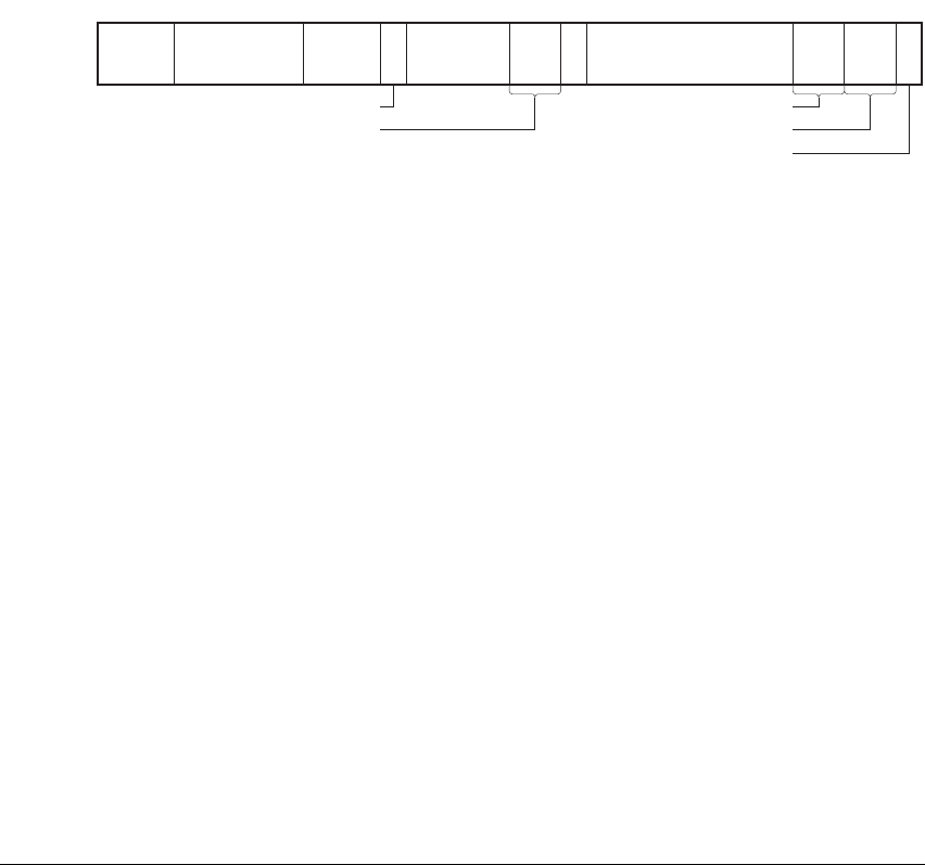
Debug Registers Reference
ARM DDI 0406B Copyright © 1996-1998, 2000, 2004-2008 ARM Limited. All rights reserved. C10-61
C10.5.4 Watchpoint Control Registers (DBGWCR)
A Watchpoint Control Register, DBGWCR, holds control information for a watchpoint. Each DBGWCR is
associated with a DBGWVR to form a Watchpoint Register Pair (WRP). For more information about WRPs
and the possible watchpoints see Watchpoint Value Registers (DBGWVR) on page C10-60.
The DBGWCRs are:
• debug registers 112-127, at offsets
0x1C0-0x1FC
• read/write registers
• when the Security Extensions are implemented, Common registers.
The format of a DBGWCR, in v7 Debug, is:
See the bit descriptions for the differences in other Debug architecture versions.
Bits [31:29, 23:21,13]
Reserved, UNK/SBZP.
Address range mask, bits [28:24], v7 Debug
In v7 Debug, support for watchpoint address range masking is optional. If it is not supported
these bits are RAZ/WI.
If watchpoint address range masking is supported, this field can be used to watch a range of
addresses by masking lower order address bits out of the watchpoint comparison. The value
of this field is the number of low order bits of the address that are masked off, except that
values of 1 and 2 are reserved. Therefore, the meaning of Watchpoint Address range mask
values are:
0b00000 No mask
0b00001 Reserved
0b00010 Reserved
0b00011
0x00000007
mask for data address, three bits masked
0b00100
0x0000000F
mask for data address, four bits masked
0b00101
0x0000001F
mask for data address, five bits masked
. .
. .
. .
0b11111
0x7FFFFFFF
mask for data address, 31 bits masked.
31 029
Address
range mask
28 24
UNK/
SBZP
20
Linked
BRP num.
19 16 15 14 13
Byte address select
4321
Privileged mode control
Watchpoint enable
UNK/
SBZP
23 21 512
Security state control
Enable linking Load/Store access control
(0)

Debug Registers Reference
C10-62 Copyright © 1996-1998, 2000, 2004-2008 ARM Limited. All rights reserved. ARM DDI 0406B
This field must be programmed to 0b00000 if either:
• DBGWCR[12:5] != 0b11111111, if an 8-bit Byte address select field is implemented
• DBGWCR[8:5] != 0b1111, if a 4-bit Byte address select field is implemented.
If this is not done, the generation of Watchpoint debug events is UNPREDICTABLE.
If this field is not zero, the DBGWVR bits that are not included in the comparison must be
zero, otherwise the generation of Watchpoint debug events is UNPREDICTABLE.
To watch for a write to any byte in an doubleword-aligned object of size 8 bytes, ARM
recommends that debuggers set DBGWCR[28:24] =
0x7
, and
DBGWCR[12:5] = 0b11111111. This setting is compatible with both implementations with
an 8-bit Byte address select field and implementations with a 4-bit Byte address select field,
because implementations with a 4-bit Byte address select field ignore writes to
DBGWCR[12:9].
Bits [28:24], v6 Debug and v6.1 Debug
Reserved, UNK/SBZP.
Enable linking, bit [20]
This bit is set to 1 if this WRP is linked to a BRP to set a linked watchpoint that requires
both DVA and Context ID comparison. The possible values of this bit are
0 linking disabled
1 linking enabled.
When this bit is set to 1 the Linked BRP number field indicates the BRP to which this WRP
is linked. For more information, see Linked comparisons on page C10-59.
Linked BRP number, bits [19:16]
If this WRP is programmed with linking enabled then this field must be programmed with
the number of the BRP that holds the Context ID to be used for the combined DVA and
Context ID comparison, otherwise, this field must be programmed to 0b0000.
If this field is programmed with a value other than zero or the number of a BRP that supports
Context ID comparison then reading this register returns an UNKNOWN value for this field.
The generation of Watchpoint debug events is UNPREDICTABLE if either:
• this WRP does not have linking enabled and this field is not programmed to 0b0000
• this WRP has linking enabled and the BRP indicated by this field does not support
Context ID comparison or is not programmed for Linked Context ID match.
Security state control, bits [15:14], when the Security Extensions are implemented
Note
The Security Extensions cannot be implemented with v6 Debug.
When a processor implements the Security Extensions, these bits enable the breakpoint to
be conditional on the security state of the processor:
0b00 watchpoint generated on match in both Non-secure state and Secure state

Debug Registers Reference
ARM DDI 0406B Copyright © 1996-1998, 2000, 2004-2008 ARM Limited. All rights reserved. C10-63
0b01 watchpoint generated on match only in Non-secure state
0b10 watchpoint generated on match only in Secure state
0b11 Reserved.
For more information about watchpoint matching when this field is set to a value other than
0b00, see About security state control on page C10-66.
Bits [15:14], when the Security Extensions are not implemented
Reserved, UNK/SBZP.
Bit [12:9], v6 Debug and v6.1 Debug
Reserved, UNK/SBZP.
Byte address select, bits [12:5] or bits [8:5]
The width of this field can depend on the ARM Debug architecture version:
v6 Debug and v6.1 Debug
The Byte address select field is always 4 bits, DBGWCR[8:5]
v7 Debug
It is IMPLEMENTATION DEFINED whether a 4-bit or an 8-bit Byte address select
field is implemented:
• an 8-bit Byte address select field is DBGWCR[12:5]
• if a 4-bit Byte address select field is implemented then the Byte address
select field is DBGWCR[8:5] and DBGWCR[12:9] is RAZ/WI.
DBGWVRs are programmed with word-aligned addresses. This field enables the
watchpoint to hits only if certain byte addresses are accessed. The watchpoint hits if an
access hits any byte being watched, even if:
• the access size is larger than the size of the region being watched
• the access is unaligned, and the base address of the access is not in the same word of
memory as the address in the DBGWVR.
For details of the use of this field see Byte address masking behavior on DVA match on
page C10-65.
If the Address range mask field is implemented and programmed to a value other than
0b00000, no mask, then this field must be programmed to:
• 0b1111, if a 4-bit Byte address select field is implemented.
• 0b11111111, an 8-bit Byte address select field is implemented.
If this is not done, the generation of Watchpoint debug events is UNPREDICTABLE.
Load/store access control, bits [4:3]
This field enables watchpoint matching conditional on the type of access being made.
Possible values of this field are:
0b00 Reserved.
0b01 Match on any load, Load-Exclusive, or swap.

Debug Registers Reference
C10-64 Copyright © 1996-1998, 2000, 2004-2008 ARM Limited. All rights reserved. ARM DDI 0406B
0b10 Match on any store, Store-Exclusive or swap.
0b11 Match on any either type of access.
If an implementation supports watchpoint generation by:
• a memory hint instruction, then that instruction is treated as generating a load access
• a cache maintenance operation, then that operation is treated as generating a store
access.
Privileged mode control, bits [2:1]
This field enables watchpoint matching conditional on the mode of the processor. Possible
values of this field are:
0b00 Reserved.
0b01 Match privileged accesses.
0b10 Match unprivileged accesses.
0b11 Match all accesses.
Note
• For all cases the match refers to the privilege of the access, not the mode of the
processor. For example, if the watchpoint is configured to match privileged accesses
only (0b01), and the processor executes an
LDRT
instruction in a privileged mode, the
watchpoint does not match.
• Permitted values of this field are not identical to those for the DBGBCR. In the
DBGBCR only, in v7 Debug, the value 0b00 is permitted.
Watchpoint enable, bit [0]
This bit enables the WRP. The meaning of this bit is:
0 Watchpoint disabled
1 Watchpoint enabled.
A WRP never generates Watchpoint debug events when its DBGWCR is disabled.
The debug logic reset values of all bits of the DBGWCR is UNKNOWN.
Note
• In v6 Debug and v6.1 Debug, the Watchpoint enable bit of the DBGWCR is set to 0 on a debug logic
reset, disabling the watchpoint.
• In v7 Debug, a debugger must ensure that DBGWCR[0] has a defined state before it programs
DBGDSCR[15:14] to enable debug.

Debug Registers Reference
ARM DDI 0406B Copyright © 1996-1998, 2000, 2004-2008 ARM Limited. All rights reserved. C10-65
Byte address masking behavior on DVA match
For each WRP, the DBGWVR is programmed with a word-aligned address. The Byte address select bits of
the DBGWCR can be programmed so that the watchpoint hits if only certain bits of the watched address are
accessed:
• in all implementations, DBGWCR[8:5] can be programmed to enable the watchpoint to hit on any
access to one or more of the bytes of the word addressed by the associated DBGWVR
• in a v7 Debug implementation that supports an 8-bit Byte address select field, DBGWCR[12:5] can
be programmed to enable the watchpoint to hit on any access to one or more of the bytes of the
doubleword addressed by the associated DBGWVR.
In all cases, a Watchpoint debug event is generated if an access hits any byte being watched, even if:
• the access size is larger than the size of the region being watched
• the access is unaligned, and the base address of the access is not in the word of memory addressed
by DBGWVR.
Table C10-13 and Table C10-14 on page C10-66 show the meaning of the Byte address select values.
Table C10-13 shows the values that can be programmed in any implementation.
In v6 Debug and v6.1 Debug only a 4-bit Byte address select field is implemented and DBGWCR[12:9] is
UNK/SBZP.
In v7 Debug, it is IMPLEMENTATION DEFINED whether an implementation supports a 4-bit or an 8-bit Byte
address select field:
• If the processor implements a 4-bit Byte address select field, then DBGWCR[12:9] is RAZ/WI.
• If the processor implements an 8-bit Byte address select field, then DBGWCR[12:9] can also be
programmed, and, for a given watchpoint register pair:
— DBGWVR can be programmed with a doubleword-aligned address, with DBGWVR[2] = 0.
In this case DBGWCR[12:5] can be programmed to match any of the 8 bytes in that
doubleword value.
Table C10-13 Byte address select values, word-aligned address
DBGWCR[12:5] value Description
00000000 Watchpoint never hits
xxxxxxx1 Watchpoint hits if byte at address
DBGWVR<31:2>:’00’
is accessed
xxxxxx1x Watchpoint hits if byte at address
DBGWVR<31:2>:’01’
is accessed
xxxxx1xx Watchpoint hits if byte at address
DBGWVR<31:2>:’10’
is accessed
xxxx1xxx Watchpoint hits if byte at address
DBGWVR<31:2>:’11’
is accessed

Debug Registers Reference
C10-66 Copyright © 1996-1998, 2000, 2004-2008 ARM Limited. All rights reserved. ARM DDI 0406B
— If DBGWVR[2] == 1, indicating a word-aligned address that is not doubleword-aligned, then
DBGWCR[12:9] must be programmed with zero.
If DBGWVR[2] == 1 and DBGWCR[12:9] != 0b0000, Watchpoint debug event generation is
UNPREDICTABLE.
Table C10-14 shows the additional Byte address select field encodings that are available, when
DBGWVR[2] == 0, on an implementation that supports an 8-bit Byte address select field.
The same programming model can be used on implementations that support:
• an 8-bit Byte address select field, DBGWCR[12:5]
• a 4-bit Byte address select field, DBGWCR[8:5].
This is because, on an implementation that supports only a 4-bit Byte address select field, writes to
DBGWCR[12:9] are ignored.
Note
In ARMv6, when using the optional legacy BE-32 endianness model, the values of DBGWCR[8:5] shown
in Table C10-13 on page C10-65 have different meanings. For more information see BE-32 DBGWCR Byte
address select values on page AppxG-7.
About security state control
When the Security Extensions are implemented and the security state control bits of the DBGBCR or
DBGWCR are set to a value other than 0b00, the condition for matching refers to the security state of the
processor, not the security of the access. For example, the breakpoint or watchpoint does not match when
all of the following apply:
• the breakpoint or watchpoint is configured to match in Non-secure state only (0b01)
• the processor is executing code in the Secure state, either because the SCR.NS bit is 0 or because the
processor is in Monitor mode
• the address accessed is in a page marked as Non-secure in the translation tables.
For more information about the security of accesses see Chapter B3 Virtual Memory System Architecture
(VMSA).
Table C10-14 Additional Byte address select values, doubleword-aligned address
DBGWCR[12:5] value Description
xxx1xxxx Watchpoint hits if byte at address
DBGWVR<31:3>:’100’
is accessed
xx1xxxxx Watchpoint hits if byte at address
DBGWVR<31:3>:’101’
is accessed
x1xxxxxx Watchpoint hits if byte at address
DBGWVR<31:3>:’110’
is accessed
1xxxxxxx Watchpoint hits if byte at address
DBGWVR<31:3>:’111’
is accessed

Debug Registers Reference
ARM DDI 0406B Copyright © 1996-1998, 2000, 2004-2008 ARM Limited. All rights reserved. C10-67
Note
This describes a VMSA access. In ARMv7 the Security Extensions can be implemented only in a system
that implements the VMSA.
C10.5.5 Vector Catch Register (DBGVCR)
The Vector Catch Register, DBGVCR, enables Vector Catch debug events. A Vector Catch debug event
occurs when:
• a bit in the DBGVCR is set to 1, to enable catches on a particular exception vector
• an IVA matches the corresponding exception vector address
• the instruction is committed for execution.
For more information, see Vector Catch debug events on page C3-20.
The DBGVCR is:
• debug register 7, at offset
0x01C
.
• a read/write register
• when the Security Extensions are implemented, a Common register.
The format the DBGVCR depends on whether the Security Extensions are implemented, and can depend
on the ARM Debug architecture version:
Security Extensions not implemented
Only DBGVCR bits [7:6,4:0] are implemented. All other bits are reserved and UNK/SBZP.
Note
The Security Extensions cannot be implemented with v6 Debug.
v6.1 Debug When the Security Extensions are implemented it is optional whether DBGVCR
bits [31,30,28:25,15,14,12:10] are implemented. If these bits are not implemented, they are
RAZ/WI. However, for forwards compatibility with v7 Debug, ARM recommends that
these bits are implemented.
DBGVCR bits [7:6,4:0] are always implemented. All other bits are reserved and
UNK/SBZP.
v7 Debug When the Security Extensions are implemented DBGVCR bits [31,30,28:25,15,14,12:10]
must be implemented.
DBGVCR bits [7:6,4:0] are also implemented. All other bits are reserved and UNK/SBZP.
When the Security Extensions are not implemented, and in any v6.1 Debug implementation that does not
implement DBGVCR[31,30,28:25,15,14,12:10], the format of the DBGVCR is:

Debug Registers Reference
C10-68 Copyright © 1996-1998, 2000, 2004-2008 ARM Limited. All rights reserved. ARM DDI 0406B
Bits [31:8,5] Reserved. Normally UNK/SBZP, except that in v6.1 Debug bits [31,30,28:25,15,14,12:10]
are RAZ/WI, and the other bits are UNK/SBZP.
Bits [7:6,4:0] Vector catch enable bits. When one of these bits is set to 1, any instruction prefetched from
the corresponding exception vector generates a Vector Catch debug event when it is
committed for execution. Table C10-15 on page C10-71 shows the exception vectors. The
Vector Catch enable bits are:
Bit [7] FIQ vector catch enable.
Bit [6] IRQ vector catch enable.
Bit [4] Data Abort vector catch enable.
Bit [3] Prefetch Abort vector catch enable.
Bit [2] SVC vector catch enable.
Bit [1] Undefined Instruction vector catch enable.
Bit [0] Reset vector catch enable.
The debug logic reset value of the DBGVCR depends on the ARM Debug architecture version:
v7 Debug Debug logic reset values are UNKNOWN. Before programming DBGDSCR[15:14] to
enable debug, a debugger must ensure that the DBGVCR has a defined state.
v6 Debug and v6.1 Debug
All defined bits reset to 0.
If Monitor debug-mode is configured and enabled DBGVCR bits [4:3] must be programmed to 0b00, see
Unpredictable behavior on Software debug events on page C3-24
For more information about these vector catch operations see Vector catch operation when Security
Extensions are not implemented on page C10-71.
When the Security Extensions are implemented the format of the DBGVCR is:
0
Res.
4321
IRQ
Data Abort
Reserved, see text
5
FIQ
7631 8
Prefetch Abort
SVC
Undefined Instruction
Reset
Vector catch enable

Debug Registers Reference
ARM DDI 0406B Copyright © 1996-1998, 2000, 2004-2008 ARM Limited. All rights reserved. C10-69
Bits [29,24:14,13,9:8,5]
Reserved. UNK/SBZP.
Bits [31:30,28:25]
Vector catch enable bits for exceptions in the Non-secure state. When one of these bits is set
to 1 and the processor is in the Non-secure state, a Vector Catch debug event is generated
when an instruction prefetched from the corresponding exception vector is committed for
execution. Table C10-16 on page C10-73 shows the exception vectors. The Non-secure state
vector catch enable bits are:
Bit [31] FIQ vector catch enable in Non-secure state.
Bit [30] IRQ vector catch enable in Non-secure state.
Bit [28] Data Abort vector catch enable in Non-secure state.
Bit [27] Prefetch Abort vector catch enable in Non-secure state.
Bit [26] SVC vector catch enable in Non-secure state.
Bit [25] Undefined Instruction vector catch enable in Non-secure state.
Bits [15:14,12:10]
Vector catch enable bits for exceptions in the Secure state that are taken on the Monitor
mode exception vectors. When one of these bits is set to 1 and the processor is in the Secure
state, a Vector Catch debug event is generated when an instruction prefetched from the
corresponding exception vector is committed for execution. Table C10-16 on page C10-73
shows the exception vectors. The Monitor mode vector catch enable bits are:
Bit [15] FIQ vector catch enable, in Secure state on Monitor mode vector.
Bit [14] IRQ vector catch enable in Secure state on Monitor mode vector.
Bit [12] Data Abort vector catch enable in Secure state on Monitor mode vector.
Bit [11] Prefetch Abort vector catch enable in Secure state on Monitor mode vector.
Bit [10] SMC vector catch enable in Secure state.
0
Res.
4321
IRQ
Data Abort
5
FIQ
30 29 28 27 26 25 15 14 13 12 11 10 7 631
Prefetch Abort
SVC
Undefined Instruction
Reset vector catch enable
Res.
98
IRQ
Data Abort
FIQ
Prefetch Abort
SMC
Reserved, UNK/SBZP
24 16
IRQ
Data Abort
FIQ
Prefetch Abort
SVC
Undefined Instruction
Res.
Res.
Vector catch enable,
VBARNS
Vector catch enable,
MVBAR
Vector catch enable,
VBARS

Debug Registers Reference
C10-70 Copyright © 1996-1998, 2000, 2004-2008 ARM Limited. All rights reserved. ARM DDI 0406B
Bits [7:6,4:1] Vector catch enable bits for exceptions in the Secure state that are taken on the exception
mode vector. When one of these bits is set to 1 and the processor is in the Secure state, a
Vector Catch debug event is generated when an instruction prefetched from the
corresponding exception vector is committed for execution. Table C10-16 on page C10-73
shows the exception vectors. The Secure state vector catch enable bits are:
Bit [7] FIQ vector catch enable in Secure state.
Bit [6] IRQ vector catch enable in Secure state.
Bit [4] Data Abort vector catch enable in Secure state.
Bit [3] Prefetch Abort vector catch enable in Secure state.
Bit [2] SVC vector catch enable in Secure state.
Bit [1] Undefined Instruction vector catch enable in Secure state.
Bit [0] Reset vector catch enable.
When this bit is set to 1, a Vector Catch debug event is generated when an instruction
prefetched from the reset exception vector is committed for execution:
• In v7 Debug the debug event is generated regardless of the security state of the
processor
• In v6 Debug and v6.1 Debug the debug event is only generated if the processor is in
Secure state.
Table C10-16 on page C10-73 shows the exception vectors.
The debug logic reset value of the DBGVCR depends on the ARM Debug architecture version:
v7 Debug Debug logic reset values are UNKNOWN. Before programming DBGDSCR[15:14] to
enable debug, a debugger must ensure that the DBGVCR has a defined state.
v6 Debug and v6.1 Debug
All defined bits reset to 0.
If Monitor debug-mode is configured and enabled DBGVCR bits [28:27,12,4:3] must be programmed to
zero, see Unpredictable behavior on Software debug events on page C3-24
For more information about these vector catch operations see Vector catch operation when Security
Extensions are implemented on page C10-71.
Vector catch operation
The following subsections give more information about vector catch operation:
•Vector catch operation when Security Extensions are not implemented on page C10-71
•Vector catch operation when Security Extensions are implemented on page C10-71.
The pseudocode function
VCRMatch()
describes the vector catch operation, for both the Secure and the
Non-secure cases, and the function
VCR_OnTakingInterrupt()
tracks the most recent interrupt vectors. For
more information about these pseudocode functions and when they are called see Breakpoints and Vector
Catches on page C3-28.

Debug Registers Reference
ARM DDI 0406B Copyright © 1996-1998, 2000, 2004-2008 ARM Limited. All rights reserved. C10-71
Vector catch operation when Security Extensions are not implemented
For each bit of the DBGVCR, the vector addresses caught depends on the exception vector configuration in
the SCTLR:
• whether the SCTLR.V bit is programmed for Normal or High exception vectors
• for catches on the FIQ and IRQ exception vectors, on the programming of the SCTLR.VE bit.
Table C10-15 shows how the vector address that corresponds to each active bit of the DBGVCR depends on
these configuration settings:
Vector catch operation when Security Extensions are implemented
When the Security Extensions are implemented, for each bit of the DBGVCR, the vector addresses caught
depends:
• On the value programmed in the appropriate Vector Base Address Register:
— the Non-secure copy of the Vector Base Address Register (VBARNS) for the Non-secure state
vector catches
— the Monitor Vector Base Address Register (MVBAR) for the Secure state vector catches on
the Monitor mode vectors
— the Secure copy of the Vector Base Address Register (VBARS) for the Secure state vector
catches on the exception vectors.
Table C10-15 Vector catch addresses, for processors without Security Extensions
DBGVCR bit Vector catch enabled
Configured exception vectors
Normal (V == 0) High (V == 1)
[7] FIQ VE == 0
0x0000001C 0xFFFF001C
VE == 1 Most recent FIQ addressa
a. For more information see Vector catch debug events and vectored interrupt support on
page C3-22.
[6] IRQ VE == 0
0x00000018 0xFFFF0018
VE == 1 Most recent IRQ addressa
[4] Data Abort
0x00000010 0xFFFF0010
[3] Prefetch Abort
0x0000000C 0xFFFF000C
[2] SVC
0x00000008 0xFFFF0008
[1] Undefined Instruction
0x00000004 0xFFFF0004
[0] Reset
0x00000000 0xFFFF0000

Debug Registers Reference
C10-72 Copyright © 1996-1998, 2000, 2004-2008 ARM Limited. All rights reserved. ARM DDI 0406B
For more information about these registers see:
—c12, Vector Base Address Register (VBAR) on page B3-148
—c12, Monitor Vector Base Address Register (MVBAR) on page B3-149.
Note
The Reset exception vectors address never depends on the Vector Base Address values, and when
SCTLR.VE == 1 the IRQ and FIQ exception vector addresses do not depend on the Vector Base
Address values, see Table C10-16 on page C10-73 for more information.
• Except for the Secure state vector catches on the Monitor mode vectors, on the exception vector
configuration in the SCTLR:
— whether the SCTLR.V bit is programmed for Normal or High exception vectors
— for catches on the FIQ and IRQ exception vectors, on the programming of the SCTLR.VE bit.
Generation of Vector Catch debug events also depends on the security state of the processor:
• the Non-secure state vector catches are generated only in Non-secure state
• the Secure state vector catches are generated only in Secure state
• in v6 Debug and v6.1 Debug, Reset vector catches are generated only in Secure state.
In v7 Debug, if Reset vector catch is enabled the Reset vector catches are generated regardless of the security
state of the processor.
Generation of Vector Catch debug events takes no account of the values in the Secure Configuration
Register (SCR), except for SCR.NS. For example, if the DBGVCR is programmed to catch Secure state
IRQs on the Monitor mode vector, by setting bit [14] of the DBGVCR to 1, and the processor is in the Secure
state, a Vector Catch debug event is generated on any instruction prefetch from (MVBAR +
0x18
). This
debug event is generated even if the SCR is programmed for IRQs to be handled in IRQ mode.
Table C10-15 on page C10-71 shows, for each active bit of the DBGVCR:
• the security state in which the Vector Catch debug event can occur
• how the corresponding vector address depends on the configuration settings.

Debug Registers Reference
ARM DDI 0406B Copyright © 1996-1998, 2000, 2004-2008 ARM Limited. All rights reserved. C10-73
Table C10-16 Vector catch operation, when Security Extensions are implemented
DBGVCR bit Vector catch enable Security state
Configured exception vectors
Normal (V == 0) High (V == 1)
Non-secure state vector catches
[31] FIQ VE == 0 Non-secure VBARNS +
0x0000001C 0xFFFF001C
VE == 1 Non-secure Most recent Non-secure FIQ addressa
[30] IRQ VE == 0 Non-secure VBARNS +
0x00000018 0xFFFF0018
VE == 1 Non-secure Most recent Non-secure IRQ addressa
[28] Data Abort Non-secure VBARNS +
0x00000010 0xFFFF0010
[27] Prefetch Abort Non-secure VBARNS +
0x0000000C 0xFFFF000C
[26] SVC Non-secure VBARNS +
0x00000008 0xFFFF0008
[25] Undefined Instruction Non-secure VBARNS +
0x00000004 0xFFFF0004
Secure state vector catches on Monitor mode vectors
[15] FIQ Secure MVBAR +
0x0000001C
[14] IRQ Secure MVBAR +
0x00000018
[12] Data Abort Secure MVBAR +
0x00000010
[11] Prefetch Abort Secure MVBAR +
0x0000000C
[10] SMC Secure MVBAR +
0x00000008

Debug Registers Reference
C10-74 Copyright © 1996-1998, 2000, 2004-2008 ARM Limited. All rights reserved. ARM DDI 0406B
In a v6.1 Debug implementation on a processor that implements the Security Extensions but does not
implement DBGVCR bits [31, 30, 28:25, 15:14, 12:10]:
• in Non-secure state, bits [7:6, 4:1] apply to offsets from VBARNS.
• in Secure state, bits [7:6, 4:1] apply to offsets from VBARS and bits [7:6, 4:2] also apply to offsets
from MVBAR.
Secure state vector catches on exception mode vectors
[7] FIQ VE = 0 Secure VBARS +
0x0000001C 0xFFFF001C
VE = 1 Secure Most recent Secure FIQ addressa
[6] IRQ VE = 0 Secure VBARS+
0x00000018 0xFFFF0018
VE = 1 Secure Most recent Secure IRQ addressa
[4] Data Abort Secure VBARS+
0x00000010 0xFFFF0010
[3] Prefetch Abort Secure VBARS+
0x0000000C 0xFFFF000C
[2] SVC Secure VBARS+
0x00000008 0xFFFF0008
[1] Undefined Instruction Secure VBARS+
0x00000004 0xFFFF0004
Reset vector catchb
[0] Reset b
0x00000000 0xFFFF0000
a. For more information see Vector catch debug events and vectored interrupt support on page C3-22.
b. The value of the Reset vector is always independent of the Vector Base Address Register values. The security state
dependence of Reset vector catches depends on the Debug architecture version. In v7 Debug, Reset vector catches
are generated regardless of the security state of the processor. In v6 Debug and v6.1 Debug, Reset vector catches
are generated only in Secure state.
Table C10-16 Vector catch operation, when Security Extensions are implemented (continued)
DBGVCR bit Vector catch enable Security state
Configured exception vectors
Normal (V == 0) High (V == 1)

Debug Registers Reference
ARM DDI 0406B Copyright © 1996-1998, 2000, 2004-2008 ARM Limited. All rights reserved. C10-75
C10.6 OS Save and Restore registers, v7 Debug only
Support for the OS Save and Restore mechanism registers depends on the Debug architecture version:
v6 Debug and v6.1 Debug
These registers are not defined.
v7 Debug If an implementation supports debug over power-down, then it must implement the OS Save
and Restore mechanism registers. On SinglePower systems, and on any other system that
does not support debug over power-down, it is IMPLEMENTATION DEFINED whether the OS
Save and Restore mechanism is implemented.
Any implementation that does not support the OS Save and Restore mechanism must
implement the DBGOSLSR as RAZ.
This section describes the registers that provide the OS Save and Restore mechanism in the following
subsections:
•OS Lock Access Register (DBGOSLAR)
•OS Lock Status Register (DBGOSLSR) on page C10-76
•OS Save and Restore Register (DBGOSSRR) on page C10-77.
In addition, the Event Catch Register enables the generation of a debug event when the OS Lock is unlocked.
This register is described in Event Catch Register (DBGECR) on page C10-78.
C10.6.1 OS Lock Access Register (DBGOSLAR)
The OS Lock Access Register, DBGOSLAR, provides a lock for the debug registers. When the registers
have been locked any access to the registers returns a slave-generated error response. Writing the key value
to the DBGOSLAR has the side effect of resetting the internal counter for the OS Save or Restore operation.
You must use the DBGOSLSR to check the current status of the lock, see OS Lock Status Register
(DBGOSLSR) on page C10-76.
The DBGOSLAR is:
• debug register 192, at offset
0x300
• a write-only register
• only defined in v7 Debug
• when the Security Extensions are implemented, a Common register.
Note
In a v7 Debug implementation that does not implement the OS Save and Restore mechanism, register 192
ignores writes.
In v6 Debug and v6.1 Debug, register 192 is not defined.

Debug Registers Reference
C10-76 Copyright © 1996-1998, 2000, 2004-2008 ARM Limited. All rights reserved. ARM DDI 0406B
The format of the DBGOSLAR is:
OS Lock Access, bits [31:0]
Writing the key value
0xC5ACCE55
to this field locks the debug registers, and resets the
internal counter for the OS Save or Restore operation.
Writing any other value to this register unlocks the debug registers if they are locked.
For details of error responses when accessing the debug registers, see Access permissions on page C6-26.
If bit [0] of the Event Catch Register is set to 1 at the point when the OS Lock is unlocked, an OS Unlock
Catch debug event is generated, see Event Catch Register (DBGECR) on page C10-78.
C10.6.2 OS Lock Status Register (DBGOSLSR)
The OS Lock Status Register, DBGOSLSR, provides status information for the OS Lock.
The DBGOSLSR is:
• debug register 193, at offset
0x304
• a read-only register
• only defined in v7 Debug
• when the Security Extensions are implemented, a Common register.
Note
In any v7 Debug implementation you can read the DBGOSLSR to detect whether the OS Save and Restore
mechanism is implemented. If it is not implemented the read of the DBGOSLSR returns zero.
In v6 Debug and v6.1 Debug, register 193 is not defined.
The format of the DBGOSLSR is:
Bits [31:3] Reserved, UNK.
32-bit access, bit [2]
This bit is always RAZ. It indicates that a 32-bit access is needed to write the key to the OS
Lock Access Register.
31 0
OS Lock Access
0
Reserved, UNK
21
Locked
Lock implemented
32-bit access
31 3

Debug Registers Reference
ARM DDI 0406B Copyright © 1996-1998, 2000, 2004-2008 ARM Limited. All rights reserved. C10-77
Locked, bit [1]
This bit indicates the status of the OS Lock. The possible values are:
0 Lock not set.
1 Lock set. Writes to debug registers are ignored.
The OS Lock is set or cleared by writing to the DBGOSLAR, see OS Lock Access Register
(DBGOSLAR) on page C10-75.
On a debug logic reset the state of the OS Lock and the value of this bit are
IMPLEMENTATION DEFINED. If the implementation includes the recommended external
debug interface they are determined by the value of the DBGOSLOCKINIT signal:
DBGOSLOCKINIT LOW
The lock is not set, and the Locked bit is 0
DBGOSLOCKINIT HIGH
The lock is set, and the Locked bit is 1.
Lock implemented, bit [0]
This bit reads 1 if it is possible to set the OS Lock for this processor.
If this bit reads 0, OS Lock and the OS Save and Restore mechanism are not implemented
and the entire register is RAZ.
C10.6.3 OS Save and Restore Register (DBGOSSRR)
The OS Save and Restore Register, DBGOSSRR, enables the entire debug logic state of the processor to be
either saved or restored, by performing a series of reads or writes of the DBGOSSRR. The register works
in conjunction with an internal sequence counter to perform the OS Save or Restore operation.
The DBGOSSRR is:
• debug register 194, at offset
0x308
• a read/write register
• only defined in v7 Debug
• when the Security Extensions are implemented, a Common register.
Note
• In a v7 Debug implementation that does not implement the OS Save and Restore mechanism, register
194 is RAZ/WI.
• For more information about access permissions in an implementation that includes the OS Save and
Restore mechanism but does not provide access to the DBGOSSRR through the external debug
interface, see the Note in The OS Save and Restore mechanism on page C6-8.
In v6 Debug and v6.1 Debug, register 194 is not defined.

Debug Registers Reference
C10-78 Copyright © 1996-1998, 2000, 2004-2008 ARM Limited. All rights reserved. ARM DDI 0406B
The format of the DBGOSSRR is:
OS Save or Restore value, bits [31:0]
After a write to the DBGOSLAR to lock the debug registers, the first access to the
DBGOSSRR must be a read:
• when performing an OS Save sequence this read returns the number of reads from to
the DBGOSSRR that are needed to save the entire debug logic state
• when performing an OS Restore sequence the value of this read is UNKNOWN and
must be discarded.
After that first read access:
• a read of this register returns the next debug logic state value to be saved
• a write to this register restores the next debug logic state value.
Before accessing the DBGOSSRR, you must write to the DBGOSLAR to set the OS Lock, see OS Lock
Access Register (DBGOSLAR) on page C10-75. This write to the DBGOSLAR resets the internal counter
for the OS Save or Restore operation.
The result is UNPREDICTABLE if:
• you access the DBGOSSRR when the OS Lock is not set
• after setting the OS Lock, the first access to the DBGOSSRR is not a read.
See The OS Save and Restore mechanism on page C6-8 for a description of using the OS Save and Restore
mechanism registers.
C10.6.4 Event Catch Register (DBGECR)
The Event Catch Register, DBGECR, configures the debug logic to generate a debug event when the OS
Lock is unlocked.
The DBGECR is:
• debug register 9, at offset
0x024
• a read/write register
• only defined in v7 Debug
• when the Security Extensions are implemented, a Common register.
In v6 Debug and v6.1 Debug, register 9 is not defined.
31 0
OS Save or Restore value

Debug Registers Reference
ARM DDI 0406B Copyright © 1996-1998, 2000, 2004-2008 ARM Limited. All rights reserved. C10-79
The format of the DBGECR is:
Bits [31:1] Reserved. UNK/SBZP.
OS Unlock Catch, bit [0]
When this bit is set to 1, an OS Unlock Catch debug event is generated when the OS Lock
is unlocked by writing to the DBGOSLAR, see OS Lock Access Register (DBGOSLAR) on
page C10-75. The possible values of this bit are:
0 OS Unlock Catch disabled
1 OS Unlock Catch enabled.
The debug logic reset value of this bit is 0.
The OS Unlock Catch bit is part of the OS Save and Restore mechanism. If an
implementation supports debug over power-down it must support the OS Save and Restore
mechanism, including the OS Unlock Catch debug event. If an implementation does not
support debug over power-down, it is IMPLEMENTATION DEFINED whether the OS Save and
Restore mechanism and the OS Unlock Catch debug event are supported. If the OS Unlock
Catch debug event is not supported then this bit is RAZ/WI.
The OS Unlock Catch debug event is a Halting debug event, see Halting debug events on page C3-38. If a
debugger is monitoring an application running on top of an OS with OS Save and Restore capability, this
event indicates the right time for the debug session to continue.
Note
The OS Unlock Catch debug event is generated only on clearing of the OS Lock, that is, on the transition of
OS Lock from locked to unlocked.
0
Reserved, UNK/SBZP
31 1
OS Unlock Catch

Debug Registers Reference
C10-80 Copyright © 1996-1998, 2000, 2004-2008 ARM Limited. All rights reserved. ARM DDI 0406B
C10.7 Memory system control registers
Support for the Memory system control registers can depend on the Debug architecture version:
v6 Debug and v6.1 Debug
In some v6 Debug and v6.1 Debug implementations a Cache Behavior Override Register
(CBOR) is provided in an IMPLEMENTATION DEFINED region of the CP15 register space. In
addition, particularly in v6.1 Debug implementations, the Debug State MMU Control
Register (DBGDSMCR) and Debug State Cache Control Register (DBGDSCCR) might be
implemented as IMPLEMENTATION DEFINED extensions to CP14, as described below.
v6 Debug and v6.1 Debug do not require these registers. However, ARM recommends these
features to assist debuggers to maintaining memory coherency, avoiding costly explicit
coherency operations.
v7 Debug In v7 Debug, the DBGDSMCR and DBGDSCCR are required, but there can be
IMPLEMENTATION DEFINED limits on their behavior. The CP15 register CBOR remains
IMPLEMENTATION DEFINED.
The Memory system control registers are described in the subsections:
•Debug State Cache Control Register (DBGDSCCR) on page C10-81
•Debug State MMU Control Register (DBGDSMCR) on page C10-84.
The Debug State Cache Control Register (DBGDSCCR) and Debug State MMU Control Register
(DBGDSMCR) control cache and TLB behavior for memory operations issued by a debugger when the
processor is in Debug state. They enable a debugger to request the minimum amount of intrusion to the
processor caches, as permitted by the implementation. It is IMPLEMENTATION DEFINED what levels of cache
and TLB are controlled by these requests, and it is IMPLEMENTATION DEFINED to what extent the intrusion
is limited.
The DBGDSCCR also provides a mechanism for a debugger to force writes to memory through to the point
of coherency without the overhead of issuing additional operations.
The DBGDSCCR and DBGDSMCR controls must apply for all memory operations issued in Debug state
when DBGDSCR.ADAdiscard, the Asynchronous Data Aborts Discarded bit, is set to 1. It is
IMPLEMENTATION DEFINED whether memory operations issued in Debug state whilst this bit is not set to 1
are affected by the DBGDSCCR and DBGDSMCR.

Debug Registers Reference
ARM DDI 0406B Copyright © 1996-1998, 2000, 2004-2008 ARM Limited. All rights reserved. C10-81
C10.7.1 Debug State Cache Control Register (DBGDSCCR)
The Debug State Cache Control Register, DBGDSCCR, controls cache behavior when the processor is in
Debug state.
The DBGDSCCR is:
• debug register 10, at offset
0x028
• a read/write register, with some bits that might not be implemented and therefore are RAZ/WI
• required in v7 Debug
• when the Security Extensions are implemented, a Common register.
It is IMPLEMENTATION DEFINED whether the DBGDSCCR is included in a v6 Debug or v6.1 Debug
implementation.
The format of the DBGDSCCR is:
Bits [31:3] Reserved, UNK/SBZP.
Force Write-Through, nWT, bit [2]
The possible values of this bit are:
0 Force Write-Through behavior for memory operations issued by a debugger
when the processor is in Debug state
1 Normal operation for memory operations issued by a debugger when the
processor is in Debug state.
In Debug state, if the nWT bit is set to 0, when a write to memory completes the effect of
the write must be visible at all levels of memory to the point of coherency. This means a
debugger can write through to the point of coherency without having to perform any cache
clean operations.
If implemented, the nWT control must act at all levels of memory to the point of coherency.
If the nWT control is not implemented this bit is RAZ/WI.
Note
nWT does not force the ordering of writes, and does not force writes to complete
immediately. A debugger might have to insert a barrier operations to ensure ordering.
0
Reserved, UNK/SBZP
21
Instruction Cache linefill and eviction, nIL
Data Cache linefill and eviction, nDL
Force Write-through, nWT
31 3

Debug Registers Reference
C10-82 Copyright © 1996-1998, 2000, 2004-2008 ARM Limited. All rights reserved. ARM DDI 0406B
Cache linefill and eviction bits, bits [1:0]
Either or both of these bits might not be implemented, in which case the bit is RAZ/WI. If
implemented these bits are:
nIL, bit [1] Instruction cache, where separate data and instruction caches are
implemented.
nDL, bit [0] Data or unified cache.
The possible values of an implemented bit are:
0 Request disabling of cache linefills and evictions for memory operations issued
by a debugger when the processor is in Debug state
1 Normal operation of cache linefills and evictions for memory operations issued
by a debugger when the processor is in Debug state.
When cache linefill and eviction is disabled, all memory accesses that would be checked
against a cache are checked against the cache. If a match is found, the cached result is used.
If no match is found the next level of memory is used, but the result is not cached, and no
cache entries are evicted.
The next level of memory can refer to looking in the next level of cache, or to accessing
external memory, depending on the numbers of levels of cache implemented.
When the processor is in Debug state, cache maintenance operations are not affected by the
nDL and nIL control bits, and have their normal architecturally-defined behavior.
The memory hint instructions
PLD
and
PLI
have UNPREDICTABLE behavior in Debug state
when the corresponding nDL or nIL control bit is set to 1.
The debug logic reset value of the DBGDSCCR depends on the ARM Debug architecture version:
v7 Debug Debug logic reset values are UNKNOWN. Before issuing operations through the
DBGITR with the processor in Debug state, a debugger must ensure that the
DBGDSCCR has a defined state.
ARMv6 All defined bits reset to 0.

Debug Registers Reference
ARM DDI 0406B Copyright © 1996-1998, 2000, 2004-2008 ARM Limited. All rights reserved. C10-83
Permitted IMPLEMENTATION DEFINED limits
The DBGDSCCR is required. However, there can be IMPLEMENTATION DEFINED limits on its behavior.
Table C10-17 lists some examples of possible options for implementations.
Interaction with Cache Behavior Override Register
An IMPLEMENTATION DEFINED Cache Behavior Override Register (CBOR) might also be implemented in
CP15.
Table C10-18 on page C10-84 shows, for a processor that implements both the Debug state Cache Control
Register (DBGDSCCR) and the CBOR, the relative precedence of the CBOR and the DBGDSCCR
according to the state of the processor.
Table C10-17 Permitted IMPLEMENTATION DEFINED limits on DBGDSCCR behavior
Limit Description Notes
Full DBGDSCCR Bits [2:0]
implemented
-
No Write-Back
support
Bit [2] is RAZ/WI -
No
Write-Through
support
Bit [2] is RAZ/WI Force Write-Through feature not supported.
If Secure User halting debug is supported the implementation must
provide cache clean operations in Debug state, see Access to specific
cache management functions in Debug state on page C5-25.
No I-cache
control
Bit [1] is RAZ/WI Instruction cache linefill and eviction disable features not
implemented.
Instruction fetches are disabled in Debug state. For most
implementations no instruction cache accesses take place in Debug
state, and nIL is not required.
Unified cache Bit [1] is RAZ/WI -
Cache evictions
always enabled
- nIL and nDL disable cache linefills in Debug state. However cache
evictions might still take place even when these control bits are set
to 0.
No linefill control Bits [1:0] are RAZ/WI No cache linefill and eviction disable features are implemented.

Debug Registers Reference
C10-84 Copyright © 1996-1998, 2000, 2004-2008 ARM Limited. All rights reserved. ARM DDI 0406B
A processor that does not implement Security Extensions has only WT, IL and DL settings in the CP15
Cache Behavior Override Register. Processors that implement Security Extensions can have separate
settings for, for example, NS_WT and S_WT in the CP15 Cache Behavior Override Register. For brevity
Table C10-18 does not show the full matrix of possibilities in this case. For the behavior on such a processor,
duplicate Table C10-18:
• once for the Non-secure case, for example NS_WT
• once for the Secure case, for example S_WT.
C10.7.2 Debug State MMU Control Register (DBGDSMCR)
The Debug State MMU Control Register, DBGDSMCR, controls TLB behavior when the processor is in
Debug state.
The DBGDSMCR is:
• debug register 11, at offset
0x02C
• a read/write register, with some bits that might not be implemented and therefore are RAZ/WI
• required in v7 Debug
• when the Security Extensions are implemented, a Common register.
Table C10-18 Interaction of CP15 Cache Behavior Override Register (CBOR) and DBGDSCCR
DBGDSCCR setting CBOR setting Debug state Behavior
nWT = 1 WT = 0 X Areas marked WB are Write-Back
nWT = X WT = 0 No Areas marked WB are Write-Back
nWT = X WT = 1 X Areas marked WB are Write-Through
nWT = 0 WT = X Yes Areas marked WB are Write-Through
nDL = 1 DL = 0 X Data or unified cache linefills are enabled
nDL = X DL = 0 No Data or unified cache linefills are enabled
nDL = X DL = 1 X Data or unified cache linefills are disabled
nDL = 0 DL = X Yes Data or unified cache linefills are disabled
nIL = 1 IL = 0 X Instruction cache linefills are enabled
nIL = X IL = 0 No Instruction cache linefills are enabled
nIL = X IL = 1 X Instruction cache linefills are disabled
nIL = 0 IL = X Yes Instruction cache linefills are disabled

Debug Registers Reference
ARM DDI 0406B Copyright © 1996-1998, 2000, 2004-2008 ARM Limited. All rights reserved. C10-85
It is IMPLEMENTATION DEFINED whether the DBGDSMCR is included in a v6 Debug or v6.1 Debug
implementation.
The format of the DBGDSMCR is:
Bits [31:4] Reserved, UNK/SBZP.
TLB matching bits, bits [3:2]
Either or both of these bits might not be implemented, in which case the bit is RAZ/WI. If
implemented these bits are:
nIUM, bit [3] Instruction TLB matching bit, where separate Data and Instruction
TLBs are implemented.
nDUM, bit [2] Data or Unified TLB matching bit.
The possible values of an implemented TLB matching bit are:
0 Request disabling of TLB matching for memory operations issued by a
debugger when the processor is in Debug state
1 Normal operation of TLB matching for memory operations issued by a
debugger when the processor is in Debug state.
When TLB matching is disabled, all memory accesses normally checked against a TLB are
not checked against the TLB. For every access the next level of translation is performed. The
results are not cached in the TLB, and no TLB entries are evicted. The next level of
translation is used for every access.
The next level of translation might mean looking in the next level TLB, or doing a
translation table walk, depending on the numbers of levels of TLB implemented.
Note
If TLB matching is disabled, and TLB maintenance functions have not been correctly
performed by the system being debugged, for example, if the TLB has not been flushed
following a change to the translation tables, memory accesses made by the debugger might
not undergo the same virtual to physical memory mappings as the application being
debugged.
A debugger can create temporary alternative memory mappings by altering the contents of
the external translation tables and disabling all levels of TLB matching. However, for
normal debugging operations, ARM recommends that the TLB Matching bit is set to 1.
0
Reserved, UNK/SBZP
21
Data TLB matching, nDUM
Instruction TLB loading, nIUL
Instruction TLB matching, nIUM
331 4
Data TLB loading, nDUL

Debug Registers Reference
C10-86 Copyright © 1996-1998, 2000, 2004-2008 ARM Limited. All rights reserved. ARM DDI 0406B
TLB loading bits, bits [1:0]
Either or both of these bits might not be implemented, in which case the bit is RAZ/WI. If
implemented these bits are:
nIUL, bit [1] Instruction TLB loading bit, where separate Data and Instruction
TLBs are implemented.
nDUL, bit [0] Data or Unified TLB loading bit.
The possible values of an implemented TLB loading bit are:
0 Request disabling of TLB load and flush for memory operations issued by a
debugger when the processor is in Debug state
1 Normal operation of TLB loading and flushing for memory operations issued
by a debugger when the processor is in Debug state.
When TLB load and flush is disabled, all memory accesses normally checked against a TLB
are checked against the TLB. If a match is found, the cached result is used. If no match is
found the next level of translation is performed, but the result is not cached in the TLB, and
no TLB entries are evicted.
The next level of translation might mean looking in the next level TLB, or doing a
translation table walk, depending on the numbers of levels of TLB implemented.
In Debug state, TLB maintenance operations are not affected by the nDUL and nIUL control
bits, and have their normal architecturally-defined behavior.
The debug logic reset value of the DBGDSMCR depends on the ARM Debug architecture version:
v7 Debug Debug logic reset values are UNKNOWN. Before issuing operations through the
DBGITR with the processor in Debug state, a debugger must ensure that the
DBGDSMCR has a defined state.
v6 Debug, v6.1 Debug
All defined bits reset to 0.

Debug Registers Reference
ARM DDI 0406B Copyright © 1996-1998, 2000, 2004-2008 ARM Limited. All rights reserved. C10-87
Permitted IMPLEMENTATION DEFINED limits
The DBGDSMCR is required. However, there can be IMPLEMENTATION DEFINED limits on its behavior.
Table C10-19 lists six permitted options for implementations. Some of these options are orthogonal.
Table C10-19 Permitted IMPLEMENTATION DEFINED limits on DBGDSCCR behavior
Limit Description Notes
Full
DBGDSMCR
Bits [3:0]
implemented
-
No I-TLB
controls
Bits [3,1] are
RAZ/WI
Instruction cache linefill and eviction disable features not implemented.
Instruction fetches disabled in Debug state. For most implementations no TLB
accesses take place in Debug state, and nIUL and nIUM are not required.
Unified TLB Bits [3,1] are
RAZ/WI
-
No matching
control
Bits [3:2] are
RAZ/WI
The TLB matching controls are not used to reduce the impact of debugging, only
for advanced debugging features. If not implemented, these bits are RAZ,
although the processor behaves as if they were set to 1.
TLB evictions
always enabled
- nIUL and nDUL disable TLB loading in Debug state. However TLB evictions
can still take place even when these control bits are set to 0.
No loading
control
Bits [1:0] are
RAZ/WI
-

Debug Registers Reference
C10-88 Copyright © 1996-1998, 2000, 2004-2008 ARM Limited. All rights reserved. ARM DDI 0406B
C10.8 Management registers, ARMv7 only
Support for the management registers depends on the ARM architecture version:
ARMv6 These registers are not defined in ARMv6.
ARMv7 The processor identification registers are summarized in this section and are defined in one
or more of:
•CP15 registers for a VMSA implementation on page B3-64
•CP15 registers for a PMSA implementation on page B4-22
• Chapter B5 The CPUID Identification Scheme.
Additional management registers are defined in this section.
The layout of the management registers, registers 832-1023, complies with the CoreSight Architecture
Specification.
Processor identification registers summarizes the processor identification registers.
The following sections describe the remaining management registers:
•Integration Mode Control Register (DBGITCTRL) on page C10-91
•Claim Tag Set Register (DBGCLAIMSET) on page C10-92
•Claim Tag Clear Register (DBGCLAIMCLR) on page C10-93
•Lock Access Register (DBGLAR) on page C10-94
•Lock Status Register (DBGLSR) on page C10-95
•Authentication Status Register (DBGAUTHSTATUS) on page C10-96
•Device Type Register (DBGDEVTYPE) on page C10-98
•Debug Peripheral Identification Registers (DBGPID0 to DBGPID4) on page C10-98
•Debug Component Identification Registers (DBGCID0 to DBGCID3) on page C10-102
C10.8.1 Processor identification registers
The processor identification registers return the values stored in the Main ID and feature registers of the
processor.
The processor identification registers are:
• debug registers 832-895, at offsets
0xD00-0xDFC
• read-only registers.
Note
The Extended CP14 interface
MRC
and
MCR
instructions that map to these registers are UNDEFINED in User
mode and UNPREDICTABLE in privileged modes. The CP15 interface must be used to access these registers.
Table C10-20 on page C10-89 lists the processor identification registers, in register number order.

Debug Registers Reference
ARM DDI 0406B Copyright © 1996-1998, 2000, 2004-2008 ARM Limited. All rights reserved. C10-89
Table C10-20 Processor identification registers
Register number Accessa
a. For more information, see CP14 debug registers access permissions on page C6-36 and
Permission summaries for memory-mapped and external debug interfaces on page C6-45.
Mnemonic Register
832 Read-only MIDR Main ID Registerb
b. Identification registers with register numbers 832-839 return the same value as an
MRC
instruction
MRC p15,0,<Rt>,c0,c0,<opc2>,
where
<opc2>
= (register number - 832).
833 Read-only CTR Cache Type Registerb
834 Read-only TCMTR TCM Type Registerb
835 Read-only TLBTR TLB Type Registerb
836 Read-only MPUIR MPU Type Registerb
837 Read-only MPIDR Multiprocessor Affinity Registerb
838, 839 Read-only - Alias of Main ID Registerb
840 Read-only ID_PFR0 Processor Feature Register 0
841 Read-only ID_PFR1 Processor Feature Register 1
842 Read-only ID_DFR0 Debug Feature Register 0
843 Read-only ID_AFR0 Auxiliary Feature Register 0
844 Read-only ID_MMFR0 Memory Model Feature Register 0
845 Read-only ID_MMFR1 Memory Model Feature Register 1
846 Read-only ID_MMFR2 Memory Model Feature Register 2
847 Read-only ID_MMFR3 Memory Model Feature Register 3
848 Read-only ID_ISAR0 Instruction Set Attribute Register 0
849 Read-only ID_ISAR1 Instruction Set Attribute Register 1
850 Read-only ID_ISAR2 Instruction Set Attribute Register 2
851 Read-only ID_ISAR3 Instruction Set Attribute Register 3
852 Read-only ID_ISAR4 Instruction Set Attribute Register 4
853 Read-only ID_ISAR5 Instruction Set Attribute Register 5
854-895 - - Reserved, UNK/SBZP

Debug Registers Reference
C10-90 Copyright © 1996-1998, 2000, 2004-2008 ARM Limited. All rights reserved. ARM DDI 0406B
Some of these registers form part of the CPUID scheme and are described in Chapter B5 The CPUID
Identification Scheme. The other ARMv7 registers are described in either or both of:
•CP15 registers for a VMSA implementation on page B3-64
•CP15 registers for a PMSA implementation on page B4-22.
Table C10-21 shows where each register is described
Table C10-21 Index to descriptions of the processor Identification registers
Register Description, VMSA Description, PMSA
Main ID Register c0, Main ID Register (MIDR) on
page B3-81
c0, Main ID Register (MIDR) on
page B4-32
Cache Type Register c0, Cache Type Register (CTR) on
page B3-83
c0, Cache Type Register (CTR) on
page B4-34
TCM Type Register c0, TCM Type Register (TCMTR)
on page B3-85
c0, TCM Type Register (TCMTR)
on page B4-35
TLB Type Register c0, TLB Type Register (TLBTR) on
page B3-86
VMSA only. Alias of Main ID
Register.
MPU Type Register PMSA only. Alias of Main ID
Register.
c0, MPU Type Register (MPUIR)
on page B4-36
Multiprocessor Affinity Register c0, Multiprocessor Affinity Register
(MPIDR) on page B3-87
c0, Multiprocessor Affinity Register
(MPIDR) on page B4-37
Processor Feature Register 0
CP15 c0, Processor Feature registers on page B5-4
Processor Feature Register 1
Debug Feature Register 0 c0, Debug Feature Register 0 (ID_DFR0) on page B5-6
Auxiliary Feature Register 0 c0, Auxiliary Feature Register 0 (ID_AFR0) on page B5-8
Memory Model Feature Register 0 to
Memory Model Feature Register 3 CP15 c0, Memory Model Feature registers on page B5-9
Instruction Set Attribute Register 0 to
Instruction Set Attribute Register 5 CP15 c0, Instruction Set Attribute registers on page B5-19

Debug Registers Reference
ARM DDI 0406B Copyright © 1996-1998, 2000, 2004-2008 ARM Limited. All rights reserved. C10-91
C10.8.2 Integration Mode Control Register (DBGITCTRL)
The Integration Mode Control Register, DBGITCTRL, enables the device to switch from its default
functional mode into integration mode, where the inputs and outputs of the device can be directly controlled
for integration testing or topology detection. When the processor is in integration mode, the
IMPLEMENTATION DEFINED integration registers can be used to drive output values and to read inputs.
The DBGITCTRL Register is:
• debug register 960, at offset
0xF00
• a read/write register
• when the Security Extensions are implemented, a Common register.
The format of the DBGITCTRL Register is:
Bits [31:1] Reserved, UNK/SBZP.
Integration mode enable, bit [0]
The possible values of this bit are:
0 Normal operation
1 Integration mode enabled.
When this bit is set to 1, the device reverts to an integration mode to enable integration
testing or topology detection. The integration mode behavior is IMPLEMENTATION DEFINED.
0
Reserved, UNK/SBZP
Integration mode enable
131

Debug Registers Reference
C10-92 Copyright © 1996-1998, 2000, 2004-2008 ARM Limited. All rights reserved. ARM DDI 0406B
C10.8.3 Claim Tag Set Register (DBGCLAIMSET)
The Claim Tag Set Register, DBGCLAIMSET, enables the CLAIM bits, bits [7:0] of the register, to be set
to 1. CLAIM bits do not have any specific functionality. ARM expects the usage model to be that an external
debugger and a debug monitor can set specific bits to 1 to claim the corresponding debug resources.
The CLAIM bits are always RAO in the DBGCLAIMSET Register. This enables a debugger to identify the
number of CLAIM bits that are implemented. See Claim Tag Clear Register (DBGCLAIMCLR) on
page C10-93 for details of how to:
• clear CLAIM bits to 0
• read the current values of the CLAIM bits.
The DBGCLAIMSET Register is:
• debug register 1000, at offset
0xFA0
• a read/write register, in which:
— the CLAIM bits are always RAO
— writing 0 to a CLAIM bit has no effect
• when the Security Extensions are implemented, a Common register.
The format of the DBGCLAIMSET Register is:
Bits [31:8] Reserved, RAZ/SBZP.
CLAIM bits, bits [7:0]
Writing a 1 to one of these bits sets the corresponding CLAIM bit to 1. Multiple bits can be
set to 1 in a single write operation.
Writing 0 to one of these bits has no effect.
You must use the DBGCLAIMCLR Register to:
• read the values of the CLAIM bits
• clear a CLAIM bit to 0.
These bits are always RAO.
If a debugger reads this register, the bits that are set to 1 correspond to the implemented CLAIM bits.
31 87 0
Reserved, RAZ/SBZP CLAIM

Debug Registers Reference
ARM DDI 0406B Copyright © 1996-1998, 2000, 2004-2008 ARM Limited. All rights reserved. C10-93
C10.8.4 Claim Tag Clear Register (DBGCLAIMCLR)
The Claim Tag Clear Register, DBGCLAIMCLR, enables the values of the CLAIM bits, bits [7:0] of the
register, to be:
•read
• cleared to 0.
For more information about the CLAIM bits and how they might be used, see Claim Tag Set Register
(DBGCLAIMSET) on page C10-92.
The DBGCLAIMCLR Register is:
• debug register 1001, at offset
0xFA4
• a read/write register, in which:
— writing 0 to a CLAIM bit has no effect
— writing 1 to a CLAIM bit clears that bit to 0
— a read of the register returns the current values of the CLAIM bits
• when the Security Extensions are implemented, a Common register.
The format of the DBGCLAIMCLR Register is:
Bits [31:8] Reserved, RAZ/SBZP.
CLAIM bits, bits [7:0]
Writing a 1 to one of these bits clears the corresponding CLAIM bit to 0. Multiple bits can
be cleared to 0 in a single write operation.
Writing 0 to one of these bits has no effect.
Reading the register returns the current values of these bits.
The debug logic reset value of each of these bits is 0.
31 87 0
Reserved, RAZ/SBZP CLAIM

Debug Registers Reference
C10-94 Copyright © 1996-1998, 2000, 2004-2008 ARM Limited. All rights reserved. ARM DDI 0406B
C10.8.5 Lock Access Register (DBGLAR)
The Lock Access Register, DBGLAR, provides a lock on writes to the debug registers through the
memory-mapped interface. Use of this lock mechanism reduces the risk of accidental damage to the
contents of the debug registers. It does not, and cannot, prevent all accidental or malicious damage.
You must use the DBGLSR to check the current status of the lock, see Lock Status Register (DBGLSR) on
page C10-95.
The DBGLAR is:
• debug register 1004, at offset
0xFB0
• a write-only register
• only defined in the memory-mapped interface
• when the Security Extensions are implemented, a Common register.
Note
• Debug register 1004, at offset
0xFB0
, is reserved in both the Extended CP14 interface and the external
debug interface.
• Do not confuse the Software Lock mechanism with the OS Lock described in The OS Save and
Restore mechanism on page C6-8.
The format of the DBGLAR is:
Lock Access control, bits [31:0]
Writing the key value
0xC5ACCE55
to this field clears the lock, enabling write accesses to the
debug registers through the memory-mapped interface.
Writing any other value to this register sets the lock, disabling write accesses to the debug
registers through the memory-mapped interface.
Note
• In implementations with separate core and debug power-domains, this lock is maintained in the debug
power domain. Its state is unaffected by the core power domain powering down.
• This lock is set on debug logic reset, that is, on a PRESETDBGn or nSYSPORESET reset.
Accesses through the memory-mapped interface to locked debug registers are ignored. For more
information, see Permissions in relation to locks on page C6-27.
31 0
Lock Access control

Debug Registers Reference
ARM DDI 0406B Copyright © 1996-1998, 2000, 2004-2008 ARM Limited. All rights reserved. C10-95
C10.8.6 Lock Status Register (DBGLSR)
The Lock Status Register, DBGLSR, provides status information for the debug registers lock. For more
information about this lock see Lock Access Register (DBGLAR) on page C10-94.
The DBGLSR is:
• debug register 1005, at offset
0xFB4
• a read-only register
• only defined in the memory-mapped interface
• when the Security Extensions are implemented, a Common register.
Note
Debug register 1005, at offset
0xFB4
, is reserved in both the Extended CP14 interface and the external debug
interface.
The format of the DBGLSR is:
Bits [31:3] Reserved, UNK.
32-bit access, bit [2]
This bit is always RAZ. It indicates that a 32-bit access is needed to write the key to the Lock
Access Register.
Locked, bit [1]
This bit indicates the status of the debug registers lock. The possible values are:
0 Lock clear. Debug register writes are permitted.
1 Lock set. Debug register writes are ignored.
The debug registers lock is set or cleared by writing to the DBGLAR, see Lock Access
Register (DBGLAR) on page C10-94.
The debug logic reset value of this bit is 1.
Lock implemented, bit [0]
This bit is RAO.
0
Reserved, UNK
21
Locked
Lock implemented
32-bit access
31 3
1
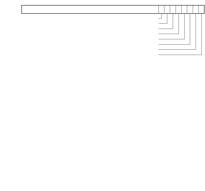
Debug Registers Reference
C10-96 Copyright © 1996-1998, 2000, 2004-2008 ARM Limited. All rights reserved. ARM DDI 0406B
C10.8.7 Authentication Status Register (DBGAUTHSTATUS)
The Authentication Status Register, DBGAUTHSTATUS, indicates the implemented debug features and
provides the current values of the configuration inputs that determine the debug permissions. The value
returned depends on whether the processor implements the Security Extensions.
The DBGAUTHSTATUS Register is:
• debug register 1006, at offset
0xFB8
• a read-only register
• when the Security Extensions are implemented, a Common register.
When the Security Extensions are implemented, the format of the DBGAUTHSTATUS Register is:
Bits [31:8] Reserved, UNK.
Secure non-invasive debug features implemented, bit [7]
This bit is RAO, Secure non-invasive debug features are implemented.
Secure non-invasive debug enabled, bit [6]
This bit indicates the logical result of:
(DBGEN OR NIDEN) AND (SPIDEN OR SPNIDEN).
Secure invasive debug features implemented, bit [5]
This bit is RAO, Secure invasive debug features are implemented.
Secure invasive debug enabled, bit [4]
This bit indicates the logical result of (DBGEN AND SPIDEN).
Non-secure non-invasive debug features implemented, bit [3]
This bit is RAO, Non-secure non-invasive debug features are implemented.
Non-secure non-invasive debug enabled, bit [2]
This bit indicates the logical result of (DBGEN OR NIDEN)
0
Reserved, UNK
21
Secure non-invasive debug enabled
Secure invasive debug features implemented
Secure non-invasive debug features implemented
34
Secure invasive debug enabled
76531 8
Non-secure non-invasive debug features implemented
Non-secure non-invasive debug enabled
Non-secure invasive debug features implemented
Non-secure invasive debug enabled
1111
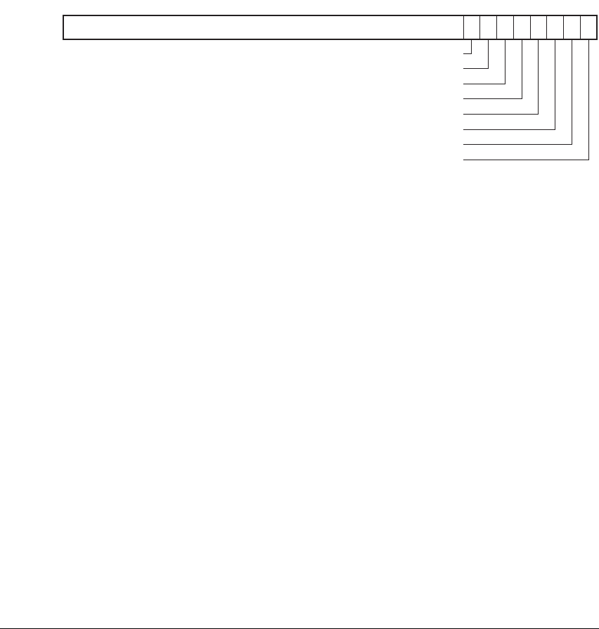
Debug Registers Reference
ARM DDI 0406B Copyright © 1996-1998, 2000, 2004-2008 ARM Limited. All rights reserved. C10-97
Non-secure invasive debug features implemented, bit [1]
This bit is RAO, Non-secure invasive debug features are implemented.
Non-secure invasive debug enabled, bit [0]
This bit indicates the logical state of the DBGEN signal.
When the Security Extensions are not implemented, the format of the DBGAUTHSTATUS Register is:
Bits [31:8] Reserved, UNK.
Secure non-invasive debug features implemented, bit [7]
This bit is RAO, Secure non-invasive debug features are implemented.
Secure non-invasive debug enabled, bit [6]
This bit indicates the logical result of (DBGEN OR NIDEN).
Secure invasive debug features implemented, bit [5]
This bit reads is RAO, Secure invasive debug features are implemented.
Secure invasive debug enabled, bit [4]
This bit indicates the logical state of the DBGEN signal.
Non-secure non-invasive debug features implemented, bit [3]
This bit is RAZ, Non-secure non-invasive debug features are not implemented.
Non-secure non-invasive debug enabled, bit [2]
This bit is RAZ.
Non-secure invasive debug features implemented, bit [1]
This bit is RAZ, Non-secure invasive debug features are not implemented.
Non-secure invasive debug enabled, bit [0]
This bit is RAZ.
0
Reserved, UNK
21
Secure non-invasive debug enabled
Secure invasive debug features implemented
Secure non-invasive debug features implemented
34
Secure invasive debug enabled
76531 8
Non-secure non-invasive debug features implemented
Non-secure non-invasive debug enabled
Non-secure invasive debug features implemented
Non-secure invasive debug enabled
110000
Debug Registers Reference
C10-98 Copyright © 1996-1998, 2000, 2004-2008 ARM Limited. All rights reserved. ARM DDI 0406B
If a processor does not implement the Security Extensions, it does not implement any Non-secure debug
features.
C10.8.8 Device Type Register (DBGDEVTYPE)
The Device Type Register, DBGDEVTYPE, provides the CoreSight device type information for the Debug
architecture. The DBGDEVTYPE register must be implemented in all CoreSight components, and indicates
the type of debug component.
The DBGDEVTYPE Register is:
• debug register 1011, at offset
0xFCC
• a read-only register
• when the Security Extensions are implemented, a Common register.
The format of the DBGDEVTYPE Register is:
Bits [31:8] Reserved, RAZ.
Sub type, bits [7:4]
This field reads as
0x1
, indicating a processor.
Main class, bits [3:0]
This field reads as
0x5
, indicating Debug logic.
For more information about the CoreSight registers see the CoreSight Architecture Specification.
C10.8.9 Debug Peripheral Identification Registers (DBGPID0 to DBGPID4)
The Debug Peripheral Identification Registers provide standard information required by all components that
conform to the ARM Debug Interface v5 specification. They identify a peripheral in a particular namespace.
For more information, see the ARM Debug Interface v5 Architecture Specification.
The Debug Peripheral Identification Registers are:
• debug registers 1012-1019, at offsets
0xFD0-0xFEC
• read-only registers.
• when the Security Extensions are implemented, Common registers.
0
Reserved, RAZ
Sub type
34731 8
000011
Main class
01

Debug Registers Reference
ARM DDI 0406B Copyright © 1996-1998, 2000, 2004-2008 ARM Limited. All rights reserved. C10-99
Note
• ARMv7 only defines Debug Peripheral ID Registers 0 to 4, and reserves space for Debug Peripheral
ID Registers 5 to 7.
• The register number order of the Debug Peripheral ID Registers does not match the numerical order
ID0 to ID7, see Table C10-22.
Table C10-22 lists the Debug Peripheral Identification Registers in register number order.
Only bits [7:0] of each Debug Peripheral ID Register are used. This means that the format of each register is:
The eight Debug Peripheral ID Registers can be considered as defining a single 64-bit Peripheral ID, as
shown in Figure C10-1.
Figure C10-1 Mapping between Debug Peripheral ID Registers and a 64-bit Peripheral ID value
Table C10-22 Debug Peripheral Identification Registers
Register:
Description Reference
Number Offset
1012
0xFD0
Debug Peripheral ID4 DBGPID4 on page C10-102
1013
0xFD4
Reserved for Debug Peripheral ID5, DBGPID5 -
1014
0xFD8
Reserved for Debug Peripheral ID6, DBGPID6 -
1015
0xFDC
Reserved for Debug Peripheral ID7, DBGPID7 -
1016
0xFE0
Debug Peripheral ID0 DBGPID0 on page C10-101
1017
0xFE4
Debug Peripheral ID1 DBGPID1 on page C10-101
1018
0xFE8
Debug Peripheral ID2 DBGPID2 on page C10-101
1019
0xFEC
Debug Peripheral ID3 DBGPID0 on page C10-101
31 87 0
Reserved, RAZ Peripheral ID data
63 56 048 87
70
55 47 40 39 32 31 24 23 16 15
Actual Peripheral ID Register fields
DBGPID7
Conceptual 64-bit Peripheral ID
DBGPID6 DBGPID5 DBGPID4 DBGPID3 DBGPID2 DBGPID1 DBGPID0
70707070707070
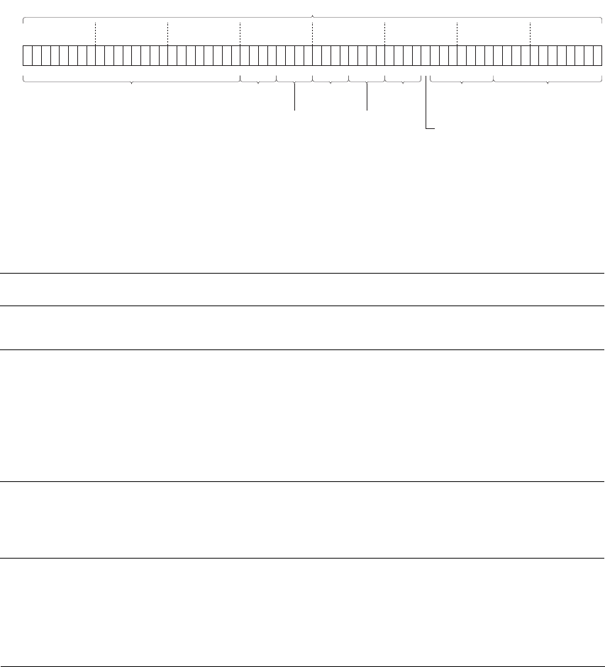
Debug Registers Reference
C10-100 Copyright © 1996-1998, 2000, 2004-2008 ARM Limited. All rights reserved. ARM DDI 0406B
Figure C10-2 shows the fields in the 64-bit Peripheral ID value, and includes the field values for fields that:
• have fixed values, including the bits that are reserved, RAZ
• have fixed values in a device that is designed by ARM.
For more information about the fields and their values see Table C10-23.
Figure C10-2 Peripheral ID fields, with values for a design by ARM
Table C10-23 shows the fields in the Peripheral ID.
63 56 048
70
55 47 40 39 32 31 24 23 12 11
DBGPID7
Conceptual 64-bit Peripheral ID
DBGPID6 DBGPID5 DBGPID4 DBGPID3 DBGPID2 DBGPID1 DBGPID0
70707070707070
0000000000000000000000000000
3536
0100
4KB
count
JEP 106
continuation
code
2728
RevAnd
Customer
modified
20 19 18
10111011
Revison JEP 106
ID code
Reserved, RAZ Part number
Uses JEP 106 ID code
Bits with no value shown are
IMPLEMENTATION
DEFINED
Some bit values shown are for a device designed by ARM Limited. See text for details.
Table C10-23 Fields in the Debug Peripheral Identification Registers
Name Size Description Register
4KB count 4 bits Log2 of the number of 4KB blocks occupied by the device. In v7 Debug,
the debug registers occupy a single 4KB block, so this field is always
0x0
.
DBGPID4
JEP 106 code 4+7
bits
Identifies the designer of the device. This value consists of:
a 4-bit continuation code, also described as the bank number
a 7-bit identity code.
For implementations designed by ARM, the continuation code is
0x4
(bank 5), and the identity code is
0x3B
.
For more information, see JEP106, Standard Manufacturers
Identification Code.
DBGPID1,
DBGPID2,
DBGPID4
RevAnd 4 bits Manufacturing Revision Number. Indicates a late modification to the
device, usually as a result of an Engineering Change Order.
This field starts at
0x0
and is incremented by the integrated circuit
manufacturer on metal fixes.
DBGPID3
Customer
modified
4 bits Indicates an endorsed modification to the device.
If the system designer cannot modify the RTL supplied by the processor
designer then this field is RAZ.
DBGPID3

Debug Registers Reference
ARM DDI 0406B Copyright © 1996-1998, 2000, 2004-2008 ARM Limited. All rights reserved. C10-101
For more information about these fields, see the ARM Debug Interface v5 Architecture Specification.
The following subsections describe the formats of each of the implemented Debug Peripheral ID Registers.
DBGPID0
DBGPID0 is debug register 1016 at offset
0xFE0
. Its format is:
Bits [31:8] Reserved, RAZ.
Part number[7:0], bits [7:0]
Bits [7:0] of the IMPLEMENTATION DEFINED Part number.
DBGPID1
DBGPID1 is debug register 1017 at offset
0xFE4
. Its format is:
Bits [31:8] Reserved, RAZ.
JEP Identity Code[3:0], bits [7:4]
Bits [3:0] of the IMPLEMENTATION DEFINED JEP Identity Code.
For a device designed by ARM the JEP Identity Code is
0x3B
and therefore this field is
0xB
.
Part number[11:8], bits [3:0]
Bits [11:8] of the IMPLEMENTATION DEFINED Part number.
DBGPID2
DBGPID2 is debug register 1018 at offset
0xFE8
. Its format is:
Bits [31:8] Reserved, RAZ.
Revision, bits [7:4]
The IMPLEMENTATION DEFINED revision number for the device.
Revision 4 bits Revision number for the device.
Starts at
0x0
and increments by 1 at both major and minor revisions.
DBGPID2
Uses JEP 106
ID code
1 bit This bit is set to 1 when a JEP 106 Identity Code is used.
This bit must be 1 on all ARMv7 implementations.
DBGPID2
Part Number 12 bits Part number for the device. Each organization designing devices to the
ARM Debug architecture specification keeps its own part number list.
DBGPID0,
DBGPID1
Table C10-23 Fields in the Debug Peripheral Identification Registers (continued)
Name Size Description Register

Debug Registers Reference
C10-102 Copyright © 1996-1998, 2000, 2004-2008 ARM Limited. All rights reserved. ARM DDI 0406B
Uses JEP Code, bit [3]
For an ARMv7 implementation this bit must be one, indicating that the Peripheral ID uses
a JEP 106 Identity Code.
JEP Identity Code[6:4], bits [2:0]
Bits [6:4] of the IMPLEMENTATION DEFINED JEP Identity Code.
For a device designed by ARM the JEP Identity Code is
0x3B
and therefore this field is
0b011.
DBGPID3
DBGPID3 is debug register 1019 at offset
0xFEC
. Its format is:
Bits [31:8] Reserved, RAZ.
RevAnd, bits [7:4]
The IMPLEMENTATION DEFINED manufacturing revision number for the device.
Customer modified, bits [3:0]
An IMPLEMENTATION DEFINED value that indicates an endorsed modification to the device.
If the system designer cannot modify the RTL supplied by the processor designer then this
field is RAZ.
DBGPID4
DBGPID4 is debug register 1012 at offset
0xFD0
. Its format is:
Bits [31:8] Reserved, RAZ.
4KB count, bits [7:4]
This field is RAZ for all ARMv7 implementations.
JEP 106 Continuation code, bits [3:0]
The IMPLEMENTATION DEFINED JEP 106 Continuation code.
For a device designed by ARM this field is
0x4
.
C10.8.10 Debug Component Identification Registers (DBGCID0 to DBGCID3)
The Debug Component Identification Registers identify the processor as an ARM Debug Interface v5
Component. For more information, see the ARM Debug Interface v5 Architecture Specification.
The Debug Component Identification Registers:
• are debug registers 1020-1023, at offsets
0xFF0-0xFFC
• are read-only registers
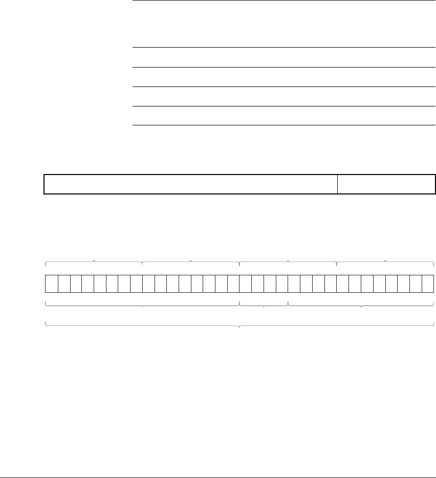
Debug Registers Reference
ARM DDI 0406B Copyright © 1996-1998, 2000, 2004-2008 ARM Limited. All rights reserved. C10-103
• occupy the last four words of the 4KB block of debug registers
• when the Security Extensions are implemented, are Common registers.
Table C10-24 lists the Debug Component Identification Registers.
Only bits [7:0] of each Debug Component ID Register are used. This means that the format of each register
is:
The four Debug Component ID Registers can be considered as defining a single 32-bit Component ID, as
shown in Figure C10-3. The value of this Component ID is fixed.
Figure C10-3 Mapping between Debug Component ID Registers and the 32-bit Component ID value
The following subsections describe the formats of each of the Debug Component ID Registers.
DBGCID0
DBGCID0 is debug register 1020 at offset
0xFF0
. Its format is:
Bits [31:8] Reserved, RAZ.
Table C10-24 Debug Component Identification Registers
Register:
Description Reference
Number Offset
1020
0xFF0
Debug Component ID0 DBGCID0
1021
0xFF4
Debug Component ID1 DBGCID1 on page C10-104
1022
0xFF8
Debug Component ID2 DBGCID2 on page C10-104
1023
0xFFC
Debug Component ID3 DBGCID3 on page C10-104
31 87 0
Reserved, RAZ Component ID data
Actual Component ID Register fields
DBGCID3
Conceptual 32-bit Component ID
Preamble
31 016 15 12 11
07070707
DBGCID2 DBGCID1 DBGCID0
PreambleComponent
class
10110001000001011001000000001101
Component ID

Debug Registers Reference
C10-104 Copyright © 1996-1998, 2000, 2004-2008 ARM Limited. All rights reserved. ARM DDI 0406B
Preamble byte 0, bits [7:0]
This byte has the value
0x0D
.
DBGCID1
DBGCID1 is debug register 1021 at offset
0xFF4
. Its format is:
Bits [31:8] Reserved, RAZ.
Component class, bits [7:4]
This field has the value
0x9
, indicating an ARM Debug component.
Preamble, bits [3:0]
This field has the value
0x0
.
DBGCID2
DBGCID2 is debug register 1022 at offset
0xFF8
. Its format is:
Bits [31:8] Reserved, RAZ.
Preamble byte 2, bits [7:0]
This field has the value
0x05
.
DBGCID3
DBGCID3 is debug register 1023 at offset
0xFFC
. Its format is:
Bits [31:8] Reserved, RAZ.
Preamble byte 3, bits [7:0]
This field has the value
0xB1
.

Debug Registers Reference
ARM DDI 0406B Copyright © 1996-1998, 2000, 2004-2008 ARM Limited. All rights reserved. C10-105
C10.9 Performance monitor registers
v6 Debug and v6.1 Debug
These registers are not defined in v6 Debug and v6.1 Debug.
v7 Debug The performance monitors are an optional feature in v7 Debug. If implemented, they are
registers in CP15 c9, see CP15 c9 register map on page C9-10.
The following subsections describe the performance monitor registers:
•c9, Performance Monitor Control Register (PMCR)
•c9, Count Enable Set Register (PMCNTENSET) on page C10-108
•c9, Count Enable Clear Register (PMCNTENCLR) on page C10-109
•c9, Overflow Flag Status Register (PMOVSR) on page C10-110
•c9, Software Increment Register (PMSWINC) on page C10-112
•c9, Event Counter Selection Register (PMSELR) on page C10-113
•c9, Cycle Count Register (PMCCNTR) on page C10-114
•c9, Event Type Select Register (PMXEVTYPER) on page C10-115
•c9, Event Count Register (PMXEVCNTR) on page C10-116
•c9, User Enable Register (PMUSERENR) on page C10-117
•c9, Interrupt Enable Set Register (PMINTENSET) on page C10-118
•c9, Interrupt Enable Clear Register (PMINTENCLR) on page C10-119.
C10.9.1 c9, Performance Monitor Control Register (PMCR)
The Performance Monitor Control Register, PMCR:
• provides details of the performance monitor implementation, including the number of counters
implemented
• configures and controls the counters.
The PMCR:
• is a 32-bit read/write CP15 register, with more restricted access to some bits
• is accessible in:
— privileged modes
— User mode only when the PMUSERENR.EN bit is set to 1
• when the Security Extensions are implemented, is a Common register
• is accessed using an
MRC
or
MCR
command with
<CRn>
set to c9,
<opc1>
set to 0,
<CRm>
set to c12, and
<opc2>
set to 0
• has defined core logic reset values for its read/write bits.

Debug Registers Reference
C10-106 Copyright © 1996-1998, 2000, 2004-2008 ARM Limited. All rights reserved. ARM DDI 0406B
The format of the PMCR is:
IMP, bits [31:24]
Implementer code. This is a read-only field with an IMPLEMENTATION DEFINED value.
The Implementer codes are allocated by ARM. Values have the same interpretation as bits
[31:24] of the CP15 Main ID Register, see:
•c0, Main ID Register (MIDR) on page B3-81 for a VMSA implementation
•c0, Main ID Register (MIDR) on page B4-32 for a PMSA implementation.
IDCODE, bits [23:16]
Identification code. This is a read-only field with an IMPLEMENTATION DEFINED value.
Each implementer must maintain a list of identification codes that is specific to the
implementer. A specific implementation is identified by the combination of the implementer
code and the identification code.
N, bits [15:11]
Number of event counters. This is a read-only field with an IMPLEMENTATION DEFINED value
that indicates the number of counters implemented.
The value of this field is the number of counters implemented, from 0b00000 for no counters
to 0b11111 for 31 counters.
An implementation can implement only the Clock Counter (PMCCNTR) Register. This is
indicated by a value of 0b00000 for the N field.
Bits [10:6] Reserved, UNK/SBZP.
DP, bit [5] Disable PMCCNTR when prohibited. The possible values of this bit are:
0 Count is enabled in prohibited regions
1 Count is disabled in prohibited regions.
Prohibited regions are defined as regions where event counting would be prohibited. For
example, if non-invasive debug is disabled in all Secure modes, the Secure state is a
prohibited region. For details of non-invasive debug authentication see Chapter C7
Non-invasive Debug Authentication.
Note
This bit permits a Non-secure process to discard cycle counts that might be accumulated
during periods when the other counts are prohibited because of security prohibitions. It is
not a control to enhance security. The function of this bit is to avoid corruption of the count.
See also Interaction with Security Extensions on page C9-7.
This is a read/write bit. Its core logic reset value is 0.
31 2423 1615 1110 6543210
IMP IDCODE N UNK/SBZP DP X D C P E

Debug Registers Reference
ARM DDI 0406B Copyright © 1996-1998, 2000, 2004-2008 ARM Limited. All rights reserved. C10-107
X, bit [4] Export enable. The possible values of this bit are:
0 Export of events is disabled
1 Export of events is enabled.
This bit is used to permit events to be exported to another debug device, such as a trace
macrocell, over an event bus. If the implementation does not include such an event bus, this
bit is RAZ/WI.
This bit does not affect the generation of performance monitor interrupts, that can be
implemented as a signal exported from the processor to an interrupt controller.
This is a read/write bit. Its core logic reset value is 0.
D, bit [3] Clock divider. The possible values of this bit are:
0 When enabled, PMCCNTR counts every clock cycle
1 When enabled, PMCCNTR counts once every 64 clock cycles.
This is a read/write bit. Its core logic reset value is 0.
C, bit [2] Clock counter reset. This is a write-only bit. The effects of writing to this bit are:
0 No action
1 Reset PMCCNTR to zero.
Note
Resetting PMCCNTR does not clear the PMCCNTR overflow flag to 0. For details see c9,
Overflow Flag Status Register (PMOVSR) on page C10-110.
This bit is always RAZ.
P, bit [1] Event counter reset. This is a write-only bit. The effects of writing to this bit are:
0 No action
1 Reset all event counters, not including PMCCNTR, to zero.
Note
Resetting the event counters does not clear any overflow flags to 0. For details see c9,
Overflow Flag Status Register (PMOVSR) on page C10-110.
This bit is always RAZ.
E, bit [0] Enable. The possible values of this bit are:
0 All counters, including PMCCNTR, are disabled
1 All counters are enabled.
Performance monitor overflow IRQs are only signaled when the enable bit is set to 1.
This is a read/write bit. Its core logic reset value is 0.

Debug Registers Reference
C10-108 Copyright © 1996-1998, 2000, 2004-2008 ARM Limited. All rights reserved. ARM DDI 0406B
C10.9.2 c9, Count Enable Set Register (PMCNTENSET)
The Count Enable Set Register, PMCNTENSET, is used to enable:
• the Cycle Count Register, PMCCNTR
• any implemented event counters, PMNx.
Reading the PMCNTENSET Register shows which counters are enabled. Counters are disabled using the
Count Enable Clear Register, see c9, Count Enable Clear Register (PMCNTENCLR) on page C10-109.
The PMCNTENSET Register is:
• a 32-bit read/write CP15 register:
— reading the register shows which counters are enabled
— writing a 1 to a bit of the register enables the corresponding counter
— writing a 0 to a bit of the register has no effect
• accessible in:
— privileged modes
— User mode only when the PMUSERENR.EN bit is set to 1
• accessed using an
MRC
or
MCR
command with
<CRn>
set to c9,
<opc1>
set to 0,
<CRm>
set to c12, and
<opc2>
set to 1.
The format of the PMCNTENSET Register is:
Note
In the description of the PMCNTENSET Register:
• N is the number of event counters implemented, as defined by the PMCR.N field, see c9,
Performance Monitor Control Register (PMCR) on page C10-105
•x refers to a single event counter, and takes values from 0 to (N-1).
C, bit [31] PMCCNTR enable bit.
See Table C10-25 on page C10-109 for the behavior of this bit on reads and writes.
Bits [30:N] RAZ/WI.
Px, bit [x], for x = 0 to (N-1)
Event counter x, PMNx, enable bit.
31 30 N N-1 0
C RAZ/WI Event counter enable bits, Px, for x= 0 to (N-1)

Debug Registers Reference
ARM DDI 0406B Copyright © 1996-1998, 2000, 2004-2008 ARM Limited. All rights reserved. C10-109
Table C10-25 shows the behavior of this bit on reads and writes.
The contents of the PMCNTENSET Register are UNKNOWN on a core logic reset.
C10.9.3 c9, Count Enable Clear Register (PMCNTENCLR)
The Count Enable Clear Register, PMCNTENCLR, is used to disable:
• the Cycle Count Register, PMCCNTR
• any implemented event counters, PMNx.
Reading the PMCNTENCLR Register shows which counters are enabled. Counters are enabled using the
Count Enable Set Register, see c9, Count Enable Set Register (PMCNTENSET) on page C10-108.
The PMCNTENCLR Register is:
• a 32-bit read/write CP15 register:
— reading the register shows which counters are enabled
— writing a 1 to a bit of the register disables the corresponding counter
— writing a 0 to a bit of the register has no effect
• accessible in:
— privileged modes
— User mode only when the PMUSERENR.EN bit is set to 1
• when the Security Extensions are implemented, a Common register
• accessed using an
MRC
or
MCR
command with
<CRn>
set to c9,
<opc1>
set to 0,
<CRm>
set to c12, and
<opc2>
set to 2.
The format of the PMCNTENCLR Register is:
Note
In the description of the PMCNTENCLR Register, N and x have the meanings used in the description of the
PMCNTENSET Register, see c9, Count Enable Set Register (PMCNTENSET) on page C10-108.
C, bit [31] PMCCNTR disable bit.
See Table C10-26 on page C10-110 for the behavior of this bit on reads and writes.
Table C10-25 Read and write bit values for the PMCNTENSET Register
Value Meaning on read Action on write
0 Counter disabled No action, write is ignored
1 Counter enabled Enable counter
31 30 N N-1 0
C RAZ/WI Event counter disable bits, Px, for x= 0 to (N-1)

Debug Registers Reference
C10-110 Copyright © 1996-1998, 2000, 2004-2008 ARM Limited. All rights reserved. ARM DDI 0406B
Bits [30:N] RAZ/WI.
Px, bit [x], for x = 0 to (N-1)
Event counter x, PMNx, disable bit.
Table C10-26 shows the behavior of this bit on reads and writes.
The contents of the PMCNTENCLR Register are UNKNOWN on a core logic reset.
Note
The PMCR.E Enable bit can be used to override the settings in this register and disable all counters including
PMCCNTR, see c9, Performance Monitor Control Register (PMCR) on page C10-105. The counter enable
register retains its value when the Enable bit is 0, even though its settings are ignored.
C10.9.4 c9, Overflow Flag Status Register (PMOVSR)
The Overflow Flag Status Register, PMOVSR, holds the state of the overflow flags for:
• the Cycle Count Register, PMCCNTR
• each of the implemented event counters, PMNx.
To clear those flags you must write to the PMOVSR.
The PMOVSR is:
• a 32-bit read/write CP15 register:
— reading the register shows the state of the overflow flags
— writing a 1 to a bit of the register clears the corresponding flag
— writing a 0 to a bit of the register has no effect
• accessible in:
— privileged modes
— User mode only when the PMUSERENR.EN bit is set to 1
• when the Security Extensions are implemented, a Common register
• accessed using an
MRC
or
MCR
command with
<CRn>
set to c9,
<opc1>
set to 0,
<CRm>
set to c12, and
<opc2>
set to 3.
Table C10-26 Read and write bit values for the PMCNTENCLR Register
Value Meaning on read Action on write
0 Counter disabled No action, write is ignored
1 Counter enabled Disable counter

Debug Registers Reference
ARM DDI 0406B Copyright © 1996-1998, 2000, 2004-2008 ARM Limited. All rights reserved. C10-111
The format of the PMOVSR is:
Note
In the description of the PMOVSR, N and x have the meanings used in the description of the
PMCNTENSET Register, see c9, Count Enable Set Register (PMCNTENSET) on page C10-108.
C, bit [31] PMCCNTR overflow flag.
Table C10-27 shows the behavior of this bit on reads and writes.
Bits [30:N] RAZ/WI.
Px, bit [x], for x = 0 to (N-1)
Event counter x, PMNx, overflow flag.
Table C10-27 shows the behavior of this bit on reads and writes.
The contents of the PMOVSR are UNKNOWN on a core logic reset.
Note
The overflow flag values for individual counters are retained until cleared to 0 by a write to the PMOVSR
or processor reset, even if the counter is later disabled by writing to the PMCNTENCLR register or through
the PMCR.E Enable bit. The overflow flags are also not cleared to 0 when the counters are reset through the
Event counter reset or Clock counter reset bits in the PMCR.
31 30 N N-1 0
C RAZ/WI Event counter overflow flags, Px, for x= 0 to (N-1)
Table C10-27 Read and write bit values for the PMOVSR
Value Meaning on read Action on write
0 Counter has not overflowed No action, write is ignored
1 Counter has overflowed Clear flag to 0

Debug Registers Reference
C10-112 Copyright © 1996-1998, 2000, 2004-2008 ARM Limited. All rights reserved. ARM DDI 0406B
C10.9.5 c9, Software Increment Register (PMSWINC)
The Software Increment Register, PMSWINC, increments a counter that is configured to count the Software
count event, event
0x00
.
The PMSWINC Register is:
• a 32-bit write-only CP15 register
• accessible in:
— privileged modes
— User mode only when the PMUSERENR.EN bit is set to 1
• when the Security Extensions are implemented, a Common register
• accessed using an
MCR
command with
<CRn>
set to c9,
<opc1>
set to 0,
<CRm>
set to c12, and
<opc2>
set
to 4.
The format of the PMSWINC Register is:
Note
In the description of the PMSWINC Register, N and x have the meanings used in the description of the
PMCNTENSET Register, see c9, Count Enable Set Register (PMCNTENSET) on page C10-108.
Bits [31:N] Reserved, SBZ.
Px, bit [x], for x = 0 to (N-1)
Event counter x, PMNx, software increment bit. This is a write-only bit. The effects of
writing to this bit are:
0 No action, the write is ignored
1, if PMNx is configured to count the Software count event
Increment PMNx Register by 1
1, if PMNx is not configured to count the Software count event
UNPREDICTABLE.
31 N N-1 0
SBZ Event counter software increment bits, Px, for x= 0 to (N-1)

Debug Registers Reference
ARM DDI 0406B Copyright © 1996-1998, 2000, 2004-2008 ARM Limited. All rights reserved. C10-113
C10.9.6 c9, Event Counter Selection Register (PMSELR)
The Event Counter Selection Register, PMSELR, selects the current event counter, PMNx. When a
particular event counter is selected:
• the PMXEVTYPER can be used to set the event that increments that counter, or to read the current
configuration, see c9, Event Type Select Register (PMXEVTYPER) on page C10-115
• the PMXEVCNTR can be used to read the current value of that counter, or to write a value to that
counter, see c9, Event Count Register (PMXEVCNTR) on page C10-116
The PMSELR is:
• a 32-bit read/write CP15 register
• accessible in:
— privileged modes
— User mode only when the PMUSERENR.EN bit is set to 1
• when the Security Extensions are implemented, a Common register
• accessed using an
MRC
or
MCR
command with
<CRn>
set to c9,
<opc1>
set to 0,
<CRm>
set to c12, and
<opc2>
set to 5.
The format of the PMSELR is:
Bits [31:5] Reserved, UNK/SBZP.
SEL, bits [4:0]
Selection value of the current event counter, PMNx, where x is the value held in this field.
This field can take any value from 0 (0b00000) to 30 (0b11110).
If this field is set to a value greater than or equal to the number of implemented counters the
results are UNPREDICTABLE. The number of implemented counters is defined by the
PMCR.N field, see c9, Performance Monitor Control Register (PMCR) on page C10-105.
The value of 0b11111 is Reserved and must not be used.
The contents of the PMSELR are UNKNOWN on a core logic reset.
The SEL field identifies which event counter, PMNSEL, is accessed by PMXEVTYPER and PMXEVCNTR,
see c9, Event Type Select Register (PMXEVTYPER) on page C10-115 and c9, Event Count Register
(PMXEVCNTR) on page C10-116.
31 54 0
Reserved, UNK/SBZP SEL

Debug Registers Reference
C10-114 Copyright © 1996-1998, 2000, 2004-2008 ARM Limited. All rights reserved. ARM DDI 0406B
C10.9.7 c9, Cycle Count Register (PMCCNTR)
The Cycle Count Register, PMCCNTR, counts processor clock cycles. Depending on the value of the
PMCR.D bit, PMCCNTR increments either on every processor clock cycle or on every 64th processor clock
cycle. See c9, Performance Monitor Control Register (PMCR) on page C10-105.
The PMCCNTR is:
• a 32-bit read/write CP15 register
• accessible in:
— privileged modes
— User mode only when the PMUSERENR.EN bit is set to 1
• when the Security Extensions are implemented, a Common register
• accessed using an
MRC
or
MCR
command with
<CRn>
set to c9,
<opc1>
set to 0,
<CRm>
set to c13, and
<opc2>
set to 0.
The format of the PMCCNTR is:
CCNT, bits [31:0]
Cycle count. Depending on the value of the PMCR.D bit, this field increments either:
• every processor clock cycle
• every 64th processor clock cycle.
The contents of the PMCCNTR are UNKNOWN on a core logic reset.
The PMCCNTR.CCNT value can be reset to zero by writing a 1 to the PMCR.C bit, see c9, Performance
Monitor Control Register (PMCR) on page C10-105.
31 0
CCNT

Debug Registers Reference
ARM DDI 0406B Copyright © 1996-1998, 2000, 2004-2008 ARM Limited. All rights reserved. C10-115
C10.9.8 c9, Event Type Select Register (PMXEVTYPER)
The Event Type Select Register, PMXEVTYPER, configures which event increments the current event
counter, PMNx, or to read the current configuration. PMSELR selects the current event counter, see c9,
Event Counter Selection Register (PMSELR) on page C10-113.
The PMXEVTYPER is:
• a 32-bit read/write CP15 register
• accessible in:
— privileged modes
— User mode only when the PMUSERENR.EN bit is set to 1
• when the Security Extensions are implemented, a Common register
• accessed using an
MRC
or
MCR
command with
<CRn>
set to c9,
<opc1>
set to 0,
<CRm>
set to c13, and
<opc2>
set to 1.
The format of the PMXEVTYPER is:
Bits [31:8] Reserved, UNK/SBZP.
evtCount, bits [7:0]
Event to count. The Event number of the event that is counted by the current event counter,
PMNx. For more information, see Event numbers.
The contents of each of the Event Type Select Registers are UNKNOWN on a core logic reset.
Event numbers
Event numbers are used in the PMXEVTYPER to determine the event that causes an event counter to
increment. These event numbers are split into two ranges:
0x00-0x3F
Common features. Reserved for the specified events. When an ARMv7 processor supports
monitoring of an event that is assigned a number in this range, if possible it must use that
number for the event. Unassigned values are reserved and might be used to define additional
common events in future editions of this manual.
0x40-0xFF
IMPLEMENTATION DEFINED features.
For more information, including the assigned values in the common features range, see Event numbers on
page C9-13.
31 87 0
Reserved, UNK/SBZP evtCount

Debug Registers Reference
C10-116 Copyright © 1996-1998, 2000, 2004-2008 ARM Limited. All rights reserved. ARM DDI 0406B
C10.9.9 c9, Event Count Register (PMXEVCNTR)
The Event Count Register, PMXEVCNTR, is used to read or write the value of the current event counter,
PMNx. PMSELR selects the current event counter, see c9, Event Counter Selection Register (PMSELR) on
page C10-113.
The PMXEVCNTR is:
• a 32-bit read/write CP15 register
• accessible in:
— privileged modes
— User mode only when the PMUSERENR.EN bit is set to 1
• when the Security Extensions are implemented, a Common register
• accessed using an
MRC
or
MCR
command with
<CRn>
set to c9,
<opc1>
set to 0,
<CRm>
set to c13, and
<opc2>
set to 2.
The format of the PMXEVCNTR is:
PMNX, bits [31:0]
Value of the current event counter, PMNx.
A read of the PMXEVCNTR always returns the current value of the register.
The contents of each of the Event Count Registers are UNKNOWN on a core logic reset.
Note
You can write to the PMXEVCNTR even when the counter is disabled. This is true regardless of why the
counter is disabled, which can be any of:
• because 1 has been written to the appropriate bit in the PMCNTENCLR
• because the PMCR.E bit is set to 0
• by the non-invasive debug authentication.
31 0
PMNX

Debug Registers Reference
ARM DDI 0406B Copyright © 1996-1998, 2000, 2004-2008 ARM Limited. All rights reserved. C10-117
C10.9.10 c9, User Enable Register (PMUSERENR)
The User Enable Register, PMUSERENR, enables or disables User mode access to the performance
monitors.
The PMUSERENR is:
• a 32-bit read/write CP15 register, with access that depends on the current mode:
— in a privileged mode, the PMUSERENR is a read/write register
— in User mode, the PMUSERENR is a read-only register
• when the Security Extensions are implemented, a Common register
• accessed using an
MRC
or
MCR
command with
<CRn>
set to c9,
<opc1>
set to 0,
<CRm>
set to c14, and
<opc2>
set to 0.
The format of the PMUSERENR is:
Bits [31:1] Reserved, UNK/SBZP.
EN, bit [0] User mode access enable bit. The possible values of this bit are:
0 User mode access to performance monitors disabled
1 User mode access to performance monitors enabled.
Some
MCR
and
MRC
instructions used to access the performance monitors are UNDEFINED in User mode when
User mode access to the performance monitors is disabled. For more information, see Access permissions
on page C9-12.
The PMUSERENR.EN bit is set to 0 on a core logic reset.
31 10
Reserved, UNK/SBZP E
N

Debug Registers Reference
C10-118 Copyright © 1996-1998, 2000, 2004-2008 ARM Limited. All rights reserved. ARM DDI 0406B
C10.9.11 c9, Interrupt Enable Set Register (PMINTENSET)
The Interrupt Enable Set Register, PMINTENSET, enables the generation of interrupt requests on overflows
from:
• the Cycle Count Register, PMCCNTR
• each implemented event counter, PMNx.
Reading the PMINTENSET Register shows which overflow interrupts are enabled. Counter overflow
interrupts must be disabled using the PMINTENCLR Register, see c9, Interrupt Enable Clear Register
(PMINTENCLR) on page C10-119.
The PMINTENSET Register is:
• A 32-bit read/write CP15 register:
— reading the register shows which overflow interrupts are enabled
— writing a 1 to a bit of the register enables the corresponding overflow interrupt
— writing a 0 to a bit of the register has no effect.
• Accessible only in privileged modes.
The instructions that access the PMINTENSET Register are always UNDEFINED in User mode, even
if the PMUSERENR.EN flag is set to 1, see c9, User Enable Register (PMUSERENR) on
page C10-117.
• When the Security Extensions are implemented, a Common register.
• Accessed using an
MRC
or
MCR
command with
<CRn>
set to c9,
<opc1>
set to 0,
<CRm>
set to c14, and
<opc2>
set to 1.
The format of the PMINTENSET Register is:
Note
In the description of the PMINTENSET Register, N and x have the meanings used in the description of the
PMCNTENSET Register, see c9, Count Enable Set Register (PMCNTENSET) on page C10-108.
C, bit [31] PMCCNTR overflow interrupt enable bit.
See Table C10-28 on page C10-119 for the behavior of this bit on reads and writes.
Bits [30:N] RAZ/WI.
Px, bit [x], for x = 0 to (N-1)
Event counter x, PMNx, overflow interrupt enable bit.
31 30 N N-1 0
C RAZ/WI Event counter overflow interrupt enable bits, Px, for x= 0 to (N-1)

Debug Registers Reference
ARM DDI 0406B Copyright © 1996-1998, 2000, 2004-2008 ARM Limited. All rights reserved. C10-119
Table C10-28 shows the behavior of this bit on reads and writes.
The contents of the PMINTENSET Register are UNKNOWN on a core logic reset. To avoid spurious
interrupts being generated, software must set the interrupt enable values before enabling any of the counters.
Interrupts are not signaled if the PMCR.E Enable bit is set to 0.
When an interrupt is signaled, it can be removed by clearing the overflow flag for the counter in the
PMOVSR Register, see c9, Overflow Flag Status Register (PMOVSR) on page C10-110.
Note
ARM expects that the interrupt request that can be generated on a counter overflow is also exported from
the processor, meaning it can be factored into a system interrupt controller if applicable. This means that
normally the system will have more levels of control of the interrupt generated.
C10.9.12 c9, Interrupt Enable Clear Register (PMINTENCLR)
The Interrupt Enable Clear Register, PMINTENCLR, disables the generation of interrupt requests on
overflows from:
• the Cycle Count Register, PMCCNTR
• each implemented event counter, PMNx.
Reading the PMINTENCLR Register shows which overflow interrupts are enabled. Counter overflow
interrupts must be enabled using the PMINTENSET Register, see c9, Interrupt Enable Set Register
(PMINTENSET) on page C10-118.
The PMINTENCLR Register is:
• A 32-bit read/write CP15 register:
— reading the register shows which overflow interrupts are enabled
— writing a 1 to a bit of the register disables the corresponding overflow interrupt
— writing a 0 to a bit of the register has no effect.
• Accessible only in privileged modes.
The instructions that access the PMINTENCLR Register are always UNDEFINED in User mode, even
if the PMUSERENR.EN flag is set to 1, see c9, User Enable Register (PMUSERENR) on
page C10-117.
• When the Security Extensions are implemented, a Common register.
• Accessed using an
MRC
or
MCR
command with
<CRn>
set to c9,
<opc1>
set to 0,
<CRm>
set to c14, and
<opc2>
set to 2.
Table C10-28 Read and write bit values for the PMINTENSET Register
Value Meaning on read Action on write
0 Interrupt disabled No action, write is ignored
1 Interrupt enabled Enable interrupt

Debug Registers Reference
C10-120 Copyright © 1996-1998, 2000, 2004-2008 ARM Limited. All rights reserved. ARM DDI 0406B
The format of the PMINTENCLR Register is:
Note
In the description of the PMINTENCLR Register, N and x have the meanings used in the description of the
PMINTENSET Register, see c9, Interrupt Enable Set Register (PMINTENSET) on page C10-118.
C, bit [31] PMCCNTR overflow interrupt disable bit.
See Table C10-29 for the behavior of this bit on reads and writes.
Bits [30:N] RAZ/WI.
Pm, bit [x], for x = 0 to (N-1)
Event counter x, PMNx, overflow interrupt disable bit.
Table C10-29 shows the behavior of this bit on reads and writes.
The contents of the PMINTENCLR Register are UNKNOWN on a core logic reset.
For more information about counter overflow interrupts see c9, Interrupt Enable Set Register
(PMINTENSET) on page C10-118.
31 30 N N-1 0
C RAZ/WI Event counter overflow interrupt disable bits, Px, for x = 0 to (N-1)
Table C10-29 Read and write bit values for the PMINTENCLR Register
Value Meaning on read Action on write
0 Interrupt disabled No action, write is ignored
1 Interrupt enabled Disable interrupt
Part D
Appendices

ARM DDI 0406B Copyright © 1996-1998, 2000, 2004-2008 ARM Limited. All rights reserved. AppxA-1
Appendix A
Recommended External Debug Interface
This chapter describes the recommended external debug interface. It contains the following sections:
•System integration signals on page AppxA-2
•Recommended debug slave port on page AppxA-13.
Note
This recommended external debug interface specification is not part of the ARM architecture specification.
Implementers and users of the ARMv7 architecture must not consider this appendix as a requirement of the
architecture. It is included as an appendix to this manual only:
• as reference material for users of ARM products that implement this interface
• as an example of how an external debug interface might be implemented.
The inclusion of this appendix is no indication of whether any ARM products might, or might not,
implement this external debug interface. For details of the implemented external debug interface you must
always see the appropriate product documentation.

Recommended External Debug Interface
AppxA-2 Copyright © 1996-1998, 2000, 2004-2008 ARM Limited. All rights reserved. ARM DDI 0406B
A.1 System integration signals
Table A-1 shows the signals recommended in v7 Debug.
Table A-1 Miscellaneous debug signals
Name Direction Versions Description Section
DBGEN In v6, v6.1, v7 Debug Enable Authentication signals
on page AppxA-3
NIDEN In v6, v6.1:
optional
v7: required
Non-Invasive Debug Enable
SPIDEN In v6.1, v7 Secure Privileged Invasive
Debug Enable
SPNIDEN In v6.1, v7 Secure Privileged
Non-Invasive Debug Enable
DBGRESTART In v7 only External restart request Run-control and
cross-triggering
signals on
page AppxA-5
DBGRESTARTED In v7 only Handshake for
DBGRESTART
DBGTRIGGER Out v7 only,
optional
Debug Acknowledge signal
EDBGRQ In v6, v6.1, v7 External Debug Request
DBGACK Out v6, v6.1, v7 Debug Acknowledge signal DBGACK and
DBGCPUDONE on
page AppxA-7
DBGCPUDONE Out v7 only,
optional
Debug Acknowledge signal
COMMRX Out v6, v6.1, v7 DBGDTRRX full signal COMMRX and
COMMTX on
page AppxA-9
COMMTX Out v6, v6.1, v7 DBGDTRTX empty signal
DBGOSLOCKINIT In v7 only Initialize OS Lock on reset DBGOSLOCKINIT on
page AppxA-9
DBGNOPWRDWN Out v6, v6.1:
optional
v7: required
No power-down request
signal
DBGNOPWRDWN on
page AppxA-9
DBGPWRDUP In v7 only Processor powered up DBGPWRDUP on
page AppxA-10

Recommended External Debug Interface
ARM DDI 0406B Copyright © 1996-1998, 2000, 2004-2008 ARM Limited. All rights reserved. AppxA-3
A.1.1 Authentication signals
DBGEN, NIDEN, SPIDEN and SPNIDEN are the authentication signals.
NIDEN and SPNIDEN can be omitted if no non-invasive debug features are implemented.
SPIDEN and SPNIDEN can be omitted if Security Extensions are not implemented.
When DBGEN is LOW, indicating that debug is disabled:
• Halting debug events are ignored
• except for ignoring Halting debug events, the processor behaves as if DBGDSCR[15:14] == 0b00,
meaning that Monitor debug-mode and Halting debug-mode are both disabled. For more information,
see Debug Status and Control Register (DBGDSCR) on page C10-10.
For details of how these signals control enabling of invasive and non-invasive debug see Chapter C2
Invasive Debug Authentication and Chapter C7 Non-invasive Debug Authentication.
Note
The v7 Debug architecture authentication signal interface described here is compatible with the CoreSight
architecture requirements for the authentication interface of a debug component. However the CoreSight
architecture places additional requirements on other components in the system. For more information, see
the CoreSight Architecture Specification.
SPIDEN also controls permissions in Debug state. For details see Privilege in Debug state on page C5-13.
See also Authentication Status Register (DBGAUTHSTATUS) on page C10-96.
DBGROMADDR[31:12] In v7 only ROM Table physical address DBGROMADDR and
DBGROMADDRV on
page AppxA-10
DBGROMADDRV In v7 only ROM Table physical address
valid
DBGSELFADDR[31:12] In v7 only Debug self-address offset DBGSELFADDR and
DBGSELFADDRV on
page AppxA-10
DBGSELFADDRV In v7 only Debug self-address offset
valid
DBGSWENABLE In v7 only Debug software access enable DBGSWENABLE on
page AppxA-11
PRESETDBGn In v7 only Debug logic reset PRESETDBGn on
page AppxA-12
Table A-1 Miscellaneous debug signals (continued)
Name Direction Versions Description Section

Recommended External Debug Interface
AppxA-4 Copyright © 1996-1998, 2000, 2004-2008 ARM Limited. All rights reserved. ARM DDI 0406B
Changing the authentication signals
In v6.1 Debug and v7 Debug, the NIDEN, DBGEN, SPIDEN, and SPNIDEN authentication signals can
be controlled dynamically, meaning that they might change while the processor is running, or while the
processor is in Debug state.
Note
In v6 Debug DBGEN is a static signal and can be changed only while the processor is in reset.
Normally, these signals are driven by the system, meaning that they are driven by a peripheral connected to
the ARM processor. If the software running on the ARM processor has to change any of these signals it must
follow this procedure:
1. Execute an implementation specific sequence of instructions to change the signal value. For example,
this might be an instruction to write a value to a control register in a system peripheral.
2. If step 1 involves any memory operation, perform a Data Synchronization Barrier (DSB).
3. Poll the debug registers to check the signal values seen by the processor. This is required because the
processor might not see the signal change until several cycles after the DSB completes.
4. Perform an Instruction Synchronization Barrier (ISB), exception entry or exception return.
The software cannot perform debug or analysis operations that rely on the new value until this procedure
has been completed. The same rules apply for instructions executed through the DBGITR while in Debug
state. The processor view of the authentication signals can be polled through DBGDSCR[17:16] and, in v7
Debug, the DBGAUTHSTATUS register.
Note
Exceptionally, the processor might be in Debug state even though the mode, security state and authentication
signal settings are such that, in Non-debug state, debug events would be ignored. This can occur because:
• it is UNPREDICTABLE whether the behavior of debug events that are generated between a change in
the authentication signals and the next Instruction Synchronization Barrier, exception entry or
exception return follow the behavior of the old or new settings
• it is possible to change the authentication signals while the processor is in Debug state.
See also Generation of debug events on page C3-40 and Altering CPSR privileged bits in Debug state on
page C5-14.

Recommended External Debug Interface
ARM DDI 0406B Copyright © 1996-1998, 2000, 2004-2008 ARM Limited. All rights reserved. AppxA-5
A.1.2 Run-control and cross-triggering signals
ARM recommends implementation of the run-control and cross-triggering signals EDBGRQ,
DBGTRIGGER, DBGRESTART, and DBGRESTARTED. These signals are particularly useful in a
multiprocessor system, because using them:
• A debugger can signal a group of processors to enter Debug state.
• A debugger can signal a group of processors to leave Debug state.
• A system component can signal a group of processors to enter Debug state when any one of them
enters Debug state because of a debug event on that processor. This is known as cross-triggering.
If you implement the recommended signalling in your system hardware, this signalling means all of the
processors in the group enter or leave Debug state nearly simultaneously.
These signals can also be used in a uniprocessor implementation. For example, debug events not defined by
the debug architecture might be generated externally to the processor. When one of these events occurs the
external system can use these signals to cause the processor to enter Debug state. A trace macrocell might
use these signals in this way.
Contact ARM for details of a recommended Embedded Cross Trigger (ECT) peripheral that you can use in
a multiprocessor system to implement this signalling.
The following subsections describe each of the recommended signals:
•EDBGRQ
•DBGTRIGGER on page AppxA-6
•DBGRESTART and DBGRESTARTED on page AppxA-6.
EDBGRQ
EDBGRQ is the recommended implementation of the External Debug Request mechanism, see Halting
debug events on page C3-38.
EDBGRQ is active-HIGH.
Once EDBGRQ is asserted it must be held HIGH until it is acknowledged:
• An implementation can use either DBGACK or DBGTRIGGER to acknowledge EDBGRQ, see:
—DBGACK and DBGCPUDONE on page AppxA-7
—DBGTRIGGER on page AppxA-6.
• Alternatively, debugger software might use an IMPLEMENTATION DEFINED method to acknowledge
EDBGRQ. For example, once the processor has entered Debug state the debugger might reprogram
the peripheral that is driving EDBGRQ.

Recommended External Debug Interface
AppxA-6 Copyright © 1996-1998, 2000, 2004-2008 ARM Limited. All rights reserved. ARM DDI 0406B
DBGTRIGGER
The processor asserts DBGTRIGGER to indicate that it is committed to entering Debug state. Therefore,
the system can use DBGTRIGGER to acknowledge EDBGRQ. See Chapter C5 Debug State for the
definition of Debug state.
DBGTRIGGER is active-HIGH.
The processor must assert DBGTRIGGER as early as possible, so that the system can use its rising edge
to signal to other devices that the processor is entering Debug state. DBGTRIGGER can be used for
cross-triggering. For example, in a multiprocessor system, when one processor halts, the DBGTRIGGER
signal from that processor can be used to generate an External Debug Request for the other processors.
See DBGACK and DBGCPUDONE on page AppxA-7 for details of the recommended External Debug
Request handshaking between EDBGRQ and DBGTRIGGER.
In addition, the processor asserts DBGTRIGGER whenever the DBGDSCR.DBGack bit is set to 1, see
Debug Status and Control Register (DBGDSCR) on page C10-10.
If the DBGDSCR.DBGack bit is 0, the processor deasserts DBGTRIGGER on exit from Debug state.
Note
Setting DBGDSCR.DBGack to 1 takes no account of the DBGEN and SPIDEN signals. Setting
DBGDSCR.DBGack to 1 asserts DBGTRIGGER regardless of the security settings.
A v7 Debug implementation of these recommendations might not implement DBGTRIGGER if it would
have identical behavior to DBGACK.
Before v7 Debug, DBGTRIGGER is not part of the recommended external debug interface.
DBGRESTART and DBGRESTARTED
DBGRESTART is the recommended implementation of the External Restart request, see Leaving Debug
state on page C5-28. DBGRESTARTED is a handshake signal for DBGRESTART.
DBGRESTART and DBGRESTARTED are active-HIGH.
Once DBGRESTART is asserted, it must be held HIGH until DBGRESTARTED is deasserted. The
processor ignores DBGRESTART if it is not in Debug state.
Figure A-1 on page AppxA-7 shows the four-phase handshake of DBGRESTART and
DBGRESTARTED. It is diagrammatic only, and does not imply any timings.
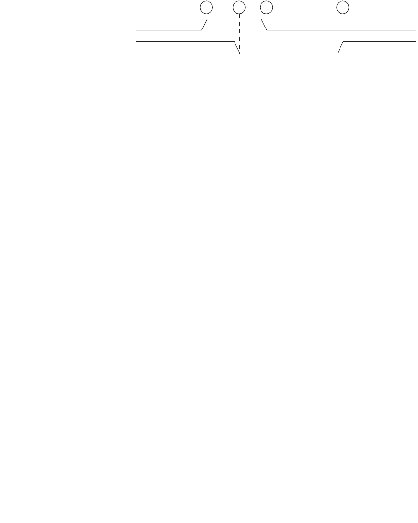
Recommended External Debug Interface
ARM DDI 0406B Copyright © 1996-1998, 2000, 2004-2008 ARM Limited. All rights reserved. AppxA-7
Figure A-1 DBGRESTART / DBGRESTARTED handshake
The numbers in Figure A-1 have the following meanings:
1. If DBGRESTARTED is asserted HIGH the peripheral asserts DBGRESTART HIGH and waits for
DBGRESTARTED to go LOW
2. The processor drives DBGRESTARTED LOW to deassert the signal and waits for DBGRESTART
to go LOW
3. The peripheral drives DBGRESTART LOW to deassert the signal. This event indicates to the
processor that it can start the transition from Debug state to Non-debug state.
4. The processor leaves Debug state and asserts DBGRESTARTED HIGH.
In the process of leaving Debug state the processor normally deasserts the DBGACK, DBGTRIGGER,
and DBGCPUDONE signals. It is IMPLEMENTATION DEFINED when this change occurs relative to the
changes in DBGRESTART and DBGRESTARTED.
A.1.3 DBGACK and DBGCPUDONE
DBGACK and DBGCPUDONE are active-HIGH.
The processor asserts DBGACK to indicate that it is in Debug state. Therefore, the system can use
DBGACK as a handshake for EDBGRQ, instead of using DBGTRIGGER.
In v6 Debug and v6.1 Debug, the system can use DBGACK for cross-triggering.
The processor asserts DBGCPUDONE only after it has completed all Non-debug state memory accesses.
Therefore the system can use DBGCPUDONE as an indicator that all memory accesses issued by the
processor result from operations performed by a debugger.
Figure A-2 on page AppxA-8 shows the signalling sequence for entry to Debug state. It is diagrammatic
only, and does not imply any timings.
Debug state Non-debug state
DBGRESTART
23
DBGRESTARTED
4
1
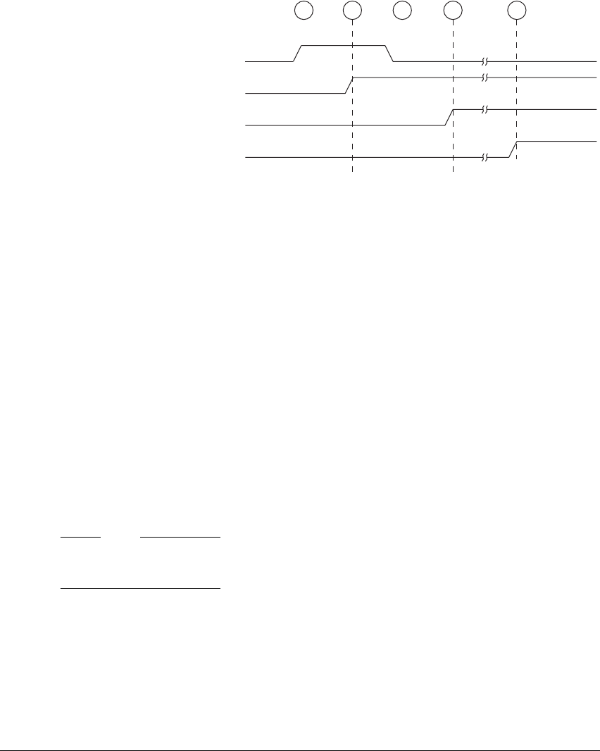
Recommended External Debug Interface
AppxA-8 Copyright © 1996-1998, 2000, 2004-2008 ARM Limited. All rights reserved. ARM DDI 0406B
Figure A-2 Signalling for Debug state entry on an External Debug Request
In Figure A-2 these events must occur in order:
1 The peripheral asserts EBDGRQ and waits for it to be acknowledged.
2 The processor takes the debug event and starts the Debug state entry sequence. The
processor asserts DBGTRIGGER.
3 The processor completes the Debug state entry sequence and asserts DBGACK.
4 The processor completes all Non-debug state memory accesses and asserts
DBGCPUDONE. It might do this only after intervention by an external debugger, see
Asynchronous aborts and entry to Debug state on page C5-5.
Event a, the peripheral deasserting EDBGRQ, can occur at any time after the assertion of EDBGRQ is
acknowledged. In the example shown in Figure A-2, the system is using DBGTRIGGER to acknowledge
EDBGRQ, and therefore event a is not ordered relative to events 3 and 4.
In addition, the processor asserts DBGCPUDONE and DBGACK when the DBGDSCR.DBGack bit is set
to 1, see Debug Status and Control Register (DBGDSCR) on page C10-10.
If the DBGDSCR.DBGack bit is 0, the processor deasserts DBGCPUDONE and DBGACK on exit from
Debug state.
Note
Setting DBGDSCR.DBGack to 1 takes no account of the DBGEN and SPIDEN signals. Setting
DBGDSCR.DBGack to 1 asserts DBGCPUDONE and DBGACK regardless of the security settings.
A v7 Debug implementation of these recommendations might not implement DBGCPUDONE if it would
have identical behavior to DBGACK.
Before v7 Debug, DBGCPUDONE was not part of the recommended external debug interface.
Debug state entryNormal state
EDBGRQ
DBGTRIGGER
1a
DBGACK
DBGCPUDONE
2
Debug state
See the text about the ordering of transition a.
34

Recommended External Debug Interface
ARM DDI 0406B Copyright © 1996-1998, 2000, 2004-2008 ARM Limited. All rights reserved. AppxA-9
A.1.4 COMMRX and COMMTX
COMMRX and COMMTX reflect the state of DBGDSCR[30:29] through the external debug interface:
•COMMTX is the inverse of DBGDSCR[29], TXfull. The processor is ready to transmit.
•COMMRX is equivalent to DBGDSCR[30], RXfull.
See Debug Status and Control Register (DBGDSCR) on page C10-10 for descriptions of the TXfull and
RXfull bits.
These signals are active HIGH indicators of when the Debug Communications Channel (DCC) requires
processing by the target system. They permit interrupt-driven communications over the DCC. By
connecting these signals to an interrupt controller, software using the DCC can be interrupted whenever
there is new data on the channel or when the channel is clear for transmission.
Note
There can be race conditions between reading the DCC flags through a read of DBGDSCRext and a read of
the DBGDTRTXint Register or a write to the DBGDTRRXint Register through the Baseline CP14 interface.
However the timing of these signals with respect to the DCC registers must be such that target code
executing off an interrupt triggered by either of these signals must be able to write to DBGDTRTXint and
read DBGDTRRXint without race conditions.
A.1.5 DBGOSLOCKINIT
DBGOSLOCKINIT is not required in v6 Debug and v6.1 Debug.
In v7 Debug, DBGOSLOCKINIT is a configuration signal that determines the state of the OS Lock
immediately after a debug registers reset. On a debug registers reset:
•if DBGOSLOCKINIT is HIGH then the OS Lock is set from the reset
•if DBGOSLOCKINIT is LOW then the OS Lock is clear from the reset.
Normally, DBGOSLOCKINIT is tied off LOW.
For a description of debug registers reset see Recommended reset scheme for v7 Debug on page C6-16. For
details of the OS Lock see OS Save and Restore registers, v7 Debug only on page C10-75.
See also Permissions in relation to locks on page C6-27.
A.1.6 DBGNOPWRDWN
DBGNOPWRDWN is optional in v6 Debug and v6.1 Debug.
DBGNOPWRDWN is equivalent to the value of bit [0] of the Device Power-Down and Reset Control
Register. The processor power controller must work in emulate mode when this signal is HIGH.
For more information, see Device Power-down and Reset Control Register (DBGPRCR), v7 Debug only on
page C10-31.

Recommended External Debug Interface
AppxA-10 Copyright © 1996-1998, 2000, 2004-2008 ARM Limited. All rights reserved. ARM DDI 0406B
A.1.7 DBGPWRDUP
DBGPWRDUP is not required in v6 Debug and v6.1 Debug.
DBGPWRDUP is not required in a SinglePower system, that is, it is not required in a design that has only
one power domain.
The DBGPWRDUP input signal is HIGH when the processor is powered up, and LOW otherwise. The
DBGPWRDUP signal is reflected in bit [0] of the Device Power-Down and Reset Status Register.
See also Device Power-down and Reset Status Register (DBGPRSR), v7 Debug only on page C10-34 and
Permissions in relation to power-down on page C6-28.
A.1.8 DBGROMADDR and DBGROMADDRV
DBGROMADDR and DBGROMADDRV are not required in v6 Debug and v6.1 Debug. They are
required in v7 Debug if the memory-mapped interface is implemented.
DBGROMADDR specifies bits [31:12] of the ROM Table table physical address. This is a configuration
input. It must be either:
• be a tie-off
• change only while the processor is in reset.
In a system with multiple ROM Tables, this address must be tied off to the top-level ROM Table address.
In a system with no ROM Table this address must be tied off with the physical address where the debug
registers are memory-mapped. Debug software can use the debug component identification registers at the
end of the 4KB block addressed by DBGROMADDR to distinguish a ROM table from a processor.
Note
If the system implements more than one debug component, for example a processor and a trace macrocell,
a ROM Table must be provided.
DBGROMADDRV is the valid signal for DBGROMADDR. If the address cannot be determined,
DBGROMADDR must be tied off to zero and DBGROMADDRV tied LOW.
The format of ROM Tables is defined in the ARM Debug Interface v5 Architecture Specification.
A.1.9 DBGSELFADDR and DBGSELFADDRV
DBGSELFADDR and DBGSELFADDRV are not required in v6 Debug and v6.1 Debug.
In v7 Debug, DBGSELFADDR and DBGSELFDDRV are required if the memory-mapped interface is
implemented. If DBGROMADDR and DBGROMADDRV are not implemented, DBGSELFADDR and
DBGSELFADDRV must not be implemented.

Recommended External Debug Interface
ARM DDI 0406B Copyright © 1996-1998, 2000, 2004-2008 ARM Limited. All rights reserved. AppxA-11
DBGSELFADDR specifies bits [31:12] of the two’s complement signed offset from the ROM Table
physical address to the physical address where the debug registers are Memory-mapped. This is a
configuration input. It must either:
• be a tie-off
• change only while the processor is in reset.
If there is no ROM Table, DBGROMADDR must be configured as described in the section
DBGROMADDR and DBGROMADDRV on page AppxA-10, and DBGSELFADDR must be tied off to
zero with DBGSELFADDRV tied HIGH.
DBGSELFADDRV is the valid signal for DBGSELFADDR. If the offset cannot be determined,
DBGSELFADDR must be tied off to zero and DBGSELFADDRV tied LOW.
A.1.10 DBGSWENABLE
DBGSWENABLE is not required in v6 Debug and v6.1 Debug.
In v7 Debug, DBGSWENABLE is driven by the Debug Access Port. For details see the ARM Debug
Interface v5 Architecture Specification.
DBGSWENABLE is an active-HIGH signal that must be asserted to enable system access to the debug
register file. That is, if deasserted it prevents access through the memory-mapped and Extended CP14
interfaces. This gives the debugger full control over the debug registers in the processor.
When this signal is deasserted by the debugger by a means that is IMPLEMENTATION DEFINED,
memory-mapped interface accesses return an error response and most Extended CP14 operations become
UNDEFINED instructions. See CP14 debug registers access permissions on page C6-36 and Permission
summaries for memory-mapped and external debug interfaces on page C6-45.
In the ARM Debug Interface v5, DBGSWENABLE is asserted by setting the DbgSwEnable control bit in
the access port Control Status Word Register (CSW) to 1. For the memory-mapped interface, when the
DbgSwEnable control bit is set to 0 the generation of slave-generated errors is a function of the ADIv5
Debug Access Port, and therefore the processor ignores the DBGSWENABLE signal for the
memory-mapped interface. For details see the ARM Debug Interface v5 Architecture Specification.
The DBGSWENABLE signal has no effect on accesses through the external debug interface.
Normally, the DBGSWENABLE signal must be asserted at debug logic reset and deasserted under
debugger control.

Recommended External Debug Interface
AppxA-12 Copyright © 1996-1998, 2000, 2004-2008 ARM Limited. All rights reserved. ARM DDI 0406B
A.1.11 PRESETDBGn
PRESETDBGn is not required in v6 Debug and v6.1 Debug. The debug logic is only reset on system
power-up reset.
The reset signal resets all debug registers. See also Recommended reset scheme for v7 Debug on
page C6-16.
Note
Do not use the PRESETDBGn signal to reset the debug registers if the debug system is connected to a
debug monitor that uses the CP14 debug interface.
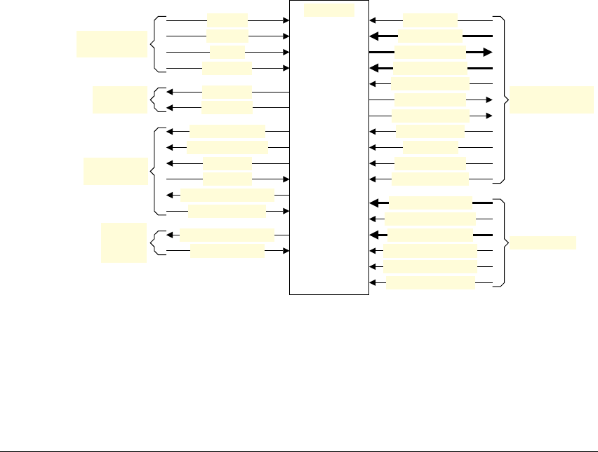
Recommended External Debug Interface
ARM DDI 0406B Copyright © 1996-1998, 2000, 2004-2008 ARM Limited. All rights reserved. AppxA-13
A.2 Recommended debug slave port
This slave port is not required in v6 Debug and v6.1 Debug.
The memory-mapped interface is optional on v7 Debug. This section describes the recommended APBv3
slave port. It provides both the memory-mapped and external debug interfaces.
A valid external debug interface for v7 Debug is any access mechanism that enables the external debugger
to complete reads or writes to the memory-mapped registers described in The memory-mapped and
recommended external debug interfaces on page C6-43.
In v7 Debug a memory-mapped interface can be implemented to provide access to the debug registers using
load and store operations. Such an interface is sufficient for the requirements of the external debug interface,
and therefore it is possible to implement both the memory-mapped and external debug interfaces using a
single memory slave port on the processor.
This section describes the v7 Debug recommendations for an APBv3 memory slave port APBv3 as part of
the external debug interface. In addition, ARM recommends a Debug Access Port capable of mastering an
APBv3 bus and compatible with the ARM Debug Interface v5 (ADIv5). Figure A-3 shows the
recommendations.
Figure A-3 Recommended external debug interface, including APBv3 slave port
In Figure A-3, signals with a lower-case n suffix are active LOW and all other signals are active HIGH.
ARM recommends that the debug registers are accessible through an ARM AMBA 3 Peripheral Bus version
1 (APBv3) external debug interface. This APBv3 interface:
• is 32 bits wide
• supports only 32-bit reads and writes
DBGEN
SPIDEN
NIDEN
SPNIDEN
Processor
Authentication
interface
COMMTX
COMMRX
DCC
handshake
DBGTRIGGER
DBGCPUDONE
DBGACK
EDBGRQ
DBGRESTARTED
DBGRESTART
Cross-trigger
interface
DBGNOPWRDWN
DBGPWRDUP
Power
controller
interface
PSELDBG
PADDRDBG
PRDATADBG
PWDATADBG
PENABLEDBG
PREADYDBG
PSLVERRDBG
PWRITEDBG
PCLKDBG
PCLKENDBG
PRESETDBGn
Debug bus
interface, APBv3
DBGROMADDR
DBGROMADDRV
DBGSELFADDR
DBGSELFADDRV
DBGOSLOCKINIT
DBGSWENABLE
Configuration

Recommended External Debug Interface
AppxA-14 Copyright © 1996-1998, 2000, 2004-2008 ARM Limited. All rights reserved. ARM DDI 0406B
• has stallable accesses
• has slave-generated aborts
• has 10 address bits ([11:2]) mapping 4KB of memory.
An extra signal, PADDRDBG[31], informs the debug slave port of the source of the access, as shown in
Table A-2.
Table A-2 lists the external debug interface signals.
Table A-2 Recommended external debug interface signals
Name Direction Description
PSELDBG In Selects the external debug interface
PADDRDBG[31,11:2] In Address. see PADDRDBG on page AppxA-15
PRDATADBG[31:0] Out Read data
PWDATADBG[31:0] In Write data
PENABLEDBG In Indicates a second and subsequent cycle of a transfer
PREADYDBG Out Used to extend a transfer, by inserting wait states
PSLVERRDBG Out Slave-generated error response, see PSLVERRDBG on
page AppxA-15
PWRITEDBG In Distinguishes between a read (LOW) and a write (HIGH)
PCLKDBG In Clock
PCLKENDBG In Clock enable for PCLKDBG

Recommended External Debug Interface
ARM DDI 0406B Copyright © 1996-1998, 2000, 2004-2008 ARM Limited. All rights reserved. AppxA-15
A.2.1 PADDRDBG
PADDRDBG selects the register to read or write.
In the recommended debug slave port that implements both the external debug interface and the
memory-mapped interface, the complete register set is aliased twice:
• the first view, the memory-mapped interface view, starts at
0x0
• the second view, the external debug interface view, starts at
0x80000000
.
This means that PADDRDBG[31] is used to distinguish the source of an access:
PADDRDBG[31] == 0 Access from system
PADDRDBG[31] == 1 Access from external debugger.
Note
The only bits of PADDRDBG that are specified are PADDRDBG[31, 11:2]. Bits [1:0] are not required
because all registers are word-sized, and bit [31] is used as described to indicate the source of the access.
Because some HDL languages do not permit partial buses to be specified in this way an actual
implementation might use a different name for PADDRDBG[31], such as PADDRDBG31.
A.2.2 PSLVERRDBG
PSLVERRDBG is used to signal an aborted access.
PSLVERRDBG has the same timing as the ready response, PREADYDBG. Under the v7 Debug model,
accesses are only aborted, by asserting PSLVERRDBG HIGH, in a situation related to power-down. See
also Permission summaries for memory-mapped and external debug interfaces on page C6-45.

Recommended External Debug Interface
AppxA-16 Copyright © 1996-1998, 2000, 2004-2008 ARM Limited. All rights reserved. ARM DDI 0406B

ARM DDI 0406B Copyright © 1996-1998, 2000, 2004-2008 ARM Limited. All rights reserved. AppxB-1
Appendix B
Common VFP Subarchitecture Specification
This appendix describes version 2 of the Common VFP subarchitecture. It contains the following sections:
•Scope of this appendix on page AppxB-2
•Introduction to the Common VFP subarchitecture on page AppxB-3
•Exception processing on page AppxB-6
•Support code requirements on page AppxB-11
•Context switching on page AppxB-14
•Subarchitecture additions to the VFP system registers on page AppxB-15
•Version 1 of the Common VFP subarchitecture on page AppxB-23.
Note
This VFP subarchitecture specification is not part of the ARM architecture specification. Implementers and
users of the ARMv7 architecture must not consider this appendix as a requirement of the architecture. It is
included as an appendix to this manual only:
• as reference material for users of ARM VFP products that implement this subarchitecture
• as an example of how a VFP subarchitecture might be implemented.
The inclusion of this appendix is no indication of whether any ARMv7 VFP implementations by ARM
might, or might not, implement this Common VFP subarchitecture. For details of the implemented VFP
subarchitecture you must always see the appropriate product documentation.

Common VFP Subarchitecture Specification
AppxB-2 Copyright © 1996-1998, 2000, 2004-2008 ARM Limited. All rights reserved. ARM DDI 0406B
B.1 Scope of this appendix
This specification describes the Common VFP subarchitecture. This is not part of the ARMv7 architecture
specification, see the Note on the cover page of this appendix.
The Common VFP subarchitecture is an interface provided by VFP coprocessor hardware to support code
in an operating system.
This appendix is for engineers implementing and validating a VFP coprocessor, and for engineers
implementing support code in an operating system.
The main sections of this appendix describe version 3 of the Common VFP subarchitecture. Version 3 is an
extension to the previously-published version 2 of the subarchitecture. Version 3 of the Common VFP
subarchitecture includes more support for synchronous exception reporting.
Support code for version 1 of the subarchitecture differs from version 2 only when trapped exception
handling of the Inexact exception is enabled. The differences from version 1 of the subarchitecture are
described in Version 1 of the Common VFP subarchitecture on page AppxB-23.
The differences between versions 2 and 3 of the subarchitecture are described in Version 2 of the Common
VFP subarchitecture on page AppxB-24.

Common VFP Subarchitecture Specification
ARM DDI 0406B Copyright © 1996-1998, 2000, 2004-2008 ARM Limited. All rights reserved. AppxB-3
B.2 Introduction to the Common VFP subarchitecture
The VFP architecture describes the interface provided by a VFP implementation to application software. A
complete implementation of the VFP architecture might include both a hardware coprocessor and a software
component, known as the support code. Support code must signal trapped floating-point exceptions to
application software, and provide other implementation-dependent functions. The Common VFP
subarchitecture describes an interface between VFP coprocessor hardware and support code.
B.2.1 VFP support code and bounced instructions
Support code is entered through the ARM Undefined Instruction exception vector, when the VFP hardware
does not respond to a VFP instruction. This software entry is known as a bounce.
The bounce mechanism supports trapped floating-point exceptions. Trapped floating-point exceptions,
known as traps, are floating-point exceptions that an implementation must pass back for application
software to resolve. See Trapped floating-point exception handling on page AppxB-10.
Support code might perform other tasks, in addition to trap handler calls. These tasks are determined by the
implementation. Typically, additional support code functions might handle rare conditions that are either
difficult to implement in hardware, or gate-intensive in hardware. This approach permits software behavior
to be consistent across implementations with varying degrees of hardware support.
B.2.2 Exception processing terminology
A condition that causes a VFP instruction to call support code is called an exceptional condition.
The VFP instruction that contains the floating-point operation requiring support code is known as the
exception-generating instruction.
The VFP instruction that causes a bounce to occur is known as the trigger instruction.
An implementation can use both synchronous and asynchronous exception signaling:
• if an exception is signaled synchronously, the exception-generating instruction is also the trigger
instruction.
• if an exception is signaled asynchronously, the trigger instruction is a VFP instruction that occurs
after the exception-generating instruction.
An implementation can issue and complete additional VFP instructions before bouncing the trigger
instruction.
An implementation can issue a maximum of one additional VFP instruction that it cannot complete. This
instruction is known as the bypassed instruction. This instruction is retired in the ARM processor and cannot
be reissued. Therefore, it must be executed by the VFP support code.

Common VFP Subarchitecture Specification
AppxB-4 Copyright © 1996-1998, 2000, 2004-2008 ARM Limited. All rights reserved. ARM DDI 0406B
B.2.3 Hardware and software implementation
The Common VFP subarchitecture requires the VFP hardware implementation to perform completely all
load, store and register transfer instructions. These instructions cannot generate floating-point exceptions.
The division of labor between the hardware and software components of a VFP implementation for
CDP
operations is IMPLEMENTATION DEFINED.
Typically, the hardware handles all common cases, to optimize performance. When the hardware encounters
a case that it cannot handle on its own it calls the software component, the support code for the hardware,
to deal with it.
For more information, see Advanced SIMD and VFP extensions on page A2-20.
B.2.4 VFP subarchitecture system registers
The Common VFP subarchitecture adds two instruction registers:
• for asynchronous exceptions, the FPINST register contains the exception-generating instruction
• the FPINST2 register contains the bypassed instruction, if there is one.
Both instruction registers are optional:
• The FPINST register is required only if at least one supported configuration can bounce instructions
asynchronously.
• The FPINST2 register is required only if the processor can commit to issuing a VFP instruction
before an exceptional case is detected in an earlier VFP instruction.
The Common VFP subarchitecture adds new fields to the FPEXC Register:
• the FPEXC.VECITR field contains an encoding that gives the remaining vector length of the
exception-generating instruction
• the FPEXC.FP2V bit indicates if the FPINST2 register contains an instruction that the support code
must execute
• the FPEXC.DEX bit is set when a synchronous bounce is caused by a floating-point exception,
indicating that the support code must execute the bounced instruction
• the FPEXC.VV bit is set when a synchronous bounce is caused by a floating-point exception, and the
FPEXC.VECITR field is valid
•an
IMPLEMENTATION DEFINED field, for the implementation to give more information about the
exceptional condition that caused the bounce.
See The Floating-Point Exception Register (FPEXC) on page B1-68 for a description of the minimum
implementation of the FPEXC required by the VFP architecture.

Common VFP Subarchitecture Specification
ARM DDI 0406B Copyright © 1996-1998, 2000, 2004-2008 ARM Limited. All rights reserved. AppxB-5
Note
In version 2 of the Common VFP subarchitecture the FPEXC.EX bit is set to 1 only when an asynchronous
bounce occurs.
Software can detect the presence of the instruction registers by testing the FPEXC.EX and FPEXC.FP2V
bits, as described in Detecting which VFP Common subarchitecture registers are implemented on
page AppxB-22.

Common VFP Subarchitecture Specification
AppxB-6 Copyright © 1996-1998, 2000, 2004-2008 ARM Limited. All rights reserved. ARM DDI 0406B
B.3 Exception processing
The following sections describe exception processing in the Common VFP subarchitecture:
•Asynchronous exceptions
•Synchronous exceptions on page AppxB-8
•VFP Access Permission faults on page AppxB-10
•Unallocated VFP instruction encodings on page AppxB-10
•Trapped floating-point exception handling on page AppxB-10.
B.3.1 Asynchronous exceptions
In the Common VFP subarchitecture, an exceptional condition can be detected after executing the
exceptional instruction. This means an implementation can detect an exceptional condition after an
instruction has passed the point for exception handling in the ARM processor pipeline.
Handling this condition is known as asynchronous exception handling, because the exceptional condition
can be detected some time after it is generated. In this case the exception handling:
• is signaled synchronously with respect to the trigger instruction
• is not signaled synchronously with respect to the instruction that generated the exceptional condition.
When an exceptional condition is detected the VFP coprocessor enters the asynchronous exceptional state,
setting the FPEXC.EX bit to 1. At the application level, subsequent VFP instructions are rejected. This
causes an Undefined Instruction exception, and information about the exceptional instruction is copied to:
• the FPINST register, see The Floating-Point Instruction Registers, FPINST and FPINST2 on
page AppxB-20
• the FPEXC.VECITR field.
For details of the FPEXC see:
•The Floating-Point Exception Register (FPEXC) on page B1-68 for the VFPv3 architectural
requirements for the register
•Additions to the Floating-Point Exception Register (FPEXC) on page AppxB-15 for the Common
VFP subarchitecture extensions to the register.
In some implementations it is possible for two VFP instructions to issue before an exceptional condition is
detected in the first instruction. In this case the second instruction is copied to FPINST2, see The
Floating-Point Instruction Registers, FPINST and FPINST2 on page AppxB-20. This instruction must be
executed by the support code. If there is a dependency between the instructions copied into FPINST and
FPINST2 then the instruction in FPINST must be executed before the instruction in FPINST2.

Common VFP Subarchitecture Specification
ARM DDI 0406B Copyright © 1996-1998, 2000, 2004-2008 ARM Limited. All rights reserved. AppxB-7
The trigger instruction might not be the VFP instruction immediately following the exceptional instruction,
and depending on the instruction sequence, the bounce can occur many instructions later. An
implementation can continue to execute some VFP instructions before detecting the exceptional condition,
provided:
• these instructions are not themselves exceptional
• these instructions are independent of the exceptional instruction
• the operands for the exceptional instruction are still available after the execution of the instructions.
Determination of the trigger instruction
VMSR
and
VMRS
instructions that access the FPEXC, FPSID, FPINST or FPINST2 registers do not trigger
exception processing.
These system registers are not used in normal VFP application code, but are designed for use by support
code and the operating system. Accesses to these registers do not bounce when the processor is in an
asynchronous exceptional state, indicated by FPEXC.EX == 1. This means the support code can read
information out of these registers, before clearing the exceptional condition by setting FPEXC.EX to 0.
All other VFP instructions, including
VMSR
and
VMRS
instructions that access the FPSCR, trigger exception
processing if there is an outstanding exceptional condition. For more information, see VFP support code on
page B1-70.
Exception processing for scalar instructions
When an exceptional condition is detected in a scalar
CDP
instruction:
• the exception-generating instruction is copied to the FPINST Register, see The Floating-Point
Instruction Registers, FPINST and FPINST2 on page AppxB-20
• the FPEXC.VECITR field is set to 0b111 to indicate that no short vector iterations are required
• the FPEXC.EX bit is set to 1
• all the operand registers to the instruction are restored to their original values, so that the instruction
can be re-executed in support code
• If the execution of the instruction would set the cumulative exception flags for any exception,
hardware might or might not set these flags.
Note
Because the cumulative exception flags are cumulative, it is always acceptable for the support code
to set the exception flags to 1 as a result of emulating the instruction, even if the hardware has set
them.
If there is a bypassed instruction then this is copied to the FPINST2 Register, and the FPEXC.FP2V bit is
set to 1.
The next VFP instruction issued becomes the trigger instruction and causes entry to the operating system.

Common VFP Subarchitecture Specification
AppxB-8 Copyright © 1996-1998, 2000, 2004-2008 ARM Limited. All rights reserved. ARM DDI 0406B
Exception processing for short vector instructions
With a short vector instruction, any iteration might be exceptional. When an exceptional condition is
detected for a vector iteration, previous iterations can complete. For the exceptional iteration:
• The exception-generating instruction is copied to the FPINST register, see The Floating-Point
Instruction Registers, FPINST and FPINST2 on page AppxB-20. The source and destination
registers are modified to point to the exceptional iteration.
• The FPEXC.VECITR field is written with the number of iterations remaining after the exceptional
iteration.
• The FPEXC.EX bit is set to 1.
• The input operand registers to that iteration, and subsequent iterations, are restored to their original
values.
• If the execution of the exception iteration, or subsequent iterations, would set the cumulative
exception flags for any exception, hardware might or might not set these flags.
Note
Because the cumulative exception flags are cumulative, it is always acceptable for the support code
to set the exception flags to 1 as a result of emulating the iterations of the instruction, even if the
hardware has set them.
If there is a bypassed instruction then this is copied to the FPINST2 Register, and the FPEXC.FP2V bit is
set to 1.
The next VFP instruction issued becomes the trigger instruction and causes entry to the operating system.
B.3.2 Synchronous exceptions
In the Common VFP subarchitecture, an implementation can signal a floating-point exception
synchronously.
When an exceptional condition is detected in a
CDP
instruction, and the implementation chooses to signal the
condition synchronously:
• if the exceptional condition is a trapped floating-point exception the FPEXC.DEX bit is set to 1
• if the reason for the exceptional condition is IMPLEMENTATION DEFINED then the value of the
FPEXC.DEX bit is IMPLEMENTATION DEFINED
• the instruction is bounced, causing an Undefined Instruction exception
• FPEXC.EX is not set to 1.
The FPINST and FPINST2 registers are not used in this case.

Common VFP Subarchitecture Specification
ARM DDI 0406B Copyright © 1996-1998, 2000, 2004-2008 ARM Limited. All rights reserved. AppxB-9
For scalar
CDP
instructions:
• All the operand registers to the instruction are restored to their original values, so that the instruction
can be re-executed in support code.
• It is IMPLEMENTATION DEFINED whether the FPEXC.VV bit is set to 1. If it is, the FPEXC.VECITR
field will contain 0b111.
• If the execution of the instruction would set the cumulative exception flags for any exception,
hardware might or might not set these flags.
Note
Because the cumulative exception flags are cumulative, it is always acceptable for the support code
to set the exception flags to 1 as a result of emulating the instruction, even if the hardware has set
them.
For short vector instructions, any iteration might be exceptional. When an exceptional condition is detected
for a vector iteration, previous iterations can complete. For the exceptional iteration:
• The FPEXC.VECITR field is written with a value that encodes the number of iterations remaining
after the exceptional iteration. For details of the encoding see Subarchitecture additions to the VFP
system registers on page AppxB-15.
• The FPEXC.VV bit is set to 1.
• The input operand registers to that iteration, and subsequent iterations, are restored to their original
values.
• If the execution of the exception iteration, or subsequent iterations, would set the cumulative
exception flags for any exception, hardware might or might not set these flags.
Note
Because the cumulative exception flags are cumulative, it is always acceptable for the support code
to set the exception flags to 1 as a result of emulating the iterations of the instruction, even if the
hardware has set them.
Note
• In version 1 of the Common VFP subarchitecture, all exceptions are signaled synchronously when
the FPSCR.IXE bit is set to 1, see Floating-point Status and Control Register (FPSCR) on
page A2-28. The FPEXC.DEX bit is RAZ/WI. For more information, see Subarchitecture v1
exception handling when FPSCR.IXE == 1 on page AppxB-23.
• In version 2 of the Common VFP subarchitecture, exceptional conditions that cause synchronous
exceptions are signaled by setting FPEXC.DEX to 1. For more information, see Version 2 of the
Common VFP subarchitecture on page AppxB-24.

Common VFP Subarchitecture Specification
AppxB-10 Copyright © 1996-1998, 2000, 2004-2008 ARM Limited. All rights reserved. ARM DDI 0406B
B.3.3 VFP Access Permission faults
When the VFP register bank is disabled by disabling coprocessors 10 and 11 in a coprocessor access control
register, any attempt to use a VFP instruction will bounce. When the VFP register bank is disabled by
clearing the FPEXC.EN bit to 0, any attempt to access a VFP registers, except the FPEXC or FPINST
register, will bounce.
In a system where the VFP can be disabled, handler code must check that the VFP is enabled before
processing a VFP exception.
B.3.4 Unallocated VFP instruction encodings
Unallocated VFP instruction encodings are those coprocessor 10 and 11 instruction encodings that are not
allocated for VFP instructions by ARM.
An unallocated VFP instruction encoding bounces synchronously to the VFP Undefined Instruction handler
code. In this case the VFP state is not modified, the FPEXC.EX bit is set to 0, and the FPEXC.DEX bit is
set to 0. Unallocated instruction exception handling is synchronous.
The VFP exception handler code can check the FPEXC.EX bit, to find out if the VFP is using asynchronous
exception handling to handle a previous exceptional condition.
If FPEXC.EX=1, the support code is called to process a previous exceptional instruction. On return from
the support code the trigger instruction is reissued, and if the trigger instruction is an unallocated instruction
the Undefined Instruction handler is re-entered, with FPEXC.EX=0.
If FPEXC.EN == 1, FPEXC.EX == 0 and FPEXC.DEX == 0, the handler code might have been called as a
result of an unallocated instruction encoding or as a result of an allocated instruction encoding which has
not been implemented:
• If the instruction is not a
CDP
instruction, the instruction is an unallocated instruction encoding and
execution can jump to the unallocated instructions handler provided by the system.
• If the instruction is a
CDP
instruction, the support code must identify whether the instruction is one
that it can handle. If it is not, then execution can jump to the unallocated instructions handler provided
by the system.
B.3.5 Trapped floating-point exception handling
Trapped floating-point exceptions are never handled by hardware. When a trapped exception is detected by
hardware the exception-generating instruction must be re-executed by the support code. The support code
must re-detect and signal the exception.

Common VFP Subarchitecture Specification
ARM DDI 0406B Copyright © 1996-1998, 2000, 2004-2008 ARM Limited. All rights reserved. AppxB-11
B.4 Support code requirements
When an instruction is bounced, control passes to the Undefined Instruction exception handler provided by
the operating system.
The operating system is expected to:
1. Perform a standard exception entry sequence, preserving process state and re-enabling interrupts.
2. Decode the bounced instruction sufficiently to determine whether it is a coprocessor instruction, and
if so, for which coprocessor.
3. Check whether the bounced instruction is conditional, and if it is conditional, check whether the
condition was passed. This ensures correct execution on implementations that perform the bounce
even for an instructions that would fail its condition code check.
4. Check whether the coprocessor is enabled in the access control register, and take appropriate action
if not. For example, in the lazy context switch case described in Context switching with the Advanced
SIMD and VFP extensions on page B1-69, the operating system context switches the VFP state.
5. Call an appropriate second-level handler for the coprocessor, passing in:
• the instruction that bounced
• the state of the associated process.
6. The second-level handler must indicate whether the bounced instruction is to be retried or skipped.
It can also signal an additional exception that must be passed on to the application.
7. Restore the original process, transferring control to an exception handler in the application context if
necessary.
If the bounced instruction is a VFP instruction, control is passed to a second-level handler for VFP
coprocessor instructions. For the Common VFP subarchitecture this:
1. Uses the FPEXC.EX and FPEXC.DEX bits to determine the bounced instruction and associated
handling. The three possible cases are:
FPEXC.EX == 0, FPEXC.DEX == 0
The bounce was synchronous. The exception-generating instruction is the instruction that
bounced:
• If the exception-generating instruction is not a
CDP
instruction, or the version of the
subarchitecture is before version 3, the bounce was caused by an unallocated
instruction encoding or a VFP access permission fault. Branch to operating system
specific code that takes appropriate action.
• If the exception-generating instruction is a
CDP
instruction, check whether the
bounce was caused by a VFP access permission fault:
— If it is a VFP access permission fault, branch to operating system specific
code that takes appropriate action.

Common VFP Subarchitecture Specification
AppxB-12 Copyright © 1996-1998, 2000, 2004-2008 ARM Limited. All rights reserved. ARM DDI 0406B
— If it is a not a VFP access permission fault, determine the iteration count
from FPSCR.LEN, and set the return address to the instruction following
the bounced instruction. Then continue processing from step 2.
FPEXC.EX == 0, FPEXC.DEX == 1
The bounced instruction was executed as a valid floating-point operation, and it bounced
because of an exceptional condition.
The exception-generating instruction is the instruction that bounced.
The iteration count is determined from either FPSCR.LEN or FPEXC.VECITR,
depending on the value of FPEXC.VV:
• if FPEXC.VV is set to 0, the iteration count is determined from FPSCR.LEN
• if FPEXC.VV is set to 1, the iteration count is determined from FPEXC.VECITR.
Clear the FPEXC.DEX bit to 0, and set the return address to the instruction following the
bounced instruction.
Continue processing from step 2.
FPEXC.EX == 1
The VFP bounce resulted from an asynchronous exception.
Collect information about the exceptional instruction, and any other instructions that are
to be executed by support code. Clear the exceptional condition. For each instruction the
data collected include the instruction encoding and the number of vector iterations.
This involves:
• Read the FPINST Register to find the exception-generating instruction.
Read the FPEXC.VECITR field to find the remaining iteration count for this
instruction.
• Check FPEXC.FP2V. If it is set to 1 there is a bypassed instruction:
— Read the FPINST2 Register to find the bypassed instruction
— Clear the FPEXC.EX and FPEXC.FP2V bits to 0.
— Read the FPSCR.LEN field to find the iteration count for the bypassed
instruction.
The FPSCR can be read-only when FPEXC.EX == 0.
Otherwise there is no bypassed instruction:
— Clear FPEXC.EX to 0.
FPEXC.EX == 0 indicates there is no subarchitecture state to context switch.
Set the return address to re-execute the trigger instruction.

Common VFP Subarchitecture Specification
ARM DDI 0406B Copyright © 1996-1998, 2000, 2004-2008 ARM Limited. All rights reserved. AppxB-13
Note
In version 1 of the Common VFP subarchitecture, the meaning of the FPEXC.EX bit
changes when the FPSCR.IXE bit is set to 1. The FPSCR.IXE bit can be checked only
after the FPEXC.EX bit is cleared to 0. If FPSCR.IXE is 0, go to step 2 below. If
FPSCR.IXE is set to 1:
• the information collected from the VFP registers and the calculated return address
are ignored
• the exception-generating instruction is the instruction that bounced, and the
iteration count is the FPSCR.LEN value, as for the FPEXC.DEX == 1 case.
• set the return address to the instruction following the bounced instruction.
2. Packages up the information about the VFP instruction and iteration count into pairs in a form
suitable to pass to the Computation Engine, described in step 3.
At this point the packaged information can be sent as a signal to another exception handler in the application,
where the support code continues. Continuing in the application context makes it possible for the support
code to call trap handlers directly, in the application.
3. Executes in software the instruction iterations described in step 2. All configuration information
except vector length is read from the FPSCR.
In previous support code implementations by ARM, this execution is performed by the VFP
Computation Engine function.
If trapped floating-point exceptions are enabled, the Computation Engine calls trap handlers as
required.
If the exceptional condition is an unallocated instruction, the Computation Engine will call a suitable
error routine.
4. Returns to the appropriate return address.

Common VFP Subarchitecture Specification
AppxB-14 Copyright © 1996-1998, 2000, 2004-2008 ARM Limited. All rights reserved. ARM DDI 0406B
B.5 Context switching
Context switch code must check the FPEXC.EX bit when saving or restoring VFP state.
If the FPEXC.EX bit is set to 1 then additional subarchitecture information must be saved. Any attempt to
access other registers while the FPEXC.EX bit is set to 1 might bounce.
For the Common VFP subarchitecture, if the FPEXC.EX bit is set to 1:
• the FPINST register contains a bounced instruction and must be saved
• if the FPEXC.FP2V bit is set, the FPINST2 register must be saved.
The FPEXC register must always be saved.
When the subarchitecture specific information has been saved, context switch code must clear the
FPEXC.EX bit to 0 before saving other registers.
When restoring state, check the saved values of the FPEXC.EX bit and FPEXC.FP2V bit to determine
whether the extra registers must be restored.
Note
Context switch code can be written to always save and restore the subarchitecture registers. In this case
appropriate context switch code must be chosen based on the registers implemented, using the detection
mechanism described in Detecting which VFP Common subarchitecture registers are implemented on
page AppxB-22.
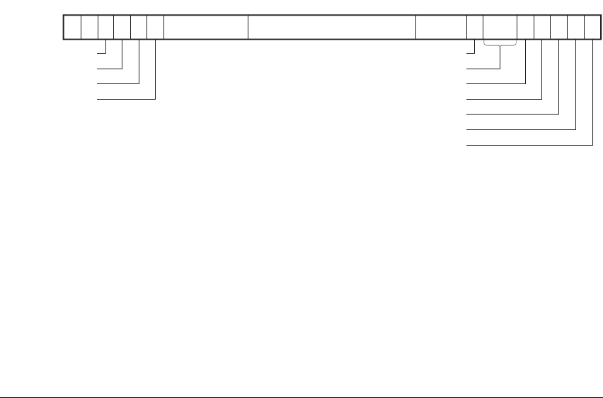
Common VFP Subarchitecture Specification
ARM DDI 0406B Copyright © 1996-1998, 2000, 2004-2008 ARM Limited. All rights reserved. AppxB-15
B.6 Subarchitecture additions to the VFP system registers
The Common VFP subarchitecture requires additions to the VFP system register implementation:
• extra fields are defined in the FPEXC, see Additions to the Floating-Point Exception Register
(FPEXC)
• additional VFP registers might be defined, see The Floating-Point Instruction Registers, FPINST and
FPINST2 on page AppxB-20.
Also, the Subarchitecture field of the FPSID must identify the Common VFP subarchitecture version, see
Floating-point System ID Register (FPSID) on page B5-34.
For more information about the VFP register implementation for the Common VFP subarchitecture see:
•Detecting which VFP Common subarchitecture registers are implemented on page AppxB-22
•Accessing the VFP Common subarchitecture registers on page AppxB-22.
B.6.1 Additions to the Floating-Point Exception Register (FPEXC)
See The Floating-Point Exception Register (FPEXC) on page B1-68 for the architectural definition of the
FPEXC, including its purpose and accessibility.
The format of the FPEXC when version 3 of the Common VFP subarchitecture is implemented
is:
EX, bit [31] See The Floating-Point Exception Register (FPEXC) on page B1-68 for the definition of
this bit.
On an implementation that does not require asynchronous exception handling this bit is
RAZ/WI. In this case the FPINST and FPINST2 registers are not implemented.
For details of how, in Common VFP subarchitecture v1, the meaning of the EX bit changes
when the FPSR.IEX bit is set to 1, see Subarchitecture v1 exception handling when
FPSCR.IXE == 1 on page AppxB-23.
EN, bit [30] See The Floating-Point Exception Register (FPEXC) on page B1-68 for the definition of
this bit.
031 30 29 28 27 10 8 7
EX EN
IMPLEMENTATION
DEFINED
UNK/SBZP VECITR
26 654321
DEX
FP2V
VV
TFV
25 21
IMPLEMENTATION
DEFINED
1120
IDF
IXF
UFF
OFF
DZF
IOF

Common VFP Subarchitecture Specification
AppxB-16 Copyright © 1996-1998, 2000, 2004-2008 ARM Limited. All rights reserved. ARM DDI 0406B
DEX, bit [29] Defined synchronous instruction exceptional flag. This field is valid only if
FPEXC.EX == 0.
When a VFP exception has occurred, the meaning of this bit is:
0 A synchronous exception has occurred when processing an instruction in CP10
or CP 11. This is either:
• an allocated floating-point instruction that is not implemented in
hardware
• an unallocated instruction in CP10 or CP11.
1 A synchronous exception has occurred on an allocated floating-point
instruction. This is either:
• an allocated floating-point instruction that is not implemented in
hardware
• an allocated floating-point instruction that has encountered an
exceptional condition.
DEX must be cleared to 0 by the exception handling routine.
On an implementation that does not require synchronous exception handling this bit is
RAZ/WI.
FP2V, bit [28] FPINST2 instruction valid flag. This field is valid only if FPEXC.EX == 1.
When an asynchronous VFP exception has occurred, the meaning of this bit is:
0 The FPINST2 Register does not contain a valid instruction.
1 The FPINST2 Register contains a valid instruction.
FP2V must be cleared to 0 by the exception handling routine.
If the FPINST2 Register is not implemented this bit is RAZ/WI.
VV, bit [27] VECITR valid flag. This field is valid only if FPEXC.DEX == 1.
When a synchronous VFP exception has occurred, the meaning of this bit is:
0 FPEXC.VECITR field is not valid, and the number of remaining vector steps
can be determined from FPSCR.LEN.
1 FPEXC.VECITR field is valid, and the number of remaining vector steps can be
determined from FPEXC.VECITR.
VV must be cleared to 0 by the exception handling routine.
If the VV field s not implemented this bit is RAZ/WI.

Common VFP Subarchitecture Specification
ARM DDI 0406B Copyright © 1996-1998, 2000, 2004-2008 ARM Limited. All rights reserved. AppxB-17
TFV, bit [26] Trapped Fault flag Valid flag. Indicates whether FPEXC bits [7,4:0] act as flags to indicate
trapped exceptions or have an IMPLEMENTATION DEFINED meaning:
0 FPEXC bits[7,4:0] have an IMPLEMENTATION DEFINED meaning
1 FPEXC bits[7,4:0] indicate the presence of trapped exceptions that have
occurred at the time of the exception. All trapped exceptions that occurred at the
time of the exception have their flags set.
This bit has a fixed value and ignores writes.
Bits [25:21] Reserved. UNK/SBZP.
Bits [20:11, 6:5]
IMPLEMENTATION DEFINED.
These bits are IMPLEMENTATION DEFINED. They can contain IMPLEMENTATION DEFINED
information about the cause of an exception. They might be used by the implementation to
indicate why an instruction was bounced to support code.
These bits must be cleared to zero by the exception handling routine.
VECITR, bits [10:8]
Vector iteration count for the VFP instruction with the exceptional condition. This field is
valid only if either:
• FPEXC.EX == 1
• FPEXC.DEX == 1 and FPEXC.VV == 1.
This field contains the number of short vector iterations remaining after the iteration in
which a potential exception was detected. Possible values are:
0b000 1 iteration
0b001 2 iterations
0b010 3 iterations
0b011 4 iterations
0b100 5 iterations
0b101 6 iterations
0b110 7 iterations
0b111 0 iterations.
The count held in this field does not include the iteration in which the exception occurred.
This field reads as 0b111 if:
• the final iteration of an instruction is bounced to the support code
• the instruction is a scalar operation.
VECITR must be cleared to 0b000 by the exception handling routine.

Common VFP Subarchitecture Specification
AppxB-18 Copyright © 1996-1998, 2000, 2004-2008 ARM Limited. All rights reserved. ARM DDI 0406B
IDF, bit [7] Input Denormal trapped exception flag, or IMPLEMENTATION DEFINED. The meaning of this
bit depends on the value of FPEXC.TFV:
FPEXC.TFV == 0
This bit is IMPLEMENTATION DEFINED. It can contain IMPLEMENTATION DEFINED
information about the cause of an exception. It might be used by the
implementation to indicate why an instruction was bounced to support code.
FPEXC.TFV == 1
This bit is the Input Denormal trapped exception flag. It indicates whether an
Input Denormal exception occurred while FPSCR.IDE was 1.
In this case, the meaning of this bit is:
0 Input denormal exception has not occurred.
1 Input denormal exception has occurred.
Input Denormal exceptions can occur only when FPSCR.FZ is 1.
In both cases this bit must be cleared to 0 by the exception handling routine.
IXF, bit [4] Inexact trapped exception flag, or IMPLEMENTATION DEFINED. The meaning of this bit
depends on the value of FPEXC.TFV:
FPEXC.TFV == 0
This bit is IMPLEMENTATION DEFINED. It can contain IMPLEMENTATION DEFINED
information about the cause of an exception. It might be used by the
implementation to indicate why an instruction was bounced to support code.
FPEXC.TFV == 1
This bit is the Inexact trapped exception flag. It indicates whether an Inexact
exception occurred while FPSCR.IXE was 1.
In this case, the meaning of this bit is:
0 Inexact exception has not occurred.
1 Inexact exception has occurred.
In both cases this bit must be cleared to 0 by the exception handling routine.
UFF, bit [3] Underflow trapped exception flag, or IMPLEMENTATION DEFINED. The meaning of this bit
depends on the value of FPEXC.TFV:
FPEXC.TFV == 0
This bit is IMPLEMENTATION DEFINED. It can contain IMPLEMENTATION DEFINED
information about the cause of an exception. It might be used by the
implementation to indicate why an instruction was bounced to support code.
FPEXC.TFV == 1
This bit is the Underflow trapped exception flag. It indicates whether an
Underflow exception occurred while FPSCR.UFE was 1.
In this case, the meaning of this bit is:
0 Underflow exception has not occurred.
1 Underflow exception has occurred.

Common VFP Subarchitecture Specification
ARM DDI 0406B Copyright © 1996-1998, 2000, 2004-2008 ARM Limited. All rights reserved. AppxB-19
Note
An Underflow trapped exception can occur only when FPSCR.FZ is 0, because
when FPSCR.FZ is 1, FPSCR.UFE is ignored and treated as 0.
In both cases this bit must be cleared to 0 by the exception handling routine.
OFF, bit [2] Overflow trapped exception flag, or IMPLEMENTATION DEFINED. The meaning of this bit
depends on the value of FPEXC.TFV:
FPEXC.TFV == 0
This bit is IMPLEMENTATION DEFINED. It can contain IMPLEMENTATION DEFINED
information about the cause of an exception. It might be used by the
implementation to indicate why an instruction was bounced to support code.
FPEXC.TFV == 1
This bit is the Overflow trapped exception flag. It indicates whether an
Overflow exception occurred while FPSCR.OFE was 1.
In this case, the meaning of this bit is:
0 Overflow exception has not occurred.
1 Overflow exception has occurred.
In both cases this bit must be cleared to 0 by the exception handling routine.
DZF, bit [1] Divide-by-zero trapped exception flag, or IMPLEMENTATION DEFINED. The meaning of this
bit depends on the value of FPEXC.TFV:
FPEXC.TFV == 0
This bit is IMPLEMENTATION DEFINED. It can contain IMPLEMENTATION DEFINED
information about the cause of an exception. It might be used by the
implementation to indicate why an instruction was bounced to support code.
FPEXC.TFV == 1
This bit is the Divide-by-zero trapped exception flag. It indicates whether a
Divide-by-zero exception occurred while FPSCR.DZE was 1.
In this case, the meaning of this bit is:
0 Divide-by-zero exception has not occurred.
1 Divide-by-zero exception has occurred.
In both cases this bit must be cleared to 0 by the exception handling routine.
IOF, bit [0] Invalid Operation trapped exception flag, or IMPLEMENTATION DEFINED. The meaning of
this bit depends on the value of FPEXC.TFV:
FPEXC.TFV == 0
This bit is IMPLEMENTATION DEFINED. It can contain IMPLEMENTATION DEFINED
information about the cause of an exception. It might be used by the
implementation to indicate why an instruction was bounced to support code.

Common VFP Subarchitecture Specification
AppxB-20 Copyright © 1996-1998, 2000, 2004-2008 ARM Limited. All rights reserved. ARM DDI 0406B
FPEXC.TFV == 1
This bit is the Invalid Operation trapped exception flag. It indicates whether an
Invalid Operation exception occurred while FPSCR.IOE was 1.
In this case, the meaning of this bit is:
0 Invalid Operation exception has not occurred.
1 Invalid Operation exception has occurred.
In both cases this bit must be cleared to 0 by the exception handling routine.
B.6.2 The Floating-Point Instruction Registers, FPINST and FPINST2
The Floating-Point Instruction Registers hold floating-point instructions relating to floating-point exception
handling in a system that implements the Common VFP subarchitecture:
• FPINST contains the exception-generating instruction
• FPINST2 contains the bypassed instruction.
FPINST and FPINST2 are:
• In the CP10 and CP11 register space.
• Present only when the Common VFP subarchitecture is implemented. A Common VFP
subarchitecture implementation can support:
— both FPINST and FPINST2
— FPINST but not FPINST2
— neither of the Floating-Point Instruction Registers.
• 32-bit read/write registers.
• If the Security Extensions are implemented, Configurable access registers. FPINST and FPINST2 are
only accessible in the Non-secure state if the CP10 and CP11 bits in the NSACR are set to 1, see c1,
Non-Secure Access Control Register (NSACR) on page B3-110.
• Accessible only in privileged modes, and only if both:
— access to coprocessors CP10 and CP11 is enabled in the Coprocessor Access Control Register,
see c1, Coprocessor Access Control Register (CPACR) on page B3-104 (VMSA
implementation), or c1, Coprocessor Access Control Register (CPACR) on page B4-51
(PMSA implementation)
— the VFP coprocessor is enabled by setting the FPEXC.EN bit to 1.

Common VFP Subarchitecture Specification
ARM DDI 0406B Copyright © 1996-1998, 2000, 2004-2008 ARM Limited. All rights reserved. AppxB-21
The format of an instruction in FPINST or FPINST2 is:
The format is the same as the format of the issued instruction, with a number of modifications. For more
information, see VFP data-processing instructions on page A7-24. The modifications from the issued
instruction are:
• In the Thumb encoding, bits [15:8] of the first halfword and bit [4] of the second halfword are
reserved. In the ARM encoding, bits [31:24, 4] are reserved:
— software must ignore these bits when reading this register, and must not modify these bits
when writing to this register
— hardware must set these bits to the values shown in the encoding diagrams, that map to the
encoding of an ARM
CDP
instruction with the AL (always) condition.
• If the instruction is a short vector instruction:
— for the FPINST Register, the source and destination registers that reference vectors are updated
to point to the source and destination registers of the exceptional iteration. The
FPEXC.VECITR field contains the number of iterations remaining. For more information, see
Exception processing for short vector instructions on page AppxB-8.
— for the FPINST Register, the full vector must be processed by support code, using the current
vector length from the FPSCR. Source and destination registers that reference vectors are
unchanged from the issued instruction.
Both
MRS
register read and
MSR
register write instructions are provided for the FPINST and FPINST2
registers, see Accessing the VFP Common subarchitecture registers on page AppxB-22.
When an exceptional instruction is bounced to support code and placed in the FPINST Register, the
FPEXC.EX bit is set to 1. This indicates that valid information is available in the FPINST Register. In
addition. when a second issued instruction is copied to the FPINST2 Register, the FPEXC.FP2V bit is set
to 1. This indicates that valid information is available in the FPINST2 Register.
When the FPEXC.EX bit is 0, indicating the VFP is not in an asynchronous exceptional state, reads of the
FPINST and FPINST2 Registers are UNPREDICTABLE and the values returned might change.
When the FPEXC.FP2V bit is 0, indicating that no second instruction was issued, reads of the FPINST2
Register are UNPREDICTABLE and the value returned might change.
Thumb encoding
15 8765432101514131211 876543210
11101110 D Vn Vd cp_num N Q M 0 Vm
ARM encoding
31 2423222120191817161514131211 876543210
11101110 D Vn Vd cp_num N Q M 0 Vm

Common VFP Subarchitecture Specification
AppxB-22 Copyright © 1996-1998, 2000, 2004-2008 ARM Limited. All rights reserved. ARM DDI 0406B
Any value read from a Floating-Point Instruction Register can be written back to the same register. This
means context switch and debugger software can save and restore Floating-Point Instruction Register
values. Writing a value that has not been read from the same register writes an UNKNOWN value to the
Floating-Point Instruction Register. For example, attempting to write an instruction with coprocessor
number 0 writes an UNKNOWN value to the Floating-Point Instruction Register.
B.6.3 Accessing the VFP Common subarchitecture registers
Use the
VMRS
and
VMSR
instructions to access the registers for the VFP Common subarchitecture
implementation, see:
•VMRS on page B6-27
•VMSR on page B6-29.
The additional registers in the VFP Common subarchitecture are accessed using:
• reg = 0b1001 for FPINST
• reg = 0b1010 for FPINST2
If FPINST or FPINST2 is not defined, the corresponding
VMRS
and
VMSR
instructions are UNPREDICTABLE.
The
VMRS
and
VMSR
instructions with reg = 0b1011 and reg = 0b11xx are UNPREDICTABLE.
B.6.4 Detecting which VFP Common subarchitecture registers are implemented
An implementation can choose not to implement FPINST and FPINST2, if these registers are not required.
System software can detect which registers are present as follows:
Set FPEXC.EX=1 and FPEXC.FP2V=1
Read back the FPEXC register
if FPEXC.EX == 0 then
Neither FPINST nor FPINST2 are implemented
else
if FPEXC.FP2V == 0 then
FPINST is implemented, FPINST2 is not implemented.
else
Both FPINST and FPINST2 are implemented.
Clean up

Common VFP Subarchitecture Specification
ARM DDI 0406B Copyright © 1996-1998, 2000, 2004-2008 ARM Limited. All rights reserved. AppxB-23
B.7 Version 1 of the Common VFP subarchitecture
Version 1 of the Common VFP subarchitecture has special behavior when the FPSCR.IXE bit is set to 1.
The Common VFP subarchitecture version can be identified by checking FPSID bits [22:16]. This field is
0b0000001 for version 1. In version 1 of the Common VFP subarchitecture the FPEXC.DEX bit is RAZ/WI.
B.7.1 Subarchitecture v1 exception handling when FPSCR.IXE == 1
In version 1 of the Common VFP subarchitecture, the mechanism for bouncing instructions changes when
the FPSCR.IXE bit, the Inexact exception enable bit, is set to 1.
When FPSCR.IXE is set to 1, the FPEXC.EX bit signals a synchronous exception, in the same way as the
FPEXC.DEX bit. In this case:
• the exceptional instruction is the instruction that caused the Undefined Instruction exception
• the FPINST Register and the FPEXC.VECITR field are not valid.
When FPSCR.IXE is 0 the FPEXC.EX bit signals an asynchronous exception, as for later versions of the
subarchitecture.

Common VFP Subarchitecture Specification
AppxB-24 Copyright © 1996-1998, 2000, 2004-2008 ARM Limited. All rights reserved. ARM DDI 0406B
B.8 Version 2 of the Common VFP subarchitecture
Version 2 of the Common VFP subarchitecture can be identified by checking FPSID bits [22:16]. This field
is 0b0000010 for version 2.
Version 2 of the Common VFP subarchitecture has three differences from version 3 of the subarchitecture.
Before version 3 of the Common VFP subarchitecture:
• The FPEXC.EX == 0, FPEXC.DEX == 0 encoding is used only for unallocated instructions or
permission faults. As a result, the determination that an instruction should be passed to the
Computation Engine is simpler than it is for version 3 of the Common VFP subarchitecture.
• Bounces are not handled synchronously on short vector instructions unless all iterations of the vector
are to be handled in software. This means that the FPEXC.VV bit is always 0 before version 3.
• The FPEXC.TFV bit is set to 0, so the additional information bits [7, 4:0] of FPEXC is
IMPLEMENTATION DEFINED.

ARM DDI 0406B Copyright © 1996-1998, 2000, 2004-2008 ARM Limited. All rights reserved. AppxC-1
Appendix C
Legacy Instruction Mnemonics
This appendix provides information about the Unified Assembler Language equivalents of older assembler
language instruction mnemonics.
It contains the following sections:
•Thumb instruction mnemonics on page AppxC-2
•Pre-UAL pseudo-instruction NOP on page AppxC-3.

Legacy Instruction Mnemonics
AppxC-2 Copyright © 1996-1998, 2000, 2004-2008 ARM Limited. All rights reserved. ARM DDI 0406B
C.1 Thumb instruction mnemonics
Table C-1 lists the UAL equivalents of the mnemonics used in pre-UAL Thumb assembly language. Except
where noted, the Thumb mnemonics conflict with UAL and cannot be supported by assemblers as
synonyms. Thumb code cannot be correctly assembled by a UAL assembler unless these changes are made.
All other Thumb instructions are the same in UAL as in Thumb assembler language, or can be supported as
synonyms.
Table C-1 Thumb instruction mnemonics
Former Thumb assembler mnemonic UAL equivalent
ADC ADCS
ADD ADDS
a
a. If either or both of the operands is R8-R15,
ADD
not
ADDS
.
AND ANDS
ASR ASRS
BIC BICS
EOR EORS
LSL LSLS
MOV <Rd>,#<imm> MOVS <Rd>,#<imm>
MOV <Rd>,<Rn> ADDS <Rd>,<Rn>,#0
b
b. If either or both of the operands is R8-R15,
MOV <Rd>,<Rn>
not
ADDS <Rd>,<Rn>,#0
.
MUL MULS
MVN MVNS
ORR ORRS
ROR RORS
SBC SBCS
SUB SUBS
c
c. If the operand register is
SP
,
SUB
not
SUBS
.

Legacy Instruction Mnemonics
ARM DDI 0406B Copyright © 1996-1998, 2000, 2004-2008 ARM Limited. All rights reserved. AppxC-3
C.2 Pre-UAL pseudo-instruction NOP
In pre-UAL assembler code,
NOP
is a pseudo-instruction, equivalent to:
•
MOV R0,R0
in ARM code
•
MOV R8,R8
in Thumb code.
Assembling the
NOP
mnemonic as UAL will not change the functionality of the code, but will change:
• the instruction encoding selected
• the architecture variants on which the resulting binary will execute successfully, because the
NOP
instruction was introduced in ARMv6K and ARMv6T2.
To avoid these changes, replace
NOP
in the assembler source code with the appropriate one of
MOV R0,R0
and
MOV R8,R8
, before assembling as UAL.

Legacy Instruction Mnemonics
AppxC-4 Copyright © 1996-1998, 2000, 2004-2008 ARM Limited. All rights reserved. ARM DDI 0406B

ARM DDI 0406B Copyright © 1996-1998, 2000, 2004-2008 ARM Limited. All rights reserved. AppxD-1
Appendix D
Deprecated and Obsolete Features
This appendix contains the following sections:
•Deprecated features on page AppxD-2
•Deprecated terminology on page AppxD-5
•Obsolete features on page AppxD-6
•Semaphore instructions on page AppxD-7
•Use of the SP as a general-purpose register on page AppxD-8
•Explicit use of the PC in ARM instructions on page AppxD-9
•Deprecated Thumb instructions on page AppxD-10.

Deprecated and Obsolete Features
AppxD-2 Copyright © 1996-1998, 2000, 2004-2008 ARM Limited. All rights reserved. ARM DDI 0406B
D.1 Deprecated features
The features described in this section are present in ARMv7 for backwards compatibility. You must avoid
using them in new applications where possible. They might not be present in future versions of the ARM
architecture.
See also Semaphore instructions on page AppxD-7, Use of the SP as a general-purpose register on
page AppxD-8, and Explicit use of the PC in ARM instructions on page AppxD-9.
D.1.1 VFP vector mode
The use of VFP vector mode is deprecated in ARMv7. For details see Appendix F VFP Vector Operation
Support.
D.1.2 VFP FLDMX and FSTMX instructions
The use of
VLDM.64
and
VSTM.64
instruction encodings with an odd immediate offset is deprecated from
ARMv6. The use of their pre-UAL mnemonics
FLDMX
and
FSTMX
is deprecated, except for disassembly
purposes. For details see FLDMX, FSTMX on page A8-101.
D.1.3 Fast context switch extension
Use of the Fast Context Switch Extension (FCSE) is deprecated from ARMv6, and in ARMv7
implementation of the FCSE is optional. For details of the FCSE see Appendix E Fast Context Switch
Extension (FCSE).
D.1.4 Direct manipulation of the Endianness bit
The use of the
MSR
instruction to write the Endianness bit in User mode is deprecated. Use the
SETEND
instruction.
D.1.5 Strongly-ordered memory accesses and interrupt masks
Any ARMv5 instruction that implicitly or explicitly changes the interrupt masks in the CPSR, and appears
in program order after a Strongly-ordered access, waits for the Strongly-ordered memory access to
complete. Dependence on this behavior is deprecated in ARMv6 and ARMv7, and code must not rely on
this behavior. Use an explicit memory barrier instead. For details see Strongly-ordered memory on
page A3-34.
D.1.6 Unaligned exception returns
ARM deprecates any dependence on the requirements that the hardware ignores bits of the address
transferred to the PC on an exception return. See Alignment of exception returns on page B1-39.

Deprecated and Obsolete Features
ARM DDI 0406B Copyright © 1996-1998, 2000, 2004-2008 ARM Limited. All rights reserved. AppxD-3
D.1.7 Use of AP[2] = 1, AP[1:0] = 0b10 in MMU access permissions
This encoding means read-only for both privileged mode and User mode accesses, but its use is deprecated
in VMSAv7. Use AP[2] = 1, AP[1:0] = 0b11. For details see Memory access control on page B3-28.
D.1.8 The Domain field in the DFSR
Use of the Domain field in the DFSR is deprecated. For details see c6, Data Fault Address Register (DFAR)
on page B3-124.
D.1.9 Watchpoint Fault Address Register in CP15
Use of the CP15 alias of the Watchpoint Fault Address Register (DBGWFAR) is deprecated. Use the CP14
DBGWFAR instead. For details see Extended CP14 interface on page C6-33.
D.1.10 CP15 memory barrier operations
Use of the CP15 c7 memory barrier operations is deprecated. The ARM and Thumb instruction sets include
instructions that perform these operations. Table D-1 shows the deprecated CP15 encodings and the
replacement ARMv7 instructions.
D.1.11 Use of Hivecs exception base address in PMSA implementations
Use of the high vector exception base address (Hivecs) of
0xFFFF0000
is deprecated in PMSA
implementations. ARM recommends that Hivecs is used only in VMSA implementations. For more
information, see Exception vectors and the exception base address on page B1-30.
D.1.12 Use of Secure User halting debug
From v7 Debug, the use of Secure User halting debug is deprecated. For more information, see About
invasive debug authentication on page C2-2.
Table D-1 Deprecated CP15 c7 memory barrier operations
Deprecated CP15 encoding
Operation Instruction description
CRn opc1 CRm opc2
c7 0 c5 4 Instruction Synchronization Barrier See ISB on page A8-102
c7 0 c10 4 Data Synchronization Barrier See DSB on page A8-92
c7 0 c10 5 Data Memory Barrier See DMB on page A8-90

Deprecated and Obsolete Features
AppxD-4 Copyright © 1996-1998, 2000, 2004-2008 ARM Limited. All rights reserved. ARM DDI 0406B
D.1.13 Escalation of privilege on CP14 and CP15 accesses in Debug state
Except for the Baseline CP14 debug registers, ARM deprecates accessing any CP14 or CP15 register from
User mode in Debug state if that register cannot be accessed from User mode in Non-debug state. For more
information, see Coprocessor and Advanced SIMD instructions in Debug state on page C5-16.
D.1.14 Interrupts or asynchronous aborts in a sequence of memory transactions
ARM deprecates any reliance by software on the behavior that an interrupt or asynchronous abort cannot
occur in a sequence of single-copy atomic memory transactions generated by a single load/store instruction
to Normal memory. For more information, see Low interrupt latency configuration on page B1-43.
D.1.15 Reading the Debug Program Counter Sampling Registers as register 33
ARM deprecates reading the DBGPCSR as debug register 33 when it is also implemented as debug register
40. For more information see Program Counter sampling on page C8-2.
D.1.16 Old mnemonics for CP15 c8 operations to invalidate entries in a unified TLB
The ARMv7-A base architecture defines three CP15 c8 operations to invalidate entries in a unified TLB.
The original mnemonics for these are changed, each dropping the initial U. The original mnemonics remain
synonyms for the operations, but ARM deprecates using the old mnemonics. Table D-2 shows the changed
mnemonics and the encodings of the operations.
For more information about these operations see CP15 c8, TLB maintenance operations on page B3-138.
Table D-2 Changed mnemonics for CP15 c8 unified TLB operations
Encoding Mnemonic
CRn opc1 CRm opc2 New Deprecated
c8 0 c7 0 TLBIALL UTLBIALL
1 TLBIMVA UTLBIMVA
2 TLBIMVA UTLBIMVA

Deprecated and Obsolete Features
ARM DDI 0406B Copyright © 1996-1998, 2000, 2004-2008 ARM Limited. All rights reserved. AppxD-5
D.2 Deprecated terminology
Table D-3 shows terms that were used in earlier editions of the ARM Architecture Reference Manual, and
the supplements to it, that are no longer used. The replacement terms are not in general exact synonyms, but
might reflect altered behavior more accurately.
Table D-3 Deprecated terminology
Old terminology Replaced by
Drain Write Buffer, Data Write Barrier (DWB) Data Synchronization Barrier
Prefetch Flush (PFF) Instruction Synchronization Barrier

Deprecated and Obsolete Features
AppxD-6 Copyright © 1996-1998, 2000, 2004-2008 ARM Limited. All rights reserved. ARM DDI 0406B
D.3 Obsolete features
The features described in the following sections were deprecated in ARMv6, and are no longer supported
in ARMv7.
D.3.1 Rotated aligned accesses
Unaligned accesses, where permitted, were treated as rotated aligned accesses before ARMv6. This
behavior was configurable, but deprecated, in ARMv6. It is obsolete in ARMv7. For more information, see
Alignment on page AppxG-6.
D.3.2 Ordering of instructions that change the CPSR interrupt masks
Any ARMv6 instruction that implicitly or explicitly changes the interrupt masks in the CPSR and appears
in program order after a Strongly-ordered access must wait for the Strongly-ordered memory access to
complete, see Ordering of instructions that change the CPSR interrupt masks on page AppxG-8 for more
information.
ARMv6 deprecated any reliance on this behavior, and this behavior is obsoleted in ARMv7.
D.3.3 ARM LDM and POP instructions that both write back and load their base registers
LDM instructions and multi-register POP instructions that specify base register writeback and load their
base register are permitted but deprecated before ARMv7, as described in Different definition of some LDM
and POP instructions on page AppxG-15. Use of such instructions is obsolete in ARMv7.

Deprecated and Obsolete Features
ARM DDI 0406B Copyright © 1996-1998, 2000, 2004-2008 ARM Limited. All rights reserved. AppxD-7
D.4 Semaphore instructions
The ARM instruction set has two semaphore instructions:
• Swap (
SWP
)
• Swap Byte (
SWPB
).
These instructions are provided for process synchronization. Both instructions generate a load access and a
store access to the same memory location, such that no other access to that location is permitted between
the load access and the store access. This enables a memory semaphore to be loaded and altered without
interruption.
SWP
and
SWPB
have a single addressing mode, whose address is the contents of a register. Separate registers
are used to specify the value to store and the destination of the load. If the same register is specified for both
of these,
SWP
exchanges the value in the register and the value in memory.
The semaphore instructions do not provide a compare and conditional write facility. If wanted, this must be
done explicitly.
Use of the swap and swap byte instructions is deprecated from ARMv6. ARM recommends that all software
uses the
LDREX
and
STREX
synchronization primitives. For details see:
•LDREX on page A8-142
•LDREXB on page A8-144
•LDREXD on page A8-146
•LDREXH on page A8-148
•STREX on page A8-400
•STREXB on page A8-402
•STREXD on page A8-404
•STREXH on page A8-406.

Deprecated and Obsolete Features
AppxD-8 Copyright © 1996-1998, 2000, 2004-2008 ARM Limited. All rights reserved. ARM DDI 0406B
D.5 Use of the SP as a general-purpose register
In the Thumb instruction set, you can only use the SP (R13) in a restricted set of instructions. This set covers
all the legitimate uses of the SP as a stack pointer. An attempt to encode any other instruction with SP in
place of a legitimate register results in either UNPREDICTABLE behavior, or a different instruction.
In addition, the use of SP (R13) as Rm in the high register forms of the 16-bit
CMP
and
ADD
instructions is
deprecated. Also, some forms of MOV (register) that use SP are deprecated, see MOV (register) on
page A8-196.
Most ARM instructions, unlike Thumb instructions, provide exactly the same access to the SP as to R0-R12.
This means that it is possible to use the SP as a general-purpose register. However, the use of the SP in an
ARM instruction, in any way that is not possible in the corresponding Thumb instruction, is deprecated.
See ARM instructions where SP use is not deprecated for a list of instructions that you can use for SP
manipulation.
D.5.1 ARM instructions where SP use is not deprecated
The use of the SP is deprecated in any ARM instruction that is not specified in this section.
Some uses of the SP are not deprecated in the following ARM data-processing instructions:
•ADD (SP plus immediate) on page A8-28
•ADD (SP plus register) on page A8-30
•CMN (immediate) on page A8-74
•CMN (register) on page A8-76
•CMP (immediate) on page A8-80
•CMP (register) on page A8-82
•MOV (register) on page A8-196
•SUB (SP minus immediate) on page A8-426
•SUB (SP minus register) on page A8-428.
In these ARM instructions, the uses of the SP that are not deprecated are the same as those uses listed in
32-bit Thumb instruction support for R13 on page A6-4.
The use of the SP as the base register in load/store/preload instructions is not deprecated. In addition, the
use of the SP as destination or source register is not deprecated in the following instructions:
•LDR (immediate, ARM) on page A8-120
•LDR (literal) on page A8-122
•LDR (register) on page A8-124
•STR (immediate, ARM) on page A8-384
•STR (register) on page A8-386.

Deprecated and Obsolete Features
ARM DDI 0406B Copyright © 1996-1998, 2000, 2004-2008 ARM Limited. All rights reserved. AppxD-9
D.6 Explicit use of the PC in ARM instructions
Most ARM instructions, unlike Thumb instructions, provide exactly the same access to the PC as to
general-purpose registers. However, the explicit use of the PC in an ARM instruction is not usually useful,
and except for specific instances that are useful, such use is deprecated.
Note
Implicit use of the PC, for example in branch instructions or load (literal) instructions, is never deprecated.
Table D-4 shows where ARM instructions can explicitly use the PC. All other explicit use of the PC is
deprecated.
Table D-4 Non-deprecated uses of the PC in ARM instructions
Instruction Non-deprecated use of PC
All load and preload instructions As destination register or base register. a
ADD (immediate, ARM) on page A8-22 As destination register.
ADD (register) on page A8-24 As destination register, source register, or both.
ADD (SP plus immediate) on page A8-28 As destination register.
ADR on page A8-32 As destination register.
MOV (register) on page A8-196 As destination register or source register, but not both.b
SUB (immediate, ARM) on page A8-420 As destination register.
SUB (register) on page A8-422 As destination register.
SUB (SP minus immediate) on page A8-426 As destination register.
SUB (SP minus register) on page A8-428 As destination register.
SUBS PC, LR and related instructions on page B6-25 As destination register.
a. Only if the instruction description permits the register to be the PC.
b. Transfer of the PC to or update of the PC from the SP is deprecated.

Deprecated and Obsolete Features
AppxD-10 Copyright © 1996-1998, 2000, 2004-2008 ARM Limited. All rights reserved. ARM DDI 0406B
D.7 Deprecated Thumb instructions
Most deprecated instructions are in the ARM instruction set. Deprecated Thumb instructions are:
• use of PC as <Rd> or <Rm> in a 16-bit ADD (SP plus register) instruction
• use of SP as <Rm> in a 16-bit ADD (SP plus register) instruction
• use of SP as <Rm> in a 16-bit CMP (register) instruction
• use of MOV (register) instructions in which both <Rd> and <Rm> are the SP or PC
• use of Rn as the lowest-numbered register in the register list of a 16-bit STM instruction with base
register writeback.

ARM DDI 0406B Copyright © 1996-1998, 2000, 2004-2008 ARM Limited. All rights reserved. AppxE-1
Appendix E
Fast Context Switch Extension (FCSE)
This appendix describes the Fast Context Switch Extension (FCSE). It contains the following sections:
•About the FCSE on page AppxE-2
•Modified virtual addresses on page AppxE-3
•Debug and trace on page AppxE-5.
Note
• From ARMv6, use of the FCSE mechanism is deprecated. The FCSE is optional in ARMv7.
• Use of both the FCSE and the ASID based memory attribute results in UNPREDICTABLE behavior.
Either the FCSE must be cleared, or all memory declared as global.

Fast Context Switch Extension (FCSE)
AppxE-2 Copyright © 1996-1998, 2000, 2004-2008 ARM Limited. All rights reserved. ARM DDI 0406B
E.1 About the FCSE
The Fast Context Switch Extension (FCSE) modifies the behavior of an ARM memory system. This
modification permits multiple programs running on the ARM processor to use identical address ranges,
while ensuring that the addresses they present to the rest of the memory system differ.
Normally, a swap between two software processes whose address ranges overlap requires changes to be
made to the virtual-to-physical address mapping defined by the MMU translation tables, see Translation
tables on page B3-7. It also typically causes cache and TLB contents to become invalid (because they relate
to the old virtual-to-physical address mapping), and so requires caches and TLBs to be flushed. As a result,
each process swap has a considerable overhead, both directly because of the cost of changing the translation
tables and indirectly because of the cost of subsequently reloading caches and TLBs.
By presenting different addresses to the rest of the memory system for different software processes even
when they are using identical addresses, the FCSE avoids this overhead. It also permits software processes
to use identical address ranges even when the rest of the memory system does not support virtual-to-physical
address mapping.
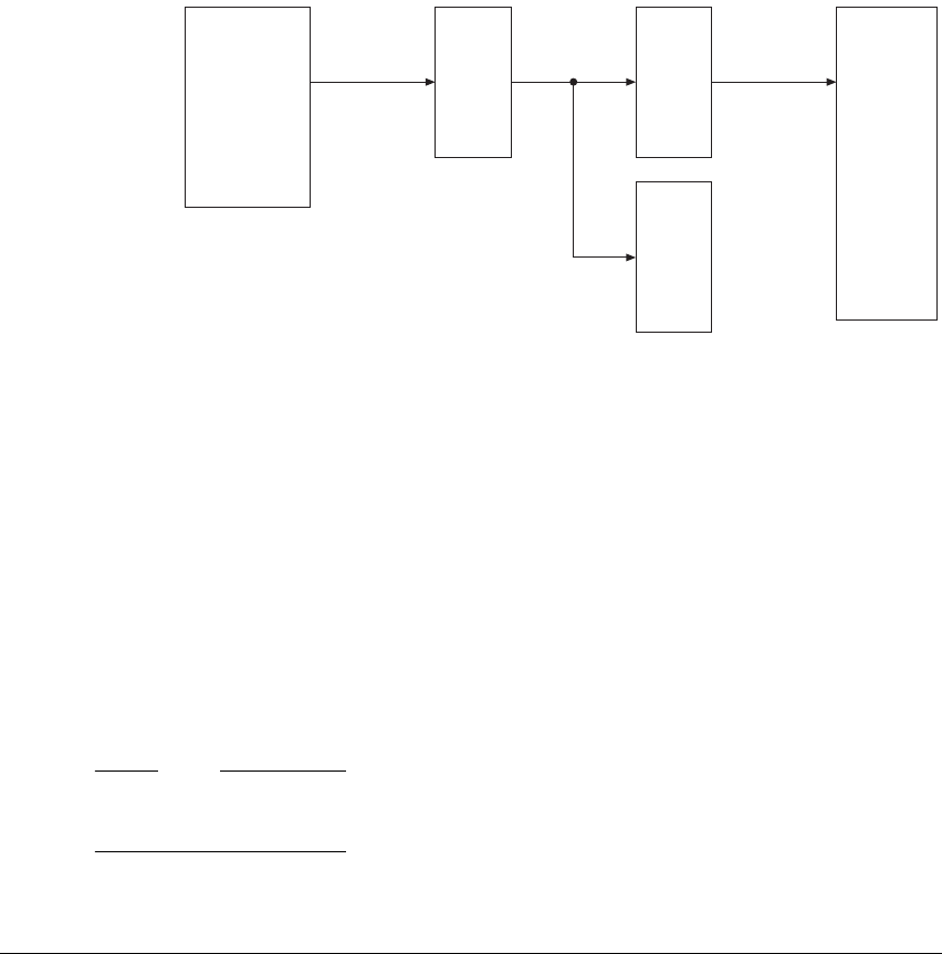
Fast Context Switch Extension (FCSE)
ARM DDI 0406B Copyright © 1996-1998, 2000, 2004-2008 ARM Limited. All rights reserved. AppxE-3
E.2 Modified virtual addresses
The 4GB virtual address space is divided into 128 process blocks, each of size 32MB. Each process block
can contain a program that has been compiled to use the address range
0x00000000
to
0x01FFFFFF
. For each
of i=0 to 127, process block i runs from address (i ×
0x02000000
) to address (i ×
0x02000000
+
0x01FF FFFF
).
The FCSE processes each virtual address for a memory access generated by the ARM processor to produce
a modified virtual address, that is sent to the rest of the memory system to be used in place of the normal
virtual address. For an MMU-based memory system, the process is illustrated in Figure E-1:
Figure E-1 Address flow in MMU memory system with FCSE
When the ARM processor generates a memory access, the translation of the Virtual Address (VA) into the
Modified Virtual Address (MVA) is described by the
FCSETranslate()
function in FCSE translation on
page B3-156.
When the top seven bits of the address are zero, the translation replaces these bits by the value of
FCSEIDR.PID when they are zero, and otherwise the translation leaves the address unchanged. When
FCSEIDR.PID has its reset value of 0b0000000, the translation leaves the address unchanged, meaning that
the FCSE is effectively disabled.
The value of FCSEIDR.PID is also known as the FCSE process ID of the current process. For more
information, see c13, FCSE Process ID Register (FCSEIDR) on page B3-152.
The effect of setting the FCSEIDR to a nonzero value at a time when any translation table entries have
enabled the alternative Context ID, ASID-based support (nG bit == 1) is UNPREDICTABLE. For more
information about ASIDs see About the VMSA on page B3-2.
Note
Virtual addresses are sometimes passed to the memory system as data. For these operations, no address
modification occurs, and MVA = VA.
Processor
core
Modified
Virtual
Address
(MVA)
FCSE MMU
Cache
Main
memory
Physical
Address
(PA)
Virtual
Address
(VA)

Fast Context Switch Extension (FCSE)
AppxE-4 Copyright © 1996-1998, 2000, 2004-2008 ARM Limited. All rights reserved. ARM DDI 0406B
Each process is compiled to use the address range
0x00000000
to
0x01FFFFFF
. When referring to its own
instructions and data, therefore, the program generates VAs whose top seven bits are all zero. The resulting
MVAs have their top seven bits replaced by FCSEIDR.PID, and so lie in the process block of the current
process.
The program can also generate VAs whose top seven bits are not all zero. When this happens, the MVA is
equal to the VA. This enables the program to address the process block of another process, provided the
other process does not have process ID 0. Provided access permissions are set correctly, this can be used for
inter-process communication.
Note
ARM recommends that only process IDs 1 and above are used for general-purpose processes, because the
process with process ID 0 cannot be communicated with in this fashion.
Use of the FCSE therefore reduces the cost of a process swap to:
• The cost of a write of the FCSEIDR.PID.
• The cost of changing access permissions if they need changing for the new process. In an
MMU-based system, this might involve changing the translation table entries individually, or
pointing to a new translation table by changing one or more of TTBR0, TTBR1, and TTBCR. Any
change to the translation tables is likely to involve invalidation of the TLB entries affected. However,
this is usually significantly cheaper than the cache flush that would be required without the FCSE.
Also, in some cases, changes to the translation table, and the associated explicit TLB management,
can be avoided by the use of domains. This reduces the cost to that of a write to the Domain Access
Control Register, see Domains on page B3-31.
The FCSE is deprecated. The use of cache, branch predictor and TLB operations with MVA based addresses
that, as a result of the Multiprocessing Extensions, would affect other processors as described in section 3.2
is UNPREDICTABLE if FCSEIDR.PID is not zero.

Fast Context Switch Extension (FCSE)
ARM DDI 0406B Copyright © 1996-1998, 2000, 2004-2008 ARM Limited. All rights reserved. AppxE-5
E.3 Debug and trace
It is IMPLEMENTATION DEFINED whether a VA or MVA is used by breakpoint and watchpoint mechanisms.
However, ARM strongly recommends that any implementation that includes the FCSE uses MVAs, to avoid
trigger aliasing.

Fast Context Switch Extension (FCSE)
AppxE-6 Copyright © 1996-1998, 2000, 2004-2008 ARM Limited. All rights reserved. ARM DDI 0406B

ARM DDI 0406B Copyright © 1996-1998, 2000, 2004-2008 ARM Limited. All rights reserved. AppxF-1
Appendix F
VFP Vector Operation Support
This appendix provides reference information about VFP vector operation.
This appendix contains the following sections:
•About VFP vector mode on page AppxF-2
•Vector length and stride control on page AppxF-3
•VFP register banks on page AppxF-5
•VFP instruction type selection on page AppxF-7.
Note
The use of VFP vector mode is deprecated. This information is provided for backwards compatibility only.

VFP Vector Operation Support
AppxF-2 Copyright © 1996-1998, 2000, 2004-2008 ARM Limited. All rights reserved. ARM DDI 0406B
F.1 About VFP vector mode
The single-precision registers can be used to hold short vectors of up to 8 single-precision values. Arithmetic
operations on all the elements of such a vector can be specified by just one single-precision arithmetic
instruction.
Similarly, the double-precision registers can be used to hold short vectors of up to 4 double-precision values,
and double-precision arithmetic instructions can specify operations on these vectors.
A vector consists of 2-8 registers from a single bank. VFP register banks on page AppxF-5 describes the
division of the VFP register set into banks.
The FPSCR.LEN field controls the number of elements in a vector. The register number in the instruction
specifies the register that contains the first element of the vector. The FPSCR.STRIDE field controls the
increment between the register numbers of the elements of the vector. If the total increment causes the
register number to overflow the top of a register bank, the register number wraps around to the bottom of
the bank, as shown in VFP register banks on page AppxF-5.
For details of the FPSCR.LEN and FPSCR.STRIDE fields see Vector length and stride control on
page AppxF-3.
A VFP instruction can operate on:
• operand vectors with LEN elements, producing a result vector with LEN elements
• an operand vector with LEN elements and a scalar operand, producing a result vector with LEN
elements
• scalar operands, producing a scalar result.
These three operation types are identical if LEN == 1.
To control which type of operation an instruction performs, you choose the registers for the instruction from
different register banks. VFP instruction type selection on page AppxF-7 describes how to select the
instruction type.
F.1.1 Affected instructions
The following VFP instructions are affected by VFP vector mode:
All other VFP instructions behave as described in their instruction descriptions regardless of the values of
FPSCR.LEN and FPSCR.STRIDE.
VABS VADD VDIV VMLA VMLS
VMOV
(immediate)
VMOV
(register)
VMUL VNEG VNMLA
VNMLS VNMUL VSQRT VSUB

VFP Vector Operation Support
ARM DDI 0406B Copyright © 1996-1998, 2000, 2004-2008 ARM Limited. All rights reserved. AppxF-3
F.2 Vector length and stride control
The FPSCR.LEN field, bits [18:16], controls the vector length for VFP instructions that operate on short
vectors, that is, how many registers are in a vector operand. Similarly, the FPSCR.STRIDE field,
bits [21:20], controls the vector stride, that is, how far apart the registers in a vector lie in the register bank.
For information about the FPSCR see Floating-point Status and Control Register (FPSCR) on page A2-28.
The permitted combinations of LEN and STRIDE are shown in Table F-1. All other combinations of LEN
and STRIDE produce UNPREDICTABLE results.
The combination LEN == 0b000, STRIDE == 0b00 is called scalar mode. When it is in effect, all arithmetic
instructions specify scalar operations. Otherwise, most arithmetic instructions specify a scalar operation if
their destination is in the range:
• S0-S7 for a single-precision operation
• D0-D3 or D16-D19 for a double-precision operation.
The full rules used to determine which operands are vectors and full details of how vector operands are
specified can be found in VFP instruction type selection on page AppxF-7.
The rules for vector operands do not permit the same register to appear twice or more in a vector. The
permitted LEN and STRIDE combinations listed in Table F-1 never cause this to happen for
single-precision instructions, so single-precision scalar and vector instructions can be used with all of these
LEN and STRIDE combinations.
For double-precision vector instructions, some of the permitted LEN and STRIDE combinations would
cause the same register to appear twice in a vector. If a double-precision vector instruction is executed with
such a LEN and STRIDE combination in effect, the instruction is UNPREDICTABLE. The last column of Table
2-2 indicates which LEN and STRIDE combinations this applies to. Double-precision scalar instructions
work normally with all of the permitted LEN and STRIDE combinations.
Table F-1 Vector length and stride combinations
LEN STRIDE Vector length Vector stride Double-precision vector instructions
0b000 0b00 1 - All instructions are scalar
0b001 0b00 2 1 Work as described in this appendix
0b001 0b11 2 2 Work as described in this appendix
0b010 0b00 3 1 Work as described in this appendix
0b010 0b11 3 2 UNPREDICTABLE
0b011 0b00 4 1 Work as described in this appendix
0b011 0b11 4 2 UNPREDICTABLE
0b100 0b00 5 1 UNPREDICTABLE

VFP Vector Operation Support
AppxF-4 Copyright © 1996-1998, 2000, 2004-2008 ARM Limited. All rights reserved. ARM DDI 0406B
0b101 0b00 6 1 UNPREDICTABLE
0b110 0b00 7 1 UNPREDICTABLE
0b111 0b00 8 1 UNPREDICTABLE
Table F-1 Vector length and stride combinations (continued)
LEN STRIDE Vector length Vector stride Double-precision vector instructions
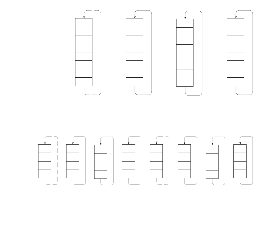
VFP Vector Operation Support
ARM DDI 0406B Copyright © 1996-1998, 2000, 2004-2008 ARM Limited. All rights reserved. AppxF-5
F.3 VFP register banks
The Advanced SIMD and VFP registers are divided into banks as follows:
• The single-precision registers are divided into four banks of eight. This is shown in Figure F-1. The
first bank is a scalar bank, and the other three are vector banks.
• In a processor with 32 double-precision registers, the double-precision registers are divided into eight
banks of four. This is shown in Figure F-2. The first and fifth banks are scalar banks, and the other
six are vector banks.
• In a processor with 16 double-precision registers, the double-precision registers are divided into four
banks of four. This is shown in Figure F-3 on page AppxF-6. The first bank is a scalar bank, and the
other three are vector banks.
Figure F-1 Single-precision register banks
Figure F-2 Register banks, 32 double-precision register VFP
Scalar bank Vector bank Vector bank Vector bank
s24
s25
s26
s27
s28
s29
s30
s31
s0
s1
s2
s3
s4
s5
s6
s7
s8
s9
s10
s11
s12
s13
s14
s15
s16
s17
s18
s18
s20
s21
s22
s23
Scalar
bank
Vector
bank
Vector
bank
Vector
bank
d12
d13
d14
d15
d0
d1
d2
d3
d4
d5
d6
d7
d8
d9
d10
d11
Scalar
bank
Vector
bank
Vector
bank
Vector
bank
d28
d29
d30
d31
d16
d17
d18
d19
d20
d21
d22
d23
d24
d25
d26
d27

VFP Vector Operation Support
AppxF-6 Copyright © 1996-1998, 2000, 2004-2008 ARM Limited. All rights reserved. ARM DDI 0406B
Figure F-3 Register banks, 16 double-precision register VFP
Scalar bank Vector bank Vector bank Vector bank
d12
d13
d14
d15
d0
d1
d2
d3
d4
d5
d6
d7
d8
d9
d10
d11

VFP Vector Operation Support
ARM DDI 0406B Copyright © 1996-1998, 2000, 2004-2008 ARM Limited. All rights reserved. AppxF-7
F.4 VFP instruction type selection
Table F-2 shows how the selection of registers in an instruction controls the operation of the instruction.
• If the instruction has two operands:
— If the destination register is in a scalar register bank, the operands and result are all scalars.
— If the destination register is in a vector register bank and the second operand is in a scalar bank,
the second operand is a scalar, but both the destination and the first operand are vectors. Each
element of the result is produced by an operation on the corresponding element of the first
operand and the same scalar.
— If the destination register and the second operand are both in vector register banks, the
operands and result are all vectors. Each element of the result is produced by an operation on
corresponding elements of both operands.
• If the instruction has one operand:
— If the destination register is in a scalar register bank, the operand and result are both scalars.
— If the destination register is in a vector register bank and the operand is in a scalar bank, the
result is a vector and the operand is a scalar. The result is duplicated to each element of the
destination vector.
— If the destination register and the operand are both in vector register banks, the operand and
result are both vectors. Each element of the result is produced by an operation on the
corresponding element of the operand.
Some VFP instructions have three operands, but in these cases one of the operand vectors is also the result
vector. They operate in the same way as two operand instructions.
Table F-2
Destination
register bank
1st operand
bank
2nd operand
bank
Destination
type
1st operand
type
2nd operand
type
Scalar Any Any Scalar Scalar Scalar
Vector Any Scalar Vector Vector Scalar
Vector Any Vector Vector Vector Vector
Scalar Any None Scalar Scalar -
Vector Scalar None Vector Scalar -
Vector Vector None Vector Vector -

VFP Vector Operation Support
AppxF-8 Copyright © 1996-1998, 2000, 2004-2008 ARM Limited. All rights reserved. ARM DDI 0406B

ARM DDI 0406B Copyright © 1996-1998, 2000, 2004-2008 ARM Limited. All rights reserved. AppxG-1
Appendix G
ARMv6 Differences
This appendix describes how ARMv6 differs from ARMv7. The appendix contains the following sections:
•Introduction to ARMv6 on page AppxG-2
•Application level register support on page AppxG-3
•Application level memory support on page AppxG-6
•Instruction set support on page AppxG-10
•System level register support on page AppxG-16
•System level memory model on page AppxG-20
•System Control coprocessor (CP15) support on page AppxG-29.
Note
In this appendix, the description ARMvN refers to all architecture variants of ARM architecture vN
described in this manual. In particular, ARMv6 refers to ARMv6, ARMv6K, and ARMv6T2, including
ARMv6K with the Security Extensions. Where the description ARMvN also describes a specific
architecture variant, this variant is sometimes described as the base architecture, for example the ARMv6
base architecture.

ARMv6 Differences
AppxG-2 Copyright © 1996-1998, 2000, 2004-2008 ARM Limited. All rights reserved. ARM DDI 0406B
G.1 Introduction to ARMv6
This appendix describes the differences in the ARMv6 architecture, compared to the description of ARMv7
given in parts A and B of this manual. Key changes introduced in ARMv7 are:
• Introduction of hierarchical cache support.
• Formalizing the alternative memory system architectures into different architecture profiles:
— the Virtual Memory System Architecture (VMSA) is formalized into the ARMv7-A profile
— the Protected Memory System Architecture (PMSA) is formalized into the ARMv7-R profile.
• Introduction of the Advanced SIMD extensions.
• Introduction of the Thumb Execution Environment (ThumbEE). ThumbEE is required in ARMv7-A,
and optional in ARMv7-R.
This appendix summarizes the features supported in ARMv6, highlighting:
• the similarities and differences with respect to ARMv7, including the following architecture variants
and extensions:
— the Security Extensions
— the extension of the Thumb instruction set using Thumb-2 technology, introduced in
ARMv6T2
— the enhanced kernel support introduced in ARMv6K.
• legacy support for ARMv4 and ARMv5.
G.1.1 Debug
Part C of this manual describes ARMv6 Debug, ARMv7 Debug, and the differences between them.
ARMv6 Differences
ARM DDI 0406B Copyright © 1996-1998, 2000, 2004-2008 ARM Limited. All rights reserved. AppxG-3
G.2 Application level register support
The ARMv6 core registers are the same as the ARMv7 core registers. For more information, see ARM core
registers on page A2-11. The following sections give more information about ARMv6 application level
register support:
•APSR support
•Instruction set state.
G.2.1 APSR support
Application Program Status Register (APSR) support in ARMv6 is identical to ARMv7. Program status is
reported in the 32-bit APSR. The format of the APSR is:
See The Application Program Status Register (APSR) on page A2-14 for the APSR bit definitions.
Earlier versions of this manual do not use the term APSR. They refer to the APSR as the CPSR
with restrictions on reserved fields determined by whether the access to the register was privileged or not.
G.2.2 Instruction set state
Instruction set state support in ARMv6 is in general the same as the support available in ARMv7. The only
differences are that:
• ThumbEE state is not supported in ARMv6. It is introduced in ARMv7.
• In ARMv6 and ARMv6K, but not in ARMv6T2, when the processor is in a privileged mode you must
take care not to attempt to change the instruction set state by writing nonzero values to CPSR.J and
CPSR.T with an
MSR
instruction. For more information, see Format of the CPSR and SPSRs on
page AppxG-17.
All ARMv6 implementations support the ARM instruction set. The ARMv6 base architecture and ARMv6K
also support a subset of the Thumb instruction set that can be executed entirely as 16-bit instructions. The
only 32-bit instructions in this subset are restricted-range versions of the
BL
and
BLX
(immediate)
instructions. See BL and BLX (immediate) instructions, before ARMv6T2 on page AppxG-4 for a
description of how these instructions can be executed as 16-bit instructions.
The supported ARM and Thumb instructions in the ARMv6 base architecture and ARMv6K are
summarized in Instruction set support on page AppxG-10, and the instruction descriptions in Chapter A8
Instruction Details give details of the architecture variants that support each instruction encoding.
Jazelle state is supported as in ARMv7. For more information, see:
•Jazelle direct bytecode execution support on page A2-73, for application level information
•Jazelle direct bytecode execution on page B1-74, for system level information.
31 30 29 28 27 26 24 23 20 19 16 15 0
NZCVQ RAZ/
SBZP Reserved GE[3:0] Reserved

ARMv6 Differences
AppxG-4 Copyright © 1996-1998, 2000, 2004-2008 ARM Limited. All rights reserved. ARM DDI 0406B
ARMv6T2 supports the full Thumb instruction set, apart from a few instructions that are introduced in
ARMv7.
Interworking
In ARMv6, the instructions that provide interworking branches between ARM and Thumb states are:
•
BL
and
BLX
•
LDR
,
LDM
, and
POP
instructions that load the PC.
In ARMv7, the following ARM instructions also perform interworking branches if their destination register
is the PC and the ’
S
’ option is not specified:
•
ADC
,
ADD
,
AND
,
ASR
,
BIC
,
EOR
,
LSL
,
LSR
,
MOV
,
MVN
,
ORR
,
ROR
,
RRX
,
RSB
,
RSC
,
SBC
, and
SUB
.
The instructions do not perform interworking branches in ARMv6, and the corresponding Thumb
instructions do not perform interworking branches in either ARMv6 or ARMv7. This functionality is
described by the
ALUWritePC()
pseudocode function. See Pseudocode details of operations on ARM core
registers on page A2-12.
BL and BLX (immediate) instructions, before ARMv6T2
In ARMv4T, ARMv5T, ARMv5TE, ARMv5TEJ, ARMv6, and ARMv6K, the
BL
and
BLX
(immediate)
instructions are the only 32-bit Thumb instructions, and the maximum range of the branches that they
specify is restricted to approximately +/-4MB. This means that each of the two halfwords of these
instructions has top five bits 0b11101, 0b11110, or 0b11111, and makes it possible to execute the two
halfwords as separate 16-bit instructions.
The following descriptions use the format described in Instruction encodings on page A8-2, except that
they:
• name the encodings H1, H2 and H3
• have pseudocode that defines the entire operation of the instruction, instead of separate
encoding-specific pseudocode and Operation pseudocode.
When the two halfwords of a
BL
or
BLX
(immediate) instruction are executed separately, their behavior is as
follows:
LR = PC + SignExtend(imm11:Zeros(12), 32);
Encoding H1 ARMv4T, ARMv5T*, ARMv6, ARMv6K Used for
BL
and
BLX
BL{X} <label>
First of two 16-bit instructions
1514131211109876543210
11110 imm11

ARMv6 Differences
ARM DDI 0406B Copyright © 1996-1998, 2000, 2004-2008 ARM Limited. All rights reserved. AppxG-5
next_instr_addr = PC - 2;
BranchWritePC(LR + ZeroExtend(imm11:’0’, 32));
LR = next_instr_addr<31:1> : ‘1’;
if op == ‘0’ then
next_instr_addr = PC - 2;
SelectInstrSet(InstrSet_ARM);
BranchWritePC(Align(LR,4) + ZeroExtend(imm10:’00’, 32));
LR = next_instr_addr;
else
UNDEFINED;
An encoding H1 instruction must be followed by an encoding H2 or encoding H3 instruction. Similarly, an
encoding H2 or encoding H3 instruction must be preceded by an encoding H1 instruction. Otherwise, the
behavior is UNPREDICTABLE.
It is IMPLEMENTATION DEFINED whether processor exceptions can occur between the two instructions of a
BL
or
BLX
pair. If they can, the ARM exception return instructions must be able to return correctly to the
second instruction of the pair. The exception handler does not have to take special precautions. See
Exception return on page B1-38 for the definition of exception return instructions.
Note
There are no Thumb exception return instructions in the architecture versions that support separate
execution of the two halfwords of
BL
and
BLX
(immediate) instructions. Also, the ARM
RFE
instruction is only
defined from ARMv6 onwards.
Encoding H2 ARMv4T, ARMv5T*, ARMv6, ARMv6K Used for
BL
BL <label>
Second of two 16-bit instructions
1514131211109876543210
11111 imm11
Encoding H3 ARMv5T*, ARMv6, ARMv6K Used for
BLX
BLX <label>
Second of two 16-bit instructions
1514131211109876543210
11101 imm10 op

ARMv6 Differences
AppxG-6 Copyright © 1996-1998, 2000, 2004-2008 ARM Limited. All rights reserved. ARM DDI 0406B
G.3 Application level memory support
Memory support covers address alignment, endian support, semaphore support, memory order model,
caches, and write buffers. The following sections give an application level description of ARMv6 memory
support:
•Alignment
•Endian support on page AppxG-7
•Semaphore support on page AppxG-8
•Memory model and memory ordering on page AppxG-8.
G.3.1 Alignment
ARMv6 supports:
• a legacy alignment configuration compatible with ARMv5
• the ARMv7 alignment configuration that supports unaligned loads and stores of 16-bit halfwords and
32-bit words.
The alignment configuration is controlled by the SCTLR.U bit, see c1, System Control Register (SCTLR) on
page AppxG-34:
SCTLR.U == 0
ARMv5 compatible alignment support, see Alignment on page AppxH-6, except for the
LDRD
and
STRD
instructions.
LDRD
and
STRD
must be doubleword-aligned, otherwise:
• if SCTLR.A == 0, the instruction is UNPREDICTABLE
• if SCTLR.A == 1, the instruction causes an Alignment fault.
Note
The behavior of
LDRD
and
STRD
with SCTLR.A == 0 is compatible with ARMv5. When
SCTLR.A == 1, whether the alignment check is for word or doubleword alignment is:
•IMPLEMENTATION DEFINED in ARMv5
• required to be for doubleword alignment in ARMv6.
SCTLR.U == 1
Unaligned access support for loads and stores of single 16-bit halfwords and 32-bit words,
using the
LDR
,
LDRH
,
LDRHT
,
LDRSH
,
LDRSHT
,
LDRT
,
STRH
,
STRHT
,
STR,
and
STRT
instructions. Some
of these instructions were introduced in ARMv6T2.
The following requirements also apply:
•
LDREX
and
STREX
exclusive access instructions must be word-aligned, otherwise the
instruction generates an abort.
• In ARMv6K, an abort is generated if:
—an
LDREXH
or
STREXH
exclusive access instruction is not halfword-aligned
—an
LDREXD
or
STREXD
exclusive access instruction is not doubleword-aligned.

ARMv6 Differences
ARM DDI 0406B Copyright © 1996-1998, 2000, 2004-2008 ARM Limited. All rights reserved. AppxG-7
•
SWP
must be word-aligned, otherwise the instruction generates an abort. From
ARMv6, use of the
SWP
instruction is deprecated.
• All multi-word load/store instructions must be word-aligned, otherwise the
instruction generates an abort.
• Unaligned access support only applies to Normal memory. Unaligned accesses to
Strongly-ordered or Device memory are UNPREDICTABLE.
In both configurations, setting the SCTLR.A bit forces an abort on an unaligned access.
Note
In ARMv7, SCTLR.U is always set to 1. ARMv7 alignment support is the same as ARMv6K in this
configuration.
In common with ARMv7, all instruction fetches must be aligned.
G.3.2 Endian support
ARMv6 supports the same Big Endian (BE) and Little Endian (LE) support model as ARMv7, see Endian
support on page A3-7. It is IMPLEMENTATION DEFINED if the legacy big endian model (BE-32) defined for
ARMv4 and ARMv5 is also supported. For more information about BE-32 see Endian support on
page AppxH-7.
For configuration and control information, see Endian configuration and control on page AppxG-20.
BE-32 DBGWCR Byte address select values
Using the BE-32 endian model changes the meaning of the Byte address select values in DBGWCR[8:5],
described in Watchpoint Control Registers (DBGWCR) on page C10-61. When using BE-32 endianness, use
Table G-1 to interpret these values. Do not use Table C10-13 on page C10-65.
Table G-1 Byte address select values, word-aligned address, ARMv6 BE-32 endianness
DBGWCR[8:5] value Description
0000 Watchpoint never hits
xxx1 Watchpoint hits if byte at address
DBGWVR<31:2>:’11’
is accessed
xx1x Watchpoint hits if byte at address
DBGWVR<31:2>:’10’
is accessed
x1xx Watchpoint hits if byte at address
DBGWVR<31:2>:’01’
is accessed
1xxx Watchpoint hits if byte at address
DBGWVR<31:2>:’00’
is accessed

ARMv6 Differences
AppxG-8 Copyright © 1996-1998, 2000, 2004-2008 ARM Limited. All rights reserved. ARM DDI 0406B
G.3.3 Semaphore support
ARM deprecates the use of the ARM semaphore instructions
SWP
and
SWPB
, in favour of the exclusive access
mechanism described in Synchronization and semaphores on page A3-12:
• ARMv6 and ARMv6T2 support the
LDREX
and
STREX
instructions
• ARMv6K and ARMv7 add the
CLREX
,
LDREXB
,
LDREXD
,
LDREXH
,
STREXB
,
STREXD,
and
STREXH
instructions.
All Load-Exclusive and Store-Exclusive access instructions must be naturally aligned. An unaligned
Exclusive access instruction generates an unaligned access Data Abort exception.
G.3.4 Memory model and memory ordering
The memory model was formalized in ARMv6. This included:
• defining Normal, Device, and Strongly-ordered memory types
• adding a Shareable memory attribute
• extending the memory attributes to support two cache policies, associated with Inner and Outer levels
of cache and including a write allocation hint capability
• adding Data Memory Barrier (DMB) and Data Synchronization Barrier (DSB) operations, to
support the formalized memory ordering requirements
• adding an Instruction Synchronization Barrier (ISB) operation, to guarantee that instructions
complete before any instructions that come after them in program order are executed.
ARMv6 provided barrier operations as CP15 c7 operations. These migrated to the ARM and Thumb
instruction sets as follows:
• ARMv6 required DMB, DSB, and ISB operations in CP15, see c7, Miscellaneous functions on
page AppxH-51. The functionality of these operations is the same as that described for ARMv7 in
Memory barriers on page A3-47.
• ARMv7 adds
DMB
,
DSB
, and
ISB
instructions to the ARM and Thumb instruction sets.
ARM deprecates use of the CP15 barrier operations.
Ordering of instructions that change the CPSR interrupt masks
In ARMv6, any instruction that implicitly or explicitly changes the interrupt masks in the CPSR and appears
in program order after a Strongly-ordered access must wait for the Strongly-ordered memory access to
complete. These instructions are:
•An
MSR
with the control field mask bit set.
• The flag-setting variants of arithmetic and logical instructions with the PC as the destination register.
These instructions copy the SPSR to CPSR.

ARMv6 Differences
ARM DDI 0406B Copyright © 1996-1998, 2000, 2004-2008 ARM Limited. All rights reserved. AppxG-9
ARM deprecates any reliance on this behavior, and this behavior is obsolete from ARMv7. Instead, when
synchronization is required, include an explicit memory barrier between the memory access and the
following instruction, see Data Synchronization Barrier (DSB) on page A3-49.
Caches and write buffers
For details of cache support in ARMv6, see Cache support on page AppxG-21.
Tightly Coupled Memory (TCM) support
TCM provides low latency memory that the processor can use without the unpredictability of caches. TCM
can hold critical routines, scratchpad data, or data types with locality properties that are not suitable for
caching. An implementation can use TCM at the application or at the system level. For more information
about ARMv6 TCM support see Tightly Coupled Memory (TCM) support on page AppxG-23.
DMA support
Direct Memory Access (DMA) enables a peripheral to read and write data directly from and to main
memory. In ARMv6, the coherency of DMA and processor memory accesses is IMPLEMENTATION DEFINED.
DMA support for TCM is IMPLEMENTATION DEFINED.

ARMv6 Differences
AppxG-10 Copyright © 1996-1998, 2000, 2004-2008 ARM Limited. All rights reserved. ARM DDI 0406B
G.4 Instruction set support
Two instruction sets are supported in ARMv6:
• the ARM instruction set
• the Thumb instruction set.
ARMv6 floating-point support, known as VFPv2, is the same as that supported in ARMv5. The instructions
use coprocessors 10 and 11 and are documented with all other instructions in Alphabetical list of
instructions on page A8-14. The following VFP instructions are not supported in ARMv6. These
instructions are introduced in ARMv7 (VFPv3):
•
VMOV
(immediate)
•
VCVT
(between floating-point and fixed-point).
Note
• VFP instruction mnemonics traditionally started with an F. However this has been changed to a V
prefix in the Unified Assembler Language introduced in ARMv6T2, and in many cases the rest of the
mnemonic has been changed to be more compatible with other instructions mnemonics. This aligns
the scalar floating-point support with the ARMv7 Advanced SIMD support, which shares some
load/store and move operations to a common register file.
• The VFPv2 instructions are summarized in F* (former VFP instruction mnemonics) on page A8-100.
This includes the two deprecated instructions in VFPv2 that do not have UAL mnemonics, the
FLDMX
and
FSTMX
instructions.
ARMv6 introduces new instructions in addition to supporting all the ARM and Thumb instructions available
in ARMv5TEJ. For more information, see Instruction set support on page AppxH-11, ARM instruction set
support on page AppxG-11, and Thumb instruction set support on page AppxG-14.
The ARM and Thumb instruction sets grew significantly in ARMv6 and ARMv6T2, compared with
ARMv5TEJ, mainly because of:
• the development of ARMv6 SIMD
• the addition of many 32-bit Thumb instructions in ARMv6T2.
ARMv6K adds some kernel support instructions. It also permits the use of the optional Security Extensions
and the
SMC
instruction.
ARMv7 extends the instruction sets as defined for ARMv6 and the ARMv6 architecture variants and
extensions as follows:
• the introduction of barrier instructions to the ARM and Thumb instruction sets
• the ThumbEE extension in ARMv7
• the new instructions added in VFPv3
• the Advanced SIMD extension in ARMv7.

ARMv6 Differences
ARM DDI 0406B Copyright © 1996-1998, 2000, 2004-2008 ARM Limited. All rights reserved. AppxG-11
Note
This appendix describes the instructions included as a mnemonic in ARMv6. For any mnemonic, to
determine which associated instruction encodings appear in a particular architecture variant, see the
subsections of Alphabetical list of instructions on page A8-14 that describe the mnemonic. Each encoding
diagram shows the architecture variants or extensions that include the encoding.
The following sections give more information about ARMv6 instruction set support:
•ARM instruction set support
•Thumb instruction set support on page AppxG-14
•System level instruction set support on page AppxG-14.
G.4.1 ARM instruction set support
ARMv6 includes all the ARM instructions present in ARMv5TEJ, see ARM instruction set support on
page AppxH-12. Table G-2 shows the ARM instruction changes in the ARMv6 base architecture.
Table G-2 ARM instruction changes in ARMv6
Instruction ARMv6 change
CPS
Introduced
LDREX
Introduced
MCRR2
Introduced
MRRC2
Introduced
PKH
Introduced
QADD16
Introduced
QADD8
Introduced
QASX
Introduced
QSUB16
Introduced
QSUB8
Introduced
QSAX
Introduced
REV
,
REV16
,
REVSH
Introduced
RFE
Introduced
SADD8
,
SADD16
,
SASX
Introduced
SEL
Introduced

ARMv6 Differences
AppxG-12 Copyright © 1996-1998, 2000, 2004-2008 ARM Limited. All rights reserved. ARM DDI 0406B
SETEND
Introduced
SHADD8
,
SHADD16
Introduced
SHSUB8
,
SHSUB16
Introduced
SMLAD
Introduced
SMLALD
Introduced
SMLSD
Introduced
SMLSLD
Introduced
SMMLA
Introduced
SMMLS
Introduced
SMMUL
Introduced
SMUAD
Introduced
SMUSD
Introduced
SRS
Introduced
SSAT
,
SSAT16
Introduced
SSUB8
,
SSUB16
,
SSAX
Introduced
STREX
Introduced
SWP
Deprecated
SWPB
Deprecated
SXTAB
,
SXTAB16
,
SXTAH
Introduced
SXTB
,
SXTB16
,
SXTH
Introduced
UADD8
,
UADD16
,
UASX
Introduced
UHADD8
,
UHADD16
,
UHASX
Introduced
UHSUB8
,
UHSUB16
,
UHSAX
Introduced
UMAAL
Introduced
UQADD8
,
UQADD16
,
UQASX
Introduced
Table G-2 ARM instruction changes in ARMv6 (continued)
Instruction ARMv6 change

ARMv6 Differences
ARM DDI 0406B Copyright © 1996-1998, 2000, 2004-2008 ARM Limited. All rights reserved. AppxG-13
The
SMC
instruction is added as part of the Security Extensions.
The
CLREX
,
LDREXB
,
LDREXD
,
LDREXH
,
NOP
,
SEV
,
STREXB
,
STREXD
,
STREXH
,
WFE
,
WFI
, and
YIELD
instructions are added
with the enhanced kernel support as part of ARMv6K.
New ARM instructions in ARMv6T2
ARMv6T2 adds the following ARM instructions:
BFC
,
BFI
,
LDRHT
,
LDRSBT
,
LDRSHT
,
MLS
,
MOVT
,
RBIT
,
SBFX
,
STRHT
, and
UBFX
.
Instructions that are only in the ARM instruction set in ARMv6T2
The following ARM instructions have no Thumb equivalents in ARMv6T2:
• register-shifted forms of the
ADC
,
ADD
,
AND
,
BIC
,
CMN
,
CMP
,
EOR
,
MVN
,
ORR
,
RSB
,
SBC
,
SUB
,
TEQ
, and
TST
instructions
• all forms of the
RSC
instruction
•
LDMDA
,
LDMIB
,
STMDA
, and
STMIB
•
SWP
and
SWPB
.
ARM instructions introduced in ARMv7
The
DMB
,
DSB
,
ISB
,
PLI
,
SDIV
, and
UDIV
instructions are added in ARMv7 and are not present in any form in
ARMv6. The
SDIV
and
UDIV
instructions are not present in ARMv7-A.
The
DBG
hint instruction is added in ARMv7. It is UNDEFINED in the ARMv6 base architecture, and executes
as a
NOP
instruction in ARMv6K and ARMv6T2.
UQSUB8
,
UQSUB16
,
UQSAX
Introduced
USAD8
,
USADA8
Introduced
USAT
,
USAT16
Introduced
USUB8
,
USUB16
,
USAX
Introduced
UXTAB
,
UXTAB16
,
UXTAH
Introduced
UXTB
,
UXTB16
,
UXTH
Introduced
Table G-2 ARM instruction changes in ARMv6 (continued)
Instruction ARMv6 change

ARMv6 Differences
AppxG-14 Copyright © 1996-1998, 2000, 2004-2008 ARM Limited. All rights reserved. ARM DDI 0406B
G.4.2 Thumb instruction set support
ARMv6 includes all the Thumb instructions present in ARMv5TE, see Thumb instruction set support on
page AppxH-15. the 16-bit Thumb instructions added in the ARMv6 base architecture are:
•
CPS
•
CPY
•
REV
,
REV16
,
REVSH
•
SETEND
•
SXTB
,
SXTH
•
UXTB
,
UXTH
.
Thumb instruction set and ARMv6T2
From the ARMv6T2 version of the Thumb instruction set:
• The Thumb instruction set provides 16-bit and 32-bit instructions that are executed in Thumb state.
• Most forms of ARM instructions have an equivalent Thumb encoding. Instructions that are only in
the ARM instruction set in ARMv6T2 on page AppxG-13 lists the exceptions to this in ARMv6T2.
The
CBZ
,
CBNZ
, and
IT
instructions are only in the Thumb instruction set and are introduced in ARMv6T2.
Before ARMv6T2, a
BL
or
BLX
(immediate) Thumb instruction can be executed as a pair of 16-bit
instructions, rather than as a single 32-bit instruction. For more information, see BL and BLX (immediate)
instructions, before ARMv6T2 on page AppxG-4. From ARMv6T2 these instructions are always executed
as a single 32-bit instruction.
From ARMv6T2, the branch range of the
BL
and
BLX
(immediate) instructions is increased from
approximately ±4MB to approximately ±16MB.
Thumb instructions introduced in ARMv7
The
CLREX
,
LDREXB
,
LDREXD
,
LDREXH
,
STREXB
,
STREXD
, and
STREXH
instructions are added to the Thumb instruction
set in ARMv7. They are Thumb equivalents to the ARM instructions added in ARMv6K. These instructions
are UNDEFINED in ARMv6T2.
The
DBG
,
SEV
,
WFE
,
WFI
, and
YIELD
hint instructions are added in ARMv7. They execute as
NOP
instructions in
ARMv6T2. The 16-bit encodings of the
SEV
,
WFE
,
WFI
, and
YIELD
instructions are UNDEFINED in the ARMv6
base architecture and in ARMv6K.
G.4.3 System level instruction set support
The system instructions supported in ARMv6 are the same as those listed for ARMv7 in Alphabetical list
of instructions on page B6-2:
• the
SMC
instruction only applies to the Security Extensions
• the
VMRS
and
VMSR
instructions only apply to VFP.

ARMv6 Differences
ARM DDI 0406B Copyright © 1996-1998, 2000, 2004-2008 ARM Limited. All rights reserved. AppxG-15
G.4.4 Different definition of some LDM and POP instructions
This difference applies to:
•
LDM
instructions that have the base register in the register list and specify base register writeback
•
POP
instructions that load at least two registers, including the base register SP.
In ARMv6, ARM instructions of these types made the value of the base register UNKNOWN, and Thumb
instructions of these types were UNPREDICTABLE. Use of ARM instructions of these types is deprecated.
In ARMv7, all instructions of these types are UNPREDICTABLE.

ARMv6 Differences
AppxG-16 Copyright © 1996-1998, 2000, 2004-2008 ARM Limited. All rights reserved. ARM DDI 0406B
G.5 System level register support
The general registers and processor modes are the same as ARMv7, except that the Security Extensions and
Monitor mode are permitted only in ARMv6K. For more information, see Figure B1-1 on page B1-9. The
following sections give information about ARMv6 system level register support:
•Program Status Registers (PSRs)
•The exception model on page AppxG-18
•Execution environment support on page AppxG-19.
G.5.1 Program Status Registers (PSRs)
The application level programmers’ model provides the Application Program Status Register, see APSR
support on page AppxG-3. This is an application level alias for the Current Program Status Register
(CPSR). The system level view of the CPSR extends the register, adding state that:
• is used by exceptions
• controls the processor mode.
Each of the exception modes has its own saved copy of the CPSR, the Saved Program Status Register
(SPSR), as shown in Figure B1-1 on page B1-9. For example, the SPSR for Monitor mode is called
SPSR_mon.
The Current Program Status Register (CPSR)
The CPSR holds the following processor status and control information:
•The APSR, see APSR support on page AppxG-3.
• The current instruction set state. See ISETSTATE on page A2-15, except that ThumbEE state is not
supported in ARMv6.
• The current endianness, see ENDIANSTATE on page A2-19.
• The current processor mode.
• Interrupt and asynchronous abort disable bits.
• In ARMv6T2, the execution state bits for the Thumb If-Then instruction, see ITSTATE on
page A2-17.
The non-APSR bits of the CPSR have defined reset values. These are shown in the
TakeReset()
pseudocode
function described in Reset on page B1-48, except that before ARMv6T2:
• CPSR.IT[7:0] are not defined and so do not have reset values
• the reset value of CPSR.T is 0.
The rules described in The Current Program Status Register (CPSR) on page B1-14 about when mode
changes take effect apply with the modification that the ISB can only be the ISB operation described in c7,
Miscellaneous functions on page AppxG-44.
ARMv6 Differences
ARM DDI 0406B Copyright © 1996-1998, 2000, 2004-2008 ARM Limited. All rights reserved. AppxG-17
The Saved Program Status Registers (SPSRs)
The SPSRs are defined as they are in ARMv7, see The Saved Program Status Registers (SPSRs) on
page B1-15, except that the IT[7:0] bits are not implemented before ARMv6T2.
Format of the CPSR and SPSRs
The format of the CPSR and SPSRs is the same as ARMv7:
In ARMv6T2, the definitions and general rules for PSR bits and support of Non-Maskable Fast Interrupts
(NMFI) are the same as ARMv7. For more information, see Format of the CPSR and SPSRs on page B1-16
and Non-maskable fast interrupts on page B1-18.
ARMv6 and ARMv6K have the following differences:
• Bits[26:25] are RAZ/WI.
• Bits[15:10] are reserved.
• The J and T bits of the CPSR must not be changed when the CPSR is written by an
MSR
instruction,
or else the behavior is UNPREDICTABLE.
MSR
instructions exist only in ARM state in these architecture
variants, so this is equivalent to saying the
MSR
instructions in privileged modes must treat these bits
as SBZP.
MSR
instructions in User mode still ignore writes to these bits.
31 30 29 28 27 26 25 24 23 20 19 16 15 10 9 8 7 6 5 4 0
NZCVQ IT
[1:0] J Reserved GE[3:0] IT[7:2] E A I F T M[4:0]

ARMv6 Differences
AppxG-18 Copyright © 1996-1998, 2000, 2004-2008 ARM Limited. All rights reserved. ARM DDI 0406B
G.5.2 The exception model
The exception vector offsets and priorities as stated in Offsets from exception base addresses on page B1-31
and Exception priority order on page B1-33 are the same for ARMv6 and ARMv7.
See Exception return on page B1-38 for the definition of exception return instructions.
The ARM abort model
ARMv6 and ARMv7 use a Base Restored Abort Model (BRAM), as defined in The ARM abort model on
page AppxH-20.
Exception entry
Entry to exceptions in ARMv6 is generally as described in the sections:
•Reset on page B1-48
•Undefined Instruction exception on page B1-49
•Supervisor Call (SVC) exception on page B1-52
•Secure Monitor Call (SMC) exception on page B1-53
•Prefetch Abort exception on page B1-54
•Data Abort exception on page B1-55
•IRQ exception on page B1-58
•FIQ exception on page B1-60.
These ARMv7 descriptions are modified as follows:
• pseudocode statements that set registers, bits and fields that do not exist in the ARMv6 architecture
variant are ignored
• CPSR.T is set to SCTLR.TE in ARMv6T2, as described by the pseudocode, but to 0 in ARMv6 and
ARMv6K.
Fault reporting
In previous ARM documentation, in descriptions of exceptions associated with memory system faults, the
terms precise and imprecise are used instead of synchronous and asynchronous. For details of the
terminology used to describe exceptions in ARMv7, see Terminology for describing exceptions on
page B1-4.
ARMv6 only supports synchronous reporting of external aborts on instruction fetches and translation table
walks. In ARMv7, these faults can be reported as synchronous or asynchronous aborts. Asynchronous
aborts are always reported as Data Abort exceptions.

ARMv6 Differences
ARM DDI 0406B Copyright © 1996-1998, 2000, 2004-2008 ARM Limited. All rights reserved. AppxG-19
Two fault status encodings are deprecated in ARMv6:
• 0b00011 was assigned as an alignment error encoding and is re-assigned as an Access Flag section
fault in ARMv6K and ARMv7
• 0b01010 was assigned as an external abort encoding and is a reserved value in ARMv7.
ARMv6 and ARMv7 provide alternative alignment and synchronous external abort error encodings that are
common to both versions of the architecture.
G.5.3 Execution environment support
In ARMv6, the JOSCR.CV bit is not changed on exception entry in any implementation of Jazelle.

ARMv6 Differences
AppxG-20 Copyright © 1996-1998, 2000, 2004-2008 ARM Limited. All rights reserved. ARM DDI 0406B
G.6 System level memory model
The pseudocode listed in Aligned memory accesses on page B2-31 and Unaligned memory accesses on
page B2-32 covers the alignment behavior of all architecture variants from ARMv4. ARMv6 supports two
alignment models, and the SCTLR.U bit controls the alignment configuration. For more information, see
Alignment on page AppxG-6.
Note
• ARMv4 and ARMv5 only support the SCTLR.U = 0 alignment model.
• ARMv7 only supports the SCTLR.U = 1 alignment model.
The following sections describe the system level memory model:
•Endian configuration and control
•Cache support on page AppxG-21
•Tightly Coupled Memory (TCM) support on page AppxG-23
•Virtual memory support on page AppxG-24
•Protected Memory System Architecture (PMSA) on page AppxG-28.
G.6.1 Endian configuration and control
Endian control and configuration is supported by two bits in the CP15 SCTlR, and a PSR flag bit:
SCTLR.B BE-32 configuration bit. This bit must be RAZ/WI when BE-32 is not supported. BE-32 is
the legacy big endian model. See Endian support on page AppxG-7.
SCTLR.EE This bit is used to update CPSR.E on exception entry and provide endian model information
for translation table walks.
CPSR.E The flag is updated on exception entry to the value of the SCTLR.EE bit. Otherwise it is
controlled by the
SETEND
instruction. Writing the bit using an
MSR
instruction is deprecated in
ARMv6.
Note
BE and BE-32 are mutually exclusive. When SCTLR.B is set, SCTLR.EE and CPSR.E must be clear,
otherwise the endian behavior is UNPREDICTABLE.
Endian behavior can be configured on reset using the CFGEND[1:0] pins. Table G-3 on page AppxG-21
defines the CFGEND[1:0] encoding and associated configurations.

ARMv6 Differences
ARM DDI 0406B Copyright © 1996-1998, 2000, 2004-2008 ARM Limited. All rights reserved. AppxG-21
Note
When an implementation does not include the CFGEND[1:0] signal, a value of 0b00 is assumed.
ARMv6 does not support the static instruction endianness configuration feature described in Instruction
endianness static configuration, ARMv7-R only on page A3-9.
G.6.2 Cache support
ARMv7 can detect and manage a multi-level cache topology. ARMv6 only detects and manages level 1
caches, and the cache type is stored in the Cache Type Register. See c0, Cache Type Register (CTR) on
page AppxH-35.
In ARMv6, the L1 cache must appear to software to behave as follows:
• the entries in the cache do not need to be cleaned, invalidated, or cleaned and invalidated by software
for different virtual to physical mappings
• for memory regions that are described in the page tables as being Cacheable, aliases to the same
physical address can exist, subject to the restrictions for 4KB small pages described in Virtual to
physical translation mapping restrictions on page AppxG-26.
Note
These requirements are different from the required ARMv7 cache behavior described in Address mapping
restrictions on page B3-23.
Table G-3 Configuration options on reset
CFGEND[1:0]
CP15 System Control Register, SCTLR PSR
EE bit U bit A bit B bit E bit
00 00000
01a
a. This configuration is reserved in implementations that do not support BE-32. In
this case, the B bit is RAZ.
00010
10 01000
11 11001

ARMv6 Differences
AppxG-22 Copyright © 1996-1998, 2000, 2004-2008 ARM Limited. All rights reserved. ARM DDI 0406B
ARMv6 defines a standard set of cache operations for level 1 instruction, data, and unified caches. The cache
operations required are:
• for an instruction cache:
— invalidate all entries
— invalidate entries by Modified Virtual Address (MVA)
— invalidate entries by set/way
• for a data cache:
— invalidate all entries, clean all entries
— invalidate entries by MVA, clean entries by MVA
— invalidate entries by set/way, clean entries by set/way
• for a unified cache:
— invalidate all entries
— invalidate entries by MVA, clean entries by MVA
— invalidate entries by set/way, clean entries by set/way
Note
In ARMv7:
• cache operations are defined as affecting the caches when the caches are disabled.
• address based cache maintenance operations are defined as affecting all memory types.
Before ARMv7 these features of the cache operations are IMPLEMENTATION DEFINED.
ARMv6 defines a number of optional cache range operations. The defined range operations are:
• for an instruction cache:
— invalidate range by VA
• for a data cache:
— invalidate range by VA
— clean range by VA
— clean and invalidate range by VA
• prefetch related operations:
— prefetch instruction range by VA
— prefetch data range by VA
— stop prefetch range.
For more information, see Block transfer operations on page AppxG-41.
CP15 also supports configuration and control of cache lockdown. For details of the CP15 cache operation
and lockdown support in ARMv6, see:
•c7, Cache operations on page AppxG-38
•c9, Cache lockdown support on page AppxG-45.

ARMv6 Differences
ARM DDI 0406B Copyright © 1996-1998, 2000, 2004-2008 ARM Limited. All rights reserved. AppxG-23
Cache behavior at reset
In ARMv6, all cache lines in a cache, and all cached entries associated with branch prediction support, are
invalidated by a reset. This is different to the ARMv7 behavior described in Behavior of the caches at reset
on page B2-6.
G.6.3 Tightly Coupled Memory (TCM) support
Tightly Coupled Memory (TCM) support on page AppxG-9 introduced TCMs and their use at the
application level. In addition, TCMs can be used to hold critical system-level routines such as interrupt
handlers, and critical data structures such as interrupt stacks. Using TCMs can avoid indeterminate cache
accesses.
ARMv6 supports up to four banks of data TCM and up to four banks of instruction TCM. You must program
each bank to be in a different location in the physical memory map.
ARMv6 expects TCM to be used as part of the physical memory map of the system, and not to be backed
by a level of external memory with the same physical addresses. For this reason, TCM behaves differently
from a cache for regions of memory that are marked as being Write-Through Cacheable. In such regions, a
write to a memory locations in the TCM never causes an external write.
A particular memory location must be contained either in the TCM or in the cache, and cannot be in both.
In particular, no coherency mechanisms are supported between the TCM and the cache. This means that it
is important when allocating the TCM base addresses to ensure that the same address ranges are not
contained in the cache.
TCM support and VMSA
TCMs are supported in ARMv6 with VMSA support. However, there are some usage restrictions.
Restriction on translation table mappings
In a VMSA implementation, the TCM must appear to be implemented as Physically-Indexed,
Physically-Addressed memory. This means it must behave as follows:
• Entries in the TCM do not have to be cleaned or invalidated by software for different virtual to
physical address mappings.
• Aliases to the same physical address can exist in memory regions that are held in the TCM. This
means the translation table mapping restrictions for TCM are less restrictive than for cache memory.
See Virtual to physical translation mapping restrictions on page AppxG-26 for cache memory
restrictions.
Restriction on translation table attributes
In a VMSA implementation, the translation table entries that describe areas of memory that are handled by
the TCM can be Cacheable or Non-cacheable, but must not be marked as Shareable. If they are marked as
either Device or Strongly-ordered, or have the Shareable attribute set, the locations that are contained in the
TCM are treated as being Non-shareable, Non-cacheable.

ARMv6 Differences
AppxG-24 Copyright © 1996-1998, 2000, 2004-2008 ARM Limited. All rights reserved. ARM DDI 0406B
TCM CP15 configuration and control
In ARMv7, a TCM Type Register is required. However, its format can be compatible with ARMv6 or
IMPLEMENTATION DEFINED. For more information, see c0, TCM Type Register (TCMTR) on page B3-85.
In ARMv6, CP15 c0 and c9 registers configure and control the TCMs in a system. For more information,
see:
•c0, TCM Type Register (TCMTR) on page AppxG-33
•c9, TCM support on page AppxG-46.
Note
In addition to the basic TCM support model in ARMv6, a set of range operations that can operate on caches
and TCMs are documented. Range operations are considered optional in ARMv6. See Block transfer
operations on page AppxG-41.
The ARM Architecture Reference Manual (DDI 0100) described an ARMv6 feature known as SmartCache,
and a level 1 DMA model associated with TCM support. Both of these features are considered as
IMPLEMENTATION DEFINED, and are not described in this manual.
In some implementations of ARMv4 and ARMv5, bits in the CP15 System Control Register, SCTLR[19:16]
or a subset, are used for TCM control. From ARMv6 these bits have fixed values, and no SCTLR bits are
used for TCM control.
G.6.4 Virtual memory support
A key component of the Virtual Memory System Architecture (VMSA) is the use of translation tables.
ARMv6 supports two formats of virtual memory translation table:
• a legacy format for ARMv4 and ARMv5 compatibility
• a revised format, called the VMSAv6 format, that is also used in ARMv7.
Both table formats support use of the Fast Context Switch Extension (FCSE), but ARM deprecates use of
the FCSE, and the FCSE is optional in ARMv7. For the differences in VMSAv6 format support between
ARMv6 and ARMv6K, see VMSAv6 translation table format on page AppxG-26.
Note
• ARMv7 does not support the legacy format.
• ARMv7 VMSA support is the same as that supported by the revised format in ARMv6K, except for
the address mapping restrictions described:
— for ARMv6 in Virtual to physical translation mapping restrictions on page AppxG-26
— for ARMv7 in Address mapping restrictions on page B3-23.
• For more information about the FCSE see Appendix E Fast Context Switch Extension (FCSE).
ARMv6 Differences
ARM DDI 0406B Copyright © 1996-1998, 2000, 2004-2008 ARM Limited. All rights reserved. AppxG-25
Execute Never (XN)
The ARMv7 requirement that instruction prefetches are not made from read-sensitive devices also applies
to earlier versions of the architecture:
• ARMv7 requires you to mark all read-sensitive devices with the Execute-never (XN) to ensure that
this requirement is met, see The Execute Never (XN) attribute and instruction prefetching on
page B3-30
• before ARMv7, how this requirement is met is IMPLEMENTATION DEFINED.
Legacy translation table format
ARMv6 legacy support only includes the coarse translation table type as described in Second level Coarse
page table descriptor format on page AppxH-25. ARMv6 does not support the fine level 2 Page table
format. Therefore the legacy translation table format includes subpage access permissions but does not
support 1KB Tiny pages. Table G-4 shows the legacy first level translation table entry formats.
Note
ARMv5TE includes optional support for Supersections, Shareable memory, and the TEX bitfield. See
Virtual memory support on page AppxH-21.
Use of the SCTLR.S and SCTLR.R bits described in Table H-6 on page AppxH-23 is deprecated. They are
implemented for use only with the legacy format translation tables, and their use is not supported in
VMSAv6 or VMSAv7.
Table G-4 Legacy first level descriptor format
31 2019 14 12111098 543210
Fault IGN 0 0
Coarse
page table Coarse page table base address
I
M
P
Domain SBZ 0 1
Section Section base address SBZ TEX AP
I
M
P
Domain
S
B
Z
CB1 0
Reserved 1 1

ARMv6 Differences
AppxG-26 Copyright © 1996-1998, 2000, 2004-2008 ARM Limited. All rights reserved. ARM DDI 0406B
VMSAv6 translation table format
The VMSAv6 translation table format is fully compatible with the virtual memory support in ARMv7-A. It
includes the following features:
• the ability to mark a virtual address as either global or context-specific
• the ability to encode the Normal, Device, or Strongly-ordered memory type into the translation tables
• the Shareable attribute
• the XN execute never access permission attribute
• a third AP bit
• a TEX bitfield used with the C and B bits to define the cache attributes for each page of memory
• support for an application specific (ASID) or global identifier
• 16MB Supersections, and the ability to map a Supersection to a 16MB range.
Related to this new translation table format, VMSAv6 provides:
• support for two translation table base registers and an associated control register
• independent fault status and fault address registers for reporting Prefetch Abort exceptions and Data
Abort exceptions
• a Context ID Register, CONTEXTIDR.
ARMv6K added the following features to VMSAv6:
• An additional access permission encoding, AP[2:0] == 0b111, and an associated simplified access
permissions model. See Access permissions on page B3-28, and Simplified access permissions model
on page B3-29.
• The access flag feature. See The access flag on page B3-21.
• TEX remapping. See Memory region attribute descriptions when TEX remap is enabled on
page B3-34.
Virtual to physical translation mapping restrictions
An ARMv6 implementation can restrict the mapping of pages that remap virtual address bits [13:12]. This
restriction, called page coloring, supports the handling of aliases by an implementation that uses VIPT
caches. On an implementation that imposes this restriction, the most significant bit of the cache size fields
for the instruction and data caches in the CTR is Read-As-One, see c0, Cache Type Register (CTR) on
page AppxH-35.
To avoid alias problems, this restriction enables these bits of the virtual address to be used to index into the
cache without requiring hardware support. The restriction supports virtual indexing on caches where a cache
way has a maximum size of 16KB. There is no restriction on the number of ways supported. Cache ways of

ARMv6 Differences
ARM DDI 0406B Copyright © 1996-1998, 2000, 2004-2008 ARM Limited. All rights reserved. AppxG-27
4KB or less do not suffer from this restriction, because any address (virtual or physical) can only be assigned
to a single cache set. Where
NSETS
is the number of sets, and
LINELEN
is the cache line length, the ARMv6
cache policy associated with virtual indexing is:
Log
2
(NSETS
×
LINELEN) =< 12 ; no VI restriction
12 < Log
2
(NSETS
×
LINELEN) =< 14 ; VI restrictions apply
Log
2
(NSETS
×
LINELEN) > 14 ; PI only, VI not supported
If a page is marked as Non-shareable, then if the most significant bits of the cache size fields are RAO, the
implementation requires the remapping restriction and the following restrictions apply:
• If multiple virtual addresses are mapped onto the same physical addresses, then for all mappings bits
[13:12] of the virtual address must be equal, and must also be equal to bits [13:12] of the physical
address. The same physical address can be mapped by TLB entries of different page sizes. These can
be 4KB, 64KB, or sections.
• If all mappings to a physical address are of a page size equal to 4KB, the restriction that bits [13:12]
of the virtual address must equal bits [13:12] of the physical address is not required. Bits [13:12] of
all virtual address aliases must still be equal.
There is no restriction on the more significant bits in the virtual address.
If a page is marked as Shareable and Cacheable, memory coherency must be maintained across the
shareability domain. In ARMv7, software manages instruction coherency, and data caches must be
transparent. See Shareable, Inner Shareable, and Outer Shareable Normal memory on page A3-30 for more
information.
Note
In some implementations, marking areas of memory as Shareable can have substantial performance effects,
because those areas might not be held in caches.
ARMv6 and the Security Extensions
The Security Extensions provide virtual memory support for two physical address spaces as described in
Secure and Non-secure address spaces on page B3-26 and are supported from ARMv6K. Support is the
same as in ARMv7 with the following exceptions:
• ARMv6 only supports CP15 operations for virtual to physical address translation as part of the
Security Extensions. ARMv7 includes support in the base architecture. For details see Virtual
Address to Physical Address translation operations on page B3-63.
• Additional bits are allocated in the NSACR register. See c1, VMSA Security Extensions support on
page AppxG-35.
• When implemented, the Cache Dirty Status Register is a Banked register. See c7, Cache Dirty Status
Register (CDSR) on page AppxG-39.
• A Cache Behavior Override Register is defined. See c9, Cache Behavior Override Register (CBOR)
on page AppxG-49.

ARMv6 Differences
AppxG-28 Copyright © 1996-1998, 2000, 2004-2008 ARM Limited. All rights reserved. ARM DDI 0406B
• TCM access support registers are defined. See c9, TCM Non-Secure Access Control Registers,
DTCM-NSACR and ITCM-NSACR on page AppxG-51.
CP15 support for the Security Extensions in ARMv7 is defined in Effect of the Security Extensions on the
CP15 registers on page B3-71.
CP15SDISABLE input
The effect of this input is described for ARMv7 in The CP15SDISABLE input on page B3-76. In ARMv6K,
TCM support is affected as follows:
• the DTCM_NSAC and ITM_NSAC registers are added to the controlled register list
• any TCM region registers restricted to Secure access only by the NSACR register settings are added
to the controlled register list.
G.6.5 Protected Memory System Architecture (PMSA)
PMSA in ARMv5 is IMPLEMENTATION DEFINED. The method described in Protected memory support on
page AppxH-28 is only supported in ARMv4 and ARMv5. PMSA is formalized in ARMv6 under a different
CP15 support model.
The PMSA support in ARMv6 (PMSAv6) differs from PMSAv7 in the following ways:
• PMSAv6 does not support subregions as defined in Subregions on page B4-3.
• The default memory map shown in Table B4-1 on page B4-6 and Table B4-2 on page B4-7 does not
support the XN bit for restricting instruction fetches. The affected addresses are treated as Normal,
Non-cacheable in PMSAv6.
• The default memory map applies only when the MPU is disabled. The SCTLR.BR bit is not
supported in PMSAv6.
• TCM memory behaves as normal when the TCM region is enabled and the MPU is disabled.
In all other respects, PMSAv6 is as described for ARMv7 in Chapter B4 Protected Memory System
Architecture (PMSA).
Execute Never (XN)
The ARMv7 requirement that instruction prefetches are not made from read-sensitive devices also applies
to earlier versions of the architecture:
• ARMv7 requires you to mark all read-sensitive devices with the Execute-never (XN) to ensure that
this requirement is met, see The Execute Never (XN) attribute and instruction prefetching on
page B3-30
• before ARMv7, how this requirement is met is IMPLEMENTATION DEFINED.

ARMv6 Differences
ARM DDI 0406B Copyright © 1996-1998, 2000, 2004-2008 ARM Limited. All rights reserved. AppxG-29
G.7 System Control coprocessor (CP15) support
Much of the CP15 support is common to VMSAv6 and PMSAv6. However:
• some registers are unique to each memory system architecture
• some registers have different functionality in the two memory system architectures, for example the
SCTLR.
The following sections summarize the ARMv6 implementations of the CP15 registers:
•Organization of CP15 registers for an ARMv6 VMSA implementation
•Organization of CP15 registers for an ARMv6 PMSA implementation on page AppxG-31.
The rest of this section describes the ARMv6 CP15 support in order of the CRn value. The description of
each register:
• indicates if the register is unique to VMSA or PMSA
• indicates any differences between the two implementations if the register is included in both VMSA
and PMSA implementations.
Note
This approach is different from that taken in Part B of this manual, where:
•CP15 registers for a VMSA implementation on page B3-64 is a complete description of CP15 support
in a VMSAv7 implementation
•CP15 registers for a PMSA implementation on page B4-22 is a complete description of CP15 support
in a PMSAv7 implementation.
The convention used for fixed bitfields in the CP15 register definitions is defined in Meaning of fixed bit
values in register diagrams on page B3-78.
In ARMv6 the execution of an
MCR
or
MRC
instruction with an unallocated CP15 register encoding is
UNPREDICTABLE.
ARMv6 provides some
MCRR
instructions to support block transfers, see Block transfer operations on
page AppxG-41.
G.7.1 Organization of CP15 registers for an ARMv6 VMSA implementation
Figure G-1 on page AppxG-30 shows the CP15 registers in an ARMv6 VMSA implementation:
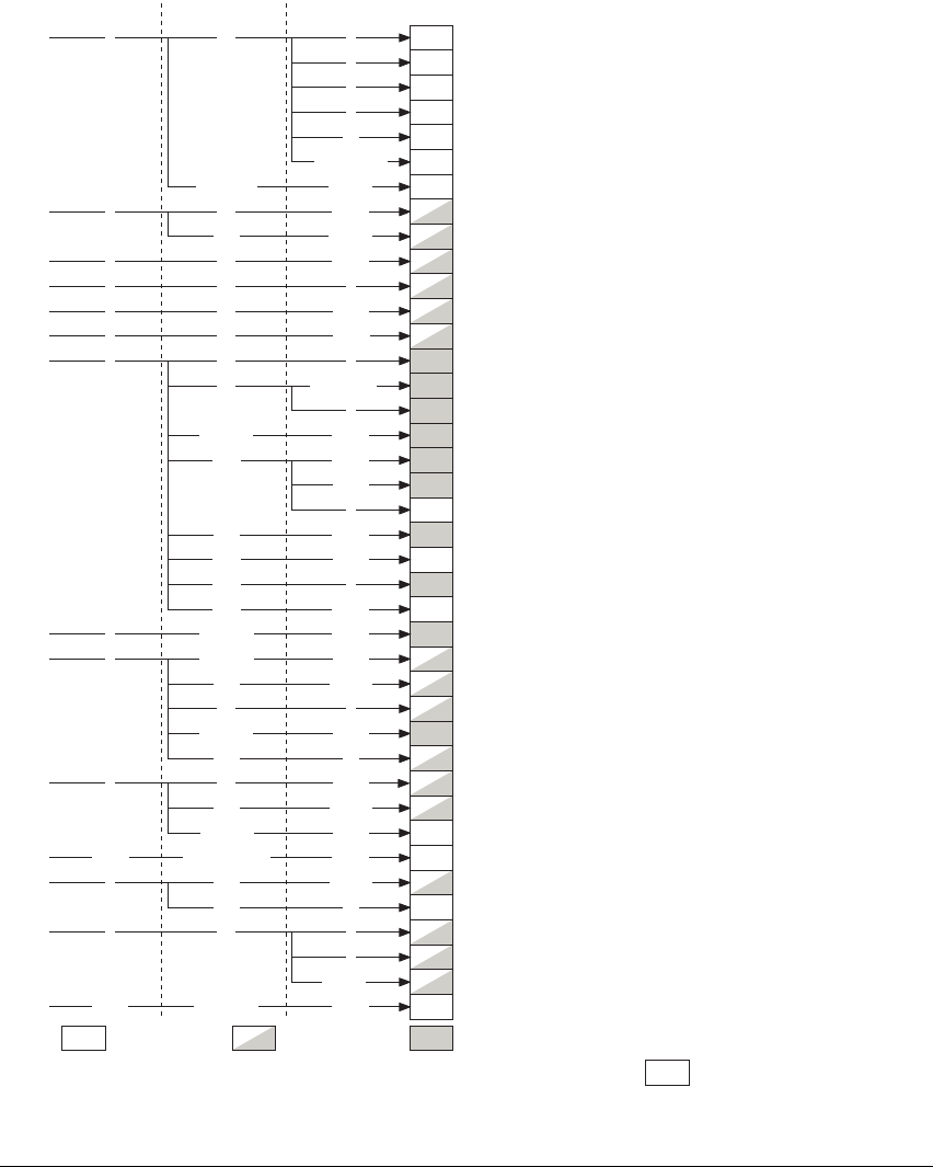
ARMv6 Differences
AppxG-30 Copyright © 1996-1998, 2000, 2004-2008 ARM Limited. All rights reserved. ARM DDI 0406B
Figure G-1 CP15 registers in an ARMv6 VMSA implementation
Access depends on operation
c14 Cache maintenance operations
c12 Block transfer support operations, optional
Cache prefetch operation, optionalc13
{0-3}
{4,5}
1
TLB Lockdown operations and registers, optional
c11 {0-7} {c0-c8,c15}
* TEX remap registers (PRRR, NMRR)
TLB Lockdown Registers
c10 0 c0
{c4,c8}
{0-7}
{0,1}
{0,1}
c8 0 {c5-c7} TLB maintenance operations
c9 0 {c0,c1} Cache Lockdown (format C) and TCM Region registers
TCMSR, TCM Selection Register
{0-2}
{0,1}
c2
{c5,c6} Cache lockdown (format D) operations
0
{0,1}
TCM Non-secure Access Control Registers
*{2,3}
*c1
CBOR, Cache Behavior Override Register*c8 *0
*c2 *{0,1}
Reserved for DMA support for TCM operations
Security Extensions registers
ISR, Interrupt Status Register
c12 0 *c0 *{0,1}
*c1 *0
c13 0 c0 FCSEIDR, FCSE PID Register
CONTEXTIDR, Context ID Register
0
1
*Software Thread ID registers*{2-4}
IMPLEMENTATION
DEFINED
registersc15 {0-7} {c0-c15} {0-7}
Bold text = Accessible in User mode
Read/WriteRead-only Write-only
If Security Extensions implemented
Not available in all versions of ARMv6
*
CRn opc1 CRm opc2
Cache maintenance operationsc11 {0-2}
CDSR, Cache Dirty Status Register6
System Control registersc1 0 c0
Security Extensions registers
{0-2}
*{0-2}
*c1
c2 0 c0 Translation Table Base Registers
DACR, Domain Access Control Register
c3 0 c0
Fault Address Registers
c6 0 c0
c5 0 c0 Fault Status Registers
c7 0
Cache and branch predictor maintenance operations
c5
c0 CP15WFI, Wait for interrupt operation
c10
{c6,c7}
Data barrier operations
Cache maintenance operations
Cache maintenance operations
CP15ISB, Instruction barrier operation
{0-2}
0
{0-2}
{0,1}
{0-2,6,7}
4
{0-3}
{4,5}
{0-2}
4
Aliases of Main ID Register{4,*5,6-7}
CTR, Cache Type Register
c0
TLBTR, TLB Type Register
0 c0
TCMTR, TCM Type Register
MIDR, Main ID Register
1
3
2
0
*5 * MPIDR, Multiprocessor Affinity Register
*CPUID Registers, optional*{c1-c7} *{0-7}
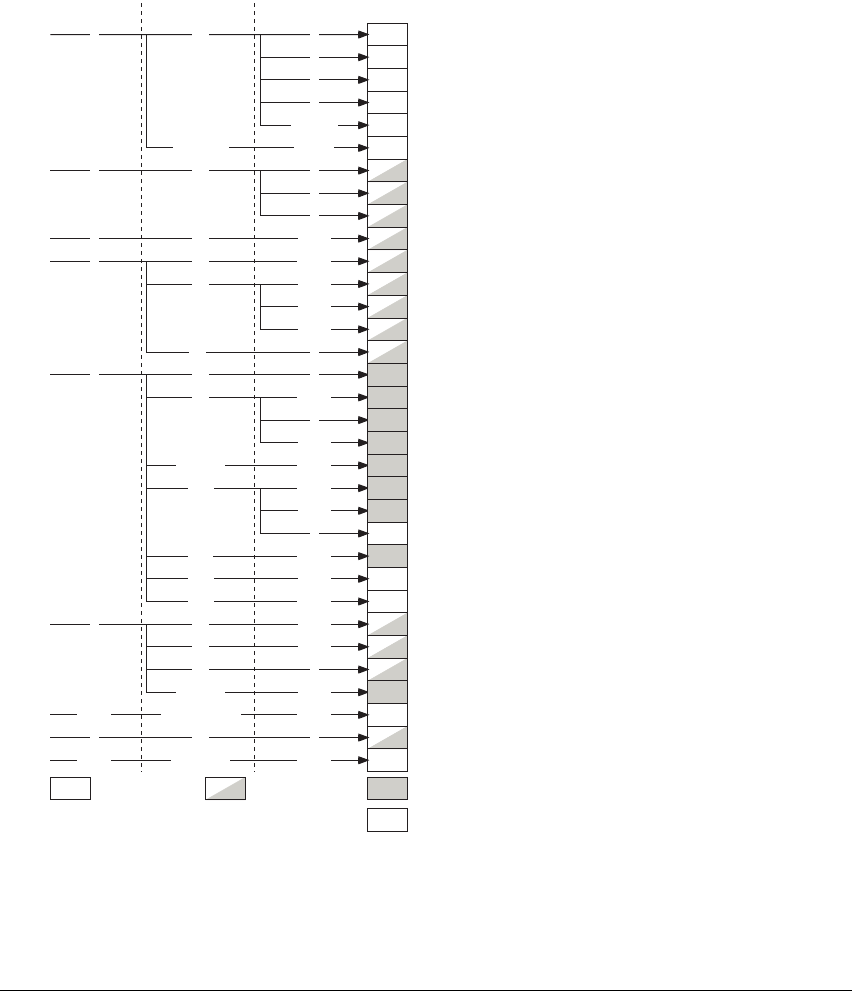
ARMv6 Differences
ARM DDI 0406B Copyright © 1996-1998, 2000, 2004-2008 ARM Limited. All rights reserved. AppxG-31
G.7.2 Organization of CP15 registers for an ARMv6 PMSA implementation
Figure G-2 shows the CP15 registers in an ARMv6 PMSA implementation:
Figure G-2 CP15 registers in an ARMv6 PMSA implementation
c7 0
Cache maintenance operations
c5
c0 CP15WFI, Wait for interrupt operation
{0-2}
4
Fault Address Registersc6 0 c0
c5 0 c0 Fault Status Registers
{0-2}
{0,1}
Memory Region Base Address registers
c1 {0,1}
Memory Region Size and Enable registers
{2,3}
{4,5} Memory Region Access Control registers
c2 0 RGNR, MPU Region Number Register
SCTLR, System Control Registerc1 0 c0
Aliases of Main ID Register
ACTLR, Auxiliary Control Register,
IMPLEMENTATION
DEFINED
CPACR, Coprocessor Access Control Register
0
{3,5-7}
1
2
*CPUID Registers, optional
*{c1-c7} *{0-7}
TCMSR, TCM Selection Registerc2
{c5,c6} Cache Lockdown (format D) operations
0
{0,1}
c11 {0-7} {c0-c8,c15} {0-7} Reserved for DMA support for TCM operations
c9 0 c0 Cache Lockdown (format C) operations{0,1}
c14 Cache maintenance operations
c12 Block transfer operations, optional
{0-3}
{4,5}
Cache maintenance operationsc11 {0-2}
c10
{c6,c7}
Data barrier operations
Cache maintenance operations
Cache maintenance operations
CP15ISB, Instruction barrier operation
{0-3}
{4,5}
{0-2}
4
CDSR, Cache Dirty Status Register6
Branch predictor maintenance operations{6,7}
TCM Region registers
c1 {0,1}
CRn opc1 CRm opc2
CTR, Cache Type Register
c0 0 c0
TCMTR, TCM Type Register
MIDR, Main ID Register
1
2
0
MPUIR, MPU Type Register4
Access depends on operation
Bold text = Accessible in User modeWrite-only
Not available in all versions of ARMv6
*
Read/WriteRead-only
IMPLEMENTATION
DEFINED
registersc15 {0-7} {c0-c15} {0-7}
CONTEXTIDR, Context ID Registerc13 0 c0 1

ARMv6 Differences
AppxG-32 Copyright © 1996-1998, 2000, 2004-2008 ARM Limited. All rights reserved. ARM DDI 0406B
G.7.3 c0, ID support
ARMv6 implementations include a Main ID Register, see c0, Main ID Register (MIDR) on page B3-81. In
this register, the architecture variant field either takes the assigned ARMv6 value or indicates support for an
identification scheme based on a set of CPUID registers. The CPUID identification scheme is required in
ARMv7 and recommended for ARMv6, and is described in Chapter B5 The CPUID Identification Scheme.
Three other ID registers provide information about cache, TCM, and TLB provisions. From ARMv6K, there
is also a Multiprocessor Affinity Register.
All of the CP15 c0 ID registers are read-only registers, They are accessed using
MRC
instructions, as shown
in Table G-5.
The Cache Type Register is as defined for ARMv4 and ARMv5, see c0, Cache Type Register (CTR) on
page AppxH-35. In ARMv6, the CType values of 0b0110, and 0b0111 are reserved and must not be used.
Note
The ARMv6 format of the Cache Type Register is significantly different from the ARMv7 implementation
described in c0, Cache Type Register (CTR) on page B3-83. However, the general properties described by
the register, and the access rights for the register, are unchanged.
The TCM Type Register is defined in c0, TCM Type Register (TCMTR) on page AppxG-33.
Table G-5 ID register support
Register CRn opc1 CRm opc2
MIDR, Main ID Register c0 0 c0 0
CTR, Cache Type ID Register c0 0 c0 1
TCMTR, TCM Type Register c0 0 c0 2
TLBTR, TLB Type Registera
a. VMSA processors only.
c0 0 c0 3
MPUIR, MPU Type Registercc0 0 c0 4
MPIDR, Multiprocessor Affinity Registerb
b. ARMv6K processors with VMSA only.
c0 0 c0 5
Aliases of MIDR c0 0 c0 3c, 4a, 5d, 6, 7
c. PMSA processors only.
d. All ARMv6 processors except ARMv6K VMSA implementations.
CPUID registers, if implemented c0 0 c1 0-7
c0 0 c2 0-5

ARMv6 Differences
ARM DDI 0406B Copyright © 1996-1998, 2000, 2004-2008 ARM Limited. All rights reserved. AppxG-33
The TLB Type ID Register and the Multiprocessor Affinity Register are as defined for ARMv7, see:
•c0, TLB Type ID Register (TLBTR)
•c0, Multiprocessor Affinity Register (MPIDR) on page B3-87.
The MPU Type Register is as defined for ARMv7, see c0, MPU Type Register (MPUIR) on page B4-36. In
an ARMv6 PMSA implementation, if the MPU is not implemented use of the default memory map is
optional.
c0, TCM Type Register (TCMTR)
The TCMTR must be implemented in ARMv6 and ARMv7. In ARMv7, the register can have a different
format from that given here, see c0, TCM Type Register (TCMTR) on page B3-85.
In ARMv7, TCM support is IMPLEMENTATION DEFINED. For ARMv6, see c9, TCM support on
page AppxG-46 and c9, TCM Non-Secure Access Control Registers, DTCM-NSACR and ITCM-NSACR on
page AppxG-51 where the Security Extensions are supported.
Bits [31:29] Set to 0b000 before ARMv7.
Bits [28:19,15:3]
Reserved.
DTCM, Bits [18:16] Indicate the number of Data TCMs implemented. This value lies in the range 0 to 4,
0b000 to 0b100. All other values are reserved.
ITCM, Bits [2:0] Indicate the number of Instruction or Unified TCMs implemented. This value lies
in the range 0 to 4, 0b000 to 0b100. All other values are reserved.
Instruction TCMs are accessible to both instruction and data sides.
c0, TLB Type ID Register (TLBTR)
In an ARMv6 VMSA implementation the TLB Type Register, TLBTR, is a read-only register that defines
whether the implementation provides separate instruction and data TLBs, or a unified TLB. It also defines
the number of lockable TLB entries. The ARMv7-A description of the register describes the general features
of the register and how to access it. See c0, TLB Type Register (TLBTR) on page B3-86. However, the
register format is different in ARMv6. The ARMv6 format of the TLBTR is:
Bits [31:24, 7:1] Reserved, UNK.
I_nlock, bits [23:16] Number of lockable entries in the instruction TLB. The value of this field gives the
number of lockable entries, between 0b00000000 for no lockable entries, and
0b11111111 for 255 lockable entries.
31 29 28 19 18 16 15 3 2 0
0 0 0 Reserved DTCM Reserved ITCM
31 24 23 16 15 8 7 1 0
Reserved I_nlock D_nlock Reserved nU
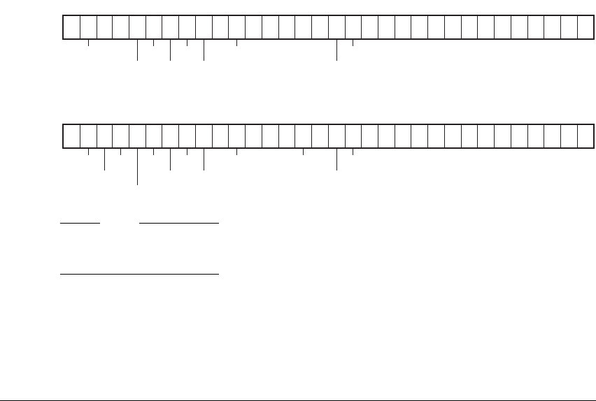
ARMv6 Differences
AppxG-34 Copyright © 1996-1998, 2000, 2004-2008 ARM Limited. All rights reserved. ARM DDI 0406B
When nU == 0 this field is reserved, UNK.
D_nlock, bits [15:8] Number of lockable entries in the data TLB. The value of this field gives the number
of lockable entries, between 0b00000000 for no lockable entries, and 0b11111111
for 255 lockable entries.
nU, bit [0] Not Unified TLB. Indicates whether the implementation has a unified TLB:
nU == 0 Unified TLB.
nU == 1 Separate instruction and data TLBs.
G.7.4 c1, System control support
ARMv6 implements the same system control registers as ARMv7:
• for a VMSA implementation, see CP15 c1, System control registers on page B3-96
• for a PMSA implementation, see CP15 c1, System control registers on page B4-44.
c1, System Control Register (SCTLR)
This register is the primary system configuration register in CP15. It is defined differently for VMSA and
PMSA.
In a VMSAv6 implementation, the format of the SCTLR is:
In an ARMv6K VMSA implementation, the format of the SCTLR is:
Note
Where the Security Extensions are implemented, some SCTLR bits are banked as described in c1, System
Control Register (SCTLR) on page B3-96.
31 30 029 28 27 26 25 24 23 22 21 20 19 18 17 16 15 14 13 12 11 10 7 6 3 2 1
CAM
(0)
Z RSB111WIV1100
RR
FI
U
VE
EENMFI
TE
(0) (0) (0)
L2
XP
(0)
L4
98 45
31 30 029 28 27 26 25 24 23 22 21 20 19 18 17 16 15 14 13 12 11 10 7 6 3 2 1
CAM(0)Z RSB111WIV1100
RR
HAFI
U
VE
EE
NMFI
AFE
TE
(0)
98 45
L2TRE
XP L4

ARMv6 Differences
ARM DDI 0406B Copyright © 1996-1998, 2000, 2004-2008 ARM Limited. All rights reserved. AppxG-35
In a PMSAv6 implementation, the format of the SCTLR is:
The differences from ARMv7 are:
• ARMv6 does not support the SCTLR.IE and SCTLR.BR, bits 31 and 17.
• ARMv7 does not support:
— The L2, L4, R, S, B, and W bits. These bits provide legacy support with ARMv4 and ARMv5.
See c1, System Control Register (SCTLR) on page AppxH-39 for their definition.
The B bit must also meet the requirements defined in Endian support on page AppxG-7.
— The U bit. This bit is always 1 in ARMv7. It selects the ARMv4 and ARMv5 or the ARMv6
and ARMv7 alignment model. For details see Alignment on page AppxG-6.
— The XP bit. This bit is always 1 in ARMv7. The bit selects the virtual memory support model
of ARMv6 and ARMv7 when SCTLR.XP = 1, and the legacy support for ARMv4 and ARMv5
when SCTLRR.XP = 0. For ARMv6 and ARMv7 support, see VMSAv6 translation table
format on page AppxG-26 and Chapter B3 Virtual Memory System Architecture (VMSA), and
for ARMv4 and ARMv5 support, see Legacy translation table format on page AppxG-25 and
Virtual memory support on page AppxH-21.
• The TE bit is defined for ARMv6T2 only. In ARMv6T2 it is the same as in ARMv7.
For the definition of bits supported in ARMv6 and ARMv7, see:
•c1, System Control Register (SCTLR) on page B3-96 for a VMSA implementation
•c1, System Control Register (SCTLR) on page B4-45 for a PMSA implementation.
G.7.5 c1, VMSA Security Extensions support
An ARMv6 implementation that includes the Security Extensions provides:
• the banking of bits in SCTLR, see c1, System Control Register (SCTLR) on page AppxG-34
• features that are include in an ARMv7 implementation of the Security Extensions, see:
—c1, Secure Configuration Register (SCR) on page B3-106
—c1, Secure Debug Enable Register (SDER) on page B3-108
—c1, Non-Secure Access Control Register (NSACR) on page B3-110
In addition, ARMv6 defines the following additional bits in the NSACR:
Bit [18], DMA DMA control register access for support in CP15 c11 in the Non-secure address space. For
more information, see c11, DMA support on page AppxG-54.
31 30 029 28 27 26 25 24 23 22 21 20 19 18 17 16 15 14 13 12 11 10 7 6 3 2 1
CAM
(0)
Z(0) (0) B111WIV1100
RR
FI
U
VE
EENMFI
TE
(0) (0) (0)
L2
(0)
L4
98 45
(0)

ARMv6 Differences
AppxG-36 Copyright © 1996-1998, 2000, 2004-2008 ARM Limited. All rights reserved. ARM DDI 0406B
Bit [17], TL TLB Lockdown Register access for support in CP15 c10 in the Non-secure address space.
For information on TLB lockdown support in ARMv6 see c10, VMSA TLB lockdown
support on page AppxG-53.
Bit [16], CL Cache Lockdown Register access for support in CP15 c9 in the Non-secure address space.
For information on cache lockdown support in ARMv6 see c9, Cache lockdown support on
page AppxG-45.
In all cases:
• a value of 0 in the bit position specifies that the associated registers cannot be accessed in the
Non-secure address space
• a value of 1 in the bit position specifies that the associated registers can be accessed in the Secure and
Non-secure address spaces.
Support of these additional bits and more details on how DMA support for TCMs, TLB lockdown, and cache
lockdown are inhibited in the Non-secure address space is IMPLEMENTATION DEFINED.
G.7.6 c2 and c3, VMSA memory protection and control registers
ARMv6 and ARMv7 provide the same CP15 support:
• two Translation Table Base Registers, TTBR0 and TTBR1
• a Translation Table Base Control Register, TTBCR
• a Domain Access Control Register, DACR.
The translation table registers are defined in CP15 c2, Translation table support registers on page B3-113.
The Domain Access Control Register (DACR) is as defined in c3, Domain Access Control Register (DACR)
on page B3-119.
Note
When the Security Extensions are implemented, these registers are Banked registers.
G.7.7 c5 and c6, VMSA memory system support
The support in ARMv6 is the same as ARMv7 with the following exceptions:
• Bit 12 of the data and instruction fault status registers is not defined in ARMv6. See c5, Data Fault
Status Register (DFSR) on page B3-121 and c5, Instruction Fault Status Register (IFSR) on
page B3-122.
• The Auxiliary Data Fault Status Register (ADFSR) and the Auxiliary Instruction Fault Status
Register (AIFSR) are not defined in ARMv6. See c5, Auxiliary Data and Instruction Fault Status
Registers (ADFSR and AIFSR) on page B3-123.
• The Access Flag faults shown in Table B3-11 on page B3-50 and Table B3-12 on page B3-51 are
only supported in ARMv6K.

ARMv6 Differences
ARM DDI 0406B Copyright © 1996-1998, 2000, 2004-2008 ARM Limited. All rights reserved. AppxG-37
Note
• Before ARMv7, the DFAR was called the Fault Address Register (FAR).
• If the Security Extensions are implemented, these registers are Banked registers.
• In ARMv6 variants other than ARMv6T2, the IFAR is optional.
G.7.8 c5 and c6, PMSA memory system support
The support in ARMv6 is the same as ARMv7 with the following exceptions:
• The SCTLR.BR bit, bit [17], is not supported in ARMv6, see c1, System Control Register (SCTLR)
on page B4-45.
• Bit 12 of the data and instruction fault status registers is not defined in ARMv6. See c5, Data Fault
Status Register (DFSR) on page B4-55 and c5, Instruction Fault Status Register (IFSR) on
page B4-56.
• The ADFSR and the AIFSR are not defined in ARMv6. See c5, Auxiliary Data and Instruction Fault
Status Registers (ADFSR and AIFSR) on page B4-56.
• Subregions are not supported. This means that DRSR[15:8] and IRSR[15:8] are not defined in
ARMv6. See c6, Data Region Size and Enable Register (DRSR) on page B4-62 and c6, Instruction
Region Size and Enable Register (IRSR) on page B4-63.
Note
• Before ARMv7, the DFAR was called the Fault Address Register (FAR).
• In ARMv6 variants other than ARMv6T2, the IFAR is optional.
G.7.9 c6, Watchpoint Fault Address Register (DBGWFAR)
From v6.1 of the Debug architecture, this register is also implemented as DBGWFAR in CP14, and the use
of CP15 DBGWFAR is deprecated.
In an ARMv6 implementation that includes the Security Extensions, CP15 DBGWFAR is a Secure register,
and can be accessed only from Secure privileged modes. For more information, see Restricted access CP15
registers on page B3-73.
For more information about this register see Effects of debug exceptions on CP15 registers and the
DBGWFAR on page C4-4 and Effect of entering Debug state on CP15 registers and the DBGWFAR on
page C5-4.
Table G-6 Debug fault address support
Register CRn opc1 CRm opc2
Watchpoint Fault Address Register, DBGWFAR c6 0 c0 1

ARMv6 Differences
AppxG-38 Copyright © 1996-1998, 2000, 2004-2008 ARM Limited. All rights reserved. ARM DDI 0406B
G.7.10 c7, Cache operations
Table G-7 shows the cache operations defined for ARMv6. They are performed as
MCR
instructions and only
operate on a level 1 cache associated with a specific processor. The equivalent operations in ARMv7 operate
on multiple levels of cache. See CP15 c7, Cache maintenance and other functions on page B3-126. For a
list of required operations in ARMv6, see Cache support on page AppxG-21. Support of additional
operations is IMPLEMENTATION DEFINED.
Table G-7 Cache operation support
Operation CRn opc1 CRm opc2
Invalidate instruction cacheac7 0 c5 0
Invalidate instruction cache line by MVAac7 0 c5 1
Invalidate instruction cache line by set/way c7 0 c5 2
Flush entire branch predictor arrayac7 0 c5 6
Flush branch predictor array entry by MVA ac7 0 c5 7
Invalidate data cache c7 0 c6 0
Invalidate data cache line by MVAac7 0 c6 1
Invalidate data cache line by set/wayac7 0 c6 2
Invalidate unified cache, or instruction cache and data cache c7 0 c7 0
Invalidate unified cache line by MVA c7 0 c7 1
Invalidate unified cache line by set/way c7 0 c7 2
Clean data cache c7 0 c10 0
Clean data cache line by MVAac7 0 c10 1
Clean data cache line by set/wayac7 0 c10 2
Test and Clean data cachebc7 0 c10 3
Cache Dirty Status Registercc7 0 c10 6
Clean entire unified cache c7 0 c11 0
Clean unified cache line by MVAac7 0 c11 1
Clean unified cache line by set/way c7 0 c11 2
Prefetch instruction cache line by MVAdc7 0 c13 1

ARMv6 Differences
ARM DDI 0406B Copyright © 1996-1998, 2000, 2004-2008 ARM Limited. All rights reserved. AppxG-39
c7, Cache Dirty Status Register (CDSR)
The Cache Dirty Status Register, CDSR, indicates whether the data or unified cache has been written to
since the last successful cache clean. For more information, see Cleaning and invalidating operations for
the entire data cache on page AppxG-40.
The Cache Dirty Status Register is:
• a 32-bit read-only register
• accessible only in privileged modes
• when the Security Extensions are implemented, a Banked register.
The format of the Cache Dirty Status Register is:
Bits [31:1] Reserved, UNK/SBZP.
C, bit [0] Cache Dirty Status. The meaning of this bit is:
0 Cache clean. No write has hit the cache since the last cache clean or reset
successfully cleaned the cache.
1 The cache might contain dirty data.
Clean and Invalidate data cache c7 0 c14 0
Clean and Invalidate data cache line by MVAac7 0 c14 1
Clean and Invalidate data cache line by set/wayac7 0 c14 2
Test and Clean and Invalidate data cachebc7 0 c14 3
Clean and Invalidate unified cache line by MVA c7 0 c15 1
Clean and Invalidate unified cache line by set/way c7 0 c15 2
a. These are the only cache operations available in ARMv7. The corresponding ARMv7 operations
are multi-level operations, and the data cache operations are defined as data or unified cache
operations.
b. For more information about these cache operations see Test and clean operations on
page AppxH-50.
c. Used with the Clean or Clean and Invalidate entire data cache and entire unified cache operations.
d. VMSA implementations only, used with TLB lockdown. See The TLB lock by entry model on
page AppxH-60.
31 10
Reserved C
Table G-7 Cache operation support (continued)
Operation CRn opc1 CRm opc2

ARMv6 Differences
AppxG-40 Copyright © 1996-1998, 2000, 2004-2008 ARM Limited. All rights reserved. ARM DDI 0406B
Accessing the Cache Dirty Status Register
To access the Cache Dirty Status Register you read the CP15 registers with
<opc1>
set to 0,
<CRn>
set to c7,
<CRm>
set to c10, and
<opc2>
set to 6. For example:
MRC p15, 0, <Rt>, c7, c10, 6
Cleaning and invalidating operations for the entire data cache
The CP15 c7 encodings include operations for cleaning the entire data cache, and for performing a clean
and invalidate of the entire data cache. If these operations are interrupted, the LR value that is captured on
the interrupt is (address of instruction that launched the cache operation + 4). This permits the standard
return mechanism for interrupts to restart the operation.
If a particular operation requires that the cache is clean, or clean and invalid, then it is essential that the
sequence of instructions for cleaning or cleaning and invalidating the cache can cope with the arrival of an
interrupt at any time when interrupts are not disabled. This is because interrupts might write to a previously
cleaned cache block. For this reason, the Cache Dirty Status Register indicates whether the cache has been
written to since the last successful cache clean.
You can interrogate the Cache Dirty Status Register to determine whether the cache is clean, and if you do
this while interrupts are disabled, a subsequent operation can rely on having a clean cache. The following
sequence illustrates this approach.
; The following code assumes interrupts are enabled at this point.
Loop1
MOV R1, #0
MCR p15, 0, R1, c7, c10, 0 ; Clean data cache. For Clean and Invalidate,
; use MCR p15, 0, R1, c7, c14, 0 instead
MRS R2, CPSR ; Save PSR context
CPSID iaf ; Disable interrupts
MRC p15, 0, R1, c7, c10, 6 ; Read Cache Dirty Status Register
TST R1, #1 ; Check if it is clean
BEQ UseClean
MSR CPSR_xc, R2 ; Re-enable interrupts
B Loop1 ; Clean the cache again
UseClean
Do_Clean_Operations ; Perform whatever operation relies on
; the cache being clean or clean & invalid.
; To reduce impact on interrupt latency,
; this sequence should be short.
MCR p15, 0, R1, c7, c6, 0 ; Optional. Can use this Invalidate all command
; to invalidate a Clean loop.
MSR CPSR_xc, R2 ; Re-enable interrupts
Note
The long cache clean operation is performed with interrupts enabled throughout this routine.

ARMv6 Differences
ARM DDI 0406B Copyright © 1996-1998, 2000, 2004-2008 ARM Limited. All rights reserved. AppxG-41
Block transfer operations
ARMv7 does not support CP15 register block transfer operations, and they are optional in ARMv6.
Table G-8 summarizes block transfer operations. Permitted combinations of the block transfer operations
are:
• all four operations
• clean, clean and invalidate, and invalidate operations
• none of the operations.
If an operation is not implemented, then it must cause an Undefined Instruction exception.
An
MCRR
instruction starts each of the range operations. The data of the two registers specifies the Block start
address and the Block end address. All block operations are performed on the cachelines that include the
range of addresses between the Block start address and Block end address inclusive. If the Block start
address is greater than the Block end address the effect is UNPREDICTABLE.
ARMv6 supports only one block transfer at a time. Attempting to start a second block transfer while a block
transfer is in progress causes the first block transfer to be abandoned and starts the second block transfer.
The Block Transfer Status Register indicates whether a block transfer is in progress. The register can be
polled before starting a block transfer, to ensure any previous block transfer operation has completed.
All block transfers are interruptible. When blocking transfers are interrupted, the LR value that is captured
is (address of instruction that launched the block operation + 4). This enables the standard return mechanism
for interrupts to restart the operation.
For performance reasons, ARM recommends that implementations permit the following instructions to be
executed while a non-blocking prefetch range instruction is being executed. In such an implementation, the
LR value captured on an interrupt is determined by the instruction set state presented to the interrupt in the
following instruction stream. However, implementations that treat a prefetch range instruction as a blocking
operation must capture the LR value as described in the previous paragraph.
If the FCSE PID is changed while a prefetch range operation is running, it is UNPREDICTABLE at which point
this change is seen by the prefetch range. For information about changing the FCSE PID see c13, FCSE
Process ID Register (FCSEIDR) on page B3-152.
Table G-8 Block transfer operations
Operation Blockinga or
non-blocking
a. See Blocking and non-blocking behavior on page AppxG-42
Instruction or
data
User or
privileged
Exception
Behavior
Prefetch range Non-blocking Instruction or data User or privileged None
Clean range Blocking Data only User or privileged Data Abort
Clean and Invalidate range Blocking Data only Privileged Data Abort
Invalidate range Blocking Instruction or data Privileged Data Abort

ARMv6 Differences
AppxG-42 Copyright © 1996-1998, 2000, 2004-2008 ARM Limited. All rights reserved. ARM DDI 0406B
Blocking and non-blocking behavior
The cache block transfer operations for cleaning, invalidating, or clean and invalidating a range of addresses
from the cache are blocking operations. Following instructions must not be executed until the block transfer
operation has completed. The prefetch range operation is non-blocking and can permit following
instructions to be executed before the operation is complete. If an exception occurs a non-blocking operation
does not signal an exception to the processor. This enables implementations to retire following instructions
while the non-blocking operation is executing, without the requirement to retain precise processor state.
The blocking operations generate a Data Abort exception on a Translation fault if a valid translation table
entry cannot be fetched. The DFAR indicates the address that caused the fault, and the DFSR indicates the
reason for the fault.
Any fault on a prefetch range operation results in the operation failing without signaling an error.
Register encodings
Table G-9 shows the block operations supported using CP15. The operations are performed using an
MCRR
instruction. See MCRR, MCRR2 on page A8-188.
The instruction format for block operations is:
MCRR p15, <Opc>, <Rt>, <Rn>, <CRm>
Note
The ARMv6
MCRR
encodings that support block operations are UNDEFINED in ARMv7.
Table G-9 Enhanced cache control operations using MCRR
CRm Opc Function Rn Data, VA a
a. The true virtual address, before any modification by the FCSE. See Appendix E Fast Context Switch
Extension (FCSE). This address is translated by the FCSE logic.
Rt Data, VA a
c5 0 Invalidate instruction cache range b
b. Accessible only in privileged modes. Results in an UNDEFINED instruction exception if the operation is
attempted in user mode.
Start address End address
c6 0 Invalidate data cache range bStart address End address
c12 0 Clean data cache range c
c. Accessible in both unprivileged and privileged modes.
Start address End address
c12 1 Prefetch instruction range cStart address End address
c12 2 Prefetch data range cStart address End address
c14 0 Clean and invalidate data cache range bStart address End address

ARMv6 Differences
ARM DDI 0406B Copyright © 1996-1998, 2000, 2004-2008 ARM Limited. All rights reserved. AppxG-43
The range operations operate on cache lines. The first cache line operated on is the line that contains the
start address. The operation is then applied to every cache line up to and including the line that contains the
end address.
The format of the start address and end address data values passed by the
MCRR
instructions is:
Start address Virtual Address bits [31:L]
The first virtual address of the block transfer.
End address Virtual Address bits [31:L]
The virtual address at which the block transfer stops. This address is at
the start of the line containing the last address to be handled by the block
transfer.
L is Log2(LINELEN), where LINELEN is the cache line length parameter. Because the least significant
address bits are ignored, the transfer automatically adjusts to a line length multiple spanning the
programmed addresses.
Note
The block operations use virtual addresses, not modified virtual addresses. All other address-based cache
operations use MVAs.
CP15 c7 operations for block transfer management
Two CP15 c7 operations support block transfer management. These operations must be implemented when
the block transfer operations are implemented:
StopPrefetchRange
MCR p15, 0, <Rt>, c7, c12, 5; Write-only, <Rt> Should-Be-Zero
PrefetchStatus
MRC p15, 0, <Rt>, c7, c12, 4; Read Block Transfer Status Register
Both operations are accessible in unprivileged and privileged modes. Because all block operations are
mutually exclusive, that is, only one operation can be active at any time, the PrefetchStatus operation returns
the status of the last issued Prefetch request, instruction, or data. This status is held in the Block Transfer
Status Register.
c7, Block Transfer Status Register
The Block Transfer Status Register indicates whether a block transfer is in progress.
The format of the Block Transfer Status Register is:
Bits [31:1] Reserved.
31 LL-1 0
Virtual address Ignored
31 10
UNK R

ARMv6 Differences
AppxG-44 Copyright © 1996-1998, 2000, 2004-2008 ARM Limited. All rights reserved. ARM DDI 0406B
R, bit [0] Block Prefetch Running
0 No prefetch in operation
1 Prefetch in operation.
G.7.11 c7, Miscellaneous functions
The Wait For Interrupt operation is used in some implementations as part of a power management support
scheme. The operation is deprecated in ARMv6 and not supported in ARMv7, where it behaves as a
NOP
instruction.
Barrier operations are used for system correctness to ensure visibility of memory accesses to other agents
in a system. Barrier functionality was formally defined as part of the memory architecture enhancements
introduced in ARMv6. The definitions are the same as for ARMv7. For details see Memory barriers on
page A3-47.
Table G-10 summarizes the
MCR
instruction encoding details.
G.7.12 c7, VMSA virtual to physical address translation support
If the Security Extensions are implemented in ARMv6K, virtual to physical address translation support is
provided as described in CP15 c7, Virtual Address to Physical Address translation operations on
page B3-130.
G.7.13 c8, VMSA TLB support
CP15 TLB operation provision in ARMv6 is the same as for ARMv7-A. For details see TLB maintenance
on page B3-56 and CP15 c8, TLB maintenance operations on page B3-138.
Table G-10 memory barrier register support
Operation CRn opc1 CRm opc2
Wait For Interrupt (CP15WFI) c7 0 c0 4
Instruction Synchronization Barrier (CP15ISB)a
a. This operation was previously known as Prefetch Flush (PF or PFF).
c7 0 c5 4
Data Synchronization Barrier (CP15DSB)b
b. This operation was previously known as Data Write Barrier or Drain Write Buffer (DWB).
c7 0 c10 4
Data Memory Barrier (CP15DMB) c7 0 c10 5

ARMv6 Differences
ARM DDI 0406B Copyright © 1996-1998, 2000, 2004-2008 ARM Limited. All rights reserved. AppxG-45
G.7.14 c9, Cache lockdown support
One problem with caches is that although they normally improve average access time to data and
instructions, they usually increase the worst-case access time. This occurs for a number of reasons,
including:
• There is a delay before the system determines that a cache miss has occurred and starts the main
memory access.
• If a Write-Back cache is being used, there might be an extra delay because of the requirement to store
the contents of the cache line that is being reallocated.
• A whole cache line is loaded from main memory, not only the data requested by the ARM processor.
In real-time applications, this increase in the worst-case access time can be significant.
Cache lockdown is an optional feature designed to alleviate this. It enables critical code and data, for
example high priority interrupt routines and the data they access, to be loaded into the cache in such a way
that the cache lines containing them are not subsequently reallocated. This ensures that all subsequent
accesses to the code and data concerned are cache hits and therefore complete as quickly as possible.
From ARMv7, cache lockdown is IMPLEMENTATION DEFINED with no recommended formats or
mechanisms on how it is achieved other than reserved CP15 register space. See Cache lockdown on
page B2-8 and CP15 c9, Cache and TCM lockdown registers and performance monitors on page B3-141.
ARMv4 and ARMv5 specify four formats for the cache lockdown mechanism, known as Format A, Format
B, Format C, and Format D. The Cache Type Register contains information on the lockdown mechanism
adopted. See c0, Cache Type Register (CTR) on page AppxH-35. Formats A, B, and C all operate on cache
ways. Format D is a cache entry locking mechanism.
ARMv6 cache lockdown support must comply with Format C or Format D. For more information, see c9,
cache lockdown support on page AppxH-52.
Note
A Format D implementation must use the CP15 lockdown operations with the CRm == {c5,c6} encodings,
and not the alternative encodings with CRm == {c1,c2}.
Interaction with CP15 c7 operations
Cache lockdown only prevents the normal replacement strategy used on cache misses from choosing to
reallocate cache lines in the locked-down region. CP15 c7 operations that invalidate, clean, or clean and
invalidate cache contents affect locked-down cache lines as normal. If invalidate operations are used, you
must ensure that they do not use virtual addresses or cache set/way combinations that affect the locked-down
cache lines. Otherwise, if it is difficult to avoid affecting the locked-down cache lines, repeat the cache
lockdown procedure afterwards.

ARMv6 Differences
AppxG-46 Copyright © 1996-1998, 2000, 2004-2008 ARM Limited. All rights reserved. ARM DDI 0406B
G.7.15 c9, TCM support
In ARMv7, CP15 c9 encodings with CRm == {c0-c2,c5-c8} are reserved for IMPLEMENTATION DEFINED
branch predictor, cache, and TCM operations. In ARMv6, the TCM Type Register can determine the TCM
support the processor provides. See c0, TCM Type Register (TCMTR) on page AppxG-33. Table G-11
summarizes the additional register support for TCMs in ARMv6.
Each implemented TCM has its own Region register that is banked onto either the Data TCM Region
Register or the Instruction or unified TCM Region Register. The TCM Selection Register supplies the index
for region register access.
Changing the TCM Region Register while a prefetch range or DMA operation is running has
UNPREDICTABLE effects.
c9, TCM Selection Register (TCMSR)
The TCM Selection Register selects the current TCM Region Registers. Where separate data and instruction
TCMs are implemented, the value in the TCM Selection Register defined the current region for accesses to
both the Data TCM Region Register and the Instruction TCM Region Register, see Table G-11.
The TCM Selection Register is:
• a 32-bit read/write register
• accessible only in privileged modes
• when the Security Extensions are implemented, a Banked register.
The format of the TCM Selection Register is:
Bits [31:2] Reserved, UNK/SBZP.
TCM, bits [1:0]
TCM number, the index used to access a region register. TCM region registers can be
accessed to read or change the details of the selected TCM.
This value resets to 0.
If this field is written with a value greater than or equal to the maximum number of
implemented TCMs then the write is ignored.
Table G-11 TCM register support
Instruction TCM Register
MRC|MCR p15, 0, <Rt>, c9, c1, 0
Data TCM Region Register, DTCMRR
MRC|MCR p15, 0, <Rt>, c9, c1, 1
Instruction or unified TCM Region Register, ITCMRR
MRC|MCR p15, 0, <Rt>, c9, c2, 0
TCM Selection Register, TCMSR
31 210
Reserved TCM

ARMv6 Differences
ARM DDI 0406B Copyright © 1996-1998, 2000, 2004-2008 ARM Limited. All rights reserved. AppxG-47
c9, TCM Region Registers (DTCMRR and ITCMRR)
The TCM Region Registers provide control and configuration information for each TCM region.
Each TCM Region Register is:
• A 32-bit read/write register with some bits that are read-only.
• Accessible only in privileged modes.
• When the Security Extensions are implemented, a Configurable access register with Non-secure
access controlled by the DTCM-NSACR. See c9, TCM Non-Secure Access Control Registers,
DTCM-NSACR and ITCM-NSACR on page AppxG-51.
• Accessed by reading or writing the CP15 registers with
<opc1>
set to 0,
<CRn>
set to c9,
<CRm>
set to
c1, and
<opc2>
set to:
— 0 for the current Data TCM Region Register
— 1 for the current Instruction or unified Region Register.
For example:
MRC p15,0,<Rt>,c9,c1,0 ; Read current Data TCM Region Register
MCR p15,0,<Rt>,c9,c1,0 ; Write current Data TCM Region Register
MRC p15,0,<Rt>,c9,c1,1 ; Read current Instruction or unified TCM Region Register
MCR p15,0,<Rt>,c9,c1,1 ; Write current Instruction or unified TCM Region Register
The format of the TCM region registers is:
BaseAddress, bits [31:12]
The base address of the TCM, given as the physical address of the TCM in the memory map.
BaseAddress is assumed to be aligned to the size of the TCM. Any address bits in the range
[(log2(RAMSize)-1):12] are ignored.
BaseAddress is 0 at reset.
Bits [11:7] Reserved
Size, bits [6:2]
Indicates the size of the TCM. See Table G-12 on page AppxG-48 for encoding of this field.
This field is read-only and ignores writes.
En, bit [0] TCM enable bit:
En == 0 Disabled. This is the reset value.
En == 1 Enabled.
31 1211 76 210
BaseAddress Reserved Size (0) En

ARMv6 Differences
AppxG-48 Copyright © 1996-1998, 2000, 2004-2008 ARM Limited. All rights reserved. ARM DDI 0406B
Note
Bit [1] was defined as a SmartCache enable bit in the previous version of the ARM architecture. SmartCache
is now considered to be IMPLEMENTATION DEFINED and not documented in this manual.
Table G-12 shows the encoding of the Size field in the TCM Region Registers:
Table G-12 TCM size field encoding
Size field Memory size
0b00000 0KByte
0b00001, 0b00010 Reserved
0b00011 4KByte
0b00100 8KByte
0b00101 16KByte
0b00110 32KByte
0b00111 64KByte
0b01000 128KByte
0b01001 256KByte
0b01010 512KByte
0b01011 1MByte
0b01100 2MByte
0b01101 4MByte
0b01110 8MByte
0b01111 16MByte
0b10000 32MByte
0b10001 64MByte
0b10010 128MByte
0b10011 256MByte
0b10100 512MByte
0b10101 1GByte

ARMv6 Differences
ARM DDI 0406B Copyright © 1996-1998, 2000, 2004-2008 ARM Limited. All rights reserved. AppxG-49
An attempt to access a TCM region that is not implemented is UNPREDICTABLE. This can occur if the number
of data and instruction TCMs supported is not the same.
The base address of each TCM must be different, and chosen so that no location in memory is contained in
more than one TCM. If a location in memory is contained in more than one TCM, it is UNPREDICTABLE
which memory location the instruction or data is returned from. Implementations must ensure that this
situation cannot result in physical damage to the TCM.
G.7.16 c9, VMSA support for the Security Extensions
ARMv6K with VMSA support and the Security Extensions provides the following CP15 c9 support in
addition to that defined for the Security Extensions in ARMv7-A:
• a Cache Behavior Override Register, CBOR
• where instruction TCM support is implemented, an ITCM Non-secure Access Control Register,
ITCM_NSAC
• where data TCM support is implemented, a DTCM Non-secure Access Control Register,
DTCM_NSAC.
c9, Cache Behavior Override Register (CBOR)
The Cache Behavior Override Register, CBOR, overrides some aspects of the normal cache behavior.
Typically, these overrides are used for system debugging.
Note
Architecturally, the CBOR is defined only as part of the Security Extensions in ARMv6. It is
IMPLEMENTATION DEFINED whether an ARMv7-A implementation includes the CBOR. An implementation
that does not include the Security Extensions might implement the CBOR, but can implement only bits [2:0]
of the register.
The CBOR is:
• a 32-bit read/write register
• accessible only in privileged modes
0b10110 2GByte
0b10111 4GByte
0b11xxx Reserved
Table G-12 TCM size field encoding (continued)
Size field Memory size

ARMv6 Differences
AppxG-50 Copyright © 1996-1998, 2000, 2004-2008 ARM Limited. All rights reserved. ARM DDI 0406B
• when the Security Extensions are implemented, a Common register, with some bits that can be
accessed only in Secure state.
The format of the CBOR is:
The CBOR resets to
0x00000000
.
Register bits [5:3] are accessible only in Secure state. In Non-secure state they are RAZ/WI.
Bits [31:6] Reserved. UNK/SBZP.
S_WT, bit [5] Secure Write-Through. Controls whether Write-Through is forced for regions marked as
Secure and Write-Back. The possible values of this bit are:
0 Do not force Write-Through. This corresponds to normal cache operation.
1 Force Write-Through for regions marked as Secure and Write-Back.
S_IL, bit [4] Secure instruction cache linefill. Can be used to disable instruction cache linefill for Secure
regions. The possible values of this bit are:
0 Instruction cache linefill enabled. This corresponds to normal cache operation.
1 Instruction cache linefill disabled for regions marked as Secure.
S_DL, bit [3] Secure data cache linefill. Can be used to disable data cache linefill for Secure regions. The
possible values of this bit are:
0 Data cache linefill enabled. This corresponds to normal cache operation.
1 Data cache linefill disabled for regions marked as Secure.
NS_WT, bit [2]
Non-secure Write-Through. Controls whether Write-Through is forced for regions marked
as Non-secure and Write-Back. The possible values of this bit are:
0 Do not force Write-Through. This corresponds to normal cache operation.
1 Force Write-Through for regions marked as Non-secure and Write-Back.
NS_IL, bit [1] Non-secure instruction cache linefill. Can be used to disable instruction cache linefill for
Non-secure regions. The possible values of this bit are:
0 Instruction cache linefill enabled. This corresponds to normal cache operation.
1 Instruction cache linefill disabled for regions marked as Non-secure.
0321
UNP/SBZ
S_WT
54
S_IL
S_DL
NS_WT
NS_IL
NS_DL
31 6

ARMv6 Differences
ARM DDI 0406B Copyright © 1996-1998, 2000, 2004-2008 ARM Limited. All rights reserved. AppxG-51
NS_DL, bit [0]
Non-secure data cache linefill. Can be used to disable data cache linefill for Non-secure
regions. The possible values of this bit are:
0 Data cache linefill enabled. This corresponds to normal cache operation.
1 Data cache linefill disabled for regions marked as Non-secure.
It might be necessary to ensure that cache contents are not changed, for example when debugging or when
processing an interruptible cache operation. The CBOR provides this option.
For example, Clean All, and Clean and Invalidate All operations in Non-secure state might not prevent fast
interrupts to the Secure side if the FW bit in the SCR is set to 0. In this case, operations in the Secure state
can read or write Non-secure locations in the cache. Such operations might cause the cache to contain valid
or dirty Non-secure entries after the Non-secure Clean All and Clean and Invalidate All operation has
completed. To prevent this problem, the Secure state must be:
• prevented from allocating Non-secure entries into the cache by disabling Non-secure linefill
• made to treat all writes to Non-secure regions that hit in the cache as being write-though by forcing
Non-secure Write-Through.
The CBOR provides separate controls for Secure and Non-secure memory regions, and can be used to
prevent cache linefill, or to force Write-Through operation, while leaving the caches enabled. The controls
for Secure memory regions can be accessed only when the processor is in the Secure state.
Accessing the CBOR
To access the CBOR you read or write the CP15 registers with
<opc1>
set to 0,
<CRn>
set to c9,
<CRm>
set to
c8, and
<opc2>
set to 0. For example:
MRC p15, 0, <Rt>, c9, c8, 0 ; Read CP15 Cache Behavior Override Register
MCR p15, 0, <Rt>, c9, c8, 0 ; Write CP15 Cache Behavior Override Register
c9, TCM Non-Secure Access Control Registers, DTCM-NSACR and ITCM-NSACR
The Data TCM Non-Secure Access Control Register (DTCM-NSACR) defines the accessibility of the Data
TCM Region Register when the processor is in Non-secure state.
The Instruction TCM Non-Secure Access Control Register (ITCM-NSACR) defines the accessibility of the
current Instruction or Unified TCM Region Register when the processor is in Non-secure state.
For information on TCM support, see Tightly Coupled Memory (TCM) support on page AppxG-23.
The TCM-NSACR registers are:
• 32-bit read/write registers
• accessible only in privileged modes
• implemented only in a VMSAv6 implementation that includes the Security Extensions
• Secure registers, see Restricted access CP15 registers on page B3-73.

ARMv6 Differences
AppxG-52 Copyright © 1996-1998, 2000, 2004-2008 ARM Limited. All rights reserved. ARM DDI 0406B
The format of a TCM-NSACR register is:
Bits [31:1] Reserved, UNK/SBZP.
NS_access, bit [0]
Non-secure access. Defines the accessibility of the corresponding current TCM Region
Register from the Non-secure state. The possible values of this bit are:
0 The corresponding TCM Region Register is accessible only in Secure privileged
modes.
The information stored in the corresponding TCM is Secure, and the TCM is
visible only if the processor is in the Secure state and the translation table is
marked as Secure.
1 The corresponding TCM Region Register is accessible in privileged modes in
both Secure and Non-secure state.
The information stored in the corresponding TCM is Non-secure. The TCM is
visible in the Non-secure state. It is visible in the Secure state only if the
translation table is marked correctly as Non-secure.
The value of the TCM-NSACR.NS_access bit and the processor security state determine whether the TCM
is visible. The value of the NS bit for the translation table entry determines what data is visible in the TCM.
Table G-13 shows when the TCM is visible, and what data is visible.
Table G-13 Visibility of TCM and TCM data
Processor
security state
TCM-NSACR
NS_access bit
Translation table
NS value TCM visibility Data visible
Secure 0 0 Visible Secure
Secure 0 1 Not visible -
Secure 1 0 Not visible -
Secure 1 1 Visible Non-secure
Non-secure 0 x Not visible -
Non-secure 1 x Visible Non-secure
31 01
Reserved
NS_access

ARMv6 Differences
ARM DDI 0406B Copyright © 1996-1998, 2000, 2004-2008 ARM Limited. All rights reserved. AppxG-53
Table G-14 shows when the TCM Region Register can be accessed, permitting control of the TCM.
Accessing the TCM-NSACR registers
To access the TCM-NSACR registers you read or write the CP15 registers with
<opc1>
set to 0,
<CRn>
set to
c9,
<CRm>
set to c1, and
<opc2>
set to:
• 2 to access the DTCM-NSACR register
• 3 to access the ITCM-NSACR register.
For example
MRC p15,0,<Rt>,c9,c1,2 ; Read CP15 Data TCM Non-secure Access Control Register
MCR p15,0,<Rt>,c9,c1,2 ; Write CP15 Data TCM Non-secure Access Control Register
MRC p15,0,<Rt>,c9,c1,3 ; Read CP15 Instruction TCM Non-secure Access Control Register
MCR p15,0,<Rt>,c9,c1,3 ; Write CP15 Instruction TCM Non-secure Access Control Register
G.7.17 c10, VMSA memory remapping support
ARMv7-A memory remapping is supported from ARMv6K with the addition of the SCTLR.TRE enable
bit and two registers:
•the c10, Primary Region Remap Register (PRRR) on page B3-143
•the c10, Normal Memory Remap Register (NMRR) on page B3-146.
G.7.18 c10, VMSA TLB lockdown support
TLB lockdown is an optional feature that enables the results of specified translation table walks to be loaded
into the TLB, in such a way that they are not overwritten by the results of subsequent translation table walks.
Translation table walks can take a long time, especially as they involve potentially slow main memory
accesses. In real-time interrupt handlers, translation table walks caused by the TLB not containing
translations for the handler or the data it accesses can increase interrupt latency significantly.
Two basic lockdown models are supported:
• a TLB lock by entry model
• a translate and lock model introduced as an alternative model in ARMv5TE.
From ARMv7-A, TLB lockdown is IMPLEMENTATION DEFINED with no recommended formats or
mechanisms on how it is achieved other than reserved CP15 register space. See TLB lockdown on
page B3-56 and CP15 c10, Memory remapping and TLB control registers on page B3-142.
Table G-14 Accessibility of TCM Region Register
Processor security state TCM-NSACR NS_access bit TCM Region Register access
Secure x In privileged modes only
Non-secure 0 No access
Non-secure 1 In privileged modes only

ARMv6 Differences
AppxG-54 Copyright © 1996-1998, 2000, 2004-2008 ARM Limited. All rights reserved. ARM DDI 0406B
For ARMv6, TLB lockdown must comply with one of the lockdown models described in c10, VMSA TLB
lockdown support on page AppxH-59.
G.7.19 c11, DMA support
The ARMv6 DMA support for TCMs described in The ARM Architecture Reference Manual (DDI 0100) is
considered IMPLEMENTATION DEFINED and not included in this manual. ARMv6 is therefore the same as
ARMv7. See CP15 c11, Reserved for TCM DMA registers on page B3-147.
G.7.20 c12, VMSA support for the Security Extensions
CP15 c12 support for the Security Extensions in ARMv6 is the same as in ARMv7:
• the Vector Base Address Register, VBAR
• the Monitor Base Address Register, MVBAR
• the Interrupt Status Register, ISR.
For details see CP15 c12, Security Extensions registers on page B3-148.
G.7.21 c13, Context ID support
Both PMSAv6 and VMSAv6 require the CONTEXTIDR described in:
•c13, Context ID Register (CONTEXTIDR) on page B3-153, for a VMSA implementation
•c13, Context ID Register (CONTEXTIDR) on page B4-76, for a PMSA implementation.
In addition:
• A VMSAv6 implementation requires the FCSEIDR, described in c13, FCSE Process ID Register
(FCSEIDR) on page B3-152. In ARMv6 the FCSE must be implemented. For more information, see
Appendix E Fast Context Switch Extension (FCSE).
• An ARMv6K implementation requires the Software Thread ID registers described in CP15 c13
Software Thread ID registers on page B3-154.
Note
In ARMv6, after any change to the CONTEXTIDR or FCSEIDR, software must use the CP15 branch
predictor maintenance operations to flush the virtual addresses affected by the change. If the branch
predictor is not invalidated in this way, attempting to execute an old branch might cause UNPREDICTABLE
behavior. ARMv7 does not require branch predictors to be invalidated after a change to the CONTEXTIDR
or FCSEIDR.
G.7.22 c15, IMPLEMENTATION DEFINED
As in ARMv7, CP15 c15 is reserved for IMPLEMENTATION DEFINED use. Typically, it is used for
processor-specific runtime and test features.

ARM DDI 0406B Copyright © 1996-1998, 2000, 2004-2008 ARM Limited. All rights reserved. AppxH-1
Appendix H
ARMv4 and ARMv5 Differences
This appendix describes how the ARMv4 and ARMv5 architectures differ from the ARMv6 and ARMv7
architectures. It contains the following sections:
•Introduction to ARMv4 and ARMv5 on page AppxH-2
•Application level register support on page AppxH-4
•Application level memory support on page AppxH-6
•Instruction set support on page AppxH-11
•System level register support on page AppxH-18
•System level memory model on page AppxH-21
•System Control coprocessor (CP15) support on page AppxH-31.
Note
In this appendix, the description ARMvN refers to all architecture variants of ARM architecture vN. For
example, ARMv4 refers to all architecture variants of ARMv4, including ARMv4 and ARMv4T.

ARMv4 and ARMv5 Differences
AppxH-2 Copyright © 1996-1998, 2000, 2004-2008 ARM Limited. All rights reserved. ARM DDI 0406B
H.1 Introduction to ARMv4 and ARMv5
ARMv4 and ARMv5 defined the instruction set support and the programmers’ model that applies to the
general-purpose registers and the associated exception model. These architecture versions are fully
described in the ARM Architecture Reference Manual (DDI 0100).
Note
This appendix is a summary of the ARMv4 and ARMv5 architecture variants. It is expected that the majority
of requirements for architecture information on ARMv4 and ARMv5 are satisfied by this appendix and the
rest of this manual. However the ARM Architecture Reference Manual (DDI 0100) might be required for
more information specific to ARMv4 or ARMv5.
Memory support is IMPLEMENTATION DEFINED in ARMv4 and ARMv5. In practice, use of CP15 to support
the Virtual Memory System Architecture (VMSA) or Protected Memory System Architecture (PMSA) is
standard in ARMv4 and ARMv5 implementations, but this is not an architectural requirement. For this
reason, the datasheet or Technical Reference Manual for a particular ARM processor is the definitive source
for its memory and system control facilities. This appendix does not specify absolute requirements on the
functionality of CP15 or other memory system components. Instead, it contains guidelines designed to
maximize compatibility with current and future ARM software.
This appendix concentrates on the features supported in ARMv4 and ARMv5, highlighting:
• features common across all architecture variants
• features supported for legacy reasons in ARMv6, but not in ARMv7
• features unique to the ARMv4 and ARMv5 variants.
H.1.1 Debug
Debug is not architecturally-defined in ARMv4 or ARMv5. ARM implementations have traditionally
supported halting debug through a JTAG port. While the support of debug features is similar across ARM
implementations, the timing and control sequencing required for access varies. Debug support in ARMv4
and ARMv5 is microarchitecture dependent and so in architectural terms is IMPLEMENTATION DEFINED.
H.1.2 ARMv6 and ARMv7
The ARM architecture was extended considerably in ARMv6. This means that a large proportion of this
manual does not apply to earlier architecture variants and can be ignored with respect to ARMv4 and
ARMv5.
The key changes in ARMv6:
• add:
— the ARM SIMD instructions to improve execution of multimedia and other DSP applications
— instructions for improved context switching.

ARMv4 and ARMv5 Differences
ARM DDI 0406B Copyright © 1996-1998, 2000, 2004-2008 ARM Limited. All rights reserved. AppxH-3
• introduce:
— a formal memory model, including level 1 cache support and revisions to alignment and endian
support
— a requirement to provide either a VMSA or a PMSA for memory management
— a formal debug model
— a requirement to support the CP15 System Control coprocessor
— enhanced kernel support, in ARMv6K
— the optional Security Extensions
— 32-bit Thumb instructions, in ARMv6T2.
For information about the changes between ARMv6 and ARMv7 see Appendix G ARMv6 Differences.
ARMv4 and ARMv5 Differences
AppxH-4 Copyright © 1996-1998, 2000, 2004-2008 ARM Limited. All rights reserved. ARM DDI 0406B
H.2 Application level register support
The ARMv4 and ARMv5 core registers are the same as ARMv7. For more information, see ARM core
registers on page A2-11. The following sections give more information about ARMv4 and ARMv5
application level register support:
•APSR support
•Instruction set state.
H.2.1 APSR support
Program status is reported in the 32-bit Application Program Status Register (APSR). The format of the
APSR is:
For details of the bit definitions, see The Application Program Status Register (APSR) on page A2-14. In
the APSR descriptions:
• the GE[3:0] field is only defined from ARMv6, and is reserved in ARMv4 and ARMv5
• the Q bit is only defined from ARMv5TE, and is RAZ/WI in ARMv4, ARMv4T and ARMv5T.
Earlier versions of this manual do not use the term APSR. They refer to the APSR as the CPSR with the
restriction on reserved fields governed by whether the register access was privileged.
H.2.2 Instruction set state
The instruction set states available in ARMv4 and ARMv5 are a subset of the states supported in ARMv7.
All implementations support the ARM instruction set that executes in ARM state. All ARM instructions are
32-bit instructions. T variants of the architecture also support a 16-bit instruction set that executes in Thumb
state. The supported ARM and Thumb instructions are summarized in Instruction set support on
page AppxH-11.
Instruction set state support in ARMv4 and ARMv5 differs from the support available in ARMv7 as follows:
• ThumbEE state is not supported
• Jazelle state is supported only in ARMv5TEJ
• In privileged modes, you must take care not to attempt to change the instruction set state by writing
nonzero values to CPSR.J and CPSR.T with an
MSR
instruction. For more information, see Format of
the CPSR and SPSRs on page AppxG-17.
All ARMv4 and ARMv5 implementations support the ARM instruction set. ARMv4T, ARMv5T,
ARMv5TE, and ARMv5TEJ also support a subset of the Thumb instruction set that can be executed entirely
as 16-bit instructions. The only 32-bit instructions in this subset are restricted-range versions of the
BL
and
BLX
(immediate) instructions. See BL and BLX (immediate) instructions, before ARMv6T2 on page AppxG-4
for a description of how these instructions can be executed as 16-bit instructions.
31 30 29 28 27 26 24 23 0
NZCVQ RAZ/
SBZP Reserved

ARMv4 and ARMv5 Differences
ARM DDI 0406B Copyright © 1996-1998, 2000, 2004-2008 ARM Limited. All rights reserved. AppxH-5
Instruction set support on page AppxH-11 summarizes the ARM and Thumb instructions supported in
ARMv4 and ARMv5, and the instruction descriptions in Chapter A8 Instruction Details give details of the
architecture variants that support each instruction encoding.
Interworking
In ARMv4T, the only instruction that supports interworking branches between ARM and Thumb states is
BX
.
In ARMv5T, the
BLX
instruction was added to provide interworking procedure calls. The
LDR
,
LDM
and
POP
instructions were modified to perform interworking branches if they load a value into the PC. This is
described by the
LoadWritePC()
pseudocode function. See Pseudocode details of operations on ARM core
registers on page A2-12.

ARMv4 and ARMv5 Differences
AppxH-6 Copyright © 1996-1998, 2000, 2004-2008 ARM Limited. All rights reserved. ARM DDI 0406B
H.3 Application level memory support
Memory support covers address alignment, endian support, semaphore support, memory type, memory
order model, caches, and write buffers.
H.3.1 Alignment
ARMv4 and ARMv5 behave differently from ARMv7 for unaligned memory accesses. The behavior is the
same as ARMv6 legacy mode except for forcing alignment checks with SCTLR.A == 1.
For more information about the SCTLR see c1, System Control Register (SCTLR) on page AppxH-39.
For ARM instructions when SCTLR.A == 0:
• Non halfword-aligned
LDRH
,
LDRSH
, and
STRH
are UNPREDICTABLE.
• Non word-aligned
LDR
,
LDRT
, and the load access of a
SWP
rotate right the word-aligned data transferred
by a non word-aligned address one, two, or three bytes depending on the value of address[1:0].
• Non word-aligned
STR
,
STRT
, and the store access of a
SWP
ignore address[1:0].
• From ARMv5TE, it is IMPLEMENTATION DEFINED whether
LDRD
and
STRD
must be
doubleword-aligned or word-aligned.
LDRD
and
STRD
instructions that do not meet the alignment
requirement are UNPREDICTABLE.
• Non word-aligned
LDM
,
LDC
,
LDC2
, and
POP
ignore address[1:0].
• Non word-aligned
STM
,
STC
,
STC2
, and
PUSH
ignore address[1:0].
For Thumb instructions when SCTLR.A == 0:
• Non halfword-aligned
LDRH
,
LDRSH,
and
STRH
are UNPREDICTABLE.
• Non word-aligned
LDR
, and
STR
are UNPREDICTABLE.
• Non word-aligned
LDMIA
, and
POP
ignore address[1:0].
• Non word-aligned
STMIA,
and
PUSH
ignore address[1:0].
For ARM and Thumb instructions, alignment checking is defined for implementations supporting CP15,
specifically the SCTLR.A bit. When this bit is set, a Data Abort exception indicating an Alignment fault is
generated for unaligned accesses. When SCTLR.A = 1, whether the alignment check for an
LDRD
or
STRD
instruction is for doubleword-alignment or word-alignment depends on the implementation choice of which
alignments are supported for these instructions when SCTLR.A = 0.
Note
The option of word alignment for
LDRD
and
STRD
instructions is not permitted in the ARMv6 legacy
configuration where SCTLR.U == 0 and SCTLR.A == 1. For more information, see legacy alignment
support in Alignment on page AppxG-6.

ARMv4 and ARMv5 Differences
ARM DDI 0406B Copyright © 1996-1998, 2000, 2004-2008 ARM Limited. All rights reserved. AppxH-7
H.3.2 Endian support
ARMv4 and ARMv5 support big and little endian operation. Little endian support is consistent with
ARMv7. Big endian control, configuration, and the connectivity of data bytes between the ARM register
file and memory is different. However, the difference is only visible when communicating between big
endian and little endian agents using memory. The agents can be different processors or programs running
with different endianness settings on the same processor.
For ARMv4 and ARMv5, the distinction between big endian memory and little endian memory is managed
by changing the addresses of the bytes in a word. For ARMv7, the distinction between big endian memory
and little endian memory is managed by keeping the byte addresses the same, and reordering the bytes in
the halfword or word. The endian formats are:
LE Little endian format used by ARMv4, ARMv5, ARMv6, and ARMv7
BE Big endian format used by ARMv6 (endianness controlled by the
SETEND
instruction) and
ARMv7
BE-32 Big endian format used by ARMv4, ARMv5, and ARMv6 (legacy format, endianness
controlled by the SCTLR.B bit).
Table H-1 shows how the addresses of bytes are changed in the BE-32 endian format. In this table, A is a
doubleword-aligned address and S, T, U, V, W, X, Y, Z are the bytes at addresses A to A+7 in the ARMv7
memory map.
Aligned memory accesses are performed using these byte addresses as shown in Table A3-4 on page A3-8
for the LE endian format and in Table A3-3 on page A3-7 for the BE and BE-32 formats, in each case
extended consistently to doubleword accesses. Table H-2 on page AppxH-8 shows which bytes are accessed
by each type of aligned memory access and the significance order in which they are accessed.
Table H-1 Addresses of bytes in endian formats
Byte Address in format BE or LE Address in format BE-32
SA A+3
TA+1 A+2
UA+2 A+1
VA+3 A
WA+4 A+7
XA+5 A+6
YA+6 A+5
ZA+7 A+4

ARMv4 and ARMv5 Differences
AppxH-8 Copyright © 1996-1998, 2000, 2004-2008 ARM Limited. All rights reserved. ARM DDI 0406B
Note
If the ARMv4 and ARMv5 endian model was extended to unaligned word and halfword accesses, for
example loading a word from byte addresses
0x1001
,
0x1002
,
0x1003
, and
0x1004
, it would not return the same
bytes of data to a big endian and little endian agent. However, ARMv4 and ARMv5 do not support unaligned
memory access and therefore this cannot occur. In ARMv4 and ARMv5 where use of an unaligned address
is permitted, the actual memory access is naturally aligned. See Alignment on page AppxH-6.
In ARMv7, all big endian accesses return the same bytes of data from memory as the corresponding little
endian accesses. It is only the byte order in the returned value that is different.
For an ARMv4 or ARMv5 implementation, whether the endianness of the memory access is fixed, defined
by an input pin on reset, or controlled by the SCTLR.B bit is IMPLEMENTATION DEFINED.
Table H-2 Bytes accessed by aligned accesses in endian formats
Memory access: Bytes accessed in endian format:
Size Address LE BE BE-32
Doubleword A ZYXWVUTS STUVWXYZ VUTSZYXW
Word A VUTS STUV VUTS
Word A+4 ZYXW WXYZ ZYXW
Halfword A TS ST VU
Halfword A+2 VU UV TS
Halfword A+4 XW WX ZY
Halfword A+6 ZY YZ XW
Byte A S S V
Byte A+1 T T U
Byte A+2 U U T
Byte A+3 V V S
Byte A+4 W W Z
Byte A+5 X X Y
Byte A+6 Y Y X
Byte A+7 Z Z W

ARMv4 and ARMv5 Differences
ARM DDI 0406B Copyright © 1996-1998, 2000, 2004-2008 ARM Limited. All rights reserved. AppxH-9
Examples
The distinction between BE and BE-32 is not visible if all agents use the same endian format, because a
given memory address always accesses the same location in memory. However, if there are two agents with
different endianness the effect is as shown in Example H-1 and Example H-2.
Example H-1 Distinction between BE and BE-32 word stores observed by an LE agent
In this example:
• Agent1 is big endian,
R1=0x1000
,
R2=0x11223344
• Agent2 is little endian,
R1=0x1000
.
Agent1:
STR R2, [R1]
Agent2:
LDR R2, [R1] // If Agent1 uses BE-32 endian format: R2 = 0x11223344
// If Agent1 uses BE endian format: R2 = 0x44332211
Example H-2 Distinction between BE and BE-32 byte stores observed by an LE agent
In this example:
• Agent1 is big endian,
R1=0x1000
,
R2=0x44
,
R3=0x11
• Agent2 is little endian,
R1=0x1000
.
Agent1:
STRB R2, [R1]
STRB R3, [R1, #3]
Agent2:
LDRB R2, [R1] // If Agent1 uses BE-32 endian format: R2 = 0x11
// If Agent1 uses BE endian format: R2 = 0x44
H.3.3 Semaphore support
The only semaphore support in ARMv4 and ARMv5 is provided by the
SWP
and
SWPB
ARM instructions. Use
of these instructions is deprecated in ARMv6 and ARMv7 in favour of the exclusive access mechanism
provided by
LDREX
,
STREX
, and related instructions.

ARMv4 and ARMv5 Differences
AppxH-10 Copyright © 1996-1998, 2000, 2004-2008 ARM Limited. All rights reserved. ARM DDI 0406B
H.3.4 Memory model and memory ordering
There is no formal definition of the memory model in ARMv4 and ARMv5. ARM implementations
generally adopted a Strongly-ordered approach. However the memory order model is IMPLEMENTATION
DEFINED.
Memory type support
In ARMv4 and ARMv5 where CP15 is implemented, memory can be tagged using two control bits:
• the B bit (Bufferable), to indicate whether write buffering between the processor and memory is
permitted
• the C bit (Cacheable).
Table H-3 shows the ARMv4 and ARMv5 definitions of the C bit and B bit that are interpreted as the formal
memory types defined in ARMv6 and ARMv7.
Table H-3 Interpretation of Cacheable and Bufferable bits
C B Memory type
0 0 Strongly-ordered
01Device
1 0 Normal, Write-Through Cacheable
1 1 Normal, Write-Back Cacheable

ARMv4 and ARMv5 Differences
ARM DDI 0406B Copyright © 1996-1998, 2000, 2004-2008 ARM Limited. All rights reserved. AppxH-11
H.4 Instruction set support
Two instruction sets are supported in ARMv4 and ARMv5:
• the ARM instruction set is supported by all variants of ARMv4 and ARMv5
• the Thumb instruction set is supported by ARMv4T, ARMv5T, ARMv5TE, and ARMv5TEJ.
Floating-point support, identified as VFPv2, was added as an option in ARMv5TE. The VFP instructions
are a subset of the coprocessor support in the ARM instruction set, and use coprocessor numbers 10 and 11.
The following instructions are not supported in VFPv2, and are specific to ARMv7 VFP support (VFPv3):
•
VMOV
(immediate)
•
VCVT
(between floating-point and fixed-point).
Note
• VFP instruction mnemonics traditionally started with an F. However this has been changed to a V
prefix in the Unified Assembler Language introduced in ARMv6T2, and in many cases the rest of the
mnemonic has been changed to be more compatible with other instructions mnemonics. This aligns
the scalar floating-point support with the ARMv7 Advanced SIMD support, which shares some
load/store and move operations to a common register file.
• The VFPv2 instructions are summarized in F* (former VFP instruction mnemonics) on page A8-100.
This includes the two deprecated instructions in VFPv2 that do not have UAL mnemonics, the
FLDMX
and
FSTMX
instructions.
The instruction sets have grown significantly in ARMv6 and ARMv7 because of:
• the introduction of ARMv6 SIMD
• improved context switching in ARMv6
• the addition of many 32-bit Thumb instructions in ARMv6T2 and ARMv7
• the ThumbEE extension in ARMv7
• addition of the
SMC
instruction with the Security Extensions
• the Advanced SIMD extension in ARMv7.
The ARM and Thumb instruction encodings including the VFP instructions are defined in Alphabetical list
of instructions on page A8-14.
Note
This appendix describes the instructions included as a mnemonic in ARMv4 and ARMv5. For any
mnemonic, to determine which associated instruction encodings appear in a particular architecture variant,
see the subsections of Alphabetical list of instructions on page A8-14 that describe the mnemonic. Each
encoding diagram shows the architecture variants or extensions that include the encoding.
The following sections give more information about ARMv4 and ARMv5 instruction set support:
•ARM instruction set support on page AppxH-12
•Thumb instruction set support on page AppxH-15
•System level instruction set support on page AppxH-17.

ARMv4 and ARMv5 Differences
AppxH-12 Copyright © 1996-1998, 2000, 2004-2008 ARM Limited. All rights reserved. ARM DDI 0406B
H.4.1 ARM instruction set support
Table H-4 shows the ARM instructions supported in ARMv4 and ARMv5, excluding VFP instructions.
Table H-4 ARM instructions - ARMv4 and ARMv5
Instruction v4, v4T, v5T v5TE, v5TEJ
ADC
Yes Ye s
ADD
Yes Ye s
AND
Yes Ye s
B
Yes Ye s
BIC
Yes Ye s
BKPT
v5T only Yes
BL
Yes Ye s
BLX
v5T only Yes
BX
v4T and v5T only Yes
BXJ
No v5TEJ only
CDP
Yes Ye s
CDP2
v5T only Yes
CLZ
v5T only Yes
CMN
Yes Ye s
CMP
Yes Ye s
EOR
Yes Ye s
LDC
Yes Ye s
LDC2
v5T only Yes
LDM
Yes Yes
LDR
Yes Ye s
LDRB
Yes Ye s
LDRD
No Yes

ARMv4 and ARMv5 Differences
ARM DDI 0406B Copyright © 1996-1998, 2000, 2004-2008 ARM Limited. All rights reserved. AppxH-13
LDRBT
Yes Ye s
LDRH
Yes Ye s
LDRSB
Yes Ye s
LDRSH
Yes Ye s
LDRT
Yes Ye s
MCR
Yes Ye s
MCR2
v5T only Yes
MCRR
No Yes
MLA
aYes Ye s
MOV
Yes Ye s
MRC
Yes Ye s
MRC2
v5T only Yes
MRRC
No Yes
MRS
Yes Ye s
MSR
Yes Ye s
MUL
aYes Ye s
MVN
Yes Ye s
ORR
Yes Ye s
PLD
No Yes
QADD
No Yes
QDADD
No Yes
QDSUB
No Yes
QSUB
No Yes
RSB
Yes Ye s
Table H-4 ARM instructions - ARMv4 and ARMv5 (continued)
Instruction v4, v4T, v5T v5TE, v5TEJ

ARMv4 and ARMv5 Differences
AppxH-14 Copyright © 1996-1998, 2000, 2004-2008 ARM Limited. All rights reserved. ARM DDI 0406B
RSC
Yes Ye s
SBC
Yes Ye s
SMLAL
bYes Ye s
SMLABB
,
SMLABT
,
SMLATB
,
SMLATT
No Yes
SMLALBB
,
SMLALBT
,
SMLALTB
,
SMLALTT
No Yes
SMLAWB, SMLAWT
No Yes
SMULBB
,
SMULBT
,
SMULTB
,
SMULTT
No Yes
SMULL
bYes Ye s
SMULWB, SMULWT
No Yes
STC
Yes Ye s
STC2
v5T only Yes
STM
Yes Ye s
STR
Yes Ye s
STRB
Yes Ye s
STRBT
Yes Ye s
STRD
No Yes
STRH
Yes Ye s
STRT
Yes Ye s
SUB
Yes Ye s
SVC (previously SWI)
Yes Ye s
SWP
Yes Ye s
SWPB
Yes Ye s
TEQ
Yes Ye s
Table H-4 ARM instructions - ARMv4 and ARMv5 (continued)
Instruction v4, v4T, v5T v5TE, v5TEJ

ARMv4 and ARMv5 Differences
ARM DDI 0406B Copyright © 1996-1998, 2000, 2004-2008 ARM Limited. All rights reserved. AppxH-15
H.4.2 Thumb instruction set support
Table H-5 shows the 16-bit Thumb instructions supported in ARMv4 and ARMv5. ARMv4 before
ARMv4T does not support any Thumb instructions.
TST
Yes Ye s
UMLAL
bYes Ye s
UMULL
bYes Ye s
a. The value of APSR.C generated by flag-setting versions of these
instructions is UNKNOWN in ARMv4 and is unchanged from ARMv5.
b. The values of APSR.C and APSR.V generated by flag-setting versions
of these instructions are UNKNOWN in ARMv4 and are unchanged from
ARMv5.
Table H-4 ARM instructions - ARMv4 and ARMv5 (continued)
Instruction v4, v4T, v5T v5TE, v5TEJ
Table H-5 ARMv4 and ARMv5 support for Thumb instructions
Instruction v4T v5T, v5TE, v5TEJ
ADC
Yes Ye s
ADD
Yes Ye s
AND
Yes Ye s
ASR
Yes Ye s
B
Yes Ye s
BIC
Yes Ye s
BKPT
No Yes
BL
Yes Ye s
BLX
No Yes
BX
Yes Ye s
CMN
Yes Ye s
CMP
Yes Ye s
EOR
Yes Ye s

ARMv4 and ARMv5 Differences
AppxH-16 Copyright © 1996-1998, 2000, 2004-2008 ARM Limited. All rights reserved. ARM DDI 0406B
LDMIA
Yes Ye s
LDR
Yes Ye s
LDRB
Yes Ye s
LDRH
Yes Ye s
LDRSB
Yes Ye s
LDRSH
Yes Ye s
LSL
Yes Ye s
LSR
Yes Ye s
MOV
Yes Ye s
MUL
Yes Ye s
MVN
Yes Ye s
NEG
Yes Ye s
ORR
Yes Ye s
POP
Yes Ye s
PUSH
Yes Ye s
ROR
Yes Ye s
SBC
Yes Ye s
STMIA
Yes Ye s
STR
Yes Ye s
STRB
Yes Ye s
STRH
Yes Ye s
SUB
Yes Ye s
SVC
(previously
SWI
)Yes Yes
TST
Yes Ye s
Table H-5 ARMv4 and ARMv5 support for Thumb instructions (continued)
Instruction v4T v5T, v5TE, v5TEJ

ARMv4 and ARMv5 Differences
ARM DDI 0406B Copyright © 1996-1998, 2000, 2004-2008 ARM Limited. All rights reserved. AppxH-17
H.4.3 System level instruction set support
The register and immediate forms of the
MRS
and
MSR
instructions are used to manage the CPSR and SPSR
as applicable. Other system level instructions are:
•
LDM
(exception return) and
LDM
(user registers)
•
LDRBT
and
LDRT
•
STM
(user registers)
•
STRBT
and
STRT
•
SUBS PC, LR
and related instructions
•
VMRS
and
VMSR
where VFP is supported.
All system level support is from ARM state.

ARMv4 and ARMv5 Differences
AppxH-18 Copyright © 1996-1998, 2000, 2004-2008 ARM Limited. All rights reserved. ARM DDI 0406B
H.5 System level register support
The general registers and programming modes are the same as ARMv7, except that the Security Extensions
and Monitor mode are not supported. For more information, see Figure B1-1 on page B1-9. The following
sections give information about ARMv4 and ARMv5 system level register support:
•Program Status Registers (PSRs)
•The exception model on page AppxH-19
•Execution environment support on page AppxH-20.
H.5.1 Program Status Registers (PSRs)
The application level programmers’ model provides the Application Program Status Register (APSR). See
The Application Program Status Register (APSR) on page A2-14. This is an application level alias for the
CPSR. The system level view of the CPSR extends the register, adding state that:
• is used by exceptions
• controls the processor mode.
Each of the exception modes has its own saved copy of the CPSR, the Saved Program Status Register
(SPSR), as shown in Figure B1-1 on page B1-9. For example, the SPSR for Abort mode is called SPSR_abt.
Note
ARMv4 and ARMv5 do not support Monitor mode and the Security Extensions.
The Current Program Status Register (CPSR)
The CPSR holds the following processor status and control information:
•The APSR, see APSR support on page AppxH-4
• The current instruction set state. See ISETSTATE on page A2-15, except that:
— ThumbEE state is not supported
— Jazelle state is supported only in ARMv5TEJ.
• The current processor mode
• Interrupt disable bits.
The non-APSR bits of the CPSR have defined reset values. These are shown in the
TakeReset()
pseudocode
function described in Reset on page B1-48, except that:
• the CPSR.IT[7:0], CPSR.E and CPSR.A bits are not defined and so do not have reset values
• before ARMv5TEJ, the CPSR.J bit is not defined and so does not have a reset value
• the reset value of CPSR.T is 0.
The rules described in The Current Program Status Register (CPSR) on page B1-14 about when mode
changes take effect apply with the modification that the ISB can only be the ISB operation described in c7,
Miscellaneous functions on page AppxH-51.

ARMv4 and ARMv5 Differences
ARM DDI 0406B Copyright © 1996-1998, 2000, 2004-2008 ARM Limited. All rights reserved. AppxH-19
The Saved Program Status Registers (SPSRs)
The SPSRs are defined as they are in ARMv7, see The Saved Program Status Registers (SPSRs) on
page B1-15, except that:
• the GE[3:0], IT[7:0], E and A bits are not implemented
• before ARMv5TEJ, the J bit is not implemented.
Format of the CPSR and SPSRs
The format of the CPSR and SPSRs is:
The definitions and general rules for the defined PSR bits are the same as ARMv7, see Format of the CPSR
and SPSRs on page B1-16, except that:
• Before ARMv5TEJ, the J bit is RAZ/WI.
• The T bit of the CPSR, and in ARMv5TEJ the J bit of the CPSR, must not be changed when the CPSR
is written by an
MSR
instruction, or else the behavior is UNPREDICTABLE.
MSR
instructions exist only in
ARM state in these architecture variants, so this is equivalent to saying the
MSR
instructions in
privileged modes must treat these bits as SBZP.
MSR
instructions in User mode still ignore writes to
these bits.
• The IT[7:0], GE[3:0], E, and A bitfield definitions for ARMv7 do not apply to ARMv4 and ARMv5.
• Monitor mode is not supported. The associated M[4:0] encoding is a reserved value in ARMv4 and
ARMv5.
H.5.2 The exception model
The exception vector offsets and priorities are consistent across all variants of the ARM architecture that use
the exception model as stated in Exceptions on page B1-30. The Security Extensions and low interrupt
latency configuration do not apply to ARMv4 and ARMv5.
In ARMv4 and ARMv5, it is IMPLEMENTATION DEFINED whether high vectors are supported. If they are
supported, a hardware configuration input selects whether the normal vectors or the high vectors are used
from reset. If high vectors are not supported then SCTLR.V, bit [13], is reserved, RAZ.
31 30 29 28 27 26 25 24 23 8 7 6 5 4 0
NZCVQRAZ
/WI J Reserved I F T M[4:0]

ARMv4 and ARMv5 Differences
AppxH-20 Copyright © 1996-1998, 2000, 2004-2008 ARM Limited. All rights reserved. ARM DDI 0406B
The ARM abort model
ARMv6 and ARMv7 use a Base Restored Abort Model (BRAM). However, in ARMv5 and ARMv4 it is
IMPLEMENTATION DEFINED whether this model, or a Base Updated Abort Model (BUAM) is used. These
two abort models are defined as:
Base Restored Abort Model
The base register of any valid load/store instruction that causes a memory system abort is
always restored to the value it had immediately before that instruction.
Base Updated Abort Model
After an abort, the base register of any valid load/store instruction that causes a memory
system abort is modified by the base register writeback, if any, of that instruction.
The implemented abort model applies uniformly across all instructions.
Exception entry
Entry to exceptions in ARMv4 and ARMv5 is generally as described in the sections:
•Reset on page B1-48
•Undefined Instruction exception on page B1-49
•Supervisor Call (SVC) exception on page B1-52
•Secure Monitor Call (SMC) exception on page B1-53
•Prefetch Abort exception on page B1-54
•Data Abort exception on page B1-55
•IRQ exception on page B1-58
•FIQ exception on page B1-60.
These ARMv7 descriptions are modified as follows:
• pseudocode statements that set registers, bits and fields that do not exist in the ARMv4 or ARMv5
architecture variant are ignored
• CPSR.T is set to 0, not to SCTLR.TE.
H.5.3 Execution environment support
In ARMv5TEJ, the JOSCR.CV bit is not changed on exception entry in any implementation of Jazelle.

ARMv4 and ARMv5 Differences
ARM DDI 0406B Copyright © 1996-1998, 2000, 2004-2008 ARM Limited. All rights reserved. AppxH-21
H.6 System level memory model
The pseudocode listed in Aligned memory accesses on page B2-31 and Unaligned memory accesses on
page B2-32 covers the alignment behavior of all architecture variants from ARMv4. For ARMv4 and
ARMv5, SCTLR.U is zero, see Alignment on page AppxG-6.
The following sections describe the system level memory model:
•Cache support
•Tightly Coupled Memory (TCM) support
•Virtual memory support
•Protected memory support on page AppxH-28.
H.6.1 Cache support
CP15 operations are defined that provide cache operations for managing level 1 instruction, data, or unified
caches. Caches can be direct mapped or N-way associative. ARMv4 and ARMv5 define a Cache Type ID
Register, to enable software to determine the level 1 cache topology.
ARMv4 and ARMv5 support virtual (virtually indexed, virtually tagged) or physical caches. In a virtual
memory system that supports virtual cache or caches, there is no coherence support for virtual aliases that
map to the same physical address. When a virtual to physical address mapping changes, caches must be
cleaned and invalidated accordingly.
Cache management and flushing of any write buffer in the processor is IMPLEMENTATION DEFINED and
managed by CP15. CP15 also supports configuration and control of cache lockdown. For more information
on cache management support see System Control coprocessor (CP15) support on page AppxH-31, and c7,
Cache operations on page AppxH-49 and c9, cache lockdown support on page AppxH-52.
H.6.2 Tightly Coupled Memory (TCM) support
TCM support in ARMv4 and ARMv5 is IMPLEMENTATION DEFINED.
H.6.3 Virtual memory support
The ARMv4 and ARMv5 translation tables support a similar two level translation table format to the
ARMv7 tables. However, there are significant differences in the translation table format because of the
following:
• ARMv6 introduced additional bits for encoding memory types, attributes, and extended cache
attributes.
• The new translation table format in ARMv6 does not support subpage access permissions.
• ARMv4 does not support 16MB Supersections.
• Only ARMv4 and ARMv5 support tiny (1KB) pages. The fine second level page format is not
supported from ARMv6.
For general information about address translation in a VMSA, see About the VMSA on page B3-2

ARMv4 and ARMv5 Differences
AppxH-22 Copyright © 1996-1998, 2000, 2004-2008 ARM Limited. All rights reserved. ARM DDI 0406B
The Fast Context Switch Extension (FCSE) is an implementation option in ARMv4 and ARMv5 VMSA
implementations. For more information, see FCSE translation on page B3-4 and Appendix E Fast Context
Switch Extension (FCSE).
Note
ARMv7 only supports the new translation table format. ARMv6 supports both old and new formats and uses
SCTLR[23] to select which format to use. For more information, see c1, System Control Register (SCTLR)
on page AppxG-34.
The Virtual Memory System Architecture (VMSA) in ARMv4 and ARMv5 supports the following:
• 16MB Supersections, optional support from ARMv5TE
• 1MB Sections
• 64KB Large pages
• 4KB Small pages
• 1KB Tiny pages.
Section virtual to physical address translation is supported by a single level translation table walk. Page
address translation requires a two level translation table walk. Each level involves an aligned word read from
a translation table in memory with the first level translation table base address held in a CP15 register,
TTBR0. Translation table entries are typically cached in a Translation Lookaside Buffer (TLB) in the
Memory Management Unit (MMU) of a given implementation. CP15 operations are used to manage the
TLB. For more information, see c8, VMSA TLB support on page AppxH-51.
Note
ARMv4 and ARMv5 support a single translation table base address register. TTBR1 and TTBCR were
introduced in ARMv6.
Second level translation table accesses are derived from the additional information provided by the first level
translation table entry. Two sizes of second level translation table are supported:
• a Coarse page table, where each entry translates a 4KB address space
• a Fine page table, where each entry translates a 1KB address space.
Translation tables are always naturally aligned in memory to the address space they occupy. This means that
the least significant n bits of the translation table base address are zero, where n = log2(SIZE), and SIZE is
the size of the table in bytes.
Translation attributes
ARMv4 and ARMv5 support the following translation table attributes:
• domain access as described in Domains on page B3-31
• cacheability with the C and B bits, see Interpretation of Cacheable and Bufferable bits on
page AppxH-10

ARMv4 and ARMv5 Differences
ARM DDI 0406B Copyright © 1996-1998, 2000, 2004-2008 ARM Limited. All rights reserved. AppxH-23
• access permissions using the AP[1:0], SCTLR.S and SCTLR.R bits as defined in Table H-6 on
page AppxH-23
• from ARMv5TE, the option of marking sections as Shareable and support for extended cache
attributes using the TEX bitfield with the C and B bits. See Table H-7 and Table H-8 on
page AppxH-25.
Note
Changes to the S and R bits do not affect the access permissions of entries already in the TLB. The TLB
must be flushed for the updated S and R bit values to take effect.
Table H-6 VMSA access permissions in ARMv4 and ARMv5
SCTLRa
AP[1:0] Privileged
permissions
User
permissions Description
SR
0 0 00 No access No access All accesses generate Permission faults
x x 01 Read/write No access Privileged access only
x x 10 Read/write Read-only Writes in User mode generate Permission faults
x x 11 Read/write Read/write Full access
0 1 00 Read-only Read-only Read-only in privileged and User modes
1 0 00 Read-only No access Privileged read-only
1100 - - Reserved
a. For more information, see c1, System Control Register (SCTLR) on page AppxH-39.
ARMv4 and ARMv5 Differences
AppxH-24 Copyright © 1996-1998, 2000, 2004-2008 ARM Limited. All rights reserved. ARM DDI 0406B
First level descriptor formats
Table H-7 shows the translation table first level descriptor formats:
• Supersection support, the TEX field, and the S bit are only permitted from ARMv5TE. Where these
features are not supported, the corresponding bits must be zero.
• Supersections can support address translation from a 32-bit virtual address to a physical address of
up to 40 bits.
Bits [1:0] of the descriptor identify the descriptor type:
0b00 Invalid or fault entry.
0b01 Coarse page table descriptor. Bits [31:10] of the descriptor give the physical address of a
second level translation table.
0b10 Section or Supersection descriptor for the associated Modified Virtual Address (MVA).
Bits [31:20] of the descriptor give the Section address, bits [31:24] provide the Supersection
address. Bit [18] indicates which to use when both are supported.
0b11 Fine page table descriptor. Bits [31:12] of the descriptor give the physical address of a
second level translation table.
Table H-7 ARMv4 and ARMv5 first level descriptor format
31 24 23 20 19 15 14 12 11 10 9 8 5 4 3 2 1 0
Fault Ignore 0 0
Coarse page
table Coarse page table base address P Domain SBZ 0 1
Section Section base address
S
B
Z
0
S
B
Z
Sa
S
B
Z
TEXbAP P Domain
S
B
Z
CB1 0
Supersection Supersection
base address
PA[35:32]
optional
S
B
Z
1
S
B
Z
S
S
B
Z
TEX AP P PA[39:36]
optional
S
B
Z
CB1 0
Fine page
table Fine page table base address SBZ P Domain SBZ 1 1
a. S=1 indicates Shareable memory. For more information, see Summary of ARMv7 memory attributes on page A3-25.
b. From ARMv5TE, the TEX bits can be used with the C and B bits as described in C, B, and TEX[2:0] encodings without
TEX remap on page B3-33.
ARMv4 and ARMv5 Differences
ARM DDI 0406B Copyright © 1996-1998, 2000, 2004-2008 ARM Limited. All rights reserved. AppxH-25
Second level Coarse page table descriptor format
In a Coarse page table, each entry provides translation information for 4KB of memory. Large page table
entries must be repeated 16 times to ensure translation of all addresses in the page. Tiny pages are not
supported. Coarse page tables are 1KB in size and must be aligned on a 1KB boundary.
Table H-8 shows the translation table second level descriptor formats for a second level Coarse page table.
Table H-8 Second level Coarse page descriptor formats
31 161514 1211109876543210
Fault Ignore 0 0
Large page Large page base address
S
B
Z
TEX AP3 AP2 AP1 AP0 C B 0 1
Small page Small page base address AP3 AP2 AP1 AP0 C B 1 0
Extended
small page
Extended small page base address optional in ARMv5TE,
otherwise reserved SBZ TEX AP C B 1 1
ARMv4 and ARMv5 Differences
AppxH-26 Copyright © 1996-1998, 2000, 2004-2008 ARM Limited. All rights reserved. ARM DDI 0406B
Second level Fine page table descriptor format
In a Fine page table, each entry provides translation information for 1KB of memory. Large page table
entries must be repeated 64 times and Small page entries four times to ensure translation of all addresses.
Fine tables are 4KB in size and must be aligned on a 4KB boundary.
Table H-9 shows the translation table second level descriptor format for a second level Fine page table.
Bits [1:0] of the descriptor identify the descriptor type:
0b00 Invalid or fault entry. The associated MVA is unmapped, and attempting to access it
generates a Translation fault.
0b01 Large page descriptor. Bits [31:16] of the descriptor give the base address of the Large page.
0b10 Small page descriptor. Bits [31:12] of the descriptor give the base address of the Small page.
0b11 Tiny page descriptor. Bits [31:10] of the descriptor give the base address of the Tiny page.
Subpage support
In the Large page and Small page formats in Table H-9, the page is divided into four equal sized subpages.
The AP0, AP1, AP2, and AP3 fields are the AP bits for subpages 0, 1, 2, and 3 respectively. Subpage 0,
controlled by the AP0 field, is the subpage with the lowest base address.
Table H-9 Second level Fine page table descriptor format
31 1615 1211109876543210
Fault Ignore 0 0
Large page Large page base address SBZ AP3 AP2 AP1 AP0 C B 0 1
Small page Small page base address AP3 AP2 AP1 AP0 C B 1 0
Tiny page Tiny page base address SBZ AP C B 1 1
ARMv4 and ARMv5 Differences
ARM DDI 0406B Copyright © 1996-1998, 2000, 2004-2008 ARM Limited. All rights reserved. AppxH-27
Translation table walks
An MVA and TTBR0 are used to access translation table information as follows:
• For a Section translation. See Figure B3-4 on page B3-17 with N == 0.
• For a Large page translation using a Coarse page table access. See Figure B3-7 on page B3-20 with
N==0.
• For a Small page translation using a Coarse page table access. See Figure B3-6 on page B3-19 with
N==0.
• For a Tiny page translation using a Fine page table access. See Figure H-1.
Note
A Large page table or Small page table translation is performed on a Fine page table access by reducing the
second level page table base address to bits [31:12] and extending the second level table index to
MVA[19:10].
Figure H-1 Tiny page address translation, VMSAv5 and VMSAv4 only
20 19
First-level
table index
MVA
PA of first-level
descriptor
31
First-level
read
First-level
descriptor
10 9
Second-level
table index
210
PA of second-level
descriptor
Page index
Second-level
read
Second-level
descriptor
PA
0
1 1
21 0
10 931
Access
control fields
Tiny page base address
0
10 931
Tiny page base address Page index
1
0 0
0
13 2
First-level
table index
31 14 13
Translation base SBZ
0
Translation Table
Base Register
31 14
Translation base
1
0 0
0
211
Second-level
table index
31 12
Page table base address
1 1
11
Access
control fields
31 12
Page table base address

ARMv4 and ARMv5 Differences
AppxH-28 Copyright © 1996-1998, 2000, 2004-2008 ARM Limited. All rights reserved. ARM DDI 0406B
H.6.4 Protected memory support
The MPU based Protected Memory System Architecture (PMSA) is a much simpler memory protection
scheme than the MMU-based VMSA model described in Virtual memory support on page AppxH-21. The
simplification applies to both the hardware and the software. PMSA in ARMv4 and ARMv5 differs from
that supported in ARMv6 and ARMv7 in the following ways:
• the programming model is unique to ARMv4 and ARMv5
• the supported number of memory regions is fixed
• background memory support requires use of a region resource
• there is no architecturally-defined recovery mechanism from memory aborts
• there is no default memory map definition.
Control and configuration
CP15 registers are used to fully define protection regions, eliminating the VMSA requirements for hardware
to do translation table walks, and for software to set up and maintain the translation tables. This makes
memory checking fully deterministic. However, the level of control is now region based rather than page
based. This means the control is not as fine-grained.
The following features apply:
• The memory is divided into regions. CP15 registers are used to define the region size, base address,
and memory attributes. For example, cacheability, bufferability, and access permissions of a region.
• Memory region control (read and write access) is permitted only from privileged modes.
• If an address is defined in multiple regions, a fixed priority scheme (highest region number) is used
to define the properties of the address being accessed.
• An access to an address that is not defined in any region causes a memory abort.
• All addresses are physical addresses. Address translation is not supported.
• PMSA supports unified (von Neumann) and separate (Harvard) instruction and data address spaces.
Eight regions can be configured, with C, B, and AP[1:0] attribute bits associated with each region. The
supported region sizes are 2NKB, where 2 =< N =< 32. It is IMPLEMENTATION DEFINED if the regions are
configurable or fixed in an implementation:
• as eight unified regions supporting data accesses and instruction fetches
• as eight data regions and eight instruction regions each with independent memory region attributes.
CP15 provides the following support:
• a global MPU enable bit, SCTLR.M
• cacheability register support, a C bit for each region
• bufferability register support, a B bit for each region

ARMv4 and ARMv5 Differences
ARM DDI 0406B Copyright © 1996-1998, 2000, 2004-2008 ARM Limited. All rights reserved. AppxH-29
• access permission register support that provides AP7[1:0] to AP0[1:0] 2-bit permission fields, an AP
bitfield for each region
• optional extended access permission register support for 4-bit AP fields
• region registers providing a base address, size field, and an enable bit for each region.
For details of the PMSA support in CP15 see c2, c3, c5, and c6, PMSA support on page AppxH-43.
The C and B bits are configured according to the type of memory that is to be accessed. For more
information, see Memory type support on page AppxH-10. Table H-10 defines the standard AP bit behavior.
Some implementations also include support for read-only access permission. Table H-11 defines the
extended AP bit behavior.
Table H-10 PMSA access permissions in ARMv4 and ARMv5
AP[1:0] Privileged
permissions
User
permissions Description
00 No access No access All accesses generate Permission faults
01 Read/write No access Privileged access only
10 Read/write Read-only Writes in User mode generate Permission faults
11 Read/write Read/write Full access
Table H-11 PMSA extended access permissions in ARMv4 and ARMv5
AP[3:0] Privileged
permissions
User
permissions Description
0000 No access No access All accesses generate a Permission fault
0001 Read/write No access Privileged access only
0010 Read/write Read-only Writes in User mode generate a Permission fault
0011 Read/write Read/write Full access
0100 UNPREDICTABLE UNPREDICTABLE -
0101 Read-only No access Privileged read-only access
0110 Read-only Read-only Read-only access
0111 UNPREDICTABLE UNPREDICTABLE -
1xxx UNPREDICTABLE UNPREDICTABLE -

ARMv4 and ARMv5 Differences
AppxH-30 Copyright © 1996-1998, 2000, 2004-2008 ARM Limited. All rights reserved. ARM DDI 0406B
Memory access sequence
When the ARM processor generates a memory access, the MPU compares the memory address with the
programmed memory regions as follows:
• If a matching memory region is not found, a memory abort is signaled to the processor.
• If a matching memory region is found, the region information is used as follows:
— The access permission bits are used to determine whether the access is permitted. If the access
is not permitted, the MPU signals a memory abort. Otherwise, the access can proceed.
— The memory region attributes are used to determine the access attributes, for example cached
or non-cached, as described in Memory type support on page AppxH-10.
Note
When a Permission fault occurs, there is no fault status information provision for PMSA in ARMv4 or
ARMv5. The CP15 registers FSR and FAR are only available in implementations with VMSA support.
Overlapping regions
The Protection Unit can be programmed with two or more overlapping regions. When overlapping regions
are programmed, a fixed priority scheme is applied to determine the region whose attributes are applied to
the memory access.
Attributes for region 7 take highest priority and those for region 0 take lowest priority. For example:
• Data region 2 is programmed to be 4KB in size, starting from address
0x3000
with AP == 0b010
(privileged modes full access, User mode read-only).
• Data region 1 is programmed to be 16KB in size, starting from address
0x0
with AP == 0b001
(privileged mode access only).
When the processor performs a data load from address
0x3010
while in User mode, the address falls into both
region 1 and region 2. Because there is a clash, the attributes associated with region 2 are applied. In this
case, the load would not abort.
Background region
Overlapping regions increase the flexibility of how regions can be mapped onto physical memory devices
in the system. The overlapping properties can also be used to specify a background region. For example,
assume a number of physical memory areas sparsely distributed across the 4GB address space. If only these
regions are configured, any access outside the defined sparse address space aborts. You can override this
behavior by programming region 0 to be a 4GB background region. In this case, if the address does not fall
into any of the other regions, the access is controlled by the attributes specified for region 0.

ARMv4 and ARMv5 Differences
ARM DDI 0406B Copyright © 1996-1998, 2000, 2004-2008 ARM Limited. All rights reserved. AppxH-31
H.7 System Control coprocessor (CP15) support
Before ARMv6, it is IMPLEMENTATION DEFINED whether a System Control coprocessor, CP15, is
implemented. However, support of ID registers, control registers, cache support, and memory management
with virtual or protected memory support resulted in the widespread adoption of a standard for control and
configuration of these features. That standard is described here. With the exception of a small number of
operations and supporting registers, for example the memory barrier operations described in c7,
Miscellaneous functions on page AppxH-51, all CP15 accesses require privileged access.
The following sections summarize the CP15 registers known to have been supported in ARMv4 or ARMv5
implementations:
•Organization of CP15 registers in an ARMv4 or ARMv5 VMSA implementation on page AppxH-32
•Organization of CP15 registers in an ARMv4 or ARMv5 PMSA implementation on page AppxH-33.
For details of the registers provided by a particular implementation see the appropriate Technical Reference
Manual, or other product documentation.
The rest of this section describes the ARMv4 and ARMv5 CP15 support in order of the CRn value.
Note
Definitions of CP15 registers in this appendix apply to both VMSA and PMSA implementations unless
otherwise indicated.
ARMv4 and ARMv5 Differences
AppxH-32 Copyright © 1996-1998, 2000, 2004-2008 ARM Limited. All rights reserved. ARM DDI 0406B
H.7.1 Organization of CP15 registers in an ARMv4 or ARMv5 VMSA implementation
Figure H-2 shows the CP15 registers in an ARMv4 or ARMv5 VMSA implementation:
Figure H-2 CP15 registers in a VMSAv4 or VMSAv5 implementation
CRn opc1 CRm opc2
Cache maintenance operationsc5
CP15ISB, Instruction Synchronization Barrier operation
{0-2}
4
c7 0 c0 CP15WFI, Wait for interrupt operation4
DACR, Domain Access Control Registerc3 0 c0
FAR, Fault Address Register
c6 0 c0
c5 0 c0 FSR, Fault Status Register
0
0
0
c2 0 c0 TTBR, Translation Table Base Register
SCTLR, System Control Registerc1 0 c0
Aliases of Main ID Register
0
0
{4-7}
CTR, Cache Type Register
c0 0 c0
TCMTR, TCM Type Register
MIDR, Main ID Register
1
2
0
TLBTR, TLB Type Register3
c2 Cache maintenance operation5
c10
{c6,c7}
CP15DSB, Data Synchronization Barrier operation
Cache maintenance operations
Cache maintenance operations
{1-3}
4
{0-2}
Branch predictor maintenance operations{6,7}
c1 TCM Region registers{0,1}
Cache maintenance operationsc11 {0-2}
c14 Cache maintenance operations
c8 0 {c5-c7} TLB maintenance operations
c9 0 c0
Cache prefetch operationc13
Cache maintenance operationc15
Cache Lockdown (format C) operations
{1-3}
{0,1}
{0,1}
1
{1-2}
c13 0 c0 FCSEIDR, FCSE PID Register0
IMPLEMENTATION
DEFINED
registersc15 {0-7} {c0-c15} {0-7}
{c5,c6} Cache Lockdown (format D) operations{0,1}
TLB Lockdown Registers
c10 0 {c0,c4,c8} {0,1}
TCMSR, TCM Selection Registerc2 0
CP15DMB, Data Memory Barrier operation5
Read/WriteRead-only Write-only
Access depends on operation
ARMv4 and ARMv5 Differences
ARM DDI 0406B Copyright © 1996-1998, 2000, 2004-2008 ARM Limited. All rights reserved. AppxH-33
H.7.2 Organization of CP15 registers in an ARMv4 or ARMv5 PMSA implementation
Figure H-3 shows the CP15 registers in an ARMv4 or ARMv5 PMSA implementation:
Figure H-3 CP15 registers in a PMSAv4 or PMSAv5 implementation
DMRR0-DMRR7, Data or unified Memory Region Registers
IMRR0-IMRR7, Instruction Memory Region Registers
DAPR, Data or unified Region Access Permissions Register
IAPR, Instruction Region Access Permissions Register
DBR, Data or unified Region Bufferability Register
SCTLR, System Control Register
Aliases of Main ID Register
CTR, Cache Type Register
TCMTR, TCM Type Register
MIDR, Main ID Register
DCR, Data or unified Region Cacheability Register
ICR, Instruction Region Cacheability Register
DEAPR, Data Region Extended Access Permissions Register
IEAPR, Instruction Region Extended Access Permissions Register
c6
c5
c2
c3
c1
c0
CRn opc1 CRm opc2
1
0
1
0
0
0
1
2
0
0
1
2
3
{c0-c7}
c0
c0
c0
c0
c0
0
0
0
0
0
0
{3-7}
Cache maintenance operations
CP15ISB, Instruction Synchronization Barrier operation
c7 CP15WFI, Wait for interrupt operation
Cache maintenance operation
{0-2}
4
4
5
c5
c0
c2
0
CP15DSB, Data Synchronization Barrier operation
Cache maintenance operations
Cache maintenance operations
{1-3}
4
{0-2}
c10
{c6,c7}
Branch predictor maintenance operations{6,7}
TCM Region registers{0,1}c1
Cache maintenance operations{0-2}c11
c9 Cache Lockdown (format C) operations
Cache maintenance operations
Cache maintenance operation
{0,1}
{1-3}
{1-2}
c0
c14
c15
0
TCMSR, TCM Selection Register
c2 0
IMPLEMENTATION
DEFINED
registersc15
Cache lockdown (format D) operations
{0-7}
{0,1}
{c0-c15}
{c5,c6}
{0-7}
5 CP15DMB, Data Memory Barrier operation
Read-only Read/Write Write-only
Access depends on operation

ARMv4 and ARMv5 Differences
AppxH-34 Copyright © 1996-1998, 2000, 2004-2008 ARM Limited. All rights reserved. ARM DDI 0406B
H.7.3 c0, ID support
ARMv4 and ARMv5 implementations support the following ID registers:
•Main ID Register (MIDR). See c0, Main ID Register (MIDR).
•Cache Type Register (CTR). See c0, Cache Type Register (CTR) on page AppxH-35.
• Optionally, the TCM Type Register (TCMTR). See c0, TCM Type Register (TCMTR) on
page AppxH-38.
Table H-12 shows how these read-only registers are accessed using the
MRC
instruction.
c0, Main ID Register (MIDR)
This register is as described for ARMv7 if either:
• the implementer code in MIDR bits [31:24] is not
0x41
• the top four bits of the primary part number in MIDR bits [15:4] are neither
0x0
nor
0x7
.
If the implementer code is
0x41
and the top four bits of the primary part number are
0x0
, the processor is an
obsolete ARMv2 or ARMv3 processor.
If the implementer code is
0x41
and the top four bits of the primary part number are
0x7
, then:
• If bit[23] is 0, the processor is an obsolete ARMv3 processor.
• If bit[23] is 1, the processor is an ARMv4T processor and bits[22:16] are an IMPLEMENTATION
DEFINED variant number. Bits[31:24,15:0] are as described for ARMv7.
For the ARMv7 descriptions of the MIDR see:
•c0, Main ID Register (MIDR) on page B3-81 for a VMSA implementation
•c0, Main ID Register (MIDR) on page B4-32 for a PMSA implementation.
Table H-12 ID register support
Register CRn opc1 CRm opc2
Main ID Register, MIDR c0 0 c0 0
Cache Type ID Register, CTR, c0 0 c0 1
TCM Type Register, TCMTR c0 0 c0 2
Aliases of MIDR c0 0 c0 3, 4, 5, 6, 7

ARMv4 and ARMv5 Differences
ARM DDI 0406B Copyright © 1996-1998, 2000, 2004-2008 ARM Limited. All rights reserved. AppxH-35
c0, Cache Type Register (CTR)
The format of the Cache Type Register is significantly different from the ARMv7 definition described in c0,
Cache Type Register (CTR) on page B3-83. However, the general properties described by the register, and
the access rights for the register, are unchanged.
This section describes the implementation of the CP15 c0 Cache Type Register and is applicable to a VMSA
or PMSA implementation.
The Cache Type Register supplies the following details about the level 1 cache implementation:
• whether there is a unified cache or separate instruction and data caches
• the cache size, line length, and associativity
• whether it is a Write-Through cache or a Write-Back cache
• the cache cleaning and lockdown capabilities.
The format of the Cache Type Register is:
Ctype, bits [28:25]
Cache type field. Specifies details of the cache not indicated by the S bit and the Dsize and
Isize fields. Table H-13 shows the encoding of this field. All values not specified in the table
are reserved.
S, bit [24] Separate caches bit. The meaning of this bit is:
0 Unified cache
1 Separate instruction and data caches.
If S == 0, the Isize and Dsize fields both describe the unified cache, and must be identical.
Dsize, bits [23:12]
Specifies the size, line length and associativity of the data cache, or of the unified cache if
S == 0. For details of the encoding see Cache size fields on page AppxH-36.
Isize, bits [11:0]
Specifies the size, line length and associativity of the instruction cache, or of the unified
cache if S == 0. For details of the encoding see Cache size fields on page AppxH-36.
Table H-13 shows the Ctype values that can be used in the CTR:
31 29 28 25 24 23 12 11 0
0 0 0 Ctype S DSize ISize
Table H-13 Cache type values
Ctypea Cache method Cache lockdownb
0b0000 Write-Through Not supported
0b0010 Write-Back Not supported

ARMv4 and ARMv5 Differences
AppxH-36 Copyright © 1996-1998, 2000, 2004-2008 ARM Limited. All rights reserved. ARM DDI 0406B
For details of the CP15 c7 operations used for cleaning Write-Back caches see c7, Cache operations on
page AppxH-49.
Cache size fields
The Dsize and Isize fields in the CTR have the same format:
P For a VMSA implementation, indicates whether the allocation of bits [13:12] of the virtual
address is restricted, imposing the page coloring restriction. The meaning of this field is:
0 No restriction, or PMSA implementation
1 Page coloring restriction applies, see Virtual to physical translation mapping
restrictions on page AppxG-26.
Size Indicates the size of the cache, but is qualified by the M bit, see Table H-14 on
page AppxH-37.
Assoc Indicates the associativity of the cache, but is qualified by the M bit, see Cache associativity
on page AppxH-37.
M Qualifies the values in the Size and Assoc subfields.
Len Specifies the line length of the cache. The possible values of this field are:
0b00 Line length is 2 words (8 bytes)
0b01 Line length is 4 words (16 bytes)
0b10 Line length is 8 words (32 bytes)
0b11 Line length is 16 words (64 bytes).
0b0101 Write-Back Format D
0b0110cWrite-Back Format A
0b0111cWrite-Back Format B
0b1110 Write-Back Format C
a. CType values not shown are reserved and must not be used.
b. For details see c9, cache lockdown support on page AppxH-52.
c. In ARMv6 this Ctype value is reserved and must not be used.
23
11
22
10
21
9
18
6
17
5
15
3
14
2
13
1
12
0
P0 Size Assoc MLen
Table H-13 Cache type values (continued)
Ctypea Cache method Cache lockdownb

ARMv4 and ARMv5 Differences
ARM DDI 0406B Copyright © 1996-1998, 2000, 2004-2008 ARM Limited. All rights reserved. AppxH-37
Table H-14 shows how the size of the cache is determined by the Size field and M bit.
Cache associativity
Table H-15 show how the associativity of the cache is determined by the Assoc field and the M bit.
The Cache absent encoding overrides all other data in the cache size field.
Table H-14 Cache sizes
Size field Size if M == 0 Size if M == 1
0b0000 0.5KB 0.75KB
0b0001 1KB 1.5KB
0b0010 2KB 3KB
0b0011 4KB 6KB
0b0100 8KB 12KB
0b0101 16KB 24KB
0b0110 32KB 48KB
0b0111 64KB 96KB
0b1000 128KB 192KB
Table H-15 Cache associativity
Assoc field
Associativity if:
M == 0 M == 1
0b000 1 way (direct mapped) Cache absent
0b001 2 way 3 way
0b010 4 way 6 way
0b011 8 way 12 way
0b100 16 way 24 way
0b101 32 way 48 way
0b110 64 way 96 way
0b111 128 way 192 way

ARMv4 and ARMv5 Differences
AppxH-38 Copyright © 1996-1998, 2000, 2004-2008 ARM Limited. All rights reserved. ARM DDI 0406B
Excluding the cache absent case (Assoc == 0b000, M == 1) you can use the following formulae to
determine the values LINELEN, ASSOCIATIVITY, and NSETS (number of sets) from the Size, Assoc and
Len fields of the CTR. These formulae give the associativity values shown in Table H-15 on
page AppxH-37:
LINELEN = 1 << (Len+3) /* In bytes */
MULTIPLIER = 2 + M
NSETS = 1 << (Size + 6 - Assoc - Len)
ASSOCIATIVITY = MULTIPLIER << (Assoc - 1)
Multiplying these together gives the overall cache size as:
CACHE_SIZE = MULTIPLIER << (Size+8) /* In bytes */
Note
Cache length fields with (Size + 6 - Assoc - Len) < 0 are invalid, because they correspond to impossible
combinations of line length, associativity, and overall cache size. So the formula for NSETS never involves
a negative shift value.
c0, TCM Type Register (TCMTR)
In an ARMv4 or ARMv5 implementation that supports CP15 and TCM, the TCMTR is an optional register.
For details of the TCMTR implementation see c0, TCM Type Register (TCMTR) on page AppxG-33.
H.7.4 c1, System control register support
ARMv4 and ARMv5 implementations support the following system control registers:
• a System Control Register (SCTLR)
•an
IMPLEMENTATION DEFINED Auxiliary Control Register (ACTLR).
Table H-16 shows how the registers are accessed using the
MCR
and
MRC
instructions.
SCTLR is the primary system configuration register in CP15.
Table H-16 System control register support
Register CRn opc1 CRm opc2
System Control Register, SCTLR c1 0 c0 0
Auxiliary Control Register, ACTLR c1 0 c0 1

ARMv4 and ARMv5 Differences
ARM DDI 0406B Copyright © 1996-1998, 2000, 2004-2008 ARM Limited. All rights reserved. AppxH-39
c1, System Control Register (SCTLR)
This section describes the implementation of the System Control Register, SCTLR, for ARMv4 and
ARMv5. The format of the SCTLR is:
Bits [31:16] Reserved.
These reserved bits in the SCTLR are allocated in some circumstances:
• bits [19:16] have been associated with TCM support
• bit [26], described as the L2 bit, has been used to indicate level 2 cache support, see
Level 2 cache support on page AppxH-51.
These usage models are not compatible with ARMv7.
L4, Bit [15] This bit inhibits ARMv5T Thumb interworking behavior when set. It stops bit [0] updating
the CPSR.T bit. Use of the feature is deprecated in ARMv6 and the feature is not supported
in ARMv7.
RR, bit [14] Round Robin bit. This bit selects an alternative replacement strategy with a more easily
predictable worst-case performance if the cache implementation supports this functionality:
0 Normal replacement strategy, for example random replacement
1 Predictable strategy, for example round robin replacement.
The replacement strategy associated with each value of the RR bit is IMPLEMENTATION
DEFINED.
V, bit [13] Vectors bit. This bit selects the base address of the exception vectors:
0 Normal exception vectors, base address
0x00000000
1 High exception vectors (Hivecs), base address
0xFFFF0000
.
This base address is never remapped.
Support of the V bit is IMPLEMENTATION DEFINED. An implementation can include a
configuration input signal that determines the reset value of the V bit. If there is no
configuration input signal to determine the reset value of this bit, it resets to 0.
I, bit [12] Instruction cache enable bit. This is a global enable bit for instruction caches:
0 Instruction caches disabled
1 Instruction caches enabled.
If the system does not implement any instruction caches that can be accessed by the
processor at any level of the memory hierarchy, this bit is RAZ/WI.
If the system implements any instruction caches that can be accessed by the processor then
it must be possible to disable them by setting this bit to 0.
31 161514131211109876543210
Reserved L4 RR V I Z F R S B L D P W C A M

ARMv4 and ARMv5 Differences
AppxH-40 Copyright © 1996-1998, 2000, 2004-2008 ARM Limited. All rights reserved. ARM DDI 0406B
Z, bit [11] Branch prediction enable bit. This bit is used to enable branch prediction, also called
program flow prediction:
0 program flow prediction disabled
1 program flow prediction enabled.
If program flow prediction cannot be disabled, this bit is RAO/WI. Program flow prediction
includes all possible forms of speculative change of instruction stream prediction. Examples
include static prediction, dynamic prediction, and return stacks.
If the implementation does not support program flow prediction this bit is RAZ/WI.
F (bit [10]) The meaning of this bit is IMPLEMENTATION DEFINED.
R (bit [9]) ROM protection bit, supported for backwards compatibility. The effect of this bit is
described in Table H-6 on page AppxH-23. Use of this feature is deprecated in ARMv6 and
the feature is not supported in ARMv7.
S (bit [8]) System protection bit, supported for backwards compatibility. The effect of this bit is
described in Table H-6 on page AppxH-23. Use of this feature is deprecated in ARMv6 and
the feature is not supported in ARMv7.
B (bit [7]) This bit configures the ARM processor to the endianness of the memory system:
0 Little-endian memory system (LE)
1 Big-endian memory system (BE-32).
ARM processors that support both little-endian and big-endian memory systems use this bit
to configure the ARM processor to rename the four byte addresses in a 32-bit word.
Endian support changed in ARMv6. Use of this feature is deprecated in ARMv6 and the
feature is not supported in ARMv7.
An implementation can include a configuration input signal that determines the reset value
of the B bit. If there is no configuration input signal to determine the reset value of this bit
then it resets to 0.
Bits [6:4] RAO/SBOP.
W (bit [3]) This is the enable bit for the write buffer:
0 Write buffer disabled
1 Write buffer enabled.
If the write buffer is not implemented, this bit is RAZ/WI. If the write buffer cannot be
disabled, this bit is RAO and ignores writes. Use of this feature is deprecated in ARMv6 and
the feature is not supported in ARMv7
C, bit [2] Cache enable bit. This is a global enable bit for data and unified caches:
0 Data and unified caches disabled
1 Data and unified caches enabled.
If the system does not implement any data or unified caches that can be accessed by the
processor at any level of the memory hierarchy, this bit is RAZ/WI.

ARMv4 and ARMv5 Differences
ARM DDI 0406B Copyright © 1996-1998, 2000, 2004-2008 ARM Limited. All rights reserved. AppxH-41
If the system implements any data or unified caches that can be accessed by the processor
then it must be possible to disable them by setting this bit to 0.
A, bit [1] Alignment bit. This is the enable bit for Alignment fault checking:
0 Alignment fault checking disabled
1 Alignment fault checking enabled.
For more information, see Alignment on page AppxH-6.
M, bit [0] Memory control bit. This is a global enable bit to enable an MMU where VMSA is
supported, or an MPU where PMSA is supported:
0 memory management (MMU or MPU) disabled
1 memory management (MMU or MPU) enabled.
H.7.5 c2 and c3, VMSA memory protection and control registers
ARMv4 and ARMv5 support a single Translation Table Base Register (TTBR) that is compatible with
TTBR0, and the Domain Access Control Register (DACR).
The TTBR is as defined for TTBR0 in CP15 c2, Translation table support registers on page B3-113 except
that:
• The base address bitfield is a fixed-length field, bits [31:14] (N=0)
• Bit [5] is reserved.
The DACR is as defined in c3, Domain Access Control Register (DACR) on page B3-119.
H.7.6 c5 and c6, VMSA memory system support
ARMv4 and ARMv5 support a Fault Status Register (FSR) and a Fault Address Register (FAR). These
registers are accessed using
MCR
and
MRC
instructions. Table H-17 summarizes them.
The FSR is updated on Prefetch Abort exceptions and Data Abort exceptions. The FAR is only updated with
the MVA on Data Abort exceptions.
Table H-17 VMSA fault support
Register CRn opc1 CRm opc2
Fault Status Register, FSR c5 0 c0 0
Fault Address Register, FAR c6 0 c0 0

ARMv4 and ARMv5 Differences
AppxH-42 Copyright © 1996-1998, 2000, 2004-2008 ARM Limited. All rights reserved. ARM DDI 0406B
In ARMv5 and ARMv4 implementations the format of the FSR is:
Bits [31:11, 9:8]
Reserved, UNK/SBZP.
Bit [10] FS[4] where defined, otherwise UNK/SBZP.
Domain, bits [7:4]
The domain of the fault address.
FS, bits [3:0] Fault status bits. Indicate the cause of the fault.
Table H-18 lists the base level of fault status encodings returned in the FSR
31 10 9 8 7 4 3 0
Reserved a
a. It is IMPLEMENTATION DEFINED whether bit [10] is reserved or supports an additional fault status bit, FS[4].
Domain FS[3:0]
Table H-18 VMSAv5 and VMSAv4 FSR encodings
FSR[10] FSR[3:0] Source of fault Domain
0 00x1 Alignment fault Invalid
0 0101
0111 Translation fault Section
Page
Invalid
Va l i d
0 1001
1011 Domain fault Section
Page
Va l i d
Va l i d
0 1100
1110 Translation table walk External Abort 1st level
2nd level
Invalid
Va l i d
0 1101
1111 Permission fault Section
Page
Va l i d
Va l i d
0 0xx0
10x0 IMPLEMENTATION DEFINEDa
a. ARM recommends that any additional codes are compatible with those defined for ARMv6 and
ARMv7 as described in Table B3-11 on page B3-50 and Table B3-12 on page B3-51.
-
1 xxxx IMPLEMENTATION DEFINEDa-

ARMv4 and ARMv5 Differences
ARM DDI 0406B Copyright © 1996-1998, 2000, 2004-2008 ARM Limited. All rights reserved. AppxH-43
H.7.7 c2, c3, c5, and c6, PMSA support
While the general principles for memory protection in ARMv4 and ARMv5 are the same, CP15 support for
protected memory is different from the programming model of ARMv6 and ARMv7. Memory regions have
configurable base address and size attributes. There are also registers for describing cacheability,
bufferability, and access permissions across the regions. For more information, see Memory model and
memory ordering on page AppxH-10.
ARMv4 and ARMv5 support a fixed number of memory regions, either:
• eight unified memory regions
• eight data and eight instruction regions.
Table H-19 shows the PMSA register support.
If an implementation has a single set of protection regions that apply to both instruction and data accesses,
only the registers that are accessed using even values of
<opc2>
exist. Where separate data and instruction
regions are supported, with the exception of the extended access permission registers, registers associated
with data have
<opc2>
== 0 and those associated with instructions have
<opc2>
== 1. All PMSA registers are
32-bit registers and only accessible in privileged modes.
Table H-19 PMSA register support
Register CRn opc1 CRm opc2
Data or unified Cacheability Register, DCR c2 0 c0 0
Instruction Cacheability Register, ICR c2 0 c0 1
Data or unified Bufferability Register, DBR c3 0 c0 0
Data or unified Access Permission Register, DAPR c5 0 c0 0
Instruction Access Permission Register, IAPR c5 0 c0 1
Data or unified Extended Access Permission Register, DEAPR c5 0 c0 2
Instruction Extended Access Permission Register, IEAPR c5 0 c0 3
Data or unified Memory Region Registers, DMRR0-DMRR7 c6 0 c0-c7a0
Instruction Memory Region Registers, IMRR0-IMRR7 c6 0 c0-c7a1
a.
<CRm>
selects the region, for example
<CRm>
== 6 selects the region register for region 6, DMRR6 or IMRR6.

ARMv4 and ARMv5 Differences
AppxH-44 Copyright © 1996-1998, 2000, 2004-2008 ARM Limited. All rights reserved. ARM DDI 0406B
c2, Memory Region Cacheability Registers (DCR and ICR)
The two Memory Region Cacheability Registers are:
• The Data or unified Cacheability Register, DCR.
• The Instruction Cacheability Register, ICR. The ICR is implemented only when the processor
implements separate data and instruction memory protection region definitions.
A Memory Region Cacheability Registers holds a Cacheability bit, C, for each of the eight memory
protection regions.
The format of a Memory Region Cacheability Register is:
Bits [31:8] Reserved. UNK/SBZP.
Cn, bit [n], for n = 0 to 7
Cacheability bit, C, for memory protection region n.
Accessing the Memory Region Cacheability Registers
To access the Memory Region Cacheability Registers you read or write the CP15 registers with
<opc1>
set
to 0,
<CRn>
set to c2,
<CRm>
set to c0, and
<opc2>
set to:
• 0 for the DCR
• 1 for the IPR.
For example:
MRC p15,0,<Rt>,c2,c0,0 ; Read CP15 Data or unified Region Cacheability Register
MCR p15,0,<Rt>,c2,c0,0 ; Write CP15 Data or unified Region Cacheability Register
MRC p15,0,<Rt>,c2,c0,1 ; Read CP15 Instruction Region Cacheability Register
MCR p15,0,<Rt>,c2,c0,1 ; Write CP15 Instruction Region Cacheability Register
c3, Memory Region Bufferability Register (DBR)
The Memory Region Bufferability Register, DBR, holds Bufferability bit, B, for each of the eight data or
unified memory protection regions.
Only data accesses are bufferable and therefore there is only a single Memory Region Bufferability Register,
regardless of whether the implementation has a single set of protection regions, or separate protection region
definitions for instruction and data accesses.
The format of the Memory Region Bufferability Register is:
Bits [31:8] Reserved. UNK/SBZP.
31 876543210
Reserved C7 C6 C5 C4 C3 C2 C1 C0
31 876543210
Reserved B7 B6 B5 B4 B3 B2 B1 B0

ARMv4 and ARMv5 Differences
ARM DDI 0406B Copyright © 1996-1998, 2000, 2004-2008 ARM Limited. All rights reserved. AppxH-45
Bn, bit [n], for n = 0 to 7
Bufferability bit, B, for memory protection region n.
Accessing the Memory Region Bufferability Register
To access the Memory Region Bufferability Register you read or write the CP15 registers with
<opc1>
set to
0,
<CRn>
set to c3,
<CRm>
set to c0, and
<opc2>
set to 0. For example:
MRC p15,0,<Rt>,c3,c0,0 ; Read CP15 Data or unified Region Bufferability Register
MCR p15,0,<Rt>,c3,c0,0 ; Write CP15 Data or unified Region Bufferability Register
c5, Memory Region Access Permissions Registers (DAPR and IAPR)
The two Memory Region Access Permissions Registers are:
• The Data or unified Access Permissions Register, DAPR.
• The Instruction Access Permissions Register, IAPR. The IAPR is implemented only when the
processor implements separate data and instruction memory protection region definitions.
A Memory Region Access Permissions Register hold the access permission bits AP[1:0] for each of the
eight memory protection regions.
The format of a Memory Region Access Permissions Register is:
Bits [31:16] Reserved. UNK/SBZP.
APn, bits [2n+1:2n], for n = 0 to 7
Access permission bits AP[1:0] for memory protection region n.
For details of the significance and encoding of these bits see Table H-10 on page AppxH-29.
If the implementation does not permit the requested type of access, it signals an abort to the processor.
Accessing the Memory Region Access Permissions Registers
To access the Memory Region Access Permissions Registers you read or write the CP15 registers with
<opc1>
set to 0,
<CRn>
set to c5,
<CRm>
set to c0, and
<opc2>
set as follows:
• 0 if there is only a single set of protection regions
• when there are separate memory protection regions for data and instructions:
— 0 to access the Data Region Access Permissions Register
— 1 to access the Instruction Region Access Permissions Register.
For example:
MRC p15,0,<Rt>,c5,c0,0 ; Read CP15 Data or unified Region Access Permissions Register
MCR p15,0,<Rt>,c5,c0,0 ; Write CP15 Data or unified Region Access Permissions Register
31 16 15 14 13 12 11 10 9 8 7 6 5 4 3 2 1 0
Reserved AP7 AP6 AP5 AP4 AP3 AP2 AP1 AP0

ARMv4 and ARMv5 Differences
AppxH-46 Copyright © 1996-1998, 2000, 2004-2008 ARM Limited. All rights reserved. ARM DDI 0406B
MRC p15,0,<Rt>,c5,c0,1 ; Read CP15 Instruction Region Access Permissions Register
MCR p15,0,<Rt>,c5,c0,1 ; Write CP15 Instruction Region Access Permissions Register
c5, Memory Region Extended Access Permissions Registers (DEAPR and IEAPR)
The two Memory Region Extended Access Permissions Registers are:
• The Data or unified Extended Access Permissions Register, DEAPR.
• The Instruction Extended Access Permissions Register, IEAPR. The IEAPR is implemented only
when the processor implements separate data and instruction memory protection region definitions.
Whether an implementation includes Extended Access Permissions Registers is IMPLEMENTATION DEFINED.
A Memory Region Extended Access Permissions Registers hold the access permission bits AP[3:0] for each
of the eight memory protection regions.
The format of a Memory Region Access Permissions Register is:
APn, bits [4n+3:4n], for n = 0 to 7
Access permission bits AP[3:0] for memory protection region n.
For details of the significance of these bits see Table H-11 on page AppxH-29.
If the implementation does not permit the requested type of access, it signals an abort to the processor.
Accessing the Memory Region Extended Access Permissions Registers
To access the Memory Region Extended Access Permissions Registers you read or write the CP15 registers
with
<opc1>
set to 0,
<CRn>
set to c5,
<CRm>
set to c0, and
<opc2>
set as follows:
• 2 if there is only a single set of protection regions
• when there are separate memory protection regions for data and instructions:
— 2 to access the Data Region Extended Access Permissions Register
— 3 to access the Instruction Region Extended Access Permissions Register.
For example:
MRC p15,0,<Rt>,c5,c0,2 ; Read CP15 Data or unified Region Extended Access Permissions Register
MCR p15,0,<Rt>,c5,c0,2 ; Write CP15 Data or unified Region Extended Access Permissions Register
MRC p15,0,<Rt>,c5,c0,3 ; Read CP15 Instruction Region Extended Access Permissions Register
MCR p15,0,<Rt>,c5,c0,3 ; Write CP15 Instruction Region Extended Access Permissions Register
31 28 27 24 23 20 19 16 15 12 11 8 7 4 3 0
AP7 AP6 AP5 AP4 AP3 AP2 AP1 AP0

ARMv4 and ARMv5 Differences
ARM DDI 0406B Copyright © 1996-1998, 2000, 2004-2008 ARM Limited. All rights reserved. AppxH-47
c6, Memory Region registers (DMRR0-DMRR7 and IMRR0-IMRR7)
The Memory Region registers define the MPU memory regions as follows:
• If an implementation supports only a single set of memory region definitions that apply to both data
and instruction accesses, it must provide a single set of eight Data or unified Memory Region
Registers, DMRR0-DMRR7.
• If an implementation supports separate memory region definitions for data and instruction accesses,
it must provide two sets of eight Memory Region Registers:
— eight Data or unified Memory Region Registers, DMRR0-DMRR7
— eight Instruction Memory Region Registers, IMRR0-IMRR7.
Each Memory Region register:
• defines a single memory region by specifying its base address and size
• includes an enable bit for the associated memory region.
The format of a Memory Region register is:
Region base address, bits [31:12]
Bits [31:12] of the base address for the region. Bits [11:0] of the address must be zero.
Therefore, the smallest region that can be defined is 4KB. Regions must be aligned
appropriately, and so for regions larger than 4KB the least significant bits of this field must
be zero. For more information, see the description of the Size field.
Bits [11:6] Reserved. UNK/SBZP.
Size, bits [5:1]
Encodes the size of the region. Table H-20 shows the permitted encodings for this field.
31 12 11 6 5 1 0
Region base address Reserved Size En
Table H-20 MPU Region size encoding
Encoding Region size Base address constraints
0b01011 4KB None
0b01100 8KB Register bit [12] must be zero
0b01101 16KB Register bits [13:12] must be zero
0b01110 32KB Register bits [14:12] must be zero
0b01111 64KB Register bits [15:12] must be zero
0b10000 128KB Register bits [16:12] must be zero
0b10001 256KB Register bits [17:12] must be zero

ARMv4 and ARMv5 Differences
AppxH-48 Copyright © 1996-1998, 2000, 2004-2008 ARM Limited. All rights reserved. ARM DDI 0406B
Encodings not shown in the table are reserved. The effect of using a reserved value in this
field is UNPREDICTABLE.
En, bit [0] Enable bit for the region:
0 Region is disabled
1 Region is enabled.
This field resets to zero. Therefore all MPU regions are disabled on reset.
The base address constraints given in Table H-20 on page AppxH-47 ensure that the specified region is
correctly aligned in memory, so that its alignment is a multiple of the region size. If a base address is entered
that does not follow these alignment constraints, behavior is UNPREDICTABLE.
Accessing the Region Access Permissions registers
To access the Region Access Permissions registers you read or write the CP15 registers with
<opc1>
set to
0,
<CRn>
set to c5, and:
•
<CRm>
set to indicate the region number, from
<CRm>
== c0 for memory region 0, to
<CRm>
== c7 for
memory region 7
0b10010 512KB Register bits [18:12] must be zero
0b10011 1MB Register bits [19:12] must be zero
0b10100 2MB Register bit [20:12] must be zero
0b10101 4MB Register bits [21:12] must be zero
0b10110 8MB Register bits [22:12] must be zero
0b10111 16MB Register bits [23:12] must be zero
0b11000 32MB Register bits [24:12] must be zero
0b11001 64MB Register bits [25:12] must be zero
0b11010 128MB Register bits [26:12] must be zero
0b11011 256MB Register bits [27:12] must be zero
0b11100 512MB Register bits [28:12] must be zero
0b11101 1G Register bits [29:12] must be zero
0b11110 2GB Register bits [30:12] must be zero
0b11111 4GB Register bits [31:12] must be zero
Table H-20 MPU Region size encoding (continued)
Encoding Region size Base address constraints

ARMv4 and ARMv5 Differences
ARM DDI 0406B Copyright © 1996-1998, 2000, 2004-2008 ARM Limited. All rights reserved. AppxH-49
•
<opc2>
set to:
— 0 if there is only a single set of protection region definitions
— 0 to access the Data Region Access Permissions Register when the data and instruction
memory regions are defined separately
— 1 to access the Instruction Region Access Permissions Register when the data and instruction
memory regions are defined separately.
For example:
MRC p15,0,<Rt>,c6,c0,0 ; Read CP15 Data or unified Region Register, Region 0
MCR p15,0,<Rt>,c6,c0,0 ; Write CP15 Data or unified Region Register, Region 0
MRC p15,0,<Rt>,c6,c1,0 ; Read CP15 Data or unified Region Register, Region 1
MCR p15,0,<Rt>,c6,c1,0 ; Write CP15 Data or unified Region Register, Region 1
MRC p15,0,<Rt>,c6,c2,1 ; Read CP15 Instruction Memory Region Register, Region 2
MCR p15,0,<Rt>,c6,c2,1 ; Write CP15 Instruction Memory Region Register, Region 2
H.7.8 c7, Cache operations
Table H-21 shows the cache operation provision in ARMv4 and ARMv5. All cache operations are
performed as
MCR
instructions and only operate on a level 1 cache associated with a specific processor. The
equivalent operations in ARMv7 operate on multiple levels of cache. See CP15 c7, Cache and branch
predictor maintenance functions on page B3-126.
Table H-21 Cache operation support
Operation CRn opc1 CRm opc2
Invalidate instruction cacheac7 0 c5 0
Invalidate instruction cache line by MVAac7 0 c5 1
Invalidate instruction cache line by set/way c7 0 c5 2
Flush entire branch predictor arrayac7 0 c5 6
Flush branch predictor array entry by MVAac7 0 c5 7
Invalidate data cache c7 0 c6 0
Invalidate data cache line by MVAac7 0 c6 1
Invalidate data cache line by set/wayac7 0 c6 2
Invalidate unified cache, or instruction cache and data cache c7 0 c7 0
Invalidate unified cache line by MVA c7 0 c7 1
Invalidate unified cache line by set/way c7 0 c7 2
Clean data cache line by MVAac7 0 c10 1

ARMv4 and ARMv5 Differences
AppxH-50 Copyright © 1996-1998, 2000, 2004-2008 ARM Limited. All rights reserved. ARM DDI 0406B
Test and clean operations
This scheme provides an efficient way to clean, or clean and invalidate, a complete data cache by executing
an
MRC
instruction with the condition code flags as the destination. A global cache dirty status bit is written
to the Z flag. How many lines are tested in each iteration of the instruction is IMPLEMENTATION DEFINED.
To clean an entire data cache with this method the following code loop can be used:
tc_loop MRC p15, 0, APSR_nzcv, c7, c10, 3 ; test and clean
BNE tc_loop
To clean and invalidate an entire data cache with this method, the following code loop can be used:
tci_loop MRC p15, 0, APSR_nzcv, c7, c14, 3 ; test, clean and invalidate
BNE tci_loop
Clean data cache line by set/wayac7 0 c10 2
Clean entire unified cache c7 0 c11 0
Clean unified cache line by MVAac7 0 c11 1
Clean unified cache line by set/way c7 0 c11 2
Prefetch instruction cache line by MVAbc7 0 c13 1
Clean and Invalidate data cache line by MVAac7 0 c14 1
Clean and Invalidate data cache line by set/wayac7 0 c14 2
Clean and Invalidate unified cache line by MVA c7 0 c15 1
Clean and Invalidate unified cache line by set/way c7 0 c15 2
Test and Clean data cache c7 0 c10 3
Test and Clean and Invalidate data cache c7 0 c14 3
a. These are the only cache operations available in ARMv7. The corresponding ARMv7 operations
are multi-level operations, and the data cache operations are defined as data or unified cache
operations.
b. Used with TLB lockdown. See TLB lockdown procedure, using the by entry model on
page AppxH-61.
Table H-21 Cache operation support (continued)
Operation CRn opc1 CRm opc2

ARMv4 and ARMv5 Differences
ARM DDI 0406B Copyright © 1996-1998, 2000, 2004-2008 ARM Limited. All rights reserved. AppxH-51
Level 2 cache support
The recommended method for adding closely coupled level 2 cache support from ARMv5TE is to define
equivalent operations to the level 1 support with
<opc1>
== 1 in the appropriate
MCR
instructions. The
operations in Table H-21 on page AppxH-49 that are supported are IMPLEMENTATION DEFINED.
H.7.9 c7, Miscellaneous functions
The Wait For Interrupt operation is used in some implementations as part of a power management support
scheme. The operation is deprecated in ARMv6 and not supported in ARMv7 (it behaves as a
NOP
instruction).
Barrier operations are used for system correctness to ensure visibility of memory accesses to other agents
in a system. For ARMv4 and ARMv5 the requirement for and use of barrier operations is IMPLEMENTATION
DEFINED. Barrier functionality is formally defined as part of the memory architecture enhancements
introduced in ARMv6.
Table H-22 summarizes the
MCR
instruction encoding details.
H.7.10 c8, VMSA TLB support
Table H-23 illustrates TLB operation provision in ARMv4 and ARMv5. All TLB operations are performed
as
MCR
instructions and are a subset of the operations available in ARMv7. See CP15 c8, TLB maintenance
operations on page B3-138.
Table H-22 Memory barrier register support
Operation CRn opc1 CRm opc2
Wait For Interrupt (CP15WFI) c7 0 c0 4
Instruction Synchronization Barrier (CP15ISB)a
a. This operation was previously known as Prefetch Flush (PF or PFF).
c7 0 c5 4
Data Synchronization Barrier (CP15DSB)b
b. This operation was previously known as Data Write Barrier or Drain Write Buffer (DWB).
c7 0 c10 4
Data Memory Barrier (CP15DMB) c7 0 c10 5
Table H-23 TLB operation support
Operation CRn opc1 CRm opc2
Invalidate Instruction TLB c8 0 c5 0
Invalidate Instruction TLB Entry (by MVA) c8 0 c5 1
Invalidate Data TLB c8 0 c6 0

ARMv4 and ARMv5 Differences
AppxH-52 Copyright © 1996-1998, 2000, 2004-2008 ARM Limited. All rights reserved. ARM DDI 0406B
H.7.11 c9, cache lockdown support
One problem with caches is that although they normally improve average access time to data and
instructions, they usually increase the worst-case access time. This is because:
• There is a delay before the system determines that a cache miss has occurred and starts the main
memory access.
• If a Write-Back cache is being used, there might be more delay because of the requirement to store
the contents of the cache line that is being reallocated.
• A whole cache line is loaded from main memory, not only the data requested by the ARM processor.
In real-time applications, this increase in the worst-case access time can be significant.
Cache lockdown is an optional feature designed to alleviate this. It enables critical code and data, for
example high priority interrupt routines and the data they access, to be loaded into the cache in such a way
that the cache lines containing them are not subsequently reallocated. This ensures that all subsequent
accesses to this code and data are cache hits and therefore complete as quickly as possible.
The ARM architecture specifies four formats for the cache lockdown mechanism. These are known as
Format A, Format B, Format C, and Format D. The Cache Type Register contains information on the
lockdown mechanism adopted. See c0, Cache Type Register (CTR) on page AppxH-35.
Formats A, B, and C all operate on cache ways. Format D is a cache entry locking mechanism. Table H-24
summarizes the CP15 provisions for format A, B, C, and D lockdown mechanisms.
From ARMv7, cache lockdown is IMPLEMENTATION DEFINED with no recommended formats or
mechanisms on how it is achieved other than reserved CP15 register space. See Cache lockdown on
page B2-8 and CP15 c9, Cache and TCM lockdown registers and performance monitors on page B3-141.
Invalidate Data TLB Entry (by MVA) c8 0 c6 1
Invalidate Unified TLB c8 0 c7 0
Invalidate Unified TLB Entry (by MVA) c8 0 c7 1
Table H-23 TLB operation support (continued)
Operation CRn opc1 CRm opc2
Table H-24 cache lockdown register support
Register or operation Lockdown
formats CRn opc1 CRm opc2
Data or unified Cache Lockdown Register, DCLR A, B, and C c9 0 c0 0
Instruction Cache Lockdown Register, ICLR A, B, and C c9 0 c0 1
Fetch and lock instruction cache line D c9 0 c5 0

ARMv4 and ARMv5 Differences
ARM DDI 0406B Copyright © 1996-1998, 2000, 2004-2008 ARM Limited. All rights reserved. AppxH-53
General conditions applying to Format A, B, and C lockdown
The instructions used to access the CP15 c9 lockdown registers are as follows:
MCR p15, 0, <Rt>, c9, c0, 0 ; write Data or unified Cache Lockdown Register
MRC p15, 0, <Rt>, c9, c0, 0 ; read Data or unified Cache Lockdown Register
MCR p15, 0, <Rt>, c9, c0, 1 ; write Instruction Cache Lockdown Register
MRC p15, 0, <Rt>, c9, c0, 1 ; read Instruction Cache Lockdown Register
Formats A, B, and C all use cache ways for lockdown granularity. Granularity is defined by the lockdown
block, and a cache locking scheme can use any number of lockdown blocks from 1 to (ASSOCIATIVITY-1).
If N lockdown blocks are locked down, they have indices 0 to N-1, and lockdown blocks N to
(ASSOCIATIVITY-1) are available for normal cache operation.
A cache way based lockdown implementation must not lock down the entire cache. At least one cache way
must be left for normal cache operation, otherwise behavior is UNPREDICTABLE.
The lockdown blocks are indexed from 0 to (ASSOCIATIVITY-1). The cache lines in a lockdown block are
chosen to have the same WAY number as the lockdown block index value. So lockdown block n consists of
the cache line with index n from each cache set, and n takes the values from n == 0 to
n == (ASSOCIATIVITY-1).
Where
NSETS
is the number of sets, and
LINELEN
is the cache line length, each lockdown block can hold
NSETS memory cache lines, provided each of the memory cache lines is associated with a different cache
set. ARM recommends that systems are designed so that each lockdown block contains a set of NSETS
consecutive memory cache lines. This is NSETS × LINELEN consecutive memory locations, starting at a
cache line boundary. Such sets are easily identified and are guaranteed to consist of one cache line associated
with each cache set.
Formats A and B lockdown
Formats A and B use a WAY field that is chosen to be wide enough to hold the way number of any lockdown
block. Its width, W, is given by W = log2(ASSOCIATIVITY), rounded up to the nearest integer if necessary.
The format of a Format A lockdown register is:
Unlock instruction cache D c9 0 c5 1
Format D Data or unified Cache Lockdown Register, DCLR2 D c9 0 c6 0
Unlock data cache D c9 0 c6 1
Table H-24 cache lockdown register support (continued)
Register or operation Lockdown
formats CRn opc1 CRm opc2
31 32–W 31–W 0
WAY UNK/SBZ

ARMv4 and ARMv5 Differences
AppxH-54 Copyright © 1996-1998, 2000, 2004-2008 ARM Limited. All rights reserved. ARM DDI 0406B
Reading a Format A register returns the value last written to it.
Writing a Format A register has the following effects:
• The next cache miss in each cache set replaces the cache line with the specified WAY in that cache set.
• The replacement strategy for the cache is constrained so that it can only select cache lines with the
specified WAY and higher until the register is written again.
The format of a Format B lockdown register is:
Reading a Format B register returns the value last written to it.
Writing a Format B register has the following effects:
• If L == 1, all cache misses replace the cache line with the specified WAY in the relevant cache set
until the register is written again.
•If L ==0:
— If the previous value of L was 0, and the previous value of WAY is smaller than the new value,
the behavior is UNPREDICTABLE.
— If the previous value of L was not 0, the replacement strategy for the cache is constrained so
that it can only select cache lines with the specified WAY and higher until the register is written
again.
Format A and B cache lockdown procedure
The procedure for locking down N lockdown blocks is as follows:
1. Ensure that no processor exceptions can occur during the execution of this procedure, for example by
disabling interrupts. If for some reason this is not possible, all code and data used by any exception
handlers that can get called must be treated as code and data used by this procedure for the purpose
of steps 2 and 3.
2. If an instruction cache or a unified cache is being locked down, ensure that all the code executed by
this procedure is in an Non-cacheable area of memory.
3. If a data cache or a unified cache is being locked down, ensure that all data used by the following
code is in an Non-cacheable area of memory, apart from the data that is to be locked down.
4. Ensure that the data or instructions that are to be locked down are in a Cacheable area of memory.
5. Ensure that the data or instructions that are to be locked down are not already in the cache, using
cache clean, invalidate, or clean and invalidate instructions as appropriate.
6. For each value of i from 0 to N-1:
a. Write to the CP15 c9 register with:
• WAY == i, for Formats A and B
• L == 1, for Format B only.
b. For each of the cache lines to be locked down in lockdown block i:
31 30 W W–1 0
L UNK/SBZ WAY

ARMv4 and ARMv5 Differences
ARM DDI 0406B Copyright © 1996-1998, 2000, 2004-2008 ARM Limited. All rights reserved. AppxH-55
If a data cache or a unified cache is being locked down, use an
LDR
instruction to load a word
from the memory cache line. This ensures that the memory cache line is loaded into the cache.
If an instruction cache is being locked down, use the CP15 c7 prefetch instruction cache line
operation to fetch the memory cache line into the cache.
7. Write to the CP15 c9 register with:
• WAY == N, for Formats A and B
• L == 0, for Format B only.
Note
If the FCSE described in Appendix E Fast Context Switch Extension (FCSE) is being used, care must be
taken in step 6b because:
• If a data cache or a unified cache is being locked down, the address used for the
LDR
instruction is
subject to modification by the FCSE.
• If an instruction cache is being locked down, the address used for the CP15 c7 operation is treated as
data and so is not subject to modification by the FCSE.
To minimize the possible confusion caused by this, ARM recommends that the lockdown procedure:
• starts by disabling the FCSE (by setting the PID to zero)
• where appropriate, generates modified virtual addresses itself by ORing the appropriate PID value
into the top seven bits of the virtual addresses it uses.
Format A and B cache unlock procedure
To unlock the locked down portion of the cache, write to the CP15 c9 register with:
• WAY == 0, for Formats A and B
• L == 0, for Format B only.
Format C lockdown
Cache lockdown Format C is a different form of cache way based locking. It enables the allocation to each
cache way to be disabled or enabled. This provides some additional control over the cache pollution caused
by particular applications, in addition to a traditional lockdown function for locking critical regions into the
cache.
A locking bit for each cache way determines whether the normal cache allocation mechanisms can access
that cache way.
For caches of higher associativity, only cache ways 0 to 31 can be locked.
A maximum of N-1 ways of an N-way cache can be locked. This ensures that a normal cache line
replacement can be performed. Handling a cache miss is UNPREDICTABLE if there are no cache ways that
have L==0.

ARMv4 and ARMv5 Differences
AppxH-56 Copyright © 1996-1998, 2000, 2004-2008 ARM Limited. All rights reserved. ARM DDI 0406B
The 32 bits of the lockdown register determine the L bit for the associated cache way. The value of
<opc2>
determines whether the instruction lockdown register or data lockdown register is accessed.
The cache lockdown register is normally modified in a read, modify, write sequence. For example, the
following sequence sets the L bit to 1 for way 0 of the instruction cache:
; In the following code, <Rn> can be any register whose value does not need to be kept.
MRC p15, 0, <Rn>, c9, c0, 1
ORR <Rn>, <Rn>, #0x01
MCR p15, 0, <Rn>, c9, c0, 1 ; Set way 0 L bit for the instruction cache
The format of the Format C lockdown register is:
Bits [31:0] The L bits for each cache way. If a cache way is not implemented, the L bit for that way is
RAO/WI. Each bit relates to its corresponding cache way, that is bit N refers to way N.
0 Allocation to the cache way is determined by the standard replacement
algorithm (reset state)
1 No Allocation is performed to this cache way.
The Format C lockdown register must only be changed when it is certain that all outstanding accesses that
can cause a cache linefill have completed. For this reason, a Data Synchronization Barrier instruction must
be executed before the lockdown register is changed.
Format C cache lock procedure
The procedure for locking down into a cache way i with N cache ways using Format C involves making it
impossible to allocate to any cache way other than the target cache way i. The architecture defines the
following method for locking data into the caches:
1. Ensure that no processor exceptions can occur during the execution of this procedure, for example by
disabling interrupts. If for some reason this is not possible, all code and data used by any exception
handlers that can get called must be treated as code and data used by this procedure for the purpose
of steps 2 and 3.
2. If an instruction cache or a unified cache is being locked down, ensure that all the code executed by
this procedure is in an Non-cacheable area of memory, including the Tightly Coupled Memory, or in
an already locked cache way.
3. If a data cache or a unified cache is being locked down, ensure that all data used by the following
code (apart from the data that is to be locked down) is in an Non-cacheable area of memory, including
the Tightly Coupled Memory, or is in an already locked cache way.
4. Ensure that the data or instructions that are to be locked down are in a Cacheable area of memory.
5. Ensure that the data or instructions that are to be locked down are not already in the cache, using
cache clean, invalidate, or clean and invalidate instructions as appropriate.
31 0
One L bit for each cache way

ARMv4 and ARMv5 Differences
ARM DDI 0406B Copyright © 1996-1998, 2000, 2004-2008 ARM Limited. All rights reserved. AppxH-57
6. Write to the CP15 c9 register with CRm == 0, setting L=0 for bit i and L=1 for all other bits. This
enables allocation to the target cache way i.
7. For each of the cache lines to be locked down in cache way i:
• If a data cache or a unified cache is being locked down, use an
LDR
instruction to load a word
from the memory cache line. This ensures that the memory cache line is loaded into the cache.
• If an instruction cache is being locked down, use the CP15 c7 prefetch instruction cache line
operation to fetch the memory cache line into the cache.
8. Write to the CP15 c9 register with CRm == 0, setting L = 1 for bit i and restoring all the other bits to
the values they had before this routine was started.
Format C cache unlock procedure
To unlock the locked down portion of the cache, write to the CP15 c9 register, setting L == 0 for each bit.
Format D lockdown
This format locks individual L1 cache line entries rather than using a cache way scheme. The methods differ
for the instruction and data caches.
The instructions used to access the CP15 c9 Format D Cache Lockdown Registers and operations are as
follows:
MCR p15, 0, <Rt>, c9, c5, 0 ; fetch and lock instruction cache line,
; Rt = MVA
MCR p15, 0, <Rt>, c9, c5, 1 ; unlock instruction cache,
; Rt ignored
MCR p15, 0, <Rt>, c9, c6, 0 ; write Format D Data Cache Lockdown Register,
; Rt = set or clear lockdown mode
MRC p15, 0, <Rt>, c9, c6, 0 ; read Format D Data Cache Lockdown Register,
; Rt = lockdown mode status
MCR p15, 0, <Rt>, c9, c6, 1 ; unlock data cache,
; Rt ignored
Note
Some format D implementations use CRm == {c1, c2} instead of CRm == {c5, c6}. You must check the
Technical Reference Manual to find the encoding uses. The architecture did not require the implementation
of CP15, and the Architecture Reference Manual only gave a recommended implementation. The actual
CP15 implementation is IMPLEMENTATION DEFINED in ARMv4 and ARMv5.
The following rules determine how many entries in a cache set can be locked:
• At least one entry per cache set must be left for normal cache operation, otherwise behavior is
UNPREDICTABLE.
• How many ways in each cache set can be locked is IMPLEMENTATION DEFINED.
MAX_CACHESET_ENTRIES_LOCKED < NWAYS.

ARMv4 and ARMv5 Differences
AppxH-58 Copyright © 1996-1998, 2000, 2004-2008 ARM Limited. All rights reserved. ARM DDI 0406B
• Whether attempts to lock additional entries in Format D are allocated as an unlocked entry or ignored
is IMPLEMENTATION DEFINED.
For the instruction cache, a fetch and lock operation fetches and locks individual cache lines. Each cache
line is specified by its MVA. To lock code into the instruction cache, the following rules apply:
• The routine used to lock lines into the instruction cache must be executed from Non-cacheable
memory.
• The code being locked into the instruction cache must be Cacheable.
• The instruction cache must be enabled and invalidated before locking down cache lines.
If these rules are not applied, results are UNPREDICTABLE. Entries must be unlocked using the global
instruction cache unlock command.
Cache lines must be locked into the data cache by first setting a global lock control bit. Data cache linefills
occurring while the global lock control bit is set are locked into the data cache. To lock data into the data
cache, the following rules apply:
• The data being locked must not exist in the cache. Cache clean and invalidate operations might be
necessary to meet this condition.
• The data to be locked must be Cacheable.
• The data cache must be enabled.
c9, Format D Data or unified Cache Lockdown Register, DCLR2
The format of the format D Data or unified Cache Lockdown Register is:
L (bit [0]) Lock bit
0 no locking occurs
1 all data fills are locked while this bit is set.
Interaction with CP15 c7 operations
Cache lockdown only prevents the normal replacement strategy used on cache misses choosing to reallocate
cache lines in the locked down region. CP15 c7 operations that invalidate, clean, or clean and invalidate
cache contents affect locked down cache lines as normal. If invalidate operations are used, you must ensure
that they do not use virtual addresses or cache set/way combinations that affect the locked down cache lines.
Otherwise, if it is difficult to avoid affecting the locked down cache lines, repeat the cache lockdown
procedure afterwards.
31 10
UNK/SBZ L

ARMv4 and ARMv5 Differences
ARM DDI 0406B Copyright © 1996-1998, 2000, 2004-2008 ARM Limited. All rights reserved. AppxH-59
H.7.12 c9, TCM support
TCM register support is optional when CP15 and TCM are supported in ARMv4 and ARMv5. For details
see c9, TCM support on page AppxG-46.
H.7.13 c10, VMSA TLB lockdown support
TLB lockdown is an optional feature that enables the results of specified translation table walks to load into
the TLB in a way that prevents them being overwritten by the results of subsequent translation table walks.
Translation table walks can take a long time because they involve potentially slow main memory accesses.
In real-time interrupt handlers, translation table walks caused by the TLB that do not contain translations
for the handler or the data it accesses can increase interrupt latency significantly.
Two basic lockdown models are supported:
• a TLB lock by entry model
• a translate and lock model introduced as an alternative model in ARMv5TE.
In an ARMv6 implementation that includes the Security Extensions, c10 TLB Lockdown registers are
Configurable access registers, with access controlled by the NSACR. For more information, see:
•Configurable access CP15 registers on page B3-74 for general information
•c1, Non-Secure Access Control Register (NSACR) on page B3-110 and c1, VMSA Security Extensions
support on page AppxG-35 for details of the NSACR.
From ARMv7, TLB lockdown is IMPLEMENTATION DEFINED with no recommended formats or mechanisms
on how it is achieved other than reserved CP15 register space. See TLB lockdown on page B3-56 and CP15
c10, Memory remapping and TLB control registers on page B3-142.
Table H-25 shows the TLB operations used to support the different mechanisms.
Table H-25 TLB lockdown register support
Register or operation Mechanism CRn opc1 CRm opc2
Data or unified TLB Lockdown Register, DTLBLR By entry c10 0 c0a0
Instruction TLB Lockdown Register, ITLBLR By entry c10 0 c0a1
Lock instruction TLB Translate and lock c10 0 c4b0
Unlock instruction TLB Translate and lock c10 0 c4b1
Lock data TLB Translate and lock c10 0 c8b0
Unlock data TLB Translate and lock c10 0 c8b1
a. Read/write register that can be accessed using
MCR
and
MRC
instructions.
b. Write-only operation that is accessed only using the
MCR
instruction.

ARMv4 and ARMv5 Differences
AppxH-60 Copyright © 1996-1998, 2000, 2004-2008 ARM Limited. All rights reserved. ARM DDI 0406B
The TLB lock by entry model
When a new entry is written to the TLB as the result of a translation table walk following a TLB miss, the
Victim field of the appropriate TLB Lockdown Register is incremented. When the value of the Victim field
reaches the maximum number of TLB entries, the incremented Victim field wraps to the value of the Base
field.
The architecture permits a modified form of this where the Base field is fixed as zero. It is particularly
appropriate where an implementation provides dedicated lockable entries (unified or Harvard) as a separate
resource from the general TLB provision. To determine which form of the locking model is provided, write
the Base field with all bits nonzero, read it back and check whether it is a nonzero value.
TLB Lockdown Register format, for the lockdown by entry mechanism
The format of the CP15 register used for the lockdown by entry form is:
If the implementation has separate instruction and data TLBs, there are two variants of this register, selected
by the
<opc2>
field of the
MCR
or
MRC
instruction used to access the CP15 c10 register:
<opc2> == 0
Selects the data TLB lockdown register.
<opc2> == 1
Selects the instruction TLB lockdown register.
If the implementation has a unified TLB, only one variant of this register exists, and
<opc2>
must be zero.
CRm must be c0 for
MCR
and
MRC
instructions that access the CP15 c10 register.
Writing the appropriate TLB lockdown by entry register has the following effects:
• The victim field specifies which TLB entry is replaced by the translation table walk result generated
by the next TLB miss.
• The Base field constrains the TLB replacement strategy to only use the TLB entries numbered from
(Base) to ((number of TLB entries)-1), provided the victim field is already in that range.
• Any translation table walk results written to TLB entries while P == 1 are protected from being
invalidated by the CP15 c8 invalidate entire TLB operations. Ones written while P == 0 are
invalidated normally by these operations.
Note
If the number of TLB entries is not a power of two, writing a value to either the Base or Victim fields that
is greater than or equal to the number of TLB entries has UNPREDICTABLE results.
Reading the appropriate TLB lockdown by entry register returns the last values written to the Base field and
the P bit, and the number of the next TLB entry to be replaced in the victim field.
31 32-Wa
a. W = log2(n), rounded up to an integer if necessary, where n is the number of TLB entries.
31-W 32-2W 31-2W 1 0
Base Victim Reserved P

ARMv4 and ARMv5 Differences
ARM DDI 0406B Copyright © 1996-1998, 2000, 2004-2008 ARM Limited. All rights reserved. AppxH-61
TLB lockdown procedure, using the by entry model
The normal procedure for locking down N TLB entries where the Base field can be modified is as follows:
1. Ensure that no processor exceptions can occur during the execution of this procedure, for example by
disabling interrupts.
2. If an instruction TLB or unified TLB is being locked down, write the appropriate version of
register c10 with Base == N, Victim == N, and P == 0. If appropriate, turn off facilities like branch
prediction that make instruction prefetching harder to understand.
3. Invalidate the entire TLB to be locked down.
4. If an instruction TLB is being locked down, ensure that all TLB entries are loaded that relate to any
instruction that could be prefetched by the rest of the lockdown procedure. Provided care is taken
about where the lockdown procedure starts, one TLB entry can usually cover all of these. This means
that the first instruction prefetch after the TLB is invalidated can do this job.
If a data TLB is being locked down, ensure that all TLB entries are loaded that relate to any data
accessed by the rest of the lockdown procedure, including any inline literals used by its code. Usually
the best way to do this is to avoid using inline literals in the lockdown procedure, and to put all other
data used by it in an area covered by a single TLB entry, and then to load one data item.
If a unified TLB is being locked down, do both of the above.
5. For each of value of i from 0 to N-1:
a. Write to the CP15 c10 register with Base == i, Victim == i, and P == 1.
b. Force a translation table walk to occur for the area of memory whose translation table walk
result is to be locked into TLB entry i as follows:
• If a data TLB or unified TLB is being locked down, load an item of data from the area
of memory.
• If an instruction TLB is being locked down, use the CP15 c7 prefetch instruction cache
line operation defined in Table H-21 on page AppxH-49 to prefetch an instruction from
the area of memory.
6. Write to the CP15 c10 register with Base == N, Victim == N, and P == 0.
Note
If the FCSE is being used, care is required in step 5b because:
• If a data TLB or a unified TLB is being locked down, the address used for the load instruction is
subject to modification by the FCSE.
• If an instruction TLB is being locked down, the address used for the CP15 c7 operation is being
treated as data and so is not subject to modification by the FCSE.
To minimize the possible confusion caused by this, ARM recommends that the lockdown procedure:
• starts by disabling the FCSE, by setting the PID to zero

ARMv4 and ARMv5 Differences
AppxH-62 Copyright © 1996-1998, 2000, 2004-2008 ARM Limited. All rights reserved. ARM DDI 0406B
• where appropriate, generates modified virtual addresses itself by ORing the appropriate PID value
into the top 7 bits of the virtual addresses it uses.
Where the Base field is fixed at zero, the algorithm can be simplified as follows:
1. Ensure that no processor exceptions can occur during the execution of this procedure, for example by
disabling interrupts.
2. If any current locked entries must be removed, an appropriate sequence of invalidate single entry
operations is required.
3. Turn off branch prediction.
4. If an instruction TLB is being locked down, ensure that all TLB entries are loaded that relate to any
instruction that could be prefetched by the rest of the lockdown procedure. Provided care is taken
about where the lockdown procedure starts, one TLB entry can usually cover all of these. This means
that the first instruction prefetch after the TLB is invalidated can do this job.
If a data TLB is being locked down, ensure that all TLB entries are loaded that relate to any data
accessed by the rest of the lockdown procedure, including any inline literals used by its code. Usually
the best way to do this is to avoid using inline literals in the lockdown procedure, and to put all other
data used by it in an area covered by a single TLB entry, and then to load one data item.
If a unified TLB is being locked down, do both of the above.
5. For each value of i from 0 to N-1:
a. Write to the CP15 c10 register with Base == 0, Victim == i, and P == 1.
b. Force a translation table walk to occur for the area of memory whose translation table walk
result is to be locked into TLB entry i as follows:
• If a data TLB or unified TLB is being locked down, load an item of data from the area
of memory.
• If an instruction TLB is being locked down, use the CP15 c7 prefetch instruction cache
line operation defined in Table H-21 on page AppxH-49 to cause an instruction to be
prefetched from the area of memory.
6. Clear the appropriate lockdown register.
TLB unlock procedure, using the by entry model
To unlock the locked down portion of the TLB after it has been locked down using the above procedure:
1. Use CP15 c8 operations to invalidate each single entry that was locked down.
2. Write to the CP15 c10 register with Base == 0, Victim == 0, and P == 0.
Note
Step 1 ensures that P == 1 entries are not left in the TLB. If they are left in the TLB, the entire TLB
invalidation step of a subsequent TLB lockdown procedure does not have the required effect.

ARMv4 and ARMv5 Differences
ARM DDI 0406B Copyright © 1996-1998, 2000, 2004-2008 ARM Limited. All rights reserved. AppxH-63
The translate and lock model
This mechanism uses explicit TLB operations to translate and lock specific addresses into the TLB. Entries
are unlocked on a global basis using the unlock operations. Addresses are loaded using their MVA. The
following actions are UNPREDICTABLE:
• accessing these functions with read (
MRC
) commands
• using functions when the MMU is disabled
• trying to translate and lock an address that is already present in the TLB.
Any abort generated during the translation is reported as a lock abort in the FSR. Only external aborts and
Translation faults are guaranteed to be detected. Any access permission, domain, or alignment checks on
these functions are IMPLEMENTATION DEFINED. Operations that generate an abort do not affect the target
TLB.
Where this model is applied to a unified TLB, the data TLB operations must be used.
Invalidate_all (
I,D,
or
I and D
) operations have no effect on locked entries.
TLB lockdown procedure, using the translate and lock model
All previously locked entries can be unlocked by issuing the appropriate unlock operation, I or D side.
Explicit lockdown operations are then issued with the required MVA in register Rt.
TLB unlock procedure, using the translate and lock model
Issuing the appropriate unlock (I or D) TLB operation unlocks all locked entries. It is IMPLEMENTATION
DEFINED whether an invalidate by MVA TLB operation removes the lock condition.
Note
The invalidate behavior is different in the TLB locking by entry model, where the invalidate by MVA
operation is guaranteed to occur.
H.7.14 c13, VMSA FCSE support
The FCSE described in Appendix E Fast Context Switch Extension (FCSE) is an IMPLEMENTATION DEFINED
option in ARMv4 and ARMv5. The feature is supported by the FCSEIDR as described in c13, FCSE
Process ID Register (FCSEIDR) on page B3-152. The Context ID and Software Thread ID registers listed
for ARMv7 are not supported in ARMv4 and ARMv5.
H.7.15 c15, IMPLEMENTATION DEFINED
CP15 c15 is reserved for IMPLEMENTATION DEFINED use. It is typically used for processor-specific runtime
and test features.

ARMv4 and ARMv5 Differences
AppxH-64 Copyright © 1996-1998, 2000, 2004-2008 ARM Limited. All rights reserved. ARM DDI 0406B

ARM DDI 0406B Copyright © 1996-1998, 2000, 2004-2008 ARM Limited. All rights reserved. AppxI-1
Appendix I
Pseudocode Definition
This appendix provides a definition of the pseudocode used in this manual, and lists the helper procedures
and functions used by pseudocode to perform useful architecture-specific jobs. It contains the following
sections:
•Instruction encoding diagrams and pseudocode on page AppxI-2
•Limitations of pseudocode on page AppxI-4
•Data types on page AppxI-5
•Expressions on page AppxI-9
•Operators and built-in functions on page AppxI-11
•Statements and program structure on page AppxI-17
•Miscellaneous helper procedures and functions on page AppxI-22.
Note
The pseudocode in this manual describes ARMv7. Where it can reasonably also describe the differences in
earlier versions of the architecture, it does so. However, it does not always do so. For details of the
differences in earlier architectures, see Appendix G ARMv6 Differences and Appendix H ARMv4 and
ARMv5 Differences.

Pseudocode Definition
AppxI-2 Copyright © 1996-1998, 2000, 2004-2008 ARM Limited. All rights reserved. ARM DDI 0406B
I.1 Instruction encoding diagrams and pseudocode
Instruction descriptions in this manual contain:
• An Encoding section, containing one or more encoding diagrams, each followed by some
encoding-specific pseudocode that translates the fields of the encoding into inputs for the common
pseudocode of the instruction, and picks out any encoding-specific special cases.
• An Operation section, containing common pseudocode that applies to all of the encodings being
described. The Operation section pseudocode contains a call to the
EncodingSpecificOperations()
function, either at its start or after only a condition check performed by
if ConditionPassed() then
.
An encoding diagram specifies each bit of the instruction as one of the following:
• An obligatory 0 or 1, represented in the diagram as 0 or 1. If this bit does not have this value, the
encoding corresponds to a different instruction.
•A should be 0 or 1, represented in the diagram as (0) or (1). If this bit does not have this value, the
instruction is UNPREDICTABLE.
• A named single bit or a bit in a named multi-bit field. The
cond
field in bits [31:28] of many ARM
instructions has some special rules associated with it.
An encoding diagram matches an instruction if all obligatory bits are identical in the encoding diagram and
the instruction, and one of the following is true:
• the encoding diagram is not for an ARM instruction
• the encoding diagram is for an ARM instruction that does not have a
cond
field in bits [31:28]
• the encoding diagram is for an ARM instruction that has a
cond
field in bits [31:28], and bits [31:28]
of the instruction are not 0b1111.
The execution model for an instruction is:
1. Find all encoding diagrams that match the instruction. It is possible that no encoding diagrams match.
In that case, abandon this execution model and consult the relevant instruction set chapter instead to
find out how the instruction is to be treated. The bit pattern of such an instruction is usually reserved
and UNDEFINED, though there are some other possibilities. For example, unallocated hint instructions
are documented as being reserved and to be executed as NOPs.
2. If the operation pseudocode for the matching encoding diagrams starts with a condition check,
perform that condition check. If the condition check fails, abandon this execution model and treat the
instruction as a NOP. If there are multiple matching encoding diagrams, either all or none of their
corresponding pieces of common pseudocode start with a condition check.
3. Perform the encoding-specific pseudocode for each of the matching encoding diagrams
independently and in parallel. Each such piece of encoding-specific pseudocode starts with a bitstring
variable for each named bit or multi-bit field in its corresponding encoding diagram, named the same
as the bit or multi-bit field and initialized with the values of the corresponding bit(s) from the bit
pattern of the instruction.

Pseudocode Definition
ARM DDI 0406B Copyright © 1996-1998, 2000, 2004-2008 ARM Limited. All rights reserved. AppxI-3
In a few cases, the encoding diagram contains more than one bit or field with same name. In these
cases, the values of all of those bits or fields must be identical. The encoding-specific pseudocode
contains a special case using the
Consistent()
function to specify what happens if they are not
identical.
Consistent()
returns
TRUE
if all instruction bits or fields with the same name as its argument
have the same value, and
FALSE
otherwise.
If there are multiple matching encoding diagrams, all but one of the corresponding pieces of
pseudocode must contain a special case that indicates that it does not apply. Discard the results of all
such pieces of pseudocode and their corresponding encoding diagrams.
There is now one remaining piece of pseudocode and its corresponding encoding diagram left to
consider. This pseudocode might also contain a special case, most commonly one indicating that it is
UNPREDICTABLE. If so, abandon this execution model and treat the instruction according to the special
case.
4. Check the should be bits of the encoding diagram against the corresponding bits of the bit pattern of
the instruction. If any of them do not match, abandon this execution model and treat the instruction
as UNPREDICTABLE.
5. Perform the rest of the operation pseudocode for the instruction description that contains the
encoding diagram. That pseudocode starts with all variables set to the values they were left with by
the encoding-specific pseudocode.
The
ConditionPassed()
call in the common pseudocode (if present) performs step 2, and the
EncodingSpecificOperations()
call performs steps 3 and 4.
I.1.1 Pseudocode
The pseudocode provides precise descriptions of what instructions do, subject to the limitations described
in Limitations of pseudocode on page AppxI-4. Instruction fields are referred to by the names shown in the
encoding diagram for the instruction. The pseudocode is described in detail in the sections:
•Data types on page AppxI-5
•Expressions on page AppxI-9
•Operators and built-in functions on page AppxI-11
•Statements and program structure on page AppxI-17
Some pseudocode helper functions are described in Miscellaneous helper procedures and functions on
page AppxI-22.

Pseudocode Definition
AppxI-4 Copyright © 1996-1998, 2000, 2004-2008 ARM Limited. All rights reserved. ARM DDI 0406B
I.2 Limitations of pseudocode
The pseudocode descriptions of instruction functionality have a number of limitations. These are mainly due
to the fact that, for clarity and brevity, the pseudocode is a sequential and mostly deterministic language.
These limitations include:
• Pseudocode does not describe the ordering requirements when an instruction generates multiple
memory accesses, except in the case of
SWP
and
SWPB
instructions where the two accesses are to the
same memory location. For a description of the ordering requirements on memory accesses see
Memory access order on page A3-41.
• Pseudocode does not describe the exact rules when an UNDEFINED instruction fails its condition
check. In such cases, the
UNDEFINED
pseudocode statement lies inside the
if ConditionPassed()
then ...
structure, either directly or in the
EncodingSpecificOperations()
function call, and so the
pseudocode indicates that the instruction executes as a NOP. Conditional execution of undefined
instructions on page B1-51 describes the exact rules.
• Pseudocode does not describe the exact ordering requirements when one VFP instruction generates
more than one floating-point exception. The exact rules are described in Combinations of exceptions
on page A2-44.
• The pseudocode statements
UNDEFINED
,
UNPREDICTABLE
and
SEE
indicate behavior that differs from that
indicated by the pseudocode being executed. If one of them is encountered:
— Earlier behavior indicated by the pseudocode is only specified as occurring to the extent
required to determine that the statement is executed.
— No subsequent behavior indicated by the pseudocode occurs. This means that these statements
terminate pseudocode execution.
For more information, see Simple statements on page AppxI-17.
• A processor exception can be taken during execution of the pseudocode for an instruction, either
explicitly as a result of the execution of a pseudocode function such as
DataAbort()
, or implicitly, for
example if an interrupt is taken during execution of an
LDM
instruction. If this happens, the pseudocode
does not describe the extent to which the normal behavior of the instruction occurs. To determine that,
see the descriptions of the processor exceptions in Exceptions on page B1-30.

Pseudocode Definition
ARM DDI 0406B Copyright © 1996-1998, 2000, 2004-2008 ARM Limited. All rights reserved. AppxI-5
I.3 Data types
This section describes:
•General data type rules
•Bitstrings
•Integers on page AppxI-6
•Reals on page AppxI-6
•Booleans on page AppxI-6
•Enumerations on page AppxI-6
•Lists on page AppxI-7
•Arrays on page AppxI-8.
I.3.1 General data type rules
ARM architecture pseudocode is a strongly-typed language. Every constant and variable is of one of the
following types:
•bitstring
•integer
• boolean
•real
• enumeration
•list
• array.
The type of a constant is determined by its syntax. The type of a variable is normally determined by
assignment to the variable, with the variable being implicitly declared to be of the same type as whatever is
assigned to it. For example, the assignments
x = 1, y = '1'
, and
z = TRUE
implicitly declare the variables
x
,
y
and
z
to have types integer, length-1 bitstring and boolean respectively.
Variables can also have their types declared explicitly by preceding the variable name with the name of the
type. This is most often done in function definitions for the arguments and the result of the function.
These data types are described in more detail in the following sections.
I.3.2 Bitstrings
A bitstring is a finite-length string of 0s and 1s. Each length of bitstring is a different type. The minimum
permitted length of a bitstring is 1.
The type name for bitstrings of length
N
is
bits(N)
. A synonym of
bits(1)
is
bit
.
Bitstring constants are written as a single quotation mark, followed by the string of 0s and 1s, followed by
another single quotation mark. For example, the two constants of type
bit
are
'0'
and
'1'
. Spaces can be
included in bitstrings for clarity.

Pseudocode Definition
AppxI-6 Copyright © 1996-1998, 2000, 2004-2008 ARM Limited. All rights reserved. ARM DDI 0406B
A special form of bitstring constant with
'x'
bits is permitted in bitstring comparisons. For details see
Equality and non-equality testing on page AppxI-11.
Every bitstring value has a left-to-right order, with the bits being numbered in standard little-endian order.
That is, the leftmost bit of a bitstring of length N is bit N–1 and its right-most bit is bit 0. This order is used
as the most-significant-to-least-significant bit order in conversions to and from integers. For bitstring
constants and bitstrings derived from encoding diagrams, this order matches the way they are printed.
Bitstrings are the only concrete data type in pseudocode, in the sense that they correspond directly to the
contents of registers, memory locations, instructions, and so on. All of the remaining data types are abstract.
I.3.3 Integers
Pseudocode integers are unbounded in size and can be either positive or negative. That is, they are
mathematical integers rather than what computer languages and architectures commonly call integers.
Computer integers are represented in pseudocode as bitstrings of the appropriate length, associated with
suitable functions to interpret those bitstrings as integers.
The type name for integers is
integer
.
Integer constants are normally written in decimal, such as
0
,
15
,
-1234
. They can also be written in C-style
hexadecimal, such as
0x55
or
0x80000000
. Hexadecimal integer constants are treated as positive unless they
have a preceding minus sign. For example,
0x80000000
is the integer
+2
31
. If
-2
31
needs to be written in
hexadecimal, it must be written as
-0x80000000
.
I.3.4 Reals
Pseudocode reals are unbounded in size and precision. That is, they are mathematical real numbers, not
computer floating-point numbers. Computer floating-point numbers are represented in pseudocode as
bitstrings of the appropriate length, associated with suitable functions to interpret those bitstrings as reals.
The type name for reals is
real
.
Real constants are written in decimal with a decimal point (so
0
is an integer constant, but
0.0
is a real
constant).
I.3.5 Booleans
A boolean is a logical true or false value.
The type name for booleans is
boolean
. This is not the same type as
bit
, which is a length-1 bitstring.
Boolean constants are
TRUE
and
FALSE
.
I.3.6 Enumerations
An enumeration is a defined set of symbolic constants, such as:
enumeration InstrSet {InstrSet_ARM, InstrSet_Thumb, InstrSet_Jazelle, InstrSet_ThumbEE};

Pseudocode Definition
ARM DDI 0406B Copyright © 1996-1998, 2000, 2004-2008 ARM Limited. All rights reserved. AppxI-7
An enumeration always contains at least one symbolic constant, and symbolic constants are not permitted
to be shared between enumerations.
Enumerations must be declared explicitly, though a variable of an enumeration type can be declared
implicitly as usual by assigning one of the symbolic constants to it. By convention, each of the symbolic
constants starts with the name of the enumeration followed by an underscore. The name of the enumeration
is its type name, and the symbolic constants are its possible constants.
Note
Booleans are basically a pre-declared enumeration:
enumeration boolean {FALSE, TRUE};
that does not follow the normal naming convention and that has a special role in some pseudocode
constructs, such as
if
statements.
I.3.7 Lists
A list is an ordered set of other data items, separated by commas and enclosed in parentheses, such as:
(bits(32) shifter_result, bit shifter_carry_out)
A list always contains at least one data item.
Lists are often used as the return type for a function that returns multiple results. For example, this particular
list is the return type of the function
Shift_C()
that performs a standard ARM shift or rotation, when its first
operand is of type
bits(32)
.
Some specific pseudocode operators use lists surrounded by other forms of bracketing than parentheses.
These are:
• Bitstring extraction operators, that use lists of bit numbers or ranges of bit numbers surrounded by
angle brackets "<…>".
• Array indexing, that uses lists of array indexes surrounded by square brackets "[…]".
• Array-like function argument passing, that uses lists of function arguments surrounded by square
brackets "[…]".
Each combination of data types in a list is a separate type, with type name given by just listing the data types
(that is,
(bits(32),bit)
in the above example). The general principle that types can be declared by
assignment extends to the types of the individual list items in a list. For example:
(shift_t, shift_n) = ('00', 0);
implicitly declares
shift_t
,
shift_n
and
(shift_t,shift_n)
to be of types
bits(2)
,
integer
and
(bits(2),integer)
respectively.
A list type can also be explicitly named, with explicitly named elements in the list. For example:
type ShiftSpec is (bits(2) shift, integer amount);

Pseudocode Definition
AppxI-8 Copyright © 1996-1998, 2000, 2004-2008 ARM Limited. All rights reserved. ARM DDI 0406B
After this definition and the declaration:
ShiftSpec abc;
the elements of the resulting list can then be referred to as
"abc.shift"
and
"abc.amount"
. This sort of
qualified naming of list elements is only permitted for variables that have been explicitly declared, not for
those that have been declared by assignment only.
Explicitly naming a type does not alter what type it is. For example, after the above definition of
ShiftSpec
,
ShiftSpec
and
(bits(2),integer)
are two different names for the same type, not the names of two different
types. To avoid ambiguity in references to list elements, it is an error to declare a list variable multiple times
using different names of its type or to qualify it with list element names not associated with the name by
which it was declared.
An item in a list that is being assigned to can be written as
"-"
to indicate that the corresponding item of the
assigned list value is discarded. For example:
(shifted, -) = LSL_C(operand, amount);
List constants are written as a list of constants of the appropriate types, like
('00', 0)
in the above example.
I.3.8 Arrays
Pseudocode arrays are indexed by either enumerations or integer ranges (represented by the lower inclusive
end of the range, then
".."
, then the upper inclusive end of the range). For example:
enumeration PhysReg {
PhysReg_R0, PhysReg_R1, PhysReg_R2, PhysReg_R3,
PhysReg_R4, PhysReg_R5, PhysReg_R6, PhysReg_R7,
PhysReg_R8, PhysReg_R8fiq, PhysReg_R9, PhysReg_R9fiq,
PhysReg_R10, PhysReg_R10fiq, PhysReg_R11, PhysReg_R11fiq,
PhysReg_R12, PhysReg_R12fiq,
PhysReg_SP, PhysReg_SPfiq, PhysReg_SPirq, PhysReg_SPsvc, PhysReg_SPabt,
PhysReg_SPund, PhysReg_SPmon,
PhysReg_LR, PhysReg_LRfiq, PhysReg_LRirq, PhysReg_LRsvc, PhysReg_LRabt,
PhysReg_LRund, PhysReg_LRmon,
PhysReg_PC};
array bits(32) _R[PhysReg];
array bits(8) _Memory[0..0xFFFFFFFF];
Arrays are always explicitly declared, and there is no notation for a constant array. Arrays always contain at
least one element, because enumerations always contain at least one symbolic constant and integer ranges
always contain at least one integer.
Arrays do not usually appear directly in pseudocode. The items that syntactically look like arrays in
pseudocode are usually array-like functions such as
R[i]
,
MemU[address,size]
or
Elem[vector,i,size]
.
These functions package up and abstract additional operations normally performed on accesses to the
underlying arrays, such as register banking, memory protection, endian-dependent byte ordering,
exclusive-access housekeeping and Advanced SIMD element processing.

Pseudocode Definition
ARM DDI 0406B Copyright © 1996-1998, 2000, 2004-2008 ARM Limited. All rights reserved. AppxI-9
I.4 Expressions
This section describes:
•General expression syntax
•Operators and functions - polymorphism and prototypes on page AppxI-10
•Precedence rules on page AppxI-10.
I.4.1 General expression syntax
An expression is one of the following:
• a constant
• a variable, optionally preceded by a data type name to declare its type
•the word
UNKNOWN
preceded by a data type name to declare its type
• the result of applying a language-defined operator to other expressions
• the result of applying a function to other expressions.
Variable names normally consist of alphanumeric and underscore characters, starting with an alphabetic or
underscore character.
Each register described in the text is to be regarded as declaring a correspondingly named bitstring variable,
and that variable has the stated behavior of the register. For example, if a bit of a register is defined as
RAZ/WI, then the corresponding bit of its variable reads as 0 and ignore writes.
An expression like
bits(32) UNKNOWN
indicates that the result of the expression is a value of the given type,
but the architecture does not specify what value it is and software must not rely on such values. The value
produced must not constitute a security hole and must not be promoted as providing any useful information
to software. (This was called an UNPREDICTABLE value in previous ARM architecture documentation. It is
related to but not the same as UNPREDICTABLE, which says that the entire architectural state becomes
similarly unspecified.)
A subset of expressions are assignable. That is, they can be placed on the left-hand side of an assignment.
This subset consists of:
• Variables
• The results of applying some operators to other expressions. The description of each
language-defined operator that can generate an assignable expression specifies the circumstances
under which it does so. (For example, those circumstances might include one or more of the
expressions the operator operates on themselves being assignable expressions.)
• The results of applying array-like functions to other expressions. The description of an array-like
function specifies the circumstances under which it can generate an assignable expression.
Every expression has a data type. This is determined by:
• For a constant, the syntax of the constant.
• For a variable, there are three possible sources for the type
— its optional preceding data type name

Pseudocode Definition
AppxI-10 Copyright © 1996-1998, 2000, 2004-2008 ARM Limited. All rights reserved. ARM DDI 0406B
— a data type it was given earlier in the pseudocode by recursive application of this rule
— a data type it is being given by assignment (either by direct assignment to it, or by assignment
to a list of which it is a member).
It is a pseudocode error if none of these data type sources exists for a variable, or if more than one of
them exists and they do not agree about the type.
• For a language-defined operator, the definition of the operator.
• For a function, the definition of the function.
I.4.2 Operators and functions - polymorphism and prototypes
Operators and functions in pseudocode can be polymorphic, producing different functionality when applied
to different data types. Each of the resulting forms of an operator or function has a different prototype
definition. For example, the operator
+
has forms that act on various combinations of integers, reals and
bitstrings.
One particularly common form of polymorphism is between bitstrings of different lengths. This is
represented by using
bits(N)
,
bits(M)
, and so on, in the prototype definition.
I.4.3 Precedence rules
The precedence rules for expressions are:
1. Constants, variables and function invocations are evaluated with higher priority than any operators
using their results.
2. Expressions on integers follow the normal exponentiation before multiply/divide before add/subtract
operator precedence rules, with sequences of multiply/divides or add/subtracts evaluated left-to-right.
3. Other expressions must be parenthesized to indicate operator precedence if ambiguity is possible, but
need not be if all permitted precedence orders under the type rules necessarily lead to the same result.
For example, if
i
,
j
and
k
are integer variables,
i > 0 && j > 0 && k > 0
is acceptable, but
i > 0 &&
j > 0 || k > 0
is not.

Pseudocode Definition
ARM DDI 0406B Copyright © 1996-1998, 2000, 2004-2008 ARM Limited. All rights reserved. AppxI-11
I.5 Operators and built-in functions
This section describes:
•Operations on generic types
•Operations on booleans
•Bitstring manipulation on page AppxI-12
•Arithmetic on page AppxI-14.
I.5.1 Operations on generic types
The following operations are defined for all types.
Equality and non-equality testing
Any two values
x
and
y
of the same type can be tested for equality by the expression
x == y
and for
non-equality by the expression
x!=y
. In both cases, the result is of type
boolean
.
A special form of comparison with a bitstring constant that includes
'x'
bits as well as
'0'
and
'1'
bits is
permitted. The bits corresponding to the
'x'
bits are ignored in determining the result of the comparison.
For example, if opcode is a 4-bit bitstring,
opcode == '1x0x'
is equivalent to
opcode<3> == '1' && opcode<1>
== '0'
. This special form is also permitted in the implied equality comparisons in
when
parts of
case ... of ...
structures.
Conditional selection
If
x
and
y
are two values of the same type and
t
is a value of type
boolean
, then
if t then x else y
is an
expression of the same type as
x
and
y
that produces
x
if
t
is
TRUE
and
y
if
t
is
FALSE
.
I.5.2 Operations on booleans
If
x
is a
boolean
, then
!x
is its logical inverse.
If
x
and
y
are booleans, then
x && y
is the result of ANDing them together. As in the C language, if
x
is
FALSE
,
the result is determined to be
FALSE
without evaluating
y
.
If
x
and
y
are booleans, then
x || y
is the result of ORing them together. As in the C language, if
x
is
TRUE
,
the result is determined to be
TRUE
without evaluating
y
.
If
x
and
y
are booleans, then
x ^ y
is the result of exclusive-ORing them together.

Pseudocode Definition
AppxI-12 Copyright © 1996-1998, 2000, 2004-2008 ARM Limited. All rights reserved. ARM DDI 0406B
I.5.3 Bitstring manipulation
The following bitstring manipulation functions are defined:
Bitstring length and most significant bit
If
x
is a bitstring, the bitstring length function
Len(x)
returns its length as an integer, and
TopBit(x)
is the
leftmost bit of
x (= x<Len(x)-1>
using bitstring extraction).
Bitstring concatenation and replication
If
x
and
y
are bitstrings of lengths
N
and
M
respectively, then
x:y
is the bitstring of length
N+M
constructed by
concatenating
x
and
y
in left-to-right order.
If
x
is a bitstring and
n
is an integer with
n > 0
,
Replicate(x,n)
is the bitstring of length
n*Len(x)
consisting
of
n
copies of
x
concatenated together, and
Zeros(n)
=
Replicate(’0’,n)
,
Ones(n)
=
Replicate(’1’,n)
.
Bitstring extraction
The bitstring extraction operator extracts a bitstring from either another bitstring or an integer. Its syntax is
x<integer_list>
, where
x
is the integer or bitstring being extracted from, and
<integer_list>
is a list of
integers enclosed in angle brackets rather than the usual parentheses. The length of the resulting bitstring is
equal to the number of integers in
<integer_list>
. In
x<integer_list>
, each of the integers in
<integer_list>
must be:
•
>= 0
•
< Len(x)
if
x
is a bitstring.
The definition of
x<integer_list>
depends on whether
integer_list
contains more than one integer. If it
does,
x<i,j,k,...,n>
is defined to be the concatenation:
x<i> : x<j> : x<k> : ... : x<n>
If
integer_list
consists of just one integer
i
,
x<i>
is defined to be:
•if
x
is a bitstring,
'0'
if bit
i
of
x
is a zero and
'1'
if bit
i
of
x
is a one.
•if
x
is an integer, let
y
be the unique integer in the range
0
to
2^(i+1)-1
that is congruent to
x
modulo
2^(i+1)
. Then
x<i>
is
'0'
if
y < 2^i
and
'1'
if
y >= 2^i
.
Loosely, this second definition treats an integer as equivalent to a sufficiently long two’s complement
representation of it as a bitstring.
In
<integer_list>
, the notation
i:j
with
i >= j
is shorthand for the integers in order from
i
down to
j
, both
ends inclusive. For example,
instr<31:28>
is shorthand for
instr<31,30,29,28>
.
The expression
x<integer_list>
is assignable provided
x
is an assignable bitstring and no integer appears
more than once in
<integer_list>
. In particular,
x<i>
is assignable if
x
is an assignable bitstring and
0 <= i
< Len(x)
.

Pseudocode Definition
ARM DDI 0406B Copyright © 1996-1998, 2000, 2004-2008 ARM Limited. All rights reserved. AppxI-13
Encoding diagrams for registers frequently show named bits or multi-bit fields. For example, the encoding
diagram for the APSR shows its bit<31> as N. In such cases, the syntax APSR.N is used as a more readable
synonym for APSR<31>.
Logical operations on bitstrings
If
x
is a bitstring,
NOT(x)
is the bitstring of the same length obtained by logically inverting every bit of
x
.
If
x
and
y
are bitstrings of the same length,
x AND y
,
x OR y
, and
x EOR y
are the bitstrings of that same length
obtained by logically ANDing, ORing, and exclusive-ORing corresponding bits of
x
and
y
together.
Bitstring count
If x is a bitstring,
BitCount(x)
produces an integer result equal to the number of bits of
x
that are ones.
Testing a bitstring for being all zero or all ones
If
x
is a bitstring,
IsZero(x)
produces
TRUE
if all of the bits of
x
are zeros and
FALSE
if any of them are ones,
and
IsZeroBit(x)
produces
'1'
if all of the bits of
x
are zeros and
'0'
if any of them are ones.
IsOnes(x)
and
IsOnesBit(x)
work in the corresponding way. So:
IsZero(x) = (BitCount(x) == 0)
IsOnes(x) = (BitCount(x) == Len(x))
IsZeroBit(x) = if IsZero(x) then '1' else '0'
IsOnesBit(x) = if IsOnes(x) then '1' else '0'
Lowest and highest set bits of a bitstring
If
x
is a bitstring, and
N
=
Len(x)
:
•
LowestSetBit(x)
is the minimum bit number of any of its bits that are ones. If all of its bits are zeros,
LowestSetBit(x) = N
.
•
HighestSetBit(x)
is the maximum bit number of any of its bits that are ones. If all of its bits are zeros,
HighestSetBit(x) = -1
.
•
CountLeadingZeroBits(x)
=
N - 1 - HighestSetBit(x)
is the number of zero bits at the left end of x,
in the range 0 to N.
•
CountLeadingSignBits(x)
=
CountLeadingZeroBits(x<N-1:1> EOR x<N-2:0>)
is the number of copies of
the sign bit of x at the left end of x, excluding the sign bit itself, and is in the range 0 to N-1.
Zero-extension and sign-extension of bitstrings
If
x
is a bitstring and
i
is an integer, then
ZeroExtend(x,i)
is
x
extended to a length of
i
bits, by adding
sufficient zero bits to its left. That is, if
i == Len(x)
, then
ZeroExtend(x,i) = x
, and if
i > Len(x)
, then:
ZeroExtend(x,i) = Replicate('0', i-Len(x)) : x

Pseudocode Definition
AppxI-14 Copyright © 1996-1998, 2000, 2004-2008 ARM Limited. All rights reserved. ARM DDI 0406B
If
x
is a bitstring and
i
is an integer, then
SignExtend(x,i)
is
x
extended to a length of
i
bits, by adding
sufficient copies of its leftmost bit to its left. That is, if
i == Len(x)
, then
SignExtend(x,i) = x
, and if
i >
Len(x)
, then:
SignExtend(x,i) = Replicate(TopBit(x), i-Len(x)) : x
It is a pseudocode error to use either
ZeroExtend(x,i)
or
SignExtend(x,i)
in a context where it is possible
that
i < Len(x)
.
Converting bitstrings to integers
If
x
is a bitstring,
SInt(x)
is the integer whose two’s complement representation is
x
:
// SInt()
// ======
integer SInt(bits(N) x)
result = 0;
for i = 0 to N-1
if x<i> == ‘1’ then result = result + 2^i;
if x<N-1> == ‘1’ then result = result - 2^N;
return result;
UInt(x)
is the integer whose unsigned representation is
x
:
// UInt()
// ======
integer UInt(bits(N) x)
result = 0;
for i = 0 to N-1
if x<i> == ‘1’ then result = result + 2^i;
return result;
Int(x, unsigned)
returns either
SInt(x)
or
UInt(x)
depending on the value of its second argument:
// Int()
// =====
integer Int(bits(N) x, boolean unsigned)
result = if unsigned then UInt(x) else SInt(x);
return result;
I.5.4 Arithmetic
Most pseudocode arithmetic is performed on integer or real values, with operands being obtained by
conversions from bitstrings and results converted back to bitstrings afterwards. As these data types are the
unbounded mathematical types, no issues arise about overflow or similar errors.

Pseudocode Definition
ARM DDI 0406B Copyright © 1996-1998, 2000, 2004-2008 ARM Limited. All rights reserved. AppxI-15
Unary plus, minus and absolute value
If x is an integer or real, then
+x
is
x
unchanged,
-x
is
x
with its sign reversed, and
Abs(x)
is the absolute value
of
x
. All three are of the same type as
x
.
Addition and subtraction
If
x
and
y
are integers or reals,
x+y
and
x-y
are their sum and difference. Both are of type
integer
if
x
and
y
are both of type
integer
, and
real
otherwise.
Addition and subtraction are particularly common arithmetic operations in pseudocode, and so it is also
convenient to have definitions of addition and subtraction acting directly on bitstring operands.
If
x
and
y
are bitstrings of the same length
N = Len(x) = Len(y)
, then
x+y
and
x-y
are the least significant
N
bits of the results of converting them to integers and adding or subtracting them. Signed and unsigned
conversions produce the same result:
x+y = (SInt(x) + SInt(y))<N-1:0>
= (UInt(x) + UInt(y))<N-1:0>
x-y = (SInt(x) - SInt(y))<N-1:0>
= (UInt(x) - UInt(y))<N-1:0>
If
x
is a bitstring of length
N
and
y
is an integer,
x+y
and
x-y
are the bitstrings of length
N
defined by
x+y = x
+ y<N-1:0>
and
x-y = x - y<N-1:0>
. Similarly, if
x
is an integer and
y
is a bitstring of length
M
,
x+y
and
x-y
are the bitstrings of length
M
defined by
x+y = x<M-1:0> + y
and
x-y = x<M-1:0> - y
.
Comparisons
If
x
and
y
are integers or reals, then
x == y
,
x!=y
,
x < y
,
x <= y, x > y
, and
x >= y
are equal, not equal,
less than, less than or equal, greater than, and greater than or equal comparisons between them, producing
boolean results. In the case of
==
and
!=
, this extends the generic definition applying to any two values of
the same type to also act between integers and reals.
Multiplication
If
x
and
y
are integers or reals, then
x * y
is the product of
x
and
y
, of type
integer
if both
x
and
y
are of type
integer
and otherwise of type
real
.
Division and modulo
If
x
and
y
are integers or reals, then
x / y
is the result of dividing
x
by
y
, and is always of type
real
.
If
x
and
y
are integers, then
x DIV y
and
x MOD y
are defined by:
x DIV y = RoundDown(x / y)
x MOD y = x - y * (x DIV y)
It is a pseudocode error to use any
x / y
,
x MOD y
, or
x DIV y
in any context where
y
can be zero.

Pseudocode Definition
AppxI-16 Copyright © 1996-1998, 2000, 2004-2008 ARM Limited. All rights reserved. ARM DDI 0406B
Square Root
If
x
is an integer or a real,
Sqrt(x)
is its square root, and is always of type real.
Rounding and aligning
If
x
is a real:
•
RoundDown(x)
produces the largest integer
n
such that
n <= x
.
•
RoundUp(x)
produces the smallest integer
n
such that
n >= x
.
•
RoundTowardsZero(x)
produces
RoundDown(x)
if
x > 0.0
,
0 if x == 0.0
, and
RoundUp(x) if x < 0.0
.
If
x
and
y
are integers,
Align(x,y) = y * (x DIV y)
is an integer.
If
x
is a bitstring and
y
is an integer,
Align(x,y) = (Align(UInt(x),y))<Len(x)-1:0>
is a bitstring of the same
length as
x
.
It is a pseudocode error to use either form of
Align(x,y)
in any context where
y
can be 0. In practice,
Align(x,y)
is only used with
y
a constant power of two, and the bitstring form used with
y = 2^n
has the
effect of producing its argument with its n low-order bits forced to zero.
Scaling
If
n
is an integer,
2^n
is the result of raising
2
to the power
n
and is of type
real
.
If
x
and
n
are integers, then:
•
x << n = RoundDown(x * 2^n)
•
x >> n = RoundDown(x * 2^(-n))
.
Maximum and minimum
If
x
and
y
are integers or reals, then
Max(x,y)
and
Min(x,y)
are their maximum and minimum respectively.
Both are of type
integer
if both
x
and
y
are of type
integer
and of type
real
otherwise.

Pseudocode Definition
ARM DDI 0406B Copyright © 1996-1998, 2000, 2004-2008 ARM Limited. All rights reserved. AppxI-17
I.6 Statements and program structure
This section describes the control statements used in the pseudocode.
I.6.1 Simple statements
The following simple statements must all be terminated with a semicolon, as shown.
Assignments
An assignment statement takes the form:
<assignable_expression> = <expression>;
Procedure calls
A procedure call takes the form:
<procedure_name>(<arguments>);
Return statements
A procedure return takes the form:
return;
and a function return takes the form:
return <expression>;
where
<expression>
is of the type the function prototype line declared.
UNDEFINED
The statement:
UNDEFINED;
indicates a special case that replaces the behavior defined by the current pseudocode (apart from behavior
required to determine that the special case applies). The replacement behavior is that the Undefined
Instruction exception is taken.

Pseudocode Definition
AppxI-18 Copyright © 1996-1998, 2000, 2004-2008 ARM Limited. All rights reserved. ARM DDI 0406B
UNPREDICTABLE
The statement:
UNPREDICTABLE;
indicates a special case that replaces the behavior defined by the current pseudocode (apart from behavior
required to determine that the special case applies). The replacement behavior is not architecturally defined
and must not be relied upon by software. It must not constitute a security hole or halt or hang the system,
and must not be promoted as providing any useful information to software.
SEE…
The statement:
SEE <reference>;
indicates a special case that replaces the behavior defined by the current pseudocode (apart from behavior
required to determine that the special case applies). The replacement behavior is that nothing occurs as a
result of the current pseudocode because some other piece of pseudocode defines the required behavior. The
<reference>
indicates where that other pseudocode can be found.
It usually refers to another instruction, but can also refer to another encoding or note of the same instruction.
IMPLEMENTATION_DEFINED
The statement:
IMPLEMENTATION_DEFINED <text>;
indicates a special case that specifies that the behavior is IMPLEMENTATION DEFINED. Following text can
give more information.
SUBARCHITECTURE_DEFINED
The statement:
SUBARCHITECTURE_DEFINED <text>;
indicates a special case that specifies that the behavior is SUBARCHITECTURE DEFINED. Following text can
give more information.

Pseudocode Definition
ARM DDI 0406B Copyright © 1996-1998, 2000, 2004-2008 ARM Limited. All rights reserved. AppxI-19
I.6.2 Compound statements
Indentation is normally used to indicate structure in compound statements. The statements contained in
structures such as
if ... then ... else ...
or procedure and function definitions are indented more deeply
than the statement itself, and their end is indicated by returning to the original indentation level or less.
Indentation is normally done by four spaces for each level.
if … then … else …
A multi-line
if ... then ... else ...
structure takes the form:
if <boolean_expression> then
<statement 1>
<statement 2>
...
<statement n>
elsif <boolean_expression> then
<statement a>
<statement b>
...
<statement z>
else
<statement A>
<statement B>
...
<statement Z>
The block of lines consisting of
elsif
and its indented statements is optional, and multiple such blocks can
be used.
The block of lines consisting of
else
and its indented statements is optional.
Abbreviated one-line forms can be used when there are only simple statements in the
then
part and (if
present) the
else
part, such as:
if <boolean_expression> then <statement 1>
if <boolean_expression> then <statement 1> else <statement A>
if <boolean_expression> then <statement 1> <statement 2> else <statement A>
Note
In these forms,
<statement 1>
,
<statement 2>
and
<statement A>
must be terminated by semicolons. This and
the fact that the
else
part is optional are differences from the
if ... then ... else ...
expression.

Pseudocode Definition
AppxI-20 Copyright © 1996-1998, 2000, 2004-2008 ARM Limited. All rights reserved. ARM DDI 0406B
repeat ... until ...
A
repeat ... until ...
structure takes the form:
repeat
<statement 1>
<statement 2>
...
<statement n>
until <boolean_expression>;
while ... do
A
while ... do
structure takes the form:
while <boolean_expression>
<statement 1>
<statement 2>
...
<statement n>
for ...
A
for ...
structure takes the form:
for <assignable_expression> = <integer_expr1> to <integer_expr2>
<statement 1>
<statement 2>
...
<statement n>
case ... of ...
A
case ... of ...
structure takes the form:
case <expression> of
when <constant values>
<statement 1>
<statement 2>
...
<statement n>
... more "when" groups ...
otherwise
<statement A>
<statement B>
...
<statement Z>
where
<constant values>
consists of one or more constant values of the same type as
<expression>
, separated
by commas. Abbreviated one line forms of
when
and
otherwise
parts can be used when they contain only
simple statements.

Pseudocode Definition
ARM DDI 0406B Copyright © 1996-1998, 2000, 2004-2008 ARM Limited. All rights reserved. AppxI-21
If
<expression>
has a bitstring type,
<constant values>
can also include bitstring constants containing
'x'
bits. For details see Equality and non-equality testing on page AppxI-11.
Procedure and function definitions
A procedure definition takes the form:
<procedure name>(<argument prototypes>)
<statement 1>
<statement 2>
...
<statement n>
where the
<argument prototypes>
consists of zero or more argument definitions, separated by commas. Each
argument definition consists of a type name followed by the name of the argument.
Note
This first prototype line is not terminated by a semicolon. This helps to distinguish it from a procedure call.
A function definition is similar, but also declares the return type of the function:
<return type> <function name>(<argument prototypes>)
<statement 1>
<statement 2>
...
<statement n>
An array-like function is similar, but with square brackets:
<return type> <function name>[<argument prototypes>]
<statement 1>
<statement 2>
...
<statement n>
An array-like function also usually has an assignment prototype:
<function name>[<argument prototypes>] = <value prototypes>
<statement 1>
<statement 2>
...
<statement n>
I.6.3 Comments
Two styles of pseudocode comment exist:
•
//
starts a comment that is terminated by the end of the line.
•
/*
starts a comment that is terminated by
*/
.

Pseudocode Definition
AppxI-22 Copyright © 1996-1998, 2000, 2004-2008 ARM Limited. All rights reserved. ARM DDI 0406B
I.7 Miscellaneous helper procedures and functions
The functions described in this section are not part of the pseudocode specification. They are miscellaneous
helper procedures and functions used by pseudocode that are not described elsewhere in this manual. Each
has a brief description and a pseudocode prototype, except that the prototype is omitted where it is identical
to the section title.
I.7.1 ArchVersion()
This function returns the major version number of the architecture.
integer ArchVersion()
I.7.2 BadReg()
This function performs the check for the register numbers 13 and 15 that are not permitted for many Thumb
register specifiers.
// BadReg()
// ========
boolean BadReg(integer n)
return n == 13 || n == 15;
I.7.3 Breakpoint()
This procedure causes a debug breakpoint to occur.
I.7.4 CallSupervisor()
This procedure causes the appropriate exception to occur to call a privileged supervisor.
In all architecture variants and profiles described in this manual,
CallSupervisor()
causes a Supervisor Call
exception.
I.7.5 Coproc_Accepted()
This function determines, for a coprocessor and one of its coprocessor instructions:
• Whether access to the coprocessor is permitted by the CPACR and, if the Security Extensions are
implemented, the NSACR.
• If access is permitted, whether the instruction is accepted by the coprocessor. The coprocessor
architecture definition specifies which instructions it accepts and in what circumstances.
It returns TRUE if access is permitted and the coprocessor accepts the instruction, and FALSE otherwise.
boolean Coproc_Accepted(integer cp_num, bits(32) instr)

Pseudocode Definition
ARM DDI 0406B Copyright © 1996-1998, 2000, 2004-2008 ARM Limited. All rights reserved. AppxI-23
I.7.6 Coproc_DoneLoading()
This function determines for an
LDC
instruction whether enough words have been loaded.
boolean Coproc_DoneLoading(integer cp_num, bits(32) instr)
I.7.7 Coproc_DoneStoring()
This function determines for an
STC
instruction whether enough words have been stored.
boolean Coproc_DoneStoring(integer cp_num, bits(32) instr)
I.7.8 Coproc_GetOneWord()
This function obtains the word for an
MRC
instruction from the coprocessor.
bits(32) Coproc_GetOneWord(integer cp_num, bits(32) instr)
I.7.9 Coproc_GetTwoWords()
This function obtains the two words for an
MRRC
instruction from the coprocessor.
(bits(32), bits(32)) Coproc_GetTwoWords(integer cp_num, bits(32) instr)
I.7.10 Coproc_GetWordToStore()
This function obtains the next word to store for an
STC
instruction from the coprocessor
bits(32) Coproc_GetWordToStore(integer cp_num, bits(32) instr)
I.7.11 Coproc_InternalOperation()
This procedure instructs a coprocessor to perform the internal operation requested by a
CDP
instruction.
Coproc_InternalOperation(integer cp_num, bits(32) instr)
I.7.12 Coproc_SendLoadedWord()
This procedure sends a loaded word for an
LDC
instruction to the coprocessor.
Coproc_SendLoadedWord(bits(32) word, integer cp_num, bits(32) instr)
I.7.13 Coproc_SendOneWord()
This procedure sends the word for an
MCR
instruction to the coprocessor.
Coproc_SendOneWord(bits(32) word, integer cp_num, bits(32) instr)

Pseudocode Definition
AppxI-24 Copyright © 1996-1998, 2000, 2004-2008 ARM Limited. All rights reserved. ARM DDI 0406B
I.7.14 Coproc_SendTwoWords()
This procedure sends the two words for an
MCRR
instruction to the coprocessor.
Coproc_SendTwoWords(bits(32) word1, bits(32) word2, integer cp_num, bits(32) instr)
I.7.15 EndOfInstruction()
This procedure terminates processing of the current instruction.
I.7.16 GenerateAlignmentException()
This procedure generates the appropriate exception for an alignment error.
In all architecture variants and profiles described in this manual,
GenerateAlignmentException()
generates a
Data Abort exception.
I.7.17 GenerateCoprocessorException()
This procedure generates the appropriate exception for a rejected coprocessor instruction.
In all architecture variants and profiles described in this manual,
GenerateCoprocessorException()
generates
an Undefined Instruction exception.
I.7.18 GenerateIntegerZeroDivide()
This procedure generates the appropriate exception for a division by zero in the integer division instructions
SDIV
and
UDIV
.
In the ARMv7-R profile,
GenerateIntegerZeroDivide()
generates an Undefined Instruction exception. The
integer division instructions do not exist in any other architecture variant or profile described in this manual,
so the
GenerateIntegerZeroDivide()
procedure is never called in those variants and profiles.
I.7.19 HaveMPExt()
This procedure returns true if the MP Extensions are implemented.
boolean HaveMPExt()
I.7.20 Hint_Debug()
This procedure supplies a hint to the debug system.
Hint_Debug(bits(4) option)

Pseudocode Definition
ARM DDI 0406B Copyright © 1996-1998, 2000, 2004-2008 ARM Limited. All rights reserved. AppxI-25
I.7.21 Hint_PreloadData()
This procedure performs a preload data hint.
Hint_PreloadData(bits(32) address)
I.7.22 Hint_PreloadDataForWrite()
This procedure performs a preload data hint with a probability that the use will be for a write.
Hint_PreloadDataForWrite(bits(32) address
I.7.23 Hint_PreloadInstr()
This procedure performs a preload instructions hint.
Hint_PreloadInstr(bits(32) address)
I.7.24 Hint_Yield()
This procedure performs a Yield hint.
I.7.25 IntegerZeroDivideTrappingEnabled()
This function returns TRUE if the trapping of divisions by zero in the integer division instructions
SDIV
and
UDIV
is enabled, and FALSE otherwise.
In the ARMv7-R profile, this is controlled by the SCTLR.DZ bit, see c1, System Control Register (SCTLR)
on page B4-45. TRUE is returned if the bit is 1 and FALSE if it is 0. This function is never called in the A
profile.
boolean IntegerZeroDivideTrappingEnabled()
I.7.26 IsExternalAbort()
This function returns TRUE if the abort currently being processed is an external abort and FALSE otherwise.
It is only used in abort exception entry pseudocode.
boolean IsExternalAbort()
I.7.27 JazelleAcceptsExecution()
This function indicates whether Jazelle hardware will take over execution when a
BXJ
instruction is executed.
boolean JazelleAcceptsExecution()

Pseudocode Definition
AppxI-26 Copyright © 1996-1998, 2000, 2004-2008 ARM Limited. All rights reserved. ARM DDI 0406B
I.7.28 MemorySystemArchitecture()
This function returns a value indicating which memory system architecture is in use on the system.
enumeration MemArch {MemArch_VMSA, MemArch_PMSA};
MemArch MemorySystemArchitecture()
I.7.29 ProcessorID()
This function returns an integer that uniquely identifies the executing processor in the system.
integer ProcessorID()
I.7.30 RemapRegsHaveResetValues()
This function returns TRUE if the remap registers PRRR and NMRR have their IMPLEMENTATION DEFINED
reset values, and FALSE otherwise.
boolean RemapRegsHaveResetValues()
I.7.31 SwitchToJazelleExecution()
This procedure passes control of execution to Jazelle hardware (for a
BXJ
instruction).
I.7.32 ThisInstr()
This function returns the currently-executing instruction. It is only used on 32-bit instruction encodings at
present.
bits(32) ThisInstr()
I.7.33 UnalignedSupport()
This function returns TRUE if the processor currently provides support for unaligned memory accesses, or
FALSE otherwise. This is always TRUE in ARMv7, controllable by the SCTLR.U bit in ARMv6, and
always FALSE before ARMv6.
boolean UnalignedSupport()

ARM DDI 0406B Copyright © 1996-1998, 2000, 2004-2008 ARM Limited. All rights reserved. AppxJ-1
Appendix J
Pseudocode Index
This appendix provides an index to pseudocode operators and functions that occur elsewhere in this manual.
It contains the following sections:
•Pseudocode operators and keywords on page AppxJ-2
•Pseudocode functions and procedures on page AppxJ-6.

Pseudocode Index
AppxJ-2 Copyright © 1996-1998, 2000, 2004-2008 ARM Limited. All rights reserved. ARM DDI 0406B
J.1 Pseudocode operators and keywords
Table J-1 lists the pseudocode operators and keywords, and is an index to their descriptions:
Table J-1 Pseudocode operators and keywords
Operator Meaning See
-
Unary minus on integers or reals Unary plus, minus and absolute value on
page AppxI-15
-
Subtraction of integers, reals and
bitstrings
Addition and subtraction on page AppxI-15
+
Unary plus on integers or reals Unary plus, minus and absolute value on
page AppxI-15
+
Addition of integers, reals and
bitstrings
Addition and subtraction on page AppxI-15
(...)
Around arguments of procedure Procedure calls on page AppxI-17, Procedure
and function definitions on page AppxI-21
(...)
Around arguments of function General expression syntax on page AppxI-9,
Procedure and function definitions on
page AppxI-21
.
Extract named member from a list Lists on page AppxI-7
.
Extract named bit or field from a
register
Bitstring extraction on page AppxI-12
!
Boolean NOT Operations on booleans on page AppxI-11
!=
Compare for non-equality (any
type)
Equality and non-equality testing on
page AppxI-11
!=
Compare for non-equality
(between integers and reals)
Comparisons on page AppxI-15
&&
Boolean AND Operations on booleans on page AppxI-11
*
Multiplication of integers and reals Multiplication on page AppxI-15
/
Division of integers and reals (real
result)
Division and modulo on page AppxI-15
/*...*/
Comment delimiters Comments on page AppxI-21
//
Introduces comment terminated by
end of line
Comments on page AppxI-21

Pseudocode Index
ARM DDI 0406B Copyright © 1996-1998, 2000, 2004-2008 ARM Limited. All rights reserved. AppxJ-3
:
Bitstring concatenation Bitstring concatenation and replication on
page AppxI-12
:
Integer range in bitstring extraction
operator
Bitstring extraction on page AppxI-12
[...]
Around array index Arrays on page AppxI-8
[...]
Around arguments of array-like
function
General expression syntax on page AppxI-9,
Procedure and function definitions on
page AppxI-21
^
Boolean exclusive-OR Operations on booleans on page AppxI-11
||
Boolean OR Operations on booleans on page AppxI-11
<
Less than comparison of integers
and reals
Comparisons on page AppxI-15
<...>
Extraction of specified bits of
bitstring or integer
Bitstring extraction on page AppxI-12
<<
Multiply integer by power of 2
(with rounding towards -infinity)
Scaling on page AppxI-16
<=
Less than or equal comparison of
integers and reals
Comparisons on page AppxI-15
=
Assignment Assignments on page AppxI-17
==
Compare for equality (any type) Equality and non-equality testing on
page AppxI-11
==
Compare for equality (between
integers and reals)
Comparisons on page AppxI-15
>
Greater than comparison of
integers and reals
Comparisons on page AppxI-15
>=
Greater than or equal comparison
of integers and reals
Comparisons on page AppxI-15
>>
Divide integer by power of 2 (with
rounding towards -infinity)
Scaling on page AppxI-16
2^N
Power of two (real result) Scaling on page AppxI-16
Table J-1 Pseudocode operators and keywords (continued)
Operator Meaning See

Pseudocode Index
AppxJ-4 Copyright © 1996-1998, 2000, 2004-2008 ARM Limited. All rights reserved. ARM DDI 0406B
AND
Bitwise AND of bitstrings Logical operations on bitstrings on
page AppxI-13
array
Keyword introducing array type
definition
Arrays on page AppxI-8
bit
Bitstring type of length 1 Bitstrings on page AppxI-5
bits(N)
Bitstring type of length N Bitstrings on page AppxI-5
boolean
Boolean type Booleans on page AppxI-6
case ... of ...
Control structure case ... of ... on page AppxI-20
DIV
Quotient from integer division Division and modulo on page AppxI-15
enumeration
Keyword introducing enumeration
type definition
Enumerations on page AppxI-6
EOR
Bitwise EOR of bitstrings Logical operations on bitstrings on
page AppxI-13
FALSE
Boolean constant Booleans on page AppxI-6
for ...
Control structure for ... on page AppxI-20
if ... then ...
else ...
Expression selecting between two
values
Conditional selection on page AppxI-11
if ... then ...
else ...
Control structure if … then … else … on page AppxI-19
IMPLEMENTATION_DEFINED
Describes IMPLEMENTATION
DEFINED behavior
IMPLEMENTATION_DEFINED on
page AppxI-18
integer
Unbounded integer type Integers on page AppxI-6
MOD
Remainder from integer division Division and modulo on page AppxI-15
OR
Bitwise OR of bitstrings Logical operations on bitstrings on
page AppxI-13
otherwise
Introduces default case in
case ...
of ...
control structure
case ... of ... on page AppxI-20
real
Real number type Reals on page AppxI-6
repeat ... until ...
Control structure repeat ... until ... on page AppxI-20
Table J-1 Pseudocode operators and keywords (continued)
Operator Meaning See

Pseudocode Index
ARM DDI 0406B Copyright © 1996-1998, 2000, 2004-2008 ARM Limited. All rights reserved. AppxJ-5
return
Procedure or function return Return statements on page AppxI-17
SEE
Points to other pseudocode to use
instead
SEE… on page AppxI-18
SUBARCHITECTURE_DEFINED
Describes SUBARCHITECTURE
DEFINED behavior
SUBARCHITECTURE_DEFINED on
page AppxI-18
TRUE
Boolean constant Booleans on page AppxI-6
UNDEFINED
Cause Undefined Instruction
exception
UNDEFINED on page AppxI-17
UNKNOWN
Unspecified value General expression syntax on page AppxI-9
UNPREDICTABLE
Unspecified behavior UNPREDICTABLE on page AppxI-18
when
Introduces specific case in
case ... of ...
control structure
case ... of ... on page AppxI-20
while ... do ...
Control structure while ... do on page AppxI-20
Table J-1 Pseudocode operators and keywords (continued)
Operator Meaning See

Pseudocode Index
AppxJ-6 Copyright © 1996-1998, 2000, 2004-2008 ARM Limited. All rights reserved. ARM DDI 0406B
J.2 Pseudocode functions and procedures
Table J-2 lists the pseudocode functions and procedures used in this manual, and is an index to their
descriptions:
Table J-2 Pseudocode functions and procedures
Function Meaning See
_Mem[]
Basic memory accesses Basic memory accesses on
page B2-30
Abs()
Absolute value of an integer or real Unary plus, minus and absolute
value on page AppxI-15
AddWithCarry()
Addition of bitstrings, with carry input
and carry/overflow outputs
Pseudocode details of addition and
subtraction on page A2-8
AdvancedSIMDExpandImm()
Expansion of immediates for Advanced
SIMD instructions
Operation on page A7-23
Align()
Align integer or bitstring to multiple of
an integer
Rounding and aligning on
page AppxI-16
AlignmentFault()
Generate an Alignment fault on the
memory system in use
Interfaces to memory system specific
pseudocode on page B2-30
AlignmentFaultP()
Generate an Alignment fault on the
PMSA memory system
Alignment fault on page B4-79
AlignmentFaultV()
Generate an Alignment fault on the
VMSA memory system
Alignment fault on page B3-156
ALUWritePC()
Write value to PC, with interworking for
ARM only from ARMv7
Pseudocode details of operations on
ARM core registers on page A2-12
ArchVersion()
Major version number of the architecture ArchVersion() on page AppxI-22
ARMExpandImm()
Expansion of immediates for ARM
instructions
Operation on page A5-10
ARMExpandImm_C()
Expansion of immediates for ARM
instructions, with carry output
ASR()
Arithmetic shift right of a bitstring Shift and rotate operations on
page A2-5
ASR_C()
Arithmetic shift right of a bitstring, with
carry output
AssignToTLB()
Allocate new TLB entry TLB operations on page B3-158

Pseudocode Index
ARM DDI 0406B Copyright © 1996-1998, 2000, 2004-2008 ARM Limited. All rights reserved. AppxJ-7
BadMode()
Test whether mode number is valid Pseudocode details of mode
operations on page B1-8
BadReg()
Test for register number 13 or 15 BadReg() on page AppxI-22
BigEndian()
Returns TRUE if big-endian memory
accesses selected
ENDIANSTATE on page A2-19
BigEndianReverse()
Endian-reverse the bytes of a bitstring Reverse endianness on page B2-34
BitCount()
Count number of ones in a bitstring Bitstring count on page AppxI-13
BKPTInstrDebugEvent()
Generate a debug event for a BKPT
instruction
Debug events on page C3-27
BranchTo()
Continue execution at specified address Pseudocode details of ARM core
register operations on page B1-12
BranchWritePC()
Write value to PC, without interworking Pseudocode details of operations on
ARM core registers on page A2-12
BreakpointDebugEvent()
Generate a debug event for a breakpoint Debug events on page C3-27
BRPLinkMatch()
Check whether an access matches a
linked Breakpoint Register Pair
Breakpoints and Vector Catches on
page C3-28
BRPMatch()
Check whether an instruction unit access
matches a Breakpoint Register Pair
BXWritePC()
Write value to PC, with interworking Pseudocode details of operations on
ARM core registers on page A2-12
CallSupervisor()
Generate exception for SVC instruction CallSupervisor() on page AppxI-22
CheckAdvSIMDEnabled()
Undefined Instruction exception if the
Advanced SIMD extension is not enabled
Pseudocode details of enabling the
Advanced SIMD and VFP extensions
on page B1-65
CheckAdvSIMDOrVFPEnabled()
Undefined Instruction exception if the
specified one of the Advanced SIMD and
VFP extensions is not enabled
Pseudocode details of enabling the
Advanced SIMD and VFP extensions
on page B1-65
CheckDomain()
VMSA check for Domain fault Domain checking on page B3-157
CheckPermissions()
Memory system check of access
permissions
Access permission checking on
page B2-37
Table J-2 Pseudocode functions and procedures (continued)
Function Meaning See

Pseudocode Index
AppxJ-8 Copyright © 1996-1998, 2000, 2004-2008 ARM Limited. All rights reserved. ARM DDI 0406B
CheckTLB()
Check whether TLB entry exists for an
address
TLB operations on page B3-158
CheckVFPEnabled()
Undefined Instruction exception if the
VFP extension is not enabled
Pseudocode details of enabling the
Advanced SIMD and VFP extensions
on page B1-65
ClearEventRegister()
Clear the Event Register of the current
processor
Pseudocode details of the Wait For
Event lock mechanism on
page B1-46
ClearExclusiveByAddress()
Clear global exclusive monitor records
for an address range
Exclusive monitors operations on
page B2-35
ClearExclusiveLocal()
Clear local exclusive monitor record of a
processor
ConditionPassed()
Returns TRUE if the current instruction
passes its condition check
Pseudocode details of conditional
execution on page A8-9
Consistent()
Test identically-named instruction bits or
fields are identical
Instruction encoding diagrams and
pseudocode on page AppxI-2
Coproc_Accepted()
Determine whether a coprocessor
accepts an instruction
Coproc_Accepted() on
page AppxI-22
Coproc_DoneLoading()
Returns TRUE if enough words have
been loaded, for an LDC or LDC2
instruction
Coproc_DoneLoading() on
page AppxI-23
Coproc_DoneStoring()
Returns TRUE if enough words have
been stored, for an STC or STC2
instruction
Coproc_DoneStoring() on
page AppxI-23
Coproc_GetOneWord()
Get word from coprocessor, for an MRC
or MRC2 instruction
Coproc_GetOneWord() on
page AppxI-23
Coproc_GetTwoWords()
Get two words from coprocessor, for an
MRRC or MRRC2 instruction
Coproc_GetTwoWords() on
page AppxI-23
Coproc_GetWordToStore()
Get next word to store from coprocessor,
for STC or STC2 instruction
Coproc_GetWordToStore() on
page AppxI-23
Coproc_InternalOperation()
Instruct coprocessor to perform an
internal operation, for a CDP or CDP2
instruction
Coproc_InternalOperation() on
page AppxI-23
Table J-2 Pseudocode functions and procedures (continued)
Function Meaning See

Pseudocode Index
ARM DDI 0406B Copyright © 1996-1998, 2000, 2004-2008 ARM Limited. All rights reserved. AppxJ-9
Coproc_SendLoadedWord()
Send next loaded word to coprocessor,
for LDC or LDC2 instruction
Coproc_SendLoadedWord() on
page AppxI-23
Coproc_SendOneWord()
Send word to coprocessor, for an MCR or
MCR2 instruction
Coproc_SendOneWord() on
page AppxI-23
Coproc_SendTwoWords()
Send two words to coprocessor, for an
MCRR or MCRR2 instruction
Coproc_SendTwoWords() on
page AppxI-24
CountLeadingSignBits()
Number of identical sign bits at left end
of bitstring, excluding the leftmost bit
itself
Lowest and highest set bits of a
bitstring on page AppxI-13
CountLeadingZeroBits()
Number of zeros at left end of bitstring
CPSRWriteByInstr()
CPSR write by an instruction Pseudocode details of PSR
operations on page B1-20
CurrentCond()
Returns condition for current instruction Pseudocode details of conditional
execution on page A8-9
CurrentInstrSet()
Returns the instruction set currently in
use
ISETSTATE on page A2-15
CurrentModeIsPrivileged()
Returns TRUE if current mode is
privileged
Pseudocode details of mode
operations on page B1-8
CurrentModeIsUserOrSystem()
Returns TRUE if current mode is User or
System mode
D[]
Doubleword / double-precision view of
the Advanced SIMD and VFP registers
Advanced SIMD and VFP extension
registers on page A2-21
DataAbort()
Cause a Data Abort exception of a
specified type
Data Abort exception on page B2-39
DataMemoryBarrier()
Perform a Data Memory Barrier
operation
Pseudocode details of memory
barriers on page A3-50
DataSynchronizationBarrier()
Perform a Data Synchronization Barrier
operation
Debug_CheckDataAccess()
Check a data access for watchpoints Watchpoints on page C3-35
Debug_CheckInstruction()
Check an instruction access for
breakpoints and vector catches
Breakpoints and Vector Catches on
page C3-28
Table J-2 Pseudocode functions and procedures (continued)
Function Meaning See

Pseudocode Index
AppxJ-10 Copyright © 1996-1998, 2000, 2004-2008 ARM Limited. All rights reserved. ARM DDI 0406B
DecodeImmShift()
Decode shift type and amount for an
immediate shift
Pseudocode details of
instruction-specified shifts and
rotates on page A8-11
DecodeRegShift()
Decode shift type for a
register-controlled shift
DefaultAttrs()
Determine memory attributes for an
address in the PMSA default memory
map
Default memory map attributes on
page B4-81
DefaultTEXDecode()
Determine default memory attributes for
a set of TEX[2:0], C, B bits
Default memory access decode on
page B2-37
Elem[]
Access element of a vector Advanced SIMD vectors on
page A2-26
EncodingSpecificOperations()
Invoke encoding-specific pseudocode
and should be checks
Instruction encoding diagrams and
pseudocode on page AppxI-2
EndOfInstruction()
Terminate processing of current
instruction
EndOfInstruction() on
page AppxI-24
EventRegistered()
Determine whether the Event Register of
the current processor is set
Pseudocode details of the Wait For
Event lock mechanism on
page B1-46
ExclusiveMonitorsPass()
Check whether Store-Exclusive
operation has control of exclusive
monitors
Exclusive monitors operations on
page B2-35
ExcVectorBase()
Return non-Monitor mode exception
base address for current security state
Operation on page B1-33
FixedToFP()
Convert integer or fixed-point to
floating-point
Conversions on page A2-64
FPAbs()
Floating-point absolute value Negation and absolute value on
page A2-47
FPAdd()
Floating-point addition Addition and subtraction on
page A2-55
FPCompare()
Floating-point comparison, producing
NZCV flag result
Comparisons on page A2-53
FPCompareEQ()
Floating-point test for equality
Table J-2 Pseudocode functions and procedures (continued)
Function Meaning See

Pseudocode Index
ARM DDI 0406B Copyright © 1996-1998, 2000, 2004-2008 ARM Limited. All rights reserved. AppxJ-11
FPCompareGE()
Floating-point test for greater than or
equal
Comparisons on page A2-53
FPCompareGT()
Floating-point test for greater than
FPDefaultNaN()
Generate floating-point default NaN Generation of specific floating-point
values on page A2-46
FPDiv()
Floating-point division Multiplication and division on
page A2-57
FPDoubleToSingle()
Convert double-precision floating-point
to single-precision floating-point
Conversions on page A2-64
FPHalfToSingle()
Convert half-precision floating-point to
single-precision floating-point
FPInfinity()
Generate floating-point infinity Generation of specific floating-point
values on page A2-46
FPMax()
Floating-point maximum Maximum and minimum on
page A2-55
FPMaxNormal()
Generate maximum normalized
floating-point value
Generation of specific floating-point
values on page A2-46
FPMin()
Floating-point minimum Maximum and minimum on
page A2-55
FPMul()
Floating-point multiplication Multiplication and division on
page A2-57
FPNeg()
Floating-point negation Negation and absolute value on
page A2-47
FPProcessException()
Process a floating-point exception Floating-point exception and NaN
handling on page A2-49
FPProcessNaN()
Generate correct result and exceptions
for a NaN operand
FPProcessNaNs()
Perform NaN operand checks and
processing for a 2-operand floating-point
operation
Table J-2 Pseudocode functions and procedures (continued)
Function Meaning See

Pseudocode Index
AppxJ-12 Copyright © 1996-1998, 2000, 2004-2008 ARM Limited. All rights reserved. ARM DDI 0406B
FPRecipEstimate()
Floating-point reciprocal estimate Reciprocal estimate and step on
page A2-58
FPRecipStep()
Floating-point 2-xy operation for
Newton-Raphson reciprocal iteration
FPRound()
Floating-point rounding Floating-point rounding on
page A2-51
FPSingleToDouble()
Convert single-precision floating-point
to double-precision floating-point
Conversions on page A2-64
FPSingleToHalf()
Convert single-precision floating-point
to half-precision floating-point
FPRSqrtEstimate()
Floating-point reciprocal square root
estimate
Reciprocal square root on
page A2-61
FPRSqrtStep()
Floating-point (3-xy)/2 operation for
Newton-Raphson reciprocal square root
iteration
FPSqrt()
Floating-point square root Square root on page A2-60
FPSub()
Floating-point subtraction Addition and subtraction on
page A2-55
FPThree()
Generate floating-point value 3.0 Generation of specific floating-point
values on page A2-46
FPToFixed()
Convert floating-point to integer or
fixed-point
Conversions on page A2-64
FPTwo()
Generate floating-point value 2.0 Generation of specific floating-point
values on page A2-46
FPUnpack()
Produce type, sign bit and real value of a
floating-point number
Floating-point value unpacking on
page A2-48
FPZero()
Generate floating-point zero Generation of specific floating-point
values on page A2-46
GenerateAlignmentException()
Generate the exception for a failed
address alignment check
GenerateAlignmentException() on
page AppxI-24
GenerateCoprocessorException()
Generate the exception for an
unclaimed coprocessor
instruction
GenerateCoprocessorException()
on page AppxI-24
Table J-2 Pseudocode functions and procedures (continued)
Function Meaning See

Pseudocode Index
ARM DDI 0406B Copyright © 1996-1998, 2000, 2004-2008 ARM Limited. All rights reserved. AppxJ-13
GenerateIntegerZeroDivide()
Generate the exception for a trapped
divide-by-zero for an integer divide
instruction
GenerateIntegerZeroDivide() on
page AppxI-24
HaveMPExt()
Returns TRUE if the MP Extensions are
implemented
HaveMPExt() on page AppxI-24
HaveSecurityExt()
Returns TRUE if the Security Extensions
are implemented
Pseudocode details of Secure state
operations on page B1-28
HighestSetBit()
Position of leftmost 1 in a bitstring Lowest and highest set bits of a
bitstring on page AppxI-13
Hint_Debug()
Perform function of DBG hint instruction Hint_Debug() on page AppxI-24
Hint_PreloadData()
Perform function of PLD memory hint
instruction
Hint_PreloadData() on
page AppxI-25
Hint_PreloadDataForWrite()
Perform function of PLDW Memory hint
instruction
Hint_PreloadDataForWrite() on
page AppxI-25
Hint_PreloadInstr()
Perform function of PLI memory hint
instruction
Hint_PreloadInstr() on
page AppxI-25
Hint_Yield()
Perform function of YIELD hint
instruction
Hint_Yield() on page AppxI-25
InITBlock()
Return TRUE if current instruction is in
an IT block
ITSTATE on page A2-17
InstructionSynchronizationBarrier()
Perform an Instruction
Synchronization Barrier operation
Pseudocode details of memory
barriers on page A3-50
Int()
Convert bitstring to integer in
argument-specified fashion
Converting bitstrings to integers on
page AppxI-14
IntegerZeroDivideTrappingEnabled()
Check whether divide-by-zero
trapping is enabled for integer
divide instructions
IntegerZeroDivideTrappingEnabled
() on page AppxI-25
IsExclusiveGlobal()
Check a global exclusive access record Exclusive monitors operations on
page B2-35
IsExclusiveLocal()
Check a local exclusive access record
IsExternalAbort()
Returns TRUE if abort being processed is
an external abort
IsExternalAbort() on page AppxI-25
Table J-2 Pseudocode functions and procedures (continued)
Function Meaning See

Pseudocode Index
AppxJ-14 Copyright © 1996-1998, 2000, 2004-2008 ARM Limited. All rights reserved. ARM DDI 0406B
IsOnes()
Test for all-ones bitstring (Boolean
result)
Testing a bitstring for being all zero
or all ones on page AppxI-13
IsOnesBit()
Test for all-ones bitstring (bit result)
IsSecure() Returns TRUE in Secure state or if no
Security Extensions
Pseudocode details of Secure state
operations on page B1-28
IsZero()
Test for all-zeros bitstring (Boolean
result)
Testing a bitstring for being all zero
or all ones on page AppxI-13
IsZeroBit()
Test for all-zeros bitstring (bit result)
ITAdvance()
Advance the ITSTATE bits to their values
for the next instruction
ITSTATE on page A2-17
JazelleAcceptsExecution()
Returns TRUE if the Jazelle extension
can start bytecode execution
JazelleAcceptsExecution() on
page AppxI-25
LastInITBlock()
Return TRUE if current instruction is the
last instruction of an IT block
ITSTATE on page A2-17
Len()
Bitstring length Bitstring length and most significant
bit on page AppxI-12
LoadWritePC()
Write value to PC, with
interworking (without it before
ARMv5T)
Pseudocode details of operations on
ARM core registers on page A2-12
LookUpRName()
Find banked register for specified
register number and mode
Pseudocode details of ARM core
register operations on page B1-12
LowestSetBit()
Position of rightmost 1 in a bitstring Lowest and highest set bits of a
bitstring on page AppxI-13
LSL()
Logical shift left of a bitstring Shift and rotate operations on
page A2-5
LSL_C()
Logical shift left of a bitstring, with carry
output
LSR()
Logical shift right of a bitstring
LSR_C()
Logical shift right of a bitstring, with
carry output
MarkExclusiveGlobal()
Set a global exclusive access record Exclusive monitors operations on
page B2-35
MarkExclusiveLocal()
Set a local exclusive access record
Table J-2 Pseudocode functions and procedures (continued)
Function Meaning See

Pseudocode Index
ARM DDI 0406B Copyright © 1996-1998, 2000, 2004-2008 ARM Limited. All rights reserved. AppxJ-15
Max()
Maximum of integers or reals Maximum and minimum on
page AppxI-16
MemA[]
Memory access that must be aligned, at
current privilege level
Aligned memory accesses on
page B2-31
MemA_unpriv[]
Memory access that must be aligned,
unprivileged
MemA_with_priv[]
Memory access that must be aligned, at
specified privilege level
MemorySystemArchitecture()
Return memory architecture of system
(VMSA or PMSA)
MemorySystemArchitecture() on
page AppxI-26
MemU[]
Memory access without alignment
requirement, at current privilege level
Unaligned memory accesses on
page B2-32
MemU_unpriv[]
Memory access without alignment
requirement, unprivileged
MemU_with_priv[]
Memory access without alignment
requirement, at specified privilege level
Min()
Minimum of integers or reals Maximum and minimum on
page AppxI-16
NOT()
Bitwise inversion of a bitstring Logical operations on bitstrings on
page AppxI-13
NullCheckIfThumbEE()
Perform base register null check if a
ThumbEE instruction
Null checking on page A9-3
Ones()
All-ones bitstring Bitstring concatenation and
replication on page AppxI-12
PCStoreValue()
Value stored when an ARM instruction
stores the PC
Pseudocode details of operations on
ARM core registers on page A2-12
PolynomialMult()
Multiplication of polynomials over {0,
1}
Pseudocode details of polynomial
multiplication on page A2-67
ProcessorID()
Return integer identifying the processor ProcessorID() on page AppxI-26
Q[]
Quadword view of the Advanced SIMD
and VFP registers
Advanced SIMD and VFP extension
registers on page A2-21
Table J-2 Pseudocode functions and procedures (continued)
Function Meaning See

Pseudocode Index
AppxJ-16 Copyright © 1996-1998, 2000, 2004-2008 ARM Limited. All rights reserved. ARM DDI 0406B
R[]
Access the main ARM core register
bank, using current mode
Pseudocode details of ARM core
register operations on page B1-12
RBankSelect()
Evaluate register banking for R13, R14
RemapRegsHaveResetValues()
Check PRRR and NMRR for reset values RemapRegsHaveResetValues() on
page AppxI-26
Replicate()
Bitstring replication Bitstring concatenation and
replication on page AppxI-12
RfiqBankSelect()
Evaluate register banking for R8-R12 Pseudocode details of ARM core
register operations on page B1-12
Rmode[]
Access the main ARM core register
bank, using specified mode
ROR()
Rotate right of a bitstring Shift and rotate operations on
page A2-5
ROR_C()
Rotate right of a bitstring, with carry
output
RoundDown()
Round real to integer (rounding towards
–infinity)
Rounding and aligning on
page AppxI-16
RoundTowardsZero()
Round real to integer (rounding towards
zero)
RoundUp()
Round real to integer (rounding towards
+infinity)
RRX()
Rotate right with extend of a bitstring Shift and rotate operations on
page A2-5
RRX_C()
Rotate right with extend of a bitstring,
with carry output
S[]
Single word / single-precision view of
the Advanced SIMD and VFP registers
Advanced SIMD and VFP extension
registers on page A2-21
Sat()
Convert integer to bitstring with specified
saturation
Pseudocode details of saturation on
page A2-9
SatQ()
Convert integer to bitstring with specified
saturation, with saturated flag output
SelectInstrSet()
Sets the instruction set currently in use ISETSTATE on page A2-15
Table J-2 Pseudocode functions and procedures (continued)
Function Meaning See

Pseudocode Index
ARM DDI 0406B Copyright © 1996-1998, 2000, 2004-2008 ARM Limited. All rights reserved. AppxJ-17
SendEvent()
Perform function of SEV hint instruction Pseudocode details of the Wait For
Event lock mechanism on
page B1-46
SerializeVFP()
Ensure exceptional conditions in
preceding VFP instructions have been
detected
Asynchronous bounces,
serialization, and VFP exception
barriers on page B1-70
SetExclusiveMonitors()
Set exclusive monitors for a
Load-Exclusive operation
Exclusive monitors operations on
page B2-35
Shift()
Perform a specified shift by a specified
amount on a bitstring
Pseudocode details of
instruction-specified shifts and
rotates on page A8-11
Shift_C()
Perform a specified shift by a specified
amount on a bitstring, with carry output
SignedSat()
Convert integer to bitstring with signed
saturation
Pseudocode details of saturation on
page A2-9
SignedSatQ()
Convert integer to bitstring with signed
saturation, with saturated flag output
SignExtend()
Extend bitstring to left with copies of its
leftmost bit
Zero-extension and sign-extension of
bitstrings on page AppxI-13
SInt()
Convert bitstring to integer in signed
(two's complement) fashion
Converting bitstrings to integers on
page AppxI-14
SPSR[]
Access the SPSR of the current mode Pseudocode details of PSR
operations on page B1-20
SPSRWriteByInstr()
SPSR write by an instruction
SwitchToJazelleExecution()
Start Jazelle extension execution of
bytecodes
SwitchToJazelleExecution() on
page AppxI-26
TakeDataAbortException()
Perform a Data Abort exception entry Data Abort exception on page B1-55
TakeFIQException()
Perform an FIQ interrupt exception entry FIQ exception on page B1-60
TakeIRQException()
Perform an IRQ interrupt exception entry IRQ exception on page B1-58
TakePrefetchAbortException()
Perform a Prefetch Abort exception entry Prefetch Abort exception on
page B1-54
TakeReset()
Perform a Reset exception entry Reset on page B1-48
Table J-2 Pseudocode functions and procedures (continued)
Function Meaning See

Pseudocode Index
AppxJ-18 Copyright © 1996-1998, 2000, 2004-2008 ARM Limited. All rights reserved. ARM DDI 0406B
TakeSMCException()
Perform a Secure Monitor Call exception
entry
Secure Monitor Call (SMC)
exception on page B1-53
TakeSVCException()
Perform a Supervisor Call exception
entry
Supervisor Call (SVC) exception on
page B1-52
TakeUndefInstrException()
Perform an Undefined Instruction
exception entry
Undefined Instruction exception on
page B1-49
ThisInstr()
Returns the bitstring encoding of the
current instruction
ThisInstr() on page AppxI-26
ThumbExpandImm()
Expansion of immediates for Thumb
instructions
Operation on page A6-18
ThumbExpandImm_C()
Expansion of immediates for Thumb
instructions, with carry output
TopBit()
Leftmost bit of a bitstring Bitstring length and most significant
bit on page AppxI-12
TranslateAddress()
Perform address translation and obtain
memory attributes for a memory access
Interfaces to memory system specific
pseudocode on page B2-30
TranslateAddressP()
Perform address translation and obtain
memory attributes for a PMSA memory
access
Address translation on page B4-79
TranslateAddressV()
Perform address translation and obtain
memory attributes for a VMSA memory
access
TranslateVAtoMVA()
Fast Context Switch Extension virtual
address to modified virtual address
translation
Modified virtual addresses on
page AppxE-3
TranslationTableWalk()
Perform VMSA translation table walk Translation table walk on
page B3-158
UInt()
Convert bitstring to integer in unsigned
fashion
Converting bitstrings to integers on
page AppxI-14
UnalignedSupport()
Check whether unaligned memory
access support (introduced in ARMv6) is
in use
UnalignedSupport() on
page AppxI-26
Table J-2 Pseudocode functions and procedures (continued)
Function Meaning See

Pseudocode Index
ARM DDI 0406B Copyright © 1996-1998, 2000, 2004-2008 ARM Limited. All rights reserved. AppxJ-19
UnsignedRecipEstimate()
Unsigned fixed-point reciprocal estimate Reciprocal estimate and step on
page A2-58
UnsignedRSqrtEstimate()
Unsigned fixed-point reciprocal square
root estimate
Reciprocal square root on
page A2-61
UnsignedSat()
Convert integer to bitstring with
unsigned saturation
Pseudocode details of saturation on
page A2-9
UnsignedSatQ()
Convert integer to bitstring with
unsigned saturation, with saturated flag
output
VCR_OnTakingInterrupt()
Track most recently used interrupt
vectors for vector catch purposes
Breakpoints and Vector Catches on
page C3-28
VCRMatch()
Check whether a vector catch occurs for
an instruction unit access
VCRVectorMatch()
Check whether an instruction unit access
matches a vector
VectorCatchDebugEvent()
Generate a debug event for a vector catch Debug events on page C3-27
VFPExcBarrier()
Ensure all outstanding VFP exception
processing has occurred
Asynchronous bounces,
serialization, and VFP exception
barriers on page B1-70
VFPExpandImm()
Expansion of immediates for VFP
extension instructions
Operation on page A7-25
VFPSmallRegisterBank()
Returns TRUE if 16-doubleword VFP
extension register bank implemented
Pseudocode details of Advanced
SIMD and VFP extension registers
on page A2-23
WaitForEvent()
Wait until
WFE
instruction completes Pseudocode details of the Wait For
Event lock mechanism on
page B1-46
WaitForInterrupt()
Wait until
WFI
instruction completes Pseudocode details of Wait For
Interrupt on page B1-48
WatchpointDebugEvent()
Generate a debug event for a watchpoint Debug events on page C3-27
Table J-2 Pseudocode functions and procedures (continued)
Function Meaning See

Pseudocode Index
AppxJ-20 Copyright © 1996-1998, 2000, 2004-2008 ARM Limited. All rights reserved. ARM DDI 0406B
WRPMatch()
Check whether a data access matches a
Watchpoint Register Pair
Watchpoints on page C3-35
ZeroExtend()
Extend bitstring to left with zero bits Zero-extension and sign-extension of
bitstrings on page AppxI-13
Zeros()
All-zeros bitstring Bitstring concatenation and
replication on page AppxI-12
Table J-2 Pseudocode functions and procedures (continued)
Function Meaning See


Register Index
AppxK-2 Copyright © 1996-1998, 2000, 2004-2008 ARM Limited. All rights reserved. ARM DDI 0406B
K.1 Register index
Table K-1 shows the main description of each register. The CP15 control coprocessor registers are described
separately for VMSA and PMSA implementations, in the sections:
•CP15 registers for a VMSA implementation on page B3-64
•CP15 registers for a PMSA implementation on page B4-22.
Table K-1 lists both descriptions of these registers. The PMSA and VMSA implementations of a register
can differ.
Some CP15 registers are only present in a PMSA implementation, or only in a VMSA implementation. This
is shown in Table K-1.
Table K-1 Register index
Register InaDescription, see
Access Permissions, pre-ARMv6 c5, Memory Region Access Permissions Registers (DAPR and IAPR) on
page AppxH-45
ACTLR PMSA c1, Implementation defined Auxiliary Control Register (ACTLR) on
page B4-50
VMSA c1, Implementation defined Auxiliary Control Register (ACTLR) on
page B3-103
ADFSR PMSA c5, Auxiliary Data and Instruction Fault Status Registers (ADFSR and
AIFSR) on page B4-56
VMSA c5, Auxiliary Data and Instruction Fault Status Registers (ADFSR and
AIFSR) on page B3-123
AIDR PMSA c0, Implementation defined Auxiliary ID Register (AIDR) on page B4-43
VMSA c0, Implementation defined Auxiliary ID Register (AIDR) on page B3-94
AIFSR PMSA c5, Auxiliary Data and Instruction Fault Status Registers (ADFSR and
AIFSR) on page B4-56
VMSA c5, Auxiliary Data and Instruction Fault Status Registers (ADFSR and
AIFSR) on page B3-123
APSR The Application Program Status Register (APSR) on page A2-14
Authentication Status, Debug Authentication Status Register (DBGAUTHSTATUS) on page C10-96
Auxiliary Control PMSA c1, Implementation defined Auxiliary Control Register (ACTLR) on
page B4-50
VMSA c1, Implementation defined Auxiliary Control Register (ACTLR) on
page B3-103

Register Index
ARM DDI 0406B Copyright © 1996-1998, 2000, 2004-2008 ARM Limited. All rights reserved. AppxK-3
Auxiliary Fault Status PMSA c5, Auxiliary Data and Instruction Fault Status Registers (ADFSR and
AIFSR) on page B4-56
VMSA c5, Auxiliary Data and Instruction Fault Status Registers (ADFSR and
AIFSR) on page B3-123
Auxiliary Feature 0 c0, Auxiliary Feature Register 0 (ID_AFR0) on page B5-8
Auxiliary ID PMSA c0, Implementation defined Auxiliary ID Register (AIDR) on page B4-43
VMSA c0, Implementation defined Auxiliary ID Register (AIDR) on page B3-94
Block Transfer Status, ARMv6 c7, Block Transfer Status Register on page AppxG-43
BPIALL PMSA CP15 c7, Cache and branch predictor maintenance functions on
page B4-68
VMSA CP15 c7, Cache and branch predictor maintenance functions on
page B3-126
BPIALLIS PMSA CP15 c7, Cache and branch predictor maintenance functions on
page B4-68
VMSA CP15 c7, Cache and branch predictor maintenance functions on
page B3-126
BPIMVA PMSA CP15 c7, Cache and branch predictor maintenance functions on
page B4-68
VMSA CP15 c7, Cache and branch predictor maintenance functions on
page B3-126
Breakpoint Control Breakpoint Control Registers (DBGBCR) on page C10-49
Breakpoint value Breakpoint Value Registers (DBGBVR) on page C10-48
c0 - c15 Generic Instruction descriptions of the
CDP
,
CDP2
,
LDC
,
LDC2
,
MCR
,
MCR2
,
MCRR
,
MCRR2
,
MRC
,
MRC2
,
MRRC
,
MRRC2
,
STC
, and
STC2
generic coprocessor instructions.
PMSA Summary of CP15 register descriptions in a PMSA implementation on
page B4-24
VMSA Summary of CP15 register descriptions in a VMSA implementation on
page B3-66
Cache Behavior Override, ARMv6
Security Extensions
c9, Cache Behavior Override Register (CBOR) on page AppxG-49
Table K-1 Register index (continued)
Register InaDescription, see

Register Index
AppxK-4 Copyright © 1996-1998, 2000, 2004-2008 ARM Limited. All rights reserved. ARM DDI 0406B
Cache Dirty Status, ARMv6 c7, Cache Dirty Status Register (CDSR) on page AppxG-39
Cache Level ID PMSA c0, Cache Level ID Register (CLIDR) on page B4-41
VMSA c0, Cache Level ID Register (CLIDR) on page B3-92
Cache Lockdown, pre-ARMv7 c9, cache lockdown support on page AppxH-52
Cache Size ID PMSA c0, Cache Size ID Registers (CCSIDR) on page B4-40
VMSA c0, Cache Size ID Registers (CCSIDR) on page B3-91
Cache Type PMSA c0, Cache Type Register (CTR) on page B4-34
VMSA c0, Cache Type Register (CTR) on page B3-83
Cacheability, pre-ARMv6 c2, Memory Region Cacheability Registers (DCR and ICR) on
page AppxH-44
CBOR, ARMv6 Security Extensions c9, Cache Behavior Override Register (CBOR) on page AppxG-49
CCSIDR PMSA c0, Cache Size ID Registers (CCSIDR) on page B4-40
VMSA c0, Cache Size ID Registers (CCSIDR) on page B3-91
CDSR, ARMv6 c7, Cache Dirty Status Register (CDSR) on page AppxG-39
Claim Tag Clear Claim Tag Clear Register (DBGCLAIMCLR) on page C10-93
Claim Tag Set Claim Tag Set Register (DBGCLAIMSET) on page C10-92
CLIDR PMSA c0, Cache Level ID Register (CLIDR) on page B4-41
VMSA c0, Cache Level ID Register (CLIDR) on page B3-92
Component ID Debug Component Identification Registers (DBGCID0 to DBGCID3)
on page C10-102
Context ID PMSA c13, Context ID Register (CONTEXTIDR) on page B4-76
VMSA c13, Context ID Register (CONTEXTIDR) on page B3-153
Context ID Sampling, Debug Context ID Sampling Register (DBGCIDSR) on page C10-39
CONTEXTIDR PMSA c13, Context ID Register (CONTEXTIDR) on page B4-76
VMSA c13, Context ID Register (CONTEXTIDR) on page B3-153
Table K-1 Register index (continued)
Register InaDescription, see

Register Index
ARM DDI 0406B Copyright © 1996-1998, 2000, 2004-2008 ARM Limited. All rights reserved. AppxK-5
Control PMSA c1, System Control Register (SCTLR) on page B4-45
VMSA c1, System Control Register (SCTLR) on page B3-96
Coprocessor Access Control PMSA c1, Coprocessor Access Control Register (CPACR) on page B4-51
VMSA c1, Coprocessor Access Control Register (CPACR) on page B3-104
Count Enable Clear c9, Count Enable Clear Register (PMCNTENCLR) on page C10-109
Count Enable Set c9, Count Enable Set Register (PMCNTENSET) on page C10-108
CPACR PMSA c1, Coprocessor Access Control Register (CPACR) on page B4-51
VMSA c1, Coprocessor Access Control Register (CPACR) on page B3-104
CPSR The Current Program Status Register (CPSR) on page B1-14
CSSELR PMSA c0, Cache Size Selection Register (CSSELR) on page B4-43
VMSA c0, Cache Size Selection Register (CSSELR) on page B3-95
CTR PMSA c0, Cache Type Register (CTR) on page B4-34
VMSA c0, Cache Type Register (CTR) on page B3-83
Cycle Count c9, Cycle Count Register (PMCCNTR) on page C10-114
D0 - D31 Advanced SIMD and VFP extension registers on page A2-21
DACR VMSA c3, Domain Access Control Register (DACR) on page B3-119
DAPR, pre-ARMv6 c5, Memory Region Access Permissions Registers (DAPR and IAPR) on
page AppxH-45
Data Fault Address PMSA c6, Data Fault Address Register (DFAR) on page B4-57
VMSA c6, Data Fault Address Register (DFAR) on page B3-124
Data Fault Status PMSA c5, Data Fault Status Register (DFSR) on page B4-55
VMSA c5, Data Fault Status Register (DFSR) on page B3-121
Data Memory Region Access
Permissions, pre-ARMv6
c5, Memory Region Access Permissions Registers (DAPR and IAPR) on
page AppxH-45
Data Memory Region Bufferability,
pre-ARMv6
c3, Memory Region Bufferability Register (DBR) on page AppxH-44
Table K-1 Register index (continued)
Register InaDescription, see

Register Index
AppxK-6 Copyright © 1996-1998, 2000, 2004-2008 ARM Limited. All rights reserved. ARM DDI 0406B
Data Memory Region Cacheability,
pre-ARMv6
c2, Memory Region Cacheability Registers (DCR and ICR) on
page AppxH-44
Data Memory Region Extended Access
Permissions, pre-ARMv6
c5, Memory Region Extended Access Permissions Registers (DEAPR
and IEAPR) on page AppxH-46
Data or unified Cache Lockdown,
pre-ARMv7
c9, cache lockdown support on page AppxH-52
Data or unified Memory Region,
pre-ARMv6
c6, Memory Region registers (DMRR0-DMRR7 and IMRR0-IMRR7) on
page AppxH-47
Data or unified TLB Lockdown,
pre-ARMv7
c10, VMSA TLB lockdown support on page AppxH-59
Data Region Access Control PMSA c6, Data Region Access Control Register (DRACR) on page B4-64
Data Region Base Address PMSA c6, Data Region Base Address Register (DRBAR) on page B4-60
Data Region Size and Enable PMSA c6, Data Region Size and Enable Register (DRSR) on page B4-62
Data TCM Non-Secure Access Control,
ARMv6
c9, TCM Non-Secure Access Control Registers, DTCM-NSACR and
ITCM-NSACR on page AppxG-51
Data TCM Region, ARMv6 c9, TCM Region Registers (DTCMRR and ITCMRR) on page AppxG-47
Data Transfer, Debug Host to Target Data Transfer Register (DBGDTRRX) on page C10-40
Target to Host Data Transfer Register (DBGDTRTX) on page C10-43
DBGAUTHSTATUS Authentication Status Register (DBGAUTHSTATUS) on page C10-96
DBGBCR0 - DBGBCR15 Breakpoint Control Registers (DBGBCR) on page C10-49
DBGBVR0 - DBGBVR15 Breakpoint Value Registers (DBGBVR) on page C10-48
DBGCID0 - DBGCID3 Debug Component Identification Registers (DBGCID0 to DBGCID3)
on page C10-102
DBGCIDSR Context ID Sampling Register (DBGCIDSR) on page C10-39
DBGCLAIMCLR Claim Tag Clear Register (DBGCLAIMCLR) on page C10-93
DBGCLAIMSET Claim Tag Set Register (DBGCLAIMSET) on page C10-92
DBGDEVID Debug Device ID Register (DBGDEVID) on page C10-6.
DBGDEVTYPE Device Type Register (DBGDEVTYPE) on page C10-98
Table K-1 Register index (continued)
Register InaDescription, see

Register Index
ARM DDI 0406B Copyright © 1996-1998, 2000, 2004-2008 ARM Limited. All rights reserved. AppxK-7
DBGDIDR Debug ID Register (DBGDIDR) on page C10-3
DBGDRAR Debug ROM Address Register (DBGDRAR) on page C10-7
DBGDRCR Debug Run Control Register (DBGDRCR), v7 Debug only on
page C10-29
DBGDSAR Debug Self Address Offset Register (DBGDSAR) on page C10-8
DBGDSCCR Debug State Cache Control Register (DBGDSCCR) on page C10-81
DBGDSCR Debug Status and Control Register (DBGDSCR) on page C10-10
DBGDSCRext Internal and external views of the DBGDSCR and the DCC registers on
page C6-21
DBGDSCRint Internal and external views of the DBGDSCR and the DCC registers on
page C6-21
DBGDSMCR Debug State MMU Control Register (DBGDSMCR) on page C10-84
DBGDTRRX Host to Target Data Transfer Register (DBGDTRRX) on page C10-40
DBGDTRRXext Internal and external views of the DBGDSCR and the DCC registers on
page C6-21
DBGDTRRXint Internal and external views of the DBGDSCR and the DCC registers on
page C6-21
DBGDTRTX Target to Host Data Transfer Register (DBGDTRTX) on page C10-43
DBGDTRTXext Internal and external views of the DBGDSCR and the DCC registers on
page C6-21
DBGDTRTXint Internal and external views of the DBGDSCR and the DCC registers on
page C6-21
DBGECR Event Catch Register (DBGECR) on page C10-78
DBGITCTRL Integration Mode Control Register (DBGITCTRL) on page C10-91
DBGITR Instruction Transfer Register (DBGITR) on page C10-46
DBGLAR Lock Access Register (DBGLAR) on page C10-94
DBGLSR Lock Status Register (DBGLSR) on page C10-95
DBGOSLAR OS Lock Access Register (DBGOSLAR) on page C10-75
Table K-1 Register index (continued)
Register InaDescription, see

Register Index
AppxK-8 Copyright © 1996-1998, 2000, 2004-2008 ARM Limited. All rights reserved. ARM DDI 0406B
DBGOSLSR OS Lock Status Register (DBGOSLSR) on page C10-76
DBGOSSRR OS Save and Restore Register (DBGOSSRR) on page C10-77
DBGPCSR Program Counter Sampling Register (DBGPCSR) on page C10-38
DBGPID0 - DBGPID4 Debug Peripheral Identification Registers (DBGPID0 to DBGPID4) on
page C10-98
DBGPRCR Device Power-down and Reset Control Register (DBGPRCR), v7 Debug
only on page C10-31
DBGPRSR Device Power-down and Reset Status Register (DBGPRSR), v7 Debug
only on page C10-34
DBGVCR Vector Catch Register (DBGVCR) on page C10-67
DBGWCR0 - DBGWCR15 Watchpoint Control Registers (DBGWCR) on page C10-61
DBGWFAR, CP14 Watchpoint Fault Address Register (DBGWFAR) on page C10-28
DBGWFAR, CP15, ARMv6 c6, Watchpoint Fault Address Register (DBGWFAR) on page AppxG-37
DBGWVR0 - DBGWVR15 Watchpoint Value Registers (DBGWVR) on page C10-60
DBR, pre-ARMv6 c3, Memory Region Bufferability Register (DBR) on page AppxH-44
DCC Internal and external views of the DBGDSCR and the DCC registers on
page C6-21
DCCIMVAC PMSA CP15 c7, Cache and branch predictor maintenance functions on
page B4-68
VMSA CP15 c7, Cache and branch predictor maintenance functions on
page B3-126
DCCISW PMSA CP15 c7, Cache and branch predictor maintenance functions on
page B4-68
VMSA CP15 c7, Cache and branch predictor maintenance functions on
page B3-126
DCCMVAC PMSA CP15 c7, Cache and branch predictor maintenance functions on
page B4-68
VMSA CP15 c7, Cache and branch predictor maintenance functions on
page B3-126
Table K-1 Register index (continued)
Register InaDescription, see

Register Index
ARM DDI 0406B Copyright © 1996-1998, 2000, 2004-2008 ARM Limited. All rights reserved. AppxK-9
DCCMVAU PMSA CP15 c7, Cache and branch predictor maintenance functions on
page B4-68
VMSA CP15 c7, Cache and branch predictor maintenance functions on
page B3-126
DCCSW PMSA CP15 c7, Cache and branch predictor maintenance functions on
page B4-68
VMSA CP15 c7, Cache and branch predictor maintenance functions on
page B3-126
DCIMVAC PMSA CP15 c7, Cache and branch predictor maintenance functions on
page B4-68
VMSA CP15 c7, Cache and branch predictor maintenance functions on
page B3-126
DCISW PMSA CP15 c7, Cache and branch predictor maintenance functions on
page B4-68
VMSA CP15 c7, Cache and branch predictor maintenance functions on
page B3-126
DCLR, pre-ARMv7 c9, cache lockdown support on page AppxH-52
DCLR2, pre-ARMv7 c9, Format D Data or unified Cache Lockdown Register, DCLR2 on
page AppxH-58
DCR, pre-ARMv6 c2, Memory Region Cacheability Registers (DCR and ICR) on
page AppxH-44
DEAPR, pre-ARMv6 c5, Memory Region Extended Access Permissions Registers (DEAPR
and IEAPR) on page AppxH-46
Debug Component ID Debug Component Identification Registers (DBGCID0 to DBGCID3)
on page C10-102
Debug Context ID Sampling Context ID Sampling Register (DBGCIDSR) on page C10-39
Debug Device ID Debug Device ID Register (DBGDEVID) on page C10-6.
Debug Feature 0 c0, Debug Feature Register 0 (ID_DFR0) on page B5-6
Debug ID Debug ID Register (DBGDIDR) on page C10-3
Table K-1 Register index (continued)
Register InaDescription, see

Register Index
AppxK-10 Copyright © 1996-1998, 2000, 2004-2008 ARM Limited. All rights reserved. ARM DDI 0406B
Debug Peripheral ID Debug Peripheral Identification Registers (DBGPID0 to DBGPID4) on
page C10-98
Debug Program Counter Sampling Program Counter Sampling Register (DBGPCSR) on page C10-38
Debug ROM Address Debug ROM Address Register (DBGDRAR) on page C10-7
Debug Run Control Debug Run Control Register (DBGDRCR), v7 Debug only on
page C10-29
Debug Self Address Offset Debug Self Address Offset Register (DBGDSAR) on page C10-8
Debug State Cache Control Debug State Cache Control Register (DBGDSCCR) on page C10-81
Debug State MMU Control Debug State MMU Control Register (DBGDSMCR) on page C10-84
Debug Status and Control Debug Status and Control Register (DBGDSCR) on page C10-10
Device ID, Debug Debug Device ID Register (DBGDEVID) on page C10-6
Device Power-down and Reset Control Device Power-down and Reset Control Register (DBGPRCR), v7 Debug
only on page C10-31
Device Power-down and Reset Status Device Power-down and Reset Status Register (DBGPRSR), v7 Debug
only on page C10-34
Device Type, Debug Device Type Register (DBGDEVTYPE) on page C10-98
DFAR PMSA c6, Data Fault Address Register (DFAR) on page B4-57
VMSA c6, Data Fault Address Register (DFAR) on page B3-124
DFSR PMSA c5, Data Fault Status Register (DFSR) on page B4-55
VMSA c5, Data Fault Status Register (DFSR) on page B3-121
DMRR0-DMRR7, pre-ARMv6 c6, Memory Region registers (DMRR0-DMRR7 and IMRR0-IMRR7) on
page AppxH-47
Domain Access Control VMSA c3, Domain Access Control Register (DACR) on page B3-119
DRACR PMSA c6, Data Region Access Control Register (DRACR) on page B4-64
DRBAR PMSA c6, Data Region Base Address Register (DRBAR) on page B4-60
DRSR PMSA c6, Data Region Size and Enable Register (DRSR) on page B4-62
DTCM-NSACR, ARMv6 c9, TCM Non-Secure Access Control Registers, DTCM-NSACR and
ITCM-NSACR on page AppxG-51
Table K-1 Register index (continued)
Register InaDescription, see

Register Index
ARM DDI 0406B Copyright © 1996-1998, 2000, 2004-2008 ARM Limited. All rights reserved. AppxK-11
DTCMRR, ARMv6 c9, TCM Region Registers (DTCMRR and ITCMRR) on page AppxG-47
DTLBIALL VMSA CP15 c8, TLB maintenance operations on page B3-138
DTLBIASID VMSA CP15 c8, TLB maintenance operations on page B3-138
DTLBIMVA VMSA CP15 c8, TLB maintenance operations on page B3-138
DTLBLR, pre-ARMv7 c10, VMSA TLB lockdown support on page AppxH-59
ENDIANSTATE ENDIANSTATE on page A2-19
Event The Event Register on page B1-46
Event Catch Event Catch Register (DBGECR) on page C10-78
Event Count c9, Event Count Register (PMXEVCNTR) on page C10-116
Event Counter Selection c9, Event Counter Selection Register (PMSELR) on page C10-113
Event Select c9, Event Type Select Register (PMXEVTYPER) on page C10-115
Extended Access Permissions,
pre-ARMv6
c5, Memory Region Extended Access Permissions Registers (DEAPR
and IEAPR) on page AppxH-46
FAR See Fault Address
Fault Address c6, Data Fault Address Register (DFAR) on page B4-57 (PMSA)
c6, Data Fault Address Register (DFAR) on page B3-124 (VMSA)
c6, Instruction Fault Address Register (IFAR) on page B4-58 (PMSA)
c6, Instruction Fault Address Register (IFAR) on page B3-125 (VMSA)
Watchpoint Fault Address Register (DBGWFAR) on page C10-28
c6, Watchpoint Fault Address Register (DBGWFAR) on page AppxG-37
(ARMv6)
Fault Status PMSA c5, Data Fault Status Register (DFSR) on page B4-55
c5, Instruction Fault Status Register (IFSR) on page B4-56
VMSA c5, Data Fault Status Register (DFSR) on page B3-121
c5, Instruction Fault Status Register (IFSR) on page B3-122
FCSE Process ID VMSA c13, FCSE Process ID Register (FCSEIDR) on page B3-152
FCSEIDR VMSA c13, FCSE Process ID Register (FCSEIDR) on page B3-152
Floating-point Exception The Floating-Point Exception Register (FPEXC) on page B1-68
Table K-1 Register index (continued)
Register InaDescription, see

Register Index
AppxK-12 Copyright © 1996-1998, 2000, 2004-2008 ARM Limited. All rights reserved. ARM DDI 0406B
Floating-point Instruction The Floating-Point Instruction Registers, FPINST and FPINST2 on
page AppxB-20
Floating-point System ID Floating-point System ID Register (FPSID) on page B5-34
Format D Data Cache Lockdown,
pre-ARMv7
c9, Format D Data or unified Cache Lockdown Register, DCLR2 on
page AppxH-58
FPEXC The Floating-Point Exception Register (FPEXC) on page B1-68
FPINST The Floating-Point Instruction Registers, FPINST and FPINST2 on
page AppxB-20
FPINST2 The Floating-Point Instruction Registers, FPINST and FPINST2 on
page AppxB-20
FPSCR Floating-point Status and Control Register (FPSCR) on page A2-28
FPSID Floating-point System ID Register (FPSID) on page B5-34
FSR See Fault Status
Host to Target Data Transfer Host to Target Data Transfer Register (DBGDTRRX) on page C10-40
IAPR, pre-ARMv6 c5, Memory Region Access Permissions Registers (DAPR and IAPR) on
page AppxH-45
ICIALLU PMSA CP15 c7, Cache and branch predictor maintenance functions on
page B4-68
VMSA CP15 c7, Cache and branch predictor maintenance functions on
page B3-126
ICIALLUIS PMSA CP15 c7, Cache and branch predictor maintenance functions on
page B4-68
VMSA CP15 c7, Cache and branch predictor maintenance functions on
page B3-126
ICIMVAU PMSA CP15 c7, Cache and branch predictor maintenance functions on
page B4-68
VMSA CP15 c7, Cache and branch predictor maintenance functions on
page B3-126
ICLR, pre-ARMv7 c9, cache lockdown support on page AppxH-52
Table K-1 Register index (continued)
Register InaDescription, see

Register Index
ARM DDI 0406B Copyright © 1996-1998, 2000, 2004-2008 ARM Limited. All rights reserved. AppxK-13
ICR, pre-ARMv6 c2, Memory Region Cacheability Registers (DCR and ICR) on
page AppxH-44
ID_AFR0 c0, Auxiliary Feature Register 0 (ID_AFR0) on page B5-8
ID_DFR0 c0, Debug Feature Register 0 (ID_DFR0) on page B5-6
ID_ISAR0 c0, Instruction Set Attribute Register 0 (ID_ISAR0) on page B5-24
ID_ISAR1 c0, Instruction Set Attribute Register 1 (ID_ISAR1) on page B5-25
ID_ISAR2 c0, Instruction Set Attribute Register 2 (ID_ISAR2) on page B5-27
ID_ISAR3 c0, Instruction Set Attribute Register 3 (ID_ISAR3) on page B5-29
ID_ISAR4 c0, Instruction Set Attribute Register 4 (ID_ISAR4) on page B5-31
ID_ISAR5 c0, Instruction Set Attribute Register 5 (ID_ISAR5) on page B5-33
ID_MMFR0 c0, Memory Model Feature Register 0 (ID_MMFR0) on page B5-9
ID_MMFR1 c0, Memory Model Feature Register 1 (ID_MMFR1) on page B5-11
ID_MMFR2 c0, Memory Model Feature Register 2 (ID_MMFR2) on page B5-14
ID_MMFR3 c0, Memory Model Feature Register 3 (ID_MMFR3) on page B5-17
ID_PFR0 c0, Processor Feature Register 0 (ID_PFR0) on page B5-4
ID_PFR1 c0, Processor Feature Register 1 (ID_PFR1) on page B5-5
ID, Debug Debug ID Register (DBGDIDR) on page C10-3
IEAPR, pre-ARMv6 c5, Memory Region Extended Access Permissions Registers (DEAPR
and IEAPR) on page AppxH-46
IFAR PMSA c6, Instruction Fault Address Register (IFAR) on page B4-58
VMSA c6, Instruction Fault Address Register (IFAR) on page B3-125
IFSR PMSA c5, Instruction Fault Status Register (IFSR) on page B4-56
VMSA c5, Instruction Fault Status Register (IFSR) on page B3-122
IMRR0-IMRR7, pre-ARMv6 c6, Memory Region registers (DMRR0-DMRR7 and IMRR0-IMRR7) on
page AppxH-47
Instruction Cache Lockdown,
pre-ARMv7
c9, cache lockdown support on page AppxH-52
Table K-1 Register index (continued)
Register InaDescription, see

Register Index
AppxK-14 Copyright © 1996-1998, 2000, 2004-2008 ARM Limited. All rights reserved. ARM DDI 0406B
Instruction Fault Address PMSA c6, Instruction Fault Address Register (IFAR) on page B4-58
VMSA c6, Instruction Fault Address Register (IFAR) on page B3-125
Instruction Fault Status PMSA c5, Instruction Fault Status Register (IFSR) on page B4-56
VMSA c5, Instruction Fault Status Register (IFSR) on page B3-122
Instruction Memory Region
Cacheability, pre-ARMv6
c2, Memory Region Cacheability Registers (DCR and ICR) on
page AppxH-44
Instruction Memory Region Extended
Access Permissions, pre-ARMv6
c5, Memory Region Extended Access Permissions Registers (DEAPR
and IEAPR) on page AppxH-46
Instruction Memory Region,
pre-ARMv6
c6, Memory Region registers (DMRR0-DMRR7 and IMRR0-IMRR7) on
page AppxH-47
Instruction Memory Region Access
Permissions, pre-ARMv6
c5, Memory Region Access Permissions Registers (DAPR and IAPR) on
page AppxH-45
Instruction Region Access
Control
PMSA c6, Instruction Region Access Control Register (IRACR) on page B4-65
Instruction Region Base
Address
PMSA c6, Instruction Region Base Address Register (IRBAR) on page B4-61
Instruction Region Size and
Enable
PMSA c6, Instruction Region Size and Enable Register (IRSR) on page B4-63
Instruction Set Attribute CP15 c0, Instruction Set Attribute registers on page B5-19
Instruction TCM Non-Secure Access
Control, ARMv6
c9, TCM Non-Secure Access Control Registers, DTCM-NSACR and
ITCM-NSACR on page AppxG-51
Instruction TCM Region, ARMv6 c9, TCM Region Registers (DTCMRR and ITCMRR) on page AppxG-47
Instruction TLB Lockdown Register,
pre-ARMv7
c10, VMSA TLB lockdown support on page AppxH-59
Instruction Transfer Register, Debug Instruction Transfer Register (DBGITR) on page C10-46
Integration Mode Control Integration Mode Control Register (DBGITCTRL) on page C10-91
Interrupt Enable Clear c9, Interrupt Enable Clear Register (PMINTENCLR) on page C10-119
Interrupt Enable Set c9, Interrupt Enable Set Register (PMINTENSET) on page C10-118
Interrupt Status VMSA c12, Interrupt Status Register (ISR) on page B3-150
Table K-1 Register index (continued)
Register InaDescription, see

Register Index
ARM DDI 0406B Copyright © 1996-1998, 2000, 2004-2008 ARM Limited. All rights reserved. AppxK-15
IRACR PMSA c6, Instruction Region Access Control Register (IRACR) on page B4-65
IRBAR PMSA c6, Instruction Region Base Address Register (IRBAR) on page B4-61
IRSR PMSA c6, Instruction Region Size and Enable Register (IRSR) on page B4-63
ISETSTATE ISETSTATE on page A2-15
ISR VMSA c12, Interrupt Status Register (ISR) on page B3-150
ITCM-NSACR, ARMv6 c9, TCM Non-Secure Access Control Registers, DTCM-NSACR and
ITCM-NSACR on page AppxG-51
ITCMRR, ARMv6 c9, TCM Region Registers (DTCMRR and ITCMRR) on page AppxG-47
ITLBIALL VMSA CP15 c8, TLB maintenance operations on page B3-138
ITLBIASID VMSA CP15 c8, TLB maintenance operations on page B3-138
ITLBIMVA VMSA CP15 c8, TLB maintenance operations on page B3-138
ITLBLR, pre-ARMv7 c10, VMSA TLB lockdown support on page AppxH-59
ITSTATE ITSTATE on page A2-17
Jazelle ID Jazelle ID Register (JIDR) on page A2-76
Jazelle Main Configuration Jazelle Main Configuration Register (JMCR) on page A2-77
Jazelle OS Control Jazelle OS Control Register (JOSCR) on page B1-77
JIDR Jazelle ID Register (JIDR) on page A2-76
JMCR Jazelle Main Configuration Register (JMCR) on page A2-77
JOSCR Jazelle OS Control Register (JOSCR) on page B1-77
Lock Access Lock Access Register (DBGLAR) on page C10-94
Lock Status Lock Status Register (DBGLSR) on page C10-95
LR ARM core registers on page A2-11 for application-level description
ARM core registers on page B1-9 for system-level description
LR_abt, LR_fiq, LR_irq, LR_mon,
LR-_svc, LR-_und, LR_usr
ARM core registers on page B1-9
Table K-1 Register index (continued)
Register InaDescription, see

Register Index
AppxK-16 Copyright © 1996-1998, 2000, 2004-2008 ARM Limited. All rights reserved. ARM DDI 0406B
Main ID PMSA c0, Main ID Register (MIDR) on page B4-32
VMSA c0, Main ID Register (MIDR) on page B3-81
Media and VFP Feature Media and VFP Feature registers on page B5-36
Memory Model Feature CP15 c0, Memory Model Feature registers on page B5-9
Memory Region Access Permissions,
pre-ARMv6
c5, Memory Region Access Permissions Registers (DAPR and IAPR) on
page AppxH-45
Memory Region Bufferability,
pre-ARMv6
c3, Memory Region Bufferability Register (DBR) on page AppxH-44
Memory Region Cacheability,
pre-ARMv6
c2, Memory Region Cacheability Registers (DCR and ICR) on
page AppxH-44
Memory Region, pre-ARMv6 c6, Memory Region registers (DMRR0-DMRR7 and IMRR0-IMRR7) on
page AppxH-47
Memory Remap VMSA CP15 c10, Memory Remap Registers on page B3-143
MIDR PMSA c0, Main ID Register (MIDR) on page B4-32
VMSA c0, Main ID Register (MIDR) on page B3-81
Monitor Vector Base
Address
VMSA c12, Monitor Vector Base Address Register (MVBAR) on page B3-149
MPIDR PMSA c0, Multiprocessor Affinity Register (MPIDR) on page B4-37
VMSA c0, Multiprocessor Affinity Register (MPIDR) on page B3-87
MPU Region Number PMSA c6, MPU Region Number Register (RGNR) on page B4-66
MPU Type PMSA c0, MPU Type Register (MPUIR) on page B4-36
MPUIR PMSA c0, MPU Type Register (MPUIR) on page B4-36
Multiprocessor affinity PMSA c0, Multiprocessor Affinity Register (MPIDR) on page B4-37
VMSA c0, Multiprocessor Affinity Register (MPIDR) on page B3-87
MVBAR VMSA c12, Monitor Vector Base Address Register (MVBAR) on page B3-149
MVFR0 Media and VFP Feature Register 0 (MVFR0) on page B5-36
MVFR1 Media and VFP Feature Register 1 (MVFR1) on page B5-38
Table K-1 Register index (continued)
Register InaDescription, see

Register Index
ARM DDI 0406B Copyright © 1996-1998, 2000, 2004-2008 ARM Limited. All rights reserved. AppxK-17
NMRR VMSA c10, Normal Memory Remap Register (NMRR) on page B3-146
Non-secure Access Control VMSA c1, Non-Secure Access Control Register (NSACR) on page B3-110
Non-Secure Access Control, ARMv6
differences
c1, VMSA Security Extensions support on page AppxG-35
Normal Memory Remap VMSA c10, Normal Memory Remap Register (NMRR) on page B3-146
NSACR VMSA c1, Non-Secure Access Control Register (NSACR) on page B3-110
ARMv6 c9, TCM Non-Secure Access Control Registers, DTCM-NSACR and
ITCM-NSACR on page AppxG-51
OS Lock Access OS Lock Access Register (DBGOSLAR) on page C10-75
OS Lock Status OS Lock Status Register (DBGOSLSR) on page C10-76
OS Save and Restore OS Save and Restore Register (DBGOSSRR) on page C10-77
Overflow Flag Status c9, Overflow Flag Status Register (PMOVSR) on page C10-110
PAR VMSA c7, Physical Address Register (PAR) and VA to PA translations on
page B3-133
PC ARM core registers on page A2-11 for application-level description
ARM core registers on page B1-9 for system-level description
Performance Monitor Control c9, Performance Monitor Control Register (PMCR) on page C10-105
Peripheral ID Debug Peripheral Identification Registers (DBGPID0 to DBGPID4) on
page C10-98
PFF PMSA Instruction Synchronization Barrier operation on page B4-73
VMSA Instruction Synchronization Barrier operation on page B3-137
Physical Address VMSA c7, Physical Address Register (PAR) and VA to PA translations on
page B3-133
PMCCNTR c9, Cycle Count Register (PMCCNTR) on page C10-114
PMCNTENCLR c9, Count Enable Clear Register (PMCNTENCLR) on page C10-109
PMCNTENSET c9, Count Enable Set Register (PMCNTENSET) on page C10-108
PMCR c9, Performance Monitor Control Register (PMCR) on page C10-105
Table K-1 Register index (continued)
Register InaDescription, see

Register Index
AppxK-18 Copyright © 1996-1998, 2000, 2004-2008 ARM Limited. All rights reserved. ARM DDI 0406B
PMINTENCLR c9, Interrupt Enable Clear Register (PMINTENCLR) on page C10-119
PMINTENSET c9, Interrupt Enable Set Register (PMINTENSET) on page C10-118
PMOVSR c9, Overflow Flag Status Register (PMOVSR) on page C10-110
PMSELR c9, Event Counter Selection Register (PMSELR) on page C10-113
PMSWINC c9, Software Increment Register (PMSWINC) on page C10-112
PMUSERENR c9, User Enable Register (PMUSERENR) on page C10-117
PMXEVCNTR c9, Event Count Register (PMXEVCNTR) on page C10-116
PMXEVTYPER c9, Event Type Select Register (PMXEVTYPER) on page C10-115
Power-down and Reset Control Device Power-down and Reset Control Register (DBGPRCR), v7 Debug
only on page C10-31
Power-down and Reset Status Device Power-down and Reset Status Register (DBGPRSR), v7 Debug
only on page C10-34
Prefetch Status, ARMv6 c7, Block Transfer Status Register on page AppxG-43
Primary Region Remap VMSA c10, Primary Region Remap Register (PRRR) on page B3-143
Processor Feature CP15 c0, Processor Feature registers on page B5-4
Program Counter Sampling, Debug Program Counter Sampling Register (DBGPCSR) on page C10-38
PRRR VMSA c10, Primary Region Remap Register (PRRR) on page B3-143
PSR Program Status Registers (PSRs) on page B1-14
Q0 - Q15 Advanced SIMD and VFP extension registers on page A2-21
R0 - R15 ARM core registers on page A2-11 for application-level description
ARM core registers on page B1-9 for system-level description
R0_usr - R12_usr ARM core registers on page B1-9
R8_fiq - R12_fiq ARM core registers on page B1-9
RGNR PMSA c6, MPU Region Number Register (RGNR) on page B4-66
Run Control, Debug Debug Run Control Register (DBGDRCR), v7 Debug only on
page C10-29
S0 - S31 Advanced SIMD and VFP extension registers on page A2-21
Table K-1 Register index (continued)
Register InaDescription, see

Register Index
ARM DDI 0406B Copyright © 1996-1998, 2000, 2004-2008 ARM Limited. All rights reserved. AppxK-19
SCR VMSA c1, Secure Configuration Register (SCR) on page B3-106
SCTLR PMSA c1, System Control Register (SCTLR) on page B4-45
VMSA c1, System Control Register (SCTLR) on page B3-96
SDER VMSA c1, Secure Debug Enable Register (SDER) on page B3-108
Secure Configuration VMSA c1, Secure Configuration Register (SCR) on page B3-106
Secure Debug Enable VMSA c1, Secure Debug Enable Register (SDER) on page B3-108
Software Increment c9, Software Increment Register (PMSWINC) on page C10-112
Software Thread ID PMSA CP15 c13 Software Thread ID registers on page B4-77
VMSA CP15 c13 Software Thread ID registers on page B3-154
SP ARM core registers on page A2-11 for application-level description
ARM core registers on page B1-9 for system-level description
SP-_abt, SP_fiq, SP_irq, SP_mon,
SP-_svc, SP-_und, SP_usr
ARM core registers on page B1-9
SPSR The Saved Program Status Registers (SPSRs) on page B1-15
SPSR_abt, SPSR_fiq, SPSR_irq,
SPSR_mon, SPSR-_svc, SPSR-_und
ARM core registers on page B1-9
System Control PMSA CP15 c1, System control registers on page B4-44
System Control VMSA CP15 c1, System control registers on page B3-96
Target to Host Data Transfer Target to Host Data Transfer Register (DBGDTRTX) on page C10-43
TCM Data Region, ARMv6 c9, TCM Region Registers (DTCMRR and ITCMRR) on page AppxG-47
TCM Instruction or unified Region,
ARMv6
c9, TCM Region Registers (DTCMRR and ITCMRR) on page AppxG-47
TCM Non-Secure Access Control,
ARMv6
c9, TCM Non-Secure Access Control Registers, DTCM-NSACR and
ITCM-NSACR on page AppxG-51
TCM Selection, ARMv6 c9, TCM Selection Register (TCMSR) on page AppxG-46
TCM Type PMSA c0, TCM Type Register (TCMTR) on page B4-35
VMSA c0, TCM Type Register (TCMTR) on page B3-85
Table K-1 Register index (continued)
Register InaDescription, see

Register Index
AppxK-20 Copyright © 1996-1998, 2000, 2004-2008 ARM Limited. All rights reserved. ARM DDI 0406B
TCMSR, ARMv6 c9, TCM Selection Register (TCMSR) on page AppxG-46
TCMTR PMSA c0, TCM Type Register (TCMTR) on page B4-35
VMSA c0, TCM Type Register (TCMTR) on page B3-85
TEECR ThumbEE Configuration Register (TEECR) on page A2-70
TEEHBR ThumbEE Handler Base Register (TEEHBR) on page A2-71
TEX Remap VMSA CP15 c10, Memory Remap Registers on page B3-143
ThumbEE Configuration ThumbEE Configuration Register (TEECR) on page A2-70
ThumbEE Handler Base ThumbEE Handler Base Register (TEEHBR) on page A2-71
TLB Lockdown Register, pre-ARMv7 c10, VMSA TLB lockdown support on page AppxH-59
TLB Type VMSA c0, TLB Type Register (TLBTR) on page B3-86
TLBIALL VMSA CP15 c8, TLB maintenance operations on page B3-138
TLBIALLIS VMSA CP15 c8, TLB maintenance operations on page B3-138
TLBIASID VMSA CP15 c8, TLB maintenance operations on page B3-138
TLBIASIDIS VMSA CP15 c8, TLB maintenance operations on page B3-138
TLBIMVA VMSA CP15 c8, TLB maintenance operations on page B3-138
TLBIMVAA VMSA CP15 c8, TLB maintenance operations on page B3-138
TLBIMVAAIS VMSA CP15 c8, TLB maintenance operations on page B3-138
TLBIMVAIS VMSA CP15 c8, TLB maintenance operations on page B3-138
TLBTR c0, TLB Type Register (TLBTR) on page B3-86
TPIDRPRW PMSA CP15 c13 Software Thread ID registers on page B4-77
VMSA CP15 c13 Software Thread ID registers on page B3-154
TPIDRURO PMSA CP15 c13 Software Thread ID registers on page B4-77
VMSA CP15 c13 Software Thread ID registers on page B3-154
TPIDRURW PMSA CP15 c13 Software Thread ID registers on page B4-77
VMSA CP15 c13 Software Thread ID registers on page B3-154
Table K-1 Register index (continued)
Register InaDescription, see

Register Index
ARM DDI 0406B Copyright © 1996-1998, 2000, 2004-2008 ARM Limited. All rights reserved. AppxK-21
Translation Table Base VMSA CP15 c2, Translation table support registers on page B3-113
TTBCR VMSA c2, Translation Table Base Control Register (TTBCR) on page B3-117
TTBR0 VMSA c2, Translation Table Base Register 0 (TTBR0) on page B3-113
TTBR1 VMSA c2, Translation Table Base Register 1 (TTBR1) on page B3-116
User Enable c9, User Enable Register (PMUSERENR) on page C10-117
UTLBIALL VMSA
Previous names for the CP15 c8 operations TLBIALL, TLBIASID, and
TLBIMVA, see CP15 c8, TLB maintenance operations on page B3-138
UTLBIASID VMSA
UTLBIMVA VMSA
V2PCWPR VMSA CP15 c7, Virtual Address to Physical Address translation operations on
page B3-130
V2PCWPW VMSA CP15 c7, Virtual Address to Physical Address translation operations on
page B3-130
V2PCWUR VMSA CP15 c7, Virtual Address to Physical Address translation operations on
page B3-130
V2PCWUW VMSA CP15 c7, Virtual Address to Physical Address translation operations on
page B3-130
V2POWPR VMSA CP15 c7, Virtual Address to Physical Address translation operations on
page B3-130
V2POWPW VMSA CP15 c7, Virtual Address to Physical Address translation operations on
page B3-130
V2POWUR VMSA CP15 c7, Virtual Address to Physical Address translation operations on
page B3-130
V2POWUW VMSA CP15 c7, Virtual Address to Physical Address translation operations on
page B3-130
VBAR VMSA c12, Vector Base Address Register (VBAR) on page B3-148
Vector Base Address VMSA c12, Vector Base Address Register (VBAR) on page B3-148
Vector Catch Register Vector Catch Register (DBGVCR) on page C10-67
Watchpoint Control Watchpoint Control Registers (DBGWCR) on page C10-61
Table K-1 Register index (continued)
Register InaDescription, see

Register Index
AppxK-22 Copyright © 1996-1998, 2000, 2004-2008 ARM Limited. All rights reserved. ARM DDI 0406B
Watchpoint Fault Address, CP14 Watchpoint Fault Address Register (DBGWFAR) on page C10-28
Watchpoint Fault Address, CP15,
ARMv6
c6, Watchpoint Fault Address Register (DBGWFAR) on page AppxG-37
Watchpoint Value Watchpoint Value Registers (DBGWVR) on page C10-60
a. Applies only to entries for ARMv7 CP15 registers and operations. Where these are included in both a VMSA
implementation and a PMSA implementation these are described in Chapter B3 Virtual Memory System Architecture
(VMSA) and in Chapter B4 Protected Memory System Architecture (PMSA), and both descriptions are included in this
index.
Table K-1 Register index (continued)
Register InaDescription, see

ARM DDI 0406B Copyright © 1996-1998, 2000, 2004-2008 ARM Limited. All rights reserved. Glossary-1
Glossary
Abort Is caused by an illegal memory access. Aborts can be caused by the external memory system or the MMU
or MPU.
Abort model
Describes what happens to the processor state when a Data Abort exception occurs. Different abort models
behave differently with regard to load/store instructions that specify base register write-back. For more
details, see Effects of data-aborted instructions on page B1-57.
Addressing mode
Means a method for generating the memory address used by a load/store instruction.
Advanced SIMD
Is an extension to the ARM architecture that provides SIMD operations on a bank of extension registers. If
the VFP extension is also implemented, the two extensions share the register bank and the SIMD operations
include single-precision floating-point SIMD operations.
Aligned Refers to data items stored in such a way that their address is divisible by the highest power of 2 that divides
their size. Aligned halfwords, words and doublewords therefore have addresses that are divisible by 2, 4 and
8 respectively.
An aligned access is one where the address of the access is aligned to the size of an element of the access
ARM instruction
Is a word that specifies an operation for a processor in ARM state to perform. ARM instructions must be
word-aligned.

Glossary
Glossary-2 Copyright © 1996-1998, 2000, 2004-2008 ARM Limited. All rights reserved. ARM DDI 0406B
Atomicity
Is a term that describes either single-copy atomicity or multi-copy atomicity. The forms of atomicity used
in the ARM architecture are defined in Atomicity in the ARM architecture on page A3-26.
See also Multi-copy Atomicity, Single-copy atomicity.
Banked register
Is a register that has multiple instances, with the instance that is in use depending on the processor mode,
security state, or other processor state.
Base register
Is a register specified by a load/store instruction that is used as the base value for the instruction's address
calculation. Depending on the instruction and its addressing mode, an offset can be added to or subtracted
from the base register value to form the virtual address that is sent to memory.
Base register write-back
Describes writing back a modified value to the base register used in an address calculation.
Big-endian memory
Means that:
• a byte or halfword at a word-aligned address is the most significant byte or halfword in the word at
that address
• a byte at a halfword-aligned address is the most significant byte in the halfword at that address.
Blocking
Describes an operation that does not permit following instructions to be executed before the operation is
completed.
A non-blocking operation can permit following instructions to be executed before the operation is
completed, and in the event of encountering an exception do not signal an exception to the processor. This
enables implementations to retire following instructions while the non-blocking operation is executing,
without the need to retain precise processor state.
Branch prediction
Is where a processor chooses a future execution path to prefetch along (see Prefetching). For example, after
a branch instruction, the processor can choose to prefetch either the instruction following the branch or the
instruction at the branch target.
Breakpoint
Is a debug event triggered by the execution of a particular instruction, specified in terms of the address of
the instruction and/or the state of the processor when the instruction is executed.
Byte Is an 8-bit data item.
Cache Is a block of high-speed memory locations whose addresses are changed automatically in response to which
memory locations the processor is accessing, and whose purpose is to increase the average speed of a
memory access.

Glossary
ARM DDI 0406B Copyright © 1996-1998, 2000, 2004-2008 ARM Limited. All rights reserved. Glossary-3
Cache contention
Is when the number of frequently-used memory cache lines that use a particular cache set exceeds the
set-associativity of the cache. In this case, main memory activity goes up and performance drops.
Cache hit
Is a memory access that can be processed at high speed because the data it addresses is already in the cache.
Cache line
Is the basic unit of storage in a cache. Its size is always a power of two (usually 4 or 8 words), and must be
aligned to a suitable memory boundary. A memory cache line is a block of memory locations with the same
size and alignment as a cache line. Memory cache lines are sometimes loosely just called cache lines.
Cache line index
Is a number associated with each cache line in a cache set. In each cache set, the cache lines are numbered
from 0 to (set associativity)–1.
Cache lockdown
Alleviates the delays caused by accessing a cache in a worst-case situation. Cache lockdown enables critical
code and data to be loaded into the cache so that the cache lines containing them are not subsequently
re-allocated. This ensures that all subsequent accesses to the code and data concerned are cache hits and so
complete quickly.
Cache lockdown blocks
Consist of one line from each cache set. Cache lockdown is performed in units of a cache lockdown block.
Cache miss
Is a memory access that cannot be processed at high speed because the data it addresses is not in the cache.
Cache sets
Are areas of a cache, divided up to simplify and speed up the process of determining whether a cache hit
occurs. The number of cache sets is always a power of two.
Cache way
A cache way consists of one cache line from each cache set. The cache ways are indexed from 0 to
ASSOCIATIVITY-1. The cache lines in a cache way are chosen to have the same index as the cache way.
So for example cache way 0 consists of the cache line with index 0 from each cache set, and cache way n
consists of the cache line with index n from each cache set.
Callee-save registers
Are registers that a called procedure must preserve. To preserve a callee-save register, the called procedure
would normally either not use the register at all, or store the register to the stack during procedure entry and
re-load it from the stack during procedure exit.
Caller-save registers
Are registers that a called procedure need not preserve. If the calling procedure requires their values to be
preserved, it must store and reload them itself.
Condition field
Is a 4-bit field in an instruction that is used to specify a condition under which the instruction can execute.

Glossary
Glossary-4 Copyright © 1996-1998, 2000, 2004-2008 ARM Limited. All rights reserved. ARM DDI 0406B
Conditional execution
Means that if the condition code flags indicate that the corresponding condition is true when the instruction
starts executing, it executes normally. Otherwise, the instruction does nothing.
Configuration
Settings made on reset, or immediately after reset, and normally expected to remain static throughout
program execution.
Context switch
Is the saving and restoring of computational state when switching between different threads or processes. In
this manual, the term context switch is used to describe any situations where the context is switched by an
operating system and might or might not include changes to the address space.
Data cache
Is a separate cache used only for processing data loads and stores.
Digital signal processing (DSP)
Refers to a variety of algorithms that are used to process signals that have been sampled and converted to
digital form. Saturated arithmetic is often used in such algorithms.
Direct-mapped cache
Is a one-way set-associative cache. Each cache set consists of a single cache line, so cache look-up just needs
to select and check one cache line.
Direct Memory Access
Is an operation that accesses main memory directly, without the processor performing any accesses to the
data concerned.
DNM See Do-not-modify.
Domain Is a collection of sections, Large pages and Small pages of memory, that can have their access permissions
switched rapidly by writing to the Domain Access Control Register, in CP15 c3.
Do-not-modify (DNM)
Means the value must not be altered by software. DNM fields read as UNKNOWN values, and must only be
written with the same value read from the same field on the same processor.
Double-precision value
Consists of two 32-bit words that must appear consecutively in memory and must both be word-aligned, and
that is interpreted as a basic double-precision floating-point number according to the IEEE 754-1985
standard.
Doubleword
Is a 64-bit data item. Doublewords are normally at least word-aligned in ARM systems.
Doubleword-aligned
Means that the address is divisible by 8.
DSP See Digital signal processing
Endianness
Is an aspect of the system memory mapping. See big-endian and little-endian.

Glossary
ARM DDI 0406B Copyright © 1996-1998, 2000, 2004-2008 ARM Limited. All rights reserved. Glossary-5
Exception
Handles an event. For example, an exception could handle an external interrupt or an Undefined Instruction.
Exception modes
Are privileged modes that are entered when specific exceptions occur.
Exception vector
Is one of a number of fixed addresses in low memory, or in high memory if high vectors are configured.
Execution stream
The stream of instructions that would have been executed by sequential execution of the program.
Explicit access
A read from memory, or a write to memory, generated by a load/store instruction executed in the processor.
Reads and writes generated by L1 DMA accesses or hardware translation table accesses are not explicit
accesses.
External abort
Is an abort that is generated by the external memory system.
Fault Is an abort that is generated by the MMU.
Fast Context Switch Extension (FCSE)
Modifies the behavior of an ARM memory system to enable multiple programs running on the ARM
processor to use identical address ranges, while ensuring that the addresses they present to the rest of the
memory system differ. From ARMv6, use of the FCSE is deprecated, and the FCSE is optional in ARMv7.
FCSE See Fast Context Switch Extension.
Flat address mapping
Is where the physical address for every access is equal to its virtual address.
Flush-to-zero mode
Is a special processing mode that optimizes the performance of some VFP algorithms by replacing the
denormalized operands and intermediate results with zeros, without significantly affecting the accuracy of
their final results.
Fully-associative cache
Has just one cache set, that consists of the entire cache. See also direct-mapped cache.
General-purpose register
Is one of the 32-bit general-purpose integer registers, R0 to R15. Note that R15 holds the Program Counter,
and there are often limitations on its use that do not apply to R0 to R14.
Halfword
Is a 16-bit data item. Halfwords are normally halfword-aligned in ARM systems.
Halfword-aligned
Means that the address is divisible by 2.
High registers
Are ARM core registers 8 to 15, that can be accessed by some Thumb instructions.

Glossary
Glossary-6 Copyright © 1996-1998, 2000, 2004-2008 ARM Limited. All rights reserved. ARM DDI 0406B
High vectors
Are alternative locations for exception vectors. The high vector address range is near the top of the address
space, rather than at the bottom.
Immediate and offset fields
Are unsigned unless otherwise stated.
Immediate values
Are values that are encoded directly in the instruction and used as numeric data when the instruction is
executed. Many ARM and Thumb instructions permit small numeric values to be encoded as immediate
values in the instruction that operates on them.
IMP Is an abbreviation used in diagrams to indicate that the bit or bits concerned have IMPLEMENTATION DEFINED
behavior.
IMPLEMENTATION DEFINED
Means that the behavior is not architecturally defined, but should be defined and documented by individual
implementations.
Index register
Is a register specified in some load/store instructions. The value of this register is used as an offset to be
added to or subtracted from the base register value to form the virtual address that is sent to memory. Some
addressing modes optionally permit the index register value to be shifted before the addition or subtraction.
Inline literals
These are constant addresses and other data items held in the same area as the code itself. They are
automatically generated by compilers, and can also appear in assembler code.
Instruction cache
Is a separate cache used only for processing instruction fetches.
Interworking
Is a method of working that permits branches between ARM and Thumb code.
Little-endian memory
Means that:
• a byte or halfword at a word-aligned address is the least significant byte or halfword in the word at
that address
• a byte at a halfword-aligned address is the least significant byte in the halfword at that address.
Load/Store architecture
Is an architecture where data-processing operations only operate on register contents, not directly on
memory contents.
Long branch
Is the use of a load instruction to branch to anywhere in the 4GB address space.
Memory barrier
See Memory barriers on page A3-47.

Glossary
ARM DDI 0406B Copyright © 1996-1998, 2000, 2004-2008 ARM Limited. All rights reserved. Glossary-7
Memory coherency
Is the problem of ensuring that when a memory location is read (either by a data read or an instruction fetch),
the value actually obtained is always the value that was most recently written to the location. This can be
difficult when there are multiple possible physical locations, such as main memory, a write buffer and/or
cache(s).
Memory Management Unit (MMU)
Provides detailed control of a memory system. Most of the control is provided via translation tables held in
memory.
Memory-mapped I/O
Uses special memory addresses that supply I/O functions when they are loaded from or stored to.
Memory Protection Unit (MPU)
Is a hardware unit whose registers provide simple control of a limited number of protection regions in
memory.
Mixed-endian
A processor supports mixed-endian memory accesses if accesses to big-endian data and little-endian data
can be freely intermixed, with only small performance and code size penalties for doing so.
Modified Virtual Address (MVA)
Is the address produced by the FCSE that is sent to the rest of the memory system to be used in place of the
normal virtual address. From ARMv6, use of the FCSE is deprecated, and the FCSE is optional in ARMv7.
When the FCSE is absent or disabled the MVA and the Virtual Address (VA) have the same value.
MMU See Memory Management Unit.
MPU See Memory Protection Unit.
Multi-copy atomicity
Is the form of atomicity described in Multi-copy atomicity on page A3-28.
See also Atomicity, Single-copy atomicity.
MVA See Modified Virtual Address.
NaN NaNs are special floating-point values that can be used when neither a numeric value nor an infinity is
appropriate. NaNs can be quiet NaNs that propagate through most floating-point operations, or signaling
NaNs that cause Invalid Operation floating-point exceptions when used. For details, see the IEEE 754
standard.
Observer
A processor or mechanism in the system, such as a peripheral device, that can generate reads from or writes
to memory.
Offset addressing
Means that the memory address is formed by adding or subtracting an offset to or from the base register
value.
PA See Physical address.

Glossary
Glossary-8 Copyright © 1996-1998, 2000, 2004-2008 ARM Limited. All rights reserved. ARM DDI 0406B
Physical address (PA)
Identifies a main memory location.
Post-indexed addressing
Means that the memory address is the base register value, but an offset is added to or subtracted from the
base register value and the result is written back to the base register.
Prefetching
Is the process of fetching instructions from memory before the instructions that precede them have finished
executing. Prefetching an instruction does not mean that the instruction has to be executed.
Pre-indexed addressing
Means that the memory address is formed in the same way as for offset addressing, but the memory address
is also written back to the base register.
Privileged mode
Is any processor mode other than User mode. Memory systems typically check memory accesses from
privileged modes against supervisor access permissions rather than the more restrictive user access
permissions. The use of some instructions is also restricted to privileged modes.
Process ID
In the FCSE, this is a 7-bit number that identifies which process block the current process is loaded into.
Protection region
Is a memory region whose position, size, and other properties are defined by Memory Protection Unit
registers.
Protection Unit
See Memory Protection Unit.
Pseudo-instruction
UAL assembler syntax that assembles to an instruction encoding that is expected to disassemble to a
different assembler syntax, and is described in this manual under that other syntax. For example,
MOV <Rd>,<Rm>, LSL #<n>
is a pseudo-instruction that is expected to disassemble as
LSL <Rd>,<Rm>,#<n>
Quiet NaN
Is a NaN that propagates unchanged through most floating-point operations.
RAO See Read-As-One.
RAZ See Read-As-Zero.
RAO/SBOP
Read-As-One, Should-Be-One-or-Preserved on writes.
In any implementation, the bit must read as 1, or all 1s for a bit field, and writes to the field must be ignored.
Software can rely on the bit reading as 1, or all 1s for a bit field, but must use an SBOP policy to write to
the field.
RAO/WI Read-As-One, Writes Ignored.
In any implementation, the bit must read as 1, or all 1s for a bit field, and writes to the field must be ignored

Glossary
ARM DDI 0406B Copyright © 1996-1998, 2000, 2004-2008 ARM Limited. All rights reserved. Glossary-9
Software can rely on the bit reading as 1, or all 1s for a bit field, and on writes being ignored.
RAZ/SBZP
Read-As-Zero, Should-Be-Zero-or-Preserved on writes.
In any implementation, the bit must read as 0, or all 0s for a bit field, and writes to the field must be ignored.
Software can rely on the bit reading as 0, or all 0s for a bit field, but must use an SBZP policy to write to the
field.
RAZ/WI Read-As-Zero, Writes Ignored.
In any implementation, the bit must read as 0, or all 0s for a bit field, and writes to the field must be ignored.
Software can rely on the bit reading as 0, or all 0s for a bit field, and on writes being ignored.
Read-allocate cache
Is a cache in which a cache miss on reading data causes a cache line to be allocated into the cache.
Read-As-One (RAO)
In any implementation, the bit must read as 1, or all 1s for a bit field.
Read-As-Zero (RAZ)
In any implementation, the bit must read as 0, or all 0s for a bit field.
Read, modify, write
In a read, modify, write instruction sequence, a value is read to a general-purpose register, the relevant fields
updated in that register, and the new value written back.
Reserved
Unless otherwise stated:
• instructions that are reserved or that access reserved registers have UNPREDICTABLE behavior
• bit positions described as Reserved are UNK/SBZP.
RISC Reduced Instruction Set Computer.
Rounding error
Is defined to be the value of the rounded result of an arithmetic operation minus the exact result of the
operation.
Rounding modes
Specify how the exact result of a floating-point operation is rounded to a value that is representable in the
destination format.
Round to Nearest (RN) mode
Means that the rounded result is the nearest representable number to the unrounded result.
Round towards Plus Infinity (RP) mode
Means that the rounded result is the nearest representable number that is greater than or equal to the exact
result.
Round towards Minus Infinity (RM) mode
Means that the rounded result is the nearest representable number that is less than or equal to the exact result.

Glossary
Glossary-10 Copyright © 1996-1998, 2000, 2004-2008 ARM Limited. All rights reserved. ARM DDI 0406B
Round towards Zero (RZ) mode
Means that results are rounded to the nearest representable number that is no greater in magnitude than the
unrounded result.
Saturated arithmetic
Is integer arithmetic in which a result that would be greater than the largest representable number is set to
the largest representable number, and a result that would be less than the smallest representable number is
set to the smallest representable number. Signed saturated arithmetic is often used in DSP algorithms. It
contrasts with the normal signed integer arithmetic used in ARM processors, in which overflowing results
wrap around from +231–1 to –231 or vice versa.
SBO See Should-Be-One.
SBOP See Should-Be-One-or-Preserved.
SBZ See Should-Be-Zero.
SBZP See Should-Be-Zero-or-Preserved.
Security hole
Is a mechanism that bypasses system protection.
Self-modifying code
Is code that writes one or more instructions to memory and then executes them. When using self-modifying
code you must use cache maintenance and barrier instructions to ensure synchronization. For details see
Ordering of cache and branch predictor maintenance operations on page B2-21.
Set-associativity
Is the number of cache lines in each of the cache sets in a cache. It can be any number ≥ 1, and is not
restricted to being a power of two.
Should-Be-One (SBO)
Should be written as 1, or all 1s for a bit field, by software. Values other than 1 produce UNPREDICTABLE
results.
Should-Be-One-or-Preserved (SBOP)
Must be written as 1, or all 1s for a bit field, by software if the value is being written without having been
previously read, or if the register has not been initialized. Where the register was previously read on the same
processor, since the processor was last reset, the value in the field should be preserved by writing the value
that was previously read.
Hardware must ignore writes to these fields.
If a value is written to the field that is neither 1 (or all 1s for a bit field), nor a value previously read for the
same field on the same processor, the result is UNPREDICTABLE.
Should-Be-Zero (SBZ)
Should be written as 0, or all 0s for a bit field, by software. Values other than 0 produce UNPREDICTABLE
results.

Glossary
ARM DDI 0406B Copyright © 1996-1998, 2000, 2004-2008 ARM Limited. All rights reserved. Glossary-11
Should-Be-Zero-or-Preserved (SBZP)
Must be written as 0, or all 0s for a bit field, by software if the value is being written without having been
previously read, or if the register has not been initialized. Where the register was previously read on the same
processor, since the processor was last reset, the value in the field should be preserved by writing the value
that was previously read.
Hardware must ignore writes to these fields.
If a value is written to the field that is neither 0 (or all 0s for a bit field), nor a value previously read for the
same field on the same processor, the result is UNPREDICTABLE.
Signaling NaNs
Cause an Invalid Operation exception whenever any floating-point operation receives a signaling NaN as an
operand. Signaling Nans can be used in debugging, to track down some uses of uninitialized variables.
Signed data types
Represent an integer in the range −2N−1 to +2N−1– 1, using two's complement format.
Signed immediate and offset fields
Are encoded in two’s complement notation unless otherwise stated.
SIMD Means Single-Instruction, Multiple-Data operations.
Single-copy atomicity
Is the form of atomicity described in Single-copy atomicity on page A3-27.
See also Atomicity, Multi-copy atomicity.
Single-precision value
Is a 32-bit word, that must be word-aligned when held in memory, and that is interpreted as a basic
single-precision floating-point number according to the IEEE 754-1985 standard.
Spatial locality
Is the observed effect that after a program has accessed a memory location, it is likely to also access nearby
memory locations in the near future. Caches with multi-word cache lines exploit this effect to improve
performance.
SUBARCHITECTURE DEFINED
Means that the behavior is expected to be specified by a subarchitecture definition. Typically, this will be
shared by multiple implementations, but it must only be relied on by specified types of code. This minimizes
the software changes required when a new subarchitecture has to be developed.
In this manual, subarchitecture definitions are used for:
• the interface between a VFP implementation and its support code
• the interface between an implementation of the Jazelle extension and an Enabled JVM.
Tag bits Are bits [31:L+S]) of a virtual address, where L = log2(cache line length) and
S=log
2(number of cache sets). A cache hit occurs if the tag bits of the virtual address supplied by the ARM
processor match the tag bits associated with a valid line in the selected cache set.

Glossary
Glossary-12 Copyright © 1996-1998, 2000, 2004-2008 ARM Limited. All rights reserved. ARM DDI 0406B
Temporal locality
Is the observed effect that after a program has accesses a memory location, it is likely to access the same
memory location again in the near future. Caches exploit this effect to improve performance.
Thumb instruction
Is one or two halfwords that specify an operation for a processor in Thumb state to perform. Thumb
instructions must be halfword-aligned.
TLB See Translation Lookaside Buffer.
TLB lockdown
Is a way to prevent specific translation table walk results being accessed. This ensures that accesses to the
associated memory areas never cause a translation table walk.
Translation Lookaside Buffer (TLB)
Is a memory structure containing the results of translation table walks. They help to reduce the average cost
of a memory access. Usually, there is a TLB for each memory interface of the ARM implementation.
Translation tables
Are tables held in memory. They define the properties of memory areas of various sizes from 1KB to 1MB.
Translation table walk
Is the process of doing a full translation table lookup. It is performed automatically by hardware.
Trap enable bits
Determine whether trapped or untrapped exception handling is selected. If trapped exception handling is
selected, the way it is carried out is IMPLEMENTATION DEFINED.
Unaligned
An unaligned access is an access where the address of the access is not aligned to the size of an element of
the access.
Unaligned memory accesses
Are memory accesses that are not, or might not be, appropriately halfword-aligned, word-aligned, or
doubleword-aligned.
Unallocated
Except where otherwise stated, an instruction encoding is unallocated if the architecture does not assign a
specific function to the entire bit pattern of the instruction, but instead describes it as UNDEFINED,
UNPREDICTABLE, or an unallocated hint instruction.
A bit in a register is unallocated if the architecture does not assign a function to that bit.
UNDEFINED
Indicates an instruction that generates an Undefined Instruction exception.
See also Undefined Instruction exception on page B1-49.
Unified cache
Is a cache used for both processing instruction fetches and processing data loads and stores.

Glossary
ARM DDI 0406B Copyright © 1996-1998, 2000, 2004-2008 ARM Limited. All rights reserved. Glossary-13
Unindexed addressing
Means addressing in which the base register value is used directly as the virtual address to send to memory,
without adding or subtracting an offset. In most types of load/store instruction, unindexed addressing is
performed by using offset addressing with an immediate offset of 0. The
LDC
,
LDC2
,
STC
, and
STC2
instructions
have an explicit unindexed addressing mode that permits the offset field in the instruction to be used to
specify additional coprocessor options.
UNKNOWN
An UNKNOWN value does not contain valid data, and can vary from moment to moment, instruction to
instruction, and implementation to implementation. An UNKNOWN value must not be a security hole.
UNKNOWN values must not be documented or promoted as having a defined value or effect.
UNK/SBOP
UNKNOWN on reads, Should-Be-One-or-Preserved on writes.
In any implementation, the bit must read as 1, or all 1s for a bit field, and writes to the field must be ignored.
Software must not rely on the bit reading as 1, or all 1s for a bit field, and must use an SBOP policy to write
to the field.
UNK/SBZP
UNKNOWN on reads, Should-Be-Zero-or-Preserved on writes.
In any implementation, the bit must read as 0, or all 0s for a bit field, and writes to the field must be ignored.
Software must not rely on the bit reading as 0, or all 0s for a bit field, and must use an SBZP policy to write
to the field.
UNK Is an abbreviation indicating that software must treat a field as containing an UNKNOWN value.
In any implementation, the bit must read as 0, or all 0s for a bit field. Software must not rely on the field
reading as zero.
UNPREDICTABLE
Means the behavior cannot be relied upon. UNPREDICTABLE behavior must not represent security holes.
UNPREDICTABLE behavior must not halt or hang the processor, or any parts of the system. UNPREDICTABLE
behavior must not be documented or promoted as having a defined effect.
Unsigned data types
Represent a non-negative integer in the range 0 to +2N−1, using normal binary format.
VA See Virtual address.
VFP Is a coprocessor extension to the ARM architecture. It provides single-precision and double-precision
floating-point arithmetic.
Virtual address (VA)
Is an address generated by an ARM processor. For a PMSA implementation, the virtual address is identical
to the physical address.
Watchpoint
Is a debug event triggered by an access to memory, specified in terms of the address of the location in
memory being accessed.

Glossary
Glossary-14 Copyright © 1996-1998, 2000, 2004-2008 ARM Limited. All rights reserved. ARM DDI 0406B
Word Is a 32-bit data item. Words are normally word-aligned in ARM systems.
Word-aligned
Means that the address is divisible by 4.
Write-Allocate cache
Is a cache in which a cache miss on storing data causes a cache line to be allocated into the cache.
Write-Back cache
Is a cache in which when a cache hit occurs on a store access, the data is only written to the cache. Data in
the cache can therefore be more up-to-date than data in main memory. Any such data is written back to main
memory when the cache line is cleaned or re-allocated. Another common term for a Write-Back cache is a
copy-back cache.
Write-Through cache
Is a cache in which when a cache hit occurs on a store access, the data is written both to the cache and to
main memory. This is normally done via a write buffer, to avoid slowing down the processor.
Write buffer
Is a block of high-speed memory whose purpose is to optimize stores to main memory.
