M820 00 100 T800/T800 SERIES 1 MANUALS/M820 100/B5.1 B5.14 B5.1
T800/T800 SERIES 1 MANUALS/M820-00-100/B5.1-B5.14 B5.1-B5.14
T800/T800 SERIES 1 MANUALS/M820-00-100/B5.1-B5.14 B5.1-B5.14
User Manual: Pdf T800/T800 SERIES 1 MANUALS/M820-00-100/B5.1-B5.14
Open the PDF directly: View PDF ![]() .
.
Page Count: 14
M820-00 T825 Fault Finding B5.1
Copyright TEL 30/04/96
5 T825 Fault Finding
The following test procedures and fault finding flow charts may be used to help locate a
hardware problem, however they are by no means a complete fault finding procedure.
If the fault still exists after having progressed through them in a logical manner, contact
your nearest authorised Tait Dealer or Service Centre. Further assistance may be
obtained from the Customer Support Group, Radio Infrastructure Division, Tait Elec-
tronics Ltd, Christchurch, New Zealand.
Refer to Section 6 where the parts lists, grid reference index and diagrams will provide
detailed information on identifying and locating components and test points on the
main PCB. The parts lists and diagrams for the memory and VCO PCBs are in Part E.
The following topics are covered in this section.
Section Title Page
5.1 Visual Checks 5.3
5.2 Component Checks 5.3
5.3
5.3.1
5.3.2
5.3.3
DC Checks
Power Rails
VCO Locking
Mute Operation
5.4
5.4
5.4
5.4
5.4
5.4.1
5.4.2
5.4.3
5.4.3.1
5.4.3.2
5.4.4
5.4.5
RF Checks
VCO Frequency
RF Sensitivity
Oscillator Stability
TCXO
Second IF
Demodulator Output
IF Distortion
5.5
5.5
5.5
5.6
5.6
5.6
5.6
5.6
5.5
5.5.1
5.5.2
5.5.3
5.5.4
5.5.5
5.5.6
Fault Finding Charts
Regulator
Synthesiser
Noise Mute
Carrier Mute
Receiver
Audio
5.8
5.8
5.9
5.11
5.12
5.13
5.14

B5.2 T825 Fault Finding M820-00
30/04/96 Copyright TEL
Figure Title Page
5.1
5.2
5.3
RF Test Cable
IF Swept Response
Ceramic Filter Swept Response
5.5
5.7
5.7

M820-00 T825 Fault Finding B5.3
Copyright TEL 30/04/96
5.1 Visual Checks
Remove the covers from the T825 and inspect the PCB for damaged or broken compo-
nents, paying particular attention to the surface mounted devices (SMDs).
Check for defective solder joints. If repair or replacement is considered necessary, refer
to Section 3 of Part A.
5.2 Component Checks
If a transistor is suspected of faulty operation, an indication of its performance can be
assessed by measuring the forward and reverse resistance of the junctions. First make
sure that the transistor is not shunted by some circuit resistance (unless the device is
completely desoldered). A 20k ohm/V or better multimeter should be used for taking
the measurements, using only the medium or low resistance ranges.
The collector current drawn by multi-junction transistors is a further guide to their per-
formance.
If an IC is suspect, the most reliable check is to measure the DC operating voltages. Due
to the catastrophic nature of most IC failures, the pin voltages will usually be markedly
different from the recommended values in the presence of a fault. The recommended
values can be obtained from either the circuit diagram or the component data catalogue.

B5.4 T825 Fault Finding M820-00
30/04/96 Copyright TEL
5.3 DC Checks
5.3.1 Power Rails
Refer to the test points & options diagrams for test point locations, and to the regulator
fault finding chart (Section 5.5.1) for fault diagnosis.
Check the 9V (TP2) and 13.8V (TP1) power supply test points in the audio com-
partment with a DMM.
Check the 20V regulator output at the test point (TP3) in the regulator compart-
ment.
Check the 5V regulator output at the test point (TP4) in the regulator compart-
ment and on pin 4 of IC303.
5.3.2 VCO Locking
Using a DMM, monitor the VCO control voltage at PL3-1 or the junction of L1 &
R1 on the VCO PCB.
If the synthesiser is locked and the VCO aligned, the voltage at this point should
be between 5 and 13V.
If the VCO is not locked, refer to the synthesiser fault finding chart (Section 5.5.2).
5.3.3 Mute Operation
The front panel LED will show the status of the mute circuitry. It will be lit when a sig-
nal is received above the threshold level. It should always be possible to open the mute
gate by rotating the mute potentiometer fully clockwise, or by enabling the monitor
with the front panel switch.
If the mute fails to operate correctly, refer to the mute fault finding chart (Section 5.5.3).
M820-00 T825 Fault Finding B5.5
Copyright TEL 30/04/96
5.4 RF Checks
5.4.1 VCO Frequency
Check that the VCO is phase locked (refer to Section 5.3.2).
Connect a frequency counter (level +17dBm) to the VCO input to the mixer
(IC301).
Monitor the local oscillator frequency and check that it is 10.7MHz above the
required receive frequency.
Refer to the synthesiser fault finding chart (Section 5.5.2) for further information.
5.4.2 RF Sensitivity
Ensure that the VCO is on the correct frequency and the receiver correctly aligned.
Check that the sensitivity into the front end is typically:
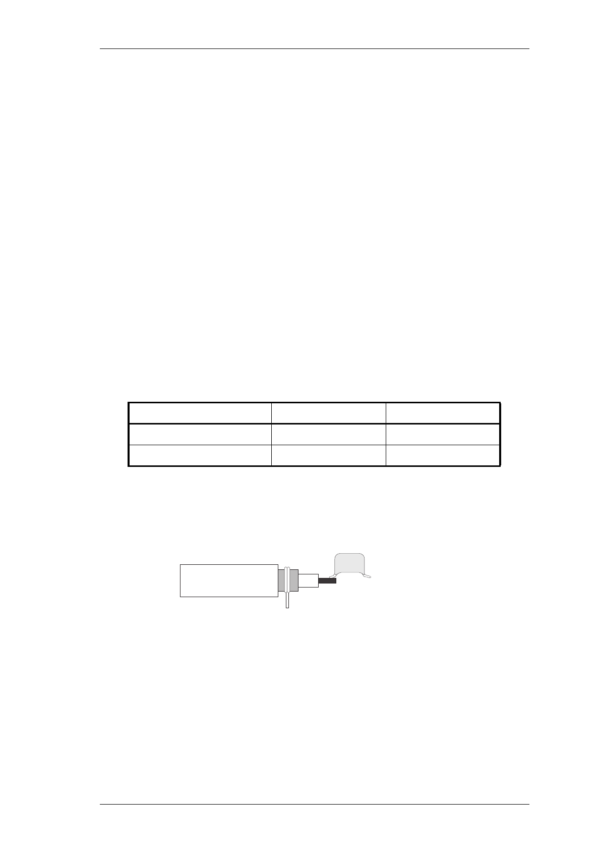
If the sensitivity is poor, the fault can be traced by measuring the sensitivity into
successive circuit blocks. Prepare a test cable by connecting a 1nF capacitor to the
end of a length of coax cable as shown in Figure 5.1.
Figure 5.1 RF Test Cable
Note: Before using the test cable, ensure the coax braid is connected to an earth
point on the PCB.
Using the RF test cable, apply a modulated 10.7MHz signal to the test breaks in
the IF section, or an on-channel RF signal to the front end test breaks.
Check that the sensitivity at each test break is within 2dB of the levels shown on
the circuit diagram.
Frequency Range Wide Band Narrow Band
66-76MHz -119dBm -120dBm
76-88MHz -118dBm -119dBm
1nF
Coax
To Test Cable
Connect To Earth

B5.6 T825 Fault Finding M820-00
30/04/96 Copyright TEL
Poor sensitivity indicates a fault in one of the circuit blocks following the test break.
Note: Poor sensitivity into the mixer can be caused by lack of drive level from the
VCO (the drive level should be >+17dBm).
Refer to the receiver fault finding charts (Section 5.5.5) for further information.
5.4.3 Oscillator Stability
5.4.3.1 TCXO
While maintaining a low level unmodulated RF input to the receiver, loosely cou-
ple into the first IF an additional high level signal at 10.7MHz - a constant low fre-
quency beat note should be heard.
Tap the TCXO with a finger and replace it if the beat note permanently changes.
5.4.3.2 Second IF
While maintaining a low level unmodulated RF input to the receiver, loosely cou-
ple into the second IF an additional high level signal at 455kHz - a constant low
frequency beat note should be heard.
Adjust the frequency of the 455kHz signal for zero beat.
If the second IF is more than 300Hz off frequency, check IC302, X301, C361 and
C362 and replace if necessary.
5.4.4 Demodulator Output
Apply an on-channel RF signal modulated by 1kHz with 3kHz [1.5kHz] deviation
at an amplitude of -65dBm.
Connect an oscilloscope probe (DC coupled) to IC303 pin 7 (audio output).
Check that an audio signal of approximately 380mV peak to peak is present.
Optimum tuning of the quad coil (L319) for minimum audio distortion (with a "flat"
audio response) should coincide with maximum audio amplitude and a DC level of
approximately 1.3V.
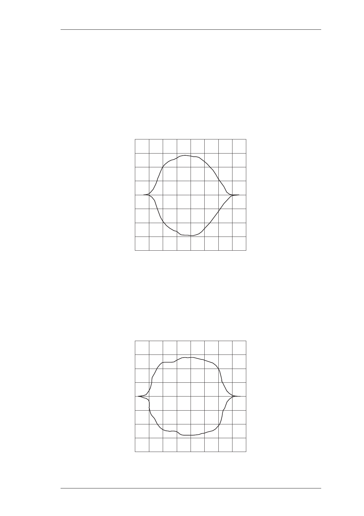
5.4.5 IF Distortion
If after careful IF alignment (Section 3.6) the audio distortion is still high or there is
irregular 1kHz ripple (refer to Figure 3.3), the IF should be swept to investigate the
bandpass response.
M820-00 T825 Fault Finding B5.7
Copyright TEL 30/04/96
Apply an on channel RF signal modulated at 10Hz with 12kHz [6kHz] deviation
at an amplitude of -65dBm.
Connect the modulating 10Hz audio signal to the "X" input of an oscilloscope and
observe the 455kHz IF input to IC303 pin 16 via a suitable RF probe on the "Y"
input.
Note: The X input should be DC coupled.
Check that the swept response has a rounded top and no sharp non-linearities
(refer to Figure 5.2).
Figure 5.2 IF Swept Response
Increase the RF level to -30dBm; the trace will now show the shape of the 455kHz
ceramic filter (&XF303).
Check that the response has no sharp non-linearities.
If sharp non-linearities do occur, replace the filter and sweep to confirm a satisfac-
tory solution (refer to Figure 5.3).
Figure 5.3 Ceramic Filter Swept Response
B5.8 T825 Fault Finding M820-00
30/04/96 Copyright TEL
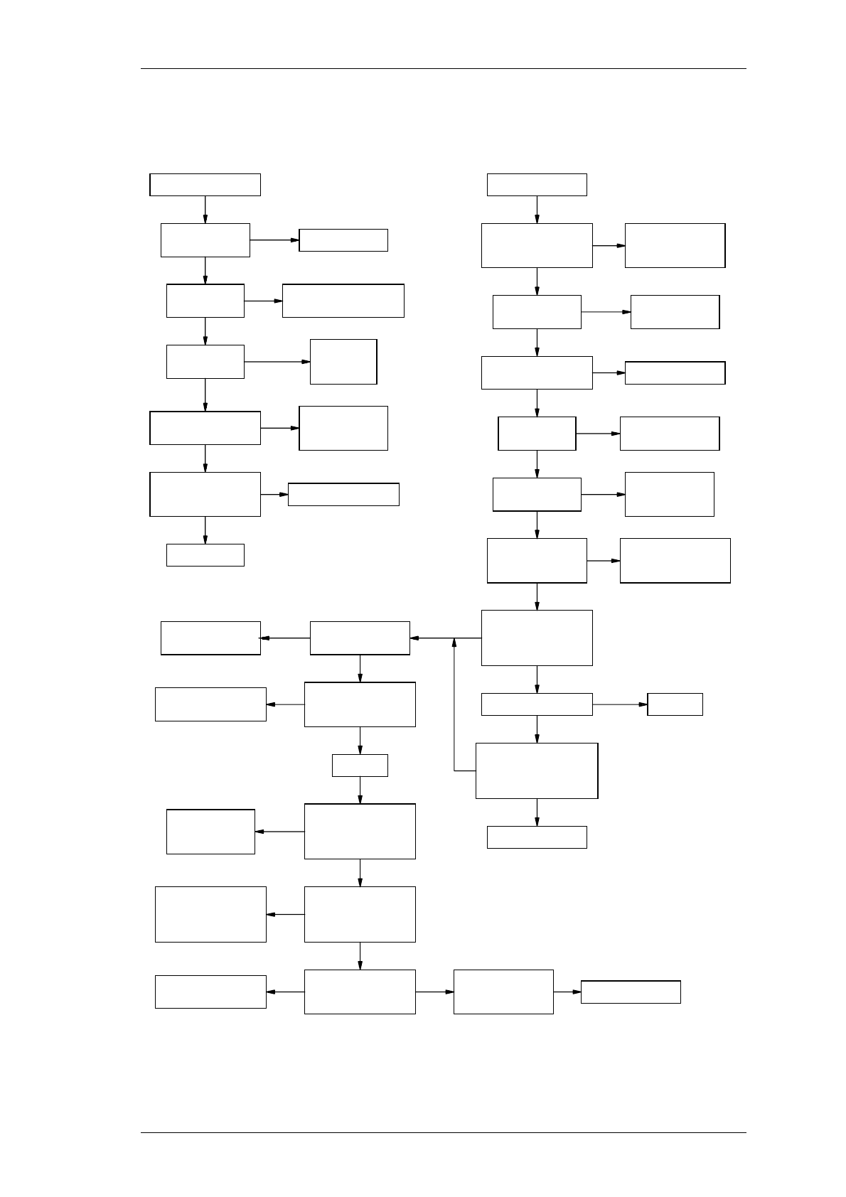
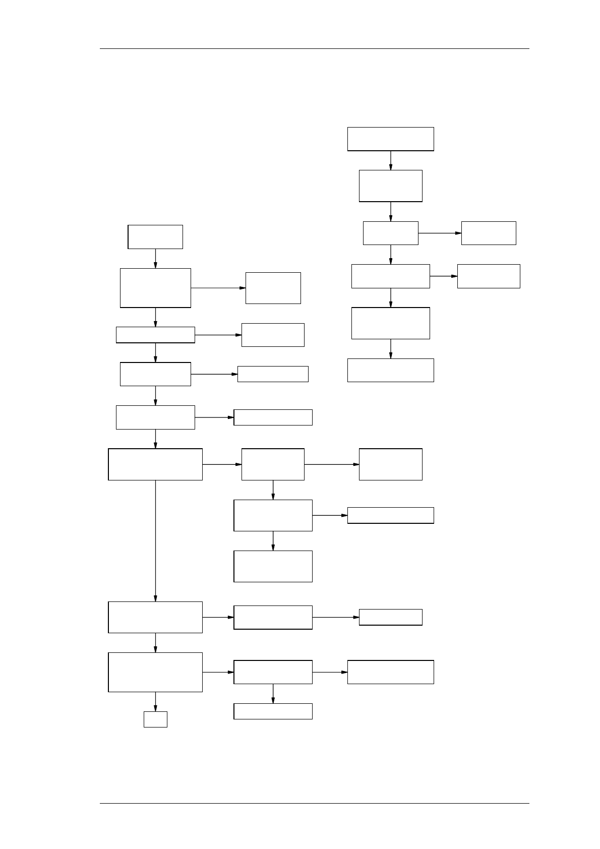
5.5 Fault Finding Charts
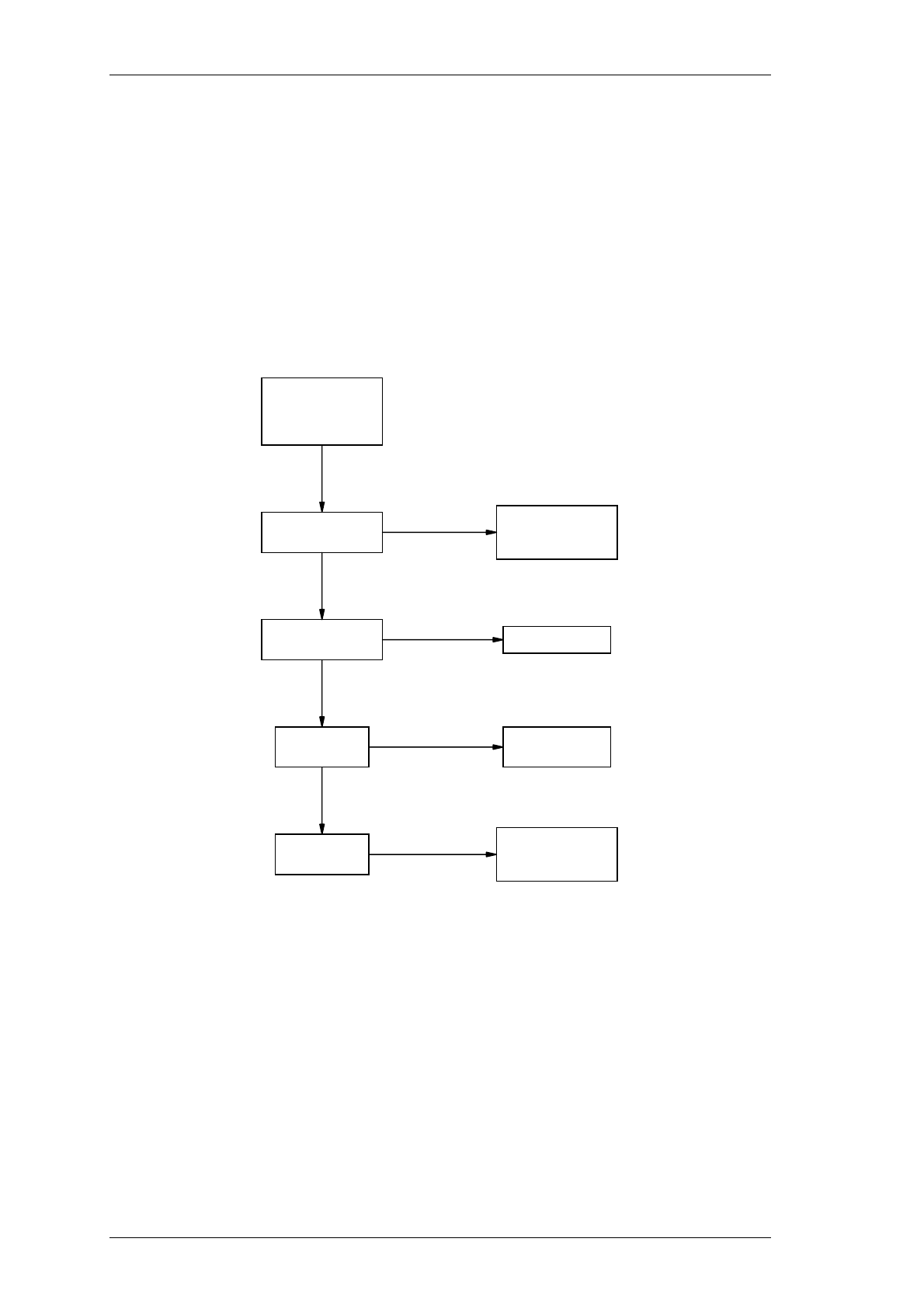
Note: The standard test point designations as used in this section are as follows:
TP1 13.8V
TP2 9V
TP3 20V
TP4 5V
5.5.1 Regulator
Check for
overheating
components &
short circuits.
13.8V present on
IC202 pin 3?
5.3V present on
IC202 pin 1?
9.0V present
on TP2?
20V present
on TP3?
Check continuity
from D-range
connector pin 9.
Replace IC202.
Check Q200,
Q201 & IC201.
N
N
N
N
Y
Y
Y
Check Q202 is
switching at
approx. 180kHz.
M820-00 T825 Fault Finding B5.9
Copyright TEL 30/04/96
5.5.2 Synthesiser
Continued on next page.
VCO out of lock.
Check 9V reg.
Check biasing
resistors, Q4 & Q5.
Check Q4 C
multiplier
(synth).
Check biasing
resistors, Q1,
Q2 & Q3.
Replace if faulty. Correct ref.
on IC3 pin 8?
Check 5V reg. &
supply resistor
to each IC.
20V present
on IC4 pin 8? 20V inverter
supply faulty.
9V present on
Q1 divider buffer? Check 9V supply.
DC V present
on Q1?
Check TCXO
& reference
divider path.
Prescaler output
freq. present on
IC3 pin 4?
VCO freq. correct? Go to C.
Synthesiser OK.
No VCO RF output.
DC V present
at Q4 & Q5?
9V present at
VCO Q4/Q5?
8.3V present
at VCO?
DC V present at
VCO, Q1, Q2 & Q3?
Capacitors OK?
Check for cracks,
shorts, etc.
Replace VCO.
Check biasing
resistors & Q1.
N
N
N
N
N
Y
Y
Y
Y
Y
N
N
N
N
NN
N
N
N
Y
Y
Y
Y
Y
Y
Y
Y
Y
Y
Y
Y
N
Y
Y
VCO trimmer
freq. range OK?
VCO OK.
Does IC3 pin 1
PDA change level
at the programmed
synth. freq?
Does control line
O/P level change
on IC4 pin 1?
Check signal
path from VCO
to prescaler.
Check synth. data
loading ccts;
change EPROM;
change synth. IC3.
Check loop filter
cct around IC4.
Check VCO tuning
caps & trimmer.
A (Refer to VCO circuit diagram)
N
N
N
N
NCheck continuity
between VCO &
IC4 pin 1 O/P. Synthesiser OK.
Y
+5V present at
TCXO, IC3, IC5,
IC6, IC1 & EPROM?
Check at IC1
pin 3; replace
IC1 if no output.
Does VCO trimmer
adjust for stable
control line
between 5 & 13V?
Does VCO trimmer
adjust for required
frequency range
between 5 & 13V?
Is 8MHz VCO range
achieved between
5 & 13V?
Does IC1 pin 3 O/P
freq. change with
VCO trimmer when
VCO not locked?
Check &C2, &C3, &C4,
VC1 & D1-D6 in VCO.
B (Refer to synth. circuit diagram)
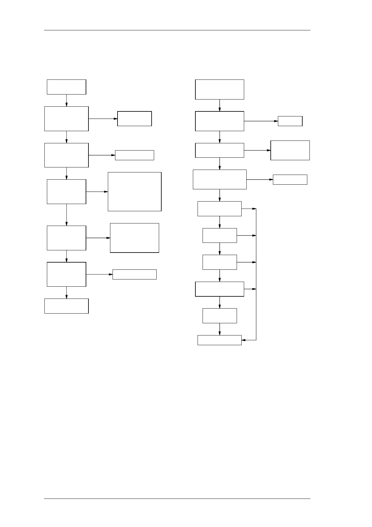
B5.10 T825 Fault Finding M820-00
30/04/96 Copyright TEL
Replace IC3;
synthesiser OK.
Substitute EPROM
with known good
unit; is freq.
wrong?
Does freq. up-
date correctly
when supply
toggled off & on?
VCO locked on
wrong freq? Noisy synth; poor
selectivity &/or
poor residual FM.
Correct channel
selected?
(switches on
external lines)
Continuity OK
between EPROM &
IC3 on 3 address
& 4 data lines?
Does toggling
each of the 3 LSB
DIP switches
change the freq?
Set correct
channel.
Repair tracks.
Check for edge
transition on
IC3 pin 14 for
3 LSB DIP switch
operation; if wrong,
check C15, C16 & C2,
C4, C6 on EPROM PCB.
Check presence
of low level on
IC3 pin 14 for
>200ms on switch-on;
change IC3.
Provide new EPROM.
Go to B.
Correct DC V
present on Q1 VCO?
Check inductors,
biasing resistors
& Q1.
Loop filter &
components around
integrator op. amp. OK? Replace if faulty.
Change trimmer;
still noisy?
Change Q1;
still noisy?
Change TCXO;
still noisy?
Change varactors;
still noisy?
Replace VCO
assembly.
Synthesiser OK.
C (Refer to synth. circuit diagram) D (Refer to synth. & VCO
circuit diagrams)
N
N
N
N
N
Y
Y
Y
Y
Y
Y
N
N
N
N
N
N
N
Y
Y
Y
Y
Y
Y
Y
Y
VCO phase locked?
5-13V present on
control line?
M820-00 T825 Fault Finding B5.11
Copyright TEL 30/04/96
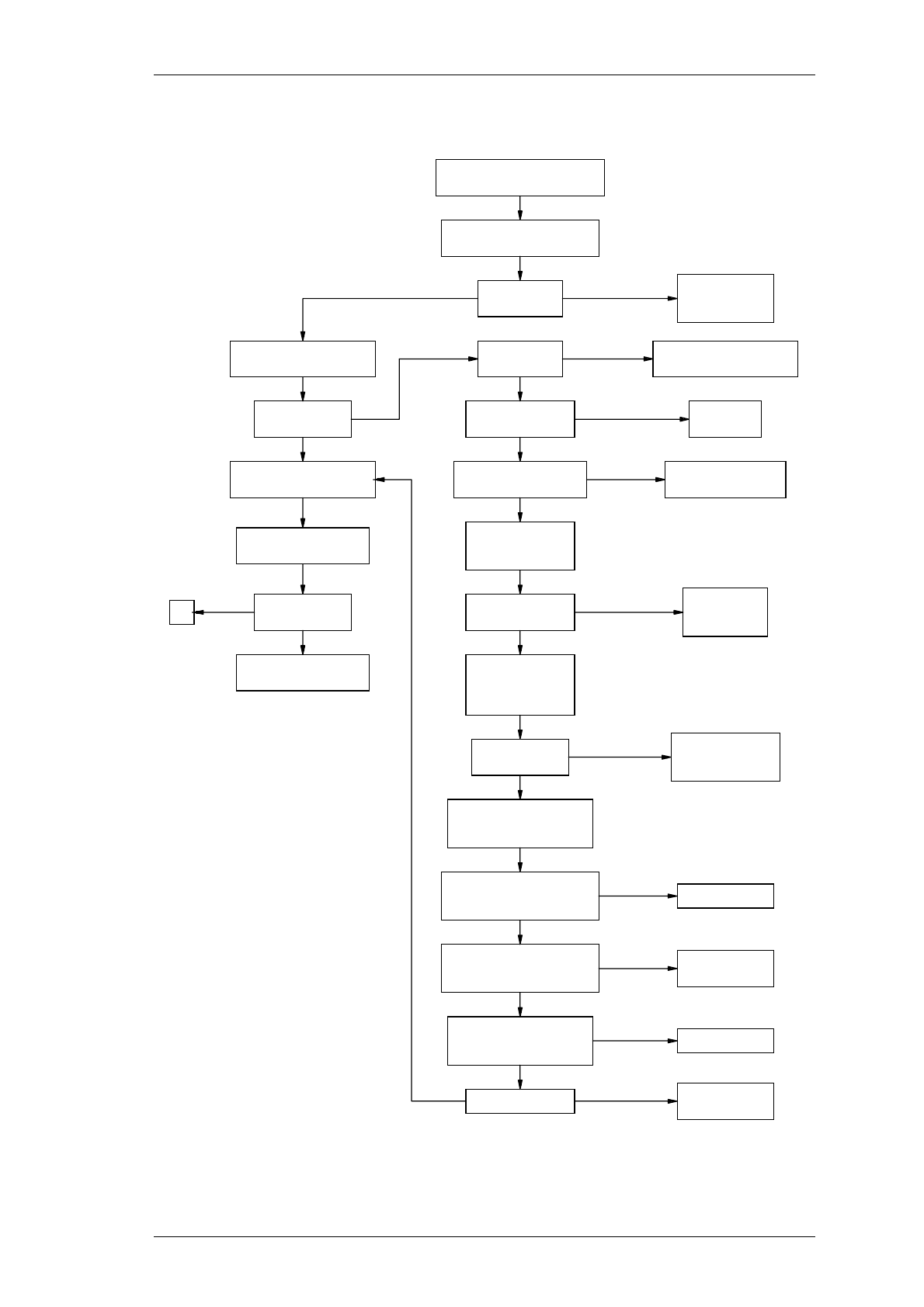
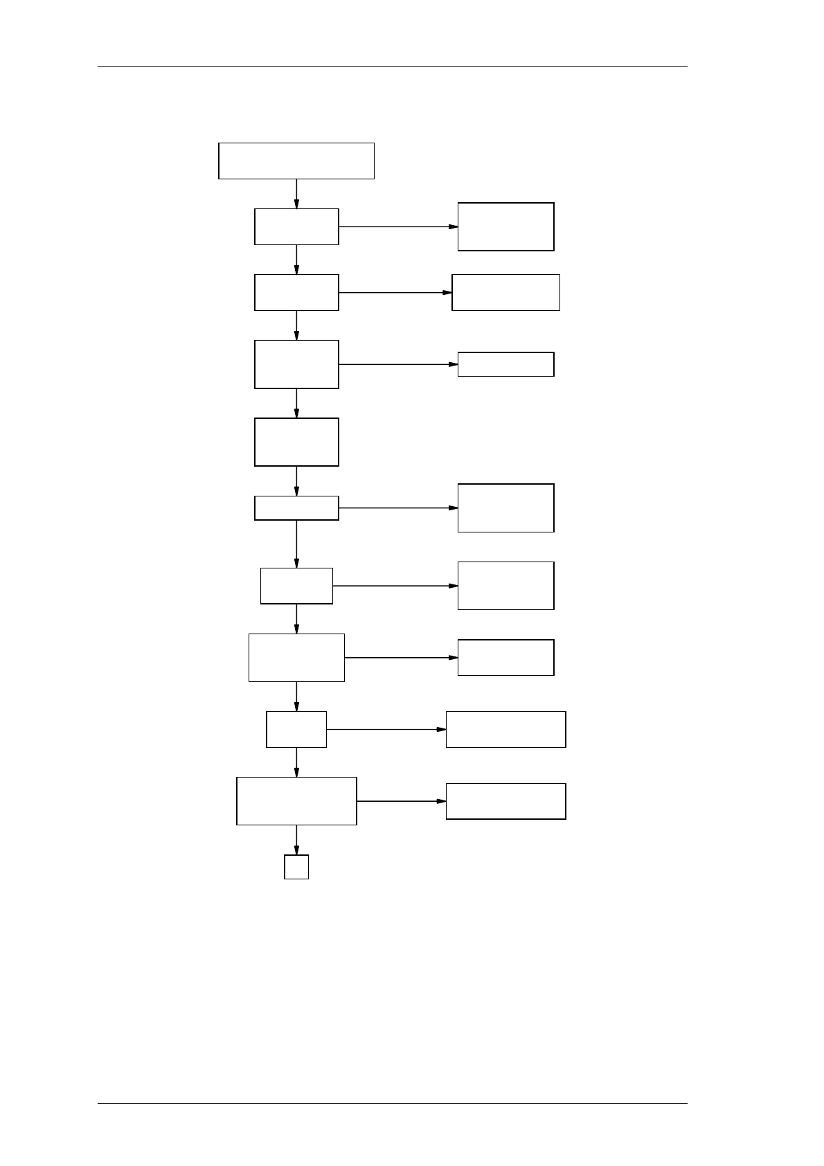
5.5.3 Noise Mute
Ensure PL104 is set
for noise mute operation.
Apply on channel signal
@ -117dBm* to receiver.
Adjust mute
pot. RV100 &
observe voltage
IC100 pin 3.
Does LED
toggle on/off?
Check Q103, Q105 &
Q106 for operation.
Mutable audio
on outputs?
Refer to audio
fault finding chart.
Switch SW100 to ensure
mute is not disabled.
Voltage varies
0-2.5V?
Set RF signal level to
-117dBm. Rotate mute
pot. RV100 c/w & cc/w.
Monitor voltage on
IC100 pin 1. Switching
0-8V as pot. rotated?
Monitor voltage on
IC100 pin 7. Switching
0-8V as pot. rotated?
Monitor voltage on
pad 101. Switching
0-8V as pot. rotated?
Does LED toggle?
Refer to Rx
fault finding
chart.
Check components
around active filter.
Check 9V rail &
resistors R149,
R100 & R101.
Replace IC100.
Check/replace
IC100 & D100.
Replace Q100.
Check/replace
Q102 & D102.
N
Y
Y
Y
Y
N
N
Y
N
N
N
N
Y
Y
Y
Y
NY
N
Y
N
Y
OK
*Modulated 3kHz [1.5kHz]
deviation @ 1kHz.
Audio on
IC303 pin 7?
Noise on
IC304 pin 7? N
Amplified noise
on C386? Check Q306
& Q307.
Check D301 is
rectifying noise.
Approx. 0.6V DC rect.
noise on pad 114?
Vary RF level &
observe voltage
on pad 114.
Pad 114 voltage
varies 0-1.8V?
Check adj.
of RV301
(gain adj.).
N
Rotate mute pot. RV100
c/w & cc/w & view LED.
B5.12 T825 Fault Finding M820-00
30/04/96 Copyright TEL
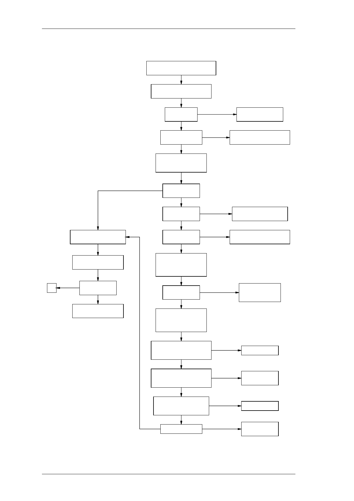
5.5.4 Carrier Mute
Rotate carrier mute
pot. RV104 c/w &
cc/w & view LED.
Does LED
toggle on/off?
Y
Y
Approx. 3.3V on
IC303 pin 5? Check for short circuits
and/or replace IC303.
N
N
Y
Ensure PL104 is set
for carrier mute operation.
Apply on channel signal
@ -95dBm* to receiver. *Modulated by 1kHz signal with
3kHz [1.5kHz] deviation.
Audio on
IC303 pin 7? Refer to Rx fault
finding chart.
Approx. 5V on
IC104 pin 1?
Adjust carrier mute
pot. RV104 &
observe voltage
on IC104 pin 6.
Voltage varies
0-6V? NCheck 9V rail &
resistors R154,
R156 & RV104.
Monitor voltage on
IC100 pin 7. Switching
0-8V as pot. rotated?
Monitor voltage on
pad 101. Switching
0-8V as pot. rotated?
Does LED toggle?
Check/replace
IC100 & D100.
Replace Q100.
Check/replace
Q102 & D102.
N
N
N
Y
Y
Y
NY
Monitor voltage on
IC104 pin 7. Switching
0-8V as pot. rotated? Replace IC104.
Check Q103, Q105 &
Q106 for operation.
Mutable audio
on outputs?
Refer to audio
fault finding chart.
Switch SW100 to ensure
mute is not disabled.
N
Y
OK
N
Y
Y
Check/replace IC104
& adjoining components.
Approx. 5V on
RSSI pad 115?
N
Y
Check IC304 and
adjoining components.
N
Set RF signal level
to -95dBm. Rotate
carrier mute pot.
RV104 c/w & cc/w.
M820-00 T825 Fault Finding B5.13
Copyright TEL 30/04/96
5.5.5 Receiver
High audio
distortion.
Y
N
B
Quad coil L319
tuned for min.
distortion (flat
audio response)?
Adjust L319.
Retune all
IF coils.
Note: T.B. = Test Break
(refer Rx circuit diagram)
Readjust TCXO
frequency.
VCO frequency OK? N
Y
Adjust IF coils.
IF alignment OK?
(see 5.4.5) N
Fault find audio.
Distortion at Rx
audio pad 111 OK?
2nd IF
frequency OK?
(see 5.4.3.2)
Check/replace
IC302, X301,
C362 & C361.
Repair stage.
TCXO stability OK?
(see 5.4.3) Refer to synthesiser
fault finding chart.
OK.
Inject 10.7MHz signal @
-15dBm into 10.7 IF pad.
Is distortion 3% or less?
Sweep shape of
whole IF (see 5.4.5).
OK? Replace ceramic filter.
Fault in IC303 or
surrounding circuitry.
Check/replace.
Inject 10.7MHz into T.B.
after diplexer & measure
distortion. OK?
Check sensitivity
into each IF stage.
Inject on-channel RF
into mixer RF input T.B.
& measure distortion.
OK?
Replace TCXO (IC2).
Y
Y
N
NN
Y
N
Y
Y
Y
Y
N
NY
N
A
Poor sensitivity:
worse than -117dBm.
Ensure VCO RF
& IF correctly
aligned.
High audio
distortion? See Chart B
(below).
Y
N
Replace
faulty device.
NDC conditions OK?
(see cct diagram)
Check/repair faulty
stage or component.
Y
Check sensitivity
into each stage
(see 5.4.2).
B5.14 T825 Fault Finding M820-00
30/04/96 Copyright TEL
5.5.6 Audio
Apply on channel signal
@ -117dBm* to receiver.
Audio on
IC101 pin 1?
Audio at
top of RV102
& RV103?
Refer to Rx
fault finding
chart.
Check components
around IC101.
Replace C112.
Ensure mute
pot. fully
clockwise.
Mute LED on? Refer to mute
fault finding
chart.
Refer to mute
fault finding
chart.
Audio on
C115/C116?
Audio on
IC102 pin 2 &
IC103 pin 2?
Replace
faulty device.
Audio on
speaker? Replace C122 &
check continuity.
Audio on line
monitor (pad 117)
& line output?
Check/replace
output components.
OK
Y
N
N
N
Y
Y
N
Y
N
Y
N
N
Y
Y
Y
N
*Modulated 3kHz [1.5kHz]
deviation @ 1kHz.
Audio on
IC303 pin 7?
