CDC_Cyber_170_s_720_730_740_750_760__176_Lev_BC_Hardware_Ref_Man_60456100L_Dec81 CDC Cyber 170 S 720 730 740 750 760 176 Lev BC Hardware Ref Man 60456100L Dec81
User Manual: Pdf CDC_Cyber_170_s_720_730_740_750_760__176_Lev_BC_Hardware_Ref_Man_60456100L_Dec81
Open the PDF directly: View PDF ![]() .
.
Page Count: 354 [warning: Documents this large are best viewed by clicking the View PDF Link!]
60456100
C / a C \ C O N T R P L D A T A
CORPORATION
CDC* CYBER 170
COMPUTER SYSTEMS
MODELS 720,730,740,750, AND 760
MODEL 176 (LEVEL B/C)
#**"
/fP*y
HARDWARE REFERENCE MANUAL
REVISION RECORD
REVISION DESCRIPTION
(03-15-79)
B, C
(10-01-79)
(12-11-79)
E
(03-17-80)
(07-31-80)
(02-24-81)
H
(07-16-81)
(07-16-81)
K
(07-16-81)
(12-23-81)
Manual released.
Manual revised; includes Engineering Change Order 40259 and 39930.
Manual revised; includes Field Change Order 40604. Pages 2-15, 2-19, 4-77, and 5-62 are revised.
Manual revised; includes Engineering Change Order 39945 (moved I/O channel parity switches from I/O
connector panel to 3UEG modules). This edition also adds model 740 information and obsoletes all previous editions.
Manual revised; includes Engineering Change Order 40842. Pages 117B3 (Inside Front Cover),
117B7 (v), 117B8 (vi), 117B9 (vii/viii), 117D4 (1-3), 117E6 (1-11), 117E7 (1-12), 118C9 (2-18), 120C1 (4-13), 120C7
(4-19), 120C9 (4-21), 120D6 (4-32), 120D12 (4-37), 120D13 (4-38), 120E1 (4-39), 120E2 (4-40), 120G8 (4-68), 121B10
(5-9), 121C2 (5-13), 122B4 (5-59), 122C3 (5-70), 122C4 (5-71), and 122C11 (5-78) are revised.
Manual revised; includes Engineering Change Order 41574. Pages 117B3 (Inside Front Cover), 118B7
(2-6), 118C1 (2-12), 118C2 (2-13), 119B6 (3-5), 119B7 (3-6), 120B6 (4-5) through 120B13 (4-12), 120B14, 120C1 (4-13)
Publication No.
60456100
through 120C13 (4-25), 120C14, 120D1 (4-26) through 120D8 (4-33), 120D14, 120E2 (4-40), 120E12 (4-48), 120E13
(4-49), 120E14, 120F1 (4-50) through 120F12 (4-61), 120F14, 120Q5 (4-65) through 120G13 (4-73), 120G14, 120H1
(4-74), 120H2 (4-75), 120H14,121C5 (5-16), 121C7 (5-18), 121C9 (5-20), and 121C11 (5-22) are revised.
Manual revised; includes Engineering Change Order 42404. Pages 117H6-122H14 (Contents), 119C4
(3-15), 119C5 (3-16), 119C8 (3-17), and 119DH (3-21) are revised. Pages 119C10 (3-18.1/3-18.2) and 119D4
(3-20.1/3-20.2) are added.
Engineering Change Order 42479. No change to manual.
Manual revised; includes Engineering Change Order 42437. Pages 117B2 (Front Cover), 117D7 (1-6),
118D6 (2-25), and 119D3 (3-20) are revised.
Manual revised; includes Engineering Change Order 42040. Pages 119B6 (3-5), 119E2 (3-29), 120B7
(4-6), 120B8 (4-7), and 120C11 (4-23) are revised.
/^^%v
REVISION LETTERS I, 0, Q AND X ARE NOT USED
© 1979,1980, 1981
by Control Data Corporation
All rights reserved
Printed in the United States of America
Address comments concerning this
manual to:
Control Data Corporation
Publications and Graphics Division
4201 North Lexington Avenue
St. Paul, Minnesota 55112
or use Comment Sheet in the back of
this manual.
0^*>..
0^
LIST OF EFFECTIVE PAGES
New features, as well as changes, deletions, and additions to information in this manual, are indicated by bars in the margins or by a dot
near the page number if the entire page Is affected. A bar by the page number indicates pagination rather than content has changed.
PAGE REV PAGE REV PAGE REV PAGE REV PAGE REV
Front Cover
Inside Front
2-23
2-24
3-24
3-25
4-51
4-52
5-31
5-32
Cover Divider 3-26 4-53 Divider
Title Page 2-25 3-27/3-28 4-54 5-33
ii 2-26 Divider 4-55 5-34
iii Divider 3-29 4-56 5-35
iv 2-27 3-30 4-57 5-36
vK2-28 Divider 4-58 5-37
vi Divider 4-1/4-2 4-59 5-38
v i i / v i i i 2-29 Divider 4-60 5-39/5-40
ix 2-30 4-3 4-61 Divider
xE2-31 4-4 4-62 5-41
xi 2-32 4-5 4-63 5-42
xii Divider 4-6 4-64 5-43
xiii 2-33/2-34 4-7 Divider 5-44
Divider Divider 4-8 4-65 Divider
1-1/1-2 2-35 4-9 4-66 5-45
Divider 2-36 4-10 4-67 5-46
1-3 Divider 4-11 4-68 Divider
1-4 2-37/2-38 4-12 4-69 5-47
1-5 Divider 4-13 4-70 5-48
1-6 2-39 4-14 4-71 5-49
Divider 2-40 4-15 4-72 5-50
1-7 2-41 4-16 4-73 5-51
1-8 2-42 4-17 4-74 5-52
1-9 Divider 4-18 4-75 5-53
1-10 2-43 4-19 4-76 5-54
1-11 2-44 4-20 4-77 5-55
1-12 2-45 4-21 Divider 5-56
1-13/1-14 2-46 4-22 5-1/5-2 Divider
Divider 2-47 4-23 Divider 5-57
1-15 Divider 4-24 5-3 5-58
1-16 3-1/3-2 4-25 5-4 5-59
1-17 Divider 4-26 5-5 5-60
1-18 3-3 4-27 5-6 5-61
Divider 3-4 4-28 5-7 5-62
2-1/2-2 3-5 4-29 5-8 5-63
Divider 3-6 4-30 5-9 5-64
2-3 3-7 4-31 5-10 5-65
2-4 3-8 4-32 5-11 5-66
2-5 3-9 4-33 5-12 5-67
2-6 3-10 4-34 5-13 5-68
2-7/2-8 3-11 4-35 5-14 5-69
Divider 3-12 4-36 5-15 5-70
2-9 3-13 4-37 5-16 5-71
2-10 3-14 4-38 5-17 5-72
2-11 3-15 4-39 5-18 5-73
2-12 3-16 4-40 5-19 5-74
2-13 Divider 4-41 5-20 5-75
2-14 3-17 4-42 5-21 5-76
2-15 3-18 4-43 5-22 5-77
2-16 3-18.1/3-18.2 4-44 5-23 5-78
Divider Divider Divider 5-24 Divider
2-17 3-19 4-45 5-25 5-79
2-18 3-20 4-46 5-26 5-80
2-19 3-20.1/3-20.2 4-47 5-27 5-81
2-20 3-21 4-48 5-28 5-82
2-21/2-22 3-22 4-49 5-29/5-30 5-83
Divider 3-23 4-50 Divider 5-84
60456100 L iii
PAGE
5-85
5-86
5-87
5-88
5-89
5-90
5-91
5-92
5-93
5-94
5-95
5-96
Divider
A-l
B-l
B-2
Index-1
Index-2
Carment
Sheet
Back Cover
REV
E
B
B
B
E
B
B
E
B
B
A
B
E
E
E
E
E
PAGE REV PAGE REV PAGE REV PAGE REV
y*S»\
iv 60456100 L
0^\
PREFACE
This manual contains hardware reference information for
the CDC®CYBER 170 Computer Systems, models 720, 730,
740, 750, and 760 and model 176 (level B/C). For model 176,
level B is equivalent to any of the model designators 408
through 444. Level C is equivalent to model designator 501.
The model numbers identify the reference information for
the various systems throughout the manual.
I NOTE |
Refer to publication number 60420000 for
reference information for models 171
through 175 and model 176 (level A). For
model 176, level A is equivalent to any of
the model designators 8 through 44.
The manual describes the functional, operational, and
programming characteristics of the computer systems
hardware. Additional system hardware information is
available for all models in the publications listing in the
system publication indexes on the following pages.
All references to chassis 11 and 12 pertain to AA110-A and
AA147-A only.
This manual is for use by customer, marketing, training,
programming, and Engineering Services personnel who
operate, program, and maintain the computer systems.
Other manuals that are applicable to the CDC CYBER 170
Computer Systems but not listed in the following indexes
are:
Control Data Publication
NOS Operator's Guide
NOS System Programmer's Instant
CYBER 70 Computer Systems 7030
Extended Core Storage Reference
Manual, Volume 3
7030-1XX ECS II and 6642
Distributive Data Path
Hardware Reference Manual
Publication
Number
60435600
60449200
60347100
60430000
Publication ordering information and latest revision levels
are available from the Literature Distribution Services
catalog, publication number 90310500.
WARNING
This equipment generates, uses and can radiate radio frequency energy
and if not installed and used in accordance with the instructions
manual, may cause interference to radio communications. As
temporarily permitted by regulation, it has not been tested for
compliance with the limits for Class A computing devices pursuant to
Subpart J of Part 15 of the FCC Rules which are designed to provide
reasonable protection against such interference. Operation of this
equipment in a residential area is likely to cause interference in which
case the user at his own expense will be required to take whatever
measures may be required to correct the interference.
60456100 K

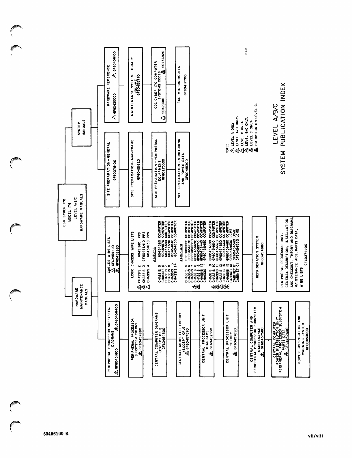
SYSTEM PUBLICATION INDEX
CDC CYBER 170
HARDWARE MANUALS
HARDWARE
MAINTENANCE MANUALS
MODELS 720. 730 MODELS 740, 750. 760
PPS THEORY. DIAGRAMS
GF 60456120
CSU THEORY. DIAGRAMS
GF 60456130
CPU THEORY. DIAGRAMS
GF 60456170
FUNCTIONAL UNITS THEORY, DIAGRAMS
GF 60420300
CMC THEORY, DIAGRAMS
GF 60456180
CPU/CMC THEORY. DIAGRAMS
GF 60456260
ECS CPLR THEORY. DIAGRAMS
GF 60456190
PPS (CHAS 2) WIRE LIST
GF 60456140
CSU {CHAS 3) WIRE LIST
GF 60456150
CPU/CMC (CHAS 1) WIRE LIST
GF 60456200
CP (CHAS 5-7) WIRE LIST
GF 60456220. 30. 40
CPU/ECS CPLR (CHAS 4LWIRE LIST
GF60456210C
4LV ECS CPLR (CHAS 4) WIRE LIST
GF 60456250
CABLES
GF 60457530
CABLES
GF 60457540
POWER DISTRIBUTION AND WARNING SYSTEM
GF 60456160
REFRIGERATION SYSTEM
GF 19983800
REFRIGERATION SYSTEM
GF 60427800
INSTALLATION AND CHECKOUT
GF 60420520
INSTALLATION AND CHECKOUT
GF 60420510
MAINTENANCE. PARTS
GF 60456980
ECS SUBSYSTEM
GF 60404700 (ECS). GF 60425800 (DPP). GF 60440500 (CONTROLLER)
M-G SET THEORY, MAINTENANCE, ETC
60166800 (EM), 60420800 (KATO)
M-G SET DIAGRAMS
60423100 (EM). 60419900 (KATO)
25-kVa FREQUENCY CONVERTER
THEORY. MAINTENANCE. DIAGRAMS
GF 60456520
VI
SYSTEM
MANUALS
CDC CYBER 170 HARDWARE REFERENCE
GF 60456100
ECS SUBSYSTEM HARDWARE REFERENCE
GF 60430000
ESM SUBSYSTEM HARDWARE REFERENCE
60455990 .'^Sfey
DISPLAY STATION HARDWARE REFERENCE/CE
GF 62952600
CDC CYBER 170 COMPUTER SYSTEMS CODES
60456920
ECL MICROCIRCUITS
GF 60417700
SITE PREPARATION-GENERAL
GF 60275100
SITE PREPARATION-MAINFRAME
GF 60456890
SITE PREPARATION-PERIPHERAL EQUIPMENT
GF 60275300
SITE PREPARATION-MONITORING AND POWER DATA
GF 60451300
NOTES:
©
O I F A T 4 0 2 - A I S
INSTALLED, USE
PUBLICATION
GF 60456250
1080D
60456100 G
J^N
<3
2-8 2 Ul
OO
O o
(T Ul
«3
LU
Q
CQ
C C S O
Ul
z <
O I-
?°8
Z CC *>
Z * w
^ Q . «>
< Q O
0- Z
Ui <
o 5 o o o z
< < C D ( D C J —
t _J —I _J —I SX.
cj ui ui uj y o
^ UjU, UjUIUJ 2
1<w<$^^
LU
>
LU CQ
ID
Q_
LU
h-
(/)
>-
01
*- rr
S«3<
UlUlmUJUIUI
l-l-JTl-Hfc
en z2 men tn sn
co{2<neo<o«o
tn<n<nsntn<n
<<<<<<
xxxxxx
oooooo
1OUJKC0C0- —
fnOTCft<s>tototo
enefuninenenen
IIIIIII
ouuuuuu
»o — CJ in « 5 5 (J
snenentnenenf^f
inensn\^tnsnt\ — *\
XXXXXX<<<
OOOOOOOOO
<3<3<3
£ U .
t U , 9 o
5 E 5
O
o
Ul
<a
cr
X
a. Ul
ec
hi Ul
a.
o °-
U J .
»- 9
„ <
5 hi
« < s
o ~ cc
§1 S
«i<
Ul sc
oo
o<
(CQ
°" o
_ l o
< t o
,°i «
£ g
t o >
CO cc
U I O o
OH J g
o i 5
( E l - «
f t p -
5g
JU1»
< t- °
iw"
o-o
— -3 O
cc a. S,
a. o.g
oyfi:
ac = o
Ul Ol f-
l-O JO
Hf*>
S o p
8 8
ESS
ii t c ^
a 4 (0
Sis
Is?
cc to
w u i o
3 £ z«>
Oo ""S
oot-S
i C z w
< Q - < o
Ul ui
"X
o^^o^
OC0UJU£
—o«i
jirot-Q
<t-crecf>
uf*r<
OtJcC
Sui
t o o
to io
60456100 K vii/viii

■"^" "■ —^—n
CONTENTS
j^*\
1. SYSTEM DESCRIPTIONS
Introduction
Physical Characteristics
Models 720 and 730 Configurations
Models 740, 750, and 760 Configurations
Model 176 Configuration
Functional Characteristics
Model 720 System
Model 730 System
Model 740 System
Models 750 and 760 Systems
Model 176 System
Major System Component Descriptions
Central Processor - Models 720 and 730
Central Processor - Models 740, 750,
760, and 176
Central Memory - All Models
Extended Core Storage (Optional) -
Models 720 through 760
Large Core Memory Extension (Optional)
Model 176
Peripheral Processor Units (Optional) -
Model 176
Peripheral Processor Subsystems - All
Models
Display Station - All Models
Condensing Unit(s) - All Models
Power Distribution Unit - Model 176
2. FUNCTIONAL DESCRIPTIONS
Central Processor - Models 720 and 730
Arithmetic Unit - Models 720 and 730
Instruction Control Section - Models
720 and 730
Operating Registers - Models 720 and
730
Support Registers - Models 720 and
730
Instruction Control Sequences -
Models 720 and 730
Central Processor - Models 740, 750, 760,
and 176
Central Processing Unit - Models 740,
750, 760, and 176
Operating Registers - Models 740,
750, 760, and 176
Support Registers - Models 740, 750,
and 760
Support Registers - Model 176
Instruction Control Sequences -
Models 740, 750, 760, and 176
Functional Units - Models 740, 750, 760,
and 176
Boolean Unit
Shift Unit
Normalize Unit
Floating-Add Unit
Long Add Unit
Multiply Unit
Divide Unit.
1-1 Population-Count Unit 2-16
Increment Unit 2-16
1-1 Central Memory Control - Models 720 through
1-3 760 2-17
1-4 Reference Priorities 2-17
1-5 SECDED Mode 2-18
1-5 Error Detection and Response 2-20
1-7 Address Parity 2-20
1-7 Data Parity 2-20
1-7 Breakpoint Check 2-21
1-7 Central Memory - Models 720 through 760 2-23
1-7 Data Format 2-23
1-7 Address Format 2-23
1-15 Address Parity 2-23
1-15 Reference Operations 2-24
Reconfiguration 2-24
1-15 Central Memory - Model 176 2-25
1-16 Data Format 2-25
Address Format 2-25
1-16 SECDED Mode 2-25
Parity Mode 2-26
1-17 Maintenance Mode 2-26
Test Mode 2-26
1-17 Inhibit Log SBE Mode 2-26
Reconfiguration 2-26
1-17 Large Core Memory Extension (Optional) -
1-18 Model 176 2-27
1-18 Address Format 2-27
1-18 SECDED Mode 2-27
Parity Mode 2-27
Maintenance Mode 2-28
Test Mode 2-28
2-1 Inhibit Log SBE Mode 2-28
Test Complement Mode 2-28
2-3 Block Copies 2-28
2-3 Direct (Single-Word) Transfers 2-28
Bank Selection 2-28
2-3 Input/Output Multiplexer - Model 176 2-29
Normal PPU to CM Data Transfer 2-30
2-3 Normal CM to PPU Data Transfer 2-30
High-Speed PPU to CM Data Transfer 2-31
2-3 High-Speed CM to PPU Data Transfer 2-31
Logic Scanner - Model 176 2-33
2-4 Data Channel Converter - All Models 2-35
3000 Series Interrupt Feature 2-35
2-9 3000 Power Failure Mode 2-36
Buffer Flushing 2-36
2-9 Display Controller - All Models
Peripheral Processor Units (Optional) -
2-37
2-10 Model 176 2-39
Computation Section 2-39
2-10 A Register 2-39
2-11 P Register 2-39
Q Register 2-39
2-13 X Register 2-39
Sk Register 2-39
2-15 fd Register 2-39
2-15 k Register 2-39
2-15 PPU Memory 2-40
2-15 PPU Input/Output 2-40
2-15 Input Channel Control 2-40
2-16 Output Channel Control 2-40
2-16 PPU to PP.U Data Transfers 2-41
2-16 PPU to Peripheral Equipment Data
Transfers 2-42
60456100 E ix
Peripheral Processor Subsystem - All Models
Real-Time Clock
Deadstart
PP Memory
Barrel and Slot
A Register
P Register
Q Register
K Register
PP Input/Output
Status and Control Register
Channel Description
3. OPERATING INSTRUCTIONS
Controls and Indicators - Models 720 and
730
Deadstart Panel
I/O Channel Parity Switches
ECS Parity Switch
Clock Selection Switches and Indicators
CM Maintenance Switches
P Register and Status Bit Selection
Switches
Keyboard Display Selection Switches
PPS-0 Status and Control Register
Indicators
PPS-1 Status and Control Register
Indicators
CP Instruction Register and P Register
Indicators
CM Configuration and SECDED/Parity Mode
Switches
Controls and Indicators - Models 740, 750,
and 760
Deadstart Panel
I/O Channel Parity Switches
ECS Parity Switch
Clock Selection Switches and Indicators
CM Maintenance Switches
P Register and Status Bit Selection
Switches
Keyboard Display Selection Switches
Status and Control Register Indicators
CM Configuration and Clock Switches and
Indicators
Control and Indicators - Model 176
Deadstart Panel
I/O Channel Parity Switches
P Register and Status Bit Selection
Switches
Keyboard Display Selection Switches
CP Clock Frequency Selection Switches
and Indicators
PPS Clock Frequency Selection Switch
CM Configuration Switches
LCME Bank Selection Switches
PPS-0 Status and Control Register Indi
cators
PPS-1 Status and Control Register Indi
cators
Power-On and Power-Off Procedures - All
Models
Operating Procedures - All Models
Control Checks
Deadstart Program Selection
Deadstart
Load Mode
Sweep Mode
Dump Mode
2-43
2-43
2-43
2-43
2-44
2-45
2-45
2-45
2-45
2-45
2-46
2-46
3-1
3-3
3-3
3-5
3-5
3-5
3-7
3-7
3-8
3-8
3-12
3-14
3-15
3-17
3-17
3-17
3-17
3-17
3-17
3-17
3-17
3-17
3-17
3-19
3-19
3-19
3-19
3-19
3-19
3-20
3-20
3-21
3-21
3-26
3-29
3-29
3-29
3-29
3-29
3-29
3-29
3-30
4. INSTRUCTION DESCRIPTIONS
Central Processor Instructions - All Models
CP Instruction Formats
CP Instruction Descriptions
CP Instruction Timing - Models 720 and
730
CP Instruction Timing - Models 740, 750,
and 760
CP Instruction Timing - Model 176
Peripheral Processor Unit Instructions -
Model 176
PPU Instruction Formats
PPU Instruction Designators
PPU Instruction Addressing Modes
No Address
Constant Address
Direct Address
Indirect Address
Indexed Direct Address
PPU Instruction Descriptions
PPU Instruction Timing
Peripheral Processor Subsystem Instruc
tions - All Models
PPS Instruction Descriptions
PPS Instruction Timing
5. PROGRAMMING INFORMATION
Central Processor Programming
Exchange Jump - Models 720 through 760
Exchange Jump - Model 176
Exchange Exit Instructions
Error Exit
Input/Output Interrupt
Real-Time Interrupt
Step Mode
Operating Characteristics - Model 720
or 730 with Two CPs
Operating Characteristics - Model 176
Instruction Execution - Models 720 and
730
Instruction Execution - Models 740, 750,
760, and 176
Floating-Point Arithmetic - All Models
Format
Packing
Overflow
Underflow
Indefinite
Nonstandard Operands
Normalized Numbers
Rounding
Double-Precision Results
Fixed-Point Arithmetic - All Models
Integer Arithmetic - All Models
Compare/Move Arithmetic - Models 720
and 730
Processing Differences
Multiply Differences
Floating-Add Differences
Floating-Divide Condition Differences
Round-Divide Differences
Instructions 22 and 23 Differences
Illegal Instructions - Models 720 through
760
Exit Mode/Error Response - Models 720
through 760
ECS Instructions - Models 720 through
760
4-1
4-3
4-3
4-5
4-32
4-32
4-32
4-45
4-46
4-46
4-46
4-46
4-46
4-46
4-47
4-47
4-48
4-61
4-65
4-65
4-75
5-1
5-3
5-3
5-4
5-5
5-5
5-6
5-6
5-6
5-6
5-6
5-7
5-8
5-9
5-9
5-9
5-10
5-10
5-10
5-10
5-12
5-12
5-12
5-13
5-13
5-13
5-14
5-14
5-14
5-15
5-15
5-15
5-15
5-15
5-16
60456100 E
Flag Register Operation - Models 720 Dot Mode 5-42
through 760 5-16 Codes 5-42
Flag Function Codes 5-28 Programming Example 5-43
Flag Register Use 5-28 Programming Timing Consideration 5-43
Central Memory Programming 5-31 Peripheral Processor Unit Programming-
Central Memory - Models 720 through 760 5-31 Model 176 5-45
Central Memory - Model 176 5-31 Programming Considerations 5-45
Breakpoint - Models 720 through 760 5-32 Control Signals 5-45
Data Channel Converter Programming 5-33 Data Signals 5-45
Codes 5-33 Sequence Timing 5-46
Function Codes 5-33 Peripheral Processor Programming 5-47
Status Reply Codes 5-34 Power-On Characteristics 5-47
Selecting the Data Channel Converter 5-35 Central Memory Read 5-47
Deselecting the Data Channel Converter 5-35 Central Memory Write 5-47
Connecting to 3000 Series Equipment 5-35 Input/Output Channel Communications 5-47
Mode I Connect 5-36 Data Input 5-47
Mode II Connect 5-36 Data Output 5-48
Sending Function Codes to 3000 Series Channel Conflicts in an Expanded System 5-48
Equipment 5-37 Channel Operation 5-49
Mode I Function 5-37 External Channel Timing 5-49
Mode II Function 5-37 Frequency Margins 5-49
Data Transfer 5-37 Channel Active/Inactive Flag 5-49
Input Operation 5-38 Register Full/Empty Flag 5-49
Output Operation 5-38 Channel Transfer Timing (Adjacent
Parity Checking 5-38 PPs) 5-49
Function Codes from PPS to DCC 5-38 Input/Output Transfers 5-52
Data from PPS to DCC 5-39 Data Input Sequence 5-52
Data from DCC to PPS 5-39 Data Output Sequence 5-52
Status Words from DCC to PPS 5-39 Force Peripheral Processor Exit 5-52
Clearing a Parity Error 5-39 Force Deadstart 5-52
Display Station Programming 5-41 Status and Control Register 5-55
Keyboard 5-41 Status and Control Register Bit Descrip
Data Display 5-41 tions - Models 720 through 760 5-57
Character Mode 5-42 Status and Control Register Bit Descrip
tions - Model 176 5-79
A. GLOSSARY
APPENDIXES
A-l MODEL 740/750/760 AND MODEL 176
DIFFERENCES B-l
INDEX
i - i
1-2
1-3
1-4
1-7
2-1
2-2
2-3
2-4
2-5
2-6
2-7
2-8
CDC CYBER 170 Computer System
Models 720 and 730 Maximum Chassis
Configurations (Top Cutaway View)
Models 740, 750, and 760 Maximum
Chassis Configurations (Top
Cutaway View)
Model 176 Maximum Chassis Configura
tion (Top Cutaway View)
Models 720 and 730 Computer Systems
Models 740, 750, and 760 Computer
Systems
Model 176 Computer System
Models 740, 750, 760, and 176 CPU
Information Flow
PSD Register Flag Bit Arrangement
SECDED Network Block Diagram (SECDED
Mode)
CMC Error Communications
Models 720 through 760 CM Data Format
Models 720 through 760 CM Address
Format
Model 176 CM Address Format
Model 176 LCME Address Format
FIGURES
1-1 2-9
2-10
1-4
2-11
2-12
1-5 2-13
2-14
1-6 2-15
1-11 3-1
3-2
1-12
1-13 3-3
3-4
2-9 3-5
2-12 3-6
3-7
2-18
2-20 3-8
2-23 3-9
2-23 3-10
2-25
2-27
Model 176 CM I/O Buffer Addresses 2-29
Model 176 CM I/O Exchange Package
Areas 2-29
Data Channel Converter Configuration 2-35
PPU Memory Address Format 2-40
PPU/PPU Communications 2-41
B a r r e l a n d S l o t O p e r a t i o n 2 - 4 4
Channel Output Pulse Characteristics 2-46
D e a d s t a r t P a n e l - A l l M o d e l s 3 - 3
Module at 110 and J10 - Models 720
and 730 3-5
Module at 4P34 - Models 720 and 730 3-5
Module at 2A26 - Models 720 and 730 3-6
Module at 2A27 - Models 720 and 730 3-6
Module at 3136 - Models 720 and 730 3-7
Module at 2D33 and 2P34 - Models 720
and 730 3-7
Module at 2R36 - Models 720 and 730 3-8
PPS-0 Module at 2C41 - Models 720
through 760 3-9
PPS-0 Module at 2D40 - Models 720
through 760 3-9
60456100 E
3-11 PPS-0 Module at 2B37 - Models 720
through 760
3-12 PPS-0 Module at 2C28 - Models 720
through 760
3-13 PPS-0 Module at 2C31 - Models 720
through 760
3-14 PPS-0 Module at 2E40 - Models 720
through 760
3-15 PPS-1 Module at 2N35 - Models 720
through 760
3-16 PPS-1 Module at 2038 - Models 720
through 760
3-17 PPS-1 Module at 2P32 - Models 720
through 760
3-18 Modules at 1G05 and 4G05 (Second
CP) - Models 720 and 730
3-19 Modules at 1K23 and 4K23 (Second
CP) - Models 720 and 730
3-20 Modules at 1L28 and 1L29 - Models
720 and 730
3-21 Controls on Modules at 5A1 through
5A3 - Models 740, 750, and 760
3-22 Switches and Indicators on Module at
7M06 - Model 176
3-23 Module at 2A25 - Model 176
3-24 Switches on Module at 8K14 - Model
176
3-25 Modules at 5H14 and 5H15 - Model 176
3-26 PPS-0 Module at 2D40 - Model 176
3-27 PPS-0 Module at 2E40 - Model 176
3-28 PPS-0 Module at 2C31 - Model 176
3-29 PPS-0 Module at 2C41-Model 176
3-30 PPS-0 Module at 2B37 - Model 176
3-31 PPS-0 Module at 2C28 - Model 176
3-32 PPS-0 Module at 2F41 - Model 176
3-33 PPS-1 Module at 2N35 - Model 176
3-34
3-10 3-35
4-1
3-10 4-2
4-3
3-11 5-1
3-11 5-2
5-3
3-12 5-4
3-12 5-5
5-6
3-13 5-7
3-14
5-8
3-14 5-9
3-15 5-10
5-11
3-17 5-12
5-13
3-19 5-14
3-20 5-15
5-16
3-20 5-17
3-21 5-18
3-22 5-19
3-22 5-20
3-23 5-21
3-23 5-22
3-24 5-23
3-24
3-25
3-26
PPS-1 Module at 2038 - Model 176
PPS-1 Module at 2P32 - Model 176
CP Instruction Parcel Arrangement
PPU/PP 12-Bit Instruction Format
PPU/PP 24-Bit Instruction Format
Exchange Package - Models 720
through 760
Exchange Package - Model 176
Instruction Execution - Models 720
and 730
Floating-Point Format
Floating-Add Result Format
Multiply Result Format
Format of Relative Address Zero on
Error Exit - Models 720 through
760
Block Copy Instruction Operations
ECS Address Format for Flag Register
Operation
Memory Map - Models 720 through 760
Memory Map- Model 176
DCC Connect Code Format
Display Station Output Function Code
Coordinate Data Word
Character Data Word
Receive and Display Program Flowchart
Output Channel Timing
Input Channel Timing
Channel Transfer Timing
Data Input Sequence Timing
Data Output Sequence Timing
Descriptor Word
CP Chassis Quadrants (Viewed from
Module Side) - Models 740, 750, and
760
3-26
3-27
4-3
4-46
4-46
5-3
5-5
5-7
5-9
5-12
5-12
5-16
5-25
5-28
5-31
5-31
5-36
5-43
5-43
5-43
5-44
5-46
5-46
5-50
5-53
5-54
5-55
5-76
TABLES
1-1 CDC CYBER 170 System Components
1-2 Central Processor Functional
Characteristics
1-3 Central Memory Functional Character
istics
1-4 Peripheral Processor Subsystem
Functional Characteristics
1-5 Optional Peripheral Processor Unit
Functional Characteristics
1-6 Data and Address Checking Functional
Characteristics
2-1 SECDED Syndrome Codes/Corrected Bits
2-2 Breakpoint Control Translations
2-3 Models 720 through 760 Central
Memory Sizes
2-4 Model 176 Central Memory Sizes
2-5 I/O Cable Line Characteristics
2-6 Data Channel Coaxial Cable Lines
3-1 Deadstart Panel Functions - All
Models
3-2 Function of Modules at 2A26 and
2A27 - Models 720 and 730
3-3 CM Maintenance Switch Functions
3-4 Functions of CP Module at 2D33 and
2P34 - Models 720 and 730
3-5 Functions of Module at 1L28 - Models
720 and 730
3-6 Functions of Module at 1L29 - Models
720 and 730
3-7 Memory Selection Scheme - Models 720
and 730 3-16
3-7A Memory Wrap-Around After
Reconfiguration - Models 720 and 730
1-3 3-8
1-8
3-9
1-8
3-9 A
1-9
1-9 3-10
1-10 3-11
2-19 3-11A
2-21
3-12
2-23
2-25 4-1
2-46
2-47 4-2
4-3
3-4
4-4
3-6
3-7 4-5
4-6
3-8 4-7
4-8
3-15
4-9
3-15 4-10
5-1
5-2
5-3
3-16 5-4
Functions of Controls on Modules 5A1
through 5A3 - Models 740, 750, and
760 3-18
Memory Selection Scheme - Models 740,
750, and 760 3-18
Memory Wrap-Around After
Reconfiguration - Models 740, 750,
and 760 3-18.1
Functions of Switches and Indicators
on Module at 7M06 - Model 176 3-19
Memory Selection Scheme - Model 176 3-20
Memory Wrap-Around After
Reconfiguration - Model 176 3-20.1
Functions of Switches on Modules at
5H14 and 5H15 - Model 176 3-21
Central Processor Instruction
Designators 4-4
Collating Table 4-28
CP Instruction Timing - Models 720
and 730 4-33
CP Instruction Timing - Models 740,
750, and 760 4-37
CP Instruction Timing - Model 176 4-41
PPU and PP Instruction Differences 4-45
PPU and PP Instruction Designators 4-46
PPU and PP Instruction Addressing
Modes 4-47
PPU Instruction Timing 4-62
PPS Instruction Timing 4-76
B i t s 5 8 a n d 5 9 C o n fi g u r a t i o n s 5 - 9
Xj Plus Xk (30, 32, 34 Instructions) 5-11
Xj Minus Xk (31, 33, 35 Instructions) 5-11
Xj Multiplied by Xk (40, 41, 42
Instructions) 5-11
60456100 H
i^N 5-5 Xj Divided by Xk (44, 45 Instructions)
5-6 CP Program Interrupt Conditions -
Models 720 through 760
5-7 Error Response with CEJ/MEJ Enabled,
MF Set - Models 720 through 760
5-8 Error Response with CEJ/MEJ Enabled,
MF Clear - Models 720 through 760
5-9 Error Response with CEJ/MEJ Disabled
- Models 720 through 760
5-10 Exchange Break-In Characteristics
During ECS Transfers
5-12 5-11
5-12
5-16 5-13
5-14
5-17 5-15
5-16
5-19
5-22 5-17
5-24
Block Copy Operation Exit Conditions
Keyboard Character Codes
Display Character Codes
Channel Signal Timing
Descriptor Word Function Codes
Status and Control Register Bit
Assignments - Models 720 through
760
Status and Control Register Bit
Assignments - Model 176
5-26
5-41
5-42
5-51
5-56
5-58
5-80
60456100 H xm


.(fp^
PH^siiAL iH^Mc;iiwries

SYSTEM DESCRIPTIONS
This section introduces the CDC CYBER 170 Computer
Systems, gives physical and functional characteristics, and
provides descriptions of major system components.
INTRODUCTION
The CDC CYBER 170 systems (figure 1-1) include models
720 through 760 and 176. These are general purpose digital
computer systems that provide varying degrees of
processing power, data storage, and input/output (I/O)
capabilities.
Depending upon options and design differences, the systems
include one or more of the following components.
e Central processor (CP).
• Central memory control (CMC) in models 720
through 760 and memory control in model 176.
• Central memory (CM), includes one central storage
unit (CSU) in models 720 through 760 and small
semiconductor memory (SSM) in model 176.
• Large core memory extension (LCME), optional, in
model 176.
• Extended core storage (ECS), optional, in models
720 through 760.
• Peripheral processor subsystem (PPS), includes 10
peripheral processors (PPs).
• Peripheral processor units (PPUs), optional, in
model 176.
• Data channel converter (DCC).
• Display station.
• Condensing unit(s).
• Power distribution unit (PDU).
Table 1-1 provides a comparison of the individual systems
on a component level. In some systems, one or more of the
components are duplicated. In such cases, manual
references to the components by name or abbreviations are
followed by a -0 or -1 for identification. For example,
model 720 contains central processor-0 (CP-0) and may
contain optional central processor-1 (CP-1).
0^!\
0$^\ Figure 1-1. CDC CYBER 170 Computer System
60456100 E 1-1/1-2

PHYSICAL CHARACTERISTICS
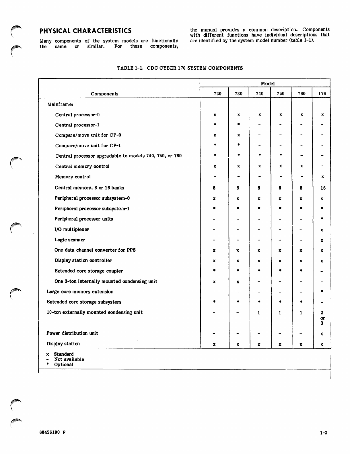
Many components of the system models are functionally
the same or similar. For these components,
the manual provides a common description. Components
with different functions have individual descriptions that
are identified by the system model number (table 1-1).
TABLE 1-1. CDC CYBER 170 SYSTEM COMPONENTS
Components
Model
720 730 740 750 760 176
Mainframe:
Central processor-0
Central processor-1
Compare/move unit for CP-0
Compare/move unit for CP-1
Central processor upgradable to models 740, 750, or 760
Central memory control
Memory control
Central memory, 8 or 16 banks 16
Peripheral processor subsystem-0
Peripheral processor subsystem-1
Peripheral processor in its
I/O multiplexer
Logic scanner
One data channel converter for PPS
Display station controller
Extended core storage coupler
One 3-ton internally mounted condensing unit
Large core memory extension
Extended core storage subsystem
10-ton externally mounted condensing unit
or
3
Power distribution unit
Display station
x Standard
- Not available
* Optional
60456100 F 1-3
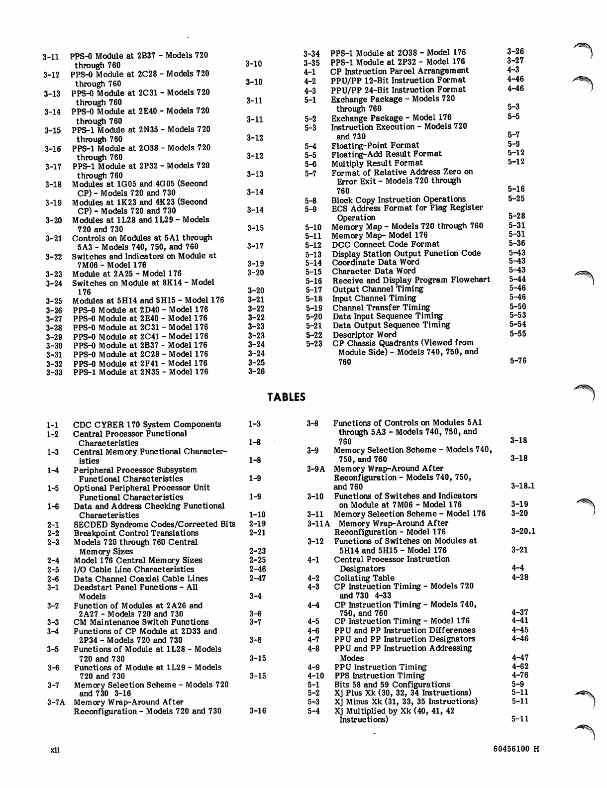
The following model configurations describe the physical
arrangements of cabinets, bays, and chassis in basic and
maximally configured systems. Additional physical
characteristics of the computer systems are on data sheets
in the CDC CYBER 170 Section 2 Site Preparation Manual,
listed in the preface. The data sheets include separate
descriptions of the mainframe models, associated
condensing units, and display stations. The sheets also
include weight, power consumption, and certain code
requirements.
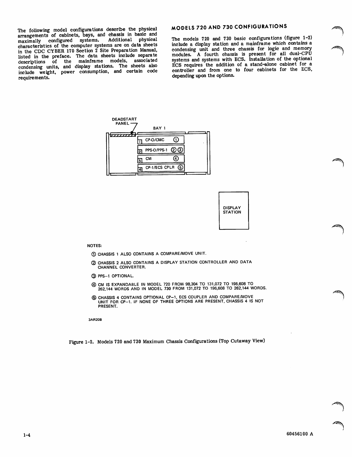
MODELS 720 AND 730 CONFIGURATIONS
The models 720 and 730 basic configurations (figure 1-2)
include a display station and a mainframe which contains a
condensing unit and three chassis for logic and memory
modules. A fourth chassis is present for all dual-CPU
systems and systems with ECS. Installation of the optional
ECS requires the addition of a stand-alone cabinet for a
controller and from one to four cabinets for the ECS,
depending upon the options.
y^^s^y
DEADSTART
PANEL—7
BAY 1
\r\rTrr**/A
I—c
-pi CP-O/CMC ©
T 1 1
n — = 1
Pi PPS-O/PPS-1 (5)®
3 ] C M ©
^ CP-1/ECS CPLR ©
.
DISPLAY
STATION
NOTES:
© CHASSIS 1 ALSO CONTAINS A COMPARE/MOVE UNIT.
@ CHASSIS 2 ALSO CONTAINS A DISPLAY STATION CONTROLLER AND DATA
CHANNEL CONVERTER.
© PPS-1 OPTIONAL.
® CM IS EXPANDABLE IN MODEL 720 FROM 98,304 TO 131,072 TO 196,608 TO
262,144 WORDS AND IN MODEL 730 FROM 131,072 TO 196,608 TO 262,144 WORDS.
<D CHASSIS 4 CONTAINS OPTIONAL CP-1, ECS COUPLER AND COMPARE/MOVE
UNIT FOR CP-1. IF NONE OF THREE OPTIONS ARE PRESENT, CHASSIS 4 IS NOT
PRESENT.
3AR20B
Figure 1-2. Models 720 and 730 Maximum Chassis Configurations (Top Cutaway View)
^^K
1-4 60456100 A
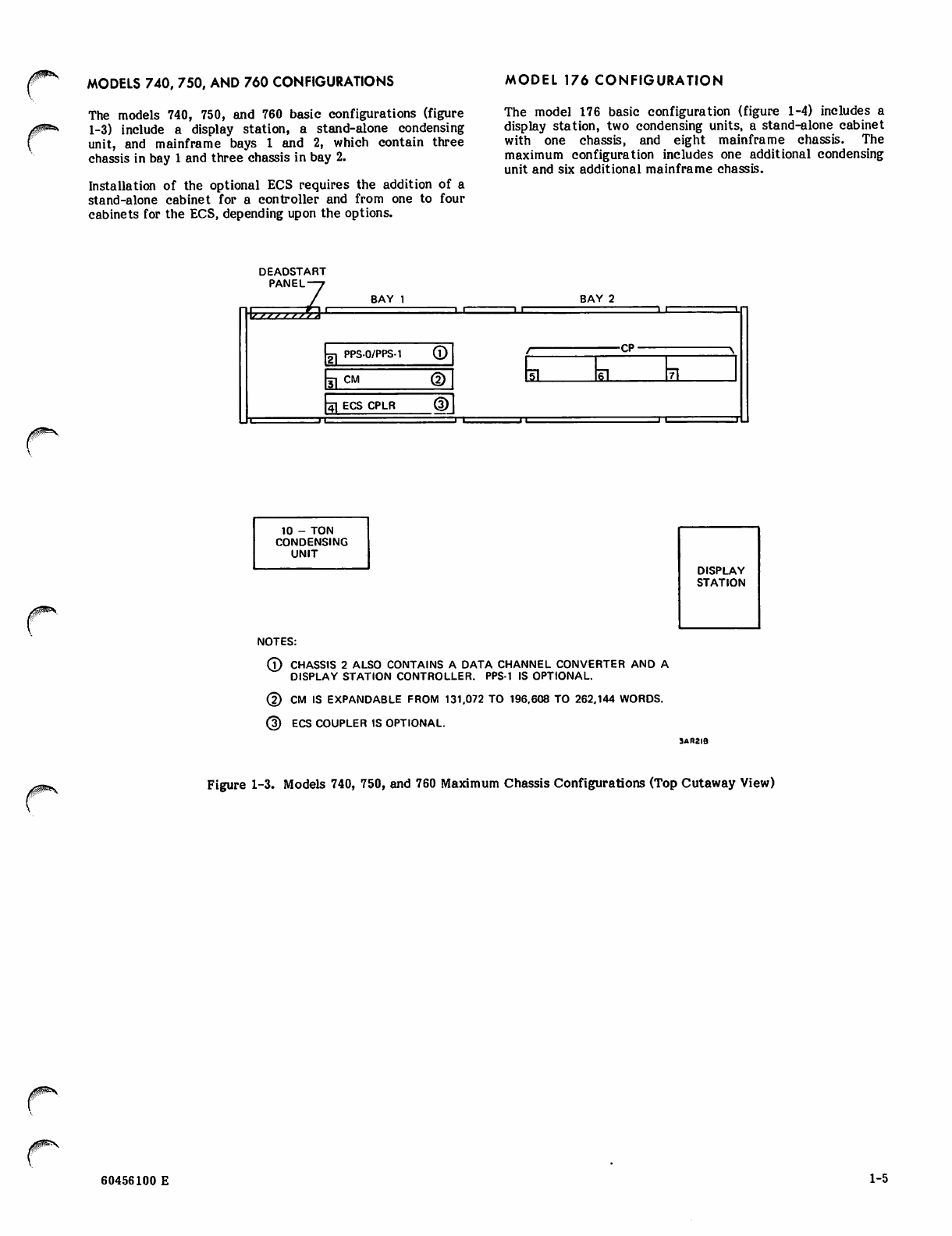
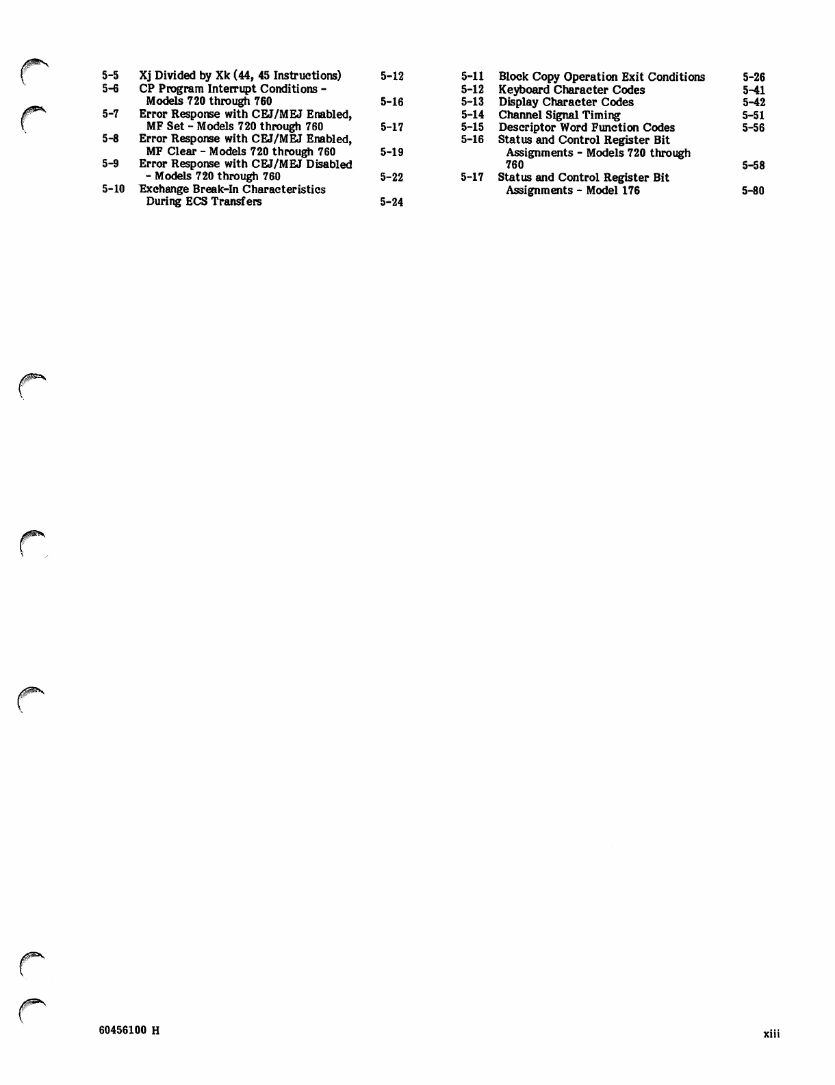
f^- MODELS 740, 750, AND 760 CONFIGURATIONS
The models 740, 750, and 760 basic configurations (figure
1-3) include a display station, a stand-alone condensing
unit, and mainframe bays 1 and 2, which contain three
chassis in bay 1 and three chassis in bay 2.
Installation of the optional ECS requires the addition of a
stand-alone cabinet for a controller and from one to four
cabinets for the ECS, depending upon the options.
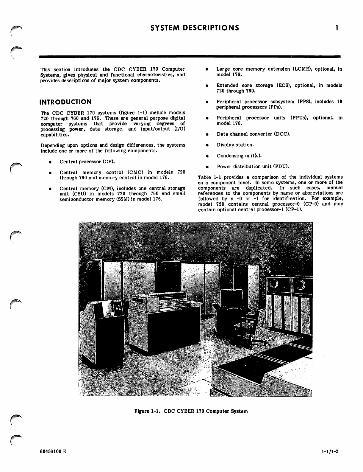
MODEL 176 CONFIGURATION
The model 176 basic configuration (figure 1-4) includes a
display station, two condensing units, a stand-alone cabinet
with one chassis, and eight mainframe chassis. The
maximum configuration includes one additional condensing
unit and six additional mainframe chassis.
DEADSTART
PANEL-
ZBAY 1 BAY 2
\j *fS / /MX _. t i i r
l l " " T
gj PPS-0/PPS-1
CP —
5l 6l 71
flCM
t - i r :t
4l ECS CPLR zn
10 - TON
CONDENSING
UNIT
DISPLAY
STATION
NOTES:
© CHASSIS 2 ALSO CONTAINS A DATA CHANNEL CONVERTER AND A
DISPLAY STATION CONTROLLER. PPS-1 IS OPTIONAL.
© CM IS EXPANDABLE FROM 131,072 TO 196,608 TO 262,144 WORDS.
© ECS COUPLER IS OPTIONAL.
Figure 1-3. Models 740, 750, and 760 Maximum Chassis Configurations (Top Cutaway View)
60456100 E 1-5
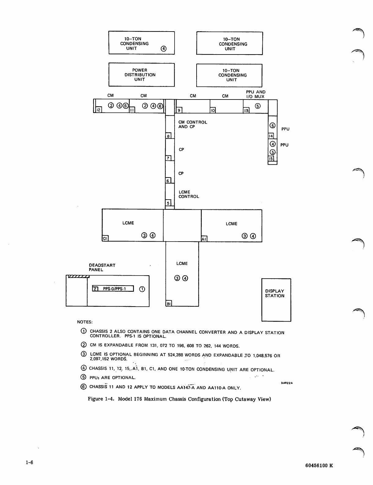
10-TON
CONDENSING
UNIT
10-TON
CONDENSING
UNIT
POWER
DISTRIBUTION
UNIT
10-TON
CONDENSING
UNIT
CM CM CM CM
PPU AND
I/O MUX
m. ©©©
EL ©@©
IL
LCME
cH (D@
IL
a
IL
LIL §L GIL
CM CONTROL
AND CP
CP
HL
PPU
PPU
CP
LCME
CONTROL
DEADSTART
PANEL
v f r f f f .A
m pps-o/pps-1 J ©
LCME
©®
IL
LCME
All ®©
DISPLAY
STATION
NOTES:
© CHASSIS 2 ALSO CONTAINS ONE DATA CHANNEL CONVERTER AND A DISPLAY STATION
CONTROLLER. PPS-1 IS OPTIONAL.
© CM IS EXPANDABLE FROM 131, 072 TO 196, 608 TO 262, 144 WORDS.
© LCME IS OPTIONAL BEGINNING AT 524,288 WORDS AND EXPANDABLE JO 1 048 576 OR
2,097,152 WORDS. ...
© CHASSIS 11, 12, 15,.Al, B1, C1, AND ONE 10-TON CONDENSING UNIT ARE OPTIONAL.
© PPUs ARE OPTIONAL.
© CHASSIS 11 AND 12 APPLY TO MODELS AA147-A AND AA110-A ONLY.
Figure 1-4. Model 176 Maximum Chassis Configuration (Top Cutaway View)
1-6 60456100 K
WH Cf IO N&k illtRAiTEiilTlIS
•jp»'N

0ts\
FUNCTIONAL CHARACTERISTICS
Tables 1-2 through 1-6 summarize the functional
characteristics of the CP, CM, PPS, and data address and
checking for each system.
MODEL 720 SYSTEM
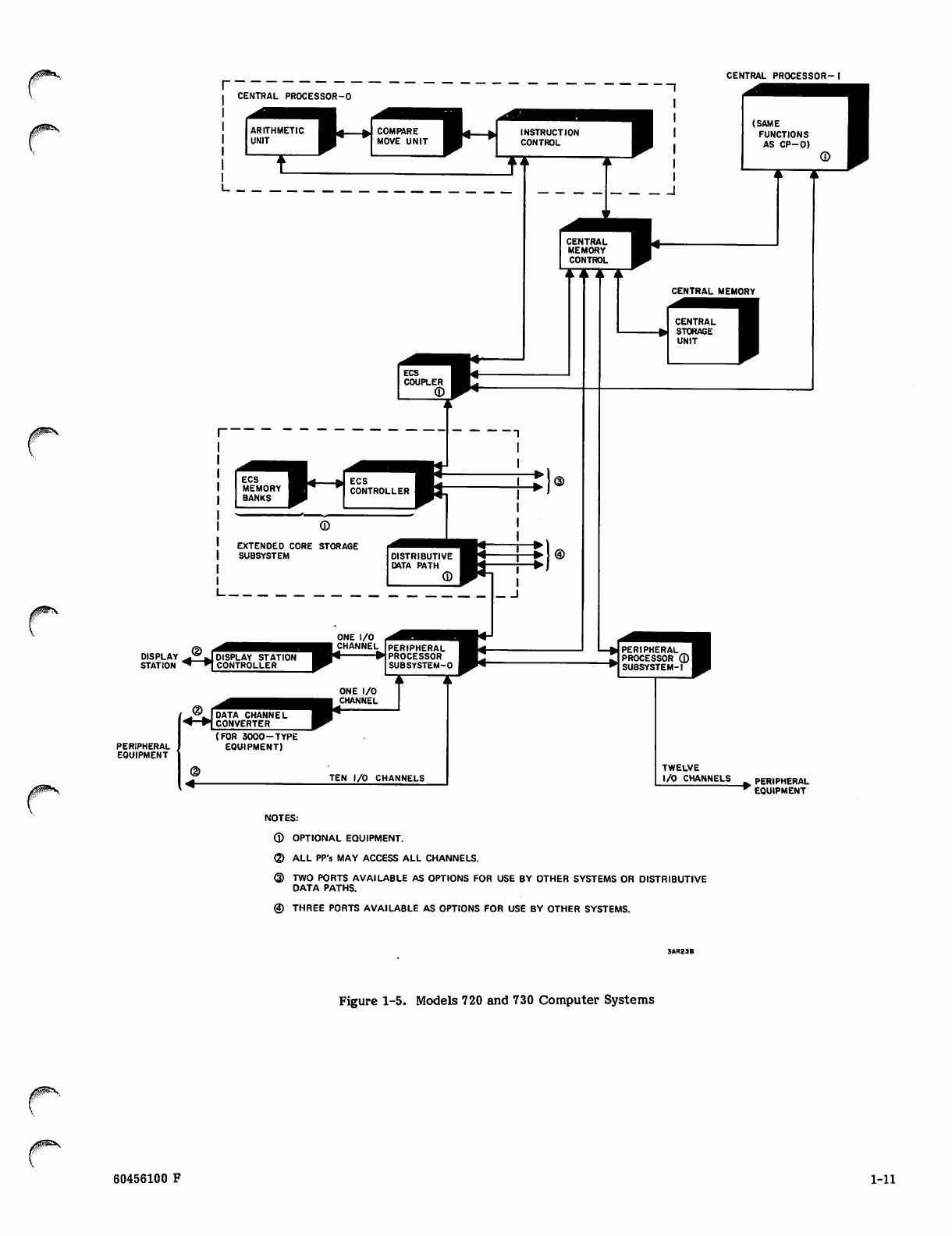
The model 720 basic computer system (figure 1-5) has a
CP-0 that operates serially. The CP contains an arithmetic
unit, compare/move unit, and instruction control unit. A
second CP, CP-1, is optional. This CP is the same as CP-0
except that its compare/move unit is optional. Both CPs
use a common CMC and CM to communicate with PPS-0
and the optional PPS-1/ECS, if installed.
The semiconductor CM is optionally expandable in three
increments from 98 304 words to 262144 words. Further
memory expansion, up to 2 097 152 words, is available by
the installation of the optional ECS. Options in the ECS
installation include ports for interfacing with other systems
or distributive data paths.
The PPS-0 contains 10 PPs. An optional installation of
PPS-1 permits expansion of the PPS to 14, 17, or 20 PPs.
Any of these options expands the I/O channels from 12 to
24. The PPs perform all I/O operations by executing
independent programs in each PP. These programs occur
through the use of a PP instruction set. Communications
between the PPs and the I/O channels occur through
individual PP memories.
MODEL 730 SYSTEM
The model 730 basic computer, system (figure 1-5) is
functionally similar to model 720, except for faster CP
operation. The system options are the same, except for
CM which begins with 131072 words instead of 98 304
words.
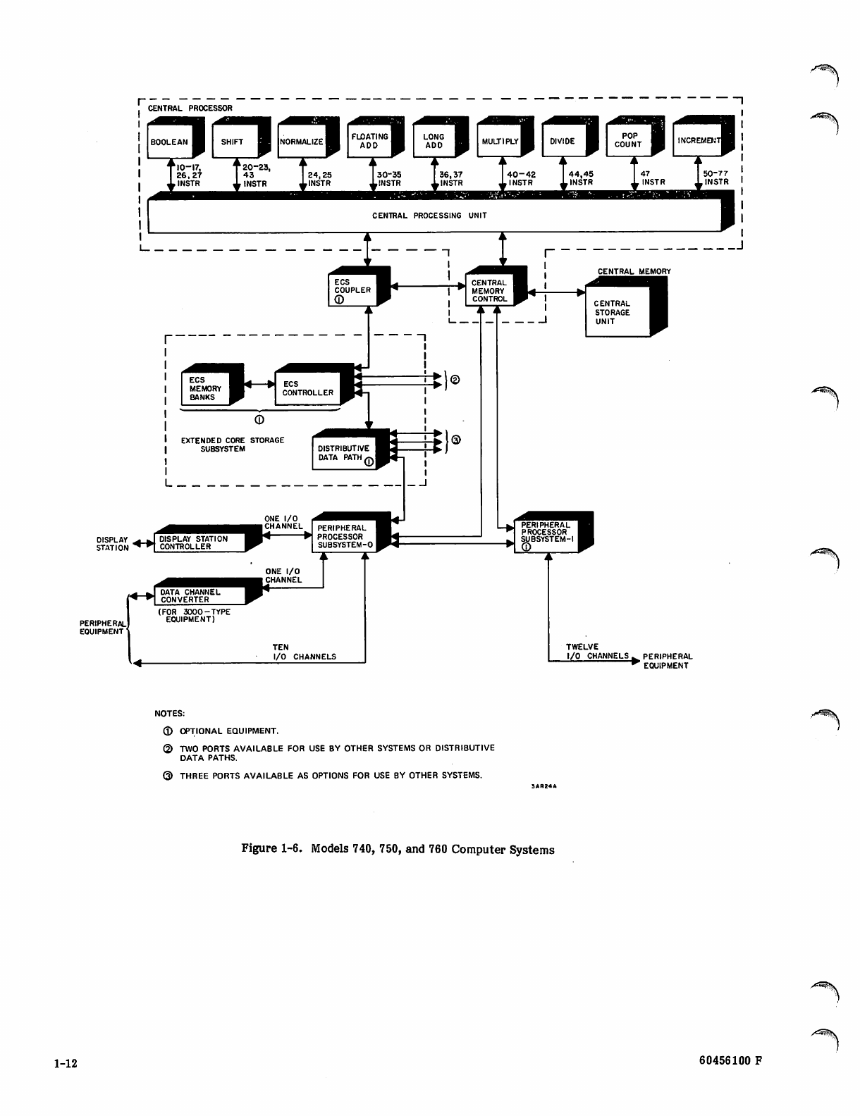
MODEL 740 SYSTEM
The model 740 basic computer system (figure 1-6) is
functionally similar to model 730, except for faster
CP operation. This operation occurs through processing
performed in a CP that has nine functional units instead of
the arithmetic, compare/move, and instruction control
units of the model 730.
The system options are the same as those for the model
730, except that model 740 does not have a second CP
option or compare/move unit.
MODELS 750 AND 760 SYSTEMS
The models 750 and 760 basic computer systems (figure
1-6) are functionally similar to the model 740, except for
faster CP operation. This operation occurs by using the CP
functional units in parallel operation. In this operation, the
independent specialized arithmetic units provide maximum
overlap of instruction retrieval and execution.
The system options are the same as those for the model 740.
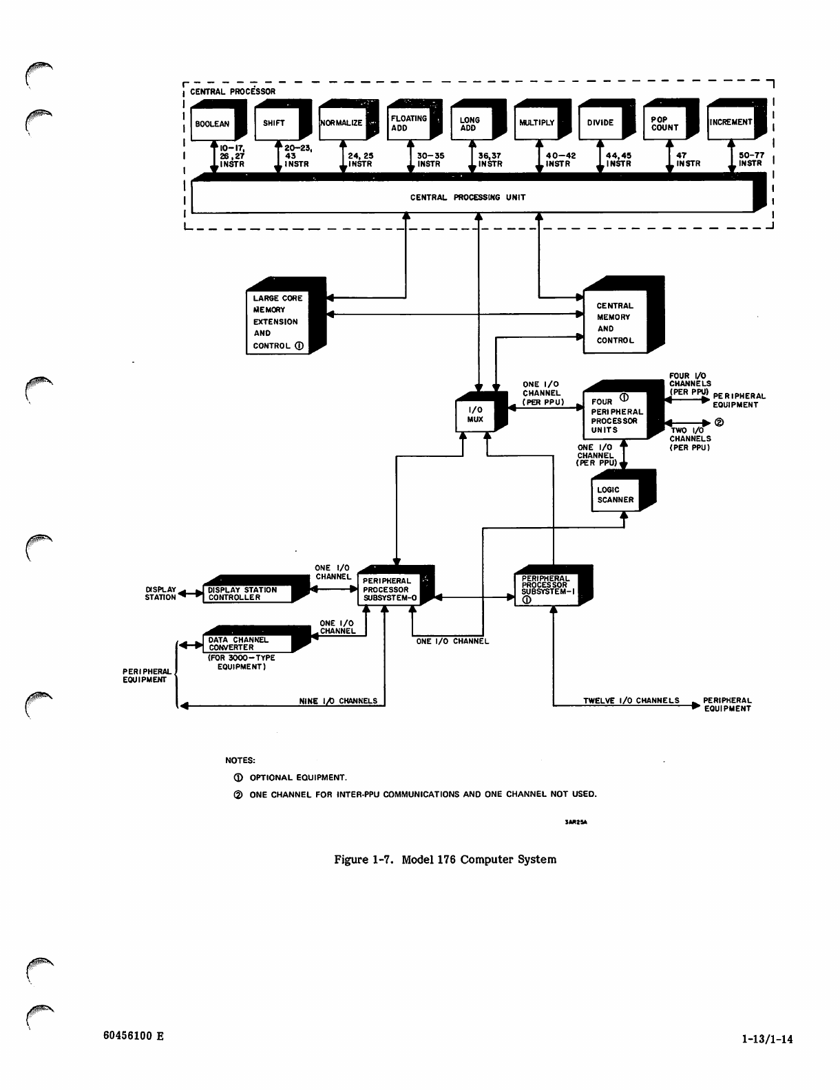
MODEL 176 SYSTEM
The model 176 basic computer system (figure 1-7) is
functionally similar to models 740 and 750 in the CP and
PPS.
The semiconductor CM has the same options for expansion
as models 750 and 760, but has some differences in its
method of internal addressing and location of the memory
control. In model 176, expansion of CM capacity is through
the use of LCME. This optional memory also includes its
own control function.
The PPUs are optional. A PPU installation must begin with
four PPUs. Following PPU installations may be in
increments of 1, up to a total of 12 PPUs. Each PPU adds
six I/O channels. Like the PPs, the PPUs perform I/O
operations by executing independent programs. These
programs occur through the use of a PPU instruction set,
similar to the PP instruction set. Communications occur
between the PPs/PPUs and the CP through the I/O
multiplexer and between the PPs and the PPUs through the
logic scanner.
60456100 E 1-7
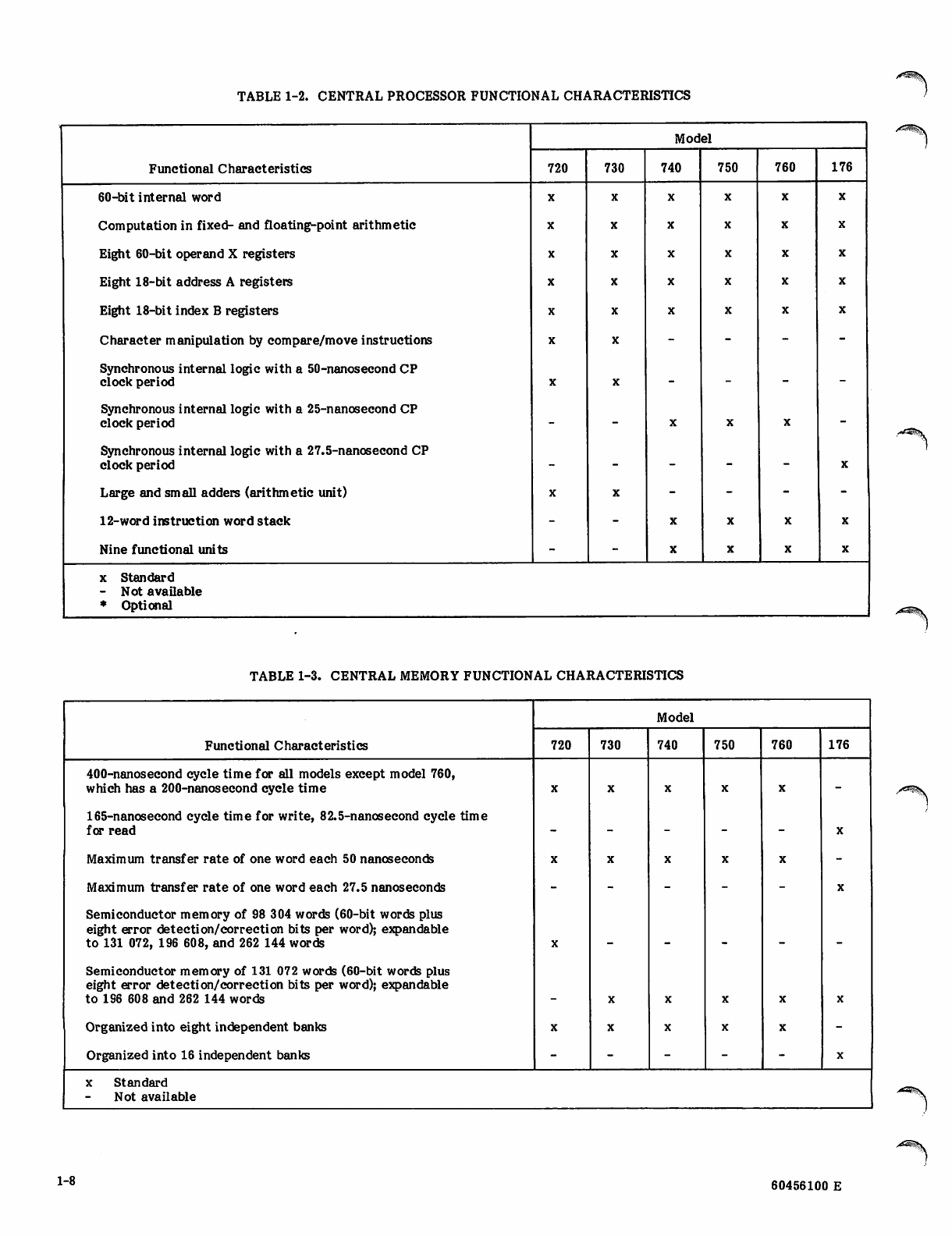
TABLE 1-2. CENTRAL PROCESSOR FUNCTIONAL CHARACTERISTICS
Functional Characteristics
Model
720 730 740 750 760 176
60-bit internal word
Computation in fixed- and floating-point arithmetic
Eight 60-bit operand X registers
Eight 18-bit address A registers
Eight 18-bit index B registers
Character manipulation by compare/move instructions
Synchronous internal logic with a 50-nanosecond CP
clock period
Synchronous internal logic with a 25-nanosecond CP
clock period
Synchronous internal logic with a 27.5-nanosecond CP
clock period
Large and small adders (arithmetic unit)
12-word instruction word stack
Nine functional units
x Standard
- Not available
* Optional
TABLE 1-3. CENTRAL MEMORY FUNCTIONAL CHARACTERISTICS
Functional Characteristics
Model
720 730 740 750 760 176
400-nanosecond cycle time fer all models except model 760,
which has a 200-nanosecond cycle time
165-nanosecond cycle time for write, 82.5-nanosecond cycle time
for read
Maximum transfer rate of one word each 50 nanoseconds
Maximum transfer rate of one word each 27.5 nanoseconds
Semiconductor memory of 98 304 words (60-bit words plus
eight error detection/correction bits per word); expandable
to 131 072, 196 608, and 262 144 words
Semiconductor memory of 131 072 words (60-bit words plus
eight error detection/correction bits per word); expandable
to 196 608 and 262 144 words
Organized into eight independent banks
Organized into 16 independent banks
x Standard
Not available
1-8 60456100 E
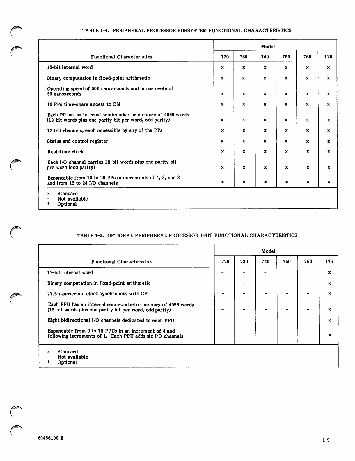
TABLE 1-4. PERIPHERAL PROCESSOR SUBSYSTEM FUNCTIONAL CHARACTERISTICS
Functional Characteristics
Model
720 730 740 750 760 176
12-bit internal word
Binary computation in fixed-point arithmetic
Operating speed of 500 nanoseconds and minor cycle of
50 nanoseconds
10 PPs time-share access to CM
Each PP has an internal semiconductor memory of 4096 words
(12-bit words plus one parity bit per word, odd parity)
12 I/O channels, each accessible by any of the PPs
Status and control register
Real-time clock
Each I/O channel carries 12-bit words plus one parity bit
per word (odd parity)
Expandable from 10 to 20 PPs in increments of 4, 3, and 3
and from 12 to 24 I/O channels
x Standard
Not available
* Optional
TABLE 1-5. OPTIONAL PERIPHERAL PROCESSOR UNIT FUNCTIONAL CHARACTERISTICS
Functional Characteristics
Model
720 730 740 750 760 176
12-bit internal word
Binary computation in fixed-point arithmetic
27.5-nanosecond clock synchronous with CP
Each PPU has an internal semiconductor memory of 4096 words
(12-bit words plus one parity bit per word, odd parity)
Eight bidirectional I/O channels dedicated to each PPU
Expandable from 0 to 12 PPUs in an increment of 4 and
following increments of 1. Each PPU adds six I/O channels
x Standard
Not available
* Optional
60456100 E 1-9
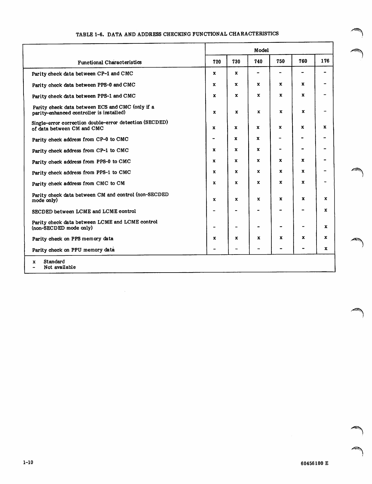
TABLE 1-6. DATA AND ADDRESS CHECKING FUNCTIONAL CHARACTERISTICS
Functional Characteristics
Parity check data between CP-1 and CMC
Parity check data between PPS-0 and CMC
Parity check data between PPS-1 and CMC
Parity check data between ECS and CMC (only if a
parity-enhanced controller is installed)
Single-error correction double-error detection (SECDED)
of data between CM and CMC
Parity check address from CP-0 to CMC
Parity check address from CP-1 to CMC
Parity check address from PPS-0 to CMC
Parity check address from PPS-1 to CMC
Parity check address from CMC to CM
Parity check data between CM and control (non-SECDED
mode only)
SECDED between LCME and LCME control
Parity check data between LCME and LCME control
(non-SECDED mode only)
Parity check on PPS memory data
Parity check on PPU memory data
x Standard
Not available
Model
720 730 740 750 760 176
z^Stjx
1-10 60456100 E
CENTRAL PROCESSOR-I
/0&\
PERIPHERAL
EQUIPMENT
NOTES:
© OPTIONAL EQUIPMENT.
<2> ALL PP's MAY ACCESS ALL CHANNELS.
® TWO PORTS AVAILABLE AS OPTIONS FOR USE BY OTHER SYSTEMS OR DISTRIBUTIVE
DATA PATHS.
@ THREE PORTS AVAILABLE AS OPTIONS FOR USE BY OTHER SYSTEMS.
Figure 1-5. Models 720 and 730 Computer Systems
60456100 F 1-11
CENTRAL PROCESSOR
TEN
I/O CHANNELS
TWELVE
I/O CHANNELS^ PERIPHERAL
EQUIPMENT
NOTES:
® OPTIONAL EQUIPMENT.
© TWO PORTS AVAILABLE FOR USE BY OTHER SYSTEMS OR DISTRIBUTIVE
DATA PATHS.
© THREE PORTS AVAILABLE AS OPTIONS FOR USE BY OTHER SYSTEMS.
Figure 1-6. Models 740, 750, and 760 Computer Systems
1-12 60456100 F
I CENTRAL PROCESSOR
LARGE
MEMORY
EXTENSION
AND
CONTROL ©
CENTRAL
MEMORY
AND
CONTROL
PERIPHERAL
EQUIPMENT
PERIPHERAL
EQUIPMENT
■>®
TWELVE I/O CHANNELS ^ PERIPHERAL
** EQUIPMENT
NOTES:
fl) OPTIONAL EQUIPMENT.
© ONE CHANNEL FOR INTER-PPU COMMUNICATIONS AND ONE CHANNEL NOT USED.
Figure 1-7. Model 176 Computer System
60456100 E 1-13/1-14

M^MtmsMM COMPOjSlNf iiseRipTi^^

MAJOR SYSTEM COMPONENT DESCRIPTIONS
The following are the major system components.
Central processor.
Central memory.
Extended core storage (optional) in models 720
through 760.
Large core memory extension (optional) in model
176.
Peripheral processor units (optional) in model 176.
Peripheral processor subsystem.
Display station.
Condensing unit(s).
Power distribution unit in model 176.
CENTRAL PROCESSOR — MODELS 720 AND 730
The CP consists of the instruction control section and the
arithmetic unit. The CP is isolated from the PPS and is
thus able to carry on computation or character
manipulation unencumbered by I/O requirements.
The instruction control section directs the arithmetic and
manipulative functions for instruction execution. The
instruction control section also performs instruction
retrieval, address preparation, m.emory protection, and
data retrieval and storage. The instruction control section
acquires instructions from CM and decodes and executes
them in a serial manner. Operating registers reduce
storage accesses for operands used during the execution of
an instruction. These registers are:
• Eight 60-bit X registers (XO through X7) which hold
operands used for computation.
• Eight 18-bit A registers (AO through A7) which use
AO primarily for indexing and Al through A7 for
CM operand addressing.
• Eight 18-bit B registers (BO through B7) which are
primarily indexing registers to control program
execution. The BO register always contains all
zeros.
The instruction control section also contains seven support
registers that support the operating registers during
program execution. These registers are:
• Program address (P) register, 18 bits.
• Reference address for CM (RAC) register, 18 bits.
• Field length for CM (FLC) register, 18 bits.
• Exit mode (EM) register, 6 bits.
• Reference address for ECS (RAE) register, 21 bits.
• Field length for ECS (FLE) register, 24 bits.
• Monitor address (MA) register, 18 bits.
The instruction control section also directs the character
manipulative functions of the compare/move instructions.
Characters are 6 bits; therefore, a CM word may contain
up to 10 characters. Characters can be moved from one
CM location to another, and fields of characters can be
compared either directly or through a collation table.
The arithmetic unit consists of a large arithmetic section
(used by instructions requiring manipulation of 60-bit
operands) and a small arithmetic section (used by
instructions requiring manipulation of 18-bit operands).
The large and small arithmetic sections also provide other
arithmetic functions required by the CP for instruction
execution, such as instruction addressing.
The CMC provides an interface between CM and five CM
access ports (PPS-0, PPS-1, CPU-0, CPU-1, and ECS). The
CMC primarily controls address and write data to CM and
read data from CM. In addition, the CMC:
Determines access priorities.
Increments addresses (for exchange jumps and ECS
transfers).
Checks and generates address and data parity.
Provides single-error correction double-error
detection (SECDED).
Performs breakpoint checks.
Controls CM reconfiguration.
Controls exchange jumps.
CENTRAL PROCESSOR — MODELS 740, 750, 760, AND 176
Models 740, 750, 760, and 176 differ from the other models
by not having the compare/move capability. In addition,
the models 750, 760, and 176 perform parallel processing
rather than serial processing within a single CP.
The models 740, 750, 760, and 176 CPs have basic
similarities in their CPUs. Each CPU contains operating
registers, support registers, and functional units. In
addition, the models 740, 750, and 760 CPs contain a CMC.
In model 176, the memory control function is part of the
CM.
The operating registers minimize CM references for
functional unit operands and results. These registers are:
• Eight 60-bit X registers (X0 through X7) which are
the source and destination of operands for the
functional units, input data from CM, and output
data to CM; for model 176 only, these registers
also input and output data and addresses for LCME.
60456100 E 1-15
• Eight 18-bit A registers (AO through A7) which use
AO primarily for indexing and Al through A7 for
addressing.
• Eight 18-bit B registers (BO through B7) which are
primarily indexing registers to control program
execution.
The support registers support the operating registers during
the execution of programs. The models 740, 750, and 760
registers differ from the model 176 registers.
Models 740, 750, and 760 support registers are:
• Program address (P) register, 18 bits.
• Reference address for CM (RAC) register, 18 bits.
• Field length for CM (FLC) register, 18 bits.
• Exit mode (EM) register, 6 bits.
• Reference address for ECS (RAE) register, 21 bits
(lower 6 bits are zeros).
• Field length for ECS (FLE) register, 24 bits (lower
6 bits are zeros).
• Monitor address (MA) register, 18 bits.
Model 176 support registers are:
• Program address (P) register, 18 bits.
• Reference address for CM (RAS) register, 18 bits.
• Field length for CM (FLS) register, 18 bits.
• Program status designator (PSD) register, 18 bits.
• Reference address for LCME (RAL) register, 22
bits.
• Field length for LCME (FLL) register, 22 bits.
• Normal exit address (NEA) register, 18 bits.
• Error exit address (EEA) register, 18 bits.
Instruction control consists of the instruction word stack
(IWS), instruction address stack (IAS), current instruction
word (CIW), and P registers. The IWS and IAS allow short
program loops to execute without rereading instructions
from CM.
The nine functional units operate as independent
specialized arithmetic units. These units are:
• Boolean unit which forms the logical product,
logical sum, or logical difference of two 60-bit
operands, transfers a 60-bit operand between X
registers, and packs and unpacks floating-point
operands.
• Shift unit which performs mask generation and left
circular or right end-off shifting of 60-bit operands.
• Normalize unit which performs the normalize
operation.
• Floating-add unit which forms the sum or
difference of two floating-point operands.
o Long-add unit which forms the sum or difference of
two 60-bit integers.
© Floating-multiply unit which forms the product of
two floating-point operands in single or double
precision and does 48-bit integer multiply.
• F l o a t i n g - d i v i d e u n i t w h i c h f o r m s t h e
single-precision quotient of two floating-point
operands.
• Population count unit which counts the number of
bits which have a value of one in a 60-bit operand.
o Increment unit which forms the one's complement
sum or difference of two 18-bit operands.
Computation is performed by the functional units. Data
moves into and out of the functional units through the
operating registers (A, B, and X) in the CPU.
In models 740, 750, and 760, the CMC controls the flow of
data between CM and the requesting elements of the
system. In addition, the CMC:
• Determines access priorities.
• Increments addresses (for exchange jumps and ECS).
• Checks and generates address and data parity.
• Provides single-error correction double-error
detection (SECDED).
• Performs breakpoint checks.
• Controls exchange jumps.
• Controls CM reconfiguration.
CENTRAL MEMORY — ALL MODELS
The CM in models 720 through 760 is a metal oxide
semiconductor (MOS) memory. The CM in model 176 is a
bipolar semiconductor memory. Each of the basic CM sizes
is field-upgradable to 262 144 words.
Words in the CMs contain 60 data bits and 8 SECDED code
bits.
EXTENDED CORE STORAGE (OPTIONAL) — MODELS
720 THROUGH 760
The ECS is an optional on-line, semirandom-access,
magnetic-core memory system which augments CM. The
ECS has a fixed-word length and is capable of two-way
communication between its memory banks and the
mainframe. An ECS contains:
• ECS controller.
• ECS memory banks.
1-16 60456100 E
/fP^x
» Distributive data path (DDP) (optional to ECS).
The ECS controller regulates the computer system access
to the ECS memory bays through four available access
ports. One access port connects to the ECS coupler. The
other ports may connect to other systems or optional
DDPs. Each access port carries 60 data bits plus 1 parity
bit and control signals. Eight 60-bit data words plus eight
parity bits comprise an ECS record. The ECS controller
performs time-sharing of ECS records in the four access
ports during ECS data transfers. The ECS controller
interfaces from one to four ECS memory bays and carries
60 data bits plus 1 parity bit. Depending upon the
controller used, the controller transfers the parity bit that
accompanies the data from the computer system to the
ECS memory bays or generates a parity bit for the ECS
data.
The ECS contains 2, 4, 8, or 16 memory banks; each bank is
capable of storing 131 072 60-bit words. ECS is available in
sizes ranging from 262144 words (2 banks) to 2 097 152
words (16 banks). A cabinet, termed bay, holds up to four
memory banks. Each ECS bank address stores one ECS
record. References of one 60-bit word are possible.
The DDP provides a data path between ECS and the PPs.
The path allows fast PP access to data in ECS using an I/O
channel and greatly reduces the data traffic through the
CM.
Each ECS requires an ECS coupler which mounts within the
mainframe cabinet. The coupler interfaces the mainframe
with the ECS processing and monitoring data and control
between the systems. The coupler:
• Receives the initial ECS address from the CP and
relays the address, request, and read or write to
the ECS controller.
• Receives the word count from the CP and
compares the number of words transferred with the
word count.
• Generates and sends a continue request signal to
CMC to set CM bank reservations.
• Generates and sends a bank initiate signal for each
transfer of a CM word.
e Increments each ECS address.
• Generates an end-of-transfer signal when the
transfer is completed normally.
• Terminates a transfer when an error condition is
detected.
• Provides a parity check of the word count and
address information received from the CP.
• Generates parity for ECS addresses transmitted to
the ECS controller.
Additional information for the ECS and ECS coupler is in
manuals listed in the system publication index in the
preface of this manual.
LARGE CORE MEMORY EXTENSION (OPTIONAL) —
MODEL 176
LCME is optional and provides additional storage for data
that is not immediately needed by the CPU. The data
transfers through a bidirectional high-speed data path
between CM and LCME. Data may also be transferred one
word at a time to or from the X operating registers.
However, programs cannot execute directly out of LCME.
LCME basically contains 512 288 words and is expandable
with system options to 2 097 152 72-bit words. Each word
includes 60 data bits, 8 error correction bits, 2 complement
control bits, and 2 unused bits.
PERIPHERAL PROCESSOR UNITS (OPTIONAL) —
MODEL 176
The PPU is a computer with an independently stored
program. The system can contain up to 12 PPUs, depending
on the number installed as options. The PPUs have 4096
words (12 bits plus 1 parity bit per word) of bipolar
semiconductor memory organized into two
independent banks of 2048 words. The PPUs share access
to CM with the PPS through I/O multiplexer channels.
Each PPU operates independently with separate hardware
for performing arithmetic, logical, and I/O operations.
PERIPHERAL PROCESSOR SUBSYSTEM — ALL MODELS
The PPS consists of 10 logically independent computers in
PPS-0 and 4, 7, or 10 of the computers in PPS-1, when
installed as options. The computers, termed PPs, have 4096
words (12 bits plus 1 parity bit per word) of MOS memory
and a repertoire of 64 instructions. The PPs share access
to CM and 12 bidirectional I/O channels. The PPs operate
in a multiplexing system that allows them to share common
hardware for arithmetic, logical, and I/O operations
without losing speed or independence.
A status and control register is included in the PPS as a
maintenance aid. This register is program-controlled and
monitors error system conditions that include address and
data parity errors, single-error correction double-error
detection conditions, and address information. Visual light
displays on the PPS chassis permit monitoring some of the
register status bits.
A real-time clock is included in the PPS.
increments once each microsecond.
The clock
Provides a data input and output interface between
CMC and the ECS controller.
Receives flag functions from the CP and relays
them to the ECS controller.
Models 720 through 760 and 176 mainframes are expandable
to 14, 17, or 20 PPs and 24 I/O channels with the addition
of PPS-1. PPS-1 includes an abbreviated status and control
register. All I/O channels are accessed by all PPs.
Receives and sends data parity from and to CMC
on models 740, 750, and 760.
60456100 E 1-17
DISPLAY STATION — ALL MODELS
The display station provides a visual, alphanumeric readout
for the computer. The receipt of symbol and position
information from the computer enables displaying program
information on a 21-inch cathode-ray tube (CRT). The
station also contains an alphanumeric keyboard which
enables an operator to send data to the computer. The
keyboard and CRT combination permits the computer
operator to modify computer programs and view the result
on the screen. The computer outputs two alternate,
nonrelated data streams. The display station keyboard has
a switch which enables the operator to select either of the
data streams or to select both for presentation on the
CRT. (Except for programming information in section 5,
refer to the display station manual listed in the system
publication index in the preface of this manual for further
display station information.)
CONDENSING UNIT(S) — ALL MODELS
One or more condensing units circulate cooling refrigerant
to cold bars and plates for the conduction cooling of the
logic and memory paks and logic and memory modules in a
system. For models 720 and 730, one 3-ton condensing unit
mounts in and cools each bay. For models 740, 750, and
760, one 10-ton condensing unit is in a stand-alone cabinet
and cools the entire system. For model 176, two 10-ton
condensing units in stand-alone cabinets cool the basic
system. System options permit a third 10-ton condensing
unit.
POWER DISTRIBUTION UNIT — MODEL 176
The PDU distributes 400-Hz power to the dc power supplies
located in the mainframe. It also contains a warning
system that monitors logic chassis temperature, room
dew-point temperature, and condensing unit condition. A
warning panel in the PDU contains relay circuits that
activate a horn and automatically shut off computer power
when the cooling system malfunctions.
1-18 60456100 E
FUNCTIONAL DESCRIPTIONS
/#»^
This section provides functional descriptions of the system
mainframe parts shown in the block diagrams in section 1.
These parts consist of:
Central processor (CP) in models 720 and 730.
Central processor in models 740, 750, 760, and 176.
Central memory control (CMC) in models 730, 740,
750, and 760.
Central memory (CM) in models 730, 740, 750, and
760.
Central memory in model 176.
Large core memory extension (LCME), optional, in
model 176.
Input/output multiplexer (MUX) in model 176.
Logic scanner in model 176.
• Data channel converter (DCC).
• Display controller.
• Peripheral processor units (PPUs), optional, in
model 176.
• Peripheral processor subsystem (PPS).
Functional descriptions for the system display station,
condensing units, and extended core storage (ECS) are in
respective manuals listed in the system publication index in
the preface of this manual.
Functional differences among the CDC CYBER 170 models
mainly exist in their CPs' program processing methods.
The CPs of models 720 and 730 perform serial processing
with an arithmetic unit, compare/move unit, and
instruction control section. Although the model 740 CP
also performs serial processing, it uses nine functional units
for this purpose. The functional units are also used by the
models 750, 760, and 176 CPs, but for parallel processing.
60456100 E 2-1/2-2

CENTRAL PROCESSOR - MODELS W$® AND 7^0
i

CENTRAL PROCESSOR - MODELS 720 AND a Registers
j00&*\.
The CP consists of the arithmetic unit (AU) and an
instruction control section. The AU performs arithmetic
operations by manipulation of 18- and 60-bit operands. The
instruction control section directs the arithmetic
operations, directs character manipulative functions of
compare/move instructions, and interfaces the CMC and
arithmetic sections. The compare/move unit is optional.
ARITHMETIC UNIT — MODELS 720 AND 730
The AU consists of the large and small arithmetic
sections. Instructions use the large section for 60-bit
operand manipulation and the small section for 18-bit
operand and exponent manipulation. The large arithmetic
section contains a 108-bit adder, shift network, normalize
network, and shift counter. The small arithmetic section
contains an 18-bit adder. The arithmetic sections also
provide other arithmetic functions required by the CP for
instruction execution.
INSTRUCTION CONTROL SECTION — MODELS 720
AND 730
The instruction control section consists of 24 operating
registers, 7 support registers, and logic for instruction
control.
The following operating and support register descriptions
are identical to those for models 740, 750, 760, and 176 and
are repeated in the CP descriptions of the those models to
provide continuous system descriptions.
Operating Registers — Models 720 and 730
The operating registers consist of operand (X), address (A),
and index (B) registers. These registers minimize memory
references for arithmetic operands and results.
X Registers
The CP contains eight 60-bit X registers, XO through X7.
The XO register is used in the compare instructions to
indicate if two fields of characters are equal. If the
system includes ECS, the XO register provides the relative
starting address in a block copy operation. The XO register
also provides the instruction information during a flag
register operation.
The XI through X7 registers are primarily data handling
registers for computation with XI through X5 used to input
data from CM and X6 and X7 used to transmit data to CM.f
The CP contains eight 18-bit A registers, AO through A7.
The AO register serves as an intermediate register for the
user's discretion. If the system includes ECS, the AO
register provides the relative CM starting address. The A0
register is also used for the collation table address. The
register is not used in an ECS flag operation.
The Al through A7 registers are essentially CM operand
address registers associated one-for-one with the X
registers. Placing a quantity into an address register (Al
through A5) causes an immediate CM read reference to
that address and transmits the CM word to the
corresponding register (XI through X5). Similarly, placing
a quantity into the A6 or A7 register causes the word in the
corresponding X6 or X7 register to be written into that
relative address of CM.
B Registers
The CP contains eight 18-bit B registers, B0 through B7.
These registers are primarily indexing registers to control
program execution. Program loop counts may also be
incremented or decremented in these registers.
Program addresses may be modified on the way to an A
register by adding or subtracting B register quantities. The
B registers also hold shift counts for the nominal Bj shifts,
the resultant exponent for the unpack, the operand
exponent for the pack, and the resultant shift count from a
normalize. The BO register always contains positive zero
which can be used as an operand. This register cannot hold
results from instructions.
Support Registers — Models 720 and 730
Seven support registers assist the operating registers during
the execution of programs. The contents of the support
registers are stored in CM, and their new contents are
loaded from CM during an exchange sequence (refer to
Exchange Jump in section 5). With the exception of the P
register, the contents of the support registers cannot be
altered during the execution interval of an exchange
package. When the execution interval completes, the data
in the support registers is sent back to CM through an
exchange jump.
P Register
The 18-bit program address (P) register loads from CM
during the first word of an exchange sequence and contains
the current program execution address. The register serves
as a program address counter and holds the relative CM
address for each program step.
Operands and results transfer between CM and the X
registers as a result of placing CM addresses into
corresponding A registers.
RAC Register
The 18-bit CM reference address (RAC) register loads from
CM during the second word of an exchange sequence. An
absolute CM address forms by adding RAC to a relative
60456100 E 2-3
address determined by the instruction. The content of the
P register is added to RAC to form the absolute program
address in CM. A P-equal-to-zero condition specifies
relative address zero and therefore RAC. This address is
reserved for recording program-error-exit-conditions and
should not be used to store data or instructions.
FLC Register
The 18-bit CM field length (FLC) register loads from CM
during the third word of an exchange sequence. The FLC
register defines the size of the field of the program in
execution. Relative CM addresses are compared with FLC
to check that the program is not going out of its allocated
memory range. (For further information, refer to Exit
Mode/Error Response under Central Processor in section 5.)
EM Register
The six-bit exit mode (EM) register loads from CM during
the fourth word of an exchange sequence. The EM register
holds six exit mode selection bits that control individual
error conditions for a program. Selected EM register bits
cause the CP to error exit when the corresponding
conditions occur. Any or all of the six bits can be selected
at one time. Unselected EM register bits allow the CP to
continue, without error processing, when most of the
corresponding conditions occur. The exit mode selection
bits appear in the exchange package as bits 48 through 50
and 57 through 59. The bits and their corresponding
conditions are:
Mode
Selection
Bit Condition Sensed
48 Address out of range
49 Infinite operand
50 Indefinite operand
57 Parity error on ECS t
58
59
operation
Central processor unit (CPU) to CMC
address or data parity error or CPU
to CMC to CM address parity error
CMC to CPU data parity error or
double error
RAE Register
The 21-bit ECS reference address (RAE) register loads
from CM during the fifth word of an exchange sequence.
The lower six bits of this register are always zero. An
absolute ECS address forms by adding RAE to the relative
address which is determined by the instruction.
FLE Register
The 24-bit ECS field length (FLE) register loads from CM
during the sixth word of an exchange sequence. The lower
six bits of this register are always zero. The FLE register
defines the size of the field in ECS for the program in
execution. Relative ECS addresses are compared with
FLE. (For further information, refer to Exit Mode/Error
Response under Central Processor in section 5.)
MA Register
The 18-bit monitor address (MA) register loads from CM
during the seventh word of an exchange sequence. The MA
register contains the absolute starting address of an
exchange package which is used when executing a central
exchange jump (013) instruction with the monitor flag clear
or when honoring a monitor exchange jump to MA (26 2x)
instruction with the monitor flag clear.
Instruction Control Sequences — Models 720
and 730
The instruction control logic performs instruction
translation and control sequences. Each control sequence
obtains the necessary instruction operands from the
operating registers and provides the control signals for
execution. Instructions read from CM are 60-bit
instruction words that are in four 15-bit groups, two 30-bit
groups, or a combination of 15-bit and 30-bit groups. The
15-bit groups are termed parcels with the first parcel
(parcel 0) being the highest-order 15 bits of a 60-bit CM
word. Second, third, and fourth parcels (parcels 1,2, and 3)
follow in order. The 30-bit groups contain two 15-bit
parcels.
The instruction control sequences control the execution of
one or more instructions of a common type. These
sequences and associated instructions are briefly described
in this section. (For further information, refer to CP
Instruction Descriptions in section 4.)
Boolean Sequence
The boolean sequence controls instructions that require
bit-by-bit data manipulation. This includes both the logical
and transmissive operations. The instructions requiring
logical operations are:
11 Logical product (Xj) and (Xk) to Xi
12 Logical sum of (Xj) and (Xk) to Xi
13 Logical difference of (Xj) and (Xk) to Xi
15 Logical product of (Xj) and (Xk) to Xi
16 Logical sum of (Xj) and (Xk) to Xi
17 Logical difference of (Xj) and (Xk) to Xi
2-4 60456100 A
The instructions requiring transmissive operations are:
10 Transmit (Xj) to Xi
14 Transmit (Xk) to Xi
Shift Sequence
The shift sequence controls instructions that require
shifting the 60-bit field of data within the operand word.
The shift instructions are:
20 Left shift (Xi) by $c
21 Right shift (Xi) by Jc
22 Left shift (Xk) nominally (Bj) places to Xi
23 Right shift (Xk) nominally (Bj) places to Xi
43 Form mask of jk bits to Xi
The shift sequence also controls the pack and unpack
instructions. In the packed floating format, the coefficient
is contained in the lower 48 bits. The sign and biased
exponents are contained in the upper 12 bits. The unpack
instruction obtains the packed word from the Xk register,
delivers the coefficient to the Xi register, and delivers the
exponent to the Bj register. The unpack and pack
instructions are:
26 Unpack (Xk) to Xi and Bj
27 Pack (Xk) and (Bj) to Xi
The shift sequence also controls the normalize operations.
The coefficient portion of the operand is repositioned, and
the exponent is adjusted so that the most significant bit of
the coefficient is in the highest-order bit position of the
coefficient, and the exponent is decreased by the number
of bit positions shifted. The normalize instructions are:
24 Normalize (Xk) to Xi and Bj
25 Round normalize (Xk) to Xi and Bj
Floating-Add Sequence
The floating-add sequence controls the operations
necessary to form the 48-bit floating sum with a 12-bit
exponent of the floating-point sum or difference of two
floating-point operands. The floating-add instructions are:
30 Floating sum of (Xj) and (Xk) to Xi
31 Floating difference of (Xj) and (Xk) to Xi
32 Floating double-precis ion sum of (Xj) and (Xk) to Xi
33 Floating double-precision difference of (Xj) and
(Xk) to Xi
34 Round floating sum of (Xj) and (Xk) to Xi
35 Round floating difference of (Xj) and (Xk) to Xi
Floating-Multiply and Floating-Divide Sequence
The floating-multiply and floating-divide sequence controls
the operation of floating-multiply, floating-divide, and
population-count instructions.
The multiply instructions are:
40 Floating product of (Xj) and (Xk) to Xi
41 Round floating product of (Xj) and (Xk) to Xi
42 Floating double-precision product of (Xj) and (Xk)
t o X i
The divide instructions are:
44 Floating divide (Xj) by (Xk) to Xi
45 Round floating divide (Xj) by (Xk) to Xi
The population-count instruction counts the number of one
bits in a 60-bit operand. The instruction is:
47 Population count of (Xk) to Xi
Increment Sequence
The increment sequence controls the one's complement
addition and subtraction of 18-bit fixed-point operands for
increment instructions 50 through 77. The sequence also
controls the 60-bit one's complement sum and difference
values for long add instructions 36 and 37.
The increment instructions are:
50 Set Ai to (Aj) + K
51 Set Ai to (Bj) + K
52 Set Ai to (Xj) + K
53 Set Ai to (Xj) + (Bk)
54 Set Ai to (Aj) + (Bk)
55 Set Ai to (Aj) - (Bk)
56 Set Ai to (Bj) + (Bk)
57 Set Ai to (Bj) - (Bk)
60 Set Bi to (Aj) + K
61 Set Bi to (Bj) + K
62 Set Bi to (Xj) + K
63 Set Bi to (Xj) + (Bk)
64 Set Bi to (Aj) + (Bk)
65 Set Bi to (Aj) - (Bk)
66 Set Bi to (Bj) + (Bk)
67 SetBito(Bj)-(Bk)
70 Set Xi to (Aj) + K
60456100 A 2-5
71 Set Xi to (Bj) + K
72 Set Xi to (Xj) + K
73 Set Xi to (Xj) + (Bk)
74 Set Xi to (Aj) + (Bk)
75 SetXito(Aj)-(Bk)
76 Set Xi to (Bj) + (Bk)
77 SetXito(Bj)-(Bk)
The long add instructions are:
36 Integer sum of (Xj) and (Xk) to Xi
37 Integer difference of (Xj) minus (Xk) to Xi
Compare/Move Sequence
The compare/move sequence controls the execution of
compare/move instructions that handle data manipulation
on a character basis. The compare/move instructions are
60-bit instructions that use six support registers for source
and result field CM addresses and character position
offsets. The support registers load from the 60-bit
instruction word. The compare/move instructions are:
464 Move indirect (Bj) + K
465 Move direct
466 Compare collated
467 Compare uncollated
The support registers are:
• An 18-bit Kl register that specifies which relative
CM address word contains the first character of
the source data field.
• An 18-bit K2 register that specifies which relative
CM address word contains the first character of
the result field.
• A 4-bit Cl register that specifies the character
position or offset of the first CM word of the
source field.
• A 4-bit C2 register that specifies the character
position or offset of the first CM word of the result
field.
• Two 16-bit L registers (LA and LC) that specify the
number of characters in the data field. The LA
register is associated with Kl, and the LC register
is associated with K2. Instruction 464 uses 14
register bits. Instructions 465, 466, and 467 use
only the lower eight register bits.
Exchange Sequence
The exchange sequence generates timed CM reference
signals to implement the exchange of data between the CP
and CM, as required by the exchange jump instruction. In
addition, the exchange sequence provides internal control
signals to the operating and control registers to
systematically enter the content of an exchange jump
package.
The CMC always initiates the exchange sequence from a
CP or peripheral processor (PP) request.
ECS Block Copy Sequence
The ECS block copy sequence controls the transfer of data
between CM and ECS. The number of words to be
transferred is determined by the addition of K to the
content of Bj. The starting address for CM is obtained
from the AO register plus the RAC reference address. The
starting address for ECS is obtained from the XO register
plus the RAE reference address. The ECS block copy
instructions are:
Oil Block copy (Bj) + K from ECS to CM
012 Block copy (Bj) + K from CM to ECS
Normal Jump Sequence
The normal jump sequence controls the execution of branch
instructions 02 through 07. The 02 instruction performs an
unconditional jump to the Bi register address plus K. The
branch address is K when i equals 0. The 02 instruction is:
02 Jump to (Bi) + K
The conditional jump instructions 03 through 07 branch to
address K if the jump condition is met. These instructions
are:
030 Branch to K if (Xj) = 0
031 Branch to K if (Xj) * 0
032 Branch to K if (Xj) positive
033 Branch to K if (Xj) negative
034 Branch to K if (Xj) in range
035 Branch to K if (Xj) out of range
036 Branch to K if (Xj) definite
037 Branch to K if (Xj) indefinite
04 Branch to K if (Bi) = (Bj)
05 Branch to K if (Bi) t (Bj)
06 Branch to K if (Bi)> (Bj)
07 Branch to K if (Bi)< (Bj)
X5X
2-6 60456100 G
Return Jump Sequence
The return jump sequence controls the execution of three
instructions.
00 Error exit to MA or program stop
010 Return jump to K
013 Central exchange jump to (Bj) + K or (MA)
60456100 A 2-7/2-8

/^
/"^l
CENlRAi PiQGESSQR.-« MJpEIS Hfy 75% ?60h $tsl& 176

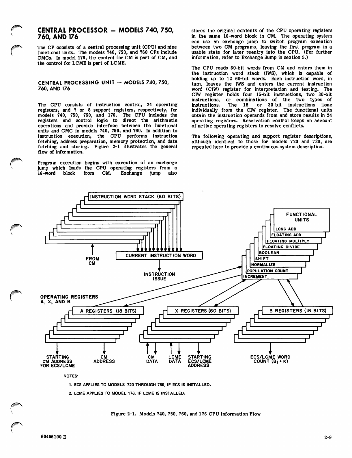
CENTRAL PROCESSOR - MODELS 740, 750,
760, AND 176
The CP consists of a central processing unit (CPU) and nine
functional units. The models 740, 750, and 760 CPs include
CMCs. In model 176, the control for CM is part of CM, and
the control for LCME is part of LCME.
CENTRAL PROCESSING UNIT — MODELS 740,750,
760, AND 176
The CPU consists of instruction control, 24 operating
registers, and 7 or 8 support registers, respectively, for
models 740, 750, 760, and 176. The CPU includes the
registers and control logic to direct the arithmetic
operations and provide interface between the functional
units and CMC in models 740, 750, and 760. In addition to
instruction execution, the CPU performs instruction
fetching, address preparation, memory protection, and data
fetching and storing. Figure 2-1 illustrates the general
flow of information.
Program execution begins with execution of an exchange
jump which loads the CPU operating registers from a
16-word block from CM. Exchange jump also
stores the original contents of the CPU operating registers
in the same 16-word block in CM. The operating system
can use an exchange jump to switch program execution
between two CM programs, leaving the first program in a
usable state for later reentry into the CPU. (For further
information, refer to Exchange Jump in section 5.)
The CPU reads 60-bit words from CM and enters them in
the instruction word stack (IWS), which is capable of
holding up to 12 60-bit words. Each instruction word, in
turn, leaves the IWS and enters the current instruction
word (CIW) register for interpretation and testing. The
CIW register holds four 15-bit instructions, two 30-bit
instructions, or combinations of the two types of
instructions. The 15- or 30-bit instructions issue
individually from the CIW register. The functional units
obtain the instruction operands from and store results in 24
operating registers. Reservation control keeps an account
of active operating registers to resolve conflicts.
The following operating and support register descriptions,
although identical to those for models 720 and 730, are
repeated here to provide a continuous system description.
v^tatcy
/^**V
INSTRUCTION WORD STACK (60 BITS)
FROM
CM
CURRENT INSTRUCTION WORD
H F U N C T I O N A L
UNITS
LONG ADD
FLOATING ADD
FLOATING MULTIPLY
FLOATING DIVIDE
BOOLEAN
INCREMENT
OPERATING REGISTERS
A, X, AND B
SHIFT
NORMALIZE
POPULATION COUNT
A REGISTERS (18 BITS) B REGISTERS (18 BITS)
tl 11 1
STARTING CM CM LCME STARTING ECS/LCME WORD
CM ADDRESS ADDRESS DATA DATA ECS/LCME COUNT (Bj + K)
FOR ECS/LCME ADDRESS
NOTES:
1. ECS APPLIES TO MODELS 720 THROUGH 750. IF ECS IS INSTALLED.
2. LCME APPLIES TO MODEL 176, IF LCME IS INSTALLED.
Figure 2-1. Models 740, 750, 760, and 176 CPU Information Flow
60456100 E 2-9
Operating Registers — Models 740, 750, 760, and 176
The operating registers consist of operand (X), address (A),
and index (B) registers. These registers minimize memory
references for arithmetic operands and results.
Program addresses may be modified on the way to an A
register by adding or subtracting B register quantities. The
B registers also hold shift counts for the nominal Bj shifts,
the result exponent for the unpack, the operand exponent
for the pack, and the resultant shift count from a
normalize. The BO register always contains positive zero
which can be used as an operand. This register cannot hold
results from instructions.
X Registers
The CP contains eight 60-bit X registers, XO through X7.
The XO register provides the relative starting address in
ECS/LCME for a block copy operation. The XO register
also provides the instruction information during a flag
register operation for a system with ECS.
The XI through X7 registers are primarily data handling
registers for computation with XI through X5 used to input
data from CM and X6 and X7 used to transmit data to CM.
All 60-bit operands involved in computation must originate
and terminate in XI through X7. The X registers are also
operand registers when referencing single words from
LCME.
Operands and results transfer between CM and the X
registers as a result of placing CM addresses into
corresponding A registers.
A Registers
The CP contains eight 18-bit A registers, AO through A7.
The AO register serves as an intermediate register for the
user's discretion. The AO register provides the relative CM
starting address for ECS/LCME operations. The register is
not used in a flag operation.
The Al through A7 registers are essentially CM operand
address registers associated one-for-one with the X
registers. Placing a quantity into an A register (Al through
A5) causes an immediate CM read reference to that
address and transmits the CM word to the corresponding X
register (XI through X5). Similarly, placing a quantity into
the A6 or A7 register causes the word in the corresponding
X6 or X7 register to be written into that relative address
of CM.
Support Registers — Models 740, 750, and 760
The support registers assist the operating registers during
the execution of programs. The support registers load from
CM during an exchange sequence (refer to Exchange Jump
in section 5). With the exception of the P register, the
contents of the support registers cannot be altered during
the execution interval of an exchange package. When the
execution interval completes, the data in these registers is
sent back to CM.
P Register
The 18-bit P register loads from the first word of an
exchange sequence and contains the current program
execution address. The register serves as a program
address counter and holds the relative CM address for each
program step. Since the P register advances one address
ahead of the instruction in progress, a P buffer register
holds the current program execution address. This buffered
address is used for the PPS read program address
instruction (27X). The content of the P register advances
to the next program step as follows:
1. The P register advances by one when an instruction
word is sent to the CIW register.
2. The P register sets to the address specified by a
branch instruction. If the instruction is a return
jump, the current P plus 1 is stored before entering
P with the new value to allow a return to the
original sequence.
3. The P register sets to the address specified in the
exchange package.
B Registers
The CPU contains eight 18-bit B registers, BO through B7.
These registers are primarily indexing registers to control
program execution. Program loop counts may also be
incremented or decremented in these registers.
Additionally, the B registers hold the Bj portion of the ECS
or LCME word count, Bj portion of the exchange jump
address, channel number for I/O instructions, and jump
index for the long jump (02) instruction.
RAC Register
The 18-bit CM reference address (RAC) register loads from
CM during the second word of an exchange sequence. An
absolute CM address forms by adding RAC to a relative
address determined by the instruction. The content of the
P register is added to RAC to form the absolute program
address in CM. A P-equal-to-zero condition specifies
relative address zero and therefore RAC. This address is
reserved for recording program-error-exit-conditions and
should not be used to store data or instructions.
y*=SSv
2-10 60456100 E
FLC Register MA Register
The 18-bit CM field length (FLC) register loads from CM
during the third word of an exchange sequence. The FLC
register defines the size of the field of the program in
execution. Relative CM addresses are compared with FLC
to check that the program is not going out of its allocated
CM range. (For further information, refer to Exit
Mode/Error Response under Central Processor in section 5.)
The 18-bit monitor address (MA) register loads from CM
during the seventh word of an exchange sequence. The MA
register contains the absolute starting address of an
exchange package which is used when executing a central
exchange jump (013) instruction with the monitor flag clear
or when honoring a monitor exchange jump to MA (262x)
instruction with the monitor flag clear.
EM Register
The six-bit exit mode (EM) register loads from CM during
the fourth word of an exchange sequence. The EM register
holds six exit mode selection bits that control individual
error conditions for a program. Selected EM register bits
cause the CP to error exit when the corresponding
conditions occur. Any or all of the six bits can be selected
at one time. Unselected EM register bits allow the CP to
continue, without error processing, when most of the
corresponding conditions occur. The exit mode selection
bits appear in the exchange package as bits 48 through 50
and 57 through 59. The bits and their corresponding
conditions are:
Mode
Selection
Bit Condition Sensed
48 Address out of range
49 Infinite operand
50 Indefinite operand
57 Parity error on EC
58
59
operation
CPU to CMC address or data parity
error or CPU to CMC to CM address
parity error
CMC to CPU parity error or double
error
RAE Register
The 21-bit ECS reference address (RAE) register loads
from CM during the fifth word of an exchange sequence.
An absolute ECS address forms by adding RAE to the
relative address determined by the instruction.
FLE Register
The 24-bit ECS field length (FLE) register loads from CM
during the sixth word of an exchange sequence. The FLE
register defines the size of the field in ECS for the
program in execution. Relative ECS addresses are
compared with FLE. (For further information, refer to
Exit Mode/Error Response under Central Processor in
section 5.)
Support Registers — Model 176
The support registers assist the operating registers during
the execution of programs. The support registers load from
CM during an exchange sequence (refer to Exchange Jump
in section 5).' With the exception of the P register and the
PSD condition designators, the contents of the support
registers cannot be altered during the execution interval of
an exchange package. When the execution interval
completes, the data in these registers is sent back to CM.
P Register
The 18-bit P register loads from the first word of an
exchange sequence and contains the current program
execution address. The register serves as a program
address counter and holds the relative CM address for each
program step. Since the P register advances one address
ahead of the instruction in progress, a P buffer register
holds the current program execution address. This buffered
address is used for the PPS read program address (27X)
instruction. The content of the P register advances to the
next program step as follows:
1. The P register advances by one when an instruction
word is sent to the CIW register.
2. The P register sets to the address specified by a
branch instruction. If the instruction is a return
jump, the current P plus 1 is stored before entering
P with the new value to allow a return to the
original sequence.
3. The P register sets to the address specified in the
exchange package.
RAS Register
The 18-bit reference address for CM (RAS) register loads
from CM during the second word of an exchange sequence.
An absolute CM address is formed by adding RAS to the
relative address that is determined by the instruction. CM
references from the MUX are absolute addresses and
therefore are not added to RAS.
60456100 A 2-11
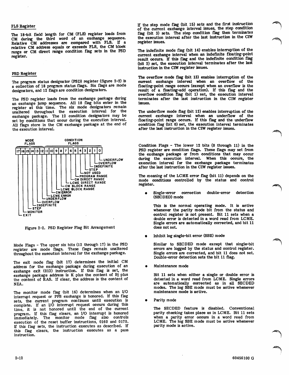
FLS Register
The 18-bit field length for CM (FLS) register loads from
CM during the third word of an exchange sequence.
Relative CM addresses are compared with FLS. If a
relative CM address equals or exceeds FLS, the CM block
range or CM direct range condition flag sets in the PSD
register.
PSD Register
The program status designator (PSD) register (figure 2-2) is
a collection of 18 program status flags. Six flags are mode
designators, and 12 flags are condition designators.
The PSD register loads from the exchange package during
an exchange jump sequence. All 18 flag bits enter in the
register at this time. The six mode designators remain
unaltered throughout the execution interval for the
exchange package. The 12 condition designators may be
set by conditions that occur during the execution interval.
All flags store in the CM exchange package at the end of
the execution interval.
If the step mode flag (bit 15) sets and the first instruction
of the current exchange interval issues, the step condition
flag (bit 3) sets. The step condition flag then terminates
the execution interval after the last instruction in the CIW
register issues.
The indefinite mode flag (bit 14) enables interruption of the
current exchange interval when an indefinite floating-point
result occurs. If this flag and the indefinite condition flag
(bit 2) set, the execution interval terminates after the last
instruction in the CIW register issues.
The overflow mode flag (bit 13) enables interruption of the
current exchange interval when an overflow of the
floating-point range occurs (except when an overflow is the
result of a floating-add operation). If this flag and the
overflow condition flag (bit 1) set, the execution interval
terminates after the last instruction in the CIW register
issues.
The underflow mode flag (bit 12) enables interruption of the
current exchange interval when an underflow of the
floating-point range occurs. If this flag and the underflow
condition flag (bit 0) set, the execution interval terminates
after the last instruction in the CIW register issues.
MODE
FLAGS
CONDITION
FLAGS
17 16 15 14 13 12 II 10 9 8 7 6 5 4 3 2 I 0
LUNDERFLOW
I—OVERFLOW
INDEFINITE
L-STEP
I—NOT USED
I—PROGRAM RANGE
L-CM DIRECT RANGE
L-LCME DIRECT RANGE
I— CM BLOCK RANGE
I—LCME BLOCK RANGE
L-CM ERROR
LCME ERROR
L-UNDERFLOW
•—OVERFLOW
L-INDEFINITE
I-STEP
I—MONITOR
I—EXIT
Figure 2-2. PSD Register Flag Bit Arrangement
Mode Flags - The upper six bits (12 through 17) in the PSD
register are mode flags. These flags remain unaltered
throughout the execution interval for the exchange package.
The exit mode flag (bit 17) determines the initial CM
address for the exchange package during execution of an
exchange exit (013) instruction. If this flag is set, the
exchange package address is K plus the content of Bj plus
the content of RAS. If clear, the address is the content of
NEA.
The monitor mode flag (bit 16) determines when an I/O
interrupt request or PPS exchange is honored. If this flag
sets, the current program continues until execution is
complete. If an I/O interrupt request occurs during this
time, it is not honored until the end of the current
program. If this flag clears, an I/O interrupt is honored
immediately. The monitor mode flag also controls
execution of the reset buffer instructions, 0160 and 0170.
If this flag sets, the instruction executes as described. If
this flag clears, the instruction executes as a pass
instruction.
Condition Flags - The lower 12 bits (0 through 11) in the
PSD register are condition flags. These flags may set from
the exchange package or from conditions that may occur
during the execution interval. When this occurs, the
execution interval for the exchange package terminates
after the last instruction in the CIW register issues.
The meaning of the LCME error flag (bit 11) depends on the
mode conditions controlled by the status and control
register.
• Single-error correction double-error detection
(SECDED) mode
This is the normal operating mode. It is active
whenever the parity mode bit from the status and
control register is not present. Bit 11 sets when a
double error is detected in a word read from LCME.
Single errors are automatically corrected, and bit 11
does not set.
• Inhibit log single-bit error (SBE) mode
Similar to SECDED mode except that single-bit
errors are logged by the status and control register.
Single errors are corrected, and bit 11 does not set.
Double-error detection sets the bit 11 flag.
• Maintenance mode
Bit 11 sets when either a single or double error is
detected in a word read from LCME. Single errors
are automatically corrected as in all SECDED
modes. The log SBE mode must be active whenever
maintenance mode is active.
• Parity mode
The SECDED feature is disabled. Conventional
parity checking takes place as in LCME. Bit 11 sets
when a parity error occurs in a word read from
LCME. The log SBE mode must be active whenever
parity mode is active.
^\
2-12 60456100 G
z$iftv
The meaning of the CM error flag (bit 10) depends on the
mode conditions controlled by the status and control
register and the status and control register bit 138 (212g).
When bit 138 is set, bit 10 will not set on any CM error
caused by an I/O read. When bit 138 is clear, mode
conditions control bit 10.
When a block copy instruction issues and causes an LCME
reference to an address which equals or exceeds the
lowest-order 22 bits of the register for the LCME field
length (FLL), the LCME block range condition flag (bit 9)
sets.
When a block copy instruction issues and causes a CM
reference to an address which equals or exceeds the
content of the register for the CM field length (FLS), the
CM block range condition flag (bit 8) sets.
When a direct read or write LCME instruction issues and
causes an LCME reference to an address which equals or
exceeds the lowest-order 22 bits of the FLL register, the
LCME direct range condition flag (bit 7) sets.
When an increment (50 through 57) instruction issues and
causes a CM reference to an address equal to or greater
than FLS or when P is equal to or greater than FLS, the CM
direct range condition flag (bit 6) sets.
The program range condition flag (bit 5) sets whenever P
equals zero or an error exit (00) instruction issues. When
this flag sets by a 00 instruction, execution terminates
immediately.
The step condition flag (bit 3) sets whenever the step mode
flag (bit 15) sets and a new word enters the CIW register.
The indefinite condition flag (bit 2) sets when one of the
floating-point functional units generates an indefinite
result. The execution interval does not terminate unless
the indefinite mode flag (bit 14) also sets.
The overflow condition flag (bit 1) sets when an overflow of
the floating-point range occurs in the result from a
functional unit (except floating-add). The execution
interval does not terminate unless the overflow mode flag
(bit 13) also sets.
The underflow condition flag (bit 0) sets when an underflow
of the floating-point range occurs in the result from a
functional unit. The execution interval does not terminate
unless the underflow mode flag (bit 12) also sets.
RAL Register
The 22-bit reference address for LCME (RAL) register loads
from CM during the fifth word of an exchange sequence. An
absolute LCME address forms by adding the lowest-order 22
bits of RAL to the relative address determined by the
instruction.
FLL Register
The 22-bit field length for LCME (FLL) register loads from
CM during the sixth word of an exchange sequence.
Relative LCME addresses are compared with FLL. If a
relative LCME address equals or exceeds the lowest-order
22 bits of FLL, the LCME block range or LCME direct
range condition flag sets in the PSD register.
NEA Register
The 24-bit normal exit address (NEA) register loads from
CM during the seventh word of an exchange sequence. This
register is used during an exchange exit (013) instruction
when the exit mode flag in the PSD register clears. When
this occurs, the current program terminates with an
exchange sequence. The absolute CM address for the new
exchange package is in the lowest-order 18 bits of NEA.
EEA Register
The 24-bit error exit address (EEA) register loads from CM
during the eighth word of an exchange sequence. This
register is used whenever an error exit occurs during the
execution interval for an exchange package. When this
occurs, the lowest-order 17 bits of EEA comprise the
absolute address in CM for the exchange package that
terminates the program.
Instruction Control Sequences — Models 740, 750,
760, and 176
The main instruction control components include an IWS,
instruction address stack (IAS), and CIW. The instruction
control reads 60-bit instruction words from CM and issues
them to the CP functional units for execution in 15-, 30-,
or 60-bit instruction groups for models 740, 750, and 760
and in 15- or 30-bit instruction groups for model 176. The
instruction control also performs instruction translation
and control of the exchange, ECS/LCME block copy, LCME
direct reads and writes, normal jump, and return jump
sequences.
Instruction Word Stack
The IWS is a group of 12 60-bit registers that hold program
instruction words for execution. It is essentially a moving
window in the program code. The IWS fills two words
ahead of the program address currently being executed. A
program loop of up to 10 instruction words may be entirely
contained within the IWS. When this happens, the
instruction loop may be executed repeatedly without
further references to CM.
The 12 IWS registers are individually identified by rank.
The rank 1 register contains the oldest data. If the IWS in
models 740, 750, and 760 contains sequential program
instruction words, the rank 1 register corresponds to the
lowest CM address in the IAS.
60456100 G 2-13
Under certain conditions, the IWS in models 740, 750, 760,
or 176 may be voided. Voiding the stack means that the
IWS is not accessible, and the IAS clears. New instructions
must then be read from CM into the IWS and IAS.
In models 740, 750, and 760, voiding the stack results from
an exchange jump, return jump, jump to Bi plus K (02
instruction), or a branch (03 through 07 instructions) to a
location not in the stack. The stack always contains a
sequential code.
In model 176, voiding the stack results from an exchange or
return jump. This stack can contain a nonsequential code
or duplicate entries.
The IWS shifts to accommodate a new word arriving from
CM. New information arriving from CM enters in rank 12.
Ranks 11 through 1 clear and enter with information from
the next highest-order rank. The information in rank 1
discards.
Instruction Address Stack
The IAS is a group of 12 18-bit address registers associated
with the IWS. It holds relative CM program addresses on a
one-for-one basis with the program words in the IWS. The
rank 1 register contains the relative CM address from
which the word in rank 1 of the IWS is read. AU ranks are
compared with the current program address. If coincidence
occurs for a rank, the corresponding rank in the IWS is sent
to the 60-bit CIW register.
A maintenance switch in models 740, 750, and 760 permits
disabling of IAS ranks 1 through 10 or ranks 1 through 4.
Current Instruction Word Register
The CIW register is divided into four 15-bit parcels. All
four parcels load when an instruction word reads from the
IWS. An instruction, consisting of one, two, or four
parcels, issues from the CIW register when conditions in
the functional units and operating registers permit the
instruction to execute without conflicting with previously
issued instructions.
Exchange Sequence
The exchange sequence generates timed CM reference
signals to implement the exchange of data between the CP
and CM, as required by the exchange jump instruction. In
addition, the exchange sequence provides internal control
signals to the operating and control registers to
systematically enter the content of an exchange jump
package.
The exchange sequence is always initiated by the memory
control or a PP multiplexer interrupt request.
ECS/LCME Block Copy Sequence
The ECS/LCME block copy sequence controls the transfer
of data between CM and ECS/LCME. The number of words
to be transferred is determined by the addition of K to the
value in Bj. The starting address for CM is obtained from
the A0 register plus the RAC/RAS reference address. The
starting address for ECS/LCME is obtained from the X0
register plus the RAE/RAL reference address. The
ECS/LCME block copy instructions are:
011 Block copy (Bj + K) from ECS/LCME to CM
012 Block copy (Bj + K) from CM to ECS/LCME
In model 176, (Bj + K) cannot exceed 17778.
Normal Jump Sequence
The normal jump sequence controls the execution of branch
instructions 02 through 07. The 02 instruction performs an
unconditional jump to the Bi register address plus K,
causing the models 740, 750, and 760 instruction stacks to
be voided. The branch address is K when i equals 0. The 02
instruction is:
/ J ^ K
02 Jump to (Bi) + K
The conditional jump instructions 03 through 07 branch to
address K if the jump condition is met. These instructions
are:
030 Branch to K if (Xj) = 0
031 Branch to K if (Xj) = 0
032 Branch to K if (Xj) positive
033 Branch to K if (Xj) negative
034 Branch to K if (Xj) in range
035 Branch to K if (Xj) out of range
036 Branch to K if (Xj) definite
037 Branch to K if (Xj) indefinite
04 Branch to K if (Bi) = (Bj)
05 Branch to K if (Bi) = (Bj)
06 Branch to K if (Bi) (Bj)
07 Branch to K if (Bi) (Bj)
Return Jump Sequence
The return jump sequence controls the execution of three
instructions.
00 Error exit to MA or program stop for models
740, 750, and 760 and EEA for model 176
,«&E5i?K
2-14 60456100 E
/0^\
010 Return jump to K
013 Central exchange jump to (Bj) + K or exchange
exit to NEA
FUNCTIONAL UNITS — MODELS 740. 750.760, AND 176
Each of the nine functional units in the CP is a specialized
arithmetic unit with algorithms for a portion of the CP
instructions. Each unit is independent of the other units,
and a number of functional units may be in operation at the
same time. No visible registers are in the functional units
from a programming standpoint. A functional unit receives
one or two operands from operating registers at the
beginning of instruction execution and delivers the result to
the operating registers when the function has been
performed. No information is retained in a functional unit
for reference in subsequent instructions.
All functional units, with the exception of the
floating-multiply and -divide units, have a 1-clock-period
segmentation. This means that the information arriving at
a unit, or moving within a unit, is captured and held in a
new set of registers every clock period. In models 750,
760, and 176, it is possible to start a new set of operands
for unrelated computation in a functional unit each clock
period even though the unit may require more than 1 clock
period to complete the calculation. This process may be
compared to a delay line in which data moves through the
unit in segments to arrive at the destination in the proper
order but at a later time. In model 740, a new set of
operands may start only after completion of the previous
instruction. All functional units perform their algorithms
in a fixed amount of time. No delays are possible once the
instruction issues.
The floating-multiply unit has a 2-clock-period
segmentation. In models 750, 760, and 176, operands may
enter the multiply unit in any clock period providing there
was no multiply instruction initiated in the preceding clock
period. There is a 1-clock-period delay in initiating a
multiply instruction if another multiply instruction has just
started. In model 740, operands may enter the multiple
unit only after completion of the previous instruction.
The floating-divide unit is the only functional unit in which
an iterative algorithm executes. No segmentation is
possible in this unit although the beginning of a new
operation can overlap the completion of the previous
operation by 2 clock periods (models 750, 760, and 176 only).
Boolean Unit
The boolean unit executes instructions that require
bit-by-bit data manipulation. This includes both the logical
and transmissive operations. The instructions requiring
logical operations are:
11 Logical product (Xj) and (Xk) to Xi
12 Logical sum of (Xj) and (Xk) to Xi
13 Logical dif f erence of (Xj) and (Xk) to Xi
15 Logical product of (Xj) and (Xk) to Xi
16 Logical sum of (Xj) and (Xk) to Xi
17 Logical difference of (Xj) and (Xk) to Xi
The instructions requiring transmissive operations are:
10 Transmit (Xj) to Xi
14 Transmit (Xk) to Xi
26 Unpack (Xk) to Xi and Bj
27 Pack (Xk) and (Bj) to Xi
Shift Unit
The shift unit executes instructions that require shifting
the entire 60-bit field of data within the operand word.
The shift instructions are:
20 Left shift (Xi) by jk
21 Right shift (Xi) by jk
22 Left shift (Xk) nominally (Bj) places to Xi
23 Right shift (Xk) nominally (Bj) places to Xi
43 Form mask of jk bits to Xi
Normalize Unit
The normalize unit executes instructions that require
rearranging operands in floating-point format. The unit
left shifts the coefficient so that the most significant bit
shifts into the highest-order bit position of the coefficient.
The exponent adjusts by subtracting the shift count. The
normalize instructions are:
24 Normalize (Xk) to Xi and Bj
25 Round normalize (Xk) to Xi and Bj
Floating-Add Unit
The floating-add unit executes instructions that require
adding operands in floating-point format. The floating-add
instructions are:
30 Floating sum of (Xj) and (Xk) to Xi
31 Floating difference of (Xj) and (Xk) to Xi
32 Floating double-precision sum of (Xj) and (Xk) to Xi
33 Floating double-precision difference of (Xj) and
(Xk) to Xi
34 Round floating sum of (Xj) and (Xk) to Xi
35 Round floating difference of (Xj) and (Xk) to Xi
60456100 E 2-15
Long Add Unit
The long add unit executes instructions that require integer
addition of two 60-bit operands. The long add instructions
are:
36 Integer sum of (Xj) and (Xk) to Xi
37 Integer difference of (Xj) and (Xk) to Xi
Multiply Unit
The multiply unit executes instructions that require
multiplication of two operands in floating-point format.
The multiply instructions are:
40 Floating product of (Xj) and (Xk) to Xi
41 Round floating product of (Xj) and (Xk) to Xi
42 Floating double-precision product of (Xj) and (Xk)
toXi
Divide Unit
The divide unit executes instructions that require division
of two operands in floating-point format. The divide
instructions are:
44 Floating divide (Xj) by (Xk) to Xi
45 Round floating divide (Xj) by (Xk) to Xi
Population-Count Unit
The population-count unit executes an instruction that
requires counting the number of one bits in a 60-bit
operand. The population-count instruction is:
47 Population count of (Xk) to Xi
Increment Unit
The increment unit executes instructions 50 through 77
that require arithmetic operations on two 18-bit operands.
During the 50 through 57 instructions, the result transmits
to an A register. The same result plus RAC is sent to CM
for the increment read or write address.
The two operations perform independently and in parallel
with each other. During 60 through 67 instructions, the
result transmits to a B register. During 70 through 77
instructions, the result transmits to an X register.
The increment instructions are:
50 Set Ai
51 Set Ai
52 Set A
53 Set A
54 Set A
55 Set A
56 Set A
57 Set A
60 Set B
61 SetB
62 Set B
63 Set B
64 Set B
65 Set B
66 Set B
67 Set B
70 Set X
71 Set X
72 SetX
73 SetX
74 SetX
75 Set X
76 Set X
77 Set X
to (Aj) + K
to (Bj) + K
to (Xj) + K
to (Xj) + (Bk)
to (Aj) + (Bk)
to(Aj)-(Bk)
to (Bj) + (Bk)
to(Bj)-(Bk)
to (Aj) + K
to (Bj) + K
to (Xj) + K
to (Xj) + (Bk)
to (Aj) + (Bk)
to(Aj)-(Bk)
to (Bj) + (Bk)
to(Bj)-(Bk)
to (Aj) + K
to (Bj) + K
to (Xj) + K
to (Xj) + (Bk)
to (Aj) + (Bk)
to(Aj)-(Bk)
to (Bj) + (Bk)
to(Bj)-(Bk)
,**C^5v
2-16 60456100 A
JP5*'
SUNlftAL MEMORY CONTROL - MlDEI^ 720 TMROU^ 760

'^s%.
V
V
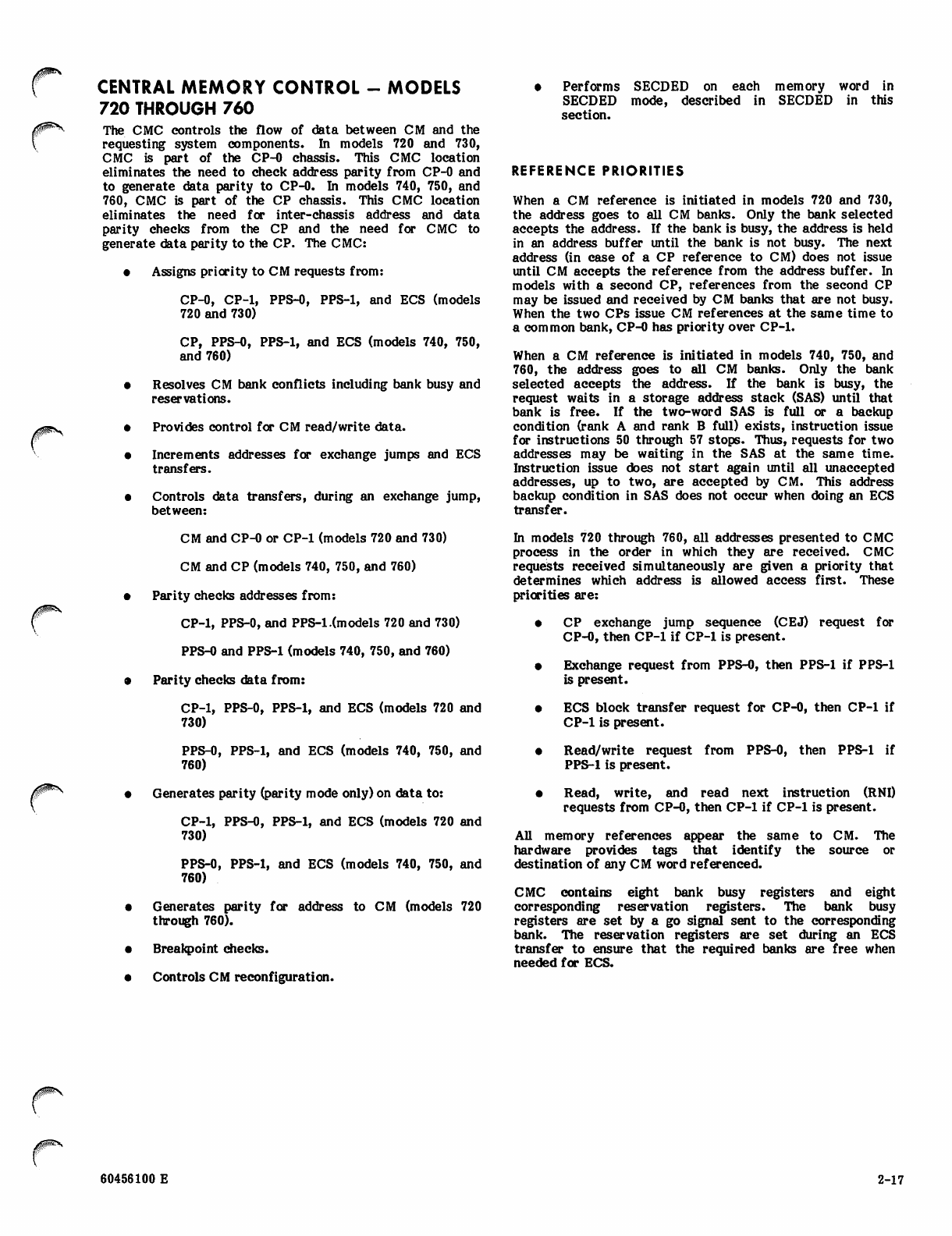
CENTRAL MEMORY CONTROL - MODELS
720 THROUGH 760
The CMC controls the flow of data between CM and the
requesting system components. In models 720 and 730,
CMC is part of the CP-0 chassis. This CMC location
eliminates the need to check address parity from CP-0 and
to generate data parity to CP-0. In models 740, 750, and
760, CMC is part of the CP chassis. This CMC location
eliminates the need for inter-chassis address and data
parity checks from the CP and the need for CMC to
generate data parity to the CP. The CMC:
• Assigns priority to CM requests from:
CP-0, CP-1, PPS-0, PPS-1, and ECS (models
720 and 730)
CP, PPS-0, PPS-1, and ECS (models 740, 750,
and 760)
• Resolves CM bank conflicts including bank busy and
reservations.
• Provides control for CM read/write data.
• Increments addresses for exchange jumps and ECS
transfers.
• Controls data transfers, during an exchange jump,
between:
CM and CP-0 or CP-1 (models 720 and 730)
CM and CP (models 740, 750, and 760)
• Parity checks addresses from:
CP-1, PPS-0, and PPS-1 .(models 720 and 730)
PPS-0 and PPS-1 (models 740, 750, and 760)
• Parity checks data from:
CP-1, PPS-0, PPS-1, and ECS (models 720 and
730)
PPS-0, PPS-1, and ECS (models 740, 750, and
760)
• Generates parity (parity mode only) on data to:
CP-1, PPS-0, PPS-1, and ECS (models 720 and
730)
PPS-0, PPS-1, and ECS (models 740, 750, and
760)
• Generates parity for address to CM (models 720
through 760).
• Breakpoint checks.
• Controls CM reconfiguration.
• Performs SECDED on each memory word in
SECDED mode, described in SECDED in this
section.
REFERENCE PRIORITIES
When a CM reference is initiated in models 720 and 730,
the address goes to all CM banks. Only the bank selected
accepts the address. If the bank is busy, the address is held
in an address buffer until the bank is not busy. The next
address (in case of a CP reference to CM) does not issue
until CM accepts the reference from the address buffer. In
models with a second CP, references from the second CP
may be issued and received by CM banks that are not busy.
When the two CPs issue CM references at the same time to
a common bank, CP-0 has priority over CP-1.
When a CM reference is initiated in models 740, 750, and
760, the address goes to all CM banks. Only the bank
selected accepts the address. If the bank is busy, the
request waits in a storage address stack (SAS) until that
bank is free. If the two-word SAS is full or a backup
condition (rank A and rank B full) exists, instruction issue
for instructions 50 through 57 stops. Thus, requests for two
addresses may be waiting in the SAS at the same time.
Instruction issue does not start again until all unaccepted
addresses, up to two, are accepted by CM. This address
backup condition in SAS does not occur when doing an ECS
transfer.
In models 720 through 760, all addresses presented to CMC
process in the order in which they are received. CMC
requests received simultaneously are given a priority that
determines which address is allowed access first. These
priorities are:
• CP exchange jump sequence (CEJ) request for
CP-0, then CP-1 if CP-1 is present.
• Exchange request from PPS-0, then PPS-1 if PPS-1
is present.
• ECS block transfer request for CP-0, then CP-1 if
CP-1 is present.
• Read/write request from PPS-0, then PPS-1 if
PPS-1 is present.
• Read, write, and read next instruction (RNI)
requests from CP-0, then CP-1 if CP-1 is present.
All memory references appear the same to CM. The
hardware provides tags that identify the source or
destination of any CM word referenced.
CMC contains eight bank busy registers and eight
corresponding reservation registers. The bank busy
registers are set by a go signal sent to the corresponding
bank. The reservation registers are set during an ECS
transfer to ensure that the required banks are free when
needed for ECS.
60456100 E 2-17
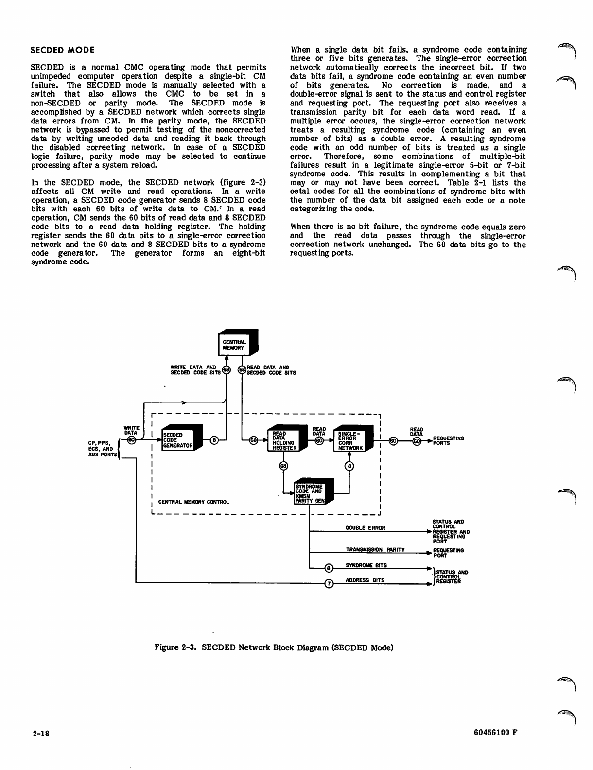
SECDED MODE
SECDED is a normal CMC operating mode that permits
unimpeded computer operation despite a single-bit CM
failure. The SECDED mode is manually selected with a
switch that also allows the CMC to be set in a
non-SECDED or parity mode. The SECDED mode is
accomplished by a SECDED network which corrects single
data errors from CM. In the parity mode, the SECDED
network is bypassed to permit testing of the noncorrected
data by writing uncoded data and reading it back through
the disabled correcting network. In case of a SECDED
logic failure, parity mode may be selected to continue
processing after a system reload.
In the SECDED mode, the SECDED network (figure 2-3)
affects all CM write and read operations. In a write
operation, a SECDED code generator sends 8 SECDED code
bits with each 60 bits of write data to CM/ In a read
operation, CM sends the 60 bits of read data and 8 SECDED
code bits to a read data holding register. The holding
register sends the 60 data bits to a single-error correction
network and the 60 data and 8 SECDED bits to a syndrome
code generator. The generator forms an eight-bit
syndrome code.
When a single data bit fails, a syndrome code containing
three or five bits generates. The single-error correction
network automatically corrects the incorrect bit. If two
data bits fail, a syndrome code containing an even number
of bits generates. No correction is made, and a
double-error signal is sent to the status and control register
and requesting port. The requesting port also receives a
transmission parity bit for each data word read. If a
multiple error occurs, the single-error correction network
treats a resulting syndrome code (containing an even
number of bits) as a double error. A resulting syndrome
code with an odd number of bits is treated as a single
error. Therefore, some combinations of multiple-bit
failures result in a legitimate single-error 5-bit or 7-bit
syndrome code. This results in complementing a bit that
may or may not have been correct. Table 2-1 lists the
octal codes for all the combinations of syndrome bits with
the number of the data bit assigned each code or a note
categorizing the code.
When there is no bit failure, the syndrome code equals zero
and the read data passes through the single-error
correction network unchanged. The 60 data bits go to the
requesting ports.
REQUESTING
PORTS
Figure 2-3. SECDED Network Block Diagram (SECDED Mode)
2-18 60456100 F
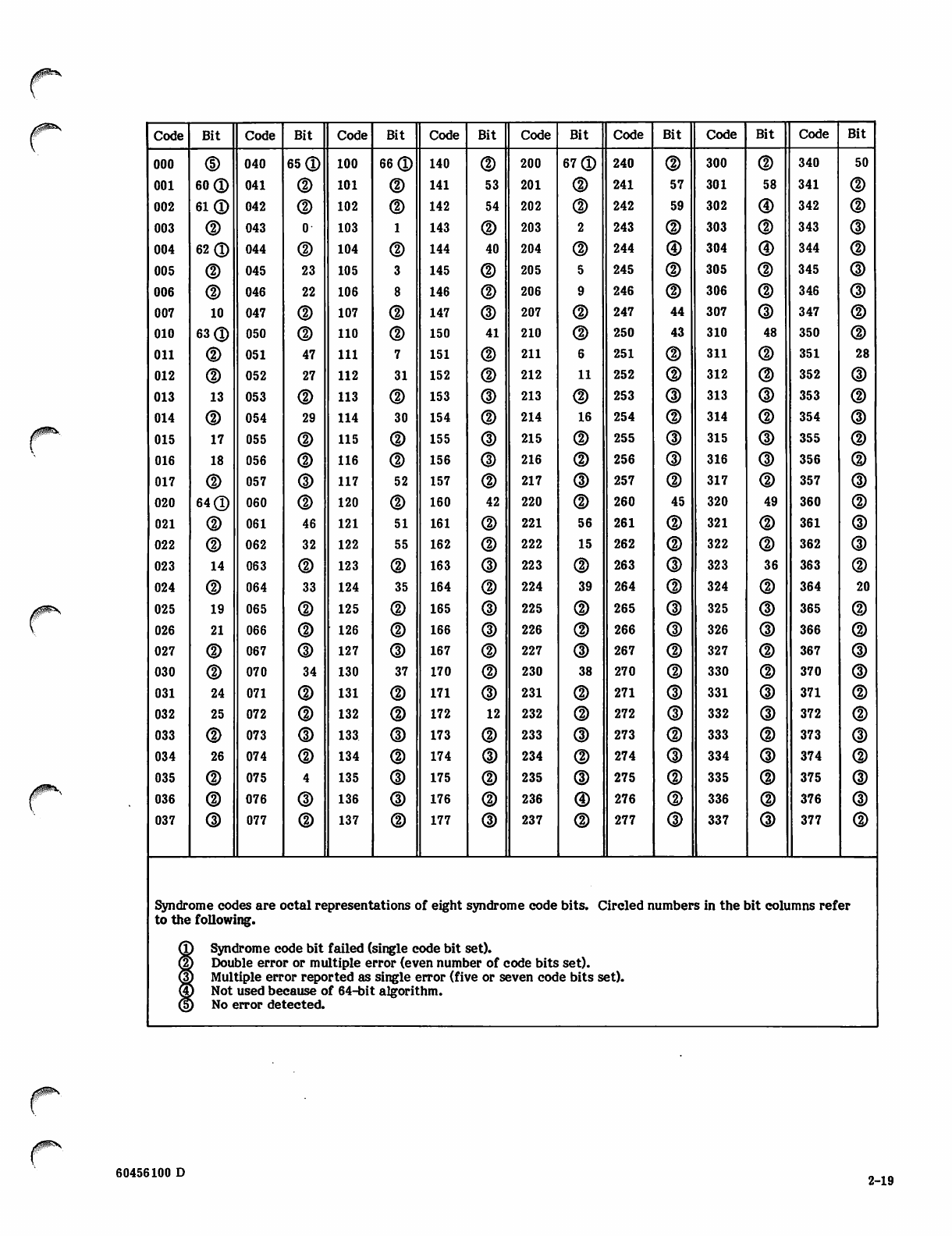
Code Bit Code Bit Code Bit Code Bit Code Bit Code Bit Code Bit Code Bit
000 <D 040 65® 100 66® 140 200 67® 240 300 340 50
001 60® 041 101 141 53 201 241 57 301 58 341
002 61® 042 102 142 54 202 242 59 302 342
003 043 103 143 203 243 303 343
004 62® 044 104 144 40 204 244 304 344
005 045 23 105 145 205 245 305 345
006 046 22 106 146 206 246 306 346
007 10 047 107 147 207 247 44 307 347
010 63® 050 110 CD 150 41 210 250 43 310 48 350
Oil 051 47 111 151 211 251 311 351 28
012 052 27 112 31 152 212 11 252 312 352
013 13 053 113 153 213 253 313 353
014 054 29 114 30 154 214 16 254 314 354
015 17 055 115 155 215 255 315 355
016 18 056 116 156 216 256 316 356
017 057 117 52 157 217 257 317 357
020 64® 060 120 160 42 220 260 45 320 49 360
021 061 46 121 51 161 221 56 261 321 361
022 062 32 122 55 162 222 15 262 322 362
023 14 063 123 163 223 263 323 36 363
024 064 33 124 35 164 224 39 264 324 364 20
025 19 065 125 165 225 265 325 365
026 21 066 126 166 226 266 326 366
027 <D 067 127 167 227 267 327 367
030 (D 070 34 130 37 170 230 38 270 330 370
031 24 071 131 171 231 271 331 371
032 25 072 132 172 12 232 272 332 372
033 073 133 173 233 273 333 373
034 26 074 CD 134 174 234 274 334 374
035 <D 075 135 175 235 275 335 375
036 076 (D 136 176 236 276 336 376
037 077 (D 137 177 237 277 337 377
Syndr
to the
ome codes are <
following.
jctal representations of eight syndro me code bits. Clircled n umbers in the 1Mt coliimns refer
) Syndrome c
) Double erro
j Multiple err
) Not used be
) No error de
ode bit failed (
r or multiple e
or reported as
cause of 64-bit
tected.
single code bit
rror (even numt
single error (f ii
t algorithm.
set).
>er of c
/e or a
•ode bits
3ven cod set),
e bits »Bt).
60456100 D 2-19
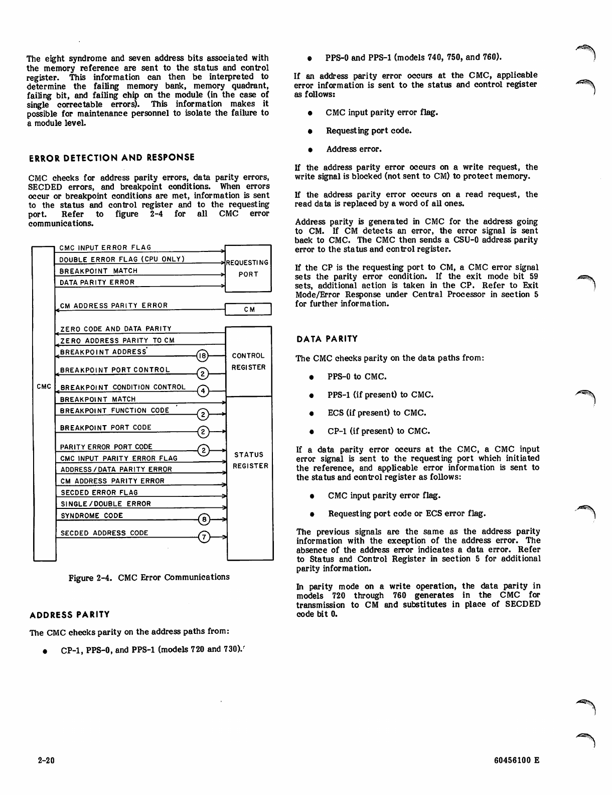
The eight syndrome and seven address bits associated with
the memory reference are sent to the status and control
register. This information can then be interpreted to
determine the failing memory bank, memory quadrant,
failing bit, and failing chip on the module (in the case of
single correctable errors). This information makes it
possible for maintenance personnel to isolate the failure to
a module level.
ERROR DETECTION AND RESPONSE
CMC checks for address parity errors, data parity errors,
SECDED errors, and breakpoint conditions. When errors
occur or breakpoint conditions are met, information is sent
to the status and control register and to the requesting
port. Refer to figure 2-4 for all CMC error
communications.
CMC
CMC INPUT ERROR FLAG
REQUESTING
PORT
DOUBLE ERROR FLAG (CPU ONLY)
BREAKPOINT MATCH
DATA PARITY ERROR
CM ADDRESS PARITY ERROR CM
ZERO CODE AND DATA PARITY
CONTROL
REGISTER
ZERO ADDRESS PARITY TO CM
BREAKPOINT ADDRESS (To)
BREAKPOINT PORT CONTROL P)
BREAKPOINT CONDITION CONTROL (?)
BREAKPOINT MATCH \V
STATUS
REGISTER
BREAKPOINT FUNCTION CODE (°1 *
BREAKPOINT PORT CODE
KtJ
PARITY ERROR PORT CODE
^ J 1
CMC INPUT PARITY ERROR FLAG \ z j
ADDRESS /DATA PARITY ERROR
CM ADDRESS PARITY ERROR
SECDED ERROR FLAG
SINGLE/DOUBLE ERROR
SYNDROME CODE f n ) 5
SECDED ADDRESS CODE
Kits ■*
( ? ) ?
\ U ?
Figure 2-4. CMC Error Communications
ADDRESS PARITY
The CMC checks parity on the address paths from:
• CP-1, PPS-0, and PPS-1 (models 720 and 730)/
• PPS-0 and PPS-1 (models 740, 750, and 760).
If an address parity error occurs at the CMC, applicable
error information is sent to the status and control register
as follows:
• CMC input parity error flag.
• Requesting port code.
• Address error.
If the address parity error occurs on a write request, the
write signal is blocked (not sent to CM) to protect memory.
If the address parity error occurs on a read request, the
read data is replaced by a word of all ones.
Address parity is generated in CMC for the address going
to CM. If CM detects an error, the error signal is sent
back to CMC. The CMC then sends a CSU-0 address parity
error to the status and control register.
If the CP is the requesting port to CM, a CMC error signal
sets the parity error condition. If the exit mode bit 59
sets, additional action is taken in the CP. Refer to Exit
Mode/Error Response under Central Processor in section 5
for further information.
DATA PARITY
The CMC checks parity on the data paths from:
• PPS-0 to CMC.
• PPS-1 (if present) to CMC.
• ECS (if present) to CMC.
• CP-1 (if present) to CMC.
If a data parity error occurs at the CMC, a CMC input
error signal is sent to the requesting port which initiated
the reference, and applicable error information is sent to
the status and control register as follows:
• CMC input parity error flag.
• Requesting port code or ECS error flag.
The previous signals are the same as the address parity
information with the exception of the address error. The
absence of the address error indicates a data error. Refer
to Status and Control Register in section 5 for additional
parity information.
In parity mode on a write operation, the data parity in
models 720 through 760 generates in the CMC for
transmission to CM and substitutes in place of SECDED
code bit 0.
>*5^l.
2-20 60456100 E
In parity mode on a read operation, the data parity bit in
models 720 and 730 propagates (unchanged) for
interrogation by the requesting unit. In models 740, 750,
and 760, parity is checked on the data from CM, and code
bit 0 is used as the parity bit. When a parity error occurs
in models 740, 750, and 760, the CMC sends only an error
signal to the CPU if the CPU is the requesting unit. For
other ports in models 740, 750, and 760, the parity bit
propagates for interrogation by the requesting unit.
In SECDED mode on a write operation, data parity is
checked at the input requesting ports on all models (except
the CPU port in models 740, 750, and 760). SECDED code
bits then generate for transmission to CM.
In SECDED mode on a read operation, all models send data
through the SECDED network. A parity bit then generates
in CMC and transmits to the requesting unit (except the
CPU in models 740, 750, and 760) along with the read data.
BREAKPOINT CHECK
The CMC performs a breakpoint check on references to CM
when breakpoint is selected. Breakpoint is controlled by
the status and control register in the PPS.
The CMC receives 18 breakpoint address bits, 2 port
control bits, and 2 access control bits. Table 2-2 lists the
breakpoint control translations.
The 18-bit address of each CM reference is compared to
the breakpoint address bits. If there is a match, if the
requesting unit is selected by the port control bits, and if
the type of access is one that is selected by the access
control bits, the breakpoint flag is sent to the requesting
unit.
The breakpoint flag is also sent to the status and control
register along with the two port code bits. For further
information, refer to Breakpoint in section 5.
When executing an exchange jump, this operation is treated
by breakpoint as both a read and a write. A return jump is
treated as a write.
TABLE 2-2. BREAKPOINT CONTROL
TRANSLATIONS
Control Bit
Translation
117 116 115 114
0 0 X X Breakpoint check disabled
0 1 X X Breakpoint check for PP
ports
1 0 X X Breakpoint check for CP
ports
1 1 X X Breakpoint check for PP and
CP ports
X X 0 0 Breakpoint check on read
X X 0 1 Breakpoint check on write
X X 1 0 Breakpoint check on read
next instruction
XX 1 1 Breakpoint check on any
access
60456100 E 2-21/2-22

/#^\
CENTRA* MEMORY - MO DELS 720 THROUGH 760
//P*

■^%
V
•-^fe.
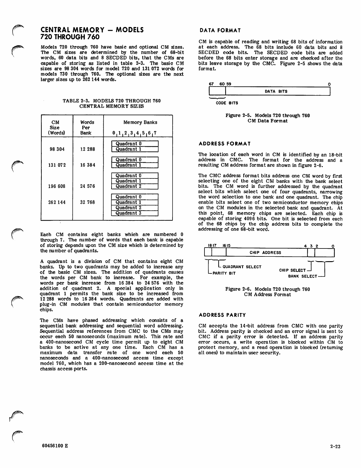
00^. CENTRAL MEMORY - MODELS
720 THROUGH 760
Models 720 through 760 have basic and optional CM sizes.
The CM sizes are determined by the number of 68-bit
words, 60 data bits and 8 SECDED bits, that the CMs are
capable of storing as listed in table 2-3. The basic CM
sizes are 98 304 words for model 720 and 131 072 words for
models 730 through 760. The optional sizes are the next
larger sizes up to 262 144 words.
TABLE 2-3. MODELS 720 THROUGH 760
CENTRAL MEMORY SEES
CM
Size
(Words)
Words
Per
Bank
Memory Banks
0,1,2,3,4,516,7
98 304
131 072
196 608
262144
12 288
16 384
24 576
32 768
Quadrant 0
Quadrant 1
Quadrant 0
Quadrant 1
Quadrant 0
Quadrant 1
Quadrant 2
Quadrant 0
Quadrant 1
Quadrant 2
Quadrant 3
Each CM contains eight banks which are numbered 0
through 7. The number of words that each bank is capable
of storing depends upon the CM size which is determined by
the number of quadrants.
A quadrant is a division of CM that contains eight CM
banks. Up to two quadrants may be added to increase any
of the basic CM sizes. The addition of quadrants causes
the words per CM bank to increase. For example, the
words per bank increase from 16 384 to 24 576 with the
addition of quadrant 2. A special application only in
quadrant 1 permits the bank size to be increased from
12 288 words to 16 384 words. Quadrants are added with
plug-in CM modules that contain semiconductor memory
chips.
The CMs have phased addressing which consists of a
sequential bank addressing and sequential word addressing.
Sequential address references from CMC to the CMs may
occur each 50 nanoseconds (maximum rate). This rate and
a 400-nanosecond CM cycle time permit up to eight CM
banks to be active at any one time. Each CM has a
maximum data transfer rate of one word each 50
nanoseconds and a 400-nanosecond access time except
model 760, which has a 200-nanosecond access time at the
chassis access ports.
DATA FORMAT
CM is capable of reading and writing 68 bits of information
at each address. The 68 bits include 60 data bits and 8
SECDED code bits. The SECDED code bits are added
before the 68 bits enter storage and are checked after the
bits leave storage by the CMC. Figure 2-5 shows the data
format.
67 60 59
DATA BITS
CODE BITS
Figure 2-5. Models 720 through 760
CM Data Format
ADDRESS FORMAT
The location of each word in CM is identified by an 18-bit
address in CMC. The format for the address and a
resulting CM address format are shown in figure 2-6.
The CMC address format bits address one CM word by first
selecting one of the eight CM banks with the bank select
bits. The CM word is further addressed by the quadrant
select bits which select one of four quadrants, narrowing
the word selection to one bank and one quadrant. The chip
enable bits select one of two semiconductor memory chips
on the CM modules in the selected bank and quadrant. At
this point, 68 memory chips are selected. Each chip is
capable of storing 4096 bits. One bit is selected from each
of the 68 chips by the chip address bits to complete the
addressing of one 68-bit word.
1817 1615 4 3 2
CHIP ADDRESS | |
QUADRANT SELECT
L-PARITY BIT •J
CHIP SELECT
BANK SELECT-
Figure 2-6. Models 720 through 760
CM Address Format
ADDRESS PARITY
CM accepts the 14-bit address from CMC with one parity
bit. Address parity is checked and an error signal is sent to
CMC if a parity error is detected. If an address parity
error occurs, a write operation is blocked within CM to
protect memory, and a read operation is blocked (returning
all ones) to maintain user security.
idiff^N
60456100 E 2-23
REFERENCE OPERATIONS
Major CM reference operations which are under CMC
control are read and write.
During a read or write CM reference, CMC sends the
address information to CM/ The CM sends the address
information to all banks. A go bank signal from CMC,
decoded from the bank select code, is sent to one of the
banks. Only the bank receiving the go bank signal gates the
address and data (write operation) into holding registers.
The holding registers then select the storage locations and
place the data into CM. During a read operation, the
addressing is the same except that the absence of a write
signal causes data to be read from the addressed location
and sent to a common data-out register for transmission to
CMC.
RECONFIGURATION
Central memory reconfiguration is a manually performed
function that permits the computer operator to restructure
the CM addresses so that a failing part of CM can be
quickly locked out to provide a continuous block of usable
CM. CM reconfiguration is accomplished by setting
switches to manipulate upper address bits. Hardware
configures the CM quadrants so that sequential addressing
is maintained. Reconfiguration options are:
Models 720 and 730 262K to 196K to 131K to
98K to 65K
Models 740, 750, and 760 262K to 196K to 131K to 65K
A reconfiguration permits only one part of the CM to be
locked out at a time. The reconfiguration provides the
same-sequential addressing characteristics as a same-size
normally operating CM without reconfiguration. CM
reconfiguration switching information is described in
section 3.
/"^Sv
2-24 60456100 E
||FK
0p>\
CENiliAL ME^iiRY - JVfc^PEL If 6

■^j
■^%.
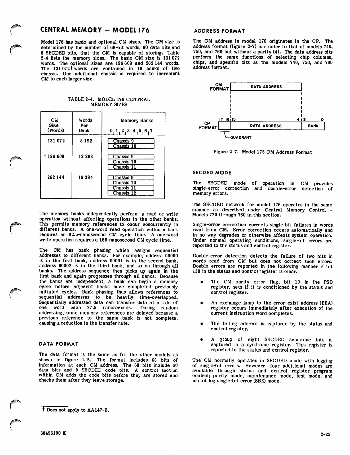
CENTRAL MEMORY - MODEL 176 ADDRESS FORMAT
Model 176 has basic and optional CM sizes. The CM size is
determined by the number of 68-bit words, 60 data bits and
8 SECDED bits, that the CM is capable of storing. Table
2-4 lists the memory sizes. The basic CM size is 131 072
words. The optional sizes are 196 608 and 262 144 words.
The 1310721 words are contained in 16 banks of two
chassis. One additional chassis is required to increment
CM to each larger size.
TABLE 2-4. MODEL 176 CENTRAL
MEMORY SIZES
CM
Size
(Words)
Words
Per
Bank
Memory Banks
0, 1 ,2 , 3 , 4 , 5 , 6 , 7
131 072
t196 608
262 144
8 192
12 288
16 384
Chassis 9
Chassis 10
Chassis 9
Chassis 10
Chassis 11
Chassis 9
Chassis 10
Chassis 11
Chassis 12
The memory banks independently perform a read or write
operation without affecting operations in the other banks.
This permits memory references to occur concurrently in
different banks. A one-word read operation within a bank
requires an 82.5-nanosecond CM cycle time. A one-word
write operation requires a 165-nanosecond CM cycle time.
The CM has bank phasing which assigns sequential
addresses to different banks. For example, address 00000
is in the first bank, address 00001 is in the second bank,
address 00002 is in the third bank, and so on through all
banks. The address sequence then picks up again in the
first bank and again progresses through all banks. Because
the banks are independent, a bank can begin a memory
cycle before adjacent banks have completed previously
initiated cycles. Bank phasing thus allows references to
sequential addresses to be heavily time-overlapped.
Sequentially addressed data can transfer data at a rate of
one word each 27.5 nanoseconds. During random
addressing, some memory references are delayed because a
previous reference to the same bank is not complete,
causing a reduction in the transfer rate.
DATA FORMAT
The data format is the same as for the other models as
shown in figure 2-5. The format includes 68 bits of
information at each CM address. The 68 bits include 60
data bits and 8 SECDED code bits. A control section
within CM adds the code bits before they are stored and
checks them after they leave storage.
The CM address in model 176 originates in the CP. The
address format (figure 2-7) is similar to that of models 740,
750, and 760 but without a parity bit. The data address bits
perform the same functions of selecting chip columns,
chips, and specific bits as the models 740, 750, and 760
address format.
CM
FORMAT DATA ADDRESS
I
1
1
1
1
17 I6l15 3 O
CP
FORMAT DATA ADDRESS BANK
\_QUADRANT
Figure 2-7. Model 176 CM Address Format
SECDED MODE
The SECDED mode of operation in CM provides
single-error correction and double-error detection of
memory errors.
The SECDED network for model 176 operates in the same
manner as described under Central Memory Control -
Models 720 through 760 in this section.
Single-error correction corrects single-bit failures in words
read from CM. Error correction occurs automatically and
in no way degrades or otherwise affects system operation.
Under normal operating conditions, single-bit errors are
reported to the status and control register.
Double-error detection detects the failure of two bits in
words read from CM but does not correct such errors.
Double errors are reported in the following manner if bit
138 in the status and control register is clear.
o The CM parity error flag, bit 10 in the PSD
register, sets if it is conditioned by the status and
control register.
• An exchange jump to the error exist address (EEA)
register occurs immediately after execution of the
current instruction word completes.
• The failing address is captured by the status and
control register.
• A group of eight SECDED syndrome bits is
captured in a syndrome register. This register is
reported to the status and control register.
The CM normally operates in SECDED mode with logging
of single-bit errors. However, four additional modes are
available through status and control register program
control; parity mode, maintenance mode, test mode, and
inhibit log single-bit error (SBE) mode.
/ ^ ^ N
t Does not apply to AA147-B.
60456100 K 2-25
PARITY MODE
Parity mode is selected under program control through the
status and control register. The semiconductor memory
operates in an 8-bit parity mode. Parity errors are
detected only on read memory references including all
exchange jump references. The address for each read
memory reference enters the error address register. If a
parity error occurs, the parity bit(s) for the failing byte(s)
is locked into the parity error/syndrome bit register, and
the failing memory address is locked into the parity address
register. The contents of these registers are accessed by
the status and control register and are held until that
register sends a clear parity signal/ Occurrence of a parity
error also causes bit 10 of the PSD register to set, if it is
properly conditioned by the status and control register.
When bit 10 sets, it causes an exchange jump to the error
exit address. Parity errors that occur while the parity
error/syndrome bit register is locked up from a previous
error are not detected.
When the parity mode signal from the status and control
register is absent, the memory operates in SECDED mode.
The access time is identical in either mode.
MAINTENANCE MODE
Maintenance mode is selected under program control
through the status and control register. Single-bit errors
are reported the same as double-bit errors. Bit 10 of the
PSD register sets if it is properly conditioned by the status
and control register. When bit 10 sets, the CPU performs
an exchange jump to EEA. The error address and syndrome
bits are reported to the status and control register.
TEST MODE
Test mode is selected under program control through the
status and control register. When the memory is operating
in SECDED mode, the test mode signal forces all eight
error correction code bits to logical zeros prior to writing
into memory. Error correction is still performed in this
mode of operation.
If memory is operating in eight-bit parity mode, the test
mode signal forces all eight parity bits to be complemented
prior to writing into memory. This feature allows the
diagnostic program to force errors in order to check the
SECDED hardware.
INHIBIT LOG SBE MODE
Single-bit errors are normally reported to the status and
control register. When bit 118 of the status and control
register sets, the inhibit log SBE mode prevents single-bit
errors from being reported.
RECONFIGURATION
Central memory reconfiguration is a manually performed
function that permits the computer operator to restructure
the CM addresses so that a failing part of CM can be
quickly locked out to provide a continuous block of usable
CM. CM reconfiguration is accomplished by setting
switches to manipulate upper address bits. Hardware
configures the CM quadrants so that sequential addressing
is maintained. Model 176 reconfiguration options are 262K
to 196K to 13IK.
A reconfiguration permits only one part of the CM to be
locked out at a time. The reconfiguration provides the
same-sequential addressing characteristics as a same-size
normally operating CM without reconfiguration. CM
reconfiguration switching information is described in
section 3.
2-26 60456100 A
imm core ^mmmt E^tNSiiOH { optionm$ - mobel 176
0^:

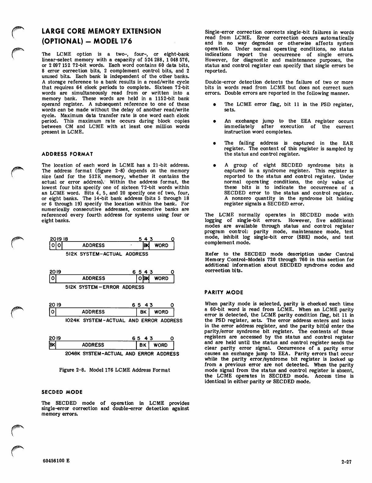
LARGE CORE MEMORY EXTENSION
(OPTIONAL) - MODEL 176
The LCME option is a two-, four-, or eight-bank
linear-select memory with a capacity of 524 288, 1 048 576,
or 2 097 152 72-bit words. Each word contains 60 data bits,
8 error correction bits, 2 complement control bits, and 2
unused bits. Each bank is independent of the other banks.
A storage reference to a bank results in a read/write cycle
that requires 64 clock periods to complete. Sixteen 72-bit
words are simultaneously read from or written into a
memory bank. These words are held in a 1152-bit bank
operand register. A subsequent reference to one of these
words can be made without the delay of another read/write
cycle. Maximum data transfer rate is one word each clock
period. This maximum rate occurs during block copies
between CM and LCME with at least one million words
present in LCME.
ADDRESS FORMAT
The location of each word in LCME has a 21-bit address.
The address format (figure 2-8) depends on the memory
size (and for the 512K memory, whether it contains the
actual or error address). Within the address format, the
lowest four bits specify one of sixteen 72-bit words within
an LCME word. Bits 4, 5, and 20 specify one of two, four,
or eight banks. The 14-bit bank address (bits 5 through 18
or 6 through 19) specify the location within the bank. For
numerically consecutive addresses, consecutive banks are
referenced every fourth address for systems using four or
eight banks.
2 0 1 9 1 8 5 4 3 0
00ADDRESS BK WORD
2019
5I2K SYSTEM-ACTUAL ADDRESS
6 5 4 3
ADDRESS o]bk WORD
5I2K SYSTEM-ERROR ADDRESS
2019 6 5 43
OADDRESS BK WORD
2019
I024K SYSTEM-ACTUAL AND ERROR ADDRESS
6 5 4 3
BK ADDRESS BK WORD
2048K SYSTEM-ACTUAL AND ERROR ADDRESS
Figure 2-8. Model 176 LCME Address Format
SECDED MODE
The SECDED mode of operation in LCME provides
single-error correction and double-error detection against
memory errors.
Single-error correction corrects single-bit failures in words
read from LCME. Error correction occurs automatically
and in no way degrades or otherwise affects system
operation. Under normal operating conditions, no status
indications report the occurrence of single errors.
However, for diagnostic and maintenance purposes, the
status and control register can specify that single errors be
reported.
Double-error detection detects the failure of two or more
bits in words read from LCME but does not correct such
errors. Double errors are reported in the following manner.
• The LCME error flag, bit 11 in the PSD register,
sets.
• An exchange jump to the EEA register occurs
immediately after execution of the current
instruction word completes.
• The failing address is captured in the EAR
register. The content of this register is sampled by
the status and control register.
• A group of eight SECDED syndrome bits is
captured in a syndrome register. This register is
reported to the status and control register. Under
normal operating conditions, the only value of
these bits is to indicate the occurrence of a
SECDED error to the status and control register.
A nonzero quantity in the syndrome bit holding
register signals a SECDED error.
The LCME normally operates in SECDED mode with
logging of single-bit errors. However, five additional
modes are available through status and control register
program control: parity mode, maintenance mode, test
mode, inhibit log single-bit error (SBE) mode, and test
complement mode.
Refer to the SECDED mode description under Central
Memory Control-Models 720 through 760 in this section for
additional information about SECDED syndrome codes and
correction bits.
PARITY MODE
When parity mode is selected, parity is checked each time
a 60-bit word is read from LCME. When an LCME parity
error is detected, the LCME parity condition flag, bit 11 in
the PSD register, sets. The error address enters and locks
in the error address register, and the parity bit(s) enter the
parity/error syndrome bit register. The contents of these
registers are accessed by the status and control register
and are held until the status and control register sends the
clear parity error signal. Occurrence of a parity error
causes an exchange jump to EEA. Parity errors that occur
while the parity error/syndrome bit register is locked up
from a previous error are not detected. When the parity
mode signal from the status and control register is absent,
the LCME operates in SECDED mode. Access time is
identical in either parity or SECDED mode.
60456100 E 2-27
MAINTENANCE MODE
When maintenance mode is selected, single-bit errors are
reported in the same manner as double-bit errors in
SECDED mode. Bit 11 of the PSD register sets, and the
CPU performs an exchange jump to EEA. The error
address and syndrome bits are reported to the status and
control register.
TEST MODE
When test mode is selected, the diagnostic program forces
errors in order to check the SECDED hardware. When the
LCME is operating in SECDED mode, the test mode signal
forces all eight error correction code bits to logical zeros
prior to writing into memory. Error correction is still
performed in this mode of operation.
If memory is operating in parity mode, the test mode signal
forces the complement of all eight parity bits prior to
writing into memory.
INHIBIT LOG SBE MODE
Single-bit errors are normally reported to the status and
control register in SECDED mode. When bit 178 of the
status and control register sets, the inhibit log SBE mode
prevents single-bit errors from being reported.
TEST COMPLEMENT MODE
When test complement mode is selected, the
recomplementing of data read from LCME is inhibited.
The data is transmitted to the X register or to CM in the
same form as it appears in the LCME bank. This allows
diagnostic software to check the operation of the
population count performed on the write data and data
paths for the upper and lower 36 bits of the LCME words.
BLOCK COPIES
Block copy instructions move quantities of data between
LCME and CM at high speeds. All other activity in the
CPU, except for I/O word requests, stops during a block
copy operation. All instructions issued prior to this
instruction execute to completion, and no further
instructions issue until the block copy is nearly complete.
Also, an exchange interrupt request is not honored until the
block copy is nearly complete.
In systems with 1048K words of LCME, data flow between
LCME and CM can occur at the rate of one 60-bit word
each clock period. Systems with 512K words of LCME have
a rate of approximately 32 words each 64 clock periods.
An instruction following a block copy instruction may issue
prior to the completion of the block copy. If an error
occurs in the final words of the block copy, an error exit
occurs. At that time, the P register may not be the
address of the block copy + 1.
DIRECT (SINGLE-WORD) TRANSFERS
A read LCME instruction for a word not currently residing
in a bank operand register requires 23 clock periods to
deliver a 60-bit word to the designated X register. A read
instruction for a word already residing in a bank operand
register as a result of a previous instruction requires 6
clock periods (up to 15 clock periods if lockout occurs) to
deliver the requested word to the designated X register.
The execution time for writing a word in LCME from an X
register normally requires 3 clock periods. A delay of up to
37 additional clock periods is possible if a lockout condition
occurs. A delay occurs if the required LCME bank is busy
completing a bank read/write cycle for a different block of
words than that required for the current instruction. In
this case, the word is held in the LCME write register until
the LCME bank is free.
BANK SELECTION
LCME bank selection may be specified manually or by
program control to configure or degrade the memory.
Manual selection requires the setting of LCME BANK
SELECT switches, described in section 3. Program control
requires the setting of status and control register bits 88
through 90, described in section 5.
2-28 60456100 A
INP^OtOTUTM ~ /W^iHEt 176

><^%
V
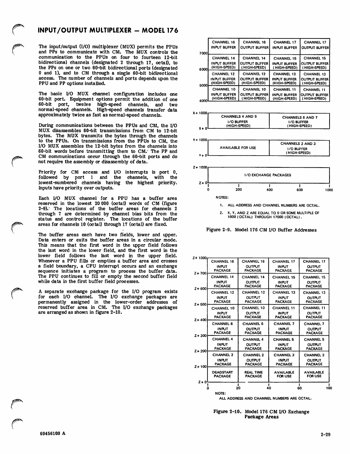
(^ INPUT/OUTPUT MULTIPLEXER - MODEL 176
The input/output (I/O) multiplexer (MUX) permits the PPUs
and PPs to communicate with CM. The MUX controls the
communication to the PPUs on four to fourteen 12-bit
bidirectional channels (designated 2 through 17, octal), to
the PPs on one or two 60-bit bidirectional ports (designated
0 and 1), and to CM through a single 60-bit bidirectional
access. The number of channels and ports depends upon the
PPU and PP options installed.
The basic I/O MUX channel configuration includes one
60-bit port. Equipment options permit the addition of one
60-bit port, twelve high-speed channels, and two
normal-speed channels. High-speed channels transfer data
approximately twice as fast as normal-speed channels.
During communications between the PPUs and CM, the I/O
MUX disassembles 60-bit transmissions from CM to 12-bit
bytes. The MUX transmits the bytes through the channels
to the PPUs. On transmissions from the PPUs to CM, the
I/O MUX assembles the 12-bit bytes from the channels into
60-bit words before transmitting them to CM.' The PP and
CM communications occur through the 60-bit ports and do
not require the assembly or disassembly of data.
Priority for CM access and I/O interrupts is port 0,
followed by port 1 and the channels, with the
lowest-numbered channels having the highest priority.
Inputs have priority over outputs.
Each I/O MUX channel for a PPU has a buffer area
reserved in the lowest 20 000 (octal) words of CM (figure
2-9). • The locations of the buffer areas for channels 2
through 7 are determined by channel bias bits from the
status and control register. The locations of the buffer
areas for channels 10 (octal) through 17 (octal) are fixed.
The buffer areas each have two fields, lower and upper.
Data enters or exits the buffer areas in a circular mode.
This means that the first word in the upper field follows
the last word in the lower field, and the first word in the
lower field follows the last word in the upper field.
Whenever a PPU fills or empties a buffer area and crosses
a field boundary, a CPU interrupt occurs and an exchange
sequence initiates a program to process the buffer data.
The PPU continues to fill or empty the second buffer field
while data in the first buffer field processes.
A separate exchange package for the I/O program exists
for each I/O channel. The I/O exchange packages are
permanently assigned in the lower-order addresses of
reserved buffer area in CM. The I/O exchange packages
are arranged as shown in figure 2-10.
7000
6000
5000
4000
X+1000
X+0
Y+1000
CHANNEL 16
INPUT BUFFER
CHANNEL 16
OUTPUT BUFFER
CHANNEL 17
INPUT BUFFER
CHANNEL 17
OUTPUT BUFFER
CHANNEL 14
INPUT BUFFER
(HIGH-SPEED)
CHANNEL 14
OUTPUT BUFFER
(HIGH-SPEED)
CHANNEL 15
INPUT BUFFER
(HIGH-SPEED)
CHANNEL 15
OUTPUT BUFFER
(HIGH-SPEED)
CHANNEL 12
INPUT BUFFER
(HIGH-SPEED)
CHANNEL 12
OUTPUT BUFFER
(HIGH-SPEED)
CHANNEL 13
INPUT BUFFER
(HIGH-SPEED)
CHANNEL 13
OUTPUT BUFFER
(HIGH-SPEEO)
CHANNEL 10
INPUT BUFFER
(HIGH-SPEED)
CHANNEL 10
OUTPUT BUFFER
(HIGH-SPEEO)
CHANNEL 11
INPUT BUFFER
(HIGH-SPEED)
CHANNEL 11
OUTPUT BUFFER
(HIGH-SPEED)
CHANNELS 4 AND 5
I/O BUFFER
(HIGH-SPEED)
CHANNELS 6 AND 7
I/O BUFFER
(HIGH-SPEED)
AVAILABLE FOR USE
CHANNELS 2 AND 3
I/O BUFFER
(HIGH-SPEED)
2+0
I/O EXCHANGE PACKAGES
I
200 400 600 1000
NOTES:
1. ALL ADDRESS AND CHANNEL NUMBERS ARE OCTAL.
2. X, Y. AND 2 ARE EQUAL TO 0 OR SOME MULTIPLE OF
1000 (OCTAL) THROUGH 17000 (OCTAL).
Figure 2-9. Model 176 CM I/O Buffer Addresses
2+ 1000
2+600
2+500
2+400
2+300
2+200
2+100
CHANNEL 16
INPUT
PACKAGE
CHANNEL 16
OUTPUT
PACKAGE
CHANNEL 17
INPUT
PACKAGE
CHANNEL 17
OUTPUT
PACKAGE
CHANNEL 14
INPUT
PACKAGE
CHANNEL 14
OUTPUT
PACKAGE
CHANNEL 15
INPUT
PACKAGE
CHANNEL 15
OUTPUT
PACKAGE
CHANNEL 12
INPUT
PACKAGE
CHANNEL 12
OUTPUT
PACKAGE
CHANNEL 13
INPUT
PACKAGE
CHANNEL 13
OUTPUT
PACKAGE
CHANNEL 10
INPUT
PACKAGE
CHANNEL 10
OUTPUT
PACKAGE
CHANNEL 11
INPUT
PACKAGE
CHANNEL 11
OUTPUT
PACKAGE
CHANNEL 6
INPUT
PACKAGE
CHANNEL 6
OUTPUT
PACKAGE
CHANNEL 7
INPUT
PACKAGE
CHANNEL 7
OUTPUT
PACKAGE
CHANNEL 4
INPUT
PACKAGE
CHANNEL 4
OUTPUT
PACKAGE
CHANNEL 5
INPUT
PACKAGE
CHANNEL 5
OUTPUT
PACKAGE
CHANNEL 2
INPUT
PACKAGE
CHANNEL 2
OUTPUT
PACKAGE
CHANNEL 3
INPUT
PACKAGE
CHANNEL 3
OUTPUT
PACKAGE
DEADSTART
PACKAGE
REAL TIME
PACKAGE
AVAILABLE
FOR USE
AVAILABLE
FOR USE
I
20 40 60 100
NOTE:
ALL ADDRESS AND CHANNEL NUMBERS ARE OCTAL.
Figure 2-10. Model 176 CM I/O Exchange
Package Areas
60456100 A 2-29
NORMAL PPU TO CM DATA TRANSFER
The following description lists the events in a normal PPU
to CM input record sequence. The sequence begins with a
reset input channel buffer instruction that resets the input
channel buffer for receipt of a new record. This sets the
input assembly counter and the input buffer address to
zero. The CPU then notifies the PPU that CM is ready to
receive data. It does this by transmitting a message to the
PPU over the associated MUX output channeL The
contents and format of the message depends upon the
communication scheme, which is determined by the
software.
Upon receipt of the message, the PPU enters the first
12-bit word into its output register. This entry causes the
transmission of a word pulse and 12 data bits to the input
channel control for this channel in the MUX. The MUX
enters the first word in the upper 12 bits of the 60-bit
assembly register. The MUX then sends a resume pulse to
the PPU and advances the assembly counter. The resume
pulse clears the output word flag at the PPU, and the
second 12-bit word enters the PPU output register. The
sequence of word pulse, input assembly, and resume pulse is
repeated for each 12-bit word transmitted over the data
path. When five 12-bit words have been assembled into a
60-bit word, a resume pulse is sent to the PPU and a word
request is made for CM access. The MUX does not accept
the next 12-bit word from the PPU until the request for
CM access has been accepted by the CM/ This may be only
a few clock periods or many clock periods, depending upon
CM bank conflicts. Once the word request has been
accepted by CM, the buffer address is advanced, the
assembly counter is reset to zero, and the transmit and
assembly procedure is repeated for the next 60-bit word.
When the PPU transmits enough words to fill half of its
assigned CM buffer area, the MUX sends an interrupt
request to the CPU. When this is accepted by the CPU, an
exchange jump is initiated to a program that processes the
data in the first half of the buffer. Meanwhile, the PPU
continues to transmit 12-bit words, which the MUX
assembles into 60-bit words and stores in the upper half of
the buffer. When the upper half of the buffer becomes full,
the MUX sends another interrupt request to the CPU,
provided that the program from the first interrupt has
completed processing the lower half of the buffer and has
performed an exchange exit. Otherwise, the interrupt
request is not sent to the CPU, and further input from the
PPU is locked out until the exchange exit is executed.
NOTE
If an error condition occurs which causes the
I/O program to exit to an error handling
routine at EEA, the error routine may, in
returning to the I/O program, inadvertently
release the interrupt lockout condition
prematurely by performing an exchange exit
(013) instruction. To prevent this situation
from occurring, bit 17 of EEA can be set in
the incoming exchange package. This bit is
sent to exchange jump control and blocks a
013 instruction from releasing any I/O
interrupt request flags that might be set.
When the interrupt request has been sent, the PPU begins
to enter data into the lower half of the buffer while the
data in the upper half is being processed. Thus, the buffer
operates in a circular mode with interrupts at the center
and end of the buffer area.
An input record may contain any amount of data. The
transmitting PPU terminates the record by sending a
record pulse to the MUX. Before sending the record pulse,
the PPU ensures that the last 12-bit word was accepted by
the MUX. (If the PPU output word flag is clear, the MUX
has accepted the last word.) Upon receipt of the record
pulse, the MUX sends an interrupt request to the CPU. If
the PPU has not transmitted enough 12-bit words to form a
complete 60-bit word, the remainder of the word is filled
with zeros. Other than this, the CPU handles this request
the same as an interrupt request caused by a threshold
condition. The resulting I/O program determines whether
the interrupt was caused by a buffer threshold or a record
pulse. It does this by reading the CM address (read input
channel status instruction) to determine whether a
threshold has been crossed since the last interrupt. The I/O
program processes the input data according to the situation
sensed.
The PPU must not begin transmitting a new record of input
data until the data in the buffer has been processed. There
is no hardware provision to prevent the PPU from doing
this. Therefore, the PPU program must not enter new data
until directed to do so by the CPU program. If the PPU
proceeds before the CPU has reset the input buffer, the
incoming data for the new record may be partially lost.
The incoming record continues to be input with no
indication of error except that the record is shortened by
the lost data.
NORMAL CM TO PPU DATA TRANSFER
The following description lists the events in a normal CM
to PPU output record sequence. The I/O program has
already loaded the output buffer with some data. The
output sequence begins with a reset output buffer
instruction that sets the output buffer address to zero and
sends a word request to CM to read the first word from the
output buffer to the 60-bit disassembly register in the
MUX. When CM delivers the 60-bit word to the
disassembly register, the output channel control for this
channel clears the disassembly counter and outputs a
record pulse and a word pulse to the PPU to indicate that
transmission of a new record is starting.
The upper 12 bits of the data in the disassembly register
are placed on the input channel for the PPU. When the
PPU program senses the record pulse on its input channel,
it reads the 12 bits of data and sends a resume pulse to the
MUX. The MUX output data remains on the PPU input
channel until the PPU accepts it.
When the resume pulse arrives from the PPU, the MUX
advances the disassembly register to the next 12 bits of the
60-bit word and sends another word pulse to the PPU. The
output buffer address also advances to the next address at
this time so that a program monitoring this channel could
determine that the PPU has accepted the first 12 bits of a
new 60-bit word. The sequence of output disassembly,
word pulse, PPU input, and resume pulse continues until the
entire 60-bit word has been sent by the MUX. At
"^fev
2-30 60456100 A
0^\
this time, the MUX sends another word request to CM for
the next word in the output buffer. When this word arrives
in the disassembly register, the upper 12 bits and a word
pulse are sent to the PPU, and the process of delivering a
new 60-bit word is repeated.
When the PPU has emptied half its assigned buffer area,
the MUX sends an interrupt request to the CPU. When this
is accepted by the CPU, an exchange jump initiated to the
program that refills the portion of the buffer that has just
been emptied. This operation is similar to that performed
for a PPU to CM transfer. Output to the PPU continues
from the upper half of the buffer while the lower half is
being refilled.
When the upper half of the buffer becomes empty, the
MUX sends another interrupt request to the CPU, provided
that the program from the first interrupt has completed
processing the lower half of the buffer and has performed
an exchange exit. Otherwise, the interrupt request is not
sent to the CPU, and further output to the PPU is locked
out until the exchange exit is executed.
| NOTE |
If an error condition occurs which causes the
I/O program to exit to an error handling
routine at EEA, the error routine may, in
returning to the I/O program, inadvertently
release the interrupt lockout condition
prematurely by performing an exchange exit
(013) instruction. To prevent this situation
from occurring, bit 17 of EEA can be set on
the incoming exchange package. This bit is
sent to exchange jump control and blocks a
013 instruction from releasing an I/O
interrupt request flag that might be set.
Using a software-determined communication scheme, the
CPU has notified the PPU of the length of the record.
When the PPU receives the expected amount of data, it
stops reading data on its input channel, stopping further
transmission by the MUX.
HIGH-SPEED PPU TO CM DATA TRANSFER
The following description lists the events in a high-speed
input record sequence. The sequence for a high-speed
channel is basically the same as for a normal channel
except that the word and record pulses from the PPU are
not synchronized by the MUX.
The sequence begins with a reset input channel instruction
that resets the input channel buffer for receipt of a new
record. This sets the input assembly counter to zero and
the input buffer address to the starting address of the
buffer for the selected channeL
Next, the PPU enters the first 12-bit word into its output
register. This causes the transmission of a word pulse and
12 data bits to the input channel control for this channel in
the MUX. The MUX enters the 12-bit word in the upper 12
bits of the 60-bit assembly register.
A static high-speed resume signal is sent to the PPU during
this time. This clears the output word flag in the PPU
immediately after it sets. The second 12-bit word may now
be entered in the PPU output register. This sequence
continues as each 12-bit word transmits over the data path.
When five 12-bit words are assembled into a 60-bit word,
the MUX sets the input word request flag for CM access.
This blocks the high-speed resume signal to the PPU and
clears the input assembly counter in preparation for the
arrival of the next PPU word. It also blocks the processing
of a new 12-bit word if one arrives before the request for
access has been accepted by CM. This may be only a few
clock periods or many clock periods, depending upon CM
bank conflicts and channel priority. Once the word request
is accepted by CM, the buffer address advances, the input
word request flag clears, and the high-speed resume signal
is again sent to the PPU. The transmit and assembly
procedure then repeats for the next 60-bit word.
Interrupt requests resulting from reaching a buffer
threshold or receiving a record pulse from the PPU are the
same as for the normal PPU to CM data transfer.
HIGH-SPEED CM TO PPU DATA TRANSFER
The following description lists the events in a high-speed
output record sequence. The sequence for a high-speed
channel is basically the same as for a normal channel
except that the resume pulse is not resynchronized by the
MUX. Also, the output data path includes a series of three
output data buffer registers. The output channel control
also controls the flow of data from the disassembly register
through these buffer registers to the PPU. The three
buffer registers are designated ranks A, B, and C.
The output sequence begins with a reset output buffer
instruction that sets the output buffer address to the
starting address of the buffer. At this time, the MUX also
sends a word request to CM to read the first word from the
buffer to the 60-bit disassembly register. When the 60-bit
word has been delivered to the disassembly register, the
MUX clears the disassembly counter and sends a word pulse
and a record pulse to the high-speed control. Concurrently,
the upper 12-bit word in the disassembly register transmits
to rank A of the buffer registers.
Upon receipt of the record pulse from the output channel
control, the high-speed buffer control transmits a record
pulse to the PPU/ This sets the input record flag in the
PPU.
60456100 A 2-31
Upon receipt of the word pulse from the output channel
control, the high-speed buffer control enters the 12-bit
word from the disassembly register into rank A. It then
transmits the word pulse to the PPU where it sets the input
word flag. The word pulse is not sent to the PPU if an
interrupt lockout condition exists in the output channel
controLf
In consecutive clock periods, the data moves from rank A
to rank B to rank C of the buffer registers. The data in
rank C is transmitted to the PPU and remains in the data
path until the PPU transmits a resume pulse to the
high-speed controL
The high-speed control does not wait for the resume pulse
from the PPU before sending a resume pulse to the output
channel controL' The output channel control increments
the disassembly count and transmits the second 12-bit word
to rank A, At this time, the output channel control
advances the address register to the next address in the CM
buffer and sends a word pulse to the high-speed control.
Upon receipt of this second word pulse, rank A is entered
with the second 12-bit word, and the resume pulse is again
sent to the output channel controL In the following clock
period, the data in rank A moves into rank B.
The process is repeated for the third 12-bit word.
However, when the output channel control sends the third
word to rank A, the resume pulse is not sent back to the
output channel control.
At this point, all action stops until the PPU accepts the
first 12-bit word and transmits a resume pulse to the
high-speed buffer control/ When a resume pulse arrives
from the PPU, rank C clears and is entered with the second
12-bit word in rank B. A resume pulse is then sent to the
output channel controL
The sequence continues until the fifth 12-bit word has been
sent to rank A by the output channel control. At this time,
the output channel control sends another word request to
CM for the next 60-bit word in the buffer.
At the time the output word request flag sets, the last two
12-bit words are in ranks B and C. The PPU accepts the
fourth word and transmits a resume pulse to the high-speed
buffer controL' Rank C is then cleared and entered with
the fifth word from rank B. When this data has been
delivered to the PPU, action halts until the requested word
is delivered to the disassembly register from CM.
Some clock periods later, the word is delivered to the
disassembly register, and the process of delivering a new
60-bit word to the PPU begins.
Interrupt request results from reaching a buffer threshold
are the same as for the normal CM to PPU data transfer.
■^®Sy
2-32 60456100 A
LOGIC SCANNER -. MODEL 176

Vs.
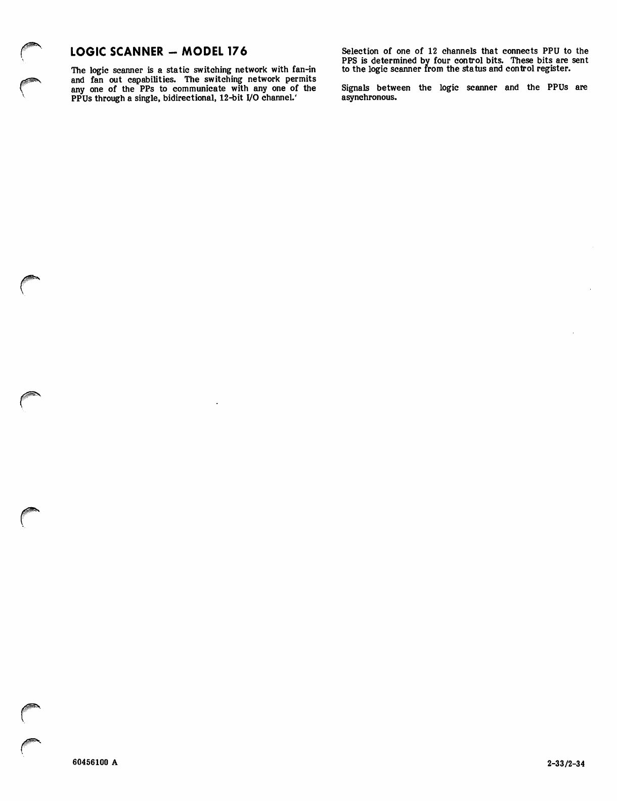
LOGIC SCANNER — MODEL 176 Selection of one of 12 channels that connects PPU to the
PPS is determined by four control bits. These bits are sent
The logic scanner is a static switching network with fan-in to the logic scanner from the status and control register,
and fan out capabilities. The switching network permits
any one of the PPs to communicate with any one of the Signals between the logic scanner and the PPUs are
PPUs through a single, bidirectional, 12-bit I/O channeL' asynchronous.
r
60456100 A 2-33/2-34

r\
^
DATA CHANNEL CONVERTER - ALL MODELS
.^-

r^kk
**%
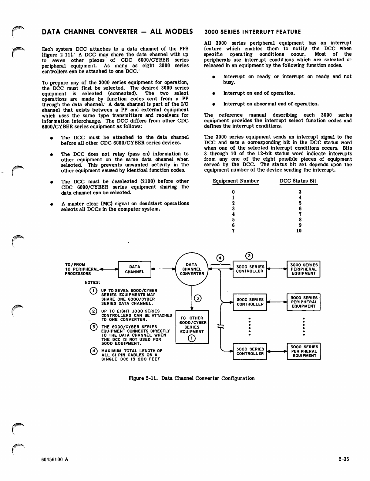
DATA CHANNEL CONVERTER - ALL MODELS 3000 series interrupt feature
- / ^ K Each system DCC attaches to a data channel of the PPS
(figure 2-11).' A DCC may share the data channel with up
to seven other pieces of CDC 6000/CYBER series
peripheral equipment. As many as eight 3000 series
controllers can be attached to one DCC
To prepare any of the 3000 series equipment for operation,
the DCC must first be selected. The desired 3000 series
equipment is selected (connected). The two select
operations are made by function codes sent from a PP
through the data channeL' A data channel is part of the I/O
channel that exists between a PP and external equipment
which uses the same type transmitters and receivers for
information interchange. The DCC differs from other CDC
6000/CYBER series equipment as follows:
• The DCC must be attached to the data channel
before all other CDC 6000/CYBER series devices.
• The DCC does not relay (pass on) information to
other equipment on the same data channel when
selected. This prevents unwanted activity in the
other equipment caused by identical function codes.
• The DCC must be deselected (2100) before other
CDC 6000/CYBER series equipment sharing the
data channel can be selected.
• A master clear (MC) signal on deadstart operations
selects all DCCs in the computer system.
All 3000 series peripheral equipment has an interrupt
feature which enables them to notify the DCC when
specific operating conditions occur. Most of the
peripherals use interrupt conditions which are selected or
released in an equipment by the following function codes.
• Interrupt on ready or interrupt on ready and not
busy.
• Interrupt on end of operation.
• Interrupt on abnormal end of operation.
The reference manual describing each 3000 series
equipment provides the interrupt select function codes and
defines the interrupt conditions.
The 3000 series equipment sends an interrupt signal to the
DCC and sets a corresponding bit in the DCC status word
when one of the selected interrupt conditions occurs. Bits
3 through 10 of the 12-bit status word indicate interrupts
from any one of the eight possible pieces of equipment
served by the DCC. The status bit set depends upon the
equipment number of the device sending the interrupt.
Equipment Number
0
1
2
3
4
5
6
7
DCC Status Bit
3
4
5
6
7
8
9
10
TO/FROM
10 PERIPHERAL*
PROCESSORS
NOTES:
DATA
CHANNEL
0
©
©
©
UP TO SEVEN 6000/CYBER
SERIES EQUIPMENTS MAY
SHARE ONE 6000/CYBER
SERIES DATA CHANNEL.
UP TO EIGHT 3000 SERIES
CONTROLLERS CAN BE ATTACHED
TO ONE CONVERTER.
THE 6000/CYBER SERIES
EQUIPMENT CONNECTS DIRECTLY
TO THE DATA CHANNEL WHEN
THE DCC IS NOT USED FOR
3000 EQUIPMENT.
MAXIMUM TOTAL LENGTH OF
ALL 61 PIN CABLES ON A
SINGLE DCC IS 200 FEET
TO OTHER
6000/CYBER
SERIES
EQUIPMENT
©
3000 SERIES
CONTROLLER
3000 SERIES
CONTROLLER
3000 SERIES
CONTROLLER
3000 SERIES
PERIPHERAL
EQUIPMENT
3000 SERIES
PERIPHERAL
EQUIPMENT
3000 SERIES
PERIPHERAL
EQUIPMENT
Figure 2-11. Data Channel Converter Configuration
z#^,
60456100 A 2-35
Peripheral equipment need not be connected to the DCC to
send an interrupt signal to it. Thus, the interrupt feature
provides a limited status check for an equipment even
though it is not connected.
An interrupt status bit in the DCC is present (set) as long
as the equipment maintains the interrupt signal. An
interrupt signal clears by any one of the following.
• A DCC MC function (1700). This clears all 3000
series equipment attached to the DCC and the
DCC itself/
• A function code sent to the interrupting equipment.
• A deadstart MC signal from the CDC 6000/CYBER
data channeL'
3000 POWER FAILURE MODE
The power failure mode enhancement allows each DCC to
check for a power failure on a connected piece of external
equipment. The detection of this power failure sets main
power fail bit 36 (44, octal) in the status and control
register. The power failure also terminates I/O operations
on the DCCs under certain conditions. Refer to Data
Channel Programming in section 5 for further details.
BUFFER FLUSHING
The buffer-flush feature allows the DCC to terminate the
PP I/O buffer when an interrupt on abnormal end of
operation condition exists in the peripheral equipment. To
enable this, the peripheral equipment must be set to
interrupt on an abnormal end of operation. This action
sends an interrupt override signal to the DCC. The
interrupt override signal initiates the buffer-flush
operation by forcing full or empty signals to the PP until
the I/O buffer is terminated. Data transmitted during the
buffer-flush operation is undefined.
V^BfSv
y^ffejk-
/^HiK
i<^^V
2-36 60456100 A
"**
DISPLAY CONTROLLER - ALL MODELS
:/0^S

■^%:
DISPLAY CONTROLLER - ALL MODELS
The display controller provides the display station with
analog and digital signals that direct the writing of symbols
on the display station cathode-ray tube (CRT)/ The
controller provides analog-symbol signals and
digital-position, unblank, and size-selection signals.
The analog-symbol signals cause small-scale deflection of
the CRT beam for tracing symbols on the face of the CRT.
Four lines carry the signals to the display station. Two
lines are for the x (horizontal) deflection, and two lines are
for the y (vertical) deflection.
The digital-position signals cause large-scale deflection of
the CRT beam for positioning the symbols on the face of
the CRT. The signal lines to the display station carry nine
bits for the beam x deflection and nine bits for the beam y
deflection.
The unblank signal enables the CRT beam only during the
time an analog-symbol signal is causing a symbol trace.
The unblank signal is a pulse train that is synchronized with
the symbol signal.
The size-selection signal is binary-coded. It is carried on
two lines and provides the selection of one of three symbol
sizes.
Eight other lines between the display controller and display
station carry control signals and display station keyboard
character codes.
60456100 A 2-37/2-38

/^%
/p^
rPERIPHERAL PROCESSOR, UNIT PROGRAMMING - MO DEI 176
^p5*

PERIPHERAL PROCESSOR UNITS
(OPTIONAL) - MODEL 176
The model 176 basic system has the option of adding 4
PPUs initially, then 1 at a time to a total of 12 PPUs.
Each PPU is a self-contained functionally independent
computer with a memory. A PPU shares access paths to
CM and the peripheral processor subsystem (PPS) with each
installed PPU. Each PPU has its own hardware for
arithmetic operations, logic operations, and I/O channels.
A primary function of the PPU is to perform I/O tasks at
the request of the CP. The PPU may also directly control
peripheral equipment with a minimum of intervening
circuits and perform a modest amount of character
conversion and data formatting before transmitting data to
the CP. Another function may be to perform the
synchronization required to interface an electromechanical
device to the CP. This function generally requires
dedication of the PPU to one or more specific units such as
printers, card readers, tape units, or disk files.
A PPU communicates through its eight I/O channels. Each
I/O channel is bidirectional and carries 12 data bits. One
channel can be used for communications with another PPU,
one for communication with the logic scanner, one for
communication with the I/O MUX, and four for
communication with 7000 peripheral equipment. One
channel is not available for external use. Only one channel
is active at a time. On a write operation, the MUX
assembles data into 60-bit words for CM/ On a read
operation, the MUX disassembles the 60-bit CM word into
12-bit bytes for the PPU.
Channel instructions direct all activities with other PPUs,
the logic scanner, I/O MUX, and external equipment.
These instructions select any equipment on any channel and
transfer data to or from the selected equipment, PPU, or
logic scanner.
Sign extension and the clearing of unused upper bits to zero
depend on the instruction. Zero is represented by all zero
bits.
The A register counts the length of the block for block
input or output instructions. At the transmission of each
word, the A register enters the new count.
The A register receives the input data word (12 bits) for
the input to A instruction and holds the output data word
(12 bits) for the output from A instruction.
P Register
The 12-bit P register holds the address of the current
instruction. During the execution of the current
instruction, the content of P advances by one or two to
provide the address of the next instruction in the program
for 12- or 24-bit instructions. If the current instruction is
a jump, P receives the jump address.
Q R e g i s t e r
The 12-bit Q register has two major functions. It holds the
address of an operand during instruction execution and
holds the upper six bits of an 18-bit operand in the lower
six bits of the register during operand arithmetic.
X Register
The 13-bit X register holds all data read from memory.
The register also holds the lower 12 bits of the operand
during the 18-bit arithmetic operations of the A register.
r
COMPUTATION SECTION
The computation section performs the arithmetic
operations associated with manipulating operands and with
indirect addressing. The arithmetic operations involve
seven registers: A, P, Q, X, Sk, fd, and k. The A register
is the only one used directly by a programmer.
A Register
The 18-bit A register is the principal operand register and
is used for the I/O, shift, and logical arithmetic
instructions. In an arithmetic operation, the A register
always holds one of the operands and always receives the
arithmetic result. The content of A is treated as a signed
operand. If bit 17 is set, the operand is negative.
Overflows are ignored although an end-around carry may
show in the register at the end of an instruction execution.
Sk Register
The 6-bit Sk register contains a shift count during
execution of shift instructions. The lowest-order five bits
contain the number of bit positions by which the A register
is to be shifted. The highest-order bit determines whether
the shift is left circular or right open-ended.
fd Register
The 12-bit fd register holds the current instruction word
for translation. The upper six bits are the f designator, and
the lower six bits are the d designator from the instruction.
Ic Register
The 3-bit k register is the instruction cycle counter and is
used to count the number of memory references required
during execution.
60456100 E 2-39
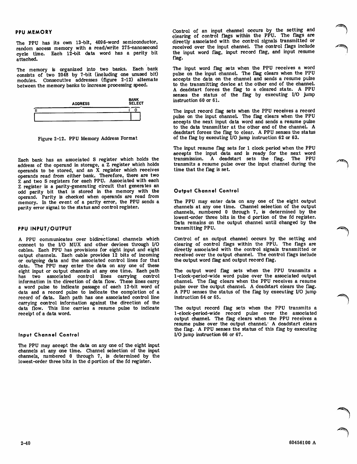
PPU MEMORY
The PPU has its own 13-bit, 4096-word semiconductor,
random access memory with a read/write 275-nanosecond
cycle time. Each 12-bit data word has a parity bit
attached.
The memory is organized into two banks. Each bank
consists of two 2048 by 7-bit (including one unused bit)
modules. Consecutive addresses (figure 2-12) alternate
between the memory banks to increase processing speed.
ADDRESS
BANK
SELECT
Figure 2-12. PPU Memory Address Format
Each bank has an associated S register which holds the
address of the operand in storage, a Z register which holds
operands to be stored, and an X register which receives
operands read from either bank. Therefore, there are two
Z and two S registers for each PPU. Associated with each
Z register is a parity-generating circuit that generates an
odd parity bit that is stored in the memory with the
operand. Parity is checked when operands are read from
memory. In the event of a parity error, the PPU sends a
parity error signal to the status and control register.
PPU INPUT/OUTPUT
A PPU communicates over bidirectional channels which
connect to the I/O MUX and other devices through I/O
cables. Each PPU has provisions for eight input and eight
output channels. Each cable provides 12 bits of incoming
or outgoing data and the associated control lines for that
data. The PPU may enter the data on any one of these
eight input or output channels at any one time. Each path
has two associated control lines carrying control
information in the direction of data flow. These lines carry
a word pulse to indicate passage of each 12-bit word of
data and a record pulse to indicate the completion of a
record of data. Each path has one associated control line
carrying control information against the direction of the
data flow. This line carries a resume pulse to indicate
receipt of a data word.
Input Channel Control
The PPU may accept the data on any one of the eight input
channels at any one time. Channel selection of the input
channels, numbered 0 through 7, is determined by the
lowest-order three bits in the d portion of the fd register.
Control of an input channel occurs by the setting and
clearing of control flags within the PPU. The flags are
directly associated with the control signals transmitted or
received over the input channel. The control flags include
the input word flag, input record flag, and input resume
flag.
The input word flag sets when the PPU receives a word
pulse on the input channel. The flag clears when the PPU
accepts the data on the channel and sends a resume pulse
to the transmitting device at the other end of the channel.
A deadstart forces the flag to a cleared state. A PPU
senses the status of the flag by executing I/O jump
instruction 60 or 61.
The input record flag sets when the PPU receives a record
pulse on the input channel. The flag clears when the PPU
accepts the next input data word and sends a resume pulse
to the data transmitter at the other end of the channel. A
deadstart forces the flag to clear. A PPU senses the status
of the flag by executing I/O jump instruction 62 or 63.
The input resume flag sets for 1 clock period when the PPU
accepts the input data and is ready for the next word
transmission. A deadstart sets the flag. The PPU
transmits a resume pulse over the input channel during the
time that the flag is set.
Output Channel Control
The PPU may enter data on any one of the eight output
channels at any one time. Channel selection of the output
channels, numbered 0 through 7, is determined by the
lowest-order three bits in the d portion of the fd register.
Data remains on the output channel until changed by the
transmitting PPU.
Control of an output channel occurs by the setting and
clearing of control flags within the PPU. The flags are
directly associated with the control signals transmitted or
received over the output channel. The control flags include
the output word flag and output record flag.
The output word flag sets when the PPU transmits a
1-clock-period-wide word pulse over the associated output
channel. The flag clears when the PPU receives a resume
pulse over the output channel. A deadstart clears the flag.
A PPU senses the status of the flag by executing I/O jump
instruction 64 or 65.
The output record flag sets when the PPU transmits a
1-clock-period-wide record pulse over the associated
output channel. The flag clears when the PPU receives a
resume pulse over the output channel/ A deadstart clears
the flag. A PPU senses the status of this flag by executing
I/O jump instruction 66 or 67.
>,a8?\
2-40 60456100 A
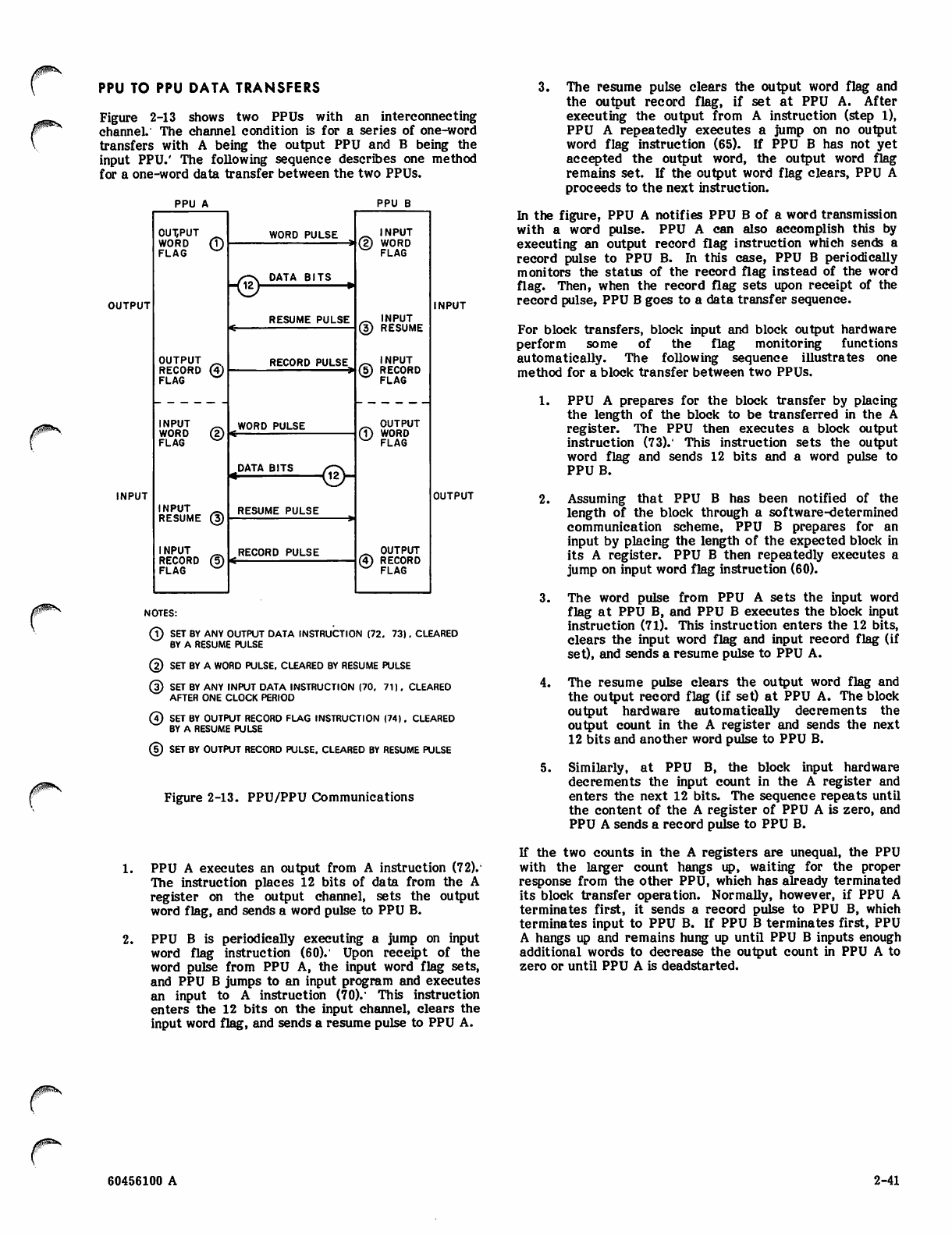
PPU TO PPU DATA TRANSFERS
Figure 2-13 shows two PPUs with an interconnecting
channel. The channel condition is for a series of one-word
transfers with A being the output PPU and B being the
input PPU/ The following sequence describes one method
for a one-word data transfer between the two PPUs.
PPU A PPU B
OUTPUT
INPUT
2.
OUTPUT
WORD (T)
F L A G w
■€>
OUTPUT _
RECORD @
FLAG
INPUT _
W O R D ©
FLAG v~/
INPUT ^
RESUME (3)
INPUT _
RECORD (5)
F L A G ^
WORD PULSE
DATA BITS
RESUME PULSE
RECORD PULSE
WORD PULSE
DATA BITS
■©-
RESUME PULSE
RECORD PULSE
^ INPUT
© WORD
FLAG
_ INPUT
(3) RESUME
INPUT
5) RECORD
FLAG
©
^ O U T P U T
(T) WORD
W F L A G
OUTPUT
4) RECORD
FLAG
©
INPUT
OUTPUT
NOTES:
© SET BY ANY OUTPUT DATA INSTRUCTION (72. 73), CLEARED
BY A RESUME PULSE
© SET BY A WORD PULSE. CLEARED BY RESUME PULSE
(D SET BY ANY INPUT DATA INSTRUCTION (70. 71). CLEAREO
AFTER ONE CLOCK PERIOD
0 SET BY OUTPUT RECORD FLAG INSTRUCTION (74). CLEARED
BY A RESUME PULSE
(§) SET BY OUTPUT RECORD PULSE. CLEARED BY RESUME PULSE
Figure 2-13. PPU/PPU Communications
PPU A executes an output from A instruction (72).-
The instruction places 12 bits of data from the A
register on the output channel, sets the output
word flag, and sends a word pulse to PPU B.
PPU B is periodically executing a jump on input
word flag instruction (60)/ Upon receipt of the
word pulse from PPU A, the input word flag sets,
and PPU B jumps to an input program and executes
an input to A instruction (70).' This instruction
enters the 12 bits on the input channel, clears the
input word flag, and sends a resume pulse to PPU A.
3. The resume pulse clears the output word flag and
the output record flag, if set at PPU A. After
executing the output from A instruction (step 1),
PPU A repeatedly executes a jump on no output
word flag instruction (65). If PPU B has not yet
accepted the output word, the output word flag
remains set If the output word flag clears, PPU A
proceeds to the next instruction.
In the figure, PPU A notifies PPU B of a word transmission
with a word pulse. PPU A can also accomplish this by
executing an output record flag instruction which sends a
record pulse to PPU B. In this case, PPU B periodically
monitors the status of the record flag instead of the word
flag. Then, when the record flag sets upon receipt of the
record pulse, PPU B goes to a data transfer sequence.
For block transfers, block input and block output hardware
perform some of the flag monitoring functions
automatically. The following sequence illustrates one
method for a block transfer between two PPUs.
1. PPU A prepares for the block transfer by placing
the length of the block to be transferred in the A
register. The PPU then executes a block output
instruction (73)/ This instruction sets the output
word flag and sends 12 bits and a word pulse to
PPUB.
2. Assuming that PPU B has been notified of the
length of the block through a software-determined
communication scheme, PPU B prepares for an
input by placing the length of the expected block in
its A register. PPU B then repeatedly executes a
jump on input word flag instruction (60).
3. The word pulse from PPU A sets the input word
flag at PPU B, and PPU B executes the block input
instruction (71). This instruction enters the 12 bits,
clears the input word flag and input record flag (if
set), and sends a resume pulse to PPU A.
4. The resume pulse clears the output word flag and
the output record flag (if set) at PPU A. The block
output hardware automatically decrements the
output count in the A register and sends the next
12 bits and another word pulse to PPU B.
5. Similarly, at PPU B, the block input hardware
decrements the input count in the A register and
enters the next 12 bits. The sequence repeats until
the content of the A register of PPU A is zero, and
PPU A sends a record pulse to PPU B.
If the two counts in the A registers are unequal, the PPU
with the larger count hangs up, waiting for the proper
response from the other PPU, which has already terminated
its block transfer operation. Normally, however, if PPU A
terminates first, it sends a record pulse to PPU B, which
terminates input to PPU B. If PPU B terminates first, PPU
A hangs up and remains hung up until PPU B inputs enough
additional words to decrease the output count in PPU A to
zero or until PPU A is deadstarted.
60456100 A 2-41
PPU TO PERIPHERAL EQUIPMENT DATA TRANSFERS peripheral device, the associated control signals are '^J
terminated, set to 1 or 0, or assigned functions.
A direct-driven peripheral device requires two PPU For detailed information on data transfers between a PPU st^m*.
channels. One channel performs control and status, and the and a peripheral device, refer to the documentation on the )
other performs data transfers. Depending upon the specific peripheral device.
2-42 60456100 A
PERIPHERAL PROCESSOR SUBSYSTEM - ALL MODELS
j^\

•v"*^--
3
0^K
PERIPHERAL PROCESSOR SUBSYSTEM -
ALL MODELS
The peripheral processor subsystem (PPS) consists of 10
peripheral processors (PPs)/ Each PP is a functionally
independent computer that has its own memory. The PPs
share access to CM and 12 bidirectional I/O channels. The
PPs are organized into a multiplexing system, termed
barrel and slot, which allows them to share common
hardware for arithmetic, logical, and I/O operations
without losing speed or independence.
The PPS can be expanded to 14, 17, or 20 PPs in all system
models. Expansion to 14 PPs includes the addition of 12
I/O channels. Any PP can access any VO channeL
The PPS operates in a 500-nanosecond major cycle time.
All PPs communicate with either external equipment or
each other over the 12 or 24 independent (12 bits plus 1
parity bit) bidirectional I/O channels. Only one piece of
external equipment can communicate over one channel at a
time, but all channels can be active at the same time.
Channel instructions direct all activities with external
equipment. These instructions select any equipment on any
channel and transfer data to or from the selected
equipment.
Each PP exchanges data with CM through CMC in models
720 through 760 or through the I/O MUX in model 176 in
60-bit words. In a write operation, five successive 12-bit
PP words are assembled into a 60-bit word and sent to
CMC or the I/O MUX. In a read operation, a 60-bit word
from CM is disassembled into five 12-bit words and sent to
successive locations in the peripheral processor memory
(PPM). Separate assembly/disassembly read and write
paths to CM are time-shared by each of the 10 PPs.
Assembly/disassembly is performed in random access
memories (RAMs). These RAMs are also provided for the
4, 7, or 10 PPs in PPS-1.
In models 720 through 760, data transmission parity is
generated on all CM writes and is checked on all CM
reads. If a data parity error is detected, a bit sets in the
status and control register.
REAL-TIME CLOCK
The PPS contains a real-time clock. The clock may be used
to determine program running time, as a reference to track
the time-of-day, or for other functions determined by the
computer programs.
The clock runs continuously during computer power
application. Output from the clock comes from a 12-bit
register that increments once each microsecond to the
maximum capacity of the register (4096 microseconds).'
When the register reaches capacity, it resets and continues
counting. The counting cannot be preset or altered.
Any PP may read the 12-bit clock output with the input to
A channel d (70) instruction. The instruction permits
access to the clock on internal channel 14 (octal). Any
attempts to output information on channel 14 do not
execute and cause the instruction to hang.
A PP may also read the clock with an input (A) words to m
from channel d (71) instruction. When this happens, the PP
receives one word from the clock and then exits from the
instruction because channel 14 is inactive. In a CDC
CYBER 70 or 6000 Computer System, the same routine
causes the PP to always receive a word of zeros and then
exit from the instruction.
Channel 14 appears empty and inactive when checked for
status. This is compatible with the CDC CYBER 70 and
6000 Computer Systems.
DEADSTART
Deadstart is a PPS operation that provides initial starting
of the computer, dumping of the contents of PPMs to an
output device (normally a printer), or sweeping PPMs
without executing instructions. Deadstart sequence is
initiated by the DEAD START switch on the deadstart
panel in bay 1 or the DEAD START switch on the display
station. The panel includes controls for assigning any PPM
to PP-0 (control PP). Another control enables central
exchange jump/monitor exchange jump (CEJ/MEJ). (For
further information, refer to Exchange Jump in section 5.)
PP MEMORY
Each PP has an independent 4096-word, 13-bit (12 data bits
plus 1 parity bit) MOS memory. s
PPM data words are checked for parity on each read. If a
parity error is detected, a bit sets in the status and control
register. All PPs of a PPS can be selected to stop on PPM
parity error by setting bit 95 in the status and control
register.
A PPM reconfiguration feature permits the user to restore
the PPS operation after a critical failure of a PPM assigned
to PP-0. PP-0 has a special controlling function at
deadstart time. The reconfiguration is accomplished by
logically exchanging the failing PPM with a good PPM and
degrading the PPS with software so the PPS operates
without the failing PPM. Degrading the PPS must be done
through the operating system. A PPS reconfiguration and a
PPS degradation permit computer operation to continue
without the failing PPM. This permits correction of the
failing PPM during scheduled maintenance.
j^^*V,
60456100 E 2-43
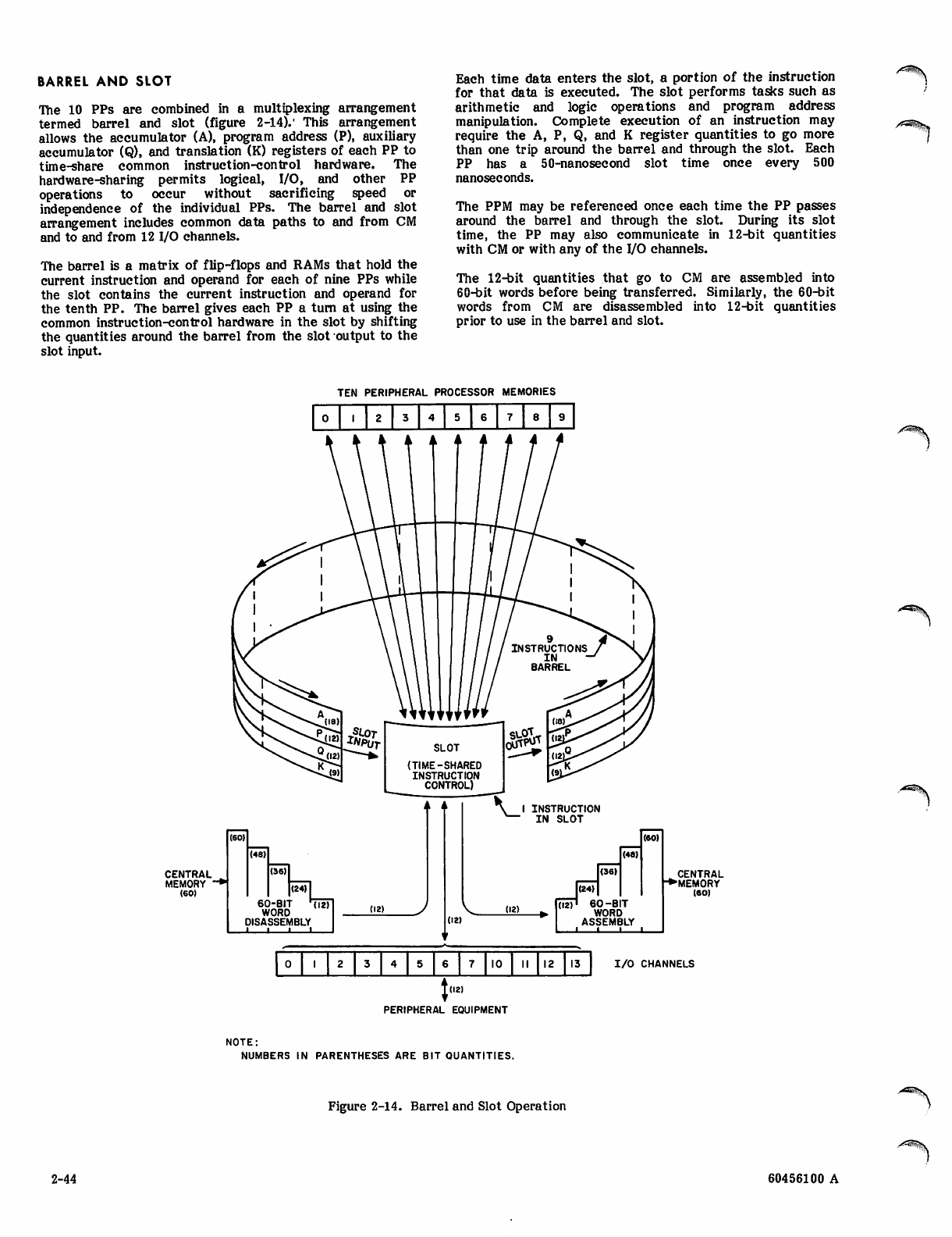
BARREL AND SLOT
The 10 PPs are combined in a multiplexing arrangement
termed barrel and slot (figure 2-14)/ This arrangement
allows the accumulator (A), program address (P), auxiliary
accumulator (Q), and translation (K) registers of each PP to
time-share common instruction-control hardware. The
hardware-sharing permits logical, I/O, and other PP
operations to occur without sacrificing speed or
independence of the individual PPs. The barrel and slot
arrangement includes common data paths to and from CM
and to and from 12 I/O channels.
The barrel is a matrix of flip-flops and RAMs that hold the
current instruction and operand for each of nine PPs while
the slot contains the current instruction and operand for
the tenth PP. The barrel gives each PP a turn at using the
common instruction-control hardware in the slot by shifting
the quantities around the barrel from the slot output to the
slot input.
Each time data enters the slot, a portion of the instruction
for that data is executed. The slot performs tasks such as
arithmetic and logic operations and program address
manipulation. Complete execution of an instruction may
require the A, P, Q, and K register quantities to go more
than one trip around the barrel and through the slot. Each
PP has a 50-nanosecond slot time once every 500
nanoseconds.
The PPM may be referenced once each time the PP passes
around the barrel and through the slot. During its slot
time, the PP may also communicate in 12-bit quantities
with CM or with any of the I/O channels.
The 12-bit quantities that go to CM are assembled into
60-bit words before being transferred. Similarly, the 60-bit
words from CM are disassembled into 12-bit quantities
prior to use in the barrel and slot.
TEN PERIPHERAL PROCESSOR MEMORIES
0 1 2 3 A 5 6 7 8
CENTRAL
MEMORY '
(60)
CENTRAL
"MEMORY
(60)
6 0 - B I T r ( i 2 )
WORD
DISASSEMBLY
- I I I 1
0 1 5 | 6 j| 7 10 II 12 13 I/O CHANNELS
PERIPHERAL EQUIPMENT
NOTE:
NUMBERS IN PARENTHESES ARE BIT QUANTITIES.
Figure 2-14. Barrel and Slot Operation
y^EiSv
2-44 60456100 A
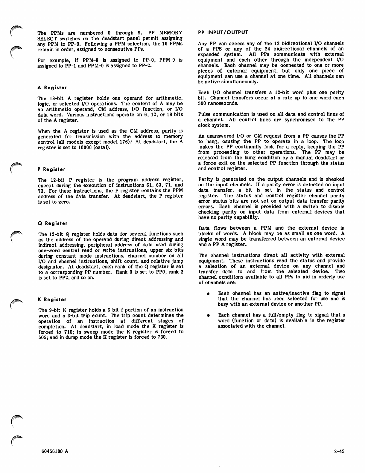
0^\
r
The PPMs are numbered 0 through 9. PP MEMORY
SELECT switches on the deadstart panel permit assigning
any PPM to PP-0. Following a PPM selection, the 10 PPMs
remain in order, assigned to consecutive PPs.
For example, if PPM-8 is assigned to PP-0, PPM-9 is
assigned to PP-1 and PPM-0 is assigned to PP-2.
A Register
The 18-bit A register holds one operand for arithmetic,
logic, or selected I/O operations. The content of A may be
an arithmetic operand, CM address, I/O function, or I/O
data word. Various instructions operate on 6, 12, or 18 bits
of the A register.
When the A register is used as the CM address, parity is
generated for transmission with the address to memory
control (all models except model 176)/ At deadstart, the A
register is set to 10000 (octal).
P Register
The 12-bit P register is the program address register,
except during the execution of instructions 61,.63, 71, and
73. For these instructions, the P register contains the PPM
address of the data transfer. At deadstart, the P register
is set to zero.
Q Register
The 12-bit Q register holds data for several functions such
as the address of the operand during direct addressing and
indirect addressing, peripheral address of data used during
one-word central read or write instructions, upper six bits
during constant mode instructions, channel number on all
I/O and channel instructions, shift count, and relative jump
designator. At deadstart, each rank of the Q register is set
to a corresponding PP number. Rank 0 is set to PPO, rank 2
is set to PP2, and so on.
PP INPUT/OUTPUT
Any PP can access any of the 12 bidirectional I/O channels
of a PPS or any of the 24 bidirectional channels of an
expanded system. All PPs communicate with external
equipment and each other through the independent I/O
channels. Each channel may be connected to one or more
pieces of external equipment, but only one piece of
equipment can use a channel at one time. All channels can
be active simultaneously.
Each I/O channel transfers a 12-bit word plus one parity
bit. Channel transfers occur at a rate up to one word each
500 nanoseconds.
Pulse communication is used on all data and control lines of
a channel. All control lines are synchronized to the PP
clock system.
An unanswered I/O or CM request from a PP causes the PP
to hang, causing the PP to operate in a loop. The loop
makes the PP continually look for a reply, keeping the PP
from proceeding to other operations. The PP may be
released from the hung condition by a manual deadstart or
a force exit on the selected PP function through the status
and control register.
Parity is generated on the output channels and is checked
on the input channels. If a parity error is detected on input
data transfer, a bit is set in the status and control
register. The status and control register channel parity
error status bits are not set on output data transfer parity
errors. Each channel is provided with a switch to disable
checking parity on input data from external devices that
have no parity capability.
Data flows between a PPM and the external device in
blocks of words. A block may be as small as one word. A
single word may be transferred between an external device
and a PP A register.
The channel instructions direct all activity with external
equipment. These instructions read the status and provide
a selection of an external device on any channel and
transfer data to and from the selected device. Two
channel conditions available to all PPs to aid in orderly use
of channels are:
/$^v
K Register
The 9-bit K register holds a 6-bit f portion of an instruction
word and a 3-bit trip count. The trip count determines the
operation of an instruction at different stages of
completion. At deadstart, in load mode the K register is
forced to 710; in sweep mode the K register is forced to
505; and in dump mode the K register is forced to 730.
Each channel has an active/inactive flag to signal
that the channel has been selected for use and is
busy with an external device or another PP.
Each channel has a full/empty flag to signal that a
word (function or data) is available in the register
associated with the channel.
60456100 A 2-45
STATUS AND CONTROL REGISTER
The status and control register is a program-controlled
register that monitors system error conditions and provides
control of some system features. Bit assignments within
the register permit monitoring of parity error and SECDED
networks and controlling such things as breakpoint
(available only in models 720 through 760) and
maintainability features. In addition, the register provides
control for testing the parity error and SECDED networks.
The register is permanently hardwired on channel 16 and
located in PPS-0 chassis.
A second status and control register is present in a system
expanded to include PPS-1. This register is hardwired to
channel 36 in the PPS-1 chassis. The PPS-1 register is
smaller and contains only the bits that affect the PP in
PPS-1. The test-error portion of both status and control
registers may be interrogated with one test.
The status and control register bit usages differ among all
models. Section 5 defines the status and control register
bits and describes their use.
Some status bits and some control bits in the status and
control register are displayed by modules with
light-emitting diodes. The modules and the bits they
display are described in section 3.
O VOLT
NOTES:
1. MAXIMUM VOLTAGE SWING IS+ 2.7 VOLTS AND
2. MINIMUM VOLTAGE SWING IS+2.1 VOLTS AND
2.7 VOLTS.
•2.1 VOLTS.
3. VOLTAGE MEASURED AT OUTPUT PIN OF TRANSMITTER,
INTO A 75-OHM IMPEDANCE.
Figure 2-15. Channel Output Pulse
Characteristics
TABLE 2-5. I/O CABLE UNE CHARACTERISTICS
CHANNEL DESCRIPTION
All PPs communicate with each other and with external
devices on bidirectional data channels. In a 10-PP system,
any PP can access any of 12 data channels (numbered 0
through 13, octal). In a 20-PP system, any PP can access
any of 24 data channels (numbered 0 through 13, octal and
20 through 33, octal).
Each data channel has 12 data bits and 1 parity bit, plus
several control designators. A channel may connect to one
or more external devices, providing the device has data
pass-on capability. Only one device can communicate on a
channel at one time, but all channels can be active at the
same time.
Each channel contains two 13-bit (12 data bits and 1 parity
bit) registers, a function control signal, the channel
active/inactive flags, and the rank 1 and rank 2 channel
data register full/empty flags.
Communication between the data channel and the external
device is by one-shot, nonrepeat pulses that are
synchronized to the PP clock system. A logical one is a
pulse (figure 2-15). A logical zero is no signal. Table 2-5
describes the I/O cable line characteristics. Input circuit
of the external device must terminate the Une in its
characteristic impedance and provide storage for the
channel data and control signals.
The data and control lines are grouped into input and
output 19-pin coaxial cables for each channel. The input
cables carry the external device signals to the PPS and two
clocks from the PPS to the external device.
Parameter Description
Line length, maximum 22.9 metres (75-foot)
typical cable
Pulse amplitude at
output of transmitter
2.3-volt peak at 32
milliamperes into a
70-73 ohm coaxial cable
terminated in its
approximate character
istic impedance
Rise time at output
of transmitter 2 nanoseconds
Fall time at output
of transmitter 2 nanoseconds
Line capacitance 70.5 picofarads/metre
(21.5 picofarads/foot)
maximum
Line attenuation 0.15 decibel/metre
(0.045 decibel/foot)
(typical)
Voltage rating 30 volts maximum
Total line length from 1
metres (75 feet) inck
cables on the PPS chassi
ransmitter to receiver is 22.9
(ding the 1.5-metre (5-foot)
s and external equipment.
The output cables carry PPS signals to the external
devices. Table 2-6 lists the signals; the following is a
brief description of each.
2-46 60456100 E
TABLE 2-6.
r
DATA CHANNEL COAXIAL
CABLE LINES
Disconnect/Inactive
Input Cable Pin
Color
Code Output Cable
Data bit 0 90 Data bit 0
Data bit 1 91 Data bit 1
Data bit 2 92 Data bit 2
Data bit 3 93 Data bit 3
Data bit 4 94 Data bit 4
Data bit 5 95 Data bit 5
Data bit 6 96 Data bit 6
Data bit 7 97 Data bit 7
Data bit 8 98 Data bit 8
Data bit 9 99 Data bit 9
Data bit 10 900 Data bit 10
Data bit 11 901 Data bit 11
Active 902 Activate
Inactive 903 Deactivate
Full 904 Full
Empty 905 Empty
Clock (10-MHz) 906 Function
Clock (1-MHz) 907 Master clear
Input data
parity
908 Output data
parity
Output/Full
Empty
Function
Clock (10-MHz)
Clock (1-MHz)
Master Clear
Disconnect originates from the
PPS, and inactive originates
from the external device to
clear the channel full and
active flags and terminate
communication.
Output originates from the
PPS to set two register full
flags in succession. Full
originates from the external
device to set one full flag.
The flags i ndica t e t h at a
12-bit data word plus parity
has entered a channel register.
Originates from the PPS or the
external device to clear one of
the register full flags and
clear the channel register.
Originates from the PPS to
identify a data transmission as
a function code.
Is a free-running clock
transmitted from the PPS to
all external devices connected
to the data channels. This
clock synchronizes the
external devices to the PPS.
All other signals lag the
10-MHz clock by 25 + 5
nanoseconds.
Is a free-running clock
transmitted from the PPS to
all external devices.
Is a 1-microsecond train pulse
sent at deadstart time to clear
all external devices connected
to the data channels. This
signal is transmitted each 4
milliseconds in the continuous
deadstart mode.
/f$*V.
Activate/Active Activate originates from the
PPS, and active originates
from the external device to
set the channel active flag and
reserve a channel for
communication.
><33>y
60456100 A 2-47

j^*V OPERATING INSTRUCTIONS
This section describes the mainframe controls and • Controls and indicators - models 740, 750, and 760.
indicators and the operating procedures which are
hardware-dependent. Software-dependent procedures are • Controls and indicators - model 176.
in system software reference manuals. The section groups
control and indicator descriptions, power-on procedures, • Power-on and power-off procedures - all models.
power-off procedures, and operating procedures by model
number as follows: • Operating procedures - all models.
• Controls and indicators - models 720 and 730.
/SPS&S,
60456100 E 3-1/3-2

N...
eosNTRois Mm immm^m - $$©dels 720 mm 7m

■/*s%-
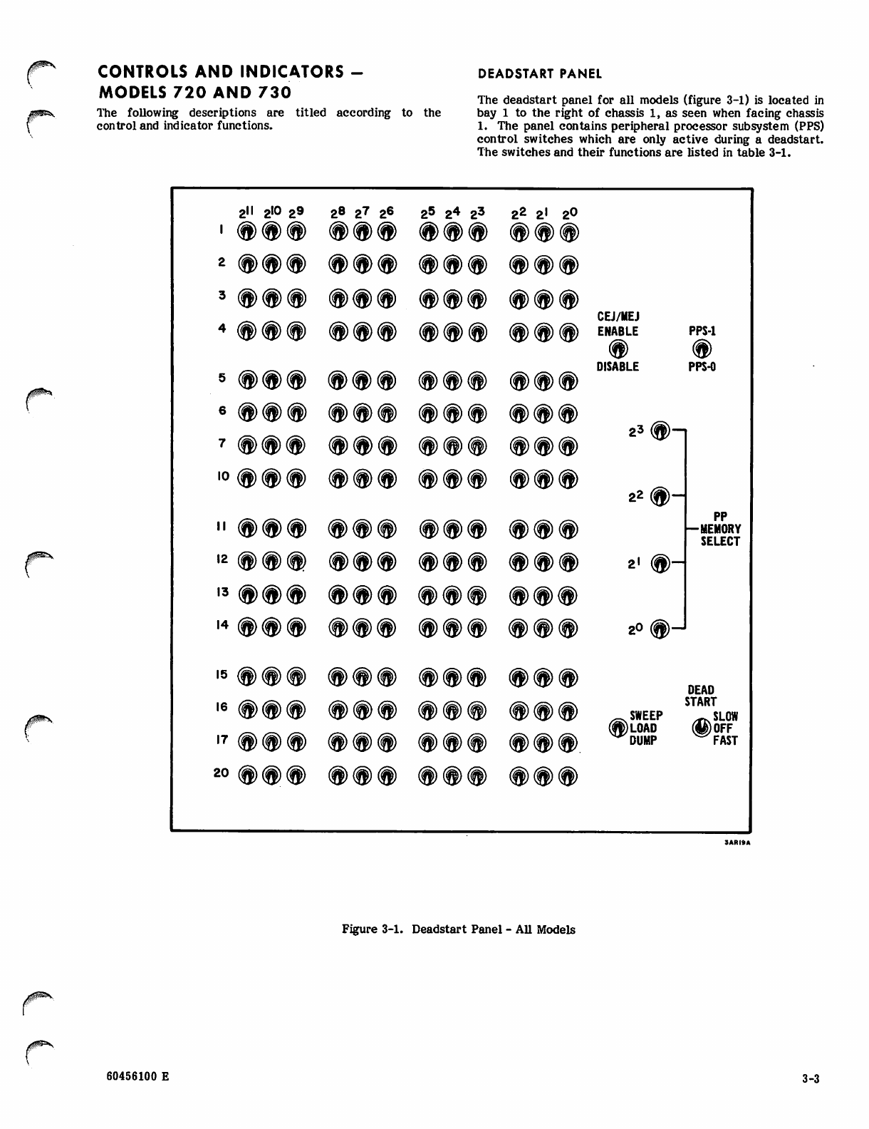
CONTROLS AND INDICATORS -
MODELS 720 AND 730
The following descriptions are titled according to the
control and indicator functions.
DEADSTART PANEL
The deadstart panel for all models (figure 3-1) is located in
bay 1 to the right of chassis 1, as seen when facing chassis
1. The panel contains peripheral processor subsystem (PPS)
control switches which are only active during a deadstart.
The switches and their functions are listed in table 3-1.
2II 2I0 2 9
1 ®®® 2® 2^ 2®
®®®> g5 20 2^
®®® 22 o \ 2 0
®®®
2 ®®® ®®® ®®® ®®®
3 ®®®
4 ®®® ®®®
®®®
®®®
®®®
®®®
®®® CEJ/MEJ
ENABLE
®
DISABLE
PPS-1
®
PPS-0
5 ®®® ®®® ®®® ®®®
6 ®®®
7 ®®® ®®@
®®®
®®®
®®@
®®®
®®® 2 ^ ® -
10 ®®® ®®® ®®® ®®® 2 2 ® -
11 ®®® ®®® ®®® ®®® PP
—MEMORY
SELECT
12 ®®® ®®® ®®® ®®® 2' ®-
13 ®®® ®®® ®®® ®®®
14 ®®® ®®® ®®® ®®® 2°®-
15 ®®® ®®® ®®® ®®® DEAD
16 ®®® ®®® ®®@ ®®® _ SWEEP
(?t>) LOAD
^DUMP
START
@0FF
^ FA S T
17 ®®® ®®® ®®® ®®®.
20 ®®® ®®® ®®® ®®®
Figure 3-1. Deadstart Panel - All Models
60456100 E 3-3
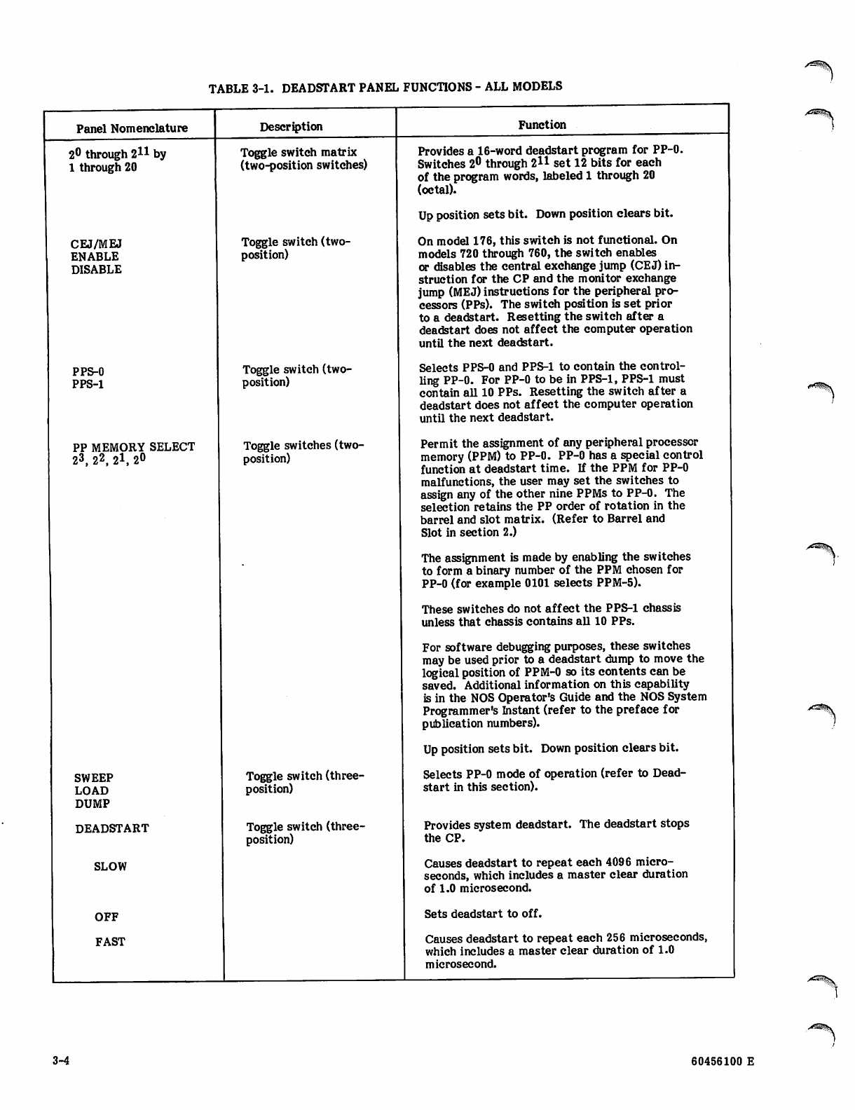
TABLE 3-1. DEADSTART PANEL FUNCTIONS - ALL MODELS
Panel Nomenclature
2° through 211 by
1 through 20
CEJ/MEJ
ENABLE
DISABLE
Description
Toggle switch matrix
(two-position switches)
Toggle switch (two-
position)
PPS-0
PPS-1
PP MEMORY SELECT
23, 22, 2l, 2«
Toggle switch (two-
position)
Toggle switches (two-
position)
SWEEP
LOAD
DUMP
DEADSTART
SLOW
OFF
FAST
Toggle switch (three-
position)
Toggle switch (three-
position)
Function
Provides a 16-word deadstart program for PP-0.
Switches 2° through 2*1 set 12 bits for each
of the program words, labeled 1 through 20
(octal).
Up position sets bit. Down position clears bit.
On model 176, this switch is not functional. On
models 720 through 760, the switch enables
or disables the central exchange jump (CE J) in
struction for the CP and the monitor exchange
jump (MEJ) instructions for the peripheral pro
cessors (PPs). The switch position is set prior
to a deadstart. Resetting the switch after a
deadstart does not affect the computer operation
until the next deadstart.
Selects PPS-0 and PPS-1 to contain the control
ling PP-0. For PP-0 to be in PPS-1, PPS-1 must
contain all 10 PPs. Resetting the switch after a
deadstart does not affect the computer operation
until the next deadstart.
Permit the assignment of any peripheral processor
memory (PPM) to PP-0. PP-0 has a special control
function at deadstart time. If the PPM for PP-0
malfunctions, the user may set the switches to
assign any of the other nine PPMs to PP-0. The
selection retains the PP order of rotation in the
barrel and slot matrix. (Refer to Barrel and
Slot in section 2.)
The assignment is made by enabling the switches
to form a binary number of the PPM chosen for
PP-0 (for example 0101 selects PPM-5).
These switches do not affect the PPS-1 chassis
unless that chassis contains all 10 PPs.
For software debugging purposes, these switches
may be used prior to a deadstart dump to move the
logical position of PPM-0 so its contents can be
saved. Additional information on this capability
is in the NOS Operator's Guide and the NOS System
Programmer's Instant (refer to the preface for
publication numbers).
Up position sets bit. Down position clears bit.
Selects PP-0 mode of operation (refer to Dead-
start in this section).
Provides system deadstart. The deadstart stops
the CP.
Causes deadstart to repeat each 4096 micro
seconds, which includes a master clear duration
of 1.0 microsecond.
Sets deadstart to off.
Causes deadstart to repeat each 256 microseconds,
which includes a master clear duration of 1.0
microsecond.
3-4 60456100 E
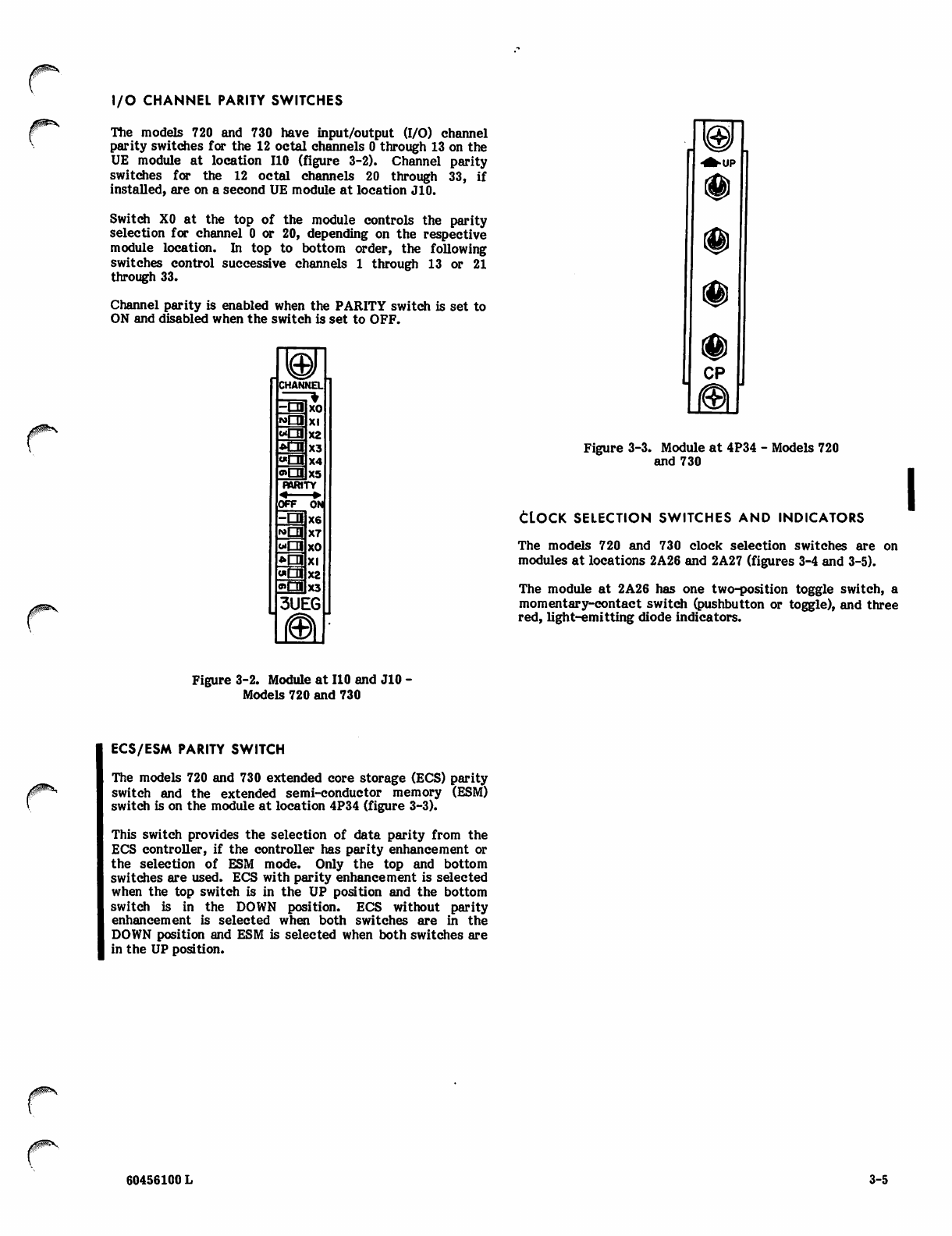
I/O CHANNEL PARITY SWITCHES
The models 720 and 730 have input/output (I/O) channel
parity switches for the 12 octal channels 0 through 13 on the
UE module at location 110 (figure 3-2). Channel parity
switches for the 12 octal channels 20 through 33, if
installed, are on a second UE module at location J10.
Switch XO at the top of the module controls the parity
selection for channel 0 or 20, depending on the respective
module location. In top to bottom order, the following
switches control successive channels 1 through 13 or 21
through 33.
Channel parity is enabled when the PARITY switch is set to
ON and disabled when the switch is set to OFF.
CHANNEL
t
-tn
mLH
XO
XI
X2
X3
X4
X5
oCU
«r~H
o»OI
PARI'Vf
OFF ON
-cn X6
X7
XO
XI
X2
X3
r»CH
wLH
«DDI
3UE
Figure 3-3. Module at 4P34 - Models 720
and 730
CLOCK SELECTION SWITCHES AND INDICATORS
The models 720 and 730 clock selection switches are on
modules at locations 2A26 and 2A27 (figures 3-4 and 3-5).
The module at 2A26 has one two-position toggle switch, a
momentary-contact switch (pushbutton or toggle), and three
red, light-emitting diode indicators.
Figure 3-2. Module at UO and J10 -
Models 720 and 730
ECS/ESM PARITY SWITCH
The models 720 and 730 extended core storage (ECS) parity
switch and the extended semi-conductor memory (ESM)
switch is on the module at location 4P34 (figure 3-3).
This switch provides the selection of data parity from the
ECS controller, if the controller has parity enhancement or
the selection of ESM mode. Only the top and bottom
switches are used. ECS with parity enhancement is selected
when the top switch is in the UP position and the bottom
switch is in the DOWN position. ECS without parity
enhancement is selected when both switches are in the
DOWN position and ESM is selected when both switches are
in the UP position.
/if^V
60456100 L 3-5
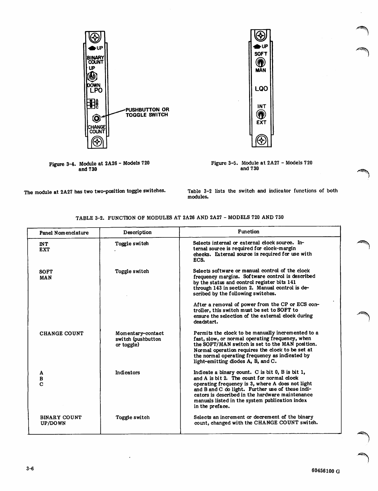
UP
BINARY
COUNT
UP
DOWN
LPO
CHANGE
COUNT
-PUSHBUTTON OR
TOGGLE SWITCH
♦ UP
SOFT
MAN
LOO
INT
<§>
EXT
y^^^V
Figure 3-4. Module at 2A26 - Models 720
and 730 Figure 3-5. Module at 2A27 - Models 720
and 730
The module at 2A27 has two two-position toggle switches. Table 3-2 lists the switch and indicator functions of both
modules.
TABLE 3-2. FUNCTION OF MODULES AT 2A26 AND 2A27 - MODELS 720 AND 730
Panel Nomenclature Description Function
INT
EXT
SOFT
MAN
CHANGE COUNT
A
B
C
BINARY COUNT
UP/DOWN
Toggle switch
Toggle switch
Mom entary-contact
switch (pushbutton
or toggle)
Indicators
Toggle switch
Selects internal or external clock source. In
ternal source is required for dock-margin
checks. External source is required for use with
ECS.
Selects software or manual control of the clock
frequency margins. Software control is described
by the status and control register bits 141
through 143 in section 2. Manual control is de
scribed by the following switches.
After a removal of power from the CP or ECS con
troller, this switch must be set to SOFT to
ensure the selection of the external clock during
deadstart.
Permits the clock to be manually incremented to a
fast, slow, or normal operating frequency, when
the SOFT/MAN switch is set to the MAN position.
Normal operation requires the clock to be set at
the normal operating frequency as indicated by
light-emitting diodes A, B, and C.
Indicate a binary count. C is bit 0, B is bit 1,
and A is bit 2. The count for normal clock
operating frequency is 3, where A does not light
and B and C do light. Further use of these indi
cators is described in the hardware maintenance
manuals listed in the system publication index
in the preface.
Selects an increment or decrement of the binary
count, changed with the CHANGE COUNT switch.
3-6 60456100 G
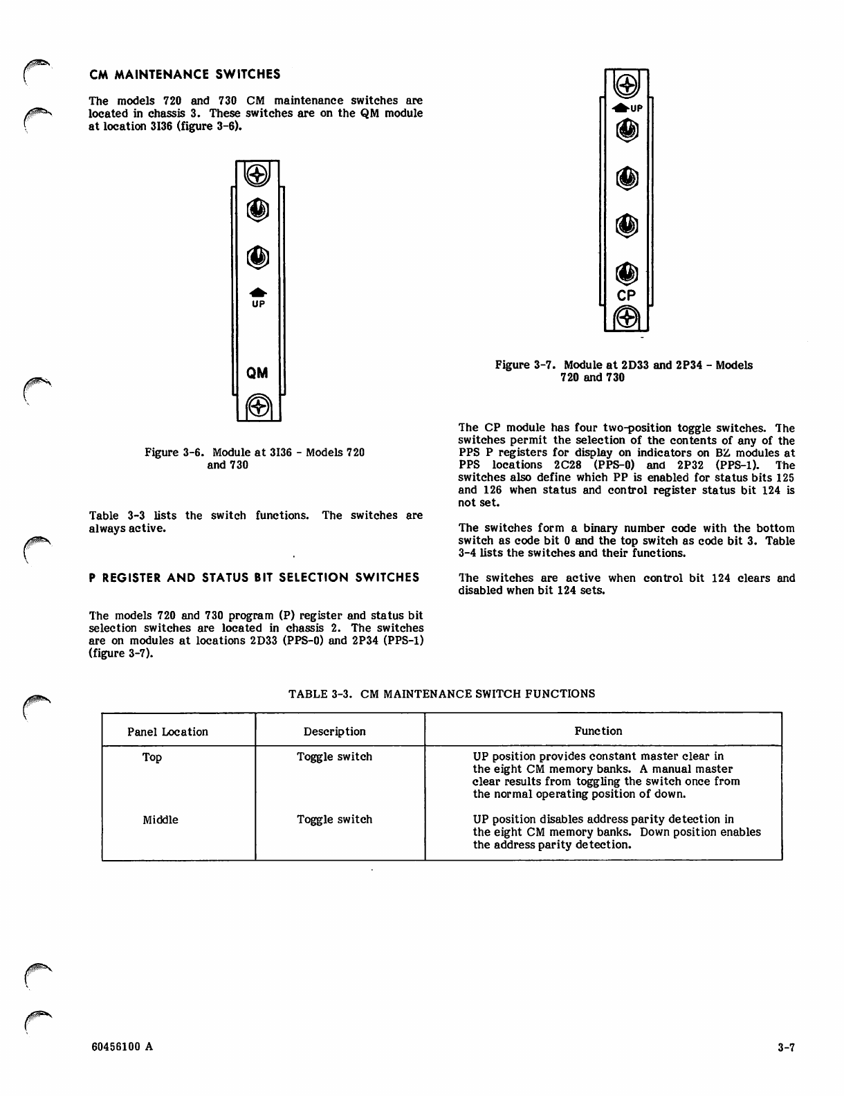
CM MAINTENANCE SWITCHES
The models 720 and 730 CM maintenance switches are
located in chassis 3. These switches are on the QM module
at location 3136 (figure 3-6).
UP
QM
'UP
CP
Figure 3-6. Module at 3136 - Models 720
and 730
Table 3-3 lists the switch functions. The switches are
always active.
P REGISTER AND STATUS BIT SELECTION SWITCHES
The models 720 and 730 program (P) register and status bit
selection switches are located in chassis 2. The switches
are on modules at locations 2D33 (PPS-0) and 2P34 (PPS-1)
(figure 3-7).
Figure 3-7. Module at 2D33 and 2P34 - Models
720 and 730
The CP module has four two-position toggle switches. The
switches permit the selection of the contents of any of the
PPS P registers for display on indicators on BZ modules at
PPS locations 2C28 (PPS-0) and 2P32 (PPS-1). The
switches also define which PP is enabled for status bits 125
and 126 when status and control register status bit 124 is
not set.
The switches form a binary number code with the bottom
switch as code bit 0 and the top switch as code bit 3. Table
3-4 lists the switches and their functions.
The switches are active when control bit 124 clears and
disabled when bit 124 sets.
TABLE 3-3. CM MAINTENANCE SWITCH FUNCTIONS
Panel Location Description Function
Top
Middle
Toggle switch
Toggle switch
UP position provides constant master clear in
the eight CM memory banks. A manual master
clear results from toggling the switch once from
the normal operating position of down.
UP position disables address parity detection in
the eight CM memory banks. Down position enables
the address parity detection.
60456100 A 3-7
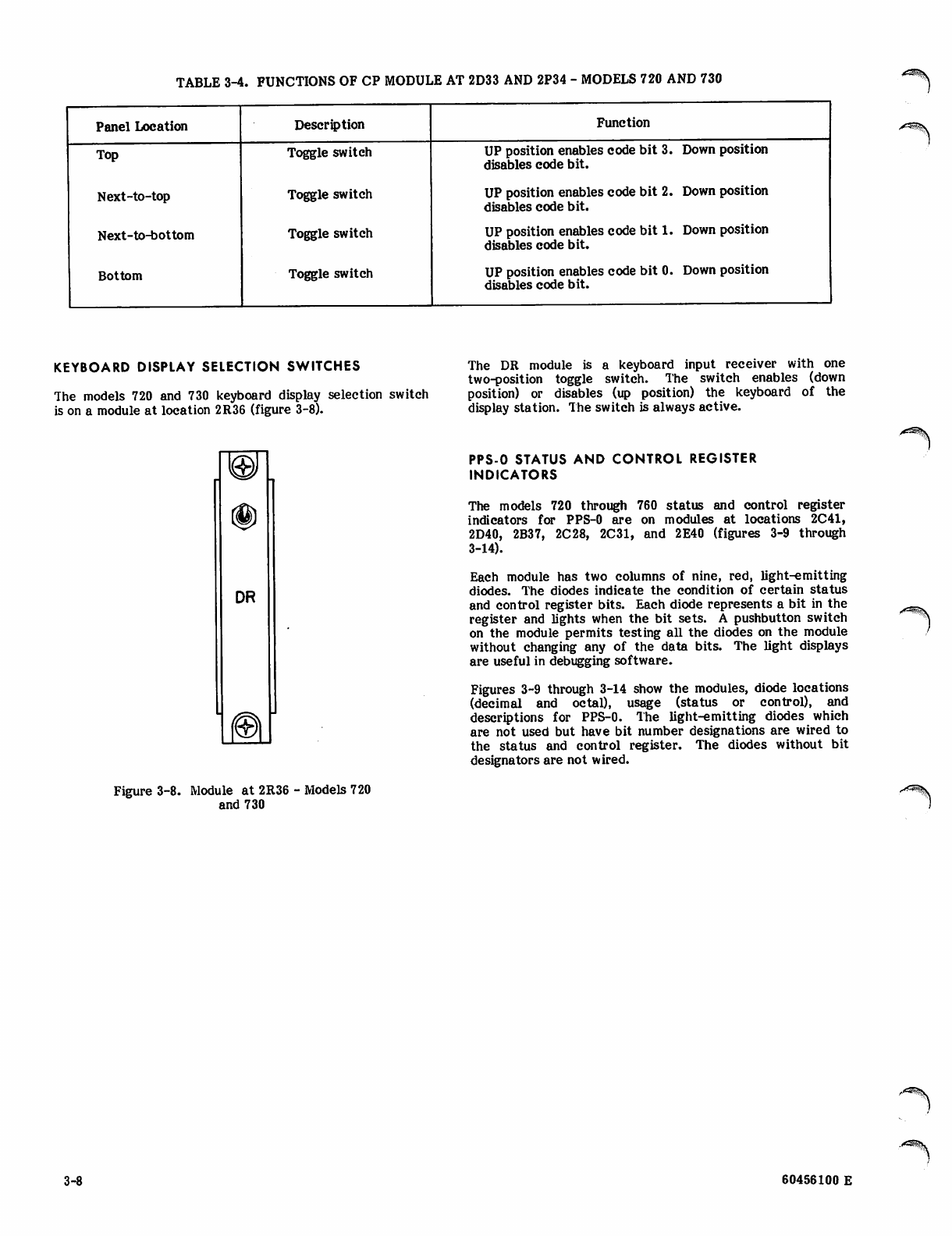
TABLE 3-4. FUNCTIONS OF CP MODULE AT 2D33 AND 2P34 - MODELS 720 AND 730
Panel Location Description Function
Top
Next-to-top
Next-to-bottom
Bottom
Toggle switch
Toggle switch
Toggle switch
Toggle switch
UP position enables code bit 3. Down position
disables code bit.
UP position enables code bit 2. Down position
disables code bit.
UP position enables code bit 1. Down position
disables code bit.
UP position enables code bit 0. Down position
disables code bit.
y^»s\
KEYBOARD DISPLAY SELECTION SWITCHES
The models 720 and 730 keyboard display selection switch
is on a module at location 2R36 (figure 3-8).
DR
The DR module is a keyboard input receiver with one
two-position toggle switch. The switch enables (down
position) or disables (up position) the keyboard of the
display station. The switch is always active.
PPS-0 STATUS AND CONTROL REGISTER
INDICATORS
The models 720 through 760 status and control register
indicators for PPS-0 are on modules at locations 2C41,
2D40, 2B37, 2C28, 2C31, and 2E40 (figures 3-9 through
3-14).
Each module has two columns of nine, red, light-emitting
diodes. The diodes indicate the condition of certain status
and control register bits. Each diode represents a bit in the
register and lights when the bit sets. A pushbutton switch
on the module permits testing all the diodes on the module
without changing any of the data bits. The light displays
are useful in debugging software.
Figures 3-9 through 3-14 show the modules, diode locations
(decimal and octal), usage (status or control), and
descriptions for PPS-0. The light-emitting diodes which
are not used but have bit number designations are wired to
the status and control register. The diodes without bit
designators are not wired.
Figure 3-8. Module at 2R36 - Models 720
and 730
3-8 60456100 E
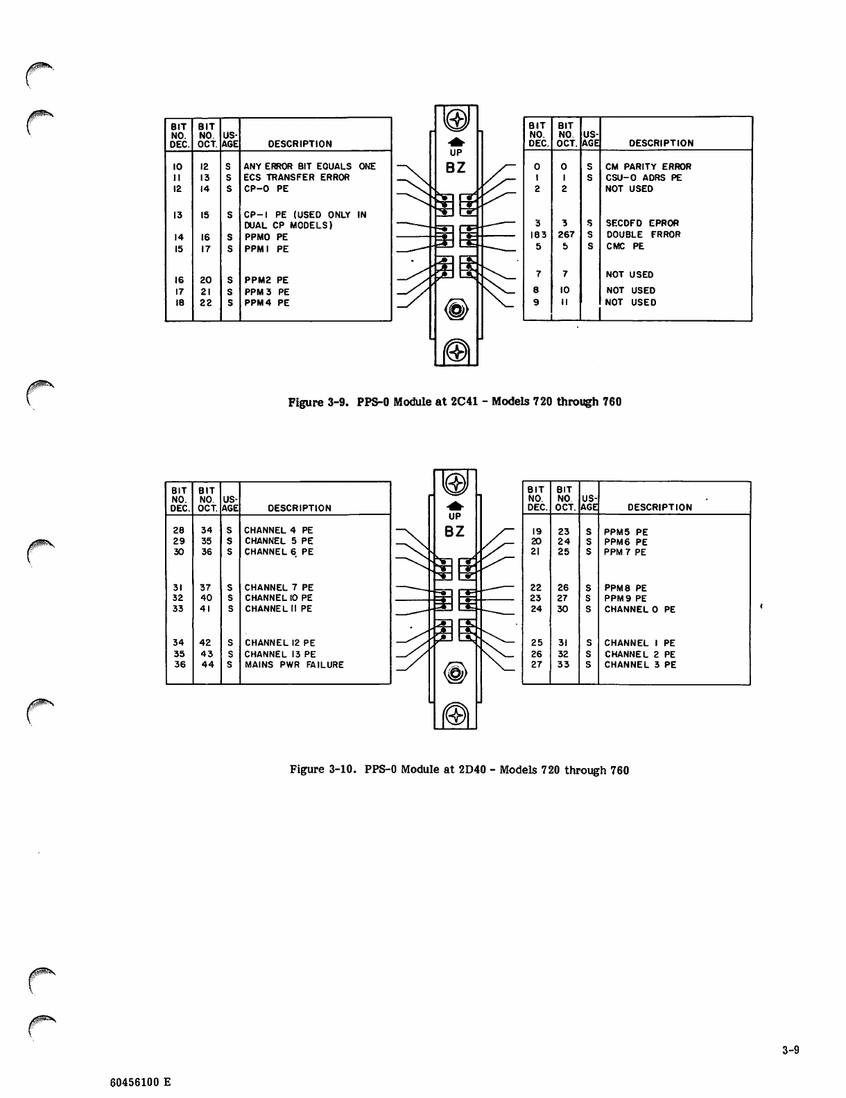
BIT
NO.
DEC.
BIT
NO.
OCT.
US
AGE DESCRIPTION
IO 12 ANY ERROR BIT EQUALS ONE
II 13 ECS TRANSFER ERROR
12 14 CP-0 PE
13 15 CP-1 PE (USED ONLY IN
DUAL CP MODELS)
14 16 PPMO PE
15 17 PPMI PE
16 20 PPM2 PE
17 21 PPM 3 PE
18 22 PPM 4 PE
BIT
NO.
DEC.
BIT
NO.
OCT. US
AGE DESCRIPTION
0 0 S CM PARITY ERROR
1 1 S CSU-0 ADRS PE
2 2 NOT USED
3 3 S SECOFD EPROR
183 267 DOUBLE FRROR
5 5 S CMC PE
7 7 NOT USED
810 NOT USED
9II NOT USED
Figure 3-9. PPS-0 Module at 2C41 - Models 720 through 760
BIT
NO.
DEC.
BIT
NO.
OCT. US
AGE DESCRIPTION
28
29
30
34
35
36
CHANNEL 4 PE
CHANNEL 5 PE
CHANNEL 6 PE
31
32
33
37
40
41
CHANNEL 7 PE
CHANNEL 10 PE
CHANNEL II PE
34
35
36
42
43
44
CHANNEL 12 PE
CHANNEL 13 PE
MAINS PWR FAILURE
BIT
NO.
DEC.
BIT
NO
OCT.
US
AGE DESCRIPTION
19 23 PPM5 PE
20 24 PPM6 PE
21 25 PPM 7 PE
22 26 PPM8 PE
23 27 PPM 9 PE
24 30 CHANNEL 0 PE
25 31 CHANNEL 1 PE
26 32 CHANNEL 2 PE
27 33 CHANNEL 3 PE
Figure 3-10. PPS-0 Module at 2D40 - Models 720 through 760
3-9
60456100 E
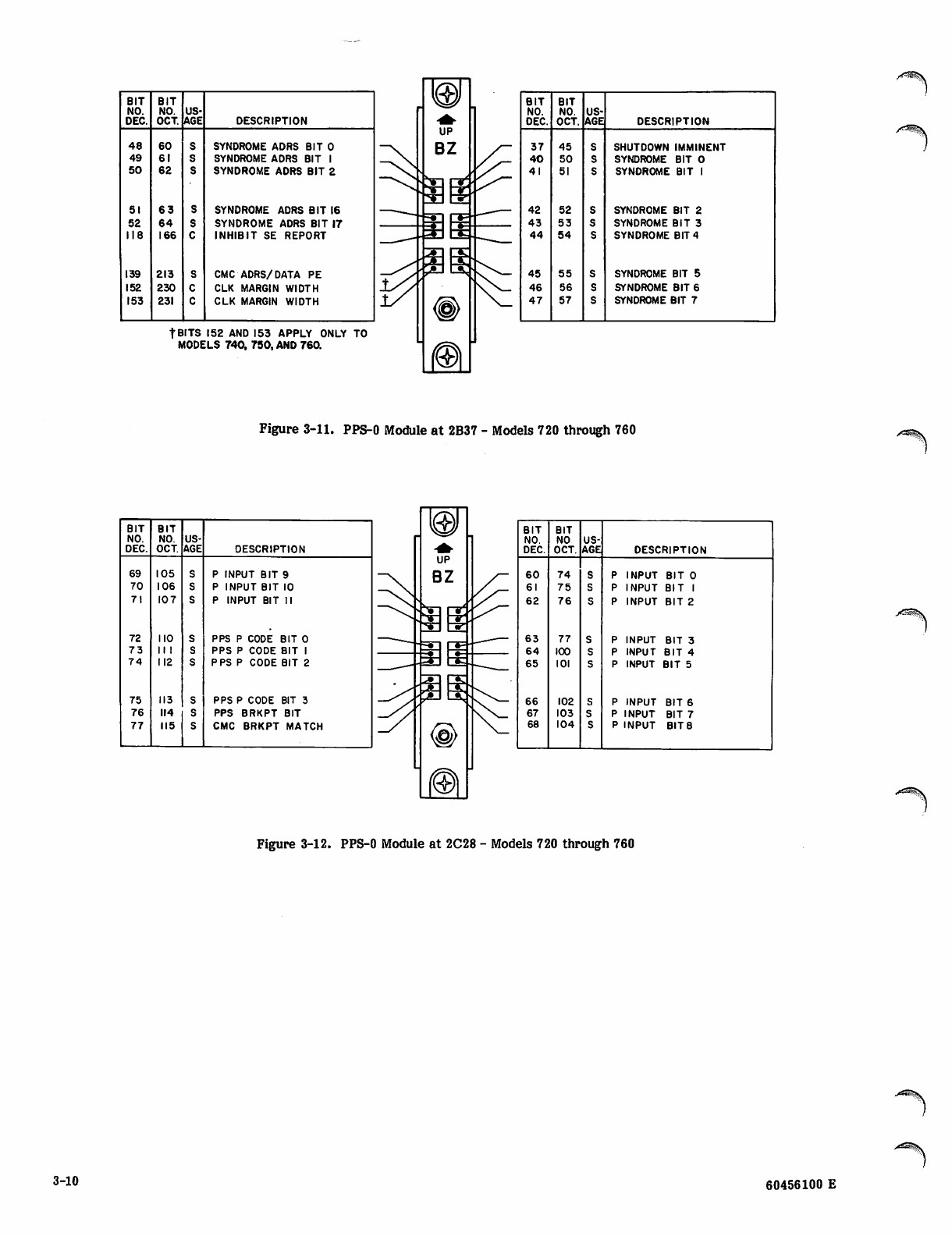
BIT
NO.
DEC.
BIT
NO.
OCT. US
AGE DESCRIPTION
48
49
50
60
61
62
SYNDROME ADRS BIT 0
SYNDROME ADRS BIT 1
SYNDROME ADRS BIT 2
51
52
118
63
64
166
SYNDROME ADRS BIT 16
SYNDROME ADRS BIT 17
INHIBIT SE REPORT
139
152
153
213
230
231
CMC ADRS/DATA PE
CLK MARGIN WIDTH
CLK MARGIN WIDTH
tBITS 152 AND 153 APPLY ONLY TO
MODELS 740, 750, AND 760.
BIT
NO.
DEC.
BIT
NO.
OCT.
US
AGE DESCRIPTION
37 45 SHUTDOWN IMMINENT
40 50 SYNDROME BIT 0
41 51 SYNDROME BIT 1
42 52 SYNDROME BIT 2
43 53 SYNDROME BIT 3
44 54 SYNDROME BIT 4
45 55 SYNDROME BIT 5
46 56 SYNDROME BIT 6
47 57 SYNDROME BIT 7
Figure 3-11. PPS-0 Module at 2B37 - Models 720 through 760
BIT
NO.
DEC.
BIT
NO.
OCT. US
AGE DESCRIPTION
69
70
71
105
106
107
P INPUT BIT 9
P INPUT BIT 10
P INPUT BIT 11
72
73
74
110
II 1
112
PPS P CODE BIT 0
PPS P CODE BIT 1
PPS P CODE BIT 2
75
76
77
113
114
115
PPS P CODE BIT 3
PPS BRKPT BIT
CMC BRKPT MATCH
BIT
NO.
DEC.
BIT
NO
OCT. US
AGE DESCRIPTION
60
61
74
75
INPUT BIT 0
INPUT BIT 1
62 76 INPUT BIT 2
63
64
65
77
100
101
INPUT BIT 3
INPUT BIT 4
INPUT BIT 5
66
67
68
102
103
104
INPUT BIT 6
INPUT BIT 7
INPUT BITS
Figure 3-12. PPS-0 Module at 2C28 - Models 720 through 760
3-10 60456100 E
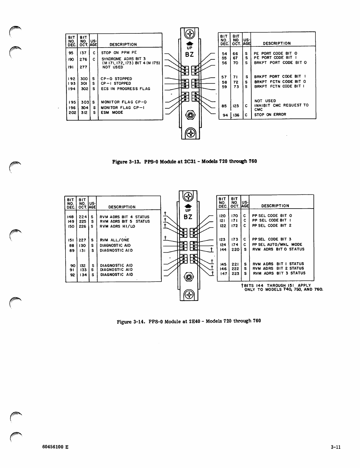
BIT
NO.
DEC.
BIT
NO.
OCT.
US
AGE DESCRIPTION
95 137 STOP ON PPM PE
190
191
276
277
SYNDROME ADRS BIT 3
(M 171,172,173) BIT 4 (M 175)
NOT USED
192 300 CP-0 STOPPED
1 93 301 CP-1 STOPPED
194 302 ECS IN PROGRESS FLAG
195 303 M ON I TO R F L AG C P- 0
196 304 MONITOR FLAG CP-1
202 312 ESM MODE
BIT
NO.,
DEC.
BIT
NO.
OCT.
US
AGE DESCRIPTION
54
55
66
67
PE PORT CODE BIT 0
PE PORT CODE BIT 1
56 70 BRKPT PORT CODE BIT 0
57 71 BRKPT PORT CODE BIT 1
58
59
72
73
BRKPT FCTN CODE BIT 0
BRKPT FCTN CODE BIT 1
85 125
NOT USED
INHIBIT CMC REQUEST TO
CMC
94 136 STOP ON ERROR
Figure 3-13. PPS-0 Module at 2C31 - Models 720 through 760
BIT BIT
NO. NO. US
DEC. OCT. AGE DESCRIPTION
148 224 RVM ADRS BIT 4 STATUS
149 225 RVM ADRS BIT 5 STATUS
150 226 RVM ADRS HI/LO
151 227 RV M A LL/ ON E
88 130 DIAGNOSTIC AID
89 131 DIAGNOSTIC AID
90 132 DIAGNOSTIC AID
91 133 DIAGNOSTIC AID
92 134 DIAGNOSTIC AID
BIT
NO.
DEC.
BIT
NO.
OCT.
US
AGE DESCRIPTION
120
121
170
171
PP SEL CODE BIT 0
PP SEL CODE BIT 1
122 172 PP SEL CODE BIT 2
123 173 PPSEL CODE BIT 3
124
144
174
220
PP SEL AUTO/MNL MODE
RVM ADRS BIT 0 STATUS
145
146
147
221
222
223
RVM ADRS BIT 1 STATUS
RVM ADRS BIT 2 STATUS
RVM ADRS BIT 3 STATUS
tBITS 144 THROUGH 151 APPLY
ONLY TO MODELS 740, 750. AND 760.
Figure 3-14. PPS-0 Module at 2E40 - Models 720 through 760
60456100 E 3-11
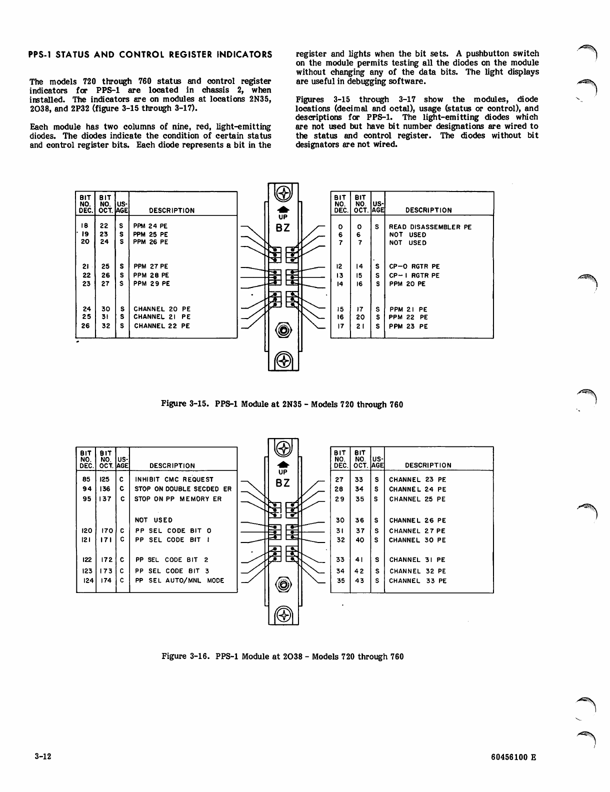
PPS-1 STATUS AND CONTROL REGISTER INDICATORS
The models 720 through 760 status and control register
indicators for PPS-1 are located in chassis 2, when
installed. The indicators are on modules at locations 2N35,
2038, and 2P32 (figure 3-15 through 3-17).
Each module has two columns of nine, red, light-emitting
diodes. The diodes indicate the condition of certain status
and control register bits. Each diode represents a bit in the
register and lights when the bit sets. A pushbutton switch
on the module permits testing all the diodes on the module
without changing any of the data bits. The light displays
are useful in debugging software.
Figures 3-15 through 3-17 show the modules, diode
locations (decimal and octal), usage (status or control), and
descriptions for PPS-1. The light-emitting diodes which
are not used but have bit number designations are wired to
the status and control register. The diodes without bit
designators are not wired.
BIT BIT
NO. NO. US
DEC. OCT. AGE DESCRIPTION
18 22 PPM 24 PE
• 19 23 PPM 25 PE
20 24 PPM 26 PE
21 25 PPM 27 PE
22 26 PPM 28 PE
23 27 PPM 29 PE
24 30 CHANNEL 20 PE
25 31 CHANNEL 21 PE
26 32 CHANNEL 22 PE
BIT
NO.
DEC.
BIT
NO.
OCT.
US
AGE DESCRIPTION
0 0 S READ DISASSEMBLER PE
6 6 NOT USED
7 7 NOT USED
12 14 CP-0 RGTR PE
13 15 CP- 1 RGTR PE
14 16 PPM 20 PE
15 17 PPM 21 PE
16 20 PPM 22 PE
17 21 PPM 23 PE
Figure 3-15. PPS-1 Module at 2N35 - Models 720 through 760
BIT
NO.
DEC.
BIT
NO.
OCT.
US
AGE DESCRIPTION
85 125 INHIBIT CMC REQUEST
94 136 STOP ON DOUBLE SECDED ER
95 137 STOP ON PP MEMORY ER
NOT USED
120 170 PP S E L CO D E B IT 0
121 171 PP SEL CODE B IT 1
122 172 PP SEL CODE BIT 2
123 173 PP SEL CODE B IT 3
124 174 PP SEL AUTO/MNL MODE
BIT
NO.
DEC.
BIT
NO.
OCT.
US
AGE DESCRIPTION
27 33 CHANNEL 23 PE
28 34 CHANNEL 24 PE
29 35 CHANNEL 25 PE
30 36 CHANNEL 26 PE
31 37 CHANNEL 27 PE
32 40 CHANNEL 30 PE
33 41 CHANNEL 31 PE
34 42 CHANNEL 32 PE
35 43 CHANNEL 33 PE
Figure 3-16. PPS-1 Module at 2038 - Models 720 through 760
/<®?v
3-12 60456100 E
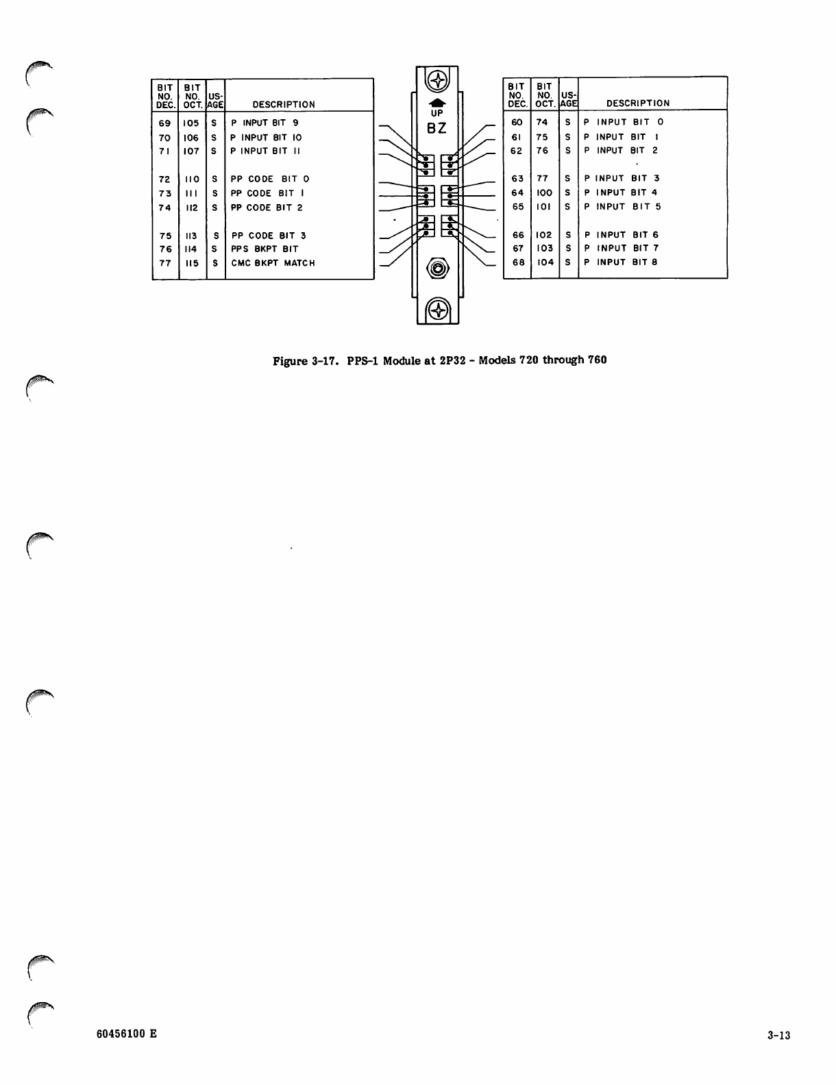
BIT
NO.
DEC.
BIT
NO.
OCT.
US
AGE DESCRIPTION
69 105 P INPUT BIT 9
70 106 P INPUT BIT 10
71 107 P INPUT BIT II
72 no PP CO DE BI T 0
73 III PP CODE BIT 1
74 112 PP CODE BIT 2
75 113 PP CODE BIT 3
76 114 PPS BKPT BIT
77 115 CMC BKPT MATCH
BIT
NO.
DEC.
BIT
NO.
OCT.
US
AGE DESCRIPTION
60 74 I N P U T B I T 0
61 75 INPUT BIT 1
62 76 INPUT BIT 2
63 77 INPUT BIT 3
64 100 IN PUT B IT 4
65 101 I N P U T B I T 5
66 102 INPUT BIT 6
67 103 INPUT BIT 7
68 104 INPUT BIT 8
Figure 3-17. PPS-1 Module at 2P32 - Models 720 through 760
60456100 E 3-13
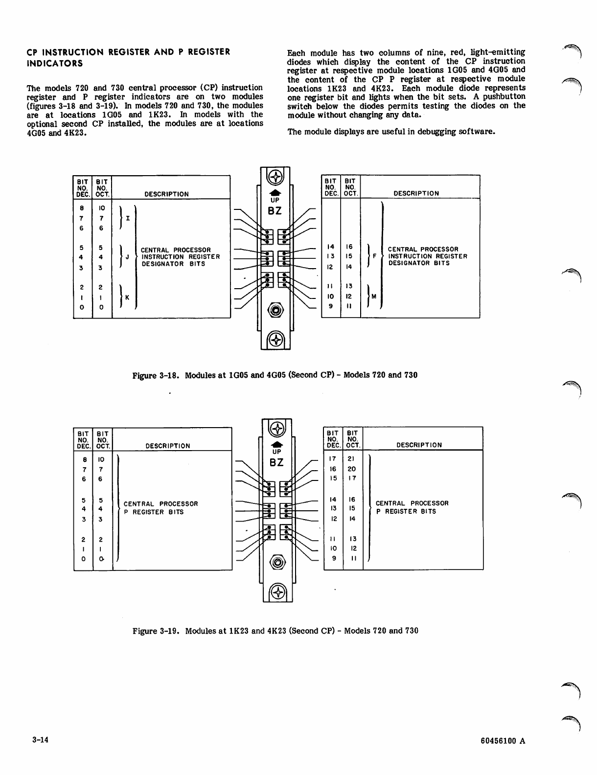
CP INSTRUCTION REGISTER AND P REGISTER
INDICATORS
The models 720 and 730 central processor (CP) instruction
register and P register indicators are on two modules
(figures 3-18 and 3-19). In models 720 and 730, the modules
are at locations 1G05 and 1K23. In models with the
optional second CP installed, the modules are at locations
4G05 and 4K23.
Each module has two columns of nine, red, light-emitting
diodes which display the content of the CP instruction
register at respective module locations 1G05 and 4G05 and
the content of the CP P register at respective module
locations 1K23 and 4K23. Each module diode represents
one register bit and lights when the bit sets. A pushbutton
switch below the diodes permits testing the diodes on the
module without changing any data.
The module displays are useful in debugging software.
BIT
NO.
DEC.
BIT
NO.
OCT. DESCRIPTION
810 ) ]
7 7 h
6 6 J
5
4
3
5
4
3)■
CENTRAL PROCESSOR
INSTRUCTION REGISTER
DES IGNATOR BITS
2
1
2
1I-
0 O j
BIT BIT
NO. NO
DEC. OCT. DESCRIPTION
14 16 CENTRAL PROCESSOR
13 15 INSTRUCTION REGISTER
12 14 DESIGNATOR BITS
II 13
IO 12
9II I )
Figure 3-18. Modules at 1G05 and 4G05 (Second CP) - Models 720 and 730
BIT
NO.
DEC.
BIT
NO.
OCT. DESCRIPTION
8
7
6
5
4
3
2
1
O
IO
7
6
5
4
3
2
1
O
CENTRAL PROCESSOR
P REGISTER BITS
BIT
NO.
DEC.
BIT
NO.
OCT. DESCRIPTION
17
16
15
14
13
12
II
IO
9
21
20
17
16
15
14
13
12
II
CENTRAL PROCESSOR
P REGISTER BITS
Figure 3-19. Modules at 1K23 and 4K23 (Second CP) - Models 720 and 730
3-14 60456100 A
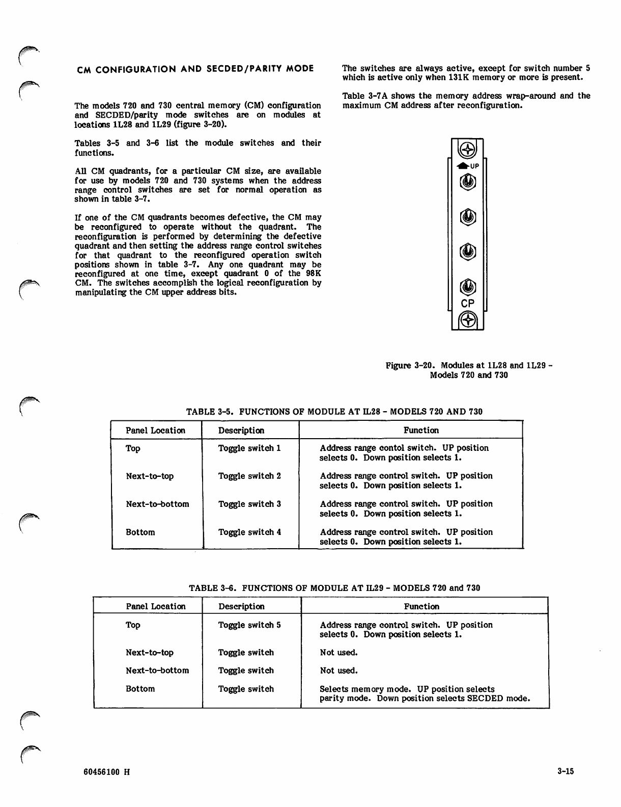
CM CONFIGURATION AND SECDED/PARITY MODE
The models 720 and 730 central memory (CM) configuration
and SECDED/parity mode switches are on modules at
locations 1L28 and 1L29 (figure 3-20).
Tables 3-5 and 3-6 list the module switches and their
functions.
All CM quadrants, for a particular CM size, are available
for use by models 720 and 730 systems when the address
range control switches are set for normal operation as
shown in table 3-7.
If one of the CM quadrants becomes defective, the CM may
be reconfigured to operate without the quadrant. The
reconfiguration is performed by determining the defective
quadrant and then setting the address range control switches
for that quadrant to the reconfigured operation switch
positions shown in table 3-7. Any one quadrant may be
reconfigured at one time, except quadrant 0 of the 98K
CM. The switches accomplish the logical reconfiguration by
manipulating the CM upper address bits.
The switches are always active, except for switch number 5
which is active only when 131K memory or more is present.
Table 3-7A shows the memory address wrap-around and the
maximum CM address after reconfiguration.
'UP
CP
m
Figure 3-20. Modules at 1L28 and 1L29
Models 720 and 730
TABLE 3-5. FUNCTIONS OF MODULE AT IL28 - MODELS 720 AND 730
Panel Location Description Function
Top Toggle switch 1 Address range contol switch. UP position
selects 0. Down position selects 1.
Next-to-top Toggle switch 2 Address range control switch. UP position
selects 0. Down position selects 1.
Next-to-bottom Toggle switch 3 Address range control switch. UP position
selects 0. Down position selects 1.
Bottom Toggle switch 4 Address range control switch. UP position
selects 0. Down position selects 1.
TABLE 3-6. FUNCTIONS OF MODULE AT IL29 - MODELS 720 and 730
Panel Location Description Function
Top Toggle switch 5 Address range control switch. UP position
selects 0. Down position selects 1.
Next-to-top Toggle switch Not used.
Next-to-bottom Toggle switch Not used.
Bottom Toggle switch Selects memory mode. UP position selects
parity mode. Down position selects SECDED mode.
c60456100 H 3-15
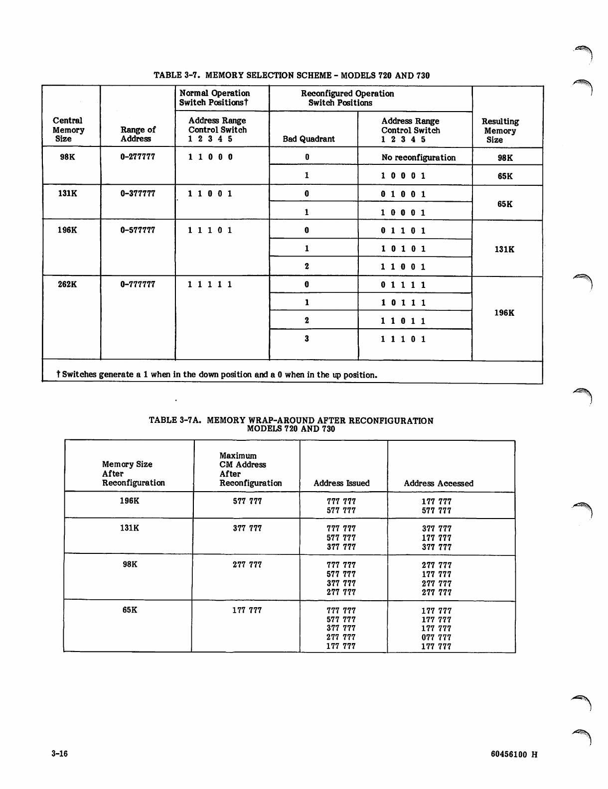
TABLE 3-7. MEMORY SELECTION SCHEME - MODELS 720 AND 730
Central
Memory
Size Range of
Address
Normal Operation
Switch PositionsT Reconfigured Operation
Switch Positions
Resulting
Memory
Size
Address Range
Control Switch
12 3 4 5 Bad Quadrant
Address Range
Control Switch
12 3 4 5
98K 0-277777 11 0 0 0 No reconfiguration 98K
110 0 0 1 65K
131K 0-377777 11 0 0 1 0 10 0 1
65K
1 10 0 0 1
196K 0-577777 1 1 1 0 1 0 1 1 0 1
131K
11 0 1 0 1
21 1 0 0 1
262K 0-777777 11111 0 1 1 1 1
196K
1 1 0 1 1 1
2 1 1 0 1 1
31 1 1 0 1
t Switches |generate a 1 when in the down position and a 0 when in the up position.
TABLE 3-7A. MEMORY WRAP-AROUND AFTER RECONFIGURATION
MODELS 720 AND 730
Memory Size
After
Reconfiguration
Maximum
CM Address
After
Reconfiguration Address Issued Address Accessed
196K 577 777 777 777
577 777 177 777
577 777
131K 377 777 777 777
577 777
377 777
377 777
177 777
377 777
98K 277 777 777 777
577 777
377 777
277 777
277 777
177 777
277 777
277 777
65K 177 777 777 777
577 777
377 777
277 777
177 777
177 777
177 777
177 777
077 777
177 777
/^!*\
3-16 60456100 H
Jfl^N
COlNfROW mm INDICATORS -, MODELS 740f /SO, AND 760

>*%
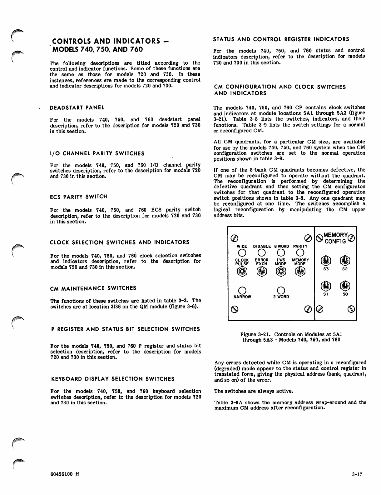
CONTROLS AND INDICATORS -
MODELS 740, 750, AND 760
The following descriptions are titled according to the
control and indicator functions. Some of these functions are
the same as those for models 720 and 730. In these
instances, references are made to the corresponding control
and indicator descriptions for models 720 and 730.
STATUS AND CONTROL REGISTER INDICATORS
For the models 740, 750, and 760 status and control
indicators description, refer to the description for models
720 and 730 in this section.
CM CONFIGURATION AND CLOCK SWITCHES
AND INDICATORS
DEADSTART PANEL
For the models 740, 750, and 760 deadstart panel
description, refer to the description for models 720 and 730
in this section.
I/O CHANNEL PARITY SWITCHES
For the models 740, 750, and 760 I/O channel parity
switches description, refer to the description for models 720
and 730 in this section.
ECS PARITY SWITCH
For the models 740, 750, and 760 ECS parity switch
description, refer to the description for models 720 and 730
in this section.
CLOCK SELECTION SWITCHES AND INDICATORS
For the models 740, 750, and 760 clock selection switches
and indicators description, refer to the description for
models 720 and 730 in this section.
CM MAINTENANCE SWITCHES
The functions of these switches are listed in table 3-3. The
switches are at location 3136 on the QM module (figure 3-6).
P REGISTER AND STATUS BIT SELECTION SWITCHES
For the models 740, 750, and 760 P register and status bit
selection description, refer to the description for models
720 and 730 in this section.
KEYBOARD DISPLAY SELECTION SWITCHES
For the models 740, 750, and 760 keyboard selection
switches description, refer to the description for models 720
and 730 in this section.
The models 740, 750, and 760 CP contains clock switches
and indicators at module locations 5A1 through 5A3 (figure
3-21). Table 3-8 lists the switches, indicators, and their
functions. Table 3-9 lists the switch settings for a normal
or reconfigured CM.
All CM quadrants, for a particular CM size, are available
for use by the models 740, 750, and 760 system when the CM
configuration switches are set to the normal operation
positions shown in table 3-9.
If one of the 8-bank CM quadrants becomes defective, the
CM may be reconfigured to operate without the quadrant.
The reconfiguration is performed by determining the
defective quadrant and then setting the CM configuraton
switches for that quadrant to the reconfigured operation
switch positions shown in table 3-9. Any one quadrant may
be reconfigured at one time. The switches accomplish a
logical reconfiguration by manipulating the CM upper
address bits.
Q)
WIDE DISABL E 8 WORD PARITY
OOOO
CLOCK ERROR IWS MEMORY
PULSE EXCH MODE MODE
o
NARROW 2 WORD
MEMORY/
CONFIG v
S3 S2
SI SO
0<S>
Figure 3-21. Controls on Modules at 5A1
through 5A3 - Models 740, 750, and 760
Any errors detected while CM is operating in a reconfigured
(degraded) mode appear to the status and control register in
translated form, giving the physical address (bank, quadrant,
and so on) of the error.
The switches are always active.
Table 3-9A shows the memory address wrap-around and the
maximum CM address after reconfiguration.
60456100 H 3-17
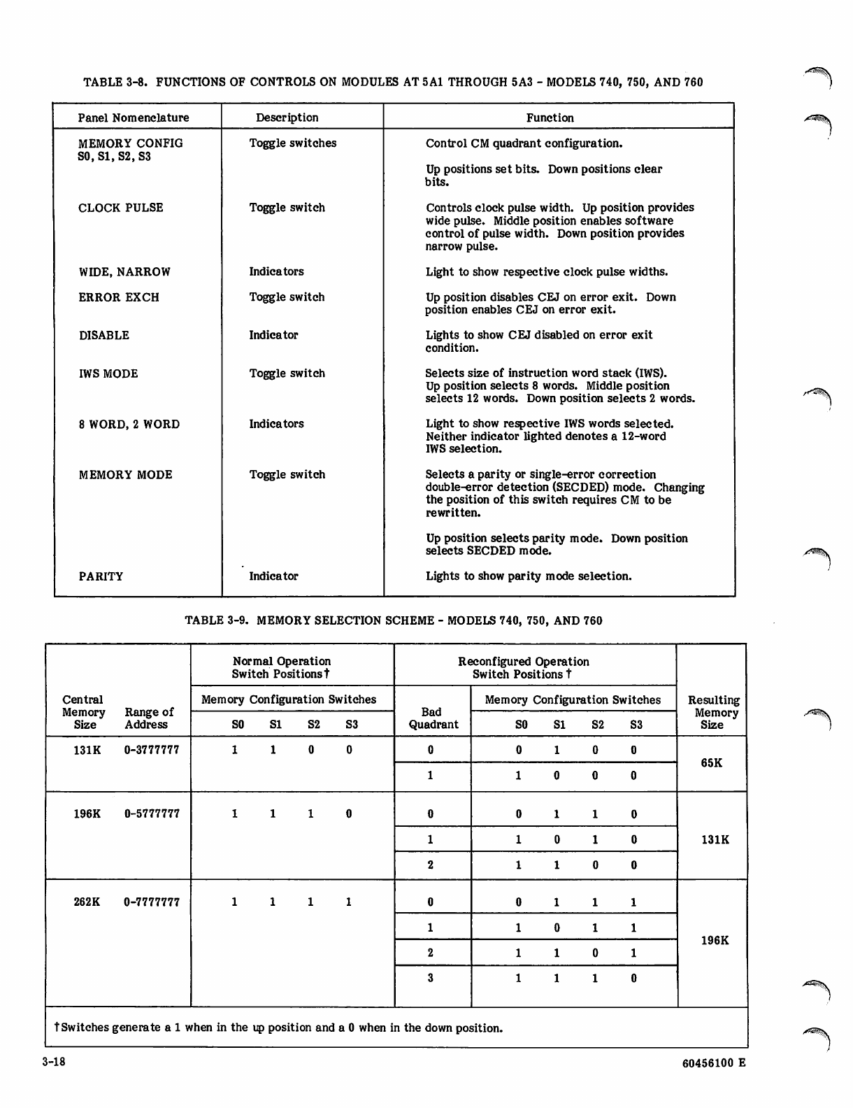
TABLE 3-8. FUNCTIONS OF CONTROLS ON MODULES AT 5A1 THROUGH 5A3 - MODELS 740, 750, AND 760
Panel Nomenclature Description Function
MEMORY CONFIG
SO, Sl, S2, S3
Toggle switches Control CM quadrant configuration.
Up positions set bits. Down positions clear
bits.
CLOCK PULSE Toggle switch Controls clock pulse width. Up position provides
wide pulse. Middle position enables software
control of pulse width. Down position provides
narrow pulse.
WIDE, NARROW Indicators Light to show respective clock pulse widths.
ERROR EXCH Toggle switch Up position disables CEJ on error exit. Down
position enables CEJ on error exit.
DISABLE Indicator Lights to show CEJ disabled on error exit
condition.
IWS MODE Toggle switch Selects size of instruction word stack (IWS).
Up position selects 8 words. Middle position
selects 12 words. Down position selects 2 words.
8 WORD, 2 WORD Indicators Light to show respective IWS words selected.
Neither indicator lighted denotes a 12-word
IWS selection.
MEMORY MODE Toggle switch Selects a parity or single-error correction
double-error detection (SECDED) mode. Changing
the position of this switch requires CM to be
rewritten.
Up position selects parity mode. Down position
selects SECDED mode.
PARITY Indicator Lights to show parity mode selection.
TABLE 3-9. MEMORY SELECTION SCHEME - MODELS 740, 750, AND 760
Central
Memory Range of
Size Address
Normal Operation
Switch Positions t Reconfigured Operation
Switch Positions t
Resulting
Memory
Size
Memory Configuration Switches Bad
Quadrant
Memory Configuration Switches
S O S l S 2 S 3 S O S l S 2 S 3
131K 0-3777777 1 1 0 0 0 1 0 0
65K
1 1 0 0 0
196K 0-5777777 1 1 1 0 0 1 1 0
131K1 1 0 1 0
2 1 1 0 0
262K 0-7777777 1111 0 1 1 1
196K
1 1 0 1 1
2 1 1 0 1
3 1 1 1 0
tSwitches generate a 1 when in the up position and a 0 when in the down position.
3-18 60456100 E
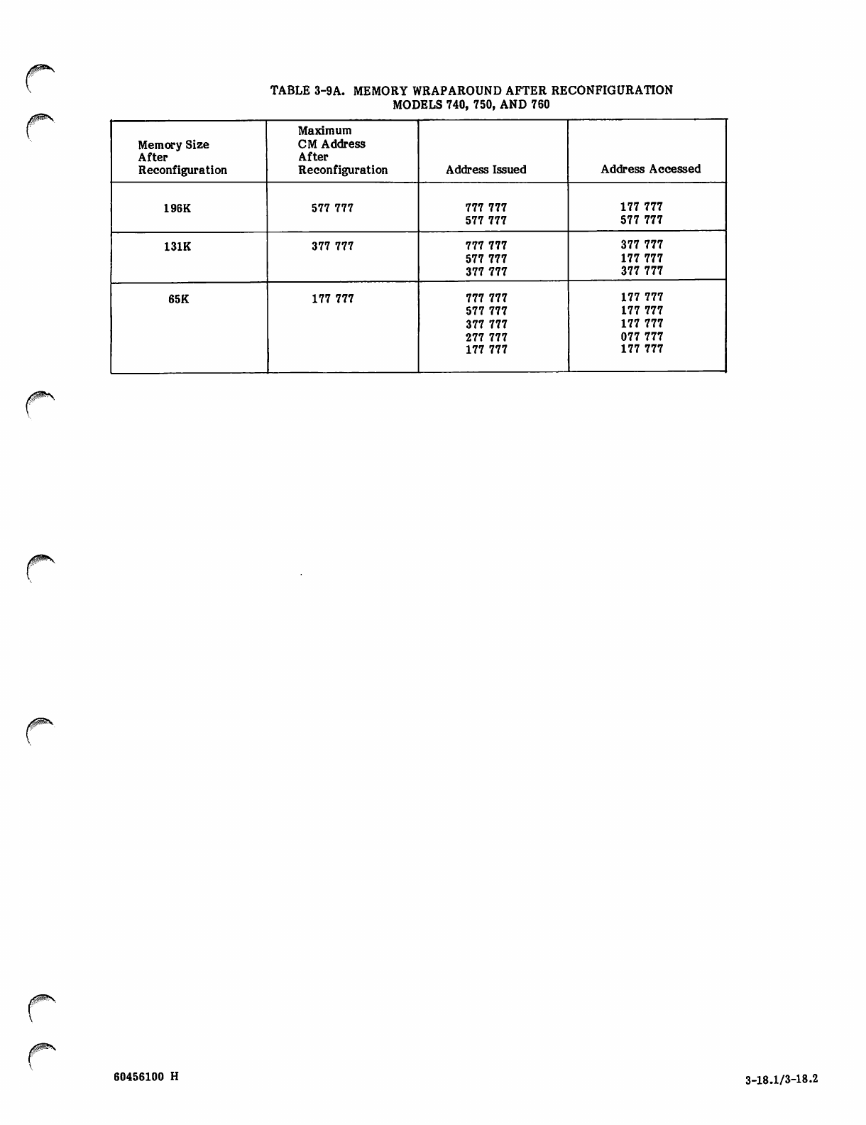
TABLE 3-9A. MEMORY WRAPAROUND AFTER RECONFIGURATION
MODELS 740, 750, AND 760
Memory Size
After
Reconfiguration
Maximum
CM Address
After
Reconfiguration Address Issued Address Accessed
196K 577 777 777 777
577 777
177 777
577 777
131K 377 777 777 777
577 777
377 777
377 777
177 777
377 777
65K 177 777 777 777
577 777
377 777
277 777
177 777
177 777
177 777
177 777
077 777
177 777
60456100 H 3-18.1/3-18.2

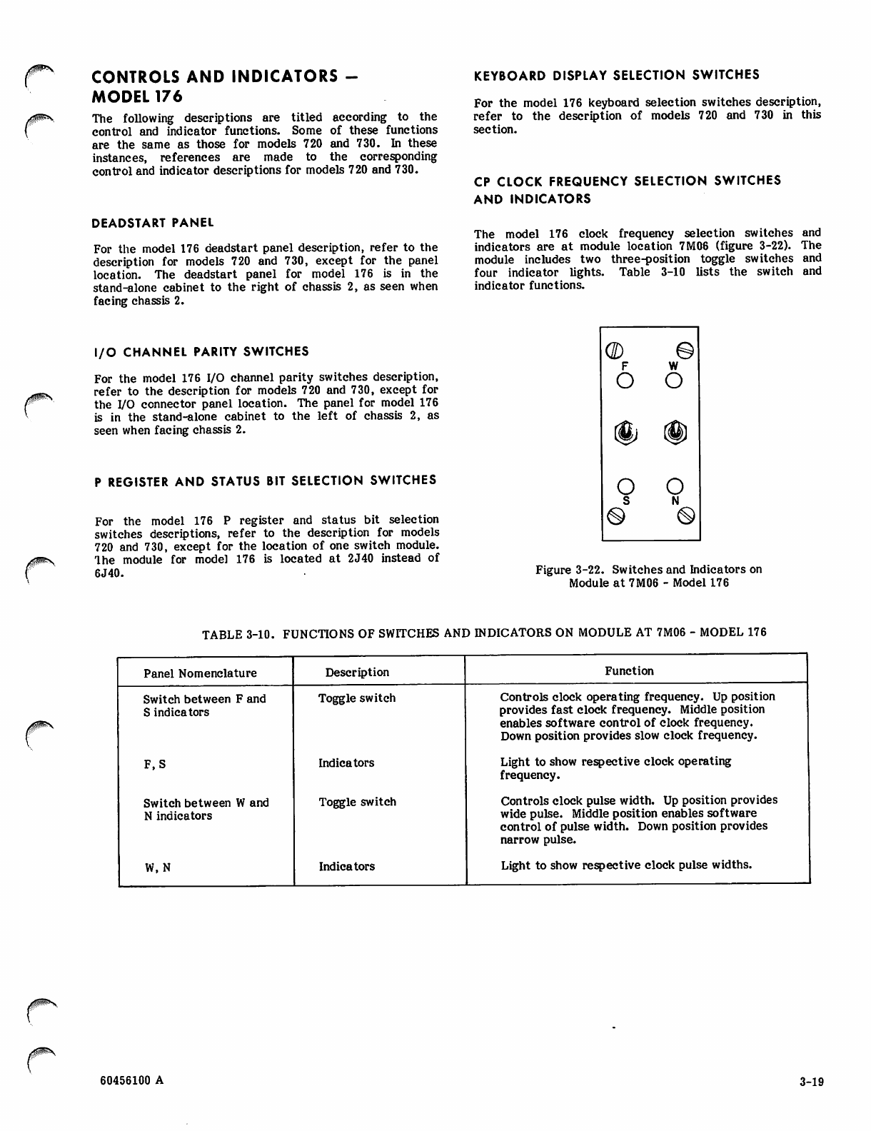
CONTROLS AND INDICATORS -
MODEL 176
The following descriptions are titled according to the
control and indicator functions. Some of these functions
are the same as those for models 720 and 730. In these
instances, references are made to the corresponding
control and indicator descriptions for models 720 and 730.
DEADSTART PANEL
For the model 176 deadstart panel description, refer to the
description for models 720 and 730, except for the panel
location. The deadstart panel for model 176 is in the
stand-alone cabinet to the right of chassis 2, as seen when
facing chassis 2.
KEYBOARD DISPLAY SELECTION SWITCHES
For the model 176 keyboard selection switches description,
refer to the description of models 720 and 730 in this
section.
CP CLOCK FREQUENCY SELECTION SWITCHES
AND INDICATORS
The model 176 clock frequency selection switches and
indicators are at module location 7M06 (figure 3-22). The
module includes two three-position toggle switches and
four indicator lights. Table 3-10 lists the switch and
indicator functions.
I/O CHANNEL PARITY SWITCHES
For the model 176 I/O channel parity switches description,
refer to the description for models 720 and 730, except for
the I/O connector panel location. The panel for model 176
is in the stand-alone cabinet to the left of chassis 2, as
seen when facing chassis 2.
P REGISTER AND STATUS BIT SELECTION SWITCHES
For the model 176 P register and status bit selection
switches descriptions, refer to the description for models
720 and 730, except for the location of one switch module.
Ihe module for model 176 is located at 2J40 instead of
6J40.
I§]
o o
S N
®®
Figure 3-22. Switches and Indicators on
Module at 7M06 - Model 176
TABLE 3-10. FUNCTIONS OF SWITCHES AND INDICATORS ON MODULE AT 7M06 - MODEL 176
Panel Nomenclature
Switch between F and
S indicators
F,S
Switch between W and
N indicators
W, N
Description
Toggle switch
Indicators
Toggle switch
Indicators
Function
Controls clock operating frequency. Up position
provides fast clock frequency. Middle position
enables software control of clock frequency.
Down position provides slow clock frequency.
Light to show respective clock operating
frequency.
Controls clock pulse width. Up position provides
wide pulse. Middle position enables software
control of pulse width. Down position provides
narrow pulse.
Light to show respective clock pulse widths.
60456100 A 3-19
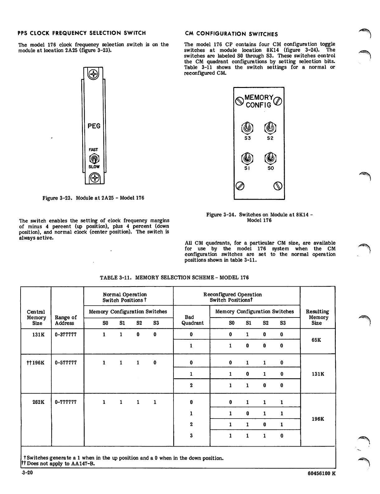
PPS CLOCK FREQUENCY SELECTION SWITCH CM CONFIGURATION SWITCHES
The model 176 clock frequency selection switch is on the
module at location 2A25 (figure 3-23).
PEG
FAST
SLOW
The model 176 CP contains four CM configuration toggle
switches at module location 8K14 (figure 3-24). The
switches are labeled SO through S3. These switches control
the CM quadrant configurations by setting selection bits.
Table 3-11 shows the switch settings for a normal or
reconfigured CM.
Figure 3-23. Module at 2A25 - Model 176
.MEMORY
' CONFIG <Z>
S3
SI
S2
SO
<S>
The switch enables the setting of clock frequency margins
of minus 4 percent (up position), plus 4 percent (down
position), and normal clock (center position). The switch is
always active.
Figure 3-24. Switches on Module at 8K14 -
Model 176
All CM quadrants, for a particular CM size, are available
for use by the model 176 system when the CM
configuration switches are set to the normal operation
positions shown in table 3-11.
/*^\
TABLE 3-11. MEMORY SELECTION SCHEME- MODEL 176
Central
Memory
Size Range of
Address
Normal Operation
Switch Positions t Reconfigured Operation
Switch Positionst
Resulting
Memory
Size
Memory Configuration Switches Bad
Quadrant
Memory Configuration Switches
S O S l S 2 S 3 S O S l S 2 S3
131K 0-377777 1 1 0 0 0 1 0
65K
1 1 0 0
ttl96K 0-577777 1 1 1 0 0 1 1
131K
1 1 0 1
2 1 1 0
262K 0-777777 1111 0 1 1
196K
1 0 1
1 1 0
1 1 1
tSwitches generate a 1 when in the up position and a 0 when
ft Does not apply to AA147-B.
in the down position. /«*%.
•3-20 60456100 K
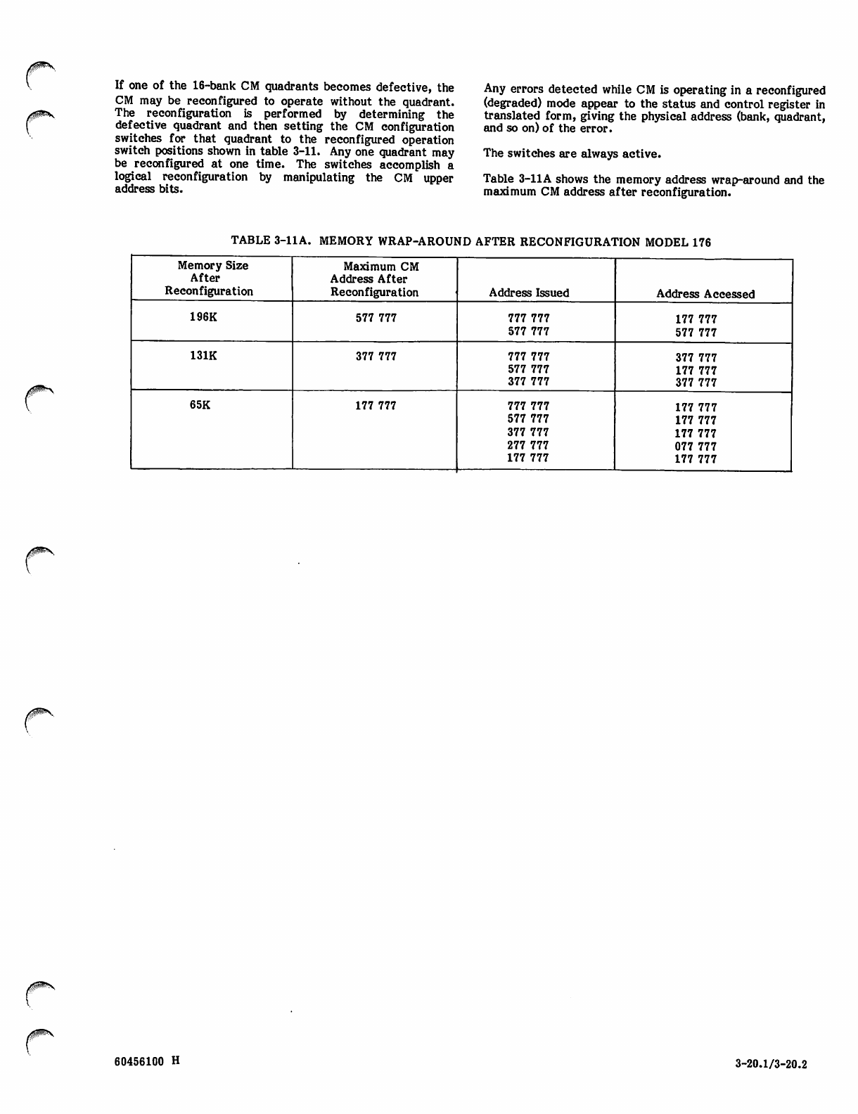
If one of the 16-bank CM quadrants becomes defective, the
CM may be reconfigured to operate without the quadrant.
The reconfiguration is performed by determining the
defective quadrant and then setting the CM configuration
switches for that quadrant to the reconfigured operation
switch positions shown in table 3-11. Any one quadrant may
be reconfigured at one time. The switches accomplish a
logical reconfiguration by manipulating the CM upper
address bits.
Any errors detected while CM is operating in a reconfigured
(degraded) mode appear to the status and control register in
translated form, giving the physical address (bank, quadrant,
and so on) of the error.
The switches are always active.
Table 3-11A shows the memory address wrap-around and the
maximum CM address after reconfiguration.
TABLE 3-11A. MEMORY WRAP-AROUND AFTER RECONFIGURATION MODEL 176
Memory Size
After
Reconfiguration
Maximum CM
Address After
Reconfiguration Address Issued Address Accessed
196K 577 777 777 777
577 777
177 777
577 777
131K 377 777 777 777
577 777
377 777
377 777
177 777
377 777
65K 177 777 777 777
577 777
377 777
277 777
177 777
177 777
177 777
177 777
077 777
177 777
y!$P^V
60456100 H 3-20.1/3-20.2

f^i
v_
V
0^
CONf ROLS AND INDICATORS - MODEL 17l
iP^

y c ^ l
'"*'*%
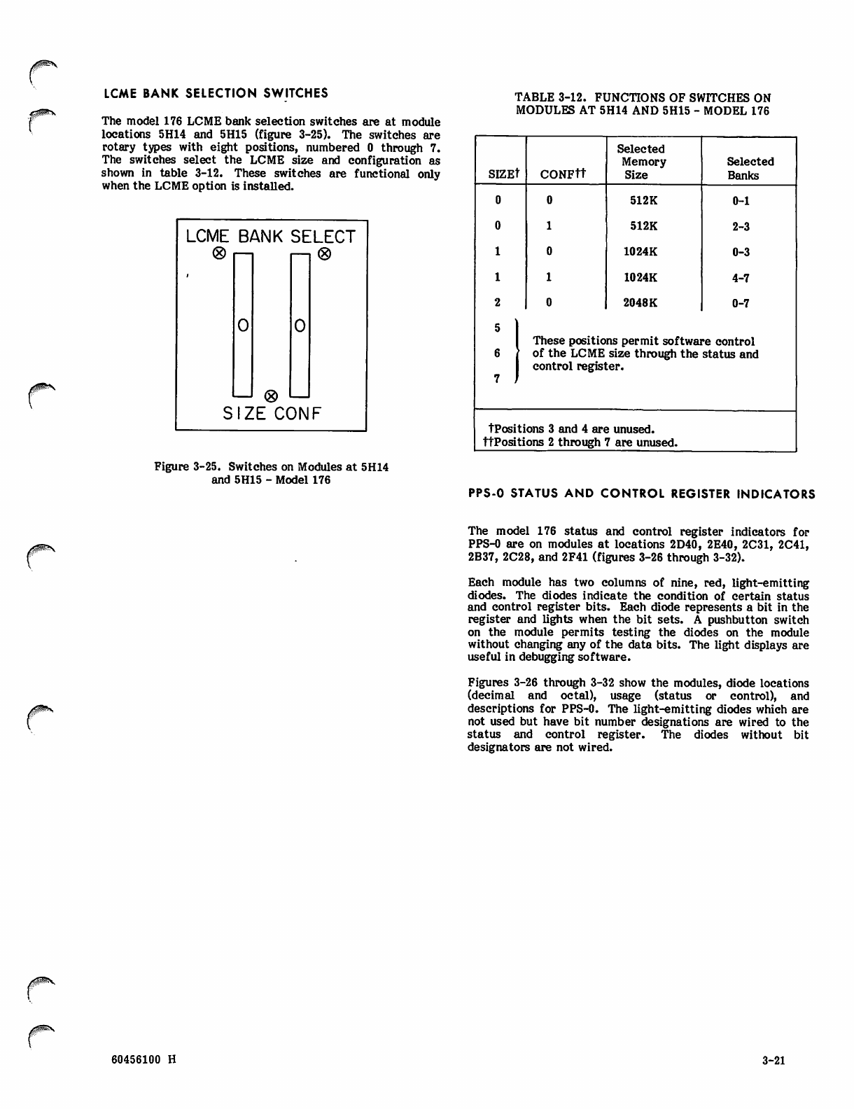
//!^^\
LCME BANK SELECTION SWITCHES
The model 176 LCME bank selection switches are at module
locations 5H14 and 5H15 (figure 3-25). The switches are
rotary types with eight positions, numbered 0 through 7.
The switches select the LCME size and configuration as
shown in table 3-12. These switches are functional only
when the LCME option is installed.
LCME
®
<
S
B/
0
IZ
UIK
:e cc
SE
0
)N
:lect
®
F
Figure 3-25. Switches on Modules at 5H14
and 5H15 - Model 176
TABLE 3-12. FUNCTIONS OF SWITCHES ON
MODULES AT 5H14 AND 5H15 - MODEL 176
Selected
SIZEt CONFtt Memory
Size
Selected
Banks
0 0 512K 0-1
0 1 512K 2-3
101024K 0-3
1 1 1024K 4-7
2 0 2048 K 0-7
5
6
7
These positions permit software control
of the LCME size through the status and
control register.
tPositions 3 and 4 are unused.
ttPositions 2 through 7 are unused.
PPS-0 STATUS AND CONTROL REGISTER INDICATORS
The model 176 status and control register indicators for
PPS-0 are on modules at locations 2D40, 2E40, 2C31, 2C41,
2B37, 2C28, and 2F41 (figures 3-26 through 3-32).
Each module has two columns of nine, red, light-emitting
diodes. The diodes indicate the condition of certain status
and control register bits. Each diode represents a bit in the
register and lights when the bit sets. A pushbutton switch
on the module permits testing the diodes on the module
without changing any of the data bits. The light displays are
useful in debugging software.
Figures 3-26 through 3-32 show the modules, diode locations
(decimal and octal), usage (status or control), and
descriptions for PPS-0. The light-emitting diodes which are
not used but have bit number designations are wired to the
status and control register. The diodes without bit
designators are not wired.
60456100 H 3-21
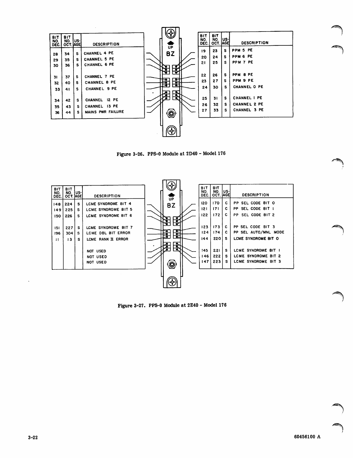
BIT
NO.
DEC.
BIT
NO.
OCT.
US
AGE DESCRIPTION
28 34 CHANNEL 4 PE
29 35 CHANNEL 5 PE
30 36 CHANNEL 6 PE
31 37 CHANNEL 7 PE
32 40 CHANNEL 8 PE
33 41 CHANNEL 9 PE
34 42 CHANNEL 12 PE
35 43 CHANNEL 13 PE
36 44 MAINS PWR FAILURE
BIT
NO.
DEC.
BIT
NO.
OCT.
US
AGE DESCRIPTION
19 23 PPM 5 PE
20 24 PPM 6 PE
21 25 PPM 7 PE
22 26 PPM 8 PE
23 27 PPM 9 PE
24 30 CHANNEL 0 PE
25 31 CHANNEL 1 PE
26 32 CHANNEL 2 PE
27 33 CHANNEL 3 PE
Figure 3-26. PPS-0 Module at 2D40 - Model 176
X«^^v
BIT
NO.
DEC.
BIT
NO.
OCT.
US
AGE DESCRIPTION
148 224 LCME SYNDROME BIT 4
149 225 LCME SYNDROME BIT 5
150 226 LCME SYNDROME BIT 6
151 227 LCME SYNDROME BIT 7
196 304 LCME DBL BIT ERROR
II 13 LCME RANK 31 ERROR
NOT USED
NOT USED
NOT USED
BIT
NO.
DEC.
BIT
NO.
OCT.
US
AGE DESCRIPTION
120 170 PP SEL CODE BIT 0
121 171 PP SEL COOE BIT 1
122 172 PP SEL CODE BIT 2
123 173 PP SEL CODE BIT 3
124 174 PP SEL AUTO/MNL MODE
144 220 LCME SYNDROME BIT 0
!45 221 LCME SYNDROME BIT 1
146 222 LCME SYNDROME BIT 2
147 223 LCME SYNDROME BIT 3
Figure 3-27. PPS-0 Module at 2E40 - Model 176
3-22 60456100 A
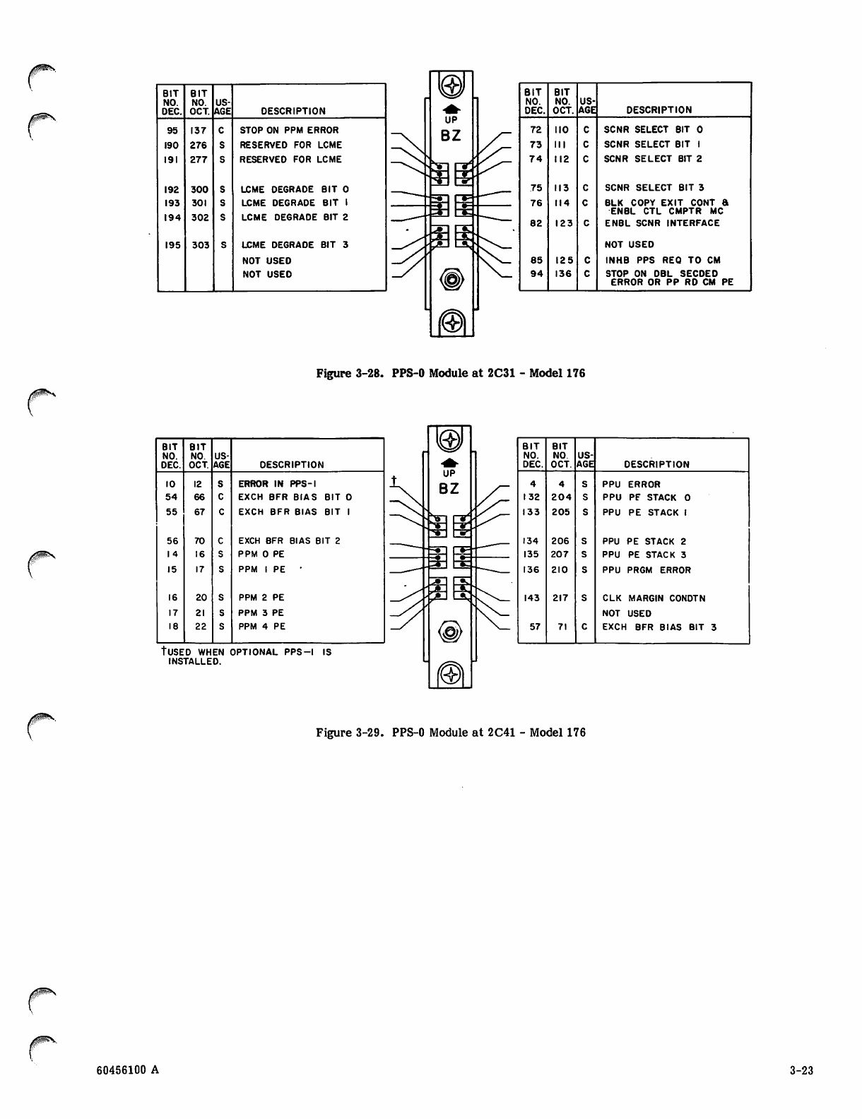
BIT
NO.
DEC.
BIT
NO.
OCT.
US
AGE DESCRIPTION
95 137 STOP ON PPM ERROR
190 276 RESERVED FOR LCME
191 277 RESERVED FOR LCME
192 300 LCME DEGRADE BIT 0
193 301 LCME DEGRADE BIT 1
194 302 LCME DEGRADE BIT 2
195 303 LCME DEGRADE BIT 3
NOT USEO
NOT USED
BIT
NO.
DEC.
BIT
NO.
OCT.
US
AGE DESCRIPTION
72 no SCNR SELECT BIT 0
73 III SCNR SELECT BIT 1
74 112 SCNR SELECT BIT 2
75 113 SCNR SELECT BIT 3
76 114 BLK COPY EXIT CONT S
EN BL C TL C MP TR MC
82 123 ENBL SCNR INTERFACE
NOT USED
85 125 INHB PPS REQ TO CM
94 136 STOP ON DBL SECDED
ERROR OR PP RD CM PE
Figure 3-28. PPS-0 Module at 2C31 - Model 176
BIT
NO.
DEC.
BIT
NO.
OCT.
US
AGE DESCRIPTION
10 12 ERROR IN PPS-1
54 66 EXCH BFR BIAS BIT 0
55 67 EXCH BFR BIAS BIT 1
56 70 EXCH BFR BIAS BIT 2
14 16 PPM 0 PE
15 17 PPM 1 PE
16 20 PPM 2 PE
17 21 PPM 3 PE
18 22 PPM 4 PE
tuSED WHEN OPTIONAL PPS-1 IS
INSTALLED.
BIT
NO.
DEC.
BIT
NO
OCT.
US
AGE DESCRIPTION
4 4 sPPU ERROR
132 204 PPU PF STACK 0
133 205 PPU PE STACK 1
134 206 PPU PE STACK 2
135 207 PPU PE STACK 3
136 210 PPU PRGM ERROR
143 217 CLK
NOT
MARGIN CONDTN
USED
57 71 EXCH BFR BIAS BIT 3
Figure 3-29. PPS-0 Module at 2C41 - Model 176
60456100 A 3-23
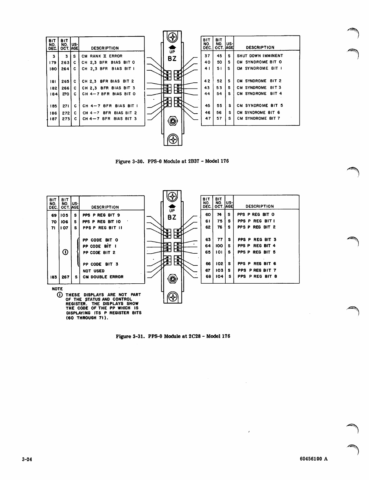
BIT
NO.
DEC.
BIT
NO.
OCT.
US
AGE DESCRIPTION
3 3 S CM RANK X ERROR
179 263 CH 2,3 B FR BI AS BIT 0
180 264 CH 2, 3 BF R BI AS B IT 1
181 265 CH 2, 3 BF R BI AS B IT 2
182 266 CH 2 ,3 B FR B IA S BIT 3
164 270 CH 4 - 7 B F R BI A S B IT 0
185 271 CH 4 - 7 B F R B I A S B I T 1
186 272 CH 4 - 7 B F R B I A S B I T 2
. 187 273 CH 4 — 7 BFR BIAS BIT 3
BIT
NO.
DEC.
BIT
NO.
OCT.
US
AGE DESCRIPTION
37 45 SHUT DOWN IMMINENT
40 50 CM SYNDROME BIT 0
41 51 CM SYNDROME BIT 1
42 52 CM SYNDROME BIT 2
43 53 CM SYNDROME BIT 3
44 54 CM SYNDROME BIT 4
45 55 CM S YNDROME BI T 5
46 56 CM SYNDROME BIT 6
47 57 CM SYNDROME BIT 7
Figure 3-30. PPS-0 Module at 2B37 - Model 176
BIT
NO.
DEC.
BIT
NO.
OCT.
US
AGE DESCRIPTION
69 105 PPS P REG BIT 9
70 106 PPS P REG BIT 10
71 107 PPS P REG BIT II
P P C O DE B I T 0
PP CODE BIT 1
0<PP CODE BIT 2
P P C O DE B I T 3
NOT USED
183 267 CM DOUBLE ERROR
NOTE
0THESE DISPLAYS ARE NOT PART
OF THE STATUS AND CONTROL
REGISTER. THE DISPLAYS SHOW
THE CODE OF THE PP WHICH IS
DISPLAYING ITS P REGISTER BITS
(60 THROUGH 71).
BIT
NO.
DEC.
BIT
NO.
OCT.
US
AGE DESCRIPTION
60 74 PPS P REG BIT 0
61 75 PPS P REG BIT 1
62 76 PPS P REG BIT 2
63 77 PPS P REG BIT 3
64 100 PPS P REG BIT 4
65 101 PPS P REG BIT 5
66 102 PPS P REG BIT 6
67 103 P P S P R E G B IT 7
68 104 PPS P REG BIT 8
j**«ft^V
Figure 3-31. PPS-0 Module at 2C28 - Model 176
^*5S\
3-24
.■/ae&^v
60456100 A
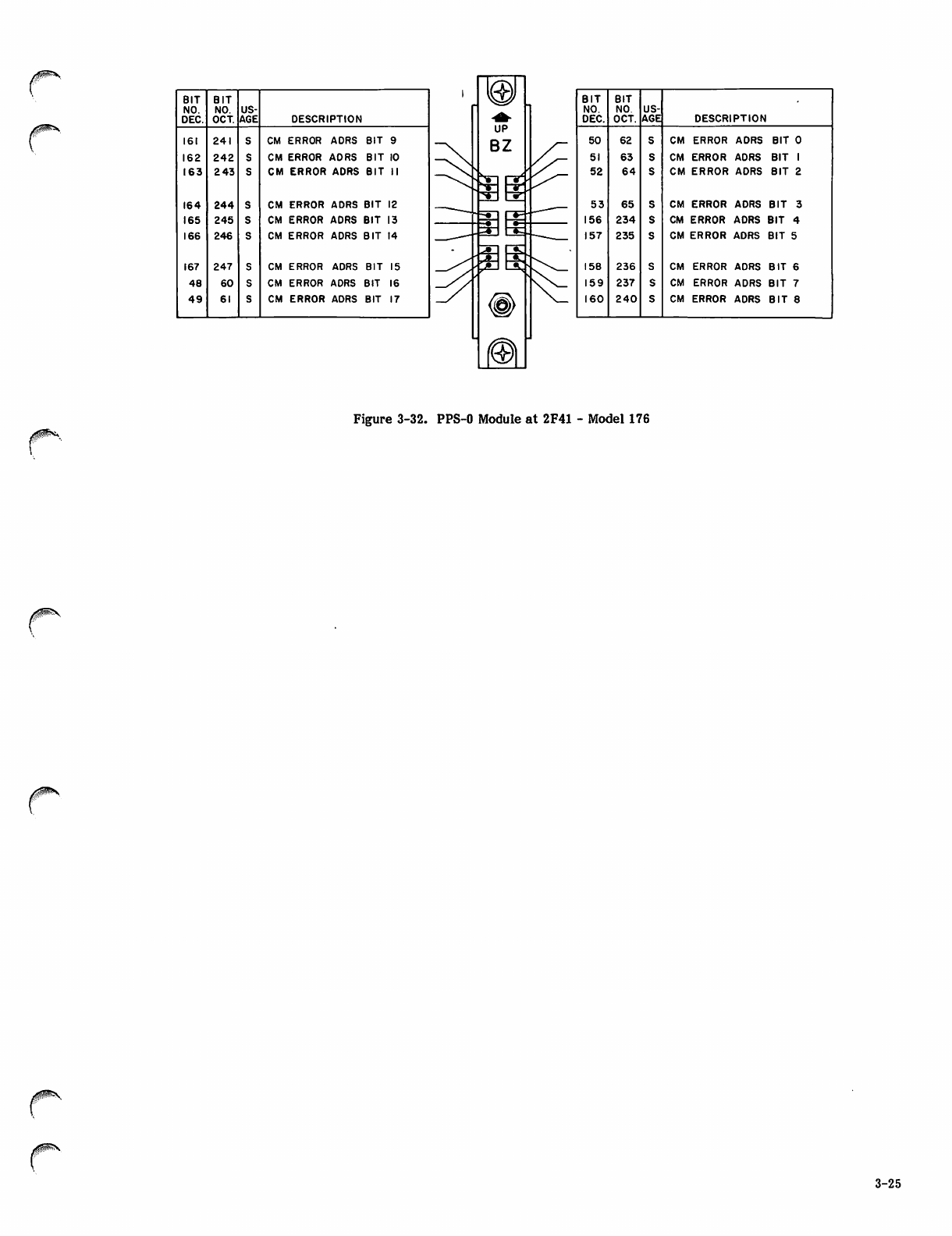
BIT
NO.
DEC.
BIT
NO.
OCT.
US
AGE DESCRIPTION
161 241 CM ERROR ADRS B IT 9
162 242 CM ERROR ADRS BIT 10
163 243 CM ERROR ADRS B IT II
164 244 CM ERROR ADRS BIT 12
165 245 CM ERROR ADRS BIT 13
166 246 CM ERROR ADRS BIT 14
167 247 CM ERROR ADRS BIT 15
48 60 CM ERROR ADRS BIT 16
49 61 CM ERROR ADRS BIT 17
BIT
NO.
DEC.
BIT
NO.
OCT.
US
AGE DESCRIPTION
50 62 CM ERROR ADRS BIT 0
51 63 CM ERROR ADRS BIT 1
52 64 CM ERROR A DRS B IT 2
53 65 CM ERROR ADR S B IT 3
156 234 CM ERROR ADRS BIT 4
157 235 CM ERROR ADRS BIT 5
158 236 CM ERROR ADRS BIT 6
159 237 CM ERROR ADRS BIT 7
160 240 CM ERROR ADRS BIT 8
Figure 3-32. PPS-0 Module at 2F41 - Model 176
3-25
PPS-llSTATUS AND CONTROL REGISTER INDICATORS
The model 176 status and control register indicators for
PPS-1 are located in chassis 2, when installed. The
indicators are on modules at location 2N35, 2038, and 2P32
(figures 3-33 through 3-35).
Each module has two columns of nine, red, light-emitting
diodes. The diodes indicate the condition of certain status
and control register bits. Each diode represents a bit in the
register and lights when the bit sets. A pushbutton switch
on the module permits testing all the diodes on the module
without changing any of the data bits. The light displays
are useful in debugging software.
Figures 3-33 through 3-35 show the modules, diode
locations (decimal and octal), usage (status or control), and
descriptions for PPS-1. The light-emitting diodes which
are not used but have bit number designations are wired to
the status and control register. The diodes without bit
designators are not wired.
BIT
NO.
DEC.
BIT
NO.
OCT.
US
AGE DESCRIPTION
18 22 PPM 4 PE
19 23 PPM 5 PE
20 24 PPM 6 PE
21 25 PPM 7 PE
22 26 PPM 8 PE
23 27 PPM 9 PE
24 30 CHANNEL 0 PE
25 31 CHANNEL 1 PE
26 32 CHAN NEL 2 PE
BIT
NO.
DEC.
BIT
NO
OCT.
US
AGE DESCRIPTION
NOT USED
6 6 NOT USED
7 7 NOT USED
NOT USED
NOT USED
14 16 PPM 0 PE
15 17 PPM 1 PE
16 20 PPM 2 PE
17 21 PPM 3 PE
Figure 3-33. PPS-1 Module at 2N35 - Model 176
BIT
no:
DEC.
BIT
NO.
OCT.
US
AGE DESCRIPTION
85 125 INHB REO TO CM
94 136 STOP ON DBL SECDED ERROR
OR PP RD CM PE
95 137 STOP ON PPM ERROR
NOT USED
120 170 PP SEL CODE BIT 0
121 171 PP SEL CODE BIT 1
122 172 PP SEL CODE BIT 2
123 173 PP SEL CODE BIT 3
124 174 PPSEL AUTO/MNL MODE
BIT
NO.
DEC.
BIT
NO.
OCT.
US
AGE DESCRIPTION
27 33 CHANNEL 3 PE
28 34 CHANNEL 4 PE
29 35 CH ANN EL 5 PE
30 36 C HAN NE L 6 P E
31 37 CHA NN E L 7 P E
32 40 CHANNEL 10 PE
33 41 CHANNEL II PE
34 42 CHANNEL 12 PE
35 43 CHANNEL 13 PE
yCSK
Figure 3-34. PPS-1 Module at 2038 - Model 176
3-26 60456100 A
BIT
NO.
DEC.
BIT
NO.
OCT.
US
AGE DESCRIPTION
69 105 PPS P RGTR BIT 9
70 106 PPS P RGTR BIT 10
71 107 PPS P RGTR BIT II
/S PP CODE BIT 0
S PP CODE BIT 1
©■PP CODE BIT 2
•S PP CODE BIT 3
NOT USED
NOT USED
BIT
NO.
DEC.
BIT
NO
OCT.
US
AGE DESCRIPTION
60 74 PPS P RGTR BIT 0
61 75 PPS P RGTR BIT 1
62 76 PPS P RGTR BIT 2
63 77 PPS P RGTR BIT 3
64 100 PPS P RGTR BIT 4
65 101 PPS P RGTR BIT 5
66 102 PPS P RGTR BIT 6
67 103 PPS P RGTR BIT 7
68 104 PPS P RGTR BIT 8
Figure 3-35. PPS-1 Module at 2P32 - Model 176
/ F ^ ^ X
60456100 A 3-27/3-28

POWER-ON AND POWER-OFF PROCEDURES - ALL MODELS
^m^
OPERATING PROCEDURES - ALL MODELS
r

y*%
/ga^X POWER-ON AND POWER-OFF
PROCEDURES - ALL MODELS
The power-on and power-off procedures are to be used by
designated personnel only and are not included here. These
procedures must be referenced in the Power Distribution
and Warning System Manual listed in the system publication
index in the preface.
CAUTION
Computer operators are generally restricted
from using the power-on and power-off
controls, except for the system
EMERGENCY OFF switch.
OPERATING PROCEDURES - ALL MODELS
Prior to program operation and keyboard control, the system
controls should be checked, a deadstart program selected,
and the system deadstarted. After the system is put into
operation, the display station keyboard provides manual
control of the system and entry of data or instructions into
the system under program control.
CONTROL CHECKS
Before deadstarting any of the CDC CYBER 170 systems,
the positions of the control switches should be checked
against their intended use. These checks can most easily be
made through the use of the applicable control and indicator
descriptions in this section.
Load Mode
Load programs and data into the computer system as follows:
1. Set mode switch to LOAD position.
2. Set 20 through 211 by 1 through 20 (octal)
toggle switch matrix according to selected
deadstart program. (Bits are set when switches are
in the up position.)
3. Check that PPS and MEMORY SELECT switches
select the desired PP to be PP-0.
4. Set DEADSTART switch to UP position,
momentarily.
Results of steps 1 through 4:
1. Assign data channels 0 through 11 (octal) to
corresponding PPs in each PPS.
2. Send a master clear (MC) to all I/O channels. An
MC selects all channel converters on each channel
and resets bits 80 through 95 and 120 through 127 of
the status and control register. MC sets all
channels to the active and empty condition, ready
for inputs.
3. Set all PPs to the input (712) instruction.
4. Clear the P registers and set the A registers to
10000 (octal) in all PPs.
5. Transmit a zero word that is followed by the 16
words from the toggle switches into PPM locations 0
through 20 (octal) of PP-0. Channel 0 is then
disconnected, clearing word 21 (octal) of PP-0 and
causing PP-0 to start execution with the instruction
at location 0001.
DEADSTART PROGRAM SELECTION
Refer to the system operator's guide or installation
handbook to select a deadstart program of 16 words or less
for the deadstart panel. The deadstart program is normally
a load routine which loads a larger program from input
equipment.
DEADSTART
The system deadstart panel provides a load, sweep, or dump
mode of operation. These modes are initiated from the
deadstart panel.
Sweep Mode
Sweep mode is a maintenance function useful in checking
PPM operation. Initiate this mode as follows:
1. Set mode switch to SWEEP position.
2. Set DEADSTART switch to ON position
momentarily. (DEADSTART switch may be left on
for synchronizing purposes.)
Results of steps 1 and 2:
1. Set all PPs to load (505) instruction.
60456100 L 3-29
2. Clear all PP P registers and start the P registers
counting.
3. Cause each PP to sweep through its PPM, reading
the contents of each location, without executing
instructions.
Dump Mode
Dump mode provides copying the contents of a PPM to an
external storage device. Initiate dump program in PP-0 as
follows:
1. Set mode switch to DUMP position.
2. Set DEADSTART switch to ON position
momentarily.
Results of steps 1 and 2:
1. All PPs set to output (732) instruction.
2. An MC is sent on all channels.
3. Channel 0 is held active and empty.
4. Each PP is assigned to its corresponding I/O
channel.
5. All P registers clear and all A registers set to
10000 (octal).
6. All PPs sense the empty and active conditions of
their assigned channels, output the contents of
their address 0000, set their channels to full, and
wait for an empty condition.
7. All PPs advance P by 1 and reduce the A register
by 1 (A equals 777776).
8. Because channel 0 is held active and empty, PPO
cycles through the 732 instruction until A equals 1.
9. PP-0 goes to memory location 0001 for its next
instruction. PP-0 can send its entire memory
contents on channel 0 although no I/O device has
been selected to receive it. PP-0 is then free to
execute a dump program which must previously
have been stored in memory, beginning at location
0001.
3-30 60456100 C
INSTRUCTION DESCRIPTIONS
This section describes the central processor (CP),
peripheral processor unit (PPU), and peripheral processor
(PP) instructions. Some differences exist in the CP
instructions because of model differences. The instruction
differences are identified with the applicable model
numbers. The PPU instructions apply only to model 176.
The PP instructions are identical for all models.
Instruction timing information follows respective
instruction descriptions. (Other programming information
and system error response information are in section 5.)
CP, PPU, and PP instruction codes and page numbers are
listed in indexes on the inside front cover for quick
reference.
60456100 A 4-1/4-2

(*%
CENTUM PROCESSOR INSTRUCT!ON£ - ALL MODELS
&**.

V.
V
^
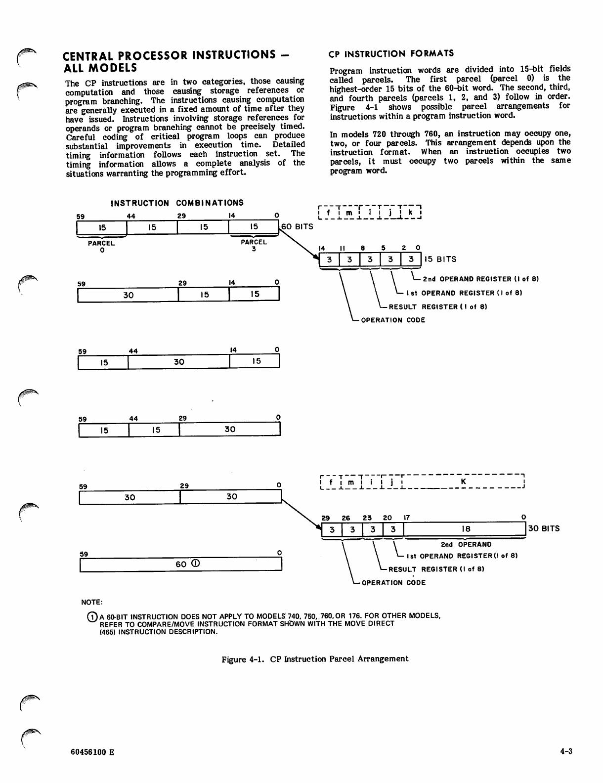
CENTRAL PROCESSOR INSTRUCTIONS -
ALL MODELS
The CP instructions are in two categories, those causing
computation and those causing storage references or
program branching. The instructions causing computation
are generally executed in a fixed amount of time after they
have issued. Instructions involving storage references for
operands or program branching cannot be precisely timed.
Careful coding of critical program loops can produce
substantial improvements in execution time. Detailed
timing information follows each instruction set. The
timing information allows a complete analysis of the
situations warranting the programming effort.
CP INSTRUCTION FORMATS
Program instruction words are divided into 15-bit fields
called parcels. The first parcel (parcel 0) is the
highest-order 15 bits of the 60-bit word. The second, third,
and fourth parcels (parcels 1, 2, and 3) follow in order.
Figure 4-1 shows possible parcel arrangements for
instructions within a program instruction word.
In models 720 through 760, an instruction may occupy one,
two, or four parcels. This arrangement depends upon the
instruction format. When an instruction occupies two
parcels, it must occupy two parcels within the same
program word.
INSTRUCTION COMBINATIONS
59 44 29 1 4 0
14
yi---T--T---l
m ■ i i j K i
1 L L _ 1 1
15 15 15 15 ,60 BITS
PARCEL
0
29
PARCEL I I 8 5 2 0
13 3 3 3 3 15 BITS
59 1 4 01r \ \u2nd OPERAND REGISTER (1 of 8)
30 15 15 \ \ ^— 1 St O PER A ND R EGI STE R (1 of 8 )
\ »— RESULT REGISTER (1 of 8)
\— OPERATION CODE
59 44 14
15 30
59 44 29
15 15 30
59 29
30 30
59
60 ©
30 BITS
2nd OPERAND
Ist OPERAND REGISTEROof 8)
■RESULT REGISTER (I of 8)
OPERATION CODE
NOTE:
0A 60-BIT INSTRUCTION DOES NOT APPLY TO MODELS1740. 750,;760,OR 176. FOR OTHER MODELS,
REFER TO COMPARE/MOVE INSTRUCTION FORMAT SHOWN WITH THE MOVE DIRECT
(465) INSTRUCTION DESCRIPTION.
Figure 4-1. CP Instruction Parcel Arrangement
60456100 E 4-3
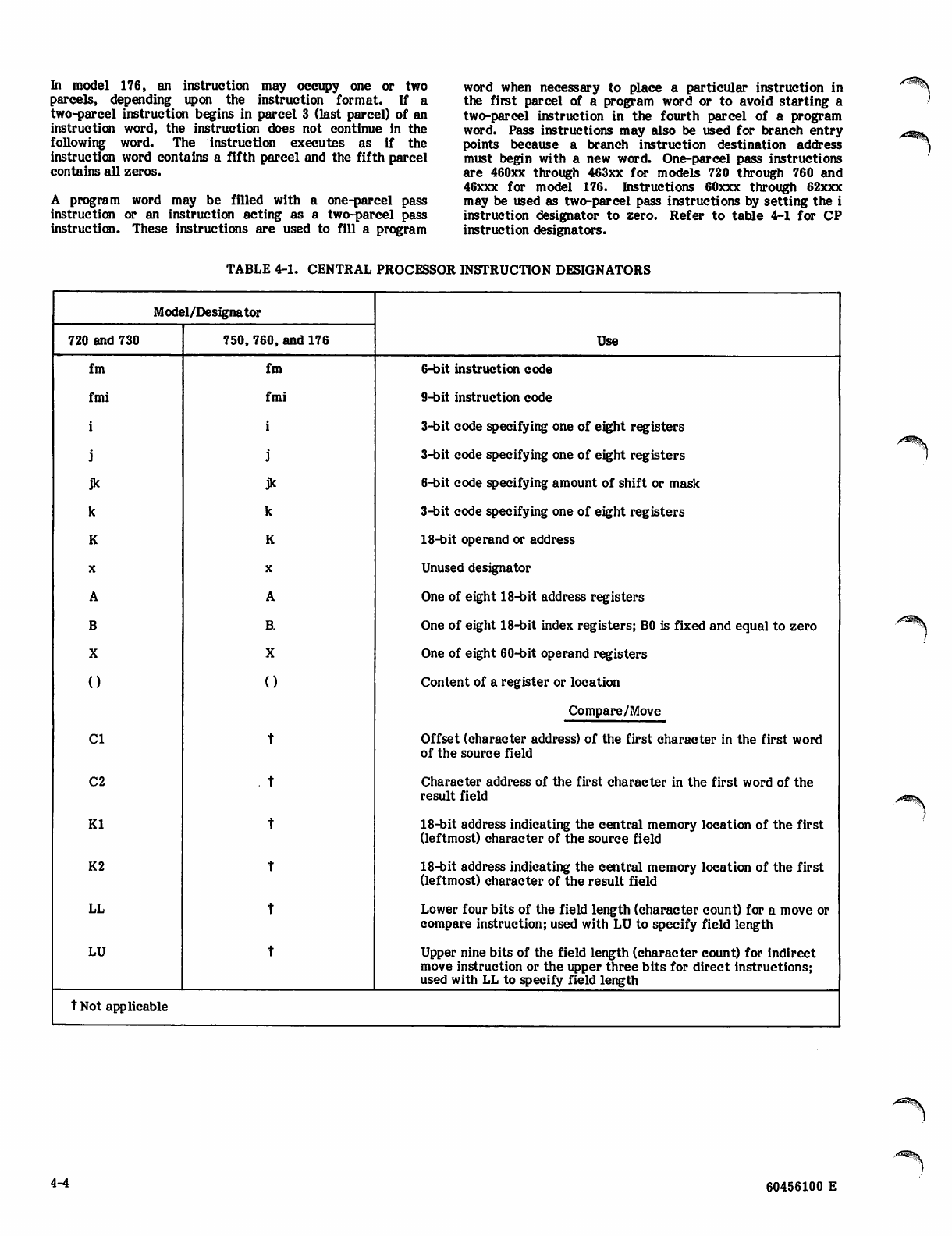
In model 176, an instruction may occupy one or two
parcels, depending upon the instruction format. If a
two-parcel instruction begins in parcel 3 (last parcel) of an
instruction word, the instruction does not continue in the
following word. The instruction executes as if the
instruction word contains a fifth parcel and the fifth parcel
contains all zeros.
A program word may be filled with a one-parcel pass
instruction or an instruction acting as a two-parcel pass
instruction. These instructions are used to fill a program
word when necessary to place a particular instruction in
the first parcel of a program word or to avoid starting a
two-parcel instruction in the fourth parcel of a program
word. Pass instructions may also be used for branch entry
points because a branch instruction destination address
must begin with a new word. One-parcel pass instructions
are 460xx through 463xx for models 720 through 760 and
46xxx for model 176. Instructions 60xxx through 62xxx
may be used as two-parcel pass instructions by setting the i
instruction designator to zero. Refer to table 4-1 for CP
instruction designators.
TABLE 4-1. CENTRAL PROCESSOR INSTRUCTION DESIGNATORS
Model/Designator
Use720 and 730 750, 760, and 176
fm fm 6-bit instruction code
fmi fmi 9-bit instruction code
ii 3-bit code specifying one of eight registers
j j 3-bit code specifying one of eight registers
jk jk 6-bit code specifying amount of shift or mask
k k 3-bit code specifying one of eight registers
K K 18-bit operand or address
X X Unused designator
A A One of eight 18-bit address registers
BB. One of eight 18-bit index registers; B0 is fixed and equal to zero
X X One of eight 60-bit operand registers
0() Content of a register or location
Compare/Move
Cl Offset (character address) of the first character in the first word
of the source field
C2 . t Character address of the first character in the first word of the
result field
Kl 18-bit address indicating the central memory location of the first
(leftmost) character of the source field
K2 18-bit address indicating the central memory location of the first
(leftmost) character of the result field
LL Lower four bits of the field length (character count) for a move or
compare instruction; used with LU to specify field length
LU Upper nine bits of the field length (character count) for indirect
move instruction or the upper three bits for direct instructions;
used with LL to specify field length
t Not applicable
/ S ^ \
/<3i!k
4-4 60456100 E
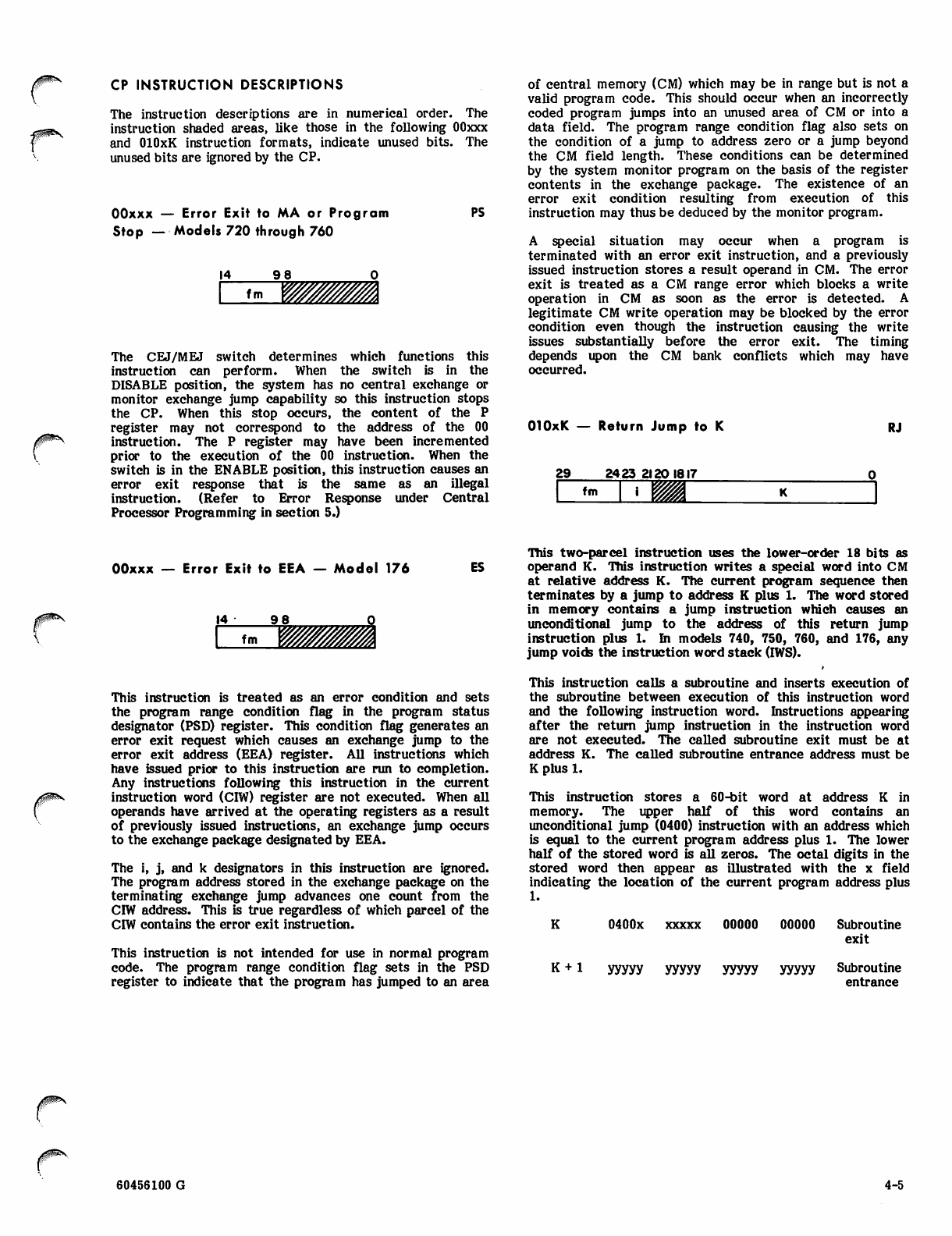
CP INSTRUCTION DESCRIPTIONS
The instruction descriptions are in numerical order. The
instruction shaded areas, like those in the following OOxxx
and OlOxK instruction formats, indicate unused bits. The
unused bits are ignored by the CP.
OOxxx — Error Exit to MA or Program
Stop — Models 720 through 760
PS
The CEJ/MEJ switch determines which functions this
instruction can perform. When the switch is in the
DISABLE position, the system has no central exchange or
monitor exchange jump capability so this instruction stops
the CP. When this stop occurs, the content of the P
register may not correspond to the address of the 00
instruction. The P register may have been incremented
prior to the execution of the 00 instruction. When the
switch is in the ENABLE position, this instruction causes an
error exit response that is the same as an illegal
instruction. (Refer to Error Response under Central
Processor Programming in section 5.)
of central memory (CM) which may be in range but is not a
valid program code. This should occur when an incorrectly
coded program jumps into an unused area of CM or into a
data field. The program range condition flag also sets on
the condition of a jump to address zero or a jump beyond
the CM field length. These conditions can be determined
by the system monitor program on the basis of the register
contents in the exchange package. The existence of an
error exit condition resulting from execution of this
instruction may thus be deduced by the monitor program.
A special situation may occur when a program is
terminated with an error exit instruction, and a previously
issued instruction stores a result operand in CM. The error
exit is treated as a CM range error which blocks a write
operation in CM as soon as the error is detected. A
legitimate CM write operation may be blocked by the error
condition even though the instruction causing the write
issues substantially before the error exit. The timing
depends upon the CM bank conflicts which may have
occurred.
OlOxK — Return Jump to K
29 2423 2120 1817
RJ
f m i
OOxxx — Error Exit to EEA — Model 176
1 4 9 8
This two-parcel instruction uses the lower-order 18 bits as
ES operand K. This instruction writes a special word into CM
at relative address K. The current program sequence then
terminates by a jump to address K plus 1. The word stored
in memory contains a jump instruction which causes an
unconditional jump to the address of this return jump
instruction plus 1. In models 740, 750, 760, and 176, any
jump voids the instruction word stack (IWS).
This instruction is treated as an error condition and sets
the program range condition flag in the program status
designator (PSD) register. This condition flag generates an
error exit request which causes an exchange jump to the
error exit address (EEA) register. AU instructions which
have issued prior to this instruction are run to completion.
Any instructions following this instruction in the current
instruction word (CIW) register are not executed. When all
operands have arrived at the operating registers as a result
of previously issued instructions, an exchange jump occurs
to the exchange package designated by EEA.
The i, j, and k designators in this instruction are ignored.
The program address stored in the exchange package on the
terminating exchange jump advances one count from the
CIW address. This is true regardless of which parcel of the
CIW contains the error exit instruction.
This instruction is not intended for use in normal program
code. The program range condition flag sets in the PSD
register to indicate that the program has jumped to an area
This instruction calls a subroutine and inserts execution of
the subroutine between execution of this instruction word
and the following instruction word. Instructions appearing
after the return jump instruction in the instruction word
are not executed. The called subroutine exit must be at
address K. The called subroutine entrance address must be
K plus 1.
This instruction stores a 60-bit word at address K in
memory. The upper half of this word contains an
unconditional jump (0400) instruction with an address which
is equal to the current program address plus 1. The lower
half of the stored word is all zeros. The octal digits in the
stored word then appear as illustrated with the x field
indicating the location of the current program address plus
1.
0400x xxxxx 00000 00000 Subroutine
exit
k + l yyyyy yyyyy yyyyy yyyyy Subroutine
entrance
60456100 G 4-5
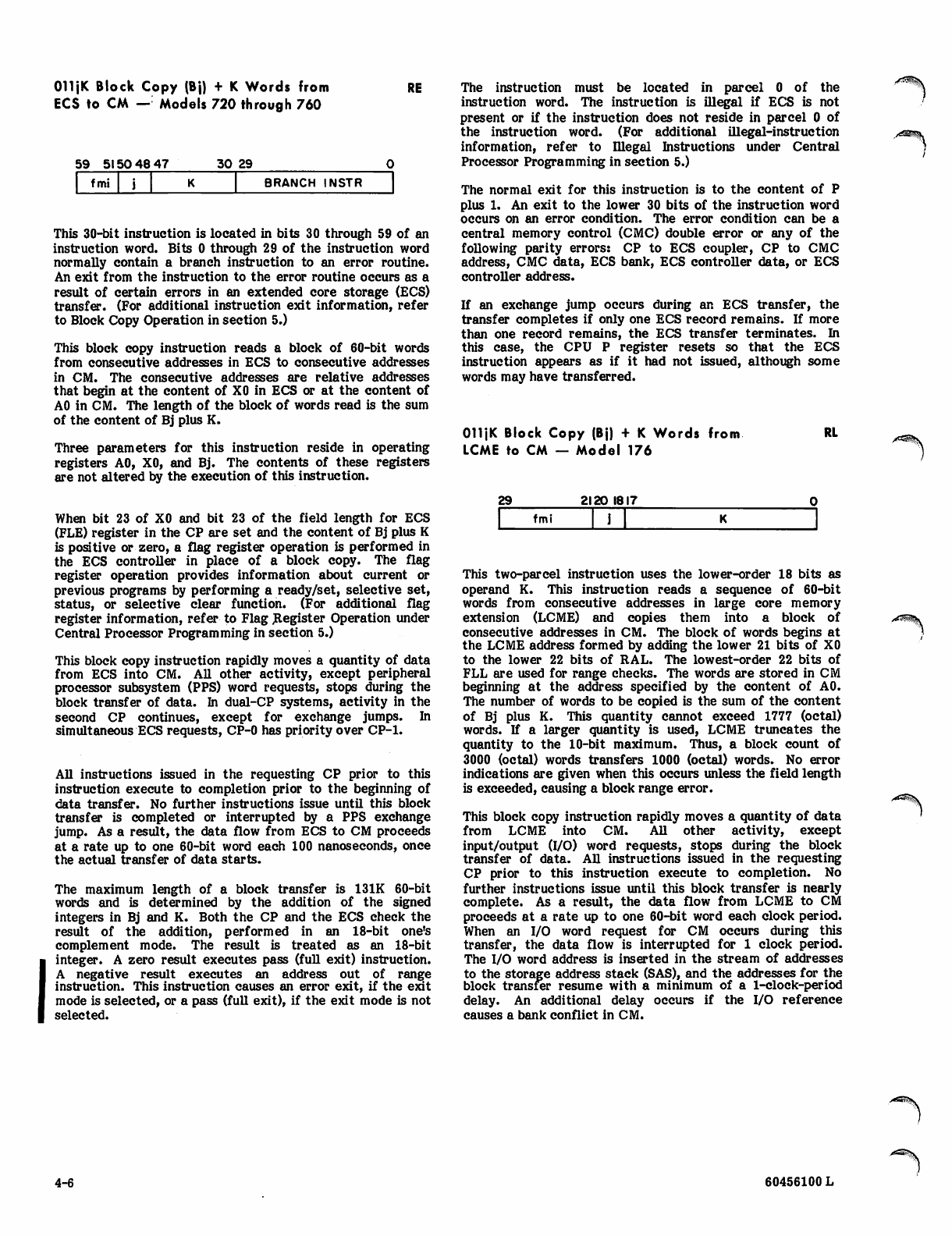
OlljK Block Copy (Bj) + K Words from
ECS to CM — Models 720 through 760
RE
59 5150 48 47 30 29
fmi BRANCH INSTR
This 30-bit instruction is located in bits 30 through 59 of an
instruction word. Bits 0 through 29 of the instruction word
normally contain a branch instruction to an error routine.
An exit from the instruction to the error routine occurs as a
result of certain errors in an extended core storage (ECS)
transfer. (For additional instruction exit information, refer
to Block Copy Operation in section 5.)
This block copy instruction reads a block of 60-bit words
from consecutive addresses in ECS to consecutive addresses
in CM. The consecutive addresses are relative addresses
that begin at the content of XO in ECS or at the content of
AO in CM. The length of the block of words read is the sum
of the content of Bj plus K.
Three parameters for this instruction reside in operating
registers AO, XO, and Bj. The contents of these registers
are not altered by the execution of this instruction.
When bit 23 of XO and bit 23 of the field length for ECS
(FLE) register in the CP are set and the content of Bj plus K
is positive or zero, a flag register operation is performed in
the ECS controller in place of a block copy. The flag
register operation provides information about current or
previous programs by performing a ready/set, selective set,
status, or selective clear function. (For additional flag
register information, refer to Flag Register Operation under
Central Processor Programming in section 5.)
This block copy instruction rapidly moves a quantity of data
from ECS into CM. All other activity, except peripheral
processor subsystem (PPS) word requests, stops during the
block transfer of data. In dual-CP systems, activity in the
second CP continues, except for exchange jumps. In
simultaneous ECS requests, CP-0 has priority over CP-1.
All instructions issued in the requesting CP prior to this
instruction execute to completion prior to the beginning of
data transfer. No further instructions issue until this block
transfer is completed or interrupted by a PPS exchange
jump. As a result, the data flow from ECS to CM proceeds
at a rate up to one 60-bit word each 100 nanoseconds, once
the actual transfer of data starts.
The maximum length of a block transfer is 131K 60-bit
words and is determined by the addition of the signed
integers in Bj and K. Both the CP and the ECS check the
result of the addition, performed in an 18-bit one's
complement mode. The result is treated as an 18-bit
integer. A zero result executes pass (full exit) instruction.
A negative result executes an address out of ran^e
instruction. This instruction causes an error exit, if the exit
mode is selected, or a pass (full exit), if the exit mode is not
selected.
The instruction must be located in parcel 0 of the
instruction word. The instruction is illegal if ECS is not
present or if the instruction does not reside in parcel 0 of
the instruction word. (For additional illegal-instruction
information, refer to Illegal Instructions under Central
Processor Programming in section 5.)
The normal exit for this instruction is to the content of P
plus 1. An exit to the lower 30 bits of the instruction word
occurs on an error condition. The error condition can be a
central memory control (CMC) double error or any of the
following parity errors: CP to ECS coupler, CP to CMC
address, CMC data, ECS bank, ECS controller data, or ECS
controller address.
If an exchange jump occurs during an ECS transfer, the
transfer completes if only one ECS record remains. If more
than one record remains, the ECS transfer terminates. In
this case, the CPU P register resets so that the ECS
instruction appears as if it had not issued, although some
words may have transferred.
OlljK Block Copy (Bj) + K Words from
LCME to CM — Model 176
RL
29 2120 1817
fmi
This two-parcel instruction uses the lower-order 18 bits as
operand K. This instruction reads a sequence of 60-bit
words from consecutive addresses in large core memory
extension (LCME) and copies them into a block of
consecutive addresses in CM. The block of words begins at
the LCME address formed by adding the lower 21 bits of XO
to the lower 22 bits of RAL. The lowest-order 22 bits of
FLL are used for range checks. The words are stored in CM
beginning at the address specified by the content of AO.
The number of words to be copied is the sum of the content
of Bj plus K. This quantity cannot exceed 1777 (octal)
words. If a larger quantity is used, LCME truncates the
quantity to the 10-bit maximum. Thus, a block count of
3000 (octal) words transfers 1000 (octal) words. No error
indications are given when this occurs unless the field length
is exceeded, causing a block range error.
This block copy instruction rapidly moves a quantity of data
from LCME into CM. All other activity, except
input/output (I/O) word requests, stops during the block
transfer of data. All instructions issued in the requesting
CP prior to this instruction execute to completion. No
further instructions issue until this block transfer is nearly
complete. As a result, the data flow from LCME to CM
proceeds at a rate up to one 60-bit word each clock period.
When an I/O word request for CM occurs during this
transfer, the data flow is interrupted for 1 clock period.
The I/O word address is inserted in the stream of addresses
to the storage address stack (SAS), and the addresses for the
block transfer resume with a minimum of a 1-clock-period
delay. An additional delay occurs if the I/O reference
causes a bank conflict in CM.
4-6 60456100 L
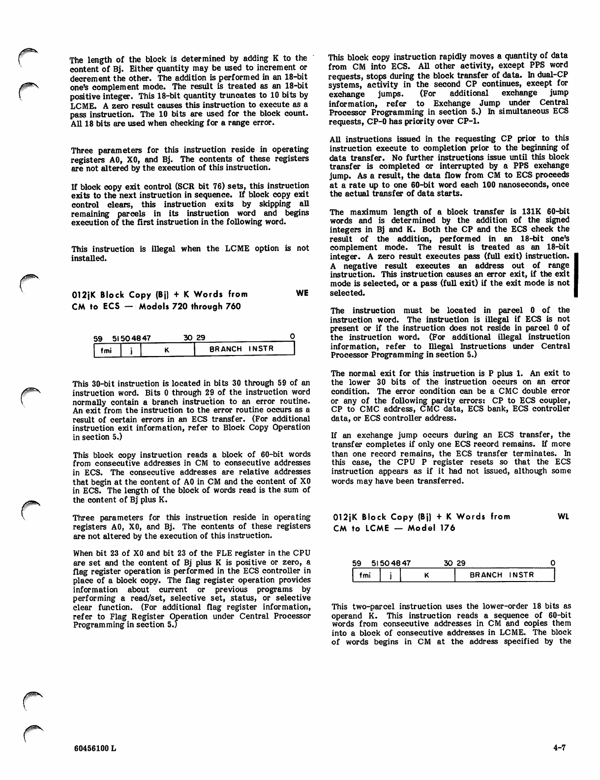
The length of the block is determined by adding K to the
content of Bj. Either quantity may be used to increment or
decrement the other. The addition is performed in an 18-bit
one's complement mode. The result is treated as an 18-bit
positive integer. This 18-bit quantity truncates to 10 bits by
LCME. A zero result causes this instruction to execute as a
pass instruction. The 10 bits are used for the block count.
All 18 bits are used when checking for a range error.
Three parameters for this instruction reside in operating
registers AO, XO, and Bj. The contents of these registers
are not altered by the execution of this instruction.
If block copy exit control (SCR bit 76) sets, this instruction
exits to the next instruction in sequence. If block copy exit
control clears, this instruction exits by skipping all
remaining parcels in its instruction word and begins
execution of the first instruction in the following word.
This instruction is illegal when the LCME option is not
installed.
012JK Block Copy (Bj) + K Words from
CM to ECS — Models 720 through 760
WE
59 51504847 30 29
fmi BRANCH INSTR
This 30-bit instruction is located in bits 30 through 59 of an
instruction word. Bits 0 through 29 of the instruction word
normally contain a branch instruction to an error routine.
An exit from the instruction to the error routine occurs as a
result of certain errors in an ECS transfer. (For additional
instruction exit information, refer to Block Copy Operation
in section 5.)
This block copy instruction reads a block of 60-bit words
from consecutive addresses in CM to consecutive addresses
in ECS. The consecutive addresses are relative addresses
that begin at the content of AO in CM and the content of XO
in ECS. The length of the block of words read is the sum of
the content of Bj plus K.
Three parameters for this instruction reside in operating
registers AO, XO, and Bj. The contents of these registers
are not altered by the execution of this instruction.
When bit 23 of XO and bit 23 of the FLE register in the CPU
are set and the content of Bj plus K is positive or zero, a
flag register operation is performed in the ECS controller in
place of a block copy. The flag register operation provides
information about current or previous programs by
performing a read/set, selective set, status, or selective
clear function. (For additional flag register information,
refer to Flag Register Operation under Central Processor
Programming in section 5.)
This block copy instruction rapidly moves a quantity of data
from CM into ECS. All other activity, except PPS word
requests, stops during the block transfer of data. In dual-CP
systems, activity in the second CP continues, except for
exchange jumps. (For additional exchange jump
information, refer to Exchange Jump under Central
Processor Programming in section 5.) In simultaneous ECS
requests, CP-0 has priority over CP-1.
All instructions issued in the requesting CP prior to this
instruction execute to completion prior to the beginning of
data transfer. No further instructions issue until this block
transfer is completed or interrupted by a PPS exchange
jump. As a result, the data flow from CM to ECS proceeds
at a rate up to one 60-bit word each 100 nanoseconds, once
the actual transfer of data starts.
The maximum length of a block transfer is 131K 60-bit
words and is determined by the addition of the signed
integers in Bj and K. Both the CP and the ECS check the
result of the addition, performed in an 18-bit one's
complement mode. The result is treated as an 18-bit
integer. A zero result executes pass (full exit) instruction.
A negative result executes an address out of range
instruction. This instruction causes an error exit, if the exit
mode is selected, or a pass (full exit) if the exit mode is not
selected.
The instruction must be located in parcel 0 of the
instruction word. The instruction is illegal if ECS is not
present or if the instruction does not reside in parcel 0 of
the instruction word. (For additional illegal instruction
information, refer to Illegal Instructions under Central
Processor Programming in section 5.)
The normal exit for this instruction is P plus 1. An exit to
the lower 30 bits of the instruction occurs on an error
condition. The error condition can be a CMC double error
or any of the following parity errors: CP to ECS coupler,
CP to CMC address, CMC data, ECS bank, ECS controller
data, or ECS controller address.
If an exchange jump occurs during an ECS transfer, the
transfer completes if only one ECS record remains. If more
than one record remains, the ECS transfer terminates. In
this case, the CPU P register resets so that the ECS
instruction appears as if it had not issued, although some
words may have been transferred.
012jK Block Copy (Bj) + K Words from
CM to LCME — Model 176
WL
59 51504847 30 29
fmi BRANCH INSTR
This two-parcel instruction uses the lower-order 18 bits as
operand K. This instruction reads a sequence of 60-bit
words from consecutive addresses in CM and copies them
into a block of consecutive addresses in LCME. The block
of words begins in CM at the address specified by the
60456100 L 4-7
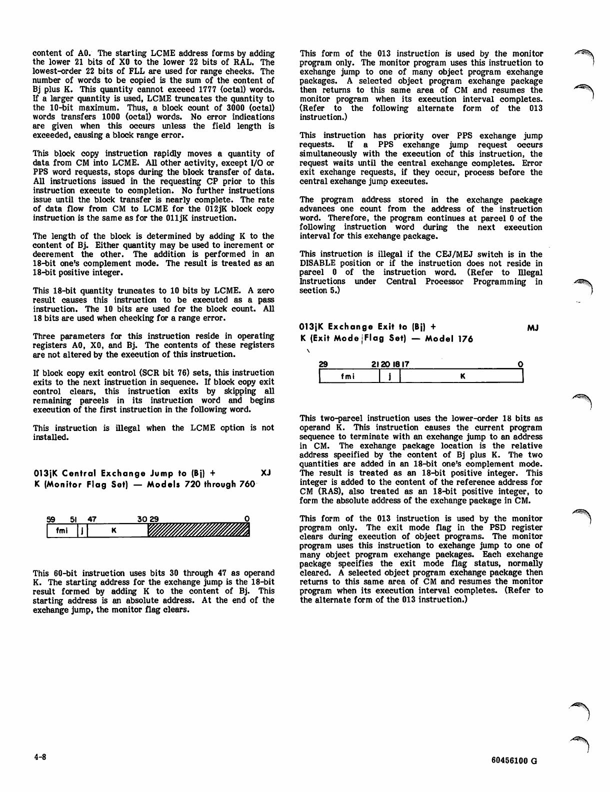
content of AO. The starting LCME address forms by adding
the lower 21 bits of XO to the lower 22 bits of RAL. The
lowest-order 22 bits of FLL are used for range checks. The
number of words to be copied is the sum of the content of
Bj plus K. This quantity cannot exceed 1777 (octal) words.
If a larger quantity is used, LCME truncates the quantity to
the 10-bit maximum. Thus, a block count of 3000 (octal)
words transfers 1000 (octal) words. No error indications
are given when this occurs unless the field length is
exceeded, causing a block range error.
This block copy instruction rapidly moves a quantity of
data from CM into LCME. All other activity, except I/O or
PPS word requests, stops during the block transfer of data.
All instructions issued in the requesting CP prior to this
instruction execute to completion. No further instructions
issue until the block transfer is nearly complete. The rate
of data flow from CM to LCME for the 012JK block copy
instruction is the same as for the OlljK instruction.
The length of the block is determined by adding K to the
content of Bj. Either quantity may be used to increment or
decrement the other. The addition is performed in an
18-bit one's complement mode. The result is treated as an
18-bit positive integer.
This 18-bit quantity truncates to 10 bits by LCME. A zero
result causes this instruction to be executed as a pass
instruction. The 10 bits are used for the block count. All
18 bits are used when checking for a range error.
Three parameters for this instruction reside in operating
registers A0, X0, and Bj. The contents of these registers
are not altered by the execution of this instruction.
If block copy exit control (SCR bit 76) sets, this instruction
exits to the next instruction in sequence. If block copy exit
control clears, this instruction exits by skipping all
remaining parcels in its instruction word and begins
execution of the first instruction in the following word.
This instruction is illegal when the LCME option is not
installed.
013JK Central Exchange Jump to (Bj) + XJ
K (Monitor Flag Set) — Models 720 through 760
This 60-bit instruction uses bits 30 through 47 as operand
K. The starting address for the exchange jump is the 18-bit
result formed by adding K to the content of Bj. This
starting address is an absolute address. At the end of the
exchange jump, the monitor flag clears.
This form of the 013 instruction is used by the monitor
program only. The monitor program uses this instruction to
exchange jump to one of many object program exchange
packages. A selected object program exchange package
then returns to this same area of CM and resumes the
monitor program when its execution interval completes.
(Refer to the following alternate form of the 013
instruction.)
This instruction has priority over PPS exchange jump
requests. If a PPS exchange jump request occurs
simultaneously with the execution of this instruction, the
request waits until the central exchange completes. Error
exit exchange requests, if they occur, process before the
central exchange jump executes.
The program address stored in the exchange package
advances one count from the address of the instruction
word. Therefore, the program continues at parcel 0 of the
following instruction word during the next execution
interval for this exchange package.
This instruction is illegal if the CEJ/MEJ switch is in the
DISABLE position or if the instruction does not reside in
parcel 0 of the instruction word. (Refer to Illegal
Instructions under Central Processor Programming in
section 5.)
013JK Exchange Exit to (Bj) +
K (Exit ModejFlag Set) — Model 176
MJ
29 2120 1817
fmi
This two-parcel instruction uses the lower-order 18 bits as
operand K. This instruction causes the current program
sequence to terminate with an exchange jump to an address
in CM. The exchange package location is the relative
address specified by the content of Bj plus K. The two
quantities are added in an 18-bit one's complement mode.
The result is treated as an 18-bit positive integer. This
integer is added to the content of the reference address for
CM (RAS), also treated as an 18-bit positive integer, to
form the absolute address of the exchange package in CM.
This form of the 013 instruction is used by the monitor
program only. The exit mode flag in the PSD register
clears during execution of object programs. The monitor
program uses this instruction to exchange jump to one of
many object program exchange packages. Each exchange
package specifies the exit mode flag status, normally
cleared. A selected object program exchange package then
returns to this same area of CM and resumes the monitor
program when its execution interval completes. (Refer to
the alternate form of the 013 instruction.)
4-8 60456100 G
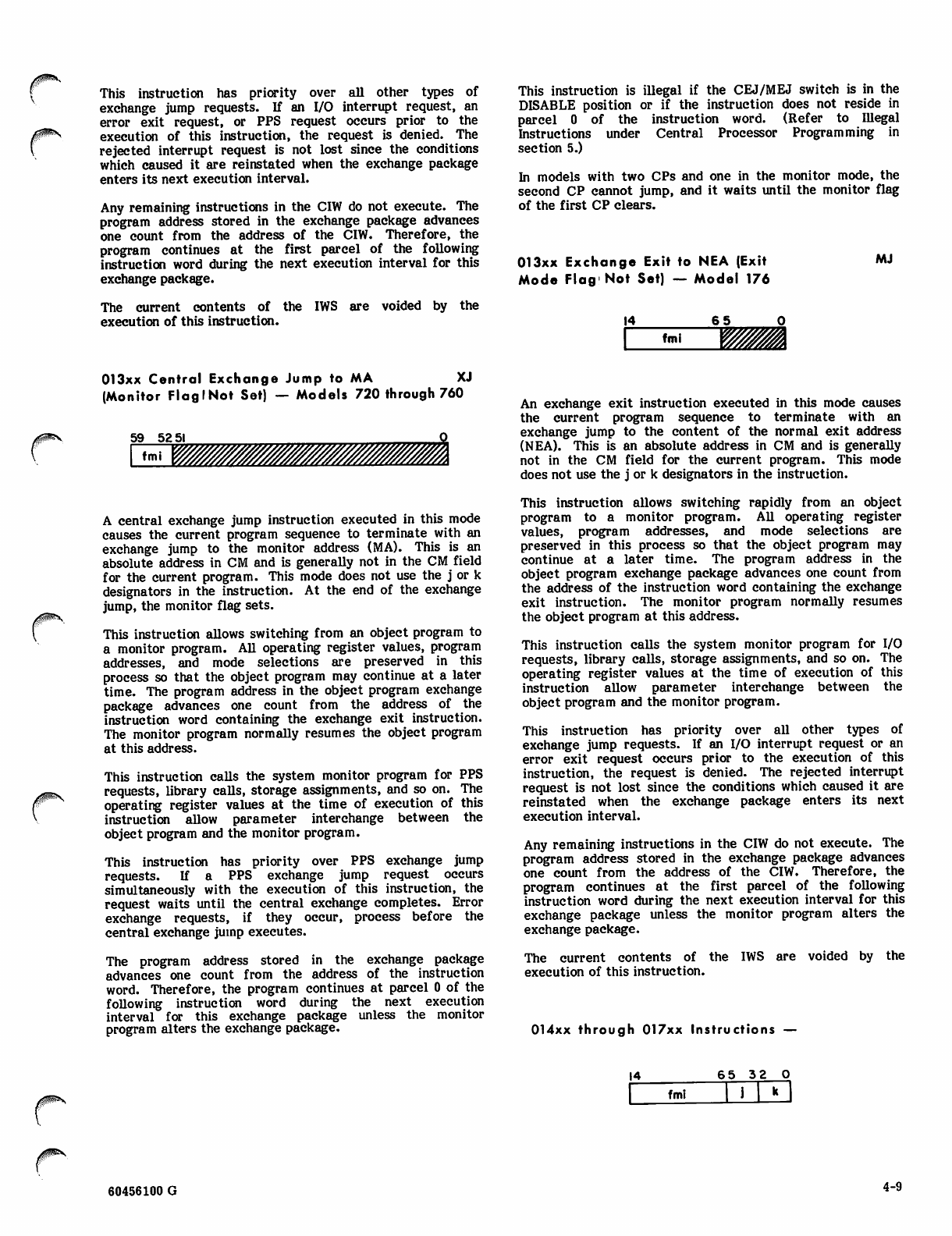
This instruction has priority over all other types of
exchange jump requests. If an I/O interrupt request, an
error exit request, or PPS request occurs prior to the
execution of this instruction, the request is denied. The
rejected interrupt request is not lost since the conditions
which caused it are reinstated when the exchange package
enters its next execution interval.
Any remaining instructions in the CIW do not execute. The
program address stored in the exchange package advances
one count from the address of the CIW. Therefore, the
program continues at the first parcel of the following
instruction word during the next execution interval for this
exchange package.
The current contents of the IWS are voided by the
execution of this instruction.
This instruction is illegal if the CEJ/MEJ switch is in the
DISABLE position or if the instruction does not reside in
parcel 0 of the instruction word. (Refer to Illegal
Instructions under Central Processor Programming in
section 5.)
In models with two CPs and one in the monitor mode, the
second CP cannot jump, and it waits until the monitor flag
of the first CP clears.
013xx Exchange Exit to NEA (Exit
Mode Flag N o t S et) — Model 1 7 6
MJ
013xx Central Exchange Jump to MA XJ
(Monitor Flag I Not Set) — Models 720 through 760
59 52 51
A central exchange jump instruction executed in this mode
causes the current program sequence to terminate with an
exchange jump to the monitor address (MA). This is an
absolute address in CM and is generally not in the CM field
for the current program. This mode does not use the j or k
designators in the instruction. At the end of the exchange
jump, the monitor flag sets.
This instruction allows switching from an object program to
a monitor program. All operating register values, program
addresses, and mode selections are preserved in this
process so that the object program may continue at a later
time. The program address in the object program exchange
package advances one count from the address of the
instruction word containing the exchange exit instruction.
The monitor program normally resumes the object program
at this address.
This instruction calls the system monitor program for PPS
requests, library calls, storage assignments, and so on. The
operating register values at the time of execution of this
instruction allow parameter interchange between the
object program and the monitor program.
This instruction has priority over PPS exchange jump
requests. If a PPS exchange jump request occurs
simultaneously with the execution of this instruction, the
request waits until the central exchange completes. Error
exchange requests, if they occur, process before the
central exchange jump executes.
The program address stored in the exchange package
advances one count from the address of the instruction
word. Therefore, the program continues at parcel 0 of the
following instruction word during the next execution
interval for this exchange package unless the monitor
program alters the exchange package.
An exchange exit instruction executed in this mode causes
the current program sequence to terminate with an
exchange jump to the content of the normal exit address
(NEA). This is an absolute address in CM and is generally
not in the CM field for the current program. This mode
does not use the j or k designators in the instruction.
This instruction allows switching rapidly from an object
program to a monitor program. All operating register
values, program addresses, and mode selections are
preserved in this process so that the object program may
continue at a later time. The program address in the
object program exchange package advances one count from
the address of the instruction word containing the exchange
exit instruction. The monitor program normally resumes
the object program at this address.
This instruction calls the system monitor program for I/O
requests, library calls, storage assignments, and so on. The
operating register values at the time of execution of this
instruction allow parameter interchange between the
object program and the monitor program.
This instruction has priority over all other types of
exchange jump requests. If an I/O interrupt request or an
error exit request occurs prior to the execution of this
instruction, the request is denied. The rejected interrupt
request is not lost since the conditions which caused it are
reinstated when the exchange package enters its next
execution interval.
Any remaining instructions in the CIW do not execute. The
program address stored in the exchange package advances
one count from the address of the CIW. Therefore, the
program continues at the first parcel of the following
instruction word during the next execution interval for this
exchange package unless the monitor program alters the
exchange package.
The current contents of the IWS are voided by the
execution of this instruction.
014xx through 017xx Instructions —
1 4 6 5 3 2 0
fmi
60456100 G 4-9
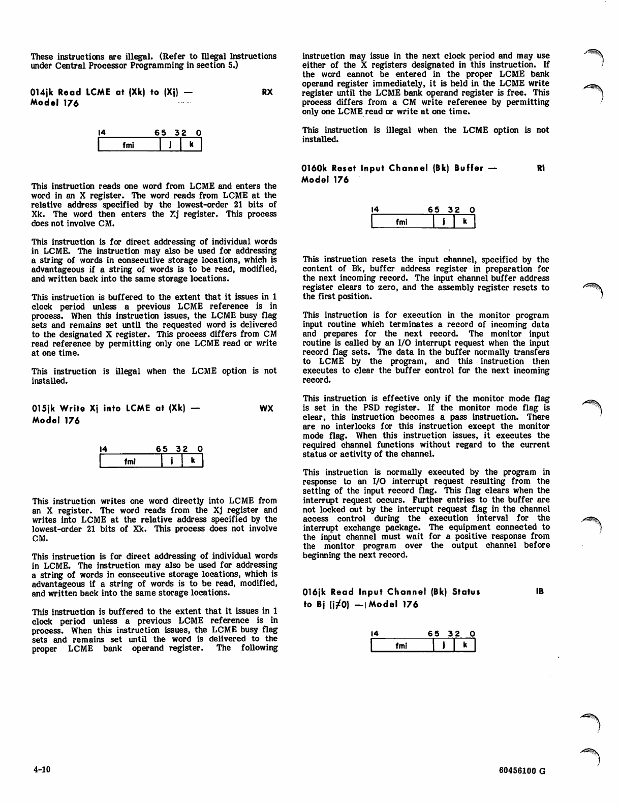
These instructions are illegal. (Refer to Illegal Instructions
under Central Processor Programming in section 5.)
OUjk Read LCME at (Xk) to (Xj) —
Model 176
RX
14 65 32 0
fmi
instruction may issue in the next clock period and may use
either of the X registers designated in this instruction. If
the word cannot be entered in the proper LCME bank
operand register immediately, it is held in the LCME write
register until the LCME bank operand register is free. This
process differs from a CM write reference by permitting
only one LCME read or write at one time.
This instruction is illegal when the LCME option is not
installed.
This instruction reads one word from LCME and enters the
word in an X register. The word reads from LCME at the
relative address specified by the lowest-order 21 bits of
Xk. The word then enters the Xj register. This process
does not involve CM.
This instruction is for direct addressing of individual words
in LCME. The instruction may also be used for addressing
a string of words in consecutive storage locations, which is
advantageous if a string of words is to be read, modified,
and written back into the same storage locations.
This instruction is buffered to the extent that it issues in 1
clock period unless a previous LCME reference is in
process. When this instruction issues, the LCME busy flag
sets and remains set until the requested word is delivered
to the designated X register. This process differs from CM
read reference by permitting only one LCME read or write
at one time.
This instruction is illegal when the LCME option is not
installed.
015jk Write Xj into LCME at (Xk) —
Model 176
WX
14 65 32 0
fmi
This instruction writes one word directly into LCME from
an X register. The word reads from the Xj register and
writes into LCME at the relative address specified by the
lowest-order 21 bits of Xk. This process does not involve
CM.
This instruction is for direct addressing of individual words
in LCME. The instruction may also be used for addressing
a string of words in consecutive storage locations, which is
advantageous if a string of words is to be read, modified,
and written back into the same storage locations.
This instruction is buffered to the extent that it issues in 1
clock period unless a previous LCME reference is in
process. When this instruction issues, the LCME busy flag
sets and remains set until the word is delivered to the
proper LCME bank operand register. The following
0160k Reset Input Channel (Bk) Buffer —
Model 176
Rl
14 6 5 3 2 0
fmi
This instruction resets the input channel, specified by the
content of Bk, buffer address register in preparation for
the next incoming record. The input channel buffer address
register clears to zero, and the assembly register resets to
the first position.
This instruction is for execution in the monitor program
input routine which terminates a record of incoming data
and prepares for the next record. The monitor input
routine is called by an I/O interrupt request when the input
record flag sets. The data in the buffer normally transfers
to LCME by the program, and this instruction then
executes to clear the buffer control for the next incoming
record.
This instruction is effective only if the monitor mode flag
is set in the PSD register. If the monitor mode flag is
clear, this instruction becomes a pass instruction. There
are no interlocks for this instruction except the monitor
mode flag. When this instruction issues, it executes the
required channel functions without regard to the current
status or activity of the channel.
This instruction is normally executed by the program in
response to an I/O interrupt request resulting from the
setting of the input record flag. This flag clears when the
interrupt request occurs. Further entries to the buffer are
not locked out by the interrupt request flag in the channel
access control during the execution interval for the
interrupt exchange package. The equipment connected to
the input channel must wait for a positive response from
the monitor program over the output channel before
beginning the next record.
016jk Read Input Channel (Bk) Status
to Bj (j/0) —| Model 176
IB
14 65 32 0
fmi
4-10 60456100 G
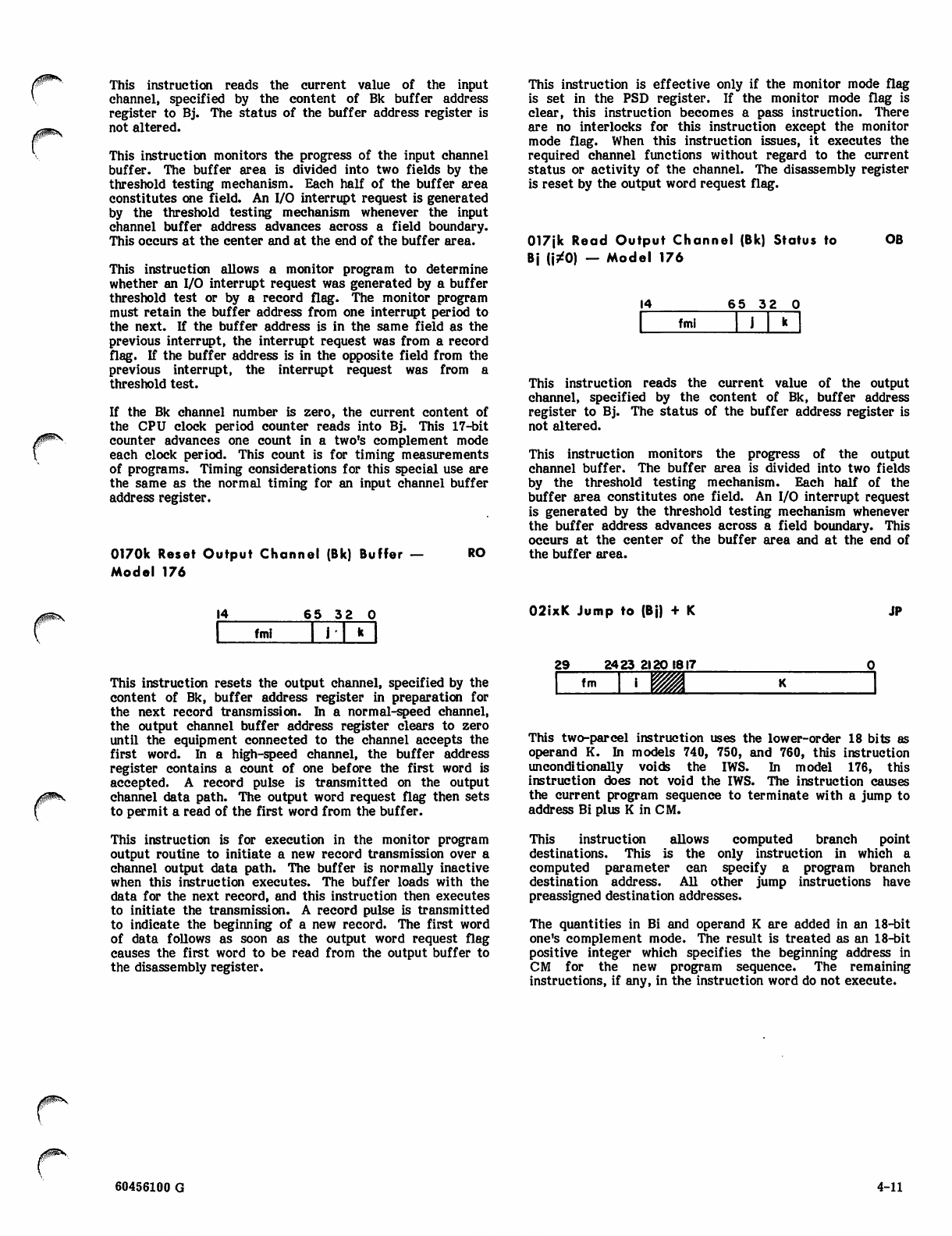
/KS*Vi
This instruction reads the current value of the input
channel, specified by the content of Bk buffer address
register to Bj. The status of the buffer address register is
not altered.
This instruction monitors the progress of the input channel
buffer. The buffer area is divided into two fields by the
threshold testing mechanism. Each half of the buffer area
constitutes one field. An I/O interrupt request is generated
by the threshold testing mechanism whenever the input
channel buffer address advances across a field boundary.
This occurs at the center and at the end of the buffer area.
This instruction allows a monitor program to determine
whether an I/O interrupt request was generated by a buffer
threshold test or by a record flag. The monitor program
must retain the buffer address from one interrupt period to
the next. If the buffer address is in the same field as the
previous interrupt, the interrupt request was from a record
flag. If the buffer address is in the opposite field from the
previous interrupt, the interrupt request was from a
threshold test.
If the Bk channel number is zero, the current content of
the CPU clock period counter reads into Bj. This 17-bit
counter advances one count in a two's complement mode
each clock period. This count is for timing measurements
of programs. Timing considerations for this special use are
the same as the normal timing for an input channel buffer
address register.
0170k Reset Output Channel (Bk) Buffer — RO
Model 176
This instruction is effective only if the monitor mode flag
is set in the PSD register. If the monitor mode flag is
clear, this instruction becomes a pass instruction. There
are no interlocks for this instruction except the monitor
mode flag. When this instruction issues, it executes the
required channel functions without regard to the current
status or activity of the channel. The disassembly register
is reset by the output word request flag.
017j k Read Outpu t Chan nel (Bk) Sta tus to
Bj (j*0) — Model 176
OB
14 6 5 3 2 0
fmi
This instruction reads the current value of the output
channel, specified by the content of Bk, buffer address
register to Bj. The status of the buffer address register is
not altered.
This instruction monitors the progress of the output
channel buffer. The buffer area is divided into two fields
by the threshold testing mechanism. Each half of the
buffer area constitutes one field. An I/O interrupt request
is generated by the threshold testing mechanism whenever
the buffer address advances across a field boundary. This
occurs at the center of the buffer area and at the end of
the buffer area.
0^*\
14 6 5 3 2 0
fmi
02ixK Jump to (Bj) -I- K JP
29 2423 2120 1817
This instruction resets the output channel, specified by the
content of Bk, buffer address register in preparation for
the next record transmission. In a normal-speed channel,
the output channel buffer address register clears to zero
until the equipment connected to the channel accepts the
first word. In a high-speed channel, the buffer address
register contains a count of one before the first word is
accepted. A record pulse is transmitted on the output
channel data path. The output word request flag then sets
to permit a read of the first word from the buffer.
This instruction is for execution in the monitor program
output routine to initiate a new record transmission over a
channel output data path. The buffer is normally inactive
when this instruction executes. The buffer loads with the
data for the next record, and this instruction then executes
to initiate the transmission. A record pulse is transmitted
to indicate the beginning of a new record. The first word
of data follows as soon as the output word request flag
causes the first word to be read from the output buffer to
the disassembly register.
f m I I W % f a *
This two-parcel instruction uses the lower-order 18 bits as
operand K. In models 740, 750, and 760, this instruction
unconditionally voids the IWS. In model 176, this
instruction does not void the IWS. The instruction causes
the current program sequence to terminate with a jump to
address Bi plus K in CM.
This instruction allows computed branch point
destinations. This is the only instruction in which a
computed parameter can specify a program branch
destination address. All other jump instructions have
preassigned destination addresses.
The quantities in Bi and operand K are added in an 18-bit
one's complement mode. The result is treated as an 18-bit
positive integer which specifies the beginning address in
CM for the new program sequence. The remaining
instructions, if any, in the instruction word do not execute.
60456100 G 4-11
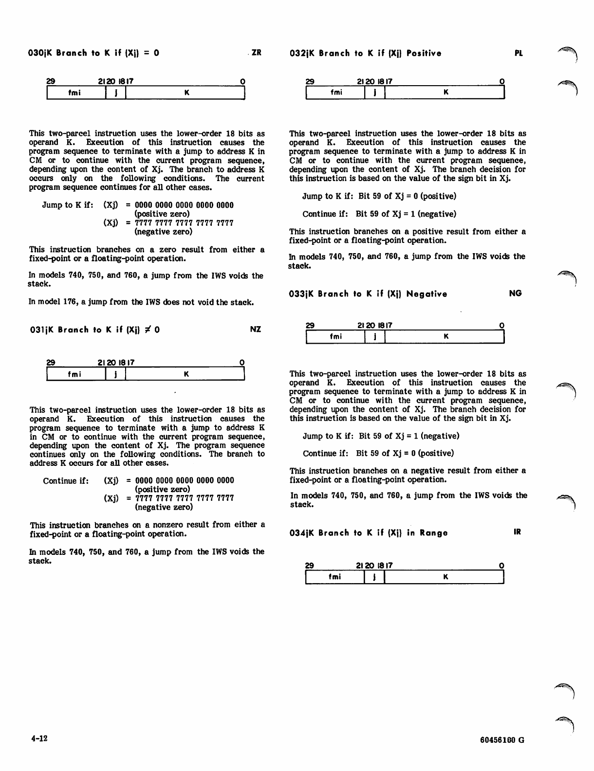
030JK Branch to K if (Xj) = 0 ZR 032jK Branch to K if (Xj) Positive PI
29 2120 1817
fmi
29 2120 1817
fmi
This two-parcel instruction uses the lower-order 18 bits as
operand K. Execution of this instruction causes the
program sequence to terminate with a jump to address K in
CM or to continue with the current program sequence,
depending upon the content of Xj. The branch to address K
occurs only on the following conditions. The current
program sequence continues for all other cases.
Jump to K if: (Xj) = OOOO OOOO OOOO OOOO OOOO
(positive zero)
(Xj) = 7777 7777 7777 7777 7777
(negative zero)
This instruction branches on a zero result from either a
fixed-point or a floating-point operation.
In models 740, 750, and 760, a jump from the IWS voids the
stack.
In model 176, a jump from the IWS does not void the stack.
This two-parcel instruction uses the lower-order 18 bits as
operand K. Execution of this instruction causes the
program sequence to terminate with a jump to address K in
CM or to continue with the current program sequence,
depending upon the content of Xj. The branch decision for
this instruction is based on the value of the sign bit in Xj.
Jump to K if: Bit 59 of Xj = 0 (positive)
Continue if: Bit 59 of Xj = 1 (negative)
This instruction branches on a positive result from either a
fixed-point or a floating-point operation.
In models 740, 750, and 760, a jump from the IWS voids the
stack.
033JK Branch to K if (Xj) Negative NG
031JK Branch to K if (Xj) / 0 NZ 29 2120 1817
fmi
29 2120 1817
fmi
This two-parcel instruction uses the lower-order 18 bits as
operand K. Execution of this instruction causes the
program sequence to terminate with a jump to address K
in CM or to continue with the current program sequence,
depending upon the content of Xj. The program sequence
continues only on the following conditions. The branch to
address K occurs for all other cases.
Continue if: (Xj) = 0000 0000 0000 0000 0000
(positive zero)
(Xj) = 7777 7777 7777 7777 7777
(negative zero)
This instruction branches on a nonzero result from either a
fixed-point or a floating-point operation.
In models 740, 750, and 760, a jump from the IWS voids the
stack.
This two-parcel instruction uses the lower-order 18 bits as
operand K. Execution of this instruction causes the
program sequence to terminate with a jump to address K in
CM or to continue with the current program sequence,
depending upon the content of Xj. The branch decision for
this instruction is based on the value of the sign bit in Xj.
Jump to K if: Bit 59 of Xj = 1 (negative)
Continue if: Bit 59 of Xj = 0 (positive)
This instruction branches on a negative result from either a
fixed-point or a floating-point operation.
In models 740, 750, and 760, a jump from the IWS voids the
stack.
034JK Branch to K if (Xj) in Range IR
29 2120 1817
fmi
4-12 60456100 G
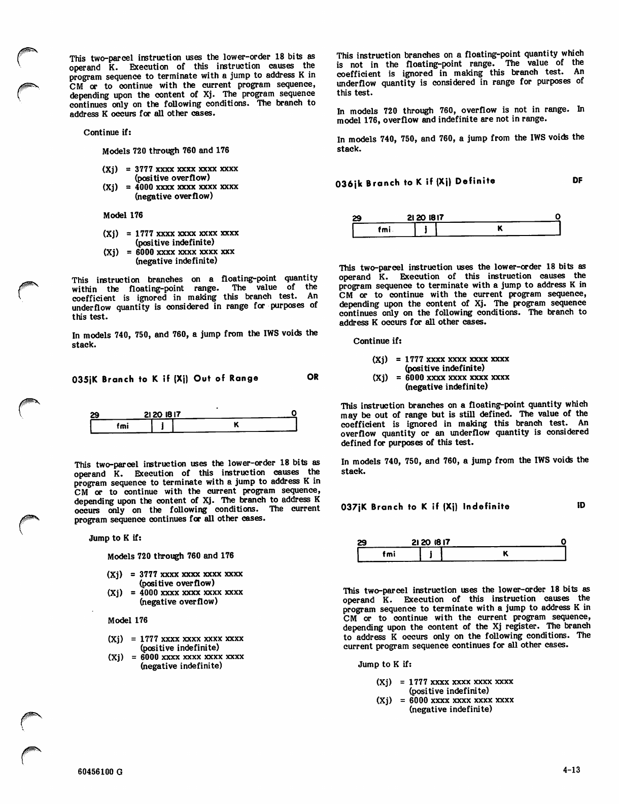
This two-parcel instruction uses the lower-order 18 bits as
operand K. Execution of this instruction causes the
program sequence to terminate with a jump to address K in
CM or to continue with the current program sequence,
depending upon the content of Xj. The program sequence
continues only on the following conditions. The branch to
address K occurs for all other cases.
Continue if:
Models 720 through 760 and 176
(Xj) = 3777 xxxx xxxx xxxx xxxx
(positive overflow)
(Xj) = 4000 xxxx xxxx xxxx xxxx
(negative overflow)
Model 176
(Xj) = 1777 xxxx xxxx xxxx xxxx
(positive indefinite)
(Xj) = 6000 xxxx xxxx xxxx xxx
(negative indefinite)
This instruction branches on a floating-point quantity
within the floating-point range. The value of the
coefficient is ignored in making this branch test. An
underflow quantity is considered in range for purposes of
this test.
In models 740, 750, and 760, a jump from the IWS voids the
stack.
035JK Branch to K if (Xj) Out of Range OR
z^^X
29 2120 1817
fmi
This two-parcel instruction uses the lower-order 18 bits as
operand K. Execution of this instruction causes the
program sequence to terminate with a jump to address K in
CM or to continue with the current program sequence,
depending upon the content of Xj. The branch to address K
occurs only on the following conditions. The current
program sequence continues for all other cases.
Jump to K if:
Models 720 through 760 and 176
(Xj) = 3777 xxxx xxxx xxxx xxxx
(positive overflow)
(Xj) = 4000 xxxx xxxx xxxx xxxx
(negative overflow)
Model 176
(Xj) =1777 xxxx xxxx xxxx xxxx
(positive indefinite)
(Xj) = 6000 xxxx xxxx xxxx xxxx
(negative indefinite)
This instruction branches on a floating-point quantity which
is not in the floating-point range. The value of the
coefficient is ignored in making this branch test. An
underflow quantity is considered in range for purposes of
this test.
In models 720 through 760, overflow is not in range. In
model 176, overflow and indefinite are not in range.
In models 740, 750, and 760, a jump from the IWS voids the
stack.
036jk Branch to K if (Xj) Definite DF
29 2120 1817
fmi
This two-parcel instruction uses the lower-order 18 bits as
operand K. Execution of this instruction causes the
program sequence to terminate with a jump to address K in
CM or to continue with the current program sequence,
depending upon the content of Xj. The program sequence
continues only on the following conditions. The branch to
address K occurs for all other cases.
Continue if:
(Xj) = 1777 xxxx xxxx xxxx xxxx
(positive indefinite)
(Xj) = 6000 xxxx xxxx xxxx xxxx
(negative indefinite)
This instruction branches on a floating-point quantity which
may be out of range but is still defined. The value of the
coefficient is ignored in making this branch test. An
overflow quantity or an underflow quantity is considered
defined for purposes of this test.
In models 740, 750, and 760, a jump from the IWS voids the
stack.
037JK Branch to K if (Xj) Indefinite ID
29 21 20 1817
fmi
Ttiis two-parcel instruction uses the lower-order 18 bits as
operand K. Execution of this instruction causes the
program sequence to terminate with a jump to address K in
CM or to continue with the current program sequence,
depending upon the content of the Xj register. The branch
to address K occurs only on the following conditions. The
current program sequence continues for all other cases.
Jump to K if:
(Xj)
(Xj)
1777 xxxx xxxx xxxx xxxx
(positive indefinite)
6000 xxxx xxxx xxxx xxxx
(negative indefinite)
60456100 G 4-13
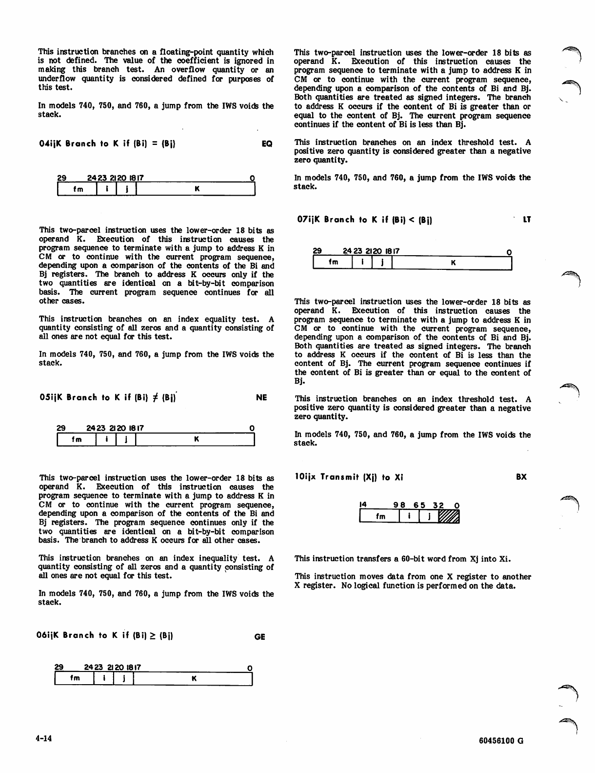
This instruction branches on a floating-point quantity which
is not defined. The value of the coefficient is ignored in
making this branch test. An overflow quantity or an
underflow quantity is considered defined for purposes of
this test.
In models 740, 750, and 760, a jump from the IWS voids the
stack.
04IJK Branch to K if (Bi) = (Bj) EQ
29 2423 2120 1817
fm
This two-parcel instruction uses the lower-order 18 bits as
operand K. Execution of this instruction causes the
program sequence to terminate with a jump to address K in
CM or to continue with the current program sequence,
depending upon a comparison of the contents of Bi and Bj.
Both quantities are treated as signed integers. The branch
to address K occurs if the content of Bi is greater than or
equal to the content of Bj. The current program sequence
continues if the content of Bi is less than Bj.
This instruction branches on an index threshold test. A
positive zero quantity is considered greater than a negative
zero quantity.
In models 740, 750, and 760, a jump from the IWS voids the
stack.
-^
This two-parcel instruction uses the lower-order 18 bits as
operand K. Execution of this instruction causes the
program sequence to terminate with a jump to address K in
CM or to continue with the current program sequence,
depending upon a comparison of the contents of the Bi and
Bj registers. The branch to address K occurs only if the
two quantities are identical on a bit-by-bit comparison
basis. The current program sequence continues for all
other cases.
This instruction branches on an index equality test. A
quantity consisting of all zeros and a quantity consisting of
all ones are not equal for this test.
In models 740, 750, and 760, a jump from the IWS voids the
stack.
07ijK Branch to K if (Bi) < (Bj) LT
05ijK Branch to K if (Bi) f (Bj)
29 2423 2120 1817
NE
29 24 23 2120 1817
fm
fm
This two-parcel instruction uses the lower-order 18 bits as
operand K. Execution of this instruction causes the
program sequence to terminate with a jump to address K in
CM or to continue with the current program sequence,
depending upon a comparison of the contents of Bi and Bj.
Both quantities are treated as signed integers. The branch
to address K occurs if the content of Bi is less than the
content of Bj. The current program sequence continues if
the content of Bi is greater than or equal to the content of
Bj.
This instruction branches on an index threshold test. A
positive zero quantity is considered greater than a negative
zero quantity.
In models 740, 750, and 760, a jump from the IWS voids the
stack.
This two-parcel instruction uses the lower-order 18 bits as
operand K. Execution of this instruction causes the
program sequence to terminate with a jump to address K in
CM or to continue with the current program sequence,
depending upon a comparison of the contents of the Bi and
Bj registers. The program sequence continues only if the
two quantities are identical on a bit-by-bit comparison
basis. The branch to address K occurs for all other cases.
lOijx Transmit (Xj) to Xi BX
This instruction branches on an index inequality test. A
quantity consisting of all zeros and a quantity consisting of
all ones are not equal for this test.
In models 740, 750, and 760, a jump from the IWS voids the
stack.
This instruction transfers a 60-bit word from Xj into Xi.
This instruction moves data from one X register to another
X register. No logical function is performed on the data.
06ijK Branch to K if (Bi) > (Bj) GE
29 2423 2120 1817
fm
,^S&?v
4-14 60456100 G
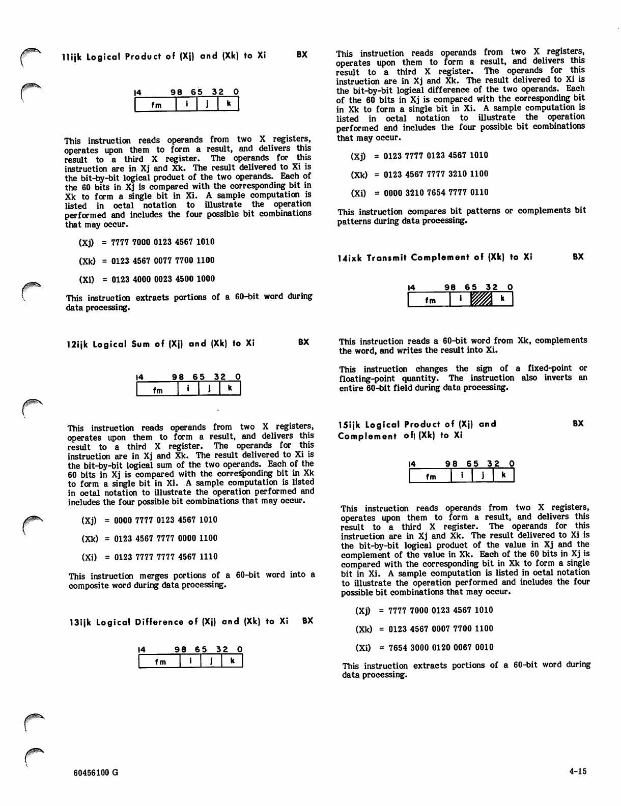
i#^V
llijk Logical Product of (Xj) and (Xk) to Xi BX
1 4 9 8 6 5 3 2 0
fm
This instruction reads operands from two X registers,
operates upon them to form a result, and delivers this
result to a third X register. The operands for this
instruction are in Xj and Xk. The result delivered to Xi is
the bit-by-bit logical product of the two operands. Each of
the 60 bits in Xj is compared with the corresponding bit in
Xk to form a single bit in Xi. A sample computation is
listed in octal notation to illustrate the operation
performed and includes the four possible bit combinations
that may occur.
(Xj) = 7777 7000 0123 4567 1010
(Xk) = 0123 4567 0077 7700 1100
(Xi) = 0123 4000 0023 4500 1000
This instruction extracts portions of a 60-bit word during
data processing.
This instruction reads operands from two X registers,
operates upon them to form a result, and delivers this
result to a third X register. The operands for this
instruction are in Xj and Xk. The result delivered to Xi is
the bit-by-bit logical difference of the two operands. Each
of the 60 bits in Xj is compared with the corresponding bit
in Xk to form a single bit in Xi. A sample computation is
listed in octal notation to illustrate the operation
performed and includes the four possible bit combinations
that may occur.
(Xj) = 0123 7777 0123 4567 1010
(Xk) = 0123 4567 7777 3210 1100
(Xi) = 0000 3210 7654 7777 0110
This instruction compares bit patterns or complements bit
patterns during data processing.
14i xk Transmit C omplement of (Xk) to Xi BX
14 98 65 32 O
f m j
12ijk Logical Sum of (Xj) and (Xk) to Xi
14 9865320
fm
BX This instruction reads a 60-bit word from Xk, complements
the word, and writes the result into Xi.
This instruction changes the sign of a fixed-point or
floating-point quantity. The instruction also inverts an
entire 60-bit field during data processing.
This instruction reads operands from two X registers,
operates upon them to form a result, and delivers this
result to a third X register. The operands for this
instruction are in Xj and Xk. The result delivered to Xi is
the bit-by-bit logical sum of the two operands. Each of the
60 bits in Xj is compared with the corresponding bit in Xk
to form a single bit in Xi. A sample computation is listed
in octal notation to illustrate the operation performed and
includes the four possible bit combinations that may occur.
(Xj) = 0000 7777 0123 4567 1010
(Xk) = 0123 4567 7777 0000 1100
(Xi) = 0123 7777 7777 4567 1110
This instruction merges portions of a 60-bit word into a
composite word during data processing.
13ijk Logical Difference of (Xj) and (Xk) to Xi BX
14 98 65 32 O
fm
15ijk L ogical P roduct o f (Xj) and
Complement of) (Xk) to Xi
BX
14 9 8 6 5 3 2 0
fm
This instruction reads operands from two X registers,
operates upon them to form a result, and delivers this
result to a third X register. The operands for this
instruction are in Xj and Xk. The result delivered to Xi is
the bit-by-bit logical product of the value in Xj and the
complement of the value in Xk. Each of the 60 bits in Xj is
compared with the corresponding bit in Xk to form a single
bit in Xi. A sample computation is listed in octal notation
to illustrate the operation performed and includes the four
possible bit combinations that may occur.
(Xj) = 7777 7000 0123 4567 1010
(Xk) = 0123 4567 0007 7700 1100
(Xi) = 7654 3000 0120 0067 0010
This instruction extracts portions of a 60-bit word during
data processing.
60456100 G 4-15
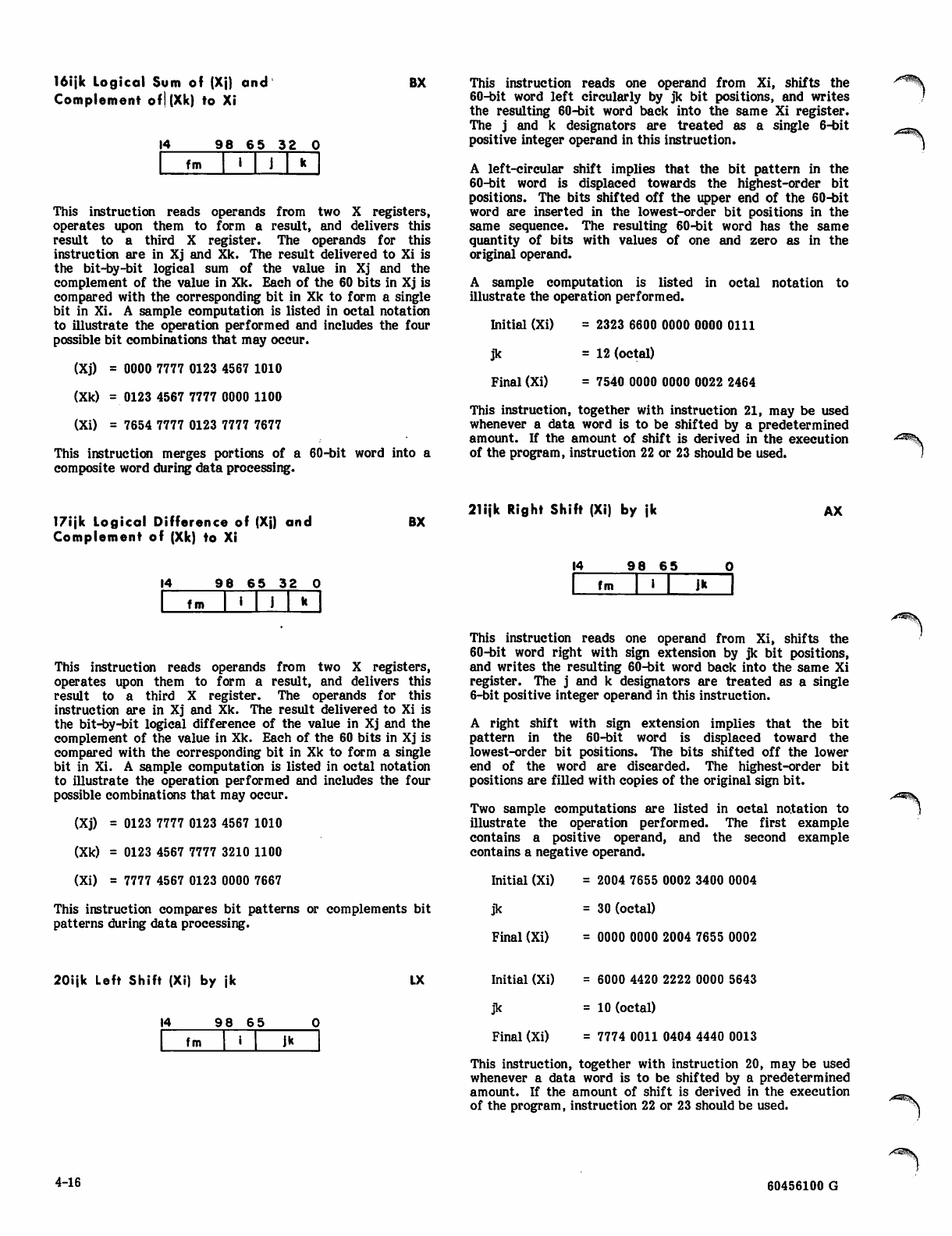
16ijk Logical Sum of (Xj) and
Complement ofj(Xk) to Xi
BX
14 98 65 3 2 0
fm
This instruction reads operands from two X registers,
operates upon them to form a result, and delivers this
result to a third X register. The operands for this
instruction are in Xj and Xk. The result delivered to Xi is
the bit-by-bit logical sum of the value in Xj and the
complement of the value in Xk. Each of the 60 bits in Xj is
compared with the corresponding bit in Xk to form a single
bit in Xi. A sample computation is listed in octal notation
to illustrate the operation performed and includes the four
possible bit combinations that may occur.
(Xj) = 0000 7777 0123 4567 1010
(Xk) =0123 4567 7777 0000 1100
(Xi) = 7654 7777 0123 7777 7677
This instruction merges portions of a 60-bit word into a
composite word during data processing.
This instruction reads one operand from Xi, shifts the
60-bit word left circularly by jk bit positions, and writes
the resulting 60-bit word back into the same Xi register.
The j and k designators are treated as a single 6-bit
positive integer operand in this instruction.
A left-circular shift implies that the bit pattern in the
60-bit word is displaced towards the highest-order bit
positions. The bits shifted off the upper end of the 60-bit
word are inserted in the lowest-order bit positions in the
same sequence. The resulting 60-bit word has the same
quantity of bits with values of one and zero as in the
original operand.
A sample computation is listed in octal notation
illustrate the operation performed. to
Initial (Xi) = 2323 6600 0000 0000 0111
jk = 12 (octal)
Final (Xi) = 7540 0000 0000 0022 2464
This instruction, together with instruction 21, may be used
whenever a data word is to be shifted by a predetermined
amount. If the amount of shift is derived in the execution
of the program, instruction 22 or 23 should be used.
/&«^sy
17ijk Logical Difference of (Xj) and
Complement of (Xk) to Xi
BX 21ijk Right Shift (Xi) by jk AX
14 98 65
14 98 65 32 O
fm
This instruction reads operands from two X registers,
operates upon them to form a result, and delivers this
result to a third X register. The operands for this
instruction are in Xj and Xk. The result delivered to Xi is
the bit-by-bit logical difference of the value in Xj and the
complement of the value in Xk. Each of the 60 bits in Xj is
compared with the corresponding bit in Xk to form a single
bit in Xi. A sample computation is listed in octal notation
to illustrate the operation performed and includes the four
possible combinations that may occur.
(Xj) = 0123 7777 0123 4567 1010
(Xk) = 0123 4567 7777 3210 1100
(Xi) = 7777 4567 0123 0000 7667
This instruction compares bit patterns or complements bit
patterns during data processing.
20ijk Left Shift (Xi) by jk LX
14 9 8 6 5
fm jk
fm Jk
This instruction reads one operand from Xi, shifts the
60-bit word right with sign extension by jk bit positions,
and writes the resulting 60-bit word back into the same Xi
register. The j and k designators are treated as a single
6-bit positive integer operand in this instruction.
A right shift with sign extension implies that the bit
pattern in the 60-bit word is displaced toward the
lowest-order bit positions. The bits shifted off the lower
end of the word are discarded. The highest-order bit
positions are filled with copies of the original sign bit.
Two sample computations are listed in octal notation to
illustrate the operation performed. The first example
contains a positive operand, and the second example
contains a negative operand.
Initial (Xi) = 2004 7655 0002 3400 0004
jk = 30 (octal)
Final (Xi) = 0000 0000 2004 7655 0002
Initial (Xi) = 6000 4420 2222 0000 5643
jk = 10 (octal)
Final (Xi) = 7774 0011 0404 4440 0013
This instruction, together with instruction 20, may be used
whenever a data word is to be shifted by a predetermined
amount. If the amount of shift is derived in the execution
of the program, instruction 22 or 23 should be used.
>^^\
4-16 60456100 G
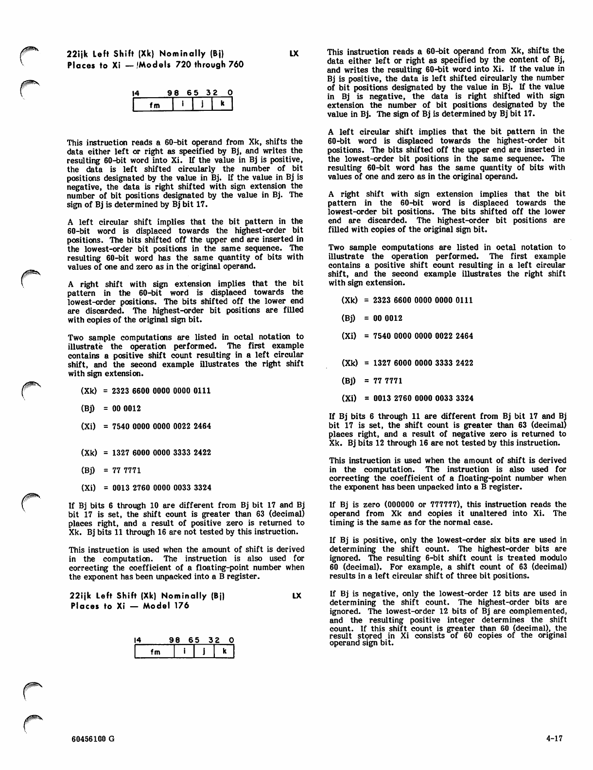
22ijk Left Shift (Xk) Nominally (Bj)
Places to Xi —'Models 720 through 760
/ # ^ V
14 9 8 6 5 3 2 0
fm
This instruction reads a 60-bit operand from Xk, shifts the
data either left or right as specified by Bj, and writes the
resulting 60-bit word into Xi. If the value in Bj is positive,
the data is left shifted circularly the number of bit
positions designated by the value in Bj. If the value in Bj is
negative, the data is right shifted with sign extension the
number of bit positions designated by the value in Bj. The
sign of Bj is determined by Bj bit 17.
A left circular shift implies that the bit pattern in the
60-bit word is displaced towards the highest-order bit
positions. The bits shifted off the upper end are inserted in
the lowest-order bit positions in the same sequence. The
resulting 60-bit word has the same quantity of bits with
values of one and zero as in the original operand.
A right shift with sign extension implies that the bit
pattern in the 60-bit word is displaced towards the
lowest-order positions. The bits shifted off the lower end
are discarded. The highest-order bit positions are filled
with copies of the original sign bit.
Two sample computations are listed in octal notation to
illustrate the operation performed. The first example
contains a positive shift count resulting in a left circular
shift, and the second example illustrates the right shift
with sign extension.
(Xk) = 2323 6600 0000 0000 0111
(Bj) = 00 0012
(Xi) = 7540 0000 0000 0022 2464
(Xk) = 1327 6000 0000 3333 2422
(Bj) = 77 7771
(Xi) = 0013 2760 0000 0033 3324
If Bj bits 6 through 10 are different from Bj bit 17 and Bj
bit 17 is set, the shift count is greater than 63 (decimal)
places right, and a result of positive zero is returned to
Xk. Bj bits 11 through 16 are not tested by this instruction.
This instruction is used when the amount of shift is derived
in the computation. The instruction is also used for
correcting the coefficient of a floating-point number when
the exponent has been unpacked into a B register.
LX This instruction reads a 60-bit operand from Xk, shifts the
data either left or right as specified by the content of Bj,
and writes the resulting 60-bit word into Xi. If the value in
Bj is positive, the data is left shifted circularly the number
of bit positions designated by the value in Bj. If the value
in Bj is negative, the data is right shifted with sign
extension the number of bit positions designated by the
value in Bj. The sign of Bj is determined by Bj bit 17.
A left circular shift implies that the bit pattern in the
60-bit word is displaced towards the highest-order bit
positions. The bits shifted off the upper end are inserted in
the lowest-order bit positions in the same sequence. The
resulting 60-bit word has the same quantity of bits with
values of one and zero as in the original operand.
A right shift with sign extension implies that the bit
pattern in the 60-bit word is displaced towards the
lowest-order bit positions. The bits shifted off the lower
end are discarded. The highest-order bit positions are
filled with copies of the original sign bit.
Two sample computations are listed in octal notation to
illustrate the operation performed. The first example
contains a positive shift count resulting in a left circular
shift, and the second example illustrates the right shift
with sign extension.
(Xk) = 2323 6600 0000 0000 0111
(Bj) = 00 0012
(Xi) = 7540 0000 0000 0022 2464
22ijk Left Shift (Xk) Nominally (Bj)
Places to Xi — Model 176
(Xk) = 1327 6000 0000 3333 2422
(Bj) = 77 7771
(Xi) = 0013 2760 0000 0033 3324
If Bj bits 6 through 11 are different from Bj bit 17 and Bj
bit 17 is set, the shift count is greater than 63 (decimal)
places right, and a result of negative zero is returned to
Xk. Bj bits 12 through 16 are not tested by this instruction.
This instruction is used when the amount of shift is derived
in the computation. The instruction is also used for
correcting the coefficient of a floating-point number when
the exponent has been unpacked into a B register.
If Bj is zero (000000 or 777777), this instruction reads the
operand from Xk and copies it unaltered into Xi. The
timing is the same as for the normal case.
If Bj is positive, only the lowest-order six bits are used in
determining the shift count. The highest-order bits are
ignored. The resulting 6-bit shift count is treated modulo
60 (decimal). For example, a shift count of 63 (decimal)
results in a left circular shift of three bit positions.
14 9 8 6 5 3 2 O
fm
Lx If Bj is negative, only the lowest-order 12 bits are used in
determining the shift count. The highest-order bits are
ignored. The lowest-order 12 bits of Bj are complemented,
and the resulting positive integer determines the shift
count. If this shift count is greater than 60 (decimal), the
result stored in Xi consists of 60 copies of the original
operand sign bit.
60456100 G 4-17
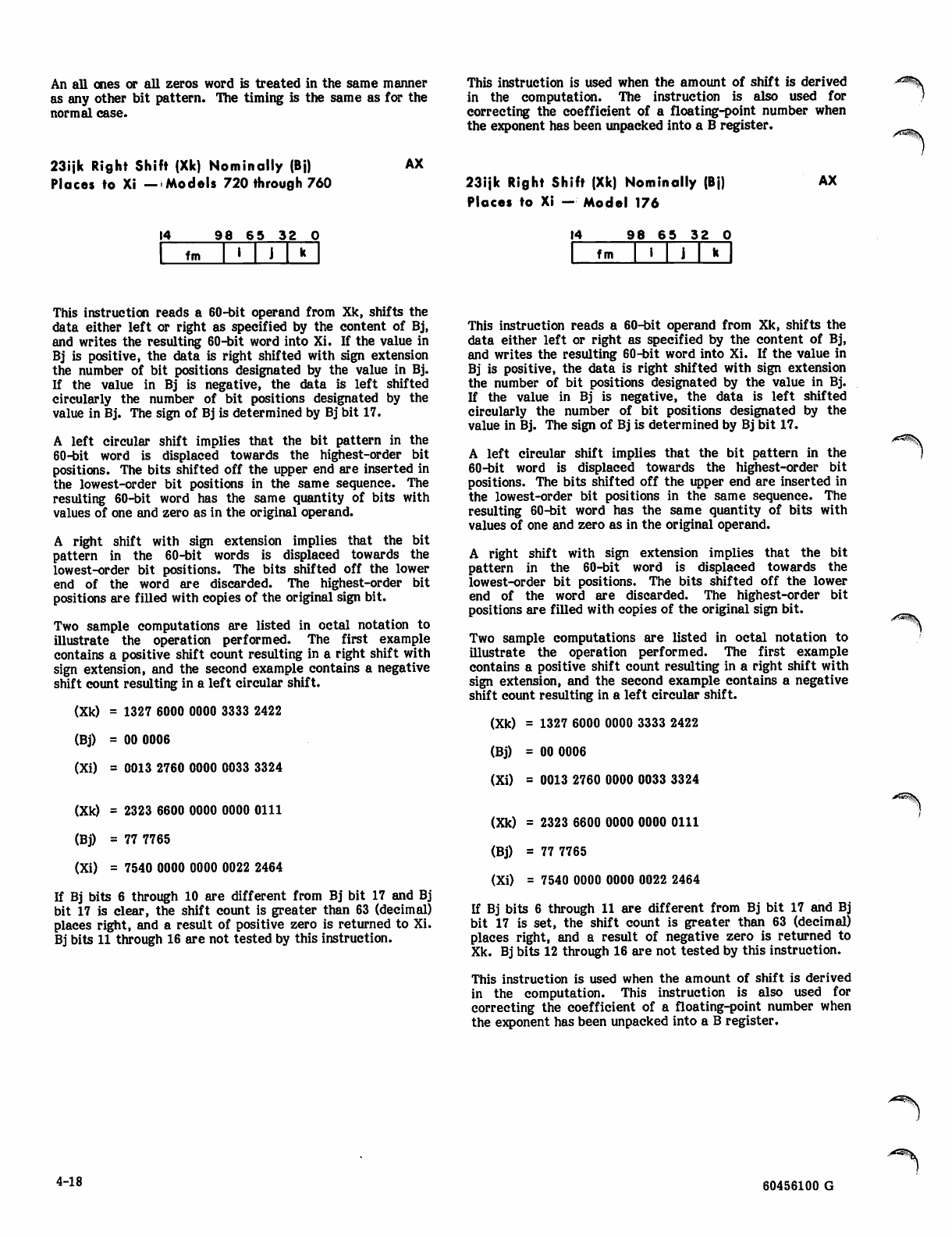
An all ones or all zeros word is treated in the same manner
as any other bit pattern. The timing is the same as for the
normal case.
This instruction is used when the amount of shift is derived
in the computation. The instruction is also used for
correcting the coefficient of a floating-point number when
the exponent has been unpacked into a B register.
23ijk Right Shift (Xk) Nominally (Bj)
Places to Xi — Models 720 through 760
AX
23ijk Right Shift (Xk) Nominally (Bj)
Places to Xi — Model 176
AX
14 98 65 3 2 0
fm
14 98 65 3 2 0
fm
This instruction reads a 60-bit operand from Xk, shifts the
data either left or right as specified by the content of Bj,
and writes the resulting 60-bit word into Xi. If the value in
Bj is positive, the data is right shifted with sign extension
the number of bit positions designated by the value in Bj.
If the value in Bj is negative, the data is left shifted
circularly the number of bit positions designated by the
value in Bj. The sign of Bj is determined by Bj bit 17.
A left circular shift implies that the bit pattern in the
60-bit word is displaced towards the highest-order bit
positions. The bits shifted off the upper end are inserted in
the lowest-order bit positions in the same sequence. The
resulting 60-bit word has the same quantity of bits with
values of one and zero as in the original operand.
A right shift with sign extension implies that the bit
pattern in the 60-bit words is displaced towards the
lowest-order bit positions. The bits shifted off the lower
end of the word are discarded. The highest-order bit
positions are filled with copies of the original sign bit.
Two sample computations are listed in octal notation to
illustrate the operation performed. The first example
contains a positive shift count resulting in a right shift with
sign extension, and the second example contains a negative
shift count resulting in a left circular shift.
(Xk) = 1327 6000 0000 3333 2422
(Bj) = 00 0006
(Xi) = 0013 2760 0000 0033 3324
(Xk) = 2323 6600 0000 0000 0111
(Bj) = 77 7765
(Xi) = 7540 0000 0000 0022 2464
If Bj bits 6 through 10 are different from Bj bit 17 and Bj
bit 17 is clear, the shift count is greater than 63 (decimal)
places right, and a result of positive zero is returned to Xi.
Bj bits 11 through 16 are not tested by this instruction.
This instruction reads a 60-bit operand from Xk, shifts the
data either left or right as specified by the content of Bj,
and writes the resulting 60-bit word into Xi. If the value in
Bj is positive, the data is right shifted with sign extension
the number of bit positions designated by the value in Bj.
If the value in Bj is negative, the data is left shifted
circularly the number of bit positions designated by the
value in Bj. The sign of Bj is determined by Bj bit 17.
A left circular shift implies that the bit pattern in the
60-bit word is displaced towards the highest-order bit
positions. The bits shifted off the upper end are inserted in
the lowest-order bit positions in the same sequence. The
resulting 60-bit word has the same quantity of bits with
values of one and zero as in the original operand.
A right shift with sign extension implies that the bit
pattern in the 60-bit word is displaced towards the
lowest-order bit positions. The bits shifted off the lower
end of the word are discarded. The highest-order bit
positions are filled with copies of the original sign bit.
Two sample computations are listed in octal notation to
illustrate the operation performed. The first example
contains a positive shift count resulting in a right shift with
sign extension, and the second example contains a negative
shift count resulting in a left circular shift.
(Xk) = 1327 6000 0000 3333 2422
(Bj) = 00 0006
(Xi) = 0013 2760 0000 0033 3324
(Xk) = 2323 6600 0000 0000 0111
(Bj) = 77 7765
(Xi) = 7540 0000 0000 0022 2464
If Bj bits 6 through 11 are different from Bj bit 17 and Bj
bit 17 is set, the shift count is greater than 63 (decimal)
places right, and a result of negative zero is returned to
Xk. Bj bits 12 through 16 are not tested by this instruction.
This instruction is used when the amount of shift is derived
in the computation. This instruction is also used for
correcting the coefficient of a floating-point number when
the exponent has been unpacked into a B register.
4-18 60456100 G
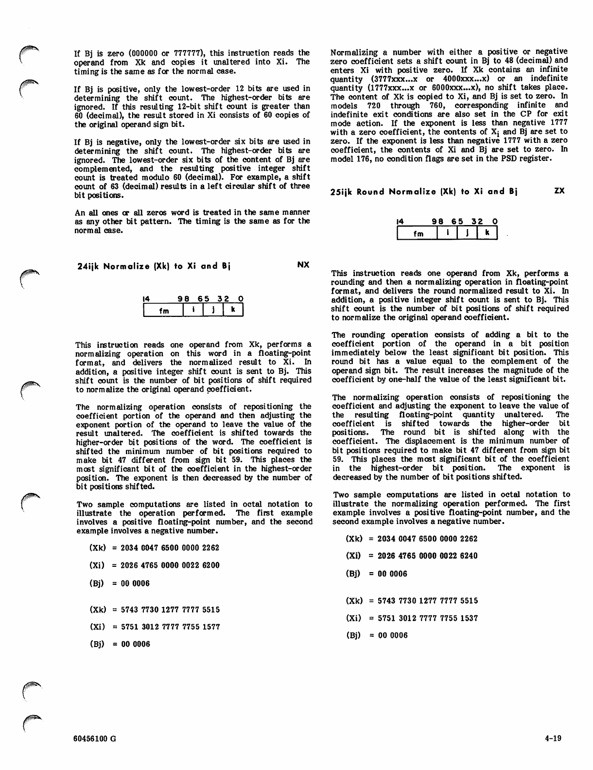
/0^,
If Bj is zero (000000 or 777777), this instruction reads the
operand from Xk and copies it unaltered into Xi. The
timing is the same as for the normal case.
If Bj is positive, only the lowest-order 12 bits are used in
determining the shift count. The highest-order bits are
ignored. If this resulting 12-bit shift count is greater than
60 (decimal), the result stored in Xi consists of 60 copies of
the original operand sign bit.
If Bj is negative, only the lowest-order six bits are used in
determining the shift count. The highest-order bits are
ignored. The lowest-order six bits of the content of Bj are
complemented, and the resulting positive integer shift
count is treated modulo 60 (decimal). For example, a shift
count of 63 (decimal) results in a left circular shift of three
bit positions.
An all ones or all zeros word is treated in the same manner
as any other bit pattern. The timing is the same as for the
normal case.
Normalizing a number with either a positive or negative
zero coefficient sets a shift count in Bj to 48 (decimal) and
enters Xi with positive zero. If Xk contains an infinite
quantity (3777xxx...x or 4000xxx...x) or an indefinite
quantity (1777xxx...x or 6000xxx...x), no shift takes place.
The content of Xk is copied to Xi, and Bj is set to zero. In
models 720 through 760, corresponding infinite and
indefinite exit conditions are also set in the CP for exit
mode action. If the exponent is less than negative 1777
with a zero coefficient, the contents of Xj and Bj are set to
zero. If the exponent is less than negative 1777 with a zero
coefficient, the contents of Xi and Bj are set to zero. In
model 176, no condition flags are set in the PSD register.
25ijk Round Normalize (Xk) to Xi and Bj ZX
14 9865320
fm
24i jk Normalize ( Xk) to Xi a nd Bj NX
r
14 9865320
fm
This instruction reads one operand from Xk, performs a
normalizing operation on this word in a floating-point
format, and delivers the normalized result to Xi. In
addition, a positive integer shift count is sent to Bj. This
shift count is the number of bit positions of shift required
to normalize the original operand coefficient.
The normalizing operation consists of repositioning the
coefficient portion of the operand and then adjusting the
exponent portion of the operand to leave the value of the
result unaltered. The coefficient is shifted towards the
higher-order bit positions of the word. The coefficient is
shifted the minimum number of bit positions required to
make bit 47 different from sign bit 59. This places the
most significant bit of the coefficient in the highest-order
position. The exponent is then decreased by the number of
bit positions shifted.
Two sample computations are listed in octal notation to
illustrate the operation performed. The first example
involves a positive floating-point number, and the second
example involves a negative number.
(Xk) = 2034 0047 6500 0000 2262
(Xi) = 2026 4765 0000 0022 6200
(Bj) = 00 0006
(Xk) = 5743 7730 1277 7777 5515
(Xi) = 5751 3012 7777 7755 1577
(Bj) = 00 0006
This instruction reads one operand from Xk, performs a
rounding and then a normalizing operation in floating-point
format, and delivers the round normalized result to Xi. In
addition, a positive integer shift count is sent to Bj. This
shift count is the number of bit positions of shift required
to normalize the original operand coefficient.
The rounding operation consists of adding a bit to the
coefficient portion of the operand in a bit position
immediately below the least significant bit position. This
round bit has a value equal to the complement of the
operand sign bit. The result increases the magnitude of the
coefficient by one-half the value of the least significant bit.
The normalizing operation consists of repositioning the
coefficient and adjusting the exponent to leave the value of
the resulting floating-point quantity unaltered. The
coefficient is shifted towards the higher-order bit
positions. The round bit is shifted along with the
coefficient. The displacement is the minimum number of
bit positions required to make bit 47 different from sign bit
59. This places the most significant bit of the coefficient
in the highest-order bit position. The exponent is
decreased by the number of bit positions shifted.
Two sample computations are listed in octal notation to
illustrate the normalizing operation performed. The first
example involves a positive floating-point number, and the
second example involves a negative number.
(Xk) = 2034 0047 6500 0000 2262
(Xi) = 2026 4765 0000 0022 6240
(Bj) = 00 0006
(Xk) = 5743 7730 1277 7777 5515
(Xi) = 5751 3012 7777 7755 1537
(Bj) = 00 0006
60456100 G 4-19
If Xk contains either an infinite quantity (3777xxx...x or
4000xxx...x) or an indefinite quantity (1777xxx...x or
6000xxx...x), no shift takes place. The content of Xk is
copied to Xi, and Bj is set to zero. In models 720 through
760, corresponding infinite and indefinite conditions are
also set in the CP for exit mode action. In model 176, no
condition flags are set in the PSD register.
This instruction converts a number from floating-point
format to fixed-point format.
27ijk Pack (Xk) and (Bj) to Xi PX
26ijk Unpack (Xk) to Xi and Bj UX
14 9865320
fm
1 4 9 8 6 5 3 2 0
fm
This instruction reads one operand from Xk, unpacks this
word from floating-point format, and delivers the
coefficient and exponents to Xi and Bj, respectively. The
60-bit word delivered to Xi consists of the lowest 48 bits
unaltered from the original operand plus the upper 12 bits,
each equal to the original sign bit. This is a signed integer
equal to the value of the coefficient in the original
operand. The 18-bit quantity delivered to Bj is a signed
integer equal to the value of the exponent in the original
operand. The 11-bit exponent field in the operand is
altered to remove the bias and then sign extended to fill
out the 18-bit quantity. The sign of the coefficient is
removed in this process.
Four sample sets of operands and unpacked results are
listed in octal notation to illustrate the operation
performed. These examples contain the four combinations
of coefficient sign and exponent sign.
(Xk) = 2034 4500 3333 2000 0077
(Xi) = 0000 4500 3333 2000 0077
(Bj) = 00 0034
(Xk) = 1743 4500 3333 2000 0077
(Xi) = 0000 4500 3333 2000 0077
(Bj) = 77 7743
(Xk) = 5743 3277 4444 5777 7700
(Xi) = 7777 3277 4444 5777 7700
(Bj) = 00 0034
(Xk) = 6034 3277 4444 5777 7700
(Xi) = 7777 3277 4444 5777 7700
(Bj) = 77 7743
This instruction reads the contents of Xk and Bj, packs
them into a single word in floating-point format, and
delivers this result to Xi. The coefficient for the value in
Xi is obtained from the content of Xk, which is treated as a
signed integer. The exponent for the value in Xi is
obtained from the content of Bj, which is treated as a
signed integer.
The lowest-order 48 bits in Xi are copied directly from the
lowest-order 48 bits in Xk. The sign bit in Xi is copied
directly from the sign bit in Xk. The exponent field in Xi is
derived from the value in Bj by extracting the lowest-order
11 bits in Bj and modifying this quantity for exponent bias
and coefficient sign.
Four sample sets of operands and packed results are listed
in octal notation to illustrate the operation performed.
These examples contain the four combinations of
coefficient sign and exponent sign.
(Xk) = 0000 4500 3333 2000 0077
(Bj) = 00 0034
(Xi) = 2034 4500 3333 2000 0077
(Xk) = 0000 4500 3333 2000 0077
(Bj) = 77 7743
(Xi) = 1743 4500 3333 2000 0077
(Xk) = 7777 3277 4444 5777 7700
(Bj) = 00 0034
(Xi) = 5743 3277 4444 5777 7700
(Xk) = 7777 3277 4444 5777 7700
(Bj) = 77 7743
(Xi) = 6034 3277 4444 5777 7700
This instruction converts a number in fixed-point format to
floating-point format.
4-20 60456100 G
/sfP'V
30ijk Floating Sum of (Xj) and (Xk) to Xi
1 4 9 8 6 5 3 2 0
FX
fm
This instruction reads operands from two X registers,
operates upon them to form a floating-point sum, and
delivers this result to a third X register. The operands for
this instruction are in Xj and Xk. These operands are in
floating-point format and are not necessarily normalized.
The sum of the quantities in Xj and Xk is delivered to Xi in
floating-point format and is not necessarily normalized.
The two operands are unpacked from floating-point format,
and the exponents are compared. The coefficient with the
smaller exponent is right shifted by the difference of the
two exponents such that both coefficients are the same
significance. The two coefficients are then added to form
a 96-bit result. The upper half of the result is then
selected as a coefficient and packed along with the larger
exponent to form the result sent to Xi. If coefficient
overflow occurs, the sum is right shifted one place, and the
exponent is increased by one.
If the two operands have unlike signs, the result coefficient
may have leading zeros. No normalize operation is built
into this instruction to correct this situation. A separate
normalize instruction must be programmed if the result is
to be kept in a normalized form.
When the difference between the exponents is greater than
128 (decimal), models 720 through 760 extend the shifted
sign bit to the entire shifted operand. Model 176 enters a
shifted operand of plus 0 regardless of the sign of the
shifted operand. If the reference operand has a zero
coefficient, the results can differ in sign.
For models 720 through 760, infinite (3777xxx...x or
4000xxx...x) or indefinite (1777xxx...x or 6000xxx...x)
operands cause corresponding exit conditions to set in the
CP for exit mode action. For model 176, bits are set in the
PSD register for the corresponding conditions. (Refer to
Processing Differences under Central Processor
Programming in section 5.)
31ijk Flo a t i ng Diffe r e n ce of (Xj) a n d
(Xk) to Xi
FX
This instruction reads operands from two X registers,
operates upon them to form a floating-point difference,
and delivers this result to a third X register. The operands
for this instruction are in Xj and Xk. These operands are in
floating-point format and are not necessarily normalized.
The result of subtracting the quantity in Xk from the
quantity in Xj is delivered to Xi in floating-point format
and is not necessarily normalized.
The two operands are unpacked from floating-point format,
and the exponents are compared. The coefficient with the
smaller exponent is right shifted by the difference of the
two exponents such that both coefficients are the same
significance. The Xk coefficient is then subtracted from
the Xj coefficient to form a 96-bit result. The upper half
of the result is then selected and packed along with the
larger exponent to form the result sent to Xi. If
coefficient overflow occurs, the result is right shifted one
place, and the exponent is increased by one.
If the two operands have like signs, the result coefficient
may have leading zeros. No normalize operation is built
into this instruction to correct this situation. A separate
normalize instruction must be programmed if the result is
to be kept in a normalized form.
For models 720 through 760, infinite (3777xxx...x or
4000xxx...x) or indefinite (1777xxx...x or 6000xxx...x)
operands cause corresponding exit conditions to set in the
CP for exit mode action. For model 176, bits are set in the
PSD register for the corresponding conditions. (Refer to
Processing Differences under Central Processor
Programming in section 5.)
321 jk Floating Double-Precision Sum of (Xj)
and (Xk) to Xi
DX
14 98 65 32 O
fm
This instruction reads operands from two X registers,
operates upon them to form a double-precision
floating-point sum, and delivers the lower half of this
result to a third X register. The operands for this
instruction are in Xj and Xk. These operands are in
floating-point format and are not necessarily normalized.
The sum of the quantities in Xj and Xk is delivered to Xi in
floating-point format and is not necessarily normalized.
14 98 65 32 O
fm
60456100 G 4-21
The two operands are unpacked from floating-point format,
and the exponents are compared. The coefficient with the
smaller exponent is right shifted by the difference of the
two exponents such that both coefficients are the same
significance. The two coefficients are then added to form
a 96-bit result. The lower half of the result is then
selected and packed along with the larger exponent minus
48 (decimal) to form the result sent to Xi. If coefficient
overflow occurs, the result is right shifted by one place,
and the exponent is increased by one.
For models 720 through 760, infinite (3777xxx...x or
4000xxx...x) or indefinite (1777xxx...x or 6000xxx...x)
operands cause corresponding exit conditions to set in the
CP for exit mode action. For model 176, bits are set in the
PSD register for the corresponding conditions. (Refer to
Processing Differences under Central Processor
Programming in section 5.)
33ijk Floating Double-Precision
Difference of (Xj)tand (Xk) to Xi
DX
14 98 65 3 2 0
fm
This instruction reads operands from two X registers,
operates upon them to form a double-precision
floating-point difference, and delivers the lower half of
this result to a third X register. The operands for this
instruction are in Xj and Xk. These operands are in
floating-point format and are not necessarily normalized.
The result of subtracting the quantity in Xk from the
quantity in Xj is delivered to Xi in floating-point format
and is not necessarily normalized.
The two operands are unpacked from floating-point format,
and the exponents are compared. The coefficient with the
smaller exponent is right shifted by the difference of the
two exponents such that both coefficients are the same
significance. The Xk coefficient is then subtracted from
the Xj coefficient to form a 96-bit result. The lower half
of the result is then selected and packed along with the
larger exponent minus 48 (decimal) to form the result sent
to Xi. If coefficient overflow occurs, the result is right
shifted one place, and the exponent is increased by one.
For models 720 through 760, infinite (3777xxx...x or
4000xxx...x) • or indefinite (1777xxx...x or 6000xxx...x)
operands cause corresponding exit conditions to set in the
CP for exit mode action. For model 176, bits are set in the
PSD register for the corresponding conditions. (Refer to
Processing Differences under Central Processor
Programming in section 5.)
34ijk Round Floatin g Sum of (X j) an d
(Xk) to Xi
1 4 9 8 6 5 3 2 0
RX
fm
This instruction reads operands from two X registers,
operates upon them to form a rounded floating-point sum,
and delivers this result to a third X register. The operands
for this instruction are in Xj and Xk. These operands are in
floating-point format and are not necessarily normalized.
The result is delivered to Xi in floating-point format and is
not necessarily normalized.
The round floating-point sum is a single-precision
floating-point sum with a round bit (or bits) inserted before
the add operation takes place. A round bit is always
inserted in the coefficient with the larger exponent. If the
two exponents are equal, the round bit is inserted in the
coefficient for Xk. The round bit is equal to the
complement of the sign bit and is inserted immediately to
the right of the lowest-order bit in the coefficient. This
has the effect of increasing the magnitude of the
coefficient by one-half of the least significant bit. A
second round bit is inserted in a corresponding manner to
the other coefficient if both operands are normalized or
have unlike signs. The second round bit is inserted before
the coefficient has been shifted by the difference of the
exponents.
For models 720 through 760, infinite (3777xxx...x or
4000xxx...x) or indefinite (1777xxx...x or 6000xxx...x)
operands cause corresponding exit conditions to set in the
CP for exit mode action. For model 176, bits are set in the
PSD register for the corresponding conditions. (Refer to
Processing Differences under Central Processor
Programming in section 5.)
35ijk Round Floating Difference of
(Xj) Minusi (Xk) to Xi
RX
14 98 65 32 O
fm
This instruction reads operands from two X registers,
operates upon them to form a rounded floating-point
difference, and delivers this result to a third X register.
The operands for this instruction are in Xj and Xk. These
operands are in floating-point format and are not
necessarily normalized. The result of subtracting the
quantity in Xk from the quantity in Xj is delivered to Xi in
floating-point format and is not necessarily normalized.
<^^%
*^5\
4-22 60456100 G
Z^SSN
The round floating-point difference consists of
complementing the quantity in Xk and adding this quantity
to Xj. The round floating-point difference is a
single-precision floating-point difference with a round bit
(or bits) inserted after the complement of Xk and before the
subtract operation takes place. A round bit is always
inserted in the coefficient with the larger exponent. If the
two exponents are equal, the round bit is added to the
coefficient for Xk. The round bit is equal to the
complement of the sign bit and is inserted immediately to
the right of the lowest-order bit in the coefficient. This has
the effect of increasing the magnitude of the coefficient by
one-half of the least significant bit. A second round bit is
inserted in a corresponding manner to the other coefficient
if both operands are normalized or have like signs. The
second round bit is inserted before the coefficient has been
shifted by the difference of the exponents.
For models 720 through 760, infinite (3777xxx...x or
4000xxx...x) or indefinite (1777xxx...x or 6000xxx...x)
operands cause corresponding exit conditions to set in the
CP for exit mode action. For model 176, bits are set in the
PSD register for the corresponding conditions. (Refer to
Processing Differences under Central Processor
Programming in section 5.)
36ijk Integer Sum of (Xj) and (Xk) to Xi IX
1 4 9 8 6 5 3 2 0
fm
This instruction reads operands from two X registers,
operates upon them to form a 60-bit integer sum, and
delivers this result to a third X register. The operands for
this instruction are in Xj and Xk. These operands are signed
integers. The resulting integer sum is delivered to Xi.
Overflow is not detected.
This instruction adds integers too large for handling by 50
through 77 instructions. The instruction also merges and
compares data fields during data processing.
37ijk Integer Difference of (Xj) and IX
(Xk) to Xi
1 4 9 8 6 5 3 2 0
fm
This instruction subtracts integers too large for handling by
50 through 77 instructions. The instruction also compares
data fields during data processing.
40ijk Floating Product of (Xj) and
(Xk) to Xi
FX
1 4 9 8 6 5 3 2 0
fm
This instruction reads operands from two X registers,
operates upon them to form a floating-point product, and
delivers this result to a third X register. The operands for
this instruction are in Xj and Xk. These operands are in
floating-point format and are not necessarily normalized.
The result is delivered to Xi in floating-point format. If
both operands are normalized, the result is also normalized.
If both operands are not normalized, the result is not
normalized.
The two operands are unpacked from floating-point format.
The exponents are added with a correction factor to
determine the exponent for the result. The coefficients are
multiplied as signed integers to form a 96-bit integer
product. The upper half of this product is extracted to form
the coefficient for the result. If the original operands are
normalized and the product has only 95 significant bits, a
1-bit left shift to normalize the result coefficient is done.
The resulting exponent is reduced by one count in this case.
If both operands are not normalized, the resulting
double-precision product has less than 96 significant bits.
No test is made for the position of the most significant bit.
The upper 48 bits are read from the double-precision
product register. Leading zeros occur in this result
coefficient.
This instruction is used in floating-point calculations where
rounding of operands is not desired, such as in
multiple-precision arithmetic and in calculations involving
error analysis.
For models 720 through 760, infinite (3777xxx...x or
4000xxx...x) or indefinite (1777xxx...x or 6000xxx...x)
operands cause corresponding exit conditions to set in the
CP for exit mode action.
For model 176, bits are set in the PSD register for the
corresponding conditions. (Refer to Processing Differences
under Central Processor Programming in section 5.)
This instruction reads operands from two X registers,
operates upon them to form a 60-bit integer difference, and
delivers this result to a third X register. The operands for
this instruction are in Xj and Xk. These operands are signed
integers. The result of subtracting the quantity in Xk from
the quantity in Xj is delivered to Xi. Overflow is not
detected.
41ijk Round Floating Product of (Xj)
and (Xk) to Xi
14 986532 0
RX
fm
60456100 L 4-23
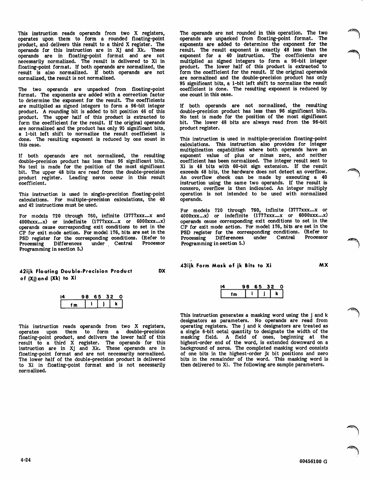
This instruction reads operands from two X registers,
operates upon them to form a rounded floating-point
product, and delivers this result to a third X register. The
operands for this instruction are in Xj and Xk. These
operands are in floating-point format and are not
necessarily normalized. The result is delivered to Xi in
floating-point format. If both operands are normalized, the
result is also normalized. If both operands are not
normalized, the result is not normalized.
The two operands are unpacked from floating-point
format. The exponents are added with a correction factor
to determine the exponent for the result. The coefficients
are multiplied as signed integers to form a 96-bit integer
product. A rounding bit is added to bit position 46 of this
product. The upper half of this product is extracted to
form the coefficient for the result. If the original operands
are normalized and the product has only 95 significant bits,
a 1-bit left shift to normalize the result coefficient is
done. The resulting exponent is reduced by one count in
this case.
If both operands are not normalized, the resulting
double-precision product has less than 96 significant bits.
No test is made for the position of the most significant
bit. The upper 48 bits are read from the double-precision
product register. Leading zeros occur in this result
coefficient.
This instruction is used in single-precision floating-point
calculations. For multiple-precision calculations, the 40
and 42 instructions must be used.
For models 720 through 760, infinite (3777xxx...x and
4000xxx...x) or indefinite (1777xxx...x or 6000xxx...x)
operands cause corresponding exit conditions to set in the
CP for exit mode action. For model 176, bits are set in the
PSD register for the corresponding conditions. (Refer to
Processing Differences under Central Processor
Programming in section 5.)
The operands are not rounded in this operation. The two
operands are unpacked from floating-point format. The
exponents are added to determine the exponent for the
result. The result exponent is exactly 48 less than the
exponent for a 40 instruction. The coefficients are
multiplied as signed integers to form a 96-bit integer
product. The lower half of this product is extracted to
form the coefficient for the result. If the original operands
are normalized and the double-precision product has only
95 significant bits, a 1-bit left shift to normalize the result
coefficient is done. The resulting exponent is reduced by
one count in this case.
If both operands are not normalized, the resulting
double-precision product has less than 96 significant bits.
No test is made for the position of the most significant
bit. The lower 48 bits are always read from the 96-bit
product register.
This instruction is used in multiple-precision floating-point
calculations. This instruction also provides for integer
multiplication capabilities where both operands have an
exponent value of plus or minus zero, and neither
coefficient has been normalized. The integer result sent to
Xi is 48 bits with 60-bit sign extension. If the result
exceeds 48 bits, the hardware does not detect an overflow.
An overflow check can be made by executing a 40
instruction using the same two operands. If the result is
nonzero, overflow is then indicated. An integer multiply
operation is not intended to be used with normalized
operands.
For models 720 through 760, infinite (3777xxx...x or
4000xxx...x) or indefinite (1777xxx...x or 6000xxx...x)
operands cause corresponding exit conditions to set in the
CP for exit mode action. For model 176, bits are set in the
PSD register for the corresponding conditions. (Refer to
Processing Differences under Central Processor
Programming in section 5.)
42ijk Floating Double-Precision Product
of (Xj)and (Xk) to Xi
DX
14 98 65 32 O
fm
This instruction reads operands from two X registers,
operates upon them to form a double-precision
floating-point product, and delivers the lower half of this
result to a third X register. The operands for this
instruction are in Xj and Xk. These operands are in
floating-point format and are not necessarily normalized.
The lower half of the double-precision product is delivered
to Xi in floating-point format and is not necessarily
normalized.
43ijk Form Mask of jk Bits to Xi
14 9865320
MX
fm
This instruction generates a masking word using the j and k
designators as parameters. No operands are read from
operating registers. The j and k designators are treated as
a single 6-bit octal quantity to designate the width of the
masking field. A field of ones, beginning at the
highest-order end of the word, is extended downward on a
background of zeros. The completed masking word consists
of one bits in the highest-order jk bit positions and zero
bits in the remainder of the word. This masking word is
then delivered to Xi. The following are sample parameters.
4-24 60456100 G
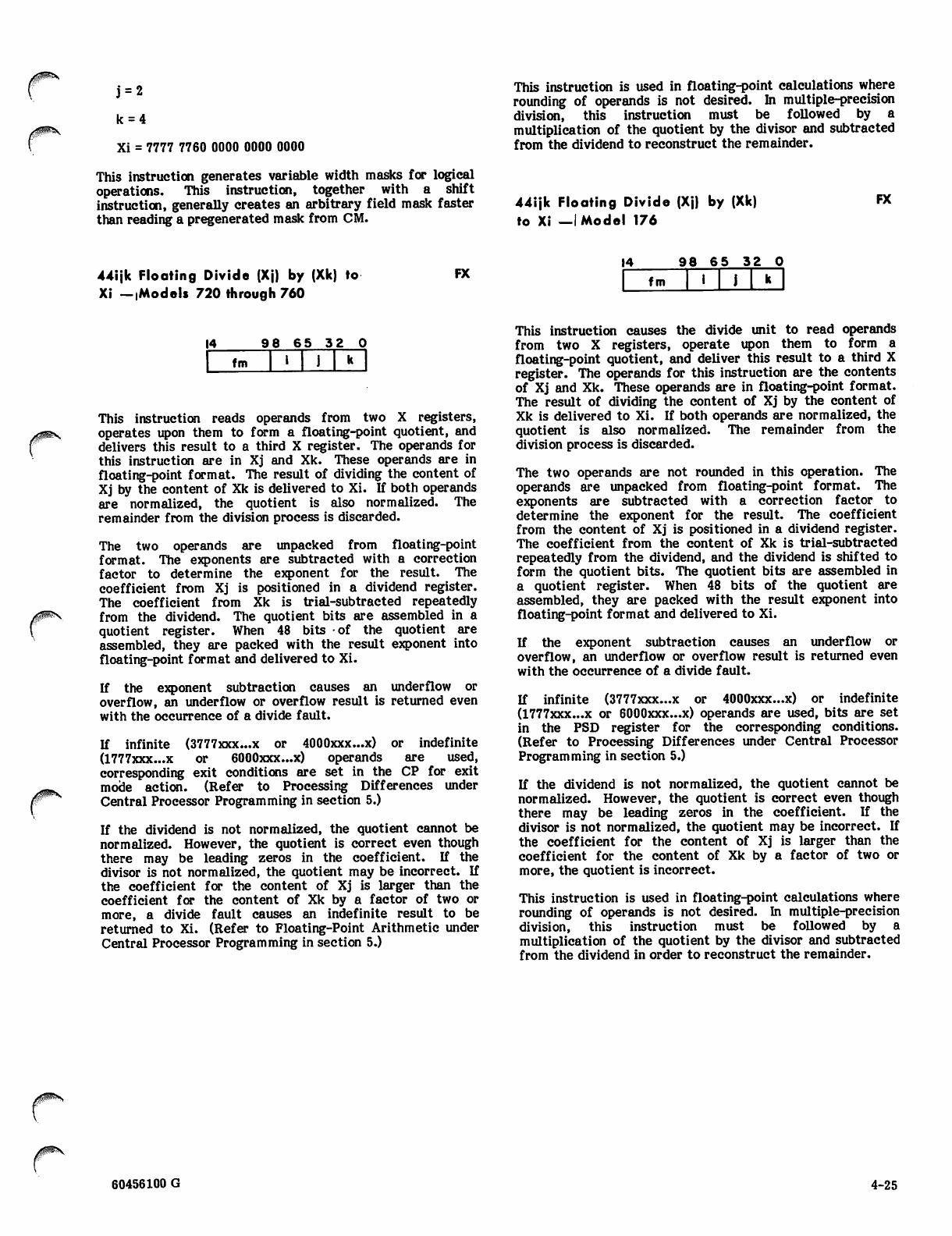
0*^\ j = 2
k = 4
Xi = 7777 7760 0000 0000 0000
This instruction generates variable width masks for logical
operations. This instruction, together with a shift
instruction, generally creates an arbitrary field mask faster
than reading a pregenerated mask from CM.
This instruction is used in floating-point calculations where
rounding of operands is not desired. In multiple-precision
division, this instruction must be followed by a
multiplication of the quotient by the divisor and subtracted
from the dividend to reconstruct the remainder.
44ijk Floating Divide (Xj) by (Xk)
to Xi —I Model 176
FX
44ijk Floating Divide (Xj) by (Xk) to
Xi —jModels 720 through 760
FX 14 98 65 32 0
fm
14 98 65 3 2 0
fm
This instruction reads operands from two X registers,
operates upon them to form a floating-point quotient, and
delivers this result to a third X register. The operands for
this instruction are in Xj and Xk. These operands are in
floating-point format. The result of dividing the content of
Xj by the content of Xk is delivered to Xi. If both operands
are normalized, the quotient is also normalized. The
remainder from the division process is discarded.
The two operands are unpacked from floating-point
format. The exponents are subtracted with a correction
factor to determine the exponent for the result. The
coefficient from Xj is positioned in a dividend register.
The coefficient from Xk is trial-subtracted repeatedly
from the dividend. The quotient bits are assembled in a
quotient register. When 48 bits of the quotient are
assembled, they are packed with the result exponent into
floating-point format and delivered to Xi.
If the exponent subtraction causes an underflow or
overflow, an underflow or overflow result is returned even
with the occurrence of a divide fault.
If infinite (3777xxx...x or 4000xxx...x) or indefinite
(1777xxx...x or 6000xxx...x) operands are used,
corresponding exit conditions are set in the CP for exit
mode action. (Refer to Processing Differences under
Central Processor Programming in section 5.)
If the dividend is not normalized, the quotient cannot be
normalized. However, the quotient is correct even though
there may be leading zeros in the coefficient. If the
divisor is not normalized, the quotient may be incorrect. If
the coefficient for the content of Xj is larger than the
coefficient for the content of Xk by a factor of two or
more, a divide fault causes an indefinite result to be
returned to Xi. (Refer to Floating-Point Arithmetic under
Central Processor Programming in section 5.)
This instruction causes the divide unit to read operands
from two X registers, operate upon them to form a
floating-point quotient, and deliver this result to a third X
register. The operands for this instruction are the contents
of Xj and Xk. These operands are in floating-point format.
The result of dividing the content of Xj by the content of
Xk is delivered to Xi. If both operands are normalized, the
quotient is also normalized. The remainder from the
division process is discarded.
The two operands are not rounded in this operation. The
operands are unpacked from floating-point format. The
exponents are subtracted with a correction factor to
determine the exponent for the result. The coefficient
from the content of Xj is positioned in a dividend register.
The coefficient from the content of Xk is trial-subtracted
repeatedly from the dividend, and the dividend is shifted to
form the quotient bits. The quotient bits are assembled in
a quotient register. When 48 bits of the quotient are
assembled, they are packed with the result exponent into
floating-point format and delivered to Xi.
If the exponent subtraction causes an underflow or
overflow, an underflow or overflow result is returned even
with the occurrence of a divide fault.
If infinite (3777xxx...x or 4000xxx...x) or indefinite
(1777xxx...x or 6000xxx...x) operands are used, bits are set
in the PSD register for the corresponding conditions.
(Refer to Processing Differences under Central Processor
Programming in section 5.)
If the dividend is not normalized, the quotient cannot be
normalized. However, the quotient is correct even though
there may be leading zeros in the coefficient. If the
divisor is not normalized, the quotient may be incorrect. If
the coefficient for the content of Xj is larger than the
coefficient for the content of Xk by a factor of two or
more, the quotient is incorrect.
This instruction is used in floating-point calculations where
rounding of operands is not desired. In multiple-precision
division, this instruction must be followed by a
multiplication of the quotient by the divisor and subtracted
from the dividend in order to reconstruct the remainder.
0$^\
60456100 G 4-25
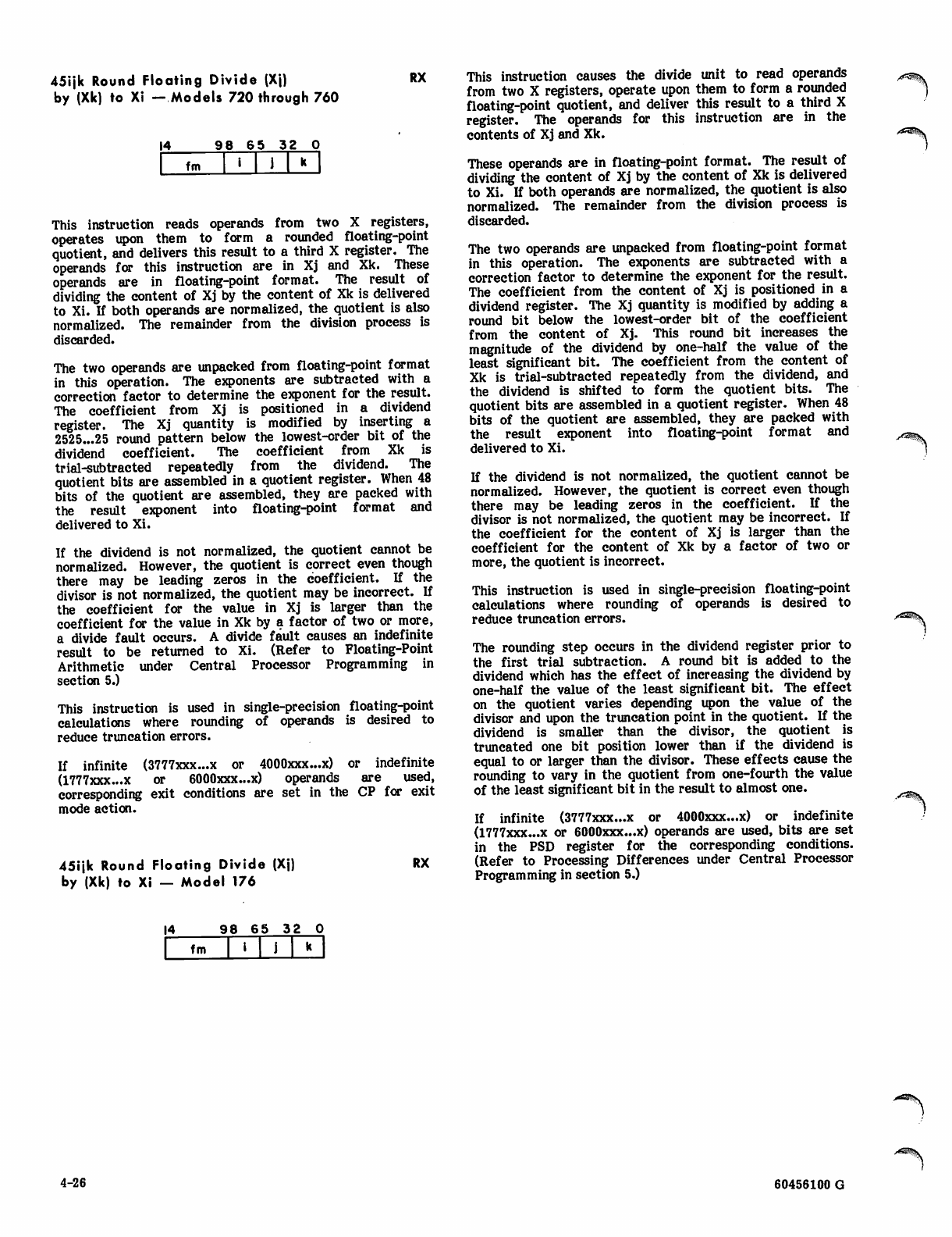
45ijk Round Floating Divide (Xj)
by (Xk) to Xi — Models 720 through 760
14 9 8 6 5 3 2 0
fm
This instruction reads operands from two X registers,
operates upon them to form a rounded floating-point
quotient, and delivers this result to a third X register. The
operands for this instruction are in Xj and Xk. These
operands are in floating-point format. The result of
dividing the content of Xj by the content of Xk is delivered
to Xi. If both operands are normalized, the quotient is also
normalized. The remainder from the division process is
discarded.
The two operands are unpacked from floating-point format
in this operation. The exponents are subtracted with a
correction factor to determine the exponent for the result.
The coefficient from Xj is positioned in a dividend
register. The Xj quantity is modified by inserting a
2525...25 round pattern below the lowest-order bit of the
dividen d coefficient. The coefficient from Xk is
trial-subtracted repeatedly from the dividend. The
quotient bits are assembled in a quotient register. When 48
bits of the quotient are assembled, they are packed with
the result exponent into floating-point format and
delivered to Xi.
If the dividend is not normalized, the quotient cannot be
normalized. However, the quotient is correct even though
there may be leading zeros in the coefficient. If the
divisor is not normalized, the quotient may be incorrect. If
the coefficient for the value in Xj is larger than the
coefficient for the value in Xk by a factor of two or more,
a divide fault occurs. A divide fault causes an indefinite
result to be returned to Xi. (Refer to Floating-Point
Arithmetic under Central Processor Programming in
section 5.)
This instruction is used in single-precision floating-point
calculations where rounding of operands is desired to
reduce truncation errors.
If infinite (3777xxx...x or 4000xxx...x) or indefinite
(1777xxx...x or 6000xxx...x) operands are used,
corresponding exit conditions are set in the CP for exit
mode action.
45ijk Round Floating Divide (Xj)
by (Xk) to Xi — Model 176
RX This instruction causes the divide unit to read operands
from two X registers, operate upon them to form a rounded
floating-point quotient, and deliver this result to a third X
register. The operands for this instruction are in the
contents of Xj and Xk.
These operands are in floating-point format. The result of
dividing the content of Xj by the content of Xk is delivered
to Xi. If both operands are normalized, the quotient is also
normalized. The remainder from the division process is
discarded.
The two operands are unpacked from floating-point format
in this operation. The exponents are subtracted with a
correction factor to determine the exponent for the result.
The coefficient from the content of Xj is positioned in a
dividend register. The Xj quantity is modified by adding a
round bit below the lowest-order bit of the coefficient
from the content of Xj. This round bit increases the
magnitude of the dividend by one-half the value of the
least significant bit. The coefficient from the content of
Xk is trial-subtracted repeatedly from the dividend, and
the dividend is shifted to form the quotient bits. The
quotient bits are assembled in a quotient register. When 48
bits of the quotient are assembled, they are packed with
the result exponent into floating-point format and
delivered to Xi.
If the dividend is not normalized, the quotient cannot be
normalized. However, the quotient is correct even though
there may be leading zeros in the coefficient. If the
divisor is not normalized, the quotient may be incorrect. If
the coefficient for the content of Xj is larger than the
coefficient for the content of Xk by a factor of two or
more, the quotient is incorrect.
This instruction is used in single-precision floating-point
calculations where rounding of operands is desired to
reduce truncation errors.
The rounding step occurs in the dividend register prior to
the first trial subtraction. A round bit is added to the
dividend which has the effect of increasing the dividend by
one-half the value of the least significant bit. The effect
on the quotient varies depending upon the value of the
divisor and upon the truncation point in the quotient. If the
dividend is smaller than the divisor, the quotient is
truncated one bit position lower than if the dividend is
equal to or larger than the divisor. These effects cause the
rounding to vary in the quotient from one-fourth the value
of the least significant bit in the result to almost one.
If infinite (3777xxx...x or 4000xxx...x) or indefinite
(1777xxx...x or 6000xxx...x) operands are used, bits are set
in the PSD register for the corresponding conditions.
RX (Refer to Processing Differences under Central Processor
Programming in section 5.)
14 98 65 3 2 0
fm
4-26 60456100 G
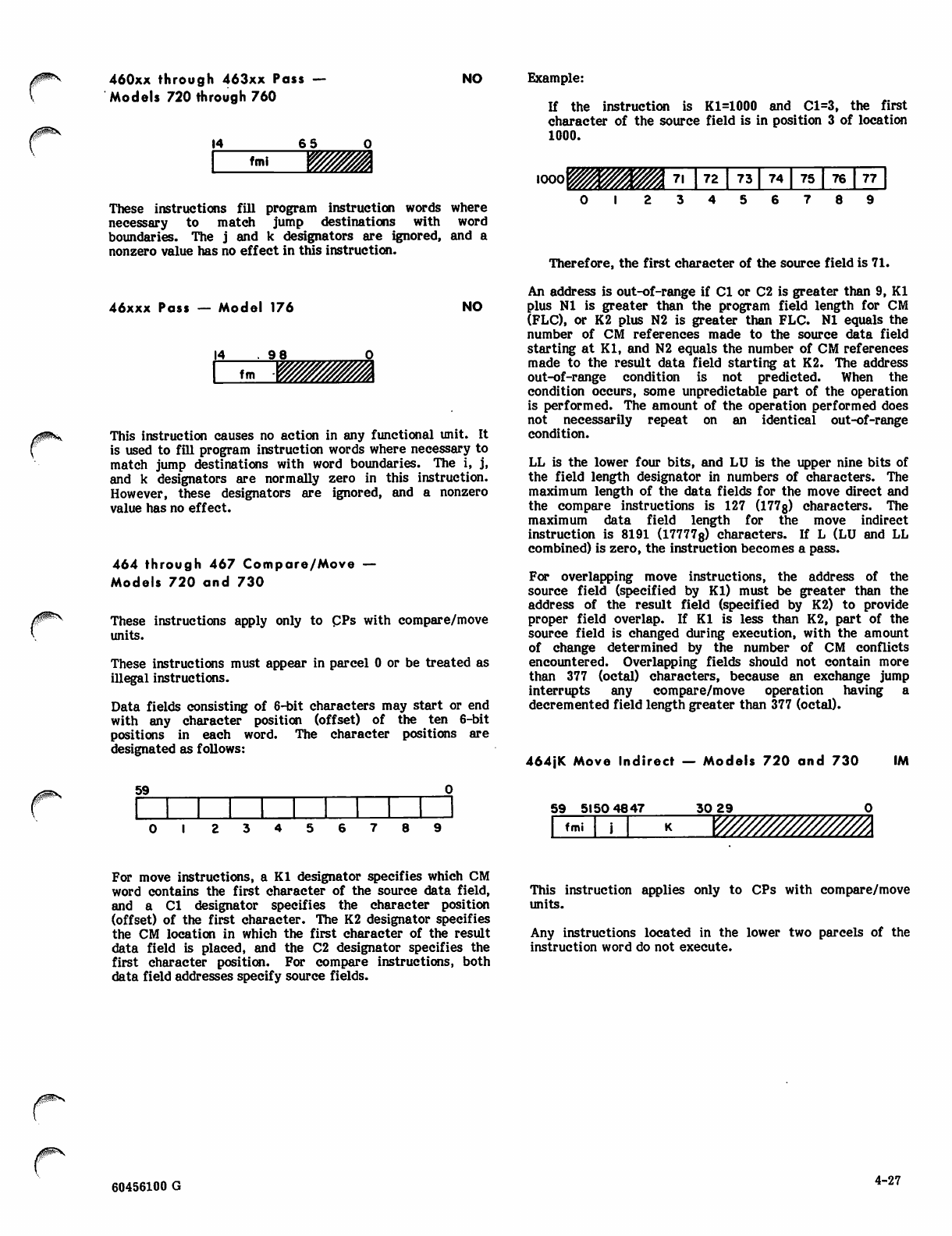
460xx through 463xx Pass —
Models 720 through 760
NO Example:
If the instruction is Kl=1000 and Cl=3, the first
character of the source field is in position 3 of location
1000.
1000 72 7 3 7 4 75 76 77
These instructions fill program instruction words where
necessary to match jump destinations with word
boundaries. The j and k designators are ignored, and a
nonzero value has no effect in this instruction.
46xxx Pass — Model 176 NO
This instruction causes no action in any functional unit. It
is used to fill program instruction words where necessary to
match jump destinations with word boundaries. The i, j,
and k designators are normally zero in this instruction.
However, these designators are ignored, and a nonzero
value has no effect.
464 through 467 Compare/Move —
Models 720 and 730
These instructions apply only to PPs with compare/move
units.
These instructions must appear in parcel 0 or be treated as
illegal instructions.
Data fields consisting of 6-bit characters may start or end
with any character position (offset) of the ten 6-bit
positions in each word. The character positions are
designated as follows:
Therefore, the first character of the source field is 71.
An address is out-of-range if Cl or C2 is greater than 9, Kl
plus NI is greater than the program field length for CM
(FLC), or K2 plus N2 is greater than FLC. NI equals the
number of CM references made to the source data field
starting at Kl, and N2 equals the number of CM references
made to the result data field starting at K2. The address
out-of-range condition is not predicted. When the
condition occurs, some unpredictable part of the operation
is performed. The amount of the operation performed does
not necessarily repeat on an identical out-of-range
condition.
LL is the lower four bits, and LU is the upper nine bits of
the field length designator in numbers of characters. The
maximum length of the data fields for the move direct and
the compare instructions is 127 (177g) characters. The
maximum data field length for the move indirect
instruction is 8191 (17777g) characters. If L (LU and LL
combined) is zero, the instruction becomes a pass.
For overlapping move instructions, the address of the
source field (specified by Kl) must be greater than the
address of the result field (specified by K2) to provide
proper field overlap. If Kl is less than K2, part of the
source field is changed during execution, with the amount
of change determined by the number of CM conflicts
encountered. Overlapping fields should not contain more
than 377 (octal) characters, because an exchange jump
interrupts any compare/move operation having a
decremented field length greater than 377 (octal).
464JK Move Indirect — Models 720 and 730 IM
59
59 5150 4847 30 29
fmi W/////////////M
For move instructions, a Kl designator specifies which CM
word contains the first character of the source data field,
and a Cl designator specifies the character position
(offset) of the first character. The K2 designator specifies
the CM location in which the first character of the result
data field is placed, and the C2 designator specifies the
first character position. For compare instructions, both
data field addresses specify source fields.
This instruction applies only to CPs with compare/move
units.
Any instructions located in the lower two parcels of the
instruction word do not execute.
60456100 G 4-27
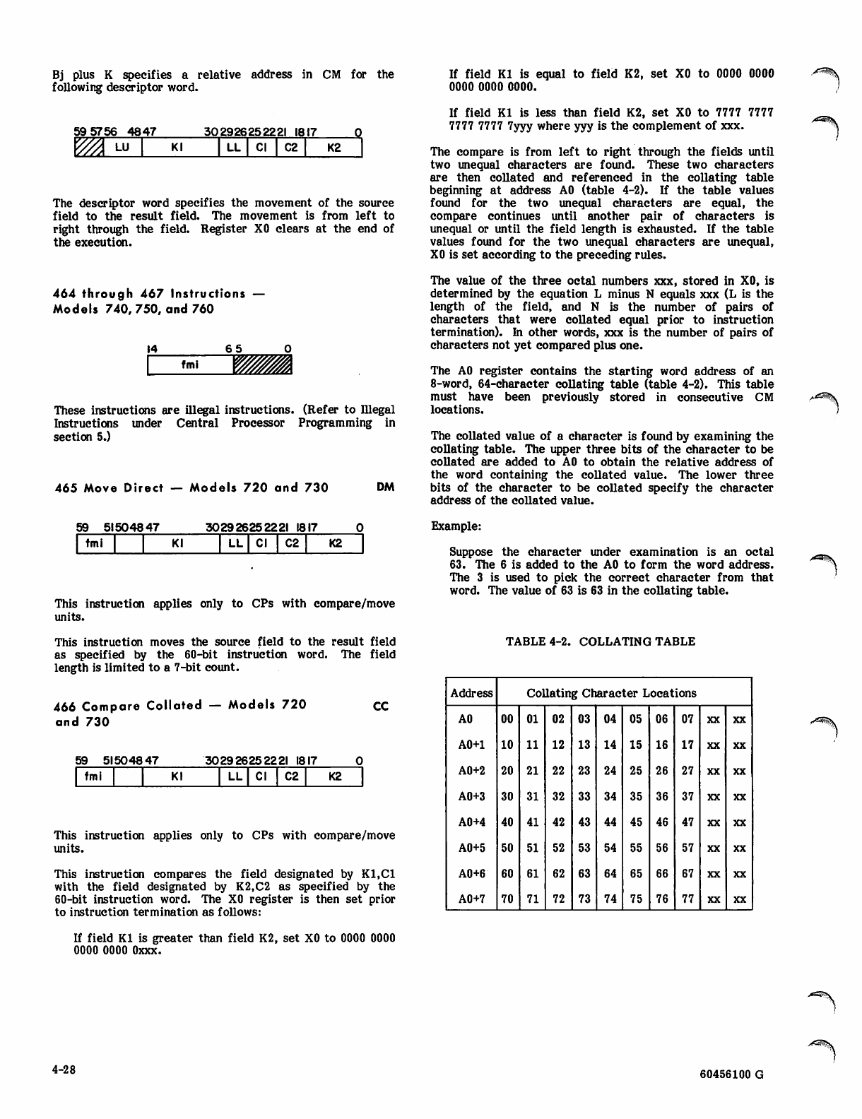
Bj plus K specifies a relative address in CM for the
following descriptor word.
59 5756 4847 302926252221 1817 0
y/A^ Kl LL Cl C2 K2
The descriptor word specifies the movement of the source
field to the result field. The movement is from left to
right through the field. Register XO clears at the end of
the execution.
464 through 467 Instructions —
Models 740, 750, and 760
These instructions are illegal instructions. (Refer to Illegal
Instructions under Central Processor Programming in
section 5.)
465 Move Direct — Models 720 and 730 DM
59 51504847 302926252221 1817
fmi Kl LL Cl C2 K2
This instruction applies only to CPs with compare/move
units.
This instruction moves the source field to the result field
as specified by the 60-bit instruction word. The field
length is limited to a 7-bit count.
466 Compare Collated — Models 720
and 730
CC
59 51504847 302926252221 1817
fmi Kl LL Cl C2 K2
This instruction applies only to CPs with compare/move
units.
This instruction compares the field designated by K1.C1
with the field designated by K2.C2 as specified by the
60-bit instruction word. The XO register is then set prior
to instruction termination as follows:
If field Kl is equal to field K2, set XO to 0000 0000
0000 0000 0000.
If field Kl is less than field K2, set X0 to 7777 7777
7777 7777 7yyy where yyy is the complement of xxx.
The compare is from left to right through the fields until
two unequal characters are found. These two characters
are then collated and referenced in the collating table
beginning at address A0 (table 4-2). If the table values
found for the two unequal characters are equal, the
compare continues until another pair of characters is
unequal or until the field length is exhausted. If the table
values found for the two unequal characters are unequal,
XO is set according to the preceding rules.
The value of the three octal numbers xxx, stored in X0, is
determined by the equation L minus N equals xxx (L is the
length of the field, and N is the number of pairs of
characters that were collated equal prior to instruction
termination). In other words, xxx is the number of pairs of
characters not yet compared plus one.
The A0 register contains the starting word address of an
8-word, 64-character collating table (table 4-2). This table
must have been previously stored in consecutive CM
locations.
The collated value of a character is found by examining the
collating table. The upper three bits of the character to be
collated are added to AO to obtain the relative address of
the word containing the collated value. The lower three
bits of the character to be collated specify the character
address of the collated value.
Example:
Suppose the character under examination is an octal
63. The 6 is added to the A0 to form the word address.
The 3 is used to pick the correct character from that
word. The value of 63 is 63 in the collating table.
TABLE 4-2. COLLATING TABLE
Address Collating Character Locations
A0 00 01 02 03 04 05 06 07 XX XX
A0+1 10 11 12 13 14 15 16 17 XX XX
AO+2 20 21 22 23 24 25 26 27 XX XX
AO+3 30 31 32 33 34 35 36 37 XX XX
AO+4 40 41 42 43 44 45 46 47 XX XX
AO+5 50 51 52 53 54 55 56 57 XX XX
AO+6 60 61 62 63 64 65 66 67 XX XX
AO+7 70 71 72 73 74 75 76 77 XX XX
If field Kl is greater than field K2, set X0 to 0000 0000
0000 0000 Oxxx.
4-28 60456100 G
467 Compare Uncollated — Models
720 and 730
CU 51ijK Set Ai to (Bj) + K SA
59 51504847 302926252221 1817
fmi Kl LL Cl C2 K2
29 2423 2120 1817
fm
This instruction applies only to CPs with compare/move
units.
This instruction is similar to the 466 instruction except
that the collating table is not used. The XO register is set
when the first pair of unequal characters is encountered or
when the field length is exhausted.
47ixk Population Count of (Xk) to Xi
14 9 8 6 5 3 2 0
fm
CX
This two-parcel instruction uses the lower-order 18 bits as
operand K. This instruction reads an operand from Bj,
forms the sum of the operand plus K, and delivers the
result to Ai. If the i designator is nonzero, a reference is
made to CM using the result as the relative address. The
type of reference is a function of the i designator value.
= 0
= 1,2,3,4,5
= 6,7
No CM reference
Read from CM to Xi
Write into CM from Xi
This instruction obtains operands from CM for computation
and delivers the result back into CM.
This instruction reads one operand from Xk, counts the
number of one bits in the operand, and stores the count in
Xi. The count delivered to Xi is a positive integer. If the
operand is all ones, a count of 60 (decimal) is delivered to
Xi. If operand is all zeros, a zero word is delivered to Xi.
52ijK Set Ai to (Xj) + K
29 2423 2120 1817
SA
fm
50ijK Set Ai to (Aj) + K SA
29 2423 2120 (817
fm
This two-parcel instruction uses the lower-order 18 bits as
operand K. This instruction reads an operand from Aj,
forms the sum of the operand plus K, and delivers the
result to Ai. If the i designator is nonzero, a reference is
made to CM using the result as the relative address. The
type of reference is a function of the i designator value.
i = 0
i = 1,2,3,4,5
i = 6,7
No CM reference
Read from CM to Xi
Write into CM from Xi
This instruction obtains operands from CM for computation
and delivers the result back into CM.
This two-parcel instruction uses the lower-order 18 bits as
operand K. This instruction reads an operand from Xj,
forms the sum of the operand plus K, and delivers the
result to Ai. If the i designator is nonzero, a reference is
made to CM using the result as the relative address. The
type of reference is a function of the i designator value.
= 0
= 1,2,3,4,5
= 6,7
No CM reference
Read from CM to Xi
Write into CM from Xi
This instruction obtains operands from CM for computation
and delivers the result back into CM.
53ijk Set Ai to (Xj) + (Bk) SA
14 9 8 6 5 3 2 0
fm
This instruction reads operands from Xj and Bk, forms the
sum of the operands, and delivers the result to Ai. If the i
designator is nonzero, a reference is made to CM using the
result as the relative address. The type of reference is a
function of the i designator value.
60456100 G 4-29
i = 0
i = 1,2,3,4,5
i = 6,7
No CM reference
Read from CM to Xi
Write into CM from Xi
This instruction obtains operands from CM for computation
and delivers the result back into CM.
54ijk Set Ai to (Aj) + (Bk)
14 9865320
fm
SA
This instruction reads operands from Bj and Bk, forms the
sum of the operands, and delivers the result to Ai. If the i
designator is nonzero, a reference is made to CM using the
result as the relative address. The type of reference is a
function of the i designator value.
i = 0
i = 1,2,3,4,5
i = 6,7
No CM reference
Read from CM to Xi
Write into CM from Xi
This instruction obtains operands from CM for computation
and delivers the results back into CM.
57ijk Set Ai to (Bj) - (Bk) SA
-^
This instruction reads operands from Aj and Bk, forms the
sum of the operands, and delivers the result to Ai. If the i
designator is nonzero, a reference is made to CM using the
result as the relative address. The type of reference is a
function of the i designator value.
= 0
= 1,2,3,4,5
= 6,7
No CM reference
Read from CM to Xi
Write into CM from Xi
This instruction obtains operands from CM for computation
and delivers the result back into CM.
55ijk Set Ai to (Aj) - (Bk) SA
14 98 65 32 0
fm
1 4 9 8 6 5 3 2 0
fm
This instruction reads operands from Bj and Bk, subtracts
the Bk operand from the Bj operand, and delivers the result
to Ai. If the i designator is nonzero, a reference is made to
CM using the result as the relative address. The type of
reference is a function of the i designator value.
i = 0
i = 1,2,3,4,5
i = 6,7
No CM reference
Read from CM to Xi
Write into CM from Xi
This instruction obtains operands from CM for computation
and delivers the result back into CM.
60ijK Set Bi to (Aj) + K SB
This instruction reads operands from Aj and Bk, subtracts
the Bk operand from the Aj operand, and delivers the result
to Ai. If the i designator is nonzero, a reference is made to
CM using the result as the relative address. The type of
reference is a function of the i designator value.
i = 0
i = 1,2,3,4,5
i = 6,7
No CM reference
Read from CM to Xi
Write into CM from Xi
This instruction obtains operands from CM for computation
and delivers the results back into CM.
29 24 23 2120 1817
fm
This two-parcel instruction uses the lower-order 18 bits as
operand K. This instruction reads an operand plus K and
delivers the result to Bi. The sum is formed in an 18-bit
one's complement mode. This instruction is for address
modification in the increment registers.'
61ijK Set Bi to (Bj) + K SB
56ijk Set Ai to (Bj) + (Bk)
1 4 9 8 6 5 3 2 0
fm
SA
29 2423 2120 1817
fm
4-30 60456100 G
This two-parcel instruction uses the lower-order 18 bits as
operand K. This instruction reads an operand from Bj,
forms the sum of the operand plus K and delivers the result
to Bi. The sum is formed in an 18-bit one's complement
mode.
66ijk Set Bi to (Bj) + (Bk) SB
14 986532 0
fm
62ijK Set Bi to (Xj) + K
29 2423 2120 1817
SB
fm
This instruction reads operands from Bj and Bk, adds the
operands, and delivers the result to Bi. The sum is formed
in an 18-bit one's complement mode. If the i designator is
zero, this becomes a pass instruction.
This two-parcel instruction uses the lower-order 18 bits as
operand K. This instruction reads an operand from Xj,
forms the sum of the operand plus K, and delivers the
result to Bi. The sum is formed in an 18-bit one's
complement mode.
67ijk Set Bi to (Bj) - (Bk) SB
14 9865320
fm
63ijk Set Bi to (Xj) + (Bk)
14 98 65 32 0
fm
SB This instruction reads operands from Bj and Bk, subtracts
the Bk operand from the Bj operand, and delivers the result
to Bi. The difference is formed in an 18-bit one's
complement mode. If the i designator is zero, this becomes
a pass instruction.
r*
This instruction reads operands from Xj and Bk, adds the
operands, and delivers the result to Bi. The sum is formed
in an 18-bit one's complement mode.
64ijk Set Bi to (Aj) + (Bk) SB
14 9865320
fm
This instruction reads operands from Aj and Bk, adds the
operands, and delivers the result to Bi. The sum is formed
in an 18-bit one's complement mode.
70ijK Set Xi to (Aj) + K SX
29 2423 2120 1817
fm
This two-parcel instruction uses the lower-order 18 bits as
operand K. This instruction reads an operand from Aj,
forms the sum of the operand plus K, and delivers the
result to Xi. The sum is formed in an 18-bit one's
complement mode. The 18-bit result is sign-extended by
copying the highest-order bit or the result into the upper 42
bit positions in Xi.
71ijK Set X! to (Bj) + JC SX
65ijk Set Bi to (Aj) - (Bk) SB
1 4 9 8 6 5 3 2 0
fm
This instruction reads operands from Aj and Bk, subtracts
the Bk operand from the Aj operand, and delivers the result
to Bi. The difference is formed in an 18-bit one's
complement mode. If the i designator is zero, this becomes
a pass instruction.
29 2423 2120 1817
fm
This two-parcel instruction uses the lower-order 18 bits as
operand K. This instruction reads an operand from Bj,
forms the sum of the operand plus K, and delivers the
result to Xi. The sum is formed in an 18-bit one's
complement mode. The 18-bit result is sign-extended by
copying the highest-order bit of the result into the upper 42
bit positions in Xi.
0I^\
60456100 G 4-31
72ijK Set Xi to (Xj) + K SX 76ijk Set Xi to (Bj) + (Bk) SX
29 2423 2120 1817
fm
14 9 8 6 5 3 2 0
fm
This two-parcel instruction uses the lower-order 18 bits as
operand K. This instruction reads an operand from Xj,
forms the sum of the operand plus K, and delivers the
result to Xi. The sum is formed in an 18-bit one's
complement mode. The 18-bit result is sign-extended by
copying the highest-order bit of the result into the upper 42
bit positions in Xi/
73ijk Set Xi to (Xj) + (Bk) SX
) 4 9 8 6 5 3 2 0
fm
This instruction reads operands from Xj and Bk, adds the
operands, and delivers the result to Xi. The sum is formed
in an 18-bit one's complement mode. The 18-bit result is
sign-extended by copying the highest-order bit of the result
into the upper 42 bit positions in Xi.'
This instruction reads operands from Bj and Bk, adds the
operands, and delivers the result to Xi. The sum is formed
in an 18-bit one's complement mode. The 18-bit result is
sign-extended by copying the highest-order bit of the result
into the upper 42 bit positions in Xi.
77ijk Set Xi to (Bj) - (Bk) SX
1 4 9 8 6 5 3 2 0
fm
This instruction reads operands from Bj and Bk, subtracts
the Bk operand from the Bj operand, and delivers the result
to Xi. The difference is formed in an 18-bit one's
complement mode. The 18-bit result is sign-extended by
copying the highest-order bit of the result into the upper 42
bit positions in Xi.
74ijk Set Xi to (Aj) + (Bk) SX
1 4 9 8 6 5 3 2 0
fm
This instruction reads operands from Aj and Bk, adds the
operands, and delivers the result to Xi. The sum is formed
in an 18-bit one's complement mode. The 18-bit result is
sign-extended by copying the highest-order bit of the result
into the upper 42 bit positions in Xi.
75ijk Set Xi to (Aj) - (Bk) SX
1 4 9 8 6 5 3 2 0
fm
CP INSTRUCTION TIMING — MODELS 720 AND 730
Execution times for the CP instructions are listed for
models 720 and 730 in table 4-3. The execution times are
listed with the assumption that no conflicts occur.
Execution delays result unless all the conditions listed in
the timing notes column exist for the particular
instruction. The numbers in the timing notes column refer
to notes listed at the end of the table. Execution times are
in 50-nanosecond clock periods.
CP INSTRUCTION TIMING — MODELS 740, 750, AND 760
Execution times for the CP instructions are listed for
models 740, 750, and 760 in table 4-4. The execution times
are listed with the assumption that no conflicts occur.
Execution delays result unless all the conditions listed in
the timing notes column exist for the particular
instruction. The numbers in the timing notes column refer
to notes listed at the end of the table. Execution times are
in 25-nanosecond clock periods.
This instruction reads operands from Aj and Bk, subtracts
the Bk operand from the Aj operand, and delivers the result
to Xi. The difference is formed in an 18-bit one's
complement mode. The 18-bit result is sign-extended by
copying the highest-order bit of the result into the upper 42
bit positions in Xi.
CP INSTRUCTION TIMING — MODEL 176
Execution times for CP instructions are listed for model
176 in table 4-5. The execution times are listed with the
assumption that no conflicts occur. Execution delays result
unless all the conditions listed in the timing notes column
exist for the particular instruction. The numbers in the
timing notes column refer to notes listed at the end of the
table. Execution times are in 27.5-nanosecond clock
periods.
4-32 60456100 G
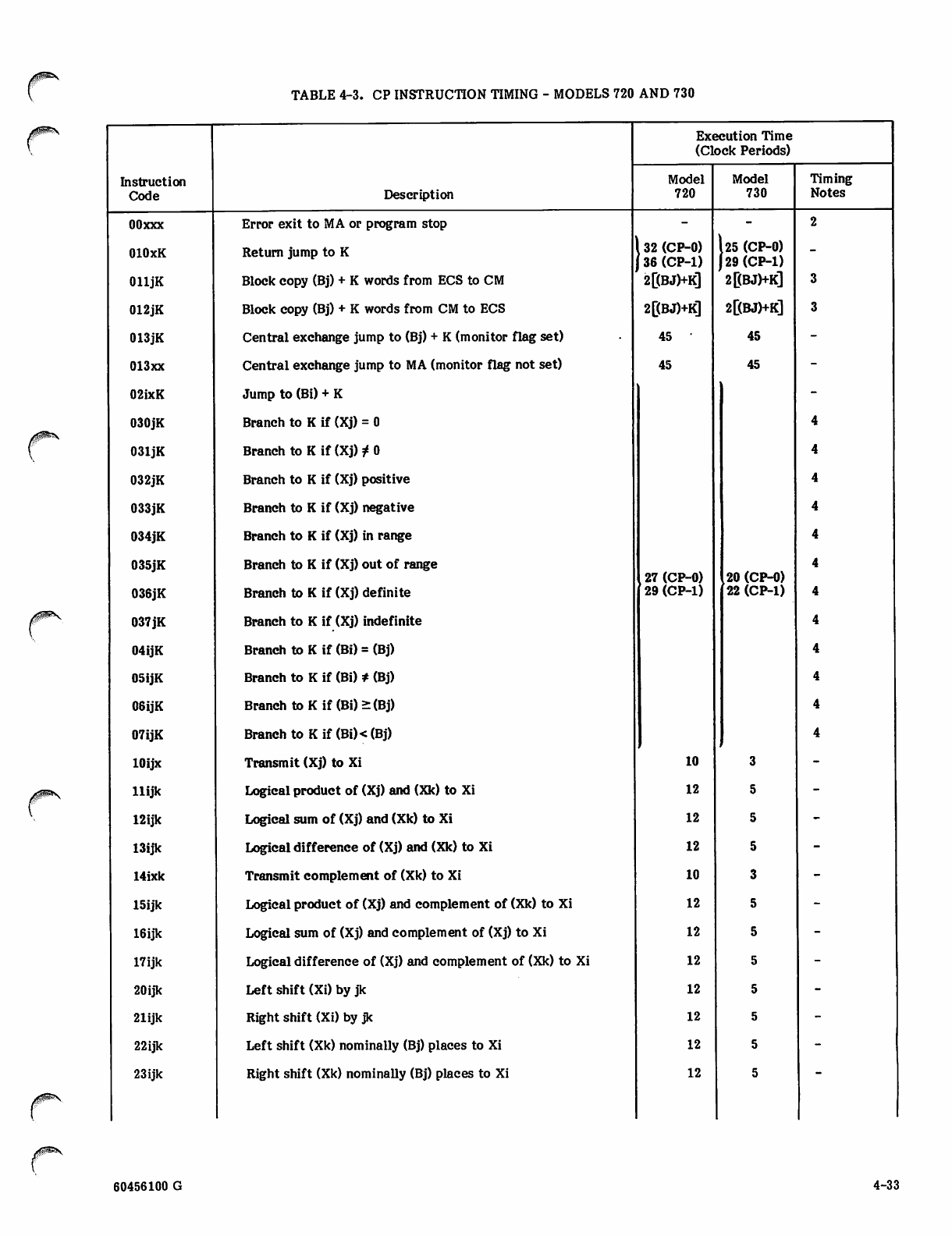
TABLE 4-3. CP INSTRUCTION TIMING - MODELS 720 AND 730
jglW*N
Instruction
Code Description
Execution Time
(Clock Periods)
Model
720
Model
730 Timing
Notes
OOxxx
OlOxK
OlljK
012JK
013JK
013xx
02ixK
030JK
031JK
032JK
033JK
034JK
035JK
036JK
037 jK
04ijK
05ijK
06ijK
07ijK
lOijx
llijk
12ijk
13ijk
14ixk
15ijk
16ijk
17ijk
20ijk
21ijk
22ijk
23ijk
Error exit to MA or program stop
Return jump to K
Block copy (Bj) + K words from ECS to CM
Block copy (Bj) + K words from CM to ECS
Central exchange jump to (Bj) + K (monitor flag set)
Central exchange jump to MA (monitor flag not set)
Jump to (Bi) + K
Branch to K if (Xj) = 0
Branch to K if (Xj) f 0
Branch to K if (Xj) positive
Branch to K if (Xj) negative
Branch to K if (Xj) in range
Branch to K if (Xj) out of range
Branch to K if (Xj) definite
Branch to K if (Xj) indefinite
Branch to K if (Bi) = (Bj)
Branch to K if (Bi) # (Bj)
Branch to K if (Bi)>(Bj)
Branch to K if (Bi)<(Bj)
Transmit (Xj) to Xi
Logical product of (Xj) and (Xk) to Xi
Logical sum of (Xj) and (Xk) to Xi
Logical difference of (Xj) and (Xk) to Xi
Transmit complement of (Xk) to Xi
Logical product of (Xj) and complement of (Xk) to Xi
Logical sum of (Xj) and complement of (Xj) to Xi
Logical difference of (Xj) and complement of (Xk) to Xi
Left shift (Xi) by jk
Right shift (Xi) by jk
Left shift (Xk) nominally (Bj) places to Xi
Right shift (Xk) nominally (Bj) places to Xi
32 (CP-0)
36 (CP-1)
2[(BJ)+K]
2[(BJ)+K]
45 •
45
27 (CP-0)
29 (CP-1)
25 (CP-0)
29 (CP-1)
2[(BJ)+K]
2[(BJ)+K]
45
45
.20 (CP-0)
22 (CP-1)
10
12
12
12
10
12
12
12
12
12
12
12
60456100 G 4-33
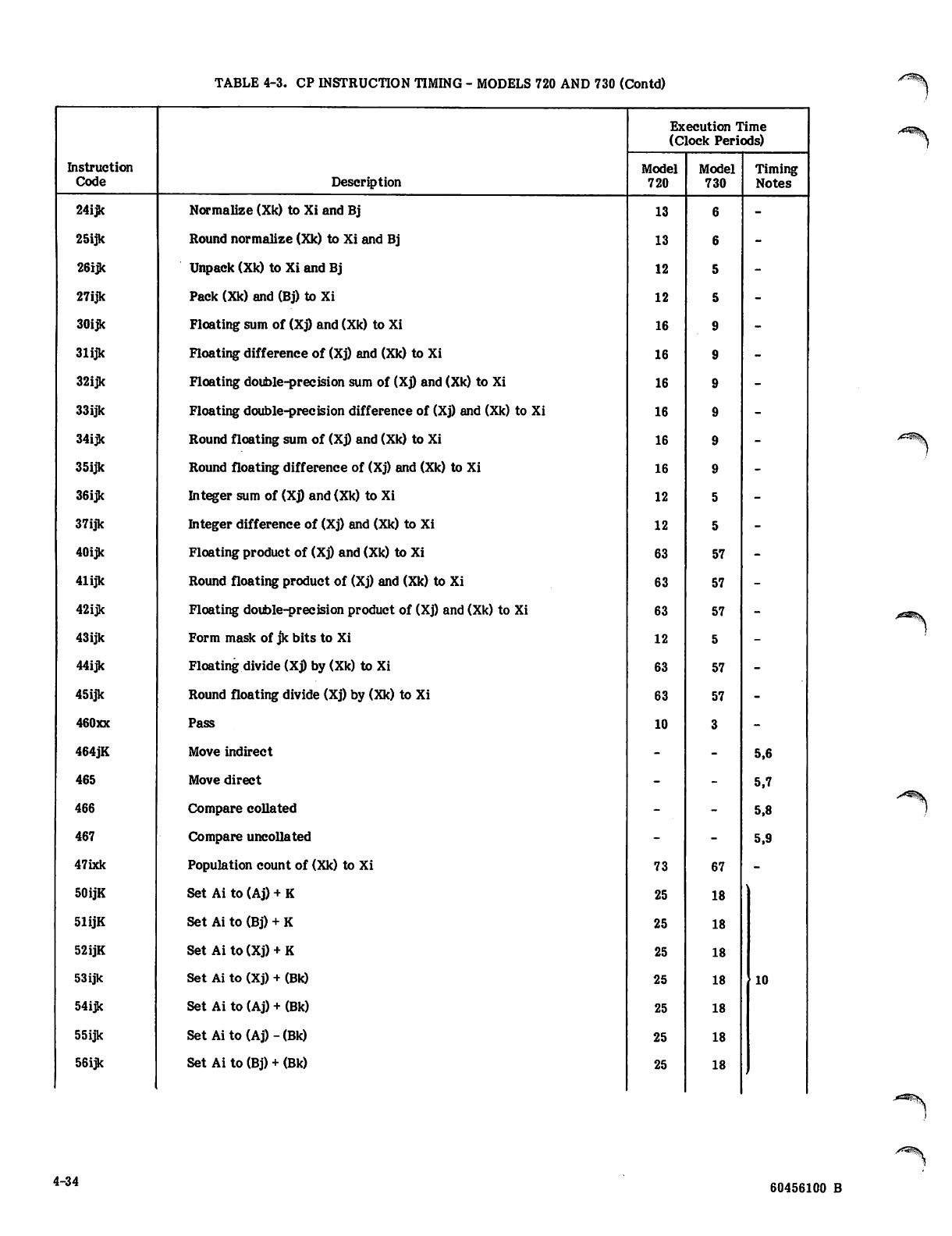
TABLE 4-3. CP INSTRUCTION TIMING - MODELS 720 AND 730 (Contd)
Instruction
Code Description
Execution Time
(Clock Periods)
Model
720
Model
730 Timing
Notes
24ijc Normalize (Xk) to Xi and Bj 13
25ijk Round normalize (Xk) to Xi and Bj 13
26ijk Unpack (Xk) to Xi and Bj 12
27ijk Pack (Xk) and (Bj) to Xi 12
30ijk Floating sum of (Xj) and (Xk) to Xi 16
31ijk Floating difference of (Xj) and (Xk) to Xi 16
32ijk Floating double-precision sum of (Xj) and (Xk) to Xi 16
33ijk Floating double-precision difference of (Xj) and (Xk) to Xi 16
34ijk Round floating sum of (Xj) and (Xk) to Xi 16
35ijk Round floating difference of (Xj) and (Xk) to Xi 16
36ijk Integer sum of (Xj) and (Xk) to Xi 12
37ijk Integer difference of (Xj) and (Xk) to Xi 12
40ijk Floating product of (Xj) and (Xk) to Xi 63 57
41ijk Round floating product of (Xj) and (Xk) to Xi 63 57
42ijk Floating double-precision product of (Xj) and (Xk) to Xi 63 57
43ijk Form mask of jk bits to Xi 12
44ijk Floating divide (Xj) by (Xk) to Xi 63 57
45ijk Round floating divide (Xj) by (Xk) to Xi 63 57
460xx Pass 10
464 jK Move indirect 5,6
465 Move direct 5,7
466 Compare collated 5,8
467 Compare uncollated 5,9
47ixk Population count of (Xk) to Xi 73 67
50ijK Set Ai to (Aj) + K 25 18
51ijK Set Ai to (Bj) + K 25 18
52ijK Set Ai to (Xj) + K 25 18
53ijk Set Ai to (Xj) + (Bk) 25 18 10
54ijk Set Ai to (Aj) + (Bk) 25 18
55ijk Set Aito(Aj)-(Bk) 25 18
56ijk Set Ai to (Bj) + (Bk) 25 18
4-34 60456100 B
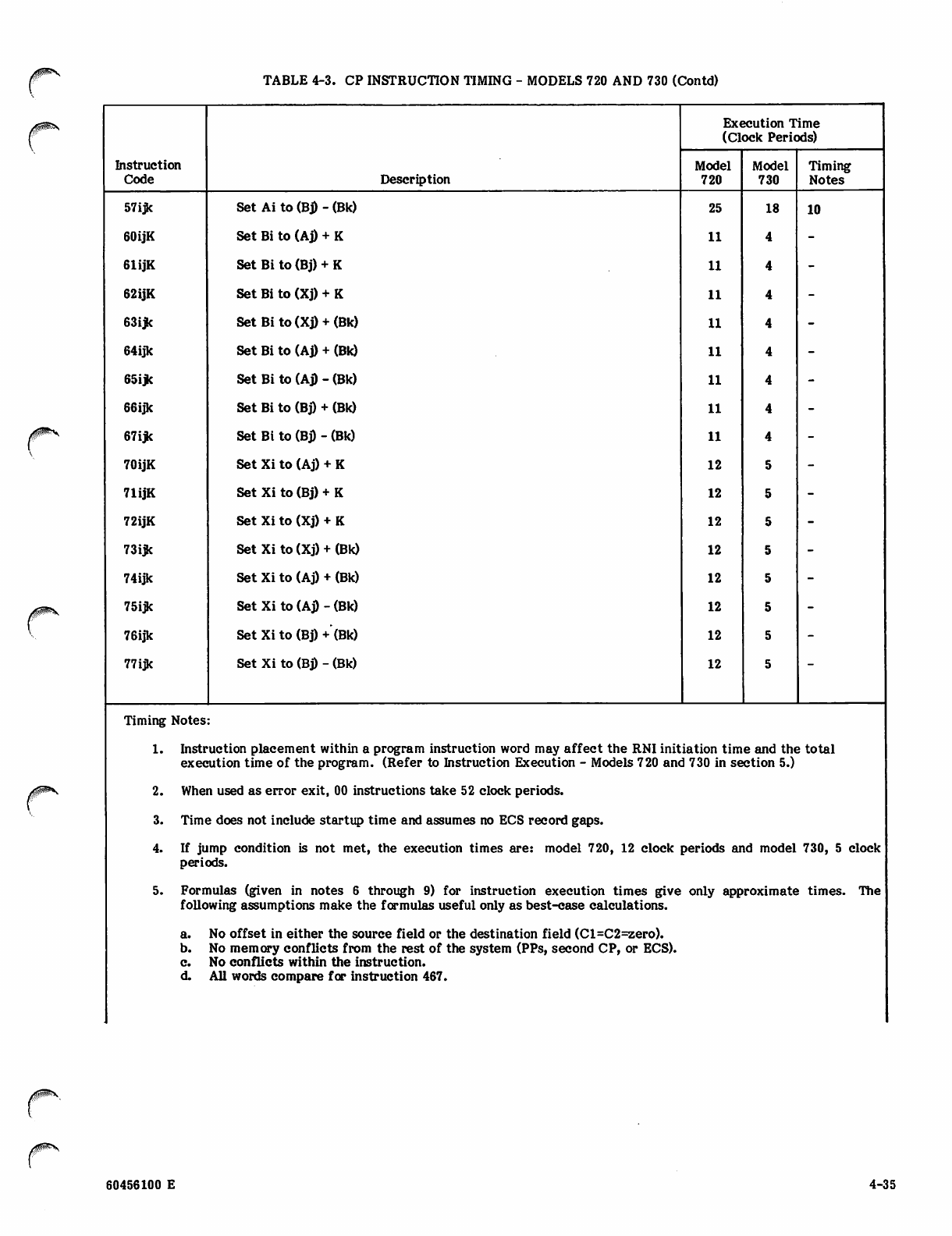
TABLE 4-3. CP INSTRUCTION TIMING - MODELS 720 AND 730 (Contd)
r
Instruction
Code Description
Execution Time
(Clock Periods)
Model
720
Model
730 Timing
Notes
57ijk Set Ai to (Bj) - (Bk) 25 18 10
60ijK Set Bi to (Aj) + K 11
61ijK Set Bi to (Bj) + K 11
62ijK Set Bi to (Xj) + K 11
63ijc Set Bi to (Xj) + (Bk) 11
64ijk Set Bi to (Aj) + (Bk) 11
65ijc Set Bi to (Aj) - (Bk) 11
66ijk Set Bi to (Bj) + (Bk) 11
67ijk Set Bi to (Bj) - (Bk) 11
70ijK Set Xi to (Aj) + K 12
71ijK Set Xi to (Bj) + K 12
72ijK Set Xi to (Xj) + K 12
73ijk Set Xi to (Xj) + (Bk) 12
74ijk Set Xi to (Aj) + (Bk) 12
75ijc Set Xi to (Aj) - (Bk) 12
76ijk Set Xi to (Bj) +'(Bk) 12
77ijk Set Xi to (Bj) - (Bk) 12
Timing Notes:
1. Instruction placement within a program instruction word may affect the RNI initiation time and the total
execution time of the program. (Refer to Instruction Execution - Models 720 and 730 in section 5.)
2. When used as error exit, 00 instructions take 52 clock periods.
3. Time does not include startup time and assumes no ECS record gaps.
4. If jump condition is not met, the execution times are: model 720, 12 clock periods and model 730, 5 clock
periods.
5. Forn
folio
nulas (given in notes 6 through 9) for instruction execution times give
wing assumptions make the formulas useful only as best-case calculations.
only approximate times. The
a. No offset in either the source field or the destination field (Cl=C2=zero).
b. No memory conflicts from the rest of the system (PPs, second CP, or ECS).
c. No conflicts within the instruction.
d. All words compare for instruction 467.
60456100 E 4-35
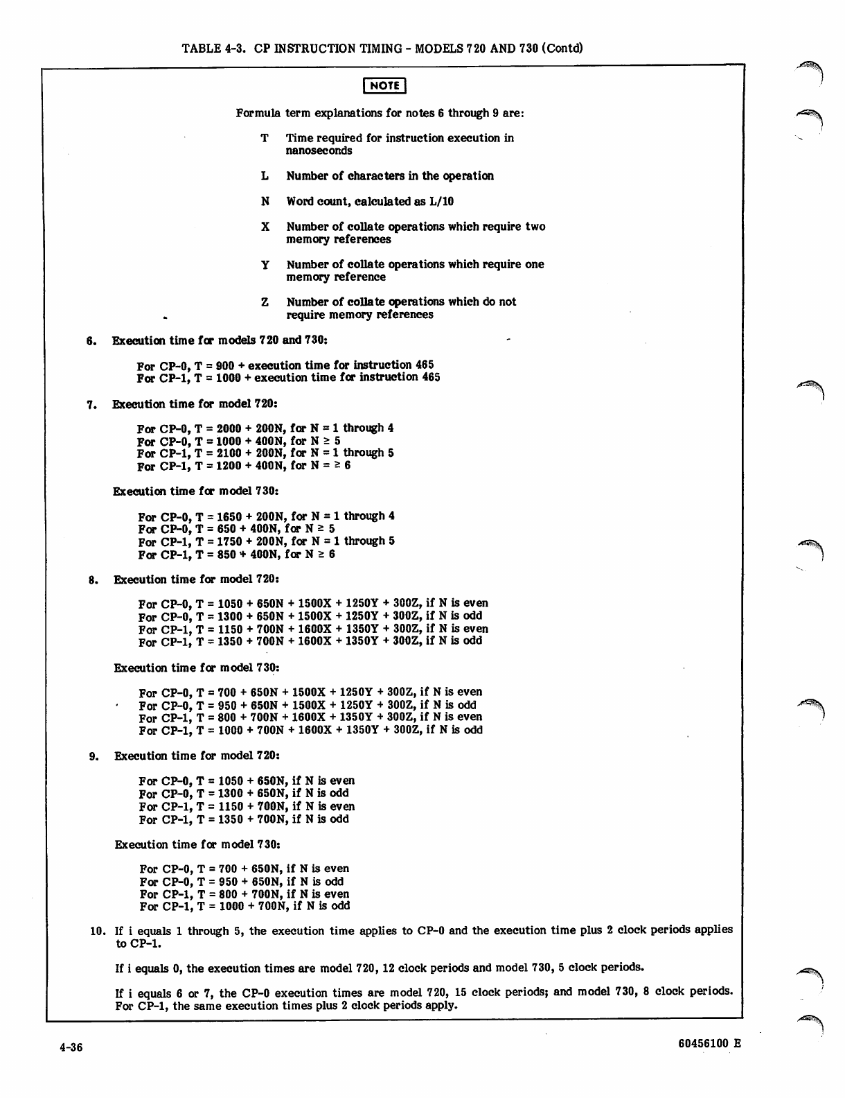
TABLE 4-3. CP INSTRUCTION TIMING - MODELS 720 AND 730 (Contd)
NOTE
Formula term explanations for notes 6 through 9 are:
T Time required for instruction execution in
nanoseconds
L Number of characters in the operation
N Word count, calculated as L/10
X Number of collate operations which require two
memory references
Y Number of collate operations which require one
memory reference
Z Number of collate operations which do not
require memory references
6. Execution time for models 720 and 730:
For CP-0, T = 900 + execution time for instruction 465
For CP-1, T = 1000 + execution time for instruction 465
7. Execution time for model 720:
For CP-0, T = 2000 + 200N, for N = 1 through 4
For CP-0, T = 1000 + 400N, for N > 5
For CP-1, T = 2100 + 200N, f or N = 1 through 5
For CP-1, T = 1200 + 400N, for N = * 6
Execution time for model 730:
For CP-0, T = 1650 + 200N, for N = 1 through 4
For CP-0, T = 650 + 400N, f or N 2 5
For CP-1, T = 1750 + 200N, for N = 1 through 5
For CP-1, T = 850 * 400N, f or N > 6
8. Execution time for model 720:
For CP-0, T = 1050 + 650N + 1500X + 1250Y + 300Z, if N is even
For CP-0, T = 1300 + 650N + 1500X + 1250Y + 300Z, if N is odd
For CP-1, T = 1150 + 700N + 1600X + 1350Y + 300Z, if N is even
For CP-1, T = 1350 + 700N + 1600X + 1350Y + 300Z, if N is odd
Execution time for model 730:
For CP-0, T = 700 + 650N + 1500X + 1250Y + 300Z, if N is even
For CP-0, T = 950 + 650N + 1500X + 1250Y + 300Z, if N is odd
For CP-1, T = 800 + 700N + 1600X + 1350Y + 300Z, if N is even
For CP-1, T = 1000 + 700N + 1600X + 1350Y + 300Z, if N is odd
9. Execution time for model 720:
For CP-0, T = 1050 + 650N, if N is even
For CP-0, T = 1300 + 650N, if N is odd
For CP-1, T = 1150 + 700N, if N is even
For CP-1, T = 1350 + 700N, if N is odd
Execution time for model 730:
For CP-0, T = 700 + 650N, if N is even
For CP-0, T = 950 + 650N, if N is odd
For CP-1, T = 800 + 700N, if N is even
For CP-1, T = 1000 + 700N, if N is odd
10. If i equals 1 through 5, the execution time applies to CP-0 and the execution time plus 2 clock periods applies
to CP-1.
If i equals 0, the execution times are model 720, 12 clock periods and model 730, 5 clock periods.
If i equals 6 or 7, the CP-0 execution times are model 720, 15 clock periods; and model 730, 8 clock periods.
For CP-1, the same execution times plus 2 clock periods apply.
.'*i^!i>
v*^\
4-36 60456100 E
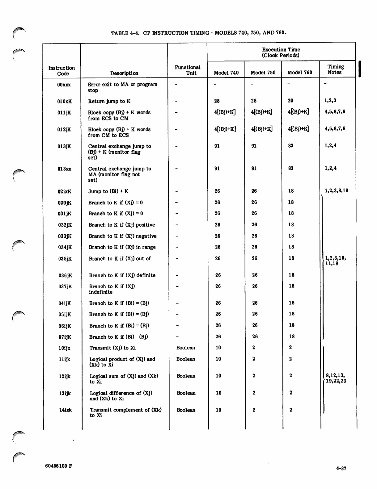
TABLE 4-4. CP INSTRUCTION TIMING - MODELS 740, 750, AND 760.
r
Instruction
Code Description
Functional
Unit
Execution Time
(Clock Periods)
Model 740 Model 750 Model 760 Timing
Notes
OOxxx Bitot exit to MA or program
stop
OlOxK Return jump to K 28 28 20 1,2,3
OlljK Block copy (Bj) + K words
from ECS to CM 4[(Bj)+K] 4[(Bj)+K] 4[(Bj)+K] 4,5,6,7,9
012JK Block copy (Bj) + K words
from CM to ECS 4[(Bj)+K] 4[(Bj)+K] 4[(Bj)+K] 4,5,6,7,9
013JK Central exchange jump to
(Bj) + K (monitor flag
set)
91 91 83 1,2,4
013xx Central exchange jump to
MA (monitor flag not
set)
91 91 83 1,2,4
02ixK Jump to (Bi) + K 26 26 18 1,2,3,8,18
030JK Branch to K if (Xj) = 0 26 26 18
031JK Branch to K if (Xj) = 0 26 26 18
032JK Branch to K if (Xj) positive 26 26 18
033JK Branch to K if (Xj) negative 26 26 18
034JK Branch to K if (Xj) in range 26 26 18
035JK Branch to K if (Xj) out of 26 26 18 ,1,2,3,10,
11,18
036JK Branch to K if (Xj) definite 26 26 18
037JK Branch to K if (Xj)
indefinite
26 26 18
04ijK Branch to K if (Bi) = (Bj) 26 26 18
05ijK Branch to K if (Bi) = (Bj) 26 26 18
06ijK Branch to K if (Bi) = (Bj) 26 26 18
07ijK Branch to K if (Bi) (Bj) 26 26 18
lOijx Transmit (Xj) to Xi Boolean 10
llijk Logical product of (Xj) and
(Xk) to Xi
Boolean 10
12ijk Logical sum of (Xj) and (Xk)
t o X i
Boolean 10 8,12,13,
19,22,23
13ijk Logical difference of (Xj)
and (Xk) to Xi
Boolean 10
14ixk Transmit complement of (Xk)
toXi Boolean 10
/t0^\
60456100 F 4-37
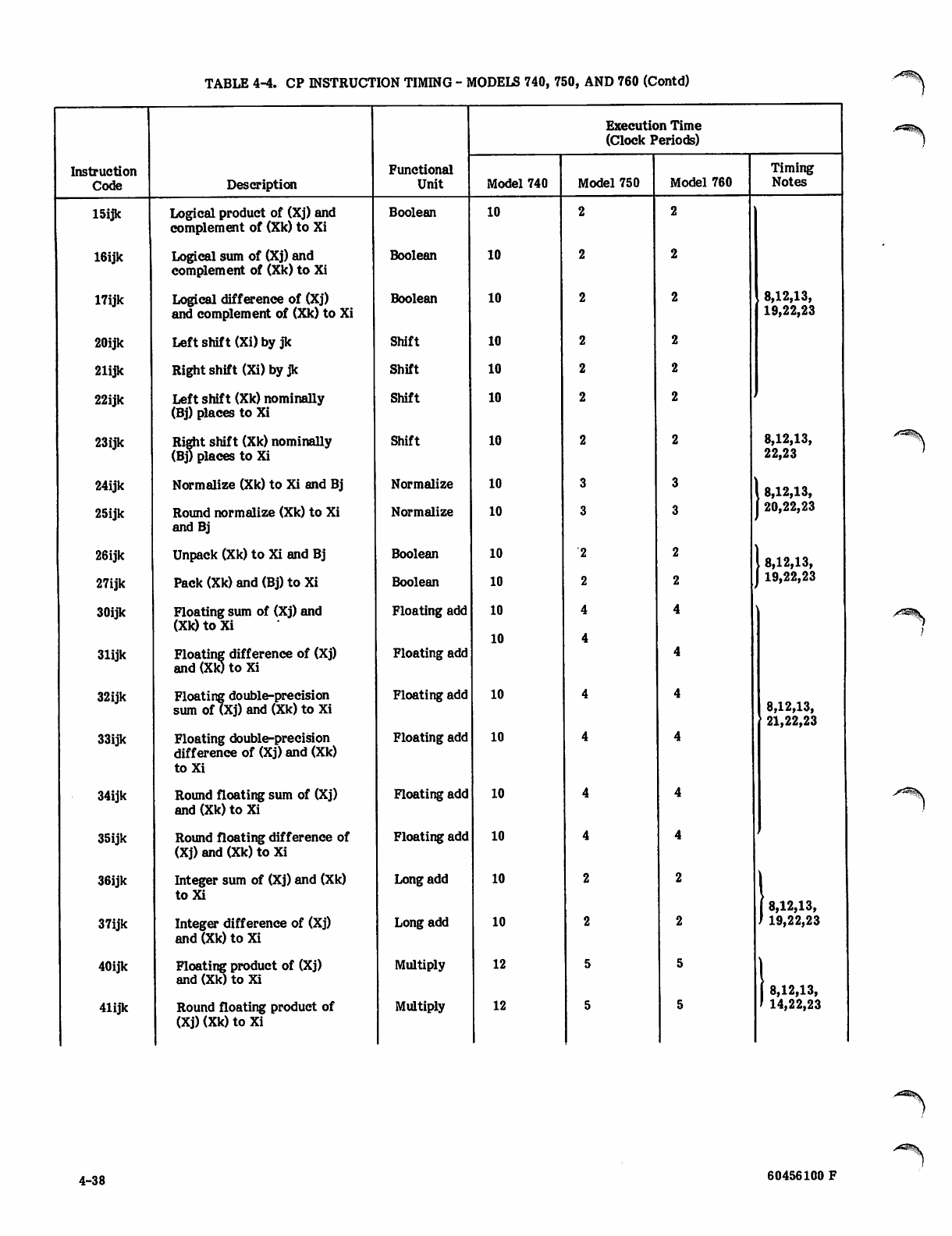
TABLE 4-4. CP INSTRUCTION TIMING - MODELS 740, 750, AND 760 (Contd)
Instruction
Code Description
Functional
Unit
Execution Time
(Clock Periods)
Model 740 Model 750 Model 760 Timing
Notes
15ijk Logical product of (Xj) and
complement of (Xk) to Xi
Boolean 10
16ijk Logical sum of (Xj) and
complement of (Xk) to Xi
Boolean 10
17ijk Logical difference of (Xj)
and complement of (Xk) to Xi
Boolean 10 8,12,13,
19,22,23
20ijk Left shift (Xi) by jk Shift 10
21ijk Right shift (Xi) by jk Shift 10
22ijk Left shift (Xk) nominally
(Bj) places to Xi
Shift 10
23ijk Right shift (Xk) nominally
(Bj) places to Xi
Shift 10 8,12,13,
22,23
24ijk Normalize (Xk) to Xi and Bj Normalize 10 I 8,12,13,
25ijk Round normalize (Xk) to Xi
and Bj
Normalize 10 I 20,22,23
26ijk
27ijk
Unpack (Xk) to Xi and Bj
Pack (Xk) and (Bj) to Xi
Boolean
Boolean
10
10
1 8,12,13,
J 19,22,23
30ijk
31ijk
Floating sum of (Xj) and
(Xk) to Xi
Floating difference of (Xj)
and (Xk) to Xi
Floating add
Floating add
10
10
32ijk
33ijk
Floating double-precision
sum of (Xj) and (Xk) to Xi
Floating double-precision
difference of (Xj) and (Xk)
t o X i
Floating add
Floating add
10
10
8,12,13,
21,22,23
34ijk Round floating sum of (Xj)
and (Xk) to Xi Floating add 10
35ijk Round floating difference of
(Xj) and (Xk) to Xi
Floating add 10
36ijk
37ijk
Integer sum of (Xj) and (Xk)
toXi
Integer difference of (Xj)
and (Xk) to Xi
Long add
Long add
10
10
I 8,12,13,
/ 19,22,23
40ijk
41ijk
Floating product of (Xj)
and (Xk) to Xi
Round floating product of
(Xj) (Xk) to Xi
Multiply
Multiply
12
12 1 8,12,13,
i 14,22,23
4-38 60456100 F
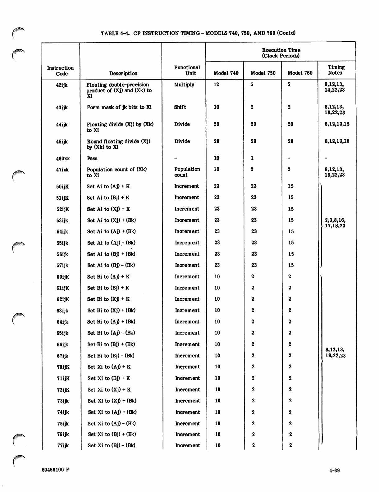
TABLE 4-4. CP INSTRUCTION TIMING - MODELS 740, 750, AND 760 (Contd)
r
0^^\
0H^\
Instruction
Code Description
Functional
Unit
Execution Time
(Clock Periods)
Model 740 Model 750 Model 760 Timing
Notes
42ijk Floating double-precision
product of (Xj) and (Xk) to
Xi
Multiply 12 8,12,13,
14,22,23
43ijk Form mask of jk bits to Xi Shift 10 8,12,13,
19,22,23
44ijk Floating divide (Xj) by (Xk)
t o X i
Divide 28 20 20 8,12,13,15
45ijk Round floating divide (Xj)
by (Xk) to Xi
Divide 28 20 20 8,12,13,15
460xx Pass 10
47ixk Population count of (Xk)
t o X i
Population
count
10 8,12,13,
19,22,23
50ijK Set Ai to (Aj) + K Increment 23 23 15
51ijK Set Ai to (Bj) + K Increment 23 23 15
52ijK Set Ai to (Xj) + K Increment 23 23 15
53ijk
54ijk
Set Ai to (Xj) + (Bk)
Set Ai to (Aj) + (Bk)
Increment
Increment
23
23
23
23
15
15
2,3,8,16,
17,18,23
55ijk Set Ai to (Aj) - (Bk) Increment 23 23 15
56ijk Set Ai to (Bj) + (Bk) Increment 23 23 15
57ijk Set Ai to (Bj) - (Bk) Increment 23 23 15
60ijK Set Bi to (Aj) + K Increment 10
61ijK Set Bi to (Bj) + K Increment 10
62ijK Set Bi to (Xj) + K Increment 10
63ijk Set Bi to (Xj) + (Bk) Increment 10
64ijk Set Bi to (Aj) + (Bk) Increment 10
65ijk Set Bi to (Aj) - (Bk) Increment 10
66ijk
67ijk
Set Bi to (Bj) + (Bk)
Set Bi to (Bj) - (Bk)
Increment
Increment
10
10 8,12,13,
19,22,23
70ijK Set Xi to (Aj) + K Increment 10
71ijK Set Xi to (Bj) + K Increment 10
72ijK Set Xi to (Xj) + K Increment 10
73ijk Set Xi to (Xj) + (Bk) Increment 10
74ijk Set Xi to (Aj) + (Bk) Increment 10
75ijk Set Xi to (Aj) - (Bk) Increment 10
76ijk Set Xi to (Bj) + (Bk) Increment 10
77ijk Set Xi to (Bj) - (Bk) Increment 10
60456100 F 4-39
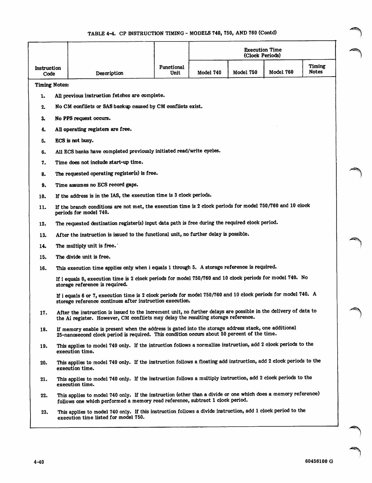
TABLE 4-4. CP INSTRUCTION TIMING - MODELS 740, 750, AND 760 (Contd)
Instruction
Code Description
Functional
Unit
Execution Time
(Clock Periods)
Model 740 Model 750 Model 760 Timing
Notes
Timing Notes:
1. All previous instruction fetches are complete.
2. No CM conflicts or SAS backup caused by CM conflicts exist.
3. No PPS request occurs.
4. All operating registers are free.
5. ECS is not busy.
All ECS banks have completed previously initiated read/write cycles.
Time does not include start-up time.
The requested operating register(s) is free.
Time assumes no ECS record gaps.
If the address is in the IAS, the execution time is 3 clock periods.
6.
7.
8.
9.
10.
11. If the branch conditions are not met, the execution time is 2 clock periods for model 750/760 and 10 clock
periods for model 740.
12. The requested destination registers) input data path is free during the required clock period.
13. After the instruction is issued to the functional unit, no further delay is possible.
14. The multiply unit is free.'
15. The divide unit is free.
16. This execution time applies only when i equals 1 through 5. A storage reference is required.
If i equals 0, execution time is 2 clock periods for model 750/760 and 10 clock periods for model 740. No
storage reference is required.
If i equals 6 or 7, execution time is 2 clock periods for model 750/760 and 10 clock periods for model 740. A
storage reference continues after instruction execution.
17. After the instruction is issued to the increment unit, no further delays are possible in the delivery of data to
the Ai register. However, CM conflicts may delay the resulting storage reference.
18. If memory enable is present when the address is gated into the storage address stack, one additional
25-nanosecond clock period is required. This condition occurs about 50 percent of the time.
19. This applies to model 740 only. If the intruction follows a normalize instruction, add 2 clock periods to the
execution time.
20. This applies to model 740 only. If the instruction follows a floating add instruction, add 2 clock periods to the
execution time.
21. This applies to model 740 only. If the instruction follows a multiply instruction, add 2 clock periods to the
execution time.
22. This applies to model 740 only. If the instruction (other than a divide or one which does a memory reference)
follows one which performed a memory read reference, subtract 1 clock period.
23. This applies to model 740 only. If this instruction follows a divide instruction, add 1 clock period to the
execution time listed for model 750.
4-40
*^\
60456100 G
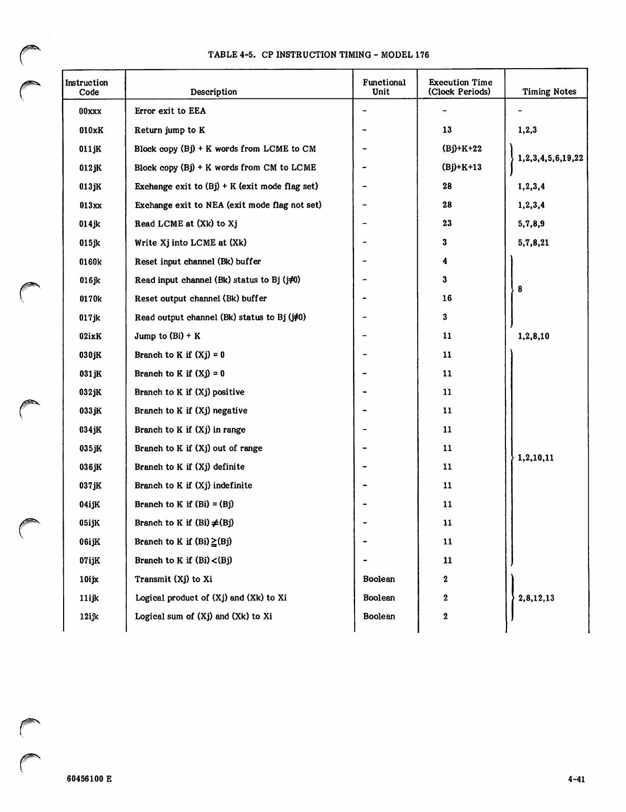
TABLE 4-5. CP INSTRUCTION TIMING - MODEL 176
Instruction
Code Description
Functional
Unit
Execution Time
(Clock Periods) Timing Notes
OOxxx Error exit to EEA
OlOxK Return jump to K 13 1,2,3
OlljK
012JK
Block copy (Bj) + K words from LCME to CM
Block copy (Bj) + K words from CM to LCME
(Bj)+K+22
(Bj)+K+13
1 1,2,3,4,5,6,19,22
013JK Exchange exit to (Bj) + K (exit mode flag set) 28 1,2,3,4
013xx Exchange exit to NEA (exit mode flag not set) 28 1,2,3,4
014jk Read LCME at (Xk) to Xj 23 5,7,8,9
015jk Write Xj into LCME at (Xk) 5,7,8,21
0160k Reset input channel (Bk) buffer
016jk Read input channel (Bk) status to Bj (j#J)
0170k Reset output channel (Bk) buffer 16
017jk Read output channel (Bk) status to Bj (j#0)
02ixK Jump to (Bi) + K 1,2,8,10
030JK Branch to K if (Xj) = 0
031 jK Branch to K if (Xj) = 0
032JK Branch to K if (Xj) positive
033 jK Branch to K if (Xj) negative
034JK Branch to K if (Xj) in range
035JK
036JK
Branch to K if (Xj) out of range
Branch to K if (Xj) definite
""
1,2,10,11
037JK Branch to K if (Xj) indefinite
04ijK Branch to K if (Bi) = (Bj)
05ijK Branch to K if (Bi) #(Bj)
06ijK Branch to K if (Bi)>(Bj)
07ijK Branch to K if (Bi)<(Bj)
lOijx Transmit (Xj) to Xi Boolean
llijk Logical product of (Xj) and (Xk) to Xi Boolean 2,8,12,13
12ijk Logical sum of (Xj) and (Xk) to Xi Boolean
60456100 E 4-41
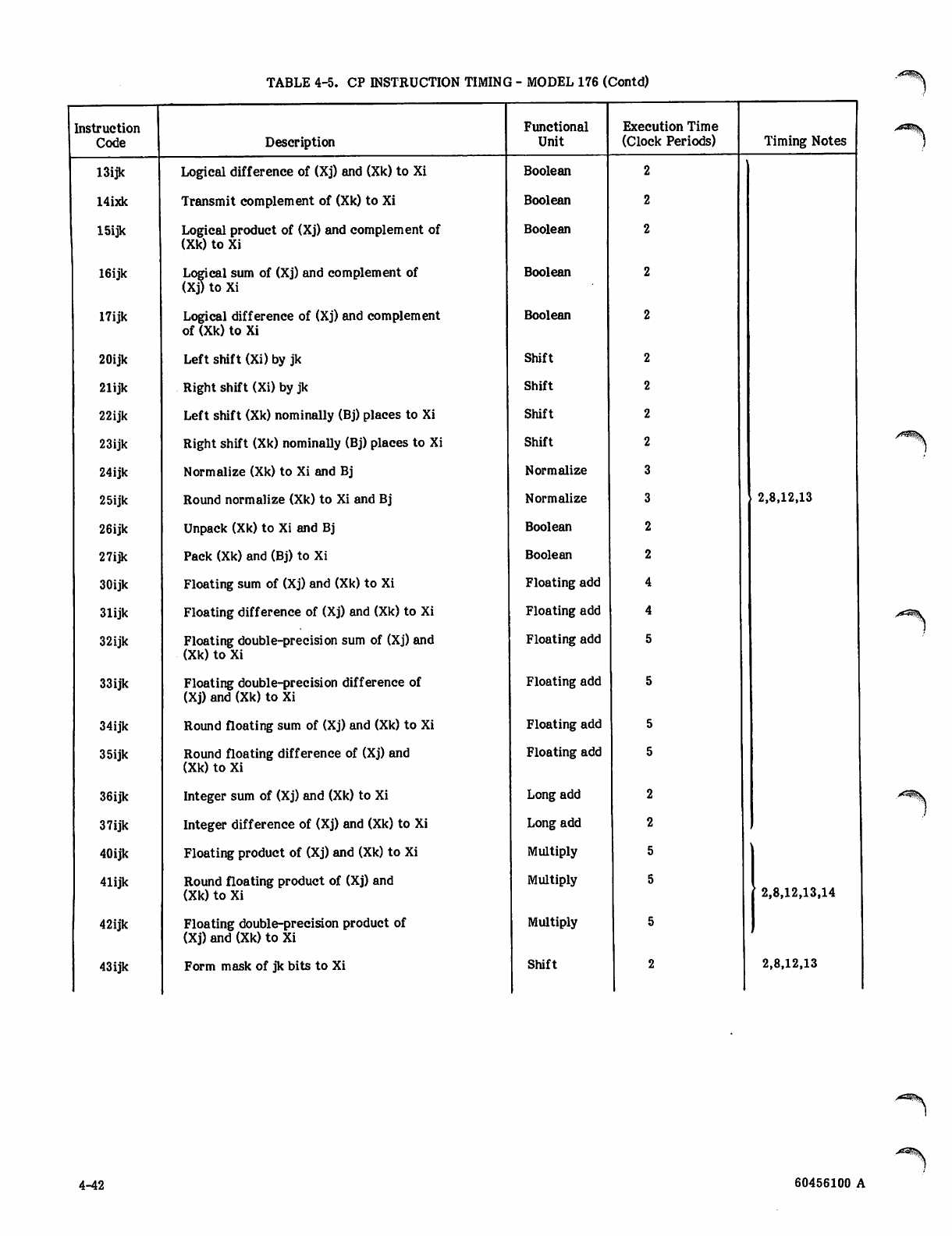
TABLE 4-5. CP INSTRUCTION TIMING - MODEL 176 (Contd)
Instruction
Code Description
13ijk Logical difference of (Xj) and (Xk) to Xi
14ixk Transmit complement of (Xk) to Xi
15ijk Logical product of (Xj) and complement of
(Xk) to Xi
16ijk Logical sum of (Xj) and complement of
(Xj) to Xi
17ijk Logical difference of (Xj) and complement
of (Xk) to Xi
20ijk Left shift (Xi) by jk
21ijk Right shift (Xi) by jk
22ijk Left shift (Xk) nominally (Bj) places to Xi
23ijk Right shift (Xk) nominally (Bj) places to Xi
24ijk Normalize (Xk) to Xi and Bj
25ijk Round normalize (Xk) to Xi and Bj
26ijk Unpack (Xk) to Xi and Bj
27ijk Pack (Xk) and (Bj) to Xi
30ijk Floating sum of (Xj) and (Xk) to Xi
31ijk Floating difference of (Xj) and (Xk) to Xi
32ijk Floating double-precision sum of (Xj) and
(Xk) to Xi
33ijk Floating double-precision difference of
(Xj) and (Xk) to Xi
34ijk Round floating sum of (Xj) and (Xk) to Xi
35ijk Round floating difference of (Xj) and
(Xk) to Xi
36ijk Integer sum of (Xj) and (Xk) to Xi
37ijk Integer difference of (Xj) and (Xk) to Xi
40ijk Floating product of (Xj) and (Xk) to Xi
41ijk Round floating product of (Xj) and
(Xk) to Xi
42ijk Floating double-precision product of
(Xj) and (Xk) to Xi
43ijk Form mask of jk bits to Xi
Functional
Unit
Boolean
Boolean
Boolean
Boolean
Boolean
Shift
Shift
Shift
Shift
Normalize
Normalize
Boolean
Boolean
Floating add
Floating add
Floating add
Floating add
Floating add
Floating add
Long add
Long add
Multiply
Multiply
Multiply
Shift
Execution Time
(Clock Periods) Timing Notes
2,8,12,13
2,8,12,13,14
2,8,12,13
4-42 60456100 A
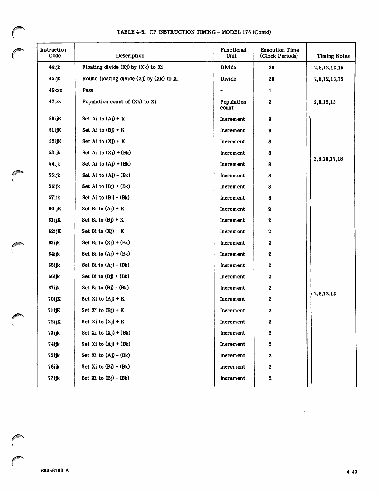
TABLE 4-5. CP INSTRUCTION TIMING - MODEL 176 (Contd)
Instruction
Code Description
Functional
Unit
Execution Time
(Clock Periods) Timing Notes
44ijk Floating divide (Xj) by (Xk) to Xi Divide 20 2,8,12,13,15
45ijk Round floating divide (Xj) by (Xk) to Xi Divide 20 2,8,12,13,15
46xxx Pass
47ixk Population count of (Xk) to Xi Population
count 2,8,12,13
50ijK Set Ai to (Aj) + K Increment
51ijK Set Ai to (Bj) + K Increment
52ijK Set Ai to (Xj) + K Increment
53ijk
54ijk
Set Ai to (Xj) + (Bk)
Set Ai to (Aj) + (Bk)
Increment
Increment 2,8,16,17,18
55ijk Set A i to (Aj) - (Bk) Increment
56ijk Set Ai to (Bj) + (Bk) Increment
57ijk Set Ai to (Bj) - (Bk) Increment
60ijK Set Bi to (Aj) + K Increment
61ijK Set Bi to (Bj) + K Increment
62ijK Set Bi to (Xj) + K Increment
63ijk Set Bi to (Xj) + (Bk) Increment
64ijk SetBito(Aj) +(Bk) Increment
65ijk Set Bi to (Aj) - (Bk) Increment
66ijk Set Bi to (Bj) + (Bk) Increment
67ijk
70ijK
Set Bi to (Bj) - (Bk)
Set Xi to (Aj) + K
Increment
Increment 2,8,12,13
71ijK Set Xi to (Bj) + K Increment
72ijK Set Xi to (Xj) + K Increment
73ijk Set Xi to (Xj) + (Bk) Increment
74ijk Set Xi to (Aj) + (Bk) Increment
75ijk Set Xi to (Aj) - (Bk) Increment
76ijk Set Xi to (Bj) + (Bk) Increment
77ijk Set Xi to (Bj) - (Bk) Increment
60456100 A 4-43
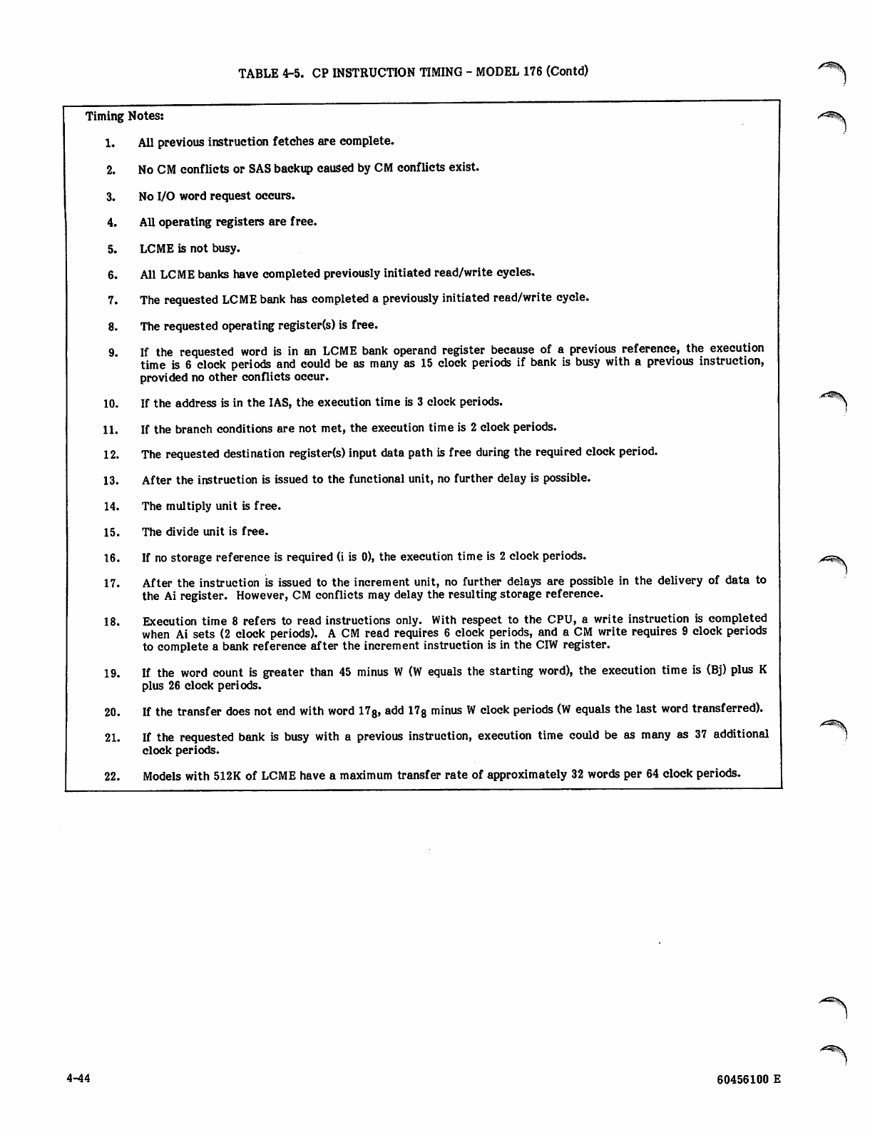
TABLE 4-5. CP INSTRUCTION TIMING - MODEL 176 (Contd)
Timing Notes:
1. All previous instruction fetches are complete.
2. No CM conflicts or SAS backup caused by CM conflicts exist.
3. No I/O word request occurs.
4. All operating registers are free.
5. LCME is not busy.
6. All LCME banks have completed previously initiated read/write cycles.
7. The requested LCME bank has completed a previously initiated read/write cycle.
8. The requested operating register(s) is free.
9. If the requested word is in an LCME bank operand register because of a previous reference, the execution
time is 6 clock periods and could be as many as 15 clock periods if bank is busy with a previous instruction,
provided no other conflicts occur.
10. If the address is in the IAS, the execution time is 3 clock periods.
11. If the branch conditions are not met, the execution time is 2 clock periods.
12. The requested destination register(s) input data path is free during the required clock period.
13. After the instruction is issued to the functional unit, no further delay is possible.
14. The multiply unit is free.
15. The divide unit is free.
16. If no storage reference is required (i is 0), the execution time is 2 clock periods.
17. After the instruction is issued to the increment unit, no further delays are possible in the delivery of data to
the Ai register. However, CM conflicts may delay the resulting storage reference.
18. Execution time 8 refers to read instructions only. With respect to the CPU, a write instruction is completed
when Ai sets (2 clock periods). A CM read requires 6 clock periods, and a CM write requires 9 clock periods
to complete a bank reference after the increment instruction is in the CIW register.
19. If the word count is greater than 45 minus W (W equals the starting word), the execution time is (Bj) plus K
plus 26 clock periods.
20. If the transfer does not end with word 178, add 17g minus W clock periods (W equals the last word transferred).
21. If the requested bank is busy with a previous instruction, execution time could be as many as 37 additional
clock periods.
22. Models with 512K of LCME have a maximum transfer rate of approximately 32 words per 64 clock periods.
/ T - t i r ^ ^ % .
^=%.
4-44 60456100 E
FERIPHIRM PROCESSOR UNITS (OPTION Al) - JVlOEEfc 176

■i"*^V-'
,./^^.
\
V
: ^ ^
0 f ^ \ PERIPHERAL PROCESSOR UNIT
INSTRUCTIONS - MODEL 176
Each PPU sequentially executes instructions from its own
memory and uses an 18-bit A register for manipulative
operations. The A register is the only PPU register used by
the programmer. All the PPU arithmetic operations are
binary and are performed in a one's complement mode.
This mode treats any value of 777777 in the A register as
negative zero.
The PPU instructions are the same and produce the same
results as the PP instructions, except for the instructions
listed in table 4-6. Corresponding PPU and PP instructions
produce the same results through the use of different
hardware processing techniques. These techniques do not
affect the programming and are not evident, except in
some of the detailed instruction descriptions that refer to
the X register, which exists only in the PPU hardware.
The PPU instruction descriptions provide greater detail
than those for the PPs and may be used with corresponding
PP descriptions to add clarity. Examples of additional
detail are in PPU instructions 01, 02, and 50 through 57.
These instruction descriptions are expanded to include
special-case explanations which are not repeated in the PP
instruction descriptions.
Similarities of the PPU and PP instructions permit common
descriptions of the instruction formats, designators, and
addressing modes (except for parts of direct and indirect
addressing).
Section 5 contains additional information for PPU and PP
programming.
TABLE 4-6. PPU AND PP INSTRUCTION DIFFERENCES
Instruction
Code PPU Instruction Description PP Instruction Description
00 OOxx Error stop 0000 Pass
24 24xx Pass 2400 Pass
25 25xx Pass 2500 Pass
26 26xx Pass 260x
261x
262x
Exchange jump
Monitor exchange jump - models
720 through 760
Monitor exchange jump to MA - models
720 through 760
27 27xx Pass 27x Read program address
60 60dm Jump to m if channel d input word
flag set
60d Central read from (A) to d
61 61dm Jump to m if channel d input word
flag not set
61dm Central read (d) words from (A) to m
62 62dm Jump to m if channel d input record
flag set
62dm Central write to (A) from d
63 63dm Jump to m if channel d input record
flag not set
63dm Central write (d) words to (A) from m
64 64dm Jump to m if channel d output word
flag set
64dm Jump to m if channel d active
65 65dm Jump to m if channel d output word
flag not set
65dm Jump to m if channel d inactive
66 66dm Jump to m if channel d output record
flag set
66dm Jump to m if channel d full
67 67dm Jump to m if channel d output record
flag not set
67dm Jump to m if channel d empty
74 74d Set output record flag on channel d 74d Activate channel d
75 75xx Pass 75d Disconnect channel d
76 76xx Pass 76d Function (A) on channel d
77 77xx Error stop 77dm Function m on channel d
60456100 E 4-45
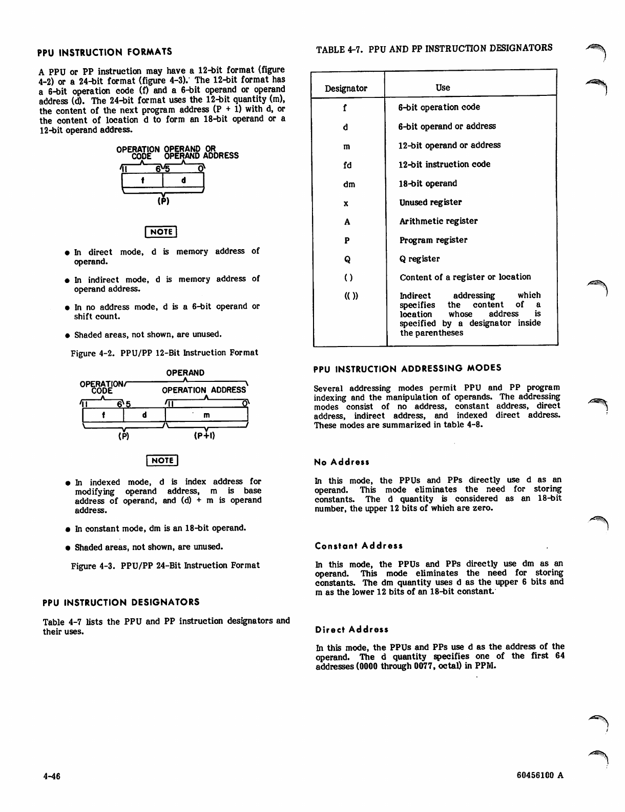
PPU INSTRUCTION FORMATS
A PPU or PP instruction may have a 12-bit format (figure
4-2) or a 24-bit format (figure 4-3). The 12-bit format has
a 6-bit operation code (f) and a 6-bit operand or operand
address (d). The 24-bit format uses the 12-bit quantity (m),
the content of the next program address (P + 1) with d, or
the content of location d to form an 18-bit operand or a
12-bit operand address.
OPERATION OPERAND OR ^
CODE OPERAND ADDRESS
41—yU-§"5—^—fr
TABLE 4-7. PPU AND PP INSTRUCTION DESIGNATORS
f d
(P)
| NOTE |
• In direct mode, d is memory address of
operand.
• In indirect mode, d is memory address of
operand address.
• In no address mode, d is a 6-bit operand or
shift count.
• Shaded areas, not shown, are unused.
Figure 4-2. PPU/PP 12-Bit Instruction Format
OPERATION/-
CODE
n 6 ^ 5
OPERAND
A
f
OPERATION ADDRESS
—v-
(P)
JV —v—
(P+l)
Designator
f
d
m
fd
dm
x
A
P
Q
()
(())
Use
6-bit operation code
6-bit operand or address
12-bit operand or address
12-bit instruction code
18-bit operand
Unused register
Arithmetic register
Program register
Q register
Content of a register or location
Indirect addressing which
specifies the content of a
location whose address is
specified by a designator inside
the parentheses
PPU INSTRUCTION ADDRESSING MODES
Several addressing modes permit PPU and PP program
indexing and the manipulation of operands. The addressing
modes consist of no address, constant address, direct
address, indirect address, and indexed direct address.
These modes are summarized in table 4-8.
1 NOTE I
• In indexed mode, d is index address for
modifying operand address, m is base
address of operand, and (d) + m is operand
address.
• In constant mode, dm is an 18-bit operand.
• Shaded areas, not shown, are unused.
Figure 4-3. PPU/PP 24-Bit Instruction Format
PPU INSTRUCTION DESIGNATORS
Table 4-7 lists the PPU and PP instruction designators and
their uses.
No Address
In this mode, the PPUs and PPs directly use d as an
operand. This mode eliminates the need for storing
constants. The d quantity is considered as an 18-bit
number, the upper 12 bits of which are zero.
Constant Address
In this mode, the PPUs and PPs directly use dm as an
operand. This mode eliminates the need for storing
constants. The dm quantity uses d as the upper 6 bits and
m as the lower 12 bits of an 18-bit constant
Direct Address
In this mode, the PPUs and PPs use d as the address of the
operand. The d quantity specifies one of the first 64
addresses (0000 through 0077, octal) in PPM.
/**^%y
4-46 60456100 A
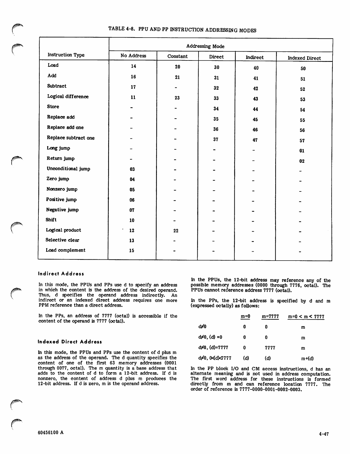
TABLE 4-8. PPU AND PP INSTRUCTION ADDRESSING MODES
r
ySiP^V
Instruction Type
Addressing Mode
No Address Constant Direct Indirect Indexed Direct
Load 14 20 30 40 50
Add 16 21 31 41 51
Subtract 17 32 42 52
Logical difference 11 23 33 43 53
Store 34 44 54
Replace add 35 45 55
Replace add one 36 46 56
Replace subtract one 37 47 57
Long jump 01
Return jump 02
Unconditional jump 03
Zero jump 04
Nonzero jump 05
Positive jump 06
Negative jump 07
Shift 10
Logical product 12 22
Selective clear 13
Load complement 15
Indirect Address
In this mode, the PPUs and PPs use d to specify an address
in which the content is the address of the desired operand.
Thus, d specifies the operand address indirectly. An
indirect or an indexed direct address requires one more
PPM reference than a direct address.
In the PPs, an address of 7777 (octal) is accessible if the
content of the operand is 7777 (octal).
Indexed Direct Address
In this mode, the PPUs and PPs use the content of d plus m
as the address of the operand. The d quantity specifies the
content of one of the first 63 memory addresses (0001
through 0077, octal). The m quantity is a base address that
adds to the content of d to form a 12-bit address. If d is
nonzero, the content of address d plus m produces the
12-bit address. If d is zero, m is the operand address.
In the PPUs, the 12-bit address may reference any of the
possible memory addresses (0000 through 7776, octal). The
PPUs cannot reference address 7777 (octal).
In the PPs, the 12-bit address is specified by d and m
(expressed oc tally) as follows:
m=0 m=7777 rn-=0 < m < 7777
oV0
d#), (d) =0
d#), (d)=7777 7777
d#), (Xd>tf777 (d) (d) m-Kd)
In the PP block I/O and CM access instructions, d has an
alternate meaning and is not used in address computation.
The first word address for these instructions is formed
directly from m and can reference location 7777. The
order of reference is 7777-0000-0001-0002-0003.
60456100 A 4-47
PPU INSTRUCTION DESCRIPTIONS 0200m Return Jump to m RJM
OOxx Error Stop ESN
23 1817 12II
td
\ _ A -
(P) (P+l)
This instruction causes the PPU program execution to stop
and to indicate a program error condition to the status and
control register. The PPU can be restarted only by a
deadstart.
0100m Long Jump to m UM
23 1817 12 11
f d
\
(F
r
>)
* V '
(P+D
This instruction interrupts the current program sequence
and inserts the execution of a subroutine between the
current instruction in the present sequence and the
following instruction. The called subroutine must have a
common exit point in the form of a long jump to m
instruction preceding the entry point. The return jump
instruction inserts the exit address in the m location of the
subroutine exit and then jumps to the entry point in the
following word.
The value of d in this instruction must be zero. The
instruction begins by reading the quantity m from the
storage location determined by the content of P plus 1 to
the Q register. This quantity is then used as an address to
store the content of P plus 2 at storage location m. The
first word of the new program sequence then reads from
storage location m plus 1.
This instruction terminates the current program sequence
with a jump to a new sequence beginning at address m. The
value of d must be zero for this instruction. The
instruction begins by reading the quantity m from the
storage location determined by the content of P plus 1 to
the X register. The address for the new program sequence
forms by adding the content of X to a zero value in the Q
register. This address is then used to obtain the first word
of the new program sequence.
02dm Return Jump to m + (d)
23 18 17 1211
RJM
f d m
\A /
V
(P) (P+l)
01dm Long Jump to m + d UM
23 18 17 12 11
f d
\ /v /
(F
t
>) (P+l)
This instruction terminates the current program sequence
with a jump to a new sequence beginning at address m plus
the content of d. The value of d must be nonzero for this
instruction. The instruction begins by reading the quantity
m from the storage location determined by the content of
P plus 1 and holding this quantity in the Q register. The
content of location d then reads into the X register. The
address for the new program sequence forms by adding the
content of Q to the content of X in a 12-bit one's
complement mode. This address is then used to obtain the
first word of the new program sequence.
This instruction interrupts the current program sequence
and inserts the execution of a subroutine between the
current instruction in the present sequence and the
following instruction. The called subroutine must have a
common exit point in the form of a long jump to m
instruction preceding the entry point. The return jump
instruction inserts the exit address in the m location of the
subroutine exit and then jumps to the entry point in the
following word.
The value of d in this instruction must be nonzero. The
instruction begins by reading the quantity m from the
storage location determined by the content of P plus 1 to
the Q register. The content of location d then reads into
the X register. The address for the new program sequence
forms by adding the content of Q to the content of X in a
12-bit one's complement mode. The resulting address is
used to store the content of P plus 2 in the m field of the
called subroutine exit instruction. The first word of the
new program then reads from the following storage
location.
4-48 60456100 G
y*SP>\,
03d Unconditional Jump d UJN
I I 6 5 0
f d
This instruction interrupts the current program sequence
with a jump to a new sequence beginning at an address
incrementally related to the current program address. The
d designator may specify a new sequence which begins at
an address either forward or backward from the current
address by an amount no greater than 31 (decimal)
locations. The d designator is considered as a 6-bit one's
complement number in determining the increment for the
jump.
As an example, consider a d value of 16 (octal). The new
program sequence in this case begins with an instruction
word located 16 (octal) locations beyond the location of the
03d instruction. Now consider a d value of 55 (octal). The
new program sequence in this case begins with an
instruction word located 22 (octal) locations before the
location of the 03d instruction. Values of 00 and 77 for the
d designator must not be used with this instruction. These
two values cause the PPU program to lock up and require
deadstarting the system with a new program.
04d Zero Jump d ZJN
I I 6 5 0
t d
This conditional branch instruction continues the current
program sequence or jumps to a new program sequence,
depending upon the content of the A register. If the
content of A is not 000000, the current program sequence
terminates with a jump to an address specified by the
content of P plus the d designator. If the content of A is
000000, the current program sequence continues with the
execution of the next instruction. When the value of the
content of A is 777777, it is not considered as zero for this
instruction.
If the jump occurs, the new program sequence begins at an
address either forward or backward from the current
address by an amount not greater than 31 (decimal)
locations. The d designator is considered as a 6-bit one's
complement number in determining the increment for the
jump. (Refer to instruction 03d for examples.)
06d Plus Jump d PJN
I I 6 5 O
f d
This conditional branch instruction continues the current
program sequence or jumps to a new program sequence,
depending upon the content of the A register. If the
highest-order bit in A has a zero value, the current
program sequence terminates with a jump to an address
specified by the content of P plus the d designator. If the
highest-order bit in A has one value, the current program
sequence continues with the execution of the next
instruction.
This conditional branch instruction continues the current
program sequence or jumps to a new program sequence,
depending upon the content of the A register. If the
content of A is 000000, the current program sequence
terminates with a jump to an address specified by the
content of P plus the d designator. If the content of A is
not 000000, the current program sequence continues with
the execution of the next instruction. When the value of
the content of A is 777777, it is not considered as zero for
this instruction.
If the jump occurs, the new program sequence begins at an
address either forward or backward from the current
address by an amount no greater than 31 (decimal)
locations. The d designator is considered as a 6-bit one's
complement number in determining the increment for the
jump. (Refer to instruction 03d for examples.)
05d Nonzero Jump d NJN
I I 6 5 O
f d
If the jump occurs, the new program sequence begins at an
address either forward or backward from the current
address by an amount not greater than 31 (decimal)
locations. The d designator is considered as a 6-bit one's
complement number in determining the increment for the
jump. (Refer to instruction 03d for examples.)
07d Minus Jump d MJN
I I 6 5 O
f d
This conditional branch instruction continues the current
program sequence or jumps to a new program sequence,
depending upon the content of the A register. If the
highest-order bit in A has a one value, the current program
sequence terminates with a jump to an address specified by
the content of P plus the d designator. If the highest-order
bit in A has a zero value, the current program sequence
continues with the execution of the next instruction.
60456100 G 4-49
If the jump occurs, the new program sequence begins at an
address either forward or backward from the current
address by an amount no greater than 31 (decimal)
locations. The d designator is considered as a 6-bit one's
complement number in determining the increment for the
jump. (Refer to instruction 03d for examples.)
lOd Shift (A) by d SHN
I I 6 5 0
f d
This instruction shifts the content of the A register either
to the right open-ended or the left circularly as specified
by the d designator. The d designator is treated as a 6-bit
one's complement number. If the highest-order bit in the d
designator is zero, the content of A shifts circularly to the
left by the number of bit positions indicated in the value of
the d designator. If the highest-order bit in the d
designator is one, the content of A shifts open-ended to the
right by the complement of the value of the d designator.
In a left circular shift, the content of A shifts one bit
position at a time. In each shift, the lowest-order bit
position in the register fills by the bit previously held in the
highest-order bit position. Bits are not lost in this process
but are repositioned toward the higher-order positions. A d
designator value of 00 causes no shift. A d designator
value greater than 18 (decimal) causes the content of A to
shift completely around the register. A maximum of 31
(decimal) shift counts may be used.
In a right open-ended shift, the content of A shifts one bit
position at a time toward the lower-order bit positions in
the register. The highest-order bit position in A fills with a
zero value as each shift occurs. The lowest order bit in A
discards as each shift occurs. A maximum of 31 (decimal)
shift counts may be used. For all shift counts larger than
17 (decimal), the final A register value is 000000. A
designator value of 77 causes no shift to take place.
The logical difference is the result of a bit-by-bit
comparison of the two binary quantities. If two
corresponding bits are equal, the resulting bit is zero; if
unequal, the result is one.
y^wisK
12d Logical Product (A) and d LPN
I I 6 5 0
f d
This instruction forms the logical product of the original
content of A and the d designator, considered as a 6-bit
positive integer, in the A register. The highest-order 12
bits in A are always cleared to zero by this instruction.
The logical product is the result of a bit-by-bit comparison
of the two binary quantities. If two corresponding bits are
ones, the resulting bit is one; if not, the result is zero.
13d Selective Clear (A) by d SCN
I I 6 5 O
f d
This instruction forms the logical product of the original
content of A and the complement of the d designator,
considered as a 6-bit positive integer, in the A register.
The highest-order 12 bits in A are not affected by this
instruction.
The selective clear is a bit-by-bit comparison of the two
binary quantities. Any of the lower six bits in A clear if
the corresponding bits of d set.
lid Logic a l D ifferen c e (A) and d LMN
I I 6 5 O
f d
14d Load d LDN
I I 6 5 O
f d
x<^«£\
This instruction forms the logical difference of the original
content of A and the d designator, considered as a 6-bit
positive integer, in the A register. The highest-order 12
bits in A are not affected by the operation.
This instruction enters a copy of the d designator,
considered as a 6-bit positive integer, into the A register.
The highest-order 12 bits in A always clear to zero by this
instruction.
15d Load Complement d LCN
I I 6 5 0
f d
4-50 60456100 G
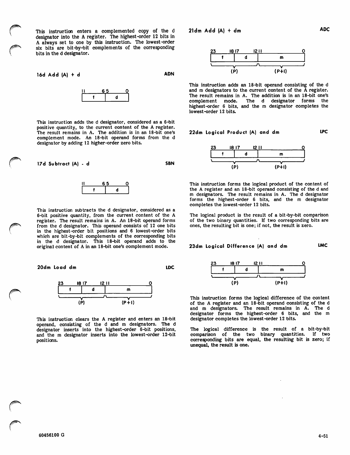
/sgP^N
This instruction enters a complemented copy of the d
designator into the A register. The highest-order 12 bits in
A always set to one by this instruction. The lowest-order
six bits are bit-by-bit complements of the corresponding
bits in the d designator.
16d Add (A) + d ADN
I I 6 5 0
f d
21dm Add (A) + dm ADC
23 1817 1211
f d
V A /
V
(P) (P+l)
This instruction adds an 18-bit operand consisting of the d
and m designators to the current content of the A register.
The result remains in A. The addition is in an 18-bit one's
complement mode. The d designator forms the
highest-order 6 bits, and the m designator completes the
lowest-order 12 bits.
0!^\
This instruction adds the d designator, considered as a 6-bit
positive quantity, to the current content of the A register.
The result remains in A. The addition is in an 18-bit one's
complement mode. An 18-bit operand forms from the d
designator by adding 12 higher-order zero bits.
17d Subtract (A) - d SBN
22dm Logical Product (A) and dm LPC
2 3 1 8 1 7 1211
f d
\A /
V
(P) (P+l)
I I 6 5 0
f d
This instruction subtracts the d designator, considered as a
6-bit positive quantity, from the current content of the A
register. The result remains in A. An 18-bit operand forms
from the d designator. This operand consists of 12 one bits
in the highest-order bit positions and 6 lowest-order bits
which are bit-by-bit complements of the corresponding bits
in the d designator. This 18-bit operand adds to the
original content of A in an 18-bit one's complement mode.
This instruction forms the logical product of the content of
the A register and an 18-bit operand consisting of the d and
m designators. The result remains in A. The d designator
forms the highest-order 6 bits, and the m designator
completes the lowest-order 12 bits.
The logical product is the result of a bit-by-bit comparison
of the two binary quantities. If two corresponding bits are
ones, the resulting bit is one; if not, the result is zero.
23dm Logical Difference (A) and dm LMC
20dm Load dm LDC
2 3 1 8 1 7 12 11
f d
(P)
J \ - —v—
(P+l)
This instruction clears the A register and enters an 18-bit
operand, consisting of the d and m designators. The d
designator inserts into the highest-order 6-bit positions,
and the m designator inserts into the lowest-order 12-bit
positions.
23 18 17 12 11
t d
\A /
(1
/
=) (P+l)
This instruction forms the logical difference of the content
of the A register and an 18-bit operand consisting of the d
and m designators. The result remains in A. The d
designator forms the highest-order 6 bits, and the m
designator completes the lowest-order 12 bits.
The logical difference is the result of a bit-by-bit
comparison of the two binary quantities. If two
corresponding bits are equal, the resulting bit is zero; if
unequal, the result is one.
60456100 G 4-51
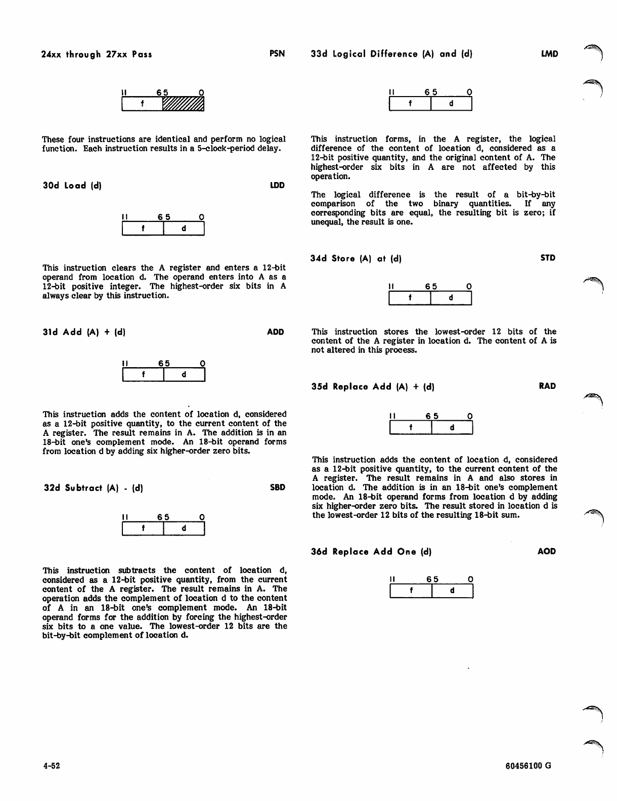
24xx through 27xx Pass PSN 33d Logical Difference (A) and (d) LMD
I I 6 5 0
f
I I 6 5 0
f d
These four instructions are identical and perform no logical
function. Each instruction results in a 5-c lock-period delay.
30d Load (d) LDD
I I 6 5 0
f d
This instruction forms, in the A register, the logical
difference of the content of location d, considered as a
12-bit positive quantity, and the original content of A. The
highest-order six bits in A are not affected by this
operation.
The logical difference is the result of a bit-by-bit
comparison of the two binary quantities. If any
corresponding bits are equal, the resulting bit is zero; if
unequal, the result is one.
This instruction clears the A register and enters a 12-bit
operand from location d. The operand enters into A as a
12-bit positive integer. The highest-order six bits in A
always clear by this instruction.
34d Store (A) at (d) STD
I I 6 5 0
f d
31d Add (A) + (d) ADD
I I 6 5 0
f d
This instruction adds the content of location d, considered
as a 12-bit positive quantity, to the current content of the
A register. The result remains in A. The addition is in an
18-bit one's complement mode. An 18-bit operand forms
from location d by adding six higher-order zero bits.
32d Subtract (A) • (d) SBD
I I 6 5 0
f d
This instruction stores the lowest-order 12 bits of the
content of the A register in location d. The content of A is
not altered in this process.
35d Replace Add (A) + (d) RAD
I I 6 5 0
td
This instruction adds the content of location d, considered
as a 12-bit positive quantity, to the current content of the
A register. The result remains in A and also stores in
location d. The addition is in an 18-bit one's complement
mode. An 18-bit operand forms from location d by adding
six higher-order zero bits. The result stored in location d is
the lowest-order 12 bits of the resulting 18-bit sum.
This instruction subtracts the content of location d,
considered as a 12-bit positive quantity, from the current
content of the A register. The result remains in A. The
operation adds the complement of location d to the content
of A in an 18-bit one's complement mode. An 18-bit
operand forms for the addition by forcing the highest-order
six bits to a one value. The lowest-order 12 bits are the
bit-by-bit complement of location d.
36d Replace Add One (d) AOD
I I 6 5 0
f d
4-52 60456100 G
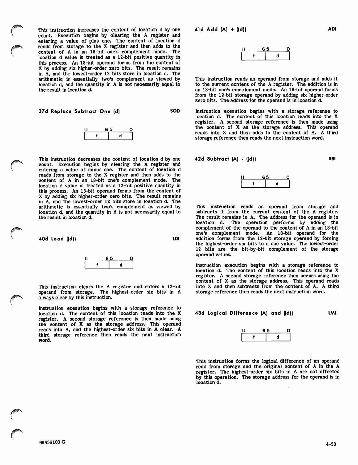
This instruction increases the content of location d by one
count. Execution begins by clearing the A register and
entering a value of plus one. The content of location d
reads from storage to the X register and then adds to the
content of A in an 18-bit one's complement mode. The
location d value is treated as a 12-bit positive quantity in
this process. An 18-bit operand forms from the content of
X by adding six higher-order zero bits. The result remains
in A, and the lowest-order 12 bits store in location d. The
arithmetic is essentially two's complement as viewed by
location d, and the quantity in A is not necessarily equal to
the result in location d.
37d Replace Subtract One (d) SOD
I I 6 5 0
t d
41 d Add (A) + ((d)) ADI
I I 6 5 0
f d
This instruction reads an operand from storage and adds it
to the current content of the A register. The addition is in
an 18-bit one's complement mode. An 18-bit operand forms
from the 12-bit storage operand by adding six higher-order
zero bits. The address for the operand is in location d.
Instruction execution begins with a storage reference to
location d. The content of this location reads into the X
register. A second storage reference is then made using
the content of X as the storage address. This operand
reads into X and then adds to the content of A. A third
storage reference then reads the next instruction word.
^jp,x This instruction decreases the content of location d by one
|#*^v count. Execution begins by clearing the A register and
v entering a value of minus one. The content of location d
reads from storage to the X register and then adds to the
content of A in an 18-bit one's complement mode. The
location d value is treated as a 12-bit positive quantity in
this process. An 18-bit operand forms from the content of
X by adding six higher-order zero bits. The result remains
in A, and the lowest-order 12 bits store in location d. The
arithmetic is essentially two's complement as viewed by
location d, and the quantity in A is not necessarily equal to
the result in location d.
42d Subtract (A) - ((d)) SBI
40d Load ((d)) LDI
I I 6 5 0
f d
This instruction clears the A register and enters a 12-bit
operand from storage. The highest-order six bits in A
always clear by this instruction.
Instruction execution begins with a storage reference to
location d. The content of this location reads into the X
register. A second storage reference is then made using
the content of X as the storage address. This operand
reads into A, and the highest-order six bits in A clear. A
third storage reference then reads the next instruction
word.
I I 6 5 0
f d
This instruction reads an operand from storage and
subtracts it from the current content of the A register.
The result remains in A. The address for the operand is in
location d. The operation performs by adding the
complement of the operand to the content of A in an 18-bit
one's complement mode. An 18-bit operand for the
addition forms from the 12-bit storage operand by forcing
the highest-order six bits to a one value. The lowest-order
12 bits are the bit-by-bit complement of the storage
operand values.
Instruction execution begins with a storage reference to
location d. The content of this location reads into the X
register. A second storage reference then occurs using the
content of X as the storage address. This operand reads
into X and then subtracts from the content of A. A third
storage reference then reads the next instruction word.
43d Logical Difference (A) and ((d)) LMI
I I 6 5 0
f d
This instruction forms the logical difference of an operand
read from storage and the original content of A in the A
register. The highest-order six bits in A are not affected
by this operation. The storage address for the operand is in
location d.
60456100 G 4-53
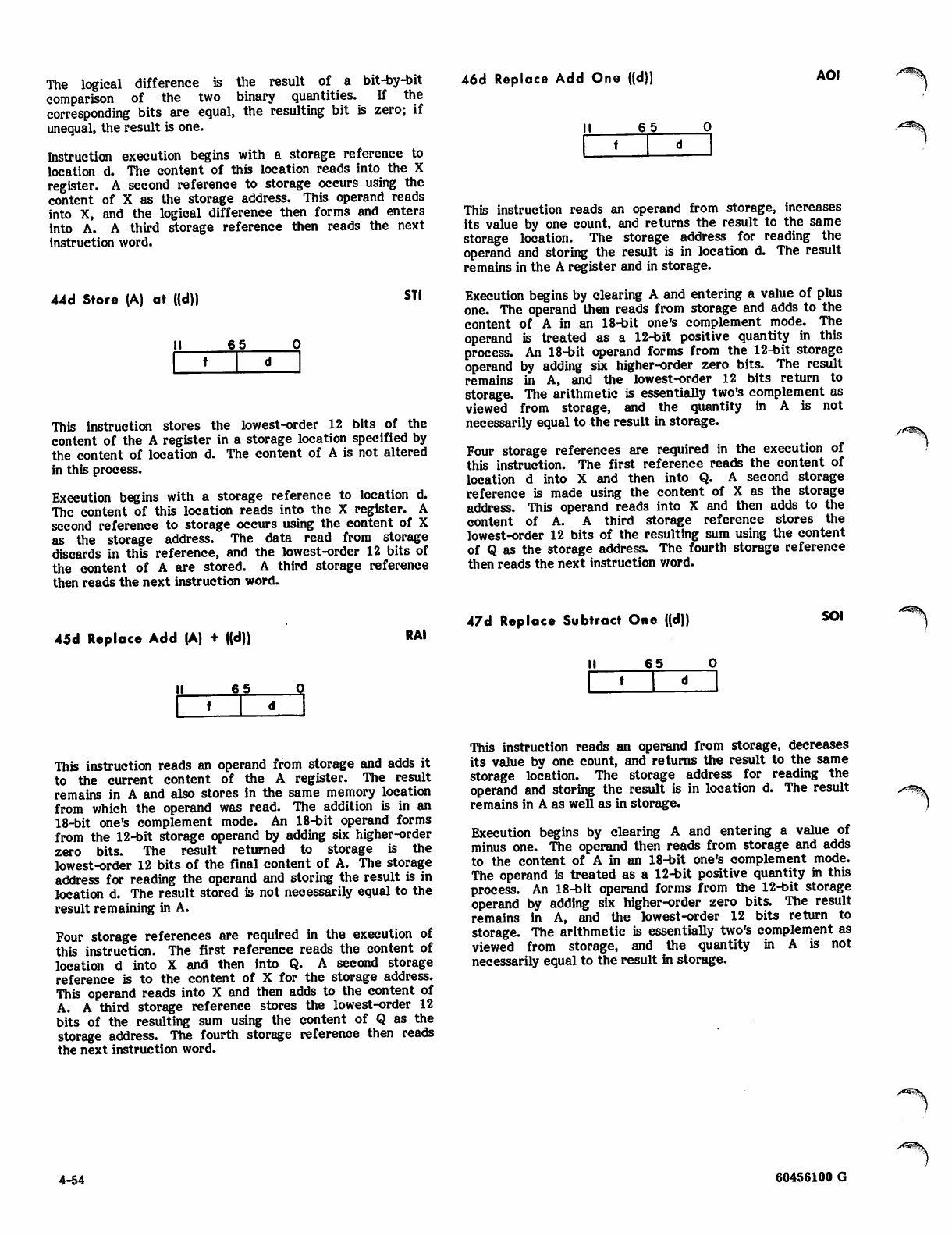
The logical difference is the result of a bit-by-bit
comparison of the two binary quantities. If the
corresponding bits are equal, the resulting bit is zero; if
unequal, the result is one.
Instruction execution begins with a storage reference to
location d. The content of this location reads into the X
register. A second reference to storage occurs using the
content of X as the storage address. This operand reads
into X, and the logical difference then forms and enters
into A. A third storage reference then reads the next
instruction word.
46d Replace Add One ((d)) AOI
44d Store (A) at ((d)) STI
I I 6 5 0
t d
This instruction stores the lowest-order 12 bits of the
content of the A register in a storage location specified by
the content of location d. The content of A is not altered
in this process.
Execution begins with a storage reference to location d.
The content of this location reads into the X register. A
second reference to storage occurs using the content of X
as the storage address. The data read from storage
discards in this reference, and the lowest-order 12 bits of
the content of A are stored. A third storage reference
then reads the next instruction word.
I I 6 5 0
t d
This instruction reads an operand from storage, increases
its value by one count, and returns the result to the same
storage location. The storage address for reading the
operand and storing the result is in location d. The result
remains in the A register and in storage.
Execution begins by clearing A and entering a value of plus
one. The operand then reads from storage and adds to the
content of A in an 18-bit one's complement mode. The
operand is treated as a 12-bit positive quantity in this
process. An 18-bit operand forms from the 12-bit storage
operand by adding six higher-order zero bits. The result
remains in A, and the lowest-order 12 bits return to
storage. The arithmetic is essentially two's complement as
viewed from storage, and the quantity in A is not
necessarily equal to the result in storage.
Four storage references are required in the execution of
this instruction. The first reference reads the content of
location d into X and then into Q. A second storage
reference is made using the content of X as the storage
address. This operand reads into X and then adds to the
content of A. A third storage reference stores the
lowest-order 12 bits of the resulting sum using the content
of Q as the storage address. The fourth storage reference
then reads the next instruction word.
45d Replace Add (A) + ((d)) RAI
I I 6 5 0
fd
47d Replace Subtract One ((d)) SOI
I I 6 5 0
t d
This instruction reads an operand from storage and adds it
to the current content of the A register. The result
remains in A and also stores in the same memory location
from which the operand was read. The addition is in an
18-bit one's complement mode. An 18-bit operand forms
from the 12-bit storage operand by adding six higher-order
zero bits. The result returned to storage is the
lowest-order 12 bits of the final content of A. The storage
address for reading the operand and storing the result is in
location d. The result stored is not necessarily equal to the
result remaining in A.
Four storage references are required in the execution of
this instruction. The first reference reads the content of
location d into X and then into Q. A second storage
reference is to the content of X for the storage address.
This operand reads into X and then adds to the content of
A. A third storage reference stores the lowest-order 12
bits of the resulting sum using the content of Q as the
storage address. The fourth storage reference then reads
the next instruction word.
This instruction reads an operand from storage, decreases
its value by one count, and returns the result to the same
storage location. The storage address for reading the
operand and storing the result is in location d. The result
remains in A as well as in storage.
Execution begins by clearing A and entering a value of
minus one. The operand then reads from storage and adds
to the content of A in an 18-bit one's complement mode.
The operand is treated as a 12-bit positive quantity in this
process. An 18-bit operand forms from the 12-bit storage
operand by adding six higher-order zero bits. The result
remains in A, and the lowest-order 12 bits return to
storage. The arithmetic is essentially two's complement as
viewed from storage, and the quantity in A is not
necessarily equal to the result in storage.
4-54 60456100 G
yf-ks^.
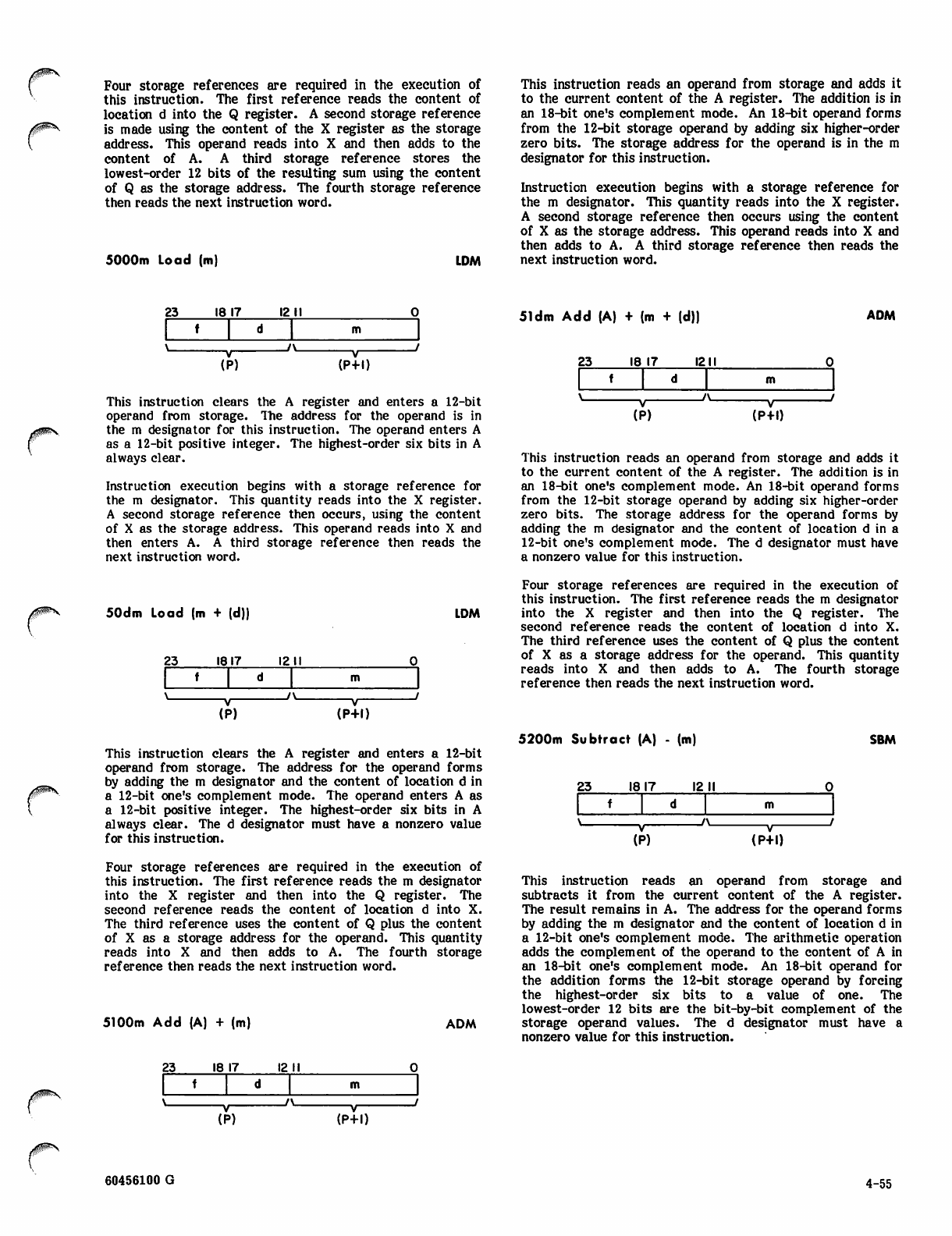
Four storage references are required in the execution of
this instruction. The first reference reads the content of
location d into the Q register. A second storage reference
is made using the content of the X register as the storage
address. This operand reads into X and then adds to the
content of A. A third storage reference stores the
lowest-order 12 bits of the resulting sum using the content
of Q as the storage address. The fourth storage reference
then reads the next instruction word.
5000m Load (m) LDM
This instruction reads an operand from storage and adds it
to the current content of the A register. The addition is in
an 18-bit one's complement mode. An 18-bit operand forms
from the 12-bit storage operand by adding six higher-order
zero bits. The storage address for the operand is in the m
designator for this instruction.
Instruction execution begins with a storage reference for
the m designator. This quantity reads into the X register.
A second storage reference then occurs using the content
of X as the storage address. This operand reads into X and
then adds to A. A third storage reference then reads the
next instruction word.
23 18 17 12 11
f d
\A /
(1 ») (P+l)
This instruction clears the A register and enters a 12-bit
operand from storage. The address for the operand is in
the m designator for this instruction. The operand enters A
as a 12-bit positive integer. The highest-order six bits in A
always clear.
Instruction execution begins with a storage reference for
the m designator. This quantity reads into the X register.
A second storage reference then occurs, using the content
of X as the storage address. This operand reads into X and
then enters A. A third storage reference then reads the
next instruction word.
51dm Add (A) + (m + (d)| ADM
23 18 17 1211
f d
\A /
V
(P) (P+l)
This instruction reads an operand from storage and adds it
to the current content of the A register. The addition is in
an 18-bit one's complement mode. An 18-bit operand forms
from the 12-bit storage operand by adding six higher-order
zero bits. The storage address for the operand forms by
adding the m designator and the content of location d in a
12-bit one's complement mode. The d designator must have
a nonzero value for this instruction.
/$(GP*>V 50dm Load (m + (d)) LDM
23 1817 1211
f d
*V
(F
t—
>)
* v '
(P+l)
This instruction clears the A register and enters a 12-bit
operand from storage. The address for the operand forms
by adding the m designator and the content of location d in
a 12-bit one's complement mode. The operand enters A as
a 12-bit positive integer. The highest-order six bits in A
always clear. The d designator must have a nonzero value
for this instruction.
Four storage references are required in the execution of
this instruction. The first reference reads the m designator
into the X register and then into the Q register. The
second reference reads the content of location d into X.
The third reference uses the content of Q plus the content
of X as a storage address for the operand. This quantity
reads into X and then adds to A. The fourth storage
reference then reads the next instruction word.
5100m Add (A) + (m) ADM
Four storage references are required in the execution of
this instruction. The first reference reads the m designator
into the X register and then into the Q register. The
second reference reads the content of location d into X.
The third reference uses the content of Q plus the content
of X as a storage address for the operand. This quantity
reads into X and then adds to A. The fourth storage
reference then reads the next instruction word.
5200m Subtract (A) - (m) SBM
23 18 17 12 11
f d
vA /
V
(F
i
») (P+D
This instruction reads an operand from storage and
subtracts it from the current content of the A register.
The result remains in A. The address for the operand forms
by adding the m designator and the content of location d in
a 12-bit one's complement mode. The arithmetic operation
adds the complement of the operand to the content of A in
an 18-bit one's complement mode. An 18-bit operand for
the addition forms the 12-bit storage operand by forcing
the highest-order six bits to a value of one. The
lowest-order 12 bits are the bit-by-bit complement of the
storage operand values. The d designator must have a
nonzero value for this instruction.
23 18 17 12 11
t d
v/\ /
V
(P) (P+l)
60456100 4-55
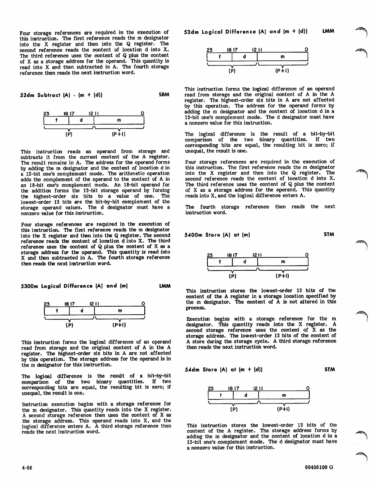
Four storage references are required in the execution of
this instruction. The first reference reads the m designator
into the X register and then into the Q register. The
second reference reads the content of location d into X.
The third reference uses the content of Q plus the content
of X as a storage address for the operand. This quantity is
read into X and then subtracted in A. The fourth storage
reference then reads the next instruction word.
53dm Logical Difference (A) and (m + (d)) LMM
2 3 1 8 1 7 1 2 1 1
f d
\A /
V
(P) (P + l)
/^5%\
52dm Subtract (A) - (m + (d)) SBM
23 18 17 12 11
f d
\A
(1 >) (P + D
This instruction reads an operand from storage and
subtracts it from the current content of the A register.
The result remains in A. The address for the operand forms
by adding the m designator and the content of location d in
a 12-bit one's complement mode. The arithmetic operation
adds the complement of the operand to the content of A in
an 18-bit one's complement mode. An 18-bit operand for
the addition forms the 12-bit storage operand by forcing
the highest-order six bits to a value of one. The
lowest-order 12 bits are the bit-by-bit complement of the
storage operand values. The d designator must have a
nonzero value for this instruction.
Four storage references are required in the execution of
this instruction. The first reference reads the m designator
into the X register and then into the Q register. The second
reference reads the content of location d into X. The third
reference uses the content of Q plus the content of X as a
storage address for the operand. This quantity is read into
X and then subtracted in A. The fourth storage reference
then reads the next instruction word.
5300m Logical Difference (A) and (m) LMM
23 1817 1211
f d
\ /v /
—\
(1 ») (P+l)
This instruction forms the logical difference of an operand
read from storage and the original content of A in the A
register. The highest-order six bits in A are not affected
by this operation. The storage address for the operand is in
the m designator for this instruction.
The logical difference is the result of a bit-by-bit
comparison of the two binary quantities. If two
corresponding bits are equal, the resulting bit is zero; if
unequal, the result is one.
Instruction execution begins with a storage reference for
the m designator. This quantity reads into the X register.
A second storage reference then uses the content of X as
the storage address. This operand reads into X, and the
logical difference enters A. A third storage reference then
reads the next instruction word.
This instruction forms the logical difference of an operand
read from storage and the original content of A in the A
register. The highest-order six bits in A are not affected
by this operation. The address for the operand forms by
adding the m designator and the content of location d in a
12-bit one's complement mode. The d designator must have
a nonzero value for this instruction.
The logical difference is the result of a bit-by-bit
comparison of the two binary quantities. If two
corresponding bits are equal, the resulting bit is zero; if
unequal, the result is one.
Four storage references are required in the execution of
this instruction. The first reference reads the m designator
into the X register and then into the Q register. The
second reference reads the content of location d into X.
The third reference uses the content of Q plus the content
of X as a storage address for the operand. This quantity
reads into X, and the logical difference enters A.
The fourth storage reference then reads the next
instruction word.
5400m Store (A) at (m) STM
23 1817 1211
t d
(P)
-—v—
(P+l)
This instruction stores the lowest-order 12 bits of the
content of the A register in a storage location specified by
the m designator. The content of A is not altered in this
process.
Execution begins with a storage reference for the m
designator. This quantity reads into the X register. A
second storage reference uses the content of X as the
storage address. The lowest-order 12 bits of the content of
A store during the storage cycle. A third storage reference
then reads the next instruction word.
54dm Store (A) at (m + (d)) STM
23 18 17 12 11
f d
*- v '
(P)
\ /' V
(P+l)
This instruction stores the lowest-order 12 bits of the
content of the A register. The storage address forms by
adding the m designator and the content of location d in a
12-bit one's complement mode. The d designator must have
a nonzero value for this instruction.
ySKES|.
4-56 60456100 G
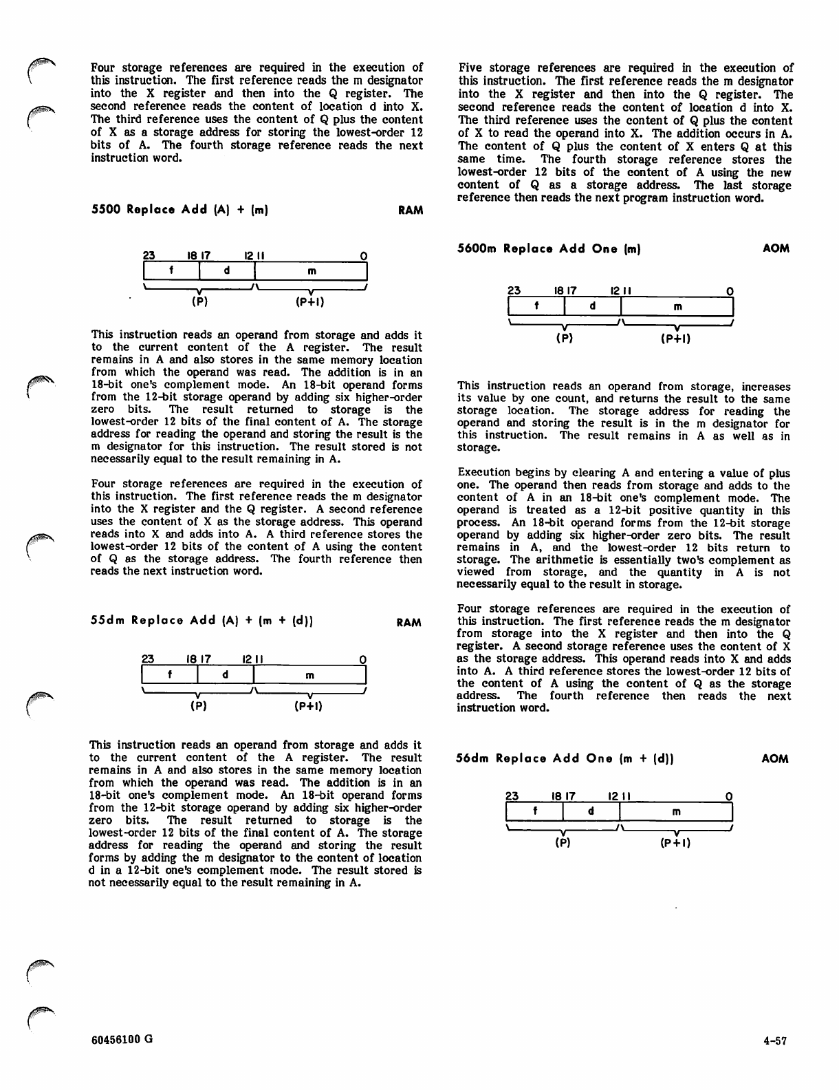
Four storage references are required in the execution of
this instruction. The first reference reads the m designator
into the X register and then into the Q register. The
second reference reads the content of location d into X.
The third reference uses the content of Q plus the content
of X as a storage address for storing the lowest-order 12
bits of A. The fourth storage reference reads the next
instruction word.
5500 Replace Add (A) + (m) RAM
Five storage references are required in the execution of
this instruction. The first reference reads the m designator
into the X register and then into the Q register. The
second reference reads the content of location d into X.
The third reference uses the content of Q plus the content
of X to read the operand into X. The addition occurs in A.
The content of Q plus the content of X enters Q at this
same time. The fourth storage reference stores the
lowest-order 12 bits of the content of A using the new
content of Q as a storage address. The last storage
reference then reads the next program instruction word.
0^*\
23 18 17 12 11
f d
vA /
(1
t
s) (P+D
This instruction reads an operand from storage and adds it
to the current content of the A register. The result
remains in A and also stores in the same memory location
from which the operand was read. The addition is in an
18-bit one's complement mode. An 18-bit operand forms
from the 12-bit storage operand by adding six higher-order
zero bits. The result returned to storage is the
lowest-order 12 bits of the final content of A. The storage
address for reading the operand and storing the result is the
m designator for this instruction. The result stored is not
necessarily equal to the result remaining in A.
Four storage references are required in the execution of
this instruction. The first reference reads the m designator
into the X register and the Q register. A second reference
uses the content of X as the storage address. This operand
reads into X and adds into A. A third reference stores the
lowest-order 12 bits of the content of A using the content
of Q as the storage address. The fourth reference then
reads the next instruction word.
55dm Replace Add (A) + (m + (d)) RAM
23 18 17 1211
f d
\ /v /
>
(
t
3) (P+D
5600m Replace Add One (m) AOM
23 18 17 1211
f d
vA /
V
(P) (P+D
This instruction reads an operand from storage, increases
its value by one count, and returns the result to the same
storage location. The storage address for reading the
operand and storing the result is in the m designator for
this instruction. The result remains in A as well as in
storage.
Execution begins by clearing A and entering a value of plus
one. The operand then reads from storage and adds to the
content of A in an 18-bit one's complement mode. The
operand is treated as a 12-bit positive quantity in this
process. An 18-bit operand forms from the 12-bit storage
operand by adding six higher-order zero bits. The result
remains in A, and the lowest-order 12 bits return to
storage. The arithmetic is essentially two's complement as
viewed from storage, and the quantity in A is not
necessarily equal to the result in storage.
Four storage references are required in the execution of
this instruction. The first reference reads the m designator
from storage into the X register and then into the Q
register. A second storage reference uses the content of X
as the storage address. This operand reads into X and adds
into A. A third reference stores the lowest-order 12 bits of
the content of A using the content of Q as the storage
address. The fourth reference then reads the next
instruction word.
This instruction reads an operand from storage and adds it
to the current content of the A register. The result
remains in A and also stores in the same memory location
from which the operand was read. The addition is in an
18-bit one's complement mode. An 18-bit operand forms
from the 12-bit storage operand by adding six higher-order
zero bits. The result returned to storage is the
lowest-order 12 bits of the final content of A. The storage
address for reading the operand and storing the result
forms by adding the m designator to the content of location
d in a 12-bit one's complement mode. The result stored is
not necessarily equal to the result remaining in A.
56dm Replace Add One (m + (d)) AOM
23 18 17 12 11
f d
v/\ /
\
(F>) (P + D
J^N
60456100 G 4-57
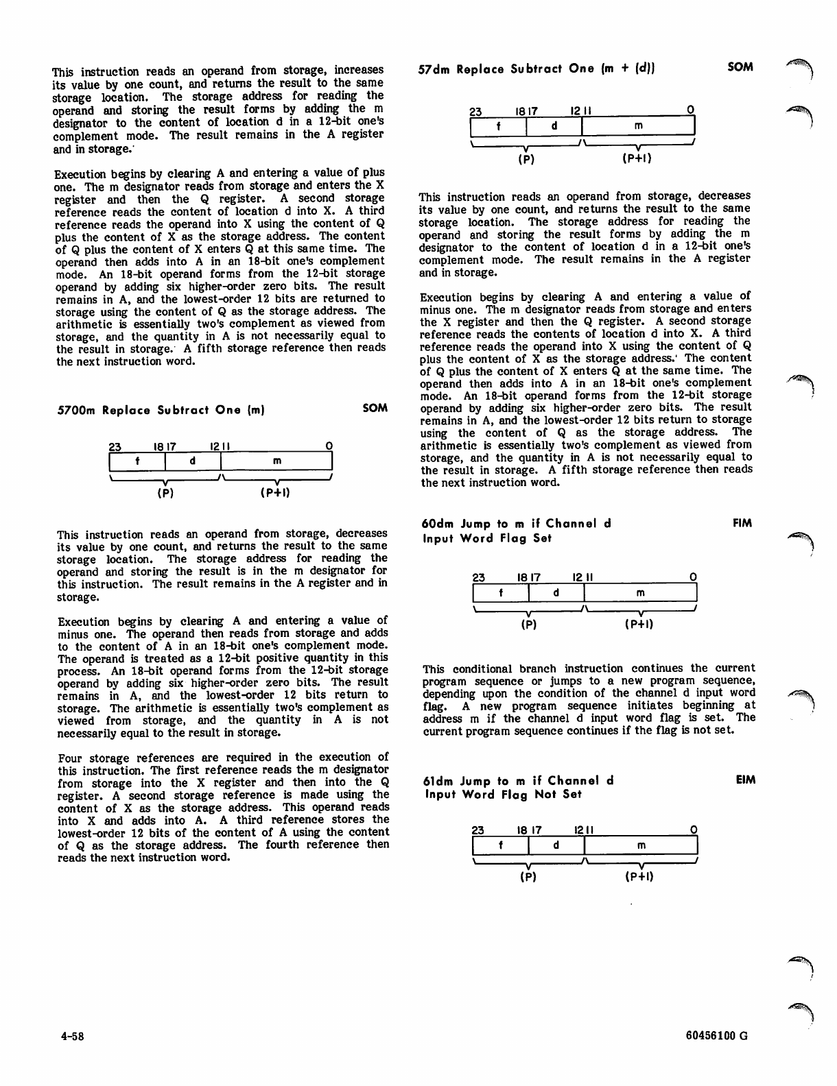
This instruction reads an operand from storage, increases
its value by one count, and returns the result to the same
storage location. The storage address for reading the
operand and storing the result forms by adding the m
designator to the content of location d in a 12-bit one's
complement mode. The result remains in the A register
and in storage.'
Execution begins by clearing A and entering a value of plus
one. The m designator reads from storage and enters the X
register and then the Q register. A second storage
reference reads the content of location d into X. A third
reference reads the operand into X using the content of Q
plus the content of X as the storage address. The content
of Q plus the content of X enters Q at this same time. The
operand then adds into A in an 18-bit one's complement
mode. An 18-bit operand forms from the 12-bit storage
operand by adding six higher-order zero bits. The result
remains in A, and the lowest-order 12 bits are returned to
storage using the content of Q as the storage address. The
arithmetic is essentially two's complement as viewed from
storage, and the quantity in A is not necessarily equal to
the result in storage. A fifth storage reference then reads
the next instruction word.
57dm Replace Subtract One (m + (d)) SOM
5700m Replace Subtract One (m)
2 3 1 8 1 7 1 2 1 1
SOM
t d m
\ /v /
(i
/
=») (P+D
23 1817 1211
fd
-v-
(P)
J\t —v—
(P+l)
This instruction reads an operand from storage, decreases
its value by one count, and returns the result to the same
storage location. The storage address for reading the
operand and storing the result forms by adding the m
designator to the content of location d in a 12-bit one's
complement mode. The result remains in the A register
and in storage.
Execution begins by clearing A and entering a value of
minus one. The m designator reads from storage and enters
the X register and then the Q register. A second storage
reference reads the contents of location d into X. A third
reference reads the operand into X using the content of Q
plus the content of X as the storage address.' The content
of Q plus the content of X enters Q at the same time. The
operand then adds into A in an 18-bit one's complement
mode. An 18-bit operand forms from the 12-bit storage
operand by adding six higher-order zero bits. The result
remains in A, and the lowest-order 12 bits return to storage
using the content of Q as the storage address. The
arithmetic is essentially two's complement as viewed from
storage, and the quantity in A is not necessarily equal to
the result in storage. A fifth storage reference then reads
the next instruction word.
/s®H%k
This instruction reads an operand from storage, decreases
its value by one count, and returns the result to the same
storage location. The storage address for reading the
operand and storing the result is in the m designator for
this instruction. The result remains in the A register and in
storage.
Execution begins by clearing A and entering a value of
minus one. The operand then reads from storage and adds
to the content of A in an 18-bit one's complement mode.
The operand is treated as a 12-bit positive quantity in this
process. An 18-bit operand forms from the 12-bit storage
operand by adding six higher-order zero bits. The result
remains in A, and the lowest-order 12 bits return to
storage. The arithmetic is essentially two's complement as
viewed from storage, and the quantity in A is not
necessarily equal to the result in storage.
Four storage references are required in the execution of
this instruction. The first reference reads the m designator
from storage into the X register and then into the Q
register. A second storage reference is made using the
content of X as the storage address. This operand reads
into X and adds into A. A third reference stores the
lowest-order 12 bits of the content of A using the content
of Q as the storage address. The fourth reference then
reads the next instruction word.
60dm Jump to m if Channel d
Input Word Flag Set
FIM
23 1817 12 11
t d
-v-
(P)
—v—
(P+l)
This conditional branch instruction continues the current
program sequence or jumps to a new program sequence,
depending upon the condition of the channel d input word
flag. A new program sequence initiates beginning at
address m if the channel d input word flag is set. The
current program sequence continues if the flag is not set.
61dm Jump to m if Channel d
Input Word Flag Not Set
EIM
23 18 17 1211
t d
\ /\ /
\
(F
(
>) (P+D
4-58 60456100 G
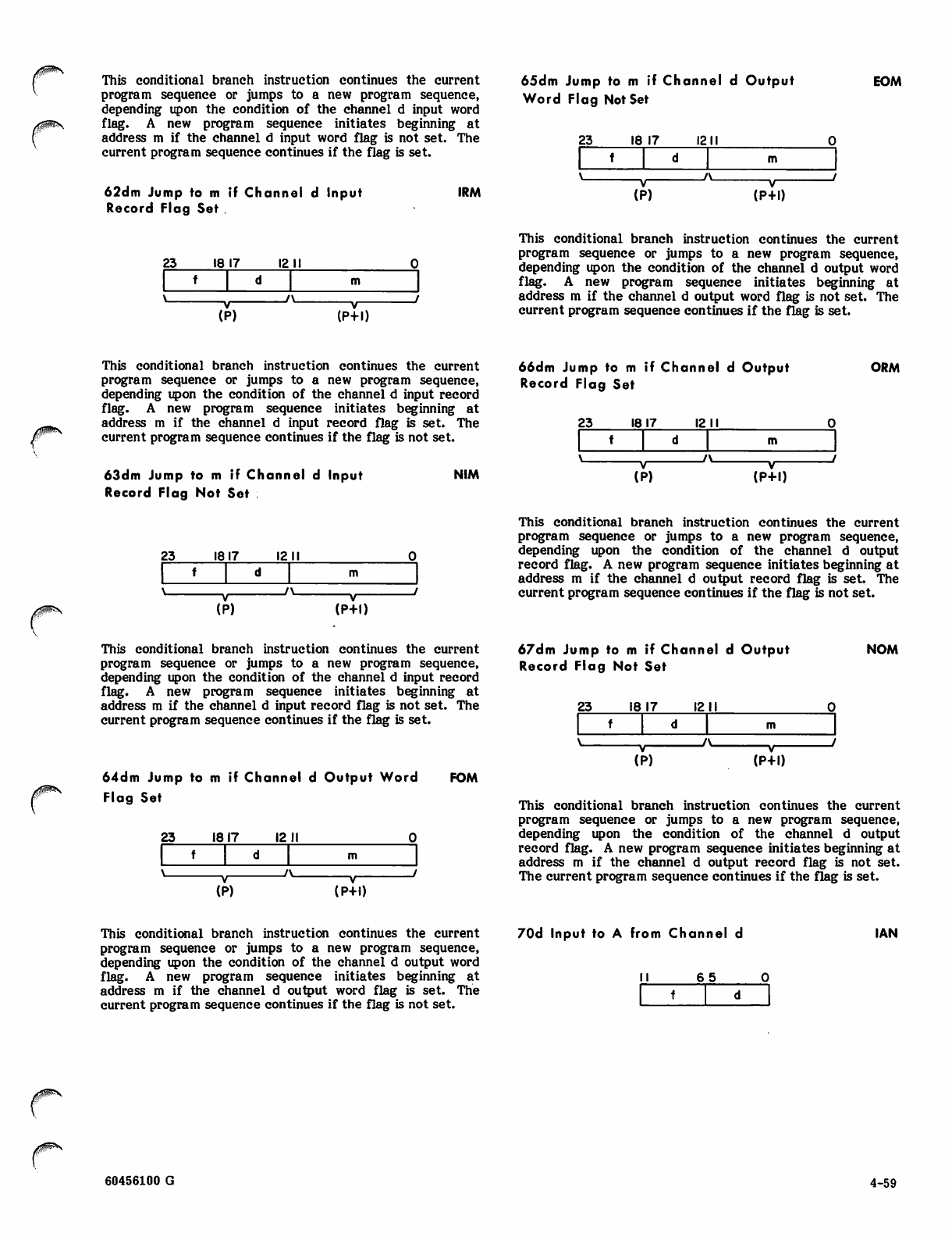
/pjpfe\
This conditional branch instruction continues the current
program sequence or jumps to a new program sequence,
depending upon the condition of the channel d input word
flag. A new program sequence initiates beginning at
address m if the channel d input word flag is not set. The
current program sequence continues if the flag is set.
62dm Jump to m if Channel d Input
Record Flag Set
23 18 17 12 11
IRM
f d m
\A /
\
(F
f
») (P+l)
65dm Jump to m if Channel d Output
Word Flag Not Set
EOM
23 18 17 1211
f d
\A /
V
(P) (P+D
This conditional branch instruction continues the current
program sequence or jumps to a new program sequence,
depending upon the condition of the channel d output word
flag. A new program sequence initiates beginning at
address m if the channel d output word flag is not set. The
current program sequence continues if the flag is set.
This conditional branch instruction continues the current
program sequence or jumps to a new program sequence,
depending upon the condition of the channel d input record
flag. A new program sequence initiates beginning at
address m if the channel d input record flag is set. The
current program sequence continues if the flag is not set.
63dm Jump to m if Channel d Input
Record Flag Not Set :
NIM
23 1817 12 11
f d
\ /\ /
V
(F
r
>) (P+l)
66dm Jump to m if Channel d Output
Record Flag Set
ORM
23 18 17 1211
t d
\A /
V
(P) (P+D
This conditional branch instruction continues the current
program sequence or jumps to a new program sequence,
depending upon the condition of the channel d output
record flag. A new program sequence initiates beginning at
address m if the channel d output record flag is set. The
current program sequence continues if the flag is not set.
/0^K
This conditional branch instruction continues the current
program sequence or jumps to a new program sequence,
depending upon the condition of the channel d input record
flag. A new program sequence initiates beginning at
address m if the channel d input record flag is not set. The
current program sequence continues if the flag is set.
64dm Jump to m if Channel d Output Word FOM
Flag Set
2 3 1 8 1 7 1 2 1 1 0
f d m
\ /\ , /
(f
f
>) (P+l)
67dm Jump to m if Channel d Output
Record Flag Not Set
NOM
23 18 17 12 11
f d
\A /
(P) (P+D
This conditional branch instruction continues the current
program sequence or jumps to a new program sequence,
depending upon the condition of the channel d output
record flag. A new program sequence initiates beginning at
address m if the channel d output record flag is not set.
The current program sequence continues if the flag is set.
This conditional branch instruction continues the current
program sequence or jumps to a new program sequence,
depending upon the condition of the channel d output word
flag. A new program sequence initiates beginning at
address m if the channel d output word flag is set. The
current program sequence continues if the flag is not set.
70d Input to A from Channel d IAN
I I 6 5 0
f d
60456100 G 4-59
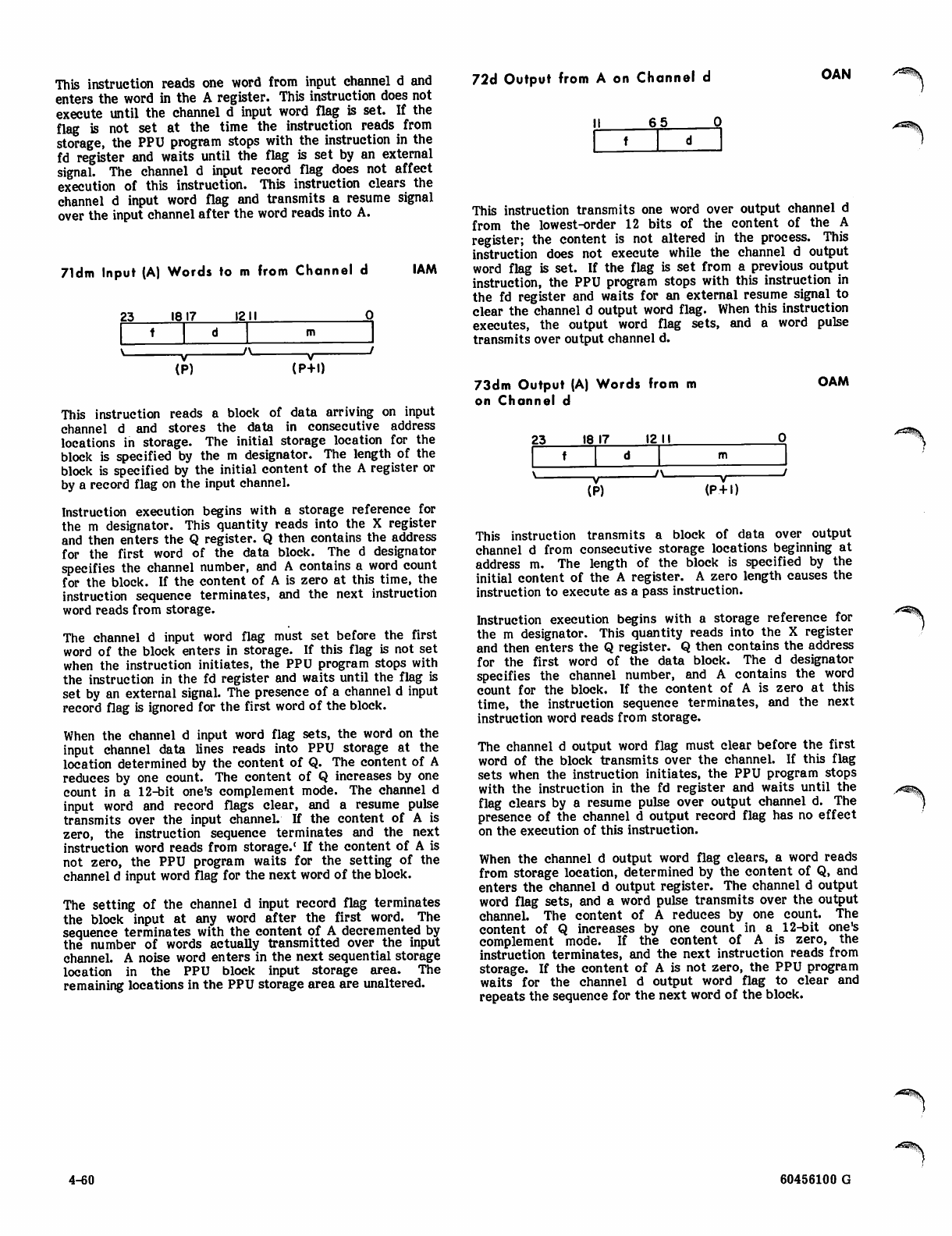
This instruction reads one word from input channel d and
enters the word in the A register. This instruction does not
execute until the channel d input word flag is set. If the
flag is not set at the time the instruction reads from
storage, the PPU program stops with the instruction in the
fd register and waits until the flag is set by an external
signal. The channel d input record flag does not affect
execution of this instruction. This instruction clears the
channel d input word flag and transmits a resume signal
over the input channel after the word reads into A.
72d Output from A on Channel d OAN
71dm Input (A) Words to m from Channel d 1AM
23 1817 1211
t d
(P)
J\. —v—
(P+l)
This instruction reads a block of data arriving on input
channel d and stores the data in consecutive address
locations in storage. The initial storage location for the
block is specified by the m designator. The length of the
block is specified by the initial content of the A register or
by a record flag on the input channel.
Instruction execution begins with a storage reference for
the m designator. This quantity reads into the X register
and then enters the Q register. Q then contains the address
for the first word of the data block. The d designator
specifies the channel number, and A contains a word count
for the block. If the content of A is zero at this time, the
instruction sequence terminates, and the next instruction
word reads from storage.
The channel d input word flag must set before the first
word of the block enters in storage. If this flag is not set
when the instruction initiates, the PPU program stops with
the instruction in the fd register and waits until the flag is
set by an external signal. The presence of a channel d input
record flag is ignored for the first word of the block.
When the channel d input word flag sets, the word on the
input channel data lines reads into PPU storage at the
location determined by the content of Q. The content of A
reduces by one count. The content of Q increases by one
count in a 12-bit one's complement mode. The channel d
input word and record flags clear, and a resume pulse
transmits over the input channel. If the content of A is
zero, the instruction sequence terminates and the next
instruction word reads from storage.' If the content of A is
not zero, the PPU program waits for the setting of the
channel d input word flag for the next word of the block.
The setting of the channel d input record flag terminates
the block input at any word after the first word. The
sequence terminates with the content of A decremented by
the number of words actually transmitted over the input
channel. A noise word enters in the next sequential storage
location in the PPU block input storage area. The
remaining locations in the PPU storage area are unaltered.
I I 6 5 0
fd
This instruction transmits one word over output channel d
from the lowest-order 12 bits of the content of the A
register; the content is not altered in the process. This
instruction does not execute while the channel d output
word flag is set. If the flag is set from a previous output
instruction, the PPU program stops with this instruction in
the fd register and waits for an external resume signal to
clear the channel d output word flag. When this instruction
executes, the output word flag sets, and a word pulse
transmits over output channel d.
73dm Output (A) Words from m
on Channel d
OAM
23 18 17 12 11
f d
\A
V
(P) (P+D
This instruction transmits a block of data over output
channel d from consecutive storage locations beginning at
address m. The length of the block is specified by the
initial content of the A register. A zero length causes the
instruction to execute as a pass instruction.
Instruction execution begins with a storage reference for
the m designator. This quantity reads into the X register
and then enters the Q register. Q then contains the address
for the first word of the data block. The d designator
specifies the channel number, and A contains the word
count for the block. If the content of A is zero at this
time, the instruction sequence terminates, and the next
instruction word reads from storage.
The channel d output word flag must clear before the first
word of the block transmits over the channel. If this flag
sets when the instruction initiates, the PPU program stops
with the instruction in the fd register and waits until the
flag clears by a resume pulse over output channel d. The
presence of the channel d output record flag has no effect
on the execution of this instruction.
When the channel d output word flag clears, a word reads
from storage location, determined by the content of Q, and
enters the channel d output register. The channel d output
word flag sets, and a word pulse transmits over the output
channel. The content of A reduces by one count. The
content of Q increases by one count in a 12-bit one's
complement mode. If the content of A is zero, the
instruction terminates, and the next instruction reads from
storage. If the content of A is not zero, the PPU program
waits for the channel d output word flag to clear and
repeats the sequence for the next word of the block.
4-60 60456100 G

F^ 74d Set Output Record Flag on Channel d RFN 77xx Error Stop ESN
I I 6 5 0
f d
I I 6 5 0
fmm
This instruction sets the channel d output record flag and
transmits a record pulse over output channel d. The
previous status of the flag is ignored in this process. The
instruction executes, and a record pulse transmits even
though the channel d output record flag was already set.
This instruction causes the PPU program to stop and
indicate a program error condition to the status and control
register. The PPU can be restarted only by a deadstart.
PPU INSTRUCTION TIMING
75xx, 76xx Pass PSN
These two instructions are identical and perform no logical
function. Each instruction results in a 5-clock-period delay.
Execution times for the PPU are listed in table 4-9. The
timing notes refer to the notes at the end of the table.
Execution times are in 27.5-nanosecond clock periods.
The execution timing for the PPU instructions is dominated
by the access time of the core storage banks. There are
two independent banks of storage. One bank contains all
even storage addresses, and the other bank contains all odd
storage addresses. If references to storage alternate
between even and odd addresses, each reference requires 5
clock periods. If two even references (or two odd
references) occur consecutively, the storage read/write
cycle for the first reference must be completed before the
second reference can begin. In this case, a storage
reference requires 10 clock periods. As a result, the
execution time for most of the PPU instructions is a
multiple of clock periods with variation in increments of 5
clock periods, depending upon the storage addresses
involved.
60456100 G 4-61
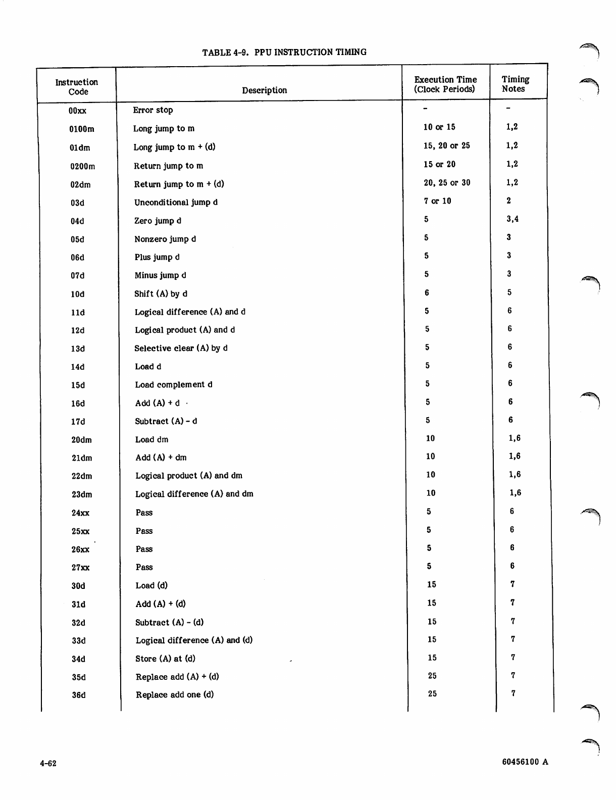
TABLE 4-9. PPU INSTRUCTION TIMING
Instruction
Code
OOxx
0100m
01dm
0200m
02dm
03d
04d
05d
06d
07d
lOd
lid
12d
13d
14d
15d
16d
17d
20dm
21dm
22dm
23dm
24xx
25xx
26xx
27xx
30d
31d
32d
33d
34d
35d
36d
Description
Error stop
Long jump to m
Long jump to m + (d)
Return jump to m
Return jump to m + (d)
Unconditional jump d
Zero jump d
Nonzero jump d
Plus jump d
Minus jump d
Shift (A) by d
Logical difference (A) and d
Logical product (A) and d
Selective clear (A) by d
Load d
Load complement d
Add(A) + d
Subtract (A) - d
Load dm
Add (A) + dm
Logical product (A) and dm
Logical difference (A) and dm
Pass
Pass
Pass
Pass
Load (d)
Add (A) + (d)
Subtract (A) - (d)
Logical difference (A) and (d)
Store (A) at (d)
Replace add (A) + (d)
Replace add one (d)
Execution Time
(Clock Periods)
10 or 15
15, 20 or 25
15 or 20
20, 25 or 30
7 or 10
5
5
5
5
6
5
5
5
5
5
5
5
10
10
10
10
5
5
5
5
15
15
15
15
15
25
25
Timing
Notes
1,2
1,2
1,2
1,2
2
3,4
3
3
3
5
6
6
6
6
6
6
6
1,6
1,6
1,6
1,6
6
6
6
6
7
7
7
7
7
7
7
4-62 60456100 A
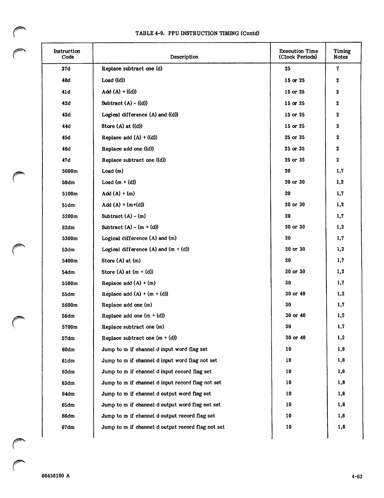
TABLE 4-9. PPU INSTRUCTION TIMING (Contd)
Instruction
Code Description
Execution Time
(Clock Periods) Timing
Notes
37d Replace subtract one (d) 25
40d Load ((d)) 15 or 25
41d Add (A) + ((d)) 15 or 25
42d Subtract (A) - ((d)) 15 or 25
43d Logical difference (A) and ((d)) 15 or 25
44d Store (A) at ((d)) 15 or 25
45d Replace add (A) + ((d)) 25 or 35
46d Replace add one ((d)) 25 or 35
47d Replace subtract one ((d)) 25 or 35
5000m Load (m) 20 1,7
50dm Load (m + (d)) 20 or 30 1,2
5100m Add (A) + (m) 20 1,7
51dm Add (A) + (m+(d)) 20 or 30 1,2
5200m Subtract (A) - (m) 20 1,7
52dm Subtract (A) - (m + (d)) 20 or 30 1,2
5300m Logical difference (A) and (m) 20 1.7
53dm Logical difference (A) and (m + (d)) 20 or 30 1.2
5400m Store (A) at (m) 20 1,7
54dm Store (A) at (m + (d)) 20 or 30 1,2
5500m Replace add (A) + (m) 30 1,7
55dm Replace add (A) + (m + (d)) 30 or 40 1,2
5600m Replace add one (m) 30 1,7
56dm Replace add one (m + (d)) 30 or 40 1,2
5700m Replace subtract one (m) 30 1,7
57dm Replace subtract one (m + (d)) 30 or 40 1,2
60dm Jump to m if channel d input word flag set 10 1,8
61dm Jump to m if channel d input word flag not set 10 1,8
62dm Jump to m if channel d input record flag set 10 1,8
63dm Jump to m if channel d input record flag not set 10 1,8
64dm Jump to m if channel d output word flag set 10 1,8
65dm Jump to m if channel d output word flag not set 10 1,8
66dm Jump to m if channel d output record flag set 10 1,8
67dm Jump to m if channel d output record flag not set 10 1,8
60456100 A 4-63
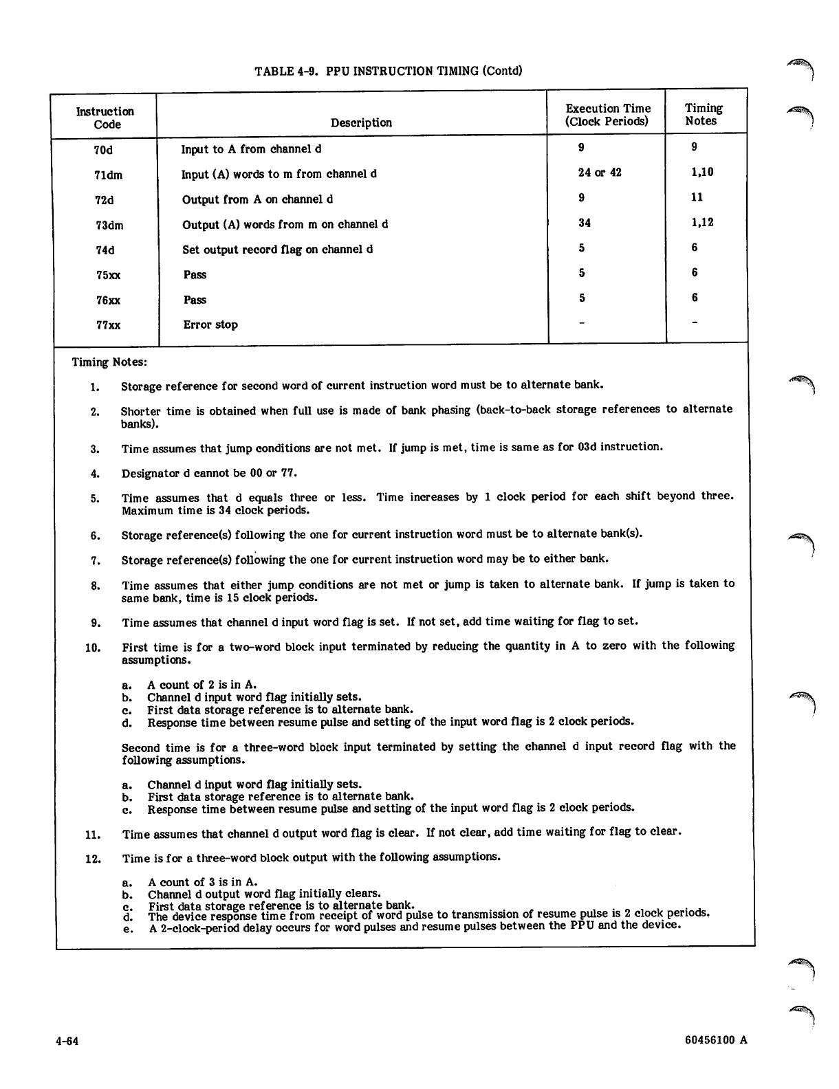
TABLE 4-9. PPU INSTRUCTION TIMING (Contd)
Instruction
Code
70d
71dm
72d
73dm
74d
75xx
76xx
77xx
Description
Input to A from channel d
Input (A) words to m from channel d
Output from A on channel d
Output (A) words from m on channel d
Set output record flag on channel d
Pass
Pass
Error stop
Execution Time
(Clock Periods)
9
24 or 42
9
34
5
5
5
Timing
Notes
9
1,10
11
1,12
6
6
6
Timing Notes:
1. Storage reference for second word of current instruction word must be to alternate bank.
2. Shorter time is obtained when full use is made of bank phasing (back-to-back storage references to alternate
banks).
3. Time assumes that jump conditions are not met. If jump is met, time is same as for 03d instruction.
4. Designator d cannot be 00 or 77.
5. Time assumes that d equals three or less. Time increases by 1 clock period for each shift beyond three.
Maximum time is 34 clock periods.
6. Storage reference(s) following the one for current instruction word must be to alternate bank(s).
7. Storage reference(s) following the one for current instruction word may be to either bank.
8. Time assumes that either jump conditions are not met or jump is taken to alternate bank. If jump is taken to
same bank, time is 15 clock periods.
9. Time assumes that channel d input word flag is set. If not set, add time waiting for flag to set.
10. First time is for a two-word block input terminated by reducing the quantity in A to zero with the following
assumptions.
a. A count of 2 is in A.
b. Channel d input word flag initially sets.
c. First data storage reference is to alternate bank.
d. Response time between resume pulse and setting of the input word flag is 2 clock periods.
Second time is for a three-word block input terminated by setting the channel d input record flag with the
following assumptions.
a. Channel d input word flag initially sets.
b. First data storage reference is to alternate bank.
c. Response time between resume pulse and setting of the input word flag is 2 clock periods.
11. Time assumes that channel d output word flag is clear. If not clear, add time waiting for flag to clear.
12. Time is for a three-word block output with the following assumptions.
a. A count of 3 is in A.
b. Channel d output word flag initially clears.
c. First data storage reference is to alternate bank. . , „ . _ , . . .
d. The device response time from receipt of word pulse to transmission of resume pulse is 2 clock periods.
e. A 2-clock-period delay occurs for word pulses and resume pulses between the PPU and the device.
4-64 60456100 A
PEMPWRA* PROCESSOR SUBSYSTEM INSTRUCTIONS -- ALL MODELS

•/s5%
'**%.
PERIPHERAL PROCESSOR SUBSYSTEM
INSTRUCTIONS - ALL MODELS
Each PP sequentially executes instructions from its own
memory and uses an 18-bit A register for manipulative
operations. The A register is the only PP register used by
the programmer. All the PPS arithmetic operations are
binary and are performed in a one's complement mode.
This mode treats a value of 777777 in the A register as a
negative zero.
The PPS instructions are the same and produce the same
results as the PPU instructions except for the instructions
listed in table 4-6. This table and other information for the
instruction formats, designators, and addressing modes are
located at the beginning of the previous subsection,
Peripheral Processor Unit Instructions - Model 176.
The following PPS instruction descriptions are briefly
stated to avoid word-for-word repetitions of similar PPU
instruction descriptions in the previous pages. Refer to
corresponding PPU descriptions when additional instruction
detail is required.
02dm Return Jump to m + (d) RJM
23 18 17 12
fd
\A /
V
(P) (P + l)
This 24-bit instruction jumps to the address given by m plus
the content of location d. If d equals zero, m is not
modified. The current program address (P) plus 2 is stored
at the jump address. The next instruction starts at the
jump address plus 1. The subprogram exits with a long
jump or normal sequencing to the jump address minus 1,
which in turn contains a long jump, 0100. This returns the
original program address plus 2 to the P register.
03d Unconditional Jump d UJN
I I 6 5 0
f d
PPS INSTRUCTION DESCRIPTIONS
The PPS instructions have separate descriptions. Shaded
areas, like those in the 260x and 261x instruction formats,
indicate unused bits. The unused bits are ignored by the
PPs.
Timing information follows the instructions.
0000 Pass PSN
I I 6 5 O
f d
This 12-bit instruction provides an unconditional jump to
any address up to 31 (decimal) locations forward or
backward from the current program address. The value of
d is added to the current program address. If d is positive
(01 through 37), 0001 through 0037 is added, and the jump is
forward. If d is negative (40 through 76), 7740 through
7776 is added, and the jump is backward. The program
hangs when d equals 00 or 77 and requires a deadstart to
restart the system.
04d Zero Jump d ZJN
I I 6 5 O
fd
This 12-bit instruction specifies that no operation is to be
performed. The instruction provides a means of padding
out a program.
01dm Long Jump to m + (d) UM
23 18 17 1211
f d
\ /\ /
\
(F
i
>) (P+l)
This 12-bit instruction provides a conditional jump to any
address up to 31 (decimal) locations forward or backward
from the current program address. If the content of the A
register is zero, the jump is taken. If the content of A is
nonzero, the next instruction executes from P plus 1.
Negative zero (777777) is treated as nonzero. For
interpretation of d, refer to 03 instruction.
05d Nonzero Jump d NJN
This 24-bit instruction jumps to the address given by m plus
the content of location d. If d equals zero, m is not
modified.
I I 6 5 0
f d
60456100 G 4-65
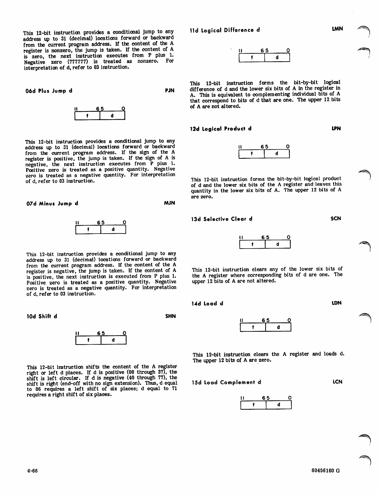
This 12-bit instruction provides a conditional jump to any
address up to 31 (decimal) locations forward or backward
from the current program address. If the content of the A
register is nonzero, the jump is taken. If the content of A
is zero, the next instruction executes from P plus 1.
Negative zero (777777) is treated as nonzero. For
interpretation of d, refer to 03 instruction.
lid Logical Difference d LMN
I I 6 5 0
fd
06d Plus Jump d PJN
I I 6 5 0
f d
This 12-bit instruction provides a conditional jump to any
address up to 31 (decimal) locations forward or backward
from the current program address. If the sign of the A
register is positive, the jump is taken. If the sign of A is
negative, the next instruction executes from P plus 1.
Positive zero is treated as a positive quantity. Negative
zero is treated as a negative quantity. For interpretation
of d, refer to 03 instruction.
07d Minus Jump d MJN
This 12-bit instruction forms the bit-by-bit logical
difference of d and the lower six bits of A in the register in
A. This is equivalent to complementing individual bits of A
that correspond to bits of d that are one. The upper 12 bits
of A are not altered.
12d Logical Product d LPN
I I 6 5 0
f d
This 12-bit instruction forms the bit-by-bit logical product
of d and the lower six bits of the A register and leaves this
quantity in the lower six bits of A. The upper 12 bits of A
are zero.
I I 6 5 0
f d
This 12-bit instruction provides a conditional jump to any
address up to 31 (decimal) locations forward or backward
from the current program address. If the content of the A
register is negative, the jump is taken. If the content of A
is positive, the next instruction is executed from P plus 1.
Positive zero is treated as a positive quantity. Negative
zero is treated as a negative quantity. For interpretation
of d, refer to 03 instruction.
13d Selective Clear d SCN
I I 6 5 0
fd/<<5i|v
This 12-bit instruction clears any of the lower six bits of
the A register where corresponding bits of d are one. The
upper 12 bits of A are not altered.
14d Load d LDN
lOd Shift d SHN
I I 6 5 0
t d
I I 6 5 0
f d
This 12-bit instruction shifts the content of the A register
right or left d places. If d is positive (00 through 37), the
shift is left circular. If d is negative (40 through 77), the
shift is right (end-off with no sign extension). Thus, d equal
to 06 requires a left shift of six places; d equal to 71
requires a right shift of six places.
This 12-bit instruction clears the A register and loads d.
The upper 12 bits of A are zero.
15d Load Complement d LCN
I I 6 5 O
fd
4-66 60456100 G
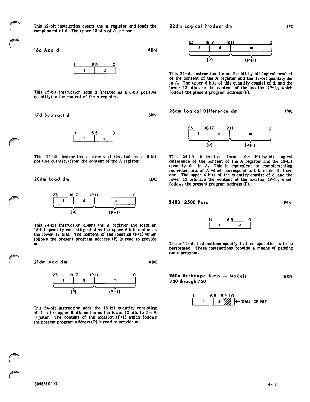
This 12-bit instruction clears the A register and loads the
complement of d. The upper 12 bits of A are one.
22dm Logical Product dm LPC
16d Add d ADN
I I 6 5 0
f d
This 12-bit instruction adds d (treated as a 6-bit positive
quantity) to the content of the A register.
23 1817 1211
f d
\A /
V
(P) (P+D
This 24-bit instruction forms the bit-by-bit logical product
of the content of the A register and the 18-bit quantity dm
in A. The upper 6 bits of this quantity consist of d, and the
lower 12 bits are the content of the location (P+l), which
follows the present program address (P).
17d Subtract d SBN
23dm Logical Difference dm IMC
I I 6 5 0
f d
23 18 17 1211
f d
\A /
V
(P) (P+D
This 12-bit instruction subtracts d (treated as a 6-bit
positive quantity) from the content of the A register.
20dm Load dm LDC
This 24-bit instruction forms the bit-by-bit logical
difference of the content of the A register and the 18-bit
quantity dm in A. This is equivalent to complementing
individual bits of A which correspond to bits of dm that are
one. The upper 6 bits of the quantity consist of d, and the
lower 12 bits are the content of the location (P+l), which
follows the present program address (P).
23 18 17 12 11
f d
\ /\ /
(1 >) (P+D
This 24-bit instruction clears the A register and loads an
18-bit quantity consisting of d as the upper 6 bits and m as
the lower 12 bits. The content of the location (P+l) which
follows the present program address (P) is read to provide
m.
21dm Add dm
2400, 2500 Pass PSN
I I 6 5 O
t d
These 12-bit instructions specify that no operation is to be
performed. These instructions provide a means of padding
out a program.
ADC
23 18 17 12 11
f d
260x Exchange Jump — Models
720 through 760
EXN
-v-
(P)
_/\_ —v—
(P+l) I I 6 5 3 2 1 0
f d m■DUAL CP BIT
This 24-bit instruction adds the 18-bit quantity consisting
of d as the upper 6 bits and m as the lower 12 bits to the A
register. The content of the location (P+l) which follows
the present program address (P) is read to provide m.
r
00^^
60456100 G 4-67
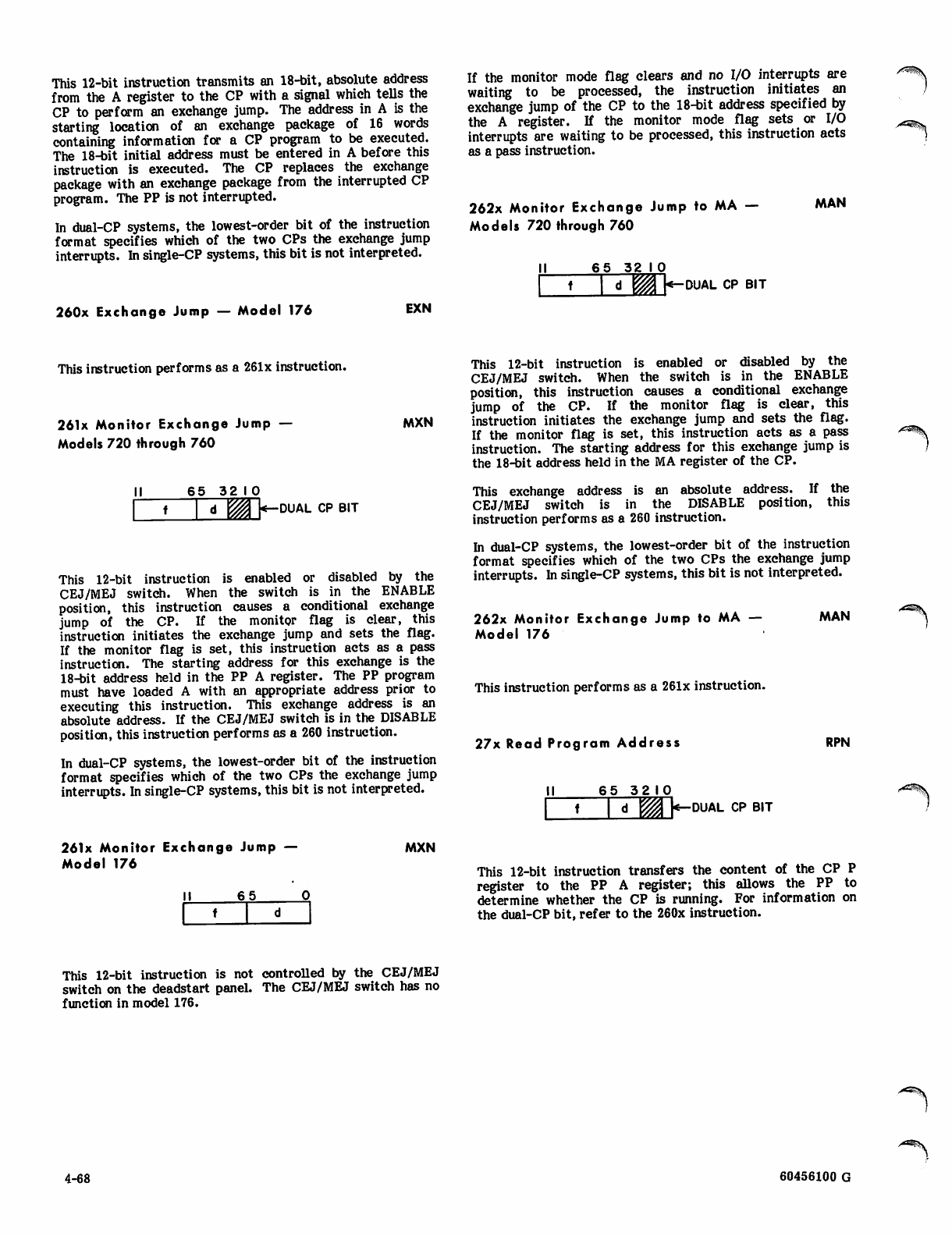
This 12-bit instruction transmits an 18-bit, absolute address
from the A register to the CP with a signal which tells the
CP to perform an exchange jump. The address in A is the
starting location of an exchange package of 16 words
containing information for a CP program to be executed.
The 18-bit initial address must be entered in A before this
instruction is executed. The CP replaces the exchange
package with an exchange package from the interrupted CP
program. The PP is not interrupted.
In dual-CP systems, the lowest-order bit of the instruction
format specifies which of the two CPs the exchange jump
interrupts. In single-CP systems, this bit is not interpreted.
260x Exchange Jump — Model 176 EXN
If the monitor mode flag clears and no I/O interrupts are
waiting to be processed, the instruction initiates an
exchange jump of the CP to the 18-bit address specified by
the A register. If the monitor mode flag sets or I/O
interrupts are waiting to be processed, this instruction acts
as a pass instruction.
262x Monitor Exchange Jump to MA —
Models 720 through 760
MAN
65 32 I 0
f*m ■DUAL CP BIT
This instruction performs as a 261x instruction.
261x Monitor Exchange Jump —
Models 720 through 760
MXN
6 5 3 2 1 0
f d yjyo ■DUAL CP BIT
This 12-bit instruction is enabled or disabled by the
CEJ/MEJ switch. When the switch is in the ENABLE
position, this instruction causes a conditional exchange
jump of the CP. If the monitor flag is clear, this
instruction initiates the exchange jump and sets the flag.
If the monitor flag is set, this instruction acts as a pass
instruction. The starting address for this exchange is the
18-bit address held in the PP A register. The PP program
must have loaded A with an appropriate address prior to
executing this instruction. This exchange address is an
absolute address. If the CEJ/MEJ switch is in the DISABLE
position, this instruction performs as a 260 instruction.
In dual-CP systems, the lowest-order bit of the instruction
format specifies which of the two CPs the exchange jump
interrupts. In single-CP systems, this bit is not interpreted.
This 12-bit instruction is enabled or disabled by the
CEJ/MEJ switch. When the switch is in the ENABLE
position, this instruction causes a conditional exchange
jump of the CP. If the monitor flag is clear, this
instruction initiates the exchange jump and sets the flag.
If the monitor flag is set, this instruction acts as a pass
instruction. The starting address for this exchange jump is
the 18-bit address held in the MA register of the CP.
This exchange address is an absolute address. If the
CEJ/MEJ switch is in the DISABLE position, this
instruction performs as a 260 instruction.
In dual-CP systems, the lowest-order bit of the instruction
format specifies which of the two CPs the exchange jump
interrupts. In single-CP systems, this bit is not interpreted.
262x Monitor Exchange Jump to MA —
Model 176
This instruction performs as a 261x instruction.
27x Read Program Address
I I 6 5 3 2 1 0
e-DUAL CP BIT
MAN
RPN
f d MA
261x Monitor Exchange Jump —
Model 176
MXN
I I 6 5 0
t d
This 12-bit instruction transfers the content of the CP P
register to the PP A register; this allows the PP to
determine whether the CP is running. For information on
the dual-CP bit, refer to the 260x instruction.
This 12-bit instruction is not controlled by the CEJ/MEJ
switch on the deadstart panel. The CEJ/MEJ switch has no
function in model 176.
4-68 60456100 G
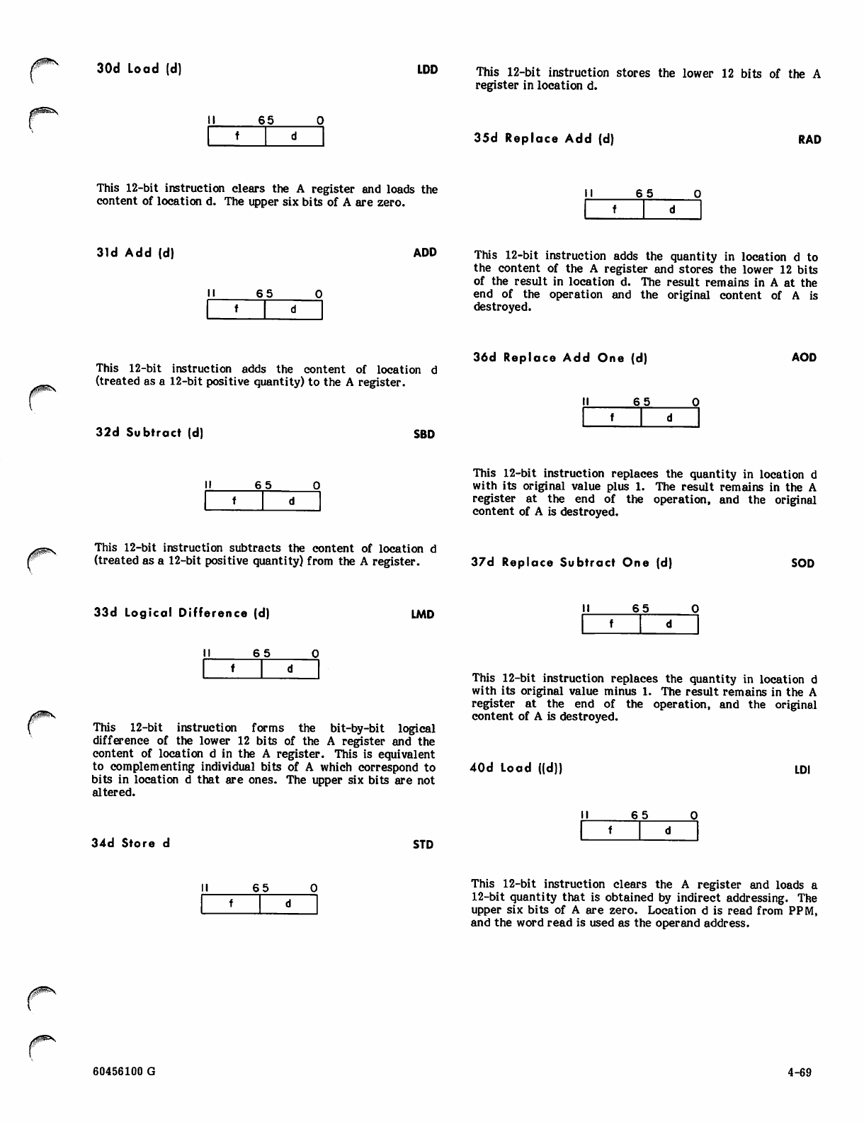
30d Load (d) LDD This 12-bit instruction stores the lower 12 bits of the A
register in location d.
I I 6 5 0
f d 35d Replace Add (d) RAD
This 12-bit instruction clears the A register and loads the
content of location d. The upper six bits of A are zero. I I 6 5 0
f d
31d Add (d) ADD
I I 6 5 0
f d
This 12-bit instruction adds the quantity in location d to
the content of the A register and stores the lower 12 bits
of the result in location d. The result remains in A at the
end of the operation and the original content of A is
destroyed.
This 12-bit instruction adds the content of location d
(treated as a 12-bit positive quantity) to the A register.
36d Replace Add One (d) AOD
32d Subtract (d)
I I 6 5 0
f d
SBD
I I 6 5 0
fd
This 12-bit instruction replaces the quantity in location d
with its original value plus 1. The result remains in the A
register at the end of the operation, and the original
content of A is destroyed.
This 12-bit instruction subtracts the content of location d
(treated as a 12-bit positive quantity) from the A register. 37d Replace Subtract One (d) SOD
33d Logical Difference (d) LMD I I 6 5 0
f d
I I 6 5 0
f d
This 12-bit instruction forms the bit-by-bit logical
difference of the lower 12 bits of the A register and the
content of location d in the A register. This is equivalent
to complementing individual bits of A which correspond to
bits in location d that are ones. The upper six bits are not
altered.
This 12-bit instruction replaces the quantity in location d
with its original value minus 1. The result remains in the A
register at the end of the operation, and the original
content of A is destroyed.
40d Load ((d)) LDI
34d Store d STD
I I 6 5 0
f d
I I 6 5 0
fd
This 12-bit instruction clears the A register and loads a
12-bit quantity that is obtained by indirect addressing. The
upper six bits of A are zero. Location d is read from PPM,
and the word read is used as the operand address.
60456100 G 4-69
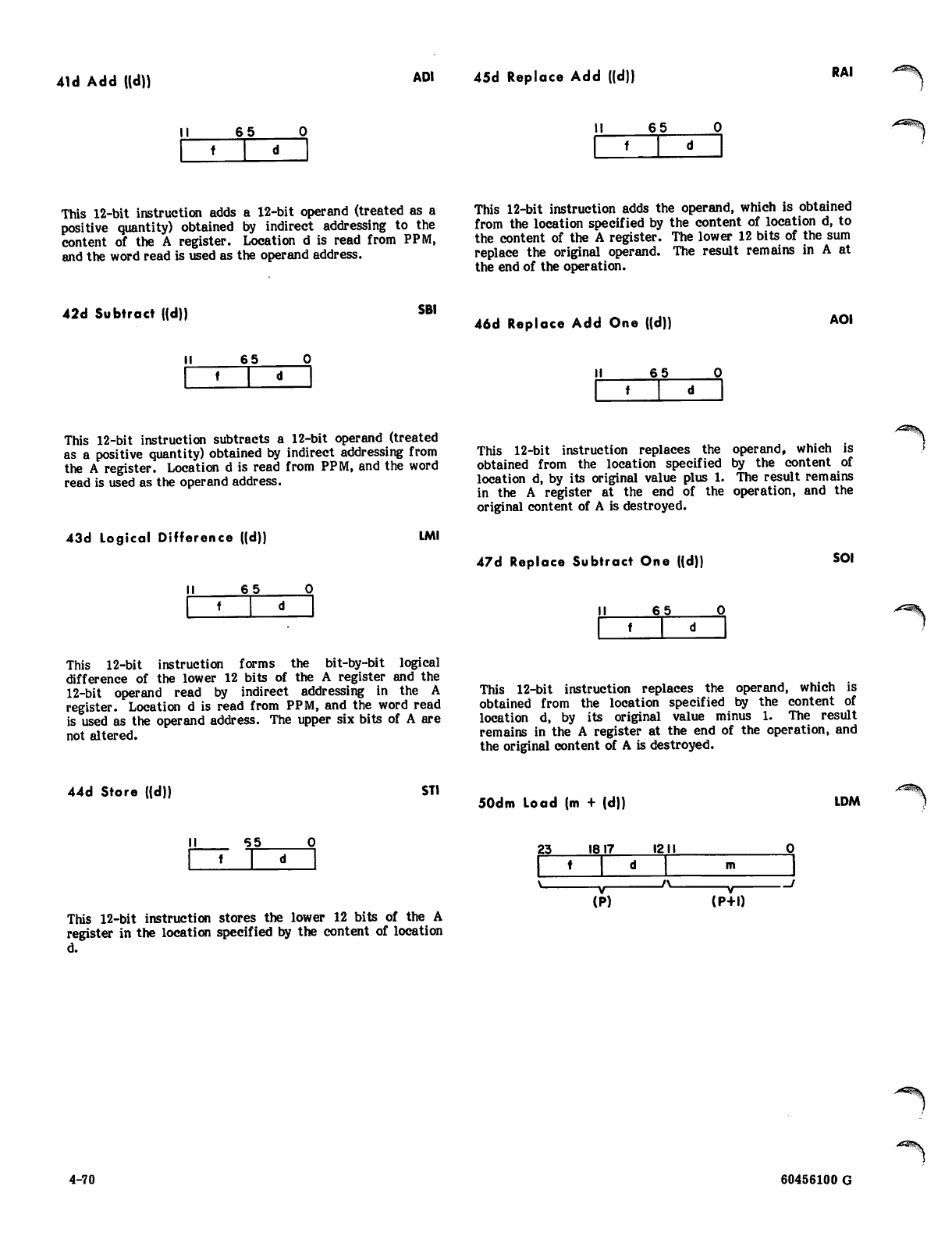
41 d Add ((d)) ADI 45d Replace Add ((d)) RAI
I I 6 5 0
td
I I 6 5 0
fd
This 12-bit instruction adds a 12-bit operand (treated as a
positive quantity) obtained by indirect addressing to the
content of the A register. Location d is read from PPM,
and the word read is used as the operand address.
This 12-bit instruction adds the operand, which is obtained
from the location specified by the content of location d, to
the content of the A register. The lower 12 bits of the sum
replace the original operand. The result remains in A at
the end of the operation.
42d Subtract ((d)) SBI
46d Replace Add One ((d)) AOI
I I 6 5 0
f d I I 6 5 0
f d
This 12-bit instruction subtracts a 12-bit operand (treated
as a positive quantity) obtained by indirect addressing from
the A register. Location d is read from PPM, and the word
read is used as the operand address.
43d Logical Difference ((d)) LMI
This 12-bit instruction replaces the operand, which is
obtained from the location specified by the content of
location d, by its original value plus 1. The result remains
in the A register at the end of the operation, and the
original content of A is destroyed.
47d Replace Subtract One ((d)) SOI
I I 6 5 0
f d I I 6 5 0
f d
r*^$k
This 12-bit instruction forms the bit-by-bit logical
difference of the lower 12 bits of the A register and the
12-bit operand read by indirect addressing in the A
register. Location d is read from PPM, and the word read
is used as the operand address. The upper six bits of A are
not altered.
This 12-bit instruction replaces the operand, which is
obtained from the location specified by the content of
location d, by its original value minus 1. The result
remains in the A register at the end of the operation, and
the original content of A is destroyed.
44d Store ((d)) STI 50dm Load (m + (d)) LDM
r^&®$!K
I I 5 5 0
f d
This 12-bit instruction stores the lower 12 bits of the A
register in the location specified by the content of location
d.
23 1817 1211
f d
V A v—
(P+D(1
f
>)
4-70 60456100 G
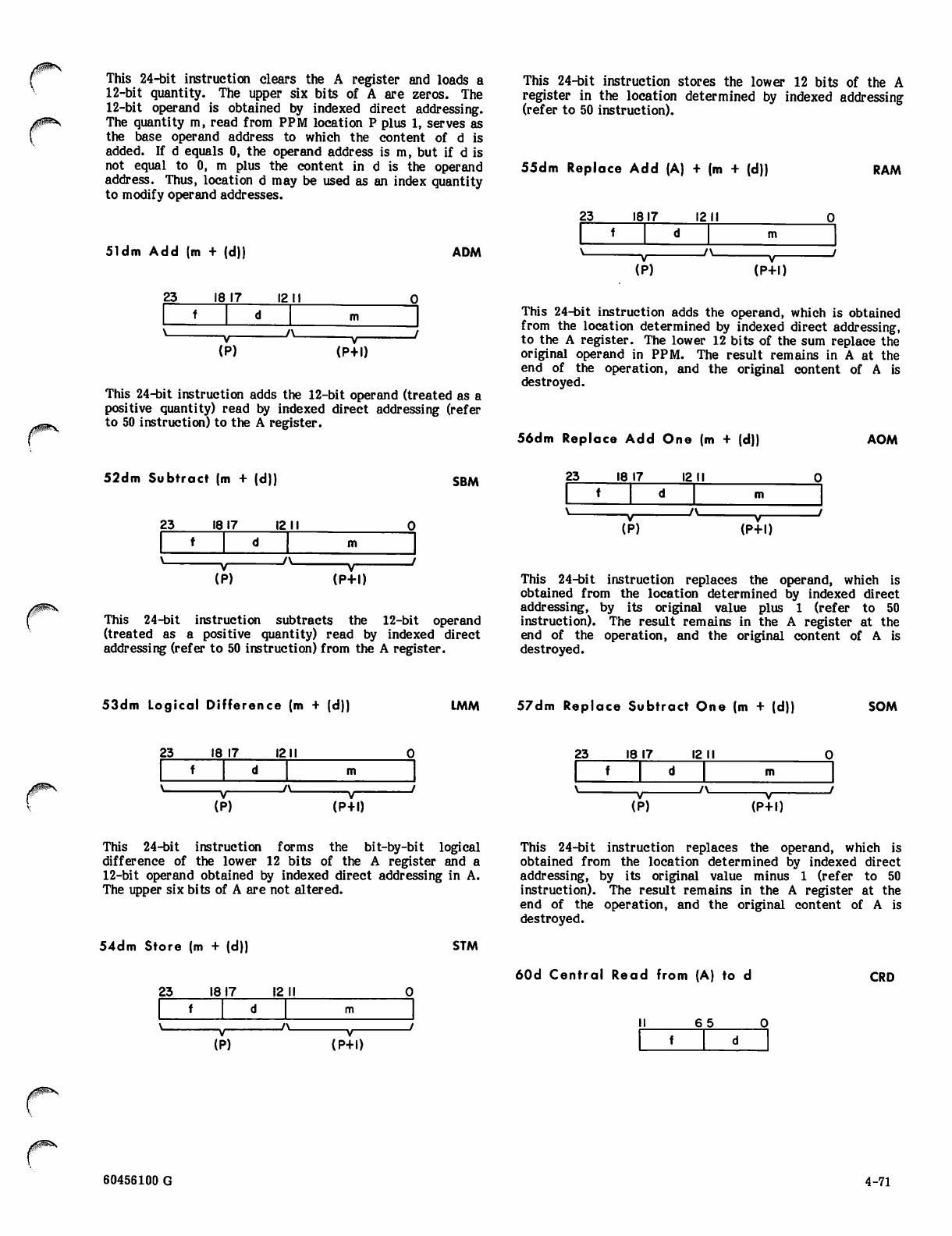
This 24-bit instruction clears the A register and loads a
12-bit quantity. The upper six bits of A are zeros. The
12-bit operand is obtained by indexed direct addressing.
The quantity m, read from PPM location P plus 1, serves as
the base operand address to which the content of d is
added. If d equals 0, the operand address is m, but if d is
not equal to 0, m plus the content in d is the operand
address. Thus, location d may be used as an index quantity
to modify operand addresses.
51dm Add (m + (d)) ADM
23 18 17 12 11
f d
\ /* v '
(P+l)
(
*
3)
This 24-bit instruction adds the 12-bit operand (treated as a
positive quantity) read by indexed direct addressing (refer
to 50 instruction) to the A register.
52dm Subtract (m + (d)) SBM
23 18 17 1211
f d
\i\ /
>
(( (P+l)
This 24-bit instruction subtracts the 12-bit operand
(treated as a positive quantity) read by indexed direct
addressing (refer to 50 instruction) from the A register.
This 24-bit instruction stores the lower 12 bits of the A
register in the location determined by indexed addressing
(refer to 50 instruction).
55dm Replace Add (A) + (m + (d)) RAM
23 1817 1211
f d
\V
(P)
" v '
(P+D
This 24-bit instruction adds the operand, which is obtained
from the location determined by indexed direct addressing,
to the A register. The lower 12 bits of the sum replace the
original operand in PPM. The result remains in A at the
end of the operation, and the original content of A is
destroyed.
56dm Replace Add One (m + (d))
2 3 1 8 1 7 1 2 1 1
AOM
t d m
\A #
V
(P) (P+D
This 24-bit instruction replaces the operand, which is
obtained from the location determined by indexed direct
addressing, by its original value plus 1 (refer to 50
instruction). The result remains in the A register at the
end of the operation, and the original content of A is
destroyed.
53dm Logical Difference (m + (d)) LMM 57dm Replace Subtract One (m + (d)) SOM
23 18 17 1211
f d
V/\ /
\
(F
i
>) (P+D
23 18 17 12 11
f d
\A /
(1
i
») (P+l)
This 24-bit instruction forms the bit-by-bit logical
difference of the lower 12 bits of the A register and a
12-bit operand obtained by indexed direct addressing in A.
The upper six bits of A are not altered.
54dm Store (m + (d))
23 1817 12 11
STM
f d m
\ /\ /
\
(F >) (P+0
This 24-bit instruction replaces the operand, which is
obtained from the location determined by indexed direct
addressing, by its original value minus 1 (refer to 50
instruction). The result remains in the A register at the
end of the operation, and the original content of A is
destroyed.
60d Central Read from (A) to d CRD
I I 6 5 O
fd
60456100 G 4-71
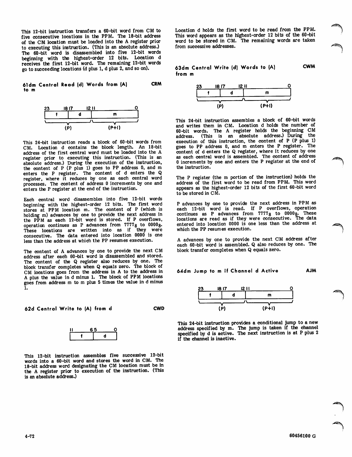
This 12-bit instruction transfers a 60-bit word from CM to
five consecutive locations in the PPM. The 18-bit address
of the CM location must be loaded into the A register prior
to executing this instruction. (This is an absolute address.)
The 60-bit word is disassembled into five 12-bit words
beginning with the highest-order 12 bits. Location d
receives the first 12-bit word. The remaining 12-bit words
go to succeeding locations (d plus 1, d plus 2, and so on).
61dm Central Read (d) Words from (A)
to m
CRM
23 1817 1211
f d
(P)
J\- —v—
(P+l)
This 24-bit instruction reads a block of 60-bit words from
CM. Location d contains the block length. An 18-bit
address of the first central word must be loaded into the A
register prior to executing this instruction. (This is an
absolute address.) During the execution of the instruction,
the content of P (P plus 1) goes to PP address 0, and m
enters the P register. The content of d enters the Q
register, where it reduces by one as each central word
processes. The content of address 0 increments by one and
enters the P register at the end of the instruction.
Each central word disassembles into five 12-bit words
beginning with the highest-order 12 bits. The first word
stores at PPM location m. The content of P (which is
holding m) advances by one to provide the next address in
the PPM as each 12-bit word is stored. If P overflows,
operation continues as P advances from 7777g to OOOOg.
These locations are written into as if they were
consecutive. The data entered into location 0000 is one
less than the address at which the PP resumes execution.
The content of A advances by one to provide the next CM
address after each 60-bit word is disassembled and stored.
The content of the Q register also reduces by one. The
block transfer completes when Q equals zero. The block of
CM locations goes from the address in A to the address in
A plus the value in d minus 1. The block of PPM locations
goes from address m to m plus 5 times the value in d minus
1.
Location d holds the first word to be read from the PPM.
This word appears as the highest-order 12 bits of the 60-bit
word to be stored in CM. The remaining words are taken
from successive addresses.
63dm Central Write (d) Words to (A)
from m
23 1817 12II
CWM
f d m
\A 1
' V
(P) (P+l)
This 24-bit instruction assembles a block of 60-bit words
and writes them in CM. Location d holds the number of
60-bit words. The A register holds the beginning CM
address. (This is an absolute address.) During the
execution of this instruction, the content of P (P plus 1)
goes to PP address 0, and m enters the P register. The
content of d enters the Q register, where it reduces by one
as each central word is assembled. The content of address
0 increments by one and enters the P register at the end of
the instruction.
The P register (the m portion of the instruction) holds the
address of the first word to be read from PPM. This word
appears as the highest-order 12 bits of the first 60-bit word
to be stored in CM.
P advances by one to provide the next address in PPM as
each 12-bit word is read. If P overflows, operation
continues as P advances from 7777 g to 00008- These
locations are read as if they were consecutive. The data
entered into location 0000 is one less than the address at
which the PP resumes execution.
A advances by one to provide the next CM address after
each 60-bit word is assembled. Q also reduces by one. The
block transfer completes when Q equals zero.
64dm Jump to m if Channel d Active AJM
23 18 17 12 11
t d
62d Centr al Wr ite to (A) fr om d CWD (P)
J\. —v—
(P+l)
I I 6 5 O
f d
This 24-bit instruction provides a conditional jump to a new
address specified by m. The jump is taken if the channel
specified by d is active. The next instruction is at P plus 2
if the channel is inactive.
This 12-bit instruction assembles five successive 12-bit
words into a 60-bit word and stores the word in CM. The
18-bit address word designating the CM location must be in
the A register prior to execution of the instruction. (This
is an absolute address.)
4-72 60456100 G
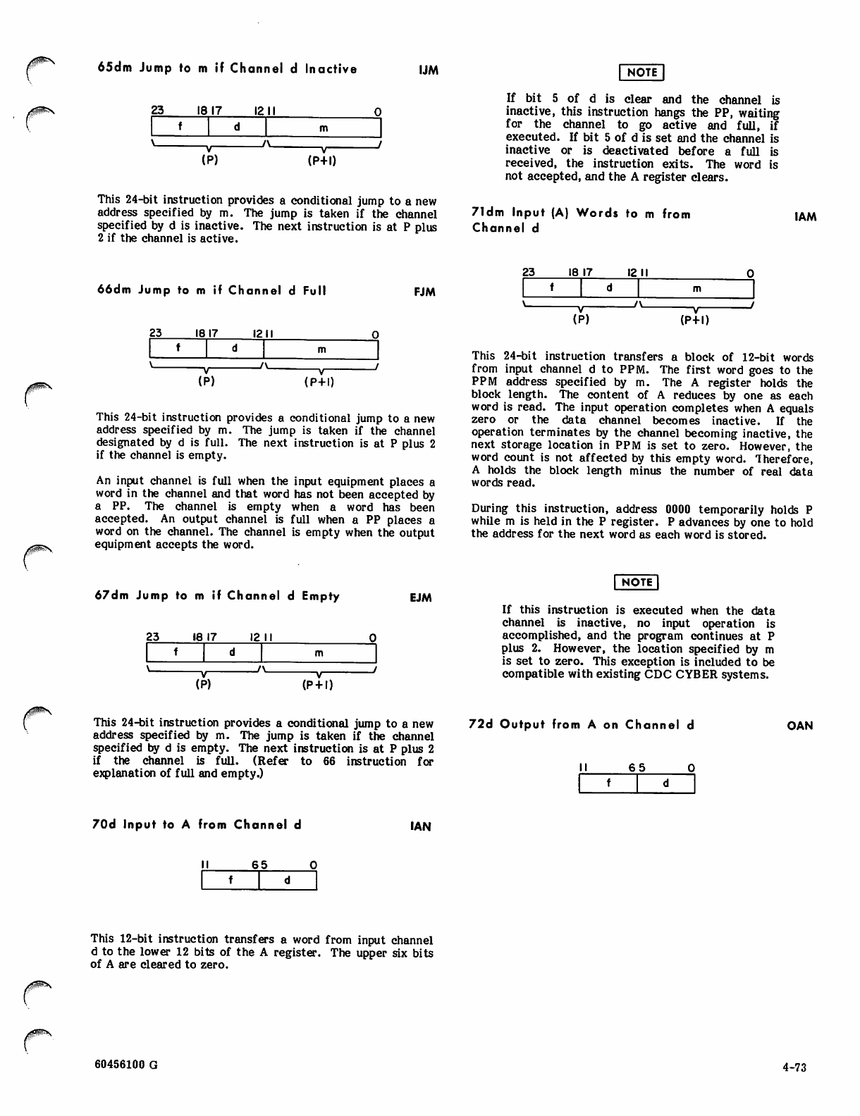
0S&\ 65dm J ump to m if Chan n el d Ina c tive UM
23 18 17 1211
f d
\- v '
(P)
v /
V
(P+D
This 24-bit instruction provides a conditional jump to a new
address specified by m. The jump is taken if the channel
specified by d is inactive. The next instruction is at P plus
2 if the channel is active.
NOTE
If bit 5 of d is clear and the channel is
inactive, this instruction hangs the PP, waiting
for the channel to go active and full, if
executed. If bit 5 of d is set and the channel is
inactive or is deactivated before a full is
received, the instruction exits. The word is
not accepted, and the A register clears.
71dm Input ( A ) Wor ds to m f r om
Channel d
1AM
23 18 17 12 11
66dm Jump to m if Channel d Full FJM
23 18 17 1211
f d
\A /
\
(F
i
>) (P+D
This 24-bit instruction provides a conditional jump to a new
address specified by m. The jump is taken if the channel
designated by d is full. The next instruction is at P plus 2
if the channel is empty.
An input channel is full when the input equipment places a
word in the channel and that word has not been accepted by
a PP. The channel is empty when a word has been
accepted. An output channel is full when a PP places a
word on the channel. The channel is empty when the output
equipment accepts the word.
A /
V
(P) (P+D
This 24-bit instruction transfers a block of 12-bit words
from input channel d to PPM. The first word goes to the
PPM address specified by m. The A register holds the
block length. The content of A reduces by one as each
word is read. The input operation completes when A equals
zero or the data channel becomes inactive. If the
operation terminates by the channel becoming inactive, the
next storage location in PPM is set to zero. However, the
word count is not affected by this empty word. Therefore,
A holds the block length minus the number of real data
words read.
During this instruction, address 0000 temporarily holds P
while m is held in the P register. P advances by one to hold
the address for the next word as each word is stored.
67dm Jump to m if Channel d Empty EJM
23 18 17 12 11
fd
\ /\ /
V
(F
f
>) (P + D
Inqte I
If this instruction is executed when the data
channel is inactive, no input operation is
accomplished, and the program continues at P
plus 2. However, the location specified by m
is set to zero. This exception is included to be
compatible with existing CDC CYBER systems.
This 24-bit instruction provides a conditional jump to a new
address specified by m. The jump is taken if the channel
specified by d is empty. The next instruction is at P plus 2
if the channel is full. (Refer to 66 instruction for
explanation of full and empty.)
72d Output from A on Channel d OAN
I I 6 5 0
fd
70d Input to A from Channel d IAN
I I 6 5 0
f d
This 12-bit instruction transfers a word from input channel
d to the lower 12 bits of the A register. The upper six bits
of A are cleared to zero.
60456100 G 4-73
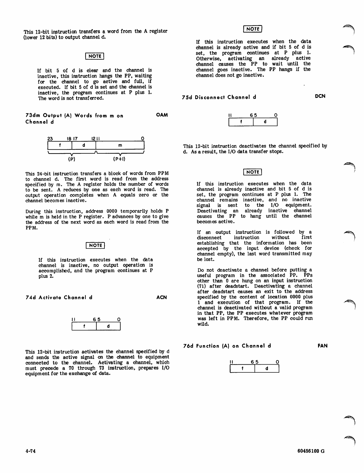
This 12-bit instruction transfers a word from the A register
(lower 12 bits) to output channel d.
NOTE
If bit 5 of d is clear and the channel is
inactive, this instruction hangs the PP, waiting
for the channel to go active and full, if
executed. If bit 5 of d is set and the channel is
inactive, the program continues at P plus 1.
The word is not transferred.
NOTE
If this instruction executes when the data
channel is already active and if bit 5 of d is
set, the program continues at P plus 1.
Otherwise, activating an already active
channel causes the PP to wait until the
channel goes inactive. The PP hangs if the
channel does not go inactive.
75d Disconnect Channel d DCN
73dm Output (A) Words from m on
Channel d
OAM I I 6 5 0
f d
23 18 17 1211
f d
\/\ /
N
(F
i
>) (P+l)
This 12-bit instruction deactivates the channel specified by
d. As a result, the I/O data transfer stops.
This 24-bit instruction transfers a block of words from PPM
to channel d. The first word is read from the address
specified by m. The A register holds the number of words
to be sent. A reduces by one as each word is read. The
output operation completes when A equals zero or the
channel becomes inactive.
During this instruction, address OOOO temporarily holds P
while m is held in the P register. P advances by one to give
the address of the next word as each word is read from the
PPM.
NOTE |
If this instruction executes when the data
channel is inactive, no output operation is
accomplished, and the program continues at P
plus 2.
74d Activate Channel d ACN
I I 6 5 0
f d
NOTE
If this instruction executes when the data
channel is already inactive and bit 5 of d is
set, the program continues at P plus 1. The
channel remains inactive, and no inactive
signal is sent to the I/O equipment.
Deactivating an already inactive channel
causes the PP to hang until the channel
becomes active.
If an output instruction is followed by a
disconnect instruction without first
establishing that the information has been
accepted by the input device (check for
channel empty), the last word transmitted may
be lost.
Do not deactivate a channel before putting a
useful program in the associated PP. PPs
other than 0 are hung on an input instruction
(71) after deadstart. Deactivating a channel
after deadstart causes an exit to the address
specified by the content of location OOOO plus
1 and execution of that program. If the
channel is deactivated without a valid program
in that PP, the PP executes whatever program
was left in PPM. Therefore, the PP could run
wild.
y^fljlBV
This 12-bit instruction activates the channel specified by d
and sends the active signal on the channel to equipment
connected to the channel. Activating a channel, which
must precede a 70 through 73 instruction, prepares I/O
equipment for the exchange of data.
76d Function (A) on Channel d
I I 6 5 0
f d
FAN
4-74 60456100 G
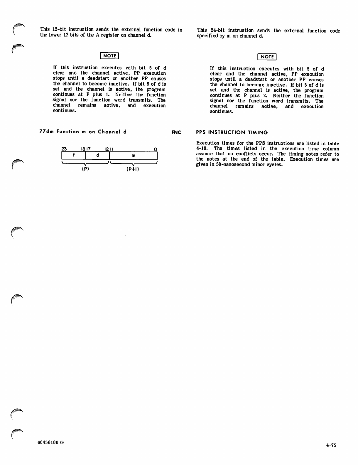
This 12-bit instruction sends the external function code in
the lower 12 bits of the A register on channel d.
["nOtF]
If this instruction executes with bit 5 of d
clear and the channel active, PP execution
stops until a deadstart or another PP causes
the channel to become inactive. If bit 5 of d is
set and the channel is active, the program
continues at P plus 1. Neither the function
signal nor the function word transmits. The
channel remains active, and execution
continues.
This 24-bit instruction sends the external function code
specified by m on channel d.
|~NOTE |
If this instruction executes with bit 5 of d
clear and the channel active, PP execution
stops until a deadstart or another PP causes
the channel to become inactive. If bit 5 of d is
set and the channel is active, the program
continues at P plus 2. Neither the function
signal nor the function word transmits. The
channel remains active, and execution
continues.
77dm Function m on Channel d
2 3 1 8 1 7 1 2 1 1
f d
*V
(F
i—
>)
N v '
(P+l)
FNC PPS INSTRUCTION TIMING
Execution times for the PPS instructions are listed in table
4-10. The times listed in the execution time column
assume that no conflicts occur. The timing notes refer to
the notes at the end of the table. Execution times are
given in 50-nanosecond minor cycles.
p
60456100 G 4-75
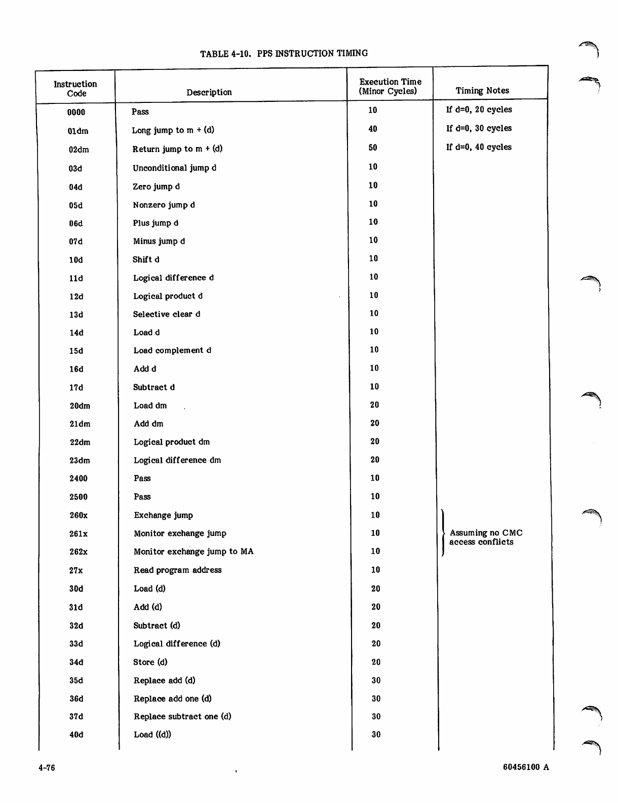
TABLE 4-10. PPS INSTRUCTION TIMING
/"^v
Instruction
Code Description
oooo Pass
01dm Long jump to m + (d)
02dm Return jump to m + (d)
03d Unconditional jump d
04d Zero jump d
05d Nonzero jump d
06d Plus jump d
07d Minus jump d
lOd Shift d
lid Logical difference d
12d Logical product d
13d Selective clear d
14d Load d
15d Load complement d
16d Addd
17d Subtract d
20dm Load dm
21dm Add dm
22dm Logical product dm
23dm Logical difference dm
2400 Pass
2500 Pass
260x Exchange jump
261x Monitor exchange jump
262x Monitor exchange jump to MA
27x Read program address
30d Load (d)
31d Add(d)
32d Subtract (d)
33d Logical difference (d)
34d Store (d)
35d Replace add (d)
36d Replace add one (d)
37d Replace subtract one (d)
40d Load ((d))
Execution Time
(Minor Cycles)
10
40
50
10
10
10
10
10
10
10
10
10
10
10
10
10
20
20
20
20
10
10
10
10
10
10
20
20
20
20
20
30
30
30
30
Timing Notes
If d=0, 20 cycles
If d=0, 30 cycles
If d=0, 40 cycles
Assuming no CMC
access conflicts
y^B^I.
4-76 60456100 A
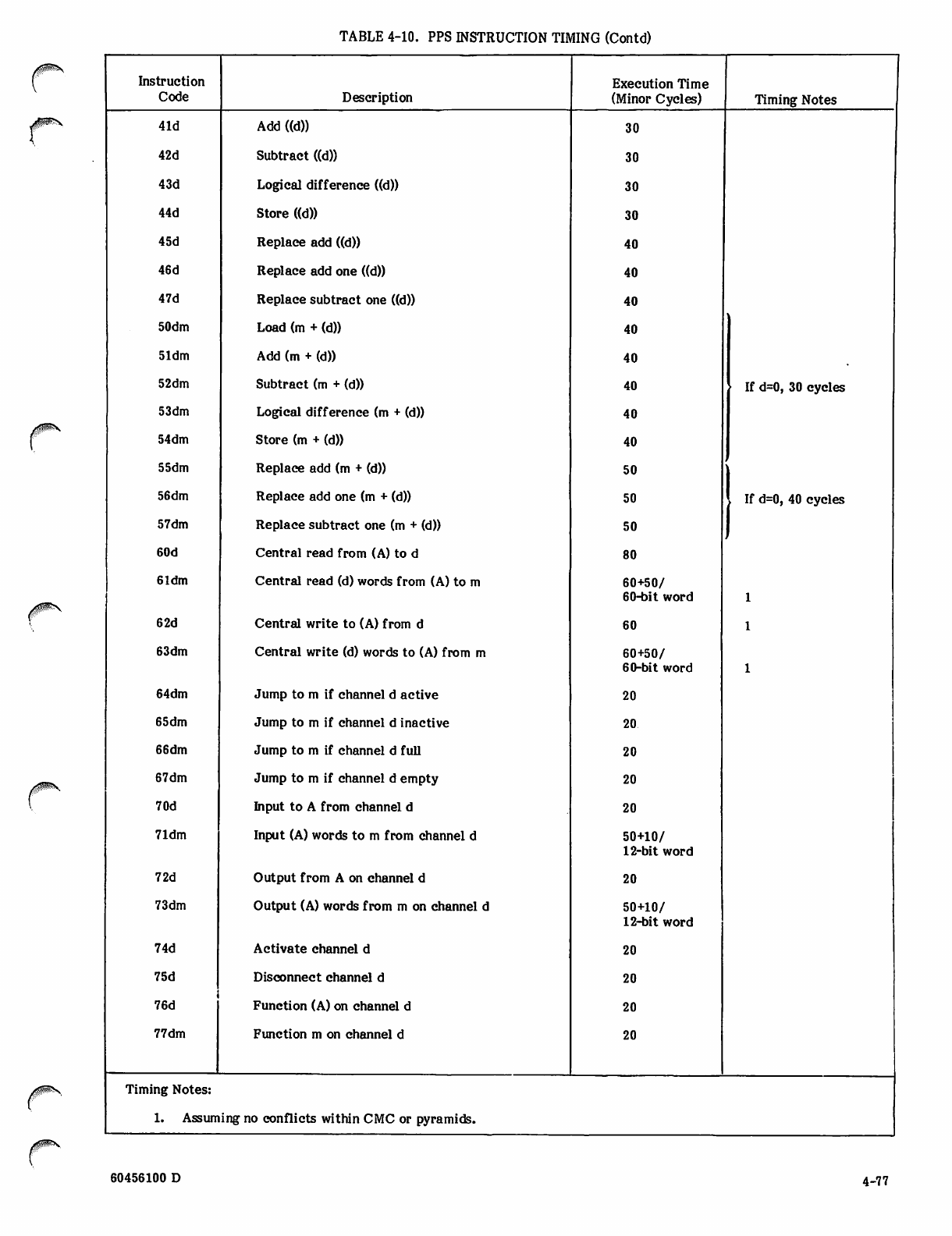
TABLE 4-10. PPS INSTRUCTION TIMING (Contd)
Instruction
Code Description
Execution Time
(Minor Cycles) Timing Notes
41d Add ((d)) 30
42d Subtract ((d)) 30
43d Logical difference ((d)) 30
44d Store ((d)) 30
45d Replace add ((d)) 40
46d Replace add one ((d)) 40
47d Replace subtract one ((d)) 40
50dm Load (m + (d)) 40
51dm Add (m + (d)) 40
52dm Subtract (m + (d)) 40 If d=0, 30 cycles
53dm Logical difference (m + (d)) 40
54dm Store (m + (d)) 40
55dm Replace add (m + (d)) 50
56dm Replace add one (m + (d)) 50 , If d=0, 40 cycles
57dm Replace subtract one (m + (d)) 50
60d Central read from (A) to d 80
61dm Central read (d) words from (A) to m 60+50/
60-bit word
6 2d Central write to (A) from d 60
63dm Central write (d) words to (A) from m 60+50/
60-bit word
64dm Jump to m if channel d active 20
65dm Jump to m if channel d inactive 20
66dm Jump to m if channel d full 20
67dm Jump to m if channel d empty 20
70d Input to A from channel d 20
71dm Input (A) words to m from channel d 50+10/
12-bit word
72d Output from A on channel d 20
73dm Output (A) words from m on channel d 50+10/
12-bit word
74d Activate channel d 20
75d Disconnect channel d 20
76d Function (A) on channel d 20
77dm Function m on channel d 20
Timing Notes:
1. Assuming no conflicts within CMC or pyramids.
60456100 D 4-77

0^%-
(*%
PROGRAMMING INFORMATION
This section describes special programming information otherwise specified, all information in this section is
such as exchange jump, instruction execution, floating- and applicable to all models.
fixed-point arithmetic, address formats, and data formats.
The section also identifies status and control register bits Refer to appendix B for specific differences between model
and lists central processor error responses. Unless 740/750/760 and model 176.
r
60456100 E 5-1/5-2

0*%
f # ^
y^m*
/p^
0^*
CENTRAL PROCESSOR PROGRAMMING
■0JP**'

*v
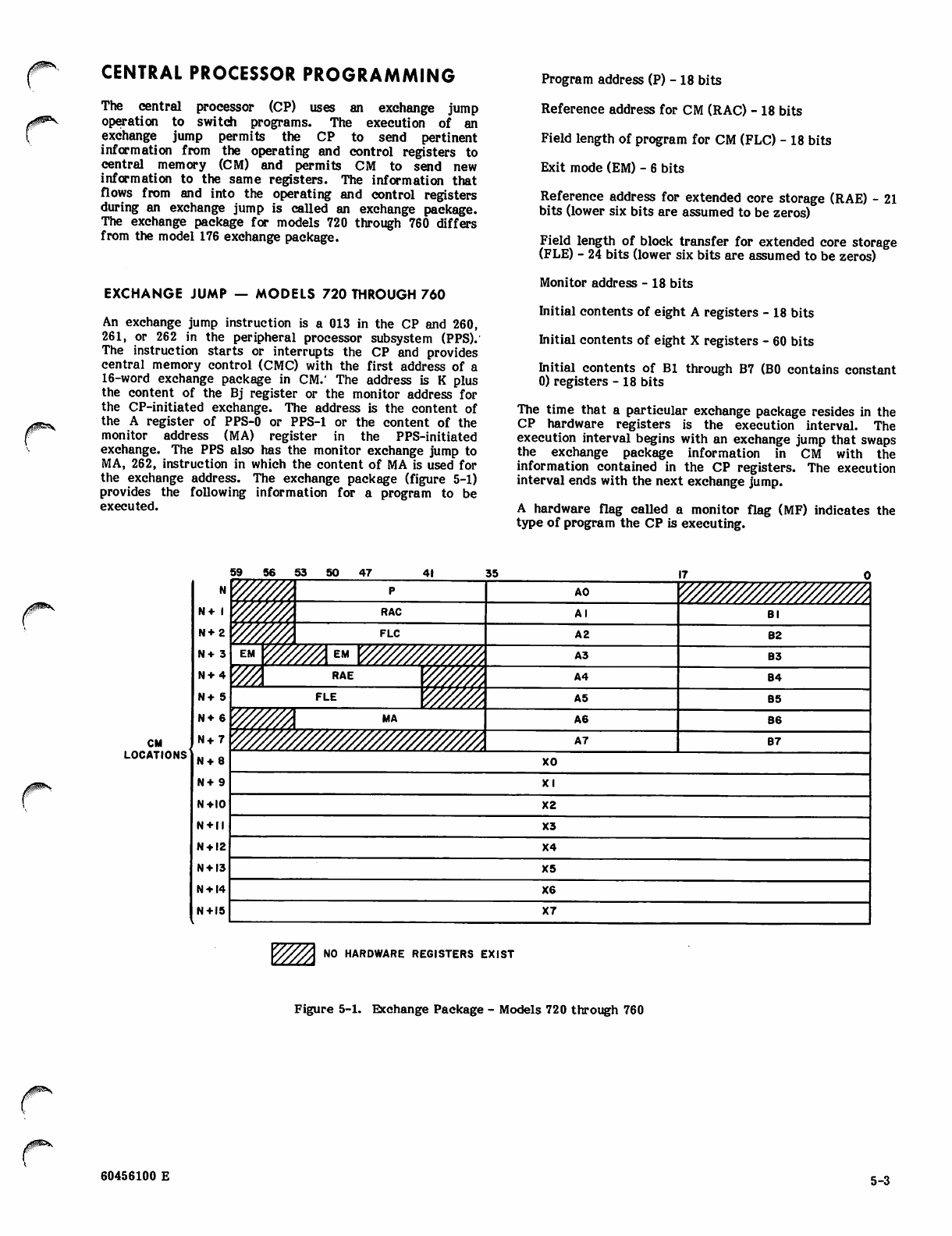
CENTRAL PROCESSOR PROGRAMMING
The central processor (CP) uses an exchange jump
operation to switch programs. The execution of an
exchange jump permits the CP to send pertinent
information from the operating and control registers to
central memory (CM) and permits CM to send new
information to the same registers. The information that
flows from and into the operating and control registers
during an exchange jump is called an exchange package.
The exchange package for models 720 through 760 differs
from the model 176 exchange package.
EXCHANGE JUMP — MODELS 720 THROUGH 760
An exchange jump instruction is a 013 in the CP and 260,
261, or 262 in the peripheral processor subsystem (PPS).
The instruction starts or interrupts the CP and provides
central memory control (CMC) with the first address of a
16-word exchange package in CM.' The address is K plus
the content of the Bj register or the monitor address for
the CP-initiated exchange. The address is the content of
the A register of PPS-0 or PPS-1 or the content of the
monitor address (MA) register in the PPS-initiated
exchange. The PPS also has the monitor exchange jump to
MA, 262, instruction in which the content of MA is used for
the exchange address. The exchange package (figure 5-1)
provides the following information for a program to be
executed.
Program address (P) - 18 bits
Reference address for CM (RAC) - 18 bits
Field length of program for CM (FLC) - 18 bits
Exit mode (EM) - 6 bits
Reference address for extended core storage (RAE) - 21
bits (lower six bits are assumed to be zeros)
Field length of block transfer for extended core storage
(FLE) - 24 bits (lower six bits are assumed to be zeros)
Monitor address - 18 bits
Initial contents of eight A registers - 18 bits
Initial contents of eight X registers - 60 bits
Initial contents of Bl through B7 (B0 contains constant
0) registers - 18 bits
The time that a particular exchange package resides in the
CP hardware registers is the execution interval. The
execution interval begins with an exchange jump that swaps
the exchange package information in CM with the
information contained in the CP registers. The execution
interval ends with the next exchange jump.
A hardware flag called a monitor flag (MF) indicates the
type of program the CP is executing.
CM
LOCATIONS
59 56 5 3 5 0 47 41 35 1 7 0
NY/M AO m***«^m
N+ 1 WM RAC Al Bl
N+2 W/A FLC A2 B2
N+ 3 EM W/M™ y//////////m. A3 B3
N+4 y/A RAE Wm A4 B4
N+ S FLE mfc A5 B5
N+ 6 r W W A M A A6 B6
N+7 ^M^^^m^ A7 B7
N+8 xo
N+9 XI
N+IO X2
N + ll X3
N + 12 X4
N + 13 X5
N + 14 X6
N+15 X7
NO HARDWARE REGISTERS EXIST
Figure 5-1. Exchange Package - Models 720 through 760
60456100 E 5-3
When the flag is set, the CP is in a noninterruptible
monitor mode. When the flag is clear, the CP is in an
interruptible program mode. A master clear (deadstart)
clears the MF.
A CP instruction and three peripheral processor (PP)
instructions may initiate exchange jumps and select the
exchange package that is to begin execution as follows:
CP 013 instruction
PP 260x, 261x, and 262x instructions
The central exchange jump/monitor exchange jump
(CEJ/MEJ) switch on the deadstart panel enables or
disables the CEJ/MEJ modes of operation.* Following each
change of the switch position, a deadstart is required
before the change is recognized.*
CEJ/MEJ Switch in DISABLE Position:
013 instruction Handled as illegal instruction
260x, 261x, and
262x instructions
Exchange jump to the address in A
of the CPU selected by x. When
x is 0, CPU-0 is selected. When
x is 1, CPU-1 is selected. If x is
1 and CPU-1 is not present, the
exchange jump is to CPU-0.'
CEJ/MEJ Switch in ENABLE Position:
013 instruction If MF is clear, the starting
address of the exchange package
is the content of MA, and MF
sets. If MF is set, the starting
address of the exchange package
is K plus the content of Bj, and
MF clears.
260x instruction Exchange jump to the address in
A.
261x instruction If MF is clear, the starting
address of the exchange package
is the content of A, and MF
sets. If MF is set, the
instruction acts as a pass
instruction.'
262x instruction If MF is clear, the starting
address of the exchange package
is the content of MA, and MF
sets. If MF is set, the
instruction acts as a pass
instruction.
EXCHANGE JUMP — MODEL 176
An exchange jump instruction is 013 in the CP and 26 in the
PPS. The instruction interrupts the CP and provides CM
with the first address of a 16 - word exchange package.
The address for the 013 instruction is K plus the content of
the Bj register plus the reference address for the CM or the
normal exit address. The address is the content of the A
register of PPS-0 or PPS-1 in the PPS-initiated (026)
exchange. The exchange package (figure 5-2) provides the
following information for a program to be executed.
Program address (P) - 18 bits
Reference address for CM (RAS) - 18 bits
Field length of program for CM (FLS) - 18 bits
Reference address for LCME (RAL) - 22 bits
Field length of program for LCME (FLL) - 22 bits
Program status designator register (PSD) - 18 bits
Normal exit address (NEA) - 18 bits
Error exit address (EEA) - 18 bits
1 NOTE |
Bit 53 of word N+7 is used as a flag and is not
used as bit 17 of the EEA. For a description of
its use, refer to the description of the
multiplexer (MUX).'
Current contents of eight A registers
Current contents of eight X registers
Current contents of Bl through B7 registers
The time that a particular exchange package resides in the
central processor unit (CPU) hardware registers is termed
the execution interval. The execution interval begins with
an exchange jump that reads the exchange package from
CM and enters these parameters into the CPU registers. It
ends with another exchange jump that stores the exchange
package back into CM.'
Several instructions or conditions initiate exchange jumps
and select the exchange package that is to begin execution.
.'^USSl
5-4 60456100 A
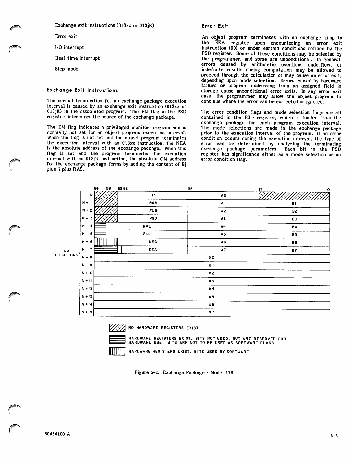
Exchange exit instructions (013xx or 013JK)
Error exit
I/O interrupt
Real-time interrupt
Step mode
Exchange Exit Instructions
The normal termination for an exchange package execution
interval is caused by an exchange exit instruction (013xx or
013JK) in the associated program. The EM flag in the PSD
register determines the source of the exchange package.
The EM flag indicates a privileged monitor program and is
normally not set for an object program execution interval.
When the flag is not set and the object program terminates
the execution interval with an 013xx instruction, the NEA
is the absolute address of the exchange package. When this
flag is set and the program terminates the execution
interval with an 013JK instruction, the absolute CM address
for the exchange package forms by adding the content of Bj
plus K plus RAS.
Error Exit
An object program terminates with an exchange jump to
the EEA register upon encountering an error exit
instruction (00) or under certain conditions defined by the
PSD register. Some of these conditions may be selected by
the programmer, and some are unconditional. In general,
errors caused by arithmetic overflow, underflow, or
indefinite results during computation may be allowed to
proceed through the calculation or may cause an error exit,
depending upon mode selection. Errors caused by hardware
failure or program addressing from an assigned field in
storage cause unconditional error exits. In any error exit
case, the programmer may allow the object program to
continue where the error can be corrected or ignored.
The error condition flags and mode selection flags are all
contained in the PSD register, which is loaded from the
exchange package for each program execution interval.
The mode selections are made in the exchange package
prior to the execution interval of the program. If an error
condition occurs during the execution interval, the type of
error can be determined by analyzing the terminating
exchange package parameters. Each bit in the PSD
register has significance either as a mode selection or an
error condition flag.
y^sm?^
CM
LOCATIONS
/^P*v
N+ I
N + 2
N + 3
N+ 4
N+ 5
N+ 6
N+ 7
N+ 8
N+ 9
N+IO
N+ll
N + 12
N + 13
N + 14
N+15
59 56 53 52 35 1 7 0
W////, AO ^mm^^
W////S RAS Al Bl
Y//////A FLS A2 B2
'////////> PSD A3 B3
RAL A4 B4
FLL A5 B5
11NEA A6 B6
EEA A7 B7
XO
X 1
X2
X3
X4
X5
X6
X7
NO HARDWARE REGISTERS EXIST
HARDWARE REGISTERS EXIST. BITS NOT USED, BUT ARE RESERVED FOR
HARDWARE USE. BITS ARE NOT TO BE USED AS SOFTWARE FLAGS.
HARDWARE REGISTERS EXIST. BITS USED BY SOFTWARE.
Figure 5-2. Exchange Package - Model 176
/j^^V
60456100 A 5-5
Input/Output Interrupt
The MUX section of the CP monitors input/output (I/O)
activity between the PPU and CM/ The MUX issues an
interrupt request to the CPU when the threshold of an CM
input or output buffer is reached. A record pulse from a
PPU also causes an interrupt request. When accepted, an
I/O interrupt request initiates an exchange jump to the
CPU program. An exchange request from the PPs also
causes an interrupt request.
Real-Time Interrupt
Programs may be timed precisely by using the CPU clock
period counter which advances one count each
27.5-nanosecond clock period.' Since the clock advances
synchronously with program execution, a program may be
timed to an exact number of clock periods.
The CPU clock period counter contains a 17-bit register
that can be sensed by a read input channel (0) status
instruction. An overflow of the highest-order bit in this
counter sets the real-time clock interrupt flag, which is
actually the 18th bit of the register.
The real-time clock interrupt flag attempts an interrupt of
the program to absolute address 0020 in CM each 3.6
milliseconds (approximate).' The program to absolute
address 0020 may change because of buffer bias bits. The
real-time exchange package at this CM address executes a
program that performs operations associated with the clock.
Step Mode
A program may be executed in step mode by setting the
step mode flag in the PSD register for the program
execution interval. Step mode causes the program to be
interrupted at the end of each program instruction word
with an exchange jump to EEA.
OPERATING CHARACTERISTICS —
MODELS 720 OR 730 WITH TWO CPs
Two CPs provide the following unique programming
characteristics.
• When one LCP is in monitor mode, a monitor
exchange jump to either CP aborts. Since the
exchange never starts, the instruction is a pass.
• When one LCP is in monitor mode, a central
exchange jump from the second CP hangs until the
monitor flag clears in the first CP.
• If a regular exchange jump (2600) executes with a
CEJ/MEJ instruction, the jump may cause the
setting of both monitor flags. This condition can
cause both CPs to hang on CEJ instructions.
OPERATING CHARACTERISTICS — MODEL 176
• When the monitor mode flag sets in the PSD
register, interrupt requests, I/O interrupt requests,
or peripheral processor subsystem (PPS) exchange
requests are not honored. When the monitor mode
flag clears, all interrupt requests are honored (in
priority order).
• I/O channel interrupt exchange packages must have
the monitor mode flag set in the PSD register. If
this bit is not set, the I/O channel interrupt request
causes repeated interrupts of the interrupt program.
• The CPU deadstart exchange jump is the result of
the CPU deadstart (master clear) signal clearing
the entire I/O channel interrupt request register.
This results in a channel 0 interrupt request which
causes an exchange jump when the CPU deadstart
signal drops, using the exchange package for
channel 0. Because the CPU deadstart exchange
jump is the result of an I/O interrupt request, the
deadstart exchange package must have the monitor
mode flag set in the PSD register. If this bit is not
set, the CPU deadstart program is reinterrupted by
the channel 0 interrupt request.
• Like other exchange jump sequences, the CPU
deadstart exchange jump swaps register data with
CM exchange package data (locations 0 through
17). This exchange package (locations 0 through
17) can be relocated by the buffer bias bits. All
exchange data swapped into CM is as it was in the
CPU registers except for the PSD register data.
The PSD bits are correct except for the
unconditional clearing of the monitor mode flag
and the unconditional setting of the program range
flag. The program range flag sets because of the
time delay between the dropping of the CPU
deadstart signal and the setting of the request
interrupt flag (RIF).
• Six P registers are in the CPU hardware, each
feeding different circuits.' All P registers always
contain the same value. Ensure that all P registers
contain the same value when working on P-related
problems.
• The 00 instruction can be blocked from setting the
program range flag under the following condition.
If an I/O interrupt request sets the RIF at the
same time as the 00 instruction enters the
translation bits of the current instruction word
(CIW) top bits, the setting of the program
range flag is blocked by RIF. The P register
advances to the next location. If the next
location contains legal instruction code, the
I/O interrupt program returns control to this
instruction word, and the 00 instruction is
missed because the program range flag did not
set.
ySSS%»
y^k
,i*^K
5-6 60456100 A
A master clear of the CPU can cause a CM parity
error. To prevent a parity error caused by a
master clear from being confused with a parity
error caused by a system failure, check CM after
each master clear to verify that it is free of parity
errors. Verify the existence of any parity errors by
reading all addresses. Eliminate any parity errors
by writing into the affected addresses.
INSTRUCTION EXECUTION — MODELS 720 AND 730
The models 720 and 730 CPs sequentially read and execute
program instruction words from their CMs. The CPs read
the instruction words with read next instruction (RNI)
operations. These operations begin with an RNI initiation
which occurs between executions of the first and second
instruction in the program instruction word (figure 5-3)
being processed. An RNI memory reference takes place in
the remaining part of the RNI operation and occurs during
the execution of the instructions that follow the RNI
initiation. In case of a memory conflict between
instructions and the RNI initiation, CMC delays the
instructions until memory is not busy.
Calculation of the best-case execution time of a program
instruction word requires adding the RNI initiation time to
the total instruction execution times within the word. If
the instruction that follows the RNI initiation does not
require a memory reference, the RNI initiation time is 2
clock periods. If the RNI has a CM conflict, the number of
conflicts determines how many more additional clock
periods are necessary. If the instruction (such as a jump,
branch, load, or store) that follows the RNI initiation does
require a memory reference and there are no CM conflicts
for the RNI reference, the instruction is delayed. The
delay for a load/store instruction is 0 clock period for
CP-0 and 1 clock period for CP-1. The delay for a
jump/branch instruction is 12 clock periods for CP-0 and 14
clock periods for CP-1.
Exceptions in the calculation of best-case program
instruction word execution times occur with the jump or
branch instructions. These instructions do not require the
addition of the RNI initiation time if they occupy the upper
position (parcel 0) of the program instruction word and
their jump conditions are met as shown in the following
example. The exceptions occur because the execution
times for the jump or branch instructions include the time
required to read the new program instruction word at the
jump or branch address.
JUMP TO K (MET) PASS PASS
ADD 1 ADD 2 SHIFT 1 SHIFT 2
Model 730 Clock
Instruction
Periods Required
for CP-0
Jump (met) 20
Add 1
RNI initiation
RNI completion
(15 clock periods CP-0)
Add 2
Shift 1
Shift 2
Total 50
PROGRAM
INSTRUCTION WORD
FIRST
INSTRUCTION SECOND
A INSTRUCTION
NO MEMORY REFERENCE FOR SECOND INSTRUCTION
RNI INITATION—»
(2 CLOCK PERIODS)
EXECUTION OF INSTRUCTION IN PARCELS 2 AND 3 -SS-
RNI OPERATION (^ CLOCK PERIODS)
NOTES
FOR MODEL 720
CP-0,X=24
CP-I,X=26
FOR MODEL 730
CP-0,X=I7
CP-|,X = I9
Figure 5-3. Instruction Execution - Models 720 and 730
60456100 E 5-7
If the conditions for the jump or branch instruction are not
met, the RNI initiation and RNI completion times must be
added to the instruction time as shown in the following
example.
ADD 1 ADD 2 MULTIPLY SUBTRACT
JUMP TO K (NOT MET) PASS 1 PASS 2
Instruction
Model 730 Clock
Periods Required
for CP-0
Jump (not met)
RNI initiation
RNI completion 15
Pass 1 (3 clock periods)
Pass 2 (3 clock periods)
Total 22
The minimum time for execution of a program instruction
word is the execution time of the first instruction in the
word plus a minimum of 17 clock periods for the RNI
operation. The following example shows that the
instruction times that follow the RNI initiation are not part
of the total clock period calculations if the instructions
execute in less time than the time required for the RNI
completion.
TRANSMIT SHIFT ADD PASS
Instruction
Transmit
RNI initiation
RNI completion
Shift (5 clock periods)
Pass (3 clock periods)
Pass (3 clock periods)
Model 730 Clock
Periods Required
for CP-0
3
2
15
Total 20
The maximum time for program instruction word
completion is the execution time of the first instruction
word plus the RNI initiation time plus the time required to
complete the following instructions in the word. The
following example shows that the time for RNI completion
is not part of the total clock-period calculations when it is
less than the time required for the execution of the
instructions that follow the RNI initiation.
Instruction
Addl
RNI initiation
RNI completion
(15 clock periods)
Add 2
Shift
Subtract
Model 720 Clock
Periods Required
for CP-0
6
2
12
12
12
Total 44
For program optimization in the CP, instructions requiring
a memory reference must be in the upper part of the
program instruction words. This optimization eliminates
the delay for load, store, jump, or branch instructions that
follow an RNI. The optimization also prevents wait time
that occurs when an unnecessary RNI operation occurs
before a jump or branch instruction.
INSTRUCTION EXECUTION —
MODELS 740, 750, 760, AND 176
Program instructions words read one at a time from the
instruction word stack (IWS) into the CIW register for
execution. In model 740, an instruction issues from the
CIW register after the complete execution of the previous
instruction. In models 750, 760, and 176, an instruction
issues from the CIW register when the conditions in the
functional units and operating registers are such that the
functions required for execution may be performed to
completion without conflicting with a previously issued
instruction. Once an instruction issues, it must complete in
a fixed time frame. No delays are allowed from issue to
delivery of data to the destination operating registers.
Since each instruction word is divided into four 15-bit
parcels, as many as four instructions may be in the CIW
register at one time. These instructions are executed in
sequence (beginning with parcel 0). Allowance must be
made for the mixture of one- and two-parcel instruction
formats. Two-parcel instructions cannot be initiated in
parcel 3 in models 740, 750, and 760. If two-parcel
instructions are initiated in parcel 3 on model 176, the
lower parcel is all zeros.
When program execution reaches a branch instruction, the
action taken depends upon whether the destination address
is already in the instruction address stack (IAS). If the
destination address is in the IAS, the P register alters to
the new program address, and the corresponding word reads
from the IWS to the CIW register. The jump is then
completed without a CM reference for a new instruction
word.
<^%.
5-8 60456100 E
If the destination address is not in the IAS, two new words
(located at the destination address and the destination
address plus 1) are requested from CM to begin the new
program sequence. In models 740, 750, and 760 the stack is
voided. Instruction execution continues upon receipt of the
words from CM.
A branch from the IWS may occur when the destination
address corresponds to a program word that has already
been requested from CM as a result of the sequential
two-word read-ahead. If the word has not arrived at the
IWS at the time of the branch test, the jump occurs. In
models 740, 750, and 760, the IWS is voided. If the word
arrives before the branch test, the stack provides the word
for execution, and the stack is not voided.
Because the IWS provides a copy of CM data for execution,
it is necessary to ensure that the stack is voided when
attempting instruction modification. In models 740, 750,
and 760, the IWS is voided by executing a return jump (01)
instruction, long jump (02) instruction, or any branch (03
through 07) instruction to an address not in the stack. In
model 176, the stack is voided by executing a return jump
(01) instruction.
FLOATING-POINT ARITHMETIC — ALL MODELS
Table 5-1 summarizes the configurations of bits 58 and 59
and the implications, regarding signs, of the possible
combinations.'
TABLE 5-1. BITS 58 AND 59 CONFIGURATIONS
Bit 59 Bit 58 Coefficient Sign Exponent Sign
0 1 Positive Positive
0 0 Positive Negative
10Negative Positive
1 1 Negative Negative
Packing
Packing refers to the conversion of numbers in the form
kBn to floating-point format. A shortcut method of
packing exponents can be derived by considering the
representation of negative and positive zero exponents.'
Assuming a positive coefficient, zero exponents are packed
as follows:
/jPSX
Format
Floating-point arithmetic expresses a number in the form
kBn.
k Coefficient
B Base number
n Exponent or power to which the base number is
raised
B is assumed to be 2 for binary-coded quantities. In the
60-bit floating-point format (figure 5-4), the binary point is
considered to be to the right of the coefficient. The lower
48 bits express the integer coefficient, which is the
equivalent of 15 decimal digits. The sign of the coefficient
is separated from the rest of the coefficient and appears in
the highest-order bit of the packed word. Negative
numbers are represented in one's-complement notation.
-COEFFICIENT SIGN
-BIAS
EXPONENT
A/£v—«-
r
'59"58x/57 48^*7
BINARY POINT-i
INTEGER COEFFICIENT
A
I I
Figure 5-4. Floating-Point Format
e*?of) #orC
The exponent is biased by complementing the coefficient
sign bit.
Positive zero exponent 2000x,...,x
Negative zero exponent 1777x,...,x
Since positive exponents are expressed in true form, begin
with a bias of 2000 (positive zero) and add the magnitude of
the exponent. The range of positive exponents is 0000
through 1777. In packed form, the range is 2000 through
3777.
When the coefficient is negative, the packed positive
exponent is complemented to become 5777 through 4000.
Negative exponents are expressed in complement form by
beginning with a bias of 1777 (negative zero) and then
subtracting the magnitude of the exponent. The range of
negative exponents is negative 0000 through negative
1777. In packed form, the range is 1777 through 0000.
When the coefficient is negative, the packed negative
exponent is complemented to become 6000 through 7777.
Examples of packed and unpacked floating-point numbers
are shown in octal notation to illustrate the packing
process. Examples 1 and 2 are different forms of the
integer positive 1. Example 3 is positive 100 (decimal), and
example 4 is negative 100 (decimal). Examples 5 and 6 are
large and small positive numbers. The unpacked values are
shown as they might appear in the X and B registers prior
to a pack operation.
The packed negative zero exponent is not used for normal
operation. Instead, 1777 is used to indicate the special
error condition of indefinite.
60456100 F 5-9
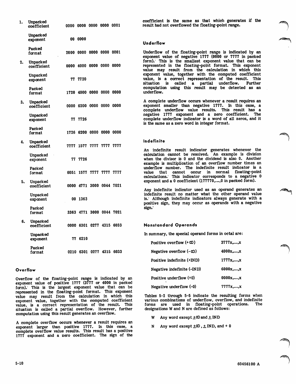
1. Unpacked
coefficient
Unpacked
exponent
Packed
format
2. Unpacked
coefficient
Unpacked
exponent
Packed
format
3. Unpacked
coefficient
Unpacked
exponent
Packed
format
4. Unpacked
coefficient
Unpacked
exponent
Packed
format
5. Unpacked
coefficient
Unpacked
exponent
Packed
format
6. Unpacked
coefficient
Unpacked
exponent
Packed
format
Ovei'flow
0000 0000 0000 0000 0001
00 oooo
2000 oooo oooo 0000 0001
0000 4000 oooo oooo oooo
77 7720
1720 4000 0000 0000 0000
0000 6200 0000 0000 0000
77 7726
1726 6200 0000 0000 0000
7777 1577 7777 7777 7777
77 7726
6051 1577 7777 7777 7777
0000 4771 3000 0044 7021
00 1363
3363 4771 3000 0044 7021
0000 6301 0277 4315 6033
77 6210
0210 6301 0277 4315 6033
Overflow of the floating-point range is indicated by an
exponent value of positive 1777 (3777 or 4000 in packed
form).' This is the largest exponent value that can be
represented in the floating-point format. This exponent
value may result from the calculation in which this
exponent value, together with the computed coefficient
value, is a correct representation of the result. This
situation is called a partial overflow. However, further
computation using this result generates an overflow.
A complete overflow occurs whenever a result requires an
exponent larger than positive 1777. In this case, a
complete overflow value results. This result has a positive
1777 exponent and a zero coefficient. The sign of the
coefficient is the same as that which generates if the
result had not overflowed the floating-point range.
Underflow
Underflow of the floating-point range is indicated by an
exponent value of negative 1777 (0000 or 7777 in packed
form).' This is the smallest exponent value that can be
represented in the floating-point format. This exponent
value may result from the calculation in which this
exponent value, together with the computed coefficient
value, is a correct representation of the result. This
situation is called a partial underflow. Further
computation using this result may be detected as an
underflow.
A complete underflow occurs whenever a result requires an
exponent smaller than negative 1777. In this case, a
complete underflow value results. This result has a
negative 1777 exponent and a zero coefficient. The
complete underflow indicator is a word of all zeros, and it
is the same as a zero word in integer format.
Indefinite
An indefinite result indicator generates whenever the
calculation cannot be resolved. An example is division
when the divisor is 0 and the dividend is also 0. Another
example is multiplication of an overflow number times an
underflow number. The indefinite result indicator is a
value that cannot occur in normal floating-point
calculations.' This indicator corresponds to a negative 0
exponent and a 0 coefficient (177770,...,0 in packed form).
Any indefinite indicator used as an operand generates an
indefinite result no matter what the other operand value
is.' Although indefinite indicators always generate with a
positive sign, they may occur as operands with a negative
sign.'
Nonstandard Operands
In summary, the special operand forms in octal are:
/•ZS^Sk
Positive overflow (+OD)
Negative overflow (-CO)
Positive indefinite (+IND)
Negative indefinite (-IND)
Positive underflow (+0)
Negative underflow (-0)
3777x,...,x
4000x,...,x
1777x,...,x
6000x,...,x
0000x,...,x
7777x,...,x
Tables 5-2 through 5-5 indicate the resulting forms when
various combinations of underflow, overflow, and indefinite
forms are used in floating-point operations. The
designations W and N are defined as follows:
W Any word except +00 and ± IN D
N Any word except +CO, ±IND, and + 0
5-10 60456100 A
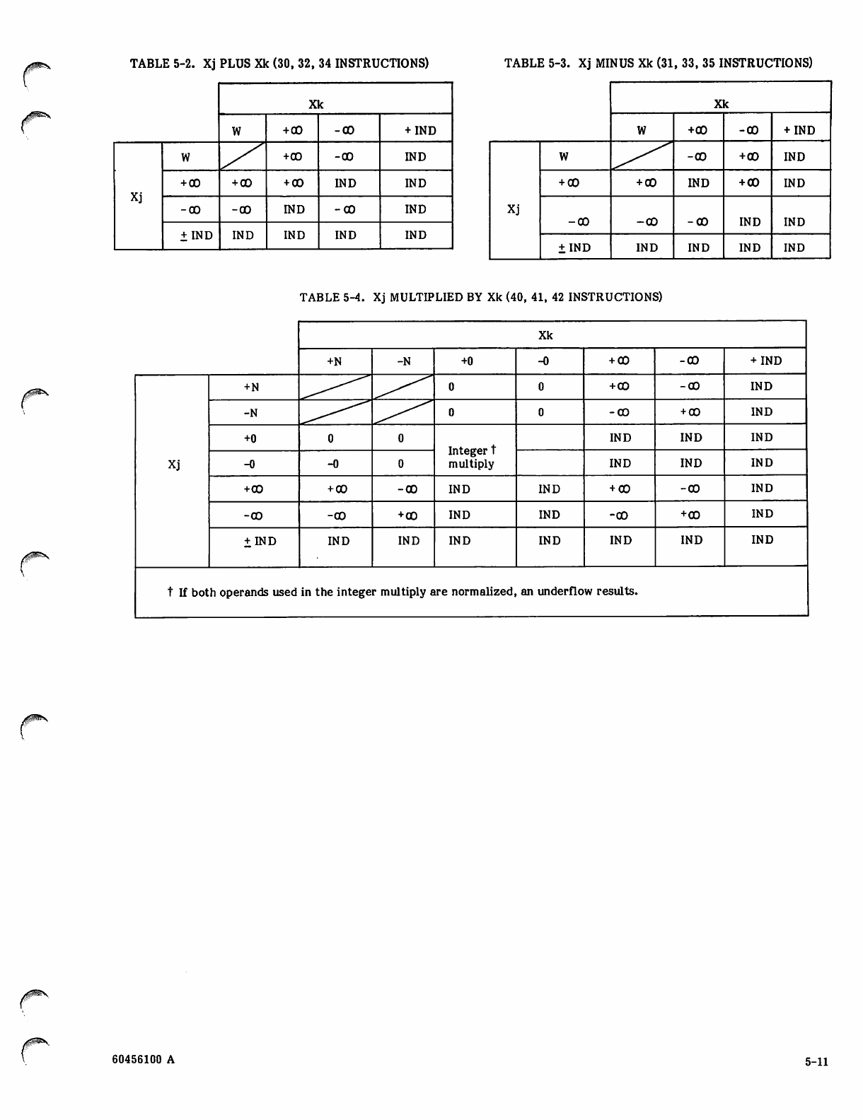
TABLE 5-2. Xj PLUS Xk (30, 32, 34 INSTRUCTIONS) TABLE 5-3. Xj MINUS Xk (31, 33, 35 INSTRUCTIONS)
jfPEV
Xk
W+ 00 -CO + IND
Xj
+00 -00 IND
+ 00 + 00 + 00 IND IND
-GO -OD IND -CO IND
+ IND IND IND IND IND
Xk
w+00 -00 + IND
Xj
-CO +00 IND
+ 00 + 00 IND + CO IND
-00 -CO -00 IND IND
±IND IND IND IND IND
TABLE 5-4. Xj MULTIPLIED BY Xk (40, 41, 42 INSTRUCTIONS)
Xk
+N -N +0 -0 + 00 -CO + IND
Xj
+N ^^^^>^ + 00 -00 IND
-N -00 + 00 IND
+0
Integer t
multiply
IND IND IND
-0 -0 IND IND IND
+00 + 00 -00 IND IND + 00 -00 IND
-co -oo + 00 IND IND -co +00 IND
+ IND IND IND IND IND IND IND IND
t If both operands used in the integer multiply are normalized, an underflow results.
/0&\
60456100 A 5-11
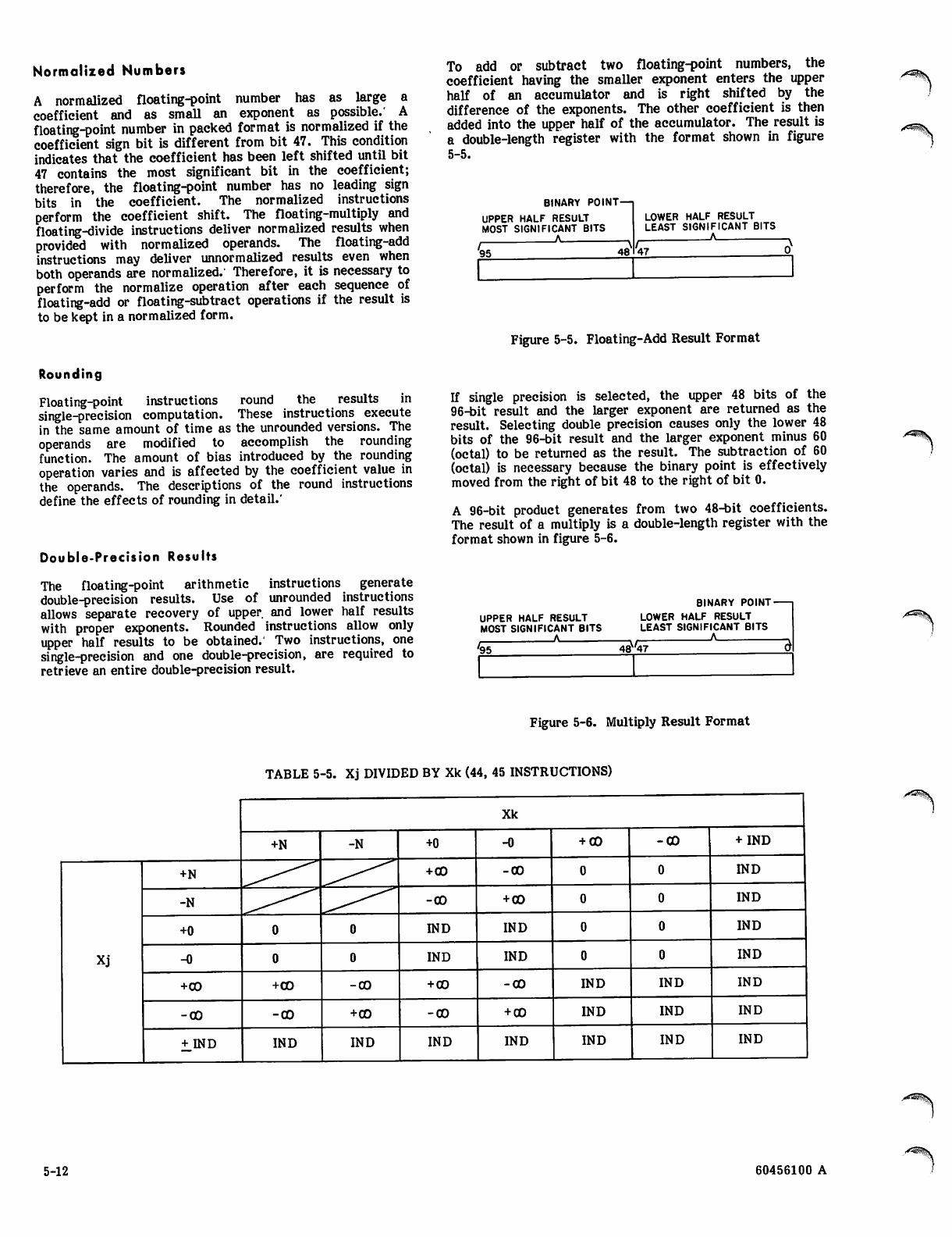
Normalized Numbers
A normalized floating-point number has as large a
coefficient and as small an exponent as possible.' A
floating-point number in packed format is normalized if the
coefficient sign bit is different from bit 47. This condition
indicates that the coefficient has been left shifted until bit
47 contains the most significant bit in the coefficient;
therefore, the floating-point number has no leading sign
bits in the coefficient. The normalized instructions
perform the coefficient shift. The floating-multiply and
floating-divide instructions deliver normalized results when
provided with normalized operands. The floating-add
instructions may deliver unnormalized results even when
both operands are normalized. Therefore, it is necessary to
perform the normalize operation after each sequence of
floating-add or floating-subtract operations if the result is
to be kept in a normalized form.
To add or subtract two floating-point numbers, the
coefficient having the smaller exponent enters the upper
half of an accumulator and is right shifted by the
difference of the exponents. The other coefficient is then
added into the upper half of the accumulator. The result is
a double-length register with the format shown in figure
5-5.
BINARY POINT—i
UPPER HALF RESULT
MOST SIGNIFICANT BITS
A
95 48
LOWER HALF RESULT
LEAST SIGNIFICANT BITS
A
47
Figure 5-5. Floating-Add Result Format
Rounding
Floating-point instructions round the results in
single-precision computation. These instructions execute
in the same amount of time as the unrounded versions. The
operands are modified to accomplish the rounding
function. The amount of bias introduced by the rounding
operation varies and is affected by the coefficient value in
the operands. The descriptions of the round instructions
define the effects of rounding in detail.'
Double-Precision Results
The floating-point arithmetic instructions generate
double-precision results. Use of unrounded instructions
allows separate recovery of upper and lower half results
with proper exponents. Rounded instructions allow only
upper half results to be obtained.' Two instructions, one
single-precision and one double-precision, are required to
retrieve an entire double-precision result.
If single precision is selected, the upper 48 bits of the
96-bit result and the larger exponent are returned as the
result. Selecting double precision causes only the lower 48
bits of the 96-bit result and the larger exponent minus 60
(octal) to be returned as the result. The subtraction of 60
(octal) is necessary because the binary point is effectively
moved from the right of bit 48 to the right of bit 0.
A 96-bit product generates from two 48-bit coefficients.
The result of a multiply is a double-length register with the
format shown in figure 5-6.
JCWWSV
UPPER HALF RESULT
MOST SIGNIFICANT BITS
, A
5i
B I N A RY P O I N T 1
LOWER HALF RESULT
LEAST SIGNIFICANT BITS
- & $ - * 6 \
Figure 5-6. Multiply Result Format
TABLE 5-5. Xj DIVIDED BY Xk (44, 45 INSTRUCTIONS)
Xk
+N -N +0 -0 + 00 -CO + IND
Xj
+N ^^^^
+ 00 -CO IND
-N ^^^ -CO + 00 IND
+0 IND IND IND
-0 IND IND IND
+00 +CO -CO + 00 -CO IND IND IND
-00 -00 +00 -CO + CO IND IND IND
+JND IND IND IND IND IND IND IND
•'*^%\
5-12 60456100 A
yfSP^N
/Ss^N,
If single precision is selected, the upper 48 bits of the
product and the sum of the exponents plus 60 (octal) are
returned as the result. The addition of 60 (octal) is
necessary because the binary point effectively moves from
the right of bit 0 to the right of bit 48 when the upper half
of the 96-bit result is selected. If double precision is
selected, the result is the lower 48 bits of the product and
the sum of the exponents.
FIXED-POINT ARITHMETIC — ALL MODELS
Fixed-point addition and subtraction of 60-bit numbers are
handled by the long-add instructions (36 and 37). Negative
numbers are represented in one's-complement notation, and
overflows are ignored. The sign bit is in the high-order bit
position (bit 59), and the binary point is to the right of the
low-order bit position (bit 0).
Fixed-point addition and subtraction of 18-bit numbers are
handled by the increment instructions (50 through 77).
Negative numbers are represented in one's complement
notation, and overflows are ignored. The sign bit is in the
high-order bit position (bit 17), and the binary point is to
the right of the low-order position (bit 0).
INTEGER ARITHMETIC — ALL MODELS
Integer multiplication is handled as a subset operation of
the floating-multiply (42) instruction. The integer multiply
requires that both 47-bit integer operands have zero
exponents and one is not normalized. The result is 48 bits
with sign extension. Normalized operands cause underflow
results to be reported. If the results exceed 48 bits,
overflow is not detected.
In integer multiplication, a 48-bit product can be formed by
using the double-precision multiply instruction. Both
operands must have an exponent value of + 0, and the
coefficients cannot both be normalized. The result is
sign-extended to 60 bits and sent to an X register.
In integer division, the divisor must be normalized but the
dividend need not be normalized. The resulting quotient
must be unpacked and the coefficient shifted by the
amount of the unpacked exponent using the left shift (22)
instruction to obtain the integer quotient.
Integer divide packs the integers into floating-point format
using the pack instruction with a zero-exponent value.
An integer divide takes several steps. For example, an
integer quotient XI equal to X2/X3 is produced by the
following steps.
Instructions
2. Pack X3 from X3
and B0
3. Normalize X3 in X0
and B0
4. Normalize X2 in X2
and B0
5. Floating quotient of
X2 and X0 to Xi
6. Unpack XI to XI
andB7
7. Shift XI nominally
left B7 places
Remarks
Pack X3
Normalize X3
(divisor)
Normalize X2
(dividend)
Divide
Unpack quotient
Shift to integer
position
1.
Instructions
Pack X2 from X2
and B0
Remarks
Pack X2
The divide requires that both integer (247 maximum)
operands be in floating-point format, and the dividend
coefficient must be less than two times the divisor
coefficient. The normalize X3 instruction ensures this
condition.
The normalize X3 instruction left shifts the divisor n places
(n>0), providing a divisor exponent of negative n. The
quotient exponent is then 0 minus (-n) minus 48 equals n
minus 48 < 0.
After unpacking and left shifting nominally, the negative
(or zero) value in B7 right shifts the quotient 48 minus n
places, producing an integer quotient in XI. A remainder
may be obtained by an integer multiply of XI and X3 and
subtracting the result from X2.
COMPARE/MOVE ARITHMETIC —
MODELS 720 AND 730
The compare/move arithmetic provides multiple character
manipulation. The characters are six bits long. Characters
can be moved from one CM location to another, and fields
of characters can be compared either directly or through a
collation table.
The move direct instruction moves a field of up to 127
characters from one location to another location as
specified in the instruction. The move indirect instruction
performs the same kind of move, but a CM reference is
used to obtain the parameters. The move indirect
instruction moves a field of up to 8181 characters.
The compare collated instruction compares two fields of up
to 127 characters. When two characters are unequal, the
characters are referenced in a collation table, and the
values are compared. If those values are unequal, the field
with the larger character is indicated. The compare
uncollated instruction compares two fields of up to 127
characters and indicates the larger of the first character
pair that is found to be unequal.
00&\
60456100 F 5-13
PROCESSING DIFFERENCES
Multiply Differences
A difference exists when an exponent overflow of a
floating product occurs and the coefficient result requires
a left shift of one to give a normalized answer. Models
740, 750, 760, and 176 test for the overflow condition by
cheeking for the exponent greater than positive 1777
before correction, if any, is made for a left shift of one.
Thus, even though the left shift of one may cause the
exponent to equal positive 1777 (partial overflow), this
condition is treated as a complete overflow, and the result
is the overflow exponent with a zero coefficient.
Models 720 and 730 test for the overflow condition by
checking for the exponent greater than positive 1777 after
correction, if any, is made for a left shift of one. In this
case, if the resulting exponent is positive 1777 (partial
overflow), the result is the overflow exponent with the
computed coefficient.
Example: 40012
XI =3700 4000 0000 0000 0000
X2 = 2020 4000 0000 0000 0000
Models 720 and 730 result:
X0 = 3777 4000 0000 0000 0000
Models 740, 750, 760, and 176 result:
X0 = 3777 0000 0000 0000 0000
A similar situation exists when an. exponent underflow of a
floating product occurs and the coefficient result does not
require a left shift of one to give a normalized answer.
Models 740, 750, 760, and 176 test for the underflow
condition by checking for the exponent less than negative
1777 before correction, if any, is made for a left shift of
one. Although no left shift of one is performed, an
exponent of negative 1777 (partial underflow) is treated as
a complete underflow, and the result is the underflow
condition with zero coefficient.
Models 720 and 730 test for the underflow condition by
checking for the exponent less than negative 1777 after
correction, if any, is made for a left shift of one. In this
case, if the resulting exponent is negative 1777 (partial
underflow), the result is the underflow exponent with the
computed coefficient.
Example: 40012
XI =0647 7777 7777 7777 7776
X2 =1050 4444 4444 4444 4444
Models 720 and 730 result:
X0 = 0000 4444 4444 4444 4442
Models 740, 750, 760, and 176 result:
X0 = 0000 0000 0000 0000 0000
Floating-Add Differences
The models 720 through 760 floating-add unit may generate
a different result from a model 176 floating-add unit when
at least one operand has a zero coefficient and the
difference between the exponents is greater than or equal
to 128 (decimal).
Example: 30012 Floating Add
XI = 4277 7777 7777 7777 7777
X2 = 5277 5555 5555 5555 5555
Models 720 through 760 result:
X0 = 4277 7777 7777 7777 7777
Model 176 result:
X0 = 3500 0000 0000 0000 0000
Reversing the operands (30021) gives the same results as
indicated previously.
Example: 31012 Floating Difference
XI = 4277 7777 7777 7777 7777
X2=2500 2222 2222 2222 2222
Models 720 through 760 result:
X0 = 4277 7777 7777 7777 7777
Model 176 result:
X0 = 3500 0000 0000 0000 0000
Example: 31012 Floating Difference
XI = 5277 5555 5555 5555 5555
X2 = 3500 0000 0000 0000 0000
Models 720 through 760 result:
X0 = 4277 7777 7777 7777 7777
Model 176 result:
X0 = 3500 0000 0000 0000 0000
Reversing the operands (31021) on either of the examples
for a floating difference gives compatible results on the
different models. The result on any model is 3500 0000
0000 0000 0000.
A difference exists when an exponent underflow of a
floating double-precision sum occurs and the coefficient
result requires a right shift of one because coefficient
overflow occurred. Models 740, 750, 760, and 176 test for
the underflow condition by checking for the exponent less
than negative 1777 before correction, if any, is made for a
right shift of one. Thus, even though the right shift of one
may cause the exponent to equal negative 1777 (partial
underflow), this condition is treated as a complete
underflow, and the result is the underflow exponent with a
zero coefficient.
Models 720 and 730 test for the exponent underflow
condition by checking for the exponent less than negative
/-*^m\
y^)«y
5-14 60456100 E
yfi^MT^
1777 after correction, if any, is made for a right shift of
one. In this case, if the resulting exponent is negative 1777
(partial underflow), the result is the underflow exponent
with the computed coefficient.
Example: 32012
XI = 0057 4000 0000 0000 0001
X2 = 0057 4000 0000 0000 0000
Models 720 and 730 result:
X0 = 0000 4000 0000 0000 0000
Models 740, 750, 760, and 176 result:
X0 = 0000 0000 0000 0000 0000
Floating-Divide Condition Differences
If model 176 senses a divide fault, an indefinite condition is
indicated only if no overflow or underflow condition exists.
If an overflow or underflow condition exists, the divide
fault is ignored. If models 720 through 760 sense a divide
fault, the fault is identified as an indefinite condition.
Example: 44012
XI =3700 0222 0000 0000 0000
X2 =1600 0022 0000 0000 0000
Models 720 through 760 result:
X0 =1777 0000 0000 0000 0000
Model 176 result:
X0 = 3777 0000 0000 0000 0000
(indefinite
condition)
(overflow
condition)
Instructions 22 and 23 Differences
When instruction 22 or 23 is used for a right shift, model
176 checks bits 6 through 11 for a shift greater than or
equal to 64 (decimal) and ignores bits 12 through 16.
Models 720 through 760 check bits 6 through 10 and ignore
bits 11 through 16.
When a negative number is right shifted more than 63
(decimal) places, models 720 through 760 return a positive
zero, and model 176 returns a negative zero.
ILLEGAL INSTRUCTIONS —
MODELS 720 THROUGH 760
The following instructions cause an error exit to MA or
program stop. System error responses for illegal
instructions are listed in tables 5-7, 5-8, and 5-9. In
addition to causing error responses, illegal instructions
execute as passes and do not change the content of any
register (except as noted in the fifth item of the following
list).
• 011, 012 with no ECS or in parcel 1, 2, 3.
• 013 with CEJ/MEJ disabled or in parcel 1, 2, 3.
• 014 through 017.
e 464 through 467 (models 740, 750, and 760), 464
through 467 in parcel 1, 2, 3 (models 720 and 730).
• Any 30-bit instruction in parcel 3. (In models 720
and 730, these illegal instructions execute. The
lower 15 bits of the instruction are provided by
whatever bits are in that part of the instruction
register. Once into execution, the instruction is
illegal and aborted. Registers and P values change
before the program stops.)
EXIT MODE/ERROR RESPONSE —
MODELS 720 THROUGH 760
Round-Divide Differences
Models 720 through 760 perform a one-third round. This
adds the quantity of one-third to the dividend on the
divide. Model 176 performs a one-half round. This adds
the quantity of one-half to the dividend on the divide.
These differences can produce different results for certain
operands.
Example: 45012
XI = 2057 7223 2220 7175 5360
X2=1347 4255 6115 0364 7225
Models 720 through 760 result:
X0=2430 6557 3505 0613 2700
Model 176 result:
X0 = 2430 6557 3505 0613 2701
When the CP detects or is informed of an error, it records
the error. Depending upon the type of error and the mode
selection bits, the program in execution may be
interrupted. If the error is an illegal instruction,
breakpoint, or an address-range error on an RNI or branch,
the program interruption is unconditional. For other types
of errors, the mode selection bits determine whether or not
the program is interrupted. If the mode selection bit is set
and the corresponding condition is detected, the program is
interrupted. The mode select bits are contained in word N
plus 3 of the exchange package and are selected as shown
in table 5-6.
The errors that cause unconditional program interruptions
and program interruptions due to corresponding mode
selection bits have the program address of the error
written into RAC zero. If the error was caused by a
condition that has a corresponding mode selection bit, the
bit is also written into RAC zero. The process of
60456100 E 5-15
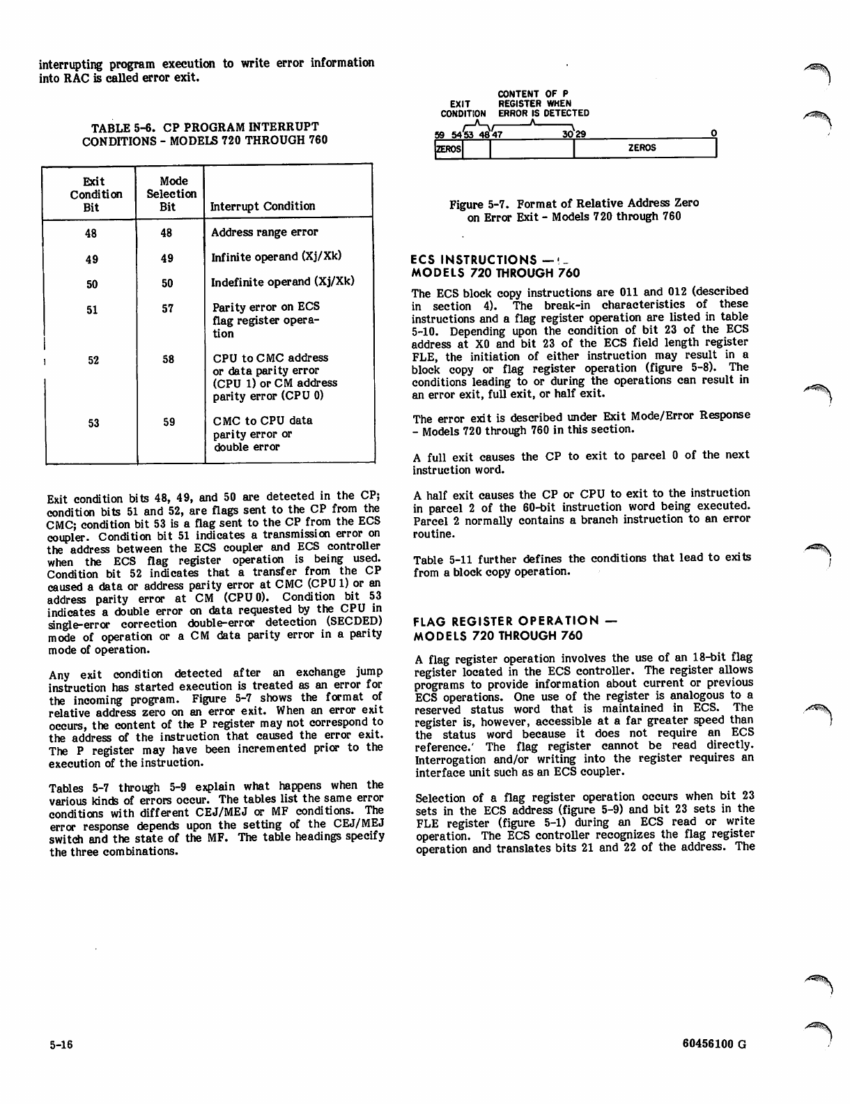
interrupting program execution to write error information
into RAC is called error exit.
TABLE 5-6. CP PROGRAM INTERRUPT
CONDITIONS - MODELS 720 THROUGH 760
Exit
Condition
Bit
Mode
Selection
Bit Interrupt Condition
48 48 Address range error
49 49 Infinite operand (Xj/Xk)
50 50 Indefinite operand (Xj/Xk)
51 57 Parity error on ECS
flag register opera
tion
I 5 2 58 CPU to CMC address
or data parity error
(CPU 1) or CM address
parity error (CPU 0)
53 59 CMC to CPU data
parity error or
double error
Exit condition bits 48, 49, and 50 are detected in the CP;
condition bits 51 and 52, are flags sent to the CP from the
CMC; condition bit 53 is a flag sent to the CP from the ECS
coupler. Condition bit 51 indicates a transmission error on
the address between the ECS coupler and ECS controller
when the ECS flag register operation is being used.
Condition bit 52 indicates that a transfer from the CP
caused a data or address parity error at CMC (CPU1) or an
address parity error at CM (CPU0). Condition bit 53
indicates a double error on data requested by the CPU in
single-error correction double-error detection (SECDED)
mode of operation or a CM data parity error in a parity
mode of operation.
Any exit condition detected after an exchange jump
instruction has started execution is treated as an error for
the incoming program. Figure 5-7 shows the format of
relative address zero on an error exit. When an error exit
occurs, the content of the P register may not correspond to
the address of the instruction that caused the error exit.
The P register may have been incremented prior to the
execution of the instruction.
Tables 5-7 through 5-9 explain what happens when the
various kinds of errors occur. The tables list the same error
conditions with different CEJ/MEJ or MF conditions. The
error response depends upon the setting of the CEJ/MEJ
switch and the state of the MF. The table headings specify
the three combinations.
CONTENT OF P
EXIT REGISTER WHEN
CONDITION ERROR IS DETECTED
/-S/—*-
59 5453 46 47 "3^29
ZEROS ZEROS
Figure 5-7. Format of Relative Address Zero
on Error Exit - Models 720 through 760
ECS INSTRUCTIONS —'_
MODELS 720 THROUGH 760
The ECS block copy instructions are 011 and 012 (described
in section 4). The break-in characteristics of these
instructions and a flag register operation are listed in table
5-10. Depending upon the condition of bit 23 of the ECS
address at X0 and bit 23 of the ECS field length register
FLE, the initiation of either instruction may result in a
block copy or flag register operation (figure 5-8). The
conditions leading to or during the operations can result in
an error exit, full exit, or half exit.
The error exit is described under Exit Mode/Error Response
- Models 720 through 760 in this section.
A full exit causes the CP to exit to parcel 0 of the next
instruction word.
A half exit causes the CP or CPU to exit to the instruction
in parcel 2 of the 60-bit instruction word being executed.
Parcel 2 normally contains a branch instruction to an error
routine.
Table 5-11 further defines the conditions that lead to exits
from a block copy operation.
FLAG REGISTER OPERATION —
MODELS 720 THROUGH 760
A flag register operation involves the use of an 18-bit flag
register located in the ECS controller. The register allows
programs to provide information about current or previous
ECS operations. One use of the register is analogous to a
reserved status word that is maintained in ECS. The
register is, however, accessible at a far greater speed than
the status word because it does not require an ECS
reference.' The flag register cannot be read directly.
Interrogation and/or writing into the register requires an
interface unit such as an ECS coupler.
Selection of a flag register operation occurs when bit 23
sets in the ECS address (figure 5-9) and bit 23 sets in the
FLE register (figure 5-1) during an ECS read or write
operation. The ECS controller recognizes the flag register
operation and translates bits 21 and 22 of the address. The
5-16 60456100 G
z^nwSv
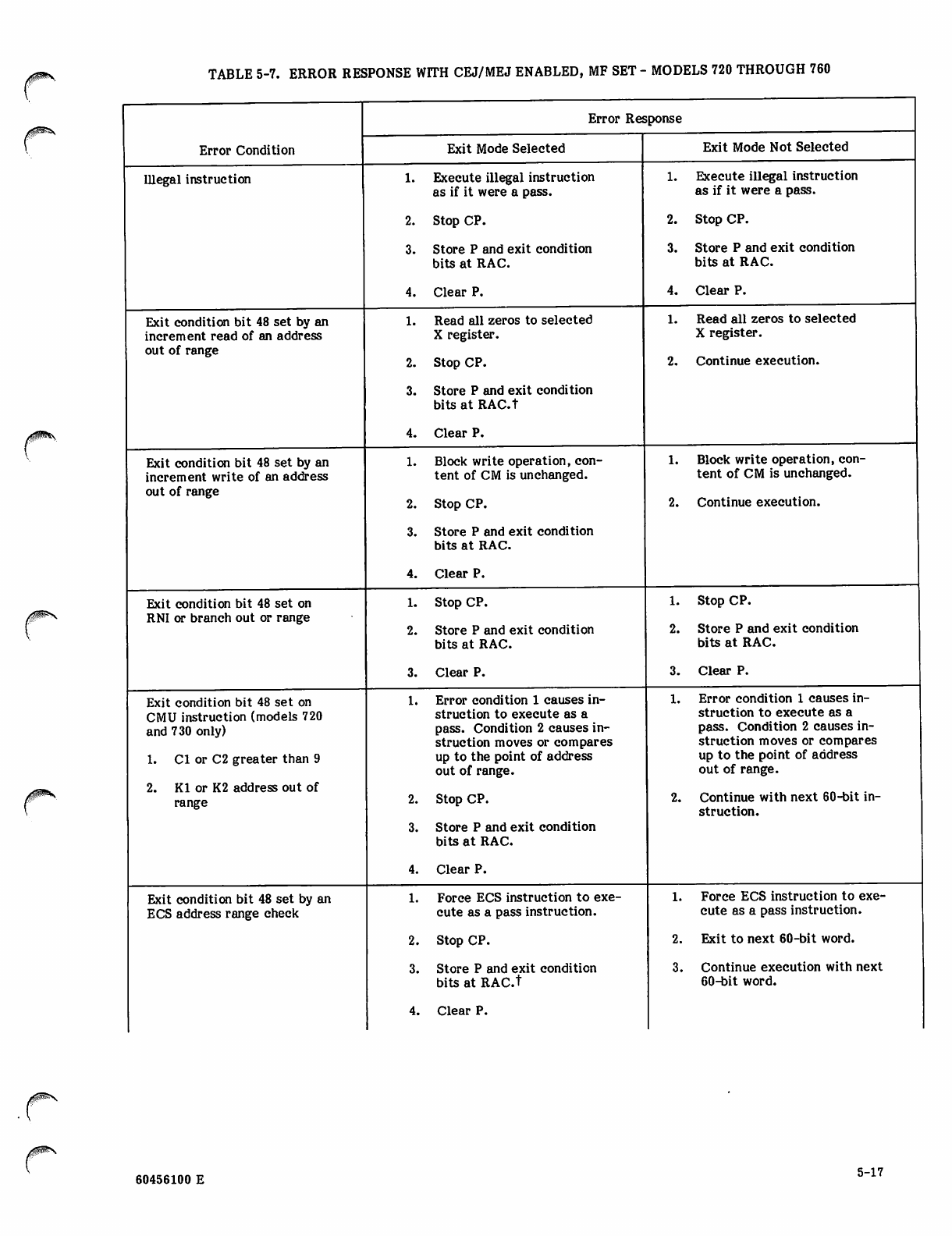
TABLE 5-7. ERROR RESPONSE WITH CEJ/MEJ ENABLED, MF SET - MODELS 720 THROUGH 760
Error Condition
Illegal instruction
Exit condition bit 48 set by an
increment read of an address
out of range
Exit condition bit 48 set by an
increment write of an address
out of range
Exit condition bit 48 set on
RNI or branch out or range
Exit condition bit 48 set on
CMU instruction (models 720
and 730 only)
1. Cl or C2 greater than 9
2. Kl or K2 address out of
range
Exit condition bit 48 set by an
ECS address range check
Error Response
Exit Mode Selected
1. Execute illegal instruction
as if it were a pass.
2. Stop CP.
3. Store P and exit condition
bits at RAC.
4. Clear P.
Read all zeros to selected
X register.
Stop CP.
Store P and exit condition
bits at RAC.t
Clear P.
Block write operation, con
tent of CM is unchanged.
Stop CP.
Store P and exit condition
bits at RAC.
Clear P.
1. Stop CP.
2. Store P and exit condition
bits at RAC.
3. Clear P.
Error condition 1 causes in
struction to execute as a
pass. Condition 2 causes in
struction moves or compares
up to the point of address
out of range.
Stop CP.
Store P and exit condition
bits at RAC.
Clear P.
Exit Mode Not Selected
1. Execute illegal instruction
as if it were a pass.
2. Stop CP.
3. Store P and exit condition
bits at RAC.
4. Clear P.
1. Read all zeros to selected
X register.
2. Continue execution.
1. Block write operation, con
tent of CM is unchanged.
2. Continue execution.
1. Force ECS instruction to exe
cute as a pass instruction.
2. Stop CP.
3. Store P and exit condition
bits at RAC.t
4. Clear P.
1. Stop CP.
2. Store P and exit condition
bits at RAC.
3. Clear P.
1. Error condition 1 causes in
struction to execute as a
pass. Condition 2 causes in
struction moves or compares
up to the point of address
out of range.
2. Continue with next 60-bit in
struction.
1. Force ECS instruction to exe
cute as a pass instruction.
2. Exit to next 60-bit word.
3. Continue execution with next
60-bit word.
60456100 E 5-17
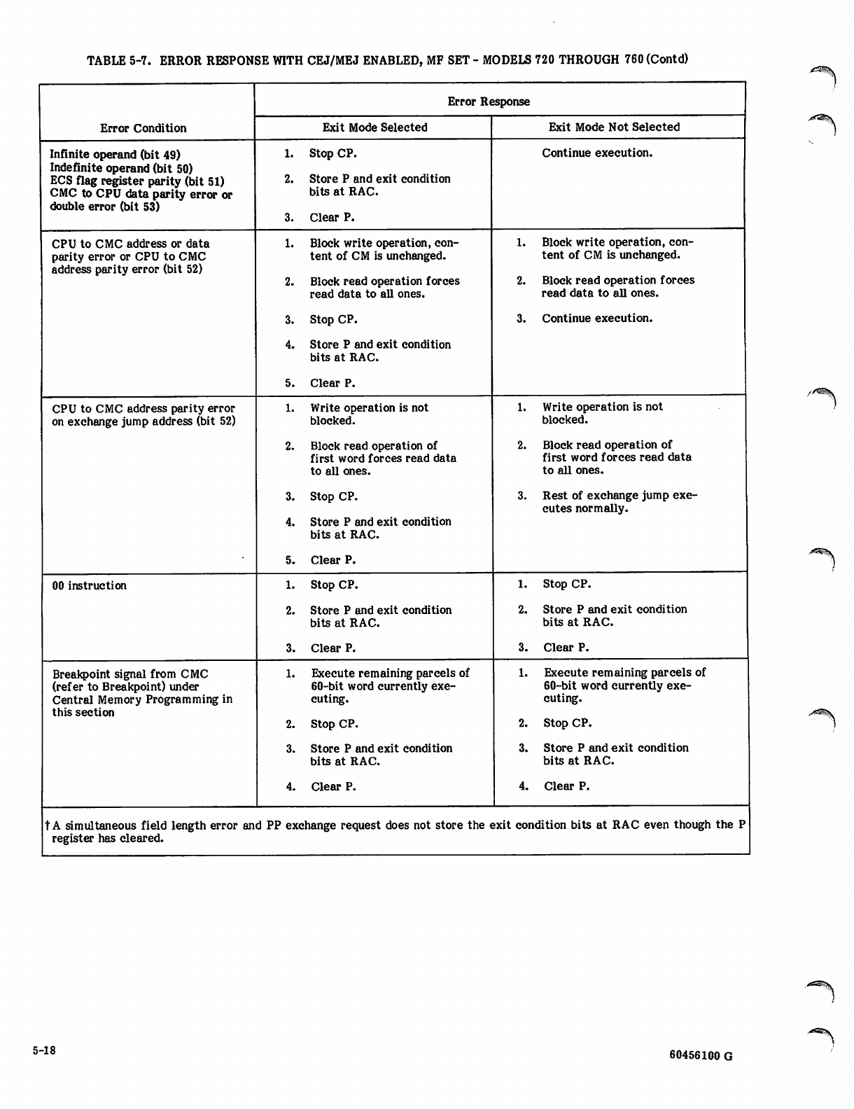
TABLE 5-7. ERROR RESPONSE WITH CEJ/MEJ ENABLED, MF SET- MODELS 720 THROUGH 760(Contd)
Error Condition
Error Response
Exit Mode Selected Exit Mode Not Selected
Infinite operand (bit 49)
Indefinite operand (bit 50)
ECS flag register parity (bit 51)
CMC to CPU data parity error or
double error (bit 53)
1. Stop CP.
2. Store P and exit condition
bits at RAC.
3. Clear P.
Continue execution.
CPU to CMC address or data
parity error or CPU to CMC
address parity error (bit 52)
1. Block write operation, con
tent of CM is unchanged.
2. Block read operation forces
read data to all ones.
3. Stop CP.
4. Store P and exit condition
bits at RAC.
5. Clear P.
1. Block write operation, con
tent of CM is unchanged.
2. Block read operation forces
read data to all ones.
3. Continue execution.
CPU to CMC address parity error
on exchange jump address (bit 52)
1. Write operation is not
blocked.
2. Block read operation of
first word forces read data
to all ones.
3. Stop CP.
4. Store P and exit condition
bits at RAC.
5. Clear P.
1. Write operation is not
blocked.
2. Block read operation of
first word forces read data
to all ones.
3. Rest of exchange jump exe
cutes normally.
00 instruction 1. Stop CP.
2. Store P and exit condition
bits at RAC.
3. Clear P.
1. Stop CP.
2. Store P and exit condition
bits at RAC.
3. Clear P.
Breakpoint signal from CMC
(refer to Breakpoint) under
Central Memory Programming in
this section
1. Execute remaining parcels of
60-bit word currently exe
cuting.
2. Stop CP.
3. Store P and exit condition
bits at RAC.
4. Clear P.
1. Execute remaining parcels of
60-bit word currently exe
cuting.
2. Stop CP.
3. Store P and exit condition
bits at RAC.
4. Clear P.
t A simultaneous field length error and PP exchange request does not store the exit condition bits at RAC even though the P
register has cleared.
/ ^ ^ \
5-18 60456100 G
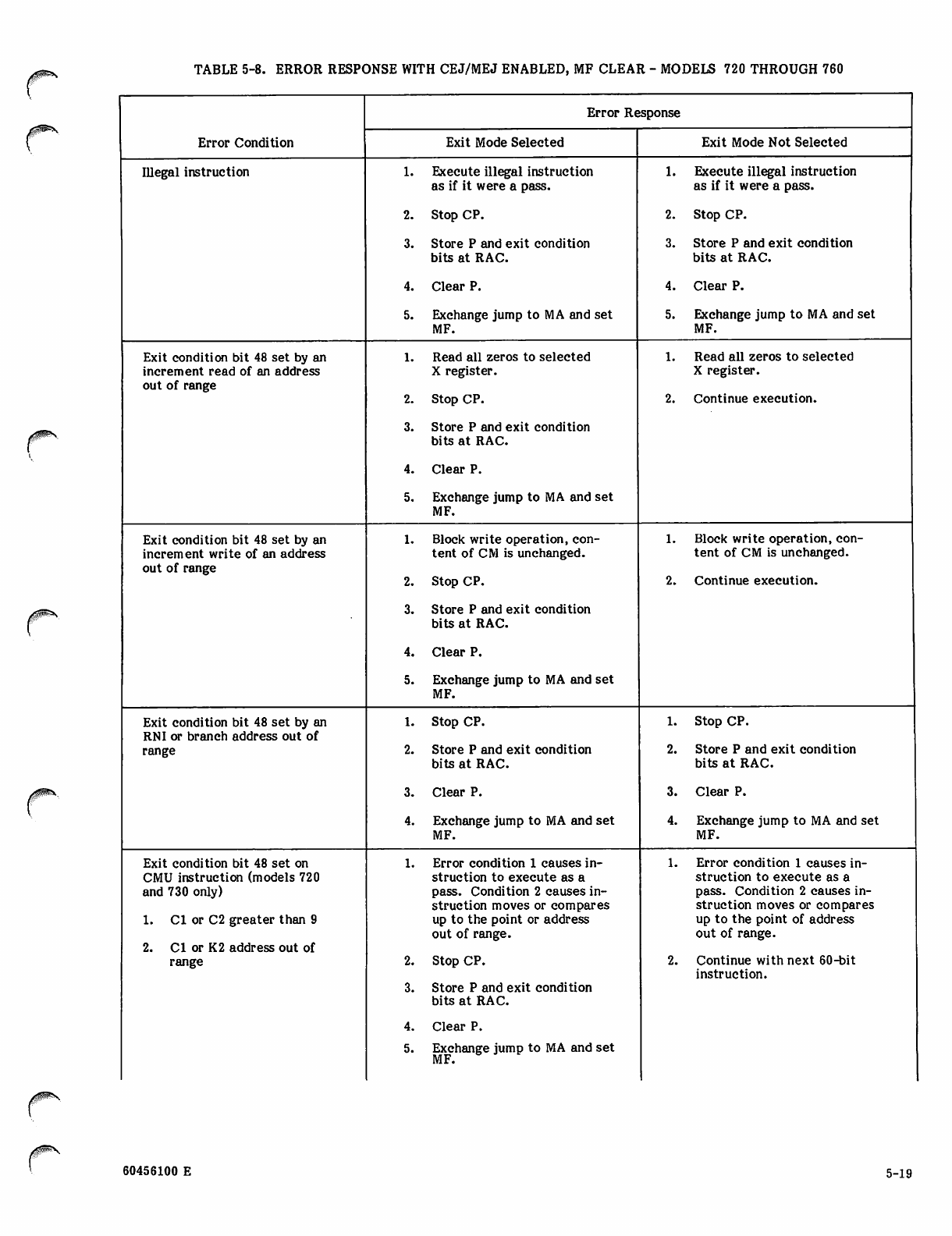
TABLE 5-8. ERROR RESPONSE WITH CEJ/MEJ ENABLED, MF CLEAR - MODELS 720 THROUGH 760
Error Condition
Error Response
Exit Mode Selected Exit Mode Not Selected
Illegal instruction 1. Execute illegal instruction
as if it were a pass.
2. Stop CP.
3. Store P and exit condition
bits at RAC.
4. Clear P.
5. Exchange jump to MA and set
MF.
1. Execute illegal instruction
as if it were a pass.
2. Stop CP.
3. Store P and exit condition
bits at RAC.
4. Clear P.
5. Exchange jump to MA and set
MF.
Exit condition bit 48 set by an
increment read of an address
out of range
1. Read all zeros to selected
X register.
2. Stop CP.
3. Store P and exit condition
bits at RAC.
4. Clear P.
5. Exchange jump to MA and set
MF.
1. Read all zeros to selected
X register.
2. Continue execution.
Exit condition bit 48 set by an
increment write of an address
out of range
1. Block write operation, con
tent of CM is unchanged.
2. Stop CP.
3. Store P and exit condition
bits at RAC.
4. Clear P.
5. Exchange jump to MA and set
MF.
1. Block write operation, con
tent of CM is unchanged.
2. Continue execution.
Exit condition bit 48 set by an
RNI or branch address out of
range
1. Stop CP.
2. Store P and exit condition
bits at RAC.
3. Clear P.
4. Exchange jump to MA and set
MF.
1. Stop CP.
2. Store P and exit condition
bits at RAC.
3. Clear P.
4. Exchange jump to MA and set
MF.
Exit condition bit 48 set on
CMU instruction (models 720
and 730 only)
1. Cl or C2 greater than 9
2. Cl or K2 address out of
range
1. Error condition 1 causes in
struction to execute as a
pass. Condition 2 causes in
struction moves or compares
up to the point or address
out of range.
2. Stop CP.
3. Store P and exit condition
bits at RAC.
4. Clear P.
5. Exchange jump to MA and set
MF.
1. Error condition 1 causes in
struction to execute as a
pass. Condition 2 causes in
struction moves or compares
up to the point of address
out of range.
2. Continue with next 60-bit
instruction.
60456100 E 5-19
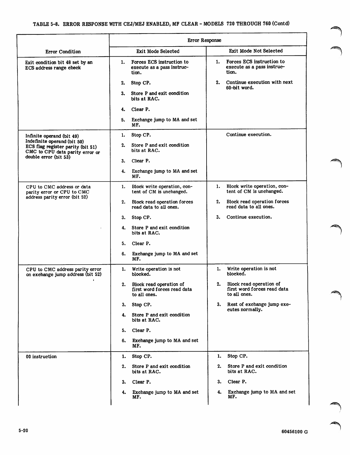
TABLE 5-8. ERROR RESPONSE WITH CEJ/MEJ ENABLED, MF CLEAR - MODELS 720 THROUGH 760 (Contd)
Error Condition
Error Response
Exit Mode Selected Exit Mode Not Selected
Exit condition bit 48 set by an
ECS address range cheek
1. Forces ECS instruction to
execute as a pass instruc
tion.
2. Stop CP.
3. Store P and exit condition
bits at RAC.
4. Clear P.
5. Exchange jump to MA and set
MF.
1. Forces ECS instruction to
execute as a pass instruc
tion.
2. Continue execution with next
60-bit word.
Infinite operand (bit 49)
Indefinite operand (bit 50)
ECS flag register parity (bit 51)
CMC to CPU data parity error or
double error (bit 53)
1. Stop CP.
2. Store P and exit condition
bits at RAC.
3. Clear P.
4. Exchange jump to MA and set
MF.
Continue execution.
CPU to CMC address or data
parity error or CPU to CMC
address parity error (bit 52)
1. Block write operation, con
tent of CM is unchanged.
2. Block read operation forces
read data to all ones.
3. Stop CP.
4. Store P and exit condition
bits at RAC.
5. Clear P.
6. Exchange jump to MA and set
MF.
1. Block write operation, con
tent of CM is unchanged.
2. Block read operation forces
read data to all ones.
3. Continue execution.
CPU to CMC address parity error
on exchange jump address (bit 52)
1. Write operation is not
blocked.
2. Block read operation of
first word forces read data
to all ones.
3. Stop CP.
4. Store P and exit condition
bits at RAC.
5. Clear P.
6. Exchange jump to MA and set
MF.
1. Write operation is not
blocked.
2. Block read operation of
first word forces read data
to all ones.
3. Rest of exchange jump exe
cutes normally.
00 instruction 1. Stop CP.
2. Store P and exit condition
bits at RAC.
3. Clear P.
4. Exchange jump to MA and set
MF.
1. Stop CP.
2. Store P and exit condition
bits at RAC.
3. Clear P.
4. Exchange jump to MA and set
MF.
5-20 60456100 G
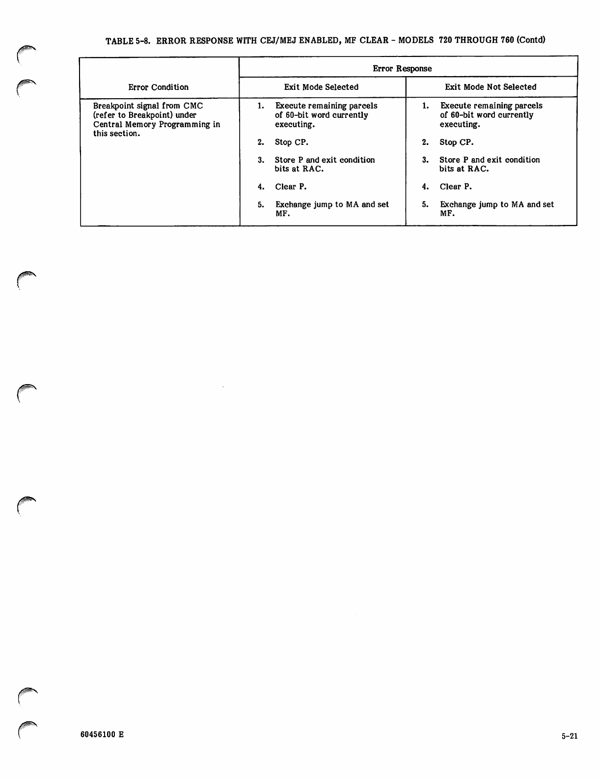
TABLE 5-8. ERROR RESPONSE WITH CEJ/MEJ ENABLED, MF CLEAR - MODELS 720 THROUGH 760 (Contd)
Error Condition
Error Response
Exit Mode Selected Exit Mode Not Selected
Breakpoint signal from CMC
(refer to Breakpoint) under
Central Memory Programming in
this section.
1. Execute remaining parcels
of 60-bit word currently
executing.
2. Stop CP.
3. Store P and exit condition
bits at RAC.
4. Clear P.
5. Exchange jump to MA and set
MF.
1. Execute remaining parcels
of 60-bit word currently
executing.
2. Stop CP.
3. Store P and exit condition
bits at RAC.
4. Clear P.
5. Exchange jump to MA and set
MF.
/H ^ \
60456100 E 5-21
TABLE 5-9. ERROR RESPONSE WITH CEJ/MEJ DISABLED - MODELS 720 THROUGH 760
Error Condition
Error Response
Exit Mode Selected Exit Mode Not Selected
Illegal instruction 1. Execute illegal instruction
as if it were a pass.
2. Stop CP.
3. Store P and exit condition
bits at RAC.
4. Clear P.
1. Execute illegal instruction
as if it were a pass.
2. Stop CP.
3. Store P and exit condition
bits at RAC.
4. Clear P.
Exit condition bit 48 set by an
increment read or an address
out of range
1. Read all zeros to selected
X register.
2. Stop CP.
3. Store P and exit condition
bits at RAC.
4. Clear P.
1. Read all zeros to selected
X register.
2. Continue execution.
3. Continue execution.
Exit condition bit 48 set by an
increment write of an address
out of range
1. Block write operation, con
tent of CM is unchanged.
2. Stop CP.
3. Store P and exit condition
bits at RAC.
4. Clear P.
1. Block write operation, con
tent of CM is unchanged.
2. Continue execution.
Exit condition bit 48 set by an
RNI or branch address out of
range
1. Stop CP.
2. Store P and exit condition
bits at RAC.
3. Clear P.
Stop CP.
Exit condition bit 48 set on
CMU instruction
1. Cl or C2 greater than 9
2. Cl or K2 address out of
range
1. Error condition 1 causes in
struction to execute as a
pass. Condition 2 causes in
struction moves or compares
up to the point of address
out of range.
2. Stop CP.
3. Store P and exit condition
bits at RAC.
4. Clear P.
1. Error condition 1 causes in
struction to execute as a
pass. Condition 2 causes in
struction moves or compares
up to the point of address
out of range.
2. Continue with next 60-bit
instruction.
Exit condition bit 48 set by
ECS address range check
1. Forces ECS instruction to
execute as a pass.
2. Stop CP.
3. Store P and exit condition
bits at RAC.
4. Clear P.
1. Forces ECS instruction to
execute as a pass.
2. Continue execution with next
60-bit word.
Infinite operand (bit 49)
Indefinite operand (bit 50)
ECS flag register parity (bit 51)
CMC to CPU data error or double
error (bit 53)
1. Stop CP.
2. Store P and exit condition
bits at RAC.
3. Clear P.
Continue execution.
5-22 60456100 G
TABLE 5-9. ERROR RESPONSE WITH CEJ/MEJ DISABLED - MODELS 720 THROUGH 760 (Contd)
j00>^\.
Error Condition
Error Response
Exit Mode Selected Exit Mode Not Selected
CPU to CMC address or data parity
error or CPU to CMC address parity
error (bit 52)
1. Block write operation, con
tent of CM is unchanged.
2. Block read operation forces
read data to all ones.
3. Stop CP.
4. Store P and exit condition
bits at RAC.
5. Clear P.
1. Block write operation, con
tent of CM is unchanged.
2. Block read operation forces
read data to all ones.
3. Continue execution.
CPU to CMC address parity error
on exchange jump address (bit 52)
1. Write operation is not
blocked.
2. Block read operation of
first word forces read data
to all ones.
3. Stop CP.
4. Store P and exit condition
bits at RAC.
5. Clear P.
1. Write operation is not
blocked.
2. Block read operation of
first word forces read data
to all ones.
3. Rest of exchange jump exe
cutes normally.
00 instruction Stop CP. Stop CP.
Breakpoint signal from CMC
(refer to Breakpoint) under
Central Memory Programming in .
this section
1. Execute remaining parcels of
60-bit instruction word.
2. Stop CP.
3. Store P and exit condition
bits at RAC.
4. Clear P.
1. Execute remaining parcels of
60-bit instruction word.
2. Stop CP.
3. Store P and exit condition
bits at RAC.
4. Clear P.
0^S\
60456100 E 5-23
TABLE 5-10. EXCHANGE BREAK-IN CHARACTERISTICS DURING ECS TRANSFERS
Operation Condition CP without ECS CP with ECS
Instruction Oil read or
012 write Regular exchange No break-in, exchange
waits for ECS Break-in request is
sent to ECS coupler
Monitor or 262 instruction
exchange with monitor flag
clear
No break-in, exchange
aborts Break-in request is
sent to ECS coupler
Monitor or 262 instruction
exchange with monitor flag
set
No break-in, exchange
aborts No break-in, exchange
aborts
Central exchange jump No break-in, exchange
waits for ECS Not applicable
ECS flag operation Regular exchange Exchange is normal Break-in request is
sent to ECS coupler
but is not honored
during a flag op
eration
Monitor or 262 instruction
exchange with monitor flag
clear
Exchange is normal
Monitor or 262 instruction
exchange with monitor flag
set
No break-in, exchange
aborts No break-in, exchange
aborts
Central exchange jump Exchange is normal Not applicable
J * ^ f \
5-24 60456100 B
(INITIATE N
INSTRUCTION )
O i l O R 0 1 2 J
(BLOCK COPY
NO INSTRUCTION)
YES
(FLAG REGISTER
INSTRUCTION)
PERFORM
FLAG REGISTER
OPERATION
ERROR EXIT
ADDRESS
RANGE
ERROR EXIT
ILLEGAL
INSTRUCTION
YES » F U L L E X I T
YES
N^ADRS PEX
JUIO
PERFORM
BLOCK COPY
HALF EXIT
wFULL EXIT
NOTES:
0 A 24-BIT COMPARE WITH BIT 23 OF FLE
INTERPRETED AS ZERO AND BITS 24
THROUGH 59 OF XO IGNORED.
Figure 5-8. Block Copy Instruction Operations
60456100 A 5-25
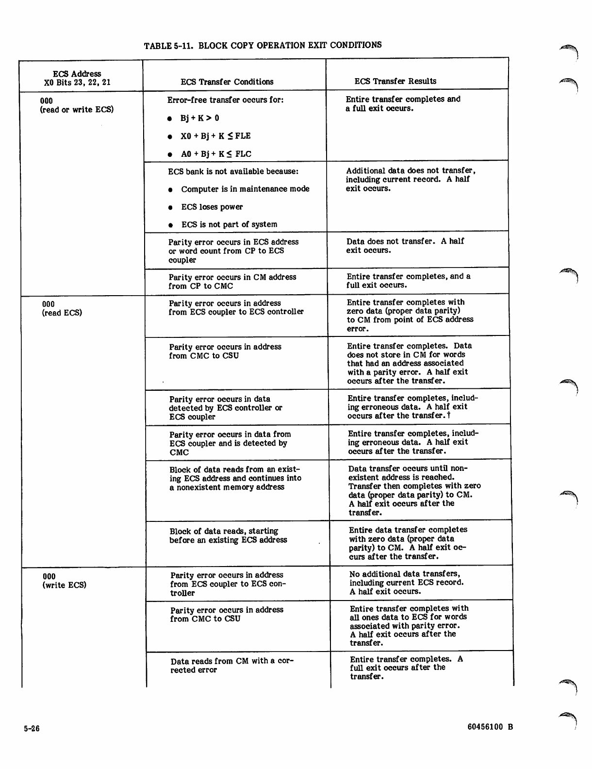
TABLE 5-11. BLOCK COPY OPERATION EXIT CONDITIONS
ECS Address
XO Bits 23, 22, 21 ECS Transfer Conditions ECS Transfer Results
000
(read or write ECS)
Error-free transfer occurs for:
• Bj + K > 0
• X0 + Bj + K < FLE
• A0 + Bj + K < FLC
Entire transfer completes and
a full exit occurs.
ECS bank is not available because:
• Computer is in maintenance mode
• ECS loses power
• ECS is not part of system
Additional data does not transfer,
including current record. A half
exit occurs.
Parity error occurs in ECS address
or word count from CP to ECS
coupler
Data does not transfer. A half
exit occurs.
Parity error occurs in CM address
from CP to CMC
Entire transfer completes, and a
full exit occurs.
000
(read ECS)
Parity error occurs in address
from ECS coupler to ECS controller
Entire transfer completes with
zero data (proper data parity)
to CM from point of ECS address
error.
Parity error occurs in address
from CMC to CSU
Entire transfer completes. Data
does not store in CM for words
that had an address associated
with a parity error. A half exit
occurs after the transfer.
Parity error occurs in data
detected by ECS controller or
ECS coupler
Entire transfer completes, includ
ing erroneous data. A half exit
occurs after the transfer, t
Parity error occurs in data from
ECS coupler and is detected by
CMC
Entire transfer completes, includ
ing erroneous data. A half exit
occurs after the transfer.
Block of data reads from an exist
ing ECS address and continues into
a nonexistent memory address
Data transfer occurs until non
existent address is reached.
Transfer then completes with zero
data (proper data parity) to CM.
A half exit occurs after the
transfer.
Block of data reads, starting
before an existing ECS address
Entire data transfer completes
with zero data (proper data
parity) to CM. A half exit oc
curs after the transfer.
000
(write ECS)
Parity error occurs in address
from ECS coupler to ECS con
troller
No additional data transfers,
including current ECS record.
A half exit occurs.
Parity error occurs in address
from CMC to CSU
Entire transfer completes with
all ones data to ECS for words
associated with parity error.
A half exit occurs after the
transfer.
Data reads from CM with a cor
rected error
Entire transfer completes. A
full exit occurs after the
transfer.
5-26 60456100 B
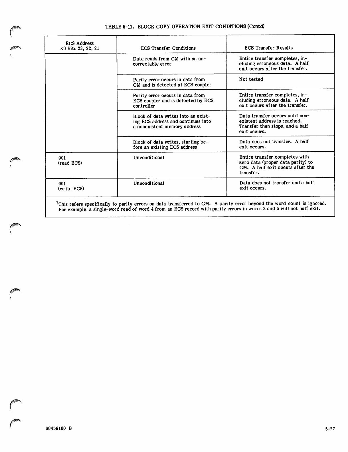
TABLE 5-11. BLOCK COPY OPERATION EXIT CONDITIONS (Contd)
ECS Address
XO Bits 23, 22, 21 ECS Transfer Conditions ECS Transfer Results
Data reads from CM with an un
correctable error
Entire transfer completes, in
cluding erroneous data. A half
exit occurs after the transfer.
Parity error occurs in data from
CM and is detected at ECS coupler
Not tested
Parity error occurs in data from
ECS coupler and is detected by ECS
controller
Entire transfer completes, in
cluding erroneous data. A half
exit occurs after the transfer.
Block of data writes into an exist
ing ECS address and continues into
a nonexistent memory address
Data transfer occurs until non
existent address is reached.
Transfer then stops, and a half
exit occurs.
Block of data writes, starting be
fore an existing ECS address
Data does not transfer. A half
exit occurs.
001
(read ECS)
Unconditional Entire transfer completes with
zero data (proper data parity) to
CM. A half exit occurs after the
transfer.
001
(write ECS)
Unconditional Data does not transfer and a half
exit occurs.
^This refers specifically to parity errors on data transferred to CM. A parity error beyond the word count is ignored.
For example, a single-word read of word 4 from an ECS record with parity errors in words 3 and 5 will not half exit.
60456100 B 5-27
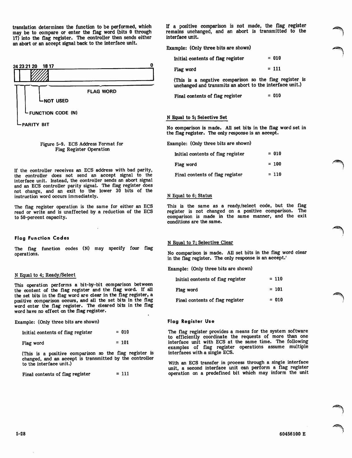
translation determines the function to be performed, which
may be to compare or enter the flag word (bits 0 through
17) into the flag register. The controller then sends either
an abort or an accept signal back to the interface unit.
24 23 2120 1817
VA
T
L-Nf
FLAG WORD
NOT USED
"-FUNCTION CODE (N)
»-PARITY BIT
Figure 5-9. ECS Address Format for
Flag Register Operation
If the controller receives an ECS address with bad parity,
the controller does not send an accept signal to the
interface unit. Instead, the controller sends an abort signal
and an ECS controller parity signal. The flag register does
not change, and an exit to the lower 30 bits of the
instruction word occurs immediately.
The flag register operation is the same for either an ECS
read or write and is unaffected by a reduction of the ECS
to 50-percent capacity.
Flag Function Codes
The flag function codes (N) may specify four flag
operations.
N Equal to 4; Ready/Select
This operation performs a bit-by-bit comparison between
the content of the flag register and the flag word. If all
the set bits in the flag word are clear in the flag register, a
positive comparison occurs, and all the set bits in the flag
word enter the flag register. The cleared bits in the flag
word have no effect on the flag register.
Example: (Only three bits are shown)
Initial contents of flag register = 010
Flag word = 101
(This is a positive comparison so the flag register is
changed, and an accept is transmitted by the controller
to the interface unit.)
Final contents of flag register = 111
If a positive comparison is not made, the flag register
remains unchanged, and an abort is transmitted to the
interface unit.
Example: (Only three bits are shown)
Initial contents of flag register = 010
F l a g w o r d = 1 1 1
(This is a negative comparison so the flag register is
unchanged and transmits an abort to the interface unit.)
Final contents of flag register = 010
N Equal to 5; Selective Set
No comparison is made. All set bits in the flag word set in
the flag register. The only response is an accept.
Example: (Only three bits are shown)
Initial contents of flag register = 010
Flag word = 100
Final contents of flag register =110
N Equal to 6; Status
This is the same as a ready/select code, but the flag
register is not changed on a positive comparison. The
comparison is made in the same manner, and the exit
conditions are the same.
N Equal to 7; Selective Clear
No comparison is made. All set bits in the flag word clear
in the flag register. The only response is an accept.'
Example: (Only three bits are shown)
Initial contents of flag register =110
Flag word = 101
Final contents of flag register = 010
Flag Register Use
The flag register provides a means for the system software
to efficiently coordinate the requests of more than one
interface unit with ECS at the same time. The following
examples of flag register operations assume multiple
interfaces with a single ECS.
With an ECS transfer in process through a single interface
unit, a second interface unit can perform a flag register
operation on a predefined bit which may inform the unit
<*^%v
5-28 60456100 E
0$@fc\
that ECS is in use. The flag operation delays the current
ECS transfer by 0.3 microseconds (best-case) or by 3.5
microseconds (worst-case). If the third and fourth
interface units also request flag register operations, the
ECS controller performs these operations before returning
to the ECS transfer. In this case, the third and fourth
interface flag requests add only 0.3 microsecond to the
original delay.
With four computers each requesting 5000-word transfers
from ECS at the same time, an effective transfer rate to
each computer is one 60-bit word every 0.4 microsecond.'
A total transfer of 20 000 words (5000 per computer)
requires 2000 microseconds for a best-case transfer. This
transfer ignores conflicts due to two requests to the same
ECS bank at the same time. Because bank conflicts can
occur a significant percentage of time, the calculated
transfer time of 2000 microseconds is less than the actual
time required. The worst-case transfer time is 0.4
microsecond times the 20 000 words, which equals 8000
microseconds.
With the four computers requesting sequential word
transfers, one interface unit transfers data while the other
three perform flag register operations to check the status
of the ECS. The flag register operations occur once each
50 microseconds. Each flag operation incurs an average
penalty of 1.6 microseconds. This penalty and the
best-case flag register operation time of 0.3 microsecond
cause a 1.9-microsecond penalty to the data transfer for
each flag register operation.
The first interface unit to transfer data in a sequential
transfer requires 500 microseconds to transfer 5000 words.
During the transfer, flag register requests of the other
three interface units interrupt the transfer a total of 30
times. This adds 57 microseconds (30 by 1.9) to the first
5000-word transfer. During the second 5000-word transfer,
only two interface units perform flag register requests and
add 38 microseconds (20 by 1.9). During the third
5000-word request, only one interface unit performs a flag
register request and adds 19 microseconds (10 by 1.9). The
fourth request adds no penalty. The total transfer time
calculation is:
(500+57) (500+38)+(500+19)+500 = 2114 microseconds
The 2114 microseconds obtained with the use of the flag
register are a considerable improvement over the
worst-case time of 8000 microseconds with only a slight
increase to the best-case time of 2000 microseconds. The
flag register also enhances the system by permitting the
first computer to start using its data only 557 microseconds
after starting a transfer. This time is 2000 microseconds if
the flag register is not used. In addition to improving the
total transfer rate of the ECS system, the flag register is
particularly useful in determining the priority of transfers.
r
jgji&\
60456100 E 5-29/5-30

r%
V
V
CENTRAL MEMORY PROGRAMMING

CENTRAL MEMORY PROGRAMMING CM references beyond the described limits cause error
responses listed in tables 5-7, 5-8, and 5-9.
z^R\
CENTRAL MEMORY —
MODELS 720 THROUGH 760
All references to CM by the CP for instructions or
read/write data are made relative to RAC. The RAC
defines the lower limit of the addresses of a program in
CM. The upper limit of the program addresses is defined
by FLC added to RAC. The field length is a number of
60-bit words established by the operating system prior to
program execution. All references to CM for a program
must be within the field established for that program.
During an exchange jump, an 18-bit RAC and an 18-bit FLC
load into respective registers to define the CM limits of
the program that is initiated by the exchange jump.
Figure 5-10 shows the absolute and relative memory
addresses, RAC, FLC, and P register relationships. For a
program to operate within the established limits, the
following conditions must exist.
For absolute memory addresses:
RAC < (RAC+P) < (RAC+FLC)
For relative memory addresses:
O < P < FLC
fNOTE I
To avoid possible artificial range faults,
instructions should not be stored near the
upper limit address of the field length. For
example, using absolute address ((RAC + FLC)
- 1) for an instruction produces a range fault
when the RNI occurs to (RAC + FLC). Data,
rather than instructions, should always be
stored in absolute address location ((RAC +
FLC) -1).
CENTRAL MEMORY — MODEL 176
All references to CM by the CP for instructions or
read/write data are made relative to RAS. The RAS
defines the lower limit of the addresses of a program in
CM. Changes to RAS permit relocation of the program in
CM. The upper limit of the program addresses is defined
by the FLS added to RAS. The field length is a number of
60-bit words established by the operating system prior to
program execution. All references to CM for a program
must be within the field established for that program.
During an exchange jump, an 18-bit RAS and an 18-bit FLS
load into respective registers to define the CM limits of
the program that is initiated by the exchange jump.
Figure 5-11 shows the absolute and relative memory
addresses, RAS, FLS, and P register relationships. For u
program to operate within the established limits, the
following conditions must exist.
For absolute memory addresses:
RAS < (RAS+P) < (RAS+FLS)
For relative memory addresses:
O < P < FLS
[NOTE |
To avoid possible artificial range faults,
instructions should not be stored near the
upper limit address of the field length. For
example, using absolute address ((RAS + FLS) -
1) for an instruction produces a range fault
when the RNI occurs to (RAS + FLS). Data,
rather than instructions, should always be
stored in absolute address location ((RAS +
FLS) - 1).
MEMORY MAP
MEMORY MAP
FIRST LOCATION IN
PROGRAM AREA
PROGRAM AREA
SOME ARBITRARY LOCATION
IN PROGRAM AREA
LAST LOCATION t I IN
PROGRAM AREA
FIRST LOCATION IN
PROGRAM AREA
FLS b-PROGRAM AREA
SOME ARBITRARY LOCATION
IN PROGRAM AREA
LAST LOCATION f
PROGRAM AREA
Figure 5-10. Memory Map - Models 720 through 760
Figure 5-11. Memory Map - Model 176
60456100 E 5-31
CM references beyond the described limits set flags in the
PSD register, described for the model 176 CP in section 2.
BREAKPOINT — MODELS 720 THROUGH 760
The breakpoint feature provides a diagnostic aid by
allowing a breakpoint on a given absolute CM address.
An 18-bit field in the status and control register is reserved
for the breakpoint address. Four additional bits specify
control when breakpoint is enabled.*
When a breakpoint compare occurs in CMC, the breakpoint
flag is set, and a signal is sent to the requesting unit. CM
access is not blocked. The CMC reports the breakpoint
status code to the status and control register.
Status and control register bit 77 is the CMC breakpoint
match. This bit loads and locks bits 56 through 59 which
hold the port code and condition code that resulted in
breakpoint compare.
When a breakpoint compare occurs during a PPS access to
CM, the breakpoint flag is sent to the PPS port. The PPS
sets bit 76 of the status and control register to indicate
that a PPS compare occurred. This bit locks in bits 60
through 75. If bit 83 is set, the PP number code stores in
bits 72 through 75, and the content of that PP's P register
stores in status and control register bits 60 through 71.
This status holds until bit 76 clears.
The following breakpoint notes only apply to models 740,
750, and 760.
• Since breakpoint is for an address request to CM, a
breakpoint does not occur for an instruction
executed from the instruction stack if the
instruction enters the instruction stack before
selecting breakpoint.
• The value of P plus RAC when the CP stops for
breakpoint may not correspond with the value of
breakpoint address because the CP normally
requests two words ahead of P on an RNI.
• The value of P plus RAC when the CP stops for
breakpoint on an increment address may not
correspond with the value of P plus RAC of the
increment instruction. Advancing P is based on the
60-bit word of instructions entering CIW instead of
any given parcel of CIW being executed.
5-32 60456100 E
DATA CHANNEL CONVERTER PfeOORAMMiPG

'*as%'
V
DATA CHANNEL CONVERTER
PROGRAMMING
The following programming information is for one data
channel converter (DCC) and applies to each DCC in a
basic or expanded CDC CYBER 170 system.
CODES
Two sets of codes are required to operate a 3000 series
peripheral equipment through a DCC.
• Function and status response codes for the DCC.
• Connect, function, and status codes for the specific
3000 series equipment.
The DCC function codes allow the computer system to
connect to the 3000 series equipment and to transmit 3000
series function codes to the connected equipment.
Function codes also permit the sensing of both DCC and
external equipment status and enable the flow of data
between the data channel and the 3000 series equipment
through the DCC.
The 3000 series codes include connect, function, and status
reply. These codes prepare a connected equipment for an
I/O operation. They do not affect unconnected equipment.
The 3000 series status codes monitor the operating
conditions of several pieces of equipment (refer to 3000
series equipment manuals for a complete list of these
codes).'
Function codes are transmitted to the DCC by PP function
A on channel d (FAN, 76) and function m on channel d
(FNC, 77) instructions. Bit 0 is rightmost in all codes.
The function codes are:
Function Code
Select DCC 2000 (D
Deselect DCC 2100
Connect equipment - mode I NUUU (D
Connect equipment - mode n 1000
Function transmit - mode I 0FFF ®
Function initiate - mode 11 1100
Input EOR initiate 14XX 0
Input initiate 15XX
Output initiate 16XX
Deactivate option XX4X/XX6X
Function master clear 1700
DCC status request 1200
Equipment status request 1300
Notes:
(D Each DCC is assigned different select and deselect
codes, such as 2200 and 2300 or 2400 and 2500,
when two or more DCCs share a common data
channel.
N equals equipment number 4 through 7, and UUU
equals lower nine bits of connect code.
FFF equals lower nine bits of function code.
Initiate conditions are defined by XX.
In the following code descriptions, some of the code
characters have been expanded to show the character bits.
For example, the 14XX code is expanded to 14Xoox, where
oox represents the last three character bits. The XXXI
code is expanded to XXXool, where ool represents the last
three character bits.
Function Codes
Select Converter (2000)
Function code 2000 selects the DCC from among the
equipment sharing the same data channel. Each DCC is
assigned different select and deselect codes, such as 2200
and 2300 or 2400 and 2500, when two or more DCCs share a
common data channel. A deadstart master clear
automatically selects all DCCs in the computer system.
The DCC must be the first equipment on a data channel.
Deselect Converter (2100)
Function code 2100 deselects the DCC. The DCC must be
deselected before other equipment on the same data
channel is used.
Connect Equipment, Mode 1 (NUUU)
Function code NUUU connects 3000 series equipment 4, 5,
6, or 7 and units UUU, where N equals the equipment
number 4 through 7 and UUU equals the lower nine bits of
the connect code.
Connect Initiate, Mode n (1000)
Function code 1000, specifying a mode II operation, causes
the DCC to send the next data word received to the 3000
series equipment as a connect code. Code 1000 connects
3000 series equipment 0 through 7. The 1000 function code
must be followed by a one-word data output. The data is
the connect code.
Function Transmit, Mode 1 (OFFF)
Function code OFFF, specifying a mode I operation, causes
the DCC to transmit the 12-bit function code
60456100 A 5-33
(OFFF) to the connected 3000 series equipment. FFF can
be the lower nine bits of any 12-bit code whose upper three
bits are zeros.
Function Initiate, Mode n (1100)
Function code 1100, specifying a mode n operation, causes
the DCC to send the next data word received to the
connected 3000 series equipment as a function code. This
code can be used to transmit any 3000 series function code
to the connected equipment. The 1100 code should be
followed by a one-word data output. The data is the
function code.
Input EOR Initiate (14Xoox)
Function code 14Xoox prepares the DCC for an input
operation. The code terminates the input by either an
end-of-record (EOR) signal from the 3000 series equipment
or by a channel disconnect from the PP.' Initiate conditions
are defined by Xoox. A negate BCD conversion line is
enabled by the external equipment when bit 0 of code
14Xoox is set.
• The XX6X code must be sent to the DCC with an
input or output function code 1460, 1560, or 1660/
This sends an active signal to the data channel
when this option is selected in the DCC, and an
interrupt-override signal is returned from the
peripheral controller. The XX6X code may be used
for any 3000 series peripheral controller that has
an interrupt-override signal feature.
The interrupt-override signal is generated in a 3000
series peripheral controller when interrupt on
abnormal end-of-operation is selected and an
abnormal condition exists. The interrupt-override
signal is returned to the DCC which generates an
inactive signal that is sent to the data channel.
• The XX4X code must be sent to the DCC with
input or output function code 1440, 1540, or 1640.
This code is used for 3000 series peripheral
controllers that do not have the interrupt-override
signal feature.
When an abnormal end-of-operation is selected in
the 3000 series peripheral controller and an
abnormal condition exists, an abnormal
end-of-operation status code 1XXX is returned to
the DCC. The DCC senses for status code 1XXX
and generates an inactive signal that is sent to the
data channel.
Input Initiate (15Xoox)
Function code 15Xoox prepares the DCC for an input
operation. The code terminates the input by a channel
disconnect only. (Refer to Input EOR Initiate description
in this section.) A negate BCD conversion line is enabled
to the external equipment when bit 0 of code 15Xoox is
set. The negate BCD conversion remains in effect until a
14X0,15X0, or 16X0 function code is received.
The 15Xoox function code should not be used for magnetic
tape units. A magnetic tape transport stops tape motion
when it senses the end of a record. However, when code
15XX is in effect, the DCC does not disconnect the data
channel on the end of a record. If the specified word
matches the record word count, the PP exits the IAM
instruction with the channel active.
Output Initiate (16XX)
Function code 16XX prepares the DCC for an output
operation. The code terminates the output by a channel
disconnect. (Refer to Input EOR Initiate description in this
section.) A negate BCD conversion line is enabled to the
external equipment when bit 0 of code 16XX is set. The
negate BCD conversion remains in effect until a 14X0,
15X0, or 16X0 function code is received.
Function Master Clear (1700)
Function code 1700 master clears all 3000 series equipment
attached to the DCC, as well as all the conditions within
the DCC.
Data Channel Converter Status Request (1200)
Function code 1200 permits the PP to input DCC status. A
one-word input must follow to read the status response.
Equipment Status Request (1300)
Function code 1300 permits the PP to input the status
response from the connected 3000 series equipment. A
one-word input must follow to read the status word.
["NOTE |
Any 1XXX function code sent to the DCC
clears the previous 1XXX function condition.
Deactivate Option (XX6X) and (XX4X)
Function codes XX6X and XX4X allow two additional
methods of generating an inactive signal in the DCC during
a read or write operation.
Status Reply Codes
Two types of status codes are available from the DCC,
DCC status codes and equipment status codes.
y^^SV
5-34 60456100 A
Function code 1200 makes the DCC status response
available to the PP.' A one-word data input must follow to
read the status word. The 12-bit DCC status responses are:
Code
XXXO
XXXxxl
XXXxll
XXXXlxx
XX1X-2XXX
lxxXXlxx
Description
Reply
Reject (internal or external)
Internal reject
Transmission parity error between
DCC and 3000 series peripheral
controller
Equipment interrupts
Transmission parity error on data
from PP to DCC
Each piece of 3000 series peripheral equipment provides a
12-bit status response. The response code is available at
the time the equipment is connected to the DCC or after
the peripheral equipment rejects a connect code. Each bit
in the response code indicates a condition within the
peripheral equipment, such as ready, busy, or end-of-tape.
A PP makes a status request to the connected 3000 series
equipment by sending a 1300 function code to the DCC.
The PP then makes a one-word input to read the response.
Equipment status codes differ for each equipment. The
codes are listed in the manual describing the individual
equipment. The DCC status codes are defined in the
following paragraphs.
Reply (XXXO)
Bits 0 and 1 clear when the 3000 series equipment returns a
reply signal to the DCC in response to a connect or
function code.
Reject (Internal or External) (XXXxxl)
Bit 0 sets when the 3000 series equipment returns a reject
signal to the DCC in response to a connect or function
code. An internal reject signal sets both bits 0 and 1.
series equipment. A parity error on a connect code does
not set bit 2.
Equipment Interrupts (XX1X-2XXX)
One of bits 3 through 10 indicates the interrupt signal from
one of eight possible 3000 series pieces of equipment. If
equipment N sends an interrupt, status bit N plus 3 sets and
remains set until the equipment drops the interrupt signal.
Transmission Parity Error on Data from
Channel (lxxXXlxx)
A parity error is detected on data transmitted from the
data channel. The DCC retransmits this data with
incorrect parity and sets bits 2 and 11.
SELECTING THE DATA CHANNEL CONVERTER
The DCC must be selected from among the other
equipment that shares the same data channel before it
communicates with 3000 series peripheral equipment. The
selected (2000) function code, transmitted by a PP FAN
(76) or FNC (77) instruction, selects the DCC. DCCs are
assigned different select and deselect codes, such as 2200
and 2300 or 2400 and 2500, when two or more DCCs share a
common data channel. Selection activates the DCC and
renders inactive all other I/O equipment on the data
channel.
A deadstart master clear automatically selects all DCCs in
the computer system. The DCC must be the first
equipment on a data channel.
DESELECTING THE DATA CHANNEL CONVERTER
Once selected, the DCC remains selected until it is
deselected by function code 2100. The DCC must always
be deselected before any other I/O equipment on the same
data channel can be used.
If two DCCs on the same data channel have been selected
by a deadstart master clear, the first DCC must be
deselected before the second DCC can be deselected.
Internal Reject (XXXxll)
Bits 0 and 1 set, after a 100-microsecond delay, if the 3000
series equipment fails to return a reply or a reject signal to
the DCC in response to a connect or function code.
Transmission Parity Error (XXXlxx)
Bit 2 sets when a parity error occurs on a function code or
data transfer between the DCC and the 3000
CONNECTING TO 3000 SERIES EQUIPMENT
One of eight possible 3000 series controllers attached to
the DCC may be connected after the DCC is selected. The
connect operation activates one controller and
automatically deactivates the other seven controllers so
that only one of eight possible controllers can be connected
at a given time.
A 12-bit connect code (figure 5-12) connects a 3000 series
controller to a DCC.
60456100 A 5-35
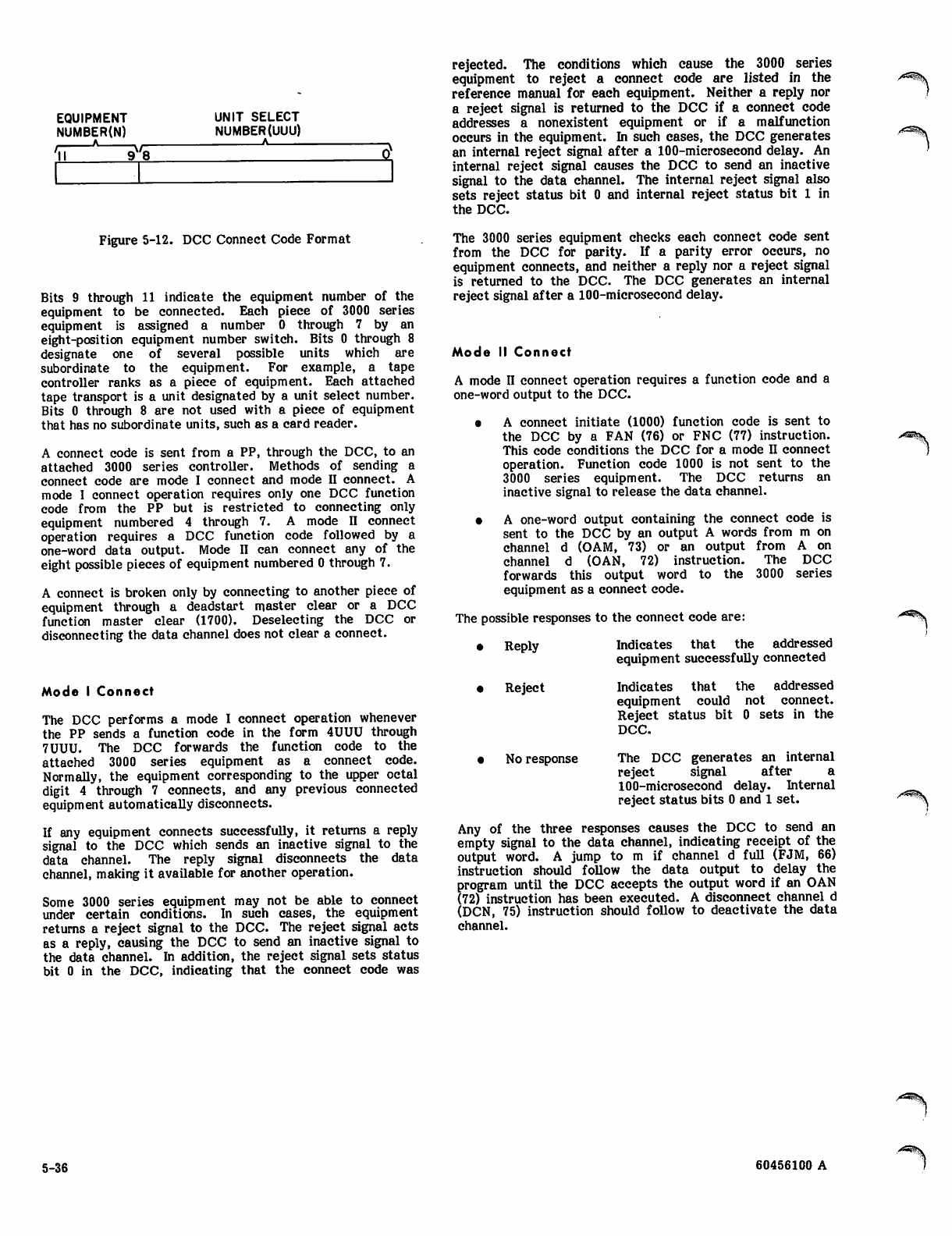
EQUIPMENT
NUMBER(N)
A
UNIT SELECT
NUMBER(UUU)
A
'll 9W8 Qv
rejected. The conditions which cause the 3000 series
equipment to reject a connect code are listed in the
reference manual for each equipment. Neither a reply nor
a reject signal is returned to the DCC if a connect code
addresses a nonexistent equipment or if a malfunction
occurs in the equipment. In such cases, the DCC generates
an internal reject signal after a 100-microsecond delay. An
internal reject signal causes the DCC to send an inactive
signal to the data channel. The internal reject signal also
sets reject status bit 0 and internal reject status bit 1 in
the DCC.
Figure 5-12. DCC Connect Code Format
Bits 9 through 11 indicate the equipment number of the
equipment to be connected. Each piece of 3000 series
equipment is assigned a number 0 through 7 by an
eight-position equipment number switch. Bits 0 through 8
designate one of several possible units which are
subordinate to the equipment. For example, a tape
controller ranks as a piece of equipment. Each attached
tape transport is a unit designated by a unit select number.
Bits 0 through 8 are not used with a piece of equipment
that has no subordinate units, such as a card reader.
A connect code is sent from a PP, through the DCC, to an
attached 3000 series controller. Methods of sending a
connect code are mode I connect and mode II connect. A
mode I connect operation requires only one DCC function
code from the PP but is restricted to connecting only
equipment numbered 4 through 7. A mode II connect
operation requires a DCC function code followed by a
one-word data output. Mode II can connect any of the
eight possible pieces of equipment numbered 0 through 7.
A connect is broken only by connecting to another piece of
equipment through a deadstart master clear or a DCC
function master clear (1700). Deselecting the DCC or
disconnecting the data channel does not clear a connect.
Mode I Connect
The DCC performs a mode I connect operation whenever
the PP sends a function code in the form 4UUU through
7 UUU. The DCC forwards the function code to the
attached 3000 series equipment as a connect code.
Normally, the equipment corresponding to the upper octal
digit 4 through 7 connects, and any previous connected
equipment automatically disconnects.
If any equipment connects successfully, it returns a reply
signal to the DCC which sends an inactive signal to the
data channel. The reply signal disconnects the data
channel, making it available for another operation.
Some 3000 series equipment may not be able to connect
under certain conditions. In such cases, the equipment
returns a reject signal to the DCC. The reject signal acts
as a reply, causing the DCC to send an inactive signal to
the data channel. In addition, the reject signal sets status
bit 0 in the DCC, indicating that the connect code was
The 3000 series equipment checks each connect code sent
from the DCC for parity. If a parity error occurs, no
equipment connects, and neither a reply nor a reject signal
is returned to the DCC. The DCC generates an internal
reject signal after a 100-microsecond delay.
Mode II Connect
A mode II connect operation requires a function code and a
one-word output to the DCC.
• A connect initiate (1000) function code is sent to
the DCC by a FAN (76) or FNC (77) instruction.
This code conditions the DCC for a mode II connect
operation. Function code 1000 is not sent to the
3000 series equipment. The DCC returns an
inactive signal to release the data channel.
• A one-word output containing the connect code is
sent to the DCC by an output A words from m on
channel d (OAM, 73) or an output from A on
channel d (OAN, 72) instruction. The DCC
forwards this output word to the 3000 series
equipment as a connect code.
The possible responses to the connect code are:
• Reply Indicates that the addressed
equipment successfully connected
• Reject Indicates that the addressed
equipment could not connect.
Reject status bit 0 sets in the
DCC.
• No response The DCC generates an internal
reject signal after a
100-microsecond delay. Internal
reject status bits 0 and 1 set.
Any of the three responses causes the DCC to send an
empty signal to the data channel, indicating receipt of the
output word. A jump to m if channel d full (FJM, 66)
instruction should follow the data output to delay the
program until the DCC accepts the output word if an OAN
(72) instruction has been executed. A disconnect channel d
(DCN, 75) instruction should follow to deactivate the data
channel.
5-36 60456100 A
/ * ^ \
y^P^^N
The 3000 series equipment checks each connect code sent
from the DCC for parity, identical to a mode I connect
operation. If a parity error occurs, no equipment connects,
and neither a reply nor a reject signal is returned to the
DCC. The DCC generates an internal reject signal after a
100-microsecond delay.
Check the DCC status response for a reject after a mode n
connect operation is complete.
• No response The DCC generates an internal
reject signal after a
100-microsecond delay if neither
a reply nor a reject signal is
received. Internal reject status
bits 0 and 1 set.
A status check should follow a mode I function operation to
test for a reject signal or a parity error at the 3000 series
peripheral controller.
NOTE
A status check should follow only after the
mode II connect operation is complete. There
is no response from the 3000 series equipment
when the connect initiate code (1000) is sent
to the DCC. Thus, a status check at this time
is not significant.
SENDING FUNCTION CODES TO
3000 SERIES EQUIPMENT
A piece of 3000 series equipment accepts 12-bit function
codes from the DCC after it connects. Function codes
establish operating conditions within an equipment or
initiate operations, such as tape rewind. The function
codes applicable to the 3000 series equipment are listed in
the reference manual for each equipment.
The function codes sent from the DCC to the 3000 series
equipment are distinct from function codes transmitted
from the PP to the DCC.
Two methods are used to transmit function codes to a 3000
series equipment.
Mode I A mode I function operation requires only
a single PP function instruction (FAN or
FNC) but is restricted to a 9-bit function
code.
Mode n A mode II function operation requires a
function instruction followed by a
one-word data output. A full 12-bit
function code can be sent to the 3000
series equipment.
Mode I Function
A mode I function operation is similar to a mode I connect
operation. The DCC performs a mode I function operation
whenever a PP sends a OFFF function code to the DCC.
FFF can be any 9-bit 3000 series function code. The DCC
forwards the OFFF to the connected equipment as a
function code.
The DCC receives one of three possible responses to a
function code from the 3000 series equipment.
• Reply
• R e j e c t
Indicates that the equipment
accepted the code.
Indicates that the equipment did
not accept the code. Reject
status bit 0 sets in the DCC.
Mode II Function
A mode n function operation is similar to a mode II connect
operation requiring a function code and a one-word output
to the DCC.
• A function initiate (1100) function code is sent to
the DCC by a FAN (76) or FNC (77) instruction.
This code conditions the DCC for a mode II
function operation and is not forwarded to the 3000
series equipment. The DCC returns an inactive
signal to release the data channel.
• A one-word output containing the desired 12-bit
function code is sent to the DCC by an OAN (72) or
OAM (73) instruction. The DCC forwards this
output word to the 3000 series equipment as a
function code.
The responses to a mode n function operation are the same
as for a mode I function operation.
• Reply Indicates that the equipment
accepted the code.
• Reject Indicates that the equipment did
not accept the code. Reject
status bit 0 sets in the DCC.
• No response The DCC generates an internal
reject signal after a
100-microsecond delay if neither
a reply nor a reject signal is
received. Internal reject status
bits 0 and 1 set.
Any of the three responses causes the DCC to send an
empty signal to the data channel, indicating receipt of the
output word. A full FJM (66) instruction should follow the
data output to delay the program until the DCC accepts
the output word if an OAN (72) instruction has been
executed. A DCN (75) instruction should follow to
deactivate the data channel.
A status check should follow a mode II function operation
to test for a reject signal or a parity error at the 3000
series peripheral controller.
DATA TRANSFER
An input or output operation can proceed only after the
DCC is selected and the desired equipment is connected to
the DCC.
0^\
60456100 A 5-37
Input Operation
An input operation requires the following actions.
• Send an input initiate (15 XX) or an input EOR
(14XX) initiate function code to the DCC to
prepare it for an input operation.
• Execute an active channel (173) instruction for the
data channel. This signals the equipment through
the DCC to begin sending data (for example, it
starts tape or card motion)/
• Execute an input (70 or 71) instruction to read the
data from the sending device.
Input function code 1400 terminates the input operation
when either the 3000 series peripheral equipment reaches
an end-of-record or a data channel disconnect is received
from the PP. An end-of-record sensed by the 3000 series
equipment causes the DCC to send an inactive signal which
disconnects the data channel. The PP then exits to the
next instruction.
Input function code 1401 suppresses the
internal-to-external binary coded decimal (BCD) conversion
that normally takes place in some 3000 series equipment.
Code 1401 is identical to code 1400 in other respects.
On some 3000 series equipment, a significant delay occurs
between the channel activate instruction that signals the
start of an input operation and the time that the first data
word is available from the equipment. For example, in the
3248 Card Reader Controller, a 20-millisecond delay occurs
between the start of card motion and the availability of the
first card column. During this period, the PP can perform
another task. The latent period is different for each 3000
series equipment. Its length can be found in the reference
manual describing the device.' An input instruction should
immediately follow the channel activate instruction if the
delay is unknown.
The DCC does not deactivate the data channel on
end-of-record if input initiate code 15XX is used. A
channel disconnect instruction must immediately follow the
input instruction to notify the equipment of the end of
operation.
Input function codes 14XX and 15XX remain in effect until
the next DCC function code is received. The negate
internal-to-external BCD condition established by codes
14X1 and 15X1 is cleared when the PP sends a new I/O
function with bit 0 clear. An input operation is normally
followed by a status request function code. Thus, each
input operation usually requires a new input initiate code.
Output Operation
An output operation requires the following actions.
• Send an output initiate (16XX) function code to the
DCC to prepare it for an output operation.
• Execute an activate channel (74) instruction for the
data channel. This signals the equipment, through
the DCC, that an output operation is about to
begin. The connected device prepares to receive
data (for example, it starts tape or card motion).
• Execute an output (72 or 73) instruction to send
data to the 3000 series equipment.
• Execute a full jump (66) instruction to ensure that
the 3000 series equipment has accepted the last
word. Execute a DCN (75) instruction. This step
releases the data channel and notifies the 3000
series equipment of the end of the record.
Output function code 1601 suppresses the
internal-to-external BCD conversion that normally takes
place in some 3000 series equipment. Code 1601 is
identical to code 1600 in other respects.
On some 3000 series equipment, a delay occurs between the
channel activate instruction that signals the start of an
output operation and the time that the equipment is ready
to accept the first data word. During this period, the PP
can perform another task. An output instruction should
immediately follow the channel activate instruction if the
delay is unknown.
Output initiate code 1600 remains in effect until the next
DCC function code is received. The negate
internal-to-external BCD condition established by code
16X1 is cleared when the PP sends a new I/O function with
bit 0 clear. An output operation is normally followed by a
status request function code which clears the output
condition in the DCC. Thus, each output operation usually
requires a new output initiate code.
PARITY CHECKING
The DCC checks parity on all function codes and data
received from the data channel or the connected 3000
series controllers. The DCC generates parity for data sent
in any direction.
Function Codes from PPS to DCC
The PPS transmits a 12-bit function code plus one parity
bit to the DCC. The DCC checks each function code that
it receives for odd parity. If the DCC detects a parity
error, the following occurs.
• The connect or function signal to the peripheral
controller is blocked.
• The DCC does not send an inactive signal to the
data channel. A time-out must be executed, and if
no inactive signal is received, a DCN must follow.
• Parity error status bits 2 and 11 in the data channel
status word remain clear.
• The function register in the DCC clears.
Therefore, the function does not execute.
5-38 60456100 A
■"^N
Data from PPS to DCC
The PPS transmits a 12-bit data byte (includes functional
data on mode n connect or function operation) plus one
parity bit to the DCC. The DCC checks each data byte
that it receives for odd parity. If the DCC detects a parity
error, the following occurs.
• Parity error status bits 2 and 11 in the channel
status word set.
• The parity bit received from the data channel is
sent unchanged to the peripheral controller with
the data byte. The controller also detects the
parity error and responds.
• The response to a mode II functional data byte is
either an external or internal reject signal.
Data from DCC to PPS
The 3000 series controller transmits 12 bits of data plus
one parity bit to the DCC. The DCC checks each data byte
that is receives for odd parity. If the DCC detects a parity
error, the following occurs.
• Parity error status bit 2 in the data channel status
word sets.
The data byte and the parity bit received from the
controller are sent unchanged to the PPS.
Operations proceed as normal.
Status Words from DCC to PPS
There is no parity on status words sent from the peripheral
controller to the DCC. The DCC transmits 12 bits of data
plus 1 parity bit to the PPS. The PPS checks each word it
receives for odd parity and sets channel bit X in its status
and control register if a parity error is detected.
CLEARING A PARITY ERROR
A DCC function master clear (1700) must be executed to
clear a parity error condition in the 3000 series equipment
if a status check reveals that a parity error occurred. This
action also clears DCC parity error status bits 2 and 11.
Each piece of equipment must complete its operation
before the master clear code is issued if the DCC is
alternately operating two or more pieces of 3000 series
equipment on a time-sharing basis. This procedure ensures
that the master clear code does not cause a loss of data.
zg^N
60456100 A 5-39/5-40

(**%
PJtSteLAY STATION PfcOGRAMMlNG

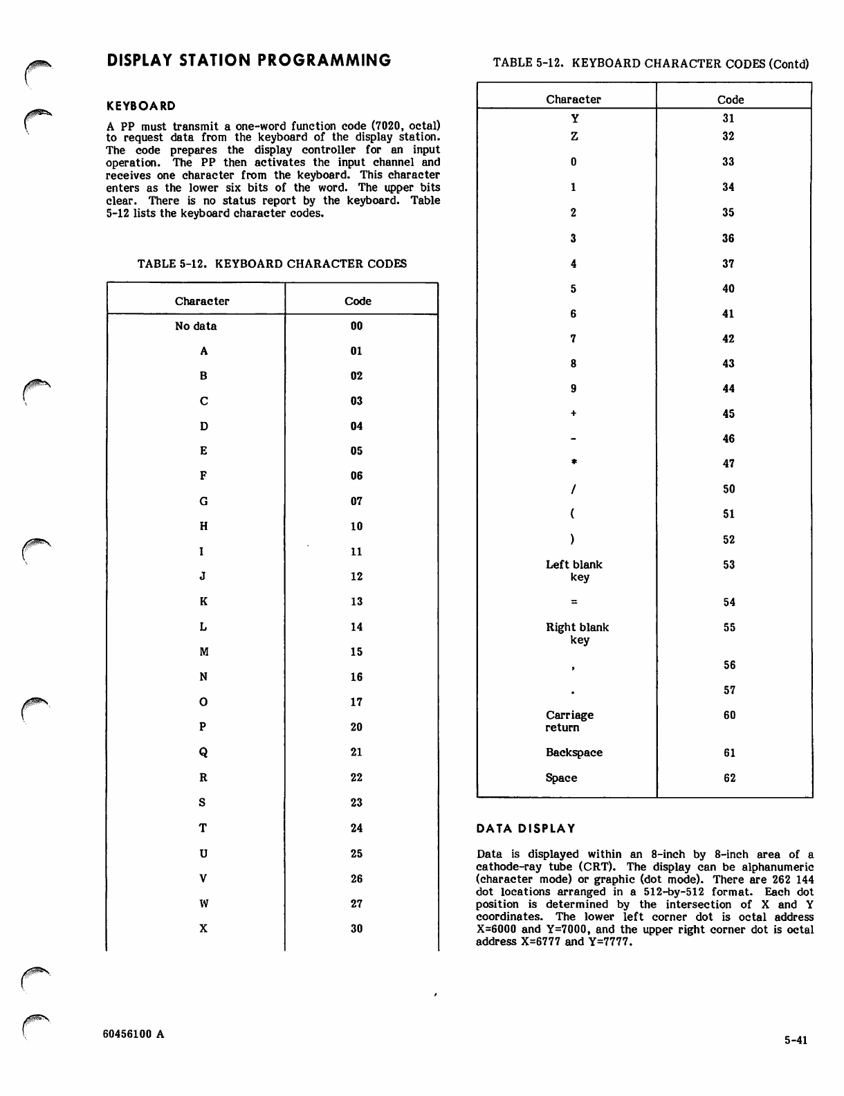
DISPLAY STATION PROGRAMMING TABLE 5-12. KEYBOARD CHARACTER CODES (Contd)
KEYBOARD
A PP must transmit a one-word function code (7020, octal)
to request data from the keyboard of the display station.
The code prepares the display controller for an input
operation. The PP then activates the input channel and
receives one character from the keyboard. This character
enters as the lower six bits of the word. The upper bits
clear. There is no status report by the keyboard. Table
5-12 lists the keyboard character codes.
TABLE 5-12. KEYBOARD CHARACTER CODES
Character Code
No data 00
A01
B02
C03
D04
E05
F06
G07
H10
I11
J12
K13
L14
M15
N16
017
P20
Q21
R22
S23
T24
U25
V26
W27
X30
Character Code
Y31
Z32
033
134
235
336
437
540
641
742
843
944
+45
-46
*47
/50
(51
)52
Left blank
key
53
=54
Right blank
key
55
t56
•57
Carriage
return 60
Backspace 61
Space 62
DATA DISPLAY
Data is displayed within an 8-inch by 8-inch area of a
cathode-ray tube (CRT). The display can be alphanumeric
(character mode) or graphic (dot mode). There are 262 144
dot locations arranged in a 512-by-512 format. Each dot
position is determined by the intersection of X and Y
coordinates. The lower left corner dot is octal address
X=6000 and Y=7000, and the upper right corner dot is octal
address X=6777 and Y=7777.
60456100 A 5-41
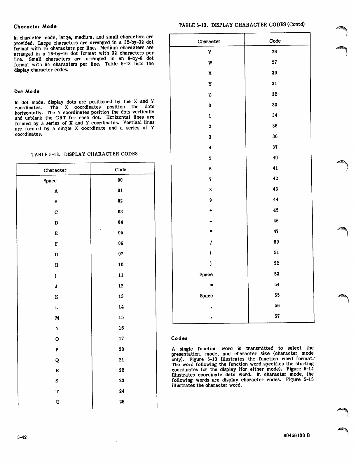
Character Mode
In character mode, large, medium, and small characters are
provided. Large characters are arranged in a 32-by-32 dot
format with 16 characters per line. Medium characters are
arranged in a 16-by-16 dot format with 32 characters per
line. Small characters are arranged in an 8-by-8 dot
format with 64 characters per line. Table 5-13 lists the
display character codes.
Dot Mode
In dot mode, display dots are positioned by the X and Y
coordinates. The X coordinates position the dots
horizontally. The Y coordinates position the dots vertically
and unblank the CRT for each dot. Horizontal lines are
formed by a series of X and Y coordinates. Vertical lines
are formed by a single X coordinate and a series of Y
coordinates.
TABLE 5-13. DISPLAY CHARACTER CODES
TABLE 5-13. DISPLAY CHARACTER CODES (Contd)
Character
Character Code
Space 00
A01
B02
C03
D04
E05
F06
G07
H10
I11
J12
K13
L14
M15
N16
017
P20
Q21
R22
S23
T24
U25
Space
Space
Code
26
27
30
31
32
33
34
35
36
37
40
41
42
43
44
45
46
47
50
51
52
53
54
55
56
57
•rf*®$&\
Codes
A single function word is transmitted to select the
presentation, mode, and character size (character mode
only). Figure 5-13 illustrates the function word format.'
The word following the function word specifies the starting
coordinates for the display (for either mode). Figure 5-14
illustrates coordinate data word. In character mode, the
following words are display character codes. Figure 5-15
illustrates the character word.
5-42 60456100 B
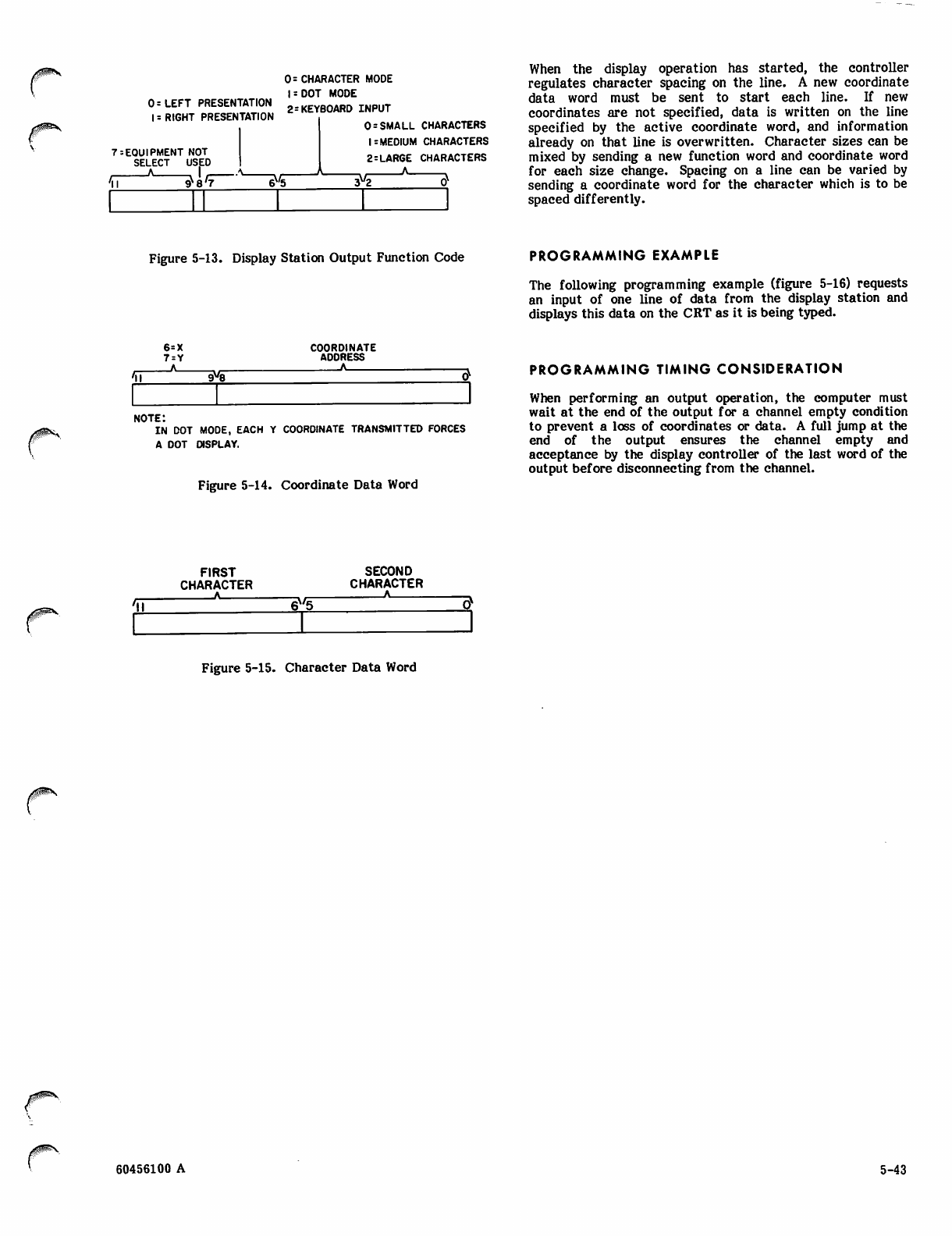
0=LEFT PRESENTATION
I = RIGHT PRESENTATION
0= CHARACTER MODE
|:DOT MODE
2=KEYBOARD INPUT
7=EQUIPMENT NOT
SELECT USED
J V . I
'II "^ef" 6W5
0=SMALL CHARACTERS
I = MEDIUM CHARACTERS
2=LARGE CHARACTERS
- A .
When the display operation has started, the controller
regulates character spacing on the line. A new coordinate
data word must be sent to start each line. If new
coordinates are not specified, data is written on the line
specified by the active coordinate word, and information
already on that line is overwritten. Character sizes can be
mixed by sending a new function word and coordinate word
for each size change. Spacing on a line can be varied by
sending a coordinate word for the character which is to be
spaced differently.
Figure 5-13. Display Station Output Function Code PROGRAMMING EXAMPLE
The following programming example (figure 5-16) requests
an input of one line of data from the display station and
displays this data on the CRT as it is being typed.
6=x
7 = Y
_J\_
COORDINATE
ADDRESS
A
9V8
note:
in dot mode, each y coordinate transmitted forces
a dot display.
Figure 5-14. Coordinate Data Word
PROGRAMMING TIMING CONSIDERATION
When performing an output operation, the computer must
wait at the end of the output for a channel empty condition
to prevent a loss of coordinates or data. A full jump at the
end of the output ensures the channel empty and
acceptance by the display controller of the last word of the
output before disconnecting from the channel.
FIRST
CHARACTER
A"e^
SECOND
CHARACTER
a
Figure 5-15. Character Data Word
60456100 A 5-43
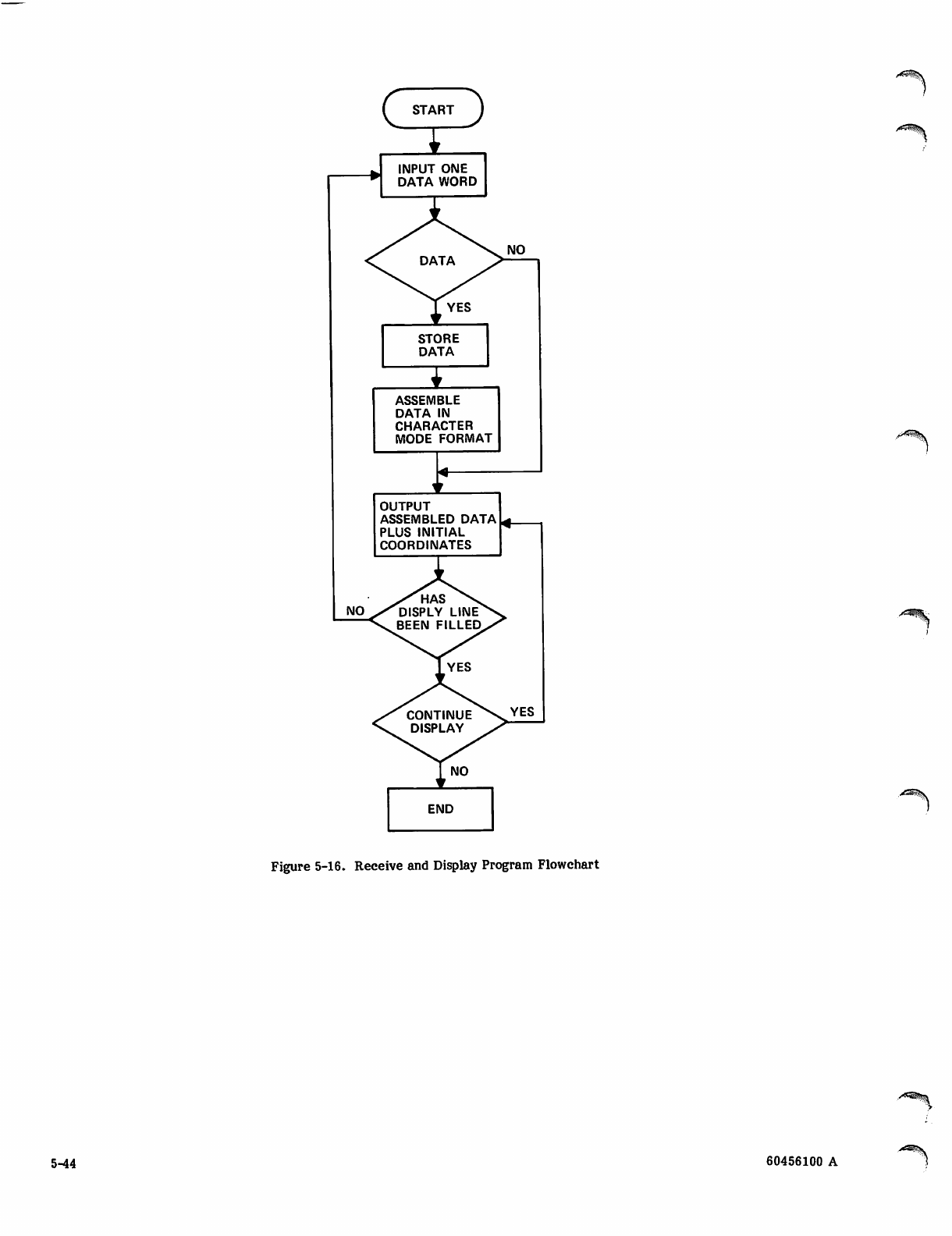
( S TA R T J
INPUT ONE
DATA WORD
STORE
DATA
I
ASSEMBLE
DATA IN
CHARACTER
MODE FORMAT
I
OUTPUT
ASSEMBLED DATA
PLUS INITIAL
COORDINATES
/*^%k
Figure 5-16. Receive and Display Program Flowchart
5-44 60456100 A
PERIPH1RAL PRQCiSSOt UNIT lN^RUCfli)N5 _ MODEL 176
^ ^ * i -

;"!
v
PERIPHERAL PROCESSOR UNIT
PROGRAMMING - MODEL 176
PROGRAMMING CONSIDERATIONS
1. PPU memory parity errors can be caused by
deadstarting a PPU while it is executing a
program. To eliminate the sensing of such parity
errors (false parity errors), the PPU deadstart and
loading program should completely load the PPU
memory by padding it with zero words and then
send the PPU clear parity signal, or cause the PPU
to sweep the remainder of the PPU memory and
then allow the clear PPU parity error (bit 83 in the
status and control register) to be set and clear.
2. If a data sample occurs at the same time that data
is changing on the line during a block input, a
parity error is likely to occur in the PPU memory.
3. If a MUX output channel resets at the same time
that a PPU does a read from the MUX, a parity
error is likely to occur in the PPU memory.
4. Deadstarting a PPU while it is executing a program
normally destroys one or two words of the program
because the deadstart signal clears the X register
when the PPU is in the process of a memory
read/write cycle. A zero word replaces the word
read from memory.
5. The deadstart signal should be applied for a
minimum of 32 clock periods when performing a
deadstart or dead dump operation on a running
PPU. Since the deadstart signal does not clear the
shift count register, application of the signal for at
least 32 clock periods allows for maximum number
of shifts and ensures that shift operations are
completed prior to the end of the deadstart or dead
dump operation. If the deadstart signal drops
before the shift count register clears itself, the
content of the A register shifts and becomes
incorrect data.
6. The deadstart signal from the status and control
register to the PPU (through the scanner) clears
the word flags and record flags of the PPU
input/output channel. While the deadstart signal is
present, all PPU input channel resume flags are
forced to ones.
7. A PPU is prepared for a dead dump by sending the
deadstart signal, dropping the deadstart signal,
sending the dead dump signal, and dropping the
dead dump signal. This order of signals ensures the
dumping of all PPM locations, excluding location
7777 (octal).
8. If an input record flag is forced to a logical one
during a block input, the block input instruction
exits and the PPU processes only the data which
was on the input channel at the time of the forced
record flag.
9. Input channels with forced input word flags can be
responsible for PPU parity errors. This occurs
when reading data from an input channel directly
into memory (71 instruction). This problem is
alleviated if all such channel data first goes to the
A register (70 instruction) and then to memory
from A.
10. If a status word is entered into the A register while
the channel input word flag is in a forced logical
one condition, the word may have been in a
transitional state at the time of entry. To allow
for this possibility, consecutively input the status
word twice and then compare the two inputs to
ensure that they are the same.
11.
12.
13.
14.
When terminating a block input instruction by a
record pulse, the input record flag remains set until
the next input instruction has input at least one
word. The last word received during the block
input is duplicated in the last block location plus
one.
When terminating a block output instruction by an
output record pulse, the output record pulse should
not be sent until the resume for the last word sent
has been received. If this is not done, the receiving
device (PPU or equipment) may lose the output
record pulse and hang (wait for another output
record pulse).
When the PPU is not selected through the scanner
(scanner channel selected for a different PPU), the
output channel 0 of the PPU receives a constant
output resume.
A PPU program cannot reference memory location
7777 (octal).
CONTROL SIGNALS
A PPU requires three control signals for I/O
communication. The signals include a word pulse, record
pulse, and resume pulse. The word pulse must accompany
each new data word being transmitted. This pulse signals
the receiver that new data is on the data lines. The record
pulse is generated by the transmitting device to indicate
the end or beginning of a data transmission. The resume
pulse is generated by the receiving device to indicate
reception of a word pulse and to signify that data will be
accepted.
DATA SIGNALS
A PPU data channel has 12 twisted pairs of conductors
which carry the 12 data bits in differential mode. In this
mode, one conductor of each pair has true data, and the
other conductor of the pair has complement data. The
characteristic impedance is between 83.3 and 111 ohms.
60456100 A 5-45
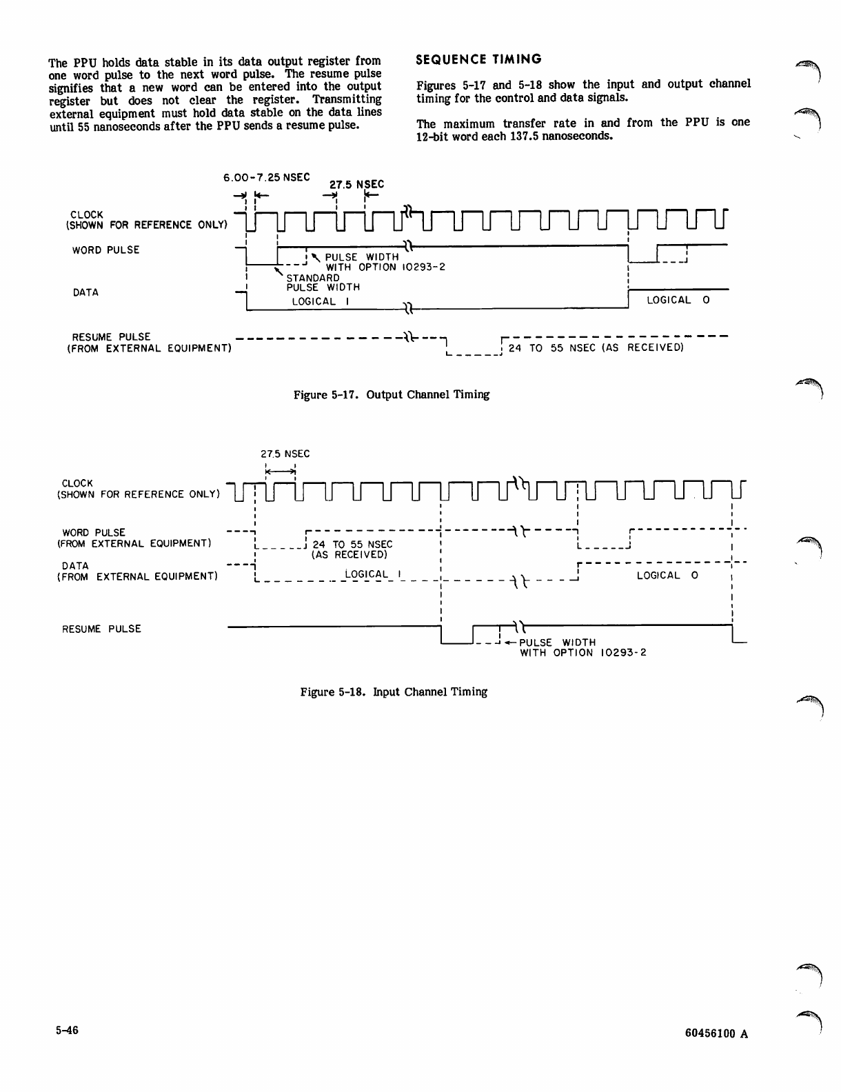
The PPU holds data stable in its data output register from
one word pulse to the next word pulse. The resume pulse
signifies that a new word can be entered into the output
register but does not clear the register. Transmitting
external equipment must hold data stable on the data lines
until 55 nanoseconds after the PPU sends a resume pulse.
SEQUENCE TIMING
Figures 5-17 and 5-18 show the input and output channel
timing for the control and data signals.
The maximum transfer rate in and from the PPU is one
12-bit word each 137.5 nanoseconds.
6.00-7.25 NSEC
- ! ! -
CLOCK
(SHOWN FOR REFERENCE ONLY)
WORD PULSE
DATA
27.5 NSEC
innnrirtf^nnnnnnnnnni
1 > !
-U ' - *
"I
• \ PULSE WIDTH
--J WITH OPTION 10293-2
STANDARD
PULSE WIDTH
LOGICAL I 4V L O G ICAL 0
RESUME PULSE
(FROM EXTERNAL EQUIPMENT) -w ! 24 TO 55 NSEC (AS RECEIVED)
Figure 5-17. Output Channel Timing
27.5 NSEC
CLOCK
(SHOWN FOR REFERENCE ONLY)
WORD PULSE
(FROM EXTERNAL EQUIPMENT)
DATA
(FROM EXTERNAL EQUIPMENT)
RESUME PULSE
imn^nnnnnn^XnjTLnnn^ni
.j 24 TO 55 NSEC
(AS RECEIVED)
LOGICAL I
-iv
u-
iV
LOGICAL 0
PULSE WIDTH
WITH OPTIO N 10293-2 1_
Figure 5-18. Input Channel Timing
5-46 60456100 A
PERIPHERAL PROCfSSOR PROGRAMMING
zp3*

>s^%
n
PERIPHERAL PROCESSOR PROGRAMMING
The PPs have access to all CM storage locations. One
60-bit word or a block of 60-bit words can be transferred
from a peripheral processor memory (PPM) to CM or from
CM to PPM. (Five 12-bit PP words equal one 60-bit CM
word.) Data from external devices is read into a PPM, and
with additional instructions, is transferred to CM.
Conversely, data is transferred from CM to a PPM and is
then transferred by additional instructions to external
devices. All addresses sent to CM from PPs are absolute
addresses.
POWER-ON CHARACTERISTIC
A power-on of the PPS may cause the parity bit of address
7777 of each PP to be in the wrong state. Any PP in a
deadstart condition reads the 7777 address and reports a
PPM parity error if the parity bit is incorrect. The
applicable deadstart routine should be checked to ensure
that the proper parity has been restored for address 7777.
d is the PPM address (0000 through 0077, octal) of the
first 12-bit word. The remaining words are taken from
locations d plus 1, d plus 2, and so on.
For a block transfer, the d and m portions of the write (63)
instruction specify the following.
(d) is the number of CM words to be transferred.
m is the PPM starting address. The content of the A
register increases by one with the transfer of each word
to provide consecutive CM locations.
The PPS may achieve a maximum transfer rate of one
60-bit word each 300 nanoseconds to CM provided that:
• Several PPs are requesting the write assembly
network in the order 0, 5, 1, 6, 2, 7, 3, 8, 4, 9, 0, 5...
• The requests are evenly distributed among eight
CM banks.
• CMC has no storage access conflicts.
CENTRAL MEMORY READ
The 48 low-order bits of the CM word enter six read data
disassembly RAMs in the PPS central memory interface
(CMI). The 12 high-order bits enter a CMI register. The
CMI disassembles the 60 bits into five 12-bit words. Each
PPS contains its own CMI.
A transfer of one word by a single-word (60) instruction
requires 3 microseconds. The first word of a block transfer
(61) instruction also requires 3 microseconds. Subsequent
60-bit transfers require 2.5 microseconds.
Up to four PPs of one PPS can simultaneously process CM
words. The maximum transfer rate from CM into one PPS
is four words every 4.3 microseconds.
If a second PP in a PPS requests a CM read before CMC
accepts the request of a previously requesting PP, the
second PP is given priority to issue the next request. The
second PP must wait for its first slot time following
acceptance of the first request.
In a read mode, the maximum transfer rate is one request
each 550 nanoseconds without storage bank or storage
access conflicts in CMC.
CENTRAL MEMORY WRITE
The 62 instruction writes one word, and the 63 instruction
transfers a block of data. These instructions assemble
12-bit words into 60-bit words in write data assembly
RAMs and then write them in CM. All PPs of a PPS can
perform write operations simultaneously in the CMI to the
point of sending assembled 60-bit words to CM. The order
in which the words are sent is based on the order of the PP
write requests.
The starting address in CM must enter the A register
before the write instruction executes.
For a one-word transfer, the d portion of the write (63)
instruction specifies the following.
INPUT/OUTPUT CHANNEL COMMUNICATIONS
Data Input
Several instructions are necessary to transfer data from
external equipment into a peripheral processor. The
instructions prepare an I/O channel and equipment for the
transfer and then start the transfer. Some external
equipment, once started, sends a series of words (record)
spaced at equal time intervals and then stops between
records. The PP can read all or a part of the record and
then disconnect the channel to end the operation and make
the channel inactive. Other equipment, such as the display
console, can send one word (or character) and then stop.
Input instructions allow the input transfer to vary from one
word to the capacity of the PP.
An input transfer may occur as follows:
1. Determine if the channel is inactive. A jump to m
on channel d inactive (65) instruction does this.
The m portion of the instruction can be a function
instruction to select read mode or determine the
status of the equipment.
2. Determine if the equipment is ready. A function m
on channel d (77) instruction followed by an active
channel d (74) instruction followed by an input to A
from channel d (70) instruction loads A with the
status response of the desired equipment. Here, m
is a status request code, and the status response in
A can be tested to determine the course of action.
3. Disconnect channel with a channel d (75)
instruction. This avoids hanging up the processor.
4. Select read mode in the equipment. A function m
on channel d (77) instruction or function (A) on
channel d (76) instruction sends a code word to the
desired device to prepare it for data transfer.
5. Enter the number of words to be transferred in A.
A load d (14) or load (d) (30) instruction
accomplishes this.
60456100 B 5-47
6. Activate the channel. An activate channel d (74)
instruction sets the channel active flag and
prepares for the impending data transfer.
7. Start input data transfer. An input (A) words to m
on channel d (71) instruction or an input to A from
channel d (70) instruction starts data transfer. The
71 instruction transfers one word or up to the
capacity of the PPM. The 70 instruction transfers
one word only.
8. Check the content of A for zero.
a. If A equals zero, the 71 instruction is complete.
b. If A does not equal zero, the external device
must have deactivated the channel.' In this
instance, check the external device status.
9. Disconnect the channel. A disconnect channel d
(75) instruction makes the channel inactive and
stops the flow of input information.
Some external equipment requires timing considerations in
issuing function, activate, and input instructions. The
timing consideration may be based on motion in the
equipment, that is, the equipment must attain a given
speed before sending data as in magnetic tape equipment).
In general, timing considerations can be ignored by issuing
the necessary instructions without an intervening time
gap. External equipment reference manuals list timing
considerations which must be considered.
5. Enter the number of words to be transferred in A.
A load d (14) instruction or load d (30) instruction
accomplishes this.
6. Activate the channel. An activate channel d (74)
instruction signals an active channel and prepares
for the impending data transfer.
7. Start output data transfer. An output (A) words
from m on channel d (73) instruction or an output
from A on channel d (72) instruction starts data
transfer. The 73 instruction transfers one or more
words while the 72 instruction transfers only one
word.
8. Test for channel empty. A jump to m if channel d
full (66) instruction where m equals the current
address provides this test. The instruction exits to
itself until the channel is empty. When the channel
is empty, the processor goes on to the next
instruction which generally disconnects the
channel. The instruction acts to idle the program
briefly to ensure successful transfer of the last
output word to the recording device.
9. Disconnect the channel. A disconnect channel d
(75) instruction makes the channel inactive. Data
flow in this case terminates automatically when
the correct number of words is sent out.
Instruction timing considerations, as in a data input
operation, are a function of the external device. Refer to
the applicable reference manual for the peripheral
equipment timing information.
Data Output
The data output operation is similar to data input in that
the channel and equipment must be ready before the data
transfer is started by an output instruction.
An output transfer may occur as follows:
1. Determine if the channel is inactive. A jump to m
on channel d inactive (65) instruction does this.
The m portion of the instruction can be a function
instruction to select write mode or determine the
status of the equipment.
2. Determine if the equipment is ready. A function m
on channel d (77) instruction followed by an
activate channel d (74) instruction followed by an
input to A from channel d (70) instruction loads A
with the status response of the desired equipment.
Here, m is a status request code, and the status
response in A can be tested to determine the
course of action.
3. Disconnect channel with a channel d (75)
instruction.' This avoids hanging up the processor.
4. Select write mode in the equipment. A function m
on channel d (77) instruction or function (A) on
channel d (76) instruction sends a code word to the
desired device to prepare it for data transfer.
CHANNEL CONFLICTS IN AN EXPANDED SYSTEM
If PPs having the same slot time (partner PPs) in PPS-0 and
PPS-1 try to perform the same channel operation on the
same channel, a conflict occurs. The outcome is
indeterminate and results from improper programming.
For example, if two partner PPs attempt an output on the
same channel, the data from the PPs would be ORed on
that channel.
If partner PPs simultaneously output to channel 16 (octal)
(PPS-0) or 36 (octal) (PPS-1), the output request from
PPS-0 has priority over the request from PPS-1 during the
odd major cycle time. The output request from PPS-1 has
priority over the request from PPS-0 during an even major
cycle time.
Channel conflicts may occur when partner PPs access any
channel in either normal or reconfigured mode of
operation. The possible conflicts are:
PPO with PP20
PP1 with PP21
PP2 with PP22
PP3 with PP23
PP4 with PP24
PP5 with PP25
,-^^\
5-48 60456100 A
/^S^N
PP6 with PP26
PP7 with PP27
PP10 with PP30
PPU with PP31
CHANNEL OPERATION
External Channel Timing
All control and logic signals occur 25 ± 5 nanoseconds
following the 10-MHz clock on the channel.
All ac signals transmitted on the channel are 25 + 5
nanoseconds in width.
The worst-case timing requirement, between function and
in a c t iv e me as u r e d at th e P PS , to ma i n ta i n a
500-nanosecond cycle time is 310 + 35 nanoseconds.
Responses from the external device may occur in multiples
of 100 nanoseconds greater than 310 nanoseconds, provided
that the maximum I/O transfer speed is not required.
Frequency Margins
The PP can vary its master clock frequency ±4 percent.
Peripheral devices designed to operate on a channel must
tolerate this frequency variation.
Channel Active/Inactive Flag
A channel is normally activated by a function (76 or 77)
instruction or by an activate channel (74) instruction. The
channel can also be activated by an external device.
A function instruction selects the mode of operation in the
external device. The instruction places a 12-bit function
word plus parity in the channel register and makes the
channel active and full. The function word and the
function signal are sent to the external device. No active
or full signals are sent during a function instruction. The
external device accepts the function word and sends an
inactive signal which drops the channel active and full
flags, clearing the channel register.
An activate channel instruction prepares a channel for data
transfer and sends an active signal to the external device.
Subsequent input or output instructions transfer data. A
disconnect channel instruction after a data transfer returns
the channel to an inactive state, and a deactivate signal is
sent to the external device.
Re g i s te r F u l l/ E m p t y Fl a g
A register is full when it contains a function or data word
for an external device or contains a word received from the
external device. The register is empty when the flag
clears. The flag is turned on or off as the register changes
state. A channel can only be full when it is active.
On data output, the processor enters a word successively in
two channel registers (the channel should be active and
empty) and sets full flags. The data word plus parity and a
full signal are sent to the external device. The external
device accepts the word and sends an empty signal to the
channel which clears the full flags, clearing the second
channel register. The active and empty status of the
channel signal the PP to send the next word to the register.
On data input, the external device sends a word and a full
signal to the data channel. The word is placed in a channel
register, and a full flag sets. The PP stores the word and
clears the full flag, clearing the data register. An empty
signal is sent to the external device signaling it to send the
next data word.
Channel Transfer Timing (Adjacent PPs)
All communication between a PP and a channel occurs
during the slot time of the PP. One 50-nanosecond time
slot repeats each 500 nanoseconds. Two adjacent PPs can
communicate over a channel across a 50-nanosecond
boundary. As an example, PP-A places a word in the
channel output register, and PP-B takes that word and
empties the channel in the following 50 nanoseconds.
To maintain a 500-nanosecond transfer rate over a channel,
responses from an external device must be received at the
PP 310 +_ 35 nanoseconds after the request is transmitted
(figure 5-19). Cable delays total 270 nanoseconds, allowing
a worst-case response time of 40 nanoseconds at the
external device.
All PP channel instructions (64 through 77) check the status
of channels 0 through 13 and 20 through 33. The status
check occurs 50 nanoseconds before the slot time of each
PP.
If adjacent PPs (such as PPO and PP1, PPO and PP21, PP1
and PP2, or PP1 and PP22) are using the same channel, an
extra trip of 500 nanoseconds may result in certain
circumstances. Adjacent PPs may ping-pong as follows:
• PP2 activates channel XX at the end of a slot time.
• PP3 or PP23 attempts to transmit on channel XX.
PP3 or P23 checks the active status during PP2 slot
time and finds the channel inactive and cannot
therefore perform a transmission.
• PP3 or PP23 checks channel XX active status 500
nanoseconds later, finds it active, and then
transmits its word on the channel.
Table 5-14 compares the signal timing of various channel
types.
60456100 E 5-49
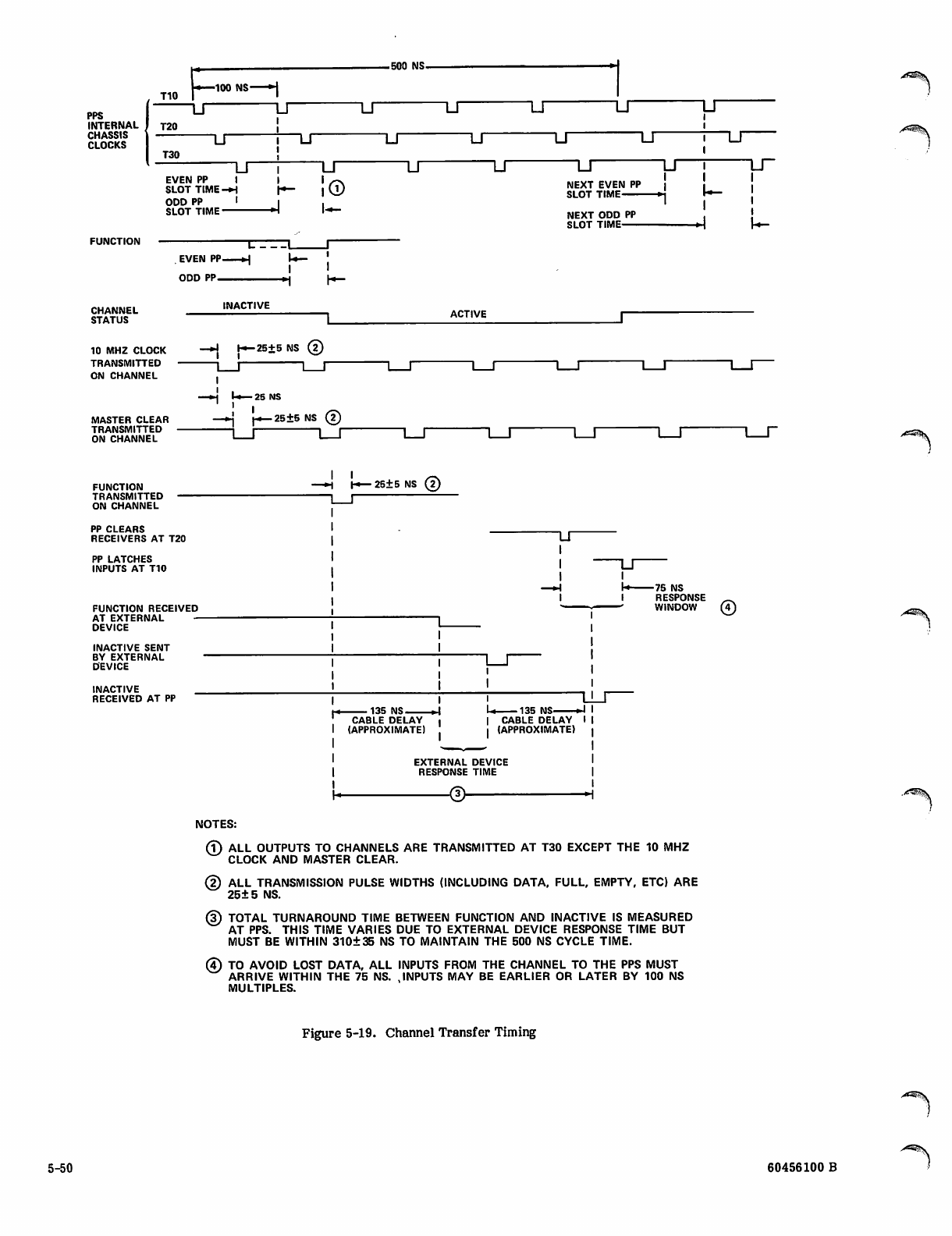
PPS
INTERNAL
CHASSIS
CLOCKS
FUNCTION
T10
r~—
t*—100 NS
u
T20
T30
EVEN PP
SLOT TIME-
ODD PP
SLOT TIME'
T_T
IS
IS
LT
■ ! ©
- 4 u -
I L
. EVEN PP-
ODD PP-
.500 NS.
11 "LI
"LT U"
"LT
"LT
TJ "LT
U
NEXT EVEN PP
SLOT TIME
NEXT ODD PP
SLOT TIME
TJ"
"I
"LT
I T -
CHANNEL
STATUS
10 MHZ CLOCK
TRANSMITTED
ON CHANNEL
MASTER CLEAR
TRANSMITTED
ON CHANNEL
INACTIVE
—*i H-25+5 NS @
-25 NS
j - . — 2 5 ± 5 N S @
ACTIVE
i r
i i
FUNCTION
TRANSMITTED
ON CHANNEL
PP CLEARS
RECEIVERS AT T20
PP LATCHES
INPUTS AT T10
FUNCTION RECEIVED
AT EXTERNAL —
DEVICE
INACTIVE SENT
BY EXTERNAL
DEVICE
25±5 NS @
INACTIVE
RECEIVED AT PP
135 NS.
CABLE DELAY
(APPROXIMATE)
1_T
-75 NS
RESPONSE
WINDOW
U 1 3 5 N S fi
| CA B L E D E L AY I
I (APPROXIMATE)
EXTERNAL DEVICE
RESPONSE TIME
■<!> -H
NOTES:
(?) ALL OUTPUTS TO CHANNELS ARE TRANSMITTED AT T30 EXCEPT THE 10 MHZ
CLOCK AND MASTER CLEAR.
(2) ALL TRANSMISSION PULSE WIDTHS (INCLUDING DATA, FULL, EMPTY, ETC) ARE
25±5 NS.
(3) TOTAL TURNAROUND TIME BETWEEN FUNCTION AND INACTIVE IS MEASURED
AT PPS. THIS TIME VARIES DUE TO EXTERNAL DEVICE RESPONSE TIME BUT
MUST BE WITHIN 310±35 NS TO MAINTAIN THE 500 NS CYCLE TIME.
(4) TO AVOID LOST DATA, ALL INPUTS FROM THE CHANNEL TO THE PPS MUST
ARRIVE WITHIN THE 75 NS. .INPUTS MAY BE EARLIER OR LATER BY 100 NS
MULTIPLES.
Figure 5-19. Channel Transfer Timing
5-50 60456100 B
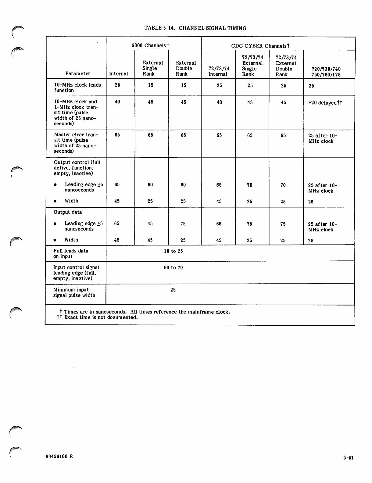
TABLE 5-14. CHANNEL SIGNAL TIMING
Parameter
6000 Channels t CDC CYBER Channels!
Internal
External
Single
Rank
External
Double
Rank
72/73/74
Internal
72/73/74
External
Single
Rank
72/73/74
External
Double
Rank 720/730/740
750/760/176
10-MHz clock leads
function
25 15 15 25 25 25 25
10-MHz clock and
1-MHz clock tran
sit time (pulse
width of 25 nano
seconds)
40 45 45 40 45 45 +20 delayed tt
Master clear tran
sit time (pulse
width of 25 nano
seconds)
65 65 65 65 65 65 25 after 10-
MHz clock
Output control (full
active, function,
empty, inactive)
• Leading edge +5
nanoseconds
• Width
65
45
60
25
60
25
65
45
70
25
70
25
25 after 10-
MHz clock
25
Output data
• Leading edge +5
nanoseconds
• Width
65
45
45
45
75
25
65
45
75
25
75
25
25 after 10-
MHz clock
25
Full leads data
on input 10 to 25
Input control signal
leading edge (full,
empty, inactive)
60 to 70
Minimum input
signal pulse width
25
t Times are in nanoseconds. All times reference the mainframe clock,
tt Exact time is not documented.
/ffcWV
60456100 E 5-51
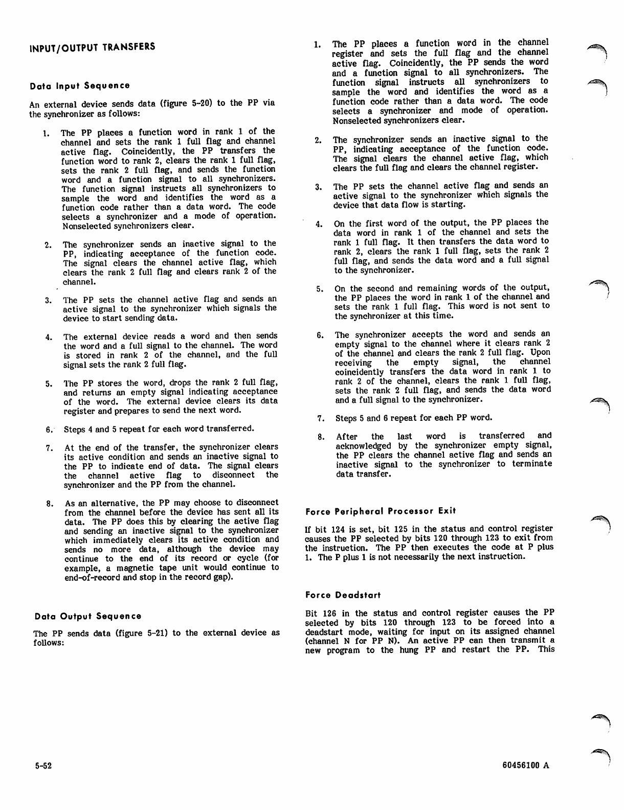
INPUT/OUTPUT TRANSFERS
Data Input Sequence
An external device sends data (figure 5-20) to the PP via
the synchronizer as follows:
1. The PP places a function word in rank 1 of the
channel and sets the rank 1 full flag and channel
active flag. Coincidently, the PP transfers the
function word to rank 2, clears the rank 1 full flag,
sets the rank 2 full flag, and sends the function
word and a function signal to all synchronizers.
The function signal instructs all synchronizers to
sample the word and identifies the word as a
function code rather than a data word. The code
selects a synchronizer and a mode of operation.
Nonselected synchronizers clear.
2. The synchronizer sends an inactive signal to the
PP, indicating acceptance of the function code.
The signal clears the channel active flag, which
clears the rank 2 full flag and clears rank 2 of the
channel.
3. The PP sets the channel active flag and sends an
active signal to the synchronizer which signals the
device to start sending data.
4. The external device reads a word and then sends
the word and a full signal to the channel. The word
is stored in rank 2 of the channel, and the full
signal sets the rank 2 full flag.
5. The PP stores the word, drops the rank 2 full flag,
and returns an empty signal indicating acceptance
of the word. The external device clears its data
register and prepares to send the next word.
6. Steps 4 and 5 repeat for each word transferred.
7. At the end of the transfer, the synchronizer clears
its active condition and sends an inactive signal to
the PP to indicate end of data. The signal clears
the channel active flag to disconnect the
synchronizer and the PP from the channel.
8. As an alternative, the PP may choose to disconnect
from the channel before the device has sent all its
data. The PP does this by clearing the active flag
and sending an inactive signal to the synchronizer
which immediately clears its active condition and
sends no more data, although the device may
continue to the end of its record or cycle (for
example, a magnetic tape unit would continue to
end-of-record and stop in the record gap).
Data Output Sequence
The PP sends data (figure 5-21) to the external device as
follows:
1. The PP places a function word in the channel
register and sets the full flag and the channel
active flag. Coincidently, the PP sends the word
and a function signal to all synchronizers. The
function signal instructs all synchronizers to
sample the word and identifies the word as a
function code rather than a data word. The code
selects a synchronizer and mode of operation.
Nonselected synchronizers clear.
2. The synchronizer sends an inactive signal to the
PP, indicating acceptance of the function code.
The signal clears the channel active flag, which
clears the full flag and clears the channel register.
3. The PP sets the channel active flag and sends an
active signal to the synchronizer which signals the
device that data flow is starting.
4. On the first word of the output, the PP places the
data word in rank 1 of the channel and sets the
rank 1 full flag. It then transfers the data word to
rank 2, clears the rank 1 full flag, sets the rank 2
full flag, and sends the data word and a full signal
to the synchronizer.
5. On the second and remaining words of the output,
the PP places the word in rank 1 of the channel and
sets the rank 1 full flag. This word is not sent to
the synchronizer at this time.
6. The synchronizer accepts the word and sends an
empty signal to the channel where it clears rank 2
of the channel and clears the rank 2 full flag. Upon
receiving the empty signal, the channel
coincidently transfers the data word in rank 1 to
rank 2 of the channel, clears the rank 1 full flag,
sets the rank 2 full flag, and sends the data word
and a full signal to the synchronizer.
7. Steps 5 and 6 repeat for each PP word.
8. After the last word is transferred and
acknowledged by the synchronizer empty signal,
the PP clears the channel active flag and sends an
inactive signal to the synchronizer to terminate
data transfer.
Force Peripheral Processor Exit
If bit 124 is set, bit 125 in the status and control register
causes the PP selected by bits 120 through 123 to exit from
the instruction. The PP then executes the code at P plus
1. The P plus 1 is not necessarily the next instruction.
Force Deadstart
Bit 126 in the status and control register causes the PP
selected by bits 120 through 123 to be forced into a
deadstart mode, waiting for input on its assigned channel
(channel N for PP N). An active PP can then transmit a
new program to the hung PP and restart the PP. This
/^ S^S.
5-52 60456100 A
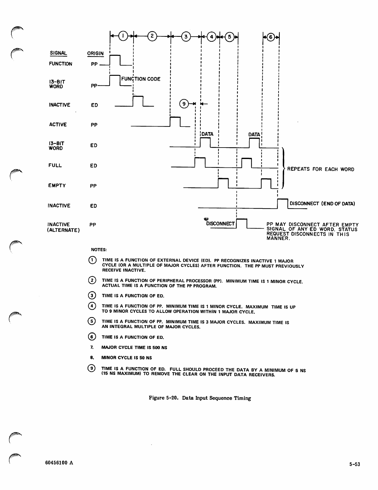
/^P*N
SIGNAL
FUNCTION
13-BIT
WORD
INACTIVE
ACTIVE
13-BIT
WORD
FULL
EMPTY
INACTIVE
INACTIVE
(ALTERNATE)
ORIGIN
PP
i i
LTLi
[•©•I
pp- r~tei
FUNCTION CODE
ED
PP
ED
ED
PP
ED
PP
NOTES:
n_ 0-!
J"L_
DATA
9St
DISCONNECT
DATA
n
ni
' REPEATS FOR EACH WORD
DISCONNECT (END OF DATA)
PP MAY DISCONNECT AFTER EMPTY
SIGNAL OF ANY ED WORD. STATUS
REQUEST DISCONNECTS IN THIS
MANNER.
(?) TIME IS A FUNCTION OF EXTERNAL DEVICE (ED). PP RECOGNIZES INACTIVE 1 MAJOR
CYCLE (OR A MULTIPLE OF MAJOR CYCLES) AFTER FUNCTION. THE PP MUST PREVIOUSLY
RECEIVE INACTIVE.
(7) TIME IS A FUNCTION OF PERIPHERAL PROCESSOR (PP). MINIMUM TIME IS 1 MINOR CYCLE
ACTUAL TIME IS A FUNCTION OF THE PP PROGRAM.
(3) TIME IS A FUNCTION OF ED.
(4) TIME IS A FUNCTION OF PP. MINIMUM TIME IS 1 MINOR CYCLE. MAXIMUM TIME IS UP
TO 9 MINOR CYCLES TO ALLOW OPERATION WITHIN 1 MAJOR CYCLE.
(5) TIME IS A FUNCTION OF PP. MINIMUM TIME IS 3 MAJOR CYCLES. MAXIMUM TIME IS
AN INTEGRAL MULTIPLE OF MAJOR CYCLES.
(£) TIME IS A FUNCTION OF ED.
7. MAJOR CYCLE TIME IS 500 NS
8. MINOR CYCLE IS 50 NS
© TIME IS A FUNCTION OF ED. FULL SHOULD PROCEED THE DATA BY A MINIMUM OF 5 NS
(15 NS MAXIMUM) TO REMOVE THE CLEAR ON THE INPUT DATA RECEIVERS.
r
Figure 5-20. Data Input Sequence Timing
60456100 A 5-53
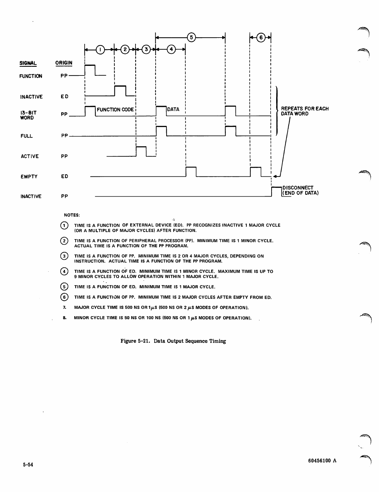
SIGNAL
FUNCTION
INACTIVE
13-BIT
WORD
FULL
ACTIVE
EMPTY
INACTIVE
pp.
ED
PP
PP-
PP
ED
PP
ORIGIN
l^r>-*|KiHKi>HiH
i
h_
<s> HiH
nJ
FUNCTION CODE DATA
JTJ
^^SSSv
REPEATS FOR EACH
DATA WORD
I (DISCONNECT
J [(END OF DATA)
NOTES:
(7) TIME IS A FUNCTION OF EXTERNAL DEVICE (ED). PP RECOGNIZES INACTIVE 1 MAJOR CYCLE
(OR A MULTIPLE OF MAJOR CYCLES) AFTER FUNCTION.
(2) TIME IS A FUNCTION OF PERIPHERAL PROCESSOR (PP). MINIMUM TIME IS 1 MINOR CYCLE.
^^ ACTUAL TIME IS A FUNCTION OF THE PP PROGRAM.
(3) TIME IS A FUNCTION OF PP. MINIMUM TIME IS 2 OR 4 MAJOR CYCLES, DEPENDING ON
INSTRUCTION. ACTUAL TIME IS A FUNCTION OF THE PP PROGRAM.
(4) TIME IS A FUNCTION OF ED. MINIMUM TIME IS 1 MINOR CYCLE. MAXIMUM TIME IS UP TO
9 MINOR CYCLES TO ALLOW OPERATION WITHIN 1 MAJOR CYCLE.
(¥) TIME IS A FUNCTION OF ED. MINIMUM TIME IS 1 MAJOR CYCLE.
(£) TIME IS A FUNCTION OF PP. MINIMUM TIME IS 2 MAJOR CYCLES AFTER EMPTY FROM ED.
7. MAJOR CYCLE TIME IS 500 NS OR 1^iS (500 NS OR 2/i.S MODES OF OPERATION).
8. MINOR CYCLE TIME IS 50 NS OR 100 NS (500 NS OR 1 ftS MODES OF OPERATION). ^*4»lv
Figure 5-21. Data Output Sequence Timing
5-54 60456100 A
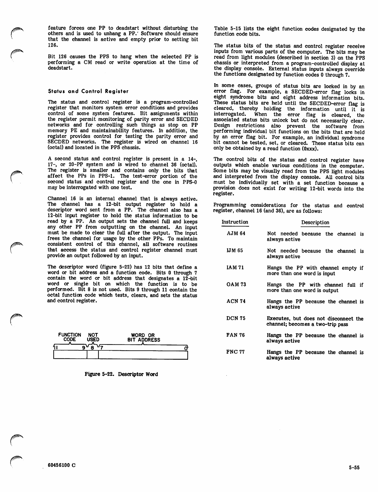
J0^t.
feature forces one PP to deadstart without disturbing the
others and is used to unhang a PP.' Software should ensure
that the channel is active and empty prior to setting bit
126.
Bit 126 causes the PPS to hang when the selected PP is
performing a CM read or write operation at the time of
deadstart.
Status and Control Register
The status and control register is a program-controlled
register that monitors system error conditions and provides
control of some system features. Bit assignments within
the register permit monitoring of parity error and SECDED
networks and for controlling such things as stop on PP
memory PE and maintainability features. In addition, the
register provides control for testing the parity error and
SECDED networks. The register is wired on channel 16
(octal) and located in the PPS chassis.
A second status and control register is present in a 14-,
17-, or 20-PP system and is wired to channel 36 (octal).
The register is smaller and contains only the bits that
affect the PPs in PPS-1. The test-error portion of the
second status and control register and the one in PPS-0
may be interrogated with one test.
Channel 16 is an internal channel that is always active.
The channel has a 12-bit output register to hold a
descriptor word sent from a PP. The channel also has a
12-bit input register to hold the status information to be
read by a PP. An output sets the channel full and keeps
any other PP from outputting on the channel. An input
must be made to clear the full after the output. The input
frees the channel for usage by the other PPs. To maintain
consistent control of this channel, all software routines
that access the status and control register channel must
provide an output followed by an input.
The descriptor word (figure 5-22) has 12 bits that define a
word or bit address and a function code. Bits 0 through 7
contain the word or bit address that designates a 12-bit
word or single bit on which the function is to be
performed. Bit 8 is not used. Bits 9 through 11 contain the
octal function code which tests, clears, and sets the status
and control register.
FUNCTION
CODE
A
NOT
USED
9V8^'7~
WORD OR
BIT ADDRESS
A
Table 5-15 lists the eight function codes designated by the
function code bits.
The status bits of the status and control register receive
inputs from various parts of the computer. The bits may be
read from light modules (described in section 3) on the PPS
chassis or interpreted from a program-controlled display at
the display console. External status inputs always override
the functions designated by function codes 0 through 7.
In some cases, groups of status bits are locked in by an
error flag. For example, a SECDED-error flag locks in
eight syndrome bits and eight address information bits.
These status bits are held until the SECDED-error flag is
cleared, thereby holding the information until it is
interrogated. When the error flag is cleared, the
associated status bits unlock but do not necessarily clear.
Design restrictions also prevent the software from
performing individual bit functions on the bits that are held
by an error flag bit. For example, an individual syndrome
bit cannot be tested, set, or cleared. These status bits can
only be obtained by a read function (Oxxx).
The control bits of the status and control register have
outputs which enable various conditions in the computer.
Some bits may be visually read from the PPS light modules
and interpreted from the display console. All control bits
must be individually set with a set function because a
provision does not exist for writing 12-bit words into the
register.
Programming considerations for the status and control
register, channel 16 (and 36), are as follows:
Instruction Description
AJM64 Not needed because the channel is
always active
IJM65 Not needed because the channel is
always active
IAM71 Hangs the PP with channel empty if
more than one word is input
OAM 73 Hangs the PP with channel full if
more than one word is output
ACN 74 Hangs the PP because the channel is
always active
DCN 75 Executes, but does not disconnect the
channel; becomes a two-trip pass
FAN 76 Hangs the PP because the channel is
always active
FNC 77 Hangs the PP because the channel is
always active
Figure 5-22. Descriptor Word
60456100 C 5-55
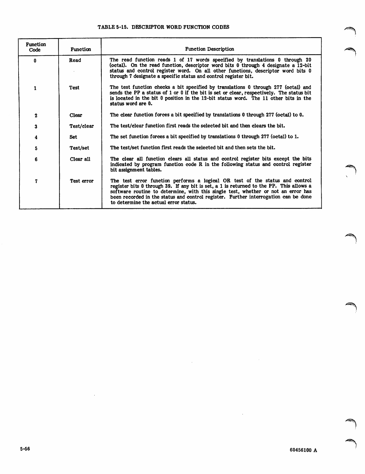
TABLE 5-15. DESCRIPTOR WORD FUNCTION CODES
Function
Code Function Function Description
0
1
2
3
4
5
6
7
Read
Test
Clear
Test/clear
Set
Test/set
Clear all
Test error
The read function reads 1 of 17 words specified by translations 0 through 20
(octal). On the read function, descriptor word bits 0 through 4 designate a 12-bit
status and control register word. On all other functions, descriptor word bits 0
through 7 designate a specific status and control register bit.
The test function checks a bit specified by translations 0 through 277 (octal) and
sends the PP a status of 1 or 0 if the bit is set or clear, respectively. The status bit
is located in the bit 0 position in the 12-bit status word. The 11 other bits in the
status word are 0.
The clear function forces a bit specified by translations 0 through 277 (octal) to 0.
The test/clear function first reads the selected bit and then clears the bit.
The set function forces a bit specified by translations 0 through 277 (octal) to 1.
The test/set function first reads the selected bit and then sets the bit.
The clear all function clears all status and control register bits except the bits
indicated by program function code R in the following status and control register
bit assignment tables.
The test error function performs a logical OR test of the status and control
register bits 0 through 39. If any bit is set, a 1 is returned to the PP. This allows a
software routine to determine, with this single test, whether or not an error has
been recorded in the status and control register. Further interrogation can be done
to determine the actual error status.
jdS^K
5-56 60456100 A
■-**i\
■0Z>-
0^°s*-
ST#FUf MM* f 0Wl*Dfc REGISTER BIT DESCRIPTIONS
MODELS 720 THROUGH 760
#^K

' V.
,>!S5%
V
D
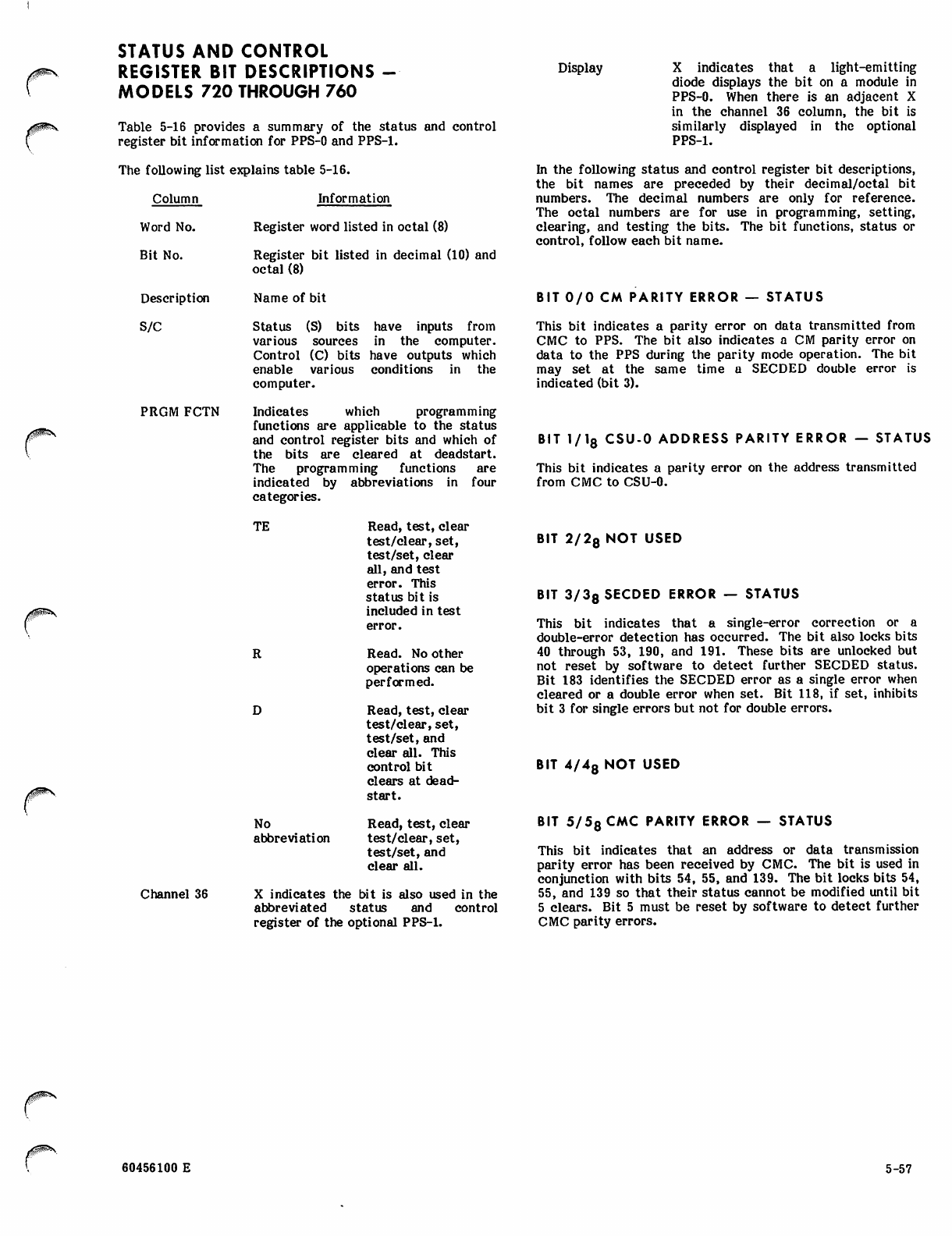
STATUS AND CONTROL
REGISTER BIT DESCRIPTIONS -
MODELS 720 THROUGH 760
Table 5-16 provides a summary of the status and control
register bit information for PPS-0 and PPS-1.
The following list explains table 5-16.
Column Information
Word No.
Bit No.
Description
S/C
PRGM FCTN
Register word listed in octal (8)
Register bit listed in decimal (10) and
octal (8)
Name of bit
Status (S) bits have inputs from
various sources in the computer.
Control (C) bits have outputs which
enable various conditions in the
computer.
Indicates which programming
functions are applicable to the status
and control register bits and which of
the bits are cleared at deadstart.
The programming functions are
indicated by abbreviations in four
categories.
Display X indicates that a light-emitting
diode displays the bit on a module in
PPS-0. When there is an adjacent X
in the channel 36 column, the bit is
similarly displayed in the optional
PPS-1.
In the following status and control register bit descriptions,
the bit names are preceded by their decimal/octal bit
numbers. The decimal numbers are only for reference.
The octal numbers are for use in programming, setting,
clearing, and testing the bits. The bit functions, status or
control, follow each bit name.
BIT 0/0 CM PARITY ERROR — STATUS
This bit indicates a parity error on data transmitted from
CMC to PPS. The bit also indicates a CM parity error on
data to the PPS during the parity mode operation. The bit
may set at the same time a SECDED double error is
indicated (bit 3).
BIT 1/18 CSU-0 ADDRESS PARITY ERROR — STATUS
This bit indicates a parity error on the address transmitted
from CMC to CSU-0.
TE
No
abbreviation
Read, test, clear
test/clear, set,
test/set, clear
all, and test
error. This
status bit is
included in test
error.
Read. No other
operations can be
performed.
Read, test, clear
test/clear, set,
test/set, and
clear all. This
control bit
clears at dead-
start.
Read, test, clear
test/clear, set,
test/set, and
clear all.
Channel 36 X indicates the bit is also used in the
abbreviated s tatus and control
register of the optional PPS-1.
BIT 2/28 NOT USED
BIT 3/38 SECDED ERROR — STATUS
This bit indicates that a single-error correction or a
double-error detection has occurred. The bit also locks bits
40 through 53, 190, and 191. These bits are unlocked but
not reset by software to detect further SECDED status.
Bit 183 identifies the SECDED error as a single error when
cleared or a double error when set. Bit 118, if set, inhibits
bit 3 for single errors but not for double errors.
BIT 4/48 NOT USED
BIT 5/58CMC PARITY ERROR — STATUS
This bit indicates that an address or data transmission
parity error has been received by CMC. The bit is used in
conjunction with bits 54, 55, and 139. The bit locks bits 54,
55, and 139 so that their status cannot be modified until bit
5 clears. Bit 5 must be reset by software to detect further
CMC parity errors.
60456100 E 5-57
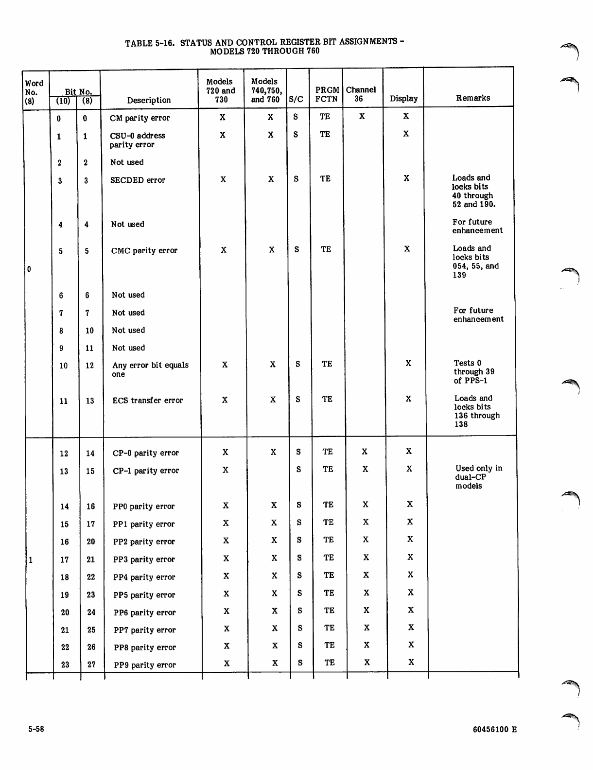
TABLE 5-16. STATUS AND CONTROL REGISTER BIT ASSIGNMENTS -
MODELS 720 THROUGH 760
Word
No.
(8)
Bit No.
(10) I (8) Description
0 0 CM parity error
1 1 CSU-0 address
parity error
2 2 N o t u s e d
3 3 SECDED error
Not used
CMC parity error
6 6 N o t u s e d
7 7 N o t u s e d
8 1 0 N o t u s e d
9 1 1 N o t u s e d
10 12 Any error bit equals
one
11 13 ECS transfer error
12 14 CP-0 parity error
13 15 CP-1 parity error
14 16 PPO parity error
15 17 PP1 parity error
16 20 PP2 parity error
17 21 PP3 parity error
18 22 PP4 parity error
19 23 PP5 parity error
20 24 PP6 parity error
21 25 PP7 parity error
22 26 PP8 parity error
23 27 PP9 parity error
Models
720 and
730
Models
740,750,
and 760
X
X
X
X
X
X
X
X
X
X
X
X
s/c
X
X
X
X
X
X
X
X
X
X
PRGM
FCTN
TE
TE
TE
TE
Channel
36
TE
TE
TE
TE
TE
TE
TE
TE
TE
TE
TE
TE
TE
TE
Display
X
X
X
X
X
X
X
X
X
X
X
X
X
X
X
X
X
X
X
X
X
X
X
X
Remarks
Loads and
locks bits
40 through
52 and 190.
For future
enhancement
Loads and
locks bits
054, 55, and
139
For future
enhancement
Tests 0
through 39
of PPS-1
Loads and
locks bits
136 through
138
Used only in
dual-CP
models
5-58 60456100 E
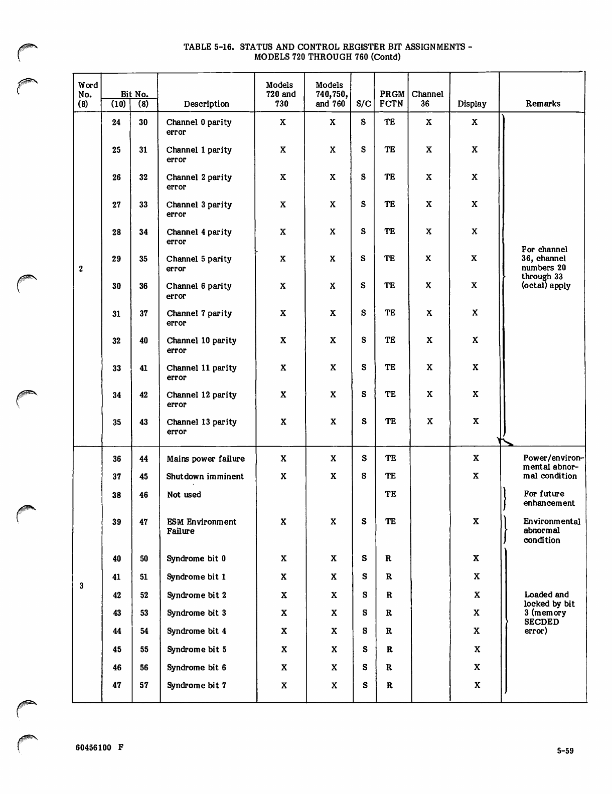
TABLE 5-16. STATUS AND CONTROL REGISTER BIT ASSIGNMENTS -
MODELS 720 THROUGH 760 (Contd)
Word
No.
(8)
Bit No.
Description
Models
720 and
730
Models
740,750,
and 760 s/c PRGM
FCTN
Channel
36 Display Remarks
(10) (8)
24 30 Channel 0 parity
error
TE
25 31 Channel 1 parity
error
TE
26 32 Channel 2 parity
error
TE
27 33 Channel 3 parity
error
TE
2
28
29
30
34
35
36
Channel 4 parity
error
Channel 5 parity
error
Channel 6 parity
error
TE
TE
TE
For channel
36, channel
numbers 20
through 33
(octal) apply
31 37 Channel 7 parity
error
TE
32 40 Channel 10 parity
error
TE
33 41 Channel 11 parity
error
TE
34 42 Channel 12 parity
error
TE
35 43 Channel 13 parity
error
TE
36
37
44
45
Mains power failure
Shutdown imminent
TE
TE
Power/environ
mental abnor
mal condition
38 46 Not used TE 1 For future
j enhancement
39 47 ESM Environment
Failure
TE | Environmental
| a b n o r m a l
J condition
40 50 Syndrome bit 0
341 51 Syndrome bit 1
42
43
44
52
53
54
Syndrome bit 2
Syndrome bit 3
Syndrome bit 4
Loaded and
locked by bit
3 (memory
SECDED
error)
45 55 Syndrome bit 5
46 56 Syndrome bit 6
47 57 Syndrome bit 7
60456100 F 5-59
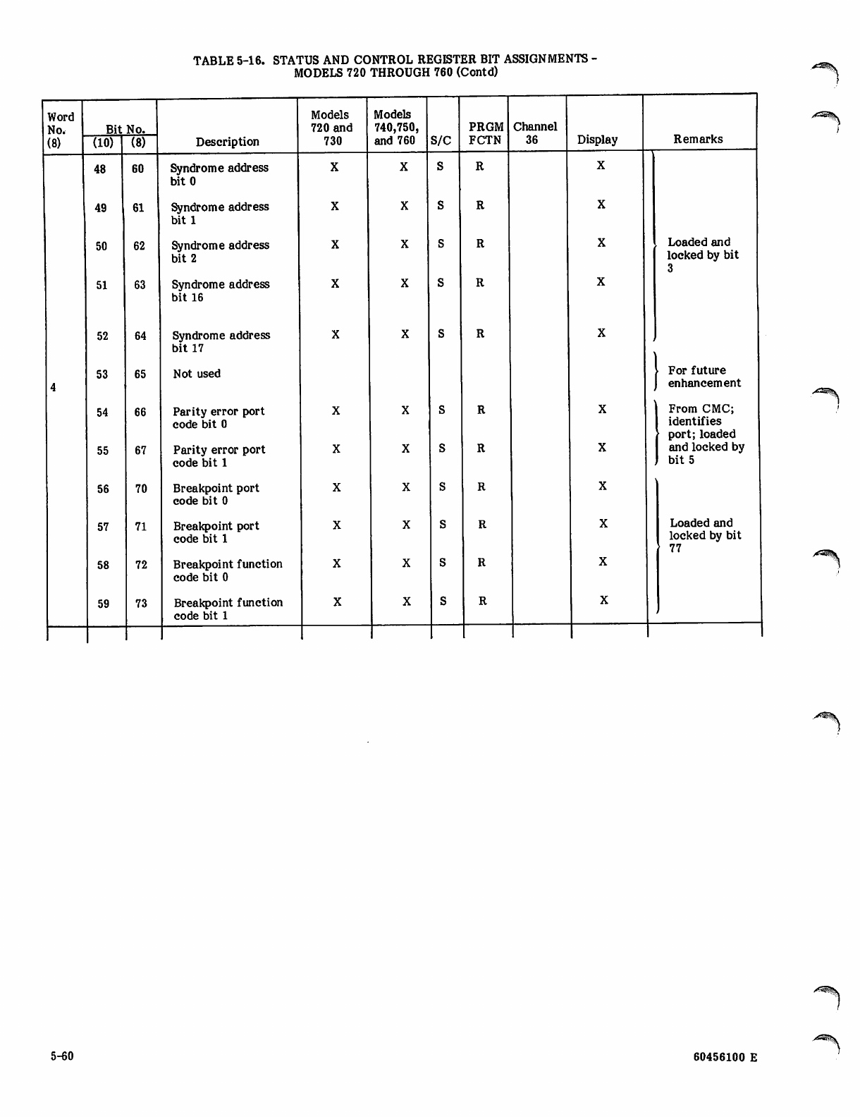
TABLE 5-16. STATUS AND CONTROL REGISTER BIT ASSIGNMENTS -
MODELS 720 THROUGH 760 (Contd)
Word
No,
(8)
Bit No.
Description
Models
720 and
730
Models
740,750,
and 760 S/C
PRGM
FCTN
Channel
36 Display Remarks
(10) (8)
48 60 Syndrome address
bitO
49 61 Syndrome address
bit 1
50 62 Syndrome address
bit 2
. Loaded and
locked by bit
3
51 63 Syndrome address
bit 16
52 64 Syndrome address
bit 17
4
53 65 Not used \ For future
j enhancement
54
55
66
67
Parity error port
code bit 0
Parity error port
code bit 1
From CMC;
identifies
port; loaded
and locked by
bit 5
56 70 Breakpoint port
code bit 0
57 71 Breakpoint port
code bit 1
Loaded and
locked by bit
77
58 72 Breakpoint function
code bit 0
59 73 Breakpoint function
code bit 1
5-60 60456100 E
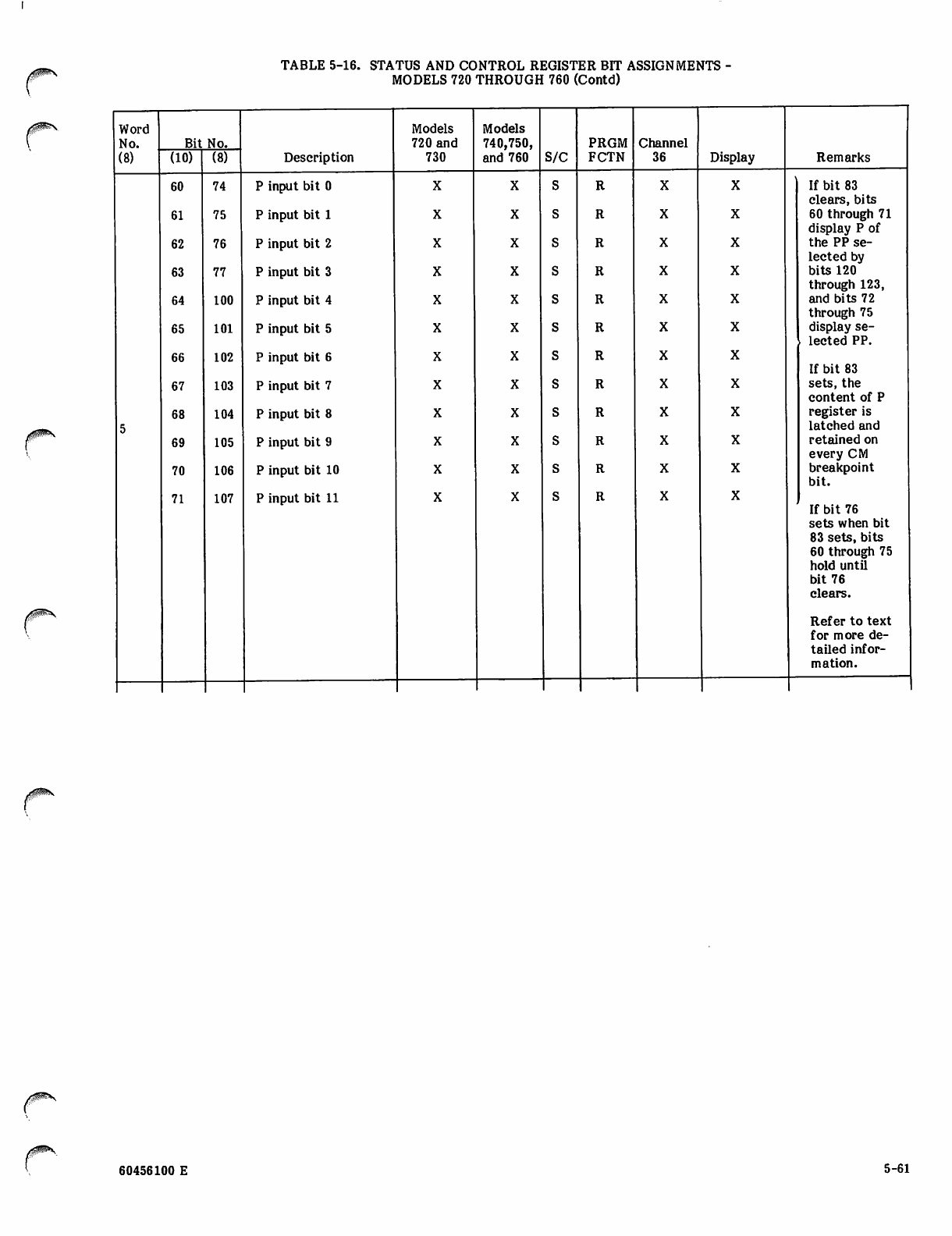
TABLE 5-16. STATUS AND CONTROL REGISTER BIT ASSIGNMENTS
MODELS 720 THROUGH 760 (Contd)
Word Models Models
No.
(8)
Bit No.
Description
720 and
730 740,750,
and 760 s/c PRGM
FCTN
Channel
36 Display Remarks
(10) (8)
60 74 P input bit 0 If bit 83
clears, bits
61 75 P input bit 1 60 through 71
display P of
62 76 P input bit 2 the PP se
lected by
63 77 P input bit 3 bits 120
through 123,
64 100 P input bit 4 and bits 72
through 75
65 101 P input bit 5 display se-
. lected PP.
66 102 P input bit 6 If bit 83
67 103 P input bit 7 sets, the
content of P
68 104 P input bit 8 register is
5latched and
69 105 P input bit 9 retained on
every CM
70 106 P input bit 10 breakpoint
bit.
71 107 P input bit 11 If bit 76
sets when bit
83 sets, bits
60 through 75
hold until
bit 76
clears.
Refer to text
for more de
tailed infor
mation.
60456100 E 5-61
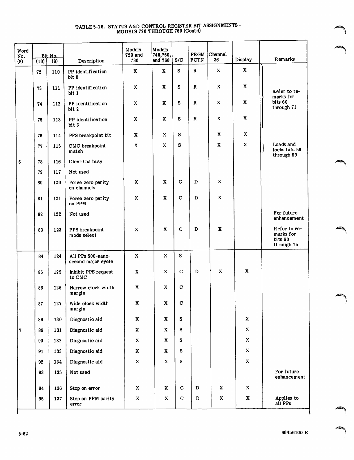
TABLE 5-16. STATUS AND CONTROL REGISTER BIT ASSIGNMENTS -
MODELS 720 THROUGH 760 (Contd)
Word
No. Bit No.
Description
Models Models
720 and 740,750,
730 and 760 s/c PRGM <
FCTN
Channel
36 Display Remarks
(8) (10) (8)
72 110 PP identification
bitO
73
74
111
112
PP identification
bit 1
PP identification
bit 2
Refer to re
marks for
bits 60
through 71
75 113 PP identification
bit 3
76 114 PPS breakpoint bit
6
77
78
79
115
116
117
CMC breakpoint
match
Clear CM busy
Not used
> Loads and
) locks bits 56
through 59
80 120 Force zero parity
on channels
81 121 Force zero parity
on PPM
82 122 Not used For future
enhancement
83 123 PPS breakpoint
mode select
Refer to re
marks for
bits 60
through 75
84 124 All PPs 500-nano
second major cycle
85 125 Inhibit PPS request
to CMC
86 126 Narrow clock width
margin
87 127 Wide clock width
margin
88 130 Diagnostic aid
789 131 Diagnostic aid
90 132 Diagnostic aid
91 133 Diagnostic aid
92 134 Diagnostic aid
93 135 Not used For future
enhancement
94 136 Stop on error
95 137 Stop on PPM parity
error
Applies to
all PPs
5-62 60456100 E
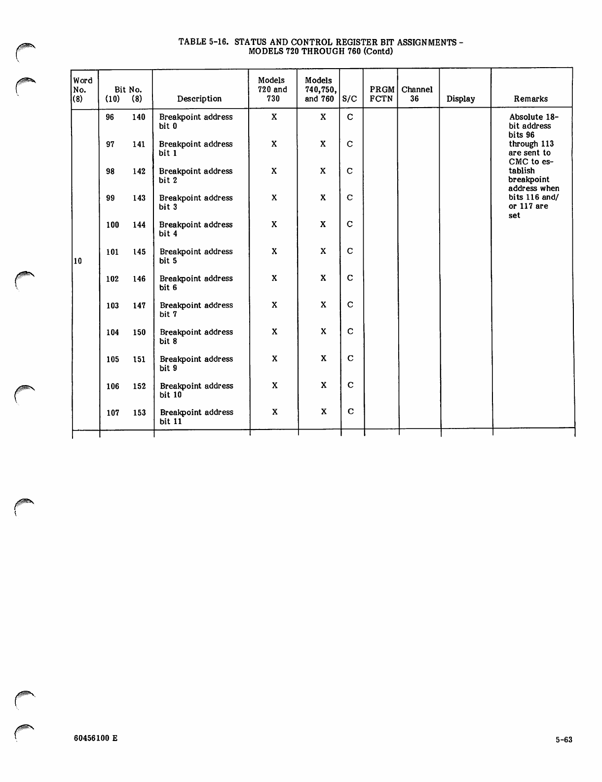
TABLE 5-16. STATUS AND CONTROL REGISTER BIT ASSIGNMENTS -
MODELS 720 THROUGH 760 (Contd)
/jSSPBs
Word Models Models
No. Bit No. 720 and 740,750, PRGM Channel
(8) (10) (8) Description 730 and 760 S/C FCTN 36 Display Remarks
9 6 1 4 0 Breakpoint address
bit 0
Absolute 18-
bit address
bits 96
9 7 1 4 1 Breakpoint address
bit 1 through 113
are sent to
CMC to es
9 8 1 4 2 Breakpoint address
bit 2
tablish
breakpoint
address when
9 9 1 4 3 Breakpoint address
bit 3
bits 116 and/
or 117 are
set
100 144 Breakpoint address
bit 4
101 145 Breakpoint address
10 bit 5
102 146 Breakpoint address
bit 6
103 147 Breakpoint address
bit 7
104 150 Breakpoint address
bit 8
105 151 Breakpoint address
bit 9
106 152 Breakpoint address
bit 10
107 153 Breakpoint address
bit 11
60456100 E 5-63
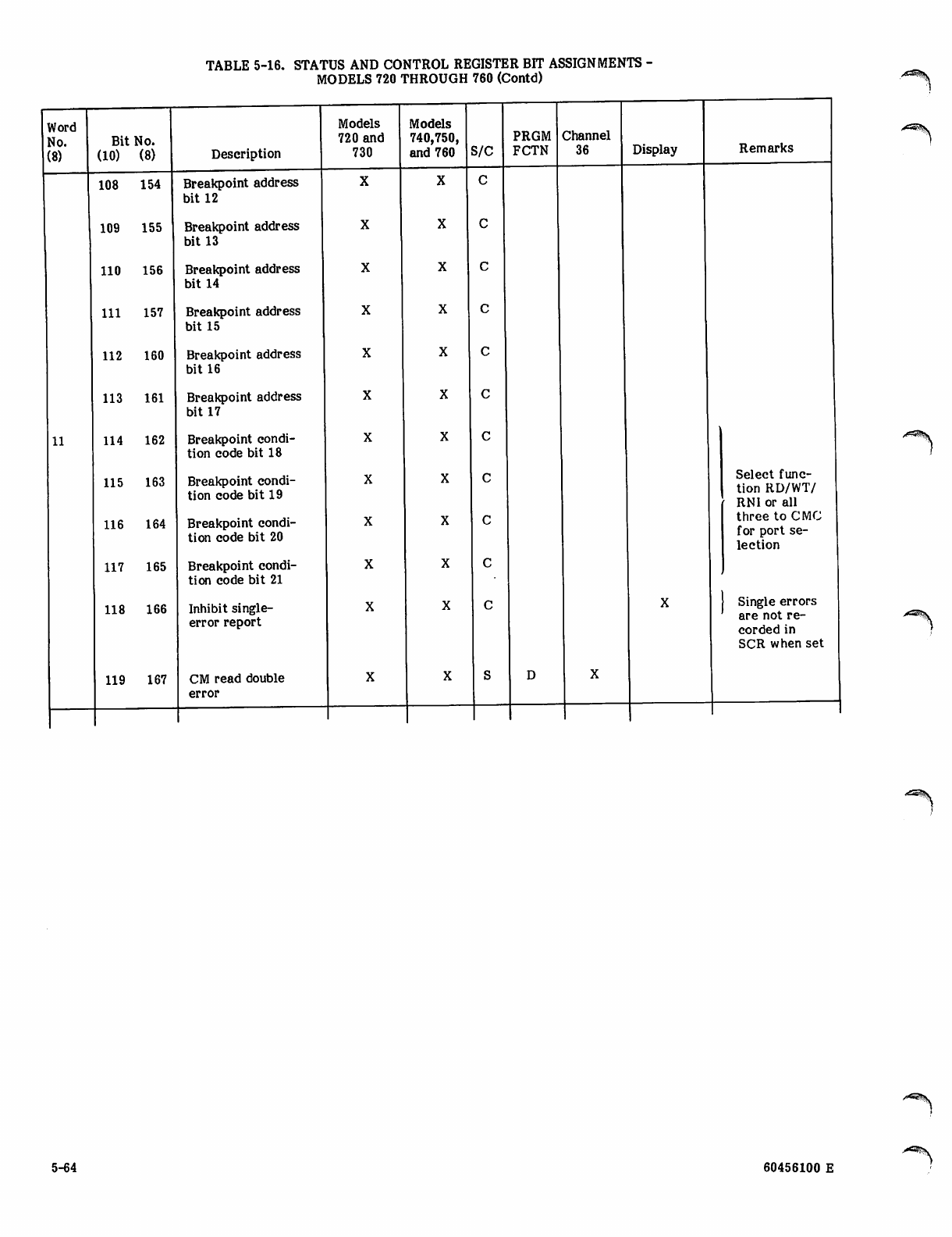
TABLE 5-16. STATUS AND CONTROL REGISTER BIT ASSIGNMENTS -
MODELS 720 THROUGH 760 (Contd) j^tsfiSSfti
Word
No.
(8)
Bit No.
(10) (8) Description
Models
720 and
730
Models
740,750,
and 760 s/c PRGM
FCTN
Channel
36 Display Remarks
,*3ftV
108 154 Breakpoint address
bit 12
109 155 Breakpoint address
bit 13
110 156 Breakpoint address
bit 14
111 157 Breakpoint address
bit 15
112 160 Breakpoint address
bit 16
113 161 Breakpoint address
bit 17
11 114 162 Breakpoint condi
tion code bit 18
^=S^v
115
116
163
164
Breakpoint condi
tion code bit 19
Breakpoint condi
tion code bit 20
Select func
tion RD/WT/
RNI or all
three to CMC
for port se
lection
117 165 Breakpoint condi
tion code bit 21
118 166 Inhibit single-
error report
Single errors
are not re
corded in
SCR when set
^*^%t.
119 167 CM read double
error
5-64 60456100 E
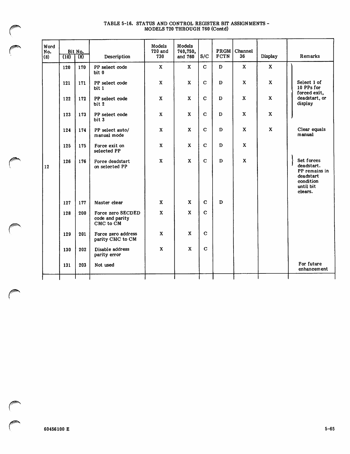
TABLE 5-16. STATUS AND CONTROL REGISTER BIT ASSIGNMENTS -
MODELS 720 THROUGH 760 (Contd)
/sjp&v Word
No.
(8)
Bit No.
Description
Models
720 and
730
Models
740,750,
and 760 s/c PRGM
FCTN
Channel
36 Display(10) (8) Remarks
120 170 PP select code
bit 0
121
122
171
172
PP select code
bit 1
PP select code
bit 2
Select 1 of
10 PPs for
forced exit,
deadstart, or
display
123 173 PP select code
bit 3
124 174 PP select auto/
manual mode
Clear equals
manual
125 175 Force exit on
selected PP
12
126 176 Force deadstart
on selected PP j Set forces
' deadstart.
PP remains in
deadstart
condition
until bit
clears.
127 177 Master clear
128 200 Force zero SECDED
code and parity
CMC to CM
129 201 Force zero address
parity CMC to CM
130 202 Disable address
parity error
131 203 Not used For future
enhancement
0^\. 60456100 E 5-65
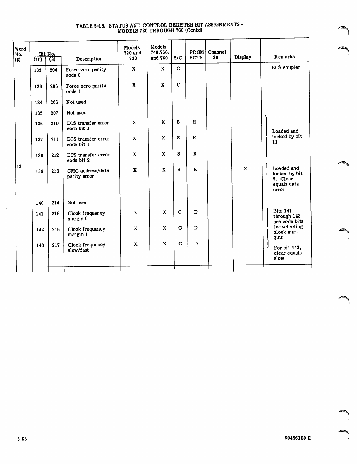
TABLE 5-16. STATUS AND CONTROL REGISTER BIT ASSIGNMENTS -
MODELS 720 THROUGH 760 (Contd)
Word Models Models
No. Bit No. 720 and 740,750, PRGM Channel Remarks
(8) (10) (8) Description 730 and 760 S/C FCTN 36 Display
132 204 Force zero parity
code 0
ECS coupler
133 205 Force zero parity
code 1
134 206 Not used
135 207 Not used
136 210 ECS transfer error
code bit 0 Loaded and
137 211 ECS transfer error locked by bit
11
code bit 1
138 212 ECS transfer error
code bit 2
13
139
140
213
214
CMC address/data
parity error
Not used
1 Loaded and
> locked by bit
5. Clear
equals data
error
141 215 Clock frequency
margin 0
Bits 141
through 143
are code bits
142 216 Clock frequency
margin 1
I for selecting
clock mar
gins
143 217 Clock frequency
slow/fast > For bit 143,
clear equals
slow
/°^^v
5-66 60456100 E
«****! i^w
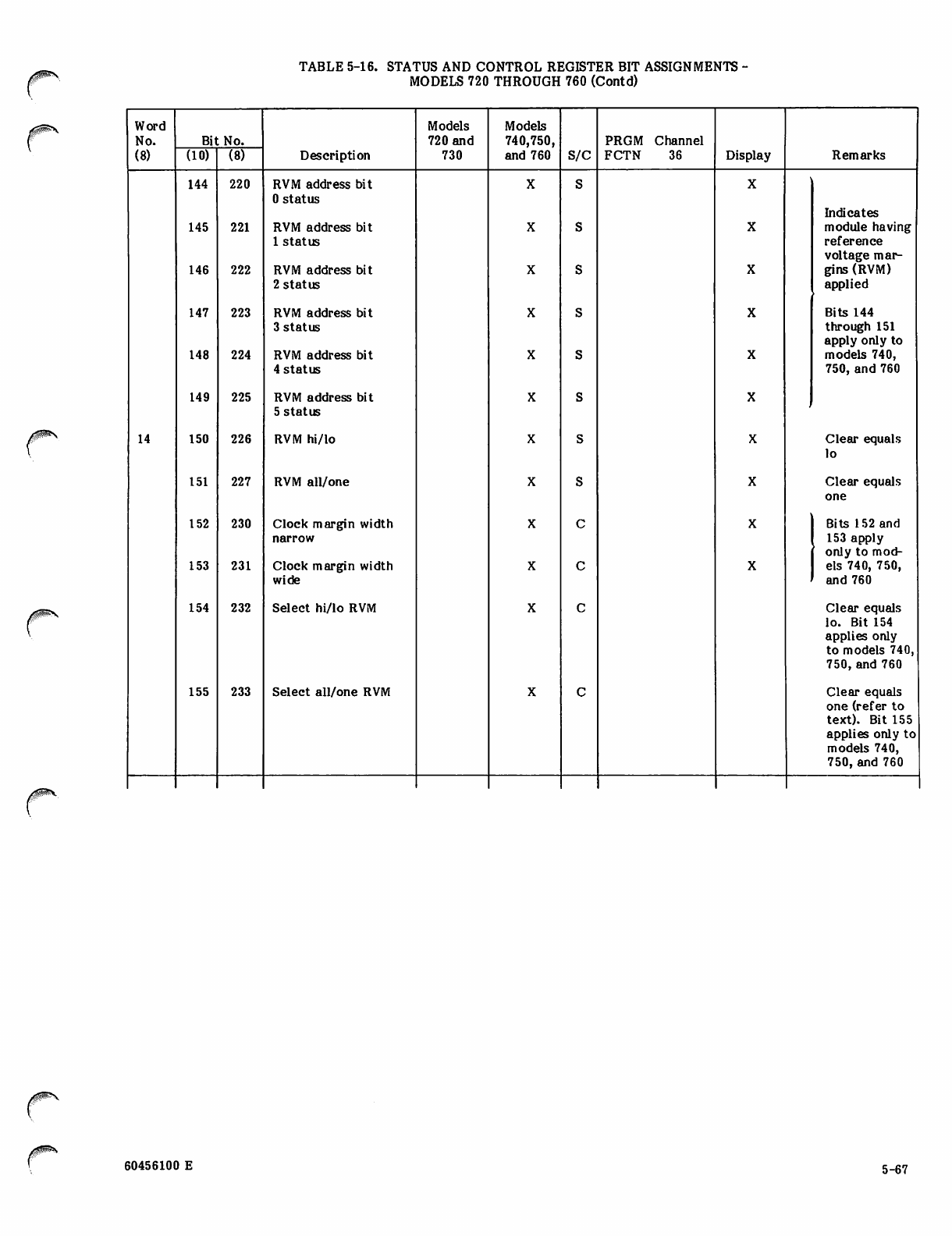
TABLE 5-16. STATUS AND CONTROL REGISTER BIT ASSIGNMENTS
MODELS 720 THROUGH 760 (Contd)
Word Models Models
No.
(8)
Bit No.
Description
720 and
730 740,750,
and 760 S/C
PRGM Channel
F C T N 3 6 Display Remarks
(10) (8)
144 220 RVM address bit
0 status
Indicates
145 221 RVM address bit
1 status
module having
reference
voltage mar
146 222 RVM address bit
2 status gins (RVM)
applied
147 223 RVM address bit
3 status
Bits 144
through 151
apply only to
148 224 RVM address bit
4 status
models 740,
750, and 760
149 225 RVM address bit
5 status
14 150 226 RVM hi/lo Clear equals
lo
151 227 RVM all/one Clear equals
one
152 230 Clock margin width
narrow
Bits 152 and
153 apply
only to mod
153 231 Clock margin width els 740, 750,
wide and 760
154 232 Select hi/lo RVM Clear equals
lo. Bit 154
applies only
to models 740,
750, and 760
155 233 Select all/one RVM Clear equals
one (refer to
text). Bit 155
applies only to
models 740,
750, and 760
60456100 E 5-67
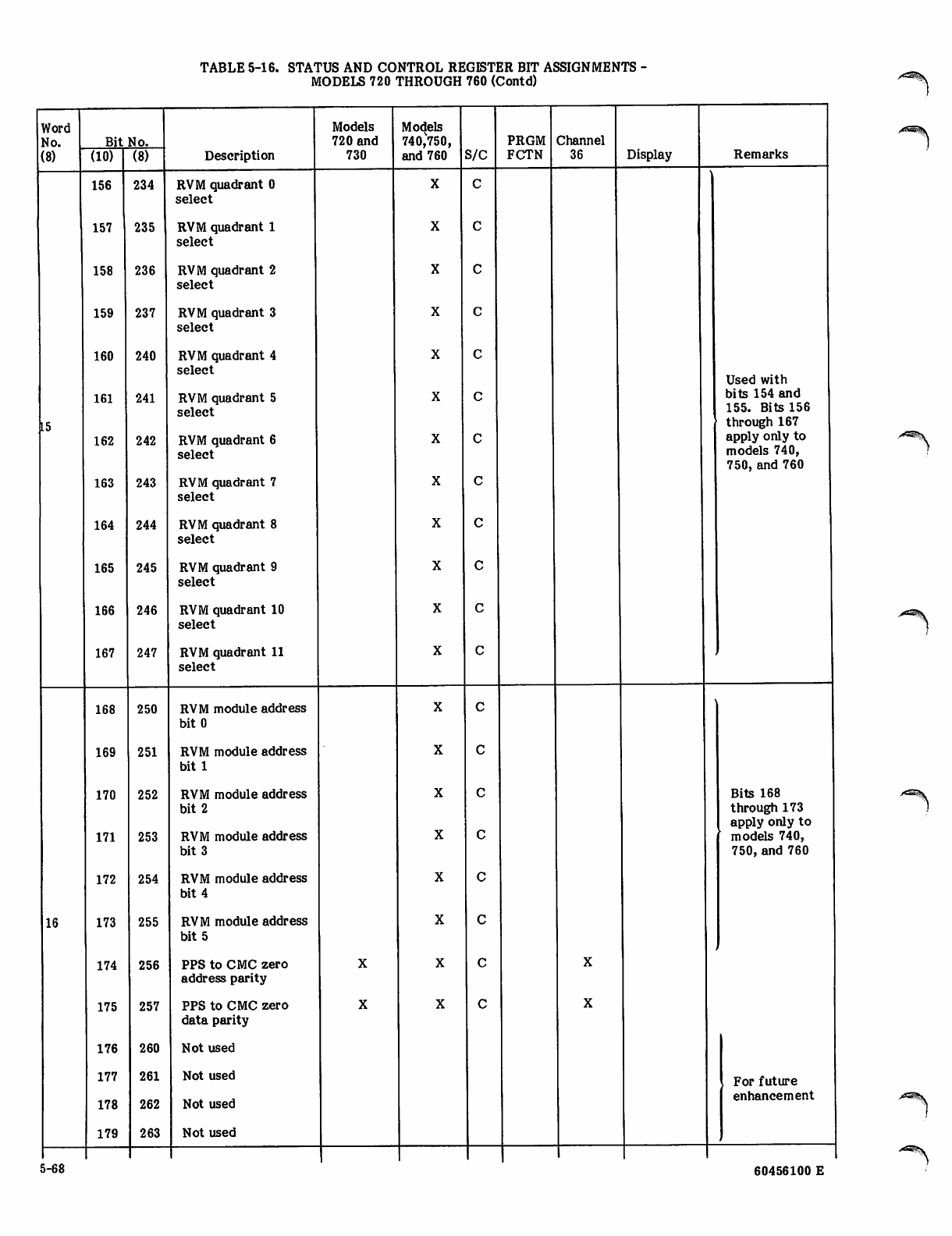
TABLE 5-16. STATUS AND CONTROL REGISTER BIT ASSIGNMENTS -
MODELS 720 THROUGH 760 (Contd)
Word
No.
(8)
Bit No.
Description
Models
720 and
730
Models
740/750,
and 760 s/c PRGM
FCTN
Channel
36 Display Remarks
(10) (8)
156 234 RVM quadrant 0
select
157 235 RVM quadrant 1
select
158 236 RVM quadrant 2
select
159 237 RVM quadrant 3
select
L5
160
161
162
163
164
165
166
240
241
242
243
244
245
246
RVM quadrant 4
select
RVM quadrant 5
select
RVM quadrant 6
select
RVM quadrant 7
select
RVM quadrant 8
select
RVM quadrant 9
select
RVM quadrant 10
select
Used with
bits 154 and
155. Bits 156
through 167
apply only to
models 740,
750, and 760
167 247 RVM quadrant 11
select
168 250 RVM module address
bitO
169 251 RVM module address
bit 1
170
171
252
253
RVM module address
bit 2
RVM module address
bit 3
Bits 168
through 173
apply only to
models 740,
750, and 760
172 254 RVM module address
bit 4
16 173 255 RVM module address
bit 5
174 256 PPS to CMC zero
address parity
175 257 PPS to CMC zero
data parity
176 260 Not used
177
178
261
262
Not used
Not used
For future
enhancement
179 263 Not used
5-68 60456100 E
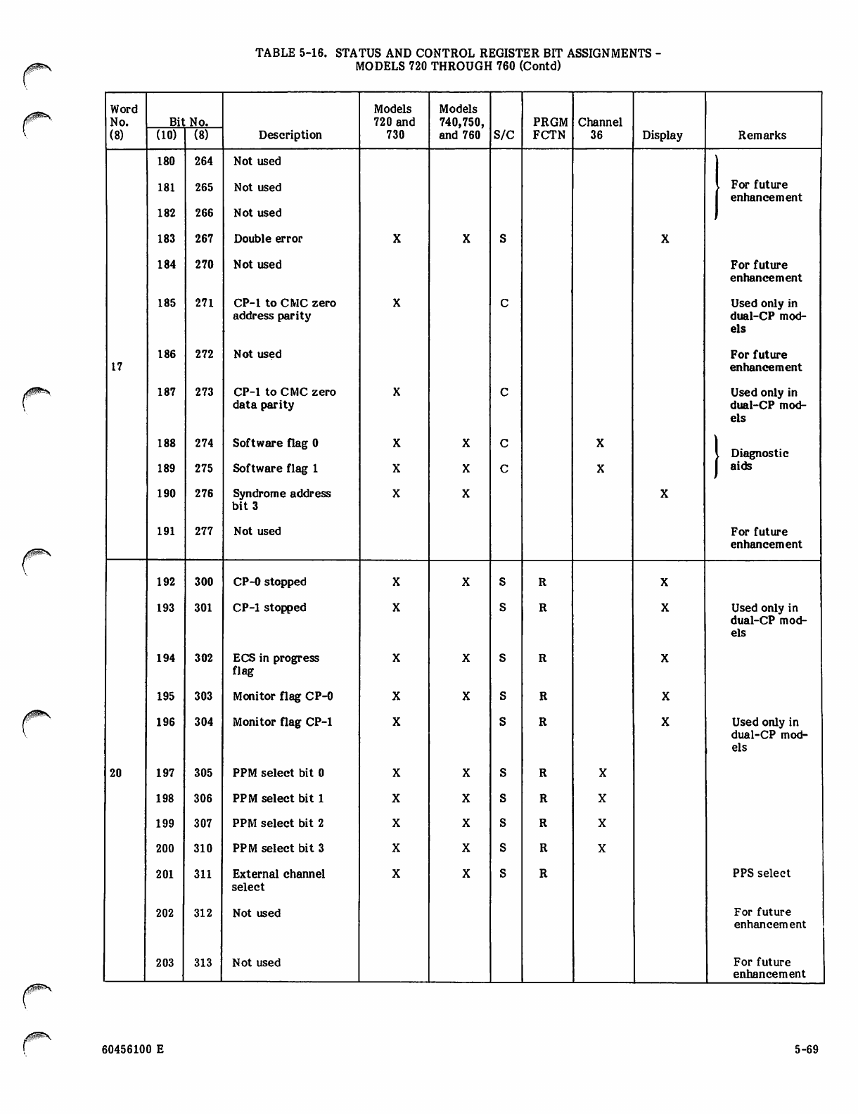
TABLE 5-16. STATUS AND CONTROL REGISTER BIT ASSIGNMENTS -
MODELS 720 THROUGH 760 (Contd)
0^>\
Word
No.
(8)
Bit No.
Description
Models
720 and
730
Models
740,750,
and 760 s/c PRGM
FCTN
Channel
36 Display
(10) (8) Remarks
180 264 Not used
181 265 Not used . For future
enhancement
182 266 Not used
183 267 Double error
184 270 Not used For future
enhancement
185 271 CP-1 to CMC zero
address parity
Used only in
dual-CP mod
els
17
186 272 Not used For future
enhancement
187 273 CP-1 to CMC zero
data parity
Used only in
dual-CP mod
els
188
189
274
275
Software flag 0
Software flag 1
I Diagnostic
I aids
190 276 Syndrome address
bit 3
191 277 Not used For future
enhancement
192 300 CP-0 stopped
193 301 CP-1 stopped Used only in
dual-CP mod
els
194 302 ECS in progress
flag
195 303 Monitor flag CP-0
196 304 Monitor flag CP-1 Used only in
dual-CP mod
els
20 197 305 PPM select bit 0
198 306 PPM select bit 1
199 307 PPM select bit 2
200 310 PPM select bit 3
201 311 External channel
select
PPS select
202 312 Not used For future
enhancement
203 313 Not used For future
enhancement
i^ssp^
60456100 E 5-69
BITS 6/68THROUGH 9/ll8NOT USED
BIT 10/128ANY ERROR BIT EQUALS ONE —
STATUS
This bit indicates that one or more status and control
register bits 0 through 39 in PPS-1 are set.
BIT 11/138 ECS TRANSFER ERROR — STATUS
This bit indicates that an error occurred on an ECS
transfer. The type of error is indicated by the status
locked in bits 136, 137, and 138 by bit 11. Bit 11 must be
reset to detect further errors.
BIT 12/U8CP-0 PARITY ERROR — STATUS
This bit indicates that the PPS detected a parity error on a
read of the P register for CP-0.
BIT 13/158CP-1 PARITY ERROR — STATUS
This bit applies only to models with two CPs and is unused
in models with one CP. The bit indicates that the PPS
detected a parity error on a read of the P register for CP-1.
BITS U/168 THROUGH 23/278 PPO THROUGH
PP9 PARITY ERROR — STATUS
These bits indicate the occurrence of a PP error condition.
The bits prevent a PP from executing instructions following
the detection of the error condition. On a one-to-one
basis, the bits indicate the status of each PP. The bits
indicate the logical PP numbers and are not affected by a
reconfiguration of the PPMs that results from resetting the
PPS-O/PPS-1 and PP MEMORY SELECT switches on the
deadstart panel.
The error conditions which can stop the PPs and their
associated status and control register bits are:
Error Condition
PPM parity error
Read pyramid parity
error on a CM read
Double SECDED
error on a CM read
Bit 0 Bit 119
1
The PP associated with the error stops only if the
appropriate enable bits are set in the status and control
register. If the enable bits are not set, the error condition
is reported but the PP is not stopped.
BITS 24/308THROUGH 35/438
CHANNELS 0 THROUGH 13 (PPS-0)
20 THROUGH 33 (PPS-1) PARITY ERROR STATUS
These bits indicate the occurrence of a parity error in the
corresponding I/O channel. Each bit indicates the status of
one channel as listed in table 5-16. The checking of these
bits may be disabled on any or all of the I/O channels with
the PARITY switches on the I/O connector panel.
BIT 36/448 MAINS POWER FAILURE - STATUS
This bit indicates that the primary power mains feeding the
computer system are deenergized and have remained so for
more than one-half cycle (8.3 milliseconds for 60-Hz power
and 10.0 milliseconds for 50-Hz power) of the mains
frequency. If power returns within one cycle of the mains
frequency, the line feeding the bit automatically goes false.
BIT 37/458 SHUTDOWN IMMINENT — STATUS
This bit indicates one of the following conditions.
• The primary power mains feeding the system are
deenergized and have remained so for at least 100
milliseconds. Power probably will not return to
normal within the regulation range of the system
secondary power supply, normally a
motor-generator set.
• An environmental condition (including dewpoint
warning and chassis temperature) is abnormal and
approaching an emergency power shutdown.
• An environmental condition is changing at an
abnormally high rate.
• An environmental condition is about to execute a
controlled power shutdown.
• A critical system device is down because of
environmental conditions. (This indication exists
only if the system has monitoring provisions for the
device.)
If power and environmental conditions return to normal,
except in the case of an emergency shutdown limit, the line
feeding the bit automatically goes false within one cycle of
the mains frequency. The bit must be cleared by software.
When both the mains power failure and power shutdown
imminent bits are set, one of the following coincident
conditions exists.
o A power mains failure has occurred for longer than
100 milliseconds. Power will probably not return
within the regulation range of the system
secondary power supplies. The kernel system (CP,
all PPs, all channels, store, all first-level
controllers, and all system disk units) remains
available for processing for the balance of the
motor-generator ride-through after the shutdown
imminent bit sets. In this case, the mains power
failure bit sets at least 50 milliseconds before the
shutdown imminent bit sets. However, all
peripheral equipment powered directly from the
mains has probably failed.
e A controlled shutdown limit has been reached. The
limit sensor has disconnected the primary power
mains from the system secondary power supply, and
the kernal system processing remains available for
the balance of the motor-generator ride-through
after the shutdown imminent bit sets. In this case,
the mains power failure and the shutdown imminent
bits set at approximately the same time.
5-70 60456100 F
x s © ^
/ifS^S
0^\
Examples of possible conditions are:
Condition Explanation
1.
4.
Mains power
failure only;
power returns.
Mains power
failure and shut
down imminent.
Mains power
failure and shut
down imminent,
mains power
failure bit clears,
or the mains
power failure and
shutdown imminent
bits clear.
Shutdown imminent,
no mains power
failure.
Indicates that all peri
pheral equipment powered
directly from the mains
has probably failed. The
system is not down, but
user intervention is
necessary to restore
power to affected peri
pherals.
Indicates the system will
probably terminate and re
quire restart.
The explanation for condi
tion 1 applies. This is a
rare occurrence and may
not be a stable condition.
Either a shutdown timeout
(1 to 2 minutes) is in
progress because of an
environmental problem, or
a warning level has been
reached which ultimately
requires user interven
tion. Sufficient time
may exist for the user or
software, if software
capability exists, to
initiate and complete
system checkpoints.
If the mains power
failure bit 36 sets
later, a time-out has
been completed and the
system behaves as though
an emergency shutdown
limit was reached.
BITS 38/468 NOT USED
BIT 39/478 ESM ENVIRONMENT
FAILURE WARNING—STATUS
Tti is bit indicates that loss of the ESM system is imminent
due to a malfunction in one of the environmental conditions
monitored by the ESM controller.
BITS 40/508 THROUGH 47/578
SYNDROME BITS 0 THROUGH 7 — STATUS
These and bits 48 through 52, 190, and 191 are provided by
CMC upon detection of a SECDED error. Bits 40 through
47 provide the information needed to isolate a single-error
failure to a particular memory module. Setting bit 3 locks
bits 40 through 47. Clearing bit 3 unlocks bits 40 through
47 but does not clear them. Software functions cannot
clear or set the read-only syndrome bits.
BITS 48/608 THROUGH 52/648
SYNDROME ADDRESS BITS 0, 1, 2, 15,
AND 16 — STATUS
These and bits 40 through 47 and 190 are provided by CMC
upon detection of a SECDED error. Bits 48, 49, and 50
indicate the CM bank number. Bits 51 and 52 indicate the
CM quadrant. Bits 48 through 52 are locked by the setting
of bit 3. Clearing bit 3 unlocks bits 48 through 52 but does
not clear them. Bits 48 through 52 are read-only bits that
cannot be cleared or set by software functions.
BIT 53/658NOT USED
BITS 54/668AND 55/67a
PARITY ERROR PORT CODE BITS 0, 1 — STATUS
These bits indicate which CMC port had a parity error.
The bits are locked by the setting of bit 5 and cannot be
modified until bit 5 clears.
Bit 55 Bit 54 Port
0 0 CP-1 (models with two CPs)
1 0 PPS-1
1 1 PPS-0
BITS 56/708 AND 57/718
BREAKPOINT PORT CODE BITS 0, 1 — STATUS
These bits indicate the CMC port that satisfied the
breakpoint condition. The bits are locked by the setting of
bit 77 and cannot be cleared until bit 77 clears.
Bit 57 Bit 56 Port
0 0 CP-1 (models with two CPs)
01CP-0
1 0 PPS-1
11PPS-0
60456100 F 5-71
BITS 58/728AND 59/738
BREAKPOINT FUNCTION CODE
BITS 0, 1 — STATUS
These bits indicate what type of instruction caused the
breakpoint condition to be satisfied. The bits are locked by
the setting of bit 77 and cannot be modified until bit 77
clears.
Bit 59 Bit 58 Type
0 0
0 1
1 0
1 1
Read
Write
RNI
This condition does not occur.
(located in bits 96 through 113) and the breakpoint
condition code (located in bits 114 through 117). It also
locks bits 56 through 59 so that their status cannot be
modified until bit 77 clears. Bit 77 must be reset by
software to detect further breakpoint conditions.
BIT 78/1168 CLEAR CENTRAL MEMORY BUSY —
CONTROL
This bit clears CM busy and unhangs a PP on an unanswered
CM request. The bit causes a one-shot operation. The bit
must be cleared by software and set again to execute its
function a second time.
BIT 79/1178NOT USED
BITS 60/748 THROUGH 71/1078 P INPUT
BITS 0 THROUGH 11 — STATUS
These bits indicate the content of the P register. The
content can be the program address or data buffer address
for the PP that satisfied the breakpoint condition when bits
76 and 83 are set. When bit 83 is not set, the bits display
the P register of the selected PP. The PP selection can be
made manually by switches on the PPS module located at
J40 or through software selection of control bits 120
through 124. Bits 60 through 71 are locked by the setting
of bit 76 and cannot be modified until bit 76 clears.
BITS 72/1108 THROUGH 75/1138
SCANNER CHANNEL SELECT
BITS 0 THROUGH 3 — STATUS
These bits indicate which PP stored the content of its P
register in bit positions 60 through 71/ Bits 72 through 75
are locked by the setting of bit 76 and cannot be modified
until bit 76 clears. Bit 83 is associated with bits 72 through
75/
BIT 76/1148 PPS BREAKPOINT BIT — STATUS
This bit, with bit 83 set, indicates that the breakpoint
address was referenced by PPS. The content of the P
register of the referencing PP is locked into bit positions
60 through 71. The referencing PP code is also locked into
bit positions 72 through 75/ These bits are locked so that
their status cannot be modified until bit 76 is cleared. Bit
76 must be reset by software to detect further PPS
breakpoint addresses. With bit 83 clear, the content of the
P register of the PP selected by bits 120 through 124 is
made available for monitoring by bits 60 through 71. The P
register status is not locked but continually tracks the
program address of the selected PP.
BIT 77/1158 CMC BREAKPOINT MATCH — STATUS
This bit indicates that the breakpoint condition occurred.
The breakpoint condition is defined by the absolute address
BIT 80/1208 FORCE ZERO PARITY ON
CHANNELS — CONTROL
This bit forces the data parity bits in the I/O channels to
zero. A deadstart clears the bit.
BIT 81/1218 FORCE ZERO PARITY
ON PP MEMORIES — CONTROL
This bit forces the PPM parity bits to zero. A deadstart
clears the bit.
BIT 82/1228 NOT USED
BIT 83/1238 PPS BREAKPOINT MODE SELECT —
CONTROL
This bit, when set, forces the P register field (bits 60
through 75) into breakpoint mode. When clear, it forces
the P register field into program address display mode.
The breakpoint field is locked by the setting of bit 76. A
deadstart clears the bit.
BIT 84/1248ALL PPs 500-NANOSECOND MAJOR
CYCLE — STATUS
This bit is constantly set to indicate a major cycle time of
500 nanoseconds for all PPs in PPS-0 and PPS-1. The bit
cannot be cleared.
BIT 85/1258 INHIBIT PPS REQUEST TO CMC —
CONTROL
This bit prevents any PP from making a
read/write/exchange request. This bit should be used with
the CP master clear bit 127 to ensure that the master clear
does not hang any PP that is accessing CM. A deadstart
clears the bit.
5-72 60456100 B
z^P^N
BITS 86/1268 AND 87/1278
NARROW AND WIDE CLOCK WIDTH MARGINS -
CONTROL
These bits control the clock pulse width in the PPS chassis
according to the following bit translations.
Bit 87 Bit 86 Clock Pulse
0 0 Normal
0 1 Narrow
1 0 Wide
1 I Normal
BITS 88/1388 THROUGH 93/1358
DIAGNOSTIC AIDS — STATUS
When a parity error is detected on a CM read instruction,
the request is sent and the PP writes the data into PPM. In
the case of a block read, the instruction terminates and the
PP always stops.
BITS 96/1408 THROUGH 113/1618
BREAKPOINT ADDRESS BITS 0 THROUGH 17 —
CONTROL
These bits define the absolute address to be used for the
breakpoint condition, defined by bits 114 through 117. Bits
96 through 113 are sent to CMC and compared with all
addresses being accessed.
BITS 114/1628 THROUGH 117/1658
BREAKPOINT CONDITION CODE
BITS 18 THROUGH 21 — CONTROL
Refer to diagnostic in use.
BIT 94/1368 STOP ON ERROR — CONTROL
This bit (when set) enables the stop on a CM read error
which may be either a double error or a pyramid parity
error. The PP associated with the error stops after
disassembling the word received from CM. The data with
the error is written into the PPM. In case of a block read,
the instruction terminates. Bits 14 through 23 are used to
identify the PP with the error condition(s). Bit 94 provides
control only in its respective status and control register
which is for PPS-0 or PPS-1.
BIT 95/1378STOP ON PPM PARITY ERROR —
CONTROL
This bit (when set) enables the stop on PPM parity error
network. When a parity error is detected, any instruction
except a CM read or write, exchange jump, or channel
executes. Following the completion of the instruction, the
PP stops.
When a parity error is detected on a channel instruction,
the channel select control disables, preventing the
instruction from performing any channel operation. The
instruction may or may not exit.
When a parity error is detected in a 20-PP system and a PP
in one chassis is making a request for a channel in the other
chassis, the request to the other chassis is blocked. The PP
with the parity error hangs in the instruction it is trying to
execute.
When a parity error is detected on a CM write or exchange
jump instruction, requests to the control of the CM are
blocked. A single-word write and exchange exits, and the
block write instruction terminates. In all cases, the PP
stops prior to writing incorrect data in CM or executing an
exchange jump. The instruction is allowed to exit,
preventing write pyramid hang-ups.
These bits define the breakpoint conditions.
Bit 117 Bit 116 Bit 115 Bit 114 Condition
X X 0 0 Read
X X 0 1 Write
X X 1 0 RNI
X X 1 1 A n y o f t h e
above
0 0 X X Disabled
0 1 X X Enabled for PPS
1 0 X X Enabled for CP
1 1 X X Enabled for
PPS or CP
BIT 118/1668 INHIBIT SINGLE-ERROR REPORT —
CONTROL
This bit, when set, stops the recording of single-error
status information and blocks setting bit 3 of the status and
control register if a single error occurs. Double errors
continue to set bit 3 and be reported by bit 183.
BIT 119/1678 CM READ DOUBLE ERROR — STATUS
This bit indicates a double SECDED error on a CM read
within the PP chassis. A PP does not force exit (bit 125) if
the hung condition resulted from a read pyramid parity
error, a PPM parity error, or double SECDED error. A
mainframe deadstart or a forced deadstart (bit 126) to the
hung PP is the only way to clear a PP that was hung by one
of these conditions. Bit 119 functions in conjunction with
bits 14 through 23, 94, and 95.
/pB-^S
60456100 B 5-73
BITS 120/1708 THROUGH 123/1738
PP SELECT CODE BITS 0 THROUGH 3 — CONTROL
These bits determine which PP is forced to exit (bit 125),
deadstart (bit 126), or display (when bit 83 is clear) its P
register. A deadstart clears bits 120 through 123.
BIT 124/1748PP SELECT AUTO/MANUAL MODE —
CONTROL
bit must be cleared immediately (in less than 6
microseconds) by the program that sets it to prevent the
possibility of a memory data error. In special cases on
models 750 or 760, immediate clearing of the bit also
prevents the possibility of a memory fault. To prevent the
data errors and memory faults, the PPU programs must
minimize the width of the master clear pulse and its
occurrence (not more than once each 128 microseconds).
The PP chassis is not affected by this bit, unless a PP is
making a CM reference. To avoid hanging any PP, bit 85
should be set before bit 127. A deadstart clears bit 127.
This bit selects the mode of PP selection. When set, PP
selection is under program control. PP selection is then
made by bits 120 through 123. When clear, selection is
manual, and the PP selection is made by switches on the PP
chassis at locations 2D33 (PPS-0) and 2P34 (PPS-1). A
deadstart clears the bit.
BIT 125/1758 FORCE EXIT ON SELECTED PP —
CONTROL
This bit clears a selected hung PP (selected by bits 120
through 124) by forcing an instruction exit except in the
manual mode. The PP resumes operation at its next slot
time at P plus 1. A forced instruction exit occurs once
each time bit 125 sets. The bit causes a one-shot
operation. The bit must be cleared by software and set
again to cause a second exit. A deadstart clears the bit.
BIT 128/2008 FORCE ZERO SECDED CODE
AND PARITY CMC TO CM — CONTROL
This bit forces the CMC to put a zero check code and
parity bit on data being sent to CM. It also forces CMC to
put a zero parity bit on data transmitted to a requesting
unit such as ECS.
BIT 129/2018 FORCE ZERO ADDRESS PARITY
CMC TO CM — CONTROL
This bit forces CMC to put a zero parity bit on the address
being sent to CM.
BIT 126/1768 FORCE DEADSTART
ON SELECTED PP — CONTROL BIT 130/2028
DISABLE ADDRESS PARITY ERROR — CONTROL
This bit, along with control bits 120 through 124, provides a
programmable capability to make individual PP deadstarts.
Bits 120 through 124 select the PP, and bit 126 forces the
selected PP into a deadstart input condition. The selected
PP then goes through the same deadstart sequence as would
occur under a hardware-controlled deadstart. The PP is set
up for a 71XX instruction, where XX is the selected PP
number. This instruction causes the PP to attempt an input
on its own channel. The software must first ensure that
the selected channel is empty and active at the time of the
deadstart. No other I/O operation can be in process on the
channel. The master clear signal to the channel is
inhibited. The selected PP remains in the deadstart
condition until bit 126 clears. A system deadstart clears
bit 126.
Bit 126 causes the PPS to hang when the selected PP is
performing a CM read or write operation at the time of
deadstart.
BIT 127/1778 MASTER CLEAR — CONTROL
This bit, when set, sends a master clear to the CSU, CMC,
and CP chassis (two CP chassis for some models). The bit
is ORed with the deadstart signal. The bit or the deadstart
signal causes a master clear. The bit holds the CMC and
CP chassis in a cleared state as long as it is set. The
This bit disables address parity error detection at the CSU.
This prevents a condition where reads or writes are
inhibited during the presence of any address parity error.
BIT 131/2038 NOT USED
BITS 132/2048AND 133/2058 FORCE ZERO
PARITY CODE 0 AND CODE 1 — CONTROL
These bits force a zero parity bit on the following
transmission paths.
Bit 133 Bit 132 Transmission Path
0 0 Normal parity
0 1 Word count or address from
CP to ECS coupler
1 0 Address from ECS coupler
to ECS controller
/^s^\
Data from ECS to CMC
Parity does not exist from CP-1 to ECS.
5-74 60456100 C
jt^Ss\
BITS 134/2068 AND 135/2078 NOT USED
BIT 136/2108 THROUGH 138/2128
ECS TRANSFER ERROR CODE
BITS 0 THROUGH 2 — STATUS
These bits indicate errors that occur during an ECS
transfer. The following list gives the status-bit code that
states where the error occurred. The bits are locked by the
setting of bit 11.
Bit 138 Bit 137 Bit 136 Status
0 CP-1 to CMC ad
dress parity
error (models 720
and 730)
1 CP-0 to ECS
coupler parity
error
0 CMC double error
1 CMC to CM address
parity error
0 CMC data input
parity error
1 ECS bank parity
error
0 ECS controller
data parity error
1 ECS controller
address parity
error (this indi
cates no error
when bit 11 is
clear)
BIT 139/2138
CMC ADDRESS/DATA PARITY ERROR — STATUS
This bit indicates an address parity error in CMC. The bit
is used with bits 5, 54, and 55. If the bit clears and bit 5
sets, the CMC parity error is a data error. Bit 139 is
locked by the setting of bit 5 and cannot be modified until
bit 5 clears.
BIT 140/2148 NOT USED
The following 3-bit code translations are for programming
use. The codes result in the margin conditions listed after
the codes. For example, code 000 results in the margin
condition normal, code 001 results in condition slow 1, and
so on.
Bit 143 Bit 142 Bit 141
0 0 0
00 1
0 1 0
01 1
10 0
10 I
11 0
11 1
Margin
Condition
40-MHz
Clock
20-MHz
Clock
10-MHz
Clock
Normal 40.000 20.000 10.000
Slow 1 39.375 19.688 9.844
Slow 2 38.750 19.375 9.688
Slow 3 38.125 19.063 9.531
Normal 40.000 20.000 10.000
Fast 1 40.625 20.313 10.156
Fast 2 41.250 20.625 10.313
Fast 3 41.875 20.938 10.469
BITS 144/2208 THROUGH 149/2258
REFERENCE VOLTAGE MARGIN ADDRESS
BITS 0 THROUGH 5 STATUS — STATUS
These bits apply only to models 740, 750, and 760 and are
unused in models 720 and 730. The bits indicate which CP
chassis quadrant address is selected for a reference voltage
margin (RVM). The bits verify operation of reference
margin addressing and correspond one-to-one with control
bits 168 through 173.
BITS 141/2158 THROUGH 143/2178
CLOCK FREQUENCY MARGINS 0, 1,
AND SLOW/FAST — CONTROL
BITS 150/2268 AND 151/2278
AND ALL/ONE — STATUS
REFERENCE VOLTAGE MARGIN HI/LO
js^N
These bits are used in maintenance operations. The bits
form a 3-bit code that sets the frequency margins of the
basic 40-MHz clock. A 20-MHz clock and a 10-MHz clock
originate from the basic clock and change frequency
margins by the same percentage as the basic clock. A
deadstart clears these bits.
These bits apply only to models 740, 750, and 760 and are
unused in models 720 and 730. Bit 150 indicates that the
RVM is low when clear and high when set. Bit 151
indicates that one CP module is selected for RVM when
clear and that all CP modules are selected for RVM when
set. The bits verify operation of the reference margin
selections and correspond with bits 154 and 155,
respectively.
60456100 E 5-75
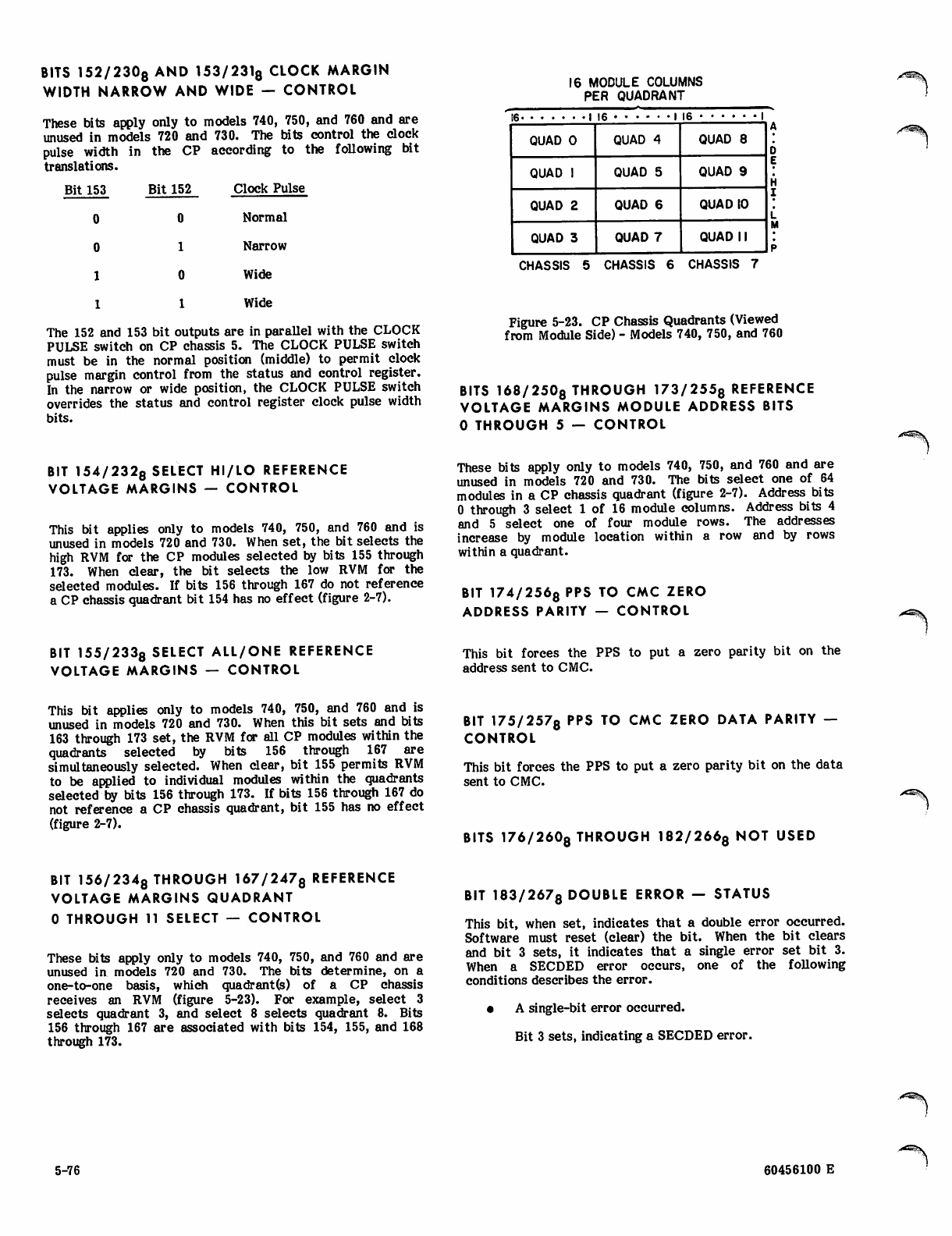
BITS 152/2308 AND 153/2318 CLOCK MARGIN
WIDTH NARROW AND WIDE - CONTROL
These bits apply only to models 740, 750, and 760 and are
unused in models 720 and 730. The bits control the clock
pulse width in the CP according to the following bit
translations.
Bit 153 Bit 152 Clock Pulse
Normal
Narrow
Wide
Wide
The 152 and 153 bit outputs are in parallel with the CLOCK
PULSE switch on CP chassis 5. The CLOCK PULSE switch
must be in the normal position (middle) to permit clock
pulse margin control from the status and control register.
In the narrow or wide position, the CLOCK PULSE switch
overrides the status and control register clock pulse width
bits.
BIT 154/2328 SELECT HI/LO REFERENCE
VOLTAGE MARGINS — CONTROL
This bit applies only to models 740, 750, and 760 and is
unused in models 720 and 730. When set, the bit selects the
high RVM for the CP modules selected by bits 155 through
173. When clear, the bit selects the low RVM for the
selected modules. If bits 156 through 167 do not reference
a CP chassis quadrant bit 154 has no effect (figure 2-7).
BIT 155/2338 SELECT ALL/ONE REFERENCE
VOLTAGE MARGINS — CONTROL
16 MODULE COLUMNS
PER QUADRANT
I 16 I 16
QUAD 0 QUAD 4 QUAD 8
QUAD 1 QUAD 5 QUAD 9
QUAD 2 QUAD 6 QUAD 10
QUAD 3 QUAD 7 QUAD 11
CHASSIS 5 CHASSIS 6 CHASSIS 7
Figure 5-23. CP Chassis Quadrants (Viewed
from Module Side) - Models 740, 750, and 760
BITS 168/2508 THROUGH 173/2558 REFERENCE
VOLTAGE MARGINS MODULE ADDRESS BITS
0 THROUGH 5 — CONTROL
These bits apply only to models 740, 750, and 760 and are
unused in models 720 and 730. The bits select one of 64
modules in a CP chassis quadrant (figure 2-7). Address bits
0 through 3 select 1 of 16 module columns. Address bits 4
and 5 select one of four module rows. The addresses
increase by module location within a row and by rows
within a quadrant.
BIT 174/2568 PPS TO CMC ZERO
ADDRESS PARITY — CONTROL
This bit forces the PPS to put a zero parity bit on the
address sent to CMC.
> ^ \
This bit applies only to models 740, 750, and 760 and is
unused in models 720 and 730. When this bit sets and bits
163 through 173 set, the RVM for all CP modules within the
quadrants selected by bits 156 through 167 are
simultaneously selected. When clear, bit 155 permits RVM
to be applied to individual modules within the quadrants
selected by bits 156 through 173. If bits 156 through 167 do
not reference a CP chassis quadrant, bit 155 has no effect
(figure 2-7).
BIT 175/2578 PPS TO CMC ZERO DATA PARITY —
CONTROL
This bit forces the PPS to put a zero parity bit on the data
sent to CMC.
BITS 176/2608 THROUGH 182/2668 NOT USED
BIT 156/2348 THROUGH 167/2478 REFERENCE
VOLTAGE MARGINS QUADRANT
0 THROUGH 11 SELECT — CONTROL
These bits apply only to models 740, 750, and 760 and are
unused in models 720 and 730. The bits determine, on a
one-to-one basis, which quadrant(s) of a CP chassis
receives an RVM (figure 5-23). For example, select 3
selects quadrant 3, and select 8 selects quadrant 8. Bits
156 through 167 are associated with bits 154, 155, and 168
through 173.
BIT 183/2678 DOUBLE ERROR — STATUS
This bit, when set, indicates that a double error occurred.
Software must reset (clear) the bit. When the bit clears
and bit 3 sets, it indicates that a single error set bit 3.
When a SECDED error occurs, one of the following
conditions describes the error.
• A single-bit error occurred.
Bit 3 sets, indicating a SECDED error.
5-76 60456100 E
.-^"^V
Bit 183 clears, indicating a single error.
Bits 40 through 47 contain the syndrome code (odd
number of bits), indicating the failing bit.
Bits 48 through 52 indicate the failing CM bank,
quadrant, and chassis.
Bit 190 indicates the failing chip enable of the
failing CM pak.
A double-bit error occurred.
Bit 3 sets, indicating a SECDED error.
Bit 183 sets, indicating a double error.
Bits 40 through 47 contain a syndrome code (even
number of bits) that does not indicate the failing
bits.
Bits 48 through 52 indicate the failing CM bank,
quadrant, and chassis.
Bit 190 indicates the failing chip enable of the
failing CM pak.
A single-bit error occurred. Before software could
clear it, a double-bit error occurred.
Bit 3 sets, indicating a SECDED error.
Bit 183 sets, indicating a double error.
Bits 40 through 47 contain a syndrome code (odd
number of bits) for the single-bit error.
Bits 48 through 52 indicate the failing CM bank,
quadrant, and chassis for the single error.
Bit 190 indicates the failing chip enable of the
failing CM pak.
BIT 186/2728NOT USED
BIT 187/2738 CP-1 TO CMC ZERO DATA PARITY —
CONTROL
This bit applies only to models with two CPs and is unused
in models with one CP. The bit forces CP-1 to put a zero
parity bit on the data sent to CMC.
BITS 188/2748 AND 189/275-
SOFTWARE FLAG 0 AND FLAG 1 — CONTROL
These bits are used by diagnostic software for
communication between PPs.
BIT 190/2768 SYNDROME ADDRESS BIT 3 —
STATUS
This bit and bits 40 through 53 are provided upon detection
of a SECDED error. Bit 190 indicates which chip enable
failed on a memory module. Setting bit 3 locks bit 190.
Clearing bit 3 unlocks bit 190 but does not clear it.
Software functions cannot clear or set the read-only
syndrome address bits.
BIT 191/2778 NOT USED
BIT 192/3008 CP-0 STOPPED — STATUS
This bit, when set, indicates that the CP has stopped.
When the CP resumes operation, the bit clears.
BIT 184/2708 NOT USED
BIT 185/2718 CP-1 TO CMC ZERO
ADDRESS PARITY — CONTROL
BIT 193/3018 CP-1 STOPPED — STATUS
This bit applies only to models with two CPs and is unused
in models with one CP. When set, the bit indicates that the
CP-1 has stopped. When the CP resumes operation, the bit
clears.
This bit applies only to models with two CPs and is unused
in models with one CP. The bit forces CP-1 to put a zero
parity bit on the address sent to CMC.
BIT 194/3028 ECS IN PROGRESS FLAG — STATUS
This bit indicates ECS transfer is currently in progress.
When the transfer completes or terminates, the bit clears.
0^\
60456100 A 5-77
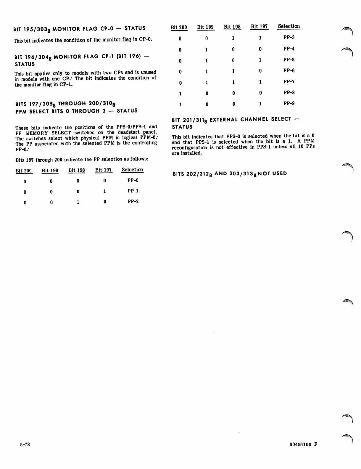
BIT 195/3038 MONITOR FLAG CP-0 — STATUS
This bit indicates the condition of the monitor flag in CP-0.
BIT 196/3048 MONITOR FLAG CP-1 (BIT 196) —
STATUS
This bit applies only to models with two CPs and is unused
in models with one CP/ The bit indicates the condition of
the monitor flag in CP-1.
BITS 197/3058 THROUGH 2O0/3108
PPM SELECT BITS 0 THROUGH 3 — STATUS
These bits indicate the positions of the PPS-O/PPS-1 and
PP MEMORY SELECT switches on the deadstart panel.
The switches select which physical PPM is logical PPM-0.'
The PP associated with the selected PPM is the controlling
PP-0.'
Bits 197 through 200 indicate the PP selection as follows:
Bit 200 Bit 199 Bit 198 Bit 197 Selection
0000PP-0
000 1 pp-1
001 0 PP-2
Bit 200 Bit 199 Bit 198 Bit 197 Selection
0011PP-3
0100PP-4
010 1 PP-5
01 1 0PP-6
0 1 1 1 PP-7
10 0 0PP-8
10 0 1PP-9
BIT 201/3118 EXTERNAL CHANNEL SELECT —
STATUS
This bit indicates that PPS-0 is selected when the bit is a 0
and that PPS-1 is selected when the bit is a 1. A PPM
reconfiguration is not effective in PPS-1 unless all 10 PPs
are installed.
BITS 202/3128 AND 203/3138NOT USED
5-78 60456100 F
y^^N.
WOTS Mm CO NT fcOL REGISTER BIT DESCftlpfmWS
MODEL W6
0^*-

V.
STATUS AND CONTROL REGISTER
BIT DESCRIPTIONS - MODEL 176
Table 5-17 provides a summary of the status and control
register bit information for PPS-0 and PPS-1.
The following list explains table 5-17.
Column Information
Word No.
Bit No.
Description
S/C
PRGM FCTN
>!$P^S
Register word listed in octal (8)
Register bit listed in decimal (10) and
octal(8)
Name of bit
Status (S) bits have inputs from
various sources in the computer.
Control (C) bits have outputs which
enable various conditions in the
computer.
Indicates which programming
functions (PRGM FCTN) are
applicable to the status and control
register bits and which of the bits are
cleared at deadstart. The
programming functions are indicated
by abbreviations in four categories.
TE
No
abbreviation
Read, test, clear
test/clear, set,
test/set, clear
all, and test
error. This
status bit is
included in test
error.
Read. No other
operations can be
performed.
Read, test,
clear, test/
clear, set, test/
set, and clear
all. This con
trol bit clears
at deadstart.
Read, test, clear,
test/clear, set,
test/set, and
clear all.
Column Information
Display X indicates that a light-emitting
diode displays the bit on a module in
PPS-0/ When there is an adjacent X
in the channel 36 column, the bit is
similarly displayed in the optional
PPS-1.
In the following status and control register bit descriptions,
the bit names are preceded by their decimal/octal bit
numbers. The decimal numbers are only for reference.
The octal numbers are for use in programming, setting,
clearing, and testing the bits. The bit functions, status or
control, follow each bit name.
BITS 0/0 THROUGH 2/28 NOT USED
BIT 3/38 CM RANK 2 ERROR — STATUS
This bit indicates a CM parity error (parity mode) or a
SECDED error (SECDED mode). Control bit 174 selects
the parity mode (set) or SECDED mode (clear). In SECDED
mode, bit 183 identifies a SECDED error as a single-bit
error when clear or a double-bit error when set. Setting
control bit 168 clears the SSM rank 2 error register.
Software must clear status bit 3.
BIT 4/48PPU ERROR — STATUS
This bit indicates that at least one of the PPUs had a
memory parity error or a CM read error or translated an
error stop instruction (00 or 77, octal). The failing PPU
can be located by selecting each PPU with the scanner
select bits 72 through 75 and monitoring PPU error status
bits 132 through 136/ When the failing PPU is selected, at
least one of the status bits 132 through 136 sets to identify
the error. After the error is corrected, the set bit must
clear.
BITS 5/58 THROUGH 9/11 NOT USED
BIT 10/128 ANY ERROR BIT EQUALS ONE — STATUS
This bit indicates that one or more status and control
register bits 0 through 39 in PPS-1 are set.
Channel 36 X indicates the bit is also used in the
abbreviated s tatus and control
register of the optional PPS-1.
BIT 11/138 LCME RANK 2 ERROR — STATUS
This bit indicates an LCME parity error when LCME is in
parity mode (bit 171 set) or SECDED error when LCME is
in SECDED mode (bit 171 clear). In SECDED mode, bit 196
identifies a SECDED error as a single-bit error when clear
or a double-bit error when set. Setting control bit 176
clears the LCME rank 2 register. Software must clear
status bit 11.
/p^\
60456100 B 5-79
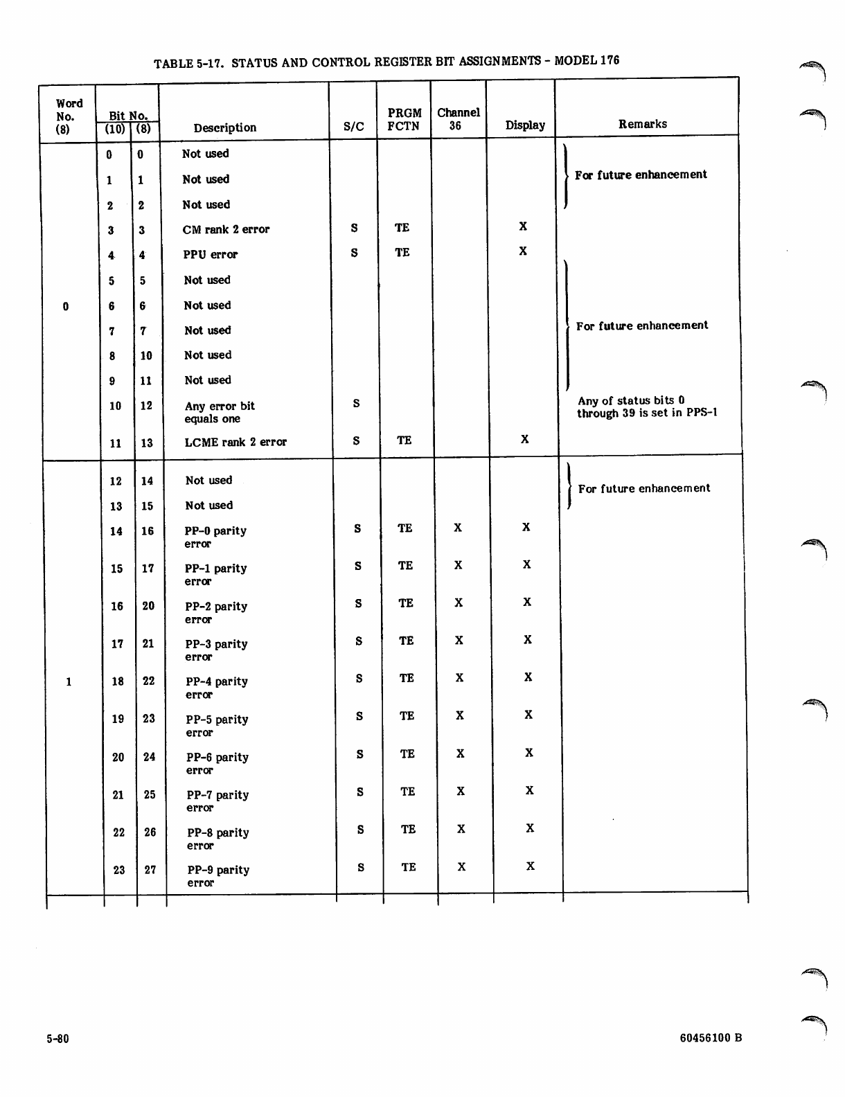
TABLE 5-17. STATUS AND CONTROL REGISTER BIT ASSIGNMENTS - MODEL 176
Word
No. Bit No.
Description S/C
PRGM
FCTN
Channel
36 Display Remarks
(8) (10) (8)
0 0 Not used
11 Not used For future enhancement
2 2 Not used
3 3 CM rank 2 error TE
4 4 PPU error TE
5 5 Not used
0 6
7
8
9
6
7
10
11
Not used
Not used
Not used
Not used
For future enhancement
10 12 Any error bit
equals one
Any of status bits 0
through 39 is set in PPS-t
11 13 LCME rank 2 error TE
12 14 Not used
J For future enhancement
13 15 Not used
14 16 PP-0 parity
error
TE
15 17 PP-1 parity
error
TE
16 20 PP-2 parity
error
TE
17 21 PP-3 parity
error
TE
118 22 PP-4 parity
error
TE
19 23 PP-5 parity
error
TE
20 24 PP-6 parity
error
TE
21 25 PP-7 parity
error
TE
22 26 PP-8 parity
error
TE
23 27 PP-9 parity
error
TE
5-80 60456100 B
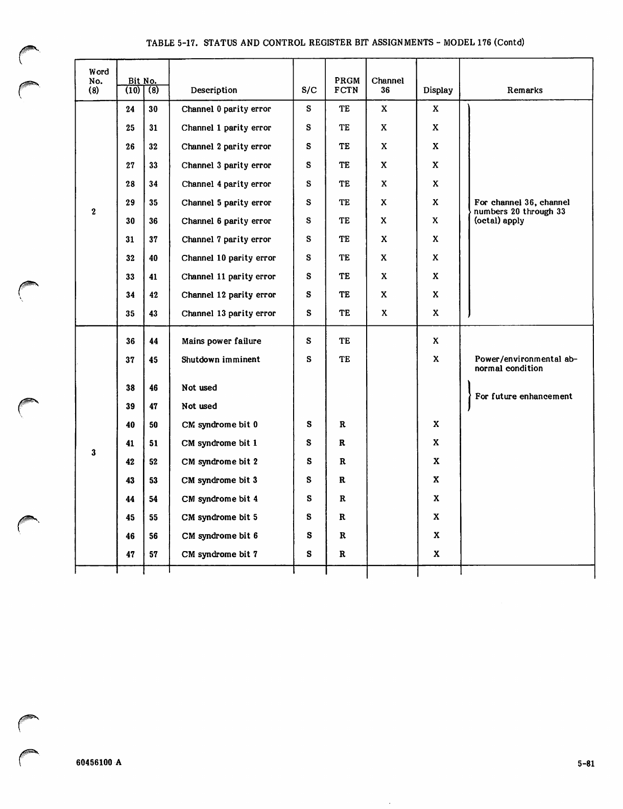
TABLE 5-17. STATUS AND CONTROL REGISTER BIT ASSIGNMENTS - MODEL 176 (Contd)
/pi*v
Word
No.
(8)
Bit No.
Description S/C
PRGM
FCTN
Channel
36 Display
(10) (8) Remarks
24 30 Channel 0 parity error TE
25 31 Channel 1 parity error TE
26 32 Channel 2 parity error TE
27 33 Channel 3 parity error TE
28 34 Channel 4 parity error TE
2
29
30
35
36
Channel 5 parity error
Channel 6 parity error
TE
TE
For channel 36, channel
numbers 20 through 33
(octal) apply
31 37 Channel 7 parity error TE
32 40 Channel 10 parity error TE
33 41 Channel 11 parity error TE
34 42 Channel 12 parity error TE
35 43 Channel 13 parity error TE
36 44 Mains power failure TE
37 45 Shutdown imminent TE Power/environmental ab
normal condition
38 46 Not used
f For future enhancement
39 47 Not used
40 50 CM syndrome bit 0
3
41 51 CM syndrome bit 1
42 52 CM syndrome bit 2
43 53 CM syndrome bit 3
44 54 CM syndrome bit 4
45 55 CM syndrome bit 5
46 56 CM syndrome bit 6
47 57 CM syndrome bit 7
/£^V
60456100 A 5-81
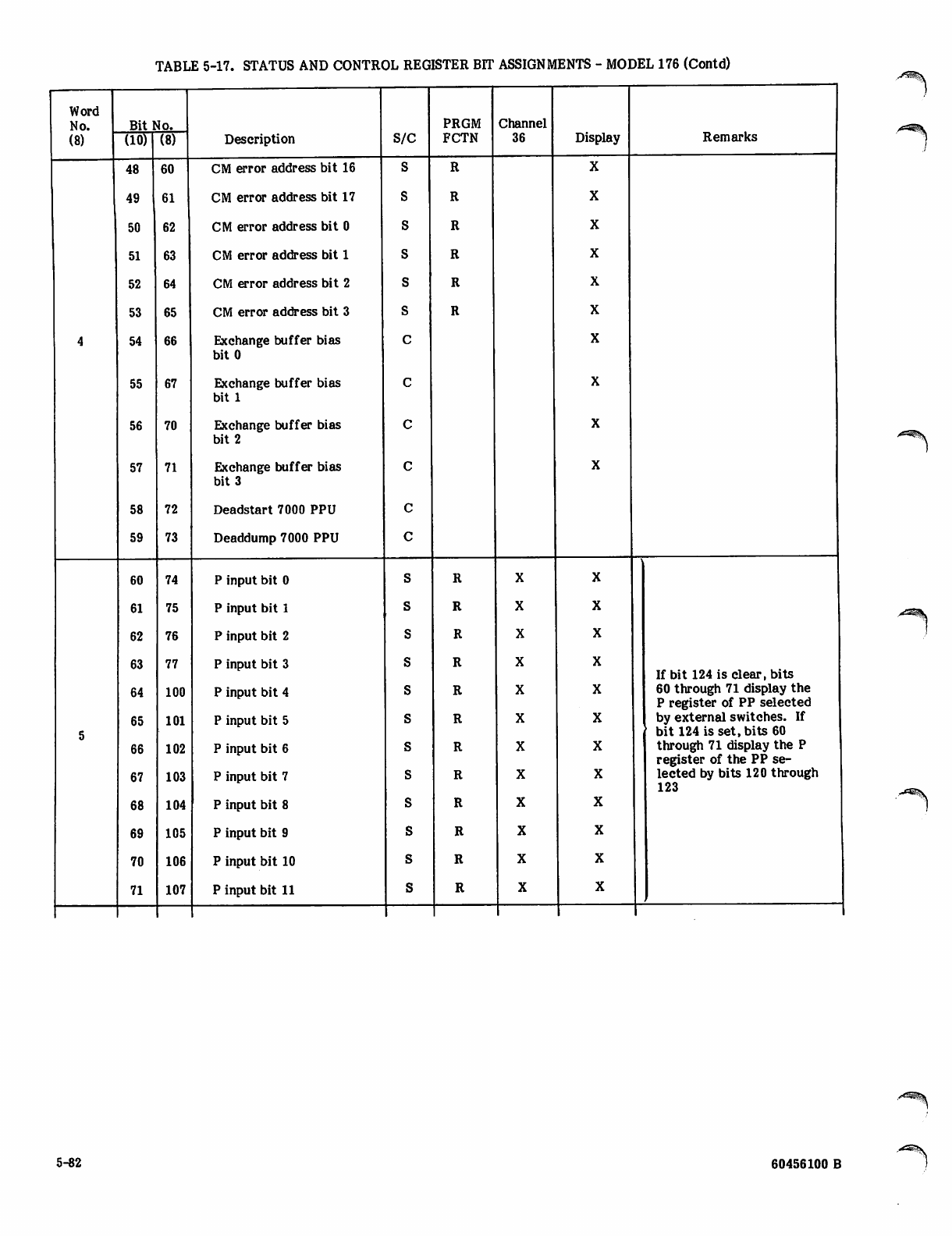
TABLE 5-17. STATUS AND CONTROL REGISTER BIT ASSIGNMENTS - MODEL 176 (Contd)
Word
No.
(8)
Bit No.
Description S/C
PRGM
FCTN
Channel
36 Display Remarks
(10) (8)
4
48
49
50
51
52
53
54
55
56
57
58
59
60
61
62
63
64
65
66
67
70
71
72
73
CM error address bit 16
CM error address bit 17
CM error address bit 0
CM error address bit 1
CM error address bit 2
CM error address bit 3
Exchange buffer bias
bit 0
Exchange buffer bias
bit 1
Exchange buffer bias
bit 2
Exchange buffer bias
bit 3
Deadstart 7000 PPU
Deaddump 7000 PPU
5
60
61
62
63
64
65
66
67
68
69
70
71
74
75
76
77
100
101
102
103
104
105
106
107
P input bit 0
P input bit 1
P input bit 2
P input bit 3
P input bit 4
P input bit 5
P input bit 6
P input bit 7
P input bit 8
P input bit 9
P input bit 10
P input bit 11
If bit 124 is clear, bits
60 through 71 display the
P register of PP selected
by external switches. If
bit 124 is set, bits 60
through 71 display the P
register of the PP se
lected by bits 120 through
123
/*^i^V
5-82 60456100 B
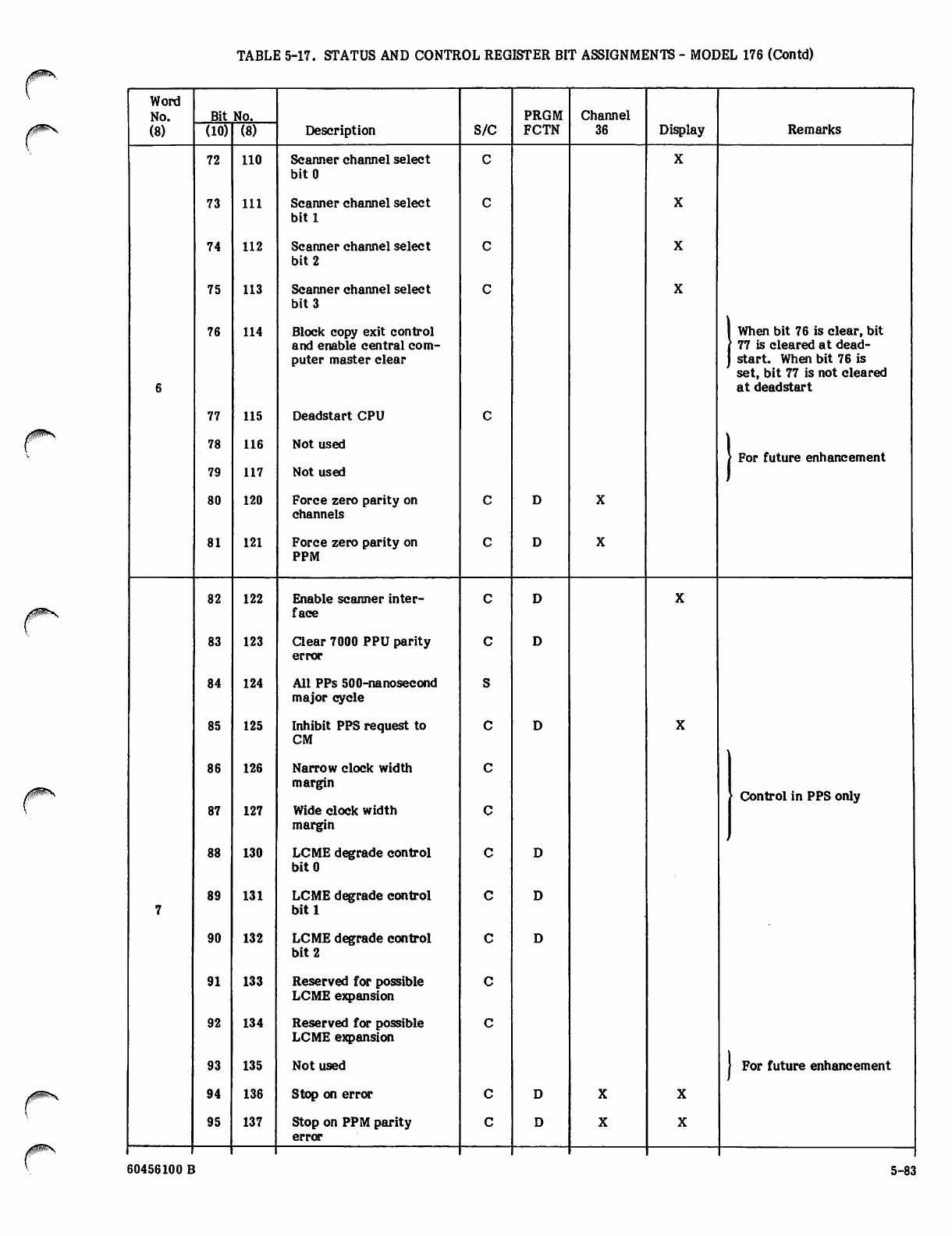
TABLE 5-17. STATUS AND CONTROL REGISTER BIT ASSIGNMENTS - MODEL 176 (Contd)
Word
No.
(8)
Bit No.
Description S/C
PRGM
FCTN
Channel
36 Display Remarks
(10) (8)
72 110 Scanner channel select
bitO
73 111 Scanner channel select
b i t l
74 112 Scanner channel select
bit 2
75 113 Scanner channel select
bit 3
6
76
77
78
79
114
115
116
117
Block copy exit control
and enable central com
puter master clear
Deadstart CPU
Not used
Not used
1 When bit 76 is clear, bit
i 77 is cleared at dead-
j start. When bit 76 is
set, bit 77 is not cleared
at deadstart
| For future enhancement
80 120 Force zero parity on
channels
81 121 Force zero parity on
PPM
82 122 Enable scanner inter
face
83 123 Clear 7000 PPU parity
error
84 124 All PPs 500-nanosecond
major cycle
85 125 Inhibit PPS request to
CM
86
87
126
127
Narrow clock width
margin
Wide clock width
margin
Control in PPS only
88 130 LCME degrade control
bitO
7
89 131 LCME degrade control
b i t l
90 132 LCME degrade control
bit 2
91 133 Reserved for possible
LCME expansion
92 134 Reserved for possible
LCME expansion
93 135 Not used J For future enhancement
94 136 Stop on error
95 137 Stop on PPM parity
error
60456100 B 5-83
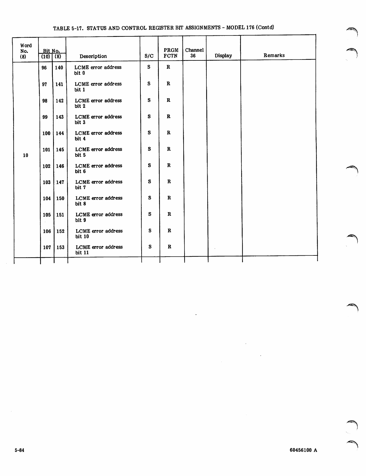
TABLE 5-17. STATUS AND CONTROL REGISTER BIT ASSIGNMENTS - MODEL 176 (Contd)
Word
No.
(8)
10
Bit No.
(10)
96
97
98
99
100
101
102
103
104
105
106
107
(8)
140
141
142
143
144
145
146
147
150
151
152
153
Description
LCME error address
bit 0
LCME error address
b i t l
LCME error address
bit 2
LCME error address
bit 3
LCME error address
bit 4
LCME error address
bit 5
LCME error address
bit 6
LCME error address
bit 7
LCME error address
bit 8
LCME error address
bit 9
LCME error address
bit 10
LCME error address
bit 11
S/C
PRGM
FCTN
R
R
R
R
R
R
R
R
R
R
R
Channel
36 Display Remarks
yAss&jN
5-84 60456100 A
^*^?x
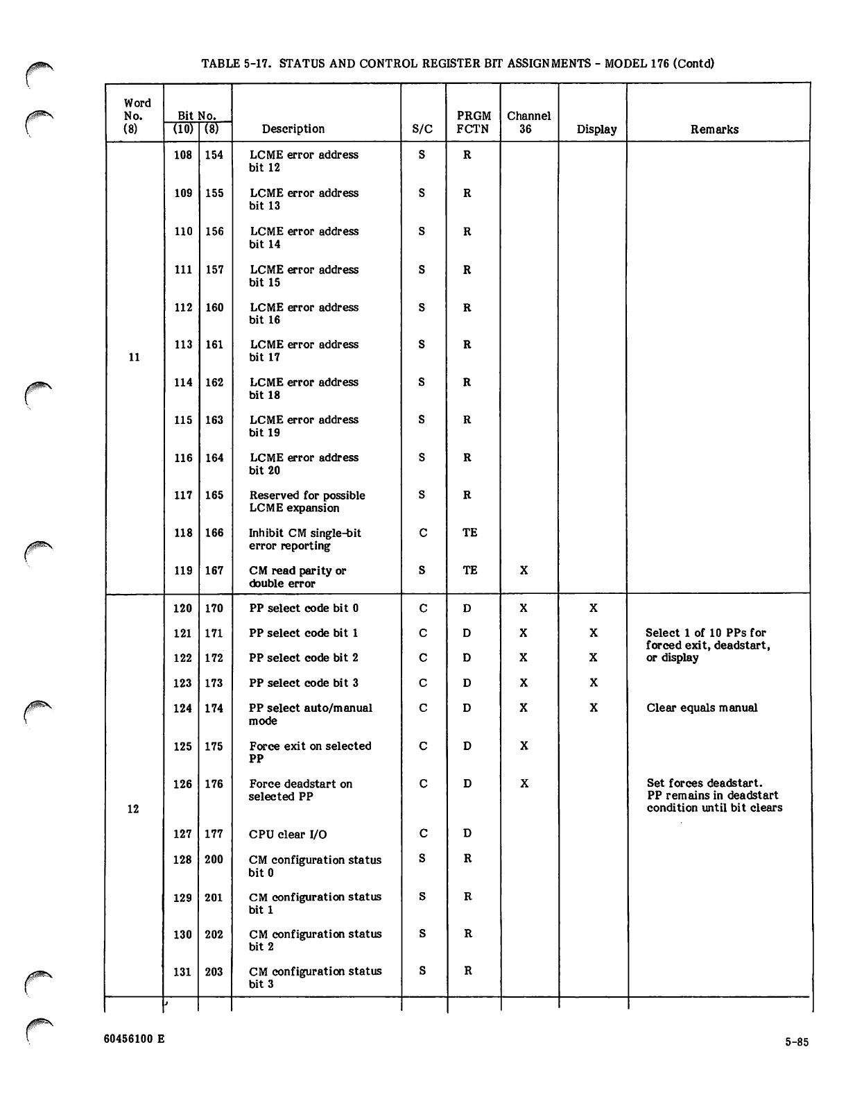
TABLE 5-17. STATUS AND CONTROL REGISTER BIT ASSIGNMENTS - MODEL 176 (Contd)
Word
No.
(8)
Bit No.
Description S/C
PRGM
FCTN
Channel
36 Display Remarks(10) (8)
108 154 LCME error address
bit 12
109 155 LCME error address
bit 13
110 156 LCME error address
bit 14
111 157 LCME error address
bit 15
112 160 LCME error address
bit 16
11
113 161 LCME error address
bit 17
114 162 LCME error address
bit 18
115 163 LCME error address
bit 19
116 164 LCME error address
bit 20
117 165 Reserved for possible
LCME expansion
118 166 Inhibit CM single-bit
error reporting
TE
119 167 CM read parity or
double error
TE
120 170 PP select code bit 0
121
122
171
172
PP select code bit 1
PP select code bit 2
Select 1 of 10 PPs for
forced exit, deadstart,
or display
123 173 PP select code bit 3
124 174 PP select auto/manual
mode
Clear equals manual
125 175 Force exit on selected
PP
12
126 176 Force deadstart on
selected PP
Set forces deadstart.
PP remains in deadstart
condition until bit clears
127 177 CPU clear I/O
128 200 CM configuration status
bitO
129 201 CM configuration status
bit 1
130 202 CM configuration status
bit 2
131 203 CM configuration status
bit 3
>
60456100 E 5-85
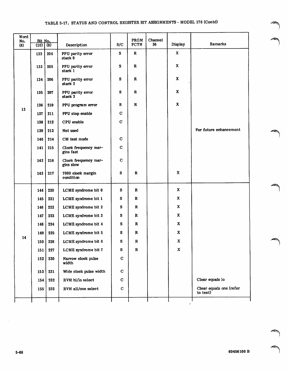
TABLE 5-17. STATUS AND CONTROL REGISTER BIT ASSIGNMENTS - MODEL 176 (Contd)
Word
No.
(8)
Bit No.
Description S/C
PRGM
FCTN
Channel
36 Display Remarks
(10) (8)
132 204 PPU parity error
stack 0
133 205 PPU parity error
stack 1
134 206 PPU parity error
stack 2
135 207 PPU parity error
stack 3
13
136
137
138
139
140
141
142
210
211
212
213
214
215
216
PPU program error
PPU stop enable
CPU enable
Not used
CM test mode
Clock frequency mar
gins fast
Clock frequency mar
gins slow
For future enhancement
143 217 7000 clock margin
condition
144 220 LCME syndrome bit 0
145 221 LCME syndrome bit 1
146 222 LCME syndrome bit 2
147 223 LCME syndrome bit 3
148 224 LCME syndrome bit 4
14
149
150
225
226
LCME syndrome bit 5
LCME syndrome bit 6
151 227 LCME syndrome bit 7
152 230 Narrow clock pulse
width
153 231 Wide clock pulse width
154 232 RVM hi/lo select Clear equals lo
155 233 RVM all/one select Clear equals one (refer
to text)
5-86 60456100 B /^a^\
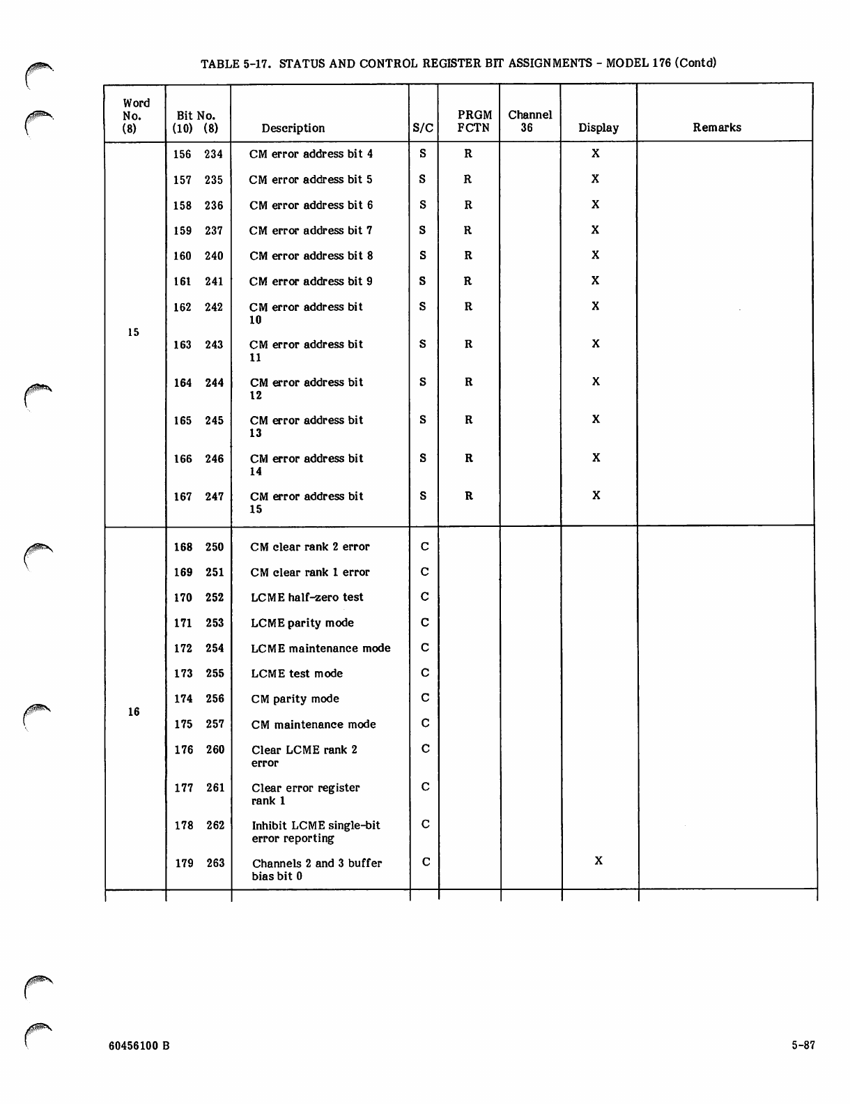
TABLE 5-17. STATUS AND CONTROL REGISTER BIT ASSIGNMENTS - MODEL 176 (Contd)
Word
No.
(8)
Bit No.
(10) (8) Description S/C
PRGM
FCTN
Channel
36 Display Remarks
15
156 234
157 235
158 236
159 237
160 240
161 241
162 242
163 243
164 244
165 245
166 246
167 247
CM error address bit 4
CM error address bit 5
CM error address bit 6
CM error address bit 7
CM error address bit 8
CM error address bit 9
CM error address bit
10
CM error address bit
11
CM error address bit
12
CM error address bit
13
CM error address bit
14
CM error address bit
15
16
168 250
169 251
170 252
171 253
172 254
173 255
174 256
175 257
176 260
177 261
178 262
179 263
CM clear rank 2 error
CM clear rank 1 error
LCME half-zero test
LCME parity mode
LCME maintenance mode
LCME test mode
CM parity mode
CM maintenance mode
Clear LCME rank 2
error
Clear error register
rank 1
Inhibit LCME single-bit
error reporting
Channels 2 and 3 buffer
bias bit 0
60456100 B 5-87
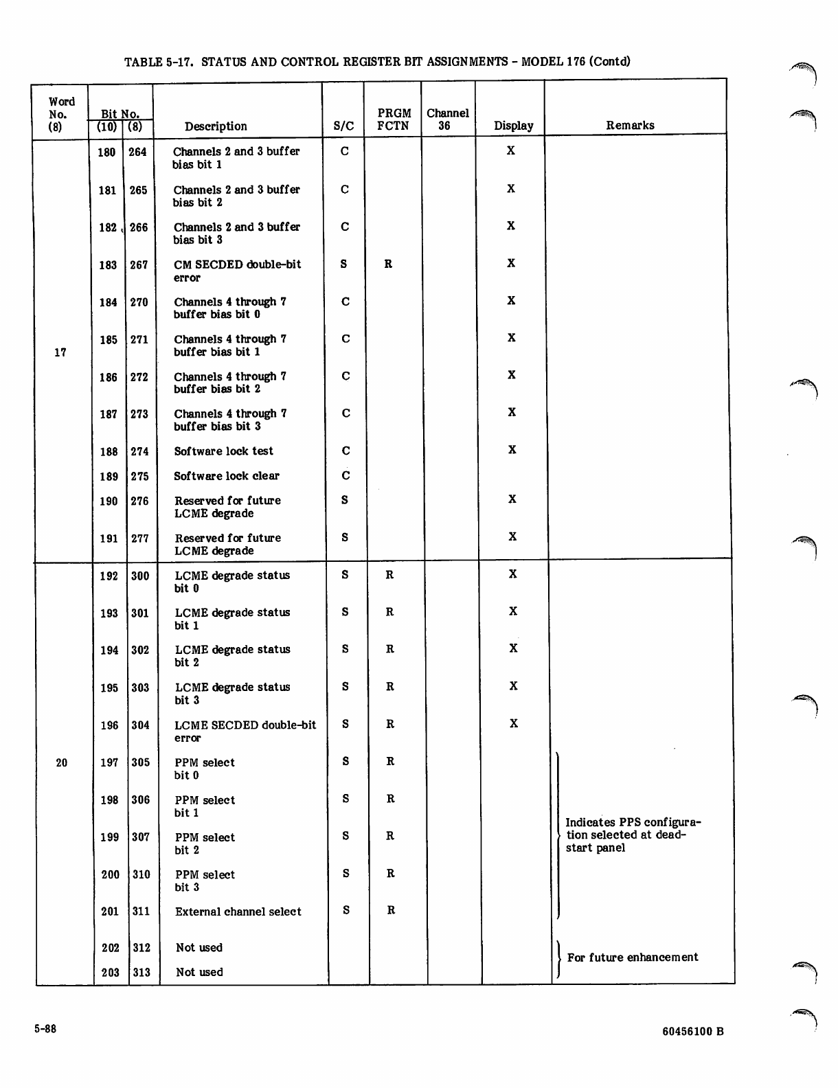
TABLE 5-17. STATUS AND CONTROL REGISTER BIT ASSIGNMENTS - MODEL 176 (Contd)
Word
No.
(8)
17
20
Bit No.
(10) (8)
180
181
182 »
183
184
185
186
187
188
189
190
191
192
193
194
195
196
197
198
199
200
201
202
203
264
265
266
267
270
271
272
273
274
275
276
277
Description
300
301
302
303
304
305
306
307
310
311
312
313
Channels 2 and 3 buffer
bias bit 1
Channels 2 and 3 buffer C
bias bit 2
Channels 2 and 3 buffer C
bias bit 3
CM SECDED double-bit S
error
Channels 4 through 7 C
buffer bias bit 0
Channels 4 through 7
buffer bias bit 1
Channels 4 through 7 C
buffer bias bit 2
Channels 4 through 7 C
buffer bias bit 3
S o f t w a r e l o c k t e s t C
Software lock clear C
Reserved for future S
LCME degrade
Reserved for future
LCME degrade
S/C
LCME degrade status
bitO
LCME degrade status
b i t l
LCME degrade status
bit 2
LCME degrade status
bit 3
LCME SECDED double-bit
error
PPM select
bitO
PPM select
b i t l
PPM select
bit 2
PPM select
bit 3
External channel select
Not used
Not used
PRGM
FCTN
Channel
36
R
R
R
R
R
R
R
R
R
R
Display
X
X
X
X
X
X
X
X
X
X
X
Remarks
Indicates PPS configura
tion selected at dead-
start panel
For future enhancement
5-88 60456100 B
BITS 12/148 AND 13/5g NOT USED
BITS 14/168 THROUGH 23/278
PPO THROUGH PP,9 PARITY ERROR — STATUS
These bits indicate the occurrence of a PP parity error in a
PP. The bits indicate, on a one-to-one basis, the status of
each PP as listed in table 5-17. The bits indicate the
logical PP numbers and are not affected by a
reconfiguration of the PPM because of resetting the
PPS-1/PPS-0 and PP MEMORY SELECT switches on the
deadstart panel.
BITS 24/308 THROUGH 35/438 CHANNEL
0 THROUGH 13 PARITY ERROR — STATUS
These bits indicate the occurrence of a parity error in the
corresponding I/O channel. Each bit indicates the status of
one channel as listed in table 5-17. The checking of these
bits may be disabled on any or all of the I/O channels with
the PARITY switches on the I/O connector panel.
BIT 36/448MAINS POWER FAILURE — STATUS
This bit indicates that the primary power mains feeding the
computer system are deenergized and have remained so for
more than one-half cycle (16.6 milliseconds for 60-Hz
power and 10.0 milliseconds for 50-Hz power) of the mains
frequency. If power returns within one cycle of the mains
frequency, the bit automatically clears. If power does not
return within one cycle of the mains frequency, software
must clear the bit.
BIT 37/458 SHUTDOWN IMMINENT — STATUS
This bit indicates one of the following conditions.
• The primary power mains feeding the system are
deenergized and have remained so for at least 100
milliseconds. Power probably will not return to
normal within the regulation range of the system
secondary power supply, normally a
motor-generator set.
• An environmental condition (including dewpoint
warning and chassis temperature) is abnormal and
approaching an emergency power shutdown.
• An environmental condition is changing at an
abnormally high rate.
• An environmental condition is about to execute a
controlled power shutdown.
• A critical system device is down because of
environmental conditions. (This indication exists
only if the system has monitoring provisions for the
device.)
If power and environmental conditions return to normal,
except in the case of an emergency shutdown limit within
one cycle of the mains frequency, the bit automatically
clears. If power and environmental conditions do not
return to normal within one cycle of the mains frequency,
the bit must be cleared by software.
When both the mains power failure and power shutdown
imminent bits are set, one of the following coincident
conditions exists.
• A power mains failure has occurred for longer than
100 milliseconds. Power will probably not return
within the regulation range of the system
secondary power supplies. The kernel system (CP,
all PPs, all channels, store, all first-level
controllers, and all system disk units) remains
available for processing for the balance of the
motor-generator ride-through after the shutdown
imminent bit sets. In this case, the mains power
failure bit sets at least 50 milliseconds before the
shutdown imminent bit sets. However, all
peripheral equipment powered directly from the
mains has probably failed.
• A controlled shutdown limit has been reached. The
limit sensor has disconnected the primary power
mains from the system secondary power supply, and
the kernel system processing remains available for
the balance of the motor-generator ride-through
after the shutdown imminent bit sets. In this case,
the mains power failure and the shutdown imminent
bits set at approximately the same time.
Examples of possible conditions are:
Condition
Mains power failure
only; power returns.
Explanation
Mains power failure
and shutdown
imminent
Mains power failure
and shutdown immi
nent, mains power
failure bit clears,
or the mains power
failure and shutdown
imminent bits clear.
Shutdown imminent,
no mains power
failure.
Indicates that all
peripheral equipment
powered directly from
the mains has prob
ably failed. The
system is not down,
but user intervention
is necessary to re
store power to
affected peripherals.
Indicates the system
will probably termi
nate and require
restart.
The explanation for
condition 1 applies.
This is a rare occur
rence and may not be
a stable condition.
Either a shutdown
time-out (1 to 2 min
utes) is in progress
because of an envi
ronmental problem, or
60456100 E 5-89
Condition Explanation
a warning level has
been reached which
ultimately requires
user intervention.
Sufficient time may
exist for the user or
software, if software
capability exists, to
initiate and complete
system checkpoints.
If the mains power
failure bit 36 sets
later, a time-out has
been completed and
the system behaves as
though an emergency
shutdown limit was
reached.
BITS 38/468 AND 39/478 NOT USED
BITS 40/508 THROUGH 47/578
CM SYNDROME BITS 0 THROUGH 7 — STATUS
BIT 58/728 DEADSTART 7000 PPU — CONTROL
This bit deadstarts the PPU selected by the scanner select
control bits 72 through 75. The selected PPU executes a
block input of 4095 words (starting at address 0) on its
channel 0.
BIT 59/738 DEADDUMP 7000 PPU — CONTROL
This bit causes the PPU selected by the scanner select
control bits 72 through 75 to execute a block output of
4095 words (starting at address 0) on its channel 0. Control
bit 58 must first set and then clear.
BITS 60/748 THROUGH 71/107a P INPUT
BITS 0 THROUGH 11 — STATUS
These bits represent the 12-bit P register of the selected
PP in the PPS. PP selection is either by four manual
switches at location 140 (if control bit 124 is clear) or by
selective setting of control bits 120 through 123 under
program control (if control bit 124 is set).
BITS 72/U08 THROUGH 75/1138 SCANNER SELECT
BITS 0 THROUGH 3 — CONTROL
Bits 40 through 47 represent CM syndrome bits 0 through 7
(SECDED mode) or CM parity error bits 0 through 7 (parity
mode). Any set bit corresponds to a CM rank 2 error. The
CM error address bits 0 through 17 (status and control
register bits 50 through 53, 156 through 167, 48, and 49)
identify the CM word with the error. Control bit 168
clears bits 40 through 47.
BITS 48/608 THROUGH 53/658 AND 156/234g
THROUGH 167/2478 CM ERROR ADDRESS BITS 0
THROUGH 17 — STATUS
These bits are the address of the CM word that has a parity
error or a SECDED rank 2 error. Control bit 168 clears the
bits. The status bits correspond to address bits as follows:
Status Bit Address Bit
48 16
49 17
50 through 53 0 through 3
156 through 167 4 through 15
BITS 54/668 THROUGH 57/718 EXCHANGE
BUFFER BIAS BITS 0 THROUGH 3 — CONTROL
These are exchange address bits 9 through 12 for I/O
interrupts.
These bits select a PPU to communicate with a PP in the
PPS. Scanner select 16g (bits 0 through 3 set) allows the
PPS to use a 12-bit address to select a CP or PPU module
for RVM testing (control bits 154 and 155).
BIT 76/1148 BLOCK COPY EXIT CONTROL
AND ENABLE CENTRAL COMPUTER
MASTER CLEAR — CONTROL
This bit is sent to CP issue control. When clear, an RNI
follows the issue of a Oil or 012 block copy instruction.
When set, a block copy instruction executes normally. This
bit also controls the clearing of bit 77 at deadstart time.
When clear, bit 77 is cleared. When set, bit 77 is not
cleared at deadstart time.
BIT 77/1158iDEADSTART CPU — CONTROL
This bit (when clear) causes a master clear in the CP.
When set, it causes a CP exchange jump to the address
determined by the exchange bias bits (control bits 54
through 57). This bit is cleared at deadstart time if bit 76
is clear. If bit 76 is set, the status of this bit is not
changed.
5-90 60456100 B
BITS 78/1168 AND 79/117g NOT USED
BIT 80/1208 FORCE ZERO PARITY ON
CHANNELS — CONTROL
This bit forces the data parity bits in the I/O channels to
zero. A deadstart clears the bit.
Bit 87 Bit 86 Clock Pulse
0 0 Normal
01Narrow
1 0 Wide
11 Normal
BIT 81/1218 FORCE ZERO PARITY ON PP
MEMORIES — CONTROL
BITS 88/1308 THROUGH 90/1328 LCME DEGRADE
CONTROL BITS 0 THROUGH 2 - CONTROL
This bit forces the PPM parity bits to zero,
clears the bit. A deadstart
BIT 82/1228 ENABLE SCANNER INTERFACE —
CONTROL
This bit, when set, enables the scanner interface circuit in
the PPS. When clear, the bit disables the interface circuit
so that a PP in the PPS is not able to send or receive the
word pulse and resume signals to or from a PPU. Software
must set the bit when a PP needs to communicate with a
PPU. Software must clear the bit as soon as the
communication terminates. A deadstart clears the bit.
BIT 83/1238 CLEAR 7000 PPU PARITY ERROR —
CONTROL
This bit clears the four-bit parity error register in the PPU
selected by the scanner select control bits 72 through 75.
Software must clear status bit 4/ A deadstart clears the
bit.
BIT 84/1248ALL PPs 500-NANOSECOND MAJOR
CYCLE — STATUS
A two-million word LCME degrades to one million and to a
half-million words. The degradation occurs by manually
setting switches in LCME control or by selectively setting
control bits 88 through 90 under program control. The
degradation method (by switches or program control) is
selectable by a manual switch in LCME control.
Bit 88 is the LCME configuration bit. Bits 89 and 90 are
the LCME size code bits 0 and 1, respectively. The various
valid combinations for bits 88 through 90 and the resulting
LCME size and banks selected are listed as follows:
Memory
Size Code
Bit 90 and Bit 89
0
Configuration
Bit 88
Size In
Millions
1/2
Banks
Selected
0 0 0, 1
0011/2 2,3
0 1 0 1 0-3
0 1 1 1 4-7
1 0 0 2 0-7
1
1
0
1
1
0
These combinations
are not allowed.
This bit is constantly set to indicate a major cycle time of
500 nanoseconds for all PPs in PPS-0 and PPS-1. The bit
cannot be cleared.
1 1 1
A deadstart clears these bits.
BIT 85/1258 INHIBIT PPS REQUEST TO CM —
CONTROL
BITS 91/1338AND 92/1348 RESERVED
FOR POSSIBLE LCME EXPANSION
This bit prevents any PP from making a
read/write/exchange request. This bit should be used with
the CP master clear bit 127 to ensure that the master clear
does not hang any PP that is accessing CM. A deadstart
clears the bit.
BIT 93/1358 NOT USED
BITS 86/1268 AND 87/1278 NARROW AND WIDE
CLOCK WIDTH MARGINS — CONTROL
These bits control the clock pulse width in the PPS chassis
according to the following bit translations.
BIT 94/1368 STOP ON ERROR — CONTROL
This bit, when set, enables the stop on a CM read which
may be either a double-bit error in SECDED mode or a CM
parity error in parity mode. The PP associated with the
60456100 B 5-91
error stops after disassembling the word received from
CM. PPM stores the error data. In case of a block read,
the instruction terminates. Bits 14 through 23 provide
identification of the PP with the error condition(s). Bit 94
provides control only in the respective status and control
register for PPS-0 or PPS-1.
BITS 120/1708 THROUGH 123/173g SELECT CODE
BITS 0 THROUGH 3 — CONTROL
These bits determine which PP is forced to exit (bit 125),
deadstart (bit 126), or display its P register. A deadstart
clears bits 120 through 123.
BIT 95/1378 STOP ON PPM PARITY ERROR —
CONTROL
This bit, when set, enables the stop on PPM parity error
network. This feature causes a PP to hang if it references
a byte containing a failing bit. The hung PP state occurs
when a nonexistent trip count (instruction 50 in trip 7)
forces a PP to perform a read mode instruction. The PP
stays in the hung state until software selectively deadstarts
that PP (bit 126) or the entire system deadstarts.
When this feature is selected and a PPM parity error is
detected, a bit sets in the status and control register to
indicate which PPM had the error. This bit remains set
until cleared by software.
If parity error occurs, the P register may not indicate the
failing address. For example, a parity error may occur on
the M portion of a 24-bit jump instruction where the jump
is satisified.
A deadstart clears the bit.
BITS 96/1408 THROUGH 116/1648 LCME ERROR
ADDRESS BITS 0 THROUGH 21 — STATUS
These bits represent LCME rank 2 error address bits. The
LCME SECDED rank 2 error condition (status bit 11) blocks
the bits. Setting control bit 176 clears the bit.
BIT 117/1658 RESERVED FOR POSSIBLE LCME
EXPANSION
BIT 118/1668 INHIBIT CM SINGLE-BIT ERROR
REPORTING — CONTROL
This bit, when set while CM is in SECDED mode, prevents
single-bit errors from being reported to status bit 3. This
bit must be clear when in parity mode (control bit 174 set)
or maintenance mode (control bit 175 set).
BIT 124/1748PP SELECT AUTO/MANUAL
MODE — CONTROL
This bit selects the mode of PP selection. When set, PP
selection is under program control. PP selection is then
made by bits 120 through 123. When clear, PP selection is
manual, and the PP selection is made by switches on the
PPS chassis at location 140. A deadstart clears the bit.
BIT 125/1758 FORCE EXIT ON SELECTED PP —
CONTROL
This bit clears a selected hung PP (selected by bits 120
through 124) by forcing an instruction exit except in the
manual mode. The PP resumes operation at its next slot
time at P plus 1. A forced instruction exit occurs once
each time bit 125 sets. The bit causes a one-shot
operation. The bit must be cleared by software and set
again to cause a second exit. A deadstart clears the bit.
BIT 126/1768 FORCE DEADSTART ON
SELECTED PP — CONTROL
This bit, along with control bits 120 through 124, provides a
programmable capability to make individual PP deadstarts.
Bits 120 through 124 select the PP, and bit 126 forces the
selected PP into a deadstart input condition. The selected
PP then goes through the same deadstart sequence as would
occur under a hardware-controlled deadstart. The PP is set
up for a 71XX instruction, where XX is the selected PP
number. This instruction causes the PP to attempt an input
on its own channel. The software must first ensure that
the selected channel is empty and active at the time of the
deadstart. No other I/O operation can be in process on the
channel. The master clear signal to the channel is
inhibited. The selected PP remains in the deadstart
condition until bit 126 clears. A system deadstart clears
bit 126.
Bit 126 causes the PPS to hang when the selected PP is
performing a CM read or write operation at the time of
deadstart.
^ii^V
BIT 119/1678 CM READ PARITY OR DOUBLE ERROR —
STATUS
This bit (when set) indicates a double SECDED error on a
PP read or a parity error on a PP read. A PP does not
force exit (bit 125) if the hung condition resulted from a
double SECDED error, parity error, or PPM parity error. A
mainframe deadstart or a forced deadstart (bit 126) to the
hung PP is the only way to clear a hung PP that was caused
by one of the three hung conditions. This bit (when clear)
indicates a PPM parity error. Bit 119 functions in
conjunction with bits 14 through 23, 94, and 95.
BIT 127/1778CP CLEAR I/O — CONTROL
This bit clears all MUX and PPS requests to CM and clears
control flags in bank control. If bit 76 is clear, a CP clear
I/O signal is sent at deadstart time.
A deadstart clears the bit.
<**&>&.
5-92 60456100 E
/IP'S
BITS 128/200 THROUGH 131/2038
CM CONFIGURATION STATUS
BITS 0 THROUGH 3 — STATUS
These bits indicate which 65K quadrants of CM are
selected and available for reference. Set bits indicate
selections of available quadrants. The following are bit
combinations for quadrant configurations. Other
combinations are undefined.
Bit Quadrant 65 K 131K 196K 262K
128 1 0 1 1 0 1 1 1 0
129 01 1 0 1 110 1
130 00 0 1 1 10 11
131 00 0 0 0 0 111
BITS 132/2048 THROUGH 135/2078 PPU PARITY
ERROR STACK 0 THROUGH 3 — STATUS
These bits indicate which memory stack failed in the PPU
selected by the scanner select bits (control bits 72 through
75).
BIT 136/2108PPU PROGRAM ERROR — STATUS
This bit indicates that the PPU selected by the scanner
select bits (control bits 72 through 75) translated an error
stop instruction (00 or 77g) or had a CM read error.
BIT 137/2118 PPU STOP ENABLE — CONTROL
If CM is in parity mode (control bit 172 set), the bit forces
a complement of all eight parity bits before they are
written into CM. This feature allows diagnostic programs
to force errors which allow SECDED hardware testing.
BITS 141/2158AND 142/2168 CLOCK FREQUENCY
MARGINS FAST AND SLOW — CONTROL
These bits are used in maintenance operations. The PPS
has clock frequency margins of plus or minus 4 percent.
Frequency margins are selected by manually setting a
switch on the clock module (PPS location R29) or by
program control setting control bit 141/142 for fast/slow
clock. Margin selection under program control has priority
over manual selection. Bits 141 and 142 are also sent to
the CP and PPU to control margins. If bits 141 and 142 are
both set at the same time, frequency margins do not occur.
BIT 143/2178 7000 CLOCK MARGIN CONDITION —
STATUS
This bit indicates that clock margins are applied to CP and
PPU chassis. The margin condition is because of the
setting of control bits 141/142 (fast/slow), control bits
152/153 (narrow/wide), or manual selection through
switches.
BITS 144/2208 THROUGH 151/2278
LCME SYNDROME BITS 0 THROUGH 7 — STATUS
These bits represent LCME SECDED syndrome bits 0
through 7. An LCME SECDED double-error locks the bits.
Setting control bit 176 clears the bits.
This bit, when set, enables the PPUs to stop on PPU
memory errors or on a CM error signal.
BITS 152/2308 AND 153/2318 NARROW AND
WIDE CLOCK PULSE WIDTH — CONTROL
BIT 138/2128 CPU ENABLE — CONTROL
This bit, when set, prevents the CP from being interrupted
by CM errors caused by I/O reads. When clear, the CP is
interrupted on all CM read errors.
These bits are used in maintenance operations. Bit 152,
when set, reduces the clock pulse width on the CP, CM, and
PPU chassis to 6.25 + 0.25 nanoseconds. Bit 153, when set,
widens the CP and PPU clock pulse to 7.25 + 0.25
nanoseconds. When bits 152 and 153 set at the same time,
the CP and PPU chassis clock pulse width remains at its
normal value of 6.75 + 0.25 nanoseconds.
BIT 139/2138 NOT USED BIT 154/2328 RVM HI/LO SELECT — CONTROL
BIT 140/214g CM TEST MODE — CONTROL
This bit, when set under program control and with CM in
SECDED mode, forces all eight error condition code bits to
zero before they are written into CM. An error correction
is performed, if necessary.
This bit, when set, selects the high RVM for the CP or PPU
module selected by the RVM address bits. When clear, the
bit selects the low RVM for the selected module.
60456100 B 5-93
BIT 155/2338,RVM ALL/ONE SELECT — CONTROL
This bit enables high or low RVM on all 64 modules in a CP
or PPU chassis quadrant. RVM address bits 3 and 7 through
11 select the quadrant. RVM address bits 0 through 2 and 4
through 6 must be set.
BIT 174/2568CM PARITY MODE —
CONTROL
This bit, when set, disables SECDED and forces the CM to
operate in an 8-bit parity mode. When clear, the bit
enables the CM to operate in SECDED mode.
BITS 156/2348 THROUGH 167/2478
CM ERROR ADDRESS — STATUS
BIT 175/257,
This bit forces the reporting of all CM single-bit errors in
CM while in SECDED mode, the same as double-bit errors.
These bit descriptions are included with descriptions for
bits 48 through 53.
BIT 168/2508CM CLEAR RANK 2 ERROR —
CONTROL
This bit clears a CM rank 2 error condition. Software must
clear the CM rank 2 error status bit 3.
BIT 169/2518 CM CLEAR RANK 1 ERROR —
CONTROL
This bit clears a CM rank 1 error condition.
BIT 176/2608 CLEAR LCME RANK 2 ERROR —
BIT 176/260j
This bit clears the LCME rank 2 error condition. Software
must clear status bit 11.
BIT 177/2618 CLEAR ERROR REGISTER RANK 1 —
CONTROL
This bit clears the LCME SECDED rank 1 error condition.
BIT 178/2628 INHIBIT LCME
SINGLE-BIT ERROR REPORTING —CONTROL
BIT 170/2528 LCME HALFZERO TEST — CONTROL
This bit disables the complement control on LCME read to
allow maintenance testing of the half-zero complement
control circuit in LCME write control.
This bit, when set while LCME is in SECDED mode,
prevents single-bit errors from being reported (status bit
11). The bit must be clear when in parity mode (control bit
174 set) or maintenance mode (control bit 175 set).
BIT 171/2538 LCME PARITY MODE —
CONTROL
This bit disables SECDED and forces LCME to operate in
an 8-bit parity mode.
BITS 179/2638 THROUGH 182/2668
CHANNELS 2, 3 BUFFER BIAS
BITS 0 THROUGH 3 — CONTROL
These bits go to memory control to form buffer address
bits 9 through 12 for MUX channels 2 and 3.
BIT 172/2548 LCME MAINTENANCE MODE —
CONTROL
This bit forces reporting of all single-bit errors in LCME
while in SECDED mode, the same as double-bit errors.
BIT 173/2558 LCME TEST MODE — CONTROL
This bit, when set under program control and with LCME in
SECDED mode, forces all eight error correction code bits
to zero before they are written into LCME. An error
correction is performed, if necessary. If LCME is in 8-bit
parity mode (control bit 174 set), this bit forces a
complement of all eight parity bits before they are written
into memory. This feature allows diagnostic programs to
force errors to allow SECDED hardware testing.
BIT 183/2678 CM SECDED DOUBLE-BIT ERROR —
STATUS
This bit, when set, indicates that a double-bit error
occurred. To enable the bit, CM must be in SECDED mode
and status bit 3 must be set. If bit 3 is not set, bit 183 has
no useful meaning. When a SECDED error occurs, one of
the following conditions describes the error.
• A single-bit error occurred.
Bit 3 sets, indicating a SECDED error.
Bit 183 clears, indicating a single-bit error.
Bits 40 through 47 contain the syndrome code (odd
number of bits set), indicating the failing bit.
^SSv
5-94 60456100 B
Bits 48 through 53 and 156 through 167 indicate the
failing CM address.
A double-bit error occurred.
Bit 3 sets, indicating a SECDED error.
Bit 183 sets, indicating a double-bit error.
Bits 40 through 47 contain a syndrome code (even
number of bits set) that does not indicate the
failing bits.
Bits 48 through 53 and 156 through 167 indicate the
failing CM address.
Error is reported to CP PSD register.
A single-bit error occurred. Before software could
clear it, a double-bit error occurred.
Bit 3 sets, indicating a SECDED error.
Bit 183 clears, indicating a single-bit error.
Bits 40 through 47 contain the syndrome code (odd
number of bits set), indicating the failing bit.
Bits 48 through 53 and 156 through 167 indicate the
CM address having the single-bit failure.
A double-bit error is held in CM SECDED rank 1
error register and indicated to the CP PSD
register. The double-bit error is indicated to the
status and control register when the single-bit
error conditions are cleared by software.
BITS 184/2708 THROUGH 187/2738 CHANNELS 4
THROUGH 7 BUFFER BIAS BITS 0 THROUGH 3 —
CONTROL
These bits go to the I/O MUX to form buffer address bits 9
through 12 for MUX channels 4 through 7.
BITS 188/2748 AND 189/2758
SOFTWARE LOCK TEST AND CLEAR — CONTROL
These bits are used by software as diagnostic aids for
communication between PPs.
BITS 190/2768AND 191/2778
RESERVED FOR FUTURE LCME DEGRADE — STATUS
BITS 192/3008 THROUGH 195/3038
LCME DEGRADE STATUS BITS 0 THROUGH 3 —
STATUS
These bits indicate the LCME size and configuration. Bit
192 is the configuration bit, and bits 193 and 194 are the
size code bits 0 and 1, respectively. Bit 195, when set,
indicates that the present LCME size and configuration is
selected through switches. Bit 195, when clear, indicates
that the LCME size and configuration is selected under
program control (control bits 88 through 90).
BIT 196/3048
LCME SECDED DOUBLE-BIT ERROR — STATUS
This bit, when set, indicates a double-bit error occurred.
To enable the bit, LCME must be in SECDED mode and
status bit 11 must be set. If bit 11 is not set, bit 196 has no
useful meaning. When a SECDED error occurs, one of the
following conditions describes the error.
• A single-bit error occurred.
Bit 11 sets, indicating a SECDED error.
Bit 196 clears, indicating a single-bit error.
Bits 144 through 151 contain the syndrome code
(odd number of bits set), indicating the failing bit.
Bits 96 through 117 indicate the failing LCME
address.
• A double-bit error occurred.
Bit 11 sets, indicating a SECDED error.
Bit 196 sets, indicating a double-bit error.
Bits 144 through 151 contain the syndrome code
(even number of bits set) that does not indicate the
failing bits.
Bits 96 through 117 indicate the failing LCME
address.
Error is reported to CP PSD register.
• A single-bit error occurred. Before software could
clear it, a double-bit error occurred.
Bit 11 sets, indicating a SECDED error.
Bit 196 clears, indicating a single-bit error.
Bits 144 through 151 contain the syndrome code
(odd number of bits set) indicating the failing bit.
Bits 96 through 117 indicate the LCME address
having the single-bit failure.
A double-bit error is held in LCME SECDED rank 1
error register and indicated to the CP PSD
register. The double-bit error is indicated to the
status and control register when the single-bit
error conditions are cleared by software.
• A double-bit error occurred. Before software could
clear it, another double-bit error occurred.
Bit 11 sets, indicating a SECDED error.
60456100 A 5-95
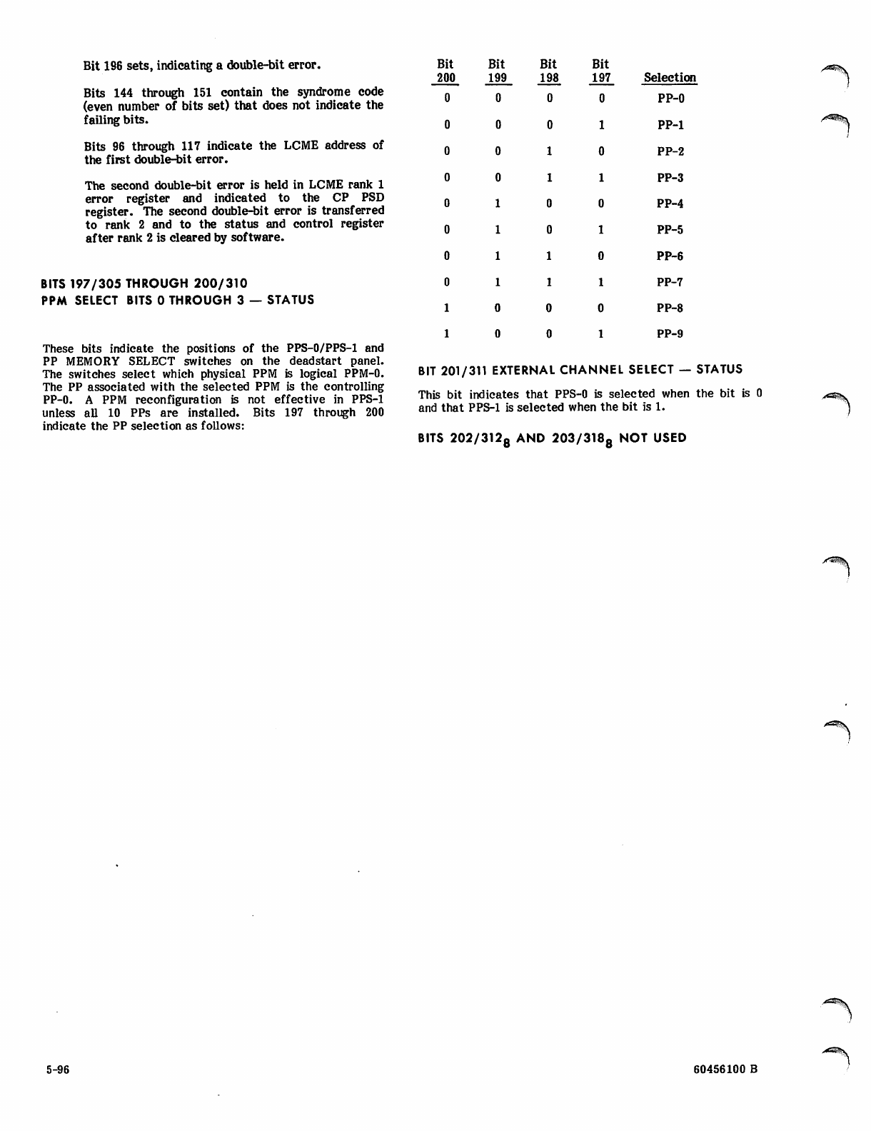
Bit 196 sets, indicating a double-bit error.
Bits 144 through 151 contain the syndrome code
(even number of bits set) that does not indicate the
failing bits.
Bits 96 through 117 indicate the LCME address of
the first double-bit error.
The second double-bit error is held in LCME rank 1
error register and indicated to the CP PSD
register. The second double-bit error is transferred
to rank 2 and to the status and control register
after rank 2 is cleared by software.
BITS 197/305 THROUGH 200/310
PPM SELECT BITS 0 THROUGH 3 — STATUS
These bits indicate the positions of the PPS-O/PPS-1 and
PP MEMORY SELECT switches on the deadstart panel.
The switches select which physical PPM is logical PPM-0.
The PP associated with the selected PPM is the controlling
PP-0. A PPM reconfiguration is not effective in PPS-1
unless all 10 PPs are installed. Bits 197 through 200
indicate the PP selection as follows:
Bit
200
Bit
199
Bit
198
Bit
197 Selection
0000 PP-0
000 1 PP-1
0 0 1 0 PP-2
00 1 1 PP-3
01 0 0 PP-4
0 1 0 1 PP-5
0 1 1 0 PP-6
0111 PP-7
1 0 0 0 PP-8
1 0 0 1 PP-9
BIT 201/311 EXTERNAL CHANNEL SELECT — STATUS
This bit indicates that PPS-0 is selected when the bit is 0
and that PPS-1 is selected when the bit is 1.
BITS 202/3128 AND 203/318& NOT USED
5-96 60456100 B
GLOSSARY
i^^>.
AU Arithmetic unit
BPA Breakpoint address
CEJ Central exchange jump
CIW Current instruction word
CM Central memory
CMC Central memory control
CMI Central memory interface
CP Central processor
CPU Central processing unit
CSU Central storage unit
ECS Extended core storage
EEA Exit error address
EM Exit mode
FLC Field length for CM
FLE Field length for ECS
FLL Field length for LCME
FLS Field length of program for CM
IAS Instruction address stack
IFA Instruction fetch address
I/O Input/output
IWS Instruction word stack
LCME Large core memory extension
MA Monitor address
MEJ Monitor exchange jump
MF Monitor flag
MOS Metal oxide semiconductor
NEA Normal exit address
P Program address
PE Parity error
PP Peripheral processor
PPM Peripheral processor memory
PPS Peripheral processor subsystem
PPU Peripheral processor unit
PSD Program status designator
RAC Reference address for CM
RAE Reference address for ECS
RAL Reference address for LCME
RAM Random access memory
RAS Reference address for CM
RNI Read next instruction
RVM Reference voltage margin
SAS Storage address stack
SECDED Single-error correction double-error detection
SRO Storage read out
SWS Storage word stack
60456100 E A-l

MODEL 740/750/760 AND MODEL 176 DIFFERENCES
r
Models 740/750/760 and model 176 differences involve the
instruction stack, central processor instructions, and the
peripheral processor subsystem instructions. The following
descriptions summarize the differences.
INSTRUCTION STACK DIFFERENCES
Models 740, 750, 760, and 176 each contain a 12-word
instruction stack. The stack is filled two words ahead of
the program address being executed.
In models 740, 750, and 760, the stack is voided by an
exchange, return jump, jump to the content of Bi plus K
(02) instruction or a branch (03 through 07) instruction to a
location not in the stack. The stack always contains
sequential code.
In model 176, the stack is voided by an exchange or a
return jump. The stack can contain nonsequential code or
duplicate entries.
CENTRAL PROCESSOR INSTRUCTION
DIFFERENCES
The central processor instruction differences occur for
shift, floating-add, divide, branch, and central exchange.
SHIFT (22 AND 23 INSTRUCTIONS)
Models 740, 750, and 760 return a plus zero when a
negative number is right shifted more than 63 (decimal)
places. Model 176 returns a minus zero when a negative
number is right shifted by more than 63 (decimal) places.
Example: 23011
XI =4000 0000 0000 0000 0000
Bl =000100
Models 750 and 760 result:
X0 = 0000 0000 0000 0000 0000
Model 176 result:
X0 = 7777 7777 7777 7777 7777
Models 740, 750, and 760 check bits 6 through 10 and ignore
bits 11 through 16. Model 176 checks bits 6 through 11 of
Bj for a shift count greater than 63 (decimal) and ignores
bits 12 through 16.
Example: 23011
XI = 2525 2525 2525 2525 2525
Bl = 004001
Models 740, 750, and 760 result:
XO =1252 5252 5252 5252 5252
Model 176 result:
X0 = 0000 0000 0000 0000 0000
FLOATING-ADD (30 INSTRUCTION)
When the difference between the exponents is greater than
128 (decimal), models 740, 750, and 760 extend the shifted
sign bit to the entire shifted operand. Model 176 enters a
shifted operand of plus zero regardless of the sign of the
shifted operand. If the reference operand has a zero
coefficient, the results can differ in sign.
Example: 30012
XI = 4277 7777 7777 7777 7777
X2 = 5277 5555 5555 5555 5555
Models 740, 750, and 760 result:
X0 = 4277 7777 7777 7777 7777
Model 176 result:
X0 = 3500 0000 0000 0000 0000
Reversing the operands (30021) gives the same results.
Example: 31012
XI =4277 7777 7777 7777 7777
X2 = 2500 2222 2222 2222 2222
Models 740, 750, and 760 result:
X0 = 4277 7777 7777 7777 7777
Model 176 result:
X0 = 3500 0000 0000 0000 0000
Example: 31012
XI = 5277 5555 5555 5555 5555
X2 = 3500 0000 0000 0000 0000
Models 740, 750, and 760 result:
X0 = 4277 7777 7777 7777 7777
Model 176 result:
X0 = 3500 0000 0000 0000 0000
60456100 E B-l
Reversing the operands (31021) on either of the examples
for a floating difference gives compatible results for
models 740, 750, 760, and 176. The result on each of these
models is 3500 0000 0000 0000 0000.
In model 176, the exit mode flag in the PSD register
controls the operation of the 013 instruction. The exit
mode flag sets to the value specified in the entering
exchange package.
DIVIDE (45 INSTRUCTION)
Models 740, 750, and 760 add one third to the dividend in a
divide round. Model 176 adds one half to the dividend in a
divide round.
Example: 45012
XI = 2027 7223 2220 7175 5360
X2 = 1347 4255 6115 0364 7225
Models 740, 750, and 760 result:
X0 = 2430 6557 3505 0613 2700
Model 176 result:
X0 = 2430 6557 3505 0613 2701
If the exponent subtract causes an underflow or overflow,
models 750 and 760 return an indefinite result with a divide
fault. With the same conditions, model 176 returns an
underflow or overflow result even with a divide fault.
Example: 44012
XI = 3700 0222 0000 0000 0000
X2 = 1600 0022 0000 0000 0000
Models 740, 750, and 760 result:
X0 = 1777 0000 0000 0000 0000
Model 176 result:
X0 = 3777 0000 0000 0000 0000
PERIPHERAL PROCESSOR SUBSYSTEM
INSTRUCTION DIFFERENCES
The PPS instruction differences occur for exchange jump,
monitor exchange jump, and monitor exchange jump to MA
instructions.
EXCHANGE JUMP (260X INSTRUCTION)
In models 740, 750, and 760, the exchange jump initiates an
exchange jump of the CP to the 18-bit address specified by
the A register. In model 176, the instruction performs as a
261 instruction.
MONITOR EXCHANGE JUMP (261X INSTRUCTION)
In models 740, 750, and 760, the monitor exchange jump
instruction is enabled or disabled by the CEJ/MEJ switch.
When the instruction is enabled and the monitor flag is
clear, the instruction sets the monitor flag and initiates an
exchange jump to the 18-bit address specified by the A
register. If the monitor flag is set, the instruction acts as
a pass instruction. When the instruction is disabled by the
CEJ/MEJ switch, the instruction executes as a 260
instruction.
In model 176, the CEJ/MEJ switch has no function. A
monitor exchange jump in this model initiates an exchange
jump of the CP. The jump is to the 18-bit address specified
by the A register. The jump occurs only if the exit mode
flag is clear and no I/O interrupts are waiting to be
processed. If the exit mode flag is set or I/O interrupts are
waiting to be processed, the instruction acts as a pass
instruction.
BRANCH (034 AND 035 INSTRUCTIONS)
In models 740, 750, and 760, overflow is out of range. In
model 176, overflow and indefinite are out of range.
CENTRAL EXCHANGE (013 INSTRUCTION)
The 013 instruction in models 740, 750, and 760 causes an
exchange jump to the content of Bj plus K. In model 176,
the instruction causes an exchange jump to the content of
Bj plus K plus the reference address for CM.
In models 740, 750, and 760, the monitor flag controls the
operation of the 013 instruction. The instruction changes
the state of the monitor flag.
MONITOR EXCHANGE JUMP TO MA
(262X INSTRUCTION)
In models 740, 750, and 760, the monitor exchange jump to
MA instruction is enabled or disabled by the CEJ/MEJ
switch. When the instruction is enabled and the monitor
flag is clear, the instruction sets the flag and initiates an
exchange jump to the 18-bit address specified by the MA
register. If the monitor flag is set, the instruction acts as
a pass instruction. When the instruction is disabled by the
CEJ/MEJ switch, the instruction executes as a 260
instruction.
In model 176, the CEJ/MEJ switch has no function. A
monitor exchange jump to MA instruction performs as a
261 instruction.
B-2 60456100 E
.0Sffc\.
INDEX
This index lists subject words not covered in the contents. Page
references to the subject words are mainly to explanatory text
and are not necessarily to all usages.
Absolute program address 2-4
Access port 1-17
Access time 2-23
Arithmetic unit 1-15
Bank phasing 2-25
Barrel and slot 2-43,44; 3-4
Bipolar semiconductor memory
Block copy 2-6,14,28; 4-6,7,8
Block transfers 2-41
Breakpoint 2-21
Buffer flush feature 2-36
Buffer, PPU 2-29,31,32
1-16
Indefinite result 5-10
Illegal instructions 5-15
Input/output exchange package 2-29
Input record sequence 2-30
Instruction address stack 1-16; 2-14; 3-18
Instruction control 1-15; 2-3
Instruction designators 4-4,46
Instruction format CP: 4-3; PP: 4-46; PPU: 4-46
Instruction word stack 1-16; 2-9,13,14
Keyboard 1-18; 3-8,19,29; 5-41
Cathode-ray tube 1-18; 2-37; 5-41,42
Central memory cycle time 1-8; 2-23,25
Channel conflicts 5-48
Channel timing 5-46,49,50,51,53,54
Channel 16/36 2-46,55
Clock 3-6,17,19,20
Clock period 1-8; 2-15; 4-61
Clock period counter 5-6
Compare/move 2-6
Condition flags 2-12
Conduction cooling 1-18
Current instruction word 1-16; 2-9,12,14
Deadstart 2-43; 3-3,4,29
Descriptor word 4-28; 5-55
Disassembly register 2-30,31
Distributive data path 1-17
Double precision 5-12
Light-emitting diodes 2-46; 3-5,6,8
Load mode 3-29
Load programs 3-29
Lockout 2-28,31,32
Loop counts 2-3,10
Major cycle 2-43
Master clear 3-29
Metal-oxide semiconductor 1-16; 2-43
Minor cycle 1-9; 4-75
Mode flags 2-12
Monitor address 2-4,11
Monitor flag 5-3
Monitor program 4-9,10,11
Multiplexing 1-17; 2-29,43,44
Nonstandard operations 5-10
Normal jump sequence 2-14
Normal-speed channels 2-29
Normalized numbers 5-12
0*
Error exit 4-5; 5-16,25
Exchange interval 2-13
Exchange jump 5-3
Exchange package 5-3,4,5
Exchange sequence 2-14
Execution interval 5-4,5,6
Execution times CP: 4-32; PPS: 4-75; PPU: 4-61
Fixed point 5-13
Flag register operation
Full exit 5-16,25 2-3,10; 5-16,28,29
Half exit 5-16,25
High speed channels 2-29,31
Hung CP: 5-6; PPS: 2-43,45, 4-73,74; PPU: 2-41
One's complement mode PPU: 4-45; PP: 4-65
Overflow 5-10
Packing 5-9
Parcels 2-4; 4-3,4; 5-8
Phased addressing 2-23
Power failure mode 2-36
Program address counter 2-10,11
Program execution 2-9
Program optimization 5-8
Program word 4-3,4
Quadrant 2-23,24; 3-15,17,20,21; 5-76
60456100 E Index-l
Random access memory 2-40,43
Read next instruction 5-7
Read operation 2-24,25
Real-time clock 1-9,15; 2-45
Real-time interrupt 5-6
Reconfiguration CM: 2-24,26; 3-15,17,21; PPM: 2-43
Reference voltage margins 5-76,93
Return jump sequence 2-14
Rounding 5-12
Syndrome code 2-18,19
Transfer rate CM: 1-8, 5-47; ECS: 4-7, 5-29;
LCME: 2-28; PPS: 5-47; PPS: channel 2-45, 5-49;
PPU: 5-46
Trip count 2-45
Segmentation 2-15
Semirandom access 1-16
Sequential addressing 2-23,24,25
Single precision 5-12,13
Slot time 2-44; 5-49
Step mode 5-6
Storage address stack 2-17
Sweep mode 3-29
Underflow 5-10
Voiding instruction word stack 2-14
Write operation 2-25
^=«ftsfti
,>fS%v
Index-2 60456100 E
