Cortex A Series Programmer’s Guide Cort AProg
CortAProgGuide
User Manual: Pdf
Open the PDF directly: View PDF ![]() .
.
Page Count: 455 [warning: Documents this large are best viewed by clicking the View PDF Link!]
- Cortex-A Series Programmer’s Guide
- Contents
- Preface
- 1: Introduction
- 2: The ARM Architecture
- 3: Tools, Operating Systems and Boards
- 4: ARM Registers, Modes and Instruction Sets
- 5: Introduction to Assembly Language
- 6: ARM/Thumb Unified Assembly Language Instructions
- 7: Caches
- 7.1 Why do caches help?
- 7.2 Cache drawbacks
- 7.3 Memory hierarchy
- 7.4 Cache terminology
- 7.5 Cache architecture
- 7.6 Cache controller
- 7.7 Direct mapped caches
- 7.8 Set associative caches
- 7.9 A real-life example
- 7.10 Virtual and physical tags and indexes
- 7.11 Cache policies
- 7.12 Allocation policy
- 7.13 Replacement policy
- 7.14 Write policy
- 7.15 Write and Fetch buffers
- 7.16 Cache performance and hit rate
- 7.17 Invalidating and cleaning cache memory
- 7.18 Cache lockdown
- 7.19 Level 2 cache controller
- 7.20 Point of coherency and unification
- 7.21 Parity and ECC in caches
- 7.22 Tightly coupled memory
- 8: Memory Management Unit
- 9: Memory Ordering
- 10: Exception Handling
- 11: Interrupt Handling
- 12: Other Exception Handlers
- 13: Boot Code
- 14: Porting
- 15: Application Binary Interfaces
- 16: Profiling
- 17: Optimizing Code to Run on ARM Processors
- 17.1 Compiler optimizations
- 17.2 ARM memory system optimization
- 17.2.1 Data cache optimization
- 17.2.2 Loop tiling
- 17.2.3 Loop interchange
- 17.2.4 Structure alignment
- 17.2.5 Associativity effects
- 17.2.6 Optimizing instruction cache usage
- 17.2.7 Fast loop mode
- 17.2.8 Optimizing L2/outer cache usage
- 17.2.9 Optimizing TLB usage
- 17.2.10 Data abort optimization
- 17.2.11 Prefetching a memory block access
- 17.2.12 Preload engine
- 17.3 Source code modifications
- 17.4 Cortex-A9 micro-architecture optimizations
- 18: Floating-Point
- 19: Introducing NEON
- 20: Writing NEON Code
- 21: Power Management
- 22: Introduction to Multi-processing
- 23: SMP Architectural Considerations
- 24: Parallelizing Software
- 25: Issues with Parallelizing Software
- 26: Security
- 27: Virtualization
- 28: Debug
- A: Instruction Summary
- A.1 Instruction Summary
- A.1.1 ADC
- A.1.2 ADD
- A.1.3 ADR
- A.1.4 ADRL
- A.1.5 AND
- A.1.6 ASR
- A.1.7 B
- A.1.8 BFC
- A.1.9 BFI
- A.1.10 BIC
- A.1.11 BKPT
- A.1.12 BL
- A.1.13 BLX
- A.1.14 BX
- A.1.15 BXJ
- A.1.16 CBNZ
- A.1.17 CBZ
- A.1.18 CDP
- A.1.19 CDP2
- A.1.20 CHKA
- A.1.21 CLREX
- A.1.22 CLZ
- A.1.23 CMN
- A.1.24 CMP
- A.1.25 CPS
- A.1.26 DBG
- A.1.27 DMB
- A.1.28 DSB
- A.1.29 ENTERX
- A.1.30 EOR
- A.1.31 ERET
- A.1.32 HB
- A.1.33 ISB
- A.1.34 IT
- A.1.35 LDC
- A.1.36 LDC2
- A.1.37 LDM
- A.1.38 LDR
- A.1.39 LDR (pseudo-instruction)
- A.1.40 LDRD
- A.1.41 LDREX
- A.1.42 LEAVEX
- A.1.43 LSL
- A.1.44 LSR
- A.1.45 MCR
- A.1.46 MCR2
- A.1.47 MCRR
- A.1.48 MCRR2
- A.1.49 MLA
- A.1.50 MLS
- A.1.51 MOV
- A.1.52 MOVT
- A.1.53 MOV32
- A.1.54 MRC
- A.1.55 MRC2
- A.1.56 MRRC
- A.1.57 MRRC2
- A.1.58 MRS
- A.1.59 MSR
- A.1.60 MUL
- A.1.61 MVN
- A.1.62 NOP
- A.1.63 ORN
- A.1.64 ORR
- A.1.65 PKHBT
- A.1.66 PKHTB
- A.1.67 PLD
- A.1.68 PLDW
- A.1.69 PLI
- A.1.70 POP
- A.1.71 PUSH
- A.1.72 QADD
- A.1.73 QADD8
- A.1.74 QADD16
- A.1.75 QASX
- A.1.76 QDADD
- A.1.77 QDSUB
- A.1.78 QSAX
- A.1.79 QSUB
- A.1.80 QSUB8
- A.1.81 QSUB16
- A.1.82 RBIT
- A.1.83 REV
- A.1.84 REV16
- A.1.85 REVSH
- A.1.86 RFE
- A.1.87 ROR
- A.1.88 RRX
- A.1.89 RSB
- A.1.90 RSC
- A.1.91 SADD8
- A.1.92 SADD16
- A.1.93 SASX
- A.1.94 SBC
- A.1.95 SBFX
- A.1.96 SDIV
- A.1.97 SEL
- A.1.98 SETEND
- A.1.99 SEV
- A.1.100 SHADD8
- A.1.101 SHADD16
- A.1.102 SHASX
- A.1.103 SHSAX
- A.1.104 SHSUB8
- A.1.105 SHSUB16
- A.1.106 SMC
- A.1.107 SMLAxy
- A.1.108 SMLAD
- A.1.109 SMLAL
- A.1.110 SMLALxy
- A.1.111 SMLALD
- A.1.112 SMLAWy
- A.1.113 SMLSLD
- A.1.114 SMMLA
- A.1.115 SMMLS
- A.1.116 SMMUL
- A.1.117 SMUAD
- A.1.118 SMUSD
- A.1.119 SMULxy
- A.1.120 SMULL
- A.1.121 SMULWy
- A.1.122 SRS
- A.1.123 SSAT
- A.1.124 SSAT16
- A.1.125 SSAX
- A.1.126 SSUB8
- A.1.127 SSUB16
- A.1.128 STC
- A.1.129 STC2
- A.1.130 STM
- A.1.131 STR
- A.1.132 STRD
- A.1.133 STREX
- A.1.134 SUB
- A.1.135 SVC
- A.1.136 SWP
- A.1.137 SXT
- A.1.138 SXTA
- A.1.139 SYS
- A.1.140 TBB
- A.1.141 TBH
- A.1.142 TEQ
- A.1.143 TST
- A.1.144 UADD8
- A.1.145 UADD16
- A.1.146 UASX
- A.1.147 UBFX
- A.1.148 UDIV
- A.1.149 UHADD8
- A.1.150 UHADD16
- A.1.151 UHASX
- A.1.152 UHSAX
- A.1.153 UHSUB8
- A.1.154 UHSUB16
- A.1.155 UMAAL
- A.1.156 UMLAL
- A.1.157 UMULL
- A.1.158 UQADD8
- A.1.159 UQADD16
- A.1.160 UQASX
- A.1.161 UQSAX
- A.1.162 UQSUB8
- A.1.163 UQSUB16
- A.1.164 USAD8
- A.1.165 USADA8
- A.1.166 USAT
- A.1.167 USAT16
- A.1.168 USAX
- A.1.169 USUB8
- A.1.170 USUB16
- A.1.171 UXT
- A.1.172 UXTA
- A.1.173 WFE
- A.1.174 WFI
- A.1.175 YIELD
- A.1 Instruction Summary
- B: NEON and VFP Instruction Summary
- B.1 NEON general data processing instructions
- B.2 NEON shift instructions
- B.3 NEON logical and compare operations
- B.4 NEON arithmetic instructions
- B.4.1 VABA{L}
- B.4.2 VABD{L}
- B.4.3 V{Q}ABS
- B.4.4 V{Q}ADD, VADDL, VADDW
- B.4.5 V{R}ADDHN
- B.4.6 VCLS
- B.4.7 VCLZ
- B.4.8 VCNT
- B.4.9 V{R}HADD
- B.4.10 VHSUB
- B.4.11 VMAX and VMIN
- B.4.12 V{Q}NEG
- B.4.13 VPADD{L}, VPADAL
- B.4.14 VPMAX and VPMIN
- B.4.15 VRECPE
- B.4.16 VRECPS
- B.4.17 VRSQRTE
- B.4.18 VRSQRTS
- B.4.19 V{Q}SUB, VSUBL and VSUBW
- B.4.20 V{R}SUBHN
- B.5 NEON multiply instructions
- B.6 NEON load and store element and structure instructions
- B.6.1 VLDn and VSTn (single n-element structure to one lane)
- B.6.2 VLDn (single n-element structure to all lanes)
- B.6.3 VLDn and VSTn (multiple n-element structures)
- B.6.4 VLDR and VSTR
- B.6.5 VLDM, VSTM, VPOP, and VPUSH
- B.6.6 VMOV (between two ARM registers and an extension register)
- B.6.7 VMOV (between an ARM register and a NEON scalar)
- B.6.8 VMRS and VMSR
- B.7 VFP instructions
- B.7.1 VABS
- B.7.2 VADD
- B.7.3 VCMP
- B.7.4 VCVT (between single-precision and double-precision)
- B.7.5 VCVT (between floating-point and integer)
- B.7.6 VCVT (between floating-point and fixed-point)
- B.7.7 VCVTB, VCVTT (half-precision extension)
- B.7.8 VDIV
- B.7.9 VFMA, VFNMA, VFMS, VFNMS
- B.7.10 VMOV
- B.7.11 VMOV
- B.7.12 VMUL, VMLA, VMLS, VNMUL, VNMLA, and VNMLS
- B.7.13 VNEG
- B.7.14 VSQRT
- B.7.15 VSUB
- B.8 NEON and VFP pseudo-instructions
- C: Building Linux for ARM Systems

Copyright © 2011 ARM. All rights reserved.
ARM DEN0013B (ID082411)
Cortex™-A Series
Version: 2.0
Programmer’s Guide

ARM DEN0013B Copyright © 2011 ARM. All rights reserved. ii
ID082411 Non-Confidential
Cortex-A Series
Programmer’s Guide
Copyright © 2011 ARM. All rights reserved.
Release Information
The following changes have been made to this book.
Proprietary Notice
This Cortex-A Series Programmer’s Guide is protected by copyright and the practice or implementation of the
information herein may be protected by one or more patents or pending applications. No part of this Cortex-A Series
Programmer’s Guide may be reproduced in any form by any means without the express prior written permission of
ARM. No license, express or implied, by estoppel or otherwise to any intellectual property rights is granted by
this Cortex-A Series Programmer’s Guide.
Your access to the information in this Cortex-A Series Programmer’s Guide is conditional upon your acceptance that
you will not use or permit others to use the information for the purposes of determining whether implementations of the
information herein infringe any third party patents.
This Cortex-A Series Programmer’s Guide is provided “as is”. ARM makes no representations or warranties, either
express or implied, included but not limited to, warranties of merchantability, fitness for a particular purpose, or
non-infringement, that the content of this Cortex-A Series Programmer’s Guide is suitable for any particular purpose or
that any practice or implementation of the contents of the Cortex-A Series Programmer’s Guide will not infringe any
third party patents, copyrights, trade secrets, or other rights.
This Cortex-A Series Programmer’s Guide may include technical inaccuracies or typographical errors.
To the extent not prohibited by law, in no event will ARM be liable for any damages, including without limitation any
direct loss, lost revenue, lost profits or data, special, indirect, consequential, incidental or punitive damages, however
caused and regardless of the theory of liability, arising out of or related to any furnishing, practicing, modifying or any
use of this Programmer’s Guide, even if ARM has been advised of the possibility of such damages. The information
provided herein is subject to U.S. export control laws, including the U.S. Export Administration Act and its associated
regulations, and may be subject to export or import regulations in other countries. You agree to comply fully with all
laws and regulations of the United States and other countries (“Export Laws”) to assure that neither the information
herein, nor any direct products thereof are; (i) exported, directly or indirectly, in violation of Export Laws, either to any
countries that are subject to U.S. export restrictions or to any end user who has been prohibited from participating in the
U.S. export transactions by any federal agency of the U.S. government; or (ii) intended to be used for any purpose
prohibited by Export Laws, including, without limitation, nuclear, chemical, or biological weapons proliferation.
Words and logos marked with ® or TM are registered trademarks or trademarks of ARM Limited, except as otherwise
stated below in this proprietary notice. Other brands and names mentioned herein may be the trademarks of their
respective owners.
Copyright © 2011 ARM Limited
110 Fulbourn Road Cambridge, CB1 9NJ, England
This document is Non-Confidential but any disclosure by you is subject to you providing notice to and the
acceptance by the recipient of, the conditions set out above.
In this document, where the term ARM is used to refer to the company it means “ARM or any of its subsidiaries as
appropriate”.
Web Address
http://www.arm.com
Change history
Date Issue Confidentiality Change
25 March 2011 A Non-Confidential First release
10 August 2011 B Non-Confidential Second release. Virtualization chapter added
Updated to include Cortex-A15 processor, and LPAE
Corrected and revised throughout

ARM DEN0013B Copyright © 2011 ARM. All rights reserved. iii
ID082411 Non-Confidential
Contents
Cortex-A Series Programmer’s Guide
Preface
References ....................................................................................................................... x
Typographical conventions .............................................................................................. xi
Feedback on this book .................................................................................................... xii
Terms and abbreviations ............................................................................................... xiii
Chapter 1 Introduction
1.1 History ........................................................................................................................... 1-3
1.2 System-on-Chip (SoC) .................................................................................................. 1-4
1.3 Embedded systems ...................................................................................................... 1-5
Chapter 2 The ARM Architecture
2.1 Architecture versions .................................................................................................... 2-3
2.2 Architecture history and extensions .............................................................................. 2-4
2.3 Key points of the ARM Cortex-A series architecture .................................................... 2-8
2.4 Processors and pipelines .............................................................................................. 2-9
Chapter 3 Tools, Operating Systems and Boards
3.1 Linux distributions ......................................................................................................... 3-2
3.2 Useful tools ................................................................................................................... 3-6
3.3 Software toolchains for ARM processors ...................................................................... 3-8
3.4 ARM DS-5 ................................................................................................................... 3-11
3.5 Example platforms ...................................................................................................... 3-13
Chapter 4 ARM Registers, Modes and Instruction Sets
4.1 Instruction sets .............................................................................................................. 4-2
4.2 Modes ........................................................................................................................... 4-3
4.3 Registers ....................................................................................................................... 4-4

Contents
ARM DEN0013B Copyright © 2011 ARM. All rights reserved. iv
ID082411 Non-Confidential
4.4 Instruction pipelines ...................................................................................................... 4-7
4.5 Branch prediction ........................................................................................................ 4-10
Chapter 5 Introduction to Assembly Language
5.1 Comparison with other assembly languages ................................................................ 5-2
5.2 Instruction sets .............................................................................................................. 5-4
5.3 ARM tools assembly language ..................................................................................... 5-5
5.4 Introduction to the GNU Assembler .............................................................................. 5-7
5.5 Interworking ................................................................................................................ 5-11
5.6 Identifying assembly code .......................................................................................... 5-12
Chapter 6 ARM/Thumb Unified Assembly Language Instructions
6.1 Instruction set basics .................................................................................................... 6-2
6.2 Data processing operations .......................................................................................... 6-6
6.3 Multiplication operations ............................................................................................... 6-9
6.4 Memory instructions .................................................................................................... 6-10
6.5 Branches ..................................................................................................................... 6-13
6.6 Integer SIMD instructions ........................................................................................... 6-14
6.7 Saturating arithmetic ................................................................................................... 6-18
6.8 Miscellaneous instructions .......................................................................................... 6-19
Chapter 7 Caches
7.1 Why do caches help? ................................................................................................... 7-3
7.2 Cache drawbacks ......................................................................................................... 7-4
7.3 Memory hierarchy ......................................................................................................... 7-5
7.4 Cache terminology ........................................................................................................ 7-6
7.5 Cache architecture ........................................................................................................ 7-7
7.6 Cache controller ............................................................................................................ 7-8
7.7 Direct mapped caches .................................................................................................. 7-9
7.8 Set associative caches ............................................................................................... 7-11
7.9 A real-life example ...................................................................................................... 7-12
7.10 Virtual and physical tags and indexes ........................................................................ 7-13
7.11 Cache policies ............................................................................................................ 7-14
7.12 Allocation policy .......................................................................................................... 7-15
7.13 Replacement policy .................................................................................................... 7-16
7.14 Write policy ................................................................................................................. 7-17
7.15 Write and Fetch buffers .............................................................................................. 7-18
7.16 Cache performance and hit rate ................................................................................. 7-19
7.17 Invalidating and cleaning cache memory .................................................................... 7-20
7.18 Cache lockdown ......................................................................................................... 7-21
7.19 Level 2 cache controller .............................................................................................. 7-22
7.20 Point of coherency and unification .............................................................................. 7-23
7.21 Parity and ECC in caches ........................................................................................... 7-24
7.22 Tightly coupled memory .............................................................................................. 7-25
Chapter 8 Memory Management Unit
8.1 Virtual memory .............................................................................................................. 8-3
8.2 Level 1 page tables ....................................................................................................... 8-4
8.3 Level 2 page tables ....................................................................................................... 8-7
8.4 The Translation Lookaside Buffer ................................................................................. 8-9
8.5 TLB coherency ............................................................................................................ 8-10
8.6 Choice of page sizes .................................................................................................. 8-11
8.7 Memory attributes ....................................................................................................... 8-12
8.8 Multi-tasking and OS usage of page tables ................................................................ 8-15
8.9 Linux use of page tables ............................................................................................. 8-18
8.10 The Cortex-A15 MMU and Large Physical Address Extensions ................................ 8-21
Chapter 9 Memory Ordering
9.1 ARM memory ordering model ....................................................................................... 9-4

Contents
ARM DEN0013B Copyright © 2011 ARM. All rights reserved. v
ID082411 Non-Confidential
9.2 Memory barriers ............................................................................................................ 9-6
9.3 Cache coherency implications .................................................................................... 9-12
Chapter 10 Exception Handling
10.1 Types of exception ...................................................................................................... 10-2
10.2 Entering an exception handler .................................................................................... 10-4
10.3 Exit from an exception handler ................................................................................... 10-5
10.4 Exception mode summary .......................................................................................... 10-6
10.5 Vector table ................................................................................................................. 10-8
10.6 Distinction between FIQ and IRQ ............................................................................... 10-9
10.7 Return instruction ...................................................................................................... 10-10
10.8 Privilege model in ARMv7-A Virtualization Extensions ............................................. 10-11
Chapter 11 Interrupt Handling
11.1 External interrupt requests .......................................................................................... 11-2
11.2 Generic Interrupt Controller ........................................................................................ 11-5
Chapter 12 Other Exception Handlers
12.1 Abort handler .............................................................................................................. 12-2
12.2 Undefined instruction handling ................................................................................... 12-4
12.3 SVC exception handling ............................................................................................. 12-5
12.4 Linux exception program flow ..................................................................................... 12-6
Chapter 13 Boot Code
13.1 Booting a bare-metal system ...................................................................................... 13-2
13.2 Configuration .............................................................................................................. 13-6
13.3 Booting Linux .............................................................................................................. 13-7
Chapter 14 Porting
14.1 Endianness ................................................................................................................. 14-2
14.2 Alignment .................................................................................................................... 14-6
14.3 Miscellaneous C porting issues .................................................................................. 14-8
14.4 Porting ARM assembly code to ARMv7 .................................................................... 14-11
14.5 Porting ARM code to Thumb .................................................................................... 14-12
Chapter 15 Application Binary Interfaces
15.1 Procedure Call Standard ............................................................................................ 15-2
15.2 Mixing C and assembly code ...................................................................................... 15-7
Chapter 16 Profiling
16.1 Profiler output ............................................................................................................. 16-3
Chapter 17 Optimizing Code to Run on ARM Processors
17.1 Compiler optimizations ............................................................................................... 17-3
17.2 ARM memory system optimization ............................................................................. 17-8
17.3 Source code modifications ........................................................................................ 17-14
17.4 Cortex-A9 micro-architecture optimizations .............................................................. 17-19
Chapter 18 Floating-Point
18.1 Floating-point basics and the IEEE-754 standard ...................................................... 18-2
18.2 VFP support in GCC ................................................................................................... 18-9
18.3 VFP support in the ARM Compiler ............................................................................ 18-10
18.4 VFP support in Linux ................................................................................................ 18-11
18.5 Floating-point optimization ........................................................................................ 18-12
Chapter 19 Introducing NEON
19.1 SIMD ........................................................................................................................... 19-2
19.2 NEON architecture overview ...................................................................................... 19-4

Contents
ARM DEN0013B Copyright © 2011 ARM. All rights reserved. vi
ID082411 Non-Confidential
19.3 NEON comparisons with other SIMD solutions ........................................................ 19-11
Chapter 20 Writing NEON Code
20.1 NEON C Compiler and assembler .............................................................................. 20-2
20.2 Optimizing NEON assembler code ............................................................................. 20-6
20.3 NEON power saving ................................................................................................... 20-9
Chapter 21 Power Management
21.1 Power and clocking ..................................................................................................... 21-2
Chapter 22 Introduction to Multi-processing
22.1 Multi-processing ARM systems .................................................................................. 22-3
22.2 Symmetric multi-processing ........................................................................................ 22-5
22.3 Asymmetric multi-processing ...................................................................................... 22-7
Chapter 23 SMP Architectural Considerations
23.1 Cache coherency ........................................................................................................ 23-2
23.2 TLB and cache maintenance broadcast ..................................................................... 23-4
23.3 Handling interrupts in an SMP system ........................................................................ 23-5
23.4 Exclusive accesses ..................................................................................................... 23-6
23.5 Booting SMP systems ................................................................................................. 23-9
23.6 Private memory region .............................................................................................. 23-11
Chapter 24 Parallelizing Software
24.1 Decomposition methods ............................................................................................. 24-2
24.2 Threading models ....................................................................................................... 24-4
24.3 Threading libraries ...................................................................................................... 24-5
24.4 Synchronization mechanisms in the Linux kernel ....................................................... 24-8
Chapter 25 Issues with Parallelizing Software
25.1 Thread safety and reentrancy ..................................................................................... 25-2
25.2 Performance issues .................................................................................................... 25-3
25.3 Profiling in SMP systems ............................................................................................ 25-5
Chapter 26 Security
26.1 TrustZone hardware architecture ................................................................................ 26-2
Chapter 27 Virtualization
27.1 ARMv7-A Virtualization Extensions ............................................................................ 27-3
27.2 Hypervisor exception model ....................................................................................... 27-5
27.3 Relationship between virtualization and ARM Security Extensions ............................ 27-6
Chapter 28 Debug
28.1 ARM debug hardware ................................................................................................. 28-2
28.2 ARM trace hardware ................................................................................................... 28-3
28.3 Debug monitor ............................................................................................................ 28-6
28.4 Debugging Linux applications ..................................................................................... 28-7
28.5 ARM tools supporting debug and trace ...................................................................... 28-8
Appendix A Instruction Summary
A.1 Instruction Summary ..................................................................................................... A-2
Appendix B NEON and VFP Instruction Summary
B.1 NEON general data processing instructions ................................................................. B-6
B.2 NEON shift instructions ............................................................................................... B-12
B.3 NEON logical and compare operations ...................................................................... B-16
B.4 NEON arithmetic instructions ...................................................................................... B-22

Contents
ARM DEN0013B Copyright © 2011 ARM. All rights reserved. vii
ID082411 Non-Confidential
B.5 NEON multiply instructions ......................................................................................... B-30
B.6 NEON load and store element and structure instructions ........................................... B-33
B.7 VFP instructions .......................................................................................................... B-39
B.8 NEON and VFP pseudo-instructions .......................................................................... B-45
Appendix C Building Linux for ARM Systems
C.1 Building the Linux kernel ............................................................................................... C-2
C.2 Creating the Linux filesystem ........................................................................................ C-6
C.3 Putting it together .......................................................................................................... C-8

ARM DEN0013B Copyright © 2011 ARM. All rights reserved. viii
ID082411 Non-Confidential
Preface
This book provides an introduction to ARM technology for programmers using ARM Cortex-A
series processors that conform to the ARM ARMv7–A architecture. The “v7” refers to version 7 of
the architecture, while the “A” indicates the architecture profile that describes Application
processors. This includes the Cortex-A5, Cortex-A8, Cortex-A9 and Cortex-A15 processors. The
book complements rather than replaces other ARM documentation that is available for Cortex-A
series processors, such as the ARM Technical Reference Manual (TRMs) for the processors
themselves, documentation for individual devices or boards and of course, most importantly, the
ARM Architecture Reference Manual (or the “ARM ARM”).
Although much of the book is also applicable to other ARM processors, we do not explicitly cover
processors that implement older versions of the Architecture. The Cortex-R series and M-series
processors are mentioned but not described. Our intention is to provide an approachable
introduction to the ARM architecture, covering the feature set in detail and providing practical
advice on writing both C and assembly language programs to run efficiently on a Cortex-A series
processor. We assume familiarity with the C language and some knowledge of microprocessor
architectures, although no ARM-specific background is needed. We hope that the text will be well
suited to programmers who have a desktop PC or x86 background and are taking their first steps
into the ARM-based world.
The first dozen chapters of the book cover the basic features of the ARM Cortex-A series
processors. An introduction to the fundamentals of the ARM architecture and some background on
individual processors is provided in Chapter 2. In Chapter 3, we briefly consider some of the tools
and platforms available to those getting started with ARM programming. Chapters 4, 5 and 6
provide a brisk introduction to ARM assembly language programming, covering the various
registers, modes and assembly language instructions. We then switch our focus to the memory
system and look at Caches, Memory Management and Memory Ordering in Chapters 7, 8 and 9.
Dealing with interrupts and other exceptions is described in Chapters 10 to 12.

Preface
ARM DEN0013B Copyright © 2011 ARM. All rights reserved. ix
ID082411 Non-Confidential
The remaining chapters of the book provide more advanced programming information.
Chapter 13 provides an overview of boot code. Chapter 14 looks at issues with porting C and
assembly code to the ARMv7 architecture, from other architectures and from older versions of
the ARM architecture. Chapter 15 covers the Application Binary Interface, knowledge of which
is useful to both C and assembly language programmers. Profiling and optimizing of code is
covered in Chapters 16 and 17. Many of the techniques presented are not specific to the ARM
architecture, but we also provide some processor-specific hints. We look at floating-point and
the ARM Advanced SIMD extensions (NEON) in Chapters 18-20. These chapters are only an
introduction to the relevant topics. It would take significantly longer to cover all of the powerful
capabilities of NEON and how to apply these to common signal processing algorithms.
Power management is an important part of ARM programming and is covered in Chapter 21.
Chapters 22-25 cover the area of multi-processing. We take a detailed look at how this is
implemented by ARM and how you can write code to take advantage of it. The final chapters
of the book provide a brief coverage of the ARM Security Extensions (TrustZone®), the ARM
Virualization extensions (Chapter 27) and the powerful hardware debug features available to
programmers (Chapter 28). Appendices A and B give a summary of the available ARM, NEON
and VFP instructions and Appendix C gives step by step instructions for configuring and
building Linux for ARM systems.

Preface
ARM DEN0013B Copyright © 2011 ARM. All rights reserved. x
ID082411 Non-Confidential
References
Cohen, D. “On Holy Wars and a Plea for Peace”, USC/ISI IEN April, 1980,
http://www.ietf.org/rfc/ien/ien137.txt.
Furber, Steve. “ARM System-on-chip Architecture”, 2nd edition, Addison-Wesley, 2000, ISBN:
9780201675191.
Hohl, William. “ARM Assembly Language: Fundamentals and Techniques” CRC Press, 2009.
ISBN: 9781439806104.
Sloss, Andrew N.; Symes, Dominic.; Wright, Chris. “ARM System Developer's Guide:
Designing and Optimizing System Software”, Morgan Kaufmann, 2004, ISBN:
9781558608740.
Yiu, Joseph. “The Definitive Guide to the ARM Cortex-M3”, 2nd edition, Newnes, 2009, ISBN:
9780750685344.
ANSI/IEEE Std 754-1985, “IEEE Standard for Binary Floating-Point Arithmetic”.
ANSI/IEEE Std 754-2008, “IEEE Standard for Binary Floating-Point Arithmetic”.
ANSI/IEEE Std 1003.1-1990, “Standard for Information Technology - Portable Operating
System Interface (POSIX) Base Specifications, Issue 7”.
ANSI/IEEE Std 1149.1-2001, “IEEE Standard Test Access Port and Boundary-Scan
Architecture”.
The ARM Architecture Reference Manual (known as the ARM ARM) is a must-read for any
serious ARM programmer. It is available (after registration) from the ARM website. It fully
describes the ARMv7 instruction set architecture, programmer’s model, system registers, debug
features and memory model. It forms a detailed specification to which all implementations of
ARM processors must adhere.
References to the ARM Architecture Reference Manual in this document are to:
ARM Architecture Reference Manual - ARMv7-A and ARMv7-R edition (ARM DDI 0406).
Note
In the event of a contradiction between this book and the ARM ARM, the ARM ARM is
definitive and must take precedence.
ARM Generic Interrupt Controller Architecture Specification (ARM IHI 0048).
ARM Compiler Toolchain Assembler Reference (DUI 0489).
The individual processor Technical Reference Manuals provide a detailed description of the
processor behavior. They can be obtained from the ARM website documentation area,
http://infocenter.arm.com/help/index.jsp.

Preface
ARM DEN0013B Copyright © 2011 ARM. All rights reserved. xi
ID082411 Non-Confidential
Typographical conventions
This book uses the following typographical conventions:
italic Highlights important notes, introduces special terminology, denotes
internal cross-references, and citations.
bold Used for terms in descriptive lists, where appropriate.
monospace
Denotes text that you can enter at the keyboard, such as commands, file
and program names, instruction names, parameters and source code.
monospace
italic
Denotes arguments to monospace text where the argument is to be
replaced by a specific value.
< and > Enclose replaceable terms for assembler syntax where they appear in code
or code fragments. For example:
MRC p15, 0, <Rd>, <CRn>, <CRm>, <Opcode_2>
“term” We use quotation marks to identify unfamiliar or configuration specific
terms when they are first used, For example: “flat mapping”.

Preface
ARM DEN0013B Copyright © 2011 ARM. All rights reserved. xii
ID082411 Non-Confidential
Feedback on this book
We have tried to ensure that the Cortex-A Series Programmer’s Guide is both easy to read, and
still covers the material in enough depth to provide the comprehensive introduction to using the
processors that we originally intended.
If you have any comments on this book, don’t understand our explanations, think something is
missing or could be better explained, or think that it is incorrect, send an e-mail to
errata@arm.com
. Give:
• The title: The Cortex-A Series Programmer’s Guide
• the number, ARM DEN0013B
• the page number(s) to which your comments apply
• what you think needs to be changed.
ARM also welcomes general suggestions for additions and improvements.

Preface
ARM DEN0013B Copyright © 2011 ARM. All rights reserved. xiii
ID082411 Non-Confidential
Terms and abbreviations
Terms used in this document are defined here.
AAPCS ARM Architecture Procedure Call Standard.
ABI Application Binary Interface.
ACP Accelerator Coherency Port.
AHB Advanced High-Performance Bus.
AMBA® Advanced Microcontroller Bus Architecture.
AMP Asymmetric Multi-Processing.
APB Advanced Peripheral Bus.
ARM ARM The ARM Architecture Reference Manual.
ASIC Application Specific Integrated Circuit.
APSR Application Program Status Register.
ASID Address Space ID.
ATPCS ARM Thumb® Procedure Call Standard.
AXI Advanced eXtensible Interface.
BE8 Byte Invariant Big-Endian Mode.
BSP Board Support Package.
BTAC Branch Target Address Cache.
BTB Branch Target Buffer.
CISC Complex Instruction Set Computer.
CP15 Coprocessor 15 - System control coprocessor.
CPSR Current Program Status Register.
DAP Debug Access Port.
DBX Direct Bytecode Execution.
DDR Double Data Rate (SDRAM).
DMA Direct Memory Access.
DMB Data Memory Barrier.
DS-5™ The ARM Development Studio.
DSB Data Synchronization Barrier.
DSP Digital Signal Processing.
DSTREAM® An ARM debug and trace unit.
DVFS Dynamic Voltage/Frequency Scaling.
EABI Embedded ABI.

Preface
ARM DEN0013B Copyright © 2011 ARM. All rights reserved. xiv
ID082411 Non-Confidential
ECC Error Correcting Code.
ECT Embedded Cross Trigger.
ETB Embedded Trace Buffer™.
ETM Embedded Trace Macrocell™.
FIQ An interrupt type (formerly fast interrupt).
FPSCR Floating-Point Status and Control Register.
GCC GNU Compiler Collection.
GIC Generic Interrupt Controller.
GIF Graphics Interchange Format.
GPIO General Purpose Input/Output.
Gprof GNU profiler.
Harvard architecture
Architecture with physically separate storage and signal pathways for
instructions and data.
IDE Integrated development environment.
IPA Intermediate Physical Address.
IRQ Interrupt Request (normally external interrupts).
ISA Instruction Set Architecture.
ISB Instruction Synchronization Barrier.
ISR Interrupt Service Routine.
Jazelle™ The ARM bytecode acceleration technology.
JIT Just In Time.
L1/L2 Level 1/Level 2.
LPAE Large Physical Address Extension.
LSB Least Significant Bit.
MESI A cache coherency protocol with four states, Modified, Exclusive, Shared
and Invalid.
MMU Memory Management Unit.
MPU Memory Protection Unit.
MSB Most Significant Bit.
NEON™ The ARM Advanced SIMD Extensions.
NMI Non-Maskable Interrupt.
Oprofile A Linux system profiler.
QEMU A processor emulator.

Preface
ARM DEN0013B Copyright © 2011 ARM. All rights reserved. xv
ID082411 Non-Confidential
PCI Peripheral Component Interconnect. A computer bus standard.
PIPT Physically Indexed, Physically Tagged.
PLE Preload Engine.
PMU Performance Monitor Unit.
PoC Point of Coherency.
PoU Point of Unification.
PPI Private Peripheral Input.
PSR Program Status Register.
PTE Page Table Entry.
RCT Runtime Compiler Target.
RISC Reduced Instruction Set Computer.
RVCT RealView® Compilation Tools (the “ARM Compiler”).
SCU Snoop Control Unit.
SGI Software Generated Interrupt.
SIMD Single Instruction, Multiple Data.
SiP System in Package.
SMP Symmetric Multi-Processing.
SoC System on Chip.
SP Stack Pointer.
SPI Shared Peripheral Interrupt.
SPSR Saved Program Status Register.
Streamline A graphical performance analysis tool.
SVC Supervisor Call. (Previously SWI.)
SWI Software Interrupt.
SYS System Mode.
TAP Test Access Port (JTAG Interface).
TCM Tightly Coupled Memory.
TDMI® Thumb, Debug, Multiplier, ICE.
TEX Type Extension.
Thumb® An instruction set extension to ARM.
Thumb-2 A technology extending the Thumb instruction set to support both 16- and
32-bit instructions.
TLB Translation Lookaside Buffer.
TLS Thread Local Storage.

Preface
ARM DEN0013B Copyright © 2011 ARM. All rights reserved. xvi
ID082411 Non-Confidential
TrustZone The ARM security extension.
TTB Translation Table Base.
UAL Unified Assembly Language.
UART Universal Asynchronous Receiver/Transmitter.
UEFI Unified Extensible Firmware Interface.
U-Boot A Linux Bootloader.
USR User mode, a non-privileged processor mode.
VFP The ARM floating-point instruction set. Before ARMv7, the VFP
extension was called the Vector Floating-Point architecture, and was used
for vector operations.
VIC Vectored Interrupt Controller.
VIPT Virtually Indexed, Physically Tagged.
VMID Virtual Machine ID.
VMSA Virtual Memory Systems Architecture.
XN Execute Never.

ARM DEN0013B Copyright © 2011 ARM. All rights reserved. 1-1
ID082411 Non-Confidential
Chapter 1
Introduction
ARM processors are everywhere. More than 10 billion ARM based devices had been manufactured
by the end of 2008 and at the time of writing (early 2011), it is estimated that around one quarter
of electronic products contain one or more ARM processors. By the end of 2010 over 20 billion
ARM processors had been shipped. It is likely that readers of this book own products containing
ARM-based devices – a mobile phone, personal computer, television or car. It might come as a
surprise to programmers more used to the personal computer to learn that the x86 architecture
occupies a much smaller (but still highly lucrative) position in terms of total microprocessor
shipments, with around three billion devices.
The ARM architecture has advanced significantly since the first ARM1 silicon in 1985. The ARM
processor is not a single processor, but a whole family of processors which share common
instruction sets and programmer’s models and have some degree of backward compatibility.
The purpose of this book is to bring together information from a wide variety of sources to provide
a single guide for programmers who want to develop applications for the latest Cortex-A series of
processors. We will cover hardware concepts such as caches and Memory Management Units, but
only where this is valuable to the application writer. The book is intended to provide information
that will be useful to both assembly language and C programmers. We will look at how complex
operating systems, such as Linux, make use of ARM features, and how to take full advantage of
the many advanced capabilities of the ARM processor, in particular writing software for
multi-processing and using the SIMD capabilities of the device.
This is not an introductory level book. We assume knowledge of the C programming language and
microprocessors, but not any ARM-specific background. In the allotted space, we cannot hope to
cover every topic in detail. In some chapters, we suggest further reading (referring either to books
or websites) that can give a deeper level of background to the topic in hand, but in this book we will

Introduction
ARM DEN0013B Copyright © 2011 ARM. All rights reserved. 1-2
ID082411 Non-Confidential
focus on the ARM-specific detail. We do not assume the use of any particular tool chain. We
will mention both GNU and ARM tools in the course of the book. Let’s begin, however, with a
brief look at the history of ARM.

Introduction
ARM DEN0013B Copyright © 2011 ARM. All rights reserved. 1-3
ID082411 Non-Confidential
1.1 History
The first ARM processor was designed within Acorn Computers Limited by a team led by
Sophie Wilson and Steve Furber, with the first silicon (which worked first time!) produced in
April 1985. This ARM1 was quickly replaced by the ARM2 (which added multiplier hardware),
which was used in real systems, including Acorn’s Archimedes personal computer.
ARM Limited was formed in Cambridge, England in November 1990, as Advanced RISC
Machines Ltd. It was a joint venture between Apple Computers, Acorn Computers and VLSI
Technology and has outlived two of its parents. The original 12 employees came mainly from
the team within Acorn Computers. One reason for spinning ARM off as a separate company was
that the processor had been selected by Apple Computers for use in its Newton product.
The new company quickly decided that the best way forward for their technology was to license
their Intellectual Property (IP). Instead of designing, manufacturing and selling the chips
themselves, they would sell rights to their designs to semiconductor companies. These
companies would design the ARM processor into their own products, in a partnership model.
This IP licensing business is how ARM continues to operate today. ARM was quickly able to
sign up licensees with Sharp, Texas Instruments and Samsung among prominent early
customers. In 1998, ARM Holdings floated on the London Stock Exchange and Nasdaq. At the
time of writing, ARM has nearly 2000 employees and has expanded somewhat from its original
remit of processor design. ARM also licenses “Physical IP” – libraries of cells (NAND gates,
RAM and so forth), graphics and video accelerators and software development products such as
compilers, debuggers, boards and application software.

Introduction
ARM DEN0013B Copyright © 2011 ARM. All rights reserved. 1-4
ID082411 Non-Confidential
1.2 System-on-Chip (SoC)
Chip designers today can produce chips with many millions of transistors. Designing and
verifying such complex circuits has become an extremely difficult task. It is increasingly rare
for all of the parts of such systems to be designed by a single company. In response to this, ARM
Limited and other semiconductor IP companies design and verify components (so-called IP
blocks or processors). These are licensed by semiconductor companies who use these blocks in
their own designs and include microprocessors, DSPs, 3D graphics and video controllers, along
with many other functions.
The semiconductor companies take these blocks and integrate many other parts of a particular
system onto the chip, to form a System-on-Chip (SoC). The architects of such devices must
select the appropriate processor(s), memory controllers, on-chip memory, peripherals, bus
interconnect and other logic (perhaps including analog or radio frequency components), in order
to produce a system.
The term Application Specific Integrated Circuit (ASIC) is one that we will also use in the book.
This is an IC design that is specific to a particular application. An individual ASIC might well
contain an ARM processor, memory and so forth. Clearly there is a large overlap with devices
which can be termed SoCs. The term SoC usually refers to a device with a higher degree of
integration, including many of the parts of the system in a single device, possibly including
analog, mixed-signal or radio frequency circuits.
The large semiconductor companies investing tens of millions of dollars to create these devices
will typically also make a large investment in software to run on their platform. It would be
uncommon to produce a complex system with a powerful processor without at least having
ported one or more operating systems to it and written device drivers for peripherals.
Of course, powerful operating systems like Linux require significant amounts of memory to run,
more than is usually possible on a single silicon device. The term System-on-Chip is therefore
not always named entirely accurately, as the device does not always contain the whole system.
Apart from the issue of silicon area, it is also often the case that many useful parts of a system
require specialist silicon manufacturing processes that preclude them from being placed on the
same die. An extension of the SoC that addresses this to some extent is the concept of
System-in-Package (SiP) that combines a number of individual chips within a single physical
package. Also widely seen is package-on-package stacking. The package used for the SoC chip
contains connections on both the bottom (for connection to a PCB) and top (for connection to a
separate package that might contain a flash memory or a large SDRAM device).
This book is not targeted at any particular SoC device and does not replace the documentation
for the individual product you intend to use for your application. It is important to be aware of,
and be able to distinguish between specifications of the processor and behavior (for example,
physical memory maps, peripherals and other features) that are specific to the device you are
using.

Introduction
ARM DEN0013B Copyright © 2011 ARM. All rights reserved. 1-5
ID082411 Non-Confidential
1.3 Embedded systems
An embedded system is conventionally defined as a piece of computer hardware running
software designed to perform a specific task. Examples of such systems might be TV set-top
boxes, smartcards, routers, disk drives, printers, automobile engine management systems, MP3
players or photocopiers. These contrast with what is generally considered as a computer system,
that is, one that runs a wide range of general purpose software and possesses input and output
devices such as a keyboard, and a graphical display of some kind.
This distinction is becoming increasingly blurred. Consider the cellular or mobile phone. A
basic model might just perform the task of making phone calls, but a smartphone can run a
complex operating system to which many thousands of applications are available for download.
Embedded systems can contain very simple 8-bit microprocessors, such as an Intel 8051 or PIC
micro-controllers, or some of the more complex 32- or 64-bit processors, such as the ARM
family that form the subject matter for this book. They need some Random Access Memory
(RAM) and some form of Read Only Memory (ROM) or other non-volatile storage to hold the
program(s) to be executed by the system. Systems will almost always have additional
peripherals, relating to the actual function of the device – typically including Universal
Asynchronous Receiver/Transmitters (UARTs), interrupt controllers, timers, General Purpose
I/O (GPIO) signals, but also potentially quite complex blocks such as Digital Signal Processing
(DSP) or Direct Memory Access (DMA) controllers.
Software running on such systems is typically grouped into two separate parts, the Operating
System (OS) and applications that run on top of the OS. A wide range of operating systems are
in use, ranging from simple kernels, to complex Real-Time Operating Systems (RTOS), to
full-featured complex operating systems, of the kind that might be found on a desktop computer.
Microsoft Windows or Linux are familiar examples of the latter. In this book, we will
concentrate mainly on examples from Linux. The source code for Linux is readily available for
inspection by the reader and is likely to be familiar to many programmers. Nevertheless, lessons
learned from Linux are equally applicable to other operating systems.
Applications running in an embedded system take advantage of the services that the OS
provides, but also need to be aware of low level details of the hardware implementation, or
worry about interactions with other applications that are running on the system at the same time.
There are many constraints on embedded systems that can make programming them rather more
difficult than writing an application for a general purpose processor.
Memory Footprint
In many systems, to minimize cost (and power), memory size can be limited. The
programmer could be forced to consider the size of the program and how to
reduce memory usage while it runs.
Real-time behavior
A feature of many systems is that there are deadlines to respond to external
events. This might be a “hard” requirement (a car braking system must respond
within a certain time) or “soft” requirement (audio processing must complete
within a certain time-frame to avoid a poor user experience – but failure to do so
under rare circumstances may not render the system worthless).
Power In many embedded systems the power source is a battery, and programmers and
hardware designers must take great care to minimize the total energy usage of the
system. This can be done, for example, by slowing the clock, reducing supply
voltage and/or switching off the processor when there is no work to be done.
Cost Reducing the bill of materials can be a significant constraint on system design.

Introduction
ARM DEN0013B Copyright © 2011 ARM. All rights reserved. 1-6
ID082411 Non-Confidential
Time to market
In competitive markets, the time to develop a working product can significantly
impact the success of that product.

ARM DEN0013B Copyright © 2011 ARM. All rights reserved. 2-1
ID082411 Non-Confidential
Chapter 2
The ARM Architecture
As described in Chapter 1 of this book, ARM does not manufacture silicon devices. Instead, ARM
creates microprocessor designs, which are licensed to semiconductor companies and OEMs, who
integrate them into System-on-Chip devices.
To ensure compatibility between implementations, ARM defines architecture specifications which
define how compliant products must behave. Processors implementing the ARM architecture
conform to a particular version of the architecture. There might be multiple processors with
different internal implementations and micro-architectures, different cycle timings and clock
speeds which conform to the same version of the architecture.
The programmer must distinguish between behaviors which are specific to the following:
Architecture This defines behavior common to a set, or family, of processor designs and is
defined in the appropriate ARM Architecture Reference Manual (ARM
ARM). It covers instruction sets, registers, exception handling and other
programmer’s model features. The architecture defines behavior that is
visible to the programmer, for example, which registers are available, and
what individual assembly language instructions actually do.
Micro-architecture This defines how the visible behavior specified by the architecture is
implemented. This could include the number of pipeline stages, for example.
It can still have some programmer visible effects, such as how long a
particular instruction takes to execute, or the number of stall cycles after
which the result is available.
Processor A processor is an individual implementation of a micro-architecture. In
theory, there could be multiple processors which implement the same
micro-architecture, but in practice, each processor has unique
micro-architectural characteristics. A processor might be licensed and

The ARM Architecture
ARM DEN0013B Copyright © 2011 ARM. All rights reserved. 2-2
ID082411 Non-Confidential
manufactured by many companies. It might therefore, have been
integrated into a wide range of different devices and systems, with a
correspondingly wide range of memory maps, peripherals, and other
implementation specific features Processors are documented in Technical
Reference Manuals, available on the ARM website.
Core We use this term to refer to a separate logical execution unit inside a
multi-core processor.
Individual systems A System-on-Chip (SoC) contains one or more processors and typically
also memory and peripherals. The device could be part of a system which
contains one or more of additional processors, memory, and peripherals.
Documentation is available, not from ARM, but from the supplier of the
individual SoC or board.

The ARM Architecture
ARM DEN0013B Copyright © 2011 ARM. All rights reserved. 2-3
ID082411 Non-Confidential
2.1 Architecture versions
Periodically, new versions of the architecture are announced by ARM. These add new features
or make changes to existing behaviors. Such changes are typically backwards compatible,
meaning that user code which ran on older versions of the architecture will continue to run
correctly on new versions. Of course, code written to take advantage of new features will not
run on older processors that lack these features.
In all versions of the architecture, some system features and behaviors are left as
implementation-defined. For example, the architecture does not define cycle timings for
individual instructions or cache sizes. These are determined by the individual
micro-architecture.
Each architecture version might also define one or more optional extensions. These may or may
not be implemented in a particular implementation of a processor. For example, in the ARMv7
architecture, the Advanced SIMD technology is available as an optional extension, and we
describe this at length in Chapter 19 Introducing NEON.
The ARMv7 architecture also has the concept of “profiles”. These are variants of the
architecture describing processors targeting different markets and usages.
The profiles are as follows:
A The Application profile defines an architecture aimed at high performance
processors, supporting a virtual memory system using a Memory Management
Unit (MMU) and therefore capable of running complex operating systems.
Support for the ARM and Thumb instruction sets is provided.
R The Real-time profile defines an architecture aimed at systems that need
deterministic timing and low interrupt latency and which do not need support for
a virtual memory system and MMU, but instead use a simpler memory protection
unit (MPU).
M The Microcontroller profile defines an architecture aimed at lower
cost/performance systems, where low-latency interrupt processing is vital. It uses
a different exception handling model to the other profiles and supports only a
variant of the Thumb instruction set.
Throughout this book, our focus will be on version 7 of the architecture (ARMv7), particularly
ARMv7-A, the Application profile. This is the newest version of the architecture at the time of
writing (2011). It is implemented by the latest high performance processors, such as the
Cortex-A5, Cortex-A8, Cortex-A9, and Cortex-A15 processors, and also by processors from
Marvell and Qualcomm, among others. We will, where appropriate, point out differences
between ARMv7 and older versions of the architecture.

The ARM Architecture
ARM DEN0013B Copyright © 2011 ARM. All rights reserved. 2-4
ID082411 Non-Confidential
2.2 Architecture history and extensions
In this section, we look briefly at the development of the architecture through previous versions.
Readers unfamiliar with the ARM architecture shouldn’t worry if parts of this description use
terms they don’t know, as we will describe all of these topics later in the text.
The ARM architecture changed relatively little between the first test silicon in the mid-1980s
through to the first ARM6 and ARM7 devices of the early 1990s. The first version of the
architecture was implemented only by the ARM1. Version 2 added multiply and
multiply-accumulate instructions and support for coprocessors, plus some further innovations.
These early processors only supported 26-bits of address space. Version 3 of the architecture
separated the program counter and program status registers and added several new modes,
enabling support for 32-bits of address space. Version 4 adds support for halfword load and store
operations and an additional kernel-level privilege mode.
The ARMv4T architecture, which introduced the Thumb (16-bit) instruction set, was
implemented by the ARM7TDMI® and ARM9TDMI® processors, products which have shipped
in their billions. The ARMv5TE architecture added improvements for DSP-type operations and
saturated arithmetic and to ARM/Thumb interworking. ARMv6 made a number of
enhancements, including support for unaligned memory access, significant changes to the
memory architecture and for multi-processor support, plus some support for SIMD operations
operating on bytes/halfwords within the 32-bit general purpose registers. It also provided a
number of optional extensions, notably Thumb-2 and Security Extensions (TrustZone).
Thumb-2 extends Thumb to be a variable length (16-bit and 32-bit) instruction set. The
ARMv7-A architecture makes the Thumb-2 extensions mandatory and adds the Advanced
SIMD extensions (NEON), described in Chapter 19 and Chapter 20.
A brief note on the naming of processors might be useful for readers. For a number of years,
ARM adopted a sequential numbering system for processors with ARM9 following ARM8,
which came after ARM7. Various numbers and letters were appended to the base family to
denote different variants. For example, the ARM7TDMI processor has T for Thumb, D for
Debug, M for a fast multiplier and I for EmbeddedICE. For the ARMv7 architecture, ARM
Limited adopted the brand name Cortex for many of its processors, with a supplementary letter
indicating which of the three profiles (A, R, or M) the processor supports. Figure 2-1 on
page 2-5 shows how different versions of the architecture correspond to different processor
implementations. The figure is not comprehensive and does not include all architecture versions
or processor implementations.
The ARM Architecture
ARM DEN0013B Copyright © 2011 ARM. All rights reserved. 2-5
ID082411 Non-Confidential
Figure 2-1 Architecture and processors
In Figure 2-2, we show the development of the architecture over time, illustrating additions to
the architecture at each new version. Almost all architecture changes are backwards-compatible,
meaning unprivileged software written for the ARMv4T architecture can still be used on
ARMv7 processors.
Figure 2-2 Architecture history
Architecture
v4 / v4T
Architecture
v5
Architecture
v6
Architecture
v7
ARM7TDMI
ARM920T
StrongARM
ARM926EJ-S
ARM946E-S
XScale
ARM1136J-S
ARM1176JZ-S
ARM1156T2-S
ARMv7-A
Cortex-A5
Cortex-A8
Cortex-A9
ARMv7-R
Cortex-R4
ARMv7-M
Cortex-M3
ARMv6-M
Cortex-M0 ARMv7E-M
Cortex-M4
4T 5 6 7
Halfword and signed
halfword/byte support
System mode
Thumb instruction
set
Improved ARM/Thumb
Interworking
CLZ
Saturated arithmetic
DSP multiply-accumulate
Instructions
Extensions:
Jazelle (v5TEJ)
SIMD instructions
Multi-processing
v6 memory architecture
Unaligned data support
Extensions:
Thumb-2 (v6T2)
TrustZone (v6Z)
Multiprocessor (v6K)
Thumb only (v6-M)
Thumb technology
NEON
TrustZone
Profiles:
v7-A (Applications)
NEON
v7-R (Real-time)
Hardware divide
NEON
v7-M (Microcontroller)
Hardware divide
Thumb only

The ARM Architecture
ARM DEN0013B Copyright © 2011 ARM. All rights reserved. 2-6
ID082411 Non-Confidential
Individual chapters of this book will cover these architecture topics in greater detail, but here
we will briefly introduce a number of architecture elements.
2.2.1 DSP multiply-accumulate and saturated arithmetic instructions
These instructions, added in the ARMv5TE architecture, improve the capability for digital
signal processing and multimedia software and are denoted by the letter E. The new instructions
provide many variations of signed multiply-accumulate, saturated add and subtract, and count
leading zeros and are present in all later versions of the architecture. In many cases, this made
it possible to remove a simple separate DSP from the system.
2.2.2 Jazelle
Jazelle-DBX (Direct Bytecode eXecution) enables a subset of Java bytecodes to be executed
directly within hardware as a third execution state (and instruction set). Support for this is
denoted by the J in the ARMv5TEJ architecture. Support for this state is mandatory from
ARMv6, although a specific ARM processor can optionally implement actual Jazelle hardware
acceleration, or handle the bytecodes through software emulation. The Cortex-A5, Cortex-A9,
and Cortex-A15 processors offer configurable support for Jazelle.
Jazelle-DBX is best suited to providing high performance Java in very memory limited systems
(for example, feature phone or low-cost embedded use). In today’s systems, it is mainly used for
backwards compatibility.
2.2.3 Thumb Execution Environment (ThumbEE)
This is also described as Jazelle-RCT (Runtime Compilation Target). It involves small changes
to the Thumb instruction set that make it a better target for code generated at runtime in
controlled environments (for example, by managed languages like Java, Dalvik, C#, Python or
Perl). The feature set includes automatic null pointer checks on loads and stores and instructions
to check array bounds, plus special instructions to call a handler. These are small sections of
critical code, used to implement a specific feature of a high level language. These changes come
from re-purposing a handful of opcodes.
ThumbEE is designed to be used by high-performance just-in-time or ahead-of-time compilers,
where it can reduce the code size of recompiled code. Compilation of managed code is outside
the scope of this document.
2.2.4 Thumb-2
Thumb-2 technology was added in ARMv6T2. This technology extended the original 16-bit
Thumb instruction set to support 32-bit instructions. The combined 16-bit and 32-bit Thumb
instruction set achieves similar code density to the original Thumb instruction set, but with
performance similar to the 32-bit ARM instruction set. The resulting Thumb instruction set
provides virtually all the features of the ARM instruction set, plus some additional capabilities.
2.2.5 Security Extensions (TrustZone)
The TrustZone extensions were added in ARMv6Z and are present in the ARMv7-A profile
covered in this book. TrustZone provides two virtual processors with rigorously enforced
hardware access control between the two. This means that the processor provides two “worlds”,
Secure and Normal, with each world operating independently of the other in a way which
prevents information leakage from the secure world to the non-secure and which stops
non-trusted code running in the secure world. This is described in more detail, in Chapter 26
Security.

The ARM Architecture
ARM DEN0013B Copyright © 2011 ARM. All rights reserved. 2-7
ID082411 Non-Confidential
2.2.6 VFP
Before ARMv7, the VFP extension was called the Vector Floating-Point Architecture, and was
used for vector operations. VFP is an extension which implements single-precision and
optionally, double-precision floating-point arithmetic, compliant with the ANSI/IEEE Standard
for Floating-Point Arithmetic.
2.2.7 Advanced SIMD (NEON)
The ARM NEON technology provides an implementation of the Advanced SIMD instruction
set, with separate register files (shared with VFP). Some implementations have a separate
NEON pipeline back-end. It supports 8-, 16-, 32- and 64-bit integer and single-precision (32-bit)
floating-point data, which can be operated on as vectors in 64-bit and 128-bit registers.

The ARM Architecture
ARM DEN0013B Copyright © 2011 ARM. All rights reserved. 2-8
ID082411 Non-Confidential
2.3 Key points of the ARM Cortex-A series architecture
Here we summarize a number of key points common to the Cortex-A family of devices.
• 32-bit RISC processor, with 16 × 32-bit visible registers with mode-based register
banking.
• Modified Harvard Architecture (separate, concurrent access to instructions and data).
• Load/Store Architecture.
• Thumb-2 technology as standard.
• VFP and NEON options which are expected to become standard in general purpose
applications processor space.
• Backward compatibility with code from previous ARM processors.
• Full 4GB virtual and physical address spaces, with no restrictions imposed by the
architecture.
• Efficient hardware page table walking for virtual to physical address translation.
• Virtual Memory for page sizes of 4KB, 64KB, 1MB and 16MB. Cacheability and access
permissions can be set on a per-page basis.
• Big-endian and little-endian support.
• Unaligned access support for load/store instructions with 8-,16- and 32-bit integer data
sizes.
• SMP support on MPCore™ variants, with full data coherency from the L1 cache level.
Automatic cache and TLB maintenance propagation provides high efficiency SMP
operation.
•Physically indexed, physically tagged (PIPT) data caches.

The ARM Architecture
ARM DEN0013B Copyright © 2011 ARM. All rights reserved. 2-9
ID082411 Non-Confidential
2.4 Processors and pipelines
In this section, we briefly look at some ARM processors and identify which processor
implements which architecture version. We then take a slightly more detailed look at some of
the individual processors which implement architecture version v7-A, which forms the main
focus of this book. Some terminology will be used in this chapter which may be unfamiliar to
the first-time user of ARM processors and which will not be explained until later in the book.
Table 2-1 indicates the architecture version implemented by a number of older ARM processors.
Table 2-2 shows the Cortex family of processors.
In the next sections, we’ll take a closer look at each of the processors which implement the
ARMv7-A architecture.
2.4.1 The Cortex-A5 processor
The Cortex-A5 processor supports all ARMv7-A architectural features, including the TrustZone
Security Extensions and the NEON multimedia processing engine. It is extremely area and
power efficient, but has lower maximum performance than other Cortex-A series processors.
Both single and multi-core versions of the Cortex-A5 processor are available.
Table 2-1 Older ARM processors and architectures
Architecture version Applications processor Embedded processor
v4T ARM720T™
ARM920T™
ARM922T™
ARM7TDMI
v5TE ARM946E-S™
ARM966E-S™
ARM968E-S
v5TEJ ARM926EJ-S™
v6K ARM1136J(F)-S™
ARM11 MPCore
v6T2 ARM1156T2-S™
v6K + security extensions ARM1176JZ(F)-S™
Table 2-2 Cortex processors and architecture versions
v7-A (Applications) v7-R (Real Time) v6-M/v7-M (Microcontroller)
Cortex-A5 (Single/MP) Cortex-R4 Cortex-M0 (ARMv6-M)
Cortex-A8 Cortex-M1™ (ARMv6-M)
Cortex-A9 (Single/MP) Cortex-M3™ (ARMv7-M)
Cortex-A15 (MP) Cortex-M4(F) (ARMv7E-M)
The ARM Architecture
ARM DEN0013B Copyright © 2011 ARM. All rights reserved. 2-10
ID082411 Non-Confidential
Figure 2-3 The Cortex-A5 processor
The Cortex-A5 processor shown in Figure 2-3 has a single-issue, 8-stage pipeline. It can
dual-issue branches in some circumstances and contains sophisticated branch prediction logic
to reduce penalties associated with pipeline refills. Both NEON and floating-point hardware
support are optional. The Cortex-A5 processor VFP implements VFPv4, which adds both the
half-precision extensions and the Fused Multiply Add instructions to the features of VFPv3.
Support for half-precision was optional in VFPv3. It supports the ARM and Thumb instruction
sets plus the Jazelle-DBX and Jazelle-RCT technology. The size of the level 1 instruction and
data caches is configurable (by the hardware implementer) from 4KB to 64KB.
2.4.2 The Cortex-A8 processor
The Cortex-A8 processor was the first to implement the ARMv7-A architecture. It is available
in a number of difference devices, including the S5PC100 from Samsung, the OMAP3530 from
Texas Instruments and the i.MX515 from Freescale. A wide range of device performances are
available, with some giving clock speeds of more than 1GHz.
The Cortex-A8 processor has a considerably more complex micro-architecture compared with
previous ARM processors. Its integer processor has dual symmetric, 13 stage instruction
pipelines, with in-order issue of instructions. The NEON pipeline has an additional 10 pipeline
stages, supporting both integer and floating-point 64/128-bit SIMD. VFPv3 floating-point is
supported, as is Jazelle-RCT.
Figure 2-4 on page 2-11 is a block diagram showing the internal structure of the Cortex-A8
processor, including the pipelines.
Data processing unit (DPU) Prefetch unit and branch predictor (PFU)
Debug
Data store
buffer (STB)
Data cache
unit (DCU) Main translation
lookaside buffer (TLB)
Instruction cache
unit (ICU)
Bus interface unit (BIU)
Cortex-A5
processor
Data micro-TLB Instruction micro-TLB
Embedded trace macrocell
(ETM) interface APB interface
AXI interface
CP15
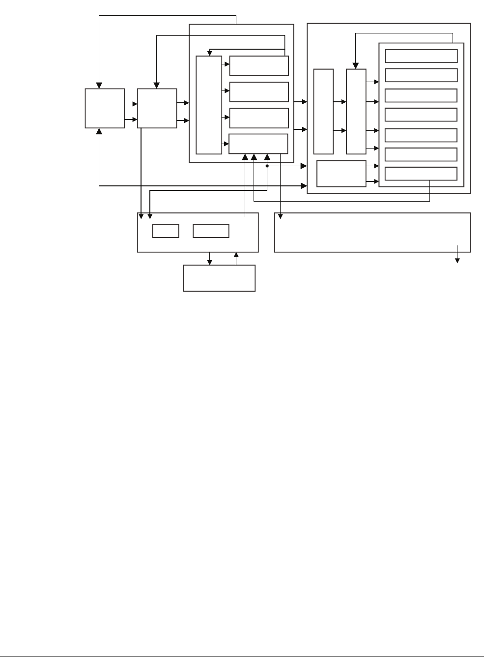
The ARM Architecture
ARM DEN0013B Copyright © 2011 ARM. All rights reserved. 2-11
ID082411 Non-Confidential
Figure 2-4 The Cortex-A8 processor integer and NEON pipelines
The separate instruction and data level 1 caches are 16KB or 32KB in size. They are
supplemented by an integrated, unified level 2 cache, which can be up to 1MB in size, with a
16-word line length. The level 1 data cache and level 2 cache both have a 128-bit wide data
interface to the processor. The level 1 data cache is virtually indexed, but physically tagged,
while level 2 uses physical addresses for both index and tags. Data used by NEON is, by default,
not allocated to L1 (although NEON can read and write data that is already in the L1 data cache).
2.4.3 The Cortex-A9 processor
The Cortex-A9MPCore processor and the Cortex-A9 uniprocessor provide higher performance
than the Cortex-A5 or Cortex-A8 processors, with clock speeds in excess of 1GHz and
performance of 2.5DMIPS/MHz. The ARM, Thumb, Thumb-2, TrustZone, Jazelle-RCT and
DBX technologies are all supported.
The level 1 cache system provides hardware support for cache coherency for between one and
four processors for multi-core software. A level 2 cache is optionally connected outside of the
processor. ARM supplies a level 2 cache controller (PL310/L2C-310) which supports caches of
up to 8MB in size. The processor also contains an integrated interrupt controller, an
implementation of the ARM Generic Interrupt Controller (GIC) architecture specification. This
can be configured to provide support for up to 224 interrupt sources.
Embedded Trace Macrocell
ALU and Load/Store Execute NEON
Integer ALU
Integer MUL
Integer shift
FP ADD
FP MUL
IEEE FP
LS permute
Load/Store
data queue
ALU pipe 0
MUL pipe 0
ALU pipe 1
LS pipe 0/1
Instruction
Decode
Instruction
Fetch
BIU pipeline
L3 memory system
NEON Register File
NEON
Instruction Decode
Branch mispredict
penalty
Replay
penalty
Integer register writeback
NEON store data
External
trace port
L1
instruction
cache miss
L1 data
cache miss
L2 data L1 data
Architectural Register File
L2 tag L2 data
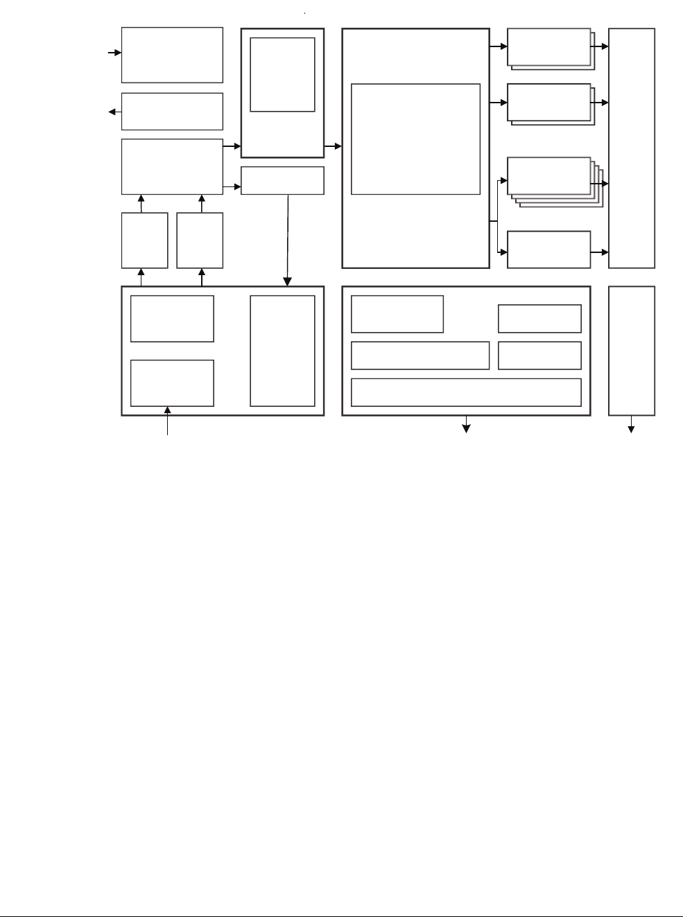
The ARM Architecture
ARM DEN0013B Copyright © 2011 ARM. All rights reserved. 2-12
ID082411 Non-Confidential
Figure 2-5 Block diagram of Cortex-A9 single core
Devices containing the Cortex-A9 processor include nVidia’s dual-core Tegra-2, the
SPEAr1300 from ST and TI’s OMAP4 platform.
2.4.4 The Cortex-A15 processor
The Cortex-A15 MPCore processor is currently the highest performance available ARM
processor. It is application compatible with the other processors described in this book. The
Cortex-A15 MPCore processor introduces some new capabilities, including support for full
hardware virtualization and Large Physical Address Extensions (LPAE), which enables
addressing of up to 1TB of memory. In this book, we will describe the LPAE extension and
provide an introduction to virtualization, but as the Cortex-A15 MPCore processor will not be
encountered by most readers for some time, we do not provide detailed coverage throughout the
text.
CoreSight
Debug Access Port
Profiling
Monitor Block
Dual-instruction
Decode Stage
Fast Loop Mode
Instruction
Cache
Branch
Prediction
Virtual to
Physical
Register
pool
Register
Rename stage
Branches
Out-of-Order
multi-issue with
speculation
Instruction queue
and
Dispatch
3+1 Dispatch Stage
Auto-prefetcher
Load-Store Unit
Data Cache
Memory System
uTLB
MMU
Program
Trace
Unit
Out-of-order Write-back Stage
ALU/MUL
ALU
FPU/NEON
Address
Instruction
queue
Prediction
queue
The ARM Architecture
ARM DEN0013B Copyright © 2011 ARM. All rights reserved. 2-13
ID082411 Non-Confidential
Figure 2-6 Cortex-A15 MPCore block diagram
Snoop Control Unit (SCU)
The SCU is responsible for managing the interconnect, arbitration,
communication, cache-to-cache and system memory transfers, cache coherence
and other capabilities for the processor.
Accelerator Coherence Port
This AMBA 4 AXI compatible slave interface on the SCU provides an
interconnect point for masters which need to be interfaced directly with the
Cortex-A15 processor.
Generic Interrupt Controller
This handles inter-processor communication and the routing and prioritization of
system interrupts. Supporting up to 224 independent interrupts, under software
control, each interrupt can be distributed across the processors, hardware
prioritized, and routed between the operating system and TrustZone software
management layer.
The Cortex-A15 MPCore processor has the following features:
• an out-of-order superscalar pipeline
• 32kB L1 Instruction and 32kB L1 Data caches
128-bit AMBA4 - Advanced Coherent Bus Interface
Generic Interrupt Control and Distribution
CoreSight MultiCore Debug and Trace Architecture
FPU/NEON
Data Engine
Integer CPU
Virtualization
40-bit PA
L1 Caches
with ECC
FPU/NEON
Data Engine
Integer CPU
Virtualization
40-bit PA
L1 Caches
with ECC
FPU/NEON
Data Engine
Integer CPU
Virtualization
40-bit PA
L1 Caches
with ECC
FPU/NEON
Data Engine
Integer CPU
Virtualization
40-bit PA
L1 Caches
with ECC
Snoop Control Unit (SCU) and L2 Cache
Direct
Cache
Transfers
Error
Correction
Accelerator
Coherence
Private
peripherals
Snoop
Filtering

The ARM Architecture
ARM DEN0013B Copyright © 2011 ARM. All rights reserved. 2-14
ID082411 Non-Confidential
• tightly-coupled low-latency level-2 cache (up to 4MB in size)
• improved floating-point and NEON media performance
• full hardware virtualization
• Large Physical Address Extension (LPAE) addressing up to 1TB of memory
• error correction capability for fault-tolerance and soft-fault recovery
• Multicore 1-4X SMP within a single processor cluster
• multiple coherent multi-core processor clusters through AMBA4 technology
• AMBA4 Cache Coherent Interconnect (CCI) allowing full cache coherency between
multiple Cortex-A15 MPCore processors.
2.4.5 Qualcomm Scorpion
ARM is not the only company which designs processors compliant with the ARMv7-A
instruction set architecture. In 2005, Qualcomm Inc. announced that it was creating its own
implementation under license from ARM, with the name Scorpion. The Scorpion processor is
available as part of Qualcomm’s Snapdragon platform, which contains the features necessary to
implement netbooks, smartphones or other mobile internet devices.
Relatively little information has been made publicly available by Qualcomm, although it has
been mentioned that Scorpion has a number of similarities with the Cortex-A8 processor. It is
an implementation of ARMv7-A, is superscalar and dual issue and has support for both VFP
and NEON (called the VeNum media processing engine in Qualcomm press releases). There are
a number of differences, however. Scorpion can process 128 bits of data in parallel in its NEON
implementation. Scorpion has a 13-stage load/store pipeline and two integer pipelines. One of
these is 10 stages long and can execute only simple arithmetic instructions (for example adds or
subtracts), while the other is 12 stages and can execute all data processing operations, including
multiplies. Scorpion also has a 23-stage floating-point/SIMD pipeline, and VFPv3 operations
are pipelined.
We will not specifically mention Scorpion again in this text. However, as the processor
conforms to the ARMv7-A architecture specification, most of the information presented here
will apply also to Scorpion.
2.4.6 Marvell Sheeva
Marvell is another company which designs and sells processors based on the ARM Architecture.
At the time of writing, Marvell has four families of ARM processors, the Armada 100, Armada
500, Armada 600, and Armada 1000. Marvell has designed a number of ARM processor
implementations, ranging from the Sheeva PJ1 (ARMv5 compatible) to Sheeva PJ4 (ARMv7
compatible). The latter is used in the Armada 500 and Armada 600 family devices.
The Marvell devices do not support the NEON SIMD instruction set, but instead use the
Wireless MMX2 technology, acquired from Intel. The Armada 510 contains 32KB I and D
caches plus an integrated 512KB level 2 cache and support for VFPv3. The Armada 610 is built
on a “low power” silicon process and has a smaller (256KB) level 2 cache and can be clocked
at the slightly slower rate than Armada 510. We will not specifically mention these processors
again in this book.

ARM DEN0013B Copyright © 2011 ARM. All rights reserved. 3-1
ID082411 Non-Confidential
Chapter 3
Tools, Operating Systems and Boards
ARM processors can be found in a very wide range of devices, running a correspondingly wide
range of software. Many readers will have ready access to appropriate hardware, tools and
operating systems, but before we proceed to look at the underlying architecture, it might be useful
to some readers to present an overview of some of these readily available compilation tools,
ARM-based hardware and Linux operating system distributions.
In this chapter, we will provide a brief mention of a number of interesting commercially available
development boards. We will provide some information about the Linux Operating System and
some useful associated tools. However, information about open source software and off-the-shelf
boards is likely to change rapidly.

Tools, Operating Systems and Boards
ARM DEN0013B Copyright © 2011 ARM. All rights reserved. 3-2
ID082411 Non-Confidential
3.1 Linux distributions
Linux is a Unix-like operating system kernel, originally developed by Linus Torvalds, who
continues to maintain the official kernel. It is open source, distributed under the GNU Public
License, widely-used and available on a large number of different processor architectures.
A number of free Linux distributions exist for ARM processors, including Debian, Ubuntu,
Fedora and Gentoo.
You can obtain pre-built Linux images, or read the Linux on ARM Wiki at
http://www.linux-arm.org/
.
In Appendix C, we will look at how to build Linux for your ARM device. Before doing that, we
will briefly look at the basics of Linux for ARM systems.
3.1.1 Linux for ARM systems
Support for the ARM architecture has been included in the standard Linux kernel for many
years. Development of this port is ongoing, with significant input from ARM to provide kernel
support for new processors and architecture versions. The ARM Embedded Linux distribution
only includes the kernel. The filesystem and U-Boot bootloader are available through Linaro.
It might seem strange to some readers that a book about the Cortex-A series of processors
contains information about Linux. There are several reasons for this. Linux source code is
available to all readers and represents a huge learning resource. In addition, it is easy to use to
program, and there are many useful resources with existing code and explanations. Many
readers will be familiar with Linux, as it can be run on most processor architectures. By
explaining how Linux features like virtual memory, multi-tasking, shared libraries and so forth
are implemented in Linux for ARM systems, readers will be able to apply their understanding
to other operating systems commonly used on ARM processors. The scalability of Linux is
another factor – it can run on the most powerful ARM processors, and its derivative uClinux is
also commonly used on much smaller processors, including the Cortex-M3 or ARM7TDMI
processors. It can run on both the ARM and Thumb ISAs, in little- or big-endian and with or
without a memory management unit.
Linux makes large amounts of system and kernel information available to user applications by
using virtual filesystems. These virtual files mean that we don’t have to know how to program
the kernel to access many hardware features. An example is
/proc/cpuinfo
. Reading this file on
a Cortex-A8 processor might give an output like that in Example 3-1. This lets code determine
useful information about the system it is running on, without having to directly interact with the
hardware.
Example 3-1 Output of /proc/cpuinfo on the Cortex-A8 processor
Processor : ARMv7 Processor rev 7 (v7l)
BogoMIPS : 499.92
Features : swp half thumb fastmult vfp edsp neon vfpv3
CPU implementer : 0x41
CPU architecture: 7
CPU variant : 0x1
CPU part : 0xc08
CPU revision : 7

Tools, Operating Systems and Boards
ARM DEN0013B Copyright © 2011 ARM. All rights reserved. 3-3
ID082411 Non-Confidential
In this book, we can merely scratch the surface of what there is to be said about Linux
development. What we hope to do here is to show some ways in which programming for an
embedded ARM architecture based system differs from a desktop x86 environment and to give
some pointers to useful tools, which the reader might care to investigate further.
3.1.2 Linaro
Linaro is a non-profit organization which works on a range of open source software running on
ARM processors, including kernel related tools and software and middleware. It is a
collaborative effort between a number of technology companies to provide engineering help and
resources to the open source community. Linaro does not produce a Linux distribution, nor is it
tied to any particular distribution or board. Instead, Linaro works to produce software and tools
which interact directly with the ARM processor, to provide a common software platform for use
by board support package developers. Its focus is on tools to help you write and debug code, on
low-level software which interacts with the underlying hardware and on key pieces of
middleware. Linaro engineers work on the kernel and tools, graphics and multimedia and power
management. Linaro provides patches to upstream projects and makes monthly source tree
tarballs available, with an integrated build every six months to consolidate the work.
See
http://www.linaro.org/
for more information about Linaro.
3.1.3 Linux terminology
Here, we define some terms which we will use when describing how the Linux kernel interacts
with the underlying ARM architecture:
Process A process is the kernel's view of an executing unprivileged application. The same
application (for example,
bin/bash
) can be running in several simultaneous
instances in the system – and each of these instances will be a separate process.
The process has resources associated with it, such as a memory map and file
descriptors. A process can consist of one or more threads.
Thread A thread is a context of software execution within a process. It is the entity which
is scheduled by the kernel, and actually executes the instructions that make up the
application. A process can consist of multiple threads, each executing with their
own program counter, stack pointer and register set – all existing within the
memory map and operating on the file descriptors held by the process as a whole.
In a multi-processor system, threads inside the same process can execute
concurrently on separate processors. Different threads within the same process
can be configured to have different scheduling priorities.
There are also threads executing inside the kernel, to manage various tasks
asynchronously, such as file cache management, or watchdog tickling (which is
not as exciting as it sounds).
Scheduler This is a vital part of the kernel which has a list of all the current threads. It knows
which threads are ready to be run and which are currently not able to run. It
dynamically calculates priority levels for each thread and schedules the highest
priority thread to be run next. It is called after an interrupt has been handled. The
scheduler is also explicitly called by the kernel via the
schedule()
function, for
example, when an application executing a system call needs to sleep. The system
will have a timer based interrupt which results in the scheduler being called at
regular intervals. This enables the OS to implement time-division multiplexing,
where many threads share the processor, each running for a certain amount of
time, giving the user the illusion that many applications are running
simultaneously.

Tools, Operating Systems and Boards
ARM DEN0013B Copyright © 2011 ARM. All rights reserved. 3-4
ID082411 Non-Confidential
System calls Linux applications run in user (unprivileged) mode. Many parts of the system are
not directly accessible in User mode. For example, the kernel might prevent User
mode programs from accessing peripherals, kernel memory space and the
memory space of other User mode programs. Access to some features of the
system control coprocessor (CP15) is not permitted in User mode. The kernel
provides an interface (via the
SVC
instruction) which permits an application to call
kernel services. Execution is transferred to the kernel through the
SVC
exception
handler, which returns to the user application when the system call is complete.
Libraries Linux applications are, with very few exceptions, not loaded as complete
pre-built binaries. Instead, the application relies on external support code linked
from files called shared libraries. This has the advantage of saving memory space,
in that the library only needs to be loaded into RAM once and is more likely to be
in the cache as it can be used by other applications. Also, updates to the library
do not require every application to be rebuilt. However, this dynamic loading
means that the library code must not rely on being in a particular location in
memory.
Files These are essentially blocks of data which are referred to using a pathname
attached to them. Device nodes have pathnames like files, but instead of being
linked to blocks of data, they are linked to device drivers which handle real I/O
devices like an LCD display, disk drive or mouse. When an application opens,
reads from or writes to a device, control is passed to specific routines in the kernel
that handle that device.
3.1.4 Embedded Linux
Linux-based systems are used all the way from servers via the desktop, through mobile devices
down to high-performance micro-controllers in the form of uClinux for processors lacking an
MMU. However, while the kernel source code base is the same, different priorities and
constraints mean that there can be some fundamental differences between the Linux running on
your desktop and the one running in your set-top box, as well as between the development
methodologies used.
In a desktop system, a form of bootloader executes from ROM – be it BIOS or UEFI. This has
support for mass-storage devices and can then load a second-stage loader (for example GRUB)
from a CD, a hard drive or even a USB memory stick. From this point on, everything is loaded
from a general-purpose mass storage device.
In an embedded device, the initial bootloader is likely to load a kernel directly from on-board
flash into RAM and execute it. In severely memory constrained systems, it might have a kernel
built to “execute in place” (XiP), where all of the read-only portions of the kernel remain in
ROM, and only the writable portions use RAM. Unless the system has a hard drive (or for fault
tolerance reasons), the root filesystem on the device is likely to be located in flash. This can be
a read-only filesystem, with portions that need to be writable overlaid by
tmpfs
mounts, or it can
be a read-write filesystem. In both cases, the storage space available is likely to be significantly
less than in a typical desktop computer. For this reason, they might use software components
such as uClibc and BusyBox to reduce the overall storage space required for the base system. A
general desktop Linux distribution is usually supplied preinstalled with a lot of software that you
might find useful at some point. In a system with limited storage space, this is not really optimal.
Instead, you want to be able to select exactly the components you need to achieve what you want
with your system. Various specific embedded Linux distributions exist to make this easier.
In addition, embedded systems often have lower performance than general purpose computers.
In this situation, development can be significantly speeded up by compiling software for the
target device on a faster desktop computer and then moving it across in so-called
cross-compiling.

Tools, Operating Systems and Boards
ARM DEN0013B Copyright © 2011 ARM. All rights reserved. 3-5
ID082411 Non-Confidential
3.1.5 Board Support Package
Getting Linux to run on a particular platform requires a Board Support Package (BSP). We can
divide the platform-specific code into a number of areas:
• Architecture-specific code. This is found in the
arch/arm/
directory and forms part of the
kernel porting effort carried out by the ARM Linux maintainers.
• Processor-specific code. This is found in
arch/arm/mm/
and
arch/arm/include/asm/
. This
takes care of MMU and cache functions (page table setup, TLB and cache invalidation,
memory barriers etc.). On SMP processors, spinlock code will be enabled.
• Generic device drivers are found under
drivers/
.
• Platform-specific code will be placed in
arch/arm/mach-*/
. This is code which is most
likely to be altered by people porting to a new board containing a processor with existing
Linux support. The code will define the physical memory map, interrupt numbers,
location of devices and any initialization code specific to that board.

Tools, Operating Systems and Boards
ARM DEN0013B Copyright © 2011 ARM. All rights reserved. 3-6
ID082411 Non-Confidential
3.2 Useful tools
Let’s take a brief look at some available tools which can be useful to developers of ARM
architecture based Linux systems. These are all extensively documented elsewhere. In this
section, we merely point out that these tools can be useful, and provides short descriptions of
their purpose and function.
3.2.1 QEMU
QEMU is a fast, open source machine emulator. It was originally developed by Fabrice Bellard
and is available for a number of architectures, including ARM. It can run operating systems and
applications made for one machine (for example, an ARM processor) on a different machine,
such as a PC or Mac. It uses dynamic translation of instructions and can achieve useful levels
of performance, enabling it to boot complex operating systems like Linux, without the need for
any target hardware.
3.2.2 BusyBox
BusyBox is a piece of software which provides many standard Unix tools, in a very small
executable, which is ideal for many embedded systems and could be considered to be a de facto
standard. It includes most of the Unix tools which can be found in the GNU Core Utilities, with
less commonly used command switches removed, and many other useful tools including
init
,
dhclient
,
wget
and
tftp
.
BusyBox calls itself the “Swiss Army Knife of Embedded Linux” – a reference to the large
number of tools packed into a small package. BusyBox is a single binary executable which
combines many applications. This reduces the overheads introduced by the executable file
format and enables code to be shared between multiple applications without needing to be part
of a library.
3.2.3 Scratchbox
If your development experience has been limited to writing code for personal computers, you
may not be familiar with cross-compiling. The general principle is to use one system (the host)
to compile software which runs on some other system (the target).
The target is a different architecture to the host and so the host cannot natively run the resulting
image. For example, you might have a powerful desktop x86 machine and want to develop code
for a small battery-powered ARM based device which has no keyboard. Using the desktop
machine will make code development simpler and compilation faster. There are some
difficulties with this process. Some build environments will try to run programs during
compilation and of course this is not possible. In addition, tools which during the build process
try to discover information about the machine (for software portability reasons), do not work
correctly when cross-compiling.
Scratchbox is a cross-compilation toolkit which solves these problems and gives the necessary
tools to cross-compile a complete Linux distribution. It can use either QEMU or a target board
to execute the cross-compiled binaries it produces.
3.2.4 U-Boot
“Das U-Boot” (Universal Bootloader) is a universal bootloader that can easily be ported to new
hardware processors or boards. It provides serial console output which makes it easy to debug
and is designed to be small and reliable. In an x86 system, we have BIOS code which initializes
the processor and system and then loads an intermediate loader such as GRUB or syslinux,
which then in turn loads and starts the kernel. U-Boot essentially covers both functions.

Tools, Operating Systems and Boards
ARM DEN0013B Copyright © 2011 ARM. All rights reserved. 3-7
ID082411 Non-Confidential
3.2.5 UEFI and Tianocore
The Unified Extensible Firmware Interface (UEFI) is the specification of an interface to
hand-off control of a system from the pre-boot environment to an operating system, such as
Windows or Linux. Its modular design permits flexibility in the functionality provided in the
pre-boot environment and eases porting to new hardware. The UEFI forum is a non-profit
collaborative trade organization formed to promote and manage the UEFI standard.
UEFI is processor architecture independent and the Tianocore EFI Development Kit 2 (EDK2)
is available under a BSD license. It contains UEFI support for ARM platforms, including ARM
Versatile Express boards and the BeagleBoard (see BeagleBoard on page 3-13).
See
http://www.uefi.org
and
http://sourceforge.net/apps/mediawiki/tianocore
for more
information.
Tools, Operating Systems and Boards
ARM DEN0013B Copyright © 2011 ARM. All rights reserved. 3-8
ID082411 Non-Confidential
3.3 Software toolchains for ARM processors
There are a wide variety of compilation and debug tools available for ARM processors. In this
section, we will focus on two toolchains, the GNU toolchain which includes the GNU Compiler
(
gcc
), and the ARM Compiler toolchain which includes the
armcc
compiler tool.
Figure 3-1 shows how the various components of a software toolchain interact to produce an
executable image.
Figure 3-1 Using a software toolchain to produce an image
3.3.1 GNU toolchain
The GNU toolchain is a collection of programming tools from the GNU project used both to
develop the Linux kernel and to develop applications (and indeed other operating systems). Like
Linux, the GNU tools are available on a large number of processor architectures and are actively
developed to make use of the latest features incorporated in ARM processors.
The toolchain includes the following components:
• GNU make
• GNU Compiler Collection (GCC)
• GNU binutils (linker, assembler (
gas
) etc.)
• GNU Debugger (GDB)
• GNU build system (autotools)
• GNU C library (glibc or eglibc).
C files(.c)
Assembly
files(.s)
Object
files(.o)
C compiler
(gcc or armcc)
Assembler
(gas or armasm)
Linker
Linkerscript
or scatter
file
Executable
image
Libraries

Tools, Operating Systems and Boards
ARM DEN0013B Copyright © 2011 ARM. All rights reserved. 3-9
ID082411 Non-Confidential
Although glibc is available on all GNU/Linux host systems and provides portability; wide
compliance with standards, and is performance optimized, it is quite large for some embedded
systems (approaching 2MB in size). Other libraries may be preferred in smaller systems. For
example, uClibc provides most features and is around 400KB in size, and produces significantly
smaller application binaries.
Prebuilt versions of GNU toolchains
If you are using a complete Linux distribution on your target platform, and you are not
cross-compiling, you can install the toolchain packages using the standard package manager.
For example, on a Debian-based distribution such as Ubuntu you can use the command:
sudo apt-get install gcc g++
Additional required packages such as
binutils
will also be pulled in by this command, or you
can add them explicitly on the command line. In fact, if
g++
is specified this way,
gcc
is
automatically pulled in. This toolchain will then be accessible in the way you would expect in
a normal Linux system, by just calling
gcc
,
g++
,
as,
or similar.
If you are cross-compiling, you will need to install a suitable cross-compilation toolchain. The
cross compilation toolchain consists of the GNU Compiler Collection (GCC) but also the GNU
C library (
glibc
) which is necessary for building applications (but not the kernel).
Ubuntu distributions from Maverick (10.10) onwards include specific packages for this. These
can be run using the command:
sudo apt-get install g++-arm-linux-gnueabi
The resulting toolchain will be able to build Linux kernels, applications and libraries for the
same Ubuntu version that is used on the target platform. It will however, have a prefix added to
all of the individual tool commands in order to avoid problems distinguishing it from the native
tools for the workstation. For example, the cross-compiling
gcc
will be accessible as
arm-linux-gnueabi-gcc
.
If your workstation uses an older Ubuntu distribution, an alternative Linux distribution or even
Windows, another toolchain must be used. CodeSourcery provide pre-built toolchains for both
Linux and Windows from
http://www.codesourcery.com
. The GNU/Linux version of this
toolchain can be used to build the Linux kernel. It can also build applications and libraries,
providing that the basic C library used on the target is compatible with the one used by the
toolchain. Like for the Ubuntu toolchain, a prefix is added to the tool commands. For the
CodeSourcery GNU/Linux toolchain, the prefix is
arm-none-linux-gnueabi
– so the C compiler
is called
arm-none-linux-gnueabi-gcc
.
Source code distributions of cross-compilation toolchains can also be downloaded from
http://www.linaro.org
.
3.3.2 ARM Compiler toolchain
The ARM Compiler toolchain can be used to build programs from C, C++, or ARM assembly
language source. It generates optimized code for the 32-bit ARM and variable length (16-bit and
32-bit) Thumb instruction sets, and supports full ISO standard C and C++. It also supports the
NEON SIMD instruction set with the vectorizing NEON compiler.
The ARM Compiler toolchain comprises the following components:
armcc The ARM and Thumb compiler. This compiles your C and C++ code. It supports
inline and embedded assemblers, and also includes the NEON vectorizing
compiler, invoked using the command:
armcc --vectorize

Tools, Operating Systems and Boards
ARM DEN0013B Copyright © 2011 ARM. All rights reserved. 3-10
ID082411 Non-Confidential
armasm The ARM and Thumb assembler. This assembles ARM and Thumb assembly
language sources.
armlink The linker. This combines the contents of one or more object files with selected
parts of one or more object libraries to produce an executable program.
armar The librarian. This enables sets of ELF format object files to be collected together
and maintained in libraries. You can pass such a library to the linker in place of
several ELF files. You can also use the library for distribution to a third party for
further application development.
fromelf The image conversion utility. This can also generate textual information about the
input image, such as disassembly and its code and data size.
C libraries The ARM C libraries provide:
• an implementation of the library features as defined in the C and C++
standards
• extensions specific to the ARM Compiler, such as
_fisatty()
,
__heapstats()
, and
__heapvalid()
• GNU extensions
• common nonstandard extensions to many C libraries
• POSIX extended functionality
• functions standardized by POSIX.
C++ libraries
The ARM C++ libraries provide:
• helper functions when compiling C++
• additional C++ functions not supported by the Rogue Wave library.
Rogue Wave C++ libraries
The Rogue Wave library provides an implementation of the standard C++ library.
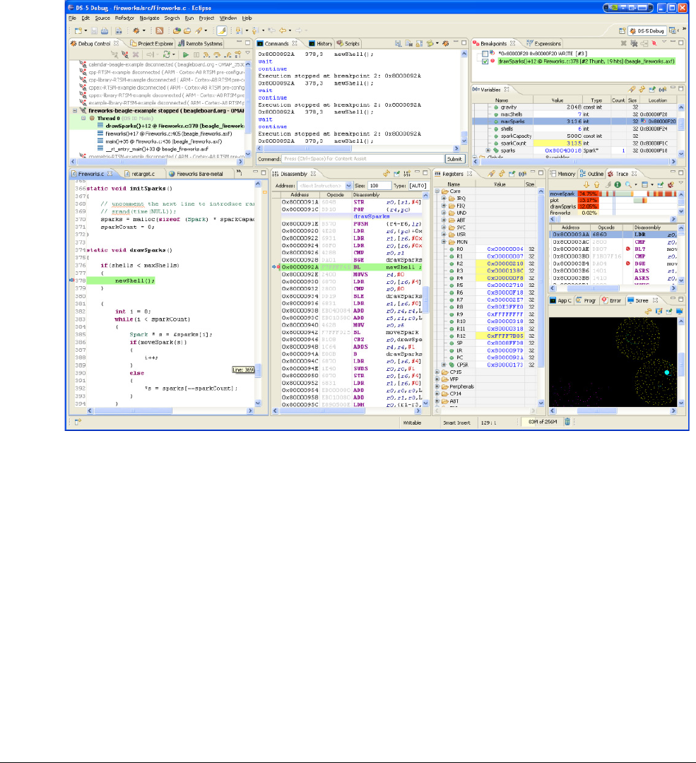
Tools, Operating Systems and Boards
ARM DEN0013B Copyright © 2011 ARM. All rights reserved. 3-11
ID082411 Non-Confidential
3.4 ARM DS-5
ARM DS-5 is a professional software development solution for Linux, Android and bare-metal
embedded systems based on ARM-based hardware platforms. DS-5 covers all the stages in
development, from boot code and kernel porting to application debug. See
http://www.arm.com/products/tools/software-tools/ds-5/index.php
.
ARM DS-5 features an application and kernel space graphical debugger with trace, system-wide
performance analyzer, real-time system simulator, and compiler. These features are included in
an Eclipse-based IDE.
Figure 3-2 DS-5 Debugger
A full list of the hardware platforms that are supported by DS-5 is available from
http://www.arm.com/products/tools/software-tools/ds-5/supported-platforms.php
.
ARM DS-5 includes the following components:
• Eclipse-based IDE combines software development with the compilation technology of
the DS-5 tools. Tools include a powerful C/C++ editor, project manager and integrated
productivity utilities such as the Remote System Explorer (RSE), SSH and Telnet
terminals.
• DS-5 Compilation Tools. Both GCC and the ARM Compiler are provided. See ARM
Compiler toolchain on page 3-9 for more information about the ARM Compiler.
• Real-time simulation model of a complete ARM Cortex-A8 processor-based device and
several Linux-based example projects that can run on this model. Typical simulation
speeds are above 250 MHz.

Tools, Operating Systems and Boards
ARM DEN0013B Copyright © 2011 ARM. All rights reserved. 3-12
ID082411 Non-Confidential
• The DS-5 Debugger, shown in Figure 3-2 on page 3-11, together with a supported debug
target, enables debugging of kernel space and application programs and complete control
over the flow of program execution to quickly isolate and correct errors. It provides
comprehensive and intuitive views, including synchronized source and disassembly, call
stack, memory, registers, expressions, variables, threads, breakpoints, and trace.
• DS-5 Streamline, a system-wide software profiling and performance analysis tool for
ARM-based Linux and Android platforms. DS-5 Streamline supports SMP
configurations, native Android applications and libraries.
Streamline only requires a standard TCP/IP network connection to the target in order to
acquire and analyze system-wide performance data from Linux and Android systems,
therefore making it an affordable solution to make software optimization possible from
the early stages of the development cycle.
See DS-5 Streamline on page 16-4 for more information.

Tools, Operating Systems and Boards
ARM DEN0013B Copyright © 2011 ARM. All rights reserved. 3-13
ID082411 Non-Confidential
3.5 Example platforms
In this section we’ll mention a few widely available, off-the-shelf ARM-based platforms which
are suitable for use by students or hobbyists for Linux development. This list is likely to become
outdated quickly, as newer and better boards are frequently announced.
3.5.1 BeagleBoard
The BeagleBoard is a readily available, inexpensive board which provides performance levels
similar to that of a laptop from a single fan-less board, powered through a USB connection. It
contains the OMAP 3530 device from Texas Instruments, which includes a Cortex-A8
processor with a 256KB level 2 cache, clocked at 720MHz. The board provides a wide range of
connection options, including DVI-D for monitors, S-Video for televisions, stereo audio and
compatibility with a wide range of USB devices, while code and data can be provided through
an MMC+/SD interface. It is highly extensible and the design information is freely available. It
is intended for use by the Open Source community and not to form a part of any commercial
product.
3.5.2 Pandora
The Pandora device also uses OMAP3530 (a Cortex-A8 processor clocked at 600MHz). It has
controls typically found on a gaming console and in fact, looks like a typical handheld gaming
device, with an 800x480 LCD.
3.5.3 nVidia Tegra 200 series developer board
This board is intended for smartbook or netbook development and contains nVidia’s Tegra2
high-performance dual-core implementation of a Cortex-A9 processor running at 1GHz, along
with 1GB DDR2 and a wide range of standard laptop peripherals. It is a small 10cm square
board that includes 2x mini-PCI-E slots, onboard Ethernet, 3xUSB, SDcard, HDMI and analog
VGA. nVidia provides BSP support for WindowsCE, Android and Linux. The performance
exceeds many low-cost x86 platforms, at much lower power.
3.5.4 ST Ericsson STE MOP500
This has a dual-core ARM Cortex-A9 processor, based on the U8500 chip design with 256MB
of memory and the Mali-400 GPU.
3.5.5 Gumstix
This derives its name from the fact that the board is the same size as a stick of chewing gum.
The Gumstix Overo uses the OMAP3503 device from TI, containing a Cortex-A8 processor
clocked at 600MHz and runs Linux 2.6 with the BusyBox utilities and OpenEmbedded build
environment.
3.5.6 PandaBoard
PandaBoard is a single-board computer based on the Texas Instruments OMAP4430 device,
including a dual-core 1GHz ARM Cortex-A9 processor, a 3D Accelerator video processor and
1GB of DDR2 RAM. Its features include ethernet, Bluetooth plus DVI and HDMI interfaces.

ARM DEN0013B Copyright © 2011 ARM. All rights reserved. 4-1
ID082411 Non-Confidential
Chapter 4
ARM Registers, Modes and Instruction Sets
In this chapter, we will introduce the fundamental features of ARM processors, including details of
registers, modes and instruction sets. We will also touch on some details of processor
implementation features including instruction pipelines and branch prediction.
ARM is a 32-bit processor architecture. It is a load/store architecture, meaning that data-processing
instructions operate on values in registers rather than external memory. Only load and store
instructions access memory. Internal registers are also 32 bits. Throughout the book, when we refer
to a word, we mean 32 bits. A doubleword is therefore 64 bits and a halfword is 16 bits wide.
Individual processor implementations do not necessarily have 32-bit width for all blocks and
interconnections. For example, we might have 64-bit wide paths for instruction fetches or for data
load and store operations.
Processors which implement the ARMv7-A architecture do not have a memory map which is fixed
by the architecture. The processor has access to a 4GB address space addressed as bytes and
memory and peripherals can be mapped freely within that space. We will describe memory further,
in Chapter 7 and Chapter 8, when we look at the caches and Memory Management Unit (MMU).

ARM Registers, Modes and Instruction Sets
ARM DEN0013B Copyright © 2011 ARM. All rights reserved. 4-2
ID082411 Non-Confidential
4.1 Instruction sets
Historically, most ARM processors support more than one instruction set:
• ARM – a full 32-bit instruction set
• Thumb – a 16-bit compressed subset of the full ARM instruction set, with better code
density (but reduced performance compared with ARM code).
The processor can switch back and forth between these two instruction sets, under program
control.
Newer ARM processors, such as the Cortex-A series covered in this book, implement Thumb-2
technology, which extends the Thumb instruction set. This gives a mixture of 32-bit and 16-bit
instructions which gives approximately the code density of the original Thumb instruction set
with the performance of the original ARM instruction set. For this reason, most code developed
for Cortex-A series processors will use the Thumb instruction set.

ARM Registers, Modes and Instruction Sets
ARM DEN0013B Copyright © 2011 ARM. All rights reserved. 4-3
ID082411 Non-Confidential
4.2 Modes
The ARM architecture has seven processor modes. There are six privileged modes and a
non-privileged User mode. In this latter mode, there are limitations on certain operations, such
as MMU access. Table 4-1 summarizes the available modes. Note that modes are associated
with exception events, which are described further in Chapter 10 Exception Handling.
There is an extra mode (Secure Monitor), which we will describe when we look at the ARM
Security Extensions, in Chapter 26.
Table 4-1 ARM processor modes
Mode Mode encoding
in the PSRs Function
Supervisor
(SVC)
10011 Entered on reset or when a Supervisor Call instruction (
SVC
) is executed
FIQ 10001 Entered on a fast interrupt exception
IRQ 10010 Entered on a normal interrupt exception
Abort (ABT) 10111 Entered on a memory access violation
Undef (UND) 11011 Entered when an undefined instruction executed
System (SYS) 11111 Privileged mode, which uses the same registers as User mode
User (USR) 10000 Unprivileged mode in which most applications run
ARM Registers, Modes and Instruction Sets
ARM DEN0013B Copyright © 2011 ARM. All rights reserved. 4-4
ID082411 Non-Confidential
4.3 Registers
The ARM architecture has a number of registers, as shown in Figure 4-1.
Figure 4-1 The ARM register set
There are a number of general purpose registers. In addition, there is R15, the program counter,
and six program status registers, which contain flags, modes etc. Many of these registers are
banked and not visible to the processor except in specific processor modes. These banked-out
registers are automatically switched in and out when a different processor mode is entered.
So, for example, if the processor is in IRQ mode, we can see R0, R1 … R12 (the same registers
we can see in User mode), plus R13_IRQ and R14_IRQ (registers visible only while we are in
IRQ mode) and R15 (the program counter, PC). R13_USR and R14_USR are not directly
visible. We do not normally need to specify the mode in the register name in the way we have
just done. If we (for example) refer to R13 in a line of code, the processor will access the R13
register of the mode we are currently in.
At any given moment, the programmer has access to 16 registers (R0-R15) and the Current
Program Status Register (CPSR). R15 is hard-wired to be the program counter and holds the
current program address (actually, it always points eight bytes ahead of the instruction that is
executing in ARM state and four bytes ahead of the current instruction in Thumb state). We can
write to R15 to change the flow of the program. R14 is the link register, which holds a return
address for a function or exception (although it can occasionally be used as a general purpose
register when not holding either of these values). R13, by convention is used as a stack pointer.
R0-R12 are general purpose registers. Some 16-bit Thumb instructions have limitations on
which registers they can access – the accessible subset is called the low registers and comprises
R0-R7. Figure 4-2 on page 4-5 shows the subset of registers visible to general data processing
instructions.
CPSR
SPSR SPSR SPSR SPSR
R0
R1
R2
R3
R4
R5
R6
R7
R8
R9
R10
R11
R12
R13
(SP)
R14
(LR)
R15
(PC)
R8
R9
R10
R11
R12
R13
(SP)
R14
(LR)
R13
(SP)
R14
(LR)
R13
(SP)
R14
(LR)
R13
(SP)
R14
(LR)
R13
(SP)
R14
(LR)
User
mode
R0-R7,
R15
and
CPSR
User
mode
R0-R12,
R15
and
CPSR
User
mode
R0-R12,
R15
and
CPSR
User
mode
R0-R12,
R15
and
CPSR
User FIQ IRQ ABT SVC UND
SPSR
User
mode
R0-R12,
R15
and
CPSR
SPSR
User
mode
R0-R12,
R15
and
CPSR
R13
(SP)
R14
(LR)
MON
ARM Registers, Modes and Instruction Sets
ARM DEN0013B Copyright © 2011 ARM. All rights reserved. 4-5
ID082411 Non-Confidential
Figure 4-2 Programmer visible registers for user code
The reset values of R0-R14 are unpredictable. R13, the stack pointer, must be initialized (for
each mode) by boot code before software makes use of the stack. The AAPCS/AEABI (see
Chapter 15 Application Binary Interfaces) specifies how software should use the general
purpose registers in order to interoperate between different toolchains or programming
languages.
Implementations which support the Virtualization Extensions have additional registers available
in Hypervisor (Hyp) mode, which are not shown in Figure 4-1 on page 4-4. Hyp mode has
access to its own versions of R13 (SP) and SPSR. It uses the User mode link register as well as
a dedicated new register (ELR). We'll discuss this in Chapter 27 Virtualization.
4.3.1 Program Status Registers
The program status registers form an additional set of banked registers. Six are used as Saved
Program Status Registers (SPSR) and save a copy of the pre-exception CPSR when switching
modes upon an exception. These are not accessible from system or User modes. So, for example,
in User mode, we can see only CPSR. In FIQ mode, we can see CPSR and SPSR_FIQ, but have
no direct access to SPSR_IRQ, SPSR_ABT, etc.
The ARM Architecture Reference Maunual describes how program status is reported in the
32-bit Application Program Status Register (APSR), with other status and control bits (system
level information) remaining in the CPSR. In the ARMv7-A architecture covered in this book,
the APSR is in fact the same register as the CPSR, despite the fact that they have two separate
names. The APSR must be used only to access the N, Z, C, V, Q, and GE[3:0] bits. These bits
are not normally accessed directly, but instead set by condition code setting instructions and
CPSR
R0
R1
R2
R3
R4
R5
R6
R7
R8
R9
R10
R11
R12
R13
(SP)
R14
(LR)
R15
(PC)
Stack pointer
Link register
Program Counter
Current Program Status Register
General Purpose
Registers
Low Registers
High Registers

ARM Registers, Modes and Instruction Sets
ARM DEN0013B Copyright © 2011 ARM. All rights reserved. 4-6
ID082411 Non-Confidential
tested by instructions which are executed conditionally. The renaming is therefore an attempt to
clean-up the mixed access CPSR of the older ARM architectures. Figure 4-3 shows the make-up
of the CPSR.
Figure 4-3 CPSR bits
The individual bits represent the following:
•N – Negative result from ALU
•Z – Zero result from ALU
•C – ALU operation Carry out
•V – ALU operation oVerflowed
•Q – cumulative saturation (also described as “sticky”)
•J – indicates if processor is in Jazelle state
•GE[3:0] – used by some SIMD instructions
•IT [7:2] –
If-Then
conditional execution of Thumb-2 instruction groups
•E bit controls load/store endianness
•A bit disables imprecise data aborts
•I bit disables IRQ
•F bit disables FIQ
•T bit – T = 1 indicates processor in Thumb state
•M[4:0] – specifies the processor mode (FIQ, IRQ, etc. as described in Table 4-1 on
page 4-3).
The processor can change between modes using instructions which directly write to the CPSR
mode bits (not possible when in User mode). More commonly, the processor changes mode as
a result of exception events.
We will consider these bits in more detail in Chapter 6 and Chapter 10.
N Z C V Q
IT
[1:0]
JReserved GE[3:0] IT[7:2] EAIFT M[4:0]
31 27 26 25 24 23 20 19 16 15 10 9 8 7 6 5 4 0
ARM Registers, Modes and Instruction Sets
ARM DEN0013B Copyright © 2011 ARM. All rights reserved. 4-7
ID082411 Non-Confidential
4.4 Instruction pipelines
All modern processors use an instruction pipeline, as a way to increase instruction throughput.
The basic concept is that the execution of an instruction is broken down into a series of
independent steps. Each instruction moves from one step to another, over a number of clock
cycles. Each pipeline stage handles a part of the process of executing an instruction, so that on
any given clock cycle, a number of different instructions can be in different stages of the
pipeline. The total time to execute an individual instruction does not change much compared
with a non-pipelined implementation, but the overall throughput is significantly raised. The
overall speed of the processor is then governed by the speed of the slowest step, which is
significantly less than the time needed to perform all steps. A non-pipelined architecture is
inefficient because some blocks within the processor will be idle most of the time during the
instruction execution.
Figure 4-4 Pipeline instruction flow
The classic pipeline comprises three stages – Fetch, Decode and Execute as shown in
Figure 4-4. More generally, an instruction pipeline might be divided into the following broad
definitions:
• Instruction prefetch (deciding from which locations in memory instructions are to be
fetched, and performing associated bus accesses).
• Instruction fetch (reading instructions to be executed from the memory system).
• Instruction decode (working out what instruction is to be executed and generating
appropriate control signals for the datapaths).
• Register fetch (providing the correct register values to act upon).
• Issue (issuing the instruction to the appropriate execute unit).
• Execute (the actual ALU or multiplier operation, for example).
• Memory access (performing data loads or stores).
• Register write-back (updating processor registers with the results).
In individual processor implementations, some of these steps can be combined into a single
pipeline stage and/or some steps can be spread over several cycles. A longer pipeline means
fewer logic gates in the critical path between each pipeline stage which results in faster
execution. However, there are typically many dependencies between instructions. If an
instruction depends on the result of a previous instruction, the control logic might need to insert
a stall (or bubble) into the pipeline until the dependency is resolved. Additional logic is needed
to detect and resolve such dependencies (for example, forwarding logic, which feeds the output
Clock cycles
Instruction 1
Instruction 2
Instruction 3
Fetch
Instruction
Fetch
Instruction
Fetch
Instruction
Decode
Decode
Decode
Execute
Execute
Execute

ARM Registers, Modes and Instruction Sets
ARM DEN0013B Copyright © 2011 ARM. All rights reserved. 4-8
ID082411 Non-Confidential
of a pipeline stage back to earlier pipeline stages). This makes processors with longer pipelines
significantly more complex to design and validate. More importantly, it makes the processor
larger and therefore more expensive.
In general, the ARM architecture tries to hide pipeline effects from the programmer. This means
that the programmer can determine the pipeline structure only by reading the processor manual.
Some pipeline artifacts are still present, however. For example, the program counter register
(R15) points two instructions ahead of the instruction that is currently executing in ARM state,
a legacy of the three stage pipeline of the original ARM1 processor.
A further drawback of a long pipeline is that sometimes the sequential execution of instructions
from memory will be interrupted. This can happen as a result of execution of a branch
instruction, or by an exception event (such as an interrupt). When this happens, the processor
cannot determine the correct location from which the next instruction should be fetched until
the branch is resolved. In typical code, many branch instructions are conditional (as a result of
loops or
if
statements). Therefore, whether or not the branch will be taken cannot be determined
at the time the instruction is fetched. If we fetch instructions which follow a branch and the
branch is taken, the pipeline must be flushed and a new set of instructions from the branch
destination must be fetched from memory instead. As pipelines get longer, the cost of this
“branch penalty” becomes higher.
Cortex-A series processors have branch prediction logic which aims to reduce the effect of the
branch penalty. In essence, the processor guesses whether a branch will be taken or not and
fetches instructions either from the instructions immediately following the branch (if the
prediction is that the conditional branch will not be taken), or from the target instruction of the
branch (if the prediction is that the branch will be taken). If the prediction is correct, the branch
does not flush the pipeline. If the prediction is wrong, the pipeline must be flushed and
instructions from the correct location fetched to refill it. We will look at this in more detail in
Branch prediction on page 4-10.
4.4.1 Multi-issue pipelines
A refinement of the processor pipeline is that we can duplicate logic within pipeline stages. In
the ARM11 processor family, for example, there are three parallel back-end pipelines – an ALU
pipeline, a load/store pipeline and a multiply pipeline. Instructions can be issued into any of
these pipelines. A logical development of this idea is to have multiple instances of the execute
hardware – for example two ALU pipelines. We can then issue more than one instruction per
cycle into these parallel pipelines – an example of instruction level parallelism. Such a processor
is said to be superscalar. The Cortex-A8, Cortex-A9, and Cortex-A15 processors are
superscalar processors – they can potentially decode and issue more than one instruction in a
single clock cycle. The Cortex-A5 processor is more limited and can only dual-issue certain
combinations of instructions – for example, a branch and a data-processing instruction can be
issued in the same cycle. The instructions are still issued from a sequential stream of instructions
in memory. Extra hardware logic is required to check for dependencies between instructions, as,
for example, in the case where one instruction must wait for the result of the other.
The processor pipeline is too complex for the programmer to take care of all pipeline effects and
dependencies.
Out-of-order execution provides scope for increasing pipeline efficiency. If instructions are
processed sequentially, one instruction is completely retired before the next is dealt with. In
out-of order processing, multiple memory accesses can be outstanding at once, and can
complete in a different order from their original program order.
Often, an instruction must be stalled due to a dependency (for example, the need to use a result
from a previous instruction). We can execute following instructions which do not share this
dependency, provided that logical hazards between instructions are rigorously respected. The
ARM Registers, Modes and Instruction Sets
ARM DEN0013B Copyright © 2011 ARM. All rights reserved. 4-9
ID082411 Non-Confidential
Cortex-A9 processor achieves very high levels of efficiency and instruction throughput using
this technique. It can be considered to have a pipeline of variable length, as the pipeline length
depends upon which back-end execution pipeline an instruction uses. It can execute instructions
speculatively and can sustain two instructions per clock, but has the ability to issue up to four
instructions on an individual clock cycle. This can improve performance if the pipeline has
become unblocked having previously been stalled for some reason.
4.4.2 Register renaming
The Cortex-A9 processor has an interesting micro-architectural implementation which makes
use of a register renaming scheme. The set of registers which form a standard part of the ARM
architecture are visible to the programmer, but the hardware implementation of the processor
actually has a much larger pool of physical registers, with logic to dynamically map the
programmer visible registers to the physical ones. Figure 4-5 shows the separate pools of
architectural and physical registers.
Consider the case where code writes the value of a register to external memory and shortly
thereafter reads the value of a different memory location into the same register. This might cause
a pipeline stall in previous processors, even though in this particular case, there is no actual data
dependency. Register renaming avoids this problem by ensuring that the two instances of R0 are
renamed to different physical registers, removing the dependency. This permits a compiler or
assembler programmer to reuse registers without the need to consider architectural penalties for
reusing registers when there are no inter-instruction dependencies. Importantly, it also allows
out-of-order execution of write-after-write and write-after-read sequences. (A write-after-write
hazard could occur when we write values to the same register in two separate instructions. The
processor must ensure that an instruction which comes after the two writes sees the result of the
later instruction.)
Figure 4-5 Register renaming
To avoid dependencies between instructions related to flag setting and comparisons, the APSR
flags also use a similar technique.
Architectural Physical
R0
R1
LR_USR
CPSR P0
P1
P2
P3
Flag 0
Flag 1

ARM Registers, Modes and Instruction Sets
ARM DEN0013B Copyright © 2011 ARM. All rights reserved. 4-10
ID082411 Non-Confidential
4.5 Branch prediction
As we have seen, branch prediction logic is an important factor in achieving high throughput in
Cortex-A series processors. With no branch prediction, we would have to wait until a
conditional branch executes before we could determine where to fetch the next instruction from.
The first time that a conditional jump instruction is fetched, there is little information on which
to base a prediction about the address of the next instruction. Older ARM processors used static
branch prediction. This is the simplest branch prediction method as it needs no prior information
about the branch. We speculate that backward branches will be taken, and forward branches will
not. A backward branch has a target address that is lower than its own address. This can easily
be recognized in hardware as the branch offset is encoded as a two’s complement number. We
can therefore look at a single opcode bit to determine the branch direction. This technique can
give reasonable prediction accuracy owing to the prevalence in code of loops, which almost
always contain backward-pointing branches and are taken more often than not taken. Due to the
pipeline length of Cortex-A series processors, we get better performance by using more
complex branch prediction schemes, which give better prediction accuracy. This comes with a
small price, as additional logic is required.
Dynamic prediction hardware can further reduce the average branch penalty by making use of
history information about whether conditional branches were taken or not taken on previous
execution. A Branch Target Address Cache (BTAC), also called Branch Target Buffer (BTB) in
the Cortex-A8 processor, is a cache which holds information about previous branch instruction
execution. It enables the hardware to speculate on whether a conditional branch will or will not
be taken.
The processor must still evaluate the condition code attached to a branch instruction. If the
branch prediction hardware predicts correctly, the pipeline does not need to be stalled. If the
branch prediction hardware speculation was wrong, the processor will flush the pipeline and
refill it.
4.5.1 Return stack
Readers who are not at all familiar with ARM assembly language may want to omit this section
until they have read Chapter 5 and Chapter 6.
The description in Branch prediction looked at strategies the processor can use to predict
whether branches are taken or not. For most branch instructions, the target address is fixed (and
encoded in the instruction). However, there is a class of branches where the branch target
destination cannot be determined by looking at the instruction. For example, if we perform a
data processing operation which modifies the PC (for example,
MOV
,
ADD
or
SUB
) we must wait for
the ALU to evaluate the result before we can know the branch target. Similarly if we load the
PC from memory, using an
LDR
,
LDM
or
POP
instruction, we cannot know the target address until
the load completes.
Such branches (often called indirect branches) cannot, in general, be predicted in hardware.
There is, however, one common case that can usefully be optimized, using a last-in-first-out
stack in the pre-fetch hardware (the return stack). Whenever a function call (
BL
or
BLX
)
instruction is executed, we enter the address of the following instruction into this stack.
Whenever we encounter an instruction which can be recognized as being a function return
instructions (
BX
LR
, or a stack pop which contains the PC in its register list), we can speculatively
pop an entry from the stack and start fetching instructions from that address. When the return
instruction actually executes, the hardware compares the address generated by the instruction
with that predicted by the stack. If there is a mismatch, the pipeline is flushed and we restart
from the correct location.

ARM Registers, Modes and Instruction Sets
ARM DEN0013B Copyright © 2011 ARM. All rights reserved. 4-11
ID082411 Non-Confidential
The return stack is of a fixed size (eight entries in the Cortex-A8 or Cortex-A9 processors, for
example). If a particular code sequence contains a large number of nested function calls, the
return stack can predict only the first eight function returns. The effect of this is likely to be very
small, as most functions do not invoke eight levels of nested functions.
4.5.2 Programmer’s view
For the majority of application level programmers, branch prediction is a part of the hardware
implementation which can safely be ignored. However, knowledge of the processor behavior
with branches can be useful when writing highly optimized code. The hardware performance
monitor counters can generate information about the numbers of branches correctly or
incorrectly predicted. This hardware is described further in Chapter 17.
Branch prediction logic is disabled at reset. Part of the boot code sequence will typically be to
set the Z bit in the CP15:SCTLR, System Control Register, which enables branch prediction.
There is one other situation where the programmer might need to take care. When moving or
modifying code at an address from which code has already been executed in the system, it might
be necessary (and is always prudent) to remove stale entries from the branch history logic by
using the CP15 instruction which invalidates all entries.

ARM DEN0013B Copyright © 2011 ARM. All rights reserved. 5-1
ID082411 Non-Confidential
Chapter 5
Introduction to Assembly Language
Assembly language is a human-readable representation of machine code. There is in general a
one-to-one relationship between assembly language instructions (mnemonics) and the actual
binary opcode executed by the processor. The purpose of this chapter is not to teach assembly
language programming. We describe the ARM and Thumb instruction sets, highlighting features
and idiosyncrasies that differentiate it from other microprocessor families.
Many programmers writing at the application level will have little need to code in assembly
language. However, knowledge of assembly code can be useful in cases where highly optimized
code is required, when writing JIT compilers, or where low level use of features not directly
available in C is needed. It might be required for portions of boot code, device drivers or when
performing OS development. Finally, it can be useful to be able to read assembly code when
debugging C, and particularly, to understand the mapping between assembly instructions and C
statements.
Programmers seeking a more detailed description of ARM assembly language should also refer to
the ARM Compiler Toolchain Assembler Reference.
The ARM architecture supports implementations across a very wide range of performance points.
Its simplicity leads to very small implementations, and this enables very low power consumption.
Implementation size, performance, and very low power consumption are key attributes of the ARM
architecture.

Introduction to Assembly Language
ARM DEN0013B Copyright © 2011 ARM. All rights reserved. 5-2
ID082411 Non-Confidential
5.1 Comparison with other assembly languages
All processors have basic data processing instructions which permit them to perform arithmetic
operations (such as
ADD
) and logical bit manipulation (for example
AND
). They also need to
transfer program execution from one part of the program to another, in order to support loops
and conditional statements. Processors always have instructions to read and write external
memory, too.
The ARM instruction set is generally considered to be simple, logical and efficient. It has
features not found in other processors, while at the same time lacking operations found in some
other processors. For example, it cannot perform data processing operations directly on
memory. To increment a value in a memory location, the value must be loaded to an ARM
register, the register incremented and a third instruction is required to write the updated value
back to memory. The Instruction Set Architecture (ISA) includes instructions that combine a
shift with an arithmetic or logical operation, auto-increment and auto-decrement addressing
modes for optimized program loops, Load, and Store Multiple instructions which allow efficient
stack and heap operations, plus block copying capability and conditional execution of almost all
instructions.
As many readers will already be familiar with one or more assembly languages, it might be
useful to compare some code sequences, showing the x86, 68K and ARM instructions to
perform equivalent tasks.
Like the x86 (but unlike the 68K), ARM instructions typically have a two or three operand
format, with the first operand in most cases specifying the destination for the result (
LDM
and
store instructions, for example, being an exception to this rule). The 68K, by contrast, places the
destination as the last operand. For ARM instructions, there are generally no restrictions on
which registers can be used as operands. Example 5-1 and Example 5-2 give a flavor of the
differences between the different assembly languages.
Example 5-1 Instructions to add 100 to a value in a register
x86: add eax, #100
68K: ADD #100, D0
ARM: add r0, r0, 100
Example 5-2 Load a register with a 32-bit value from a register pointer
x86: mov eax, DWORD PTR [ebx]
68K: MOVE.L (A0), D0
ARM: ldr r0, [r1]
An ARM processor is a Reduced Instruction Set Computer (RISC) processor. Complex
Instruction Set Computer (CISC) processors, like the x86, have a rich instruction set capable of
doing complex things with a single instruction. Such processors often have significant amounts
of internal logic which decode machine instructions to sequences of internal operations
(microcode). RISC architectures, in contrast, have a smaller number of more general purpose
instructions, which might be executed with significantly fewer transistors, making the silicon
cheaper and more power efficient. Like other RISC architectures, ARM processors have a large

Introduction to Assembly Language
ARM DEN0013B Copyright © 2011 ARM. All rights reserved. 5-3
ID082411 Non-Confidential
number of general-purpose registers and many instructions execute in a single cycle. It has
simple addressing modes, where all load/store addresses can be determined from just register
contents and instruction fields.

Introduction to Assembly Language
ARM DEN0013B Copyright © 2011 ARM. All rights reserved. 5-4
ID082411 Non-Confidential
5.2 Instruction sets
As described in Chapter 4, many ARM processors are able to execute two or even three different
instruction sets, while some (for example, the Cortex-M3 processor) do not in fact execute the
original ARM instruction set. There are at least two instruction sets that ARM processors can
use.
ARM (32-bit instructions)
This is the original ARM instruction set.
Thumb The Thumb instruction set was first added in the ARM7TDMI processor and
contained only 16-bit instructions, which gave much smaller programs (memory
footprint can be a major concern in smaller embedded systems) at the cost of
some performance. Recent processors, including those in the Cortex-A series,
support Thumb-2 technology, which extends the Thumb instruction set to provide
a mix of 16-bit and 32-bit instructions. This gives the best of both worlds,
performance similar to that of ARM, with code size similar to that of Thumb. Due
to its size and performance advantages, it is increasingly common for all code to
be compiled or assembled to take advantage of Thumb-2 technology.
The currently used instruction set is indicated by the CPSR T bit and the processor is said to be
in ARM state or Thumb state. Code has to be explicitly compiled or assembled to one state or
the other. An explicit instruction is used to change between instruction sets. Calling functions
which are compiled for a different state is known as inter-working. We’ll take a more detailed
look at this in Interworking on page 5-11.
For Thumb assembly code, there is often a choice of 16-bit and 32-bit instruction encodings,
with the 16-bit versions being generated by default. The .W (32-bit) and .N (16-bit) width
specifiers can be used to force a particular encoding (if such an encoding exists).

Introduction to Assembly Language
ARM DEN0013B Copyright © 2011 ARM. All rights reserved. 5-5
ID082411 Non-Confidential
5.3 ARM tools assembly language
The Unified Assembly Language (UAL) format now used by ARM tools enables the same
canonical syntax to be used for both ARM and Thumb instruction sets. The assembler syntax of
ARM tools is not identical to that used by the GNU Assembler, particularly for preprocessing
and pseudo-instructions which do not map directly to opcodes. In the next chapter, we will look
at the individual assembly language instructions in a little more detail. Before doing that, we
take a look at the basic syntax used to specify instructions and registers. Assembly language
examples in this book use both UAL and GNU Assembly syntax.
UAL gives the ability to write assembler code which can be assembled to run on all ARM
processors. In the past, it was necessary to write code explicitly for ARM or Thumb state. Using
UAL the same code can be assembled for different instruction sets at the time of assembly, not
at the time the code is written. This can be either through the use of command line switches or
inline directives. Legacy code will still assemble correctly.
The format of assembly language instructions consists of a number of fields. These comprise
the actual opcode or an assembler directive or pseudo-instruction, plus (optionally) fields for
labels, operands and comments. Each field is delimited by a space or tab, with commas being
used to separate operands and a semicolon marking the start of the comment field on a line.
Entire lines can be marked as comment with an asterisk. Instructions, pseudo-instructions and
directives can be written in either lower-case, or upper-case (the convention used in this book),
but cases cannot be mixed. Symbol names are case-sensitive.
5.3.1 ARM assembly language syntax
ARM assembly language source files consist of a sequence of statements, one per line.
Each statement has three optional parts, ordered as follows:
label instruction ; comment
A label lets you identify the address of this instruction. This can then be used as a target for
branch instructions or for load and store instructions.
Everything on the line after the ; symbol is treated as a comment and ignored (unless it is inside
a string). C style comment delimiters “/*” and “*/” can also be used.
The instruction can be either an assembly instruction, or an assembler directive. These are
pseudo-instructions that tell the assembler itself to do something. These are required, amongst
other things, to control sections and alignment, or create data.
5.3.2 Label
A label is required to start in the first character of a line. If the line does not have a label, a space
or tab delimiter is needed to start the line. If there is a label, the assembler makes the label equal
to the address in the object file of the corresponding instruction. Labels can then be used as the
target for branches or for loads and stores.
Example 5-3 A simple example showing use of a label
Loop MUL R5, R5, R1
SUBS R1, R1, #1
BNE Loop

Introduction to Assembly Language
ARM DEN0013B Copyright © 2011 ARM. All rights reserved. 5-6
ID082411 Non-Confidential
In Example 5-3 on page 5-5,
Loop
is a label and the conditional branch instruction (
BNE
Loop
) will
be assembled in a way which makes the offset encoded in the branch instruction point to the
address of the
MUL
instruction which is associated with the label
Loop
.
5.3.3 Directives
Most lines will normally have an actual assembly language instruction, to be converted by the
tool into its binary equivalent, but can also be a directive which tells the assembler to do
something. It can also be a pseudo-instruction (one which will be converted into one or more
real instructions by the assembler). We’ll look at the actual instructions available in hardware in
the next chapter and focus mainly on the assembler directives here. These perform a wide range
of tasks. They can be used to place code or data at a particular address in memory, create
references to other programs and so forth.
The
DEFINE CONSTANT
(
DCD
,
DCB
,
DCW
) directives let us place data into a piece of code. This can be
expressed numerically (in decimal, hex, binary) or as ASCII characters. It can be a single item
or a comma separated list.
DCB
is for byte sized data,
DCD
can be used for word sized data, and
DCW
for half-word sized data items.
For example, we might have:
MESSAGE DCB “Hello World!”,0
This will produce a series of bytes corresponding to the ASCII characters in the string, with a 0
termination.
MESSAGE
is a label which we can use to get the address of this data. Similarly, we
might have data items expressed in hex:
Masks DCD 0x100, 0x80, 0x40, 0x20, 0x10
The EQU pseudo-instruction lets us assign names to address or data values. For example:
CtrlD EQU 4
TUBE EQU 0x30000000
We can then use these labels in other instructions, as parts of expressions to be evaluated.
EQU
does not actually cause anything to be placed in the program executable – it merely equates a
name to a value, for use in other instructions, in the symbol table for the assembler. It is
convenient to use such names to make code easier to read, but also so that if we change the
address or value of something in a piece of code, we need only modify the original definition,
rather than having to change all of the references to it individually. It is usual to group together
EQU
definitions, often at the start of a program or function, or in separate include files.
The
AREA
pseudo-instruction is used to tell the assembler about how to group together code or
data into logical sections for later placement by the linker. For example, exception vectors might
need to be placed at a fixed address. The assembler keeps track of where each instruction or
piece of data is located in memory and the
AREA
directive can be used to modify that.
The
ALIGN
directive lets you align the current location to a specified boundary. It usually does
this by padding (where necessary) with zeros or
NOP
instructions, although it is also possible to
specify a pad value with the directive. The default behavior is to set the current location to the
next word (four byte) boundary, but larger boundary sizes and offsets from that boundary can
also be specified. This can be required to meet alignment requirements of certain instructions
(for example
LDRD
and
STRD
doubleword memory transfers), or to align with cache boundaries.
END
is used to denote the end of the assembly language source program. Failure to use the
END
directive will result in an error being returned.
INCLUDE
tells the assembler to include the contents
of another file into the current file. Include files can be used as an easy mechanism for sharing
definitions between related files.

Introduction to Assembly Language
ARM DEN0013B Copyright © 2011 ARM. All rights reserved. 5-7
ID082411 Non-Confidential
5.4 Introduction to the GNU Assembler
The GNU Assembler, part of the GNU tools, is used to convert assembly language source code
into binary object files. The assembler is extensively documented in the GNU Assembler
Manual, which can be found online at ,
http://sourceware.org/binutils/docs/as/index.html
or
(if you have GNU tools installed on your system) in the
gnutools/doc
sub-directory.
What follows is a brief description, intended to highlight differences in syntax between the GNU
Assembler and standard ARM assembly language, and to provide enough information to allow
programmers to get started with the tools.
The names of GNU tool components will have prefixes indicating the target options selected,
including operating system. An example would be
arm-none-eabi-gcc
, which might be used for
bare metal systems using the ARM EABI (described in Chapter 20 Writing NEON Code).
5.4.1 Invoking the GNU Assembler
You can assemble the contents of an ARM assembly language source file by running the
arm-none-eabi-as
program.
arm-none-eabi-as -g -o filename.o filename.s
The option -g requests the assembler to include debug information in the output file.
When all of your source files have been assembled into binary object files (with the extension
.o
), you use the GNU Linker to create the final executable in ELF format.
This is done by executing:
arm-none-eabi-ld -o filename.elf filename.o
For more complex programs, where there are many separate source files, it is more common to
use a utility like make to control the build process.
You can use the debugger provided by either
arm-none-eabi-gdb
or
arm-none-eabi-insight
to run
the executable files on your host, as an alternative to a real target processor.
5.4.2 GNU Assembly language syntax
The GNU Assembler can target many different processor architectures and is not ARM specific.
This means that its syntax is somewhat different from other ARM assemblers, such as the ARM
toolchain. The GNU Assembler uses the same syntax for all of the many processor architectures
that it supports.
Assembly language source files consist of a sequence of statements, one per line.
Each statement has three optional parts, ordered as follows:
label: instruction @ comment
A label lets you identify the address of this instruction. This can then be used as a target for
branch instructions or for load and store instructions. A label can be a letter followed
(optionally) by a sequence of alphanumeric characters, followed by a colon.
Everything on the line after the @ symbol is treated as a comment and ignored (unless it is inside
a string). C style comment delimiters “/*” and “*/” can also be used.
The instruction can be either an ARM assembly instruction, or an assembler directive. These
are pseudo-instructions that tell the assembler itself to do something. These are required,
amongst other things, to control sections and alignment, or create data.

Introduction to Assembly Language
ARM DEN0013B Copyright © 2011 ARM. All rights reserved. 5-8
ID082411 Non-Confidential
At link an entry point can be specified on the command line if one has not been explicitly
provided in the source code.
5.4.3 Sections
An executable program with code will have at least one section, which by convention will be
called
.text
. Data can be included in a
.data
section.
Directives with the same names enable you to specify which of the two sections should hold
what follows in the source file. Executable code should appear in a
.text
section and read/write
data in the
.data
section. Also read-only constants can appear in a
.rodata
section. Zero
initialized data will appear in
.bss
. The Block Started by Symbol (bss) segment defines the
space for uninitialized static data.
5.4.4 Assembler directives
This is a key area of difference between GNU tools and other assemblers.
All assembler directives begin with a period “.” A full list of these is described in the GNU
documentation. Here, we give a subset of commonly used directives.
.align
This causes the assembler to pad the binary with bytes of zero value, in data
sections, or NOP instructions in code, ensuring the next location will be on a word
boundary.
.ascii
“string”
Insert the string literal into the object file exactly as specified, without a NUL
character to terminate. Multiple strings can be specified using commas as
separators.
.asciiz
Does the same as
.ascii
, but this time additionally followed by a NUL character
(a byte with the value 0 (zero)).
.byte expression
,
.hword expression
,
.word expression
Inserts a byte, halfword, or word value into the object file. Multiple values can be
specified using commas as separators. The synonyms
.2byte
and
.4byte
can also
be used.
.data
Causes the following statements to be placed in the data section of the final
executable.
.end
Marks the end of this source code file.
.equ
symbol, expression
Sets the value of symbol to expression. The “=” symbol and
.set
have the same
effect.
.extern
symbol
Indicates to the assembler (and more importantly, to anyone reading the code) that
symbol is defined in another source code file.
.global
symbol
Tells the assembler that symbol is to be made globally visible to other source files
and to the linker.

Introduction to Assembly Language
ARM DEN0013B Copyright © 2011 ARM. All rights reserved. 5-9
ID082411 Non-Confidential
.includ
e “filename”
Inserts the contents of filename into the current source file and is typically used
to include header files containing shared definitions.
.text
This switches the destination of following statements into the text section of the
final output object file. Assembly instructions must always be in the text section.
For reference, Table 5-1 shows common assembler directives alongside GNU and ARM tools.
Not all directives are listed, and in some cases there is not a 100% correspondence between
them.
Table 5-1 Comparison of syntax
GNU
Assembler armasm Description
@; Comment
#& #0x An immediate hex value
.if IFDEF, IF Conditional (not 100% equivalent)
.else ELSE
.elseif ELSEIF
.endif ENDIF
.ltorg LTORG
|:OR:OR
& :AND: AND
<< :SHL: Shift Left
>> :SHR: Shift Right
.macro MACRO Start macro definition
.endm ENDM End macro definition
.include INCLUDE GNU Assembler needs “file”
.word DCD A data word
.short DCW
.long DCD
.byte DCB
.req RN
.global IMPORT,
EXPORT
.equ EQU

Introduction to Assembly Language
ARM DEN0013B Copyright © 2011 ARM. All rights reserved. 5-10
ID082411 Non-Confidential
5.4.5 Expressions
Assembly instructions and assembler directives often require an integer operand. In the
assembler, this is represented as an expression to be evaluated. Typically, this will be an integer
number specified in decimal, hexadecimal (with a 0x prefix) or binary (with a 0b prefix) or as
an ASCII character surrounded by quotes.
In addition, standard mathematical and logical expressions can be evaluated by the assembler
to generate a constant value. These can utilize labels and other pre-defined values. These
expressions produce either absolute or relative values. Absolute values are
position-independent and constant. Relative values are specified relative to some linker-defined
address, determined when the executable image is produced – an example might be some offset
from the start of the
.data
section of the program.
5.4.6 GNU tools naming conventions
Registers are named in GCC as follows:
• General registers: R0 - R15
• Stack pointer register: SP(R13)
• Frame pointer register: FP(R11)
• Link register: LR(R14)
• Program counter: PC(R15)
• Status register flags (x = C current or S saved): xPSR, xPSR_all, xPSR_f, xPSR_x,
xPSR_ctl, xPSR_fs, xPSR_fx, xPSR_f, xPSR_cs, xPSR_cf. xPSR_cx etc.
Note
In Chapter 15 Application Binary Interfaces we will see how all of the registers are assigned a
role within the procedure call standard and that the GNU Assembler lets us refer to the registers
using their PCS names. See Table 15-1 on page 15-2.

Introduction to Assembly Language
ARM DEN0013B Copyright © 2011 ARM. All rights reserved. 5-11
ID082411 Non-Confidential
5.5 Interworking
When the processor executes ARM instructions, it is said to be operating in ARM state. When
it is operating in Thumb state, it is executing Thumb instructions. A processor in a particular
state can only sensibly execute instructions from that instruction set. We must make sure that
the processor does not receive instructions of the wrong instruction set.
Each instruction set includes instructions to change processor state. ARM and Thumb code can
be mixed, if the code conforms to the requirements of the ARM and Thumb Procedure Call
Standards (described in Chapter 15). Compiler generated code will always do so, but assembly
language programmers must take care to follow the specified rules.
Selection of processor state is controlled by the T bit in the current program status register.
When T is 1, the processor is in Thumb state. When T is 0, the processor is in ARM state.
However, when the T bit is modified, it is also necessary to flush the instruction pipeline (to
avoid problems with instructions being decoded in one state and then executed in another).
Special instructions are used to accomplish this. These are
BX
(Branch with eXchange) and
BLX
(Branch and Link with eXchange).
LDR
of
PC
and
POP
/
LDM
of
PC
also have this behavior. In addition
to changing the processor state with these instructions, assembly programmers must also use the
appropriate directive to tell the assembler to generate code for the appropriate state.
The
BX
or
BLX
instruction branches to an address contained in the specified register, or an offset
specified in the opcode. The value of bit [0] of the branch target address determines whether
execution continues in ARM state or Thumb state. Both ARM (aligned to a word boundary) and
Thumb (aligned to a halfword boundary) instructions do not use bit [0] to form an address. This
bit can therefore safely be used to provide the additional information about whether the
BX
or
BLX
instruction should change the state to ARM (address bit [0] = 0) or Thumb (address bit [0]
= 1).
BL
label
will be turned into
BLX
label
as appropriate at link time if the instruction set of the
caller is different from the instruction set of
label
assuming that it is unconditional.
A typical use of these instructions is when a call from one function to another is made using the
BL
or
BLX
instruction, and a return from that function is made using the
BX
LR
instruction.
Alternatively, we can have a non-leaf function, which pushes the link register onto the stack on
entry and pops the stored link register from the stack into the program counter, on exit. Here,
instead of using the
BX
LR
instruction to return, we instead have a memory load. Memory load
instructions which modify the PC might also change the processor state depending upon the
value of bit [0] of the loaded address.

Introduction to Assembly Language
ARM DEN0013B Copyright © 2011 ARM. All rights reserved. 5-12
ID082411 Non-Confidential
5.6 Identifying assembly code
When faced with a piece of assembly language source code, it can be useful to be able to quickly
determine which instruction set will be used and which kind of assembler it is targeted at.
Older ARM Assembly language code can have three (or even four) operand instructions present
(for example,
ADD
R0, R1, R2
) or conditional execution of non-branch instructions (for example,
ADDNE R0, R0, #1
). Filenames will typically be
.s
or
.S
.
Code targeted for the newer UAL, will contain the directive
.syntax
unified
but will otherwise
appear similar to traditional ARM Assembly language. The pound (or hash) symbol # can be
omitted in front of immediate operands. Conditional instruction sequences must be preceded
immediately by the IT instruction (described in Chapter 6). Such code assembles either to
fixed-size 32-bit (ARM) instructions, or mixed-size (16-/32-bit) Thumb instructions, depending
on the presence of the directives
.code
,
.thumb
or
.arm
.
You can, on occasion, encounter code written in 16-bit Thumb assembly language. This can
contain directives like
.code 16
, .
thumb
or
.thumb_func
but will not specify
.syntax unified
. It
uses two operands for most instructions, although
ADD
and
SUB
can sometimes have three. Only
branches can be executed conditionally.
All GCC inline assembler (.c, .h, .cpp, .cxx, .c++ and so on) code can build for Thumb or ARM,
depending on GCC configuration and command-line switches (
-marm
or
–mthumb
).

ARM DEN0013B Copyright © 2011 ARM. All rights reserved. 6-1
ID082411 Non-Confidential
Chapter 6
ARM/Thumb Unified Assembly Language
Instructions
This chapter is a general introduction to ARM/Thumb assembly language; we do not aim to provide
detailed coverage of every instruction. As mentioned in the previous chapter, instructions can
broadly be placed in one of a number of classes:
•data operations (ALU operations like
ADD
)
•memory operations (load and stores to memory)
•branches (for loops, goto, conditional code and other program flow control)
•DSP (operations on packed data, saturated mathematics and other special instructions
targeting codecs)
•miscellaneous (coprocessor, debug, mode changes and so forth).
We’ll take a brief look at each of those in turn. Before we do that, let us examine capabilities which
are common to different instruction classes.

ARM/Thumb Unified Assembly Language Instructions
ARM DEN0013B Copyright © 2011 ARM. All rights reserved. 6-2
ID082411 Non-Confidential
6.1 Instruction set basics
There are a number of features common to all parts of the instruction set.
6.1.1 Constant values
ARM or Thumb assembly language instructions have a length of only 16 or 32 bits. This
presents something of a problem. It means that we cannot encode an arbitrary 32-bit value
within the opcode.
Constant values encoded in an instruction can be one of the following in Thumb:
• a constant that can be produced by rotating an 8-bit value by any even number of bits
within a 32-bit word
• a constant of the form
0x00XY00XY
• a constant of the form
0xXY00XY00
• a constant of the form
0xXYXYXYXY
.
Where
XY
is a hexadecimal number in the range
0x00
to
0xFF
.
In the ARM instruction set, as opcode bits are used to specify condition codes, the instruction
itself and the registers to be used, only 12 bits are available to specify an immediate value. We
have to be somewhat creative in how these 12 bits are used. Rather than enabling a constant of
size –2048 to +2047 to be specified, instead the 12 bits are divided into an 8-bit constant and
4-bit rotate value. The rotate value enables the 8-bit constant value to be rotated right by a
number of places from 0 to 30 in steps of 2 (that is, 0, 2, 4, 6, 8 and so on)
So, we can have immediate values like
0x23
or
0xFF
. And we can produce other useful immediate
values (for example, addresses of peripherals or blocks of memory). For example,
0x23000000
can be produced by expressing it as
0x23
ROR
8. But many other constants, like
0x3FF
, cannot be
produced within a single instruction. For these values, you must either construct them in
multiple instructions, or load them from memory. Programmers do not typically concern
themselves with this, except where the assembler gives an error complaining about an invalid
constant. Instead, we can use assembly language pseudo-instructions to generate the required
constant.
The
MOVW
instruction (move wide), will move a 16-bit constant into a register, while zeroing the
top 16 bits of the target register.
MOVT
(move top) will move a 16-bit constant into the top half of
a given register, without changing the bottom 16 bits. This permits a
MOV32
pseudo-instruction
which is able to construct any 32-bit constant. The assembler provides some further help here.
The prefixes
:upper16:
and
:lower16:
allow you to extract the corresponding half from a 32-bit
constant:
MOVW R0, #:lower16:label
MOVT R0, #:upper16:label
Although this needs two instructions, it does not require any extra space to store the constant,
and there is no need to read a data item from memory.
We can also use pseudo-instructions
LDR
Rn, =<constant>
or
LDR
Rn, =label
. (This was the only
option for older processors which lacked
MOVW
and
MOVT
.) The assembler will then use the best
sequence to generate the constant in the specified register (one of
MOV
,
MVN
or an
LDR
from a literal
pool). A literal pool is an area of constant data held within the code section, typically after the
end of a function and before the start of another. If it is necessary to manually control literal pool
placement, this can be done with an assembler directive –
LTORG
for armasm, or
.ltorg
when
using GNU tools. The register loaded could be the program counter, which would cause a

ARM/Thumb Unified Assembly Language Instructions
ARM DEN0013B Copyright © 2011 ARM. All rights reserved. 6-3
ID082411 Non-Confidential
branch. This can be useful for absolute addressing or for references outside the current section;
obviously this will result in position-dependent code. The value of the constant can be
determined either by the assembler, or by the linker.
ARM tools also provides the related pseudo-instruction
ADR
Rn, =label
. This uses a PC-relative
ADD
or
SUB
, to place the address of the label into the specified register, using a single instruction.
If the address is too far away to be generated this way, the
ADRL
pseudo-instruction is used. This
requires two instructions, which gives a better range. This can be used to generate addresses for
position-independent code, but only within the same code section.
6.1.2 Conditional execution
A feature of the ARM instruction set is that nearly all instructions are conditional. On most other
architectures, only branches/jumps can be executed conditionally. This can be useful in avoiding
conditional branches in small if/then/else constructs or for compound comparisons.
As an example of this, consider code to find the smaller of two values, in registers R0 and R1
and place the result in R2. This is shown in Example 6-1. The suffix LT indicates that the
instruction should be executed only if the most recent flag-setting instruction returned “less
than”; GE means “greater than or equal”.
Example 6-1 Example code showing branches (GNU)
@ Code using branches
CMP R0, R1
BLT .Lsmaller @ if R0<R1 jump over
MOV R2, R1 @ R1 is smaller
B .Lend @ finish
.Lsmaller:
MOV R2, R0 @ R0 is smaller
.Lend:
Now look at the same code written using conditional
MOV
instructions, rather than branches, in
Example 6-2
Example 6-2 Same example using conditional execution
CMP R0, R1
MOVGE R2, R1 @ R1 is smaller
MOVLT R2, R0 @ R0 is smaller
The latter piece of code is both smaller and on older ARM processors, is faster to execute.
However, as we shall see when we look further at optimization in Chapter 17, this code can
actually be slower on processors like the Cortex-A9 processor, where inter-instruction
dependencies could cause longer stalls than a branch.
As a reminder, this style of programming relies on the fact that status flags can be set optionally
on some instructions. If the
MOVGE
instruction above automatically set the flags, the program
might not work correctly. Load and Store instructions never set the flags. For data processing
operations, however, the programmer has a choice. By default, flags will be preserved during
such instructions. If the instruction is suffixed with an
S
(for example,
MOVS
rather than
MOV
), the
instruction will set the flags. The
S
suffix is not required, or permitted, for the explicit
comparison instructions. The flags can also be set manually, by using the dedicated PSR

ARM/Thumb Unified Assembly Language Instructions
ARM DEN0013B Copyright © 2011 ARM. All rights reserved. 6-4
ID082411 Non-Confidential
manipulation instruction (
MSR
). Some instructions set the Carry flag (C) based on the carry from
the ALU and others based on the barrel shifter carry (which shifts a data word by a specified
number of bits in one clock cycle).
Thumb-2 technology also introduced an
If
-
Then
(
IT
) instruction, which makes the following one
to four instructions conditional. The conditions may all be identical, or some may be the inverse
of the others. Instructions within an IT block must also specify the condition code to be applied.
Typically,
IT
instructions are auto-generated by the assembler, rather than being hand-coded.
16-bit instructions which normally change the condition code flags, will not do so inside an
IT
block, except for
CMP
,
CMN
and
TST
whose only action is to set flags. There are some restrictions
on which instructions can be used within an
IT
block. Exceptions can occur within
IT
blocks,
the current if-then status is stored in the CPSR and so is copied into the SPSR upon exception
entry, so that when the exception returns, the execution of the
IT
block resumes correctly.
Certain instructions always set the flags and have no other effect. These are
CMP
,
CMN
,
TST
and
TEQ
(which are analogous to
SUBS
,
ADDS
,
ANDS
and
EORS
but with the result of the ALU calculation
being used only to update the flags and not being placed in a register).
Table 6-1 lists the 15 condition codes that can be attached to most instructions.
Thumb code has a somewhat different mechanism for conditional execution. Branches can be
executed conditionally. Instructions can also be conditionally executed by using the Compare
and Branch on Zero (
CBZ
) and Compare and Branch on Non-Zero (
CBNZ
) instructions. These
compare the value of a register against zero and branch on the result. In addition, instructions
can be conditionally executed using the
If-Then
construct.
IT
is a 16-bit instruction that enables nearly all Thumb instructions to be conditionally executed,
depending on the value of the ALU flags, using the condition code suffix (see IT on page A-12).
Each
IT
instruction provides conditional execution for up to four following instructions.
Table 6-1 Conditional execution suffixes
Suffix Flags Description
EQ Z=1 zero (EQual to 0)
NE Z=0 not zero (Not Equal to 0)
CS/HS C=1 Carry Set / unsigned Higher or Same
CC/LO C=0 Carry Clear / unsigned LOwer
MI N=1 negative (MInus)
PL N=0 positive or zero (PLus)
VS V=1 sign overflow (oVerflow Set)
VC V=0 no sign overflow (oVerflow Clear)
HI C=1 AND Z=0 unsigned HIgher
LS C=0 OR Z=1 unsigned Lower or Same
GE N=V signed Greater or Equal
LT N != V signed Less Than
GT Z=0 AND N=V signed Greater Than
LE Z=1 OR N != V signed Less or Equal
AL - ALways (default)

ARM/Thumb Unified Assembly Language Instructions
ARM DEN0013B Copyright © 2011 ARM. All rights reserved. 6-5
ID082411 Non-Confidential
ITT EQ
SUBEQ r1, r1, #1
ADDEQ r0, r0, #60
6.1.3 Status flags and condition codes
When we looked at the register set, it was stated that the ARM processor has a Current Program
Status Register (CPSR) which contains 4 status flags, (Z)ero, (N)egative, (C)arry and
o(V)erflow. Table 6-2 indicates the value of these bits for flag setting operations.
The operation of the negative and zero flags should be easily understood. The C flag will be set
if the result of an unsigned operation overflows the 32-bit result register. This bit might be used
to implement 64-bit (or longer) arithmetic using 32-bit operations, for example.
The V flag operates in the same way as the C flag, but for signed operations.
0x7FFFFFFF
is the
largest signed positive integer that can be represented in 32 bits. If, for example, we add 2 to this
value, we will produce
0x80000001
, a large negative number. The V bit is set to indicate the
overflow or underflow, from bit [30] to bit [31].
Table 6-2 Summary of PSR flag bits
Flag Bit Name Description
N 31 Negative Set to the same value as bit[31] of the result. For a 32-bit signed integer, bit[31] being set indicates
that the value is negative.
Z 30 Zero Set to 1 if the result is zero, otherwise it is set to 0.
C 29 Carry Set to the carry-out value from result, or to the value of the last bit shifted out from a shift
operation.
V 28 Overflow Set to 1 if signed overflow or underflow occurred, otherwise it is set to 0.

ARM/Thumb Unified Assembly Language Instructions
ARM DEN0013B Copyright © 2011 ARM. All rights reserved. 6-6
ID082411 Non-Confidential
6.2 Data processing operations
These are essentially the fundamental arithmetic and logical operations of the processor.
Multiplies can be considered a special case of these – they typically have slightly different
format and rules and are executed in a dedicated unit of the processor.
The ARM processors can only perform data processing on registers, never directly on memory.
Data processing instructions (for the most part) use one destination register and two source
operands. The basic format can be considered to be the opcode, optionally followed by a
condition code, optionally followed by S (set flags), as follows:
Operation{cond}{s} Rd, Rn, Operand2
Table 6-3 summarizes the data processing assembly language instructions, giving their
mnemonic opcode, operands and a brief description of their function. Appendix A gives a fuller
description of all of the available instructions.
The purpose and function of many of these instructions will be readily apparent to most
programmers, but some require additional explanation.
Table 6-3 Summary of data processing operations in assembly language
Opcode Operands Description Function
Arithmetic operations
ADC
Rd, Rn, Op2 Add with Carry Rd = Rn + Op2 + C
ADD
Rd, Rn, Op2 Add Rd = Rn + Op2
MOV
Rd, Op2 Move Rd = Op2
MVN
Rd, Op2 Move NOT Rd = ~Op2
RSB
Rd, Rn, Op2 Reverse Subtract Rd = Op2 – Rn
RSC
Rd, Rn, Op2 Reverse Subtract with
Carry
Rd = Op2 – Rn - !C
SBC
Rd, Rn, Op2 Subtract with carry Rd = Rn – Op2 -!C
SUB
Rd, Rn, Op2 Subtract Rd = Rn – Op2
Logical operations
AND
Rd, Rn, Op2 AND Rd = Rn & Op2
BIC
Rd, Rn, Op2 Bit Clear Rd = Rn & ~ Op2
EOR
Rd, Rn, Op2 Exclusive OR Rd = Rn ^ Op2
ORR
Rd, Rn, Op2 OR Rd = Rn | Op2
(OR NOT)
Rd = Rn | ~Op2
Flag Setting instructions
CMP
Rn, Op2 Compare Rn – Op2
CMN
Rn, Op2 Compare Negative Rn + Op2
TEQ
Rn, Op2 Test EQuivalence Rn ^ Op2
TST
Rn, Op2 Test Rn & Op2

ARM/Thumb Unified Assembly Language Instructions
ARM DEN0013B Copyright © 2011 ARM. All rights reserved. 6-7
ID082411 Non-Confidential
In the arithmetic operations, notice that the move operations
MOV
and
MVN
require only one
operand (and this is treated as an operand 2 for maximum flexibility, as we shall see).
RSB
does
a reverse subtract – that is to say it subtracts the first operand from the second operand. This
instruction is needed because the first operand is inflexible – it can only be a register value. So
to write R0 = 100-R1, we must do
RSB
R0,R1,#100
, as we cannot write
SUB
R0,#100,R1
. The
operations
ADC
and
SBC
perform additions and subtractions with carry. This lets the programmer
synthesize arithmetic operations on values larger than 32 bits.
The logical operations are essentially the same as the corresponding C operators. Notice the use
of
ORR
rather than
OR
(this is because the original ARM instruction set had three letter acronyms
for all data-processing operations). The
BIC
instruction does an AND of a register with the
inverted value of operand 2. If, for example, we wish to clear bit [11] of register R0, we can do
this with the instruction
BIC
R0, R0, #0x800
. The second operand
0x800
has only bit [11] set to
one, with all other bits at zero. The
BIC
instruction inverts this operand, giving all bits except bit
[11] at a logical one. ANDing this value with the value in R0 has the effect of clearing bit [11]
and this result is then written back into R0.
The compare and test instructions modify the CPSR (and have no other effect).
6.2.1 Operand 2 and the barrel shifter
The first operand for all data processing operations must always be a register. The second
operand is much more flexible and can be either an immediate value (#x), a register (Rm), or a
register shifted by an immediate value or register “Rm, shift #x” or “Rm, shift Rs” There are
five shift operations: left shift (
LSL
), logical right-shift (
LSR
), arithmetic right-shift (
ASR
),
rotate-right (
ROR
) and rotate-right extended (
RRX
).
A right shift creates empty positions at the top of the register. In that case, we must differentiate
between a logical shift, which inserts 0 into the most significant bit(s) and an arithmetic shift,
which fills vacant bits with the sign bit, from bit [31] of the register. So an
ASR
operation might
be used on a signed value, with
LSR
used on an unsigned value. No such distinction is required
on left-shifts, which always insert 0 to the least significant position.
So, unlike many assembly languages, ARM assembly language does not require explicit shift
instructions. Instead, the
MOV
instruction can be used for shifts and rotates. R0 = R1>>2 is done
as
MOV
R0, R1, LSR #2
. Equally, it is common to combine shifts with
ADD
,
SUB
or other instructions.
For example, to multiply R0 by 5, we might write:
ADD R0, R0, R0, LSL #2
A left shift of n places is effectively a multiply by 2 to the power of n, so this effectively makes
R0 = R0 + (4 * R0). A right shift provides the corresponding divide operation, although
ASR
rounds negative values differently than would division in C.
Apart from multiply and divide, another common use for shifted operands is array index
look-up. Consider the case where R1 points to the base element of an array of
int
(32-bit)
values and R2 is the index which points to the nth element in that array. We can obtain the array
value with a single load instruction which uses the calculation R1 + (R2 * 4) to get the
appropriate address. Example 6-3 on page 6-8 provides examples of differing operand 2 types
used in ARM instructions.

ARM/Thumb Unified Assembly Language Instructions
ARM DEN0013B Copyright © 2011 ARM. All rights reserved. 6-8
ID082411 Non-Confidential
Example 6-3 Examples of different ARM instructions showing a variety of operand 2
types:
add R0, R1, #1 R0 = R2 + 1
add R0, R1, R2 R0 = R1 + R2
add R0, R1, R2, LSL #4 R0 = R1 + R2<<#4
add R0, R1, R2, LSL R3 R0 = R1 + R2<<R3

ARM/Thumb Unified Assembly Language Instructions
ARM DEN0013B Copyright © 2011 ARM. All rights reserved. 6-9
ID082411 Non-Confidential
6.3 Multiplication operations
The multiply operations are readily understandable. A key limitation to note is that there is no
scope to multiply by an immediate value. Multiplies operate only on values in registers.
Multiplication by a constant may need that constant to be loaded into a register first. Later
versions of the ARM processor add significantly more multiply instructions, giving a range of
possibilities for 8-, 16- and 32-bit data. We will consider these in Integer SIMD instructions on
page 6-14 when looking at the
DSP
instructions.
Table 6-4 summarizes the multiplication assembly language instructions, giving their
mnemonic opcode, operands and a brief description of their function.
6.3.1 Additional multiplies
We saw in the data-processing instructions that we have the ability to multiply one 32-bit
register with another, to produce either a 32-bit result or a 64-bit signed or unsigned result. In
all cases, there is the option to accumulate further 32-bit or 64-bit value into the result.
Additional multiply instructions have been added, as follows. There are signed most-significant
word multiplies,
SMMUL
,
SMMLA
and
SMMLS
. These perform a 32×32-bit multiply in which the result
is the top 32 bits of the result, with the bottom 32 bits discarded. The result may be rounded by
applying an R suffix, otherwise it is truncated. The
UMAAL
(Unsigned Multiply Accumulate
Accumulate Long) instruction performs a 32×32-bit multiply and adds in the contents of two
32-bit registers.
Table 6-4 Summary of multiplication operations in assembly language
Opcode Operands Description Function
Multiplies
MLA
Rd, Rn, Rm, Ra Multiply accumulate (MAC) Rd = Ra + (Rn * Rm)
MLS
Rd, Rn, Rm, Ra Multiply and Subtract Rd = Ra - (Rm * Rn)
MUL
Rd, Rn, Rm Multiply Rd = Rn * Rm
SMLAL
RdLo, RdHi, Rn, Rm 32-bit multiply with a 64-bit
accumulate.
RdHiLo += Rn * Rm
SMULL
RdLo, RdHi, Rn, Rm Signed 64-bit multiply RdHiLo = Rn * Rm
UMLAL
RdLo, RdHi, Rn, Rm Unsigned 64-bit MAC RdHiLo += Rn * Rm
UMULL
RdLo, RdHi, Rn, Rm Unsigned 64-bit multiply RdHiLo = Rn * Rm

ARM/Thumb Unified Assembly Language Instructions
ARM DEN0013B Copyright © 2011 ARM. All rights reserved. 6-10
ID082411 Non-Confidential
6.4 Memory instructions
ARM processors perform ALU operations only on registers. The only supported memory
operations are those which read data from memory into registers, a load, or which write registers
to memory, a store.
LDR
and
STR
can be conditionally executed, in the same fashion as other
instructions.
The
LDR
(Load Register) pseudo-instruction has the following general format:
LDR
Rd
, [
Rn
,
Op2
]
Rn
+
op2
provides the memory address read (or just Rn, in some addressing modes). Rd is the
register to write to. Rn is known as the base register with Op2 providing an offset from that base.
A
STR
(Store Register) instruction has the following general format:
STR
Rd
, [
Rn
,
Op2
]
Again,
Rn
+
Op2
gives the address (or just Rn, in some addressing modes) and Rd the register to
be stored out to memory.
As we shall see in section 6.4.1, this general format has a number of variants, which allows op2
to be specified in a number of different ways, providing a flexible set of memory access
instructions.
We can specify the size of the Load or Store transfer by appending a B for Byte, H for Halfword,
or D for doubleword (64 bits) to the instruction. For loads only, an extra S can be used to indicate
a signed byte or halfword (SB for Signed Byte or SH for Signed Halfword). See STR on
page A-47 for examples of this. This approach can be useful, because if we load an 8-bit or
16-bit quantity into a 32-bit register we must decide what to do with the most significant bits of
the register. For an unsigned number, we zero-extend (that is, we write the most significant 16
or 24 bits of the register to zero), but for a signed number, it is necessary to copy the sign bit (bit
[7] for a byte, or bit [15] for a halfword) into the top 16 (or 24) bits of the register.
6.4.1 Addressing modes
There are multiple addressing modes (shown in Example 6-4 on page 6-11) which can be used
for loads and stores:
•Register addressing– the address is in a register (1).
•Pre-indexed addressing – an offset to the base register is added before the memory access.
The base form of this is
LDR
Rd, [Rn, Op2]
. The offset can be positive or negative and can
be an immediate value or another register with an optional shift applied.(2),( 3)
•Pre-indexed with write-back – this is indicated with a exclamation mark (!) added after
the instruction. After the memory access has occurred, this updates the base register with
the offset value (4).
•Post-index with write-back – here, the offset value is written after the square bracket. The
address from the base register only is used for the memory access, with the offset value
added to the base register after the memory access (5).

ARM/Thumb Unified Assembly Language Instructions
ARM DEN0013B Copyright © 2011 ARM. All rights reserved. 6-11
ID082411 Non-Confidential
Examples of each of these are shown in Example 6-4:
Example 6-4 Examples of addressing modes
(1) LDR R0, [R1] @ address pointed to by R1
(2) LDR R0, [R1, R2] @ address pointed to by R1 + R2
(3) LDR R0, [R1, R2, LSL #2] @ address is R1 + (R2*4)
(4] LDR R0, [R1, #32]! @ address pointed to by R1 + 32, then R1:=R1 + 32
(5) LDR R0, [R1], #32 @ read R0 from address pointed to by R1, then R1:=R1 + 32
6.4.2 Multiple transfers
Load and Store Multiple instructions allow successive words to be read from or written to
memory. These are extremely useful for stack operations and for memory copying. Only word
values can be operated on in this way and a word aligned address should be used.
The operands are a base register (with an optional
!
denoting write-back of the base register)
with a list of registers between braces. The register list is comma separated, with hyphens used
to indicate a range. The order in which the registers are loaded or stored has nothing to do with
the order specified in this list. Instead, the operation proceeds in a fixed fashion, with the lowest
numbered register always going to the lowest address.
For example:
LDMIA R10!, { R0-R3, R12 }
This instruction reads five registers from the addresses pointed to by register (R10) and because
write-back is specified, increments R10 by 20 (5 * 4 bytes) at the end.
The instruction must also specify how to proceed from the base register Rd. The four
possibilities are: IA/IB (Increment After/Before) and DA/DB (Decrement After/Before). These
may also be specified using aliases (FD, FA, ED and EA) which work from a stack point of view
and specify whether the stack pointer points to a full or empty top of the stack, and whether the
stack ascends or descends in memory.
By convention, only the FD option is used for stacks in ARM-based systems. This means that
the stack pointer points to the last filled location in stack memory and will decrement with each
new item of data pushed to the stack.
Figure 6-1 on page 6-12 shows a push of two registers to the stack. Before the
STMFD
(
PUSH
)
instruction is executed, the stack pointer points to the last occupied word of the stack. After the
instruction is completed, the stack pointer has been decremented by 8 (two words) and the
contents of the two registers have been written to memory, with the lowest numbered register
being written to the lowest memory address.
ARM/Thumb Unified Assembly Language Instructions
ARM DEN0013B Copyright © 2011 ARM. All rights reserved. 6-12
ID082411 Non-Confidential
Figure 6-1 Stack push operation
SP
Address Memory Memory
1111
2222
1111
2222
SP
Stack
Pointer
decremented
Register
contents
R1
R2

ARM/Thumb Unified Assembly Language Instructions
ARM DEN0013B Copyright © 2011 ARM. All rights reserved. 6-13
ID082411 Non-Confidential
6.5 Branches
The instruction set provides a number of different kinds of branch instruction. For simple
relative branches (those to an offset from the current address), the
B
instruction is used. Calls to
a function, where it is necessary for the return address to be stored in the link register, use the
BL
instruction.
If we wish to change instruction set (from ARM to Thumb or vice-versa), we use
BX
, or
BLX
.
These latter cases may also use a value in a register, enabling a jump to anywhere within the
32-bit address space.
We can also specify the PC as the destination register for the result of normal data processing
operations such as
ADD
or
SUB
, but this is generally deprecated or unsupported in Thumb. An
additional type of branch instruction can be implemented using either a load (
LDR
) with the PC
as the target, load multiple (
LDM
), or stack-pop (
POP
) instruction with PC in the list of registers to
be loaded.
Thumb has the compare and branch instruction, which fuses a
CMP
instruction and a conditional
branch, but does not change the CPSR condition code flags. There are two opcodes,
CBZ
(compare and branch to label if Rn is zero) and
CBNZ
(compare and branch to label if Rn is not
zero). These instructions can only branch forward between 4 and 130 bytes. Thumb also has the
TBB
(Table Branch Byte) and
TBH
(Table Branch Halfword) instructions. These instructions read
a value from a table of offsets (either byte or halfword size) and perform a forward PC-relative
branch of twice the value of the byte or the halfword returned from the table. These instructions
require the base address of the table to be specified in one register, and the index in another.
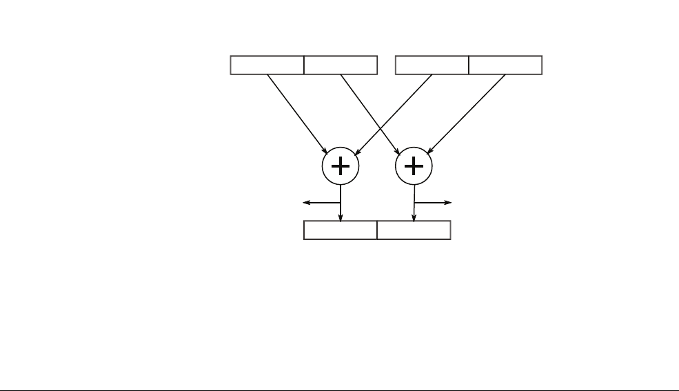
ARM/Thumb Unified Assembly Language Instructions
ARM DEN0013B Copyright © 2011 ARM. All rights reserved. 6-14
ID082411 Non-Confidential
6.6 Integer SIMD instructions
This section describes the SIMD (single instruction, multiple data) operations added in v6 of the
ARM architecture. These should not be confused with the significantly more powerful
Advanced SIMD (NEON) operations which were introduced in the ARM-v7 architecture and
are covered in detail in Chapter 19, Chapter 20 and Appendix B.
These instructions were first added in the ARMv6 architecture and provide the ability to pack,
extract and unpack 8- and 16-bit quantities within 32-bit registers and to perform multiple
arithmetic operations such as add, subtract, compare or multiply to such packed data, in a single
instruction.
6.6.1 Integer register SIMD instructions
The v6 SIMD operations make use of the GE (greater than or equal) flags within the CPSR.
There is a flag corresponding to each of the four byte positions within a word. Normal data
processing operations produce one value and set the N, Z, C and V flags (as seen in Figure 4-3
on page 4-6). The SIMD operations produce up to four outputs and set only the GE flags, to
indicate overflow. The
MSR
and
MRS
instructions can be used to write or read these flags directly.
The general form of the SIMD instructions are that subword quantities in each register are
operated on in parallel (for example, four
ADD
s on four bytes can be performed) and the GE flags
are set or cleared according to the results of the instruction. Different types of add and subtract
can be specified using appropriate prefixes. For example,
QADD16
performs saturating addition
on halfwords within a register.
SADD/UADD8
and
SSUB/USUB8
set the GE bits individually while
SADD/UADD16
and
SSUB/USUB16
set GE bits [3:2] together based on the top halfword result, and
[1:0] together on the bottom halfword result.
Also available are the
ASX
and
SAX
class of instructions, which reverse halfwords of one operand
and add/subtract or subtract/add parallel pairs. Like the previously described
ADD
and Subtract
instructions, these exist as unsigned (
UASX
/
USAX
), signed (
SASX
/
SSAX
) and saturated (
QASX
/
QSAX
)
versions.
Figure 6-2 ADD v6 SIMD example
R3 R0
R1
SADD16 R1, R3, R0
GE[1:0]GE[3:2]
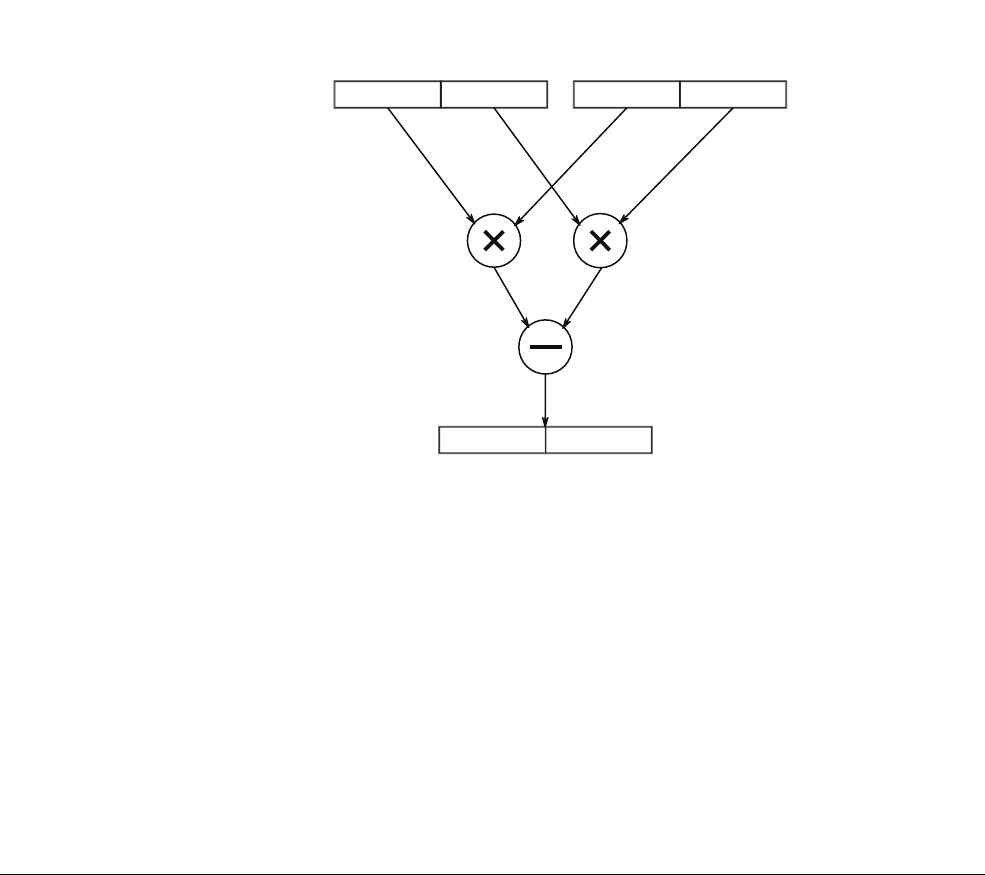
ARM/Thumb Unified Assembly Language Instructions
ARM DEN0013B Copyright © 2011 ARM. All rights reserved. 6-15
ID082411 Non-Confidential
The
SADD16
instruction shown in Figure 6-2 shows how two separate addition operations are
performed by a single instruction. The top halfwords of registers R3 and R0 are added, with the
result going into the top halfword of register R1 and the bottom halfwords of registers R3 and
R0 are added, with the result going into the bottom halfword of register R1. GE[3:2] bits in the
CPSR are set based on the top halfword result and GE[1:0] based on the bottom halfword result.
6.6.2 Integer register SIMD multiplies
Like the other SIMD operations, these operate in parallel, on subword quantities within
registers. The instruction can also include an accumulate option, with add or subtract being able
to be specified. The instructions are
SMUAD
(SIMD multiply and add with no accumulate),
SMUSD
(SIMD multiply and subtract with no accumulate),
SMLAD
(multiply and add with accumulate)
and
SMLSD
(multiply and subtract with accumulate).
Adding an L (long) before D indicates 64-bit accumulation.
Using the X (eXchange) suffix indicates halfwords in
R
s are swapped before calculation.
The Q flag is set if accumulation overflows.
Figure 6-3 v6 SIMD signed dual multiply subtract example
The
SMUSD
instruction shown in Figure 6-3 performs two signed 16-bit multiplies (top × top and
bottom × bottom) and then subtracts the two results. This kind of operation is useful when
performing operations on complex numbers (with a real and imaginary component), a common
task for filter algorithms.
6.6.3 Sum of absolute differences
Calculating the sum of absolute differences is a key operation in the motion vector estimation
component of common video codecs and is carried out over arrays of pixel data. The
USAD8
instruction performs this operation on the bytes within a word.
Rn Rm
Rd
SMUSD Rd, Rn, Rm
-
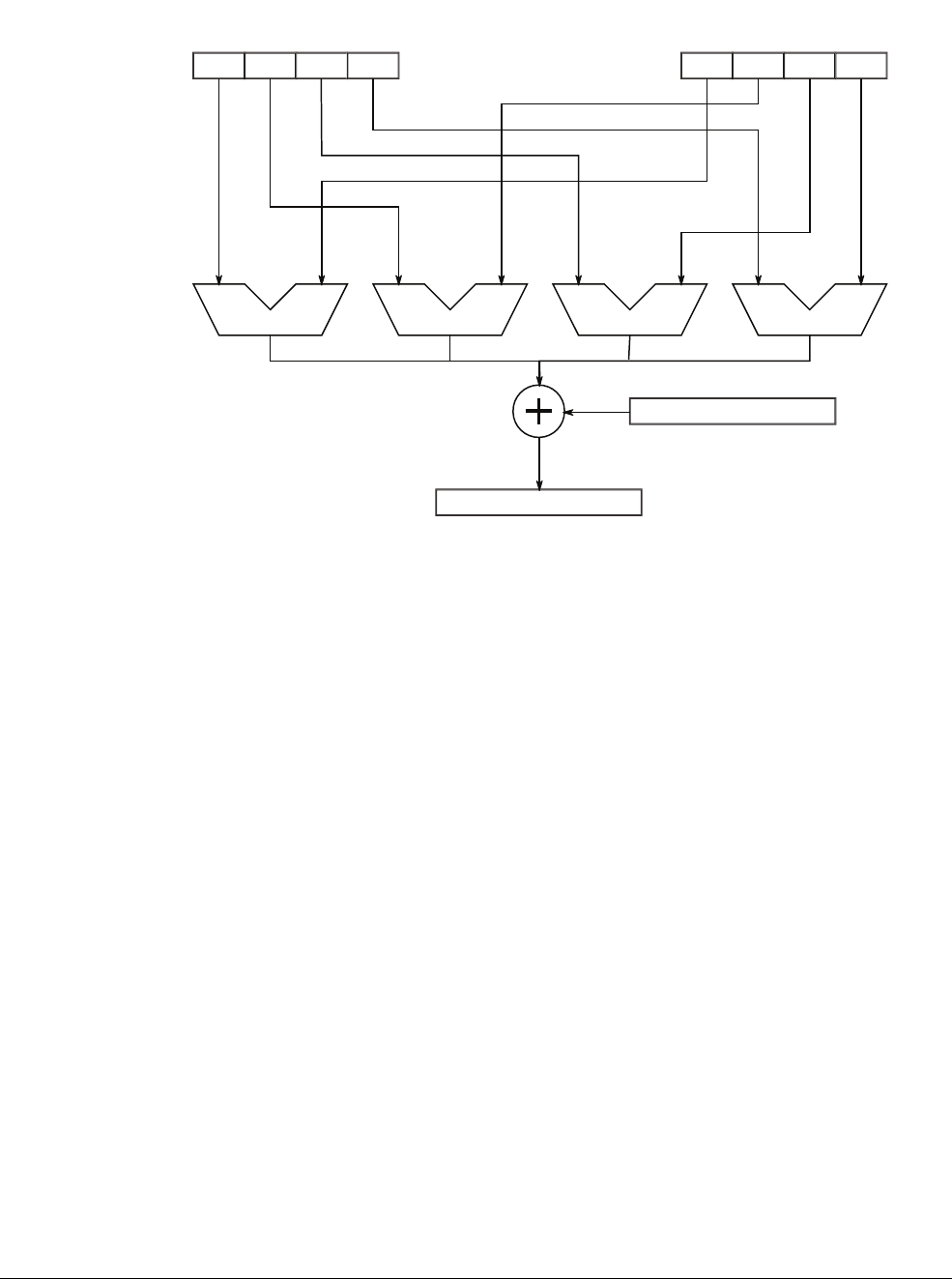
ARM/Thumb Unified Assembly Language Instructions
ARM DEN0013B Copyright © 2011 ARM. All rights reserved. 6-16
ID082411 Non-Confidential
Figure 6-4 Sum of absolute differences
The
USADA8
Rd
,
Rn
,
Rm
,
Ra
instruction is illustrated in Figure 6-4. It calculates the sum of absolute
differences of the bytes in registers Rn and Rm, adds in the value stored in Ra and places the
result in Rd.
6.6.4 Data packing/unpacking
Packed data is common in many video/audio codecs (video data is usually expressed as packed
arrays of 8-bit pixel data, audio data may use packed 16-bit samples), and also in network
protocols. Before additional instructions were added in architecture v6, this data had to be either
loaded with
LDRH
/
LDRB
instructions or loaded as words and then unpacked using Shift and Bit
Clear operations; both are relatively inefficient. Pack (
PKHBT
,
PKHTB
) instructions allow 16-bit or
8-bit values to be extracted from any position in a register and packed into another register.
Unpack instructions (
UXTH
,
UXTB
, plus many variants, including signed, with addition etc.) can
extract 8-bit or 16-bit values from any bit position within a register.
This enables sequences of packed data in memory to be loaded efficiently using word or
doubleword loads, unpacked into separate register values, operated upon and then packed back
into registers for efficient writing out to memory.
Rn Rm
Ra
Rd
ABSDIFF ABSDIFF ABSDIFF ABSDIFF
Optional accumulation
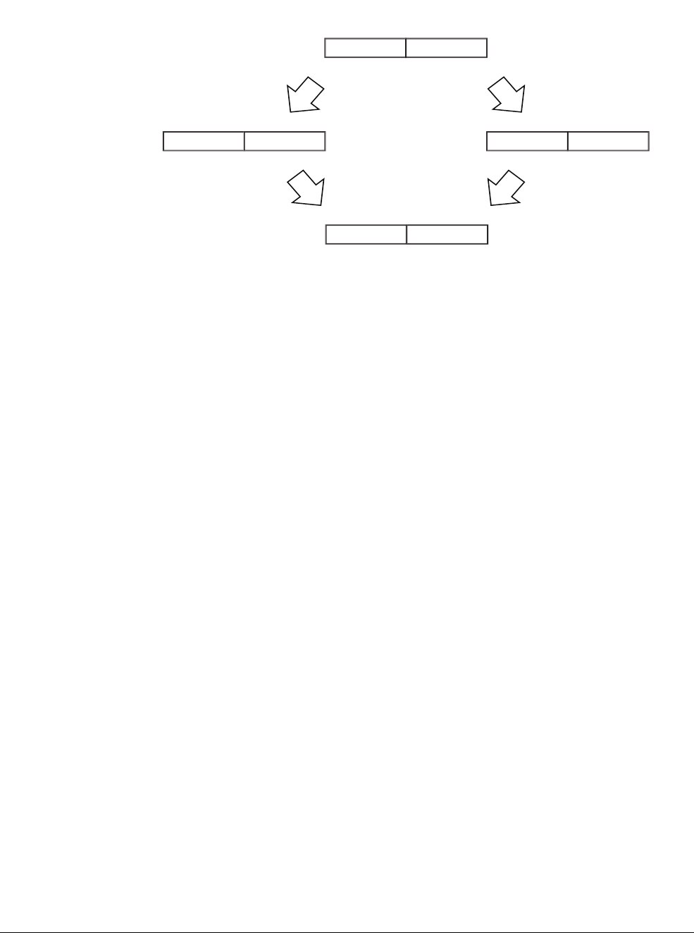
ARM/Thumb Unified Assembly Language Instructions
ARM DEN0013B Copyright © 2011 ARM. All rights reserved. 6-17
ID082411 Non-Confidential
Figure 6-5 Packing and unpacking of 16-bit data in 32-bit registers
In the simple example shown in Figure 6-5, R0 contains two separate 16-bit values, denoted A
and B. We can use the
UXTH
instruction to unpack the two halfwords into registers for further
processing and we can then use the
PKHBT
instruction to pack halfword data from two registers
into one.
6.6.5 Byte selection
The
SEL
instruction enables us to select each byte of the result from the corresponding byte in
either the first or the second operand, based on the value of the GE[3:0] bits in the CPSR. The
packed data arithmetic operations set these bits as a result of add or subtract operations, and
SEL
can be used after these to extract parts of the data – for example, to find the smaller of the two
bytes in each position.
R0
AB
R1
00...00 A
R2
00...00 B
R0
ABAB
UXTH r1, r0, ROR #16 UXTH r2, r0
PKHBT r0, r2, r1, LSL #16

ARM/Thumb Unified Assembly Language Instructions
ARM DEN0013B Copyright © 2011 ARM. All rights reserved. 6-18
ID082411 Non-Confidential
6.7 Saturating arithmetic
Saturated arithmetic is commonly used in DSP algorithms. Calculations which return a value
higher (or lower) than the largest positive (or negative) number which can be represented do not
overflow. Instead the result is set to the largest +/- value (saturated). The ARM instruction set
includes a number of instructions which allows easy implementation of such algorithms.
6.7.1 Saturated math instructions
The ARM saturated math instructions operate on either word or halfword sized values. (The
QADD8
and
QSUB8
instructions operate on byte sized values.) The result of the operation will be
saturated to the largest possible positive or negative number. If the result would have overflowed
and has been saturated, the overflow flag (CPSR Q bit) is set. This flag is said to be “sticky”.
When set it will remain set until explicitly cleared by a write to the CPSR.
The instruction set provides special instructions with this behavior,
QSUB
and
QADD
. Additionally,
we have
QDSUB
and
QDADD
which are provided in support of Q15 or Q31 fixed point arithmetic.
These instructions double and saturate their second operand before performing the specified add
or subtract.
The Count Leading Zeros (
CLZ
) instruction returns the number of 0 bits before the most
significant bit that is set. This can be useful for normalization and for certain division
algorithms. To saturate a value to a specific bit position (effectively saturate to a power of two),
we can use the
USAT
or
SSAT
(unsigned or signed) saturate operations.
USAT16
and
SSAT16
allow
saturation of two halfword values packed within a register.

ARM/Thumb Unified Assembly Language Instructions
ARM DEN0013B Copyright © 2011 ARM. All rights reserved. 6-19
ID082411 Non-Confidential
6.8 Miscellaneous instructions
The remaining instructions cover coprocessor, supervisor call, PSR modification, byte reversal,
cache preload, bit manipulation and a few others.
6.8.1 Coprocessor instructions
Coprocessor instructions occupy part of the ARM instruction set. Up to 16 coprocessors can be
implemented, numbered 0 to 15 (CP0, CP1 … CP15). These can either be internal (built-in to
the processor) or connected externally, through a dedicated interface. Use of external
coprocessors is uncommon in older processors and is not supported at all in the Cortex-A series.
• Coprocessor 15 is a built-in coprocessor which provides control over many processor
features, including cache and MMU.
• Coprocessor 14 is a built-in coprocessor which controls the hardware debug facilities of
the processor, such as breakpoint units (described in Chapter 28).
• Coprocessors 10 and 11 give access to the floating-point and/or NEON hardware in the
system (described in Chapter 16-Chapter 18).
If a coprocessor instruction is executed, but the appropriate coprocessor is not present in the
system, an undefined instruction exception occurs.
There are five classes of coprocessor instruction
•
CDP
– initiate a coprocessor data processing operation
•
MRC
– move to ARM register from coprocessor register
•
MCR
– move to coprocessor register from ARM register
•
LDC
– load coprocessor register from memory
•
STC
– store from coprocessor register to memory.
Multiple register and other variants of these instructions are also available. (
MRRC
,
MCCR
,
LDCL
,
STCL
etc.).
6.8.2 Coprocessor 15
CP15, the System Control coprocessor, is (despite the name coprocessor) an integral part of the
processor and provides control of many features. It can contain up to 16 primary registers, each
of size 32 bits. Note, however that access to CP15 is privilege controlled and not all registers
are available in User mode. The CP15 register access instructions specify the required primary
register, with the other fields in the instruction used to define the access more precisely and
increase the number of physical 32-bit registers in CP15. The 16 primary registers in CP15 are
named c0 to c15, but are often referred to by a series of letters. For example, the CP15 System
Control Register is named CP15.SCTLR. Table 6-5 on page 6-20 summarizes the function of

ARM/Thumb Unified Assembly Language Instructions
ARM DEN0013B Copyright © 2011 ARM. All rights reserved. 6-20
ID082411 Non-Confidential
each register used in Cortex-A family processors. We will consider some of these in more detail
when we look at the operation of the cache and MMU. The list is not exhaustive – the large
number of instruction attribute and processor feature registers has been omitted, for example.
Table 6-5 CP15 Register summary
Register Description
Main ID Register (MIDR) Gives identification information for the
processor (including part number and
revision).
Cache Type Register (CTR) Gives information about cache hardware
(such as cacheline size, indexing and
tagging policies).
TCM Type Register (TCMTR) Gives information about TCM hardware.
TLB Type Register (TLBTR) Gives information about TLB hardware.
Multiprocessor Affinity Register (MPIDR) Provides a way to uniquely identify
individual processors within a
multi-processor system.
Debug Feature Register 0 (ID_DFR0) Gives information about debug and trace
hardware supported.
Auxiliary Feature Register 0 (ID_AFR0) An IMPLEMENTATION DEFINED register (one
whose purpose is defined by the processor
implementer and not mandated by the ARM
architecture).
Cache Size ID Registers (CCSIDR) Provides information about supported
cache policies, associativity and set size
(see Chapter 7 Caches).
Cache Level ID Register (CLIDR) Identifies the cache type at each level and
gives information about coherency and
unification (see Chapter 7 Caches).
Auxiliary ID Register (AIDR) IMPLEMENTATION DEFINED.
Cache Size Selection Register (CSSELR) A Read/Write register which indicates
which cache level the CCSIDR applies to.
CP15 c1 System Control registers
System Control Register (SCTLR) The main processor control register (see
Chapter 8 Memory Management Unit).
Auxiliary Control Register (ACTLR) IMPLEMENTATION DEFINED.
Implementation specific additional control
and configuration options.
Coprocessor Access Control Register (CPACR) Controls access to all coprocessors except
CP14 and CP15.
Secure Configuration Register (SCR) Used by TrustZone (Chapter 26 Security).
Secure Debug Enable Register (SDER) Used by TrustZone (Chapter 26 Security).
Non-Secure Access Control Register (NSACR) Used by TrustZone (Chapter 26 Security).
CP15 c2 and c3, Memory protection and control registers

ARM/Thumb Unified Assembly Language Instructions
ARM DEN0013B Copyright © 2011 ARM. All rights reserved. 6-21
ID082411 Non-Confidential
Translation Table Base Register 0 (TTBR0) Base address of level 1 page table (see
Chapter 8 Memory Management Unit).
Translation Table Base Register 1 (TTBR1) Base address of level 1 page table (see
Chapter 8 Memory Management Unit).
Translation Table Base Control Register (TTBCR) Controls use of TTB0 and TTB1 (see
Chapter 8 Memory Management Unit).
Domain Access Control Register (DACR) Defines memory access permission for
domains (see Chapter 8 Memory
Management Unit).
CP15 c4, not used
CP15 c5 and c6, memory system fault registers
Data Fault Status Register (DFSR) Gives status information about the last data
fault (see Chapter 12 Other Exception
Handlers).
Instruction Fault Status Register (IFSR) Gives status information about the last
instruction fault (see Chapter 12 Other
Exception Handlers).
Auxiliary Data and Instruction Fault Status Registers (ADFSR and
AIFSR)
Gives extra implementation-specific status
information about the last fault (see
Chapter 12 Other Exception Handlers).
Data Fault Address Register (DFAR) Gives the virtual address of the access that
caused the most recent precise data abort
(see Chapter 12 Other Exception
Handlers).
Instruction Fault Address Register (IFAR) Gives the virtual address of the access that
caused the most recent precise prefetch
abort (see Chapter 12 Other Exception
Handlers).
CP15 c7, cache maintenance and other functions
Cache and branch predictor maintenance functions See Chapter 7 Caches.
Virtual address to physical address translation operations See Chapter 8 Memory Management Unit.
Data and instruction barrier operations See Chapter 9 Memory Ordering.
No Operation (NOP) This encoding was used for
WFI
and
PLI
in
ARMv6. These now exist as separate
dedicated instructions in ARMv7.
CP15 c8, TLB maintenance operations
CP15 c9, cache and TCM lockdown registers and performance monitors
CP15 c10, memory remapping and TLB control registers
Primary Region Remap Register (PRRR) Controls mapping of the TEX[0], C, and B
memory region attributes (see Chapter 8
Memory Management Unit).
Table 6-5 CP15 Register summary (continued)
Register Description

ARM/Thumb Unified Assembly Language Instructions
ARM DEN0013B Copyright © 2011 ARM. All rights reserved. 6-22
ID082411 Non-Confidential
All system architecture functions are controlled by reading or writing a general purpose
processor register (Rt) from/to a set of registers (CRn) located within coprocessor 15. The Op1,
Op2, and CRm fields of the instruction can also be used to select registers or operations. The
format is shown in Example 6-5.
Example 6-5 CP15 Instruction syntax
MRC p15, Op1, Rt, CRn, CRm, Op2 ;
read a CP15 register into an ARM register
MCR p15, Op1, Rt, CRn, CRm, Op2 ;
write a CP15 register from an ARM register
We will not go through each of the various CP15 registers in detail, as this would duplicate
reference information which can readily be obtained from the ARM Architecture Reference
Manual or product documentation. We will look at one example – the read-only Main ID
Register (MIDR), the format of which is shown in Figure 6-6.
Figure 6-6 Main ID Register format
Normal Memory Remap Register (NMRR) Gives additional mapping controls for
Normal memory.
CP15 c11, reserved for TCM DMA registers (not used in Cortex-Aseries processors).
CP15 c12, Security Extensions registers
Vector Base Address Register (VBAR)
Monitor Vector Base Address Register (MVBAR)
Interrupt Status Register (ISR)
CP15 c13, process, context and thread ID registers
FCSE Process ID Register (FCSEIDR) See FCSE description Chapter 8 Memory
Management Unit).
Context ID Register (CONTEXTIDR) See description of ASID Chapter 8 Memory
Management Unit).
Software thread ID registers See description of ASID Chapter 8 Memory
Management Unit).
CP15 c14 is not used
CP15 c15, IMPLEMENTATION DEFINED registers
Table 6-5 CP15 Register summary (continued)
Register Description
31 24 23 20 19 16 15 3 0
Implementer Variant Arch Primary part number Rev
4

ARM/Thumb Unified Assembly Language Instructions
ARM DEN0013B Copyright © 2011 ARM. All rights reserved. 6-23
ID082411 Non-Confidential
In a privileged mode, we can read this register, using the instruction
MRC p15, 0, <Rt>, c0, c0, 0
The result, placed in register Rt, tells software which processor it is running on. For an ARM
Cortex processor the interpretation of the results is as follows:
• Bits [31:24] – implementer, will be
0x41
for an ARM designed processor.
• Bits [23:20] – variant, shows the revision number of the processor.
• Bits [19:16] – architecture, will be
0xF
for ARM architecture v7.
• Bits [15:4] – part number (for example
0xC08
for the Cortex-A8 processor).
• Bits [3:0] – revision, shows the patch revision number of the processor.
6.8.3 SVC
The
SVC
(supervisor call) instruction, when executed, causes a supervisor call exception. This is
described further in Chapter 10 Exception Handling. The instruction includes a 24-bit (ARM)
or 8-bit (Thumb) number value, which can be examined by the
SVC
handler code. Through the
SVC
mechanism, an operating system can specify a set of privileged operations which
applications running in User mode can request. This instruction was originally called
SWI
(Software Interrupt).
6.8.4 PSR modification
Several instructions allow the PSR to be written to, or read from:
•
MRS
transfers the CPSR or SPSR value to a general purpose register.
MSR
transfers a general
purpose register to the CPSR or SPSR. Either the whole status register, or just part of it
can be updated. In User mode, all bits can be read, but only the condition flags (_f) are
permitted to be modified.
• The Change Processor State (
CPS
) instruction can be used to directly modify the mode and
interrupt enable/disable (I/F) bits in the CPSR in a privileged mode. See Figure 4-3 on
page 4-6.
•
SETEND
modifies a single CPSR bit, the E (Endian) bit. This can be used in systems with
mixed endian data to temporarily switch between little- and big-endian memory access.
6.8.5 Bit manipulation
There are instructions which allow bit manipulation of values in registers:
• the Bit Field Insert (
BFI
) instruction allows a series of adjacent bits from one register
(specified by supplying a width value and LSB position) to be placed into another.
• the Bit Field Clear (
BFC
) instruction allows adjacent bits within a register to be cleared.
•the
SBFX
and
UBFX
instructions (Signed and Unsigned Bit Field Extract) copy adjacent bits
from one register to the least significant bits of a second register, and sign extend or zero
extend the value to 32 bits.
•
the RBIT
instruction reverses the order of all bits within a register.
ARM/Thumb Unified Assembly Language Instructions
ARM DEN0013B Copyright © 2011 ARM. All rights reserved. 6-24
ID082411 Non-Confidential
6.8.6 Cache preload
Cache preloading is described further in Chapter 17 Optimizing Code to Run on ARM
Processors. Two instructions are provided,
PLD
(data cache preload) and
PLI
(instruction cache
preload). Both instructions act as hints to the memory system that an access to the specified
address is likely to occur soon. Implementations that do not support these operations will treat
a preload as a
NOP
, but all of the Cortex-A family processors described in this book are able to
preload the cache.
6.8.7 Byte reversal
Instructions to reverse byte order can be useful for dealing with quantities of the opposite
endianness or other data re-ordering operations.
•the
REV
instruction reverses the bytes in a word
• the
REV16
reverses the bytes in each halfword of a register
• the
REVSH
reverses the bottom two bytes, and sign extends the result to 32 bits.
Figure 6-7 illustrates the operation of the
REV
instruction, showing how four bytes within a
register have their ordering within a word reversed.
Figure 6-7 Operation of the REV instruction
6.8.8 Other instructions
A few other instructions are available:
• The breakpoint instruction (
BKPT
) will either cause a prefetch abort or cause the processor
to enter debug state (depending on the whether the processor is configured for monitor or
halt mode debug). This instruction is used by debuggers and does not form part of actual
application code.
• Wait For Interrupt (
WFI
) puts the processor into standby mode, which is described further
in Chapter 21 Power Management. The processor stops execution until “woken” by an
interrupt or debug event. Note that if
WFI
is executed with interrupts disabled, an interrupt
will still wake the processor, but no interrupt exception is taken. The processor proceeds
to the instruction after the
WFI
. In older ARM processors,
WFI
was implemented as a CP15
operation.
WFE
(Wait for Event) will also be described in Chapter 21.
Bit[31:24] Bit[23:16] Bit15:8 Bit[7:0]
078
15 16 23 24 31

ARM/Thumb Unified Assembly Language Instructions
ARM DEN0013B Copyright © 2011 ARM. All rights reserved. 6-25
ID082411 Non-Confidential
•A
NOP
instruction (no-operation) does nothing. It may or may not take time to execute, so
the
NOP
instruction should not be used to insert timing delays into code, instead it is
intended to be used as padding, although it is usually better to use the assembler align
directive.

ARM DEN0013B Copyright © 2011 ARM. All rights reserved. 7-1
ID082411 Non-Confidential
Chapter 7
Caches
The word cache derives from the French verb cacher, “to hide”. A cache is a hidden storage place.
The application of this word to a processor is obvious – a cache is a place where the processor can
store instructions and data, hidden from the programmer and system. In many cases, it would be
true to say that the cache is transparent to, or hidden from the programmer. But very often, as we
shall see, it is important to understand the operation of the cache in detail.
When the ARM architecture was first developed, the clock speed of the processor and the access
speeds of memory were broadly similar. Today’s processors are much more complicated and can
be clocked orders of magnitude faster. However, the frequency of the external bus and of memory
devices has not scaled to the same extent. It is possible to implement small blocks of on-chip
SRAM which can operate at the same speeds of the processor, but such RAM is very expensive in
comparison to standard DRAM blocks, which can have thousands of times more capacity. In many
ARM-based systems, access to external memory will take tens or even hundreds of cycles.
Essentially, a cache is a small, fast block of memory which (conceptually at least) sits between the
processor core and main memory. It holds copies of items in main memory. Accesses to the cache
memory happen significantly faster than those to main memory. As the cache holds only a subset
of the contents of main memory, it must store both the address of the item in main memory and the
associated data. Whenever the processor wants to read or write a particular address, it will first look
for it in the cache. Should it find the address in the cache, it will access the data in the cache, rather
than having to perform an access to main memory. This significantly increases the potential
performance of the system, by reducing the effect of slow external memory access times. An access
to an external off-chip memory can require hundreds of processor cycles. It also reduces the power
consumption of the system, by avoiding the need to drive external devices.

Caches
ARM DEN0013B Copyright © 2011 ARM. All rights reserved. 7-2
ID082411 Non-Confidential
Cache sizes are small relative to the overall memory used in the system. Larger caches make for
more expensive chips. In addition, making an internal processor cache larger can potentially
limit the maximum speed of the processor. Significant research has gone into identifying how
hardware can determine what it should keep in the cache. Efficient use of this limited resource
is a key part of writing efficient applications to run on a processor.
So, we can use on-chip SRAM to implement caches, which hold temporary copies of
instructions and data from main memory. Code and data have the properties of temporal and
spatial locality. This means that programs tend to re-use the same addresses over time (temporal
locality) and tend to use addresses which are near to each other (spatial locality). Code, for
instance, can contain loops, meaning that the same code gets executed repeatedly or a function
can be called multiple times. Data accesses (for example, to the stack) can be limited to small
regions of memory. When the memory used over short time periods is not close together, it is
often likely that the same data will be re-used. It is this fact that access to RAM by the processor
exhibits such locality, and is not truly random, that enables caches to be successful.
Access ordering rules obey the “weakly ordered” model. A read from a location followed by a
write to the same location by the same processor guarantees that the read returns the value that
was at the address before the write occurred.
We will also look at the write buffer. This is a block which decouples writes being done by the
processor (when executing store instructions, for example) from the external memory bus. The
processor places the address, control and data values associated with the store into a set of
FIFOs. This is the write buffer. Like the cache, it sits between the processor core and main
memory. This enables the processor to move on and execute the next instructions without having
to stop and wait for the slow main memory to actually complete the write operation.

Caches
ARM DEN0013B Copyright © 2011 ARM. All rights reserved. 7-3
ID082411 Non-Confidential
7.1 Why do caches help?
Caches speed things up, as we have seen, because program execution is not random. Programs
access the same sets of data repeatedly and execute the same sets of instructions repeatedly. By
moving code or data into faster memory when it is first accessed, following accesses to that code
or data become much faster. The initial access which provided the data to the cache is no faster
than normal. It is any subsequent accesses to the cached values which are faster, and it is from
this the performance increase derives. The processor hardware will check all instruction fetches
and data reads or writes in the cache, although obviously we need to mark some parts of memory
(those containing peripheral devices, for example) as non-cacheable. As the cache holds only a
subset of main memory, we need a way to determine (quickly) whether the address we are
looking for is in the cache.

Caches
ARM DEN0013B Copyright © 2011 ARM. All rights reserved. 7-4
ID082411 Non-Confidential
7.2 Cache drawbacks
It may seem that caches and write buffers are automatically a benefit, as they speed up program
execution. However, they also add some problems which are not present in an uncached
processor. One such drawback is that program execution time can become non-deterministic.
What this means is that, because the cache is small and holds only a subset of main memory, it
fills rapidly as a program executes. When the cache is full, existing code or data is replaced, to
make room for new items. So, at any given time, it is not normally possible to be certain whether
or not a particular instruction or data item is to be found in the cache.
This means that the execution time of a particular piece of code can vary significantly. This can
be something of a problem in hard real-time systems where strongly deterministic behavior is
needed.
Furthermore, as we shall see, we need a way to control how different parts of memory are
accessed by the cache and write buffer. In some cases, we want the processor to read an external
device, such as a peripheral. It would not be sensible to use a cached value of a timer peripheral,
for example. Sometimes we want the processor to stop and wait for a store to complete. So
caches and write buffers give the programmer some extra work to do.
Sometimes, we need to think about the fact that data in the cache and data in external memory
may not be the same. This is referred to as coherency. This can be a particular problem when we
have multiple processors or memory agents like an external DMA. We will consider such
coherency issues in greater detail later in the book.

Caches
ARM DEN0013B Copyright © 2011 ARM. All rights reserved. 7-5
ID082411 Non-Confidential
7.3 Memory hierarchy
A memory hierarchy in computer science refers to a hierarchy of memory types, with
faster/smaller memories closer to the processor and slower/larger memory further away. In most
systems, we can have secondary storage, such as disk drives and primary storage such as flash,
SRAM and DRAM. In embedded systems, we typically further sub-divide this into on-chip and
off-chip memory. Memory which is on the same chip (or at least in the same package) as the
processor will typically be much faster.
A cache can be included at any level in the hierarchy and should improve system performance
where there is an access time difference between parts of the memory system.
In ARM-based systems, we typically have level 1 (L1) caches, which are connected directly to
the processor logic that fetches instructions and handles load and store instructions. These are
Harvard caches (that is, there are separate caches for instructions and for data) in all but the
lowest performing members of the ARM family and effectively appear as part of the processor.
Over the years, the size of L1 caches has increased, due to SRAM size and speed improvements.
At the time of writing, 16KB or 32KB cache sizes are most common, as these are the largest
RAM sizes capable of providing single cycle access at a processor speed of 1GHz or more.
Many ARM systems have, in addition, a level 2 (L2) cache. This is larger than the L1 cache
(typically 256KB, 512KB or 1MB), but slower and unified (holding both instructions and data).
It can be inside the processor itself, as in the Cortex-A8 and Cortex A15 processors, or be
implemented as an external block, placed between the processor and the rest of the memory
system. The ARM PL310 is an example of such an external L2 cache controller block.
In addition, we have processors which can be implemented in multi-processor clusters in which
each processor has its own cache. Such systems require mechanisms to maintain coherency
between caches, so that when one processor changes a memory location, that change is made
visible to other processors which share that memory. We describe this in more detail when we
look at multi-processing.
Caches
ARM DEN0013B Copyright © 2011 ARM. All rights reserved. 7-6
ID082411 Non-Confidential
7.4 Cache terminology
A brief summary of terms used in the description may be helpful:
•A line refers to the smallest loadable unit of a cache, a block of contiguous words from
main memory.
•The index is the part of a memory address which determines in which line(s) of the cache
the address can be found.
•A way is a subdivision of a cache, each way being of equal size and indexed in the same
fashion. The line associated with a particular index value from each cache way grouped
together forms a set.
•The tag is the part of a memory address stored within the cache which identifies the main
memory address associated with a line of data.
Figure 7-1 Cache terminology
Tag Index Offset Byte
32-bit address
Data RAM Tag RAM
Offset
Index
Set
Way Tag
Line

Caches
ARM DEN0013B Copyright © 2011 ARM. All rights reserved. 7-7
ID082411 Non-Confidential
7.5 Cache architecture
In a von Neumann architecture, there is a single cache used for instruction and data (a unified
cache). A modified Harvard architecture has separate instruction and data buses and therefore
there are two caches, an instruction cache (I-cache) and a data cache (D-cache). In many ARM
systems, we can have distinct instruction and data level 1 caches backed by a unified level 2
cache.
Let’s consider how a cache memory is constructed. The cache needs to hold an address, some
data and some status information. The address tells the cache where the information came from
in main memory and is known as a tag. The total cache size is a measure of the amount of data
it can hold; the RAMs used to hold tag values are not included in the calculation. The tag does,
however, take up physical space on the silicon. It would be inefficient to hold one word of data
for each tag address, so we typically store a line of data – normally 8 words for the Cortex-A5
and Cortex-A9 processors or 16 words for the Cortex-A8 and Cortex-A15 processors with each
address. This means that the bottom few bits of the address are not required to be stored in the
tag – we need to record the address of a line, not of each byte within the line, so the five or six
least significant bits will always be 0.
Associated with each line of data are one or more status bits. Typically, we will have a valid bit,
which marks the line as containing data that can be used. (This means that the address tag
represents some real value.) We will also have one or more dirty bits which mark whether the
cache line (or part of it) holds data which is not the same as (newer than) the contents of main
memory. We will treat this in more detail later in the chapter.

Caches
ARM DEN0013B Copyright © 2011 ARM. All rights reserved. 7-8
ID082411 Non-Confidential
7.6 Cache controller
This is a hardware block which has the task of managing the cache memory, in a way which is
(largely) invisible to the program. It automatically writes code or data from main memory into
the cache. It takes read and write memory requests from the processor and performs the
necessary actions to the cache memory and/or the external memory.
When it receives a request from the processor it must check to see whether the requested address
is to be found in the cache. This is known as a cache look-up. It does this by comparing a subset
of the address bits of the request with tag values associated with lines in the cache. If there is a
match (a hit) and the line is marked valid then the read or write will happen using the cache
memory.
If there is no match with the cache tags or the tag is not valid, we have a cache miss and the
request must be passed to the next level of the memory hierarchy – an L2 cache, or external
memory. It can also cause a cache linefill. A cache linefill causes the contents of a piece of main
memory to be copied into the cache. At the same time, the requested data or instructions are
streamed to the processor. This process happens transparently and is not directly visible to the
programmer.
The processor need not wait for the linefill to complete before using the data. The cache
controller will typically access the critical word within the cache line first. For example, if we
perform a load instruction which misses in the cache and triggers a cache linefill, the first read
to external memory will be that of the actual address supplied by the load instruction. This
critical data is supplied to the processor pipeline, while the cache hardware and external bus
interface then read the rest of the cache line, in the background.
Caches
ARM DEN0013B Copyright © 2011 ARM. All rights reserved. 7-9
ID082411 Non-Confidential
7.7 Direct mapped caches
We now look at various different ways of implementing caches used in ARM processors,
starting with the simplest, a direct mapped cache.
Figure 7-2 Direct mapped cache operation
In a direct mapped cache, each location in main memory maps to a single location in the cache.
As main memory is many times larger than the cache, many addresses map to the same cache
location. Figure 7-2 shows a small cache, with four words per line and four lines. This means
that the cache controller will use two bits of the address (bits 3:2) as the offset to select a word
within the line and two bits of the address (bits 5:4) as the index to select one of the four
available lines. The remaining bits of the address (bits 31:6) will be stored as a tag value.
To look up a particular address in the cache, the hardware extracts the index bits from the
address and reads the tag value associated with that line in the cache. If the two are the same and
the valid bit indicates that the line contains valid data, it has a hit. It can then extract the data
value from the relevant word of the cache line, using the offset and byte portion of the address.
If the line contains valid data, but does not generate a hit (that is, the tag shows that the cache
holds a different address in main memory) then the cache line is removed and is replaced by data
from the requested address.
It should be clear that all main memory addresses with the same value of bits [5:4] will map to
the same line in the cache. Only one of those lines can be in the cache at any given time. This
means that we can easily get a problem called thrashing. Consider a loop which repeatedly
accesses address
0x40
and
0x80
, as in Figure 7-2. When we first read address
0x40
, it will not be
in the cache and so a linefill takes place putting the data from
0x40
to
0x4F
into the cache. When
we then read address
0x80
, it will not be in the cache and so a linefill takes place putting the data
from
0x80
to
0x8F
into the cache – and in the process we lose the data from address
0x40
to
0x4F
from the cache. The same thing will happen on each iteration of the loop and our software will
Tag Index Offset Byte
32-bit address
Data Hit
=
Lines (Index)
CacheMain memory
0x0000.0000
0x0000.0010
0x0000.0020
0x0000.0030
0x0000.0040
0x0000.0050
0x0000.0060
0x0000.0070
0x0000.0080
0x0000.0090

Caches
ARM DEN0013B Copyright © 2011 ARM. All rights reserved. 7-10
ID082411 Non-Confidential
perform poorly. Direct mapped caches are therefore not typically used in the main caches of
ARM processors, but we do see them in some places – for example in the branch target address
cache of the ARM1136 processor.
Processors can have hardware optimizations for situations where the whole cache line is being
written to. This is a condition which can take a significant proportion of total cycle time in some
systems. For example, this can happen when
memcpy()
- or
memset()
-like functions which
perform block copies or zero initialization of large blocks are executed. In such cases, there is
no benefit in first reading the data values which will be over-written.
Cache allocate policies act as a “hint” to the processor, they do not guarantee that a piece of
memory will be read into the cache, and as a result, programmers should not rely on that.
Caches
ARM DEN0013B Copyright © 2011 ARM. All rights reserved. 7-11
ID082411 Non-Confidential
7.8 Set associative caches
The main cache(s) of ARM processors are always implemented using a set associative cache.
This significantly reduces the likelihood of the cache thrashing seen with direct mapped caches,
thus improving program execution speed and giving more deterministic execution. It comes at
the cost of increased hardware complexity and a slight increase in power (because multiple tags
are compared on each cycle).
With this kind of cache organization, we divide the cache into a number of equally-sized pieces,
called ways. The index field of the address continues to be used to select a particular line, but
now it points to an individual line in each way. Commonly, there are 2- or 4-ways, but some
ARM implementations have used higher numbers (for example, the ARM920T processor has a
64-way cache). Level 2 cache implementations (such as the ARM PL310) can have larger
numbers of ways (higher associativity) due to their much larger size. The cache lines with the
same index value are said to belong to a set. To check for a hit, we must look at each of the tags
in the set.
Figure 7-3 A 2-way set-associative cache
In Figure 7-3, a cache with 2-ways is shown. Data from address 0 (or
0x40
, or
0x80
) may be
found in line 0 of either (but not both) of the two cache ways.
Increasing the associativity of the cache reduces the probability of thrashing. The ideal case is
a fully associative cache, where any main memory location can map anywhere within the cache.
However, building such a cache is impractical for anything other than very small caches (for
example, those associated with MMU TLBs – see Chapter 8). In practice, performance
improvements are minimal for Level1 caches above 4-way associativity, with 8-way or 16-way
associativity being more useful for larger level 2 caches.
Cache way 0Main memory
0x0000.0000
0x0000.0010
0x0000.0020
0x0000.0030
0x0000.0040
0x0000.0050
0x0000.0060
0x0000.0070
0x0000.0080
0x0000.0090
Cache way 1
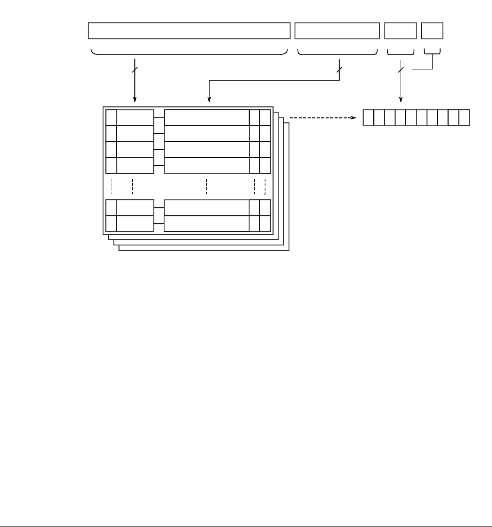
Caches
ARM DEN0013B Copyright © 2011 ARM. All rights reserved. 7-12
ID082411 Non-Confidential
7.9 A real-life example
Before we move on to look at write buffers, let’s consider an example which is more realistic
than those shown in the previous two diagrams. Figure 7-4 is a 4-way set associative 32KB data
cache, with an 8-word cache line length. This kind of cache structure might be found on the
Cortex-A9 or Cortex-A5 processors.
The cache line length is eight words (32 bytes) and we have 4-ways. 32KB divided by 4, divided
by 32 gives us a figure of 256 lines in each way. This means that we need the eight bits to index
a line within a way (bits [12:5]). We need to use bits [4:2] of the address to select from the eight
words within the line. The remaining bits [31:13] will be used as a tag.
Figure 7-4 A 32KB 4-way set associative cache
Address
Data line 0
Tag
VDD
Data line 1
Data line 2
Data line 3
Data line 254
Data line 255
Tag
31 13
Set
12 5
Word
42
Byte
10
DD01234567
19 8 3

Caches
ARM DEN0013B Copyright © 2011 ARM. All rights reserved. 7-13
ID082411 Non-Confidential
7.10 Virtual and physical tags and indexes
This section assumes some knowledge of the address translation process. Readers unfamiliar
with virtual addressing may wish to revisit this section after reading Chapter 8.
In A real-life example on page 7-12, we were a little imprecise about specification of exactly
which address is used to perform cache lookups. Early ARM processors (for example, the
ARM720T or ARM926EJ-S processors) used virtual addresses to provide both the index and
tag values. This has the advantage that the processor can do a cache look-up without the need
for a virtual to physical address translation. The drawback is that changing the virtual to physical
mappings in the system means that the cache must first be cleaned and invalidated and this can
have a significant performance impact. We will go into more detail about these terms in
Invalidating and cleaning cache memory on page 7-20.
ARM11 family processors use a different cache tag scheme. Here, the cache index is still
derived from a virtual address, but the tag is taken from the physical address. The advantage of
a physical tagging scheme is that changes in virtual to physical mappings do not now require
the cache to be invalidated. This can have significant benefits for complex multi-tasking
operating systems which can frequently modify page table mappings. Using a virtual index has
some hardware advantages. It means that the cache hardware can read the tag value from the
appropriate line in each way in parallel without actually performing the virtual to physical
address translation, giving a fast cache response. Such a cache is often described as Virtually
Indexed, Physically Tagged (VIPT). The Cortex-A8 processor uses a VIPT implementation in
its instruction cache, but not its data cache.
However, there is a drawback to a VIPT implementation. For a 4-way set associative 32KB or
64KB cache, bits [12] and/or [13] of the address are needed to select the index. If 4KB pages
are used in the MMU, bits [13:12] of the virtual address may not be equal to bits [13:12] of the
physical address. There is therefore scope for potential cache coherence problems if multiple
virtual address mappings point to the same physical address. This is resolved by placing certain
restrictions on such multiple mappings which kernel page table software must obey. This is
described as a “page coloring” issue and exists on other processor architectures for the same
reasons.
This problem is avoided by using a Physically Indexed, Physically Tagged (PIPT) cache
implementation, shown in Figure 7-4 on page 7-12. The Cortex-A series of processors
described in this book use such a scheme for their data caches. It means that page coloring issues
are avoided, but at the cost of hardware complexity.

Caches
ARM DEN0013B Copyright © 2011 ARM. All rights reserved. 7-14
ID082411 Non-Confidential
7.11 Cache policies
There are a number of different choices which can be made in cache operation. We need to
consider what causes a line from external memory to be placed into the cache (allocation
policy). We need to look at how the controller decides which line within a set associative cache
to use for the incoming data (replacement policy). And we need to control what happens when
the processor performs a write which hits or misses in the cache (write policy).

Caches
ARM DEN0013B Copyright © 2011 ARM. All rights reserved. 7-15
ID082411 Non-Confidential
7.12 Allocation policy
When the processor does a cache look-up and the address it wants is not in the cache, it must
determine whether or not to perform a cache linefill and copy that address from memory.
•A read allocate policy allocates a cache line only on a read. If a write is performed by the
processor which misses in the cache, the cache is not affected and the write goes to main
memory.
•A write allocate policy allocates a cache line for either a read or write which misses in the
cache (and so might more accurately be called a read-write cache allocate policy). For
both memory reads which miss in the cache and memory writes which miss in the cache,
a cache linefill is performed. This is typically used in combination with a write-back write
policy on current ARM processors, as we shall see in Section 7.14.

Caches
ARM DEN0013B Copyright © 2011 ARM. All rights reserved. 7-16
ID082411 Non-Confidential
7.13 Replacement policy
When there is a cache miss, the cache controller must select one of the cache lines in the set for
the incoming data. The cache line selected is called the victim. If the victim contains valid, dirty
data, the contents of that line must be written to main memory before new data can be written
to the victim cache line. This is called eviction.
The replacement policy is what controls the victim selection process. The index bits of the
address are used to select the set of cache lines, and the replacement policy selects the specific
cache line from that set which is to be replaced.
•Round-robin or cyclic replacement means that we have a counter (the victim counter)
which cycles through the available ways and cycles back to 0 when it reaches the
maximum number of ways.
•Pseudo-random replacement randomly selects the next cache line in a set to replace. The
victim counter is incremented in a pseudo-random fashion and can point to any line in the
set.
Most ARM processors support both policies.
A round-robin replacement policy is generally more predictable, but can suffer from poor
performance in certain rare use cases and for this reason, the pseudo-random policy is often
preferred.

Caches
ARM DEN0013B Copyright © 2011 ARM. All rights reserved. 7-17
ID082411 Non-Confidential
7.14 Write policy
When the processor executes a store instruction, a cache lookup on the address(es) to be written
is performed. For a cache hit on a write, there are two choices.
•Write-through. With this policy writes are performed to both the cache and main memory.
This means that the cache and main memory are kept coherent. As there are more writes
to main memory, a write-through policy is slower than a write-back policy if the write
buffer fills and therefore is less commonly used in today’s systems (although it can be
useful for debug).
•Write-back. In this case, writes are performed only to the cache, and not to main memory.
This means that cache lines and main memory can contain different data. The cache line
holds newer data, and main memory contains older data (said to be stale). To mark these
lines, each line of the cache has an associated dirty bit (or bits). When a write happens
which updates the cache, but not main memory, the dirty bit is set. If the cache later evicts
a cache line whose dirty bit is set (a dirty line), it writes the line out to main memory.
Using a write-back cache policy can significantly reduce traffic to slow external memory
and therefore improve performance and save power. However, if there are other agents in
the system which can access memory at the same time as the processor, we may need to
worry about coherency issues. This is described in more detail later.

Caches
ARM DEN0013B Copyright © 2011 ARM. All rights reserved. 7-18
ID082411 Non-Confidential
7.15 Write and Fetch buffers
A write buffer is a hardware block inside the processor (but sometimes in other parts of the
system as well), implemented using a number of FIFOs. It accepts address, data and control
values associated with processor writes to memory. When the processor executes a store
instruction, it may place the relevant details (the location to write to, the data to be written, the
transaction size and so forth) into the buffer. The processor does not have to wait for the write
to be completed to main memory. It can proceed with executing the next instructions. The write
buffer itself will drain the writes accepted from the processor, to the memory system.
A write buffer can increase the performance of the system. It does this by freeing the processor
from having to wait for stores to complete. In effect, provided there is space in the write buffer,
the write buffer is a way to hide latency. If the number of writes is low or well spaced, the write
buffer will not become full. If the processor generates writes faster than they can be drained to
memory, the write buffer will eventually fill and there will be little performance benefit.
There is a potential hazard to be considered when thinking about write buffers. What happens
if a write goes into a write buffer and then we read from that address? This is called a
read-after-write hazard. Different processors handle this problem in different ways. A simple
solution is to stall the processor on a read to the main memory system until all pending writes
have completed. A more sophisticated approach is to snoop into the write buffer and detect the
existence of a potential hazard. Hardware can then resolve the hazard either by stalling the read
until the relevant write has completed, or it can read the value directly from the write buffer.
Some write buffers support write merging (also called write combining). They can take multiple
writes (for example, a stream of writes to adjacent bytes) and merge them into one single burst.
This can reduce the write traffic to external memory and therefore boost performance.
It will be obvious to the experienced programmer that sometimes the behavior of the write
buffer is not what we want when accessing a peripheral, we might want the processor to stop
and wait for the write to complete before proceeding to the next step. Sometimes we really want
a stream of bytes to be written and we don’t want the stores to be combined. In ARM memory
ordering model on page 9-4, we’ll look at memory types supported by the ARM architecture and
how to use these to control how the caches and write buffers are used for particular devices or
parts of the memory map.
Similar components, called fetch buffers, can be used for reads in some systems. In particular,
processors typically contain prefetch buffers which read instructions from memory ahead of
them actually being inserted into the pipeline. In general, such buffers are transparent to the
programmer. We will consider some possible hazards associated with this when we look at
memory ordering rules.

Caches
ARM DEN0013B Copyright © 2011 ARM. All rights reserved. 7-19
ID082411 Non-Confidential
7.16 Cache performance and hit rate
The hit rate is defined as the number of cache hits divided by the number of memory requests
made to the cache during a specified time (normally calculated as a percentage). Similarly, the
miss rate is the number of total cache misses divided by the total number of memory requests
made to the cache. One may also calculate the number of hits or misses on reads and/or writes
only.
Clearly, a higher hit rate will generally result in higher performance. It is not really possible to
quote example figures for typical software, the hit rate is very dependent upon the size of the
critical parts of the code or data operated on and of course, the size of the cache.
There are some simple rules which can be followed to give better performance. The most
obvious of these is to enable caches and write buffers and to use them wherever possible
(typically for all parts of the memory system which contain code and more generally for RAM
and ROM, but not peripherals). Performance will be considerably increased in Cortex-A series
processors if instruction memory is cached.
Placing frequently accessed data together in memory can be helpful. Fetching a data value in
memory involves fetching a whole cache line; if none of the other words in the cache line will
be used, there will be little or no performance gain. Smaller code may cache better than larger
code and this can sometimes give (seemingly) paradoxical results. For example, a piece of C
code may fit entirely within cache when compiled for Thumb (or for the smallest size) but not
when compiled for ARM (or for maximum performance) and as a consequence can actually run
faster than the more “optimized” version. We describe cache considerations in much more detail
in Chapter 17 Optimizing Code to Run on ARM Processors.

Caches
ARM DEN0013B Copyright © 2011 ARM. All rights reserved. 7-20
ID082411 Non-Confidential
7.17 Invalidating and cleaning cache memory
Cleaning and/or invalidation can be required when the contents of external memory have been
changed and the programmer wishes to remove stale data from the cache. It can also be required
after MMU related activity such as changing access permissions, cache policies, or virtual to
physical address mappings.
The word flush is often used in descriptions of clean/invalidate operations. We avoid the term
in this text, as it is not used in a consistent fashion on different microprocessor architectures.
ARM generally uses only the terms clean and invalidate.
• Invalidation of a cache (or cache line) means to clear it of data. This is done by clearing
the valid bit of one or more cache lines. The cache always needs to be invalidated after
reset. This can be done automatically by hardware, but may need to be done explicitly by
the programmer (for example, the Cortex-A9 processor does not do this automatically). If
the cache might contain dirty data, it is generally incorrect to invalidate it. Any updated
data in the cache from writes to write-back cacheable regions would be lost by simple
invalidation.
• Cleaning a cache (or cache line) means to write the contents of dirty cache lines out to
main memory and clear the dirty bit(s) in the cache line. This makes the contents of the
cache line and main memory coherent with each other. Clearly, this is only applicable for
data caches in which a write-back policy is used.
Copying code from one location to another (or other forms of “self-modifying” code) may
require the programmer to clean and/or invalidate the cache. The memory copy code will use
load and store instructions and these will operate on the data side of the processor. If the data
cache is using a write-back policy for the area to which code is written, it will be necessary to
clean that data from the cache before the code can be executed. This ensures that the instructions
stored as data go out into main memory and are then available for the instruction fetch logic. In
addition, if the area to which code is written was previously used for some other program, the
instruction cache could contain stale code (from before main memory was re-written).
Therefore, it may also be necessary to invalidate the instruction cache before branching to the
newly copied code.
The commands to clean and/or invalidate the cache are CP15 operations. They are available
only to privileged code and cannot be executed in User mode. In systems where the TrustZone
Security Extensions are in use, there can be hardware limitations applied to non-secure usage of
some of these operations.
CP15 instructions exist which will clean, invalidate, or clean and invalidate level 1 data or
instruction caches. Invalidation without cleaning is safe only when it is known that the cache
cannot contain dirty data – for example a Harvard instruction cache. The programmer can
perform the operation on the entire cache, or just on individual lines. These individual lines can
be specified either by giving a virtual address to be clean and/or invalidated, or by specifying a
line number in a particular set, in cases where the hardware structure is known. The same
operations can be performed on the L2 or outer caches and we will look at this in Level 2 cache
controller on page 7-22.
Of course, these operations will be accessed through kernel code – in Linux, you will use the
__clear_cache()
function, which you can find in
arch/arm/mm/cache-v7.S
. Equivalent functions
exist in other operating systems – Google Android has
cacheflush()
, for example.
A common situation where cleaning or invalidation can be required is DMA (Direct Memory
Access). When it is required to make changes made by the processor visible to external memory,
so that it can be read by a DMA controller, it might be necessary to clean the cache. When
external memory is written by a DMA controller and it is necessary to make those changes
visible to the processor, the affected addresses will need to be invalidated from the cache.

Caches
ARM DEN0013B Copyright © 2011 ARM. All rights reserved. 7-21
ID082411 Non-Confidential
7.18 Cache lockdown
One of the problems with caches is their unpredictability. It is not generally possible to be
certain that a particular piece of code or data is within the cache. This can be problematic
because sometimes (particularly in systems with hard real-time requirements), variable and
unpredictable execution times cannot be tolerated.
Cache lockdown enables the programmer to place critical code/or and data into cache memory
and protect it from eviction, thus avoiding any cache miss penalty. A typical usage scenario
might be for code and data of a critical interrupt handler. As cache memory used for lockdown
is unavailable for other parts of main memory, use of lockdown effectively reduces the usable
cache size. Note that locked down code or data can still be invalidated and the locked down area
can still be immune from replacement. This can make use of lockdown impractical in systems
which frequently invalidate the cache.
The smallest lockable unit for the cache is typically quite large; normally one or more cache
ways. In a 4-way set associative cache, for example, lockdown of a single way therefore uses a
quarter of the available cache space.

Caches
ARM DEN0013B Copyright © 2011 ARM. All rights reserved. 7-22
ID082411 Non-Confidential
7.19 Level 2 cache controller
At the start of this chapter, we briefly described the partitioning of the memory system and
explained how many systems have a multi-layer cache hierarchy. The Cortex-A5 and Cortex-A9
processors do not have an integrated level 2 cache. Instead, the system designer can opt to
connect the ARM L2 cache controller (PL310) outside of the processor or MPCore instance.
This cache controller can support a cache of up 8MB in size, with a set associativity of between
four and sixteen ways. The size and associativity are fixed by the SoC designer. The level 2
cache can be shared between multiple processors (or indeed between the processor and other
agents, for example a graphics processor). It is possible to lockdown cache data on a per-master
per-way basis, enabling management of cache sharing between multiple components.
7.19.1 Level 2 cache maintenance
We saw in Virtual and physical tags and indexes on page 7-13 how the programmer may need
the ability to clean and/or invalidate some or all of a cache. This can be done by writing to
memory-mapped registers within the L2 cache controller in the case where the cache is external
to the processor (as with the Cortex-A5 and Cortex-A9 processors), or through CP15 (where the
level 2 cache is implemented inside the processor (as with the Cortex-A8 processor). Where
such operations are performed by having the processor perform memory-mapped writes, the
processor needs a way of determining when the operation is complete. It does this by polling a
further memory-mapped register within the L2 cache.
The PL310 Level 2 cache controller operates only on physical addresses. Therefore, to perform
cache maintenance operations, it may be necessary for the program to perform a virtual to
physical address translation. The PL310 provides a “cache sync” operation which forces the
system to wait for pending operations to complete.

Caches
ARM DEN0013B Copyright © 2011 ARM. All rights reserved. 7-23
ID082411 Non-Confidential
7.20 Point of coherency and unification
For set/way based clean or invalidate, the point to which the operation can be defined is
essentially the next level of cache. For operations which use a virtual address, the architecture
defines two conceptual points.
•Point of Coherency (PoC). For a particular address, the PoC is the point at which all blocks
(for example, processors, DSPs, or DMA engines) which can access memory are
guaranteed to see the same copy of a memory location. Typically, this will be the main
external system memory.
•Point of Unification (PoU). The PoU for a processor is the point at which the instruction
and data caches and the page table walks of the processor are guaranteed to see the same
copy of a memory location. For example, a unified level 2 cache would be the point of
unification in a system with Harvard level 1 caches and a TLB to cache page table entries.
Readers unfamiliar with the terms page table walk or TLB will find these described in
Chapter 8. If no external cache is present, main memory would be the PoU.
In the case of an MPCore (an example of a Inner Shareable shareability domain, using the
terminology from Chapter 9 Memory Ordering), the PoU is where instruction and data caches
and page table walks of all the processors within the MPCore cluster are guaranteed to see the
same copy of a memory location.
Knowledge of the PoU enables self-modifying code to ensure future instruction fetches are
correctly made from the modified version of the code. They can do this by using a two-stage
process:
• clean the relevant data cache entries (by address)
• invalidate instruction cache entries (by address).
In addition, the use of memory barriers will be required here, the ARM Architecture Reference
Manual provides detailed examples of the necessary code sequences.
Similarly, we can use the clean data cache entry and invalidate TLB operations to ensure that all
writes to the page tables are visible to the MMU.
7.20.1 Exclusive cache mode
The Cortex-A series processors can be connected to a level 2 cache controller which supports
an exclusive cache mode. This makes the processor data cache and the L2 cache exclusive. At
any specific time, an address can be cached in either a L1 data cache or in the L2 cache, but not
both. This increases the usable space and efficiency of the L2 cache connected to the processor.
In practice, exclusive mode is not widely used. It can be difficult to correctly invalidate lines in
multi-processor systems, for example.

Caches
ARM DEN0013B Copyright © 2011 ARM. All rights reserved. 7-24
ID082411 Non-Confidential
7.21 Parity and ECC in caches
So-called soft errors are increasingly a concern in today’s systems. Smaller transistor
geometries and lower voltages give circuits an increased sensitivity to perturbation by cosmic
rays and other background radiation, alpha particles from silicon packages or from electrical
noise. This is particularly true for memory devices which rely on storing small amounts of
charge and which also occupy large proportions of total silicon area. In some systems,
mean-time-between-failure could be measured in seconds if appropriate protection against soft
errors was not employed.
The ARM architecture provides support for parity and Error Correcting Code (ECC) in the
caches (and tightly coupled memories). Parity means that we have an additional bit which marks
whether the number of bits with the value one is even (or odd, depending upon the scheme
chosen). This provides a simple check against single bit errors. An ECC scheme enables
detection of multiple bit failures and possible recovery from soft errors, but recovery
calculations can take several cycles. Implementing a processor which is tolerant of level 1 cache
RAM accesses taking multiple clock cycles significantly complicates the processor design.
ECC is therefore more commonly used only on blocks of memory (for example, the Level 2
cache), outside the processor.
Parity is checked on reads and writes, and can be implemented on both tag and data RAMs.
Parity mismatch generates a prefetch or data abort exception, and the fault status/address
registers are updated appropriately.

Caches
ARM DEN0013B Copyright © 2011 ARM. All rights reserved. 7-25
ID082411 Non-Confidential
7.22 Tightly coupled memory
An alternative to using cache lockdown is the so-called Tightly Coupled Memory (TCM). TCM
is a block of fast memory located next to the processor core. It appears as part of the memory
system within the address map and gives similar response times to a cache. It can be used to hold
instructions or data required for real-time code which needs deterministic behavior. It can be
regarded as fast scratchpad memory local to the processor. The contents of TCM are not
initialized by the processor. It is the responsibility of the programmer to copy required code and
data into the tightly coupled memory before enabling use of the TCM. The programmer may
also have to tell the processor which physical address to locate the TCMs within the memory
map.
As TCM is more suited to systems running simpler operating systems and where determinism
is a key requirement, it is not supported in Cortex-A series processors and so is not described
further here.

ARM DEN0013B Copyright © 2011 ARM. All rights reserved. 8-1
ID082411 Non-Confidential
Chapter 8
Memory Management Unit
This chapter describes the main concepts of virtual memory systems and memory management. An
important function of a Memory Management Unit (MMU) is to allow us to manage tasks as
independent programs running in their own private virtual memory space. A key feature of such a
virtual memory system is address relocation, which is the translation of the (virtual) address issued
by the processor core to a different (physical) address in main memory. The translation is done by
the MMU hardware and is transparent to the application (ignoring for the moment any performance
issues).
In multi-tasking embedded systems, we typically need a way to partition the memory map and
assign permissions and memory attributes to these regions of memory. In more advanced systems,
running more complex operating systems, like Linux, we need even greater control over the
memory system. More advanced operating systems typically need to use a hardware-based MMU.
The MMU enables tasks or applications to be written in a way which requires them to have no
knowledge of the physical memory map of the system, or about other programs which may be
running at the same time. This makes programming of applications much simpler, as it enables us
to use the same virtual memory address space for each. This virtual address space is separate from
the actual physical map of memory in the system. The MMU translates addresses of code and data
from the virtual view of memory to the physical addresses in the real system. Applications are
written, compiled and linked to run in the virtual memory space. Virtual addresses are those used
by the programmer, compiler and linker when placing code in memory. Physical addresses are
those used by the actual hardware system. It is the responsibility of the operating system to program
the MMU to translate between these two views of memory. Figure 8-1 on page 8-2 shows an
example system, illustrating the virtual and physical views of memory.

Memory Management Unit
ARM DEN0013B Copyright © 2011 ARM. All rights reserved. 8-2
ID082411 Non-Confidential
Figure 8-1 Virtual and physical memory
The ARM MMU carries out this translation of virtual addresses into physical addresses. In
addition, it controls memory access permissions and memory ordering, cache policies etc. for
each region of memory. When the MMU is disabled, all virtual addresses map one-to-one to the
same physical address (a “flat mapping”). If the MMU cannot translate an address, it generates
an abort exception on the processor and provides information to the processor about what the
problem was.
Peripherals
RAM
ROM
Virtual Memory Map Physical Memory Map
Vectors page
Kernel
Heap
Data
ZI data
Code
Dynamic libraries

Memory Management Unit
ARM DEN0013B Copyright © 2011 ARM. All rights reserved. 8-3
ID082411 Non-Confidential
8.1 Virtual memory
The MMU enables multiple programs to be run simultaneously at the same virtual address while
being actually stored at different physical addresses. In fact, the MMU allows us to build
systems with multiple virtual address maps. Each task can have its own virtual memory map.
The OS kernel places code and data for each application in physical memory, but the application
itself does not need to know where that is.
The key feature of the MMU hardware is address translation. It does this using page tables.
These contain a series of entries, each of which describes the physical address translation for
part of the memory map. Page table entries are organized by virtual address. In addition to
describing the translation of that virtual page to a physical page, they also provide access
permissions and memory attributes for that page.
Note
In the ARM architecture, the concept referred to in generic computer terminology as page tables
has a more specific meaning. The ARM architecture uses multilevel page tables, and defines
translation tables as a generic term for all of these. It then reserves the use of the term page
tables to describe second level translation tables when using the short-descriptor format (not
making use of LPAE).
As this book is an introduction to the ARM architecture for people who may be unfamiliar with
it, this document will use the generic terminology wherever possible.
Addresses generated by the processor core are virtual addresses. The MMU essentially replaces
the most significant bits of this virtual address with some other value, to generate the physical
address (effectively defining a base address of a piece of memory). The lower bits are the same
in both addresses (effectively defining an offset in physical memory from that base address).
The portion of memory which is represented by these lower bits is known as a page. The ARM
MMU supports a multi-level page table architecture with two levels of page table: level 1 (L1)
and level 2 (L2). We will describe the meaning of level 1 and level 2 in a moment. A single set
of page tables is used to give the translations and memory attributes which apply to instruction
fetches and to data reads or writes. The process in which the MMU accesses page tables to
translate addresses is known as page table walking.
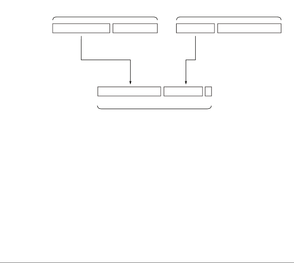
Memory Management Unit
ARM DEN0013B Copyright © 2011 ARM. All rights reserved. 8-4
ID082411 Non-Confidential
8.2 Level 1 page tables
Let’s take a look at the process by which a virtual address is translated to a physical address
using level 1 page table entries on an ARM processor. The first step is to locate the page table
entry associated with the virtual address.
There is usually a single level 1 page table (sometimes called a master page table). It can contain
two basic types of page table entry. The L1 page table divides the full 4GB address space into
4096 equally sized 1MB sections. The L1 page table therefore contains 4096 entries, each entry
being word sized. Each entry can either hold a pointer to the base address of a level 2 page table
or a page table entries for translating a 1MB section. If the page table entry is translating a 1MB
section, it gives the base address of the 1MB page in physical memory.
To locate the relevant entry in the page table, we take the top 12 bits of the virtual address and
use those to index to one of the 4096 words within the page table. This is illustrated in
Figure 8-2.
The base address of the L1 page table is known as the Translation Table Base Address and is
held within a register in CP15 c2. It must be aligned to a 16KB boundary.
Figure 8-2 Finding the address of the level 1 page table entry
To take a simple example, we place our L1 page table at address
0x12300000
. The processor core
issues virtual address
0x00100000
. The top 12 bits [31:20] define which 1MB of virtual address
space is being accessed. In this case
0x001
, so we need to read table entry [1]. Each entry is one
word (4 bytes). To get the offset into the table we must multiply the entry number by entry size:
0x001
* 4 = Address offset of
0x004
The address of the entry is
0x12300000
+
0x004
=
0x12300004
.
So, upon receiving this virtual address from the processor, the MMU will read the word from
address
0x12300004
. That word is an L1 page table entry. Figure 8-3 on page 8-5 shows the
format of a L1 page table entry.
Translation Table Base Address
31 14 13 0
Virtual Address
31 20 19 0
First Level Descriptor Address
31 14 13 2 10
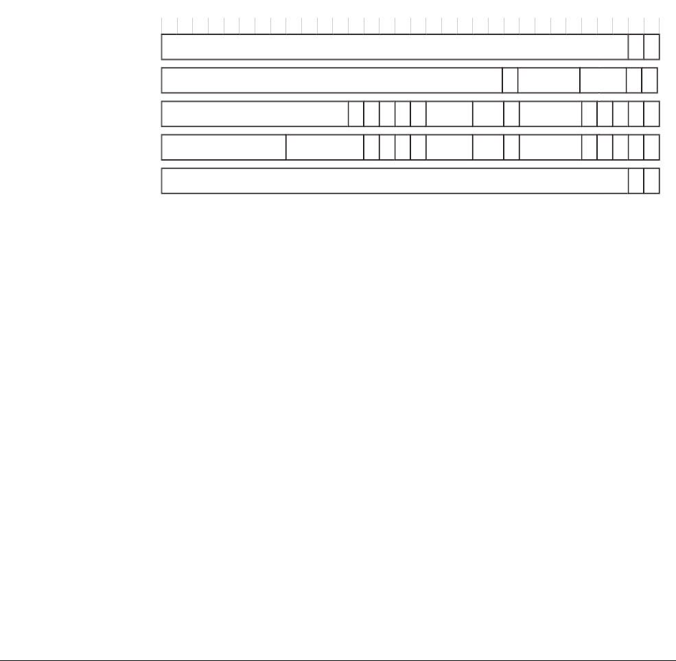
Memory Management Unit
ARM DEN0013B Copyright © 2011 ARM. All rights reserved. 8-5
ID082411 Non-Confidential
An L1 page table entry can be one of four possible types:
• A fault entry that generates an abort exception. This can be either a prefetch or data abort,
depending on the type of memory access. This effectively indicates virtual addresses
which are unmapped.
• A 1MB section translation entry.
• An entry that points to an L2 page table. This enables a 1MB piece of memory to be
further sub-divided into smaller pages.
• A 16MB supersection. This is a special kind of 1MB section entry, which requires 16
entries in the page table.
The least significant two bits [1:0] in the entry define which one of these the entry contains (with
bit [18] being used to differentiate between a section and supersection).
Figure 8-3 Level 1 page table entry format
It can be seen that the page table entry for a section (or supersection) contains the physical base
address used to translate the virtual address. You can also observe that many other bits are given
in the page table entry, including the Access Permissions (AP) and Cacheable (C) or Bufferable
(B) types, which we will examine in Memory attributes on page 8-12. This is all of the
information required to access the corresponding physical address and in these cases, the MMU
does not need to look beyond the L1 table.
Figure 8-4 on page 8-6 summarizes the translation process for an address translated by a section
entry in the L1 page table.
31 29 28 27 26 25 24 23 22 21 20 19 18 17 16 15 14 13 12 11 10 9 8 7 6 5 4 3 2 1 0
Fault Ignored 00
Reserved
11
Section 10
Section Base Address 0S
A
P
X
TEX AP
P
Domain
X
N
CB
S
B
Z
Supersection
10
Supersection
Base Address SBZ 1S TEX AP Domain
CB
P
Page table
01
Level 2 Descriptor Base Address PDomain SBZ
30
A
P
X
X
N
n
G
n
G
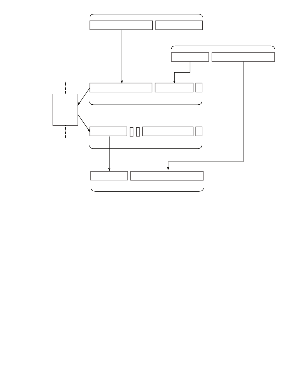
Memory Management Unit
ARM DEN0013B Copyright © 2011 ARM. All rights reserved. 8-6
ID082411 Non-Confidential
Figure 8-4 Generating a physical address from a level 1 page table entry
In a page table entry for a 1MB section of memory, the upper 12 bits of the page table entry
replace the upper 12 bits of the virtual address when generating the physical address, as
Figure 8-3 on page 8-5 shows.
A supersection is a 16MB piece of memory, which must have both its virtual and physical base
address aligned to a 16MB boundary. As L1 page table entries each describe 1MB, we need 16
consecutive, identical entries within the table to mark a supersection. In Choice of page sizes on
page 8-11, we describe why supersections can be useful.
Translation Table Base Address
31 14 13 0
Virtual Address
31 20 19 0
First Level Descriptor Address
31 14 13 2 10
Section Base Address Descriptor
31 17 2101920 18
010
Level 1
Table
31 20 019
Physical Address
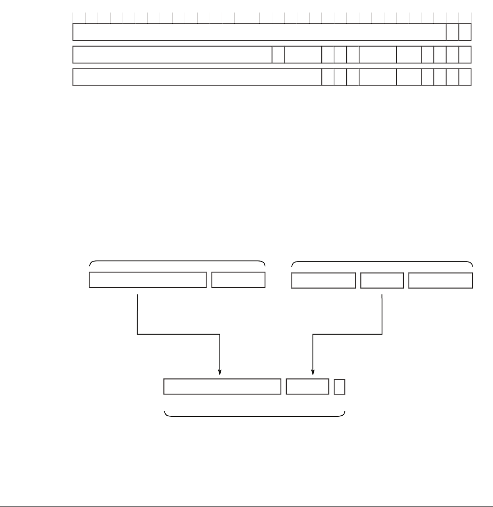
Memory Management Unit
ARM DEN0013B Copyright © 2011 ARM. All rights reserved. 8-7
ID082411 Non-Confidential
8.3 Level 2 page tables
An L2 page table has 256 word-sized entries, requires 1KB of memory space and must be
aligned to a 1KB boundary. Each entry translates a 4KB block of virtual memory to a 4KB block
in physical memory. A page table entry can give the base address of either a 4KB or 64KB page.
There are three types of entry used in L2 page tables, identified by the value in the two least
significant bits of the entry:
• A large page entry points to a 64KB page.
• A small page entry points a 4KB page.
• A fault page entry generates an abort exception if accessed.
Figure 8-5 shows the format of L2 page table entries.
Figure 8-5 Format of a level 2 page table entry
As with the L1 page table entry, a physical address is given, along with other information about
the page. Type extension (TEX), Shareable (S), and Access Permission (AP, APX) bits are used
to specify the attributes necessary for the ARMv7 memory model. The C and B bits control
(along with TEX) the cache policies for the memory governed by the page table entry. The nG
bit defines the page as being global (applies to all processes) or non-global (used by a specific
process). We will describe all of these bits in more detail in Memory attributes on page 8-12.
Figure 8-6 Generating the address of the level 2 page table entry
31 29 28 27 26 25 24 23 22 21 20 19 18 17 16 15 14 13 12 11 10 9 8 7 6 5 4 3 2 1 0
Fault Ignored 00
STEX AP
X
N
CB
Large page 01
Large Page Base Address SBZ
30
S
A
P
X
AP C B
Small page 1
Small Page Base Address TEX
X
N
A
P
X
n
G
n
G
Coarse Page Base Address
31 10 90
Virtual Address
31 20 19 0
Second Level Descriptor Address
10
12
31 10 92
11
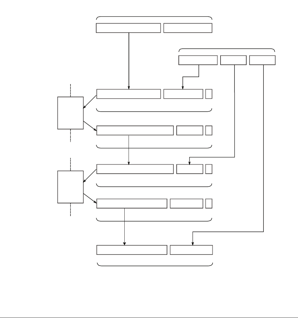
Memory Management Unit
ARM DEN0013B Copyright © 2011 ARM. All rights reserved. 8-8
ID082411 Non-Confidential
In Figure 8-6 on page 8-7 we see how the address of the L2 page table entry that we need is
calculated by taking the (1KB aligned) base address of the level 2 page table (given by the level
1 page table entry) and using 8 bits of the virtual address (bits [19:12]) to index within the 256
entries in the L2 page table.
Figure 8-7 summarizes the address translation process when using two layers of page tables.
Bits [31:20] of the virtual address are used to index into the 4096-entry L1 page table, whose
base address is given by the CP15 TTB register. The L1 page table entry points to an L2 page
table, which contains 256 entries. Bits [19:12] of the virtual address are used to select one of
those entries which then gives the base address of the page. The final physical address is
generated by combining that base address with the remaining bits of the physical address.
Figure 8-7 Summary of generation of physical address using the L2 page table entry
Translation Table Base Address
31 14 13 0
Level 1 Descriptor Address
31 14 13 2 10
Small Page Base Address
31 11 21012
10
Level 1
Table
31 12 011
Physical Address
Virtual Address
31 20 19 012 11
Level 2 Table Base Address
31 10 9210
01
Level 2 Descriptor Address
31 10 9210
Level 2
Table
TTB
L2TB
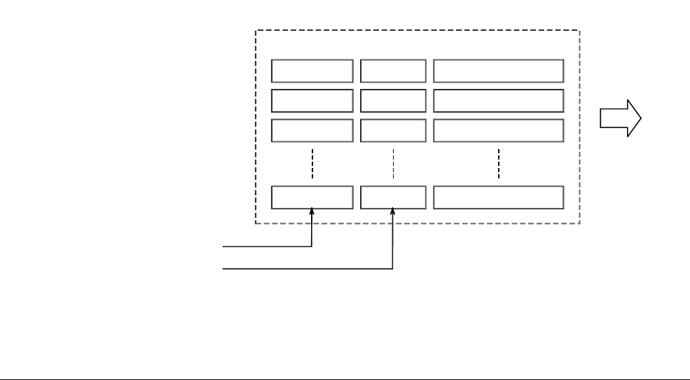
Memory Management Unit
ARM DEN0013B Copyright © 2011 ARM. All rights reserved. 8-9
ID082411 Non-Confidential
8.4 The Translation Lookaside Buffer
We have seen that a single memory request from the processor core can result in a total of three
memory requests to external memory – one for the level one page table walk, a second access
for the L2 page table walk and then finally the original request from the processor. This seems
like it would be ruinous for performance of the system. Fortunately, page table walks are
relatively uncommon events in the majority of systems, due to another part of the MMU.
The Translation Lookaside Buffer (TLB) is a cache of page translations within the MMU. On a
memory access, the MMU first checks whether the translation is cached in the TLB. If the
requested translation is available, we have a TLB hit, and the TLB provides the translation of
the physical address immediately. If the TLB does not have a valid translation for that address,
we have a TLB miss and an external page table walk is required. This newly loaded translation
can then be cached in the TLB for possible reuse.
The exact structure of the TLB differs between implementations of the ARM processors. What
follows is a description of a typical system, but individual implementations may vary from this.
There are one or more micro-TLBs, which are situated close to the instruction and data caches.
Addresses with entries which hit in the micro-TLB require no additional memory look-up and
no cycle penalty. However, the micro-TLB has only a small number of mappings (typically eight
on the instruction side and eight on the data side). This is backed by a larger main TLB (typically
64 entries), but there may be some penalty associated with accesses which miss in the
micro-TLB but which hit in the main TLB. Figure 8-8 shows how each TLB entry contains
physical and virtual addresses, but also attributes (such as memory type, cache policies and
access permissions) and potentially an ASID value (described in Address Space ID on
page 8-15).
The TLB is like other caches and so has a TLB line replacement policy and victim pointer, but
this is effectively transparent to the programmer (although see the next section on maintaining
TLB coherency). If the page table entry is a valid one, the virtual address, physical address and
other attributes for the whole page or section are stored as a TLB entry. If the page table entry
is not valid, the TLB will not be updated. The ARM architecture requires that only valid page
table descriptors are cached within the TLB.
Figure 8-8 Illustration of TLB structure
VA Tag ASID Descriptor
VA
ASID
PA

Memory Management Unit
ARM DEN0013B Copyright © 2011 ARM. All rights reserved. 8-10
ID082411 Non-Confidential
8.5 TLB coherency
When the operating system changes page table entries, it is possible that the TLB could contain
stale translation information. The OS should therefore take steps to invalidate TLB entries.
There are several CP15 operations available, which allow a global invalidate of the TLB or
removal of specific entries. As speculative instruction fetches and data reads may cause page
table walks, it is essential to invalidate the TLB when a valid page table entry is changed. Invalid
page table entries cannot be cached in TLB and so can be changed without invalidation.
The Linux kernel has a number of functions which use these CP15 operations, including
flush_tlb_all()
and
flush_tlb_range()
. Such functions are not typically required by device
driver or application code.
Many processors provide support for locking individual entries into the TLB. This can be useful
in systems which require a deterministic response time for a particular piece of code (for
example an interrupt service routine) and don’t want to worry about cycle counts being affected
by occasional page table walks. This is less commonly encountered in v7-A architecture profile
devices, where deterministic behavior is not typically required.

Memory Management Unit
ARM DEN0013B Copyright © 2011 ARM. All rights reserved. 8-11
ID082411 Non-Confidential
8.6 Choice of page sizes
This is essentially controlled by the operating system, but it is worth being aware of the
considerations involved when selecting page sizes. Smaller page sizes allow finer control of a
block of memory and potentially can reduce the amount of unused memory in a page. If a task
needs 7KB of data space, there is less unused space if it is allocated two 4KB pages as opposed
to a 64KB page or a 1MB section. Smaller page sizes also allow increased precision of control
over permissions, cache properties and so forth.
However, with increased page sizes, each entry in the TLB holds a reference to a larger piece of
memory. It is therefore more likely that a TLB hit will occur on any access and so there will be
fewer page table walks to slow external memory. For this reason, 16MB supersections can be
used with large pieces of memory which do not require detailed mapping. In addition, each L2
page table requires 1KB of memory. In some systems, memory usage by page tables may be
important.

Memory Management Unit
ARM DEN0013B Copyright © 2011 ARM. All rights reserved. 8-12
ID082411 Non-Confidential
8.7 Memory attributes
We have seen how page table entries allow the MMU hardware to translate virtual to physical
addresses. However, they also specify a number of attributes associated with each page,
including access permissions, memory type and cache policies.
8.7.1 Memory Access Permissions
The Access Permission (AP and APX) bits in the page table entry give the access permission
for a page. See Table 8-1.
An access which does not have the necessary permission (or which faults) will be aborted. On
a data access, this will result in a precise data abort exception. On an instruction fetch, the access
will be marked as aborted and if the instruction is not subsequently flushed before execution, a
prefetch abort exception will be taken. Faults generated by an external access will not, in
general, be precise.
Information about the address of the faulting location and the reason for the fault is stored in
CP15 (the fault address and fault status registers). The abort handler can then take appropriate
action – for example, modifying page tables to remedy the problem and then returning to the
application to re-try the access. Alternatively, the application which generated the abort may
have a problem and need to be terminated. In Linux use of page tables on page 8-18, we shall
see how Linux uses faults and aborts as a mechanism to manage use of memory by applications.
In addition, there are two bits in the CP15:CTLR that act to over-ride the Access Permissions
from the page table entry. These are the system (S) bit and the ROM (R) bit and their use is
deprecated in ARMv6 and later versions of the ARM architecture. Setting the S bit changes all
pages with “no access” permission to allow read access for privileged modes. Setting the R bit
changes all pages with “no access” permission to allow read access. These bits can be used to
provide access to large blocks of memory without the need to change lots of page table entries.
8.7.2 Memory attributes
ARM architecture versions 4 and 5 enabled the programmer to specify the memory access
behavior of pages by configuring whether the cache and write buffer could be used for that
location. This simple scheme is inadequate for today’s more complex systems and processors,
where we can have multiple levels of caches, hardware managed coherency between multiple
Table 8-1 Summary of Access Permission encodings
APX AP Privileged Unprivileged Description
0 00 No access No access Permission Fault
0 01 Read/Write No access Privileged Access only
0 10 Read/Write Read No user-mode write
0 11 Read/Write Read/Write Full access
1 00 - - Reserved
1 01 Read No access Privileged Read only
1 10 Read Read Read only
1 11 - - Reserved

Memory Management Unit
ARM DEN0013B Copyright © 2011 ARM. All rights reserved. 8-13
ID082411 Non-Confidential
processors sharing memory and/or processors which can speculatively fetch both instructions
and data. The new memory attributes added to the ARM architecture in ARMv6 and extended
in the ARMv7 architecture are designed to meet these needs.
Table 8-2 shows how the TEX, C and B bits within the page table entry are used to set the
memory attributes of a page and also the cache policies to be used. The meaning of memory
attributes is described in Chapter 9, while the cache policies were described in Chapter 7.
The final entry within the table needs further explanation. For normal cacheable memory, the
two least significant bits of the TEX field are used to provide the outer cache policy (perhaps
for level 2 or level 3 caches) while the C and B bits give the inner cache policy (for level 1 and
any other cache which is to be treated as inner cache). This enables us to specify different cache
policies for both the inner and outer cache. For the Cortex-A15 and Cortex-A8 processors, inner
cache properties set by the page table entry apply to both L1 and L2 caches. On some older
processors, outer cache may support write allocate, while the L1 cache may not. Such
processors should still behave correctly when running code which requests this cache policy, of
course.
It is clear that five bits to define memory types gives 32 possibilities. It is unlikely that a kernel
will wish to use all 32 possibilities. In practice only a handful will actually be needed. Therefore
the hardware provides CP15 registers (the “primary region remap registers”) which allow us to
remap the interpretation of TEX, C and B bits, so that TEX[0], C and B are used to describe
memory types. This means that up to eight different mappings from Table 8-2 can be used and
a particular value of TEX[0], C and B associated with the mapping. In this mode of operation,
the TEX[2:1] bits are freed up and can be used in an OS defined way. In Emulation of dirty and
accessed bits on page 8-18, we will see why an OS might wish to have “spare” bits within a page
table entry that it is able to modify freely. This mode is selected through the TRE bit (TEX
Remap) in the CP15 control register.
8.7.3 Domains
The ARM architecture has an unusual feature which enables regions of memory to be tagged
with a domain ID. There are 16 domain IDs provided by the hardware and CP15 c3 contains the
Domain Access Control Register (DACR) which holds a set of 2-bit permissions for each
Table 8-2 Memory type and cacheable properties encoding in page table entry
TEX C B Description Memory Type
000 0 0 Strongly-ordered Strongly-ordered
000 0 1 Sharable device Device
000 1 0 Outer and Inner writethrough, no allocate on write Normal
000 1 1 Outer and Inner write-back, no allocate on write Normal
001 0 0 Outer and Inner non-cacheable Normal
001 - - Reserved -
010 0 0 Non-shareable device Device
010 - - Reserved -
011 - - Reserved -
1XX Y Y Cached memory
XX = Outer policy
YY = Inner policy
Normal

Memory Management Unit
ARM DEN0013B Copyright © 2011 ARM. All rights reserved. 8-14
ID082411 Non-Confidential
domain number. This enables each domain to be marked as no-access, manager mode or client
mode. No-access causes an abort on any access to a page in this domain, irrespective of page
permissions. Manager mode ignores all page permissions and enables full access. Client mode
uses the permissions of the pages tagged with the domain.
The use of domains is deprecated in the ARMv7 architecture, but in order for access permissions
to be enforced, it is still necessary to assign a domain number to a section and to ensure that the
permission bits for that domain are set to client.

Memory Management Unit
ARM DEN0013B Copyright © 2011 ARM. All rights reserved. 8-15
ID082411 Non-Confidential
8.8 Multi-tasking and OS usage of page tables
In most systems using Cortex-A series processors, we will have a number of applications or
tasks running concurrently. Each task will have its own unique page tables residing in physical
memory. Typically, much of the memory system is organized so that the virtual-to-physical
address mapping is fixed, with page table entries that never change. This typically is used to
contain operating system code and data, and also the page tables used by individual tasks.
Whenever an application is started, the operating system will allocate it a set of page table
entries which map both the actual code and data used by the application to physical memory. If
the application requires to map in code or extra data space (for example through a
malloc()
call),
the kernel can subsequently modify these tables. When a task completes and the application is
no longer running, the kernel can remove any associated page table entries and re-use the space
for a new application. In this way, multiple tasks can be resident in physical memory. Upon a
task switch, the kernel switches page table entries to the page in the next thread to be run. In
addition, the dormant tasks are completely protected from the running task. This means that the
MMU does not allow the running task to access the code or data of the kernel or of other user
privilege tasks.
When the page table entries are changed, an access by code to a particular virtual address can
now translate to different location in physical memory. This can give rise to several possible
problems. The ARM architecture has some key features to try to mitigate the performance
impact of these.
Older ARM processors (from the ARM7 and ARM9 family) have cache tags which store virtual
addresses. When page table mappings are changed, the caches can contain invalid data from the
old page table mapping. To ensure memory coherency, the caches would need to be cleaned and
invalidated. This can have a significant performance impact, as often instructions and data from
a location which has just been invalidated would then need to be re-fetched from external
memory. However, all Cortex-A series processors use physically tagged caches. This means that
no coherency problems are created by changing page table entries.
In addition, the TLB may also have cached old page table entries and these will need to be
invalidated. We will describe ways in which this can be avoided in Linux use of page tables on
page 8-18.
8.8.1 Address Space ID
When we described the page table bits in Level 2 page tables on page 8-7 we noted a bit called
nG (non-global). If the nG bit is set for a particular page, it means that the page is associated
with a specific application and is not global. This means that when the MMU performs a
translation, it uses both the virtual address and an ASID value.
The ASID is a number assigned by the OS to each individual task. This value is in the range
0-255 and the value for the current task is written in the ASID register (accessed via CP15 c13).
When a page table walk occurs and the TLB is updated and the entry is marked as non-global,
the ASID value will be stored in the TLB entry in addition to the normal translation information.
Subsequent TLB look-ups will only match on that entry if the current ASID matches with the
ASID that is stored in the entry. This means that we can have multiple valid TLB entries for a
particular page (marked as non-global), but with different ASID values. This significantly
reduces the software overhead of context switches, as it avoids the need to flush the on-chip
TLBs. The ASID forms part of a larger (32-bit) process ID register that can be used in task aware
debugging.
Figure 8-9 on page 8-16 illustrates this. Here, we have multiple applications (A, B and C), each
of which is linked to run from virtual address 0. Each application is located in a separate address
space in physical memory. There is an ASID value associated with each application and this
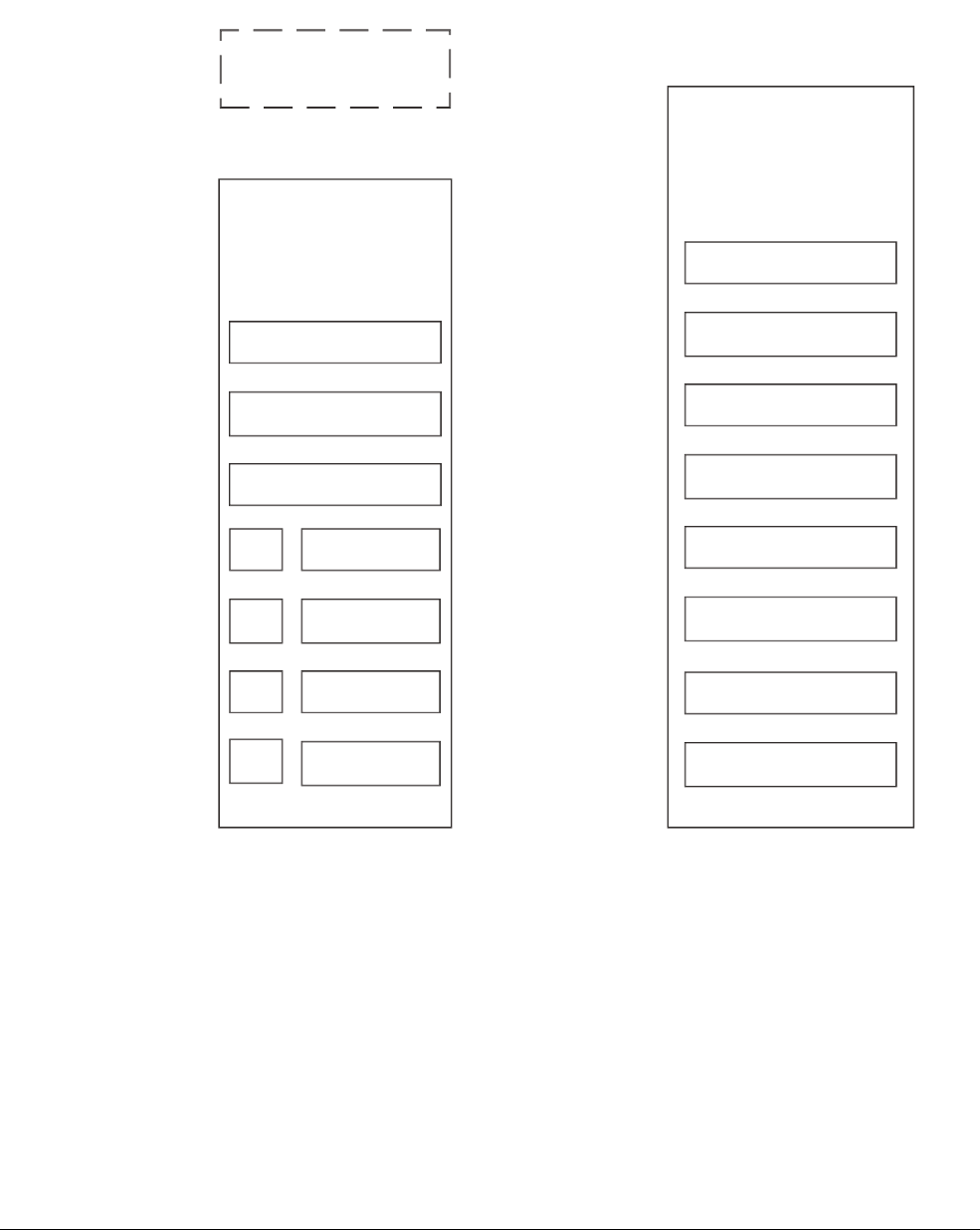
Memory Management Unit
ARM DEN0013B Copyright © 2011 ARM. All rights reserved. 8-16
ID082411 Non-Confidential
means that we can have multiple entries within the TLB at any particular time, which will be
valid for virtual address 0. Only the entry which matches the current ASID will be used for
translation, if the mapping is marked as non-global.
Figure 8-9 ASIDs in TLB mapping same virtual address
8.8.2 Page table Base Register 0 and 1
A further potential difficulty associated with managing multiple applications with their
individual page tables is that there may need to be multiple copies of the L1 page table, one for
each application. Each of these will be 16KB in size. Most of the entries will be identical in each
of the tables, as typically only one region of memory will be task-specific, with the kernel space
being unchanged in each case. Furthermore, if there is a need to modify a global page table
entry, the change will be needed in each of the tables.
Physical Memory Map
ASID
TLB
Global
Global
Global
C
A
A
B
0x000
0x002
0x000
0x000
Task A
Task C
Task B

Memory Management Unit
ARM DEN0013B Copyright © 2011 ARM. All rights reserved. 8-17
ID082411 Non-Confidential
To help reduce the effect of these problems, a second page table base register can be used. CP15
contains two page table base registers, TTBR0 and TTBR1. A control register (the TTB Control
Register) is used to program a value in the range 0 to 7. This value (denoted by N) tells the MMU
how many of the upper bits of the virtual address it should check to determine which of the two
TTB registers to use.
When N is 0 (the default), all virtual addresses are mapped using TTBR0. With N in the range
1-7, the hardware looks at the most significant bits of the virtual address. If the N most
significant bits are all zero, TTBR0 is used, otherwise TTBR1 is used.
For example, if N is set to 7, any address in the bottom 32MB of memory will use TTBR0 and
the rest of memory will use TTBR1. This means that the application-specific page table pointed
to by TTBR0 will contain only 32 entries (128 bytes). The global mappings are in the table
pointed to by TTBR1 and only one table needs to be maintained.
When these features are used, a context switch will typically require the operating system to
change the TTBR0 and ASID values, using CP15 instructions. However, as these are two
separate, non-atomic operations, some care is needed to avoid problems associated with
speculative accesses occurring using the new value of one register together with the older value
of the other. OS programmers making use of these features should become familiar with the
sequences recommended for this purpose in the ARM Architecture Reference Manual.
8.8.3 The Fast Context Switch Extension
The Fast Context Switch Extension (FCSE) is a deprecated feature which was added to the
ARMv4 architecture. It enabled multiple independent tasks to run in a fixed, overlapping area
at the bottom of the virtual memory space without the need to clean the cache or TLB on a
context switch. It does this by modifying virtual addresses by substituting a process ID value
into the top seven bits of the virtual address (but only if that address lies within the bottom
32MB of memory). Some ARM documentation distinguishes Modified Virtual Addresses
(MVA) from Virtual Addresses (VA). This distinction is useful only when the FCSE is used.
Since it is deprecated, we will not discuss the FCSE any further.

Memory Management Unit
ARM DEN0013B Copyright © 2011 ARM. All rights reserved. 8-18
ID082411 Non-Confidential
8.9 Linux use of page tables
We will start with a brief look at how Linux uses page tables and then move on to how this maps
to the ARM architecture implementation of page tables. The reader may find it helpful to refer
to the source code of the Linux kernel, in particular the ARM specific code associated with page
tables which can be found in the following file:
arch/arm/include/asm/pgtable.s
Some parts of the following description rely on a basic understanding of the Linux kernel,
exception handling and/or the memory ordering concepts explained in Chapter 9. The first-time
reader may therefore wish to skip over this section.
8.9.1 Levels of page tables in Linux
Linux uses a three level page table structure, but this can be implemented in a way which uses
only two levels of page tables – Page Global Directory (PGD) and Page Table Entry (PTE). The
intermediate third level Page Middle Directory (PMD) is defined as being of size 1 and folds
back into the PGD.
The ARCH include file
/asm-arm/page.h
contains the definition:
#define __pmd(x) ((pmd_t) { (x) } )
This tells the kernel that PMD has just one entry, effectively bypassing it.
8.9.2 Emulation of dirty and accessed bits
Linux makes use of a bit associated with each page which marks whether the page is dirty (the
page has been modified by the application and may therefore need to be written from memory
to disk when the page is no longer needed).
This is not directly supported in hardware by ARM processors, and must therefore be
implemented by kernel software. When a page is first created, it is marked as read-only. The first
write to such a page (a clean page) will cause an MMU permission fault and the kernel data abort
handler will be called. The Linux memory management code will mark the page as dirty, if the
page should indeed be writable, using the function
handle_pte_fault()
. The page table entry is
modified to make it allow both reads and writes and the TLB entry invalidated from the cache
to ensure the MMU now uses the newly modified entry. The abort handler then returns to re-try
the faulting access in the application.
A similar technique is used to emulate the accessed bit, which shows when a page has been
accessed. Read and Write accesses to the page generate an abort. The accessed bit is then set
within the handler, the access permissions are changed and we then return. This is all done
transparently to the application which actually accessed the memory. The kernel makes use of
these bits when swapping pages in and out of memory – it is preferred to swap out pages which
have not been used recently and of course we have to ensure that pages which have been written
to have their new contents copied to the backing store.
On older processors, it was necessary for Linux to maintain two hardware PTE tables – one that
was actually used by the processor and another one holding Linux state information. The
extensions to the TEX field mean that there are spare bits within the page table entry, available
for use by the operating system, potentially removing the need for two tables. A detailed
description of this is not useful to most programmers. Essentially, three TEX bits, plus a C bit
and a B bit giving five bits in each PTE which give information about the memory type, which
enables 32 possible types of memory. Most operating systems need only five or six different
types. Therefore we can use a feature called TEX Remap which enables us to specify which
settings we will actually use and encode those within three bits of the PTE, leaving two bits free.

Memory Management Unit
ARM DEN0013B Copyright © 2011 ARM. All rights reserved. 8-19
ID082411 Non-Confidential
8.9.3 Kernel MMU initialization
Linux creates an initial set of page tables when it boots. The kernel execution starts in
arch/arm/kernel/head.S
with the MMU and both caches disabled. After determining the type of
processor it is running on, the function
__create_page_tables(
) is called. This sets up an initial
set of MMU tables used only during this initialization. It finds the physical address of RAM in
the system and determines where to place the initial page table. This is immediately below the
kernel entry point. (Recall that an L1 page table is 16KB, so must start 16KB below.) Mappings
are created using 1MB sections, with no L2 page tables. After these initial page tables are set
up, we then branch to a function which invalidates the caches and TLB. The next step is to
enable the MMU. When the MMU is enabled, we are now working with virtual rather than
physical addresses. The code in
__enable_mmu()
enables the caches, branch predictors and then
the MMU. It is important that this code is in a location which has identical virtual and physical
addresses. If the virtual address and physical address of the section which holds this code are
not identical, the behavior can be unpredictable.
These page table mappings will allow the position dependent code of kernel startup to run.
These mappings will later be overwritten (albeit with identical entries) by the function
paging_init()
. This is called from
start_kernel()
via
setup_arch()
and creates the master L1
page table. The
mdesc->mapio()
function creates these mappings and must be modified when
porting Linux to a new system. The master L1 page table (
init_mm
) also maps the system RAM.
The virtual address range PAGE_OFFSET to (PAGE_OFFSET + RAMsize) are mapped to the
physical address range of the RAM in the system.
8.9.4 Memory allocation (vmalloc)
Applications running under Linux may need to make system calls for memory allocation.
kmalloc()
allocates memory which is contiguous in physical memory, while
vmalloc()
allocates
memory which is contiguous only in virtual memory space.
When a process calls
vmalloc()
, a range of virtual addresses are allocated and this can cause a
change to the L1 page table. Processes which were created before this can have L1 tables which
do not contain the newly allocated region. What happens is that the master L1 page table is
updated, but we do not at the same time modify all of the L1 tables for all processes. Instead,
when a process whose page table does not contain the new mapping tries to access the
vmalloc
region, an abort occurs and the kernel handler copies the new mapping from the master table
into the table for that process.
8.9.5 Protecting the bottom of memory
Linux enables us to define the lowest virtual address for a user space mapping. This enables the
exception vector table (if it is placed at address 0) to be protected. It also permits a safe test for
null pointers. If we try to load data from address 0, we know something has gone wrong!
Typically, the first 4KB page of memory is protected.
#define FIRST_USER_ADDRESS PAGE_SIZE
8.9.6 Linux use of page table entries and ASIDs
Linux will typically make use only of 4KB pages. 1MB sections can be used for linear kernel
mapping and I/O regions. A total of six different page types are used.
• Pages which contain code (applications or shareable libraries) will, by default, be marked
as read-only and can be mapped by multiple applications.
• Data pages are writable but can have the XN bit set, to trap erroneous execution of data.

Memory Management Unit
ARM DEN0013B Copyright © 2011 ARM. All rights reserved. 8-20
ID082411 Non-Confidential
•User
mmap()
files (and pages which hold stack or heap) will be marked as “Normal,
cacheable”, as will pages for kernel modules, kernel linear mapping, and
vmalloc()
space.
Pages which hold heap or stack are typically allocated as a result of a page fault. New heap
pages are mapped to a read-only zero initialized page. They are allocated on the first write
to the page. The page table entries themselves are accessed through the kernel linear
mapping.
• Device mapped pages are created as a result of a call to the function
mmap()
for a
/dev
file,
with the device driver code responsible for the memory mapping.
mmap()
enables driver
code to associate a range of user-space addresses to Device memory.
• The page which contains the exception vectors will be read-only for User mode code and
will be normal, cacheable.
• Static and Dynamic I/O mappings will be marked as Device memory, with no User mode
access
Strongly-ordered memory is not used directly by the kernel, by default, but can be selected for
specific tasks such as power management code.
ASIDs are dynamically allocated and not guaranteed to be constant during the lifetime of a
process. As the ASID register provides only eight bits of ASID space and we can have more
than 256 processes, Linux has a scheme for allocating ASIDs. For a new process, we increment
the last ASID value used. When the last value is reached, we have to take some action. The TLB
is flushed (across all processors in an SMP system). The value in the top 24 bits in the context
ID register, which can be considered as a “generation” number, is incremented. Stepping to a
new generation means that all ASID values from the previous generation are now invalid and
ASID numbering is restarted. On a context switch, processes which use an older generation
version of the context ID value are assigned a new ASID.
The ASID numbering scheme is global across processors. Individual threads within a process
have the same memory map and therefore share an ASID, but can run independently on separate
processors in an MP (multi-processing) system. We will consider multi-processing in much
greater detail in Chapter 22.

Memory Management Unit
ARM DEN0013B Copyright © 2011 ARM. All rights reserved. 8-21
ID082411 Non-Confidential
8.10 The Cortex-A15 MMU and Large Physical Address Extensions
The Cortex-A15 processor implements the ARMv7-A architecture Large Physical Address
Extension (LPAE), which introduces a number of new features:
• Address mapping for a 40-bit address space, giving a range of accessible physical
addresses from 4GB to 1024GB (a terabyte), with a granularity of 4kB. A new page table
entry format - the “long-descriptor format” is added. The existing VMSAv7
short-descriptor format page tables are still supported.
• Support is added for hierarchical permissions.
• A contiguous page hint bit for page table entries. This is set to show that the entry is one
of 16 contiguous entries which point to a contiguous output address range. If set, the TLB
need cache only one translation for the group of 16 pages.
• A new access permission setting – “privileged execute never” (PXN). This marks a page
as containing code that can be executed only in a non-privileged (user) mode. This setting
is also introduced in the legacy descriptor format. There is also a privileged execute
setting (PX) which means that code can be executed only in privileged mode.
• The ASID is stored in the TTBR. This allows atomic ASID changes, which reduce the
overhead of context switches.
• Simplified fault status encoding.
The Cortex-A15 processor MMU also supports virtualization. This provides a second stage of
address translation when running virtual machines. The first stage of this translation produces
an Intermediate Physical Address (IPA) and the second stage then produces the physical
address. TLB entries may also have an associated virtual machine ID (VMID), in addition to an
ASID. This will be covered in more detail in Chapter 27 Virtualization. It is possible to disable
the stage 2 MMU and have a flat mapping from IPA to PA.

ARM DEN0013B Copyright © 2011 ARM. All rights reserved. 9-1
ID082411 Non-Confidential
Chapter 9
Memory Ordering
Older implementations of the ARM architecture (for example, ARM7TDMI) execute all
instructions in program order and each instruction is completely executed before the next
instruction is started.
Newer micro-processors employ a number of optimizations which relate to the way memory
accesses are performed. As we have seen, the speed of execution of instructions by the processor
is significantly higher than the speed of external memory. Caches and write buffers are used to hide
the latency associated with this difference in speed. One potential effect of this is to re-order
memory accesses. The order in which load and store instructions are executed by the processor will
not necessarily be the same as the order in which the accesses are seen by external devices.

Memory Ordering
ARM DEN0013B Copyright © 2011 ARM. All rights reserved. 9-2
ID082411 Non-Confidential
Figure 9-1 Memory ordering example
In Figure 9-1, we have three instructions listed in program order. The first instruction performs
a write to external memory which in this example, misses in the cache (Access 1). It is followed
in program order by two reads, one which misses in the cache (Access 2) and one which hits in
the cache (Access 3). Both of the read accesses can potentially complete before the write buffer
completes the write associated with Access 1. Hit-under-miss behaviors in the cache mean that
a load which hits in the cache (like Access 3) can complete before a load earlier in the program
which missed in the cache (like Access 2).
In the main, it is still possible to preserve the illusion that the hardware executes instructions in
the order written to the programmer. There are generally only a few cases where the programmer
has to worry about such effects. For example, when modifying CP15 registers or when copying
or otherwise changing code in memory, it may be necessary for the programmer to explicitly
make the processor wait for such operations to complete.
For very high performance processors, such as the Cortex-A9 or Cortex-A15 processors, which
support speculative data accesses, multi-issuing of instructions, cache coherency protocols and
out-of-order execution in order to make further performance gains, there are even greater
possibilities for re-ordering. In general, the effects of this re-ordering are invisible to the
programmer, in a single processor system. The processor hardware takes care of many possible
hazards for us. It will ensure that address dependencies are respected and ensure the correct
value is returned by a read, allowing for potential modifications caused by earlier writes.
However, in cases where we have multiple processors which communicate through Shareable
memory (or share data in other ways), memory ordering considerations become more important.
In general, we are most likely to care about exact memory ordering at points where multiple
execution threads must be synchronized.
Processors which conform to the ARM v7-A architecture employ a weakly-ordered model of
memory. Reads and writes to Normal memory can be re-ordered by hardware, with such
re-ordering being subject only to address dependencies and explicit memory barrier
instructions. In cases where we need stronger ordering rules to be observed, we must
communicate this to the processor through the memory type attribute of the page table entry
which describes that memory. Enforcing ordering rules on the processor limits the possible
hardware optimizations and therefore reduces performance and increases power consumption.
The programmer therefore needs to understand when to apply such ordering constraints.
STR R12, [R1] @Access 1.
Program Order of Instructions Instruction ExecutionTimeline
Access 1 goes into write buffer
Time
Access 2 causes a cache lookup which misses
Access 3 causes a cache lookup which hits
Access 3 returns data into ARM register
Cache linefill triggered by Access 2 returns data
Memory store triggered by Access 1 is performed
LDR R0, [SP], #4 @Access 2.
LDR R2, [R3,#8] @Access 3.

Memory Ordering
ARM DEN0013B Copyright © 2011 ARM. All rights reserved. 9-3
ID082411 Non-Confidential
In this chapter, we will consider the memory ordering model of the ARM architecture. We will
look at the different types of memory (and other memory attributes) which are assigned to pages
using page table entries. We will look at the barrier instructions in ARM assembly language (and
accessible through C intrinsics). Finally we will look at the support for coherency between SMP
clusters and the concept of coherency domains, as well as considering some common cases
where memory ordering problems can be encountered.

Memory Ordering
ARM DEN0013B Copyright © 2011 ARM. All rights reserved. 9-4
ID082411 Non-Confidential
9.1 ARM memory ordering model
Three memory types are defined in the ARM architecture. All regions of memory are configured
as one of these three types:
• Strongly-ordered
• Device
• Normal.
In addition, for Normal and Device memory, it is possible to specify whether the memory is
Shareable (accessed by other agents) or not. For Normal memory, inner and outer cacheable
properties can be specified.
9.1.1 Strongly-ordered and Device memory
Accesses to Strongly-ordered and Device memory have the same memory-ordering model.
Access rules for this memory are as follows:
• The number and size of accesses will be preserved. Accesses will be atomic, and will not
be interrupted part way through.
• Both read and write accesses can have side-effects on the system. Accesses are never
cached. Speculative accesses will never be performed.
• Accesses cannot be unaligned.
• The order of accesses arriving at Device memory is guaranteed to correspond to the
program order of instructions which access Strongly-ordered or Device memory. This
guarantee applies only to accesses within the same peripheral or block of memory. The
size of such a block is implementation defined, but has a minimum size of 1KB.
• In the ARMv7 architecture, the processor can re-order Normal memory accesses around
Strongly-ordered or Device memory accesses.
The only difference between Device and Strongly-ordered memory is that:
• a write to Strongly-ordered memory can complete only when it reaches the peripheral or
memory component accessed by the write
• a write to Device memory is permitted to complete before it reaches the peripheral or
memory component accessed by the write.
System peripherals will almost always be mapped as Device memory.
Regions of Device memory type can further be described using the Shareable attribute.
On some ARMv6 processors, the Shareable attribute of Device accesses is used to determine
which memory interface will be used for the access, with memory accesses to areas marked as
Device, Non-Shareable performed using a dedicated interface, the private peripheral port. This
mechanism is not used on ARMv7 processors.
Note
These memory ordering rules provide guarantees only about “explicit” memory accesses (those
caused by load and store instructions). The architecture does not provide similar guarantees
about the ordering of instruction fetches or page table walks with respect to such explicit
memory accesses.

Memory Ordering
ARM DEN0013B Copyright © 2011 ARM. All rights reserved. 9-5
ID082411 Non-Confidential
9.1.2 Normal memory
Normal memory is used to describe most parts of the memory system. All ROM and RAM
devices are considered to be Normal memory. All code to be executed by the processor must be
in Normal memory. Code is not architecturally permitted to be in a region of memory which is
marked as Device or Strongly-ordered.
The properties of Normal memory are as follows:
• The processor can repeat read and some write accesses.
• The processor can pre-fetch or speculatively access additional memory locations, with no
side-effects (if permitted by MMU access permission settings). The processor will not
perform speculative writes, however.
• Unaligned accesses can be performed.
• Multiple accesses can be merged by processor hardware into a smaller number of accesses
of a larger size. Multiple byte writes could be merged into a single double-word write, for
example.
Regions of Normal memory must also have cacheability attributes described (see Chapter 7 for
details of the supported cache policies). The ARM architecture supports cacheability attributes
for Normal memory for two levels of cache, the inner and outer cache. The mapping between
these levels of cache and the implemented physical levels of cache is implementation defined.
Inner refers to the innermost caches, and always includes the processor level 1 cache. An
implementation might not have any outer cache, or it can apply the outer cacheability attribute
to L2 and/or L3 cache. For example, in a system containing a Cortex-A9 processor and the
PL310 L2 Cache controller, the PL310 is considered to be the outer cache. The Cortex-A8 L2
cache can be configured to use either inner or outer cache policy.
Normal memory must also be specified either as Shareable or Non-Shareable. A region of
Normal memory with the Non-Shareable attribute is one which is used only by this processor.
There is no requirement for the processor to make accesses to this location coherent with other
processors. If other processors do share this memory, any coherency issues must be handled in
software. For example, this can be done by having individual processors perform cache
maintenance and barrier operations.
A region with the Shareable attribute set is one which can be accessed by other processors or
masters in the system. Data accesses to memory in this region by other processors within the
same “shareability domain” are coherent. This means that the programmer does not need to take
care of the effects of data or unified caches. In situations where cache coherency is not
maintained between processors for a region of shared memory, the programmer would have to
explicitly manage coherency themselves.
The ARMv7 architecture enables the programmer to specify Shareable memory as “inner
Shareable” or “outer Shareable” (this latter case means that the location is both inner and outer
Shareable).
The outer Shareable attribute enables the definition of systems containing clusters of processors.
Within a cluster, the data caches of the processors are coherent for all data accesses which have
the inner Shareable attribute. Between clusters, the caches are not coherent for data accesses
which only have the inner Shareable attribute, but are for data accesses which have the outer
Shareable attribute. Each cluster is said to be in a different shareability domain for the inner
Shareable attribute and in the same shareability domain for the outer Shareable attribute. Such
clusters are not supported in the Cortex-A5, Cortex-A8 or Cortex-A9 processors.

Memory Ordering
ARM DEN0013B Copyright © 2011 ARM. All rights reserved. 9-6
ID082411 Non-Confidential
9.2 Memory barriers
A memory barrier is an instruction which requires the processor to apply an ordering constraint
between memory operations which occur before and after the memory barrier instruction in the
program. Such instructions may also be known as “memory fences” in other architectures (for
example, the x86).
The term memory barrier can also be used to refer to a compiler instruction which prevents the
compiler from scheduling data access instructions across the barrier when performing
optimizations. For example in GCC, we can use the inline assembler memory “clobber”, to
indicate that the instruction changes memory and therefore the optimizer cannot re-order
memory accesses across the barrier. The syntax is as follows:
asm volatile("" ::: "memory");
ARM RVCT includes a similar intrinsic, called
__schedule_barrier()
.
Here, however, we are looking at hardware memory barriers, provided through dedicated ARM
assembly language instructions. As we have seen, processor optimizations such as caches, write
buffers and out-of-order execution can result in memory operations occurring in an order
different from that specified in the executing code. Normally, this re-ordering is invisible to the
programmer and application developers do not normally need to worry about memory barriers.
However, there are cases where we may need to take care of such ordering issues, for example
in device drivers or when we have multiple observers of the data which need to be synchronized.
The ARM architecture specifies memory barrier instructions, which allow the programmer to
force the processor to wait for memory accesses to complete. These instructions are available in
both ARM and Thumb code, in both user and privileged modes. In older versions of the
architecture, these were performed using CP15 operations in ARM code only. Use of these is
now deprecated, although preserved for compatibility.
Let’s start by looking at the practical effect of these instructions in a uni-processor system. Note
that this description is a simplified version of that given in the ARM Architecture Reference
Manual, what is written here is intended to introduce the usage of these instructions. The term
explicit access is used to describe a data access resulting from a load or store instruction in the
program. It does not include instruction fetches.
Data Synchronization Barrier (DSB)
Data Synchronization Barrier (DSB) – this instruction forces the processor to wait
for all pending explicit data accesses to complete before any further instructions
can execute. There is no effect on pre-fetching of instructions.
Data Memory Barrier (DMB)
Data Memory Barrier (DMB) – this instruction ensures that all memory accesses
in program order before the barrier are observed in the system before any explicit
memory accesses that appear in program order after the barrier. It does not affect
the ordering of any other instructions executing on the processor, or of instruction
fetches.
Instruction Synchronization Barrier (ISB)
Instruction Synchronization Barrier (ISB) – this flushes the pipeline and prefetch
buffer(s) in the processor, so that all instructions following the ISB are fetched
from cache or memory, after the instruction has completed. This ensures that the
effects of context altering operations (for example, CP15 or ASID changes or
TLB or branch predictor operations), executed before the ISB instruction are
visible to any instructions fetched after the ISB. This does not in itself cause
synchronization between data and instruction caches, but is required as a part of
such an operation.

Memory Ordering
ARM DEN0013B Copyright © 2011 ARM. All rights reserved. 9-7
ID082411 Non-Confidential
Several options can be specified with the
DMB
or
DSB
instructions, to provide the type of access
and the shareability domain it should apply to, as follows:
SY This is the default and means that the barrier applies to the full system.
ST A barrier which waits only for stores to complete.
ISH A barrier which applies only to the inner Shareable domain.
ISHST A barrier which combines the above two (that is, it only stores to the inner
Shareable.
NSH A barrier only to the point of unification. (See Chapter 7).
NSHST A barrier that waits only for stores to complete and only out to the point of
unification.
OSH Barrier operation only to the outer Shareable domain.
OSHST Barrier operation that waits only for stores to complete, and only to the outer
Shareable domain.
To make sense of this, we need to use a more general definition of the
DMB
and
DSB
operations in
a multi-processor system. The use of the word “processor” (or agent) in the following text does
not necessarily mean a processor and also could refer to a DSP, DMA, hardware accelerator or
any other block that accesses shared memory.
The
DMB
instruction has the effect of enforcing memory access ordering within a shareability
domain. All processors within the shareability domain are guaranteed to observe all explicit
memory accesses before the
DMB
instruction, before they observe any of the explicit memory
accesses after it.
The
DSB
instruction has the same effect as the
DMB
, but in addition to this, it also synchronizes the
memory accesses with the full instruction stream, not just other memory accesses. This means
that when a
DSB
is issued, execution will stall until all outstanding explicit memory accesses have
completed. When all outstanding reads have completed and the write buffer is drained,
execution resumes as normal.
It may be easier to appreciate the effect of the barriers by considering an example. Consider the
case of a Cortex-A9 MPCore containing four processors. These processors operate as an SMP
cluster and form a single shareability domain. When a single processor within the cluster
executes a
DMB
instruction, that processor will ensure that all data memory accesses in program
order before the barrier complete, before any explicit memory accesses that appear in
program-order after the barrier. This way, it can be guaranteed that all processors within the
cluster will see the accesses on either side of that barrier in the same order as the processor that
performs them. If the
DMB ISH
variant is used, the same is not guaranteed for external observers
such as DMA controllers or DSPs.

Memory Ordering
ARM DEN0013B Copyright © 2011 ARM. All rights reserved. 9-8
ID082411 Non-Confidential
9.2.1 Memory barrier use example
Consider the case where we have two processors A and B and two addresses in Normal memory
(
Addr1
and
Addr2
) held in processor registers. Each processor executes two instructions as shown
in Example 9-1:
Example 9-1 Code example showing memory ordering issues
Processor A:
STR R0, [Addr1]
LDR R1, [Addr2]
Processor B:
STR R2, [Addr2]
LDR R3, [Addr1]
Here, there is no ordering requirement and we can make no statement about the order in which
any of the transactions occur. The addresses
Addr1
and
Addr2
are independent and there is no
requirement on either processor to execute the load and store in the order written in the program,
or to care about the activity of the other processor.
There are therefore four possible legal outcomes of this piece of code, with four different sets
of values from memory ending up in processor A R1 and processor B R3:
• A gets the “old” value, B gets the “old” value.
• A gets the “old” value, B gets the “new” value.
• A gets the “new” value, B gets the “old” value.
• A gets the “new” value, B gets the “new” value.
If we were to involve a third processor, C, we should also note that there is no requirement that
it would observe either of the stores in the same order as either of the other processors. It is
perfectly permissible for both A and B to see an old value in
Addr1
and
Addr2
, but for C to see
the new values.
So, let’s consider the case where the code on B looks for a flag being set by A and then reads
memory – for example if we are passing a message from A to B. We might now have code
similar to that shown in Example 9-2:
Example 9-2 Possible ordering hazard with postbox
Processor A:
STR R0, [Msg] @ write some new data into postbox
STR R1, [Flag] @ new data is ready to read
Processor B:
Poll_loop:
LDR R1, [Flag]
CMP R1,#0 @ is the flag set yet?
BEQ Poll_loop
LDR R0, [Msg] @ read new data.

Memory Ordering
ARM DEN0013B Copyright © 2011 ARM. All rights reserved. 9-9
ID082411 Non-Confidential
Again, this might not behave in the way that is expected. There is no reason why processor B is
not allowed to perform the read from
[Msg]
before the read from
[Flag]
. This is normal, weakly
ordered memory and the processor has no knowledge about a possible dependency between the
two. The programmer must explicitly enforce the dependency by inserting a memory barrier. In
this example, we actually need two memory barriers. Processor A needs a
DMB
between the two
store operations, to make sure they happen in the programmer specified order. Processor B
needs a
DMB
before the
LDR R0, [Msg]
to be sure that the message is not read until the flag is set.
9.2.2 Avoiding deadlocks with a barrier
Here is another case which can cause a deadlock if barrier instructions are not used. Consider a
situation where one processor (A) writes to an address and then polls for an acknowledge value
from another processor (B).
Example 9-3 shows the type of code which can cause a problem.
Example 9-3 Deadlock
Processor A:
STR R0, [Addr] @ write some data
Poll_loop:
LDR R1, [Flag]
CMP R1,#0 @ is the flag set yet?
BEQ Poll_loop
Processor B:
Poll_loop2:
LDR R1, [Addr]
CMP R1,#0 @ is the flag set yet?
BEQ Poll_loop2
STR R0, [Flag]
The ARMv7 architecture without multiprocessing extensions does not strictly require processor
A’s store to [
Addr
] to ever complete (it could be sitting in a write buffer while the memory system
is kept busy reading the flag), so both processors could potentially deadlock, each waiting for
the other. Inserting a DSB after the STR of processor A forces its store to be observed by
processor B before processor A will read from
Flag
. Processors which implement the
multiprocessing extensions, like the Cortex-A5MPCore processor and Cortex-A9MPCore
processor, are required to complete accesses in a finite time (that is, their write buffers must
drain) and so the barrier instruction is not absolutely required. However, most programmers
prefer not to think too hard about whether a barrier is needed and are advised to include one
anyway!
9.2.3 WFE and WFI Interaction with barriers
The
WFE
(Wait For Event) and
WFI
(Wait For Interrupt) instructions, described further in
Chapter 21 Power Management, allow us to stop execution and enter a low-power state. If we
need to ensure that all memory accesses prior to executing
WFI
or
WFE
have been completed (and
made visible to other processors), we must insert a
DSB
instruction.
A further consideration relates to usage of
WFE
and
SEV
(Send Event) in an MP system. These
instructions allow us to reduce the power consumption associated with a lock acquire loop (a
spinlock). A processor which is attempting to acquire a mutex may find that some other
processor already has the lock. Instead of having the processor repeatedly poll the lock, we can
suspend execution and enter a low-power state, using the
WFE
instruction. We wake either when

Memory Ordering
ARM DEN0013B Copyright © 2011 ARM. All rights reserved. 9-10
ID082411 Non-Confidential
an interrupt or other asynchronous exception is recognized, or another processor sends an event
(with the
SEV
instruction). The processor that had the lock will use the
SEV
instruction to wake-up
other processors in the
WFE
state after the lock has been released. For the purposes of memory
barrier instructions, the event signal is not treated as an explicit memory access. We therefore
need to take care that the update to memory which releases the lock is actually visible to other
processors before the
SEV
instruction is executed. This requires the use of a
DSB
.
DMB
is not
sufficient as it only affects the ordering of memory accesses without synchronizing them to a
particular instruction, whereas
DSB
will prevent the
SEV
from executing until all preceding
memory accesses have been seen by other processors.
9.2.4 Linux use of barriers
In this chapter, we have looked at memory barrier instructions. In this section, we will look at
the implications of barriers in multi-core systems and take a much more detailed look at SMP
operation.
Barriers are needed to enforce ordering of memory operations. Most programmers will not need
to understand, or explicitly use memory barriers. This is because they are already included
within kernel locking and scheduling primitives. Nevertheless, writers of device drivers or those
seeking an understanding of kernel operation may find a detailed description useful.
Both the compiler and processor micro-architecture optimizations permit the order of
instructions and associated memory operations to be changed. Sometimes, however, we wish to
enforce a specified order of execution of memory operations. For example, we can write to a
memory mapped peripheral register. This write can have side-effects elsewhere in the system.
Memory operations which are in before or after this operation in our program can appear as if
they can be re-ordered, as they operate on different locations. In some cases, however, we wish
to ensure that all operations complete before this peripheral write completes. Or, we may want
to make sure that the peripheral write completes before any further memory operations are
started. Linux provides some functions to do this, as follows:
• We instruct the compiler that re-ordering is not permitted for a particular memory
operation. This is done with the
barrier()
function call. This controls only the compiler
code generation and optimization and has no effect on hardware re-ordering.
• We call a memory barrier function which maps to ARM processor instructions that
perform the memory barrier operations. These enforce a particular hardware ordering.
The available barriers are as follows (in a Linux kernel compiled with Cortex-A SMP
support):
— the read memory barrier
rmb()
function ensures that any read that appears before the
barrier is completed before the execution of any read that appears after the barrier
— the write memory barrier
wmb()
function ensures that any write that appears before
the barrier is completed before the execution of any write that appears after the
barrier
— the memory barrier
mb()
function ensures that any memory access that appears
before the barrier is completed before the execution of any memory access that
appears after the barrier.
• There are corresponding SMP versions of these barriers, called
smp_mb()
,
smp_rmb()
and
smp_wmb()
. These are used to enforce ordering on Normal cacheable memory, between
processors inside the same SMP processor. For example, each processor inside a
Cortex-A9MPCore. They can be used with devices and they work even for normal
non-cacheable memory.
For these memory barriers, it is almost always the case that a pair of barriers is required. For
further information, see
http://www.kernel.org/doc/Documentation/memory-barriers.txt
.

Memory Ordering
ARM DEN0013B Copyright © 2011 ARM. All rights reserved. 9-11
ID082411 Non-Confidential
There are also SMP specific barriers:
smp_mb()
,
smp_rmb()
and
smp_wmb()
. These are not supersets
of those listed above, but rather subsets for resolving ordering issues only between processors
within an SMP system. When the kernel is compiled without
CONFIG_SMP
, each invocation of
these are expanded to
barrier()
statements.
All of Linux's locking primitives include any needed barrier.

Memory Ordering
ARM DEN0013B Copyright © 2011 ARM. All rights reserved. 9-12
ID082411 Non-Confidential
9.3 Cache coherency implications
The caches are largely invisible to the application programmer. However they can become
visible when there is a breakdown in the coherency of the caches, when memory locations are
changed elsewhere in the system or when memory updates made from the application code must
be made visible to other parts of the system.
A system containing an external DMA device and a processor provides a simple example of
possible problems. There are two situations in which a breakdown of coherency can occur. If
the DMA reads data from main memory while newer data is held in the processor’s cache, the
DMA will read the old data. Similarly, if a DMA writes data to main memory and stale data is
present in the processor’s cache, the processor can continue to use the old data.
Therefore dirty data which is in the ARM data cache must be explicitly cleaned before the DMA
starts. Similarly, if the DMA is copying data to be read by the ARM, it must be certain that the
ARM data cache does not contain stale data (the cache will not be updated by the DMA writing
memory and this may need the ARM to clean and/or invalidate the affected memory areas from
the cache(s) before starting the DMA). As all ARMv7-A processors can do speculative memory
accesses, it will also be necessary to invalidate after using the DMA.
9.3.1 Issues with copying code
Boot code, kernel code or JIT compilers can copy programs from one location to another, or
modify code in memory. There is no hardware mechanism to maintain coherency between
instruction and data caches. The programmer must invalidate stale data from the instruction
cache by invalidating the affected areas, and ensure that the data written has actually reached
the main memory. Specific code sequences including instruction barriers are needed if the
processor is then intended to branch to the modified code.
9.3.2 Compiler re-ordering optimizations
It is important to understand that memory barrier instructions apply only to hardware
re-ordering of memory accesses. Inserting a hardware memory barrier instruction may not have
any direct effect on compiler re-ordering of operations. The
volatile
type qualifier in C tells the
compiler that the variable can be changed by something other than the code that is accessing it.
This is often used for C language access to memory mapped I/O, allowing such devices to be
safely accessed through a pointer to a
volatile
variable. The C standard does not provide rules
relating to the use of
volatile
in systems with multiple processors. So, although we can be sure
that
volatile
loads and stores will happen in program specified order with respect to each other,
there are no such guarantees about re-ordering of accesses relative to non-volatile loads or
stores. This means that
volatile
does not provide a shortcut to implement mutexes.

ARM DEN0013B Copyright © 2011 ARM. All rights reserved. 10-1
ID082411 Non-Confidential
Chapter 10
Exception Handling
In this chapter, we look at how ARM processors respond to exceptions – also known as traps or
interrupts in other architectures. All microprocessors need to respond to external asynchronous
events, such as a button being pressed, or a clock reaching a certain value. Normally, there is
specialized hardware which activates input lines to the processor. This causes the microprocessor
to temporarily stop the current program sequence and execute a special handler routine. The speed
with which a processor can respond to such events may be a critical issue in system design. Indeed
in many embedded systems, there is no “main” program as such – all of the functions of the system
are handled by code which runs from interrupts, and assigning priorities to these is a key area of
design. Rather than have the processor constantly polling the flags from different parts of the
system to see if there is something to be done, we instead allow the system to tell the processor that
something needs to happen, by generating an interrupt. Complex systems have very many interrupt
sources with different levels of priority and requirements for nested interrupt handling (where a
higher priority interrupt can interrupt a lower priority one).
In normal program execution, the program counter increments through the address space, with
branches in the program modifying the flow of execution (for example, for function calls, loops,
and conditional code). When an exception occurs, this sequence is interrupted.
In addition to responding to external interrupts, there are a number of other things which can cause
the processor to take an exception, both external (reset, external aborts from the memory system)
and internal (MMU generated aborts or OS calls using the
SVC
instruction). Dealing with interrupts
and exceptions causes the ARM processor to switch between modes and copy some registers into
others. Readers new to the ARM architecture may wish to refresh their understanding of the modes
and registers previously described, before continuing with this chapter.
We start by introducing exceptions and see how the ARM processor handles each of the different
types and what they are used for. We then look in more detail at interrupts and describe mechanisms
of interrupt handling on ARM and standard interrupt handling schemes.

Exception Handling
ARM DEN0013B Copyright © 2011 ARM. All rights reserved. 10-2
ID082411 Non-Confidential
10.1 Types of exception
As we have already seen, the A classes and R classes of architecture support seven processor
modes, six privileged modes called FIQ, IRQ, SUPERVISOR, ABORT, UNDEFINED and
SYSTEM, and the non-privileged USER mode. The HYP mode and MONITOR registers can be
added to the list where the Virtualization and Security Extensions are implemented.The current
mode can change under software control or when processing an exception.
However, the unprivileged User mode can switch to another mode only by generating an
exception.
An exception is any condition that needs to halt normal execution and instead run software
associated with each exception type, known as an exception handler.
When an exception occurs, the processor saves the current status and the return address, enters
a specific mode and possibly disables hardware interrupts. Execution is then forced from a fixed
memory address called an exception vector. This happens automatically and is not under direct
control of the programmer.
The following types of exception exist:
Interrupts There are two types of interrupts provided on ARMv7-A processors, called IRQ
and FIQ.
FIQ is higher priority than IRQ. FIQ also has some potential speed advantages
owing to its position in the vector table and the higher number of banked registers
available in FIQ mode. This potentially saves processor clock cycles on pushing
registers to the stack within the handler. Both of these kinds of exception are
typically associated with input pins on the processor – external hardware asserts
an interrupt request line and the corresponding exception type is raised when the
current instruction finishes executing, assuming that the interrupt is not disabled.
Aborts Aborts can be generated either on instruction fetches (prefetch aborts) or data
accesses (data aborts). They can come from the external memory system giving
an error response on a memory access (indicating perhaps that the specified
address does not correspond to real memory in the system). Alternatively, the
abort can be generated by the Memory Management Unit (MMU) of the
processor. An operating system can use MMU aborts to dynamically allocate
memory to applications. An instruction can be marked within the pipeline as
aborted, when it is fetched. The prefetch abort exception is taken only if the
processor then actually tries to execute it. The exception takes place before the
instruction actually executes. If the pipeline is flushed before the aborted
instruction reaches the execute stage of the pipeline, the abort exception will not
occur. A data abort exception happens when a load or store instruction executes
and is considered to happen after the data read or write has been attempted. The
ARMv7 architecture distinguishes between precise and imprecise aborts. Aborts
generated by the MMU are always precise. The architecture does not require
particular classes of externally aborted accesses to be precise.
For example, on a particular processor implementation, it may be the case that an
external abort reported on a page table walk is treated as precise, but this is not
required to be the case for all processors. For precise aborts, the abort handler can
be certain which instruction caused the abort and that no further instructions were
executed after that instruction. This is in contrast to an imprecise abort, which
results when the external memory system reports an error on an access. In this
case, the abort handler cannot determine which instruction caused the problem (or
further instructions may have executed after the one which generated the abort).
For example, if a buffered write receives an error response from the external
memory system, further instructions will have been executed after the store. This

Exception Handling
ARM DEN0013B Copyright © 2011 ARM. All rights reserved. 10-3
ID082411 Non-Confidential
means that it will be impossible for the abort handler to fix the problem and return
to the application. All it can do is to kill the application which caused the problem.
Device probing therefore needs special handling, as externally reported aborts on
reads to non-existent areas will generate imprecise, asynchronous aborts even
when such memory is marked as Strongly-ordered, or Device. Generation of
imprecise aborts is controlled by the CPSR A bit. If the A bit is set, imprecise
aborts from the external memory system will be recognized by the processor, but
no abort exception will be generated immediately. Instead, the processor keeps
the abort pending until the A bit is cleared and takes an exception at that time.
This bit is set by default on reset, and certain other exception types. Kernel code
will typically ensure (through the use of a barrier instruction) that pending
imprecise aborts are recognized against the correct application. If a thread has to
be killed due to an imprecise abort, it needs to be the correct one!
Reset All processors have a reset input and will take the reset exception immediately
after they have been reset. It is the highest priority exception and cannot be
masked.
Exceptional instructions
There are two classes of instruction which can cause exceptions on the ARM. The
first is the Supervisor Call (
SVC
), previously known as Software Interrupt (
SWI
).
This is typically used to provide a mechanism by which User mode programs can
pass control to privileged, kernel code in the OS to perform OS-level tasks. The
second is an undefined instruction. The architecture defines certain bit-patterns as
corresponding to undefined opcodes. Trying to execute one of these causes an
Undefined Instruction exception to be taken. In addition, executing coprocessor
instructions for which there is no corresponding coprocessor hardware will also
cause this trap to happen. Some instructions can be executed only in a privileged
mode and executing these from User mode will cause an undefined instruction
exception.
When an exception occurs, code execution passes to an area of memory called the vector table.
Within the table just one word is allocated to each of the various exception types and this will
usually contain a branch instruction to the actual exception handler.
You can write the exception handlers in either ARM or Thumb code. The CP15 SCTLR.TE bit
is used to specify whether exception handlers will use ARM or Thumb. When handling
exceptions, the prior mode, state, and registers of the processor must be preserved so that the
program can be resumed after the exception has been handled.

Exception Handling
ARM DEN0013B Copyright © 2011 ARM. All rights reserved. 10-4
ID082411 Non-Confidential
10.2 Entering an exception handler
When an exception occurs, the ARM processor automatically does the following things:
• Preserves the address of the next instruction, in the Link Register (LR) of the new mode.
• Copies CPSR to the SPSR, one of the banked registers specific to each (non-user) mode
of operation.
• Modifies the CPSR mode bits to a mode associated with the exception type. The other
CPSR mode bits are set to values determined by bits in the CP15 System Control Register.
The T bit is set to the value given by the CP15 TE bit. The J bit is cleared and the E bit
(Endianness) is set to the value of the EE (Exception Endianness) bit. This enables
exceptions to always run in ARM or Thumb state and in little or big-endian, irrespective
of the state the processor was in before the exception.
• Forces the PC to point to the relevant instruction from the exception vector table.
It will almost always be necessary for the exception handler software to save registers onto the
stack immediately upon exception entry. (FIQ mode has more dedicated registers and so a
simple handler may be able to be written in a way which needs no stack usage.)
A special assembly language instruction is provided to assist with saving the necessary registers,
called
SRS
(Store Return State). This instruction pushes the LR and SPSR onto the stack of any
mode; which stack should be used is specified by the instruction operand.

Exception Handling
ARM DEN0013B Copyright © 2011 ARM. All rights reserved. 10-5
ID082411 Non-Confidential
10.3 Exit from an exception handler
Exiting from an exception and returning to the main program is always done by executing a
special instruction. This has the effect of doing both of the following (at the same time):
• restore the CPSR from the saved SPSR.
• set the PC to the value of (LR - offset) where the offset value is fixed for a particular
exception type, shown in Table 10-1 on page 10-6.
This can be accomplished by using an instruction like
SUBS
PC, LR, #offset
if the link register
was not pushed on to the stack at the start of the handler. Otherwise, it will be necessary to pop
the values to be restored from the stack. Again, there is a special assembly language instruction
provided to assist with this. The Return From Exception (
RFE
) instruction pops the link register
and SPSR off the current mode stack.

Exception Handling
ARM DEN0013B Copyright © 2011 ARM. All rights reserved. 10-6
ID082411 Non-Confidential
10.4 Exception mode summary
Table 10-1 summarizes different exceptions and the associated mode. This table contains a great
deal of information and we’ll take a moment to look at each row and column in turn.
The CPSR column indicates the setting of the CPSR I and F bits, used to disable IRQ and FIQ
respectively.
The suggested return instructions in Table 10-1 assumes that we wish to retry the aborted
instruction in the case of an abort, but to not retry an instruction which caused an undefined
instruction exception.
10.4.1 Exception priorities
As some of the exception types can occur simultaneously, the processor assigns a fixed priority
for each exception, as shown in Table 10-1. The UNDEFINED Instruction, prefetch abort and
Supervisor Call exceptions are due to execution of an instruction (there are specific bit patterns
for undefined and
SVC
opcodes) and so can never happen together and therefore have the same
priority.
Table 10-1 Summary of exception behavior
Vector
address Exception Mode Event CPSR Return
instruction
0x0
Reset Supervisor Reset input asserted F = 1
I = 1
Not applicable
0x4
Undefined
instruction
Undefined Executing undefined
instruction
I = 1
MOVS
PC, LR
(if emulating the
instruction)
SUBS
PC, LR, #4
(if re-executing
after for example
enabling VFP)
0x8
Supervisor call Supervisor
SVC
instruction I = 1
MOVS
PC,LR
0xC
Prefetch Abort Abort Instruction fetch from
invalid address
I = 1
SUBS
PC, LR, #4
0x10
Data Abort Abort Data Read/Write to
invalid address
I = 1
SUBS
PC, LR, #8
(if
retry of the aborting
instruction is
wanted)
0x14
Yesa
a. Hypervisor entry exception (described in Chapter 27 Virtualization) is available only in processors which
support Virtualization Extensions and is unused in other processors.
HYP Hypervisor entry -
ERET
0x18
Interrupt IRQ IRQ input asserted I = 1
SUBS
PC, LR, #4
0x1C
Fast Interrupt FIQ FIQ input asserted F = 1
I = 1
SUBS
PC, LR, #4

Exception Handling
ARM DEN0013B Copyright © 2011 ARM. All rights reserved. 10-7
ID082411 Non-Confidential
It is important to distinguish between prioritization of exceptions, which happens when multiple
exceptions are required at the same time, and the actual exception handler code. You will notice
that Table 10-1 on page 10-6 contains columns explaining how FIQ and IRQ are automatically
disabled by some exceptions. (All exceptions disable IRQ, only FIQ and reset disable FIQ.) This
is done by the processor automatically setting the CPSR I (IRQ) and F (FIQ) bits.
So, an FIQ exception can interrupt an abort handler or IRQ exception. In the case of a data abort
and FIQ occurring simultaneously, the data abort (which has higher priority) is taken first. This
lets the processor record the return address for the data abort. But as FIQ is not disabled by data
abort, we then take the FIQ exception immediately. At the end of the FIQ we return back to the
data abort handler.
More than one exception can potentially be generated at the same time, but some combinations
are mutually exclusive. A prefetch abort marks an instruction as invalid and so cannot occur at
the same time as an undefined instruction or
SVC
(and of course, an
SVC
instruction cannot also
be an undefined instruction). These instructions cannot cause any memory access and therefore
cannot cause a data abort. The architecture does not define when asynchronous exceptions, FIQ,
IRQ and/or imprecise aborts must be taken, but the fact that taking an IRQ or data abort
exception does not disable FIQ exceptions means that FIQ execution will be prioritized over
IRQ and/or asynchronous abort handling.

Exception Handling
ARM DEN0013B Copyright © 2011 ARM. All rights reserved. 10-8
ID082411 Non-Confidential
10.5 Vector table
The first column in the table gives the vector address within the vector table associated with the
particular type of exception. This is a table of instructions that the ARM processor goes to when
an exception is raised. These instructions are located in a specific place in memory. The normal
vector base address is
0x00000000
, but most ARM processors allow the vector base address to be
moved to
0xFFFF0000
. All Cortex-A series processors permit this, and it is the default address
selected by the Linux kernel.
You will notice that there is a single word address associated with each exception type.
Therefore, only a single instruction can be placed in the vector table for each exception
(although, in theory, two 16-bit Thumb instructions could be used). FIQ is different, as we shall
see in Distinction between FIQ and IRQ on page 10-9. Therefore, the vector table entry almost
always contains one of the various forms of branches.
B<label>
This performs a PC-relative branch. It is suitable for calling exception handler
code which is close enough in memory that the 24-bit field provided in the branch
instruction is large enough to encode the offset.
LDR PC, [PC, #offset]
This loads the PC from a memory location whose address is defined relative to
the PC. This lets the exception handler be placed at any arbitrary address within
the full 32-bit memory space (but takes some extra cycles relative to the simple
branch above).
The FIQ exception is the entry at the end of the vector table and so potentially the FIQ handler
code can be placed directly after the vector table, eliminating the need for a branch to the actual
handler (which saves clock cycles).

Exception Handling
ARM DEN0013B Copyright © 2011 ARM. All rights reserved. 10-9
ID082411 Non-Confidential
10.6 Distinction between FIQ and IRQ
FIQ is reserved for a single, high-priority interrupt source that requires a guaranteed fast
response time, with IRQ used for all of the other interrupts in the system.
As FIQ is the last entry in the vector table, the FIQ handler can be placed directly at the vector
location and run sequentially from that address. This avoids a branch instruction and any
associated delay, speeding up FIQ response times. The extra banked registers available in FIQ
mode relative to other modes allows state to be retained between calls to the FIQ handler, again
increasing execution speed by potentially removing the need to push some registers before using
them.
A further key difference between IRQ and FIQ is that the FIQ handler is not expected to
generate any other exceptions. FIQ is therefore reserved for special system-specific devices
which have all their memory mapped (that is, no MMU page table faults) and no need to make
SVC
calls to access kernel functions (so FIQ can be used only by code which does not need to use
the kernel API). FIQ is not typically used by Linux. As the kernel is architecture-independent,
it does not have a concept of multiple forms of interrupt. Some systems running Linux can still
make use of FIQ, but as the Linux kernel never disables FIQs they have priority over anything
else in the system and so some care is needed.

Exception Handling
ARM DEN0013B Copyright © 2011 ARM. All rights reserved. 10-10
ID082411 Non-Confidential
10.7 Return instruction
The Link Register (LR) is used to store the appropriate return address for the PC after the
exception has been handled. Its value needs to be modified as shown in Table 10-1 on page 10-6,
depending upon the type of exception occurred. The ARM Architecture Reference Manual
defines the LR values that must be used (the definition derives from the values which convenient
for early hardware implementations).

Exception Handling
ARM DEN0013B Copyright © 2011 ARM. All rights reserved. 10-11
ID082411 Non-Confidential
10.8 Privilege model in ARMv7-A Virtualization Extensions
The ARMv7-A Virtualization Extensions introduce a privilege model which is a little different
to that of previous processors, which is described elsewhere in this book. The Cortex-A15
processor has three different levels of privilege:
• PL0 (referred to as Unprivileged elsewhere in this text). This the privilege level of User
mode
• PL1 (referred to as Privileged elsewhere in this text). This is the privilege level of SVC,
Undef, Abort, FIQ, IRQ, System and Monitor modes.
• PL2 (new level for Cortex-A15): This is the privilege level of Hyp mode (see Chapter 27
Virtualization).
These privilege levels are separate from the TrustZone Secure and Non-Secure settings.

ARM DEN0013B Copyright © 2011 ARM. All rights reserved. 11-1
ID082411 Non-Confidential
Chapter 11
Interrupt Handling
In this section, we will look at a range of methods by which interrupts are handled in ARM
processors, and briefly consider the Generic Interrupt Controller (GIC).

Interrupt Handling
ARM DEN0013B Copyright © 2011 ARM. All rights reserved. 11-2
ID082411 Non-Confidential
11.1 External interrupt requests
As we discussed in Types of exception on page 10-2, all ARM processors have two external
interrupt requests, FIQ and IRQ. Both of these are level-sensitive active low inputs. Individual
implementations have interrupt controllers which accept interrupt requests from a wide variety
of external sources and map them onto FIQ or IRQ, causing the processor to take an exception.
In general, an interrupt exception can be taken only when the appropriate CPSR disable bit (the
F and I bits respectively) is clear.
The
CPS
assembly language instruction provides a simple mechanism to enable or disable the
exceptions controlled by CPSR A, I and F bits (imprecise abort, IRQ and FIQ respectively).
CPS
can be used additionally to change mode, as shown below.
CPS #<mode>
CPSIE <if>
CPSID <if>
where
<mode>
is the number of the mode to change to. If this option is omitted, no mode change
occurs. The values of these modes are listed in Table 4-1 on page 4-3.
IE or ID will enable or disable exceptions respectively. The exceptions to be enabled or disabled
are specified using one or more of the letters A, I and/or F. Exceptions whose corresponding
letters are omitted will not be modified.
In Cortex-A series processors, it is possible to configure the processor so that FIQs cannot be
masked by software. This is known as Non-Maskable FIQ and is controlled by a hardware
configuration input signal which is sampled when the processor is reset. They will still be
masked automatically upon taking an FIQ exception.
11.1.1 Assigning interrupts
A system will always have an interrupt controller which accepts interrupt requests from multiple
pieces of external hardware. This typically contains a number of registers enabling software
running on the ARM to mask individual interrupt sources, to acknowledge interrupts from
external devices and to determine which interrupt sources are currently active.
This interrupt controller can be a design specific to the system, or it can be an implementation
of the ARM Generic Interrupt Controller (GIC), which is described in Generic Interrupt
Controller on page 11-5.
11.1.2 Interrupt latency
In embedded systems with real-time requirements, interrupt latency is an important
consideration. This is generally defined as the maximum time taken from the external interrupt
request to execution of the first instruction of the Interrupt Service Routine (ISR) for that
request.
In normal operation, ARM processors will take an interrupt exception when the currently
executing instruction completes. This could be a load-multiple operation which could cause
page table walks, cache linefills and write-back of dirty data, each potentially taking a number
of cycles to complete. Some processors provide support for a low-latency interrupt mode. When
this is selected, the processor can abandon multiple loads or stores to Normal memory upon
receiving an interrupt. After processing the interrupt it returns to the original instruction and
re-executes it from the start. This can give significantly lower interrupt latency, at the cost of
reduced overall processor performance. The reduced performance is due to the fact that the
processor cannot utilize hit-under-miss memory access methods and must execute instructions
strictly in-order.

Interrupt Handling
ARM DEN0013B Copyright © 2011 ARM. All rights reserved. 11-3
ID082411 Non-Confidential
An access to Device or Strongly-ordered memory cannot be abandoned in this way, because, as
we saw in Chapter 9, there are certain rules which apply to these memory types. The processor
must not repeat accesses to such memory, or modify the size or number of accesses.
In addition to latency caused by these hardware effects, a key factor in interrupt latency is how
long interrupts are disabled for, since this also prevents high-priority interrupts from
pre-empting processing of lower-priority interrupts. This is the responsibility of the operating
system and any device drivers, and will often exceed the hardware latency.
Total worst-case interrupt latency (for the highest priority interrupt in your entire system.
Latencies for lower-priority ones can be much higher) = (maximum processor latency) +
(maximum cycles of interrupts disabled).
11.1.3 Non-nested interrupt handling
This represents the simplest kind of interrupt handler. An interrupt occurs and while processing
that interrupt, further interrupts are disabled. We can only handle further interrupts at the
completion of the first interrupt request and there is no scope for a higher priority or more urgent
interrupt to be handled during this time. This is not generally suitable for complex embedded
systems, but it is useful to examine before proceeding to a more realistic example.
The steps taken to handle an interrupt are as follows:
• An IRQ exception is raised by external hardware. The processor performs several steps
automatically. The contents of the PC in the current execution mode are stored in
LR_IRQ. The CPSR register is copied to SPSR_IRQ. The bottom byte of the CPSR is
updated to change to IRQ mode, and to disable IRQ which prevent further exceptions
from occurring. The PC is set to IRQ entry in the vector table.
• The instruction at the IRQ entry in the vector table (a branch to the interrupt handler) is
executed.
• The interrupt handler saves the context of the interrupted program (that is, it pushes onto
the stack any registers which will be corrupted by the handler).
• The interrupt handler determines which interrupt source needs to be processed and calls
the appropriate ISR.
• Finally, the SPSR_IRQ is copied back into CPSR, which switches the system back to the
previous execution mode. At the same time, the PC is restored from the LR_IRQ.
11.1.4 Nested interrupt handling
In a nested handler, we re-enable interrupts before the handler has fully served the current
interrupt. This allows us to prioritize interrupts and make significant improvements to the
latency of high priority events at the cost of additional complexity.
A reentrant interrupt handler must save the IRQ state and then switch processor modes, and save
the state for the new processor mode, before it branches to a nested subroutine or C function
with interrupts enabled. This is because a fresh interrupt could occur at any time, which would
cause the processor to store the return address of the new interrupt in LR_IRQ, overwriting the
original When the original interrupt attempts to return to the main program, it will cause the
system to fail. The nested handler must change into an alternative kernel mode before
re-enabling interrupts in order to prevent this. This is not the case within Linux, for example,
and unlikely to be the case for most cross-platform operating systems.

Interrupt Handling
ARM DEN0013B Copyright © 2011 ARM. All rights reserved. 11-4
ID082411 Non-Confidential
A reentrant interrupt handler must therefore take the following steps after an IRQ exception is
raised and control is transferred to the interrupt handler in the way previously described.
• The interrupt handler saves the context of the interrupted program (that is, it pushes onto
the alternative kernel mode stack any registers which will be corrupted by the handler,
including the return address and SPSR_IRQ).
• It determines which interrupt source needs to be processed and clears the source in the
external hardware (preventing it from immediately triggering another interrupt).
• The interrupt handler changes the processor to the other kernel mode, leaving the CPSR I
bit set (interrupts are still disabled).
• The interrupt handler saves the exception return address on the stack (a stack for the new
mode, located in kernel memory) and re-enables interrupts.
• It calls the appropriate C handler for the original interrupt (interrupts are still disabled).
• Upon completion, the interrupt handler disables IRQ and pops the exception return
address from the stack.
• It restores the context of the interrupted program directly from the alternative kernel mode
stack. This includes restoring the PC, and the CPSR which switches back to the previous
execution mode.
11.1.5 Vectored interrupts
Some processors have optional hardware support of a Vectored Interrupt Controller (VIC). This
provides automatic prioritization and preemption in hardware. More importantly, it speeds up
exception entry, bypassing the normal IRQ vector address at
0x18
and instead allowing the
interrupt hardware to supply the processor with address of the handler for the highest priority
active source. This avoids the need to have a branch from the vector table to the handler, and
then read the interrupt controller to determine which handler to call followed by a further
branch. The use of the VIC is disabled by default and must be enabled by setting the CP15
Control Register (CP15:SCTLR) VE bit. FIQ is not vectored in this way.
Vectored interrupts are typically not used in systems running Linux. Some extra hardware is
required in the system to support vectored interrupts (a VIC). The saving of an additional load
to memory to go from the interrupt number to the handler routine address is small in relation to
the overall interrupt latency. A VIC is more likely to be found in systems with hard real-time
response requirements.

Interrupt Handling
ARM DEN0013B Copyright © 2011 ARM. All rights reserved. 11-5
ID082411 Non-Confidential
11.2 Generic Interrupt Controller
Older versions of the ARM architecture allowed implementers considerable freedom in their
external interrupt controller, with no agreement over the number or types of interrupts or the
software model to be used to interface to the interrupt controller block. GIC architecture
provides a much more tightly controlled specification, with a much greater degree of
consistency between parts from different manufacturers. This enables interrupt handler code to
be more portable.
GIC architecture defines a Generic Interrupt Controller (GIC) which comprises a set of
hardware resources for managing interrupts in a single or multi-core system. The GIC provides
memory mapped registers which can be used to manage interrupt sources and behavior and (in
multi-core systems) for routing interrupts to individual processors. It enables software to mask,
enable and disable interrupts from individual sources, to prioritize (in hardware) individual
sources and to generate software interrupts. It also provides support for the TrustZone Security
Extensions described in Chapter 26 Security. The GIC accepts interrupts asserted at the system
level and can signal them to each processor it is connected to, potentially resulting in an IRQ or
FIQ exception being taken.
From a software perspective, a GIC has two major functional blocks:
Distributor
which is shared between all processors in a multiprocessor system. This is used
for configuring things like prioritization and routing, as well as providing global
enabling/disabling of individual interrupts.
CPU Interface
which is each processor’s private channel for handling interrupts. This is where
you find out which interrupt has been triggered and notify when you have
completed processing an interrupt.
Each interrupt can be considered to be in one of four states:
•Inactive
•Pending – this means that the interrupt source has been asserted, but is waiting to be
handled by a processor
•Active – this describes an interrupt that has been acknowledged by a processor and is
currently being serviced
•Active and pending – this describes the situation where a processor is servicing the
interrupt and the GIC also has a pending interrupt from the same source.
Interrupts can be of a number of different types
What follows is a brief overview of GIC terminology and its usage model.
Software Generated Interrupt (SGI)
This is generated by writing to a dedicated register, the Software Generated
Interrupt Register (ICDSGIR). It is most commonly used for inter-processor
communication.
Private Peripheral Interrupt (PPI)
This is generated by a peripheral that is private to an individual processor.

Interrupt Handling
ARM DEN0013B Copyright © 2011 ARM. All rights reserved. 11-6
ID082411 Non-Confidential
Shared peripheral Interrupt (SPI)
This is generated by a peripheral that the Interrupt Controller can route to more
than one processor.
Interrupts can either be edge-triggered (considered to be asserted when the Interrupt Controller
detects a rising edge on the relevant input – and to remain asserted until cleared) or
level-sensitive (considered to be asserted only when the relevant input to the Interrupt
Controller is high).
The source of an individual interrupt can be determined using an ID number. The GIC assigns
a specified range of ID values to different types of interrupt.
The processor hardware then compares the interrupt priority with the current interrupt priority
for the processor. If the interrupt has sufficient priority, an interrupt exception request is
signaled.
11.2.1 Configuration
Access to the Generic Interrupt Controller registers is memory-mapped. In an MPCore cluster
which uses the GIC, this is done using an interface private to each processor (See Handling
interrupts in an SMP system on page 23-5 for further details).
Within the distributor you have series of configuration registers, the number depending on how
many external interrupts are implemented:
• The Interrupt Configuration Registers configure individual interrupt sources as edge or
level sensitive.
• The Interrupt Priority Registers set priority values for individual interrupts. A lower value
indicates a higher priority.
The CPU interfaces provide per-processor instances of registers for interrupt handling, as
opposed to configuration:
• The Priority Mask Register that prevents interrupts below a certain priority level from
being delivered to a processor. Interrupts of the lowest priority are always disabled.
• The Binary Point Register that enables a configurable number of the least significant bits
of the priority value to be ignored for pre-emption purposes. This enables interrupts to be
configured such that groups of interrupts with similar levels of priority do not pre-empt
each other, but are still handled in priority order if triggered simultaneously.
Implementation sequence
This section describes the implementation sequence.
1. Enable the distributor using the Distributor Control Register.
2. Enable and set priority of SPIs using the Enable Set and Priority Level registers. The reset
priority level of interrupts might be too low for them to be delivered.
3. Enable the CPU Interface using the CPU Interface Control Register.
4. Set Priority Mask Register (the reset value prevents all interrupts from being delivered).
5. Enable and set priority of Private Peripheral Interrupts and Software Generated Interrupts
using the Enable Set and Priority Level registers. These operations are performed in the
Distributor Priority Level Registers. These registers are banked providing a separate copy
for each processor.

Interrupt Handling
ARM DEN0013B Copyright © 2011 ARM. All rights reserved. 11-7
ID082411 Non-Confidential
6. Clear the I bit in CPSR.
11.2.2 Interrupt handling
When the processor takes the interrupt exception, it reads the Interrupt Acknowledge Register
(ICCIAR), to acknowledge the interrupt. This read returns an interrupt ID, which is used to
select the correct interrupt handler. When the GIC sees this read, it changes the state of the
interrupt from pending to active or to active and pending, as appropriate. If no interrupt is
currently pending, a pre-defined “spurious” ID is returned.
If an interrupt was made active, the interrupt controller then de-asserts the IRQ input to the
processor. This means that the interrupt service routine can now re-enable interrupts. This
enables the arrival of a higher-priority interrupt to pre-empt processing of the current one.
When the interrupt service routine has completed handling the interrupt, it signals this by
writing to the End of Interrupt Register (ICCEOIR) in the GIC. Until this is done, new signaling
of that interrupt (and any interrupts of lower priority) will not be detected.
• Interrupt numbers ID1020-ID1023 are reserved for special purposes, including signaling
“spurious” interrupts.
• Interrupt ID values in the range ID32-ID1019 are used for SPIs.
• Interrupt numbers ID0-ID31 are used for interrupts that are private to a processor
interface. In MPCore systems (or non-MPCore GICs implemented with more than one
processor interface) these numbers are banked on a per processor basis. ID0-ID15 are
used for SGIs and ID16-ID31 are used for PPIs.
Further reading
We will return to the subject of the GIC in Chapter 23, where we describe its implementation
within an ARM MPCore processor. More detailed information on GIC behavior can be found
in the TRMs for the individual processors and in the ARM Generic Interrupt Controller
Architecture specification.

ARM DEN0013B Copyright © 2011 ARM. All rights reserved. 12-1
ID082411 Non-Confidential
Chapter 12
Other Exception Handlers
In this chapter, we will briefly look at handlers for aborts, undefined instructions and
SVC
instructions and look at how interrupts are handled by the Linux kernel. Reset handlers are covered
in depth in Chapter 13 Boot Code.

Other Exception Handlers
ARM DEN0013B Copyright © 2011 ARM. All rights reserved. 12-2
ID082411 Non-Confidential
12.1 Abort handler
Abort handler code can vary significantly between systems. In many embedded systems, an
abort indicates an unexpected error and the handler will record any diagnostic information,
report the error and have the application (or system) quit gracefully.
In systems which support virtual memory using an MMU, the abort handler can load the
required virtual page into physical memory. In effect, it tries to fix the cause of the original abort
and then return to the instruction which aborted and re-execute it. Chapter 8 Memory
Management Unit gives further information about how Linux does this.
CP15 registers provide the address of the data access which caused an abort (the Fault Address
Register) and the reason for the abort (Fault Status Register). The reason might be lack of access
permission, an external abort, a page table translation fault etc. In addition, the link register
(with a –8 or –4 adjustment, as appropriate), gives the address of the instruction executing
before the abort exception. By examining these registers, the last instruction executed and
possibly other things in the system (for example, page table entries), the abort handler can
determine what action to take.
The format of the CP15.DFSR (Data Fault Status Register) is shown in Figure 12-1. The EXT
bit can provide classification of external aborts on some implementations, while the WnR bit
indicates whether the abort was on a data write (1) or data read (0).
Figure 12-1 Data Fault Status Register format
Table 12-1 shows the encoding of the Fault Status bits [4;0]. These are formed from bits [10]
and [3:0] of the DFSR. It also indicates whether the address stored in the CP15.DFAR is valid
and correctly indicates the memory address which received the abort.
31 13 12 11 3 0
UNK/SBZP Domain FS[3:0]
47
0 (0)
89
LPAE
10
FS[4]
ExT
WnR
CM
ExT
14
Table 12-1 CP15 DFSR fault status encoding
DFSR [10,3:0] Source DFAR
00001 Alignment fault Valid
00100 Instruction cache maintenance fault Valid
01100
01100
Page table walk synchronous external abort 1st level
2nd level
Valid
Valid
11100
11100
Page table walk synchronous parity error 1st level
2nd level
Valid
Valid
00101
00111
Translation fault Section
Page
Valid
Valid
00011
00110
Access flag fault Section
Page
Valid
Valid
01001
01011
Domain fault Section
Page
Valid
Valid
Other Exception Handlers
ARM DEN0013B Copyright © 2011 ARM. All rights reserved. 12-3
ID082411 Non-Confidential
The Cache Maintenance (CM) bit is included in implementations which include the LPAE
extensions. For synchronous faults, it shows whether the abort was generated by a cache
maintenance operation.
When the LPAE extensions are used, the format of the DFSR is changed when the
long-descriptor page table format is used. Figure 12-2 shows this. A key difference is that
domains are not used and therefore the DFSR does not provide domain information. The Fault
Status bits are now derived from bits [5:0] of the DFSR.
Figure 12-2 DFSR format when using long descriptors
01101
01111
Permission fault Section
Page
Valid
Valid
00010 Debug event
00001 Alignment fault Valid
01000 Synchronous external abort Valid
10100 IMPLEMENTATION DEFINED -
11010 IMPLEMENTATION DEFINED -
11001 Memory access synchronous parity error Valid
10110 Asynchronous external abort
11000 Memory access asynchronous parity error
Table 12-1 CP15 DFSR fault status encoding (continued)
DFSR [10,3:0] Source DFAR
31 13 12 11 5 0
UNK/
SBZP STATUS
6
1
89
LPAE
10
ExT
WnR
CM
ExT
14
(0)

Other Exception Handlers
ARM DEN0013B Copyright © 2011 ARM. All rights reserved. 12-4
ID082411 Non-Confidential
12.2 Undefined instruction handling
An undefined instruction exception is taken if the processor tries to execute an instruction with
an opcode which is defined within the ARM architecture specification as UNDEFINED, or when
a coprocessor instruction is executed but no coprocessor recognizes it as an instruction that it
can execute.
In some systems, it is possible that code includes instructions for a coprocessor (such as a VFP
coprocessor), but that no corresponding VFP hardware is present in the system. In addition, it
may be that the VFP hardware cannot handle the particular instruction and wishes to call
software to emulate it. Alternatively, the VFP hardware is disabled, and we take the exception
so that we can enable it and re-execute the instruction.
Such emulators are called through the undefined instruction vector. They examine the
instruction opcode which caused the exception and determine what action to take (for example,
perform the appropriate floating-point operation in software). In some cases, such handlers may
need to be daisy-chained together (for example, there might be multiple coprocessors to
emulate).
If there is no software which makes use of undefined or coprocessor instructions, the handler
for the exception should record suitable debug information and kill the application which failed
due to this unexpected event.
An additional use for the undefined instruction exception in some cases is to implement user
breakpoints, see Chapter 28 Debug for more information on breakpoints. (See also the
description of the Linux context switch for VFP in Chapter 18.)

Other Exception Handlers
ARM DEN0013B Copyright © 2011 ARM. All rights reserved. 12-5
ID082411 Non-Confidential
12.3 SVC exception handling
A supervisor call
(SVC)
is typically used to allow User mode code to access OS functions. For
example, if user code wishes to access privileged parts of the system (for example to perform
file I/O) it will typically do this using an
SVC
instruction. (In fact, not every OS does this –
Windows CE uses calls to an aborting address range to achieve the same thing.)
Parameters can be passed to the
SVC
handler either in registers or (less frequently) by using the
comment field within the opcode.
Code to illustrate
SVC
usage with the Linux kernel is shown in Example 12-1.
Example 12-1 Linux kernel SVC usage
_start:
MOV R0, #1 @ STDOUT
ADR R1, msgtext @ Address
MOV R2, #13 @ Length
MOV R7, #4 @ sys_write
SVC #0
….
.align 2
msgtxt:
.asciz "Hello World\n"
The
SVC
#
0
instruction makes the ARM processor take the
SVC
exception, which is the
mechanism to access a kernel function. Register R7 defines which system call we want (in this
case,
sys_write
). The other parameters are passed in registers; for
sys_write
we have R0 telling
where to write to, R1 pointing to the characters to be written and R2 giving the length of the
string.
There is a further usage of the
SVC
instruction which can be seen by application developers. Tools
developed by ARM use
SVC
0x123456
(ARM state) or
SVC
0xAB
(Thumb) to represent
semi-hosting debug functions (for example to output a character on a debugger window).
For Linux application programmers, it is better practice to access such kernel functions through
calls to the C library, rather than by direct use of system calls. Typically, the library code will
perform some checks, call the kernel and set
errno
(if needed). Duplicating this code will waste
memory, and increase the risk of introducing bugs in your software.

Other Exception Handlers
ARM DEN0013B Copyright © 2011 ARM. All rights reserved. 12-6
ID082411 Non-Confidential
12.4 Linux exception program flow
For the ARM architecture, all exceptions are handled in (privileged)
SVC
mode, regardless of
which exception type occurred. A branch instruction is placed in each vector table entry, to call
the first part of the exception handler – the so-called exception stub. This is written in assembly
code and performs stack maintenance operations, return address calculation and the switch into
SVC
mode. The stub is provided as a macro, with different argument values used to specify the
exception type.
The stub then calls the code which does the actual exception specific operation, again written in
assembler code and then the corresponding exception handler function (written in C code). After
the exception is handled, the processor can return (through the exception stub) back to the
originally executing code.
The Linux exception related code is found (mostly) in the
arch/arm/kernel/
directory. The most
interesting files are as follows:
•
entry-armv.S
•
entry-common.S
•
entry-header.S
We’ll start by looking at the exception stubs and then move onto the actual exception handlers,
which can be re-configured dynamically and are rather more complex.
12.4.1 Exception stubs
The file
entry-armv.S
contains the exception vector table and the stub code for each exception.
It has the following symbols:
.__vectors_start
.__vectors_end
The first thing to consider is how Linux fills the ARM processor exception vector table, that is,
the space between
__vectors_start
and
__vectors_end
? The following example demonstrates
one possibility:
Example 12-2 ARM Linux exception vector table
.globl __vectors_start
__vectors_start
ARM( swi SYS_ERROR0 )
THUMB( svc #0 )
THUMB( nop )
W(b) vector_und + stubs_offset
W(ldr) pc, .LCvswi + stubs_offset
W(b) vector_pabt + stubs_offset
W(b) vector_dabt + stubs_offset
W(b) vector_addrexcptn + stubs_offset
W(b) vector_irq + stubs_offset
W(b) vector_fiq + stubs_offset
.globl __vectors_end
__vectors_end:

Other Exception Handlers
ARM DEN0013B Copyright © 2011 ARM. All rights reserved. 12-7
ID082411 Non-Confidential
At system boot, the code shown in Example 12-2 on page 12-6 is copied into memory at the
location of the exception vector table of the ARM. So, when an exception occurs, the
appropriate stub within the kernel will be run.
Note
The
addrexcptn
entry above is a legacy detail and is not used on any ARM processor that
supports 32-bit addressing.
You might have noticed that we have a
SWI
(
SVC
)
as the first entry in the table.
SWI
is the former
name for the
SVC
instruction. When the system has booted, we do not expect the reset exception
to happen. The assembly instruction
swi SYS_ERROR0
causes a kernel dump, should this
unexpected situation arise. The most likely cause of execution from PC = 0 is unexpected use
of a null pointer.
Now let’s look at the stub definitions. The kernel defines a macro, which generates the common
stub entry routines used for all exceptions except FIQ and
SVC
.
Example 12-3 Exception vector stub code
macro vector_stub, name, mode, correction=0
.align 5
vector_\name:
.if \correction
sub lr, lr, #\correction
.endif
@
@ Save r0, lr_<exception> (parent PC) and spsr_<exception>
@ (parent CPSR)
@
stmia sp, {r0, lr} @ save r0, lr
mrs lr, spsr
str lr, [sp, #8] @ save spsr
@
@ Prepare for SVC32 mode. IRQs remain disabled.
@
mrs r0, cpsr
eor r0, r0, #(\mode ^ SVC_MODE)
msr spsr_cxsf, r0
@
@ the branch table must immediately follow this code
@
and lr, lr, #0x0f
mov r0, sp
ldr lr, [pc, lr, lsl #2]
movs pc, lr @ branch to handler in SVC mode
.endm
The macro code in Example 12-3 is straightforward. It makes a mode dependent correction to
the value in the link register, to calculate the correct return address. It saves R0 and the link
register to the stack, followed by the SPSR. It has to save R0, as we need to use a register for
SPSR modification. Recall that IRQ interrupts are automatically disabled upon exception entry
and therefore this code can all be treated as atomic. It copies the CPSR into the SPSR, modifying
the mode bits so that they select Supervisor (SVC) mode. Finally, we use the mode bits of the
SPSR (now copied into LR) as the index to a jump table, to get the address of the handler itself.

Other Exception Handlers
ARM DEN0013B Copyright © 2011 ARM. All rights reserved. 12-8
ID082411 Non-Confidential
The
MOVS
PC, LR
instruction is a special one – it copies the link register to the PC, but also the
SPSR to the CPSR. This means it both does the branch to the handler and changes the mode to
supervisor in one shot.
Linux code runs either in User mode, or in Supervisor mode. Therefore, only two of the entries
in this jump table should be valid. Example 12-4 shows the jump table for IRQ. Each entry
corresponds to a value of SPSR bits [3:0] – the first being User mode, the second FIQ, the third
IRQ and so forth.
Example 12-4 Linux IRQ jump table
vector_stub irq, IRQ_MODE, 4
.long __irq_usr @ 0 (USR_26 / USR_32)
.long __irq_invalid @ 1 (FIQ_26 / FIQ_32)
.long __irq_invalid @ 2 (IRQ_26 / IRQ_32)
.long __irq_svc @ 3 (SVC_26 / SVC_32)
.long __irq_invalid @ 4
.long __irq_invalid @ 5
etc.
So,
__irq_usr
is the function which handles IRQ exceptions that happened in User mode and
__irq_svc
looks after IRQ exceptions which happened in Supervisor mode.
12.4.2 Boot process
During the boot process, the kernel will allocate a 4KB page as the vector page. It maps this to
the location of the exception vectors, virtual address
0xFFFF0000
and/or
0x00000000
. This is done
by
devicemaps_init()
in the file
arch/arm/mm/mmu.c
. This is invoked very early in the ARM
system boot. After this,
trap_init
(in
arch/arm/kernel/traps.c
), copies the exception vector
table, exception stubs and kuser helpers into the vector page. The exception vector table
obviously has to be copied to the start of the vector page, the exception stubs being copied to
address
0x200
(and kuser helpers copied to the top of the page, at
0x1000
- kuser_sz
), using a
series of
memcpy()
operations, as shown in Example 12-5.
Example 12-5 Copying exception vectors during Linux boot
unsigned long vectors = CONFIG_VECTORS_BASE;
memcpy((void *)vectors, __vectors_start, __vectors_end - __vectors_start);
memcpy((void *)vectors + 0x200, __stubs_start, __stubs_end - __stubs_start);
memcpy((void *)vectors + 0x1000 - kuser_sz, __kuser_helper_start, kuser_sz);
When the copying is complete, the kernel exception handler is in its runtime dynamic status,
ready to handle exceptions
12.4.3 Interrupt dispatch
There are two different handlers,
__irq_usr
and
__irq_svc
. These save all of the processor
registers and use a macro
get_irqnr_and_base
which indicates if there is an interrupt pending.
The handlers loop around this code until no interrupts remain. If there is an interrupt, the code
will branch to
do_IRQ
which exists in
arch/arm/kernel/irq.c
.

Other Exception Handlers
ARM DEN0013B Copyright © 2011 ARM. All rights reserved. 12-9
ID082411 Non-Confidential
At this point, the code is the same in all architectures and we call an appropriate handler written
in C.
There is however, a further point to consider. When the interrupt is completed, we would
normally need to check whether or not the handler did something which needs the kernel
scheduler to be called. If the scheduler decides to go to a different thread, the one that was
originally interrupted stays dormant until it is selected to run again.

ARM DEN0013B Copyright © 2011 ARM. All rights reserved. 13-1
ID082411 Non-Confidential
Chapter 13
Boot Code
In this chapter, we will look at the work which needs to be undertaken within the boot code running
in an ARM processor based system. We will focus on two distinct areas:
• Code to be run immediately after the processor comes out of reset, on a so-called bare-metal
system, that is, one in which code is run without the use of an operating system. This is a
situation which is often encountered when first bringing-up a chip or system.
• The operation of a Linux bootloader.
If you are writing an application to run on an existing OS port, it is unlikely that you will need to
make use of the contents of this chapter. On the other hand, if you are porting from one ARM
processor based platform to another, it is highly likely that you might have to work on such code.

Boot Code
ARM DEN0013B Copyright © 2011 ARM. All rights reserved. 13-2
ID082411 Non-Confidential
13.1 Booting a bare-metal system
When the processor has been reset, it will commence execution at the location of the reset vector
within the exception vector table (at either address
0
or
0xFFFF0000
). The reset handler code will
need to do some, or all of the following:
• in a multi-processor system, put non-primary processors to sleep
• initialize exception vectors
• initialize the memory system, including the MMU
• initialize processor mode stacks and registers
• initialize variables required by C
• initialize any critical I/O devices
• perform any necessary initialization of NEON/VFP
• enable interrupts
• change processor mode and/or state
• handle any set-up required for the Secure world (see Chapter 26)
• call the
main()
application.
The first consideration is placement of the exception vector table. We need to make sure that it
contains a valid set of instructions which branch to the appropriate handlers. The
_start
directive in the GNU Assembler tells the linker to locate code at a particular address and can be
used to place code in the vector table. The initial vector table will be in non-volatile memory
and can contain branch to self instructions (other than the reset vector) as no exceptions are
expected at this point. Typically, the reset vector contains a branch to the boot code in ROM.
The ROM can be aliased to the address of the exception vector. The ROM then writes to some
memory-remap peripheral, which maps RAM into address 0 and the real exception vector table
is copied into RAM. This means the initial instructions which handle remapping must be
position-independent, as only PC-relative addressing can be used. Example 13-1 shows an
example of typical code which will be placed in the exception vector table.
Example 13-1 Typical exception vector table code
start
B Reset_Handler
B Undefined_Handler
B SWI_Handler
B Prefetch_Handler
B Data_Handler
NOP @ Reserved vector
B IRQ_Handler
@ FIQ_Handler will follow directly after this table
We may then need to initialize stack pointers for the various modes that our application can
make use of. Example 13-2 on page 13-3 gives a simple example, showing code which
initializes the stack pointers for FIQ and IRQ modes.

Boot Code
ARM DEN0013B Copyright © 2011 ARM. All rights reserved. 13-3
ID082411 Non-Confidential
Example 13-2 Code to initialize the stack pointers
LDR R0, stack_base
@ Enter each mode in turn and set up the stack pointer
MSR CPSR_c, #Mode_FIQ:OR:I_Bit:OR:F_Bit ;
MOV SP, R0
SUB R0, R0, #FIQ_Stack_Size
MSR CPSR_c, #Mode_IRQ:OR:I_Bit:OR:F_Bit ;
MOV SP, R0
The next step is to set up the caches, MMU and branch predictors. An example of such code is
shown in Example 13-3. We begin by disabling the MMU and caches and invalidating the
caches and TLB. The example code is for the Cortex-A9 processor. For the Cortex-A8 and
Cortex-A5 processors, the cache invalidation can be done automatically by a hardware state
machine at reset, but for the Cortex-A9 processor, boot code must explicitly cycle through the
lines of the cache and invalidate them. The MMU TLBs must be invalidated. The branch target
predictor hardware may not need to be explicitly invalidated, but it should be enabled by boot
code. Branch prediction can safely be enabled at this point; this will improve performance.
Example 13-3 Setting up caches, MMU and branch predictors
@ Disable MMU
MRC p15, 0, r1, c1, c0, 0 @ Read Control Register configuration data
BIC r1, r1, #0x1
MCR p15, 0, r1, c1, c0, 0 @ Write Control Register configuration data
@ Disable L1 Caches
MRC p15, 0, r1, c1, c0, 0 @ Read Control Register configuration data
BIC r1, r1, #(0x1 << 12) @ Disable I Cache
BIC r1, r1, #(0x1 << 2) @ Disable D Cache
MCR p15, 0, r1, c1, c0, 0 @ Write Control Register configuration data
@ Invalidate L1 Caches
@ Invalidate Instruction cache
MOV r1, #0
MCR p15, 0, r1, c7, c5, 0
@ Invalidate Data cache
@ to make the code general purpose, we calculate the
@ cache size first and loop through each set + way
MRC p15, 1, r0, c0, c0, 0 @ Read Cache Size ID
MOV r3, #0x1ff
AND r0, r3, r0, LSR #13 @ r0 = no. of sets - 1
MOV r1, #0 @ r1 = way counter way_loop
way_loop:
MOV r3, #0 @ r3 = set counter set_loop
set_loop:
MOV r2, r1, LSL #30 @
ORR r2, r3, LSL #5 @ r2 = set/way cache operation format
MCR p15, 0, r2, c7, c6, 2 @ Invalidate line described by r2
ADD r3, r3, #1 @ Increment set counter
CMP r0, r3 @ Last set reached yet?
BNE set_loop @ if not, iterate set_loop
ADD r1, r1, #1 @ else, next
CMP r1, #4 @ Last way reached yet?
BNE way_loop @ if not, iterate way_loop

Boot Code
ARM DEN0013B Copyright © 2011 ARM. All rights reserved. 13-4
ID082411 Non-Confidential
@ Invalidate TLB
MCR p15, 0, r1, c8, c7, 0
After this, we can create some page tables, as shown in the example code of Example 13-4. The
variable
ttb_address
is used to denote the address to be used for the initial page table. This
should be a 16KB area of memory (whose start address is aligned to a 16KB boundary), to
which an L1 page table can be written by this code.
Example 13-4 Create page tables
@ Branch Prediction Enable
MOV r1, #0
MRC p15, 0, r1, c1, c0, 0 @ Read Control Register configuration data
ORR r1, r1, #(0x1 << 11) @ Global BP Enable bit
MCR p15, 0, r1, c1, c0, 0 @ Write Control Register configuration data
@ Enable D-side Prefetch
MRC p15, 0, r1, c1, c0, 1 @ Read Auxiliary Control Register
ORR r1, r0, #(0x1 <<2) Enable D-side prefetch
MCR p15, 0, r1, c1, c0, 1 ;@ Write Auxiliary Control Register
DSB
ISB
@ DSB causes completion of all cache maintenance operations appearing in program
@ order before the DSB instruction
@ An ISB instruction causes the effect of all branch predictor maintenance
@ operations before the ISB instruction to be visible to all instructions
@ after the ISB instruction.
@ Initialize PageTable
@ We will create a basic L1 page table in RAM, with 1MB sections containing a flat
(VA=PA) mapping, all pages Full Access, Strongly Ordered
@ It would be faster to create this in a read-only section in an assembly file
LDR r0, =2_00000000000000000000110111100010 @ r0 is the non-address part of
descriptor
LDR r1, ttb_address
LDR r3, = 4095 @ loop counter
write_pte
ORR r2, r0, r3, LSL #20 @ OR together address & default PTE bits
STR r2, [r1, r3, LSL #2] @ write PTE to TTB
SUBS r3, r3, #1 @ decrement loop counter
BNE write_pte
@ for the very first entry in the table, we will make it cacheable, normal,
write-back, write allocate
BIC r0, r0, #2_1100 @ clear CB bits
ORR r0, r0, #2_0100 @ inner write-back, write allocate
BIC r0, r0, #2_111000000000000 @ clear TEX bits
ORR r0, r0, #2_101000000000000 @ set TEX as write-back, write allocate
ORR r0, r0, #2_10000000000000000 @ shareable
STR r0, [r1]
@ Initialize MMU
MOV r1,#0x0
MCR p15, 0, r1, c2, c0, 2 @ Write Translation Table Base Control Register
LDR r1, ttb_address
MCR p15, 0, r1, c2, c0, 0 @ Write Translation Table Base Register 0

Boot Code
ARM DEN0013B Copyright © 2011 ARM. All rights reserved. 13-5
ID082411 Non-Confidential
@ In this simple example, we don't use TRE or Normal Memory Remap Register.
@ Set all Domains to Client
LDR r1, =0x55555555
MCR p15, 0, r1, c3, c0, 0 @ Write Domain Access Control Register
@ Enable MMU
MRC p15, 0, r1, c1, c0, 0 @ Read Control Register configuration data
ORR r1, r1, #0x1 @ Bit 0 is the MMU enable
MCR p15, 0, r1, c1, c0, 0 @ Write Control Register configuration data
It is usual to leave the cache disabled until after the C library has initialized, as establishing the
run-time environment can require copying of code and thus create cache coherency issues. The
L2 cache, if present, may also need to be invalidated and enabled. NEON/VFP access must also
be enabled. If the system makes use of the TrustZone Security Extensions, it may need to switch
to the Normal world when the Secure world is initialized.
The next steps will depend upon the exact nature of the system. It may be necessary, for
example, to zero-initialize memory which will hold uninitialized C variables, copy the initial
values of other variables from a RAM image to ROM, and set up application stack and heap
spaces. It may also be necessary to initialize C library functions, call top-level constructors (for
C++ code) and other standard embedded C initialization.
We will examine MPCore programming in more detail in Chapter 22 - Chapter 25, but we can
touch briefly on how these are booted here. A common approach is to allow a single processor
within the MPCore to perform system initialization, while the same code, if run on a different
processor, will cause it to sleep (that is, enter
WFI
state, as described in Chapter 21). The other
processors might be woken after processor 0 has created a simple set of L1 page table entries,
as these could be used by all processors in the system. Example 13-5 shows example code which
determines which processor it is running on and either branches to initialization code (if running
on processor 0), or goes to sleep otherwise. The secondary processors are typically woken up
later by an SMP OS.
Example 13-5 Determining which processor is running
@ Only CPU 0 performs initialization. Other CPUs go into WFI
@ to do this, first work out which CPU this is
@ this code typically is run before any other initialization step
MRC p15, 0, r1, c0, c0, 5 @ Read Multiprocessor Affinity Register
AND r1, r1, #0x3 @ Extract CPU ID bits
CMP r1, #0
BEQ initialize @ if we’re on CPU0 goto the start
wait_loop:
@ Other CPUs are left powered-down
.....
.....
.....
initialize:
@ next section of boot code goes here
Boot Code
ARM DEN0013B Copyright © 2011 ARM. All rights reserved. 13-6
ID082411 Non-Confidential
13.2 Configuration
There are a number of control register bits within the ARM processor which will typically be
set by boot code. In all cases, for best performance, code should run with the MMU, instruction
and data caches and branch prediction enabled. Page table entries for all regions of memory
which are not peripheral I/O devices should be marked as L1 Cacheable and (by default) set to
read-allocate, write-back cache policy. For MPCore systems, pages should be marked as
Shareable and the broadcasting feature for CP15 maintenance operations should be enabled.
In addition to the CP15 registers mandated by the ARM architecture, processors typically also
have registers which control implementation-specific features. Programmers of boot code
should refer to the relevant technical reference manual for the correct usage of these. We will
consider an example here. Figure 13-1 shows recommended settings for the auxiliary control
register of the Cortex-A9 processor when trying to maximize performance for
memset()
or
memcpy()
code.
Figure 13-1 Cortex-A9 Auxiliary Control Register
The “Allocate in one way” bit forces only a single cache way to be used. This minimizes
pollution of the cache when large blocks of memory are being copied.
L2 exclusive mode was described in Exclusive cache mode on page 7-23.
“Full of Zeros” mode is applicable only when a PL310 L2 Cache Controller is present and has
had its own “Full of Zeros” mode already enabled. When this mode is used, writing zero to
memory will not cause a linefill. This can avoid unnecessary cache accesses, achieving
performance achievement and some power savings, when running
memset()
like operations
which write zero to blocks of memory to initialize them.
Data prefetching refers to the ability of the caches to detect repeated access patterns and to
automatically speculatively fetch further data in accordance with that pattern. CP15 broadcast
will be described in Chapter 23.
101111
31 9 8 7 6 4 3 0
Allocate in one way
Enable L2 Exclusive mode (enable on small L2)
Full of Zeros Mode
Enable automatic data prefetching into L1
Enable automatic data prefetching into L2
Enable CP15 broadcast operations
21

Boot Code
ARM DEN0013B Copyright © 2011 ARM. All rights reserved. 13-7
ID082411 Non-Confidential
13.3 Booting Linux
It is useful to understand what happens from the ARM coming out of reset and executing its first
instruction at address
0
(or
0xFFFF0000
if
HIVECS
is selected) until the Linux command prompt
appears. When the kernel is present in memory, the sequence on an ARM based system is
similar to what might happen on a desktop computer. However, the bootloading process can be
very different, as ARM based phones or more deeply embedded devices can lack a hard drive
or PC-like BIOS.
Typically, what happens when we power the system on is that hardware specific boot code runs
(from flash or ROM). This code initializes the system, including any necessary hardware
peripheral code and then launches the bootloader (for example U-Boot). This initializes main
memory and copies the compressed Linux kernel image into main memory (from a flash device,
memory on a board, MMC, host pc or elsewhere). The bootloader passes certain initialization
parameters to the kernel. The Linux kernel then decompresses itself and initializes its data
structures and running user processes, before starting the command shell environment. Let’s
take a more detailed look at each of those processes.
13.3.1 Reset handler
There is typically a small amount of system-specific boot monitor code, which configures
memory controllers and performs other system peripheral initialization. It sets up stacks in
memory and typically copies itself from ROM into RAM, before changing the hardware
memory mapping so that RAM is not mapped to the exception vector address, rather than ROM.
It can also perform some actions on the C library I/O functions to target particular devices (for
example selecting output to a particular UART). In essence this code is independent of which
operating system is to be run on the board and performs a function similar to a PC BIOS. When
it has completed execution, it will call a Linux bootloader, such as U-Boot.
13.3.2 Bootloader
Linux needs a certain amount of code to be run out of reset, to initialize the system. This
performs the basic tasks needed to allow the kernel to boot:
• Initializing the memory system and peripherals
• Loading the kernel image to an appropriate location in memory (and possibly also an
initial RAM disk)
• Generate the boot parameters to be passed to the kernel (including machine type)
• Set up a console (video or serial) for the kernel
• Enter the kernel.
The exact steps taken vary between different bootloaders, so for detailed information, please
refer to documentation for the one that you wish to use. U-Boot is a widely used example, but
other bootloader possibilities include Apex, Blob, Bootldr and Redboot.
When the bootloader starts, it is typically not present in main memory. It must start by allocating
a stack and initializing the processor (for example invalidating its caches) and installing itself
to main memory. It must also allocate space for global data and for use by
malloc()
and copy
exception vector entries into the appropriate location.

Boot Code
ARM DEN0013B Copyright © 2011 ARM. All rights reserved. 13-8
ID082411 Non-Confidential
13.3.3 Initialize memory system
This is very much a board/system specific piece of code. The Linux kernel has no responsibility
for the configuration of the RAM in the system. It is presented with the physical memory layout
(through
ATAG_MEM
), but has no other knowledge of the memory system.
ATAG_MEM
is a Linux tag
which describes a physical area of memory and allows for multiple blocks of specified size and
base address, It is therefore the task of the bootloader to provide this information and to perform
any required setup. This can be done with the kernel command line option
mem=
. In many
systems, the available RAM and its location are fixed and the bootloader task is straightforward.
In other systems, code must be written which discovers the availability of RAM.
The kernel image from the build process is typically compressed in zImage format. Its head code
contains a magic number, used to verify the integrity of the decompression, plus start and end
addresses. The kernel code is position independent and can be located anywhere in memory.
Conventionally, it is placed at a
0x8000
offset from the base of physical RAM. This gives space
for the parameter block placed at a
0x100
offset (used for page tables etc).
Many systems need an initial RAM disk (initrd), as this lets us have a root filesystem available
without other drivers being setup. The bootloader can place an initial ramdisk image into
memory and pass the location of this to the kernel using
ATAG_INITRD2
(a tag which describes the
physical location of the compressed RAM disk image) and
ATAG_RAMDISK
.
The bootloader will typically setup a serial port in the target, allowing the kernel serial driver to
detect the port and use it for a console. In some systems, another output device such as a video
driver can be used as a console. The kernel command line parameter
console=
can be used to
pass the information.
13.3.4 Kernel parameters
The parameters passed to the kernel are in the form of a tagged list, placed in physical RAM
with register R2 holding the address of the list. Tag headers hold two 32-bit unsigned
int
s, with
the first giving the size of the tag in words and the second providing the tag value (indicating
the type of tag). For a full list of parameters which can be passed, consult the appropriate
documentation. Examples include
ATAG_MEM
to describe the physical memory map and
ATAG_INITRD2
to describe where the compressed ramdisk image is located. The bootloader must
also provide an ARM Linux machine type number (
MACH_TYPE
). This can be a hard-coded value,
or the boot code can inspect the available hardware and assign a value accordingly
13.3.5 Kernel entry
Kernel execution must commence with the ARM processor in a fixed state. The bootloader calls
the kernel image by branching directly to its first instruction – the ! “start” label in
arch/arm/boot.compressed/head.S
. The MMU and data cache must be disabled. The processor
must be in Supervisor mode, with CPSR I and F Bits set (IRQ and FIQ disabled). R0 must
contain 0, R1 the
MACH_TYPE
value and R2 the address of the tagged list of parameters.
The first step in getting the kernel working is to decompress it. This is mostly architecture
independent. The parameters passed from the bootloader are saved and the caches and MMU
are enabled. Checks are made to see if the decompressed image will overwrite the compressed
image, before calling
decompress_kernel()
in
arch/arm/boot/compressed/misc.c
, The cache is
then cleaned and invalidated before being disabled again. We then branch to the kernel startup
entry point in
arch/arm/kernel/head.S
.

Boot Code
ARM DEN0013B Copyright © 2011 ARM. All rights reserved. 13-9
ID082411 Non-Confidential
13.3.6 ARM-specific actions
A number of architecture specific tasks are now undertaken. The first checks processor type
using
__lookup_processor_type()
which returns a code specifying which processor it is running
on. The function
__lookup_machine_type()
is then used (unsurprisingly) to look up machine
type. A basic set of page tables is then defined which map the kernel code. The cache and MMU
are initialized and other control registers set. The data segment is copied to RAM and
start_kernel()
is called.
13.3.7 Kernel start-up code
In principle, the rest of the startup sequence is the same on any architecture, but in fact some
functions are still hardware dependent.
IRQ interrupts are disabled, with
local_irq_disable()
and
lock_kernel()
is used to stop FIQ
interrupts from interrupting the kernel. It initializes the tick control, memory system and
architecture-specific subsystems and deals with the command line options passed by the
bootloader. Stacks are setup and the Linux scheduler is initialized. The various memory areas
are set-up and pages allocated. The interrupt and exception table and handlers are setup, along
with the GIC. The system timer is setup and at this point IRQs are enabled. Further memory
system initialization occurs and then a value called BogoMips is used to calibrate the processor
clock speed. Internal components of the kernel are set up, including the filesystem and the
initialization process, followed by the thread daemon which creates kernel threads. The kernel
is unlocked (FIQ enabled) and the scheduler started. The function
do_basic_setup()
is called to
initialize drivers, sysctl, work queues and network sockets. At this point, the switch to User
mode is performed.
Boot Code
ARM DEN0013B Copyright © 2011 ARM. All rights reserved. 13-10
ID082411 Non-Confidential
Figure 13-2 Linux virtual memory view
The memory map used by Linux is shown in Figure 13-2. There is a broad split between kernel
memory, above address
0xBF000000
and user memory, below that address. Kernel memory uses
global mappings, while user memory uses non-global mappings, although both code and data
can be shared between processes. As already mentioned, code starts at
0x1000
, leaving the first
4KB page unused, to allow for trapping of NULL pointer references. ZI refers to zero-initialized
data.
Vectors page
Static mappings
Dynamic mappings
Kernel linear mapping
Modules
User stacks
Heap
Dynamic libraries
Data
ZI data
Code
0xFFFF.0000
0xC000.0000
0xBF00.0000
0x4000.0000
0x0000.0000
Kernel memoryUser memory

ARM DEN0013B Copyright © 2011 ARM. All rights reserved. 14-1
ID082411 Non-Confidential
Chapter 14
Porting
New projects will normally use an existing operating system and re-use code from existing
applications. New code might already be targeted at the ARMv7-A architecture, but could need
porting to a different board. In this chapter, we will mainly cover issues associated with porting
code from a different architecture to run on an ARM processor, or from older versions of the ARM
architecture to ARMv7-A.
For many applications (particularly those coded with portability issues in mind), this will mean
recompiling the source code. For example, a large amount of Linux application software is
designed to run in many different environments and tends to make fewer assumptions about the
underlying hardware. However, there are a number of areas where C code is not fully portable. We
shall look at these further and see what problems this causes and how to resolve them. In particular,
low level, hardware-specific code such as device drivers tends not to be portable and such code is
often written from scratch.
There is a further consideration when porting code between processors, that of efficiency. It may
be the case that optimizations applied to code running on another processor, or to older versions of
the ARM architecture, do not apply to that code when running on ARMv7-A. Equally, there may
be scope for making code smaller and/or faster on ARMv7-A class processors. Optimizations may
differ between processors or systems. Code which is optimal for one processor may not be optimal
for others. We will consider the area of ARM-specific optimization in Chapter 17.

Porting
ARM DEN0013B Copyright © 2011 ARM. All rights reserved. 14-2
ID082411 Non-Confidential
14.1 Endianness
The term endianness is used to describe the ordering of individually addressable quantities,
which means bytes and halfwords in the ARM architecture. The term byte-ordering can also be
used rather than endian. Other kinds of endianness do exist, notably middle-endian and
bit-endian, but we will not discuss these further.
The use of the terms “little-endian” and “big-endian” was introduced by Danny Cohen in his
1980 paper “On Holy Wars and a Plea for Peace”. Cohen has also been responsible for many
advances in the fields of networks and computer graphics. It is a reference to Gulliver’s Travels,
a famous satire from the early 18th century, by Irish writer Jonathan Swift, in which a war is
fought between the fictional countries of Lilliput and Blefuscu over the correct end to open a
boiled egg.
There are two basic ways of viewing bytes in memory – little-endian and big-endian. On
big-endian machines, the most significant byte of an object in memory is stored at the least
significant (closest to zero) address. On little-endian machines, the least significant byte is
stored at the address closest to zero (lowest address).
Consider the following simple piece of code (Example 14-1):
Example 14-1 Endian access
int i = 0x11223344;
unsigned char c = *(unsigned char *)&i;
On a big-endian machine,
c
becomes the most significant byte of
i
:
0x11
. On little-endian
machines,
c
is the least significant byte of
i
:
0x44
.
Figure 14-1 on page 14-3 illustrates the two differing views of memory. It should be stated at
this point that many people find endianness confusing and that even the act of drawing a
diagram to illustrate it can reveal a personal bias! The diagram shows a 32-bit value in a register
being written to address
0x1000
, using a
STR
instruction. The processor then performs a read of
a byte, using a
LDRB
instruction. A different value will be returned by this instruction sequence
depending upon whether we have a little- or big-endian memory system.
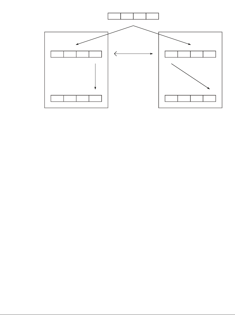
Porting
ARM DEN0013B Copyright © 2011 ARM. All rights reserved. 14-3
ID082411 Non-Confidential
Figure 14-1 Different endian behavior
ARM processors support either mode, but typically default to, and are most commonly used in
little-endian mode. Most Linux distributions for ARM tend to be little-endian only. The x86
architecture is little-endian. The PowerPC or the venerable 68K, on the other hand, are generally
big-endian (although the Power architecture can also handle little-endian). Several common file
formats and networking protocols specify different endianness. For example, .BMP and .GIF
files are little-endian, while .JPG is big-endian, and TCP/IP is big-endian, but USB and PCI are
little-endian.
So, there are two issues to consider – code portability and data sharing. Systems are built from
multiple blocks and can include one or more processors, DSPs, peripherals, memory, network
connections and so forth. Whenever data is shared between these elements, there is a potential
endianness conflict. If code is being ported from a system with one endianness to a system with
different endianness, it may be necessary to modify that code, either to make it endian-neutral
or to work with the opposite byte-ordering.
Cortex-A series processors provide support for systems of either endian configuration,
controlled by the CPSR E bit, which enables software to switch dynamically between viewing
data as little- or big-endian. (Instructions in memory are always treated as little-endian.)
Multi-byte loads and stores will make use of built-in byte reversing hardware to allow
big-endian accesses by the processor. The
REV
instruction (see Byte reversal on page 6-24) can
be used to reverse bytes within an ARM register, providing simple conversion between big and
little-endian formats.
In principle, it is straightforward to support mixed endian systems (typically this means the
system is natively of one endian configuration, but there are peripherals which are of the
opposite endianness). The CPSR E bit can be modified dynamically by software, and there is a
SETEND
assembly instruction provided to do this. The CP15:SCTLR (System Control Register,
c1), contains the EE bit (see Coprocessor 15 on page 6-19), which defines the endian mode to
switch to upon an exception. It would be difficult if exception code had to worry about which
11 22 33 44
031
STR r0, [r1]
LDRB r2, [r1]
11 22 33 44 11 22 33 44
00 00 00 44
031
00 00 00 11
031
0x103 0x102 0x101 0x100 0x100 0x101 0x102 0x103
r2=0x11r2=0x44
r0=0x11223344
(r1=0x100)
Memory
Little-endian view Big-endian view

Porting
ARM DEN0013B Copyright © 2011 ARM. All rights reserved. 14-4
ID082411 Non-Confidential
endian state the processor was in upon arrival at the handler. In practice, however, it can be
difficult to tell the compiler that part of the system is of a different endian configuration to the
rest of memory. Linux does not support such mixed-endian operation.
Processors conforming to the ARMv7-A architecture have a byte-invariant view of endianness.
This means that they access a byte in the same way in both little and big-endian modes of
operation. This is sometimes described as BE-8 in ARM documentation.
On the other hand, older ARM processors use a word-invariant view of endianness. This means
that a word is the same in both little- and big-endian states, but bytes and halfword accesses
occur differently. This is often referred to as BE-32. This is the only big-endian mode available
on ARM7 and ARM9 processors and is also available for legacy support on ARM11 family
devices.
Let’s look at a simple piece of code (Example 14-2) which will behave differently when run on
architectures with different endianness.
Example 14-2 Non-portable code
int i;
char *buf = (char*)&i;
char i0, i1, i2, i3;
i0 = buf[0];
i1 = buf[1];
i2 = buf[2];
i3 = buf[3];
The values of
i0
…
i3
are not guaranteed to be the same if the system endianness changes. This
kind of code is therefore inherently non-portable.
When inspecting code in which you suspect endianness problems, you should look for the
following potential causes of problems:
Unions A union can hold objects of different types and sizes. The programmer must keep
track of what the data member represents at any particular time. Code which uses
unions should be carefully checked. If the union is used to access the same data,
but with different data types, there exists a possible endian (and alignment)
problem. Any time that halfword, word (or longer) data types are combined or
viewed as an array of bytes is a potential issue.
Casting of data types
Anywhere that data is accessed in a way outside of its native data type is a
potential problem. Similarly, if there are arrays of bytes, they should not be
accessed other than as a byte data type. Casting of pointers changes how data is
addressed and can be endian sensitive.
Bitfields Code that defines bitfields or performs bit operations will always be a potential
source of endian problems.
Data sharing
Any code which reads shared data from another block, or exports data to another
block, should be checked to see whether the two blocks agree endian definitions.
If the two are different, it may be necessary to implement byte swapping at one
location.

Porting
ARM DEN0013B Copyright © 2011 ARM. All rights reserved. 14-5
ID082411 Non-Confidential
Network code
Code which accesses networking or other I/O devices needs to be reviewed to see
if there is any endian dependency. Again, it may be necessary to re-write code for
greater efficiency, or swap bytes at the interface.
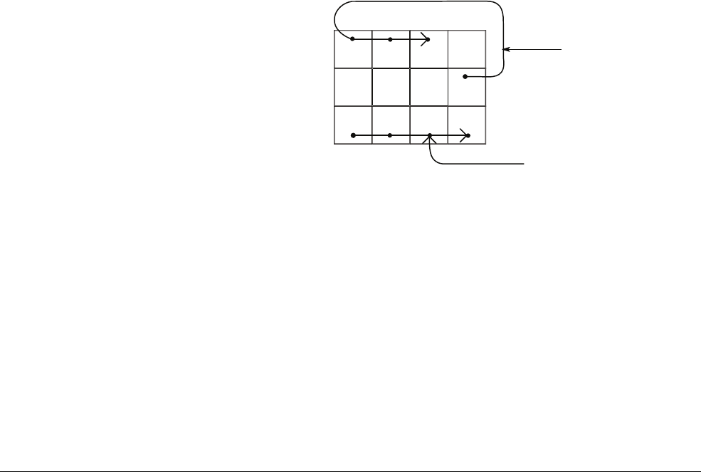
Porting
ARM DEN0013B Copyright © 2011 ARM. All rights reserved. 14-6
ID082411 Non-Confidential
14.2 Alignment
ARM processors care about the alignment of accesses. On older ARM processors, accesses to
addresses which are not aligned are possible, but with a different behavior to those using the
ARMv7 architecture. On ARM7 and ARM9 processors, an unaligned
LDR
is performed in the
memory system in the same way as an aligned access, but with the data returned being rotated
so that the data at the requested address is placed in the least significant byte of the loaded
register. Some older compilers and operating systems were able to use this behavior for clever
optimizations. This can represent a portability problem when moving code from an ARMv4 or
ARMv5 to ARMv7 architecture.
ARM MMUs can be configured to automatically detect such unaligned accesses and abort them
(using the CP15:SCTL A bit), see Coprocessor 15 on page 6-19.
For the Cortex-A series of processors, unaligned accesses are supported (although one must
enable this by setting the U bit in the CP15:SCTL register, indicating that unaligned accesses
are permitted). This means that instructions to read or write words or halfwords can access
addresses which are not aligned to word or halfword boundaries. However, load and store
multiple instructions (
LDM
and
STM
) and load and store double-word (
LDRD
/
STRD
) must be aligned
to at least a word boundary. Furthermore, loads and stores of floating-point values must always
be aligned.
These unaligned accesses can take additional cycles in comparison with aligned accesses and
therefore alignment is also a performance issue. In addition, such accesses are not guaranteed
to be atomic. This means that a external agent (another processor in the system) might perform
a memory access which appears to occur part way through the unaligned access. For example,
it might read the accessed location and see the “new” value of some bytes and the “old” value
of others.
Figure 14-2 Aligned words at address 0 or 8
A word aligned address is one which is a multiple of four, for example
0x100
,
0x104
,
0x108
,
0x10C
,
0x110
etc. Figure 14-2 shows examples of aligned accesses.
0123
4
5
6
7
89AB
The word at address 1
The word at address 8
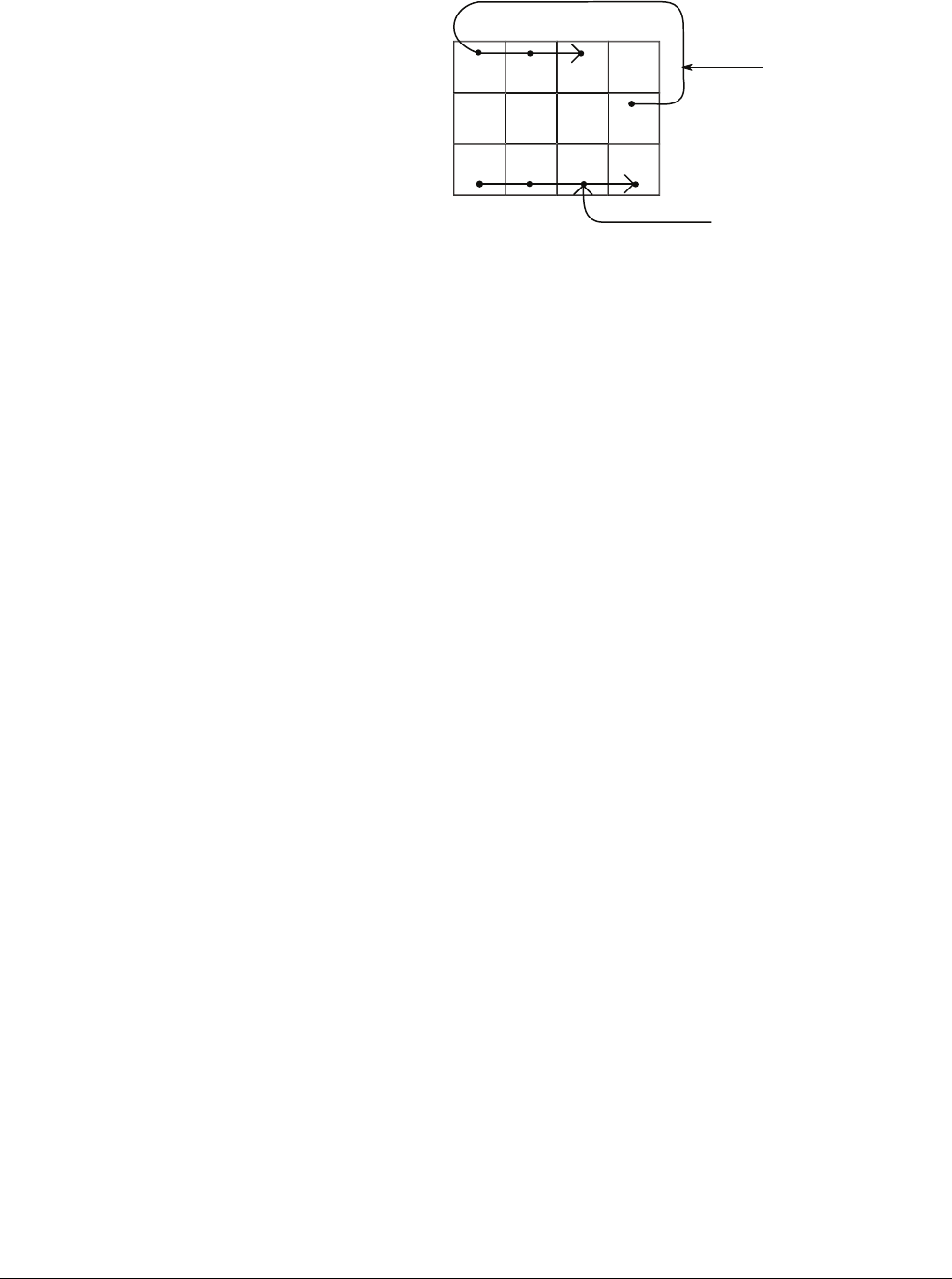
Porting
ARM DEN0013B Copyright © 2011 ARM. All rights reserved. 14-7
ID082411 Non-Confidential
Figure 14-3 An unaligned word
An unaligned word at address 1 is shown in Figure 14-3. It takes three bytes from the word at 0
and one byte from the word at 4.
A simple example where alignment effects can have significant performance effects is the use
of
memcpy()
. Copying small numbers of bytes between word aligned addresses will be replaced
with inline
LDM
/
STM
instructions. Copying larger blocks of memory aligned to word boundaries
will typically be done with an optimized library function which will also use
LDM
/
STM
. Copying
blocks of memory whose start or end points do not fall on a word boundary can result in a call
to a generic
memcpy()
function which can be significantly slower. Although, if the source and
destination are similarly unaligned then only the start and end fragments are non-optimal.
Furthermore, if pointer alignment (or lack of alignment) has not been correctly indicated to the
tools, the compiler can make incorrect assumptions and do the wrong thing.
0123
4
5
6
7
89AB
The word at address 1
The word at address 8

Porting
ARM DEN0013B Copyright © 2011 ARM. All rights reserved. 14-8
ID082411 Non-Confidential
14.3 Miscellaneous C porting issues
In this section we consider some other possible causes of problems when porting C code.
14.3.1 unsigned char and signed char
The piece of code in Example 14-3 illustrates a very simple example of a possible issue when
porting code to ARM.
Example 14-3 Use of unsigned char
char c = -1;
if (c > 0) printf("c is positive \n");
else printf("c is negative \n”);
On some architectures (for example x86), the result is the one you might intuitively expect,
which is that it reports the variable
c
as negative, but compiling the code on an ARM compiler
will produce code which reports
c
as positive (and typically a warning will be emitted by the
compiler, too).
The ANSI C standard specifies a range for both signed (at least -127 to +127) and unsigned (at
least 0 to 255) chars. Simple
char
s are not specifically defined and it is compiler dependent
whether they are signed or unsigned. Although the ARM architecture now has the instruction
LDRSB (which loads a signed byte into a 32-bit register with sign extension), the earliest
versions of the processor did not. And so it made sense for the compiler to treat simple
char
s as
unsigned, whereas on the x86 simple
char
s are, by default, treated as signed.
One workaround for users of GCC is to use the
-fsigned-char
command line switch (or
--signed-chars
for RVCT), which forces all
char
s to become signed, but a better practise is to
write portable code by declaring
char
variables appropriately. Unsigned
char
should be used for
accessing memory as a block of bytes or for small unsigned integers. Signed
char
should be used
for small signed integers and simple
char
should be used only for ASCII characters and strings.
In fact, on an ARM processor, it is usually better to use
int
s rather than chars, even for small
values, for performance reasons. You can read more on this in Chapter 17 Optimizing Code to
Run on ARM Processors.
A second piece of code, in Example 14-4, illustrates another possible problem with chars. Here
we compare
EOF
with an
unsigned char
. On the ARM, the
while
loop will never complete. The
value of
EOF
is defined as -1 and when it is converted to be compared with a
char
(which is
unsigned and therefore in the range 0 to 255), it can never be equal and so the loop does not
terminate.
Example 14-4 Use of EOF
char c;
while ((c = getchar()) != EOF) putchar(c);
Here, we should declare the variable as
int
instead of
char
to avoid the problem – in fact, this
is how the functions in
stdio.h
are defined.
Similar cases to look out for include the use of
getopt()
and
getc()
– both are defined as
returning an
int
.
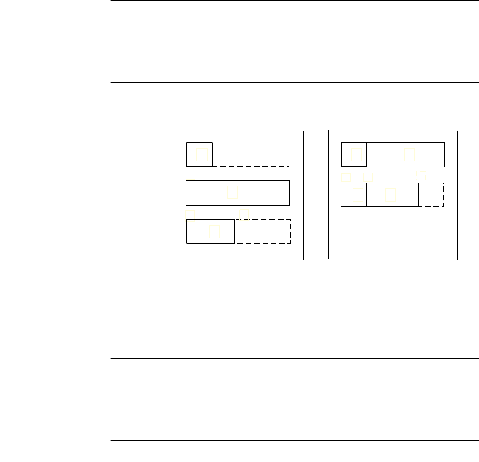
Porting
ARM DEN0013B Copyright © 2011 ARM. All rights reserved. 14-9
ID082411 Non-Confidential
14.3.2 Compiler packing of structures
Compilers are not allowed to re-order members of a structure and have to follow the alignment
restrictions of the processor architecture. This means that compilers may have to add unused
bytes into user defined structures, for best performance and code size. Such padding is
architecture specific and can therefore lead to portability problems if assumptions have been
made about the location and size of this padding.
Marking a structure as
__packed
in the ARM Compiler or using the attribute
__packed__
in GCC,
will remove any padding. This reduces the size of the structure and can be useful when porting
code or for structures being passed from external hardware, but can reduce performance and/or
increase code size, although generally it will be relatively efficient on Cortex-A series
processors.
If we have some simple
struct
code, as shown in Example 14-5:
Example 14-5 A typical C struct
struct test
{
unsigned char c;
unsigned int i ;
unsigned short s;
}
Then the arrangement of data within the
struct
will be as in Figure 14-4.
Figure 14-4 Packed versus unpacked
If we now mark the structure as packed, as in Example 14-6:
Example 14-6 Packed structure
struct test
{
unsigned char c;
unsigned int i ;
unsigned short s;
} __attribute__((__packed__));
0
Unpacked Structure Layout Packed Structure Layout
c
i
s
c
s
i
i
0
4
8
4
13
1
A
9
57

Porting
ARM DEN0013B Copyright © 2011 ARM. All rights reserved. 14-10
ID082411 Non-Confidential
The layout is now that byte 0 holds
c
, bytes 1-4 hold
i
and bytes 5-6 will hold
s
. To access
s
or
i
will require the processor to perform an unaligned access, which is also shown in Figure 14-4
on page 14-9.
14.3.3 Use of the stack
Code which makes assumptions about the stack structure can require porting effort. For
example, functions with a variable number and type of arguments can receive their variables
through the stack. The
<stdarg.h>
macros dealing with accessing these arguments will walk
through the stack frame and provide compatibility between systems, but code which does not
use standard libraries or macros can have a problem.
14.3.4 Other issues
A function prototype is a declaration that omits the function body but gives the function name,
argument and return types. It effectively gives a way to specify the interface of a function
separately from its definition. Incorrectly prototyped functions can behave differently between
different compilers.
Compilers can allocate different numbers of bytes to
enum
. Care is therefore required when
enumerations are used; cross-linking of code and libraries between different compilers may not
be possible if
enum
s are used.
Code written for 8-bit or 16-bit microprocessors can assume that integer variables are 16-bit. On
ARM processors, they will always be 32 bits. The program may rely on 16-bit behaviors. In
general, this is easily fixed by the use of the C short type. Use of short
int
s can be less efficient,
as we shall see in the chapter on optimization and in cases where the code does not rely on 16-bit
behavior, it is usually better to promote these variables to a 32-bit
int
.

Porting
ARM DEN0013B Copyright © 2011 ARM. All rights reserved. 14-11
ID082411 Non-Confidential
14.4 Porting ARM assembly code to ARMv7
So far in this chapter, we have looked at porting C code from other architectures to ARM. It is
sometimes necessary to port assembly code from older ARM processors to the Cortex-A series.
Sometimes, it can be difficult to determine which ARM architecture variant your code was
originally targeting. GCC has a series of macros, with names like
__ARM_ARCH_6__
which are
mutually exclusive. The ARM Compiler has a similar set of macros such as
__TARGET_ARCH_7_A
.
In general, ARM assembler code is backward compatible and will work unmodified.
There are a few special cases to look for:
CP15 Operations
The architecture specifies a consistent mapping of CP15 to designed system
control operations. In general, one should attempt to understand the purpose of
code which performs CP15 instructions and ensure that this code is appropriate
for the ARMv7-A Architecture. In addition, a number of CP15 registers (for
example CP15:ACTL, the Auxiliary Control Register) are implementation
specific. Code which references such registers will always need attention when
being ported.
SWAP The
SWP
(or
SWPB
) instruction was used to implement atomic operations in older
versions of the ARM architecture, but such use is strongly discouraged in the
ARMv7 Architecture. There is no encoding for
SWP
in Thumb at all, so
SWP
is not
allowed when building for Thumb. In the ARMv7 Architecture,
SWP
is disabled
by default, but can be re-enabled by setting CP15:SYSCTL bit 10. Code which
uses
SWP
should be rewritten to make use of
LDREX
/
STREX
(and possibly also barrier
instructions – see Chapter 9). Alternatively, the GCC
__sync_
... intrinsics could be
used. It is usually preferable to use library functions for such things as spinlocks,
semaphores, and mutexes, rather than writing such primitives yourself. The
mechanisms used are different from those used by SWP, so it is necessary to port
all code accessing an atomic object, not just some of it. Usually an atomic object
will be managed by a piece of library code shared between the threads which
access it, so this is not typically a problem.
14.4.1 Memory access ordering and memory barriers
The ARMv7 architecture has a weakly-ordered memory model. Code for older processors
which makes implicit assumptions about ordering of memory accesses may not operate
correctly on ARMv7 devices. This may be particularly true for code which interacts with other
devices, such as a DMA controller or other bus master. Such code should be inspected and
modified, possibly by the insertion of appropriate barrier instructions or by the use of suitable
atomic primitives. See Chapter 9 for a more detailed description of memory ordering and
memory barriers.

Porting
ARM DEN0013B Copyright © 2011 ARM. All rights reserved. 14-12
ID082411 Non-Confidential
14.5 Porting ARM code to Thumb
We also consider problems associated with porting code written for the ARM instruction set to
the Thumb instruction set. As we have seen, use of Thumb is often preferred due to its
combination of small code size with higher performance relative to the older 16-bit only Thumb
instruction set.
14.5.1 Use of PC as an operand
Instructions which use PC (R15) as an explicit operand can cause problems when assembling in
Thumb. As we have seen, it is not possible to encode any arbitrary 32-bit address into any
instruction as an operand. For this reason, it is common to address data stored in a literal pool
using offsets relative to the current instruction location. In ARM code, the PC value can be used
(with some adjustment) to determine the address of the currently executing instruction, for this
purpose and this enables position-independent coding. However, the PC value obtained in this
way can show some inconsistencies between ARM and Thumb states and can also depend upon
the type of instruction executed. For this reason, ARM assembly code which directly references
the PC register may need to be modified in order to work correctly in Thumb. We will consider
a number of examples here.
Example 14-7 shows two different methods of loading a literal from the text section. This would
most often be needed if the code is trying to load a value which cannot be encoded in the
immediate operand portion of a
MOV
instruction, but could also be used for the address of an
object which needs link-time relocation.
Example 14-7 Two potentially problematic ways of loading a literal value
LDR r0, [pc, #(data - . - 8)]
LDR r0, [pc, #<some offset>]
...
data:
.long 0x12345678
In ARM state, either of these statements would work, although the second method is highly
likely to cause problems. For example if an instruction is added to, or removed from, the code,
or the data location is moved, the load will return incorrect data.
In all such cases, it is better to avoid explicit PC arithmetic and instead to use an instruction like:
LDR r0, =<value>
This automatically puts
<value>
somewhere in the text section and assembles an appropriate
PC-relative
LDR
instruction. You can still do a load from a local text section label which you
declare explicitly, as shown below, but again, the assembler/linker should be allowed to perform
the PC offset calculation:
LDR r0, data
...
data: .long <value>
Sometimes the required PC-relative address offset is too large to encode in a single
LDR
instruction, causing the assembler to complain that a literal pool is out of range. This can be
resolved by explicitly placing a literal pool, using the
.ltorg
directive, which tells the assembler
where to insert literal data. The programmer must ensure that the literal data is not located where
it might be executed as code. This typically means the
.ltorg
directive is placed after an
unconditional branch or function return instruction.

Porting
ARM DEN0013B Copyright © 2011 ARM. All rights reserved. 14-13
ID082411 Non-Confidential
Sometimes, code needs to get the address of local data in the text section. It is tempting to do
this using PC-relative arithmetic, usually an
ADD
or
SUB
instruction using the PC as an operand,
as in Example 14-8.
Example 14-8 PC-relative arithmetic
ADD r1, pc, #(data - . - 8)
...
data:
However, this will not work in the same way in Thumb state, where the -8 value will be
incorrect. Instead, the
ADR
pseudo-instruction should be used. The assembler will produce a
PC-based
ADD
or
SUB
with the correct offset value.
14.5.2 Branches and interworking
When using Thumb, the system will typically have both ARM and Thumb functions (even if we
compile our application for Thumb, we may still need to think about such things as libraries and
prebuilt binaries). The processor does not know which instruction set is to be used for the code
being executed after a branch, procedure call or return. This “interworking” between instruction
sets was described in Interworking on page 5-11. When writing C code, the linker takes care of
this for us, but a little more care is needed when porting assembly code.
The target instruction set state is determined in different ways depending on the type of branch.
We can consider a number of different instructions:
Function return
Code written for ARMv4 can use the
MOV
PC, LR
instruction. This is unsafe for
systems which contain a mix of ARM and Thumb code and should be replaced
by
BX
LR
for code running on all later architectures.
Function return from the stack
This is done using the
LDMFD
SP!, {registers, pc}
instruction, which will
continue to work correctly in the ARMv7-A architecture (although a newer,
equivalent form,
POP
{<registers>, pc}
is also available). This is used when the
LR and other registers which need to be preserved by the function are PUSHed at
the start of the function.
Branch A simple
B
instruction will work in the same fashion on all ARM architectures. If
ARM and Thumb are mixed in a single source file (this is unusual), there is no
automatic instruction set switch for local symbols. The assembler may or may not
introduce a veneer depending on whether it knows that the destination is in a
different instruction set and is definitely a code symbol (such as a .
type
<symbol>, %function or .
thumb_func
). Note that just because a symbol appears in
a code section it is not assumed to be a code symbol unless specifically tagged in
this way. If the label is in a different file, the linker will take care of any necessary
instruction set change. Similar considerations apply for a function call (
BL
).
PC modification
Care may be needed with other instructions which modify the PC and produce a
branch effect. For example,
MOV
PC, register
must be replaced with
BX
register in
systems which contain both ARM and Thumb code.

Porting
ARM DEN0013B Copyright © 2011 ARM. All rights reserved. 14-14
ID082411 Non-Confidential
Function call to register address
If code contains a sequence like
MOV LR, PC
followed by
MOV
PC, register
, this
will not work in a system which has both ARM and Thumb code. It should be
replaced with the single instruction
BLX
<register>
.
When a destination or return address is variable or calculated at run-time, care is needed to
appropriately set the “Thumb bit” (bit [0]) in the address correctly and to do the correct type of
branch, to make sure that the call (and return, if applicable) switches instruction set
appropriately.
If an external label or function defined in another object is referenced, the linker will produce
an address with the “Thumb bit” (bit [0]) set appropriately. However, if you reference a symbol
internal to the object, things are more complicated. For C functions, or code tagged as Thumb,
bit [0] will be set appropriately, but it will not be set appropriately for other symbols. In
particular, GNU Assembler local labels will not have the Thumb bit set appropriately, nor will
the GNU current assembly location symbol “.”.
Therefore, when coding in assembler, if an address will be passed to any other function or object
(as a return address, method address, callback etc.), you must handle the Thumb bit setting
yourself, setting bit [0] of the address where required.
14.5.3 Use of PC, “.” and position-independent addressing
In ARM code, for many instructions, we can use the PC as one of the operands and normally, it
will give the address of the current instruction +8. (There are some exceptions – a
STR
pc
instruction, for example, is not guaranteed to do this.) In Thumb code, things are more complex.
Most instructions are unable to use the PC as an operand. Those instructions which can access
the PC as a source operand do not all produce a value with an identical offset from the current
instruction. Care is therefore needed when porting in instances where we use the PC as an
operand, in particular where we need to get the address of a function or piece of code, to use as
a callback, either by passing it to another function or by storing it in a structure.
14.5.4 Operand combinations
Thumb and ARM Assembly code have different restrictions on instruction operands. You may
therefore find that existing ARM code can produce assembler errors when targeted for Thumb.
“Branch out of range” errors occur when the distance between the current instruction and the
branch target is too large to be encoded in a Thumb instruction. To resolve this, it may be
necessary to use a different type of branch, move code sections or to use a two-stage branch, a
so-called “trampoline”.
Similarly, “index out of range” errors may be produced on load and store operations, and to
resolve these it may be necessary to manually add part (or all) of the required index offset to the
base register in a separate explicit instruction.
Generally, use of SP should be limited to stack operations – other usage may not be permitted
in Thumb code. This means that
PUSH
,
POP
,
LDMFD
SP!
,
STMFD
SP
!,
ADD
,
SUB
or
MOV
instructions which
use the SP are allowed, but other operations should be treated as possible problems. Similarly,
operations which directly operate on the PC should be checked (other than the usual function or
exception return operations, or literal pool loads).

Porting
ARM DEN0013B Copyright © 2011 ARM. All rights reserved. 14-15
ID082411 Non-Confidential
14.5.5 Other ARM/Thumb differences
There are a number of other differences which can need attention by the assembly language
programmer.
•The
RSC
instruction is not available in Thumb. Therefore, code which uses
RSC
needs to be
re-coded using
RSB
and/or
SBC
, or be built in ARM state.
• Most ARM instructions can optionally be made conditional. This is not the case in
Thumb, other than for branches. Instead, small instruction sequences can be executed
conditionally by preceding them with the
IT
instruction. For compatibility with both ARM
and Thumb, the IT block construct is always understood when using unified assembler
syntax. Manually modifying code to use
IT
instructions can be tedious. Fortunately, the
assembler command-line option
-mimplicit-it=<when>
, where
<when>
can be one of
never
,
arm
,
thumb
or
always
. When assembling for Thumb, it is therefore sensible to use
-mimplicit-it=thumb
.

ARM DEN0013B Copyright © 2011 ARM. All rights reserved. 15-1
ID082411 Non-Confidential
Chapter 15
Application Binary Interfaces
The C compiler is able to generate code from many separately compiled modules. For programs
to execute successfully these modules must be able to work together with each other, with the
operating system code and any code which is written in assembler or any other compiled language.
For that reason, we must define a set of conventions to govern inter-operability between separate
pieces of code.
The Application Binary Interface (ABI) for the ARM architecture specification describes a set of
rules that an ARM executable must adhere to in order to execute in a specific environment. It
specifies conventions for executables, including file formats and ensures that objects from different
compilers or assemblers can be linked together successfully. There are variants of the ABI for
specific purposes, for example, we may consider the Linux ABI for the ARM architecture or the
Embedded ABI (EABI).
The ARM Architecture Procedure Call Standard (AAPCS) is part of the ABI and specifies
conventions for register and stack usage by the compiler and during subroutine calls. Knowledge
of this is vital for inter-working C and assembly code and can be useful for writing optimal code.
The AAPCS supersedes the previous ARM-Thumb Procedure Call Standard (ATPCS).
The AAPCS mandates specific things that must be done by a caller to allow a callee function to run
and what the called routine must do to preserve the program state of the caller through a function.
It describes the way that data is laid out in memory and how the stack is laid out, plus permitted
variations for processor extensions. It defines how code which has been separately compiled and/or
assembled works together.

Application Binary Interfaces
ARM DEN0013B Copyright © 2011 ARM. All rights reserved. 15-2
ID082411 Non-Confidential
15.1 Procedure Call Standard
As we have seen, there are 16 integer registers available in the processor, each of size 32-bits.
These are labeled R0-R15. Table 15-1 shows the role assigned to registers within the procedure
call standard.
For the purposes of function calls, the registers are divided into three groups:
•Argument registers R0-R3 (a1-a4). These can be used as scratch registers or as
caller-saved register variables which can hold intermediate values within a routine,
between calls to other functions.
• Callee-saved registers, normally used as register variables. Typically, the registers R4-R8,
R10 and R11 (v1-v5, v7 and v8) are used for this purpose.
• Registers which have a dedicated role. The function of the program counter, link register
and stack pointer should by now be clear. If not, you should refer to Registers on page 4-4.
The IP (R12) register can be used by the linker, as a scratch register between a routine and
any subroutine it calls, or as an additional local variable within a function. As the
BL
instructions cannot address the full 32-bit address space, the linker may need to insert a
veneer between the caller and callee. Veneers can also be used for ARM-Thumb
inter-working or dynamic linking. Veneers are permitted to modify the contents of IP
(R12). Register R9 has a role which is specific to a particular environment. It can be used
as the static base register (SB) to point to position-independent data, or as the thread
register (TR) where thread-local storage is used. In code that has no need for such a special
register, it can be used as an extra callee-saved variable register, v6.
Table 15-1 APCS registers
Register PCS name PCS role
R0 a1 argument 1/scratch register/result
R1 a2 argument 2/scratch register/result
R2 a3 argument 3/scratch register/result
R3 a4 argument 4/scratch register/result
R4 v1 register variable
R5 v2 register variable
R6 v3 register variable
R7 v4 register variable
R8 v5 register variable
R9 tr/sb/v6 static base/ register variable
R10 s1/v7 stack limit/stack chunk handle/register variable
R11 FP/v8 frame pointer/register variable
R12 IP scratch register/new -sb in inter-link-unit calls
R13 SP Lower end of the current stack frame
R14 LR link register/scratch register
R15 PC program counter

Application Binary Interfaces
ARM DEN0013B Copyright © 2011 ARM. All rights reserved. 15-3
ID082411 Non-Confidential
The first four word-sized parameters passed to a function will be transferred in registers R0-R3.
Sub-word sized arguments (for example,
char
) will still use a whole register. Arguments larger
than a word will be passed in multiple registers. If more arguments are passed, the fifth and
subsequent words will be passed on the stack. Passing arguments on the stack always requires
additional instructions and memory accesses and therefore reduces performance. For optimal
code, therefore, the programmer should always try to limit arguments to four words or fewer. If
this is not possible, the most commonly used parameters should be defined in the first four
positions of the function definition. If the arguments are part of a structure then it is more
optimal to pass a pointer to the structure instead. C++ uses the first argument to pass the
this
pointer to member functions, so only three arguments can be passed in registers.
There are additional rules about 64-bit types. 64-bit types must always be 8-byte aligned in
memory (recall that in Alignment on page 14-6 we described how there are limitations on use of
LDRD
and
STRD
double-word instructions to unaligned addresses). In addition, 64-bit arguments
to functions must be passed in an “even + consecutive” odd register pair (for example, R0 + R1
or R2 + R3). If 64-bit arguments are passed on the stack, they must be at an 8-byte aligned
location. Again, this is because of restrictions on
LDRD
and
STRD
instructions. If such 64-bit
arguments are listed in a sub-optimal fashion, there can be “wasted” space in registers or on the
stack. When considering such issues, it is important to take into account the
this
pointer in R0
present in all non-static C++ member functions.
Figure 15-1 Efficient parameter passing
Figure 15-1 shows some examples of how sub-optimal listing of arguments can cause
unnecessary spilling of variables to the stack. The figure shows how two different function calls,
which pass identical parameters, make use of the registers and stack. The first function passes
an
int
, a
double
and a further
int
. The first parameter is passed in R0. The second argument is
64-bits and must be passed in an even and consecutive odd register (or in an 8-byte aligned
location on the stack). It is therefore passed in R2 and R3. This means that the final argument is
passed on the stack. As the stack pointer needs to be 8-word aligned, there will be an additional
unused word pushed and popped. In the second function call, we can pass the two
int
values
in registers R0 and R1 and the double value in R2 and R3. This means that no values are spilled
to the stack, which gives more efficient code, requiring both fewer instructions and fewer
memory accesses.
The registers R4-R11 (v1-v8) are used to hold the values of the local variables of a subroutine.
A subroutine is required to preserve (on the stack), the contents of the registers R4-R8, R10, R11
and SP (and R9 in PCS variants that designate R9 as v6), if they are used by that subroutine.
R0 R1 R2 R3
Stack
Foo1 (int i0, double d, int i1)
i0 d d
Stack
Foo2 (int i0, int i1, double d)
i0 d d
Stack
i1
Unused i1 Unused

Application Binary Interfaces
ARM DEN0013B Copyright © 2011 ARM. All rights reserved. 15-4
ID082411 Non-Confidential
A caller function will have code like this:
@ may need to preserve r0-r3
@ does not need to preserve r4-r11
BL Func
while the callee function will have code like this:
Func:
@ Must preserve r4-r11, lr (if used)
@ May corrupt r0-r3, r12
PUSH {r4-r11, lr}
...
...
...
POP {r4-r11, pc}
@ Returns value in r0 - char, short or int
@ Returns value in r0 & r1 - double
The
PUSH
/
POP
must use an even number of registers for function calls beyond an external
boundary, to maintain 8-byte stack alignment. Leaf functions do not have to do so. The example
callee code as shown pushes/pops R4-R11 and LR/PC, which would not preserve an 8-byte
aligned stack. It is shown like this to indicate which registers need to be saved. In practise, the
compiler will normally push an extra register, depending on whether the function is leaf and
which registers are modified by the function. Actual instructions will usually be one of
PUSH
/
POP
{r4, lr/pc},
PUSH
/
POP
{r4-r8, lr/pc},
PUSH
/
POP
{r4-r10, lr/pc} or
PUSH
/
POP
{r4-r12, lr/pc}. In each
case, we would
PUSH
lr and
POP
pc.
15.1.1 VFP and NEON register usage
Readers unfamiliar with ARM floating-point may wish to refer to Chapter 18 Floating-Point
before reading this section.
VFPv3 has 32 single-precision registers s0-s31, which can also be accessed as double-precision
registers d0-d15. There are a further 16 double-precision registers, d16-d31. NEON can also
view these as quadword registers q0-q15. Registers s16-s31 (d8-d15, q4-q7) must be preserved
across subroutine calls; registers s0-s15 (d0-d7, q0-q3) do not need to be preserved (and can be
used for passing arguments or returning results in standard procedure-call variants). Registers
d16-d31 (q8-q15), do not need to be preserved.
The Procedure Call Standard specifies two ways in which floating-point parameters can be
passed. For software floating-point, they will be passed using ARM registers R0-R3 and on the
stack, if required. An alternative, where floating-point hardware exists in the processor, is to
pass parameters in the VFP/NEON registers.
This hardware floating-point variant behaves in the following way:
• Integer arguments are treated in exactly the same way as in softfp. So, if we consider the
function f below, we see that the 32-bit value a will be passed to the function in R0, and
because the value
b
must be passed in an even/odd register pair, it will go into R2/R3 and
R1 is unused.
void f(uint32_t a, uint64_t b)
r0: a
r1: unused
r2: b[31:0]
r3: b[63:32]

Application Binary Interfaces
ARM DEN0013B Copyright © 2011 ARM. All rights reserved. 15-5
ID082411 Non-Confidential
• FP arguments fill d0-d7 (or s0-s15), independently of any integer arguments. This means
that integer arguments can flow onto the stack and FP arguments will still be slotted into
FP registers (if there are enough available).
• FP arguments are able to back-fill, so it's less common to get the unused slots that we see
in integer arguments. Consider the following examples:
void f(float a, double b)
d0:
s0: a
s1: unused
d1: b
Here,
b
is aligned automatically by being assigned to
d1
(which occupies the same
physical registers as VFP s2/s3).
void f(float a, double b, float c)
d0:
s0: a
s1: c
d1: b
In this example, the compiler is able to place
c
into
s1
; it does not need to be placed into
s
4.
In practice, this is implemented (and described) by using separate counters for
s
,
d
and
q
arguments, and the counters always point at the next available slot for that size. In the
second FP example above,
a
is allocated first because it's first in the list, and it goes into
first available
s
register, which is
s0
. Next,
b
is allocated into the first available
d
register,
which is
d1
because
a
is using part of
d0
. When
c
is allocated, the first available
s
register
is
s1
. A subsequent double or single argument would go in
d2
or
s4
, respectively.
• There is a further case when filling FP registers for arguments. When an argument must
be spilled to the stack, no back-filling can occur, and stack slots are allocated in exactly
the same way for further parameters as they are for integer arguments.
void f( double a, double b, double c, double d,
double e, double f, float g, double h,
double i, float j)
d0: a
d1: b
d2: c
d3: d
d4: e
d5: f
d6:
s12: g
s13: unused
d7: h
*sp: i
*sp+8: j
*sp+12: unused (4 bytes of padding for 8-byte sp alignment)
Arguments
a
-
f
are allocated to
d0
-
d5
as expected.
The single-precision
g
is allocated to
s12
, and h goes to
d7
.
The next argument,
i
, can't fit in registers, so it is stored on the stack. (It would be
interleaved with stacked integer arguments if there were any.) However, while
s13
is still
unused,
j
must go on the stack because we cannot back-fill to registers when FP
arguments have hit the stack.
• Double-precision and quad-precision registers can also be used to hold vector data. This
would not occur in typical C code.

Application Binary Interfaces
ARM DEN0013B Copyright © 2011 ARM. All rights reserved. 15-6
ID082411 Non-Confidential
• No VFP registers are used for variadic procedures, that is, a procedure which does not
have a fixed number of arguments. They are instead treated as in softfp, in that they are
passed in integer registers (or the stack). Note that single-precision variadic arguments are
converted to doubles, as in softfp.
15.1.2 Stack and heap
The stack is an area of memory used for storage of local variables (and for passing additional
arguments to subroutines when there are insufficient argument registers available, as we have
seen). The stack implementation is full-descending, with the current top of the stack pointed to
by R13 (SP). The stack must be contiguous in the virtual memory space. The stack will typically
have both a base address and a limit. The base address is that of the bottom entry on the stack.
The limit represents the lowest address that the stack may grow down to. This may be able to
change dynamically in some systems. An application may not be able to determine either value.
The stack limit must, of course, always be lower than the current value of the stack pointer.
Detection of a stack overflowing this limit is usually handled with memory management. The
stack must always be aligned to a word boundary, except at a public interface, when it must be
double-word aligned. This means that interrupt handler code cannot rely on the stack being
double-wordaligned (an interrupt could occur at a time when the stack is merely word-aligned).
The heap is an area (or areas) of memory that are managed by the process itself (for example,
with the C
malloc()
function). It is typically used for the creation of dynamic data objects.
15.1.3 Returning results
A function which returns a char, short,
int
or single-precision
float
value will do so using R0.
A function which returns a 64-bit value (a double-precision
float
or
long
long
) does so in R0
and R1. As mentioned in VFP and NEON register usage on page 15-4, floating-point and
NEON return values will be in
s0
,
d0
, or
q0
when using hardware linkage. If the software uses
hardware linkage it will return floating-point values in
s0
,
d0
, or
q0
. If the software uses software
linkage, it will return single-precision float in r0. A function which returns a 64-bit value (a
double-precision float when using software linkage or a long long) does so in R0 and R1.

Application Binary Interfaces
ARM DEN0013B Copyright © 2011 ARM. All rights reserved. 15-7
ID082411 Non-Confidential
15.2 Mixing C and assembly code
One example of why it can be useful to understand the AAPCS is to write assembly code which
is compatible with C code. One way to do this is write separate modules and assemble them with
GNU Assembler. They can be defined as
extern
functions in C and called; provided the AAPCS
rules are followed, there should be no problem.
We can also insert assembly code into our C code. Let’s have a looked at such inline or
embedded assembly, through the GCC
asm
statement. This is very simple to use. For example,
we can implement a
NOP
as shown in Example 15-1.
Example 15-1 NOP
asm("nop");
The time taken to carry out a
NOP
is undefined.
In fact, it is likely that this
NOP
will have no effect, because the C compiler will optimize it away,
or the processor will discard the instruction. When you include assembly language code with
inline assembler, the resulting code is still subject to optimization by the C compiler. This is a
very important point which must be taken into account whenever inline assembly is used. Even
if the compiler does not optimize-away the NOP instruction, the processor itself may “fold-out”
the NOP from the instruction stream so that it never reaches the execute stage.
Inline assembly code has a different syntax than regular assembly code. Registers and constants
have to be specified differently, if they refer to C expressions.
Let’s look at a slightly more complicated example. We take the value of an
int
and use the
USAD8
assembly instruction to calculate the sum of difference of bytes and then store the result in a
different
int
. Example 15-2 shows the relevant code.
Example 15-2 Using the USAD8 instruction
asm volatile (“usad8 %0, %1, %2” : “=r” (result): “r”(value1), “r”(value2));
The general format of such inline assembly code is:
asm volatile (assembler instructions : output operands (optional) : input operands
(optional) : clobbered registers (optional) );
The colons divide the statement up into parts. The first part “
usad8 %0, %1, %2
” is the actual
assembly instruction. The second part is an (optional) list of output values from the sequence.
If more than one output is needed, commas are used to separate the entries. Each entry has a
symbolic name surrounded by square brackets, followed by a constraint string and finally a C
expression surrounded by brackets . We may then optionally have a list of input values for the
sequence, with the same format as the output. If you don’t specify an output operand for an
assembly sequence, it is quite likely that the C compiler optimizer will decide that it is not
serving any useful purpose and optimize it away! A way to avoid this is to use the
volatile
attribute, which tells GCC not to optimize the sequence.
In the actual assembly language statement, operands are referenced by a percent sign followed
by the symbolic name in square brackets. The symbolic name references the item with the same
name in either the input or output operand list. This name is completely distinct from any other
symbol within your C code (although clearly it is less confusing to use symbols which do have

Application Binary Interfaces
ARM DEN0013B Copyright © 2011 ARM. All rights reserved. 15-8
ID082411 Non-Confidential
a meaning within your code). Alternatively, the name can be omitted and the operand can be
specified using a percent sign followed by a digit indicating the position of the operand in the
list (that is,
%0
,
%1
…
%9
), as shown in the example.
There is an optional fourth part to an asm statement, called the “clobber” list. This enables us to
specify to the compiler what will be changed by the assembly code. We can specify registers
(for example, “R0”), the condition code flags (“cc”) or memory.
This makes the compiler store affected values before and reload them after executing the
instruction.
The constraints mentioned when we talked about input and output operand lists relate to the fact
that assembly language instructions have specific operand type requirements. When passing
parameters to inline assembly statements, the compiler must know how they should be
represented. For example, the constraint “
r
“ specifies one of the registers R0-R15 in ARM state,
while “
m
” is a memory address and “
w
” is a single precision floating-point register. These
characters have an
=
placed before them to indicate a write-only output operand, a “
+
” for a
read/write output operand (that is, one that is both input and output to the instruction). The “
&
”
modifier instructs the compiler not to select any register for the output value, which is used for
any of the input operands.
You can force the inline assembler to use a particular register to hold a local variable by using
something like the code shown in Example 15-3.
Example 15-3 Inline assembler local variable usage
void func (void) {
register unsigned int regzero asm(“r0”);
and later
asm volatile("rev r0, r0");
This usage can interfere with the compiler optimization and does not guarantee that the register
will not be re-used, for example when the local variable is no longer referenced. Hard coding
register usage is always bad practice. It is almost always better to use local variables instead.
Example 15-4 Inline assembler
void __naked get_fiq_regs(struct pt_regs *regs)
{
register unsigned long tmp;
asm volatile (
"mov ip, sp\n\
stmfd sp!, {fp, ip, lr, pc}\n\
sub fp, ip, #4\n\
mrs %0, cpsr\n\
msr cpsr_c, %2 @ select FIQ mode\n\
mov r0, r0\n\
stmia %1, {r8 - r14}\n\
msr cpsr_c, %0 @ return to SVC mode\n\
mov r0, r0\n\
ldmfd sp, {fp, sp, pc}"
: "=&r" (tmp)
: "r" (®s->ARM_r8), "I" (PSR_I_BIT | PSR_F_BIT | FIQ_MODE));
}

Application Binary Interfaces
ARM DEN0013B Copyright © 2011 ARM. All rights reserved. 15-9
ID082411 Non-Confidential
Example 15-4 gives a longer example of inline assembler, taken from the Linux kernel. It shows
how a series of inline assembly language instructions can be used. The code manipulates the
CPSR, to change modes. This would not be possible using C code.
The ARM compiler tools have a similar concept, albeit with different syntax. In addition to
inline assembly, they also support “embedded” assembly which is assembled separately from
the C code and produces a compiled object which is combined with the object from the C
compilation.
A global index gives unique data for each thread within a process. A thread allocates the index
when the process starts. The other threads use this to retrieve the unique data associated with the
index. When a thread starts, it allocates a block of dynamic memory and stores a Thread Local
Storage (TLS) pointer to this memory. This can either be located in memory, or in ARM
MPCore systems, a dedicated CP15 register.

ARM DEN0013B Copyright © 2011 ARM. All rights reserved. 16-1
ID082411 Non-Confidential
Chapter 16
Profiling
The computer scientist Donald Knuth once famously observed that “Premature optimization is the
root of all evil”. However, Knuth's comment does not argue against appropriate optimization.
Code optimization is an important part of the work of software engineers– modifying software so
that it runs more quickly, uses less power and/or makes less use of memory or other resources. In
order to do this, we must first identify which part (or parts) of the code should be optimized.
Profiling is a technique that lets us identify functions (or other pieces of code) which consume large
proportions of the total execution time. It is usually more productive to focus optimization efforts
on code segments which are executed very frequently, or which take a long time to execute than to
optimize rarely used functions or code which takes little time to execute. A profiler will tell us
which parts of the code are frequently executed and which occupy the most processor cycles. A
profiler can help us identify bottlenecks, situations where the performance of the system is
constrained by a small number of functions (or just one). This data is collected using
instrumentation, an execution trace or sampling, and can often be a good method for finding hidden
bugs too.
When you have identified some slow part of your code it's important to consider first whether you
can change the algorithm, before trying to improve the existing code. For example, if the time is
being spent searching a linked list, it's probably much more beneficial to change to using a tree or
hash table instead of spending effort to speed up the linked list searching.

Profiling
ARM DEN0013B Copyright © 2011 ARM. All rights reserved. 16-2
ID082411 Non-Confidential
Profiling can be considered as a form of dynamic code analysis. Profiling tools can gather
information in a number of different ways. We can distinguish two basic approaches to
gathering information.
Time based sampling
Here, the state of the system is sampled at a periodic, time-based interval. The
size of this interval can affect the results – a smaller sampling interval can
increase execution time but produce more detailed data.
Event based sampling
Here, sampling is driven by occurrences of an event, which means that the time
between sampling intervals is usually variable. Events can often be hardware
related – for example, cache misses.
It is also important to understand that profilers typically operate on a statistical basis – they may
not necessarily produce absolute counts of events. In complex systems, it may be necessary to
control profiling information by use of annotation options to specify which events are to be
recorded, which events shown, or thresholds to avoid counting large numbers of functions with
low count numbers.

Profiling
ARM DEN0013B Copyright © 2011 ARM. All rights reserved. 16-3
ID082411 Non-Confidential
16.1 Profiler output
Profiler tools normally provide two kinds of information:
Call graph The call graph tells us the number of times each function was called. This can help
point out which function calls can be eliminated or replaced and shows
inter-relations between different functions. Viewing a call graph can suggest code
to optimize and reveal hidden bugs (for example, if code is unexpectedly calling
an error function many times). Collecting call graph information can require
building the code with special options.
Flat profile A flat profile, as in Example 16-1 shows how much processor time each function
uses and the number of times it was called. This enables a simple identification
of which functions consume large fractions of run-time and should therefore be
considered first for possible optimizations.
Example 16-1 Example flat profile
Flat profile:
Each sample counts as 0.01 seconds.
% cumulative self self total
time seconds seconds calls ms/call ms/call name
33.34 0.02 0.02 6275 0.00 0.00 start
16.67 0.03 0.01 192 0.07 0.21 func1
16.67 0.04 0.01 15 1.20 1.20 memcpy
16.67 0.05 0.01 7 1.41 1.41 write
It may be useful at this point to consider some example profiling tools which can be used in
Cortex-A series processors.
16.1.1 Gprof
GProf is a GNU tool which provides an easy way to profile your C/C++ application and find the
locations that need work.
Using GCC, you can generate profile information by compiling with a special flags. The source
code has to be compiled with the
-pg
option. For line-by-line profiling, the
–g
option would also
be needed. You then execute the compiled program and the profiling data is collected. You then
run
gprof
on the resulting statistics file to view the data, in a variety of convenient formats.
When you compile with
-pg
the compiler adds profiling instrumentation that collects data at
function entry and exits at runtime. It therefore profiles only the user application code and not
anything that happens in code that has not been built for profiling (for example, libc) or the
kernel. Gprof can give misleading results if the performance limitations of the code come from
kernel or I/O issues (memory fragmentation or file accesses for example).
It may be necessary to remove GCC optimization flags, as some compiler optimizations can
cause problems while profiling. It is also the case that the use of the profiling flags will actually
slow the program down. This can be an important consideration in some types of real-time
system, where it may be that the interaction of real-time events has a significant effect on the
performance of the profiled code. A binary file called
gmon.out
containing profiling information
is generated. This file can then be operated on by the
gprof
tool.

Profiling
ARM DEN0013B Copyright © 2011 ARM. All rights reserved. 16-4
ID082411 Non-Confidential
16.1.2 OProfile
OProfile is a system profiling tool which runs on Linux. Unlike
gprof
, it works using a statistical
sampling method. OProfile can examine the system at regular intervals, determine what code is
running, and update appropriate counters. If a long enough profile is taken, with a sufficient
sample rate, an accurate picture of the execution is obtained. Like other profilers which make
use of interrupts, code which disables interrupts can cause inaccuracies. For this reason, the
Linux function
spinlock_irq_restore()
, which re-enables interrupts after a spinlock has been
relinquished can erroneously appear to be a major system bottleneck, as the time for which
interrupts were disabled can be counted against it. OProfile can also be made to trigger on
hardware events and will record all system activity including kernel and library code execution.
OProfile does not need code to be recompiled with any special flags (provided symbol
information is available). It provides useful hardware information about clock cycles, cache
misses etc. Call graphs are statistically generated, so may not be completely accurate. If
OProfile did not make use of such sampling, the execution speed of the system would be
reduced (and of course would just result in a profile of the profiler itself).
16.1.3 DS-5 Streamline
DS-5 Streamline is a graphical performance analysis tool, which can be used to analyze the
performance of an Linux or Android system. It is a component of ARM DS-5 and combines a
kernel driver, target daemon and Eclipse-based user interface. (For more information about
DS-5, see ARM DS-5 on page 3-11.)
DS-5 Streamline takes sampling data and system trace information and produces reports that
present the data visually and in a statistical form. It uses hardware performance counters and
kernel metrics to provide an accurate representation of system resources.
For example, DS-5 Streamline has a display mode called X-ray mode. In this mode the process
trace view changes from an intensity map of time to a view that highlights processor affinity.
Figure 16-1 on page 16-5 shows the DS-5 Streamline view of a multi-threaded Linux
application running on a multi-core processor. Threads are being assigned to the processors by
the Linux kernel:
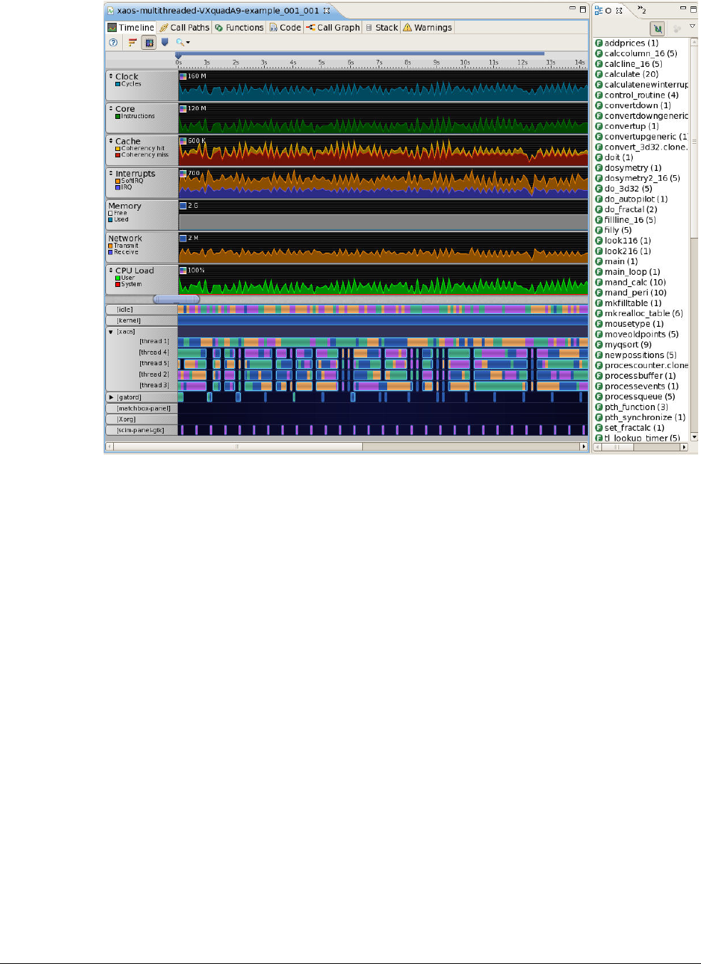
Profiling
ARM DEN0013B Copyright © 2011 ARM. All rights reserved. 16-5
ID082411 Non-Confidential
Figure 16-1 X-ray mode in ARM DS-5 Streamline
16.1.4 ARM performance monitor
The performance monitor hardware is able to count several events, using multiple counters.
Normally, we combine together multiple values to generate useful parameters to optimize. For
example, we can choose to count the total number of clock cycles and the number of instructions
executed and use this to derive a cycles per instruction figure which is a useful proxy for the
efficiency with which the processor is operating. We can generate information about cache hit
or miss rates (separately for both L1 data and instruction caches) and examine how code changes
can affect these.
Cortex-A series processors contain event counting hardware which can be used to profile and
benchmark code, including generation of cycle and instruction count figures and to derive
figures for cache misses and so forth. The performance counter block contains a cycle counter
which can count processor cycles, or be configured to count every 64 cycles. There are also a
number of configurable 32-bit wide event counters which can be set to count instances of events
from a wide-ranging list (for example, instructions executed, or MMU TLB misses). These
counters can be accessed through debug tools, or by software running on the processor, through
the CP15 Performance Monitoring Unit (PMU) registers. They provide a non-invasive debug
feature and do not change the behavior of the processor. CP15 also provides a number of
controls for enabling and resetting the counters and to indicate overflows (there is an option to
generate an interrupt on a counter overflow). The cycle counter can be enabled independently
of the event counters.
It is important to understand that information generated by such counters may not be exact. In
a superscalar, out-of-order processor, for example, it can be difficult to guarantee that the
number of instructions executed is precise at the time any other counter is updated.

Profiling
ARM DEN0013B Copyright © 2011 ARM. All rights reserved. 16-6
ID082411 Non-Confidential
The standard countable events, common to all ARMv7-A processors are listed in Table 16-1.
The TRM for the specific processor being used provides further information on the lists of
events which can be monitored, which can include a large number of additional possibilities
above those listed here.
MPCore versions of the Cortex-A5 and Cortex-A9 processors include a significant number of
additional events relating to SMP capabilities, described in Chapter 23 SMP Architectural
Considerations. These include numbers of barrier instructions executed, measures of coherent
cache activity and counts of exclusive access failures.
In Linux, these counters are normally accessed through the kernel via the Linux OProfile tool
or the Linux perf events framework. However, User mode access to these counters can be
enabled for direct access if required.
16.1.5 Linux perf events
Linux contains patches (as of Linux-2.6.34) to support the Ingo Molnar Perf Events framework.
It handles multiple events, including processor cycles and cache-misses but also measures
kernel events like context switches. It provides simple, platform independent access to the the
ARM performance counter registers and also to software events. Through this framework, tools
can produce graphs and statistics about function calls etc. You can also record execution traces,
profile on a per-processor, per-application and per-thread basis and generate summaries of
events.
Table 16-1 Performance monitor events
Number Event counted
0x00
Software increment of the Software Increment Register
0x01
Instruction fetch that causes a refill
0x02
Instruction fetch that causes a TLB refill
0x03
Memory Read or Write operation that causes a cache line refill
0x04
Memory Read or Write operation that causes cache access
0x05
Memory Read or Write operation that causes a TLB refill
0x06
Memory-reading instruction executed
0x07
Memory-writing instruction executed
0x09
Exception taken
0x0A
Exception return executed
0x0B
Instruction that writes to the Context ID register
0x0C
Software change of program counter
0x0D
Immediate branch instruction executed
0x0F
Unaligned access
0x10
Branch mispredicted or not predicted
0x11
Cycle count; The register is incremented on every cycle
0x12
Branch or other change in program flow that could have been branch predicted
0x13
-
0x3F
Reserved

Profiling
ARM DEN0013B Copyright © 2011 ARM. All rights reserved. 16-7
ID082411 Non-Confidential
16.1.6 Ftrace
Ftrace is an increasingly widely used trace tool on Linux. It provides visualization of the flow
within the kernel by tracing each function call. It enables interactions between parts of the kernel
to be viewed and enables to developers to investigate potential problem paths where interrupts
or pre-emption are disabled for long periods.
16.1.7 Valgrind/Cachegrind
Valgrind is a widely used tool, commonly used for detection of memory leaks and other memory
handling problems; however, it can also be used for profiling memory usage and is potentially
able to give much more detailed results than OProfile. Valgrind translates a program into a
processor-neutral intermediate representation. Other tools associated with Valgrind are able to
operate on this and then Valgrind translates the code back into native machine code. This
process makes the code run an order of magnitude slower, but enables checks for accesses to
undefined memory, off-by-one errors and so forth to be performed by tools like Memcheck.
For memory access optimization, the Cachegrind tool can be used. As Valgrind simulates the
execution of the program, we can use Cachegrind to record all uses of program memory. By
simulating the operation of the processor caches, we can generate statistics about cache usage.
Some care is needed – this is a simulation of the cache and it is possible that it does not represent
the real cache hardware completely accurately. Nevertheless, it can be a very useful tool to
examine cache and memory usage by an application. When writing high level applications, it
can be difficult for the programmer to have much appreciation for (or control over) addresses
used by a program. The linker will typically generate many of the virtual addresses used within
an image, while the runtime loader will control positioning of libraries and so forth. Finally, the
kernel is responsible for placement of code and data in physical memory. Memory profiling
tools can therefore be a useful aid.

ARM DEN0013B Copyright © 2011 ARM. All rights reserved. 17-1
ID082411 Non-Confidential
Chapter 17
Optimizing Code to Run on ARM Processors
In Chapter 16, we looked at how to identify which parts of the program are suitable for
optimization. In this chapter we will look at some possible software optimizations. Much of what
is presented will apply equally to any system, but some of the suggested optimizations are specific
to ARM systems, or indeed to particular ARM processors.
Optimization does not necessarily mean optimizing to make programs faster. In embedded systems,
we may prefer to optimize for battery life, code density or memory footprint, for example. Writing
code which is more efficient delivers not only higher levels of performance, but can also be crucial
in conserving battery life. If we can get a job done faster, in fewer cycles, we can turn off the power
for longer periods.
Many compilers provide options to help with this. For example, both the ARM compiler and the
GNU GCC compiler have
-O
flags to specify the level of optimization. So, we will spend some time
looking at the effects of these and how to trade off optimizations of code density, speed and debug
visibility.
We will continue by looking at ways in which you can modify your program in order to generate
more optimized code. In a book of this size, we cannot cover such topics of algorithm design which
can lead to significant performance gains, but we will instead concentrate our efforts on those
things where an understanding of the underlying ARM architecture can help to optimize code.
Although cycle timing information can be found in the Technical Reference Manual (TRM) for the
processor that you are using, it is very difficult to work out how many cycles even a trivial piece of
code will take to execute. The movement of instructions through the pipeline is dependent on the
progress of the surrounding instructions and can be significantly affected by memory system
activity. Pending loads or instruction fetches which miss in the cache can stall code for tens of
cycles. Standard data processing instructions (logical and arithmetic) will take only one or two

Optimizing Code to Run on ARM Processors
ARM DEN0013B Copyright © 2011 ARM. All rights reserved. 17-2
ID082411 Non-Confidential
cycles to execute, but this does not give the full picture. Instead, we must use profiling tools, or
the system performance monitor built-in to the processor, to extract useful information about
performance.

Optimizing Code to Run on ARM Processors
ARM DEN0013B Copyright © 2011 ARM. All rights reserved. 17-3
ID082411 Non-Confidential
17.1 Compiler optimizations
The ARM compiler and GNU GCC give us a wide range of options which aim to increase the
speed, or reduce the size, of the executable files it generates. For each line in the source code
there are generally many possible choices of assembly instructions that could be used. The
compiler must trade-off a number of resources, such as registers, stack and heap space, code size
(number of instructions) and number of cycles per instruction in order to produce the “best”
image file.
We’ll begin by looking at some of the source-level optimization options available to the
compiler.
17.1.1 Function inlining
When a function is called, there is a certain overhead. On ARM processors, the instruction
pipeline must be invalidated, which costs cycles. For non-leaf functions, it must store the
function return address on the stack. Instructions may be required to place arguments in the
appropriate registers and push registers on the stack, in accordance with the Procedure Call
Standard. There is a corresponding overhead when returning to the original point of execution
when the function ends, again requiring a branch (and corresponding instruction pipeline flush)
and possibly popping registers from the stack. This function-call overhead can become
important when there are functions which contain only a few instructions, and where these
functions represent a significant amount of the total run-time. Function inlining eliminates this
overhead by replacing calls to a function by a copy of the actual code of the function itself
(known as placing the code inline).
Inlining is always a worthwhile optimization if there is only one place where the function is
called. It is always worthwhile if calling the function requires more instructions (memory) than
inlining the function body. A further consideration is that inlining can help permit other
optimizations. Clearly, increasing the number of times that a function is called will increase the
number of inlined copies of the function that are made and this will increase the cost in code
size. Two cases where inlining is not appropriate are:
• functions that are intended to be patched – inlining makes patching of functions much
harder
• common library functions that are separate from the main codebase for special handling,
for example, burning separately onto ROM.
GCC performs inlining only within each compilation unit. The
inline
keyword can be used to
request that a specific function should be inlined wherever possible, even in other files. The
GCC documentation gives more details of this (and how its use can be combined with
static
and
extern
).
We will look at inlining in a little more detail when we consider cache optimizations.
17.1.2 Eliminating common sub-expressions
Another simple source-level optimization is re-using already computed results in a later
expression. This common sub-expression elimination is performed automatically when
optimization command line switches are used and can make code both smaller and faster.

Optimizing Code to Run on ARM Processors
ARM DEN0013B Copyright © 2011 ARM. All rights reserved. 17-4
ID082411 Non-Confidential
Example 17-1 illustrates how this works:
Example 17-1 Common sub-expression
i = a * b + c;
j = a * b * d;
The compiler can treat this code as if it had been written as in Example 17-2.
Example 17-2 Common sub-expression elimination
tmp = a * b;
i = tmp + c;
j = tmp * d;
This reduces both the instruction count and cycle count.
17.1.3 Loop unrolling
Every iteration of a loop has a certain penalty associated with it. Every conditional loop must
include a test for the end of loop on each iteration. Furthermore, there is a branch instruction to
iterate over the loop, which can take a number of cycles to execute. We can avoid this penalty
by unrolling loops, partially or fully.
Consider the simple code shown in Example 17-4, to initialize an array.
Example 17-3 Initializing an array
for (i = 0; i < 10; i++)
{
x[i] = i;
}
Each iteration of the loop contains an assembler sequence of the form in Example 17-4.
Example 17-4 Loop termination assembly code
CMP i,#10
BLT for_loop
A large proportion of the total run time will have been spent checking if the loop has terminated
and in executing a branch to re-execute the loop.
The same code can be written by unrolling the loop, as shown in Example 17-5.
Example 17-5 Unrolled loop
x[0] = 0;
x[1] = 1;
x[2] = 2;

Optimizing Code to Run on ARM Processors
ARM DEN0013B Copyright © 2011 ARM. All rights reserved. 17-5
ID082411 Non-Confidential
x[3] = 3;
x[4] = 4;
x[5] = 5;
x[6] = 6;
x[7] = 7;
x[8] = 8;
x[9] = 9;
When the code is written in this way, we remove the compare and branch instruction and have
a sequence of stores and adds. This is clearly larger than the original code but can execute
considerably faster.
Conventionally, loop unrolling is often considered to increase the speed of the program but at
the expense of an increase in size (except for very short loops). However, this is not always the
case on true hardware. In many systems, an access to external memory takes significant
numbers of cycles and an instruction cache is provided. Code which loops will typically cache
very well. The code is fetched into the cache during the first loop iteration and is executed
directly from cache after that. Unrolling the loop can mean that the code is executed only once
and so does not cache so well. This is more likely to be the case for functions which are executed
only once – loops which are frequently executed may well be cached whether they are unrolled
or not. A further consideration is that modern ARM processors typically include branch
prediction logic which can hide the effect of pipeline flushes from the programmer by
speculatively predicting whether a branch will or will not be taken ahead of the actual evaluation
of a condition. In some cases, the branch instruction can be “folded”, so that it does not require
an actual processor cycle to execute.
The Cortex-A series processors can have long, complex instruction pipelines, with
interdependencies between instructions, particularly loads and instructions which set condition
code flags. The compiler understands the rules associated with a particular processor and can
often re-arrange instructions so that pipeline interlocks are avoided. This is called “scheduling”
and typically involves re-arranging the order of assembly language instructions in ways which
do not alter the logical correctness of the program or its size, but which reduce its execution
time. This can significantly increase the compiler effort, increasing both the time and memory
required for the compilation. It can also restrict the ability to perform source level debug. There
may no longer be a strict one-to-one link between a line of C source and a sequence of assembly
instructions. We can instead have a couple of instructions from a C statement followed by
instructions for the next statement and then some more instructions for the first statement.
17.1.4 GCC optimization options
GCC has a range of optimization levels, plus individual options to enable or disable particular
optimizations.
The command line option
–OLEVEL
gives a choice of optimization levels, as described below:
•
-O0
. (default). No optimization is performed. Each source code command relates directly
to the corresponding instructions in the executable file. This gives the clearest view for
source level debugging.
•
-O1
. This enables most common forms of optimization that requires no size versus speed
decisions. It can often actually produce a faster compile than –O0, due to the resulting
files being smaller.
•
-O2
.This enables further optimizations, such as instruction scheduling. Again,
optimizations which can have speed versus size implications will not be used.

Optimizing Code to Run on ARM Processors
ARM DEN0013B Copyright © 2011 ARM. All rights reserved. 17-6
ID082411 Non-Confidential
•
-O3
. This enables further optimizations, such as function inlining and can therefore
increase the speed at the expense of image size. Furthermore, this option enables
-ftree-vectorize
- causing the compiler to attempt to automatically generate NEON code
from standard C/C++. See Chapter 20 Writing NEON Code.
•
-funroll-loops
. This option is independent of the above and enables loop unrolling. As
previously described, loop unrolling can increase code size and may not have a beneficial
effect in all cases.
•
-Os
. This selects optimizations which attempt to minimize the size of the image, even at
the expense of speed.
Higher levels of optimization can restrict debug visibility and increase compile times. It is usual
to use
-O0
for debugging, and
-O2
for finished code. When using the above optimization options
with the
–g
(debug) switch, it can be difficult to see what is happening. The optimizations can
change the order of statements, remove (or add) temporary variables, etc. But an understanding
of the kinds of things the compiler will do means that satisfactory debug is normally still
possible with
–O2 -g
.
For optimal code, it is important to specify to the compiler which ARM processor you are using;
without knowledge of that (and in many cases what optional hardware like VFP or NEON is
available), it cannot do a good job.
For the compiler to optimize for a specific processor or instruction set version, you also need to
provide some information about your target platform. Many useful options are documented on
http://gcc.gnu.org/onlinedocs/gcc/ARM-Options.html
.
In particular, try to specify as many as possible of the following:
-march=<arch>
where
<arch>
is the architecture version to compile for. This defines the instruction set
supported, It can make a significant difference to performance to specify
–march=armv7-a
if this
is supported by your platform but is not used by default by your compiler.
-mcpu=<cpu>
More specific than
–march
,
-mcpu
specifies which processor to optimize for, including scheduling
instructions in the way most efficient for that processor’s pipeline.
-mtune=<cpu>
This option provides instruction scheduling optimizations for a specific processor even when
only an architecture version has been specified.
-mfpu=<fpu>
If your target platform supports hardware floating-point or NEON, specify this to ensure that
the compiler can make use of these instructions. For a Cortex-A5 target, you would specify
–mfpu=neon-vfpv4
.
17.1.5 armcc optimization options
The armcc compiler enables you to compile your C and C++ code. It is an optimizing compiler
with a range of command-line options to enable you to control the level of optimization.
The command line option gives a choice of optimization levels, as follows:
•
-Ospace
. This option instructs the compiler to perform optimizations to reduce image size
at the expense of a possible increase in execution time.

Optimizing Code to Run on ARM Processors
ARM DEN0013B Copyright © 2011 ARM. All rights reserved. 17-7
ID082411 Non-Confidential
•
-Otime
. This option instructs the compiler to perform optimizations to reduce execution
time at the expense of a possible increase in image size.
•
-O0
. Turns off most optimizations. It gives the best possible debug view and the lowest
level of optimization.
•
-O1
. Removes unused inline functions and unused static functions. Turns off optimizations
that seriously degrade the debug view. If used with
--debug
, this option gives a satisfactory
debug view with good code density.
•
-O2
(default). High optimization. If used with
--debug
, the debug view might be less
satisfactory because the mapping of object code to source code is not always clear.
•
-O3
. performs the same optimizations as
-O2
however the balance between space and time
optimizations in the generated code is more heavily weighted towards space or time
compared with
-O2
. That is:
—
-O3 -Otime
aims to produce faster code than
-O2 -Otime
, at the risk of
increasing your image size
—
-O3 -Ospace
aims to produce smaller code than
-O2
-Ospace, but performance might
be degraded.

Optimizing Code to Run on ARM Processors
ARM DEN0013B Copyright © 2011 ARM. All rights reserved. 17-8
ID082411 Non-Confidential
17.2 ARM memory system optimization
Writing code which is optimal for the system it will run on is a key part of the art of
programming. It requires the programmer to understand how the compiler and underlying
hardware will carry out the tasks described in the lines of code. If we can do the job with less
access to external memory, we can save power by keeping everything on-chip. Furthermore, by
accessing the cache more frequently, we improve the performance of the system, allowing
software to run faster (or the processor to be clocked more slowly or for shorter periods, to save
power).
17.2.1 Data cache optimization
In most Cortex-A series processors, there is a significant gap in performance between memory
accesses which hit in the cache and those that do not. Cache hits will normally not stall the
processor pipeline. Cache misses can take tens of cycles to resolve. For most algorithms,
therefore, ensuring that cache misses are minimized is the most important possible optimization.
The most important improvements are those which affect the level 1 cache.
Let us consider the problem of data cache misses first. Optimization is particularly significant
for pieces of code which use a dataset larger than the available cache size. It is important for the
programmer of such code to understand the arrangement of data in memory and how that
corresponds to data cache accesses. Code should be structured in a way which ensures
maximum re-use of data already loaded into the cache. It is this principle of data locality, the
degree to which accesses to the same cache line are concentrated during program execution, in
both space and time, which gives best performance.
Several techniques to improve this locality can be considered.
17.2.2 Loop tiling
Loop tiling divides loop iterations into smaller pieces, in a way which promotes data cache
re-use. Large arrays are divided into smaller blocks (tiles), which match the accessed array
elements to the cache size. The classic example to illustrate this approach is a large matrix vector
product.
Consider two square matrices
a
and
b
, each of size 1024 × 1024. Example 17-6 shows code to
compute a matrix vector product. This requires us to multiply each element in each array with
each element in the other array.
Example 17-6 Matrix vector product code
for (i = 0; i < 1024; i++)
for (j = 0; j < 1024; j++)
for (k = 0; k < 1024; k++)
result[i][j] = result[i][j] + a[i][k] * b[k][j];
In this case, the contents of matrix
a
are accessed sequentially, but matrix
b
advances in the inner
loop, by row. It is therefore, highly probable that we will encounter a cache miss for each
multiply operation.
It is obvious that the order in which the additions for each element of the result matrix are
calculated does not change the result (ignoring the effect of overflows etc.). It should therefore
be possible to rewrite the code in a way which improves the cache hit rate. The elements of
matrix b are accessed in the following way (0,0), (1,0), (2,0)… (1023, 0), (0,1), (1,1)… (1023,1).
The elements are stored in memory in the order (0,0), (0,1) etc. For word sized elements, it
means that the elements (0,0), (0,1)…(0,7) will be stored in the same cache line. (For simplicity,
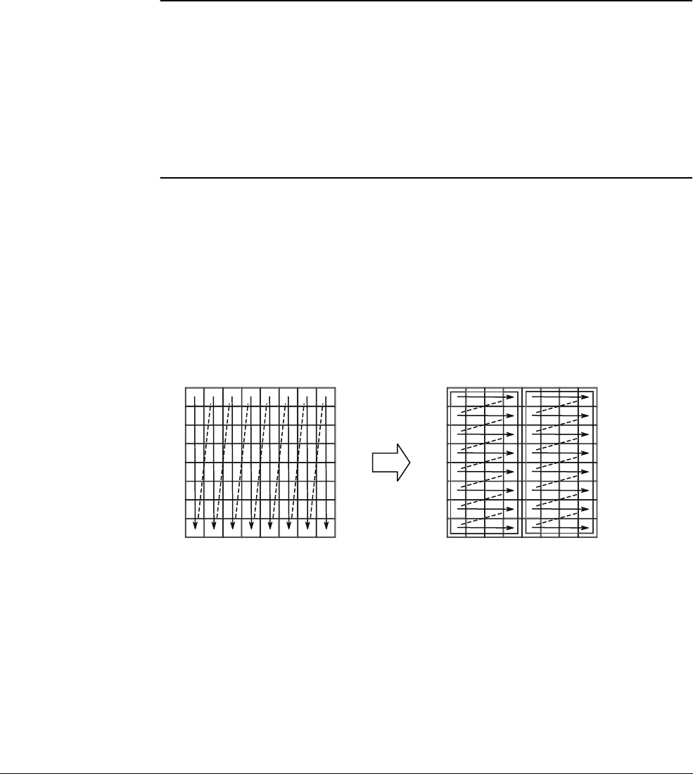
Optimizing Code to Run on ARM Processors
ARM DEN0013B Copyright © 2011 ARM. All rights reserved. 17-9
ID082411 Non-Confidential
we will assume that the start address of the matrix is aligned to a cache line. Alignment will be
mentioned again in Structure alignment on page 17-10.) Therefore, elements (0,0), (0,1), (0,2)
etc. will be in the same cache line; when we load (0,0) into the cache, we get (0,1...7) too. By
the time the inner loop completes, it is likely that this cache line will be evicted.
If we modify the code so that two (or indeed four, or eight) iterations of the middle loop are
performed at once while executing the inner loop, as in Example 17-7 we can make a big
improvement. Similarly, we should unroll the outer loop two (or four, or eight) times as well.
Example 17-7 Code using tiles
for (io = 0; io < 1024; io += 8)
for (jo = 0; jo < 1024; jo += 8)
for (ko = 0; ko < 1024; ko += 8)
for (ii = 0, rresult = &result[io][jo],
ra = &a[io][ko]; ii < 8;
ii++, rresult += 1024, ra += 1024)
for (ki = 0, rb = &b[ko][jo];
ki < 8; ki++, rb += 1024)
for (ji = 0; ji < 8; ji++)
rresult[ji] += ra[ki] * rb[ji];
There are now six nested loops. The outer loops iterate with steps of 8, representing the fact that
eight
int
sized elements are stored in each line of the level 1 cache. Some further optimizations
have also been introduced. The order of
ji
and
ki
has been reversed as only one expression uses
ki
, but two use
ji
. In addition, we optimize by removing common expressions from the inner
loops. All pointer accesses are potential sources of aliasing in C, so by using
result
,
ra
and
rb
to access array elements, the array indexing is speeded up. We cover this in more detail in Source
code modifications on page 17-14. Figure 17-1 illustrates the changing cache access pattern
which results from changes to the C code.
Figure 17-1 Effect of tiling on cache usage
17.2.3 Loop interchange
In many programs, there will be nested loops – a very simple example would be code that
stepped through the items in a 2-dimensional array. For reasonably complex code, we can
sometimes get better performance by re-arrangement of the loops. It is better to have the loop
with the smaller number of iterations as the outer loop and the one with the highest iteration
count as the innermost loop.

Optimizing Code to Run on ARM Processors
ARM DEN0013B Copyright © 2011 ARM. All rights reserved. 17-10
ID082411 Non-Confidential
This gives two potential advantages. One is that the compiler can potentially unroll the inner
loop. Perhaps more importantly for complex loops where the size of the nested loop is
sufficiently large that it may not all be held in level 1 cache at the same time, the overall cache
hit rate will be improved by this change. Some compilers can make this change automatically
at higher levels of optimization. For example, GCC 4.4 adds the switch
-floop-interchange
to
do this.
17.2.4 Structure alignment
Efficient placement of structure elements and alignment are not the only aspects of data
structures which influence cache efficiency. Where code has a large working data set, it is
important to make efficient use of the available cache space. To achieve this, it might be
necessary to rearrange data structures.
It is common to have data structures which span multiple cache lines, but where the program
uses only a few parts of the structure at any particular time. If there are many objects of this type,
it can make sense to try to compress the structure so that it fits within a cache line. This only
makes sense if the object itself is aligned to a cache boundary. For example, consider the case
where we have a very large array of instances of a 64-byte structure (much larger than the cache
size). Within that structure, we have a byte-sized quantity and we have a commonly used
function which iterates through the array looking only at that byte-sized quantity. This function
would probably make inefficient use of the cache, as we would need to load an entire cache line
to read the 8-bit value. If instead those 8-bit values were stored in their own array (rather than
as part of a larger structure), we would get 32 (or 64 on the Cortex-A8 processor) values per
cache linefill.
Furthermore, as we saw in Chapter 14 Porting, unaligned accesses are supported, but can take
extra cycles in comparison to aligned accesses. For performance reasons, therefore, it can be
sensible to remove or reduce unaligned accesses.
17.2.5 Associativity effects
AS we have seen, ARM L1 caches are typically 4-way set-associative, but L2 caches typically
have 8- or 16-way associativity. There can be performance problems if more than four of the
locations in the data fall into the same cache set, as there can be repeated cache misses, even
though other parts of the cache can be unused. The ARM L1 Cache uses physical rather than
virtual addresses, so it can be difficult for programmers operating in User mode to take care of
this.
A particularly common cause of this problem is arranging data so that it is on boundaries of
powers of two. If the cache size is 16KB, each way is 4KB in size. If you have multiple blocks
of data arranged on boundaries which are multiples of 4KB, the first access to each block will
go into line 0 of a way. If code accesses the first line in several such blocks then we can get cache
misses even if only five cache lines in total are being used. Unaligned accesses can increase the
likelihood of this, as each access might require two cache lines rather than one.
17.2.6 Optimizing instruction cache usage
The C programmer does not directly have control over how the instruction cache is used by
code. Code is linear between branch instructions and this pattern of sequential accesses uses the
cache efficiently. The branch prediction logic of the processor will try to minimize the stalls due
to branches, so there is little the programmer can do to assist. So, the main goal for the
programmer is to reduce the code footprint. Many of the compiler optimizations enabled at
-O2
and
-O3
for the ARM compiler and GCC, deal with loop optimizations and function inlining.
These optimizations will improve performance if the code accounts for a significant part of the
total program execution. In particular, function inlining has multiple potential benefits.

Optimizing Code to Run on ARM Processors
ARM DEN0013B Copyright © 2011 ARM. All rights reserved. 17-11
ID082411 Non-Confidential
Obviously, it can reduce branch penalties, by removing branches on both function call and exit,
and potentially also stack usage. Equally importantly, it enables the compiler to optimize over a
larger block of code which can lead to better optimizations for value range propagation and
elimination of unused code.
However, apparent speed optimizations which increase code size can actually reduce
performance due to cache issues. Larger code is less likely to fit in the L1 cache (or indeed the
L2 cache) and the performance lost by the additional cache linefills can well outweigh any
benefits of the optimization. It is often better to use the armcc -
Ospace
or
gcc –Os
option to
optimize for code density rather than speed. Clearly, using Thumb code will also improve code
density and cache efficiency.
There are some interesting decisions to be made around function inlining and in some cases
human judgment can improve on that of the compiler. A function which is only ever called from
one place will always give a benefit if inlined. One might think that inlining very small functions
always gives a benefit, but this is not the case. An instance of a tiny function which is called
from many places is likely to be re-used many times within the instruction cache. If the same
function is repeatedly inlined, it is much more likely that it will cause a cache miss (and also
evict other potentially useful code from the cache). The branch prediction logic within Cortex-A
series processors is efficient and an unconditional function call and return consumes few cycles
– much less than would be used for a cache linefill. The programmer may wish to use the GCC
function attributes
noinline
and
always_inline
to control such cases.
This is a general problem and not specific to inlining functions. Whenever conditional execution
is used and it is lopsided (that is, the expression far more often leads to one result than the other)
there is the potential for false static branch prediction and thus bubbles in the pipeline. It is
usually better to order conditional blocks so that the often-executed code is linear, while the less
commonly executed code has to be branched to and does not get pre-fetched unless it is actually
used. The GCC attribute
__builtin_expect
used with the
–freorder-blocks
optimization option
can help with this.
The performance monitor block of the processor (and OProfile) can be used to measure branch
prediction rates in code. Note that there are two effects at play here. Correct branch prediction
saves clock cycles by avoiding pipeline flushes, but taking fewer conditional branches which
skip forward over code can help performance by making more of the program fit within the L1
cache.
17.2.7 Fast loop mode
The Cortex-A9 processor contains special hardware which can optimize execution of fast loops.
If the loop is sufficiently short, the code for the whole loop can be maintained within the decode
and prefetch stages of the processor and subsequent iterations of the loop do not need to be
refetched from the cache. This mode applies for loops which fit into one or two cache lines (that
is, up to 64 bytes, provided the start of the loop is aligned to a cache line boundary) and are
terminated with a conditional branch backward. The loop is allowed to contain predicted
non-taken branches. This permits loops which have an
if
statement to be handled.
17.2.8 Optimizing L2/outer cache usage
Everything said about optimizations for using the L1 cache also applies to the L2 cache
accesses. Best performance results from having a working dataset which is smaller than the L2
cache size, and where the data is used more than once; there is little benefit caching data which
is used only once, other than possibly producing more optimal bus accesses. If the dataset is
larger than the cache size, the programmer should consider similar techniques to those already
described for the L1 cache. There is, however, a further point to consider with outer caches,
which is that they may well be shared with other processors and therefore the effective size for
an individual processor can be less than the actual size. In addition, when writing generic code

Optimizing Code to Run on ARM Processors
ARM DEN0013B Copyright © 2011 ARM. All rights reserved. 17-12
ID082411 Non-Confidential
to run on a number of ARM families, it can be difficult to make optimal use of the L2 cache.
The presence of such a cache is not guaranteed and its size can vary significantly between
systems.
17.2.9 Optimizing TLB usage
In general, the scope for optimizing usage of the Translation Lookaside Buffer (see Chapter 8)
is much less than for optimizing cache accesses. The key points are to minimize the number of
pages in use (this obviously gives fewer TLB misses) and to use large MMU mappings
(supersections or sections in preference to 4KB pages) as this both reduces the cost of individual
page table walks (one external memory access rather than two) and also means that a larger
amount of memory is represented within an individual TLB entry (thus also giving fewer TLB
misses). In practice, however, an operating system like Linux uses 4KB pages everywhere, so
the main optimization technique available is trying to limit the number of active pages to below
the maximum number supported by the processor hardware (for example, 128 TLB entries on
the Cortex-A9 processor). The main optimization would be to try to process multiple cache
lines’ worth of data per page, so that the L1 cache is the limiting factor rather than TLB entries.
17.2.10 Data abort optimization
As we saw in Chapter 8 Memory Management Unit, in the context of Linux, data aborts will be
generated by page faults on the first time that a memory page is accessed and again when the
page is first written to. This means that the kernel abort handler is called to take appropriate
action and there is a certain performance overhead to this. Simplistically, we can reduce this
overhead by using fewer pages. Again, code optimizations which make code smaller will help,
as will reducing the size of the data space.
17.2.11 Prefetching a memory block access
ARM Cortex-A series processors contain sophisticated cache systems, and support for
speculation and out of order execution which can hide latencies associated with memory
accesses. However, accesses to the external memory system are usually sufficiently slow that
there will still be some penalty. If we can prefetch instructions or data into the cache before we
need them, we can hide this latency.
Many ARM processors provide support for preloading of data under programmer control, using
the
PLD
instruction. This enables the programmer to request that data is loaded to the data cache
in advance of it actually being read or written by the application. The
PLD
operation generates a
cache linefill on a data cache miss, independent of load and store instruction execution, and
happens in the background while the processor continues to execute other instructions. If used
correctly,
PLD
can significantly improve performance by hiding memory access latencies. In the
Cortex-A8 processor, the
PLD
instruction loads data only to the L2 cache. Assembly language
also has a
PLI
instruction, which enables the programmer to hint to the processor that an
instruction load from a particular address is likely in the near future. This can cause the
processor to preload the instructions to its cache.
In addition to this programmer-initiated prefetch, the Cortex-A9 processor has support for
automatic data prefetching. This must be explicitly enabled using the DP bit in the
CP15:ACTLR (Auxiliary Control Register). Essentially, this causes the processor to look out
for a series of sequential accesses to memory. When it sees this happen, it automatically requests
the following cache lines speculatively, in advance of the program actually using them. It can
cope with two independent data streams, such as when a program is performing streams of
sequential accesses to two different locations. The state of this bit may not be under programmer
control in your system (it can be fixed by boot code, for example), but it can be useful to be
aware of this behavior when optimizing code which moves blocks of memory.

Optimizing Code to Run on ARM Processors
ARM DEN0013B Copyright © 2011 ARM. All rights reserved. 17-13
ID082411 Non-Confidential
In many systems, significant numbers of cycles are consumed initializing or moving blocks of
memory, using the
memset()
or
memcpy()
functions. Optimized ARM libraries will typically
implement such functions by using
STM
, Store Multiple instructions, with each store aligned to
a cache line boundary. Cortex-A9 processor hardware automatically attempts to optimize such
cases. It will ignore page table settings for normal, cacheable memory and dynamically optimize
the read and write data cache allocation policies to give best performance.
Consider the case where we have a large block of RAM with a write-allocate policy indicated
in the page table. We wish to zero initialize part of that memory by loading zero into eight ARM
registers and then executing a tight loop of
STM
instructions which writes zero into a series of
locations in memory. If we were to write-allocate this memory, the cache would first read the
uninitialized memory, and then over-write all of the garbage values just written. It therefore
makes no sense to perform the initial read. The hardware can detect this situation and optimize
accordingly.
17.2.12 Preload engine
The Cortex-A8 processor has a built-in preload engine which can be used to move data to and
from the L2 cache under programmer control. It is a dedicated piece of hardware, built into the
processor, but completely separate from the processor pipeline. When programmed, it can
perform its memory operations in the background, while the processor runs other code. It
contains two channels and is programmed by specifying the start and end address to be
transferred. When moving data out of the cache and into external memory, writes will take place
only for lines which are marked as dirty. The maximum number of cache lines which can be
transferred in a single operation is limited by the cache way size. The ability to lock data to a
specific cache way is supported. It has hardware outputs which can be used to generate
interrupts upon completion or if there is an error.
The Cortex-A9 processor, however, does not have a built-in L2 cache. Instead, it can be
implemented in a system which contains a discrete L2 cache block (known as L2C-310,
formerly PL310), which supports the use of a Preload Engine (PLE). The PLE loads regions of
memory into the L2 cache, using a CP15 instruction (MCRR preload channel).
Preload blocks enter a FIFO within the PLE. Each FIFO entry contains a number of parameters:
- base address, length of stride, number of blocks, Translation Table Base (TTB) address,
Address Space ID (ASID) value and valid and secure/non-secure bits. Programmed entries can
remain valid through context switches.
The Preload Engine performs cache line preload requests in the same way as a preload request
from the
PLD
instruction, with the difference that it uses its own TTB and ASID parameters. If
there is a translation abort from the page table entry, the preload request is ignored and the PLE
moves on to the next request, that is, it fails without generating an abort. Translation Lookaside
Buffer (TLB) maintenance operations in the processor are applied to the PLE FIFO entries too.
You are advised to refer to the latest Cortex-A9 Technical Reference Manual for further
information about the Preload Engine.
Optimizing Code to Run on ARM Processors
ARM DEN0013B Copyright © 2011 ARM. All rights reserved. 17-14
ID082411 Non-Confidential
17.3 Source code modifications
We have seen how profiling tools allow us to identify code segments or functions which can
benefit from optimization and how different compiler options can enable compiler
optimizations to our code. We will now look at a variety of source code modifications which can
yield faster or smaller code on the ARM.
17.3.1 Loop termination
Where possible, it is better to have integer loop counters which end at 0 (zero), rather than start
from 0 (zero). This is because a compare with zero comes for free with the
ADD
or
SUB
instruction
used to update the loop counter, whereas a compare with a non-zero value will typically require
an explicit
CMP
instruction.
Replace a loop which counts up to a terminating value:
for (i = 1; i<= total; i++)
with one which counts down to zero:
for (i = total; i != 0; i--)
This will remove a
CMP
instruction from each iteration of the loop.
It is also good practice to use
int
(32-bit) variables for loop counters, rather than
char
(8-bit),
even when the number of iterations is less than 255. This is because the ARM is natively a 32-bit
machine. Its
ADD
assembly language instruction operates on two 32-bit registers. If it does an
ADD
(or other data processing operation) with an eight bit quantity, the compiler may need to insert
additional instructions to handle overflow to a value larger than 255 (see also Variable selection
on page 17-15).
17.3.2 Loop choice
A useful optimization can be achieved by correct choice of loop type. If there are times when
the loop condition is never met, a
for
or
while
loop is the best choice, since these have a
comparison only at the end of the loop. If the loop condition is always true on the first iteration,
it is better to use a do…
while
loop.
17.3.3 Loop fusion
This is one of a variety of other possible loop techniques which can be employed either by the
programmer, or by an optimizing compiler. It essentially means merging loops which have the
same iteration count and no interdependencies (Example 17-8 and Example 17-9 on
page 17-15).
Example 17-8 Loop fusion
for (i = 0; i < 10; i++)
{
x[i] = 1;
}
for (j = 0; j < 10; j++)
{
y[j] = j;
}
It should be immediately apparent that this can be optimized to:

Optimizing Code to Run on ARM Processors
ARM DEN0013B Copyright © 2011 ARM. All rights reserved. 17-15
ID082411 Non-Confidential
Example 17-9 Fused loops
for (i = 0; i < 10; i++)
{
x[i] = 1;
y[i] = i;
}
17.3.4 Reducing stack/heap usage
In general, it is a good idea to try to minimize memory usage by code. The ARM processor has
a register set which provides a relatively limited set of resources for the compiler to keep
variables in. When all registers are allocated with currently live variables, further variables will
be spilled to the stack – causing memory operations and extra cycles for the code to execute.
There are a number of ways available to the programmer to try to help. A key rule is to try to
limit the number of “live” variables at any one time.
When we looked at the procedure call standard in Chapter 15, it was stated that up to four
parameters can be passed to a function. Further parameters are passed on the stack. It is therefore
significantly more efficient to pass four or fewer parameters than to pass five or more. Of course,
the ARM registers in question are 32-bits in size and therefore if we pass a 64-bit variable, it
will take two of our four register slots. For similar reasons, recursive functions do not typically
yield efficient processor register usage.
17.3.5 Variable selection
ARM registers are 32-bit sized and optimal code is therefore produced most readily when using
32-bit sized variables, as this avoids the need to provide extra code to deal with the case where
a 32-bit result overflows an 8- or 16-bit sized variable.
Consider the following code:
unsigned int i, j, k;
i = j+k;
The compiler would typically emit assembly code similar to:
ADD R0, R1, R2
If these variables were instead
short
(16-bit) or
char
(8-bit), the compiler must ensure the result
does not overflow the halfword or byte.
The same code might need to be as shown in Example 17-10, for signed halfwords (shorts).
Example 17-10 Addition of 2 signed shorts (assembly code)
ADD R0, R1, R2
MOV R0, R0, LSL#16
MOV R0, R0, ASR#16
Or for unsigned halfwords as in Example 17-11.
Example 17-11 Addition of 2 unsigned shorts (assembly code)
ADD R0, R1, R2

Optimizing Code to Run on ARM Processors
ARM DEN0013B Copyright © 2011 ARM. All rights reserved. 17-16
ID082411 Non-Confidential
BIC R0, R0, #0x10000
This has the effect of clipping the result to the defined size.
It is therefore best practice for loop counter variables to be defined as type
int
and not as
char
.
This is less of an issue for later versions of the architecture. The compiler can avoid code like
the above by using instructions such as
UXTB
, which was added in the ARMv6 architecture.
17.3.6 Pointer aliasing
If a function has two pointers
*pa
and
*pb
, with the same value, we say the pointers alias each
other. This introduces constraints on the order of instruction execution. If two write accesses
which alias occur in program order, they must happen in the same order on the processor and
cannot be re-ordered. This is also the case for a write followed by a read, or a read followed by
a write. Two read accesses to aliases are safe to re-order. As any function pointer argument could
alias any other function pointer argument in C, the compiler must assume that any accesses
through these pointers can alias, which prevents many possible optimizations. C++ enables
more optimizations, as pointer arguments will not be treated as possible aliases if they point to
different types.
C99 introduces the
restrict
keyword which specifies that a particular pointer argument does
not alias any other. If you know that pointers do not overlap, using this keyword to give the
compiler this information can yield significant improvements. However, misusing it can lead to
incorrect program function. This consideration is not specific to the ARM architecture and
applies to all processors.
Consider the following simple code sequence:
void foo(unsigned int *ptr1, unsigned int *ptr2, unsigned int *i)
{
*ptr1 += *i;
*ptr2 += *i;
}
The pointers could possibly refer to the same memory location and this causes the compiler to
generate code which is less efficient. In this example, it must read the value
*i
from memory
twice, once for each add, as it cannot be certain that changing the value of
*ptr1
does not also
change the value of
*i
.
If the function is instead declared as:
void foo(unsigned int *restrict ptr1, unsigned int *restrict ptr2, unsigned int
*restrict i)
This means that the compiler can assume that the three pointers may not refer to the same
location and optimize accordingly. The programmer must ensure that the pointers do not ever
overlap.
17.3.7 Division/modulo
Many ARM processors do not include hardware for division. The Cortex-M3 and Cortex-R4
processors are two exceptions. C division typically calls a library routine which takes tens of
cycles to run for divides of 32-bit integers,
Where possible, divides should be avoided, or removed from loops. Division by a fixed power
of two can be done using arithmetic shift right operations provided by the processor - it is
significantly faster to divide by 8 or 16 than to divide by 10. Division with a fixed divisor is
faster than dividing two variable quantities. The compiler can replace a divide by a fixed
multiply in this case.

Optimizing Code to Run on ARM Processors
ARM DEN0013B Copyright © 2011 ARM. All rights reserved. 17-17
ID082411 Non-Confidential
Modulo arithmetic is another case to be aware of, as this will also use division library routines.
The code
minutes = (minutes + 1) % 60;
will run significantly faster on machines with no hardware divide, if coded as
if (++minutes == 60) minutes=0;
which substitutes a two cycle add and compare in place of a call to a library function.
17.3.8 Global data
Accessing global variables requires the processor to execute a series of load instructions to
acquire the address of the variable through a base pointer and then read the actual variable value.
If global variables are defined together, they can share a base pointer, saving cycles and
instructions. It is therefore good practice to either declare the variables inside the same source
file or place them in an
extern struct
.
17.3.9 Inline or embedded assembler
In some cases, it can be a worthwhile optimization to use assembly code, in addition to C. The
general principle here is for the programmer to code in a high level language, use a profiler to
determine which sections will produce the most benefit if optimized and then inspect the
compiler-produced assembly code to look for possible improvements.
If a code section is identified as being a performance bottleneck, one should not immediately
reach for the assembly language manual. Improvements to the algorithm should first be sought
and then compiler optimizations tried before considering use of assembly code. Even then, it is
often the case that poor performance is due to cache misses and memory access delays rather
than the actual assembly code.
The ARM compiler and GCC (and most other C compilers) uses the
–s
flag to tell the compiler
to produce assembly code output. The
–fverbose-asm
command line option can also be useful in
gcc. Interleaved source and assembler can be produced by the ARM Compiler with the
--interleave
option.
Chapter 14 Porting, of this book gives further information about the use of an inline assembler.
17.3.10 Linker optimizations
Some code optimizations can be performed at the link, rather than the compile stage of the build,
for example, unused section elimination and linker feedback. Multi-file optimization can be
carried out across multiple C files, and unused sections can be removed. Similarly, multi-file
compilation enables the compiler to perform optimization across multiple files instead of on
individual files.
17.3.11 Veneers
Veneers are small pieces of code which are automatically inserted by the linker when it detects
that a branch target is out of range or a conditional branch to code in the other state, for example,
from Thumb to ARM or vice-versa. The veneer becomes an intermediate target of the original
branch with the veneer itself then being a branch to the target address. Often these veneers can
be inlined. The linker can reuse a veneer generated for a previous call, for other calls to the same
function if it is in range from both calls. Occasionally, such veneers can be a performance factor.
If you have a loop which calls multiple functions through veneers, you will get many pipeline

Optimizing Code to Run on ARM Processors
ARM DEN0013B Copyright © 2011 ARM. All rights reserved. 17-18
ID082411 Non-Confidential
flushes and therefore sub-optimal performance. Placing related code together in memory can
avoid this. The ARM linker can be made to export information on this by specifying the
–info
veneers
option.

Optimizing Code to Run on ARM Processors
ARM DEN0013B Copyright © 2011 ARM. All rights reserved. 17-19
ID082411 Non-Confidential
17.4 Cortex-A9 micro-architecture optimizations
In some cases, knowledge of the processor pipeline can be beneficial for optimization of code.
Typically, this information is required only by writers of low-level code, such as compilers, OS
code, JITs, and codecs, but there can be some situations where application programmers can
make savings by using assembly code. In Chapter 3, we mentioned some features of the
Cortex-A9 processor, including its long pipeline, small loop mode, branch prediction and
register re-naming. Let’s look at how these can affect cycle timings of code.
Branches Code which has no more than two branches within a single 16-byte block will
perform better. This is because the Branch Target Address Cache (BTAC) is
arranged around lines of 16-byte size and up to two branches per line can be
predicted. Using more branches than this will mean that a pipeline flush is likely.
Loops The small loop mode of the Cortex-A9 processor is used for loops which fit
within 64 bytes (four lines of the BTAC) terminating with a backward branch.
This mode saves power by eliminating cache look-ups and also runs faster. There
are two lines of microcache and these are not aligned to cache boundaries, so it is
not necessary for the 64 bytes used for the small loop to be aligned to any
particular address boundary. Very small loops which fit within a single 32-byte
cache line will save a BTAC lookup and so save a small amount of power
compared with a similar loop spread across two lines.
Register renaming
We saw in Chapter 3 that the Cortex-A9 processor has a pool of physical registers
which are used to hold the programmer’s model registers, R0-R14. The mapping
process between these two sets of registers is described as Register Renaming. Up
to two registers per cycle can be renamed. Therefore, long Load and Store
Multiple instructions (of five or more registers) will cause stalls, when compared
with shorter
LDM
/
STMs
.
Conditional execution
It can often be better to branch around single instructions than to have single
conditional instructions which fail their condition code. This is opposite to the
situation in the ARM7 or ARM9 architectures and is due to the cost of unwinding
instructions which fail condition codes. This is true only if the conditional branch
is one which is predictable by the global history buffer. This means the branch has
some recognizable pattern (for example, it depends upon a counter rather than
random data values). The Thumb IT instructions show the same behavior. Data
dependent loads are a particularly severe case of this problem.
If we have a code sequence such as that in Example 17-12, we potentially have
two speculative memory loads to unwind. There are two special cases for which
hardware optimizations exist. One is the case of a pair of opposite conditions that
resolve to a single renamed register (for example,
MOVNE
R0
followed by
MOVEQ
R0
).
The other is for conditional execution of
LDM
{…, PC}
(a conditional function
return).
Example 17-12 Worst case conditional execution example
LDREQ R0,[R1]
LDR R2,[R0]

Optimizing Code to Run on ARM Processors
ARM DEN0013B Copyright © 2011 ARM. All rights reserved. 17-20
ID082411 Non-Confidential
Complex addressing modes
It is often better to avoid complex addressing modes. In cases where the address
to be used for a load or store requires a complex calculation, dual-issue of
instructions is not possible. Only the addressing mode which uses a base register
plus an offset (specified either by a register or an immediate value) with an
optional shift left by an immediate value of two is “fast”. Other, less commonly
used, addressing modes can be executed more quickly by splitting into two
instructions which might be dual-issued. For example,
MOV
R2, R1 LSL#3
;
LDR
R2,[R0, R2]
can be faster than
LDR
R2, [R0, R1 LSL #3]
.
LDRH
/
LDRB
have no extra
penalty, but
LDRSH
/
LDRSB
have a single cycle load-use penalty, but no early
forwarding path and can therefore incur additional latency if a subsequent
instruction uses the loaded value. Unaligned
LDR
s have an extra cycle penalty
compared with aligned loads, but unaligned
LDR
s which cross cache-lines have
many cycles of additional penalty. In general, stores are less likely to stall the
system compared to loads.
STRB
and
STRH
have similar performance to
STR
, due to
the merging write buffer. As there are four slots in the load/store unit, more than
four consecutive pending loads will always cause a pipeline stall.
memcpy()
and
memset()
Best performance for
memcpy()
is somewhat dependent upon characteristics of the
external memory system and may vary between devices. A sensible approach is
to use two (or four)
LDM
s to fetch a whole cache line and then write these values
using two (or four)
STM
s to generate a whole cache line write. Alignment of the
stores is more important than alignment of the loads. The
PLD
instruction should
be used where possible. There are four
PLD
slots in the load/store unit. A
PLD
instruction takes precedence over the automatic pre-fetcher and has no cost in
terms of the integer pipeline performance. The exact timing of
PLD
instructions for
best memcpy() can vary slightly between systems, but
PLD
to an address three
cache lines ahead of the currently copying line is a useful starting point.
An example of a generic copy loop which illustrates the above principles can be
found in the Linux kernel,
arch/arm/lib/copy_page.S
This advice may not be applicable to other ARM processors. For example, on
processors which have a 8-word cache line length, a single
LDM
or
STM
will be
sufficient to use a full line.

ARM DEN0013B Copyright © 2011 ARM. All rights reserved. 18-1
ID082411 Non-Confidential
Chapter 18
Floating-Point
All computer programs deal with numbers. Floating-point numbers, however, can sometimes
appear counter-intuitive to programmers who are not familiar with their detailed implementation.
For example, numbers which look equivalent to the human eye can return
false
using a C
==
comparison. Before looking at floating-point implementation on ARM processors, a short
overview of floating-point fundamentals is included. Programmers with prior floating-point
experience may wish to skip the following section.

Floating-Point
ARM DEN0013B Copyright © 2011 ARM. All rights reserved. 18-2
ID082411 Non-Confidential
18.1 Floating-point basics and the IEEE-754 standard
The IEEE-754 standard is the reference for almost all modern computer floating-point
mathematics implementations, including ARM floating-point systems. The original
IEEE-754-1985 standard was updated with the publication of IEEE-754-2008. The standard
defines precisely what result will be produced by each of the fundamental floating-point
operations over all of the possible input values. It describes what a compliant implementation
should do with respect to rounding of results which cannot be expressed precisely. A simple
example of such a calculation would be 1.0/3.0, which would require an infinite number of
digits to express precisely in decimal or binary notation. IEEE-754 provides a number of
different rounding options to cope with this (round towards positive infinity, round towards
negative infinity, round toward zero, and two forms of round to nearest, see Rounding
algorithms on page 18-4). IEEE-754 also specifies the outcome when an exceptional operation
occurs. This means a calculation which potentially represents a problem. These conditions can
be tested, either by querying the FPSCR (on ARM processors) or by setting up trap handlers (on
some systems). Examples of exceptional operations are as follows:
Overflow A result which is too large to represent.
Underflow A result which is so small that precision is lost.
Inexact A result which cannot be represented without some loss of precision. It is clear
that many floating-point calculations will fall into this category.
Invalid For example, attempting to calculate the square root of a negative number.
Division by zero
The specification also describes what action should be taken when one of the above exceptional
operations is detected. Possible outcomes include the generation of a NaN (Not a Number) result
(for invalid operations), positive or negative infinity (for overflow or division by zero) or
denormalized numbers in the case of underflow. The standard further defines what results
should be produced if subsequent floating-point calculations operate on NaN or infinities.
One of the things that IEEE-754 defines is how floating-point numbers are stored within the
hardware. Floating-point numbers are typically represented using either single precision
(32-bit) or double-precision (64-bit). VFP supports single-precision (32-bit) and
double-precision (64-bit) formats in hardware. In addition, VFPv3 can have half-precision
extensions to allow 16-bit values to be used for storage. These extensions are supported by the
Cortex-A5 and Cortex-A9 processors.
These use the available space to store three pieces of information about a floating-point number:
• a sign bit which shows whether the number is positive (0) or negative (1)
• an exponent giving its order of magnitude
• a mantissa giving the fractional binary digits of the number
For a single precision
float
, for example, bit [31] of the word is the sign bit, bits [30: 23] give
the exponent and bits [22:0] give the mantissa. See Figure 18-1 on page 18-3.
The value of the number is then ±m × 2exp, where “m” is derived from the mantissa and “exp” is
derived from the exponent.

Floating-Point
ARM DEN0013B Copyright © 2011 ARM. All rights reserved. 18-3
ID082411 Non-Confidential
Figure 18-1 Single precision floating-point format
The mantissa is not generated by directly taking the 23-bit binary value, but rather, it is
interpreted as being to the right of the binary point, with a 1 present to the left. In other words,
the binary mantissa must be greater than or equal to one and less than two. In the case where the
number is zero, this is represented by setting all of the exponent and mantissa bits to 0. There
are other special-case representations, for positive and negative infinity, and for the
not-a-number (NaN) values. A further special case is that of denormalized values (which we
will look at later in this section).
The sign bit lets us distinguish positive and negative infinity and NaN representations.
Similarly, the 8-bit exponent value is used to give a value in the range +128 to –127, so there is
an implicit offset of -127 in the encoding. Table 18-1 summarizes this.
Let’s consider an example:
The decimal value +0.5 will be represented as a single precision
float
by the hexadecimal value
0x3F000000
. This has a sign value of 0 (positive).
The value of the mantissa is 1.0, though the integral part (1) is implicit and is not stored. The
exponent value is specified in bits [30:23] – which hold
0b11111100
, or 126 – offset by 127 to
represent an exponent of -1.
The value is therefore given by (-1)sign × mantissa × 2exponent = 1 × 1 × 2-1 = 0.5 (decimal)
Denormalized numbers are a special case. If we set the exponent bits to zero, we can represent
very small numbers other than zero, by setting mantissa bits. Because normal values have an
implied leading 1, the closest value to zero we can represent as a normal value is ±2-126. To get
smaller numbers, the “1.m” interpretation of the mantissa value is replaced with a “0.m”
interpretation. Now, the number's magnitude is determined only by bit positions. When using
these extremely-small numbers, the available precision does not scale with the magnitude of the
value. Without the implied 1 attached to the mantissa, all bits to the left of the lowest set bit are
leading zeros, so the smallest representable number is 1.401298464e-45, represented by
0x00000001
. For performance reasons, such subnormal values are often ignored and are flushed
to zero. This is strictly a violation of IEEE-754, but denormal values are used rarely enough in
31 22 0
30 23
Mantissa
ExponentS
Table 18-1 Single precision floating-point representation
Exponent Mantissa Description
–127 0 ±0
–127 !=0 Subnormal values
128 0 ±INFINITY
128 !=0 NaN values
Other Any Normal values +/-1.<mantissa> × 2<exp>

Floating-Point
ARM DEN0013B Copyright © 2011 ARM. All rights reserved. 18-4
ID082411 Non-Confidential
real programs that the performance benefit is worth more than correct handling of these
extremely small numbers. Cortex processors with VFP allow code to select between
flush-to-zero mode and full subnormal support.
Because a 32-bit floating-point number has a 23-bit mantissa there are many values of a 32-bit
int
that if converted to 32-bit
float
cannot be represented exactly. This is referred to as “loss of
precision”. If you convert one of these values to
float
and back to
int
you will get a different,
nearby value. In the case of double-precision floating-point numbers, the exponent field has 11
bits (giving an exponent range from –1022 to +1023) and a mantissa field with 52 bits.
18.1.1 Rounding algorithms
The IEEE 754-1985 standard defines four different ways in which results can be rounded, as
follows:
•Round to nearest (ties to even). This mode causes rounding to the nearest value. If a
number is exactly midway between two possible values, it is rounded to the nearest value
with a zero least significant bit.
•Round toward 0. This causes numbers to always be rounded towards zero (this can be also
be viewed as truncation).
•Round toward +∞ .This selects rounding towards positive infinity.
•Round toward -∞. This selects rounding towards negative infinity.
The IEEE 754-2008 standard adds an additional rounding mode. In the case of round to nearest,
it is now also possible to round numbers which are exactly halfway between two values, away
from zero (in other words, upwards for positive numbers and downwards for negative numbers).
This is in addition to the option to round to the nearest value with a zero least significant bit. At
the time of writing VFP does not support this rounding mode.
18.1.2 ARM VFP co-processor
The VFP architecture is an optional co-processor extension to the ARM architecture. It provides
both single-precision and double-precision floating-point arithmetic, conforming to the IEEE
754 standard.
VFPv3 is an optional (but rarely omitted) extension to the instruction sets in the ARMv7-A
architecture. It can be implemented with either thirty-two, or sixteen double-word registers. The
terms VFPv3-D32 and VFPv3-D16 are used to distinguish between these two options. If the
Advanced SIMD (NEON) extension is implemented together with VFPv3, VFPv3-D32 is
always present. VFPv3 can also be optionally extended by the half-precision extensions that
provide conversion functions in both directions between half-precision floating-point (16-bit)
and single-precision floating-point (32-bit). The Cortex-A5 and Cortex-A9 processors both
support these half-precision floating-point extensions. Besides conversion, there are no
operations on half-precision floating-point values.
The Cortex-A5 processor VFP also implements VFPv4, which adds both the half-precision
extensions and the Fused Multiply-Add instructions to the features of VFPv3. In a Fused
Multiply-Add operation, only a single rounding occurs. This is one of the new facets of the IEEE
754-2008 specification. Fused operations can improve the accuracy of calculations which
repeatedly accumulate products, such as matrix multiplication or dot product calculation.

Floating-Point
ARM DEN0013B Copyright © 2011 ARM. All rights reserved. 18-5
ID082411 Non-Confidential
In addition to the registers described above, there are a number of other VFP registers. These
are listed below.
Floating-Point System ID Register (FPSID)
This can be read by system software to determine which floating-point features
are supported in hardware.
Floating-Point Status and Control register (FPSCR)
This holds comparison results and flags for exceptions. Control bits select
rounding options and enable floating-point exception trapping.
Floating-Point Exception Register (FPEXC)
The FPEXC register contains bits which allow system software that handles
exceptions to determine what has happened.
Media and VFP Feature registers 0 and 1 (MVFR0 and MVFR1)
These registers allow system software to determine which Advanced SIMD and
floating-point features are provided on the processor implementation.
User mode code can only access the FPCSR. One implication of this is that applications cannot
read the FPSID to determine which features are supported unless the host OS provides this
information. Linux provides this via
/proc/cpuinfo
, for example, but the information is not
nearly as detailed as that provided by the VFP hardware registers.
Unlike ARM integer processor instructions, no VFP operations can set the APSR directly. The
flags are stored in the FPSCR. Before the result of a floating-point comparison can be used by
the integer processor, the flags set by a floating-point comparison must be transferred to the
APSR, using the
VMRS
instruction. This includes use of the flags for conditional execution, even
of other VFP instructions. Example 18-1 shows a simple piece of code to illustrate this. The
VCMP
instruction performs a comparison the values in VFP registers d0 and d1 and sets FPSCR flags
as a result. These flags must then be transferred to the integer processor APSR, using the
VMRS
instruction. We can then conditionally execute instructions based on this.
Example 18-1 Example code illustrating usage of floating-point flags
VCMP d0, d1
VMRS APSR_nzcv, FPSCR
BNE label
Flag meanings
The integer comparison flags support comparisons which are not applicable to floating-point
numbers. For example, floating-point values are always signed, so there is no need for unsigned
comparisons. On the other hand, floating-point comparisons can result in the unordered result

Floating-Point
ARM DEN0013B Copyright © 2011 ARM. All rights reserved. 18-6
ID082411 Non-Confidential
(meaning that one or both operands was NaN, or “not a number”). IEEE-754 defines four
testable relationships between two floating-point values, which map onto the ARM condition
codes as follows:
Compare with zero
Unlike the integer instructions, most VFP (and NEON) instructions can operate only on
registers, and cannot accept immediate values encoded in the instruction stream. The
VCMP
instruction is a notable exception in that it has a special-case variant that enables quick and easy
comparison with zero.
Interpreting the Flags
When the flags are in the APSR, they can be used almost as if an integer comparison had set the
flags. However, floating-point comparisons support different relationships, so the integer
condition codes do not always make sense. The Table 18-3 is equivalent to the condition code
table from the first post in this series, but describes floating-point comparisons rather than
integer comparisons:
Table 18-2 ARM APSR flags
IEEE-754 relationship ARM APSR flags
NZCV
Equal 0 1 1 0
Less Than (LT) 1 0 0 0
Greater Than (GT) 0 0 1 0
Unordered (At least one argument was NaN) 0 0 1 1
Table 18-3 Interpreting the flags
Code Meaning (when set by vcmp) Meaning (when set by cmp) Flags tested
EQ Equal to Equal to Z =1
NE Unordered, or not equal to Not equal to. Z = 0
CS or HS Greater than, equal to, or unordered Greater than or equal to (unsigned). C = 1
CC or LO Less than. Less than (unsigned). C = 0
MI Less than Negative. N = 1
PL Greater than, equal to, or unordered Positive or zero. N = 0
VS Unordered. (At least one argument
was NaN.)
Signed overflow. V = 1
VC Not unordered. (No argument was
NaN.)
No signed overflow. V = 0
HI Greater than or unordered Greater than (unsigned). (C = 1) && (Z = 0)
LS Less than or equal to Less than or equal to (unsigned). (C = 0) || (Z = 1)
GE Greater than or equal to. Greater than or equal to (signed). N==V
LT Less than or unordered. Less than (signed). N!=V

Floating-Point
ARM DEN0013B Copyright © 2011 ARM. All rights reserved. 18-7
ID082411 Non-Confidential
It should be obvious that the condition code is attached to the instruction reading the flags, and
the source of the flags makes no difference to the flags that are tested. It is the meaning of the
flags that differs when you perform a
vcmp
rather than a
cmp
. Similarly, it is clear that the opposite
conditions still hold. (For example, HS is still the opposite of LO.)
The flags when set by
CMP
generally have analogous meanings when set by
VCMP
. For example,
GT still means “greater than”. However, the unordered condition and the removal of the signed
conditions can confuse matters. Often, for example, it is desirable to use LO, normally an
unsigned “less than” check, in place of LT, because it does not match in the unordered case.
18.1.3 Instructions
VFP instructions are provided which perform arithmetic and data processing, load and stores to
memory, and register transfers (between VFP registers and to/from ARM registers). These
instructions are encoded with ARM coprocessor instructions, but are typically viewed as part of
the main instruction set, rather than as coprocessor operations. VFP offers all the common
arithmetic operations, format conversions, a few complex arithmetic operations (for example,
Multiply accumulate,
VMLA
, and square root,
VSQRT
), along with memory access instructions.
Appendix B of this book provides a full list of the supported instructions.
18.1.4 Exceptions
The standard VFPv3 and VFPv4 architectures do not support trapped exception handling. Older
ARM processors could be configured to bounce exceptional cases which could not be handled
in hardware to special software support code. This is supported in the VFPv3U architecture.
VFP hardware has a number of flags in the FPSCR, which are set when an exceptional case is
detected. These are cumulative flags, which when set, remain in that state until explicitly cleared
by support code. With the exception of IDC (Input Denormal), these correspond to the IEEE
exceptions described in Floating-point basics and the IEEE-754 standard on page 18-2.
•IOC (Invalid Operation). The flag is set when an operation produced a result which has
no mathematical value or cannot be represented. An example of this is multiplying an
infinity by zero. IOC can also be set on a floating-point operation with one or more
signaling NaNs as operands.
•DZC (Division by Zero). The flag is set when a divide operation has a zero divisor and a
dividend that is not zero, an infinity or a NaN.
•OFC (Overflow). The flag is set when the absolute value of the result (after rounding) of
an operation is larger than the maximum positive normalized number and the rounded
result is inexact.
•UFC U(nderflow). The flag is set when the absolute value of the result (before rounding)
of an operation is less than the minimum positive normalized number.
GT Greater than. Greater than (signed). (Z==0) && (N==V)
LE Less than, equal to or unordered. Less than or equal to (signed). (Z==1) || (N!=V)
AL (or
omitted)
Always executed. Always executed. None tested.
Table 18-3 Interpreting the flags (continued)
Code Meaning (when set by vcmp) Meaning (when set by cmp) Flags tested

Floating-Point
ARM DEN0013B Copyright © 2011 ARM. All rights reserved. 18-8
ID082411 Non-Confidential
•IXC (Inexact). The flag is set when the result of an operation is not the same as the value
that would be produced if that operation was performed with unbounded precision and
exponent range.
•IDC (Input Denormal). The flag is set when a denormalized input operand is replaced
with zero.
The performance of floating-point software can be reduced when performing calculations which
use denormalized numbers. In many cases, the denormalized operands and intermediate results
can be treated as zero, without significantly affecting the result. VFP implementations have
Flush-to-zero mode to allow this. Flush-to-zero mode is incompatible with the IEEE 754
standard, and so must not be used when IEEE 754 compatibility is needed.
18.1.5 Enabling VFP
If an ARMv7 processor includes VFP hardware, boot code must explicitly enable its use.
Several steps are required to do this:
• access to CP10 and CP11 must be enabled in the Coprocessor Access Control Register
(CP15.CACR)
• if access to VFP is required in the Non-Secure world, access to CP10 and CP11 must be
enabled in the Non-Secure Access Control Register (CP15.NSACR)
• the EN bit in the FPEXC register must be set.

Floating-Point
ARM DEN0013B Copyright © 2011 ARM. All rights reserved. 18-9
ID082411 Non-Confidential
18.2 VFP support in GCC
Use of VFP is fully supported by GCC (although some builds can be configured to default to
assume no VFP support, in which case floating-point calculations will use library code).
The main option to use for VFP support is:
•
-mfpu=vfp
specifies that the target has VFP hardware. (As does specifying the option
-mfpu=neon
.)
Other options can be used to specify support for a specific VFP implementation on an ARM
Cortex A-series processor:
•
-mfpu=vfpv3
or
-mfpu=vfpv3-d16
(for Cortex-A8 and Cortex-A9 processors)
•
-mfpu=vfpv4
or
-mfpu=vfpv4-d16
(for Cortex-A5 and Cortex-A15 processors).
These options can be used for code which will run only on these VFP implementations, and do
not require backward compatibility with older VFP implementations.
•
-mfloat-abi=softfp
(or
hard
) specify which ABI to use to enable the use of VFP.
softfp
uses a Procedure Call Standard compatible with software floating-point, and so provides
binary compatibility with legacy code. This permits running older
soft
float
code with new
libraries which support hardware floating-point, but still makes use of hardware floating-point
registers between function calls.
hard
has floating-point values passed in floating-point
registers. This is more efficient but is not backward compatible with the
softfp
ABI variant.
Particular care is needed with libraries, including the C platform library. See VFP and NEON
register usage on page 15-4 for more information on efficient parameter passing.
C programmers should note that there can be a significant function call overhead when using
-mfloat-abi=softfp
, if many floating-point values are being passed.

Floating-Point
ARM DEN0013B Copyright © 2011 ARM. All rights reserved. 18-10
ID082411 Non-Confidential
18.3 VFP support in the ARM Compiler
Use of VFP is fully supported by the ARM Compiler (although some builds can be configured
by default to assume no VFP support, in which case floating-point calculations will use library
code).
The main option to use with the ARM Compiler for VFP support is:
•
--fpu=name
which lets you specify the target floating-point hardware
The options used to specify support for a specific VFP implementation on an ARM Cortex
A-series processor are:
•
--fpu=vfpv3
or
--fpu=vfpv3_d16
(for the Cortex-A8 and Cortex-A9 processors)
•
--fpu=vfpv4
or
--fpu=vfpv4_d16
(for the Cortex-A5 processors).
These options can be used for code which will run only on these VFP implementations, and do
not require backward compatibility with older VFP implementations. Use
--fpu=list
to see the
full list of FPUs supported.
The following options can be used for linkage support:
•
--apcs=/hardfp
generates code for hardware floating-point linkage.
•
--apcs=/softfp
generates code for software floating-point linkage.
Hardware floating-point linkage uses the FPU registers to pass the arguments and return values.
Software floating-point linkage means that the parameters and return value for a function are
passed using the ARM integer registers R0 to R3 and the stack.
--apcs=/hardfp
and
--apcs=/softfp
interact with or override explicit or implicit use of
--fpu
.

Floating-Point
ARM DEN0013B Copyright © 2011 ARM. All rights reserved. 18-11
ID082411 Non-Confidential
18.4 VFP support in Linux
An application which uses VFP (or calls into a library which uses VFP) places some additional
requirements on the Linux kernel. For the application to run correctly, the kernel must save and
restore the VFP registers at appropriate points. The kernel may also need to decode and emulate
VFP instructions where the VFP hardware is not present.
18.4.1 Context switching
In addition to saving and restoring integer registers, the kernel may also need to perform saving
and restoring of VFP registers on a context switch. To avoid wasting cycles, this is done only
when an application actually used VFP. As the VFP initialization code leaves VFP disabled, the
first time a thread actually tries to access the floating-point hardware, an undefined exception
occurs. The
kernel
function which handles this, sees that VFP is disabled and that a new thread
wishes to use VFP. It saves the current VFP state and restores the state for the new thread. If,
after a context switch, execution would return to a thread which bounced an exceptional
instruction, the exception is handled before returning (to avoid wasting cycles by repeated
bounces).
On systems with multiple processors, where threads can migrate to a different processor, this
simple system will no longer work correctly. Instead, the kernel saves the state if the VFP was
used by the previous thread.

Floating-Point
ARM DEN0013B Copyright © 2011 ARM. All rights reserved. 18-12
ID082411 Non-Confidential
18.5 Floating-point optimization
This section contains some suggestions for developers writing FP assembly code. Some caution
is needed when applying these points, as recommendations can be specific to a particular piece
of hardware. A code sequence which is optimal for one processor can be sub-optimal on
different hardware.
• Avoid mixing of VFP and NEON instructions on the Cortex-A9 processor, as there is a
significant overhead in switching between data engines.
— VLDR/VSTM can be executed by both VFP and NEON, but VLD1/VLD2 can only
be executed by NEON. VFP Double-Precision instructions which are not NEON
can only be executed by the VFP.
• Moves to and from VFP system control registers, such as FPSCR are not typically present
in high-performance code, and may not be optimized. These should therefore not be
placed in time-critical loops, if possible. For example, accesses to control registers on the
Cortex-A9 processor are serializing, and will have a significant performance impact if
used in tight loops or performance-critical code.
• Register transfer between the integer processor register bank and the floating-point
register bank should similarly be avoided in time-critical loops. For the Cortex-A8
processor, this is particularly true of register transfers from VFP registers to integer
registers.
• Load/store multiple operations are preferred to the use of multiple, individual
floating-point loads and stores, to make efficient use of available transfer bandwidth.
• Unroll tight loops, with different registers for each loop. Again, the floating-point
hardware on the Cortex-A5, Cortex-A8 and Cortex-A9 processors does not perform
register renaming, but on a processor which did possess this capability, this advice would
no longer be correct.

ARM DEN0013B Copyright © 2011 ARM. All rights reserved. 19-1
ID082411 Non-Confidential
Chapter 19
Introducing NEON
This chapter provides an introduction to NEON technology, which can be used to accelerater the
performance of multimedia applications running on ARM Cortex-A series processors.
The ARM implementation of the ARMv7 Advanced Single Instruction Multiple Data (SIMD)
architecture extension, its associated implementations, and supporting software, are commonly
referred to as NEON technology. It is a powerful vector extension to the ARM instruction set,
allowing data to be processed more quickly in parallel.
NEON is implemented as a separate hardware unit that is available as an option on the Cortex-A
series processors. Allowing the NEON hardware to be optional enables ARM SoCs to be optimized
for specific markets. In most general-purpose applications processor SoCs, NEON will probably
be included. However, for an embedded application such as a network router, NEON can be
omitted, allowing a small saving in silicon area which translates to a small cost saving.
We provide only a brief introduction to NEON technology here. A complete description could fill
a book of its own!
Introducing NEON
ARM DEN0013B Copyright © 2011 ARM. All rights reserved. 19-2
ID082411 Non-Confidential
19.1 SIMD
SIMD is a computational technique for processing a number of data values (generally a power
of two) using a single instruction, with the data for the operands packed into special wide
registers. One instruction can therefore do the work of many separate instructions. For code
which can be parallelized, large performance improvements can be achieved. SIMD extensions
exist on many 32-bit architectures – PowerPC has AltiVec, while x86 has several variants of
MMX/SSE.
Many software programs operate on large datasets. The data items can be less than 32 bits in
size (8-bit pixel data is common in video, graphics and image processing, 16-bit samples in
audio codecs). In such cases, the operations to be performed are simple, repeated many times
and have little need for control code. SIMD can offer considerable performance improvements
for this type of data processing. It is particularly beneficial for digital signal processing or
multimedia algorithms, such as:
• block-based data processing
• audio/video/image processing and codecs
• 2D graphics based on rectangular blocks of pixels
• gaming (processing of multiple values simultaneously).
On a 32-bit microprocessors such as the Cortex-A series processors, it is relatively inefficient
to perform large numbers of 8- or 16-bit single operations. The processor ALU, registers and
datapath are designed for the 32-bit calculations. SIMD enables a single instruction to treat a
register value as multiple data elements (for example, as four 8-bit values in a 32-bit register)
and to perform multiple identical operations on those elements.
Figure 19-1 Comparing SIMD parallel add with 32-bit scalar add
To achieve four separate additions without using SIMD requires us to use four
ADD
instructions,
as shown in Figure 19-1, and additional instructions to prevent one result from overflowing into
the adjacent byte. SIMD needs only one instruction to do this.
A0
A1
A2
A3
B0
B1
B2
B3
C0
C1
C2
C3
B0
B1
B2
B3
C0
C1
C2
C3
A0
A1
A2
A3
32-bit scalar add SIMD parallel add

Introducing NEON
ARM DEN0013B Copyright © 2011 ARM. All rights reserved. 19-3
ID082411 Non-Confidential
19.1.1 ARMv6 SIMD instructions
A set of basic 32-bit SIMD instructions was introduced in ARMv6, allowing the processor to
operate on packed 8- or 16-bit values in 32-bit general purpose registers. These instructions
have an 8 or 16 as a suffix, to indicate the size of data to operate on. These were described in
Integer SIMD instructions on page 6-14.
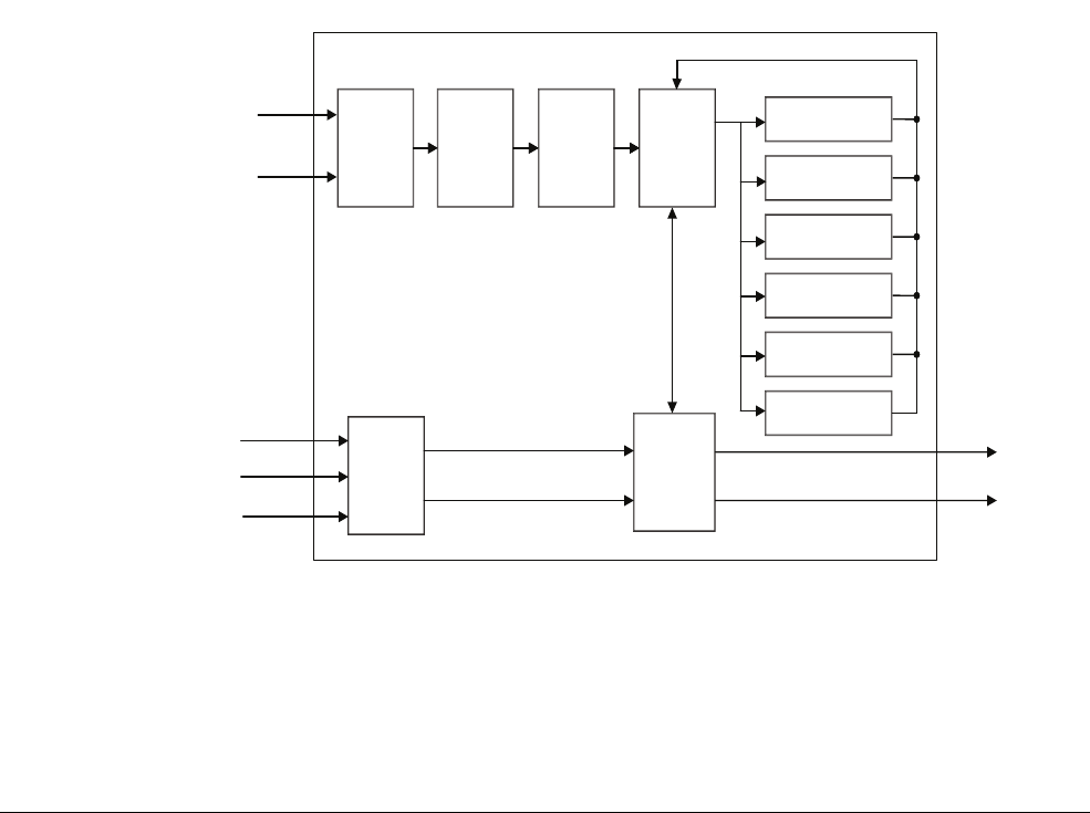
Introducing NEON
ARM DEN0013B Copyright © 2011 ARM. All rights reserved. 19-4
ID082411 Non-Confidential
19.2 NEON architecture overview
NEON has been designed with a powerful yet clean load/store architecture to provide good
vectorizing compiler support from languages such as C/C++. A rich set of new NEON
instructions are defined which operate on wide 64-bit and 128-bit vector registers, which
enables a high level of parallelism. The NEON instructions are straightforward and easy to
understand, which also makes hand-coding easy for applications that need the very highest
performance.
A key advantage of NEON technology is that instructions form part of the normal ARM or
Thumb code, making programming simpler than with an external hardware accelerator. There
are NEON instructions available to read and write external memory, move data between NEON
registers and other ARM registers and to perform SIMD operations.
The NEON architecture uses a 32×64-bit register file. These are actually the same registers used
by the floating-point unit (VFPv3). It does not matter that the floating-point registers are re-used
as NEON registers. All compiled code and subroutines will conform to the EABI, which
specifies which registers can be corrupted and which registers must be preserved. The compiler
is free to use any NEON/VFPv3 registers for floating-point values or NEON data at any point
in the code.
The NEON architecture allows for 64-bit/128-bit parallelism. This choice was made to keep the
size of the NEON unit manageable (a vector ALU can easily become quite large), while still
offering good performance benefits from vectorization. NEON performance on current
implemetations of the Cortex family of processors is summarized in Table 19-1 on page 19-5.
Figure 19-2 Cortex-A8 NEON unit block diagram
The NEON unit of the Cortex-A8 processor is shown in Figure 19-2. A key point to observe is
that we have 128-bit paths for input data from the L1 data and L2 caches, but only a 32-bit path
for data to or from the integer processor registers, limiting the rate at which data can be
transferred between the two.
16-Entry
Instruction
Queue
Decode Score
board
Register
File
12-Entry
Load Data
Queue
Integer ALU
Integer MUL
Integer Shift
FP MUL
FP ADD
IEEE FP
NEON
Instructions
32-bit RegData
128-bit L1 NEON Data
128-bit L2 NEON Data
32-bit RegData
128-bit L1 Data
Load/Store
Permute

Introducing NEON
ARM DEN0013B Copyright © 2011 ARM. All rights reserved. 19-5
ID082411 Non-Confidential
The internal structure of the Cortex-A8 NEON unit is mostly invisible to the programmer. The
function of most blocks in Figure 19-2 on page 19-4 should be obvious. However, the
Scoreboard keeps track of the regiser visibility, while the Load/Store Permute block is
responsible for moving individual data items into the correct locations (as described in NEON
registers on page 19-6).
19.2.1 Commonality with VFP
NEON and Vector Floating-Point (VFP) instructions are both defined as coprocessor CP10 and
CP15 operations (see ARM VFP co-processor on page 18-4). The ARM architecture can support
a wide range of different NEON and VFP options, but in practice we see only the combinations:
• no NEON or VFP
• VFP only
• NEON and VFP.
The key differences between NEON and VFP are that NEON only works on vectors, does not
support double-precision floating-point (double-precision is supported by the VFP), and does
not support certain complex operations such as square root and divide. NEON has a register
bank of thirty-two 64-bit registers. If both NEON and VFPv3 are implemented, this register
bank is shared between them in hardware. This means that VFPv3 must be present in its
VFPv3-D32 form, which has 32 double-precision floating-point registers. This makes support
for context switching simpler. Code which saves and restores VFP context also saves and
restores NEON context.
19.2.2 Data types
NEON instructions operate on elements of the following types:
• 32-bit single precision floating-point
• 8, 16, 32 and 64-bit unsigned and signed integers
• 8 and 16-bit polynomials.
Table 19-1 NEON performance on current implementations
Max NEON
performance
(operations per cycle)
Cortex-A9 Cortex-A8 Cortex-A5
VADD integer elements
(Q reg)
16 (8-bit elements)
8 (16-bit elements)
4 (32-bit elements)
16 (8-bit elements)
8 (16-bit elements)
4 (32-bit elements)
8 (8-bit elements)
4 (16-bit elements)
2 (32-bit elements)
VMLA integer elements
(D or Q reg)
8 (8-bit elements)
4 (16-bit elements)
1 (32-bit elements)
8 (8-bit elements)
4 (16-bit elements)
1 (32-bit elements)
4 (8-bit elements)
4 (16-bit elements)
1 (32-bit elements)
VADD 32-bit
single-precision
(D or Q reg)
221
VMLA 32-bit single
precision
(D or Q reg)
221
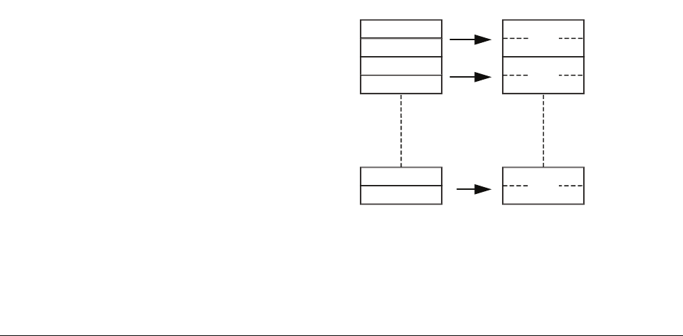
Introducing NEON
ARM DEN0013B Copyright © 2011 ARM. All rights reserved. 19-6
ID082411 Non-Confidential
Data type specifiers in NEON instructions comprise a letter indicating the type of data and a
number indicating the width. They are separated from the instruction mnemonic by a point, for
example,
VMLAL.S8
. So we have the following possibilities:
• unsigned integer U8 U16 U32 U64
• signed integer S8 S16 S32 S64
• integer of unspecified type I8 I16 I32 I64
• floating-point number F16 F32 (or F)
• polynomial over {0,1} P8.
The polynomial type is to help with anything that needs to use power-of-two finite fields or
simple polynomials over {0,1}. Normal ARM integer code would typically use a lookup table
for finite field arithmetic, but large lookup tables cannot be vectorized. Polynomial operations
are hard to synthesize out of other operations, so it is useful having a basic multiply operation
(add is EOR) out of which larger multiplies or other operations can be synthesized.
Applications of polynomial arithmetic can include error correction, such as Reed Solomon
codes, and CRCs (the field operations typically use a polynomial multiply + mod, but this can
be reduced to just multiplies using the Montgomery reduction method). Also elliptic curve
cryptography often uses power-of-type fields.
NEON is IEEE 754-1985 compliant, but only supports round-to-nearest rounding mode. This is
the rounding mode used by most high-level languages, such as C and Java. Additionally, NEON
always treats denormals as zero.
19.2.3 NEON registers
NEON has a unique feature in that the register bank has two views as either sixteen 128-bit
registers (Q0-Q15) or as thirty-two 64-bit registers (D0-D31). Each of the Q0-Q15 registers
maps to a pair of D registers, as shown in Figure 19-3. The view of registers is determined by
the instruction used; software does not have to explicitly change state. NEON views each
register as containing a vector of 1, 2, 4, 8, or 16 elements, each of identical size and type.
Individual elements can also be accessed as scalars.
Figure 19-3 NEON register bank
The advantage of the dual view is that it accommodates mathematical operations which widen
or narrow the result. For example multiplying two D registers gives a Q register result. The
dual-view enables the register bank to be optimized.
D0
D1
D2
D3
D30
D31
Q0
Q1
Q15
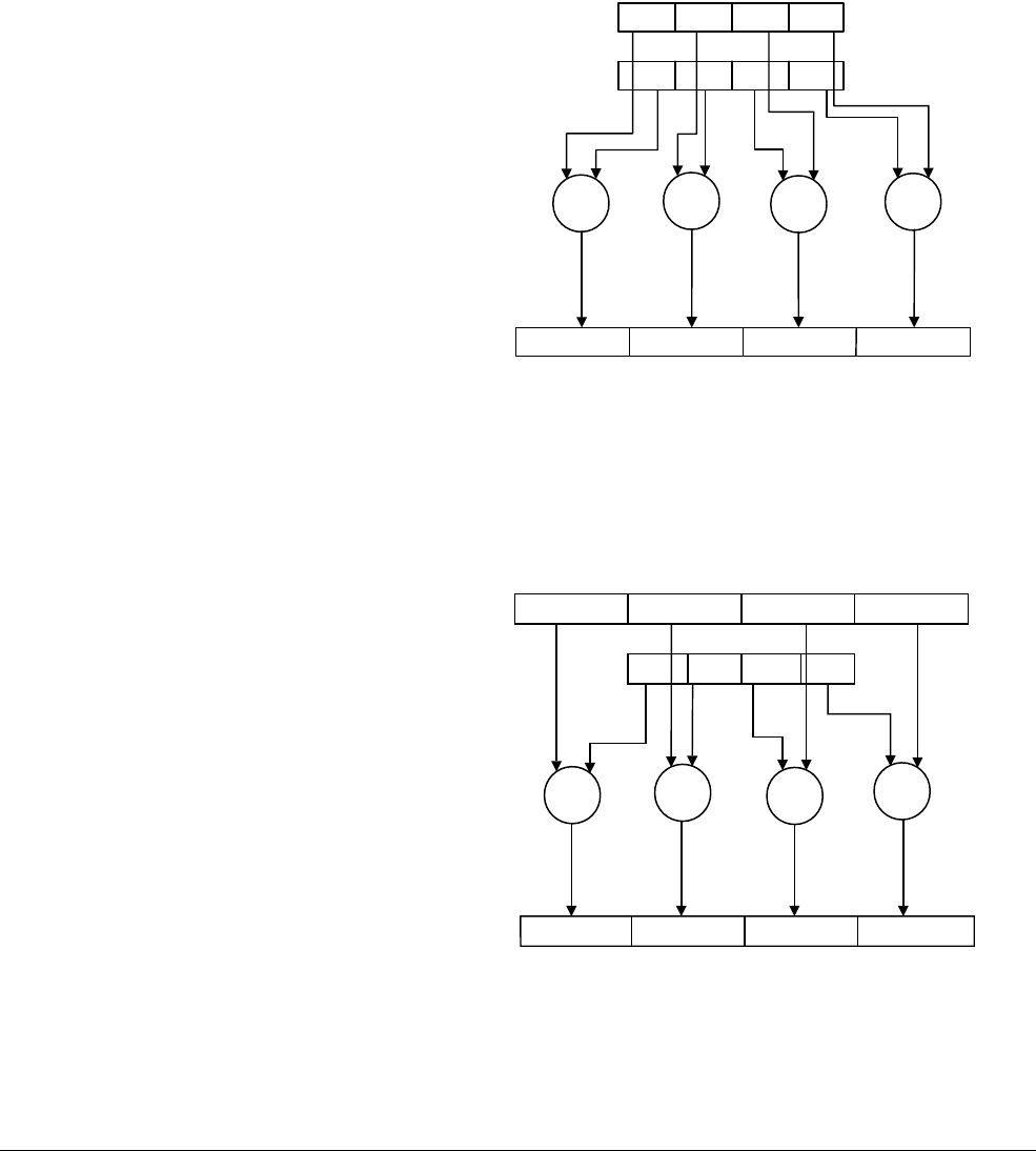
Introducing NEON
ARM DEN0013B Copyright © 2011 ARM. All rights reserved. 19-7
ID082411 Non-Confidential
NEON data processing instructions are typically available in Normal, Long, Wide, Narrow and
Saturating variants.
•Normal instructions can operate on any vector types, and produce result vectors the same
size, and usually the same type, as the operand vectors.
•Long instructions operate on doubleword vector operands and produce a quadword vector
result. The result elements are usually twice the width of the operands, and of the same
type. Long instructions are specified using an L appended to the instruction. Figure 19-4
shows this, with input operands being promoted before the operation.
Figure 19-4 NEON long instructions
•Wide instructions operate on a doubleword vector operand and a quadword vector
operand, producing a quadword vector result. The result elements and the first operand
are twice the width of the second operand elements. Wide instructions have a W appended
to the instruction. Figure 19-5 shows this, with the input doubleword operands being
promoted before the operation.
Figure 19-5 NEON wide instructions
•Narrow instructions operate on quadword vector operands, and produce a doubleword
vector result. The result elements are usually half the width of the operand elements.
Narrow instructions are specified using an N appended to the instruction. Figure 19-6 on
page 19-8 shows this, with input operands being demoted before the operation.
Dn
Dm
Qd
Dn
Qd
Qn
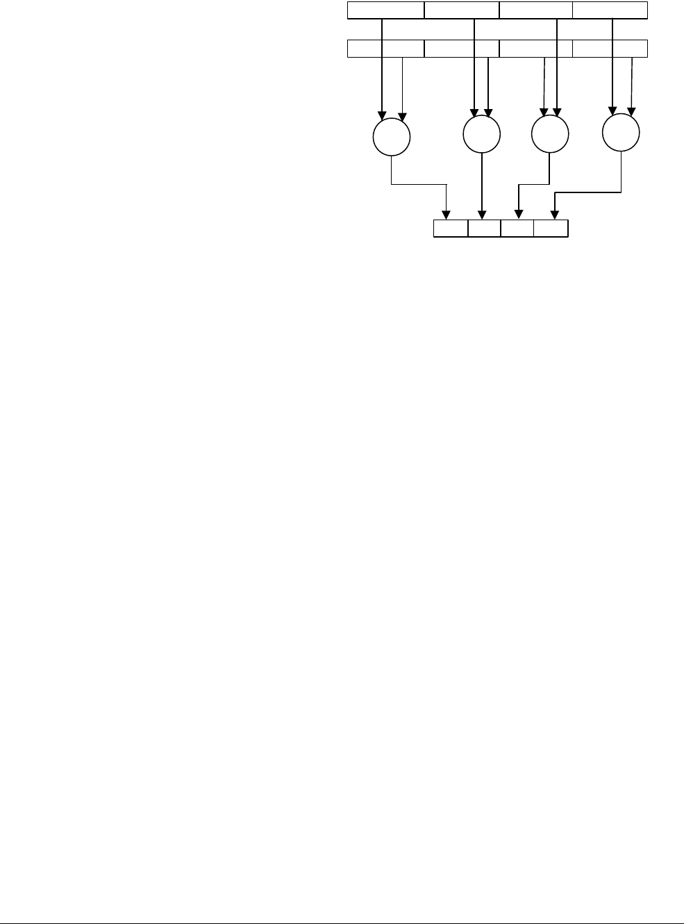
Introducing NEON
ARM DEN0013B Copyright © 2011 ARM. All rights reserved. 19-8
ID082411 Non-Confidential
Figure 19-6 NEON narrow instructions
Some NEON instructions act on scalars together with vectors. The scalars can be 8-, 16-, 32-,
or 64-bit. Instructions which use scalars can access any element in the register bank, although
there are differences for multiply instructions. The instruction uses an index into a doubleword
vector to specify the scalar value. Multiply instructions only support 16-bit or 32-bit scalars, and
can only access the first 32 scalars in the register bank (that is, D0-D7 for 16-bit scalars or
D0-D15 for 32-bit scalars).
19.2.4 NEON instruction set
NEON instructions (as with VFP) all have mnemonics which begin with the letter V.
Instructions are generally able to operate on different data types, with this being specified in the
instruction encoding. The size is indicated with a suffix to the instruction. The number of
elements is indicated by the specified register size.
For example, looking at the instruction
VADD.I8 D0, D1, D2
VADD
indicates a NEON
ADD
operation.
the
I8
suffix indicates that 8-bit integers are to be added
D0
,
D1
and
D2
specify the 64-bit registers used (
D0
for the result destination,
D1
and
D2
for the
operands).
So this instruction performs eight additions in parallel.
There are operations which have different size registers for input and output.
VMULL.S16 Q2, D8, D9
This instruction performs four 16-bit multiplies of data packed in
D8
and
D9
and produces four
32-bit results packed into
Q2
.
The
VCVT
instruction converts elements between single-precision floating-point and 32-bit
integer, fixed-point and half-precision floating-point (if implemented).
NEON includes load and store instructions which can load or store individual or multiple values
to a register. In addition, there are instructions which can transfer blocks of data between
multiple registers and memory. It is also possible to interleave or de-interleave data during such
multiple transfers.
Qn
Qm
Dd

Introducing NEON
ARM DEN0013B Copyright © 2011 ARM. All rights reserved. 19-9
ID082411 Non-Confidential
The following modifiers can be used with certain Advanced SIMD instructions (some modifiers
can be used only with a small subset of the available instructions):
Q This means that the instruction uses saturating arithmetic, so that the result is
saturated within the range of the specified data type. The “sticky” QC bit in the
FPSCR is set if saturation occurs in any lane.
VQADD
is an example of such an
instruction.
H This means that the instruction will halve the result. It does this by shifting right
by one place (effectively a divide by two with truncation).
VHADD
is an example of
such an instruction – it could be used to calculate the mean of two inputs.
D This means that the instruction doubles the result. This is commonly required
when multiplying numbers in Q15 format, where an additional doubling is
needed to get the result into the correct form.
R This means the instruction will perform rounding on the result, equivalent to
adding 0.5 to the result before truncating.
VRHADD
is an example of this.
Instructions have the following general format:
V{<mod>}<op>{<shape>}{<cond>}{.<dt>}(<dest>}, src1, src2
where:
<mod>
is one of the previously described Modifiers (Q, H, D, R)
<op>
- operation (e.g.
ADD
,
SUB
,
MUL
etc.)
<
shape
> - Shape (L, W or N as described in NEON registers on page 19-6)
<
cond
> - Condition, used with
IT
instruction
<
.dt
> - Data type
<
dest
> - Destination
<
src1
> - Source operand 1
<
src2
> - Source operand 2.
The NEON instruction set includes a range of vector addition and subtraction operations,
including pairwise adding, which adds adjacent vector elements together. There are a number
of multiply operations, including multiply-accumulate and multiply-subtract and doubling and
saturating options. There is no SIMD division operation, but such an operation can be performed
using the
VRECPE
(Vector Reciprocal Estimate) and
VCREPS
(Vector Reciprocal Step) instructions
to perform Newton-Raphson iteration. Similarly, there is no vector square root instruction, but
VRSQRTE
,
VRSQRTS
, and multiplies to compute square roots. Shift left, right and insert operations
are also available, along with instructions which select minimum or maximum values. Common
logic operations (
AND
,
OR
,
EOR
,
AND NOT
and
OR NOT
) can be performed. The instruction set also
includes the ability to count numbers of bits set in an element or to count leading zeros or sign
bits.
As SIMD instructions perform multiple operations, they cannot use the standard ALU flags for
comparison instructions. Instead two elements can be compared, with the result of the
comparison in the destination register. The destination element is set to all 0’s if the tested
condition is false or all 1’s if the tested condition is true. This bit mask can then be used to
control subsequent instructions. A number of different comparison operations are supported.
There are bitwise select instructions which can be used in conjunction with these bit masks.

Introducing NEON
ARM DEN0013B Copyright © 2011 ARM. All rights reserved. 19-10
ID082411 Non-Confidential
There are a number of different instructions to move data between registers, or between
elements. It is also possible for instructions to swap or duplicate registers, to perform reversal,
matrix transposition and extract individual vector elements.
Appendix B lists all NEON and VFP instructions and gives a brief description of their function.
Full details for each instruction can also be found in the ARM Architecture Reference Manual.

Introducing NEON
ARM DEN0013B Copyright © 2011 ARM. All rights reserved. 19-11
ID082411 Non-Confidential
19.3 NEON comparisons with other SIMD solutions
The ARMv6 architecture introduced a small set of SIMD instructions which operated on
multiple 16-bit or 8-bit values packed into standard 32-bit general purpose registers. The
mnemonics for these instructions are described in Appendix A and have 8 or 16 appended to the
base form to show the size of data they operate on. Other microprocessor architectures support
similar sets of SIMD operations. For example, the x86 architecture has the MMX multimedia
and SSE Streaming SIMD architecture extensions, while the PowerPC architecture has Altivec.
As readers may be familiar with these solutions, we will briefly compare them with NEON.
19.3.1 NEON compared with a separate DSP
Many ARM SoCs also incorporate a Digital Signal Processor or custom signal processing
hardware, so they can include both NEON and a DSP. There are some differences between using
NEON compared with using a DSP:
NEON features:
• Part of the ARM processor pipeline.
• Uses ARM register file for memory addressing.
• Single thread of control providing easier development and debug.
• OS multitasking supported (if OS already saves/restores VFPv3-D32 registers).
Table 19-2 NEON compared with MMX and Altivec
NEON x86 MMX/SSE Altivec
Unaligned
access
Yes aSignificant penalty if not
16-byte aligned, except certain
specific new instructions
(LDDQU)
No unaligned support
Number of
registers
32×64-bit (dual
view as
16×128-bit)
SSE2: 8×128-bit XMM (in
x86-32 mode; additional 8
registers in x86-64 mode
32×128-bit
Memory /
register
operations
Register-based
3-operand
instructions
Mix of register and memory
operations
Register-based 3- and 4-operand
instructions
Load/store
support for
packed data
types
Yes: 2,3,4 element No No
Move
between
scalar and
vector register
Yes Yes N o
Floating-point
support?
Single-precision Single-precision,
Double-precision
Single-precision
a. Vector load and stores can be optimized, where the memory access is aligned to a specified boundary. This is
done by adding an alignment qualifier to an instruction for example @64 or @128 (or :64 or :128 on GNU),
to specify alignment to a 64 or 128 bit boundary. This can improve performance by reducing the number of
cycles used to access memory. When an alignment qualifier is specified, the processor will take an alignment
fault exception if the address used for the access is not aligned to the specified boundary. See also Alignment
on page 20-7.

Introducing NEON
ARM DEN0013B Copyright © 2011 ARM. All rights reserved. 19-12
ID082411 Non-Confidential
• SMP capability. There is one NEON unit per ARM processor within an MPCore. This
provides up to N× performance using standard “pthreads”.
• As part of the ARM processor architecture, NEON will be available on future faster
processors and is supported by many ARM processor based SoCs.
• Broad NEON tools support is provided in both the open-source community and the ARM
ecosystem.
DSP features:
• Runs in parallel with ARM processors.
• Lack of OS and task switching overhead can provide guaranteed performance, but only if
DSP system design provides predictable performance.
• Generally more difficult to use by applications programmers: two toolsets, separate
debugger, potential synchronization issues.
• Less tightly integrated with the ARM processor. Can be some cache clean/flush overhead
with transferring data between DSP and the ARM processor. It makes using a DSP less
efficient for processing very small blocks of data.

ARM DEN0013B Copyright © 2011 ARM. All rights reserved. 20-1
ID082411 Non-Confidential
Chapter 20
Writing NEON Code
Support for NEON is provided in the ARM Compiler toolchain and in GNU tools. When writing
assembly code with the GNU tools, you must use the
-mfpu=neon
option to specify that the hardware
supports NEON. In the ARM Compiler, you specify a target which supports NEON, for example,
by using
--cpu=Cortex-A5
.

Writing NEON Code
ARM DEN0013B Copyright © 2011 ARM. All rights reserved. 20-2
ID082411 Non-Confidential
20.1 NEON C Compiler and assembler
Code targeted at NEON hardware can be written in C and/or in assembly language and a range
of tools and libraries is available to support this.
In many cases, it may be preferable to use NEON code within a larger C/C++ function, rather
than in a separate file to be processed by the assembler. This can be done using the intrinsics,
described in Section 20.1.3.
20.1.1 Vectorization
A vectorizing compiler can take your C or C++ source code and parallelize it in a way which
enables efficient usage of NEON hardware. This means you can write portable C code, while
still obtaining the levels of performance made possible by NEON. The C language does not
specify parallelizing behavior, so it can be necessary to provide hints to the compiler about this.
For example, it may be necessary to use the
__restrict
keyword when defining pointers. This
has the effect of guaranteeing that pointers will not overlap regions of memory. It can also be
necessary to ensure that the number of loop iterations is a multiple of four or eight. Automatic
vectorization is specified with the GCC option -
ftree-vectorize
(along with
–mfpu=neon
). Using
the ARM Compiler, you must specify optimization level
–O2
(or
–O3
),
-Otime
and
–-vectorize
.
20.1.2 NEON libraries
There is much free open source software which makes use of NEON, for example:
• OpenMAX, a set of APIs for processing audio, video, and still images. It is part of a
standard created by the Khronos group. ARM has a free implementation of the OpenMAX
DL layer for NEON.
• ffmpeg, a collection of codecs for many different audio/video standards under LGPL
license.
• Eigen2, a linear algebra/matrix math C++ template library.
• Pixman, a 2D graphics library (part of Cairographics).
• x264, a GPL H.264 encoder.
• Math-neon.
20.1.3 Intrinsics
NEON C/C++ intrinsics are available in armcc, GCC/
g++
, and
llvm
. They use the same syntax,
so source code that uses intrinsics can be compiled by any of these compilers.
NEON intrinsics are a way to write NEON code that is more easily maintained than assembler,
while still keeping control of the NEON instructions which are generated. There are new data
types that correspond to NEON registers (both D-registers and Q-registers) containing different
sized elements, allowing C variables to be created that map directly onto NEON registers. These
variables are passed to NEON intrinsic functions. The compiler will generate NEON
instructions directly instead of performing an actual subroutine call.
NEON intrinsics provide low-level access to NEON instructions but with the compiler doing
some of the hard work normally associated with writing assembly language, such as:
• Register allocation.

Writing NEON Code
ARM DEN0013B Copyright © 2011 ARM. All rights reserved. 20-3
ID082411 Non-Confidential
• Code scheduling, or re-ordering instructions to get highest performance. The C compilers
are aware of which processor is being targeted, and they can reorder code to ensure the
minimum number of stalls.
The main disadvantage with intrinsics is that it is not possible to get the compiler to output
exactly the code you want, so there is still some possibility of improvement when moving to
NEON assembler code.
20.1.4 NEON types in C
The ARM Compiler Toolchain Assembler Reference contains a full list of NEON types. The
format is:
<basic type>x<number of elements>_t
There are also further types, which combine two, three or four of each of the above, into a larger
struct
type. These types are used to map the registers accessed by NEON load/store operations,
which can load/store up to four registers with a single instruction. For example:
struct int16x4x2_t
{
int16x4_t val[2];
}<var_name>;
These types are only used by loads, stores, transpose, interleave and de-interleave instructions;
to perform operations on the actual data, the individual registers would be selected using, for
example,
<var_name>.val[0]
and
<var_name>.val[1]
in the example above.
20.1.5 Variables and constants in NEON
In this section we show some example code to access variable or constant data using NEON.
Table 20-1 NEON type definitions
64-bit type (D-register) 128-bit type (Q-register)
int8x8_t int8x16_t
int16x4_t int16x8_t
int32x2_t int32x4_t
int64x1_t int64x2_t
uint8x8_t uint8x16_t
uint16x4_t uint16x8_t
uint32x2_t uint32x4_t
uint64x1_t uint64x2_t
float16x4_t float16x8_t
float32x2_t float32x4_t
poly8x8_t poly8x16_t
poly16x4_t poly16x8_t

Writing NEON Code
ARM DEN0013B Copyright © 2011 ARM. All rights reserved. 20-4
ID082411 Non-Confidential
Declaring a variable
Declaring a new variable is as simple as declaring any variable in C:
uint32x2_t vec64a, vec64b; // create two D-register variables
Using constants
Using constants is straightforward. The following code will replicate a constant into each
element of a vector:
uint8x8 start_value = vdup_n_u8(0);
To load a general 64-bit constant into a vector, use:
uint8x8 start_value = vreinterpret_u8_u64(vcreate_u64(0x123456789ABCDEFULL));
Moving results back to normal C variables
To access a result from a NEON register, we can either store it to memory using VST, or move
it back to ARM using a “get lane” type operation:
result = vget_lane_u32(vec64a, 0); // extract lane 0
This MRC operation can have some performance impact, particularly on the Cortex-A8
processor.
Accessing two D-registers of a Q-register
This can be done using
vget_low
and
vget_high
, as below:
vec64a = vget_low_u32(vec128); // split 128 bit vector
vec64b = vget_high_u32(vec128); // into 2x 64 bit vectors
Casting NEON variables between different types
NEON intrinsics are strongly typed, so they must be cast between vectors of different types.
This is done using
vreinterpret
, which doesn’t actually generate any code, but just enables you
to cast the NEON types:
uint8x8_t byteval;
uint32x2_t wordval;
byteval = vreinterpret_u8_u32(wordval);
Note that the destination type,
u8
is listed first after
vreinterpret
.
20.1.6 NEON assembler and ABI restrictions
For the very highest performance, hand-coded NEON assembler is the best approach for
experienced programmers. This requires familiarity with the pipeline and cycle timings of the
specific ARM processor that is being used, to ensure maximum throughput. Both GNU
Assembler
(gas
) and ARM
armasm
support assembly of NEON instructions.
When writing assembler functions, you must be aware of the ARM EABI which defines how
registers can be used.

Writing NEON Code
ARM DEN0013B Copyright © 2011 ARM. All rights reserved. 20-5
ID082411 Non-Confidential
The ARM EABI (Embedded Application Binary Interface) specifies which registers are used to
pass parameters, return results, or must be preserved. This specifies the usage of 32 D-registers
in addition to the ARM integer registers and is summarized in Table 20-2.
Typically, data values are not actually passed to a NEON subroutine, so the best order to use
NEON registers is D0-D7, then D15-D31 (then finally D8-D15 only if saved). See also VFP and
NEON register usage on page 15-4.
20.1.7 Detecting NEON
As NEON hardware can be omitted from a processor implementation, it may be necessary to
test for its presence.
Build-time NEON detection
This is the easiest way to detect NEON. In armcc (RVCT 4.0 and later), or GCC, the predefined
macro
__ARM_NEON__
is defined when a suitable set of processor and FPU options is provided to
the compiler. The armasm equivalent predefined macro is
TARGET_FEATURE_NEON
.
This could be used to have a C source file which has both NEON and non-NEON optimized
versions.
Run-time NEON detection
To detect NEON at run-time requires help from the operating system, since the ARM
architecture intentionally does not expose processor capabilities to user-mode applications.
Under Linux,
/proc/cpuinfo
contains this information in human-readable form.
On Tegra2 (a dual-core Cortex-A9 processor with FPU),
cat /proc/cpuinfo
reports:
…
Features : swp half thumb fastmult vfp edsp thumbee vfpv3 vfpv3d16
…
The ARM quad-core Cortex-A9 processor with NEON gives a different result:
…
Features : swp half thumb fastmult vfp edsp thumbee neon vfpv3
…
As the
/proc/cpuinfo
output is text based, it is often preferred to look at the auxiliary vector
/proc/self/auxv
. This contains the kernel
hwcap
in a binary format. The
/proc/self/auxv
file can
be easily searched for the
AT_HWCAP
record, to check for the
HWCAP_NEON
bit (4096).
Some Linux distributions (for example, Ubuntu 09.10, or later) take advantage of NEON
transparently. The
ld.so
linker script is modified to read the
hwcap
via
glibc
, and add an
additional search path for NEON-enabled shared libraries. In the case of Ubuntu, a new search
path
/lib/neon/vfp
contains NEON-optimized versions of libraries from
/lib
.
Table 20-2 ARM EABI NEON register use
D0-D7 Argument registers / return value (can
be corrupted if not required)
D8-D15 callee-saves registers
D15-D31 caller-save register

Writing NEON Code
ARM DEN0013B Copyright © 2011 ARM. All rights reserved. 20-6
ID082411 Non-Confidential
20.2 Optimizing NEON assembler code
To obtain best performance from hand-written NEON code, it is necessary to be aware of some
underlying hardware features. In particular, the programmer should be aware of pipelining and
scheduling issues, memory access behavior and scheduling hazards. We will briefly describe
each of these here.
20.2.1 NEON pipeline differences between Cortex-A processors
Although there are some small differences in how it is integrated into the processor pipeline, the
Cortex-A8 and Cortex-A9 processors share the same basic NEON pipelines. The Cortex-A5
processor contains a simplified NEON execution pipeline which is fully compatible, but is
designed for the smallest and lowest-power implementation possible.
20.2.2 Memory access optimizations
It is likely NEON will be processing large amounts of data, such as digital images. One
important optimization is to make sure the algorithm is accessing the data in the most
cache-friendly way possible. This gets the maximum hit rate from the L1 and L2 caches. It is
also important to consider the number of active memory locations. Under Linux, each 4KB page
will require a separate TLB entry. The Cortex-A9 processor has 32 element micro-TLBs and a
128-element main TLB, after which it will start using the L1 cache to load page table entries. A
typical optimization is to arrange the algorithm to process image data in suitably sized “tiles” in
order to maximize the cache and TLB hit rate. In general, the memory optimization
considerations described in Chapter 17 will also apply to NEON code.
The instructions which support interleaving and de-interleaving can provide significant scope
for performance improvements. VLD1 loads registers from memory, with no de-interleaving.
However, the other VLD operations allow us to load, store and de-interleave structures
containing two, three or four equally sized 8-, 16- or 32-bit elements. VLD2 loads two or four
registers, de-interleaving even and odd elements. This could, for example, be used to split stereo
audio data. Similarly, VLD3 could be used to split RGB pixels into separate channels and
correspondingly, VLD4 might be used with ARGB images.
Figure 20-1 Labeled example of load de-interleaving
0
VLD2.16 {D0, D1}, [R1]
L0
R1 offset 4
8
R0
L1
R1
L2
2
6
D0
D1
Memory NEON Registers
R0
R1
R2R3
L0
L1
L2L3

Writing NEON Code
ARM DEN0013B Copyright © 2011 ARM. All rights reserved. 20-7
ID082411 Non-Confidential
Figure 20-1 on page 20-6 shows loading two NEON registers with VLD2.16, from memory
pointed to by R1. This produces four 16-bit elements in the first register, and four 16-bit
elements in the second, with adjacent paired left and right values separated to each register.
20.2.3 Alignment
The NEON architecture provides full unaligned support for NEON data access. However, the
instruction opcode contains an “alignment hint” which permits implementations to be faster
when the address is aligned and a hint is specified.
The base address specified as
[<Rn>:<align>]
Note
It is a programming error to specify a hint, but to then use an incorrectly aligned address.
An alignment hint can be one of :64, :128 or :256 bits depending on the number of D-regs. The
ARM Architecture Reference Manual uses an “@” symbol to describe this, but this is not
recommended in source code.
Note
The GNU gas assembler will still accept [Rn,:128] syntax (note the extra “,” before the colon)
but [Rn:128] syntax is preferred.
20.2.4 Scheduling
To get the very best performance with NEON, you should be aware of how to schedule code for
the specific ARM processor you are using. Careful hand-scheduling is recommended to get the
best out of any NEON assembler code you write, especially for performance-critical
applications such as video codecs.
If writing C or NEON intrinsics, the compiler (GCC or armcc) will automatically schedule code
from NEON intrinsics or vectorizable C source code, but it can still help to make the source code
as friendly as possible to scheduling optimizations.
Result-use scheduling
This is the main performance optimization when writing NEON code. NEON instructions
typically issue in one cycle, but the result is not always ready in the next cycle except for the
simplest NEON instructions, such as
VADD
and
VMOV
.
In some cases there can be a considerable latency, particularly
VMLA
multiply-accumulate (five
cycles for an integer; seven cycles for a floating-point). Code using these instructions should be
optimized to avoid trying to use the result value before it is ready, otherwise a stall will occur.
Despite having a few cycles result latency, these instructions do fully pipeline so several
operations can be “in flight” at once.
The resulting latency is the same between the Cortex-A8 and Cortex-A9 processors for the
majority of instructions. The Cortex-A5 processor uses a simplified NEON design more tailored
to reduced power and area implementation, and most NEON instructions have a three-cycle
result latency.

Writing NEON Code
ARM DEN0013B Copyright © 2011 ARM. All rights reserved. 20-8
ID082411 Non-Confidential
Dual-issue scheduling
On the Cortex-A8 processor, certain types of NEON instruction can be issued in parallel (in one
cycle). A load/store, permute or
MCR
/
MRC
type instruction can be dual issued with a NEON
data-processing instruction, such as a floating-point add or multiply, or a NEON integer ALU,
shift or multiply-accumulate. Programmers may be able to save cycles by ordering code to take
advantage of this.
20.2.5 Cortex-A8 specific ARM-NEON memory and NEON-ARM pipeline hazards
The Cortex-A8 NEON coprocessor operates several pipeline stages after the ARM integer
pipeline. It receives instructions from the ARM pipeline through a FIFO. Transfer of data from
ARM to NEON is quick, but moving data from the NEON pipeline to ARM using an MRC takes
20 cycles.
NEON also has its own load/store unit separate from that of the ARM, with scope to bypass the
level 1 cache. To avoid data hazards due to out-of-order memory accesses, there is special
hardware to detect such cases and to resolve them. If both NEON and ARM units perform loads
and/or stores to addresses within the same cache line, a delay of around 20 cycles is required to
resolve ordering issues.
These delays can be avoided with careful coding. Firstly, we must try to minimize a combination
of ARM memory accesses and NEON memory accesses to the same region of memory. It can
still be sensible to store a NEON result to memory and then load the result into an ARM register
from memory. If we don’t need the result immediately, it should be possible to hide the 20 cycle
latency by having the ARM do some other work before it attempts the load. This is better than
using direct NEON to ARM register transfer, which always incurs a penalty because the
Cortex-A8 pipeline stalls.
Most compilers use a
softfp
calling convention to pass arguments and return values in ARM
integer registers. To return a
float
value therefore requires passing a value from a NEON
register into ARM registers, incurring the 20 cycle delay. A way to avoid this problem is to try
to inline such functions.
Conditional branches which depend upon floating-point values can also incur this penalty.
Although the floating-point unit has its own logic to evaluate comparisons and set flags, the
contents of this register must be transferred to the ARM to take a conditional branch and this
incurs a penalty.

Writing NEON Code
ARM DEN0013B Copyright © 2011 ARM. All rights reserved. 20-9
ID082411 Non-Confidential
20.3 NEON power saving
Not all code can benefit from NEON. It depends to a large extent how data-intensive an
application is and whether the algorithm can operate on multiple values in parallel. In a typical
mobile device, NEON will be in a different power domain to the main processor core, which
allows it to be powered off when not in use. This can save significant power because NEON is
often used intensively by applications (for example, real-time multi-media processing) or not at
all. Mobile devices can spend significant amounts of time in standby with the clocked stopped,
and it makes sense to ensure NEON is powered down then, as well.
The power saving mechanism is implemented by the OS, and is expected to be transparent to
the user application. Typically the OS will turn off NEON after a period of non-activity, and
turning on again when there is an exception caused by attempting to execute a NEON
instruction.
NEON power-down sequence (performed by the operating system):
1. Disable NEON (for example, setting the Cortex-A9 processor
ASEDIS
to 1).
2. Remove power to the NEON region (SoC specific).
If a NEON instruction is executed when NEON is disabled, the processor will take an
“undefined instruction” exception (as would any coprocessor if the coprocessor is disabled).
The OS “undefined instruction” handler would detect that a NEON instruction (CP10 or CP11)
has caused the exception and would execute the power-on sequence:
1. Restore power supply (SoC specific) and wait for the power to stabilize.
2. Enable NEON (for example, setting the Cortex-A9 processor
ASEDIS
to 0).
3. Re-execute the instruction.

ARM DEN0013B Copyright © 2011 ARM. All rights reserved. 21-1
ID082411 Non-Confidential
Chapter 21
Power Management
Many ARM systems are mobile devices, powered by batteries. In such systems, optimization of
power usage (in fact, it would be more accurate to look at total energy usage) is a key design
constraint. Programmers often spend significant amounts of time trying to save battery life in such
systems. Power-saving can also be of concern even in systems which do not use batteries. For
example, we may wish to minimize energy usage for reduction of electricity costs to the consumer
or for environmental reasons.
Built in to ARM processors are many hardware design methods aimed at reducing power usage. In
this chapter, we will focus on the features available to the programmer to reduce processor power
consumption. Before we do so, let’s review the components of processor energy usage.
Energy usage can be divided into two components – dynamic and static. Both are important. Static
power consumption occurs whenever the processor logic or RAM blocks have power applied to
them. In general terms, the leakage currents are proportional to the total silicon area – the bigger
the chip, the more the leakage. The proportion of power consumption due to leakage gets
significantly higher as we move to more advanced manufacturing process – they are much worse
on fabrication geometries of 130nm and below. Dynamic power consumption occurs due to
transistors switching and is a function of the processor clock speed and the numbers of transistors
which change state per cycle. Clearly, higher clock speeds and more complex processors will
consume more power.

Power Management
ARM DEN0013B Copyright © 2011 ARM. All rights reserved. 21-2
ID082411 Non-Confidential
21.1 Power and clocking
One way in which we can reduce energy usage is to remove power, which removes both
dynamic and static currents (sometimes called power gating) or to stop the clock of the
processor which removes dynamic power consumption only and can be referred to as clock
gating.
ARM processors typically support a number of levels of power management, as follows:
• Run (Normal operation)
• Standby
• Shutdown
• Dormant.
In this chapter, we will examine each of these in turn and understand how each saves power. We
will also look at the latency associated with each of these modes. For certain operations, there
is a requirement to save and restore state before and after removing power and the time taken to
do this can be an important factor in software selection of the appropriate power management
activity.
The SoC device which includes the ARM processor can have further low power states, with
names such as “STOP” and “Deep sleep.” These refer to the ability for the hardware Phase
Locked Loop (PLL) and voltage regulators to be controlled by power management software.
21.1.1 Standby mode
In the standby mode of operation, the device is left powered-up, but most of its clocks are
stopped, or clock-gated. This means that almost all parts of the processor are in a static state and
the only power drawn is due to leakage currents and the clocking of the small amount of logic
which looks out for the wake-up condition.
This mode is entered using either the
WFI
(Wait For Interrupt) or
WFE
(Wait For Event)
instructions, which we’ll take a more detailed look at in a moment. We recommend use of a DSB
memory barrier before
WFI
or
WFE
, to ensure that pending memory transactions complete.
If a debug channel is active, it will remain active. The processor stops execution until a wakeup
event is detected. The wakeup condition is dependent on the entry instruction. For
WFI
an
interrupt or external debug request will wake the processor. For
WFE
, a number of specified
events exist, including another processor in an MP system executing the
SEV
instruction. A
request from the Snoop Control Unit (SCU) can also wake up the clock for a cache coherency
operation in an MP system. This means that the cache of a processor which is in standby state
will continue to be coherent with caches of other processors. A processor reset will always force
the processor to exit from the standby condition.
Various forms of dynamic clock gating can also be implemented in hardware. For example the
SCU, GIC, timers, CP15, instruction pipeline and/or NEON blocks can be automatically clock
gated when an idle condition is detected, to save power.
Standby mode can be entered and exited quickly (typically a two-clock-cycle wake-up). It
therefore has an almost negligible affect on the latency and responsiveness of the processor.

Power Management
ARM DEN0013B Copyright © 2011 ARM. All rights reserved. 21-3
ID082411 Non-Confidential
21.1.2 Dormant mode
In dormant mode, the actual processor logic is powered down, but the cache RAMs are left
powered up. Often the RAMs will be held in a low-power retention state where they hold their
contents but are not otherwise functional. This provides a far faster restart than complete
shutdown, as live data and code persists in the caches. Again, in a multi-processor system,
individual processors can be placed in dormant mode.
In an MPCore system which allows individual processors within the SMP cluster to go into
dormant mode, there is no scope for maintaining coherency while the processor has its power
removed. Such processors must therefore first isolate themselves from the coherence domain.
(Of course, in an AMP system, they may already not be coherent.) They will clean all dirty data
before doing this and will be typically be woken up via another processor telling the external
logic to re-apply power. The woken processor will then need to restore the original processor
state before rejoining the coherency domain. As the memory state may have changed while the
processor was in dormant mode, it might well need to invalidate the caches anyway. Dormant
mode is therefore much more likely to be useful in a single processor environment rather than
in a multi-processor set-up. In an MPCore cluster, dormant mode is typically likely to be used
only by the last processor when the other processors have already been shutdown.
21.1.3 Assembly language power instructions
ARM assembly language includes instructions which can be used to place the processor in a low
power state. The architecture defines these instructions as “hints” – the processor is not required
to take any specific action when it executes them. In the Cortex-A processor family, however,
these instructions are implemented in a way which shuts down the clock to almost all parts of
the processor. This means that the power consumption of the processor is significantly reduced
– only static leakage currents will be drawn, and there will be no dynamic power consumption.
The
WFI
instruction has the effect of suspending execution until the processor is “woken up” by
one of the following conditions:
• an IRQ interrupt (even if CPSR I-bit is set)
• an FIQ interrupt (even if CPSR F-bit is set)
• an Imprecise Data abort
• a Debug Entry request (even if JTAG Debug is disabled).
In the event of the processor being woken by an interrupt when the relevant CPSR interrupt flag
is disabled, the processor will implement the next instruction after
WFI
. On older versions of the
ARM architecture, the wait for interrupt function (also called standby mode) was accessed using
a CP15 operation, rather than a dedicated instruction.
The
WFI
instruction is widely used in systems which are battery powered. For example, mobile
telephones can place the processor in standby mode many times a second, while waiting for the
user to press a button.
WFE
is similar to
WFI
. It suspends execution until an event occurs. This can be one the events listed
above, or an additional possibility – an event signaled by another processor in an MPCore. Other
processors can signal events by executing the
SEV
instruction.
SEV
signals an event to all
processors in a multi-processor system. We will describe
WFE
further when we look at
multi-processor systems.

Power Management
ARM DEN0013B Copyright © 2011 ARM. All rights reserved. 21-4
ID082411 Non-Confidential
21.1.4 Dynamic Voltage/Frequency Scaling
Many systems operate under conditions where their workload is very variable. It would be
useful to have the ability to reduce or increase the processor performance to match the expected
processor workload. If we could clock the processor more slowly when it is less busy, we could
save dynamic power consumption. The dynamic power consumption has a linear correlation
with clock frequency, but a quadratic relationship with voltage (it is proportional to the square
of the supply voltage).
If the processor is running more slowly, it is also the case that its supply voltage can be reduced
somewhat (but not past the point where it can no longer operate correctly at the reduced clock
frequency). This hardware approach is called Dynamic Voltage and Frequency Scaling (DVFS).
The advantage of reducing supply voltage is that it reduces both dynamic and static power.
Compared to the alternative of running fast, then entering standby, then running fast and so
forth, the approach of running slowly at a lower supply can save energy. To do this successfully
requires two difficult engineering problems to be solved. The SoC needs a way in which
software running on the ARM processor can reliably modify the clock speed and supply voltage
of the processor, without causing problems in the system. (This needs things like voltage
level-shifters and split power supplies on chip to cope with the variable supply, plus
synchronizers between voltage domains to cope with timing changes.) Of equal importance is
the ability of software running in the system to make accurate predictions about future
workloads to set the voltage and clock speed accordingly.

ARM DEN0013B Copyright © 2011 ARM. All rights reserved. 22-1
ID082411 Non-Confidential
Chapter 22
Introduction to Multi-processing
In the chapters that follow we look at systems with multiple processors and examine programming
techniques for these. We distinguish between systems that contain multiple separate processor
elements (a majority of today’s embedded systems) and true multi-processors, with multiple
processors closely coupled together in hardware. We will introduce terminology to describe and
categorize such systems, in terms of both hardware and software and we look at some example
ARM implementations.
Multi-processing can be defined as running two or more sequences of instructions within a device
containing two or more processors. The concept of multi-processing has been a subject of research
for a number of decades, and has seen widespread commercial use over the past 15 years.
Multi-processing is now a widely adopted technique in both systems intended for general-purpose
application processors and in areas more traditionally defined as embedded systems.
Multi-processing systems can deliver higher performance, due to the simple fact that more
processing units are available. This allows multiple tasks to be executed in parallel, potentially
reducing the amount of time required to perform the allocated task.
The overall energy consumption of a multi-core system can be significantly lower than that of a
system based on a single processor core. Multiple cores allow execution to be completed faster and
so some elements of the system might be completely powered down for longer periods.
Alternatively, a system with multiple cores may be able to operate at a lower frequency than that
required by a single processor to achieve the same throughput. A lower power silicon process
and/or a lower supply voltage can result in lower power consumption and reduced energy usage.
Note that most current systems do not allow the frequency of cores to be changed on an individual
basis. However, each core can be dynamically clock gated, giving further power/energy savings.

Introduction to Multi-processing
ARM DEN0013B Copyright © 2011 ARM. All rights reserved. 22-2
ID082411 Non-Confidential
Multi-core systems also add flexibility and scalability to system designs. A system that contains
one or two cores could be scaled up for more performance by adding further cores, without
requiring redesign of the whole system or significant changes to software.
Having multiple cores at our disposal also allows more options for system configuration. For
example, we might have a system which uses separate cores – one to handle a hard real-time
requirement and another for an application requiring high, uninterrupted performance. These
could be consolidated into a single multi-processor system.
A multi-core device is also likely to be more responsive than one with a single core. When
interrupts are distributed between cores there will be more than one core available to respond to
an interrupt and fewer interrupts per core to be serviced. Multiple cores will also allow an
important background process to progress simultaneously with an important but unrelated
foreground process.
Multi-core systems can also extract more performance from high latency memory systems (for
example, DDR memory) by allowing a memory controller to queue up and optimize requests to
the memory. Processors working on coherent data can benefit from reductions in
linefills/evictions. When the data is not shared, the result is likely to be negative. An L2 cache
can mean improved utilization for shared memory regions (including file caches), shared
libraries and kernel code. Of course, if the number of cores is increased and they are not sharing
code or data, then without a corresponding increase in memory bandwidth performance will
instead go down.
In the past, much software was written to operate within the context of a single processor. Some
operating systems provide support for time-slicing. this gives the illusion of multiple
processes/tasks running simultaneously. It is important to clearly understand the difference
between multi-threading (for example POSIX threads, or Java) and multi-processing. A
multi-threaded application can be run on a single core, but only with multi-processing can the
threads truly execute in parallel.
Migrating multi-threaded software from a single processor system to a multi-processing one can
trigger problems with incorrect programs that could not be exposed by running the same
program time-sliced on a single processor. It can also cause very infrequent bugs to become very
frequently triggered. What it cannot do is to cause correctly written multi-threaded programs to
misbehave – only expose previously unnoticed errors.
Introduction to Multi-processing
ARM DEN0013B Copyright © 2011 ARM. All rights reserved. 22-3
ID082411 Non-Confidential
22.1 Multi-processing ARM systems
From early in the history of the architecture, ARM processors were likely to be implemented in
systems which contained other processors. This commonly meant a heterogeneous system,
perhaps containing an ARM plus a separate DSP processor. Such systems have different
software executing on different cores and the individual processors can have differing privileges
and views of memory. Many widely used ARM systems (for example, TI’s OMAP series, or
Freescale’s i.MX) provide examples of this.
Figure 22-1 Example of a system with multiple processors
We can distinguish between systems which contain:
• a single processor
• multiple processors (such as that shown in Figure 22-1), which contain multiple
independent processing elements
• a multi-core processor, which contain multiple cores capable of independent instruction
execution, which can be externally viewed like a single unit, either by the system designer
or by an operating system that can abstract the underlying resources from the application
layer. In this chapter (and those which follow), we will focus on such processors.
ARM was among the first companies to introduce such multi-core processors to the
System-on-Chip market, when it introduced the ARM11MPCore processor, in 2004. The
Cortex-A5MPCore and Cortex-A9MPCore processors described in this book provide further
examples of such systems.
An ARM MPCore processor can contain between one and four processing cores. Each core can
be individually configured to take part (or not) in a data cache coherency management scheme.
A Snoop Control Unit (SCU) device inside the processor has the task of automatically
maintaining cache coherency, between cores within the processor without software intervention.
ARM MPCore processors include an integrated Interrupt Controller. Multiple external interrupt
sources can be independently configured to target one or more of the individual processor cores.
Furthermore, each core is able to signal (or broadcast) any interrupt to any other core or set of
Memory System
Cortex-A9 Mali-400 DSP
Introduction to Multi-processing
ARM DEN0013B Copyright © 2011 ARM. All rights reserved. 22-4
ID082411 Non-Confidential
cores in the system, from software (software triggered Interrupts). These mechanisms allow the
OS to share and distribute the interrupts across all cores and to coordinate activities using the
low-overhead signaling mechanisms provided.
Cortex-A MPCore processors also provide hardware mechanisms to accelerate OS kernel
operations such as system wide cache and TLB maintenance operations. (This feature is not
found in the ARM11MPCore.)
In summary, each of the Cortex-A series MPCore processors can have the following features:
• configurable between one and four cores (at design time)
• data cache coherency
• integrated interrupt controller
• local timers and watchdogs
• (optional) Accelerator Coherency Port (ACP).
Figure 22-2 shows the structure of the Cortex-A9 MPCore. We will describe each of these
features in more detail in the course of this chapter and those which follow.
Figure 22-2 Cortex-A9 MPCore
CoreSight MultiCore Debug and Trace Architecture
Generic Interrupt
Control and
Distribution
Snoop Control Unit (SCU)
Cache-to-Cache
Transfers
Snoop
Filtering Timers
Accelerator
Coherency
Port
Advanced Bus Interface Unit
Primary AMBA3 64-Bit Interface Optional 2nd I/F with Address Filtering
FPU/
NEON
PTM
I/F
Cortex-A9
processor
I-
Cache
D-
Cache
FPU/
NEON
PTM
I/F
Cortex-A9
processor
I-
Cache
D-
Cache
FPU/
NEON
PTM
I/F
Cortex-A9
processor
I-
Cache
D-
Cache
FPU/
NEON
PTM
I/F
Cortex-A9
processor
I-
Cache
D-
Cache

Introduction to Multi-processing
ARM DEN0013B Copyright © 2011 ARM. All rights reserved. 22-5
ID082411 Non-Confidential
22.2 Symmetric multi-processing
Symmetric multi-processing (SMP) is a software architecture which dynamically determines
the roles of individual processors. Each core has the same view of memory and of shared
hardware. Any application, process or task can run on any core and the operating system
scheduler can dynamically migrate tasks between cores to achieve optimal system load.
We expect that readers will be familiar with the fundamental operating principles of an OS, but
OS terminology will be briefly reviewed here. An application which executes under an
operating system is known as a process. It performs many operations through calls to the system
library, which provides certain functions from library code, but also acts a wrapper for system
calls to kernel operations.
For the purposes of describing SMP operation, we will use the term kernel to represent that
portion of the operating system which contains exception handlers, device drivers and other
resource and process management code. We will assume also the presence of a scheduler, which
typically is called using a timer interrupt and which has the task of time-slicing the available
cycles on processors between multiple tasks and dynamically determining the priority level of
individual processes and deciding which process to run next. Individual processes have
associated resources (including stack, heap and constant data areas) and properties (such as
scheduling priority settings). The kernel view of a process is called a task.
A context switch denotes the scheduler transferring execution from one process to another. This
typically requires saving the current process state and restoring the state of the next process
waiting to be run. Threads are separate tasks executing within the same process space, which
allow separate parts of the application to execute in parallel on different cores. They also permit
one part of an application to keep executing while another part is waiting for a resource.
In general, all threads within a process share a number of global resources (including the same
memory map and access to any open file and resource handles). Threads also have their own
local resources, including their own stacks and register usage, which will be saved and restored
by the kernel on a context switch. The fact that these resources are local does not, however,
mean that the local resources of any thread are guaranteed to be protected from incorrect
accesses by other threads. Threads are scheduled individually and can have different priority
levels even within a single process.
An SMP capable operating system provides an abstracted view of the available processor
resources to the application. Multiple applications can run concurrently in an SMP system
without re-compilation or source code changes. A conventional multitasking OS enables the
system to perform several task or activities at the same time, in both single-core and multi-core
processors. There is, however, a key distinction. In the single (uniprocessor) case, multitasking
is performed through time slicing of a single processor, giving the illusion of many tasks being
performed at the same time. In the multi-core system, we can have true concurrency: multiple
task are actually carried out at the same time, in parallel, on separate cores. The role of managing
the distribution of such tasks across the available cores is performed by the operating system.
To provide the best possible energy usage, it may be desirable for the OS to distribute the
concurrent tasks evenly across the available processors. This enables us to maximize the
benefits of Dynamic Voltage and Frequency Scaling (DVFS) power management techniques,
since, typically, DVFS applies to the whole multi-core cluster. Such activity is known as load
balancing. It attempts to ensure that there is an even spread of workloads across all available
cores. To do this, it must be able to dynamically re-prioritize tasks and have the ability to
monitor the workload of each core.
Interrupt handling can also be load balanced. By default on ARM processors all interrupts are
sent to CPU0. This allows for using user space software to rebalance interrupts. Under Linux
this can be performed by the irqbalance daemon,
http://irqbalance.org/
. Irqbalance monitors
the interrupt handling load on each core and tries to shift interrupts around, using the

Introduction to Multi-processing
ARM DEN0013B Copyright © 2011 ARM. All rights reserved. 22-6
ID082411 Non-Confidential
irq_set_affinity
system call, to achieve an even load across the system. This is not as trivial a
task as it might first appear. For example, a single device might have more than one interrupt
output, or separate devices might be feeding data into the same kernel subsystems. Both these
situations, if ignored, could lead to a lot of data being shuffled back and forth between cores by
the cache coherency hardware. To combat this,
irqbalance
tries to make clever decisions about
which interrupts should be grouped together on a specific core. However, it provides additional
facilities for controlling this behavior if the default parameters are not optimal for your system.
It is possible to manually configure interrupt targets for load balancing, for example, you may
want to do this for interrupts associated with an individual peripheral. On ARM and Intel
processors, the default in-kernel behavior is NOT to do interrupt load balancing.
The scheduler in an SMP system can dynamically reprioritize tasks. This dynamic task
prioritization allows other tasks to run while the current task sleeps. In Linux, for example, tasks
whose performance is bound by I/O activity can have their priority decreased in favor of tasks
whose performance is limited by processor activity. The I/O-bound task will typically schedule
I/O activity and then sleep pending such activity.

Introduction to Multi-processing
ARM DEN0013B Copyright © 2011 ARM. All rights reserved. 22-7
ID082411 Non-Confidential
22.3 Asymmetric multi-processing
It is conventional to distinguish between SMP (Symmetric) and AMP (Asymmetric)
multi-processing. In an AMP system, the programmer statically assigns individual roles to a
core, so that in effect, we have separate cores, each performing separate jobs. This can be
referred to as a function-distribution software architecture and typically means that we have
separate operating systems running on the individual cores. The system can appear to the
programmer as a single-core system with dedicated accelerators for certain critical system
services. In general AMP does not refer to systems in which tasks or interrupts are associated
with a particular core.
In an AMP system, each task can have a different view of memory and there is no scope for a
core which is highly loaded to pass work to one which is lightly loaded. There is no need for
hardware cache coherency in such systems, although there will typically be mechanisms for
communication between the cores through shared resources, possibly requiring dedicated
hardware. The Cortex-A9 processor cache coherence management hardware described in Cache
coherency on page 23-2, can help reduce the overheads associated with sharing data between
the systems.
Reasons for implementing an AMP system using a multi-core processor might include security,
need for guaranteeing meeting of real-time deadlines, or because individual cores are dedicated
to perform specific tasks.
There are classes of systems that have both SMP and AMP features. This means that we have
two or more cores running an SMP operating system, but the system has additional elements
which do not operate as part of the SMP system. The SMP sub-system can be regarded as one
element within the AMP system. Cache coherency is implemented between the SMP cores, but
not necessarily between SMP cores and AMP elements within the system. In this way,
independent subsystems can be implemented within the same multi-core processor.
It is entirely possible (and normal) to build AMP systems in which individual processors are
running different operating systems (so-called Multi-OS systems).
The selection of software MP model is determined by the characteristics of the applications
running in the system. In networking systems, for example, it can be convenient to provide a
separation between control-plane (AMP) and data-plane (SMP) sections of the system. In other
systems, it may be desirable to isolate those parts of the system which require hard real-time
response from applications which require raw processor performance and to implement these
on separate processors.
Note
Where synchronization is required between these separate processors, it can be provided
through message passing communication protocols, for example: Multicore Association,
MCAPI. These can be implemented by using shared memory to pass data packets and by use of
software triggered interrupts to implement a so-called door-bell mechanism.

ARM DEN0013B Copyright © 2011 ARM. All rights reserved. 23-1
ID082411 Non-Confidential
Chapter 23
SMP Architectural Considerations
An SMP system will by definition have shared memory between the processors. To maintain the
desired level of abstraction to application software, the hardware must take care of providing a
consistent and coherent view of memory for the programmer.
Changes to shared regions of memory must be visible to all processors without any explicit
software coherency management. Likewise, any updates to the memory map (for example due to
demand paging, allocation of new memory or mapping a device into the current virtual address
space) of either the kernel or applications must be consistently presented to all processors.
The ARM MPCore technology provides a number of features that reduce some of the overheads
traditionally associated with writing software for SMP systems. This chapter describes these
features, as well as going through other important aspects of system software running on an ARM
MPCore processor.

SMP Architectural Considerations
ARM DEN0013B Copyright © 2011 ARM. All rights reserved. 23-2
ID082411 Non-Confidential
23.1 Cache coherency
Cache coherency is vitally important in an SMP system. It means that changes to data held in
one processor’s cache are visible to the other processors, making it impossible for processors to
see “stale” copies of data (the old data from before it was changed by the first processor).
This activity is handled in ARM MPCore systems by a device known as the Snoop Control Unit
(SCU). This device maintains coherency between the core’s L1 data caches. Since executable
code changes much less frequently, this functionality is not extended to the L1 instruction
caches. The coherency management is implemented using a MESI-based protocol, optimized to
decrease the number of external memory accesses. In order for the coherency management to
be active for a memory access, all of the following must be true:
• The SCU is enabled, through its control register located in the private memory region. See
Private memory region on page 23-11. (The SCU has configurable access control,
allowing restriction of which processors can configure it.)
• The core performing the access is configured to participate in the inner Shareable domain
(configured by the operating system at boot time, by setting the somewhat misleadingly
named SMP bit in the CP15:ACTLR, Auxiliary Control Register).
• The MMU is enabled.
• The page being accessed is marked as "Normal Shareable”, with a cache policy of
“write-back, write-allocate”. Device and Strongly-ordered memory, however, are not
cacheable, and write-through caches behave just like uncached memory from the point of
view of the core.
Note that the SCU can only maintain coherency within the MP block. If there are additional
processors or other bus masters in the system, explicit software synchronization is required
when these share memory with the MP block. Alternatively, the Accelerated Coherency Port
can be used (described in Accelerator Coherency Port (ACP) on page 23-3)
23.1.1 MESI protocol
There are a number of standard ways by which cache coherency schemes can operate. As
mentioned in Cache coherency, ARM MPCore processors use a modified version of the MESI
protocol. Let’s take a look at how that works and then describe some of the modifications made
to it for performance reasons:
The SCU marks each line in the cache with one of the following attributes: M (Modified), E
(Exclusive), S (Shared) or I (Invalid). These are described below:
Modified The most up-to-date version of the cache line is within this cache. No other copies
of the memory location exist within other caches. The contents of the cache line
are no longer coherent with main memory.
Exclusive The cache line is present in this cache and coherent with main memory. No other
copies of the memory location exist within other caches.
Shared The cache line is present in this cache and coherent with main memory. Copies of
it can also exist in other caches in the coherency scheme.
Invalid The cache line is invalid.
Now let’s look at the standard implementation of the protocol. The rules are as follows:
• A write can only be done if the cache line is in the Modified or Exclusive state. If it is in
the Shared state, all other cached copies must be invalidated first. A write moves the line
into the Modified State.

SMP Architectural Considerations
ARM DEN0013B Copyright © 2011 ARM. All rights reserved. 23-3
ID082411 Non-Confidential
• A cache can discard a Shared line at any time, changing to the Invalid state. A Modified
line is written back first.
• If a cache holds a line in the Modified state, reads from other caches in the system will get
the updated data from the cache. This is conventionally done by first writing the data to
main memory and then changing the cache line to the Shared state, before performing a
read.
• A cache that has a line in the Exclusive state must move the line to the Shared state when
another cache reads that line.
• The Shared state may not be precise. If one cache discards a Shared line, another cache
may not be aware that it could now move the line to Exclusive status.
ARM MPCores also implement optimizations that can copy clean data and move dirty data
directly between participating L1 caches, without having to access (and wait for) external
memory.
23.1.2 MOESI protocol
The Cortex-A5MPCore implements a slightly different coherency protocol. It uses the MOESI
protocol, which introduces a fifth state for a shareable line in an L1 data cache. This is Owned,
which describes a line that is dirty and in possibly more than one cache. A cache line in the
owned state holds the most recent, correct copy of the data. Only one core can hold the data in
the owned state. The other cores can hold the data in the shared state.
23.1.3 Accelerator Coherency Port (ACP)
The Accelerator Coherency Port (ACP) is an optional feature of the Cortex-A9 and Cortex-A5
processors. It provides an AXI slave interface into the snoop control unit of the processor. (The
AXI bus interface is defined in ARM's AMBA specification.)
This slave interface can be connected to an external uncached AXI master, such as a DMA
engine, for example, and is able to initiate both read and write memory transfers to the ACP. It
enables such a device to snoop the L1 caches of all cores, avoiding the need for synchronization
through external memory. A cached device can also be connected, but this requires manual
coherency management through software.
The behavior of accesses performed on the ACP is as follows:
• addresses used by the ACP are physical addresses that can be snooped by the SCU to be
fully coherent.
• ACP reads can hit in any core’s L1 D-cache
• writes on the ACP invalidate any stale data in L1 and write-through to L2.
The ACP allows an external device to see processor-coherent data without knowledge of where
the data is in the memory hierarchy. Memory transfers are automatically coherent in the same
way as happens between the processor’s L1 D-caches.
Use of the ACP can both increase performance and save power, as there will be reduced traffic
to external memory and faster execution.
Programmers writing device drivers which use ACP do not need to be concerned with
coherency issues, as no cache cleaning or invalidation is required to ensure coherency. However,
the use of memory barriers (DMB) or external cache synchronization operations can still be
necessary, if a particular ordering must be enforced.

SMP Architectural Considerations
ARM DEN0013B Copyright © 2011 ARM. All rights reserved. 23-4
ID082411 Non-Confidential
23.2 TLB and cache maintenance broadcast
An individual core can broadcast TLB and cache maintenance operations to other cores in the
inner Shareable coherency domain. This can be required whenever shared page tables are
modified, for example. This behavior may need to be enabled by the programmer. For example,
in the Cortex-A9 processor, this is controlled by the FW bit in the Auxiliary Control Register
(ACTLR). Maintenance operations can only be broadcast and received when the core is
configured to participate in the inner Shareable domain (using the SMP bit in ACTLR). Only
“inner Shareable” operations are broadcast, for example:
• invalidate TLB entry by virtual address
• clean/invalidate data cache line by virtual address
• invalidate nstruction cache line by virtual address.
Maintenance broadcasting was not available in ARM11MPCore, requiring broadcasting of the
above operations to be implemented in software.
Some care is needed with cache maintenance activity in multi-core systems which include a
PL310 L2 cache (or similar). Cleaning and/or invalidating the L1 cache and L2 cache will not
be a single atomic operation. A processor may therefore perform cache maintenance on a
particular address in both L1 and L2 caches only as two discrete steps. If another processor were
to access the affected address between those two actions, a coherency problem can occur. Such
problems can be avoided by following two simple rules.
• when cleaning, always clean the innermost (L1) cache first and then clean the outer
cache(s)
• when invalidating, always invalidate the outermost cache first and the L1 cache last.

SMP Architectural Considerations
ARM DEN0013B Copyright © 2011 ARM. All rights reserved. 23-5
ID082411 Non-Confidential
23.3 Handling interrupts in an SMP system
MPCore processors include an integrated interrupt controller, which is an implementation of the
GIC architecture. See Generic Interrupt Controller on page 11-5 for further details. This
controller provides 32 private interrupts per core, of which the lower 16 are Software Generated
Interrupts (SGI) that can be generated only through software operations, and the rest are Private
Peripheral Interrupts (PPI). It also provides a configurable number of Shared Peripheral
Interrupts (SPI) – up to 224 in current MPCore implementations). It supports interrupt
prioritization, pre-emption and routing to different cores.
In an ARM MPCore processor, the GIC control registers are memory mapped and located
within the Private memory region, see Private memory region on page 23-11.
The Interrupt Processor Targets registers configure which cores individual interrupts are routed
to. They are ignored for private interrupts.
The registers controlling the private interrupts (0-31) are banked, so that each core can have its
own configuration for these. This includes priority configuration and enabling/disabling of
individual interrupts.
The Software Generated Interrupt (SGI) Register can assert a private software generated
interrupt on any core, or a groups of cores. The priority of a software interrupt is determined by
the priority configuration of the receiving core, not the one that sends the interrupt. The interrupt
acknowledge register bits [12:10] will provide the ID of the core that made the request. The
target list filter field within this register provides “shorthand” for an SGI to be sent to all
processors, all but self or to a target list.
For a software generated interrupt in an MPCore processor, the Interrupt Acknowledge Register
also contains a bitfield holding the ID of the core that generated it. When the interrupt service
routine has completed, it must write-back the value previously read from the Interrupt
Acknowledge Register into the End Of Interrupt Register. For an SGI, this must also match the
ID of the signalling core.
In both AMP and SMP systems, it is likely that cores will need to trigger interrupts on other
cores (or themselves) - a so called “softirq”.
These Inter-Processor Interrupts can be used for kernel synchronization operations, or for
communicating between AMP processors. For operations requiring more information passed
than a raised interrupt, you can use a shared buffer to store messages. Before the core can receive
an interrupt, some initialization steps are required both in the distributor and in the processor
interface.

SMP Architectural Considerations
ARM DEN0013B Copyright © 2011 ARM. All rights reserved. 23-6
ID082411 Non-Confidential
23.4 Exclusive accesses
In an SMP system, data accesses frequently have to be restricted to one modifier at any
particular time. This can be true of peripheral devices, but also for global variables and data
structures accessed by more than one thread or process. Furthermore, library code which is used
by multiple threads must be designed to ensure that concurrent access/execution is possible – it
must be reentrant.
Protection of such shared resources is often through a method known as mutual exclusion. The
section of code which is being executed by a core while accessing such a shared resource is
known as the critical section.
In a single processor system, mutual exclusion can be achieved by disabling interrupts when
inside critical sections. This is not sufficient in a multi-core system, as disabling interrupts on
one core will not prevent others from entering the critical section. It is also not ideal since
interrupts cannot be disabled from within User mode. Of course, there are other problems with
this technique, including reduced responsiveness to real-time events, particularly if the critical
section is long.
In a multi-core system, we can use a spinlock – effectively a shared flag with an atomic
(indivisible) mechanism to test and set its value. We perform this operation in a tight loop to
wait until another thread (or core) clears the flag. We require hardware assistance in the form of
special assembly language instructions to implement this. Most application developers do not
need to understand the low-level implementation detail, but should instead become familiar
with the lock and unlock calls available in their OS or threading library API. Nevertheless, in
the next section, we will examine how this is implemented on the ARM architecture.
Three assembly language instructions relating to exclusive access are provided in the ARM
architecture (in ARMv6 onwards). Variants of these instructions which operate on byte,
halfword, word or doubleword sized data are also provided. The instructions rely on the ability
of the core and/or memory system to tag particular addresses to be monitored for exclusive
access by that core, using an “exclusive access monitor”.
•
LDREX
(Load Exclusive) performs a load of memory, but also tags the physical address to
be monitored for exclusive access by that processor.
•
STREX
(Store Exclusive) performs a conditional store to memory, succeeding only if the
target location is tagged as being monitored for exclusive access for that core. This
instruction returns the value of 1 in a general purpose register if the store does not take
place, and a value of 0 if the store is successful.
•
CLREX
(Clear Exclusive) clears any exclusive access tag for that processor.
Load Exclusive and Store Exclusive operations must be performed only on Normal memory
(see Normal memory on page 9-5) and have slightly different effect depending on whether the
memory is marked as Shareable or not. If the core reads from Shareable memory with an
LDREX
,
the load happens and that physical address is tagged to be monitored for exclusive access by that
processor. If any other processor writes to that address and the memory is marked as Shareable,
the tag is cleared.
If the memory is not Shareable then any attempt to write to the tagged address by the one that
tagged it results in the tag being cleared. If the processor does a further
LDREX
to a different
address, the tag for the previous
LDREX
address is cleared. Each processor can only have one
address tagged.
STREX
can be considered as a conditional store. The store is performed only if the physical
address is still marked as exclusive access (this means it was previously tagged by this core and
no other core has since written to it).
STREX
returns a status value showing if the store succeeded.
STREX
always clears the exclusive access tag.

SMP Architectural Considerations
ARM DEN0013B Copyright © 2011 ARM. All rights reserved. 23-7
ID082411 Non-Confidential
The use of these instructions is not limited to multi-core systems. In fact, they are frequently
employed in single processor systems, to implement synchronization operations between
threads running on the same processor.
Let’s take a very simple example (Example 23-1) of how the load and store exclusive operations
can be used to implement a spinlock.
Example 23-1 Example spin lock implementation with LDREX/STREX
MOV R1, #0 @ the LOCK value
LDR R2, <spinlock_addr>
spin_lock:
LDREX R0, [R2] @ load value
CMP R0, R1 @ if not locked already
STREXNE R0, R1, [R2] @ try to claim the lock
CMPNE R0, #1 @ check if we succeeded
BEQ spin_lock @ retry if failed
In this code, we perform an
LDREX
(exclusive load) from the memory address which holds the
lock value (address held in R2). This does two things. It returns the value of the lock into register
R0. It also tags the address as being exclusively accessed. We then check to see if the value at
the address is equal to 0 (the value we have chosen to represent that the lock is in a locked state).
If it is not, we proceed to try to claim the lock. We execute the
STREX
(exclusive store)
instruction. This first checks that the address is still marked as exclusive. If it is, this means that
we check that no other thread on this processor, or on another, has touched the address in the
time since the read was done and the address was tagged as exclusive. If this check succeeds
then the memory location is updated and the exclusive access tag is cleared. In this case the
value 0 is written, indicating that the resource is now locked. The register R0 is used to hold the
value returned by the
STREX
instruction. If R0 is 1 then the
STREX
failed. The
BEQ
at the end covers
both cases (that is,
LDREX
returned a value of 0 indicating the lock is taken or that
STREX
returned
a 1 indicating that someone touched the lock since we read a non-zero value in the
LDREX
).
It should be clear from this that
LDREX
and
STREX
provide the necessary primitives to allow us to
build complex synchronization objects. Now let’s take a look at how the exclusive tagging
actually works.
In hardware, the processor includes a device named the local monitor. This monitor observes
the processor. When the core performs an exclusive load access, it records that fact in the local
monitor. When it performs an exclusive store, it checks that a previous exclusive load was
performed and fails the exclusive store if this was not the case. The architecture enables
individual implementations to determine the level of checking performed by the monitor. The
processor can only tag one physical address at a time. An
LDREX
from a particular address should
be followed shortly after by an
STREX
to the same location, before an
LDREX
from a different
address is performed. This is because the local monitor does not need to store the address of the
exclusive tag (although it can do, if the processor implementer decides to do this). The
architecture enables the local monitor to treat any exclusive store as matching a previous
LDREX
address. For this reason, use of the
CLREX
instruction to clear an existing tag is required upon
context switches.
Where exclusive accesses are used to synchronize with external masters outside the processor,
or to regions marked as Sharable even between cores in the same processor, it is necessary to
implement a global monitor within the hardware system. This acts as a wrapper to one or more
memory slave devices and is independent of the individual processors. This is specific to a
particular SoC and may or may not exist in any particular system. An
LDREX
/
STREX
sequence
performed to a memory location which has no suitable exclusive access monitor will fail, with
the
STREX
instruction always returning 1.

SMP Architectural Considerations
ARM DEN0013B Copyright © 2011 ARM. All rights reserved. 23-8
ID082411 Non-Confidential
Finally, let’s look at the specific case of Linux – the
arch/arm/include/asm/spinlock.h
file,
which includes two functions
arch_spin_lock()
and
arch_spin_unlock()
. The first of these
contains the inline assembly sequence shown in Example 23-2.
Example 23-2 Linux spinlock code
static inline void arch_spin_lock(arch_spinlock_t *lock )
{
unsigned long tmp;
__asm__ __volatile__(
"1: ldrex %0, [%1]\n"
" teq %0, #0\n"
#ifdef CONFIG_CPU_32v6K
" wfene\n"
#endif
" strexeq %0, %2, [%1]\n"
" teqeq %0, #0\n"
" bne 1b"
: "=&r" (tmp)
: "r" (&lock->lock), "r" (1)
: "cc");
smp_mb();
}
As you can see, this is very similar to the code in Example 23-1 on page 23-7, a key difference
being that Linux running on an MPCore processor can put a core which is waiting for a lock to
become available into standby state, to save power. Of course, this relies on the other processor
telling us when it has finished with the lock to wake this processor up, using the
SEV
instruction.
More information on
WFE
and
SEV
is contained in Chapter 21 Power Management).
The
smb_mb()
macro at the end of the sequence is required to ensure that external observers see
the lock acquisition before they see any modifications of the protected resource, and also to
ensure that accesses to the region before the acquisition, have completed before the lock holder
reads from it. See Linux use of barriers on page 9-10 for more information on the barrier macros
used in the Linux kernel.

SMP Architectural Considerations
ARM DEN0013B Copyright © 2011 ARM. All rights reserved. 23-9
ID082411 Non-Confidential
23.5 Booting SMP systems
Initialization of the external system may need to be synchronized between cores. Typically, only
one of the cores in the system needs to run code which initializes the memory system and
peripherals. Similarly, the SMP operating system initialization typically runs on only one core
– the primary core. When the system is fully booted, the remaining cores are brought online and
this distinction between the primary core and the others (secondary cores) is lost.
If all of the cores come out of reset at the same time, they will normally all start executing from
the same reset vector. The boot code will then read the processor ID to determine which core is
the primary. The primary core will perform the initialization described above and then signal to
the secondary ones that everything is ready. An alternative method is to hold the secondary cores
in reset while the primary core does the initialization. This requires hardware support to
co-ordinate the reset.
In an AMP system, the bootloader code will determine the suitable start address for the
individual cores, based on their processor ID (as each processor will be running different code).
Care may be needed to ensure correct boot order in the case where there are dependencies
between the various applications running on different cores.
23.5.1 Processor ID
Booting provides a simple example of a situation where particular operations need to be
performed only on a specific core. Other operations need to perform different actions dependent
on the core on which they are executing.
The CP15:MPIDR Multiprocessor Affinity Register provides a processor identification
mechanism in a multiprocessor system.
This register was introduced in version 7 of the ARM architecture, but was in fact already used
in the same format in the ARM11 MPCore. In its basic form, it provides up to three levels of
affinity identification, with 8 bits identifying individual blocks at each level. In less abstract
terms, you could say that there is:
• one 8-bit field showing which core you are executing on within an MPCore processor
• one 8-bit field showing which MPCore processor you are executing on within a cluster of
MPCore processors
• one 8-bit field showing which cluster of MPCore processors you are executing on within
a cluster of clusters of MPCore processors.
This information can also be of value to an operating system scheduler, as an indication of the
order of magnitude of the cost of migrating a process to a different core, processor or cluster.
The format of the register was slightly extended with the ARMv7-A multiprocessing extensions
implemented in the Cortex-A9 and Cortex-A5. This extends the previous format by adding an
identification bit to reflect that this is the new register format, and also adds the “U” bit which
indicates whether the current core is the only core a uniprocessor implementation or not.
23.5.2 SMP boot in Linux
The boot process for the primary core is as described in Boot process on page 12-8. The method
for booting the secondary cores can differ somewhat depending on the SoC being used. The
method that the primary core invokes in order to get a secondary core booted into the operating
system is called
boot_secondary()
and needs to be implemented for each “mach” type that
supports SMP. Most of the other SMP boot functionality is extracted out into generic functions
in
linux/arch/arm/kernel
.

SMP Architectural Considerations
ARM DEN0013B Copyright © 2011 ARM. All rights reserved. 23-10
ID082411 Non-Confidential
The method below describes the process on an ARM Versatile Express development board
(
mach-vexpress
).
While the primary core is booting, the secondary cores will be held in a standby state, using the
WFI
instruction. It will provide a startup address to the secondary cores and wake them using an
Inter-Processor Interrupt (IPI), meaning an SGI signalled through the GIC (see Handling
interrupts in an SMP system on page 23-5). Booting of the secondary cores is serialized, using
the global variable
pen_release
. Conceptually, we can think of the secondary cores being in a
“holding pen” and being released one at a time, under control of the primary core. The variable
pen_release
is set by the kernel code to the ID value of the processor to boot and then reset by
that core when it has booted. When an inter-processor interrupt occurs, the secondary core will
check the value of
pen_release
against their own ID value using the MPIDR register.
Booting of the secondary processor will proceed in a similar way to the primary. It enables the
MMU (setting the TTB register to the new page tables already created by the primary). It
enables the interrupt controller interface to itself and calibrates the local timers. It sets a bit in
cpu_online_map
and calls
cpu_idle()
. The primary processor will see the setting of the
appropriate bit in
cpu_online_map
and set
pen_release
to the next secondary processor.

SMP Architectural Considerations
ARM DEN0013B Copyright © 2011 ARM. All rights reserved. 23-11
ID082411 Non-Confidential
23.6 Private memory region
In the Cortex-A5, and Cortex-A9 MPCore processors, all of the internal peripherals are mapped
to the private address space. This is an 8KB region location within the memory map at an
address determined by the hardware implementation of the specific device used (this can be read
using the CP15 Configuration Base Address Register).
The registers in this region are fixed in little-endian byte order, so some care is needed if the
CPSR E bit is set when accessing it. Some locations within the region exist as banked versions,
dependent on the processor ID. The Private memory region is not accessible through the
Accelerator Coherency Port. Table 23-1 shows the layout of this Private memory region.
23.6.1 Timers and watchdogs
We looked at the SCU and interrupt control functions in Cache coherency on page 23-2. In
addition, each core in an ARM MPCore implements a standard timer and a watchdog, both
private to that core.
These can be configured to trigger after a number of processor cycles, using a 32-bit start value
and an 8-bit pre-scale. They can be operated using interrupts, or by periodic polling (supported
with the timer/watchdog Interrupt Status Registers). They stop counting while the core is in
debug state. The timer can be configured in “single-shot” or “auto-reload” mode. The watchdog
can be operated in classic watchdog fashion, where it asserts the core reset signal (for that
specific core) on timeout. Alternatively, it can be used as a second timer.
Revision 1 and later of the Cortex-A9 processor, and all versions of the Cortex-A5 processor
also include a global timer, shared between all cores, but with banked comparator and
auto-increment registers for each core. It is a single, incrementing 64-bit counter, accessible
only through 32-bit accesses. It can be configured to trigger an interrupt when the comparator
value is reached. The auto-increment feature causes the processor comparator register to be
incremented after each match. This is typically used by the OS scheduler, to trigger the
scheduler on each core, at different times.
Table 23-1 Private memory region layout
Base Address offset Function
0x0000
Snoop Control Unit (SCU)
0x0100
Interrupt Controller CPU Interface
0x0200
Global Timer
0x0600
Local Timer/Watchdog
0x1000
Interrupt Controller Distributor

ARM DEN0013B Copyright © 2011 ARM. All rights reserved. 24-1
ID082411 Non-Confidential
Chapter 24
Parallelizing Software
In previous chapters, we described how an SMP system can allow us to run multiple threads
efficiently and concurrently across multiple processors. In this case, the parallelization is, in effect,
handled on our behalf by the OS scheduler.
In many cases, however, this is insufficient and the programmer must take steps to rewrite code to
take advantage of speed-ups available through parallelization. An obvious example is where a
single application requires more performance than can be delivered by a single processor. More
commonly, we can have the situation where an application requires much more performance than
all of the others within a system, when it is said to be dominant. This prevents efficient energy
usage, as we cannot perform optimal load-balancing. An unbalanced load distribution does not
allow efficient dynamic voltage/frequency scaling.
The operating system cannot automatically parallelize an application. It is limited to treating that
application as a single scheduling unit. In such cases, the application itself has to be split into
multiple smaller tasks by the programmer. Of course, this means each of these tasks must be able
to be independently scheduled by the OS, as separate threads. A thread is a part of a program that
can be run independently and concurrently with other parts of a program. If the programmer
decomposes an application into smaller execution entities which can be separately scheduled, the
OS can spread the threads of the application across multiple processors.

Parallelizing Software
ARM DEN0013B Copyright © 2011 ARM. All rights reserved. 24-2
ID082411 Non-Confidential
24.1 Decomposition methods
There are a number of common methods to perform this decomposition.
The best approach to decomposition of an application into smaller tasks capable of parallel
execution depends on the characteristics of the original application. Large data-processing
algorithms can be broken down into smaller pieces by sub-division into a number of similar
threads which execute in parallel on smaller portions of a dataset. This is known as data
decomposition.
Consider the example of color-space conversion, from RGB to YUV. We start with an array of
pixel data. The output is a similar array giving chrominance and luminance data for each pixel.
Each output value is calculated by performing a small number of multiplies and adds. Crucially,
the output Y, U and V values for each pixel depend only upon the input R, G and B values for
that pixel. There is no dependency on the data values of other pixels. Therefore, the image can
be divided into smaller blocks and we can perform the calculation using any number of instances
of our code. This does not require any change to our original algorithm – simply changes to the
amount of data supplied to each thread. We split the image into stripes (1/N arrays, where we
have N threads) and each thread works on a stripe. The level of detail of the stripes can be an
important consideration (it is clearly better for cacheability if each thread works on a contiguous
block of pixels in array order). The code does not have to be modified to take care of scheduling
– it is the operating system which takes care of it. Color space conversion would be a task where
the NEON unit could significantly improve performance. Splitting the task across several
processors can provide further parallelization gains than using Advanced SIMD (NEON)
instructions alone.
A different approach is that of task decomposition. Here, we identify areas of code which are
independent of each other and capable of being executed concurrently. This is a little more
difficult, as we need now to think about the discrete operations being carried out and the
interactions between them. A simple example might be the start-up sequence of a program. One
task might be to check that the user has a valid license for the software. Another task might be
to display a start-up banner with a copyright message. These are independent tasks with no
dependency on each other and can be performed in separate threads. Again, no change is
required to the source code which carries out these isolated tasks. We have to supply them to the
OS kernel Scheduler as separate execution threads.
Of course, not all algorithms are able to be handled through data or task decomposition. Instead,
we must analyze the program with the aim of identifying functional blocks. These are
independent pieces of code with defined inputs and outputs that have some scope to be
parallelized. Such functional blocks often depend upon input from other blocks (they have a
serial dependency), but do not have a corresponding dependency upon time (a temporal
dependency). This is (in some respects) analogous to the hardware pipelining employed in the
processor itself.
MPEG video encoder software provides a good example of this. Input data, in the form of an
analog video signal is sampled and processed through a pipeline of discrete functional blocks.
First, both inter-frame and intra-frame redundancies are removed. Then, quantization takes
place to reduce the number of bits required to represent the video. After this, motion vector
compensation takes place, run length compression and finally the encoded sub-stream is stored.
At the same time that data from one frame is being run-length compressed and stored, we can
also start to process the next frame. Within a frame, the motion vector compensation process can
be parallelized. We can use multiple parallel threads to operate on a frame (an example of data
decomposition).

Parallelizing Software
ARM DEN0013B Copyright © 2011 ARM. All rights reserved. 24-3
ID082411 Non-Confidential
When decomposing an application using these techniques, we must consider the overheads
associated with task creation and management. An appropriate level of granularity is required
for best performance. If we make our datasets too small, too big, or have too many datasets, it
can reduce performance. In our example of color-space conversion, it would not be sensible to
have a separate thread for each pixel, even though this is logically possible.

Parallelizing Software
ARM DEN0013B Copyright © 2011 ARM. All rights reserved. 24-4
ID082411 Non-Confidential
24.2 Threading models
When an algorithm has been analyzed to determine potential changes which can be made for
parallelization, the programmer must modify code to map the algorithm to smaller, threaded
execution units. There are two widely-used threading models, the workers’ pool model and the
fork-join model, not to be confused with the UNIX fork system call. The latter creates
(“spawns”) a new thread whenever one is needed (that is, threads are created “on-demand.”) The
operating system then schedules the various threads across the available processors.
Each of the newly spawned threads is typically considered to be either a detached thread, or a
joinable thread. A detached thread executes in the background and terminates when it has
completed, without any message to the parent process. Of course, communication to or from
such processes can be implemented manually by the programmer, through the available
signaling mechanisms, or using global variables. A joinable thread, in contrast, will
communicate back to the main thread, at a point set by the programmer. The parent process
might have to wait for all joinable threads to return before proceeding with the next execution
step.
In the fork-join model, individual threads have explicit start and end conditions. There is an
overhead associated with managing their creation and destruction and latencies associated with
the synchronization point. This means that threads must be sufficiently long-lived to justify
these costs.
If we know that some execution threads will be repeatedly required to consume input data, we
can instead use the workers’ pool threading model. Here, we create a pool of worker threads at
the start of the application. The pool can consist of multiple instances of the same algorithm,
where the distributor (also called producer or boss) will dispatch the task to the first available
worker (consumer) thread. Alternatively, the workers’ pool can contain several different data
processing operators and data-items will be tagged to show which worker should consume the
data.
The number of worker threads can be changed dynamically to handle peaks in the workload.
Each worker thread performs a task until it is finished, then interrupts the boss to be assigned
another task. Alternatively, the boss can periodically poll workers to see whether one is ready
to receive another task. The work queue model is similar. The boss places tasks in a queue, and
workers check the queue and take tasks to perform. A further variant is to have multiple bosses,
sharing the pool of workers. The boss threads place tasks onto a queue, from where they are
taken by the worker threads.
In each of these models, it should be understood that the amount of work to be performed by a
thread can be variable and unpredictable. Even for threads which operate on a fixed quantity of
data, it can be the case that data dependencies cause different execution times for similar
threads. There is always likely to be some synchronization overhead associated with the need
for a parent thread to wait for all spawned threads to return (in the fork-join model) or for a pool
of workers to complete data consumption before execution can be resumed.

Parallelizing Software
ARM DEN0013B Copyright © 2011 ARM. All rights reserved. 24-5
ID082411 Non-Confidential
24.3 Threading libraries
We have looked at how to make our target application capable of concurrent execution. We must
now consider actual source code modifications. This is normally done using a threading library,
normally utilizing multi-threading support available in the OS. When modifying existing code,
we must take care to ensure that all shared resources are protected by proper synchronization.
This includes any libraries used by the code, as all libraries are not reentrant. In some cases,
there can be separate reentrant libraries for use in multi-threaded applications. A library which
is designed to be used in multi-threaded applications is called thread-safe. If a library is not
known to be thread-safe, only one thread should be allowed to make calls to the library
functions.
The most commonly used standard in this area is POSIX threads (Pthreads), a subset of the
wider POSIX standard. POSIX (IEEE std .1003) is the Portable Operating System Interface, a
collection of OS interface standards. Its goal is to assure interoperability and portability of code
between systems. Pthreads defines a set of API calls for creating and managing threads.
Pthreads libraries are available for Linux, Solaris, and Windows.
There are several other multi-threading frameworks, such as OpenMP, which can simplify
multi-threaded development by providing high-level primitives, or even automatic
multi-threading. OpenMP is a multi-platform, multi-language API that supports shared memory
multi-processing through a set of libraries and compiler directives plus environment variables
which affect run-time behavior.
Pthreads provides a set of C primitives which allow us to create, manage, and terminate threads
and to control thread synchronization and scheduling attributes. Let us examine, in general
terms, how we can use Pthreads to build multi-threaded software to run on our SMP system.
We’ll deal with the following types:
•pthread_t – thread identifier
•pthread_mutex_t – mutex
•sem_t - semaphore.
We need to modify our code to include the appropriate header files.
#include <pthread.h>
#include <semaphore.h>
We must link our code using the pthread library with the switch
-lpthread
.
To create a thread, we must call
pthread_create()
, a library function which requires four
arguments. The first of these is a pointer to a
pthread_t
, which is where we will store the thread
identifier. The second argument is the attribute, which can point to a structure which modifies
the thread's attributes (for example scheduling priority), or be set to NULL if no special
attributes are required. The third argument is the function the new thread will start by executing.
The thread will be terminated should this function return. The fourth argument is a
void *
pointer supplied to the thread. This can receive a pointer to a variable or data structure
containing relevant information to the thread function.
A thread can complete either by returning, or calling
pthread_exit()
. Both will terminate the
thread. A thread can be “detached”, using
pthread_detach()
. A detached thread will
automatically have its associated data structures (but not explicitly allocated data) released on
exit.

Parallelizing Software
ARM DEN0013B Copyright © 2011 ARM. All rights reserved. 24-6
ID082411 Non-Confidential
For a thread that has not been detached, this resource cleanup will happen as part of a
pthread_join()
call from another thread. The library function
pthread_join()
enables us to
make a thread stall and wait for completion of another thread. Take care, as so-called “zombie”
threads can be created by joining a thread which has already completed. It is not possible to join
a detached thread (one which has called
pthread_detach()
).
Mutexes are created with the
pthread_mutex_init()
function. The functions
pthread_mutex_lock()
and
pthread_mutex_unlock()
are used to lock or unlock a mutex.
pthread_mutex_lock()
blocks the thread until the mutex can be locked.
pthread_mutex_trylock()
checks whether the mutex can be claimed and returns an error if it cannot, rather than just
blocking. A mutex can be deleted when no longer required with the
pthread_mutex_destroy()
function.
Semaphores are created in a similar way, using
sem_init()
– one key difference being that we
must specify the initial value of the semaphore.
sem_post()
and
sem_wait()
are used to increment
and decrement the semaphore.
The GNU tools for ARM support full thread-local storage using the Native POSIX Thread
library (NPTL), which enables efficient use of POSIX threads with the Linux kernel. There is a
one-to-one correspondence between threads created with
pthread_create()
and kernel tasks
Example 24-1 provides a simple example of using the Pthreads library.
Example 24-1 Pthreads code
void *thread(void *vargp);
int main(void)
{
pthread_t tid;
pthread_create(&tid, NULL, thread, NULL);
/* Parallel execution area */
pthread_join(tid, NULL);
return 0;
}
/* thread routine */
void *thread(void *vargp)
{
/* Parallel execution area */
printf(“Hello World from a POSIX thread!\n”);
return NULL;
}
24.3.1 Inter-thread communications
Semaphores can be used to signal to another thread. A simple example would be where one
thread produces a buffer containing shared data. It could use a semaphore to indicate to another
thread that the data can now be processed.
For more complex signaling, a message passing protocol can be needed. Threads within a
process use the same memory space, so an easy way to implement message passing is by posting
in a previously agreed-upon mailbox and then incrementing a semaphore.

Parallelizing Software
ARM DEN0013B Copyright © 2011 ARM. All rights reserved. 24-7
ID082411 Non-Confidential
24.3.2 Threaded performance
There are a few general points to consider when writing a multi-threaded application:
• Each thread has its own stack space and care may be needed with the size of this if large
numbers of threads are in use.
• Multiple threads contending for the same mutex or semaphore creates contention and
wasted processor cycles. There is a large body of research on programming techniques to
reduce this performance loss.
• There is an overhead associated with thread creation. Some applications avoid this by
creating a thread pool at startup. These threads are used on demand and then returned to
the thread pool for later re-use, rather than being closed completely.
24.3.3 Thread affinity
Thread affinity refers to the practice of assigning a thread to a particular processor or processors.
When the scheduler wants to run a particular thread, it will use only the selected processor(s)
even if others are idle (this can be quite a problem if too many threads have an affinity set to a
specific processor). By default, threads are able to run on any core in an SMP system.
ARM DS-5 Streamline is able to reveal a thread's affinity by using a display mode called X-Ray
mode. This mode can be used to visualize how tasks are divided up by the kernel and shared
amongst several processors. See DS-5 Streamline on page 16-4.

Parallelizing Software
ARM DEN0013B Copyright © 2011 ARM. All rights reserved. 24-8
ID082411 Non-Confidential
24.4 Synchronization mechanisms in the Linux kernel
When porting software from a uniprocessor environment to run on multiple processors, there
can be situations where we need to modify code to enforce a particular order of execution or to
control parallel access to shared peripherals or global data. The Linux kernel (like other
operating systems) provides a number of different synchronization primitives for this purpose.
Most such primitives are implemented using the same architectural features as application-level
threading libraries like Pthreads. Understanding which of these is best suited for a particular
case will give software performance benefits. Serialization and multiple threads contending for
a resource can cause suboptimal use of the increased processing throughput provided by the
multiple processors. In all cases, minimizing the size of the critical section provides best
performance.
24.4.1 Completions
Completions are a feature provided by the Linux kernel, which can be used to serialize task
execution. They provide a lightweight mechanism with limited overhead that essentially
provides a flag to signal completion of an event between two tasks. The task which is waiting
can sleep until it receives the signal, using
wait_for_completion (struct completion *comp)
and
the task that is sending the signal typically uses either
complete
(struct completion *comp)
,
which will wake up one waiting process, or
complete_all (struct completion *comp)
which
wakes all processes which are waiting for the event. Kernel version 2.6.11 added support for
completions which can time out and for interruptible completions.
24.4.2 Spinlocks
A spinlock provides a simple binary locking mechanism, designed for protection of critical
sections. It implements a busy-wait loop. A spinlock is a generic synchronization primitive that
can be accessed by any number of threads. More than one thread might be spinning for obtaining
the lock. However, only one thread can obtain the lock. The waiting task executes
spin_lock
(spinlock_t *lock)
and the signaling task uses
spin_unlock(spinlock_t *lock)
. Spinlocks do
not sleep and disable pre-emption.
24.4.3 Semaphores
Semaphores are a widely used method to control access to shared resources, and can also be
used to achieve serialization of execution. They provide a counting locking mechanism, which
can cope with multiple threads attempting to lock. They are designed for protection of critical
sections and are useful when there is no fixed latency requirement. However, where there is a
significant amount of contention for a semaphore, performance will be reduced. The Linux
kernel provides a straightforward API with functions
down(struct semaphore *sem)
and
up(struct semaphore *sem)
; to lower and raise the semaphore.
Unlike spinlocks, which spin in a busy wait loop, semaphores have a queue of pending tasks.
When a semaphore is locked, the task yields, so that some other task can run. Semaphores can
be binary (in which case they are also mutexes) or counting.
24.4.4 Lock-free synchronization
The use of lock-free data structures, such as circular buffers, is widespread and can avoid the
overheads associated with spinlocks or semaphores. The Linux kernel also provides two
synchronization mechanisms which are lock-free, the Read-Copy-Update (RCU) and seqlocks.
Neither of these mechanisms is normally used in device drivers.

Parallelizing Software
ARM DEN0013B Copyright © 2011 ARM. All rights reserved. 24-9
ID082411 Non-Confidential
If you have multiple readers and writers to a shared resource, using a mutex may not be very
efficient. A mutex would prevent concurrent read access to the shared resource because only a
single thread is allowed inside the critical section. Large numbers of readers might delay a writer
from being able to update the shared resource. RCUs can help in the case where the shared
resource is mainly accessed by readers. Reader threads execute with little synchronization
overhead. A thread which writes the shared resource has a much higher overhead, but is
executed relatively infrequently. The writer thread must make a copy of the shared resource
(access to shared resources must be done though pointers). When the update is complete, it
publishes the new data structure, so that it is visible to all readers. The original copy is preserved
until the next context switch on all processors. This guarantees that all ongoing read operations
can complete. RCUs are more complex to use than standard mutexes and are typically used only
when traditional solutions are not suitable. Examples include shared file buffers or networking
routing tables and garbage collection.
Seqlocks are also intended to provide quick access to shared resources, without use of a lock.
They are optimized for short critical sections. Readers are able to access the shared resource
with no overhead, but must explicitly check and re-try if there is a conflict with a write. Writes,
of course, still require exclusive access to the shared resource. They were originally developed
to handle things like system time – a global variable which can be read by many processes and
is written only by a timer-based interrupt (on a frequent basis, of course!) The timer write has a
high priority and a hard deadline, in order to be accurate. Using a seqlock instead of a mutex
enables many readers to share access, without locking out the writer from accessing the critical
section.

ARM DEN0013B Copyright © 2011 ARM. All rights reserved. 25-1
ID082411 Non-Confidential
Chapter 25
Issues with Parallelizing Software
In this chapter, we will consider some of the problems and potential difficulties associated with
making software concurrent. You might also at this point wish to revisit the explanation of barrier
use in the Linux kernel described in Linux use of barriers on page 9-10.
Amdahl’s Law defines the theoretical maximum speedup achievable by parallelizing an application.
The maximum speedup is given by the formula:
Max speedup = 1/ ((1-P) + (P/N))
where:
P = parallelizable proportion of program,
N = Number of processors.
This is, of course, an abstract, academic view. In practice, this provides a theoretical maximum
speedup, as there are a number of overheads associated with concurrency. Synchronization
overheads occur when a thread must wait for another task or tasks before it can continue execution.
If a single task is slow, the whole program must wait. In addition, we will have critical sections of
code, where only a single task is able to run at a time. We may also have occasions when all tasks
are contending for the same resource or where no other tasks can be scheduled to run by the OS.

Issues with Parallelizing Software
ARM DEN0013B Copyright © 2011 ARM. All rights reserved. 25-2
ID082411 Non-Confidential
25.1 Thread safety and reentrancy
Functions which can be used concurrently by more than one thread concurrently must be both
thread-safe and reentrant. This is particularly important for device drivers and for library
functions.
For a function to be reentrant, it must fulfill the following conditions:
• all data must be supplied by the caller
• the function must not hold static or global data over successive calls
• the function cannot return a pointer to static data
• the function cannot itself call functions which are not reentrant.
For a function to be thread-safe, it must protect shared data with locks. (This means that the
implementation needs to be changed by adding synchronization blocks to protect concurrent
accesses to shared resources, from different threads.) Reentrancy is a stronger property, this
means that not every thread-safe function is reentrant.
There are number of common library functions which are not reentrant. For example, the
function
ctime()
returns a pointer to static data which is over-written on each call.

Issues with Parallelizing Software
ARM DEN0013B Copyright © 2011 ARM. All rights reserved. 25-3
ID082411 Non-Confidential
25.2 Performance issues
There are several multi-core specific issues relating to performance of threads:
Bandwidth The connection to external memory is shared between all processors within the
MPCore. The individual cores run at speeds far higher than the external memory
and so are potentially limited (in I/O intensive code) by the available bandwidth.
Thread dependencies and priority inversion
The execution of a higher priority thread can be stalled by a lower priority thread
holding a lock to some shared data. Alternatively, an incorrect split in thread
functionality can lead to a situation where no benefit is seen because the threads
have fully serialized dependencies.
Cache contention and false sharing
If multiple threads are using data which reside within the same coherent cache
lines, there can be cache line migration overhead even if the actual variables are
not shared.
25.2.1 Bandwidth concerns
Bandwidth issues can be optimized in a number of ways. Clearly, the code itself must be
optimized using the techniques described in Chapter 17, to minimize cache misses and therefore
reduce the bandwidth utilization.
Another option is to pay attention to thread allocation. The kernel scheduler does not pay any
attention to data usage by threads; instead it makes use of priority to decide which threads to
run. The programmer may be able to provide hints which allow more efficient scheduling
through the use of thread affinity.
25.2.2 Thread dependencies
In real systems we can have threads with higher or lower priority which both access a shared
resource. This gives scope for some potential difficulties. The term starvation is used to describe
the situation where a thread is unable to get access to a resource after repeated attempts to claim
it.
Priority inversion is said to occur when a lower priority task has a lock on a resource that a
higher priority requires in order to be able to execute. In other words, a lower priority task
prevents the higher priority task from executing. Priority inheritance resolves this by
temporarily raising the priority of the task which has the lock to the highest level. This causes
that task to execute as quickly as possible and relinquish the shared resource as soon as it can.
Operating systems (particularly real time operating systems) have ways to avoid such problems
automatically. One method is not to allow lower-priority threads from directly accessing
resources needed by higher-priority threads, they may need to use a higher-priority proxy thread
to perform the operation. A similar approach is to temporarily increase the priority of the
low-priority thread while it is holding the critical resource, ensuring that the scheduler will not
pre-empt execution of that thread while in the critical selection.
A program that relies on threads executing in a particular sequence to work correctly may have
a race condition. Single-core real-time systems often implicitly rely on tasks being executed in
a priority based order. Tasks will then execute to completion, without pre-emption. Later tasks
can rely on earlier tasks having completed. This can cause problems if such software is moved
to a multi-core system without careful checking for such assumptions. A lower-priority task can
run at the same time as a higher-priority task and the expected execution order of the original
single-core system is no longer guaranteed. There are number of ways to resolve this. A simple

Issues with Parallelizing Software
ARM DEN0013B Copyright © 2011 ARM. All rights reserved. 25-4
ID082411 Non-Confidential
approach is to set task affinity to make those tasks run on the same processor. This requires little
change to the legacy code, but does break the symmetry of the system and remove scope for load
balancing. A better approach is to enforce serial execution through the use of the kernel
synchronization mechanisms, which gives the programmer explicit control over the execution
flow and better SMP performance, but does require the legacy code to be modified.
25.2.3 Cache thrashing
Processors implementing ARM architecture version 6 and later, including all ARM MPCore
processors, use physically tagged caches which remove the need for flushing caches on context
switch. In an SMP system, it is possible for tasks to migrate between the different processors in
the system. The scheduler starts a task on a processor and it runs for a certain period and is then
replaced by a different task. When that task is restarted at a later time by the scheduler, this could
be on a different processor. This means that the task does not get the potential benefit of cache
data already being present in the processor cache. Memory intensive tasks which quickly fill
data cache might thrash each others cached data. This has an impact on both performance
(slower execution due to higher number of cache misses) and system energy usage (due to
additional interaction with external memory). The ARM MPCore processor optimizations for
cache line migration mitigate the effects of this. In addition, the OS scheduler can try to reduce
the problem by aiming to keep tasks on the same processor. As we have seen, the programmer
can also do this by setting processor affinity to threads and processes.
25.2.4 False sharing
This is a problem of systems with shared coherent caches and is effectively a form of
involuntary memory contention. It can happen when a processor (or other block) regularly
accesses data that is never changed by another processor and this data shares a cache line with
data that will be altered by another processor. The MESI protocol can end up migrating data that
is not truly shared between different parts of the memory system, costing clock cycles and
power. Even though there is no actual coherency to be maintained, the MESI protocol
invalidates the cache line, forcing it to be re-loaded on each write. However, the cache-to-cache
migration capability of ARM MPCore processors reduces the overhead. Therefore,
programmers should avoid having processors operating on independent data that is stored
within the same cache line and increasing the level of detail for inner loop parallelization.
25.2.5 Deadlock and livelock
When writing code that includes critical sections, it is important to be aware of common
problems that can break correct execution of the program:
•Deadlock is the situation where two (or more) threads are each waiting for another thread
to release a resource. Such threads are effectively blocked, waiting for a lock that can
never be released.
•Livelock occurs when multiple threads are able to execute, without blocking indefinitely
(the deadlock case), but the system as a whole is unable to proceed, due to a repeated
pattern of resource contention.
Both deadlocks and livelocks can be avoided either by correct software design, or by use of
lock-free software techniques.

Issues with Parallelizing Software
ARM DEN0013B Copyright © 2011 ARM. All rights reserved. 25-5
ID082411 Non-Confidential
25.3 Profiling in SMP systems
ARM MPCores contain additional performance counter functions, which allow counting of the
following SMP cache events:
• coherent linefill missed in all processors
• coherent linefill hit in other processor caches.
ARM DS-5 Streamline configures a default set of hardware performance counters that are a
best-fit for optimizing applications. See DS-5 Streamline on page 16-4 for more information.

ARM DEN0013B Copyright © 2011 ARM. All rights reserved. 26-1
ID082411 Non-Confidential
Chapter 26
Security
The term security is used in the context of computer systems to cover a wide variety of features.
For the purposes of this chapter, we will use a narrower definition. A secure system means one
which protects assets (resources which need protecting, for example passwords, or credit card
details) and can prevent them from being copied or damaged or made unavailable (denial of
service). Confidentiality is a key security concern for assets such as passwords and cryptographic
keys. Defense against modification and proof of authenticity is vital for security software and
on-chip secrets used for security. Examples of secure systems might include entry of Personal
Identification Numbers (PINs) for such things as mobile payments, digital rights management, and
e-Ticketing.
Security is harder to achieve in today’s world of open systems where a wide range of software can
be downloaded onto a platform. This gives the potential for malevolent or untrusted code to tamper
with the system.
ARM processors include specific hardware extensions to allow construction of secure systems.
Creating secure systems is outside the scope of this book. In the remainder of this chapter, we
present the basic concepts behind the ARM Security Extensions (TrustZone). If your system is one
which makes use of these extensions, you should be aware that this imposes some restrictions on
the operating system and on unprivileged code (in other words, code which is not part of the secure
system). TrustZone is of little or no use without memory system support.
It should, of course, be emphasized, that no security is absolute!
Security
ARM DEN0013B Copyright © 2011 ARM. All rights reserved. 26-2
ID082411 Non-Confidential
26.1 TrustZone hardware architecture
The TrustZone hardware architecture aims to provide resources that enables a system designer
to build secure systems. It does this through a range of components and infrastructure additions.
Low-level programmers need to have some awareness of the restrictions placed on the system
by the TrustZone architecture, even if they are not intending to make use of the security features.
In essence, system security is achieved by dividing all of the device’s hardware and software
resources, so that they exist in either the Secure world for the security subsystem, or the Normal
world for everything else. System hardware ensures that no Secure world resources can be
accessed from the Normal world. A secure design places all sensitive resources in the Secure
world, and has robust software running which can protect assets against a wide range of possible
attacks.
Note that the use of the term Non-Secure is used in the ARM Architecture Reference Manual as
a contrast to Secure state, but this does not imply that there is a security vulnerability associated
with this state. We will refer to this as “Normal” operation here. The use of the word “world” is
to emphasize the orthogonality between the secure world and other states the device is capable
of.
The additions to the processor core enable a single physical processor core to act as two virtual
processors, executing code from both the Normal world and the Secure world in a time-sliced
fashion. The memory system is similarly divided. An additional bit, indicating whether the
access is Secure or Non-Secure (the NS bit) is added to all memory system transactions,
including cache tags and access to system memory and peripherals. This can be considered as
an additional address bit, giving a 32-bit physical address space for the Secure world and a
completely separate 32-bit physical address space for the Normal world.
Figure 26-1 Switching between Normal and Secure worlds
SMC
RFE
SMC
RFE
SVC SVC
Platform
OS
Application
Code
Secure
Kernel
Secure
Service
Privileged Mode
User Mode
Privileged Mode
User Mode
Secure
Monitor Mode
Normal World Secure World
Security
ARM DEN0013B Copyright © 2011 ARM. All rights reserved. 26-3
ID082411 Non-Confidential
As the two virtual processors execute in a time-sliced fashion, context switching between them
is done using an additional core mode (like the existing modes for IRQ, FIQ etc.) called Monitor
mode. A limited set of mechanisms by which the physical processor can enter Monitor mode
from the Normal world is provided. Entry to monitor can be through a dedicated instruction, the
Secure Monitor Call (
SMC
) instruction, or by hardware exception mechanisms. IRQ, FIQ and
external aborts can all be configured to cause the processor to switch into Monitor mode. In each
case, this will appear as an exception to be dealt with by the Monitor mode exception handler.
Figure 26-1 on page 26-2 provides a conceptual summary of this switching.
Figure 26-2 shows how, in many systems, FIQ is reserved for use by the secure world (it
becomes, in effect, a non-maskable secure interrupt). An IRQ which occurs when in the Normal
world is handled in the normal way, described in the chapters on exception handling. An FIQ
which occurs while executing in the Normal world is vectored directly to Monitor mode.
Monitor mode handles the transition to Secure world and transfers directly to the Secure world
FIQ handler. If the FIQ occurs when in the Secure world, it is handled through the Secure vector
table and routed directly to the Secure world handler. IRQs are typically disabled during
execution in the Secure world.
Figure 26-2 Banked out registers
The software handler for Monitor mode is implementation specific, but will typically save the
state of the current world and restore the state of the world being switched to, much like a normal
context switch.
The NS bit in the Secure Configuration Register (SCR) in CP15 indicates which world the
processor is currently in. In Monitor mode, the processor is always executing in the Secure
world, regardless of the value of the SCR NS-bit, which is used to signal which world you were
previously in. The NS-bit also enables code running in Monitor mode to snoop security banked
registers, to see what is in either world.
Normal
IRQ
FIQ
SVC
FIQ
IRQ
Undef
Abort
System
Monitor
User
Privileged Modes
Secure
SVC
FIQ
IRQ
Undef
Abort
System
User
Privileged Modes
FIQ
IRQ (Normal Interrupt)
FIQ (Secure Interrupt)

Security
ARM DEN0013B Copyright © 2011 ARM. All rights reserved. 26-4
ID082411 Non-Confidential
TrustZone hardware also effectively provides two virtual MMUs, one for each virtual processor.
This enables each world to have a local set of translation tables, with the Secure world mappings
hidden and protected from the Normal world. The page table descriptions include a NS bit,
which is used to determine whether accesses are made to the secure or non-secure physical
address space. Although the page table entry bit is still present, the Normal virtual processor
hardware does not use this field, and memory accesses are always made with NS = 1. The Secure
virtual processor can therefore access either Secure or Normal memory. Cache and TLB
hardware permits Normal and Secure entries to co-exist.
It is good practice for code which modifies page table entries and which does not care about
TrustZone based security, to always set the page table NS-bit to zero. This means that it will be
equally applicable when the code is executing in the Secure or Normal worlds.
The ability to direct aborts, IRQ and FIQ directly to the monitor, enables trusted software to
route the interrupt request accordingly, which permits a design to provide secure interrupt
sources immune from manipulation by the Normal world software. Similarly, the Monitor mode
routing means that from the point of view of Normal world code, an interrupt that occurs during
Secure world execution appears to occur in the last Normal world instruction that occurred
before the Secure world was entered.
A typical implementation is to use FIQ for the Secure world and IRQ for the Normal world.
Exceptions are configured to be taken by the current world (whether Secure or Non-Secure), or
to cause an entry to the monitor. The monitor has its own vector table. As a result of this, the
processor has three sets of exception vector tables. It has a table for the Non-Secure world, one
for the Secure world, and one for Monitor mode.
The hardware must also provide the illusion of two separate cores within CP15. Sensitive
configuration CP15 registers can only be written by Secure world software. Other settings are
normally banked in the hardware, or by the Monitor mode software, so that each world sees its
own version.
Implementations which use TrustZone will typically have a light-weight kernel (Trusted
Execution Environment) which hosts services (for example, encryption) in the Secure world. A
full OS runs in the Normal world and is able to access the secure services via SMC. In this way,
the Normal world gets access to functions of the service, without any ability to see keys or other
protected data.
26.1.1 Multi-processor systems with security extensions
Each processor in a multi-core system has the programmer’s model features described for
uniprocessors earlier in this book. Any number of the processors in the cluster can be in the
Secure world at any point in time, and processors are able to transition between the worlds
independently of each other. The Snoop Control Unit is aware of security settings. Additional
registers are provided to control whether Non-secure world code can modify SCU settings.
Similarly, the generic interrupt controller which distributes prioritized interrupts across the
Multi-processor cluster must also be modified to be aware of security concerns.
Theoretically, the Secure world OS on an SMP system could be as complicated as the Normal
world OS. However, this is highly undesirable when aiming for security. In general, it is
expected that a Secure world OS will actually only execute on one core of an SMP system (with
security requests from the other cores being routed to this chosen core). This does provide some
bottleneck issues. To some extent these will be balanced by the Normal world OS performing
load balancing against the core that it will see as “busy” for unknown reasons. Beyond that this
limitation has to be seen as one of the compromises that can be reached to hit a particular target
level of security.
Security
ARM DEN0013B Copyright © 2011 ARM. All rights reserved. 26-5
ID082411 Non-Confidential
26.1.2 Interaction of Normal and Secure worlds
If you are writing code in a system which contains some secure services, it can be useful to
understand how these are used. As we have seen, a typical system will have a light-weight
kernel, Trusted Execution Environment (TEE) hosting services (for example, encryption) in the
Secure world. This interacts with a full OS in the Normal world, which can access the secure
services using the SMC call. In this way, the Normal world is able to have access to functions
of the service, without getting to see keys (for example).
Generally applications developers won’t directly interact with TrustZone (or TEEs or Trusted
Services). Instead, one makes use of a high level API (for example, it might be called
reqPayment()
) provided by a Normal world library. The library would be provided by the same
vendor as the Trusted Service (for example, a credit card company), and would handle the low
level interactions. Figure 26-3 shows this interaction and illustrates the flow from user
application calling the API, which makes an appropriate OS call, which then passes to the
TrustZone driver code, which passes execution into the TEE, through the secure monitor.
Figure 26-3 Interaction with TrustZone
It is common to share data between the Secure and Normal worlds. For example, in the Secure
world you might have a signature checker. The Normal world can request that the Secure world
verifies the signature of a downloaded update, using the
SMC
call. The Secure world needs access
to the memory used by the Normal world to store the package. The Secure world can use the
NS-bit in its page table descriptors to ensure that it used non-secure accesses to read the data.
This is important because data relating to the package might already be in the caches, due to the
accesses done by the Normal world. These accesses with addresses marked as non-secure. As
mentioned previously the security attribute can be thought of as an additional address bit. If the
core used secure access to try to read the package, it would not hit on data already in the cache.
If you are a Normal world programmer, in general, you can ignore something happening in the
Secure world, as its operation is hidden from you. One side-effect is that interrupt latency can
increase slightly, if an interrupt goes off in the Secure world, but this increase is small compared
to the overall latency on a typical OS.
Secure Monitor
Normal
Trusted Execution
Environment
Trusted Services
Trustzone Driver
Operating System
Vendor Specific
Library
Application
Secure

Security
ARM DEN0013B Copyright © 2011 ARM. All rights reserved. 26-6
ID082411 Non-Confidential
If you do need to access a secure application, you will need a driver like function to “talk” to
the Secure world OS and Secure applications, but the details of creating that Secure world OS
and applications are beyond the scope of this book. Programmers writing code for the Normal
world only need to know the particular protocol for the secure application being called.
Finally, the TrustZone System also controls availability of debug provision. Separate hardware
over full JTAG debug and trace control is separately configurable for Non-secure and Secure
software worlds, so that no information about the Secure system leaks.

ARM DEN0013B Copyright © 2011 ARM. All rights reserved. 27-1
ID082411 Non-Confidential
Chapter 27
Virtualization
Modern compute systems are powerful but often under utilized. The domains that these systems
address increasingly require multiple software environments working simultaneously on the same
physical processor systems. Software applications and their environments may need to be
completely separated for reasons of robustness, differing requirements for real-time behavior, or
simply to have them isolated from each other. This is done by providing “virtual processors” for
the software to execute on.
Implementing such virtual processors in an efficient fashion needs both dedicated hardware
extensions (to accelerate switching between virtual machines) and software hypervisors. The
Virtualization Extensions to the ARMv7 architecture provide a standard hardware accelerated
implementation allowing the creation of high performance hypervisors. Writing a hypervisor is
outside the scope of this book, as such software is typically produced by specialized teams. Here,
we will provide an overview of how the Virtualization Extensions work and the effects of this on
OS and application code, in a fashion similar to our previous discussion of the TrustZone Security
Extensions.
The term hypervisor actually dates back to the 1960s and was first used by IBM to describe
software running on mainframes. Today’s hypervisors are conceptually very similar and may be
thought of as operating at a level higher than the supervisor or operating system. They typically
allow multiple instances of one ore more different operating systems, called guests, to run on the
system. The hypervisor provides a virtual system to each of the guest operating systems and
monitors their execution. The guest OS does not typically need to be aware that it is running under
a hypervisor or that other operating systems may be using the system. The term Virtual Machine
Monitor (VMM) is sometimes used to describe a hypervisor.
The ARM Cortex-A15 processor is the first device implementing the Virtualization Extensions.
One possible use of virtual machine hypervisors is in so-called cloud computing solutions, where
software may be partitioned into client/server devices or where large amounts of data or content

Virtualization
ARM DEN0013B Copyright © 2011 ARM. All rights reserved. 27-2
ID082411 Non-Confidential
exist. This scenario is likely to increase the amount of addressable physical memory required in
the system. For this reason, the Virtualization Extensions require that the processor also
implement the Large Physical Address Extension (LPAE) which was described in Chapter 8.
This allows each of the multiple software environments, as well as different processes within,
to access separate windows of physical addresses. LPAE provides an additional level of MMU
translation table, so that each 32-bit virtual memory address can be mapped within a 40-bit
physical memory range. In this scenario, this permits software to allocate enough physical
memory to each virtual machine, even when total demands on memory exceed the range of
32-bit addressing. It would also be possible for a single operating system kernel to handle up to
40 bits of physical address space, with up to 4GB available at any given time. In theory, this can
mean up to ~3GB per process.

Virtualization
ARM DEN0013B Copyright © 2011 ARM. All rights reserved. 27-3
ID082411 Non-Confidential
27.1 ARMv7-A Virtualization Extensions
The ARMv7-A architecture Virtualization Extensions add a number of additional features to the
programmer’s model of the processor.
• A new mode – hypervisor mode, in addition to the existing privileged modes.
• An additional memory translation stage is added. Previously, the MMU would translate
the processor’s virtual address to a physical address. Now, the virtual address is translated
to an intermediate physical address (using the mappings provided by the OS itself). This
intermediate physical address is then translated to a physical address, with access to real
memory being supervised by the hypervisor.
• Hardware interrupts can be configured such that they are directed to the hypervisor.
Registers are provided to hold virtual interrupts – called “guest IRQs.”
27.1.1 Hypervisor mode
Hypervisor mode operates at the new PL2 level of privilege. It has access to its own versions of
R13 (SP) and SPSR. It uses the User mode link register for storing function return addresses,
but has a dedicated new register, called ELR_hyp, to store the exception return address. HYP
mode is available only in the Non-Secure state and provides facilities for virtualization, which
are only accessible in this mode.
When the processor is operating in HYP mode, it uses HYP mode vector entries, which are
taken from a dedicated vector table belonging to the hypervisor. Hypervisor mode is entered
through a special exception process called “HYP trap entry” which makes use of the previously
reserved
0x14
address within the vector table. A dedicated register (the Hyp Syndrome Register)
gives information to the hypervisor about the exception or other reason for entering the
hypervisor (a trapped CP15 operation, for example).
27.1.2 Memory translation
The memory translation process in a processor which implements the Virtualization Extensions
may be thought of as comprising four different MMUs (although the underlying hardware is
likely to be a single actual block).
• A Non-Secure PL1&0 Stage 1 MMU. The operation of this MMU is typically under
control of the guest OS which may use two sets of translation tables, defined by the
Non-Secure copies of TTBR1 and TTBR0, and controlled by the Non-Secure copy of
TTBCR. This MMU supports both the short-descriptor and long-descriptor formats.
• A Non-Secure PL1&2 Stage 2 MMU. This performs translation between the Intermediate
Physical Address (IPA) and the Physical Address (PA). The VTTBR defines the
translation table for this MMU under control by the VTCR register. This MMU supports
only the long-descriptor format.
• A Non-Secure PL2 Stage 1 MMU. This performs the virtual to physical address
translations used for the hypervisor software itself. It is controlled by the HTCR and its
translation table is located by the setting of the HTTBR. This MMU supports only the
long-descriptor format.
• A Secure MMU used in secure state at both PL0 and PL1. Its operation is controlled by
two sets of translation tables, whose use is governed by the secure versions of TTBCR,
TTBR0 and TTBR1. This produces a physical address from a virtual address. This MMU
supports both the short-descriptor and long-descriptor formats.

Virtualization
ARM DEN0013B Copyright © 2011 ARM. All rights reserved. 27-4
ID082411 Non-Confidential
The MMU translation process now has two stages. The first stage translates to a physical
address – either an Intermediate Physical Address (IPA) when two stages are used or directly to
a physical address when only one-stage translation is required. The second translation stage is
used to translate an IPA to a PA.

Virtualization
ARM DEN0013B Copyright © 2011 ARM. All rights reserved. 27-5
ID082411 Non-Confidential
27.2 Hypervisor exception model
Asynchronous exceptions (IRQ, FIQ and asynchronous or imprecise aborts) may be routed to
Hypervisor mode. This behavior may be selected through dedicated control bits in the Hyp
Configuration Register (HCR). A further bit in this register allows synchronous exceptions
(undef, SVC or precise aborts) to also be routed to the Hypervisor Trap entry. The hypervisor
may also be called through the
HVC
instruction. If this is performed while in privilege level PL1,
it causes a hypervisor trap exception and entry into hypervisor mode. If performed when already
in hypervisor mode, it causes an HVC exception.
The concept of virtual exceptions is introduced to the architecture – we have a virtual abort, a
virtual IRQ and a virtual FIQ, each corresponding to their physical equivalent. These are taken
in their conventional exception mode (i.e. a virtual abort is taken in Abort mode and so on). This
concept is useful only when the corresponding physical exception is routed to Hyp mode. This
means that the hypervisor has control of masking and generating a virtual exception. A real
physical exception occurs, and is routed to the hypervisor software, which then signals the
virtual exception to the current guest OS. The guest OS handles the exception as it would do for
an equivalent physical exception and does not need to be aware that the hypervisor has been
involved. The virtual exception is signalled through the virtual GIC, or by using dedicated HCR
bits. When exceptions are routed to the hypervisor in this fashion, the CPSR A, I and F bits no
longer mask physical exceptions, instead they mask the handling of virtual exceptions within
the guest OS.

Virtualization
ARM DEN0013B Copyright © 2011 ARM. All rights reserved. 27-6
ID082411 Non-Confidential
27.3 Relationship between virtualization and ARM Security Extensions
We discussed the concept of privilege levels, PL0, PL1 and PL2, in Chapter 9 (MMU).
Figure 27-1 illustrates how in the non-secure world, we have PL0 (User mode), PL1 (for
exception modes) and PL2 for the hypervisor, while in the secure world, we have only PL0 and
PL1, with secure monitor mode at PL1.
Figure 27-1 Privilege levels and security
In general, the hypervisor has no impact on the secure world. It is unable to access secure parts
of memory or otherwise interfere in the correct operation of the secure system.
Non Secure World Secure World
PL0 User User PL0
SVC
Abort
IRQ
FIQ
Undef
System
SVC
Abort
IRQ
FIQ
Undef
System
Monitor
PL1 PL1
HYP
PL2

ARM DEN0013B Copyright © 2011 ARM. All rights reserved. 28-1
ID082411 Non-Confidential
Chapter 28
Debug
Debugging is a key part of software development and is often considered to be the most time
consuming (and therefore expensive) part of the process. Bugs can be difficult to detect, reproduce
and fix and it can be difficult to predict how long it will take to resolve a defect. The cost of
resolving problems grows significantly when the product is delivered to a customer. In many cases,
when a product has a small time window for sales, if the product is late, it can miss the market
opportunity. Therefore, the debug facilities provided by a system are a vital consideration for any
developer.
Many embedded systems using ARM processors have limited input/output facilities. This means
that traditional desktop debug methods (such as use of
printf()
) may not be appropriate. In such
systems in the past, developers might have used expensive hardware tools like logic analyzers or
oscilloscopes to observe the behavior of programs. The processors described in this book have
caches and are part of a complex system-on-chip containing memory and many other blocks. There
may be no processor signals which are visible off-chip and therefore no ability to monitor behavior
by connecting up a logic analyzer (or similar). For this reason, ARM systems typically include
dedicated hardware to provide wide-ranging control and observation facilities for debug.

Debug
ARM DEN0013B Copyright © 2011 ARM. All rights reserved. 28-2
ID082411 Non-Confidential
28.1 ARM debug hardware
The Cortex-A series processors provide hardware features which enable debug tools to provide
significant levels of control over processor activity and to non-invasively collect large amounts
of data about program execution. We can sub-divide the hardware features into two broad
classes, invasive and non-invasive.
Invasive debug provides facilities which enable us to stop programs and step through them line
by line (either at the C source level, or stepping through assembly language instructions). This
can be by means of an external device which connects to the processor using the chip JTAG pins,
or (less commonly) by means of debug monitor code in system ROM. JTAG stands for Joint
Test Action Group and refers to the IEEE-1149.1 specification, which was originally designed
to standardize testing of electronic devices on boards, but is now widely re-used for processor
debug connection. A JTAG connection typically has five pins – two inputs, plus a clock, a reset
and an output.
The debugger gives the ability to control execution of the program, allowing us to run code to
a certain point, halt the processor, step through code and resume execution. We can set
breakpoints on specific instructions (causing the debugger to take control when the core reaches
that instruction). These work using one of two different methods. Software breakpoints work by
replacing the instruction with the opcode of the
BKPT
instruction. Obviously, these can only be
used on code which is stored in RAM, but have the advantage that they can be used in large
numbers. The debug software must keep track of where it has placed software breakpoints and
what opcodes were originally located at those addresses, so that it can put the correct code back
when we wish to execute the breakpointed instruction. Hardware breakpoints use comparators
built into the core and stop execution when execution reaches the specified address. These can
be used anywhere in memory, as they do not require changes to code, but the hardware provides
limited numbers of hardware breakpoint units (typically four in the Cortex-A family). Debug
tools can support more complex breakpoints (for example stopping on any instruction in a range
of addresses, or only when a specific sequence of events occurs or hardware is in a specific
state). Data watchpoints give debugger control when a particular data address or address range
is read or written. These can also be called data breakpoints.
Upon hitting a breakpoint, or when single-stepping, we can inspect and change the contents of
ARM registers and of memory. A special case of changing memory is code download. Debug
tools typically enable the user to change our code, recompile and then download the new image
to the system.

Debug
ARM DEN0013B Copyright © 2011 ARM. All rights reserved. 28-3
ID082411 Non-Confidential
28.2 ARM trace hardware
Non-invasive debug (often called “trace” in ARM documentation) enables observation of the
processor behavior while it is executing. It is possible to record memory accesses performed
(including address and data values) and generate a real-time trace of the program, seeing
peripheral accesses, stack and heap accesses and changes to variables. For many real-time
systems, it is not possible to use invasive debug methods. Consider, for example, an engine
management system – while we may be able to stop the processor at a particular point, the
engine will keep moving and we will not be able to do useful debug. Even in systems with less
onerous real-time requirements, trace can be very useful.
Trace is typically provided by an external hardware block connected to the processor. This is
known as an Embedded Trace Macrocell (ETM) or Program Trace Macrocell (PTM) and is an
optional part of an ARM processor based system. System-on-chip designers can omit this block
from their silicon to reduce costs. These blocks observe (but do not affect) the processor
behavior and are able to monitor instruction execution and data accesses.
There are two main problems with capturing trace. The first is that with today’s very high
processor clock speeds, even a few seconds of operation can mean trillions of cycles of
execution. Clearly, to look at this volume of information would be extremely difficult. The
second, related problem is that today’s processors can potentially perform one or more 64-bit
cache accesses per cycle, and to record both the data address and data values can require a large
bandwidth. This presents a problem in that typically, only a few pins might be provided on the
chip and these outputs can be switched at significantly lower rates than the processor can be
clocked. If the processor generates 100 bits of information every cycle at a speed of 1GHz, but
the chip can only output four bits of trace at a speed of 200MHz, we clearly have a problem. To
solve this latter problem, the trace macrocell will try to compress information to reduce the
bandwidth needed. However, the main method to deal with these issues is to control the trace
block so that only selected trace information is gathered. For example, we might trace only
execution, without recording data values, or we might trace only data accesses to a particular
peripheral or during execution of a particular function.
In addition, it is common to store trace information in an on-chip memory buffer (the Embedded
Trace Buffer (ETB)). This alleviates the problem of getting information off-chip at speed, but
has an additional cost in terms of silicon area (and therefore price of the chip) and also provides
a fixed limit on the amount of trace that can be captured.
The ETB stores the compressed trace information in a circular fashion, continuously capturing
trace information until stopped. The size of the ETB varies between chip implementations, but
a buffer of 8 or 16KB is typically enough to hold a few thousand lines of program trace.
When a program fails, if the trace buffer is enabled, you can see a portion of program history.
With this program history, it is easier to walk back through your program to see what happened
just before the point of failure. This is particularly useful for investigating intermittent and
real-time failures, which can be difficult to identify through traditional debug methods that
require stopping and starting the processor. The use of hardware tracing can significantly reduce
the amount of time needed to find these failures, as the trace shows exactly what was executed,
what the timing was and what data accesses occurred.
28.2.1 CoreSight
The ARM CoreSight™ technology expands on the capabilities provided by the ETM. Again its
presence and capabilities in a particular system are defined by the system designer. CoreSight
provides a number of extremely powerful debug facilities. It enables debug of multi-processor
systems (both asymmetric and SMP) which can share debug access and trace pins, with full

Debug
ARM DEN0013B Copyright © 2011 ARM. All rights reserved. 28-4
ID082411 Non-Confidential
control of which cores are being traced at which times. The embedded cross trigger mechanism
enables tools to control multiple cores in a synchronized fashion, so that, for example when one
core hits a breakpoint, all of the other cores will also be stopped.
Commercial debug tools can use trace data to provide features such as real-time views of
processor registers, memory and peripherals, allowing the user to step forward and backward
through the program execution. Profiling tools can use the data to show where the program is
spending its time and what performance bottlenecks exist. Code coverage tools can use trace
data to provide call graph exploration. Operating system aware debuggers can make use of trace
(and in some cases additional code instrumentation) to provide high level system context
information. Here, we list some of the available CoreSight components and give a brief
description of their purpose:
Debug Access Port (DAP)
The debug access port (DAP) is an optional part of an ARM CoreSight
system. Not every device will contain a DAP. It enables an external
debugger to directly access the memory space of the system without
having to put the core into debug state. To read or write memory without
a DAP might need the debugger to stop the processor and have it execute
Load or Store instructions. The DAP gives an external debug tool access
to all of the JTAG scan chains in a system (and therefore to all debug and
trace configuration registers of the available processors).
Embedded Cross Trigger (ECT)
The Embedded Cross Trigger block is a CoreSight component which can
be included within in a CoreSight system. Its purpose is to link together
the debug capabilities of multiple devices in the system. For example, we
can have two cores which run independently of each other. When we set a
breakpoint on a program running on one core, it would be useful to be able
to specify that when that core stops at the breakpoint, the other one should
also be stopped (regardless of which instruction it is currently executing).
The Cross Trigger Matrix and Interface within the ECT enable debug
status and control information to be propagated between cores and trace
macrocells.
AHB Trace Macrocell
The AMBA AHB Trace Macrocell enables the debugger to have visibility
of what is happening on the system memory bus. This information is not
directly obtainable from the processor ETM, as the integer core is unable
to determine whether data comes from a cache or external memory.
CoreSight Serial Wire
CoreSight Serial Wire Debug gives a 2-pin connection using a Debug
Access Port (DAP) which is equivalent in function to a 5-pin JTAG
interface.
System Trace Macrocell (STM)
This provides a way for multiple processors (and processes) to perform
printf()
style debugging. Software running on any master in the system
is able to access STM channels, without needing to be aware of usage by
others, using very simple fragments of code. This enables timestamped
software instrumentation of both kernel and user space code. The
timestamp information gives a delta with respect to previous events and
can be extremely useful.

Debug
ARM DEN0013B Copyright © 2011 ARM. All rights reserved. 28-5
ID082411 Non-Confidential
Trace Memory Controller (TCM)
As already described, adding additional pins to a packaged IC can
significantly increase its cost. In situations where we have multiple cores
(or other blocks capable of generating trace information) on a single
device, it is likely that economics preclude the possibility of providing
multiple trace ports. The CoreSight Trace Memory Controller can be used
to combine multiple trace sources into a single bus. Controls are provided
to enable prioritize and select between these multiple input sources. The
trace information can be exported off-chip using a dedicated trace port,
through the JTAG or serial wire interface or by re-using I/O ports of the
SoC. Trace information can be stored in an ETB or in system memory.
Programmers should consult documentation specific to the device they are using to determine
what trace capabilities are present and which tools are available to make use of them.

Debug
ARM DEN0013B Copyright © 2011 ARM. All rights reserved. 28-6
ID082411 Non-Confidential
28.3 Debug monitor
We have seen how the ARM architecture provides a wide range of features accessible to an
external debugger. Many of these facilities can also be used by code running on the processor –
a so called debug monitor, which is resident on the target system. Monitor systems can be
inexpensive, as they may not need any additional hardware. However, they take up memory
space in the system and can only be used if the target system itself is actually running. They are
of little value on a system which does not at least boot correctly. The breakpoint and watchpoint
hardware facilities of the core are available to a debug monitor. When Monitor mode debug is
selected, breakpoint units can be programmed by code running on the ARM processor. If a
BKPT
instruction is executed, or a hardware breakpoint unit matches, the system behaves differently
in Monitor mode. Instead of stopping the processor under control of an external hardware
debugger, the processor instead takes an abort exception and this can recognize that the abort
was generated by a debug event and call the Monitor code.

Debug
ARM DEN0013B Copyright © 2011 ARM. All rights reserved. 28-7
ID082411 Non-Confidential
28.4 Debugging Linux applications
Linux is a multi-tasking operating system in which each process has its own process address
space, complete with private page table mappings. This can make debug of some kinds of
problems quite tricky.
We can broadly define two different debug approaches used in Linux systems.
• Linux applications are typically debugged using a GDB debug server running on the
target, communicating with a host computer, usually through Ethernet. The kernel
continues to operate normally while the debug session takes place. This method of debug
does not provide access to the built-in hardware debug facilities. The target system is
permanently in a running state. The server receives a connection request from the host
debugger and then receives commands and provides data back to the host.
The host debugger sends a load request to the GDB server, which responds by starting a
new process to run the application being debugged. Before execution begins, it uses the
system call
ptrace()
to control the application process. All signals from this process are
forwarded to the GDB server. Any signals sent to the application will go instead to the
GDB server, which can deal with the signal and/or forward it to the application being
debugged. To set a breakpoint, the GDB server inserts code which generates the
SIGTRAP signal at the desired location in the code. When this is executed, the GDB
server is called and can then perform classic debugger tasks such as examining call stack
information, variables or register contents.
• For kernel debug, a JTAG-based debugger is used. The system is halted when a breakpoint
is executed. This is the easiest way to examine problems such as device driver loading or
incorrect operation or the kernel boot failure. Another common method is through
printk()
function calls. The
strace
tool shows information about user system calls. Kgdb
is a source-level debugger for the Linux kernel, which works with GDB on a separate
machine and enables inspection of stack traces and view of kernel state (such as PC value,
timer contents, and memory). The device
/dev/kmem
enables run-time access to the kernel
memory.
Of course, a Linux-aware JTAG debugger can be used to debug threads. It is usually
possible only to halt all processes; one cannot halt an individual thread or process and
leave others running. A breakpoint can be set either for all threads, or it can be set only on
a specific thread.
As the memory map depends on which process is active, software breakpoints can usually
only be set when a particular process is mapped in.
The ARM DS-5 Debugger is able to debug Linux applications via gdbserver and Linux kernel
and Linux kernel modules via JTAG. The debug and trace features of DS-5 are described in the
next section.

Debug
ARM DEN0013B Copyright © 2011 ARM. All rights reserved. 28-8
ID082411 Non-Confidential
28.5 ARM tools supporting debug and trace
ARM DS-5 is a professional software development solution for Linux and Android embedded
systems, covering all the stages in development, from boot code and kernel porting to
application debug and profiling.
The DS-5 Debugger takes care of downloading and connecting to the debug server. Developers
need to specify the platform and the IP address. This reduces a complex task using several
applications and a terminal to just a couple of steps in the IDE.
In addition, the DS-5 Debugger supports ARM CoreSight ETM, PTM and STM, to provide
non-intrusive program trace that enables you to review instructions (and the associated source
code) as they have occurred. It also provides the ability to debug time-sensitive issues which
would otherwise not be picked up with conventional intrusive stepping techniques. The DS-5
Debugger currently uses DSTREAM to capture trace on the ETB.
28.5.1 The DS-5 Debugger
The DS-5 Debugger provides a powerful tool for debugging applications on both hardware
targets and models using ARM architecture-based processors. You can have complete control
over the flow of the execution so that you can quickly isolate and correct errors.
The following features are provided in the DS-5 Debugger:
• loading images and symbols
• running images
• breakpoints and watchpoints
• source and instruction level stepping
• controlling variables and register values
• viewing the call stack
• support for handling exceptions and Linux signals
• debug of multi-threaded Linux applications
• debug of Linux kernel modules, boot code and kernel porting.
The debugger supports a comprehensive set of DS-5 Debugger commands that can be executed
in the Eclipse IDE, script files, or a command-line console. In addition there is a small subset of
CMM-style commands sufficient for running target initialization scripts. (CMM is a scripting
language supported by some third-party debuggers.)
The DS-5 Debugger supports bare-metal debug via JTAG, Linux application debug via
gdbserver, Linux kernel debug via JTAG, and Linux kernel module debug via JTAG. Debug and
trace support for bare-metal SMP systems, including cross-triggering and core-dependent views
and breakpoints, PTM trace, and up to 4 GB trace with DSTREAM. This support is described
in the following sections.
Debugging Linux applications using DS-5
To debug a Linux application you can use a TCP or serial connection:
•to
gdbserver
running on a model that is pre-configured to boot ARM Embedded Linux
•to
gdbserver
running on a hardware target
Debug
ARM DEN0013B Copyright © 2011 ARM. All rights reserved. 28-9
ID082411 Non-Confidential
This type of development requires
gdbserver
to be installed and running on the target.
Debugging Linux kernels using DS-5
To debug a Linux kernel module you can use a debug hardware agent connected to the host
workstation and the running target.
Debugging a multi-threaded applications using DS-5
The DS-5 Debugger tracks the current thread using the debugger variable,
$thread
. You can use
this variable in print commands or in expressions. Threads are displayed in the Debug Control
view with a unique ID that is used by the debugger and a unique ID from the Operating System
(OS). For example:
Thread 1 (OS ID 1036)
where
Thread 1
is the ID used by the debugger and
OS ID 1036
is the ID from the OS.
A separate call stack is maintained for each thread and the selected stack frame is shown in bold
text. All the views in the DS-5 Debug perspective are associated with the selected stack frame
and are updated when you select another frame.
Figure 28-1 Threading call stacks in the DS-5 Debug Control view
Debugging shared libraries
Shared libraries enable parts of your application to be dynamically loaded at runtime. You must
ensure that the shared libraries on your target are the same as those on your host. The code layout
must be identical, but the shared libraries on your target do not need to contain debug
information.
You can set standard execution breakpoints in a shared library but not until it is loaded by the
application and the debug information is loaded into the debugger. Pending breakpoints
however, enable you to set execution breakpoints in a shared library before it is loaded by the
application.
When a new shared library is loaded the DS-5 debugger re-evaluates all pending breakpoints,
those with addresses that it can resolve, are set as standard execution breakpoints. Unresolved
addresses remain as pending breakpoints.
Debug
ARM DEN0013B Copyright © 2011 ARM. All rights reserved. 28-10
ID082411 Non-Confidential
The debugger automatically changes any breakpoints in a shared library to a pending breakpoint
when the library is unloaded by your application.
Figure 28-2 Adding shared libraries for debug using DS-5
Debugging Linux kernel modules
Linux kernel modules provide a way to extend the functionality of the kernel, and are typically
used for things such as device and file system drivers. Modules can either be built into the kernel
or can be compiled as a loadable module and then dynamically inserted and removed from a
running kernel during development without the need to frequently recompile the kernel.
However, some modules must be built into the kernel and are not suitable for loading
dynamically. An example of a built-in module is one that is required during kernel boot and must
be available prior to the root file system being mounted.
You can use DS-5 to set source-level breakpoints in a module provided that the debug
information is loaded into the debugger. Attempts to set a breakpoint in a module before it is
inserted into the kernel results in the breakpoint being pended.
When debugging a module, you must ensure that the module on your target is the same as that
on your host. The code layout must be identical, but the module on your target does not need to
contain debug information.
Built in module
To debug a module that has been built into the kernel using DS-5, the procedure is the same as
for debugging the kernel itself:
1. Compile the kernel together with the module.
2. Load the kernel image on to the target.
3. Load the related kernel image with debug information into the debugger

Debug
ARM DEN0013B Copyright © 2011 ARM. All rights reserved. 28-11
ID082411 Non-Confidential
4. Debug the module as you would for any other kernel code.
Loadable module
The procedure for debugging a loadable kernel module is more complex. From a Linux terminal
shell you can use the
insmod
and
rmmod
commands to insert and remove a module. Debug
information for both the kernel and the loadable module must be loaded into the debugger.
When you insert and remove a module the DS-5 debugger automatically resolves memory
locations for debug information and existing breakpoints.
To do this, the debugger intercepts calls within the kernel to insert and remove modules. This
introduces a small delay for each action while the debugger stops the kernel to interrogate
various data structures.
28.5.2 Trace support in DS-5
DS-5 enables you to perform trace on your application or system. You can capture in real-time
a historical, non-intrusive trace of instructions. Tracing is a powerful tool that enables you to
investigate problems while the system runs at full speed. These problems can be intermittent,
and are difficult to identify through traditional debugging methods that require starting and
stopping the processor. Tracing is also useful when trying to identify potential bottlenecks or to
improve performance-critical areas of your application.
Before the debugger can trace function executions in your application you must ensure that:
• you have a debug hardware agent, for example, an ARM DSTREAM unit with a
connection to a trace stream
• the debugger is connected to the debug hardware agent.
Trace view
When the trace has been captured the debugger extracts the information from the trace stream
and decompresses it to provide a full disassembly, with symbols, of the executed code.
This view shows a graphical navigation chart that displays function executions with a
navigational timeline. In addition, the disassembly trace shows function calls with associated
addresses and if selected, instructions. Clicking on a specific time in the chart synchronizes the
disassembly view.
In the left-hand column of the chart, percentages are shown for each function of the total trace.
For example, if a total of 1000 instructions are executed and 300 of these instructions are
associated with
myFunction()
then this function is displayed with 30%.
In the navigational timeline, the color coding is a “heat” map showing the executed instructions
and the amount of instructions each function executes in each timeline. The darker red color
showing more instructions and the lighter yellow color showing less instructions. At a scale of
1:1 however, the color scheme changes to display memory access instructions as a darker red
color, branch instructions as a medium orange color, and all the other instructions as a lighter
green color.
Debug
ARM DEN0013B Copyright © 2011 ARM. All rights reserved. 28-12
ID082411 Non-Confidential
Figure 28-3 DS-5 Debugger Trace view
Trace-based profiling
Based on trace data received from a trace buffer such as the ETB, The DS-5 Debugger can
generate timeline charts with information to help developers to quickly understand how their
software executes on the target and which functions are using the processor the most. The
timeline offers various zoom levels, and can display a heat-map based on the number of
instructions per time unit or, at its highest resolution, provide per-instruction visualization
color-coded by the typical latency of each group of instructions.

ARM DEN0013B Copyright © 2011 ARM. All rights reserved. A-1
ID082411 Non-Confidential
Appendix A
Instruction Summary
A summary of the instructions available in ARM/Thumb assembly language is given in this
Appendix.
For most instructions, further explanation can be found in Chapter 6. The optional condition code
field (denoted by
cond
below) is described in Section 6.1.2 Conditional execution on page 6-3. The
format of the flexible
operand2
used by data processing operations is described in Section 6.2.1
Operand 2 and the barrel shifter on page 6-7, while the various addressing mode options for loads
and stores is given in Addressing modes on page 6-10.
This Appendix is intended for quick reference. If more detail about the precise operation of an
instruction is required, please refer to the ARM Architecture Reference Manual, or to the official
ARM documentation (for example the ARM Compiler Toolchain Assembler Reference) which can
be found at
http://infocenter.arm.com/help/index.jsp
.

Instruction Summary
ARM DEN0013B Copyright © 2011 ARM. All rights reserved. A-2
ID082411 Non-Confidential
A.1 Instruction Summary
Instructions are listed in alphabetic order, with a description of the syntax, operands and
behavior of the instruction. Not all usage restrictions are documented here, nor do we show the
associated binary encoding or any detail of changes associated with older architecture versions.
A.1.1 ADC
ADC
(Add with Carry) adds together the values in
Rn
and
Operand2
, with the carry flag.
Syntax
ADC{S}{cond} {Rd}, Rn, <Operand2>
where:
S
(if specified) means that the condition code flags will be updated depending upon the result of
the instruction.
cond
is an optional condition code. See Section 6.1.2.
Rd
is the destination register.
Rn
is the register holding the first operand.
Operand2
is a flexible second operand. See Section 6.2.1.
A.1.2 ADD
ADD
adds together the values in
Rn
and
Operand2
(or
Rn
and
imm12
).
Syntax
ADD{S}{cond} {Rd,} Rn, <Operand2>
ADD{cond} {Rd,} Rn, #imm12
(Only available in Thumb)
where:
S
(if specified) means that the condition code flags will be updated depending upon the result of
the instruction.
cond
is an optional condition code. See Section 6.1.2.
Rd
is the destination register.
Rn
is the register holding the first operand.
Operand2
is a flexible second operand. See Section 6.2.1.
imm12
is in the range 0-4095.
A.1.3 ADR
ADR
(Address) is an instruction which loads a program or register-relative address (short range).
It generates an instruction which adds or subtracts a value to the PC (in the PC-relative case).
Alternatively, it can be some other register for a label defined as an offset from a base register
defined with the
MAP
directive (see the ARM tools documentation for more detail).

Instruction Summary
ARM DEN0013B Copyright © 2011 ARM. All rights reserved. A-3
ID082411 Non-Confidential
Syntax
ADR{cond} Rd, label
where:
cond
is an optional condition code. See Section 6.1.2.
Rd
is the destination register.
label
is a PC or register-relative expression.
A.1.4 ADRL
ADRL
(Address) is a pseudo-instruction which loads a program or register-relative address (long
range). It always generates two instructions.
Syntax
ADRL{cond} Rd, label
where:
cond
is an optional condition code. See Section 6.1.2.
Rd
is the destination register.
label
is a PC-relative expression. The offset between label and the current location has some
restrictions.
The
ADRL
pseudo-instruction can generate a wider range of addresses than
ADR
.
A.1.5 AND
AND
does a bitwise AND on the values in
Rn
and
Operand2
.
Syntax
AND{S}{cond} {Rd,} Rn, <Operand2>
where:
S
(if specified) means that the condition code flags will be updated depending upon the result of
the instruction.
cond
is an optional condition code. See Section 6.1.2.
Rd
is the destination register.
Rn
is the register holding the first operand.
Operand2
is a flexible second operand. See Section 6.2.1.
A.1.6 ASR
ASR
(Arithmetic Shift Right) shifts the value in
Rm
right, by the number of bit positions specified
and copies the sign bit into vacated bit positions on the left. Allowed shift values are in the range
1-32. It can be considered as giving the signed value of a register divided by a power of two.

Instruction Summary
ARM DEN0013B Copyright © 2011 ARM. All rights reserved. A-4
ID082411 Non-Confidential
Syntax
ASR{S}{cond} {Rd,} Rm, Rs
ASR{S}{cond} {Rd,} Rm, imm
where:
S
(if specified) means that the condition code flags will be updated depending upon the result of
the instruction.
cond
is an optional condition code. See Section 6.1.2.
Rd
is the destination register.
Rm
is the register holding the operand to be shifted.
Rs
is the register which holds a shift value to apply to the value in
Rm
. Only the least significant
byte of the register is used.
imm
is a shift amount, in the range 1-32.
A.1.7 B
B
(Branch) transfers program execution to the address specified by label.
Syntax
B{cond}{.W} label
where:
cond
is an optional condition code. See Section 6.1.2.
label
is a PC-relative expression.
.W
is an optional instruction width specifier to force the use of a 32-bit instruction in Thumb.
A.1.8 BFC
BFC
(Bit Field Clear) clears bits in a register. A number of bits specified by width are cleared in
Rd
, starting at
lsb
. Other bits in
Rd
are unchanged.
Syntax
BFC{cond} Rd, #lsb, #width
where:
cond
is an optional condition code. See Section 6.1.2
Rd
is the destination register.
lsb
specifies the least significant bit to be cleared.
width
is the number of bits to be cleared.
A.1.9 BFI
BFI
(Bit Field Insert) copies bits into a register. A number of bits in
Rd
specified by width,
starting at
lsb
, are replaced by bits from
Rn
, starting at bit[0]. Other bits in
Rd
are unchanged.

Instruction Summary
ARM DEN0013B Copyright © 2011 ARM. All rights reserved. A-5
ID082411 Non-Confidential
Syntax
BFI{cond} Rd, Rn, #lsb, #width
where:
cond
is an optional condition code. See Section 6.1.2.
Rd
is the destination register.
Rn
is the register which contains the bits to be copied.
lsb
specifies the least significant bit in
Rd
to be written to.
width
is the number of bits to be copied.
A.1.10 BIC
BIC
(bit clear) does an AND operation on the bits in
Rn
, with the complements of the
corresponding bits in the value of
Operand2
.
Syntax
BIC{S}{cond} {Rd}, Rn, <Operand2>
where:
S
(if specified) means that the condition code flags will be updated depending upon the result of
the instruction.
cond
is an optional condition code. See Section 6.1.2.
Rd
is the destination register.
Rn
is the register holding the first operand.
Operand2
is a flexible second operand. See Section 6.2.1.
A.1.11 BKPT
BKPT
(Breakpoint) causes the processor to enter Debug state.
Syntax
BKPT #imm
where:
imm
is an integer in the range 0-65535 (ARM) or 0-255 (Thumb). This integer is not used by the
processor itself, but can be used by Debug tools.
A.1.12 BL
BL
(Branch with Link) transfers program execution to the address specified by label and stores
the address of the next instruction in the LR (R14) register.
Syntax
BL{cond} label
where:

Instruction Summary
ARM DEN0013B Copyright © 2011 ARM. All rights reserved. A-6
ID082411 Non-Confidential
cond
is an optional condition code. See Section 6.1.2.
label
is a PC-relative expression.
A.1.13 BLX
BLX
(Branch with Link and eXchange) transfers program execution to the address specified by
label and stores the address of the next instruction in the LR (R14) register.
BLX
can change the
processor state from ARM to Thumb, or from Thumb to ARM.
BLX
label always changes the
processor state from Thumb to ARM, or ARM to Thumb.
BLX
Rm
will set the state based on bit[0]
of
Rm
:
•
Rm
bit[0]=0 ARM state
•
Rm
bit[0]=1 Thumb state.
Syntax
BLX{cond} label
BLX{cond} Rm
where:
cond
is an optional condition code. See Section 6.1.2.
label
is a PC-relative expression.
Rm
is a register which holds the address to branch to.
A.1.14 BX
BX
(Branch and eXchange) transfers program execution to the address specified in a register.
BX
can change the processor state from ARM to Thumb, or from Thumb to ARM.
BX
Rm
will set the
state based on bit[0] of Rm:
•
Rm
bit[0]=0 ARM state.
•
Rm
bit[0]=1 Thumb state.
Syntax
BX{cond} Rm
where:
cond
is an optional condition code. See Section 6.1.2.
Rm
is a register which holds the address to branch to.
A.1.15 BXJ
BXJ
(Branch and eXchange Jazelle) enter Jazelle State or perform a BX branch and exchange to
the address contained in
Rm
..
Syntax
BXJ{cond} Rm
where:

Instruction Summary
ARM DEN0013B Copyright © 2011 ARM. All rights reserved. A-7
ID082411 Non-Confidential
cond
is an optional condition code. See Section 6.1.2.
Rm
is a register which holds the address to branch to if entry to Jazelle fails.
A.1.16 CBNZ
CBNZ
(Compare and Branch if Nonzero) causes a branch if the value in
Rn
is not zero. It does not
change the
PSR
flags. There is no ARM or 32-bit Thumb versions of this instruction.
Syntax
CBNZ Rn, label
where:
label
is a pc-relative expression.
Rn
is a register which holds the operand.
A.1.17 CBZ
CBZ
(Compare and Branch if Zero) causes a branch if the value in
Rn
is zero. It does not change
the
PSR
flags. There is no ARM or 32-bit Thumb versions of this instruction.
Syntax
CBZ Rn, label
where:
label
is a PC-relative expression.
Rn
is a register which holds the operand.
A.1.18 CDP
CDP
(Coprocessor Data Processing operation) performs a coprocessor operation. The purpose of
this instruction is defined by the coprocessor implementer.
Syntax
CDP{cond} coproc, #opcode1, CRd, CRn, CRm{, #opcode2}
where:
cond
is an optional condition code. See Section 6.1.2.
coproc
is the name of the coprocessor the instruction is for. This is usually of the form p
n
, where
n
is an integer in the range 0 to 15.
opcode1
is a 4-bit coprocessor-specific opcode.
opcode2
is an optional 3-bit coprocessor-specific opcode.
CRd
,
CRn
,
CRm
are coprocessor registers.
A.1.19 CDP2
CDP2
(Coprocessor Data Processing operation) performs a coprocessor operation. The purpose
of this instruction is defined by the coprocessor implementer.

Instruction Summary
ARM DEN0013B Copyright © 2011 ARM. All rights reserved. A-8
ID082411 Non-Confidential
Syntax
CDP2{cond} coproc, #opcode1, CRd, CRn, CRm{, #opcode2}
where:
cond
is an optional condition code See Section 6.1.2.
coproc
is the name of the coprocessor the instruction is for. This is usually of the form p
n
, where
n
is an integer in the range 0 to 15.
opcode1
is a 4-bit coprocessor-specific opcode.
opcode2
is an optional 3-bit coprocessor-specific opcode.
CRd
,
CRn
,
CRm
are coprocessor registers.
A.1.20 CHKA
CHKA
(Check array) is a ThumbEE instruction. If the value in the first register is less than or equal
to, the second, the IndexCheck handler is called. This instruction is only available in 16-bit
ThumbEE and only when Thumb-2EE support is present.
Syntax
CHKA Rn, Rm
where:
Rn
holds the size of the array.
Rm
contains the array index.
A.1.21 CLREX
CLREX
(Clear Exclusive) moves a local exclusive access monitor to its open-access state.
Syntax
CLREX{cond}
where:
cond
is an optional condition code. See Section 6.1.2.
A.1.22 CLZ
CLZ
(Count Leading Zeros) counts the number of leading zeros in the value in
Rm
and returns the
result in
Rd
. The result returned is 32 if no bits are set in
Rm
, or 0 if bit [31] is set.
Syntax
CLZ{cond} Rd, Rm
where:
cond
is an optional condition code. See Section 6.1.2.
Rd
is the destination register.
Rm
is the register holding the operand.

Instruction Summary
ARM DEN0013B Copyright © 2011 ARM. All rights reserved. A-9
ID082411 Non-Confidential
A.1.23 CMN
CMN
(Compare Negative) performs a comparison by adding the value of
Operand2
to the value in
Rn
. The condition flags are changed, based on the result, but the result itself is discarded.
Syntax
CMN{cond} Rn, <Operand2>
where:
cond
is an optional condition code. See Section 6.1.2.
Rn
is the register holding the first operand.
Operand2
is a flexible second operand. See Section 6.2.1.
A.1.24 CMP
CMP
(Compare) performs a comparison by subtracting the value of
Operand2
from the value in
Rn
.
The condition flags are changed, based on the result, but the result itself is discarded.
Syntax
CMP{cond} Rn, <Operand2>
where:
cond
is an optional condition code. See Section 6.1.2.
Rn
is the register holding the first operand.
Operand2
is a flexible second operand. See Section 6.2.1.
A.1.25 CPS
CPS
(Change Processor State) can be used to change the processor mode and/or to enable or
disable individual exception types.
Syntax
CPS #mode
CPSIE iflags{, #mode}
CPSID iflags{, #mode}
where:
mode
is the number of a mode for the processor to enter.
IE
Interrupt or Abort Enable.
ID
Interrupt or Abort Disable.
iflags
specifies one or more of:
• a = imprecise abort
•i = IRQ
•f = FIQ.

Instruction Summary
ARM DEN0013B Copyright © 2011 ARM. All rights reserved. A-10
ID082411 Non-Confidential
A.1.26 DBG
DBG
(Debug) is a hint operation, treated as a
NOP
by the processor, but can provide information to
debug systems.
Syntax
DBG{cond} {option}
where:
cond
is an optional condition code. See Section 6.1.2.
option
is in the range 0-15.
A.1.27 DMB
DMB
(Data Memory Barrier) requires that all explicit memory accesses in program order before
the
DMB
instruction are observed before any explicit memory accesses in program order after the
DMB
instruction. See Chapter 9 for a detailed description.
Syntax
DMB{cond} {option}
where:
cond
is an optional condition code. See Section 6.1.2.
option
is covered in depth in Chapter 9.
A.1.28 DSB
DSB
(Data Synchronization Barrier) requires that no further instruction executes until all explicit
memory accesses, cache maintenance operations, branch prediction and TLB maintenance
operations before this instruction complete. See Chapter 9 for a detailed description.
Syntax
DSB{cond} {option}
where:
cond
is an optional condition code. See Section 6.1.2.
option
is covered in depth in Chapter 9.
A.1.29 ENTERX
ENTERX
causes a change from Thumb state to ThumbEE state, or has no effect in ThumbEE state.
It is not available in the ARM instruction set.
Syntax
ENTERX
A.1.30 EOR
EOR
performs an Exclusive OR operation on the values in
Rn
and
Operand2
.

Instruction Summary
ARM DEN0013B Copyright © 2011 ARM. All rights reserved. A-11
ID082411 Non-Confidential
Syntax
EOR{S}{cond} {Rd,} Rn, <Operand2>
where:
S
(if specified) means that the condition code flags will be updated depending upon the result of
the instruction.
cond
is an optional condition code. See Section 6.1.2.
Rd
is the destination register.
Rn
is the register holding the first operand.
Operand2
is a flexible second operand. See Section 6.2.1.
A.1.31 ERET
ERET
(Exception Return) loads the PC from the ELR-hyp and loads the CPSR from SPSR-hyp
when executed in Hyp mode.
When executed in a Secure or Non-Secure PLI mode, ERET behaves as:
•
MOVS
PC
,
LR
in the ARM instruction set.
•
SUBS
PC
,
LR
,
#0
in the Thumb instruction set.
Syntax
ERET{cond} {q}
where:
cond
is the optional condition code. See Section 6.1.2.
q
specifies optional assembler qualifiers on the instruction. The following qualifiers are defined:
•
.N
(narrow), specifies that the assembler must select a 16-bit encoding for the instruction.
•
.W
(wide), specifies that the assembler must select a 32-bit encoding for the intruction.
If neither
.W
nor
.N
are specified, the assembler can select either 16-bit or 32-bit encodings. if
both are available, it must select a 16-bit encoding.
A.1.32 HB
HB
(Handler Branch) branches to a specified handler (available in ThumbEE only).
Syntax
HB{L} #HandlerID
HB{L}P #imm, #HandlerID
where:
L
indicates that the instruction saves a return address in the LR.
P
means that the instruction passes the value of
imm
to the handler in R8.
imm
is an immediate value in the range 0-31 (if L is present), otherwise in the range 0-7.

Instruction Summary
ARM DEN0013B Copyright © 2011 ARM. All rights reserved. A-12
ID082411 Non-Confidential
HandlerID
is the index number of the handler to be called, in the range 0-31 (if
P
is specified),
otherwise in the range 0-255.
A.1.33 ISB
ISB
(Instruction Synchronization Barrier) flushes the processor pipeline and ensures that context
altering operations (such as ASID or other CP15 changes, branch prediction or TLB
maintenance activity) before the
ISB,
are visible to the instructions fetched after the
ISB
.
See Chapter 9 for a detailed description of barriers.
Syntax
ISB{cond} {option}
where:
cond
is an optional condition code. See Section 6.1.2.
option
can be SY (full system), which is the default and so can be omitted.
A.1.34 IT
IT
(If-then) makes up to four following instructions conditional (known as the
IT
block). The
conditions can all be the same, or some can be the logical inverse of others.
IT
is a
pseudo-instruction in ARM state.
Syntax
IT{x{y{z}}} {cond}
where:
cond
is a condition code. See Section 6.1.2 which specifies the condition for the first instruction
in the IT block.
x
,
y
and
z
specify the condition switch for the second, third and fourth instructions in the IT
block, for example,
ITTET
.
The condition switch can be either:
• T (Then), which applies the condition
cond
to the instruction.
• E (Else), which applies the inverse condition of
cond
to the instruction.
A.1.35 LDC
LDC
(Load Coprocessor Registers ) reads a coprocessor register from memory (or multiple
registers, if
L
is specified).
Syntax
LDC{L}{cond} coproc, CRd, [Rn]
LDC{L}{cond} coproc, CRd, [Rn, #{-}offset]{!}
LDC{L}{cond} coproc, CRd, [Rn], #{-}offset
LDC{L}{cond} coproc, CRd, label
where:

Instruction Summary
ARM DEN0013B Copyright © 2011 ARM. All rights reserved. A-13
ID082411 Non-Confidential
L
specifies that more than one register can be transferred (called a long transfer). The length of
the transfer is determined by the coprocessor, but may not be more than 16 words.
cond
is an optional condition code. See Section 6.1.2.
coproc
is the name of the coprocessor the instruction is for. This is usually of the form p
n
, where
n
is an integer in the range 0 to 15.
CRd
is the coprocessor register to be stored.
Rn
is the register holding the base address for the memory operation.
Offset
is a multiple of 4, in the range 0-1020, to be added or subtracted from
Rn
. If
!
is present,
the address including the offset is written back into
Rn
.
label
is a word-aligned PC-relative address label.
A.1.36 LDC2
LDC2
(Load Coprocessor Registers) reads a coprocessor register from memory (or multiple
registers, if
L
is specified).
Syntax
LDC2{L}{cond} coproc, CRd, [Rn]
LDC2{L}{cond} coproc, CRd, [Rn, #{-}offset]{!}
LDC2{L}{cond} coproc, CRd, [Rn], #{-}offset
LDC2{L}{cond} coproc, CRd, label
where:
L
specifies that more than one register can be transferred (called a long transfer). The length of
the transfer is determined by the coprocessor, but may not be more than 16 words.
cond
is an optional condition code. See Section 6.1.2.
coproc
is the name of the coprocessor the instruction is for. This is usually of the form p
n
, where
n
is an integer in the range 0 to 15.
CRd
is the coprocessor register to be stored.
Rn
is the register holding the base address for the memory operation.
Offset
is a multiple of 4, in the range 0-1020, to be added or subtracted from
Rn
. If
!
is present,
the address including the offset is written back into
Rn
.
label
is a word-aligned PC-relative address label.
A.1.37 LDM
LDM
(Load Multiple registers) loads one or more registers from consecutive addresses in memory
at an address specified in a base register.
Syntax
LDM{addr_mode}{cond} Rn{!},reglist{^}
where:
addr_mode
is one of:
•
IA
– Increment address After each transfer. This is the default, and can be omitted

Instruction Summary
ARM DEN0013B Copyright © 2011 ARM. All rights reserved. A-14
ID082411 Non-Confidential
•
IB
– Increment address Before each transfer (ARM only)
•
DA
– Decrement address After each transfer (ARM only)
•
DB
– Decrement address Before each transfer.
It is also possible to use the corresponding stack oriented addressing modes (
FD
,
ED
,
EA
,
FA
). For
example LDMFD is a synonym of LDMDB.
cond
is an optional condition code. See Section 6.1.2.
Rn
is the base register, giving the initial address for the transfer.
!
if present, specifies that the final address is written back into
Rn
.
Reglist
is a list of one or more registers to be stored, enclosed in braces. It can contain register
ranges. It must be comma separated if it contains more than one register or register range.
^
if specified (in a mode other than User or System) means one of two possible special actions
will be taken:
• data is transferred into the User mode registers instead of the current mode registers (in
the case where
Reglist
does not contain the PC).
•if
Reglist
does contain the PC, the normal multiple register transfer happens and the SPSR
is copied into the CPSR. This is used for returning from exception handlers.
A.1.38 LDR
LDR
(Load Register) loads a value from memory to an ARM register, optionally updating the
register used to give the address.
A variety of addressing options are provided. For full details of the available addressing modes,
see Addressing modes on page 6-10.
Syntax
LDR{type}{T}{cond} Rt, [Rn {, #offset}]
LDR{type}{cond} Rt, [Rn, #offset]!
LDR{type}{T}{cond} Rt, [Rn], #offset
LDR{type}{cond} Rt, [Rn, +/-Rm {, shift}]
LDR{type}{cond} Rt, [Rn, +/-Rm {, shift}]!
LDR{type}{T}{cond} Rt, [Rn], +/-Rm {, shift}
where:
type
can be any one of:
•
B
– unsigned Byte. (Zero extend to 32 bits on loads.)
•
SB
– signed Byte. (Sign extend to 32 bits.)
•
H
– unsigned Halfword. (Zero extend to 32 bits on loads.)
•
SH
– signed Halfword. (Sign extend to 32 bits.)
or omitted, for a Word load.
T
specifies that memory is accessed as if the processor was in User mode (not available in all
addressing modes).
cond
is an optional condition code. See Section 6.1.2.
Rn
is the register holding the base address for the memory operation.

Instruction Summary
ARM DEN0013B Copyright © 2011 ARM. All rights reserved. A-15
ID082411 Non-Confidential
!
if present, specifies that the final address is written back into
Rn
.
offset
is a numeric value.
Rm
is a register holding an offset value to be applied.
shift
is either a register or immediate based shift to apply to the offset value.
A.1.39 LDR (pseudo-instruction)
LDR
(Load Register) pseudo-instruction loads a register with a 32-bit immediate value or an
address. It generates either a
MOV
or
MVN
instruction (if possible), or a PC-relative
LDR
instruction
that reads the constant from the literal pool.
Syntax
LDR{cond}{.W} Rt, =expr
LDR{cond}{.W} Rt, label_expr
where:
cond
is an optional condition code. See Section 6.1.2.
.W
specifies that a 32-bit Thumb instruction must be used.
Rt
is the register to load.
expr
is a numeric value.
label_expr
is a label, optionally plus or minus a numeric value.
A.1.40 LDRD
LDRD
(Load Register Dual) calculates an address from a base register value and a register offset,
loads two words from memory, and writes them to two registers.
Syntax
LDRD{cond} Rt, Rt2, [{Rn},+/-{Rm}]{!}
LDRD{cond} Rt, Rt2, [{Rn}],+/-{Rm}
where:
cond
is an optional condition code. See Section 6.1.2.
Rt
is the first destination register. This register must be even-numbered and not R14.
Rt
is the second destination register. This register must be <R(t+1)>.
Rn
is the base register. The SP or the PC can be used.
+/-
is + or omitted if the value of <
Rm
> is to be added to the base register value (add == TRUE),
or – if it is to be subtracted (add == FALSE).
Rm
contains the offset that is applied to the value of <Rn> to form the address.
A.1.41 LDREX
LDREX
(Load register exclusive). Performs a load from a location and marks it for exclusive
access. Byte, halfword, word and doubleword variants are provided.

Instruction Summary
ARM DEN0013B Copyright © 2011 ARM. All rights reserved. A-16
ID082411 Non-Confidential
Syntax
LDREX{cond} Rt, [Rn {, #offset}]
LDREXB{cond} Rt, [Rn]
LDREXH{cond} Rt, [Rn]
LDREXD{cond} Rt, Rt2, [Rn]
where:
cond
is an optional condition code. See Section 6.1.2.
Rt
is the register to load.
Rt2
is the second register for doubleword loads.
Rn
is the register holding the address.
offset
is an optional value, allowed in Thumb only.
A.1.42 LEAVEX
LEAVEX
causes a change from ThumbEE state to Thumb state, or has no effect in Thumb state. It
is not available in the ARM instruction set.
Syntax
LEAVEX
A.1.43 LSL
LSL
(Logical Shift Left) shifts the value in
Rm
left by the specified number of bits, inserting zeros
into the vacated bit positions.
Syntax
LSL{S}{cond} Rd, Rm, Rs
LSL{S}{cond} Rd, Rm, imm
where:
S
(if specified) means that the condition code flags will be updated depending upon the result of
the instruction.
cond
is an optional condition code. See Section 6.1.2.
Rd
is the destination register.
Rm
is the register holding the operand to be shifted.
Rs
is the register which holds a shift value to apply to the value in
Rm
. Only the least significant
byte of the register is used.
imm is a shift amount, in the range 0-31.
A.1.44 LSR
LSR
(Logical Shift Right) shifts the value in
Rm
right by the specified number of bits, inserting
zeros into the vacated bit positions.

Instruction Summary
ARM DEN0013B Copyright © 2011 ARM. All rights reserved. A-17
ID082411 Non-Confidential
Syntax
LSR{S}{cond} Rd, Rm, Rs
LSR{S}{cond} Rd, Rm, imm
where:
S
(if specified) means that the condition code flags will be updated depending upon the result of
the instruction.
cond
is an optional condition code. See Section 6.1.2.
Rd
is the destination register.
Rm
is the register holding the operand to be shifted.
Rs
is the register which holds a shift value to apply to the value in
Rm
. Only the least significant
byte of the register is used.
imm
is a shift amount, in the range 1-32.
A.1.45 MCR
MCR
(Move to Coprocessor from Register) writes a coprocessor register, from an ARM register.
The purpose of this instruction is defined by the coprocessor implementer.
Syntax
MCR{cond} coproc, #opcode1, Rt, CRn, CRm{, #opcode2}
where:
cond
is an optional condition code. See Section 6.1.2.
Rt
is the ARM register to be transferred.
coproc
is the name of the coprocessor the instruction is for. This is usually of the form p
n
, where
n
is an integer in the range 0 to 15.
opcode1
is a 4-bit coprocessor-specific opcode.
opcode2
is an optional 3-bit coprocessor-specific opcode.
CRn
,
CRm
are coprocessor registers.
A.1.46 MCR2
MCR2
(Move to Coprocessor from Register) writes a coprocessor register, from an ARM register.
The purpose of this instruction is defined by the coprocessor implementer.
Syntax
MCR2{cond} coproc, #opcode1, Rt, CRn, CRm{, #opcode2}
where:
cond
is an optional condition code. See Section 6.1.2.
Rt
is the ARM register to be transferred.
coproc
is the name of the coprocessor the instruction is for. This is usually of the form p
n
, where
n
is an integer in the range 0 to 15.

Instruction Summary
ARM DEN0013B Copyright © 2011 ARM. All rights reserved. A-18
ID082411 Non-Confidential
opcode1
is a 4-bit coprocessor-specific opcode.
opcode2
is an optional 3-bit coprocessor-specific opcode.
CRn
,
CRm
are coprocessor registers.
A.1.47 MCRR
MCRR
(Move to Coprocessor from Registers) transfers a pair of ARM register to a coprocessor.
The purpose of this instruction is defined by the coprocessor implementer.
Syntax
MCRR{cond} coproc, #opcode3, Rt, Rt2, CRm
where:
cond
is an optional condition code. See Section 6.1.2.
Rt
and
Rt2
are the ARM registers to be transferred.
coproc
is the name of the coprocessor the instruction is for. This is usually of the form p
n
, where
n
is an integer in the range 0 to 15.
CRm
is a coprocessor register.
Opcode3
is an optional 4-bit coprocessor-specific opcode.
A.1.48 MCRR2
MCRR2
(Move to Coprocessor from Registers) transfers a pair of ARM register to a coprocessor.
The purpose of this instruction is defined by the coprocessor implementer.
Syntax
MCRR2{cond} coproc, #opcode3, Rt, Rt2, CRm
where:
cond
is an optional condition code. See Section 6.1.2.
Rt
and
Rt2
are the ARM registers to be transferred.
coproc
is the name of the coprocessor the instruction is for. This is usually of the form p
n
, where
n
is an integer in the range 0 to 15.
CRm
is a coprocessor register.
Opcode3
is an optional 4-bit coprocessor-specific opcode.
A.1.49 MLA
MLA
(Multiply Accumulate) multiplies
Rn
and
Rm
, adds the value from
Ra
, and stores the least
significant 32 bits of the result in
Rd
.
Syntax
MLA{S}{cond} Rd, Rn, Rm, Ra
where:

Instruction Summary
ARM DEN0013B Copyright © 2011 ARM. All rights reserved. A-19
ID082411 Non-Confidential
S
(if specified) means that the condition code flags will be updated depending upon the result of
the instruction.
cond
is an optional condition code. See Section 6.1.2.
Rd
is the destination register.
Rn
is the register holding the first multiplicand.
Rm
is the register holding the second multiplicand.
Ra
is the register holding the accumulate value.
A.1.50 MLS
MLS
(Multiply and Subtract) multiplies
Rn
and
Rm
, subtracts the result from
Ra
, and stores the least
significant 32 bits of the final result in
Rd
.
Syntax
MLS{S}{cond} Rd, Rn, Rm, Ra
where:
S
(if specified) means that the condition code flags will be updated depending upon the result of
the instruction.
cond
is an optional condition code. See Section 6.1.2.
Rd
is the destination register.
Rn
is the register holding the first multiplicand.
Rm
is the register holding the second multiplicand.
Ra
is the register holding the accumulate value.
A.1.51 MOV
MOV
(Move) copies the value of
Operand2
into
Rd
.
Syntax
MOV{S}{cond} Rn, <Operand2>
MOV{cond} Rd, #imm16
where:
S
(if specified) means that the condition code flags will be updated depending upon the result of
the instruction.
cond
is an optional condition code. See Section 6.1.2.
Rd
is the destination register.
Operand2
is a flexible second operand. See Section 6.2.1.
imm16
is an immediate value in the range 0-65535.
A.1.52 MOVT
MOVT
(Move Top) writes
imm16
to
Rd
[31:16]. It does not affect
Rd
[15:0].

Instruction Summary
ARM DEN0013B Copyright © 2011 ARM. All rights reserved. A-20
ID082411 Non-Confidential
Syntax
MOVT{cond} Rd, #imm16
where:
cond
is an optional condition code. See Section 6.1.2.
Rd
is the destination register.
Operand2
is a flexible second operand. See Section 6.2.1.
imm16
is an immediate value in the range 0-65535.
A.1.53 MOV32
MOV32
is a pseudo-instruction which loads a register with a 32-bit immediate value or address. It
generates two instructions, a
MOV
,
MOVT
pair.
Syntax
MOV32 Rd, expr
where:
Rd
is the destination register.
expr
is a 32-bit constant, or address label.
A.1.54 MRC
MRC
(Move to Register from Coprocessor) reads a coprocessor register to an ARM register. The
purpose of this instruction is defined by the coprocessor implementer.
Syntax
MRC{cond} coproc, #opcode1, Rt, CRn, CRm{, #opcode2}
where:
cond
is an optional condition code. See Section 6.1.2.
Rt
is the ARM register to be transferred.
coproc
is the name of the coprocessor the instruction is for. This is usually of the form p
n
, where
n
is an integer in the range 0 to 15.
opcode1
is a 4-bit coprocessor-specific opcode.
opcode2
is an optional 3-bit coprocessor-specific opcode.
CRn
,
CRm
are coprocessor registers.
A.1.55 MRC2
MRC2
(Move to Register from Coprocessor) reads a coprocessor register to an ARM register. The
purpose of this instruction is defined by the coprocessor implementer.
Syntax
MRC2{cond} coproc, #opcode1, Rt, CRn, CRm{, #opcode2}

Instruction Summary
ARM DEN0013B Copyright © 2011 ARM. All rights reserved. A-21
ID082411 Non-Confidential
where:
cond
is an optional condition code. See Section 6.1.2.
Rt
is the ARM register to be transferred.
coproc
is the name of the coprocessor the instruction is for. This is usually of the form p
n
, where
n
is an integer in the range 0 to 15.
opcode1
is a 4-bit coprocessor-specific opcode.
opcode2
is an optional 3-bit coprocessor-specific opcode.
CRn
,
CRm
are coprocessor registers.
A.1.56 MRRC
MRRC
(Move to Registers from Coprocessor) transfers a value from a Coprocessor to a pair of
ARM registers. The purpose of this instruction is defined by the Coprocessor implementer.
Syntax
MRRC{cond} coproc, #opcode3, Rt, Rt2, CRm
where:
cond
is an optional condition code, See Section 6.1.2. MRRC instructions may not specify a
condition code in ARM state.
Rt
and
Rt2
are the ARM registers to be transferred.
coproc
is the name of the coprocessor the instruction is for. This is usually of the form p
n
, where
n
is an integer in the range 0 to 15.
CRm
is a coprocessor register.
Opcode3
is an optional 4-bit coprocessor-specific opcode.
A.1.57 MRRC2
MRRC2
(Move to Registers from Coprocessor) transfers a value from a Coprocessor to a pair of
ARM registers. The purpose of this instruction is defined by the Coprocessor implementer.
Syntax
MRRC2{cond} coproc, #opcode3, Rt, Rt2, CRm
where:
cond
is an optional condition code, See Section 6.1.2. MRRC2 instructions may not specify a
condition code in ARM state.
Rt
and
Rt2
are the ARM registers to be transferred.
coproc
is the name of the coprocessor the instruction is for. This is usually of the form p
n
, where
n
is an integer in the range 0 to 15.
CRm
is a coprocessor register.
Opcode3
is an optional 4-bit coprocessor-specific opcode.

Instruction Summary
ARM DEN0013B Copyright © 2011 ARM. All rights reserved. A-22
ID082411 Non-Confidential
A.1.58 MRS
MRS
(Move Status register or Coprocessor Register to General purpose register) can be used to
read the CPSR/APSR, CP14 or CP15 Coprocessor registers.
Syntax
MRS{cond} Rd, psr
MRS{cond} Rn, coproc_register
MRS{cond} APSR_nzcv, DBGDSCRint
MRS{cond} APSR_nzcv, FPSCR
where:
cond
is an optional condition code. See Section 6.1.2.
Rd
is the destination register.
psr
is one of: APSR, CPSR or SPSR.
coproc_register
is the name of a CP14 or CP15 readable register.
DBGDSCRint
is the name of a CP14 register which can be copied to the APSR.
A.1.59 MSR
MSR
(Move Status Register or Coprocessor Register from General Purpose Register) can be used
to write all or part of the CPSR/APSR or CP14 or CP15 registers.
Syntax
MSR{cond} APSR_flags, Rm
MSR{cond} coproc_register
MSR{cond} APSR_flags, #constant
MSR{cond} psr_fields, #constant
MSR{cond} psr_fields, Rm
where:
cond
is an optional condition code. See Section 6.1.2.
Rm and Rn are the source registers.
flags
can be one or more of nzcvq (ALU flags) and/or g (SIMD flags).
coproc_register
is the name of a CP14 or CP15 readable register.
constant
is an 8-bit pattern rotated by an even number of bits within a 32-bit word. (Not
available in Thumb.)
psr
is one of: APSR, CPSR or SPSR.
fields
is one or more of:
•
c
control field mask byte, PSR[7:0]
•
x
extension field mask byte, PSR[15:8]
•
s
status field mask byte, PSR[23:16]
•
f
flags field mask byte, PSR[31:24].
A.1.60 MUL
MUL
(Multiply) Multiplies
Rn
and
Rm
, and stores the least significant 32 bits of the result in
Rd
.

Instruction Summary
ARM DEN0013B Copyright © 2011 ARM. All rights reserved. A-23
ID082411 Non-Confidential
Syntax
MUL{S}{cond} {Rd,} Rn, Rm
where:
S
(if specified) means that the condition code flags will be updated depending upon the result of
the instruction.
cond
is an optional condition code. See Section 6.1.2.
Rd
is the destination register.
Rn
is the register holding the first multiplicand.
Rm
is the register holding the second multiplicand.
A.1.61 MVN
MVN
(Move Not) performs a bitwise NOT operation on the
operand2
value, and places the result
into
Rd
.
Syntax
MVN{S}{cond} Rn, <Operand2>
where:
S
(if specified) means that the condition code flags will be updated depending upon the result of
the instruction.
cond
is an optional condition code. See Section 6.1.2.
Rd is the destination register.
Operand2
is a flexible second operand. See Section 6.2.1.
A.1.62 NOP
NOP
(No Operation) does nothing.
Syntax
NOP{cond}
where:
NOP
does not have to consume clock cycles. It can be removed by the processor pipeline. It is
used for padding, to ensure following instructions align to a boundary.
A.1.63 ORN
ORN
(OR NOT) performs an OR operation on the bits in
Rn
with the complement of the
corresponding bits in the value of
Operand2
.
Syntax
ORN{S}{cond} {Rd,} Rn, <Operand2>
where:

Instruction Summary
ARM DEN0013B Copyright © 2011 ARM. All rights reserved. A-24
ID082411 Non-Confidential
S
(if specified) means that the condition code flags will be updated depending upon the result of
the instruction.
cond
is an optional condition code. See Section 6.1.2.
Rd
is the destination register.
Rn
is the register holding the first operand.
Operand2
is a flexible second operand. See Section 6.2.1.
A.1.64 ORR
Performs an OR operation on the bits in
Rn
with the corresponding bits in the value of
Operand2
.
Syntax
ORR{S}{cond} {Rd,} Rn, <Operand2>
where:
S
(if specified) means that the condition code flags will be updated depending upon the result of
the instruction.
cond
is an optional condition code. See Section 6.1.2.
Rd
is the destination register.
Rn
is the register holding the first operand.
Operand2
is a flexible second operand. See Section 6.2.1.
A.1.65 PKHBT
PKHBT
(Pack Halfword Bottom Top) combines bits[15:0] of
Rn
with bits[31:16] of the shifted
value from
Rm
.
Syntax
PKHBT{cond} {Rd,} Rn, Rm{, LSL #leftshift}
where:
cond
is an optional condition code. See Section 6.1.2.
Rd
is the destination register.
Rn
is the register holding the first operand.
Rm
is the register holding the second operand.
leftshift
is a number in the range 0-31.
A.1.66 PKHTB
PKHTB
(Pack Halfword Top Bottom) combines bits[31:16] of
Rn
with bits[15:0] of the shifted
value from
Rm
.
Syntax
PKHTB{cond} {Rd,} Rn, Rm {, ASR #rightshift}

Instruction Summary
ARM DEN0013B Copyright © 2011 ARM. All rights reserved. A-25
ID082411 Non-Confidential
where:
cond
is an optional condition code. See Section 6.1.2.
Rd
is the destination register.
Rn
is the register holding the first operand.
Rm
is the register holding the second operand.
rightshift
is a number in the range 1-32.
A.1.67 PLD
PLD
(Preload Data) is a hint instruction which can cause data to be preloaded into the cache.
Syntax
PLD{cond} [Rn {, #offset}]
PLD{cond} [Rn, +/-Rm {, shift}]
PLD{cond} label
where:
cond
is an optional condition code. See Section 6.1.2.
Rn
is a base address.
offset
is an immediate value, which defaults to 0 if not specified.
Rm
contains an offset value and must not be PC (or SP, in Thumb state).
shift
is an optional shift.
label
is a PC-relative expression.
A.1.68 PLDW
PLDW
(Preload data with intent to write) is a hint instruction which can cause data to be preloaded
into the cache. It is available only in processors which implement multi-processing extensions.
Syntax
PLDW{cond} [Rn {, #offset}]
PLDW{cond} [Rn, +/-Rm {, shift}]
where:
cond
is an optional condition code. See Section 6.1.2.
Rn
is a base address.
offset
is an immediate value, which defaults to 0 if not specified.
Rm
contains an offset value and must not be PC (or SP, in Thumb state).
shift
is an optional shift.
A.1.69 PLI
PLI
(Preload instructions) is a hint instruction which can cause instructions to be preloaded into
the cache.

Instruction Summary
ARM DEN0013B Copyright © 2011 ARM. All rights reserved. A-26
ID082411 Non-Confidential
Syntax
PLI{cond} [Rn {, #offset}]
PLI{cond} [Rn, +/-Rm {, shift}]
PLI{cond} label
where:
cond
is an optional condition code. See Section 6.1.2.
Rn
is a base address.
offset
is an immediate value, which defaults to 0 if not specified.
Rm
contains an offset value and must not be PC (or SP, in Thumb state).
shift
is an optional shift.
label
is a PC-relative expression.
A.1.70 POP
POP
is used to pop registers off a full descending stack.
POP
is a synonym for
LDMIA sp!, reglist
.
Syntax
POP{cond} reglist
where:
cond
is an optional condition code. See Section 6.1.2.
reglist
is a list of one or more registers, enclosed in braces.
A.1.71 PUSH
PUSH
is used to push registers on to a full descending stack.
PUSH
is a synonym for
STMDB sp!,
reglist
.
Syntax
PUSH{cond} reglist
where:
cond
is an optional condition code. See Section 6.1.2.
reglist
is a list of one or more registers, enclosed in braces.
A.1.72 QADD
QADD
(Saturating signed Add) does a signed addition and saturates the result to the signed range
–231 ≤ x ≤ 231-1. If saturation occurs, the Q flag is set.
Syntax
QADD{cond} {Rd,} Rm, Rn
where:
cond
is an optional condition code. See Section 6.1.2.

Instruction Summary
ARM DEN0013B Copyright © 2011 ARM. All rights reserved. A-27
ID082411 Non-Confidential
Rd
is the destination register.
Rm
and
Rn
are the register holding the operands.
A.1.73 QADD8
QADD8
(Saturating signed bytewise Add) does a signed bytewise addition (4 adds) and saturates
the results to the signed range -27 ≤ x ≤ 27-1. The Q flag is not affected by this instruction.
Syntax
QADD8{cond} {Rd,} Rn, Rm
where:
cond
is an optional condition code. See Section 6.1.2.
Rd
is the destination register.
Rm
and
Rn
are the registers holding the operands.
A.1.74 QADD16
QADD16
(Saturating signed bytewise Add) does a signed halfword-wise addition (2 adds) and
saturates the results to the signed range -27 ≤ x ≤ 27-1. The Q flag is not affected by this
instruction.
Syntax
QADD16{cond} {Rd,} Rn, Rm
where:
cond
is an optional condition code. See Section 6.1.2.
Rd
is the destination register.
Rm
and
Rn
are the registers holding the operands.
A.1.75 QASX
QASX
(Saturating signed Add Subtract eXchange) exchanges halfwords of
Rm
, then adds the top
halfwords and subtracts the bottom halfwords and saturates the results to the signed range -215
≤ x ≤ 215-1. The Q flag is not affected by this instruction.
Syntax
QASX{cond} {Rd,} Rn, Rm
where:
cond
is an optional condition code. See Section 6.1.2.
Rd
is the destination register.
Rm
and
Rn
are the registers holding the operands.

Instruction Summary
ARM DEN0013B Copyright © 2011 ARM. All rights reserved. A-28
ID082411 Non-Confidential
A.1.76 QDADD
QADD
(Saturating signed Add) does a signed doubling addition and saturates the result to the
signed range –231 ≤ x ≤ 231–1. If saturation occurs, the Q flag is set.
Syntax
QDADD{cond} {Rd,} Rm, Rn
where:
cond
is an optional condition code. See Section 6.1.2.
Rd
is the destination register.
Rm
and
Rn
are the registers holding the operands.
The value in
Rn
is multiplied by 2, saturated and then added to the value in
Rm
. A second saturate
operation is then performed.
A.1.77 QDSUB
QDSUB (Saturating signed Doubling Subtraction) does a signed doubling subtraction and
saturates the result to the signed range –231 ≤ x ≤ 231–1. If saturation occurs, the Q flag is set.
Syntax
QDSUB{cond} {Rd,} Rm, Rn
where:
cond
is an optional condition code. See Section 6.1.2.
Rd
is the destination register.
Rm
and
Rn
are the registers holding the operands.
The value in
Rn
is multiplied by 2, saturated and then subtracted from the value in
Rm
. A second
saturate operation is then performed.
A.1.78 QSAX
QSAX
(Saturating signed Subtract Add Exchange) exchanges the halfwords of
Rm
, then subtracts
the top halfwords and adds the bottom halfwords and saturates the results to the signed range
-215 ≤ x ≤ 215-1. The Q flag is not affected by this instruction.
Syntax
QSAX{cond} {Rd,} Rn, Rm
where:
cond
is an optional condition code. See Section 6.1.2.
Rd
is the destination register.
Rm
and
Rn
are the registers holding the operands.

Instruction Summary
ARM DEN0013B Copyright © 2011 ARM. All rights reserved. A-29
ID082411 Non-Confidential
A.1.79 QSUB
QSUB
(Saturating signed Subtraction) does a signed subtraction and saturates the result to the
signed range -231 ≤ x ≤ 231-1. If saturation occurs, the Q flag is set.
Syntax
QDSUB{cond} {Rd,} Rm, Rn
where:
cond
is an optional condition code. See Section 6.1.2.
Rd
is the destination register.
Rm
and
Rn
are the registers holding the operands.
The value in
Rn
is subtracted from the value in
Rm
. A saturate operation is then performed.
A.1.80 QSUB8
QSUB8
(Saturating signed bytewise Subtract) does bytewise subtraction (4 subtracts), with
saturation of the results to the signed range -27 ≤ x ≤ 27-1. The Q flag is not affected by this
instruction.
Syntax
QSUB8{cond} {Rd,} Rn, Rm
where:
cond
is an optional condition code. See Section 6.1.2.
Rd
is the destination register.
Rm
and
Rn
are the registers holding the operands.
A.1.81 QSUB16
QSUB16
(Saturating signed halfword Subtract) does halfword-wise subtraction (2 subtracts), with
saturation of the results to the signed range -215 ≤ x ≤ 215-1. The Q flag is not affected by this
instruction.
Syntax
QSUB16{cond} {Rd,} Rn, Rm
where:
cond
is an optional condition code. See Section 6.1.2.
Rd
is the destination register.
Rm
and
Rn
are the registers holding the operands.
A.1.82 RBIT
RBIT
(Reverse bits) reverses the bit order in a 32-bit word.

Instruction Summary
ARM DEN0013B Copyright © 2011 ARM. All rights reserved. A-30
ID082411 Non-Confidential
Syntax
RBIT{cond} Rd, Rn
where:
cond
is an optional condition code. See Section 6.1.2.
Rd
is the destination register.
Rn
is the register holding the operand.
A.1.83 REV
REV
(Reverse) converts 32-bit big-endian data into little-endian data, or 32-bit little-endian data
into big-endian data.
Syntax
REV{cond} {Rd}, Rn
where:
cond
is an optional condition code. See Section 6.1.2.
Rd
is the destination register.
Rn
is the register holding the operand.
A.1.84 REV16
REV16
(Reverse byte order halfwords) converts 16-bit big-endian data into little-endian data, or
16-bit little-endian data into big-endian data.
Syntax
REV16{cond} {Rd}, Rn
where:
cond
is an optional condition code. See Section 6.1.2.
Rd
is the destination register.
Rn
is the register holding the operand.
A.1.85 REVSH
REVSH
(Reverse byte order halfword, with sign extension) does a reverse byte order of the bottom
halfword, and sign extends the result to 32 bits.
Syntax
REVSH{cond} Rd, Rn
where:
cond
is an optional condition code. See Section 6.1.2.
Rd
is the destination register.

Instruction Summary
ARM DEN0013B Copyright © 2011 ARM. All rights reserved. A-31
ID082411 Non-Confidential
Rn
is the register holding the operand.
A.1.86 RFE
RFE
(Return from Exception) is used to return from an exception where the return state was saved
with SRS. If
!
is specified, the final address is written back into
Rn
.
Syntax
RFE{addr_mode}{cond} Rn{!}
where:
addr_mode
is one of:
•
IA
– Increment address After each transfer. This is the default, and can be omitted.
•
IB
– Increment address Before each transfer (ARM only).
•
DA
– Decrement address After each transfer (ARM only).
•
DB
– Decrement address Before each transfer.
cond
is an optional condition codes. See Section 6.1.2, and is allowed only in Thumb, using a
preceding IT instruction.
Rn
specifies the base register.
A.1.87 ROR
ROR
(Rotate right Register) rotates a value in a register by a specified number of bits. The bits
that are rotated off the right end are inserted into the vacated bit positions on the left.
Syntax
ROR{S}{cond} {Rd,} Rm, Rs
ROR{S}{cond} {Rd,} Rm, imm
where:
S
(if specified) means that the condition code flags will be updated depending upon the result of
the instruction.
cond
is an optional condition code. See Section 6.1.2.
Rd
is the destination register.
Rn
is the register holding the operand.
Rm
is the register holding the operand to be shifted.
Rs
is the register which holds a shift value to apply to the value in
Rm
. Only the least significant
byte of the register is used.
imm
is a shift amount, in the range 1-31.
A.1.88 RRX
RRX
(Rotate Right with extend) performs a shift right one bit on a register value. The old carry
flag is shifted into bit[31]. If the
S
suffix is present, the old bit[0] is placed in the carry flag.

Instruction Summary
ARM DEN0013B Copyright © 2011 ARM. All rights reserved. A-32
ID082411 Non-Confidential
Syntax
RRX{S}{cond} {Rd,} Rm
where:
S
(if specified) means that the condition code flags will be updated depending upon the result of
the instruction.
cond
is an optional condition code. See Section 6.1.2.
Rd
is the destination register.
Rm
is the register holding the operand to be shifted.
A.1.89 RSB
RSB
(Reverse Subtract) subtracts the value in
Rn
from the value of
Operand2
. This is useful
because
Operand2
has more options than
Operand1
(which is always a register).
Syntax
RSB{S}{cond} {Rd,} Rn, <Operand2>
where:
S
(if specified) means that the condition code flags will be updated depending upon the result of
the instruction.
cond
is an optional condition code. See Section 6.1.2.
Rd
is the destination register.
Rn
is the register holding the first operand.
Operand2
is a flexible second operand. See Section 6.2.1.
A.1.90 RSC
RSC
(Reverse Subtract with Carry) subtracts
Rn
from
Operand2
. If the carry flag is clear, the result
is reduced by one.
Syntax
RSC{S}{cond} {Rd,} Rn, <Operand2>
where:
S
(if specified) means that the condition code flags will be updated depending upon the result of
the instruction.
cond
is an optional condition code. See Section 6.1.2.
Rd
is the destination register.
Rn
is the register holding the first operand.
Operand2
is a flexible second operand. See Section 6.2.1.
A.1.91 SADD8
SADD8
(Signed bytewise Add) does a signed bytewise addition (4 adds).

Instruction Summary
ARM DEN0013B Copyright © 2011 ARM. All rights reserved. A-33
ID082411 Non-Confidential
Syntax
SADD8{cond} {Rd,} Rn, Rm
where:
cond
is an optional condition code. See Section 6.1.2.
Rd
is the destination register.
Rm
and
Rn
are the registers holding the operands.
A.1.92 SADD16
SADD16
(Signed bytewise Add) does a signed halfword-wise addition (2 adds).
Syntax
SADD16{cond} {Rd,} Rn, Rm
where:
cond
is an optional condition code. See Section 6.1.2.
Rd
is the destination register.
Rm
and
Rn
are the registers holding the operands.
A.1.93 SASX
SASX
(Signed Add Subtract Exchange) exchanges halfwords of
Rm
, then adds the top halfwords
and subtracts the bottom halfwords.
Syntax
SASX{cond} {Rd,} Rn, Rm
where:
cond
is an optional condition code. See Section 6.1.2.
Rd
is the destination register.
Rm
and
Rn
are the registers holding the operands.
A.1.94 SBC
SBC
(Subtract with Carry) subtracts the value of
Operand2
from the value in
Rn
. If the carry flag
is clear, the result is reduced by one.
Syntax
SBC{S}{cond} {Rd,} Rn, <Operand2>
where:
S
(if specified) means that the condition code flags will be updated depending upon the result of
the instruction.
cond
is an optional condition code. See Section 6.1.2.

Instruction Summary
ARM DEN0013B Copyright © 2011 ARM. All rights reserved. A-34
ID082411 Non-Confidential
Rd
is the destination register.
Rn
is the register holding the first operand.
Operand2
is a flexible second operand. See Section 6.2.1.
A.1.95 SBFX
SBFX
(Signed Bit Field Extract) writes adjacent bits from one register into the least significant
bits of a second register and sign extends to 32 bits.
Syntax
SBFX{cond} Rd, Rn, #lsb, #width
where:
cond
is an optional condition code. See Section 6.1.2.
Rd
is the destination register.
Rn
is the register which contains the bits to be extracted.
lsb
specifies the least significant bit of the bitfield.
width
is the width of the bitfield.
A.1.96 SDIV
SDIV
(Signed Divide). divides a 32-bit signed integer register value by a 32-bit signed integer
register value, and writes the result to the destination register. This instruction is not present in
all variants of the ARMv7_A architecture.
Syntax
SDIV{cond}{q} {Rd,} Rn, Rm
where:
cond
is the optional condition code. See section 6.1.2.
q
specifies optional assembler qualifiers on the instruction. The following qualifiers are defined:
•
.N
(narrow), specifies that the assembler must select a 16-bit encoding for the instruction.
•
.W
(wide), specifies that the assembler must select a 32-bit encoding for the intruction.
If neither
.W
nor
.N
are specified, the assembler can select either 16-bit or 32-bit encodings. If
both are available, it must select a 16-bit encoding.
Rd
the destination register.
Rn
is the register that contains the dividend.
Rm
is the register that contains the divisor.
A.1.97 SEL
SEL
(Select) selects bytes from Rn or Rm, depending on the APSR GE flags.
If GE[0] is set,
Rd
[7:0] comes from
Rn
[7:0], else from
Rm
[7:0].

Instruction Summary
ARM DEN0013B Copyright © 2011 ARM. All rights reserved. A-35
ID082411 Non-Confidential
If GE[1] is set,
Rd
[15:8] comes from
Rn
[15:8], else from
Rm
[15:8].
If GE[2] is set,
Rd
[23:16] comes from
Rn
[23:16], else from
Rm
[23:16].
If GE[3] is set,
Rd
[31:24] comes from
Rn
[31:24], else from
Rm
[31:24].
Syntax
SEL{cond} {Rd,} Rn, Rm
where:
cond
is an optional condition code. See Section 6.1.2.
Rd
is the destination register.
Rn
is the register which contains the bits to be extracted.
Rm
is the register holding the second operand.
A.1.98 SETEND
SETEND (Set endianness) selects little-endian or big-endian memory access. See Endianness
on page 14-2 for more details.
Syntax
SETEND LE
SETEND BE
A.1.99 SEV
SEV
(Send Event) causes an event to be signaled to all cores in an MPCore. See Power and
clocking on page 21-2 for more detail.
Syntax
SEV{cond}
where:
cond
is an optional condition code. See Section 6.1.2.
A.1.100 SHADD8
SHADD8
(Signed halving bytewise Add) does a signed bytewise addition (4 adds) and halves the
results.
Syntax
SHADD8{cond} {Rd,} Rn, Rm
where:
cond
is an optional condition code. See Section 6.1.2.
Rd
is the destination register.
Rm
and
Rn
are the registers holding the operands.

Instruction Summary
ARM DEN0013B Copyright © 2011 ARM. All rights reserved. A-36
ID082411 Non-Confidential
A.1.101 SHADD16
SHADD16
(Signed halving bytewise Add) does a signed halfword-wise addition (2 adds) and
halves the results.
Syntax
SHADD16{cond} {Rd,} Rn, Rm
where:
cond
is an optional condition code. See Section 6.1.2.
Rd
is the destination register.
Rm
and
Rn
are the registers holding the operands.
A.1.102 SHASX
SHASX
(Signed Halving Add Subtract Exchange) exchanges halfwords of
Rm
, then adds the top
halfwords and subtracts the bottom halfwords and halves the results.
Syntax
SHASX{cond} {Rd,} Rn, Rm
where:
cond
is an optional condition code. See Section 6.1.2.
Rd
is the destination register.
Rm
and
Rn
are the registers holding the operands.
A.1.103 SHSAX
SHSAX
(Signed Halving Subtract Add Exchange) exchanges halfwords of
Rm
, then subtracts the
top halfwords and adds the bottom halfwords and halves the results.
Syntax
SHSAX{cond} {Rd,} Rn, Rm
where:
cond
is an optional condition code. See Section 6.1.2.
Rd
is the destination register.
Rm
and
Rn
are the registers holding the operands.
A.1.104 SHSUB8
SHSUB8
(Signed halving bytewise subtraction) does a signed bytewise subtraction (4 subtracts)
and halves the results.
Syntax
SHSUB8{cond} {Rd,} Rn, Rm

Instruction Summary
ARM DEN0013B Copyright © 2011 ARM. All rights reserved. A-37
ID082411 Non-Confidential
where:
cond
is an optional condition code. See Section 6.1.2.
Rd
is the destination register.
Rm
and
Rn
are the registers holding the operands
A.1.105 SHSUB16
SHSUB16
(Signed Halving halfword-wise Subtract) does a signed halfword-wise subtraction (2
subtracts) and halves the result.
Syntax
SHSUB16{cond} {Rd,} Rn, Rm
where:
cond
is an optional condition code. See Section 6.1.2.
Rd
is the destination register.
Rm
and
Rn
are the register holding the operands.
A.1.106 SMC
SMC
(Secure Monitor Call) is used by the ARM Security Extensions. This instruction was
formerly called
SMI
. See Chapter 26 Security for more details.
Syntax
SMC{cond} #imm4
where:
cond
is an optional condition code. See Section 6.1.2.
imm4
is an immediate value in the range 0-15, which is ignored by the processor, but can be used
by the SMC exception handler.
A.1.107 SMLAxy
The
SMLAxy
(Signed Multiply Accumulate; 32 <= 32 + 16 × 16) instruction multiplies the 16-bit
signed integers from the selected halves of
Rn
and
Rm
, adds the 32-bit result to the value from
Ra
,
and writes the result in
Rd
.
Syntax
SMLA<x><y>{cond} Rd, Rn, Rm, Ra
where:
<x>
and
<y>
can be either B or T. B means use the bottom half (bits [15:0]) of a register, T means
use the top half (bits [31:16]) of a register.
<x>
specifies which half of
Rn
to use,
<y>
does the
same for
Rm
.
cond
is an optional condition code. See Section 6.1.2.
Rd
is the destination register.

Instruction Summary
ARM DEN0013B Copyright © 2011 ARM. All rights reserved. A-38
ID082411 Non-Confidential
Rn
is the register holding the first multiplicand.
Rm
is the register holding the second multiplicand.
Ra
is the register which holds the accumulate value.
A.1.108 SMLAD
SMLAD
(Dual Signed Multiply Accumulate; 32 <= 32 + 16 x 16 + 16 x 16) multiplies the bottom
halfword of
Rn
with the bottom halfword of
Rm
, and the top halfword of
Rn
with the top halfword
of
Rm
. It then adds both products to the value in
Ra
and writes the sum to
Rd
.
Syntax
SMLAD{X}{cond} Rd, Rn, Rm, Ra
where:
{X}
if present, means that the most and least significant halfwords of the second operand are
swapped, before the multiplication.
cond
is an optional condition code. See Section 6.1.2.
Rd
is the destination register.
Rn
is the register holding the first multiplicand.
Rm
is the register holding the second multiplicand.
Ra
is the register which holds the accumulate value.
A.1.109 SMLAL
SMLAL
(Signed Multiply Accumulate 64 <= 64 + 32 x 32) multiplies
Rn
and
Rm
(treated as signed
integers) and adds the 64-bit result to the 64-bit signed integer contained in
RdHi
and
RdLo
.
Syntax
SMLAL{S}{cond} RdLo, RdHi, Rn, Rm
where:
S
(if specified) means that the condition code flags will be updated depending upon the result of
the instruction.
cond
is an optional condition code. See Section 6.1.2.
RdLo
and
RdHi
are the destination registers.
Rn
is the register holding the first multiplicand.
Rm
is the register holding the second multiplicand.
A.1.110 SMLALxy
SMLALxy
(Signed Multiply Accumulate; 64 <= 64 + 16 x 16) multiplies the signed integer from
the selected half of
Rm
by the signed integer from the selected half of
Rn
, and adds the 32-bit
result to the 64-bit value in
RdHi
and
RdLo
.

Instruction Summary
ARM DEN0013B Copyright © 2011 ARM. All rights reserved. A-39
ID082411 Non-Confidential
Syntax
SMLAL<x><y>{cond} RdLo, RdHi, Rn, Rm
where:
<x>
and
<y>
can be either B or T. B means use the bottom half (bits [15:0]) of a register, T means
use the top half (bits [31:16]) of a register.
<x>
specifies which half of
Rn
to use,
<y>
does the
same for
Rm
.
cond
is an optional condition code. See Section 6.1.2.
RdLo
and
RdHi
are the destination registers.
Rn
is the register holding the first multiplicand.
Rm
is the register holding the second multiplicand.
A.1.111 SMLALD
SMLALD
(Dual Signed Multiply Accumulate Long; 64 <= 64 + 16 x 16 + 16 x 16) multiplies the
bottom halfword of
Rn
with the bottom halfword of
Rm
, and the top halfword of
Rn
with the top
halfword of Rm and adds both products to the value in
RdLo
,
RdHi
and stores the result in
RdLo
and
RdHi
.
Syntax
SMLALD{X}{cond} RdLo, RdHi Rn, Rm
where:
{X}
if present, means that the most and least significant halfwords of the second operand are
swapped, before the multiplication.
cond
is an optional condition code. See Section 6.1.2.
RdLo
and
RdHi
are the destination registers.
Rn
is the register holding the first multiplicand.
Rm
is the register holding the second multiplicand.
A.1.112 SMLAWy
SMLAW
(Signed Multiply with Accumulate Wide; 32 <= 32 x 16 + 32) multiplies the signed
integer from the selected half of
Rm
by the signed integer from
Rn
, adds the 32-bit result to the
32-bit value in
Ra
, and writes the result in
Rd
.
Syntax
SMLAW<y>{cond} Rd, Rn, Rm, Ra
where:
<y>
can be either B or T. B means use the bottom half (bits [15:0]) of
Rm
, T means use the top
half (bits [31:16]) of
Rm
.
cond
is an optional condition code. See Section 6.1.2.
Rd
is the destination register.
Rn
is the register holding the first multiplicand.

Instruction Summary
ARM DEN0013B Copyright © 2011 ARM. All rights reserved. A-40
ID082411 Non-Confidential
Rm
is the register holding the second multiplicand.
Ra
is the register which holds the accumulate value.
A.1.113 SMLSLD
SMLSLD
(Dual Signed Multiply Subtract Accumulate Long; 64 <= 64 + 16 x 16 - 16 x 16)
multiplies
Rn
[15:0] with
Rm
[15:0] and
Rn
[31:16] with
Rm
[31:16]. It then subtracts the second
product from the first, adds the difference to the value in
RdLo
,
RdHi
, and writes the result to
RdLo
,
RdHi
.
Syntax
SMLSLD{X}{cond} RdLo, RdHi Rn, Rm
where:
{X}
if present, means that the most and least significant halfwords of the second operand are
swapped, before the multiplication.
cond
is an optional condition code. See Section 6.1.2.
RdLo
and
RdHi
are the destination registers and hold the value to be accumulated.
Rn
is the register holding the first multiplicand.
Rm
is the register holding the second multiplicand.
A.1.114 SMMLA
SMMLA
(Signed top word Multiply with Accumulate; 32 <= top word (32 × 32 + 32)) multiplies
Rn
and
Rm
, adds
Ra
to the most significant 32 bits of the product, and writes the result in
Rd
.
Syntax
SMMLA{R}{cond} Rd, Rn, Rm, Ra
where:
R
, if present means that
0x80000000
is added before extracting the most significant 32 bits. This
rounds the result.
cond
is an optional condition code. See Section 6.1.2.
Rd
is the destination register.
Rn
is the register holding the first multiplicand.
Rm
is the register holding the second multiplicand.
Ra
is the register holding the accumulate value.
A.1.115 SMMLS
SMMLS
(Signed top word Multiply with Subtract; 32 <= top word (32 × 32 - 32)) multiplies
Rn
and
Rm
, subtracts the product from the value in
Ra
shifted left by 32 bits, and stores the most
significant 32 bits of the result in
Rd
.

Instruction Summary
ARM DEN0013B Copyright © 2011 ARM. All rights reserved. A-41
ID082411 Non-Confidential
Syntax
SMMLS{R}{cond} Rd, Rn, Rm, Ra
where:
R
, if present means that
0x80000000
is added before extracting the most significant 32 bits. This
rounds the result.
cond
is an optional condition code. See Section 6.1.2.
Rd
is the destination register.
Rn
is the register holding the first multiplicand.
Rm
is the register holding the second multiplicand.
Ra
is the register holding the accumulate value.
A.1.116 SMMUL
SMMUL
(Signed top word Multiply; 32 <= top word (32 × 32 )) multiplies
Rn
and
Rm
, and writes
the most significant 32 bits of the 64-bit result to
Rd
.
Syntax
SMMUL{R}{cond} Rd, Rn, Rm
where:
R
, if present means that
0x80000000
is added before extracting the most significant 32 bits. This
rounds the result.
cond
is an optional condition code. See Section 6.1.2.
Rd
is the destination register.
Rn
is the register holding the first multiplicand.
Rm
is the register holding the second multiplicand.
A.1.117 SMUAD
SMUAD
(Dual Signed Multiply and Add products) multiplies
Rn
[15:0] with
Rm
[15:0] and
Rn
[31:16] with
Rm
[31:16]. It then adds the products and stores the sum to
Rd
.
Syntax
SMUAD{X}{cond} Rd, Rn, Rm
where:
X
, if present means that the most and least significant halfwords of the second operand are
exchanged before the multiplications occur.
cond
is an optional condition code. See Section 6.1.2.
Rd
is the destination register.
Rn
is the register holding the first multiplicand.
Rm
is the register holding the second multiplicand.

Instruction Summary
ARM DEN0013B Copyright © 2011 ARM. All rights reserved. A-42
ID082411 Non-Confidential
A.1.118 SMUSD
SMUSD
(Dual Signed Multiply and Subtract products) multiplies
Rn
[15:0] with
Rm
[15:0] and
Rn
[31:16] with
Rm
[31:16]. It then subtracts the products and stores the sum to
Rd
.
Syntax
SMUSD{X}{cond} Rd, Rn, Rm
where:
X
, if present means that the most and least significant halfwords of the second operand are
exchanged before the multiplications occur.
cond
is an optional condition code. See Section 6.1.2.
Rd
is the destination register.
Rn
is the register holding the first multiplicand.
Rm
is the register holding the second multiplicand.
A.1.119 SMULxy
The
SMULxy
(Signed Multiply (32 <= 16 × 16) instruction multiplies the 16-bit signed integers
from the selected halves of
Rn
and
Rm
, and places the 32-bit result in
Rd
.
Syntax
SMUL<x><y>{cond} {Rd}, Rn, Rm
where:
<x>
and
<y>
can be either B or T. B means use the bottom half (bits [15:0]) of a register, T means
use the top half (bits [31:16]) of a register.
<x>
specifies which half of
Rn
to use,
<y>
does the
same for
Rm
.
cond
is an optional condition code. See Section 6.1.2.
Rd
is the destination register.
Rn
is the register holding the first multiplicand.
Rm
is the register holding the second multiplicand.
A.1.120 SMULL
The
SMULL
(signed multiply long; 64 <= 32 x 32) instruction multiplies
Rn
and
Rm
(treated as
containing as two’s complement signed integers) and places the least significant 32 bits of the
result in
RdLo
, and the most significant 32 bits of the result in
RdHi
.
Syntax
SMULL{S}{cond} RdLo, RdHi, Rn, Rm
where:
S
(if specified) means that the condition code flags will be updated depending upon the result of
the instruction.
cond
is an optional condition code. See Section 6.1.2.

Instruction Summary
ARM DEN0013B Copyright © 2011 ARM. All rights reserved. A-43
ID082411 Non-Confidential
RdLo
and
RdHi
are the destination registers.
Rn
is the register holding the first multiplicand.
Rm
is the register holding the second multiplicand.
A.1.121 SMULWy
SMULWy
(Signed Multiply Wide; 32 <= 32 x 16) multiplies the signed integer from the chosen half
of
Rm
with the signed integer from
Rn
, and places the upper 32-bits of the 48-bit result in
Rd
.
Syntax
SMULW<y>{cond} {Rd}, Rn, Rm
where:
<y>
is either B or T. B means use the bottom half (bits [15:0]) of
Rm
, T means use the top half
(bits [31:16]) of
Rm
.
cond
is an optional condition code. See Section 6.1.2.
Rd
is the destination register.
Rn
is the register holding the first multiplicand.
Rm
is the register holding the second multiplicand.
A.1.122 SRS
SRS
(Store Return State) stores the LR and the SPSR of the current mode, at the address
contained in the SP of the mode specified by modenum. The optional
!
means that the SP value
is updated. This is compatible with the normal use of the
STM
instruction for stack accesses.
Syntax
SRS{addr_mode}{cond} sp{!}, #modenum
where:
addr_mode
is one of:
•
IA
– Increment address After each transfer. This is the default, and can be omitted.
•
IB
– Increment address Before each transfer (ARM only).
•
DA
– Decrement address After each transfer (ARM only).
•
DB
– Decrement address Before each transfer.
It is also possible to use the corresponding stack oriented addressing modes (
FD
,
ED
,
EA
,
FA
).
cond
is an optional condition code. See Section 6.1.2.
modenum
gives the number of the mode whose SP is used.
A.1.123 SSAT
SSAT
(Signed Saturate) performs a shift and saturates the result to the signed range -2sat-1 ≤ x ≤
2sat-1-1. If saturation occurs, the Q flag is set.

Instruction Summary
ARM DEN0013B Copyright © 2011 ARM. All rights reserved. A-44
ID082411 Non-Confidential
Syntax
SSAT{cond} Rd, #sat, Rm{, shift}
where:
<y>
is either B or T. B means use the bottom half (bits [15:0]) of
Rm
, T means use the top half
(bits [31:16]) of
Rm
.
cond
is an optional condition code. See Section 6.1.2
Rd
is the destination register.
sat
specifies the bit position to saturate to, in the range 1 to 32.
Rm
is the register holding the second multiplicand.
shift
is optional shift amount and can be either
ASR
#
n
where
n
is in the range (1-32 ARM state,
1-31 Thumb state) or
LSL
#
n
where
n
is in the range (0-31).
A.1.124 SSAT16
SSAT16
(Signed Saturate, parallel halfwords) saturates each signed halfword to the signed range
-2sat-1 ≤ x ≤ 2sat-1 -1. If saturation occurs, the Q flag is set.
Syntax
SSAT16{cond} Rd, #sat, Rn
where:
cond
is an optional condition code. See Section 6.1.2.
Rd
is the destination register.
sat
specifies the bit position to saturate to, in the range 1 to 32.
Rn
is the register holding the operand.
A.1.125 SSAX
SSAX
(Signed Subtract Add Exchange) exchanges halfwords of
Rm
, then subtracts the top
halfwords and adds the bottom halfwords.
Syntax
SSAX{cond} {Rd,} Rn, Rm
where:
cond
is an optional condition code. See Section 6.1.2.
Rd
is the destination register.
Rm
and
Rn
are the register holding the operands.
A.1.126 SSUB8
SSUB8
(Signed halving bytewise Subtraction) does a signed bytewise subtraction (4 subtracts).

Instruction Summary
ARM DEN0013B Copyright © 2011 ARM. All rights reserved. A-45
ID082411 Non-Confidential
Syntax
SSUB8{cond} {Rd,} Rn, Rm
where:
cond
is an optional condition code. See Section 6.1.2.
Rd
is the destination registers.
Rm
and
Rn
are the register holding the operands.
A.1.127 SSUB16
SSUB16
(Signed halfword-wise Subtract) does a signed halfword-wise subtraction (2 subtracts).
Syntax
SSUB16{cond} {Rd}, Rn, Rm
where:
cond
is an optional condition code. See Section 6.1.2.
Rd
is the destination registers.
Rm
and
Rn
are the register holding the operands.
A.1.128 STC
STC
(Store Coprocessor Registers) writes a coprocessor register to memory (or multiple
registers, if
L
is specified).
Syntax
STC{L}{cond} coproc, CRd, [Rn]
STC{L}{cond} coproc, CRd, [Rn, #{-}offset]{!}
STC{L}{cond} coproc, CRd, [Rn], #{-}offset
STC{L}{cond} coproc, CRd, label
where:
L
specifies that more than one register can be transferred (called a long transfer). The length of
the transfer is determined by the coprocessor, but may not be more than 16 words.
cond
is an optional condition code. See Section 6.1.2.
coproc
is the name of the coprocessor the instruction is for. This is usually of the form pn, where
n is an integer in the range 0 to 15.
CRd
is the coprocessor register to be stored.
Rn
is the register holding the base address for the memory operation.
offset
is a multiple of four, in the range 0-1020, to be added or subtracted from
Rn
. If
!
is present,
the address including the offset is written back into
Rn
.
label
is a word-aligned PC-relative address label.

Instruction Summary
ARM DEN0013B Copyright © 2011 ARM. All rights reserved. A-46
ID082411 Non-Confidential
A.1.129 STC2
STC2
(Store Coprocessor registers) writes a coprocessor register to memory (or multiple
registers, if L is specified).
Syntax
STC2{L}{cond} coproc, CRd, [Rn]
STC2{L}{cond} coproc, CRd, [Rn, #{-}offset]{!}
STC2{L}{cond} coproc, CRd, [Rn], #{-}offset
STC2{L}{cond} coproc, CRd, label
where:
L
specifies that more than one register can be transferred (called a long transfer). The length of
the transfer is determined by the coprocessor, but may not be more than 16 words.
cond
is an optional condition code. See Section 6.1.2.
coproc
is the name of the coprocessor the instruction is for. This is usually of the form pn, where
n is an integer in the range 0 to 15.
CRd
is the coprocessor register to be stored.
Rn
is the register holding the base address for the memory operation.
offset
is a multiple of four, in the range 0-1020, to be added or subtracted from
Rn
. If
!
is present,
the address including the offset is written back into
Rn
.
label
is a word-aligned PC-relative address label.
A.1.130 STM
STM
(Store Multiple registers) writes one or more registers to consecutive addresses in memory
to an address specified in a base register.
Syntax
STM{addr_mode}{cond} Rn{!},reglist{^}
where:
addr_mode
is one of:
•
IA
– Increment address After each transfer. This is the default, and can be omitted.
•
IB
– Increment address Before each transfer (ARM only).
•
DA
– Decrement address After each transfer (ARM only).
•
DB
– Decrement address Before each transfer.
It is also possible to use the corresponding stack oriented addressing modes (
FD
,
ED
,
EA
,
FA
). For
example
STMFD
is a synonym of
STMDB
.
cond
is an optional condition code. See Section 6.1.2.
Rn
is the base register, giving the initial address for the transfer.
!
if present, specifies that the final address is written back into
Rn
.
^
if specified (in ARM state and a mode other than User or System) means that data is transferred
into or out of the User mode registers instead of the current mode registers.

Instruction Summary
ARM DEN0013B Copyright © 2011 ARM. All rights reserved. A-47
ID082411 Non-Confidential
reglist
is a list of one or more registers to be stored, enclosed in braces. It can contain register
ranges. It must be comma separated if it contains more than one register or register range.
A.1.131 STR
STR
(Store Register) stores a value to memory from an ARM register, optionally updating the
register used to give the address.
A variety of addressing options are provided. For full details of the available addressing modes,
see Addressing modes on page 6-10.
Syntax
STR{type}{T}{cond} Rt, [Rn {, #offset}]
STR{type}{cond} Rt, [Rn, #offset]!
STR{type}{T}{cond} Rt, [Rn], #offset
STR{type}{cond} Rt, [Rn, +/-Rm {, shift}]
STR{type}{cond} Rt, [Rn, +/-Rm {, shift}]!
STR{type}{T}{cond} Rt, [Rn], +/-Rm {, shift}
where:
type can be any one of:
•
B
– unsigned Byte (Zero extend to 32 bits on loads.)
•
SB
– signed Byte (Sign extend to 32 bits.)
•
H
– unsigned Halfword (Zero extend to 32 bits on loads.)
•
SH
– signed Halfword (Sign extend to 32 bits.)
or omitted, for a Word load.
T
specifies that memory is accessed as if the processor was in User mode (not available in all
addressing modes).
cond
is an optional condition code. See Section 6.1.2.
Rn
is the register holding the base address for the memory operation.
!
if present, specifies that the final address is written back into
Rn
.
offset
is a numeric value.
Rm
is a register holding an offset value to be applied.
shift
is either a register or immediate based shift to apply to the offset value.
A.1.132 STRD
STRD
(Store Register Dual) calculates an address from a base register value and a register offset,
and stores two words from two registers to memory. It can use offset, post-indexed, or
pre-indexed addressing.
Syntax
STRD{cond} Rt, Rt2, [Rn {,#+/-<imm>}]
STRD{cond} Rt, Rt2, [<Rn>, #+/-<imm>
STRD{cond} Rt, Rt2, [<Rn>, #+/-<imm>]!
STRD{cond} Rt, Rt2, [{Rn},+/-{Rm}]{!}
STRD{cond} Rt, Rt2, [{Rn}],+/-{Rm}

Instruction Summary
ARM DEN0013B Copyright © 2011 ARM. All rights reserved. A-48
ID082411 Non-Confidential
where:
cond
is an optional condition code. See Section 6.1.2.
Rt
is the first source register. For an ARM instruction
Rt
must be even-numbered and not R14.
Rt
is the second source register. For an ARM instruction
Rt2
must be <
R
(t+1)>.
Rn
is the base register. The SP can be used. In the ARM instruction set for offset addressing only,
the PC can be used. However, use of the PC is deprecated.
+/-
is + or omitted if the value of
<Rm>
is to be added to the base register value (add = TRUE),
or – if it is to be subtracted (add = FALSE). #0 and #-0 generate different instructions.
imm
is the immediate offset used to form the address.
imm
can be omitted, meaning an offset of 0.
Rm
contains the offset that is applied to the value of
<Rn>
to form the address.
A.1.133 STREX
STREX
(Store register exclusive). Performs a store to a location marked for exclusive access,
returning a status value if the store succeeded. Byte, halfword, word and doubleword variants
are provided.
Syntax
STREX{cond} Rd, Rt, [Rn {, #offset}]
STREXB{cond} Rd, Rt, [Rn]
STREXH{cond} Rd, Rt, [Rn]
STREXD{cond} Rd, Rt, Rt2, [Rn]
where:
cond
is an optional condition code. See Section 6.1.2.
Rd
is the destination register for the return status.
Rt
is the register to store.
Rt2
is the second register for doubleword stores.
Rn
is the register holding the address.
offset
is an optional value, allowed in Thumb only.
A.1.134 SUB
SUB
(Subtract) subtracts the value
Operand2
from
Rn
(or subtracts
imm12
from
Rn
).
Syntax
SUB{S}{cond} {Rd,} Rn, <Operand2>
SUB{cond}{Rd,}, Rn, #imm12
(Only available in Thumb)
where:
S
(if specified) means that the condition code flags will be updated depending upon the result of
the instruction.
cond
is an optional condition code. See Section 6.1.2.

Instruction Summary
ARM DEN0013B Copyright © 2011 ARM. All rights reserved. A-49
ID082411 Non-Confidential
Rd
is the destination register.
Rn
is the register holding the first operand.
Operand2
is a flexible second operand. See Section 6.2.1.
imm12
is in the range 0-4095.
A.1.135 SVC
SVC
(SuperVisor Call) causes an
SVC
exception (was called
SWI
in older documentation).
Syntax
SVC{cond} #imm
where:
cond
is an optional condition code. See Section 6.1.2.
imm
is an integer in the range
0
-
0xFFFFFF
(ARM) or
0
-
0xFF
(Thumb). This integer is not used
by the processor itself, but can be used by exception handler code.
A.1.136 SWP
SWP
(Swap registers and memory) performs the following two actions. Data from memory is
loaded into
Rt
.
Rt2
is saved to memory, at the address given by
Rn
. Use of this instruction is
deprecated and its use is disabled by default.
Syntax
SWP{B}{cond} Rt, Rt2, [Rn]
where:
B
is an optional suffix. If specified, a byte is swapped. If not present, a word is specified.
Rt
is the destination register.
Rt2
is the source register and can be the same as
Rt
.
Rn is the register holding the address and cannot be the same as
Rt
or
Rt2
.
A.1.137 SXT
SXT
(Signed Extend) extracts the specified byte and extends to 32-bit.
Syntax
SXT<extend>{cond} {Rd,} Rm {,rotation}
where:
extend
must be one of:
•
B16
– extends two 8-bit values to two 16-bit values.
•
B
– extends an 8-bit value to a 32-bit value.
•
H
– extends a 16-bit value to a 32-bit value.

Instruction Summary
ARM DEN0013B Copyright © 2011 ARM. All rights reserved. A-50
ID082411 Non-Confidential
cond
is an optional condition code. See Section 6.1.2.
Rd
is the destination register.
Rm
is the register which contains the value to be extended.
rotation
can be one of
ROR #8
,
ROR #16
or
ROR #24
(or can be omitted).
A.1.138 SXTA
SXTA
(Signed Extend and Add) extracts the specified byte, adds the value from
Rn
and extends
to 32-bit.
Syntax
SXTA<extend>{cond} {Rd,} Rn, Rm {,rotation}
where:
extend
must be one of:
•
B16
– extends two 8-bit values to two 16-bit values.
•
B
– extends an 8-bit value to a 32-bit value.
•
H
– extends a 16-bit value to a 32-bit value.
cond
is an optional condition code. See Section 6.1.2.
Rd
is the destination register.
Rn
is the register holding the value to be added.
Rm
is the register which contains the value to be extended.
rotation
can be one of
ROR #8
,
ROR #16
or
ROR #24
(or can be omitted).
A.1.139 SYS
SYS
(System coprocessor instruction) is used to execute special coprocessor instructions such as
cache, branch predictor, and TLB operations. The instructions operate by writing to special
write-only coprocessor registers.
Syntax
SYS{cond} instruction {,Rn}
where:
cond
is an optional condition code. See Section 6.1.2.
instruction
is a write-only system coprocessor register name.
Rn
is the register holding the operand.
A.1.140 TBB
TBB
(Table Branch Byte) causes a PC-relative forward branch using a table of single byte offsets.
Rn
provides a pointer to the table, and
Rm
supplies an index into the table. The branch length is
twice the value of the byte returned from the table. The target of the branch table must be in the
same execution state. There is no ARM or 16-bit Thumb version of this instruction.

Instruction Summary
ARM DEN0013B Copyright © 2011 ARM. All rights reserved. A-51
ID082411 Non-Confidential
Syntax
TBB [Rn, Rm]
where:
Rn
is the base register which holds the address of the table of branch lengths.
Rm
is a register which holds the index into the table.
A.1.141 TBH
TBH
(Table Branch Halfword) causes a PC-relative forward branch using a table of halfword
offsets.
Rn
provides a pointer to the table, and
Rm
supplies an index into the table. The branch
length is twice the value of the halfword returned from the table. The target of the branch table
must be in the same execution state.
There is no ARM or 16-bit Thumb version of this instruction.
Syntax
TBH [Rn, Rm, LSL #1]
where:
Rn
is the base register which holds the address of the table of branch lengths.
Rm
is a register which holds the index into the table.
A.1.142 TEQ
TEQ
(Test Equivalence) does a bitwise AND operation on the value in
Rn
and the value of
Operand2
. This is the same as an
ANDS
instruction, except that the result is discarded.
Syntax
TEQ{cond} Rn, <Operand2>
where:
cond
is an optional condition code. See Section 6.1.2.
Rn
is the register holding the first operand.
Operand2
is a flexible second operand. See Section 6.2.1.
A.1.143 TST
TST
(Test) does an Exclusive OR operation on the value in
Rn
and the value of
Operand2
. This is
the same as an
EORS
instruction, except that the result is discarded.
Syntax
TST{cond} Rn, <Operand2>
where:
cond is an optional condition code. See Section 6.1.2.
Rn
is the register holding the first operand.

Instruction Summary
ARM DEN0013B Copyright © 2011 ARM. All rights reserved. A-52
ID082411 Non-Confidential
Operand2
is a flexible second operand. See Section 6.2.1.
A.1.144 UADD8
UADD8
(Unsigned bytewise Add) does an unsigned bytewise addition (4 adds).
Syntax
UADD8{cond} {Rd,} Rn, Rm
where:
cond
is an optional condition code. See Section 6.1.2.
Rd
is the destination register.
Rm
and
Rn
are the registers holding the operands.
A.1.145 UADD16
UADD16
(Unsigned halfword-wise Add) does an unsigned halfword-wise addition (2 adds).
Syntax
UADD16{cond} {Rd,} Rn, Rm
where:
cond
is an optional condition code. See Section 6.1.2.
Rd
is the destination register.
Rm
and
Rn
are the registers holding the operands.
A.1.146 UASX
UASX
(Unsigned Add Subtract Exchange) exchanges halfwords of
Rm
, then adds the top halfwords
and subtracts the bottom halfwords.
Syntax
UASX{cond} {Rd,} Rn, Rm
where:
cond
is an optional condition code. See Section 6.1.2.
Rd
is the destination register.
Rm
and
Rn
are the registers holding the operands.
A.1.147 UBFX
UBFX
(Unsigned Bit Field Extract) writes adjacent bits from one register into the least significant
bits of a second register and zero extends to 32 bits.
Syntax
UBFX{cond} Rd, Rn, #lsb, #width

Instruction Summary
ARM DEN0013B Copyright © 2011 ARM. All rights reserved. A-53
ID082411 Non-Confidential
where:
cond
is an optional condition code. See Section 6.1.2.
Rd
is the destination register.
Rn
is the register which contains the bits to be extracted.
lsb
specifies the least significant bit of the bitfield.
width
is the width of the bitfield.
A.1.148 UDIV
UDIV
(Unsigned Divide). divides a 32-bit unsigned integer register value by a 32-bit unsigned
integer register value, and writes the result to the destination register. This instruction is not
present in all variants of the ARMv7-A architecture.
Syntax
UDIV{cond}{q} {Rd,} Rn, Rm
where:
cond
is the optional condition code. See Section 6.1.2.
q
specifies optional assembler qualifiers on the instruction. The following qualifiers are defined:
•
.N
(narrow), specifies that the assembler must select a 16-bit encoding for the instruction.
•
.W
(wide), specifies that the assembler must select a 32-bit encoding for the instruction.
If neither
.W
nor
.N
are specified, the assembler can select either 16-bit or 32-bit encodings. If
both are available, it must select a 16-bit encoding.
Rd
the destination register.
Rn
is the register that contains the dividend.
Rm
is the register that contains the divisor.
A.1.149 UHADD8
UHADD8
(Unigned Halving bytewise Add) does an unsigned bytewise addition (4 adds) and halves
the results.
Syntax
UHADD8{cond} {Rd,} Rn, Rm
where:
cond
is an optional condition code. See Section 6.1.2.
Rd
is the destination register.
Rm
and
Rn
are the registers holding the operands.
A.1.150 UHADD16
UHADD16
(Unsigned Halving halfword-wise Add) does an unsigned halfword-wise addition (2
adds) and halves the results.

Instruction Summary
ARM DEN0013B Copyright © 2011 ARM. All rights reserved. A-54
ID082411 Non-Confidential
Syntax
UHADD16{cond} {Rd,} Rn, Rm
where:
cond
is an optional condition code. See Section 6.1.2.
Rd
is the destination register.
Rm
and
Rn
are the registers holding the operands.
A.1.151 UHASX
UHASX
(Unsigned Halving Add Subtract Exchange) exchanges halfwords of
Rm
, then adds the top
halfwords and subtracts the bottom halfwords and halves the results.
Syntax
UHASX{cond} {Rd,} Rn, Rm
where:
cond
is an optional condition code. See Section 6.1.2.
Rd
is the destination register.
Rm
and
Rn
are the registers holding the operands.
A.1.152 UHSAX
UHSAX
(Unsigned Halving Subtract Add Exchange) exchanges halfwords of
Rm
, then subtracts the
top halfwords and adds the bottom halfwords and halves the results.
Syntax
UHSAX{cond} {Rd}, Rn, Rm
where:
cond
is an optional condition code. See Section 6.1.2.
Rd
is the destination register.
Rm
and
Rn
are the registers holding the operands.
A.1.153 UHSUB8
UHSUB8
(Unsigned Halving bytewise Subtraction) does an unsigned bytewise subtraction (4
subtracts) and halves the results.
Syntax
UHSUB8{cond} {Rd,} Rn, Rm
where:
cond
is an optional condition code. See Section 6.1.2.
Rd
is the destination register.

Instruction Summary
ARM DEN0013B Copyright © 2011 ARM. All rights reserved. A-55
ID082411 Non-Confidential
Rm
and
Rn
are the register holding the operands.
A.1.154 UHSUB16
UHSUB16
(Unsigned Halving halfword-wise Subtract) does an unsigned halfword-wise
subtraction (2 subtracts) and halves the result.
Syntax
UHSUB16{cond} {Rd}, Rn, Rm
where:
cond
is an optional condition code. See Section 6.1.2.
Rd
is the destination register.
Rm
and
Rn
are the registers holding the operands.
A.1.155 UMAAL
UMAAL
(Unsigned Multiply Accumulate Long; 64 <= 32 + 32 + 32 x 32) multiplies
Rn
and
Rm
(treated as unsigned integers) adds the two 32-bit values in
RdHi
and
RdLo
, and stores the 64-bit
result to
RdLo
,
RdHi
.
Syntax
UMAAL{cond} RdLo, RdHi, Rn, Rm
where:
cond
is an optional condition code. See Section 6.1.2.
RdLo
and
RdHi
are the destination accumulator registers.
Rn
is the register holding the first multiplicand.
Rm
is the register holding the second multiplicand.
A.1.156 UMLAL
UMLAL
(Unsigned Multiply Accumulate 64 <= 64 + 32 x 32) multiplies
Rn
and
Rm
(treated as
unsigned integers) and adds the 64-bit result to the 64-bit unsigned integer contained in
RdHi
and
RdLo
.
Syntax
UMLAL{S}{cond} RdLo, RdHi, Rn, Rm
where:
S
(if specified) means that the condition code flags will be updated depending upon the result of
the instruction.
cond
is an optional condition code. See Section 6.1.2.
RdLo
and
RdHi
are the destination accumulator registers.
Rn
is the register holding the first multiplicand.
Rm
is the register holding the second multiplicand.

Instruction Summary
ARM DEN0013B Copyright © 2011 ARM. All rights reserved. A-56
ID082411 Non-Confidential
A.1.157 UMULL
UMULL
(Unsigned Multiply; 64 <= 32 x 32) multiplies
Rn
and
Rm
(treated as unsigned integers) and
stores the least significant 32 bits of the result in
RdLo
, and the most significant 32 bits of the
result in
RdHi
.
Syntax
UMULL{S}{cond} RdLo, RdHi, Rn, Rm
where:
S
(if specified) means that the condition code flags will be updated depending upon the result of
the instruction.
cond
is an optional condition code. See Section 6.1.2.
RdLo
and
RdHi
are the destination registers.
Rn
is the register holding the first multiplicand.
Rm
is the register holding the second multiplicand.
A.1.158 UQADD8
UQADD8
(Saturating Unsigned bytewise Add) does an unsigned bytewise addition (4 adds) and
saturates the results to the unsigned range 0 ≤ x ≤ 28-1. The Q flag is not affected by this
instruction.
Syntax
UQADD8{cond} {Rd,} Rn, Rm
where:
cond
is an optional condition code. See Section 6.1.2.
Rd
is the destination register.
Rm
and
Rn
are the registers holding the operands.
A.1.159 UQADD16
UQADD16
(Saturating Unsigned halfword-wise Add) does an unsigned halfword-wise addition (2
adds) and saturates the results to the unsigned range 0 ≤ x ≤ 216-1. The Q flag is not affected by
this instruction.
Syntax
UQADD16{cond} {Rd,} Rn, Rm
where:
cond
is an optional condition code. See Section 6.1.2.
Rd
is the destination register.
Rm
and
Rn
are the register holding the operands.

Instruction Summary
ARM DEN0013B Copyright © 2011 ARM. All rights reserved. A-57
ID082411 Non-Confidential
A.1.160 UQASX
UQASX
(Saturating Unsigned Add Subtract Exchange) exchanges halfwords of
Rm
, then adds the
top halfwords and subtracts the bottom halfwords and saturates the results to the unsigned range
0 ≤ x ≤ 216-1. The Q flag is not affected by this instruction.
Syntax
UQASX{cond} {Rd,} Rn, Rm
where:
cond
is an optional condition code. See Section 6.1.2.
Rd
is the destination register.
Rm
and
Rn
are the registers holding the operands.
A.1.161 UQSAX
UQSAX
(Saturating Unsigned Subtract Add Exchange) exchanges the halfwords of
Rm
, then
subtracts the top halfwords and adds the bottom halfwords and saturates the results to the signed
range 0 ≤ x ≤ 216-1. The Q flag is not affected by this instruction.
Syntax
QSAX{cond} {Rd,} Rn, Rm
where:
cond
is an optional condition code. See Section 6.1.2.
Rd
is the destination register.
Rm
and
Rn
are the registers holding the operands.
A.1.162 UQSUB8
UQSUB8
(Saturating Unsigned bytewise Subtract) does bytewise subtraction (4 subtracts), with
saturation of the results to the unsigned range 0 ≤ x ≤ 28-1. The Q flag is not affected by this
instruction.
Syntax
UQSUB8{cond} {Rd,} Rn, Rm
where:
cond
is an optional condition code. See Section 6.1.2.
Rd
is the destination register.
Rm
and
Rn
are the registers holding the operands.
A.1.163 UQSUB16
UQSUB16
(Saturating Unsigned halfword Subtract) does halfword-wise subtraction (two
subtracts), with saturation of the results to the unsigned range 0 ≤ x ≤ 216-1. The Q flag is not
affected by this instruction.

Instruction Summary
ARM DEN0013B Copyright © 2011 ARM. All rights reserved. A-58
ID082411 Non-Confidential
Syntax
UQSUB16{cond} {Rd,} Rn, Rm
where:
cond
is an optional condition code. See Section 6.1.2.
Rd
is the destination register.
Rm
and
Rn
are the registers holding the operands.
A.1.164 USAD8
USAD8
(Unsigned Sum of Absolute Differences) finds the 4 differences between the unsigned
values in corresponding bytes of
Rn
and
Rm
and adds the absolute values of the 4 differences, and
stores the result in
Rd
.
Syntax
USAD8{cond} Rd, Rn, Rm
where:
cond
is an optional condition code. See Section 6.1.2.
Rd
is the destination register.
Rn
is the register holding the first operand.
Rm
is the register holding the second operand.
A.1.165 USADA8
USADA8
(Unsigned Sum of Absolute Differences Accumulate) finds the 4 differences between the
unsigned values in corresponding bytes of
Rn
and
Rm
and adds the absolute values of the 4
differences to the value in
Ra
, and stores the result in
Rd
.
See Sum of absolute differences on page 6-15 for more information.
Syntax
USADA8{cond} Rd, Rn, Rm, Ra
where:
cond
is an optional condition code. See Section 6.1.2.
Rd
is the destination register.
Rn
is the register holding the first operand.
Rm
is the register holding the second operand.
Ra
is the register which holds the accumulate value.
A.1.166 USAT
USAT
(Unsigned Saturate) performs a shift and saturates the result to the signed range 0 ≤ x ≤
2sat-1. If saturation occurs, the Q flag is set.

Instruction Summary
ARM DEN0013B Copyright © 2011 ARM. All rights reserved. A-59
ID082411 Non-Confidential
Syntax
USAT{cond} Rd, #sat, Rm{, shift}
where:
cond
is an optional condition code. See Section 6.1.2.
Rd
is the destination register.
sat
specifies the bit position to saturate to, in the range 0 to 31.
Rm
is the register holding the operand.
shift
is optional shift amount and can be either
ASR #n
where n is in the range (1-32 ARM state,
1-31 Thumb state) or
LSL #n
where
n
is in the range (0-31).
A.1.167 USAT16
USAT16
(Unigned Saturate, parallel halfwords) saturates each unsigned halfword to the signed
range 0 ≤ x ≤ 2sat -1. If saturation occurs, the Q flag is set.
Syntax
USAT16{cond} Rd, #sat, Rn
where:
cond
is an optional condition code. See Section 6.1.2.
Rd
is the destination register.
sat
specifies the bit position to saturate to, in the range 0 to 31.
Rn
is the register holding the operand.
A.1.168 USAX
USAX
(Unsigned Subtract Add Exchange) exchanges halfwords of
Rm
, then subtracts the top
halfwords and adds the bottom halfwords.
Syntax
USAX{cond} {Rd,} Rn, Rm
where:
cond
is an optional condition code. See Section 6.1.2.
Rd
is the destination register.
Rm
and
Rn
are the registers holding the operands.
A.1.169 USUB8
USUB8
(Unsigned bytewise Subtraction) does an unsigned bytewise subtraction (4 subtracts).
Syntax
USUB8{cond} {Rd,} Rn, Rm

Instruction Summary
ARM DEN0013B Copyright © 2011 ARM. All rights reserved. A-60
ID082411 Non-Confidential
where:
cond
is an optional condition code. See Section 6.1.2.
Rd
is the destination register.
Rm
and
Rn
are the registers holding the operands.
A.1.170 USUB16
USUB16
(Unsigned halfword-wise Subtract) does an unsigned halfword-wise subtraction (2
subtracts).
Syntax
USUB16{cond} {Rd,} Rn, Rm
where:
cond
is an optional condition code. See Section 6.1.2.
Rd
is the destination register.
Rm
and
Rn
are the registers holding the operands.
A.1.171 UXT
UXT
(Unsigned Extend) extracts the specified byte and zero extends to a 32-bit value.
Syntax
UXT<extend>{cond} {Rd,} Rm {,rotation}
where:
extend must be one of:
•
B16
– extends two 8-bit values to two 16-bit values.
•
B
– extends an 8-bit value to a 32-bit value.
•
H
– extends a 16-bit value to a 32-bit value.
cond
is an optional condition code. See Section 6.1.2.
Rd
is the destination register.
Rm
is the register which contains the value to be extended.
rotation
can be one of ROR #8, ROR #16 or ROR #24 (or can be omitted).
A.1.172 UXTA
UXTA
(Unsigned Extend and Add) extracts the specified byte, adds the value from
Rn
and zero
extends to a 32-bit value.
Syntax
UXTA<extend>{cond} {Rd,} Rn, Rm {,rotation}
where:

Instruction Summary
ARM DEN0013B Copyright © 2011 ARM. All rights reserved. A-61
ID082411 Non-Confidential
extend must be one of:
•
B16
– extends two 8-bit values to two 16-bit values.
•
B
– extends an 8-bit value to a 32-bit value.
•
H
– extends a 16-bit value to a 32-bit value.
cond
is an optional condition code. See Section 6.1.2.
Rd
is the destination register.
Rn
is the register holding the value to be added.
Rm
is the register which contains the value to be extended.
rotation
can be one of
ROR
#8,
ROR
#16 or
ROR
#24 (or can be omitted).
A.1.173 WFE
WFE
(Wait for Event). If the Event Register is not set,
WFE
suspends execution until one of the
following events occurs:
• an IRQ interrupt (even when CPSR I-bit is set)
• an FIQ interrupt (even when CPSR F-bit is set)
• an Imprecise Data abort (not when masked by the CPSR A-bit)
• Debug Entry request, even when debug is disabled.
• an Event signaled by another processor using the
SEV
instruction.
If the Event Register is set,
WFE
clears it and returns immediately.
Syntax
WFE{cond}
where:
cond
is an optional condition code. See Section 6.1.2.
A.1.174 WFI
WFI
(Wait For Interrupt) suspends execution until one of the following events occurs:
• an IRQ interrupt (even when CPSR I-bit is set)
• an FIQ interrupt (even when CPSR F-bit is set)
• an Imprecise Data abort (not when masked by the CPSR A-bit)
• Debug Entry request, even when debug is disabled.
If the Event Register is set,
WFE
clears it and returns immediately.
Syntax
WFI{cond}
where:

Instruction Summary
ARM DEN0013B Copyright © 2011 ARM. All rights reserved. A-62
ID082411 Non-Confidential
cond
is an optional condition code. See Section 6.1.2.
A.1.175 YIELD
YIELD
indicates to the hardware that the current thread is performing a task that can be swapped
out (for example, a spinlock). Hardware could use this hint to suspend and resume threads in a
multithreading system.
Syntax
YIELD{cond}
where:
cond
is an optional condition code. See Section 6.1.2.

ARM DEN0013B Copyright © 2011 ARM. All rights reserved. B-1
ID082411 Non-Confidential
Appendix B
NEON and VFP Instruction Summary
This appendix provides a summary of the assembly language instructions available to the NEON
and VFP programmer. It groups the instructions into the following classifications:
For each instruction, we provide a description of the syntax, operands and behavior. Not all usage
restrictions are documented here, nor do we show the associated binary encoding. For most
instructions, further explanation can be found in Chapter 19 and Chapter 20.
This appendix is intended for quick reference. If more detail about the precise operation of an
instruction is required, please refer to the ARM Architecture Reference Manual, or to the official
ARM documentation (for example the ARM Compiler Toolchain Assembler Reference) which can
be found at
http://infocenter.arm.com/help/index.jsp
.
We divide the NEON and VFP instructions into a number of sections:
•NEON general data processing instructions on page B-6
•NEON shift instructions on page B-12
•NEON logical and compare operations on page B-16
•NEON arithmetic instructions on page B-22
•NEON multiply instructions on page B-30
•NEON load and store element and structure instructions on page B-33
•VFP instructions on page B-39
•NEON and VFP pseudo-instructions on page B-45.

NEON and VFP Instruction Summary
ARM DEN0013B Copyright © 2011 ARM. All rights reserved. B-2
ID082411 Non-Confidential
Within each of these groups, instructions are listed alphabetically. Table B-1 shows an
alphabetic listing of all NEON and VFP instructions, showing which section of this appendix
describes them and which instruction sets support the instruction.
Table B-1 NEON and VFP instructions
Instruction Section Instruction set
V{Q}{R}SHL
B2 Advanced-SIMD
V{Q}ABS
B4 Advanced-SIMD
V{Q}ADD
B4 Advanced-SIMD
V{Q}MOVN
B1 Advanced-SIMD
V{Q}SUB
B4 Advanced-SIMD
V{R}ADDHN
B4 Advanced-SIMD
V{R}HADD
B4 Advanced-SIMD
V{R}SHR{N}
B2 Advanced-SIMD
V{R}SRA
B2 Advanced-SIMD
V{R}SUBHN
B4 Advanced-SIMD
VABA{L}
B4 Advanced-SIMD
VABD{L}
B4 Advanced-SIMD
VABS
B7 VFP
VACGE
B3 Advanced-SIMD
VACGT
B3 Advanced-SIMD
VACLE
B8 Advanced-SIMD
VACLT
B8 Advanced-SIMD
VADD
B7 VFP
VADDL
B4 Advanced-SIMD
VADDW
B4 Advanced-SIMD
VAND
B3 Advanced-SIMD
B8 Advanced-SIMD
VBIC
B3 Advanced-SIMD
VBIF
B3 Advanced-SIMD
VBIT
B3 Advanced-SIMD
VBSL
B3 Advanced-SIMD
VCEQ
B3 Advanced-SIMD
VCGE
B3 Advanced-SIMD
VCGT
B3 Advanced-SIMD

NEON and VFP Instruction Summary
ARM DEN0013B Copyright © 2011 ARM. All rights reserved. B-3
ID082411 Non-Confidential
VCLE
B3 Advanced-SIMD
B8 Advanced-SIMD
VCLS
B4 Advanced-SIMD
VCLT
B3 Advanced-SIMD
B8 Advanced-SIMD
VCLZ
B4 Advanced-SIMD
VCMP
B7 VFP
VCNT
B4 Advanced-SIMD
VCVT
B1 Advanced-SIMD
B7 VFP
VCVTB
B7 VFP
VCVTT
B7 VFP
VDIV
B7 VFP
VDUP
B1 Advanced-SIMD
VEOR
B3 Advanced-SIMD
VEXT
B1 Advanced-SIMD
VFMA
B5 Advanced-SIMD
B7 VFP
VFMS
B5 Advanced-SIMD
B7 VFP
VFNMA
B7 VFP
VFNMS
B7 VFP
VHSUB
B4 Advanced-SIMD
VLD
B8 Advanced-SIMD, VFP
VLDM
B6 Advanced-SIMD, VFP
VLDR
B6 Advanced-SIMD, VFP
VMAX
B4 Advanced-SIMD
VMIN
B4 Advanced-SIMD
VMLA
B7 VFP
VMLA{L}
B5 Advanced-SIMD
VMLS
B7 VFP
VMLS{L}
B5 Advanced-SIMD
Table B-1 NEON and VFP instructions (continued)
Instruction Section Instruction set

NEON and VFP Instruction Summary
ARM DEN0013B Copyright © 2011 ARM. All rights reserved. B-4
ID082411 Non-Confidential
VMOV
B1 Advanced-SIMD
B3 Advanced-SIMD
B7 VFP
B6 Advanced-SIMD, VFP
VMOV2
B8 Advanced-SIMD
VMOVL
B1 Advanced-SIMD
VMRS
B6 Advanced-SIMD, VFP
B6 Advanced-SIMD, VFP
VMUL
B7 VFP
VMUL{L}
B5 Advanced-SIMD
VMVN
B1 Advanced-SIMD
B3 Advanced-SIMD
VNEG
B7 VFP
VNMLA
B7 VFP
VNMLS
B7 VFP
VNMUL
B7 VFP
VORN
B3 Advanced-SIMD
B8 Advanced-SIMD
VORR
B3 Advanced-SIMD
VPADAL
B4 Advanced-SIMD
VPADD{L}
B4 Advanced-SIMD
VPMAX
B4 Advanced-SIMD
VPMIN
B4 Advanced-SIMD
VPOP
B6 Advanced-SIMD, VFP
VPUSH
B6 Advanced-SIMD, VFP
VQ{R}DMULH
B5 Advanced-SIMD
VQ{R}SHR{U}N
B2 Advanced-SIMD
VQDMLAL
B5 Advanced-SIMD
VQDMLSL
B5 Advanced-SIMD
VQDMULL
B5 Advanced-SIMD
VQMOVUN
B1 Advanced-SIMD
VQSHL
B2 Advanced-SIMD
VQSHLU
B2 Advanced-SIMD
Table B-1 NEON and VFP instructions (continued)
Instruction Section Instruction set

NEON and VFP Instruction Summary
ARM DEN0013B Copyright © 2011 ARM. All rights reserved. B-5
ID082411 Non-Confidential
VRECPE
B4 Advanced-SIMD
VRECPS
B4 Advanced-SIMD
VREV
B1 Advanced-SIMD
VRSQRTE
B4 Advanced-SIMD
VRSQRTS
B4 Advanced-SIMD
VSHL
B2 Advanced-SIMD
VSHLL
B2 Advanced-SIMD
VSLI
B2 Advanced-SIMD
VSQRT
B7 VFP
VSRI
B2 Advanced-SIMD
VST
B8 Advanced-SIMD, VFP
VSTM
B6 Advanced-SIMD, VFP
VSTR
B6 Advanced-SIMD, VFP
VSUB
B7 VFP
VSUBL
B4 Advanced-SIMD
VSUBW
B4 Advanced-SIMD
VSWP
B1 Advanced-SIMD
VTBL
B1 Advanced-SIMD
VTBX
B1 Advanced-SIMD
VTRN
B1 Advanced-SIMD
VTST
B3 Advanced-SIMD
VUZP
B1 Advanced-SIMD
VZIP
B1 Advanced-SIMD
Table B-1 NEON and VFP instructions (continued)
Instruction Section Instruction set

NEON and VFP Instruction Summary
ARM DEN0013B Copyright © 2011 ARM. All rights reserved. B-6
ID082411 Non-Confidential
B.1 NEON general data processing instructions
This section covers NEON data processing instructions, including those which extract or
manipulate values in registers, perform type conversion or other operations.
B.1.1 VCVT (fixed-point or integer to floating-point)
VCVT
(Vector Convert) converts each element in a vector and places the results in the destination
vector. The possible conversions are:
• floating-point to integer
• integer to floating-point
• floating-point to fixed-point
• fixed-point to floating-point.
Integer or fixed-point to floating-point conversions use round to nearest.
Floating-point to integer or fixed-point conversions use round towards zero.
Syntax
VCVT{cond}.type Qd, Qm {, #fbits}
VCVT{cond}.type Dd, Dm {, #fbits}
where:
type
specifies the data types for the elements of the vectors and can be:
•
S32.F32
floating-point to signed integer or fixed-point
•
U32.F32
floating-point to unsigned integer or fixed-point
•
F32.S32
signed integer or fixed-point to floating-point
•
F32.U32
unsigned integer or fixed-point to floating-point.
Qd
and
Qm
specify the destination and operand vectors for a quadword operation.
Dd
and
Dm
specify the destination and operand vectors for a doubleword operation.
fbits
specifies the number of fraction bits in the fixed point number, in the range 0-32. If
fbits
is not present, the conversion is between floating-point and integer.
B.1.2 VCVT (between half-precision and single-precision floating-point)
VCVT
(Vector Convert), with half-precision extension, converts each element in a vector and
places the results in the destination vector. The conversion can be:
• from half-precision floating-point to single-precision floating-point (
F32.F16
)
• single-precision floating-point to half-precision floating-point (
F16.F32
).
This instruction is present only in NEON systems with the half-precision extension.
Syntax
VCVT{cond}.F32.F16 Qd, Dm
VCVT{cond}.F16.F32 Dd, Qm
where:
Qd
and
Dm
specify the destination vector for the single-precision results and the half-precision
operand vector.

NEON and VFP Instruction Summary
ARM DEN0013B Copyright © 2011 ARM. All rights reserved. B-7
ID082411 Non-Confidential
Dd
and
Qm
specify the destination vector for half-precision results and the single-precision
operand vector.
B.1.3 VDUP
VDUP
(Vector Duplicate) duplicates a scalar into every element of the destination vector. The
source can be either a NEON scalar or an ARM register.
Syntax
VDUP{cond}.size Qd, Dm[x]
VDUP{cond}.size Dd, Dm[x]
VDUP{cond}.size Qd, Rm
VDUP{cond}.size Dd, Rm
where:
size
is 8, 16, or 32.
Qd
specifies the destination register for a quadword operation.
Dd
specifies the destination register for a doubleword operation.
Dm[x]
specifies the NEON scalar or
Rm
the ARM register.
B.1.4 VEXT
VEXT
(Vector Extract) extracts 8-bit elements from the bottom end of the second operand vector
and the top end of the first, concatenates them, and stores the result in the destination vector.
Syntax
VEXT{cond}.8 {Qd,} Qn, Qm, #imm
VEXT{cond}.8 {Dd,} Dn, Dm, #imm
where:
Qd
,
Qn
, and
Qm
specify the destination, first operand and second operand registers for a quadword
operation.
Dd
,
Dn
, and
Dm
specify the destination, first operand and second operand registers for a
doubleword operation.
imm
gives the number of 8-bit elements to extract from the bottom of the second operand vector,
between 0-7 for doubleword operations, or 0-15 for quadword operations.
VEXT
can also be written as a pseudo-instruction. In this case, a datatype of 16, 32, or 64 can be
used and
#imm
refers to halfwords, words, or doublewords, with a corresponding reduction in the
permitted range.
B.1.5 VMOV
VMOV
(Vector Bitwise Move) (immediate), places an immediate value into every element of the
destination register.
Syntax
VMOV{cond}.datatype Qd, #imm
VMOV{cond}.datatype Dd, #im

NEON and VFP Instruction Summary
ARM DEN0013B Copyright © 2011 ARM. All rights reserved. B-8
ID082411 Non-Confidential
where:
datatype
is
I8
,
I16
,
I32
,
I64
, or
F32
.
Qd
or
Dd
specify the NEON register for the result.
imm
is an immediate value of the type specified by
datatype
, which is replicated to fill the
destination register.
B.1.6 VMVN
VMVN
(Vector Bitwise NOT) (immediate), places the bitwise inverse of an immediate integer
value into every element of the destination register.
Syntax
VMVN{cond}.datatype Qd, #imm
VMVN{cond}.datatype Dd, #imm
where:
datatype
is one of
I8
,
I16
,
I32
,
I64
, or
F32
.
Qd
or
Dd
specify the NEON register for the result.
imm
is an immediate value of the type specified by
datatype
, which is replicated to fill the
destination register.
B.1.7 VMOVL, V{Q}MOVN, VQMOVUN
VMOVL
(Vector Move Long) takes each element in a doubleword vector and sign or zero-extends
them to twice their original length. The results are stored in a quadword vector.
VMOVN
(Vector Move and Narrow) copies the least significant half of each element of a quadword
vector into the corresponding element of a doubleword vector.
VQMOVN
(Vector Saturating Move and Narrow) copies each element of the operand vector to the
corresponding element of the destination. The result element is half the width of the operand
element, and values are saturated to the result width.
VQMOVUN
(Vector Saturating Move and Narrow, signed operand with Unsigned result) copies each
element of the operand vector to the corresponding element of the destination. The result
element is half the width of the operand element and values are saturated to the result width.
Syntax
VMOVL{cond}.datatype Qd, Dm
V{Q}MOVN{cond}.datatype Dd, Qm
VQMOVUN{cond}.datatype Dd, Qm
where:
Q specifies that the results are saturated.
datatype
is one of:
•
S8
,
S16
,
S32
for
VMOVL
•
U8
,
U16,
U32
for
VMOVL
•
I16
,
I32
,
I64
for
VMOVN
•
F32
.
U32
unsigned integer or fixed-point to floating-point

NEON and VFP Instruction Summary
ARM DEN0013B Copyright © 2011 ARM. All rights reserved. B-9
ID082411 Non-Confidential
•
U16
,
U32
,
U64
for
VQMOVN
.
Qd
and
Dm
specify the destination vector and the operand vector for
VMOVL
.
Dd
and
Qm
specify the destination vector and the operand vector for
V{Q}MOV{U}N
.
B.1.8 VREV
VREV16
(Vector Reverse halfwords) reverses the order of 8-bit elements within each halfword of
the vector and stores the result in the corresponding destination vector.
VREV32
(Vector Reverse words) reverses the order of 8-bit or 16-bit elements within each word
of the vector, and stores the result in the corresponding destination vector.
VREV64
(Vector Reverse doublewords) reverses the order of 8-bit, 16-bit, or 32-bit elements
within each doubleword of the vector, and stores the result in the destination vector.
Syntax
VREVn{cond}.size Qd, Qm
VREVn{cond}.size Dd, Dm
where:
n
is one of 16, 32, or 64.
size
is one of 8, 16, or 32, and must be less than
n
.
Qd
and
Qm
specify the destination and operand registers for a quadword operation.
Dd
and
Dm
specify the destination and operand registers for a doubleword operation.
B.1.9 VSWP
VSWP
(Vector Swap) exchanges the contents of two vectors, which can be either doubleword or
quadword.
Syntax
VSWP{cond}{.datatype} Qd, Qm
VSWP{cond}{.datatype} Dd, Dm
where:
Qd
and
Qm
specify the vectors for a quadword operation.
Dd
and
Dm
specify the vectors for a doubleword operation.
B.1.10 VTBL
VTBL
(Vector Table Lookup) uses byte indexes in a control vector to look up byte values in a table
and generate a new vector. Indexes which are out of range return 0.
Syntax
VTBL{cond}.8 Dd, list, Dm
where:
Dd
specifies the destination vector.

NEON and VFP Instruction Summary
ARM DEN0013B Copyright © 2011 ARM. All rights reserved. B-10
ID082411 Non-Confidential
Dm
specifies the index vector.
list
specifies the vectors containing the table. It is one of:
•
{Dn}
•
{Dn,D(n+1)}
•
{Dn,D(n+1),D(n+2)}
•
{Dn,D(n+1),D(n+2),D(n+3)}
•
{Qn,Q(n+1)}
.
All of the registers in
list
must be in the range D0-D31 or Q0-Q15 and are not permitted to
wrap around the end of the register bank.
B.1.11 VTBX
VTBX
(Vector Table Extension) uses byte indexes in a control vector to look up byte values in a
table and generate a new vector, but leaves the destination element unchanged when an out of
range index is used.
Syntax
VTBX{cond}.8 Dd, list, Dm
where:
Dd
specifies the destination vector.
Dm
specifies the index vector.
list
specifies the vectors containing the table. It is one of:
•
{Dn}
•
{Dn,D(n+1)}
•
{Dn,D(n+1),D(n+2)}
•
{Dn,D(n+1),D(n+2),D(n+3)}
•
{Qn,Q(n+1)}
.
All of the registers in
list
must be in the range D0-D31 or Q0-Q15 and are not permitted to
wrap around the end of the register bank.
B.1.12 VTRN
VTRN
(Vector Transpose) treats the elements of its operand vectors as elements of 2 × 2 matrices,
and transposes them.
Syntax
VTRN{cond}.size Qd, Qm
VTRN{cond}.size Dd, Dm
where:
size
is one of 8, 16, or 32.
Qd
and
Qm
specify the vectors for a quadword operation.
Dd
and
Dm
specify the vectors, for a doubleword operation.

NEON and VFP Instruction Summary
ARM DEN0013B Copyright © 2011 ARM. All rights reserved. B-11
ID082411 Non-Confidential
B.1.13 VUZP
VUZP
(Vector Unzip) de-interleaves the elements of two vectors.
Syntax
VUZP{cond}.size Qd, Qm
VUZP{cond}.size Dd, Dm
where:
size
is one of 8, 16, or 32.
Qd
and
Qm
specify the vectors for a quadword operation.
Dd
and
Dm
specify the vectors, for a doubleword operation.
B.1.14 VZIP
VZIP
(Vector Zip) interleaves the elements of two vectors.
Syntax
VZIP{cond}.size Qd, Qm
VZIP{cond}.size Dd, Dm
where:
size
is one of 8, 16, or 32.
Qd
and
Qm
specify the vectors for a quadword operation.
Dd
and
Dm
specify the vectors, for a doubleword operation.

NEON and VFP Instruction Summary
ARM DEN0013B Copyright © 2011 ARM. All rights reserved. B-12
ID082411 Non-Confidential
B.2 NEON shift instructions
This section covers NEON instructions which perform logical shift or insert operations.
B.2.1 VSHL, VQSHL, VQSHLU, and VSHLL (by immediate)
Vector Shift Left (by immediate) instructions take each element in a vector of integers, left shift
them by an immediate value, and write the result to the destination vector. The instruction
variants are:
•
VSHL
(Vector Shift Left) discards bits shifted out of the left of each element.
•
VQSHL
(Vector Saturating Shift Left) sets the sticky QC flag (FPSCR bit[27]) if saturation
occurs.
•
VQSHLU
(Vector Saturating Shift Left Unsigned) sets the sticky QC flag (FPSCR bit[27]) if
saturation occurs.
•
VSHLL
(Vector Shift Left Long) takes each element in a doubleword vector, left shifts them
by an immediate value, and places the results in a quadword vector.
Syntax
V{Q}SHL{U}{cond}.datatype {Qd,} Qm, #imm
V{Q}SHL{U}{cond}.datatype {Dd,} Dm, #imm
VSHLL{cond}.datatype Qd, Dm, #imm
where:
Q
indicates that results are saturated if they overflow.
U
is only permitted if
Q
is also specified and indicates that the results are unsigned, even though
the operands are signed.
datatype
is one of:
•
I8
,
I16
,
I32
,
I64
for
VSHL
•
S8
,
S16
,
S32
for
VSHLL
,
VQSHL
, or
VQSHLU
•
U8
,
U16
,
U32
for
VSHLL
or
VQSHL
•
S64
for
VQSHL
or
VQSHLU
•
U64
for
VQSHL
.
Qd
and
Qm
are the destination and operand vectors for a quadword operation.
Dd
and
Dm
are the destination and operand vectors for a doubleword operation.
Qd
and
Dm
are the destination and operand vectors, for a long operation.
imm
is the immediate value that sets the size of the shift and must be in the range:
• 1 to size(
datatype
) for
VSHLL
• 1 to (size(
datatype
) – 1) for
VSHL
,
VQSHL
, or
VQSHLU
.
A shift of 0 is permitted, but the code disassembles to
VMOV
or
VMOVL
.

NEON and VFP Instruction Summary
ARM DEN0013B Copyright © 2011 ARM. All rights reserved. B-13
ID082411 Non-Confidential
B.2.2 V{Q}{R}SHL
VSHL
(Vector Shift Left) (by signed variable) shifts each element in a vector by a value from the
least significant byte of the corresponding element of a second vector, and stores the results in
the destination vector. If the shift value is positive, the operation is a left shift. Otherwise, it is
a right shift. The results can be optionally saturated, rounded, or both. The sticky QC flag is set
if saturation occurs.
Syntax
V{Q}{R}SHL{cond}.datatype {Qd,} Qm, Qn
V{Q}{R}SHL{cond}.datatype {Dd,} Dm, Dn
where:
Q
indicates that results are saturated if they overflow.
R
indicates that each result is rounded. If
R
is not specified, each result is truncated.
datatype
is one of
S8
,
S16
,
S32
,
S64
,
U8
,
U16
,
U32
, or
U64
.
Qd
,
Qm
, and
Qn
specify the destination, first operand and second operand registers for a quadword
operation.
Dd
,
Dm
, and
Dn
specify the destination, first operand and second operand registers for a
doubleword operation.
B.2.3 V{R}SHR{N}, V{R}SRA
V{R}SHR{N}
(Vector Shift Right) (by immediate value) right shifts each element in a vector by an
immediate value and stores the results in the destination vector. The results can be optionally
rounded, or narrowed, or both.
V{R}SRA
(Vector Shift Right (by immediate value) and Accumulate) right shifts each element in
a vector by an immediate value, and accumulates the results into the destination vector. The
results can be optionally rounded.
Syntax
V{R}SHR{cond}.datatype {Qd,} Qm, #imm
V{R}SHR{cond}.datatype {Dd,} Dm, #imm
V{R}SRA{cond}.datatype {Qd,} Qm, #imm
V{R}SRA{cond}.datatype {Dd,} Dm, #imm
V{R}SHRN{cond}.datatype Dd, Qm, #imm
where:
R
indicates that the results are rounded. If
R
is not present, the results are truncated.
datatype
is one of:
•
S8
,
S16
,
S32
,
S64
for
V{R}SHR
or
V{R}SRA
•
U8
,
U16
,
U32
,
U64
for
V{R}SHR
or
V{R}SRA
•
I16
,
I32
,
I64
for
V{R}SHRN
.
Qd
and
Qm
are the destination and operand vectors, for a quadword operation.
Dd
and
Dm
are the destination and operand vectors for a doubleword operation.
Dd
and
Qm
are the destination vector and the operand vector, for a narrow operation.
imm
is the immediate value specifying the size of the shift, in the range 0 to (size(
datatype
) – 1).

NEON and VFP Instruction Summary
ARM DEN0013B Copyright © 2011 ARM. All rights reserved. B-14
ID082411 Non-Confidential
B.2.4 VQ{R}SHR{U}N
VQ{R}SHR{U}N
(Vector Saturating Shift Right, Narrow (by immediate value) with optional
Rounding) right shifts each element in a quadword vector of integers by an immediate value,
and stores the results in a doubleword vector. The sticky QC flag (FPSCR bit[27]) is set if
saturation occurs.
Syntax
VQ{R}SHR{U}N{cond}.datatype Dd, Qm, #imm
where:
R
indicates that the results are rounded. If
R
is not present, the results are truncated.
U
indicates that the results are unsigned, although the operands are signed.
datatype
is one of:
•
S16
,
S32
,
S64
for
VQ{R}SHRN
or
VQ{R}SHRUN
•
U16
,
U32
,
U64
for
VQ{R}SHRN
only.
Dd
and
Qm
are the destination vector and the operand vector.
imm
is the immediate value specifying the size of the shift, in the range 0 to (size(datatype) – 1).
B.2.5 VSLI
VSLI
(Vector Shift Left and Insert) left shifts each element in a vector by an immediate value,
and inserts the results in the destination vector. Bits shifted out of the left of each element are
lost.
Syntax
VSLI{cond}.size {Qd,} Qm, #imm
VSLI{cond}.size {Dd,} Dm, #imm
where:
size
is one of 8, 16, 32, or 64.
Qd
and
Qm
are the destination and operand vectors for a quadword operation.
Dd
and
Dm
are the destination and operand vectors for a doubleword operation.
Dd
and
Qm
are the destination vector and the operand vector.
imm
is the immediate value that sets the size of the shift, in the range 0 to (
size
– 1)
B.2.6 VSRI
VSRI
(Vector Shift Right and Insert) right shifts each element in a vector by an immediate value,
and inserts the results in the destination vector. Bits shifted out of the right of each element are
lost.
Syntax
VSRI{cond}.size {Qd,} Qm, #imm
VSRI{cond}.size {Dd,} Dm, #imm
where:

NEON and VFP Instruction Summary
ARM DEN0013B Copyright © 2011 ARM. All rights reserved. B-15
ID082411 Non-Confidential
size
is one of 8, 16, 32, or 64.
Qd
and
Qm
are the destination and operand vectors for a quadword operation.
Dd
and
Dm
are the destination and operand vectors for a doubleword operation.
imm
is the immediate value that sets the size of the shift, in the range 1 to
size
.

NEON and VFP Instruction Summary
ARM DEN0013B Copyright © 2011 ARM. All rights reserved. B-16
ID082411 Non-Confidential
B.3 NEON logical and compare operations
This section covers NEON instructions which perform bitwise boolean operations and
comparisons.
B.3.1 VACGE and VACGT
Vector Absolute Compare takes the absolute value of each element in a vector, and compares it
with the absolute value of the corresponding element in a second vector. If the condition is true,
the corresponding element in the destination vector is set to all ones. If the condition is not true,
it is set to all zeros.
Syntax
VACop{cond}.F32 {Qd,} Qn, Qm
VACop{cond}.F32 {Dd,} Dn, Dm
where:
op
is either
GE
(Absolute Greater than or Equal) or
GT
(Absolute Greater Than).
Qd
,
Qn
, and
Qm
specify the destination, first operand and second operand registers for a quadword
operation.
Dd
,
Dn
, and
Dm
specify the destination, first operand and second operand registers for a
doubleword operation. The result datatype is
I32
.
B.3.2 VAND
VAND
performs a bitwise logical AND operation between values in two registers, and places the
results in the destination register.
Syntax
VAND{cond}{.datatype} {Qd,} Qn, Qm
VAND{cond}{.datatype} {Dd,} Dn, Dm
where:
datatype
is an optional data type, which is ignored by the assembler.
Qd
,
Qn
, and
Qm
specify the destination, first operand and second operand registers for a quadword
operation.
Dd
,
Dn
, and
Dm
specify the destination, first operand and second operand registers for a
doubleword operation.
B.3.3 VBIC (immediate)
VBIC
(Vector Bitwise Clear) (immediate) takes each element of the destination vector, does a
bitwise AND Complement with an immediate value, and stores the result in the destination
vector.
Syntax
VBIC{cond}.datatype Qd, #imm
VBIC{cond}.datatype Dd, #imm
where:

NEON and VFP Instruction Summary
ARM DEN0013B Copyright © 2011 ARM. All rights reserved. B-17
ID082411 Non-Confidential
datatype
is one of
I8
,
I16
,
I32
, or
I64
.
Qd
or
Dd
is the NEON register for the source and result.
imm
is the immediate value.
Immediate values can be specified as a pattern which the assembler repeats to fill the destination
register. Alternatively, you can specify the entire value, provided it meets certain requirements.
The permitted patterns for immediate value are
0x00XY
or
0xXY00
for I16, or
0x000000XY
,
0x0000XY00
,
0x00XY0000
or
0xXY000000
for
I32
. If you choose
I8
or
I64
datatypes, the assembler
produces the
I16
or
I32
equivalent.
B.3.4 VBIC (register)
VBIC
(Vector Bitwise Clear) performs a bitwise logical AND complement operation between
values in two registers, and places the results in the destination register.
Syntax
VBIC{cond}{.datatype} {Qd,} Qn, Qm
VBIC{cond}{.datatype} {Dd,} Dn, Dm
where:
datatype
is an optional data type, which is ignored by the assembler.
Qd
,
Qn
, and
Qm
specify the destination, first operand and second operand registers for a quadword
operation.
Dd
,
Dn
, and
Dm
specify the destination, first operand and second operand registers for a
doubleword operation.
B.3.5 VBIF
VBIF
(Vector Bitwise Insert if False) inserts each bit from the first operand into the destination,
if the corresponding bit of the second operand is 0, otherwise it does not change the destination
bit.
Syntax
VBIF{cond}{.datatype} {Qd,} Qn, Qm
VBIF{cond}{.datatype} {Dd,} Dn, Dm
where:
datatype
is an optional data type, which is ignored by the assembler.
Qd
,
Qn
, and
Qm
specify the destination, first operand and second operand registers for a quadword
operation.
Dd
,
Dn
, and
Dm
specify the destination, first operand and second operand registers for a
doubleword operation.
B.3.6 VBIT
VBIT
(Vector Bitwise Insert if True) inserts each bit from the first operand into the destination if
the corresponding bit of the second operand is 1, otherwise it does not change the destination bit.

NEON and VFP Instruction Summary
ARM DEN0013B Copyright © 2011 ARM. All rights reserved. B-18
ID082411 Non-Confidential
Syntax
VBIT{cond}{.datatype} {Qd,} Qn, Qm
VBIT{cond}{.datatype} {Dd,} Dn, Dm
where:
datatype
is an optional data type, which is ignored by the assembler.
Qd
,
Qn
, and
Qm
specify the destination, first operand and second operand registers for a quadword
operation.
Dd
,
Dn
, and
Dm
specify the destination, first operand and second operand registers for a
doubleword operation.
B.3.7 VBSL
VBSL
(Vector Bitwise Select) selects each destination bit from the first operand if the
corresponding destination bit was 1 or from the second operand if the corresponding destination
bit was 0.
Syntax
VBSL{cond}{.datatype} {Qd,} Qn, Qm
VBSL{cond}{.datatype} {Dd,} Dn, Dm
where:
datatype
is an optional data type, which is ignored by the assembler.
Qd
,
Qn
, and
Qm
specify the destination, first operand and second operand registers for a quadword
operation.
Dd
,
Dn
, and
Dm
specify the destination, first operand and second operand registers for a
doubleword operation.
B.3.8 VCEQ, VCGE, VCGT, VCLE, and VCLT
Vector Compare takes each element in a vector and compares it with the corresponding element
of a second vector (or zero). If the condition is true, the corresponding element in the destination
vector is set to all ones. Otherwise, it is set to all zeros.
Syntax
VCop{cond}.datatype {Qd,} Qn, Qm
VCop{cond}.datatype {Dd,} Dn, Dm
VCop{cond}.datatype {Qd,} Qn, #0
VCop{cond}.datatype {Dd,} Dn, #0
where:
op
is one of:
•
EQ
– Equal
•
GE
– Greater than or Equal
•
GT
– Greater Than
•
LE
– Less than or Equal (only if the second operand is #0)
•
LT
– Less Than (only if the second operand is #0).

NEON and VFP Instruction Summary
ARM DEN0013B Copyright © 2011 ARM. All rights reserved. B-19
ID082411 Non-Confidential
datatype
is one of:
•
I8
,
I16
,
I32
, or
F32
for
VCEQ
•
S8
,
S16
,
S32
,
U8
,
U16
,
U32
, or
F32
for
VCGE
,
VCGT
,
VCLE
, or
VCLT
(except #0 form)
•
S8
,
S16
,
S32
, or
F32
for
VCGE
,
VCGT
,
VCLE
, or
VCLT
(#0 form).
The result datatype is:
•
I32
for operand datatypes
I32
,
S32
,
U32
, or
F32
•
I16
for operand datatypes
I16
,
S16
, or
U16
•
I8
for operand datatypes
I8
,
S8
, or
U8
.
Qd
,
Qn
, and
Qm
specify the destination, first operand and second operand registers for a quadword
operation.
Dd
,
Dn
, and
Dm
specify the destination, first operand and second operand registers for a
doubleword operation. #0 replaces
Qm
or
Dm
for comparisons with zero.
B.3.9 VEOR
VEOR
performs a bitwise logical exclusive OR operation between values in two registers, and
places the results in the destination register.
Syntax
VEOR{cond}{.datatype} {Qd,} Qn, Qm
VEOR{cond}{.datatype} {Dd,} Dn, Dm
where:
Qd
,
Qn
, and
Qm
specify the destination, first operand and second operand registers for a quadword
operation.
Dd
,
Dn
, and
Dm
specify the destination, first operand and second operand registers for a
doubleword operation.
B.3.10 VMOV
VMOV
, Vector Move (register) copies a value from a source register to a destination register.
Syntax
VMOV{cond}{.datatype} Qd, Qm
VMOV{cond}{.datatype} Dd, Dm
where:
Qd
and
Qm
specify the destination vector and the source vector, for a quadword operation.
Dd
and
Dm
specify the destination and source vector, for a doubleword operation.
B.3.11 VMVN
VMVN
, Vector Bitwise NOT (register) inverts the value of each bit from the source register and
stores the result to the destination register.
Syntax
VMVN{cond}{.datatype} Qd, Qm
VMVN{cond}{.datatype} Dd, Dm

NEON and VFP Instruction Summary
ARM DEN0013B Copyright © 2011 ARM. All rights reserved. B-20
ID082411 Non-Confidential
where:
Qd
and
Qm
specify the destination vector and the source vector, for a quadword operation.
Dd
and
Dm
specify the destination and source vector, for a doubleword operation.
B.3.12 VORN
VORN
performs a bitwise logical OR NOT operation between values in two registers, and places
the results in the destination register.
Syntax
VORN{cond}{.datatype} {Qd,} Qn, Qm
VORN{cond}{.datatype} {Dd,} Dn, Dm
where:
Qd
,
Qn
, and
Qm
specify the destination, first operand and second operand registers for a quadword
operation.
Dd
,
Dn
, and
Dm
specify the destination, first operand and second operand registers for a
doubleword operation.
B.3.13 VORR (immediate)
VORR
(Bitwise OR) (immediate) takes each element of the destination vector, does a bitwise OR
with an immediate value, and stores the result into the destination vector.
Syntax
VORR{cond}.datatype Qd, #imm
VORR{cond}.datatype Dd, #imm
where:
datatype
is one of
I8
,
I16
,
I32
, or
I64
.
Qd
or
Dd
is the NEON register for the source and result.
imm
is the immediate value.
Immediate values can be specified as a pattern which the assembler repeats to fill the destination
register. Alternatively, you can specify the entire value, provided it meets certain requirements.
The permitted patterns for immediate value are
0x00XY
or
0xXY00
for
I16
, or
0x000000XY
,
0x0000XY00
,
0x00XY0000
or
0xXY000000
for
I32
. If you choose
I8
or
I64
datatypes, the assembler
produces the
I16
or
I32
equivalent.
B.3.14 VORR (register)
VORR
(Bitwise OR) (register) performs a bitwise logical OR operation between values in two
registers, and places the results in the destination register.
Syntax
VORR{cond}{.datatype} {Qd,} Qn, Qm
VORR{cond}{.datatype} {Dd,} Dn, Dm
where:

NEON and VFP Instruction Summary
ARM DEN0013B Copyright © 2011 ARM. All rights reserved. B-21
ID082411 Non-Confidential
Qd
,
Qn
, and
Qm
specify the destination, first operand and second operand registers for a quadword
operation.
Dd
,
Dn
, and
Dm
specify the destination, first operand and second operand registers for a
doubleword operation.
B.3.15 VTST
VTST
(Vector Test Bits) takes each element in a vector and does a bitwise AND with the
corresponding element in a second vector. If the result is zero, the corresponding element in the
destination vector is set to all zeros. Otherwise, it is set to all ones.
Syntax
VTST{cond}.size {Qd,} Qn, Qm
VTST{cond}.size {Dd,} Dn, Dm
where:
size
is one of 8, 16, or 32.
Qd
,
Qn
, and
Qm
specify the destination, first operand and second operand registers for a quadword
operation.
Dd
,
Dn
, and
Dm
specify the destination, first operand and second operand registers for a
doubleword operation.

NEON and VFP Instruction Summary
ARM DEN0013B Copyright © 2011 ARM. All rights reserved. B-22
ID082411 Non-Confidential
B.4 NEON arithmetic instructions
This section describe NEON instructions which perform arithmetic operations such as addition,
subtraction, reciprocal calculation, etc.
B.4.1 VABA{L}
VABA
(Vector Absolute Difference and Accumulate) subtracts the elements of one vector from
the corresponding elements of another and accumulates the absolute values of the results into
the elements of the destination vector. A long version of this instructions is available.
Syntax
VABA{cond}.datatype {Qd,} Qn, Qm
VABA{cond}.datatype {Dd,} Dn, Dm
VABAL{cond}.datatype Qd, Dn, Dm
where:
datatype
is one of
S8
,
S16
,
S32
,
U8
,
U16
, or
U32
.
Qd
,
Qn
, and
Qm
specify the destination, first operand and second operand registers for a quadword
operation.
Dd
,
Dn
, and
Dm
specify the destination, first operand and second operand registers for a
doubleword operation.
Qd
,
Dn
and
Dm
specify the destination, first operand and second operand vectors for a long
operation.
B.4.2 VABD{L}
VABD
(Vector Absolute Difference) subtracts the elements of one vector from the corresponding
elements of another and places the absolute values of the results into the elements of the
destination vector. A long version of the instruction is available.
Syntax
VABD{cond}.datatype {Qd,} Qn, Qm
VABD{cond}.datatype {Dd,} Dn, Dm
VABDL{cond}.datatype Qd, Dn, Dm
where:
datatype
is one of:
•
S8
,
S16
,
S32
,
U8
,
U16
,
U32
or
F32
for
VABD
•
S8
,
S16
,
S32
,
U8
,
U16
, or
U32
for
VABDL
.
Qd
,
Qn
, and
Qm
specify the destination, first operand and second operand registers for a quadword
operation.
Dd
,
Dn
, and
Dm
specify the destination, first operand and second operand registers for a
doubleword operation.
Qd
,
Dn
, and
Dm
specify the destination, first operand and second operand vectors for a long
operation.

NEON and VFP Instruction Summary
ARM DEN0013B Copyright © 2011 ARM. All rights reserved. B-23
ID082411 Non-Confidential
B.4.3 V{Q}ABS
VABS
(Vector Absolute) takes the absolute value of each element in a vector, and stores the results
in the destination. The floating-point version only clears the sign bit. A saturating version of the
instructions is available. The sticky QC flag is set if saturation occurs.
Syntax
V{Q}ABS{cond}.datatype Qd, Qm
V{Q}ABS{cond}.datatype Dd, Dm
where:
Q
indicates that saturation is performed if any of the results overflow.
datatype is one of:
•
S8
,
S16
,
S32
for
VABS
or
VQABS
•
F32
for
VABS
only.
Qd
and
Qm
specify the destination and operand vectors for a quadword operation.
Dd
and
Dm
specify the destination and operand vectors for a doubleword operation.
B.4.4 V{Q}ADD, VADDL, VADDW
VADD
(Vector Add) adds corresponding elements in two vectors, and stores the results in the
destination vector.
VADD
has long, wide and saturating variants.
Syntax
V{Q}ADD{cond}.datatype {Qd,} Qn, Qm ;
V{Q}ADD{cond}.datatype {Dd,} Dn, Dm ;
VADDL{cond}.datatype Qd, Dn, Dm ;
VADDW{cond}.datatype {Qd,} Qn, Dm ;
where:
Q
indicates that saturation is performed if any of the results overflow.
datatype
is one of:
•
I8
,
I16
,
I32
,
I64
,
F32
for
VADD
•
S8
,
S16
,
S32
for
VQADD
,
VADDL
or
VADDW
•
U8
,
U16
,
U32
for
VQADD
,
VADDL
or
VADDW
•
S64
,
U64
for
VQADD
.
Qd
,
Qn
, and
Qm
specify the destination, first operand and second operand registers for a quadword
operation.
Dd
,
Dn
, and
Dm
specify the destination, first operand and second operand registers for a
doubleword operation.
Qd
,
Dn
, and
Dm
specify the destination, first operand and second operand vectors for a long
operation.
Qd
,
Qn
and
Dm
specify the destination, first operand and second operand vectors for a
wideoperation.

NEON and VFP Instruction Summary
ARM DEN0013B Copyright © 2011 ARM. All rights reserved. B-24
ID082411 Non-Confidential
B.4.5 V{R}ADDHN
V{R}ADDHN
(Vector Add and Narrow, selecting High half) adds corresponding elements in two
vectors, selects the most significant halves of the results, and stores them in the destination
vector.
Syntax
V{R}ADDHN{cond}.datatype Dd, Qn, Qm
where:
R
specifies that each result is rounded. If
R
is not specified, each result is truncated.
datatype
is one of
I16
,
I32
, or
I64
.
Dd
,
Qn
, and
Qm
are the destination vector, the first operand vector, and the second operand vector.
B.4.6 VCLS
VCLS
(Vector Count Leading Sign Bits) counts the number of consecutive bits following the
topmost bit that are the same as that bit, in each element in a vector, and stores the results in a
destination vector.
Syntax
VCLS{cond}.datatype Qd, Qm
VCLS{cond}.datatype Dd, Dm
where:
datatype
is one of
S8
,
S16
, or
S32
.
Qd
and
Qm
specify the destination and operand vectors for a quadword operation.
Dd
and
Dm
specify the destination and operand vectors for a doubleword operation.
B.4.7 VCLZ
VCLZ
(Vector Count Leading Zeros) counts the number of consecutive zeros, starting from the
top bit, in each element in a vector, and stores the results in a destination vector.
Syntax
VCLZ{cond}.datatype Qd, Qm
VCLZ{cond}.datatype Dd, Dm
where:
datatype
is one of
S8
,
S16
, or
S32
.
Qd
and
Qm
specify the destination and operand vectors for a quadword operation.
Dd
and
Dm
specify the destination and operand vectors for a doubleword operation.
B.4.8 VCNT
VCNT
(Vector Count Set Bits) counts the number of bits that are one in each element in a vector,
and stores the results in a destination vector.

NEON and VFP Instruction Summary
ARM DEN0013B Copyright © 2011 ARM. All rights reserved. B-25
ID082411 Non-Confidential
Syntax
VCNT{cond}.datatype Qd, Qm
VCNT{cond}.datatype Dd, Dm
where:
datatype
must be
I8
.
Qd
and
Qm
specify the destination and operand vectors for a quadword operation.
Dd
and
Dm
specify the destination and operand vectors for a doubleword operation.
B.4.9 V{R}HADD
VHADD
(Vector Halving Add) adds corresponding elements in two vectors, shifts each result right
one bit and stores the results in the destination vector. Results can be either rounded or truncated.
Syntax
V{R}HADD{cond}.datatype {Qd,} Qn, Qm
V{R}HADD{cond}.datatype {Dd,} Dn, Dm
where:
R
specifies that each result is rounded. If
R
is not specified, each result is truncated.
datatype
is one of
S8
,
S16
,
S32
,
U8
,
U16
, or
U32
.
Qd
,
Qn
, and
Qm
specify the destination, first operand and second operand registers for a quadword
operation.
Dd
,
Dn
, and
Dm
specify the destination, first operand and second operand registers for a
doubleword operation.
B.4.10 VHSUB
VHSUB
(Vector Halving Subtract) subtracts the elements of one vector from the corresponding
elements of another vector, shifts each result right one bit, and stores the result in the destination
vector. Results are always truncated.
Syntax
VHSUB{cond}.datatype {Qd,} Qn, Qm
VHSUB{cond}.datatype {Dd,} Dn, Dm
where:
datatype
is one of
S8
,
S16
,
S32
,
U8
,
U16
, or
U32
.
Qd
,
Qn
, and
Qm
specify the destination, first operand and second operand registers for a quadword
operation.
Dd
,
Dn
, and
Dm
specify the destination, first operand and second operand registers for a
doubleword operation.
B.4.11 VMAX and VMIN
VMAX
(Vector Maximum) compares corresponding elements in two vectors, and writes the larger
of them into the corresponding element in the destination vector.

NEON and VFP Instruction Summary
ARM DEN0013B Copyright © 2011 ARM. All rights reserved. B-26
ID082411 Non-Confidential
VMIN
(Vector Minimum) compares corresponding elements in two vectors, and writes the smaller
value into the corresponding element in the destination vector.
Syntax
VMAX{cond}.datatype Qd, Qn, Qm
VMAX{cond}.datatype Dd, Dn, Dm
VMIN{cond}.datatype Qd, Qn, Qm
VMIN{cond}.datatype Dd, Dn, Dm
where:
datatype
is one of
S8
,
S16
,
S32
,
U8
,
U16
,
U32
, or
F32
.
Qd
,
Qn
, and
Qm
specify the destination, first operand and second operand registers for a quadword
operation.
Dd
,
Dn
, and
Dm
specify the destination, first operand and second operand registers for a
doubleword operation.
B.4.12 V{Q}NEG
VNEG
(Vector Negate) negates each element in a vector, and places the results in a second vector.
The floating-point version only inverts the sign bit. A saturating version of the instruction is
available. The sticky QC flag is set if saturation occurs.
Syntax
V{Q}NEG{cond}.datatype Qd, Qm
V{Q}NEG{cond}.datatype Dd, Dm
where:
Q
indicates that saturation is performed if any of the results overflow.
datatype
is one of:
•
S8
,
S16
,
S32
for
VNEG
, or
VQNEG
•
F32
or F64 for
VNEG
.
Qd
and
Qm
specify the destination and operand vectors for a quadword operation.
Dd
and
Dm
specify the destination and operand vectors for a doubleword operation.
B.4.13 VPADD{L}, VPADAL
VPADD
(Vector Pairwise Add) adds adjacent pairs of elements of two vectors, and stores the
results in the destination vector.
VPADDL
(Vector Pairwise Add Long) adds adjacent pairs of elements of a vector, sign or zero
extends the results to twice their original width and stores the results in the destination vector.
VPADAL
(Vector Pairwise Add and Accumulate Long) adds adjacent pairs of elements of a vector,
and accumulates the results into the elements of the destination vector.
Syntax
VPADD{cond}.datatype {Dd,} Dn, Dm
VPopL{cond}.datatype Qd, Qm
VPopL{cond}.datatype Dd, Dm

NEON and VFP Instruction Summary
ARM DEN0013B Copyright © 2011 ARM. All rights reserved. B-27
ID082411 Non-Confidential
where:
op
is either
ADD
or
ADA
.
datatype
is one of:
•
I8
,
I16
,
I32
,
F32
for
VPADD
•
S8
,
S16
,
S32
for
VPADDL
or
VPADAL
•
U8
,
U16
,
U32
for
VPADDL
or
VPADAL
.
Dd
,
Dn
, and
Dm
specify the destination, first operand and second operand registers for a
VPADD
.
Qd
and
Qm
specify the destination and operand vectors for a quadword operation.
Dd
and
Dm
specify the destination and operand vectors for a doubleword operation.
B.4.14 VPMAX and VPMIN
VPMAX
(Vector Pairwise Maximum) compares adjacent pairs of elements in two vectors and
writes the larger of each pair into the corresponding element in the destination vector.
VPMIN
(Vector Pairwise Minimum) compares adjacent pairs of elements in two vectors, and
writes the smaller of each pair into the corresponding element in the destination vector.
Operands and results must be doubleword vectors for the latter two pairwise operations.
Syntax
VPMAX{cond}.datatype Dd, Dn, Dm
VPMIN{cond}.datatype Dd, Dn, Dm
where:
datatype
is one of
S8
,
S16
,
S32
,
U8
,
U16
,
U32
, or
F32
.
Dd
,
Dn
, and
Dm
specify the destination, first operand and second operand registers for a
doubleword operation.
B.4.15 VRECPE
VRECPE
(Vector Reciprocal Estimate) finds an approximate reciprocal of each element in a vector,
and stores the results in a destination vector.
Syntax
VRECPE{cond}.datatype Qd, Qm
VRECPE{cond}.datatype Dd, Dm
where:
datatype
is either
U32
or
F32
.
Qd
and
Qm
specify the destination and operand vectors for a quadword operation.
Dd
and
Dm
specify the destination and operand vectors for a doubleword operation.
B.4.16 VRECPS
VRECPS
(Vector Reciprocal Step) multiplies the elements of one vector by the corresponding
elements of another, subtracts each of the results from 2.0, and stores the final results into the
elements of the destination. This instruction is used as part of the Newton-Raphson iteration
algorithm.

NEON and VFP Instruction Summary
ARM DEN0013B Copyright © 2011 ARM. All rights reserved. B-28
ID082411 Non-Confidential
Syntax
VRECPS{cond}.F32 {Qd,} Qn, Qm
VRECPS{cond}.F32 {Dd,} Dn, Dm
where:
datatype
is either
U32
or
F32
.
Qd
and
Qm
specify the destination and operand vectors for a quadword operation.
Dd
and
Dm
specify the destination and operand vectors for a doubleword operation.
B.4.17 VRSQRTE
VRSQRTE
(Vector Reciprocal Square Root Estimate) finds an approximate reciprocal square root
of each element in a vector and stores the results in a destination vector.
Syntax
VRSQRTE{cond}.datatype Qd, Qm
VRSQRTE{cond}.datatype Dd, Dm
where:
datatype
is either
U32
or
F32
.
Qd
and
Qm
specify the destination and operand vectors for a quadword operation.
Dd
and
Dm
specify the destination and operand vectors for a doubleword operation.
B.4.18 VRSQRTS
VRSQRTS
(Vector Reciprocal Square Root Step) multiplies the elements of one vector by the
corresponding elements of another, subtracts each of the results from 3.0, divides these results
by 2.0, and places the final results into the elements of the destination. This instruction is used
as part of the Newton-Raphson iteration algorithm.
Syntax
VSQRTS{cond}.F32 {Qd,} Qn, Qm
VSQRTS{cond}.F32 {Dd,} Dn, Dm
where:
Qd
and
Qm
specify the destination and operand vectors for a quadword operation.
Dd
and
Dm
specify the destination and operand vectors for a doubleword operation.
B.4.19 V{Q}SUB, VSUBL and VSUBW
VSUB
(Vector Subtract) subtracts the elements of one vector from the corresponding elements of
another vector and stores the results in the destination vector.
VSUB
has Long, Wide and
Saturating variants.
Syntax
V{Q}SUB{cond}.datatype {Qd,} Qn, Qm
V{Q}SUB{cond}.datatype {Dd,} Dn, Dm
VSUBL{cond}.datatype Qd, Dn, Dm
VSUBW{cond}.datatype {Qd,} Qn, Dm

NEON and VFP Instruction Summary
ARM DEN0013B Copyright © 2011 ARM. All rights reserved. B-29
ID082411 Non-Confidential
where:
Q
specifies that saturation should be performed if any of the results overflow.
datatype
is one of:
•
I8
,
I16
,
I32
,
I64
,
F32
for
VSUB
•
S8
,
S16
,
S32
for
VQSUB
,
VSUBL
, or
VSUBW
•
U8
,
U16
,
U32
for
VQSUB
,
VSUBL
, or
VSUBW
•
S64
,
U64
for
VQSUB
.
Qd
,
Qn
, and
Qm
specify the destination, first operand and second operand registers for a quadword
operation.
Dd
,
Dn
, and
Dm
specify the destination, first operand and second operand registers for a
doubleword operation.
Qd
,
Dn
, and
Dm
specify the destination, first operand and second operand vectors for a long
operation.
Qd
,
Qn
and
Dm
specify the destination, first operand and second operand vectors for a
wideoperation.
B.4.20 V{R}SUBHN
V{R}SUBHN
(Vector Subtract and Narrow, selecting High Half) subtracts the elements of one
vector from the corresponding elements of another vector, selects the most significant halves of
the results and stores them in the destination vector. Results can be either rounded or truncated
for both operations.
Syntax
V{R}SUBHN{cond}.datatype Dd, Qn, Qm
where:
R
specifies that each result is rounded. If
R
is not specified, each result is truncated.
datatype
is one of
I16
,
I32
, or
I64
.
Dd
,
Qn
, and
Qm
are the destination vector, the first operand vector, and the second operand vector.

NEON and VFP Instruction Summary
ARM DEN0013B Copyright © 2011 ARM. All rights reserved. B-30
ID082411 Non-Confidential
B.5 NEON multiply instructions
This section describe NEON instructions which perform multiplication or multiply-accumulate.
B.5.1 VFMA, VFMS
VFMA
(Vector Fused Multiply Accumulate) multiplies corresponding elements in two vectors,
and accumulates the results into the destination vector.
VFMS
(Vector Fused Multiply Subtract) multiplies corresponding elements in two operand
vectors, subtracts the products from the corresponding elements of the destination vector, and
stores the final results in the destination vector. The result of the multiply is not rounded before
performing the accumulate or subtract operation.
Syntax
Vop{cond}.F32 {Qd,} Qn, Qm
Vop{cond}.F32 {Dd,} Dn, Dm
Vop{cond}.F64 {Dd,} Dn, Dm
Vop{cond}.F32 {Sd,} Sn, Sm
where:
op
is one of
FMA
or
FMS
.
Sd
,
Sn
, and
Sm
are the destination and operand vectors for word operation.
Dd
,
Dn
, and
Dm
are the destination and operand vectors for doubleword operation.
Qd
,
Qn
, and
Qm
are the destination and operand vectors for quadword operation.
B.5.2 VMUL{L}, VMLA{L}, and VMLS{L}
VMUL
(Vector Multiply) multiplies corresponding elements in two vectors and stores the results
in the destination vector.
VMLA
(Vector Multiply Accumulate) multiplies corresponding elements in two vectors and
accumulates the results into the elements of the destination vector.
VMLS
(Vector Multiply Subtract) multiplies elements in two vectors, subtracts the results from
corresponding elements of the destination vector, and stores the results in the destination vector.
Syntax
Vop{cond}.datatype {Qd,} Qn, Qm
Vop{cond}.datatype {Dd,} Dn, Dm
VopL{cond}.datatype Qd, Dn, Dm
where:
op
is one of:
•
MUL
, Multiply
•
MLA
, Multiply Accumulate
•
MLS
, Multiply Subtract.
datatype
is one of:
•
I8
,
I16
,
I32
,
F32
for
VMUL
,
VMLA
, or
VMLS
•
S8
,
S16
,
S32
for
VMULL
,
VMLAL
, or
VMLSL
•
U8
,
U16
,
U32
for
VMULL
,
VMLAL
, or
VMLSL

NEON and VFP Instruction Summary
ARM DEN0013B Copyright © 2011 ARM. All rights reserved. B-31
ID082411 Non-Confidential
•
P8
for
VMUL
or
VMULL
.
Qd
,
Qn
, and
Qm
specify the destination, first operand and second operand registers for a quadword
operation.
Dd
,
Dn
, and
Dm
specify the destination, first operand and second operand registers for a
doubleword operation.
Qd
,
Dn
, and
Dm
specify the destination, first operand and second operand vectors for a long
operation.
B.5.3 VMUL{L}, VMLA{L}, and VMLS{L} (by scalar)
VMUL
(Vector Multiply by scalar) multiplies each element in a vector by a scalar and stores the
results in the destination vector.
VMLA
(Vector Multiply Accumulate) multiplies each element in a vector by a scalar and
accumulates the results into the corresponding elements of the destination vector.
VMLS
(Vector Multiply Subtract) multiplies each element in a vector by a scalar and subtracts the
results from the corresponding elements of the destination vector and stores the final results in
the destination vector.
Syntax
Vop{cond}.datatype {Qd,} Qn, Dm[x]
Vop{cond}.datatype {Dd,} Dn, Dm[x]
VopL{cond}.datatype Qd, Dn, Dm[x]
where:
op
is one of:
•
MUL
– Multiply
•
MLA
– Multiply Accumulate
•
MLS
– Multiply Subtract.
datatype
is one of:
•
I16
,
I32
,
F32
for
VMUL
,
VMLA
, or
VMLS
•
S16
,
S32
for
VMULL
,
VMLAL
, or
VMLSL
•
U16
,
U32
for
VMULL
,
VMLAL
, or
VMLSL
Qd
,
Qn
, and
Qm
specify the destination, first operand and second operand registers for a quadword
operation.
Dd
,
Dn
, and
Dm
specify the destination, first operand and second operand registers for a
doubleword operation.
Qd
,
Dn
, and
Dm
specify the destination, first operand and second operand vectors for a long
operation.
Dm[x]
is the scalar holding the second operand.
B.5.4 VQ{R}DMULH (by vector or by scalar)
Vector Saturating Doubling Multiply Returning High Half instructions multiply their operands
and double the result. They return only the high half of the results. If any of the results overflow,
they are saturated and the sticky QC flag is set.

NEON and VFP Instruction Summary
ARM DEN0013B Copyright © 2011 ARM. All rights reserved. B-32
ID082411 Non-Confidential
Syntax
VQ{R}DMULH{cond}.datatype {Qd,} Qn, Qm
VQ{R}DMULH{cond}.datatype {Dd,} Dn, Dm
VQ{R}DMULH{cond}.datatype {Qd,} Qn, Dm[x]
VQ{R}DMULH{cond}.datatype {Dd,} Dn, Dm[x]
where:
R
specifies that each result is rounded. If
R
is not specified, each result is truncated.
datatype
is either
S16
or
S32
.
Qd
and
Qn
are the destination and first operand vector, for a quadword operation.
Dd
and
Dn
are the destination and first operand vector for a doubleword operation.
Qm
or
Dm
specifies the vector holding the second operand, for a by vector operation.
Dm[x]
is the scalar holding the second operand for a by scalar operation.
B.5.5 VQDMULL, VQDMLAL, and VQDMLSL (by vector or by scalar)
Vector Saturating Doubling Multiply Long instructions multiply their operands and double the
results. The instruction variants are:
•
VQDMULL
stores the results in the destination register.
•
VQDMLAL
adds the results to the values in the destination register.
•
VQDMLSL
subtracts the results from the values in the destination register.
If any of the results overflow, they are saturated and the sticky QC flag is set.
Syntax
VQDopL{cond}.datatype Qd, Dn, Dm
VQDopL{cond}.datatype Qd, Dn, Dm[x]
where:
op
is one of:
•
MUL
, Multiply
•
MLA
, Multiply Accumulate
•
MLS
, Multiply Subtract.
datatype
is either
S16
or
S32
.
Qd
and
Dn
are the destination vector and the first operand vector.
Dm
is the vector holding the second operand in the case of a by vector operation.
Dm[x]
is the scalar holding the second operand for a by scalar operation.

NEON and VFP Instruction Summary
ARM DEN0013B Copyright © 2011 ARM. All rights reserved. B-33
ID082411 Non-Confidential
B.6 NEON load and store element and structure instructions
This section describe NEON instructions which load or store data to or from memory or ARM
integer registers.
B.6.1 VLDn and VSTn (single n-element structure to one lane)
VLDn
(Vector Load single n-element structure to one lane) loads an n-element structure from
memory into one or more NEON registers. Elements of the register that are not loaded remain
unchanged.
VSTn
(Vector Store single n-element structure to one lane) stores an n-element structure to
memory from one or more NEON registers.
Syntax
Vopn{cond}.datatype list, [Rn{@align}]{!}
Vopn{cond}.datatype list, [Rn{@align}], Rm
where:
op
is either
LD
or
ST
.
n
is one of 1, 2, 3, or 4.
cond
is an optional conditional code. (See Conditional execution on page 6-3)
datatype
is one of 8, 16 or 32.
The following table shows the permitted options.
Table B-2 Permitted combinations of parameters
n datatype list align alignment
1 8 {Dd[x]} - Standard only
16 {Dd[x]} @16 2-byte
32 {Dd[x]} @32 4-byte
2 8 {Dd[x], D(d+1)[x]} @16 2-byte
16 {Dd[x], D(d+1)[x]} @32 4-byte
{Dd[x], D(d+2)[x]} @32 4-byte
32 {Dd[x], D(d+1)[x]} @64 8-byte
{Dd[x], D(d+2)[x]} @64 8-byte
3 8 {Dd[x], D(d+1)[x], D(d+2)[x]} - Standard only
16 or 32 {Dd[x], D(d+1)[x], D(d+2)[x]} - Standard only
{Dd[x], D(d+2)[x], D(d+4)[x]} - Standard only
4 8 {Dd[x], D(d+1)[x], D(d+2)[x], D(d+3)[x]} @32 4-byte
16 {Dd[x], D(d+1)[x], D(d+2)[x], D(d+3)[x]} @64 8-byte

NEON and VFP Instruction Summary
ARM DEN0013B Copyright © 2011 ARM. All rights reserved. B-34
ID082411 Non-Confidential
list
is a list of NEON registers in the range D0-D31, subject to the limitations given in the table.
Rn
is the ARM register containing the base address (cannot be PC). If
!
is present,
Rn
is updated
to (
Rn
+ the number of bytes transferred by the instruction). The update occurs after all the loads
or stores have been performed.
Rm
is an ARM register containing an offset from the base address. If
Rm
is present, then
Rn
is
updated to (
Rn
+
Rm
) after the memory accesses have been performed.
Rm
cannot be SP or PC.
B.6.2 VLDn (single n-element structure to all lanes)
VDLn
(Vector Load single n-element structure to all lanes) loads multiple copies of an n-element
structure from memory into one or more NEON registers.
Syntax
VLDn{cond}.datatype list, [Rn{@align}]{!}
VLDn{cond}.datatype list, [Rn{@align}], Rm
where:
n
is one of 1, 2, 3, or 4.
cond
is an optional conditional code (see Conditional execution on page 6-3).
datatype
is one of 8, 16 or 32.
The following table shows the permitted options:
{Dd[x], D(d+2)[x], D(d+4)[x], D(d+6)[x]} @64 8-byte
32 {Dd[x], D(d+1)[x], D(d+2)[x], D(d+3)[x]} @64 or @128 8-byte or 16-byte
{Dd[x], D(d+2)[x], D(d+4)[x], D(d+6)[x]} @64 or @128 8-byte or 16-byte
Table B-2 Permitted combinations of parameters (continued)
n datatype list align alignment
Table B-3 Permitted combinations of parameters
n datatype list align Alignment
1 8 {Dd[]} - Standard only
{Dd[],D(d+1)[]} - Standard only
16 {Dd[]} @16 2 byte
{Dd[],D(d+1)[]} @16 2 byte
32 {Dd[]} @32 4 byte
{Dd[],D(d+1)[]} @32 4 byte
2 8 {Dd[], D(d+1)[]} @8 byte
{Dd[], D(d+2)[]} @8 byte
16 {Dd[], D(d+1)[]} @16 2 byte
{Dd[], D(d+2)[]} @16 2 byte

NEON and VFP Instruction Summary
ARM DEN0013B Copyright © 2011 ARM. All rights reserved. B-35
ID082411 Non-Confidential
list
is a list of NEON registers in the range D0-D31, subject to the limitations given in the table.
Rn
is an ARM register containing the base address.
Rn
cannot be PC. If
!
is specified,
Rn
is
updated to (
Rn
+ the number of bytes transferred by the instruction). The update occurs after the
memory accesses are performed.
Rm
is an ARM register containing an offset from the base address. If
Rm
is present,
Rn
is updated
to (
Rn
+
Rm
) after the address is used to access memory.
Rm
cannot be SP or PC.
B.6.3 VLDn and VSTn (multiple n-element structures)
VLDn
(Vector Load multiple n-element structures) loads multiple n-element structures from
memory into one or more NEON registers, with de-interleaving (unless
n
== 1). Every element
of each register is loaded.
VSTn
(Vector Store multiple n-element structures) writes multiple n-element structures to
memory from one or more NEON registers, with interleaving (unless
n
== 1). Every element of
each register is stored.
Syntax
Vopn{cond}.datatype list, [Rn{@align}]{!}
Vopn{cond}.datatype list, [Rn{@align}], Rm
where:
op
is either
LD
or
ST
.
n
is one of 1, 2, 3, or 4.
cond
is an optional conditional code (see Conditional execution on page 6-3).
datatype
is one of 8, 16 or 32.
32 {Dd[], D(d+1)[]} @32 4 byte
{Dd[], D(d+2)[]} @32 4 byte
3 8, 16, or 32 {Dd[], D(d+1)[], D(d+2)[]} - Standard only
{Dd[], D(d+2)[], D(d+4)[]} - Standard only
4 8 {Dd[], D(d+1)[], D(d+2)[], D(d+3)[]} @32 4 byte
{Dd[], D(d+2)[], D(d+4)[], D(d+6)[]} @32 4 byte
16 {Dd[], D(d+1)[], D(d+2)[], D(d+3)[]} @64 8 byte
{Dd[], D(d+2)[], D(d+4)[], D(d+6)[]} @64 8 byte
32 {Dd[], D(d+1)[], D(d+2)[], D(d+3)[]} @64 or @128 8 byte or 16 byte
{Dd[], D(d+2)[], D(d+4)[], D(d+6)[]} @64 or @128 8 byte or 16 byte
Table B-3 Permitted combinations of parameters (continued)
n datatype list align Alignment

NEON and VFP Instruction Summary
ARM DEN0013B Copyright © 2011 ARM. All rights reserved. B-36
ID082411 Non-Confidential
The following table shows the permitted options:
list
is a list of NEON registers in the range D0-D31, subject to the limitations given in the table.
Rn
is the ARM register containing the base address.
Rn
cannot be PC. If
!
is specified,
Rn
is
updated to (
Rn
+ the number of bytes transferred by the instruction). The update occurs after the
memory accesses are performed.
Rm
is an ARM register containing an offset from the base address. If
Rm
is present,
Rn
is updated
to (
Rn
+
Rm
) after the address is used to access memory.
Rm
cannot be SP or PC.
B.6.4 VLDR and VSTR
VLDR
loads a single extension register from memory, using an address from an ARM core
register, with an optional offset.
VSTR
saves the contents of a NEON or VFP register to memory.
One word is transferred if
Fd
is a VFP single-precision register, otherwise two words are
transferred.
This instruction is present in both NEON and VFP instruction sets.
Syntax
VLDR{cond}{.size} Fd, [Rn{, #offset}]
VSTR{cond}{.size} Fd, [Rn{, #offset}]
VLDR{cond}{.size} Fd, label
VSTR{cond}{.size} Fd, label
where:
size
is an optional data size specifier, which is 32 if
Fd
is an S register, or 64 otherwise.
Fd
is the extension register to be loaded or saved. For a NEON instruction, it must be a D register.
For a VFP instruction, it can be either a D or S register.
Table B-4 Permitted combinations of parameters
n datatype list align Alignment
1 8, 16, 32, or 64 {Dd} @64 8 byte
{Dd, D(d+1)} @64 or @128 8 byte or 16 byte
{Dd, D(d+1), D(d+2)} @64 8 byte
{Dd, D(d+1), D(d+2), D(d+3)} @64, @128, or @256 8 byte, 16 byte, or 32 byte
2 8, 16, or 32 {Dd, D(d+1)} @64, @128 8 byte or 16 byte
{Dd, D(d+2)} @64, @128 8 byte or 16 byte
{Dd, D(d+1), D(d+2), D(d+3)} @64, @128, or @256 8 byte, 16 byte, or 32 byte
3 8, 16, or 32 {Dd, D(d+1), D(d+2)} @64 8 byte
{Dd, D(d+2), D(d+4)} @64 8 byte
4 8, 16, or 32 {Dd, D(d+1), D(d+2), D(d+3)} @64, @128, or @256 8 byte, 16 byte, or 32 byte
{Dd, D(d+2), D(d+4), D(d+6)} @64, @128, or @256 8 byte, 16 byte, or 32 byte

NEON and VFP Instruction Summary
ARM DEN0013B Copyright © 2011 ARM. All rights reserved. B-37
ID082411 Non-Confidential
Rn
is the ARM register holding the base address for the transfer.
offset
is an optional numeric expression. It must be a multiple of 4, within the range –1020 to
+1020. The value is added to the base address to form the address used for the transfer. Label is
a PC-relative expression and must align to a word boundary within ±1KB of the current
instruction.
B.6.5 VLDM, VSTM, VPOP, and VPUSH
NEON/VFP register load multiple (
VLDM
), store multiple (
VSTM
), pop from stack (
VPOP
), push onto
stack (
VPUSH
).
These instructions are present in both NEON and VFP instruction sets.
Syntax
VLDMmode{cond} Rn{!}, Registers
VSTMmode{cond} Rn{!}, Registers
VPOP{cond} Registers
VPUSH{cond} Registers
where:
mode
is one of:
•
IA
– Increment address after each transfer. This is the default, and can be omitted.
•
DB
– Decrement address before each transfer.
•
EA
– Empty Ascending stack operation. This is the same as
DB
for loads and
IA
for saves.
•
FD
– Full Descending stack operation. This is the same as
IA
for loads, and
DB
for saves.
Rn
is the ARM register holding the base address for the transfer. If
!
is specified, the updated
base address must be written back to
Rn
. If
!
is not specified, the mode must be
IA
.
Registers is a list of one or more consecutive NEON or VFP registers enclosed in braces, { }.
The list can be comma-separated, or in range format. S, D, or Q registers can be specified, but
they must not be mixed. The number of registers must not exceed 16 D registers, or 8 Q
registers.
VPOP
is equivalent to
VLDM
sp!
and
VPUSH
is equivalent to
VSTMDB
sp!
.
B.6.6 VMOV (between two ARM registers and an extension register)
Transfer contents between two ARM registers and a 64-bit NEON or VFP register, or two
consecutive 32-bit VFP registers.
This instruction is present in both NEON and VFP instruction sets.
Syntax
VMOV{cond} Dm, Rd, Rn
VMOV{cond} Rd, Rn, Dm
VMOV{cond} Sm, Sm1, Rd, Rn
VMOV{cond} Rd, Rn, Sm, Sm1
where:
Dm
is a 64-bit extension register.
Sm
is a VFP 32-bit register and
Sm1
is the next consecutive VFP 32-bit register after
Sm
.
Rd
and
Rn
are the ARM registers.

NEON and VFP Instruction Summary
ARM DEN0013B Copyright © 2011 ARM. All rights reserved. B-38
ID082411 Non-Confidential
B.6.7 VMOV (between an ARM register and a NEON scalar)
Transfer contents between an ARM register and a NEON scalar.
This instruction is present in both NEON and VFP instruction sets.
Syntax
VMOV{cond}{.size} Dn[x], Rd
VMOV{cond}{.datatype} Rd, Dn[x]
where:
size
can be 8, 16, or 32(default) for NEON, or 32 for VFP.
datatype
can be
U8
,
S8
,
U16
,
S16
, or
32
(default). For VFP instructions,
datatype
must be
32
or
omitted.
Dn[x]
is the NEON scalar.
Rd
is the ARM register.
B.6.8 VMRS and VMSR
VMRS
transfers the contents of NEON or VFP system register FPSCR into
Rd
.
VMSR
transfers the contents of
Rd
into a NEON or VFP system register, FPSCR.
These instructions are present in both NEON and VFP instruction sets.
Syntax
VMRS{cond} Rd, extsysreg
VMSR{cond} extsysreg, Rd
where:
extsysreg
specifies a NEON and VFP system register, one of:
•FPSCR
•FPSID
•FPEXC.
Rd
is the ARM register.
Rd
can be APSR_nzcv, if
extsysreg
is FPSCR. Here, the floating-point
status flags are transferred into the corresponding flags in the ARM APSR.
These instructions stall the ARM until all current NEON or VFP operations complete.

NEON and VFP Instruction Summary
ARM DEN0013B Copyright © 2011 ARM. All rights reserved. B-39
ID082411 Non-Confidential
B.7 VFP instructions
This section describes VFP floating-point instructions.
B.7.1 VABS
Floating-point absolute value (
VABS
). This instruction can be scalar, vector, or mixed.
VABS
takes
the contents of the specified register, clears the sign bit and stores the result.
Syntax
VABS{cond}.F32 Sd, Sm
VABS{cond}.F64 Dd, Dm
where:
Sd
and
Sm
are the single-precision registers for the result and operand.
Dd
and
Dm
are the double-precision registers for the result and operand.
B.7.2 VADD
VADD
adds the values in the operand registers and places the result in the destination register.
Syntax
VADD{cond}.F32 {Sd,} Sn, Sm
VADD{cond}.F64 {Dd,} Dn, Dm
where:
Sd
,
Sn
, and
Sm
are the single-precision registers for the result and operands.
Dd
,
Dn
, and
Dm
are the double-precision registers for the result and operands.
B.7.3 VCMP
VCMP
(Floating-Point Compare) subtracts the value in the second operand register (or 0 if the
second operand is #0) from the value in the first operand register and sets the VFP condition
flags depending on the result.
VCMP
is always scalar.
Syntax
VCMP{cond}.F32 Sd, Sm
VCMP{cond}.F32 Sd, #0
VCMP{cond}.F64 Dd, Dm
VCMP{cond}.F64 Dd, #0
where:
Sd
and
Sm
are the single-precision registers holding the operands.
Dd
and
Dm
are the double-precision registers holding the operands.
B.7.4 VCVT (between single-precision and double-precision)
VCVT
converts the single-precision value in
Sm
to double-precision and stores the result in
Dd
, or
converts the double-precision value in
Dm
to single-precision, storing the result in
Sd
.
VCVT
is
always scalar.

NEON and VFP Instruction Summary
ARM DEN0013B Copyright © 2011 ARM. All rights reserved. B-40
ID082411 Non-Confidential
Syntax
VCVT{cond}.F64.F32 Dd, Sm
VCVT{cond}.F32.F64 Sd, Dm
where:
Dd
is a double-precision register for the result, with
Sm
a single-precision register which holds
the operand.
Sd
is a single-precision register for the result with
Dm
a double-precision register holding the
operand.
B.7.5 VCVT (between floating-point and integer)
VCVT
forms which convert from floating-point to integer or from integer to floating-point.
VCVT
is always scalar.
Syntax
VCVT{R}{cond}.type.F64 Sd, Dm
VCVT{R}{cond}.type.F32 Sd, Sm
VCVT{cond}.F64.type Dd, Sm
VCVT{cond}.F32.type Sd, Sm
where:
R
makes the operation use the rounding mode specified by the FPSCR. If
R
is not specified,
VCVT
rounds towards zero.
type
is either
U32
(unsigned 32-bit integer) or
S32
(signed 32-bit integer).
Sd
is a single-precision register for the result.
Dd
is a double-precision register for the result.
Sm
is a single-precision register holding the operand.
Dm
is a double-precision register holding the operand.
B.7.6 VCVT (between floating-point and fixed-point)
Convert between floating-point and fixed-point numbers. In all cases the fixed-point number is
contained in the least significant 16 or 32 bits of the register.
VCVT
is always scalar.
Syntax
VCVT{cond}.type.F64 Dd, Dd, #fbits
VCVT{cond}.type.F32 Sd, Sd, #fbits
VCVT{cond}.F64.type Dd, Dd, #fbits
VCVT{cond}.F32.type Sd, Sd, #fbits
where:
type
can be any one of:
•
S16
, 16-bit signed fixed-point number
•
U16
, 16-bit unsigned fixed-point number
•
S32
, 32-bit signed fixed-point number
•
U32
, 32-bit unsigned fixed-point number.
Sd
is a single-precision register for the operand and result.

NEON and VFP Instruction Summary
ARM DEN0013B Copyright © 2011 ARM. All rights reserved. B-41
ID082411 Non-Confidential
Dd
is a double-precision register for the operand and result.
fbits
is the number of fraction bits in the fixed-point number, in the range 0-16 (if
type
is
S16
or
U16
), or 1-32 (if
type
is
S32
or
U32
).
B.7.7 VCVTB, VCVTT (half-precision extension)
These instructions convert between half-precision and single-precision floating-point numbers:
•
VCVTB
uses the lower half (bits [15:0]) of the single word register to obtain or store the
half-precision value.
•
VCVTT
uses the upper half (bits [31:16]) of the single word register to obtain or store the
half-precision value.
VCVTB
and
VCVTT
are always scalar.
Syntax
VCVTB{cond}.type Sd, Sm
VCVTT{cond}.type Sd, Sm
where:
type
is either
F32.F16
(convert from half-precision to single-precision) or
F16.F32
(convert from
single-precision to half-precision).
Sd
is a single word register for the result.
Sm
is a single word register for the operand.
B.7.8 VDIV
VDIV
divides the value in the first operand register by the value in the second operand register,
and places the result in the destination register. The instructions can be scalar, vector, or mixed.
Syntax
VDIV{cond}.F32 {Sd,} Sn, Sm
VDIV{cond}.F64 {Dd,} Dn, Dm
where:
Sd
,
Sn
, and
Sm
are the single-precision registers for the result and operands.
Dd
,
Dn
, and
Dm
are the double-precision registers for the result and operands.
B.7.9 VFMA, VFNMA, VFMS, VFNMS
VFMA
(Fused Floating-point Multiply Accumulate (with optional Negation)) multiplies the
operand registers, adds the value from the destination register and stores the final result in the
destination register. The result of the multiply is not rounded before the accumulation.
VFMS
(Fused Floating-point Multiply Subtract (with optional Negation)) multiplies the values in
the operand registers, subtracts the product from the destination register value and places the
final result in the destination register. The result of the multiply is not rounded before the
subtraction.
These instructions are always scalar.

NEON and VFP Instruction Summary
ARM DEN0013B Copyright © 2011 ARM. All rights reserved. B-42
ID082411 Non-Confidential
Syntax
VF{N}op{cond}.F64 {Dd,} Dn, Dm
VF{N}op{cond}.F32 {Sd,} Sn, Sm
where:
op
is either
MA
or
MS
.
N
negates the final result.
Sd
,
Sn
, and
Sm
are the single-precision registers for the result and operands.
Dd
,
Dn
, and
Dm
are the double-precision registers for the result and operands.
Qd
,
Qn
, and
Qm
are the double-precision registers for the result and operands.
B.7.10 VMOV
VMOV
puts a floating-point immediate value into a single-precision or double-precision register,
or copies one register into another register. This instruction is always scalar.
Syntax
VMOV{cond}.F32 Sd, #imm
VMOV{cond}.F64 Dd, #imm
VMOV{cond}.F32 Sd, Sm
VMOV{cond}.F64 Dd, Dm
where:
Sd
is the single-precision destination register.
Dd
is the double-precision destination register.
imm
is the floating-point immediate value.
Sm
is the single-precision source register.
Dm
is the double-precision source register.
B.7.11 VMOV
Transfer contents between a single-precision floating-point register and an ARM register.
Syntax
VMOV{cond} Rd, Sn
VMOV{cond} Sn, Rd
where:
Sn
is the VFP single-precision register.
Rd
is the ARM register.
B.7.12 VMUL, VMLA, VMLS, VNMUL, VNMLA, and VNMLS
VMUL
(Floating-point Multiply (with optional Negation)) multiplies the values in the operand
registers and stores the result in the destination register.

NEON and VFP Instruction Summary
ARM DEN0013B Copyright © 2011 ARM. All rights reserved. B-43
ID082411 Non-Confidential
VMLA
(Floating-point Multiply Accumulate (with optional Negation)) multiplies the values in the
operand registers, adds the value from the destination register, and stores the final result in the
destination register.
VMLS
(Floating-point Multiply and Multiply Subtract (with optional Negation)) multiplies the
values in the operand registers, subtracts the result from the value in the destination register, and
stores the final result in the destination register.
The final result is negated if the
N
option is used.
These instructions can be scalar, vector, or mixed.
Syntax
V{N}MUL{cond}.F32 {Sd,} Sn, Sm
V{N}MUL{cond}.F64 {Dd,} Dn, Dm
V{N}MLA{cond}.F32 Sd, Sn, Sm
V{N}MLA{cond}.F64 Dd, Dn, Dm
V{N}MLS{cond}.F32 Sd, Sn, Sm
V{N}MLS{cond}.F64 Dd, Dn, Dm
where:
N
negates the final result.
Sd
,
Sn
, and
Sm
are the single-precision registers for the result and operands.
Dd
,
Dn
, and
Dm
are the double-precision registers for the result and operands.
B.7.13 VNEG
VNEG
(Floating-point negate). This instruction can be scalar, vector, or mixed.
VNEG
takes the
contents of the specified register, inverts the sign bit and stores the result.
Syntax
VNEG{cond}.F32 Sd, Sm
VNEG{cond}.F64 Dd, Dm
where:
Sd
and
Sm
are the single-precision registers for the result and operand.
Dd
and
Dm
are the double-precision registers for the result and operand.
B.7.14 VSQRT
VSQRT
(Floating-point square root) takes the square root of the contents of
Sm
or
Dm
, and places
the result in
Sd
or
Dd
. It can be scalar, vector, or mixed.
Syntax
VSQRT{cond}.F32 Sd, Sm
VSQRT{cond}.F64 Dd, Dm
where:
Sd
and
Sm
are the single-precision registers for the result and operand.
Dd
and
Dm
are the double-precision registers for the result and operand.

NEON and VFP Instruction Summary
ARM DEN0013B Copyright © 2011 ARM. All rights reserved. B-44
ID082411 Non-Confidential
B.7.15 VSUB
VSUB
subtracts the value in the second operand register from the value in the first operand
register, and places the result in the destination register. The instructions can be scalar, vector,
or mixed.
Syntax
VSUB{cond}.F32 {Sd,} Sn, Sm
VSUB{cond}.F64 {Dd,} Dn, Dm
where:
Sd
,
Sn
, and
Sm
are the single-precision registers for the result and operands.
Dd
,
Dn
, and
Dm
are the double-precision registers for the result and operands.

NEON and VFP Instruction Summary
ARM DEN0013B Copyright © 2011 ARM. All rights reserved. B-45
ID082411 Non-Confidential
B.8 NEON and VFP pseudo-instructions
This section describe pseudo-instructions which will be translated by the assembler to a real
machine instruction.
B.8.1 VACLE and VACLT
Vector Absolute Compare takes the absolute value of each element in a vector, and compares
with the absolute value of the corresponding element of a second vector. If the condition is true,
the corresponding element in the destination vector is set to all ones. If false, it is set to all zeros.
This produces the corresponding
VACGE
and
VACGT
instructions, with the operands reversed.
Syntax
VACop{cond}.datatype {Qd,} Qn, Qm
VACop{cond}.datatype {Dd,} Dn, Dm
where:
op
is either
LE
(Absolute Less than or Equal) or
LT
(Absolute Less Than).
datatype
must be
F32
.
Qd
or
Dd
is the NEON register for the result. The result datatype is always I32.
Qn
or
Dn
is the NEON register holding the first operand,
Qm
or
Dm
is the NEON register which holds the second operand.
B.8.2 VAND (immediate)
VAND
(bitwise AND immediate) takes each element of the destination vector, does a bitwise AND
with an immediate value, and stores the result into the destination.
Syntax
VAND{cond}.datatype Qd, #imm
VAND{cond}.datatype Dd, #imm
where:
datatype
is one of
I8
,
I16
,
I32
, or
I64
.
Qd
or
Dd
is the NEON register for the result.
imm
is the immediate value.
If
datatype
is
I16
, the immediate value must have one of the following forms:
•
0xFFXY
•
0xXYFF
.
If
datatype
is
I32
, the immediate value must have one of the following forms:
•
0xFFFFFFXY
•
0xFFFFXYFF
•
0xFFXYFFFF
•
0xXYFFFFFF
.

NEON and VFP Instruction Summary
ARM DEN0013B Copyright © 2011 ARM. All rights reserved. B-46
ID082411 Non-Confidential
B.8.3 VCLE and VCLT
Vector Compare takes the value of each element in a vector, and compares it with the value of
the corresponding element of a second vector. If the condition is true, the corresponding element
in the destination vector is set to all ones. If false, it is set to all zeros. These pseudo-instructions
produce the corresponding
VCGE
and
VCGT
instructions, with the operands reversed.
Syntax
VCop{cond}.datatype {Qd,} Qn, Qm
VCop{cond}.datatype {Dd,} Dn, Dm
where:
op
is either
LE
(Less than or Equal) or
LT
(Less Than).
datatype
is one of
S8
,
S16
, S32,
U8
,
U16
,
U32
, or
F32
.
Qd
or
Dd
is the NEON register for the result. The result datatype is as follows:
•
I32
for operand datatypes
I32
,
S32
,
U32
, or
F32
•
I16
for operand datatypes
I16
,
S16
, or
U16
•
I8
for operand datatypes
I8
,
S8
, or
U8
•
U32
32-bit unsigned fixed-point number.
Qn
or
Dn
is the NEON register holding the first operand.
Qm
or
Dm
is the NEON register which holds the second operand.
B.8.4 VLDR pseudo-instruction
The
VLDR
pseudo-instruction loads a constant value into every element of a 64-bit NEON vector
(or a VFP single-precision or double-precision register).
Syntax
VLDR{cond}.datatype Dd,=constant
VLDR{cond}.datatype Sd,=constant
where:
datatype
is one of
In
,
Sn
,
Un
(where n is one of 8, 16, 32, or 64) or
F32
for NEON. For VFP code,
use either
F32
or
F64
.
Dd
or
Sd
is the register to be loaded.
constant
is an immediate value of the appropriate type for datatype. If an instruction is available
that can generate the constant directly, the assembler uses it. Otherwise, it generates a
doubleword literal pool entry containing the constant and use a
VLDR
instruction to load the
constant.
B.8.5 VLDR and VSTR (post-increment and pre-decrement)
The
VLDR
and
VSTR
pseudo-instructions load or store extension registers with post-increment and
pre-decrement.
Syntax
op{cond}{.size} Fd, [Rn], #offset ; post-increment
op{cond}{.size} Fd, [Rn, #-offset]! ; pre-decrement

NEON and VFP Instruction Summary
ARM DEN0013B Copyright © 2011 ARM. All rights reserved. B-47
ID082411 Non-Confidential
where:
op
is either
VLDR
or
VSTR
.
size
is 32 if
Fd
is an S register, or 64 if
Fd
is a D register. For a NEON instruction, it must be a
doubleword (Dd) register. For a VFP instruction, it can be a double-precision (Dd) or single
precision (Sd) register.
Rn
is the ARM register that sets the base address for the transfer.
The post-increment instruction increments the base address in the register by the offset value,
after the transfer. The pre-decrement instruction decrements the base address in the register by
the offset value, and then does the transfer using the new address in the register. These
pseudo-instructions assemble to
VLDM
or
VSTM
instructions.
B.8.6 VMOV2
The
VMOV2
pseudo-instruction generates an immediate value and places it in every element of a
NEON vector, without a load from a literal pool. It always generates two instructions typically
a
VMOV
or
VMVN
followed by a
VBIC
or
VORR
.
VMOV2
can generate any 16-bit immediate value, and a
restricted range of 32-bit and 64-bit immediate values.
Syntax
VMOV2{cond}.datatype Qd, #constant
VMOV2{cond}.datatype Dd, #constant
where:
datatype
is one of:
•
I8
,
I16
,
I32
, or
I64
•
S8
,
S16
,
S32
, or
S64
•
U8
,
U16
,
U32
, or
U64
•
F32
.
Qd
or
Dd
is the extension register to be loaded.
constant
is an immediate value of the appropriate type for
datatype
.
B.8.7 VORN
VORN
(Bitwise OR NOT) (immediate) takes each element of the destination vector, does a bitwise
OR complement with an immediate value and stores the result into the destination vector.
Syntax
VORN{cond}.datatype Qd, #imm
VORN{cond}.datatype Dd, #imm
where:
datatype
is one of
I8
,
I16
,
I32
, or
I64
.
Qd
or
Dd
is the NEON register for the result.
imm
is the immediate value.
If
datatype
is I16, the immediate value must have one of the following forms:
•
0xFFXY

NEON and VFP Instruction Summary
ARM DEN0013B Copyright © 2011 ARM. All rights reserved. B-48
ID082411 Non-Confidential
•
0xXYFF
.
If
datatype
is I32, the immediate value must have one of the following forms:
•
0xFFFFFFXY
•
0xFFFFXYFF
•
0xFFXYFFFF
•
0xXYFFFFFF
.

ARM DEN0013B Copyright © 2011 ARM. All rights reserved. C-1
ID082411 Non-Confidential
Appendix C
Building Linux for ARM Systems
The objective of this appendix is to enable the reader to build a Linux system for an ARM platform.
Though the process for doing this will vary slightly for different processors and platforms, most of
the steps will be very similar to those outlined here.
A working Linux system has two primary components, namely the kernel and the root filesystem.
The kernel is the core of the operating system and acts as a resource manager. It is loaded into RAM
by the bootloader and then executed during the boot process, as described in Chapter 13. The root
filesystem contains system libraries, applications, tools and utilities, for example, command line
interfaces or shells, graphical interfaces (such as the X window system), text editors (such as vi,
emacs, gedit) and advanced applications like web browsers or office suites.
The root filesystem is often located in persistent storage, such as a hard disk or a flash device.
However, the root filesystem can also reside in primary memory (RAM). This book will not cover
RAM-based file systems in great detail. We will first cover the steps for building the kernel and
then the root filesystem, before analyzing how these fit together to get the system running.

Building Linux for ARM Systems
ARM DEN0013B Copyright © 2011 ARM. All rights reserved. C-2
ID082411 Non-Confidential
C.1 Building the Linux kernel
This section explains the steps required to build the kernel for an ARM processor based
platform, either natively on the target platform or cross-compiled on, for example, an x86 PC.
The platform we build the kernel for is called the target platform. The platform on which we
build is called the build platform. We assume that the reader has some experience in using
Linux, C compilers and has a machine (either x86 or ARM based) running a Linux distribution
like Ubuntu – for other distributions some of the steps of the build procedure might differ
slightly. We also assume that the build machine has a working internet connection. If this
machine is ARM based, it is not necessary for the build platform to be exactly the same as the
target platform.
The Linux kernel can be viewed as consisting two parts. One part is architecture independent
and consists of components like process schedulers, system call interfaces
architecture-independent device drivers and high-level network subsystems. The other part is
closely related to the hardware platform for which the kernel is being built. This consists of
board initialization code and drivers corresponding to a specific hardware platform. While
building a kernel one has be sure of having the correct set of initialization code and drivers for
the platform at hand.
The Linux kernel sources can be found at ,
http://www.kernel.org/
.
There are two ways to get the kernel source code. The first is to download a compressed tar file.
The exact name of this file will naturally depend upon the version of the kernel selected, for
example 2.6.34. When downloaded, this file must be uncompressed using a command similar
to the following.
tar xjvf linux-2.6.34.tar.bz2
The other option for obtaining the kernel source is to obtain the source tree using GIT (git)
commands. Linux is developed using the GIT version control system, which can be installed
using a command similar to the one below for Ubuntu.
sudo apt-get install git-core
Obviously, a working internet connection is required for the above steps and those which follow.
The Linux source tree can be cloned with a command similar to the following:
git clone git://git.kernel.org/pub/scm/linux/kernel/git/torvalds/linux-2.6.git
This command will copy the official Linux kernel repository to the current directory, which can
take some time. You can then check out a specific tag, which is a local operation and fairly
quick.
git checkout -b v2.6.34
Follow the instructions in Prebuilt versions of GNU toolchains on page 3-9 in order to obtain
and install a suitable toolchain. Also ensure that the toolchain is accessible on your path.
When the source tree is in place, the kernel needs to be configured to match the hardware
platform and desired kernel features. The standard method is to use a command such as:
make ARCH=arm realview_defconfig
which generates a default configuration file for the RealView platform file and stores it as
.config
.
There are several methods available for configuring the kernel. The most commonly used
provides a text based interface based on the
ncurses
library. It can be invoked using the
command:
Building Linux for ARM Systems
ARM DEN0013B Copyright © 2011 ARM. All rights reserved. C-3
ID082411 Non-Confidential
make ARCH=arm menuconfig
This gives a configuration screen for selecting or omitting features of the kernel, as shown in
Figure C-1.
Figure C-1 Kernel Configuration screen using make menuconfig
If this command fails, and the configuration menu does not appear, this could be because the
ncurses
header files are not installed on your build host. You can install them by executing:
sudo apt-get install libncurses5-dev
The other alternative is to use a graphical Xconfig tool; this uses the Qt GUI library and can be
invoked using the command:
make ARCH=arm xconfig
Figure C-2 on page C-4 shows the Kernel Configuration screen from this tool.
Building Linux for ARM Systems
ARM DEN0013B Copyright © 2011 ARM. All rights reserved. C-4
ID082411 Non-Confidential
Figure C-2 Kernel Configuration screen using make xconfig
When the kernel is configured correctly then it can be built using a simple make command as
below – exact details can differ slightly depending on the bootloader used:
make ARCH=arm CROSS_COMPILE=arm-none-linux-gnueabi-
The
CROSS_COMPILE
value should be set to the toolchain cross-compilation prefix (Prebuilt
versions of GNU toolchains on page 3-9) or should be completely left out for native
compilation.
The output of the compilation would be in the form of a compressed kernel zImage. This can
usually be found in the path
<source root>/arch/arm/boot
as a file named zImage.
When compiling natively on an ARM based system, the
CROSS_COMPILE
... parameter should be
left out. If a different cross compilation toolchain than the codesourcery Linux EABI toolchain
is used,
arm-none-linux-eabi-
might need to be modified to reflect the name of the toolchain
executables. The above also assumes that the cross compilation toolchain executable directory
is listed in your
PATH
environment variable.
This operation requires the
mkimage
utility to be installed. The Ubuntu package name for this tool
is
uboot-mkimage
.

Building Linux for ARM Systems
ARM DEN0013B Copyright © 2011 ARM. All rights reserved. C-5
ID082411 Non-Confidential
If the hardware platform uses the U-Boot bootloader, the kernel image will need to be converted
into a form accepted by U-boot. For example, in Ubuntu the
uboot-mkimage
package can be
installed followed by the command below, instead of the simple make, to create an “ubootified”
image.
make ARCH=arm CROSS_COMPILE=arm-none-linux-gnueabi- uImage
The built kernel image would be found as the file named
uImage
, again in the path
<source
root>/arch/arm/boot
.
Now that the kernel is built, the filesystem needs to be created in order to have a working ARM
Linux system. The next section deals with creating the filesystem.

Building Linux for ARM Systems
ARM DEN0013B Copyright © 2011 ARM. All rights reserved. C-6
ID082411 Non-Confidential
C.2 Creating the Linux filesystem
Creating a filesystem for an ARM platform is relatively straightforward, using a Ubuntu
distribution. The procedure described here does not actually compile the filesystem, rather it
downloads pre-built packages to create the filesystem. A full compilation of the filesystem
would take many hours of compilation time and can be technically challenging.
For carrying out the process of putting together the filesystem the rootstock package needs to
be installed, which can be done using the command below:
sudo apt-get install rootstock
When the package is installed, navigate to the directory to be used for creating and saving the
filesystem. The filesystem can be created in the form of a compressed tarball using the
command below.
sudo rootstock --fqdn ubuntu --login ubuntu --password ubuntu --imagesize 3G --seed
ubuntu-desktop
In this case, the system would be based on the
ubuntu-desktop
seed which includes a desktop
windowing system. Other “seeds” could be used instead, for example
xubuntu-desktop
(for a
smaller, more lightweight desktop system) or
build-essential
(for a text based interface).
Note
This step might take a significant amount of time, depending on the speed of the internet
connection.
The following steps describe the process of preparing a disk drive and transferring the
filesystem to it. This disk would then be used as the root filesystem on the ARM platform. The
term disk drive is used here in a loose sense and refers to a variety of secondary storage devices,
for example, hard disks, compact-flash drives, or USB drives. After plugging in the disk drive
to the computer which was used to create the filesystem, the following command can be used to
check the connected drives
sudo fdisk –l
Note
The disk drive being used for storing the root filesystem of the ARM platform will be formatted
by the following steps. The process of formatting the disk will destroy any data that might exist
on the disk. Therefore the user needs to ensure that the disk does not contain any useful data
prior to formatting, as this data will be permanently erased. It is also easy to lose the data
elsewhere on the system if the wrong device is specified here.
The disk drive to be used needs to be identified correctly in the list given by the command above
(for example,
/dev/sdb
). Assuming that
/dev/sdb
is the correct device or disk drive, the
following command is needed to partition the drive correctly.
sudo fdisk /dev/sdb
On entering the above command, the
fdisk
prompt will be displayed. Now a sequence of
fdisk
command needs to be entered which are in the form of single characters. Type “m” to display
the help for the possible set of
fdisk
commands. Use “d” to delete any existing partitions on the
disk. You can then create a new partition using “n”. The character “w” is used to write the
changes to the disk and exit. You can check that the partition has been written correctly by
starting
fdisk
again using the above command, followed by a “p” for printing the partition table.

Building Linux for ARM Systems
ARM DEN0013B Copyright © 2011 ARM. All rights reserved. C-7
ID082411 Non-Confidential
When the partition table has been written correctly, the disk partition that has been created can
be formatted. Usually the first partition created on the disk identified by (for example)
/dev/sdb
is denoted as
/dev/sdb1
. The command for formatting this partition as an ext-3 filesystem is as
below.
sudo mkfs.ext3 /dev/sdb1
Now, the previously created tarball for the Linux filesystem needs to be decompressed into this
disk partition. To do this, the disk partition needs to be “mounted” which either can be done
manually with the mount command, or automatically by unplugging and re-plugging the drive.
In the automatic mounting case, the disk is usually mounted at the location
/media/<disk_directory>
. Navigate to the directory at which the disk is mounted and
uncompress the file-stem tarball into it using the command below:
sudo tar zxvf <path_to_tarred_file_system/file.tgz>
Now that both the kernel and filesystem have been created, the two need to be brought together
to have a working Linux system.
Note
It is also possible to store the root filesystem in primary memory, using a RAMDISK. However,
this alternative will not be described here and is left to advanced users.

Building Linux for ARM Systems
ARM DEN0013B Copyright © 2011 ARM. All rights reserved. C-8
ID082411 Non-Confidential
C.3 Putting it together
The steps for creating the kernel and the filesystem are generic and common to many different
boards/platforms. However, the steps for having the kernel programmed onto the platform can
vary between boards. For most boards, the kernel needs to be transferred to some form of
secondary memory that either exists on the board or is connected to it. For example, on ARM
Versatile boards, the kernel needs to be copied on to a flash device on the board. There can be
two different kinds of procedures for doing this depending on the board.
Use the documentation for your development board to find the appropriate method for getting
your kernel installed, and follow the instructions. You should also ensure that the root filesystem
which was created earlier is connected correctly or copied onto the target board.
In order to obtain a list of possible U-Boot commands type
help
at the U-Boot prompt.
The U-Boot bootloader is popular on many ARM platforms. It is free and open-source. Other
than U-Boot, there are also other bootloaders which might be proprietary for certain ARM
platforms. In order to interact with the bootloader, it might be necessary to connect a serial
interface between the board/platform and a personal computer running a serial terminal. Again,
refer to the board’s user manual for more details.
The bootloader can pass a set of parameters to the kernel during the boot process. Among these
is the kernel command line, known in U-Boot as “bootargs” (short for boot arguments).These
parameters are used by the kernel for some initialization configurations. An example command
for setting up the bootargs on ARM Versatile boards is shown below. This needs to be entered
at the U-Boot prompt.
setenv bootargs root=/dev/sda1 mem=512M@0x20000000 ip=dhcp console=ttyAMA0 clcd=xvga
rootwait
The bootargs in this case specifies the following:
• The root filesystem is in
/dev/sda1
.
• The memory region to be used by the operating system in the form of a size (512MB) and
a starting address location. This isn’t required if the bootloader passes the correct
ATAG_MEM atag.
• The IP address (for example, 192.168.0.7) or the mechanism for obtaining it (in this case
DHCP).
• The display interface details.
• The delay required before trying to mount the root filesystem which can be needed for
devices to be recognized (for example, USB disks).
The command above can be followed by a
saveenv
command in U-Boot, to save the changes
into flash and make them permanent. In order to obtain a list of possible U-Boot commands type
help at the U-Boot prompt. Type
help <command>
at the U-Boot prompt, to get more details
regarding a particular command.
The bootloader also needs a boot command to start the boot process automatically. In the
simplest case the bootcmd can be set as follows, where
0x41000000
is the location where the
kernel is stored for example in flash memory.
setenv bootcmd bootm 0x41000000
If the kernel image exists at a different location, or on the network, a
cp
or
tftp
command can
precede the
bootm
command. U-Boot commands on the same line need to be separated by a “
;
”,
for example:

Building Linux for ARM Systems
ARM DEN0013B Copyright © 2011 ARM. All rights reserved. C-9
ID082411 Non-Confidential
setenv bootcmd cp 0x65000000 0x41000000 0x8000000; bootm 0x41000000
Again, a
saveenv
command would be required, to ensure that changes are saved to secondary
storage. Now that the bootcmd is in place, the system needs to be restarted such that the bootcmd
is used automatically and the system should start running. The sequence of boot commands can
also be entered manually at the U-Boot prompt, to try different options without saving them
permanently.
