MAX 7 / NEO GPS MAX7 NEO7 Hardware Integration Manual (UBX 13003704)
MAX7-NEO7-Hardware-Integration-Manual
User Manual: Pdf
Open the PDF directly: View PDF ![]() .
.
Page Count: 50
- /
- Preface
- Contents
- 1 Quick reference
- 2 Hardware description
- 2.1 Overview
- 2.2 Architecture
- 2.3 Operating modes
- 2.4 Configuration
- 2.5 Connecting power
- 2.6 Interfaces
- 2.7 I/O pins
- 3 Design
- 3.1 Design checklist
- 3.2 Design considerations for minimal designs
- 3.3 Layout
- 3.4 Antenna and Antenna supervision
- 3.4.1 Antenna design with passive antenna
- 3.4.2 Active antenna design without antenna supervisor (NEO-7N/7M/7P, MAX-7C/7Q)
- 3.4.3 Antenna design with active antenna using antenna supervisor (MAX-7W)
- 3.4.3.1 Status reporting
- 3.4.3.2 Module design with active antenna, short circuit protection / detection (MAX-7W)
- 3.4.3.3 Antenna supervision open circuit detection (OCD) (MAX-7W)
- 3.4.3.4 External active antenna supervisor using customer uP (NEO-7N, MAX-7Q, MAX-7C)
- 3.4.3.5 External active antenna control (NEO-7N, MAX-7Q, MAX-7C)
- 3.4.4 Design with GLONASS / GPS active antenna
- 3.4.5 Design with GLONASS / GPS passive antenna
- 3.5 Recommended parts
- 4 Migration to u-blox-7 modules
- 5 Product handling
- 5.1 Packaging, shipping, storage and moisture preconditioning
- 5.2 Soldering
- 5.3 EOS/ESD/EMI precautions
- 6 Product testing
- 7 Appendix
- A Abbreviations
- Related documents
- Revision history
- Contact
MAX-7 / NEO-7
u-blox 7 GNSS modules
Hardware Integration Manual
Abstract
This document describes the features and specifications of the cost
effective and high-performance MAX-7 and NEO-7
GPS/GLONASS/QZSS modules featuring the u-blox 7 positioning
engine.
These compact, easy to integrate stand-alone GNSS receiver
modules combine exceptional GNSS performance with highly
flexible power, design, and connectivity options. Their compact
form factors and SMT pads allow fully automated assembly with
standard pick & place and reflow soldering equipment for cost-
efficient, high-volume production enabling short time-to-market.
www.u
-blox.com
UBX
-13003704 - R07
MAX-7 / NEO-7 - Hardware Integration Manual
UBX-13003704 - R07 Page 2 of 50
Document Information
Title MAX-7 / NEO-7
Subtitle u-blox 7 GNSS modules
Document type Hardware Integration Manual
Document number UBX-13003704
Revision and date R07 20-Jan-2014
Document status Early Production Information
Document status explanation
Objective Specification Document contains target values. Revised and supplementary data will be published later.
Advance Information Document contains data based on early testing. Revised and supplementary data will be published later.
Early Production Information Document contains data from product verification. Revised and supplementary data may be published later.
Production Information Document contains the final product specification.
This document applies to the following products:
Name Type number ROM/FLASH version PCN reference
MAX-7C-0 All ROM1.00
MAX-7Q-0 All ROM1.00
MAX-7W-0 All ROM1.00
NEO-7N-0 All FLASH1.00
NEO-7M-0 All ROM1.00
NEO-7P-0 All FLASH1.01
u-blox reserves all rights to this document and the information contained herein. Products, names, logos and designs described herein
may in whole or in part be subject to intellectual property rights. Reproduction, use, modification or disclosure to third parties of this
document or any part thereof without the express permission of u-blox is strictly prohibited.
The information contained herein is provided “as is” and u-blox assumes no liability for the use of the information. No warranty, either
express or implied, is given, including but not limited, with respect to the accuracy, correctness, reliability and fitness for a particular
purpose of the information. This document may be revised by u-blox at any time. For most recent documents, visit www.u-blox.com.
Copyright © 2014, u-blox AG.
u-blox® is a registered trademark of u-blox Holding AG in the EU and other countries. ARM®
is the registered trademark of ARM Limited in
the EU and other countries.
MAX-7 / NEO-7 - Hardware Integration Manual
UBX-13003704 - R07 Early Production Information Preface
Page 3 of 50
Preface
u-blox Technical Documentation
As part of our commitment to customer support, u-blox maintains an extensive volume of technical
documentation for our products. In addition to our product-specific technical data sheets, the following manuals
are available to assist u-blox customers in product design and development.
• GPS Compendium: This document, also known as the GPS book, provides a wealth of information
regarding generic questions about GPS system functionalities and technology.
• Receiver Description including Protocol Specification: Messages, configuration and functionalities of
the u-blox 7 software releases and positioning modules are explained in this document.
• Hardware Integration Manuals: This manual provides hardware design instructions and information on
how to set up production and final product tests.
• Application Note: These documents provide general design instructions and information that applies to all
u-blox GPS/GNSS positioning modules.
How to use this Manual
The MAX-7 and NEO-7 Hardware Integration Manual provides the necessary information to successfully design-
in and configure these u-blox 7-based positioning modules. This manual has a modular structure. It is not
necessary to read it from beginning to end.
The following symbols are used to highlight important information within the manual:
An index finger points out key information pertaining to module integration and performance.
A warning symbol indicates actions that could negatively influence or damage the module.
Questions
If you have any questions about u-blox 7 Hardware Integration, please:
• Read this manual carefully.
• Contact our information service on the homepage http://www.u-blox.com
• Read the questions and answers on our FAQ database on the homepage http://www.u-blox.com
• Technical Support
Worldwide Web
Our website (www.u-blox.com) is a rich pool of information. Product information, technical documents and
helpful FAQ are available 24h a day.
By E-mail
If you have technical problems or cannot find the required information in the provided documents, contact the
closest Technical Support office. To ensure that we process your request as soon as possible, use our service pool
email addresses rather than personal staff email addresses. Contact details are at the end of the document.
Helpful Information when Contacting Technical Support
When contacting Technical Support please have the following information ready:
• Receiver type (e.g. NEO-7N-0-000), Datacode (e.g. 172100.0100.000) and firmware version (e.g. ROM1.0)
• Receiver configuration
• Clear description of your question or the problem together with a u-center logfile
• A short description of the application
• Your complete contact details

MAX-7 / NEO-7 - Hardware Integration Manual
UBX-13003704 - R07 Early Production Information Contents
Page 4 of 50
Contents
Preface ................................................................................................................................ 3
Contents .............................................................................................................................. 4
1 Quick reference ............................................................................................................ 7
2 Hardware description .................................................................................................. 8
2.1 Overview .............................................................................................................................................. 8
2.2 Architecture .......................................................................................................................................... 8
2.3 Operating modes .................................................................................................................................. 8
2.3.1 Continuous Mode ......................................................................................................................... 8
2.3.2 Power Save Mode ......................................................................................................................... 9
2.4 Configuration ....................................................................................................................................... 9
2.4.1 Electrical Programmable Fuse (eFuse) ............................................................................................. 9
2.5 Connecting power .............................................................................................................................. 10
2.5.1 VCC: Main supply voltage ........................................................................................................... 10
2.5.2 VCC_IO: IO supply voltage (MAX-7) ............................................................................................ 10
2.5.3 V_BCKP: Backup supply voltage .................................................................................................. 10
2.5.4 VDD_USB: USB interface power supply (NEO-7) ........................................................................... 11
2.5.5 VCC_RF: Output voltage RF section ............................................................................................. 11
2.5.6 V_ANT: Antenna supply (MAX-7W) ............................................................................................. 11
2.6 Interfaces ............................................................................................................................................ 11
2.6.1 UART ........................................................................................................................................... 11
2.6.2 USB ............................................................................................................................................. 11
2.6.3 Display Data Channel (DDC) ........................................................................................................ 12
2.6.4 SPI (NEO-7) .................................................................................................................................. 13
2.7 I/O pins ............................................................................................................................................... 13
2.7.1 RESET_N: Reset input .................................................................................................................. 13
2.7.2 EXTINT: External interrupt ............................................................................................................ 13
2.7.3 D_SEL: Interface select (NEO-7) .................................................................................................... 13
2.7.4 TX Ready signal ........................................................................................................................... 14
2.7.5 ANT_ON: Antenna ON (LNA enable) (NEO-7N, MAX-7Q, MAX-7C) ............................................. 14
2.7.6 Antenna Short circuit detection (MAX-7W) ................................................................................. 14
2.7.7 Antenna open circuit detection ................................................................................................... 14
2.7.8 Time pulse ................................................................................................................................... 14
3 Design ......................................................................................................................... 15
3.1 Design checklist .................................................................................................................................. 15
3.1.1 Schematic checklist ..................................................................................................................... 15

MAX-7 / NEO-7 - Hardware Integration Manual
UBX-13003704 - R07 Early Production Information Contents
Page 5 of 50
3.1.2 Layout checklist ........................................................................................................................... 15
3.1.3 Antenna checklist ........................................................................................................................ 16
3.2 Design considerations for minimal designs .......................................................................................... 16
3.2.1 Minimal design (NEO-7N) ............................................................................................................ 17
3.2.2 Minimal design (MAX-7Q) ........................................................................................................... 18
3.3 Layout ................................................................................................................................................ 19
3.3.1 Footprint and paste mask ............................................................................................................ 19
3.3.2 Placement ................................................................................................................................... 20
3.3.3 Antenna connection and ground plane design ............................................................................ 20
3.3.4 General design recommendations: .............................................................................................. 21
3.3.5 Antenna micro strip ..................................................................................................................... 22
3.4 Antenna and Antenna supervision ...................................................................................................... 23
3.4.1 Antenna design with passive antenna ......................................................................................... 23
3.4.2 Active antenna design without antenna supervisor (NEO-7N/7M/7P, MAX-7C/7Q) ...................... 24
3.4.3 Antenna design with active antenna using antenna supervisor (MAX-7W) .................................. 25
3.4.4 Design with GLONASS / GPS active antenna ................................................................................ 30
3.4.5 Design with GLONASS / GPS passive antenna .............................................................................. 31
3.5 Recommended parts ........................................................................................................................... 32
3.5.1 Recommended GPS & GLONASS active antenna (A1) .................................................................. 33
3.5.2 Recommended GPS & GLONASS passive patch antenna .............................................................. 33
3.5.3 Recommended GPS & GLONASS passive chip antenna ................................................................ 33
4 Migration to u-blox-7 modules ................................................................................. 34
4.1 Migrating u-blox 6 designs to a u-blox 7 module ................................................................................ 34
4.2 Hardware migration............................................................................................................................ 34
4.2.1 Hardware compatibility: .............................................................................................................. 34
4.2.2 Hardware migration NEO-6 -> NEO-7 .......................................................................................... 35
4.2.3 Hardware migration MAX-6 -> MAX-7 ........................................................................................ 36
4.3 Software migration ............................................................................................................................. 37
4.3.1 Software compatibility ................................................................................................................. 37
4.3.2 Messages no longer supported .................................................................................................... 37
5 Product handling ........................................................................................................ 38
5.1 Packaging, shipping, storage and moisture preconditioning ............................................................... 38
5.1.1 Population of Modules ................................................................................................................ 38
5.2 Soldering ............................................................................................................................................ 38
5.2.1 Soldering paste............................................................................................................................ 38
5.2.2 Reflow soldering ......................................................................................................................... 38
5.2.3 Optical inspection ........................................................................................................................ 39
5.2.4 Cleaning ...................................................................................................................................... 39
5.2.5 Repeated reflow soldering ........................................................................................................... 40
5.2.6 Wave soldering............................................................................................................................ 40
5.2.7 Hand soldering ............................................................................................................................ 40
5.2.8 Rework ........................................................................................................................................ 40
5.2.9 Conformal coating ...................................................................................................................... 40

MAX-7 / NEO-7 - Hardware Integration Manual
UBX-13003704 - R07 Early Production Information Contents
Page 6 of 50
5.2.10 Casting ........................................................................................................................................ 40
5.2.11 Grounding metal covers .............................................................................................................. 41
5.2.12 Use of ultrasonic processes .......................................................................................................... 41
5.3 EOS/ESD/EMI precautions ................................................................................................................... 41
5.3.1 Electrostatic discharge (ESD) ........................................................................................................ 41
5.3.2 ESD handling precautions ............................................................................................................ 41
5.3.3 ESD protection measures ............................................................................................................. 42
5.3.4 Electrical Overstress (EOS) ............................................................................................................ 42
5.3.5 EOS protection measures ............................................................................................................. 43
5.3.6 Electromagnetic interference (EMI) .............................................................................................. 43
5.3.7 Applications with wireless modules LEON / LISA .......................................................................... 44
6 Product testing ........................................................................................................... 46
6.1 u-blox in-series production test ........................................................................................................... 46
6.2 Test parameters for OEM manufacturer .............................................................................................. 46
6.3 System sensitivity test ......................................................................................................................... 46
6.3.1 Guidelines for sensitivity tests ...................................................................................................... 47
6.3.2 ‘Go/No go’ tests for integrated devices ........................................................................................ 47
7 Appendix .................................................................................................................... 48
A Abbreviations ............................................................................................................. 48
Related documents........................................................................................................... 49
Revision history ................................................................................................................ 49
Contact .............................................................................................................................. 50

MAX-7 / NEO-7 - Hardware Integration Manual
UBX-13003704 - R07 Early Production Information Quick reference
Page 7 of 50
1 Quick reference
When using this manual for a design, make sure you also have the data sheet for the specific positioning module
(see Related documents).
For information about migration, see sections 4.2.3 (MAX-7) and 4.2.2 (NEO-7).
Layout Power Interfaces I/Os Antenna
See section 3.3 See sections 2.3 and 2.4 See section 2.6 See section 2.7 See sections 2.5.6 and 3.4
Table 1: Quick guide to this document
MAX-7 / NEO-7 - Hardware Integration Manual
UBX-13003704 - R07 Early Production Information Hardware description
Page 8 of 50
2 Hardware description
2.1 Overview
u-blox 7 modules are standalone GNSS positioning modules featuring the high performance u-blox 7 positioning
engine. Available in industry standard form factors in leadless chip carrier (LCC) packages, they are easy to
integrate and they combine exceptional positioning performance with highly flexible power, design, and
connectivity options. SMT pads allow fully automated assembly with standard pick & place and reflow-soldering
equipment for cost-efficient, high-volume production enabling short time-to-market.
For product features see the module data sheet.
To determine which u-blox product best meets your needs, see the product selector tables on the u-blox
website (www.u-blox.com).
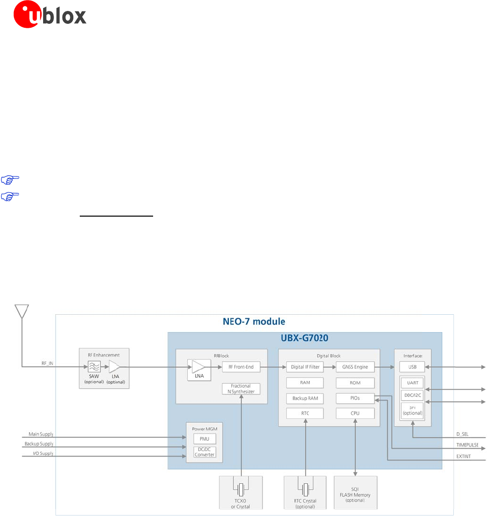
2.2 Architecture
u-blox 7 modules consist of two functional parts - the RF block and the digital block (see Figure 1).
The RF block includes the input matching elements, the SAW band pass filter, the integrated LNA and the
oscillator, while the digital block contains the u-blox 7 GNSS engine, the RTC crystal and additional elements
such as the optional FLASH Memory for enhanced programmability and flexibility.
Figure 1: u-blox-7 block diagram
2.3 Operating modes
u-blox receivers support different power modes. These modes represent strategies of how to control the
acquisition and tracking engines in order to achieve either the best possible performance or good performance
with reduced power consumption.
2.3.1 Continuous Mode
During a cold start, a receiver in Continuous Mode continuously deploys the acquisition engine to search for all
satellites. Once the receiver can calculate a position and track a sufficient number of satellites, the acquisition
engine powers off, resulting in significant power savings. The tracking engine continuously tracks acquired
satellites and acquires other available or emerging satellites. Whenever the receiver can no longer calculate a
position or the number of satellites tracked is below the sufficient number, the acquisition engine powers on
MAX-7 / NEO-7 - Hardware Integration Manual
UBX-13003704 - R07 Early Production Information Hardware description
Page 9 of 50
again to guarantee a quick reacquisition. Even if the acquisition engine powers off, the tracking engine
continues to acquire satellites.
For best performance, use continuous mode.
2.3.2 Power Save Mode
Two Power Save Mode (PSM) operations called ON/OFF and Cyclic tracking are available. These use different
ways to reduce the average current consumption in order to match the needs of the specific application. PSM
operations are set and configured using serial commands. For more information, see the u-blox 7 Receiver
Description Including Protocol Specification [4].
The system can shut down an optional external LNA using the ANT_ON signal in order to optimize power
consumption, see section 2.7.5.
Using the USB Interface is not recommended with Power Save Mode since the USB standard does not
allow a device to be non-responsive. Thus, it is not possible to have full advantage of Power Save Mode
operations in terms of saving current consumption.
Power Save Mode is not supported in GLONASS mode.
2.4 Configuration
The configuration settings can be modified using UBX protocol configuration messages. The modified settings
remain effective until power-down or reset. If these settings have been stored in BBR (Battery Backed RAM), then
the modified configuration will be retained, as long as the backup battery supply is not interrupted.
Configuration can be saved permanently in SQI flash.
2.4.1 Electrical Programmable Fuse (eFuse)
u-blox 7 includes an integrated eFuse memory for permanently saving configuration settings.
If no external FLASH memory is available, the eFuse memory can also be used to store the configuration. The
customer can program the eFuse.
eFuse is One-Time-Programmable; it cannot be changed if it has been programmed once.
String to change the default Baud rate:
USB self powered / UART Baud Rate 1200 B5 62 06 41 09 00 01 01 30 81 00 00 00 00 FE 01 22
USB self powered / UART Baud Rate 2400 B5 62 06 41 09 00 01 01 30 81 00 00 00 00 FD 00 21
USB self powered / UART Baud Rate 4800 B5 62 06 41 09 00 01 01 30 81 00 00 00 00 FC FF 20
USB self powered / UART Baud Rate 9600 B5 62 06 41 09 00 01 01 30 81 00 00 00 00 FF 02 23
USB self powered / UART Baud Rate 19200 B5 62 06 41 09 00 01 01 30 81 00 00 00 00 FB FE 1F
USB self powered / UART Baud Rate 38400 B5 62 06 41 09 00 01 01 30 81 00 00 00 00 FA FD 1E
USB self powered / UART Baud Rate 57600 B5 62 06 41 09 00 01 01 30 81 00 00 00 00 F9 FC 1D
USB self powered / UART Baud Rate 115200 B5 62 06 41 09 00 01 01 30 81 00 00 00 00 F8 FB 1C
MAX-7 / NEO-7 - Hardware Integration Manual
UBX-13003704 - R07 Early Production Information Hardware description
Page 10 of 50
USB bus powered / UART Baud Rate 1200 B5 62 06 41 09 00 01 01 30 81 00 00 00 00 F6 F9 1A
USB bus powered / UART Baud Rate 2400 B5 62 06 41 09 00 01 01 30 81 00 00 00 00 F5 F8 19
USB bus powered / UART Baud Rate 4800 B5 62 06 41 09 00 01 01 30 81 00 00 00 00 F4 F7 18
USB bus powered / UART Baud Rate 9600 B5 62 06 41 09 00 01 01 30 81 00 00 00 00 F7 FA 1B
USB bus powered / UART Baud Rate 19200 B5 62 06 41 09 00 01 01 30 81 00 00 00 00 F3 F6 17
USB bus powered / UART Baud Rate 38400 B5 62 06 41 09 00 01 01 30 81 00 00 00 00 F2 F5 16
USB bus powered / UART Baud Rate 57600 B5 62 06 41 09 00 01 01 30 81 00 00 00 00 F1 F4 15
USB bus powered / UART Baud Rate 115200 B5 62 06 41 09 00 01 01 30 81 00 00 00 00 F0 F3 14
To set the default Vendor or Vendor ID, you will need the specific string. To obtain the USB Vendor ID or USB
Vendor string, contact the the nearest Technical Support office by email. You will find the Contact details at
the end of the document.
2.5 Connecting power
u-blox 7 positioning modules have up to five power supply pins: VCC, VCC_IO, V_BCKP, V_ANT and
VDD_USB.
2.5.1 VCC: Main supply voltage
The VCC pin provides the main supply voltage. During operation, the current drawn by the module can vary by
some orders of magnitude, especially if enabling low-power operation modes. For this reason, it is important
that the supply circuitry be able to support the peak power (see datasheet for specification) for a short time.
Some u-blox 7 modules integrate a DC/DC converter. This allows reduced power consumption, especially when
using a main supply voltage above 2.5 V.
When switching from backup mode to normal operation or at start-up, u-blox 7 modules must charge the
internal capacitors in the core domain. In certain situations, this can result in a significant current draw.
For low power applications using Power Save and backup modes it is important that the power supply or
low ESR capacitors at the module input can deliver this current/charge.
Use a proper GND concept. Do not use any resistors or coils in the power line. For ground plane design
see section 3.3.3
2.5.2 VCC_IO: IO supply voltage (MAX-7)
VCC_IO from the host system supplies the digital I/Os. The wide range of VCC_IO allows seamless interfacing to
standard logic voltage levels independent of the VCC voltage level. In many applications, VCC_IO is simply
connected to the main supply voltage.
Without a VCC_IO supply, the system will remain in reset state.
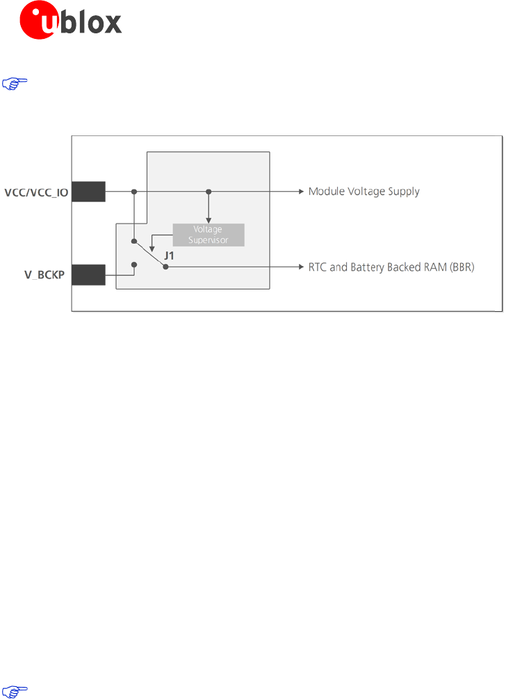
2.5.3 V_BCKP: Backup supply voltage
In case of a power failure on the module supply, the real-time clock (RTC) and battery backed RAM (BBR) are
supplied by V_BCKP. Use of valid time and the GNSS orbit data at start up will improve the GNSS performance
i.e. enables hot starts, warm starts, AssistNow Autonomous and AssistNow Offline. If no backup battery is
connected, the module performs a cold start at power up.
Avoid high resistance on the V_BCKP line: During the switch from main supply to backup supply a short
current adjustment peak can cause high voltage drop on the pin with possible malfunctions.
If no backup supply voltage is available, connect the V_BCKP pin to VCC_IO (or to VCC if not avaiable).
MAX-7 / NEO-7 - Hardware Integration Manual
UBX-13003704 - R07 Early Production Information Hardware description
Page 11 of 50
As long as the u-blox 7 module is supplied to VCC and VCC_IO, the backup battery is disconnected from
the RTC and the BBR to avoid unnecessary battery drain (see Figure 2). In this case, VCC supplies power to
the RTC and BBR.
Figure 2: Backup battery and voltage (for exact pin orientation, see data sheet)
2.5.3.1 RTC derived from the system clock; “Single Crystal” feature (MAX-7C)
On MAX-7C, the reference frequency for the RTC clock can be internally derived from the crystal system clock
frequency (26 MHz) when in Hardware Backup Mode. This feature is called “single crystal” operation. The
backup battery supplies the crystal via V_BCKP in the event that VDD_IO fails to provide power to derive and
maintain the RTC clock. This makes MAX-7C a more cost efficient solution, at the expense of a higher backup
current, compared to the usage of an ordinary RTC crystal on other MAX-7 variants. The capacity of the backup
battery at V_BCKP must be increased accordingly if Hardware Backup Mode is needed.
2.5.4 VDD_USB: USB interface power supply (NEO-7)
VDD_USB supplies the USB interface. If the USB interface is not used, the VDD_USB pin must be connected to
GND. For more information about correctly handling the VDD_USB pin, see section 2.6.2.1.
2.5.5 VCC_RF: Output voltage RF section
The VCC_RF pin can supply an active antenna or external LNA. For more information, see section 3.4.3.2.
2.5.6 V_ANT: Antenna supply (MAX-7W)
The V_ANT pin is available to provide antenna bias voltage to supply an optional external active antenna. For
more information, see section 3.4.3.2.
If not used, connect the V_ANT pin to GND.
2.6 Interfaces
2.6.1 UART
u-blox 7 positioning modules include a Universal Asynchronous Receiver Transmitter (UART) serial interface
RxD/TxD supporting configurable baud rates. The baud rates supported are specified in the u-blox 7 Receiver
Description Including Protocol Specification [4]
The signal output and input levels are 0 V to VCC for NEO-7 and 0 V to VCC_IO for MAX-7 modules. An
interface based on RS232 standard levels (+/- 12 V) can be implemented using level shifters such as Maxim
MAX3232. Hardware handshake signals and synchronous operation are not supported.
2.6.2 USB
A USB version 2.0 FS (Full Speed, 12 Mb/s) compatible interface is available for communication as an alternative
to the UART. The USB_DP integrates a pull-up resistor to signal a full-speed device to the host. The VDD_USB
pin supplies the USB interface.
MAX-7 / NEO-7 - Hardware Integration Manual
UBX-13003704 - R07 Early Production Information Hardware description
Page 12 of 50
u-blox provides Microsoft® certified USB drivers for Windows XP, Windows Vista, and Windows 7 operating
systems (also Windows 8 compatible). These drivers are available at www.u-blox.com.
2.6.2.1 USB external components
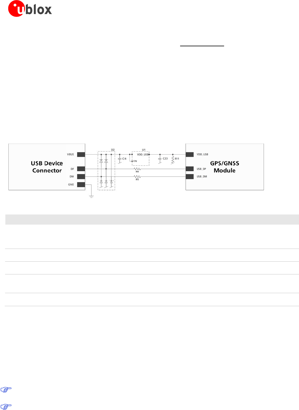
The USB interface requires some external components to implement the physical characteristics required by the
USB 2.0 specification. These external components are shown in Figure 3 and listed in Table 2. To comply with
USB specifications, VBUS must be connected through an LDO (U1) to pin VDD_USB on the module.
If the USB device is self-powered, the power supply (VCC) can be turned off and the digital block is not
powered. In this case, since VBUS is still available, the USB host would still receive the signal indicating that the
device is present and ready to communicate. This should be avoided by disabling the LDO (U1) using the enable
signal (EN) of the VCC-LDO or the output of a voltage supervisor. Depending on the characteristics of the LDO
(U1) it is recommended to add a pull-down resistor (R11) at its output to ensure VDD_USB is not floating if the
LDO (U1) is disabled or the USB cable is not connected i.e. VBUS is not supplied.
If the device is bus-powered, LDO (U1) does not need an enable control.
Figure 3: USB Interface
Name Component Function Comments
U1 LDO Regulates VBUS (4.4 …5.25 V)
down to a voltage of 3.3 V.
Almost no current requirement (~1 mA) if the GNSS receiver is operated as a
USB self-powered device, but if bus-powered LDO (U1) must be able to deliver
the maximum current. For the peak supply current, see a low-cost DC/DC
converter such as LTC3410 from Linear Technology.
C23,
C24
Capacitors Required according to the specification of LDO U1
D2 Protection
diodes
Protect circuit from overvoltage
/ ESD when connecting.
Use low capacitance ESD protection such as ST Microelectronics USBLC6-2.
R4, R5 Serial
termination
resistors
Establish a full-speed driver
impedance of 28…44 Ω
A value of 27 Ω is recommended.
R11 Resistor 1 kΩ is recommended for USB self-powered setup. For bus-powered setup,
R11 can be ignored.
Table 2: Summary of USB external components
2.6.3 Display Data Channel (DDC)
An I2C compatible Display Data Channel (DDC) interface is available with u-blox 7 modules for serial
communication with an external host CPU. The interface only supports operation in slave mode (master mode is
not supported). The DDC protocol and electrical interface are fully compatible with the Fast-Mode of the I2C
industry standard. DDC pins SDA and SCL have internal pull-up resistors.
For more information about the DDC implementation, see the u-blox 7 Receiver Description Including Protocol
Specification [4]. For bandwidth information, see the Data Sheet. For timing, parameters consult the I2C-bus
specification [9].
The u-blox 7 DDC interface supports serial communication with u-blox wireless modules. See the
specification of the applicable wireless module to confirm compatibility.
With u-blox 7, when reading the DDC internal register at address 0xFF (messages transmit buffer), the
master must not set the reading address before every byte is accessed, as this could cause a faulty
MAX-7 / NEO-7 - Hardware Integration Manual
UBX-13003704 - R07 Early Production Information Hardware description
Page 13 of 50
behavior. After every byte is read from register 0xFF the internal address counter is incremented by one,
saturating at 0xFF. Therefore, subsequent reads can be performed continuously.
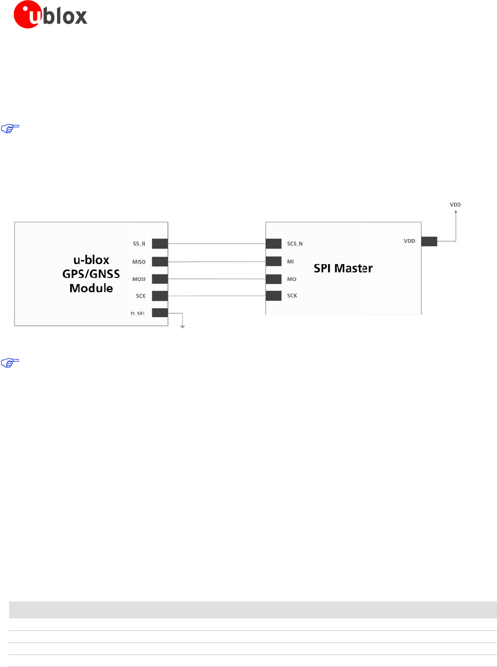
2.6.4 SPI (NEO-7)
With NEO-7 modules, an SPI interface is available for communication to a host CPU.
SPI is not available in the default configuration, because its pins are shared with the UART and DDC
interfaces. The SPI interface can be enabled by connecting D_SEL to ground (NEO-7) (see section 2.7.3).
For speed and clock frequency see the Data Sheet.
Figure 4 shows how to connect a u-blox GNSS receiver to a host/master. The signal on the pins must meet the
conditions specified in the Data Sheet.
Figure 4: Connecting to SPI Master
VCC_IO must have the same voltage level as the host.
2.7 I/O pins
2.7.1 RESET_N: Reset input
Driving RESET_N low activates a hardware reset of the system. Use this pin only to reset the module. Do not use
RESET_N to turn the module on and off, since the reset state increases power consumption. With u-blox 7
RESET_N is an input only.
2.7.2 EXTINT: External interrupt
EXTINT is an external interrupt pin with fixed input voltage thresholds with respect to VCC or VCC_IO (see the
data sheet for more information). It can be used for wake-up functions in Power Save Mode on all u-blox 7
modules and for aiding. Leave open if unused.
2.7.3 D_SEL: Interface select (NEO-7)
The D_SEL pin, available on all NEO-7 modules, selects the available interfaces. SPI cannot be used
simultaneously with UART/DDC.
If open, UART and DDC are available. If pulled low, the SPI Interface is available.
Pin D_SEL pin open D_SEL pin low
18 DDC Data SPI CS_N
19 DDC Clock SPI SCK
20 TxD SPI MISO
21 RxD SPI MOSI
Table 3: D_SEL pin on NEO-7

MAX-7 / NEO-7 - Hardware Integration Manual
UBX-13003704 - R07 Early Production Information Hardware description
Page 14 of 50
2.7.4 TX Ready signal
The TX Ready signal indicates that the receiver has data to transmit. A listener can wait on the TX Ready signal
instead of polling the DDC or SPI interfaces. The UBX-CFG-PRT message lets you configure the polarity and the
number of bytes in the buffer before the TX Ready signal goes active. The TX Ready signal can be mapped to
UART TXD (PIO 06). The TX Ready function is disabled by default.
The TX-ready functionality can be enabled and configured by proper AT commands sent to the involved u-
blox wireless module supporting the feature. For more information see GPS Implementation and Aiding
Features in u-blox wireless modules [10].
2.7.5 ANT_ON: Antenna ON (LNA enable) (NEO-7N, MAX-7Q, MAX-7C)
In Power Save Mode, the system can turn on/off an optional external LNA using the ANT_ON signal in order to
optimize power consumption.
2.7.6 Antenna Short circuit detection (MAX-7W)
The MAX-7W module includes internal short circuit antenna detection. For more information, see section
3.4.3.2.
2.7.7 Antenna open circuit detection
2.7.7.1 Antenna open circuit detection (MAX-7)
Antenna open circuit detection (OCD) is not activated by default on the MAX-7 module. OCD can be mapped to
PIO13 (EXTINT). For more information about how to implement OCD, see section 3.4.3.3. To learn how to
configure OCD see the u-blox 7 Receiver Description including Protocol Specification [4].
2.7.8 Time pulse
A configurable time pulse signal is available with all u-blox 7 modules. By default, the time pulse signal is
configured to 1 pulse per second. For more information see the u-blox 7 Receiver Description including Protocol
Specification [4].

MAX-7 / NEO-7 - Hardware Integration Manual
UBX-13003704 - R07 Early Production Information Design
Page 15 of 50
3 Design
3.1 Design checklist
Designing-in a u-blox 7 module is easy, especially when based on a u-blox reference design. Nonetheless, it pays
to do a quick sanity check of the design. This section lists the most important items for a simple design check.
The design checklist can also help to avoid an unnecessary PCB respin and achieve the best possible
performance. Follow the design checklists when developing any u-blox 7 GNSS applications. This can
significantly reduce development time and costs.
3.1.1 Schematic checklist
If required, does your schematic allow for using different module variants? See the u-blox website
(www.u-blox.com) to compare the available features of u-blox 7 GNSS modules.
Plan the use of a second interface (Test points on UART, DDC or USB) for firmware updates or as a
service connector.
Power supply requirements
GNSS positioning modules require a stable power supply. In selecting a strategy to achieve a clean and
stable power supply, any resistance in the VCC supply line can negatively influence performance.
Consider the following points:
Wide power lines or even power planes are preferred.
Avoid resistive components in the power line (e.g. narrow power lines, coils, resistors, etc.).
Placing a filter or other source of resistance at VCC can create significantly longer acquisition times.
For ground plane design, see section 3.3.3.
Are all power supplies (VCC, VDD_USB) within the specified range? (See the data sheet: NEO-7 [1] or
MAX-7 [2])
Compare the peak supply current consumption of your u-blox 7 module with the specification of the
power supply. (See the data sheet for more information.)
At the module input, use low ESR capacitors that can deliver the required current/charge for switching
from backup mode to normal operation.
Backup battery
Use of valid time and the GNSS orbit data at startup will improve the GNSS performance i.e. enables hot
starts, warm starts and the AssistNow Autonomous process as well as AssistNow Offline. To make use of
these features connect a battery to V_BCKP to continue supplying the backup domain in case of power
failure at VCC_IO.
If no backup supply voltage is available, connect the V_BCKP pin to VCC_IO (or to VCC if not avaiable).
3.1.2 Layout checklist
See section 3.3.
Is the GNSS module located according to the recommendation?
Has the grounding concept been followed?
Has the micro strip been kept as short as possible?
Add a ground plane underneath the GNSS module to reduce interference.
For improved shielding, add as many vias as possible around the micro strip, around the serial
communication lines, underneath the GNSS module etc.
Have appropriate EOS/ESD/EMI protection measures been included? This is especially important for
designs including wireless modules.

MAX-7 / NEO-7 - Hardware Integration Manual
UBX-13003704 - R07 Early Production Information Design
Page 16 of 50
3.1.3 Antenna checklist
The total noise figure should be well below 3 dB.
If a patch antenna is the preferred antenna, choose a patch of at least 15x15x4 mm for standalone
GPS/QZSS, or choose a patch of at least 25x25x4 mm for GPS + GLONASS. For smaller antennas, an LNA
with a noise figure <2 dB is recommended. (MAX-7Q, NEO-7N)
Make sure the antenna is not placed close to noisy parts of the circuitry. (E.g. micro-controller, display,
etc.)
To optimize performance in environments with out-of band jamming sources, use an additional SAW
filter.
The micro strip must be 50 Ω and be routed in a section of the PCB where minimal interference from
noise sources can be expected.
In case of a multi-layer PCB, use the thickness of the dielectric between the signal and the first GND layer
(typically the 2nd layer) for the micro strip calculation.
If the distance between the micro strip and the adjacent GND area (on the same layer) does not exceed 5
times the track width of the micro strip, use the “Coplanar Waveguide” model in AppCad to calculate
the micro strip and not the “micro strip” model see section 3.3.5
Use an external LNA if your design does not include an active antenna when optimal performance is
important.
For information on ESD protection for patch antennas and removable antennas, see section 5.3.3 and if
you use GPS for design in combination with GSM or other radio then check sections 5.3.5 to 5.3.7.
For more information dealing with interference, issues see the GPS Antenna Application Note [6].
3.2 Design considerations for minimal designs
For a minimal design with a u-blox 7 GNSS module, the following functions and pins need consideration:
• Connect the Power supply to VCC.
• Connect VCC_IO to VCC or to the corresponding voltage.
• Assure an optimal ground connection to all ground pins of the module.
• Connect the antenna to RF_IN over a 50 Ω line and define the antenna supply (V_ANT) for active antennas
(internal or external power supply).
• Choose the required serial communication interface (UART, USB, SPI or DDC) and connect the appropriate
pins to your application.
• If you need improved start-up or use AssistNow Autonomous in your application, connect a backup supply
voltage to V_BCKP.
For active antenna design, see section 3.4.2.
MAX-7 / NEO-7 - Hardware Integration Manual
UBX-13003704 - R07 Early Production Information Design
Page 17 of 50
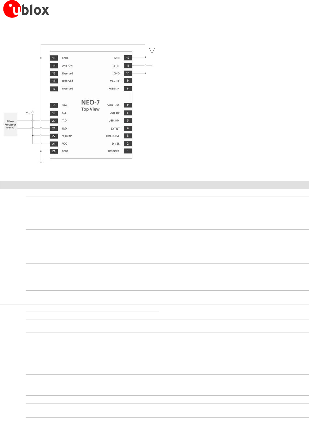
3.2.1 Minimal design (NEO-7N)
Figure 5: NEO-7 passive antenna design
Function PIN No I/O Description Remarks
Power VCC 23 I Supply voltage Provide clean and stable supply.
GND 10,12,
13, 24
I Ground Assure a good GND connection to all GND pins of the module,
preferably with a large ground plane.
V_BCKP 22 I Backup supply
voltage
It is recommended to connect a backup supply voltage to V_BCKP
in order to enable Warm and Hot Start features on the positioning
modules. Otherwise, connect to VCC.
VDD_USB 7 I USB power
supply
To use the USB interface connect this pin to 3.0 – 3.6 V.
If no USB serial port used connect to GND.
Antenna RF_IN 11 I GPS signal input
from antenna
The connection to the antenna has to be routed on the PCB. Use a
controlled impedance of 50 Ω to connect RF_IN to the antenna or
the antenna connector.
VCC_RF 9 O Output voltage
RF section
VCC_RF can be used to power an external active antenna.
UART TxD 20 O Serial port/
SPI MISO
Communication interface, Can be programmed as TX Ready for
DDC interface. If pin 2 low => SPI MISO.
RxD 21 I Serial port /
SPI MOSI
Serial input. Internal pull-
up resistor to VCC. Leave open if
not used. If pin 2 low => SPI MOSI.
USB USB_DM 5 I/O USB I/O line USB bidirectional communication pin. Leave open if unused.
Implementations see section 2.6.2.
USB_DP 6 I/O USB I/O line
System TIMEPULSE 3 O Time pulse
signal
Configurable time pulse signal (one pulse per second by default).
Leave open if not used.
EXTINT 4 I External
interrupt
External Interrupt pin.
Internal pull-up resistor to VCC. Leave open if not used.
SDA 18 I/O DDC data /
SPI CS_N
DDC Data
If pin 2 low => SPI chip select.
SCL 19 I DDC clock /
SPI SCK
DDC Clock. If pin 2 low => SPI clock.
ANT_ON (NEO-7N)
RESERVED (NEO-7M)
14
O ANT_ON ANT_ON (antenna on) HIGH can be used to turn on and LOW to
turn off an optional external LNA.
- Reserved Reserved, leave open.
RESET_N 8 I Reset input Reset input
D_SEL 2 I selects the
interface
Used to select UART/DDC or SPI
Open = UART/DDC; low = SPI
RESERVED 1, 15,
16, 17
- Reserved Leave open.
Table 4: Pinout NEO-7
MAX-7 / NEO-7 - Hardware Integration Manual
UBX-13003704 - R07 Early Production Information Design
Page 18 of 50
3.2.2 Minimal design (MAX-7Q)
Figure 6: MAX-7 passive antenna design
For information on increasing immunity to jammers such as GSM, see section 5.3.7.
Function PIN No I/O Description Remarks
Power VCC 8 I Supply voltage Provide clean and stable supply.
GND 1,10,12 I Ground Assure a good GND connection to all GND pins of the module,
preferably with a large ground plane.
V_BCKP 6 I Backup supply
voltage
Backup supply voltage input pin. Connect to VCC_IO if not used.
Antenna RF_IN 11 I GPS signal
input from
antenna
The connection to the antenna has to be routed on the PCB. Use a
controlled impedance of 50 Ω to connect RF_IN to the antenna or
the antenna connector. DC block inside.
VCC_RF 14 O Output voltage
RF section
Can be used for active antenna or external LNA supply.
ANT_ON
(MAX-7C/Q)
Reserved
(MAX-7W)
13
O
ANT_ON
ANT_ON (antenna on) HIGH can be used to turn on and LOW to
turn off an optional external LNA.
ANT_ON pin voltage level is VCC_IO
- Reserved Leave open
UART TXD 2 O Serial port UART, leave open if not used, voltage level referred VCC_IO. Can
be configured as TX Ready indication for the DDC interface.
RXD 3 I Serial port UART, leave open if not used, voltage level referred VCC_IO
System TIMEPULSE 4 O Time pulse
signal
Leave open if not used, voltage level referred VCC_IO
EXTINT 5 I External
interrupt
Leave open if not used, voltage level referred VCC_IO
SDA 16 I/O DDC pins DDC Data. Leave open, if not used.
SCL 17 I DDC pins DDC Clock. Leave open, if not used.
VCC_IO 7 I
VCCC_IO
IO supply voltage. Input must be always supplied. Usually connect to
VCC pin 8
RESET_N 9 I Reset Reset
V_ANT
(MAX-7W )
Reserved
(MAX-7C/Q)
15
I Antenna bias
voltage
Connect to GND (or leave open) if passive antenna is used. If an
active antenna is used, add a 10 Ω resistor in front of V_ANT input
to the Antenna Bias voltage or VCC_RF
- Reserved Leave open
Reserved 18 - Reserved Leave open
Table 5: Pinout MAX-7
MAX-7 / NEO-7 - Hardware Integration Manual
UBX-13003704 - R07 Early Production Information Design
Page 19 of 50
3.3 Layout
This section provides important information for designing a robust GNSS system.
GNSS signals at the surface of the Earth are about 15 dB below the thermal noise floor. Signal loss from the
antenna to RF_IN pin of the module must be minimized as much as possible. When defining a GNSS receiver
layout, the placement of the antenna with respect to the receiver, as well as grounding, shielding and jamming
from other digital devices, are crucial issues requiring careful consideration.
For all layout and routing figures shown in this section, see the data sheet for exact pin orientation.
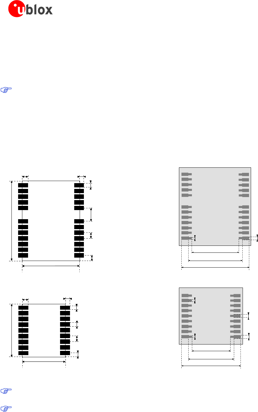
3.3.1 Footprint and paste mask
Figure 7 through Figure 10 describe the footprint and provide recommendations for the paste mask for u-blox 7
LCC modules. These are recommendations only and not specifications. Note that the Copper and Solder masks
have the same size and position.
To improve the wetting of the half vias, reduce the amount of solder paste under the module and increase the
volume outside of the module by defining the dimensions of the paste mask to form a T-shape (or equivalent)
extending beyond the Copper mask.
12.2 mm [480.3 mil]
16.0 mm [630 mil]
1.0 mm
[39.3 mil]
0.8 mm
[31.5 mil]
0.8 mm
[31.5 mil]
3.0 mm
[118.1 mil]
1.0 mm
[39.3 mil]
1.1 mm
[43.3 mil]
Figure 7: NEO-7 footprint
9.7 mm [382 mil]
10.1 mm [398 mil]
1.0 mm
[39.3 mil]
0.7 mm
[27.6 mil]
0.8 mm
[31.5 mil]
0.65 mm
[26.6 mil]
1.1 mm
[43.3 mil]
0.8 mm
[31.5 mil]
Figure 8: MAX-7 footprint
Stencil: 150
µ
m
10.4 mm [409.5 mil]
14.6 mm [575 mil]
12.2 mm [480 mil]
0.8 mm
[31.5 mil]
0.6 mm
[23.5 mil]
Figure 9: NEO-7 paste mask
Stencil: 150
µ
m
7.9 mm [311 mil]
12.5 mm [492 mil]
9.7 mm [382 mil]
0.7 mm
[27.6 mil]
0.5 mm
[19.7 mil]
0.8 mm
[31.5 mil]
0.6 mm
[23.5 mil]
Figure 10: MAX-7 paste mask
MAX Form Factor (10.1 x 9.7 x 2.5): Same Pitch as NEO for all pins: 1.1 mm, but 4 pads in each corner
(pin 1, 9, 10 and 18) only 0.7 mm wide instead 0.8 mm
Consider the paste mask outline when defining the minimal distance to the next component. The exact
geometry, distances, stencil thicknesses and solder paste volumes must be adapted to the specific
production processes (e.g. soldering) of the customer.
MAX-7 / NEO-7 - Hardware Integration Manual
UBX-13003704 - R07 Early Production Information Design
Page 20 of 50
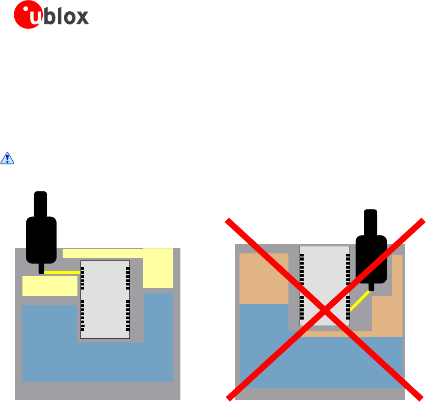
3.3.2 Placement
A very important factor in achieving maximum performance is the placement of the receiver on the PCB. The
connection to the antenna must be as short as possible to avoid jamming into the very sensitive RF section.
Make sure that the RF critical circuits are separated from any other digital circuits on the system board. To
achieve this, position the module’s digital part towards the digital section on the system PCB. Exercise care if
placing the receiver in proximity to heat emitting circuitry. The RF part of the receiver is very sensitive to
temperature and sudden changes can have an adverse impact on performance.
The RF part of the receiver is a temperature sensitive component. Avoid high temperature drift
and air vents near the receiver.
Non 'emitting'
circuits
PCB
Digital & Analog circuits
Non
'emitting'
circuits
Antenna
Digital Part
RF Part
1
2
3
4
5
6
7
8
9
10
11
12
13
14
28
27
26
25
24
23
22
21
20
19
18
17
16
15
RF & heat
'emitting'
circuits
PCB
Digital & Analog circuits
RF& heat
'emitting'
circuits
Antenna
1
2
3
4
5
6
7
8
9
10
11
12
13
14
28
27
26
25
24
23
22
21
20
19
18
17
16
15
Figure 11: Placement
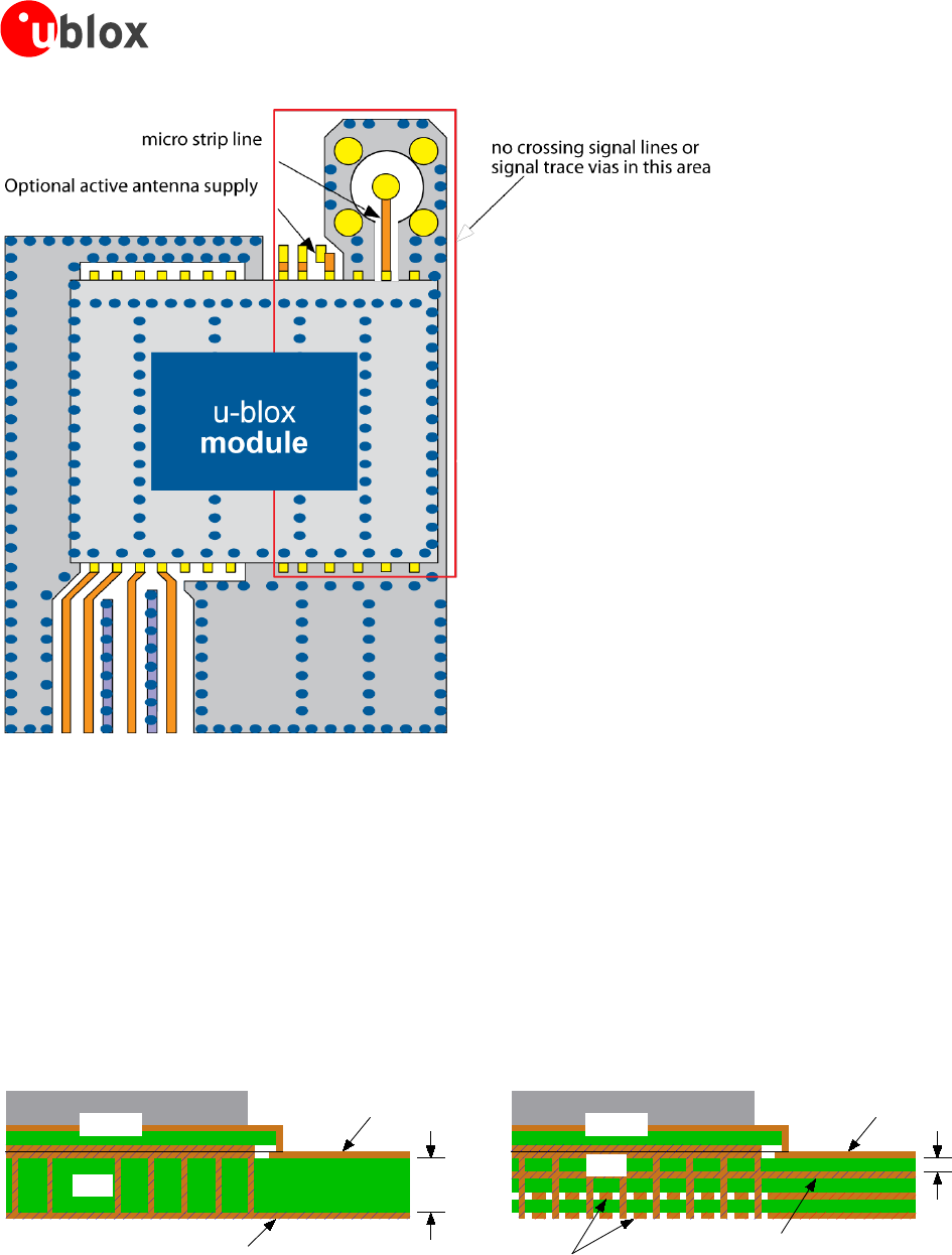
3.3.3 Antenna connection and ground plane design
u-blox 7 modules can be connected to passive or active antennas. The RF connection is on the PCB and connects
the RF_IN pin with the antenna feed point or the signal pin of the connector, respectively. Figure 12 illustrates
connection to a typical five-pin RF connector. One can see the improved shielding for digital lines as discussed in
the GPS Antenna Application Note [6]. Depending on the actual size of the ground area, if possible place
additional vias in the outer region. In particular, terminate the edges of the ground area with a dense line of vias.
MAX-7 / NEO-7 - Hardware Integration Manual
UBX-13003704 - R07 Early Production Information Design
Page 21 of 50
Figure 12: Recommended layout
As seen in Figure 12, an isolated ground area exists around and below the RF connection. This part of the circuit
MUST be kept as far from potential noise sources as possible. Make certain that no signal lines cross, and that no
signal trace vias appear at the PCB surface within the area of the red rectangle. The ground plane should also be
free of digital supply return currents in this area. On a multi layer board, the whole layer stack below the RF
connection should be kept free of digital lines. This is because even solid ground planes provide only limited
isolation.
The impedance of the antenna connection must match the 50 Ω impedance of the receiver. To achieve an
impedance of 50 Ω, the width W of the micro strip has to be chosen depending on the dielectric thickness H,
the dielectric constant εr of the dielectric material of the PCB and on the build-up of the PCB (see section 3.3.5).
Figure 13 shows two different builds: A 2 Layer PCB and a 4 Layer PCB. The reference ground plane is in both
designs on layer 2 (red). Therefore, the effective thickness of the dielectric is different.
Module micro strip line
Ground plane
Module micro strip line
Ground plane
PCB
PCB
Either don't use these layers or fill with ground planes
H
H
Figure 13: PCB build-up for micro strip line. Left: 2-layer PCB, right: 4-layer PCB
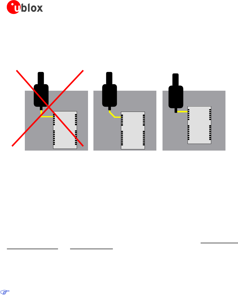
3.3.4 General design recommendations:
• The length of the micro strip line should be kept as short as possible. Lengths over 2.5 cm (1 inch) should be
avoided on standard PCB material and without additional shielding.
MAX-7 / NEO-7 - Hardware Integration Manual
UBX-13003704 - R07 Early Production Information Design
Page 22 of 50
• For multi layer boards the distance between micro strip line and ground area on the top layer should at least
be as large as the dielectric thickness.
• Routing the RF connection close to digital sections of the design should be avoided.
• To reduce signal reflections, sharp angles in the routing of the micro strip line should be avoided. Chamfers
or fillets are preferred for rectangular routing; 45-degree routing is preferred over Manhattan style
90-degree routing.
Antenna
Antenna
Antenna
PCB
PCB PCB
1
2
3
4
5
6
7
8
9
10
11
12
13
14
28
27
26
25
24
23
22
21
20
19
18
17
16
15
1
2
3
4
5
6
7
8
9
10
11
12
13
14
28
27
26
25
24
23
22
21
20
19
18
17
16
15
1
2
3
4
5
6
7
8
9
10
11
12
13
14
28
27
26
25
24
23
22
21
20
19
18
17
16
15
wrong better best
Figure 14: Recommended micro strip routing to RF pin
• Do not route the RF-connection underneath the receiver. The distance of the micro strip line to the ground
plane on the bottom side of the receiver is very small (some 100 µm) and has huge tolerances (up to 100%).
Therefore, the impedance of this part of the trace cannot be controlled.
• Use as many vias as possible to connect the ground planes.
• In order to avoid reliability hazards, the area on the PCB under the receiver should be entirely covered with
solder mask. Vias should not be open. Do not route under the receiver.
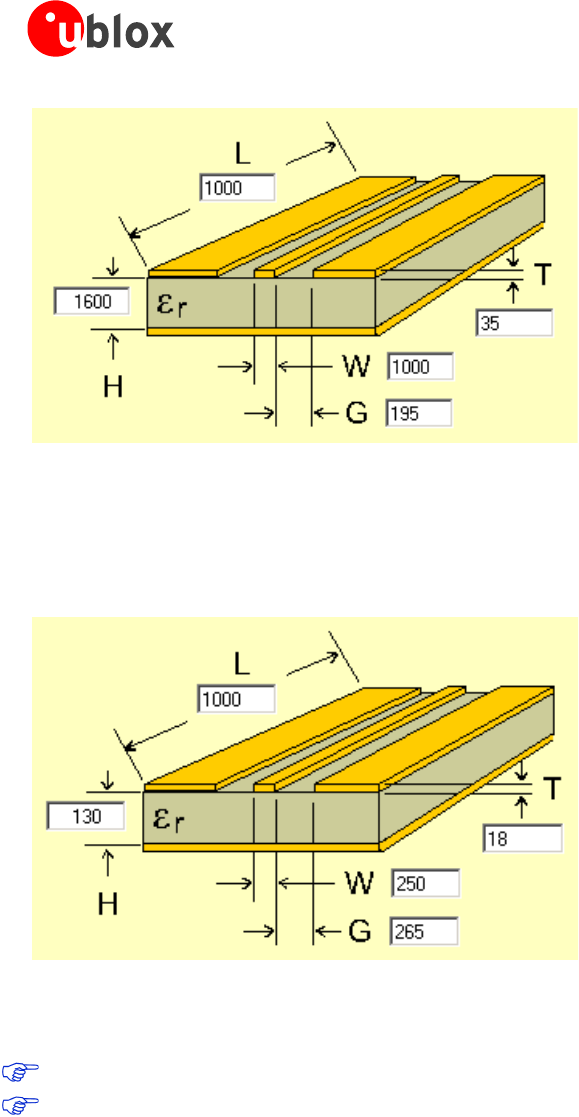
3.3.5 Antenna micro strip
There are many ways to design wave-guides on printed circuit boards. A common factor to all is that calculation
of the electrical parameters is not straightforward. Freeware tools like AppCAD from Agilent or TXLine from
Applied Wave Research, Inc. are of great help in this regard. They can be downloaded from www.agilent.com or
www.hp.woodshot.com and www.mwoffice.com.
Micro strip is the most commonly used configuration on printed circuit boards and shown below in Figure 15
and Figure 16. As a rule of thumb, to achieve a 50 Ω line impedance with FR-4 material, the width of the
conductor is roughly double the thickness of the dielectric.
Note: For the correct calculation of the micro strip impedance, one does not only need to consider the distance
between the top and the first inner layer, but also the distance between the micro strip and the adjacent GND
plane on the same layer
Use the Grounded Coplanar Waveguide model for the calculation of the line dimensions.
MAX-7 / NEO-7 - Hardware Integration Manual
UBX-13003704 - R07 Early Production Information Design
Page 23 of 50
Figure 15: Micro strip on a 2-layer board (Agilent AppCAD Coplanar Waveguide)
Figure 15 shows an example of a 2-layer FR4 board with 1.6 mm thickness (H) and a 35 µm (1 ounce) copper
cladding (T). The thickness of the micro strip is comprised of the cladding (35 µm) plus the plated copper
(typically 25 µm). Figure 16 is an example of a multi layer FR4 board with 18 µm (½ ounce) cladding (T) and 180
µm dielectric between layer 1 and 2.
Figure 16: Micro strip on a multi layer board (Agilent AppCAD Coplanar Waveguide)
3.4 Antenna and Antenna supervision
For all module designs shown in this section, see the data sheet for exact pin orientation.
For recomended parts, see section 3.5.
3.4.1 Antenna design with passive antenna
A design using a passive antenna requires more attention to the layout of the RF section. Typically, a passive
antenna is located near electronic components; therefore, care should be taken to reduce electrical ‘noise’ that
may interfere with the antenna performance. Passive antennas do not require a DC bias voltage and can be
directly connected to the RF input pin RF_IN. Sometimes, they may also need a passive matching network to
match the impedance to 50 Ω.
MAX-7 / NEO-7 - Hardware Integration Manual
UBX-13003704 - R07 Early Production Information Design
Page 24 of 50
3.4.1.1 Minimal setup with a good patch antenna
Figure 17 shows a minimal setup for a design with a good GPS patch antenna.
NEO-7N is optimized for Immunity to near field Wireless.
Figure 17: Module design with passive antenna
3.4.1.2 Setup for best performance with passive antenna
Figure 18 shows a design using an external LNA to increase the sensitivity for best performance with passive
antenna.
Figure 18: Module design with passive antenna and external LNA
ANT_ON (antenna on) can be used to turn on and off an optional external LNA.
The VCC_RF output can be used to supply the LNA with a filtered supply voltage.
A standard GPS LNA has enough bandwidth to amplify GPS and GLONASS signals.
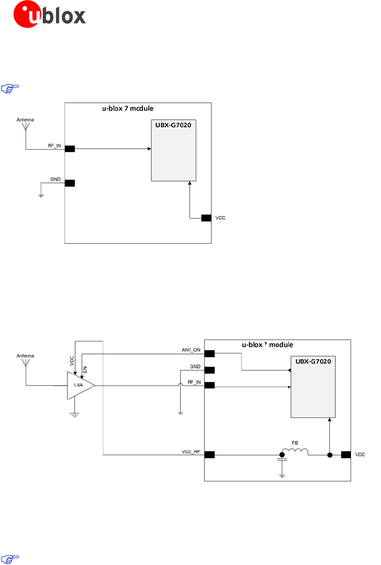
3.4.2 Active antenna design without antenna supervisor (NEO-7N/7M/7P, MAX-7C/7Q)
Active antennas have an integrated low-noise amplifier. Active antennas require a power supply that will
contribute to the total GPS system power consumption budget with additional 5 to 20 mA typically.
If the supply voltage of the u-blox 7 receiver matches the supply voltage of the antenna (e.g. 3.0 V), use the
filtered supply voltage VCC_RF output to supply the antenna. See section 3.4.2.1. This design is used for
modules MAX-7C, MAX-7Q, NEO-7N, and NEO-7M in combination with active antenna.
In case of different supply voltage, use a filtered external supply as shown in section 3.4.2.2
MAX-7 / NEO-7 - Hardware Integration Manual
UBX-13003704 - R07 Early Production Information Design
Page 25 of 50
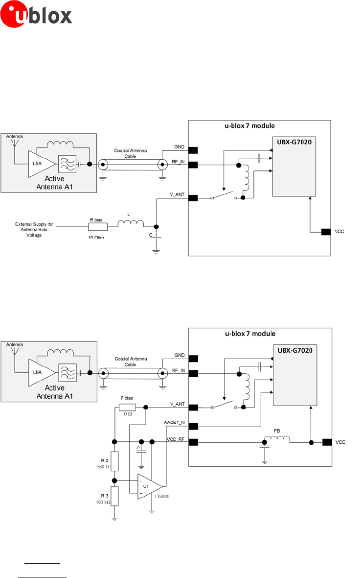
3.4.2.1 Active antenna design, VCC_RF used to supply active antenna
Figure 19 shows an active antenna design supplied by VCC_RF.
Figure 19: Active antenna design, external supply from VCC_RF
3.4.2.2 Active antenna design powered from external supply
Figure 20 shows a design with direct externally powered active antenna.
This circuit works with all u-blox 7 modules, also with modules without VCC_RF output.
Figure 20: Active antenna design, direct external supply
For recomended parts, see section 3.5.
In case VCC_RF voltage does not match with the antenna supply voltage, use a filtered external supply as
shown in Figure 20.
3.4.3 Antenna design with active antenna using antenna supervisor (MAX-7W)
An active antenna supervisor provides the means to check the antenna for open and short circuits and to shut
off the antenna supply if a short circuit is detected. The Antenna Supervisor is configured using serial port UBX
binary protocol message. Once enabled, the active antenna supervisor produces status messages, reporting in
NMEA and/or UBX binary protocol (see section 3.4.3.1). These indicate the particular state of the antenna
supervisor shown in the state diagram below (Figure 21).
The current active antenna status can be determined by polling the UBX-MON-HW monitor command. If an
antenna is connected, the initial state after power-up is “Active Antenna OK.”
MAX-7 / NEO-7 - Hardware Integration Manual
UBX-13003704 - R07 Early Production Information Design
Page 26 of 50
No
Super-
vision
Active
Antenna
OK
Open
Circuit
detected
Short
Circuit
detected
Powerup
Events AADET0_N
User controlled events
Disable Supervision
Enable Supervision
Short Circuit
detected
Disable
Supervision
Antenna
connected
Short Circuit
detected
open circuit
detected,given
OCD enabled
Periodic
reconnection
attempts
Figure 21: State diagram of active antenna supervisor
The module firmware supports an active antenna supervisor circuit, which is connected to the AADET_N pin. For
an example of an open circuit detection circuit, see Figure 24. High on pin AADET_N means that an external
antenna is not connected.
3.4.3.1 Status reporting
At startup, and on every change of the antenna supervisor configuration, the u-blox 7 GPS/GALILEO module will
output an NMEA ($GPTXT) or UBX (INF-NOTICE) message with the internal status of the antenna supervisor
(disabled, short detection only, enabled).
None, one or several of the strings below are part of this message to inform about the status of the active
antenna supervisor circuitry (e.g. “ANTSUPERV= AC SD OD PdoS”).
Abbreviation Description
AC Antenna Control (e.g. the antenna will be switched on/ off controlled by the GPS receiver)
SD Short Circuit Detection Enabled
SR Short Circuit Recovery Enabled
OD Open Circuit Detection Enabled
PdoS Power Down on short
Table 6: Active Antenna Supervisor Message on startup (UBX binary protocol)
To activate the antenna supervisor use the UBX-CFG-ANT message. For further information, refer to the
u-blox 7 Receiver Description Including Protocol Specification [4].
Similar to the antenna supervisor configuration, the status of the antenna supervisor will be reported in an
NMEA ($GPTXT) or UBX (INF-NOTICE) message at start-up and on every change.
MAX-7 / NEO-7 - Hardware Integration Manual
UBX-13003704 - R07 Early Production Information Design
Page 27 of 50
Message Description
ANTSTATUS=DONTKNOW Active antenna supervisor is not configured and deactivated.
ANTSTATUS=OK Active antenna connected and powered
ANTSTATUS=SHORT Antenna short
ANTSTATUS=OPEN Antenna not connected or antenna defective
Table 7: Active antenna supervisor message on startup (NMEA protocol)
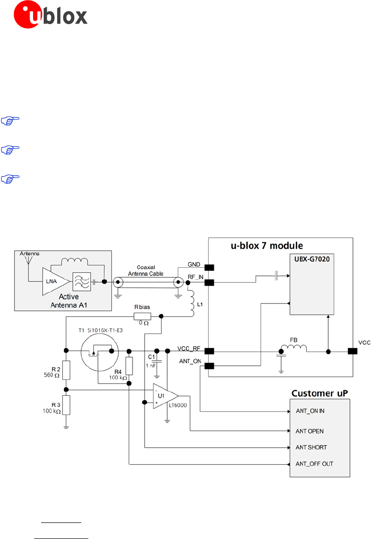
3.4.3.2 Module design with active antenna, short circuit protection / detection (MAX-7W)
If a suitably dimensioned series resistor R_BIAS is placed in front of pin V_ANT, a short circuit can be detected in
the antenna supply. This is detected inside the u-blox 7 module and the antenna supply voltage will be
immediately shut down. After which, periodic attempts to re-establish antenna power are made by default.
An internal switch (under control of the receiver) can turn off the supply to the external antenna whenever it is
not needed. This feature helps to reduce power consumption in power save mode.
To configure the antenna supervisor use the UBX-CFG-ANT message. For further information see the
u-blox 7 Receiver Description Including Protocol Specification [4].
Short circuits on the antenna input without limitation (R_BIAS) of the current can result in
permanent damage to the receiver! Therefore, it is mandatory to implement an R_BIAS in all
risk applications, such as situations where the antenna can be disconnected by the end-user or
that have long antenna cables.
If the VCC_RF voltage does not match the antenna supply voltage, use a filtered external supply as shown
in Figure 23.
Supply from VCC_RF (MAX-7W)
Figure 22 shows an active antenna supplied from the u-blox 7 module.
The VCC_RF pin can be connected with V_ANT to supply the antenna. Note that the voltage specification of the
antenna has to match the actual supply voltage of the u-blox module (e.g. 3.0 V), see Figure 22.
Figure 22: Module design with active antenna, internal supply from VCC_RF
External supply (MAX-7W)
MAX-7 / NEO-7 - Hardware Integration Manual
UBX-13003704 - R07 Early Production Information Design
Page 28 of 50
Figure 23 shows an externally powered active antenna design.
Since the external bias voltage is fed into the most sensitive part of the receiver (i.e. the RF input), this supply
should be free of noise. Usually, low frequency analog noise is less critical than digital noise of spurious
frequencies with harmonics up to the GPS/QZSS band of 1.575 GHz and GLONASS band of 1.602 GHz.
Therefore, it is not recommended to use digital supply nets to feed the V_ANT pin.
Figure 23: Module design with active antenna, external supply
3.4.3.3 Antenna supervision open circuit detection (OCD) (MAX-7W)
The open circuit detection circuit uses the current flow to detect an open circuit in the antenna. Calculate the
threshold current using Equation 1.
Figure 24: Schematic of open circuit detection
RFVcc
Rbias
RR
R
I_
32
2
•
+
=
Equation 1: Calculation of threshold current for open circuit detection
Antenna open circuit detection (OCD) is not activated by default. It can be enabled by the UBX-CFG-ANT
message. This configuration can be sent to the receiver at every startup or can be saved permanently in flash.
MAX-7W does not have a dedicated AADET_N pin. The AADET_N pin can be made available on the EXINT pin.
To do so, the following command must be sent once and stored permanently to the receiver:
• “B5 62 06 41 0C 00 00 00 03 1F 06 5F 8B B1 FF F6 B7 FF C1 D7”.
MAX-7 / NEO-7 - Hardware Integration Manual
UBX-13003704 - R07 Early Production Information Design
Page 29 of 50
To enable the OCD feature, the following command must be sent to the receiver at every startup:
• “B5 62 06 13 04 00 1F 00 F0 B5 E1 DE”.
The AADET_N pin then has High = "ANTSTATUS=OPEN", Low = "ANTSTATUS=OK",.
For more information about how to implement and configure OCD, see u-blox 7 Receiver Description
including Protocol Specification [4]
If the antenna supply voltage is not derived from VCC_RF, do not exceed the maximum voltage rating of
the AADET_N pin.
For more information, see section 3.4.3.1.
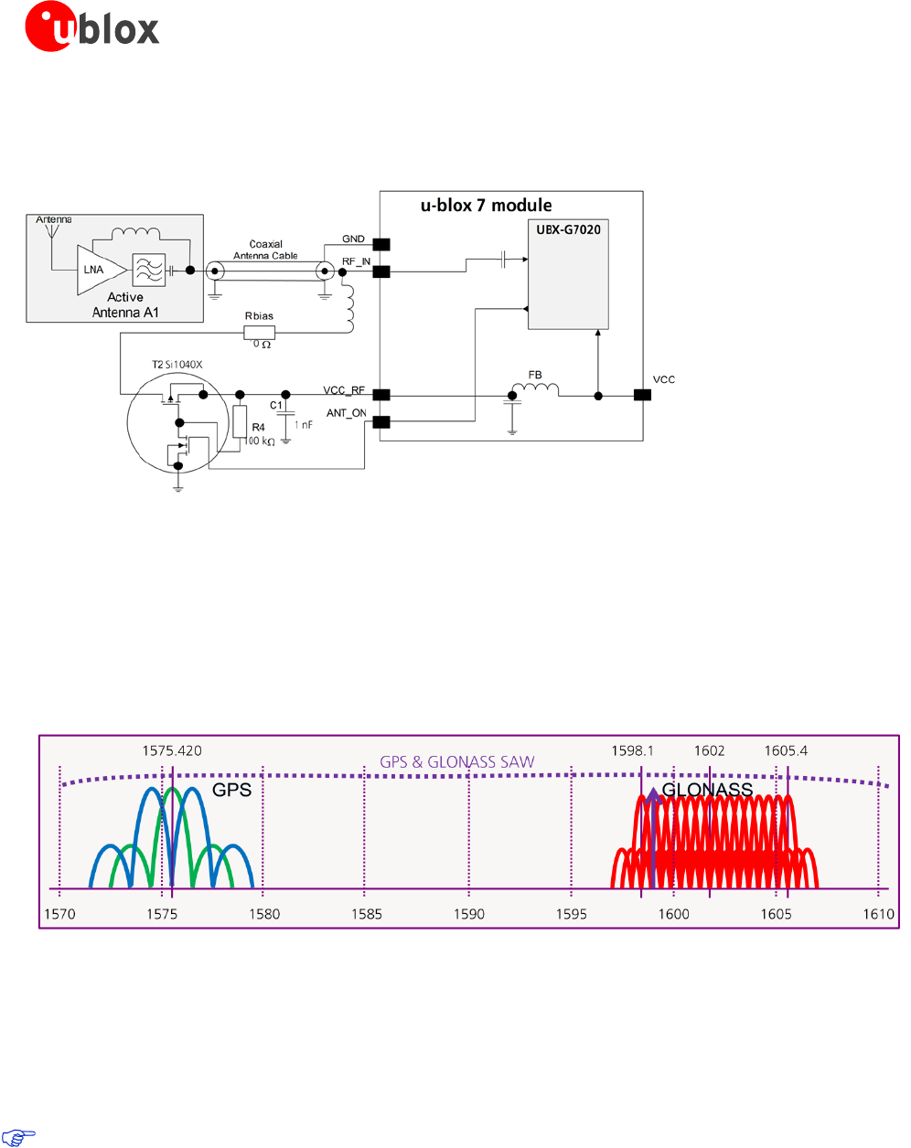
3.4.3.4 External active antenna supervisor using customer uP (NEO-7N, MAX-7Q, MAX-7C)
Figure 25: External active antenna supervisor using ANT_ON
RFVcc
R
RR
R
I
bias
_
32
2
•
+
=
Equation 2: Calculation of threshold current for open circuit detection
MAX-7 / NEO-7 - Hardware Integration Manual
UBX-13003704 - R07 Early Production Information Design
Page 30 of 50
3.4.3.5 External active antenna control (NEO-7N, MAX-7Q, MAX-7C)
The ANT_ON signal can be used to turn on and off an external LNA. This reduces power consumption in Power
Save Mode (Backup mode).
Figure 26: External active antenna control (MAX-7Q / MAX-7C)
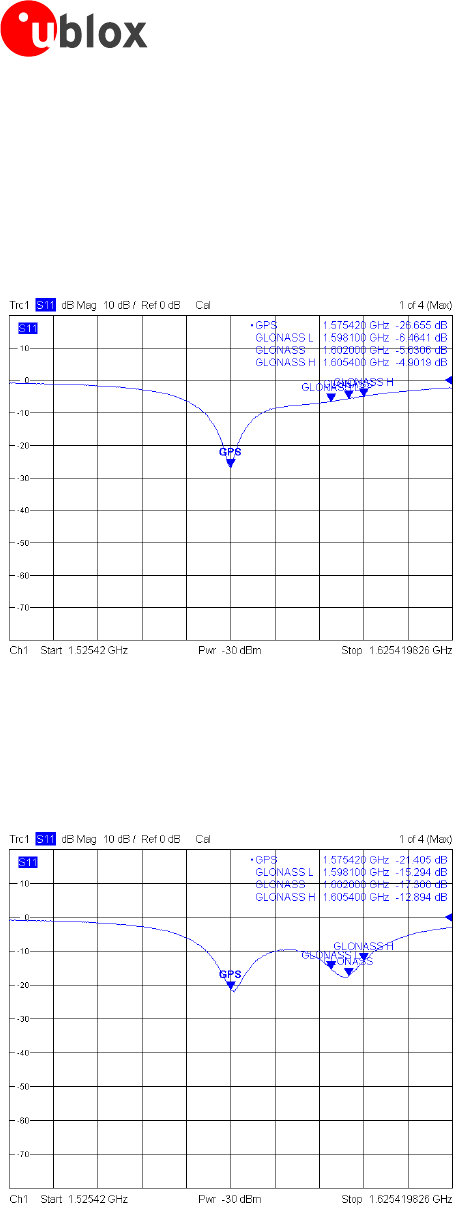
3.4.4 Design with GLONASS / GPS active antenna
The Russian GLONASS satellite system is an alternative system to the US-based Global Positioning System (GPS).
u-blox 7 modules can receive and process GLONASS signals. GLONASS and GPS satellite signals are not
transmitted at the same frequency (as seen in Figure 27). In existing designs that were only intended for GPS
reception, the RF path has to be modified (the LNA, filter, and antenna) accordingly to let both signals pass.
Figure 27: GPS & GLONASS SAW filter
Usually an active GPS antenna includes a GPS band pass filter, which may filter out the GLONASS signal (see
Figure 27). For this reason, make sure that the filter in the active antenna is wide enough to let the GPS and
GLONASS signals pass. Use a good performance GPS & GLONASS active antenna (for recommended
components see section 3.5.1).
In a combined GPS & GLONASS antenna, be sure to tune the antenna for receiving both signals. In addition, any
internal filter has a larger bandwidth to provide optimal GPS & GLONASS signal reception.
Use a good performance GPS & GLONASS active antenna (for recommended components see section
3.5.1).
MAX-7 / NEO-7 - Hardware Integration Manual
UBX-13003704 - R07 Early Production Information Design
Page 31 of 50
3.4.5 Design with GLONASS / GPS passive antenna
In general, GPS patch antennas only receive GPS signals well. A typical return plot (S11 measurement) shows
that the GLONASS signal is highly attenuated. (See Figure 28)
u-blox 7 modules supporting GLONASS have a GPS & GLONASS SAW filter that lets both GPS and GLONASS
signals pass. For best performance with passive antenna designs, use an external LNA. (See section 3.4.1.2).
Figure 28: 25*25*4 mm GPS patch antenna on 70*70 mm GND plane
To receive GPS and GLONASS, a special antenna patch (which can receive both GPS and GLONASS) is needed.
The return plot (S11 measurement) in Figure 29 below shows the two areas of lower attenuation.
Figure 29: 25*25*4 mm GPS / GLONASS patch antenna on 70*70 mm GND plane
MAX-7 / NEO-7 - Hardware Integration Manual
UBX-13003704 - R07 Early Production Information Design
Page 32 of 50
3.5 Recommended parts
u-blox has tested and recommends the parts listed in Table 8. Other untested components may also be used.
Manufacturer Part ID Remarks Parameters to consider
Diode ON
Semiconductor
ESD9R3.3ST5G Standoff voltage > 3.3 V Low Capacitance < 0.5 pF
ESD9L3.3ST5G Standoff voltage > 3.3 V Standoff voltage > voltage for active
antenna
ESD9L5.0ST5G Standoff voltage > 5 V Low Inductance
SAW TDK/ EPCOS B8401: B39162-B8401-P810 GPS+GLONASS High attenuation
TDK/ EPCOS B3913: B39162B3913U410 GPS+GLONASS For automotive application
TDK/ EPCOS B9850: B39162B9850P810 GPS Low insertion loss
TDK/ EPCOS B8400: B39162B8400P810 GPS ESD protected and high input power
muRata SAFEA1G58KB0F00 GPS+GLONASS Low insertion loss, only for mobile
application
muRata SAFEA1G58KA0F00 GPS+GLONASS High attenuation, only for mobile
application
muRata SAFFB1G58KA0F0A GPS+GLONASS High attenuation, only for mobile
application
muRata SAFFB1G58KB0F0A GPS+GLONASS Low insertion loss, Only for mobile
application
Triquint B9850 GPS Compliant to the AEC-Q200 standard
CTS CER0032A GPS Ceramic filter also offers robust ESD
protection
LNA Avago ALM-1106 LNA pHEMT (GaAS)
ALM-1412 LNA + FBAR Filter
ALM-1712 Filter + LNA + FBAR Filter
ALM-1912 LNA Module, for GPS only, also including
FBAR filter in front of LNA
ALM-2412 LNA + FBAR Filter
ALM-2712 LNA Module, for GPS only, FBAR filter-LNA
filter FBAR
MAXIM MAX2659ELT+ LNA Low noise figure, up to 10 dBm RF input
power
JRC NJG1143UA2 LNA Low noise figure, up to 15 dBm RF input
power
Infineon BGM1032N16 Filter + LNA
BGM781N11 Filter + LNA + Filter
BGM1052N16 LNA + Filter
Triquint TQM640002 Filter + LNA + Filter
Inductor Murata LQG15HS27NJ02 L, 27 nH Impedance @ freq GPS > 500 Ω
Capacitor Murata GRM1555C1E470JZ01 C, 47 pF DC-block
Ferrite
Bead
Murata BLM15HD102SN1 FB High IZI @ fGSM
Feed thru Murata
Capacitor
for Signal
NFL18SP157X1A3
Monolithic Type
Array Type
Load Capacitance appropriate to
Baud rate
CL < xxx pF
NFA18SL307V1A45
Feed thru
Capacitor
Murata NFM18PC ….
NFM21P….
0603 2A
0805 4A
Rs < 0.5 Ω
Resistor 10 Ω ± 10%, min 0.250 W Rbias
560 Ω ± 5% R2
100 kΩ ± 5% R3, R4
Op Amp Linear
Technology
LT6000 U1 Rail to Rail
Transistor Vishay Si1016X T1
Transistor Vishay Si1040X T2
Table 8: Recommended parts
MAX-7 / NEO-7 - Hardware Integration Manual
UBX-13003704 - R07 Early Production Information Design
Page 33 of 50
3.5.1 Recommended GPS & GLONASS active antenna (A1)
Manufacturer Order No. Comments
Taoglas (www.taoglas.com)
AA.160.301111
36*36*4 mm, 3 to 5V / 30mA
Taoglas (www.taoglas.com) AA.161.301111 36*36*3 mm, 1.8 to 5.5V / 10mA at 3V
INPAQ B3G02G-S3-01-A 2.7 to 3.9 V / 10 mA
Hirschmann GLONASS 9 M 2.7 to 5.5 V / 13 mA
Additional antenna Manufacturer:
Allis Communications, 2J, Tallysman Wireless
Table 9: Recommend GPS & GLONASS active antenna (A1)
3.5.2 Recommended GPS & GLONASS passive patch antenna
Manufacturer Order No. Comments
Amotech (www.amotech.co.kr) B35-3556920-2J2 35x35x3 mm GPS+GLONASS
Amotech (www.amotech.co.kr) A25-4102920-2J3 25x25x4 mm GPS+GLONASS
Amotech (www.amotech.co.kr) A18-4135920-AMT04 18x18x4 mm GPS+GLONASS
Table 10: Recommend GPS & GLONASS passive patch antenna
3.5.3 Recommended GPS & GLONASS passive chip antenna
Manufacturer Order No. Comments
INPAQ (www.inpaq.com.tw) ACM4-5036-A1-CC-S 5.2 x 3.7 x 0.7 mm GPS+GLONASS
Table 11: Recommend GPS & GLONASS passive chip antenna
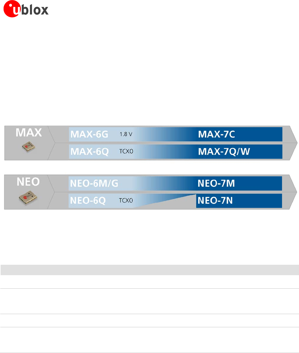
MAX-7 / NEO-7 - Hardware Integration Manual
UBX-13003704 - R07 Early Production Information Migration to u-blox-7 modules
Page 34 of 50
4 Migration to u-blox-7 modules
4.1 Migrating u-blox 6 designs to a u-blox 7 module
Figure 30 below shows a recommended migration path from u-blox 6 designs to use with u-blox 7 modules.
u-blox is committed to ensuring that products in the same form factor are backwards compatible over several
technology generations. Utmost care has been taken to ensure no negative impact on function or performance
and to make u-blox 7 modules as fully compatible as possible with u-blox 6 versions. No limitations of the
standard features have resulted. It is highly advisable that customers consider a design review with the u-blox
support team to ensure the compatibility of key functionalities.
Figure 30: Migrating u-blox 6 designs to a u-blox 7 receiver module
4.2 Hardware migration
4.2.1 Hardware compatibility:
Table 12 provides a summary of important hardware migration issues to note.
NEO-7 MAX-7
Fully compatible VCC, RF_IN, GND, USB pins, TxD, RxD, VCC_RF, SDA
and SCL
VCC, RF_IN, GND, TxD, RxD, VCC_RF, SDA and SCL
Changes SPI implementation has changed:
With u-blox 6, SPI uses pins 2, 14, 15, 16.
With u-blox 7, SPI is available on pins 18, 19, 20, 21
when pin 2 set low. See Table 13
Not supported SPI Flash On-board RTC clock unavailable on MAX-7C, use the
“Single Crystal” feature instead.
Limitations UART/ DDC and SPI share the same pins and are
mutually exclusive.
No Configuration pins: use of e-fuse possible
(See Data Sheet for more information)
ANT_ON voltage level (VCC_IO)
Table 12: Summary of important hardware migration issues

MAX-7 / NEO-7 - Hardware Integration Manual
UBX-13003704 - R07 Early Production Information Migration to u-blox-7 modules
Page 35 of 50
4.2.2 Hardware migration NEO-6 -> NEO-7
Pin
NEO-6 NEO-7 Remarks for Migration
Pin Name Typical Assignment Pin Name Typical Assignment
1 RESERVED Leave open. RESERVED Leave open. No difference
2 SS_N SPI Slave Select D_SEL selects the interface -> Different functions, compatible only when not
using SPI for communication.
3 TIMEPULSE Time pulse (1PPS) TIMEPULSE Time pulse (1PPS) No difference
4 EXTINT0 External interrupt pin EXTINT0 External interrupt pin No difference
5 USB_DM USB data USB_DM USB Data No difference
6 USB_DP USB data USB_DP USB Data No difference
7 VDD_USB USB supply VDD_USB USB supply No difference
8 RESERVED
Pin 8 and 9 must be
connected together.
RESET_N Reset input
If pin 8 is connected to pin 9 on NEO-7N, the
device always runs. With NEO-6Q, if Reset input
is used, it implements the 3k3 resistor from pin 8
to pin 9. This also works with NEO-7N. If used
with NEO-7N, do not populate the pull-up
resistor.
9 VCC_RF
Can be used for active
antenna or external
LNA supply.
VCC_RF
Can be used for active
antenna or external
LNA supply.
No difference
10 GND GND GND GND No difference
11 RF_IN GPS signal input RF_IN GPS signal input No difference
12 GND GND GND GND No difference
13 GND GND GND GND No difference
14 MOSI/CFG_
COM0
SPI MOSI /
Configuration pin.
Leave open if not
used.
ANT_ON turn on and off an
optional external LNA
ANT_ON (antenna on) can be used to turn on
and off an optional external LNA.
-> Different functions, no SPI MOSI and
configuration pins with NEO-7. If not used as
default configuration, it must be set using
software command!
It is not possible to migrate from NEO-6 to NEO-
7N, if NEO-6 pin 14 is connected to GND. In this
case, migrate to NEO-7M!
15 MISO/CFG_
COM1
SPI MISO /
Configuration pin.
Leave open if not
used.
RESERVED Leave open.
16 CFG_GPS0/
SCK
Power Mode
Configuration pin / SPI
Clock. Leave open if
not used.
RESERVED Leave open.
17 RESERVED Leave open. RESERVED Leave open. No difference
18 SDA DDC Data SDA DDC Data / SPI CS_N No difference for DDC. If pin 2 low = SPI chip
select.
19 SCL DDC Clock SCL DDC Clock / SPI SCK No difference for DDC. If pin 2 low = SPI clock.
20 TxD Serial Port TxD Serial Port / SPI MISO No difference for UART. If pin 2 low = SPI
MISO.
21 RxD Serial Port RxD Serial Port / SPI MOSI No difference for UART. If pin 2 low = SPI
MOSI.
22 V_BCKP
Backup supply voltage
V_BCKP
Backup supply voltage Check current in Data Sheet
If on u-blox 6 module this was connected to
GND, no problem to do the same in u-blox 7.
23 VCC
Supply voltage
NEO-6G: 1.75 – 2.0V
NEO-6Q/M/P/V/T:
2.7 – 3.6V
VCC
Supply voltage
NEO-7M: 1.65 – 3.6V
NEO-7N/P: 2.7 – 3.6V
See Figure 30 for migration path
24 GND GND GND GND No difference
Table 13: Pin-out comparison NEO-6 vs. NEO-7
MAX-7 / NEO-7 - Hardware Integration Manual
UBX-13003704 - R07 Early Production Information Migration to u-blox-7 modules
Page 36 of 50
4.2.3 Hardware migration MAX-6 -> MAX-7
Pin
MAX-6 MAX-7 Remarks for Migration
Pin Name Typical Assignment Pin Name Typical Assignment
1 GND GND GND GND No difference
2 TxD Serial Port TxD Serial Port No difference
3 RxD Serial Port RxD Serial Port No difference
4 TIMEPULSE Time pulse (1PPS) TIMEPULSE Time pulse (1PPS) No difference
5 EXTINT0 External Interrupt
pin EXTINT0 External Interrupt
pin No difference
6 V_BCKP
Backup supply
voltage
V_BCKP
Backup supply
voltage If on u-blox 6 module this was connected to GND,
no problem to do the same in u-blox 7.
(MAX-7C: Higher backup current, see 2.5.3.1
Single Crystal)
7 VCC_IO
IO supply voltage
Input must be
always supplied.
Usually connect to
VCC pin 8
VCC_IO
IO supply voltage
Input must be
always supplied.
Usually connect to
VCC pin 8
No difference
8 VCC
Power supply of
module
MAX-6G 1.75 –
2.0V
MAX-6Q/C: 2.7 –
3.6V
VCC
Power supply of
module
MAX-7C: 1.65 –
3.6V
MAX-7Q: 2.7 –
3.6V
9 VRESET connect to pin 8 RESET_N Reset input
With MAX-6, if Reset input is used, it implements
the 3k3 resistor from pin 9 to pin 8. This also
works with MAX-7. If used with MAX-7, do not
populate the pull-up resistor.
10 GND GND GND GND No difference
11 RF_IN Matched RF-Input,
DC block inside. RF_IN Matched RF-Input,
DC block inside. No difference
12 GND GND GND GND No difference
13 ANT_ON
Active antenna or
ext. LNA control
pin in power save
mode.
ANT_ON pin
voltage level: MAX-
6 -> VCC_RF (pull-
up)
ANT_ON
Active antenna or
ext. LNA control
pin in power save
mode.
ANT_ON pin
voltage level: MAX-
7 -> VCC_IO (push-
pull)
On MAX-6, ANT_ON pin voltage level is with
respect to VCC_RF, on MAX-7 to VCC_IO
(only relevant when VCC_IO does not share the
same supply with VCC)
14 VCC_RF
Can be used for
active antenna or
external LNA
supply.
VCC_RF
Can be used for
active antenna or
external LNA
supply.
No difference
15 RESERVED Leave open.
RESERVED
(MAX-7W:
V_ANT )
Leave open. No difference
16 SDA DDC Data SDA DDC Data No difference
17 SCL DDC Clock SCL DDC Clock No difference
18 RESERVED Leave open. RESERVED Leave open. No difference
Table 14: Pin-out comparison MAX-6 vs. MAX-7
MAX-7 / NEO-7 - Hardware Integration Manual
UBX-13003704 - R07 Early Production Information Migration to u-blox-7 modules
Page 37 of 50
4.3 Software migration
For an overall description of the module software operation, refer to the u-blox 7 Receiver Description
including Protocol Specification [4].
4.3.1 Software compatibility
u-blox 7 modules introduce a new firmware: Version 1.00. When migrating, customers should ensure that
commands used originally with u-blox 6 products are supported by the new firmware version. For information
about known limitations that could affect migration, see the u-blox 7 Firmware Version 1.0 Release Note [5].
Table 15 provides a summary of important software migration issues to note.
Changes The configuration of the TX Ready feature has changed between MAX-6 and MAX-7 modules and is only recognized from
LEON FW 07.70 and LISA-U2 01S onwards. The MAX-6 TxD pin is mapped to PIO#5 while the MAX-7 TxD pin is mapped
to PIO#6. When communicating with u-blox wireless modules, this change of pins is not recognized by LEON FW7.60.02
and previous versions.
u-blox 6: 0 s leap second by default FW 6.02 and FW7.0x: 15 s leap second by default
u-blox 7: 16 s leap second by default
Table 15: Summary of important software migration issues
Low power modes are supported by the Power Save Mode of FW 1.0 or ROM 1.0. For migration, consult
the u-blox 7 Firmware Version 1.0 Release Note [5] and the u-blox 7 Receiver Description Including
Protocol Specification [4].
4.3.2 Messages no longer supported
u-blox 6 u-blox 7 Remarks
UBX-CFG-TP UBX-CFG-TP5 This has been replaced with the more versatile CFG-TP5, which allows
for two separate time pulses and more parameters to set their function.
UBX-CFG-PM UBX-CFG-PM2 This has been replaced with CFG-PM2, which allows for a more
extended Power management configuration.
UBX-CFG-FXN UBX-CFG-PM2 This has been replaced by CFG-PM2.
UBX-CFG-TMODE UBX-CGF-TMODE2 This has been replaced by CGF-TMODE2.
NMEA-PUBX05 - Not available in this firmware.
NMEA-PUBX06 - Not available in this firmware.
Table 16: Main differences between u-blox 6 and u-blox 7 software for migration

MAX-7 / NEO-7 - Hardware Integration Manual
UBX-13003704 - R07 Early Production Information Product handling
Page 38 of 50
5 Product handling
5.1 Packaging, shipping, storage and moisture preconditioning
For information pertaining to reels and tapes, Moisture Sensitivity levels (MSD), shipment and storage
information, as well as drying for preconditioning see the specific u-blox 7 GNSS module data sheet.
5.1.1 Population of Modules
When populating our modules make sure that the pick and place machine is aligned to the copper pins of
the module and not on the module edge.
5.2 Soldering
5.2.1 Soldering paste
Use of "No Clean" soldering paste is strongly recommended, as it does not require cleaning after the soldering
process has taken place. The paste listed in the example below meets these criteria.
Soldering Paste: OM338 SAC405 / Nr.143714 (Cookson Electronics)
Alloy specification: Sn 95.5/ Ag 4/ Cu 0.5 (95.5% Tin/ 4% Silver/ 0.5% Copper)
Melting Temperature: 217 °C
Stencil Thickness: 150μm The final choice of the soldering paste depends on the approved manufacturing
procedures.
The paste-mask geometry for applying soldering paste should meet the recommendations.
The quality of the solder joints on the connectors (’half vias’) should meet the appropriate IPC
specification.
5.2.2 Reflow soldering
A convection type-soldering oven is strongly recommended over the infrared type radiation oven.
Convection heated ovens allow precise control of the temperature and all parts will be heated up evenly,
regardless of material properties, thickness of components and surface color.
Consider the "IPC-7530 Guidelines for temperature profiling for mass soldering (reflow and wave) processes,
published 2001. “
Preheat phase
Initial heating of component leads and balls. Residual humidity will be dried out. Please note that this preheat
phase will not replace prior baking procedures.
• Temperature rise rate: max. 3 °C/s If the temperature rise is too rapid in the preheat phase it may cause
excessive slumping.
• Time: 60 - 120 s If the preheat is insufficient, rather large solder balls tend to be generated. Conversely,
if performed excessively, fine balls and large balls will be generated in clusters.
• End Temperature: 150 - 200 °C If the temperature is too low, non-melting tends to be caused in areas
containing large heat capacity.
Heating/ Reflow phase
The temperature rises above the liquidus temperature of 217°C. Avoid a sudden rise in temperature as the slump
of the paste could become worse.
• Limit time above 217 °C liquidus temperature: 40 - 60 s
• Peak reflow temperature: 245 °C
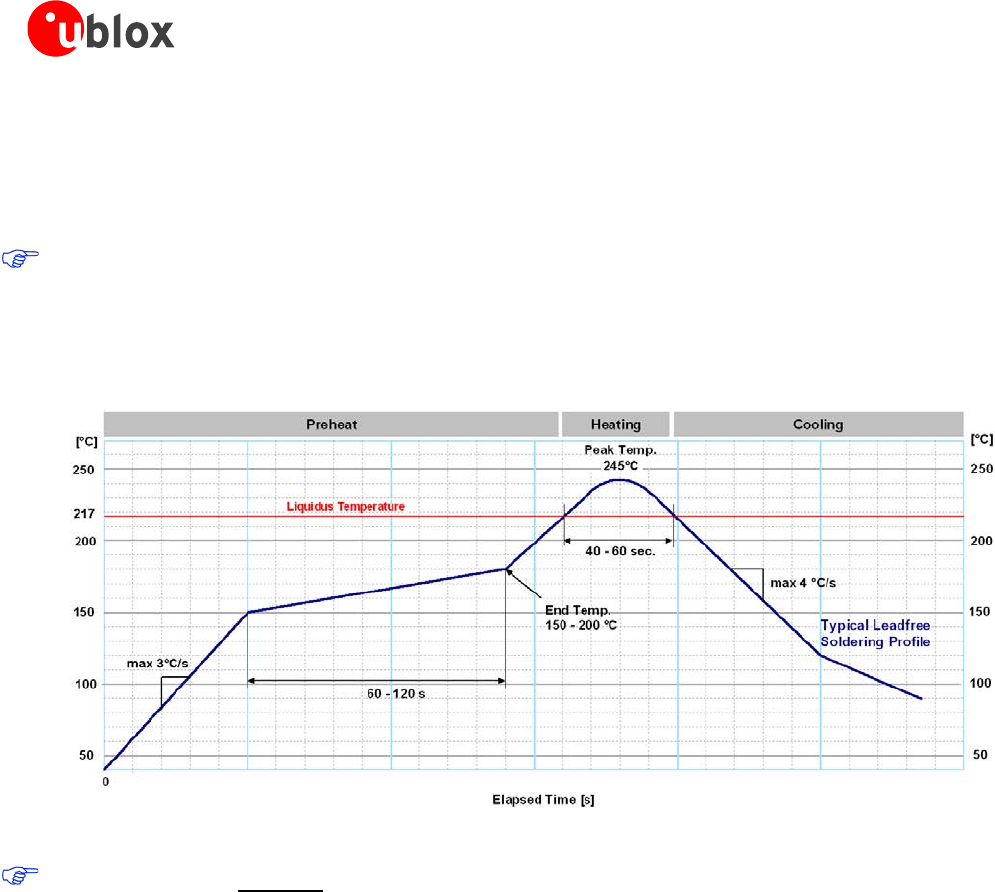
MAX-7 / NEO-7 - Hardware Integration Manual
UBX-13003704 - R07 Early Production Information Product handling
Page 39 of 50
Cooling phase
A controlled cooling avoids negative metallurgical effects (solder becomes more brittle) of the solder and
possible mechanical tensions in the products. Controlled cooling helps to achieve bright solder fillets with a good
shape and low contact angle.
• Temperature fall rate: max 4 °C/s
To avoid falling off, the u-blox 7 GNSS module should be placed on the topside of the motherboard
during soldering.
The final soldering temperature chosen at the factory depends on additional external factors like choice of
soldering paste, size, thickness and properties of the base board, etc. Exceeding the maximum soldering
temperature in the recommended soldering profile may permanently damage the module.
Figure 31: Recommended soldering profile
u-blox 7 modules must not be soldered with a damp heat process.
5.2.3 Optical inspection
After soldering the u-blox 7 module, consider an optical inspection step to check whether:
• The module is properly aligned and centered over the pads
• All pads are properly soldered
• No excess solder has created contacts to neighboring pads, or possibly to pad stacks and vias nearby
5.2.4 Cleaning
In general, cleaning the populated modules is strongly discouraged. Residues underneath the modules cannot be
easily removed with a washing process.
• Cleaning with water will lead to capillary effects where water is absorbed in the gap between the baseboard
and the module. The combination of residues of soldering flux and encapsulated water leads to short circuits
or resistor-like interconnections between neighboring pads.
• Cleaning with alcohol or other organic solvents can result in soldering flux residues flooding into the two
housings, areas that are not accessible for post-wash inspections. The solvent will also damage the sticker
and the ink-jet printed text.
• Ultrasonic cleaning will permanently damage the module, in particular the quartz oscillators.
The best approach is to use a "no clean" soldering paste and eliminate the cleaning step after the soldering.

MAX-7 / NEO-7 - Hardware Integration Manual
UBX-13003704 - R07 Early Production Information Product handling
Page 40 of 50
5.2.5 Repeated reflow soldering
Only single reflow soldering processes are recommended for boards populated with u-blox 7 modules. u-blox 7
modules should not be submitted to two reflow cycles on a board populated with components on both sides in
order to avoid upside down orientation during the second reflow cycle. In this case, the module should always
be placed on that side of the board, which is submitted into the last reflow cycle. The reason for this (besides
others) is the risk of the module falling off due to the significantly higher weight in relation to other
components.
Two reflow cycles can be considered by excluding the above described upside down scenario and taking into
account the rework conditions described in Section 5.2.8.
Repeated reflow soldering processes and soldering the module upside down are not recommended.
5.2.6 Wave soldering
Base boards with combined through-hole technology (THT) components and surface-mount technology (SMT)
devices require wave soldering to solder the THT components. Only a single wave soldering process is
encouraged for boards populated with u-blox 7 modules.
5.2.7 Hand soldering
Hand soldering is allowed. Use a soldering iron temperature setting equivalent to 350 °C and carry out the hand
soldering according to the IPC recommendations / reference documents IPC7711. Place the module precisely on
the pads. Start with a cross-diagonal fixture soldering (e.g. pins 1 and 15), and then continue from left to right.
5.2.8 Rework
The u-blox 7 module can be unsoldered from the baseboard using a hot air gun. When using a hot air gun for
unsoldering the module, max one reflow cycle is allowed. In general, we do not recommend using a hot air gun
because this is an uncontrolled process and might damage the module.
Attention: use of a hot air gun can lead to overheating and severely damage the module.
Always avoid overheating the module.
After the module is removed, clean the pads before placing and hand soldering a new module.
Never attempt a rework on the module itself, e.g. replacing individual components. Such
actions immediately terminate the warranty.
In addition to the two reflow cycles, manual rework on particular pins by using a soldering iron is allowed. For
hand soldering the recommendations in IPC 7711 should be followed. Manual rework steps on the module can
be done several times.
5.2.9 Conformal coating
Certain applications employ a conformal coating of the PCB using HumiSeal® or other related coating products.
These materials affect the HF properties of the GNSS module and it is important to prevent them from flowing
into the module. The RF shields do not provide 100% protection for the module from coating liquids with low
viscosity; therefore, care is required in applying the coating.
Conformal Coating of the module will void the warranty.
5.2.10 Casting
If casting is required, use viscose or another type of silicon pottant. The OEM is strongly advised to qualify such
processes in combination with the u-blox 7 module before implementing this in the production.
Casting will void the warranty.
MAX-7 / NEO-7 - Hardware Integration Manual
UBX-13003704 - R07 Early Production Information Product handling
Page 41 of 50
5.2.11 Grounding metal covers
Attempts to improve grounding by soldering ground cables, wick or other forms of metal strips directly onto the
EMI covers is done at the customer's own risk. The numerous ground pins should be sufficient to provide
optimum immunity to interferences and noise.
u-blox makes no warranty for damages to the u-blox 7 module caused by soldering metal cables or any
other forms of metal strips directly onto the EMI covers.
5.2.12 Use of ultrasonic processes
Some components on the u-blox 7 module are sensitive to Ultrasonic Waves. Use of any Ultrasonic Processes
(cleaning, welding etc.) may cause damage to the GNSS Receiver.
u-blox offers no warranty against damages to the u-blox 7 module caused by any Ultrasonic Processes.
5.3 EOS/ESD/EMI precautions
When integrating GNSS positioning modules into wireless systems, careful consideration must be given to
electromagnetic and voltage susceptibility issues. Wireless systems include components, which can produce
Electrical Overstress (EOS) and Electro-Magnetic Interference (EMI). CMOS devices are more sensitive to such
influences because their failure mechanism is defined by the applied voltage, whereas bipolar semiconductors
are more susceptible to thermal overstress. The following design guidelines are provided to help in designing
robust yet cost effective solutions.
To avoid overstress damage during production or in the field it is essential to observe strict
EOS/ESD/EMI handling and protection measures.
To prevent overstress damage at the RF_IN of your receiver, never exceed the maximum input
power (see Data Sheet).
5.3.1 Electrostatic discharge (ESD)
Electrostatic discharge (ESD) is the sudden and momentary electric current that flows between
two objects at different electrical potentials caused by direct contact or induced by an
electrostatic field. The term is usually used in the electronics and other industries to describe
momentary unwanted currents that may cause damage to electronic equipment.
5.3.2 ESD handling precautions
ESD prevention is based on establishing an Electrostatic Protective Area (EPA). The EPA can be a small working
station or a large manufacturing area. The main principle of an EPA is that there are no highly charging materials
near ESD sensitive electronics, all conductive materials are grounded, workers are grounded, and charge build-up
on ESD sensitive electronics is prevented. International standards are used to define typical EPA and can be
obtained for example from International Electrotechnical Commission (IEC) or American National Standards
Institute (ANSI).
GNSS positioning modules are sensitive to ESD and require special precautions when handling. Particular care
must be exercised when handling patch antennas, due to the risk of electrostatic charges. In addition to
standard ESD safety practices, the following measures should be taken into account whenever handling the
receiver.
• Unless there is a galvanic coupling between the local GND (i.e. the
work table) and the PCB GND, then the first point of contact when
handling the PCB must always be between the local GND and PCB
GND.
• Before mounting an antenna patch, connect ground of the device
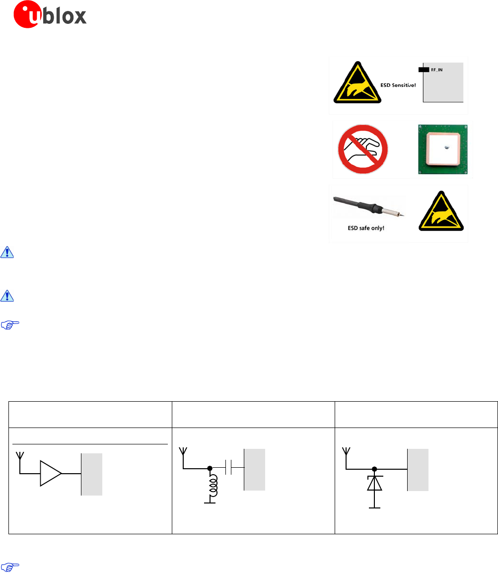
MAX-7 / NEO-7 - Hardware Integration Manual
UBX-13003704 - R07 Early Production Information Product handling
Page 42 of 50
• When handling the RF pin, do not come into contact with any
charged capacitors and be careful when contacting materials that
can develop charges (e.g. patch antenna ~10 pF, coax cable ~50 -
80 pF/m, soldering iron, …)
• To prevent electrostatic discharge through the RF input, do not
touch any exposed antenna area. If there is any risk that such
exposed antenna area is touched in non ESD protected work area,
implement proper ESD protection measures in the design.
• When soldering RF connectors and patch antennas to the receiver’s
RF pin, make sure to use an ESD safe soldering iron (tip).
Failure to observe these precautions can result in severe damage to the GNSS module!
5.3.3 ESD protection measures
GNSS positioning modules are sensitive to Electrostatic Discharge (ESD). Special precautions are
required when handling.
For more robust designs, employ additional ESD protection measures. Using an LNA with appropriate ESD
rating can provide enhanced GNSS performance with passive antennas and increases ESD protection.
Most defects caused by ESD can be prevented by following strict ESD protection rules for production and
handling. When implementing passive antenna patches or external antenna connection points, then additional
ESD measures as shown in Figure 32 can also avoid failures in the field.
Small passive antennas (<2 dBic
and performance critical)
Passive antennas (>2 dBic or
performance sufficient)
Active antennas
A
RF_IN
GPS
Receiver
LNA
B
L
RF_IN
GPS
Receiver
C
D
RF_IN
GPS
Receiver
LNA with appropriate ESD rating
Figure 32: ESD Precautions
Protection measure A is preferred because it offers the best GNSS performance and best level of ESD
protection.
5.3.4 Electrical Overstress (EOS)
Electrical Overstress (EOS) usually describes situations when the maximum input power exceeds the maximum
specified ratings. EOS failure can happen if RF emitters are close to a GNSS receiver or its antenna. EOS causes
damage to the chip structures. If the RF_IN is damaged by EOS, it is hard to determine whether the chip
structures have been damaged by ESD or EOS.
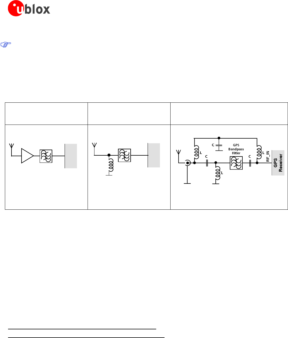
MAX-7 / NEO-7 - Hardware Integration Manual
UBX-13003704 - R07 Early Production Information Product handling
Page 43 of 50
5.3.5 EOS protection measures
For designs with GNSS positioning modules and wireless (e.g. GSM/GPRS) transceivers in close proximity,
ensure sufficient isolation between the wireless and GNSS antennas. If wireless power output causes the
specified maximum power input at the GNSS RF_IN to be exceeded, employ EOS protection measures to
prevent overstress damage.
For robustness, EOS protection measures, as shown in the examples in Figure 33, are recommended for designs
combining wireless communication transceivers (e.g. GSM, GPRS) and GNSS receivers in the same design or in
close proximity.
Small passive antennas
(<2 dBic and performance
critical)
Passive antennas (>2 dBic or
performance sufficient)
Active antennas (without internal filter
which need the module antenna supervisor
circuits)
D
RF_IN
GPS
Receiver
LNA
GPS
Bandpass
Filtler
E
RF_IN
GPS
Receiver
L
GPS
Bandpass
Filtler
F
LNA with appropriate ESD
rating and maximum input
power
GPS Band pass Filter: SAW or
Ceramic with low insertion loss
and appropriate ESD rating
Figure 33: EOS and ESD Precautions
5.3.6 Electromagnetic interference (EMI)
Electromagnetic interference (EMI) is the addition or coupling of energy originating from any RF emitting device.
This can cause a spontaneous reset of the GNSS receiver or result in unstable performance. Any unshielded line
or segment (>3mm) connected to the GNSS receiver can effectively act as antenna and lead to EMI disturbances
or damage.
The following elements are critical regarding EMI:
• Unshielded connectors (e.g. pin rows etc.)
• Weakly shielded lines on PCB (e.g. on top or bottom layer and especially at the border of a PCB)
• Weak GND concept (e.g. small and/or long ground line connections)
EMI protection measures are recommended when RF emitting devices are near the GNSS receiver. To minimize
the effect of EMI a robust grounding concept is essential. To achieve electromagnetic robustness follow the
standard EMI suppression techniques.
http://www.murata.com/products/emc/knowhow/index.html
http://www.murata.com/products/emc/knowhow/pdf/4to5e.pdf
Improved EMI protection can be achieved by inserting a resistor (e.g. R>20 Ω) or better yet a ferrite bead
(BLM15HD102SN1) or an inductor (LQG15HS47NJ02) into any unshielded PCB lines connected to the GNSS
receiver. Place the resistor as close as possible to the GNSS receiver pin.
Example of EMI protection measures on the RX/TX line using a ferrite bead:
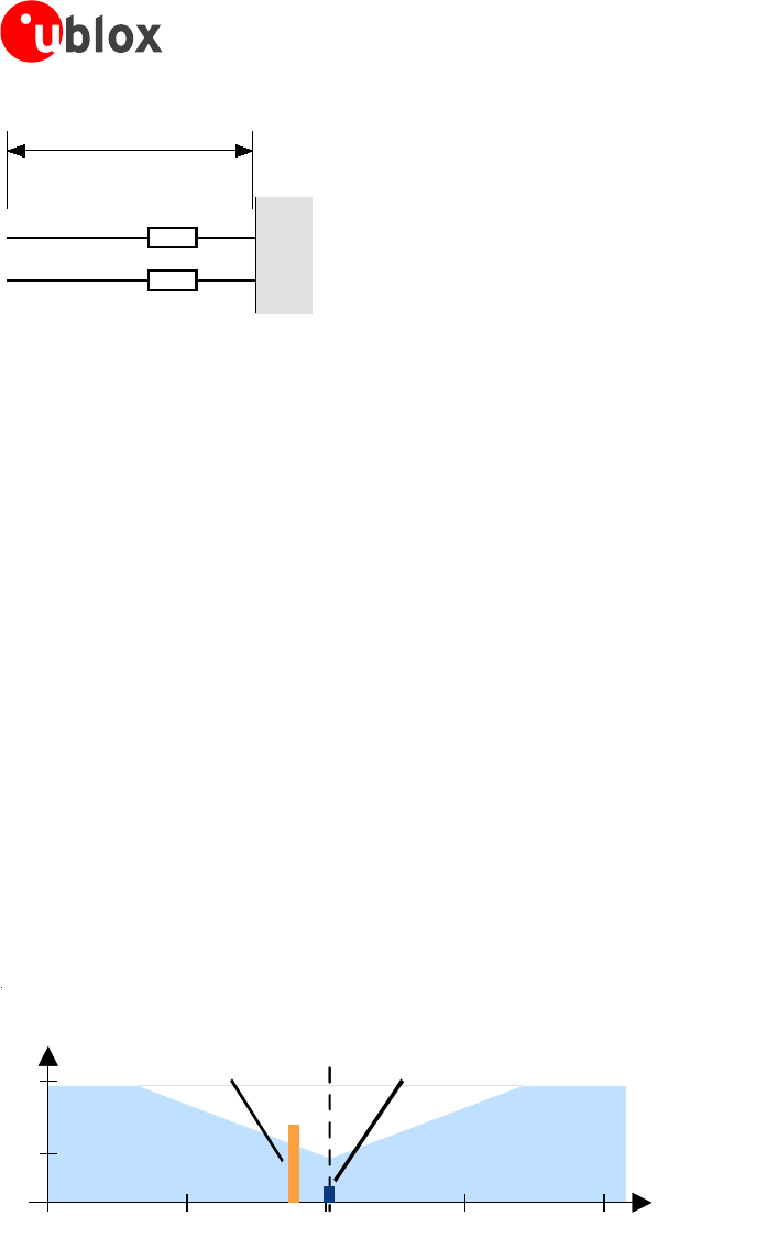
MAX-7 / NEO-7 - Hardware Integration Manual
UBX-13003704 - R07 Early Production Information Product handling
Page 44 of 50
TX
RX
GPS
Receiver
FB
FB
BLM15HD102SN1
>10mm
Figure 34: EMI Precautions
VCC can be protected using a feed thru capacitor. For electromagnetic compatibility (EMC) of the RF_IN pin,
refer to section 5.3.5
5.3.7 Applications with wireless modules LEON / LISA
GSM uses power levels up to 2 W (+33 dBm). Consult the Data Sheet for the absolute maximum power input at
the GNSS receiver.
5.3.7.1 Isolation between GPS and GSM antenna
In a handheld type design, an isolation of approximately 20 dB can be reached with careful placement of the
antennas. If such isolation cannot be achieved, e.g. in the case of an integrated GSM/GPS antenna, an additional
input filter is needed on the GPS side to block the high energy emitted by the GSM transmitter. Examples of
these kinds of filters would be the SAW Filters from Epcos (B9444 or B7839) or Murata.
5.3.7.2 Increasing jamming immunity
Jamming signals come from in-band and out-band frequency sources.
5.3.7.3 In-band jamming
With in-band jamming the signal frequency is very close to the GPS frequency of 1575 MHz (see Figure 35). Such
jamming signals are typically caused by harmonics from displays, micro-controller, bus systems, etc.
1525 1550 1625
GPS input filter
characteristics
1575 1600
0
-110
J ammi n
g signal
1525 1550 1625
Frequency [MHz]
Power [dBm]
GPS input filter
characteristics
1575 1600
0
J ammi n g
signal
GPS
signals
GPS Carrier
1575.4 MHz
Figure 35: In-band jamming signals
MAX-7 / NEO-7 - Hardware Integration Manual
UBX-13003704 - R07 Early Production Information Product handling
Page 45 of 50
Figure 36: In-band jamming sources
Measures against in-band jamming include:
• Maintaining a good grounding concept in the design
• Shielding
• Layout optimization
• Filtering
• Placement of the GPS antenna
• Adding a CDMA, GSM, WCDMA band pass filter before handset antenna
5.3.7.4 Out-band jamming
Out-band jamming is caused by signal frequencies that are different from the GPS carrier (see Figure 37). The
main sources are wireless communication systems such as GSM, CDMA, WCDMA, Wi-Fi, BT, etc.
0500 1000 1500 2000
GPS input filter
characteristics
0
-110
0500 1500 2000
Frequency [MHz]
GSM
900
GSM
1800
GSM
1900
Power [dBm]
GPS input filter
characteristics
GPS
1575
0
-110
GPS
signals
GSM
950
Figure 37: Out-band jamming signals
Measures against out-band jamming include maintaining a good grounding concept in the design and adding a
SAW or band pass ceramic filter (as recommend in Section 5.3.5) into the antenna input line to the GNSS
receiver (see Figure 38).
Figure 38: Measures against in-band jamming
MAX-7 / NEO-7 - Hardware Integration Manual
UBX-13003704 - R07 Early Production Information Product testing
Page 46 of 50
6 Product testing
6.1 u-blox in-series production test
u-blox focuses on high quality for its products. To achieve a high standard it is our philosophy to supply fully
tested units. Therefore, at the end of the production process, every unit is tested. Defective units are analyzed in
detail to improve the production quality.
This is achieved with automatic test equipment, which delivers a detailed test report for each unit. The following
measurements are done:
• Digital self-test (Software Download, verification of FLASH firmware, etc.)
• Measurement of voltages and currents
• Measurement of RF characteristics (e.g. C/No)
• Traceability down to component level
• X-Ray and Automated Optical Inspection (AOI)
• Ongoing Reliability Tests
Figure 39: Automatic Test Equipment for Module Tests
Figure 40: X-Ray Inspection
6.2 Test parameters for OEM manufacturer
Because of the testing done by u-blox (with 100% coverage), it is obvious that an OEM manufacturer does not
need to repeat firmware tests or measurements of the GNSS parameters/characteristics (e.g. TTFF) in their
production test.
An OEM manufacturer should focus on:
• Overall sensitivity of the device (including antenna, if applicable)
• Communication to a host controller
6.3 System sensitivity test
The best way to test the sensitivity of a GNSS device is with the use of a 1-channel GPS simulator. It assures
reliable and constant signals at every measurement.
MAX-7 / NEO-7 - Hardware Integration Manual
UBX-13003704 - R07 Early Production Information Product testing
Page 47 of 50
Figure 41: 1-channel GPS simulator
u-blox recommends the following Single-Channel GPS Simulators:
• Spirent GSS6100 (GPS)
• Spirent GSS6300 (GPS/GLONASS)
Spirent Communications Positioning Technology, www.spirent.com
6.3.1 Guidelines for sensitivity tests
1. Connect a 1-channel GPS simulator to the OEM product
2. Choose the power level in a way that the “Golden Device” would report a C/No ratio of 38-40 dBHz
3. Power up the DUT (Device Under Test) and allow enough time for the acquisition
4. Read the C/No value from the NMEA GSV or the UBX-NAV-SVINFO message (e.g. with u-center)
5. Compare the results to a “Golden Device” or a u-blox 7 Evaluation Kit.
6.3.2 ‘Go/No go’ tests for integrated devices
The best test is to bring the device to an outdoor position with excellent sky view (HDOP < 3.0). Let the
receiver acquire satellites and compare the signal strength with a “Golden Device”.
As the electro-magnetic field of a redistribution antenna is not homogenous, indoor tests are in most
cases not reliable. These kind of tests may be useful as a ‘go/no go’ test but not for sensitivity
measurements.
MAX-7 / NEO-7 - Hardware Integration Manual
UBX-13003704 - R07 Early Production Information Appendix
Page 48 of 50
7 Appendix
A Abbreviations
Abbreviation Definition
ANSI American National Standards Institute
CDMA Code Division Multiple Access
EMC Electromagnetic compatibility
EMI Electromagnetic interference
EOS Electrical Overstress
EPA Electrostatic Protective Area
ESD Electrostatic discharge
GLONASS Russian satellite system
GND Ground
GNSS Global Navigation Satellite System
GPS Global Positioning System
GSM Global System for Mobile Communications
IEC International Electrotechnical Commission
PCB Printed circuit board
QZSS Quasi-Zenith Satellite System
Table 17: Explanation of abbreviations used
MAX-7 / NEO-7 - Hardware Integration Manual
UBX-13003704 - R07 Early Production Information Related documents
Page 49 of 50
Related documents
[1] NEO-7 Data Sheet, Docu. No GPS.G7-HW-11004
[2] MAX-7 Data Sheet, Docu. No GPS.G7-HW-12012
[3] u-blox 7 Receiver Description including Protocol Specification, Docu. No GPS.G7-SW-12001
[4] u-blox 7 Firmware Version 1.0 Release Note, Docu. No GPS.G7-SW-12003
[5] GPS Antenna Application Note, Docu. No GPS-X-08014
[6] UBX-G7020 Data Sheet, Docu. No GPS.G7-HW-10002
[7] GPS Compendium, Docu. No GPS-X-02007
[8] I2C-bus specification, Rev. 5, Oct 2012, http://www.nxp.com/documents/other/UM10204_v5.pdf
[9] GPS Implementation and Aiding Features in u-blox wireless modules, Docu. No GSM.G1-CS-09007
All these documents are available on our homepage (http://www.u-blox.com).
For regular updates to u-blox documentation and to receive product change notifications, please register
on our homepage (http://www.u-blox.com).
Revision history
Revision Date Name Status / Comments
- 04-Sep-2012 jfur Initial draft
1 20-Dec-2012 jfur MAX-7W added, Revision Chapter 3.4 Antenna supervision
DC-bloc removed from Figure 21 and Figure 22.
MAX-7C: Higher backup current, new Figure 42 and 43
2 11-Feb-2013 jfur NEO-7P added, Electrical Programmable Fuse (eFuse) added
3 22-Apr-2013 jfur Stencil thickness 150 um (Figure 9, 12, 13)
Table 15: (MAX-7W: V_ANT ) added
Added section 5.1.1 Population of Modules
4 17-Jun-2013 jfur ANT_ON description
Recommended GPS & GLONASS active antenna updated
Last revision with old document number GPS.G7-HW-11006
R06 30-Sep-2013 jfur Antenna open circuit detection (OCD) for MAX-7W in section 3.4.3.3
R07 20-Jan-2014 jfur LEA-7N removed
Figure 26 updated
Document status changed to Early Production Information

MAX-7 / NEO-7 - Hardware Integration Manual
UBX-13003704 - R07 Early Production Information Contact
Page 50 of 50
Contact
For complete contact information, visit us at www.u-blox.com
u-blox Offices
North, Central and South America
u-blox America, Inc.
Phone: +1 703 483 3180
E-mail: info_us@u-blox.com
Regional Office West Coast:
Phone: +1 408 573 3640
E-mail: info_us@u-blox.com
Technical Support:
Phone: +1 703 483 3185
E-mail: support_us@u-blox.com
Headquarters
Europe, Middle East, Africa
u-blox AG
Phone: +41 44 722 74 44
E-mail: info@u-blox.com
Support: support@u-blox.com
Asia, Australia, Pacific
u-blox Singapore Pte. Ltd.
Phone: +65 6734 3811
E-mail: info_ap@u-blox.com
Support: support_ap@u-blox.com
Regional Office Australia:
Phone: +61 2 8448 2016
E-mail: info_anz@u-blox.com
Support: support_ap@u-blox.com
Regional Office China (Beijing):
Phone: +86 10 68 133 545
E-mail: info_cn@u-blox.com
Support: support_cn@u-blox.com
Regional Office China (Shenzhen):
Phone: +86 755 8627 1083
E-mail: info_cn@u-blox.com
Support: support_cn@u-blox.com
Regional Office India:
Phone: +91 959 1302 450
E-mail: info_in@u-blox.com
Support: support_in@u-blox.com
Regional Office Japan:
Phone: +81 3 5775 3850
E-mail: info_jp@u-blox.com
Support: support_jp@u-blox.com
Regional Office Korea:
Phone: +82 2 542 0861
E-mail: info_kr@u-blox.com
Support: support_kr@u-blox.com
Regional Office Taiwan:
Phone: +886 2 2657 1090
E-mail: info_tw@u-blox.com
Support: support_tw@u-blox.com
