GS Users Manual
User Manual: Pdf
Open the PDF directly: View PDF ![]() .
.
Page Count: 176 [warning: Documents this large are best viewed by clicking the View PDF Link!]
- GS USER'S MANUAL
- About This Manual
- Changes Since Release of 5th Edition
- Overview
- Local Memory
- Drawing Function
- Image Data Transmission
- CRTC
- Signal
- Registers
- General Purpose Registers
- ALPHA_1 / ALPHA_2 : Alpha Blending Setting
- BITBLTBUF : Setting for Transmission between Buffers
- CLAMP_1 / CLAMP_2 : Texture Wrap Mode
- COLCLAMP : Color Clamp Control
- DIMX : Dither Matrix Setting
- DTHE : Dither Control
- FBA_1 / FBA_2 : Alpha Correction Value
- FINISH : FINISH Event Occurrence Request
- FOG : Vertex Fog Value Setting
- FOGCOL : Distant Fog Color Setting
- FRAME_1 / FRAME_2 : Frame Buffer Setting
- HWREG : Data Port for Transmission between Buffers
- LABEL : LABEL Event Occurrence Request
- MIPTBP1_1 / MIPTBP1_2 : MIPMAP Information Setting (Level 1 to 3)
- MIPTBP2_1 / MIPTBP2_2 : MIPMAP Information Setting (Level 4 to 6)
- PABE : Alpha Blending Control in Units of Pixels
- PRIM : Drawing Primitive Setting
- PRMODE : Setting for Attributes of Drawing Primitives
- PRMODECONT : Specification of Primitive Attribute Setting Method
- RGBAQ : Vertex Color Setting
- SCANMSK : Raster Address Mask Setting
- SCISSOR_1 / SCISSOR_2 : Setting for Scissoring Area
- SIGNAL : SIGNAL Event Occurrence Request
- ST : Specification of Vertex Texture Coordinates
- TEST_1 / TEST_2 : Pixel Test Control
- TEX0_1 / TEX0_2 : Texture Information Setting
- TEX1_1 / TEX1_2 : Texture Information Setting
- TEX2_1 / TEX2_2 : Texture Information Setting
- TEXA : Texture Alpha Value Setting
- TEXCLUT : CLUT Position Specification
- TEXFLUSH : Texture Page Buffer Disabling
- TRXDIR : Activation of Transmission between Buffers
- TRXPOS : Specification of Transmission Areas in Buffers
- TRXREG : Specification of Transmission Areas in Buffers
- UV : Specification of Vertex Texture Coordinates
- XYOFFSET_1 / XYOFFSET_2 : Offset Value Setting
- XYZ2 : Setting for Vertex Coordinate Values
- XYZ3 : Setting for Vertex Coordinate Values (without Drawing Kick)
- XYZF2 : Setting for Vertex Coordinate Values
- XYZF3 : Setting for Vertex Coordinate Values (without Drawing Kick)
- ZBUF_1 / ZBUF_2 : Z Buffer Setting
- Privileged Registers
- BGCOLOR (w) : Background Color Setting
- BUSDIR (w) : Host Interface Bus Switching
- CSR (r/w) : System Status
- DISPFB1 (w) : Setting for Rectangular Area Read Output Circuit 1
- DISPFB2 (w) : Setting for Rectangular Area Read Output Circuit 2
- DISPLAY1 (w) : Setting for Rectangular Area Read Output Circuit 1
- DISPLAY2 (w) : Setting for Rectangular Area Read Output Circuit 2
- EXTBUF (w) : Setting for Feedback Write Buffer
- EXTDATA (w) : Feedback Write Setting
- EXTWRITE (w) : Feedback Write Function Control
- IMR (w) : Interrupt Mask Control
- PMODE (w) : PCRTC Mode Setting
- SIGLBLID (r/w) : Signal ID Value Read
- SMODE2 (w) : Setting for Modes Related to Video Synchronization
- Register List in Address Order
- General Purpose Registers
- Details of GS Local Memory

GS User's Manual
Copyright © 2002 Sony Computer Entertainment Inc.
All Rights Reserved.
SCE Confidential

SCE CONFIDENTIAL GS User's Manual Version 6.0
© SCEI
-2-
© 2002 Sony Computer Entertainment Inc.
Publication date: April 2002
Sony Computer Entertainment Inc.
1-1, Akasaka 7-chome, Minato-ku
Tokyo 107-0052 Japan
Sony Computer Entertainment America
919 East Hillsdale Blvd.
Foster City, CA 94404, U.S.A.
Sony Computer Entertainment Europe
30 Golden Square
London W1F 9LD, U.K.
The GS User’s Manual is supplied pursuant to and subject to the terms of the Sony Computer Entertainment
PlayStation® license agreements.
The GS User’s Manual is intended for distribution to and use by only Sony Computer Entertainment licensed
Developers and Publishers in accordance with the PlayStation® license agreements.
Unauthorized reproduction, distribution, lending, rental or disclosure to any third party, in whole or in part, of
this book is expressly prohibited by law and by the terms of the Sony Computer Entertainment PlayStation®
license agreements.
Ownership of the physical property of the book is retained by and reserved by Sony Computer Entertainment.
Alteration to or deletion, in whole or in part, of the book, its presentation, or its contents is prohibited.
The information in the GS User’s Manual is subject to change without notice. The content of this book is
Confidential Information of Sony Computer Entertainment.
® and PlayStation® are registered trademarks, and GRAPHICS SYNTHESIZERTM and
EMOTION ENGINETM are trademarks of Sony Computer Entertainment Inc. All other trademarks are property
of their respective owners and/or their licensors.

SCE CONFIDENTIAL GS User's Manual Version 6.0
© SCEI
-3-
About This Manual
The "GS User's Manual" describes the functional specifications and command set of the Graphics Synthesizer.
For information on how to access the Graphics Synthesizer from the Emotion Engine, refer to the "EE User's
Manual".
- Chapter 1 "Overview" describes the features, block configuration, and performance characteristics of the
Graphics Synthesizer.
- Chapter 2 "Local Memory" describes the Graphics Synthesizer's local memory and the formats for data
stored in memory.
- Chapter 3 "Drawing Function" describes the drawing primitives, called GS primitives, and the drawing
environment. It also describes the stages of pixel generation based on the GS primitives and drawing
environment, and explains texture mapping, fogging, antialiasing, pixel test, alpha-blending, and dithering.
- Chapter 4 "Image Data Transmission" describes the functions of data transmission between the Graphics
Synthesizer and the Emotion Engine, and within local memory.
- Chapter 5 "CRTC" describes the video signal output functions and feedback input functions.
- Chapter 6 "Signal" describes the signal generation function.
- Chapter 7 "Registers" describes the registers accessible from the Emotion Engine.
- Chapter 8 "Details of GS Local Memory" provides detailed descriptions of local memory addressing.
Changes Since Release of 5th Edition
Since release of the 5th Edition of the GS User's Manual, the following changes have been made.
Note that each of these changes is indicated by a revision bar in the margin of the affected page.
Ch. 1: Overview
• A correction has been made to “Local Memory” in the GS functional block description on page 17.
• A correction has been made to the “Shading” column of the Processing Performance in Sprite table on
page 18.
• A correction has been made to the “Shading” column of the Processing Performance in Point table on
page 18.
Ch. 3: Drawing Function
• Figure 3-1 Block Diagram for Drawing Processing, on page 34, has been revised.
• A correction has been made to “Pixel Test” in the process descriptions on page 35.
• Corrections have been made to section 3.4.1. Outline of Texture Mapping Process, on page 50. The
texture page buffer was also added to Figure 3-9 Texture Mapping Process Flow.
• A new section, “Texture Page Buffer”, has been added to section 3.4.2. Texture Mapping Process Flow,
on page 51. This section provides details about the texture page buffer.
• Information about the texture coordinate range was added to section 3.4.4. Specification of Texture
Coordinate values, on page 52.
• A correction has been made to section 3.7. Pixel Test, on page 66. Further clarification about the
position of scissoring in the pixel pipeline was also added.
• A correction has been made to section 3.7.2. Alpha Test, on page 67.
• A correction has been made to section 3.7.3. Destination Alpha Test, on page 68.
• A correction has been made to section 3.7.4. Depth Test, on page 68. A note on hardware bug relating
to Z test modes was also added.

SCE CONFIDENTIAL GS User's Manual Version 6.0
© SCEI
-4-
Ch. 4: Image Data Transmission
• Corrections have been made to the introduction for section 4. Image Date Transmission, on page 73.
• The procedure in section 4.2.2. Transmission from Local Buffer to Host, on page 77, has been revised.
• Corrections have been made to section 4.2.3. Transmission from Local Buffer to Local Buffer, on page
77.
• Section 4.2.4. Restrictions on Drawing after Transmission, has been added to page 78. This section
contains information about a hardware bug related to texture transmission and drawing on the same
page.
Ch. 5: CRTC
• Corrections have been made to the “NTSC” and “PAL” rows in the Corresponding Video Signal table
on page 84.
Ch. 6: Signal
• Corrections have been made and information has been added to section 6.2.1. SIGNAL Register, on
page 95.
• Corrections have been made and information has been added to section 6.2.2. FINSH Register, on page
95.
Ch. 7: Registers
• A reference note (*3) has been added to the BITBLTBUF register FIELD table on page 101.
• A correction has been made to the “Contents” column in the FBA_1/FBA_2 register FIELD table on
page 106.
• Information has been added to the notes for the RGBAQ register FIELD table on page 119.
• Information has been added to the “S” and “T” rows in the ST register FIELD table on page 123.
• A correction has been made to the “ZTE” row in the TEST_1/TEST_2 register FIELD table on page
124.
• Information has been added to the description of the BUSDIR (w) register on page 144.
• A correction has been made to the note for the CSR (r/w) register FIELD table on page 146.
Ch. 8: Details of GS Local Memory
• Corrections have been made and information added to “Column” in section 8.1. Memory Access Units,
on page 162.
• Information has been added to section 8.3.1. PSMCT32/PSMCT24/PSMZ32/PSMZ24, on page 164.
• A correction has been made to section 8.6. Pixel Storage Format Conversion, on page 172.
• A correction has been made to section 8.6.3. PSMT16, on page 175.

SCE CONFIDENTIAL GS User's Manual Version 6.0
© SCEI
-5-
Glossary
Term Definition
EE Emotion Engine. CPU of the PlayStation 2.
EE Core Generalized computation and control unit of EE. Core of the CPU.
COP0 EE Core system control coprocessor.
COP1 EE Core floating-point operation coprocessor. Also referred to as FPU.
COP2 Vector operation unit coupled as a coprocessor of EE Core. VPU0.
GS Graphics Synthesizer.
Graphics processor connected to EE.
GIF EE Interface unit to GS.
IOP Processor connected to EE for controlling input/output devices.
SBUS Bus connecting EE to IOP.
VPU (VPU0/VPU1) Vector operation unit.
EE contains 2 VPUs: VPU0 and VPU1.
VU (VU0/VU1) VPU core operation unit.
VIF (VIF0/VIF1) VPU data decompression unit.
VIFcode Instruction code for VIF.
SPR Quick-access data memory built into EE Core (Scratchpad memory).
IPU EE Image processor unit.
word Unit of data length: 32 bits
qword Unit of data length: 128 bits
Slice Physical unit of DMA transfer: 8 qwords or less
Packet Data to be handled as a logical unit for transfer processing.
Transfer list A group of packets transferred in serial DMA transfer processing.
Tag Additional data indicating data size and other attributes of packets.
DMAtag Tag positioned first in DMA packet to indicate address/size of data and address
of the following packet.
GS primitive Data to indicate image elements such as point and triangle.
Context A set of drawing information (e.g. texture, distant fog color, and dither matrix)
applied to two or more primitives uniformly. Also referred to as the drawing
environment.
GIFtag Additional data to indicate attributes of GS primitives.
Display list A group of GS primitives to indicate batches of images.

SCE CONFIDENTIAL GS User's Manual Version 6.0
© SCEI
-6-
(This page is left blank intentionally)

SCE CONFIDENTIAL GS User's Manual Version 6.0
© SCEI
-7-
Contents
1. Overview.................................................................................................................................................................................13
1.1. GS Features ....................................................................................................................................................................14
1.1.1. Drawing Process.....................................................................................................................................................14
1.1.2. Local Memory......................................................................................................................................................... 15
1.1.3. Video I/O ...............................................................................................................................................................15
1.2. Block Configuration ......................................................................................................................................................16
1.2.1. Whole Block Diagram ........................................................................................................................................... 16
1.3. Maximum Performance.................................................................................................................................................18
2. Local Memory........................................................................................................................................................................19
2.1. Data Stored in Local Memory......................................................................................................................................20
2.2. Addressing ......................................................................................................................................................................21
2.2.1. Address Value.........................................................................................................................................................21
2.2.2. Starting Address of Buffer ....................................................................................................................................21
2.2.3. Address in Buffer ...................................................................................................................................................21
2.3. Data Formats..................................................................................................................................................................22
2.3.1. Color Data Format (Pixel/Texel Format)...........................................................................................................22
2.3.2. Z Value Format ......................................................................................................................................................22
2.4. Frame Buffer ..................................................................................................................................................................23
2.4.1. Size of Frame Buffer..............................................................................................................................................23
2.4.2. Starting Address of Frame Buffer........................................................................................................................23
2.4.3. Coordinate Systems................................................................................................................................................23
2.4.4. Pixel Correspondence............................................................................................................................................24
2.4.5. Pixel Storage Format..............................................................................................................................................25
2.5. Z Buffer...........................................................................................................................................................................26
2.5.1. Starting Address of Z Buffer ................................................................................................................................26
2.5.2. Coordinate System of Z Buffer............................................................................................................................26
2.5.3. Z Value Storage Format........................................................................................................................................26
2.5.4. Combinations of Frame Buffer and Z Buffer Formats ....................................................................................26
2.6. Texture Buffer................................................................................................................................................................27
2.6.1. Starting Address of Texture Buffer......................................................................................................................27
2.6.2. Coordinate System of Texture Buffer .................................................................................................................27
2.6.3. Texel Storage Format.............................................................................................................................................29
2.7. CLUT Buffer ..................................................................................................................................................................30
2.7.1. CLUT Configuration .............................................................................................................................................30
2.7.2. Starting Address......................................................................................................................................................30
2.7.3. CLUT Storage Mode..............................................................................................................................................30
2.7.4. CLUT Storage Format...........................................................................................................................................31
3. Drawing Function .................................................................................................................................................................33
3.1. Outline of Drawing Function....................................................................................................................................... 34
3.2. GS Primitive ...................................................................................................................................................................36

SCE CONFIDENTIAL GS User's Manual Version 6.0
© SCEI
-8-
3.2.1. Types of GS Primitives..........................................................................................................................................36
3.2.2. Drawing Attributes.................................................................................................................................................37
3.2.3. Outline of Drawing Procedure .............................................................................................................................38
3.2.4. Example of the Drawing Procedure.....................................................................................................................39
3.2.5. Drawing Control.....................................................................................................................................................42
3.2.6. Change of Drawing Attributes..............................................................................................................................43
3.2.7. Register Setting Order and Drawing Order ........................................................................................................43
3.2.8. Enabled Vertex Information.................................................................................................................................43
3.2.9. Primitive Drawing Rule..........................................................................................................................................44
3.3. Drawing Environment...................................................................................................................................................47
3.3.1. Drawing Environment Setting Registers .............................................................................................................47
3.3.2. Two Context Drawing Environment...................................................................................................................47
3.4. Texture Mapping ............................................................................................................................................................50
3.4.1. Outline of Texture Mapping Process...................................................................................................................50
3.4.2. Texture Mapping Process Flow ............................................................................................................................50
3.4.3. Texture Information Setting..................................................................................................................................51
3.4.4. Specification of Texture Coordinate Values .......................................................................................................52
3.4.5. Texture Wrap Modes..............................................................................................................................................52
3.4.6. Format Conversion.................................................................................................................................................54
3.4.7. CLUT Buffer Control ............................................................................................................................................55
3.4.8. Texel Sampling........................................................................................................................................................58
3.4.9. Texture Function ....................................................................................................................................................59
3.4.10. Perspective Correction.........................................................................................................................................60
3.4.11. MIPMAP................................................................................................................................................................61
3.4.12. LOD Setting..........................................................................................................................................................62
3.4.13. Texture Mapping Procedure ...............................................................................................................................63
3.5. Fog Effect........................................................................................................................................................................64
3.6. Antialiasing ......................................................................................................................................................................65
3.6.1. Principle of Antialiasing.........................................................................................................................................65
3.6.2. Antialiasing Control................................................................................................................................................65
3.7. Pixel Test .........................................................................................................................................................................66
3.7.1. Scissoring Test.........................................................................................................................................................66
3.7.2. Alpha Test................................................................................................................................................................67
3.7.3. Destination Alpha Test ..........................................................................................................................................68
3.7.4. Depth Test...............................................................................................................................................................68
3.8. Alpha Blending ...............................................................................................................................................................69
3.8.1. Blending Setting ......................................................................................................................................................69
3.8.2. PABE Flag...............................................................................................................................................................69
3.9. Writing to the Frame Buffer .........................................................................................................................................70
3.9.1. Dithering..................................................................................................................................................................70
3.9.2. Color Clamp ............................................................................................................................................................71
3.9.3. Alpha Value Correction .........................................................................................................................................71
3.9.4. Format Conversion.................................................................................................................................................71
3.9.5. Masking ....................................................................................................................................................................72
4. Image Data Transmission .....................................................................................................................................................73
4.1. Transmission Parameters...............................................................................................................................................74

SCE CONFIDENTIAL GS User's Manual Version 6.0
© SCEI
-9-
4.1.1. Destination Buffer / Source Buffer (BITBLTBUF Register)..........................................................................74
4.1.2. Offset in Buffer (TRXPOS Register) ..................................................................................................................74
4.1.3. Width and Height of Transmission Area (TRXREG Register)....................................................................... 75
4.1.4. Transmission Direction and Transmission Start (TRXDIR Register) ............................................................75
4.1.5. Limitations on Transmission Start Coordinates and Width .............................................................................76
4.2. Transmission Process....................................................................................................................................................77
4.2.1. Transmission from Host to Local Buffer ...........................................................................................................77
4.2.2. Transmission from Local Buffer to Host ...........................................................................................................77
4.2.3. Transmission from Local Buffer to Local Buffer .............................................................................................. 77
4.2.4. Restrictions on Drawing after Transmission ......................................................................................................78
4.3. Transmission Data Format...........................................................................................................................................79
5. CRTC ......................................................................................................................................................................................81
5.1. CRTC Function..............................................................................................................................................................82
5.1.1. PCRTC Features.....................................................................................................................................................82
5.1.2. Corresponding Video Signal .................................................................................................................................84
5.2. Video Output..................................................................................................................................................................85
5.2.1. Video Clock.............................................................................................................................................................85
5.2.2. Rectangular Area Read Output Circuit................................................................................................................85
5.2.3. Merge Circuit ..........................................................................................................................................................87
5.3. Feedback Write...............................................................................................................................................................90
5.3.1. Rectangular Area Write Input Circuit..................................................................................................................90
6. Signal ....................................................................................................................................................................................... 93
6.1. Outline of Signal Processing.........................................................................................................................................94
6.2. Signal Register ................................................................................................................................................................95
6.2.1. SIGNAL Register...................................................................................................................................................95
6.2.2. FINISH Register ....................................................................................................................................................95
6.2.3. LABEL Register .....................................................................................................................................................95
7. Registers..................................................................................................................................................................................97
7.1. General Purpose Registers............................................................................................................................................98
ALPHA_1 / ALPHA_2 : Alpha Blending Setting.....................................................................................................100
BITBLTBUF : Setting for Transmission between Buffers .......................................................................................101
CLAMP_1 / CLAMP_2 : Texture Wrap Mode .........................................................................................................102
COLCLAMP : Color Clamp Control...........................................................................................................................103
DIMX : Dither Matrix Setting ......................................................................................................................................104
DTHE : Dither Control.................................................................................................................................................105
FBA_1 / FBA_2 : Alpha Correction Value................................................................................................................106
FINISH : FINISH Event Occurrence Request..........................................................................................................107
FOG : Vertex Fog Value Setting ..................................................................................................................................108
FOGCOL : Distant Fog Color Setting........................................................................................................................109
FRAME_1 / FRAME_2 : Frame Buffer Setting .......................................................................................................110
HWREG : Data Port for Transmission between Buffers.........................................................................................111
LABEL : LABEL Event Occurrence Request ...........................................................................................................112
MIPTBP1_1 / MIPTBP1_2 : MIPMAP Information Setting (Level 1 to 3).........................................................113
MIPTBP2_1 / MIPTBP2_2 : MIPMAP Information Setting (Level 4 to 6).........................................................114
PABE : Alpha Blending Control in Units of Pixels...................................................................................................115
PRIM : Drawing Primitive Setting................................................................................................................................116

SCE CONFIDENTIAL GS User's Manual Version 6.0
© SCEI
-10-
PRMODE : Setting for Attributes of Drawing Primitives ....................................................................................... 117
PRMODECONT : Specification of Primitive Attribute Setting Method.............................................................. 118
RGBAQ : Vertex Color Setting.................................................................................................................................... 119
SCANMSK : Raster Address Mask Setting ................................................................................................................ 120
SCISSOR_1 / SCISSOR_2 : Setting for Scissoring Area......................................................................................... 121
SIGNAL : SIGNAL Event Occurrence Request ...................................................................................................... 122
ST : Specification of Vertex Texture Coordinates..................................................................................................... 123
TEST_1 / TEST_2 : Pixel Test Control..................................................................................................................... 124
TEX0_1 / TEX0_2 : Texture Information Setting................................................................................................... 125
TEX1_1 / TEX1_2 : Texture Information Setting................................................................................................... 127
TEX2_1 / TEX2_2 : Texture Information Setting................................................................................................... 128
TEXA : Texture Alpha Value Setting.......................................................................................................................... 129
TEXCLUT : CLUT Position Specification ................................................................................................................ 130
TEXFLUSH : Texture Page Buffer Disabling ........................................................................................................... 131
TRXDIR : Activation of Transmission between Buffers ......................................................................................... 132
TRXPOS : Specification of Transmission Areas in Buffers..................................................................................... 133
TRXREG : Specification of Transmission Areas in Buffers.................................................................................... 134
UV : Specification of Vertex Texture Coordinates.................................................................................................... 135
XYOFFSET_1 / XYOFFSET_2 : Offset Value Setting ......................................................................................... 136
XYZ2 : Setting for Vertex Coordinate Values ........................................................................................................... 137
XYZ3 : Setting for Vertex Coordinate Values (without Drawing Kick) ................................................................ 138
XYZF2 : Setting for Vertex Coordinate Values......................................................................................................... 139
XYZF3 : Setting for Vertex Coordinate Values (without Drawing Kick).............................................................. 140
ZBUF_1 / ZBUF_2 : Z Buffer Setting ...................................................................................................................... 141
7.2. Privileged Registers ..................................................................................................................................................... 142
BGCOLOR (w) : Background Color Setting ............................................................................................................. 143
BUSDIR (w) : Host Interface Bus Switching............................................................................................................. 144
CSR (r/w) : System Status............................................................................................................................................. 145
DISPFB1 (w) : Setting for Rectangular Area Read Output Circuit 1...................................................................... 147
DISPFB2 (w) : Setting for Rectangular Area Read Output Circuit 2...................................................................... 148
DISPLAY1 (w) : Setting for Rectangular Area Read Output Circuit 1 .................................................................. 149
DISPLAY2 (w) : Setting for Rectangular Area Read Output Circuit 2 .................................................................. 150
EXTBUF (w) : Setting for Feedback Write Buffer.................................................................................................... 151
EXTDATA (w) : Feedback Write Setting .................................................................................................................. 152
EXTWRITE (w) : Feedback Write Function Control .............................................................................................. 153
IMR (w) : Interrupt Mask Control............................................................................................................................... 154
PMODE (w) : PCRTC Mode Setting.......................................................................................................................... 155
SIGLBLID (r/w) : Signal ID Value Read................................................................................................................... 156
SMODE2 (w) : Setting for Modes Related to Video Synchronization................................................................... 157
7.3. Register List in Address Order.................................................................................................................................. 158
8. Details of GS Local Memory............................................................................................................................................. 161
8.1. Memory Access Units................................................................................................................................................. 162
8.2. Page Arrangement in Buffer ...................................................................................................................................... 163
8.3. Data Structure in a Page ............................................................................................................................................. 164
8.3.1. PSMCT32/PSMCT24/PSMZ32/PSMZ24 ..................................................................................................... 164
8.3.2. PSMCT16/PSMCT16S....................................................................................................................................... 165

SCE CONFIDENTIAL GS User's Manual Version 6.0
© SCEI
-11-
8.3.3. PSMT8 ...................................................................................................................................................................166
8.3.4. PSMT4 ...................................................................................................................................................................168
8.4. Occupied Memory Area..............................................................................................................................................170
8.5. Pointing within a Page.................................................................................................................................................171
8.6. Pixel Storage Format Conversion..............................................................................................................................172
8.6.1. PSMT4 ...................................................................................................................................................................172
8.6.2. PSMT8 ...................................................................................................................................................................174
8.6.3. PSMT16.................................................................................................................................................................175

SCE CONFIDENTIAL GS User's Manual Version 6.0
© SCEI
-12-
(This page is left blank intentionally)

SCE CONFIDENTIAL GS User's Manual Version 6.0
© SCEI
-13-
1. Overview

SCE CONFIDENTIAL GS User's Manual Version 6.0
© SCEI
-14-
1.1. GS Features
The GS is a high-performance graphics processor. The following sections summarize the features of the
drawing process, local memory and video input/output.
1.1.1. Drawing Process
The GS draws primitives, such as Polygon or Line, to the frame buffer in local memory, based on drawing
requests from the host processor. The main features are:
Full color internal operation
32-bit calculation precision (8 bits each for RGB + 8 bits for Alpha value)
A wide variety of drawing primitives
Point, Line, LineStrip, Triangle, TriangleStrip, TriangleFan, and Sprite
Shading
Flat shading and Gouraud shading
Texture mapping
Perspective correction
Bilinear and trilinear texture mapping
MIPMAP
Tiled textures specified by wrap mode
Texture mode
16/24/32 bits (without CLUT), 4/8 bits (with CLUT)
Z buffer
High-speed Z buffer processing without speed decrease
Z value format of 3 types: 16 bits, 24 bits and 32 bits
Alpha blending
High-speed blending without speed decrease
Edge antialiasing
Removing the edge aliasing of Lines and Triangles
Fogging
Fog effects in pixel units enabled for all primitives
High-efficiency scissoring
High-efficiency scissoring to negate the need for scissoring in geometry calculation
Registers with 2 contexts
Makes saving and restoring the drawing environment by a context switch unnecessary.

SCE CONFIDENTIAL GS User's Manual Version 6.0
© SCEI
-15-
1.1.2. Local Memory
The chip contains 4 MB of DRAM as local memory to save pixel information (frame buffer and Z buffer)
generated by the drawing function and texture information.
Unified configuration
Contains the frame buffer, Z buffer, textures and CLUTs in the same memory space.
2 port configuration
In this configuration, the frame + Z buffer port is independent of the texture port. They each have a page
buffer of 8KB, and are concurrently accessible.
Wide bandwidth
Bandwidth of frame buffer: 38.4 GBytes/sec (1024 bits x 150 MHz x 2)
Texture bandwidth: 9.6 GBytes/sec (512 bits x 150 MHz)
Transmission from DRAM to page buffer: 8192 bits @ 1cycle at maximum
High-speed transmission between buffers
Host -> Local, Local -> Local and Local -> Host transmissions
Maximum transmission speed: 1.2 GB/sec
1.1.3. Video I/O
This function reads image information from memory in the scanning order of the television signal, performs
D/A conversion and outputs the video signal.
Various output formats
NTSC/PAL/VESA
Interlace/non-interlace can be switched.
SCE CONFIDENTIAL GS User's Manual Version 6.0
© SCEI
-16-
1.2. Block Configuration
1.2.1. Whole Block Diagram
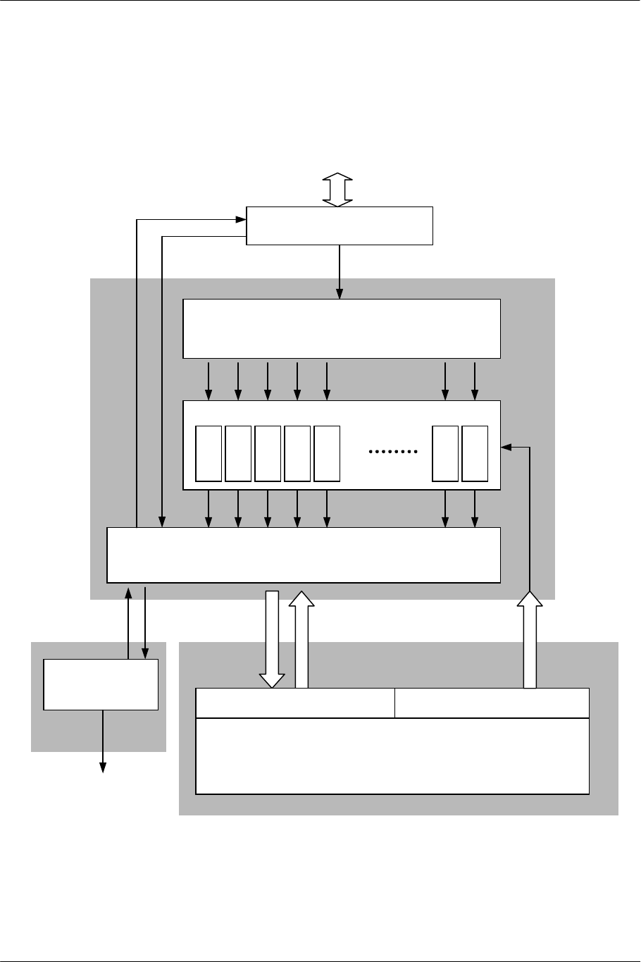
The whole GS configuration is shown in the following figure:
Host Interface
Memory Interface
XYZ/RGBA/STQ etc.
Local Memory
(4 MB)
Texture Page Buffer
RGBA + Z
(1024 bits x 2)
PCRTC
Video Out
Host Bus
Local/Host
Vertex Info/Drawing Environment
Drawing Function
Block
Memory Block
Display Function
Block
Texture
(512 bits)
Host/Local
Pixel Pipeline x 16 (Max)
#0
Setup/Rasterizing
#1 #2 #3 #4 #14 #15
RGBA/Z
Frame Page Buffer
Texel x 16
Figure 1-1 GS Whole Block Diagram
The functional blocks in the figure perform as follows:

SCE CONFIDENTIAL GS User's Manual Version 6.0
© SCEI
-17-
Host Interface
This interface transfers data with the host (CPU). Drawing data and buffer transfer data from the host pass
through this interface.
Setup/Rasterizing (preprocessing)
This block develops the graphics to draw to the pixels based on vertex information received from the host,
and calculates information such as RGBA value, Z value, texture value, and fog value for each pixel.
Pixel Pipeline
This block performs processes such as texture mapping, Fogging, and Alpha-blending, and determines the
final drawing color based on pixel information calculated in the Rasterizing block. It can process a
maximum of 16 pixels concurrently.
Memory Interface
This block reads data from and writes data to the GS local memory. It writes to memory the drawing pixel
values (RGBA, Z) at the end of a pixel operation, reads from memory the pixel values of the frame buffer
(used for the pixel test or Alpha-blending), and reads from memory the RGBA values for the display image.
Local Memory
The GS has a 32-Mbit built-in local memory, containing the frame buffer, Z buffer, texture and CLUT. This
memory has a 1024-bit read port and a 1024-bit write port for drawing and accessing the frame buffer and Z
buffer and a 512-bit port for texture reading.
PCRTC
PCRTC displays the contents of the frame memory in the specified output format.
SCE CONFIDENTIAL GS User's Manual Version 6.0
© SCEI
-18-
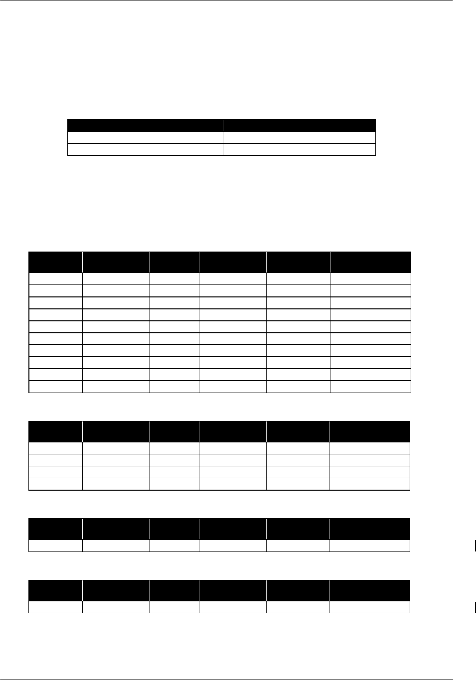
1.3. Maximum Performance
Maximum pixel writing rate
The GS processes 16 pixels per cycle when not performing texture mapping and 8 pixels per cycle when
performing texture mapping. The maximum achievable pixel writing rates are:
Texture Mapping Max Pixel Writing Rate
Without Texture Mapping 2.4 Gpixel/sec
With Texture Mapping 1.2 Gpixel/sec
(Each case has 32-bit pixels, Z-buffering ON and Alpha-Blending ON.)
Maximum setup performance
Setup performance means how many polygons the preprocessor can process per second; the upper limit
occurs when pixel writing does not create a processing bottleneck. It changes depending on the kind of
primitives to be drawn and the drawing conditions, as shown below.
Processing Performance in Triangle Drawing
Texture Shading Fogging Anti-aliasing Necessary
cycle count
Performance
(triangle/sec)
OFF Flat ON/OFF OFF 2 75M
ON Flat/Gouraud OFF OFF 4 37.5M
ON Flat/Gouraud ON OFF 5 30M
ON/OFF Gouraud OFF OFF 4 37.5M
ON/OFF Gouraud ON OFF 5 30M
OFF Flat ON/OFF ON 6 25M
ON Flat/Gouraud OFF ON 8 18M
ON Flat/Gouraud ON ON 9 16M
ON/OFF Gouraud OFF ON 8 18M
ON/OFF Gouraud ON ON 9 16M
Processing Performance in Line Drawing
Texture Shading Fogging Anti-aliasing Necessary
cycle count
Performance
(line/sec)
ON Flat/Gouraud OFF OFF 4 37.5M
ON Flat/Gouraud ON OFF 5 30M
OFF Flat ON/OFF ON 6 25M
ON Flat/Gouraud OFF ON 7 21M
Processing Performance in Sprite
Texture Shading Fogging Anti-aliasing Necessary
cycle count
Performance
(sprite/sec)
ON/OFF Flat/Gouraud ON/OFF OFF 3 50M
Processing Performance in Point
Texture Shading Fogging Anti-aliasing Necessary
cycle count
Performance
(point/sec)
ON/OFF Flat/Gouraud ON/OFF OFF 1 150M
When a difference in Z coordinates between the vertices composing one drawing primitive exceeds 216, a penalty
occurs and the cycle count required increases.

SCE CONFIDENTIAL GS User's Manual Version 6.0
© SCEI
-19-
2. Local Memory

SCE CONFIDENTIAL GS User's Manual Version 6.0
© SCEI
-20-
2.1. Data Stored in Local Memory
The GS uses four kinds of data in local memory for drawing. The user must secure data areas (buffers) in local
memory before starting drawing.
Frame buffer
Area for drawing. Stores pixels (RGBA) of the drawing result.
Z buffer
Area for drawing. Stores Z value of the drawing result.
Texture buffer
Stores texture image data.
CLUT buffer
Stores the Color Look up Table (CLUT) used when the texture is an index color.
These buffers can be freely arranged in local memory.
SCE CONFIDENTIAL GS User's Manual Version 6.0
© SCEI
-21-
2.2. Addressing
2.2.1. Address Value
Local memory addressing uses linear addresses in 32-bit word units.
FBP: Frame Buffer Starting Address
TBP: Texture Buffer Starting Address
CBP: CLUT Buffer Starting Address
32 bits
(0x00000)
(0xfffff)
Z
Texture
Texture
CLUT
Address
ZBP: Z Buffer Starting Address
Frame
Figure 2-1 Local Memory of GS
2.2.2. Starting Address of Buffer
The different buffer types require different starting address alignments, as follows:
Buffer Type Alignment Size
Frame buffer 2K words
Z buffer 2K words
Texture buffer 64 words
CLUT buffer 64 words
The starting address of a buffer is specified, not as a 32-bit address, but in units of the address divided by the
above alignment size.
2.2.3. Address in Buffer
Two-dimensional coordinates are used to specify the data position in each buffer. Given the starting address
and the buffer width (maximum X), the XY coordinate values in the buffer are converted to one-dimensional
real memory addresses. When converting from two-dimensional coordinates to a memory address, the GS
performs special processing to improve drawing efficiency. (For details of the conversion, see "8. Details of GS
Local Memory".)

SCE CONFIDENTIAL GS User's Manual Version 6.0
© SCEI
-22-
2.3. Data Formats
The formats for data stored in the buffer (pixels, Z values, etc.) are shown below.
2.3.1. Color Data Format (Pixel/Texel Format)
The GS supports the following five color data formats.
RGBA32
31 24 23 16 15 8 7 0
A (8 bits) B (8 bits) G (8 bits) R (8 bits)
RGB24
23 16 15 8 7 0
B (8 bits) G (8 bits) R (8 bits)
RGBA16
15 14 10 9 5 4 0
A B (5 bits) G (5 bits) R (5 bits)
IDTEX8
7 0
index (8 bits)
IDTEX4
3 0
index
(4 bits)
Color formats IDTEX8 and IDTEX4 can be used only in the texture buffer. They become index values for
the Color Look up Table (CLUT). For details of the interpretation of the index value, see "2.7. CLUT
Buffer".
2.3.2. Z Value Format
Data in the following three formats can be stored in the Z buffer.
Z32
31 0
Z (32 bits)
Z24
23 0
Z (24 bits)
Z16
15 0
Z (16 bits)

SCE CONFIDENTIAL GS User's Manual Version 6.0
© SCEI
-23-
2.4. Frame Buffer
The frame buffer is the area where image data of drawing results are stored. Settings related to the frame buffer
are made in the FRAME register (FRAME_1 or FRAME_2).
2.4.1. Size of Frame Buffer
The frame buffer width must be a multiple of 64 pixels. This value is specified in the FBW field of the FRAME
register.
The frame buffer height is arbitrary, and not specially set by the register. The height can be limited by limiting
the rectangular area where drawing is performed with the Scissoring function (described later in this document).
2.4.2. Starting Address of Frame Buffer
The starting address of the frame buffer in local memory is specified in the FBP field of the FRAME register.
Since the alignment of the frame buffer is 2K words, the FBP field is set as the address divided by 2048.
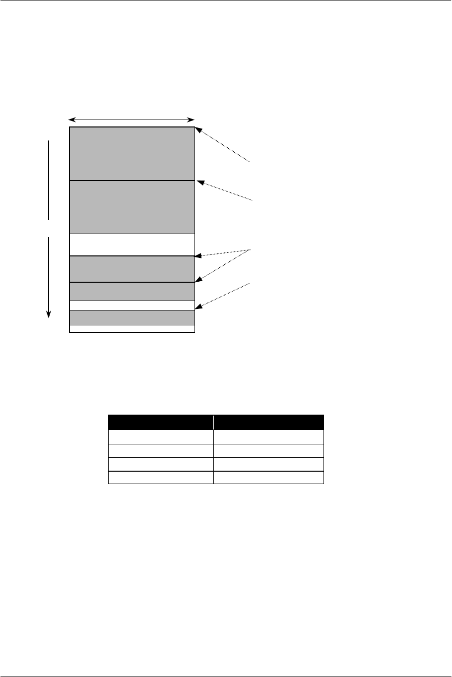
2.4.3. Coordinate Systems
There are two kinds of coordinate systems that point to the pixels in the frame buffer.
Primitive Coordinate System
This is the coordinate system of the drawing space. It is used to set vertex coordinate values during the
drawing process. Both X and Y coordinates are fixed 16-bit decimal values (12-bit integer and 4-bit decimal)
in the range of 0 to 4095.9375. The rectangular area in the frame buffer where drawing is actually performed
is defined in this space.
Window Coordinate System
This coordinate system uses the upper left point of the rectangular area of the frame buffer as the origin.
The calculation of memory addresses is based on the coordinate values.
Mapping to the Primitive coordinate system is done by using the offset value. The offset is stored in the
XYOFFSET register.
Assuming that the Primitive coordinate values are (Px,Py) and the Offset values are (Offx,Offy), the Window
coordinate values (Wx,Wy) are obtained from the following formulas:
Wx = Px – Offx
Wy = Py – Offy
The following figure shows the relation between the Primitive Coordinate System and the Window
Coordinate System:
SCE CONFIDENTIAL GS User's Manual Version 6.0
© SCEI
-24-
(0,0)
Origin Point
in Window
Coordinate System
4095.9375
4095.9375
x
Offset
Origin Point
in Primitive
Coordinate System
(0,0) x
y
Px,Py
Wx,Wy
y
Figure 2-2 Coordinate Systems in Frame Buffer
2.4.4. Pixel Correspondence
The pixels in the frame buffer are centered on positions where the fractional parts of the Window coordinate
values are 0 (the intersection of the grid in the figure).
Center of Pixel
1.0 2.0 3.0
Wy
Wx
1.0
2.0
3.0
Frame
Buffer
Figure 2-3 Frame Buffer Coordinates and Pixel Position

SCE CONFIDENTIAL GS User's Manual Version 6.0
© SCEI
-25-
2.4.5. Pixel Storage Format
The pixel storage format defines how the pixels are arranged in each 32-bit word of local memory. The eight
formats are shown below:
PSMCT32
31 0
RGBA32
PSMCT24
31 24 23 0
Not used RGB24
PSMCT16, PSMCT16S
31 16 15 0
RGBA16 (Upper) RGBA16 (Lower)
PSMZ32
31 0
Z32
PSMZ24
31 24 23 0
Not used Z24
PSMZ16, PSMZ16S
31 16 15 0
Z16 Z16
The pixel storage format used is specified in the PSM field (Pixel Storage Mode) of the FRAME register.

SCE CONFIDENTIAL GS User's Manual Version 6.0
© SCEI
-26-
2.5. Z Buffer
The Z buffer is an area where the Z values of the pixels are stored as a result of drawing. The size (width and
height) of the Z buffer is the same as that of the frame buffer.
2.5.1. Starting Address of Z Buffer
The starting address of the Z buffer in local memory is specified in the ZBP field of the ZBUF register. The
alignment of the Z buffer is 2048 words, so the ZBP field is set to the address divided by 2048.
2.5.2. Coordinate System of Z Buffer
The coordinate system of the Z buffer is the same as that of the frame buffer.
2.5.3. Z Value Storage Format
The data storage format of the Z buffer is as follows:
PSMZ32
31 0
Z32
PSMZ24
31 24 23 0
Not used Z24
PSMZ16, PSMZ16S
31 16 15 0
Z16 Z16
2.5.4. Combinations of Frame Buffer and Z Buffer Formats
To use the pixel storage format for the frame buffer and the Z value storage format for the Z buffer in
combination, both the formats must belong to the same group (Group1 or 2 below).
Group 1 Group 2
PSMCT32
PSMCT24
PSMCT16S
PSMZ32
PSMZ24
PSMZ16S
PSMCT16
PSMZ16
The following are some examples of applicable and inapplicable combinations.
Pixel Storage Format for
Frame Buffer
Z Value Storage Format for Z
Buffer
Combination
PSMCT32 PSMZ24 Yes
PSMCT32 PSMZ16 No
PSMCT32 PSMZ16S Yes
PSMCT16 PSMZ24 No
PSMCT16S PSMZ24 Yes
PSMCT16 PSMZ16 Yes
SCE CONFIDENTIAL GS User's Manual Version 6.0
© SCEI
-27-
2.6. Texture Buffer
The texture buffer stores texture image data for drawing textured polygons. The TEX0 register stores settings
related to the texture buffer.
The height and width of textures in the buffer are specifiable separately, and independently of the width of the
buffer. They must be a power of 2, with a maximum size of 1024 texels.
The width of the buffer is a multiple of 64 texels, but it must be a multiple of 128 texels when PSMT8 or
PSMT4 is specified as the buffer storage format.
2.6.1. Starting Address of Texture Buffer
The starting address of the texture buffer in local memory is called the texture base pointer. It is specified in the
TBP0 field in the TEX0 register, in units of 64 words, that is, the starting address divided by 64.
When MIPMAP is performed, it is necessary to set the starting addresses and buffer widths for the textures of
two or more MIP levels. Texture settings of Level 0 (the maximum resolution) are stored in the TEX0 register
(as well as the case where MIPMAP is not used). Texture settings of Level 1 to 6 are specified in the MIPTBP1
and MIPBP2 registers.
2.6.2. Coordinate System of Texture Buffer
Coordinates in the texture buffer are specified as either texture coordinates (STQ) or texel coordinates (UV).
When performing perspective correction, texture coordinates must be used.
Texture coordinates
The GS registers use texture coordinates specified in a two-dimensional homogeneous coordinate system (S,
T, Q) to achieve perspective correction.
The coordinate values stored in the texture buffer are indicated by the normalized texture coordinates (s, t)
showing the upper left point as (0.0, 0.0) and the lower right point as (1.0, 1.0) in a single-precision floating-
point representation.
1.0
A
s
t
1.00.0
0.0
1.0
1.0
Figure 2-4 Normalized Texture Coordinates
The texture coordinates (S, T, Q) use the results of the conversion of (s, t). For the calculation, see "3.4.10.
Perspective Correction".
SCE CONFIDENTIAL GS User's Manual Version 6.0
© SCEI
-28-
Texel coordinates
Texel coordinates are two-dimensional coordinate values indicated by (U, V). The UV value is a fixed 16-bit
decimal value, where 1 texel is 1.0. The upper 12 bits are the unsigned integer part, and the lower 4 bits are
the fractional part.
16.0
A
U
V
16.00.0
0.0
16.0
16.0
Figure 2-5 Texture Coordinates (in case Texture Size is 16x16)
Texels are centered on the position where the fractional parts of the texel coordinate values are 0.5 (the
center of the square in the grid in the figure).
1.0
1.0 2.0 3.0
2.0
3.0
V
U
Center of Texel
Figure 2-6 Texel Coordinate System and Center of Texel

SCE CONFIDENTIAL GS User's Manual Version 6.0
© SCEI
-29-
2.6.3. Texel Storage Format
There are 8 forms of Texel Storage Format for the texture buffer as shown below:
PSMCT32
31 0
RGBA32
PSMCT24
31 24 23 0
Not used RGB24
PSMCT16
31 16 15 0
RGBA16 RGBA16
PSMT8
31 24 23 16 15 8 7 0
IDTEX8 IDTEX8 IDTEX8 IDTEX8
PSMT8H
31 24 23 0
IDTEX8 Not used
PSMT4
31 24 23 16 15 8 7 0
IDTEX4 IDTEX4 IDTEX4 IDTEX4 IDTEX4 IDTEX4 IDTEX4 IDTEX4
PSMT4HH
31 28 27 0
IDTEX4 Not used
PSMT4HL
31 28 27 24 23 0
Not used IDTEX4 Not used
Since there is no influence on the "not used" bits, it is possible to combine textures of two different modes (e.g.
PSMCT24 and PSMT8H) in the same area.
The PSM field of the TEX0 register specifies which texel storage format is used.
SCE CONFIDENTIAL GS User's Manual Version 6.0
© SCEI
-30-
2.7. CLUT Buffer
A CLUT (Color Look up Table) converts a texel value from an index to RGBA color data, when the color
format of the texel is IDTEX8 or IDTEX4. The CLUT buffer is the area where the CLUT is stored. Settings
related to the CLUT are stored in the TEX0 register or the TEX2 register.
The TEX2 register is a subset of the TEX0 register. Among the values set by the TEX0 register, it is possible to
change only CLUT-related information by changing the values in the TEX2 register.
2.7.1. CLUT Configuration
A CLUT is an array of two or more elements (CLUT entries) that describe color information, arranged in a
prescribed order. The number of CLUT entries depends on the texel color format; it is 16 for IDTEX4 and 256
for IDTEX8. The CLUT data format in local memory is the same as for pixels. For instance, CLUT entries
arranged as 16x16 in width and height are the same as 16x16 image data.
2.7.2. Starting Address
The starting address of the CLUT buffer in local memory is called the CLUT base pointer, and is specified in the
CBP field of the TEX0 or TEX2 register. The CLUT base pointer is in units of 64 words; that is, the value of
the address divided by 64 is stored in the CBP field.
2.7.3. CLUT Storage Mode
The CLUT buffer is a two-dimensional space like the other buffers. The CLUT storage mode determines how
CLUT entries are arranged in the two-dimensional space of the CLUT buffer. There are two CLUT storage
modes, CSM1 and CSM2. They are specified in the CSM field of the TEX0 register.
CSM1
Data can be more efficiently read from local memory in CSM1 than in CSM2.
The CLUT entries are arranged in order in 16x16 rectangles in IDTEX8 (8 bits) and 8x2 in IDTEX4 (4 bits)
as shown below. The numbers in the figures show the corresponding index values (in hexadecimal).
Arrangement of CLUT in IDTEX4
Y
X
054312 76
a9
8fedcb
Arrangement of CLUT in IDTEX8
Y
X
3221 34
f2f1
e0 e1 e2 e6e3 e4 e5 f0e7 f5f4f3 f7f6
e9e8 fceeea edeceb fbfaf9f8ef fd ff
fe
00
0a
05040301 02
0908
0706
0f0e0d0c0b
10 11 12 13 14 15 16 17
18
3120
19
22 2623 24 25 30
2928
27
3c2e
3533
2a
3736
2d2c2b 3b3a39382f 3d 3f3e
1c 1d 1e 1f1b
1a
In CSM1, arrangement should be made from the start of the buffer (the position where X and Y are each 0).

SCE CONFIDENTIAL GS User's Manual Version 6.0
© SCEI
-31-
CSM2
In CSM2, two or more CLUT sets can be arranged at free positions in one big CLUT buffer. However, the
CLUT entries must be in PSMCT16, and the efficiency of transmission to the temporary buffer decreases.
The position in the buffer is specified in the TEXCLUT register.
The CLUT entries are arranged in order as shown below. The CLUT entries are arranged in a width of 256
or 16 and a height of 1. The numbers in the figures show the corresponding index values (in hexadecimal).
Arrangement of CLUT in IDTEX4
Y
X
0afedcb54312 9876
Arrangement of CLUT in IDTEX8
Y
X
00 fa fffefdfcfb05040301 02 f90706
2.7.4. CLUT Storage Format
The storage formats of individual CLUT entries are the same as those of the pixels in the frame buffer. When
the CLUT storage mode is CSM1, PSMCT32, PSMCT16 or PSMCT16S can be specified. When it is CSM2,
only PSMCT16 can be specified. They are specified in the CPSM field of the TEX0 register.

SCE CONFIDENTIAL GS User's Manual Version 6.0
© SCEI
-32-
(This page is left blank intentionally)

SCE CONFIDENTIAL GS User's Manual Version 6.0
© SCEI
-33-
3. Drawing Function
SCE CONFIDENTIAL GS User's Manual Version 6.0
© SCEI
-34-
3.1. Outline of Drawing Function
The GS receives the information necessary for drawing (vertex and drawing environment information) from the
host processor via the Host interface. It draws drawing primitives called GS primitives as processing units.
The drawing flow in the GS is shown below.
Setup (preprocessing)
Rasterizing (DDA)
Scissoring
Texture Mapping
Texture Function
Fogging
RGB
Antialiasing
Pixel Test
Alpha Test
Destination Alpha Test
Depth Test
RGBZXY
Coverage
Texture
CLUT
RGB
XY FRGBA STQ/UV
A
A
(Initial Value / Gradient)
Z
A
Drawing
Environment
Register
To Each Process
DDA Set Value
Alpha Blending
Formatting
RGB
A, Z
XYZRGBA....
Host Interface
Vertex InformationDrawing Environment
Memory Interface
Figure 3-2 Block Diagram for Drawing Processing

SCE CONFIDENTIAL GS User's Manual Version 6.0
© SCEI
-35-
The processes shown in the figure are:
Setup (Preprocessing)
The gradient (e.g. shading coefficient) and the initial value of DDA necessary for drawing primitives are
calculated based on the vertex information received from the host.
If the primitive is a Triangle, the gradient of the RGBA value, Z value, texture value, and Fog value on the
three sides and on the scan line are calculated.
Rasterizing (DDA)
The pixels of a primitive are generated by DDA (Digital Differential Algorithm). 8 or 16 pixels are generated
concurrently. The RGBA value, Z value, texture value and Fog value for each pixel are calculated from the
gradient obtained in the preprocessing stage, and are given to each of the parallel pixel pipelines.
Texture Mapping
Textures are mapped to pixels. The pixel color is determined by applying the texture function to the Texture
CLUT RGBA value read from the memory block and the RGBA value calculated by DDA.
Antialiasing
The alpha value is replaced with the pixel coverage calculated by DDA (proportion of the pixel occupied by
the theoretical edge of the primitive.) The edges of the primitive are smoothed when Alpha-blending is
implemented with this alpha value.
Fogging
The RGB value and Fog color value output from the texture mapping block are blended according to the
Fog value of the pixel calculated by DDA.
Pixel Test
Whether to draw a pixel is based on its XYZ and RGBA values. Three kinds of tests—alpha test,
destination alpha test, and depth test—are performed one by one.
Alpha-blending
Blending the RGB value of a pixel and the RGB value in the frame memory is implemented according to the
alpha value of the pixel or the alpha value in the frame memory.
Formatting
The pixel value for drawing is converted into the data format of the frame buffer. Dithering and color
clamping are applied if necessary.
Memory Interface
Read/write is performed to local memory in the chip. The operations are: writing drawing pixel values
(RGBA, Z) to the memory after a pixel operation, reading pixel values into the frame buffer from the
memory (used for pixel test and alpha-blending), and reading RGBA values for display from memory.
Environment Registers
These registers store various parameters necessary for drawing. These values are referred to in each process
of drawing.
SCE CONFIDENTIAL GS User's Manual Version 6.0
© SCEI
-36-
3.2. GS Primitive
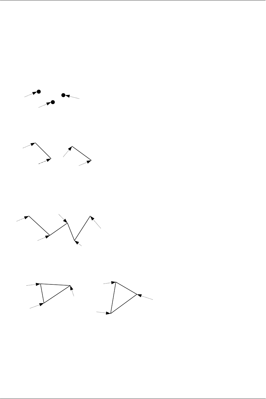
3.2.1. Types of GS Primitives
The GS uses the following seven primitive types:
Point
A Point is an independent point that is drawn with 1 piece of vertex information.
1
2
3
Line
A Line is an independent line that is drawn with 2 pieces of vertex information.
1
23
4
LineStrip
A LineStrip is a series of continuous lines that share endpoints. The first line is drawn with 2 pieces of
vertex information. The succeeding lines are drawn with 1 piece of vertex information.
1
2
3
4
5
Triangle
A Triangle is an independent triangle that is drawn with 3 pieces of vertex information.
1
2
3
4
5
6
SCE CONFIDENTIAL GS User's Manual Version 6.0
© SCEI
-37-
TriangleStrip
A TriangleStrip is a series of triangles that share sides. The first triangle is drawn with 3 pieces of vertex
information, and the succeeding ones are drawn whenever 1 piece of vertex information is added.
1
2
3
4
5
6
7
TriangleFan
A TriangleFan is a series of triangles sharing one vertex. The first triangle is drawn with 3 pieces of vertex
information, and the succeeding triangles are drawn whenever 1 piece of vertex information is added.
1
2
3
4
5
6
7
Sprite
A Sprite is an independent rectangle, drawn with 2 pieces of vertex information showing the endpoints of a
diagonal line.
1
2
3
4
3.2.2. Drawing Attributes
Besides their types, GS primitives have the following drawing attributes:
Drawing
Attribute
Contents Setting
IIP Shading Method Flat/Gouraud
TME Texture Mapping ON/OFF
FGE Fogging ON/OFF
ABE Alpha-Blending ON/OFF
AA1 Antialiasing ON/OFF
FST Texture Coordinates STQ/UV
CTXT Context 1/2
FIX Interpolation FIX ON/OFF

SCE CONFIDENTIAL GS User's Manual Version 6.0
© SCEI
-38-
Some drawing attributes are fixed for specific GS primitive types:
Point: Shading Method flat and Antialiasing Off
Sprite: Shading Method flat and Antialiasing Off
3.2.3. Outline of Drawing Procedure
The general drawing procedure is:
1) Set GS primitive type/drawing attribute (PRIM register)
2) Set vertex information (Vertex info setting registers)
3) Vertex Kick (XYZF2, XYZF3 registers, etc.)
4) Start drawing (XYZF2 register etc.)
1) Set GS Primitive Type and Drawing Attribute
The GS primitive type is specified by writing to the PRIM register. The condition of the vertex queue is also
initialized. The drawing attributes of the GS primitive can be set, and it is also possible to set GS primitive
drawing attributes in the PRMODE register. (See "3.2.6. Change of Drawing Attributes".)
2) Set Vertex Information
Vertex information includes the drawing coordinates, vertex color, texture coordinates, and Fog coefficient.
These values are set in the vertex information setting registers shown below.
Setting Item Register
Name
Vertex
Kick
Drawing
Kick
Coordinate values XYZ2 Yes Yes
Coordinate values and Fog coefficient XYZF2 Yes Yes
Coordinate values XYZ3 Yes No
Coordinate values and Fog coefficient XYZF3 Yes No
Color info and Q value of texture coordinates RGBAQ No No
ST of texture coordinates ST No No
UV of texel coordinates UV No No
Fog coefficient FOG No No
3) Vertex Kick
If the vertex information setting registers that have a Vertex Kick function are written to, the vertex
information set up to that point is placed in the vertex queue, and the queue goes one step forward. This
operation is called the Vertex Kick. The following figure shows the image of operation.
SCE CONFIDENTIAL GS User's Manual Version 6.0
© SCEI
-39-
XYZ RGBA STQ/UV F
Vertex Information Setting Resisters
Vertex Queue
1st Vertex
2nd Vertex
3rd Vertex
Copy
Move
Move
Differs depending
on the primitive
t
yp
e.
XYZ, RGBA, STQ/UV, F
XYZ, RGBA, STQ/UV, F
XYZ, RGBA, STQ/UV, F
Figure 3-3 Operation Image of Vertex Kick
4) Start Drawing (Drawing Kick)
When the necessary vertex information is arranged in the vertex queue, drawing begins.
3.2.4. Example of the Drawing Procedure
The following examples show the order of register setting for the drawing procedures for the GS primitive
types. The examples show the drawing sequences for non-textured GS primitives, and the RGBA value and the
coordinate values are given to each vertex.
Point Drawing Procedure
[Register Setting Order]
Vertex Kick & Drawing Kick (Vertex1)
Vertex1 Setting
Vertex Kick & Drawing Kick (Vertex2)
Vertex2 Setting
:
XYZ2
RGBA
Q
XYZ2
RGBA
Q
PRIM
Line Drawing Procedure
[Register Setting Order]
:
XYZ2
RGBA
Q
XYZ2
RGBA
Q
PRIM
Vertex Kick
Vertex1 Setting
Vertex Kick & Drawing Kick (Vertex1 & Vertex2)
Vertex2 Setting
SCE CONFIDENTIAL GS User's Manual Version 6.0
© SCEI
-40-
LineStrip Drawing Procedure
[Register Setting Order]
:
XYZ2
RGBA
Q
XYZ2
RGBA
Q
PRIM
Vertex Kick
Vertex1 Setting
Vertex Kick & Drawing Kick(Vertex1 & Vertex2)
Vertex2 Setting
Vertex Kick & Drawing Kick (Vertex2 & Vertex3)
Vertex3 Setting
Vertex Kick & Drawing Kick (Vertex3 & Vertex4)
Vertex4 Setting
RGBA
Q
XYZ2
RGBA
Q
XYZ2
Triangle Drawing Procedure
[Register Setting Order]
:
XYZ2
RGBA
Q
XYZ2
RGBA
Q
PRIM
RGBA
Q
XYZ2
RGBA
Q
XYZ2
RGBA
Q
RGBA
Q
XYZ2
XYZ2
Vertex Kick
Vertex1 Setting
Vertex Kick
Vertex2 Setting
Vertex Kick & Drawing Kick
(Vertex1 & Vertex2 & Vertex3)
Vertex3 Setting
Vertex Kick
Vertex4 Setting
Vertex Kick
Vertex Kick & Drawing Kick
(Vertex4 & Vertex5 & Vertex6)
Vertex5 Setting
Vertex6 Setting
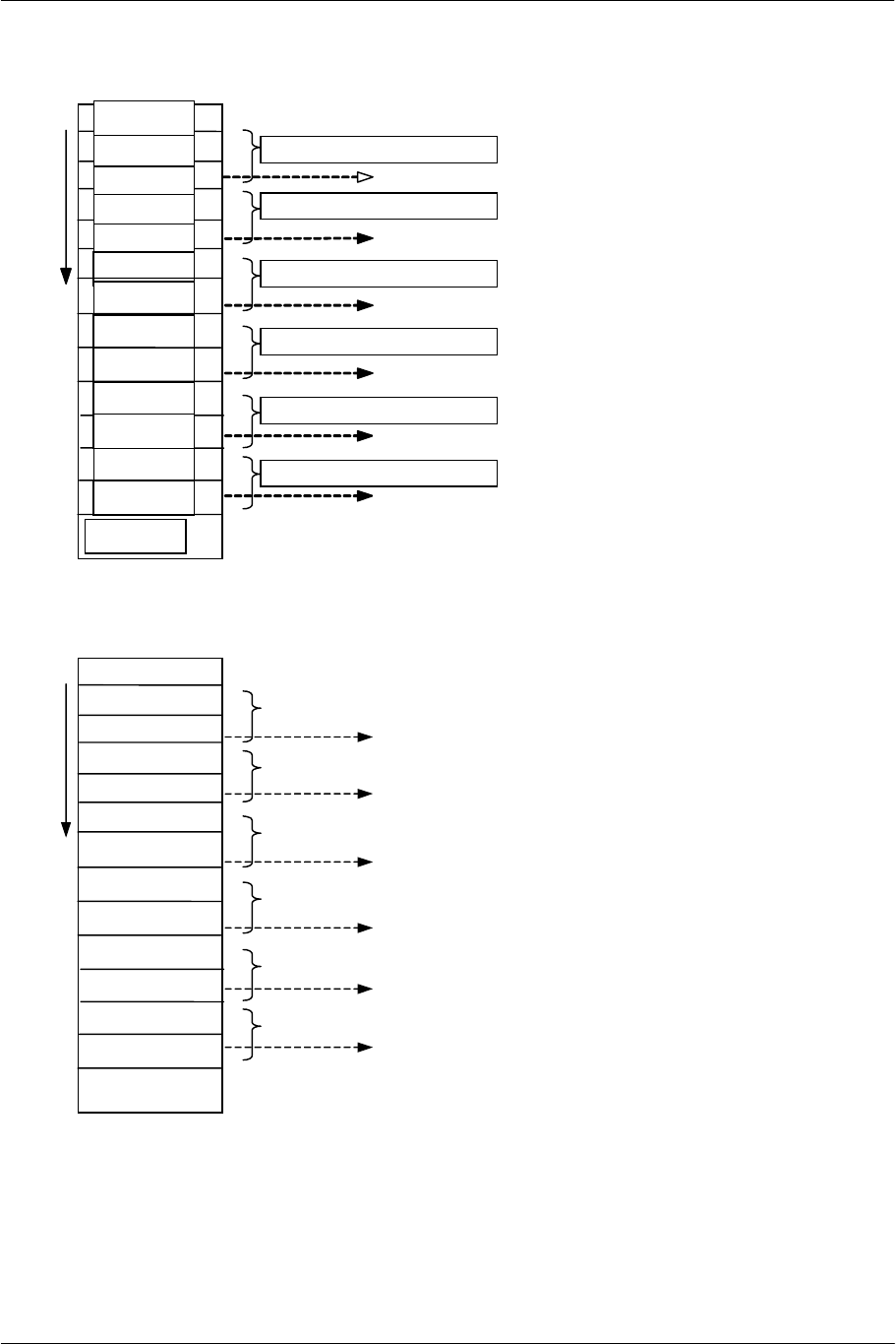
SCE CONFIDENTIAL GS User's Manual Version 6.0
© SCEI
-41-
TriangleStrip Drawing Procedure
[Register Setting Order]
:
XYZ2
RGBA
Q
XYZ2
RGBA
Q
PRIM
RGBA
Q
XYZ2
RGBA
Q
XYZ2
RGBA
Q
RGBA
Q
XYZ2
XYZ2
Vertex Kick
Vertex1 Setting
Vertex Kick
Vertex2 Setting
Vertex Kick & Drawing Kick
(Vertex1 & Vertex2 & Vertex3)
Vertex3 Setting
Vertex Kick & Drawing Kick
(Vertex2 & Vertex3 & Vertex4)
Vertex4 Setting
Vertex Kick & Drawing Kick
(Vertex3 & Vertex4 & Vertex5)
Vertex Kick & Drawing Kick
(Vertex4 & Vertex5 & Vertex6)
Vertex5 Setting
Vertex6 Setting
TriangleFan Drawing Procedure
[Register Setting Order]
:
XYZ2
RGBA
Q
XYZ2
RGBA
Q
PRIM
RGBA
Q
XYZ2
RGBA
Q
XYZ2
RGBA
Q
RGBA
Q
XYZ2
XYZ2
Vertex Kick
Vertex1 Setting
Vertex Kick
Vertex2 Setting
Vertex Kick & Drawing Kick
(Vertex1 & Vertex2 & Vertex3)
Vertex3 Setting
Vertex Kick & Drawing Kick
(Vertex1 & Vertex3 & Vertex4)
Vertex4 Setting
Vertex Kick & Drawing Kick
(Vertex1 & Vertex4 & Vertex5)
Vertex Kick & Drawing Kick
(Vertex1 & Vertex5 & Vertex6)
Vertex5 Setting
Vertex6 Setting
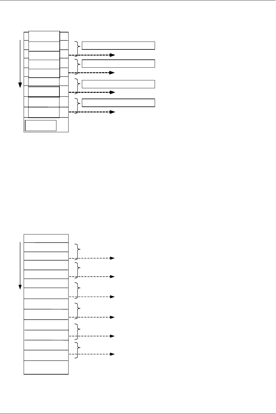
SCE CONFIDENTIAL GS User's Manual Version 6.0
© SCEI
-42-
Sprite Drawing Procedure
[Register Setting Order]
:
XYZ2
RGBA
Q
XYZ2
RGBA
Q
PRIM
RGBA
Q
XYZ2
RGBA
Q
XYZ2
Vertex Kick
Vertex1 Setting
Vertex Kick & Drawing Kick
(Vertex1 & Vertex2)
Vertex2 Setting
Vertex Kick
Vertex3 Setting
Vertex Kick & Drawing Kick
(Vertex3 & Vertex4)
Vertex4 Setting
3.2.5. Drawing Control
When drawing a GS primitive consisting of two or more polygons, such as TriangleStrip, it is possible to control
a polygon that is being drawn without changing the vertex string order. As a result, operations like normal clips
become easy.
To control drawing in this way, the vertex information is written to the XYZ3 register instead of the XYZ2
register and to the XYZF3 register instead of the XYZF2 register. Because of this, the Drawing Kick is not
performed at the Vertex Kick, and only the vertex queue is advanced. For this reason, the polygon is not drawn.
The figure below is an example of such register settings. In this example, only the 2nd triangle is not drawn.
[Register Setting Order]
:
XYZ2
RGBA
Q
XYZ2
RGBA
Q
PRIM
RGBA
Q
XYZ2
RGBA
Q
XYZ3
RGBA
Q
RGBA
Q
XYZ2
XYZ2
Vertex Kick
Vertex1 Setting
Vertex Kick
Vertex2 Setting
Vertex Kick & Drawing Kick
(Vertex1 & Vertex2 & Vertex3)
Vertex3 Setting
Vertex Kick (No Drawing Kick)
Vertex4 Setting
Vertex Kick & Drawing Kick
(Vertex3 & Vertex4 & Vertex5)
Vertex Kick & Drawing Kick
(Vertex4 & Vertex5 & Vertex6)
Vertex5 Setting
Vertex6 Setting
SCE CONFIDENTIAL GS User's Manual Version 6.0
© SCEI
-43-
3.2.6. Change of Drawing Attributes
The drawing attributes of a GS primitive are specified in the PRIM register. However, if the PRMODE register
is used, it is possible to change drawing attributes while drawing a primitive consisting of two or more polygons
such as TriangleStrip.
The following is an example of performing Flat shading to only one of the triangles in the process of drawing a
TriangleStrip, to which Gouraud shading is specified.
[Register Setting Order]
:
XYZ2
RGBA
Q
XYZ2
RGBA
Q
PRMODE
RGBA
Q
XYZ2
RGBA
Q
XYZ2
RGBA
Q
RGBA
Q
XYZ2
XYZ2
PRMODE
Vertex Kick
Vertex1 Setting
Vertex Kick
Vertex2 Setting
Vertex Kick & Drawing Kick
(Vertex1 & Vertex2 & Vertex3)
Vertex3 Setting
Vertex Kick & Drawing Kick
(Vertex2 & Vertex3 & Vertex4)
Vertex4 Setting
Vertex Kick & Drawing Kick
(Vertex3 & Vertex4 & Vertex5)
Vertex Kick & Drawing Kick
(Vertex4 & Vertex5 & Vertex6)
Vertex5 Setting
Vertex6 Setting
Set to IIP=1(Gouraud)
Reset to IIP=0(Flat)
PRMODECONT
PRIM Specify types of primitive (The attribute is ignored)
Set to AC=1
3.2.7. Register Setting Order and Drawing Order
Since the pixel pipeline, where drawing is performed, is designed to maintain the input register setting order,
dependence between register setting and drawing is in register setting order. This means register setting will not
override drawing. Moreover, the order of texture data transmission (Host/Local transmission) and drawing
operation will not be reversed. However, when using the data converted in Host/Local transmission or
Local/Local transmission as texture or CLUT for the first time, the texture buffer must be disabled with the
TEXFLUSH register.
3.2.8. Enabled Vertex Information
Note that there may be unusable vertex information in a register, depending on the primitive type and drawing
attribute.
For instance, a Sprite consists of two pieces of vertex information, but it only needs one piece of vertex
information for the Z coordinate value and Fog information, since depth is not provided. Therefore, the Z
coordinate and Fog coordinate of the first vertex are ignored, and the setting for the second one takes effect.
Also, when doing Flat shading, one piece of vertex color information is sufficient, so the vertex color
information set immediately before each drawing kick becomes effective. By this method, it is possible to
perform proper drawing by specifying Flat shading even in case of TriangleStrip.
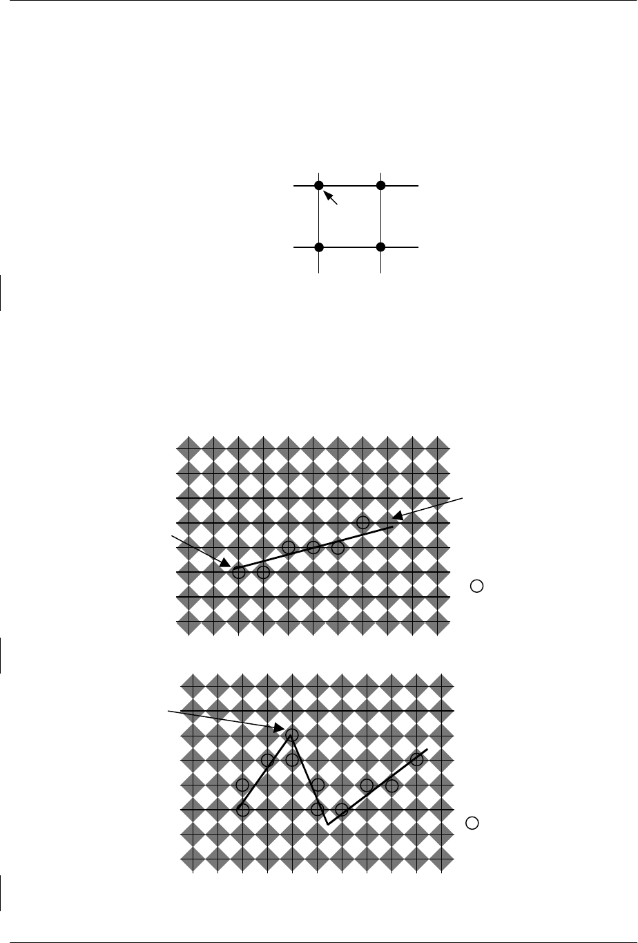
SCE CONFIDENTIAL GS User's Manual Version 6.0
© SCEI
-44-
3.2.9. Primitive Drawing Rule
The rules for how the DDA generates pixels are shown for each primitive.
Point
The pixel closest to the specified XY coordinates is drawn.
×
Specified XY coordinates
Closest Pixel
Figure 3-4 Pixel Drawing Rule for Point
Line, LineStrip
By defining the area for each pixel as shown with small gray squares in Figure 3-5, the pixels located in the
areas where a line goes through are drawn. However, a pixel located at the endpoint of a line is not drawn.
Any line can be drawn without being broken. Even when continued lines that share endpoints are drawn,
they cannot be drawn doubly unless crossed.
End point
is not drawn.
Start point
is drawn.
Pixel Drawn
Figure 3-5 Pixel Drawing Rule for Line
Drawn
only once
Pixel Drawn
Figure 3-6 Pixel Drawing Rule for LineStrip
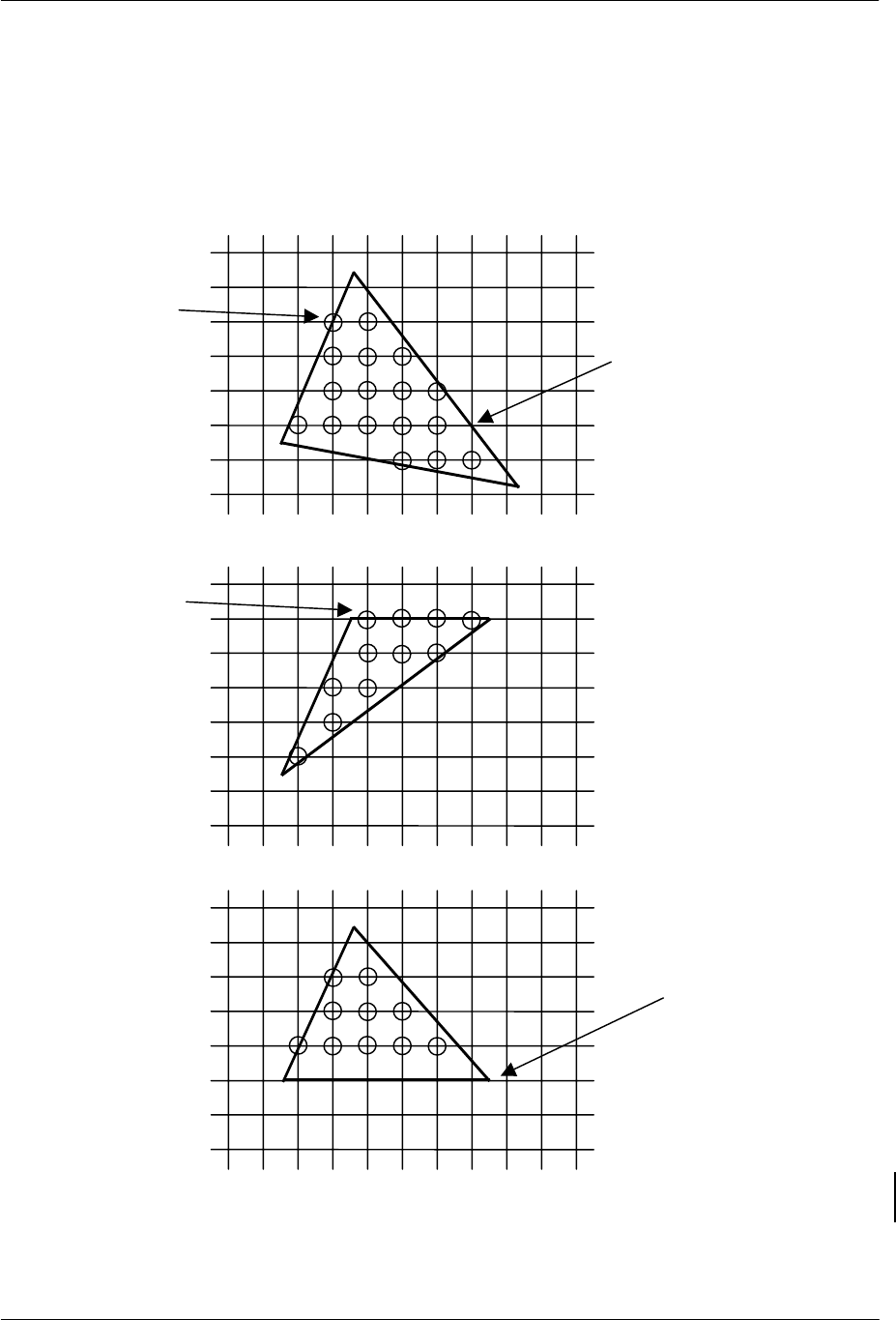
SCE CONFIDENTIAL GS User's Manual Version 6.0
© SCEI
-45-
Triangle, TriangleStrip, TriangleFan
Draws the pixels in the three sides specified by the three vertices. When a side passes the center of a pixel,
drawing is performed if it is the left side, and is not performed if it is the right side. When a side parallel to
the X axis passes the center of a pixel, drawing is performed if it is the top side, and is not performed if it is
the bottom side.
Even when drawing triangles that share sides with the same vertices, neither a gap nor a double line can be
created. (Figure 3-7)
Drawn on
the Left Side.
Not Drawn on
the Right Side.
Not Drawn on
the Bottom Side.
Drawn on
the Top Side.
Figure 3-7 Pixel Drawing Rule for Triangle
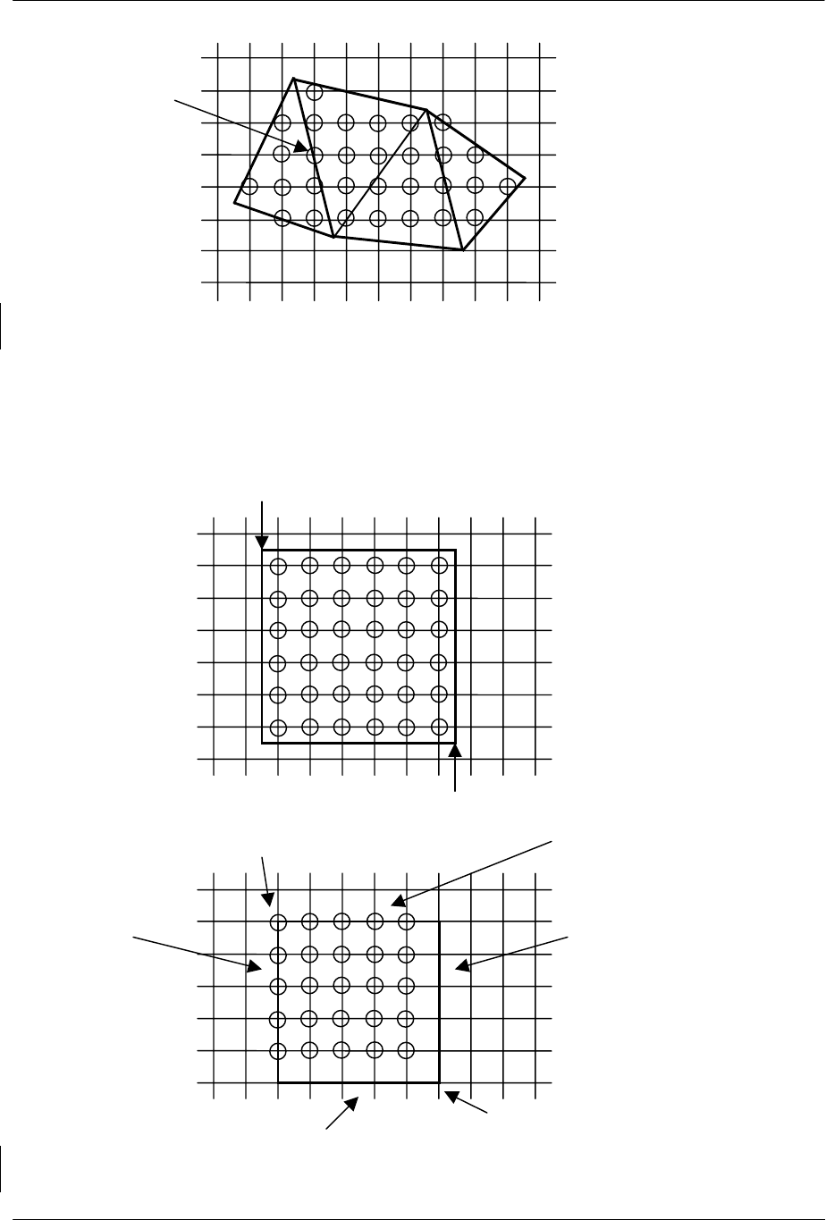
SCE CONFIDENTIAL GS User's Manual Version 6.0
© SCEI
-46-
Drawn
only once.
Figure 3-8 Pixel Drawing Rule for Side-Sharing Triangles
Sprite
Draws pixels in a rectangular area with two vertices specified as diagonal points. When a side passes the
center of a pixel, drawing is performed if it is the top or left side and not performed if it is the bottom or
right side.
1st Diagonal Point
2nd Diagonal Point
1st Diagonal Point
2nd Diagonal Point
Drawn on the Top Side.
Not Drawn on the Bottom Side.
Drawn on
the Left Side. Not Drawn on the Right Side.
Figure 3-9 Pixel Drawing Rule for Sprite

SCE CONFIDENTIAL GS User's Manual Version 6.0
© SCEI
-47-
3.3. Drawing Environment
There are various parameters used for GS primitive drawing, such as texture information, in addition to the
drawing attributes set by the PRIM register. These are called the drawing environment. Once the drawing
environment is set, it remains in effect for multiple GS primitives until it is reset. Settings can be changed even
in the process of drawing a GS primitive consisting of two or more polygons, such as TriangleStrip.
3.3.1. Drawing Environment Setting Registers
The following are the drawing environment setting registers.
Register Name Contents
XYOFFSET_1/2 Offset value of vertex coordinates
PRMODECONT PRIM attributes enabled/disabled
TEX0_1/2 Attributes of texture buffer and texture mapping
TEX1_1/2 Attributes of texture mapping
TEX2_1/2 CLUT entry
CLAMP_1/2 Wrap mode of texture mapping
TEXCLUT CLUT setting
SCANMSK Drawing control with Y coordinate of pixel
MIPTBP1_1/2 Base pointer for MIPMAP on each level
MIPTBP2_1/2 Base pointer for MIPMAP on each level
TEXA Reference value when expanding Alpha value of TEX16 and
TEX24
FOGCOL Fogging distant color
SCISSOR_1/2 Scissoring area
ALPHA_1/2 Alpha-blending attributes
DIMX Dither matrix
DTHE Dithering enabled/disabled
COLCLAMP Color clamp/mask
TEST_1/2 Pixel operation
PABE Alpha-blending in pixel units enabled/disabled
FBA_1/2 Alpha correction value
FRAME_1/2 Frame buffer setting
ZBUF_1/2 Z buffer setting
3.3.2. Two Context Drawing Environment
Some of the drawing environment registers have two registers for the same function, such as XYOFFSET_1
and XYOFFSET_2. The selection of the first or second can be made by the primitive attribute CTXT. Even in
drawing command strings containing drawing commands from two kinds of contexts intermixed in GS primitive
units, drawing can be performed without repeating register save/load.
SCE CONFIDENTIAL GS User's Manual Version 6.0
© SCEI
-48-
The registers with two contexts are listed below.
Register Name Contents
XYOFFSET_1/2 Offset value of Vertex coordinates
TEX0_1/2 Attributes of texture buffer and texture mapping
TEX1_1/2 Attributes of texture mapping
TEX2_1/2 CLUT entry
CLAMP_1/2 Wrap mode of texture mapping
MIPTBP1_1/2 Base pointer for MIPMAP on each level
MIPTBP2_1/2 Base pointer for MIPMAP on each level
SCISSOR_1/2 Scissoring area
ALPHA_1/2 Alpha-blending attributes
TEST_1/2 Pixel operation
FBA_1/2 Alpha correction value
FRAME_1/2 Frame buffer setting
ZBUF_1/2 Z buffer setting
The following is an example of switching the contexts by the primitive.
[Register Setting Order]
PRIM Triangle, CTXT=1
ST
RGBAQ
XYZF2
RGBAQ
ST
XTZF2
RGBAQ
ST
XYZF2
RGBAQ
ST
TEX1_2 MMAG=1
TEX1_1 MMAG=0
XYZF2
RGBAQ
ST
XYZF2
RGBAQ
ST
XYZF2
Drawing Triangle with
Context 1 (Point Sampling)
Point Sampling
Bilinear Sampling
Drawing Triangle with
Context 2 (Bilinear Sampling)
PRIM Triangle, CTXT=0
SCE CONFIDENTIAL GS User's Manual Version 6.0
© SCEI
-49-
Moreover, the contexts can be switched in the process of drawing a primitive.
[Register Setting Order]
XYZF2
RGBAQ
ST
XYZF2
RGBAQ
ST
XYZF2
RGBAQ
ST
TEX1_2 MMAG=1
TEX1_1 MMAG=0
XYZF2
RGBAQ
ST
XYZF2
RGBAQ
ST
PRMODE CTXT=0
PRMODE CTXT=1
Point Sampling
Bilinear Sampling
Drawing 1st Triangle with Context 1
(Point Sampling)
Drawing 2nd Triangle with Context 2
(Bilinear Sampling)
Drawing 3rd Triangle with Context 1
(Point Sampling)
PRMODE CTXT=0
PRIM Trian
g
leStri
p
PRMODECONT AC=0
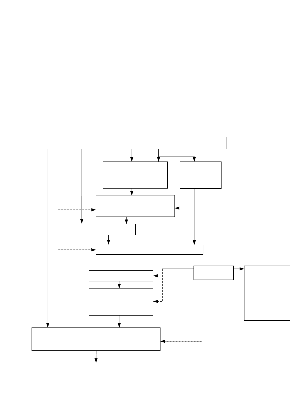
SCE CONFIDENTIAL GS User's Manual Version 6.0
© SCEI
-50-
3.4. Texture Mapping
3.4.1. Outline of Texture Mapping Process
The GS can do texture mapping for all drawing primitives.
Assuming TME=1 in the primitive drawing information, texture mapping is based on the coordinate values of
the texture corresponding to each vertex.
Texture data must be stored in the texture buffer in local memory before drawing. Texture data is normally
transmitted from the host processor by the transmitting function between buffers. To obtain special effects,
however, images created via the drawing process can be used as textures.
3.4.2. Texture Mapping Process Flow
The texture mapping flow is shown in Figure 3-9.
DDA
LOD
Calculation
Normalization Texel
Coordinate Calculation
s = S / Q
t = T / Q
Texel Coordinate Calculation
u = s x USIZE
v = t x VSIZE
Texture
Width / Height
Filtering
Point Sampling
Bilinear
Texture Function
MODULATE/DECAL/HIGHLIGHT
STQ/UV Selection
U,V S,T
RGBA
Memory Address Calculation
Q
Texture
Buffer
Texel Color
Fragment Color
Wrap Mode
Bit Expansion
Color Component
Texel Value
Address
Pixel Color
Address (Fractional Part)
Texture
Pa
g
e Buffer
Figure 3-11 Texture Mapping Process Flow

SCE CONFIDENTIAL GS User's Manual Version 6.0
© SCEI
-51-
The address in the texture buffer is calculated by using the texture coordinate (STQ or UV) values of the pixel
output from the DDA, and then the texel is read from the texture buffer. Bit expansion of RGB values and
Alpha value, and reference to the CLUT, are made according to the texture information, and bilinear filter etc.
are applied according to the filter mode. The texel color from this result and the fragment color output from the
DDA are calculated according to the texture function mode, and become the pixel color.
Texture Page Buffer
When texture mapping is performed, reference to local memory is made through the texture page buffer. To
appropriately reflect the changes made to local memory in drawing, it is necessary to invalidate the texture
page buffer when:
• Starting to use the data transmitted from the host (or within local memory) as texture data
• Starting to use the CLUT data stored in the CLUT buffer (or loading it into the temporary buffer)
• Starting to use the images created via the drawing process as textures
To invalidate the texture page buffer, write an arbitrary value to the TEXFLUSH register.
3.4.3. Texture Information Setting
Texture information is set in the TEX0_1 or TEX0_2 registers. The following values can be set; they should
correspond to the format of the texture data stored in the texture buffer.
Texture Size (TW, TH)
The texture size can be 1 x 1 texel (min.) to 1024 x 1024 texels (max.). Width (TW) and height (TH) are
specifiable independently as powers of 2. When performing bilinear or trilinear sampling, the texture size
must be 8 x 8 texels.
Assume USIZE and VSIZE represent the texture height and width in texel units. Then
USIZE = 2TW (texels)
VSIZE = 2TH (texels)
The TW and TH values are specified in the TW and TH fields in the register.
Texel Storage Mode (PSM)
Can be one of the following: RGBA32, RGB24, RGBA16, IDTEX8, IDTEX4
Starting Address (TBP0: Texture Base Pointer)
The TBP0 field of the register represents the address in units of 64 words.
Address = TBP0 x 64 (words)
Texture Buffer Width (TBW)
The TBW field of the register represents the buffer width in units of 64 texels. It is used for address
conversion in the texture buffer, and it is the same value as the buffer width set when the data is transferred
from host to local buffer. It differs from the texture size TW.
Width = TBW x 64 (words)
Color Component (TCC)
The TCC field determines whether to use the A value of the texture during the texture function execution.
Texture Function (TFX)
The TFX field represents the operation mode of the texture function.
When the texel storage format is IDTEX8 or IDTEX4, settings related to the CLUT buffer should be made in
addition to the above settings. See "3.4.7. CLUT Buffer Control".

SCE CONFIDENTIAL GS User's Manual Version 6.0
© SCEI
-52-
3.4.4. Specification of Texture Coordinate Values
There are two types of texture coordinate values: the texture coordinate system (S, T, Q), and the texel
coordinate system (U, V). The FST field of the primitive drawing attribute determines which coordinate system
to use. The features of the two types of coordinate systems are:
Coordinate System Texture Coordinate System Texel Coordinate System
Type Two Dimensional Homogeneous
Coordinate System
Two Dimensional Coordinate System
Features When s and t (normalized texel
coordinates) obtained from the
division of S and T by Q are in the
[0.0, 1.0] range, they show the whole
texture.
When the width in u direction is USIZE
and the width in v direction is VSIZE in
the texture, and U is [0.0, USIZE] and V
is [0.0, VSIZE], they show the whole
texture.
Perspective
Correction
Possible by setting Q to the
appropriate value. (See "3.4.10.
Perspective Correction".)
Impossible
MIPMAP
(LOD Value
Specification)
Possible
(Fixed value in each primitive)
Possible
(Fixed value in each primitive)
MIPMAP
(Q Linear
Interpolation)
Possible Impossible
The relationship between texture coordinates (S, T, Q) and texel coordinates (U, V) is as follows:
u = USIZE x S/Q
v = VSIZE x T/Q
u and v values that the GS can process are in the range of -2047 to +2047. Values exceeding this range are
clamped. This may cause irregularities in texture drawing when s and t values become large.
The GS performs processing by rounding down the lower 8 bits of the mantissa of 32-bit floating-point values
specified to S, T, and Q. This may cause irregularities to the texture on the screen when expanded.
3.4.5. Texture Wrap Modes
When trying to refer to the outside of the valid range of the texture, a processing method (wrap mode) can be
selected. This method enables tiling, the repetition of a small texture. Using antialiasing and bilinear filter in
inappropriately set wrap mode may cause a defect when drawing the boundary lines of the texture, since they
refer to the texels outside the primitive edges.
Assuming the texture width and height are USIZE and VSIZE, when the texel coordinate values (u, v) of a texel
to be processed are outside the range of (0, 0) - (USIZE, VSIZE), the texel coordinate values (u', v') are
calculated by a method specific to each wrap mode.
There are four wrap modes (REPEAT, CLAMP, REGION_CLAMP, and REGION_REPEAT), and they can
be set independently for the horizontal and vertical directions. Settings are made in the WMS and WMT fields
of the CLAMP register.
REPEAT Mode
The original image is mapped repeatedly.
(Formulas)
u' = u % USIZE
v' = v % VSIZE

SCE CONFIDENTIAL GS User's Manual Version 6.0
© SCEI
-53-
CLAMP Mode
The outermost color of the texel is enlarged.
(Formulas)
u < 0.0: u' = 0.0
v < 0.0: v' = 0.0
u > USIZE: u' = USIZE
v > VSIZE: v' = VSIZE
REGION_CLAMP Mode
The data of the rectangular area specified in the MINU, MINV, MAXU and MAXV areas in the CLAMP
register becomes effective, and the outermost texel color is enlarged outside the area in the same way as the
CLAMP mode.
(Formulas)
u < MINU: u' = MINU
v < MINV: v' = MINV
u > MAXU: u' = MAXU
v > MAXV: v' = MAXV
When MIPMAP is performed, on the levels other than MIPMAP0, clamping is performed within the range
MINU >>n, MINV >>n, MAXU >>n, and MAXV >>n in the texel coordinate system, assuming the level
value to be n.
REGION_REPEAT Mode
The following operations are applied to the integer parts (uint, vint) of the texel coordinates, and the texel
coordinate values are calculated.
(Formulas)
u' = (uint & UMSK) | UFIX
v' = (vint & VMSK) | VFIX
When using the REGION_REPEAT mode, the pattern, by which a part of the texture area is repeated, can
be used, and a mosaic effect can be achieved.
Example of Original Texture Pattern (64 x 64)
UMSK=0x00f UFIX=0x020
VMSK=0x00f VFIX=0x010
UMSK=0x3f0 UFIX=0x000
VMSK=0x3f0 VFIX=0x000
Figure 3-12 REGION_REPEAT Mode Effect
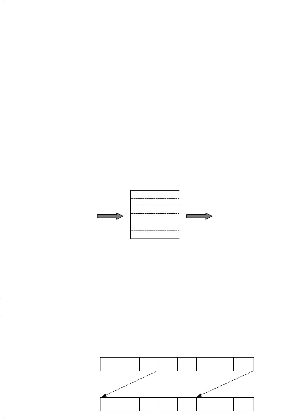
SCE CONFIDENTIAL GS User's Manual Version 6.0
© SCEI
-54-
UMSK, VMSK, UFIX, and VFIX are specified in the CLAMP_1 or CLAMP_2 register. They are the same
bits as the MINU, MINV, MAXU, and MAXV fields respectively, but are processed differently, according to
the wrap mode.
However, the following conditions exist to perform drawing correctly when the bilinear filter is used as a
filter for reading texels.
In the mask pattern of UMSK and VMSK, the bit position where the value is 1 should take 0 as the
corresponding bit values of UFIX and VFIX. This is shown in the formulas below.
UFIX & (1 << (iu + 1) - 1) = 0
VFIX & (1 << (iv + 1) - 1) = 0
(iu/iv shows the position of the most significant bit out of the bits with UMSK/VMSK equal to 1.)
3.4.6. Format Conversion
The GS performs calculations of 8 bits each for RGBA. When the color format of the texel value read from the
texture buffer is not RGBA32, the color format is converted as follows.
CLUT Conversion
When the texel storage formats are IDTEX8 and IDTEX4, the actual color value is obtained via the Color
Look-up Table (CLUT) based on the texel value.
CLUT
Color Value 0
Color Value 1
Color Value 2
:
:
:
Color Value 15
Texel Value
(IDTEX4)
Format
Conversion
Figure 3-13 Conversion from Texel Value (IDTEX4) to Color Value via CLUT
The CLUT is a color value table of 256 entries with IDTEX8 and 16 entries with IDTEX4. This table is
read temporarily from the local buffer to a temporary buffer and used. (This temporary buffer is different
from the texture page buffer, so the contents of the texture page buffer are not destroyed by using the
CLUT.)
Data load control from the CLUT to a temporary buffer is described in detail in "3.4.7.
CLUT Buffer Control".
RGB Bit Expansion
When the texel value or the color format of the color value converted via the CLUT is RGBA16, 5 bits each
for RGB are expanded into 8 bits as follows:
EABCD
Input Luminance
Value (5bits)
Output
Luminance
Value
(
8bits
)
0ABCDE 00
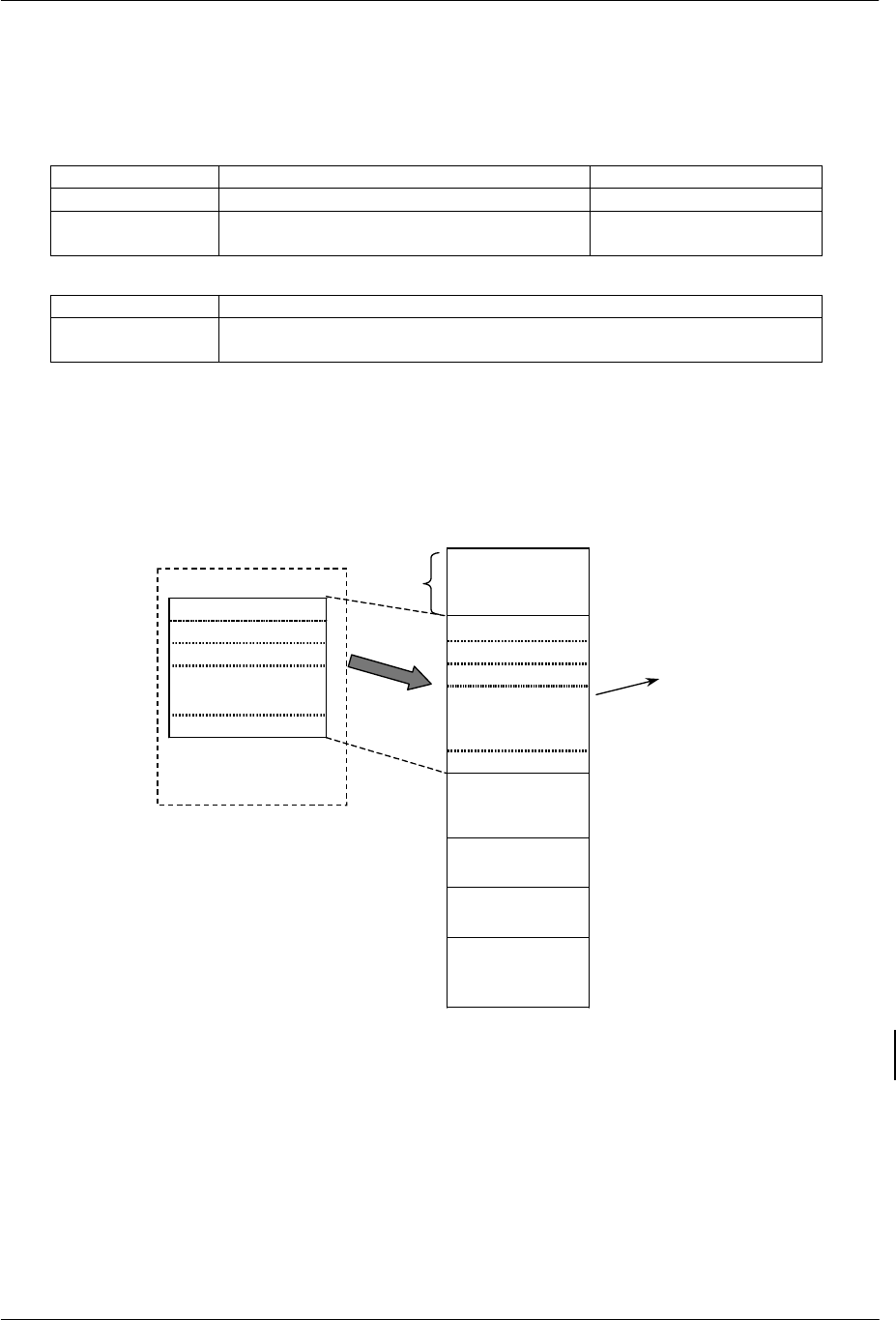
SCE CONFIDENTIAL GS User's Manual Version 6.0
© SCEI
-55-
Alpha Value Bit Expansion
When the color formats are RGBA16 and RGB24, the Alpha value of 8 bits is obtained as shown in the table
below based on the TEXA register.
RGBA16
A = 0 A = 1
AEM = 0 TA0 TA1
AEM = 1 R = G = B = 0 -> 0
R | G | B is not equal to 0 -> TA0
TA1
RGB24
AEM = 0 TA0
AEM = 1 R = G = B = 0 -> 0
R | G | B is not equal to 0 -> TA0
3.4.7. CLUT Buffer Control
The Color Look-up Table (CLUT) for texture mapping is used to convert the texture's index value to a color
value after copying from the CLUT buffer in local memory to the temporary buffer.
CLUT Buffer
Color Value 0
Color Value 1
Color Value 2
.
.
.
Color Value 15
Temporary Buffer
.
.
.
.
Color Value 0
Color Value 1
Color Value 2
.
.
.
.
Color Value 15
.
.
.
.
CLUT2
CLUT3
.
.
.
.
CSA
Load
Local Memory
Format
Conversion
Figure 3-14 Loading from CLUT Buffer to Temporary Buffer
When loading to the CLUT for the first time after CLUT data is stored in local memory, it is necessary to
invalidate the texture buffer by accessing the TEXFLUSH register.
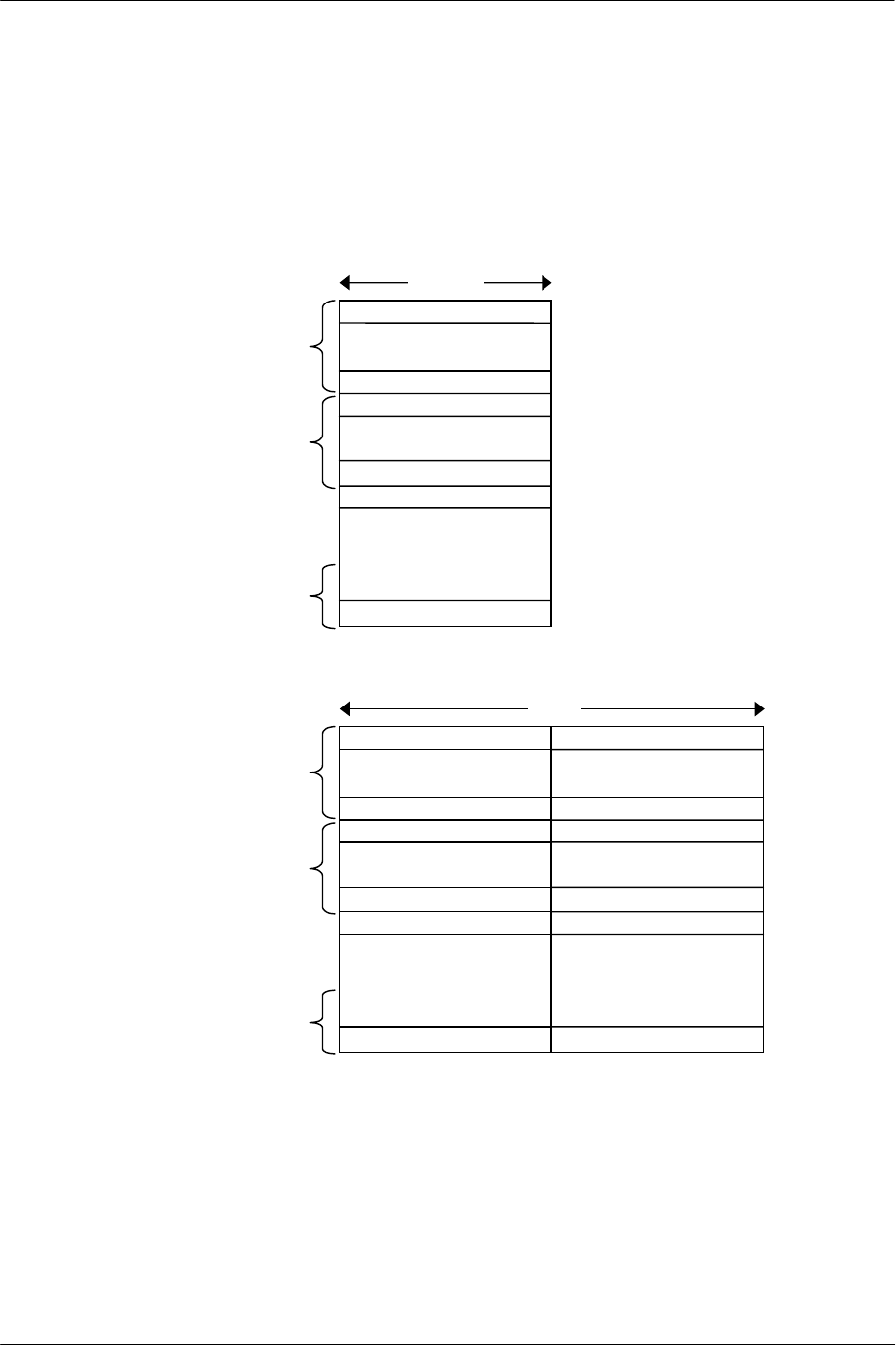
SCE CONFIDENTIAL GS User's Manual Version 6.0
© SCEI
-56-
Temporary Buffer for CLUT
The temporary buffer is a cache-like memory inside the GS. It has a 1 KB capacity, which is equivalent to the
entries of 256 colors in a 32-bit CLUT Entry Storage Format (CPSM) and 512 colors in a 16-bit CPSM. CSA
specifies which part of the temporary buffer is used.
Entries in the temporary buffer are arranged as follows:
CPSM=PSMCT16,PSMCT16S:(0 to 31 can be specified in CSA)
0
:
:
15
16
:
:
31
32
:
:
:
511
16 bits
CPSM=PSMCT32: (0 to 15 can be specified in CSA)
CSA=0
CSA=1
CSA=31
32 bits
256
:
:
271
272
:
:
303
304
:
:
:
511
0
:
:
15
16
:
:
31
32
:
:
:
255
CSA=0
CSA=1
CSA=15

SCE CONFIDENTIAL GS User's Manual Version 6.0
© SCEI
-57-
Load Operation
CLUT data is loaded from the CLUT buffer to the temporary buffer when the TEX0 or TEX2 register is
accessed. Only one set of CLUT data is loaded, and values in other areas of the temporary buffer are saved.
CLUT Data Specification
The CLUT data in the source is specified with CBP, CPSM or PSM of the TEX0 or TEX2 register or may
occasionally be specified with TEXCLUT. When the CLUT storage mode in the CLUT buffer is CSM1, the
CLUT must be located at the buffer starting address (the upper left point). When it is CSM2, the CLUT
location in the buffer is specified with TEXCLUT.
Loading Position in Temporary Buffer
CLUT data in the temporary buffer is loaded to the entry address (CSA multiplied by 16) with CSA in the
TEX0 or TEX2 register.
Loading Condition
The condition of loading to the temporary buffer is specified with CLD.
CLD Flag Transmission Control
000 CLUT data is not loaded. (Data in the temporary buffer is stored.)
001 CLUT data is always loaded.
010 CLUT data is always loaded, and internal register CBP0 is rewritten by the value of CBP.
011 CLUT data is always loaded, and internal register CBP1 is rewritten by the value of CBP.
100 CBP0 is compared with CBP, and if different, CLUT data is loaded.
101 CBP1 is compared with CBP, and if different, CLUT data is loaded.
The internal registers CBP0 and CBP1 control loading. Since they remember which CLUT buffer the data
has been loaded from, the temporary buffer can be used as cache memory (only in CSM1).
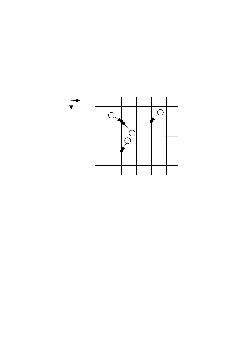
SCE CONFIDENTIAL GS User's Manual Version 6.0
© SCEI
-58-
3.4.8. Texel Sampling
Point sampling or bilinear sampling can be selected when performing filter processing during texel sampling.
The sampling method is specified in the drawing environment register, TEX1.
Point Sampling
Texel coordinates (iu, iv) are calculated from the normalization texel coordinates (s, t) according to the
following formulas, and the color value of the texel is assumed to be the texture value.
iu = Integer Part of (s x USIZE) iv = Integer Part of (t x VSIZE)
Operations such as repetition and clamping are performed to iu and iv depending on the wrap mode.
U
V
1.0 2.0 3.0
1.0
2.0
3.0
Figure 3-15 Texel Selection with Point Sampling Filter
Bilinear Sampling
The texture value is calculated by applying linear interpolation to four texel colors as below. First, texel
coordinates (iu0, iv0), (iu1, iv0), (iu0, iv1), and (iu1, iv1) are calculated from the normalization texel
coordinates (s, t) by the following formulas.
iu0 = Integer Part of (s x USIZE – 0.5) iu1 = iu0 + 1
iv0 = Integer Part of (t x VSIZE – 0.5) iv1 = iv0 + 1
The texture value is calculated by linear interpolation from the following formulas, assuming that the color
values of these four texels are (Ra, Ga, Ba, Aa), (Rb, Gb, Bb, Ab), (Rc, Gc, Bc, Ac), and (Rd, Gd, Bd, Ad)
respectively and that the decimal parts of (s x USIZE - 0.5) and (t x VSIZE - 0.5) are Alpha and Beta
respectively.
R =
(1.0- α)(1.0-β)Ra + α (1.0-β)Rb + (1.0-α)β Rc + αβ Rd
G = (1.0- α)(1.0-β)Ga + α (1.0-β)Gb + (1.0-α)β Gc + αβ Gd
B =
(1.0- α)(1.0-β)Ba + α (1.0-β)Bb + (1.0-α)β Bc + αβ Bd
A =
(1.0- α)(1.0-β)Aa + α (1.0-β)Ab + (1.0-α)β Ac + αβ Ad
Operations such as repetition and clamping are performed to iu0, iv0, iu1, and iv1 depending on the
wrapping mode.

SCE CONFIDENTIAL GS User's Manual Version 6.0
© SCEI
-59-
U
V
1.0 2.0 3.0
1.0
2.0
3.0
ab
cd
Figure 3-16 Texel Selection with Bilinear Filter
3.4.9. Texture Function
The colors (Rt, Gt, Bt, At) obtained from the texture are blended with the colors (Rf, Gf, Bf, Af) of the
fragment obtained from the primitive by the DDA and converted into output colors (Rv, Gv, Bv, Av). At this
time, according to the texture function specified by the TFX flag of the TEX0 register and the mode specified
by the TCC flag, the conversion operation in the following table is applied. When the TCC flag is RGBA and
the texel format is TEX 24 or TEX16, the value set in the TEXA register is used as the Alpha value.
Function TCC=RGB TCC=RGBA
Description
MODULATE Rv = Rt * Rf
Gv = Gt * Gf
Bv = Bt * Bf
Av = Af
Rv = Rt * Rf
Gv = Gt * Gf
Bv = Bt * Bf
Av = At * Af
Adjusts the brightness of the texture
color according to the fragment color.
When the value of the fragment color
is 0x80, the brightness of the output
color is the same as that of the original
texture.
DECAL Rv = Rt
Gv = Gt
Bv = Bt
Av = Af
Rv = Rt
Gv = Gt
Bv = Bt
Av = At
Outputs the texture color as is.
HIGHLIGHT Rv = Rt * Rf + Af
Gv = Gt * Gf + Af
Bv = Bt * Bf + Af
Av = Af
Rv = Rt * Rf + Af
Gv = Gt * Gf + Af
Bv = Bt * Bf + Af
Av = At + Af
Adjusts the brightness of the texture
color as in the case of MODULATE,
then adds a highlight in pure white
based on the alpha value of the
fragment color. Suitable for
highlighting translucent polygons.
HIGHLIGHT2 Rv = Rt * Rf + Af
Gv = Gt * Gf + Af
Bv = Bt * Bf + Af
Av = Af
Rv = Rt * Rf + Af
Gv = Gt * Gf + Af
Bv = Bt * Bf + Af
Av = At
Similar to HIGHLIGHT, but stores
the alpha value of the texture color.
Suitable for highlighting opaque
polygons.
However, the operator * means A*B = (A x B) >> 7, and the calculation result is clamped between 0 and 0xff.
(When the value of the fragment color is 0x80, the brightness of the texture corresponds to the brightness of the
output color.)
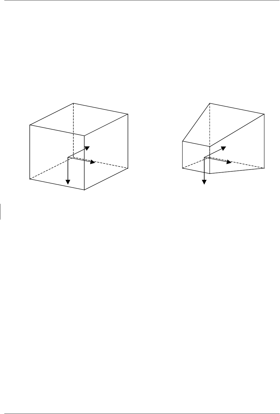
SCE CONFIDENTIAL GS User's Manual Version 6.0
© SCEI
-60-
3.4.10. Perspective Correction
The GS has the ability to correct texture perspective distortion. This is done by giving the value, to which
appropriate preprocessing is performed in the texture coordinate system (S, T, Q), to the GS as the vertex
coordinate values in the texture space.
When drawing a three-dimensional primitive, the point (Xv, Yv, Zv) in the view coordinate system usually
shown in the rectangular parallelepiped is converted into the point (Xp, Yp, Zp) in the primitive coordinate
system shown in the truncated quadrangular-pyramid by transparency perspective conversion. In the primitive
coordinate system, a place close to the viewpoint is expanded, and a place far from the viewpoint is reduced and
distorted.
X
Y
Z
X
Y
Z
View Coordinate System Primitive Coordinate System
Figure 3-17 Coordinate System in Transparency Perspective Conversion
This distortion is caused by transparency perspective conversion. Calculations for linear interpolation for DDA
etc. are made when drawing a primitive to the frame buffer. This is performed in the primitive coordinate
system. However, since the relation between texture and primitive is defined in the view coordinate system, a
positional deviation from the primitive is caused if the texture coordinate values are linear-interpolated as they
are when drawing the primitive. This is the so-called perspective distortion of the texture.
To avoid this, equivalent conversion is performed to the texture coordinates as well. Let the texture coordinates
of the primitive vertex in the view coordinate system (the world coordinate system or local coordinate system is
also OK) be (sv, tv) and the divisor in the transparency perspective conversion be W. The texture coordinates
(S, T, Q) in the primitive coordinate system are gained from the formulas below.
S = sv / W T = tv / W Q = 1 / W
Proper perspective correction can be achieved by giving these S, T, and Q to the GS. (After linear-interpolating
S, T, and Q, the GS calculates the normalization texel coordinate values from s = S/Q and t = T/Q.)
Moreover, perspective distortion is not generated for Sprites, where each fragment always takes the same Z
value. In such a case, texel coordinates for the vertex of each primitive can be specified directly. (Note that they
are not the normalization texel coordinates.)
Whether the homogeneous texture coordinates (S, T, Q) or texel coordinates (U, V) are used to specify the
texture coordinates is determined by the FST flag of the PRIM register or PRMODE register. Regarding the
primitive vertex, S and T values are set in the ST register and Q value is set in the Q area of the RGBAQ
register. Moreover, U and V values are set in the UV register.

SCE CONFIDENTIAL GS User's Manual Version 6.0
© SCEI
-61-
3.4.11. MIPMAP
MIPMAP textures can be set in seven stages from level 0 to level 6. The texture height and width should each
be a power of 2. When MIPMAP level 0 texture is 2m x 2n in sizing, levels 1 and 2 are set to 2m-1 x 2n-1 and 2m-2
x 2n-2 respectively in texture sizing. Sizing is set in succession by reducing the height and width by half, until
either the width or height reaches 1 for point sampling or 8 for bilinear sampling.
When MIPMAP is not performed, level 0 is used.
Calculation of Texture Base Pointer
The user can set the base pointer of the MIPMAP texture at each level to the desired position in the same
way as texture level 0. However, because the page size changes according to the pixel storage format of the
texture, it is necessary to set the base pointer so that the textures do not overlap.
In the example below, the MIPMAP is composed assuming a texture of 512 x 512 texels is level 0 when the
format is PSMCT16.
MIPMAP
Level
Base Pointer Buffer
Width
Texture Width Texture Height
0 7200 8 9 9
1 9248 4 Not specified Not specified
2 9760 2 Not specified Not specified
3 9888 1 Not specified Not specified
4 9920 1 Not specified Not specified
5 9928 1 Not specified Not specified
6 9930 1 Not specified Not specified
The minimum value at base pointer intervals by which the textures of different MIPMAP levels are stored
changes depending on the texture format, texture size and ratio of height and width.
Automatic Calculation of Base Pointer
The base pointer for texture levels 1 to 3 can be calculated automatically on the condition that texture format
and size must meet the following requirements.
• PSMCT32/PSMCT24/PSMT8H/PSMT4HL/PSMT4HH
Width = Height = {32, 64, 128, 256, 512}
• PSMCT16/PSMT8/PSMT4
Width = Height = {32, 64, 128, 256, 512, 1024}
With automatic calculation, textures up to level 3 are stored in a continuous memory area, as in the examples
above. When the texture is loaded, it is necessary to store the texture at the position of the base pointer
calculated automatically.
The automatic calculation is executed when the TEX0 register is set after the MTBA field of the TEX1
register is set to 1.
For the texture of MIPMAP levels 1 to 3, the base pointer is specified in the fields TBP1 to TBP3 of the
MIPTBP1 register and the buffer width is specified in the field TBW1 to TBW3. As for the texture of
MIPMAP levels 4 to 6, the base pointer is specified in the fields TBP4 to TBP6 of the MIPTBP2 register and
the buffer width is specified in the field TBW4 to TBW6. Moreover, the maximum MIPMAP level used is
set to the MXL flag in the TEX1 register.

SCE CONFIDENTIAL GS User's Manual Version 6.0
© SCEI
-62-
3.4.12. LOD Setting
The texture level and filter used for mapping are controlled by the value of the LOD (Level of Detail). There
are two methods of calculating the LOD, and they are specified in the LCM fields of the TEX1 register. One
method is to obtain the LOD from the Q value of each primitive vertex and the L and K fields of the TEX1
register according to the formula below, and the other is to specify the LOD in the K field only. When LCM is
set to 0, LOD is calculated from the Q value even if the texture coordinates are given by UV.
LCM = 0 : LOD = ( log2(1/Q) << L) + K
LCM = 1 : LOD = K
When the calculated LOD value is 0.0 or less, the level 0 texture is used, and the filter specified in the MMAG
field of the TEX1 register is used.
When the LOD value is more than 0.0, the level 0 to 6 textures are used depending on the LOD value, and the
filter specified by the MMIN flag of the TEX1 register is used.
The following table shows the relation between the MMIN flag and the filter used.
MMIN Flag Level m Filer Level m+1 Filter Processing between Levels
0 Disabled Disabled Level 0 point sampling
1 Disabled Disabled Level 0 bilinear
2 Point sampling Point sampling Selection of m or m+1 by LOD
(round-off)
3 Point sampling Point sampling Linear interpolation by LOD
4 Bilinear Bilinear Selection of m or m+1 by LOD
(round-off)
5 Bilinear Bilinear Linear interpolation by LOD
(trilinear)
*m is the integer part of the LOD value.
The bilinear filter in each MIPMAP imposes almost no speed penalty, but the linear interpolation filter between
levels affects the drawing time.
Moreover, when the number of pixels for the height or width of the texture is four or less, correct images
cannot be obtained with bilinear and trilinear filters.
Specifications of L and K
The weight of the MIPMAP filter is specified by L, and the position of MIPMAP level 0 is set by K.
Assuming the fragment position, where the ratio of the texel to the frame buffer pixel is 1 to 1, to be Z0 in
texture mapping, K is set by the following formula.
K = - ( log2(Z0 / h ) << L )
However, h is assumed to be the distance between the viewpoint and screen, and Q of each vertex of the
primitive is assumed to be h/Z. The relation between Z and LOD is shown in the figure below.

SCE CONFIDENTIAL GS User's Manual Version 6.0
© SCEI
-63-
LOD
01 2
Viewpoint
Z0
Z1
Z2
Z
Figure 3-18 LOD when L = 0 and K = - log2( Z0 / h )
When mapping the texture to the primitive parallel to the screen, it is appropriate to set L = 0, in which the
reduction on the display corresponds to the increase of LOD. However, when the primitive is inclined to the
screen, a value more than 0 is set to L.
Because the effect of MIPMAP changes with the texture pattern, appropriate L and K values should be set
according to the texture used. To control the MIPMAP levels individually in primitives units, the value of Q can
be directly controlled.
3.4.13. Texture Mapping Procedure
The following is an example of a register setting procedure for texture mapping. (The registers necessary for
general drawing should already be set.)
1. Transmit the texture to the local buffer.
2. Transmit the CLUT to the local buffer.
3. Set the TEXCLUT register (if necessary).
4. Access the TEXFLUSH register (only once at first).
5. Set the TEXA register.
6. Set the TEX1_1 | TEX1_2 register.
7. Set the TEX0_1 | TEX0_2 register.
8. Set the MIPTBP1_1 | MIPTBP1_2 register.
9. Set the MIPTBP2_1 | MIPTBP2_2 register.
(Repeat the following.)
10. Set the PRIM register.
11. Set the ST or UV register.
12. Set the RGBAQ register.
13. Set the XYZF register.

SCE CONFIDENTIAL GS User's Manual Version 6.0
© SCEI
-64-
3.5. Fog Effect
The Fog effect is achieved by blending the color of each texel output from the texture function and the Fog
color. Let the output colors from the texture function be (Rv, Gv, Bv, Av); let the Fog coefficient, which has
been obtained by linear-interpolating the Fog value set for each vertex of the primitive, be F; and the Fog colors
written to the FOGCOL register be (Rfc, Gfc, Bfc). The blending operation is shown in the formulas below.
R = F * Rv + ( 0xff – F )* Rfc
G = F * Gv + ( 0xff – F )* Gfc
B = F * Bv + ( 0xff – F )* Bfc
A = Av
However, A*B = ( A x B) >> 8.
The Fog coefficient is stored in the F field of the XYZF or XYZF2 register. The Fog color is stored in the
FOGCOL register. Whether or not Fogging is performed is specified with the FGE flag of the PRIM register.

SCE CONFIDENTIAL GS User's Manual Version 6.0
© SCEI
-65-
3.6. Antialiasing
In the GS, Antialiasing can be performed for Line, LineStrip, Triangle, TriangleStrip, and TriangleFan. This
process is performed for each line or triangle.
3.6.1. Principle of Antialiasing
Antialiasing is achieved by calculating the coverage Cov (ratio of the area that covers the pixel) to each pixel at
the edge of the GS primitive, assuming this to be the Alpha value, and performing Alpha-blending to the
destination color (color distant from the primitive) and the primitive color.
The effect of Antialiasing is different depending on the combination of the AA1 flag to set Antialiasing, ABE
flag to set Alpha-blending, and the Alpha value calculated for the pixel. This is shown in the table below. Cov
shows the value of the coverage of the pixel. When the coverage is 100%, Cov = 0 x 80 (128 in decimal) is
obtained.
AA1
Flag
ABE
Flag
Alpha Value to be Output Antialiasing
Effect
Blending
Effect
0 0 A NO NO
0 1 A NO YES
1 0 Cov YES NO
1 1 Cov (Pixel with A equal to 0x80) YES NO
1 1 A (Pixel with A not equal to 0x80) NO YES
3.6.2. Antialiasing Control
Drawing Order
To perform Antialiasing appropriately, the part distant from the primitive should be drawn before drawing
the primitive. It is necessary to sort all the drawing primitives in positional order (far to close) to achieve
ideal Antialiasing.
Write to Z Buffer
Since Antialiasing is performed to each line or triangle, how to deal with the parts shared by lines and
triangles becomes a problem. In the GS, to guarantee the connection of the image in the boundary part,
writing to the Z buffer is not performed for pixels with coverage Cov less than 0x80.
As for the line, Cov is always less than 0x80. Therefore, the Z buffer is not written when the AA1 flag is 1.
Antialiasing is controlled by the AA1 flag of the PRIM or PRMODE register. Moreover, it is necessary to
set the flags of the ALPHA register for blending, as shown below.
A = Cs (Source Color)
B = Cd (Destination Color)
C = As (Source Alpha)
D = Cd (Destination Color)

SCE CONFIDENTIAL GS User's Manual Version 6.0
© SCEI
-66-
3.7. Pixel Test
The pixel test is the process of inspecting whether or not a pixel to be drawn meets specified conditions. It also
controls drawing processing for pixels that failed. The pixel test does not change the pixel value.
The pixel test consists of the following test items, which are executed in this order.
Pixel Test Test Contents
Scissoring Test Test by the position where the pixel is drawn.
Alpha Test Comparison test between the pixel's alpha value and standard value.
Destination
Alpha Test
Test by the pixel's alpha value at the drawing destination in the frame buffer.
Depth Test Comparison test between the pixel's Z value and the corresponding Z value in
Z buffer.
From the point of view of GS internal processing, the scissoring test is carried out in the Rasterizing (DDA)
stage and not in the pixel test stage. For the convenience of the user, however, it is described in this section.
Processes succeeding the pixel test such as Alpha-blending are performed even to a pixel that failed the alpha
test, destination alpha test, or depth test, and the pixel is finally controlled in drawing when the pixel value is
written in the frame buffer and the Z buffer. It may appear as if the pixel test were performed after Alpha-
blending.
3.7.1. Scissoring Test
This test checks whether the coordinate values of the pixel to be drawn are in the rectangular (scissoring) area
specified in the window coordinate system. Pixels judged to be outside the scissoring area are not processed
further.
Set Register
SCISSOR_1, SCISSOR_2
Test Contents
The pixel is judged by the following formulas, assuming the pixel coordinates are (x, y). A pixel located on
the boundary of the scissoring area passes.
scissor_test(int x, y)
{
if (x < SCISSOR.SCAX0 || x > SCISSOR.SCAX1) return(FAIL);
if (y < SCISSOR.SCAY0 || y > SCISSOR.SCAY1) return(FAIL);
return(PASS);
}
The scissoring test cannot be omitted.
SCE CONFIDENTIAL GS User's Manual Version 6.0
© SCEI
-67-
3.7.2. Alpha Test
The Alpha value of the drawing pixel and the preset standard alpha value are compared. Processing is controlled
if the pixel does not meet the comparison condition that was set.
Set Register
TEST_1, TEST_2 (ATE, ATST, AREF, and AFAIL fields)
Test Contents
ATE ATST Test Contents
0 - No testing. (All pixels pass.)
NEVER All pixels fail.
ALWAYS All pixels pass.
LESS Pixels less than AREF pass.
LEQUAL Pixels less than or equal to AREF pass.
EQUAL Pixels equal to AREF pass.
GEQUAL Pixels greater than or equal to AREF pass.
GREATER Pixels greater than AREF pass.
1
NOTEQUAL Pixels not equal to AREF pass.
A pixel that failed the alpha test is not controlled completely in drawing, but can be specified in the AFAIL
field in the TEST register so that the RGB, A, and Z values are controlled individually. Details are as
follows.
Alpha Test Result AFAIL Setting RGB A Z
KEEP Controlled Controlled Controlled
FB_ONLY Effective Effective Controlled
ZB_ONLY Controlled Controlled Effective
Failed
RGB_ONLY* Effective Controlled Controlled
*RGB_ONLY is effective only when the color format is RGBA32.
In other formats, operation is made with FB_ONLY.
Controlled values do not become effective even if they pass in other pixel tests after this.
SCE CONFIDENTIAL GS User's Manual Version 6.0
© SCEI
-68-
3.7.3. Destination Alpha Test
This test checks the Alpha value of the pixel for drawing in the frame buffer (Destination Alpha Value). A
failed pixel is controlled in drawing.
Set Register
TEST_1, TEST_2 (DATE and DATM fields)
Test Contents
The contents of the Destination Alpha Test depend on the pixel storage mode of the frame buffer.
Frame Buffer: PSMCT32 (RGBA32)
DATE DATM Test Contents
0 - No testing. (All pixels pass.)
1 0 Pixels with bit 7 of A set to 0 pass.
1 1 Pixels with bit 7 of A set to 1 pass.
Frame Buffer: PSMCT16 (RGBA16)
DATE DATM Test Contents
0 - No testing. (All pixels pass.)
1 0 Pixels with A set to 0 pass.
1 1 Pixels with A set to 1 pass.
Frame Buffer is PSMCT24 (RGB24)
Because the frame buffer does not have A value, all pixels pass regardless of the setting of DATE and
DATM.
3.7.4. Depth Test
This test compares the Z value of the drawing pixel and the corresponding Z value in the Z buffer. A failed
pixel is controlled in drawing.
Set Register
TEST_1, TEST_2 (ZTE and ZTST fields)
Test Contents
ZTE ZTST Test Contents
0 - (Disabled)
NEVER All pixels fail.
ALWAYS All pixels pass.
GEQUAL Pixels greater than or equal to Z buffer value pass.
1
GREATER Pixels greater than Z buffer value pass.
Setting ZTE to 0 is prohibited since it may cause a malfunction. To omit the depth test, set ZTE to 1 and
ZTST to ALWAYS, and the ZMSK field of the ZBUF register to 1 respectively. Due to these settings, the Z
buffer is neither accessed nor updated for any pixels. As a result, the operation becomes the same as the one
without the depth test.
SCE CONFIDENTIAL GS User's Manual Version 6.0
© SCEI
-69-
3.8. Alpha Blending
Blending calculation can be made between the depth test output color (Source Color) Cs and the frame buffer
pixel color (Destination Color) Cd.
Calculation of RGB values is performed. With Alpha value A, the source Alpha value (As) is written in the
frame buffer as is. However, when the FBA flag of the FBA register is set, a prescribed operation is performed.
Alpha-blending is set ON/OFF by the ABE flag of the PRIM or PRMODE register. When performing
antialiasing (setting AA1 to 1), the blending function operates automatically. Therefore, the ABE flag must
always be set to 0 (OFF).
3.8.1. Blending Setting
The formula for blending is shown below. A, B, C, and D in the formula can be set to take the value in the
following table with the flag of the ALPHA register. FIX is the fixed Alpha value set in the ALPHA register.
Output Color = (A - B) * C + D
However, X * Y = (X x Y) >> 7
Flag Selectable Color
A Cs, Cd, 0
B Cs, Cd, 0
C As, Ad, FIX
D Cs, Cd, 0
When the Alpha value is 0x80, the multiplier to the source color becomes 1.0. An example of flag setting
applied to normal blending is shown as follows. When Antialiasing AA1 is performed, the same setting is made.
A B C D Equivalent Formula
Cs Cd As Cd Cs*As + Cd*(0x80 - As)
Additionally, various settings such as subtraction and brightness addition/decrease are possible.
A B C D Equivalent Formula
Cd Cs 0x80 0 Cd - Cs
Cd 0 As Cd Cd*(0x80 + As)
0 Cd As Cd Cd*(0x80 - As)
In the RGBA16 mode, where Destination Alpha value is 1 bit only, Alpha is treated as 0 when A is 0 and as
0x80 when A is 1. In the RGB24 mode, Alpha is treated as 0x80.
The result of Alpha-blending is passed to the following Dithering processing as is, without being clamped.
3.8.2. PABE Flag
When the PABE flag is 1, the value of MSB of the Source Alpha determines whether to perform Alpha-blending
per pixel. Alpha-blending is ON when MSB is 1 and OFF when MSB is 0.
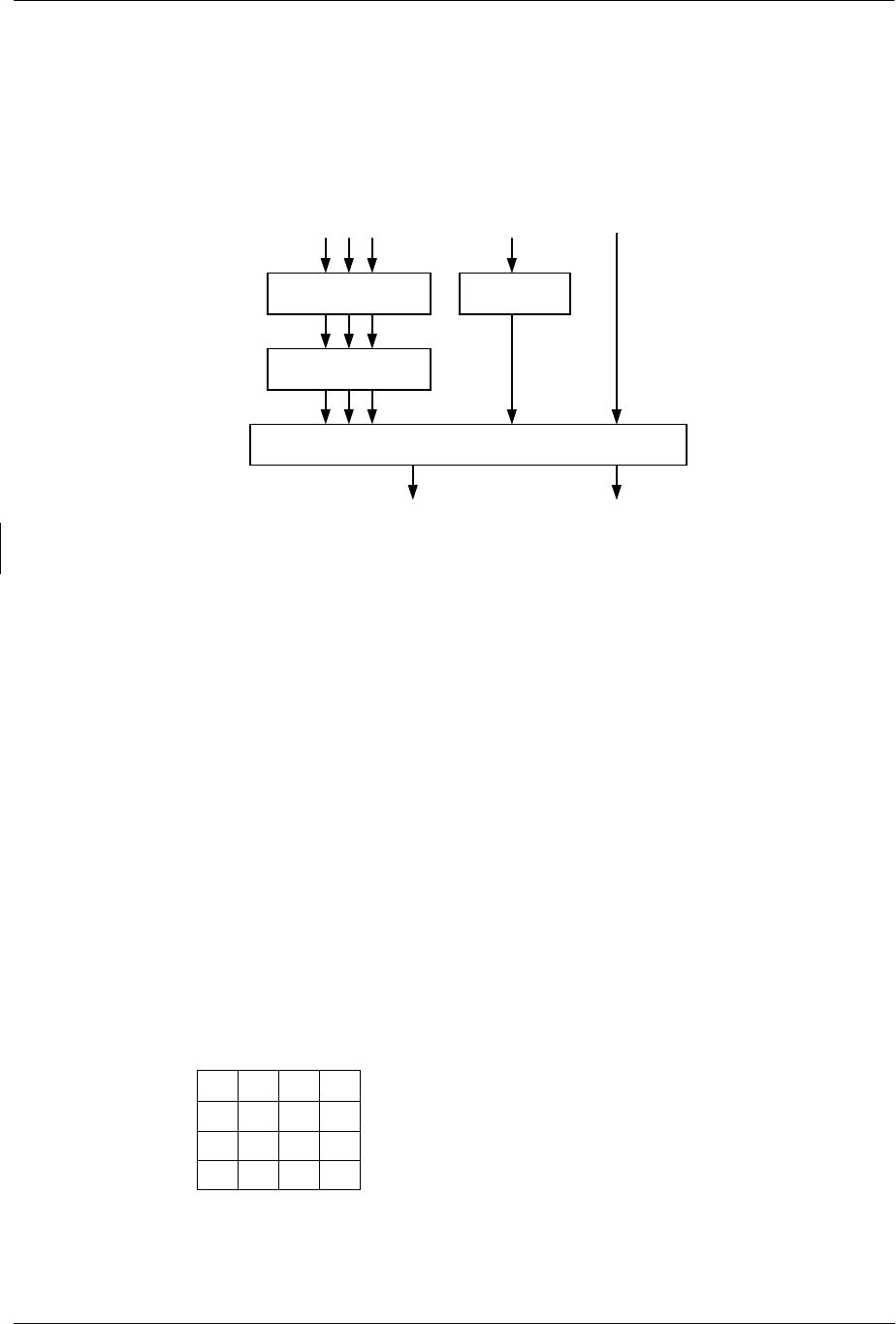
SCE CONFIDENTIAL GS User's Manual Version 6.0
© SCEI
-70-
3.9. Writing to the Frame Buffer
The following processing is performed according to the pixel storage mode before the pixel value, the output
from the pixel pipeline, is written in the frame buffer.
Dithering
RGB
Clamping
A Value
Correction
Format Conversion
Frame Buffer
AZ
Z Buffer
Figure 3-19 Write Process to Frame Buffer
3.9.1. Dithering
If the frame buffer color format is RGBA16, the RGB luminance values are each converted from 8 bits to 5 bits.
At this time, it is possible to decrease the Mach band by dithering.
Dithering is set ON/OFF by the DTHE register.
Dithering is performed by adding the offset value selected according to the coordinates of the pixel from the
dither matrix of 4 x 4 set in the DIMX register to each luminance value of the RGB of the pixel. It is shown in
the following formulas.
Rout = Rin + DIMX[Y%4][X%4]
Gout = Gin + DIMX[Y%4][X%4]
Bout = Bin + DIMX[Y%4][X%4]
X,Y : Window Coordinate Values of Pixel in Frame Buffer
Rin, Gin, Bin : Input Luminance Value (8 bits)
Rout, Gout, Bout : Output Luminance Value (8 bits)
Dither Matrix Setting Example
-4 2 -3 3
0 -2 1 -1
-3 3 -4 2
1 -1 0 -2
When the color format of the frame buffer is RGBA32 or RGB24, the result of dithering is not guaranteed.
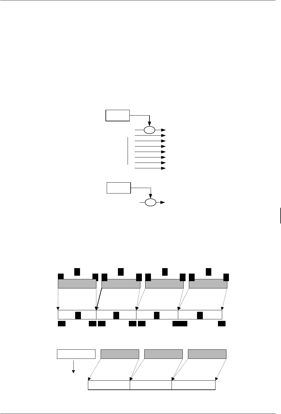
SCE CONFIDENTIAL GS User's Manual Version 6.0
© SCEI
-71-
3.9.2. Color Clamp
Since the RGB value of a pixel occasionally exceeds the range of 0-255 after operations such as Alpha-blending,
the result is stored with 9 bits for each RGB value. It is possible to select clamping to set this value within the
range of 0-255, or to extract the lower 8 bits. Whether or not to perform clamping is determined by the
COLCLAMP register.
3.9.3. Alpha Value Correction
It is possible to correct the pixel alpha value with the value previously set in the FBA register. This is done
when reusing the image data in the frame buffer as a texture.
RGBA32
FBA
b
it 7
b
it 0
b
it 6
Output A ValueInput A Value
OR
RGBA16
FBA
OR Output A Value
Input A Value bit 7
Figure 3-20 Alpha Value Correction
3.9.4. Format Conversion
Pixel color values are packed into a fixed number of bits, according to the pixel storage mode set by the
FRAME_1 or FRAME_2 register, and written in the frame buffer.
RGBA32 (PSMCT32) Mode
A G RB
B G R
7 0 0 0 7 07 7
A
31 24 23 16 15 8 7 0
RGB24 (PSMCT24) Mode
AGRB
BGR
70007077
Not Used
23 16 15 8 7 0
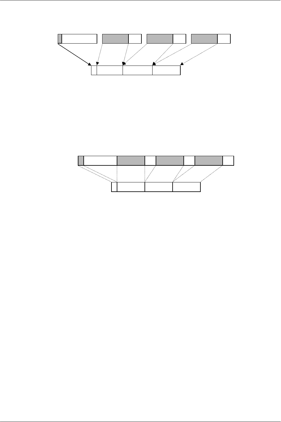
SCE CONFIDENTIAL GS User's Manual Version 6.0
© SCEI
-72-
RGBA16 (PSMCT16,PSMCT16S) Mode
R
AGR
AB G
70007077333
B
R
915 5 4 01014
3.9.5. Masking
The mask can be set so that only the prescribed bits are written when writing data to the frame buffer.
The value of the mask is specified in the FBMSK field of the FRAME_1 or FRAME_2 register. Since the bit
position of the FBMSK corresponds to the pixel value before format conversion, special care is needed when
the pixel format of the frame buffer is RGBA16. The relation between FBMSK and the frame buffer in the case
of RGBA16 is shown as follows.
FBMSK
31 24 1923 15 11 7 3
Frame Buffer AB GR
915 5 4 01014
0
Regarding the Z buffer, it is possible to control only whether or not to write all the bits.
This is specified with the ZMSK of ZBUF_1 or ZBUF_2 register.

SCE CONFIDENTIAL GS User's Manual Version 6.0
© SCEI
-73-
4. Image Data Transmission
The GS supports three modes of image data transmission, according to the direction of transmission:
• Transmission from host to local buffer
• Transmission from local buffer to host
• Transmission from local buffer to local buffer
The local buffer is the local memory in the GS, and the host is the external device connected to the GS.
When transmitting data, the arrangement of the pixels in local memory, or the pixel storage format, is converted
according to the specification. At this time, however, no processes involving changes to the pixel value (e.g.
color reduction, Alpha value operation, and masking) are performed. When transferring between local buffers,
transmission is supported only between buffers that have the same number of bits per pixel.
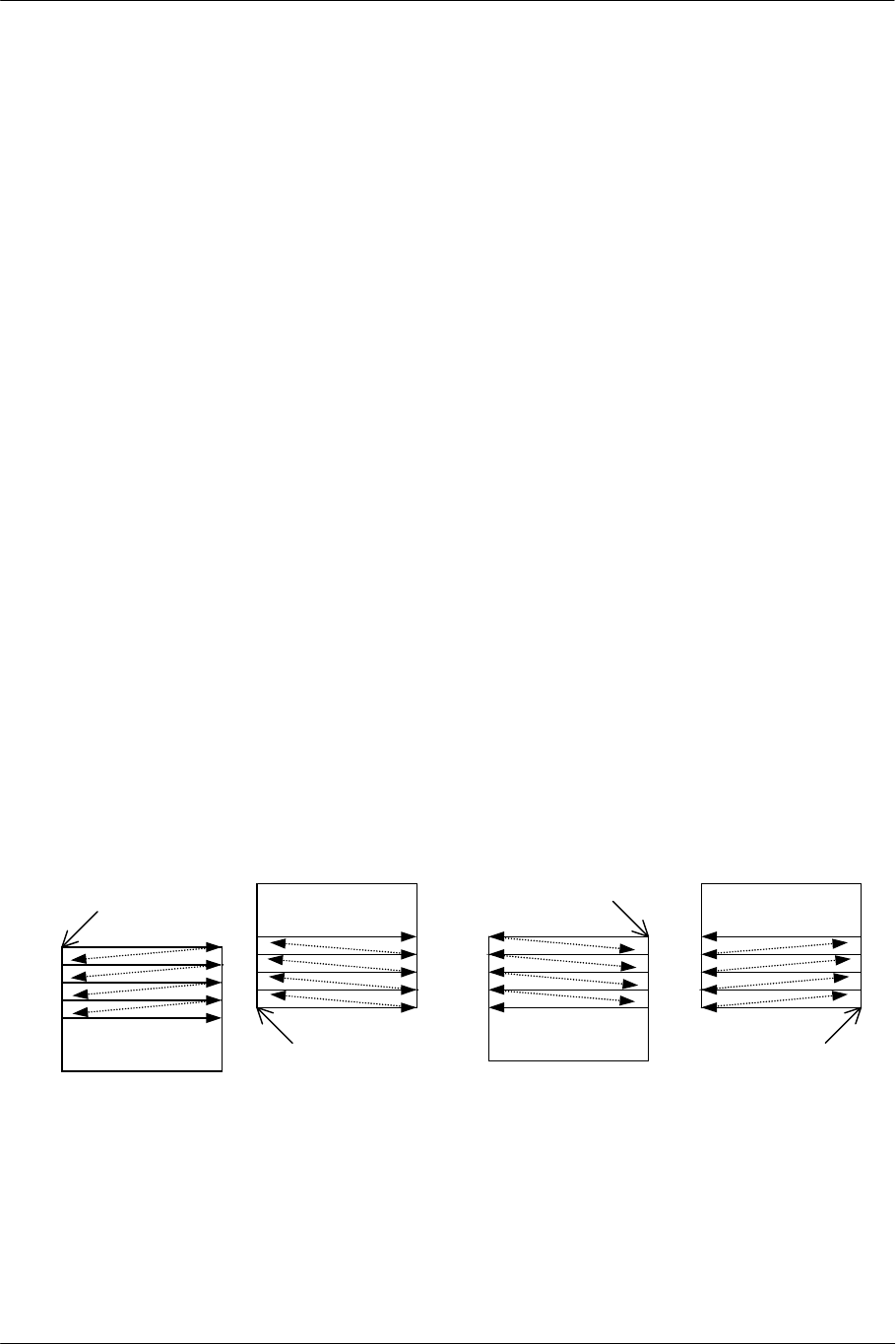
SCE CONFIDENTIAL GS User's Manual Version 6.0
© SCEI
-74-
4.1. Transmission Parameters
When transmitting data, it is necessary to set the following parameters.
4.1.1. Destination Buffer / Source Buffer (BITBLTBUF Register)
For each buffer from/to which data is transmitted, the base pointer, buffer width, and pixel storage format are
set in the BITBLTBUF register.
When transmitting from host to local buffer, only the destination buffer is set. When transmitting from local
buffer to host, only the source buffer is set. When transmitting from local buffer to local buffer, both the
destination and source buffers are set.
The buffer base pointer is specified as a 14-bit unsigned integer in units of 64 words. The buffer width is
specified by a 6-bit unsigned integer in units of 64 pixels.
All pixel storage formats can be used, except that when transmitting from local buffer to host, pixel storage
formats PSMT4, PSMT4HL and PSMT4HH cannot be used. When transmitting from local buffer to local
buffer, the bit length of the pixels to be stored respectively in the source and destination buffer should be the
same.
4.1.2. Offset in Buffer (TRXPOS Register)
The TRXPOS register specifies the offset coordinates at the upper left point of the transmission area in the
transmission buffer and the pixel transmission direction. When transmitting from host to local buffer, only the
settings for the destination buffer are made. When transmitting from local buffer to host, only the settings for
the source buffer are made. And when transmitting from local buffer to local buffer, settings are made for both
the source and destination buffers.
The four figures below show the direction of the pixel transmission of the transfer data within the transmission
destination area. This setting is enabled only when transmitting from local buffer to local buffer, and when
transmitting from host to local buffer and local buffer to host, data is arranged in the direction from left to right
and top to bottom. The transmission starting point in the rectangular area varies according to the pixel
transmission direction.
Start
Start
Start
Start
0. Left to Right
Top to Bottom
1. Left to Right
Bottom to Top
2. Right to Left
Top to Bottom
3. Right to Left
Bottom to Top
Figure 4-1 Pixel Transmission Direction
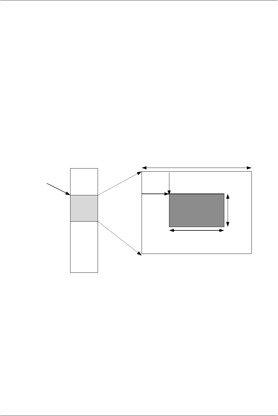
SCE CONFIDENTIAL GS User's Manual Version 6.0
© SCEI
-75-
4.1.3. Width and Height of Transmission Area (TRXREG Register)
The TRXREG register specifies the width and height of the transmission area.
When transmitting from host to local buffer, settings for the destination buffer are made. When transmitting
from local buffer to host, settings for the source buffer are made. And when transmitting from local buffer to
local buffer, settings are made for the destination buffer. (The width and height of the transmission area in the
destination and the source should be the same.)
When the coordinate value of the transmission area is 2048 or more, it wraps around at 2048. That is, if the
transmission start coordinates are (SAX, SAY), the coordinates of the pixel to be transmitted actually are (X, Y)
and the offset coordinates from the transmission start coordinates of the pixel are (RRX, RRY), then:
X = (SAX + RRX) % 2048
Y = (SAY + RRY) % 2048
The figure below shows the relation between transmission area parameters when the pixel transmission direction
is left to right and top to bottom.
Buffer Width
(SBW/DBW)
(SSAY/DSAY)
(SSAX/
DSAX)
RRW
RRH
Address
(SBP/DBP)
Figure 4-2 Parameters to Show Transmission Area
4.1.4. Transmission Direction and Transmission Start (TRXDIR Register)
This register specifies the directions of transmission. The following three can be specified.
• Host to local buffer
• Local buffer to host
• Local buffer to local buffer
The GS starts transmission immediately after the TRXDIR register is accessed.

SCE CONFIDENTIAL GS User's Manual Version 6.0
© SCEI
-76-
4.1.5. Limitations on Transmission Start Coordinates and Width
The table below shows the limitations on the start coordinates and transmission area width according to the
pixel storage format. These limitations do not apply to the transmission from local buffer to host.
Pixel Storage
Format
Limitation on
Start X Coordinate
Limitation on
Width
PSMCT32
PSMZ32
No limitation Multiples of 2
PSMCT24
PSMZ24
No limitation Multiples of 8
PSMCT16
PSMCT16S
PSMZ16
PSMZ16S
No limitation Multiples of 4
PSMT8
PSMT8H
Multiples of 2 Multiples of 8
PSMT4
PSMT4HL
PSMT4HH
Multiples of 4 Multiples of 8

SCE CONFIDENTIAL GS User's Manual Version 6.0
© SCEI
-77-
4.2. Transmission Process
4.2.1. Transmission from Host to Local Buffer
Transmission of image data from host to local buffer is performed by writing data to the transmission data
register (HWREG) after setting the parameters described above.
Data is written to HWREG in 64-bit units. During data transmission, it is possible to access other registers and
to issue drawing primitives. It is guaranteed that in the GS, transmission data will not overtake a drawing
primitive that was issued before setting the transmission direction setting register (TRXDIR).
If the TRXDIR has been accessed before transmission is ended (before a fixed amount of data are written to
HWREG), transmission is ended, and a new transmission is started using the current values of BITBLTBUF,
TRXPOS and TRXREG.
To perform drawing using the transmitted data as a texture immediately after data transmission, it is necessary to
access the TEXFLUSH register before primitive drawing because the order of writing to local memory is not
guaranteed.
4.2.2. Transmission from Local Buffer to Host
When transmitting image data from local buffer to host, it is necessary to switch the transmission directions of
the bus between the GS and host after checking the GS input FIFO is empty. The process is as follows:
1. Set the transmission parameters. (See "4.1. Transmission Parameters".)
2. Access the FINISH register. (FINISH event occurs when data is input to the GS.)
3. Wait until the FINISH field of the privileged port CSR register becomes 1.
4. Set the FINISH field of the CSR register to 0 and clear the event.
5. Write 1 to the privileged port BUSDIR register.
(The transmission direction between the GS and host is reversed.)
6. Read data from Host interface.
7. Write 0 to the BUSDIR register after reading all data.
(The transmission direction is changed to the original one.)
The host interface has a built-in FIFO for access to the general-purpose port register, and is usually put in the
direction from the host to the inside of the GS. It is necessary to use this FIFO in the reverse direction only in
the image transmission from the local buffer to the host. The general-purpose port register cannot be accessed
while the FIFO is in the reverse direction. However, the privileged port register can be accessed.
The Host FIFO requires the total data size of Local-Host transmission to be multiples of 128 bytes during DMA
transmission and multiples of 16 bytes during IO transmission.
4.2.3. Transmission from Local Buffer to Local Buffer
Image data transmission from local buffer to local buffer starts when the above-mentioned parameters are set
and the TRXDIR register is accessed.
The color formats of the source and destination buffers must have the same number of bits per pixel (pixel
depth). If the pixel depth is the same, conversion between pixel storage formats with different pixel
arrangement (e.g. PSMT4 and PSMT4HH) is possible.

SCE CONFIDENTIAL GS User's Manual Version 6.0
© SCEI
-78-
4.2.4. Restrictions on Drawing after Transmission
A problem may occur when performing drawing immediately after performing an image data transmission to the
local buffer. If both the pixel to be drawn and the pixel most recently written during the image data
transmission are on the same page, and no page break has occurred, the z value will be written to an invalid
address (equivalent to ZBP = 0).
This phenomenon should present no problems under normal processing patterns. However, it should be
considered in situations such as transmitting image data to an area in the frame buffer, or when drawing a
primitive (using the Z buffer) to a texture area.
The following sequence is a workaround to this problem:
Transmit image data
Force a page break via a dummy data transmission to an address
Begin drawing
An alternative workaround would be to force a page break while preventing the write operation to the Z buffer
via t he alpha test, by drawing a dummy primitive (such as a LINE primitive).
In the case of local-to-local transmissions, changing pixel transmission directions may correct the problem.
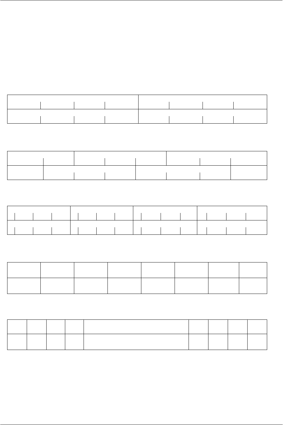
SCE CONFIDENTIAL GS User's Manual Version 6.0
© SCEI
-79-
4.3. Transmission Data Format
In transmitting the image data, the data is packed according to the following data format. Even if it is a
transmission to a buffer with a storage format that leaves blanks such as PSMCT24 and PSMT8H, padding is
unnecessary and the data packed as below can be transmitted.
Packed data is read after the transmission from local buffer to host.
RGBA32/TEX32/Z32
63 55 47 39 31 23 15 7 0
Texel 1 Texel 0
A1 B1 G1 R1 A0 B0 G0 R0
Texel 3 Texel 2
A3 B3 G3 R3 A2 B2 G2 R2
RGB32/TEX24/Z24
63 55 47 39 31 23 15 7 0
Texel 2 Texel 1 Texel 0
G2 R2 B1 G1 R1 B0 G0 R0
Texel 4 Texel 3
R5 B4 G4 R4 B3 G3 R3 B2
RGBA16/TEX16/Z16
63 47 31 15 0
Texel 3 Texel 2 Texel 1 Texel 0
A B3 G3 R3 A B2 G2 R2 A B1 G1 R1 A B0 G0 R0
Texel 7 Texel 6 Texel 5 Texel 4
A B7 G7 R7 A B6 G6 R6 A B5 G5 R5 A B4 G4 R4
IDTEX8
63 55 47 39 31 23 15 7 0
Texel 7 Texel 6 Texel 5 Texel 4 Texel 3 Texel 2 Texel 1 Texel 0
Texel 15 Texel 14 Texel 13 Texel 12 Texel 11 Texel 10 Texel 9 Texel 8
IDTEX4
63 59 55 51 ..... 15 11 7 3
T15 T14 T13 T12 ..... T3 T2 T1 T0
T31 T30 T29 T28 ..... T19 T18 T17 T16

SCE CONFIDENTIAL GS User's Manual Version 6.0
© SCEI
-80-
(This page is left blank intentionally)

SCE CONFIDENTIAL GS User's Manual Version 6.0
© SCEI
-81-
5. CRTC
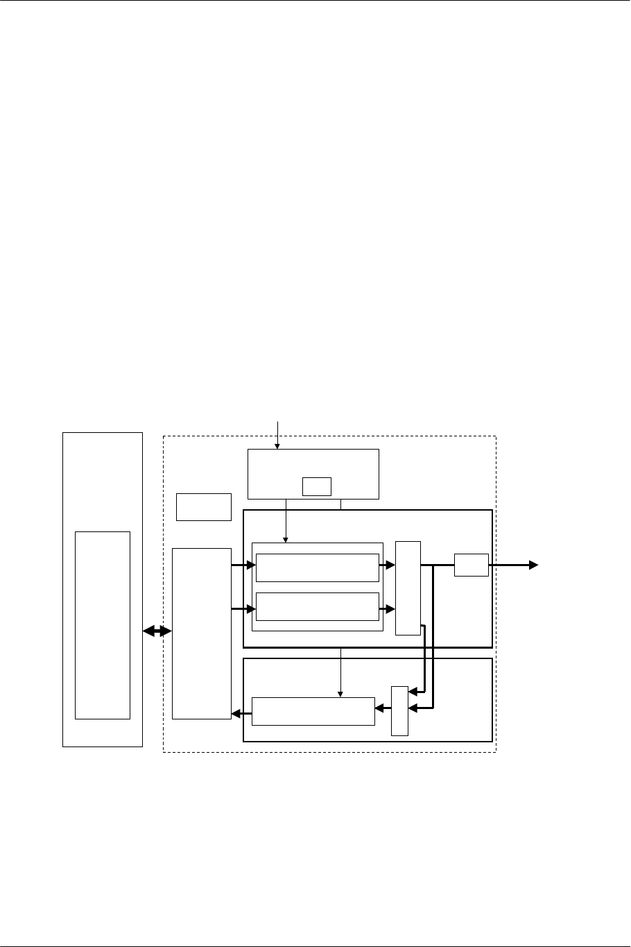
SCE CONFIDENTIAL GS User's Manual Version 6.0
© SCEI
-82-
5.1. CRTC Function
5.1.1. PCRTC Features
The GS's video output is performed in the PCRTC block as shown in Figure 5-1. The PCRTC has the
following functions:
• Image signals can be output with video clocks conforming to VESA standard (135MHz at maximum),
NTSC, and PAL by setting the standard video clock and the CRT mode.
• There are two independent rectangular area read output circuits. Input area, input pixel format, output
resolution, output size, output screen position, etc. can be set independently. Also, two output images can
be alpha-blended with BGColor and output using the built-in merge circuit (see Figure 5-2).
• There is a rectangular area write input circuit allowing a rectangular area in the output feedback image to be
written to an area in the frame or texture buffer. Also, RGB -> YCbCr conversion can be performed at
that time.
Register
PLL
Rectangular Area Read Output
Circuit 1
Rectangular Area Read Output
Circuit 2
Sync Generator
Rectangular Area Write Input
Circuit
Memory
Controller
Memory
Controller
Frame
Buffer
(ASIC DRAM)
Clock NTSC/PAL
Merge Circuit
DAC
out1
CRT 1
(Analog)
PCRTC
M
U
X
Output Circuit
Input Circuit
Figure 5-1 PCRTC Block Diagram
The following is an example of PCRTC data flow.
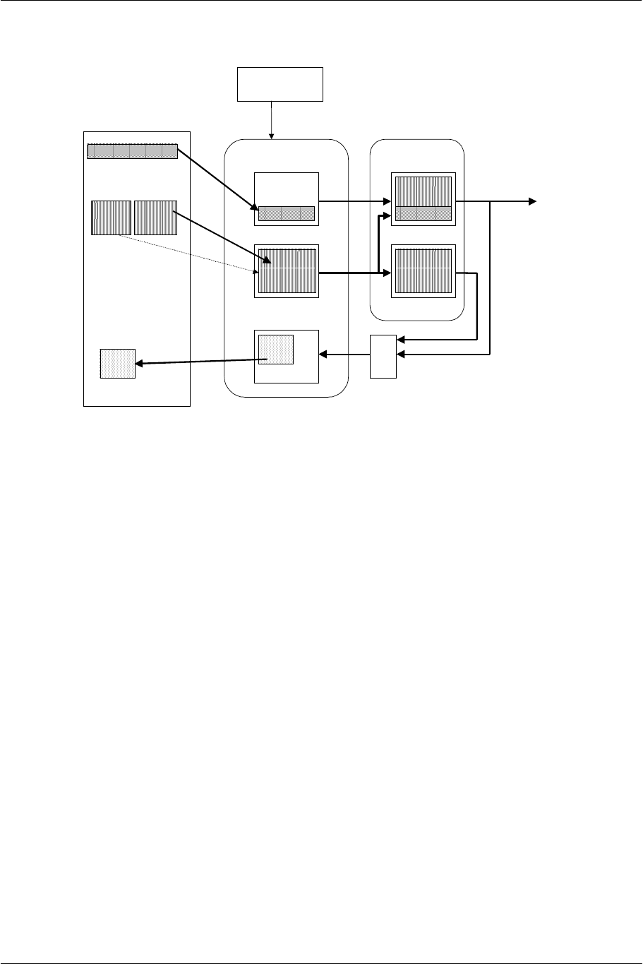
SCE CONFIDENTIAL GS User's Manual Version 6.0
© SCEI
-83-
Frame Buffer
0 1
1
Sync Gen.
Rectangular
Area Read Output
Circuit 1
Rectangular Area Read Output
Circuit 2
Rectangular Area Write Input
Circuit
out2
out1 CRT1
Output
1
1
Merge Circuit
NTSC/PAL/VESA
Figure 5-2 PCRTC Merge Circuit
As shown in the above figure, two rectangular area read output circuits read rectangular data in different sizes
and different pixel formats located in different areas of the frame buffer, arrange the data to arbitrary positions
with different resolutions, and output to the merge circuit. In the merge circuit, two output images are blended
at the set alpha value and are output as the CRT1 image.
In the above figure, the rectangular area read output circuit 1 controls the high-resolution text image in a single
buffer, and rectangular area read output circuit 2 controls the three-dimensional polygon image with a Z buffer
by RGBA 32-bit dual buffering. The two images are blended in the merge circuit, and a blended image of the
high-resolution text image and 24-bit full color three-dimensional image can be seen.
The rectangular write circuit can write a specified rectangular area in the CRT output image to a specified area in
the frame buffer at an arbitrary sampling rate (feedback write).

SCE CONFIDENTIAL GS User's Manual Version 6.0
© SCEI
-84-
5.1.2. Corresponding Video Signal
The following are the display frequencies and typical resolutions that the GS supports.
Mode Resolution fv(Hz) fH(kHz) Remarks
NTSC* 256 x 448(224)
320 x 448(224)
384 x 448(224)
512 x 448(224)
640 x 448(224)
59.940
(59.82)
15.734 ( ): Resolution in non-
interlaced scanning
PAL* 256 x 512(256)
320 x 512(256)
384 x 512(256)
512 x 512(256)
640 x 512(256)
50.000
(49.76)
15.625 ( ): Resolution in non-
interlaced scanning
640 x 480 59.940
72.809
75.000
85.008
31.469
37.861
37.500
43.269
Frequencies may vary
within VESA standard
(+/- 0.5%).
800 x 600 56.250
60.317
72.188
75.000
85.061
35.156
37.879
48.077
46.875
53.674
Frequencies may vary
within VESA standard
(+/- 0.5%).
1024 x 768 60.004
70.069
75.029
84.997
48.363
56.476
60.023
68.677
Frequencies may vary
within VESA standard
(+/- 0.5%).
VESA
1280 x 1024 60.020
75.025
63.981
79.976
Frequencies may vary
within VESA standard
(+/- 0.5%).
720 x 480 59.94 31.469 480 P DTV
1920 x 1080 60.00 33.750 1080 I
*Resolutions in NTSC and PAL modes are recommended to realize the appropriate screen size.
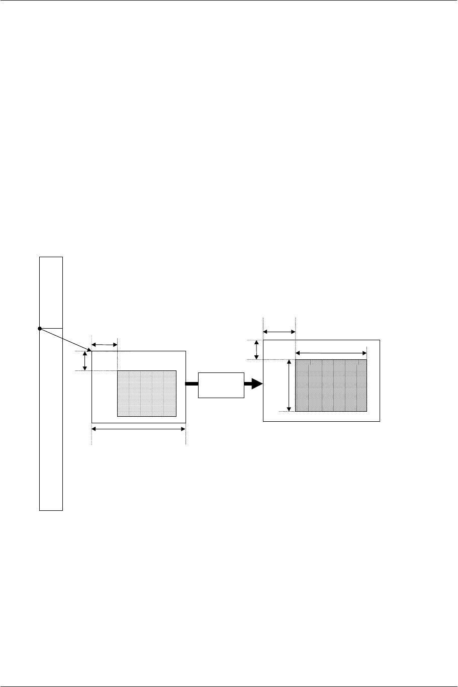
SCE CONFIDENTIAL GS User's Manual Version 6.0
© SCEI
-85-
5.2. Video Output
5.2.1. Video Clock
Besides the system clock, the GS internally generates the standard video clock VCK, which defines the PCRTC
operation timing. The main settings related to the display area on the screen are done in VCK units. The VCK
frequency predetermined for each video mode is set by the kernel service.
5.2.2. Rectangular Area Read Output Circuit
This circuit reads the specified rectangular area in the frame buffer adjusting to CRT scanning, and outputs the
converted data to the display coordinates. It can display the contents of the read rectangular area magnified by
the specified coefficients (MAGH/MAGV).
The figure below shows the operation of this circuit.
Local Memory
Display
Coordinates
FBP
DBY
DBX
FBW
DX
DY
DH+1
DW+1
X MAGH
X MAGV
Frame Memory
Figure 5-3 Read from Frame Buffer to PCRTC
The PCRTC is equipped with two independent rectangular area read output circuits. Each of them
independently has a DISPFB1/2 register (FBP, FBW, DBX, DBY, PSM) and DISPLAY1/2 register (DH, DW,
DX, DY, MAGH, MAGV), where the parameters in the above figure and the input pixel format can be set. The
two circuits function almost the same, but differ in the merging order and some of the input pixel format
settings in the merge circuit (described later in this document).
The unit of horizontal coefficients, DX, DW, and MAGH, which are related to the display coordinates, is VCK
(sub-pixel).
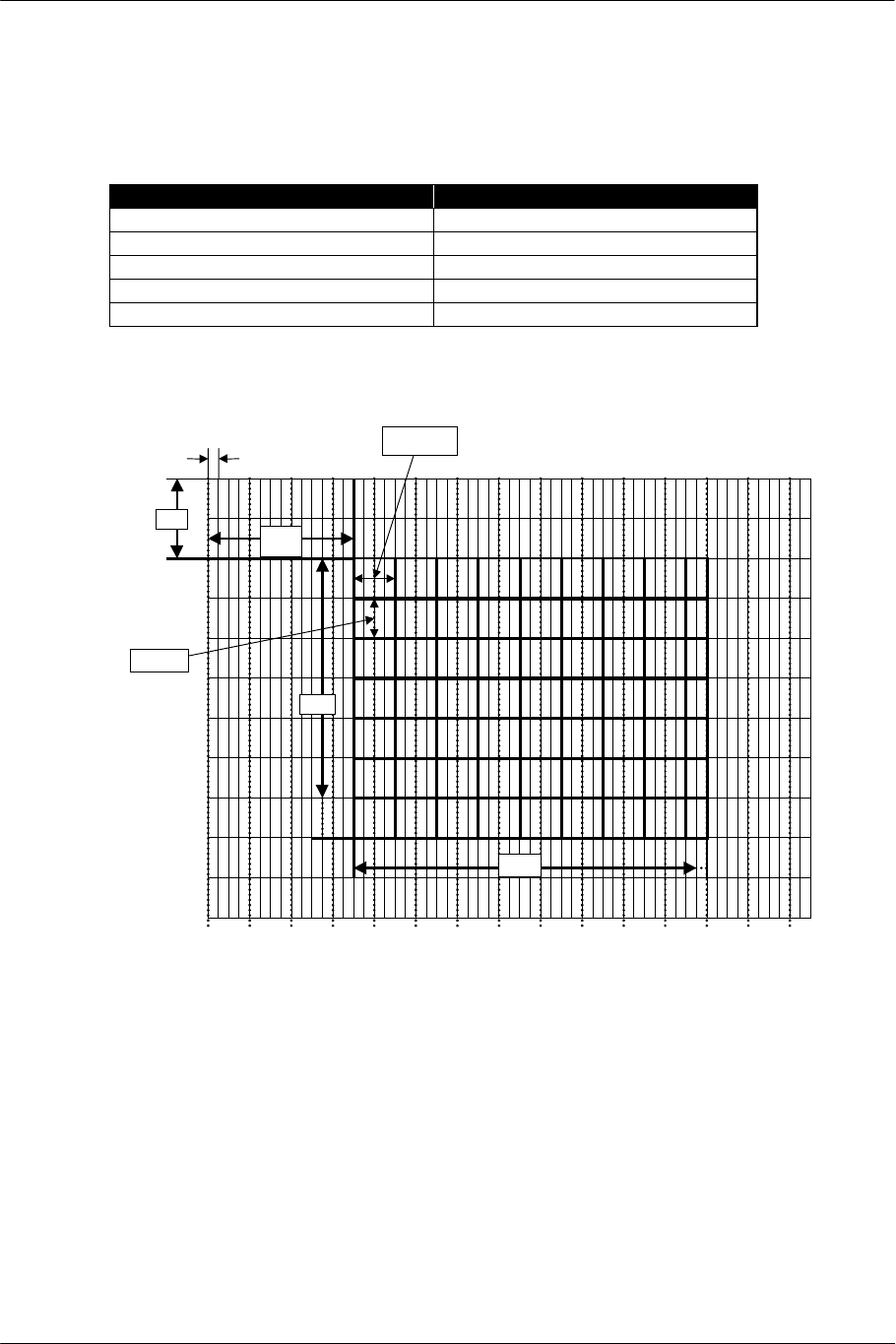
SCE CONFIDENTIAL GS User's Manual Version 6.0
© SCEI
-86-
MAGH/MAGV
MAGH and MAGV decide the magnification of width and height respectively. MAGV actually decides the
magnification to the scanning line, and MAGH decides the magnification in units of sub-pixels (VCK).
The values of MAGH to obtain typical resolutions in NTSC/PAL mode are shown below.
Horizontal Resolution (Pixel) MAGH Set Value
256 9
320 7
384 6
512 4
640 3
Other free resolutions can be set according to the value of MAGH.
The relation between the display pixels, DX and MAGH is as follows.
VCK
DW
DH
DX
DY
MAGH
MAGV
Figure 5-4 Relation between Display Pixels, DX and MAGH
Read Format
The format of data read from the frame buffer by the rectangular area read output circuit can be selected
from the following four kinds, depending on the PSM field of the DISPFB register.
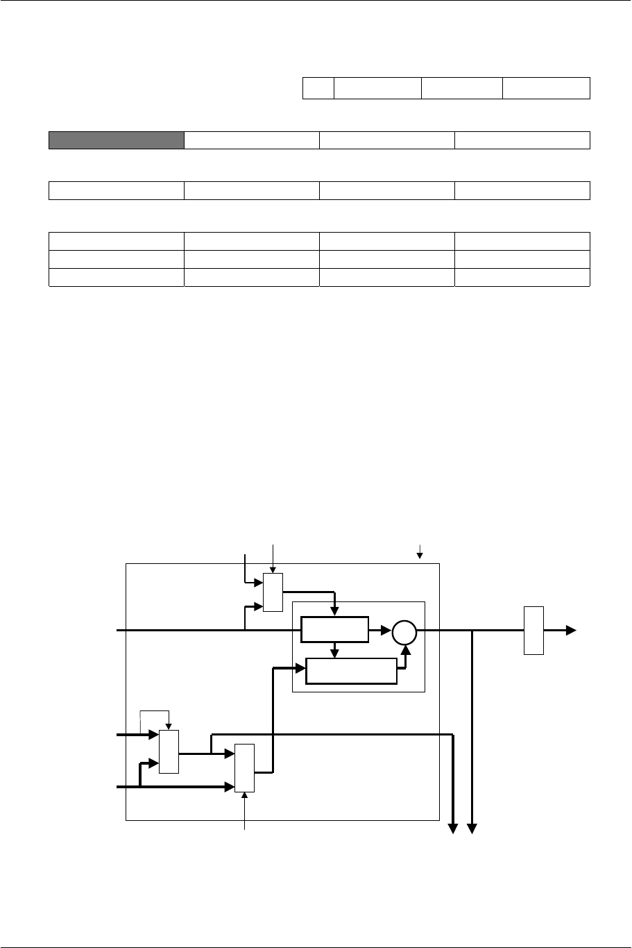
SCE CONFIDENTIAL GS User's Manual Version 6.0
© SCEI
-87-
PSMCT16/16S
15
31
10
26
8
21
0
16
A B G R
PSMCT24
24 16 8 0
B G R
PSMCT32
24 16 8 0
A B G R
PS-GPU24
24 16 8 0
R1 B0 G0 R0
G2 R2 B1 G1
B3 G3 R3 B2
*Rectangular area read output circuit 2 does not support the PS-GPU24 format.
*Rectangular area setting of the PS-GPU24 should be the same as that of the PSMCT16.
Interlace Read
In interlace mode, the reading method in the vertical direction differs depending on the value of the FFMD
field in the SMODE 2 register as follows.
0: FIELD Mode Read every other line from the start (+0,+2,+4…/+1,+3,+5...)
1: FRAME Mode Read every line from the start (+0,+1,+2,+3,+4,+5….)
5.2.3. Merge Circuit
The merge circuit synthesizes two image outputs of rectangular area read output circuits 1/2 and BGColor
(background color) and obtains two different output images, as shown in Figure 5-5.
Merge Circuit
D
A
C
out2
out1 CRT 1
(Analog)
M
U
X
M
U
X
+
xα
x (1 -α)
α
Rectangular Area Write Circuit
Rectangular
Area
Output
NO.1
Rectangular
Area
Output
NO.2 M
U
X
BGColor
enable
SLBG
MMOD
ALP
AMOD
Alpha-Blending Circuit
Figure 5-5 PCRTC Merge Circuit

SCE CONFIDENTIAL GS User's Manual Version 6.0
© SCEI
-88-
OUT 2 Output
The output image of rectangular area read circuit 2 is output to OUT2. The BGColor register value is output
outside the rectangular area or when rectangular area read circuit 2 is in the enable-off state.
The alpha value from rectangular area read circuit 2 is output within the rectangular area and 0x00 is output
outside the area.
OUT 1 Output
An alpha-blended image of the output image of rectangular area read circuit 1 and OUT2 or BGColor is
output to OUT1. OUT2 and BGColor is selected by the value of the SLBG field of the PMODE register.
SLBG=0: OUT2
SLBG=1: BGColor
The alpha used for blending is selected according to the value of the MMOD field of the PMODE register,
as follows.
MMOD=0: Alpha value from rectangular area read circuit 1*
MMOD=1: Value of ALP field in PMODE register
* When the alpha value from rectangular area read circuit 1 is selected, the alpha in the frame buffer is set
based on 0x80 =1.0. The value doubled first and then clamped with 0xff is used for blending.
The alpha output to OUT1 is selected according to the value of the AMOD field of the PMODE register, as
follows.
AMOD=0: Alpha value from rectangular area read circuit 1
AMOD=1: Alpha value from rectangular area read circuit 2
Assuming that the output of rectangular area read circuit 1 is Rs, Gs, and Bs, the output of rectangular area
read circuit 2/BGColor is Rd, Gd, and Bd, and the alpha value is A, the output (Ro,Go,Bo) of OUT1 is
calculated as follows:
Ro = Rs x A + Rd x (0xff – A)
Go = Rs x A + Gd x (0xff – A)
Bo = Rs x A + Bd x (0xff – A)
The above results are multiplied by 256(0x100) / 255(0xff).
Data Format and Alpha Value
The Alpha value is handled as follows, based on the format of the data read from the frame buffer.
PSMCT32: 8-bit alpha value in 32-bit color is used.
PSMCT24: 0x80 is used.
PSMCT16: 0x80 is used if 1-bit alpha value in 16-bit color is 1.
0x00 is used if 1-bit alpha value in 16-bit color is 0.
PS-GPU24: 0x80 is used.

SCE CONFIDENTIAL GS User's Manual Version 6.0
© SCEI
-89-
Color Processing in PSMCT16(S) Mode
Since only 5 bits each are given to color data R, G and B in the PSMCT16(S) mode, the color is expanded to
8 bits.
E000DCB A
DCBA
E
bit4 bit3 bit2 bit1 bit0
bit7 bit5 bit4 bit3 bit2 bit1 bit0bit6
Input Luminance
Value (5bits)
Output Luminance
Value (8bits)
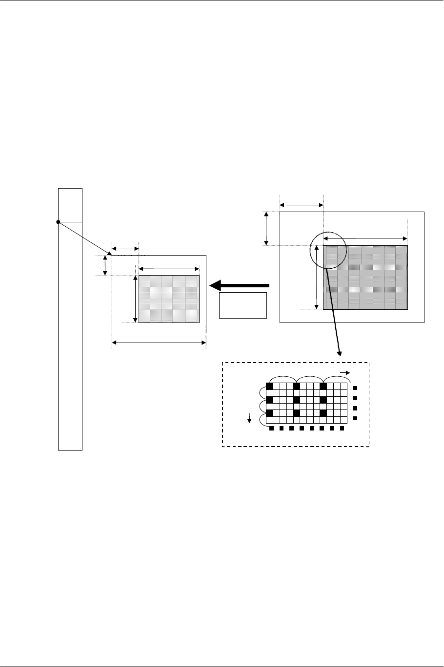
SCE CONFIDENTIAL GS User's Manual Version 6.0
© SCEI
-90-
5.3. Feedback Write
5.3.1. Rectangular Area Write Input Circuit
This circuit can write a specified rectangular area in the output feedback image to an arbitrary position in a local
buffer at an arbitrary sampling rate, as shown in the figure below.
The writing format is fixed to RGBA 32-bit (PSMCT32).
When inputting data, RGB→YCbCr conversion can be made.
Frame Buffer
Feedback Input Image
WDY
WDX
EXBW
SX
SY
WH+1
WW+1
1 / SMPH
1 / SMPV
(WW+1)*SMPH
(WH+1)
*SMPV
SX
SY
Captured/SMPH
Captured/SMPV
Local Memory
EXBP
Figure 5-6 Write from PCRTC to Frame Buffer
The rectangular area write input circuit can set the parameters shown in the figure above by means of the
EXTBUF register (EXBP, EXBW, WDX, WDY, FBIN, WFFMD, EMODA, EMODC) and the EXTDATA
register (SX, SY, WH, WW, SMPH, SMPV).
The unit of horizontal coefficients SX and SMPH, which relate to the input image, is VCK (sub-pixel).
Selection of Input Image
The input image of the rectangular area write input circuit is selected according to the value of the FBIN
field in the EXTBUF register, as follows:
FBIN=0: OUT1 (Synthetic Image of Rectangular Area Read Circuits 1 and 2)
FBIN=1: OUT2 (Image of Rectangular Area Read Circuit 2)

SCE CONFIDENTIAL GS User's Manual Version 6.0
© SCEI
-91-
Processing at Data Write
The input Alpha data and color data perform the following processing according to the value of the
EMODA/EMODC field in the EXTBUF register.
Alpha Value Write Mode Setting (EMODA)
EMODA =0: A (Input Alpha Value)
EMODA =1: Y (Conversion Value of Input RGB)
EMODA =2: Y/2 (Conversion Value of Input RGB)
EMODA =3: 0
Color Value Write Mode Setting (EMODC)
EMODC =0: (R,G,B) (Direct Input of Input RGB)
EMODC =1: (Y,Y,Y) (Conversion Value of Input RGB: Y for All RGB)
EMODC =2: (Y,Cb,Cr) (YCbCr Conversion Value of Input RGB)
EMODC =3: (A, A, A) (Input Alpha Value: Alpha for All RGB)
Calculation of RGB->YCbCr conversion is as below:
Ey = 0.587 x Eg + 0.114 x Eb + 0.299 x Er
Ecb = -0.311 x Eg + 0.500 x Eb - 0.169 x Er
Ecr = -0.419 x Eg - 0.081 x Eb + 0.500 x Er
Er,Eg,Eb = R,G,B(0~0xff) / 255(0xff)
Y = (DBh) x Ey + (0x10)
Cr = (E0h) x Ecb + (0x80)
Cb = (E0h) x Ecr + (0x80)
Write Processing in Interlace Mode
For the input image of the rectangular area write input circuit, the writing method is decided depending on
the value of the WFFMD field of the EXTBUF register as follows.
WFFMD =0:
FIELD: Write to every other line from the start (+0,+2,+4.. / +1,+3,+5..)
WFFMD =1:
FRAME: Write to every line from the start (+0,+1,+2,+3,+4,+5….)
Write Command
The register EXTWRITE to execute write commands is provided in addition to the registers to set addresses
and coordinates. Write processing of the feedback image is begun by writing 1 to this register and ended by
writing 0.
If write processing of the specified rectangular area ends, an interrupt (EXTWINT field in the CSR register)
occurs.
When the system is reset and FLUSH is caused during write processing, write processing is suspended.

SCE CONFIDENTIAL GS User's Manual Version 6.0
© SCEI
-92-
(This page is left blank intentionally)

SCE CONFIDENTIAL GS User's Manual Version 6.0
© SCEI
-93-
6. Signal

SCE CONFIDENTIAL GS User's Manual Version 6.0
© SCEI
-94-
6.1. Outline of Signal Processing
The GS can generate a signal (an interrupt) to the host, by writing data to the signal register. By using this
function in the drawing command string, it is possible to synchronize with the progress of drawing in the host.
The GS has three kinds of signal registers. Although it asserts interrupt signals to the host when signals are
generated, it can control them individually with the Interrupt Mask Register, IMR.

SCE CONFIDENTIAL GS User's Manual Version 6.0
© SCEI
-95-
6.2. Signal Register
The three kinds of signal registers of the GS are described below.
6.2.1. SIGNAL Register
If data is written to the SIGNAL register, an exception is generated immediately regardless of the ongoing
drawing process. The value of the SIGID field of the SIGLBLID register is updated, and the value of the
SIGNAL flag of the CSR register becomes 1. At this time, if the SIGMSK flag of the IMR register is 0, an
interrupt is generated to the host.
The interrupt state is cleared when the SIGNAL flag of the CSR register is cleared.
When the second write operation is performed to the SIGNAL register without clearing the interrupt state, an
interrupt is not generated to the host. The GS stops the drawing process and will not honor write operations to
the general-purpose registers. The GS will resume the drawing process and will honor write operations to the
general-purpose registers when the SIGNAL flag of the CSR register is cleared. However, the interrupt state
remains not cleared. At this time, the interrupt corresponding to the second write operation to the SIGNAL
register occurs by setting the SIGMSK flag of the IMR register to 1 and then to 0. The interrupt state is cleared
by clearing the SIGNAL flag of the CSR register again.
6.2.2. FINISH Register
If data is written to the FINISH register, an exception is generated after all the ongoing drawing and host ->
local transmission processes, and the value of the FINISH flag of the CSR register becomes0. At this time, if
the FINISHMSK flag of the IMR register is 0, an interrupt is generated to the host. By adding a write operation
to the FINISH register at the end of the drawing command, the host can check the end of drawing.
Unlike the SIGNAL register, the FINISH register does not stop the GS from drawing when it is written
successively.
6.2.3. LABEL Register
If data is written to the LABEL register, the value of the LABELID field of the SIGLBLID register is updated.
An interrupt is not generated.
The drawing process does not stop by writing to the LABEL register.

SCE CONFIDENTIAL GS User's Manual Version 6.0
© SCEI
-96-
(This page is left blank intentionally)

SCE CONFIDENTIAL GS User's Manual Version 6.0
© SCEI
-97-
7. Registers
This chapter describes the functions of the registers, which are accessible from the host, and the meanings of the
fields in the registers.

SCE CONFIDENTIAL GS User's Manual Version 6.0
© SCEI
-98-
7.1. General Purpose Registers
The general purpose registers are mainly used to set vertex information, drawing environment and transmission
between buffers for the drawing primitives. All of them are write-only registers.
Among the registers that set the drawing environment, the registers with names in the format "XXX_1,
XXX_2" are designed to have two contexts. They consist of two sets of registers with the same functions.
Registers with two contexts are as shown below:
FRAME (FRAME_1, FRAME_2)
ZBUF (ZBUF_1, ZBUF_2)
TEX0 (TEX0_1, TEX0_2)
TEX1 (TEX1_1, TEX1_2)
TEX2 (TEX2_1, TEX2_2)
MIPTBP1 (MIPTBP1_1, MIPTBP1_2)
MIPTBP2 (MIPTBP2_1, MIPTBP2_2)
CLAMP (CLAMP_1, CLAMP_2)
TEST (TEST_1, TEST_2)
ALPHA (ALPHA_1, ALPHA_2)
XYOFFSET (XYOFFSET_1, XYOFFSET_2)
SCISSOR (SCISSOR_1, SCISSOR_2)
FBA (FBA_1, FBA_2)
SCE CONFIDENTIAL GS User's Manual Version 6.0
© SCEI
-99-
Explanatory Notes
FOGCOL : Fog Color
This register sets fogging ........
BIT ASSIGN
0x3d
6 2 1 1 0 0 0
3 3 6 5 8 7 0
Fo
g
Color
(
RED
)
FCR int0:8:0
ContentsName Format
Fo
g
Color
(
GREEN
)
FCG int0:8:0
FCRFCGFCB
Fo
g
Color
(
BLUE
)
FCB int0:8:0
7:0
Pos.
15:8
23:16
Register Name
A
ddress
Outline
Field
Name
Field Name in
the Register
Bit Position
in the Field
Field Data
Format
Details of
Function
FIELD
Notation of the field bit position
63:48 Bit 63 to bit 48
15 Bit 15 only
Notation of the field data format
float 32 IEEE754-based 32-bit single-precision floating-point value.
int *:*:* Integer or fixed decimal value.
"*" indicates number of sign bits, number of integer bits, and number of decimal bits, left to
right.
(Notation example of "int")
int 1:11:4 16-bit fixed decimal value with 1 bit for sign, 11 bits for integer part and 4 bits for decimal
part.
int 0:8:0 8-bit integer with no sign, 8 bits for integer part and 0 bit for decimal part.
int 0:2:0 Bit field of 2-bit width with no sign.
SCE CONFIDENTIAL GS User's Manual Version 6.0
© SCEI
-100-
ALPHA_1 / ALPHA_2 : Alpha Blending Setting
0x42 / 0x43
These registers define the blend function of Alpha Blending. ALPHA_1 sets Context 1 and ALPHA_2 sets
Context 2.
The basic form of the blending function is as follows:
Cv = (A-B)*C>>7 + D
(Cv = Output Color Value)
(A,B,D = Input Color Value)
(C = Input Alpha Value)
Each item of A/B/C/D in the function above is set by this register.
BIT ASSIGN
3
9
3
2
0
7
0
6
0
5
0
4
0
3
0
2
0
1
0
0
FIX
D C B A
FIELD
Name Pos. Format Contents
A 1:0 int 0:2:0 Specification of Input Color Value A
00 Cs RGB value of the source is used.
01 Cd RGB value in the frame buffer is used.
10 0
11 Reserved
B 3:2 int 0:2:0 Specification of Input Color Value B
00 Cs RGB value of the source is used.
01 Cd RGB value in the frame buffer is used.
10 0
11 Reserved
C 5:4 int 0:2:0 Specification of Input Alpha Value C
00 As Alpha of the source is used.
01 Ad Alpha in the frame buffer is used.
10 FIX FIX-field value is used as Alpha.
11 Reserved
D 7:6 int 0:2:0 Specification of Input Color Value D
00 Cs RGB value of the source is used.
01 Cd RGB value in the frame buffer is used.
10 0
11 Reserved
FIX 39:32 int 0:8:0 Fixed Alpha Value
Referred to when the value of C above is FIX.
(The range is 0 - 255, and at the 128 position, 1.0 is indicated.)
SCE CONFIDENTIAL GS User's Manual Version 6.0
© SCEI
-101-
BITBLTBUF : Setting for Transmission between Buffers
0x50
This register stores buffer-related settings for transmission source and destination during transmission between
buffers.
BIT ASSIGN
6
1
5
6
5
3
4
8
4
5
3
2
2
9
2
4
2
1
1
6
1
3
0
0
DPSM
DBW DBP SPSM SBW SBP
FIELD
Name Pos. Format Contents
SBP 13:0 int 0:14:0 Source Buffer Base Pointer (SBP = Word Address/64)
SBW 21:16 int 0:6:0 Source Buffer Width (SBW = Width in Units of Pixels/64) (*1)
SPSM 29:24 int 0:6:0 Source Pixel Storage Format (*2, *3)
000000 PSMCT32
000001 PSMCT24
000010 PSMCT16
001010 PCMCT16S
010011 PSMT8
010100 PSMT4
011011 PSMT8H
100100 PSMT4HL
101100 PSMT4HH
110000 PSMZ32
110001 PSMZ24
110010 PSMZ16
111010 PSMZ16S
DBP 45:32 int 0:14:0 Destination Buffer Base Pointer (DBP = Word Address/64)
DBW 53:48 int 0:6:0 Destination Buffer Width (DBW = Width in Units of Pixels/64) (*1)
DPSM 61:56 int 0:6:0 Destination Pixel Storage Format (*3)
(Same as Source Pixel Storage Format)
*1 Values must be in the range of 1 to 32.
*2 Operation is undefined when values other than those in the table are set.
*3 In local-local transmission, the formats specified in the SPSM and DPSM fields must have the same number
of bits per pixel (pixel depth).

SCE CONFIDENTIAL GS User's Manual Version 6.0
© SCEI
-102-
CLAMP_1 / CLAMP_2 : Texture Wrap Mode
0x08 / 0x09
These registers set the texture's wrap mode (repeating or clamping) for both S and T. CLAMP_1 sets Context 1
and CLAMP_2 sets Context 2.
BIT ASSIGN
4
3
3
4
3
3
2
4
2
3
1
4
1
3
0
4
0
3
0
2
0
1
0
0
MAXV MINV MAXU MINU
W
M
T
W
M
S
FIELD
Name Pos. Format Contents
WMS 1:0 int 0:2:0 Wrap Mode in Horizontal (S) Direction
00 REPEAT
01 CLAMP
10 REGION_CLAMP
11 REGION_REPEAT
WMT 3:2 int 0:2:0 Wrap Mode in Vertical (T) Direction
00 REPEAT
01 CLAMP
10 REGION_CLAMP
11 REGION_REPEAT
MINU 13:4 int 0:10:0 Clamp Parameter in U Direction (*1)
(In REGION_CLAMP Mode)
Clamp Value of Lower Limit
(In REGION_REPEAT Mode)
UMSK Value
MAXU 23:14 int 0:10:0 Clamp Parameter in U Direction (*1)
(In REGION_CLAMP Mode)
Clamp Value of Upper Limit
(In REGION_REPEAT Mode)
UFIX Value
MINV 33:24 int 0:10:0 Clamp Parameter in V Direction (*2)
(In REGION_CLAMP Mode)
Clamp Value of Lower Limit
(In REGION_REPEAT Mode)
VMSK Value
MAXV 43:34 int 0:10:0 Clamp Parameter in V Direction (*2)
(In REGION_CLAMP Mode)
Clamp Value of Upper Limit
(In REGION_REPEAT Mode)
VFIX Value
*1 Fields MINU and MAXU are not used when the value of WMS, the wrap mode in horizontal direction, is
REPEAT or CLAMP. (Don't Care.)
*2 Fields MINV and MAXV are not used when the value of WMT, the wrap mode in vertical direction, is
REPEAT or CLAMP. (Don't Care.)

SCE CONFIDENTIAL GS User's Manual Version 6.0
© SCEI
-103-
COLCLAMP : Color Clamp Control
0x46
This register stores settings as to whether clamping for the RGB value of the pixel is performed.
BIT ASSIGN
0
0
C
L
A
M
P
FIELD
Name Pos. Format Contents
CLAMP 0 int 0:1:0 Color Clamping Method
0 MASK Lower 8 bits are enabled (wraps around.)
1 CLAMP Clamped in [0,255] range.

SCE CONFIDENTIAL GS User's Manual Version 6.0
© SCEI
-104-
DIMX : Dither Matrix Setting
0x44
This register sets the value of the dither matrix.
BIT ASSIGN
6
2
6
0
5
8
5
6
5
4
5
2
5
0
4
8
4
6
4
4
4
2
4
0
3
8
3
6
3
4
3
2
DM
33 DM
32 DM
31 DM
30 DM
23 DM
22 DM
21 DM
20
3
0
2
8
2
6
2
4
2
2
2
0
1
8
1
6
1
4
1
2
1
0
0
8
0
6
0
4
0
2
0
0
DM
13 DM
12 DM
11 DM
10 DM
03 DM
02 DM
01 DM
00
FIELD
Name Pos. Format Contents
DM00 2:0 int 1:2:0 Dither Matrix (0,0)
DM01 6:4 int 1:2:0 Dither Matrix (0,1)
DM02 10:8 int 1:2:0 Dither Matrix (0,2)
DM03 14:12 int 1:2:0 Dither Matrix (0,3)
DM10 18:16 int 1:2:0 Dither Matrix (1,0)
DM11 22:20 int 1:2:0 Dither Matrix (1,1)
DM12 26:24 int 1:2:0 Dither Matrix (1,2)
DM13 30:28 int 1:2:0 Dither Matrix (1,3)
DM20 34:32 int 1:2:0 Dither Matrix (2,0)
DM21 38:36 int 1:2:0 Dither Matrix (2,1)
DM22 42:40 int 1:2:0 Dither Matrix (2,2)
DM23 46:44 int 1:2:0 Dither Matrix (2,3)
DM30 50:48 int 1:2:0 Dither Matrix (3,0)
DM31 54:52 int 1:2:0 Dither Matrix (3,1)
DM32 58:56 int 1:2:0 Dither Matrix (3,2)
DM33 62:60 int 1:2:0 Dither Matrix (3,3)

SCE CONFIDENTIAL GS User's Manual Version 6.0
© SCEI
-105-
DTHE : Dither Control
0x45
This register stores settings for dithering (performed/not performed).
If the pixel storage mode of the frame buffer is PSMCT32 or PSMCT24, dithering should be turned off.
BIT ASSIGN
0
0
D
T
H
E
FIELD
Name Pos. Format Contents
DTHE 0 int 0:1:0 Dithering Control
0 Dithering is not performed.
1 Dithering is performed.
SCE CONFIDENTIAL GS User's Manual Version 6.0
© SCEI
-106-
FBA_1 / FBA_2 : Alpha Correction Value
0x4a / 0x4b
These registers set the fixed value of Alpha when writing to the frame buffer. FBA_1 sets Context 1 and FBA_2
sets Context 2.
The OR of the fixed value set by this register and the most significant bit of the Alpha value of the pixel is
written to the frame buffer.
BIT ASSIGN
0
0
F
B
A
FIELD
Name Pos. Format Contents
FBA 0 int 0:1:0 MSB of Alpha value for drawing to the frame buffer.
RGBA32 Mode: A = As | (FBA<<7)
RGBA16 Mode: A = As | FBA&0x01

SCE CONFIDENTIAL GS User's Manual Version 6.0
© SCEI
-107-
FINISH : FINISH Event Occurrence Request
0x61
When the drawing process currently being performed is completed, this register makes a request for the
occurrence of the FINISH event. Any data can be written.
BIT ASSIGN

SCE CONFIDENTIAL GS User's Manual Version 6.0
© SCEI
-108-
FOG : Vertex Fog Value Setting
0x0a
This register sets the fog value of the vertex. When the fog value is 0, the fog effect is at the maximum (the
drawing color becomes the same as the distant color). When the fog value is 255, the fog effect is at the
minimum.
To completely eliminate the fog effect, fogging should be set off with the FGE flag of the PRIM register.
BIT ASSIGN
6
3
5
6
F
FIELD
Name Pos. Format Contents
F 63:56 int0:8:0 Fog Value
SCE CONFIDENTIAL GS User's Manual Version 6.0
© SCEI
-109-
FOGCOL : Distant Fog Color Setting
0x3d
This register sets the distant color with RGB value when performing fogging.
BIT ASSIGN
2
3
1
6
1
5
0
8
0
7
0
0
FCB
FCG FCR
FIELD
Name Pos. Format Contents
FCR 7:0 int 0:8:0 Fog Color (R)
FCG 15:8 int 0:8:0 Fog Color (G)
FCB 23:16 int 0:8:0 Fog Color (B)
SCE CONFIDENTIAL GS User's Manual Version 6.0
© SCEI
-110-
FRAME_1 / FRAME_2 : Frame Buffer Setting
0x4c / 0x4d
These registers store various settings related to the frame buffer. FRAME_1 sets Context 1 and FRAME_2 sets
Context 2.
BIT ASSIGN
6
3
3
2
2
9
2
4
2
1
1
6
0
8
0
0
FBMSK
PSM FBW FBP
FIELD
Name Pos. Format Contents
FBP 8:0 int0:9:0 Frame Buffer Base Pointer
FBP = Word Address/2048
FBW 21:16 int0:6:0 Frame Buffer Width
FBW = Width in Units of Pixels/64
The effective range of set value is 1 to 32
PSM 29:24 int0:6:0 Frame Buffer Pixel Storage Format
000000 PSMCT32
000001 PSMCT24
000010 PSMCT16
001010 PSMCT16S
010011 reserved
010100 reserved
011011 reserved
100100 reserved
101100 reserved
110000 PSMZ32
110001 PSMZ24
110010 PSMZ16
111010 PSMZ16S
FBMSK 63:32 int0:32:0 Frame Buffer Drawing Mask (*)
0 The corresponding bit in the frame buffer is updated.
1 The corresponding bit in the frame buffer is not updated.
* See "3.9.5. Masking". When the pixel storage format of the frame buffer is PSMCT16, PSMCT16S or
PSMZ16, note the bit relation between the mask pattern and frame buffer.

SCE CONFIDENTIAL GS User's Manual Version 6.0
© SCEI
-111-
HWREG : Data Port for Transmission between Buffers
0x54
This register writes transmission data when host -> local transmission between buffers is performed.
It is enabled only when the BITBLTBUF/TRXPOS/TRXREG/TRXDIR registers are set effectively in terms
of transmission, and the transmission between buffers is activated. When this register is written in other
conditions, no operation is made.
BIT ASSIGN
6
3
0
0
DATA
FIELD
Name Pos. Format Contents
DATA 63:0 int0:64:0 Host -> Local Transmission Data

SCE CONFIDENTIAL GS User's Manual Version 6.0
© SCEI
-112-
LABEL : LABEL Event Occurrence Request
0x62
This register updates the value of LBLID field in the SIGLBLID register. The ID field is composed of 32 bits,
and SIGLBLID is updated only in the bit position where the bit value corresponding to IDMSK is 1.
BIT ASSIGN
6
3
3
2
3
1
0
0
IDMSK
ID
FIELD
Name Pos. Format Contents
ID 31:0 int0:32:0 Value to be written to SIGLBLID register
IDMSK 63:32 int0:32:0 Whether or not corresponding SIGLBLID bit is updated.
0 Masked. (Not updated.)
1 Not masked. (Updated.)

SCE CONFIDENTIAL GS User's Manual Version 6.0
© SCEI
-113-
MIPTBP1_1 / MIPTBP1_2 : MIPMAP Information Setting (Level 1 to 3)
0x34 / 0x35
These registers set the buffer pointer and buffer width of Level 1 to Level 3 textures when performing
MIPMAP. MIPTBP1_1 sets Context 1 and MIPTBP1_2 sets Context 2.
BIT ASSIGN
5
9
5
4
5
3
4
0
3
9
3
4
3
3
2
0
1
9
1
4
1
3
0
0
TBW3
TBP3 TBW2 TBP2 TBW1 TBP1
FIELD
Name Pos. Format Contents
TBP1 13:0 int0:14:0 MIPMAP Level 1 Texture Base Pointer (*1)
TBW1 19:14 int0:6:0 MIPMAP Level 1 Texture Buffer Width (*2)
TBP2 33:20 int0:14:0 MIPMAP Level 2 Texture Base Pointer (*1)
TBW2 39:34 int0:6:0 MIPMAP Level 2 Texture Buffer Width (*2)
TBP3 53:40 int0:14:0 MIPMAP Level 3 Texture Base Pointer (*1)
TBW3 59:54 int0:6:0 MIPMAP Level 3 Texture Buffer Width (*2)
*1 The texture base pointer is set to the value of the word address divided by 64.
*2 The buffer width is set to the value of the width (in units of texels) divided by 64. It is set to 1 if the width is
less than 64.
SCE CONFIDENTIAL GS User's Manual Version 6.0
© SCEI
-114-
MIPTBP2_1 / MIPTBP2_2 : MIPMAP Information Setting (Level 4 to 6)
0x36 / 0x37
These registers set the buffer pointer and buffer width of Level 4 to Level 6 textures when performing
MIPMAP. MIPTBP2_1 sets Context 1 and MIPTBP2_2 sets Context 2.
BIT ASSIGN
5
9
5
4
5
3
4
0
3
9
3
4
3
3
2
0
1
9
1
4
1
3
0
0
TBW6
TBP6 TBW5 TBP5 TBW4 TBP4
FIELD
Name Pos. Format Contents
TBP4 13:0 int0:14:0 MIPMAP Level 4 Texture Base Pointer (*1)
TBW4 19:14 int0:6:0 MIPMAP Level 4 Texture Buffer Width (*2)
TBP5 33:20 int0:14:0 MIPMAP Level 5 Texture Base Pointer (*1)
TBW5 39:34 int0:6:0 MIPMAP Level 5 Texture Buffer Width (*2)
TBP6 53:40 int0:14:0 MIPMAP Level 6 Texture Base Pointer (*1)
TBW6 59:54 int0:6:0 MIPMAP Level 6 Texture Buffer Width (*2)
*1 The texture base pointer is set to the value of the word address divided by 64.
*2 The buffer width is set to the value of the width (in units of texels) divided by 64. It is set to 1 if the width is
less than 64.

SCE CONFIDENTIAL GS User's Manual Version 6.0
© SCEI
-115-
PABE : Alpha Blending Control in Units of Pixels
0x49
This register sets whether Alpha Blending control in units of pixels is performed.
For details, see "3.8. Alpha Blending".
BIT ASSIGN
0
0
P
A
B
E
FIELD
Name Pos. Format Contents
PABE 0 int0:1:0 Alpha Blending Control in Units of Pixels
0 Not performed.
1 Performed. (Alpha blending is OFF for the pixel where the A value
is MSB=0 and ON for the pixel where the A value is MSB=1.)

SCE CONFIDENTIAL GS User's Manual Version 6.0
© SCEI
-116-
PRIM : Drawing Primitive Setting
0x00
This register specifies the types of drawing primitives and various attributes, and initializes the contents of the
vertex queue.
Each of the IIP/TME/FGE/ABE/AA1/FST/CTXT/FIX fields is enabled only when AC=1 is set by the
PRMODECONT register.
BIT ASSIGN
1
0
0
9
0
8
0
7
0
6
0
5
0
4
0
3
0
2
0
0
F
I
X
C
T
X
T
F
S
T
A
A
1
A
B
E
F
G
E
T
M
E
I
I
P
PRIM
FIELD
Name Pos. Format Contents
PRIM 2:0 int0:3:0 Types of Drawing Primitives
000 Point
001 Line
010 Line Strip
011 Triangle
100 Triangle Strip
101 Triangle Fan
110 Sprite
111 Specification Prohibited
IIP 3 int0:1:0 Shading Method
0 Flat Shading
1 Gouraud Shading
TME 4 int0:1:0 Texture Mapping
0 Texture Mapping OFF
1 Texture Mapping ON
FGE 5 int0:1:0 Fogging
0 Fogging OFF
1 Fogging ON
ABE 6 int0:1:0 Alpha Blending
0 Alpha Blending OFF
1 Alpha Blending ON
AA1 7 int0:1:0 1 Pass Antialiasing (*1)
0 1 Pass Antialiasing OFF
1 1 Pass Antialiasing ON
FST 8 int0:1:0 Method of Specifying Texture Coordinates (*2)
0 STQ value is used (ST/RGBAQ Register is referred
to.)
1 UV value is used (UV Register is referred to.)
CTXT 9 int0:1:0 Context
0 Environment of Context 1 is used.
1 Environment of Context 2 is used.
FIX 10 int0:1:0 Fragment Value Control (RGBAFSTQ Change by DDA)
0 Unfixed (Normal)
1 Fixed
*1 When AA1=1 is set, note Alpha Blending process. See "3.6. Antialiasing".
*2 When FST=1 is set, perspective correction is not performed.

SCE CONFIDENTIAL GS User's Manual Version 6.0
© SCEI
-117-
PRMODE : Setting for Attributes of Drawing Primitives
0x1b
This register changes the attributes of drawing primitives. It is enabled only when AC=0 is set by the
PRMODECONT register.
BIT ASSIGN
1
0
0
9
0
8
0
7
0
6
0
5
0
4
0
3
F
I
X
C
T
X
T
F
S
T
A
A
1
A
B
E
F
G
E
T
M
E
I
I
P
FIELD
Name Pos. Format Contents
IIP 3 int0:1:0 Shading Method
0 Flat Shading
1 Gouraud Shading
TME 4 int0:1:0 Texture Mapping
0 Texture Mapping OFF
1 Texture Mapping ON
FGE 5 int0:1:0 Fogging
0 Fogging OFF
1 Fogging ON
ABE 6 int0:1:0 Alpha Blending
0 Alpha Blending OFF
1 Alpha Blending ON
AA1 7 int0:1:0 1 Pass Antialiasing (*1)
0 1 Pass Antialiasing OFF
1 1 Pass Antialiasing ON
FST 8 int0:1:0 Method of Specifying Texture Coordinates (*2)
0 STQ value (ST/RGBAQ register is referred to.)
1 UV value (UV register is referred to.)
CTXT 9 int0:1:0 Context
0 Environment of Context 1 is used.
1 Environment of Context 2 is used.
FIX 10 int0:1:0 Fragment Value Control (RGBAFSTQ Change by DDA)
0 Unfixed (Normal)
1 Fixed
*1 When AA1=1 is set, note Alpha Blending process. See "3.6. Antialiasing".
*2 When FST=1 is set, perspective correction is not performed.

SCE CONFIDENTIAL GS User's Manual Version 6.0
© SCEI
-118-
PRMODECONT : Specification of Primitive Attribute Setting Method
0x1a
This register sets whether to use primitive attributes (IIP, TME, FGE, ABE, AA1, FST, CTXT, FIX) specified
by the PRMODE register or the PRIM register.
BIT ASSIGN
0
0
A
C
FIELD
Name Pos. Format Contents
AC 0 int0:1:0 Register that specifies primitive attributes
0 PRMODE register
1 PRIM register
SCE CONFIDENTIAL GS User's Manual Version 6.0
© SCEI
-119-
RGBAQ : Vertex Color Setting
0x01
This register sets the RGBA value of the vertex and the Q value of the normalized texture coordinates.
The Q value is not only used for calculating texture coordinates but also as the parameter to decide the LOD.
BIT ASSIGN
6
3
3
2
3
1
2
4
2
3
1
6
1
5
0
8
0
7
0
0
Q
A B G R
FIELD
Name Pos. Format Contents
R 7:0 int 0:8:0 Luminance value of R element of vertex color
G 15:8 int 0:8:0 Luminance value of G element of vertex color
B 23:16 int 0:8:0 Luminance value of B element of vertex color
A 31:24 int 0:8:0 Alpha value of vertex (0x80 = 1.0)
Q 63:32 float 32 Normalized texture coordinates (Q) (*)
* Negative values are acceptable. However, the vertices of one primitive must be the same. The lower 8 bits of
the mantissa are rounded down.

SCE CONFIDENTIAL GS User's Manual Version 6.0
© SCEI
-120-
SCANMSK : Raster Address Mask Setting
0x22
This register sets whether drawing is performed only to odd or even row by the row address of the frame buffer.
When drawing is prohibited, drawing efficiency decreases (1/2 in the worst case.)
The mask is only effective for drawing primitives.
BIT ASSIGN
0
1
0
0
M
S
K
FIELD
Name Pos. Format Contents
MSK 1:0 int0:2:0 00 Normal drawing (not masked.)
01 Reserved.
10 Drawing of pixel with even Y coordinate is prohibited.
11 Drawing of pixel with odd Y coordinate is prohibited.
SCE CONFIDENTIAL GS User's Manual Version 6.0
© SCEI
-121-
SCISSOR_1 / SCISSOR_2 : Setting for Scissoring Area
0x40 / 0x41
These registers specify the scissoring area. The coordinate values for the upper-left/lower-right points of the
enabled drawing area are specified by the window coordinate system. SCISSOR_1 sets Context 1 and
SCISSOR_2 sets Context 2.
BIT ASSIGN
5
8
4
8
4
2
3
2
2
6
1
6
1
0
0
0
SCAY1
SCAY0 SCAX1 SCAX0
FIELD
Name Pos. Format Contents
SCAX0 10:0 int 0:11:0 X-coordinate value for upper-left point of enabled drawing area
(Window coordinate system)
SCAX1 26:16 int 0:11:0 X-coordinate value for lower-right point of enabled drawing area
(Window coordinate system)
SCAY0 42:32 int 0:11:0 Y-coordinate value for upper-left point of enabled drawing area
(Window coordinate system)
SCAY1 58:48 int 0:11:0 Y-coordinate value for lower-right point of enabled drawing area
(Window coordinate system)

SCE CONFIDENTIAL GS User's Manual Version 6.0
© SCEI
-122-
SIGNAL : SIGNAL Event Occurrence Request
0x60
This register generates the SIGNAL event and updates the value of the SIGLBLID register. The ID field is
composed of 32 bits, and SIGLBLID is updated only in the bit position where the bit value corresponding to
IDMSK is 1.
BIT ASSIGN
6
3
3
2
3
1
0
0
IDMSK
ID
FIELD
Name Pos. Format Contents
ID 31:0 int0:32:0 Value to be written to SIGLBLID register
IDMSK 63:32 int0:32:0 Whether or not corresponding SIGLBLID bit is updated.
0 Masked. (Not updated.)
1 Not masked. (Updated.)

SCE CONFIDENTIAL GS User's Manual Version 6.0
© SCEI
-123-
ST : Specification of Vertex Texture Coordinates
0x02
This register sets the S and T values of the vertex texture coordinates. The value Q is specified by the RGBAQ
register.
For the relation between the texture coordinate values S, T and Q and the texel, see "3.4.10. Perspective
Correction".
BIT ASSIGN
6
3
3
2
3
1
0
0
T
S
FIELD
Name Pos. Format Contents
S 31:0 float 32 Texture Coordinate Value S (The lower 8 bits of the mantissa are
rounded down.)
T 63:32 float 32 Texture Coordinate Value T (The lower 8 bits of the mantissa are
rounded down.)

SCE CONFIDENTIAL GS User's Manual Version 6.0
© SCEI
-124-
TEST_1 / TEST_2 : Pixel Test Control
0x47 / 0x48
These registers perform settings related to the pixel test. TEST_1 sets Context 1 and TEST_2 sets Context 2.
For details, see "3.7. Pixel Test".
BIT ASSIGN
1
8
1
7
1
6
1
5
1
4
1
3
1
2
1
1
0
4
0
3
0
1
0
0
Z
T
S
T
Z
T
E
D
A
T
M
D
A
T
E
A
F
A
I
L
AREF
A
T
S
T
A
T
E
FIELD
Name Pos. Format Contents
ATE 0 int 0:1:0 Alpha Test
0 Alpha test OFF
1 Alpha test ON
ATST 3:1 int 0:3:0 Alpha Test Method
000 NEVER All pixels fail.
001 ALWAYS All pixels pass.
010 LESS Pixels with A less than AREF pass.
011 LEQUAL Pixels with A less than or equal to
AREF pass.
100 EQUAL Pixels with A equal to AREF pass.
101 GEQUAL Pixels with A greater than or equal to
AREF pass.
110 GREATER Pixels with A greater than AREF pass.
111 NOTEQUAL Pixels with A not equal to AREF pass.
AREF 11:4 int 0:8:0 Alpha Value to be Compared and Referred to
AFAIL 13:12 int 0:2:0 Processing Method when Failed in Alpha Test
00 KEEP Neither frame buffer nor Z buffer is updated.
01 FB_ONLY Only frame buffer is updated.
10 ZB_ONLY Only Z buffer is updated.
11 RGB_ONLY Only frame-buffer RGB is updated.
DATE 14 int 0:1:0 Destination Alpha Test
0 Destination Alpha Test OFF
1 Destination Alpha Test ON
DATM 15 int 0:1:0 Destination Alpha Test Mode
0 Pixels with destination alpha equal to 0 pass.
1 Pixels with destination alpha equal to 1 pass.
ZTE 16 int 0:1:0 Depth Test
0 Depth test OFF (not allowed)
1 Depth test ON
ZTST 18:17 int 0:2:0 Depth Test Method
00 NEVER All pixels fail.
01 ALWAYS All pixels pass.
10 GEQUAL Pixels with Z greater than or equal to
Z buffer value pass.
11 GREATER Pixels with Z greater than Z buffer
value pass.

SCE CONFIDENTIAL GS User's Manual Version 6.0
© SCEI
-125-
TEX0_1 / TEX0_2 : Texture Information Setting
0x06 / 0x07
These registers set various kinds of information regarding the textures to be used. TEX0_1 sets Context 1 and
TEX0_2 sets Context 2.
BIT ASSIGN
6
3
6
1
6
0
5
6
5
5
5
4
5
1
5
0
3
7
3
6
3
5
3
4
3
3
3
0
2
9
2
6
2
5
2
0
1
9
1
4
1
3
0
0
CLD CSA
C
S
M
C
P
S
M
CBP
T
F
X
T
C
C
TH TW PSM TBW TBP0
FIELD
Name Pos. Format Contents
TBP0 13:0 int0:14:0 Texture Base Pointer
TBP0 = Word Address/64
TBW 19:14 int0:6:0 Texture Buffer Width
TBW0 = Width in Units of Texels/64
PSM 25:20 int0:6:0 Texture Pixel Storage Format
000000 PSMCT32
000001 PSMCT24
000010 PSMCT16
001010 PSMCT16S
010011 PSMT8
010100 PSMT4
011011 PSMT8H
100100 PSMT4HL
101100 PSMT4HH
110000 PSMZ32
110001 PSMZ24
110010 PSMZ16
111010 PSMZ16S
TW 29:26 int0:4:0 Texture Width: Width = 2TW (max 210) (*1)
TH 33:30 int0:4:0 Texture Height: Height = 2TH (max 210) (*1)
TCC 34 int0:1:0 Texture Color Component
0 RGB
1 RGBA (TEXA register value is At in RGB24/RGBA16)
TFX 36:35 int0:2:0 Texture Function
00 MODULATE
01 DECAL
10 HIGHLIGHT
11 HIGHLIGHT2
CBP 50:37 int0:14:0 CLUT Buffer Base Pointer
CBP = Word Address/64
CPSM 54:51 int0:4:0 CLUT Pixel Storage Format
0000 PSMCT32
0010 PSMCT16
1010 PSMCT16S
CSM 55 int0:1:0 CLUT Storage Mode
0 CSM1
1 CSM2

SCE CONFIDENTIAL GS User's Manual Version 6.0
© SCEI
-126-
Name Pos. Format Contents
CSA 60:56 int0:5:0 CLUT Entry Offset
CSA = Offset/16
In CSM2 mode, CSA=0 must be set.
CLD 63:61 int0:3:0 CLUT Buffer Load Control
000 Temporary buffer contents are not changed.
001 Load is performed to CSA position of buffer.
010 Load is performed to CSA position of buffer and
CBP is copied to CBP0. (*2)
011 Load is performed to CSA position of buffer and
CBP is copied to CBP1. (*2)
100 If CBP0 !=CBP, load is performed and
CBP is copied to CBP0. (*2)
101 If CBP1 != CBP, load is performed and
CBP is copied to CBP1. (*2)
*1 Texture size must be 8 x 8 texels or more when using bilinear or trilinear sampling.
*2 CBP0 and CBP1 are internal registers of the GS.

SCE CONFIDENTIAL GS User's Manual Version 6.0
© SCEI
-127-
TEX1_1 / TEX1_2 : Texture Information Setting
0x14 / 0x15
These registers set information on the sampling method of the textures. TEX1_1 sets Context 1 and TEX1_2
sets Context 2.
BIT ASSIGN
4
3
3
2
2
0
1
9
0
9
0
8
0
6
0
5
0
4
0
2
0
0
K L
M
T
B
A
MMIN
M
M
A
G
MXL
L
C
M
FIELD
Name Pos. Format Contents
LCM 0 int0:1:0 LOD Calculation Method
0 Due to the formula (LOD = (log2(1/|Q|)<<L)+K)
1 Fixed value (LOD = K)
MXL 4:2 int0:3:0 Maximum MIP Level (0-6)
MMAG 5 int0:1:0 Filter when Texture is Expanded (LOD < 0)
0 NEAREST
1 LINEAR
MMIN 8:6 int0:3:0 Filter when Texture is Reduced (LOD >= 0)
000 NEAREST
001 LINEAR
010 NEAREST_MIPMAP_NEAREST
011 NEAREST_MIPMAP_LINEAR
100 LINEAR_MIPMAP_NEAREST
101 LINEAR_MIPMAP_LINEAR
MTBA 9 int0:1:0 Base Address Specification of MIPMAP Texture of Level 1 or More
0 Value specified by MIPTBP1 and MIPTBP2 is used.
1 Base address of TBP1 - TBP3 is automatically set.
(See "3.4.11. MIPMAP".)
L 20:19 int0:2:0 LOD Parameter Value L (See the section for LCM.)
K 43:32 int1:7:4 LOD Parameter Value K (See the section for LCM.)

SCE CONFIDENTIAL GS User's Manual Version 6.0
© SCEI
-128-
TEX2_1 / TEX2_2 : Texture Information Setting
0x16 / 0x17
These registers set texture information. They are subsets of the TEX0 register. TEX2_1 sets Context 1 and
TEX2_2 sets Context 2.
BIT ASSIGN
6
3
6
1
6
0
5
6
5
5
5
4
5
1
5
0
3
7
2
5
2
0
CLD CSA
C
S
M
C
P
S
M
CBP PSM
FIELD
Name Pos. Format Contents
PSM 25:20 int0:6:0 Texture Pixel Storage Format
000000 PSMCT32
000001 PSMCT24
000010 PSMCT16
001010 PCMCT16S
010011 PSMT8
010100 PSMT4
011011 PSMT8H
100100 PSMT4HL
101100 PSMT4HH
110000 PSMZ32
110001 PSMZ24
110010 PSMZ16
111010 PSMZ16S
CBP 50:37 int0:14:0 CLUT Buffer Base Pointer
CBP=Word Address/64
CPSM 54:51 int0:4:0 CLUT Entry Storage Format
0000 PSMCT32
0010 PSMCT16
1010 PSMCT16S
CSM 55 int0:1:0 CLUT Storage Mode
0 CSM1
1 CSM2
CSA 60:56 int0:5:0 CLUT Entry Offset
CSA = Offset/16
In CSM2 mode, CSA=0 must be set.
CLD 63:61 int0:3:0 CLUT Buffer Load Control
000 CLUT buffer contents are not changed.
001 Load is performed to CSA position of buffer.
010 Load is performed to CSA position of buffer and
CBP is copied to CBP0. (*)
011 Load is performed to CSA position of buffer and
CBP is copied to CBP1. (*)
100 If CBP0 != CBP, load is performed and
CBP is copied to CBP0. (*)
101 If CBP1 != CBP, load is performed and
CBP is copied to CBP1. (*)
* CBP0 and CBP1 are internal registers of the GS. For details, see "3.4.7. CLUT Buffer Control".
SCE CONFIDENTIAL GS User's Manual Version 6.0
© SCEI
-129-
TEXA : Texture Alpha Value Setting
0x3b
This register sets the Alpha value to be referred to when the Alpha value of the texture is not an 8-bit value. See
"3.4.6. Format Conversion".
BIT ASSIGN
3
9
3
2
1
5
0
7
0
0
TA1
A
E
M
TA0
FIELD
Name Pos. Format Contents
TA0 7:0 int0:8:0 The "As" value referred to when A field is 0 in RGBA16 format or
when the format is RGB24.
AEM 15 int0:1:0 Method of Expanding Texture Alpha
0 Processed normally even when R=G=B=0.
1 Treated as "Transparent" (A=0) when R=G=B=0.
TA1 39:32 int0:8:0 The "As" value referred to when A field is 1 in RGBA16 format.
SCE CONFIDENTIAL GS User's Manual Version 6.0
© SCEI
-130-
TEXCLUT : CLUT Position Specification
0x1c
This register specifies the CLUT position in the buffer when the CLUT storage mode is CSM=1 (CSM2 mode).
It is disabled when CSM=0 (CSM1 mode).
BIT ASSIGN
2
1
1
2
1
1
0
6
0
5
0
0
COV
COU CBW
FIELD
Name Pos. Format Contents
CBW 5:0 int 0:6:0 CLUT Buffer Width (CBW = Width in Units of Pixels /64)
COU 11:6 int 0:6:0 CLUT Offset U (COU = Offset in Units of Pixels/16)
COV 21:12 int 0:10:0 CLUT Offset V (COV = Offset in Units of Pixels)

SCE CONFIDENTIAL GS User's Manual Version 6.0
© SCEI
-131-
TEXFLUSH : Texture Page Buffer Disabling
0x3f
This register waits for the completion of the current drawing process, and then disables the texture data read to
the texture page buffer. Any data can be written.
A drawing process succeeding the write to this register is started after the texture page buffer is disabled.
BIT ASSIGN

SCE CONFIDENTIAL GS User's Manual Version 6.0
© SCEI
-132-
TRXDIR : Activation of Transmission between Buffers
0x53
This register specifies the transmission direction in the transmission between buffers, and activates transmission.
Appropriate settings must be made by the BITBLTBUF/TRXPOS/TRXREG before activating the
transmission.
BIT ASSIGN
0
1
0
0
X
D
I
R
FIELD
Name Pos. Format Contents
XDIR 1:0 int0:2:0 Transmission direction is specified and transmission is started.
00 Host -> Local Transmission
01 Local -> Host Transmission
10 Local -> Local Transmission
11 Transmission is deactivated.

SCE CONFIDENTIAL GS User's Manual Version 6.0
© SCEI
-133-
TRXPOS : Specification of Transmission Areas in Buffers
0x51
This register specifies the position and scanning direction of the rectangular area in each buffer where buffer
transmission is performed. For details, see "4.1. Transmission Parameters".
BIT ASSIGN
6
0
5
9
5
8
4
8
4
2
3
2
2
6
1
6
1
0
0
0
DIR
DSAY DSAX SSAY SSAX
FIELD
Name Pos. Format Contents
SSAX 10:0 int0:11:0 X Coordinate of Upper Left Point of Source Rectangular Area
SSAY 26:16 int0:11:0 Y Coordinate of Upper Left Point of Source Rectangular Area
DSAX 42:32 int0:11:0 X Coordinate of Upper Left Point in Destination Rectangular Area
DSAY 58:48 int0:11:0 Y Coordinate of Upper Left Point in Destination Rectangular Area
DIR 60:59 int0:2:0 Pixel Transmission Order (Enabled only in Local -> Local
Transmission.)
00 Upper Left -> Lower Right
01 Lower Left -> Upper Right
10 Upper Right -> Lower Left
11 Lower Right -> Upper Left
Note that the set rectangular area wraps around when exceeding the buffer width.
SCE CONFIDENTIAL GS User's Manual Version 6.0
© SCEI
-134-
TRXREG : Specification of Transmission Areas in Buffers
0x52
This register specifies the size of the rectangular area, where the transmission between buffers is implemented, in
units of pixels. The pixel mode must be the one set by the BITBLTBUF register.
BIT ASSIGN
4
3
3
2
1
1
0
0
RRH
RRW
FIELD
Name Pos. Format Contents
RRW 11:0 int0:12:0 Width of Transmission Area
RRH 43:32 int0:12:0 Height of Transmission Area
SCE CONFIDENTIAL GS User's Manual Version 6.0
© SCEI
-135-
UV : Specification of Vertex Texture Coordinates
0x03
This register specifies the texel coordinate (UV) values of the vertex.
It is enabled when FST is set to 1 in the PRIM register. When FST=0, the value of the UV register is ignored.
BIT ASSIGN
2
9
1
6
1
3
0
0
V U
FIELD
Name Pos. Format Contents
U 13:0 int 0:10:4 Texel Coordinate (U)
V 29:16 int 0:10:4 Texel Coordinate (V)
SCE CONFIDENTIAL GS User's Manual Version 6.0
© SCEI
-136-
XYOFFSET_1 / XYOFFSET_2 : Offset Value Setting
0x18 / 0x19
These registers set the offset value for converting from the primitive coordinate system to the window
coordinate system. XYOFFSET_1 sets Context 1 and XYOFFSET_2 sets Context 2.
BIT ASSIGN
4
7
3
2
1
5
0
0
OFY OFX
FIELD
Name Pos. Format Contents
OFX 15:0 int 0:12:4 Offset (X)
OFY 47:32 int 0:12:4 Offset (Y)
SCE CONFIDENTIAL GS User's Manual Version 6.0
© SCEI
-137-
XYZ2 : Setting for Vertex Coordinate Values
0x05
This register sets the vertex coordinate values and moves the vertex queue a step forward. The coordinate
values X and Y are specified in the primitive coordinate system.
When the vertex information stored in the vertex queue reaches a fixed number, drawing is started. The method
of moving the vertex queue forward and the number of vertices at which drawing starts depend on the type of
the drawing primitive.
BIT ASSIGN
6
3
3
2
3
1
1
6
1
5
0
0
Z
Y X
FIELD
Name Pos. Format Contents
X 15:0 int 0:12:4 Vertex Coordinate Value X (0 – 4095.9375)
Y 31:16 int 0:12:4 Vertex Coordinate Value Y (0 – 4095.9375)
Z 63:32 int 0:32:0 Vertex Coordinate Value Z

SCE CONFIDENTIAL GS User's Manual Version 6.0
© SCEI
-138-
XYZ3 : Setting for Vertex Coordinate Values (without Drawing Kick)
0x0d
This register sets the coordinate values of the vertex and moves the vertex queue a step forward. The X and Y
coordinate values are specified in the primitive coordinate system.
Drawing is not started.
BIT ASSIGN
6
3
3
2
3
1
1
6
1
5
0
0
Z
Y X
FIELD
Name Pos. Format Contents
X 15:0 int 0:12:4 Vertex Coordinate Value X (0 – 4095.9375)
Y 31:16 int 0:12:4 Vertex Coordinate Value Y (0 – 4095.9375)
Z 63:32 int 0:32:0 Vertex Coordinate Value Z
SCE CONFIDENTIAL GS User's Manual Version 6.0
© SCEI
-139-
XYZF2 : Setting for Vertex Coordinate Values
0x04
This register sets the vertex coordinate values and the Fog coefficient, and then moves the vertex queue a step
forward. The X and Y coordinate values are specified in the primitive coordinate system.
When the vertex information stored in the vertex queue reaches a fixed number, drawing is started. The method
of moving the vertex queue forward and the number of vertices at which drawing starts depend on the type of
the drawing primitive.
BIT ASSIGN
6
3
5
6
5
5
3
2
3
1
1
6
1
5
0
0
F
Z Y X
FIELD
Name Pos. Format Contents
X 15:0 int0:12:4 Vertex Coordinate Value X (0 – 4095.9375)
Y 31:16 int0:12:4 Vertex Coordinate Value Y (0 – 4095.9375)
Z 55:32 int0:24:0 Vertex Coordinate Value Z
F 63:56 int0:8:0 Fog Coefficient
SCE CONFIDENTIAL GS User's Manual Version 6.0
© SCEI
-140-
XYZF3 : Setting for Vertex Coordinate Values (without Drawing Kick)
0x0c
This register sets the vertex coordinate values and the Fog coefficient, and then moves the vertex queue a step
forward.
Drawing is not started.
BIT ASSIGN
6
3
5
6
5
5
3
2
3
1
1
6
1
5
0
0
F
Z Y X
FIELD
Name Pos. Format Contents
X 15:0 int0:12:4 Vertex Coordinate Value X (0 – 4095.9375)
Y 31:16 int0:12:4 Vertex Coordinate Value Y (0 – 4095.9375)
Z 55:32 int0:24:0 Vertex Coordinate Value Z
F 63:56 int0:8:0 Fog Coefficient
SCE CONFIDENTIAL GS User's Manual Version 6.0
© SCEI
-141-
ZBUF_1 / ZBUF_2 : Z Buffer Setting
0x4e / 0x4f
These registers make various settings regarding Z buffer. ZBUF_1 sets Context 1 and ZBUF_2 sets Context 2.
BIT ASSIGN
3
2
2
7
2
4
0
8
0
0
Z
M
S
K
PSM ZBP
FIELD
Name Pos. Format Contents
ZBP 8:0 int0:9:0 Z Buffer Base Pointer (ZBP = Word Address/2048)
PSM 27:24 int0:4:0 Z Value Storage Format
0000 PSMZ32
0001 PSMZ24
0010 PSMZ16
1010 PSMZ16S
ZMSK 32 int0:1:0 Z Value Drawing Mask
0 Z buffer is updated.
1 Z buffer is not updated regardless of the result of the depth
test.
The buffer width of the Z buffer is not set since it is the same size as that of the frame buffer.

SCE CONFIDENTIAL GS User's Manual Version 6.0
© SCEI
-142-
7.2. Privileged Registers
The privileged registers are as shown below:
• System Control/Status Register
• PCRTC Setting Register
• Event ID Register
Since the privileged registers and general-purpose registers are mapped to different spaces, their register
addresses may be duplicated. Also, unlike the general-purpose registers, which have write access only, some of
the privileged registers can have read/write access. For clarification, the following information is added to the
register names in this section:
(r/w) Read/Write
(w) Write Only

SCE CONFIDENTIAL GS User's Manual Version 6.0
© SCEI
-143-
BGCOLOR (w) : Background Color Setting
0x0e
This register sets the background color of the PCRTC with RGB value.
BIT ASSIGN
2
3
1
6
1
5
0
8
0
7
0
0
B G R
FIELD
Name Pos. Format Contents
R 7:0 int 0:8:0 Luminance of R element of background color
G 15:8 int 0:8:0 Luminance of G element of background color
B 23:16 int 0:8:0 Luminance of B element of background color

SCE CONFIDENTIAL GS User's Manual Version 6.0
© SCEI
-144-
BUSDIR (w) : Host Interface Bus Switching
0x44
This register switches the direction of the FIFO used for data transmission with the host.
When switching, the FIFO must be empty. For details, see "4.2.2. Transmission from Local Buffer to Host".
BIT ASSIGN
0
0
D
I
R
FIELD
Name Pos. Format Contents
DIR 0 int 0:1:0 Transmission Direction of Interface
0 Host -> Local (Normal)
1 Local -> Host

SCE CONFIDENTIAL GS User's Manual Version 6.0
© SCEI
-145-
CSR (r/w) : System Status
0x40
This register sets the mode and obtains the status of the GS system.
BIT ASSIGN
3
1
2
4
2
3
1
6
1
5
1
4
1
3
1
2
0
9
0
8
0
6
0
5
0
4
0
3
0
2
0
1
0
0
ID REV
F
I
F
O
F
I
E
L
D
N
F
I
E
L
D
R
E
S
E
T
F
L
U
S
H
0 0
E
D
W
I
N
T
V
S
I
N
T
H
S
I
N
T
F
I
N
I
S
H
S
I
G
N
A
L
FIELD
Name Pos. Format Contents
SIGNAL 0 int 0:1:0 SIGNAL Event Control
(Write)
0 Nothing is done.
1 Old event is cleared and event is enabled.
(Read)
0 SIGNAL event has not been generated.
1 SIGNAL event has been generated.
FINISH 1 int 0:1:0 FINISH Event Control
(Write)
0 Nothing is done.
1 Event is enabled.
(Read)
0 FINISH event has not been generated.
1 FINISH event has been generated.
HSINT 2 int 0:1:0 HSync Interrupt Control
(Write)
0 Nothing is done.
1 HSync interrupt is enabled.
(Read)
0 HSync interrupt has not been generated.
1 HSync interrupt has been generated.
VSINT 3 int 0:1:0 VSync Interrupt Control
(Write)
0 Nothing is done.
1 VSync interrupt is enabled.
(Read)
0 VSync interrupt has not been generated.
1 VSync interrupt has been generated.
EDWINT 4 int 0:1:0 Rectangular Area Write Termination Interrupt Control
(Write)
0 Nothing is done.
1 Rectangular area write interrupt is enabled.
(Read)
0 Rectangular area write interrupt has not been generated.
1 Rectangular area write interrupt has been generated.
FLUSH 8 int 0:1:0 Drawing Suspend and FIFO Clear (enabled during data write)
0 Not flushed.
1 Flushed.

SCE CONFIDENTIAL GS User's Manual Version 6.0
© SCEI
-146-
Name Pos. Format Contents
RESET 9 int 0:1:0 GS System Reset (enabled during data write)
0 Not reset.
1 Reset.
NFIELD 12 int 0:1:0 Output Value of NFIELD Output
(Output value is updated by sampling at VSync.)
FIELD 13 int 0:1:0 Field Displayed Currently
(In Interlace Mode)
0 EVEN
1 ODD
(In Non-Interlace Mode)
0 Equivalent to EVEN
1 Equivalent to ODD
FIFO 15:14 int 0:2:0 Host Interface FIFO Status
00 Neither Empty nor Almost Full
01 Empty
10 Almost Full
11 Reserved
REV 23:16 int 0:8:0 Revision No. of the GS
ID 31:24 int 0:8:0 ID of the GS
Bit 5 and bit 6 should be set to 0 when data is written.
SCE CONFIDENTIAL GS User's Manual Version 6.0
© SCEI
-147-
DISPFB1 (w) : Setting for Rectangular Area Read Output Circuit 1
0x07
This register makes settings for the frame buffer regarding information on Rectangular Area Read Output
Circuit 1 for the PCRTC.
BIT ASSIGN
5
3
4
3
4
2
3
2
1
9
1
5
1
4
0
9
0
8
0
0
DBY DBX PSM FBW FBP
FIELD
Name Pos. Format Contents
FBP 8:0 int0:9:0 Base Pointer (Address/2048)
FBW 14:9 int0:6:0 Buffer Width (Width/64)
PSM 19:15 int0:5:0 Pixel Storage Format
00000 PSMCT32
00001 PSMCT24
00010 PSMCT16
01010 PSMCT16S
10010 PS-GPU24
DBX 42:32 int0:11:0 X Position in Buffer of Upper Left Point of Rectangular Area
(in units of pixels)
DBY 53:43 int0:11:0 Y Position in Buffer of Upper Left Point of Rectangular Area
(in units of pixels)
SCE CONFIDENTIAL GS User's Manual Version 6.0
© SCEI
-148-
DISPFB2 (w) : Setting for Rectangular Area Read Output Circuit 2
0x09
This register makes settings for the frame buffer regarding information on Rectangular Area Read Output
Circuit 2 for the PCRTC.
BIT ASSIGN
5
3
4
3
4
2
3
2
1
9
1
5
1
4
0
9
0
8
0
0
DBY DBX PSM FBW FBP
FIELD
Name Pos. Format Contents
FBP 8:0 int0:9:0 Base Pointer (Address/2048)
FBW 14:9 int0:6:0 Buffer Width (Width/64)
PSM 19:15 int0:5:0 Pixel Storage Format
00000 PSMCT32
00001 PSMCT24
00010 PSMCT16
01010 PSMCT16S
DBX 42:32 int0:11:0 X Position in Buffer of Upper Left Point of Rectangular Area
(in units of pixels)
DBY 53:43 int0:11:0 Y Position in Buffer of Upper Left Point of Rectangular Area
(in units of pixels)

SCE CONFIDENTIAL GS User's Manual Version 6.0
© SCEI
-149-
DISPLAY1 (w) : Setting for Rectangular Area Read Output Circuit 1
0x08
This register makes settings for the display position on the screen regarding information on Rectangular Area
Read Output Circuit 1 for the PCRTC.
BIT ASSIGN
5
4
4
4
4
3
3
2
2
8
2
7
2
6
2
3
2
2
1
2
1
1
0
0
DH DW
M
A
G
V
M
A
G
H
DY DX
FIELD
Name Pos. Format Contents
DX 11:0 int 0:12:0 X Position in the Display Area (in VCK units)
DY 22:12 int 0:11:0 Y Position in the Display Area (in Raster units)
MAGH 26:23 int 0:4:0 Magnification in H Direction
0000 x 1
0001 x 2
0010 x 3
0011 x 4
:
:
1111 x 16
MAGV 28:27 int 0:2:0 Magnification in V Direction
00 x 1
01 x 2
10 x 3
11 x 4
DW 43:32 int 0:12:0 Display Area Width - 1 (in VCK units)
DH 54:44 int 0:11:0 Display Area Height - 1 (in Pixel units)
SCE CONFIDENTIAL GS User's Manual Version 6.0
© SCEI
-150-
DISPLAY2 (w) : Setting for Rectangular Area Read Output Circuit 2
0x0a
This register makes settings for the display position on the screen regarding information on Rectangular Area
Read Output Circuit 2 for the PCRTC.
BIT ASSIGN
5
4
4
4
4
3
3
2
2
8
2
7
2
6
2
3
2
2
1
2
1
1
0
0
DH DW
M
A
G
V
M
A
G
H
DY DX
FIELD
Name Pos. Format Contents
DX 11:0 int 0:12:0 X Position in the Display Area (in VCK units)
DY 22:12 int 0:11:0 Y Position in the Display Area (in Raster units)
MAGH 26:23 int 0:4:0 Magnification in H Direction
0000 x 1
0001 x 2
0010 x 3
0011 x 4
:
:
1111 x 16
MAGV 28:27 int 0:2:0 Magnification in V Direction
00 x 1
01 x 2
10 x 3
11 x 4
DW 43:32 int 0:12:0 Display Area Width - 1 (in VCK units)
DH 54:44 int 0:11:0 Display Area Height - 1 (in Pixel units)

SCE CONFIDENTIAL GS User's Manual Version 6.0
© SCEI
-151-
EXTBUF (w) : Setting for Feedback Write Buffer
0x0b
This register makes settings for the frame buffer used when feedback write is performed.
BIT ASSIGN
5
3
4
3
4
2
3
2
2
6
2
5
2
4
2
3
2
2
2
1
2
0
1
9
1
4
1
3
0
0
WDY WDX
E
M
O
D
C
E
M
O
D
A
W
F
F
M
D
F
B
I
N
EXBW EXBP
FIELD
Name Pos. Format Contents
EXBP 13:0 int 0:14:0 Base pointer of the buffer where data is written.
EXBP=Word Address/64
EXBW 19:14 int 0:6:0 Width of the buffer where data is written.
EXBW=Width in Pixel units/64
FBIN 21:20 int 0:2:0 Selection of Input Source
00 OUT1
01 OUT2
WFFMD 22 int 0:1:0 Interlace Mode
0 FIELD (Written to every other raster.)
1 FRAME (Written to every raster.)
EMODA 24:23 int 0:2:0 Method of Processing Input Alpha Value
00 Input Alpha value is written as it is.
01 Value converted from Input RGB to Luminance value Y is written.
10 Value converted from Input RGB to Luminance value Y and
reduced by half is written.
11 Always 0
EMODC 26:25 int 0:2:0 Method of Processing Input Color Value
00 Input RGB is written as it is.
01 Value converted from Input RGB to Luminance value Y is written
to RGB respectively.
10 Value converted from Input RGB to YCbCr is written.
11 Input Alpha value is written to RGB respectively.
WDX 42:32 int 0:11:0 X Coordinate in the buffer of upper left point of the rectangular area where
input image data is written.
WDY 53:43 int 0:11:0 Y Coordinate in the buffer of upper left point of the rectangular area where
input image data is written.

SCE CONFIDENTIAL GS User's Manual Version 6.0
© SCEI
-152-
EXTDATA (w) : Feedback Write Setting
0x0c
This register sets the area to be read when feedback write is performed.
BIT ASSIGN
5
4
4
4
4
3
3
2
2
8
2
7
2
6
2
3
2
2
1
2
1
1
0
0
WH WW
S
M
P
V
SMPH SY SX
FIELD
Name Pos. Format Contents
SX 11:0 int0:12:0 X Coordinate of upper left point of the rectangular area where input
image is written (in VCK units).
SY 22:12 int0:11:0 Y Coordinate of upper left point of the rectangular area where input
image is written (in Pixel units).
SMPH 26:23 int0:4:0 Sampling Rate in H Direction (in VCK units)
0000 Every VCK
0001 At intervals of 1 VCK
0010 At intervals of 2 VCKs
0011 At intervals of 3 VCKs
:
:
1111 At intervals of 15 VCKs
SMPV 28:27 int0:2:0 Sampling Rate in V Direction
00 Every H-Sync
01 At intervals of 1 H-Sync
10 At intervals of 2 H-Syncs
11 At intervals of 3 H-Syncs
WW 43:32 int0:12:0 Rectangular Area Width - 1
WH 54:44 int0:11:0 Rectangular Area Height - 1

SCE CONFIDENTIAL GS User's Manual Version 6.0
© SCEI
-153-
EXTWRITE (w) : Feedback Write Function Control
0x0d
This register controls the feedback write operation (start-stop).
BIT ASSIGN
0
0
W
R
I
T
E
FIELD
Name Pos. Format Contents
WRITE 0 int 0:1:0 Activation/Deactivation of Write
0 Write to memory is completed in the current frame.
1 Write to memory is started from the next frame.

SCE CONFIDENTIAL GS User's Manual Version 6.0
© SCEI
-154-
IMR (w) : Interrupt Mask Control
0x41
This register specifies whether various kinds of interrupts are masked.
All initial values after reset are 1 (masked).
BIT ASSIGN
1
4
1
3
1
2
1
1
1
0
0
9
0
8
* *
E
D
W
M
S
K
V
S
M
S
K
H
S
M
S
K
F
I
N
I
S
H
M
S
K
S
I
G
M
S
K
FIELD
Name Pos. Format Contents
SIGMSK 8 int 0:1:0 SIGNAL Event Interrupt Mask
0 Not masked.
1 Masked.
FINISHMSK 9 int 0:1:0 FINISH Event Interrupt Mask
0 Not masked.
1 Masked.
HSMSK 10 int 0:1:0 HSync Interrupt Mask
0 Not masked.
1 Masked.
VSMSK 11 int 0:1:0 VSync Interrupt Mask
0 Not masked.
1 Masked.
EDWMSK 12 int 0:1:0 Rectangular Area Write Termination Interrupt Mask
0 Not masked.
1 Masked.
* Undefined bits should be set to 1.

SCE CONFIDENTIAL GS User's Manual Version 6.0
© SCEI
-155-
PMODE (w) : PCRTC Mode Setting
0x00
This register makes various settings for the PCRTC.
BIT ASSIGN
1
6
1
5
0
8
0
7
0
6
0
5
0
4
0
2
0
1
0
0
* ALP
S
L
B
G
A
M
O
D
M
M
O
D
CRTMD
E
N
2
E
N
1
FIELD
Name Pos. Format Contents
EN1 0 int 0:1:0 Read Circuit 1 ON/OFF
0 OFF
1 ON
EN2 1 int 0:1:0 Read Circuit 2 ON/OFF
0 OFF
1 ON
CRTMD 4:2 int 0:3:0 CRT Output Switching
Always 001
MMOD 5 int 0:1:0 Alpha Value Selection for Alpha Blending
0 Alpha Value of Read Circuit 1
1 ALP Register Value
AMOD 6 int 0:1:0 OUT1 Alpha Output Selection
0 Alpha Value of Read Circuit 1
1 Alpha Value of Read Circuit 2
SLBG 7 int 0:1:0 Alpha Blending Method Selection
0 Blended with the output of Read Circuit 2.
1 Blended with the background color.
ALP 15:8 int 0:8:0 Fixed Alpha Value (0xff = 1.0)
* Undefined bits should be set to 0.

SCE CONFIDENTIAL GS User's Manual Version 6.0
© SCEI
-156-
SIGLBLID (r/w) : Signal ID Value Read
0x48
This register obtains ID values of the SIGNAL event and LABEL event.
BIT ASSIGN
6
3
3
2
3
1
0
0
LBLID
SIGID
FIELD
Name Pos. Format Contents
SIGID 31:0 int 0:32:0 ID Value Set by SIGNAL Register
LBLID 63:32 int 0:32:0 ID Value Set by LABEL Register

SCE CONFIDENTIAL GS User's Manual Version 6.0
© SCEI
-157-
SMODE2 (w) : Setting for Modes Related to Video Synchronization
0x02
This register makes settings related to PCRTC video synchronization.
BIT ASSIGN
0
3
0
2
0
1
0
0
D
P
M
S
F
F
M
D
I
N
T
FIELD
Name Pos. Format Contents
INT 0 int 0:1:0 Interlace Mode Setting
0 Non-Interlace Mode
1 Interlace Mode
FFMD 1 int 0:1:0 Setting in Interlace Mode
0 FIELD Mode (Read every other line.)
1 FRAME Mode (Read every line.)
DPMS 3:2 int 0:2:0 VESA DPMS Mode Setting
00 On
01 Stand-by
10 Suspend
11 Off

SCE CONFIDENTIAL GS User's Manual Version 6.0
© SCEI
-158-
7.3. Register List in Address Order
General Purpose Registers
Address Register Name Description
0x00 PRIM Drawing primitive setting
0x01 RGBAQ Vertex color setting
0x02 ST Vertex texture coordinate setting (texture coordinates)
0x03 UV Vertex texture coordinate setting (texel coordinates)
0x04 XYZF2 Vertex coordinate value setting
0x05 XYZ2 Vertex coordinate value setting
0x06 TEX0_1 Texture information setting
0x07 TEX0_2 Texture information setting
0x08 CLAMP_1 Texture wrap mode
0x09 CLAMP_2 Texture wrap mode
0x0a FOG Vertex fog value setting
0x0c XYZF3 Vertex coordinate value setting (without drawing kick)
0x0d XYZ3 Vertex coordinate value setting (without drawing kick)
0x14 TEX1_1 Texture information setting
0x15 TEX1_2 Texture information setting
0x16 TEX2_1 Texture information setting
0x17 TEX2_2 Texture information setting
0x18 XYOFFSET_1 Offset value setting
0x19 XYOFFSET_2 Offset value setting
0x1a PRMODECONT Specification of primitive attribute setting method
0x1b PRMODE Drawing primitive attribute setting
0x1c TEXCLUT CLUT position setting
0x22 SCANMSK Raster address mask setting
0x34 MIPTBP1_1 MIPMAP information setting (Level 1 – 3)
0x35 MIPTBP1_2 MIPMAP information setting (Level 1 – 3)
0x36 MIPTBP2_1 MIPMAP information setting (Level 4 – 6)
0x37 MIPTBP2_2 MIPMAP information setting (Level 4 – 6)
0x3b TEXA Texture alpha value setting
0x3d FOGCOL Distant fog color setting
0x3f TEXFLUSH Texture page buffer disabling
0x40 SCISSOR_1 Scissoring area setting
0x41 SCISSOR_2 Scissoring area setting
0x42 ALPHA_1 Alpha blending setting
0x43 ALPHA_2 Alpha blending setting
0x44 DIMX Dither matrix setting
0x45 DTHE Dither control
0x46 COLCLAMP Color clamp control
0x47 TEST_1 Pixel test control
0x48 TEST_2 Pixel test control
0x49 PABE Alpha blending control in pixel units
0x4a FBA_1 Alpha correction value
0x4b FBA_2 Alpha correction value
0x4c FRAME_1 Frame buffer setting
0x4d FRAME_2 Frame buffer setting
0x4e ZBUF_1 Z buffer setting
0x4f ZBUF_2 Z buffer setting
0x50 BITBLTBUF Setting for transmission between buffers
0x51 TRXPOS Specification for transmission area in buffers

SCE CONFIDENTIAL GS User's Manual Version 6.0
© SCEI
-159-
Address Register Name Description
0x52 TRXREG Specification for transmission area in buffers
0x53 TRXDIR Activation of transmission between buffers
0x54 HWREG Data port for transmission between buffers
0x60 SIGNAL SIGNAL event occurrence request
0x61 FINISH FINISH event occurrence request
0x62 LABEL LABEL event occurrence request
Privileged Registers
Address Register Name Description
0x00 PMODE PCRTC mode setting
0x02 SMODE2 Mode setting related to video synchronization
0x07 DISPFB1 Setting for rectangular area read output circuit 1
0x08 DISPLAY1 Setting for rectangular area read output circuit 1
0x09 DISPFB2 Setting for rectangular area read output circuit 2
0x0a DISPLAY2 Setting for rectangular area read output circuit 2
0x0b EXTBUF Feedback write buffer setting
0x0c EXTDATA Feedback write setting
0x0d EXTWRITE Feedback write control
0x0e BGCOLOR Background color setting
0x40 CSR System status
0x41 IMR Interrupt mask control
0x44 BUSDIR Host interface bus switching
0x48 SIGLBLID Signal ID value read

SCE CONFIDENTIAL GS User's Manual Version 6.0
© SCEI
-160-
(This page is left blank intentionally)

SCE CONFIDENTIAL GS User's Manual Version 6.0
© SCEI
-161-
8. Details of GS Local Memory
The GS uses non-linear address conversion rules when converting from a two-dimensional address to a one-
dimensional physical memory address to improve the efficiency of memory access. This chapter describes the
address conversion rules.

SCE CONFIDENTIAL GS User's Manual Version 6.0
© SCEI
-162-
8.1. Memory Access Units
The GS local memory can be considered to be a linear address space of 32-bit word units, but it cannot be
accessed uniformly due to its complex configuration affected by the DRAM's physical structure.
Since accessible units vary according to the type of processing, 3 processing units are defined as follows:
Page
Size: 8 Kbytes
FBP of FRAME (frame buffer) and ZBP of ZBUF (Z buffer) can point to page boundaries.
This is the same as a DRAM page. An access to a page does not result in a page break.
Block
Size: 256 bytes
TBP0 of TEX0 and TBPn of MIPTBP1/2 (texture buffer), and DBP and SBP of BITBLTBUF (destination
and source buffers during transmission between buffers) point to block boundaries.
Column
Size: 64 bytes (512 bits)
A column in a buffer is accessible in a single cycle.
Data can be read from and written to a column in the frame buffer and Z buffer in a single cycle (2048 bits
in total).
The relationships between page, block, and column are as follows from the point of view of memory
capacity:
Entire local memory = 512 pages = 16,384 blocks = 65,536 columns
1 page = 32 blocks
1 block = 4 columns
Each of page, block, and column corresponds to the pixels arranged in the form of a rectangle, in the two-
dimensional space in the buffer (i.e. when viewed as a drawn image or a texture image). The width and
height of the rectangle vary according to the pixel storage format.
Pixel Storage Format Page (W x H) Block (W x H) Column (W x H)
PSMCT32, PSMCT24,
PSMZ32, PSMZ24
64 x 32 pixels 8 x 8 pixels 8 x 2 pixels
PSMCT16, PSMCT16S,
PSMZ16, PSMZ16S
64 x 64 pixels 16 x 8 pixels 16 x 2 pixels
PSMT8 128 x 64 pixels 16 x 16 pixels 16 x 4 pixels
PSMT4 128 x 128 pixels 32 x 16 pixels 32 x 4 pixels

SCE CONFIDENTIAL GS User's Manual Version 6.0
© SCEI
-163-
8.2. Page Arrangement in Buffer
The following is the page arrangement order in a buffer in a two-dimensional space:
(e.g.) Frame Buffer (FBP=0 and FBW=10)
x
y3210
121110
94
cc
2120
191413 cc
cc
c
c
Figure 8-1 Page Arrangement Order in Buffer
SCE CONFIDENTIAL GS User's Manual Version 6.0
© SCEI
-164-
8.3. Data Structure in a Page
The relationship between page, block, and column, such as block allocation in a page or pixel arrangement order
in a column, varies from one pixel storage format to another.
It is illustrated by pixel storage format below. Data with the same block number and column number in the
same page shows the same memory regardless of the pixel storage format.
8.3.1. PSMCT32/PSMCT24/PSMZ32/PSMZ24
Column Configuration in
a Block
Block size = 8x8 (pixels)
Column size = 8x2 (pixels)
Pixel Arrangement Order in a
Column
(Numbers in the figure show 32-bit word
addresses.)
COLUMN 0
COLUMN 2
8 pixels
2 pixels
10
2367
45 98
10 11 14 15
12 13
PSMCT32, PSMCT24
8
0 1 4 5 16 17 20 21
2 3 6 7 18 19 22 23
9 121324252829
10 11 14 15 26 27 30 31
64 pixels
16
24 25 28 29 8 9 12 13
26 27 30 31 10 11 14 15
17 20 21 0 1 4 5
18 19 22 23 2 3 6 7
64 pixels
PSMZ32, PSMZ24
8 pixels
COLUMN 1
COLUMN 3
Block Configuration in a Page (Numbers in the figures show block addresses.)
PSMT8H, PSMT4HH, and PSMT4HL have the same data structure as PSMCT32. Effective pixel data is put
in the position of bits 31 to 24, 31 to 27, and 27 to 24 respectively.
SCE CONFIDENTIAL GS User's Manual Version 6.0
© SCEI
-165-
8.3.2. PSMCT16/PSMCT16S
Block Configuration in a Page (Numbers in the figures show block addresses.)
PSMCT16 PSMZ16
64 pixels 64 pixels
0 2 8 10 24 26 16 18
1 3 9 11 25 27 17 19
4 6 12 14 28 30 20 22
5 7 13 15 29 31 21 23
16 18 24 26 8 10 0 2
17 19 25 27 9 11 1 3
20 22 28 30 12 14 4 6
21 23 29 31 13 15 5 7
PSMCT16S PSMZ16S
64 pixels 64 pixels
0 2 16 18 24 26 8 10
1 3 17 19 25 27 9 11
8 10 24 26 16 18 0 2
9 11 25 27 17 19 1 3
4 6 20 22 28 30 12 14
5 7 21 23 29 31 13 15
12 14 28 30 20 22 4 6
13 15 29 31 21 23 5 7
Column Configuration in a Block
Block size = 16x8 (pixels)
Column size = 16x2 (pixels)
COLUMN 0
COLUMN 1
COLUMN 2
COLUMN 3
8 pixels
16 pixels
2 pixels
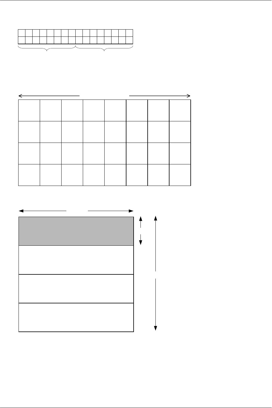
SCE CONFIDENTIAL GS User's Manual Version 6.0
© SCEI
-166-
Pixel Arrangement Order in a Column (Numbers in the figure show 32-bit word addresses.)
10
2367
45 98
10 11 14 15
12 13 10
2367
45 98
10 11 14 15
12 13
Bits 0-15 Bits 16-31
8.3.3. PSMT8
Block Configuration in a Page (Numbers in the figure show block addresses.)
128 pixels
0 1 4 5 16 17 20 21
2 3 6 7 18 19 22 23
8 9 12 13 24 25 28 29
10 11 14 15 26 27 30 31
Column Configuration in a Block
COLUMN 0
COLUMN 1
COLUMN 2
COLUMN 3
4 pixels
16 pixels
16 pixels
SCE CONFIDENTIAL GS User's Manual Version 6.0
© SCEI
-167-
Pixel Arrangement Order in a Column (Numbers in the figures show 32-bit word addresses.)
Pixel arrangement order varies according to the column number in PSMT8.
10
2367
45 98
10 11 14 15
12 13
10
2367
4598
10 11 14 15
12 13
10
2367
45 98
10 11 14 15
12 13
10
2367
4598
10 11 14 15
12 13
Bits 8-15 Bits 24-31
Bits 0-7 Bits 16-23
COLUMNS 0 and 2
10
2367
45 98
10 11 14 15
12 13
10
2367
4598
10 11 14 15
12 13
10
2367
45 98
10 11 14 15
12 13
10
2367
4598
10 11 14 15
12 13
Bits 8-15 Bits 24-31
Bits 0-7 Bits 16-23
COLUMNS 1 and 3

SCE CONFIDENTIAL GS User's Manual Version 6.0
© SCEI
-168-
8.3.4. PSMT4
Block Configuration in a Page (Numbers in the figure show block addresses.)
128 pixels
0 2 8 10
1 3 9 11
4 6 12 14
5 7 13 15
16 18 24 26
17 19 25 27
20 22 28 30
21 23 29 31
Column Configuration in a Block
COLUMN 0
COLUMN 1
COLUMN 2
COLUMN 3
16 pixels
4 pixels
32 pixels
SCE CONFIDENTIAL GS User's Manual Version 6.0
© SCEI
-169-
Pixel Arrangement Order in a Column (Numbers in the figures show 32-bit word addresses.)
Pixel arrangement order varies according to the column number in PSMT4.
10
2367
45 98
10 11 14 15
12 13
10
2367
4598
10 11 14 15
12 13
10
2367
45 98
10 11 14 15
12 13
10
2367
4598
10 11 14 15
12 13
10
2367
45 98
10 11 14 15
12 13
10
2367
4598
10 11 14 15
12 13
10
2367
45 98
10 11 14 15
12 13
10
2367
4598
10 11 14 15
12 13
Bits 4-7 Bits 12-15 Bits 20-23 Bits 28-31
Bits 0-3 Bits 8-11 Bits 16-19 Bits 24-27
COLUMNS 0 and 2
10
2367
45 98
10 11 14 15
12 13 10
2367
45 98
10 11 14 15
12 13 10
2367
45 98
10 11 14 15
12 13 10
2367
45 98
10 11 14 15
12 13
Bits 4-7 Bits 12-15 Bits 20-23 Bits 28-31
Bits 0-3 Bits 8-11 Bits 16-19 Bits 24-27
10
2367
4598
10 11 14 15
12 13 10
2367
4598
10 11 14 15
12 13 10
2367
4598
10 11 14 15
12 13 10
2367
4598
10 11 14 15
12 13
COLUMNS 1 and 3
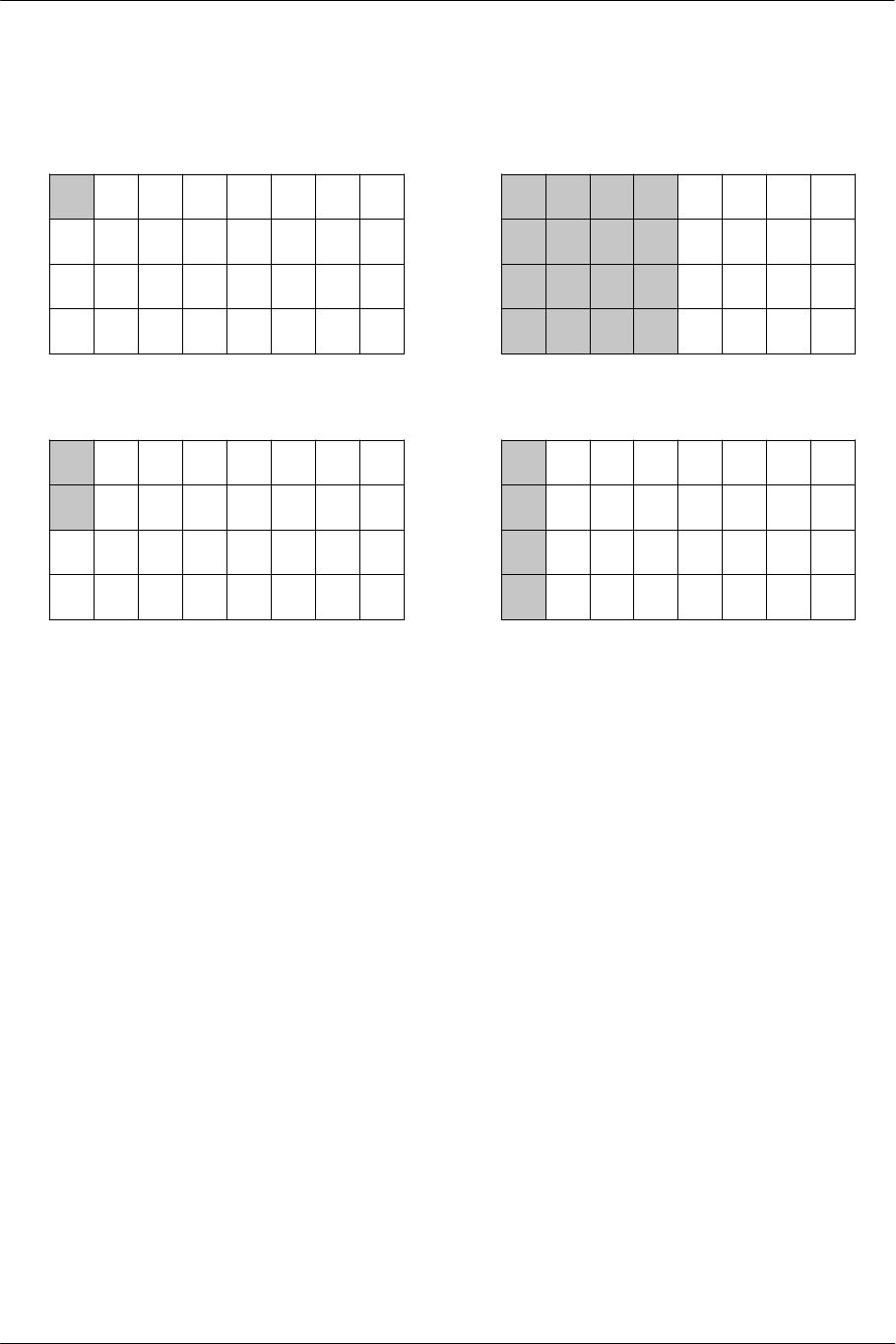
SCE CONFIDENTIAL GS User's Manual Version 6.0
© SCEI
-170-
8.4. Occupied Memory Area
8 (W) x 8 (H) in PSMCT32 32 (W) x 32 (H) in PSMCT32
Occupied block: 0 only Occupied blocks: 0 to 15
01 4 5 16172021 0 1 4 5 16 17 20 21
2 3 6 7 18 19 22 23 2 3 6 7 18 19 22 23
8 9 12 13 24 25 28 29 8 9 12 13 24 25 28 29
10 11 14 15 26 27 30 31 10 11 14 15 26 27 30 31
8 (W) x 16 (H) in PSMCT32 8 (W) x 32 (H) in PSMCT32
Occupied blocks: 0 and 2 Occupied blocks: 0, 2, 8, and 10
01 4 5 16172021 01 4 5 16 17 20 21
23 6 7 18192223 23 6 7 18 19 22 23
8 9 12 13 24 25 28 29 89 121324252829
10 11 14 15 26 27 30 31 10 11 14 15 26 27 30 31
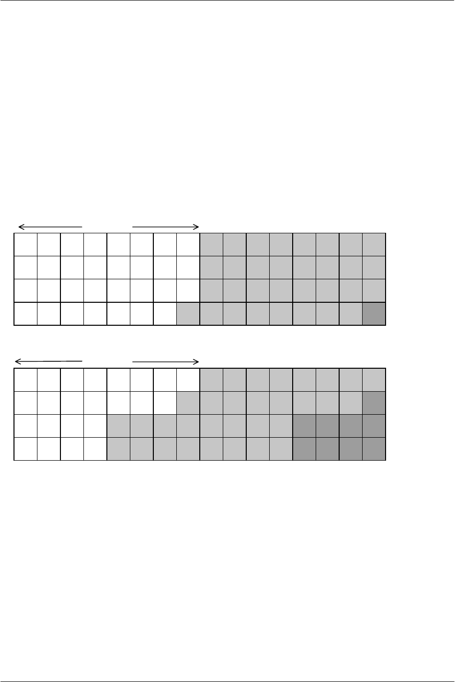
SCE CONFIDENTIAL GS User's Manual Version 6.0
© SCEI
-171-
8.5. Pointing within a Page
A buffer starting address points to a block boundary (not a page boundary), when using a texture (TBP0 of
TEX0 or TBPn of MIPTBP1/2) or transferring data between buffers (SBP or DBP of BITBLTBUF). When it
points to a block within a page, blocks are arranged as follows from the point of view of the texture buffer:
• The block pointed to is located at the upper left point in a two-dimensional space
• The block arrangement order conforms to the one obtained when the start of a page is pointed to
• The block pointed to and the ones following configure a one-page rectangle (64 x 32 in PSMCT32)
Examples of block arrangement order are shown below. Light gray blocks show the next page, followed by the
dark gray page.
Pointing to Block 1 in PSMCT32
64 pixels
1 2 5 6 17 18 21 22
1 2 5 6 17 18 21 22
3 4 7 8 19 20 23 24 3 4 7 8 19 20 23 24
9 10 13 14 25 26 29 30 9 10 13 14 25 26 29 30
11 12 15 16 27 28 31 0 11 12 15 16 27 28 31 0
Pointing to Block 9 in PSMCT32
64 pixels
9 10 13 14 25 26 29 30 9 10 13 14 25 26 29 30
11 12 15 16 27 28 31 0 11 12 15 16 27 28 31 0
17 18 21 22 1 2 5 6 17 18 21 22 1 2 5 6
19 20 23 24 3 4 7 8 19 20 23 24 3 4 7 8
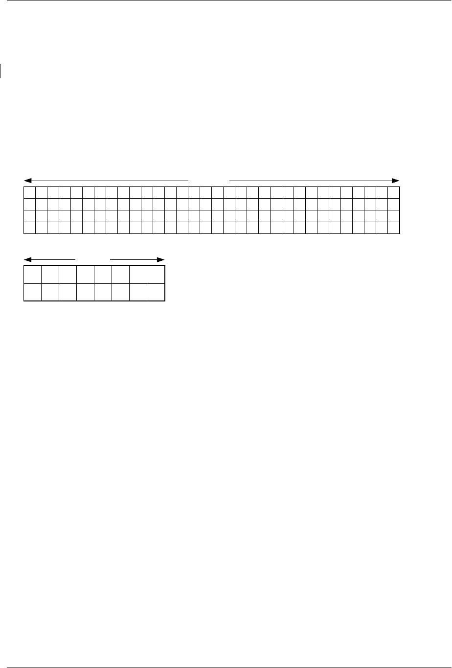
SCE CONFIDENTIAL GS User's Manual Version 6.0
© SCEI
-172-
8.6. Pixel Storage Format Conversion
When transferring PSMT4/PSMT8/PSMT16 texture data as PSMCT32 data, use the following rules to convert
pixel storage format in the preprocessing stage. This allows textures of different modes to be packed together
and transferred at one time as PSMCT32 data.
8.6.1. PSMT4
The following is an example of converting 1-column PSMT4 data (32 x 4) to PSMCT32 (8 x 2).
1-column PSMT4 Data (Pixel numbers in the figure are arranged in scan line order.)
32 pixels
10
32 33 34 35
23 54
36 37 38 39
67
6968
100 101 102 103
70 716564
96 97 98 99
66 67
98
40 41 42 43
10 11 13
12
44 45 46 47
14 15
7776
108 109 110 111
78 797372
104 105 106 107
74 75
1716
48 49 50 51
18 19 2120
52 53 54 55
22 23
8584
116 11 7 118 119
86 878180
112 11 3 114 115
82 83
2524
56 57 58 59
26 27 2928
60 61 62 63
30 31
9392
124 125 126 127
94 958988
120 121 122 123
90 91
1-column PSMCT32 Data
A
I
B
J
C
K
D
L
E
M
F
N
G
O
H
P
8 pixels
SCE CONFIDENTIAL GS User's Manual Version 6.0
© SCEI
-173-
PSMCT32 pixels (A to P) correspond to PSMT4 pixels (0 to 127) as follows:
92
93
24
25
84
85
16
17
76
77
8
9
68
69
0
1
94
95
26
27
86
87
18
19
78
79
10
11
70
71
2
3
88
89
28
29
80
81
20
21
72
73
12
13
64
65
4
5
90
91
30
31
82
83
22
23
74
75
14
15
66
67
6
7
124
125
56
57
116
117
48
49
108
109
40
41
100
101
32
33
126
127
58
59
118
119
50
51
110
111
42
43
102
103
34
35
120
121
60
61
112
113
52
53
104
105
44
45
96
97
36
37
122
123
62
63
114
115
54
55
106
107
46
47
98
99
38
39
A
B
C
D
E
F
G
H
I
J
K
L
M
N
O
P
Bit 31 Bit 0
COLUMNS 0 and 2 COLUMNS 1 and 3
SCE CONFIDENTIAL GS User's Manual Version 6.0
© SCEI
-174-
8.6.2. PSMT8
The following is an example of converting 1-column PSMT8 data (16 x 4) to PSMCT32 (8 x 2).
1-column PSMT8 Data (Pixel numbers in the figure are arranged in scan line order.)
16 pixels
10
32 33 34 35
23 54
36 37 38 39
67 98
40 41 42 43
10 11 13
12
44 45 46 47
14 15
1716
48 49 50 51
18 19 2120
52 53 54 55
22 23 2524
56 57 58 59
26 27 2928
60 61 62 63
30 31
1-column PSMCT32 Data
A
I
B
J
C
K
D
L
E
M
F
N
G
O
H
P
8 pixels
PSMCT32 pixels (A to P) correspond to PSMT8 pixels (0 to 63) as follows:
44
45
8
9
36
37
0
1
46
47
10
11
38
39
2
3
40
41
12
13
32
33
4
5
42
43
14
15
34
35
6
7
60
61
24
25
52
53
16
17
62
63
26
27
54
55
18
19
56
57
28
29
48
49
20
21
58
59
30
31
50
51
22
23
A
B
C
D
E
F
G
H
I
J
K
L
M
N
O
P
Bit 31 Bit 0
44
45
8
9
36
37
0
1
46
47
10
11
38
39
2
3
40
41
12
13
32
33
4
5
42
43
14
15
34
35
6
7
60
61
24
25
52
53
16
17
62
63
26
27
54
55
18
19
56
57
28
29
48
49
20
21
58
59
30
31
50
51
22
23
A
B
C
D
E
F
G
H
I
J
K
L
M
N
O
P
Bit 31 Bit 0
COLUMNS 0 and 2 COLUMNS 1 and 3
SCE CONFIDENTIAL GS User's Manual Version 6.0
© SCEI
-175-
8.6.3. PSMT16
The following is an example of converting 1-column PSMT16 data (16 x 2) to PSMCT32 (8 x 2).
1-column PSMT16 Data (Pixel numbers in the figure are arranged in scan line order.)
16 pixels
1023546798101113
12 14 15
1716 18 19 2120 22 23 2524 26 27 2928 30 31
1-column PSMCT32 Data
A
I
B
J
C
K
D
L
E
M
F
N
G
O
H
P
8 pixels
PSMCT32 pixels (A to P) correspond to PSMT16 pixels (0 to 31) as follows:
8
9
0
1
10
11
2
3
12
13
4
5
14
15
6
7
24
25
16
17
26
27
18
19
28
29
20
21
30
31
22
23
A
B
C
D
E
F
G
H
I
J
K
L
M
N
O
P
Bit 31 Bit 0

SCE CONFIDENTIAL GS User's Manual Version 6.0
© SCEI
-176-
(This page is left blank intentionally)
