Hi Key960 So C Reference Manual
HiKey960_SoC_Reference_Manual
HiKey960_SoC_Reference_Manual
User Manual: Pdf
Open the PDF directly: View PDF ![]() .
.
Page Count: 100

Hi3660
Data Sheet
Contents
Issue 05 (2016-12-22)
HiSilicon Proprietary and Confidential
Copyright © HiSilicon Technologies Co., Ltd.
i
Contents
Contents .............................................................................................................................................. i
Figures ............................................................................................................................................... ii
Tables ............................................................................................................................................... iii
1 Introduction to Hi3660 .............................................................................................................. 1-1
1.1 Main Features ................................................................................................................................................ 1-1
1.1.1 Basic Features ...................................................................................................................................... 1-1
1.1.2 Interface Features ................................................................................................................................. 1-3
1.1.3 Low-Power Features ............................................................................................................................ 1-5
1.2 Chip Architecture .......................................................................................................................................... 1-5
1.3 Typical Application ....................................................................................................................................... 1-6

Hi3660
Data Sheet
Figures
Issue 05 (2016-12-22)
HiSilicon Proprietary and Confidential
Copyright © HiSilicon Technologies Co., Ltd.
ii
Figures
Figure 1-1 Architecture of the Hi3660 ............................................................................................................... 1-6
Figure 1-2 Typical (smartphone) application of the Hi3660............................................................................... 1-7

Hi3660
Data Sheet
Tables
Issue 05 (2016-12-22)
HiSilicon Proprietary and Confidential
Copyright © HiSilicon Technologies Co., Ltd.
iii
Tables
Table 1-1 Multimedia features of the Hi3660 ..................................................................................................... 1-2
Table 1-2 Peripheral interfaces of the Hi3660 .................................................................................................... 1-3
Table 1-3 Memory interfaces of the Hi3660 ....................................................................................................... 1-4
Table 1-4 Debugging interfaces of the Hi3660 ................................................................................................... 1-4
Table 1-5 Low-power features of the Hi3660 ..................................................................................................... 1-5

Hi3660
Data Sheet
1 Introduction to Hi3660
Issue 05 (2016-12-22)
HiSilicon Proprietary and Confidential
Copyright © HiSilicon Technologies Co., Ltd.
1-1
1 Introduction to Hi3660
1.1 Main Features
1.1.1 Basic Features
Computing Capability
The Hi3660 has the following computing specifications:
- 8-core CPU, including the ARM Cortex-A73 MPCore high-performance heavy cores
(four 2.4 GHz cores) and ARM Cortex-A53 MPCore energy-efficient light cores (four
1.8 GHz cores)
- High-performance 3D acceleration technologies, including OpenGL ES 3.2, OpenCL 1.2,
OpenCL 2.0, DirectX 11, and Renderscript
- Memory management unit (MMU) management for all the chip channels, reducing the
overhead of reserved memories
- 1866 MHz 4-channel low-power double data rate 4 (LPDDR4) and maximum 8 GB
space for the double data rate (DDR)
Multimedia Features
The Hi3660 has the following multimedia features:
- Built-in video hardware decoder (H.265/H.264 4096 x 2160@60 fps)
- Built-in video hardware encoder (H.265/H.264 4096 x 2160@30 fps)
- Built-in independent graphics processing unit (GPU), Mali G71 MP8@1 GHz
- 960 megapixel/s throughput rate, up to 23 megapixels@30 fps, and 16 megapixels@30
fps for each of the two pipes
- Independent JPEG encoder and face detection acceleration module
- Dual Mobile Industry Processor Interface (MIPI) Display Serial Interfaces (DSIs),
supporting the maximum resolution of 3840 x 2400@60 Hz and multiple IFBCs
- External display interface extended by using the MIPI DSI and Sony/Philips Digital
Interface Format (S/PDIF) interface
- TypeC interface supported when the Hi3660 connects to another chip

Hi3660
Data Sheet
1 Introduction to Hi3660
Issue 05 (2016-12-22)
HiSilicon Proprietary and Confidential
Copyright © HiSilicon Technologies Co., Ltd.
1-2
Table 1-1 Multimedia features of the Hi3660
Media Feature
Description
GPU
3D acceleration
- OpenGL 3.2/Open VG1.1
- OpenGL ES 1.1/2.0/OpenGL ES 3.0/ OpenGL ES 3.1/ OpenGL ES 3.2
- OpenCL 1.1/1.2/2.0
- DirectX 11.1 Specification
- Renderscript
Display pixel depth
RGB888, RGB565
LCD resolution
Maximum resolution of 3840 x 2400, 60 Hz refresh rate
LCD interface
Two MIPI-DSI LCD interfaces. The display data can be compressed to 1/3 or 1/2 of
the original data. The 3840 x 2400 display is supported.
TV interface
- External display interface extended by using the MIPI DSI and S/PDIF interface
- TypeC interface supported when the Hi3660 connects to another chip
Wi-Fi Display (WFD)
1080p@60 fps
Video encoding
- H.265 or H.264 encoding format
- 3840 x 2400@30 fps HD photographing
- 4 x 1080p@30 fps simultaneous HD encoding
- 720p 240 fps video, supporting fast recording and slow playing
Video decoding
- Decoding formats: H.265, High Efficiency Video Coding (HEVC) MP/High Tier,
Main 10/High Tier, H.264 BP/MP/HP, MPEG1/2/4, VC-1, VP6/8, RV8/9/10,
Scalable Video Coding (SVC), DIVX, and multiview video coding (MVC)
- Up to H.265 4K@60 fps and H.264 4K@30 fps
Audio interface
- SLIMbus, I2S, and PCM interfaces, supporting the master and slave modes
- DSD interface
Audio sampling rate
- 8 kHz
- 16 kHz
- 32 kHz
- 48 kHz
- 96 kHz
ADC/DAC
- Five independent DAC channels and four digital DAC channels supported by the
analog codec (two channels supporting ultrasonic wave transmission and the other
two channels supporting HD playing)
- 100 dB signal-to-noise ratio (SNR) ADC (A-weighted) with –80 dB THD and 48
kHz sampling rate
Data precision
24-bit data precision, SNR supported by audio channels
Audio digital signal
processor (DSP)
- Hi-Fi 3.0 DSP served as an independent DSP on the Hi3660 and Hi6403 sides
- Up to 533 MHz frequency

Hi3660
Data Sheet
1 Introduction to Hi3660
Issue 05 (2016-12-22)
HiSilicon Proprietary and Confidential
Copyright © HiSilicon Technologies Co., Ltd.
1-3
Media Feature
Description
Audio
MP3 playing
Microphone (MIC) input
Four MIC inputs
Audio effect
Various audio effect processing methods
Audio recording
Dual-track recording
Communication voice
High-performance voice features such as AVS and voice over Long Term Evolution
(VoLTE)
1.1.2 Interface Features
Table 1-2 Peripheral interfaces of the Hi3660
Interface
Description
USB port
- USB 3.0 and USB 2.0 On-The-Go (OTG) protocols
- BC1.2 charging
PCIe interface
PCIe 1.1/2.0 protocol
Micro SD card interface
- SD 3.0 or SD 2.0 card
- High-speed SD card
- Hot plug
BT/Wi-Fi air interface
- Wi-Fi: WLAN, portable hotspot, Wi-Fi-DIRECT, compliance with the
IEEE802.11 b/g/n/ac protocol
- BT: BT 4.1/BT 4.0/BT Class 1.5/ BT Profile (call, A2DP, FTP)
FM air interface
- FM radio over the headphone
- FM radio over the FM speaker
- FM recording
Mobile TV interface
Integrated Service Digital Broadcasting-Terrestrial (ISDB-T)
Human-machine
interface
- Multiple keys. If the keyboard matrix is supported, keys can be extended over the
I2C interface.
- Touchscreen
- Multi-point touch
MIC interface
The MIC interface supports the following voice inputs:
- MIC input
- MIC input of the headphone
- MIC input of the Bluetooth headphone
I2C interface
Seven groups of high-speed I2C interfaces, up to 3 Mbit/s rate
SPI
Five groups of SPIs (master), up to 30 Mbit/s rate
Hi3660
Data Sheet
1 Introduction to Hi3660
Issue 05 (2016-12-22)
HiSilicon Proprietary and Confidential
Copyright © HiSilicon Technologies Co., Ltd.
1-4
Interface
Description
UART interface
Nine groups of high-speed UART interfaces, up to 9 MBauds frequency
GPIO interface
Multiple GPIO interfaces supported by the Hi3660 and Hi6403
Headset interface
- 3.5 mm headphone output
- MIC input of the headphone
- MIC with controller (four keys)
Speaker interface
- Extended power amplifier of the stereo speaker
- Two line-out interfaces
Receiver interface
One receiver
Keyboard
Keyboard backlight
Table 1-3 Memory interfaces of the Hi3660
Interface
Description
eMMC flash
- eMMC 5.1 and non-volatile memory for storing information such as boot code and
data
- Bus rate in HS400 mode
Universal Flash
Storage (UFS) flash
UFS 2.1 and non-volatile memory for storing information such as boot code and data,
supporting in-line encryption
LPDDR4 SDRAM
- Dynamic memory for system running and four channels (each channel supporting at
most two chip selects)
- 366 balls
- 1866 MHz frequency
- Maximum capacity of 8 GB
Micro SD card
- Compliance with the SD 3.0 protocol
- Support for user data storage, user software installation, and user space extension as
the main memory
Table 1-4 Debugging interfaces of the Hi3660
Interface
Description
CoreSight interface
CoreSight debugging interface, supporting the SWD debugging mode
JTAG interface
JTAG debugging interface, which is compliant with IEEE Std 1149.1

Hi3660
Data Sheet
1 Introduction to Hi3660
Issue 05 (2016-12-22)
HiSilicon Proprietary and Confidential
Copyright © HiSilicon Technologies Co., Ltd.
1-5
1.1.3 Low-Power Features
Table 1-5 Low-power features of the Hi3660
Power
Consumption
Control
Description
Dynamic voltage
and frequency
scaling (DVFS)
Independent DVFS function for the four Cortex A73 heavy cores, four Cortex A53 light
cores, and the GPU
Power management
in the idle state
Ultra-low-power design in the idle state to minimize system power consumption
1.2 Chip Architecture
The Hi3660 uses the 16 nm fin field-effect transistor (FinFET) technology of TSMC, and
features multiple cores, multiple modes, high performance, and high integration. As the core
system on chip (SoC) in the Kirin960 high-end smartphone solution, the Hi3660 provides
high-speed mobile computing, integrates various multimedia processing functions and high-
specification communication processing functions, and uses the industry-leading low-power
technology.
Hi3660
Data Sheet
1 Introduction to Hi3660
Issue 05 (2016-12-22)
HiSilicon Proprietary and Confidential
Copyright © HiSilicon Technologies Co., Ltd.
1-6
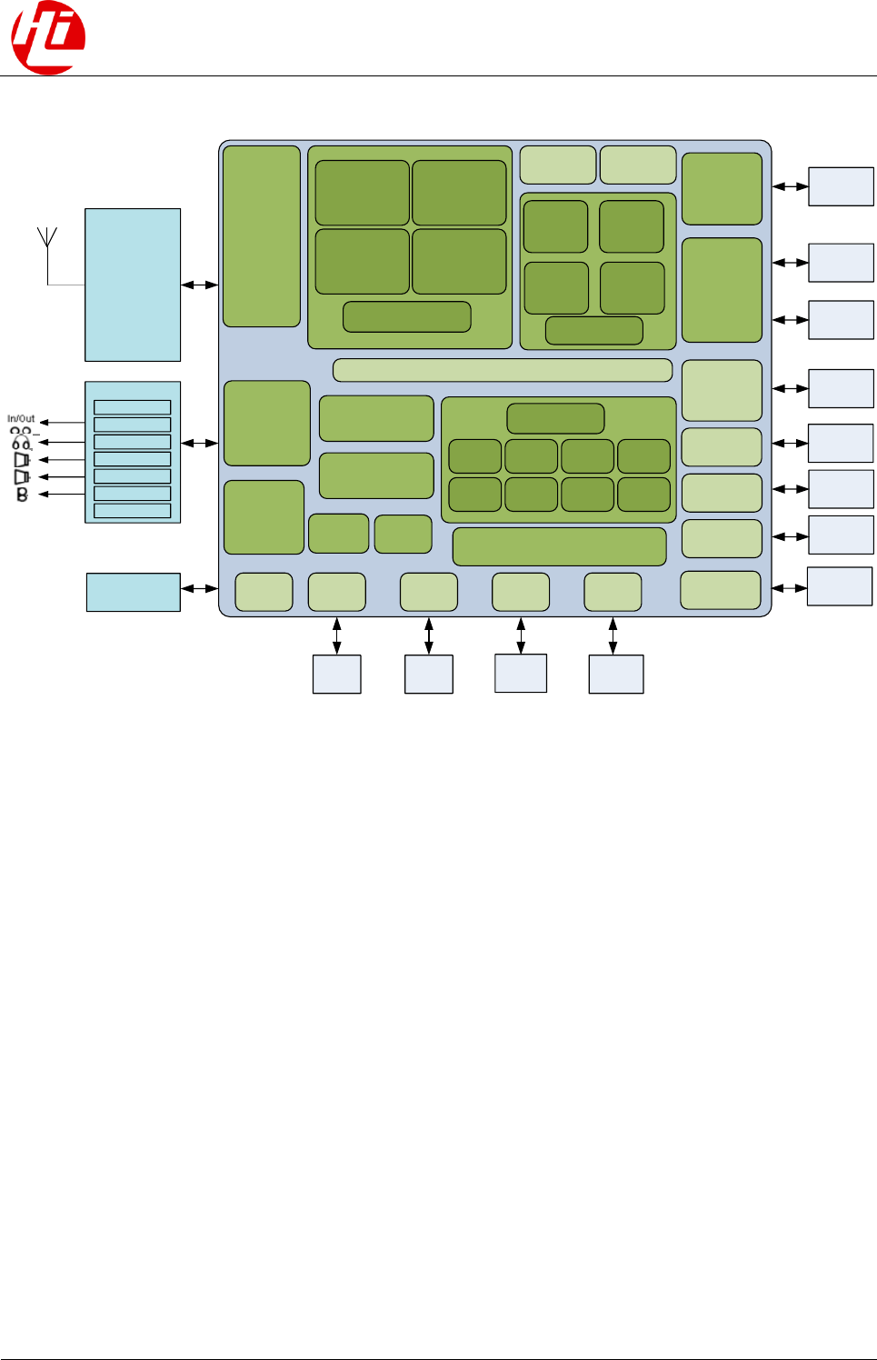
Figure 1-1 Architecture of the Hi3660
BT GPS Sensor SIM x 2
GCUTL
modem
baseband
CCI bus
HD video codec
Dual security
engines
ASP
subsystem
Display
subsystem
ISP
subsystem
L2 cache
(2 MB)
Cortex A73
with NEON
(2.4 GHz)
L2 cache
(512 KB)
Cortex A53
with NEON
(1.8 GHz)
Cortex A53
with NEON
(1.8 GHz)
Cortex A53
with NEON
(1.8 GHz)
Cortex A53
with NEON
(1.8 GHz)
L2 cache
(1 MB)
LP M3
Transceiver
Power
Audio
Receiver
Speaker
MIC x 4
Headset
Hi6403
UART
Security IP
UART I2C SCI
eMMC 5.1
USB 3.0
OTG
Quad-
channel
DDRC
IVP
DSP
IPC GIC
PC
eMMC
LPDDR4
Camera
Camera
LCD
Vibrator Sensor Hub
subsystem
Cortex A73
with NEON
(2.4 GHz)
Cortex A73
with NEON
(2.4 GHz)
Cortex A73
with NEON
(2.4 GHz)
UFS 2.1 UFS
PCIe Wi-Fi
Mali G71
Shader Mali G71
Shader Mali G71
Shader Mali G71
Shader
Mali G71
Shader Mali G71
Shader Mali G71
Shader Mali G71
Shader
Hi1102 SDIO
The Hi3660 consists of the following functional modules and subsystems:
- Big.LITTLE 8-core CPU subsystem, which contains the ARM Cortex-A73 MPCore
high-performance heavy cores (four cores) and ARM Cortex-A53 MPCore energy-
efficient light cores (four cores)
- ARM Mali G71 MP8 3D GPU
- Independent image signal processor (ISP)
- 3840 x 2400 HD video hardware decoder and encoder
- Display and graphics acceleration subsystem
- Audio subsystem with one Tensilica Hi-Fi 3.0 DSP
- Peripheral subsystem for the I/O device controllers such as the direction memory access
(DMA), PCIe, USB 3.0, and SD card controllers
- DDR and UFS controllers
1.3 Typical Application
The Hi3660 is applied to the smartphone and tablet.
Hi3660
Data Sheet
1 Introduction to Hi3660
Issue 05 (2016-12-22)
HiSilicon Proprietary and Confidential
Copyright © HiSilicon Technologies Co., Ltd.
1-7
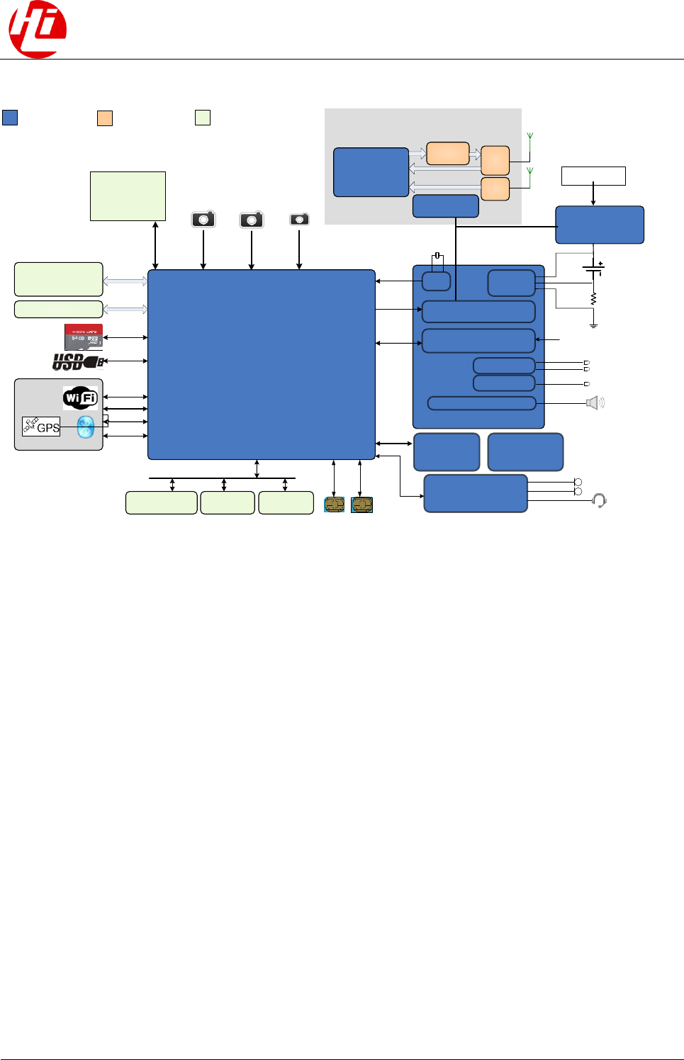
Figure 1-2 Typical (smartphone) application of the Hi3660
MIPI
CSI_0
Main
FEM
Hi3660
UFS/eMMC 5.1
4-channel
LPDDR4 3733
Mbit/s
Power
management
RTC Coulomb
meter
Audio codec
Hi6403
LED driver
HK ADC
MIPI
DSI0/1
19.2 MHz
SSI 0.01 Ω
One backlight
RFIC
Hi6362
TRx
SD 3.0
SDIO 3.0
USB 3.0
USB 2.0
MMMB
PA
DIV
FEM
Sleep
CLK
Gyroscope CompassAccelerometer
I2C bus
Hi6523
APT/RFIC
RF8081
5 V IN
16 channels for Temp/ID/
Voltage
MIPI
CSI_2
Three indicators
Only 1% THD @ 1.6 W
ClassD with boost
Vsys
PCM
UART
Main Front
RF subsystem
PMU Hi6421
FM
HiSilicon IC Customized IC Third-party IC
Motor driver Motor
MIPI
CSI_1
Main
LCD
SSI
SSI Power Management
PMU Hi6422 V200
(CPU Small & GPU)
Power
Management
PMU Hi6422 V200
(CPU Big)
PCIe

Hi3660
Data Sheet
Contents
Issue 05 (2016-12-22)
HiSilicon Proprietary and Confidential
Copyright © HiSilicon Technologies Co., Ltd.
i
Contents
Contents .............................................................................................................................................. i
Figures ............................................................................................................................................... ii
Tables ............................................................................................................................................... iii
2 Overall Description ................................................................................................................... 2-1
2.1 Chip Structure ............................................................................................................................................... 2-1
2.1.1 SoC System .......................................................................................................................................... 2-1
2.1.2 Media Subsystem ................................................................................................................................. 2-3
2.1.3 Storage Subsystem ............................................................................................................................... 2-3
2.2 Clock ............................................................................................................................................................. 2-4
2.2.1 Function Description ............................................................................................................................ 2-4
2.2.2 Clock Input........................................................................................................................................... 2-4
2.3 Reset .............................................................................................................................................................. 2-4
2.3.1 Function Description ............................................................................................................................ 2-4
2.3.2 Chipset Reset Scheme .......................................................................................................................... 2-4
2.3.3 Reset Structure ..................................................................................................................................... 2-5
2.4 Interrupt ......................................................................................................................................................... 2-7
2.4.1 Function Description ............................................................................................................................ 2-7
2.4.2 Interrupt Structure ................................................................................................................................ 2-7
2.4.3 Interrupt Mapping ................................................................................................................................ 2-8
2.5 Chip Operating Mode and Control .............................................................................................................. 2-14
2.6 Boot Mechanism ......................................................................................................................................... 2-15
2.6.1 Overall Process .................................................................................................................................. 2-15
2.6.2 eMMC Boot ....................................................................................................................................... 2-16
2.7 Debugging Mode ......................................................................................................................................... 2-16
2.7.1 JTAG Debugging ............................................................................................................................... 2-16
2.7.2 CoreSight Debugging ......................................................................................................................... 2-17
2.8 Maintainability and Testability .................................................................................................................... 2-17
2.9 Memory Map ............................................................................................................................................... 2-17
2.9.1 Address Space Allocation (From the ACPU Perspective) .................................................................. 2-18

Hi3660
Data Sheet
Figures
Issue 05 (2016-12-22)
HiSilicon Proprietary and Confidential
Copyright © HiSilicon Technologies Co., Ltd.
ii
Figures
Figure 2-1 SoC system architecture ..................................................................... Error! Bookmark not defined.
Figure 2-2 External reset .................................................................................................................................... 2-5
Figure 2-3 GIC architecture................................................................................................................................ 2-8

Hi3660
Data Sheet
Tables
Issue 05 (2016-12-22)
HiSilicon Proprietary and Confidential
Copyright © HiSilicon Technologies Co., Ltd.
iii
Tables
Table 2-1 Modules in the SoC system ................................................................................................................ 2-1
Table 2-2 Allocation table of GIC interrupts ...................................................................................................... 2-8
Table 2-3 Register groups and memory address ranges (ACPU)...................................................................... 2-18
Hi3660
Data Sheet
2 Overall Description
Issue 05 (2016-12-22)
HiSilicon Proprietary and Confidential
Copyright © HiSilicon Technologies Co., Ltd.
2-1
2 Overall Description
2.1 Chip Structure
2.1.1 SoC System
Table 2-1 Modules in the SoC system
Module
Description
Module
Description
A73/A53
Application processor
cluster, big.LITTLE
architecture
IVP
Image and video processor
(IVP) module
ASP
Audio signal processor
(ASP) subsystem
LPMCU
Low-power processing
subsystem
BLPWM
Backlight pulse-width
modulation (PWM) module
MMC
Multimedia card (MMC)
control module
BOOTROM
On-chip read-only memory
(ROM)
NANDC
Flash memory controller
(FMC)
CODEC_SSI
Synchronous serial
interface (SSI) module used
to communicate with the
codec
PCTRL
Peripheral controller
CRG
Clock and reset generator
(CRG) module
PMCTRL
Power management
control (PMC) module
such as dynamic frequency
scaling (DFS) and
dynamic voltage and
frequency scaling (DVFS)
CSSYS
Processor joint-debugging
module
PMU_I2C
I2C interface module used
to communicate with the
power management unit
(PMU)

Hi3660
Data Sheet
2 Overall Description
Issue 05 (2016-12-22)
HiSilicon Proprietary and Confidential
Copyright © HiSilicon Technologies Co., Ltd.
2-2
Module
Description
Module
Description
DDRC
Double data rate SDRAM
controller (DDRC)
PMU_SSI
SSI module used to
communicate with the
PMU
DJTAG
JTAG port debugging
module
PWM
PWM module
DMAC
Direct memory access
controller (DMAC) module
RTC
Real-time clock (RTC)
counter
DSS
Display module
SCI
SIM card controller
EFUSEC
eFUSE control module
SCTRL
System controller
Generic
interrupt
controller
(GIC)
Processor interrupt
processing module
SEC_P/SEC_S
Security processing
module
GNSPWM
Universal PWM module
SPI
Serial peripheral interface
(SPI) controller
GPIO
General-purpose
input/output (GPIO)
interface module
SYS_CNT
Processor-dedicated
counter module
GPU
Media service processor
TIMER
Timing and counting
module
HKADC_SSI
Bus interface module, used
to read the converted
digital data in the
housekeeping analog-to-
digital converter (HKADC)
of the external PMU
through the SSI
TSENSORC
TSensor controller
I2C
I2C controller
TZPC
Security signal allocation
module
IOC
I/O control module
UART
Universal serial port
module
IOMCU
Sensor-hub processing
subsystem
USB3OTG
USB 3.0 controller module
IPC
Inter-core communication
module
VENC/VDEC
Video
encryption/decryption
processing module
ISP
Image signal processing
(ISP) module
WD
Watchdog counter
EMMC5.1
eMMC 5.1 controller
module
UFS
Unified File system (UFS)
controller module
SDIO
SDIO controller module
SD
SD card controller module

Hi3660
Data Sheet
2 Overall Description
Issue 05 (2016-12-22)
HiSilicon Proprietary and Confidential
Copyright © HiSilicon Technologies Co., Ltd.
2-3
Module
Description
Module
Description
PCIe
PCIe controller module
-
-
The system on chip (SoC) system uses the multi-layer bus architecture. Each layer supports
separate parallel access.
The bus architecture of the SoC system has the following features:
- Supports hardware coherency through coherency bus interconnection.
- Connects the independent buses from multiple layers to improve the bus bandwidth of
the Hi3660 and provide excellent scalability.
- Uses the advanced eXtensible interface (AXI) as the high-speed data bus, supporting
128-bit or 64-bit width.
- Uses the 32-bit AXI as the low-speed data bus and configuration bus.
2.1.2 Media Subsystem
The media subsystem provides superior multimedia processing and acceleration functions:
- Image capturing
- Image display and output
- Acceleration of image encoding and decoding
- 3D graphics acceleration
- Audio processing acceleration
The media subsystem supports the following upper-level applications:
- Digital photographing
- Digital video recording
- Audio recording
- Playing local audio and video
- Browsing local pictures
- Playing audio and video in the stream media format
- Multimedia editor
- Video call
- UI and video hardware acceleration
- Hardware acceleration for gaming
For details about the media subsystem, see chapter 6 "Media Processing."
2.1.3 Storage Subsystem
The Hi3660 supports the following external storage interfaces to provide flexible storage
solutions for the system and meet different product requirements:
- UFS/eMMC/SD/SDIO static storage card interface
- Low-power double data rate 4 (LPDDR4) dynamic memory interface

Hi3660
Data Sheet
2 Overall Description
Issue 05 (2016-12-22)
HiSilicon Proprietary and Confidential
Copyright © HiSilicon Technologies Co., Ltd.
2-4
- NAND flash interface
For details about the storage subsystem, see chapter 7 "Storage Control."
2.2 Clock
2.2.1 Function Description
The Hi3660 accepts external clock inputs, generates required internal operating clocks by
using the internal phase-locked loops (PLLs) and clock circuits, and provides multiple clocks
for other chips.
The Hi3660 provides 11 internal PLLs for generating operating clocks required by chip
modules.
2.2.2 Clock Input
The Hi3660 supports the following external input clocks:
- 32 kHz clock
- 19.2 MHz clock
- External backup clock
2.3 Reset
2.3.1 Function Description
The Hi3660 receives external reset inputs and resets or deasserts reset on internal modules
based on the reset deassertion sequence during power-on.
After the AO area is powered on, the internal power-on reset (POR) module outputs low-level
signals, resets the Hi3660, and pulls the output level up about 12–48 ms after the power-on.
This ensures that the entire chip is in reset state when the I/O (external input reset) is in
indefinite state.
Besides POR, the Hi3660 supports the following global reset types:
- Watchdog reset
- Temperature sensor reset
- Chip soft reset
When any of the preceding reset types is valid, the global reset of the Hi3660 is triggered. All
reset types have the same priority.
2.3.2 Chipset Reset Scheme
During the power-on process, the PMU provides the reset input signal (RSTIN_N) for the
Hi3660. The SoC automatically performs the POR operation on internal modules.
Hi3660
Data Sheet
2 Overall Description
Issue 05 (2016-12-22)
HiSilicon Proprietary and Confidential
Copyright © HiSilicon Technologies Co., Ltd.
2-5
When any global reset mode in the Hi3660 is valid, the Hi3660 outputs the PMU reset signal
(PMU_RST_N) to reset the PMU. After that, the PMU pulls RSTIN_N down to implement
global reset.
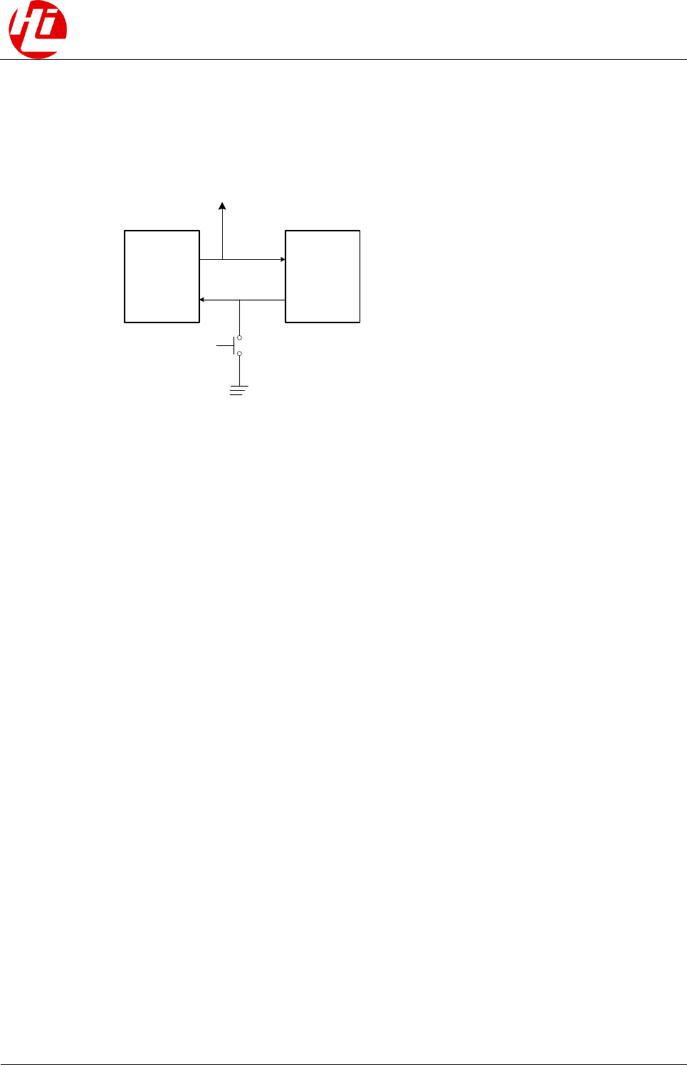
Figure 2-1 External reset
PMU Hi3660
RSTIN_N
To other devices
Reset_button
PMU_RST_N
2.3.3 Reset Structure
The Hi3660 supports the following global reset types:
- POR
- Watchdog reset
- Temperature sensor reset
- Chip soft reset
There are two reset modes: dying gasp reset and non-dying gasp reset. Setting SCPEREN1[31]
to 1 enables the dying gasp reset mode. Setting SCPERDIS1[31] to 1 disables the dying gasp
reset mode.
- Dying gasp reset: When the wd reset request and over-temperature reset request are valid,
the request for the DDR SDRAM to enter the self-refresh mode is initiated first. Then
there are two options:
− Wait for the DDR SDRAM to enter the self-refresh mode. (After receiving the
interrupt, the software protects the scene, saves the critical system information to the
external non-volatile memory or SDRAM, and then sets the SDRAM to the self-
refresh mode.)
− Send the reset request signal, pull the PMU reset signal down, and reset the entire
system 1 ms after timeout occurs.
- Non-dying gasp reset: When the wd reset request, over-temperature reset request, and
software reset request are valid, directly send the reset request signal, pull the PMU reset
signal down, and reset the entire system. The scene is not preserved in the entire process.
POR
The global POR is obtained after two reset signals are ANDed: external reset signal RSTIN_N
and the POR output reset signal. After the AO area is powered on, the internal POR signal
outputs low level, resets the entire chip, and deasserts reset within 12–48 ms. The PMU

Hi3660
Data Sheet
2 Overall Description
Issue 05 (2016-12-22)
HiSilicon Proprietary and Confidential
Copyright © HiSilicon Technologies Co., Ltd.
2-6
generates the external reset signal RSTIN_N. The chip maintains the reset state after the I/O is
powered on. The global reset of the chip can be deasserted after the PMU deasserts reset.
Watchdog Reset
The following subsystems provide the watchdogs:
- WD0, WD1, and LPMCU subsystems
- IOMCU subsystem
- Modem subsystem
- ASP subsystem
- IVP subsystem
- ISPA7 subsystem
- UCE
- OCBC
- GPU
- LITTLE core
- Big core
The watchdog module monitors the system running status. In normal cases, the system needs
to periodically set the initial count value. If the system does not promptly set the initial count
value, the software is running abnormally. In this case, the watchdog performs the following
operations:
- The watchdog reports an exception interrupt, loads the initial value of the counter, and
re-counts from the initial value.
- If the exception interrupt is not handled, a reset signal is initiated when the watchdog
counter is decremented to 0.
Temperature Sensor Reset
The A53, A73, and G3D areas each contains a temperature sensor. When the chip temperature
reaches the preset threshold, a reset request signal is initiated to reset the A53 and A73 cores
in the chip.
Chip Soft Reset
The software can soft-reset the Hi3660 when necessary. When the software writes to the
SCSYSSTAT register, global soft reset of the Hi3660 is triggered.
Soft reset can be performed only in non-dying gasp reset mode. In dying gasp reset mode,
writing to SCSYSSTAT does not trigger the global soft reset of the Hi3660.

Hi3660
Data Sheet
2 Overall Description
Issue 05 (2016-12-22)
HiSilicon Proprietary and Confidential
Copyright © HiSilicon Technologies Co., Ltd.
2-7
Module Soft Reset
The software can independently reset the major modules of the Hi3660. These modules
include the RTC, timer, GPIO, USB, DMAC, VENC, VDEC, DSS, ISP, ASP, DDRC, MMC,
PWM, UART, SPI, and G3D. For details, see the description of each module.
2.4 Interrupt
2.4.1 Function Description
The ACPU uses the GIC to handle and control interrupts. Other microcontrollers, media, and
communication processors have their own interrupt handling logic. This section describes the
basic interrupt handling functions of the GIC.
The GIC has the following basic features:
- Supports interrupt nesting for the A53, A73, and G3D.
- Manages multi-core interrupt distribution.
- Supports security extension.
- Queries the states of interrupt sources.
- Provides a unique ID for each interrupt.
- Supports configurable interrupt trigger mode: high-level-triggered mode or edge-
triggered mode.
- Sets the priority of each interrupt.
- Generates software interrupts.
The GIC supports the following interrupt types:
- Software-generated interrupt (SGI)
The GIC supports 16 SGIs (SCI0 to SCI15), which are controlled by writing to registers.
- Private peripheral interrupt (PPI)
Each processor corresponds to seven PPIs.
- Shared peripheral interrupt (SPI)
A total of 352 peripheral interrupts are supported.
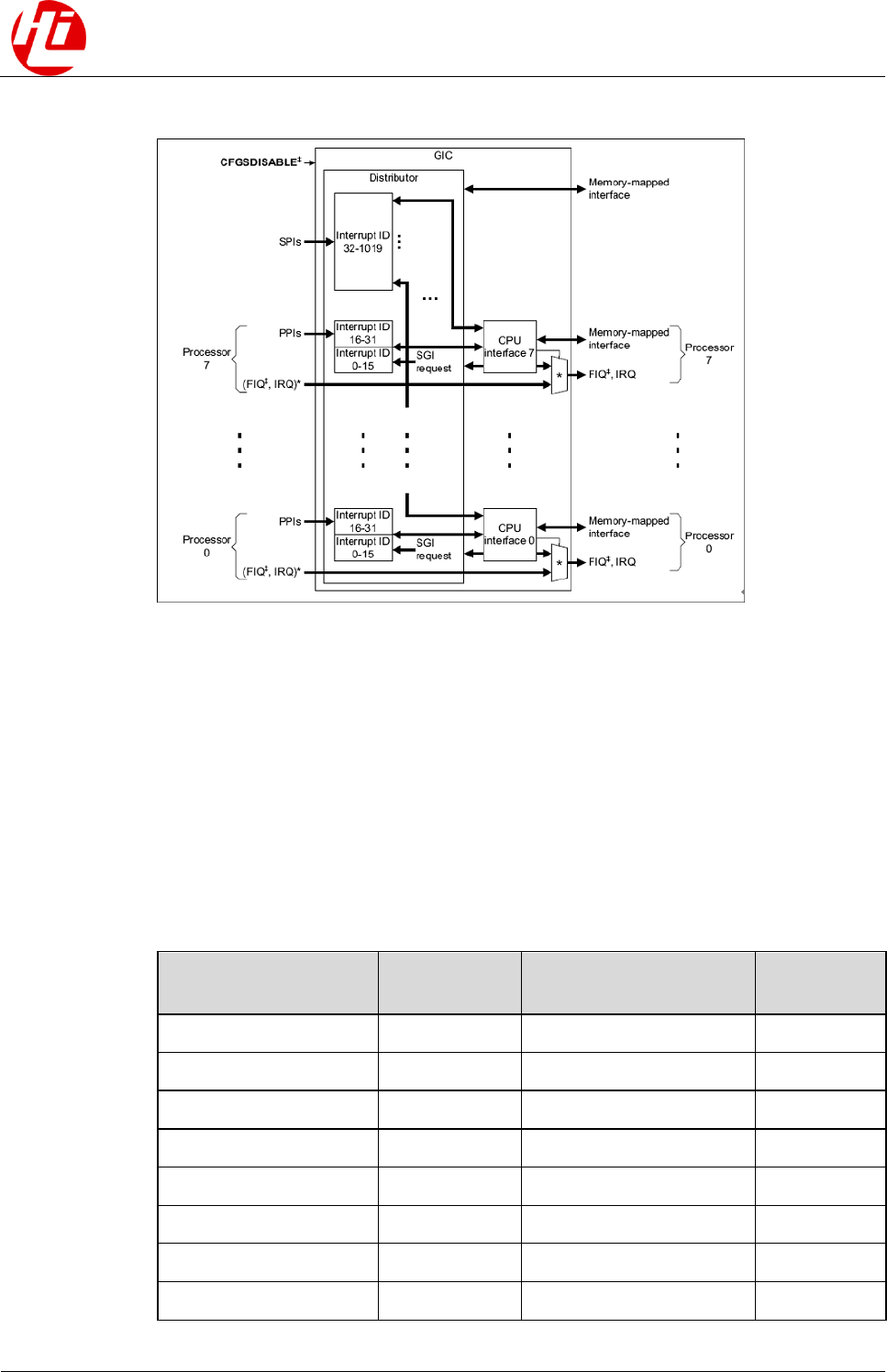
2.4.2 Interrupt Structure
As shown in Figure 2-2, the GIC contains one distributor and multiple CPU interfaces. The
distributor manages all interrupts in a centralized manner, and the CPU interfaces implement
interaction between the interrupts and the CPU. The integrated GIC-400 of the Hi3660 has
eight CPU interfaces, which connect to the quad-core A73 and quad-core A53, respectively.
Hi3660
Data Sheet
2 Overall Description
Issue 05 (2016-12-22)
HiSilicon Proprietary and Confidential
Copyright © HiSilicon Technologies Co., Ltd.
2-8
Figure 2-2 GIC architecture
The GIC supports the TrustZone. Each interrupt source can be configured as a secure interrupt
source or a non-secure interrupt source.
The GIC configures the priority of each interrupt. A smaller interrupt priority value indicates a
higher priority. If two interrupts have the same priority, the interrupt with a smaller interrupt
ID takes priority over the other one.
2.4.3 Interrupt Mapping
The Hi3660 GIC supports 384 interrupts, including 352 peripheral interrupts. Table 2-2 lists
the interrupt sources and interrupt IDs.
Table 2-2 Allocation table of GIC interrupts
Interrupt Source
GIC Interrupt
ID
Interrupt Source
GIC
Interrupt ID
A73_interr
32
PMC-AVS-IDLE-G3D
205
A73_exterr
33
M3_LP_wd
206
A73_pmu0
34
~CCI400_err
207
A73_pmu1
35
~&CCI400_overflow[6:0]
208
A73_pmu2
36
~CCI400_overflow[7]
209
A73_pmu3
37
IPC_S_int0
210
A73_cti0
38
IPC_S_int1
211
A73_cti1
39
IPC_S_int4
212
Hi3660
Data Sheet
2 Overall Description
Issue 05 (2016-12-22)
HiSilicon Proprietary and Confidential
Copyright © HiSilicon Technologies Co., Ltd.
2-9
Interrupt Source
GIC Interrupt
ID
Interrupt Source
GIC
Interrupt ID
A73_cti2
40
IPC_S_mbx0
213
A73_cti3
41
IPC_S_mbx1
214
A73_COMMRX0
42
IPC_S_mbx2
215
A73_COMMRX1
43
IPC_S_mbx3
216
A73_COMMRX2
44
IPC_S_mbx4
217
A73_COMMRX3
45
IPC_S_mbx5
218
A73_COMMTX0
46
IPC_S_mbx6
219
A73_COMMTX1
47
IPC_S_mbx7
220
A73_COMMTX2
48
IPC_S_mbx8
221
A73_COMMTX3
49
IPC_S_mbx9
222
A73_COMMIRQ0
50
IPC_S_mbx18
223
A73_COMMIRQ1
51
IPC_NS_int0
224
A73_COMMIRQ2
52
IPC_NS_int1
225
A73_COMMIRQ3
53
IPC_NS_int4
226
A53_interr
54
IPC_NS_int5
227
A53_exterr
55
IPC_NS_int6
228
A53_pmu0
56
IPC_NS_mbx0
229
A53_pmu1
57
IPC_NS_mbx1
230
A53_pmu2
58
IPC_NS_mbx2
231
A53_pmu3
59
IPC_NS_mbx3
232
A53_cti0
60
IPC_NS_mbx4
233
A53_cti1
61
IPC_NS_mbx5
234
A53_cti2
62
IPC_NS_mbx6
235
A53_cti3
63
IPC_NS_mbx7
236
A53_COMMRX0
64
IPC_NS_mbx8
237
A53_COMMRX1
65
IPC_NS_mbx9
238
A53_COMMRX2
66
IPC_NS_mbx18
239
A53_COMMRX3
67
mdm_aximon_intr
240
A53_COMMTX0
68
MDM_WDOG_intr
241
A53_COMMTX1
69
ASP-IPC-ARM
242

Hi3660
Data Sheet
2 Overall Description
Issue 05 (2016-12-22)
HiSilicon Proprietary and Confidential
Copyright © HiSilicon Technologies Co., Ltd.
2-10
Interrupt Source
GIC Interrupt
ID
Interrupt Source
GIC
Interrupt ID
A53_COMMTX2
70
ASP-IPC-MCPU
243
A53_COMMTX3
71
ASP-IPC-BBE16
244
A53_COMMIRQ0
72
ASP_WD
245
A53_COMMIRQ1
73
ASP_AXI_DLOCK
246
A53_COMMIRQ2
74
ASP_DMA_SECURE
247
A53_COMMIRQ3
75
ASP_DMA_SECURE_N
248
WatchDog0
76
SCI0
249
WatchDog1
77
SCI1
250
RTC0
78
SOCP0
251
RTC1
79
SOCP1
252
TIME00
80
MDM_IPF_intr0
253
TIME01
81
MDM_IPF_intr1
254
TIME10
82
|ddrc_fatal_int[3:0]
255
TIME11
83
mdm_axi_dlock_int
256
TIME20
84
mdm_wdt1_intr (CDSP)
257
TIME21
85
~GIC_IRQ_OUT[0]
258
TIME30
86
~GIC_IRQ_OUT[1]
259
TIME31
87
~GIC_IRQ_OUT[2]
260
TIME40
88
~GIC_IRQ_OUT[3]
261
TIME41
89
~GIC_IRQ_OUT[4]
262
TIME50
90
~GIC_IRQ_OUT[5]
263
TIME51
91
~GIC_IRQ_OUT[6]
264
TIME60
92
~GIC_IRQ_OUT[7]
265
TIME61
93
~GIC_FIQ_OUT[0]
266
TIME70
94
~GIC_FIQ_OUT[1]
267
TIME71
95
~GIC_FIQ_OUT[2]
268
TIME80
96
~GIC_FIQ_OUT[3]
269
TIME81
97
~GIC_FIQ_OUT[4]
270
TIME90
98
~GIC_FIQ_OUT[5]
271
TIME91
99
~GIC_FIQ_OUT[6]
272

Hi3660
Data Sheet
2 Overall Description
Issue 05 (2016-12-22)
HiSilicon Proprietary and Confidential
Copyright © HiSilicon Technologies Co., Ltd.
2-11
Interrupt Source
GIC Interrupt
ID
Interrupt Source
GIC
Interrupt ID
TIME100
100
~GIC_FIQ_OUT[7]
273
TIME101
101
NANDC
274
TIME110
102
CoreSight_ETR_Full
275
TIME111
103
CoreSight_ETF_Full
276
TIME120
104
DSS-pdp
277
TIME121
105
DSS-sdp
278
UART0
106
DSS-offline
279
UART1
107
DSS_mcu_pdp
280
UART2
108
DSS_mcu_sdp
281
UART4
109
DSS_mcu_offline
282
UART5
110
DSS_dsi0
283
UART6
111
DSS_dsi1
284
SPI1
112
IVP32_SMMU_irpt_s
285
I2C3
113
IVP32_SMMU_irpt_ns
286
I2C4
114
IVP32_WATCH_DOG
287
I2C5 (PMU_I2C)
115
ATGC
288
GPIO0_INTR1
116
G3D_IRQEVENT
289
GPIO1_INTR1
117
G3D_JOB
290
GPIO2_INTR1
118
G3D_MMU
291
GPIO3_INTR1
119
G3D_GPU
292
GPIO4_INTR1
120
isp_irq[0]
293
GPIO5_INTR1
121
isp_irq[1]
294
GPIO6_INTR1
122
isp_irq[2]
295
GPIO7_INTR1
123
isp_irq[3]
296
GPIO8_INTR1
124
isp_irq[4]
297
GPIO9_INTR1
125
isp_irq[5]
298
GPIO10_INTR1
126
isp_irq[6]
299
GPIO11_INTR1
127
isp_irq[7]
300
GPIO12_INTR1
128
isp_a7_to_gic_mbx_int[0]
301
GPIO13_INTR1
129
isp_a7_to_gic_mbx_int[1]
302
Hi3660
Data Sheet
2 Overall Description
Issue 05 (2016-12-22)
HiSilicon Proprietary and Confidential
Copyright © HiSilicon Technologies Co., Ltd.
2-12
Interrupt Source
GIC Interrupt
ID
Interrupt Source
GIC
Interrupt ID
GPIO14_INTR1
130
isp_a7_to_gic_ipc_int
303
GPIO15_INTR1
131
isp_a7_watchdog_int
304
GPIO16_INTR1
132
isp_axi_dlcok
305
GPIO17_INTR1
133
isp_a7_irq_out
306
GPIO18_INTR1
134
ivp32_dwaxi_dlock_irq
307
GPIO19_INTR1
135
mmbuf_asc0
308
GPIO20_INTR1
136
mmbuf_asc1
309
GPIO21_INTR1
137
UFS
310
GPIO22_INTR1
138
pcie_link_down_int
311
GPIO23_INTR1
139
pcie_edma_int
312
GPIO24_INTR1
140
pcie_pm_int
313
GPIO25_INTR1
141
pcie_radm_inta
314
GPIO26_INTR1
142
pcie_radm_intb
315
GPIO27_INTR1
143
pcie_radm_intc
316
IOMCU_WD
144
pcie_radm_intd
317
IOMCU_SPI
145
psam_intr[0]
318
IOMCU_UART3
146
psam_intr[1]
319
IOMCU_UART8
147
ocbc_pe_npint[0]
320
IOMCU_SPI2
148
intr_wdog_ocbc
321
IOMCU_I2C3
149
intr_vdec_mfde_norm
322
IOMCU_I2C0
150
intr_vdec_scd_norm
323
IOMCU_I2C1
151
intr_vdec_bpd_norm
324
IOMCU_I2C2
152
intr_vdec_mmu_norm
325
IOMCU_GPIO0_INT1
153
intr_vdec_mfde_safe
326
IOMCU_GPIO1_INT1
154
intr_vdec_scd_safe
327
IOMCU_GPIO2_INT1
155
intr_vdec_bpd_safe
328
IOMCU_GPIO3_INT1
156
intr_vdec_mmu_safe
329
IOMCU_DMAC_INT0
157
intr_venc_vedu_norm
330
IOMCU_DMAC_NS_IN
T0
158
intr_venc_mmu_norm
331
PERF_STAT
159
intr_venc_vedu_safe
332
Hi3660
Data Sheet
2 Overall Description
Issue 05 (2016-12-22)
HiSilicon Proprietary and Confidential
Copyright © HiSilicon Technologies Co., Ltd.
2-13
Interrupt Source
GIC Interrupt
ID
Interrupt Source
GIC
Interrupt ID
IOMCU_COMB
160
intr_venc_mmu_safe
333
IOMCU_BLPWM
161
intr_qosbuf0
334
NOC-comb
162
intr_qosbuf1
335
intr_dmss
163
intr_ddrc2_err
336
intr_ddrc0_err
164
intr_ddrc3_err
337
intr_ddrc1_err
165
intr_ddrphy[0]
338
PMCTRL
166
intr_ddrphy[1]
339
SECENG_P
167
intr_ddrphy[2]
340
SECENG_S
168
intr_ddrphy[3]
341
EMMC51
169
intr0_mdm_ipc_gic_s
342
ASP_IPC_MODEM_CB
BE
170
intr1_mdm_ipc_gic_s
343
SD3
171
SPI3
344
SDIO
172
SPI4 (Finger/Ink screen)
345
GPIO28_INTR1
173
I2C7
346
PERI_DMAC_int0
174
intr_uce0_wdog
347
PERI_DMAC_NS_int0
175
intr_uce1_wdog
348
CLK_MONITOR (in
SCTRL)
176
intr_uce2_wdog
349
TSENSOR_A73
177
intr_uce3_wdog
350
TSENSOR_A53
178
intr_exmbist
351
TSENSOR_G3D
179
intr_hisee_wdog
352
TSENSOR_Modem
180
intr_hisee_ipc_mbx_gic[0]
353
ASP_ARM_SECURE
(asp_hmdi secure
interrupt and src_up
secure interrupt)
181
intr_hisee_ipc_mbx_gic[1]
354
ASP_ARM
(asp_hmdi non-secure
interrupt, src_up non-
secure interrupt, and
slimbus combined
interrupt)
182
intr_hisee_ipc_mbx_gic[2]
355
VDM_INT2
183
intr_hisee_ipc_mbx_gic[3]
356
Hi3660
Data Sheet
2 Overall Description
Issue 05 (2016-12-22)
HiSilicon Proprietary and Confidential
Copyright © HiSilicon Technologies Co., Ltd.
2-14
Interrupt Source
GIC Interrupt
ID
Interrupt Source
GIC
Interrupt ID
VDM_INT0
184
intr_hisee_ipc_mbx_gic[4]
357
VDM_INT1
185
intr_hisee_ipc_mbx_gic[5]
358
|{MODEM_IPC0[0],
MDM_IPC_APPCPU_int
r0}
186
intr_hisee_ipc_mbx_gic[6]
359
|{MODEM_IPC1[0],
MDM_IPC_APPCPU_int
r1}
187
intr_hisee_ipc_mbx_gic[7]
360
MDM_bus_err
188
intr_hisee_alarm[0]
361
Reserved
189
intr_hisee_alarm[1]
362
MDM_EDMAC0_INTR
_NS[0]
190
Reserved
363
USB3
191
Reserved
364
Reserved
192
intr_hisee_eh2h_slv
365
USB3_OTG
193
intr_hisee_as2ap_irq
366
USB3_BC
194
intr_hisee_ds2ap_irq
367
GPIO1_SE_INTR1
195
intr_hisee_senc2ap_irq
368
GPIO0_SE_INTR1
196
GPIO0_EMMC
369
PMC-DVFS-A73
197
GPIO1_EMMC
370
PMC-DVFS-A53
198
AONOC_TIMEOUT
371
PMC-DVFS-G3D
199
intr_hisee_tsensor[0]
372
PMC-AVS-A73
200
intr_hisee_tsensor[1]
373
PMC-AVS-A53
201
intr_hisee_lockup
374
PMC-AVS-G3D
202
intr_hisee_dma
375
PMC-AVS-IDLE-A73
203
Reserved
376~383
PMC-AVS-IDLE-A53
204
2.5 Chip Operating Mode and Control
The Hi3660 system supports four operating modes, which are controlled by configuring
SCCTRL[modectrl] (0xFFF0_A000 for LPMCU access and 0x4020_A000 for CPU access):
- 000: The system mode is switched to sleep mode.

Hi3660
Data Sheet
2 Overall Description
Issue 05 (2016-12-22)
HiSilicon Proprietary and Confidential
Copyright © HiSilicon Technologies Co., Ltd.
2-15
- 001: The system mode is switched to doze mode.
- 01X: The system mode is switched to slow mode.
- 1XX: The system mode is switched to normal mode.
After POR, the state machine is in slow mode by default. The software controls the system
state transition by configuring SCCTRL[modectrl] (0xFFF0_A000 for LPMCU access and
0x4020_A000 for CPU access).
The system state machine is restored to slow mode after a global reset such as the global soft
reset, watchdog reset, or Tsensor over-temperature reset.
2.6 Boot Mechanism
2.6.1 Overall Process
The Hi3660 supports two boot modes: USB loading mode and memory boot mode. The
memory boot modes include eMMC boot mode and UFS boot mode. All these modes are
booted by the BOOTROM in the Hi3660. Then the corresponding boot process is started.
Apart from the preceding common boot modes, the Hi3660 also supports the NAND boot and
UFS boot in test mode.
Pin Settings
For the UFS boot mode booted by BOOTROM, the pin settings are as follows:
- TEST_MODE: 0
- BOOT_MODE: 1
- BOOT_UFS: 1
Basic Process
Step 1 Power on the system to start POR.
Step 2 Judge the boot mode.
Execute the BOOTROM code. Read the boot_mode register to judge the boot mode. If the
value of the BOOT_MODE pin is 1, enter the memory boot branch. Then read the boot_ufs
register. If the value of the BOOT_UFS pin is 1, enter the UFS boot process.
Step 3 Initialize the UFS clock and IP.
Step 4 Start the UFS link startup process.
Step 5 Initialize the UFS parameters and components.
Step 6 Transfer the bootloader image in the UFS device to the RAM.
Step 7 Verify the security.
Step 8 Execute the bootloader.
Step 9 Initialize the DDR, and copy the fastboot images stored in the UFS device to the DDR.
Initialize the ACPU and deassert reset. Then the ACPU side starts executing fastboot and
performs the subsequent startup process.

Hi3660
Data Sheet
2 Overall Description
Issue 05 (2016-12-22)
HiSilicon Proprietary and Confidential
Copyright © HiSilicon Technologies Co., Ltd.
2-16
----End
2.6.2 eMMC Boot
Pin Settings
For the eMMC boot mode booted by BOOTROM, the pin settings are as follows:
- TEST_MODE: 0
- BOOT_MODE: 1
- BOOT_UFS: 0
Basic Process
Step 1 Power on the system to start POR.
Step 2 Judge the boot mode.
Execute the BOOTROM code. Read the boot_mode register to judge the boot mode. If the
value of the BOOT_MODE pin is 1, enter the memory boot branch. Then read the boot_ufs
register. If the value of the BOOT_UFS pin is 0, enter the eMMC boot process.
Step 3 Initialize the eMMC clock and IP.
Step 4 Transfer the images in the eMMC device to the buffer in the eMMC and then to the RAM.
Step 5 Verify the security.
Step 6 Execute the bootloader.
Step 7 Initialize the DDR, and copy the fastboot images stored in the eMMC device to the DDR.
Initialize the ACPU and deassert reset. Then the ACPU side starts executing fastboot and
performs the subsequent startup process.
----End
2.7 Debugging Mode
2.7.1 JTAG Debugging
The Hi3660 provides the JTAG interface that complies with the IEEE 1149.1 standard:
- The DSP simulator can debug the four internal DSPs.
- The PC can connect to the JTAG simulator to separately debug the ARM processor.
The JTAG MUX connects external JTAG pin signals to the cores of the Hi3660.
The debugging steps are as follows:
Step 1 Power on and reset the Hi3660.
Step 2 Set JTAG_SEL1 and JTAG_SEL0 to 2'b01 to multiplex the CPU JTAG function on the
JTAG pin.

Hi3660
Data Sheet
2 Overall Description
Issue 05 (2016-12-22)
HiSilicon Proprietary and Confidential
Copyright © HiSilicon Technologies Co., Ltd.
2-17
Step 3 Set JTAG_SEL1 and JTAG_SEL0 to 2'b00 to enter the register selection mode. Configure the
system control register JTAGSYS_SW_SEL [7:0] to switch to the selected debugging
interface for debugging.
Step 4 Connect the corresponding simulator and open the corresponding debugging software to start
debugging.
----End
2.7.2 CoreSight Debugging
The Hi3660 has a powerful debug system that integrates an ARM CoreSight system. The
CoreSight system supports the following features:
- Top-level CoreSight and local CoreSight in each cluster. The local CoreSight contains
the A73 CoreSight and A53 CoreSight.
- Intrusive debugging (debug) and non-intrusive debugging (trace)
A73 and A53 support both debug and trace.
- Software debugging and traditional JTAG debugging
2.8 Maintainability and Testability
The Hi3660 provides the following maintainability and testability means:
- JTAG debugging
2.9 Memory Map
The Hi3660 supports the 8-/6-/4-GB DDR storage solution. The system address space varies
according to the capacity of the connected DDR and the processor perspective. The general
principles are as follows:
- When the 4-GB component is connected, in the unified addressing space of the entire
chip system viewed from the perspective of the ACPU, IVP, GPU, VENC, VDEC, DSS,
and ISP:
− The 0–3.5 GB and 4–4.5 GB address space is specified as the accessible 4-GB
DRAM space.
− The 3.5–4 GB address space viewed from the perspective of these masters is the
register space.
Only the 0–3.5 GB DRAM space and the 3.5–4 GB peripheral space are accessible.
- When the 8-GB component is connected, in the unified addressing space of the entire
chip system viewed from the perspective of the A53, A73, IVP, GPU, VENC, VDEC,
DSS, and ISP:
− The 0–3.5 GB and 4–8.5 GB address space is specified as the accessible 8-GB
DRAM space.
− The 3.5–4 GB address space viewed from the perspective of these masters is the
register space.
Hi3660
Data Sheet
2 Overall Description
Issue 05 (2016-12-22)
HiSilicon Proprietary and Confidential
Copyright © HiSilicon Technologies Co., Ltd.
2-18
The modem and peripheral subsystems (including the IOMCU, LPMCU, ASP, DMAC,
USB3OTG, SECENG, and MMC) can access only the 0–3.5 GB DRAM space and the
3.5–4 GB peripheral space.
- When the 6-GB DDR or DDR with other capacity is connected, the address mapping
solution is similar to that when the 8-GB DDR is connected. The 3.5–4 GB space is used
as the peripheral space.
2.9.1 Address Space Allocation (From the ACPU Perspective)
To prevent unpredictable results, do not access the address space marked with "Reserved".
Table 2-3 lists all the register groups and memory address ranges visible to the Hi3660 ACPU.
Table 2-3 Register groups and memory address ranges (ACPU)
Start Address
End Address
Size (Byte)
Module
0xFFF38000
0xFFF38FFF
4K
PMU_SSI2
0xFFF36000
0xFFF36FFF
4K
PMU_SSI1
0xFFF35000
0xFFF35FFF
4K
PERI_CRG
0xFFF34000
0xFFF34FFF
4K
PMU_SSI0
0xFFF33000
0xFFF33FFF
4K
PMU_I2C
0xFFF32000
0xFFF32FFF
4K
UART6
0xFFF31000
0xFFF31FFF
4K
PMCTRL
0xFFF30000
0xFFF30FFF
4K
TSENSORC
0xFFF20000
0xFFF2FFFF
64K
Reserved
0xFFF1F000
0xFFF1FFFF
4K
Reserved
0xFFF1D000
0xFFF1DFFF
4K
GPIO28
0xFFF1C000
0xFFF1CFFF
4K
TIMER8
0xFFF1B000
0xFFF1BFFF
4K
TIMER7
0xFFF1A000
0xFFF1AFFF
4K
TIMER6
0xFFF19000
0xFFF19FFF
4K
TIMER5
0xFFF18000
0xFFF18FFF
4K
TIMER4
0xFFF17000
0xFFF17FFF
4K
TIMER3
0xFFF16000
0xFFF16FFF
4K
TIMER2
0xFFF15000
0xFFF15FFF
4K
TIMER1

Hi3660
Data Sheet
2 Overall Description
Issue 05 (2016-12-22)
HiSilicon Proprietary and Confidential
Copyright © HiSilicon Technologies Co., Ltd.
2-19
Start Address
End Address
Size (Byte)
Module
0xFFF14000
0xFFF14FFF
4K
TIMER0
0xFFF11000
0xFFF11FFF
4K
AO_IOC
0xFFF10000
0xFFF10FFF
4K
GPIO27
0xFFF0F000
0xFFF0FFFF
4K
GPIO26
0xFFF0E000
0xFFF0EFFF
4K
GPIO25
0xFFF0D000
0xFFF0DFFF
4K
GPIO24
0xFFF0C000
0xFFF0CFFF
4K
GPIO23
0xFFF0B000
0xFFF0BFFF
4K
GPIO22
0xFFF0A000
0xFFF0AFFF
4K
SCTRL
0xFFF08000
0xFFF09FFF
8K
SYS_CNT
0xFFF05000
0xFFF05FFF
4K
RTC1
0xFFF04000
0xFFF04FFF
4K
RTC0
0xFFD00000
0xFFD7FFFF
512K
IOMCU
0xFF400000
0xFFCFFFFF
9M
Reserved
0xFF3FF000
0xFF3FFFFF
4K
SDIO0
0xFF3FE000
0xFF3FEFFF
4K
PCIE_APB_CFG
0xFF3FD000
0xFF3FDFFF
4K
IOC_MMC1
0xFF3FC000
0xFF3FCFFF
4K
Reserved
0xFF3FB000
0xFF3FBFFF
4K
EMMC
0xFF3E2000
0xFF3FAFFF
100K
Reserved
0xFF3E1000
0xFF3E1FFF
4K
GPIO1_MMC1
0xFF3E0000
0xFF3E0FFF
4K
GPIO0_MMC1
0xFF3B8000
0xFF3DFFFF
160K
Reserved
0xFF3B7000
0xFF3B7FFF
4K
Reserved
0xFF3B6000
0xFF3B6FFF
4K
IOC_FIX
0xFF3B5000
0xFF3B5FFF
4K
GPIO19
0xFF3B4000
0xFF3B4FFF
4K
GPIO18
0xFF3B3000
0xFF3B3FFF
4K
SPI3
0xFF3B2000
0xFF3B2FFF
4K
Reserved
0xFF3B1000
0xFF3B1FFF
4K
UFS_SYS_CTRL
0xFF3B0000
0xFF3B0FFF
4K
UFS_CFG

Hi3660
Data Sheet
2 Overall Description
Issue 05 (2016-12-22)
HiSilicon Proprietary and Confidential
Copyright © HiSilicon Technologies Co., Ltd.
2-20
Start Address
End Address
Size (Byte)
Module
0xFF3A0000
0xFF3AFFFF
64K
Reserved
0xFF390000
0xFF39FFFF
64K
Reserved
0xFF380000
0xFF38FFFF
64K
Reserved
0xFF37F000
0xFF37FFFF
4K
SD3
0xFF37E000
0xFF37EFFF
4K
IOC_MMC0
0xFF37D000
0xFF37DFFF
4K
Reserved
0xFF300000
0xFF37CFFF
500K
Reserved
0xFF201000
0xFF2FFFFF
1020K
Reserved
0xFF200000
0xFF200FFF
4K
USB3OTG_BC
0xFF100000
0xFF1FFFFF
1M
USB3OTG
0xFF050000
0xFF0FFFFF
704K
Reserved
0xFF013000
0xFF02FFFF
116K
Reserved
0xFF012000
0xFF012FFF
4K
Reserved
0xFF011000
0xFF011FFF
4K
IPC_MDM_NS
0xFF010000
0xFF010FFF
4K
IPC_MDM_S
0xFF00F000
0xFF00FFFF
4K
Reserved
0xFF000000
0xFF00EFFF
60K
Reserved
0xFDF31000
0xFDFFFFFF
828K
Reserved
0xFDF30000
0xFDF30FFF
4K
PERI_DMAC
0xFDF20000
0xFDF2FFFF
64K
Reserved
0xFDF16000
0xFDF1FFFF
40K
Reserved
0xFDF15000
0xFDF15FFF
4K
Reserved
0xFDF14000
0xFDF14FFF
4K
Reserved
0xFDF13000
0xFDF13FFF
4K
Reserved
0xFDF12000
0xFDF12FFF
4K
Reserved
0xFDF11000
0xFDF11FFF
4K
Reserved
0xFDF10000
0xFDF10FFF
4K
PERF_STAT
0xFDF0D000
0xFDF0DFFF
4K
I2C4
0xFDF0C000
0xFDF0CFFF
4K
I2C3
0xFDF0B000
0xFDF0BFFF
4K
I2C7
0xFDF09000
0xFDF0AFFF
8K
Reserved

Hi3660
Data Sheet
2 Overall Description
Issue 05 (2016-12-22)
HiSilicon Proprietary and Confidential
Copyright © HiSilicon Technologies Co., Ltd.
2-21
Start Address
End Address
Size (Byte)
Module
0xFDF08000
0xFDF08FFF
4K
SPI1
0xFDF07000
0xFDF07FFF
4K
Reserved
0xFDF06000
0xFDF06FFF
4K
SPI4
0xFDF05000
0xFDF05FFF
4K
UART5
0xFDF04000
0xFDF04FFF
4K
Reserved
0xFDF03000
0xFDF03FFF
4K
UART2
0xFDF02000
0xFDF02FFF
4K
UART0
0xFDF01000
0xFDF01FFF
4K
UART4
0xFDF00000
0xFDF00FFF
4K
UART1
0xFC000000
0xFDEFFFFF
31M
Reserved
0xF4000000
0xFBFFFFFF
128M
PCIECtrl
0xF3F40000
0xF3FFFFFF
768K
Reserved
0xF3F00000
0xF3F3FFFF
256K
PCIEPHY
0xF1300000
0xF3EFFFFF
44M
Reserved
0xF12F0000
0xF12FFFFF
64K
Reserved
0xF1110000
0xF12EFFFF
1920K
Reserved
0xF0E00000
0xF0E1FFFF
128K
Reserved
0xF0C00000
0xF0DFFFFF
2M
Reserved
0xF0000000
0xF0BFFFFF
12M
IOMCU_TCM
0xED800000
0xEFFFFFFF
40M
Reserved
0xEC000000
0xED7FFFFF
24M
CSSYS_APB
0xE9890000
0xE989FFFF
64K
MMC0_NOC_Service_Target
0xE9880000
0xE988FFFF
64K
MMC1_NOC_Service_Target
0xE9870000
0xE987FFFF
64K
AOBUS_Service_Target
0xE9860000
0xE986FFFF
64K
DMA_NOC_Service_Target
0xE9810000
0xE981FFFF
64K
UFSBUS_Service_Target
0xE9800000
0xE980FFFF
64K
CFGBUS_Service_Target
0xE8E00000
0xE97FFFFF
10M
Reserved
0xE8DD0000
0xE8DFFFFF
192K
Reserved
0xE8A20000
0xE8A20FFF
4K
GPIO21
0xE8A1F000
0xE8A1FFFF
4K
GPIO20

Hi3660
Data Sheet
2 Overall Description
Issue 05 (2016-12-22)
HiSilicon Proprietary and Confidential
Copyright © HiSilicon Technologies Co., Ltd.
2-22
Start Address
End Address
Size (Byte)
Module
0xE8A1E000
0xE8A1EFFF
4K
Reserved
0xE8A1D000
0xE8A1DFFF
4K
Reserved
0xE8A1C000
0xE8A1CFFF
4K
GPIO17
0xE8A1B000
0xE8A1BFFF
4K
GPIO16
0xE8A1A000
0xE8A1AFFF
4K
GPIO15
0xE8A19000
0xE8A19FFF
4K
GPIO14
0xE8A18000
0xE8A18FFF
4K
GPIO13
0xE8A17000
0xE8A17FFF
4K
GPIO12
0xE8A16000
0xE8A16FFF
4K
GPIO11
0xE8A15000
0xE8A15FFF
4K
GPIO10
0xE8A14000
0xE8A14FFF
4K
GPIO9
0xE8A13000
0xE8A13FFF
4K
GPIO8
0xE8A12000
0xE8A12FFF
4K
GPIO7
0xE8A11000
0xE8A11FFF
4K
GPIO6
0xE8A10000
0xE8A10FFF
4K
GPIO5
0xE8A0F000
0xE8A0FFFF
4K
GPIO4
0xE8A0E000
0xE8A0EFFF
4K
GPIO3
0xE8A0D000
0xE8A0DFFF
4K
GPIO2
0xE8A0C000
0xE8A0CFFF
4K
GPIO1
0xE8A0B000
0xE8A0BFFF
4K
GPIO0
0xE8A0A000
0xE8A0AFFF
4K
GPIO0_SE
0xE8A09000
0xE8A09FFF
4K
PCTRL
0xE8A07000
0xE8A07FFF
4K
WD1
0xE8A06000
0xE8A06FFF
4K
WD0
0xE8A04000
0xE8A04FFF
4K
PWM
0xE8A03000
0xE8A03FFF
4K
TIMER12
0xE8A02000
0xE8A02FFF
4K
TIMER11
0xE8A01000
0xE8A01FFF
4K
TIMER10
0xE8A00000
0xE8A00FFF
4K
TIMER9
0xE8971000
0xE89FFFFF
572K
Reserved
0xE896E000
0xE8970FFF
12K
Reserved
Hi3660
Data Sheet
2 Overall Description
Issue 05 (2016-12-22)
HiSilicon Proprietary and Confidential
Copyright © HiSilicon Technologies Co., Ltd.
2-23
Start Address
End Address
Size (Byte)
Module
0xE896D000
0xE896DFFF
4K
Reserved
0xE896C000
0xE896CFFF
4K
IOC
0xE896B000
0xE896BFFF
4K
IPC_NS
0xE896A000
0xE896AFFF
4K
IPC
0xE8969800
0xE8969FFF
2K
Reserved
0xE8961800
0xE89697FF
32K
Reserved
0xE8961400
0xE89617FF
1K
Reserved
0xE8961000
0xE89613FF
1K
Reserved
0xE8960000
0xE8960FFF
4K
Reserved
0xE8950000
0xE895FFFF
64K
Reserved
0xE8300000
0xE83FFFFF
1M
Reserved
0xE82C4000
0xE82FFFFF
240K
Reserved
0xE82C0000
0xE82C3FFF
16K
G3D
0xE82BA000
0xE82BFFFF
24K
Reserved
0xE82B9000
0xE82B9FFF
4K
CODEC_SSI
0xE82B8000
0xE82B8FFF
4K
HKADC_SSI
0xE82B0000
0xE82B7FFF
32K
GIC400
0xE82A0000
0xE82AFFFF
64K
Reserved
0xE8200000
0xE829FFFF
640K
Reserved
0xE8100000
0xE81FFFFF
1M
CCI_CFG
0x00000000
0xDFFFFFFF
3584M
DRAM
Table 2-3 lists the device address allocation in the 4 GB space. The DRAM space is 0–3.5 GB. When the
8-/6-/4-GB DDR is connected, the DRAM occupies the addresses that are beyond the 4 GB space.

Hi3660
Data Sheet
Contents
Issue 05 (2016-12-22)
HiSilicon Proprietary and Confidential
Copyright © HiSilicon Technologies Co., Ltd.
i
Contents
Contents .............................................................................................................................................. i
Figures ............................................................................................................................................... ii
Tables ............................................................................................................................................... iii
3 Mobile Processing Module ...................................................................................................... 3-1
3.1 CPU ............................................................................................................................................................... 3-1
3.1.1 Overview .............................................................................................................................................. 3-1
3.1.2 Operating Mode ................................................................................................................................... 3-2
3.1.3 Coherency Bus ..................................................................................................................................... 3-3

Hi3660
Data Sheet
Figures
Issue 05 (2016-12-22)
HiSilicon Proprietary and Confidential
Copyright © HiSilicon Technologies Co., Ltd.
ii
Figures
Figure 3-1 Relationship between the running modes ......................................................................................... 3-3

Hi3660
Data Sheet
Tables
Issue 05 (2016-12-22)
HiSilicon Proprietary and Confidential
Copyright © HiSilicon Technologies Co., Ltd.
iii
Tables
Table 3-1 Exception levels of ARMv8-A ........................................................................................................... 3-2

Hi3660
Data Sheet
3 Mobile Processing Module
Issue 05 (2016-12-22)
HiSilicon Proprietary and Confidential
Copyright © HiSilicon Technologies Co., Ltd.
3-1
3 Mobile Processing Module
3.1 CPU
3.1.1 Overview
The main processor is a big.LITTLE heterogeneous CPU subsystem that consists of the
Cortex-A73 MP and Cortex-A53 MP processors. The Cortex-A73 MP and Cortex-A53 MP
processors are based on the ARMv8-A architecture.
The Cortex-A73 MP processor has the following features:
- Processing performance of 3.66 Dhrystone Millions Of Instructions Per Second
(DMIPS)/MHz
- Superscaler, variable-length, and out-or-order pipeline
- Dynamic branch prediction with the branch target buffer (BTB), global history buffer
(GHB), return address stack, and indirect predictor
- Fully-associative L1 instruction translation lookaside buffer (TLB) with 32 entries,
supporting the page entry size of 4 KB, 16 KB, 64 KB, or 1 MB
- Fully-associative L1 data TLB with 48 entries, supporting the page entry size of 4 KB,
16 KB, 64 KB, or 1 MB
- 4-way set-associative L2 TLB with 1024 entries
- Fixed size of 64 KB for the L1 instruction cache and 64 KB for the L1 data cache
- 2 MB L2 cache shared by the data and instruction
- ACE bus interface
- Embedded Trace Macrocell (ETM) trace debugging
- CTI multi-core debugging
- Performance statistics unit with the PMUv3 architecture
- Vector floating point (VFP) and NEON units
- ARMv8-based Cryptography extended instruction
- External generic interrupt controller (GIC)
- Internal 64-bit universal counter for each CPU
- Independent power-off for the CPU core
The Cortex-A53 MP processor has the following features:
- Processing performance of 2.3 DMIPS/MHz

Hi3660
Data Sheet
3 Mobile Processing Module
Issue 05 (2016-12-22)
HiSilicon Proprietary and Confidential
Copyright © HiSilicon Technologies Co., Ltd.
3-2
- In-order pipeline, supporting dual-instruction execution
- Direct and indirect branch prediction
- Two independent fully-associative L1 TLBs for instructions and data loads/stores,
respectively.10 entries for each TLB
- 2-way set-associative L2 TLB with 256 entries
- 32 KB L1 data cache and 32 KB L1 instruction cache
- 512 KB L2 cache shared by the data and instruction
- ACE bus interface
- ETM trace debugging
- CTI multi-core debugging
- Performance statistics unit with the PMUv3 architecture
- VFP and NEON units
- ARMv8-based Cryptography extended instruction
- External GIC
- Internal 64-bit universal counter for each CPU
- Independent power-off for the CPU core
The Cortex-A73 MP and Cortex-A53 MP processors implement the following functions:
- Cache data coherency by using the CCI-550
- Interrupt virtualization by using the GIC-400
- Timer virtualization by using the system counter
- Event interaction by using the event interface
3.1.2 Operating Mode
3.1.2.1 Operating State
The Cortex-A73 MP and Cortex-A53 MP processors have the following four working states
determined by the ARMv8-A architecture:
- Architecture state: AArch32 or AArch64
- Instruction set state, determined by the supported instruction set. The instruction set
states include A32, T32, and A64.
- Exception level state. There are four exception level states, as described in Table 3-1.
- Security state: non-secure state or secure state
3.1.2.2 Exception Level
Table 3-1 Exception levels of ARMv8-A
Exception Level of the
Processor
Description
EL0
Execution mode of the user program, non-
privileged, one mode for the Secure World and one
mode for the Non-Secure World
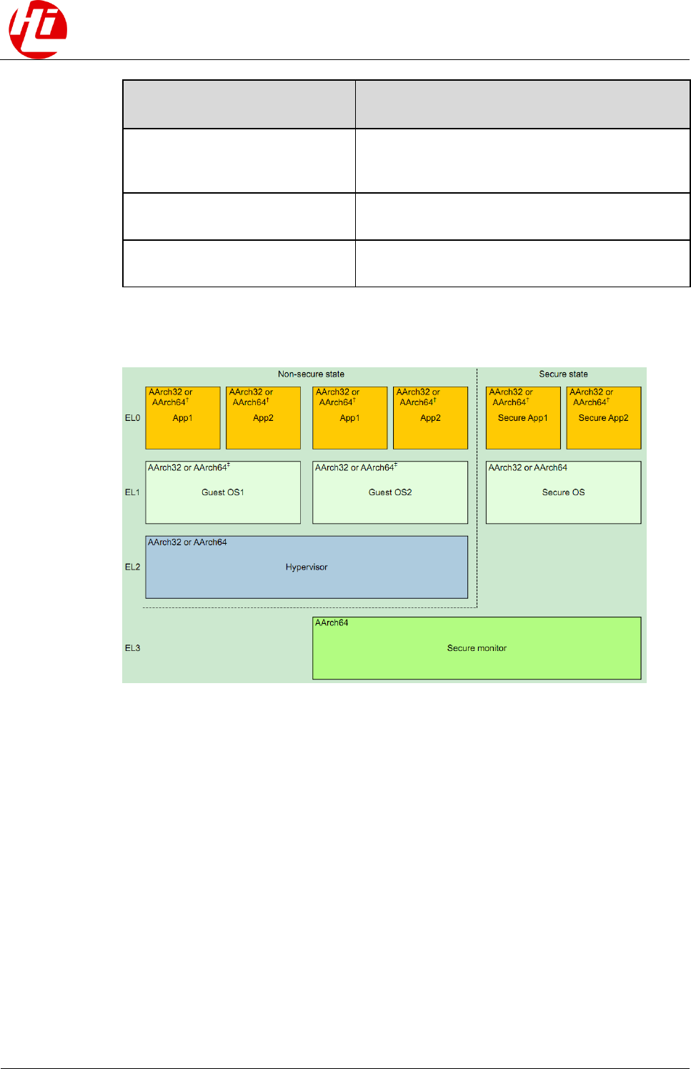
Hi3660
Data Sheet
3 Mobile Processing Module
Issue 05 (2016-12-22)
HiSilicon Proprietary and Confidential
Copyright © HiSilicon Technologies Co., Ltd.
3-3
Exception Level of the
Processor
Description
EL1
Running mode of the operating system, privileged,
one mode for the Secure World and one mode for
the Non-Secure World
EL2
Mode used for virtualization extension, used only in
the Non-Secure World
EL3
Mode used to switch between the Secure World and
Non-Secure World
Figure 3-1 Relationship between the running modes
3.1.3 Coherency Bus
The data coherency between the big and LITTLE cores in the big.LITTLE architecture is
implemented by using the ARM coherency bus CCI-550. The CCI-550 has the following
features:
- Supports the AMBA FULL-ACE and AMBA ACE-Lite protocols and implements data
coherency between the big and LITTLE cores as well as other coherency masters.
- Supports the crossbar bus interconnection structure, allowing the upstream master to
access the memory and configuration space.
- Implements the snoop filter to improve the snoop performance between coherency
masters.
- Supports Distributed Virtual Memory (DVM) message broadcasting between the big and
LITTLE cores.
- Supports the bandwidth-based quality of service (QoS) traffic management mechanism.
- Configures the granularity and mode of static interleaving.

Hi3660
Data Sheet
3 Mobile Processing Module
Issue 05 (2016-12-22)
HiSilicon Proprietary and Confidential
Copyright © HiSilicon Technologies Co., Ltd.
3-4
- Uses the PMU counter to collect performance statistics of the master, slave, and global
events.
- Implements the CCI automatic gating mechanism using the Q-channel handshake.
- Implements the dynamic retention function of the RAM in the CCI using the P-channel
handshake.
- Controls the coherency and bus functions using the advanced peripheral bus (APB) slave
configuration interface.

Hi3660
Data Sheet
Contents
Issue 05 (2016-12-22)
HiSilicon Proprietary and Confidential
Copyright © HiSilicon Technologies Co., Ltd.
i
Contents
Contents .............................................................................................................................................. i
Figures ............................................................................................................................................... ii
Tables ............................................................................................................................................... iii
4 System Control ........................................................................................................................... 4-1
4.1 SC .................................................................................................................................................................. 4-1
4.1.1 CRG ..................................................................................................................................................... 4-1
4.1.2 SCTRL ................................................................................................................................................. 4-2
4.1.3 PCTRL ................................................................................................................................................. 4-3
4.2 RTC ............................................................................................................................................................... 4-3
4.2.1 Function Description ............................................................................................................................ 4-3
4.2.2 Register Description ............................................................................................................................. 4-4
4.3 Watchdog ....................................................................................................................................................... 4-4
4.3.1 Function Description ............................................................................................................................ 4-4
4.3.2 Register Description ............................................................................................................................. 4-5
4.4 GIC ................................................................................................................................................................ 4-5
4.4.1 Function Description ............................................................................................................................ 4-5
4.4.2 Register Description ............................................................................................................................. 4-6
4.5 DMAC ........................................................................................................................................................... 4-7
4.5.1 Overview .............................................................................................................................................. 4-7
4.5.2 Application Background ...................................................................................................................... 4-7
4.5.3 Function Description ............................................................................................................................ 4-8
4.5.4 Application Description ....................................................................................................................... 4-8
4.5.5 Register Description ........................................................................................................................... 4-10

Hi3660
Data Sheet
Figures
Issue 05 (2016-12-22)
HiSilicon Proprietary and Confidential
Copyright © HiSilicon Technologies Co., Ltd.
ii
Figures
Figure 4-1 GIC architecture................................................................................................................................ 4-5

Hi3660
Data Sheet
Tables
Issue 05 (2016-12-22)
HiSilicon Proprietary and Confidential
Copyright © HiSilicon Technologies Co., Ltd.
iii
Tables
Table 4-1 DMAC registers. .............................................................................................................................. 4-10

Hi3660
Data Sheet
4 System Control
Issue 05 (2016-12-22)
HiSilicon Proprietary and Confidential
Copyright © HiSilicon Technologies Co., Ltd.
4-1
4 System Control
4.1 SC
4.1.1 CRG
The clock and reset generator (CRG) is provides clocks and reset for each IP. This section
describes only the AO CRG and PERIPH CRG functions. The functions of other CRGs are
described in the clock reset section of the corresponding modules.
4.1.1.1 AOCRG
The AO CRG has the following functions:
- Provides clock reset for each IP in the system area.
- Implements software control and state query for the clock reset and configures the clock
divider for each IP in the system area.
- Supports automatic frequency scaling of the always-on network on chip (AONOC).
4.1.1.2 PERICRG
The PERIPH CRG has the following functions:
- Accesses registers over the advanced peripheral bus (APB) interface.
- Isolates the securely-accessed register area from the non-securely-accessed register area.
- Provides clock reset for each IP and the NOC bus in the peripheral area.
- Supports software control and state query for the clock reset of each IP and the NOC bus
in the peripheral area.
- Configures the clock divider for each IP and the NOC bus in the peripheral area.
- Provides the software configuration interfaces and state query interfaces for the A73_B,
A53_L, LPM3, CCI500, ADB, and CoreSight modules.
- Supports the anti-suspension function of the APB and advanced high-performance bus
(AHB) interfaces.
- Supports enable control for timer clocks and watchdog clocks in the peripheral area.

Hi3660
Data Sheet
4 System Control
Issue 05 (2016-12-22)
HiSilicon Proprietary and Confidential
Copyright © HiSilicon Technologies Co., Ltd.
4-2
− Enables the counting frequency to be independent of the system clock frequency. If
the system clock changes, the counter maintains the original counting frequency.
− Samples the input counting clocks to generate clock enable signals, and outputs the
signals to the timers 4–7 in the peripheral area.
− Selects the counting clock source for the timers in the peripheral area (32 kHz or 4.8
MHz).
− Forcibly pulls the timers in the peripheral area up through software configuration. In
this case, the operating clock of the timer is the bus clock.
− Forcibly pulls the watchdog in the peripheral area up through software configuration.
In this case, the operating clock of the watchdog is the bus clock.
If the watchdog in the peripheral area is not forcibly pulled up, the counting clock for
the watchdog in the peripheral area is 32 kHz.
- Controls the power-on/power-off state machine of the A73_B and A53_L cores.
− Allows the software to enable or disable the state machine used to power on and
power off A73_B and A53_L cores by configuring registers.
− Allows the software to configure whether to report the A73_B/A53_L power-
on/power-off completion interrupt and query the interrupt state when the state
machine is enabled.
− Responds to the generic interrupt controller (GIC) interrupt and powers on the
corresponding cores of A73_B and A53_L cores when the state machine is enabled.
Whether to respond to the GIC interrupt can be separately configured for each core of
A73_B and A53_L.
− Allows the software to independently power on each core of A73_B and A53_L by
writing to corresponding registers when the power-on/power-off state machine is
enabled.
− Allows the software to independently power off each core of A73_B and A53_L by
writing to corresponding registers when the power-on/power-off state machine is
enabled.
− Queries the state of the power-on/power-off state machine for each core of A73_B
and A53_L in real time when the state machine is enabled.
− Independently configures the reset time, reset deassertion time, MTCMOS power-on
wait time, ISO wait time, ISO deassertion wait time, DBG configuration wait time
during the power-on/power-off process of each core of A73_B and A53_L.
- Controls the A73_B ocldo state machine.
− Allows the state machine to respond to the independent ocldo request signal of
starting the state machine for the four big cores.
− Allows the state machine to control the mtcmos control signal of the four big cores.
− Allows the state machine to control the ISO clamping signal of the four big cores.
This function can be statically bypassed.
− Allows the state machine to control the ocldo enable signal of the four big cores.
− Allows the software to query the state of the state machine.
- Supports automatic gating and frequency scaling for the double data rate (DDR) clocks.
4.1.2 SCTRL
The system controller (SC) provides system control interfaces and consists of the following
modules:

Hi3660
Data Sheet
4 System Control
Issue 05 (2016-12-22)
HiSilicon Proprietary and Confidential
Copyright © HiSilicon Technologies Co., Ltd.
4-3
- APB interface module
- System main control module
- Interrupt response mode request module
- Power-on/Power-off control module
- Universal counter module
- Crystal oscillator control module
- Low-power random access memory (LPRAM) low-power control module
- eFUSE control module
The SC has the following features:
- Bus interface
The bus interface complies with the advanced microcontroller bus architecture 2.0
(AMBA 2.0) APB Slave Interface Specifications, and supports 32-bit data width and 12-
bit address width.
- Reset
− The SC supports preset_n reset.
− Global soft reset is supported, and the global soft reset request is sent to the CRG.
4.1.3 PCTRL
The peripheral controller (PCTRL) provides configuration interfaces for some external IPs.
The PCTRL takes effect only after the system enters the normal mode. Therefore, ensure that
the system is in normal mode before using any PCTRL function.
The PCTRL has the following functions:
- Supports 3D LCD raster control.
- Provides configuration interfaces for some peripheral IPs.
- Supports resource locks.
4.2 RTC
4.2.1 Function Description
The real-time clock (RTC) is used to display the time in real time and periodically generate
alarms. The Hi3660 provides three RTCs: RTC0 to RTC2.
The RTC works based on a 32-bit up counter. The initial count value is loaded from the
RTCLR register. The count value is incremented by 1 on the rising edge of each counting
clock. When the count value of RTCDR is the same as the value of RTCMR, the RTC
generates an interrupt. Then the counter continues counting in incremental mode on the next
rising edge of the counting clock.
The RTC uses a 1 Hz counting clock to convert the count value into a value in the format of
year, month, day, hour, minute, and second.
The RTC has the following features:
- Allows you to configure the initial count value.
- Allows you to configure the match value.

Hi3660
Data Sheet
4 System Control
Issue 05 (2016-12-22)
HiSilicon Proprietary and Confidential
Copyright © HiSilicon Technologies Co., Ltd.
4-4
- Generates the timeout interrupt.
- Supports soft reset.
4.2.2 Register Description
See the SP804 manual of the ARM timer IP
(http://infocenter.arm.com/help/index.jsp?topic=/com.arm.doc.ddi0270b/index.html).
4.3 Watchdog
4.3.1 Function Description
The watchdog is used to send a reset signal to reset the entire system within a period after
exceptions occurs in the system. The Hi3660 provides two watchdogs: WD0 and WD1.
The watchdog has the following features:
- Supports a 32-bit down counter. The counting clock is configurable.
- Supports configurable timeout interval (initial count value).
- Locks registers to prevent them from being modified incorrectly.
- Generates timeout interrupts.
- Generates reset signals.
- Supports the debugging mode.
The watchdog works based on a 32-bit down counter. The initial count value is loaded from
the WdogLoad register. When the watchdog clock is enabled, the count value is decremented
by 1 on the rising edge of each counting clock. When the count value is decremented to 0, the
watchdog generates an interrupt. On the next rising edge of the counting clock, the counter
reloads the initial count value from WdogLoad, and then continues counting decreasingly.
If the count value is decremented to 0 for the second time and the CPU does not clear the
watchdog interrupt, the watchdog sends a reset signal and the counter stops counting.
You can determine whether to allow the watchdog to generate interrupts and reset signals by
configuring WdogControl.
- When interrupt generation is disabled, the counter stops counting.
- When interrupt generation is enabled again, the watchdog counter counts from the
configured value of WdogLoad instead of the last count value. The initial count value
can be reloaded before an interrupt is generated.
The counting clock of the watchdog can be a sleep clock or a bus clock, which provides
different count time ranges.
You can disable the operation of writing to the watchdog registers by configuring WdogLock.
- Writing 0x1ACC_E551 to WdogLock enables the write permission for all watchdog
registers.
- Writing any other value to WdogLock disables the write permission for all watchdog
registers (except WdogLock).
Hi3660
Data Sheet
4 System Control
Issue 05 (2016-12-22)
HiSilicon Proprietary and Confidential
Copyright © HiSilicon Technologies Co., Ltd.
4-5
The write permission control feature prevents watchdog registers from being incorrectly
modified by the software. In this way, the watchdog operation will not be incorrectly
terminated by the software when exceptions occur.
In ARM debugging mode, the watchdog is automatically disabled to avoid intervention to
normal debugging operations.
The watchdog must be disabled before the system enters the sleep mode.
4.3.2 Register Description
See the SP805x manual of the ARM watchdog IP
(http://infocenter.arm.com/help/index.jsp?topic=/com.arm.doc.ddi0270b/index.html).
4.4 GIC
4.4.1 Function Description
The GIC is used to detect, manage, and allocate external interrupts, internal interrupts, and
software-generated interrupts (SGIs). The GIC supports security extension and virtualization
extension.
Figure 4-1 GIC architecture
Distributor
AXI
interface
CPU interface
Virtual CPU interface
registers
Processor
Virtual interface contorl
registers Hypervisor
Virtual distributor
GIC
Virtual interface control
registers
Virtual CPU interface
registers
CPU interface
VFIQ/VIRQ
Generating virtual
interrupts
Physical interrupts
Interrupts
The GIC has the following features:
- Supports three types of interrupts: SGIs, private peripheral interrupts (PPIs), and shared
peripheral interrupts (SPIs).
- Supports two interrupt trigger modes: level-sensitive mode and edge-triggered mode.
The trigger mode of each interrupt source can be separately configured.

Hi3660
Data Sheet
4 System Control
Issue 05 (2016-12-22)
HiSilicon Proprietary and Confidential
Copyright © HiSilicon Technologies Co., Ltd.
4-6
- Provides an interface for each CPU core to process the physical fast interrupt request
(FIQ) and interrupt request (IRQ).
- Supports virtualization extension and virtualizes only the physical IRQs; generates the
virtual FIQ (VFIQ) and virtual IRQ (VIRQ) through configuration and adds an interface
for each CPU core to process the VFIQ and VIRQ.
- Supports interrupt routing. The physical interrupts are routed to the corresponding CPU
core by querying the target processor register. The Hypervisor configures the target
processor register based on the virtual machine ID (VMID) information. The virtual
interrupts are routed to the corresponding CPU core based on the configured route target.
- Separately enables interrupts.
- Queries the interrupt states.
- Masks interrupts and configures the Mask Priority. An interrupt is reported only when its
priority is greater than Mask Priority.
- Supports interrupt nesting.
− For physical interrupts, the depth of interrupt nesting is determined by the Group
Priority. Interrupt nesting is triggered only when the Group Priority is a large value.
The number of Group Priority levels is configurable.
− For virtual interrupts, the depth of interrupt nesting is 32.
- Provides the following for each CPU core:
− Six PPIs of internal components. The PPIs of one core are independent of those of the
other cores.
− One internal virtual maintenance PPI
− One BypassFIQ input and one BypassIRQ input
- Supports TrustZone extension. The input interrupts can be classified into the Secure
group or the Non-Secure group. A smaller interrupt priority value indicates a higher
interrupt priority.
For the physical interrupts, the priority of all the Secure interrupts is higher than that of
Non-Secure interrupts.
− In Secure mode, the interrupt priority field is at least 5 bits, and can be extended to at
most 8 bits.
− In Non-Secure mode, the interrupt priority field is at least 4 bits, and can be extended
to at most 7 bits.
For the virtual interrupts, the number of priority levels is fixed at 32.
- Locks SPIs and support 32 lockable shared peripheral interrupts (LSPIs). The LSPIs
must be Secure interrupts, and their configuration registers cannot be modified after
these interrupts are locked.
- Supports interrupt wakeup events and reserves the nFIQOUT signal. Directly output over
the port, the nIRQOUT signal can report interrupts as wakeup events when the GIC is
disabled.
4.4.2 Register Description
See the ARM GIC-400 manual
(http://infocenter.arm.com/help/index.jsp?topic=/com.arm.doc.ddi0270b/index.html).

Hi3660
Data Sheet
4 System Control
Issue 05 (2016-12-22)
HiSilicon Proprietary and Confidential
Copyright © HiSilicon Technologies Co., Ltd.
4-7
4.5 DMAC
4.5.1 Overview
The advanced eXtensible interface (AXI) direct memory access controller (DMAC) is a low-
cost and high-performance IP targeted for the system-on-chip (SoC) chip. It is based on the
AMBA AXI protocol. Direct memory access (DMA) is an operating mode in which data
transfer is completely implemented by the hardware. In DMA mode, the DMAC transfers data
using a master bus controller that is independent of the processor. Data is transferred between
memories, or between a memory and a peripheral. The DMA mode applies to data block
transfer at a high speed. After receiving a DMA request, the DMAC enables the master bus
controller based on the CPU settings and transmits address and read/write control signals to
memories or peripherals. The DMAC also counts the number of data transfers and reports
data transfer completion to the CPU in interrupt mode.
The DMAC of the Hi3660 has the following features:
- A total of 16 logical channels
- Programmable logical channel priority
- An AXI master interface
- An APB 2.0 configuration interface
- A total of 32 sets of peripheral requests (Each set of peripheral request includes single
requests and burst requests.)
- Data transfer from a memory to another memory, from a memory to a peripheral, and
from a peripheral to a memory
- DMAC flow control when data is transferred between memories and peripherals
- Linked-list data transfer
- Link transfer of the logical channels
- One-dimensional, two-dimensional, and three-dimensional data transfer modes
- Four sets of interrupts
- Consistency operations and non-consistency operations
- Secure transfer, non-secure transfer, and interrupt reporting
4.5.2 Application Background
The DMA is an operating mode in which I/O switching is fully implemented by the hardware.
In DMA mode, the DMAC directly transfers data between a memory and a peripheral, or
between memories. This avoids the processor intervention and reduces the interrupt
processing overhead of the processor.
The DMA mode applies to data block transfer at a high speed. After receiving a DMA transfer
request, the DMAC enables the master bus controller based on the CPU settings and transmits
address and read/write control signals to memories or peripherals. The DMAC also counts the
number of data transfers and reports data transfer completion or errors to the CPU in interrupt
mode.
The DMAC improves the system performance from the following aspects:
- The DMAC implements data transfer, reducing the CPU load.
- Channels are allocated to the I/O peripherals based on DMAC programming. As a result,
large-amount data is transferred and the interrupt reporting frequency is reduced.

Hi3660
Data Sheet
4 System Control
Issue 05 (2016-12-22)
HiSilicon Proprietary and Confidential
Copyright © HiSilicon Technologies Co., Ltd.
4-8
4.5.3 Function Description
The DMAC consists of the following components:
- A DMAC hardware request interface
- A total of 16 channels
- An arbiter
- An AXI master interface
- An APB slave interface
For a DMA data transfer, a logical channel of the DMAC must be triggered first. Then the
master interface reads data from the source address and writes it to the destination address.
DMAC hardware request I/F is used by peripherals to request the DMAC to transfer data.
The following describes a data transfer triggered by the software:
The processor configures a logical channel through the APB slave interface, and specifies the
source address, destination address, and transfer mode. Then the DMAC is triggered to
perform the transfer operation. After the arbiter arbitrates channels, the DMAC reads data
from the source address from the AXI master interface and writes data to the destination
address based on the configured information. In this way, an interrupt is generated.
4.5.4 Application Description
4.5.4.1 Initialization Configuration
To configure the DMAC during system initialization, perform the following steps:
Step 1 Configure the channel parameter registers based on the required transfer, including
CX_AXI_SPECIAL, CX_SRC_ADDR, CX_DES_ADDR, CX_LLI, CX_CNT0, CX_CNT1,
CX_BINDX, and CX_CINDX.
For a one-dimensional non-linked-list transfer, if the AXI cache operation is not required,
configure only CX_SRC_ADDR, CX_DES_ADDR, and CX_CNT0. This reduces the time of
configuring registers.
For a one-dimensional non-linked-list transfer, configure only CX_SRC_ADDR,
CX_DES_ADDR, CX_CNT0, and CX_CONFIG. This reduces the time of configuring
registers. Ensure that other registers are set to default values.
Step 2 Specify the transfer mode, peripheral ID, and bus operation parameters by configuring
CX_CONFIG.
Step 3 Set CX_CONFIG bit[0] to 1 to enable a channel to start the DMAC transfer.
----End
The sequence of step 1 and step 2 is exchangeable. Ensure that CX_CONFIG bit[0] is set to 1
to start the transfer.

Hi3660
Data Sheet
4 System Control
Issue 05 (2016-12-22)
HiSilicon Proprietary and Confidential
Copyright © HiSilicon Technologies Co., Ltd.
4-9
4.5.4.2 Typical Configuration Processes
Memory Transfer
The following describes the one-dimensional INCR memory transfer(32-bit burst size and 8-
bit burst length):
Step 1 Enable the clocks and deassert reset.
Step 2 Configure the interrupt mask register to enable all the interrupts.
Step 3 Determines the logical channel used for the transfer. The registers of the selected channel are
configured in the following steps.
Step 4 Configure the channel parameter registers based on the required transfer, including
CX_AXI_SPECIAL, CX_SRC_ADDR, CX_DES_ADDR, CX_LLI, and CX_CNT0.
For a one-dimensional non-linked-list transfer, if the AXI cache operation is not required,
configure only CX_SRC_ADDR, CX_DES_ADDR, and CX_CNT0. This reduces the time of
configuring registers. That is, configure the source address, destination address, and amount
of the data to be transferred.
If there are requirements on the security attribute, configure CX_AXI_SPECIAL. Otherwise,
the secure channel is used by default.
For a one-dimensional non-linked-list transfer, configure only CX_SRC_ADDR,
CX_DES_ADDR, CX_CNT0, and CX_CONFIG. This reduces the time of configuring
registers. Ensure that other registers are set to default values.
Step 5 Configure CX_CONFIG to specify the transfer mode and bus operation parameters. The
peripheral ID is not required for memory transfer. The flow control mode must be set to "00:
transfer between memories, DMAC flow control".
1. Set CX_CONFIG bit[31] and bit[30] to 1 to configure the operations of transferring the
source address and destination address in DMA mode as INCR operations.
2. Set CX_CONFIG bit[27:24] and bit[23:20] to 0111 to configure the burst length for
transferring the source address and destination address in DMA mode as 8.
3. Set CX_CONFIG bit[18:16] and bit[14:12] to 010 to configure the data width for
transferring the source address and destination address in DMA mode as 32 bits.
4. Set CX_CONFIG bit[3:2] to 00 to configure the flow control mode of the DMA transfer
as DMA flow control for memory transfer.
Step 6 Set CX_CONFIG bit[0] to 1 to enable a channel to start the DMAC transfer.
----End
Peripheral Transfer
The following describes the one-dimensional transfer from the memory to the peripheral
(DMA flow control, 32-bit burst size, and 8-bit burst length):
Step 1 Repeat Step 1 and Step 2 in "Memory Transfer."
Step 2 Determines the logical channel used for the transfer. The registers of the selected channel are
configured in the following steps.
Step 3 Configure the channel parameter registers based on the required transfer, including
CX_AXI_SPECIAL, CX_SRC_ADDR, CX_DES_ADDR, CX_LLI, and CX_CNT0.

Hi3660
Data Sheet
4 System Control
Issue 05 (2016-12-22)
HiSilicon Proprietary and Confidential
Copyright © HiSilicon Technologies Co., Ltd.
4-10
For a one-dimensional non-linked-list transfer, if the AXI cache operation is not required,
configure only CX_SRC_ADDR, CX_DES_ADDR, and CX_CNT0 for the consistency
operation. This reduces the time of configuring registers. That is, configure the source address,
destination address, and amount of the data to be transferred.
If there are requirements on the security attribute, configure CX_AXI_SPECIAL. Otherwise,
the secure channel is used by default.
For a one-dimensional non-linked-list transfer, configure only CX_SRC_ADDR,
CX_DES_ADDR, CX_CNT0, and CX_CONFIG. This reduces the time of configuring
registers. Ensure that other registers are set to default values.
Step 4 Configure CX_CONFIG to specify the transfer mode, peripheral ID, and bus operation
parameters.
Step 5 Set CX_CONFIG bit[31] to 1 and bit[30] to 0 to configure the operation of transferring the
source address in DMA mode as an INCR operation and the operation of transferring the
destination address in DMA mode as an FIX operation because a peripheral is connected.
Set CX_CONFIG bit[27:24] and bit[23:20] to 0111 to configure the burst length for
transferring the source address and destination address in DMA mode as 8.
Set CX_CONFIG bit[18:16] and bit[14:12] to 010 to configure the data width for transferring
the source address and destination address in DMA mode as 32 bits.
Set CX_CONFIG bit[9:4] to the ID of the selected peripheral. The peripheral ID is unique to
the corresponding peripheral and is allocated in advance.
Set CX_CONFIG bit[3:2] to 01 to configure the flow control mode of the DMA transfer as
DMA flow control for peripheral transfer.
Step 6 Set CX_CONFIG bit[0] to 1 to enable a channel to start the DMAC transfer.
----End
4.5.5 Register Description
The base address of AP DMAC registers is 0xFDF30000.
Table 4-1 DMAC registers.
Offset
Register
Register Description
0x0000 + 0x40 x in
INT_STAT
Interrupt status register of processor X
0x0004 + 0x40 x in
INT_TC1
Channel transfer completion interrupt status register of
processor X
0x0008 + 0x40 x in
INT_TC2
Linked list node transfer completion interrupt status register
of processor X
0x000C + 0x40 x in
INT_ERR1
Configuration error interrupt status register of processor X
0x0010 + 0x40 x in
INT_ERR2
Data transfer error interrupt status register of processor X
0x0014 + 0x40 x in
INT_ERR3
Linked list read error interrupt status register of processor X

Hi3660
Data Sheet
4 System Control
Issue 05 (2016-12-22)
HiSilicon Proprietary and Confidential
Copyright © HiSilicon Technologies Co., Ltd.
4-11
Offset
Register
Register Description
0x0018 + 0x40 x in
INT_TC1_MASK
Channel transfer completion interrupt mask register of
processor X
0x001C + 0x40 x in
INT_TC2_MASK
Linked list node transfer completion interrupt mask register
of processor X
0x0020 + 0x40 x in
INT_ERR1_MASK
Configuration error interrupt mask register of processor X
0x0024 + 0x40 x in
INT_ERR2_MASK
Data transfer error interrupt mask register of processor X
0x0028 + 0x40 x in
INT_ERR3_MASK
Linked list read error interrupt mask register of processor X
0x0600
INT_TC1_RAW
Raw channel transfer completion interrupt status register
0x0608
INT_TC2_RAW
Raw linked list node transfer completion interrupt status
register
0x0610
INT_ERR1_RAW
Raw configuration error interrupt status register
0x0618
INT_ERR2_RAW
Raw data transfer error interrupt status register
0x0620
INT_ERR3_RAW
Raw linked list read error interrupt status register
0x660
SREQ
Single transfer request register
0x664
LSREQ
Last single transfer request register
0x668
BREQ
Burst transfer request register
0x66C
LBREQ
Last burst transfer request register
0x670
FREQ
Bulk transfer request register
0x674
LFREQ
Last bulk transfer request register
0x688
CH_PRI
Priority control register
0x690
CH_STAT
Global DMA status register
0x0694
SEC_CTRL
DMA global security control register
0x0698
DMA_CTRL
DMA global control register
0x0700 + 0x10 x cn
CX_CURR_CNT1
Remaining size status register for the three-dimensional
transfer of channel X
0x0704 + 0x10 x cn
CX_CURR_CNT0
Remaining size status register for the one-dimensional and
two-dimensional transfer of channel X
0x0708 + 0x10 x cn
CX_CURR_SRC_ADDR
Source address register of channel X
Hi3660
Data Sheet
4 System Control
Issue 05 (2016-12-22)
HiSilicon Proprietary and Confidential
Copyright © HiSilicon Technologies Co., Ltd.
4-12
Offset
Register
Register Description
0x070C + 0x10 x cn
CX_CURR_DES_ADDR
Destination address register of channel X
0x0800 + 0x40 x cn
CX_LLI
Linked list address register of channel X
0x0804 + 0x40 x cn
CX_BINDX
Two-dimensional address offset configuration register of
channel X
0x0808 + 0x40 x cn
CX_CINDX
Three-dimensional address offset configuration register of
channel X
0x080C + 0x40 x cn
CX_CNT1
Transfer length 1 configuration register of channel X
0x0810 + 0x40 x cn
CX_CNT0
Transfer length configuration register of channel X
0x0814 + 0x40 x cn
CX_SRC_ADDR
Source address register of channel X
0x0818 + 0x40 x cn
CX_DES_ADDR
Destination address register of channel X
0x081C + 0x40 x cn
CX_CONFIG
Configuration register of channel X
0x0820 + 0x40 x cn
CX_AXI_CONF
AXI special operation configuration register of channel X

Hi3660
Data Sheet
Contents
Issue 05 (2016-12-22)
HiSilicon Proprietary and Confidential
Copyright © HiSilicon Technologies Co., Ltd.
i
Contents
Contents .............................................................................................................................................. i
6 Media Processing ....................................................................................................................... 6-1
6.1 Overview ....................................................................................................................................................... 6-1
6.2 VENC ............................................................................................................................................................ 6-1
6.3 VDEC ............................................................................................................................................................ 6-3
6.4 DSS ............................................................................................................................................................... 6-3
6.5 ASP................................................................................................................................................................ 6-3
6.5.1 DSP ...................................................................................................................................................... 6-4
6.5.2 SIO ....................................................................................................................................................... 6-4

Hi3660
Data Sheet
6 Media Processing
Issue 05 (2016-12-22)
HiSilicon Proprietary and Confidential
Copyright © HiSilicon Technologies Co., Ltd.
6-1
6 Media Processing
6.1 Overview
The Hi3660 integrates a powerful multimedia processing subsystem. This subsystem is used
for applications such as picture capturing and processing, LCD control, video
encoding/decoding acceleration, 2D/3D graphics acceleration, and audio capturing/output
processing.
6.2 VENC
The Hi3660 integrates the H.264/H265/JPEG hardware video encoder (VENC), which
supports the H.264/H265/JPEG encoding standard, respectively.
The VENC has the following features:
- One JPEG encoder
− ITU-T T.81 Baseline (sequential) discrete cosine transform (DCT)-based coding
− Input data formats: 420PL111YCbCr8, 420PL12YCbCr8, 420PL12YCrCb8,
422PL111YCbCr8, 422PL12YCbCr8, 422PL12YCrCb8, 422IL3YCbYCr8,
422IL3YCrYCb8, 422IL3CbYCrY8, and 422IL3CrYCbY8
− Output data formats: JFIF 1.02 and non-progressive JPEG
− Maximum 16K x 16K pixels, 16-pixel horizontal/vertical step
- One H.264 encoder
− Features supported by H.264 Baseline Profile
I slice and P slice
The 4 x 4 and 16 x 16 intra-frame division methods support the DC/V/H prediction
mode.
The 8 x 8 and 16 x 16 inter-frame division methods are supported.
The MB-level bit rate control is supported.
The inter-frame prediction is supported for the 1/2 and 1/4 pixels.
The cosine transform supports Hadamard transform.
De-blocking is supported.
− New feature supported by H.265 Main Profile on the basis of H.264 Baseline Profile
The context-adaptive binary arithmetic coding (CABAC) is supported.

Hi3660
Data Sheet
6 Media Processing
Issue 05 (2016-12-22)
HiSilicon Proprietary and Confidential
Copyright © HiSilicon Technologies Co., Ltd.
6-2
− New features supported by H.265 High Profile on the basis of H.264 Baseline Profile
Apart from the 4 x 4 conversion, the 8 x 8 conversion is also supported.
The 8 x 8 intra-frame prediction is supported.
− Input data formats
Planar YUV 4:2:0
Planar YUV 4:2:2
Semi-planar YUV 4:2:0
Semi-planar YVU 4:2:0
Package UYVY4:2:2, VYUY4:2:2
Package YUYV4:2:2, YVYU4:2:2
ARGB/BGRA8888
ABGR/RGBA8888
− Output data formats: raw streams in the preceding formats
− Maximum 4K x 2K pixels, 2-pixel horizontal/vertical step
− Maximum frame rate of 720p@240 fps
− Maximum bit rate of 80 Mbit/s
− 4K x 2K@30 fps performance for a single pipe
− Frame storage format: linear
− Minimum size of 176 x 144
− Maximum 1/4x horizontal/vertical scaling
− Region of interest (ROI) encoding
− Multi-channel encoding: 4-channel H.264 encoding
- One H.265 encoder
− Features supported by H.265 Main Profile
I slice and P slice
The 4 x 4, 8x 8, 16 x 16, and 32 x 32 intra-frame division methods are supported. The
4 x 4, 8x 8, and 16 x 16 division methods support 35 prediction modes. The 32 x 32
division supports the DC/Planar prediction mode.
The 8x 8, 16 x 16, 32 x 32, and 64 x 64 inter-frame division methods are supported.
The CU-level bit rate control is supported.
The ±512 horizontal integer search and ±144 vertical integer search are supported.
The inter-frame prediction is supported for the 1/2 and 1/4 pixels.
DCT4/8/16/32 and DST4 are supported.
Merge and MergeSkip are supported.
TMV is supported.
De-blocking and sample adaptive offset (SAO) are supported.
− Input data formats
Planar YUV 4:2:0
Planar YUV 4:2:2
Semi-planar YUV 4:2:0
Semi-planar YVU 4:2:0
Package UYVY4:2:2, VYUY4:2:2

Hi3660
Data Sheet
6 Media Processing
Issue 05 (2016-12-22)
HiSilicon Proprietary and Confidential
Copyright © HiSilicon Technologies Co., Ltd.
6-3
Package YUYV4:2:2, YVYU4:2:2
ARGB/BGRA8888
ABGR/RGBA8888
− Output data formats: raw streams in the preceding formats
− Maximum 4K x 2K pixels, 2-pixel horizontal/vertical step
− Maximum frame rate of 720p@240 fps
− Maximum bit rate of 60 Mbit/s
− 4K x 2K@30 fps performance for a single pipe
− Frame storage format: linear
− Minimum size of 176 x 144
− Maximum 1/4x horizontal/vertical scaling
− ROI encoding
− Multi-channel encoding: 4-channel H.265 encoding
6.3 VDEC
The Hi3660 integrates a video decoder (VDEC), which supports the H.265, H.264, MPEG1,
MPEG2, MPEG4, VC1 (including WMV9), VP6, and VP8 protocols.
The VDEC consists of the video firmware (VFMW) running on the ARM processor and an
embedded hardware video decoding engine. The VFMW obtains streams from the upper-layer
software, parses the streams, and calls the video decoding engine to generate the image
decoding sequences. Under the control of the upper-layer software, the downstream module
outputs the sequences to a monitor or other devices.
6.4 DSS
The display subsystem (DSS) implements overlaying and 3D synthesis for multiple graphics
layers such as the Base, Video, and Graphic, and sends the overlaid or synthesized pixels to
the Display Serial Interface (DSI) or HDMI for displaying.
6.5 ASP
The audio signal processor (ASP) is a subsystem used to manage and process various audio
and voice data applications. The ASP supports the following application scenarios:
- Audio playing
- Audio recording
- Digital FM playing
- Bluetooth voice dialing (audio recording)
- Uplink and downlink calling
- Audio mixing
- Voice wakeup

Hi3660
Data Sheet
6 Media Processing
Issue 05 (2016-12-22)
HiSilicon Proprietary and Confidential
Copyright © HiSilicon Technologies Co., Ltd.
6-4
6.5.1 DSP
The audio digital signal processor (DSP) uses the Tensilica Hi-Fi 3.0 processor, and
implements HD video sound decoding (such as DTS) and post-processing as well as common
audio decoding (such as MP3) of the dedicated player.
6.5.2 SIO
The Sonic Input/Output (SIO) interface connects to the off-chip audio codec to play and
record music (voice). The SIO transfers the digital data that complies with the I2S/PCM
protocol. The ASP integrates two SIOs: SIO0 and SIO2. SIO0 is SIO_AUDIO, which plays
and records music, and supports the inputs and outputs in the I2S and PCM formats. SIO2 is
SIO_BT, which is used for Bluetooth calling.
- The SIO module supports the master and slave modes as well as playing transmit (TX)
and recording receive (RX).
- The SIO module supports the I2S and PCM interface timings. The interface signal lines
in two modes are multiplexed.
- The SIO module supports only the inputs of the clock and synchronization signals. In I2S
master mode, the SIO module needs to work with the CRG module and the CRC module
sends the clock and synchronization signals to the outside.
The SIO module has the following features in I2S mode:
- The I2S interface supports the 16-bit, 18-bit, 20-bit, 24-bit, and32-bit transfer modes.
- The 8–192 ksps sampling rate is supported.
- The extended module supports 2-/4-/8-/16-channel RX and 8-/16-bit transfer mode.
- The I2S RX and TX channels have independent FIFOs. The audio-left and audio-right
channels each has an independent FIFO. The FIFO depth is 16 and the width is 32 bits.
- The I2S interface supports the function of disabling the FIFO. When a FIFO is disabled,
the RX and TX data is stored in a buffer rather than the FIFO.
- The I2S interface allows the TX and RX channels to be separately enabled. If a channel is
disabled, the control unit and data storage unit of this channel are not reversed. In this
way, power consumption is saved.
- For the I2S interface in 16-bit transfer mode, the RX/TX data of the audio-left and audio-
right channels can be combined into one 32-bit data segment and then stored/written into
the RX/TX FIFO. In this way, the buffering capacity of the FIFO is improved. The
extended module does not support this combination function.
- The RX channel supports upper-bit sign extension.
- The TX and RX audio channel selection signals can be the same, facilitating connection
with the 4-wire codec.
The SIO module has the following features in PCM mode:
- The 8-bit and 16-bit transfer modes are supported.
- The extended module supports 2-/4-/8-/16-channel RX and 8-/16-bit transfer mode.
- Only the short frame synchronization mode is supported. Both the standard and
customized timing modes are supported.
- The RX and TX channels have independent FIFOs. The FIFO depth is 16 and the width
is 32 bits.
- The FIFO can be disabled. When a FIFO is disabled, the RX and TX data is stored in a
buffer rather than the FIFO.

Hi3660
Data Sheet
6 Media Processing
Issue 05 (2016-12-22)
HiSilicon Proprietary and Confidential
Copyright © HiSilicon Technologies Co., Ltd.
6-5
- The TX and RX channels can be separately enabled. If a channel is disabled, the control
unit and data storage unit of this channel are not reversed. In this way, power
consumption is saved.
- The RX channel supports upper-bit sign extension.
The SIO module also provides the CPU/DSP access interface, which has the following
features:
- The CPU/DSP can access the SIO using the advanced high-performance bus (AHB)
Slave (AMBA 2.0) interface provided by the SIO module.
- The SIO AHB interface supports only 32-bit operations.
- The SIO AHB interface supports only the OK response, and does not support the
ERROR, Retry, and Split responses.
- The SIO AHB interface supports various burst operations.
- The SIO supports direct memory access (DMA) operations in burst mode.
- The SIO allows the audio-left and audio-right channels to use the same TX address for
the TX data and the same RX address for the RX data.
- The master and slave modes of the SIO module differ in the sources of the clock (BCLK) and
sampling rate (ADWS). In master mode, the AP side of Hi3660 generates the clock and sampling
rate. In slave mode, the AUDIO_CODEC side generates the clock and sampling rate. The master and
slave modes are not related to the TX and RX.
- If the data width is 24 bits or 32 bits in PCM mode, only the upper-16-bit data is transferred because
the maximum bit width of the SIO is 16.

Hi3660
Data Sheet
Contents
Issue 05 (2016-12-22)
HiSilicon Proprietary and Confidential
Copyright © HiSilicon Technologies Co., Ltd.
i
Contents
Contents .............................................................................................................................................. i
Figures ............................................................................................................................................... ii
Tables ............................................................................................................................................... iii
7 Storage Control ........................................................................................................................... 7-1
7.1 Overview ....................................................................................................................................................... 7-1
7.2 Storage Solution ............................................................................................................................................ 7-1
7.3 eMMC ........................................................................................................................................................... 7-2
7.3.1 Function Description ............................................................................................................................ 7-2
7.3.2 Register Description ............................................................................................................................. 7-3
7.4 SD/SDIO ....................................................................................................................................................... 7-3
7.4.1 Function Description ............................................................................................................................ 7-3
7.4.2 Register Description ............................................................................................................................. 7-5
7.5 UFS ............................................................................................................................................................... 7-5
7.5.1 Function Description ............................................................................................................................ 7-5
7.5.2 Register Description ............................................................................................................................. 7-6

Hi3660
Data Sheet
Figures
Issue 05 (2016-12-22)
HiSilicon Proprietary and Confidential
Copyright © HiSilicon Technologies Co., Ltd.
ii
Figures
Figure 7-1 Functional block diagram of the eMMC controller .......................................................................... 7-2

Hi3660
Data Sheet
Tables
Issue 05 (2016-12-22)
HiSilicon Proprietary and Confidential
Copyright © HiSilicon Technologies Co., Ltd.
iii
Tables
Table 7-1 Storage solution .................................................................................................................................. 7-2

Hi3660
Data Sheet
7 Storage Control
Issue 05 (2016-12-22)
HiSilicon Proprietary and Confidential
Copyright © HiSilicon Technologies Co., Ltd.
7-1
7 Storage Control
7.1 Overview
The Hi3660 provides the following storage control modules:
- Universal Flash Storage (UFS) controller
The UFS controller connects to UFS components.
The protocol version has the following features:
− Compliance with the UFS 2.1, UniPro 1.6, and M-PHY 3.1 protocols
− 2-lane transmit (TX) and receive (RX) channels
− PWM G1–4 and HS G1–3 Rate A/B mode
− Booting from the UFS and using UFS to meet the major non-volatile storage need
- Embedded multimedia card (eMMC) controller
The eMMC controller supports the eMMC 5.1 protocol and controls the 8-bit eMMC 5.1
component. The SoC and external eMMC components support system startup and meet
the major non-volatile storage need of the system.
- SD card controller
The SD card controller supports the SD 3.0 protocol, and is backward compatible with
the SD 2.0 protocol. The controller connects to external SD cards that comply with the
Default-Speed, High-Speed, and UHS-I specifications. The SD card is used to extend the
non-volatile storage capacity of the system.
- DDRC
The double data rate controller (DDRC) supports the 4-channel low-power double data
rate 4 (LPDDR4) synchronous dynamic random access memory (SDRAM). Each
channel supports at most two ranks. As the major dynamic memory of the system, the
LPDDR4 SDRAM provides at most 4-GB dynamic storage space and up to 21.3 GB/s
theoretical access bandwidth.
7.2 Storage Solution
The Hi3660 supports only two storage solutions, as described in Table 7-1.
Hi3660
Data Sheet
7 Storage Control
Issue 05 (2016-12-22)
HiSilicon Proprietary and Confidential
Copyright © HiSilicon Technologies Co., Ltd.
7-2
Table 7-1 Storage solution
No.
Solution Description
1
4-channel LPDDR4 + UFS + SD card
2
4-channel LPDDR4 + eMMC + SD card
- The symmetric 4-channel LPDDR4 SDRAM is supported. The data width of each
channel is 16 bits. Each channel supports at most 2 chip selects. The maximum operating
frequency of the LPDDR4 interface is 1866 MHz.
- The UFS supports the 2-lane TX and RX channels, and the PWM G1–4 and HS G1–3
Rate A/B mode.
- The eMMC supports the 8-bit width and the maximum operating frequency of 200 MHz.
The eMMC is backward compatible with various single data rate (SDR) and DDR
frequencies.
- The SD card supports the 4-bit width and the maximum operating frequency of 200
MHz. The SD card is backward compatible with various frequencies in SDR mode.
7.3 eMMC
7.3.1 Function Description
The eMMC controller is used to receive and transmit commands targeted for the eMMCs and
process the data read and write operations on the eMMCs.
The eMMC controller supports the following features:
- Compliance with the JEDEC eMMC 5.1 protocol
- Enhanced strobe
- Command queue (CQ)
- Auto-tuning
- Direct memory access (DMA) transfer in Single Operation DMA (SDMA) or Advanced
DMA (ADMA) mode
- Cyclic redundancy check (CRC) on the commands and data
Figure 7-1 Functional block diagram of the eMMC controller
AXI master
AHB target
PIO/DMA
controller
Host controller
register set
Block
buffer
FIFO
SD tuning
SD_RECV_CTRL
SD CMD CTRL
SD CMDQ CTRL
SD TIME OUT
SD CARD_DET
SD CLK_GEN
SD
INTF
CTRL
SD host control core
RX FLOPS
TX FLOPS
HS400
FIFO
HS400
FLOPS
I/O
pads
DLL
PHY TOP

Hi3660
Data Sheet
7 Storage Control
Issue 05 (2016-12-22)
HiSilicon Proprietary and Confidential
Copyright © HiSilicon Technologies Co., Ltd.
7-3
The eMMC controller consists of the following units:
- Host interface
The host interface contains the advanced high-performance bus (AHB) target and
advanced eXtensible interface (AXI) master. The AHB target is used to configure
controller registers and directly read data from or write data to the FIFO. The AXI master
is used to read and write data in DMA mode.
- Host controller register set
The Host controller register set is used to configure registers and read/write FIFO data in
Programming Input/Output Model (PIO) mode. The register set supports access to byte
operations.
- PIO/DMA controller
The DMA controller implements the ADMA and SDMA functions. To reduce CPU
interference during the read/write process, the DMA controller also transfers data in
DMA mode when the eMMC is being read or written. The DMA controller can also
directly read data from or write data to the FIFO in PIO mode.
- CQ controller
The CQ controller implements the CQ function and manages the transmission, query,
and execution of tasks.
- Block buffer
The block buffer is a dual-port data read/write interface and implements data transfer and
relay for the bus clock domain and card clock domain.
- Clock generator
The clock generator is used to divide the clock frequency.
- SD tuning control
The SD tuning control implements the automatic tuning of the eMMC, transmits tuning
commands, checks data, and selects the phase.
- PHY TOP
The PHY TOP contains the digital circuits of the interface, analog delay-locked loop
(DLL), and I/O. The analog DLL contains the TX_DLL, RX_DLL, and STROBE_DLL,
which implement the output clock tx_clk, sampling clock rx_clk, and strobe_90 clock,
respectively.
7.3.2 Register Description
For details about the eMMC IP manual, see https://arasan.com/products/emmc51.html.
7.4 SD/SDIO
7.4.1 Function Description
Functional Block Diagram
The SD/SDIO controller processes the read/write operations on the SD card, and supports
extended peripherals such as Wi-Fi devices based on the secure digital input/output (SDIO)
protocol. The Hi3660 provides two SD/SDIO controllers (SD and SDIO0), which are used to
control the SD card and the Wi-Fi device that uses the SDIO interface, respectively.
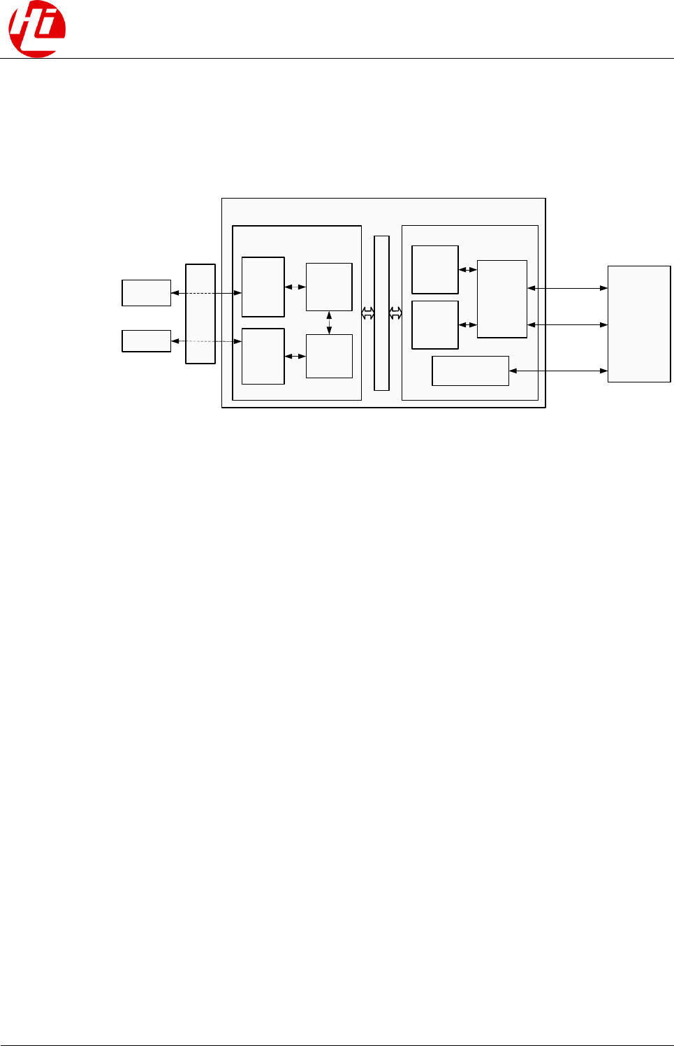
Hi3660
Data Sheet
7 Storage Control
Issue 05 (2016-12-22)
HiSilicon Proprietary and Confidential
Copyright © HiSilicon Technologies Co., Ltd.
7-4
The SD/SDIO controller controls the devices that comply with the following protocols:
- Secure Digital memory (SD mem-version 3.0, compatible with 2.0 and 1.1)
- Secure Digital I/O (SDIO-version 3.0, compatible with 2.0)
Figure 7-2 Functional block diagram of the SD/SDIO controller
CIU
BIU
CPU
Memory
APB
slave
AHB
master Internal
DMA
FIFO
Synchronizer
Mux/
De-mux
unit
CMD
path
Data
path
Clock
control
CLK
DATA[7:0]
CMD
Bus SD/SDIO
SD/SDIO
The SD/SDIO controller connects to the system through the internal bus. It consists of the
following units:
- Bus interface module: Provides the advanced microcontroller bus architecture (AMBA)
AHB master and advanced peripheral bus (APB) slave interfaces. The registers are
configured and the FIFO is read and written through the APB slave interface. The
internal DMA can control the read and write operations on the FIFO data through the
AHB master interface.
- Card interface module: Processes protocol-related contents and clocks.
− Command path: Transmits commands and receives responses.
− Data path: Reads and writes data by working with the command path.
− Codec unit: Encodes and decodes the input and output data based on protocols,
respectively.
− Control unit of the interface clock: Determines whether to enable or disable the
interface clock, or divides the frequency of the cclk_in clock and uses the output
clock as the operating clock of the SD card as required.
The SD/SDIO controller has the following features:
- Internal DMA data transfer
- 256-bit FIFO depth and 32-bit width, configurable FIFO threshold and burst size during
DMA transfer
- FIFO overflow and underflow interrupts used to avoid errors during data transfer
- CRC code generation and check for data and commands
- Configurable interface clock frequency
- Disabling of the SD/SDIO controller clock and interface clock in low-power mode
- 1-bit and 4-bit data transfer and SDIO interrupt detection
- Read/Write operations on data blocks with the size ranging from 1 byte to 512 bytes
- Suspend, resume, and read wait operations on the SDIO card
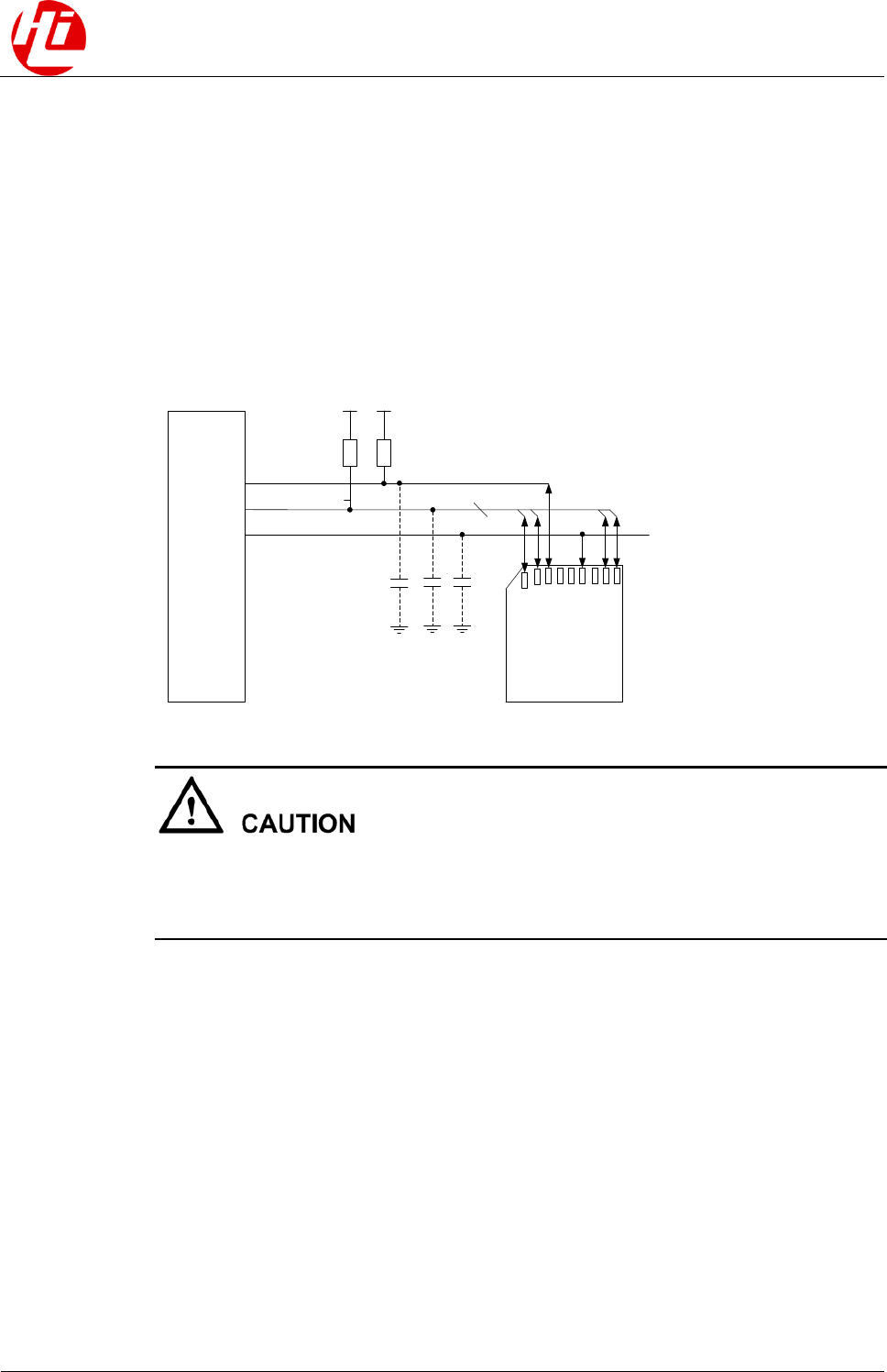
Hi3660
Data Sheet
7 Storage Control
Issue 05 (2016-12-22)
HiSilicon Proprietary and Confidential
Copyright © HiSilicon Technologies Co., Ltd.
7-5
- DDR50 mode not supported
Typical Application
Figure 7-3 shows the typical application circuit of the SD/SDIO controller by taking the SD
card as an example.
The SD/SDIO controller exchanges commands and data with the connected SD card over a
clock signal line, a bidirectional command signal line, and four bidirectional data signal lines.
The command signal and data signal work in pull-up mode.
Figure 7-3 Typical application circuit of the SD/SDIO controller
MMC
98765432
1
RDAT RCMD
CMD
DAT0–3
CLK
C1C2C3
SD/
SDIO
Besides the signal lines in Figure 7-3, the card slot also provides the mechanical write
protection signal and card detection signal. The system can detect the level on the two signal
lines using the GPIO and implement card detection during mechanical write protection and
hot plug.
7.4.2 Register Description
For details about the SD/SDIO IP manual, see
https://www.synopsys.com/dw/ipdir.php?ds=dwc_sd_emmc_host_controller.
7.5 UFS
7.5.1 Function Description
The UFS controller is used to receive and transmit commands targeted for the UFS mass
storage devices and process the data read and write operations on these devices. The UFS is a
simple and high-performance serial interface that supports mass storage media. It is used for
the mobile phone system.

Hi3660
Data Sheet
7 Storage Control
Issue 05 (2016-12-22)
HiSilicon Proprietary and Confidential
Copyright © HiSilicon Technologies Co., Ltd.
7-6
The UFS controller supports the following features:
- Compliance with the JEDEC UFS 2.0 protocol
− Higher speed up to HS-G3 (High-Speed Gear 3)
− Symmetric 2RX-2TX lanes, supporting two lanes
− Auto-hibernate entry and exit sequences
- Compliance with the JEDEC UFSHCI 2.1 protocol
− Up to 32 task requests
− Up to eight task management requests
− Pre-fetching more than one PRD entry (up to 16 PRD entries)
− Clock gating ready design
− Inline encryption (IE)
- Compliance with the MIPI UniPro 1.6 and MIPI UniPro 1.6 protocols
− SKIP symbol insertion
− Scrambling for EMI mitigation
− HS-Gear3 adaption
− Advanced granularity support
7.5.2 Register Description
For details about the UFS IP manual, see https://www.synopsys.com/dw/ipdir.php?ds=ufs.

Hi3660
Data Sheet
Contents
Issue 05 (2016-12-22)
HiSilicon Proprietary and Confidential
Copyright © HiSilicon Technologies Co., Ltd.
i
Contents
Contents .............................................................................................................................................. i
Figures ............................................................................................................................................... ii
Tables ............................................................................................................................................... iii
8 Interface Control ........................................................................................................................ 8-1
8.1 USB3OTG ..................................................................................................................................................... 8-1
8.1.1 Function Description ............................................................................................................................ 8-1
8.1.2 Register Description ............................................................................................................................. 8-2
8.2 UART ............................................................................................................................................................ 8-2
8.2.1 Function Description ............................................................................................................................ 8-2
8.2.2 Signal Description ................................................................................................................................ 8-5
8.2.3 Timing .................................................................................................................................................. 8-6
8.2.4 Register Description ............................................................................................................................. 8-6
8.3 SPI ................................................................................................................................................................. 8-6
8.3.1 Function Description ............................................................................................................................ 8-6
8.3.2 Interrupt Handling ................................................................................................................................ 8-9
8.3.3 Signal Description .............................................................................................................................. 8-10
8.3.4 Timings and Parameters ..................................................................................................................... 8-12
8.3.5 Register Description ........................................................................................................................... 8-16
8.4 I2C ............................................................................................................................................................... 8-16
8.4.1 Function Description .......................................................................................................................... 8-16
8.4.2 Signal Description .............................................................................................................................. 8-19
8.4.3 Timings and Parameters ..................................................................................................................... 8-20
8.4.4 Register Description ........................................................................................................................... 8-22
8.5 GPIO ........................................................................................................................................................... 8-22
8.5.1 Function Description .......................................................................................................................... 8-22
8.5.2 Signal Description .............................................................................................................................. 8-24
8.5.3 Register Description ........................................................................................................................... 8-24

Hi3660
Data Sheet
Figures
Issue 05 (2016-12-22)
HiSilicon Proprietary and Confidential
Copyright © HiSilicon Technologies Co., Ltd.
ii
Figures
Figure 8-1 Logical block diagram of the UART module .................................................................................... 8-3
Figure 8-2 UART frame format .......................................................................................................................... 8-4
Figure 8-3 Typical application scenario of the UART module ........................................................................... 8-4
Figure 8-4 UARTx signals.................................................................................................................................. 8-5
Figure 8-5 UART timing .................................................................................................................................... 8-6
Figure 8-6 UART timing in infrared mode ......................................................................................................... 8-6
Figure 8-7 Functional block diagram of the SPI module .................................................................................... 8-7
Figure 8-8 Application of the SPI connected to a single slave device ................................................................ 8-8
Figure 8-9 Application of the SPI connected to multiple slave devices ............................................................. 8-9
Figure 8-10 Format of a single SPI frame (SPO = 0, SPH = 0) ........................................................................ 8-12
Figure 8-11 Format of consecutive SPI frames (SPO = 0, SPH = 0) ................................................................ 8-12
Figure 8-12 Format of a single SPI frame (SPO = 0, SPH = 1) ........................................................................ 8-13
Figure 8-13 Format of consecutive SPI frames (SPO = 0, SPH = 1) ............................................................... 8-13
Figure 8-14 Format of a single SPI frame (SPO = 1, SPH = 0) ........................................................................ 8-14
Figure 8-15 Format of consecutive SPI frames (SPO = 1, SPH = 0) ............................................................... 8-14
Figure 8-16 Format of a single SPI frame (SPO = 1, SPH = 1) ........................................................................ 8-14
Figure 8-17 Format of consecutive SPI frames (SPO = 1, SPH = 1) ............................................................... 8-15
Figure 8-18 SPI timing ..................................................................................................................................... 8-15
Figure 8-19 Typical I2C application circuit ...................................................................................................... 8-17
Figure 8-20 I2C START/STOP timing .............................................................................................................. 8-18
Figure 8-21 I2C frame formats in different transfer modes .............................................................................. 8-18
Figure 8-22 Inputs and outputs of the OD gates for the SCL and SDA............................................................ 8-19
Figure 8-23 I2C timing ..................................................................................................................................... 8-20

Hi3660
Data Sheet
Tables
Issue 05 (2016-12-22)
HiSilicon Proprietary and Confidential
Copyright © HiSilicon Technologies Co., Ltd.
iii
Tables
Table 8-1 UART interface signals....................................................................................................................... 8-5
Table 8-2 Signals of the SPI0 interface............................................................................................................. 8-10
Table 8-3 Signals of the SPI1 interface............................................................................................................. 8-10
Table 8-4 Signals of the SPI2 interface............................................................................................................. 8-11
Table 8-5 Signals of the SPI3 interface............................................................................................................. 8-11
Table 8-6 Signals of the SPI4 interface............................................................................................................. 8-11
Table 8-7 Input timing parameters of the SPI ................................................................................................... 8-16
Table 8-8 Signals of the I2C interface ............................................................................................................... 8-19
Table 8-9 I2C timing parameters (F/S mode) .................................................................................................... 8-20
Table 8-10 I2C timing parameters (HS mode) .................................................................................................. 8-21
Table 8-12 GPIO interface signals .................................................................................................................... 8-24

Hi3660
Data Sheet
8 Interface Control
Issue 05 (2016-12-22)
HiSilicon Proprietary and Confidential
Copyright © HiSilicon Technologies Co., Ltd.
8-1
8 Interface Control
8.1 USB3OTG
8.1.1 Function Description
Features
The USB 3.0 On-The-Go (OTG) of the Hi3660 contains the USB 3.0 controller and USB 3.0
femtoPHY, and supports the host and device functions. As a device, the USB 3.0 OTG
connects to the PC or USB host. As a host, the USB 3.0 OTG connects to the USB flash drive
or USB device.
The USB module has the following features:
- Complies with the USB 3.0 protocol.
- Integrates the USB controller and USB 3.0 femtoPHY.
- Supports the Super-Speed, High-speed, Full-speed, and low speed in host mode.
- Supports the Super-Speed, High-speed, and Full-speed in device mode.
- Supports the Link Power Management (LPM) protocol.
- Supports a maximum of 16 IN endpoints and 16 OUT endpoints when functioning as a
device.
- Uses endpoint 0 as the control endpoint. The type of endpoint 1 to endpoint 15 can be set
to bulk, isochronous, or interrupt.
- Provides an independent TX FIFO for each endpoint. The FIFO size is dynamically
configurable.
- Complies with the eXtensible Host Controller Interface 1.0 (xHCI 1.0) protocol when
functioning as a host.
- Supports the built-in DMA in scatter or gather mode.
- Supports the PHY interface for the PCI Express (PIPE) between the controller and PHY
when working in Super-Speed mode. The clock rate is 125 MHz.
- Supports the USB 2.0 transceiver macrocell interface (UTMI) between the controller and
PHY when working in High-speed or Full-speed mode. The clock rate is 60 MHz.
- Complies with the BC 1.2 protocol (excluding ACA).

Hi3660
Data Sheet
8 Interface Control
Issue 05 (2016-12-22)
HiSilicon Proprietary and Confidential
Copyright © HiSilicon Technologies Co., Ltd.
8-2
8.1.2 Register Description
See the Synopsys IP manual
(https://www.synopsys.com/cn/IP/InterfaceIP/USB/Pages/default.aspx).
8.2 UART
8.2.1 Function Description
Features
The universal asynchronous receiver transmitter (UART) performs serial-to-parallel
conversion on the receive (RX) data and parallel-to-serial conversion on the transmit (TX)
data.
The Hi3660 integrates nine UARTs and provides nine UART interfaces to the outside. All the
UARTs support flow control except UART7. The UARTs described here do not include the
UART used for modem debugging.
UART6 supports up to 1.2 Mbaud rate, and the other UARTs support up to 9 Mbaud rate.
The UART module has the following features:
- Configurable data bit width and stop bit width. The data bit width can be 5, 6, 7, or 8
bits, and the stop bit width can be 1 bit or 2 bits
- Parity check or no check bit
- Programmable transfer rate, up to 9 Mbit/s
- Data transfer in direct memory access (DMA) mode (UART7 does not support DMA.)
- RX FIFO interrupt, TX FIFO interrupt, RX timeout interrupt, and error interrupt
- TX FIFO with 64-bit depth and 8-bit width and RX FIFO with 64-bit depth and 12-bit
width (For UART7 and UART8, the depth of the TX FIFO and RX FIFO is 16 bits.)
- Infrared Data Association (IrDA) serial infrared mode
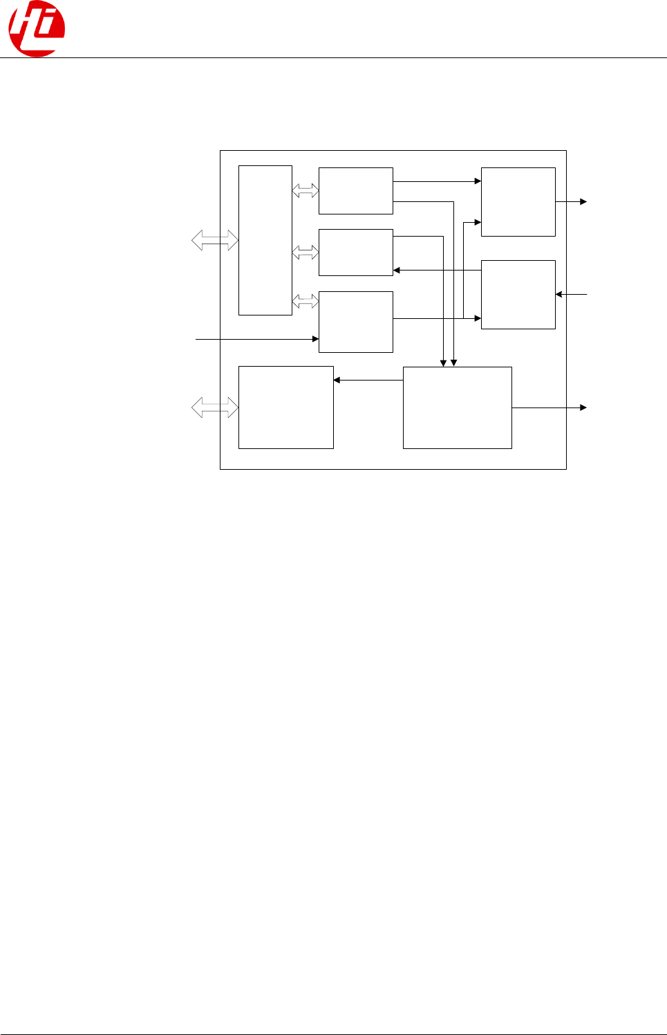
Hi3660
Data Sheet
8 Interface Control
Issue 05 (2016-12-22)
HiSilicon Proprietary and Confidential
Copyright © HiSilicon Technologies Co., Ltd.
8-3
Logical Block Diagram
Figure 8-1 Logical block diagram of the UART module
APB_IF
TX FIFO
RX FIFO
Baud rate
generator
Transmitter
Receiver
DMA
interface
FIFO status
and
interrupt generation
APB slave
UART CLK
DMA signals
Baud 16
UART TXD
UART RXD
UART INTR
The UART module consists of eight units. The function or operating principle of each unit is
described as follows:
- Advanced peripheral bus (APB) interface: APB slave interface used to process the
read/write data of the bus and configure registers
- TX FIFO: Stores the data to be transmitted.
- RX FIFO: Stores the received data.
- Baud rate generator: Generates the configured baud 16 clock.
- Transmitter: Performs parallel-to-serial conversion on the data and then outputs data, and
decodes data into the infrared format for output.
- Receiver: Performs serial-to-parallel conversion on the received data and decodes data in
the infrared format.
- DMA interface: Handles DMA interface processing.
- FIFO status and interrupt generation: Monitors the FIFO state and generates interrupts
based on the configured interrupt FIFO level.
Frame Format
One frame transfer of the UART involves the start bit, data bits, parity bit, and stop bits, as
shown in Figure 8-2.
The TX and RX data is the non-return-to-zero (NRZ) code. The data frame is output from the
TXD end of one UART and then input to the RXD end.
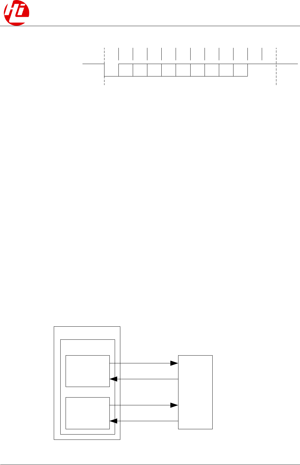
Hi3660
Data Sheet
8 Interface Control
Issue 05 (2016-12-22)
HiSilicon Proprietary and Confidential
Copyright © HiSilicon Technologies Co., Ltd.
8-4
Figure 8-2 UART frame format
TX/RX bit
Idle
state Start bit Data
<0> Data
<1> Data
<2> Data
<3> Data
<4> Data
<5> Data
<6> Data
<7> Parity
bit Stop bit
1Stop bit
2Idle
state
The fields in the frame format are described as follows:
- Start bit
It indicates the start of a data frame. According to the UART protocol, a low level in the
TX signal indicates the start of a data frame. When the UART does not transmit data, the
start bit must be fixed at 1.
- Data bit
The data bit width can be set to 5 bits, 6 bits, 7 bits, or 8 bits based on the application
requirements.
- Parity bit
The parity bit is a 1-bit error correction signal. The UART parity bit can be an odd parity
bit, even parity bit, or stick parity bit. The parity bit can be enabled or disabled.
- Stop bit
The stop signal is the stop bit of a data frame. The stop bit width is 1 bit or 2 bits. Setting
the TX signal to 1 indicates the end of a data frame.
Typical Application Scenario
The UART receives data from or transmits data to the off-chip component or interface
complying with the UART protocol, and implements serial-to-parallel conversion on the RX
data and parallel-to-serial conversion on the TX data. The UART can also transmit the
infrared data that complies with the IrDA protocol.
Figure 8-3 Typical application scenario of the UART module
TX control
TX control
UART
Hi3660
UART
device
UARTx_TXD
UARTx_CTS_N
UARTx_RXD
UARTx_RTS_N
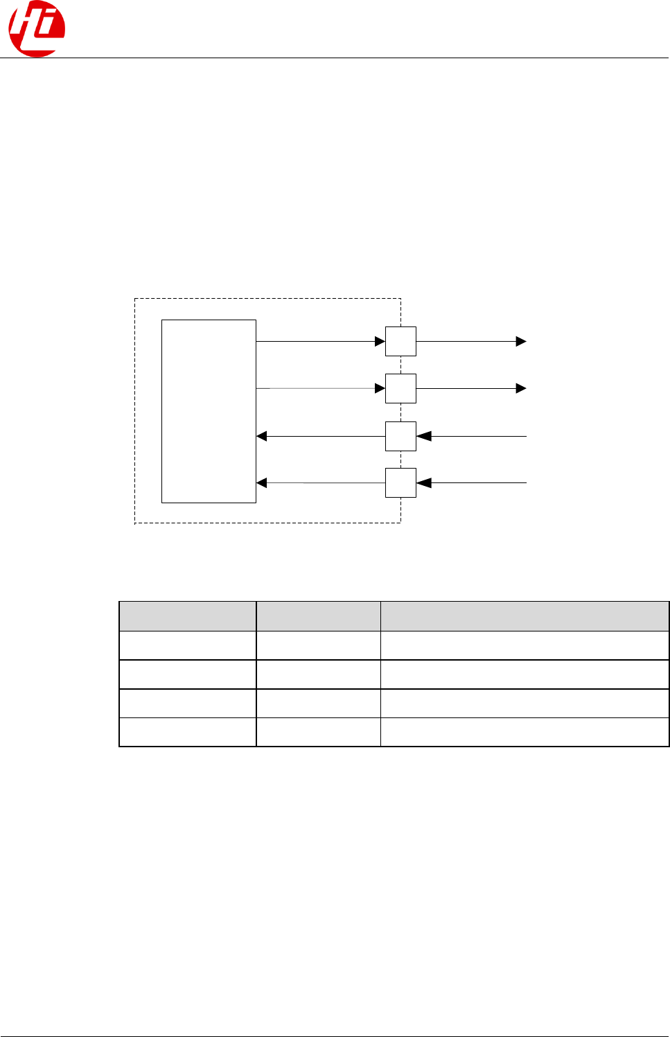
Hi3660
Data Sheet
8 Interface Control
Issue 05 (2016-12-22)
HiSilicon Proprietary and Confidential
Copyright © HiSilicon Technologies Co., Ltd.
8-5
The UART supports the following operating modes:
- UART mode: Supports flow control and reception and transmission of the data
complying with the UART protocol.
- Infrared mode: Supports the reception and transmission of the serial infrared data
complying with the IrDA protocol.
8.2.2 Signal Description
Figure 8-4 UARTx signals
UARTx
UARTx_TXD
UARTx_RTS_N
UARTx_TXD
UARTx_RTS_N
UARTx_RXD UARTx_RXD
UARTx_CTS_N UARTx_CTS_N
Table 8-1 UART interface signals
Signal
Direction
Description
UARTx_TXD
O
TX data signal of UARTx
UARTx_RXD
I
RX data signal of UARTx
UARTx_RTS_N
O
Request to send (RTS) signal of UARTx
UARTx_CTS_N
I
Clear to send (CTS) signal of UARTx
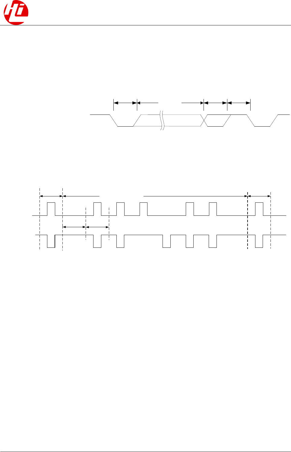
Hi3660
Data Sheet
8 Interface Control
Issue 05 (2016-12-22)
HiSilicon Proprietary and Confidential
Copyright © HiSilicon Technologies Co., Ltd.
8-6
8.2.3 Timing
UART Timing
Figure 8-5 UART timing
UARTx_TXD
UARTx_RXD LSB MSB
Start bit (1 bit)
Data bit (5–
8 bits)
Parity bit (1
bit, optional) Stop bit (1 bit
or 2 bits)
Timing in Infrared Mode
Figure 8-6 UART timing in infrared mode
UARTx_TXD
UARTx_RXD
Start bit
(1 bit)
Data 1 Data 0
Data bit (8 bits)
Stop bit
(1 bit)
8.2.4 Register Description
See the ARM public-version PL011 IP manual
(http://infocenter.arm.com/help/index.jsp?topic=/com.arm.doc.ddi0183g/index.html).
8.3 SPI
8.3.1 Function Description
Features
The serial peripheral interface (SPI) transfers data in serial or parallel mode. In the Hi3660,
the SPI is used as the master to implement synchronous serial communication with external
devices. The SPI does not serve as a slave.
The Hi3660 provides five SPIs: SPI0 to SPI4.
- SPI0 is reserved temporarily.
- SPI1 has one chip select (CS) for connecting the ESE.
- SPI2 has four CSs.
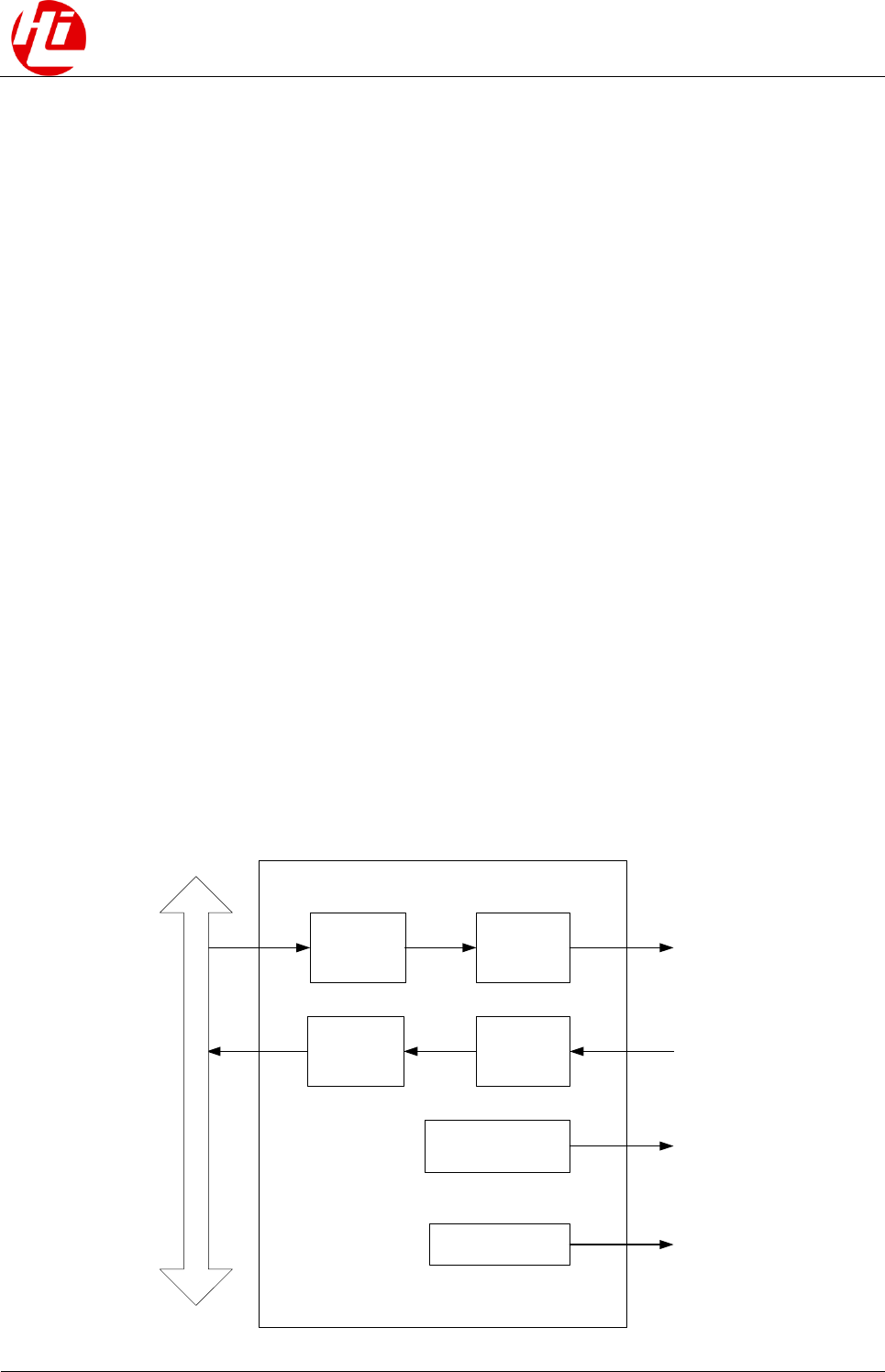
Hi3660
Data Sheet
8 Interface Control
Issue 05 (2016-12-22)
HiSilicon Proprietary and Confidential
Copyright © HiSilicon Technologies Co., Ltd.
8-7
− SPI2_CS0 connects to the fingerprint sensor.
− SPI2_CS1 to SPI2_CS3 are reserved.
- SPI3 has four CSs.
− SPI3_CS0 connects to the MINI_ISP.
− SPI3_CS1 connects to the ink screen.
− SPI3_CS2 and SPI3_CS3 are reserved.
- SPI4 has four CSs.
− SPI4_CS0 connects to the fingerprint sensor.
− SPI4_CS1 to SPI4_CS3 are reserved.
The SPI module supports the following functions:
- Supports the programmable interface clock frequency.
- Provides two separate 256 x 16-bit FIFOs: one TX FIFO and one RX FIFO.
- Supports SPI frame formats.
- Supports the programmable length of the serial data frame: 4 bits to 16 bits.
- Supports the programmable threshold of the TX FIFO and RX FIFO to request
interrupts.
- Supports the programmable threshold for the TX FIFO and RX FIFO to request the
DMA to implement burst transfer.
- Independently masks TX FIFO interrupts, RX FIFO interrupts, RX timeout interrupts,
and RX FIFO overflow interrupts.
- Provides the internal loopback test.
- Supports the DMA operation.
Logical Block Diagram
Figure 8-7 Functional block diagram of the SPI module
TX
channel
CS logic
Clock TX module
RX
channel
Parallel-to-
serial
conversion
Serial-to-
parallel
conversion
APB interface
SPI_DO
SPI_CS
SPI_CLK
SPI_DI
SPI
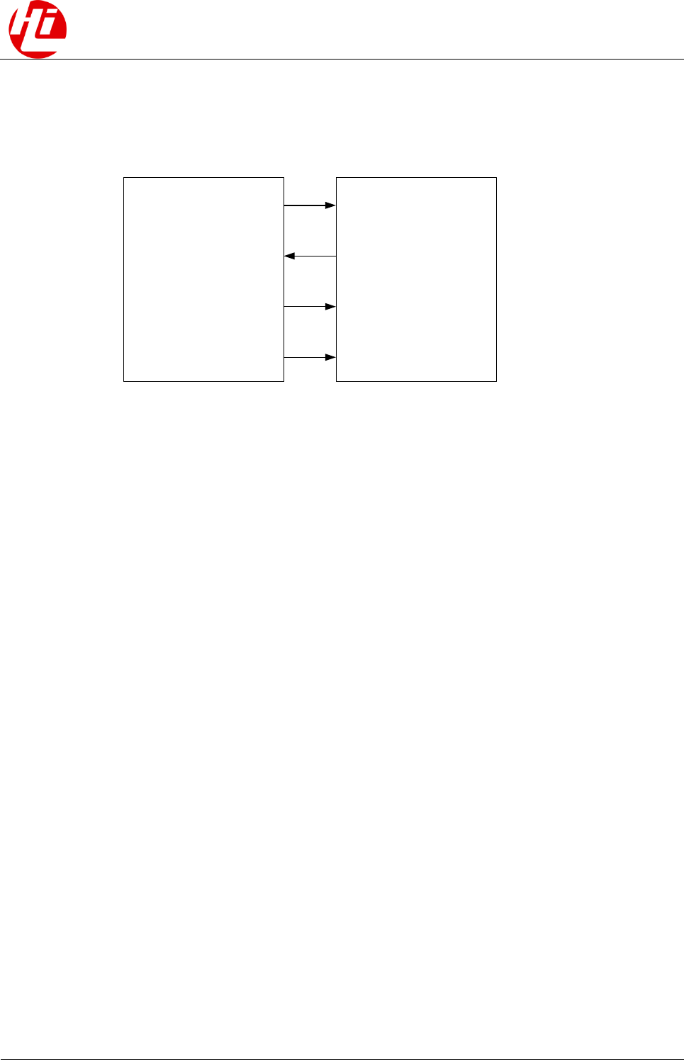
Hi3660
Data Sheet
8 Interface Control
Issue 05 (2016-12-22)
HiSilicon Proprietary and Confidential
Copyright © HiSilicon Technologies Co., Ltd.
8-8
SPI0 to SPI4 can connect to a single slave device, as shown in Figure 8-8.
Figure 8-8 Application of the SPI connected to a single slave device
SPI_DO
SPI_CS
SPI_CLK
SPI_DI
SPI master SPI slave
DIN
CS
CLK
DOUT
SPI0, SPI2, SPI3, and SPI4 can connect to multiple slave devices, as shown in Figure 8-9.
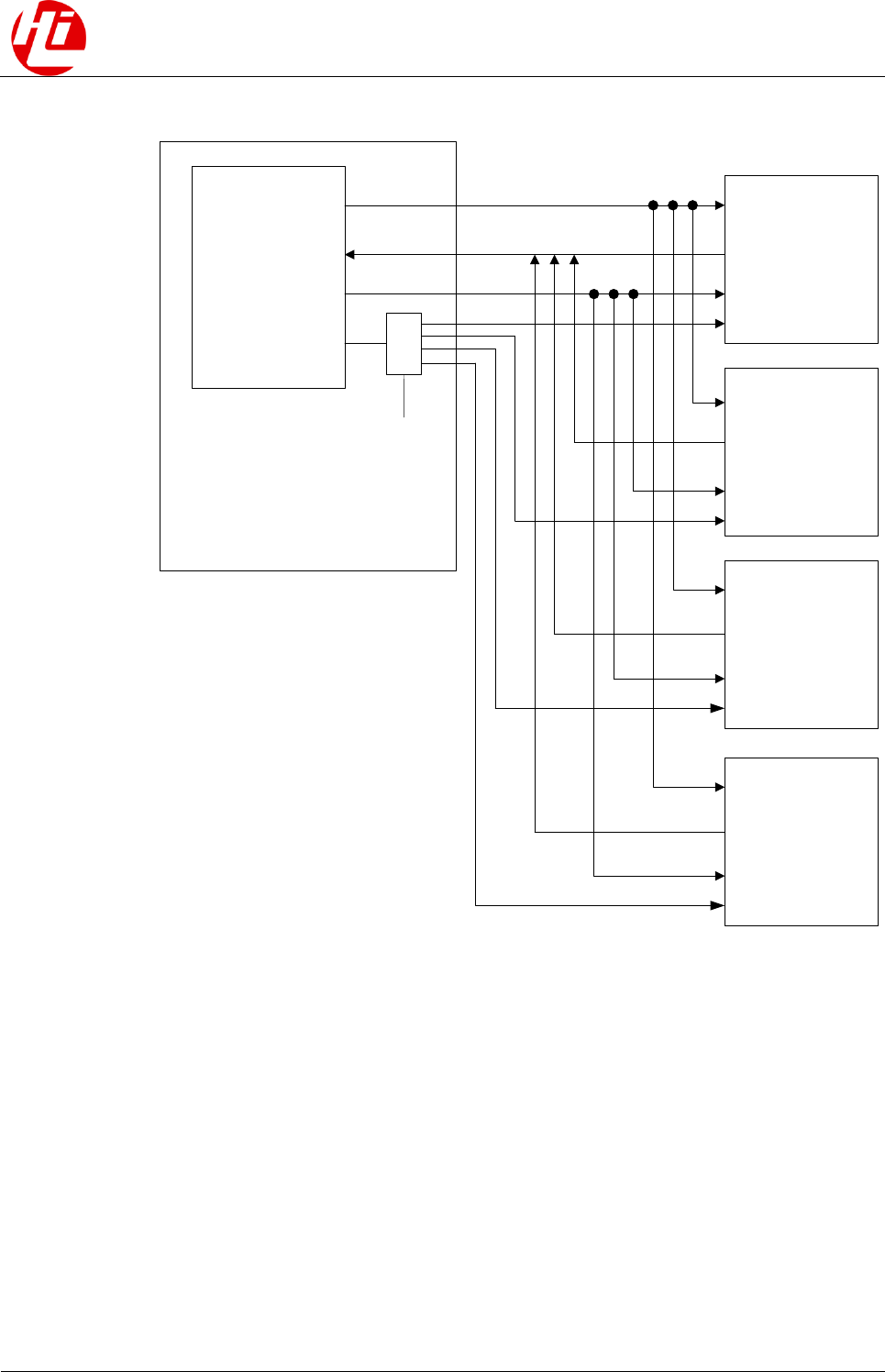
Hi3660
Data Sheet
8 Interface Control
Issue 05 (2016-12-22)
HiSilicon Proprietary and Confidential
Copyright © HiSilicon Technologies Co., Ltd.
8-9
Figure 8-9 Application of the SPI connected to multiple slave devices
SPI_DO
SPI_DI
SPI_CLK
SPI_CS
SPI master
XXX_DIN
XXX_DOUT
XXX_CLK
XXX_CS
Slave_0
XXX_DIN
XXX_DOUT
XXX_CLK
XXX_CS
Slave_1
XXX_DIN
XXX_DOUT
XXX_CLK
XXX_CS
Slave_2
XXX_DIN
XXX_DOUT
XXX_CLK
XXX_CS
Slave_3
Hi3660
Typical Application Scenario
The SPI supports two data transfer modes:
- Data transfer in interrupt or query mode
- Data transfer in DMA mode
8.3.2 Interrupt Handling
The SPI has five interrupts. The first four interrupts have independent sources and are
maskable and active high.
- SPIRXINTR
RX FIFO interrupt. When there are four or more valid data segments in the RX FIFO,
this interrupt is enabled.
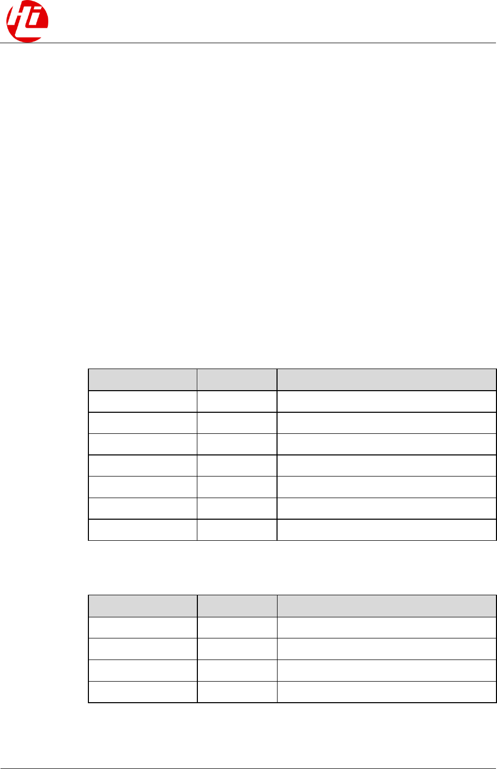
Hi3660
Data Sheet
8 Interface Control
Issue 05 (2016-12-22)
HiSilicon Proprietary and Confidential
Copyright © HiSilicon Technologies Co., Ltd.
8-10
- SPITXINTR
TX FIFO interrupt. When there are four or fewer valid data segments in the TX FIFO,
this interrupt is enabled.
- SPIRORINTR
RX overflow interrupt. When the FIFO is full and new data needs to be written to the
FIFO, FIFO overflow occurs and this interrupt is enabled. In this case, data is written to
the RX shift register rather than the FIFO.
- SPIRTINTR
RX timeout interrupt. When the RX FIFO is not empty and the SPI is idle for more than
one fixed 32-bit cycle, this interrupt is enabled.
In this case, data in the RX FIFO needs to be transmitted. When the RX FIFO is read
empty or new data is received into SPIRXD, this interrupt is disabled. This interrupt can
be cleared by writing the SPIICR[RTIC] register.
- SPIINTR
Combined interrupt, which is obtained after the preceding four interrupts are ORed. If
any of the preceding four interrupts is enabled, this combined interrupt is enabled.
The IDs of the SPI0–4 interrupts are 145, 112, 148, 344, and 345, respectively.
8.3.3 Signal Description
Table 8-2 Signals of the SPI0 interface
Signal
Direction
Description
SPI0_CLK
Output
SPI clock, output in master mode
SPI0_CS0_N
Output
SPI CS0 in master mode
SPI0_CS1_N
Output
SPI CS1 in master mode
SPI0_CS2_N
Output
SPI CS2 in master mode
SPI0_CS3_N
Output
SPI CS3 in master mode
SPI0_DI
Input
RX data input of the SPI
SPI0_DO
Output
TX data output of the SPI
Table 8-3 Signals of the SPI1 interface
Signal
Direction
Description
SPI1_CLK
Output
SPI clock, output in master mode
SPI1_CS_N
Output
SPI CS0 in master mode
SPI1_DI
Input
RX data input of the SPI
SPI1_DO
Output
TX data output of the SPI
Hi3660
Data Sheet
8 Interface Control
Issue 05 (2016-12-22)
HiSilicon Proprietary and Confidential
Copyright © HiSilicon Technologies Co., Ltd.
8-11
Table 8-4 Signals of the SPI2 interface
Signal
Direction
Description
SPI2_CLK
Output
SPI clock, output in master mode
SPI2_CS0_N
Output
SPI CS0 in master mode
SPI2_CS1_N
Output
SPI CS1 in master mode
SPI2_CS2_N
Output
SPI CS2 in master mode
SPI2_CS3_N
Output
SPI CS3 in master mode
SPI2_DI
Input
RX data input of the SPI
SPI2_DO
Output
TX data output of the SPI
Table 8-5 Signals of the SPI3 interface
Signal
Direction
Description
SPI3_CLK
Output
SPI clock, output in master mode
SPI3_CS0_N
Output
SPI CS0 in master mode
SPI3_CS1_N
Output
SPI CS1 in master mode
SPI3_CS2_N
Output
SPI CS2 in master mode
SPI3_CS3_N
Output
SPI CS3 in master mode
SPI3_DI
Input
RX data input of the SPI
SPI3_DO
Output
TX data output of the SPI
Table 8-6 Signals of the SPI4 interface
Signal
Direction
Description
SPI4_CLK
Output
SPI clock, output in master mode
SPI4_CS0_N
Output
SPI CS0 in master mode
SPI4_CS1_N
Output
SPI CS1 in master mode
SPI4_CS2_N
Output
SPI CS2 in master mode
SPI4_CS3_N
Output
SPI CS3 in master mode
SPI4_DI
Input
RX data input of the SPI
SPI4_DO
Output
TX data output of the SPI
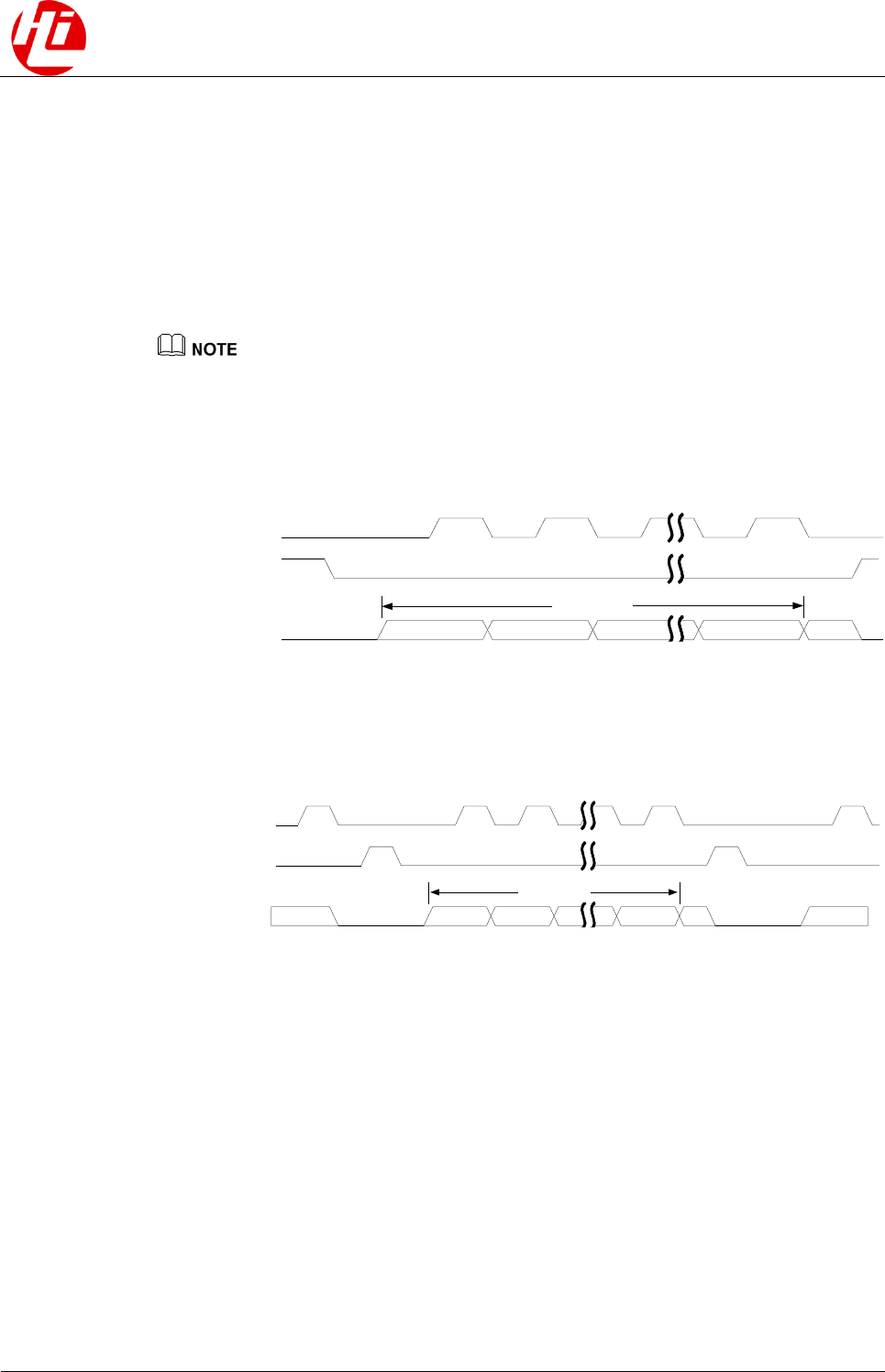
Hi3660
Data Sheet
8 Interface Control
Issue 05 (2016-12-22)
HiSilicon Proprietary and Confidential
Copyright © HiSilicon Technologies Co., Ltd.
8-12
8.3.4 Timings and Parameters
The acronyms in Figure 8-10 to Figure 8-17 are described as follows:
- MSB: most significant bit
- LSB: least significant bit
- Q: undefined signal
SPI Frame Formats
SPO indicates the polarity of SPICLKOUT and SPH indicates the phase of SPICLKOUT. The
corresponding register bits are SPICR0 bit[7] and SPICR0 bit[6], respectively.
(1) SPO = 0 and SPH = 0
Figure 8-10 Format of a single SPI frame (SPO = 0, SPH = 0)
4 to16bits
MSB LSB Q
SPI_CLK
SPI_CS_N
SPI_DI/
SPI_DO
Figure 8-11 Format of consecutive SPI frames (SPO = 0, SPH = 0)
4 to 16 bits4 to 16 bits
SPI_CLK
SPI_CS_N
SPI_DI/SPI_DO LSB MSBMSB LSB Q
When the SPI is idle in this mode:
- The SPI_CLK signal is set to low.
- The SPI_CS_N signal is set to high.
- The TX data line SPI_DO is forced to low.
When the SPI is enabled and valid data is ready in the TX FIFO, setting the SPI_CS_N signal
to low starts data transfer, and data of the enabled slave is placed on the master RX data line
SPI_DI. Half an SPI_CLK cycle later, the valid master data is transmitted to SPI_DO. At this
time, both the master data and slave data are valid. The SPI_CLK pin changes to high level
half an SPI_CLK cycle later. Data is captured on the rising edge of the SPI_CLK clock and
transmitted on the falling edge.
If a single word is transferred, SPI_CS_N is restored to high level one SPI_CLK cycle after
the last bit of data is captured.
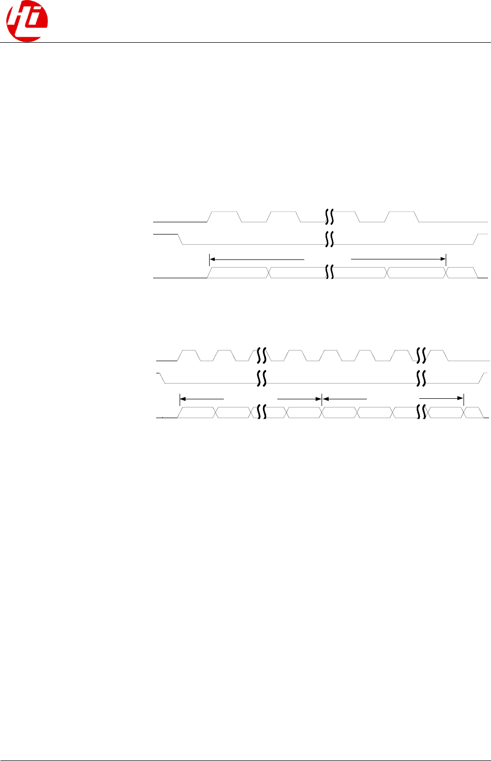
Hi3660
Data Sheet
8 Interface Control
Issue 05 (2016-12-22)
HiSilicon Proprietary and Confidential
Copyright © HiSilicon Technologies Co., Ltd.
8-13
If consecutive words are transferred, the SPI_CS_N signal must be pulled up by one
SPI_CLK cycle at each word transfer interval. This is because when SPH is 0, the slave
selection pin retains the data in the internal serial device register. Therefore, the master device
must pull the SPI_CS_N signal up at each word transfer interval during consecutive transfer.
When the transfer of consecutive words is complete, SPI_CS_N is restored to high level one
SPI_CLK cycle after the last bit of data is captured.
(2) SPO = 0 and SPH = 1
Figure 8-12 Format of a single SPI frame (SPO = 0, SPH = 1)
4 to 16 bits4 to 16 bits
SPI_CLK
SPI_CS_N
SPI_DI/SPI_DO LSBMSB Q
Figure 8-13 Format of consecutive SPI frames (SPO = 0, SPH = 1)
4 to 16bits4 to 16bits
MSB LSB QMSB LSB
SPI_CLK
SPI_CS_N
SPI_DI/
SPI_DO
When the SPI is idle in this mode:
- The SPI_CLK signal is set to low.
- The SPI_CS_N signal is set to high.
- The TX data line SPI_DO is forced to low.
When the SPI is enabled and there is valid data in the TX FIFO, setting the SPI_CS_N signal
to low starts a data transfer. If data transfer starts, the master data and slave data are valid on
their respective transmission lines half an SPI_CLK cycle later. In addition, SPI_CLK
becomes valid on the first rising edge. Data is captured on the falling edge of the SPI_CLK
clock and transmitted on the rising edge.
If a single word is transferred, SPI_CS_N is restored to high level one SPI_CLK cycle after
the last bit of data is captured.
If consecutive words are transferred, SPI_CS_N retains low at the word transfer interval.
When the consecutive transfer ends, SPI_CS_N is restored to high level one SPI_CLK cycle
later after the last 1-bit data is captured.
(3) SPO = 1 and SPH = 0
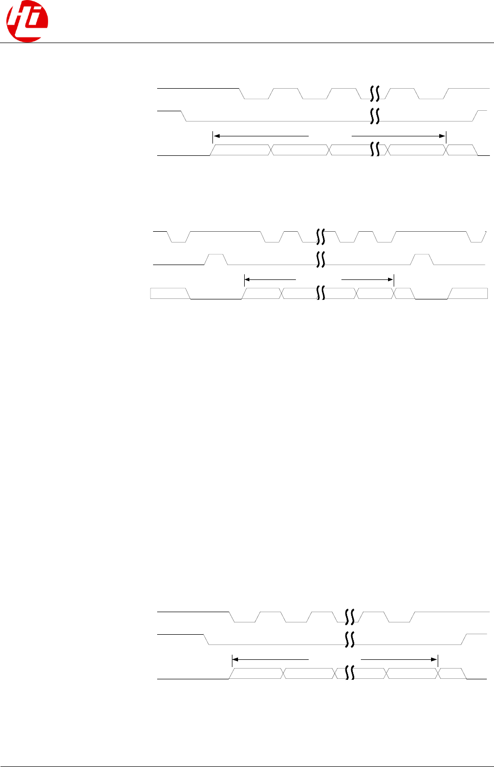
Hi3660
Data Sheet
8 Interface Control
Issue 05 (2016-12-22)
HiSilicon Proprietary and Confidential
Copyright © HiSilicon Technologies Co., Ltd.
8-14
Figure 8-14 Format of a single SPI frame (SPO = 1, SPH = 0)
4 to16bits
MSB LSB Q
SPI_CLK
SPI_CS_N
SPI_DI/
SPI_DO
Figure 8-15 Format of consecutive SPI frames (SPO = 1, SPH = 0)
4 to 16 bits4 to 16 bits
SPI_CLK
SPI_CS_N
SPI_DI/SPI_DO MSB LSB Q MSBLSB
When the SPI is idle in this mode:
- The SPI_CLK signal is set to high.
- The SPI_CS_N signal is set to high.
- The TX data line SPI_DO is forced to low.
When the SPI is enabled and there is valid data in the TX FIFO, setting the SPI_CS_N signal
to low starts a data transfer. The slave data is immediately transmitted to the master RX data
line SPI_DI. Half an SPI_CLK cycle later, the valid master data is transmitted to SPI_DO.
Another half SPI_CLK cycle later, the SPI_CLK master pin is set to low, indicating that data
is captured on the falling edge of the SPI_CLK clock and transmitted on the rising edge.
If a single word is transferred, SPI_CS_N is restored to high level one SPI_CLK cycle after
the last bit of data is captured.
If consecutive words are transferred, the SPI_CS_N signal must be pulled up at each word
transfer interval. This is because when SPH is 0, the slave selection pin retains the data in the
internal serial device register. SPI_CS_N is restored to high level one SPI_CLK cycle after
the last bit of data is captured.
(4) SPO = 1 and SPH = 1
Figure 8-16 Format of a single SPI frame (SPO = 1, SPH = 1)
4 to 16bits
MSB LSB Q
SPI_CLK
SPI_CS_N
SPI_DI/
SPI_DO
Hi3660
Data Sheet
8 Interface Control
Issue 05 (2016-12-22)
HiSilicon Proprietary and Confidential
Copyright © HiSilicon Technologies Co., Ltd.
8-15
Figure 8-17 Format of consecutive SPI frames (SPO = 1, SPH = 1)
4 to 16bits
4 to16bits
MSB LSB QMSB LSB
SPI_CLK
SPI_CS_N
SPI_DI/
SPI_DO
When the SPI is idle in this mode:
- The SPI_CLK signal is set to high.
- The SPI_CS_N signal is set to high.
- The TX data line SPI_DO is forced to low.
When the SPI is enabled and there is valid data in the TX FIFO, setting the SPI_CS_N master
signal to low starts the data transfer. Half an SPI_CLK cycle later, the master data and slave
data are valid on their respective transmission lines. In addition, SPI_CLK becomes valid on
the first falling edge. Data is captured on the rising edge of the SPI_CLK clock and
transmitted on the falling edge.
If a single word is transferred, SPI_CS_N is restored to high level one SPI_CLK cycle after
the last bit of data is captured.
If consecutive words are transferred, the SPI_CS_N signal retains low. SPI_CS_N is restored
to high level one SPI_CLK cycle after the last bit of data is captured. For the transfer of
consecutive words, SPI_CS_N retains low during data transfer, and the end mode is the same
as that during single word transfer.
Timing
Figure 8-18 SPI timing
MSB LSB
MSB LSB
Tdh
Tds 4 to 16 bits
Tdd 4 to 16 bits
SPI_CLK(SPO=0,SPH=0)
SPI_CLK(SPO=1,SPH=0)
SPI_CLK(SPO=0,SPH=1)
SPI_CLK(SPO=1,SPH=1)
SPI_CS_N
SPI_DO
SPI_DI

Hi3660
Data Sheet
8 Interface Control
Issue 05 (2016-12-22)
HiSilicon Proprietary and Confidential
Copyright © HiSilicon Technologies Co., Ltd.
8-16
Table 8-7 Input timing parameters of the SPI
Parameter
Symbol
Min
Max
Unit
DI setup time
Tds
10
-
ns
DI hold time
Tdh
10
-
ns
8.3.5 Register Description
See the ARM public-version PL022 IP manual
(http://infocenter.arm.com/help/index.jsp?topic=/com.arm.doc.ddi0183g/index.html).
8.4 I2C
8.4.1 Function Description
Functional Block Diagram
The I2C controller uses the SCL and SDA signal lines to communicate with off-chip devices
that provide I2C interfaces. The I2C interface can transmit data to and receive data from the
slave device on the I2C bus in compliance with I2C specifications V2.1. In the Hi3660, the I2C
controller can only be used as the master device.
The Hi3660 integrates eight I2C modules.
- I2C0 is used to connect sensors, such as the acceleration sensor, gyro sensor, and
barometer.
- I2C1 is the backup of I2C0.
- I2C2 is used to connect the capacitive touch pad (TP).
- I2C3 can be multiplexed as the common GPIO function.
- I2C4 is used for charging, Near Field Communication (NFC), external flash light driver,
and external speaker PA.
- I2C5 is used to connect the external buck power chip.
- I2C6 is reserved for the backup solution.
- I2C7 is reserved.
Hi3660
Data Sheet
8 Interface Control
Issue 05 (2016-12-22)
HiSilicon Proprietary and Confidential
Copyright © HiSilicon Technologies Co., Ltd.
8-17
Figure 8-19 Typical I2C application circuit
Rp Rp
SCL
SDA
SDA SCL
I2C0
master
SDA SCL
I2C2
master
SDA SCL
I2C6
master
...
+Vdd
Pull-up
resistors
The I2C controller has the following features:
- Supports the I2C bus protocol V2.1.
- Serves as only the master device on the I2C bus.
- Acts as the transmitter (master device) on the I2C bus and sends data to the slave device.
- Supports the 7-bit standard slave address or 10-bit extended slave address when serving
as a master.
- Supports the standard mode (100 kbit/s), fast mode (400 kbit/s), and high-speed mode
(3.4 Mbit/s).
- Provides the TX FIFO and RX FIFO and supports DMA data transfer.
- Reports interrupts and queries the states of raw and masked interrupts.
- Supports clock stretching. During data transmission, when the TX FIFO is empty, pull
down the SCL and wait for the FIFO to be filled with data again. During data reception,
when the RX FIFO is empty, pull down the SCL and wait for the FIFO to be filled with
data again.
- Supports the restart transmission of the SDA data. The data bus is not released and data
continues to be transferred in the same channel.
- Configures the SDA setup time and hold time in registers.
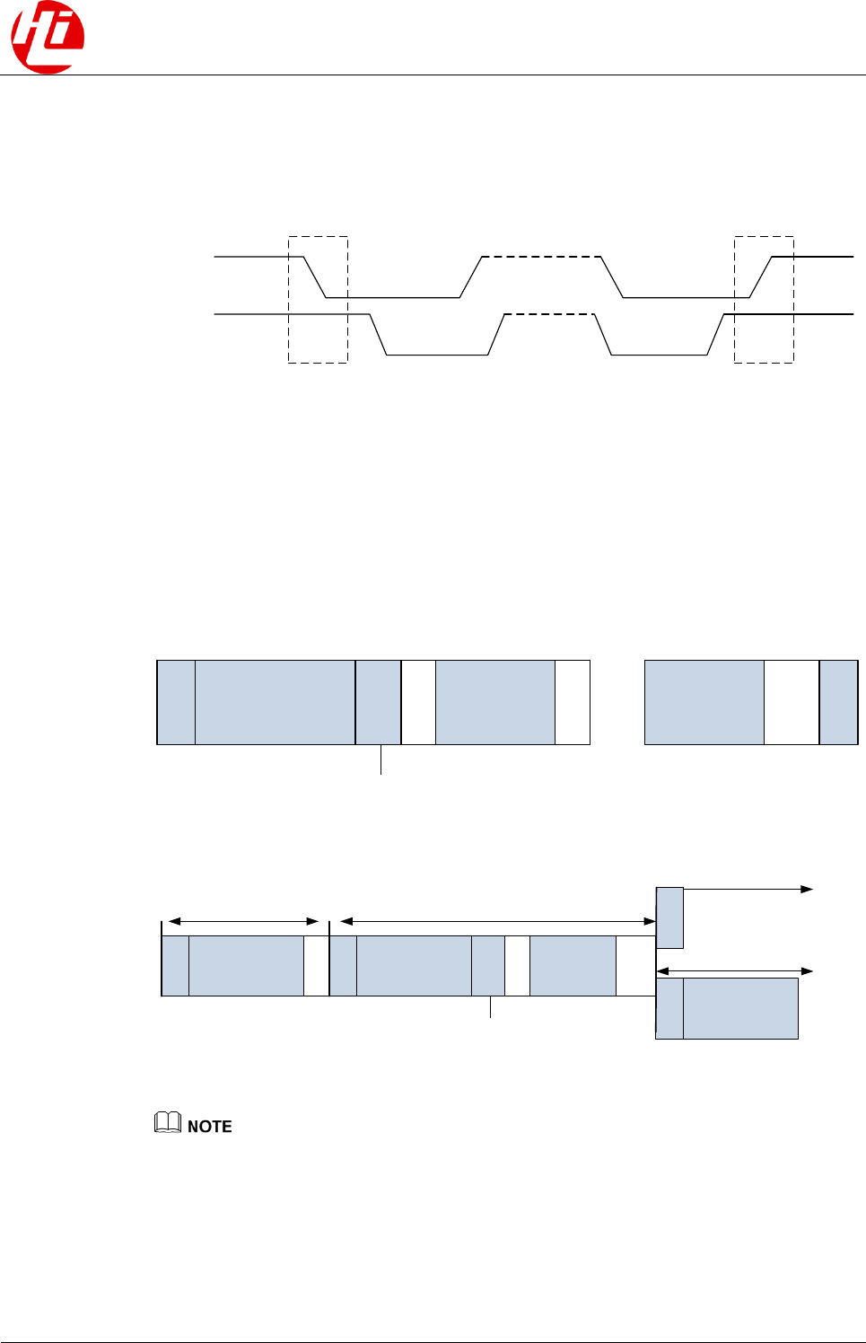
Hi3660
Data Sheet
8 Interface Control
Issue 05 (2016-12-22)
HiSilicon Proprietary and Confidential
Copyright © HiSilicon Technologies Co., Ltd.
8-18
START/STOP Conditions
Figure 8-20 I2C START/STOP timing
SDA
SCL
START STOP
- START: The SDA level is switched from high to low when the SCL level is high.
- STOP: The SDA level is switched from low to high when the SCL level is high.
I2C Frame format
Figure 8-21 I2C frame formats in different transfer modes
S Slave address R/W A DATA A DATA A/NA P
...
'0' write Master-transmitter protocol
for the 7-bit slave address
Sr Slave address R/W A
N
ADATA A/NA
P
...
'0' write
S Master code
Sr Slave address
F/S mode HS mode
F/S mode
HS mode
...
- S: start condition
- A: acknowledge (SDA low)
- P: stop condition
- NA: no acknowledge (SDA high)
Hi3660
Data Sheet
8 Interface Control
Issue 05 (2016-12-22)
HiSilicon Proprietary and Confidential
Copyright © HiSilicon Technologies Co., Ltd.
8-19
The start signal (Start) specified in the I2C standard protocol is transmitted from the master
device on the bus to wake up all slave devices. The Start is a special signal indicating the start
of data transfer.
When the master device works in F/S mode, the first data packet transmitted after the Start
signal is sent is the address of the slave device (Slave address + W/R). This data packet
consists of the 7-bit slave address (two data packets are required if the slave address is 10 bits)
and 1-bit read/write data.
When working in HS mode, the master device needs to transmit the master code first. Then
the frame format in HS mode is the same as that in F/S mode. The HS mode and F/S mode
differ only in the speed. Each slave address determines whether to transmit or receive data
based on the slave address information. After a slave address is successfully received, the
corresponding slave device pulls the SDA down at the ninth clock cycle (SCL) and returns an
ACK signal to the master device. Then, subsequent data transfer starts.
DATA refers to data reception or transmission based on the read or write command after the
master device successfully receives the slave address ACK signal. During the data transfer,
the SDA changes when the SCL level is low and retains when the SCL level is high. Each
time the receiver (slave device) receives one byte, it must send an ACK signal to the
transmitter (master device). If the transmitter fails to receive an ACK signal, it stops data
transfer or starts re-transmission.
The stop signal (Stop) is sent when the master device completes the current data transfer and
there is no new data to be transferred. The stop signal is a special signal indicating the end of
data transfer, and complies with the standard I2C protocol. After the master device sends a
Stop signal, the slave device must release the bus.
8.4.2 Signal Description
8.4.2.1 OD Gate of the Interface
The I2C interface uses the open drain (OD) gate, as shown in Figure 8-22.
Figure 8-22 Inputs and outputs of the OD gates for the SCL and SDA
VDD
ic_clk_in_a
ic_clk_oe
SCL
VDD
ic_data_in_a
ic_data_oe
SDA
8.4.2.2 Interface Signals
Table 8-8 describes the signals of the I2C interface. For details about the multiplexing
relationship of the signals in Table 8-8, see the IOC-related documents.
Table 8-8 Signals of the I2C interface
Signal
Direction
Description
I2C0_SDA
Input/Output
I2C0 data signal
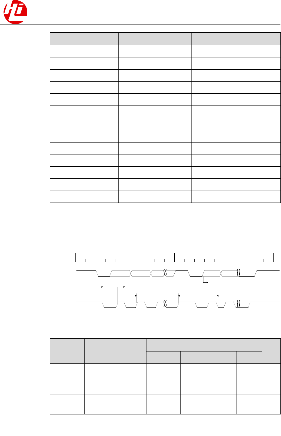
Hi3660
Data Sheet
8 Interface Control
Issue 05 (2016-12-22)
HiSilicon Proprietary and Confidential
Copyright © HiSilicon Technologies Co., Ltd.
8-20
Signal
Direction
Description
I2C0_SCL
Output
I2C0 clock signal
I2C2_SDA
Input/Output
I2C2 data signal
I2C2_SCL
Output
I2C2 clock signal
I2C3_SDA
Input/Output
I2C3 data signal
I2C3_SCL
Output
I2C3 clock signal
I2C4_SDA
Input/Output
I2C4 data signal
I2C4_SCL
Output
I2C4 clock signal
I2C5_SDA
Input/Output
I2C5 data signal
I2C5_SCL
Output
I2C5 clock signal
I2C6_SDA
Input/Output
I2C6 data signal
I2C6_SCL
Output
I2C6 clock signal
I2C7_SDA
Input/Output
I2C7 data signal
I2C7_SCL
Output
I2C7 clock signal
8.4.3 Timings and Parameters
Figure 8-23 I2C timing
START
RESTART
STOP
tHD,SDA
tSU,SDA
tSU,STA
tLOW
tHIGH
tHD,STA
0ns
250ns
500ns
750ns
1000ns
SDA
SCL
Table 8-9 I2C timing parameters (F/S mode)
Parameter
Description
Standard Mode
Fast Mode
Unit
Min
Max
Min
Max
fSCL
SCL clock frequency
0
100
0
400
kHz
tHD;STA
Hold time of the
START condition
4.0
-
0.6
-
µs
tLOW
Width of the SCL low
level
4.7
-
1.3
-
µs
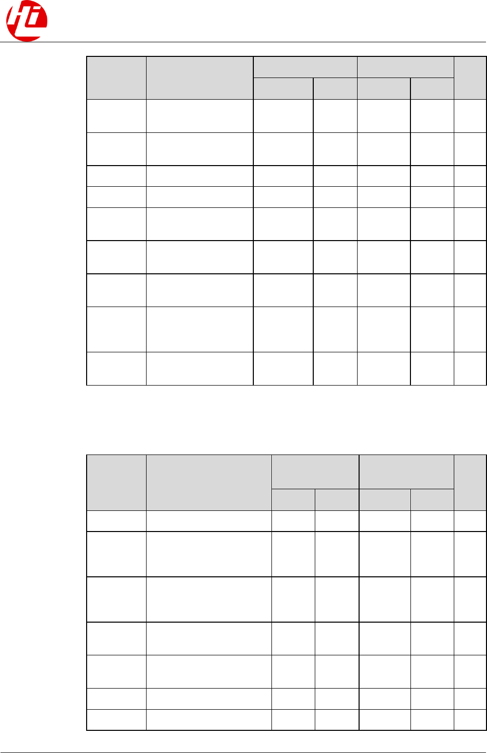
Hi3660
Data Sheet
8 Interface Control
Issue 05 (2016-12-22)
HiSilicon Proprietary and Confidential
Copyright © HiSilicon Technologies Co., Ltd.
8-21
Parameter
Description
Standard Mode
Fast Mode
Unit
Min
Max
Min
Max
tHIGH
Width of the SCL
high level
4.0
-
0.6
-
µs
tSU;STA
Setup time of the
START condition
4.7
-
0.6
-
µs
tHD;DAT
Data hold timea
0
3.45
0
0.9
µs
tSU;DAT
Data setup timea
250
-
100
-
ns
tR
Rising time of the
SDA and SCL signals
-
1000
20+0.1Cb
300
ns
tF
Falling time of the
SDA and SCL signals
-
300
20+0.1Cb
300
ns
tSU;STO
Setup time of the
STOP condition
4.0
-
0.6
-
µs
tBUF
Bus idle duration
between the STOP
and START states
4.7
-
1.3
-
µs
Cb
Capacitor load of each
bus line
-
400
-
400
pF
a: For the Hi3660, the registers related to the data hold time and setup time are configurable.
Table 8-10 I2C timing parameters (HS mode)
Parameter
Description
Cb (Max) = 100
pF
Cb = 400 pF
Unit
Min
Max
Min
Max
fSCL
SCL clock frequency
0
3.4
0
1.7
MHz
tSU;STA
Setup time of the
START/RESTART
condition
160
-
160
-
ns
tHD;STA
Hold time of the
START/RESTART
condition
160
-
160
-
ns
tLOW
Width of the SCL low
level
160
-
320
-
ns
tHIGH
Width of the SCL high
level
60
-
120
-
ns
tSU;DAT
Data setup timea
10
-
10
-
ns
tHD;DAT
Data hold timea
0
70
0
150
ns
Hi3660
Data Sheet
8 Interface Control
Issue 05 (2016-12-22)
HiSilicon Proprietary and Confidential
Copyright © HiSilicon Technologies Co., Ltd.
8-22
Parameter
Description
Cb (Max) = 100
pF
Cb = 400 pF
Unit
Min
Max
Min
Max
trCL
Rising time of the SCL
signal
10
40
20
80
ns
trCL1
Rising time of the SCL
signal after the RESTART
and response bit
10
80
20
160
ns
tF
Falling time of the SCL
signal
10
40
20
80
ns
trDA
Rising time of the SDA
signal
10
80
20
160
ns
tfDA
Falling time of the SD
signal
10
80
20
160
ns
tSU;STO
Setup time of the STOP
condition
160
-
160
-
ns
Cb
Capacitor load between
the SCL and SDA
-
100
-
400
pF
a: For the Hi3660, the registers related to the data hold time and setup time are configurable.
The conditions for the I2C data transfer rate to reach 3.4 Mbit/s are as follows:
- The maximum value of tHD:DAT must be no greater than 70 ns.
- The minimum data window duration must be 230 ns.
- The maximum hold time must be 70 ns.
8.4.4 Register Description
See the Synopsys I2C IP manual (https://www.synopsys.com/dw/ipdir.php?c=DW_apb_i2c).
8.5 GPIO
8.5.1 Function Description
Features
The Hi3660 has 27 common GPIO modules: GPIO0–17, GPIO20–21, and GPIO22–28. The
peripheral area has 20 GPIO modules (GPIO0–17 and GPIO20–21), and the always-on area
(AON_SUBSYS) has seven GPIO modules (GPIO22–28).
Hi3660
Data Sheet
8 Interface Control
Issue 05 (2016-12-22)
HiSilicon Proprietary and Confidential
Copyright © HiSilicon Technologies Co., Ltd.
8-23
The Hi3660 provides two secure GPIO modules: one (GPIO0_SE) in the peripheral area and
one (GPIO1_SE) in the always-on area (AON_SUBSYS).
The Hi3660 also has the following GPIO modules in the independent subsystems:
- Four GPIO modules in the sensor hub: GPIO0_SH to GPIO3_SH
- Two GPIO modules in the UFS_PERI_SUBSYS area: GPIO18 and GPIO 19
- Two GPIO modules in the MMC1_PERI_SUBSYS area: GPIO0_EMMC and
GPIO1_EMMC
Each GPIO module corresponds to a group of eight GPIO interfaces. Each GPIO group
generates three interrupts, which are sent to the generic interrupt controller (GIC), LPMCU,
and CCPU, respectively. (The interrupts of GPIO0SH to GPIO3SH are sent to the GIC and
IOMCU, respectively.) The source interrupts of the three index interrupts share the eight
GPIO interfaces in the same group but have independent mask bits.
Table 8-11 GPIO group information
Instance
Valid GPIO Pins
Interrupt Registration Support
GPIO22 to
GPIO27
GPIO_176 to GPIO_190
GPIO_192 to GPIO_222
GIC
GPIO28
GPIO28 is not used.
GIC
GPIO1_SE
GPIO_008_SE to
GPIO_015_SE
GIC
GPIO0 to
GPIO17
GPIO_001 to GPIO_098
GPIO_103 to GPIO_127
GIC
GPIO20
GPIO_160 to GPIO_165
GIC
GPIO21
GPIO_168 to GPIO_173
GIC
GPIO0_SE
GPIO_000_SE to
GPIO_007_SE
GIC
GPIO0_SH to
GPIO3_SH
GPIO_000_SH to
GPIO_027_SH
GIC
GPIO_028_SH to
GPIO_031_SH
GIC
GPIO18 to
GPIO19
GPIO_144 to GPIO_155
GIC
GPIO0_EMMC
to
GPIO1_EMMC
GPIO_00_EMMC to
GPIO_09_EMMC
GIC
Each GPIO group provides eight programmable I/O pins to generate output signals or collect
input signals for specific applications.
You can obtain the group ID of a GPIO pin by using the following formula:
Group ID = int(GPIO pin number/8)
Hi3660
Data Sheet
8 Interface Control
Issue 05 (2016-12-22)
HiSilicon Proprietary and Confidential
Copyright © HiSilicon Technologies Co., Ltd.
8-24
The remainder is the sequence number of this pin in the group, ranging from 0 to 7. (0 is the
LSB and 7 is the MSB.)
Sequence number within the group = mod(GPIO pin number/8)
Take GPIO_017 as an example. The pin number is 17. Its group ID is 2 (int(17/8)), and the
remainder is 1. Therefore, GPIO_017 belongs to GPIO group 2 (GPIO2), and its sequence
number within this group is 1. Similarly, the sequence number of GPIO_016 in GPIO2 is 0,
and that of GPIO_023 in GPIO2 is 7.
The GPIO has the following features:
- Configures each GPIO pin as the input, output, or OD output.
− When acting as an input pin, a GPIO pin can be used as an interrupt source. Each
GPIO pin supports independent interrupt control.
− When acting as an output pin, a GPIO pin can be independently set to 0 or 1.
− When a GPIO pin acts as the OD output, pull-up control is required on the board. The
output is enabled by using the GPIODIR register to implement the "wired AND"
function on the board.
- Queries the states of raw and masked interrupts.
- Supports the interrupt wakeup system. Configure the GPIO enable interrupt before the
system enters the sleep state. After the system enters the sleep state, the GPIO will
generate an interrupt to wake up the system when peripheral inputs change.
- Does not support separate soft reset.
8.5.2 Signal Description
GPIO_000 is an internal signal and is invisible to users.
Table 8-12 GPIO interface signals
Signal
Direction
Description
GPIO_001
Input/Output
Standard I/O port
GPIO_002
Input/Output
…
GPIO_174
Input/Output
GPIO_222
Input/Output
8.5.3 Register Description
See the ARM public-version PL061 IP manual
(http://infocenter.arm.com/help/index.jsp?topic=/com.arm.doc.ddi0183g/index.html).
