JI 131 03 TB8100 Tech Notes/Job Instructions/JI POCSAG Paging Setup Guide
User Manual: Pdf TB8100 Tech Notes/Job Instructions/JI-131-03 TB8100 POCSAG Paging Setup Guide
Open the PDF directly: View PDF ![]() .
.
Page Count: 7
Tait Electronics (Aust) Pty Ltd Job Instruction
JI-131-03.doc Page 1 of 7 22-06-06
TBA101B POCSAG Interface Setup guide.
Issue No.: JI-131-03
Author: TEA Workshop
General
This guide is too be used in conjunction with TN-1047 “Using a TB8100 in Paging Applications”,
dated 5 May 2006.
This guide can be used as a substitute of Section 7.2, “Adjusting Audio Output Levels”, of TN-1047.
The aim of this job instruction is to guide the technician through setting up the RF frequency offset
output level of the paging transmitter using the TBA101B onboard test mode, and to recognize how this
relates to the users POCSAG encoder output deviation level.
The test levels were set up at various differing levels to show what the resulting effect of adjusting the
high and low DC biasing pots (RV1 and RV2) on the TBA101B had on the POCSAG signal output to
air. The procedure below will set up the base to give a POCSAG output deviation of about +/- 4.5 KHz,
which is generally regarded as standard for a POCSAG paging base.
There are a number of photos of screenshot of the COM120B screens showing relevant screens referred
to in this document. They will be referred to as Picture 1, Picture 2…etc. On other communications
test sets there will be equivalent fields or screens to display similar information.
Parts
The equipment used to do this testing was as follows:
Part Number Description Supplier Qty.
TB8100 TB8100 50W VHF-hi band base Tait 1
TBA101B Paging Interface Board Tait 1
CAD-POCSAG Raedale CAD-POCSAG paging Encoder Raedale 1
Pager VHF-Hi band POCSAG Pager Unicom 1
COM120B IFR COM120B Comms Test Set Vicom 1
** Test Plug DB15 male connector wired as a test plug Generic 1
CRO Probe CRO Probe Generic 1
Coax 50ohm coax cable (TB8100 PA to COM120B) Generic 1
** If a TB8100 Calibration Test Unit (CTU) is on hand you could use that instead of the Test Plug.
Basically just plug the 15pin Drange cable that comes with the CTU between J4 on the TBA101B and
the DB15 socket on the CTU. You can then use the Tx Key switch on the CTU to key the TB8100.
Procedure
• Make a simple test plug out of a 15 pin male Drange solder connector.
o Solder about 20cm of jumper wire to pin 15 (GND).
o Solder about 20cm of jumper wire to pin 5 (Tx Key).
o Plug the test plug into J4 (DB15F) socket on the TBA101B.
o When required, in the following tests, the base can be keyed up from the TBA101B by
twisting or touching the Tx Key (pin 5) wire, on the test plug, to the GND (pin 15) wire
on the test plug.

Tait Electronics (Aust) Pty Ltd Job Instruction
JI-131-03.doc Page 2 of 7 22-06-06
• Connect the 50W PA RF out to the high power TX Input of the Comms Test Set using a coax
cable.
• Enter the transmit frequency of the TB8100 into the Comms Test Sets Tx monitor screen.
• On the Comms test set in the Tx monitor mode, the High Pass Audio Filter was disabled and
the Low Pass Audio Filters was set to a low pass frequency of 20KHz. On a different test set
the Low Pass Audio Filters typically have various selections of between <300Hz and <20KHz,
so use the higher one (ie. <15 KHz as is available on a HP8920, or <20 KHz as is available on
a COM120B). The high pass filter can be switched off. If the audio filters are not set up as
above then the waveforms seen will probably vary from the pictures and results shown below
in the Results section.
• Set the Comms Test Set up so that the RF Frequency Error can be seen when a signal is
transmitted into the test set.
• As a quick test, press the TB8100 Front Panel TX Carrier button (button marked with 2
squiggly arrows). Note on the Comms Test Set the RF Frequency Error that is displayed while
holding down the Tx Carrier button. Typically on a new TB8100 it is within about +/- 100 Hz
of the programmed frequency. Once you have noted this, dekey the TB8100.
To adjust the overall POCSAG deviation levels, follow these steps:
1. On the TBA101B set the S1 DIP switch bank as shown:
Switch Function State
1 Force POCSAG Enable ON
2 Enable POCSAG Externally ON
3 Disable POCSAG ON
4 Not Used OFF
5 Force High DC bias Level ON
6 Force Low DC bias Level OFF
7 Non-Inverted ON
8 Inverted OFF
2. This sets the SW1 Dip switch bank in preparation to adjust the DC bias on the TBA101B for
positive RF frequency offset, by forcing the DC signal biasing high on the TBA101B.
3. Now key the TB8100 base by grounding J4 Pin 5 (Tx Key).
4. The POCSAG Encoder used in this testing was a Raedale CAD-POCSAG which outputs a
POCSAG level to the TBA101B (J4 pin 6) that is 0Volts (low) and 3.5Volts (high). We will set
up the RF offset frequency to +/-4 KHz of the centre frequency in the Test Mode. When the
CAD-POCSAG is connected this will result in TX deviation of about +/-4.5 KHz when
POCSAG is being transmitted.
5. You should be observing on the Comms Test Set, the RF Carrier Frequency offset. You need to
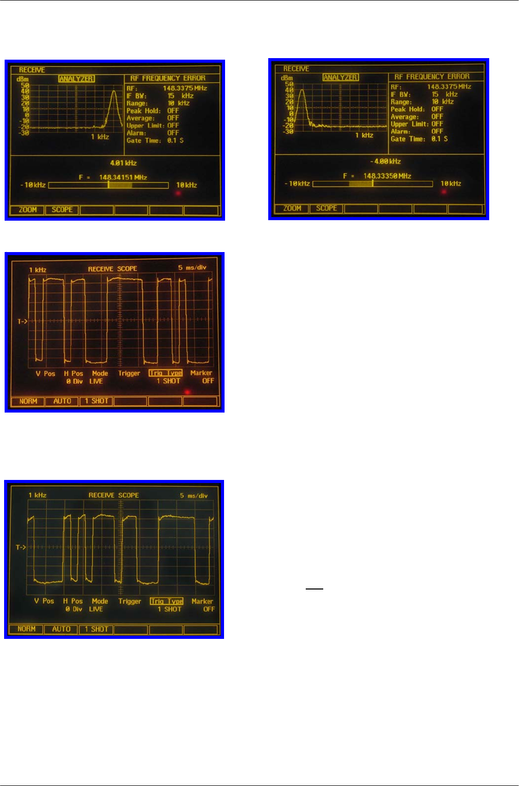
adjust RV1 to adjust the offset level to +4KHz from the centre frequency. Picture 14 shows the
view of the COM120B spectrum analyzer view and RF frequency error.
6. Now change SW1 DIP switch 5 to OFF and switch 6 to ON. This sets the SW1 Dip switch
bank in preparation to adjust the DC bias on the TBA101B for negative RF frequency offset, by
forcing the DC signal biasing low on the TBA101B.
7. You should be observing on the Comms Test Set, the RF Carrier Frequency offset.
Tait Electronics (Aust) Pty Ltd Job Instruction
JI-131-03.doc Page 3 of 7 22-06-06
8. You need to adjust RV2 to adjust the offset level to -4KHz from the centre frequency. Picture
15 shows the view of the COM120B spectrum analyzer view and RF frequency error.
9. Now turn S1 DIP switch 1 OFF and switch 6 OFF. Switch 1 in the OFF position means that J4
pin 11 DATA/SPEECH line controls if either POGSAG or voice is to be sent (usually for a
dedicated paging base SW1 DIP switch 1 can be set to ON as only POCSAG is ever used).
Switch 5(force high) and 6(force low) being off means that the DC bias is in the correct state for
a POCSAG encoder signal to be injected into J4 pin 6 (POCSAG DATA Input).
10. After having set the POCSAG audio levels S1 should be set back to a working configuration
(see Table 4 in TN-1047).
Results
The following table shows what the resulting POCSAG deviation is after having been set up in the
TBA101B test mode with various RF frequency offsets.
RF offset
(Test Mode) POCSAG deviation with
CAD-POCSAG connected Associated Picture
Numbers
+/- 2.5Khz 3.0Khz 3, 4, 5
+/- 3.0Khz 3.5khz 6, 7, 8, 9, 10
+/- 3.5Khz 4.0Khz 11, 12, 13
+/- 4.0Khz 4.5Khz 14, 15, 16
The TTL POCSAG signal level going from the CAD-POCSAG encoder into J4 Pin 6 (DATA) on the
TBA101B was adjustable in the encoder (via an adjustable pot. on the POCSAG data line in the
encoder) between 3.5V and 5.3V. This level had no effect on the output deviation. So whether it was
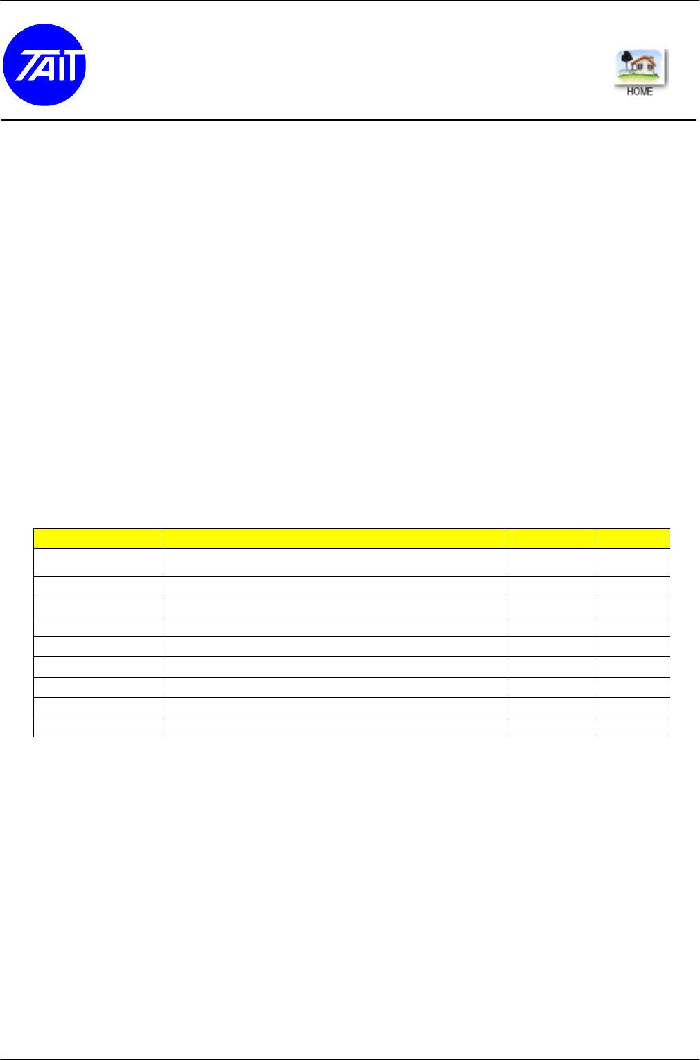
adjusted to 3.5V or 5.5V, the POCSAG output deviation did not vary. (Pictures 1 and 2)
1 – 3.5V POCSAG from encoder into J4 Pin 6 2 - 5V POCSAG from encoder into J4 Pin 6
Tait Electronics (Aust) Pty Ltd Job Instruction
JI-131-03.doc Page 4 of 7 22-06-06
The following pictures are displays of the COM120B screens that are related to setting up the
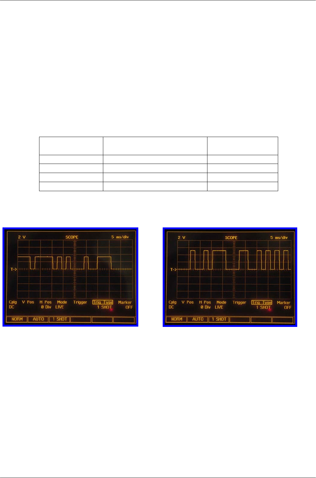
TBA101B for a RF offset in test mode of +/- 2.5 KHz (Pictures 3 and 4). When the POCSAG encoder
is connected this results in a nominal POCSAG deviation of 3 KHz (Picture 5).
3 – RV1 adjusted for an RF offset +2.5 KHz 4 – RV2 adjusted for an RF offset -2.5 KHz
5 – After TBA101B test mode RF frequency offset has
been set up for +/-2.5Khz this results in a POCSAG
deviation output of 3.0 KHz.
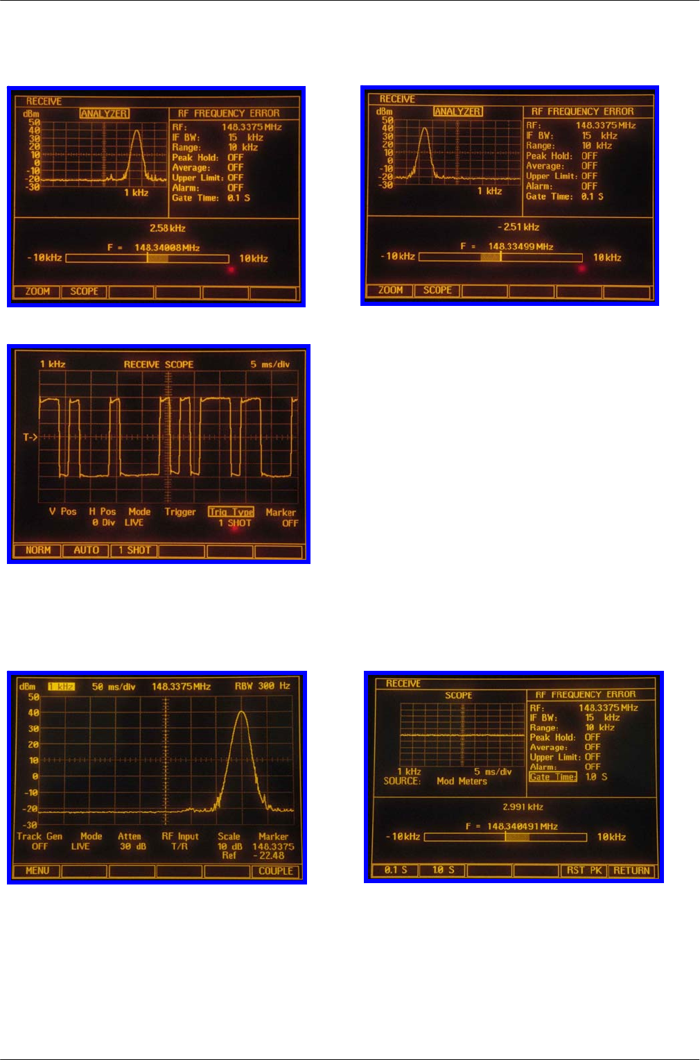
The following pictures are displays of the COM120B screens that are related to setting up the
TBA101B for a RF offset in test mode of +3.0Khz (Pictures 6 and 7) and -3.0K
HZ
(Pictures
8 and
9).
When the POCSAG encoder is connected this results in a nominal POCSAG deviation of 3.5 KHz
(Picture 8).
6 – RV1 adjusted for an RF offset +3.0 KHz (View 1) 7 – RV1 adjusted for an RF offset -3.0 KHz (View 2)
Tait Electronics (Aust) Pty Ltd Job Instruction
JI-131-03.doc Page 5 of 7 22-06-06
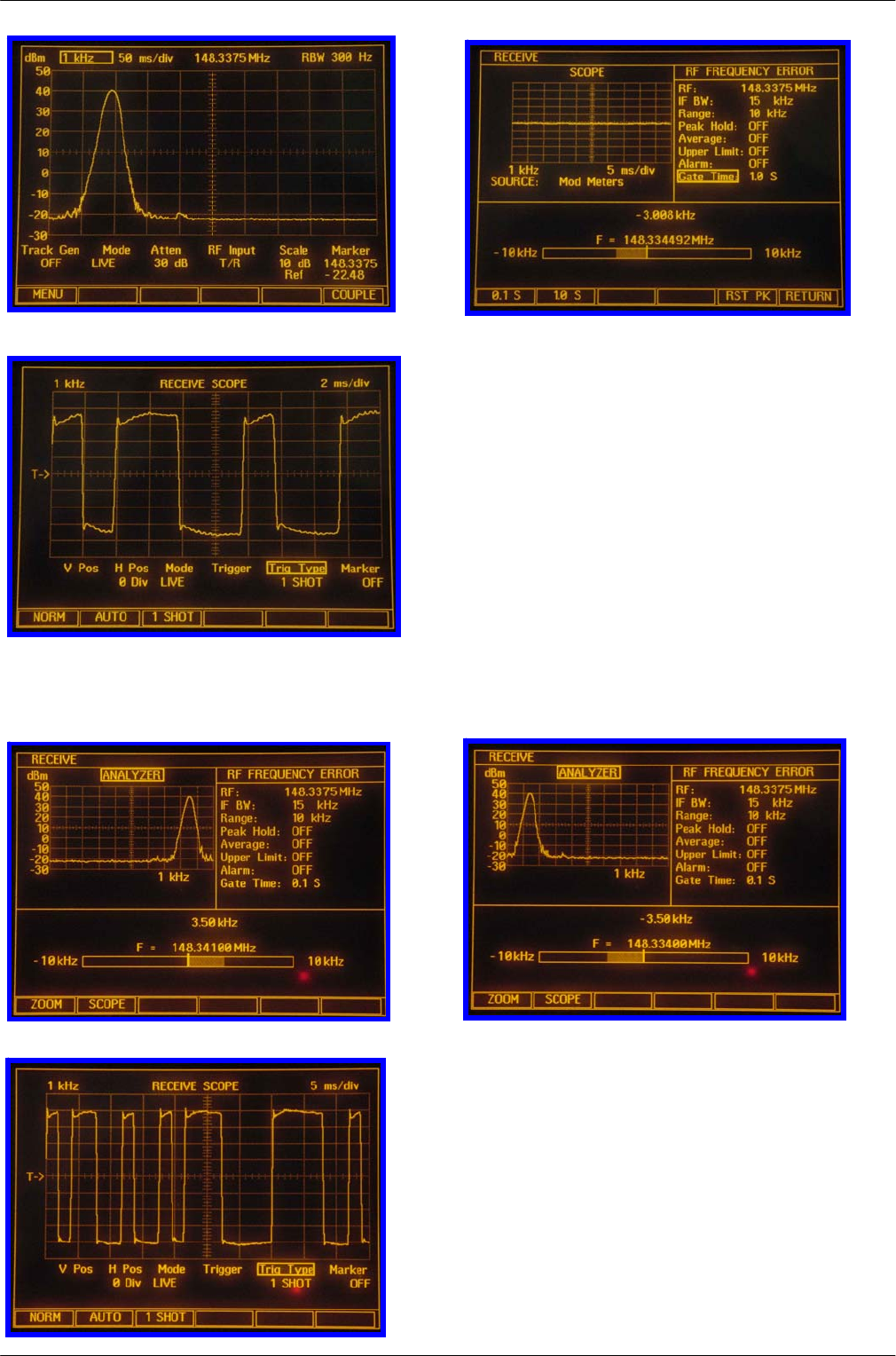
8 – RV2 adjusted for an RF offset -3.0 KHz (View 1) 9 – RV2 adjusted for an RF offset -3.0 KHz (View 2)
10 – After TBA101B test mode RF frequency offset has
been set up for +/-3.0 KHz this results in a POCSAG
deviation output of 3.5 KHz.
The following pictures are displays of the COM120B screens that are related to setting up the
TBA101B for a RF offset in test mode of +3.5Khz (Picture 11) and -3.5Khz (Pictures
12). When the
POCSAG encoder is connected this results in a nominal POCSAG deviation of 4.0 KHz (Picture 13).
11 – RV1 adjusted for an RF offset +3.5 KHz 12 – RV2 adjusted for an RF offset -3.5 KHz
13 – After TBA101B test mode RF frequency offset has
been set up for +/-3.5 KHz this results in a POCSAG
deviation output of 4.0 KHz.
Tait Electronics (Aust) Pty Ltd Job Instruction
JI-131-03.doc Page 6 of 7 22-06-06
The following pictures are displays of the COM120B screens that are related to setting up the
TBA101B for a RF offset in test mode of +4.0Khz (Picture 14) and -4.0Khz (Pictures
15). When the
POCSAG encoder is connected this results in a nominal POCSAG deviation of 4.5 KHz (Picture 16).
14 – RV1 adjusted for an RF offset +4.0Khz 15 – RV2 adjusted for an RF offset -4.0Khz
16 – After TBA101B test mode RF frequency offset has
been set up for +/-4.0 KHz this results in a POCSAG
deviation output of 4.5 KHz.
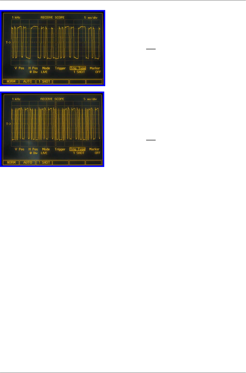
Varying the POCSAG encoders baud rate from 512, 1200 and 2400 does not affect the POCSAG
deviation. Below are screenshots of the POCSAG output at 512 (Picture 17), 1200 (Picture 18) and
2400 baud (Picture 19). These were setup with the RF offset in test mode adjusted to +/-3.0KHz.
17 – After TBA101B test mode RF frequency
offset has been set up for +/-3.0 KHz
this results in a POCSAG deviation output
of 3.5 KHz at 512 baud.
Tait Electronics (Aust) Pty Ltd Job Instruction
JI-131-03.doc Page 7 of 7 22-06-06
18 – After TBA101B test mode RF frequency
offset has been set up for +/-3.0 KHz
this results in a POCSAG deviation output
of 3.5 KHz at 1200 baud.
19 – After TBA101B test mode RF frequency
offset has been set up for +/-3.0 KHz
this results in a POCSAG deviation output
of 3.5 KHz at 2400 baud.
Summary
The results show that setting up the TBA101B test mode (forcing a high or low) results in a RF
frequency offset at a specific level (ie +/-4Khz from centre frequency) which in turn results in a
POCSAG deviation of approximately 500hz more (ie. 4.5Khz POCSAG deviation). Also POCSAG
baud rate does not affect the POCSAG deviation.
