KCPSM6 User Guide 30Sept14
KCPSM6_User_Guide_30Sept14
KCPSM6_User_Guide_30Sept14
User Manual: Pdf
Open the PDF directly: View PDF ![]() .
.
Page Count: 124 [warning: Documents this large are best viewed by clicking the View PDF Link!]

© Copyright 2010-2014 Xilinx
.
PicoBlaze for Spartan-6, Virtex-6, 7-Series, Zynq and
UltraScale Devices (KCPSM6)
Ken Chapman
30th September 2014
Release: 9
Including Ultra-Compact UART Macros and Reference Designs

© Copyright 2010-2014 Xilinx
.
Page 2
Disclaimer
Copyright © 2010-2014, Xilinx, Inc.
This file contains proprietary information of Xilinx, Inc. and is protected under U.S. and international copyright and other intellectual property laws.
Notice of Disclaimer
Xilinx is disclosing this Application Note to you “AS-IS” with no warranty of any kind. This Application Note is one
possible implementation of this feature, application, or standard, and is subject to change without further notice from
Xilinx. You are responsible for obtaining any rights you may require in connection with your use or implementation of
this Application Note. XILINX MAKES NO REPRESENTATIONS OR WARRANTIES, WHETHER EXPRESS OR
IMPLIED, STATUTORY OR OTHERWISE, INCLUDING, WITHOUT LIMITATION, IMPLIED WARRANTIES OF
MERCHANTABILITY, NONINFRINGEMENT, OR FITNESS FOR A PARTICULAR PURPOSE. IN NO EVENT WILL
XILINX BE LIABLE FOR ANY LOSS OF DATA, LOST PROFITS, OR FOR ANY SPECIAL, INCIDENTAL,
CONSEQUENTIAL, OR INDIRECT DAMAGES ARISING FROM YOUR USE OF THIS APPLICATION NOTE.

© Copyright 2010-2014 Xilinx
.
Page 3
Contents
The KCPSM6 Design Flow
8 – Components and Connections
9 – Inserting KCPSM6 into HDL
11 – Program Memory
12 – Inserting Program Memory into HDL
13 – PSM files and Assembler
15 – Adding Files to ISE Project
16 – I/O Ports
17 – Defining Output Ports
18 – CONSTANT Directives
19 – Defining Input Ports
21 – Your first Program
23 – Formatted PSM file (.fmt)
24 – Configuration
25 – JTAG Loader
30 – That’s It!
Hardware Reference (p31)
32 – Pin Descriptions
34 – KCPSM6 Generics
35 – Reset operation and waveforms
37 – Sleep control and waveforms
40 – Interrupts
42 – Interrupt vector and ADDRESS directive
43 – Interrupt circuits
44 – Interrupt waveforms
45 – HDL Simulation Features
47 – Production Program Memory (ROM_form)
Software Reference (p48)
49 – Assembler
51 – Log File (.log)
52 – PSM Syntax
53 – Registers and NAMEREG
54 – KCPSM6 Instruction Set
55 – LOAD
56 – AND
57 – OR
58 – XOR
59 – ADD
60 – ADDCY
61 – SUB
62 – SUBCY
63 – TEST
64 – TESTCY
65 – COMPARE
66 – COMPARECY
67 – SL0 / SL1 / SLX / SLA
68 – SR0 / SR1 / SRX / SRA
69 – RL / RR
70 – REGBANK
71 – STAR
72 – General Purpose I/O Ports
(plus performance figures)
73 – INPUT
74 – OUTPUT
75 – Constant-Optimised Ports
78 – OUTPUTK
79 – Hybrid Output Ports
80 – Hybrid Ports and STRING Directive
81 – STORE
82 – FETCH
83 – ENABLE / DISABLE INTERRUPT
84 – RETURNI ENABLE /DISABLE
86 – Interrupts and Register Banks
87 – JUMP
88 – JUMP cc
89 – JUMP@
90 – Subroutines
92 – CALL
93 – CALL cc
94 – CALL@
96 – RETURN
97 – RETURN cc
98 – LOAD&RETURN
99 – LOAD&RETURN and STRING Directive
100 – TABLE Directive for Data and Sequences
101 – HWBUILD
Notes for KCPSM3 Users
102 – Hardware differences
103 – Assembler and software considerations
104 – ADDCY / SUBCY and the Z flag.
4 – Acknowledgements
5 – Welcome!
6 – KCPSM6 Architecture and Features
Reliability
106 – KCPSM6 Reliability
109 – KCPSM6 Reliability and Single Event
Upsets (SEU)
114 – Error Detection for Very High Reliability
Designs.
119 – Error Detection & Correction for
Very High Reliability Designs (BRAM ECC)
123 – High Reliability Memory Templates
124 – Is this the highest reliability scheme?

© Copyright 2010-2014 Xilinx
.
Page 4
Acknowledgments
Thank you to everyone that has used PicoBlaze over the years and for all the feedback you have provided. It is clear that having a processor that is very small
and simple to use is important and valuable and hopefully you will agree that KCPSM6 continues the tradition. Your feedback has influenced the expansions
and inclusion of new features but even the most commonly requested features are secondary to being small and easy to use so please don’t be too
disappointed if your ideal feature didn’t make it this time. We are really looking forward to hearing your feedback on KCPSM6.
Thank you to Nick Sawyer for all the design reviews, ideas and discussions over the past 18 years of PicoBlaze.
Thank you to Kris Chaplin for JTAG Loader; you have saved every user days of our lives and truly made PicoBlaze easy to use and now you have made it
even easier. Thank you to Srinivasa Attili and Ahsan Raza for adding the Digilent capability to this invaluable tool.
Thank you to Austin Lesea, Eric Crabill and Jim Wesselkamper for all your advice, suggestions and experiments relating to the use of PicoBlaze in
applications requiring the very highest levels of reliability.
Finally, a special thank you to all of those PicoBlaze users that share their experiences and knowledge with others. The professors that teach so many
students, the course instructors, those that provide helpful answers on the PicoBlaze forum, the amazing people that develop additional development tools for
PicoBlaze, those that inspire others by showing what they did with PicoBlaze in a technical paper (or even on YouTube). To all of you, a huge thank you.

© Copyright 2010-2014 Xilinx
.
Page 5
Welcome to KCPSM6
Welcome to the KCPSM6; the PicoBlaze optimised for use in Spartan-6, Virtex-6 and 7-Series devices. PicoBlaze has been very popular for more than 10
years and it continues to be used and adopted by thousands of engineers around the world. So either you are new to PicoBlaze or one of its existing users....
Why use KCPSM6?
KCPSM6 is a soft macro which defines an 8-bit micro controller which can be
included one or more times in any Spartan-6, Virtex-6, 7-Series, Zynq or
UltraScale design. Probably its greatest strengths are that it is 100%
embedded and requires only 26 logic Slices and a Block Memory which
equates to 4.3% of the smallest XC6SLX4 and just 0.11% of the
XC6SLX150T. This combination means that you can decide when and where
to insert KCPSM6 in your design as it develops rather than requiring any pre-
planning. Insertion only requires the most fundamental HDL coding and
design techniques making it a simple task for any competent hardware
engineer and nothing too challenging for a novice. PicoBlaze has been used
in many student projects so just follow the steps and examples and you will
have it working before lunch time.
But why embed a small processor in an FPGA design?
In simple terms, hardware is parallel and processors are sequential. So
converting a small amount of hardware into a processor is often a more
efficient way to implement sequential functions such as state machines
(especially complex ones) or to time-share hardware resources when there
are several slower tasks to be performed. It is also more natural to describe
sequential tasks in software whereas HDL is best at describing parallel
hardware. Don’t worry about this theory; it will just make sense when you
start using KCPSM6 and see for yourself what it can do well (and can’t do).
Please carefully follow pages 6 to 30. It sounds a lot but it is a step by step
guide and it shouldn’t take long to get your first KCPSM6 running. The rest
of this document is for reference including examples, suggestions and more
advanced techniques which you can look at more later. Most of all, have fun!
I’m new to PicoBlaze.... I’ve used PicoBlaze before....
What is KCPSM6?
The most important thing is that KCPSM6 will look very familiar to you.
There are some minor changes to the hardware ports associated with
enhancements but it is a drop in replacement for KCPSM3 in most
respects. Likewise, the instruction set has expanded but you should be
able to assemble KCPSM3 code to begin with and have it running in your
first KCPSM6 design before looking at what you can now do better.
KCPSM6 is bigger smaller and better!
The architectural differences between Generation-3 and Generation-6 and
later devices does not make comparison of size obvious, but at only 26
Slices, KCPSM6 really is 25% smaller in real terms. This equates to 4.3%
of the smallest XC6SLX4 and just 0.11% of the XC6SLX150T so how
many will you be putting in your next design? By the way, the current
record stands at 3,602 in an XC7V2000T and it wasn’t full .
KCPSM6 has quite a few additional features for you to discover but the
principle enhancements are support for programs up to 4K instructions,
an additional bank of 16 registers, dynamic JUMP and CALL, user
defined interrupt vector and constant-optimised output ports.
A special section called ‘Notes for KCPSM3 Users’ is provided starting on
page 102 and you are advised to start with pages 102 and 103 which will
refer you to the relevant sections in the main document. Alternatively,
have a quick look through the following pages (6 to 29) where you should
quickly notice the differences amongst all that seems to be familiar! Of
course you could just dive in and start playing
© Copyright 2010-2014 Xilinx
.
Page 6
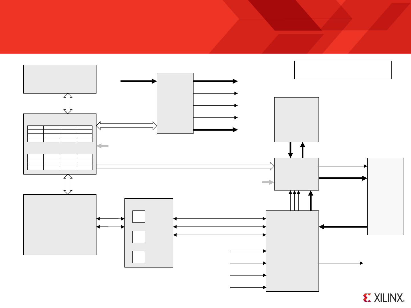
KCPSM6 Architecture and Features
s0
s1
s2
s3
s4
s5
s6
s7
s8
s9
sA
sB
sC
sD
sE
sF
s0
s1
s2
s3
s4
s5
s6
s7
s8
s9
sA
sB
sC
sD
sE
sF
Register Bank ‘A’
Register Bank ‘B’
Scratch Pad Memory
64, 128 or 256 Bytes
ALU
LOAD / STAR
AND / OR/ XOR
ADD / ADDCY
SUB / SUBCY
TEST / TESTCY
COMPARE / COMPARECY
SL0 / SL1 / SLX / SLA / RL
SR0 / SR1 / SRX / SRA / RR
Flags
C
Z
Carry
Zero
Program
Counter
Decode
and
Control
I/O Ports
address[11:0]
port_id[7:0]
out_port[7:0] in_port[7:0]
write_strobe
k_write_strobe
read_strobe
Program
Memory
up to 4K
instructions
instruction[17:0]
sleep
reset
interrupt interrupt_ack
IE Interrupt
Enable
Program
Counter
Stack
30 Deep
interrupt_vector
hwbuild
Please refer to descriptions on
the following page
clk
bram_enable
JUMP / CALL
JUMP@ / CALL@
RETURN
ENABLE INTRRUPT
DISABLE INTRRUPT
RETURNI
REGBANK A/B

© Copyright 2010-2014 Xilinx
.
Page 7
KCPSM6 Architecture and Features
KCPSM6 is an 8-bit data processor that can execute a program of up to 4K instructions. All instructions are defined by a single 18-bit instruction and all
instructions execute in 2 clock cycles. The maximum clock frequency is device and design dependant but up to 105MHz can be achieved in a Spartan-6 (-2
speed grade) and up to 238MHz can be achieved in a Kintex-7 (-3 speed grade) device. This means that the execution performance of KCPSM6 can be in the
range 52 to 119 million instructions per second (52 to 119 MIPS) which is many times faster than achieved by small commercial 8-bit processors. Page 72
shows the circuit that was used to evaluate performance and provides figures for more devices and speed grades. Whilst performance is not the most
important reason for using KCPSM6 in a design, it is the ability to operate at the same clock frequency as the hardware it interacts which makes it so
straightforward to embed in your design. The combination of total predictability and relatively high performance also makes KCPSM6 capable of implementing
many functions traditionally considered to be the domain of pure hardware.
KCPSM6 provides 2 banks of 16 general purpose registers which are central to the flow and manipulation of all 8-bit data. In a typical application information
is read from input ports into registers, the contents of the registers are manipulated and interrogated using the Arithmetic Logical Unit (ALU), and the resulting
values contained in the registers are written to the output ports. All operations can be performed using any register (i.e. there are no special purpose
registers) so you have complete freedom to allocate and use registers when writing your programs.
The 16 registers provided in bank ‘A’ (the default bank) are adequate to implement most individual tasks. However, when moving from one task to another
(e.g. when calling a subroutine) or handling larger data sets the scratch pad memory provides 64-bytes (default), 128-byte or 256-bytes of random access
storage. Once again there is complete freedom to transfer information between any register in the active bank and any location of scratch pad memory. A
second completely independent set of 16 registers are provided in bank ‘B’ and are of most value when it is desirable to switch rapidly between tasks that are
generally unrelated. The most compelling example is when servicing an interrupt which is a rather more advanced technique to be covered later!
The ALU implements a comprehensive set of instructions including bitwise logical AND, OR and XOR, arithmetic ADD and SUBtract, a set of shift and rotate
left/right, TEST including parity calculation and COMPARE. All operations are performed using contents of registers and/or constant values contained in the
instruction word. As well as results being returned to registers there are two flags; zero (Z) and carry (C) whose states reflect the outcome of the operation.
These flags can be used to influence the flow of the program execution or to cascade 8-bit operations to implement operations on data of 16, 24, 32-bits or
more.
The program counter is used to fetch each instruction from the program memory. A program always starts at address zero and under normal conditions
executes sequentially with the program counter incrementing every 2 clock cycles. ‘JUMP’ instructions can be used to deviate from this natural flow to
implement loops and branches within the program. These jumps can also be made conditionally based on the states of the flags (e.g. jump if the result was
zero ‘JUMP Z, aaa’) allowing different program execution depending on the circumstances. A fully automatic program counter stack enables the nesting of up
to 30 subroutines (including an interrupt service routine) to be performed in response to conditional and unconditional CALL and RETURN instructions.
KCPSM6 can be reset, supports one mask-able interrupt with acknowledge, and a ‘sleep’ control can be used to suspend program execution for any period of
time to save power, wait under hardware control (e.g. Handshaking) or to enforce slower execution rate relative to the clock frequency.
© Copyright 2010-2014 Xilinx
.
hwbuild => X"00"
interrupt_vector => X"3FF"
scratch_pad_memory_size => 64
C_FAMILY => "S6"
C_RAM_SIZE_KWORDS => 1
C_JTAG_LOADER_ENABLE => 1
Page 8
KCPSM6 Components and Connections
address
instruction bram_enable
clk
interrupt
sleep
reset
interrupt_ack
port_id
out_port
in_port
k_write_strobe
read_strobe
write_strobe
kcpsm6
[11:0]
[17:0]
[7:0]
[7:0]
[7:0]
KCPSM6 supports programs up to 4K
instructions the address is 12-bits. To
keep your design as simple as possible
and to maintain flexibility the full 12-bit
address is always connected even
when the program size is smaller.
The ‘bram_enable’ signal is used to
achieve the lowest power consumption.
The program memory has the option to
include the JTAG Loader utility which
facilitates rapid development of your
KCPSM6 program. ‘rdl’ is a ‘reset
during load’ signal associated with the
loader and needs to be connected to
the reset on the processor.
Connections to input
and output ports
Connection of
control signals
To insert KCPSM6 into a design there are only two files defining two components. Not surprisingly ‘kcpsm6’ defines the actual processor and its ports. It also
has three generic values but they have been assigned default values which can be used until you have any reason to change them. The second component
defines the memory that will contain your program once it has been written and assembled. It also has three generic values which do need to be set
appropriately. Please take a moment to familiarise yourself with the components and the general arrangement for the connection of the program memory to
the processor. The following pages will show you the details of how to insert this in your HDL design.
instruction
address
enable
your_program
rdl
Hint – If you want to include your own reset
control in your design then OR it with the ‘rdl’
signal. However it is recommended that you only
do this once you are familiar with KCPSM6 and
have your first design working.
kcpsm6_reset <= cpu_rst or rdl;
clk

© Copyright 2010-2014 Xilinx
.
Page 9
Inserting KCPSM6 into Your Design
KCPSM6 is included in your design in exactly the same way as any hardware component. This document is not intended to teach you HDL coding or how to
use the Xilinx ISE tools to implement a complete Spartan-6, Virtex-6 or 7-Series design but it will remind you of the steps that need to be taken and provide
you with everything you need that is specific to KCPSM6.
Inserting the actual KCPSM6 component into your design is easy especially if you adopt the recommended signal names as shown below.
component kcpsm6
generic( hwbuild : std_logic_vector(7 downto 0) := X"00";
interrupt_vector : std_logic_vector(11 downto 0) := X"3FF";
scratch_pad_memory_size : integer := 64);
port ( address : out std_logic_vector(11 downto 0);
instruction : in std_logic_vector(17 downto 0);
bram_enable : out std_logic;
in_port : in std_logic_vector(7 downto 0);
out_port : out std_logic_vector(7 downto 0);
port_id : out std_logic_vector(7 downto 0);
write_strobe : out std_logic;
k_write_strobe : out std_logic;
read_strobe : out std_logic;
interrupt : in std_logic;
interrupt_ack : out std_logic;
sleep : in std_logic;
reset : in std_logic;
clk : in std_logic);
end component;
Hint – This is not supposed to be an exercise in typing so the file called ‘kcpsm6_design_template.vhd’ is provided and contains all these pieces of code
for you to simply copy and paste into the appropriate places in your own design.
Paste the KCPSM6 component declaration into the
appropriate section of your design file (i.e. after ‘architecture’
and before ‘begin’ in VHDL).
The generics can be left with the default values as shown as
it is the component instantiation that will actually define them.
signal address : std_logic_vector(11 downto 0);
signal instruction : std_logic_vector(17 downto 0);
signal bram_enable : std_logic;
signal in_port : std_logic_vector(7 downto 0);
signal out_port : std_logic_vector(7 downto 0);
Signal port_id : std_logic_vector(7 downto 0);
Signal write_strobe : std_logic;
Signal k_write_strobe : std_logic;
Signal read_strobe : std_logic;
Signal interrupt : std_logic;
Signal interrupt_ack : std_logic;
Signal kcpsm6_sleep : std_logic;
Signal kcpsm6_reset : std_logic;
In order that you can instantiate KCPSM6 in the design section of your design file
(shown on the next page) it is necessary to define the signals to connect to each of the
ports. The recommended signal names are shown here and can also be pasted into
your design file (after ‘architecture’ and before ‘begin’ in VHDL). Of course you can
modify the signal names if you wish and you would need to if you had more than one
KCPSM6 instance in the same design file but neither is recommended until you have
more experience.
Please note that the Verilog equivalent of each file is also provided.

© Copyright 2010-2014 Xilinx
.
Page 10
Inserting KCPSM6 into Your Design
processor: kcpsm6
generic map ( hwbuild => X"00",
interrupt_vector => X"3FF",
scratch_pad_memory_size => 64)
port map( address => address,
instruction => instruction,
bram_enable => bram_enable,
port_id => port_id,
write_strobe => write_strobe,
k_write_strobe => k_write_strobe,
out_port => out_port,
read_strobe => read_strobe,
in_port => in_port,
interrupt => interrupt,
interrupt_ack => interrupt_ack,
sleep => kcpsm6_sleep,
reset => kcpsm6_reset,
clk => clk );
kcpsm6_sleep <= '0';
interrupt <= '0';
The values assigned to the three generics can remain set to the default values as shown.
Their purpose is described in detail later in this document and they only need to be
changed if and when you want to use the features they are associated with.
If this is your first KCPSM6 design or you have no intention of using
interrupts or the sleep function then these signals should be tied to ‘0’.
If you used the default signal names then nothing needs to be modified.
Otherwise connect the signals you have defined to these ports.
Paste the instantiation of KCPSM6 into your design. If this is your first design then there is very little to do except copy and paste from the reference file and
specify your clock. Even advanced users will only have minor adjustments to make but they are covered later in this document (page 101).
You will need to specify the clock signal that is available in your design. As a guide anything
up to 105MHz in a Spartan-6 (-2) and up to 240MHz in Virtex-6 or 7-Series (-3) is suitable
and as with all general clocks it should be distributed via a clock buffer (typically inserted
automatically by the synthesis tools).
interrupt => ‘0’,
sleep => ‘0’, Alternatively these KCPSM6 inputs can be tied directly to ‘0’ in the port map. This
avoids the requirement for these signals to be defined but if you decide to make
use of either of these features as your design develops it will just result in more
modifications so it is not the recommended technique.
Please note that the Verilog equivalent of each file is also provided.
© Copyright 2010-2014 Xilinx
.
Page 11
Program Memory
KCPSM6 Programs are stored in Block Memory (BRAM). The number of BRAMs required depends on the target device as well as the size of the program.
Due to the flexibility of BRAM and FPGA devices it would be possible to implement a memory of any size up to the maximum of 4K instructions supported by
KCPSM6. However the most natural and commonly used program sizes are shown in the table below showing how many BRAMs are required.
Hint – A program of up to 128 or 256 instructions can be implemented in just
9 or 18 Slices and this can be a useful technique when there is a high
demand for block memory within a design (see page 47 for details). Even
with such small programs, KCPSM6 can implement a complex state machine
in ~40 Slices. However, it is strongly recommended that a program is always
developed using block memory first using JTAG Loader to help you.
Programs Size
(instructions)
0.125K / 0.25K
1K
2K
4K
Spartan-6 Vitex-6, Artix-7,
Kintex-7, Virtex-7
9 / 18 Slices
1 BRAM
2 BRAMs
4 BRAMs
½ BRAM
1 BRAM
2 BRAM
The 36k-bit BRAMs found in Virtex-6 and 7-Series devices are naturally
suited to programs of up to 2K instructions whereas the 18k-bit BRAMs of
Spartan-6 are best suited to programs of 1K instructions. These are
therefore the recommended sizes when initially setting up KCPSM6.
These sizes are also supported by the files provided and fit well in the
devices when required.
Whilst a 4K memory is supported in a Spartan-6 is not such a
natural fit and will result in a lower maximum clock frequency
(i.e. Be aware of this when operating closer to device limits).
ROM_form.vhd
ROM_form.v
(Template)
KCPSM6
Assembler
your_program.psm
your_program.vhd
your_program.v
(Used in design)
Program Memory Definition
To be completely compatible with the normal hardware design flow the program
memory is defined by a standard HDL file which you include in your design in the same
way as any other component (see next page). This file is generated by the KCPSM6
assembler and you will see how to do that later but the basic principle is as follows....
The KCPSM6 assembler reads and assembles your program (PSM file) into the
instruction codes. It then reads an HDL template file called ‘ROM_form.vhd’ (or
ROM_form.v) into which it inserts your assembled program and writes out the HDL file
defining the program memory containing your program for use in your design.
Due to the errata described in EN148 there are no plans to support a 0.5K
memory using a 9K BRAM in Spartan-6.
9 / 18 Slices

© Copyright 2010-2014 Xilinx
.
Page 12
Inserting a Program Memory into Your Design
During the development phase of your hardware design and KCPSM6 program it is highly recommended that you use the default ‘ROM_form’ template with
the assembler such that the KCPSM6 assembler will generate a program definition file exactly as shown below. In this way you don’t need to worry that you
haven’t written a program or run the assembler yet because we know the format of the program definition file that will be generated in advance and we can
control everything by setting the generic values as shown below.
component your_program
generic( C_FAMILY : string := "S6";
C_RAM_SIZE_KWORDS : integer := 1;
C_JTAG_LOADER_ENABLE : integer := 0);
Port ( address : in std_logic_vector(11 downto 0);
instruction : out std_logic_vector(17 downto 0);
enable : in std_logic;
rdl : out std_logic;
clk : in std_logic);
end component;
program_rom: your_program
generic map( C_FAMILY => "S6",
C_RAM_SIZE_KWORDS => 1,
C_JTAG_LOADER_ENABLE => 1)
port map( address => address,
instruction => instruction,
enable => bram_enable,
rdl => kcpsm6_reset,
clk => clk);
Hint – This is not supposed to be an exercise in typing so the file called ‘kcpsm6_design_template.vhd’ is provided and contains all these pieces of code
for you to simply copy and paste into the appropriate places in your own design.
Paste the program memory component declaration into the appropriate section of
your design file (i.e. after ‘architecture’ and before ‘begin’ in VHDL).
You must modify the name of the component so that you assign a unique name that
will correspond with your KCPSM6 program.
The generics can be left with the default values as shown but you could modify them
if you would prefer (e.g. if you are using a Virtex-6 it probably makes sense and looks
better in your design if you change the default ‘C_FAMILY’ value to “V6”).
generic map( C_FAMILY => "7S",
C_RAM_SIZE_KWORDS => 2,
C_JTAG_LOADER_ENABLE => 1)
Paste the instantiation of the program memory into your design. It normally makes sense to instantiate the program memory immediately after the
instantiation of the KCPSM6 processor that it is attached to. Once again you must modify the name of the instantiated component to correspond with the
name of your KCPSM6 program. Unless you wish to change the instance name (‘program_rom’ is used below) it can remain the same unless you are
instantiating another program memory in the same design file.
At this point the appropriate values must be assigned to each of the three generics. For a
Spartan-6 design set ‘C_FAMILY’ to “S6” and it is recommended that you start with a program
size of 1K by setting ‘C_RAM_SIZE_KWORDS’ to ‘1’ as shown in this example.
For a Virtex-6 or 7-Series designs set
“V6” or “7S” and it is recommended that
you start with a program size of 2K.
Start by setting the ‘C_JTAG_LOADER_ENABLE’ generic to ‘1’ as this will automatically
include the JTAG Loader circuitry that will help you to rapidly develop your program.
Note that if you do have multiple KCPSM6 program memories in your design only one should
have this generic set at a time.
Connect the appropriate signals to the ports. If you
used the default signal names then nothing needs to
be modified.
Please note that the Verilog equivalent of each file is also provided.
© Copyright 2010-2014 Xilinx
.
Page 13
Starting ‘your_program.psm’
Any KCPSM6 based design faces a ‘chicken and egg’ situation because you are defining both the hardware in your HDL design and writing a the software
program for the processor to execute. Once you are familiar with using KCPSM6 you will resolve this naturally but if this is your first time using any PicoBlaze
then please just follow the flow being described in these pages and it will all fit together.
So far you have inserted the program memory and connected it in your HDL design. You have assigned that component a name to correspond with your
program (this document has shown that name to be ‘your_program’) but as yet you do not have a program. More significantly you do not have the
corresponding HDL file that the assembler generates. To resolve this situation the next step is to start your KCPSM6 program and run the assembler for the
first time. At this stage the program only needs to act as a place keeper so you don't need to actually write a real program yet ; it only has to be a file to
present to the KCPSM6 assembler.
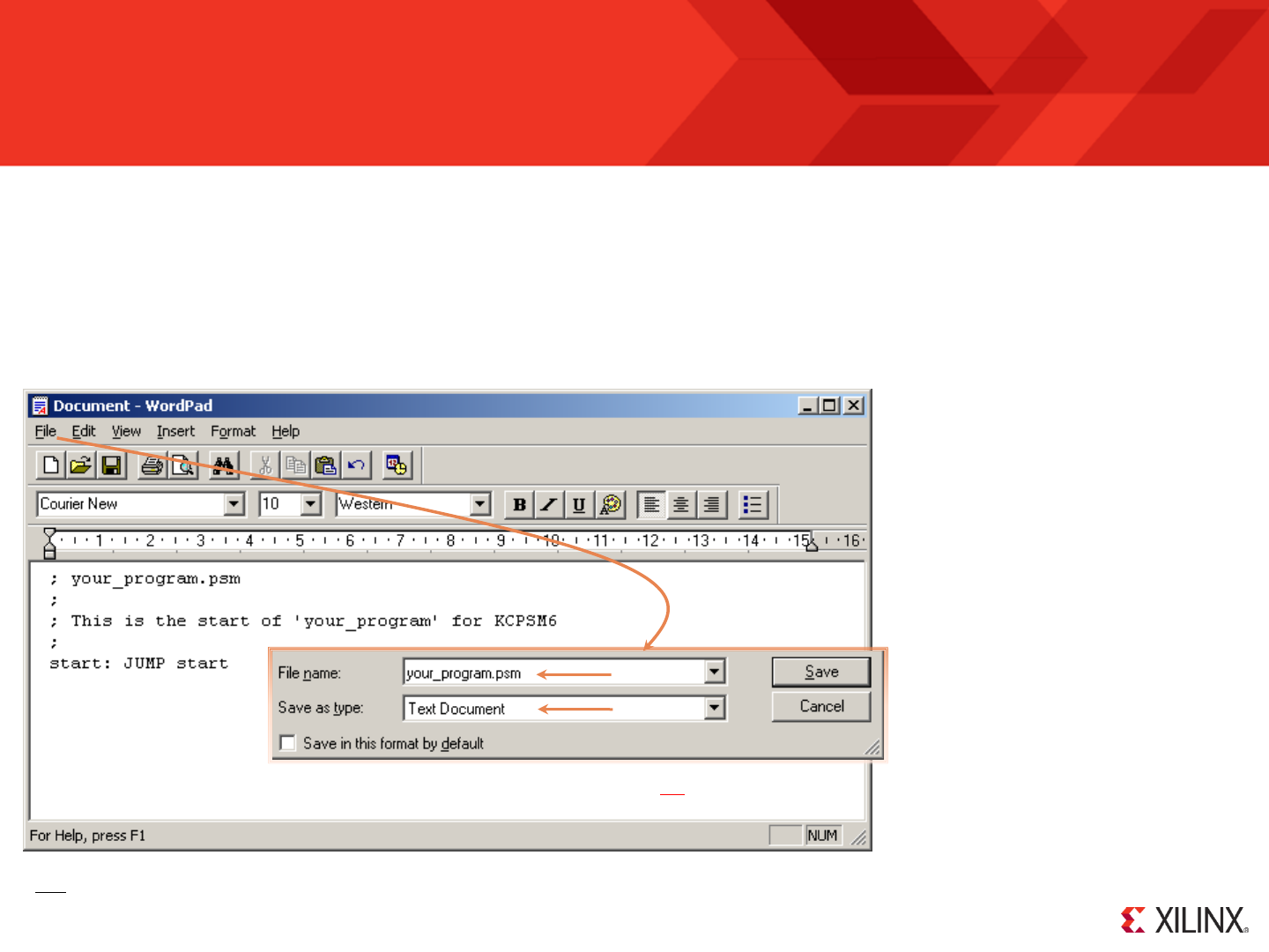
Making a PSM file
A program for KCPSM6 is written as a
standard text file and then saved with the
.psm’ file extension. As such you are free to
use whatever text editor you prefer and
WordPad supplied as an Accessory in
Windows is more that adequate as shown in
this example.
If this is your first experience of using
PicoBlaze then start your first program by
copying this example (that does nothing!) as
it will be adequate at this stage.
Then save your program in your working
directory as plain text with the ‘.psm’
extension. Check that it really in in your
working directory with the correct name (e.g.
‘your_program.psm’ and not something like
‘your_program.psm.txt’) and to be sure
reopen the file in your text editor and check
that it still looks Ok.
File -> Save As....
Hint – A semicolon (;) is used to start a comment so feel free to write whatever you like in your PSM program.
IMPORTANT – Your chosen filename should not contain spaces
© Copyright 2010-2014 Xilinx
.
Page 14
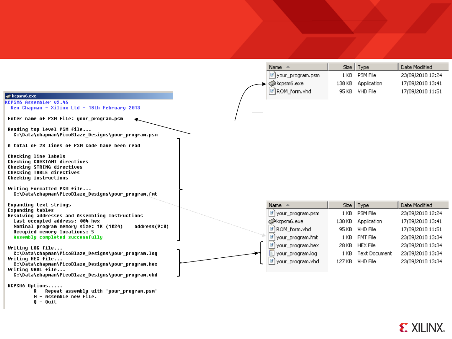
Running the Assembler for the First Time
The easiest way to use the KCPSM6 assembler is in interactive mode within your working
directory. In order to be able to do this, copy ‘kcpsm6.exe’ and the default ‘ROM_form.vhd’
(or .v) file from the ZIP file into the working directory containing ‘your_program.psm’.
Double click on ‘kcpsm6.exe’ to launch the assembler which will open the KCPSM6 window.
You will be prompted to ‘Enter name of PSM file:’ so type in the name you have
given for your program. You can include the ‘.psm’ file extension if you like typing!
The assembly of any simple program is very fast and unless you made a mistake
(which it would tell you about) the assembly will be successful.
Then most important of all, the assembler generates the ‘your_program.vhd’ (or .v)
definition of the program memory ready for you to include in your ISE project. The
assembler has also generated ‘.fmt’, ‘hex’ and ‘.log’ files which we can look at more later.
Hint – Copy ‘kcpsm6.vhd’ into your working directory at the same time.
If using ISE v13.x or later then continue reading and having fun but if you are still using ISEv12.x please check READ_ME_FIRST.txt to prepare.
You are presented with some simple options but in a while you will modify ‘your_program.psm’
and it will be easier to leave the assembler window open and then choose ‘R’...
© Copyright 2010-2014 Xilinx
.
Page 15
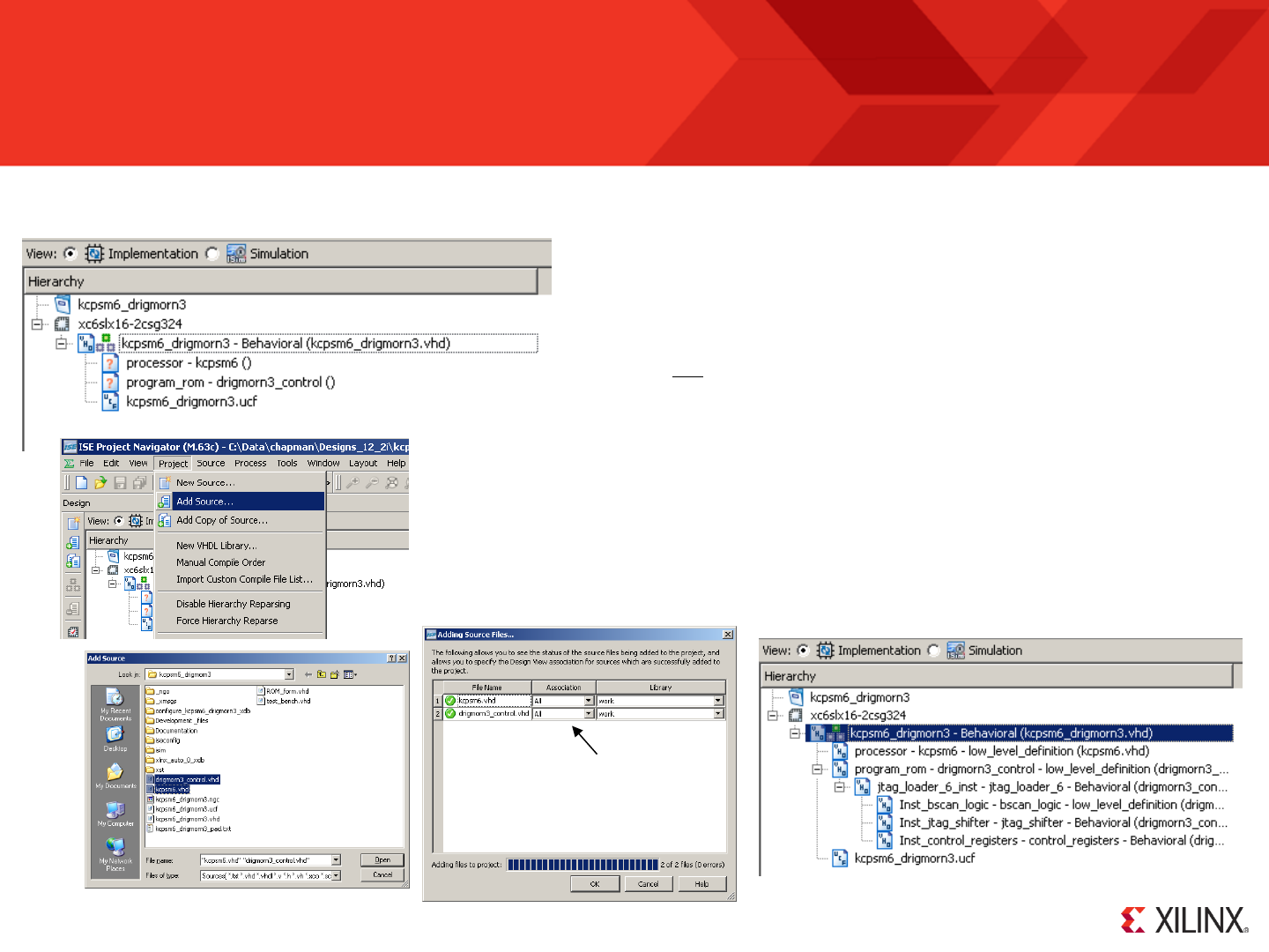
Adding the Source Files to Your ISE Project
As previously stated this document is not intended to teach you how to use ISE but simply to remind you of the steps required. At this point you can add the
‘kcpsm6.vhd’ and ‘your_program.vhd’ files (or their verilog equivalents) to your ISE project.
Assuming your design file is already in your ISE project and you have saved that
files since including the KCPSM6 and program memory components then the
’Hierarchy’ view should show the processor and program ROM but with ‘?’ indicating
that no files are associated with them.
Make sure you have the ‘kcpsm6.vhd’ and ‘your_program.vhd’ files to your working directory, then use
the ‘Project -> Add Source...’ option to locate and add them to your project.
Association: ALL
Hint – In these screen shots of ISE the KCPSM6
program was called ‘drigmorn3_control’
This should complete the hierarchy (no ‘?’ symbols) of your
ISE project. The program memory includes the definition of
the JTAG Loader utility (even if it is not actually enabled the
definition will be present) .
KCPSM6 can also be used in a Vivado project but the images below are for ISE Project Navigator.
© Copyright 2010-2014 Xilinx
.
Page 16
Programmable2 Design – Adding I/O Ports
Your design now includes KCPSM6 and its associated program memory but as yet it is not connected to anything else. This is the point at which every design
is going to be different depending on the application. However, in all cases the primary interface between KCPSM6 and the rest of your design is made using
input and output ports. Whether you need a few or many, the method is the same.
Programmable2 Design
The key advantage of a Field Programmable Gate Array (FPGA) is that you can define, program, modify and re-program your hardware. As such it makes a
lot of sense to develop a design in stages. Start with something simple, perform experiments and tests to get it working and then expanding the design as you
gain confidence. This is of particular value when bringing unproven hardware to life for the first time where simple designs whose only purpose is to prove that
the board and pin connections are correct often prove to be invaluable. In contrast, the person or team that develop their entire complex design using
simulation tools then often spend months trying to debug simple hardware issues.
Including KCPSM6 in your design means that you now have the benefit of software programmability embedded within your hardware. However, that degree of
flexibility is only truly beneficial if the interface between software in the KCPSM6 processor and the hardware is correct to begin with. So once again the key
to success is to start simple and build up. As you will see, it takes less than 10 seconds to modify a KCPSM program and have it executing within your design
so simple experiments to prove functionality become so natural that you soon forget that you are exploiting programmable2 every day.
Whatever Your Design – Start Simple!
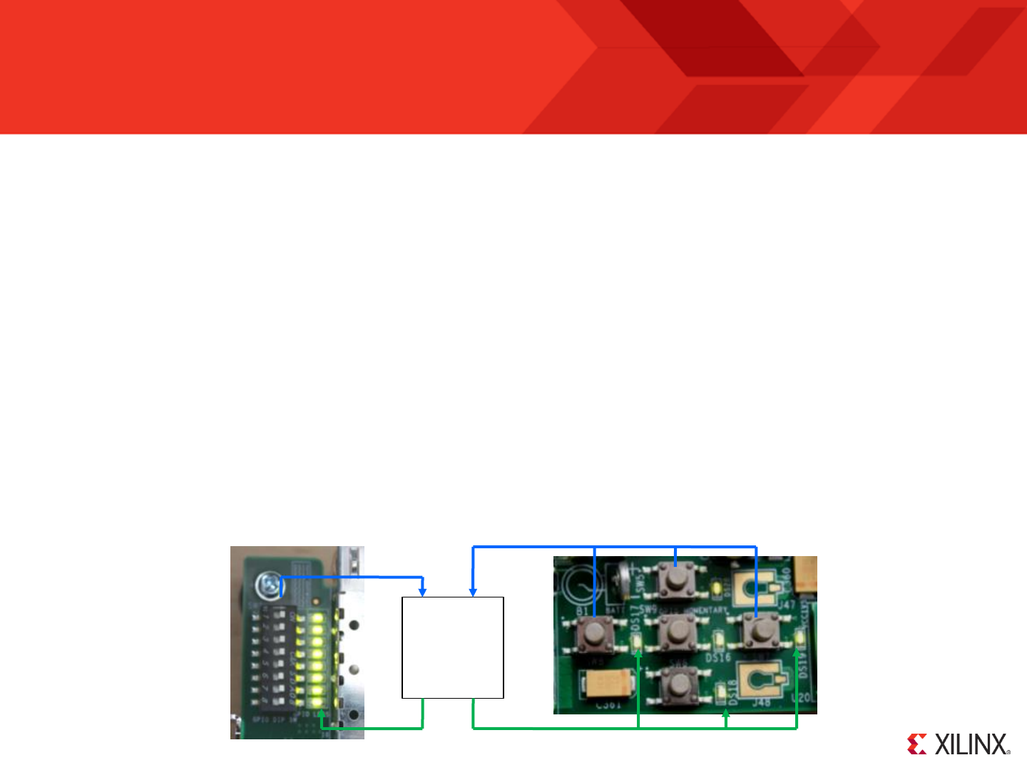
Unless you are an experienced PicoBlaze designer or starting with a known good platform and reference it is always best to start with something simple and
then to expand. The following pages will take you through one simple case study that connects KCPSM6 to the switches, press buttons and LEDs on the
Virtex-6 FPGA Evaluation Kit. Whatever the hardware you have access to, try to start with something at least as simple as this.
The ML605 board has a row
of 8 DIP switches and a row of
8 general purpose LEDs.
Although adjacent on the
board there is no direct
connection between them but
they all connect to pins on the
Virtex-6 device.
XC6VLX240T
In a similar way there
are 5 ‘direction’ push
buttons with adjacent
LEDs.
© Copyright 2010-2014 Xilinx
.
Page 17
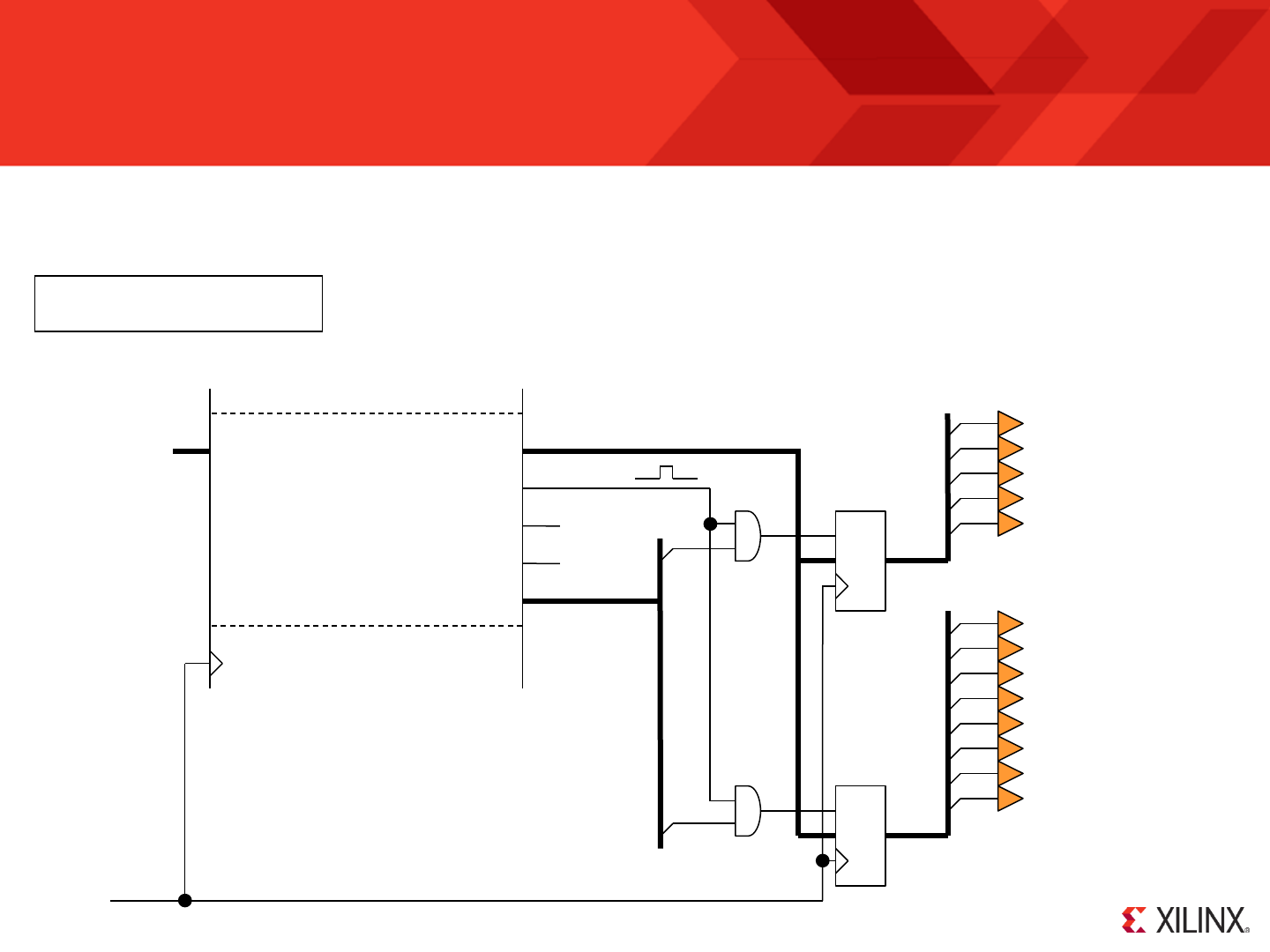
Output Ports
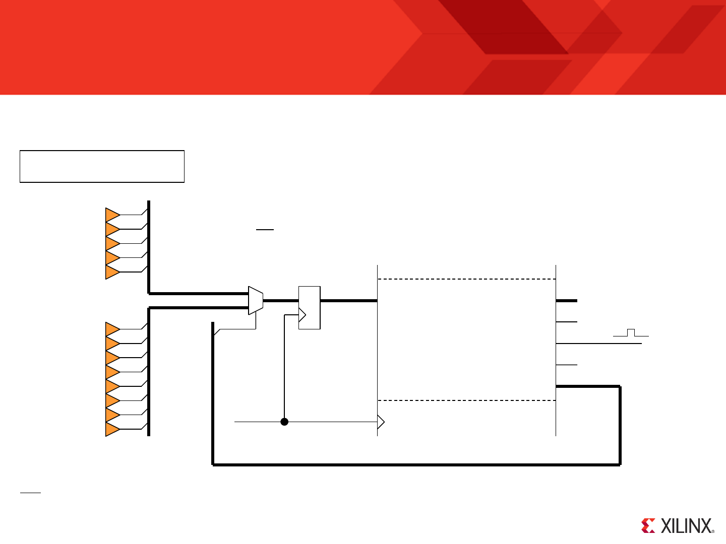
KCPSM6 can output 8-bit values to up to 256 general purpose output ports using its ‘OUTPUT sX, pp’ and ‘OUTPUT sX, (sY)’ instructions. A complete
description is provided in the reference section later in this document but here we can see this put into practice so that KCPSM6 can control the 8 general
purpose LEDs and 5 ‘direction’ LEDs on the ML605 board.
[7:0]
D
CE
[7:0]
D
CE
[0]
[1]
PORT 01
port_id
out_port
in_port
k_write_strobe
read_strobe
write_strobe
out_port[7:0]
port_id[7:0]
[7:0]
kcpsm6 (port connections only)
write_strobe
[0]
[1]
[2]
[3]
[4]
[5]
[6]
[7]
led<0>
led<1>
led<2>
led<3>
led<4>
led<5>
led<6>
led<7>
[0]
[1]
[2]
[3]
[4] led_c
led_n
led_e
led_s
led_w
PORT 02
clk
clk
When KCPSM6 executes an ‘OUTPUT’ instruction it sets ‘port_id’ to specify which of 256 ports it wants to
write the 8-bit data value present on ‘out_port’. A single clock cycle enable pulse is generated on
‘write_strobe’ and your hardware must use ‘write_strobe’ to qualify the decodes of ‘port_id’ to ensure
that only the correct register (or peripheral) captures the ‘out_port’ value.
The output ports should be
connected to the same
clock as KCPSM6
(synchronous design).
Please see next page for the
corresponding VHDL and PSM

© Copyright 2010-2014 Xilinx
.
Page 18
Output Ports…. VHDL and PSM
VHDL corresponding with circuit diagram of output ports shown on the previous page.
output_ports: process(clk)
begin
if clk'event and clk = '1' then
if write_strobe = '1' then
-- 8 General purpose LEDs at port address 01 hex
if port_id(0) = '1' then
led <= out_port;
end if;
-- Direction LEDs at port address 02 hex
if port_id(1) = '1' then
led_n <= out_port(0);
led_e <= out_port(1);
led_s <= out_port(2);
led_w <= out_port(3);
led_c <= out_port(4);
end if;
end if;
end if;
end process output_ports;
Output ports should be synchronous with the same clock used by KCPSM6.
Writes to general purpose output ports must be qualified with ‘write_strobe’.
KCPSM6 always presents an 8-bit value on ‘out_port’ but you can assign
individual bits as required and use only the number of bits you need.
Decode the ‘port_id’ to enable only the appropriate port to be written.
if port_id = X"01" then
The majority of PicoBlaze designs use far less than the 256 output ports
available so it is best practice to allocate ports such that the decoding logic
can be minimised (smaller and faster) as shown here. For full -8-bit
decoding the equivalent code would be....
; 8 General Purpose LEDs
CONSTANT LED_port, 01
;
; 5 Direction LEDs
CONSTANT Direction_LED_port, 02
; Bit assignements for each LED/button
CONSTANT North, 00000001'b ; North - bit0
CONSTANT East, 00000010'b ; East - bit1
CONSTANT South, 00000100'b ; South - bit2
CONSTANT West, 00001000'b ; West - bit3
CONSTANT Centre, 00010000'b ; Centre – bit4
PSM corresponding with circuit diagram and VHDL
As you assign your output ports in your hardware design take the opportunity to define
constants in ‘your_program.psm’. The assembler has a CONSTANT directive which
enables you to define a unique name (case sensitive no spaces) and assign it a value.
You can study more details about assembler syntax later but hopefully just seeing this
example makes it fairly obvious.
Hint – Although CONSTANT directives are optional they make programs much
easier to write, modify, understand, maintain and re-use in comparison to always
specifying absolute port addresses in ‘OUTPUT’ instructions.
© Copyright 2010-2014 Xilinx
.
Page 19
Input Ports
KCPSM6 can read 8-bit values from up to 256 general purpose input ports using its ‘INPUT sX, pp’ and ‘INPUT sX, (sY)’ instructions. A complete description
is provided in the reference section later in this document but here we can see this put into practice so that KCPSM6 can read the 8 DIP switches and 5
‘direction’ push buttons on the ML605 board.
D
[0]
port_id
out_port
in_port
k_write_strobe
read_strobe
write_strobe
port_id[7:0]
in_port[7:0]
kcpsm6 (port connections only)
read_strobe
[0]
[1]
[2]
[3]
[4]
[5]
[6]
[7]
dip_switch<0>
dip_switch<1>
dip_switch<2>
dip_switch<3>
dip_switch<4>
dip_switch<5>
dip_switch<6>
dip_switch<7>
[0]
[1]
[2]
[3]
[4]
button_c
button_n
button_e
button_s
button_w
PORT 01
clk
clk
Please see next page for the
corresponding VHDL and PSM
PORT 00
When KCPSM6 executes an ‘INPUT’ instruction it sets ‘port_id’ to specify which of 256 ports it wants
to read from and it is the task of the hardware circuit to present that 8-bit data to the ‘in_port’. A
simple multiplexer can be used to achieve this. It is best practice to pipeline the output of the
multiplexer and to only use the appropriate number of bits of ‘port_id’ to facilitate the number of input
ports actually required.
Hint – Failure to pipeline the input multiplexer and fully decoding ‘port_id’ when only a few input ports
are actually used are the most common reasons for a PicoBlaze design not meeting performance.
Hint - The ‘read_strobe’ is also pulsed High when KCPSM6 executes an ‘INPUT’ instruction but this does not need to be used to qualify the multiplexer
selection. This strobe would be used in situations where the circuit being read needs to know when data has been captured. The most obvious example
is reading data from a FIFO so that it can discard the oldest information and present the information to be read on its output.

© Copyright 2010-2014 Xilinx
.
Page 20
Input Ports…. VHDL and PSM
VHDL corresponding with circuit diagram of input ports shown on the previous page.
input_ports: process(clk)
begin
if clk'event and clk = '1' then
case port_id(0) is
-- Read 8 DIP switches at port address 00 hex
when '0' => in_port <= dip_switch;
-- Read 5 Push Buttons at port address 01 hex
when '1' => in_port(0) <= push_n;
in_port(1) <= push_e;
in_port(2) <= push_s;
in_port(3) <= push_w;
in_port(4) <= push_c;
when others => in_port <= "XXXXXXXX";
end case;
end if;
end process input_ports;
The input port selection multiplexer should be pipelined and synchronous
with KCPSM6 (i.e. use the same clock as connected to KCPSM6).
Assign the 8-bit data to ‘in_port’ as required.
Limit the number of bits of ‘port_id’ used to those necessary to
select the number of inputs that you have. For example if you had
5 to 8 input ports then your code would take the general form
shown below....
; 8 DIP Switches
CONSTANT Switch_port, 00
;
; 5 Direction Push Buttons
CONSTANT Direction_Button_port, 01
PSM corresponding with circuit diagram and VHDL
As with the output ports, take the opportunity to define constants in ‘your_program.psm’
corresponding to your allocations of input ports in your hardware design. Hopefully this is all
beginning to make sense and already beginning to look familiar!
Hint – The previously defined constants North, South, East, West and Centre can apply to
both the direction LEDs and direction buttons because of the consistent allocation of the
bits within those ports.
case port_id(2 downto 0) is
when "000" => in_port <= dip_switch;
when "001" => in_port <=
For smallest and fastest hardware always use ‘don't care’ to cover the
unused cases and bit assignments. Your KCPSM6 program should not
read unused ports and can mask/ignore bits that have no meaning.
© Copyright 2010-2014 Xilinx
.
Page 21
Some First Instructions for ‘your_program.psm’
As you have been defining the hardware input and output ports connected to
KCPSM6 you should have been adding the corresponding CONSTANT
directives to your PSM file. So hopefully it looks something like the file shown
here. However, the program still doesn’t actually do anything until we include
some somewhat meaningful instructions.
CONSTANT directives to help identify port assignments and also the
allocation of bits within a port.
Hint – Anything written on a line following a semicolon (;) is a
comment and so you can add any notes that you like.
A Simple Test Program
The key is to start with something simple that will help you to verify your
hardware, your hardware design and the corresponding port assignments in
the PSM file. In this case the program is just going to read the switches and
output their values to the LEDs. Likewise it will read the direction press buttons
and output their values to the corresponding direction LEDs.
Hint – If something did not work properly in this example it would be good to try
driving the LEDs with a known pattern
(A5 = “10100101”) to determine if it was
the input or output path that was incorrect.
LOAD s0, A5
OUTPUT s0, LED_port
Each INPUT instruction reads the value from a specified port into one of the
general purpose registers (registers are named ‘s0’, ‘s1, through to ‘sF’).
Likewise the OUTPUT instructions write the contents of registers to the
specified ports.
So that the program continuously repeats a JUMP instruction is used to ‘loop’
back to the start of the program. ‘start:’ is a ‘line label’ and this lets the
assembler work out the actual program address for you.
© Copyright 2010-2014 Xilinx
.
Page 22
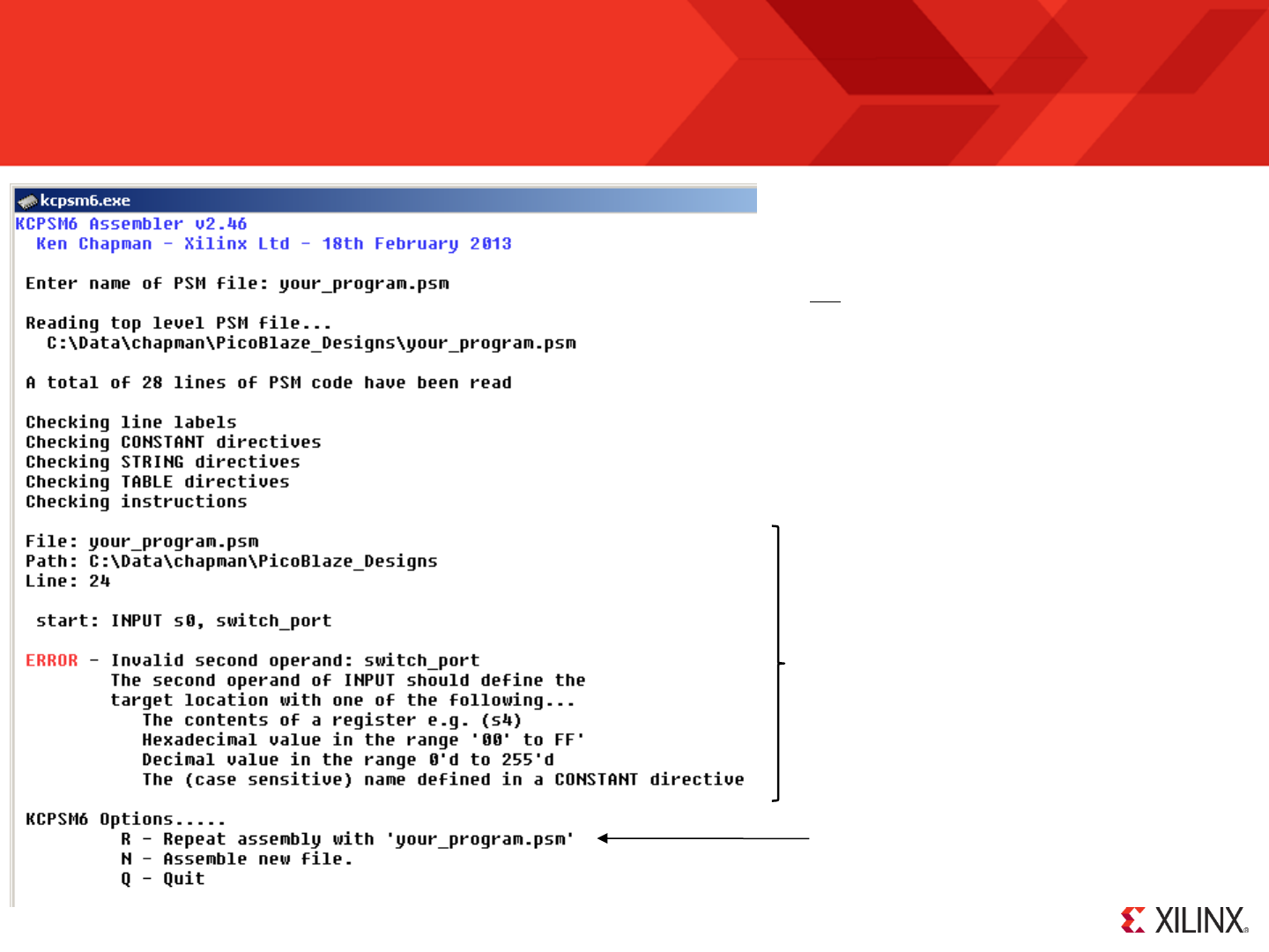
Assemble ‘your_program.psm’ (again)
Each time you modify your PSM file you need to run
the assembler again so that the changes are also
included in the HDL program memory definition file.
If you should make any mistakes in your PSM
program then the assembler will identify the PSM file
and the line in that file that it can not resolve and make
suggestions for you to be able to rectify the issue.
In this example my mistake was using a lower case ‘s’
in ‘switch_port’ when the constant directive had
specified it to be ‘Switch_port’.
Hint – Even though the assembly process is fast it can
become tiresome to keep entering the name of your
program. There are several solutions to this including
the use of batch files but probably the most elegant
technique during code development is to keep the
assembler open (i.e. Do not ‘Q’uit or manually close the
window) and then use the ‘R’ option each time you need
to repeat the assembly process with the same file.
Use ‘R’ once you have made any changes
or corrections to your PSM file.

© Copyright 2010-2014 Xilinx
.
Page 23
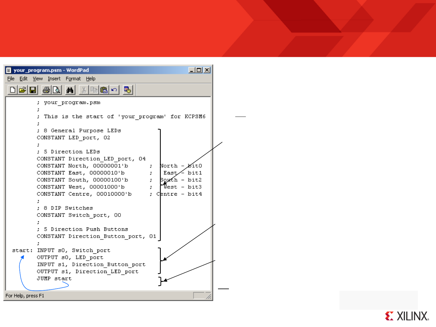
The Formatted PSM File (.fmt)
; your_program.psm
;
; This is the start of 'your_program' for KCPSM6
;
; 8 General Purpose LEDs
CONSTANT LED_port, 01
;
; 5 Direction LEDs
CONSTANT Direction_LED_port, 02
CONSTANT North, 00000001’b; North - bit0
CONSTANT East, 00000010’b; East - bit1
CONSTANT South, 00000100’b; South - bit2
CONSTANT West, 00001000’b; West - bit3
CONSTANT Centre, 00010000’b; Centre – bit4
;
; 8 DIP Switches
CONSTANT Switch_port,00
;
; 5 Direction Push Buttons
CONSTANT Direction_Button_port, 01
;
start: INPUT s0, Switch_port
OUTPUT s0, LED_port
input s1,Direction_Button_port
OUTPUT s1, Direction_LED_port
Jump start
; your_program.psm
;
; This is the start of 'your_program' for KCPSM6
;
; 8 General Purpose LEDs
CONSTANT LED_port, 01
;
; 5 Direction LEDs
CONSTANT Direction_LED_port, 02
CONSTANT North, 00000001’b ; North - bit0
CONSTANT East, 00000010’b ; East - bit1
CONSTANT South, 00000100’b ; South - bit2
CONSTANT West, 00001000’b ; West - bit3
CONSTANT Centre, 00010000’b ; Centre – bit4
;
; 8 DIP Switches
CONSTANT Switch_port, 00
;
; 5 Direction Push Buttons
CONSTANT Direction_Button_port, 01
;
start: INPUT s0, Switch_port
OUTPUT s0, LED_port
INPUT s1, Direction_Button_port
OUTPUT s1, Direction_LED_port
JUMP start
your_program.psm
Use of the FMT file is completely optional but even this small example illustrates that the KCPSM6 assembler can help your code look tidy and professional.
Over time you will discover that the assembler is very tolerant of the way that you space items on a line and the use of upper and lower case characters when
entering instructions and directives. This enables you to write code quickly but this will also tend to make your code look untidy and difficult to maintain. So
from time to time it is recommended that you discard your original PSM file and simply rename the ‘.fmt’ file to make it your new tidy ‘.psm’ file.
your_program.fmt
KCPSM6
copy your_program.psm previous_your_program.psm
del your_program.psm
copy your_program.fmt your_program.psm
Hint – A typical batch file that makes a back up of the
PSM file before replacing it with the FMT file.
© Copyright 2010-2014 Xilinx
.
Page 24
Ready to Download
You have done everything there is to do!...
You have put KCPSM6 into your HDL design and included the ‘kcpsm6.vhd’ file in your ISE project.
You have connected a program memory to KCPSM6 setting the generics to define the target device, memory size and enable JTAG Loader utility.
You have started a simple PSM program, assembled it and included the program memory definition file ‘your_program.vhd’ file in your ISE project.
You defined some output ports connected to the ‘port_id’, ‘out_port’ and ‘write_strobe’ signals.
You defined some input ports connected to the ‘port_id’ and ‘in_port’ signals.
You have added CONSTANT directives to your PSM to give the ports meaningful names and define their addresses.
You have written the most simple test program and run the assembler again to make sure that file ‘your_program.vhd’ contains that program.
WARNING:Xst:647 - Input <instruction<0:11>> is never used. This port will be
preserved and left unconnected if it belongs to a top-level block or it belongs
to a sub-block and the hierarchy of this sub-block is preserved.
So as long as you have everything else ready in your design (e.g. UCF file defining pins and timing
specifications etc) you should be able to synthesize, Map, Place & Route your design and generate
the configuration programming file (.bit).
WARNING:NgdBuild:443 - SFF primitive 'processor/read_strobe_flop'
has unconnected output pin
Note - When using XST in ISE v12.x or v13.x the warning shown below will be generated
associated with ‘kcpsm6.vhd’. Unfortunately this is an erroneous message and should not occur
when using v14.x or later. This warning can be safely ignored but any others associated with
KCPSM6 in your design should be given further consideration.
Hint – The warning message shown below is quite common especially in simple KCPSM6
designs. It is a genuine warning message but can be safely ignored because it relates to the fact
that ‘read_strobe’ does not need to be used when implementing INPUT ports (see ‘INPUT ports’
in this example).
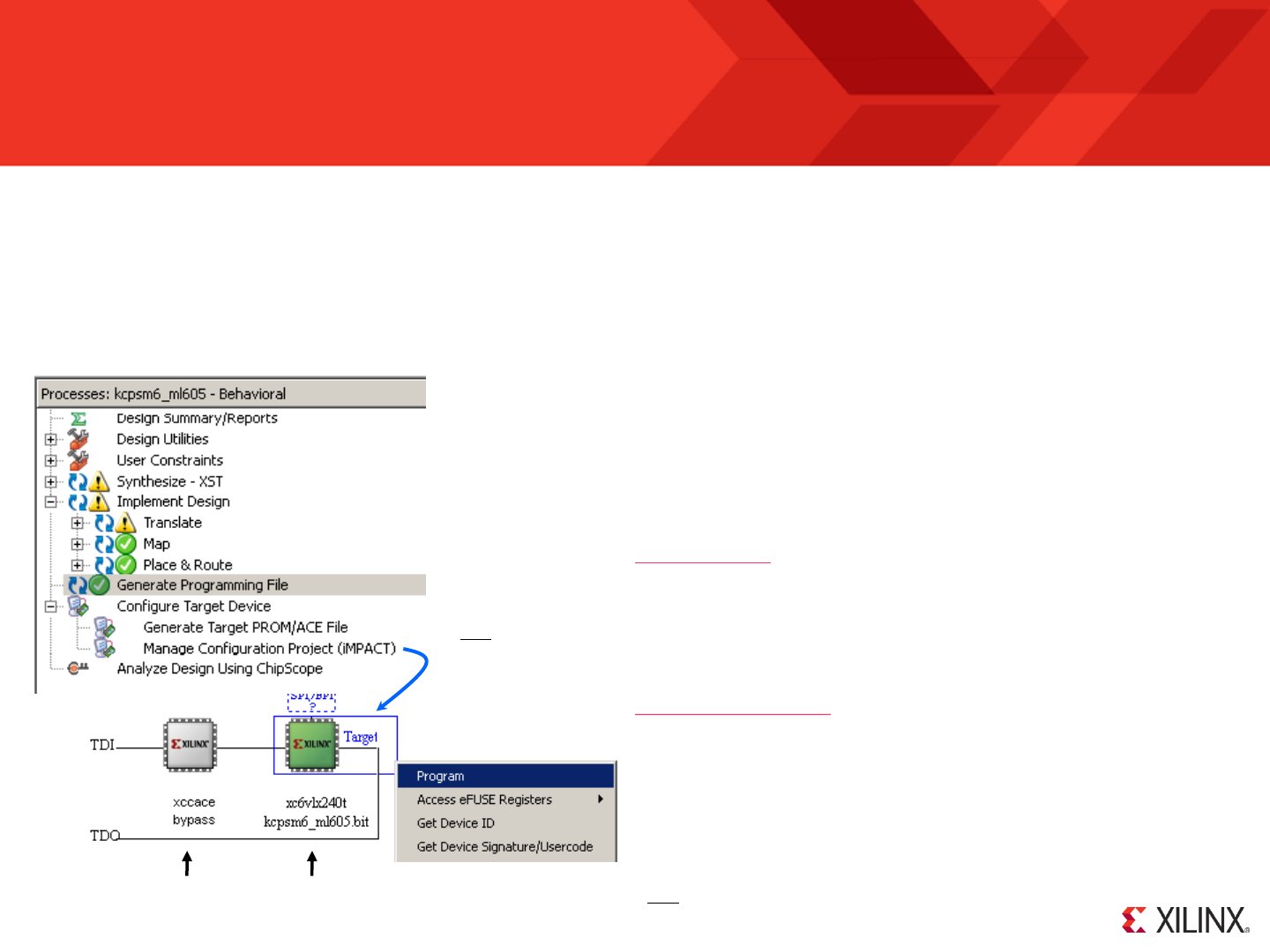
Then connect your download cable, open iMPACT and program the device.
Does your simple test design work? My switches and LEDs do
Note – Next we are going to exploit the JTAG chain in order to modify the
KCPSM6 program so make a quick note of which devices are in your chain
and which device ‘your_program’ is located in. In this example it is device ‘1’.
Hint – The first device in any chain is device ‘0’ (not ‘1’).
Device 0 Device 1
© Copyright 2010-2014 Xilinx
.
Page 25
JTAG Loader
Running your design through the ISE tools and configuring the device didn’t take long compared with procuring an ASIC (and it certainly didn’t cost as much),
but even so, it would become a huge waste of time if you had to do that every time you modified your KCPSM6 program and wanted to try it out. For this
reason the JTAG Loader utility exists to enable you to download a new program directly into the program memory inside the Spartan-6, Virtex-6 or 7-Series
device whilst it remains configured and active with your design.
Preparing to use JTAG Loader program_rom: your_program
generic map( C_FAMILY => "S6",
C_RAM_SIZE_KWORDS => 1,
C_JTAG_LOADER_ENABLE => 1)
port map( address => address,
instruction => instruction,
enable => bram_enable,
rdl => kcpsm6_reset,
clk => clk);
If you are following this worked example then
you have already done the main things but if
you are only looking at this section for the first
time then you do need to prepare the program
memory in your design as shown here.
The program memory should be generated by the
assembler using the default ‘ROM_form’ template (also
supplied as ‘ROM_form_JTAGLoader_14March13.vhd’)
and the ‘C_JTAG_LOADER_ENABLE’ generic value
must be set to ‘1’. If you have multiple KCPSM6 in your
design then make sure that you only enable JTAG
Loader on one program memory at a time.
Generate the configuration BIT file for your design and configure the target device using iMPACT and JTAG.
Hint – Boards like the SP605 and ML605 have the circuits of the ‘Platform Cable USB’ built on to them and boards like ATLYS, KC705 and VC707 have
the equivalent Digilent circuit on them. It is best if you only have the equivalent of one download cable connected to your PC at a time.
Open a ‘Command Prompt’ (i.e. DOS Window) and navigate to
your working directory.
1
2
3
4
Copy the ‘JTAG Loader’ executable corresponding with your
operating system from the ZIP file into your working directory.
IMPORTANT -The Command Prompt must know the location of your
Xilinx ISE installation so both ‘Path’ and ‘XILINX’ environment variable
must be defined. There are three ways in which you can achieve this:-
- Permanently define ‘Path’ and ‘XILINX’ in your your system
environment; please see the ‘Requirements’ section of
‘READ_ME_FIRST.txt’ for details.
- Use the ISE Design Suite Command Prompt (see right).
- Run the ‘settings32.bat’ or ‘settings64.bat’ provided in C:\Xilinx\14.3\ISE_DS (or equivalent for your version of ISE and its location on your PC).
Requires ISE v12.x or later
You will see that with JTAG Loader it is possible to modify your program and then have it running in KCPSM6 in under 10 seconds. With this rapid facility it is
possible to develop your programs iteratively taking many small steps and trying out each as you go. Including temporary code to perform and experiment or
help debug your program or test something else in your system becomes quick and easy.
© Copyright 2010-2014 Xilinx
.
Page 26
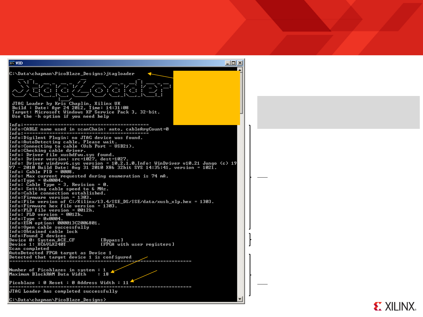
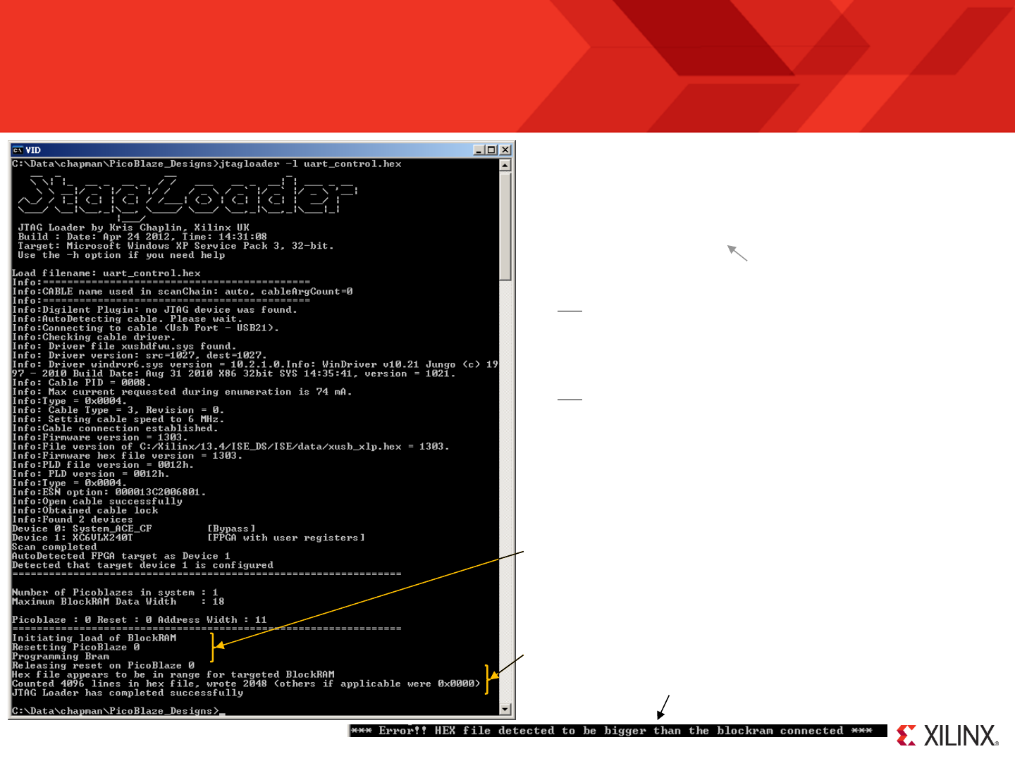
JTAG Loader
Confirming Setup - Assuming you have performed the
simple preparatory steps described on the previous page
then enter ‘jtagloader’ to run the JTAG Loader utility (please
see the note about name in the yellow box). The result
should be similar to the screen shown here.
Given that you have previously configured the target FPGA
using iMPACT there is normally no difficulty for JTAG Loader
to automatically detect your download cable and the
PicoBlaze memory in your design.
Hint – ‘jtagloader -h’ will provide a brief description of all the
options including ‘-u’ and ‘-p’ which can be used to force the
selection of the Platform Cable USB or Digilent equivalent
respectively.
JTAG Loader determines which devices are in the JTAG
chain and this should match with what you saw in iMPACT
(see 2 pages previous).
JTAG Loader tries to make an intelligent choice for the target
FPGA and will report the size of the program memory that it
finds in that device.
KCPSM6 has 18-bit instructions
11-bit address = 2K program
Hint – To override the automatic device selection use
‘jtagloader -t#’ and set # to the chain position of the FPGA
you do want to target (e.g. –t3). Note that first device in the
chain is ‘-t0’.
Requires ISE v12.x or later
Should reflect the value you set
for ‘C_RAM_SIZE_KWORDS’
If for any reason the utility fails then read any messages
displayed as they should indicate the reason. Check again
the preparatory steps shown on the previous page and also
look in the ‘READ_ME_FIRST.txt’ file for further guidance.
For simplicity, this
documentation
assumes that the
executable required
for your operating
system has been
renamed 'jtagloader‘.
© Copyright 2010-2014 Xilinx
.
Page 27
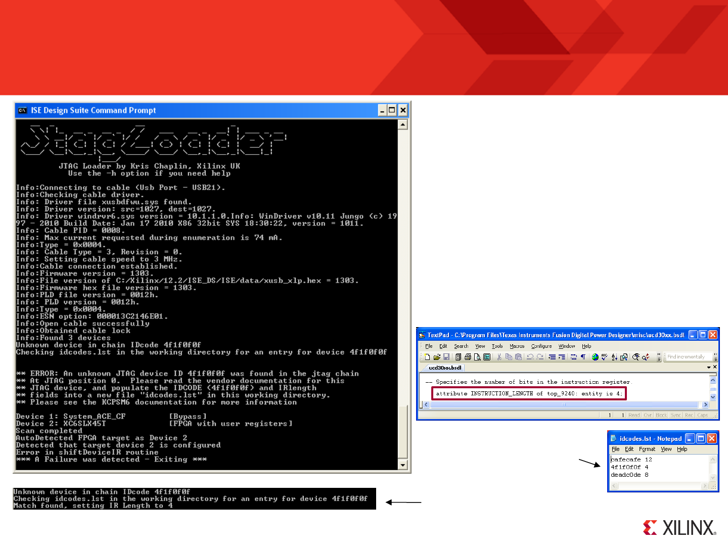
JTAG Loader With 3rd Party JTAG Devices
Failures due to “Unknown JTAG device(s)” in the chain
JTAG Loader will automatically detect if there are JTAG devices
in the chain that are not known to the Xilinx tools. This is most
likely to occur on custom hardware that has third-party hardware
in the chain.
If this event occurs, JTAG Loader will look for a “idcodes.lst” file
in the directory from which it was called. The purpose of this file is
simply to be a lookup table defining the Instruction Register (IR)
length of any unknown devices. This is the only extra information
that is needed.
Your third party device vendor should be able to provide you with
a “BSDL” file describing the device; it is a text file describing the
JTAG abilities and registers that it has. Open this file, and look
for the line specifying “INSTRUCTION_LENGTH”. In this example
the device the length is “4”.
Modify, or create the file “idcodes.lst”
to include the device ID (reported by
JTAG loader) and the IR Register
Length (from the BSDL file).
The next (hopefully successful!)
run of JTAG loader will report that
this information has been used.
© Copyright 2010-2014 Xilinx
.
Page 28
JTAG Loader
Modifying ‘your_program.psm’
Requires ISE v12.x or later
start: LOAD s4, 00
flash: XOR s4, FF
OUTPUT s4, LED_port
OUTPUT s4, Direction_LED_port
CALL delay_1s
JUMP flash
;
; Software delay of 1 second
;
; ML605 is fitted with a 66MHz clock.
; 1 second is 66,000,000 clock cycles.
; KCPSM6 will execute 33,000,000 instructions.
;
; The delay loop below decrements the 24-bit value held
; in registers [s2,s1,s0] until it reaches zero and this
; loop consists of 4 instructions.
;
; Therefore the loop needs to count 8,250,000 times so
; the start value is 7DE290 hex.
;
delay_1s: LOAD s2, 7D
LOAD s1, E2
LOAD s0, 90
delay_loop: SUB s0, 1'd
SUBCY s1, 0'd
SUBCY s2, 0'd
JUMP NZ, delay_loop
RETURN
The whole point of JTAG Loader is to enable you to download a new program into KCPSM6’s program memory so really you need to modify your program in
a way that you will be able to notice the difference. Obviously you will soon be working on a real application but initially look to make a simple change to your
first test program.
Continuing with the same example on the ML605 evaluation board
this simple program has ignored the input ports and simply turns
all the LEDs on both output ports on and off at 1 second intervals.
The program illustrates the use of a few more KCPSM6
instructions including a subroutine. All instructions are described in
detail later in this guide but at this point it just describes something
else that should be an obvious difference when executing on the
ML605 board used in this case.
KCPSM6
Assembler
your_program.psm
your_program.hex
Generating the HEX file
Simply assemble the modified program and, as we have seen
before, it will generate a ‘.hex’ file which contains your modified
program ready for JTAG Loader. There will also be a new ‘.vhd’ file
but that will only be used next time you invoke the ISE.
© Copyright 2010-2014 Xilinx
.
Page 29
JTAG Loader
Downloading Your New Program
Simply run JTAG Loader again but this time specifying the name of the
HEX file to be loaded into the KCPSM6 program memory.
Unless you have changed something then JTAG Loader should detect the
cable, target device and program memory as before.
Hint – If you needed to use an option to direct the loader to use a
particular type of cable or to specify the target device in the chain then
include those options again when loading.
E.g. jtagloader -t1 -d -l your_program.hex
Requires ISE v12.x or later
The loader will then force KCPSM6 into reset (using the ‘rdl’ signal you
connected in your design) whilst the new program is written into the
program memory. Finally, it releases the reset and KCPSM6 starts
executing your new program from address zero. All in under 10 seconds.
A program can be up to 4K instructions but your physical program memory
will often be only 1K or 2K. JTAG Loader checks that all the locations
described in the HEX file that are beyond the end of the physical memory
are unused (zero) or warns you if they are not (i.e. your program has
become too big).
That’s a lower case ‘L’
jtagloader -l your_program.hex
Hint – The HEX file specification may include a PATH. If the path
contains spaces then enclose within quotation marks.
E.g. ‘jtagloader -l “learning picoblaze\your_program.hex”

© Copyright 2010-2014 Xilinx
.
Page 30
That’s It!
You really have seen how to include KCPSM6 in a design, write and assemble programs and rapidly make changes to your code. What applications you go
on to implement using KCPSM6 is really down to you.
Of course there is more to learn about the instruction set but you can grow your understanding by reading the descriptions that follow and actually trying them.
Some instructions are more advanced than others but try to build on success rather than struggle with a concept that you find difficult to begin with. In most
cases it is possible to produce a solution in multiple ways so just do what you find most natural. As you gain experience you will probably recognise why
certain other instructions and features are included and start to incorporate them in your programs and designs. Remember that with Programmabe2
(programmable hardware a very rapid loading of KCPSM6 programs) you can experiment and try different techniques as much as you like.
INPUT sX, pp
OUTPUT sX, pp
JUMP
LOAD
ADD / SUB
AND / OR / XOR
CALL / RETURN
JUMP Z / JUMP NZ / JUMP C / JUMP NC
COMPARE / TEST
STORE sX, ss
FETCH sX, ss
SL0 / SR0 /RL / RR
Recommended for New PicoBlaze Users
So if KCPSM6 is your first experience of PicoBlaze design then hopefully you have already worked through all the pages of this guide prior to this one. If not,
then please do! Having mastered the fundamentals, and ideally you will now have a working hardware platform containing a working KCPSM6 in front of you,
it would be best if you focus on the following instructions as you write your first programs.
This may seem like quite a list to begin with. However, you have seen some of these used already
and it really will not take long to understand what each of them does if you try them one out in
your program. The description of each instruction contained later in this document includes
example code. It may also feel a little daunting when you see that KCPSM6 has more instructions
but do not feel under pressure to learn them all as you can achieve most things with this subset
and they will help prepare you for the others.
Although you will learn most about the assembler language syntax from the examples given, it
would be good to look at the more formal descriptions to understand the rules for line labels,
register and constant names and the multiple ways in which you can specify constants. Take look
at page 52 and in the file called ‘all_kcpsm6_syntax.psm’.
From a hardware perspective you have seen that KCPSM6 is small and connecting input and output ports is a straightforward piece of design. For
completeness you should look at the fundamental waveforms associated with INPUT and OUTPUT operations (included in the description of those
instructions) and also the waveforms and actions that occur at power up and during a RESET.
Hint – The ZIP file contains several simple but complete reference designs using the UART macros
which are also provided with PicoBlaze (see UART directory for code and documents).
Hint – The assembler is very tolerant about format and will advise you what to rectify so just try!

© Copyright 2010-2014 Xilinx
.
Page 31
Hardware
Hardware Reference
The following information provides more detailed descriptions of the hardware aspects of KCPSM6 and the associated program memory.
All information is in addition to that contained in pages 6 to 29.
Please note that the waveforms and circuits associated with I/O ports are located with the descriptions of the ‘INPUT’, ‘OUTPUT’ and
‘OUTPUTK’ instructions.

© Copyright 2010-2014 Xilinx
.
Page 32
Pin Descriptions
address[11:0]
instruction[17:0]
bram_enable
clk
sleep
reset
12-bit program address to access programs up to 4K instructions. This should be connected to the address inputs of
the program ROM which is typically implemented using one or more BRAMs. The majority of programs are of 1K or
2K instructions and in these cases only the lower 10 or 11 bits of the address are actually used. Note that the memory
templates provided always expect all 12-bits to be connected.
Output
Input 18-bit instructions. This port should be connected to the instruction (data) output of the program memory which is
typically implemented using one or more BRAMs. Since BRAM are synchronous there is a one clock cycle latency
from the address changing and the instruction being presented to KCPSM6.
Output
Read enable for the program memory. This signal should be connected to the enable input of the program memory
and is used to reduce the power consumption associated with the BRAM(s) during normal operation as well as in
sleep mode. This connection can be left open if program memory is permanently enabled (e.g. Distributed ROM).
Input
All operations are synchronous to this clock input. The clock should be provided using a clock buffer typically inserted
automatically by the ISE tools. In the majority of applications the same clock will be used as the circuits KCPSM6 is
expected to interact with as this ensures that all data transfers are synchronous and reliable. All timing internal to
KCPSM6 would be covered by the time specification associated with the clock frequency or period. The maximum
clock frequency will depend on the device type and speed grade as well as your design as a whole. However, it would
be rare for KCPSM6 to be the single reason for a design failing to meet timing specifications as it is typically of higher
performance than the peripheral logic you connect to it. All instructions execute in two clock cycles so KCPSM6
executes clk/2 instructions per second.
Input
Active High reset control. When driven High for at least one rising edge of ‘clk’ KCPSM6 enters a reset state in which
all activity ceases with the ‘address’ forced to zero, all strobes inactive and the ‘bram_enable’ Low to disable the
program ROM. On release of reset (‘0’), KCPSM6 starts up in a predictable sequence executing program code from
address zero using register bank ‘A’ with interrupts disabled. Note that ‘reset’ should be connected to ‘rdl’ associated
with the JTAG Loader utility during the development phase. If reset is not required during operation then tie the reset
input permanently Low and the reset sequence will still be performed automatically following device configuration.
Input
Active High sleep control. When driven High KCPSM6 will complete the current instruction and then enter a sleep
mode in which all activity stops. Whilst in the sleep mode all strobes are inactive and the ‘bram_enable’ is Low to
disable the program memory resulting in minimum power consumption. All inputs except ‘reset’ are ignored. When
‘sleep’ is returned Low, KCPSM6 resumes execution from the point that it stopped.

© Copyright 2010-2014 Xilinx
.
Page 33
Pin Descriptions
interrupt
interrupt_ack
port_id[7:0]
out_port[7:0]
read_strobe
write_strobe
Output
Input
Active High interrupt control. Providing interrupts have been enabled within the program then when this input is driven
High KCPSM6 will perform an interrupt in which the address is forced to an interrupt vector (default 3FF but can be
defined by the user) and the current states of the flags and register bank selection are preserved. Please see section
on interrupts for more details.
This output will pulse High for one clock cycle as KCPSM6 starts to service an interrupt by calling the interrupt vector.
‘interrupt_ack’ is generally used by the peripheral logic to cancel the interrupt signal to guarantee that no interrupts
are missed and to ensure that each interrupt is only serviced once.
Output The port through which KCPSM6 presents 8-bit data to peripheral logic during ‘OUTPUT’ and ‘OUTPUTK’
instructions. This data is valid when ‘write_strobe’ or ‘k_write_strobe’ are active and ‘port_id’ will define the intended
destination.
in_port[7:0] Input
The port to which the peripheral logic must present 8-bit data for KCPSM6 to read during an ‘INPUT’ instruction. The
peripheral logic should select and present the information based on the value of ‘port_id’. When performing an INPUT
operation the ‘port_id’ is valid for 2 clock cycles so it is highly recommended that the input data multiplexer be
pipelined. Note that ‘read_strobe’ is not required to qualify the read process but may be required by the peripheral(s).
Output This output will pulse High for one clock cycle when KCPSM6 executes an ‘OUTPUT’ instruction and the peripheral
logic should capture the data provided on ‘out_port’ (on the next rising edge of the clock) into the intended destination
defined by the value of ‘port_id’.
k_write_strobe Output This output will pulse High for one clock cycle when KCPSM6 executes an ‘OUTPUTK’ instruction and the peripheral
logic should capture the data provided on ‘out_port’ (on the next rising edge of the clock) into the intended destination
defined by the value of ‘port_id[3:0]’. Note that only the lower 4-bits of ‘port_id’ are used during ‘OUTPUTK’.
Output This output will pulse High for one clock cycle when KCPSM6 executes an ‘INPUT’ instruction and indicates that
KCPSM6 will capture the data being presented on the ‘in_port’ on the next rising edge of the clock. ‘read_strobe’ is
only used by peripheral logic when it needs to know that data has been read e.g. when reading a FIFO.
Output
This value defines which output port KCPSM6 intends to write data to during ‘OUTPUT’ and ‘OUTPUTK’ instructions
or which input port in wants to read from during an ‘INPUT’ instruction. During an ‘OUTPUTK’ instruction only the
lower 4-bits (port_id[3:0]) are valid and allow the definition of 16 constant-optimised ports qualified by
‘k_write_strobe’. During ‘INPUT’ and ‘OUTPUT’ instructions all 8-bits are valid supporting up to 256 output ports
qualified by ‘write_strobe’ and up to 256 input ports with ‘read_strobe’ available when required.

© Copyright 2010-2014 Xilinx
.
Page 34
KCPSM6 Generics
Component Instantiation showing changes to the default settings
interrupt_vector => X"F80",
hwbuild => X"41",
scratch_pad_memory_size => 256)
‘hwbuild’ can be used to define any 8-bit value in the range ‘00’ to ‘FF’. It is then possible to load any KCPSM6 register
with this value using the ‘HWBUILD sX’ instruction (see page 101 for more details).
When an interrupt occurs (and interrupts are enabled) then KCPSM6 inserts and executes a special form of
CALL instruction to a fixed address known as the interrupt vector (see page 42 for more details). The default
this is address for the interrupt vector is ‘3FF’ (the last location of a 1K program memory). Use this generic to
adjust the address of the interrupt vector when larger program memories are used as well as to arrange that
the vector correspond with the start of the actual interrupt service routine (ISR) eliminating a JUMP instruction.
The default size of the scratch pad memory is 64 bytes (‘00’ to ‘3F’) but this generic can be used to
increase it to 128 bytes (‘00’ to ‘7F’) or 256 bytes (‘00’ to ‘FF’). These will also increase the size of the
KCPSM6 macro by 2 and 6 slices respectively (i.e. Maximum size of KCPSM6 will be 32 Slices).
See pages 81 and 82 for more details about the STORE and FETCH instructions.
processor: kcpsm6
generic map ( hwbuild => X"41",
interrupt_vector => X"F80",
scratch_pad_memory_size => 256)
port map( address => address,
instruction => instruction,
bram_enable => bram_enable,
port_id => port_id,
write_strobe => write_strobe,
k_write_strobe => k_write_strobe,
out_port => out_port,
read_strobe => read_strobe,
in_port => in_port,
interrupt => interrupt,
interrupt_ack => interrupt_ack,
sleep => kcpsm6_sleep,
reset => kcpsm6_reset,
clk => clk );
KCPSM6 has three generics that can be adjusted if required.
Please note that the Verilog equivalent of each file is also provided.

© Copyright 2010-2014 Xilinx
.
Page 35
RESET
Following device configuration KCPSM6 generates an internal reset to ensure predictable a reliable operation. The ‘reset’ input can then be driven High at
any time during operation to force a restart (e.g. When the ‘rdl’ signal from JTAG Loader is asserted).
Stack
Pointer
PC
Z
C
Program counter (PC) is forced to address ‘000’ ready to fetch and execute the
instruction located in the first location of the program memory.
PC Stack
“000”
‘0’
‘0’
IE
‘0’
REGBANK
‘A’
The zero and carry flags are reset.
Interrupts are disabled.
Register bank ‘A’ is selected and therefore ‘A’ is the default bank of registers.
The pointer in the program counter stack is reset to ensure that the program is able to execute programs
in which up to 30 nested subroutine calls can be made.
30
Hint– Following device power up and configuration the contents of all registers and scratch pad memory locations will be zero. Any subsequent reset will
perform all the items shown above but registers and scratch pad memory will retain the values. This can be useful in certain application but your code
should not rely of values being zero if manual reset is to be used during operation.
Note – If you should inadvertently write a program whose execution results in stack overflow or stack underflow
then KCPSM6 will automatically generate an internal reset.
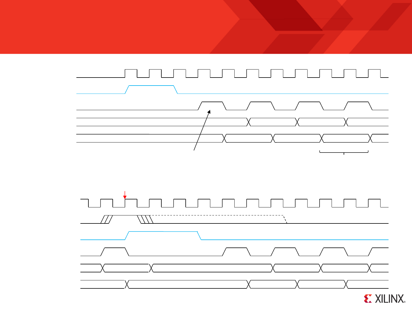
© Copyright 2010-2014 Xilinx
.
Page 36
RESET
Power up reset and fundamental operation
000
instruction
clk
internal_reset
All instructions execute
in 2 clock cycles.
address
bram_enable
001
00000 inst_0
Program memory is only enabled to
read each instruction saving power.
Operational Reset
instruction
clk
internal_reset
address
bram_enable
reset hold in reset state as long as required
aaa
inst_aaa
Your reset pulse must be observed by at least one rising edge of the clock.
BRAM power saving during reset
inst_1 inst_2
002 003
inst_0 inst_1 inst_2
001 002
000

© Copyright 2010-2014 Xilinx
.
Page 37
SLEEP
When the ‘sleep’ input is driven High, KCPSM6 will complete execution of the last instruction that has been read from the program memory and then freeze
all operations. This ensures that the outputs from KCPSM6 are static with all the strobe signals inactive (Low). When the ‘sleep’ input is returned Low,
KCPSM6 will wake up and resume from the point at which it stopped.
There are three fundamental use models for the ‘sleep’ control and your own circuit will control the ‘sleep’ input accordingly. Of course there is nothing to
prevent combinations of these through appropriate control.
Maximum Power Reduction - Total power consumption is a combination of static power and dynamic power. When the ‘sleep’ control is active there is no
dynamic switching occurring within KCPSM6 and hence the dynamic power consumption of KCPSM6 becomes zero. In addition, the ‘bram_enable’ is
permanently driven Low by KCPSM6 whilst in the sleep state. This reduces the static power consumption of the BRAM(s) used to implement the program
ROM virtually to zero.
It should be noted that although KCPSM6 will respond to a reset when in the sleep mode it will not react to an interrupt. If you would like KCPSM6 to wake
up when an interrupt occurs then your control circuit should drive ‘sleep’ Low when it drives ‘interrupt’ High. In this situation KCPSM6 will wake up and
immediately respond to the interrupt (assuming interrupts have been enabled by the previously executed PSM code) .
Performance Matching - KCPSM6 is typically supplied with a ‘system clock’ which leads to simple and reliable synchronous interfacing of the input and
output ports to the other circuits being monitored and controlled within the system. However, it is also typical for KCPSM6 to be used to implement relatively
slow functions for which the MIPS associated with the system clock frequency dived by 2 are excessive. Driving the ‘sleep’ input with a simple repeating
waveform can force KCPSM6 to continuously alternate between sleep and awake modes. The duty factor of the waveform defining the relative reduction in
the MIPS available with a corresponding reduction in average power consumption. In some applications it may be suitable to ‘single step’ the program
execution whilst in others it may be more appropriate to wake KCPSM6 up occasionally for bursts of intense activity.
System Handshake - In this case ‘sleep’ can be considered to be a special case of a very simple non-maskable interrupt. It may also have the potential to
reduce power consumption but this would not be the primary motivation. It provides the system with a way to make KCPSM6 wait for some reason. One
example would be where KCPSM6 is writing information to a FIFO. Whenever the FIFO is at risk of overflowing the ‘sleep’ control could then be a asserted
to allow the FIFO some time to empty. In another example KCPSM6 may read and process information contained in a memory and the system could make
KCPSM6 wait whilst that information was in the process of being changed.
System Debugging – By generally holding the ‘sleep’ input High it can then be can be pulsed Low for one clock cycle at a time to force KCPMS3 to single
step through the program one instruction at a time. This can be a useful mechanism for system debugging. Note that one instruction ‘step’ will always be
over a period of 2 clock cycles and this ensures that strobes will always be single clock cycle pulses.
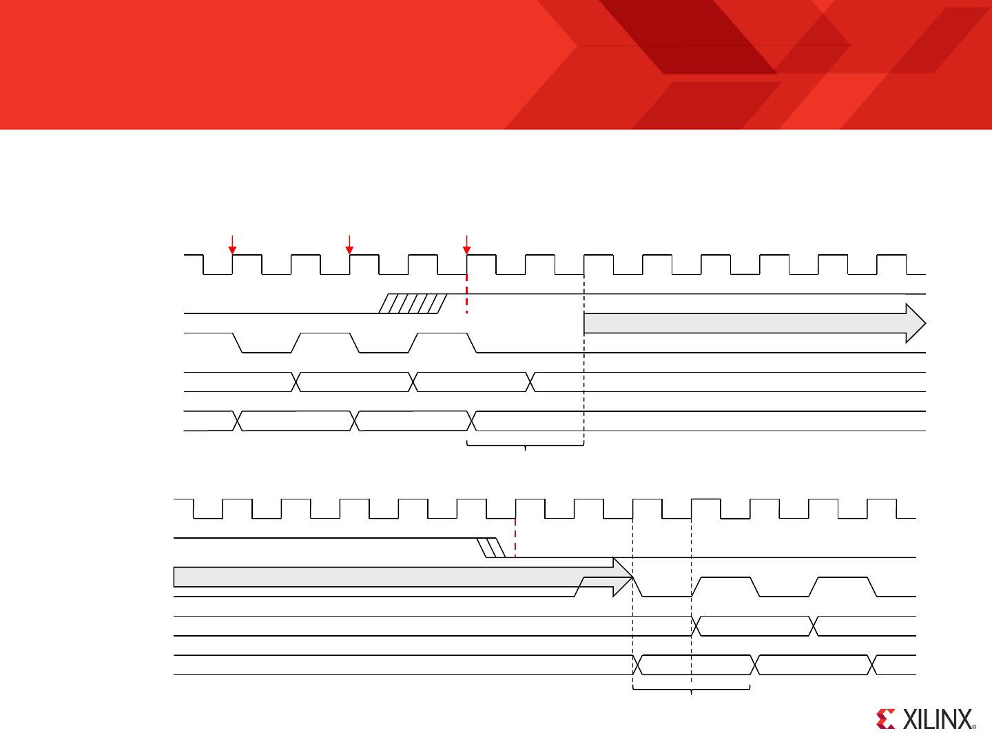
© Copyright 2010-2014 Xilinx
.
Page 38
SLEEP
When the ‘sleep’ input is driven High, KCPSM6 executes the instruction that has just been fetched from the program ROM and then enters sleep mode.
Everything stops with all strobes Low and BRAM disabled for minimum power consumption. All inputs except for ‘reset’ are ignored whilst in sleep mode.
When ‘sleep’ is returned Low there is a 2 clock cycle latency whilst KCPSM6 wakes up and reads the next instruction to resume execution from the point
that it stopped.
sleep
instruction
clk
address
bram_enable
inst_123 inst_124 inst_125
123 124 125
Last instruction executes
Sleep Mode
126
The ‘sleep’ input is only sampled on the rising clock edges that the instruction changes
Enter Sleep
sleep
instruction
clk
address
bram_enable
inst_126 inst_127
inst_125
126 127 128
Sleep Mode
Wake Up
First instruction executes
Exit ‘sleep’ on any rising clock edge
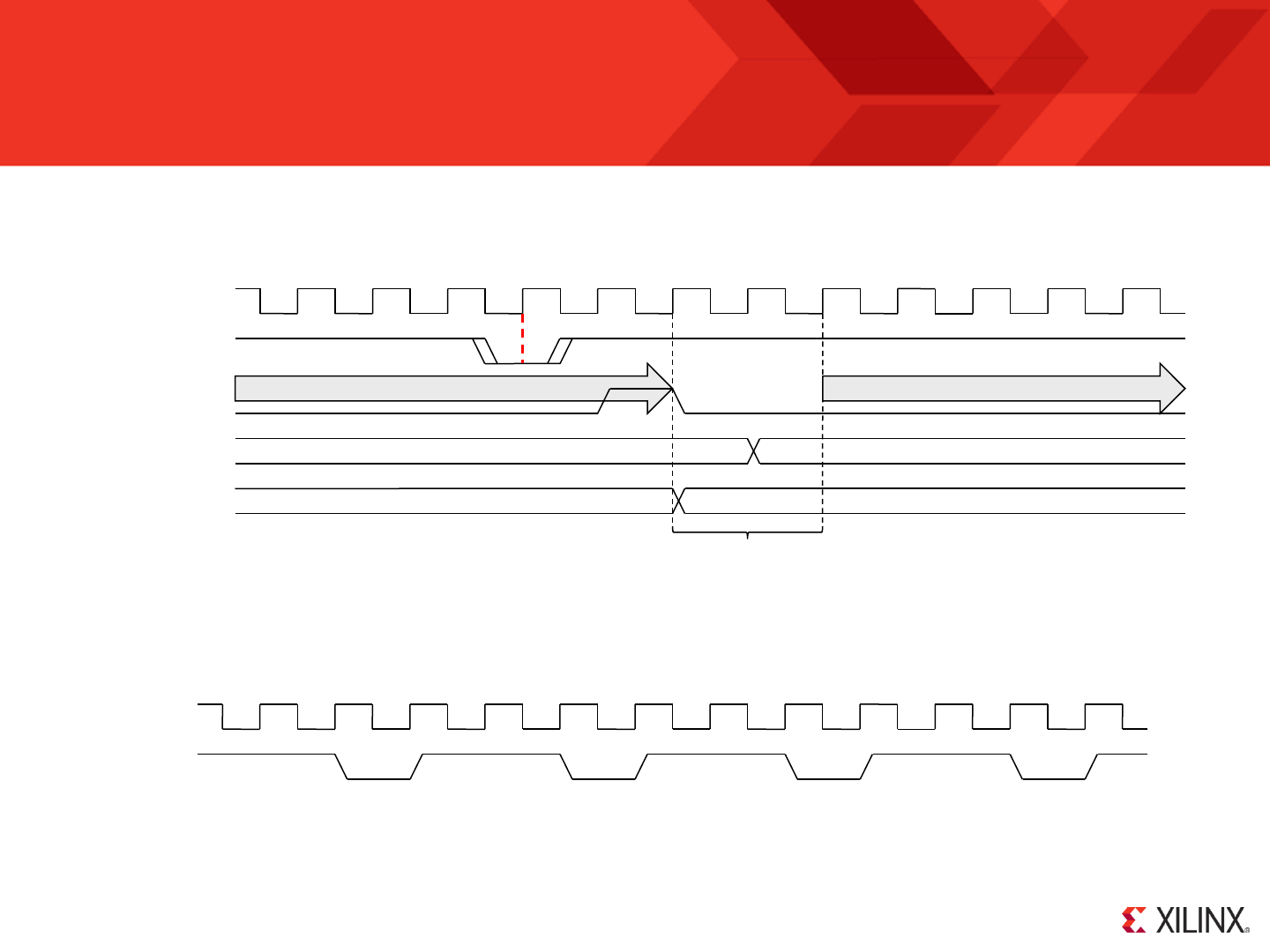
© Copyright 2010-2014 Xilinx
.
Page 39
SLEEP
Once in sleep mode it is possible to execute the program one instruction at a time simply by pulsing the ‘sleep’ input Low for one clock cycle. This could be
used as a system debugging mechanism or just as a way of slowing KCPSM6 down to better match the required performance of an application and save
power.
sleep
instruction
clk
address
bram_enable
inst_126
inst_125
126 127
Sleep Mode
Single Stepping
instruction executes
Sleep Mode
sleep
clk
Slow Down Waveforms
Driving ‘sleep’ with a ‘110’ waveform (shown below) will make KCPSM6 sleep for one clock cycle after the execution of each instruction that takes 2 clock
cycles. Obviously this is the smallest amount KCPSM6 can be slowed down. The important observation is that all KCPSM6 operations remain fully
synchronous with the clock, e.g. a ‘write_strobe’ will still only be a single cycle pulse ensuring that an OUTPUT instruction only writes once to logic.
Likewise, driving ‘sleep’ with a ‘1110’ waveform will make KCPSM6 sleep for two clock cycles after executing each instruction resulting in KCPSM6 running at
half its normal speed. Hence KCPSM6 can be slowed down to any speed required using the appropriate ‘sleep’ waveform.
Hint - See page 122 for a special case in which this slowdown waveform can been used.
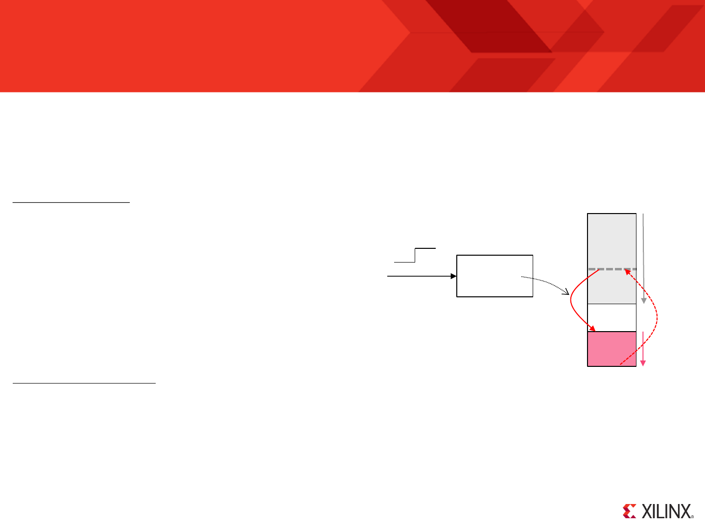
© Copyright 2010-2014 Xilinx
.
Page 40
Interrupts
Interrupts can be extremely useful so KCPSM6 provides an ‘interrupt’ input pin, an ‘interrupt_ack’ output pin, an optional ‘interrrupt_vector’ generic and three
interrupt related instructions. However, it would be fair to say that interrupts are quite an advanced technique and require understanding, thought and
preparation to be used wisely and successfully. This subject is made more interesting because each KCPSM6 is fully embedded into your FPGA design
meaning that you have the option to define hardware dedicated to servicing tasks in a way that simply isn’t available when using a standard microcontroller
device. In fact, many PicoBlaze users have discovered that because each PicoBlaze is so small and efficient, it is often beneficial to use multiple instances
within the same design in order that each is dedicated to a particular task and therefore avoiding the requirements for interrupts altogether. So it is well worth
considering what an interrupt actually does and when it provides greatest benefit in a KCPSM6 design.
What does an interrupt do?
To state the obvious, an interrupt is used to interrupt the normal program execution
sequence of KCPSM6. This means that when the ‘interrupt’ input is driven High
(‘1’), it will force KCPSM6 to abandon the code that it is executing, save its current
operational state and divert its attention to executing a special section of program
code known as an Interrupt Service Routine (ISR). Once the interrupt has been
serviced, KCPSM6 returns to the program at the point from which it was interrupted
and restores the operational states so that it can resume execution of the program
as if nothing had happened.
ISR
Main
Program
Interrupt
Service
Routine
interrupt
kcpsm6
0
1
When do interrupts make sense?
The key observation is that an interrupt has the highest priority. So clearly the most obvious application for an interrupt is to react quickly to system critical or
emergency situations. These may be such rare events that they may never happen in normal operation such as the detection of a fire and the need to activate
the water sprinklers. More common situations are less of an emergency but important to system integrity with a good example being the requirement to react
to a FIFO buffer becoming full so that data is read from it before it actually overflows and data is lost.
Another application involves a regular or semi-regular steam of interrupts to KCPSM6 which become a fundamental part of the way in which the program
normally operates. For example a hardware counter could easily generate an interrupt every milli-second which KCPSM6 uses as the reference for an
accurate real time clock. The main program possibly enabling that clock to be set, displayed and for controlling the times at which appliances must be turned
on and off. Alternatively KCPSM6 may use each interrupt as the trigger to perform a sequence of tasks but do virtually nothing else whilst waiting.
Hence the interrupt mechanism provides a way for KCPSM6 to react to an event at any time and quite independently to
the main tasks being performed. In other words an interrupt is given the highest priority which can be very useful
particularly when reacting to a critical situation. However, it must also be recognised that in giving priority to one task all
other tasks can be interrupted and hence their execution rates can be erratic or delayed.

© Copyright 2010-2014 Xilinx
.
Page 41
Interrupts
When are interrupts NOT suitable?
To answer this question their are two important observations. First is that whilst KCPSM6 is servicing an interrupt, it is not making any progress executing the
main program (i.e. the main program has been interrupted!). Secondly, KCPSM6 can only service one interrupt at a time which means that if another interrupt
occurs whilst KCPSM6 is busy executing the ISR then that new interrupt will either be missed or will have to wait neither of which is ideal. In general terms, an
interrupt scheme in not suitable if the rate at which interrupts occur is too fast for them to be serviced and for the main program to make adequate progress.
Clearly the definition of ‘too fast’ depends on how demanding both the main program and the ISR are but the one absolute constant is that every KCPSM6
instruction always takes 2 clock cycles to execute. So at least you can easily determine the code execution rate for a given clock frequency and compare that
with the demands of your program and your expected interrupt rate.
For example, consider the use of interrupts generated at 1ms intervals for use as a time reference for a real time clock. With a KCPSM6 operating at a clock
frequency of 66MHz it will execute 33,000,000 instructions per second and therefore it will be able to execute 33,000 instructions between each interrupt. This
is clearly a large number and most unlikely to impede the ability to make good progress through any program whilst always being ready to service the next
interrupt. But suppose the interrupts are generated at 1µs intervals with the aim of achieving finer timing resolution. Now KCPSM6 would only be able to
execute 33 instructions between each interrupt (i.e. Less instructions that you can print out on one side of a piece of paper!). Unless the ISR is very brief it will
not complete in time. Even if the ISR was only 12 instructions it would mean that over a third of the computing power was consumed servicing the simple ISR
and that means that the main program would execute proportionally slower with an associated ‘hesitancy’ caused by the continuous interruptions. This may
still be acceptable for the application but it is certainly on the verge of being unsuitable and will make it very difficult to expand the features implemented by
the program code.
What are the alternatives?
When interrupts make sense then it a very useful feature of KCPSM6 to exploit. However, when they are not suitable the benefit of using a Xilinx FPGA is
that there are very good alternatives. The biggest mistake people often make it to battle with interrupt based solutions when they are not suitable. It is much
better to exploit alternative solutions to make the overall design much easier to implement.
Increased use of hardware – Quite simply circuits are implement which perform what would have been achieved by the software based ISR such that
interrupts are avoided or their rate greatly reduced. For example a hardware based counter/timer block can be very simple to implement in hardware and then
KCPSM6 can read time values from it when it needs to. The complexity of a real time clock could still be implemented in software but the timing resolution is
best handled by the naturally fast hardware. Interrupts could then be used occasionally when a hardware comparator matches a time value set by KCPSM6.
Divide and conquer! – If a KCPSM6 processor is 100% dedicated to a task then really it is always performing an ISR. This makes sense if the ISR is relatively
complex to consider implementing in hardware. With KCPSM6 being so small (26 Slices) dedicating a different processor to each demanding task can often
be the easiest and best solution. Indeed, PicoBlaze is often used to service interrupts for a larger processor such as MicroBlaze.

© Copyright 2010-2014 Xilinx
.
Page 42
‘interrupt_vector’ and ‘ADDRESS’ Directive
processor: kcpsm6
generic map ( hwbuild => X"00",
interrupt_vector => X"3FF",
scratch_pad_memory_size => 64)
port map( address => address,
instruction => instruction,
Etc... Component Instantiation (part of) showing that the
interrupt vector has been set to ‘F80’ hex.
processor: kcpsm6
generic map ( hwbuild => X"41",
interrupt_vector => X"F80",
scratch_pad_memory_size => 256)
port map( address => address,
instruction => instruction,
Etc...
When KCPSM6 responds to an interrupt it executes the equivalent of a CALL instruction as well as the interrupt specific tasks such as preserving the states
of the flags. The interrupt vector is the address that KCPSM6 effectively calls and it has the default value of 3FF hex. However, this can be set to any value
within the range of the program memory available in your design using the ‘interrupt_vector’ generic in your HDL design description.
What is a good address for ‘interrupt_vector’?
3FF is the last location in a 1K program memory and is consistent with KCPSM, KCPSM-II and KCPSM3. So for direct compatibility with legacy PicoBlaze
programs this is the best address to start with and hence the reason why it is the default. Of course you could modify the program and vector.
Generally the most convenient address is somewhere close to the end of the program memory available but leaving enough space for the ISR. This means
that the ISR can begin servicing the interrupt immediately. It is also convenient from a programming perspective because the ADDRESS directive must be
used to align the start of the ISR code with interrupt vector and having this as the last section of your PSM program allows your main program the flexibility
to expand up to it. As your code becomes stable you can always fine tune your matching ‘interrupt_vector’ and ADDRESS directive for best memory fit.
Component declaration (part of) showing the default
values of the three generics.
What are bad values? If you try to put your ISR somewhere in the middle of your program then you will probably find that you are always having to adjust
the ADDRESS directive and ‘interrupt_vector’ which is just an inconvenient waste of time as well as error prone. The absolute worst address would be zero!
Under no circumstances would you want your ISR to execute on power up or following a reset (RETURNI should only be used following an interrupt).
ADDRESS F80
;
ISR : ADD sF, 1’d
RETURNI ENABLE
Use the ADDRESS directive in your PSM
code to force the ISR to be assembled starting
at the same address as the interrupt vector.
PSM file...
ADDRESS Directive
See pages 83-85 for interrupt related instructions
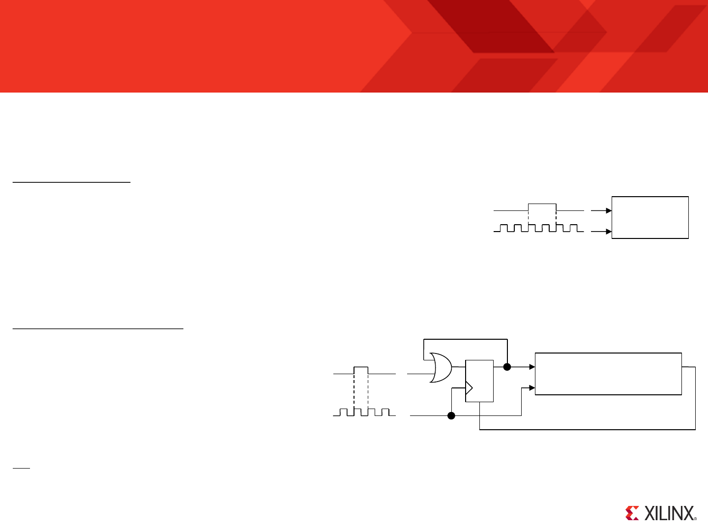
© Copyright 2010-2014 Xilinx
.
Hardware arrangements for KCPSM6 Interrupt
The KCPSM6 processor has two pins dedicated to interrupts; an ‘interrupt’ input and an ‘interrupt_ack’ output. To initiate an interrupt the ‘interrupt’ input must
be driven High and the fundamental interrupt response time is just 3 or 4 clock cycles. As shown on the next page (Interrupt Waveforms) the interrupt input is
sampled once every two clock cycles consistent with the instruction execution rate. For this reason it is vital that the interrupt input is High at the right time to
be observed by KCPSM6 and the easiest way to achieve that us to drive the interrupt input High for longer than one clock cycle. There are two fundamental
schemes that can be used which can really be describes as being ‘open-loop’ and ‘closed loop’.
The simplicity of the ‘open-loop’ method is obvious but it must also be recognised that any open loop system has its limitations. In this case there is the
potential for KCPSM6 to miss an interrupt request and therefore fail to service it. This could happen if the KCPSM6 program has deliberately disabled
interrupts or is already servicing a previous ISR. KCPSM6 will also ignore the interrupt input whilst held in sleep mode. Therefore this technique should only
be used if you can predict that KCPSM6 will always be ready to respond to an interrupt request or if it is acceptable for interrupts to be missed.
‘Open-Loop’ interrupt pulse
The simplest way of initiating an interrupt is to generate an active High pulse that has a duration of 2 clock
cycles. The pulse can be longer but should have returned Low before the ISR completes otherwise
KCPSM6 will immediate think there is another interrupt to service (remember that each instruction
executes in 2 clock cycles so some ISR’s may not take very many clock cycles). Once KCPSM6 observes
the High level on its interrupt input it will abandon the next instruction and immediately move to the ISR.
interrupt
kcpsm6
clk
Hint – Some systems can require a more comprehensive closed-loop arrangement in which KCPSM6 would be expected to indicate when the ISR has
completed rather than just started (which is what ‘interrupt_ack’ signifies). This can be achieved using an output port with associated ‘OUTPUT’ or
‘OUTPUTK’ instructions at the end of your ISR. Alternatively you could detect when instruction[17:12] = “101001” corresponding with the ‘RETURNI’
instruction being fetched from the program memory.
‘Closed-Loop’ interrupt (recommended)
In this scheme your design drives the interrupt signal High to request
an interrupt and then keeps driving it High until KCPSM6 generates an
‘interrupt_ack’ pulse confirming that it has seen it. This ensures that
the interrupt will always be observed by KCPSM6 when it is able to. If
interrupts have been temporarily disabled deliberately, or whilst
servicing a previous interrupt, then the response will be delayed but
the event can not be missed. Likewise, if KCPSM6 is held in sleep
mode when the interrupt is requested it will remain active until
KCPSM6 is allowed to wake up and observe it.
interrupt
kcpsm6
clk
interrupt_ack
D Q
R
Page 43
See pages 83-85 for interrupt related instructions
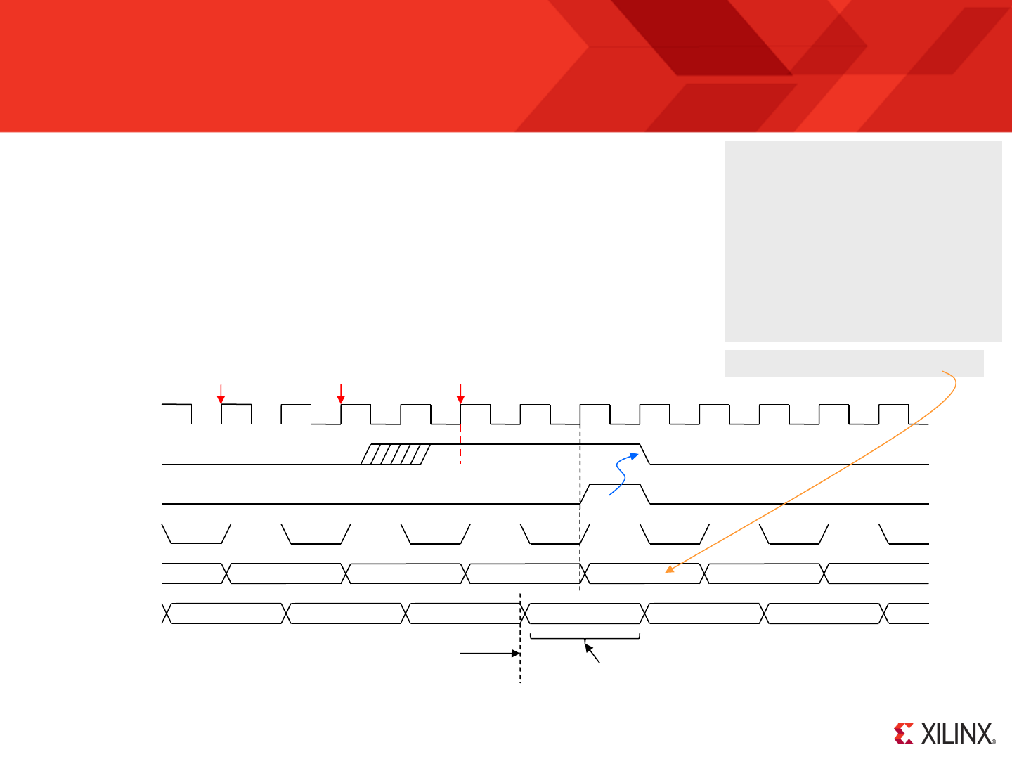
© Copyright 2010-2014 Xilinx
.
Page 44
Interrupt Waveforms
instruction
clk
The last instruction read from program memory before the interrupt takes
place is abandoned. This will be the first instruction executed following a
RETURNI after the interrupt has been serviced.
address 5A1
inst_05A1
An interrupt is performed when the ‘interrupt’ input is driven High, interrupts have been enabled by the program
and KCPSM6 is not in sleep mode or otherwise busy servicing a previous interrupt. When KCPSM6 detects an
interrupt it forces the next instruction to be abandoned, preserves the current states of the ‘Z’ and ‘C’ flags,
notes the current bank selection (‘A’ or ’B’) and then forces the program counter to the interrupt vector (default
value is 3FF hex which is the last location of a 1K program memory but can be set to any value using the
‘interrupt_vector’ generic).
bram_enable
5A2 5A3 FF0 FF1 FF2
inst_5A0 inst_5A3
inst_5A2 inst_FF1
inst_FF0
5A0
interrupt
interrupt_ack
The ‘interrupt’ input is sampled on the rising clock edges that the address
Z and C flags preserved. Bank selection preserved.
All will be restored by the RETURNI instruction.
interrupt_vector => X“FF0“,
interrupt_control: process(clk)
begin
if clk'event and clk = '1' then
if interrupt_ack = '1' then
interrupt <= '0';
else
if kcpsm6_interrupt = '1' then
interrupt <= '1';
else
interrupt <= interrupt;
end if;
end if;
end if;
end process interrupt_control;
The waveforms shown below illustrate a normal response to an interrupt when interrupts have been enabled
within the program and KCPSM6 is ready to respond. In the hardware design the interrupt vector was set to
FF0 hex and a ‘closed-loop’ interrupt scheme used (implemented by the VHDL shown on the right) to ensure
that the interrupt pulse can not be missed.
See pages 83-85 for interrupt related instructions
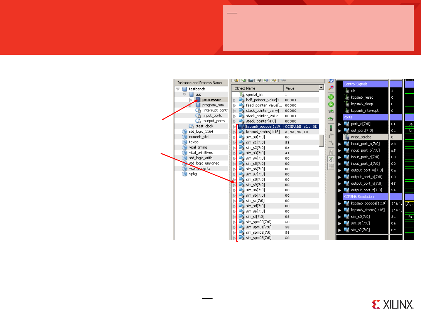
© Copyright 2010-2014 Xilinx
.
HDL Simulation Features
Page 45
Since KCPSM6 is a fully embedded part of your hardware design it will simulate along with the rest of your design in an HDL simulator such as iSim or XSim.
This means that you can see how KCPSM6 interacts with your design in the same fundamental way in which you might check the operation of a dedicated
state machine.
As well as being able to observe any of the input and output
signals connecting KCPSM6 to the rest of your design
KCPSM6 contains some additional signals specifically for
simulation purposes only.
Within the simulator locate the instance of KCPSM6 to be
observed. In this case the instance name is ‘processor’ and
the simulator is iSIM (part of ISE).
Then all the internal signals of KCPSM6 can be seen and
selected for waveform display as desired. Look down the list
and the simulation specific signals can be found.
Hint – Adjust the radix of the values displayed.
kcpsm6_opcode – This is a text string displaying the
instruction being executed. As well as
being easier to understand than the raw
codes being read from the program
memory they can also be compared with
the LOG file from the assembler to directly
trace code execution
kcpsm6_status – This is a text string displaying the status…
Active register bank ‘A’ or ‘B’
Zero flag Z or NZ
Carry flag C or NC
Interrupts enabled (IE) or disabled (ID)
Reset or Sleep modes.
e.g. A, Z, NC, IE, Sleep
Bank A, Z=1, C=0, interrupts enabled, in sleep mode
‘sim_s0’ to ‘sim_sf’ – The contents of each of the 16 registers in the active register
bank (i.e. Contents will reflect bank selection).
‘sim_spm00’ to ‘sim_spmff’ – The contents of each of the 256 scratch pad
memory locations. Remember that default memory
size is 64 bytes (only up to sim_spm3f).
Hint – In most of the cases in which a user reports that KCPSM6 does
not simulate at all (e.g. the ‘address’ does not advance as expected),
the cause has been the failure on the part of the user to define valid
logic levels for the ‘interrupt’, ‘sleep’ and ‘reset’ controls. So please
make sure that all signals are defined at the start of your simulation
either in your design or in your simulation test bench.
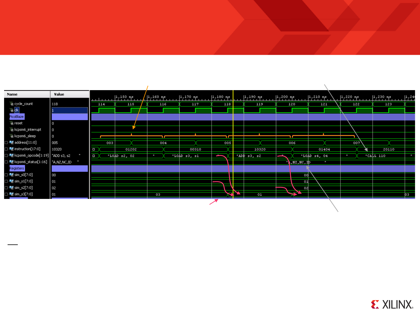
© Copyright 2010-2014 Xilinx
.
HDL Simulation Features
Hint – KCPMS6 programs often contain code that is used to deliberately slow down the progress through the program to service the application correctly
either using software delay loops or polling of status signals. For example, when communicating with a UART that has a BAUD rate of 115200 then each
character will take 86.8µms to be received and that would equate to 8,680 clock cycles of a 100MHz system clock. Due to this, it is not uncommon for users to
become confused by what they perceive as a “lack of activity” in their simulated design simply because KCPSM6 is taking so many clock cycles. So if this is
the situation, it may be necessary to alter the PSM code to make the HDL simulation practical but obviously you will need to remember to restore the correct
code for the real application. In practice, most PSM code is developed interactively in real-time on the target hardware using JTAG_Loader to facilitate rapid
iterations. As such, HDL simulation is best used to confirm your port interfacing logic and generation of particular strobes and waveforms etc.
In this iSim or Xsim waveform view the following can be seen…
Each instruction taking 2 clock cycles to execute
The contents of registers. In this example we can see ‘s3’ being loaded with the contents of ‘s1’
followed by the addition of the contents of ‘s2’.
Page 46
Instruction op-codes decoded and displayed as text strings.
Register bank ‘A’, States of flags and interrupt.
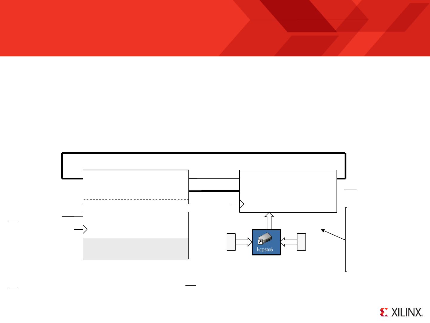
© Copyright 2010-2014 Xilinx
.
hwbuild => X"00"
interrupt_vector => X"3FF"
scratch_pad_memory_size => 64
Production Program Memory (ROM_form)
address
instruction bram_enable
clk
reset
kcpsm6
[11:0]
[17:0]
ROM_form_S6_1K_date.vhd
ROM_form_S6_2K_date.vhd
ROM_form_S6_4K_date.vhd
ROM_form_V6_1K_date.vhd
ROM_form_V6_2K_date.vhd
ROM_form_V6_4K_date.vhd
ROM_form_7S_1K_date.vhd
ROM_form_7S_2K_date.vhd
ROM_form_7S_4K_date.vhd
ROM_form_128_date.vhd
ROM_form_256_date.vhd
instruction
address
enable
your_program
During the design and code development phase the default ‘ROM_form’ template is used with the assembler. This generates the hardware definition of the
program memory and the three generics make it easy to specify the target family (Spartan-6, Virtex-6 or 7-Series), adjust the size of the memory and include
the JTAG Loader which you almost certainly found to be an invaluable tool. Whilst such flexibility and the JTAG Loader are extremely useful tools during
development it does mean that the program memory definition file generated by the assembler is somewhat large and over complicated for a production
release. The JTAG Loader may well have been an invaluable tool during development but leaving your KCPSM6 program open to adjustment in a production
product could present a threat to design security. Of course you may decide to exploit the JTAG Loader utility as part of your production product too in which
case just leave everything as it is!
Hint - A ‘ROM_form’ template is a standard HDL file except that it contains special {tags}
that the assembler intercepts. You can modify any of the templates provided to define
your own special format of program memory (e.g. a dual port memory in which the
program can be changed by a different mechanism to JTAG Loader).
your_program.psm
Page 47
ROM_form.vhd
Hint – The default ‘ROM_form.vhd’ is a renamed copy of
the file called ‘ROM_form_JTAGLoader_14March13.vhd’
which is also provided in the KCPSM6 package.
clk
Please note that the Verilog equivalent of each file is also provided.
Hint - No generics required
for fixed memory.
Hint
Connect your ‘rdl’ signal
to ‘0’. This retains the
signal in your design
definition in case you
need to go back to the
development memory
again later.
In order that you can go into production with the most simplified hardware definition of your program memory and ensure that JTAG Loader is not accidently
enabled a set of ‘production’ templates are provided. The name of each production template describes the target family ('S6' for Spartan-6, 'V6' for Virtex-6
and ‘7S’ for 7-Series) and the size of the program memory implemented (1K, 2K or 4K instructions). There is also one special case that replaces the BRAM
completely with 18-Slices of distributed ROM and provides a very efficient implementation for programs up to 256 instructions. Make a copy the appropriate
file and rename it ‘ROM_form.vhd’. Then use this file with the assembler and your PSM file to generate the simplified memory definition.

© Copyright 2010-2014 Xilinx
.
Page 48
Assembler and PSM Software
PSM Software Reference
The following information provides more detailed descriptions of the KCPSM6 assembler and PSM syntax. Where necessary additional descriptions
are provided to give the context in which groups of instructions are used.
Hint - The descriptions for each of the instructions contain examples of PSM code. So please do not dwell too long on the formal but brief descriptions
of assembler syntax because most of this should be made clear through the examples and become natural to you once you start writing your own code.
The KCPSM6 assembler will quickly provide you with feedback when processing your code so just have a go and allow it to help you to learn the
precise syntax interactively; you’ll soon be an expert!
To complement this documentation the following additional reference material is provided in the KCPSM6 package (ZIP file)...
all_kcpsm6_syntax.psm – This Provides a PSM file (albeit not a real program) in which there are examples of all the PSM syntax supported
by the KCPSM6 assembler including all valid forms of instructions, operands and directives.
Hint – ‘all_kcpsm6_syntax.psm’ contains the most comprehensive descriptions of PSM syntax and the assembler
directives. In contrast, this document is focusses its descriptions on the actual KCPSM6 instruction set.
kcpsm6_assembler_readme.txt – This document will have more appeal to the advanced user, particularly those that would prefer to invoke the
assembler as part of a batch flow. As such, this document is rather clinical and factual!
Hint – This file documents any known issues and limitations but hopefully you won’t encounter them.
Directories
UART_and_PicoTerm These directories include simple but fully documented designs in which KCPSM6 is presented on various evaluation
Reference Designs boards. Across the designs there is a common theme in which UART macros (provided in the KCPSM6 package) are
used to implement simple communication with the user . The designs include examples of data manipulation (e.g. ASCII
hexadecimal to decimal conversion routines) and interaction with a variety of peripheral components including XADC
and the implementation of SPI and I2C signalling and transactions to read and write external flash memory.
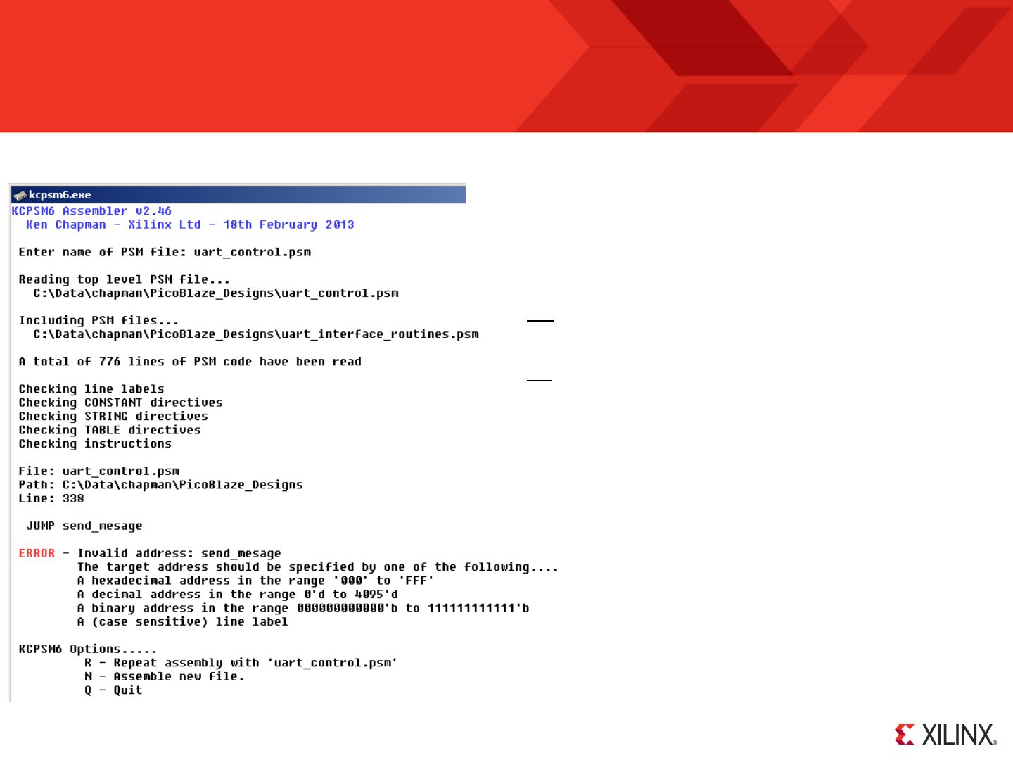
© Copyright 2010-2014 Xilinx
.
Page 49
The KCPSM6 Assembler
The KCPSM6 Assembler is provided as a single executable file ‘kcpsm6.exe’. This can be placed anywhere in your system but in most cases it is just
easier and more convenient if you place a copy in the working directory of your ISE project (it is only 109k-bytes) .
If the assembler detects an error in your PSM code then the
assembler it will identify the PSM file and the line in that file
that it can not resolve and make suggestions for you to be
able to rectify the issue.
You are then presented with 3 simple options. The ‘R’ option means
that can quickly re-run the assembler as soon as you have used your
chosen text editor to make appropriate modifications to your in your
PSM file (and saved it). This makes very rapid iterations very easy.
Hint – A text file called ‘kcpsm6_assembler_readme.txt’ contains
additional information for those interested in invoking the assembler from
batch files or using a ‘drag and drop’ method.
Hint – Should you encounter any unexpected issues using the assembler
then please check the “Known Issues and Workarounds” section contained
in the file called ‘kcpsm6_assembler_readme.txt’.
In most cases, or at least to begin with, the interactive method is adequate.
Simply double click on the executable and a window like this will open.
Type in the name of your top level PSM file (you don’t have to put ‘.psm’ on
the end of the name but the file must have the ‘.psm’ extension).
The assembler will read your top level PSM file and include any PSM
defined by INCLUDE directives. It will then check all your definitions and
code for correct syntax.
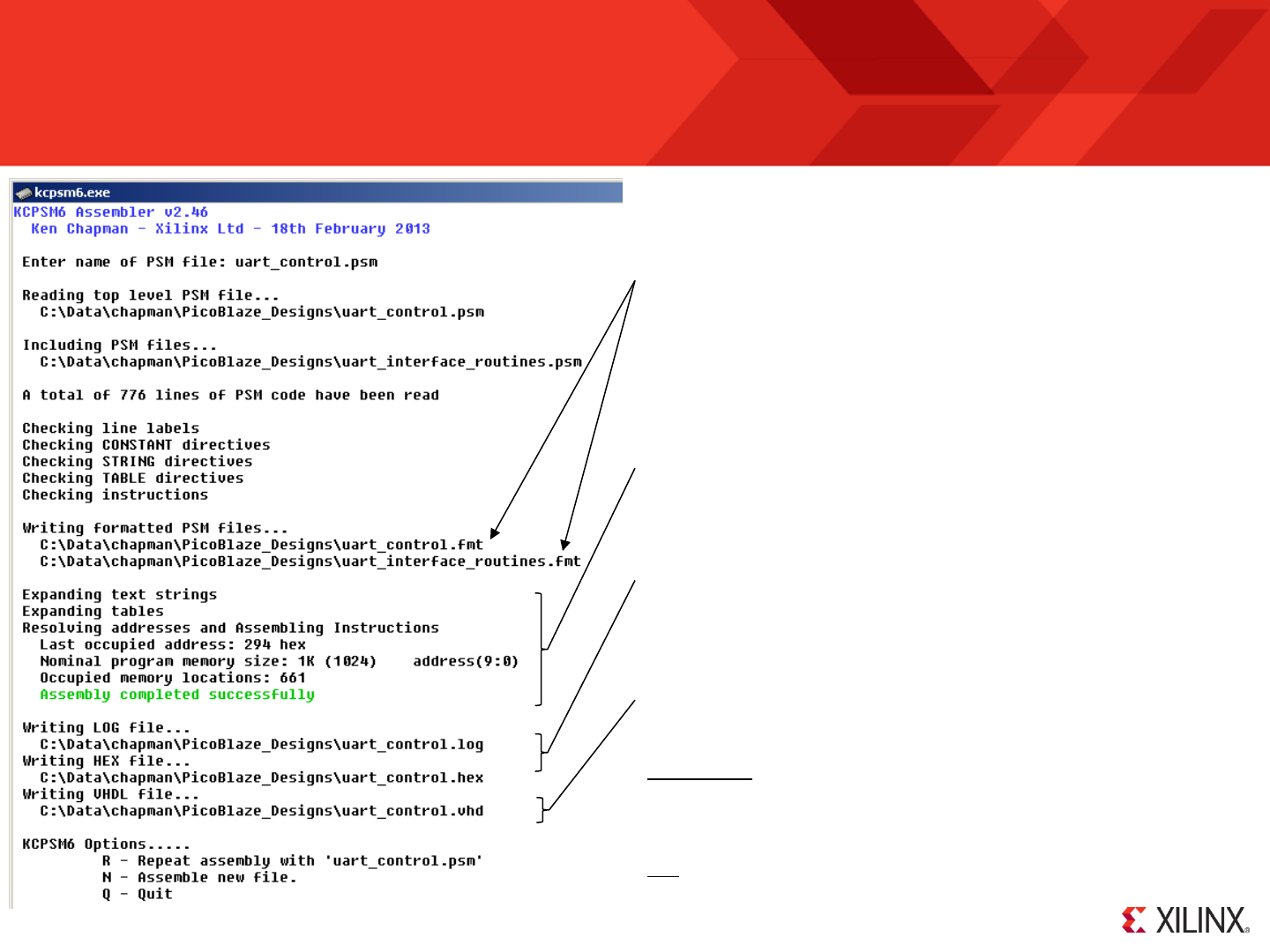
© Copyright 2010-2014 Xilinx
.
Page 50
The KCPSM6 Assembler
Then as long as your program can fit into the available address range
(default is 4K but you may like to use the ‘-c’ option when invoking the
assembler to specify a smaller memory ), the assembler will tell you the last
occupied address and indicate the nominal size of program memory
required. This is where you may need to review your code and adjust any
ADDRESS directives so that your program will fit within a smaller program
memory.
Providing your PSM file contains valid syntax then the assembler will
generate a perfectly formatted version of your original program that you can
adopt to make it look like you have been working hard all day making
something look that nice . See example on page 23. As shown in this
example, when INCLUDE directives are used then a formatted file will be
generated corresponding with each source PSM file.
Following a successful assembly, a LOG file and a HEX file will always be
generated. The log file provides you with a detailed report showing how your
PSM file has been interpreted and the addresses and op-codes assigned to
each instruction (see next page). The HEX file is a simple hexadecimal list of
the 4096 op-codes defined by your program (all undefined locations are zero)
and this is primarily for use with the JTAG Loader utility during development.
Finally the assembler has the ability to generate a VHDL or Verilog file that
defines the program memory you need to synthesise your hardware design.
The VHDL or Verilog file describes the BRAMs pre-initialised with your
program.
IMPORTANT – The assembler will only generate a VHDL or Verilog file
when there is a corresponding ‘ROM_form.vhd’ or ‘ROM_form.v’ template
provided in the same directory as your top level PSM file. If both templates
are provided then both VHDL and Verilog files will be generated.
Hint – The default ‘ROM_form.vhd’ is a renamed copy of the file called
‘ROM_form_JTAGLoader_14March13.vhd’ also provided in ZIP file.

© Copyright 2010-2014 Xilinx
.
Page 51
The Assembler Log File (‘.log’)
Assembly datestamp: 19 Apr 2012
Assembly timestamp: 16:02:20
This ’LOG’ file should not be something you need to look at very often but it can be useful reference when you are debugging a system or your code
especially when you are analyzing the interaction with the hardware design in an HDL simulator or in real hardware with ChipScope etc.
Addr Code Instruction
000 ;
000 ; Simple example
000 ;
000 CONSTANT A_port, 00 ;Input ports
000 CONSTANT B_port, 01
000 CONSTANT C_port, 02
000 CONSTANT D_port, 03
000 CONSTANT W_port, 01 ;Output ports
000 CONSTANT X_port, 02
000 CONSTANT Y_port, 04
000 CONSTANT Z_port, 08
000 ;
000 NAMEREG sF, counter
000 09000 start: INPUT s0, 00[A_port] ; read port A
001 0D001 TEST s0, 01 ;test value of LSB
002 32005 JUMP Z, 005[count_up]
003 19F01 SUB sF[counter], 01[1'd] ;count down
004 22006 JUMP 006[update_X]
005 11F01 count_up: ADD sF[counter], 01[1'd] ;count up
006 2DF02 update_X: OUTPUT sF[counter], 02[X_port]
007 09201 INPUT s2, 01[B_port] ; Z = B AND C
008 09302 INPUT s3, 02[C_port]
009 02230 AND s2, s3
00A 2D208 OUTPUT s2, 08[Z_port]
00B 22000 JUMP 000[start]
CONSTANT name Value
timestamp_hours 16'd
timestamp_minutes 16'd
timestamp_seconds 54'd
datestamp_year 12'd
datestamp_month 4'd
datestamp_day 19'd
A_port 00
B_port 01
C_port 02
D_port 03
W_port 01
X_port 02
Y_port 04
Z_port 08
No TABLEs defined
List of text strings
STRING name String
KCPSM6_version$ "v2.00"
datestamp$ "19 Apr 2012"
timestamp$ "16:16:54"
This file begins with a header includes a time and date stamp to help you keep track of your code
iterations and know what program you are using
The main part of the log file shows your program and the
addresses and op-codes for each instruction.
Each time the assembler has resolved the value of an operand the
way in which you originally defined that operand is displayed in square
brackets for reference. For example…
The register ‘sF’ was defined by the name ‘counter’ and the port_id
address ‘02’ was defined by the CONSTANT directive ‘X_port’.
After the program assembly
listing is followed by lists of all the
constants, tables, strings and line
labels defined in your program or
by the assembler.
These lists can be particularly
useful when confirming your
allocation of ports with your
hardware design.
Although not shown in this
example, the lists also identify
the PSM file in which item was
defined. This helps when
INCLUDE directives are used.
Hint – The ‘datestamp’ and ’timestamp’ constants and strings, along with HWBUILD, provide everything you need to
implement a version reporting scheme for production units as well as keeping track throughout development.
OUTPUT sF[counter], 02[X_port]
This PSM code is suitable for the
hardware shown on page 72.

© Copyright 2010-2014 Xilinx
.
Page 52
PSM Syntax
Any line can be given a label
that will eventually be a
associated with an address.
When a label is defined it
must be followed by a colon
‘:’ . A label is case sensitive
and can be any number of
the standard characters ‘a’
to ‘z’ , ‘A’ to ‘Z’, ‘0’ to ‘9’’ and
‘_’ (underscore) but it should
not be a name that could be
confused with a hex value.
Each line of your PSM file should adhere to the following basic syntax. Don’t worry too much about getting everything perfect or tidy because the assembler
will look after things like additional spaces and is very tolerant of upper or lower case characters except where it really matters. If you get something wrong
the assembler will show you what it doesn’t like and provide advice to help you correct it. KCPSM6 writes out a nicely formatted FMT file for you to adopt.
Anything following a
semicolon ‘;’ will be treated
as a comment and otherwise
ignored by the assembler.
Hint - The assembler
ignores empty lines so use
an empty comment (just a
semicolon) to preserve a
blank line in the FMT and
LOG files.
Lines only containing
comments will be formatted
in-line with the instructions.
Comments on lines
containing an instruction will
be formatted in a column to
the right of the longest
instruction. Looks nice
Any of the KCPSM6
instructions or an
assembler directive.
Upper or lower case
accepted.
label: instruction operand1, operand2 ; comment
All instructions and directives
except RETURN have at least
one operand and this should be
separated from the instruction
by at least one space.
Instructions and directives that
require a second operand should
be separated from the first
operand by a comma ‘,’
(spaces are formatting only).
Assembler directives follow the same basic syntax but are only used to direct the assembler and make code easier to write and understand.
Default register names are represented by ‘sX’ or ‘sY’ and can be any of the following...
‘s0’, ‘s1’, ‘s2’, ‘s3’, ‘s4’, ‘s5’, ‘s6’, ‘s7’, ‘s8’, ‘s9’, ‘sA’, ‘sB’, ‘sC’, ‘sD’, ‘sE’, ‘sF’.
The assembler will accept upper and lower case, e.g. ‘sb’, ‘SB’ and ‘Sb’ are also ‘sB’.
Constant values are represented by ‘aaa’, ‘kk’, ‘ss’, ‘p’ and ‘pp.
Each character represents the requirement for a hexadecimal digit to define an address,
constant or port. So for example ‘kk’ is any value in the range ‘00’ to ‘FF’ hex.
Hex values are the default and can be specified in upper or lower case, e.g, ‘6d’ or ‘6D’.
Decimal and binary values can be defined using ‘d and ‘b attributes
e.g. 109’d and 01101101’b are both equiavent to ‘6D’ hex.
Also for ‘kk’ constants only…
The ASCII equivalent of a character can be assigned, e.g. “n” is the same as ‘6D’
The lower 8-bits of an address can be identified using label’lower.
The upper 4-bits of an address can be identified using label’upper (msb 4-bits will be zero).
NOTE – ‘all_kcpsm6_syntax.psm’ provides a PSM file (albeit not a real program) that further describes all directives and has
examples of all the supported syntax. Since it is a valid PSM file you can assemble it and then look at the FMT and LOG files
that KCPSM6 generates as well.
A label can then be used
anywhere in the program to
define the target address for
a JUMP or CALL instruction
as well as with the ‘lower
and ‘upper attributes to
define constants for use in
other instructions.
INCLUDE “file.psm” / CONSTANT name, kk / ADDRESS aaa / NAMEREG oldname, newname / STRING name$, “text” / TABLE name#, [kk,kk,kk,..] / INST hhhhh
DEFAULT_JUMP aaa

© Copyright 2010-2014 Xilinx
.
Page 53
Registers and the NAMEREG Directive
KCPSM6 can generally access 16 general purpose registers assigned the default names ‘s0’ through to ‘sF’. There
are absolutely no restrictions on which register or combination of registers can be specified as ‘sX’ or ‘sY’ operands in
any of the instructions that work with registers. This provides you with complete freedom to allocate registers as you
wish. If you are careful with your allocation of registers to different tasks it will often avoid the requirement to ‘shuffle’
data around too much (as is often the case when using a processor has an accumulator based architecture).
The KCPSM6 assembler is able to identify the default name of a resister regardless of the mixture of upper and lower
case characters that you use to describe it but it will always convert it to the lower case ‘s’ followed by an upper case
hexadecimal digit when writing the FMT and LOG files. For example ‘S4’ will be interpreted as the default register
name ‘s4’. Likewise, ‘sd’, ‘Sd’ and ‘SD’ will all be interpreted as default register name ‘sD’. In other words, the
assembler allows you to concentrate on writing your code without having to be so precise about syntax and format.
ADD sB, 42
;
NAMEREG sB, Status
;
;
INPUT Status, flags_port
COMPARE Status, 12
;
NAMEREG Status, speed
;
SUB speed, 01
;
NAMEREG speed, sB
;
LOAD sB, 19
NAMEREG Directive
The NAMEREG directive is an optional facility that can help you keep track of what data you expect a particular
register to contain. Prior to the NAMEREG directive, a resister will have its default name such as ‘sB’. Once renamed,
only the new name will identify the register and that name is case sensitive exactly as you defined it. Changing the
name has no effect on the contents of the register or how it can be used.
sF
sE
sD
sC
sB
sA
s9
s8
s7
s6
s5
s4
s3
s2
s1
s0
Default register name applies before the NAMEREG directive.
The new name can only contain ‘a’ to ‘z’, ‘A’ to ‘Z’ and ‘_’ underscore (no
spaces). It can be any length but it must not be a name that could be
confused for anything else like a line label or a hexadecimal value.
Following the NAMEREG directive, only the new name is valid and that
name is case sensitive. In this case ‘sB’ will no longer be recognised.
The NAMEREG directive can be used to change the name of a register
again. Only the new name is valid in the code that follows. Depending on
your way of thinking this is either useful or something to be avoided!
NAMEREG can also be used to restore the appropriate default register
name and then the normal case insensitivity rules also apply.
16 Registers
All general purpose
All 8-bits

© Copyright 2010-2014 Xilinx
.
Page 54
KCPSM6 Instruction Set
00xy0 LOAD sX, sY
01xkk LOAD sX, kk
16xy0 STAR sX, sY
17xkk STAR sX, kk
28000 DISABLE INTERRUPT
28001 ENABLE INTERRUPT
29000 RETURNI DISABLE
29001 RETURNI ENABLE
14x06 SL0 sX
14x07 SL1 sX
14x04 SLX sX
14x00 SLA sX
14x02 RL sX
14x0E SR0 sX
14x0F SR1 sX
14x0A SRX sX
14x08 SRA sX
14x0C RR sX
08xy0 INPUT sX, (sY)
09xpp INPUT sX, pp
2Cxy0 OUTPUT sX,(sY)
2Dxpp OUTPUT sX, pp
2Bkkp OUTPUTK kk, p
Register loading
10xy0 ADD sX, sY
11xkk ADD sX, kk
12xy0 ADDCY sX, sY
13xkk ADDCY sX, kk
18xy0 SUB sX, sY
19xkk SUB sX, kk
1Axy0 SUBCY sX, sY
1Bxkk SUBCY sX, kk
Logical
02xy0 AND sX, sY
03xkk AND sX, kk
04xy0 OR sX, sY
05xkk OR sX, kk
06xy0 XOR sX, sY
07xkk XOR sX, kk
Arithmetic
Test and Compare
0Cxy0 TEST sX, sY
0Dxkk TEST sX, kk
0Exy0 TESTCY sX, sY
0Fxkk TESTCY sX, kk
1Cxy0 COMPARE sX, sY
1Dxkk COMPARE sX, kk
1Exy0 COMPARECY sX, sY
1Fxkk COMPARECY sX, kk
Shift and Rotate
Register Bank Selection
Interrupt Handling
37000 REGBANK A
37001 REGBANK B
22aaa JUMP aaa
32aaa JUMP Z, aaa
36aaa JUMP NZ, aaa
3Aaaa JUMP C, aaa
3Eaaa JUMP NC, aaa
26xy0 JUMP@ (sX, sY)
Input and Output
2Exy0 STORE sX,(sY)
2Fxss STORE sX, ss
0Axy0 FETCH sX, (sY)
0Bxss FETCH sX, ss
Scratch Pad Memory
Jump
Subroutines
20aaa CALL aaa
30aaa CALL Z, aaa
34aaa CALL NZ, aaa
38aaa CALL C, aaa
3Caaa CALL NC, aaa
24xy0 CALL@ (sX, sY)
25000 RETURN
31000 RETURN Z
35000 RETURN NZ
39000 RETURN C
3D000 RETURN NC
21xkk LOAD&RETURN sX, kk
aaa : 12-bit address 000 to FFF
kk : 8-bit constant 00 to FF
pp : 8-bit port ID 00 to FF
p : 4-bit port ID 0 to F
ss : 8-bit scratch pad location 00 to FF
x : Register within bank s0 to sF
y : Register within bank s0 to sF
14x80 HWBUILD sX
Version Control
(64, 128 or 256 bytes)
Page Opcode Instruction
55
55
71
71
56
56
57
57
58
58
59
59
60
60
61
61
62
62
63
63
64
64
65
65
66
66
67
67
67
67
67
68
68
68
68
68
92
93
93
93
93
94
96
97
97
97
97
98
70
70
73
73
74
74
78
81
81
82
82
83
83
84
84
87
88
88
88
88
89
101
Page Opcode Instruction Page Opcode Instruction

© Copyright 2010-2014 Xilinx
.
Page 55
LOAD sX, kk
LOAD sX, sY
The ‘LOAD’ instructions provides a simple way to define the contents of any register (sX). The value loaded into a register can a fixed value (kk) or the value
contained in any register (sY) can be copied. The states of the zero flag (Z) and the carry flag (C) will be unaffected.
LOAD sA, 8E
LOAD s4, 42'd
LOAD s9, 10001110'b
LOAD s6, "k"
LOAD s7, sA
LOAD s5, CR
The KCPSM6 assembler enables constant values in all instructions that require them to be defined in hexadecimal
(default), decimal, binary or using a single character which is converted to its ASCII equivalent value.
C
Z
kk
Examples
LOAD sX, kk sX = kk
‘sX’ and ‘sY’ define any of the 16 registers in the range ‘s0’ through to ‘sF’ in the active register bank. Please see the ‘Using Register Banks’ section to see
how to switch between the ‘A’ and ‘B’ register banks and techniques for copying values from registers in one bank to registers in the other.
The instruction op-code 00000 hex was specifically assigned to be the instruction ‘LOAD s0, s0’. In this way the default value (zero) of any unused program
memory contents will have the minimum effect should an improper program result in these undefined locations being executed.
No Change
No Change
sX
C
Z
sY
LOAD sX, sY sX = kY
No Change
No Change
sX
Notes
Hint - Loading a register with itself has no effect other than taking 2 clock cycles but this can be useful way to create a known delay.
After this example has executed….
‘s7’, ‘s9’ and ‘sA’ will all contain 8E hex.
‘sA’ will contain 2A hex
‘s6’ will contain 77 hex (the ASCII code for ‘k’) and ‘s5’ will contain 0D hex (the ASCII code for Carriage Return) .
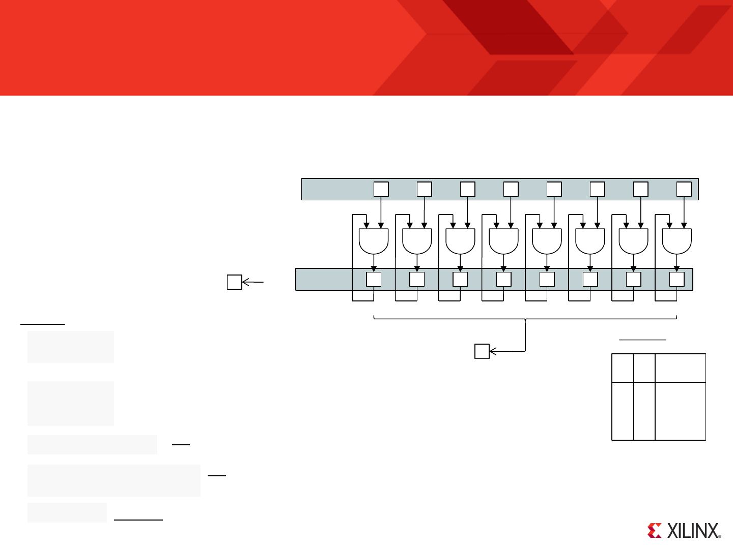
© Copyright 2010-2014 Xilinx
.
Page 56
AND sX, kk
AND sX, sY
The ‘AND’ instructions perform the bit-wise logical AND operation.
The first operand must specify a register ‘sX’ whose value provides one input to the AND operation and in to which the result is returned.
The second operand defines the second input to the AND operation and can either be an 8-bit constant ‘kk’ or a register ‘sY’.
The zero flag (Z) will be set if all 8-bits of the result returned to ‘sX’ are zero.
The carry flag (C) will be cleared (C=0) in all cases.
LOAD sA, CA
AND sA, 53
CA = 1 1 0 0 1 0 1 0
53 = 0 1 0 1 0 0 1 1
CA AND 53 = 0 1 0 0 0 0 1 0 = 42
sX
AND sX, sY sX = sX AND sY
C
Z
= ’00’ ?
‘0’
sY or kk
Examples
sA = 42, Z=0, C=0.
AND sX, kk sX = sX AND kk
0
0
1
1
2
2
3
3
4
4
5
5
6
6
7
7
LOAD sA, CA
LOAD sB, 14
AND sA, sB
CA = 1 1 0 0 1 0 1 0
14 = 0 0 0 1 0 1 0 0
CA AND 14 = 0 0 0 0 0 0 0 0 = 00
sA = 00, Z=1, C=0.
Reference
A B
0
1
0
1
0
0
1
1
0
0
0
1
A AND B
Hint – This will clear the upper nibble of ‘s5’ and could be used to convert the ASCII characters
‘0’ to ‘9’ (30 to 39 hex) into their equivalent numerical values (00 to 09 hex).
CONSTANT bit2, 00000100'b
AND s0, ~bit2
AND s5, 00001111'b
Hint – ‘AND’ provides a way to clear bits to ‘0’. In this example bit2 of register s0 is cleared. Note how all bits of a
CONSTANT can be locally inverted using ~ before the name. Hence the constant actually applied in this
case is 11111011’b. (see ‘OR’ for setting bits).
Coding Tip – Clears the Carry Flag with no change to register contents (see also HWBUILD).
AND s5, FF
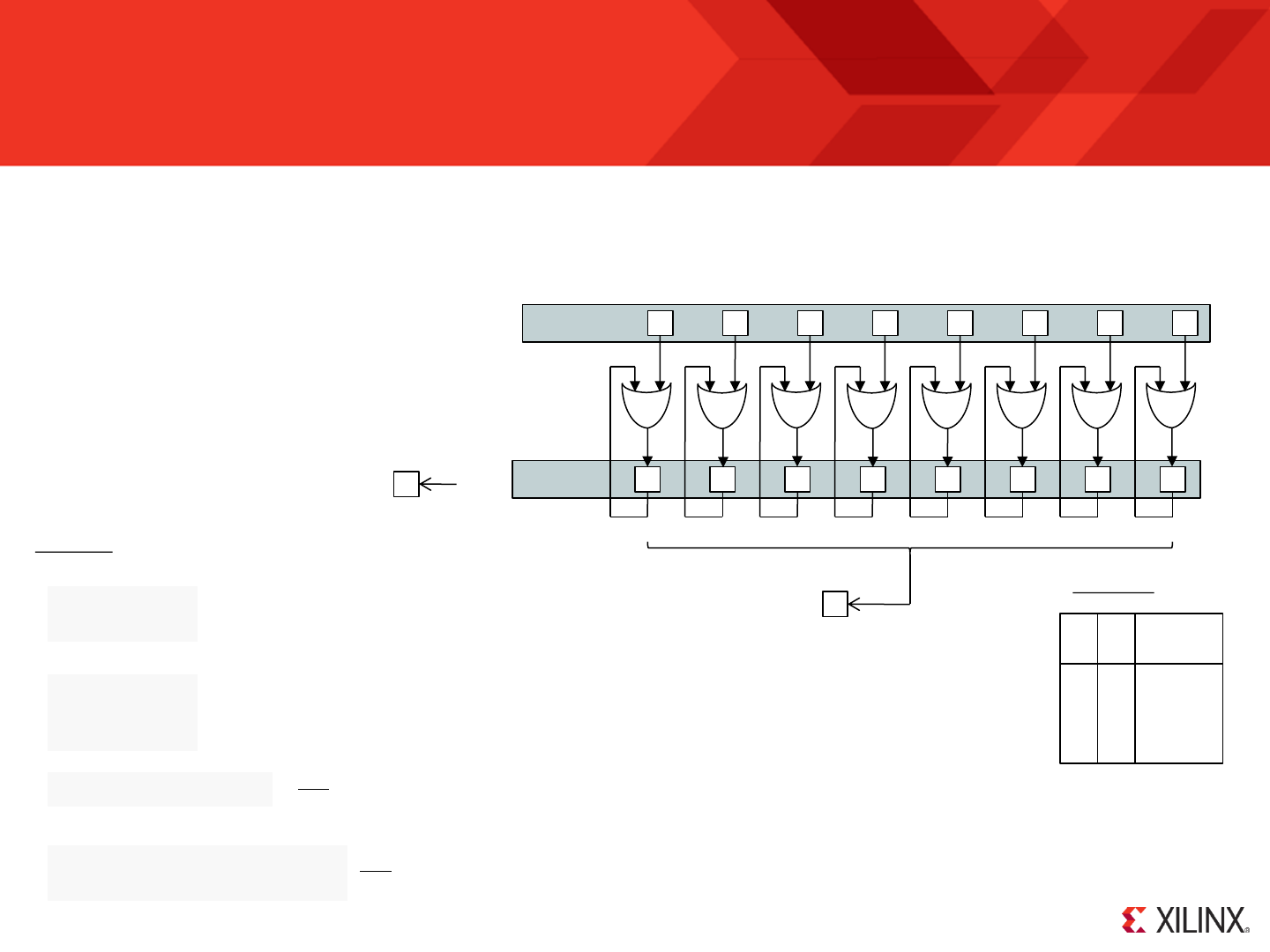
© Copyright 2010-2014 Xilinx
.
Page 57
OR sX, kk
OR sX, sY
The ‘OR’ instructions perform the bit-wise logical OR operation.
The first operand must specify a register ‘sX’ whose value provides one input to the OR operation and in to which the result is returned.
The second operand defines the second input to the OR operation and can either be an 8-bit constant ‘kk’ or a register ‘sY’.
The zero flag (Z) will be set if all 8-bits of the result returned to ‘sX’ are zero.
The carry flag (C) will be cleared (C=0) in all cases.
LOAD sA, CA
OR sA, 53
CA = 1 1 0 0 1 0 1 0
53 = 0 1 0 1 0 0 1 1
CA OR 53 = 1 1 0 1 1 0 1 1 = DB
sX
OR sX, sY sX = sX OR sY
C
Z
= ’00’ ?
‘0’
sY or kk
Examples
sA = DB, Z=0, C=0.
OR sX, kk sX = sX OR kk
0
0
1
1
2
2
3
3
4
4
5
5
6
6
7
7
CA = 1 1 0 0 1 0 1 0
14 = 0 0 0 1 0 1 0 0
CA OR 14 = 1 1 0 1 1 1 1 0 = DE
sA = DE, Z=0, C=0.
Reference
A B
0
1
0
1
0
0
1
1
0
1
1
1
A OR B
Hint – This sets 2 bits in the upper nibble of ‘s5’ and could be used to convert the numerical
values 00 to 09 hex into their ASCII equivalent characters ‘0’ to ‘9’ (30 to 39 hex).
OR s5, 00110000'b
LOAD sA, CA
LOAD sB, 14
OR sA, sB
CONSTANT bit2, 00000100'b
OR s0, bit2
Hint – ‘OR’ provides a way to set bits to ‘1’. The CONSTANT directive provides a convenient way to name bits
that you may wish to control in this way (see ‘AND’ for clearing bits).

© Copyright 2010-2014 Xilinx
.
Page 58
XOR sX, kk
XOR sX, sY
The ‘XOR’ instructions perform the bit-wise logical exclusive-OR operation.
The first operand must specify a register ‘sX’ whose value provides one input to the XOR operation and in to which the result is returned.
The second operand defines the second input to the XOR operation and can either be an 8-bit constant ‘kk’ or a register ‘sY’.
The zero flag (Z) will be set if all 8-bits of the result returned to ‘sX’ are zero.
The carry flag (C) will be cleared (C=0) in all cases.
LOAD sA, CA
XOR sA, 53
CA = 1 1 0 0 1 0 1 0
53 = 0 1 0 1 0 0 1 1
CA XOR 53 = 1 0 0 1 1 0 0 1 = 99
sX
XOR sX, sY sX = sX XOR sY
C
Z
= ’00’ ?
‘0’
sY or kk
Examples
sA = 99, Z=0, C=0.
XOR sX, kk sX = sX XOR kk
0
0
1
1
2
2
3
3
4
4
5
5
6
6
7
7
CA = 1 1 0 0 1 0 1 0
14 = 0 0 0 1 0 1 0 0
CA XOR 14 = 1 1 0 1 1 1 1 0 = DE
sA = DE, Z=0, C=0.
Reference
A B
0
1
0
1
0
0
1
1
0
1
1
0
A XOR B
Hint – The XOR instruction can be used to toggle the state of bits within a register. In this example the least
significant bit of ‘s0’ is twice toggled and output to a port. Assuming the LSB was ‘0’ to begin with
then this will have generated a positive (‘1’) pulse on the LSB of the output port whilst all other bits
remained unaffected. The CONSTANT directive provides a convenient way to name bits that you
may wish to control in this way.
LOAD sA, CA
LOAD sB, 14
XOR sA, sB
CONSTANT strobe, 00000001'b
XOR s0, strobe
OUTPUT s0, ctrl_port
XOR s0, strobe
OUTPUT s0, 0 ctrl_port
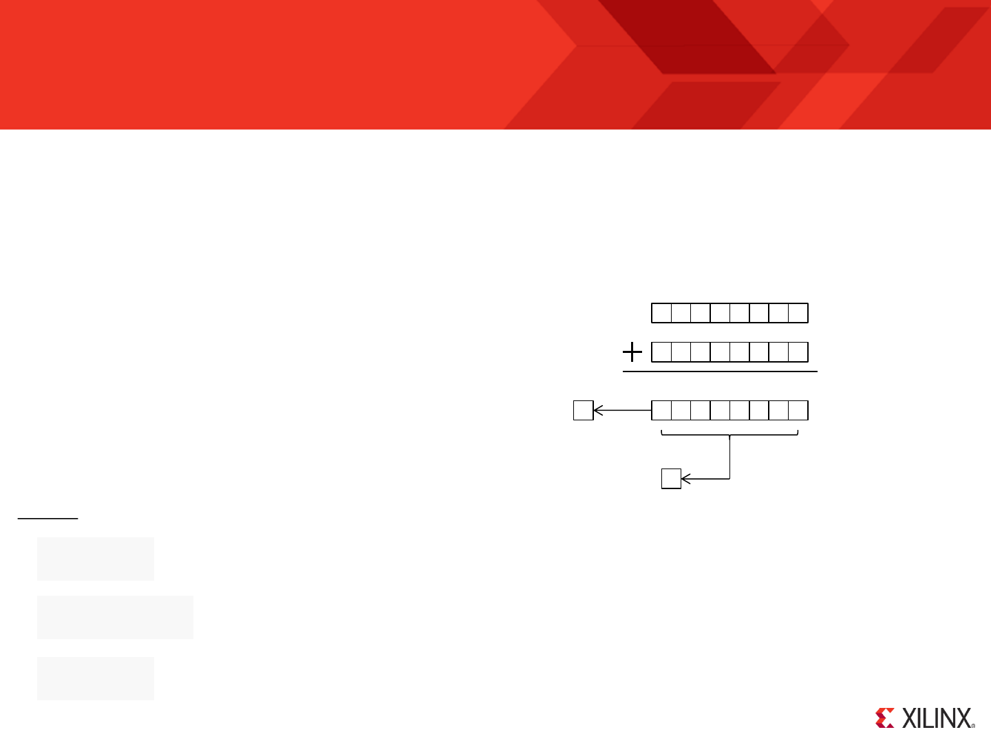
© Copyright 2010-2014 Xilinx
.
Page 59
ADD sX, kk
ADD sX, sY
The ‘ADD’ instructions perform the arithmetic addition of two 8-bit values and set the carry and zero flags according to the result.
The first operand must specify a register ‘sX’ whose value provides one input to the addition function and in to which the result is returned.
The second operand defines the second input to the addition and can either be an 8-bit constant ‘kk’ or a register ‘sY’.
The zero flag (Z) will be set if the 8-bit result returned to ‘sX’ is zero.
The carry flag (C) will be set if the addition results in an overflow.
LOAD sA, 8E
ADD sA, 43 8E + 43 = D1 sA = D1 which is not zero (Z=0) and with no overflow (C=0).
sX
sX
ADD sX, sY sX = sX + sY
C
Z
= ’00’ ?
Set if result > ‘FF’
sY or kk
Examples
LOAD sA, 142'd
ADD sA, sA 142 + 142 = 284
LOAD sA, 8E
ADD sA, 72 8E + 72 = 100 sA = 00 which is zero (Z=1) but there was also an overflow that made this happen (C=1).
ADD sX, kk sX = sX + kk
284 = 256 + 28 hence sA =28 (1C hex) which is not zero (Z=0) and there has been an overflow (C=1).
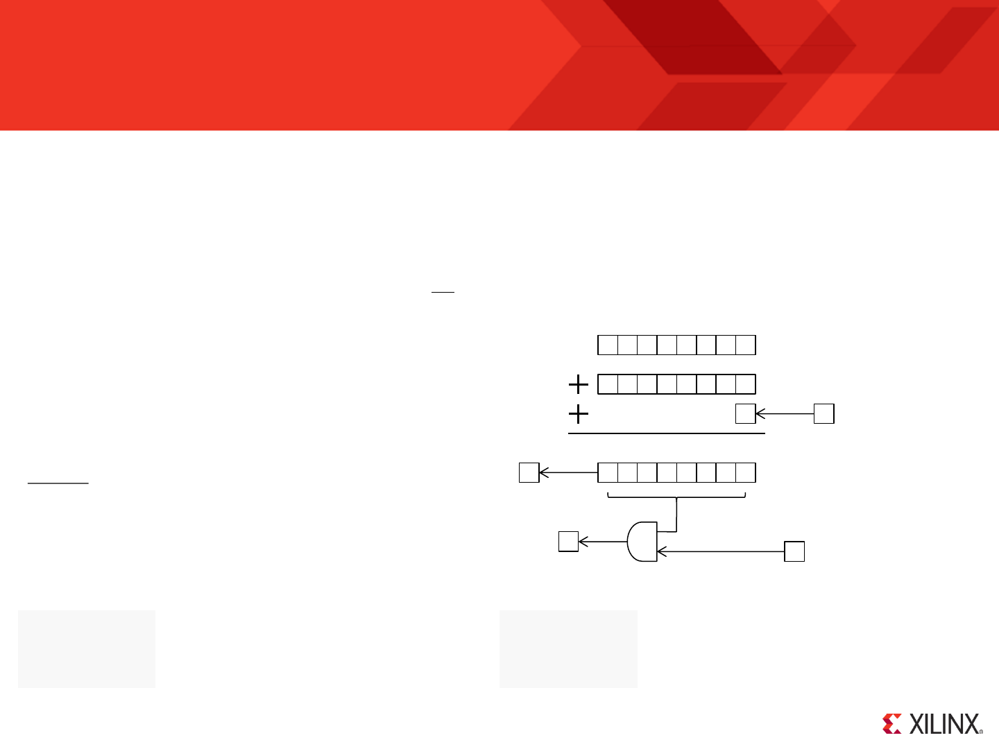
© Copyright 2010-2014 Xilinx
.
Page 60
ADDCY sX, kk
ADDCY sX, sY
The ‘ADDCY’ instructions are primarily intended as an extension to the basic ‘ADD’ instructions in order to support arithmetic addition of values more than 8-
bits. The key difference from the ADD instructions is that the zero and carry flags are also used as inputs to the addition function and these can influence both
the 8-bit result and the new states of the flags. Although each register only contains an 8-bit value, any combination of registers can be used to hold larger
values segmented into bytes. For example a 32-bit value can be held in a 4 registers. Although there is no restriction on which registers, and no formal way of
describing the assignment, it is common practice to assign adjacent registers and refer to them as a ‘register set’ such as [sD, sC, sB, sA].
The first operand must specify a register ‘sX’ whose value provides one input to the addition function and in to which the result is returned.
The second operand defines the second input to the addition and can either be an 8-bit constant ‘kk’ or a register ‘sY’.
The zero flag (Z) will be set if the 8-bit result returned to ‘sX’ is zero and the zero flag was set prior to the ADDCY instruction.
The carry flag (C) will be set if the addition results in an overflow.
sX
k k k k k k k k
sX
C
LOAD sA, 7B
LOAD sB, A2
ADD sA, 85
ADDCY sB, 5D
= ’00’ ?
sY or kk
Examples
Carry from
previous operation
C
Z Zero from
previous operation
Z=1 ?
[sB, sA] = A2 7B
+ 5D 85 = 10000
7B + 85 = 100 sA = 00, Z=1, C=1.
A2 + 5D + 1 = 100 sB = 00, Z=1, C=1.
LOAD sA, 7B
LOAD sB, A2
ADD sA, 85
ADDCY sB, 5D
[sB, sA] = A2 7B
+ 5E 1A = 10095
7B + 1A = 95 sA = 95, Z=0, C=0.
A2 + 5E + 0 = 100 sB = 00, Z=0, C=1.
The key observation to make as illustrated by these
examples is that carry and zero flags reflect the entire result
of a multi-byte addition. In particular, the zero flag is only set
if the complete multi-byte result is zero and is not just based
on the 8-bit result of the final ADDCY operation.
Z AND
ADDCY sX, sY sX = sX + sY + C
ADDCY sX, kk sX = sX + kk + C
Set if result > ‘FF’
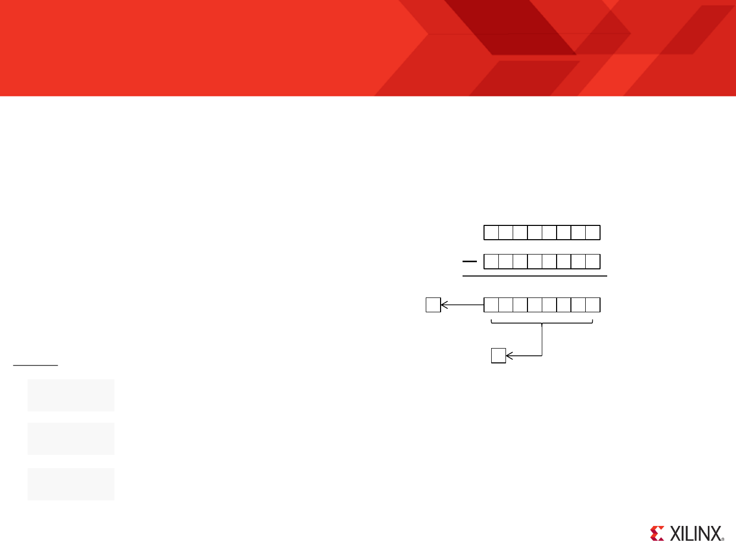
© Copyright 2010-2014 Xilinx
.
Page 61
SUB sX, kk
SUB sX, sY
The ‘SUB’ instructions perform the arithmetic subtraction of two 8-bit values and set the carry and zero flags according to the result.
The first operand must specify a register ‘sX’ from which the second operand will be subtracted and to which the result is returned.
The second operand defines the value to be subtracted from the first operand and can either be an 8-bit constant ‘kk’ or a register ‘sY’.
The zero flag (Z) will be set if the 8-bit result returned to ‘sX’ is zero.
The carry flag (C) will be set if the result of the subtraction is negative. Hence the carry flag represents an underflow or a ‘borrow’ to complete the operation.
LOAD sA, 8E
SUB sA, 43 8E - 43 = 4B sA = 4B which is not zero (Z=0) and with no underflow (C=0).
sX
sX
SUB sX, sY sX = sX - sY
C
Z
= ’00’ ?
sY or kk
Examples
LOAD sA, 8E
ADD sA, sA 8E - 8E = 00 sA = 00 which is zero (Z=1) but there was still no underflow (C=0).
LOAD sA, 8E
SUB sA, B5
8E – B5 = 1D9 sA = D9 which is not zero (Z=0) but there was an underflow (C=1).
This is equivalent to 142 – 181 = -39 where D9 hex is the twos complement representation of -39.
However, it is the users responsibility to implement and interpret signed arithmetic values and operations.
SUB sX, kk sX = sX - kk
Set if result < ‘00’

© Copyright 2010-2014 Xilinx
.
Page 62
SUBCY sX, kk
SUBCY sX, sY
The ‘SUBCY’ instructions are primarily intended as an extension to the basic ‘SUB’ instructions in order to support arithmetic subtraction of values more than
8-bits. The key difference from the SUB instructions is that the zero and carry flags are also used as inputs to the subtraction function and these can influence
both the 8-bit result and the new states of the flags. Although each register only contains an 8-bit value, any combination of registers can be used to hold
larger values segmented into bytes. For example a 32-bit value can be held in a 4 registers. Although there is no restriction on which registers, and no formal
way of describing the assignment, it is common practice to assign adjacent registers and refer to them as a ‘register set’ such as [sD, sC, sB, sA].
The first operand must specify a register ‘sX’ from which the second operand and carry flag will be subtracted and to which the result is returned.
The second operand defines the value to be subtracted from the first operand and can either be an 8-bit constant ‘kk’ or a register ‘sY’.
The zero flag (Z) will be set if the 8-bit result returned to ‘sX’ is zero and the zero flag was set prior to the SUBCY instruction.
The carry flag (C) will be set if the result of the subtraction is negative. Hence the carry flag represents an underflow or a ‘borrow’ to complete the operation.
sX
k k k k k k k k
sX
C
LOAD sA, 7B
LOAD sB, A2
SUB sA, sA
SUBCY sB, sB
= ’00’ ?
sY or kk
Examples
Carry from
previous operation
C
Z Zero from
previous operation
Z=1 ?
[sB, sA] = A2 7B
- A2 7B = 0000
7B – 7B = 00 sA = 00, Z=1, C=0.
A2 – A2 - 0 = 00 sB = 00, Z=1, C=0.
LOAD sA, 7B
LOAD sB, A2
SUB sA, B9
SUBCY sB, A1
[sB, sA] = A2 7B
- A1 B9 = 00C2
7B – B9 = (-)C2 sA = C2, Z=0, C=1.
A2 – A1 - 1 = 00 sB = 00, Z=0, C=0.
The key observation to make as illustrated by these
examples is that carry and zero flags reflect the entire result
of a multi-byte subtraction. In particular, the zero flag is only
set if the complete multi-byte result is zero and is not just
based on the 8-bit result of the final SUBCY operation.
Z AND
SUBCY sX, sY sX = sX - sY - C
SUBCY sX, kk sX = sX - kk - C
Set if result < ‘00’
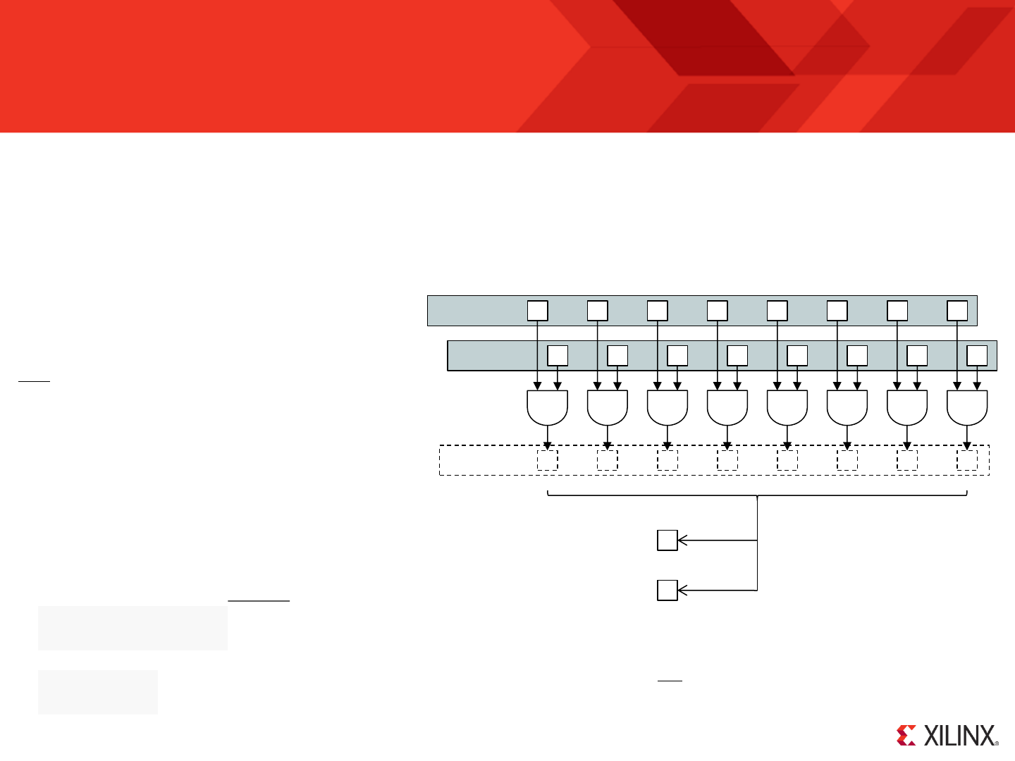
© Copyright 2010-2014 Xilinx
.
Page 63
TEST sX, kk
TEST sX, sY
The ‘TEST’ instructions are similar to the ‘AND’ instructions in that a bit-wise logical AND operation is performed. However, the actual result is discarded and
only the flags are updates to reflect the temporary 8-bit. The ‘TEST’ instruction also reports then exclusive-OR of the temporary result which can be used to
compute the ‘odd parity’ of a value.
The first operand must specify a register ‘sX’ whose value provides one input to the AND operation (sX will not be effected by the operation).
The second operand defines the second input to the AND operation and can either be an 8-bit constant ‘kk’ or a register ‘sY’.
The zero flag (Z) will be set if all 8-bits of the temporary result are zero.
The carry flag (C) will be set if the temporary result contains an odd number of bits set to ‘1’ (the exclusive-OR of the 8-bit temporary result).
LOAD sA, CA
TEST sA, 01000000'b
CA = 1 1 0 0 1 0 1 0
40 = 0 1 0 0 0 0 0 0
CA AND 40 = 0 1 0 0 0 0 0 0 = 40
TEST sX, sY temp = sX AND sY
Z = ’00’ ?
sY or kk
Examples
Z=0, C=1 (odd).
TEST sX, kk temp = sX AND kk
0
0
1
1
2
2
3
3
4
4
5
5
6
6
7
7
LOAD sA, 51
TEST sA, FF
51 = 0 1 0 1 0 0 0 1
FF = 1 1 1 1 1 1 1 1
51 AND FF = 0 1 0 1 0 0 0 1 = 51
Z=0, C=1.
Parity is odd.
sX 0 1 2 3 4 5 6 7
temp
C Odd ?
Hints
It is typical to think of ‘sX’ containing the information to be tested
and for ‘sY’ or ‘kk’ to be acting as a bit-mask to select only those
bits to be tested.
To test a single bit the value of ‘kk’ is best described using a
binary format such as 00100000’b that will text bit 5 (equivalent
to 20 hex). The ‘C’ flag will be set if the corresponding bit in ‘sX’
is ‘1’ and the ‘Z’ flag will be set if the tested bit is ‘0’.
Use a mask value of kk = FF to compute the odd parity of the
whole byte contained in ‘sX’.
Hint – The ‘SLA’ and ‘SRA’ shift instructions and the
ADDCY and SUBCY instructions can all be used to
move the value of the carry flag into a register.
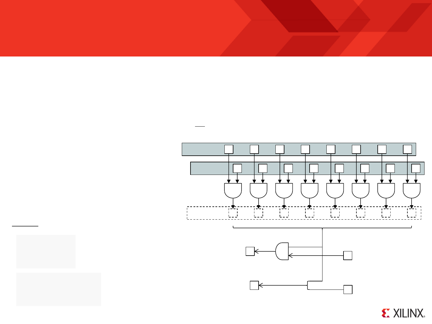
© Copyright 2010-2014 Xilinx
.
Page 64
TESTCY sX, kk
TESTCY sX, sY
LOAD sA, CA
LOAD sB, 52
TEST sA, FF
TESTCY sB, FF
TEST sX, sY temp = sX AND sY sY or kk
Examples
[sB, sA] = 11001010 0101001
7 bits in total are ‘1’ so parity is odd. Z=0, C=1.
TEST sX, kk temp = sX AND kk
0
0
1
1
2
2
3
3
4
4
5
5
6
6
7
7
sX 0 1 2 3 4 5 6 7
temp
Odd ?
The ‘TESTCY’ instructions are primarily intended as an extension to the basic ‘TEST’ instructions in order to support testing and odd parity calculation of
values more than 8-bits. The key difference from the TEST instructions is that the zero and carry flags are also used as inputs that can influence the new
states of the flags. Although each register only contains an 8-bit value, any combination of registers can be used to hold larger values segmented into bytes.
For example a 32-bit value can be held in a 4 registers. Although there is no restriction on which registers, and no formal way of describing the assignment, it
is common practice to assign adjacent registers and refer to them as a ‘register set’ such as [sD, sC, sB, sA].
The first operand must specify a register ‘sX’ whose value provides one input to the AND operation (sX will not be effected by the operation).
The second operand defines the second input to the AND operation and can either be an 8-bit constant ‘kk’ or a register ‘sY’.
The zero flag (Z) will be set if all 8-bits of the temporary result are zero and the zero flag was set prior to the TESTCY instruction.
The carry flag (C) will be set if the temporary result together with the previous state of the carry flag contains an odd number of bits set to ‘1’.
The meaning of the ‘C’ and ‘Z’ flags are the same following a
TEST and TESTCY combination of instructions used to test
and compute the odd parity of a multi-byte value as they are
after a single 8-bit TEST operation.
= ’00’ ?
Z Zero from
previous operation
Z=1 ?
Z AND
C Carry from
previous operation
C
LOAD sA, CA
LOAD sB, 52
TEST sA, 00000100'b
TESTCY sB, 00100000'b
[sB, sA] = 11001010 0101001
Both bit13 and bit3 of the 16-bit word are ‘0’.
Z=1, C=0 (even).
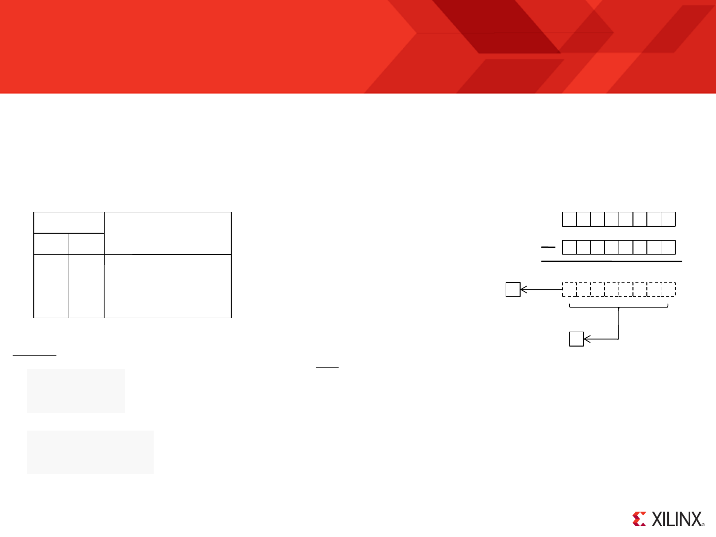
© Copyright 2010-2014 Xilinx
.
Page 65
COMPARE sX, kk
COMPARE sX, sY
The ‘COMPARE’ instructions perform the arithmetic subtraction of two 8-bit values but the actual result is discarded and only the carry and zero flags are
updated according to the temporary result.
The first operand must specify a register ‘sX’ from which the second operand will be subtracted (the value of sX will not be effected by the operation).
The second operand defines the value to be subtracted from the first operand and can either be an 8-bit constant ‘kk’ or a register ‘sY’.
The zero flag (Z) will be set if the temporary 8-bit result is zero corresponding with both operand being equal or ‘matching’.
The carry flag (C) will be set if the temporary result of the subtraction is negative and hence indicating when ‘sX’ is less than the second operand.
LOAD sA, 8E
COMPARE sA, 8E
JUMP Z, equal
Values are equal, Z=1, C=0.
sX
temp
COMPARE sX, sY temp = sX - sY
C
Z
= ’00’ ?
sY or kk
Examples
COMPARE sX, kk temp = sX - kk
Set if temp < ‘00’
sX > kk or sX > sY
Z C
Flag States
Comparison
0 0
1 x
x 1 sX = kk or sX = sY
sX < kk or sX < sY
LOAD sA, 8E
COMPARE sA, 98
JUMP C, less_than sA < 98, Z=0, C=1.
Hints
Use ‘Z’ to determine when the values are equal or ‘match’.
The ‘C’ flag can be used to determine when sX is less than the second operand.
Hence, it can also be used to determine when sX is greater than or equal to the
second operand’. So when comparing the contents of two registers assign them to ‘sX’
and ‘sY’ such that you can use ‘C’ to identify which is less. This will avoid the
requirement to test both ‘C’ and ‘Z’ flags.
The KSPSM6 Assembler enables you to specify constants in hex, decimal and ASCII
characters, e.g. COMPARE s0, “Q”
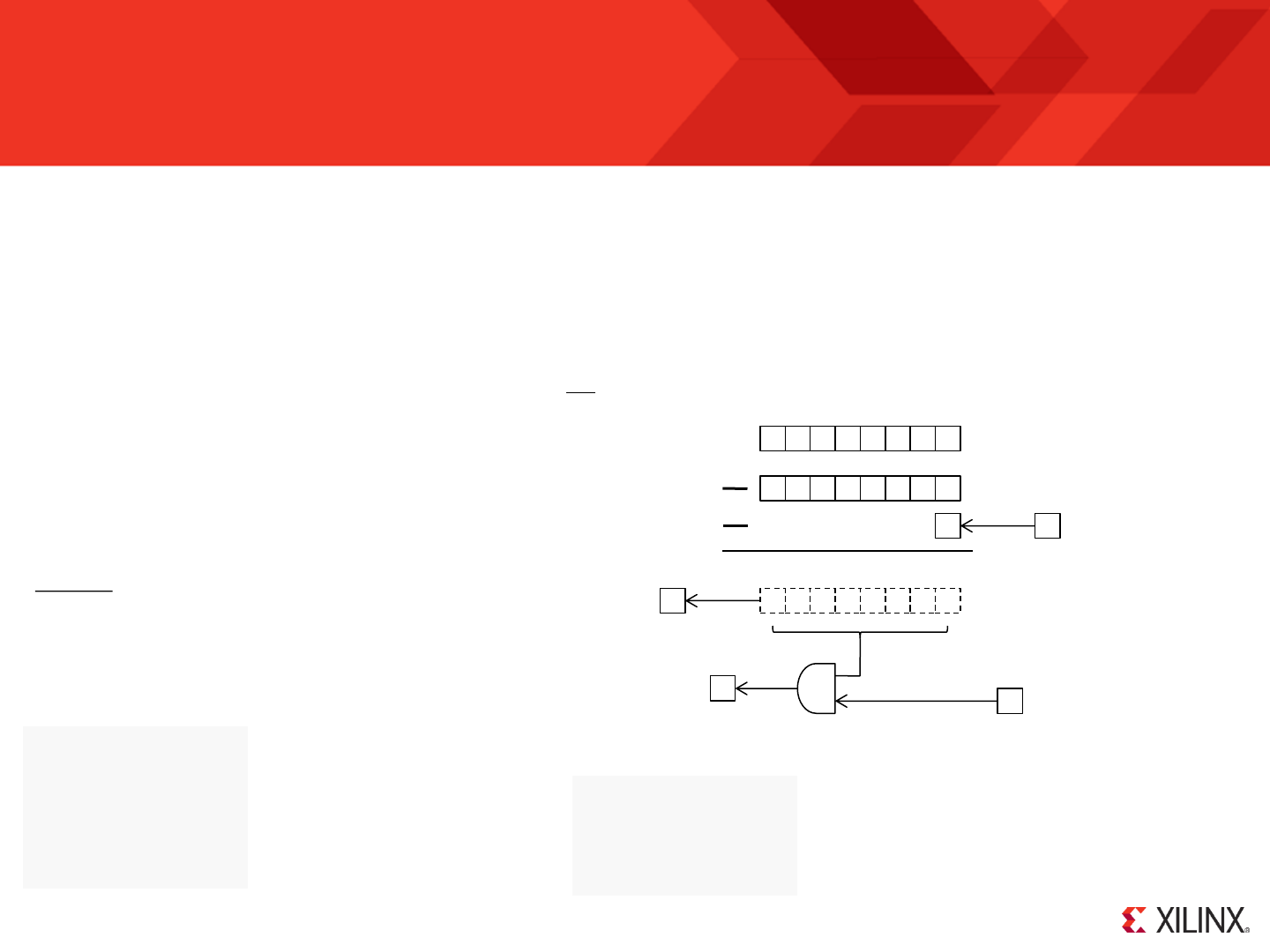
© Copyright 2010-2014 Xilinx
.
Page 66
COMPARECY sX, kk
COMPARECY sX, sY
The ‘COMPARECY’ instructions are primarily intended as an extension to the basic ‘COMPARE’ instructions in order to support comparison of values more
than 8-bits. The key difference from the COMPARE instructions is that the zero and carry flags are also used as inputs to the subtraction used to perform the
comparison and these can influence both the 8-bit result before it is discarded and the new states of the flags. Although each register only contains an 8-bit
value, any combination of registers can be used to hold larger values segmented into bytes. For example a 32-bit value can be held in a 4 registers. Although
there is no restriction on which registers, and no formal way of describing the assignment, it is common practice to assign adjacent registers and refer to them
as a ‘register set’ such as [sD, sC, sB, sA].
The first operand must specify a register ‘sX’ from which the second operand and carry flag will be subtracted (sX will not be effected by the operation).
The second operand defines the value to be subtracted from the first operand and can either be an 8-bit constant ‘kk’ or a register ‘sY’.
The zero flag (Z) will be set if the temporary 8-bit result is zero is zero and the zero flag was set prior to the COMPARECY instruction.
The carry flag (C) will be set if the temporary result of the subtraction is negative. sX
k k k k k k k k
temp
C
= ’00’ ?
sY or kk
Examples
Carry from
previous operation
C
Z Zero from
previous operation
Z=1 ?
LOAD sA, 7B
LOAD sB, A2
LOAD sC, 14
COMPARE sA, 7B
COMPARECY sB, A2
COMPARECY sC, 14
JUMP Z, equal
[sC,sB, sA] = 14 A2 7B
14A27B – 14A27B = 000000
Values are equal Z=1, C=0.
The meaning of the ‘C’ and ‘Z’ flags are the same following a
COMPARE and COMPARECY combination of instructions
used to compare multi-byte values as they are after a single
8-bit COMPARE operation. Z AND
COMPARECY sX, sY temp = sX - sY - C
COMPARECY sX, kk temp = sX - kk - C
Set if temp < ‘00’
LOAD sA, 7B
LOAD sB, A2
COMPARE sA, 7B
COMPARECY sB, B9
JUMP C, less_than
[sB, sA] = A2 7B
A27B – B97B = (-) E900
[sB, sA] < B97B Z=0, C=1.
© Copyright 2010-2014 Xilinx
.
SL0 sX
C
Page 67
SL0 sX SL1 sX SLX sX SLA sX
These instructions all shift the contents of the specified register (sX) one bit to the left. The most significant bit (MSB) is shifted out of the register into the
carry flag (C). The bit that is shifted into the least significant bit (LSB) is defined by the shift left instruction that is used. The zero flag (Z) will be set only if all
8-bits of the resulting value contained in the register are zero.
LOAD sB, 14
LOAD sA, B5
SL0 sA
SLA sB
A shift left injecting a ‘0’ has the effect of multiplying a value by 2. The ‘SLA’ instruction enables multi-byte values contained in multiple registers to be shifted.
C ‘0’
Examples
sX
Outputs a simple pattern shown on the right hand side to the to ‘port’.
The process terminates when all 8-bits have been set and the final
shift sets the carry flag.
[sB,sA] = 14B5 = 530110 = 0001 0100 1011 0101
C ‘1’ SL1 sX
sX
C
SLX sX
sX
C
SLA sX
sX
SL0 sX shifts a ‘0’ into the LSB. The Z flag will only be set if bits(7:1)
are also all ‘0’ after the shift.
SL1 sX shifts a ‘1’ into the LSB. This means that the Z flag will be
always be cleared (Z=0) by this instruction.
SLX sX replicates the existing state of the LSB. The Z flag will only be
set if all 8-bits of the register are zero.
SLA sX shifts the previous state of the carry flag into the LSB at the
same time that the carry flag is loaded with the MSB. The Z flag will
only be set if all 8-bits of the register are zero.
C ‘0’
sA
C
sB
SL0 sA SLA sB
[sB,sA] = 296A = 1060210 = 0010 1001 0110 1010
LOAD sF, 00000001'b
loop: OUTPUT sF, port
SLX sF
JUMP NC, loop
00000001
00000011
00000111
00001111
00011111
00111111
01111111
11111111
Z
Z
Z
Z
=?
=0
=?
=?
Previous
© Copyright 2010-2014 Xilinx
.
C
Page 68
SR0 sX SR1 sX SRX sX SRA sX
These instructions all shift the contents of the specified register (sX) one bit to the right. The least significant bit (LSB) is shifted out of the register into the
carry flag (C). The bit that is shifted into the most significant bit (MSB) is defined by the shift right instruction that is used. The zero flag (Z) will be set only if all
8-bits of the resulting value contained in the register are zero.
LOAD sB, ED
LOAD sA, 2A
SL0 sA
SLA sB
A shift right has the effect of dividing a value by 2. The ‘SRA’ instruction enables multi-byte values contained in multiple registers to be shifted.
When 2’s complement is used to represent signed values then ‘SRX’ implements sign extension.
C
‘0’
Examples
SR0 sX
sX
Outputs to ‘port’ a simple ‘walking 1’ pattern as illustrated on the right hand side.
The process terminates when the ‘1’ is shifted into the carry flag.
[sB,sA] = ED2A = -482210 = 1110 1101 0010 1010
C
‘1’
SR1 sX
sX
C
SRX sX
sX
C
SRA sX
sX
SR0 sX shifts a ‘0’ into the MSB. The Z flag will only be set if
bits(6:0) are all also ‘0’ after the shift.
SR1 sX shifts a ‘1’ into the MSB. This means that the Z flag will be
always be cleared (Z=0) by this instruction.
SRX sX replicates the existing state of the MSB. The Z flag will only be
set if all 8-bits of the register are zero.
SRA sX shifts the previous state of the carry flag into the MSB at the
same time that the carry flag is loaded with the LSB. The Z flag will
only be set if all 8-bits of the register are zero.
C
sA sB
SRA sA SRX sB
[sB,sA] = F695 = -241110 = 1111 0110 1001 0101
LOAD sF, 10000000'b
loop: OUTPUT sF, port
SR0 sF
JUMP NC, loop
10000000
01000000
00100000
00010000
00001000
00000100
00000010
00000001
00000000
C
Z
Z
Z
Z
=?
=0
=?
=?
Previous
© Copyright 2010-2014 Xilinx
.
RL sX
Page 69
RL sX
RR sX
The ‘RL’ and ‘RR’ instructions rotate the contents of the specified register (sX) one bit to the left or right. The bit that is shifted out of on end of the register and
back into the other end is also copied into the into the carry flag (C). The zero flag (Z) will be set only if all 8-bits of the register contents are zero.
LOAD s6, 03
loop: OUTPUT s6, motor_ctrl
CALL step_delay
INPUT s0, direction
TEST s0, 01
JUMP NZ, move_right
RL s6
JUMP loop
move_right: RR s6
JUMP loop
Rotate operations are typically used in the generations of bit patterns or sequences such as in the control of stepper motors.
C
Example
sX
In this example we can imagine a stepper motor that has 8 coils arranged
in a circle such that the coil mapped to bit0 is adjacent to the coil mapped
to bit7. The position of the motor is defined by the coils being energised
and in this case it is beneficial to energise two adjacent coils of a motor at
the same time (hence the initial value of 03 loaded into ‘s6’).
An input is sampled to determine in which direction the motor should
rotate and this is translated into the direction in which the “11” pattern is
rotated either to the left or right.
RL sX shifts all bits one place to the left and the MSB that is shifted
out is shifted into the LSB as well as copied into the carry flag. The Z
flag will only be set if all bits of the register are zero.
Note that because the rotate instructions only reorganize the existing contents of ‘sX’ the zero flag will only be set if ‘sX’ contained zero on entry to the
rotate operation.
00000011
00000110
00001100
00011000
00110000
01100000
11000000
10000001
00000011
00000110
00000011
10000001
11000000
01100000
Z =?
RR sX
sX
Z =?
C RR sX shifts all bits one place to the right and the LSB that is shifted
out is shifted into the MSB as well as copied into the carry flag. The Z
flag will only be set if all bits of the register are zero.
Left
Right
© Copyright 2010-2014 Xilinx
.
Page 70
REGBANK A
REGBANK B
KCPSM6 actually has 32 registers that are arranged into 2 banks of 16
registers called bank ‘A’ and bank ‘B’. Only one bank can be active at a given
time and all instructions (except ‘STAR’) can only perform operations involving
the registers in the active bank. To put it another way the registers in the
inactive bank are almost completely isolated and their contents are unaffected
by instructions modifying values within the registers of the active bank.
Following device configuration, or an active High reset pulse on the ‘reset’
input of the KCPSM6 macro, bank ‘A’ will be the active bank. Hence KCPSM6
can initially be considered to have 16 registers and this will be adequate for
many applications.
The REGBANK instruction can be used to select which bank is to be active and
therefore assign the other bank to being inactive. There is only one carry flag
and one zero flag neither of which is effected by the bank selection.
sF
sE
sD
sC
sB
sA
s9
s8
s7
s6
s5
s4
s3
s2
s1
s0
BANK B
sF
sE
sD
sC
sB
sA
s9
s8
s7
s6
s5
s4
s3
s2
s1
s0
BANK A
- Select bank B active.
- Select bank A active (or restore default bank).
Default Bank
Hint - If you use the NAMEREG directive in your code then you will probably
want to assign different names to the registers following the REGBANK
instruction to reflect that you are no longer accessing the same information.
Hint – When selecting a different bank there is no effect on the contents of
any registers in either bank. However, it will almost certainly appear as if the
contents of all registers change as the swap is made. Note that there is only
one set of flags and their values will not change.
REGBANK B
REGBANK A
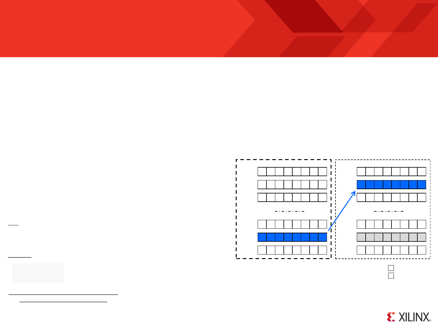
© Copyright 2010-2014 Xilinx
.
Page 71
STAR sX, kk
STAR sX, sY
Apart from bank ‘A’ being the default on power up or following a reset you are completely free to select bank ‘A’ or bank ‘B’ as and when you wish using a
REGBANK instruction. All instructions only operate on the registers in the actively selected bank which preserves the values in the inactive bank. This can be
particularly useful when creating a subroutine that implements an intense task; having many registers available to manipulate data can make the task much
easier to implement. It is also very appealing when servicing an interrupt as the bank swap can help to ensure that the contents of registers being used
anywhere else in the program at the time of the interrupt are not disturbed. This is covered in more detail in the interrupt section of this guide (see page 86 ).
KCPSM3 only had one bank of registers, so a common technique was to preserve the contents of registers in scratch pad memory before those registers
were used again in a subroutine. The values were then fetched from memory to restore their values before returning to the main program. This is still a
perfectly valid technique in KCPSM6 programs but it can result in a significant number of STORE and FETCH instructions consuming code space and
slowing program execution. By switching to the ‘B’ bank of registers at the start of an intense subroutine, or when servicing and interrupt, you can effectively
provide yourself with 16 temporary registers in one instruction cycle (2 system clock cycles) automatically preserving the contents of registers in bank ‘A’.
Although it is useful to have two banks of registers that are isolated and
independent this also presents a challenge when it comes to data being passed
between a main program and a subroutine. Once again a potential solution is to
assign particular scratch pad memory locations which are then accessed by both
sections of code when using different register banks but this requires a memory
location and a pair of STORE and FETCH instructions for each byte of data. For
this reason the ‘Send To Alternate Reregister’ (‘STAR’) instruction provides you
with a way to pass information from a register in the active bank (sY) to a register
in the inactive bank (sX) or to pre-set a constant in a register of the inactive bank.
sF
sE
sD
s2
s1
s0
sF
sE
sD
s2
s1
s0
Active Bank
STAR sE, s1
STAR s1, 37
‘sE’ in the inactive bank is loaded with a copy of ‘s1’ in the active bank.
‘s1’ in the inactive bank is loaded with constant value 37 hex (note ‘s1’ in active bank is unchanged).
Inactive Bank
ASSEMBLER CODING REQUIREMENT
when using the STAR instruction
Hint – Like the ‘LOAD’ instructions, the ‘STAR’ instructions have no effect on the
states of the flags. However, it should be recognised that ‘STAR s0, s0’ is not
equivalent to a ‘no-operation’ instruction because each reference to ‘s0’ is in a
different bank (i.e. ‘s0’ in the inactive bank will probably be changed).
Example
The alternate register ‘sX’ must be specified using a default name ‘s0’ to ‘sF’. Any NAMEREG directives do not
apply to the specification of ‘sX’. The current active register ‘sY’ must be specified using an active name for a
register (i.e. NAMEREG does apply as normal). These are deliberate coding rules intended to minimise the
probability of coding mistakes (i.e. They force you to think carefully about which bank is active).
C
Z
No Change
No Change
0 1 0 1 1 0 1 1
(Effect illustrated in the diagram)
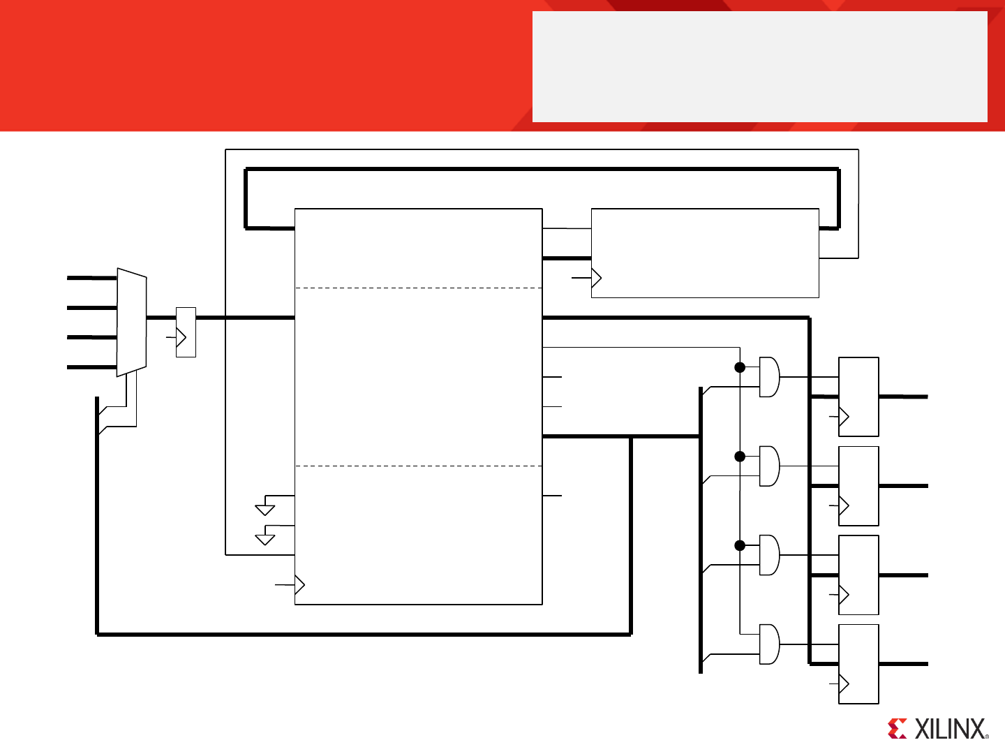
© Copyright 2010-2014 Xilinx
.
Page 72
General Purpose I/O Ports
address
instruction bram_enable
clk
interrupt
sleep
reset
interrupt_ack
port_id
out_port
in_port
k_write_strobe
read_strobe
write_strobe
kcpsm6
[11:0]
[17:0]
[7:0]
[7:0]
[7:0]
This diagram represents one possible arrangement in which KCPSM6 can be used to service 4 input ports
and 4 general purpose output ports. Each port is up to 8-bits and could be connected directly to pins on the
device package or may connect to some of your other logic within the device. All KCPSM6 designs build on
variations of this fundamental arrangement. Suitable PSM code for this circuit is shown on page 51.
instruction
address
enable
your_program
rdl
[7:0]
[7:0]
[7:0]
[7:0]
D
C
B
A
[7:0]
D
CE
Z
[7:0]
D
CE
Y
[7:0]
D
CE
X
[7:0]
D
CE
W
[2]
[1]
[0]
[3]
[0]
[1]
Input Ports
Output Ports
A = PORT 00
B = PORT 01
C = PORT 02
D = PORT 03
00
01
10
11
= PORT 08
= PORT 04
= PORT 02
= PORT 01
clk
This design has been used to evaluate the maximum clock rates that
can be achieved for a variety of device types and speed grades...
Spartan-6: (-1L) ~82MHz | (-2) ~105MHz | (-3) ~136MHz
Virtex-6: | | (-3) ~238MHz
Kintex-7: (-1) ~185MHz | | (-3) ~238MHz
Virtex-7: | | (-3) ~232MHz
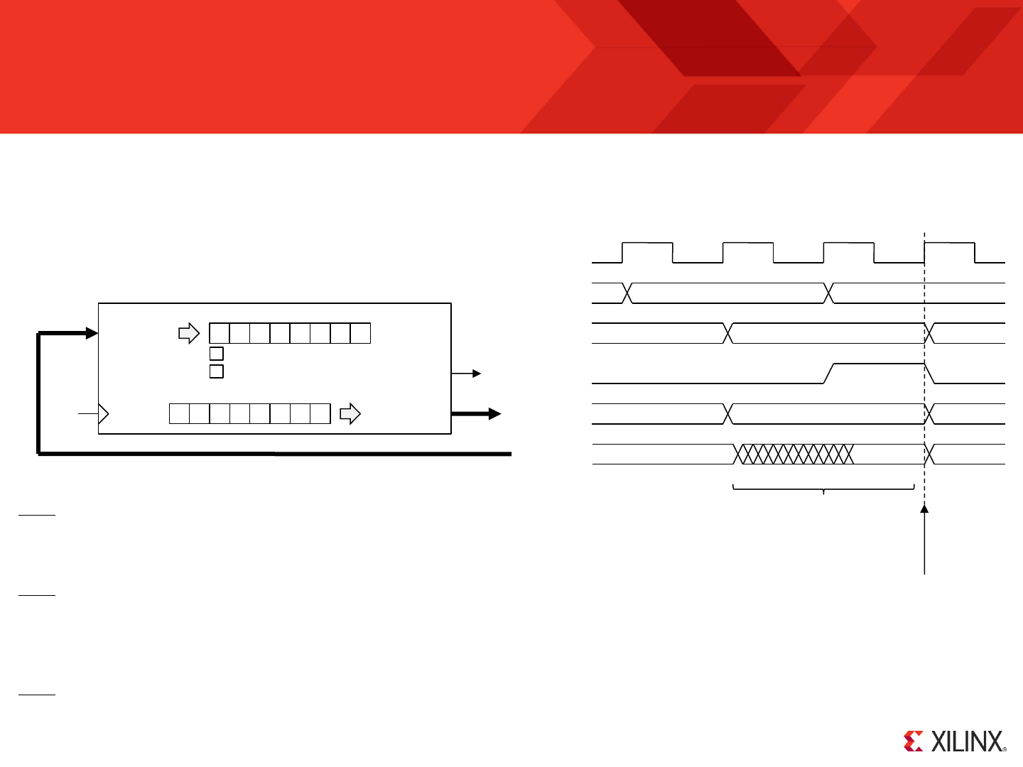
© Copyright 2010-2014 Xilinx
.
Page 73
INPUT sX, pp
INPUT sX, (sY)
An ‘INPUT’ instruction enables KCPSM6 to read information from the from your hardware design into a register ‘sX’ using a general purpose input port
specified by an 8-bit constant value ‘pp’ or the contents of another register ‘(sY)’. KCPSM6 presents the port address defined by ‘pp’ or ‘(sY)’ on ‘port_id’ and
your hardware interface is then responsible for selecting and presenting the appropriate information to the ‘in_port’ so that it can be captured into the ‘sX’
register. An active High (‘1’) synchronous pulse is also generated on the ‘read_strobe’ pin and may be used by the hardware interface to confirm when a
particular port has been read.
INPUT sX, pp
in_port
instruction
read_strobe
clk
port_id
in_port
read_strobe
[7:0]
[7:0]
clk
kcpsm6 address
port_id pp
sX
sY or pp
There are 2 clock cycles available
to decode the port address ‘pp’ or
‘(sY)’ and present the requested
information to the ‘in_port’.
Hint 3 – ‘read_strobe’ can be ignored in most cases and never needs to be part of the multiplexer feeding ‘in_port’. However, some functions such as a FIFO
buffer do need to know when they have been read and it is in those situations that ‘read_strobe’ together with a decode of the appropriate value of ‘port_id’
would be used to generate a “port has been read” pulse to confirm when a read has taken place.
Data captured into ‘sX’ on
this rising clock edge.
Hint 1 – Assign your input port addresses such that the data selection multiplexer feeding ‘in_port’
uses the minimum number of ‘port_id’ signals to make the selection, e.g. port addresses ‘00’ to ‘0F’
provide 16 input ports and only require ‘port_id(3:0)’ to be selection inputs to the multiplexer
resulting in smaller faster designs.
Hint 2 – Unless there is a specific reason not to, the input data selection multiplexer should include a
pipeline register (i.e. your case statement should be within a clocked process). In this way the data is
selected during the first clock cycle of ‘port_id’ and presented to ‘in_port’ during the second clock cycle.
Failure to define a pipeline register anywhere in the ‘port_id’ to ‘in_port’ path is the most common reason
for PicoBlaze designs failing to meet the required performance (a ‘false path’ for one clock cycle) .
INPUT sX, pp
INPUT sX, (sY)
C
Z
No Change
No Change
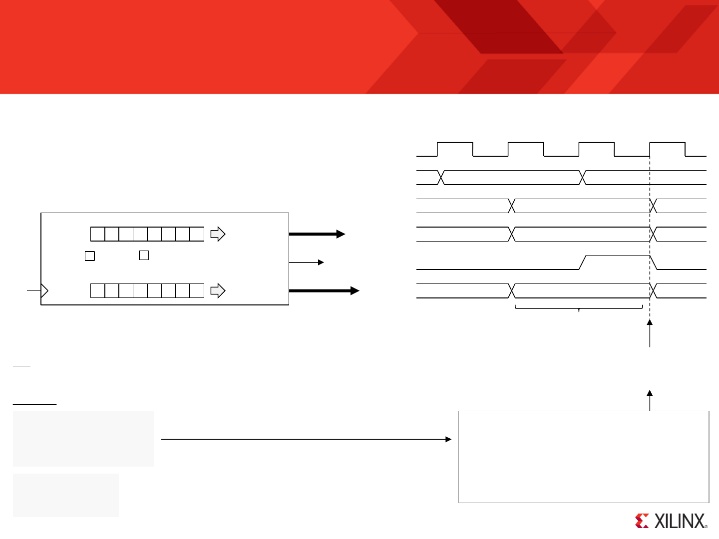
© Copyright 2010-2014 Xilinx
.
Page 74
OUTPUT sX, pp
OUTPUT sX, (sY)
An ‘OUTPUT’ instruction is used to transfer information from a register ‘sX’ to a general purpose output port specified by an 8-bit constant value ‘pp’ or the
contents of another register ‘(sY)’. KCPSM6 presents the contents of the register ‘sX’ on ‘out_port’ and the port address defined by ‘pp’ or ‘(sY)’ is presented
on ‘port_id’. Both pieces of information are qualified by an active High (‘1’)
synchronous pulse on the ‘write_strobe’ pin. Your hardware interface is
responsible for capturing the information presented.
CONSTANT LED_port, 05
;
LOAD s3, 3A
OUTPUT s3, LED_port
OUTPUT sX, pp
out_port
instruction
write_strobe
clk
The value presented on ‘out_port’
should be captured on the rising edge
of the clock when ‘write_strobe’ is High.
Decimal values can be used to specify port addresses but hex or binary
values are normally easier to work with when defining the hardware.
Note that ‘out_port’ and ‘port_id’ will vary during the execution of other instructions but
‘write_strobe’ will only be active during an OUTPUT instruction.
port_id
out_port
write_strobe
[7:0]
[7:0]
clk
kcpsm6
address
port_id
sX
pp
sX
sY or pp
There are 2 clock cycle available to
decode the port address ‘pp’ or ‘(sY)’
Examples
Hint – In most cases a fixed port address ‘pp’ is used so CONSTANT directives provide an ideal
why track your port assignments and make your code easier to write, understand and maintain.
OUTPUT s6, (s2)
OUTPUT s4, 40
OUTPUT sB, 64'd
if clk'event and clk = '1' then
if write_strobe = '1' then
if port_id(2 downto 0) = "101" then
led <= out_port;
end if;
end if;
end if;
VHDL
If you want to keep your designs small and fast then assign
port addresses that facilitate smaller logic functions.
In this example a set of 8 LEDs are mapped to port 05 hex and
only 3-bits of ‘port_id’ together with ‘write_strobe’ are decoded.
OUTPUT sX, pp
OUTPUT sX, (sY)
C
Z No Change
No Change
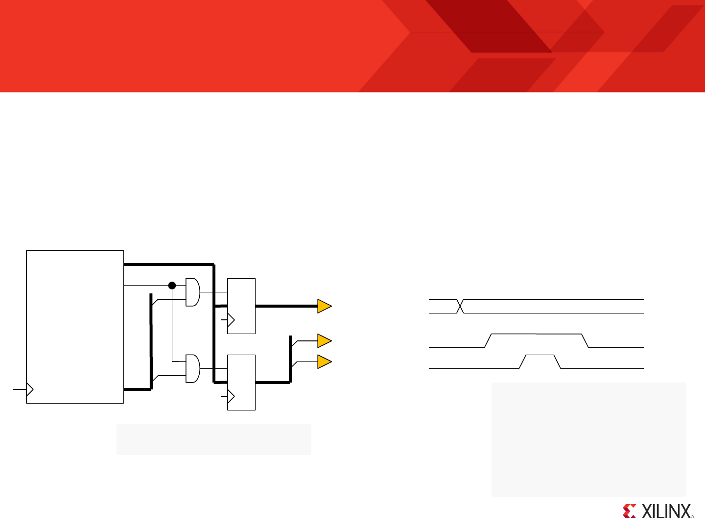
© Copyright 2010-2014 Xilinx
.
Page 75
Constant-Optimised Output Ports
In order to understand the motive for the constant-optimised ports and to know when it is better to use them, it is necessary to appreciate the situations in
which the general output ports can adversely effect the size of your program code and/or result in lower performance. The ‘OUTPUT sX, pp’ and ‘OUTPUT
sX, (sY)’ instructions associated with the general purpose output ports both require that the value to be written to the port to be held in a register ‘sX’. This is
ideal when the value is a variable in your system but when you want to send a constant value, or more likely, a series of constant values to a port the act of
loading ‘sX’ each time increases code size and reduces performance. In many applications this overhead can be tolerated and you should feel no pressure to
adapt your design and code to use the constant-optimised ports unless you really want to. However, using constant-optimised ports appropriately can make
code easier to write and avoid the code size and performance overhead associated with general purpose output ports when necessary.
port_id
out_port
write_strobe
[7:0] [7:0]
D
CE
PORT 08
[3]
[0]
[1] Dev_write
Dev_clk
[7:0]
[7:0]
D
CE
[5]
Dev_data[7:0]
clk
kcpsm6
PORT 20
Valid Data
OUTPUT s1, Dev_data_port
LOAD s0, 00000010'b
OUTPUT s0, Dev_control_port
LOAD s0, 00000011'b
OUTPUT s0, Dev_control_port
LOAD s0, 00000010'b
OUTPUT s0, Dev_control_port
LOAD s0, 00
OUTPUT s0, Dev_control_port
CONSTANT Dev_data_port, 20
CONSTANT Dev_control_port, 08
Using General Purpose Output ports……
For each OUTPUT instruction of
the control sequence waveform
there is a corresponding LOAD
instruction that prepares ‘s0’ with
the required constant value.
In this example KCPSM6 is required to write 8-bit data to an external device. The data is naturally variable
and is presented to the device interface by outputting to port 20 hex. Then KCPSM6 is required to
generate the correct sequence of control signals; ‘Dev_write’ is set High before a pulse is generated on
the ‘Dev_clk’ followed by ‘Dev_write’ being returned Low. These signals are controlled by outputting the
appropriate sequence of constant values to port 08 hex that define the states of bit0 and bit1.
(This technique of driving control signals is often called ‘bit banging’).
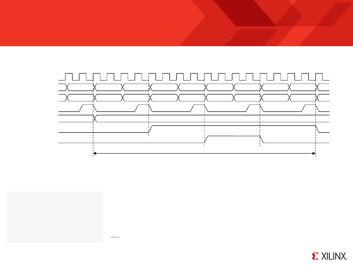
© Copyright 2010-2014 Xilinx
.
Page 76
Constant-Optimised Output Ports
The timing diagram for the code using the general purpose output ports shows that it takes 16 system clock cycles to generate the control sequence because
every instruction takes 2 clock cycles and every OUTPUT instruction requires a corresponding LOAD instruction to initialise ‘sX’ (‘s0’ was used in the
example). It can also be seen that this results in 4 clock cycles between each transition of the control sequence.
OUTPUT s1, Dev_data_port
LOAD s2, 00000010'b
LOAD s3, 00000011'b
LOAD s0, 00000000'b
OUTPUT s2, Dev_control_port
OUTPUT s3, Dev_control_port
OUTPUT s2, Dev_control_port
OUTPUT s0, Dev_control_port
LOAD OUTPUT
out_port
Dev_write
Dev_clk
Dev_data[7:0]
instruction
write_strobe
02
LOAD OUTPUT
03
LOAD OUTPUT
02
LOAD OUTPUT
00 data
OUTPUT
clk
16 clock cycles
There are a number of applications where it is beneficial that KPCSM6 slows down the generation of waveforms. For example, the communication rate with
an SPI Flash memory device may be 33MHz maximum. So if your system clock was 200MHz you would be looking to divide that by at least a factor or 6 and
KCPSM6 could help to achieve that naturally. However, if you require higher ‘bit banging’ performance without just increasing the system clock frequency
then clearly there is a limit when using the general purpose output ports.
One potential workaround that has been used in KCPSM3 based designs in the past, and is still applicable
to KCPSM6 designs, is to reorder your code. As shown on the left, the constant values have been pre-
loaded into a set of registers so that the waveform can be generated with a burst of sequential OUTPUT
instructions. Whilst this does result in the highest possible ‘bit banging’ transition rate of the signals during
the actual generation of the sequence it also requires more registers to be used and the same amount of
time is required to execute the code overall.
Hint – To generate single clock cycle pulses you can use the single clock cycle ‘write_strobe’ qualified by
the ‘port_id’ rather than set and reset a data bit of a full output port.
Valid Data
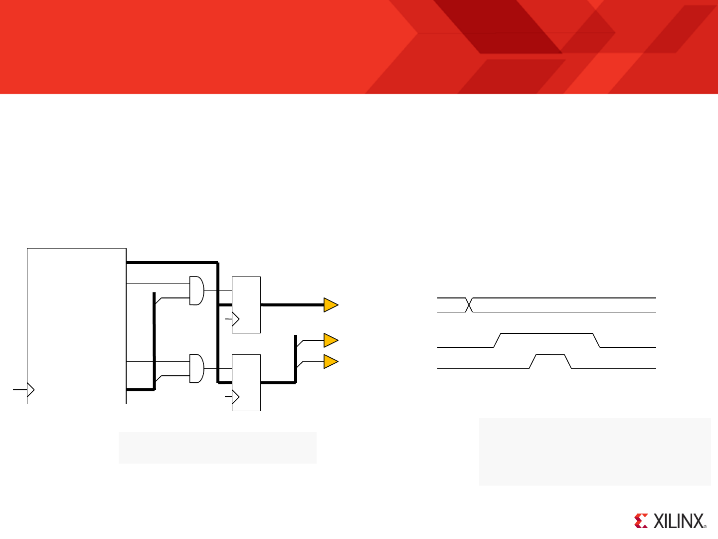
© Copyright 2010-2014 Xilinx
.
Page 77
Constant-Optimised Output Ports
KCPSM6 provides up to 16 constant-optimised output ports. From a hardware perspective these are used in an identical way to the general purpose output
ports except that ‘k_write_strobe’ is used to qualify the port address which is presented on port_id[3:0]. Hence only port addresses ‘0’ to ‘F’ (0’d to 15’d) can
be used and port_id[7:4] should be ignored. Good optimum designs will allocate output port addresses to minimise the decoding of ‘port_id’ so this should not
pose any challenges.
Returning to the same example of writing data to an external device we can see that port 08 hex has now been allocated to a constant-optimised output port
by using the ‘k_write_strobe’ whilst port 20 hex is still associated with ‘write_strobe’ because the data is naturally variable. So there is very little difference in
the hardware as long as you remember that only port_id[3:0] are defined during an OUTPUTK instruction. Note also that you could now have two different
output ports with the same address; on for variable data and the other for constant values (see page 79).
port_id
out_port
write_strobe
[7:0] [7:0]
D
CE
PORT 08
[3]
[0]
[1] Dev_write
Dev_clk
[7:0]
[7:0]
D
CE
[5]
Dev_data[7:0]
k_write_strobe
clk
kcpsm6
PORT 20
Valid Data
OUTPUT s1, Dev_data_port
OUTPUTK 00000010'b, Dev_control_port
OUTPUTK 00000011'b, Dev_control_port
OUTPUTK 00000010'b, Dev_control_port
OUTPUTK 00000000'b, Dev_control_port
CONSTANT Dev_data_port, 20
CONSTANT Dev_control_port, 08
Using a Constant-Optimised Output Port and a General Purpose Output Port……
It can be seen immediately that
all the LOAD instructions have
been eliminated saving code
space and reducing the execution
time. This also means that
register ‘s0’ used previously to
define the sequence of values is
now free for another purpose.
Smaller and Faster Code
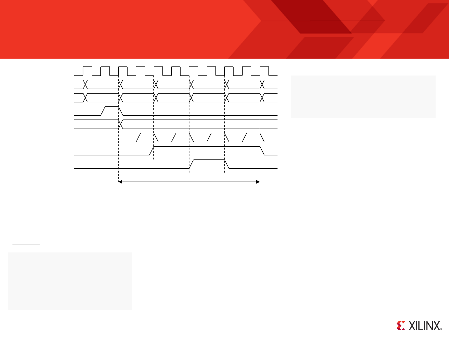
© Copyright 2010-2014 Xilinx
.
Page 78
Constant-Optimised Output Ports
OUTPUTK kk, p
out_port
Dev_write
Dev_clk
Dev_data[7:0]
instruction
write_strobe
data
OUTPUT
clk
OUTPUTK OUTPUTK OUTPUTK OUTPUTK
Valid Data
k_write_strobe
02 03 02 00
8 clock cycles
This timing diagram clearly shows the performance
advantage when using a constant-optimised output
port for a ‘bit banging’ application. The example
control sequence is now completed in 8 rather than
16 clock cycles. More significantly, the standard
transition rate is every instruction or 2 system clock
cycles. All without the need to use any registers.
OUTPUTK kk, p
The OUTPUTK instruction has two operands. The first operand is the 8-bit constant value ‘kk’ that will be presented on ‘out-port’ and therefore must be in
the range ‘00’ to ‘FF’ hex. The second operand must specify the port address that will be presented on port_id[3:0] and therefore must be in the range ‘0’ to
‘F’ hex. This instruction has no effect on the contents of any registers used or the state of the flags.
These examples show how the KCPSM6 assembler enables the constant and port to be defined and
specified in multiple ways. All four ‘OUTPUTK’ instructions shown are actually the same!
The constant value ‘kk’ can be specified immediately using hex, decimal or an ASCII character.
Alternatively the name allocated to a constant by a CONSTANT directive can be used.
The port address ‘p’ can also be specified immediately using hex or decimal but remember that this can
only be in the range ‘0’ to ‘F’ (0’d to 15’d). Likewise, the name of constant defined by a CONSTANT
directive can be used providing that the value assigned to it also falls within the required range.
CONSTANT token, 61
CONSTANT control_port, 0A
OUTPUTK 61, A
OUTPUTK 97'd, 10'd
OUTPUTK "a", A
OUTPUTK token, control_port
Smaller and Faster Code
Examples
OUTPUT s1, Dev_data_port
OUTPUTK 00000010'b, Dev_control_port
OUTPUTK 00000011'b, Dev_control_port
OUTPUTK 00000010'b, Dev_control_port
OUTPUTK 00000000'b, Dev_control_port
Hint – Using a TABLE directive would also
make this code easier to write.
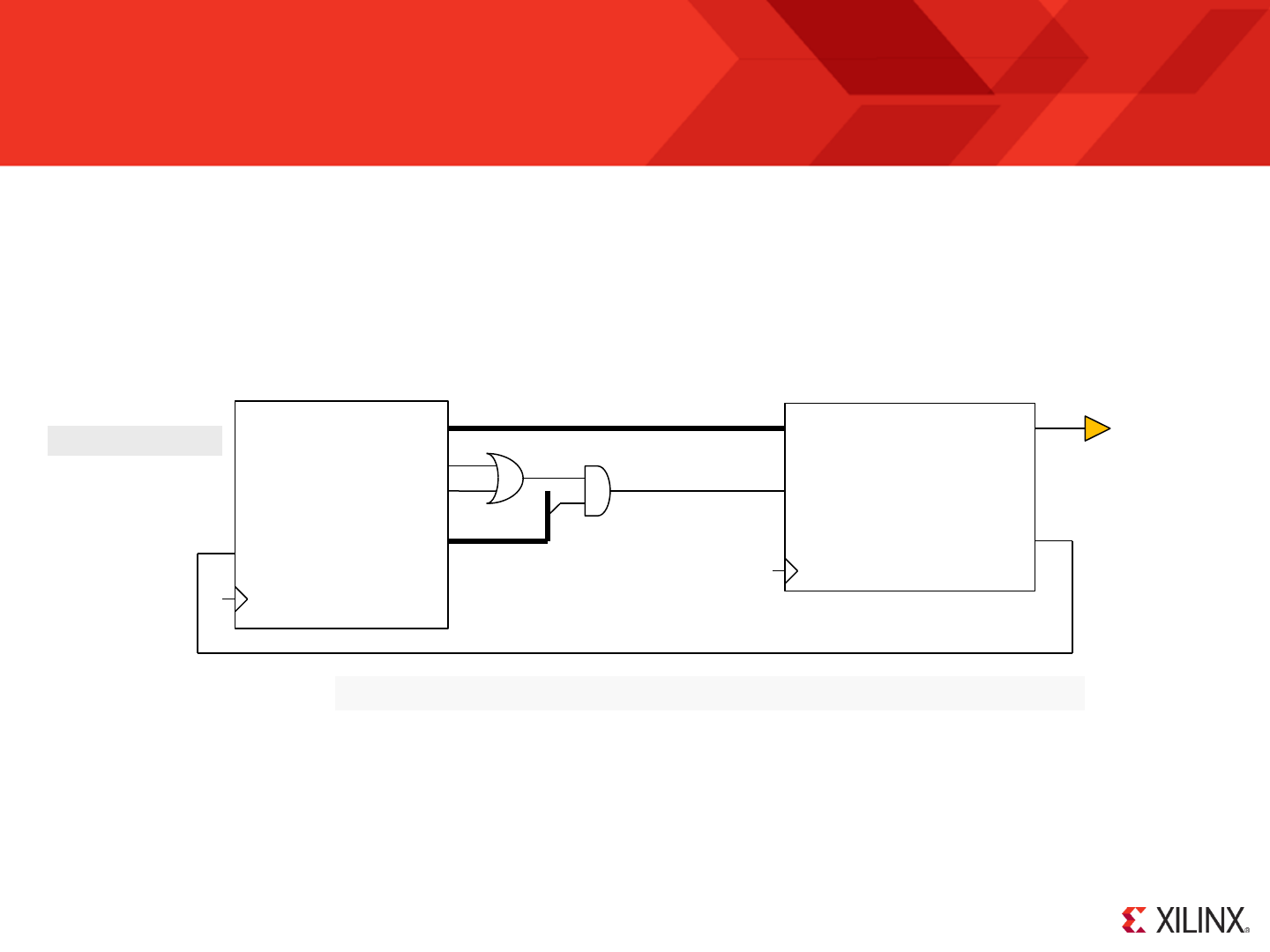
© Copyright 2010-2014 Xilinx
.
Page 79
Implementing Hybrid Output Ports
Whenever variable data needs to be sent to an output port then a general purpose output port must be used. However, mainly to improve code density the
‘OUTPUTK kk, p’ instruction is more suitable in some situations so it then becomes desirable to deliver constants to the same port. This can be achieved
simply by allocating the same port address (in the range ‘00’ to ‘0F’ hex) to be used by both ‘OUTPUT sX, pp’ and ‘OUTPUTK kk, p’ instructions and
implementing a hybrid port in hardware.
An example of a hybrid port is shown below. In this case KCPSM6 is required to send information to a UART transmitter to be observed on a PC terminal. Not
surprisingly, the information will be a series of ASCII characters but many of these will be pre-defined strings or constants whilst others will represent the
variable data to be displayed. This example also illustrates a possible use of the ‘sleep’ control and the ‘STRING’ directive in the KCPSM6 assembler.
port_id
out_port
write_strobe
[7:0]
PORT 08
[3]
write_to_uart
[7:0]
k_write_strobe
kcpsm6
write_to_uart <= (k_write_strobe or write_strobe) and port_id(3);
data_in serial_out
buffer_half_full
clk
uart_tx (includes 16-byte FIFO buffer)
write_buffer
clk
sleep
In order to create a hybrid port the port address must be in the range ‘00’ to ‘0F’ hex and in this example 08 hex has been used in a optimised decode of
‘port_id’ (i.e. only port_id[3] is actually being observed to minimise the logic function performing the decode). Then both ‘write_strobe’ and ‘k_write_strobe’ are
used to qualify the port address so that either an ‘OUTPUT sX, 08’ or an ‘OUTPUT kk, 8’ instruction will result in data being written to the FIFO buffer within
the UART transmitter macro.
The circuit diagram also shows how the ‘half full’ status output from the FIFO buffer could be used to make KCPSM6 wait (sleep) each time the buffer starts to
fill up and this hardware form of handshaking is important if code density is to be achieved as we will see on the next page.…
Hybrid port decode in VHDL
hwbuild => X“41“,

© Copyright 2010-2014 Xilinx
.
Page 80
Implementing Hybrid Output Ports & Text Strings
This code uses the hybrid port to display the hardware build state on the PC terminal display.
CONSTANT UART_Tx_port, 08
;
STRING hw_intro$, "Hardware Build: “
OUTPUTK hw_intro$, UART_Tx_port
HWBUILD s0
OUTPUT s0, UART_Tx_port
OUTPUTK 0D, UART_Tx_port
000 2B488 OUTPUTK 48[hw_intro$:"H"], 8[UART_Tx_port]
001 2B618 OUTPUTK 61[hw_intro$:"a"], 8[UART_Tx_port]
002 2B728 OUTPUTK 72[hw_intro$:"r"], 8[UART_Tx_port]
003 2B648 OUTPUTK 64[hw_intro$:"d"], 8[UART_Tx_port]
004 2B778 OUTPUTK 77[hw_intro$:"w"], 8[UART_Tx_port]
005 2B618 OUTPUTK 61[hw_intro$:"a"], 8[UART_Tx_port]
006 2B728 OUTPUTK 72[hw_intro$:"r"], 8[UART_Tx_port]
007 2B658 OUTPUTK 65[hw_intro$:"e"], 8[UART_Tx_port]
008 2B208 OUTPUTK 20[hw_intro$:" "], 8[UART_Tx_port]
009 2B428 OUTPUTK 42[hw_intro$:"B"], 8[UART_Tx_port]
00A 2B758 OUTPUTK 75[hw_intro$:"u"], 8[UART_Tx_port]
00B 2B698 OUTPUTK 69[hw_intro$:"i"], 8[UART_Tx_port]
00C 2B6C8 OUTPUTK 6C[hw_intro$:"l"], 8[UART_Tx_port]
00D 2B648 OUTPUTK 64[hw_intro$:"d"], 8[UART_Tx_port]
00E 2B3A8 OUTPUTK 3A[hw_intro$:":"], 8[UART_Tx_port]
00F 2B208 OUTPUTK 20[hw_intro$:" "], 8[UART_Tx_port]
010 14080 HWBUILD s0
011 2D008 OUTPUT s0, 08[UART_Tx_port]
012 2B0D8 OUTPUTK 0D, 8[UART_Tx_port]
Hardware Build: A
The code exploits the STRING directive to describe the sequence of 16 constant values required to
send ‘Hardware Build: ’ to the UART using ‘OUTPUTK’ instructions. It then loads ‘s0’ with the
‘hwbuild’ value defined as 41 hex (character “A”) using the KCPSM6 generic (see pages 34 and
100) which it sends to the UART using an ‘OUTPUT’ instruction. The communication is completed
by sending a carriage return (0D hex) using an ‘OUTPUTK’ instruction.
KCPSM6 The LOG file shows how the text string has been used to expand the
code into multiple ‘OUTPUTK’ instructions. Under normal operating
conditions the complete 19 instruction sequence will execute in just 38
system clock cycles. It is therefore vital that whatever you are sending
data to has the capability of receiving information at that speed. In this
example the UART transmitter only has a 16 character FIFO buffer so
hardware handshaking exploiting the ‘sleep’ control is the solution. An
alternative would be to have a larger FIFO buffer and to be sure it had
adequate free space before starting to send the characters (i.e. test for
FIFO empty state prior to sending the burst of information).
PSM file
LOG file
CALL test_FIFO_full
OUTPUTK "H", 8
CALL test_FIFO_full
OUTPUTK "a", 8
Note that if you were to implement a
software based check of the FIFO status
by reading an input port then you would
increase the code to the same size as it
would be if you only used a general
purpose output port . Therefore
hardware handshaking schemes using
‘sleep’ or interrupts are the key to
slowing down ‘OUTPUTK’ sequences if
code density is the key objective.
Hint – Look also at string support using ‘LOAD&RETURN’ (page 99)
and TABLE directive (page 100).
LOAD s1, "H"
CALL send_to_UART
LOAD s1, "a"
CALL send_to_UART
Hint – Also look at ‘all_kcpsm6_syntax.psm’.
© Copyright 2010-2014 Xilinx
.
Page 81
STORE sX, ss
STORE sX, (sY)
The store instructions write the contents of a register ‘sX’ into the scratch pad memory (SPM). The location (or address) within the SPM into which the register
contents are written can be defined by a specific address ‘ss’ or by the contents of a second register ‘(sY)’. The contents of the register and the states of the
zero and carry flags are not effected by the operation.
The default setting of KCPSM6 provides 64-bytes of scratch pad memory with locations 00 to 3F hex (0’d to 63’d). If more memory is required then the
‘scratch_pad_memory_size’ generic can be set to ‘128’ or ‘256’ to increase the size to 128-bytes (locations 00 to 7F) or 256 bytes (locations 00 to FF). It is
your responsibility to ensure that you only write to locations that physically exist.
Examples
The status of a system is read from a
port and after the 5 least significant
bits have been isolated the value is
stored in a SPM location 0C (12’d).
Hint – The CONSTANT directive can be used to assign meaningful names to specific locations. The constants
defined in this example are then used in the code examples below
Fact – If you do write to a location larger than the size of the scratch pad memory available then the location specified in the STORE instruction will alias
down into the active range and write the information at that location. For example, if ‘STORE s3, 5A ‘ is executed when the size of memory is 64 bytes then
the contents of ‘s3’ will be written to location 2A hex (5A = 0101 1010 but only the lower 6-bits are used to address up to 64 locations and 10 1010 = 2A).
sX
Scratch Pad
Memory
00
ss
STORE sX, ss
sX
Scratch Pad
Memory
00
STORE sX, (sY)
address
sY
address
3F / 7F / FF 3F / 7F / FF
CONSTANT status, 12’d
CONSTANT buffer_start, 30
INPUT s0, system_state
AND s0, 1F
STORE s0, status
LOAD s1, buffer_start
read8: INPUT s0, data_in
STORE s0, (s1)
ADD s1, 01
COMPARE s1, 38
JUMP NZ, read8
With ‘s1’ acting as a memory
pointer and counter, this code
reads 8 bytes of data from a port
and stored it in a buffer formed of
SPM locations 30 to 37 hex.
C
Z No Change
No Change
C
Z No Change
No Change
© Copyright 2010-2014 Xilinx
.
Page 82
FETCH sX, ss
FETCH sX, (sY)
The fetch instructions read the contents of a location of scratch pad memory (SPM) into a register ‘sX’ into The SPM location (or address) to be read can be
defined by a specific address ‘ss’ or by the contents of a second register ‘(sY)’. The contents of the SPM and the states of the zero and carry flags are not
effected by the operation.
The default setting of KCPSM6 provides 64-bytes of scratch pad memory with locations 00 to 3F hex (0’d to 63’d). If more memory is required then the
‘scratch_pad_memory_size’ generic can be set to ‘128’ or ‘256’ to increase the size to 128-bytes (locations 00 to 7F) or 256 bytes (locations 00 to FF). It is
your responsibility to ensure that you only read locations that physically exist.
Examples
Bit1 of the status stored in SPM
location 0C (12’d) is isolated and used
to set bit0 of output ‘ok_port’. Note
how the full status information remains
unchanged in the SPM.
Hint – The CONSTANT directive can be used to assign meaningful names to specific locations. The constants
defined in this example are then used in the code examples below
Fact – If you do read from a location larger than the size of the scratch pad memory available then the location specified in the FETCH instruction will alias
down into the active range and read information from that location. For example, if ‘FETCH s3, 5A ‘ is executed when the size of memory is 64 bytes then ‘s3’
will be loaded with the contents of SPM location 2A hex (5A = 0101 1010 but only the lower 6-bits are used to address up to 64 locations and 10 1010 = 2A).
sX
Scratch Pad
Memory
00
ss
FETCH sX, ss sX
Scratch Pad
Memory
00
FETCH sX, (sY)
address
sY
address
3F / 7F / FF 3F / 7F / FF
CONSTANT status, 12’d
CONSTANT buffer_start, 30
FETCH s0, status
AND s0, 02
SR0 s0
OUTPUT s0, ok_port
LOAD s2, 00
LOAD s1, buffer_start
chksum8: FETCH s0, (s1)
ADD s2, s0
ADD s1, 01
COMPARE s1, 38
JUMP NZ, chksum8
With ‘s1’ acting as a memory
pointer and counter, this code
reads the 8 bytes of data stored
in SPM locations 30 to 37 hex
and adds them together (ignoring
any overflow) to form a
checksum value in ‘s2’.
C
Z
No Change
No Change
C
Z
No Change
No Change

© Copyright 2010-2014 Xilinx
.
Page 83
ENABLE INTERRUPT
DISABLE INTERRUPT
These instructions are used to control when interrupts are allowed to happen. Following device configuration or the application of a reset to the KCPSM6
macro the program starts executing from address zero and interrupts are disabled. Quite simply, this means that a High level on the ‘interrupt’ input will be
ignored. The ‘ENABLE INTERRUPT’ instruction is used to enable interrupts by setting the interrupt enable flag (IE = 1). Hence this instruction needs to be
included at a suitable point in your code to activate the ‘interrupt’ input such that KCPSM6 will react to an interrupt request. ‘ENABLE INTERRUPT’ has no
other effects.
Examples
TEST s6, 02
JUMP NZ, no_pulse
DISABLE INTERRUPT
OUTPUTK 01, trigger_port
LOAD s0, s0
LOAD s0, s0
OUTPUTK 00, trigger_port
ENABLE INTERRUPT
no_pulse: LOAD s3, JUMP Z,
This section of code is taken from a program at a point when interrupts are enabled and therefore
subject to interruption at any time that the interrupt input is driven High.
IE ‘1’
INTERRUPT ENABLE
Hint – It is considered good coding practice if these instructions are only executed when they actually modify the state of the interrupt enable flag. Whilst it
does not cause a problem to execute the instruction in a way that confirms the state (e.g. using ‘ENABLE INTERRUPT’ when IE is already ‘1’) such a coding
style makes it less clear at what points you in your code interrupts are enabled and disabled and this can lead to confusion when debugging in the long term.
Important – You should never execute an ‘ENABLE INTERRUPT’ within your ISR (i.e. anywhere between the interrupt vector and the RETURNI instruction).
Only one interrupt can be serviced at a time and if you re-enable interrupts before the end of the ISR then there is every risk that another interrupt may occur.
IE ‘0’
DISABLE INTERRUPT
The ‘DISABLE INTERRUPT’ instruction is used to disable interrupts interrupts by clearing the interrupt enable flag (IE = 0). This would typically be used to
temporarily prevent an interrupt from interfering with the execution of a critical section of code. ‘DISABLE INTERRUPT’ has no other effects.
6 clock cycles
The state of Bit1 of register ‘s6’ is tested, and if it is High, a pulse
is generated on Bit0 of ‘trigger_port’. A pair of ‘LOAD s0, s0’
instructions are used to stretch the pulse to be exactly 6 clock
cycles in duration (3 instructions).
If an interrupt were to occur whilst generating the pulse then its duration could be considerably
increased would have been unacceptable in this example. So to ensure that the pulse would always be
6 clock cycles long, interrupts are temporarily disabled only when the time critical code is executed.
Another example would be to temporarily disable interrupts whist the main program reads information from scratch pad memory that was put there by a
previous ISR. This would ensure that the information read is a complete set and not a mixture of the information resulting from 2 separate interrupts.
See also pages 40-44
C Z No Change No Change
C Z No Change No Change
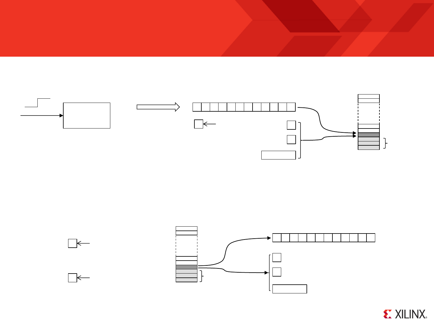
© Copyright 2010-2014 Xilinx
.
Page 84
RETURNI ENABLE
RETURNI DISABLE
When an interrupt occurs the program counter is loaded with the interrupt vector and the current address (corresponding with the location of the instruction
that is abandoned) is pushed onto the stack. In addition, the states of the carry flag (C), the zero flag (Z) and the register bank selection are also pushed onto
the stack and further interrupts automatically disabled (IE = 0).
PC
RETURNI ENABLE
PC Stack
30
Nested
Subroutines
PC
v v v v v v v v v v v v
PC Stack
Current
Address
30
Interrupt_vector
Nested
Subroutines
interrupt
kcpsm6
0
1
IE ‘0’ Z
C
REGBANK
Current
States
The ‘RETURNI’ instruction is similar to the unconditional ‘RETURN’ instruction but it must only be used to terminate an interrupt service routine (ISR). When
the ‘RETURNI’ is executed, the last address held on the PC Stack is popped off and loaded directly into the program counter so that the program resumes
execution starting with the instruction that was abandoned when the interrupt occurred. In addition, the RETURNI restores the values of the carry flag (C), the
zero flag (Z) and the register bank selection so that they are exactly the same as when the interrupt occurred. Either the ‘ENABLE’ or ‘DISABLED operand
must be used to specify if interrupts are to be enabled or disabled on return from the ISR.
RETURNI DISABLE
IE ‘1’
IE ‘0’
Z
C
REGBANK
Continued on next page….
Effects of hardware interrupt when
interrupts are enabled (IE = 1)
See also pages 40-44

© Copyright 2010-2014 Xilinx
.
Page 85
RETURNI ENABLE
RETURNI DISABLE
This ISR reads two bytes of information from input ports and stores them in scratch pad memory. It is reasonable to
assume that this information relates in some way to the reason for the interrupt and therefore probably represents
some important information that had to be captured at that particular time. It can also be imagined that the main
program needs to process this special information in some way with the value ‘2A’ loaded into register ‘sE’ signifying
that information has been captured and stored starting at location 2A hex. It can be imagined that the main program
must be given time to process the captured information so the ‘RETURNI DISABLE’ instruction terminates the ISR
but prevents a further interrupts overwriting the important information before it has been used. The main program
would use an ‘ENABLE INTERRUPT’ once it had.
Examples
This simple ISR increments the 16-bit value contained in the register pair [sF, sE]. This may relate to a scheme in
which interrupts occur at regular intervals to provide the basis for a real time clock or timer (i.e. the value held in
[SF,sE] is then used by the main program when required). The ‘RETURNI ENABLE’ instruction terminates the ISR and
enables interrupts ready for the next time.
ISR: ADD sE, 1’d
ADDCY sF, 0’d
RETURNI ENABLE
Important 1 – Always terminate an ISR with a ‘RETURNI’ and always terminate a normal subroutine with ‘RETURN’. The execution of the inappropriate
instruction will result in incorrect operation. Obviously that would be bad enough, but combined with the whole concept of interrupts occurring at any point in
the execution of the main code the symptoms of the incorrect operation failure can be subtle and make it extremely difficult to identify the cause.
Important 2 – Just as each ‘RETURN’ must be executed to correspond with the ‘CALL’ that invoked a normal subroutine, a ‘RETURNI’ must only be executed
to correspond with the interrupt that invoked the ISR. Your ISR can exploit KCPSM6’s ability to implement nested subroutines just as they can be used in any
part of your program but it is vital that each level is invoked and completed in order. The maximum number of levels is 30 and it should be remembered that
an interrupt requires one of these levels. If an interrupt does result in a stack overflow then KCPSM6 will automatically generate an internal reset. Likewise if
RETURNI is used in a way that results in a stack underflow then KCPSM6 will also reset itself automatically.
ISR: INPUT sF, int_data0
STORE sF, 2A
INPUT sF, int_data1
STORE sF, 2B
LOAD sE, 2A
RETURNI DISABLE
ISR: LOAD sA 00
CALL motor_drive
RETURNI ENABLE
motor_drive: OUTPUT sA, PWM_value
OUTPUTK 01, update_strobe
OUTPUTK 00, update_strobe
RETURN
Providing all the normal rules of nested subroutines are followed then an ISR can also make use of subroutines.
Hint – Be very careful to make sure that no code
executed as part of your ISR procedure contains an
‘ENABLE INTERRUPT’ instruction.
See also pages 40-44
© Copyright 2010-2014 Xilinx
.
Page 86
Interrupts and Register Banks
ENABLE INTERRUPT
loop: LOAD sA, 00
LOAD sE, FF
wait: SUB sE, 01
JUMP NZ, wait
COMPARE sA, 01
JUMP Z, post_int_action
LOAD s4, 19
LOAD s5, 1C
CALL mult
JUMP loop
mult: REGBANK B
LOAD s3, 8’d
SR0 s4
REGBANK A
RETURN
ADDRESS 3D0
ISR: REGBANK B
ADD sE, 1’d
ADDCY sF, 00
STAR sA, 01
RETURNI ENABLE
If an interrupt occurs in this loop which is decrementing ‘sE’ until it reaches zero then it is important that
the interrupt service routine (ISR) does not corrupt the value held in ‘sE’. So in this case the ISR has
switched to register bank ‘B’ where it implements a 16-bit interrupt counter using registers [sF, sE]. safe
in the knowledge that ‘sE’ in bank ‘A’ is preserved.
RETURNI automatically restores the states of the ‘C’ and
‘Z’ flags to the values they had when the interrupt
occurs. RETURNI also select the register
bank that was active prior to the
interrupt which in this case
restores the default
bank ‘A’.
Hint - STAR can be used to
pass some information from
the ISR to the main program.
RETURNI automatically ensures that the states of flags and the register bank are restored to their values prior to the
interrupt. In this case bank ‘B’ is retained at the end of the ISR as that was the active bank when the interrupt occurred.
The main program calls a ‘mult’
subroutine which also temporarily
uses register bank ‘B’. If an interrupt occurs whilst in this ‘mult’ subroutine then bank ‘B’ is
already active so the ‘REGBANK B’ at the start of the ISR doesn’t
change anything and the ISR must be written carefully not to
disturb the registers used by the ‘mult’ subroutine.
Although both banks of registers can be exploited at any time, the option to reserve at least some of the resisters in the second bank of registers for use in the
ISR is very compelling as this guarantees that no undesirable changes are made to the contents of registers used by the main program that has been
interrupted. This example illustrates two situations in which an interrupt could occur and how ‘RETURNI’ always restores the correct register bank.

© Copyright 2010-2014 Xilinx
.
Page 87
JUMP aaa
‘JUMP aaa’ is an unconditional JUMP which forces the program counter (PC) to the absolute address defined by the value ‘aaa’. Following power up or a
reset KCPSM6 executes code starting at address zero and in general the address increments as each instruction is executed. The unconditional JUMP
instruction forces the address to a new value and hence directs KCPSM6 to deviate from the normal incrementing sequence. A JUMP instruction has no
effect on any other features within KCPSM6 including the states of the flags.
PC
JUMP aaa
cold_start: LOAD s0, 27
STORE s0, status
...
warm_start: FETCH s0, status
OUTPUT s0, LED_port
CALL update_status
...
JUMP warm_start
Example
Nearly all programs include code that is repeatedly executed . These excerpts of a typical program
illustrate how a program generally begins with some initialisation tasks that are only performed on
power up or following a hardware reset and then the main program code that repeats. The unconditional
JUMP forced the execution to loop back to the start of the main program .
a a a a a a a a a a a a
32C 2202B JUMP 02B[warm_start]
The assembler resolves the line label ‘warm_start’
into an actual address value which you can see in
the LOG file if you are interested.
Hint – The example on the right forces KCPSM6 to stop at the current address.
This may seem pointless but a reset or an interrupt can override this and
makes KCPSM6 resume a normal execution flow. This technique can be a
useful during development and testing of both hardware and software.
Halt: JUMP Halt
LOG file shows resolved address...
‘aaa’ represents a 12-bit address with the range 000 to FFF hex (0’d to 4095’d). However, in nearly all cases it is the assembler which resolves the actual
value of the address based on the line labels you include in your program code so you don’t have to think about this yourself. Therefore it could be said that
the format of the instruction is normally ‘JUMP <line_label>’.
Whilst the address range supports programs up to 4K instructions the physical size of the program memory is defined by your hardware. Obviously the larger
the program memory, the more block memories (BRAMs) are consumed within the device so the typical methodology is to start with the smallest memory of
1K (address range 000 to 3FF) requiring only a single in a Spartan-6 device and then only to increase the size of the memory if the program outgrows it. It is
your responsibility to ensure that the program can fit within the physical address range available but since the assembler resolves most addresses from line
labels for you and reports the highest occupied address for your program this is rarely an issue.
No change to states of flags.
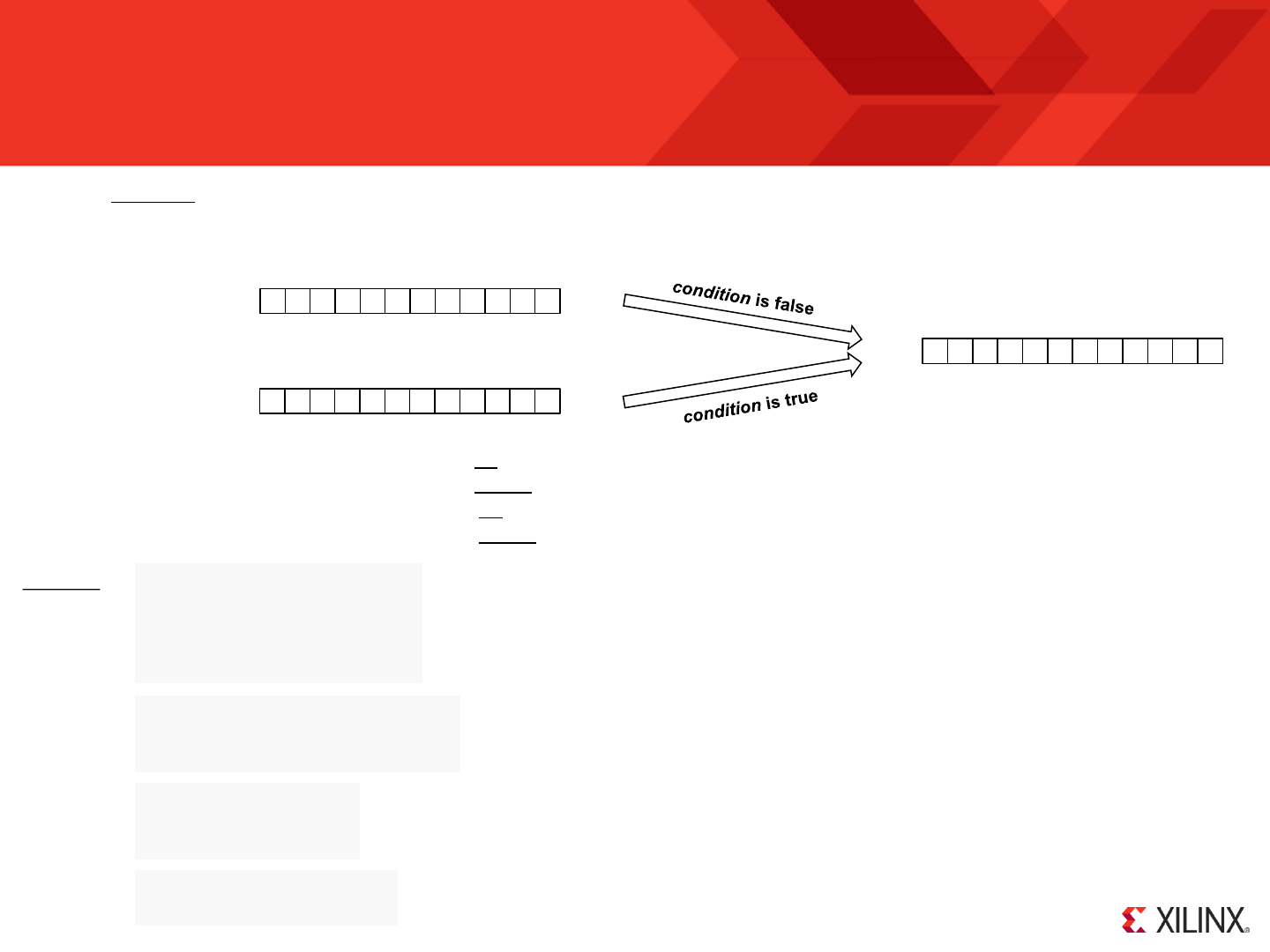
© Copyright 2010-2014 Xilinx
.
Page 88
JUMP Z, aaa JUMP NZ, aaa
JUMP C, aaa JUMP NC, aaa
These four conditional JUMP instructions force the program counter (PC) to the absolute address defined by the value ‘aaa’ providing that either the carry flag
(C) or the zero flag (Z) is the state specified. If the condition is false the program counter will increment the address and advance to the next instruction. A
conditional JUMP instruction has no effect on any other features within KCPSM6 including the states of the flags. See also description of ‘JUMP aaa’.
JUMP condition, aaa
LOAD s0, 25’d
delay100: SUB s0, 1’d
JUMP NZ, delay100
Examples
a a a a a a a a a a a a
JUMP to address ‘aaa’ if the zero flag is set otherwise advance to next instruction.
An ASCII character is read from a UART and this is first compared with the letter ‘R’. If the ASCII value
is the same then the zero flag is set and hence the flow of the program will transfer to the address
associated with the label ‘read_process’. If the character does not match then the program continues
and performs a similar comparison with the letter ‘W’ to decide if ‘write_process’ should be executed.
JUMP Z, aaa
PC
+ 1 PC
JUMP to address ‘aaa’ if the zero flag is not set otherwise advance to next instruction. JUMP NZ, aaa
JUMP to address ‘aaa’ if the carry flag is set otherwise advance to next instruction. JUMP C, aaa
JUMP to address ‘aaa’ if the carry flag is not set otherwise advance to next instruction. JUMP NC, aaa
No change to states of flags.
INPUT s0, uart_rx_data
COMPARE s0, "R"
JUMP Z, read_process
COMPARE s0, "W"
JUMP Z, write_process
The value contained in ‘s0’ is repeatedly decremented until it reaches zero forming a delay of 100
clock cycles (25 × 2 instructions × 2 clock_cycles). The state of the zero flag is determined by the
result of the ‘SUB’ instruction so until the value in ‘s0’ reaches zero the state of the zero flag is not-
zero (NZ) so the loop is repeated.
TEST sB, FF
JUMP C, odd_parity
AND sB, 7F
The parity of the 8-bit value contained in ‘sB’ is tested and if it is odd a jump is made to the code
located at ‘odd_parity’. When even parity the ‘AND sB, 7F’ instruction is executed.
shift: SR1 s3
JUMP NC, shift
Shifts ‘s3’ to the right until a ‘1’ in the least significant bit is shifted into the carry flag.
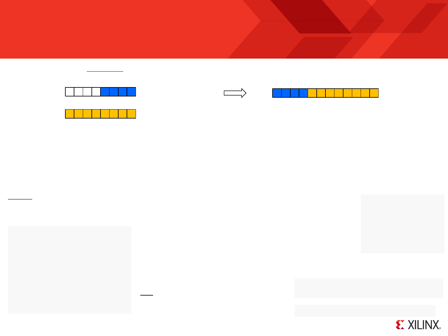
© Copyright 2010-2014 Xilinx
.
Page 89
JUMP@ (sX, sY)
The ‘JUMP@ (sX, sY)’ is an unconditional JUMP which forces the program counter (PC) to the address defined by the contents of the ‘sX’ and ‘sY’ registers.
No change to states of flags.
INPUT s0, selection_port
COMPARE s0, "1"
JUMP Z, choice1
COMPARE s0, "2"
JUMP Z, choice2
COMPARE s0, "3"
JUMP Z, choice3
COMPARE s0, "4"
JUMP Z, choice4
sX
sY
PC
JUMP@ (sX, sY)
The 12-bit address is formed of the lower 4-bits of the ‘sX’ register and all 8-bits of the ‘sY’ register. The upper 4-bits of ‘sX’ are ignored and the contents of
both registers are unaffected by the operation. There is no restriction on which registers can be used but it would be common coding practice to assign an
adjacent pair such as ‘sB’ and ‘sA’.
Since the destination address is defined by the contents of the registers this is powerful instruction but also has the potential to be dangerous! You are
entirely responsible for writing a program in which the computed address presented by the pair of registers corresponds with a valid location within your
physical program space. The KCPSM6 assembler can do nothing to prevent you computing an inappropriate address but it does provide a mechanism to
enable you to determine the addresses associated with line labels as shown in the following example.
LOAD sB, menu'upper
LOAD sA, menu'lower
INPUT s0, selection_port
SUB s0, "1"
ADD sA, s0
ADDCY sB, 00
JUMP@ (sB, sA)
menu: JUMP choice1
JUMP choice2
JUMP choice3
JUMP choice4
Example This example assumes that a user selects an option from a menu by providing a numerical ASCII character in the
range “1” to “4” (this range could easily be extended). The program reads this character, converts it to a value in
the range 0 to 3 and then jumps to the appropriate routine of ‘choice’.
7B4 01B07 LOAD sB, 07[menu'upper]
7B5 01ABB LOAD sA, BB[menu'lower]
7BB 22862 menu: JUMP 862[choice1]
The KCPSM6 assembler provides ‘upper and ‘lower attributes that can be used with labels to define the 8-
bit constants to be loaded into the registers. These abstracts of the LOG file show how the upper and lower
parts of the address are resolved into ‘kk’ values.
Hint - The ‘upper and ‘lower attributes can also be
Used to derive ‘kk’ values for use in other instructions
Such as ‘ADD sX, kk’ or ‘COMPARE sX, kk’.
Without the ‘JUMP@’ instruction the menu would be implemented by a
sequential series of compare and jumps (as shown on the right) which does
not scale very well but is suitable when there is a small number of choices.
Using the ‘JUMP@’ can help when there are lots of choices and also means
that the execution time is the same regardless of the selection being made.

© Copyright 2010-2014 Xilinx
.
Page 90
Subroutines
Subroutines are sections of code that are written to perform certain tasks which are then called (invoked) from another
section of code. The key point about a subroutine is that it can be called from anywhere within a program and the processor
will return to that point in the code when the subroutine’s task is complete. This means that it is possible to call the same
subroutine from different places within a program because the processor knows which place to return to on each occasion.
An analogy is like you watching a film on DVD and pressing the pause playback button whilst you make a telephone call.
Once you have completed your phone call you return to the DVD and press play button to resume the film from the point that
you left it. A little tater you need to make another phone call so pause the film again whilst you make that call. Once complete
you return to the film to continue the film from the point you left it the second time. In this case the DVD player had
remembered where you had paused the film so that each time you returned from making a phone call it resumed playback
from the point that you had left it. Making a phone call was effectively a ‘subroutine’ that you invoked whilst pausing the main
task of watching the film.
Reasons for using subroutines.
Common tasks – When the same task needs to be performed at several different places within a program then it is more code efficient to describe it once in a
subroutine than replicate in each place that it is required.
Tidy code – By placing the details of particular tasks into subroutines your main code becomes more compact and easier to write/understand.
Code development and Maintenance – A subroutine can be developed and tested in relative isolation until it provides the desired functionality. With good
definition of registers, memory locations and ports used by a subroutine the main program will know the ‘interface’ when calling it and can have a high degree
of certainty that it will perform the task expected without unexpected disturbance to register contents etc. As always, the inclusion of accurate and meaningful
comments in your code will always be rewarded in the long term.
Library of common tasks – Depending on the application and product there will often be functions that are replicated within a system or carried forward from
one generation to the next. These functions will often be specific to your products but they will still be ‘common’ tasks to you. Well defined and described
subroutines make it very easy to copy these functions form a known working design and paste them into your other designs saving time and effort.
Interrupt handling – A hardware driven interrupt is a special case but uses the same mechanism which effectively calls a special subroutine commonly known
as an interrupt service routine (ISR) which then returns to the main program at the point at which it was interrupted. This is described in more detail in the
interrupt section.
CALL
CALL
RETURN
Main
Sub

© Copyright 2010-2014 Xilinx
.
Page 91
KCPSM6 support for Subroutines
Built-in Protection
In the unlikely event that execution of a CALL instruction or an interrupt does result in a stack overflow then KCPSM6 will automatically reset. Whilst this is
rather dramatic it is predictable when compared with the alternative of incorrect code execution. In practice, the main reason for this ever happening is
incorrect PSM code where the CALL and RETURN instructions do not correspond. A typical coding error is the use of a JUMP back to a main program
instead of a RETURN which can appear to work correctly until the CALL without a corresponding RETURN has executed nearly 30 times leaving inadequate
levels for even the correct subroutines. Likewise, if incorrect coding leads to the execution of a RETURN or RETURNI instruction that results in a stack
underflow then KCPSM6 will also automatically generate an internal reset.
Nested subroutine support
KCPSM6 provides ‘CALL’ and ‘RETURN’ instructions which work with a fully automatic program counter stack which it used to remember the location
(address) associated with each ‘CALL’ used to invoke a subroutine in order that it can return to that location when a ‘RETURN’ instruction is executed to
terminate the subroutine. There is no requirement for you to reserve any memory, set up any stack pointers or implement any special code, KCPSM6 will do
everything for you.
CALL
CALL
RETURN
Main
Sub
Your code must be right!
RETURN
Sub
Level 1
Level 2
Hint – Although this diagram shows each subroutine located below the other your subroutines can be arranged in any order within the program space and
there are absolutely no restrictions on which order in which they can be called. The only thing you need to ensure that a subroutine is only executed by
being called otherwise it will encounter a RETURN that did not have a corresponding CALL.
Nested subroutine refers to the ability to call a subroutine whilst already executing another subroutine. The
program counter stack within KCPSM6 actually has the ability to support nested subroutine calls to a maximum
of 30 levels. Given that it is unusual for a program to exceed 8 levels of nested subroutine calls at one time the
30 levels supported by KCPSM6 provides you with significant freedom when writing your code without the worry
of reaching the limit.
It should be remembered that an interrupt is a special case which also uses a level as the ISR is invoked but
with 30 levels available even the ISR could include nested subroutine calls of its own.
Whist the PC Stack is completely dedicated and automatic you are entirely responsible for making sure that for
each CALL made to a subroutine you have a corresponding RETURN which completes it. You need to ensure that
each CALL and RETURN is a related pair. As the term ‘nesting’ implies, each CALL starts a new level and each
RETURN terminates a level in the reverse order. In practice this is all very logical and intuitive providing you truly
understand the concept and the diagram on the right.
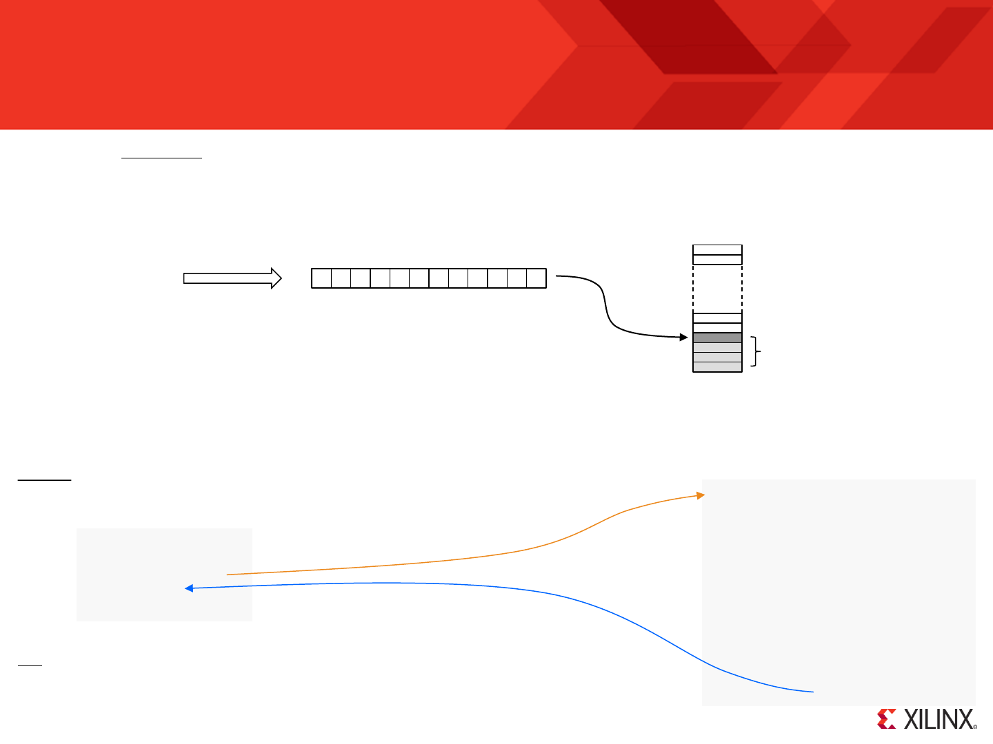
© Copyright 2010-2014 Xilinx
.
Page 92
CALL aaa
‘CALL aaa’ is an unconditional CALL to a subroutine which pushes the current contents of the program counter (PC) onto the stack and loads the PC with the
address defined by the value ‘aaa’. A subroutine should end with a ‘RETURN’ instruction which will pop the last pushed address off of the stack, increment it
and load it back into the program counter such that the program then executes the instruction following the initial CALL. Please also see the description of
‘JUMP aaa’ regarding the valid range of ‘aaa’ values and how the assembler is typically used to resolve their values for you.
PC
CALL aaa
AND s0, 01
OUTPUT s0, status
CALL inc_count32
LOAD s0, 38
JUMP main_loop
Example
a a a a a a a a a a a a
Within some code a CALL is made to a subroutine called ‘inc_count’ which contains a 12-instruction
procedure that increments a 32-bit number stored in 4 bytes of scratch pad memory. The
corresponding RETURN at the end of the subroutine allows the program to continue.
Hint – A subroutine can be located anywhere in a program relative to the CALL instructions that invoke it
but it is vital that the subroutine is only executed as the result of a CALL otherwise their will be no address
in the PC stack to correspond with the subsequent RETURN instruction.
No change to states of flags.
PC Stack
Current
Address
30
New Address
Whist the PC Stack is completely dedicated and automatic you are entirely responsible for making sure that for each CALL made to a subroutine you have a
corresponding RETURN. You must also ensure that execution of your program does not exceed 30 ‘nested’ subroutines but this limit is rarely challenged by
typical programs. Remember that an interrupt is a special case equivalent to a call and will use one level. If the stack does overflow then KCPSM6 will
automatically reset.
Nested
Subroutines
inc_count32: FETCH s0, count0
FETCH s1, count1
FETCH s2, count2
FETCH s3, count3
ADD s0, 1’d
ADDCY s1, 00
ADDCY s2, 00
ADDCY s3, 00
STORE s0, count0
STORE s1, count1
STORE s2, count2
STORE s3, count3
RETURN
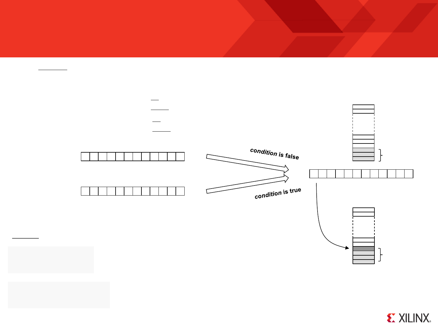
© Copyright 2010-2014 Xilinx
.
Page 93
CALL Z, aaa CALL NZ, aaa
CALL C, aaa CALL NC, aaa
These four conditional CALL instructions invoke a subroutine located at ‘aaa’ providing that either the carry flag (C) or the zero flag (Z) is the state specified. If
the condition is false the program counter will increment the address and advance directly to the next instruction . A conditional CALL instruction has no effect
on any other features within KCPSM6 including the states of the flags. See also description of ‘CALL aaa’.
CALL condition, aaa
a a a a a a a a a a a a
PC
+ 1 PC
No change to states of flags.
PC Stack
Push the current address
onto the stack and load PC
with the new address
specified.
30
Nested
Subroutines
PC Stack
30
Nested
Subroutines
CALL Z, aaa
CALL NZ, aaa
CALL C, aaa
CALL NC, aaa
Call address ‘aaa’ if the zero flag is set otherwise advance to next instruction.
Call address ‘aaa’ if the zero flag is not set otherwise advance to next instruction.
Call address ‘aaa’ if the carry flag is set otherwise advance to next instruction.
Call address ‘aaa’ if the carry flag is not set otherwise advance to next instruction.
INPUT sF, sensor
TEST sF, 01
CALL NZ, stop_motor
Examples
The LSB of a port is tested to see if a sensor has detected a
condition under which the drive to a motor should be turned off.
The ‘stop_motor’ subroutine is only invoked when the sensor is active.
TEST s0, FF
TESTCY s1, 01
CALL C, parity_error
An 8-bit value in register ‘s0’ together with a corresponding parity bit located in the LSB of register ‘s1’ are tested. When
there are an odd number bits with the value ‘1’ the carry flag is set this is used to detect when there is an even parity
error. If that does occur then a special ‘parity_error’ subroutine is invoked.
New Address
condition is false
Increment current
address and no
change to stack.
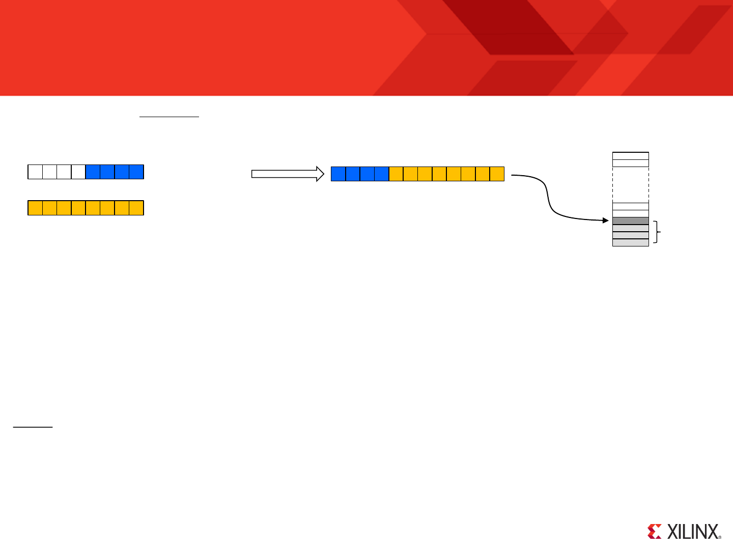
© Copyright 2010-2014 Xilinx
.
Page 94
CALL@ (sX, sY)
The ‘CALL@ (sX, sY)’ is an unconditional CALL to a subroutine which pushes the current contents of the program counter (PC) onto the stack and loads the
PC with the address defined by the contents of the ‘sX’ and ‘sY’ registers.
sX
sY
PC
CALL@ (sX, sY)
The 12-bit address is formed of the lower 4-bits of the ‘sX’ register and all 8-bits of the ‘sY’ register. The upper 4-bits of ‘sX’ are ignored and the contents of
both registers are unaffected by the operation. There is no restriction on which registers can be used but it would be common coding practice to assign an
adjacent pair such as ‘sB’ and ‘sA’. As the program counter is loaded, the existing address (the address at which the CALL@ instruction is located) is
preserved on the PC Stack to be recovered and used by a RETURN instruction completing the subroutine that has been called.
Whist the PC Stack is completely dedicated and automatic you are entirely responsible for making sure that for each call made to a subroutine you have a
corresponding return. You must also ensure that execution of your program does not exceed 30 ‘nested’ subroutines but this limit is rarely challenged by
typical programs. Remember that an interrupt is a special case equivalent to a call and will use one level. If the stack does overflow then KCPSM6 will
automatically reset. The real challenge when using the CALL@ instruction is to ensure that the address defined by the pair of registers does correspond with
the start of a valid subroutine. Whilst the instruction facilitates a scheme in which the address to call can be computed this also has the potential to be
dangerous! The KCPSM6 assembler can do nothing to prevent you computing an inappropriate address but it does provide ‘upper and ‘lower attributes which
are helpful.
PC Stack
Current
Address
30
Example
Probably the most common use of the CALL@ instruction will be in combination with the LOAD&RETURN instruction to generate text strings or other
sequences of constant values and this is explained in more detail in the LOAD&RETURN section.
However, the example shown on the next page illustrates how a system variable is used to decide at which point to enter the same subroutine to achieve a
desired set up.
No change to states of flags.
New Address
Nested
Subroutines
© Copyright 2010-2014 Xilinx
.
Page 95
CALL@ (sX, sY)
LOAD sB, setup0'upper
LOAD sA, setup0'lower
INPUT s0, currency
SL0 s0
SL0 s0
SL0 s0
ADD sA, s0
ADDCY sB, 00
CALL@ (sB, sA)
In this example we can imagine that KCPSM6 is part of an application involved
with foreign currencies and for each different currency it must set up
communication using a particular IP Address.
In the main program shown above KCPSM6 reads an input port ‘currency’ from
which it obtains a value in the range 0 to 3 relating to four different currencies
but this could be easily expanded to many more. The program then calls the
subroutine shown on the right (the LOG file is shown so that the addresses can
be seen) which defines the 3-character name of the currency and the IP
Address for internet communication in particular scratch pad memory locations.
The CALL@ instruction is used to enter the subroutine at the appropriate
address to set up the information that corresponds with the value read into ‘s0’
from the ‘currency’ port. When the currency is 0 then the address is ‘A49’ and
this was known through use of the ‘upper and ‘lower attributes which were used
to load registers [sB, sA] and required no modification.
For currency values 1, 2 and 3 the target addresses are ‘A51’, ‘A59’ and ‘A61’ .
Each target address is 8 instructions apart so the value held in [sB, sA] is
modified by the addition of the currency values multiplied by 8 (shift left 3 times).
The worked example shown in blue shows how currency value ‘2’ is translated
into address ‘A59’ to enter the subroutine at the European ‘setup2’.
A49 01047 setup0: LOAD s0, 47["G"]
A4A 01142 LOAD s1, 42["B"]
A4B 01250 LOAD s2, 50["P"]
A4C 016AC LOAD s6, AC[172'd]
A4D 0170E LOAD s7, 0E[14'd]
A4E 0184E LOAD s8, 4E[78'd]
A4F 019BF LOAD s9, BF[191'd]
A50 22A68 JUMP A68[set_mem]
A51 ;
A51 01055 setup1: LOAD s0, 55["U"]
A52 01053 LOAD s0, 53["S"]
A53 01244 LOAD s2, 44["D"]
A54 016C3 LOAD s6, C3[195'd]
A55 0172A LOAD s7, 2A[42'd]
A56 01801 LOAD s8, 01[1'd]
A57 0194A LOAD s9, 4A[74'd]
A58 22A68 JUMP A68[set_mem]
A59 ;
A59 01045 setup2: LOAD s0, 45["E"]
A5A 01055 LOAD s0, 55["U"]
A5B 01252 LOAD s2, 52["R"]
A5C 01695 LOAD s6, 95[149'd]
A5D 017C9 LOAD s7, C9[201'd]
A5E 01805 LOAD s8, 05[5'd]
A5F 01911 LOAD s9, 11[17'd]
A60 22A68 JUMP A68[set_mem]
A61 ;
A61 0104A setup3: LOAD s0, 4A["J"]
A62 01050 LOAD s0, 50["P"]
A63 01259 LOAD s2, 59["Y"]
A64 016C0 LOAD s6, C0[192'd]
A65 017A8 LOAD s7, A8[168'd]
A66 01831 LOAD s8, 31[49'd]
A67 01920 LOAD s9, 20[32'd]
A68 ;
A68 2F010 set_mem: STORE s0, 10
A69 2F111 STORE s1, 11
A6A 2F212 STORE s2, 12
A6B 2F63C STORE s6, 3C
A6C 2F73D STORE s7, 3D
A6D 2F83E STORE s8, 3E
A6E 2F93F STORE s9, 3F
A6F 25000 RETURN
39C 01B0A LOAD sB, 0A[setup0'upper]
39D 01A49 LOAD sA, 49[setup0'lower]
8 instructions
8 instructions
8 instructions
The KCPSM6 assembler provides ‘upper and ‘lower
attributes that can be used with labels to define the 8-
bit constants to be loaded into the registers.
02
04
08
10
49 + 10 = 59
0A + 00 + 0 = 0A
CALL A59
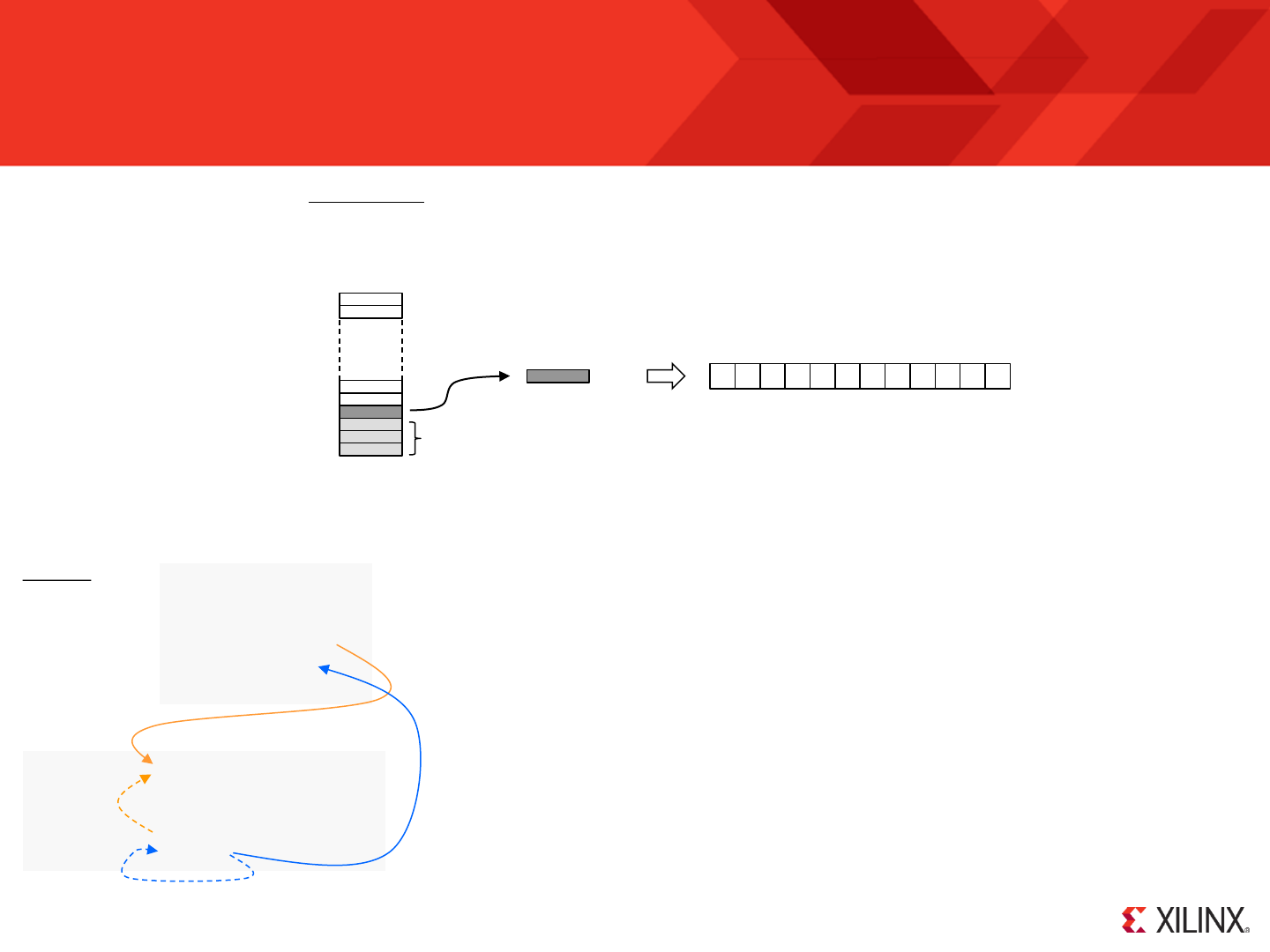
© Copyright 2010-2014 Xilinx
.
Page 96
RETURN
The ‘RETURN’ instruction is used to unconditionally complete a subroutine. The last address pushed on to the PC Stack by the previous call to the subroutine
is popped off the stack, incremented and loaded into the program counter. This automatic process ensures that the return is made to the address following
the CALL instruction that initiated the subroutine.
PC
RETURN
This example illustrates the general arrangement in which one part of the program calls a subroutine. In
most cases line labels are used to make the code easier to write and maintain and the assembler
resolves the actual addresses.
The subroutine labelled ‘test_stack’ is called from the main program. When this subroutine completes
the RETURN forces the program counter to the address corresponding with the instruction immediately
following the CALL which in this case is an OUTPUT instruction.
Whilst this example does show the general arrangement it actually describes a rather special case
when we look at the code in detail. In the main program [s9,s8] has been cleared and then ‘s1’ has been
loaded with 30 decimal. The ‘test_stack’ subrouine adds the value of ‘s1’ to [s9,s8] and then decrements
the value in ‘s1’. But each time ‘s1’ is not zero it actually calls ‘test_stack’ again. Hence this subroutine is
called 30 times and eventually [s9,s8] will be the sum of all values from 1 to 30 which is 465 (01D1 hex).
When ‘s1’ does reach zero, KCPSM6 will execute the RETURN instruction 30 times until it eventually
returns to the main program. Hence there is no restriction on how subroutines are arranged providing
you do not exceed 30 levels and every CALL has a corresponding RETURN.
PC Stack
30
Example
+1
Whist the PC Stack is completely dedicated and automatic you are entirely responsible for making sure that each RETURN is only executed to complete a
subroutine that was invoked by the corresponding call instruction. If your code should incorrectly execute a RETURN that results in stack underflow then
KCPSM6 will automatically reset. Remember that an interrupt is a special case equivalent to a call and requires a corresponding RETURNI instruction.
LOAD s9, 00
LOAD s8, 00
LOAD s1, 30’d
CALL test_stack
OUTPUT s9, 02
OUTPUT s8, 01
test_stack: ADD s8, s1
ADDCY s9, 00
SUB s1, 01
CALL NZ, test_stack
RETURN
No change to states of flags.
Nested
Subroutines
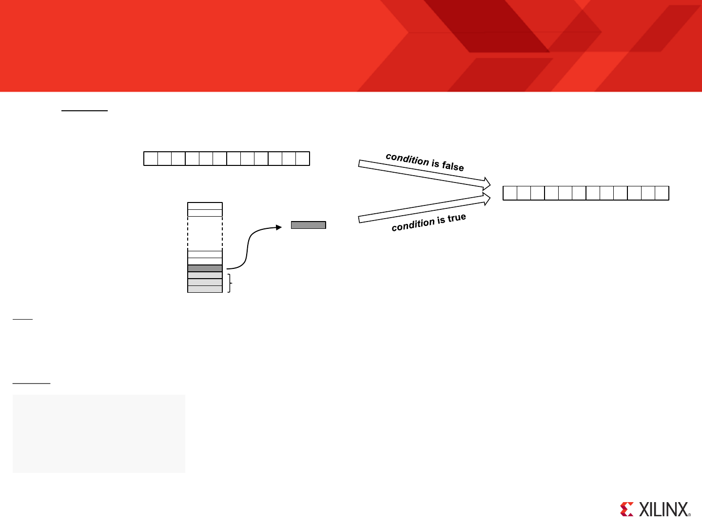
© Copyright 2010-2014 Xilinx
.
Page 97
RETURN Z RETURN NZ
RETURN C RETURN NC
PC
PC Stack
30
+1 No change to states of flags.
These four conditional RETURN instructions will complete a subroutine providing that either the carry flag (C) or the zero flag (Z) is the state specified. If the
condition is false the program counter will increment the address and advance to the next instruction. See also description of ‘RETURN’.
RETURN condition New Address
PC
+ 1
Nested
Subroutines
This subroutine converts lower case characters to upper case characters. The subroutine examines an ASCII
character code provided in register ‘s1’ to determine if it is a lower case letter in the range ‘a’ (61 hex) to ‘z’ (7A
hex). If the character falls below or above that range then the conditional ‘RETURN C’ and ‘RETURN NC’
instructions are used to terminate the subroutine without any modification to the value in ‘s1’. When the character
falls within the lower case range bit5 of the ASCII code is cleared by the ‘AND s1, DF’ instruction to convert the
code into the range ‘A’ (41 hex) to ‘Z’ (5A hex) before the unconditional ‘RETURN’.
Note that although this subroutine contains three RETURN instructions one is guaranteed to execute especially as
the final one is unconditional.
Example
upper_case: COMPARE s1, 61
RETURN C
COMPARE s1, 7B
RETURN NC
AND s1, DF
RETURN
Hint – You are still entirely responsible for making sure that each RETURN is executed to complete a subroutine that was invoked by the corresponding call
instruction. Because these instructions are conditional you do need to be certain that a corresponding RETURN will be executed at some point so care is
required when exploiting these conditional instructions. Many would recommend a coding style in which a subroutine always ends with a single unconditional
RETURN instruction and this is certainly a good practice to follow until you have some experience.
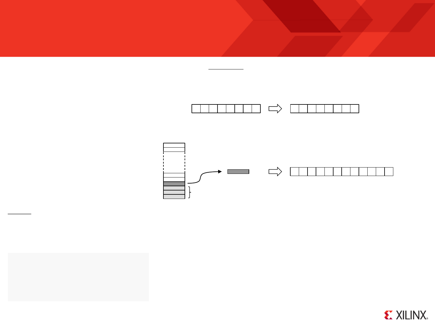
© Copyright 2010-2014 Xilinx
.
Page 98
LOAD&RETURN sX, kk
The ‘LOAD&RETURN sX, kk’ is the combination of a ‘LOAD sX, kk’ and an unconditional RETURN into a single instruction (i.e. one 18-bit instruction that
executes in 2 clock cycles). At the same time that the ‘sX’ register is being loaded with any 8-bit constant value, the last address pushed on to the PC Stack is
by the previous call to the subroutine is popped back off, incremented and loaded into the program counter.
sX kk
PC
LOAD&RETURN sX, kk
This subroutine is used to convert a value in the range ‘0’ to ‘9’ into the equivalent ASCII character
before calling a further subroutine that will print it. In addition to the simple conversion the routine
checks that the value provided in ‘s5’ is within the range in order that only the expected ASCII
characters are printed (and not nasty control characters etc!). This checking means that the outcome
of the ‘print_decimal’ subroutine could be successful or unsuccessful so the LOAD&RETURN
instruction is used to load ‘sF’ with a ‘token’ or ‘error code’. If each subroutine set a different error
code into ‘sF’ then it would be easy for you or the program to locate where things were going wrong
in a program especially during code development.
PC Stack
30
Example
Probably the most common use of the LOAD&RETURN instruction will be in combination with the CALL@ instruction to generate text strings or other
sequences of constant values and this is explained in more detail on the next page. However, the LOAD&RETURN instruction can be used to complete any
subroutine with the advantage that an 8-bit value can be loaded into any register at no additional cost.
+1
print_decimal: COMPARE s5, 10’d
JUMP C, convert
LOAD&RETURN sF, 39
convert: ADD s5, "0"
CALL print_character
RETURN
Nested
Subroutines
No change to states of flags.

© Copyright 2010-2014 Xilinx
.
Page 99
CALL@ (sX, sY)
LOAD&RETURN sX, kk
Using ‘CALL@ (sX, sY)’ and ‘LOAD&RETURN sX, kk’ instructions together enables a text strings or sequences of constant values to be generated with
maximum code efficiency. The KCPSM6 assembler has a STRING directive that simplifies this common application as shown below.
To send a string of characters to the UART you can then repeatedly load ‘s1’ with the next character in the sequence
and call the ‘send_to_UART’ subroutine. This was the fundamental technique used in KCPSM3 programs and it still a
valid technique to use with KCPSM6. However as users of KCPSM3 have often reported, this tends to consume a
significant amount of code space when there are longer and/or many text strings to be generated. It can be seen in
this small example that there are 2 instructions associated with each ASCII character and that is quite an overhead.
Although the code can be partly optimised for frequently used characters this does not make code easier to write.
send_Help: LOAD s1, "H"
CALL send_to UART
LOAD s1, "e"
CALL send_to UART
LOAD s1, "l"
CALL send_to UART
LOAD s1, "p"
RETURN
“Text Strings”
send_string: CALL@ (sB, sA)
CALL send_to_UART
COMPARE s1, 0D
RETURN Z
ADD sA, 01
ADDCY sB, 00
JUMP send_string
send_to_UART: INPUT s0, UART_status_port
TEST s0, tx_full
JUMP NZ, send_to_UART
OUTPUT s1, UART_data_port
RETURN
In this example we will assume that text ASCII characters are output from KCPSM6 to a UART
transmitter. The UART macro also contains a 16 character FIFO buffer but given that the serial
communication is slow compared with KCPSM6 it is necessary for the program to check that
the FIFO is not full before sending another character. The ‘send_to_UART’ routine on the right
will wait until the FIFO is not full before outputting the ASCII character provided in ‘s1’.
3A7 STRING Hello$, "Hello World"
3A7 21148 Hello: LOAD&RETURN s1, 48[Hello$:"H"]
3A8 21165 LOAD&RETURN s1, 65[Hello$:"e"]
3A9 2116C LOAD&RETURN s1, 6C[Hello$:"l"]
3AA 2116C LOAD&RETURN s1, 6C[Hello$:"l"]
3AB 2116F LOAD&RETURN s1, 6F[Hello$:"o"]
3AC 21120 LOAD&RETURN s1, 20[Hello$:" "]
3AD 21157 LOAD&RETURN s1, 57[Hello$:"W"]
3AE 2116F LOAD&RETURN s1, 6F[Hello$:"o"]
3AF 21172 LOAD&RETURN s1, 72[Hello$:"r"]
3B0 2116C LOAD&RETURN s1, 6C[Hello$:"l"]
3B1 21164 LOAD&RETURN s1, 64[Hello$:"d"]
3B2 2110D LOAD&RETURN s1, 0D
STRING Hello$, "Hello World"
Hello: LOAD&RETURN s1, Hello$
LOAD&RETURN s1, 0D
LOAD sB, Hello'upper
LOAD sA, Hello'lower
CALL send_string
The solution with KCPSM6 is to describe each text string using sequential ‘LOAD&RETURN’
instructions. In this case ‘s1’ loaded with a different character and this is made much easier to
write because of the STRING directive. The original PSM code is shown below and the
expanded code is shown in the LOG file on the right.
KCPSM6
Each ‘LOAD&RETURN’ can now be considered to be a single instruction subroutine.
The address of the first ‘LOAD&RETURN’ instruction is
loaded into a pair of registers [sB, sA] and then a routine
is called that sends the whole text string to the UART.
The ‘CALL@’ instruction is used to call each ‘LOAD&RETURN’ subroutine in turn by
incrementing the address held in [sB, sA]. Each call returns a character in ‘s1’ which is then
sent to the UART. Although this ‘send_string’ routine is 7 instructions, text strings are now
defined by only one instruction per character improving code efficiency by a factor of two.
The routine
requires a suitable
scheme in order
to terminate. In this
case a carriage
return is detected.
Hint – Also see TABLE Directive on next page

© Copyright 2010-2014 Xilinx
.
Page 100
TABLE Directive for Data and Sequences
The TABLE directive is used in conjunction with ‘OUTPUTK’ and ‘LOAD&RETURN’ instructions in the same way as a STRING directive except for the fact
that it defines a series of constants using numerical values rather than ASCII characters.
STRING Hello$, "Hello"
Hint – Also see STRING Directive described on previous page.
This string is formed of 5 ASCII characters that have the codes 48, 65, 6C, 6C and 6F hex (see previous page).
TABLE Hex_data#, [48,65,6C,6C,6F]
TABLE Dec_data#, [72,101,108,108,111]'d
TABLE Bin_data#, [01001000,01100101,01101100,01101100,01101111]'b
These TABLE directives show how the same series of 8-bit constants can be defined in
hexadecimal, decimal or binary and assigned to a table name ending with # rather than a string
name ending with $. Obviously it doesn’t make much sense to replace a string with a table but
hopefully these examples emphasize how both directives are used to define a series of
constants and you can apply the directive (and radix) that is
most suitable for the data you are defining.
OUTPUTK 00000010'b, Dev_control_port
OUTPUTK 00000011'b, Dev_control_port
OUTPUTK 00000010'b, Dev_control_port
OUTPUTK 00000000'b, Dev_control_port
Dev_write
Dev_clk
Control Sequences using ‘OUTPUTK’’
On pages 75 and 76 there is a simple example showing how the ‘OUTPUTK kk,p’ instruction can be efficiently
used to generate waveforms for the control of external circuits. The example actually generates a High ‘write’
enable (bit1) during which a positive clock pulse is generated (bit0).
TABLE write_seq#, [00000010,00000011,00000010,00000000]‘b
KCPSM6
After a TABLE directive has been used to define the series of constants required for each control sequence it enables the code be easier to write. It also
makes the code more compact and descriptive which tends to help your code easier to read and maintain.
OUTPUTK write_seq#, Dev_control_port
Look-Up Tables using ‘CALL@’ and ‘LOAD&RETURN’
On the previous page you can see how this combination of instructions are used to scan sequentially through all the characters forming a text string. Whilst
the same requirement could also apply to a table of constants it is more likely that the objective will be to pick out one item from the ‘list’. In this example we
can see how the value (range 0 to 9) held in the register ‘s1’ can be converted into its equivalent 7-Segment display pattern by selecting the appropriate value
from a table…. TABLE 7_segment_decode#, [3F,06,5B,4F,66,6D,7D,07,7F,6F]
sevenseg: LOAD&RETURN s1, 7_segment_decode#
LOAD sB, sevenseg'upper
LOAD sA, sevenseg'lower
ADD sA, s1
ADDCY sB, 00
CALL@ (sB, sA)
a
b
c
d
f
e
g xgfedcba
01001111 = 4F
[sB,sA] loaded with
start of table address
Add ‘s1’ to address.
Call to offset address returns required value from table.
If s1=03 then the 4th value in
the table is returned
x
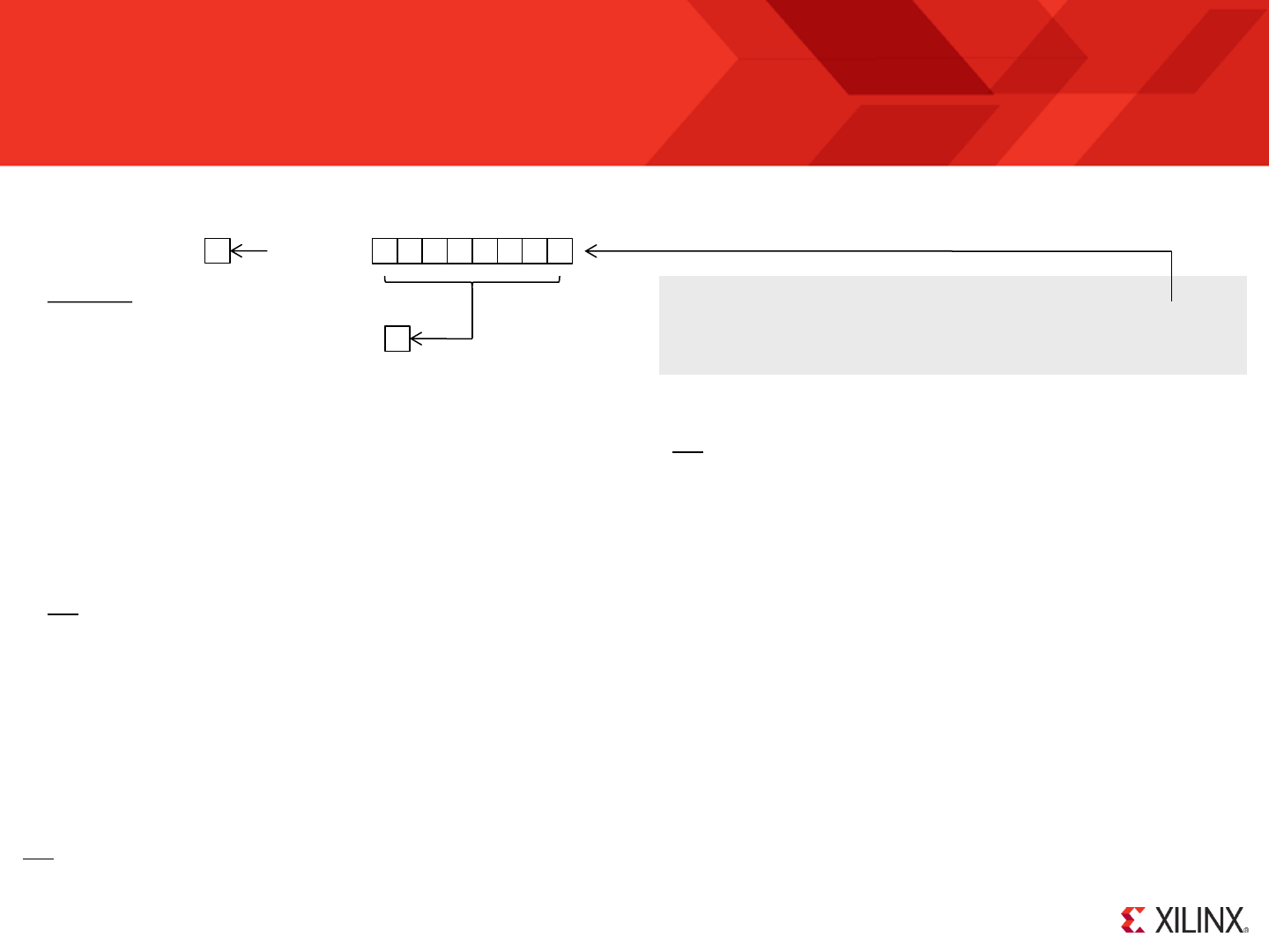
© Copyright 2010-2014 Xilinx
.
Page 101
HWBUILD sX
The ‘HWBUILD’ instruction loads the ‘sX’ register with the 8-bit value defined by the ‘hwbuild’ generic set within the hardware design.
sX
C
Z
= ’00’ ?
The zero flag (Z) will be set if the value loaded is zero and this corresponds with the default value of the generic on the KCPSM6 macro.
The carry flag (C) will always be set (C=1).
processor: kcpsm6
generic map ( hwbuild => X"41",
interrupt_vector => X"F80",
scratch_pad_memory_size => 256)
’1’
You are free to test or use the value loaded into a register by the HWBUILD in any way you wish but here are a few general ways in which you may
consider using it in your system…..
Version Control - To enable KCPSM6 to generate a version report (e.g. as part of a message sent to a host or displayed on an LCD). This is the
hardware complement to the ‘datestamp$’ and ‘timestamp$’ for version control of the PSM assembly code.
Coding Tip - HWBUILD is the only
guaranteed way of setting the carry
flag using only one instruction.
Hint – If a system only needs to indentify if it is one of two things (e.g. Left or Right, Standard or Advanced etc) then the ‘hwbuild’ generic could be zero or
any non-zero value. When using the ‘HWBUILD sX’ the zero flag (Z) will be set accordingly ready for an immediate decision to be made in the program.
Hint – HWBUILD is the only instruction that will always set the carry flag.
Mode Control - Although most of the functionality would probably be the same, a single PSM file could be written that was capable of different behaviour
depending on the hardware in which it was being asked to execute within. For example the HWBUILD could be used to:-
Define if the unit was to act as a master or slave.
Adjust the command codes and protocol required to access SPI Flash devices from different manufactures.
Define the feature set supported and/or included in a product.
Priority or Unit Address - When a unit is placed on a bus then it would generally be assigned an address so that it would know when to respond to
commands etc. For example, an audio entertainment system may have multiple speakers that fundamentally operate in the same way but each would be
assigned to a particular position in the room and therefore be expected to only generate sounds intended for a particular channel.
Hint – The value “41” hex shown above could also be used to represent the ASCII letter for version ‘A’ or the packed BCD value meaning version 4.1.

© Copyright 2010-2014 Xilinx
.
Page 102
Notes for KCPSM3 Users
Overall KCPSM6 should look very similar to KCPSM3 because it is . As such, it is expected that the vast majority of KCPSM3 based designs and KCPSM3
programs should work in KCPSM6 with no, or only very minor, adjustments. It is then hoped that you will enjoy learning and including some of the additional
instructions and features in your designs at your leisure. The following points should answer your immediate questions and concerns as well as point out the
specific items that may just need a little attention depending on your use of KCPSM3.
Size and Performance – Even though KCPSM6 has more features than KCPSM3 it has been optimized for Spartan-6, Virtex-6 and 7-Series devices and will
appear to be quite a bit smaller (26 Slices) and slightly faster. As such, it really should be a better ISE experience as well.
New Pins – KCPSM6 has 1 additional input pin and 4 additional output pins…..
‘sleep’ - If you permanently tie the ‘sleep’ control Low then it will have no effect and KCPSM6 will execute code just like a KCPSM3 (see page 37)
‘k_write_strobe’ - This output can be left open as it is associated with 16 additional ‘constant optimized ports’ that have their own ‘OUTPUTK’ instruction.The
normal input and output ports associated with ‘read-Strobe’ and ‘write_strobe’ will all behave exactly the same as they did previously. Many PicoBlaze users
have expressed their desire for a PicoBlaze that can write constant values directly to a port so KCPSM6 can and you can read more on pages 75 to 80.
‘bram_enable’ – This is purely a power reduction feature and failure to connect it will have no effect on the execution of a program providing the BRAM
containing the program is locally enabled. If you want to continue using your existing ‘ROM_form’ templates you can but it probably is worth making the small
adjustment to include the enable since it is virtually free and will save some power (every little helps!). Given the migration to the ‘6’ and ‘7’ devices it is
generally better for you to adopt the new program memory templates which already have the enable input (and ‘rdl’ output for JTAG Loader). See page 8.
Address[11:10] – So this is the one you probably do need to look at because it means that KCPSM6 can support programs up to 4K. The address port is 12-
bits rather than the 10-bit address port of KCPSM3. Of course this means that any KCPSM3 programs will continue to fit in 1K and only the lower 10-bits of
the address will really be used in these situations. Whilst address[11:10] are redundant until you implement larger programs, the new program memory
templates always connect all 12-bits to make design easy and facilitate easy when required. Please see pages 8 to 13 to see how easy and flexible this is!
New Generics – KCPSM6 has 3 generics (KCPSM3 didn’t have any!). The three generics enable you to increase the size of the scratch pad memory, define
an interrupt vector address of your choice and define a hardware build value. However, the default settings result in an identical implementation to KCPSM3
meaning that you will have 64 bytes of scratch pad memory and the interrupt vector will be address ‘3FF’. The hardware build value is associated with a new
instruction so will have no effect on code imported from a KCPSM3 design. Put simply, you can ignore the generics until you read page 34.
Hardware Differences
JTAG Loader – An all new JTAG Loader utility has been provided. The concept is the same but it is easier to include in your design and much easier to use.
See pages 25 to 29 for details.

© Copyright 2010-2014 Xilinx
.
Page 103
Notes for KCPSM3 Users
‘ROM_form’ Templates – As with KCPSM3 before, the VHDL and Verilog generated by the KCPSM6 assembler are based on the ‘ROM_form.vhd’ and
‘ROM_form.v’ templates which must be placed in the same directory as your PSM file. The key difference is that the KCPSM6 will only generate a VHDL or
Verilog file when it finds a corresponding template file. The KCPSM3 assembler used to fail if it did not find all templates and always generated both VHDL
and Verilog regardless of which you needed. KCPSM6 will only generate the file type that you need corresponding with the ‘ROM_form’ template that you
provide. If it doesn’t generate a VHDL or Verilog file it means that you forgot to provide it with the right template! Please study pages 11 and 12 to learn about
the features of the default template including generics that select target family, program size and insert JTAG Loader.
Code Compatibility – KCPSM6 supports the same 30 fundamental instructions that KCPSM3 has and then has 9 new instructions for you to play with in the
future. The KCPSM6 assembler also supports the same fundamental syntax for the original instructions as well as the ADDRESS, CONSTANT and
NAMEREG directives. As such, all programs written for a KCPSM3 are expected to assemble when porting to KCPSM6. However, you may find that some of
the names you have assigned to line labels, constants and registers are rejected by the KCPSM6 assembler and need a small modification. This will occur if
the name you have chosen could be confused with a hexadecimal value. For example ‘dac’ and ‘DAC’ were acceptable line labels for KCPSM3 but are not
accepted by KCPSM6. One reason for this is that KCPSM6 has an address range of ‘000’ to ‘FFF’ and that means that values such as ‘DAC’ are now valid
hexadecimal addresses. The KCPSM6 assembler has several new features such as the ability to define constants using decimals and ASCII characters (see
page 52) but the default is still hexadecimal so you should not need to change anything to begin with.
ADDCY and SUBCY – All the KCPSM3 instructions are supported in KCPSM6 and execute in exactly the same way except for one very subtle difference in
the way ADDCY and SUBCY influence the zero (Z) flag. Both the numerical result loaded into ‘sX’ and the carry (C) flag behavior are identical so unless your
code specifically uses the value of the Z flag following an ADDCY or SUBCY this difference can be ignored . It is actually very rare for the value of the zero
flag to be used following an ADDCY or SUBCY in KCPSM3 because it doesn’t tend to have a very practical meaning. The subtle change seen in KCPSM6
infers much greater meaning to the zero flag and as a KCPSM3 expert you should soon recognize multiple situations in which your coding becomes easier
and smaller. However, because this is the one situation in which code written for KCPSM3 may not execute identically in a KCPSM6 the next page really
details the difference as well as acting as in introduction to the new TESTCY and COMPARECY instructions.
Software and Assembler Considerations
KCPSM6 Assembler – Just to state the obvious; you must use the KCPSM6 assembler when targeting KCPSM6 (and you should continue to use the
KCPSM3 assembler when targeting KCPSM3 based designs). Whilst the fundamental instruction set is the same the op-codes assigned to the instructions
are completely different . The KCPSM6 assembler looks rather different and leaves behind the limitations of the DOS based KCPSM3 assembler but overall
its functionality should appear familiar to you. Please see pages 13 and 14 and you will see that it is just as easy to run (see also pages 49 and 50).
CALL/RETURN Stack – KCPSM6 supports nesting of subroutines to a depth of 30 levels compared with KCPSM3 which supported 31. However, KCPSM6
will also detect a stack overflow and stack underflow and automatically assert an internal reset. Although this is an enhanced feature for long term design
reliability, KCPSM3 code in which stack ‘leakage’ has previously passed undetected may now reveal its flaw (e.g. where a corresponding RETURN is not
performed for every CALL).
© Copyright 2010-2014 Xilinx
.
Page 104
Notes for KCPSM3 Users
ADDCY and SUBCY continued….. Consider the simple example in which a 16-bit value is held in the pair of registers [sB, sA] and this is decremented
using SUB and SUBCY instructions. This may then be used to define the number of times which a loop is executed. First look at what happens in KCPSM3 in
great detail and see how that tends to influence the code that you need to write when using KCPSM3.
sB
0 0 0 0 0 0 0 0
sB
in KCPSM3…. sA
0 0 0 0 0 0 0 1
sA
SUBCY sB, 00 SUB sA, 01
C C
Z
sA=“00000000”?
Z
sB = “00000000”?
Obviously when performing subtraction the carry flag indicates
when a ‘borrow’ is required from the more significant byte.
So first consider when [sB, sA] = 02 00 and the subtraction
takes place. The ‘SUB sA, 01’ results in sA = FF and the carry
flag being set. The zero flag is reset because ‘FF’ is definitely
not zero. The ‘SUBCY sB, 00’ results in sB = 01 as the carry
flag has the effect of decrementing sB. The carry flag is now
reset because there is no borrow and the zero flag remains
reset because ‘01’ definitely isn’t zero either. All good so far!
Now imagine that we have decremented 255 more times so that [sB, sA] = 01 00 as we enter the next iteration. Once again ‘SUB sA, 01’ results in
sA = FF and the carry flag being set and the zero flag is reset because ‘FF’ is still not zero. But this time the set carry flag causes the ‘SUBCY sB, 00’ to
result in sB = 00 which does set the zero flag. Although this correctly reflects the value stored in sB it doesn’t reflect the overall result of the 16-bit
operation that was actually performed because [sB, sA] = 00 FF and will require another 255 iterations before it truly reaches zero.
If the decrement loop was performed with an 8-bit value only requiring the ‘SUB sA, 01’ instruction then the zero
flag has the obvious meaning and can provide the test condition for the JUMP instruction as illustrated.
loop: SUB sA, 01
JUMP NZ, loop
loop: SUB sA, 01
SUBCY sB, 00
JUMP NZ, loop
loop: SUB sA, 01
SUBCY sB, 00
JUMP NC, loop
If the same technique is expanded to 16 bits then the loop will actually terminate when [sB, sA] = 00 FF because
the zero flag only represents the result of the local SUBCY instruction. Of course your code could take this into
account but it really isn’t intuitive or desirable.
Because testing the zero flag terminates the loop 255 iterations too early the typical coding style resorts to testing the
condition of the carry flag which is actually set as [sB, sA] rolls over from 00 00 to FF FF (effectively -1). Note how the
carry flag is truly representing the result of the whole 16 bit operation in all circumstances.
SUB sA, 01
SUBCY sB, 00
© Copyright 2010-2014 Xilinx
.
Page 105
Notes for KCPSM3 Users
ADDCY and SUBCY continued….. Now look at the same example in KCPSM6 and notice how the subtle change in the way the zero flag is defined.
It makes code more logical but may just be a reason to change the
way your old KCPSM3 executes in KCPSM6.
sB
0 0 0 0 0 0 0 0
sB
SUB sA, 01
SUBCY sB, 00
sA
0 0 0 0 0 0 0 1
sA
SUBCY sB, 00 SUB sA, 01
C C
Z
The difference is that when the SUBCY executes it observes
the state of the zero flag as well as using the carry flag. The
zero flag is then only set if the 8-bit result of the SUBCY is zero
and the zero flag was already set. This means that the zero
flag now represents the entire 16-bit result and not just the
local 8-bit result.
With this arrangement the flags will have the same meaning
having performed a 16-bit operation as they would having
performed an 8-bit operation.
Using the same example where [sB, sA] = 01 00 as we enter the decrement function the ‘SUB sA, 01’ is exactly the same resulting in sA = FF, the carry
flag will be set and the zero flag is reset (0) because ‘FF’ is not zero. The carry flag again causes the ‘SUBCY sB, 00’ to result in sB = 00 with carry
reset but this time the zero flag remains reset because the zero flag was reset before the ‘SUBCY’ was executed.
loop: SUB sA, 01
SUBCY sB, 00
JUMP NZ, loop
loop: SUB sA, 01
SUBCY sB, 00
JUMP NC, loop
With KCPSM6 the logical code now works because the zero flag is only set when [sB, sA] = 00 00.
This becomes the more obvious coding style for KCPSM6 based programs in the future.
There is a high probability that your KCPSM3 code only uses the carry flag so it will work exactly as it did before. You may
also find that for similar reasons your code decomposed the operations into separate 8-bits functions or used COMPARE
instructions to test the values of each byte and again this will all work exactly the same.
sA=“00000000”?
sB = “00000000”?
The advantage of KCPSM6 is that addition and subtraction can now be expanded to any number of bytes and the flags will have the same meaning after
the last ADDCY or SUBCY as they would for a simple ADD or SUB. But KCPSM6 goes further by providing you with COMPARECY and TESTCY
instructions that have the same ability to expand the COMPARE and TEST instructions. E.g. If you want to compare [sB, sA] with ‘1234’ all you need to do
now is ‘COMPARE sA, 34’ followed by ‘COMPARECY sB, 12’ and then test the zero flag. Is that nice or what?
in KCPSM6….
Z AND Z = ‘1’?

© Copyright 2010-2014 Xilinx
.
KCPSM6 Reliability
Page 106
Is KCPSM6 Reliable? Quick Answer: Yes!
It would be nice to say that KCPSM6 is 100% reliable and will never ever go wrong. Unfortunately it is all too easy to say and claim such things but the reality
is that there is absolutely no product in the world that could truly claim to be 100% reliable; it simply isn’t possible. In practice you have to work on either
instinct, or preferably, real data and numbers. The following pages include discussion, numbers and calculations intended to allow you to make your own
decisions about how reliable KCPSM6 is and if it is adequate and suitable for inclusion in your designs.
If you are looking for a quick answer and simple guidance then it is fair and reasonable to say that all indications are that KCPSM6 is inherently very reliable
and you should have no immediate concerns about using it in your designs. In fact, its level of reliability indicates that virtually all other aspects of using an
FPGA device would be of greater cause for concern, and using a Xilinx FPGA is rarely anything for a good engineer to worry about too much either .
Seriously, providing it is used correctly, KCPSM6 is so inherently reliable that unless you are extremely serious about all aspects of designing for reliability
you could stop reading this section now! However, if you are serious (or just interested) then please continue because there is a lot of details and discussions
following for you to digest. Hopefully you will find discussion useful, educational and even enjoyable.
Ancestry
KCPSM6 is the 5th in the line of PicoBlaze processors dating back to 1993. Whilst the macro has evolved even the first PSM appears familiar and not so
different to KCPSM6 today. With relatively small changes taking place over so many years there is a consistency that helps KCPSM6 itself to be a good
implementation and for users to build on past experiences of their own and others.
KCPSM, KCPSM-II, and particularly KCPSM3 have been used by thousands of engineers within the electronics industry. Combined with their widespread use
in educational establishments, the potential number of PicoBlaze designs is enormous. It should be recognised that the number of combinations in which
different instructions could be ordered to form a program (let alone the combinations of data values being processed) is such a large figure that an exhaustive
test of every combination would be impossible. As such, every new design and program to this day also serves as a test and validation of each macro.
KCPSM had been actively in use by customers for nearly a year before an interesting combination of events revealed a small but fundamental flaw in the
architecture. This was rectified in late 2000 and no other issues have been reported in the (13) years since. In a similar way, it took about year for a KCPSM3
design to reveal an undesirable behaviour; albeit that this was the result of an essentially improper program, this was addressed in 2004 and again there have
been no other reported issues in the (9) years following. The implementation of KCPSM6 was able to benefit from these rare events of the past.
KCPSM6 is Growing Up
KCPSM6 started to be used by customers in mid-2010. Just over 6 months later an issue was encountered and a small but fundamental coding error was
discovered in the HDL definition. This was corrected and no other issues relating to KCPSM6 itself have been reported in the 3 years since.

© Copyright 2010-2014 Xilinx
.
KCPSM6 Reliability
Page 107
The overall reliability of a KCPSM6 based design greatly depends on the quality of your hardware design and program code. Development, testing and
debugging are all a natural part of the design engineering process, but it is the final state of the design and code (i.e. when it enters production) that defines its
operational reliability. Any subsequent failures may be the consequence of inherently incorrect hardware or software but may also reveal that the original
design specification was flawed. However, the relative simplicity of KCPSM6 and its ease of use help to facilitate reliable design as do the following items...
Possibly the most challenging aspect of designing for reliability is to anticipate and prepare for the
unexpected. For example, imagine that a specification states that data packets begin with the byte value
0A hex followed by 0D hex. The example PSM code shown on the right perfectly meets this specification
and therefore work well under normal operating conditions. But now image a situation in which the second
byte value has been corrupted before it is received by KCPSM6. This possibility should really have been a
consideration in the original design specification but is just the sort of thing that is overlooked. With the
code shown on the right hand side, KCPSM6 will appear to lock-up as it waits for a 0D hex to arrive.
Your Design and Code
packet_start: INPUT s0, data_port
COMPARE s0, 0A
JUMP NZ, packet_start
wait_0D: INPUT s0, data_port
COMPARE s0, 0D
JUMP NZ, wait_0D
CALL receive_packet
So if a failure occurs, it is important to identify the root cause and avoid the temptation to attribute the
failure to the KCPSM6 sub-system (i.e. “don’t shoot the messenger”). In practice, KCPSM6 is well suited
to helping you to cover for the unexpected situations; unlike a hardware state machine in which each
check and exception leads to more states, more logic and increased cost, including more instructions in
a KCPSM6 program is (within reason) virtually free. As shown by the refined code on the left hand side,
one potential solution to this example is to ‘time-out’ if the second byte (0D hex) isn’t received within a
reasonable period (e.g. 200 × 5 × 2 = 2,000 clock cycles as shown in this example).
LOAD s1, 200’d
wait_0D: SUB s1, 1’d
JUMP Z, packet_start
INPUT s0, data_port
COMPARE s0, 0D
JUMP NZ, wait_0D
CALL receive_packet
- Standard VHDL or Verilog design flow.
- Fully synchronous design.
- Simple synchronous interfaces.
- Integral local synchronous reset circuit which is automatically used during every start-up or to synchronise a user reset input.
- Automatic reset on stack overflow or underflow (i.e. a predictable response even when executing incorrect user code).
- The coding style of the KCPSM6 source HDL files (i.e. instantiated primitives) minimises synthesis involvement leading to predictable implementation.
- Predictable code execution and timing (e.g. all instructions execute in 2 clock cycles under all conditions).
- Assembler programming has predictable one-for-one correspondence between instructions and memory op-codes.
Whilst a higher level language can be appealing for some applications it also represents the possibility for errors being introduced by the compiler.
The precise control that assembler code naturally provides is ideally suited to the control and monitoring applications that KCPSM6 can service.
Coding for the unexpected (or getting your specification right)…

© Copyright 2010-2014 Xilinx
.
KCPSM6 Reliability
Page 108
KCPSM6 Assembler – Obviously the KCPSM6 Assembler converts PSM code into the final op-codes KCPSM6 will execute but we must not forget that it
also initialises the program memory to complete this process so all those steps must be performed correctly. Although there have been incremental
enhancements to the assembler these have only been to aid usability; there have been no reported issues relating to incorrect assembly or memory
initialisation when using the memory templates provided. The one-for-one correspondence between instructions and op-codes makes this very achievable.
KCPSM6 Lives in an FPGA
Design Implementation Tools (ISE) – KCPSM6 is ultimately processed as a standard HDL design to become part of configuration image. As such, any
errors introduced by the processing tools would not be unique to KCPSM6 but KCPSM6 applications have a tendency to make them more apparent and
observable. To date there has only been one issue with the ISE tool flow that has resulted in incorrect operation of KCPSM6 and this only occurred when a
specific ISE option was changed from the default setting (for details see ‘'global_opt' may result in incorrect implementation’ in the ‘READ_ME_FIRST.txt’
file). This defect within the ISE tools has been corrected so this specific failure mechanism has been eliminated. With hundreds of users for over 3 years it
appears that the integrity of the ISE tool flow with regards to KCPSM6 is high and the level of certainty continues to grow daily.
KCPSM6 can not exist without an FPGA device to live within and the development tools that enable it to be included within the design. As such, the final and
total reliability of KCPSM6 depends on everything; not just the KCPSM6 macro, your design and your code.
The good news is that the previous page has already covered all the items likely to have the greatest influence on reliable operation of KCPSM6 and we are
about to look into aspects that should only concern extreme applications requiring the very highest levels of reliability. Please be aware that the analysis
becomes ever more involved and detailed and you should ideally be familiar with failure rate analysis, FIT (Failures In Time) Rates and the ‘Device Reliability
Report’ (UG116) that Xilinx publishes each quarter. However, the following discussion may also serve as an introduction to what can be a very interesting
subject. If that is your situation, then do enjoy reading this section but please also be careful because “a little knowledge can be a dangerous thing” .
Before proceeding it is important to recognise that the purpose of failure analysis is to estimate the operational reliability of a deployed product. Whilst it is
frustrating to encounter and debug issues during the development of a design, those issues should have no impact the long term operational reliability of a
final product once they have been resolved. Failure analysis in this case will identify and focus on the aspects of the development tool flow and FPGA devices
that can result in a deviation from the behaviour defined by the design code (hardware and software) after the product has been deployed.
It is a rather depressing fact that we learn most when failures do occur! Obviously a high number of failures would be a bad. However, a low number of
failures actually validate testing and verification techniques and bring real meaning to the figures and calculations. For example, In the ‘Ancestry’ section
(p106), it was reassuring to learn that there had been no reported issues with KCPSM3 for the last 9 years. However, that 9 years carries more significance
knowing that one issue was discovered in 2004 and that there have been thousands of people using KCPSM3 since. In contrast, a claim of zero failures when
something has only used by a few people to implement the same function every time carries little weight. FIT rates are the real or estimated number of
failures to occur in 109 hours (~114,155 years). The larger the number of units/designs/users involved over a prolonged period of time then the greater the
accumulation of ‘hours’ and the more accurate and meaningful the FIT figures will carry (i.e. the better the ‘confidence interval’ of the statistical data).
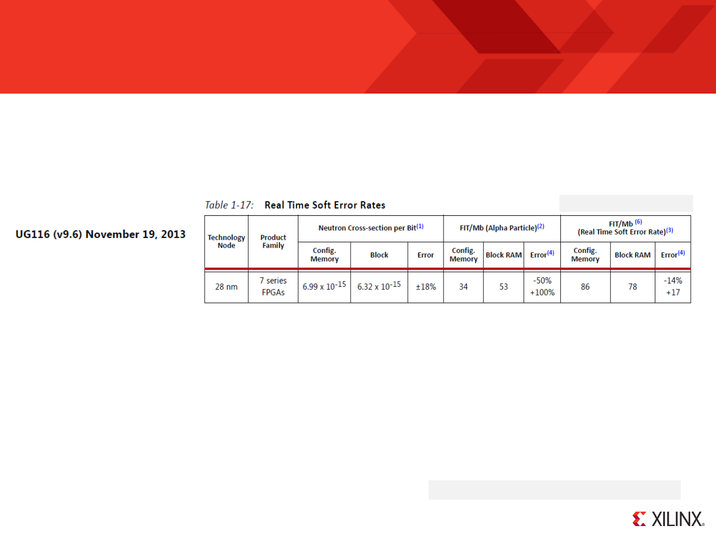
© Copyright 2010-2014 Xilinx
.
The ‘Real Time Soft Error Rate’ figures are the result of real upsets observed in real devices and normalised to sea level at New York. These figures are
inclusive of all upsets however caused and therefore include the upsets caused by alpha particles (i.e. take care not to account for alpha particles twice when
interpreting this table). Note that the potential ‘Error’ shown in the table from UG116 is -14% to +17% and reflects the fact that Xilinx has monitored (and
continues to monitor) hundreds of devices for thousands of hours thus continuously improving the confidence interval of these figures over time.
KCPSM6 Reliability and Single Event Upsets (SEU)
Page 109
There are some people for whom single event upsets (SEU) or soft errors are of concern because an FPGA is an SRAM based device and we live with
cosmic radiation every day. In fact, the configuration cells of a Xilinx FPGA are far more robust or tolerant than cells of any typical ‘data memory’ (e.g. DRAM
cells are several hundred times more susceptible). However, the possibility of any upsets occurring can still be a valid consideration so Xilinx takes this subject
very seriously both in the design of its products and in the ongoing monitoring and publication of real time soft error (UG116 updated every quarter). Correct
application of this real failure rate information enables sensible decisions to be made. The following analysis relating to a KCPSM6 sub-system in a 7-Series
device will estimate the FIT rates associated with SEU. In the end what really matters is how those figures compare with the target figures required for your
system (i.e. these real figures must be compared with other real figures and not just with vague claims or human emotions can run wild! ).
1 FIT is equivalent to one failure every 114,155 years.
Always use the latest version
for the most accurate figures
The nominal FIT rates shown in the table can be scaled appropriately for the
environment in which a device is to be operated. For example the neutron flux
density increases with altitude and fluctuates with geographical location. Whilst it is
rather pessimistic to do so, scaling the ‘Real Time Soft Error Rate’ by a factor of 17
would more than adequately cover the use of a device anywhere on the surface of
the Earth. This figure over-estimates the increase in neutron flux density and also
attributes all of the ‘Real Time Soft Error Rate’ figures to neutron upsets. Even so,
this twice over pessimistic scaling will also be used during the following analysis of
KCPSM6 to ensure the figures presented cover the majority of situations in which it
could be deployed. The figures presented are truly intended to facilitate you in
making a decision that is right for your design specification (not human emotion!).
Configuration BRAM
Memory contents
Nominal (sea level New York) 86 FIT/Mb 78 FIT/Mb
Pessimistically scaled to
cover anywhere on the 1,462 FIT/Mb 1,326 FIT/Mb
surface of the Earth (17×)
1Mb is one million bits of memory

© Copyright 2010-2014 Xilinx
.
KCPSM6 Reliability and Single Event Upsets (SEU)
Page 110
Estimating FIT Rates of KCPSM6 Program Memory
2K Instruction Memory 1K Instruction Memory 0.5K Critical Configuration
(0.036864Mb) (0.018432Mb) Instructions (0.009216Mb)
Nominal 78 FIT/Mb (sea level New York) 2.88 FIT (39,700 years) 1.44 FIT (79,401 years) 0.72 FIT (158,803 years)
Pessimistically scaled to
the worst location on the 48.88 FIT (2,335 years) 24.44 FIT (4,670years) 12.22FIT (9,341 years)
surface of the Earth (17×)
In most cases a KCPSM6 program is stored in a BRAM which is used as a ROM (initialised by the KCPSM6 Assembler). Although the maximum program
size is 4K instructions, typical programs tend to be in the range 1K to 2K instructions and are a good fit with the native size (36-kbits) of a BRAM in the 7-
Series. It is interesting to note that KCPSM3 had a 1K memory limit so users are tending to implement somewhat more when more when using KCPSM6.
Obviously the larger the memory (more bits), the higher the probability of a single event upset (SEU) occurring. Using the ‘Soft Error Rates’ it is possible to
estimate the FIT rate for a PicoBlaze program memory as a whole. In practice, KCPSM6 must actually fetch and execute an instruction containing an upset in
order for it to have any potential of deviating from its normally expected behaviour. Clearly any memory locations not occupied by instructions should not be
executed, and therefore an upset occurring in unused locations, should not impact the execution. For this reason the estimated FIT rate for operational failure
should at least be scaled to the actual size of a program rather than the total memory capacity (hint: see the assembler LOG file).
Somewhat less obvious, and rather more effort to establish, is how many instructions of a program are actually critical for normal operation. For example, it is
normal for a program to include some code that is only executed during initialisation, so a corruption to any of those instructions have executed would have no
adverse effect during normal operation. For those extremely serious about reliability, a program could be analysed in more detail looking at which sections of
code are really critical to operation. It is even possible to analyse individual instructions for their criticality (e.g. the bits of an op-code defining the instruction
would be considered critical but an 8-bit constant defining an ASCII character in a text message would typically be considered non-critical).
The table below estimates nominal and pessimistically scaled FIT rates for different sizes of program memory and includes the estimate for 0.5K instructions
of critical code (which is quite large even if a program occupied most of a 2K memory). It is important to remember that these FIT rates (and their
corresponding time intervals) represent the potential for a KCPSM6 execution error to occur due to a bit change somewhere in an instruction. For KCPSM6 to
deviate from the expected behaviour is must execute the corrupted instruction and the result of that execution must be different to that normally expected of it.
For example, if a ‘COMPARE s4, 23’ instruction was corrupted to become ‘COMPARE s4, 27’ then its execution would still set the zero or carry flags; a
deviation from intended behaviour then depends on the value held in ‘s4’ when it is executed and which flag is used in a subsequent instruction. Hence the
figures below should be interpreted as being very pessimistic indeed but how do they compare with the FIT rate requirements of your system?
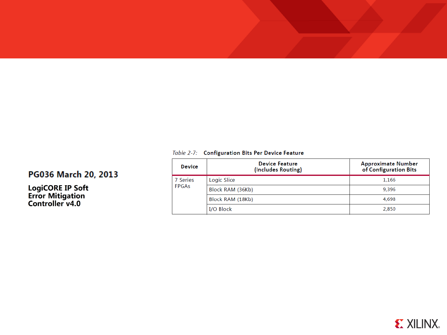
© Copyright 2010-2014 Xilinx
.
KCPSM6 Reliability and Single Event Upsets (SEU)
Page 111
Estimating FIT Rates of KCPSM6 Logic and Interconnect
The 7-Series devices have a built-in Readback CRC mechanism that, once enabled, will continuously scan all the static configuration cells in the device. Each
scan takes 8 to 70ms depending on the size of the device and will detect and report any upsets that occur anywhere in the device. In addition, an Error
Correction Code (ECC) is stored as part of every frame (3,232 bits) of the configuration memory and this can be used to correct the majority of errors with
minimum overhead (see the SEM IP and PG036 for details). This means that the majority of upsets are only temporary soft errors which limits the time (i.e. 8
to 70ms depending on device size) that an upset has to impact a circuit’s operation should it happen to flip one of the bits used by KCPSM6 in the first place.
Although not immediately obvious, it should be no surprise to realise that real designs (including KCSPM6) do not use all the logic and interconnect provided
in a device. In fact, only 20 to 40% of configuration cells are used to define the circuits and connections of typical designs that otherwise fill devices (hint: EBD
files reveal which and how many configuration bits are used by a particular design). So even when an SEU results in a configuration error that is detected,
reported and corrected, there is only a 20 to 40% probability that it impacted the definition of the design (i.e. 60 to 80% of upsets will ‘miss’ the design).
The KCPSM6 processor occupies 26 to 32 Slices depending on the size of scratch pad memory specified. To be of practical use, KCPSM6 would typically be
associated with logic implementing several input and output ports and maybe some additional logic to service interrupts. It is left to personal debate to decide
what logic in a design constitutes the KCPSM6 sub-system but a figure of 40 Slices appears to be reasonable for the purposes of estimation. This would
include the immediate interfacing logic but peripherals are considered to be modules in their own right with their own reliability figures.
In order to be able to estimate the FIT rates of these 40 Slices it is first necessary to have an estimate for the number of configuration memory cells
associated with each Slice. It is important to remember that it is not just the configuration cells that define the logic within each Slice but also the configuration
cells that define a fair share of the interconnect associated with each Slice. Whilst the contents of the BRAM have been accounted for separately (i.e.
Program Memory) it is also necessary to account for the configuration cells which define the format of the BRAM and its associated interconnect.
This table from PG036 provides the estimates
of configuration bits associated with each feature.
Hence a KCPSM6 Sub-System consisting of 40 Slices and a 2K program memory = (40 × 1,166) + 9,396 = 56,036bits (0.056036Mb)

© Copyright 2010-2014 Xilinx
.
KCPSM6 Reliability and Single Event Upsets (SEU)
Page 112
A more challenging concept to understand is that not all upsets that flip configuration cells that are part of the design definition (i.e. the 20 to 40%) will impact
the operation in any meaningful way. This is because the particular logic or interconnect altered by the upset also needs to be actively used by the design for
it to have any effect (i.e. a signal needs to be prevented from changing state for its value to become incorrect). Furthermore, the window of opportunity for this
to happen is limited to the few milliseconds it takes to detect and correct an error. For example, an upset that temporarily disconnects the reset single to
KCPSM6 would have no impact on normal operation unless the reset control was pulsed High during that few milliseconds that the bit error was present.
Operational Failure Rate
KCPSM6 Sub-System
(40 Slices + 2K memory)
The Complete KCPSM6 Solution (Program Memory, Logic and Interconnect)
Combining the estimated FIT rates for both the program memory and the logic resources of a typical KCPSM6 sub-system reveals the total estimated FIT
rates. It is interesting to note the relative rates associated with the program memory verses the logic and interconnect. In order to avoid ‘number overload’ the
figures presented below have been limited to a program memory of 2K instructions of which 0.5K is considered to be critical to operation. This covers most
typical configurations but obviously you should collate the figures appropriate to your design (not forgetting to use the latest version of UG116).
The FIT rates below have been calculated by applying the 8% susceptibility factor to the number of configuration cells associated with a KCPSM6 sub-system
(40 Slices and a 2K program memory) and the nominal and pessimistically scaled FIT rates for configuration memory in 7-Series devices.
Nominal (sea level New York): 86FIT/Mb × 0.056036Mb × 8% = 0.39 FIT (296,101 years)
Pessimistically scaled to cover anywhere
on the surface of the Earth (17×):
An exhaustive experiment has been conducted using a design containing 400 KCPSM6 Sub-Systems (i.e. 40 Slices and a 2K program memory). Thousands
of SEU were simulated using the Soft Error Mitigation (SEM) IP core to inject errors (see PG036) at random locations. The program being executed by each
of the KCPSM6 processors used virtually all instructions and features making it very sensitive to any disruption. Just as important, any deviation from
expected behaviour was detected and reported. The results shows that a KCPSM6 Sub-System was sensitive to 1 in every 12 simulated SEU which is a
susceptibility of 8%. It is extremely rare for any design to exceed 10% susceptibility with most HDL designs falling somewhere in the range 1% to 5%.
48.88 FIT (2,335 years) 12.22 + 6.55 = 18.77 FIT (6,081 years)
6.55 FIT (17,417 years)
Nominal (sea level New York): 2.88 FIT (39,700 years) 0.72 + 0.39 = 1.11 FIT (102,842 years)
Pessimistically scaled to cover anywhere
on the surface of the Earth (17×):
2K Instruction Memory 0.5K Critical Program + KCPSM6 Sub-System
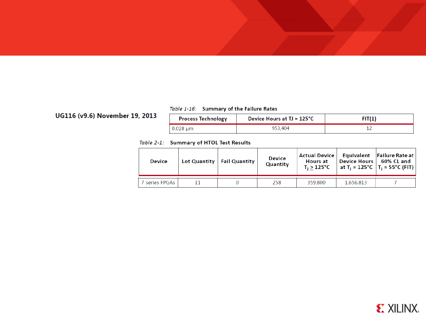
© Copyright 2010-2014 Xilinx
.
KCPSM6 Reliability and Single Event Upsets (SEU)
Design for reliability should be driven by the operational FIT rates and so the first and most significant observation is that 1.11 FIT under nominal conditions
and less than 19 FIT when pessimistically scaled are very low indeed. In other words, KCPSM6 really is very reliable . To give further perspective to these
figures, the following abstracts from UG116 present the fundamental hardware failure rates of the 7-Series devices.
Quite simply, the conclusion to be made is that unless the device containing KCPSM6 is to be operated in a significantly more hostile environment, then the
potential for KCPSM6 to fail during operation is almost negligible when compared with just about everything else that is likely to surround it. Of course total
system reliability is the sum of many small parts so it would be inappropriate to suggest that the FIT rate of KCPSM6 should be ignored completely. However,
it would be equally inappropriate to be concerned about a KCPSM sub-system with such a low FIT rate until other parts of a system with much higher FIT
rates have been adequately addressed. As it happens, the intrinsically low FIT rate of KCPSM6 sub-system often makes it a suitable candidate for the
monitoring and management of other functions with higher FIT rates so it is not surprising that watchdog supervision and control is one of the application
areas in which KCPSM6 is used in larger FPGA devices.
In reality, the operational reliability of KCPSM6 sub-system almost certainly depends more on the quality of the hardware design and PSM code used with it.
Hence it is far better to invest time and effort ensuring that your fundamental code is correct than wondering how to improve the fundamental 1.11 FIT rate
(but the following pages will ). Remember too you should compare ‘real numbers’ with other ‘real numbers’. Avoid the temptation to react to ‘human
emotions’ when making designing for reliability. Any fundamental flaws or weaknesses in the definition of a hardware design or the coding of a PSM program
would almost certainly result in a FIT rate many times greater than 1.11 so this is a clear indication that your code should be your primary area of focus. In
fact, it is a challenge to prove that your code has a FIT rate less than 100 let alone a FIT rate approaching 1.
Interpreting the KCPSM6 Sub-System FIT Rates
Total hardware failure rates of a system
would also need to include the FIT rates
associated with the board on which the
device is mounted and various power
supplies that enable it to operate in the first
place. Do you know what these are for
your products?
Page 113

© Copyright 2010-2014 Xilinx
.
Error Detection for Very High Reliability Designs
Page 114
The reality is that nothing can be absolutely 100% reliable, so albeit undesirable, it is acceptable for failures to occur in any module up to a sensibly defined
FIT rate. For the majority of electronic products, the point of failure is simply seen as the time to try “turning it off and back on again”, or when that doesn’t
work, a food excuse to go and buy the new model . For most commercial products the failure rate just needs to be low enough to prevent your products
gaining a bad reputation or costing too much in returns. However, for some products and applications it is not so much the failure rate that matters, but how
failures will be handled when they do occur because every one of them could be important at that moment.
Consideration must be given to the characteristics of potential failures and the course of action to be taken in response to each type. Such analysis will always
lead to a strong desire to detect when a failure or error has occurred. In fact, when it comes to very high reliability equipment, the requirement for error
detection and reporting will be a key specification from the outset; often demanding a level of confidence for detection that far exceeds the acceptable failure
rate for the main functionality. The general premise being that it whilst it is undesirable for a system to suffer a failure, it is almost totally unacceptable for any
failure to pass unnoticed with the risk that the equipment continues to operate erroneously for an indefinite period. In this domain there is no such thing as a
standard solution; every system will have its own requirements and priorities as the following contrasting examples hopefully illustrate.
1) A data back-up system has “five nines” availability (99.999% availability equates to ~5 minutes of downtime per year) and is required to maintain a good
copy of information. It is vital that any failures or errors are detected in order to prevent the backed-up data from being corrupted. When an error is
reported, the system will keep operating in order to meet the availability target. However, the error report will also trigger additional checks which will
establish the cause of the error, and when possible, make a running repair. The integrity of the data will be achieved though a repeat of any tasks
attempted or performed during the period prior to the error being detected through to the time when the repair had been completed.
2) A high reliability communication link employs a Triple Modular Redundancy (TMR) scheme. Through this arrangement it is possible for the system as a
whole to continue operating normally when one unit fails (i.e. if one unit provides conflicting information, a voting mechanism will ignore that unit in favour
of the other two). In this case the voting mechanism could also be the error detector, but if each unit can detect and report errors independently before the
voting mechanism even observes anything wrong, then the sooner a failed unit can be taken off line, ‘repaired’ and returned to operation. This minimises
the time the system is reliant on two out of three units and also means that voter mechanism is a secondary monitor (i.e. Detection redundancy).
3) The primary feed for a television network is delivered by a unit (A) but there is a back-up unit (B) standing by. As soon as an error is detected with unit ‘A’
the ‘B’ unit is switched in to take over until ‘A’ has fully recovered and there is a suitable moment in the transmission to switch back.
4) A gas valve controller has no electronic redundancy and the acceptable operational failure rate is surprisingly high. However, it is vital that the gas valve
should always shut off should any error occur. The valve is fitted with a mechanical bias to close during a power failure, but if there is any other kind of
error in the controller it must stop driving the valve open. A service engineer will be called to implement any repairs and will be present to manually put the
controller back on line and verify that it is operating correctly.
In each of these applications it is highly desirable for the detection and reporting to occur rapidly; the longer it takes to detect an error the longer things could
be going wrong in the system. But the overwhelming desire is that no failures or errors should be missed completely.

© Copyright 2010-2014 Xilinx
.
Error Detection for Very High Reliability Designs
Page 115
It must also be accepted that an error detection and reporting mechanism can not be 100% reliable either. In the vast majority of cases, the level of error
detection and reporting provided by Xilinx will be considered to be acceptable. However, if the level of fault detection is inadequate within a given unit then
different parts of a system must be used to ‘cross-check’ each other (i.e. effectively employing redundancy in error detection schemes too).
The ‘price to be paid’ for having a highly sensitive error detection mechanism with extremely high coverage is that it will result in more ‘false alarms’ than
actual events of concern. The fundamental fact is that high sensitivity and coverage leads to the detection of real events and therefore legitimate real alarms;
the issue is that more often than not, no other effects can be observed giving the impression of a false alarm. Although every system will have its own specific
requirements the following FIT rates could be representative of the targets for a high reliability system…
Operational Failure Rate: 11,400 FIT (MTBF = 10 years)
Unreported Operational Failure Rate: 23 FIT (MTBF = 4963 years)
Error Detection and Reporting Rate: 114,000 FIT (MTBF = 1 year)
These example figures indicate that it is extremely unlikely (23 FIT) that a genuine error will occur without it being reported. However, an ‘alarm’ (i.e. an error
detection report) it is expected once per year (114,000 FIT) even though an operational failure is only expected once every 10 years (11,400 FIT). This
implies that 9 out of 10 alarms will appear to be ‘false alarms’. Hence it is necessary to consider the potential causes of alarms and to avoid making the all too
common human mistake of ignoring alarms just because most of them appear to be false!
Genuine alarm - This is the straightforward case in which the alarm is accompanied by obvious erroneous behaviour of the unit. This would be the 1 in 10
case (11,400 FIT) in the above example and is the primary reason for implementing error detection and reporting to ensure the primary (23 FIT) target.
Apparent false alarm - An alarm occurs but no abnormal behaviour in the system is observed. Based on the example figures above this will account for 9 out
of 10 alarms. The ‘alarm’ is the result of the error detection mechanism finding and reporting a genuine error somewhere in the unit; therefore these are
actually genuine alarms. The issue is that unless the failure is widespread or in a critical spot it is very common for nothing abnormal to be observed so we
think it is a false alarm. For example, corruption to a KCPSM6 instruction in the program memory is a genuine error but only observable if and when KCPSM6
executes that particular instruction and the outcome of that execution is a deviation from the normally intended behaviour. A comprehensive error detection
mechanism would raise an alarm very soon after the corruption occurred even if KCPSM6 never executed the corrupted instruction during operation.
Failure of alarm circuit - The error detection and reporting circuit can not be 100% reliable. That can also include an alarm being raised for no valid reason as
well as the failure to raise the alarm when something does occur. In the above example, 23 FIT is a low figure but it still has meaning. If KCPSM6 was used to
monitor other circuits and systems to detect and report errors then its nominal operational FIT rate of 1.11 (102,842 years) is an indication of how reliable
KCPSM6 really is and therefore how unlikely it would be to miss something (or to be the cause of a real false alarm). That said, we will now explore how to
detect errors in KCPSM6 sub systems requiring analysis of some very low FIT rates indeed. Do keep in mind that analysing one KCPSM6 in isolation results
in all figures being less than the fundamental hardware failure rate of a device (see page 113) but a whole design can contain many KCPSM6.

© Copyright 2010-2014 Xilinx
.
Error Detection for Very High Reliability Designs
Page 116
Detecting Errors in KCPSM6 Logic and Interconnect
As indicated on page 111, Xilinx have a built-in Readback CRC mechanism (see ‘Readback CRC’ chapter in UG470 for more details) that will detect and
report any changes to the otherwise fixed configuration cells anywhere in the device. Using this mechanism will therefore detect and report any upsets (e.g.
those resulting from an SEU) and this would include any that are associated with the logic and interconnect of a KCPSM6 processor.
It must be appreciated and accepted that Readback CRC detects and reports errors on a device level; not isolated to a specific element in a design like
KCPSM6. As calculated on page 112, the logic and interconnect of a KCPSM6 sub system has a nominal FIT rate of 0.39 (296,101 years). In contrast, the
nominal rate at which upsets would occur and be detected in an XC7K325T device would be 6,462 FIT (18 years). So if an error was detected and reported
by a XC7K325T device there would only be a 0.006% probability of that upset effecting the operation of a particular KCPSM6 (logic and interconnect).
In 7-Series devices, the majority of errors can also be corrected using the Error Correcting Codes (ECC) stored in each of the configuration frames. However,
consideration should be given to the fact that it typically takes 8 to 71ms (depending on device size) for an error to be detected and corrected. In the unlikely
event that that the error did impact the operation of the KCPSM6, the deviation from the intended behaviour could continue to have effects even after the initial
configuration error has been corrected (e.g. a register could be left holding an incorrect value calculated when the error was present).
The suitable course of action following the detection of an error really depends on the needs of your equipment. In some applications the device will be
reconfigured when an error is detected so KCPSM6. If this scheme was implemented then KCPSM6 would get a clean start along with the rest of the system.
In other applications, the interruption to service caused by reconfiguring the device and a system restart is undesirable (especially when <10% of upsets have
any meaningful effect on operation). So the most common course of action taken following the reported detection and correction of a configuration error
(anywhere in a device) is to issue a fast local reset to any critical circuits. This would probably include resetting KCPSM6 processors to ensure they are all in
a known state. In such cases, the initial portion of the program may be written is a way that gather information from the surrounding system to establish if it is
a ‘cold’ or ‘warm’ start. This can greatly minimise the interruption to service and possibly eliminate any interruption at all.
Although we are unable to determine from the built-in Readback mechanism when an upset in a device ‘hits’ a particular KCPSM6, there are a few
possibilities to locally detect deviation from intended operation as part of the design itself. The first and easiest method is to use the ‘DEFAULT_JUMP’
directive supported by the KCPSM6 Assembler (please see ‘all_kcpsm6_syntax.psm’ for details). Appropriate use of this directive will help KCPSM6 to
recover from a situation where a configuration error has lead to KCPSM6 attempting to fetch an instruction from unused space in your program memory. This
will only cover certain types of defect but improving on a fundamental nominal FIT rate of 0.39 is never going to be easy! Beyond this, you really need to
consider redundancy schemes. Running two KCPSM6 processors in parallel and comparing their ‘address’ and ‘out_port’ busses every clock cycle will reveal
any deviation from normal behaviour. Although you would not know which of the two processors was effected by an error, the more significant benefit is that
you would be identify the most common cases in which they continue to work correctly avoiding the need to reset them following the detection of an error at
the device level. Any deviation from normal behaviour will also be detected in one clock cycle which could be very useful in critical control applications. Of
course Triple Modular Redundancy (TMR) is the golden solution but comes with further complexity and overhead.

© Copyright 2010-2014 Xilinx
.
Error Detection for Very High Reliability Designs
Page 117
Program Size Slices Total Upset Rate Operational Failure
(instructions) (86FIT/Mb) Rate (10%)
Implementing Program Memory in Slices (Distributed ROM)
Each of the four LUTs contained in a Slice can be used individually or combined to implement a 64 × 4, 128 × 2 or 256 × 1 ROM. Therefore multiple Slices
can be used to implement 18-bit program memories of various sizes for KCPSM6. Two templates to implement 128 and 256 instruction memories in this way
are provided for use with the assembler (please see page 47 for usage of ‘ROM_form_128_date.vhd’ and ‘ROM_form_256_date.vhd’). LUTs and Slices are
not as efficient at implementing pure memory as BRAM but the key advantage of implementing a ROM in this way is that the ROM contents also become part
of the otherwise static configuration of the device. This allows the device level Readback CRC mechanism to detect errors within the program memory and
also means that the majority of them will be corrected; the memory becomes an extension of the logic and interconnect of KCPSM6 itself. The table below
shows the nominal (sea level New York) FIT rates for four sizes of Slice-based ROM.
Detecting Errors in KCPSM6 Program Memory
When the device is configured, it will initialise the contents of all Block Memories (BRAM) in the device. Those BRAM’s used to implement a KCPSM6
program memory will be initialised with the op-codes prepared by the Assembler based on your PSM code. Although a program memory uses BRAM as a
ROM (i.e. fixed contents), a BRAM is primarily a RAM expected to hold variable data. For this reason, BRAM contents are not scanned by the Readback CRC
and therefore an upset to the connects of a normal KCPSM6 program will not be detected or reported at the device level.
As shown on page 110, a program ROM of 2K instructions (one 36kb BRAM) has a nominal FIT rate of 2.88; a small number, but with the potential for
KCPSM6 to execute a corrupted instruction without that error being detected or reported. As previously discussed (page 115), in some systems, an
undetected error would be highly undesirable and even 2.88 FIT starts to become significant. It is also clear from the FIT rates (2.88 FIT versus 0.39 FIT) that
the program memory is potentially the more significant weakness in a typical KCPSM6 sub system.
Fortunately there three schemes that can be considered to detect errors in KCPSM6 program memory and one of those will actually reduce the operational
FIT rate of the memory close to zero. However, there are engineering trade-offs to be considered when reviewing these alternatives so do be certain that the
standard nominal FIT rate really is inadequate before using any of them. Of course, as discussed in the last paragraph of the previous page, a redundancy
scheme could be implemented with standard program memory. In practice, it probably makes more sense to implement redundancy using complete KCPSM6
sub systems (i.e. each module consisting of a KCPSM6 and Program Memory) rather than implement a program memory with redundancy connecting to a
single KCPSM6 (or even a KCPSM6 with redundancy) as this would reduces the common points of failure.
As previously described, operation will only be sensitive to a percentage of the
configuration cells associated with each Slice. KCPSM6 would also need to execute
a corrupted instruction during the short time (e.g. ~20ms) taken for the error to be
detected and corrected. So the operational failure rate is unlikely to exceed 10% of
the total raw configuration rate (an accurate figure for a particular design can be
determined using the SEM IP to inject random errors to simulate SEU).
128 9 0.90 FIT 0.09 FIT
256 18 1.80 FIT 0.18 FIT
512 39 3.91 FIT 0.39 FIT
1024 77 7.72 FIT 0.77 FIT
See page 123 for HDL instantiation of this special memory
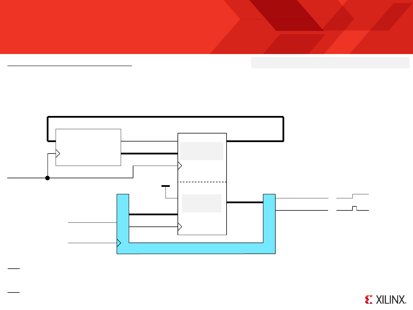
© Copyright 2010-2014 Xilinx
.
Error Detection for Very High Reliability Designs
Page 118
scan_data[8:0]
RAMB36E1
scan_address[11:0]
address[11:0]
instruction[17:0]
enable
clk
KCPSM6
system_clock
instruction
address
bram_enable
clk
A-Port
WIDTH = 18
Standard connection of
the ‘A’ port to KCPSM6.
B-Port
WIDTH = 9
scan_clk
scan_complete
scan_error
EN
scan_reset
The integrity of error
detection will be
enhanced when using
an independent clock
and monitor.
Local CRC Scanning Circuit
CRC Error Detection for BRAM Program Memory
The inherently larger capacity of a BRAM combined with its relatively low FIT rate for larger programs means that BRAM remains the preferred solution for
most applications. The ‘ROM_form_7S_2K_with_error_detection_14March13.vhd’ template implements a 2K program memory in a single BRAM. As far as
KCSPM6 is concerned, this just like a standard program memory with identical connections and system performance. However, an additional and completely
independent circuit exploits the second port of the BRAM allowing the memory contents to be continuously scanned and checked against a ‘golden’ CRC
value computed by the assembler. A worst case error detection time of <1ms is easily achieved. Please take a while to read further descriptions and advice
included in the template.
The ‘B’ port is used to continuously scan the entire contents
(36,864 bits) and compute a CRC-16 value. If the computed
CRC-16 value does not match with the ‘golden’ value calculated
by the KCPSM6 assembler the ‘scan_error’ signal will go High.
‘scan_complete’ pulses High at the end of each
scan (every 36,873 ‘scan_clk’ cycles). You and/or
an independent watchdog monitor would use this
to confirm that detection is active.
Note – The CRC scanning circuit occupies ~10 Slices so it too will have a nominal operational FIT of ~0.1 (i.e. potential for ‘false alarms’ to be generated).
2K
Instructions
Note – An error anywhere in the memory will cause ‘scan_error’ to go High so the nominal rate at which this will occur is the same as the nominal upset rate
(i.e. 2.88 FIT). There is a high probability that the error will be reported before KCPSM6 fetches and executes a corrupted instruction. In fact, it is quite
likely that this will appear to be a false alarm because KCPSM6 may never fetch the corrupted instruction during normal operation.
See page 123 for HDL instantiation of this special memory
‘High’ when
error detected
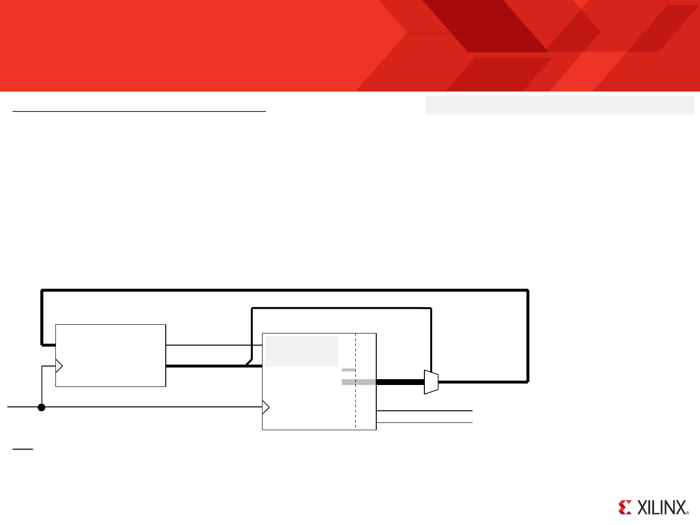
© Copyright 2010-2014 Xilinx
.
Error Detection & Correction for
Very High Reliability Designs (BRAM ECC)
Page 119
Error Detection and Correction for BRAM Program Memory
The Block Memories (BRAM) in 7-Series devices provide an optional Error Correction Code (ECC) feature which is described in chapter 3 of UG473. It should
be understood that the nominal upset rate of the BRAM remains the same (i.e. 2.88 FIT). The difference and advantage when using the ECC feature is that
single bit errors will be detected, reported and corrected. It should be appreciated that the detection, reporting and correction only takes place as a ‘word’ of
memory is being read and presented at the BRAM outputs. Multiple bit upsets within any particular word can not be corrected but the probability of this
happening is virtually zero due to the physical layout of the memory cells forming a BRAM in a 7-Series device.
Note – The ECC only detects and corrects errors contained in the word being read and presented to the BRAM outputs; it does not correct the contents held
within the memory. It would be possible to write the corrected word back into the memory but the circuits to perform this operation would probably increase
the total FIT rate! Due to the inherently low FIT rate (i.e. 2.88 nominal), the probability of accumulating multiple errors within the same word of the same
BRAM during an operational period is virtually zero. If an upset does occur then ‘SBITERR’ will pulse High every time the word containing that error is read
from the memory. All single bit errors are corrected so this is purely for information (e.g. used to log the event and/or schedule a reconfiguration).
RAMB36E1 with ECC
address[11:0]
instruction[17:0]
enable
clk
KCPSM6
clk
instruction
address
bram_enable A-Port
WIDTH = 72
1.5K
Instructions
[63:0]
Decode & Correct
8
64
SBITERR
DBITERR
The ‘ROM_form_7S_1K5_with_ecc_5Dec13.vhd’ template exploits the ECC feature resulting in a program memory with an operational FIT rate approaching
zero. However, in order to use the ECC feature, this template must configure the BRAM to have a 512×72 aspect ratio. Each 72-bit ‘word’ supports 64-bits of
information protected by an 8-bit ECC. The ECC values consume just over 11% of the memory and 18-bit instructions for KCPSM6 do not fit naturally into the
64-bits of protected information. Combined, these factors reduce the program storage capacity of a RAMB36E1 from 2K instructions to 1.5K instructions and
also impact performance (more about performance on page 122).
The KCPSM6 assembler packs 3 instructions (3 ×18 = 54 bits) into each 64-bit protected word and computes
the corresponding 8-bit ECC value to be stored with them. Maximum of 512 × 3 = 1,536 instructions (000-5FF). The template uses address[11:9]
to selects which of the three
instructions contained in the word
fetched from address[8:0] is
presented to KCPSM6.
The ECC decoder reports any single or
double bit errors detected in each 72-bit word.
In addition, any address outside
the working range (i.e. 600-FFF)
will result in the instruction being
forced to zero or assigned the
DEFAULT_JUMP instruction.
8
3
See page 123 for HDL instantiation of this special memory
8:0]
[11:9]

© Copyright 2010-2014 Xilinx
.
Error Detection & Correction for
Very High Reliability Designs (BRAM ECC)
When using the memory with ECC protection the operational FIT rate will be so close to zero that it becomes a real challenge to suggest anything that will
result in further improvement. The following points make further observations to substantiate this claim and hopefully provide you with ideas that could be
useful when using a PicoBlaze module in your most critical applications.
Nominal FIT rate of a KCPSM6 Sub-System (40-Slices and a BRAM) using ECC protected BRAM.
When using BRAM with ECC the integrity of the values presented at the memory output has a FIT rate approaching zero; the upset rate of memory contents
remains 2.88 FIT but all single bit errors can be corrected and a double bit error are so unlikely that it is impossible to estimate a FIT rate low enough! Even if
a ‘DBITERR’ was reported for the 72-bit memory word there would only be a 1 in 4 chance that the corruption was present in the 18-bit instruction being read.
The ~5 Slices and associated interconnect used to implement the instruction selection and DEFAULT_JUMP have a nominal FIT rate of 0.05 which must be
added to the 0.39 nominal FIT rate of the KCPSM6 Sub-System (see page 112). Therefore the estimate of nominal FIT rate for a KCPSM6 Sub-System
using ECC protected BRAM is 0.4 FIT. The key observation to make is that part of that 0.4 FIT could result in an incorrect address being presented to the
ECC protected BRAM; i.e. a higher probability of reading the wrong instruction rather than the memory itself producing an instruction containing an error.
‘SBITERR’ and ‘DBITERR’ Signals and Meaning
These status signals will go High (1) if the 72-bit word being read from the memory contains either a single bit error (‘SBITERR’) or a double bit error
(‘DBITERR’). Note that an error is only detected and reported when a word containing an error is read. As such, KCPSM6 needs to read one of the three
instructions packed into a word for an error to be detected and words that are not accessed by KCPSM6 are never checked. The BRAM with CRC Error
Detection (page 118) continuously scans all memory locations and will detect and report any errors at a rate of 2.88 FIT. The BRAM with ECC protection will
only be checking the words being accessed by KCPSM6, so for a typical program, we would expect the ‘SBITERR’ detection rate to be lower that the ‘CRC’
detection rate. Errors that occur in locations not being accessed by KCPSM6 may contain errors but they will have no impact on operation anyway. In other
words, the BRAM with ECC protection generally reduces the ‘apparent false alarm rate’ as well as providing error correction.
All single bit errors will be corrected so the ‘SBITERR’ report is purely the indication that a bit has been corrupted in the memory. Given the low nominal FIT
rate of the memory contents (2.88) there should be no particular reason to react to an ‘SBITERR’ although it is common practice for very high reliability
systems to log any such events (e.g. gathering statistical data for future reference). It would also be good practice to schedule a maintenance cycle (i.e.
device reconfiguration) at a convenient time within the next few years! It is important to recognise that ‘SBITERR’ will go High every time that the 72-bit word
containing an error is read. Hence, if KCPSM6 repeatedly executes a section of code that requires a 72-bit word containing an error to be read then
‘SBITTERR’ will be seen to pulse repeatedly as well. Take care to log only the first ‘SBITERR’ report and not the subsequent repeats.
When a double bit error is detected in a 72-bit word then a ‘DBITERR’ will be reported. This is so unlikely to happen that it is impossible to state a FIT rate
(currently zero but nothing can be perfect!). If ‘DBITERR’ should ever go High then the most important thing is that an error has been detected (i.e. not
missed) and a truly critical system should take notice. The three instructions in each word have been spaced so that an adjacent double bit error cannot
impact more than one instruction. There is only a 25% chance (18/72) that a double bit error will have impacted the 18-bit instruction being read.
Page 120
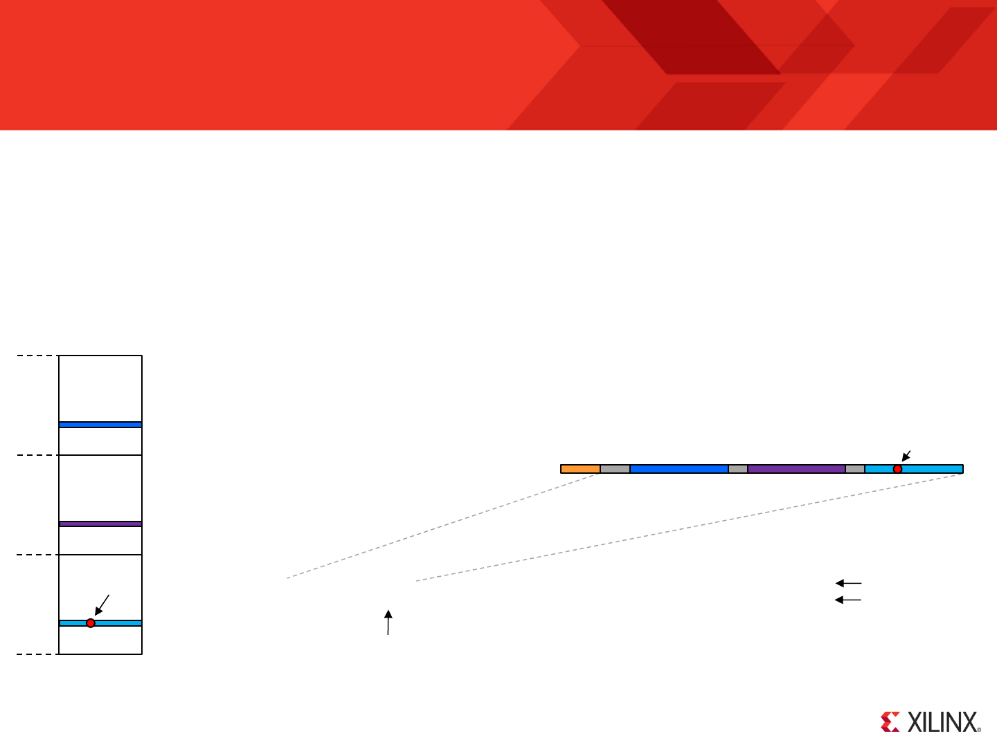
© Copyright 2010-2014 Xilinx
.
Error Detection & Correction for
Very High Reliability Designs (BRAM ECC)
Testing ‘SBITERR’ and ‘DBITERR’ signals
If you decide to monitor or react to these signals then you almost certainly need a way to test them. The low FIT rate of the memory contents means that even
neutron or proton beam facilities makes testing with real upsets impractical (a real ‘DBITERR’ being virtually impossible to achieve). So the practical solution
is to manually inject errors in the memory. This could be achieved by modifying the hardware design to write a suitably corrupted word into the BRAM (see
UG473 for full details) but implementing such a scheme is not as straightforward as it may first appear, and more significantly, such circuitry would increase
the FIT rate of the memory! i.e. The FIT rate of the error injection circuit would exceed the FIT rate for genuine double bit errors. Fortunately, this memory is
being used as a ROM so we can deliberately embed errors in the memory contents and maintain the same circuit. The assembler generates the program
ROM definition file containing BRAM initialisation values and these can be modified to deliberately create a single or double bit error at any location. The
program can be written in such a way that locations containing the errors are only executed as part of a test routine (hint - use the ADDRESS directive to
locate test code in a known and predictable location).
000
1FF
200
3FF
400
5FF
Error
063
263
463
7 40
19 18
20 17 0
39 38
37
0
58
57
63
Deliberately corrupting the memory contents is best performed in a controlled manner (i.e. at a known address). This requires further
knowledge of the way in which instructions are packed into the memory words and how the assembler builds the INIT strings which
define the memory contents during device configuration.
Each 72-bit word contains three 18-bit instructions taken from addresses of the assembled program that are 512 (200 hex) locations
apart. As well as the three instructions, each word contains 10 unused bits and the 8-bit ECC value. Any of the 72-bits can be
corrupted to generate an error when the word is read but it is generally a more reassuring test case to corrupt an instruction and then
observe that it is corrected (or not in the case of a double bit error).
The instructions and unused bits form part of the 64-bit ‘data’
word defined by the ‘INIT_nn’ strings and the 8-bit ECC
values are defined by the ‘INITP_0n’ strings.
INIT_18 => X"03620731DCB1CB3B028882101191E2F302923C3432A35B640108413F96B2D6A3",
INIT_18 => X"03620731DCB1DB3B028882101191E2F302923C3432A35B640108413F96B2D6A3",
C = “1100”
D = “1101”
Error
Error
Original
Modified
The ‘INIT_nn’ strings contain hexadecimal values so make sure that your modification
represents only a single bit (or adjacent double bit) change. For example, changing ‘7’ to
‘8’ is actually a change of all four bits (‘0111’ to ‘1000’) so be careful!
Remember that ‘SBITERR’ or ‘DBITERR’ will be reported when KCPSM3 reads any of the three instructions contained in the same 72-bit word. So plan
where you insert your errors and locate your PSM code in a corresponding way.
1.5K ECC Memory
This example shows a single bit error being created in the instruction stored at KCPSM6 address 063 hex (9910). Each ‘INIT_nn’
string defines four 64-bit words so 063 hex corresponds with the 4th word of ‘INIT_18’ (i.e. The first string is ‘INIT_00’ so ‘INIT_18’ is
the 24th frame holding words 96 to 99 which in turn holds instructions for KCPSM6 addresses 060-063, 260-263 and 460-463)
ECC
Page 121
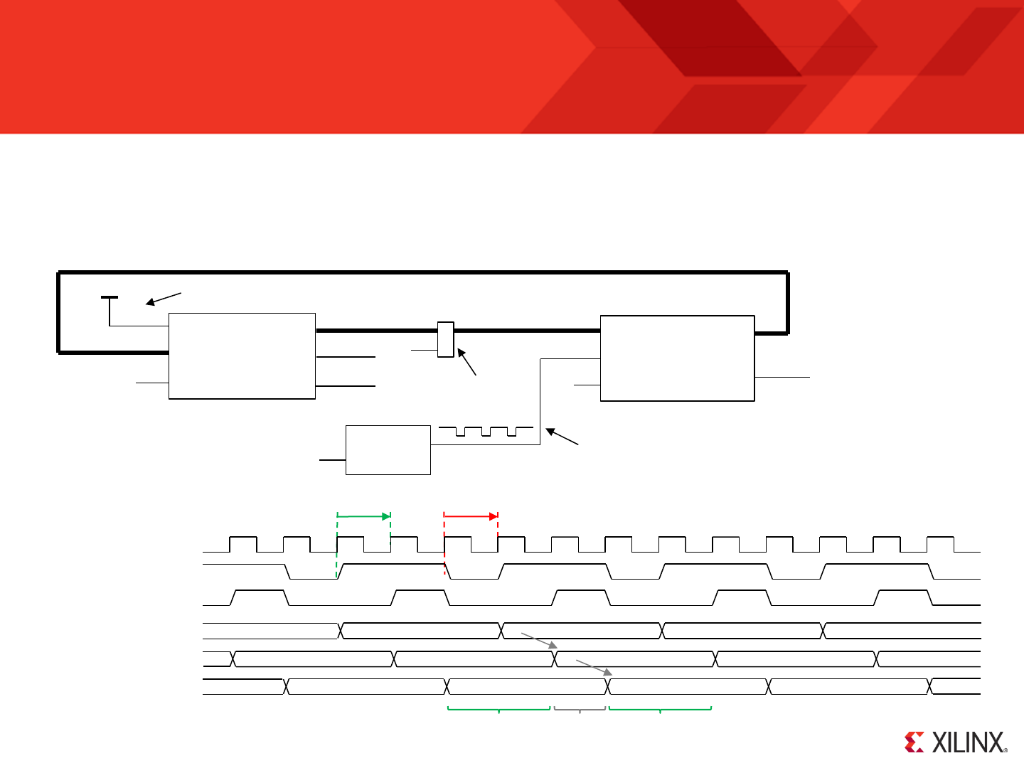
© Copyright 2010-2014 Xilinx
.
Error Detection & Correction for
Very High Reliability Designs (BRAM ECC)
Maintaining performance when using ECC protected BRAM
As indicated on page 119, the ECC protected memory will impact performance. The ECC decode and correction circuit at the output of the BRAM and the
instruction selection multiplexer combine to increase the effective clock to output delay of the program memory which will limit the maximum clock frequency
that can be achieved by a KCPSM6 sub-system. For ease of design and reliability, it is highly desirable for KCPSM6 to run from the same clock domain as
the logic that it monitors and controls, so if the use of ECC protection does adversely impact performance in your design, you should consider using the
‘sleep’ control with a ‘slow down’ waveform (see also page 39). This scheme allows the output of the program memory to be pipelined.
KCPSM6
clk
instruction(17:0)
enable
address(11:0)
clk DBITERR
SBITERR
ECC protected
PicoBlaze
Program memory sleep
clk Slowdown
Control
clk
Note that program
memory must be
permanently enabled
bram_enable
pipe_instruction(17:0)
clk
sleep
address
instruction
bram_enable (not used)
pipe_instruction
AA0 AA1 AA2 AA3 AA4
LOAD s4, 42
LOAD s4, 42
AND s7, 80
AND s7, 80
FETCH sC, 05
FETCH sC, 05
ADD sC, 01
ADD sC, 01
wake up
execute
go to sleep When KCPSM6 is awake it only samples the ‘sleep’ control on the
rising clock edge that ‘bram_enable’ is High
One additional clock cycle available to read memory
1 1 0 1 1 0 1 1 0 1 1
Insert Pipeline
KCPSM6 executes an instruction every
3 clock cycles (rather than every 2).
Slower code execution, but facilitating a
higher clock frequency.
Permanently Enabled
Slowdown Waveform applied to ‘sleep’
Page 122

© Copyright 2010-2014 Xilinx
.
Page 123
Using High Reliability Memory Templates
As described in the previous pages, there are three types of program memory provided for use in designs requiring the very highest levels of reliability. To use
any of these memories in your design, simply make a copy of the appropriate template, name it ‘ROM_form.vhd’ and place it in the same directory as your top
level PSM file. The KCPSM6 assembler will then automatically read the template that you have provided and generate a VHDL file defining the memory type
that you have chosen initialised with your assembled program (see page 47). It is recommended that you develop your PSM code using a standard program
memory that allows you to use JTAG Loader. Limit your code to the size that you will have available in your choice of high reliability memory (hint: Use the
assembler with the ‘-c’ option). Once your PSM code is stable you can switch over to your final choice of memory. This will require some small modifications
to the declaration and instantiation of the memory in your design. The various ports and their names for each type of memory are shown below (there are no
generics). Of course you will have to define ways in which to connect the special ports related with the high reliability features of the BRAM-based memories.
component your_program
Port ( address : in std_logic_vector(11 downto 0);
instruction : out std_logic_vector(17 downto 0);
enable : in std_logic;
clk : in std_logic;
scan_error : out std_logic;
scan_complete : out std_logic;
scan_reset : in std_logic;
scan_clk : in std_logic);
end component;
program_rom: your_program
port map( address => address,
instruction => instruction,
enable => bram_enable,
clk => clk,
scan_error => scan_error,
scan_complete => scan_complete,
scan_reset => scan_reset,
scan_clk => scan_clk);
component your_program
Port ( address : in std_logic_vector(11 downto 0);
instruction : out std_logic_vector(17 downto 0);
enable : in std_logic;
SBITERR : out std_logic;
DBITERR : out std_logic;
clk : in std_logic);
end component;
program_rom: your_program
port map ( address => address,
instruction => instruction,
enable => bram_enable,
SBITERR => program_SBITERR,
DBITERR => program_DBITERR,
clk => clk);
ROM_form_128_date.vhd
ROM_form_256_date.vhd component your_program
Port ( address : in std_logic_vector(11 downto 0);
instruction : out std_logic_vector(17 downto 0);
enable : in std_logic;
clk : in std_logic);
end component;
program_rom: your_program
port map( address => address,
instruction => instruction,
enable => bram_enable,
clk => clk);
ROM_form_7S_2K_with_error_detection_date.vhd
ROM_form_7S_1K5_with_ecc_date.vhd
Component Declarations Component Instantiations
Slice-based
128 or 256 instructions
BRAM-based with
CRC error detection
2K instructions
BRAM-based with
ECC error detection
and correction
1.5K instructions
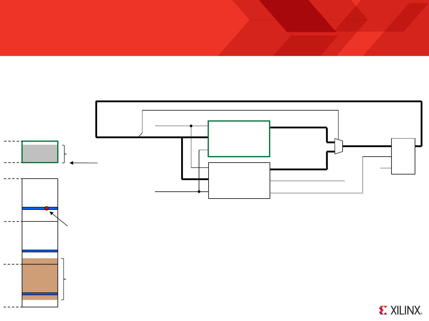
© Copyright 2010-2014 Xilinx
.
Is a Hybrid Technique the Best Solution
for Very High Reliability Designs ?
When using the ECC protected BRAM, all single bit errors are corrected. This also covers cases in which multiple bits are corrupted provided each 72-bit
memory word only contains one error. That leaves only the slightest possibility of a encountering a double bit error (‘DBITERR’); so slight that such an event
has yet to be observed even during beam testing of 7-Series devices. But if you have a signal to tell you that it has occurred then what do you do if it did pulse
High during operation? The only way to fully recover is to reconfigure the device. However, it will often be helpful if KCPSM6 can continue to help the system
as it prepares to take this recovery action (e.g. to make a report and to gracefully shut down the peripherals that it controls before stopping).
000
1FF
200
3FF
400
5FF
Code most
used during
normal
operation
Special
code
Double
bit
error
086
286
486
800
8FF
instruction(17:0)
clk DBITERR
SBITERR
ECC protected
PicoBlaze
Program memory
instruction(17:0) enable
Slice-Based
PicoBlaze
Program memory
(11)
instruction(17:0)
KCPSM6
clk
address(11:0)
interrupt
The hybrid arrangement shown above uses an ECC protected BRAM (page 119) and a Slice-based ROM (page 117).
The main program resides in the ECC protected BRAM. The example illustrated on the left shows that an upset has
caused one of the 72-bit memory words to have a double bit error. When KCPSM6 fetches the instruction from address
086 the ‘DBITERR’ status will go High. Although there is only a 1 in 4 chance of the instruction being corrupted,
‘DBITERR’ is used to interrupt KCPSM6 and force it to start executing code from the Slice-based ROM. Although an
interrupt is used, the special code will never return (RETURNI); it will only perform the operations required to shut the
system down gracefully. When KCPSM6 responds to an interrupt it automatically disables any further interrupts (page
84) so it will not react to any ‘DBITERR’ pulses that may continue to be generated by the ECC protected memory. The
Slice-based ROM has a total nominal FIT rate of 1.80 (page 117) but this memory is always being kept clean by the
device level Readback CRC and frame ECC mechanisms so there is an extremely high confidence in its integrity at the
moment that it is required. In contrast, notice that if the special code was also located in the ECC BRAM then KCPSM6
could execute a corrupted instruction (e.g. at address 486 in the example).
interrupt_vector
ECC Memory
Slice-based ROM
Hint - The real limiting factor is the 0.40 FIT of the logic and interconnect (i.e. not the ECC protected memory).
So the ‘Best Solution’ for high reliability is still debateable
Page 124
