LEA 6 NEO MAX Hardware Integration Manual (GPS.G6 HW 09007 H)
User Manual: Pdf
Open the PDF directly: View PDF ![]() .
.
Page Count: 87
- /
- Preface
- Contents
- Hardware description
- Design-in
- Checklist
- LEA-6 design
- NEO-6 design
- MAX-6 design
- Layout
- Antenna and antenna supervisor
- Passive antenna
- Active antenna (LEA-6)
- Active antenna bias power (LEA-6)
- Active antenna supervisor (LEA-6)
- Active antenna (NEO-6 and MAX-6)
- External active antenna supervisor using ANTOFF (NEO-6)
- External active antenna supervisor using ANTON (MAX-6)
- External active antenna control (NEO-6)
- External active antenna control (MAX-6)
- GPS antenna placement for LEA-6R
- Product handling
- Packaging, shipping, storage and moisture preconditioning
- Soldering
- EOS/ESD/EMI Precautions
- Product testing
- Appendix
- Abbreviations
- Migration to u-blox-6 receivers
- Interface Backgrounder
- DR calibration
- Related documents
- Revision history
- Contact
LEA-6 / NEO-6 / MAX-6
u-blox 6 GPS Modules
Hardware Integration Manual
Abstract
This document describes the features and specifications of the cost
effective and high-performance LEA-6, NEO-6 and MAX-6 GPS
modules featuring the u-blox 6 positioning engine.
These compact, easy to integrate stand-alone GPS receiver modules
combine exceptional GPS performance with highly flexible power,
design, and connectivity options. Their compact form factors and
SMT pads allow fully automated assembly with standard pick &
place and reflow soldering equipment for cost-efficient, high-
volume production enabling short time-to-market.
locate, communicate, accelerate
www.u-blox.com
LEA-6 / NEO-6 / MAX-6 - Hardware Integration Manual
GPS.G6-HW-09007-H Page 2 of 87
Document Information
Title
LEA-6 / NEO-6 / MAX-6
Subtitle
u-blox 6 GPS Modules
Document type
Hardware Integration Manual
Document number
GPS.G6-HW-09007-H
Document status
Preliminary
Document status information
Objective
Specification
This document contains target values. Revised and supplementary data will be published
later.
Advance
Information
This document contains data based on early testing. Revised and supplementary data will
be published later.
Preliminary
This document contains data from product verification. Revised and supplementary data
may be published later.
Released
This document contains the final product specification.
This document applies to the following products:
Name
Type number
ROM/FLASH version
LEA-6H
All
FW6.02, FW 7.01, FW 7.03
LEA-6S
All
ROM6.02, ROM7.03
LEA-6A
All
ROM6.02, ROM7.03
LEA-6T-0
All
ROM6.02, ROM7.03
LEA-6T-1
All
FW 7.03
LEA-6R
All
FW DR 1.0, FW 7.03 DR2.0
NEO-6G
All
ROM6.02, ROM7.03
NEO-6Q
All
ROM6.02, ROM7.03
NEO-6M
All
ROM6.02, ROM7.03
NEO-6P
All
ROM6.02
NEO-6T
All
ROM7.03
NEO-6V
All
ROM7.03
MAX-6G
All
ROM7.03
MAX-6Q
All
ROM7.03

LEA-6 / NEO-6 / MAX-6 - Hardware Integration Manual
GPS.G6-HW-09007-H Preliminary Preface
Page 3 of 87
This document and the use of any information contained therein, is subject to the acceptance of the u-blox terms and conditions. They
can be downloaded from www.u-blox.com.
u-blox makes no warranties based on the accuracy or completeness of the contents of this document and reserves the right to make
changes to specifications and product descriptions at any time without notice.
u-blox reserves all rights to this document and the information contained herein. Reproduction, use or disclosure to third parties without
express permission is strictly prohibited. Copyright © 2011, u-blox AG.
u-blox® is a registered trademark of u-blox Holding AG in the EU and other countries. ARM® is the registered trademark of ARM Limited in
the EU and other countries.
LEA-6 / NEO-6 / MAX-6 - Hardware Integration Manual
GPS.G6-HW-09007-H Preliminary Preface
Page 4 of 87
Preface
u-blox Technical Documentation
As part of our commitment to customer support, u-blox maintains an extensive volume of technical
documentation for our products. In addition to our product-specific technical data sheets, the following manuals
are available to assist u-blox customers in product design and development.
GPS Compendium: This document, also known as the GPS book, provides a wealth of information
regarding generic questions about GPS system functionalities and technology.
Receiver Description including Protocol Specification: Messages, configuration and functionalities of
the u-blox 6 software releases and receivers are explained in this document.
Hardware Integration Manual: This Manual provides hardware design instructions and information on
how to set up production and final product tests.
Application Note: document provides general design instructions and information that applies to all u-blox
GPS receivers. See Section Design-in for a list of Application Notes related to your GPS receiver.
How to use this Manual
The LEA-6 / NEO-6 / MAX-6 Hardware Integration Manual provides the necessary information to successfully
design in and configure these u-blox 6-based GPS receiver modules. For navigating this document please note
the following:
This manual has a modular structure. It is not necessary to read it from the beginning to the end. To help in
finding needed information, a brief section overview is provided below:
1. Hardware description: This chapter introduces the basics of function and architecture of the u-blox 6
modules.
2. Design-in: This chapter provides the Design-In information necessary for a successful design.
3. Product handling: This chapter defines packaging, handling, shipment, storage and soldering.
4. Product testing: This chapter provides information about testing of OEM receivers in production.
5. Appendix: The Appendix includes guidelines on how to successfully migrate to u-blox 6 designs, and useful
information about the different antenna types available on the market and how to reduce interference in
your GPS design.
The following symbols are used to highlight important information within the manual:
An index finger points out key information pertaining to module integration and performance.
A warning symbol indicates actions that could negatively impact or damage the module.
Questions
If you have any questions about u-blox 6 Hardware Integration, please:
Read this manual carefully.
Contact our information service on the homepage http://www.u-blox.com
Read the questions and answers on our FAQ database on the homepage http://www.u-blox.com

LEA-6 / NEO-6 / MAX-6 - Hardware Integration Manual
GPS.G6-HW-09007-H Preliminary Preface
Page 5 of 87
Technical Support
Worldwide Web
Our website (www.u-blox.com) is a rich pool of information. Product information, technical documents and
helpful FAQ can be accessed 24h a day.
By E-mail
If you have technical problems or cannot find the required information in the provided documents, contact the
nearest of the Technical Support offices by email. Use our service pool email addresses rather than any personal
email address of our staff. This makes sure that your request is processed as soon as possible. You will find the
contact details at the end of the document.
Helpful Information when Contacting Technical Support
When contacting Technical Support please have the following information ready:
Receiver type (e.g. LEA-6A-0-000), Datacode (e.g. 160200.0300.000) and firmware version (e.g. FW6.02)
Receiver configuration
Clear description of your question or the problem together with a u-center logfile
A short description of the application
Your complete contact details

LEA-6 / NEO-6 / MAX-6 - Hardware Integration Manual
GPS.G6-HW-09007-H Preliminary Contents
Page 6 of 87
Contents
Preface ................................................................................................................................ 4
Contents .............................................................................................................................. 6
1 Hardware description ................................................................................................ 10
1.1 Overview ............................................................................................................................................ 10
1.2 Architecture ........................................................................................................................................ 10
1.3 Power management ........................................................................................................................... 11
1.3.1 Connecting power ...................................................................................................................... 11
1.3.2 Operating modes ........................................................................................................................ 12
1.4 Antenna supply - V_ANT (LEA-6) ........................................................................................................ 12
1.5 System functions ................................................................................................................................ 13
1.5.1 System monitoring ...................................................................................................................... 13
1.6 Interfaces ............................................................................................................................................ 13
1.6.1 UART ........................................................................................................................................... 13
1.6.2 USB (LEA-6/NEO-6) ...................................................................................................................... 13
1.6.3 Display Data Channel (DDC) ........................................................................................................ 14
1.6.4 SPI (NEO-6, LEA-6R) ..................................................................................................................... 16
1.7 I/O pins ............................................................................................................................................... 19
1.7.1 RESET_N ...................................................................................................................................... 19
1.7.2 EXTINT - External interrupt pin ..................................................................................................... 19
1.7.3 AADET_N (LEA-6) ........................................................................................................................ 19
1.7.4 Configuration pins (LEA-6S/6A, NEO-6) ....................................................................................... 19
1.7.5 Second time pulse for LEA-6T ...................................................................................................... 19
1.7.6 TX ready signal (FW 7.0x) ............................................................................................................ 20
1.7.7 ANTOFF (NEO-6) .......................................................................................................................... 20
1.7.8 Antenna supervision signals for LEA-6T-0 .................................................................................... 20
1.7.9 LEA-6R considerations ................................................................................................................. 21
2 Design-in ..................................................................................................................... 22
2.1 Checklist ............................................................................................................................................. 22
2.1.1 Design-in checklist ....................................................................................................................... 22
2.1.2 Design considerations .................................................................................................................. 24
2.1.3 Automotive Dead Reckoning (ADR) solutions .............................................................................. 25
2.2 LEA-6 design ...................................................................................................................................... 26
2.2.1 LEA-6 passive antenna design ...................................................................................................... 26
2.2.2 GLONASS HW design recommendations ..................................................................................... 27
2.2.3 LEA-6R design ............................................................................................................................. 31
2.2.1 Pin description for LEA-6 designs ................................................................................................. 35
2.3 NEO-6 design ..................................................................................................................................... 36
2.3.1 Passive antenna design (NEO-6) ................................................................................................... 36

LEA-6 / NEO-6 / MAX-6 - Hardware Integration Manual
GPS.G6-HW-09007-H Preliminary Contents
Page 7 of 87
2.3.2 Pin description for NEO-6 designs ................................................................................................ 38
2.4 MAX-6 design .................................................................................................................................... 39
2.4.1 MAX-6 passive antenna design.................................................................................................... 39
2.4.2 Pin description for MAX-6 designs ............................................................................................... 40
2.5 Layout ................................................................................................................................................ 40
2.5.1 Footprint and paste mask ............................................................................................................ 40
2.5.2 Placement ................................................................................................................................... 42
2.5.3 Antenna connection and grounding plane design ....................................................................... 43
2.5.4 Antenna micro strip ..................................................................................................................... 44
2.6 Antenna and antenna supervisor ........................................................................................................ 45
2.6.1 Passive antenna ........................................................................................................................... 46
2.6.2 Active antenna (LEA-6) ................................................................................................................ 46
2.6.3 Active antenna bias power (LEA-6) .............................................................................................. 47
2.6.4 Active antenna supervisor (LEA-6)................................................................................................ 48
2.6.5 Active antenna (NEO-6 and MAX-6) ............................................................................................ 51
2.6.6 External active antenna supervisor using ANTOFF (NEO-6) ........................................................... 53
2.6.7 External active antenna supervisor using ANTON (MAX-6) ........................................................... 54
2.6.8 External active antenna control (NEO-6) ...................................................................................... 55
2.6.9 External active antenna control (MAX-6) ..................................................................................... 56
2.6.10 GPS antenna placement for LEA-6R ............................................................................................. 56
3 Product handling ........................................................................................................ 57
3.1 Packaging, shipping, storage and moisture preconditioning ............................................................... 57
3.2 Soldering ............................................................................................................................................ 57
3.2.1 Soldering paste............................................................................................................................ 57
3.2.2 Reflow soldering ......................................................................................................................... 57
3.2.3 Optical inspection ........................................................................................................................ 58
3.2.4 Cleaning ...................................................................................................................................... 59
3.2.5 Repeated reflow soldering ........................................................................................................... 59
3.2.6 Wave soldering............................................................................................................................ 59
3.2.7 Hand soldering ............................................................................................................................ 59
3.2.8 Rework ........................................................................................................................................ 59
3.2.9 Conformal coating ...................................................................................................................... 60
3.2.10 Casting ........................................................................................................................................ 60
3.2.11 Grounding metal covers .............................................................................................................. 60
3.2.12 Use of ultrasonic processes .......................................................................................................... 60
3.3 EOS/ESD/EMI Precautions .................................................................................................................... 60
3.3.1 Abbreviations .............................................................................................................................. 60
3.3.2 Electrostatic discharge (ESD) ........................................................................................................ 60
3.3.3 ESD handling precautions ............................................................................................................ 61
3.3.4 ESD protection measures ............................................................................................................. 62
3.3.5 Electrical Overstress (EOS) ............................................................................................................ 62
3.3.6 EOS protection measures ............................................................................................................. 62
3.3.7 Electromagnetic interference (EMI) .............................................................................................. 63

LEA-6 / NEO-6 / MAX-6 - Hardware Integration Manual
GPS.G6-HW-09007-H Preliminary Contents
Page 8 of 87
3.3.8 Applications with wireless modules LEON / LISA .......................................................................... 64
3.3.9 Recommended parts ................................................................................................................... 66
4 Product testing ........................................................................................................... 67
4.1 u-blox in-series production test ........................................................................................................... 67
4.2 Test parameters for OEM manufacturer .............................................................................................. 67
4.3 System sensitivity test ......................................................................................................................... 68
4.3.1 Guidelines for sensitivity tests ...................................................................................................... 68
4.3.2 ―Go/No go‖ tests for integrated devices ........................................................................................ 68
4.3.3 Testing LEA-6R designs ................................................................................................................ 68
4.3.4 Testing NEO-6V designs .............................................................................................................. 69
Appendix .......................................................................................................................... 70
A Abbreviations ............................................................................................................. 70
B Migration to u-blox-6 receivers ................................................................................. 70
B.1 Checklist for migration ....................................................................................................................... 70
B.2 Software migration ............................................................................................................................. 72
B.2.1 Software migration from ANTARIS 4 or u-blox 5 to a u-blox 6 GPS receiver ................................. 72
B.2.2 Software migration from 6.02 to 7.03 ......................................................................................... 73
B.3 Hardware Migration ........................................................................................................................... 73
B.3.1 Hardware Migration: ANTARIS 4 u-blox 6 ............................................................................... 73
B.3.2 Hardware Migration: u-blox 5 u-blox 6 ................................................................................... 73
B.4 Migration of LEA modules .................................................................................................................. 74
B.4.1 Migration from LEA-4 to LEA-6 ................................................................................................... 74
B.4.2 Migration of LEA-4R designs to LEA-6R ....................................................................................... 75
B.4.3 Migration from LEA-5 to LEA-6 ................................................................................................... 76
B.5 Migration of NEO modules ................................................................................................................. 76
B.5.1 Migration from NEO-4S to NEO-6................................................................................................ 76
B.5.2 Migration from NEO-5 to NEO-6 ................................................................................................. 77
C Interface Backgrounder ............................................................................................. 78
C.1 DDC Interface ..................................................................................................................................... 78
C.1.1 Addresses, roles and modes ........................................................................................................ 78
C.1.2 DDC troubleshooting .................................................................................................................. 79
C.2 SPI Interface ........................................................................................................................................ 80
C.2.1 SPI basics ..................................................................................................................................... 80
D DR calibration ............................................................................................................. 83
D.1 Constraints ......................................................................................................................................... 83
D.2 Initial calibration drive ......................................................................................................................... 83
Related documents........................................................................................................... 85
Revision history ................................................................................................................ 86

LEA-6 / NEO-6 / MAX-6 - Hardware Integration Manual
GPS.G6-HW-09007-H Preliminary Hardware description
Page 10 of 87
1 Hardware description
1.1 Overview
The u-blox 6 leadless chip carrier (LCC) modules are standalone GPS receivers featuring the high performance
u-blox-6 positioning engine. These compact, easy to integrate modules combine exceptional GPS performance
with highly flexible power, design, and connectivity options. Their compact form factors and SMT pads allow
fully automated assembly with standard pick & place and reflow-soldering equipment for cost-efficient, high-
volume production enabling short time-to-market.
u-blox GPS modules are not designed for life saving or supporting devices or for aviation and should not be used
in products that could in any way negatively impact the security or health of the user or third parties or that
could cause damage to goods.
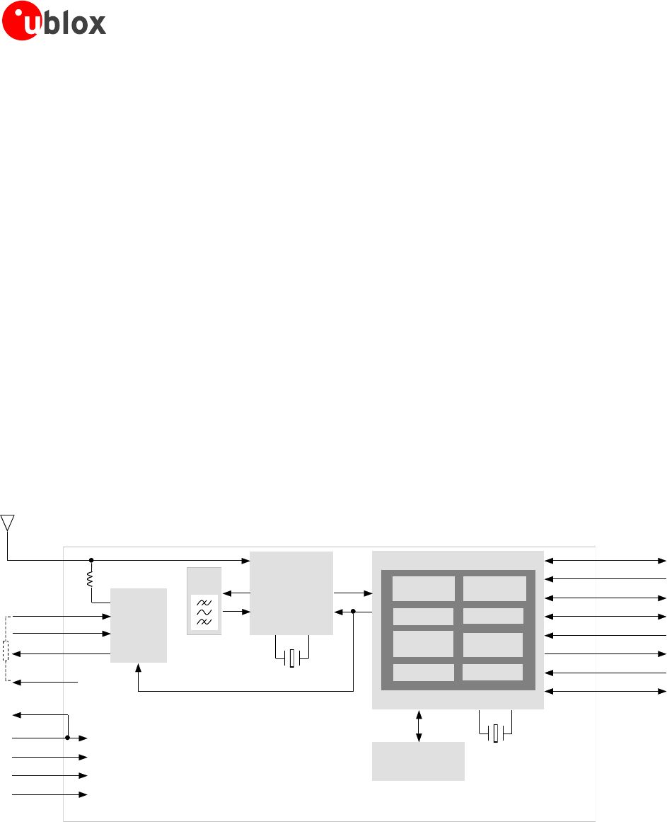
1.2 Architecture
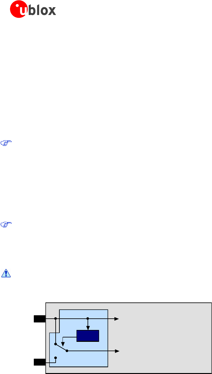
u-blox 6 LCC modules consist of two functional parts - the RF and the Baseband sections. See Figure 1 for block
diagrams of the modules.
The RF Front-End includes the input matching elements, the SAW bandpass filter, the u-blox 6 RF-IC (with
integrated LNA) and the frequency source.
The Baseband section contains the u-blox 6 Baseband processor, the RTC crystal and additional elements such as
the optional FLASH Memory for enhanced programmability and flexibility.
RF Front-End
with
Integrated LNA
Baseband Processor
Power
Management
TCXO or
Crystal
RTC
Cr y s ta l
(optiona l)
FLASH EPROM
(optional)
Antenna
Supervision
& Supply
(optional)
Power Control
RF_IN
V_ANT
AADET_N
VCC_RF
VCC
V_BACKUP
GND
VCC_OUT
UART
EXTINT
RESET_N
USB V2.0
CFG
Digital
IF Filter
Backup
RAM
ROM Code
GPS/GALILEO
Engine
ARM7TDMI-S®
SRAM
TIMEPULSE
SAW
Filter
RTC DDC
SPI (optional)
VCC_IO
ANTON
Figure 1: u-blox-6 block diagram
LEA-6 / NEO-6 / MAX-6 - Hardware Integration Manual
GPS.G6-HW-09007-H Preliminary Hardware description
Page 11 of 87
1.3 Power management
1.3.1 Connecting power
u-blox 6 receiver modules have three power supply pins: VCC, V_BCKP and VDDUSB.
(No VDDUSB for MAX-6)
1.3.1.1 VCC - main power
The main power supply is fed through the VCC pin. During operation, the current drawn by the u-blox 6 GPS
module can vary by some orders of magnitude, especially, if low-power operation modes are enabled. It is
important that the system power supply circuitry is able to support the peak power (see datasheet for
specification) for a short time. In order to define a battery capacity for specific applications the sustained power
figure shall be used.
When switching from backup mode to normal operation or at start-up u-blox 6 modules must charge the
internal capacitors in the core domain. In certain situations this can result in a significant current draw. For
low power applications using Power Save and backup modes it is important that the power supply or low
ESR capacitors at the module input can deliver this current/charge.
1.3.1.2 V_BCKP - backup battery
In case of a power failure on pin VCC, the real-time clock and backup RAM are supplied through pin V_BCKP.
This enables the u-blox 6 receiver to recover from a power failure with either a Hotstart or a Warmstart
(depending on the duration of VCC outage) and to maintain the configuration settings saved in the backup
RAM. If no backup battery is connected, the receiver performs a Coldstart at power up.
If no backup battery is available connect the V_BCKP pin to GND.
As long as VCC is supplied to the u-blox 6 receiver, the backup battery is disconnected from the RTC and the
backup RAM in order to avoid unnecessary battery drain (see Figure 2). Power to RTC and BBR is supplied from
VCC in this case.
Avoid high resistance on the on the V_BCKP line: During the switch from main supply to backup
supply a short current adjustment peak can cause high voltage drop on the pin and possible
malfunctions.
VCC
V_BCKP
Voltage
Supervisor
Module Voltage Supply
RTC and Battery Backup RAM (BBR)
J1
Figure 2: Backup Battery and Voltage
1.3.1.3 VDD_USB - USB interface power supply
On LEA-6 and NEO-6 VDD_USB supplies the USB interface. If the USB interface is not used, the VDD_USB pin
must be connected to GND. For more information regarding the correct handling of VDD_USB see section
1.6.2.1

LEA-6 / NEO-6 / MAX-6 - Hardware Integration Manual
GPS.G6-HW-09007-H Preliminary Hardware description
Page 12 of 87
1.3.2 Operating modes
u-blox 6 modules with FW 7.0x or ROM6.02 have two continuous operating modes (Maximum Performance and
Eco) and one intermittent operating mode (Power Save mode). Maximum Performance mode freely uses the
acquisition engine, resulting in the best possible TTFF, while Eco mode optimizes the use of the acquisition
engine to deliver lower current consumption. At medium to strong signals, there is almost no difference for
acquisition and tracking performance in these modes.
1.3.2.1 Maximum Performance mode
In Maximum Performance mode, u-blox 6 receivers use the acquisition engine at full performance to search for
all possible satellites until the Almanac is completely downloaded.
As a consequence, tracking current consumption level will be achieved when:
A valid GPS position is fixed
Almanac is entirely downloaded
Ephemeris for all satellites in view are valid
1.3.2.2 Eco mode
In Eco mode, u-blox 6 receivers use the acquisition engine to search for new satellites only when needed for
navigation:
In cold starts, u-blox 6 searches for enough satellites to navigate and optimizes use of the acquisition
engine to download their ephemeris.
In non-cold starts, u-blox 6 focuses on searching for visible satellites whose orbits are known from the
Almanac.
In Eco mode, the u-blox 6 acquisition engine limits use of its searching resources to minimize power
consumption. As a consequence the time to find some satellites at weakest signal level might be slightly
increased in comparison to the Maximum Performance mode.
u-blox 6 deactivates the acquisition engine as soon as a position is fixed and a sufficient number (at least 4) of
satellites are being tracked. The tracking engine continues to search and track new satellites without orbit
information.
1.3.2.3 Power Save mode
u-blox 6 receivers include a Power Save Mode. Its operation is called cyclic tracking and allows reducing the
average power consumption significantly. The Power Save Mode can be configured for different update periods.
u-blox recommends an update period of 1s for best GPS performance. For more information, see the u-blox 6
Receiver Description including Protocol Specification [3]
Dead Reckoning, PPP and Precision Timing features should not be used together with Power Save Mode.
1.4 Antenna supply - V_ANT (LEA-6)
LEA-6 modules support active antenna supply and supervision use the pin V_ANT to supply the active antenna.
Use a 10 resistor in front of V_ANT. For more information about antenna and antenna supervisor see chapter
2.6.
If not used, connect the V_ANT pin to GND.
LEA-6 / NEO-6 / MAX-6 - Hardware Integration Manual
GPS.G6-HW-09007-H Preliminary Hardware description
Page 13 of 87
1.5 System functions
1.5.1 System monitoring
The u-blox-6 receiver modules provide system monitoring functions that allow the operation of the embedded
processor and associated peripherals to be supervised. These System Monitoring functions are output as part of
the UBX protocol, class ―MON‖.
Please refer to the u-blox 6 Receiver Description including Protocol Specification [3]. For more information on
UBX messages, serial interfaces for design analysis and individual system monitoring functions.
1.6 Interfaces
1.6.1 UART
u-blox 6 modules include a Universal Asynchronous Receiver Transmitter (UART) serial interface. RxD1/TxD1
supports data rates from 4.8 to 115.2 kBit/s. The signal output and input levels are 0 V to VCC. An interface
based on RS232 standard levels (+/- 12 V) can be realized using level shifters such as Maxim MAX3232.
Hardware handshake signals and synchronous operation are not supported.
For more information see the LEA-6 Data Sheet [1], NEO-6 Data Sheet [2]or MAX-6 Data Sheet [8]
1.6.2 USB (LEA-6/NEO-6)
The u-blox 6 Universal Serial Bus (USB) interface supports the full-speed data rate of 12 Mbit/s.
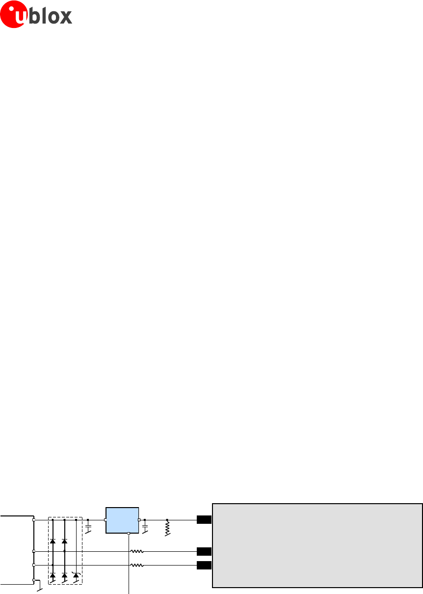
1.6.2.1 USB external components
The USB interface requires some external components in order to implement the physical characteristics required
by the USB 2.0 specification. These external components are shown in Figure 3 and listed in Table 1.
In order to comply with USB specifications, VBUS must be connected through a LDO (U1) to pin VDD_USB of
the module.
If the USB device is self-powered it is possible that the power supply (VCC) is shut down and the Baseband-IC
core is not powered. Since VBUS is still available, it still would be signaled to the USB host that the device is
present and ready to communicate. This is not desired and thus the LDO (U1) should be disabled using the
enable signal (EN) of the VCC-LDO or the output of a voltage supervisor. Depending on the characteristics of the
LDO (U1) it is recommended to add a pull-down resistor (R11) at its output to ensure VDD_USB is not floating if
LDO (U1) is disabled or the USB cable is not connected i.e. VBUS is not supplied.
If the device is bus-powered, LDO (U1) does not need an enable control.
Module
VDD_USB
LDO
VDD_USB
R4
USB_DP
USB_DM
R5
C24 C23
D2
VBUS
DP
DM
GND
USB Device Connector
U1
EN R11
EN
Figure 3: USB Interface
LEA-6 / NEO-6 / MAX-6 - Hardware Integration Manual
GPS.G6-HW-09007-H Preliminary Hardware description
Page 14 of 87
Name
Component
Function
Comments
U1
LDO
Regulates VBUS (4.4 …5.25 V)
down to a voltage of 3.3 V.
Almost no current requirement (~1 mA) if the GPS receiver is operated as a USB
self-powered device, but if bus-powered LDO (U1) must be able to deliver the
maximum current of ~70 mA. A low-cost DC/DC converter such as LTC3410
from Linear Technology may be used as an alternative.
C23,
C24
Capacitors
Required according to the specification of LDO U1
D2
Protection
diodes
Protect circuit from overvoltage
/ ESD when connecting.
Use low capacitance ESD protection such as ST Microelectronics USBLC6-2.
R4, R5
Serial
termination
resistors
Establish a full-speed driver
impedance of 28…44
A value of 22 is recommended.
R11
Resistor
10 k is recommended for USB self-powered setup. For bus-powered setup
R11 can be ignored.
Table 1: Summary of USB external components
1.6.3 Display Data Channel (DDC)
An I2C compatible Display Data Channel (DDC) interface is available with LEA-6, NEO-6 and MAX-6 modules for
serial communication. For more information about DDC implementation refer to the u-blox 6 Receiver
Description including Protocol Specification [3]. Background information about the DDC interface is available in
Appendix C.1.
u-blox 6 GPS receivers normally run in I2C slave mode. Master Mode is only supported when external
EEPROM is used to store configuration. No other nodes may be connected to the bus. In this case, the
receiver attempts to establish presence of such a non-volatile memory component by writing and reading
from a specific location.
TX ready indicator (data ready) for FW 7.0x see 1.7.6
The u-blox 6 DDC interface supports serial communication with u-blox wireless modules. See the
specification of the applicable wireless module to confirm compatibility.
With u-blox 6, when reading the DDC internal register at address 0xFF (messages transmit buffer), the
master must not set the reading address before every byte accessed as this could cause a faulty behavior.
Since after every byte being read from register 0xFF the internal address counter is incremented by one
saturating at 0xFF, subsequent reads can be performed continuously.
Pins SDA2 and SCL2 have internal 13 k pull-ups. If capacitive bus load is very large, additional external pull-ups
may be needed in order to reduce the pull-up resistance.
Table 2 lists the maximum total pull-up resistor values for the DDC interface. For small loads, e.g. if just
connecting to an external EEPROM, these built-in pull-ups are sufficient.
Load Capacitance
Pull-Up Resistor Value R20, R21
50 pF
N/A
100 pF
18 k
250 pF
4.7 k
Table 2: Pull-up resistor values for DDC interface
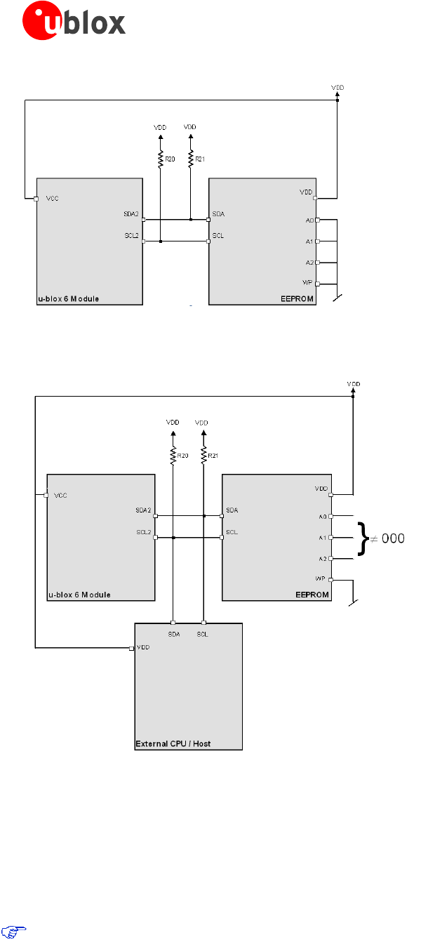
1.6.3.1 Communicating to an I2C EEPROM with the GPS receiver as I2C master
Serial I2C memory can be connected to the DDC interface. This can be used to save configuration permanently. It
will automatically be recognized by firmware. The memory address must be set to 0b10100000 (0xA0) and the
size fixed to 4 kB.
LEA-6 / NEO-6 / MAX-6 - Hardware Integration Manual
GPS.G6-HW-09007-H Preliminary Hardware description
Page 15 of 87
Figure 4: Connecting external serial I2C memory used by the GPS receiver (see EEPROM data sheet for exact pin orientation)
Figure 5: Connecting external serial I2C memory used by external host (see data sheet for exact pin orientation)
Note that the case shown on Figure 4 is different than the case when EEPROM is present but used by external
host / CPU as indicated on Figure 5. This is allowed but precaution is required to ensure that the GPS receiver
does not detect the EEPROM device, which would effectively configure the GPS receiver to be MASTER on the
bus causing collision with the external host.
To ensure that the EEPROM device (connected to the bus and used by the host) is not detected by the GPS
receiver it is important to set the EEPROM‖s address to a value different than 0xA0. This way EEPROM remains
free to be used for other purposes and the GPS receiver will assume the SLAVE mode.
Ensure that at the start up the host allows enough time for the receiver to communicate over the bus to
establish presence of the EEPROM. It is only when this interrogation is complete that the host can exercise
full control over the bus (MASTER mode).
LEA-6 / NEO-6 / MAX-6 - Hardware Integration Manual
GPS.G6-HW-09007-H Preliminary Hardware description
Page 16 of 87
Also note that the FLASH based modules do not attempt to store any information in the external EEPROM
and as such do not attempt to communicate to the external EEPROM. The ROM based receivers always
interrogate external EEPROM at the start-up. The interrogation process is guaranteed to complete within
250ms upon start up. This is the time the external host has to give to the ROM based GPS receiver to
complete the EEPROM interrogation.
Although the FLASH based modules do not attempt to detect the EEPROM at the start up, an attempt to
communicate to the GPS receiver via DDC before 250 msec expires is not advised because the GPS
receiver is unable to respond due to other start up activities.
Following I2C serial EEPROM are supported:
Manufacturer
Order No.
ST
M24C32-R
Microchip
24AA32A
Catalyst
CAT24C32
Samsung
S524AB0X91
Table 3: Recommend parts list for I2C Serial EEPROM memory
1.6.4 SPI (NEO-6, LEA-6R)
A Serial Peripheral Interface (SPI) is available with u-blox 6 NEO modules. The SPI allows for the connection of
external devices with a serial interface, e.g. FLASH memories or A/D converters, or to interface to a host CPU.
LEA-6R includes a Serial Peripheral Interface (SPI) for connecting external sensors. The interface can be operated
in SPI master mode only. Two chip select signals are available to select external slaves. See 2.2.3.1
TX ready indicator (data ready) for LEA-6H (FW 7.0x) see 1.7.6
Background information about the SPI interface is available in Appendix C.2.
1.6.4.1 Connecting SPI FLASH memory (NEO-6 modules)
SPI FLASH memory can be connected to the SPI interface to save Assist Now Offline data and/or receiver
configuration. It will automatically be recognized by firmware when connected to SS_N.
Figure 6 shows how external memory can be connected. Minimum SPI FLASH memory size is 1 Mbit.
u-blox GPS Receiver SPI Master
SS_N
MISO
SCS_N
MI
VDD
MOMOSI
SCK SCK
VDD
Figure 6: Connecting external SPI Memory to u-blox GPS receivers
LEA-6 / NEO-6 / MAX-6 - Hardware Integration Manual
GPS.G6-HW-09007-H Preliminary Hardware description
Page 17 of 87
Following SPI serial Flash are supported:
Manufacturer
Order No.
Winbond
W25X10A
Winbond
W25X20A
AMIC
A25L010
AMIC
A25L020
Table 4: Supported SPI FLASH memory devices
Only use serial FLASH types listed in Table 4. For new designs confirm if the listed type is still available. It is
not possible to use other serial FLASH types than those listed in Table 4 with u-blox 6 receivers.
1.6.4.2 SPI communication (connecting to an SPI master) NEO-6
Figure 7 shows how to connect a u-blox GPS receiver to a host/master. The signal on the pins must meet the
conditions specified in the Data Sheet.
u-blox GPS Receiver SPI Master
SS_N
MISO
SCS_N
MI
VDD
MOMOSI
SCK SCK
VDD
Figure 7: Connecting to SPI Master
For those u-blox 6 modules supporting SPI the SPI MOSI, MISO and SCK pins share a configuration
function at start up. To secure correct receiver operation make sure that the SS_N pin is high at start up.
Afterwards the SPI function will not affect the configuration pins.
LEA-6 / NEO-6 / MAX-6 - Hardware Integration Manual
GPS.G6-HW-09007-H Preliminary Hardware description
Page 18 of 87
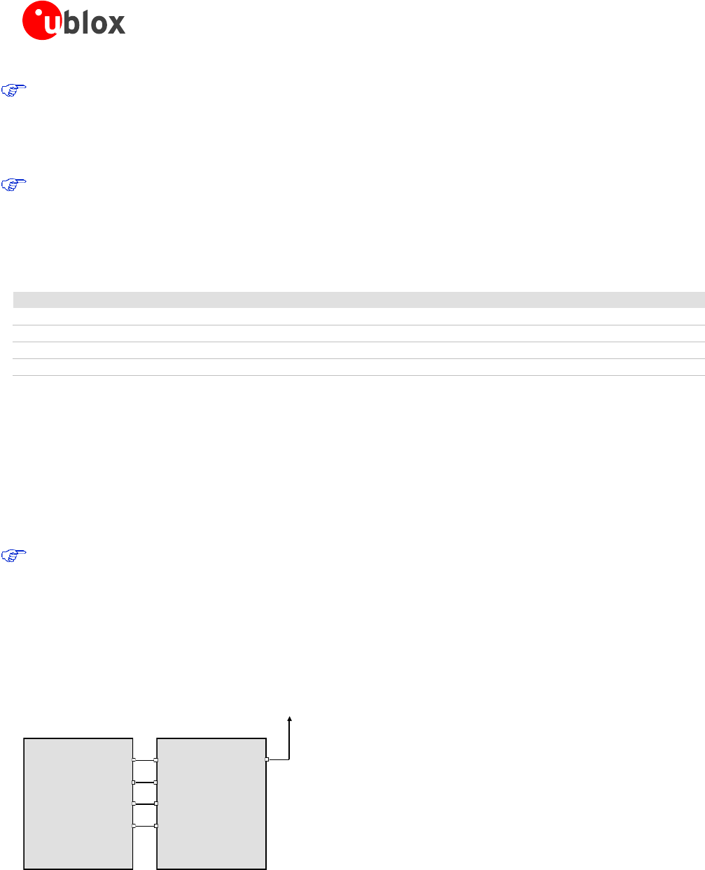
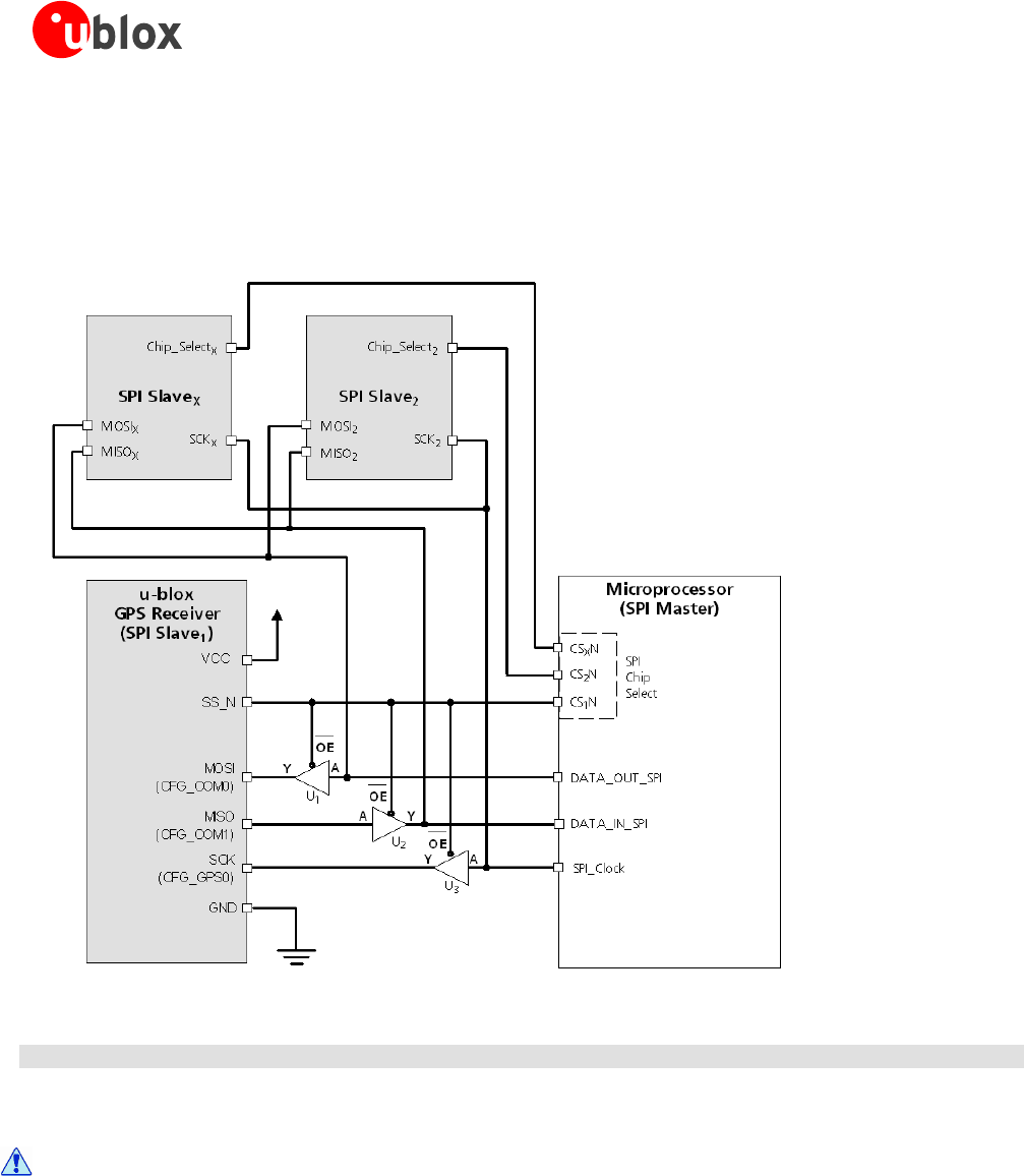
1.6.4.3 Pin configuration with module as one of several slaves
The buffers enabled by the CS_N signal make sure that the GPS receiver starts up with a known defined
configuration, since the SPI pins (MOSI, MISO and SCK) are at start up also configuration pins.
Figure 8: Diagram of SPI Pin Configuration
Component
Description
Model
Supplier
U1 – U3
Buffer
NC7SZ125
Fairchild
Table 5: Recommended components for SPI pin configuration
Use same power voltage to supply U1 – U3 and VCC.
LEA-6 / NEO-6 / MAX-6 - Hardware Integration Manual
GPS.G6-HW-09007-H Preliminary Hardware description
Page 19 of 87
1.7 I/O pins
1.7.1 RESET_N
LEA-6 modules include a RESET_N pin. Driving RESET_N low activates a hardware reset of the system. RESET_N
is only an input and will not reset external circuitry.
Use components with open drain output (i.e. with buffer or voltage supervisor).
There is an internal pull up resistor of 3.3 k to VCC inside the module that requires that the reset circuitry can
deliver enough current (e.g. 1 mA).
Do not drive RESET_N high.
NEO-6 and MAX-6 modules do not include a RESET_N pin. However, this functionality can be implemented for
these modules by connecting the NEO-6 and MAX-6 pin 8 to pin 9 with a 3.3 k resistor, instead of connecting
them directly. Pin 8 (NEO-6) or pin 9 (MAX-6) can then be used as a RESET_N input with the same
characteristics as the reset pin on LEA-6 modules.
Use caution when implementing RESET_N on NEO-6 and MAX-6 modules since forward
compatibility is not guaranteed.
1.7.2 EXTINT - External interrupt pin
EXTINT0 is an external interrupt pin with fixed input voltage thresholds with respect to VCC (see the data sheet
for more information). It can be used for the time mark function on LEA-6T or for wake-up functions in Power
Save Mode on all u-blox 6 LCC modules. Leave open if unused.
1.7.3 AADET_N (LEA-6)
AADET_N is an input pin and is used to report whether an external circuit has detected an external antenna or
not. Low means the antenna has been detected. High means no external antenna has been detected.
See chapter 2.6.4 for an implementation example.
1.7.4 Configuration pins (LEA-6S/6A, NEO-6)
ROM-based modules provide up to 3 pins (CFG_COM0, CFG_COM1, and CFG_GPS0) for boot-time
configuration. These become effective immediately after start-up. Once the module has started, the
configuration settings can be modified with UBX configuration messages. The modified settings remain effective
until power-down or reset. If these settings have been stored in battery-backup RAM, then the modified
configuration will be retained, as long as the backup battery supply is not interrupted.
The module data sheets indicate the meaning of the configuration pins when they are high (1) or low (0). In fact
no configuration pins need to be pulled high. All have internal pull ups and therefore default to the high (1)
state when left open or connected to a high impedance output. They should be left open unless there is a need
to pull them low to alter the initial configuration.
Some configuration pins are shared with other functions. During start-up, the module reads the state of the
configuration pins. Afterwards the other functions can be used.
The configuration pins of u-blox 6 use an internal pull-up resistor, which determines the default setting.
For more information about settings and messages see the module data sheet.
MAX-6 doesn‖t have pins for boot-time configuration
1.7.5 Second time pulse for LEA-6T
LEA-6T includes a second time pulse pin (TIMEPULSE2). For more information and configuration see the LEA-6
Data Sheet [1]and also the u-blox 6 Receiver Description including Protocol Specification [3].

LEA-6 / NEO-6 / MAX-6 - Hardware Integration Manual
GPS.G6-HW-09007-H Preliminary Hardware description
Page 20 of 87
1.7.6 TX ready signal (FW 7.0x)
The TX ready signal indicates that the receiver has data to transmit. A listener can wait on the TX ready signal
instead of polling the DDC or SPI interfaces. The UBX-CFG-PRT message lets you configure the polarity and the
number of bytes in the buffer before the TX ready signal goes active. The TX ready signal can be mapped to
GPIO 05 (TXD1). The TX ready pin is disabled by default.
u-blox wireless modules (LEON and LISA) configure and enable the TX ready functionality automatically.
For more information on configuration and remap of this pin see the LEA-6 Data Sheet [1] and see also the
u-blox 6 Receiver Description including Protocol Specification [3].
1.7.7 ANTOFF (NEO-6)
The ANTOFF signal can be mapped to GPIO22 (Pin 17). The ANTOFF signal is disabled by default.
To configure the ANTOFF function refer to the u-blox 6 Receiver Description including Protocol
Specification [3].
Use caution when implementing ANTOFF configuration since forward compatibility is not
guaranteed
1.7.8 Antenna supervision signals for LEA-6T-0
With LEA-6T-0, the antenna supervisor GPIOs are numbered differently than the other LEA-6 modules and are
wired to specific PIOs:
ANTOFF is internally mapped to GPIO13
ANTSHORT is internally mapped to GPIO17
AADET_N (Active Antenna Detect) is mapped to GPIO8 (Pin 20)
If the unit is reverted to the default configuration, there is no antenna supply.
The CFG-ANT command sets the PIOs and enables Power Control, Short Circuit Detection, Power Down on Short
and Short Circuit Recovery.
To store the settings permanently send the UBX-CFG-CFG command with the option 'save current parameters'
to BBR AND SPI Flash (!)
See also schematic of open circuit detection Figure 46 .
To configure this function refer to the u-blox 6 Receiver Description including Protocol Specification [3].
LEA-6 / NEO-6 / MAX-6 - Hardware Integration Manual
GPS.G6-HW-09007-H Preliminary Hardware description
Page 21 of 87
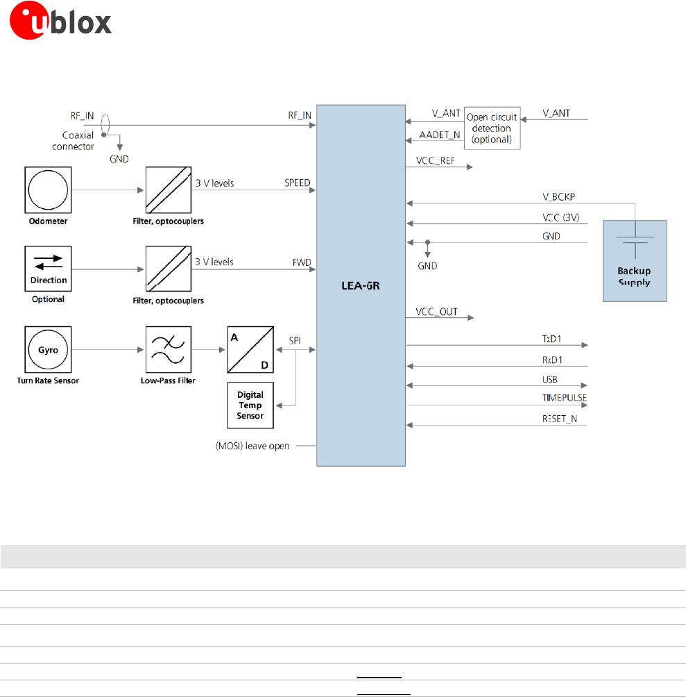
1.7.9 LEA-6R considerations
Figure 9: Block schematic of complete LEA-6R design
LEA-6R includes the following special pins: SPI_MOSI, SPI_MISO, SPI_SCS2_N, FWD, SPI_ SCS1_N, SPI_SCK, and SPEED.
Pin
Signal name
Direction
Usage
27
SPEED
Input
Odometer Speedpulses
23
SCK
Output
SPI clock
22
SPI_SCS1_N
Output
Chip Select signal for ADC/turn rate sensor
21
FWD
Input
Direction indication (1 = forward)
9
SPI_SCS2_N
Output
Chip Select signal for temperature sensor
2
MISO
Input
Serial data (Master In / Slave Out)
1
MOSI
Output
Serial data (Master Out / Slave In), leave open
Table 6: LEA-6R special pins

LEA-6 / NEO-6 / MAX-6 - Hardware Integration Manual
GPS.G6-HW-09007-H Preliminary Design-in
Page 22 of 87
2 Design-in
For migrating existing ANTARIS®4 product designs to u-blox 6 please refer to Appendix B.
In order to obtain good performance with a GPS receiver module, there are a number of points that require
careful attention during the design-in. These include:
Power Supply: Good performance requires a clean and stable power supply.
Interfaces: Ensure correct wiring, rate and message setup on the module and your host system.
Antenna interface: For optimal performance seek short routing, matched impedance and no stubs.
2.1 Checklist
Good performance requires a clean and stable power supply with minimal ripple. Care needs to be exercised in
selecting a strategy to achieve this. Series resistance in the Vcc supply line can negatively impact performance.
For better performance, use an LDO to provide a clean supply at Vcc and consider the following:
Wide power lines or even power planes are preferred.
Place LDO near the module.
Avoid resistive components in the power line (e.g. narrow power lines, coils, resistors, etc.).
Placing a filter or other source of resistance at Vcc can create significantly longer acquisition times.
2.1.1 Design-in checklist
Designing-in a u-blox 6 module is easy, especially when based on a u-blox reference design. Nonetheless, it pays
to do a quick sanity check of the design. This section lists the most important items for a simple design check.
The Design-In Checklist also helps to avoid an unnecessary respin of the PCB and helps to achieve the best
possible performance.
Follow the design-in checklist when developing any u-blox 6 GPS applications. This can significantly
reduce development time and costs.
Have you chosen the optimal module?
u-blox 6 modules have been intentionally designed to allow GPS receivers to be optimally tailored to specific
applications. Changing between the different variants is easy.
Do you need TCXO performance – Then choose an H
1
, S
2
, Q
3
or G
4
variant.
Do you want to be able to upgrade the firmware? Then you will have to use a Programmable receiver
module: choose an H1 variant.
Do you need USB? All LEA-6 and NEO-6 modules support USB.
Do you need Dead Reckoning – Then choose a LEA-6R or NEO-6V (see section 2.1.3)
Do you need Precise Point Positioning – Then choose a NEO-6P
Do you need Precision Timing – Then choose a LEA-6T or NEO-6T.
Do you need onboard Antenna Supervisor circuitry - Then choose the LEA form factor.
Do you need onboard Antenna control - Then choose the MAX form factor.
Du you need smallest size and forward compatibility- Then choose the MAX form factor.
Do you need low power - Then choose 1.8V 6G module variant.
1
LEA-6H
2
LEA-6S
3
NEO-6Q / MAX-6Q
4
NEO-6G / MAX-6G

LEA-6 / NEO-6 / MAX-6 - Hardware Integration Manual
GPS.G6-HW-09007-H Preliminary Design-in
Page 23 of 87
Check Power Supply Requirements and Schematic:
Is the power supply within the specified range (see data sheet)?
Is the voltage VDDUSB within the specified range?
Compare the peak current consumption of your u-blox 6 module (~70 mA) with the specification of the
power supply.
GPS receivers require a stable power supply, avoid ripple on VCC (<50 mVpp)
For low power applications using Power Save and backup modes, ensure that the power supply or low ESR
capacitors at the module input can deliver the required current/charge for switching from backup mode to
normal operation. In certain situations charging the internal capacitors in the core domain can result in a
significant instantaneous current draw.
Backup Battery
For achieving a minimal Time To First Fix (TTFF) in Hotstart or a Warmstart, connect a backup battery to
V_BCKP.
Time information is a requirement for AssistNow Offline, AssistNow Autonomous and when in Power Save
Mode with update period longer than 10 s.
Antenna
The total noise figure should be well below 3 dB.
If a patch antenna is the preferred antenna, choose a patch of at least 15x15x4mm. For smaller antennas
an LNA with a noise figure <2 dB is recommended. To optimize TTFF make use of u-blox‖ free A-GPS
services AssistNow Online and AssistNow Offline.
Make sure the antenna is not placed close to noisy parts of the circuitry. (e.g. micro-controller, display, etc.)
For active antennas add a 10 resistor in front of V_ANT
5
input for short circuit protection or use the
antenna supervisor circuitry.
To optimize performance in environments with out-band jamming sources, use an additional SAW filter.
For information on ESD protection for patch antennas and removable antennas, see section 3.3.4 and if
you use GPS for design in combination with GSM or other radio then check sections 3.3.6 to 3.3.8.
For more information dealing with interference issues see the GPS Antenna Application Note [4].
Schematic
If required, does your schematic allow using different module variants?
Don‖t drive RESET_N high!
Don‖t drive configuration pins high, they already have internal pull-ups.
Plan the use of 2nd interface (Testpoints on UART, DDC or USB) for firmware updates or as a service
connector.
Layout optimizations (Section 2.5)
Is the GPS module placed according to the recommendation in Section 2.5.2?
Has the Grounding concept been followed (see Section 2.5.3)?
Has the micro strip been kept as short as possible?
Add a ground plane underneath the GPS module to reduce interference.
For improved shielding, add as many vias as possible around the micro strip, around the serial
communication lines, underneath the GPS module etc.
Have appropriate EOS/ESD/EMI protection measures been included (see Section 3.3)? This is especially
important for designs including 2G, 3G modules.
5
Only available with LEA-6 modules

LEA-6 / NEO-6 / MAX-6 - Hardware Integration Manual
GPS.G6-HW-09007-H Preliminary Design-in
Page 24 of 87
Calculation of the micro strip (Section 2.5.4)
The micro strip must be 50 and be routed in a section of the PCB where minimal interference from noise
sources can be expected.
In case of a multi-layer PCB, use the thickness of the dielectric between the signal and the 1st GND layer
(typically the 2nd layer) for the micro strip calculation.
If the distance between the micro strip and the adjacent GND area (on the same layer) does not exceed 5
times the track width of the micro strip, use the “Coplanar Waveguide” model in AppCad to calculate the
micro strip and not the “micro strip” model.
2.1.2 Design considerations
For a minimal design with a u-blox 6 GPS module the following functions and pins need to be considered:
Connect the Power supply to VCC.
VDDUSB: Connect the USB power supply to a LDO before feeding it to VDDUSB and VCC. Or connect to
GND if USB is not used.
Assure a optimal ground connection to all ground pins of the module
Connect the antenna to RF_IN over a matching 50 micro strip and define the antenna supply (V_ANT)
6
for active antennas (internal or external power supply)
Choose the required serial communication interface (UART, USB, SPI or DDC) and connect the appropriate
pins to your application
If you need Hot- or Warmstart in your application, connect a backup battery to V_BCKP
Decide whether TIMEPULSE or RESET_N6 options are required in your application and connect the
appropriate pins on your module
6
Only available with LEA-6 modules, but see section 1.7.1 for NEO-6 modules.
LEA-6 / NEO-6 / MAX-6 - Hardware Integration Manual
GPS.G6-HW-09007-H Preliminary Design-in
Page 25 of 87
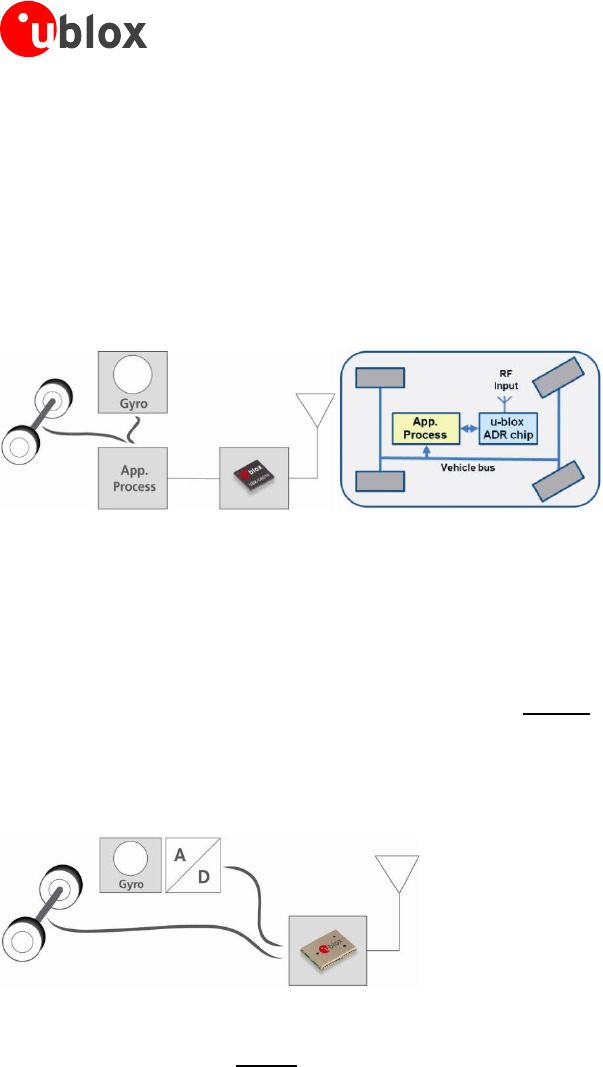
2.1.3 Automotive Dead Reckoning (ADR) solutions
u-blox‖ ADR supports different sensor inputs. The classical setup, called “Gyroscope plus Wheel Tick” (GWT),
consists of a gyroscope providing the heading information and wheel tick providing the speed information.
Alternatively, sensor information from left and right wheels (front or rear) or all wheels are used differentially to
deduce heading, called “Differential Wheel Tick” (DWT). This results in slightly lower performance compared to
GWT, but has the big advantage of saving the cost of a gyroscope.
2.1.3.1 Software sensor interface
Figure 10: Software sensor interface
The industry proven u-blox ADR solution is highly flexible. The application processor can support a vast array of
sensors, and must only convert the sensor data into UBX messages and pass them to the GPS receiver via a
standard serial interface (USB, SPI, UART, DDC). This makes the u-blox ADR solution very portable between
various vehicle platforms and reduces development effort and time-to-market. u-blox ADR is completely self-
calibrating, and requires only pre-configuration to the specific vehicle platform.
u-blox‖ ADR with software sensor interface is available as NEO-6V module. These components are ideal for
factory installed navigation since they use sensor data (wheel tick and gyroscope data) taken directly from the
CAN bus.
2.1.3.2 Hardware sensor interface
Figure 11: Hardware sensor interface
The standard quality grade LEA-6R module is a dedicated ADR solution (GWT only) for aftermarket installations
with no access to the vehicle bus and no application processor for sensor data processing. Sensors are connected
directly to the module: gyroscopes via SPI and ADC and the speed pulse information from the tachometer.
LEA-6 / NEO-6 / MAX-6 - Hardware Integration Manual
GPS.G6-HW-09007-H Preliminary Design-in
Page 26 of 87
2.2 LEA-6 design
2.2.1 LEA-6 passive antenna design
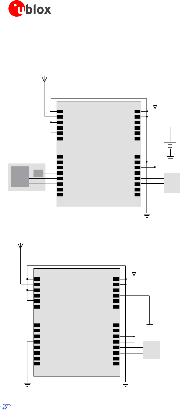
This is a minimal setup for a PVT GPS receiver with a LEA-6 module.
USB port
Passive Antenna
Vcc
Micro
Processor
(serial)
(optional)
Backup
Battery
(optional)
+
Micro
Processor
(USB)
1
SDA2 /SPI_MOSI
SCL2 / SPI_MISO
TxD1
RxD1
NC
VCC
GND
VCC_OUT
CFG_COM1/ NC
SPI_SCS2_N /TIMEPULSE2
RESET_N
V_BCKP
Reserved
GND
GND
RF_IN
VCC_RF
V_ANT
Reserved / FWD
Reserved / SPI_SCS1_N
Reserved / SPI_SCK
VDDUSB
USB_DM
USB_DP
EXTINT0 / SPEED
TIMEPULSE
GND
GND
AADET_N
2
3
4
5
6
7
8
9
10
11
12
13
14
28
27
26
25
24
23
22
21
20
19
18
17
16
15
LEA-6
Top View
LDO
Figure 12: LEA-6 passive antenna design with USB port
Passive Antenna
Vcc
Micro
Processor
(serial)
1
SDA2 / SPI_MOSI
SCL2 / SPI_MISO
TxD1
RxD1
NC
VCC
GND
VCC_OUT
CFG_COM1/ NC
SPI_SCS2_N /TIMEPULSE2
RESET_N
V_BCKP
Reserved
GND
GND
RF_IN
VCC_RF
V_ANT
Reserved / FWD
Reserved / SPI_SCS1_N
Reserved / SPI_SCK
VDDUSB
USB_DM
USB_DP
EXTINT0 / SPEED
TIMEPULSE
GND
GND
AADET_N
2
3
4
5
6
7
8
9
10
11
12
13
14
28
27
26
25
24
23
22
21
20
19
18
17
16
15
LEA-6
Top View
Figure 13: LEA-6 passive antenna design with no USB port or backup battery
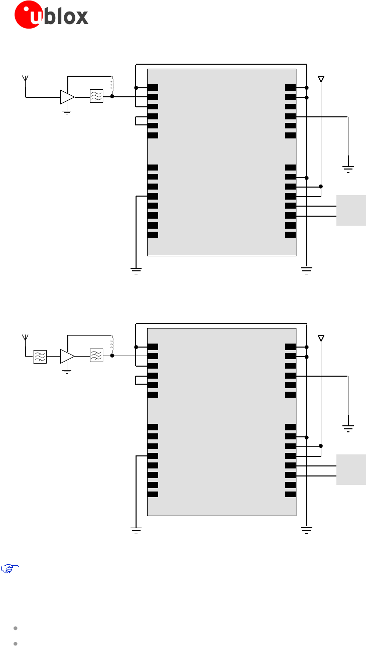
For best performance with passive antenna designs use an external LNA to increase the sensitivity up to 2
dB. See Figure 12 and Figure 15.
LEA-6 / NEO-6 / MAX-6 - Hardware Integration Manual
GPS.G6-HW-09007-H Preliminary Design-in
Page 27 of 87
Passive
Antenna Vcc
Micro
Processor
(serial)
1
SDA2 / SPI_MOSI
SCL2 / SPI_MISO
TxD1
RxD1
NC
VCC
GND
VCC_OUT
CFG_COM1/ NC
SPI_SCS2_N /TIMEPULSE2
RESET_N
V_BCKP
Reserved
GND
GND
RF_IN
VCC_RF
V_ANT
Reserved / FWD
Reserved / SPI_SCS1_N
NReserved / SPI_SCK
VDDUSB
USB_DM
USB_DP
EXTINT0 / SPEED
TIMEPULSE
GND
GND
AADET_N
2
3
4
5
6
7
8
9
10
11
12
13
14
28
27
26
25
24
23
22
21
20
19
18
17
16
15
LEA-6
Top View
LNA SAW L
Figure 14: LEA-6 passive antenna design for best performance (with external LNA and SAW)
Passive
Antenna Vcc
Micro
Processor
(serial)
1
SDA2 / SPI_MOSI
SCL2 / SPI_MISO
TxD1
RxD1
NC
VCC
GND
VCC_OUT
CFG_COM1/ NC
SPI_SCS2_N /TIMEPULSE2
RESET_N
V_BCKP
Reserved
GND
GND
RF_IN
VCC_RF
V_ANT
Reserved / FWD
Reserved / SPI_SCS1_N
Reserved / SPI_SCK
VDDUSB
USB_DM
USB_DP
EXTINT0 / SPEED
TIMEPULSE
GND
GND
AADET_N
2
3
4
5
6
7
8
9
10
11
12
13
14
28
27
26
25
24
23
22
21
20
19
18
17
16
15
LEA-6
Top View
SAW LNA SAW L
Figure 15: LEA-6 passive antenna design for best performance and increased immunity to jammers such as GSM
For information on increasing immunity to jammers such as GSM see section 3.3.8.
2.2.2 GLONASS HW design recommendations
u-blox 6 designs for GLONASS require:
u-blox 6 Module with Flash (LEA-6H GLONASS ready module)
Wide RF path (antenna, external SAW) to allow GLONASS & GPS signals to pass (see Figure 16)
2.2.2.1 u-blox 6 GLONASS module
u-blox will provide a GLONASS / GPS Flash firmware image. For this reason it is absolutely necessary to choose
the LEA-6H GLONASS ready module which can be updated when the GLONASS / GPS firmware is available. A
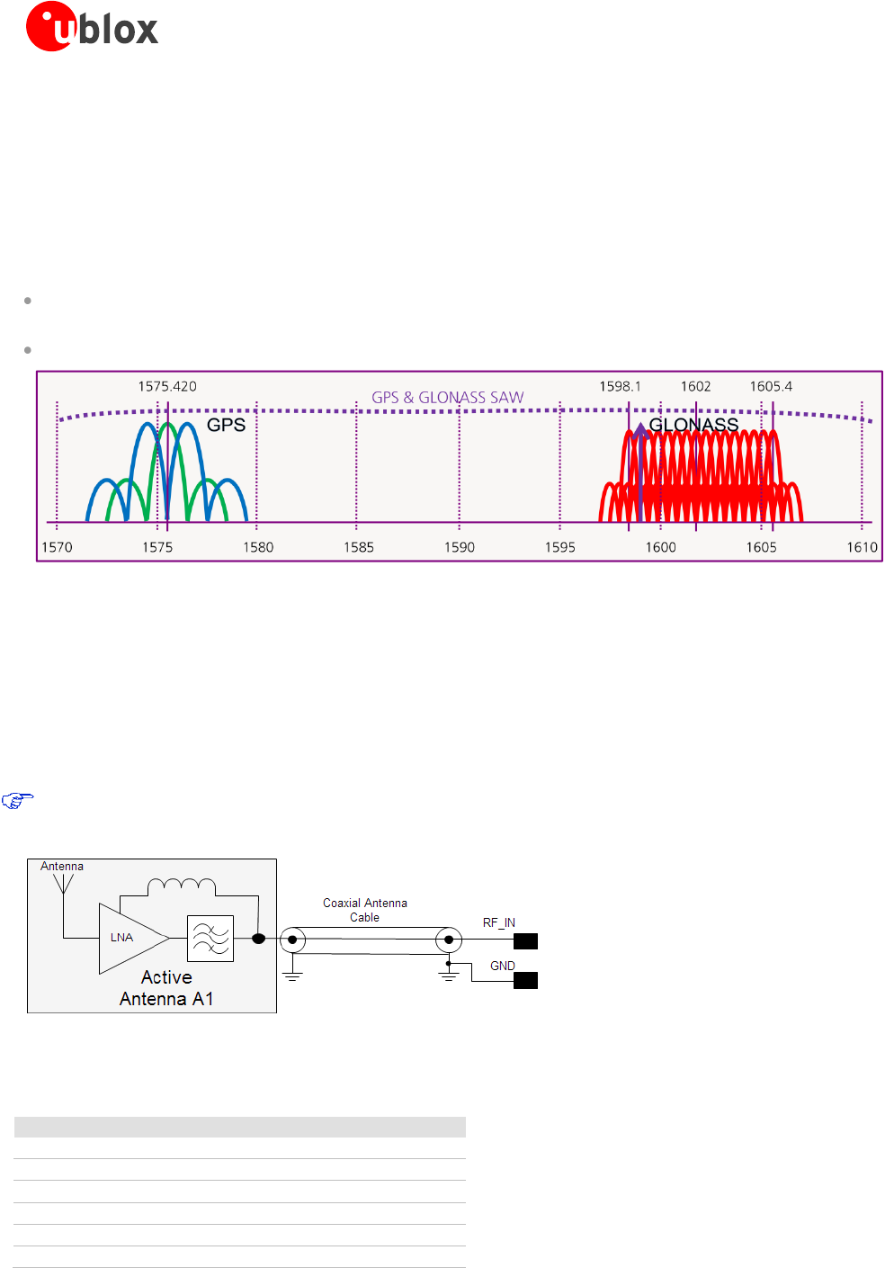
LEA-6 / NEO-6 / MAX-6 - Hardware Integration Manual
GPS.G6-HW-09007-H Preliminary Design-in
Page 28 of 87
GLONASS module which will be pin-compatible to the GLONASS ready LEA-6H module when the GLONASS /
GPS firmware is available.
2.2.2.2 Wide RF path
As seen in Figure 16, the GLONASS / GPS satellite signals are not at the same frequency. For this reason the RF
path, LNA, filter, and antenna must be modified accordingly to let both signals pass.
2.2.2.3 Filter
Use a GPS & GLONASS SAW filter (see Figure 16) that lets both GPS and GLONASS signals pass (see the
recommended parts list in section 3.3.9)
In case an active antenna is used, make sure the filter (if any) inside is wide enough.
Figure 16: GPS & GLONASS SAW filter
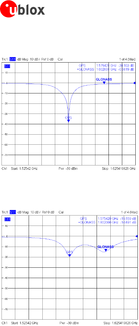
2.2.2.4 Antenna
2.2.2.5 Active antenna
Usually an active GPS antenna includes a GPS band pass filter that filters out the GLONASS signal (see Figure 16).
For this reason make sure that the filter in the active antenna is wide enough.
In combined GPS & GLONASS antennas, the antenna is tuned for receiving both signals and the filter has a
larger bandwidth to provide optimal GPS & GLONASS signal reception (see Figure 16).
Use a good performance GPS & GLONASS active antenna (for recommended components see section
3.3.9.1).
Figure 17: GPS & GLONASS active antenna
2.2.2.6 Passive Antenna
The bandwidth of a ceramic patch antenna narrows with size (see Table 7).
size
Typical bandwidth
36*36*4 mm
40 MHz
25*25*4 mm
20 MHz
18*18*4 mm
10 MHz
15*15*4 mm
8 MHz
12*12*4 mm
7 MHz
10*10*4 mm
5 MHz
Table 7: Typical bandwidths for GPS patch antennas
LEA-6 / NEO-6 / MAX-6 - Hardware Integration Manual
GPS.G6-HW-09007-H Preliminary Design-in
Page 29 of 87
Figure 18 shows a 12*12*4 mm patch antenna with 20*20 mm ground plane, tuned to GPS. This patch
bandwidth is so narrow that it cannot be simultaneously matched to GPS and GLONASS.
Figure 18: 12*12*4 patch antenna on 20*20 mm GND plane
Figure 19 show a 25*25*4 mm patch antenna with 60*60 mm ground plane. Due to the larger bandwidth, it
can be matched to GPS and GLONASS.
Figure 19: 25*25*4 mm patch antenna on 60*60 mm GND plane
Figure 20 show a 36*36*4 mm patch antenna. Due to the large bandwidth, the antenna is also tolerant with
changes in the ground plane.
LEA-6 / NEO-6 / MAX-6 - Hardware Integration Manual
GPS.G6-HW-09007-H Preliminary Design-in
Page 30 of 87
Figure 20 36*36*4 mm patch antenna
Use at least a 25*25*4 mm patch antenna, (a 36*36*4 mm patch antenna is better) and tune it so that
GPS & GLONASS signals are received.
2.2.2.7 Module designs
For GPS & GLONASS designs chose the LEA-6H GLONASS ready module, which has a wide RF path and includes
an internal Flash.
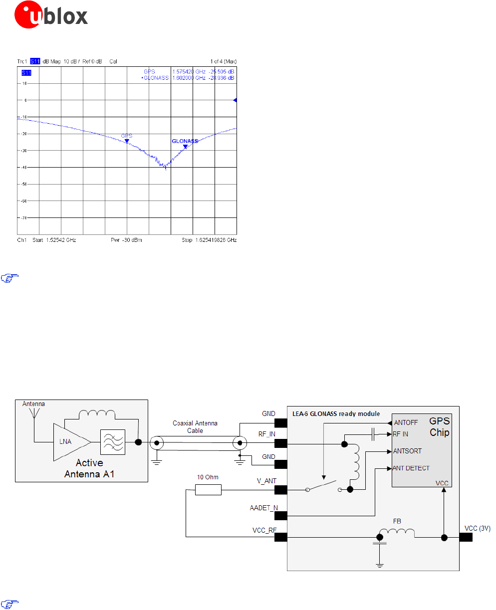
2.2.2.8 Module design with active antenna
Figure 21 shows a GPS & GLONASS active antenna design with the LEA-6H GLONASS ready module.
Figure 21: Module design with active antenna
Use a good performance GPS & GLONASS active antenna (for recommended components see section
3.3.9.1).
LEA-6 / NEO-6 / MAX-6 - Hardware Integration Manual
GPS.G6-HW-09007-H Preliminary Design-in
Page 31 of 87
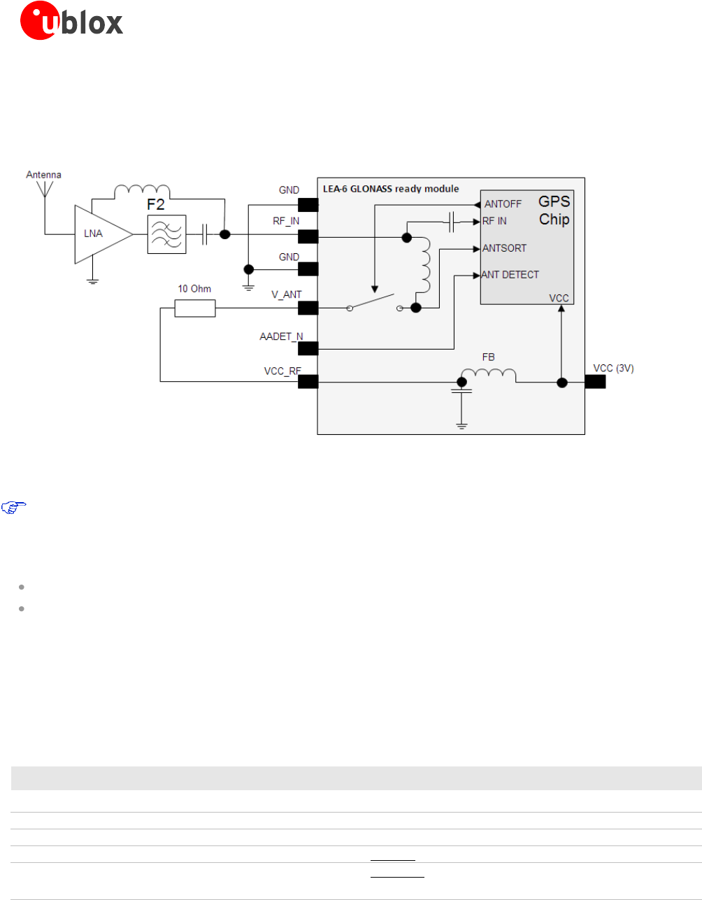
2.2.2.9 Module design with passive antenna
Figure 22 shows a GPS & GLONASS passive antenna design with the LEA-6H GLONASS ready module.
For best performance with passive antenna designs use an external LNA.
Figure 22: Module design with passive antenna
A standard GPS LNA has enough bandwidth to amplify GPS and GLONASS.
For recommended SAW Filters for GPS & GLONASS (Part F2 in Figure 20) see section 3.3.9.
2.2.2.10 GLONASS SW integration
To activate GLONASS system modes on u-blox GLONASS ready module, the customer application will have to:
Upgrade the (Flash) firmware once available.
Send UBX proprietary commands for activating and switching to GLONASS reception (SW command will be
documented in the u-blox 6 Receiver Description including Protocol Specification [3]).
2.2.3 LEA-6R design
2.2.3.1 Connecting gyroscope and temperature sensor to the LEA-6R
The LEA-6R acts as SPI master. Following signals are used by the SPI:
Pin
Signal name
Direction
Usage
23
SPI_SCK
Output
SPI clock
22
SPI_SCS1_N
Output
Chip Select signal for ADC/turn rate sensor
9
SPI_SCS2_N
Output
Chip Select signal for temperature sensor
2
SPI_MISO
Input
Serial data (Master In / Slave Out)
1
SPI_MOSI
Output
Serial data (Master Out / Slave In), leave open
Table 8: SPI pins for LEA-6R
LEA-6 / NEO-6 / MAX-6 - Hardware Integration Manual
GPS.G6-HW-09007-H Preliminary Design-in
Page 32 of 87
The following block schematic specifies the A/D converter and temperature sensor for the LEA-6R.
The LTC1860 and LM70-5 function at 5 V. A level translation with open-drain buffers and pull-up
resistors on the outputs is required.
LEA-6R
Turn Rate Sensor
(MOSI)
22K
10R
leave open
Gyro
SCK
MISO
SPI_SCS2_N
+5VREF
100nF
GND
GND
CONV
SCK
VCC
SC
CS
VREF
IN+
IN-
12-Bit
A/D Converter
Linear LTC1860
Temperature
Sensor
National LM70-5
SDO
SI/O
V+
GND
GND
GND
100nF
RATE
100nF
GND
100K
SPI_SCS1_N
10uF
220nF
+5V
+5V
+5V
+5V
+3V
+3V
+3V
+5V
+3V
Figure 23: Attaching A/D converter and temperature sensor using the SPI
Add appropriate coupling capacitances according to the recommendations in the data sheets of the illustrated
semiconductor products. All shown resistors shall have 5% accuracy or better. All shown capacitors (X7R types)
shall have 10% accuracy or better.
For correct operation with the LEA-6R firmware, this circuit must be adopted without making any
modifications such as, but not limited to, using different types of semiconductor devices and changing
signal assignment.
LEA-6R default SPI clock is 870 kHz. As LEA-4R default value is 460 kHz, migrating from LEA-4R to LEA-6R
will require a bandwidth verification of the SPI circuits and shall be designed for a bandwidth of 4 MHz.
2.2.3.2 Gyroscope requirements
Gyroscopes should meet the requirements listed below:
Parameter
Specification
Supply Voltage
5.0 V ± 0.25 V
Zero Point
2.5 V ± 0.4 V
Scale Factor
25 mV/(°/s) ± 5 mV/(°/s)
Dynamic Range
±60 °/s to ±125 °/s
Linearity
±0.5 % (full scale)
Recommended operating temperature range
-40 to +85°C
Table 9: Requirements for gyroscopes
Follow the gyroscope manufacturer design recommendations for proper analog signal conditioning.
LEA-6 / NEO-6 / MAX-6 - Hardware Integration Manual
GPS.G6-HW-09007-H Preliminary Design-in
Page 33 of 87
2.2.3.3 Supported A/D converters
The following table lists the supported A/D converters:
Manufacturer
Device
Linear Technology
LTC1860
Table 10: Supported A/D converters
2.2.3.4 Supported temperature sensors
The following table lists the supported temperature sensors:
Manufacturer
Device
National Semiconductor
LM70
Table 11: Supported temperature sensors
Note, that the temperature sensor inside the EPSON XV-8000 gyroscope sensor is not supported.
2.2.3.5 Forward / Backward indication
Use of the forward / backward indication signal FWD is optional but strongly recommended for good dead
reckoning performance. It has an internal pull-up and therefore can be left open or connected to VCC_OUT or
VCC if not used.
You need to check the voltage levels and the quality of the vehicle signals. They may be of different voltage
levels, for example 12V nominal with a certain degree of variation. Use of optocouplers or other approved EMI
protection and filtering is strongly recommended.
If no direction signal is available, the direction must be set to forward by configuring the meaning of the
direction pin appropriately, otherwise DR positioning will be incorrect due to the wrong direction. GPS
only navigation is not affected by this configuration.
As the forward/backward direction signal is not available in all cars, try to make use of the reverse gear
light.
Pin
Signal name
Direction
Usage
21
FWD
Input
Direction indication (1 = forward)
Table 12: LEA-6R Forward / Backward indication
LEA-6 / NEO-6 / MAX-6 - Hardware Integration Manual
GPS.G6-HW-09007-H Preliminary Design-in
Page 34 of 87
2.2.3.6 Odometer / Speedpulses
DR receivers use signals from sensors in the car to establish the velocity and distance traveled. These sensors are
referred to as the odometer and the signals can be designated odometer pulses, speedpulses, speed ticks, wheel
pulses or wheel ticks. These terms are often used interchangeably which can sometimes lead to confusion. For
the sake of consistency, in this document we will be referring to these signals as speedpulses.
Pin
Signal name
Direction
Usage
27
SPEED
Input
Odometer Speedpulses
Table 13: LEA-6R Odometer / Speedpulses
The speedpulse signal required for DR modules must have a frequency range from 1 Hz to 2 kHz (0 Hz is equal
to a speed of 0 km/hour) and must be linear to the driven speed.
For DR calibration see Section D.
LEA-6 / NEO-6 / MAX-6 - Hardware Integration Manual
GPS.G6-HW-09007-H Preliminary Design-in
Page 35 of 87
2.2.1 Pin description for LEA-6 designs
Function
PIN
No
I/O
Description
Remarks
Power
VCC
6
I
Supply Voltage
Provide clean and stable supply.
GND
7, 13-15,
17
I
Ground
Assure a good GND connection to all GND pins of the module,
preferably with a large ground.
VCC_OUT
8
O
Leave open if not used.
V_BCKP
11
I
Backup voltage
supply
It‖s recommended to connect a backup battery to V_BCKP in order
to enable Warm and Hot Start features on the receivers. Otherwise
connect to GND.
VDDUSB
24
I
USB Power
Supply
To use the USB interface connect this pin to 3.0 – 3.6V derived from
VBUS.
If no USB serial port used connect to GND.
Antenna
RF_IN
16
I
GPS/GALILEO
signal input
from antenna
Use a controlled impedance transmission line of 50 Ohm to connect
to RF_IN.
Don‖t supply DC through this pin. Use V_ANT pin to supply power.
VCC_RF
18
O
Output Voltage
RF section
Can be used to power an external active antenna (VCC_RF
connected to V_ANT with 10 ). The max power consumption of
the Antenna must not exceed the datasheet specification of the
module.
Leave open if not used.
V_ANT
19
I
Antenna Bias
voltage
Connect to GND (or leave open) if Passive Antenna is used. If an
active Antenna is used, add a 10 resistor in front of V_ANT input
to the Antenna Bias Voltage or VCC_RF
AADET_N
20
I
Active Antenna
Detect
Input pin for optional antenna supervisor circuitry. Leave open if not
used.
UART
TxD1
3
O
Serial Port 1
Communication interface can be programmed as TX ready for I2C
interface. Leave open if not used.
RxD1
4
I
Serial Port 1
Serial port input with internal pull-up resistor to VCC. Leave open if
not used. Don‖t use external pull up resistor.
USB
USB_DM
25
I/O
USB I/O line
USB2.0 bidirectional communication pin. Leave open if unused.
Implementations see Section 1.6.2.
USB_DP
26
I/O
USB I/O line
System
RESET_N
10
I
Hardware Reset
(Active Low)
Leave open if not used. Do not drive high.
TIMEPULSE
28
O
Timepulse
Signal
Configurable Timepulse signal (one pulse per second by default).
Leave open if not used.
EXTINT0
/SPEED
27
I
Ext. Interrupt
/Odometer
Ext. Interrupt Pin. Int. pull-up resistor to VCC. Leave open if unused.
LEA-6R: Odometer speed
CFG_COM1
/NC
/SPI_SCS2_N
/TIMEPULSE2
9
I
Config. Pin
/NC
/SPI
/TIMEPULSE2
LEA-6S, LEA-6A: Leave open for default configuration.
LEA-6H: Do not connect
LEA-6R: SPI select 2
LEA-6T: TIMEPULSE2
SDA2
/SPI_MOSI
1
I/O
DDC Pins
/SPI
DDC Data. Leave open if not used.
LEA-6R: SPI MOSI
SCL2
/SPI_MISO
2
I/O
DDC Pins
/SPI
DDC Clock. Leave open if not used.
LEA-6R: SPI MISO
Reserved
12
I
Leave open, do not drive low.
NC
5
Leave open for only LEA-6x design. Connect to VCC for backward
compatibility to LEA-5x.
NC
/FWD
21
Not Connect
/Direction
Leave open
LEA-6R: Forward / Backward indication
NC
/SPI_ SCS1_N
22
Not Connect
/SPI
Leave open
LEA-6R: SPI select 1
NC
/SPI_SCK
23
Not Connect
/SPI
Leave open
LEA-6R: SPI clock
Table 14: Pin description LEA-6
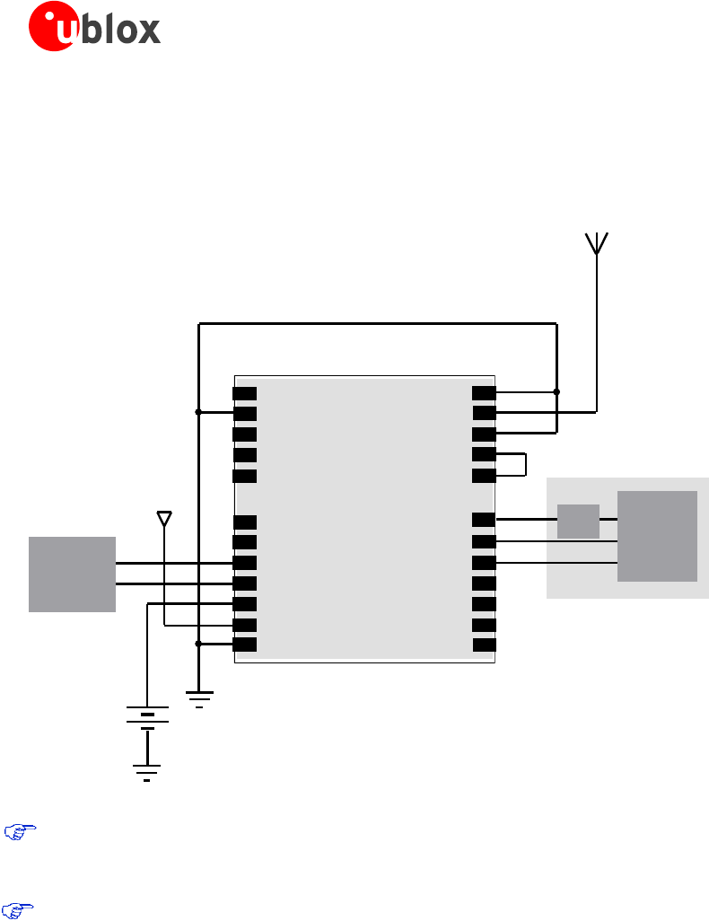
LEA-6 / NEO-6 / MAX-6 - Hardware Integration Manual
GPS.G6-HW-09007-H Preliminary Design-in
Page 36 of 87
2.3 NEO-6 design
2.3.1 Passive antenna design (NEO-6)
This is a minimal setup for a PVT GPS receiver with a NEO-6 module.
Vcc
Micro
Processor
(serial)
Passive Antenna
Backup
Battery+
NEO-6
Top View
2
3
4
5
6
8
10
12
24
22
21
20
19
17
15
13
23
GND Reserved
SS_N
TIMEPULSE
EXTINT0
USB_DM
USB_DP
VDDUSB
Reserved
VCC_RF
GND
GND
RF_IN
GND
VCC
V_BCKP
RxD1
TxD1
SCL2
SDA2
Reserved
CFG_GPS0/SCK
MISO/CFG_COM1
MOSI/CFG_COM0
14
16
11
9
7
1
18
USB port (Optional)
Micro
Processor
(USB)
LDO
Figure 24: NEO-6 passive antenna design (with USB)
The above design is for the USB in self-powered mode. For bus-powered mode pin 14 (CFG_COM0) must
be left open and VCC must be connected to VDDUSB. NMEA baud rate is 38400 when in self-powered
mode.
For best performance with passive antenna designs use an external LNA to increase the sensitivity up to 2
dB. See Figure 25 and Figure 26.
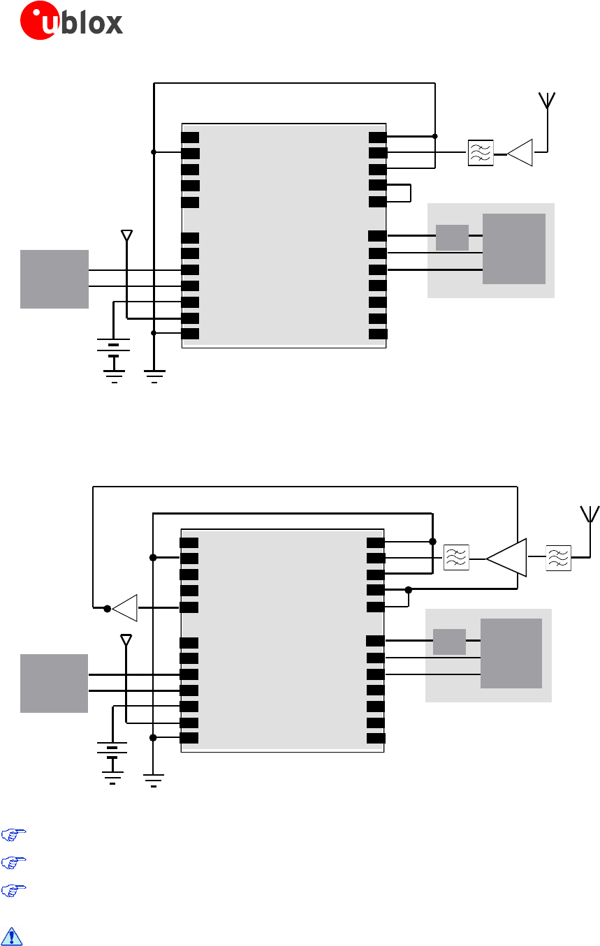
LEA-6 / NEO-6 / MAX-6 - Hardware Integration Manual
GPS.G6-HW-09007-H Preliminary Design-in
Page 37 of 87
Vcc
Micro
Processor
(serial)
Passive Antenna
Backup
Battery
+
NEO-6
Top View
2
3
4
5
6
8
10
12
24
22
21
20
19
17
15
13
23
GND Reserved
SS_N
TIMEPULSE
EXTINT0
USB_DM
USB_DP
VDDUSB
Reserved
VCC_RF
GND
GND
RF_IN
GND
VCC
V_BCKP
RxD1
TxD1
SCL2
SDA2
Reserved
CFG_GPS0/SCK
MISO/CFG_COM1
MOSI/CFG_COM0
14
16
11
9
7
1
18
USB port (Optional)
Micro
Processor
(USB)
LDO
LNA
SAW
Figure 25: NEO-6 passive antenna design for best performance (with external LNA and SAW)
Figure 26 below shows a passive antenna design for NEO-6 GPS modules with an external SAW-LNA-SAW for
best performance and increased immunity to jammers such as GSM. For lowest power in backup mode use
ANTOFF
Vcc
Micro
Processor
(serial)
Passive
Antenna
Backup
Battery
+
NEO-6
Top View
2
3
4
5
6
8
10
12
24
22
21
20
19
17
15
13
23
GND Reserved
SS_N
TIMEPULSE
EXTINT0
USB_DM
USB_DP
VDDUSB
Reserved
VCC_RF
GND
GND
RF_IN
GND
VCC
V_BCKP
RxD1
TxD1
SCL2
SDA2
(ANTOFF)
CFG_GPS0/SCK
MISO/CFG_COM1
MOSI/CFG_COM0
14
16
11
9
7
1
18
USB port (Optional)
Micro
Processor
(USB)
LDO
SAW
LNA
SAW
inverter
on
VCC
Figure 26: NEO-6 passive antenna design for best performance and increased immunity to jammers such as GSM
For information on increasing immunity to jammers such as GSM see section 3.3.8.
When using an external LNA in PSM on / off mode, pin 17 can be programmed as ANTOFF.
To configure the ANTOFF function refer to the u-blox 6 Receiver Description including Protocol
Specification [3].
Use caution when implementing ANTOFF configuration since forward compatibility is not
guaranteed
LEA-6 / NEO-6 / MAX-6 - Hardware Integration Manual
GPS.G6-HW-09007-H Preliminary Design-in
Page 38 of 87
2.3.2 Pin description for NEO-6 designs
Function
PIN
No
I/O
Description
Remarks
Power
VCC
23
I
Supply Voltage
Max allowed ripple on VCC=50 mVpp
GND
10,12,13,24
I
Ground
Assure a good GND connection to all GND pins of the module,
preferably with a large ground plane.
V_BCKP
22
I
Backup voltage
supply
It‖s recommended to connect a backup battery to V_BCKP in order
to enable Warm and Hot Start features on the receivers. Otherwise
connect to GND.
VDDUSB
7
I
USB Power
Supply
To use the USB interface connect this pin to 3.0 – 3.6 V.
If no USB serial port used connect to GND.
Antenna
RF_IN
11
I
GPS signal
input from
antenna
The connection to the antenna has to be routed on the PCB. Use a
controlled impedance of 50 to connect RF_IN to the antenna or
the antenna connector.
VCC_RF
9
O
Output Voltage
RF section
Pins 8 and 9 must be connected together. VCC_RF can also be used
to power an external active antenna.
UART
TxD1
20
O
Serial Port 1
Communication interface, can be programmed as TX ready for I2C
interface.
RxD1
21
I
Serial Port 1
Serial input. Internal pull-up resistor to VCC. Leave open if not used.
USB
USB_DM
5
I/O
USB I/O line
USB2.0 bidirectional communication pin. Leave open if unused.
Implementation see Section 0
USB_DP
6
I/O
USB I/O line
System
TIMEPULSE
3
O
Timepulse
Signal
Configurable Timepulse signal (one pulse per second by default).
Leave open if not used.
EXTINT0
4
I
External
Interrupt
External Interrupt Pin.
Internal pull-up resistor to VCC. Leave open if not used.
SDA2
18
I/O
DDC Pins
DDC Data. Leave open, if not used.
SCL2
19
I/O
DDC Pins
DDC Clock. Leave open, if not used.
Reserved
17
I/O
Reserved
Can be configured as ANTOFF
CFG_COM1
/MISO
15
I/O
Config. Pin
/SPI MISO
Leave open if not used.
CFG_COM0
/MOSI
14
I/O
Config. Pin
/SPI MOSI
Leave open if not used.
Note Connect to GND to use USB in Self Powered mode. See
Section 1.7.4 and the NEO-6 Data Sheet [2]
Reserved
8
I
Reserved
Pins 8 and 9 must be connected together. Can be used as a
RESET_N input. See Section 1.7.1
Reserved
1
-
Reserved
Leave open.
SS_N
2
I/O
SPI Select
Leave open if not used.
CFG_GPS0
/SCK
16
I/O
Config. Pin
/SPI SCK
Leave open if not used.
Table 15: Pinout NEO-6
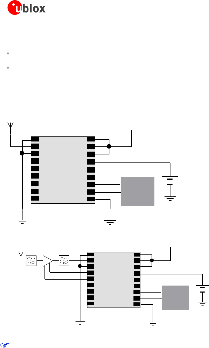
LEA-6 / NEO-6 / MAX-6 - Hardware Integration Manual
GPS.G6-HW-09007-H Preliminary Design-in
Page 39 of 87
2.4 MAX-6 design
MAX-6 modules provide the following signals:
ANTON Signal (to turn on and off external LNA). To save power consumption in Power Save mode. See
Section 2.6.9
TX ready Signal (to trigger a host, e.g. a u-blox LEON wireless module, when data at DDC interface is ready
to be picked up). To save power consumption on Host side.
2.4.1 MAX-6 passive antenna design
This is a minimal setup for a PVT GPS receiver with a MAX-6 module.
Vcc
Micro
Processor
(serial)
Passive
Antenna
Backup
Battery
2
3
4
5
6
8
10
12
17
15
13
Reserved
TIMEPULSE
EXTINT0
TxD1
VCC_IO
V_RESET
VCC_RF
GND
GND
RF_IN
GND
VCC
V_BCKP
RxD1
ANTON
SCL2
SDA2
Reserved
14
16
11
9
7
1
18
MAX-6
Figure 27: MAX-6 passive antenna design
Passive Antenna LNA SAW
Vcc
Micro
Processor
(serial)
Backup
Battery
2
3
4
5
6
8
10
12
17
15
13
Reserved
TIMEPULSE
EXTINT0
TxD1
VCC_IO
V_RESET
VCC_RF
GND
GND
RF_IN
GND
VCC
V_BCKP
RxD1
ANTON
SCL2
SDA2
Reserved
14
16
11
9
7
1
18
MAX-6
SAW
Vcc
on
Figure 28: MAX-6 passive antenna design for best performance and increased immunity to jammers such as GSM
For information on increasing immunity to jammers such as GSM see section 3.3.8.
LEA-6 / NEO-6 / MAX-6 - Hardware Integration Manual
GPS.G6-HW-09007-H Preliminary Design-in
Page 40 of 87
2.4.2 Pin description for MAX-6 designs
Function
PIN
No
I/O
Description
Remarks
Power
VCC
8
I
Supply Voltage
Max allowed ripple on VCC=50 mVpp
GND
1,10,12
I
Ground
Assure a good GND connection to all GND pins of the module,
preferably with a large ground plane.
V_BCKP
6
I
Backup voltage
supply
Backup voltage input pin. Connect to GND if not used.
Antenna
RF_IN
11
I
GPS signal
input from
antenna
The connection to the antenna has to be routed on the PCB. Use a
controlled impedance of 50 to connect RF_IN to the antenna or
the antenna connector. DC block inside.
VCC_RF
14
O
Output Voltage
RF section
Can be used for active antenna or external LNA supply.
ANTON
13
O
Active antenna or ext. LNA control pin in power save mode. Int.
pull-up resistor to VCC
UART
TxD1
2
O
Serial Port 1
UART, leave open if not used, Voltage level referred VCC_IO. Can
be configured as TX ready indication for the DDC interface.
RxD1
3
I
Serial Port 1
UART, leave open if not used, Voltage level referred VCC_IO
System
TIMEPULSE
4
O
Timepulse
Signal
Leave open if not used, Voltage level referred VCC_IO
EXTINT0
5
I
External
Interrupt
Leave open if not used, Voltage level referred VCC_IO
SDA2
16
I/O
DDC Pins
DDC Data. Leave open, if not used.
SCL2
17
I/O
DDC Pins
DDC Clock. Leave open, if not used.
Reserved
18
Reserved
Leave open
VCC_IO
7
I
IO supply voltage Input must be always supplied. Usually connect to
VCC Pin 8. If I/O level should be different from VCC, supply VCC_IO
with the I/O level required.
V_RESET
9
I
VRESET
Must be connected to VCC always. Can be used as reset input pin
with additional circuit (connected to VCC by 3.3 k resistor). See
Section 1.7.1
Reserved
15
Reserved
Leave open
Table 16: Pinout MAX-6
2.5 Layout
This section provides important information for designing a reliable and sensitive GPS system.
GPS signals at the surface of the Earth are about 15 dB below the thermal noise floor. Signal loss at the antenna
and the RF connection must be minimized as much as possible. When defining a GPS receiver layout, the
placement of the antenna with respect to the receiver, as well as grounding, shielding and jamming from other
digital devices are crucial issues and need to be considered very carefully.
2.5.1 Footprint and paste mask
Figure 29 - Figure 34 describe the footprint and provide recommendations for the paste mask for u-blox 6 LCC
modules. These are recommendations only and not specifications. Note that the Copper and Solder masks have
the same size and position.
To improve the wetting of the half vias, reduce the amount of solder paste under the module and increase the
volume outside of the module by defining the dimensions of the paste mask to form a T-shape (or equivalent)
extending beyond the Copper mask. For the stencil thickness see 3.2.1.
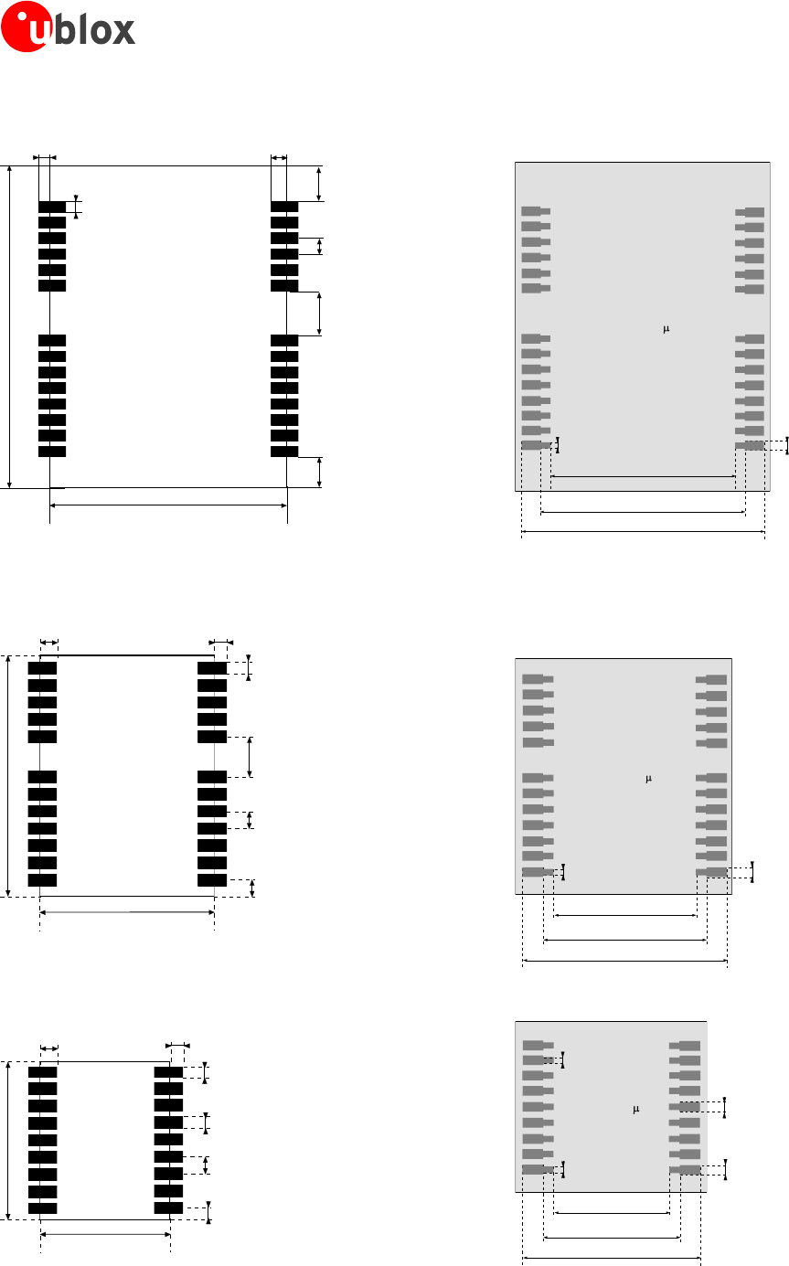
LEA-6 / NEO-6 / MAX-6 - Hardware Integration Manual
GPS.G6-HW-09007-H Preliminary Design-in
Page 41 of 87
17.0 mm [669 mil]
22.4 mm [881.9 mil]
1.0 mm
[39 mil]
0.8 mm
[31.5 mil]
2.45 mm
[96.5 mil]
1.1 mm
[43 mil]
3.0 mm
[118 mil]
2.15 mm
[84.5 mil]
0.8 mm
[31.5 mil]
Figure 29: LEA-6 footprint
Stencil: 200 m
15.7 mm [618 mil]
17.0 mm [669 mil]
20.8 mm [819 mil]
0.8 mm
[31.5 mil]
0.6 mm
[23.5 mil]
Figure 30: LEA-6 paste mask
12.2 mm [480.3 mil]
16.0 mm [630 mil]
1.0 mm
[39.3 mil]
0.8 mm
[31.5 mil]
0.8 mm
[31.5 mil]
3.0 mm
[118.1 mil]
1.0 mm
[39.3 mil]
1.1 mm
[43.3 mil]
Figure 31: NEO-6 footprint
9.7 mm [382 mil]
10.1 mm [398 mil]
1.0 mm
[39.3 mil]
0.7 mm
[27.6 mil]
0.8 mm
[31.5 mil]
0.65 mm
[26.6 mil]
1.1 mm
[43.3 mil]
0.8 mm
[31.5 mil]
Figure 32: MAX-6 footprint
Stencil: 170 m
10.4 mm [409.5 mil]
14.6 mm [575 mil]
12.2 mm [480 mil]
0.8 mm
[31.5 mil]
0.6 mm
[23.5 mil]
Figure 33: NEO-6 paste mask
Stencil: 170 m
7.9 mm [311 mil]
12.5 mm [492 mil]
9.7 mm [382 mil]
0.7 mm
[27.6 mil]
0.5 mm
[19.7 mil]
0.8 mm
[31.5 mil]
0.6 mm
[23.5 mil]
Figure 34: MAX-6 paste mask
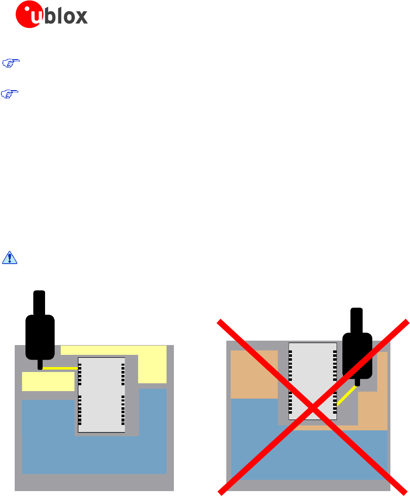
LEA-6 / NEO-6 / MAX-6 - Hardware Integration Manual
GPS.G6-HW-09007-H Preliminary Design-in
Page 42 of 87
MAX Form Factor (10.1 x 9.7 x 2.5): Same Pitch as NEO: 1.1 mm, but 4 pads in each corner only 0.7 mm
wide instead 0.8 mm
The paste mask outline needs to be considered when defining the minimal distance to the next
component. The exact geometry, distances, stencil thicknesses and solder paste volumes must be adapted
to the specific production processes (e.g. soldering etc.) of the customer.
2.5.2 Placement
A very important factor in achieving maximum performance is the placement of the receiver on the PCB. The
connection to the antenna must be as short as possible to avoid jamming into the very sensitive RF section.
Make sure that RF critical circuits are clearly separated from any other digital circuits on the system board. To
achieve this, position the receiver digital part towards your digital section of the system PCB. Care must also be
exercised with placing the receiver in proximity to circuitry that can emit heat. The RF part of the receiver is very
sensitive to temperature and sudden changes can have an adverse impact on performance.
The RF part of the receiver is a temperature sensitive component. Avoid high temperature drift
and air vents near the receiver.
Non 'emitting'
circuits
PCB
Digital & Analog circuits
Non
'emitting'
circuits
Antenna
Digital Part
RF Part
1
2
3
4
5
6
7
8
9
10
11
12
13
14
28
27
26
25
24
23
22
21
20
19
18
17
16
15
RF & heat
'emitting'
circuits
PCB
Digital & Analog circuits
RF& heat
'emitting'
circuits
Antenna
1
2
3
4
5
6
7
8
9
10
11
12
13
14
28
27
26
25
24
23
22
21
20
19
18
17
16
15
Figure 35: Placement (for exact pin orientation see data sheet)
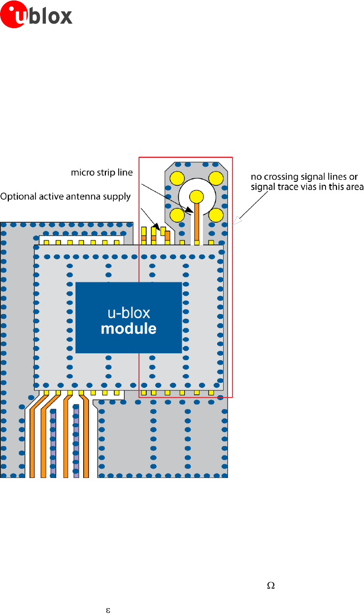
LEA-6 / NEO-6 / MAX-6 - Hardware Integration Manual
GPS.G6-HW-09007-H Preliminary Design-in
Page 43 of 87
2.5.3 Antenna connection and grounding plane design
u-blox 6 modules can be connected to passive patch or active antennas. The RF connection is on the PCB and
connects the RF_IN pin with the antenna feed point or the signal pin of the connector, respectively. Figure 36
illustrates connection to a typical five-pin RF connector. One can see the improved shielding for digital lines as
discussed in the GPS Antenna Application Note [4]. Depending on the actual size of the ground area, additional
vias should be placed in the outer region. In particular, the edges of the ground area should be terminated with
a dense line of vias.
Figure 36: Recommended layout (for exact pin orientation see data sheet)
As seen in Figure 36, an isolated ground area is created around and below the RF connection. This part of the
circuit MUST be kept as far from potential noise sources as possible. Make certain that no signal lines cross, and
that no signal trace vias appear at the PCB surface within the area of the red rectangle. The ground plane should
also be free of digital supply return currents in this area. On a multi layer board, the whole layer stack below the
RF connection should be kept free of digital lines. This is because even solid ground planes provide only limited
isolation.
The impedance of the antenna connection has to match the 50 impedance of the receiver. To achieve an
impedance of 50 Ohms, the width W of the micro strip has to be chosen depending on the dielectric thickness
H, the dielectric constant r of the dielectric material of the PCB and on the build-up of the PCB (see
Section 2.5.4). Figure 37 shows two different builds: A 2 Layer PCB and a 4 Layer PCB. The reference ground
plane is in both designs on layer 2 (red). Therefore the effective thickness of the dielectric is different.
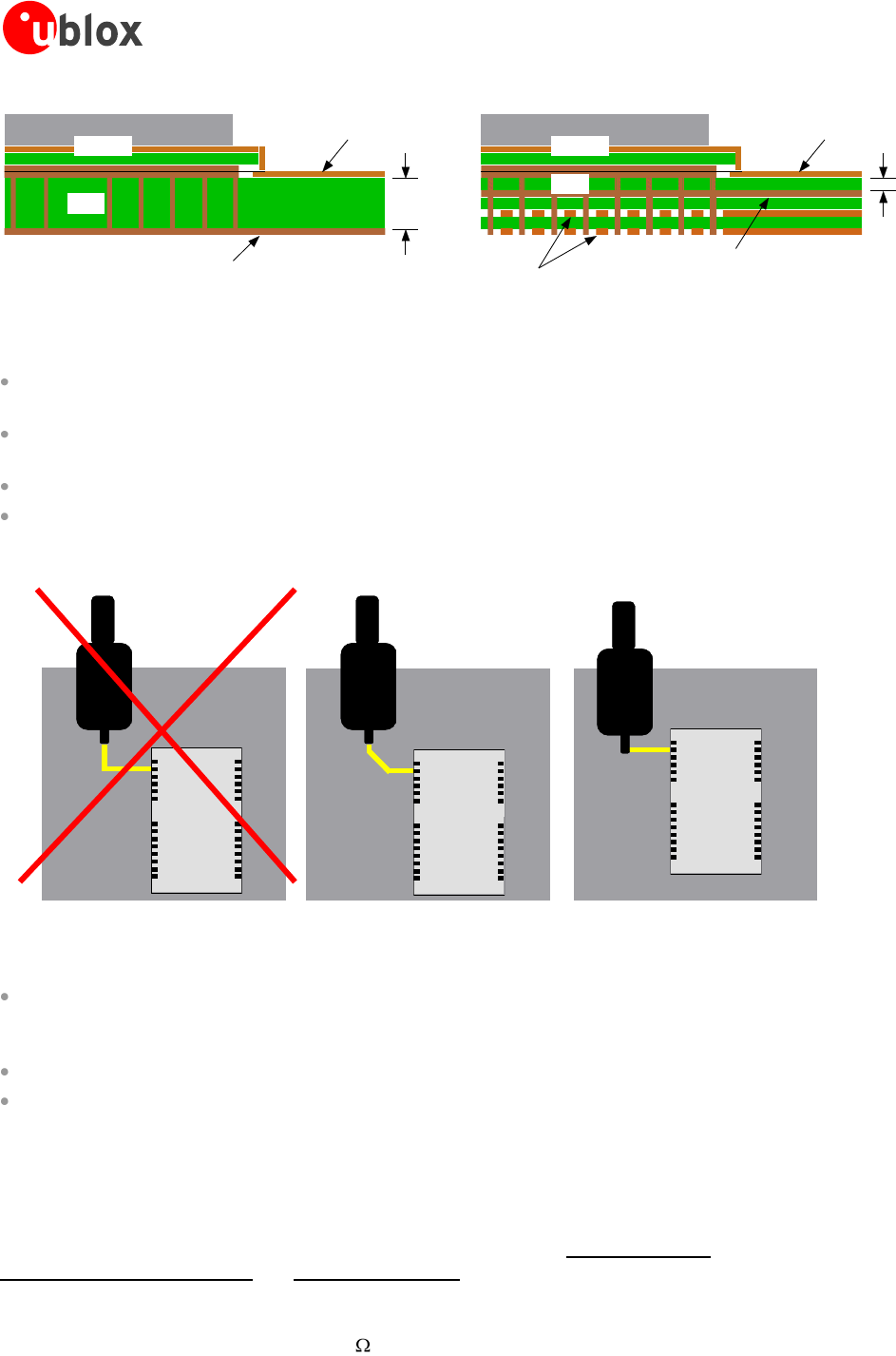
LEA-6 / NEO-6 / MAX-6 - Hardware Integration Manual
GPS.G6-HW-09007-H Preliminary Design-in
Page 44 of 87
Module micro strip line
Ground plane
Module micro strip line
Ground plane
PCB
PCB
Either don't use these layers or fill with ground planes
H
H
Figure 37: PCB build-up for micro strip line. Left: 2-layer PCB, right: 4-layer PCB
General design recommendations:
The length of the micro strip line should be kept as short as possible. Lengths over 2.5 cm (1 inch) should be
avoided on standard PCB material and without additional shielding.
For multi layer boards the distance between micro strip line and ground area on the top layer should at least
be as large as the dielectric thickness.
Routing the RF connection close to digital sections of the design should be avoided.
To reduce signal reflections, sharp angles in the routing of the micro strip line should be avoided. Chamfers
or fillets are preferred for rectangular routing; 45-degree routing is preferred over Manhattan style
90-degree routing.
Antenna
Antenna
Antenna
PCB
PCB PCB
1
2
3
4
5
6
7
8
9
10
11
12
13
14
28
27
26
25
24
23
22
21
20
19
18
17
16
15
1
2
3
4
5
6
7
8
9
10
11
12
13
14
28
27
26
25
24
23
22
21
20
19
18
17
16
15
1
2
3
4
5
6
7
8
9
10
11
12
13
14
28
27
26
25
24
23
22
21
20
19
18
17
16
15
Wrong better best
Figure 38: Recommended micro strip routing to RF pin (for exact pin orientation see data sheet)
Do not route the RF-connection underneath the receiver. The distance of the micro strip line to the ground
plane on the bottom side of the receiver is very small (some 100 µm) and has huge tolerances (up to 100%).
Therefore, the impedance of this part of the trace cannot be controlled.
Use as many vias as possible to connect the ground planes.
In order to avoid reliability hazards, the area on the PCB under the receiver should be entirely covered with
solder mask. Vias should not be open. Do not route under the receiver.
2.5.4 Antenna micro strip
There are many ways to design wave-guides on printed circuit boards. Common to all is that calculation of the
electrical parameters is not straightforward. Freeware tools like AppCAD from Agilent or TXLine from Applied
Wave Research, Inc. are of great help. They can be downloaded from www.agilent.com or
http://www.hp.woodshot.com/ and www.mwoffice.com.
The micro strip is the most common configuration for printed circuit boards. The basic configuration is shown in
Figure 39 and Figure 40. As a rule of thumb, for a FR-4 material the width of the conductor is roughly double
the thickness of the dielectric to achieve 50 line impedance.
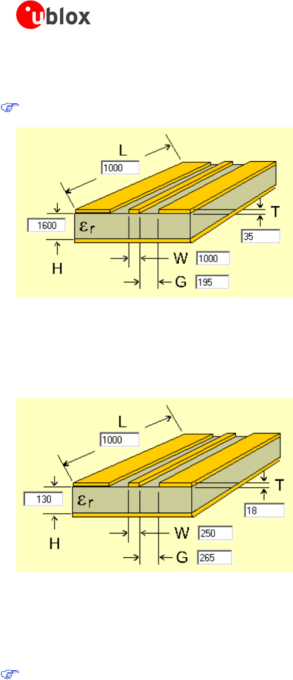
LEA-6 / NEO-6 / MAX-6 - Hardware Integration Manual
GPS.G6-HW-09007-H Preliminary Design-in
Page 45 of 87
For the correct calculation of the micro strip impedance, one does not only need to consider the distance
between the top and the first inner layer but also the distance between the micro strip and the adjacent GND
plane on the same layer
Use the Coplanar Waveguide model for the calculation of the micro strip.
Figure 39: Micro strip on a 2-layer board (Agilent AppCAD Coplanar Waveguide)
Figure 39 shows an example of a 2-layer FR4 board with 1.6 mm thickness and a 35 µm (1 ounce) copper
cladding. The thickness of the micro strip is comprised of the cladding (35µm) plus the plated copper (typically
25µm). Figure 40 is an example of a multi layer FR4 board with 18 µm (½ ounce) cladding and 180 µ dielectric
between layer 1 and 2.
Figure 40: Micro strip on a multi layer board (Agilent AppCAD Coplanar Waveguide)
2.6 Antenna and antenna supervisor
u-blox 6 modules receive L1 band signals from GPS and GALILEO satellites at a nominal frequency of
1575.42 MHz. The RF signal is connected to the RF_IN pin.
u-blox 6 modules can be connected to passive or active antennas.
For u-blox 6 receivers, the total preamplifier gain (minus cable and interconnect losses) must not exceed
50 dB. Total noise figure should be below 3 dB.
u-blox 6 Technology supports short circuit protection of the active antenna and an active antenna supervisor
circuit (open and short circuit detection). For further information refer to Section 2.6.2).
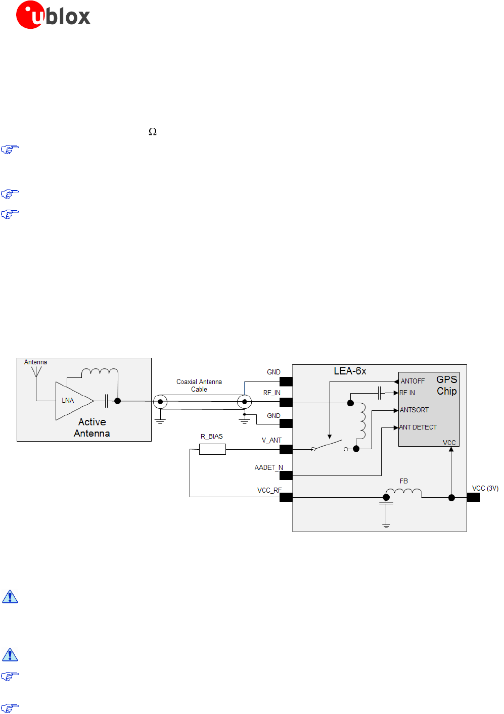
LEA-6 / NEO-6 / MAX-6 - Hardware Integration Manual
GPS.G6-HW-09007-H Preliminary Design-in
Page 46 of 87
2.6.1 Passive antenna
A design using a passive antenna requires more attention regarding the layout of the RF section. Typically a
passive antenna is located near electronic components; therefore care should be taken to reduce electrical
―noise‖ that may interfere with the antenna performance. Passive antennas do not require a DC bias voltage and
can be directly connected to the RF input pin RF_IN. Sometimes, they may also need a passive matching network
to match the impedance to 50 .
Some passive antenna designs present a DC short to the RF input, when connected. If a system is
designed with antenna bias supply AND there is a chance of a passive antenna being connected to the
design, consider a short circuit protection.
All u-blox 6 receivers have a built-in LNA required for passive antennas.
Consider optional ESD protection (see Section 3.3).
2.6.2 Active antenna (LEA-6)
Active antennas have an integrated low-noise amplifier. They can be directly connected to RF_IN. If an active
antenna is connected to RF_IN, the integrated low-noise amplifier of the antenna needs to be supplied with the
correct voltage through pin V_ANT. Usually, the supply voltage is fed to the antenna through the coaxial RF
cable. Active antennas require a power supply that will contribute to the total GPS system power consumption
budget with additional 5 to 20 mA typically. Inside the antenna, the DC component on the inner conductor will
be separated from the RF signal and routed to the supply pin of the LNA (see Figure 41).
Figure 41: Active antenna biasing (for exact pin orientation see data sheet)
Generally an active antenna is easier to integrate into a system design, but an active antenna must also be
placed far from any noise sources to have good performance.
Antennas should only be connected to the receiver when the receiver is not powered. Do not
connect or disconnect the Antenna when the u-blox 6 receiver is running as the receiver
calibrates the noise floor on power-up. Connecting the antenna after power-up can result in
prolonged acquisition time.
Never feed supply voltage into RF_IN on u-blox LEA-6 modules. Always feed via V_ANT.
To test GPS signal reacquisition, it is recommended to physically block the signal to the antenna, rather
than disconnecting and reconnecting the receiver.
Consider optional ESD protection; see section 3.3 for more information.
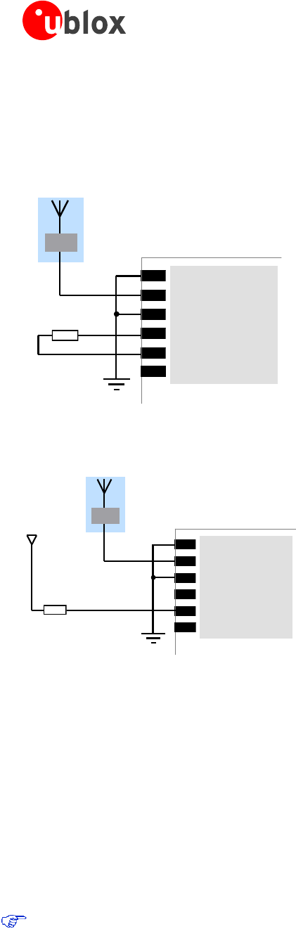
LEA-6 / NEO-6 / MAX-6 - Hardware Integration Manual
GPS.G6-HW-09007-H Preliminary Design-in
Page 47 of 87
2.6.3 Active antenna bias power (LEA-6)
There are two ways to supply the bias voltage to pin V_ANT. For Internal supply, the VCC_RF output must be
connected to V_ANT to supply the antenna with a filtered supply voltage. However, the voltage specification of
the antenna has to match the actual supply voltage of the u-blox 6 Receiver (e.g. 3.0 V).
u-blox 6 Module
GND
RF_IN
GND
Active Antenna
V_ANT
VCC_RF
LNA
R_BIAS
Figure 42: Internal supply Antenna bias voltage (for exact pin orientation see data sheet)
u-blox 6 Module
GND
RF_IN
GND
Active Antenna
V_ANT
VCC_RF
LNA
external
antenna
voltage
supply
R_BIAS
Figure 43: External supplying Antenna bias voltage (for exact pin orientation see data sheet)
Since the bias voltage is fed into the most sensitive part of the receiver, i.e. the RF input, this supply should be
virtually free of noise. Usually, low frequency noise is less critical than digital noise with spurious frequencies with
harmonics up to the GPS/GALILEO band of 1.575 GHz. Therefore, it is not recommended to use digital supply
nets to feed pin V_ANT.
An internal switch (under control of the u-blox 6 software) can shut down the supply to the external antenna
whenever it is not needed. This feature helps to reduce power consumption.
2.6.3.1 Short circuit protection
If a reasonably dimensioned series resistor R_BIAS is placed in front of pin V_ANT, a short circuit situation can
be detected by the baseband processor. If such a situation is detected, the baseband processor will shut down
supply to the antenna. The receiver is by default configured to attempt to reestablish antenna power supply
periodically.
To configure the antenna supervisor use the UBX-CFG-ANT message. For further information refer to the
u-blox 6 Receiver Description including Protocol Specification [3].
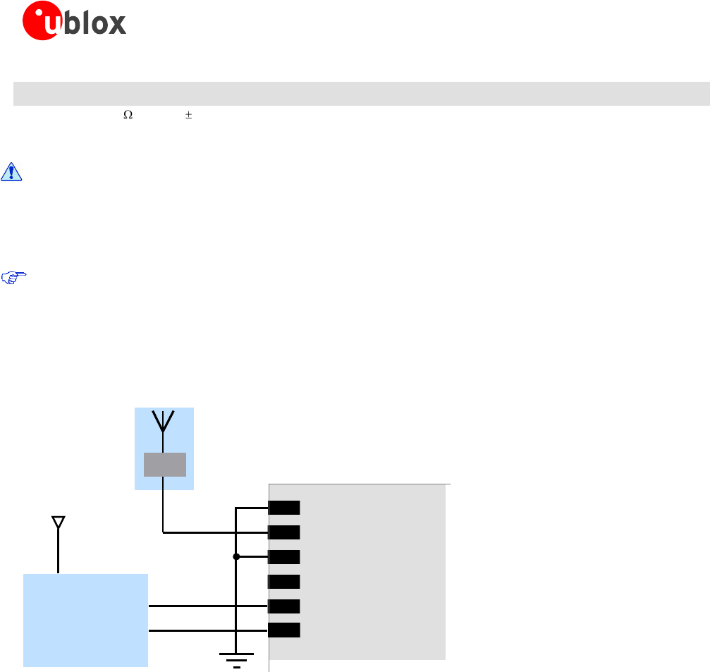
LEA-6 / NEO-6 / MAX-6 - Hardware Integration Manual
GPS.G6-HW-09007-H Preliminary Design-in
Page 48 of 87
References
Value
Tolerance
Description
Manufacturer
R_BIAS
10
10%
Resistor, min 0.250 W
Table 17: Short circuit protection, bill of material
Short circuits on the antenna input without limitation (R_BIAS) of the current can result in
permanent damage to the receiver! Therefore, it’s recommended to implement an R_BIAS in all
risk applications, such as situations where the antenna can be disconnected by the end-user or
that have long antenna cables.
An additional R_BIAS is not required when using a short and open active antenna supervisor circuitry as
defined in Section 2.6.4.1, as the R_BIAS is equal to R2.
2.6.4 Active antenna supervisor (LEA-6)
u-blox 6 Technology provides the means to implement an active antenna supervisor with a minimal number of
parts. The antenna supervisor is highly configurable to suit various different applications.
u-blox 6 Module
GND
RF_IN
GND
Active Antenna
V_ANT
VCC_RF
LNA
AADET_N
Antenna
Supervisor
Circuitry
external
antenna
voltage
supply
Figure 44: External antenna power supply with full antenna supervisor (for exact pin orientation see data sheet)
2.6.4.1 Short and open circuit active antenna supervisor
The Antenna Supervisor can be configured by a serial port message (using only UBX binary message). When
enabled the active antenna supervisor produces serial port messages (status reporting in NMEA and/or UBX
binary protocol) which indicates all changes of the antenna circuitry (disabled antenna supervisor, antenna
circuitry ok, short circuit, open circuit) and shuts the antenna supply down if required. Active antenna status
can be determined also polling UBX-MON-HW.
The active antenna supervisor provides the means to check the active antenna for open and short circuits and to
shut the antenna supply off, if a short circuit is detected. The state diagram in Figure 45 applies. If an antenna is
connected, the initial state after power-up is “Active Antenna OK”.
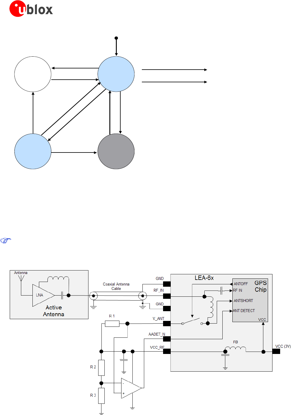
LEA-6 / NEO-6 / MAX-6 - Hardware Integration Manual
GPS.G6-HW-09007-H Preliminary Design-in
Page 49 of 87
No
Super-
vision
Active
Antenna
OK
Open
Circuit
detected
Short
Circuit
detected
Powerup
Events AADET0_N
User controlled events
Disable Supervision
Enable Supervision
Short Circuit
detected
Disable
Supervision
Antenna
connected
Short Circuit
detected
open circuit
detected, given
OCD enabled
Periodic
reconnection
attempts
Figure 45: State diagram of active antenna supervisor
Firmware supports an active antenna supervisor circuit, which is connected to the pin AADET_N. An example of
an open circuit detection circuit is shown in Figure 46 and Figure 47. High on AADET_N means that an external
antenna is not connected.
Short Circuit Detection (SCD)
A short circuit in the active antenna pulls V_ANT to ground. This is detected inside the u-blox 6 module and the
antenna supply voltage will be immediately shut down.
Antenna short detection (SCD) and control is enabled by default.
Open Circuit Detection (OCD)
Figure 46: Schematic of open circuit detection variant A (for exact pin orientation see data sheet)
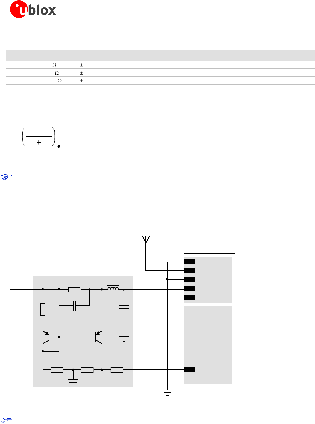
LEA-6 / NEO-6 / MAX-6 - Hardware Integration Manual
GPS.G6-HW-09007-H Preliminary Design-in
Page 50 of 87
References
Value
Tolerance
Description
Remarks
R1
10
5%
Resistor, min 0.250 W
R2
560
5%
Resistor
R3
100 k
5%
Resistor
U1
LT6000
Rail to Rail Op Amp
Linear Technology
Table 18: Active antenna supervisor, bill of material
RFVcc
R
RR
R
I_
1
32
2
Equation 1: Calculation of threshold current for open circuit detection
If the antenna supply voltage is not derived from Vcc_RF, do not exceed the maximum voltage rating of
AADET_N.
The open circuit detection circuit uses the current flow to detect an open circuit in the antenna. The threshold
current can be calculated using Equation 1.
GND
RF_IN
GND
V_ANT
VCC_RF
Active Antenna
ADDET_N
V_ANT
Antenna
Supply in
Analog GND
R1
R2
R3 R4 R5
T2
PNP
T1
PNP
C1
C2
FB1
AADET_N
LEA-6x
Figure 47: Schematic of open circuit detection variant B (for exact pin orientation see data sheet)
The open circuit supervisor circuitry shown in Figure 47 has a quiescent current of approximately 2mA.
This current can be reduced with an advanced circuitry such as shown in Figure 47.
LEA-6 / NEO-6 / MAX-6 - Hardware Integration Manual
GPS.G6-HW-09007-H Preliminary Design-in
Page 51 of 87
References
Value
Tolerance
Description
Remarks / Manufacturer
C1
2.2 µF
10%
Capacitor, X7R, min 10 V
C2
100 nF
10%
Capacitor, X7R, min 10 V
FB1
600
Ferrite Bead
e.g. Murata BLM18HD601SN1
R1
15
10%
Resistor, min 0.063 W
R2
10
10%
Resistor, min 0.250 W
R3, R4
10 k
10%
Resistor, min 0.063 W
R5
33 k
10%
Resistor, min 0.063 W
T1, T2
BC856B
PNP Transistor
e.g. Philips Semiconductors7
Table 19: Active antenna supervisor, bill of material
Status reporting
At startup and on every change of the antenna supervisor configuration the u-blox 6 GPS/GALILEO module will
output a NMEA ($GPTXT) or UBX (INF-NOTICE) message with the internal status of the antenna supervisor
(disabled, short detection only, enabled).
None, one or several of the strings below are part of this message to inform about the status of the active
antenna supervisor circuitry (e.g. “ANTSUPERV= AC SD OD PdoS”).
Abbreviation
Description
AC
Antenna Control (e.g. the antenna will be switched on/ off controlled by the GPS receiver)
SD
Short Circuit Detection Enabled
SR
Short Circuit Recovery Enabled
OD
Open Circuit Detection Enabled
PdoS
Power Down on short
Table 20: Active Antenna Supervisor Message on startup (UBX binary protocol)
To activate the antenna supervisor use the UBX-CFG-ANT message. For further information refer to the
u-blox 6 Receiver Description including Protocol Specification [3].
Similar to the antenna supervisor configuration, the status of the antenna supervisor will be reported in a NMEA
($GPTXT) or UBX (INF-NOTICE) message at start-up and on every change.
Message
Description
ANTSTATUS=DONTKNOW
Active antenna supervisor is not configured and deactivated.
ANTSTATUS=OK
Active antenna connected and powered
ANTSTATUS=SHORT
Antenna short
ANTSTATUS=OPEN
Antenna not connected or antenna defective
Table 21: Active antenna supervisor message on startup (NMEA protocol)
2.6.5 Active antenna (NEO-6 and MAX-6)
NEO-6 and MAX-6 modules do not provide the antenna bias voltage for active antennas on the RF_IN pin. It is
therefore necessary to provide this voltage outside the module via an inductor L as indicated in Figure 48. u-blox
recommends using an inductor from Murata (LQG15HS27NJ02). Alternative parts can be used if the inductor‖s
resonant frequency matches the GPS frequency of 1575.42 MHz.
7
Transistors from other suppliers with comparable electrical characteristics may be used.
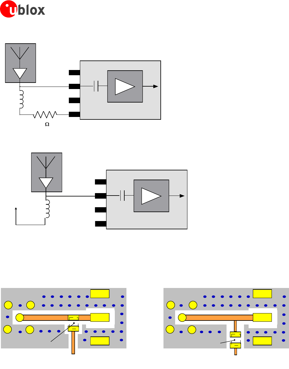
LEA-6 / NEO-6 / MAX-6 - Hardware Integration Manual
GPS.G6-HW-09007-H Preliminary Design-in
Page 52 of 87
Low Noise Amplifier
Active Antenna
RF_IN
VCC_RF
GND
GND
10
R_BIAS
L
Figure 48: Internal antenna bias voltage for active antennas
Low Noise Amplifier
Active Antenna
RF_IN
VCC_RF
GND
GND
External
antenna
supply
voltage L
Figure 49: External antenna bias voltage for active antennas
For optimal performance, it is important to place the inductor as close to the microstrip as possible. Figure 50
illustrates the recommended layout and how it should not be done.
GND
Microstrip
GND
RF_IN
Antenna Supply Voltage
(e.g. VCC_RF)
Inductor L GND
GND
Antenna Supply Voltage
(e.g. VCC_RF)
Inductor L
Microstrip RF_IN
Good Bad
Figure 50: Recommended layout for connecting the antenna bias voltage for LEA-6M and NEO-6
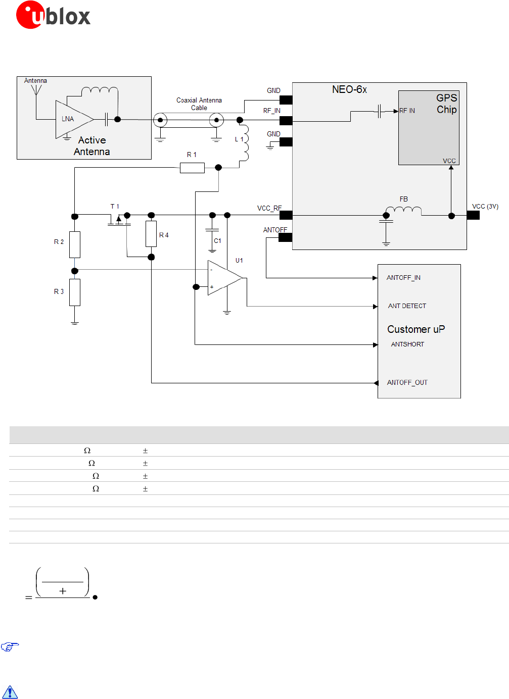
LEA-6 / NEO-6 / MAX-6 - Hardware Integration Manual
GPS.G6-HW-09007-H Preliminary Design-in
Page 53 of 87
2.6.6 External active antenna supervisor using ANTOFF (NEO-6)
Figure 51: External active antenna supervisor using ANTOFF (NEO-6)
References
Value
Tolerance
Description
Remarks / Manufacturer
R1
10
5%
Resistor, min 0.25 W
R2
560
5%
Resistor
R3
100 k
5%
Resistor
R4
100 k
5%
Resistor
U1
LT6000
Rail to Rail Op Amp
Linear Technology
T1
Si1016X-T1-E3
Transistor
Vishay
L1
LQG15HS27NJ02
Inductor
muRata
C1
X5R 100N 10V
10%
Decoupling Capacitor
muRata
Table 22: Active antenna supervisor, bill of material
RFVcc
R
RR
R
I_
1
32
2
Equation 2: Calculation of threshold current for open circuit detection
State diagram of active antenna supervisor see Figure 45. When using an external LNA in PSM on / off
mode, pin 17 can be programmed as ANTOFF (see 1.7.7). Use ANTOFF_IN and ANTOFF_OUT signals to
command antenna power supply when going into Power Save Mode (Backup mode).
Use caution when implementing ANTOFF configuration since forward compatibility is not
guaranteed
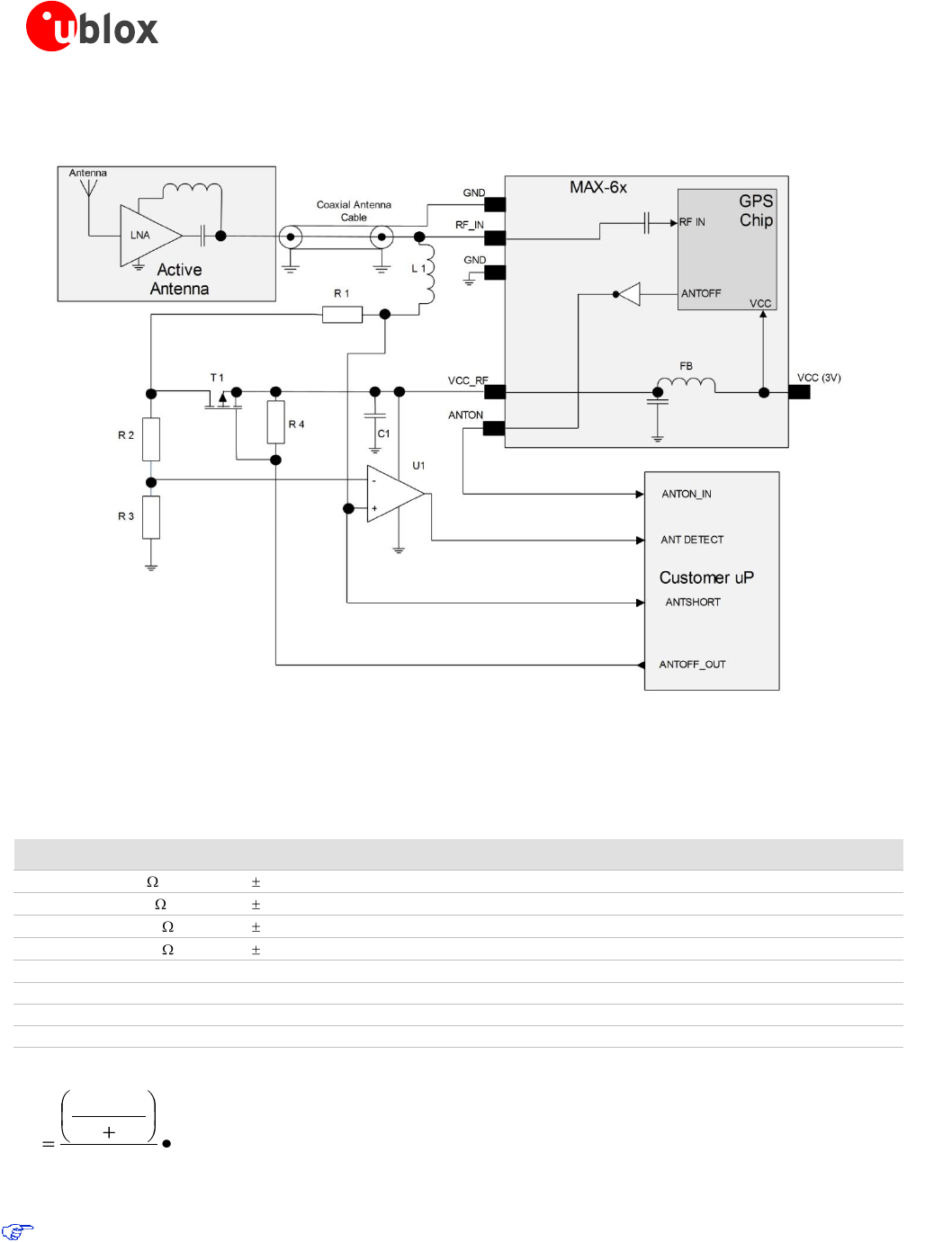
LEA-6 / NEO-6 / MAX-6 - Hardware Integration Manual
GPS.G6-HW-09007-H Preliminary Design-in
Page 54 of 87
2.6.7 External active antenna supervisor using ANTON (MAX-6)
Figure 52: External active antenna supervisor using ANON (MAX-6)
References
Value
Tolerance
Description
Remarks / Manufacturer
R1
10
5%
Resistor, min 0.25 W
R2
560
5%
Resistor
R3
100 k
5%
Resistor
R4
100 k
5%
Resistor
U1
LT6000
Rail to Rail Op Amp
Linear Technology
T1
Si1016X-T1-E3
Transistor
Vishay
L1
LQG15HS27NJ02
Inductor
muRata
C1
X5R 100N 10V
10%
Decoupling Capacitor
muRata
Table 23: Active antenna supervisor, bill of material
RFVcc
R
RR
R
I_
1
32
2
Equation 3: Calculation of threshold current for open circuit detection
State diagram of active antenna supervisor see Figure 45. When using an external LNA in PSM on / off
mode, pin 17 can be programmed as ANTOFF (see 1.7.7). Use ANTOFF_IN and ANTOFF_OUT signals to
command antenna power supply when going into Power Save Mode (Backup mode).
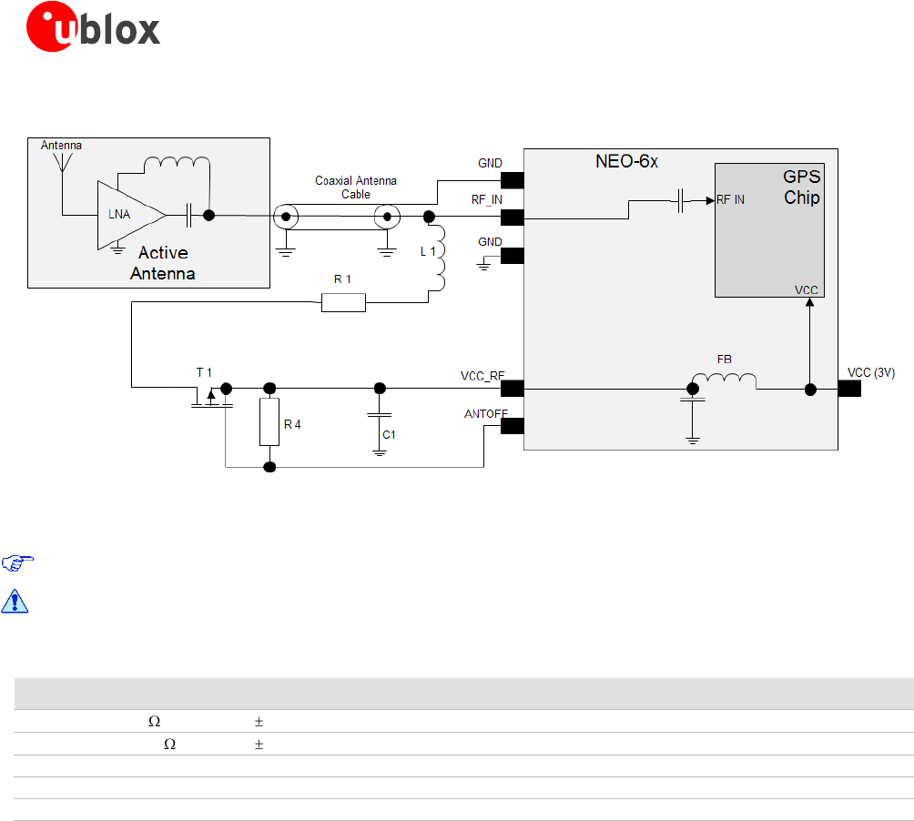
LEA-6 / NEO-6 / MAX-6 - Hardware Integration Manual
GPS.G6-HW-09007-H Preliminary Design-in
Page 55 of 87
2.6.8 External active antenna control (NEO-6)
Figure 53: External active antenna control (NEO-6)
When using an external LNA in PSM on / off mode, pin 17 can be programmed as ANTOFF (see 1.7.7).
Use caution when implementing ANTOFF configuration since forward compatibility is not
guaranteed
References
Value
Tolerance
Description
Remarks / Manufacturer
R1
10
5%
Resistor, min 0.25 W
R4
100 k
5%
Resistor
T1
Si1016X-T1-E3
Transistor
Vishay
L1
LQG15HS27NJ02
Inductor
muRata
C1
X5R 100N 10V
10%
Decoupling Capacitor
muRata
Table 24: Active antenna control, bill of material
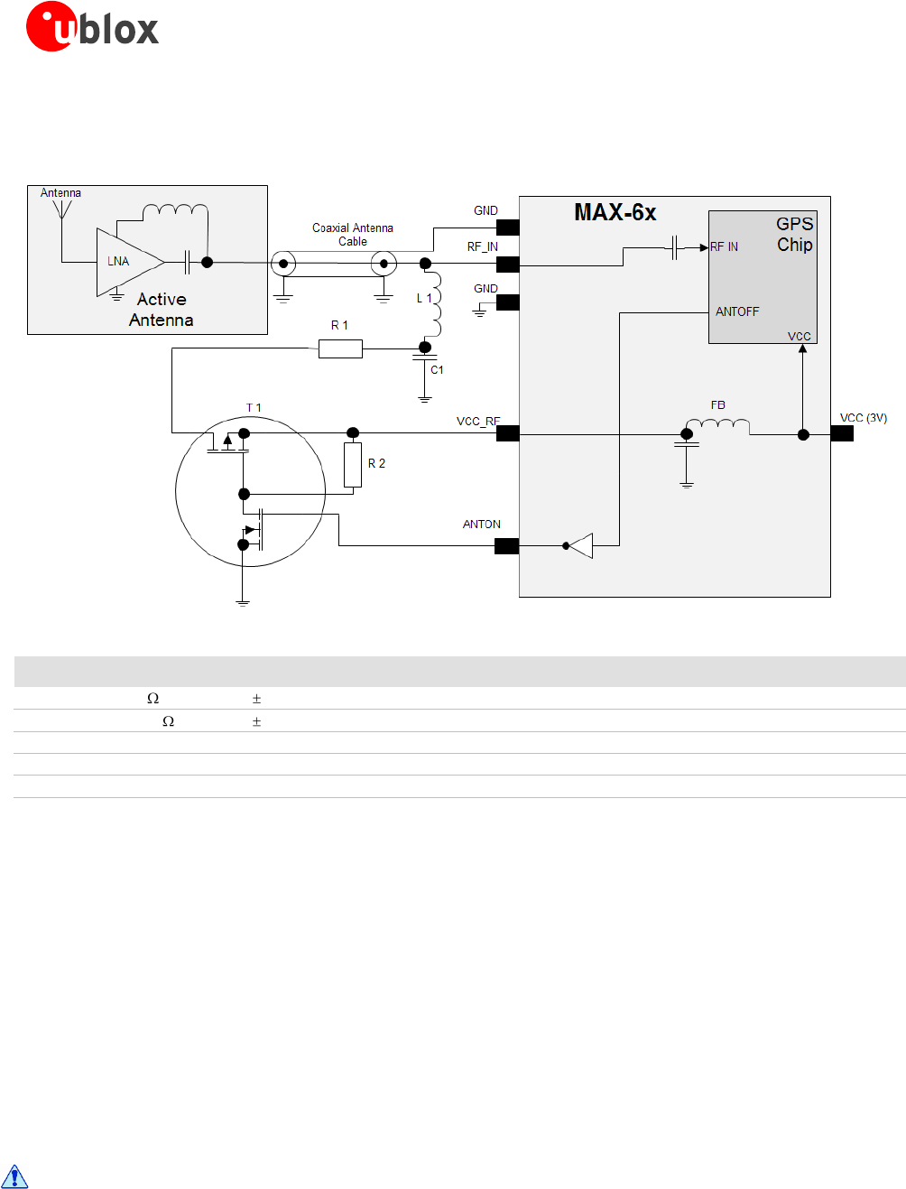
LEA-6 / NEO-6 / MAX-6 - Hardware Integration Manual
GPS.G6-HW-09007-H Preliminary Design-in
Page 56 of 87
2.6.9 External active antenna control (MAX-6)
ANTON Signal can be used to turn on and off an external LNA. This reduces power consumption in Power
Save Mode (Backup mode).
Figure 54: External active antenna control (MAX-6)
References
Value
Tolerance
Description
Remarks / Manufacturer
R1
10
5%
Resistor, min 0.25 W
R2
100 k
5%
Resistor
T1
Si1040X
Power MOSFET
Vishay
L1
LQG15HS27NJ02
Inductor
muRata
C1
X5R 1N 10V
10%
Decoupling Capacitor
muRata
Table 25: Active antenna control, bill of material
2.6.10 GPS antenna placement for LEA-6R
For an optimum ADR navigation performance, the following setup recommendations should be considered.
GPS antenna placement, gyro placement and single tick origin
Due to geometric and dynamic aspects of driving vehicles, it is important to correctly place the GPS antenna and
the external sensors - from a geometric point of view - in order to get consistent measurement information from
the different sensors.
For standard road vehicles: The GPS antenna should be placed above the middle of the rear (unsteered) axis. The
gyro can be placed anywhere on the vehicle. Single ticks should origin from the rear (unsteered) wheels. For
articulated busses, the sensors should be placed on the front car as if this was a standard road vehicle. In case
the GWT solution is used for rail vehicles: The GPS antenna should be placed in the middle of a wagon, while
the gyro can be placed anywhere on the same wagon and the single ticks can origin from any wheels of the
same wagon.
Large geometrical deviations from the optimal placement - especially of the GPS antenna (e.g.
when placing it above the front axis of a long bus) - can result in significant performance
degradation!

LEA-6 / NEO-6 / MAX-6 - Hardware Integration Manual
GPS.G6-HW-09007-H Preliminary Product handling
Page 57 of 87
3 Product handling
3.1 Packaging, shipping, storage and moisture preconditioning
For information pertaining to reels and tapes, Moisture Sensitivity levels (MSD), shipment and storage
information, as well as drying for preconditioning see the data sheet of the specific u-blox 6 GPS module.
3.2 Soldering
3.2.1 Soldering paste
Use of "No Clean" soldering paste is strongly recommended, as it does not require cleaning after the soldering
process has taken place. The paste listed in the example below meets these criteria.
Soldering Paste: OM338 SAC405 / Nr.143714 (Cookson Electronics)
Alloy specification: Sn 95.5/ Ag 4/ Cu 0.5 (95.5% Tin/ 4% Silver/ 0.5% Copper)
Melting Temperature: 217°C
Stencil Thickness: 150 µm for base boards
The final choice of the soldering paste depends on the approved manufacturing procedures.
The paste-mask geometry for applying soldering paste should meet the recommendations in section 2.5.1.
The quality of the solder joints on the connectors (‖half vias‖) should meet the appropriate IPC
specification.
3.2.2 Reflow soldering
A convection type-soldering oven is strongly recommended over the infrared type radiation oven.
Convection heated ovens allow precise control of the temperature and all parts will be heated up evenly,
regardless of material properties, thickness of components and surface color.
Consider the "IPC-7530 Guidelines for temperature profiling for mass soldering (reflow and wave) processes,
published 2001".
Preheat phase
Initial heating of component leads and balls. Residual humidity will be dried out. Please note that this preheat
phase will not replace prior baking procedures.
Temperature rise rate: max.3°C/s If the temperature rise is too rapid in the preheat phase it may cause
excessive slumping.
Time: 60 – 120 s If the preheat is insufficient, rather large solder balls tend to be
generated. Conversely, if performed excessively, fine balls and large
balls will be generated in clusters.
End Temperature: 150 - 200°C If the temperature is too low, non-melting tends to be caused in
areas containing large heat capacity.
Heating/ Reflow phase
The temperature rises above the liquidus temperature of 217°C. Avoid a sudden rise in temperature as the slump
of the paste could become worse.
Limit time above 217°C liquidus temperature: 40 – 60 s
Peak reflow temperature: 245°C
Cooling phase
A controlled cooling avoids negative metallurgical effects (solder becomes more brittle) of the solder and
possible mechanical tensions in the products. Controlled cooling helps to achieve bright solder fillets with a
good shape and low contact angle.
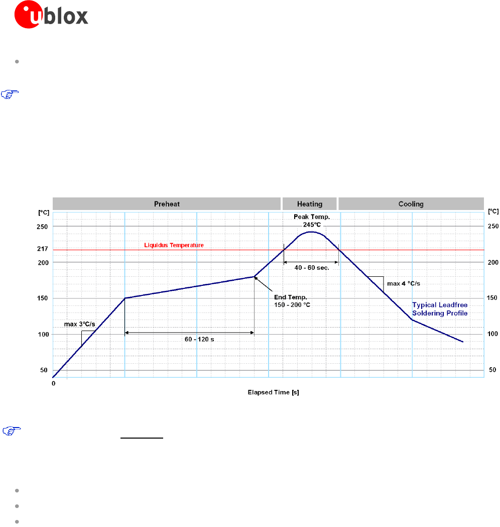
LEA-6 / NEO-6 / MAX-6 - Hardware Integration Manual
GPS.G6-HW-09007-H Preliminary Product handling
Page 58 of 87
Temperature fall rate: max 4°C / s
To avoid falling off, the u-blox 6 GPS module should be placed on the topside of the motherboard during
soldering.
The final soldering temperature chosen at the factory depends on additional external factors like choice of
soldering paste, size, thickness and properties of the base board, etc. Exceeding the maximum soldering
temperature in the recommended soldering profile may permanently damage the module.
Figure 55: Recommended soldering profile
u-blox 6 modules must not be soldered with a damp heat process.
3.2.3 Optical inspection
After soldering the u-blox 6 module, consider an optical inspection step to check whether:
The module is properly aligned and centered over the pads
All pads are properly soldered
No excess solder has created contacts to neighboring pads, or possibly to pad stacks and vias nearby.

LEA-6 / NEO-6 / MAX-6 - Hardware Integration Manual
GPS.G6-HW-09007-H Preliminary Product handling
Page 59 of 87
3.2.4 Cleaning
In general, cleaning the populated modules is strongly discouraged. Residues underneath the modules cannot be
easily removed with a washing process.
Cleaning with water will lead to capillary effects where water is absorbed in the gap between the baseboard
and the module. The combination of residues of soldering flux and encapsulated water leads to short
circuits or resistor-like interconnections between neighboring pads.
Cleaning with alcohol or other organic solvents can result in soldering flux residues flooding into the two
housings, areas that are not accessible for post-wash inspections. The solvent will also damage the sticker
and the ink-jet printed text.
Ultrasonic cleaning will permanently damage the module, in particular the quartz oscillators.
The best approach is to use a "no clean" soldering paste and eliminate the cleaning step after the soldering.
3.2.5 Repeated reflow soldering
Only single reflow soldering processes are recommended for boards populated with u-blox 6 modules. u-blox 6
modules should not be submitted to two reflow cycles on a board populated with components on both sides in
order to avoid upside down orientation during the second reflow cycle. In this case the module should always be
placed on that side of the board which is submitted into the last reflow cycle. The reason for this (besides others)
is the risk of the module falling off due to the significantly higher weight in relation to other components.
Two reflow cycles can be considered by excluding the above described upside down scenario and taking into
account the rework conditions described in Section 3.2.8.
Repeated reflow soldering processes and soldering the module upside down are not recommended.
3.2.6 Wave soldering
Base boards with combined through-hole technology (THT) components and surface-mount technology (SMT)
devices require wave soldering to solder the THT components. Only a single wave soldering process is
encouraged for boards populated with u-blox 6 modules.
3.2.7 Hand soldering
Hand soldering is allowed. Use a soldering iron temperature setting equivalent to 350°C and carry out the hand
soldering according to the IPC recommendations / reference documents IPC7711. Place the module precisely on
the pads. Start with a cross-diagonal fixture soldering (e.g. pins 1 and 15), and then continue from left to right.
3.2.8 Rework
The u-blox 6 module can be unsoldered from the baseboard using a hot air gun. When using a hot air gun for
unsoldering the module, max 1 reflow cycle is allowed. In general we do not recommend using a hot air gun
because this is an uncontrolled process and might damage the module.
Attention: use of a hot air gun can lead to overheating and severely damage the module.
Always avoid overheating the module.
After the module is removed, clean the pads before placing and hand-soldering a new module.
Never attempt a rework on the module itself, e.g. replacing individual components. Such
actions immediately terminate the warranty.
In addition to the two reflow cycles manual rework on particular pins by using a soldering iron is allowed. For
hand soldering the recommendations in IPC 7711 should be followed. Manual rework steps on the module can
be done several times.
LEA-6 / NEO-6 / MAX-6 - Hardware Integration Manual
GPS.G6-HW-09007-H Preliminary Product handling
Page 60 of 87
3.2.9 Conformal coating
Certain applications employ a conformal coating of the PCB using HumiSeal® or other related coating products.
These materials affect the HF properties of the GPS module and it is important to prevent them from flowing
into the module. The RF shields do not provide 100% protection for the module from coating liquids with low
viscosity; therefore care is required in applying the coating.
Conformal Coating of the module will void the warranty.
3.2.10 Casting
If casting is required, use viscose or another type of silicon pottant. The OEM is strongly advised to qualify such
processes in combination with the u-blox 6 module before implementing this in the production.
Casting will void the warranty.
3.2.11 Grounding metal covers
Attempts to improve grounding by soldering ground cables, wick or other forms of metal strips directly onto the
EMI covers is done at the customer's own risk. The numerous ground pins should be sufficient to provide
optimum immunity to interferences and noise.
u-blox makes no warranty for damages to the u-blox 6 module caused by soldering metal cables or any
other forms of metal strips directly onto the EMI covers.
3.2.12 Use of ultrasonic processes
Some components on the u-blox 6 module are sensitive to Ultrasonic Waves. Use of any Ultrasonic Processes
(cleaning, welding etc.) may cause damage to the GPS Receiver.
u-blox offers no warranty against damages to the u-blox 6 module caused by any Ultrasonic Processes.
3.3 EOS/ESD/EMI Precautions
When integrating GPS receivers into wireless systems, careful consideration must be given to electromagnetic
and voltage susceptibility issues. Wireless systems include components which can produce Electrical Overstress
(EOS) and Electro-Magnetic Interference (EMI). CMOS devices are more sensitive to such influences because their
failure mechanism is defined by the applied voltage, whereas bipolar semiconductors are more susceptible to
thermal overstress. The following design guidelines are provided to help in designing robust yet cost effective
solutions.
To avoid overstress damage during production or in the field it is essential to observe strict
EOS/ESD/EMI handling and protection measures.
To prevent overstress damage at the RF_IN of your receiver, never exceed the maximum input
power (see Data Sheet).
3.3.1 Abbreviations
For a list of abbreviations used see Table 28 in Appendix A.
3.3.2 Electrostatic discharge (ESD)
Electrostatic discharge (ESD) is the sudden and momentary electric current that flows between
two objects at different electrical potentials caused by direct contact or induced by an
electrostatic field. The term is usually used in the electronics and other industries to describe
momentary unwanted currents that may cause damage to electronic equipment.
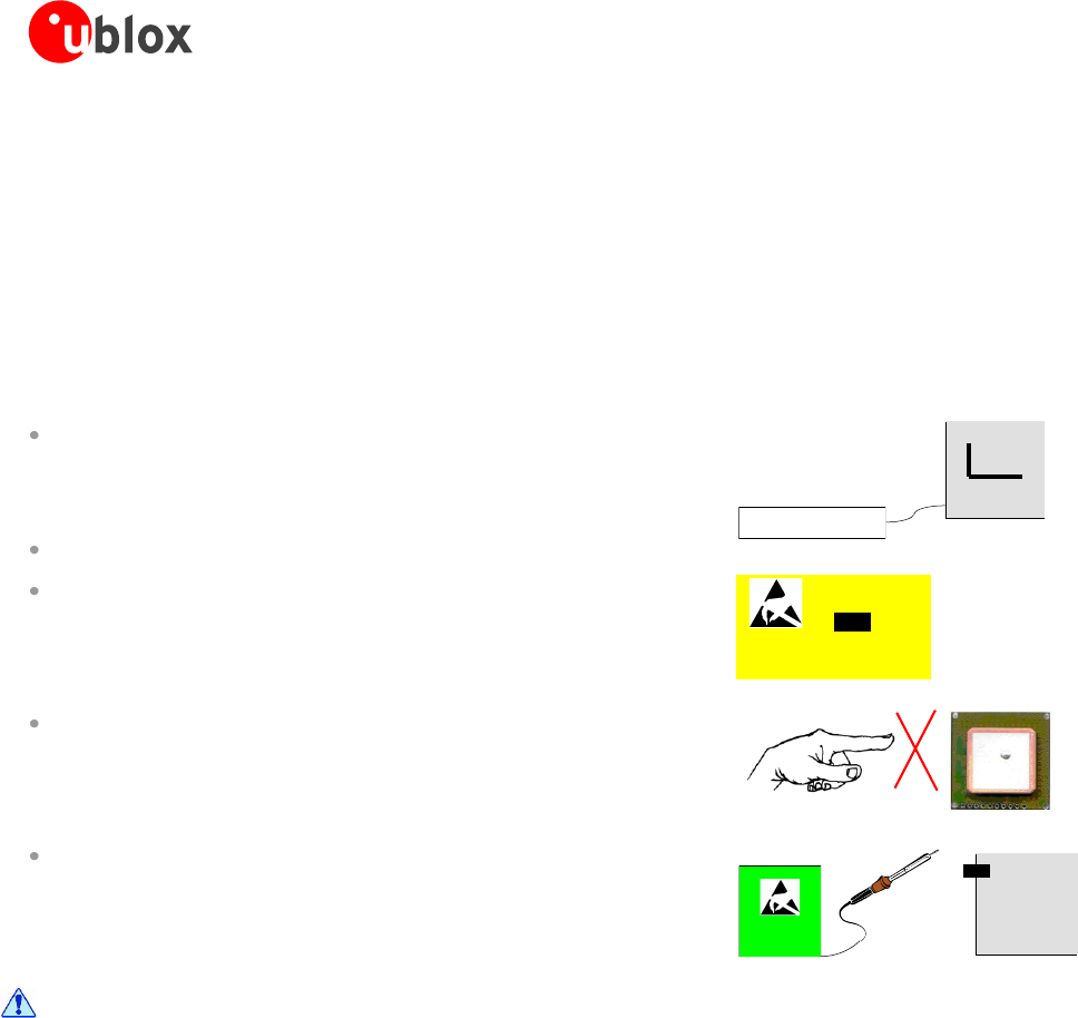
LEA-6 / NEO-6 / MAX-6 - Hardware Integration Manual
GPS.G6-HW-09007-H Preliminary Product handling
Page 61 of 87
3.3.3 ESD handling precautions
ESD prevention is based on establishing an Electrostatic Protective Area (EPA). The EPA can be a small working
station or a large manufacturing area. The main principle of an EPA is that there are no highly charging materials
in the vicinity of ESD sensitive electronics, all conductive materials are grounded, workers are grounded, and
charge build-up on ESD sensitive electronics is prevented. International standards are used to define typical EPA
and can be obtained for example from International Electrotechnical Commission (IEC) or American National
Standards Institute (ANSI).
GPS receivers are sensitive to ESD and require special precautions when handling. Particular care must be
exercised when handling patch antennas, due to the risk of electrostatic charges. In addition to standard ESD
safety practices, the following measures should be taken into account whenever handling the receiver.
Unless there is a galvanic coupling between the local GND (i.e. the
work table) and the PCB GND, the first point of contact when
handling the PCB shall always be between the local GND and PCB
GND.
Before mounting an antenna patch, connect ground of the device.
GND
Local GND
When handling the RF pin, do not come into contact with any
charged capacitors and be careful when contacting materials that
can develop charges (e.g. patch antenna ~10 pF, coax cable ~50-
80 pF/m, soldering iron, …)
ESD
Sensitive!
RF_IN
To prevent electrostatic discharge through the RF input, do not
touch any exposed antenna area. If there is any risk that such
exposed antenna area is touched in non ESD protected work area,
implement proper ESD protection measures in the design.
When soldering RF connectors and patch antennas to the receiver‖s
RF pin, make sure to use an ESD safe soldering iron (tip).
RF_IN
ESD Safe
Failure to observe these precautions can result in severe damage to the GPS receiver!
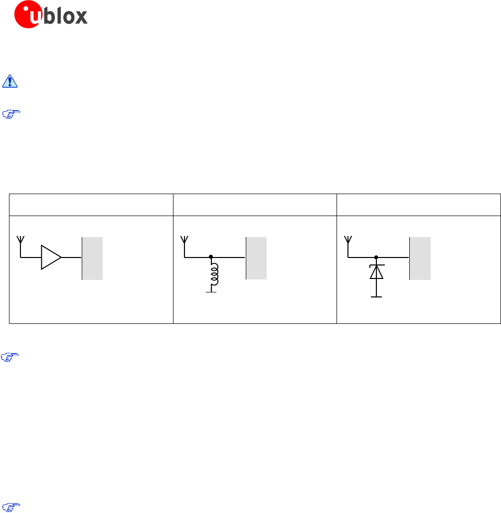
LEA-6 / NEO-6 / MAX-6 - Hardware Integration Manual
GPS.G6-HW-09007-H Preliminary Product handling
Page 62 of 87
3.3.4 ESD protection measures
GPS receivers are sensitive to Electrostatic Discharge (ESD). Special precautions are required
when handling.
For more robust designs, employ additional ESD protection measures. Using an LNA with appropriate ESD
rating can provide enhanced GPS performance with passive antennas and increases ESD protection.
Most defects caused by ESD can be prevented by following strict ESD protection rules for production and
handling. When implementing passive antenna patches or external antenna connection points, then additional
ESD measures as shown in Figure 56 can also avoid failures in the field.
Small passive antennas (<2 dBic and
performance critical)
Passive antennas (>2 dBic or performance
sufficient)
Active Antennas
A
RF_IN
GPS
Receiver
LNA
B
L
RF_IN
GPS
Receiver
C
D
RF_IN
GPS
Receiver
LNA with appropriate ESD rating
Figure 56: ESD Precautions
Protection measure A is preferred because it offers the best GPS performance and best level of ESD
protection.
3.3.5 Electrical Overstress (EOS)
Electrical Overstress (EOS) usually describes situations when the maximum input power exceeds the maximum
specified ratings. EOS failure can happen if RF emitters are close to a GPS receiver or its antenna. EOS causes
damage to the chip structures.
If the RF_IN is damaged by EOS, it‖s hard to determine whether the chip structures have been damaged by ESD
or EOS.
3.3.6 EOS protection measures
For designs with GPS receivers and wireless (e.g. GSM/GPRS) transceivers in close proximity, ensure
sufficient isolation between the wireless and GPS antennas. If wireless power output causes the specified
maximum power input at the GPS RF_IN to be exceeded, employ EOS protection measures to prevent
overstress damage.
For robustness, EOS protection measures as shown in Figure 57 are recommended for designs combining
wireless communication transceivers (e.g. GSM, GPRS) and GPS in the same design or in close proximity.
See C26 telematics reference design [9].
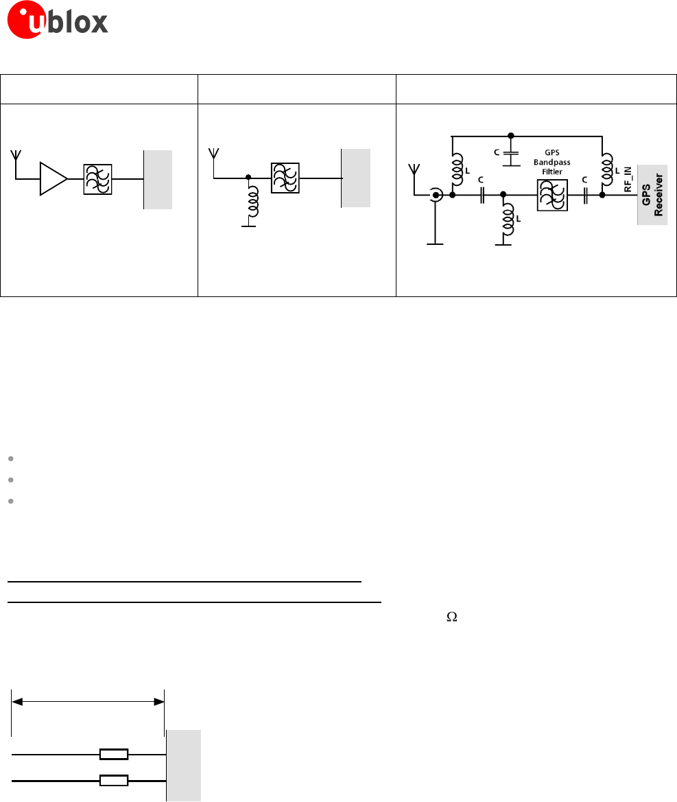
LEA-6 / NEO-6 / MAX-6 - Hardware Integration Manual
GPS.G6-HW-09007-H Preliminary Product handling
Page 63 of 87
Small passive antennas (<2 dBic and
performance critical)
Passive antennas (>2 dBic or
performance sufficient)
Active Antennas (without internal filter which need
the module antenna supervisor circuits)
D
RF_IN
GPS
Receiver
LNA
GPS
Bandpass
Filtler
E
RF_IN
GPS
Receiver
L
GPS
Bandpass
Filtler
F
LNA with appropriate ESD rating and
maximum input power
GPS Bandpass Filter: SAW or Ceramic
with low insertion loss and appropriate
ESD rating
Figure 57: EOS and ESD Precautions
3.3.7 Electromagnetic interference (EMI)
Electromagnetic interference (EMI) is the addition or coupling of energy originating from any RF emitting device.
This can cause a spontaneous reset of the GPS receiver or result in unstable performance. Any unshielded line or
segment (>3mm) connected to the GPS receiver can effectively act as antenna and lead to EMI disturbances or
damage.
The following elements are critical regarding EMI:
Unshielded connectors (e.g. pin rows etc.)
Weakly shielded lines on PCB (e.g. on top or bottom layer and especially at the border of a PCB)
Weak GND concept (e.g. small and/or long ground line connections)
EMI protection measures are recommended when RF emitting devices are near the GPS receiver. To minimize the
effect of EMI a robust grounding concept is essential. To achieve electromagnetic robustness follow the standard
EMI suppression techniques.
http://www.murata.com/products/emc/knowhow/index.html
http://www.murata.com/products/emc/knowhow/pdf/4to5e.pdf
Improved EMI protection can be achieved by inserting a resistor (e.g. R>20 ) or better yet a ferrite bead
(BLM15HD102SN1) or an inductor (LQG15HS47NJ02) into any unshielded PCB lines connected to the GPS
receiver. Place the resistor as close as possible to the GPS receiver pin.
Example of EMI protection measures on the RX/TX line using a ferrite bead:
TX
RX
GPS
Receiver
FB
FB
BLM15HD102SN1
>10mm
Figure 58: EMI Precautions
VCC can be protected using a feed thru capacitor. For electromagnetic compatibility (EMC) of the RF_IN pin refer
to section 3.3.6
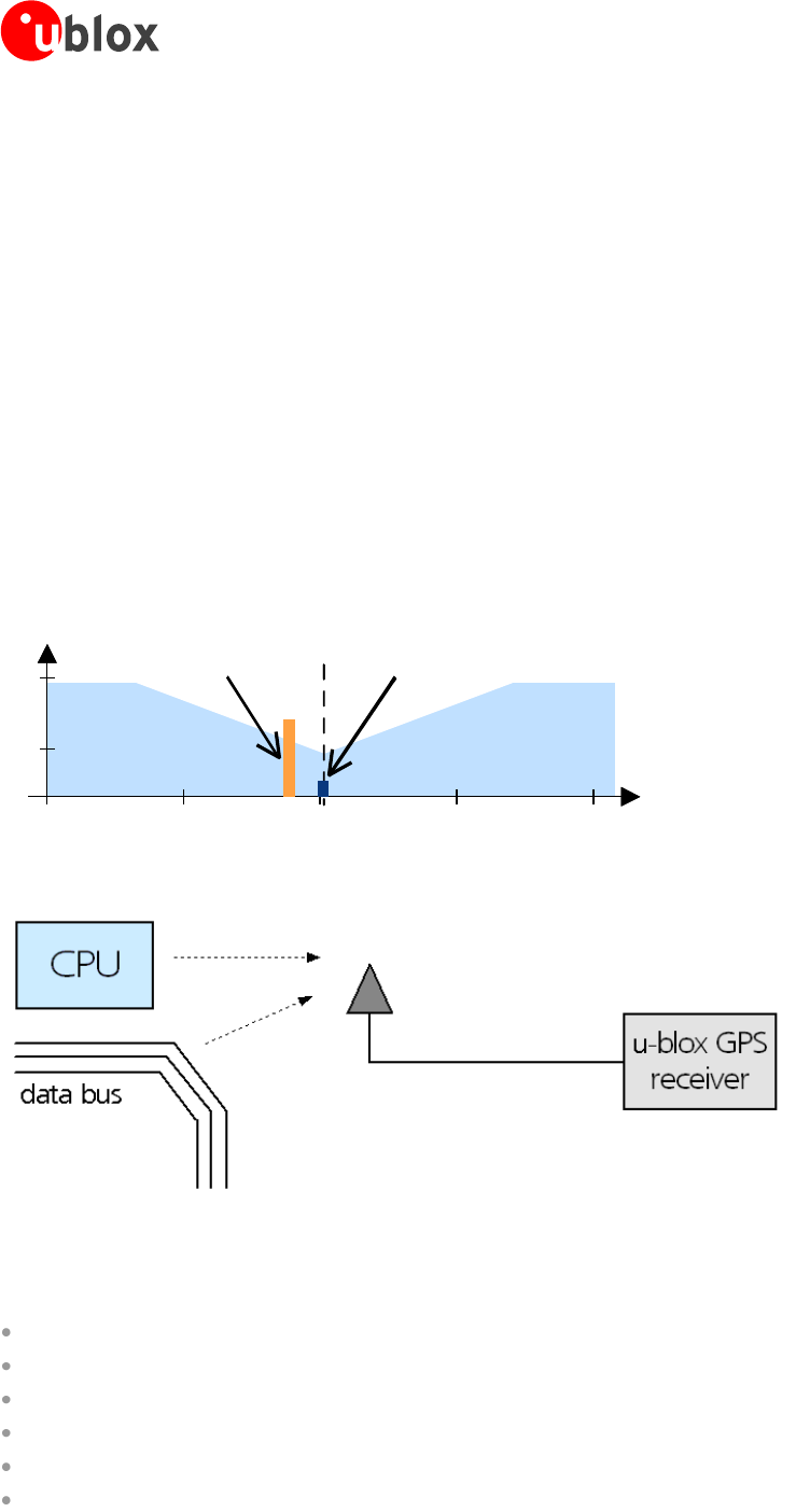
LEA-6 / NEO-6 / MAX-6 - Hardware Integration Manual
GPS.G6-HW-09007-H Preliminary Product handling
Page 64 of 87
3.3.8 Applications with wireless modules LEON / LISA
GSM uses power levels up to 2 W (+33 dBm). Consult the Data Sheet for the absolute maximum power input at
the GPS receiver.
3.3.8.1 Isolation between GPS and GSM antenna
In a handheld type design an isolation of approximately 20dB can be reached with careful placement of the
antennas. If such isolation can‖t be achieved, e.g. in the case of an integrated GSM/GPS antenna, an additional
input filter is needed on the GPS side to block the high energy emitted by the GSM transmitter. Examples of
these kinds of filters would be the SAW Filters from Epcos (B9444 or B7839) or Murata.
3.3.8.2 Increasing jamming immunity
Jamming signals come from in-band and out-band frequency sources.
3.3.8.3 In-band jamming
With in-band jamming the signal frequency is very close to the GPS frequency of 1575 MHz (see Figure 59). Such
jamming signals are typically caused by harmonics from displays, micro-controller, bus systems, etc.
1525 1550 1625
GPS input filter
characteristics
1575 1600
0
-110
Jammin
g signal
1525 1550 1625
Frequency [MHz]
Power [dBm]
GPS input filter
characteristics
1575 1600
0
Jamming
signal
GPS
signals
GPS Carrier
1575.4 MHz
Figure 59: In-band jamming signals
Figure 60: In-band jamming sources
Measures against in-band jamming include:
Maintaining a good grounding concept in the design
Shielding
Layout optimization
Filtering
Placement of the GPS antenna
Adding a CDMA, GSM, WCDMA bandpass filter before handset antenna
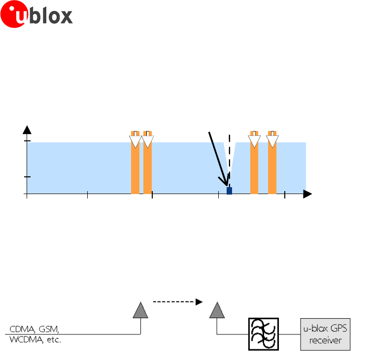
LEA-6 / NEO-6 / MAX-6 - Hardware Integration Manual
GPS.G6-HW-09007-H Preliminary Product handling
Page 65 of 87
3.3.8.4 Out-band jamming
Out-band jamming is caused by signal frequencies that are different from the GPS carrier (see Figure 61). The main
sources are wireless communication systems such as GSM, CDMA, WCDMA, WiFi, BT, etc.
0500 1000 1500 2000
GPS input filter
characteristics
0
-110
0500 1500 2000
Frequency [MHz]
GSM
900
GSM
1800
GSM
1900
Power [dBm]
GPS input filter
characteristics
GPS
1575
0
-110
GPS
signals
GSM
950
Figure 61: Out-band jamming signals
Measures against out-band jamming include maintaining a good grounding concept in the design and adding a
SAW or bandpass ceramic filter (as recommend in Section 3.3.6) into the antenna input line to the GPS receiver
(see Figure 62).
Figure 62: Measures against in-band jamming
3.3.8.5 GPS and GSM solution with integrated SMT antennas and chip SIM
An example is available on our C16 telematics reference design [9], that combines LEON-G200 GSM/GPRS
modem module with NEO-6Q GPS receiver module.
LEA-6 / NEO-6 / MAX-6 - Hardware Integration Manual
GPS.G6-HW-09007-H Preliminary Product handling
Page 66 of 87
3.3.9 Recommended parts
Manufacturer
Part ID
Remarks
Parameters to consider
Diode
ON Semiconductor
ESD9R3.3ST5G
(3.3.4 C) Standoff Voltage>3.3 V
• Low Capacitance < 0.5 pF
ESD9L3.3ST5G
(3.3.4 C) Standoff Voltage>3.3 V
• Standoff Voltage > Voltage for
active antenna
ESD9L5.0ST5G
(3.3.4 C) Standoff Voltage>5 V
• Low Inductance
SAW
Epcos
B9444: B39162-B9444-M410
(3.3.6) 15dBm Max Power Input
B9416: B39162-B9416-K610
(3.3.6) Low insertion loss
Murata
SAFEA1G57KD0F00
(3.3.6) 1.35x1.05x0.5 mm
SAFZE1G57KA0F90
(3.3.6) 2.5x2.0x1.0 mm
SAFEB1G57KB0F00
(3.3.6) 1.35x1.05x0.6 mm
SAFEA1G57KE0F00
(3.3.6) 1.35x1.05x0.45 mm
•Good wireless band suppression
SAFFB1G58KA0F0A
GPS and GLONASS
•High attenuation
SAFEA1G58KA0F00
GPS and GLONASS
•High attenuation
CTS
CER0032A
(3.3.6) 4.2x4.0x2.0 mm
> 8kV ESD HBM
LNA
Avago
ALM-1106
(3.3.4 A) LNA
pHEMT (GaAS)
ALM-1412
(3.3.6 D) LNA + FBAR Filter
ALM-1712
(3.3.6 D) Filter + LNA + FBAR
Filter
ALM-2412
(3.3.4 A) LNA + FBAR Filter
MAXIM
MAX2659ELT+
(3.3.4 A) LNA
SiGe
JRC
NJG1143UA2
LNA
Infineon
BGM1032N16
Filter + LNA
BGM981N11
Filter + LNA + Filter
BGM1052N16
LNA + Filter
Triquint
TQM640002
Filter + LNA + Filter
Inductor
Murata
LQG15HS27NJ02
(3.3.6 F) L, 27 nH
Impedance @ freq GPS > 500
Capacitor
Murata
GRM1555C1E470JZ01
(3.3.6 F) C, 47 pF
Ferrite
Bead
Murata
BLM15HD102SN1
(3.3.7) FB
High IZI @ fGSM
Feed thru Capacitor
for Signal
Murata
NFL18SP157X1A3
Monolithic Type
Array Type
Load Capacitance appropriate to
Baud rate
CL < xxx pF
NFA18SL307V1A45
Feed thru
Capacitor
for VCC
Murata
NFM18PC ….
NFM21P….
0603 2A
0805 4A
Rs < 0.5
Table 26: Recommended parts for ESD/EOS protection
3.3.9.1 Recommended GPS & GLONASS active antenna (A1)
Manufacturer
Order No.
Comments
Inpaq (www.inpaq.com.tw)
GPSGLONASS03D-S3-00-A
3 V 6 mA
Taoglas (www.taoglas.com)
AA.160.301111
36*36*4mm, 3-5V 30mA
Table 27: Recommend GPS & GLONASS active antenna (A1)
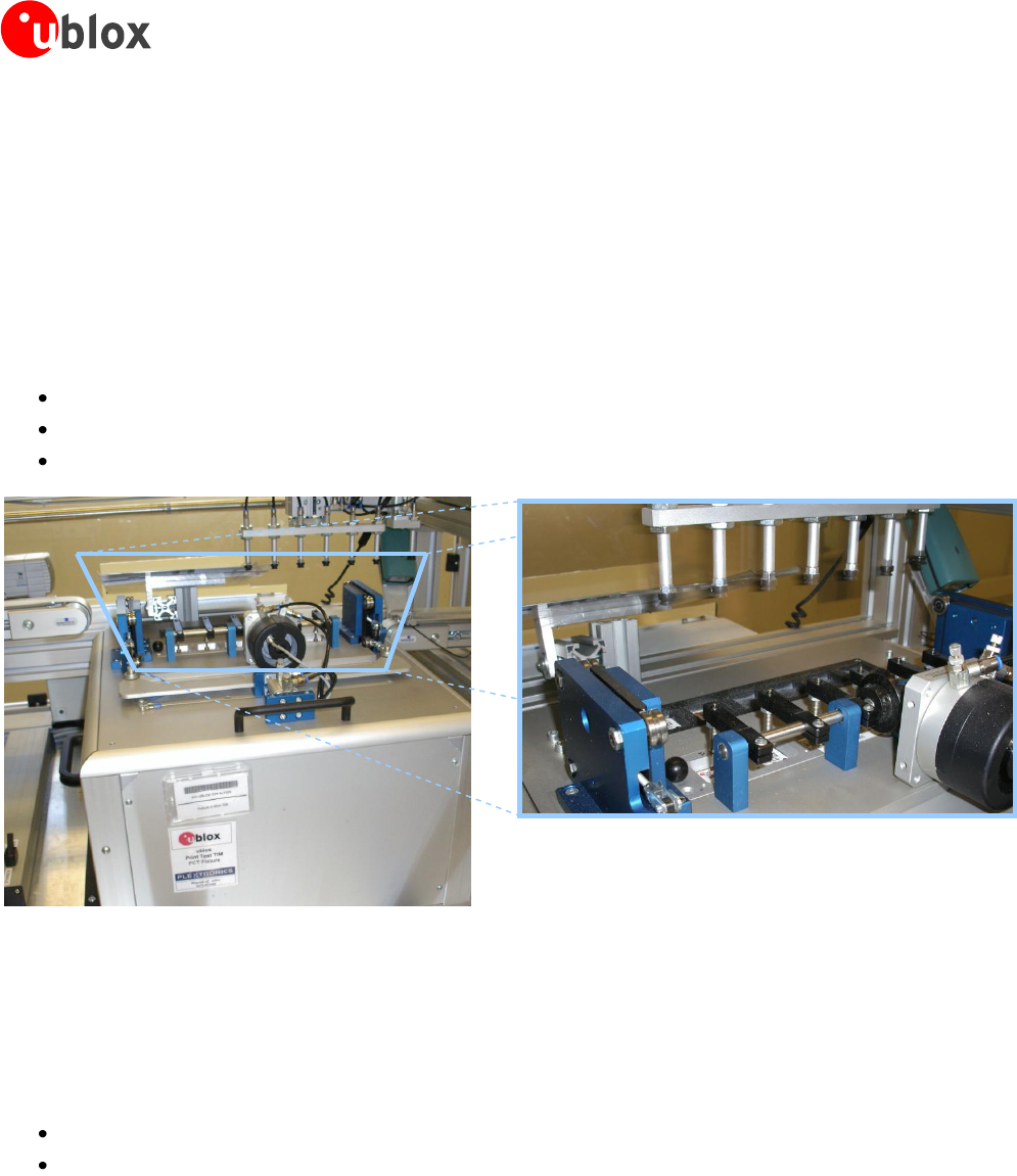
LEA-6 / NEO-6 / MAX-6 - Hardware Integration Manual
GPS.G6-HW-09007-H Preliminary Product testing
Page 67 of 87
4 Product testing
4.1 u-blox in-series production test
u-blox focuses on high quality for its products. To achieve a high standard it‖s our philosophy to supply fully
tested units. Therefore at the end of the production process, every unit is tested. Defective units are analyzed in
detail to improve the production quality.
This is achieved with automatic test equipment, which delivers a detailed test report for each unit. The following
measurements are done:
Digital self-test (Software Download, verification of FLASH firmware, etc.)
Measurement of voltages and currents
Measurement of RF characteristics (e.g. C/No)
Figure 63: Automatic Test Equipment for Module Tests
4.2 Test parameters for OEM manufacturer
Because of the testing done by u-blox (with 100% coverage), it is obvious that an OEM manufacturer doesn‖t
need to repeat firmware tests or measurements of the GPS parameters/characteristics (e.g. TTFF) in their
production test.
An OEM manufacturer should focus on:
Overall sensitivity of the device (including antenna, if applicable)
Communication to a host controller
LEA-6 / NEO-6 / MAX-6 - Hardware Integration Manual
GPS.G6-HW-09007-H Preliminary Product testing
Page 68 of 87
4.3 System sensitivity test
The best way to test the sensitivity of a GPS device is with the use of a 1-channel GPS simulator. It assures
reliable and constant signals at every measurement.
Figure 64: 1-channel GPS simulator
u-blox recommends the following Single-Channel GPS Simulator:
Spirent GSS6100
Spirent Communications Positioning Technology
(previously GSS Global Simulation Systems) www.positioningtechnology.co.uk
4.3.1 Guidelines for sensitivity tests
1. Connect a 1-channel GPS simulator to the OEM product
2. Choose the power level in a way that the “Golden Device” would report a C/No ratio of 38-40 dBHz
3. Power up the DUT (Device Under Test) and allow enough time for the acquisition
4. Read the C/No value from the NMEA GSV or the UBX-NAV-SVINFO message (e.g. with u-center)
5. Compare the results to a “Golden Device” or a u-blox 6 Evaluation Kit.
4.3.2 ‘Go/No go’ tests for integrated devices
The best test is to bring the device to an outdoor position with excellent sky view (HDOP < 3.0). Let the
receiver acquire satellites and compare the signal strength with a “Golden Device”.
As the electro-magnetic field of a redistribution antenna is not homogenous, indoor tests are in most
cases not reliable. These kind of tests may be useful as a ―go/no go‖ test but not for sensitivity
measurements.
4.3.3 Testing LEA-6R designs
When testing the design ensure that no GPS signals are being received or delete the calibration after the
tests. Failure to do so can result in operation errors.
4.3.3.1 Direction signal
This input shall be set once to high level and once to low level. In both states the software parameters are read
back with the UBX-NAV-EKFSTATUS. The direction flag shall read forward for a high level at the FWD input and
backward for a low level at the FORWARD input.
4.3.3.2 Speedpulse signal
A rectangular waveform with 2 kHz frequency shall be fed into the SPEED input. The result can be read back
with the UBX-NAV-EKFSTATUS message: Speed Ticks: 1800...2400

LEA-6 / NEO-6 / MAX-6 - Hardware Integration Manual
GPS.G6-HW-09007-H Preliminary Product testing
Page 69 of 87
4.3.3.3 Gyroscope (rate) input
Do not move the device and check UBX-ESF-MEAS: 2 > Gyro Z: > -2
Quickly turn the device to the right (clockwise), check UBX-ESF-MEAS: Gyro Z: > 50
Quickly turn the device to the left (counterclockwise), check UBX-ESF-MEAS: Gyro Z: < -50
The rate input can only be tested if an A/D converter is connected to LEA-6R.
4.3.3.4 Temperature sensor
The temperature measured by the temperature sensor connected to the LEA-6R shall be read with the UBX-ESF-
MEAS message. The measurement tolerance is in the order of about ±5°.
4.3.3.5 Erase calibration
To erase the calibration send a CFG-EKF command with the appropriate clearing flags set.
4.3.4 Testing NEO-6V designs
The NEO-6V ADR algorithm supports a variety of sensors (such as wheel ticks and gyroscope) and receives the
sensor data via UBX messages from the application processor. Digital sensor data is available on the vehicle bus.
No extra sensors are required for Dead Reckoning functionality. ADR is completely self-calibrating.
For more details on GWT protocol see u-blox 6 Receiver Description Including Protocol Specification [10]
For more details on DWT protocol contact u-blox. (Contact)
LEA-6 / NEO-6 / MAX-6 - Hardware Integration Manual
GPS.G6-HW-09007-H Preliminary Appendix
Page 70 of 87
Appendix
A Abbreviations
Abbreviation
Definition
ANSI
American National Standards Institute
CDMA
Code Division Multiple Access
EMC
Electromagnetic compatibility
EMI
Electromagnetic interference
EOS
Electrical Overstress
EPA
Electrostatic Protective Area
ESD
Electrostatic discharge
GND
Ground
GPS
Global Positioning System
GSM
Global System for Mobile Communications
IEC
International Electrotechnical Commission
PCB
Printed circuit board
Table 28: Explanation of abbreviations used
B Migration to u-blox-6 receivers
Migrating ANTARIS®4 and u-blox 5 designs to a u-blox 6 receiver module is a fairly straightforward procedure.
Nevertheless there are some points to be considered during the migration.
Not all of the functionalities available with ANTARIS®4 are supported by u-blox 6. These include:
RTCM is supported in FW7.0x but not in ROM6.02 and FW6.02 versions.
UTM (Universal Transverse Mercator Projection)
B.1 Checklist for migration
Have you chosen the optimal module?
For best GPS performance (i.e. better sensitivity level and acquisition time) select a LEA-6H, LEA-6S, NEO-
6Q or NEO-6G for the advantage of TCXO performance.
If TCXO performance is not required, choose a LEA-6A or NEO-6M.
For active antenna applications, choose a LEA-6H, LEA-6S or LEA-6A, since an antenna supply circuit is
already built in or see chapter 1.4 and chapter 2.6.
For the ability to upgrade the firmware, choose a LEA-6H.
For precision timing choose a LEA-6T or NEO-6T
For dead reckoning choose a LEA-6R
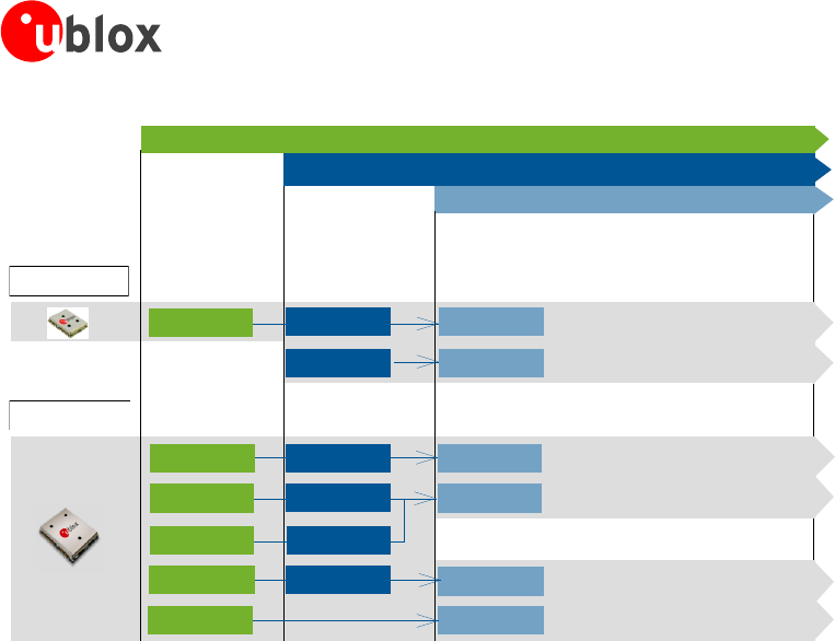
LEA-6 / NEO-6 / MAX-6 - Hardware Integration Manual
GPS.G6-HW-09007-H Preliminary Appendix
Page 71 of 87
u-blox 6
NEO-4S
NEO
NEO-6M/Q
LEA
•Flash memory, Antenna Supervisor
LEA-6H
LEA-6A/S •ROM, Antenna Supervisor
LEA-4T
LEA-4R
LEA-6T
LEA-6R
•Precision Timing
•Dead Reckoning
NEO-5D/G NEO-6G
ROM, 3.0 V
ROM, 1.8 V
•
•
•ROM
u-blox 5
ANTARIS 4
NEO-5M/Q
LEA-5T
LEA-4P/H LEA-5H
LEA-4A/S LEA-5A/S
LEA-4M LEA-5M/Q
Figure 65: u-blox 6 module migration made easy
Check u-blox 6 Hardware Requirements:
Check the battery power to supply the battery backup pin, since u-blox 6 draws higher current in
comparison to ANTARIS 4 receivers.
Compare the u-blox 6 module peak current consumption (~70 mA) with the specification of the power
supply.
u-blox 6 modules can be operated in three different modes: Max. Performance mode, Eco mode or
Power Save mode.
NEO-6Q, NEO-6G and NEO-6M feature a Configuration Pin that allows switching between the power
modes: Max Performance mode and Eco mode.
For more information on u-blox6 Power supply specifications and power modes, see the LEA-6 Data
Sheet [1] and NEO-6 Data Sheet [2].
If you use an active antenna supervisor circuitry to detect open conditions, you need to verify resistor
reference recommendations in our integration manuals.
See chapter 3.3 EOS/ESD/EMI Precautions.
If you use the USB interface, the external series resistor values in USB_DM and USB_DP line should be
adjusted, see 1.6.2.
Check u-blox 6 Software Requirements:
Not all of the functionalities available with ANTARIS 4 are supported by u-blox 6 Firmware version 6.02.
These include:
o FixNow Mode: Low power modes are supported via mapping to the Power Save mode of
FW 7.0x or ROM 6.02. For migration of FXN functionalities consult the u-blox 6 Firmware
Version 7.0x Release Note [5], respectively the u-blox 6 Receiver Description including Protocol
Specification [3]
o No UTM (Universal Transverse Mercator Projection).
o No RTCM protocol for DGPS support (ROM6.02, FW6.02).
o Raw Data support with LEA-6T only.
Check B.2 Software migration

LEA-6 / NEO-6 / MAX-6 - Hardware Integration Manual
GPS.G6-HW-09007-H Preliminary Appendix
Page 72 of 87
B.2 Software migration
B.2.1 Software migration from ANTARIS 4 or u-blox 5 to a u-blox 6 GPS receiver
Software migration from ANTARIS 4 or u-blox 5 to a u-blox 6 GPS receiver is a straightforward procedure.
Nevertheless there are some differences to be considered with u-blox 5 firmware version 5.00. Like its ANTARIS
4 and u-blox 5 predecessors, u-blox 6 technology supports UBX and NMEA protocol messages. Backward
compatibility has been maintained as far as possible. New messages have been introduced for new functions.
Only minor differences have to be expected in the UBX-NAV and UBX-AID classes of the UBX protocol and for
the standard NMEA messages such as GGA, GLL, GSA, GSV, RMC, VTG and ZDA.
ANTARIS 4
u-blox6
Remarks
UBX-CFG-NAV2
UBX-CFG-NAV5
UBX-CFG-NAV2 has been replaced by UBX-CFG-NAV5. The new message has
additional features.
The default dynamic platform is “Portable”. This platform is rather generic
and allows the receiver to be operated in a wide dynamic range covering
pedestrians, cars as well as commercial aircrafts. Automotive applications
such as first-mount navigation systems may better utilize the “Automotive”
platform, which is better geared to the dynamics of land vehicles but is only
of limited use in airborne and high-dynamics environments.
UBX-CFG-NAV5 does not support following features:
Almanac Navigation
Navigation Input filters
UBX-CFG-NAV5 has a message length of 36 Bytes (40 Bytes for UBX-CFG-
NAV2)
UBX-CFG-NAV5 FixMode is set by default to “Auto 3D/2D” as for ANTARIS4.
Check the u-blox 6 Receiver Description including Protocol Specification [3].
if this mode needs to be changed.
UBX-CFG-MSG
UBX-CFG-MSG
No support for multiple configurations in one UBX-CFG-MSG command
UBX-CFG-RXM
N/A
Contrary to ANTARIS 4, u-blox6 does not need selecting GPS acquisition
sensitivity mode (Fast, Normal, High Sens and Auto mode) since the
acquisition engine is powerful enough to search all satellite in one go.
FixNow mode is not available anymore. Contact your local u-blox support
team should you need further information.
PUBX,01
N/A
Other UBX or NMEA messages can be used to replace this message
UBX-NAV-POSUTM
N/A
UBX-CFG-TP
UBX-CFG-TP
u-blox 6 maintains this message for backwards compatibility only. For new
designs use UBX-CFG-TP5.
UBX-CFG-TP5
This is a new u-blox 6 message, for information see u-blox 6 Receiver
Description including Protocol Specification [3].
UBX-CFG-ANT
UBX-CFG-ANT
Antenna Open Circuit Detection: The default setting for LEA-4S and LEA-4A
was “enabled”. With all LEA-6 modules the default setting is “disabled”.
Automatic Short Circuit Recovery: With ANTARIS 4 this was “disabled” by
default. With u-blox 6 the default setting is “enabled”.
UBX-CFG-RATE
UBX-CFG- RATE
Set to 1 with u-blox 6
UBX-CFG-TMODE
UBX-CFG-TMODE
With u-blox 6 FW 6.02 and above it is no longer necessary to configure the
number of satellites in UBX-CFG-NAV to 1 to enable the timing mode. This is
performed automatically.
UBX-MON-HW
UBX-MON-HW
Message length has changed as the number of pins is different with u-blox6.
0s Leap second by default
FW 6.02 and FW7.0x: 15 s
Leap second by default
UBX-CFG-RATE
UBX-CFG-RATE
Disable SBAS services to achieve 4Hz navigation
UBX-NAV- EKFSTATUS
UBX-NAV- EKFSTATUS
This message is only provided for backwards compatibility and should not be
utilized for future designs. Instead, the messages ESF-STATUS and ESF-MEAS
should be used.
For u-blox 6 firmware the gyroscope value (gyroMean) is only output if the
gyroscope is used in the navigation solution. This message is only available on
LEA-4R and LEA-6R GPS Receivers.
LEA-6 / NEO-6 / MAX-6 - Hardware Integration Manual
GPS.G6-HW-09007-H Preliminary Appendix
Page 73 of 87
Table 29: Main differences between ANTARIS 4 and u-blox 6 software for migration
The default NMEA message set for u-blox 6 is GGA, GLL, GSA, GSV, RMC and VTG. Contrary to ANTARIS 4,
ZDA is disabled by default.
Firmware update is supported by all of these interfaces. The firmware update mechanism of u-blox 6 is more
sophisticated than with ANTARIS 4. It is now based on UBX protocol messages. Customers, who implemented
firmware download in their application processor, will need to replace the software. A template is available from
your u-blox support team.
In case migrating from LEA-4T or LEA-5T to LEA-6T-0, the command to safe the configuration (UBX-CGF-CFG)
changes. This is because in LEA-6T-0 a serial Flash at the SPI is used instead of the parallel Flash (LEA-4T and LEA-
5T). So for the LEA-4T, LEA-5T and LEA-6T-1 the target to save the configuration has to be set to “devFlash”,
but for the LEA-6T-0 it has to be set to “devSpiFlash”.
Please refer to the u-blox 6 Receiver Description including Protocol Specification [3] for more information. This
document is available on the u-blox website.
B.2.2 Software migration from 6.02 to 7.03
Timing Survey-in Mode:
Customers currently using survey-in need to review their accuracy limit setting with CFG-TMODE or CFG-
TMODE2.
For migration from 6.02 to 7.03 consult the u-blox 6 Firmware Version 7.0x Release Note [5], respectively the u-
blox 6 Receiver Description including Protocol Specification [3]
B.3 Hardware Migration
B.3.1 Hardware Migration: ANTARIS 4 u-blox 6
u-blox 6 modules have been designed with backward compatibility in mind but some minor differences were
unavoidable. These minor differences will however not be relevant for the majority of the ANTARIS 4 designs.
Good performance requires a clean and stable power supply with minimal ripple. Care needs to be exercised in
selecting a strategy to achieve this. Avoid placing any resistance on the Vcc line. For better performance, use an
LDO to provide a clean supply at Vcc and consider the following:
Special attention needs to be paid to the power supply requirements. (currents & backup current see
datasheet for further details)
Wide power lines or even power planes are preferred.
Place LDO near the module.
Avoid resistive components in the power line (e.g. narrow power lines, coils, resistors, etc.).
Placing a filter or other source of resistance at Vcc can create significantly longer acquisition
times.
B.3.2 Hardware Migration: u-blox 5 u-blox 6
Check the pins RxD1 and EXTINT0 regarding the input voltage threshold.
Serial termination resistors: Recommendation has changed from 27 to 22 . See chapter 1.6.2.1.
For more information see the LEA-6 Data Sheet [1]and LEA-5 Data Sheet [7].
LEA-6 / NEO-6 / MAX-6 - Hardware Integration Manual
GPS.G6-HW-09007-H Preliminary Appendix
Page 74 of 87
B.4 Migration of LEA modules
B.4.1 Migration from LEA-4 to LEA-6
See also the migration Table in the u-blox5 Hardware Integration Manual.
For u-blox6 the Input Voltage thresholds on the pins RXD1 and EXTINT0 have changed.
The Safeboot functionality is inverted compared to Antaris receivers.
VCC_OUT is now VCC and not 1.8 V as on Antaris Modules.
Also check your power supply requirements with the datasheet (for VCC and VBCKP).
Pin
LEA-4H/LEA-4P/LEA-4T
LEA-6H/LEA-6T
Remarks for Migration
Pin Name
Typical Assignment
Pin Name
Typical Assignment
1
Reserved
VDDIO level I/O;
not connected
SDA2
NC
2
Reserved
VDDIO level I/O;
not connected
SCL2
NC
3
TXD1
VDDIO level I/O
TxD1
Output
4
RXD1
VDDIO level I/O
RxD1
Input
Leave open if not used.
5
VDDIO
1.65 – 3.60 V
NC
Connect to VCC
Can be left open, but connection to VCC is
recommended for compatibility reason. With LEA-
6H the I/O voltage is always VCC.
6
VCC
2.70 – 3.30 V
VCC
2.70 – 3.60 V
Extended power supply range, higher peak supply
current.
7
GND
GND
GND
GND
No difference
8
VDD18OUT
NC
VCC_OUT
NC
Internally connected to VCC, if you have circuitry
connected to this pin, check if it withstands the
VCC voltage.
9
Reserved
NC
Reserved
NC
10
RESET_N
1.8 V
RESET_N
NC
Input only, do not drive high. Internal pull up to
VCC.
11
V_BAT
1.50 – 3.6 V
V_BCKP
1.4 – 3.6 V
Wider voltage range but needs more current.
Check your backup supply, regarding the higher
consumption.
12
BOOT_INT
NC
Reserved
NC
Do not drive low.
13
GND
GND
GND
GND
No difference
14
GND
GND
GND
GND
No difference
15
GND
GND
GND
GND
No difference
16
RF_IN
RF_IN
RF_IN
RF_IN
No difference
17
GND
GND
GND
GND
No difference
18
VCC_RF
VCC - 0.1 V
VCC_RF
VCC - 0.1 V
No difference
19
V_ANT
3.0 V –5.0 V
V_ANT
2.7 V -5.5 V
wider range
20
AADET_N
NC
AADET_N
NC
check resistor R5 in Active antenna supervisor
Figure 47
21
EXTINT1
NC
NC
NC
22
Reserved
NC
NC
NC
23
Reserved
NC
NC
NC
24
VDDUSB
Connected to GND
or VDD_USB
VDDUSB
Connected to GND
or VDD_USB
Do not leave open. (VDD_USB is 3.3V regulated
power supply from VBUS.)
25
USB_DM
NC
USB_DM
NC
New serial termination resistors recommended: 22
26
USB_DP
NC
USB_DP
NC
27
EXTINT0
NC
EXTINT0
NC
28
TIMEPULSE
VDDIO level I/O
TIMEPULSE
Output
Table 30: Pin-out comparison LEA-4H/LEA-4P/LEA-4T vs. LEA-6H/LEA-6T
LEA-6 / NEO-6 / MAX-6 - Hardware Integration Manual
GPS.G6-HW-09007-H Preliminary Appendix
Page 75 of 87
Pin
LEA-4A/LEA-4S
LEA-6A/LEA-6S
Remarks for Migration
Pin Name
Typical Assignment
Pin Name
Typical Assignment
1
TxD2
3.0 V out
SDA2
NC
2
RxD2
1.8 - 5.0 V
SCL2
NC
3
TxD1
3.0 V out
TxD1
Output
4
RxD1
1.8 - 5.0 V in
RxD1
Input
Leave open if not used. Max. 5 V
5
VDDIO
VCC
NC
Connect to VCC
Leave open for only LEA-6x design. Connect to
VCC for backward compatibility to LEA-5x.
6
VCC
2.70 – 3.30 V
VCC
2.70 – 3.60 V
Extended power supply range, higher peak supply
current.
7
GND
GND
GND
GND
No difference
8
VDD18OUT
1.8 V out
VCC_OUT
NC
Internally connected to VCC, if you have circuitry
connected to this pin, check if it withstands the
VCC voltage.
9
GPSMODE6
NC (GND or
VDD18OUT)
CFG_COM1
NC
10
RESET_N
ACTIVE LOW
RESET_N
NC
Input only, do not drive high. Internal pull up to
VCC.
11
V_BAT
1.50 – 3.6 V
V_BCKP
1.4 – 3.6 V
Wider voltage range but needs more current.
Check your backup supply, regarding the higher
consumption.
12
BOOT_INT
NC
Reserved
NC
Do not drive low.
13
GND
GND
GND
GND
No difference
14
GND
GND
GND
GND
No difference
15
GND
GND
GND
GND
No difference
16
RF_IN
RF_IN
RF_IN
RF_IN
No difference
17
GND
GND
GND
GND
No difference
18
VCC_RF
VCC - 0.1 V
VCC_RF
VCC - 0.1V
No difference
19
V_ANT
3.0 V - 5.0 V
V_ANT
2.7V -5.5V
wider range
20
AADET_N
NC (1.8 to 5.0 V)
AADET_N
NC
check resistor R5 in Active antenna supervisor
Figure 47
21
GPSMODE5
NC (GND or
VDD18OUT)
NC
NC
22
GPSMODE2
GPSMODE2
3
NC (GND or
VDD18OUT)
NC
NC
23
GPSMODE7
NC (1.8 to 5.0 V)
NC
NC
24
VDDUSB
3.0 –3.6V/ GND
VDDUSB
Connected to GND
or VDD_USB
Do not leave open. (VDD_USB is 3.3 V regulated
power supply from VBUS.)
25
USB_DM
VDDUSB I/O
USB_DM
NC
New serial termination resistors recommended: 22
26
USB_DP
VDDUSB I/O
USB_DP
NC
27
EXTINT0
NC (1.8 to 5.0 V)
EXTINT0
NC
Max. 5 V
28
TIMEPULSE
VDDIO level output
TIMEPULSE
Output
Table 31: Pin-out comparison LEA-4A/LEA-4S vs. LEA-6A/LEA-6S
B.4.2 Migration of LEA-4R designs to LEA-6R
LEA-6R module has been designed with backward compatibility in mind, but some incompatibilities were
unavoidable. These minor differences will, however, not be relevant for the majority of ANTARIS 4 designs.
Please check in your design the following points carefully to assure a safe migration:
For u-blox 6 the Input Voltage thresholds on the pins RxD1 and Extint0 have changed.
VCC_OUT is now VCC and not 1.8 V as on Antaris Modules.
Pin5 is now NC instead of VDDIO. All I/O Voltages are referenced to VCC.
Check your power supply requirements with the datasheet (for VCC and VBCKP), u-blox 6 has a higher
peak current and backup current than ANTARIS 4 modules
LEA-6 / NEO-6 / MAX-6 - Hardware Integration Manual
GPS.G6-HW-09007-H Preliminary Appendix
Page 76 of 87
The SPI is now running at 870 kHz (against 460 kHz on ANTARIS 4), check that your design supports the
signal path
If you do a redesign, ensure the signal paths of the SPI to support a bandwidth of 4 MHz.
B.4.3 Migration from LEA-5 to LEA-6
For u-blox6 only the Input Voltage thresholds on the pins RXD1 and EXTINT0 have changed.
Be aware, that with u-blox 6 there is no LEA anymore, which supports SPI interface. For SPI consider NEO-6 form
factor.
B.5 Migration of NEO modules
B.5.1 Migration from NEO-4S to NEO-6
For u-blox6 the Input Voltage thresholds on the pins RXD1 and EXTINT0 have changed.
The Safeboot functionality is inverted compared to Antaris receivers.
Also check your power supply requirements with the datasheet (for VCC and VBCKP).
Also check the setting of the configuration pins.
The pin-outs of NEO-4S and NEO-6M/NEO-6Q differ slightly. Table 32 compares the modules and highlights the
differences to be considered.
Pin
NEO-4S
NEO-6Q/NEO-6M
Remarks for Migration
Pin Name
Typ. Assignment
Pin Name
Typ. Assignment
1
BOOT_INT
NC
Reserved
NC
Do not drive low.
2
SELECT
VDDIO level I/O;
not connected
SS_N
NC
3
TIMEPULSE
VDDIO level I/O
TIMEPULSE
Output
4
EXTINT0
NC
EXTINT0
NC
5
USB_DM
NC
USB_DM
NC
New serial termination resistors recommended:
22 Ohms
6
USB_DP
NC
USB_DP
NC
7
VDDUSB
Connected to
GND or
VDD_USB
VDDUSB
Connected to
GND or
VDD_USB
Do not leave open. (VDD_USB is 3.3V regulated
power supply from VBUS.)
8
Reserved
NC
Reserved
NC
Pins 8 and 9 must be connected.
9
VCC_RF
VCC-0.1 V
VCC_RF
VCC-0.1 V
No difference
10
GND
GND
GND
GND
No difference
11
RF_IN
RF_IN
RF_IN
RF_IN
No difference
12
GND
GND
GND
GND
No difference
13
GND
GND
GND
GND
No difference
14
MOSI
NC
MOSI/CFG_COM0
NC
The function of the CFG pin has changed. See
Section 2.2.3.1 for more details.
15
MISO
NC
MISO/CFG_COM1
NC
16
SCK/
CFG_USB
NC
CFG_GPS0 /SCK
NC
Leave open if not used.
The function of the CFG pin has changed. See
Section 2.2.3.1 for more details.
17
NCS
NC
Reserved
NC
No difference
18
Reserved
NC
SDA2
NC
19
Reserved
NC
SCL2
NC
20
TXD1
VDDIO level I/O
TxD1
Output
21
RXD1
VDDIO level I/O
RxD1
Input
Leave open if not used.
22
V_BAT
1.5-3.6 V
V_BCKP
1.4-3.6 V
Wider voltage range but needs more current.
Check your backup supply, regarding the higher
consumption.
23
VCC
2.7-3.3 V
VCC
2.7-3.6 V
Higher peak supply current
24
GND
GND
GND
GND
No difference
Table 32: Pin-out comparison NEO-4S vs. NEO-6

LEA-6 / NEO-6 / MAX-6 - Hardware Integration Manual
GPS.G6-HW-09007-H Preliminary Appendix
Page 77 of 87
B.5.2 Migration from NEO-5 to NEO-6
For u-blox 6 only the Input Voltage thresholds on the pins RXD1 and EXTINT0 have changed.
Also check the setting of the configuration pins.
Serial termination resistors: Recommendation has changed from 27 to 22 . See chapter 1.6.2.1.
LEA-6 / NEO-6 / MAX-6 - Hardware Integration Manual
GPS.G6-HW-09007-H Preliminary Appendix
Page 78 of 87
C Interface Backgrounder
C.1 DDC Interface
Two wires, serial data (SDA) and serial clock (SCL), carry information between the devices connected to the bus.
These lines are connected to all devices on the DDC. SCL is used to synchronize data transfers and SDA is the
data line. Both SCL and SDA lines are "open drain" drivers. This means that DDC devices can only drive them
low or leave them open. The pull-up resistor (Rp) pulls the line up to VDD if no DDC device is pulling it down to
GND. If the pull-up resistors are missing, the SCL and SDA lines are undefined and the DDC bus will not work.
For most DDC systems the low and high input voltage level thresholds of SDA and SCL depend on VDD. See the
LEA-6 Data Sheet [1]or NEO-6 Data Sheet [2]for the applicable voltage levels.
DDC Device A DDC Device B
V
DD
SDA
SCL
GND
RpRp
SDA in
SDA out
SCL in
SDA out
SDA in
SDA out
SCL in
SDA out
Figure 66: A simple DDC connection
The signal shape and the maximum rate in which data can be transferred over SDA and SCL is limited by the
values of Rp and the wire and I/O capacitance (Cp). Long wires and a large number of devices on the bus
increase Cp, therefore DDC connections should always be as short as possible. The resistance of the pull-up
resistors and the capacitance of the wires should be carefully chosen.
Figure 67: DDC block diagram
C.1.1 Addresses, roles and modes
Each device connected to a DDC is identified by a unique 7-bit address (e.g. whether it‖s a microcontroller,
EEPROM or D/A Converter, etc.) and can operate as either a transmitter or receiver, depending on the function
Rp
Rp
LEA-6 / NEO-6 / MAX-6 - Hardware Integration Manual
GPS.G6-HW-09007-H Preliminary Appendix
Page 79 of 87
of the device. The default DDC address for u-blox GPS receivers is set to 0x42. Setting the mode field in the
CFG-PRT message for DDC accordingly can change this address.
The first byte sent is comprised of the address field and R/W bit. Hence the byte seen on the bus 0x42 is
shifted by 1 to the left plus R/W bit thus being 0x84 or 0x85 if analyzed by scope or protocol analyzer.
In addition to transmitters and receivers, devices can also be considered as masters or slaves when performing
data transfers. A master is the device which initiates a data transfer on the bus and generates the clock signals to
permit that transfer. At that time, any device addressed is considered a slave. The DDC-bus is a multi-master bus,
i.e. multiple devices are capable of controlling the bus. Such architecture is not permanent and depends on the
direction of data transfer at any given point in time. A master device not only allocates the time slots when
slaves can respond but also enables and synchronizes designated slaves to physically access the bus by driving
the clock. Although multiple nodes can assume the role of a master, only one at any time is permitted to do so.
Thus, when one node acts as master, all other nodes act as slaves. Table 33 shows the possible roles and modes
for devices connected to a DDC bus.
Transmit
Receive
Master: sends the clock and addresses slaves
Sends data to slave
Receives data from slave
Slave: receives the clock and address
Sends data to master
Receives data from master
Table 33: Possible roles and modes of devices connected to DDC bus
u-blox 6 GPS receivers normally run in the slave mode. There is an exception when an external EEPROM is
attached. In that case, the receiver attempts to establish presence of such a non-volatile memory component by
writing and reading from a specific location. If EEPROM is present (assumed to be located at a fixed address
0xA0), the receiver assumes the role of a master on the bus and never changes role to slave until the following
start-up (subject to EEPROM presence). This process takes place only once at the start-up, i.e. the receiver‖s role
cannot be changed during the normal operation afterward. This model is an exception and should not be
implemented if there are other participants on the bus contending for the bus control (µC / CPU, etc.).
As a slave on the bus, the u-blox 6 GPS receiver cannot initiate the data transfers. The master node has the
exclusive right and responsibility to generate the data clock, therefore the slave nodes need not be configured to
use the same baud rate. For the purpose of simplification, if not specified differently, SLAVE denotes the u-blox 6
GPS receiver while MASTER denotes the external device (CPU, μC) controlling the DDC bus by driving the SCL
line.
u-blox GPS receivers support Standard-Mode I2C-bus specification with 7-bit addressing and a data
transfer rate up to 100 kBit/s and a SCL clock frequency up to 100 kHz.
C.1.2 DDC troubleshooting
Consider the following questions when implementing I2C in designs:
Is there a stable supply voltage Vdd? Often, external I2C devices (like I2C masters or monitors) must be
provided with Vdd.
Are appropriate termination resistances attached between SDA, SCL and Vdd? The voltage level on SDA and
SCL must be Vdd as long as the bus is idle and drop near GND if shorted to GND. [Note: Very few I2C
masters exist which drive SCL high and low, i.e. the SCL line is not open-drain. In this case, a termination
resistor is not needed and SCL cannot be pulled low. These masters will not work together with other
masters (as they have no multi-master support) and may not be used with devices which stretch SCL during
transfers.]
Are SDA and SCL mixed up? This may accidentally happen e.g. when connecting I2C buses with cables or
connectors.
Do all I2C devices support the I2C supply voltage used on the bus?
Do all I2C devices support the maximum SCL clock rate used on the bus?
If more than one I2C master is connected to the bus: do all masters provide multi-master support?
LEA-6 / NEO-6 / MAX-6 - Hardware Integration Manual
GPS.G6-HW-09007-H Preliminary Appendix
Page 80 of 87
Are the high and low level voltages on SDA and SCL correct during I2C transfers? The I2C standard defines
the low level threshold with 0.3 Vcc, the high level threshold with 0.7 Vcc. Modifying the termination
resistance Rp, the serial resistors Rs or lowering the SCL clock rate could help here.
Are there spikes or noise on SDA, SCL or even Vdd? They may result from interferences from other
components or because the capacitances Cp and/or Cc are too high. The effects can often be reduced by
using shorter interconnections.
For more information about DDC implementation refer to the u-blox 6 Receiver Description including
Protocol Specification [3].
C.2 SPI Interface
C.2.1 SPI basics
Devices communicate in master/slave mode where the master device provides the clock signal (SCK) and
determines the state of the chip select (SCS/SS_N) lines, i.e. it activates the slave it wants to communicate with.
The slave device receives the clock and chip select from the master. Multiple slave devices are allowed with
individual slave select (chip select) lines. This means that there is one master, while the number of slaves is only
limited by the number of chip selects. In addition to reliability and relatively high speed (with respect to the
conventional UART), the SPI interface is easy to use and requires no special handling or complex communication
stack implementation in the software.
The standard configuration for a slave device (see Figure 68 ) uses two control and two data lines. These are
identified as follows:
SCS — Slave Chip Select (control: output from master, usually active low)
SCK — Serial Clock (control: output from master)
MOSI — Master Output, Slave Input (data: output from master)
MISO — Master Input, Slave Output (data: output from slave)
Alternative naming conventions are also widely used. Confirm the pin/signal naming with specific
components used.
SPI Slave
MISO
MOSI
SCK
SCS
Figure 68: SPI slave
SPI always follows the basic principle of a shift register. During an SPI transfer, command codes and data values
are simultaneously transmitted (shifted out serially) and received (shifted in serially). The data is entered into a
shift register and then internally available for parallel processing. The length of the shift registers is not fixed, but
can vary from device to device. Normally the shift registers are 8Bit or integral multiples thereof. However, they
can also have an odd number of bits. For example two cascaded 9Bit EEPROMs can store 18Bit data.
When an SPI transfer occurs, an 8-bit character is shifted out one data pin while a different 8-bit character is
simultaneously shifted in a second data pin. Another way to view this transfer is that an 8-bit shift register in the
master and another 8-bit shift register in the slave are connected as a circular 16-bit shift register. When a
transfer occurs, this distributed shift register is shifted eight bit positions; thus, the characters in the master and
slave are effectively exchanged.
The serial clock (SCK) line synchronizes shifting and sampling of the information on the two serial data lines
(MOSI and MISO). The chip select (SCS/SS_N) line allows individual selection of a slave SPI device. If an SPI slave
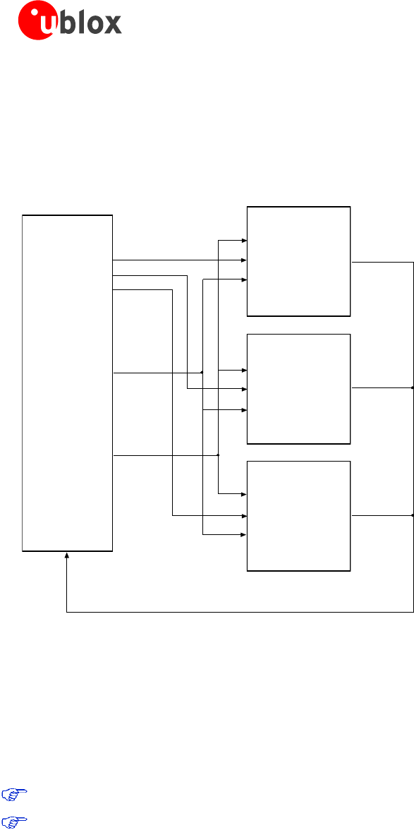
LEA-6 / NEO-6 / MAX-6 - Hardware Integration Manual
GPS.G6-HW-09007-H Preliminary Appendix
Page 81 of 87
device is not selected (i.e. its chip select is not activated), its data output enters a high-impedance state (hi-Z) and
does not interfere with SPI bus activities.
The data output MISO functions as the data return signal from the slave to the master.
Figure 69 shows a typical block diagram for an SPI master with several slaves. Here, the SCK and MOSI data lines
are shared by all of the slaves. Also the MISO data lines are linked together and led back to the master. Only the
chip selects are separately brought to each SPI device.
SPI Master
SPI Slave0
Chip Select
MOSI
SCK
Data Input
MISO
SPI Slave1
SPI Slave2
SCS
0
SCS
1
SCS
2
Clock
Data Output
MOSI
MOSI
MOSI
SS_N
SS_N
SS_N
SCK
SCK
SCK
MISO
MISO
MISO
Figure 69: Master with independent slaves
SPI allows multiple microcontrollers to be linked together. These can be configured according to single or
multiple master protocols. In the first variant the microcontroller(s) designated as slave(s) behave like a normal
peripheral device. The second variant allows for several masters and allows each microprocessor the possibility to
take the role of master and to address another microprocessor. In this case one microcontroller must
permanently provide the clock signal.
There are two SPI system errors. The first occurs if several SPI devices want to become master at the same time.
The other is a collision error that occurs for example when SPI devices work with different polarities.
Systems involving multiple microcontrollers are beyond the scope of this document.
Cascading slave peripherals is not supported.
Four I/O pin signals are associated with SPI transfers: the SCK, the MISO data line, the MOSI data line, and the
active low SCS/SS_N pin. In the unselected state the MISO lines are hi-Z and therefore inactive. The master
decides with which peripheral device it wants to communicate. The clock line SCK provides synchronization for
data communication and is brought to the device whether or not it is selected.

LEA-6 / NEO-6 / MAX-6 - Hardware Integration Manual
GPS.G6-HW-09007-H Preliminary Appendix
Page 82 of 87
The majority of SPI devices provide all four of these lines. Sometimes MOSI and MISO are multiplexed, or else
one is missing. A peripheral device, which must not or cannot be configured, requires no input line but only a
data output. As soon as it gets selected it starts sending data. In some ADCs therefore the MOSI line is missing.
Some devices have no data output (e.g. LCD controllers which can be configured, but cannot send data or status
messages).
The following rules should answer the most common questions concerning these signals:
SCK: The SCK pin is an output when the SPI is configured as a master and an input when the SPI is
configured as a slave. When the SPI is configured as a master, the SCK signal is derived from the internal bus
clock. When the master initiates a transfer, eight clock cycles are automatically generated on the SCK pin.
When the SPI is configured as a slave, the SCK pin is an input, and the clock signal from the master
synchronizes the data transfer between the master and slave devices. Slave devices ignore the SCK signal
unless the slave select pin is active low. In both the master and slave SPI devices, data is shifted on one edge
of the SCK signal and is sampled on the opposite edge where data is stable. Edge polarity is determined by
the SPI transfer protocol.
MISO/MOSI: The MISO and MOSI data pins are used for transmitting and receiving serial data. When the
SPI is configured as a master, MISO is the master data input line, and MOSI is the master data output line.
When the SPI is configured as a slave, these pins reverse roles.
SCS/SS_N: In master mode, the SCS output(s) select external slaves (e.g. SCS1_N, SCS2_N). In slave mode,
SS_N is the slave select input. The chip select pin behaves differently on master and slave devices. On a slave
device, this pin is used to enable the SPI slave for a transfer. If the SS_N pin of a slave is inactive (high), the
device ignores SCK clocks and keeps the MISO output pin in the high-impedance state. On a master device,
the SCS pin can serve as a general-purpose output not affecting the SPI.
LEA-6 / NEO-6 / MAX-6 - Hardware Integration Manual
GPS.G6-HW-09007-H Preliminary Appendix
Page 83 of 87
D DR calibration
D.1 Constraints
The calibration of the DR sensors is a transparent and continuously ongoing process during periods of good GPS
reception:
Gyroscope Bias Voltage level of the gyroscope while driving a straight route or not
moving
Gyroscope Scale Factor Adjusted while in left and right turns; gyro sensitivity
Speed Pulse Scale Factor Used to calibrate odometer pulse frequency to GPS speed over ground
Temperature Compensation The gyroscope is a temperature-dependent device that requires
temperature compensation
When a new GPS receiver is installed in a vehicle, the accuracy is only moderately good until sufficient
calibration data has been collected, e.g. during a first drive. With time, continuous calibration results in
continuous improvement of dead reckoning accuracy. Small discontinuities, like deviating wheel diameters after
exchanging tires (summer vs. snow tires) or aging of the sensors, will be balanced out by ongoing automatic
calibration.
Calibration parameters must be reset, if
a DR module is transferred to a different vehicle and/or a different gyroscope is connected
the sensor integrity check has reported any failure from the sensors and set itself into GPS only mode
Calibration can be reset with UBX message UBX – CFG (Config) – EKF (Extended Kalman Filter).
D.2 Initial calibration drive
For optimum navigation performance the system needs some learning time and distance for calibrating the
various sensors inputs. The following driving directions are recommended to achieve an efficient calibration so
dead reckoning yields high accuracy after the shortest possible period of time.
P
60
Find a place with open sky view
e.g. a big parking site
Start GPS and stand still for 90
seconds until valid position is
calculated
Drive straight route for 500m, at
least 40 km/h
Drive curves and straight segments
for ca. 5 minutes with good
visibility in any order
Exeed 60 km/h for at least 10 sec
Make at least two sharp left turns
(90 deg or more)
Make at least two sharp right turns
(90 deg or more)
Collect data of active temperature
compensation
Phase I
Phase II
Phase III
Phase IV
Initial Calibration Ongoing Fine
Calibration
Figure 70: Initial DR Calibration Drive
The mentioned distances and durations are typical values, a better indication are the sensor calibration status
given in UBX – ESF (External Sensor Fusion) – STATUS (Status). The status values indicate which phase of the
initial calibration the receiver is in (calibrating, coarse calibration, fine calibration). In Phase IV good DR

LEA-6 / NEO-6 / MAX-6 - Hardware Integration Manual
GPS.G6-HW-09007-H Preliminary Appendix
Page 84 of 87
performance can already be expected, as all sensors are calibrated. Still further fine calibration will be ongoing
with good GPS reception and, if a temperature sensor is available, the temperature compensation table will be
filled. Gyro offset values are measured as soon as the car stops for more than 3 seconds and are stored in the
temperature compensation table to further increase the performance.
The above instructions result in a calibration status within the shortest period of time. Should traffic, road
and regulatory conditions not allow such a calibration drive, the time until optimum calibration will
increase. However navigation results are already satisfactory after a relatively short driving distance and
time.
The above instructions shall not be made a rule towards any end user. They shall only be
applied in a testing environment where sufficient care is taken that these driving instructions
can be carried out without creating any risk of accidents or violation of regulations.
Consequences of a bad/wrong calibration procedure
u-blox SFDR Technology needs well-calibrated sensors to have optimal performance. A poorly calibrated system
will report wrong positions and headings during GPS loss. Also the performance is degraded during good GPS
performance, as the position output with good GPS performance will be combined with the poor data from the
sensors.
As long as the miscalibration is minor (e.g. change of tires from summer to winter tires), the system will recover
itself. If the miscalibration leads to a ―sensor integrity check error‖ (the receiver reports GPS only solutions), a
reset of the calibration data and new initial calibration is required.

LEA-6 / NEO-6 / MAX-6 - Hardware Integration Manual
GPS.G6-HW-09007-H Preliminary Related documents
Page 85 of 87
Related documents
[1] LEA-6 Data Sheet, Docu. No GPS.G6-HW-09004
[2] NEO-6 Data Sheet, Docu. No GPS.G6-HW-09005
[3] u-blox 6 Receiver Description including Protocol Specification, Docu. No GPS.G6-SW-10018
[4] GPS Antenna Application Note, Docu. No GPS-X-08014
[5] u-blox 6 Firmware Version 7.0x Release Note, Docu. No GPS.G6-SW-10024
[6] u-blox 6 Firmware Version 6.02 Release Note, Docu. No GPS.G6-SW-10003
[7] LEA-5 Data Sheet, Docu. No GPS.G5-MS5-07026
[8] MAX-6 Data Sheet, Docu. No GPS.G6-HW-10106
[9] C26 telematics reference design
[10] u-blox 6 Receiver Description Including Protocol Specification (NDA version),
Docu. No GPS.G6-SW-10019. This document requires an NDA. For more information or to obtain this
document contact your nearest u-blox sales representative.
Unless otherwise stated, all these documents are available on our homepage (http://www.u-blox.com).
Additional information is available in the FAQ section of our website
(http://www.u-blox.com/en/faq.html).
For regular updates to u-blox documentation and to receive product change notifications please contact
our local support.
LEA-6 / NEO-6 / MAX-6 - Hardware Integration Manual
GPS.G6-HW-09007-H Preliminary Revision history
Page 86 of 87
Revision history
Revision
Date
Name
Status / Comments
-
24/03/2010
tgri
Initial release
A
20/07/2010
mdur
Preliminary; updated 1.6.3 DDC, 1.7.1 RESET_N, 1.7.4 Config Pins,
2.1.1 Layout, 3.2 Soldering
B
12/22/2010
jfur
new: Integration LEA-6R (1.2), FW7, Data ready indicator (1.7.6),
Second time pulse for LEA-6T (1.7.5), Figure 41 and Figure 46,
External active antenna supervisor NEO-6 (2.6.6), D DR calibration
updated: Rework (3.2.8), Recommended parts (3.3.9), RTCM (B),
Migration of LEA-4R designs to LEA-6R (B.4.2), Checklist (2.1), 2.2.1
LEA-6 passive antenna design, 2.3.1 Passive antenna design (NEO-6)
C
2/3/2011
jfur
MAX-6x integration, External active antenna supervisor, ANTOFF,
External active antenna control (NEO-6), GPS antenna placement for
LEA-6R
D
5/18/2011
jfur
Repeated Reflow Soldering updated (3.2.5), Soldering u-blox 6
modules in a leaded process removed, updated for FW 7.03/DR2.0,
LEA-6T-1 integration
E
8/8/2011
jfur
LEA-6x / NEO-6x updated for FW 7.03
Chapter added: 1.7.8 LEA-6T-0 antenna supervision signals
Chapter 1.6.1 UART maximum baud rate.
Chapter 3.3 EOS / ESD / EMI updated
F
9/14/2011
jfur
NEO-6V integration
1.6.4 SPI FLASH For new designs
Chapter added: 2.2.2 LEA-6H GLONASS ready module integration
B.2.2 Software migration from 6.02 to 7.03
3.3.9 Recommended parts, SAW
G
11/25/2011
jfur
new Chapter 2.1.3 Dead Reckoning
Chapter 2.2.2.1 updated
NEO-6P and NEO-6T integration
1.7.1 RESET_N updated
Section 2.1.3 Updated: Automotive Dead Reckoning (ADR) solutions
new Chapter 2.6.7 External active antenna supervisor using ANTON
(MAX-6)
Chapter 1.3.2.3 Power Save mode updated
H
12/7/2011
jfur
Chapter 2.1.3 Automotive Dead Reckoning updated
Added Chapter 2.6.7 External active antenna supervisor using
ANTON
Chapter 1.3.2.3 Power Save mode updated

LEA-6 / NEO-6 / MAX-6 - Hardware Integration Manual
GPS.G6-HW-09007-H Preliminary Contact
Page 87 of 87
Contact
For complete contact information visit us at www.u-blox.com
Offices
North, Central and South America
u-blox America, Inc.
Phone: +1 (703) 483 3180
E-mail: info_us@u-blox.com
Regional Office West Coast:
Phone: +1 (703) 483 3184
E-mail: info_us@u-blox.com
Technical Support:
Phone: +1 (703) 483 3185
E-mail: support_us@u-blox.com
Headquarters
Europe, Middle East, Africa
u-blox AG
Phone: +41 44 722 74 44
E-mail: info@u-blox.com
Technical Support:
Phone: +41 44 722 74 44
E-mail: support@u-blox.com
Asia, Australia, Pacific
u-blox Singapore Pte. Ltd.
Phone: +65 6734 3811
E-mail: info_ap@u-blox.com
Support: support_ap@u-blox.com
Regional Office China:
Phone: +86 10 68 133 545
E-mail: info_cn@u-blox.com
Support: support_cn@u-blox.com
Regional Office Japan:
Phone: +81 3 5775 3850
E-mail: info_jp@u-blox.com
Support: support_jp@u-blox.com
Regional Office Korea:
Phone: +82 2 542 0861
E-mail: info_kr@u-blox.com
Support: support_kr@u-blox.com
Regional Office Taiwan:
Phone: +886 2 2657 1090
E-mail: info_tw@u-blox.com
Support: support_tw@u-blox.com
