LEA M8S / M8T Hardware Integration Manual (UBX 13003140)
User Manual: Pdf
Open the PDF directly: View PDF ![]() .
.
Page Count: 31
- /
- Contents
- 1 Hardware description
- 2 Design
- 3 Migration to u-blox M8 modules
- 4 Product handling
- Appendix
- Related documents
- Revision history
- Contact
LEA-M8S / LEA-M8T
u-blox M8 concurrent GNSS modules
Hardware Integration Manual
Abstract
This document describes the features and specifications of the
cost
effective and high-performance LEA-M8S and LEA-M8T modules,
which feature the u-blox M8 concurrent GNSS engine
with
reception of GPS, GLONASS, BeiDou and QZSS signals.
www.u
-blox.com
UBX
-13003140 - R08
LEA-M8S / LEA-M8T - Hardware Integration Manual
UBX-13003140 - R08 Production Information Page 2 of 31
Document Information
Title LEA-M8S / LEA-M8T
Subtitle u-blox M8 concurrent GNSS modules
Document type Hardware Integration Manual
Document number UBX-13003140
Revision and Date R08 21-Oct-2015
Document status Production Information
Document status explanation
Objective Specification Document contains target values. Revised and supplementary data will be published later.
Advance Information Document contains data based on early testing. Revised and supplementary data will be published later.
Early Production Information Document contains data from product verification. Revised and supplementary data may be published later.
Production Information Document contains the final product specification.
This document applies to the following products:
Product name Type number ROM/FLASH version PCN reference
LEA-M8S LEA-M8S-0-01 ROM 2.01 UBX-15015253
LEA-M8T LEA-M8T-0-01 ROM 2.01 / FLASH FW 2.30 TIMRAW 1.02 UBX-15012993
u-blox reserves all rights to this document and the information contained herein. Products, names, logos and designs described herein
may in whole or in part be subject to intellectual property rights. Reproduction, use, modification or disclosure to third parties of this
document or any part thereof without the express permission of u-blox is strictly prohibited.
The information contained herein is provided “as is” and u-blox assumes no liability for the use of the information. No warranty, either
express or implied, is given, including but not limited, with respect to the accuracy, correctness, reliability and fitness for a particular
purpose of the information. This document may be revised by u-blox at any time. For most recent documents, visit www.u-blox.com.
Copyright © 2015, u-blox AG.
u-blox® is a registered trademark of u-blox Holding AG in the EU and other countries. ARM®
is the registered trademark of ARM Limited in
the EU and other countries.

LEA-M8S / LEA-M8T - Hardware Integration Manual
UBX-13003140 - R08 Production Information Contents
Page 3 of 31
Contents
Contents .............................................................................................................................. 3
1 Hardware description .................................................................................................. 4
1.1 Overview ................................................................................................................................................................................. 4
1.2 Configuration .......................................................................................................................................................................... 4
1.3 Connecting power ................................................................................................................................................................... 4
1.3.1 VCC: Main Supply Voltage ................................................................................................................................................... 4
1.3.2 V_BCKP: Backup Supply Voltage .......................................................................................................................................... 4
1.3.3 VDD_USB: USB interface power supply ................................................................................................................................. 5
1.3.4 VCC_RF: Output Voltage RF section...................................................................................................................................... 5
1.3.5 V_ANT: Antenna supply ....................................................................................................................................................... 5
1.4 Interfaces ................................................................................................................................................................................. 5
1.4.1 UART .................................................................................................................................................................................. 5
1.4.2 USB ..................................................................................................................................................................................... 5
1.4.3 Display Data Channel (DDC) ................................................................................................................................................. 6
1.4.4 SPI (LEA-M8T ONLY) ............................................................................................................................................................ 6
1.4.5 TX Ready signal ................................................................................................................................................................... 6
1.5 I/O pins .................................................................................................................................................................................... 7
Electromagnetic interference on I/O lines ........................................................................................................................................... 8
2 Design ........................................................................................................................... 9
2.1 Pin description ......................................................................................................................................................................... 9
2.2 Minimal design ...................................................................................................................................................................... 10
2.3 Footprint and paste mask ....................................................................................................................................................... 10
2.4 Antenna and Antenna supervision .......................................................................................................................................... 11
2.4.1 Antenna design with passive antenna ................................................................................................................................. 11
2.4.2 Active antenna design ........................................................................................................................................................ 12
3 Migration to u-blox M8 modules .............................................................................. 18
3.1 Migrating u-blox 6 designs to a u-blox M8 module .................................................................................................................. 18
3.2 Hardware migration LEA-6N -> LEA-M8S ................................................................................................................................ 18
3.3 Hardware migration LEA-6T -> LEA-M8T ................................................................................................................................. 19
3.4 Software migration ................................................................................................................................................................ 19
4 Product handling ........................................................................................................ 20
4.1 Packaging, shipping, storage and moisture preconditioning ..................................................................................................... 20
4.2 Soldering ............................................................................................................................................................................... 20
4.3 EOS/ESD/EMI precautions ....................................................................................................................................................... 23
4.4 Applications with cellular modules .......................................................................................................................................... 26
Appendix .......................................................................................................................... 28
Recommended parts ............................................................................................................................................................................ 28
A.1 Design-in recommendations in combination with cellular operation ......................................................................................... 29
Related documents........................................................................................................... 30
Revision history ................................................................................................................ 30
Contact .............................................................................................................................. 31

LEA-M8S / LEA-M8T - Hardware Integration Manual
UBX-13003140 - R08 Production Information Hardware description
Page 4 of 31
1 Hardware description
1.1 Overview
LEA-M8S and LEA-M8T are standalone GNSS positioning modules featuring the high performance u-blox M8
positioning engine. They are easy to integrate and combine exceptional positioning performance with highly
flexible power, design, and connectivity options. SMT pads allow fully automated assembly with standard pick &
place and reflow-soldering equipment for cost-efficient, high-volume production enabling short time-to-market.
For specific product features, see the LEA-M8S Data Sheet [1] and the NEO/LEA-M8T Data Sheet [2].
To determine which u-blox product best meets your needs, see the product selector tables on the u-blox
website.
1.2 Configuration
The configuration settings can be modified using UBX protocol configuration messages, more information see
the u-blox M8 Receiver Description Including Protocol Specification [3]. The modified settings remain effective
until power-down or reset. If these settings have been stored in BBR (Battery Backed RAM), then the modified
configuration will be retained, as long as the backup battery supply is not interrupted.
The configuration can be saved permanently in flash of the LEA-M8T receiver.
1.3 Connecting power
The LEA-M8S and LEA-M8T positioning modules have up to three power supply pins: VCC, V_BCKP and
VDD_USB.
1.3.1 VCC: Main Supply Voltage
The VCC pin provides the main supply voltage. During operation, the current drawn by the module can vary by
some orders of magnitude, especially if enabling low-power operation modes. For this reason, it is important
that the supply circuitry is able to support the peak power for a short time (see the LEA-M8S Data Sheet [1] and
the NEO/LEA-M8T Data Sheet [2] for detail specification).
When switching from backup mode to normal operation or at start-up, the LEA-M8S and LEA-M8T
modules must charge the internal capacitors in the core domain. In certain situations, this can result in a
significant current draw. For low power applications using Power Save and backup modes, it is
important that the power supply or low ESR capacitors at the module input can deliver this
current/charge.
Use a proper GND concept. Do not use any resistors or coils in the power line.
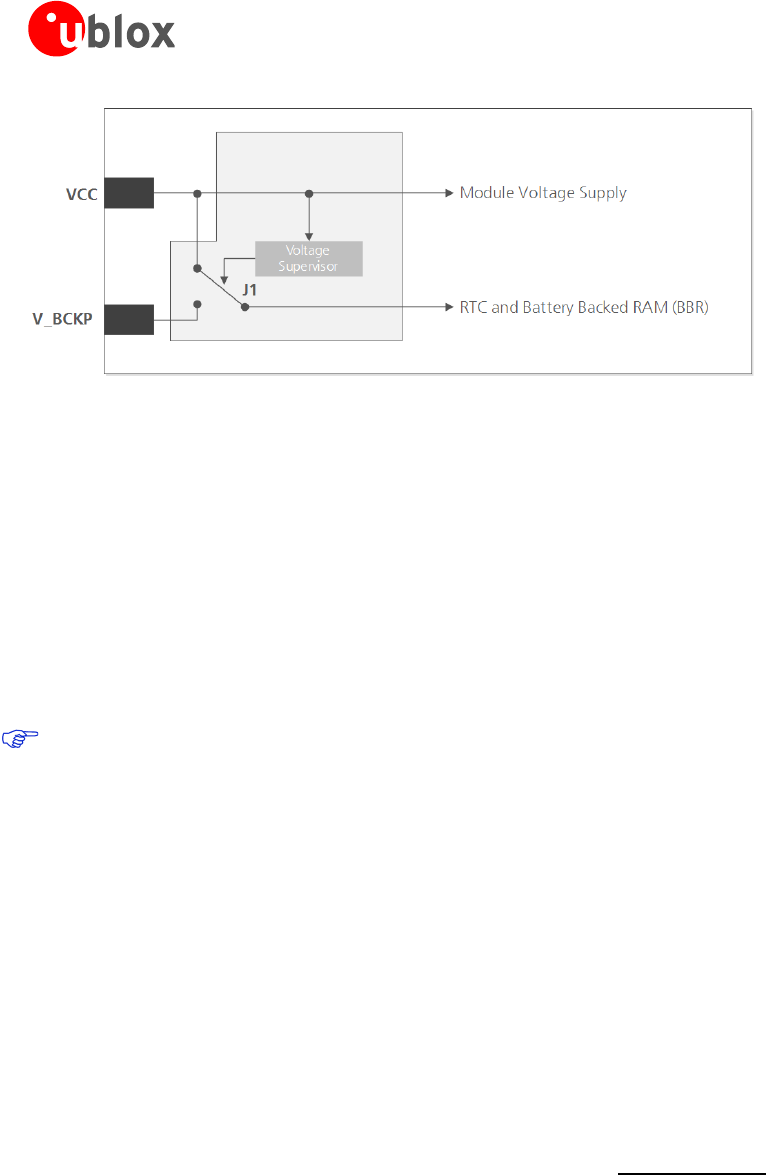
1.3.2 V_BCKP: Backup Supply Voltage
If the module supply has a power failure, the V_BCKP pin supplies the real-time clock (RTC) and battery backed
RAM (BBR). Use of valid time and the GNSS orbit data at start-up will improve the GNSS performance, i.e.
enables hot and warm starts. If no backup battery is connected, the module performs a cold start at power-up.
Avoid high resistance on the V_BCKP line: During the switch from main supply to backup supply, a
short current adjustment peak can cause high voltage drop on the pin with possible malfunctions.
If no backup supply voltage is available, connect the V_BCKP pin to VCC.
As long as the LEA-M8S / LEA-M8T module is supplied via the VCC, the backup battery is disconnected
from the RTC and the BBR to avoid unnecessary battery drain (see Figure 1). In this case, VCC supplies
power to the RTC and BBR.
LEA-M8S / LEA-M8T - Hardware Integration Manual
UBX-13003140 - R08 Production Information Hardware description
Page 5 of 31
Figure 1: Backup battery and voltage (for exact pin orientation, see the LEA-M8S Data Sheet [1] and the NEO/LEA-M8T Data
Sheet [2])
1.3.3 VDD_USB: USB interface power supply
VDD_USB supplies the USB interface. If the USB interface is not used, the VDD_USB pin must be connected to
GND. For more information about correctly handling the VDD_USB pin, see section 1.4
1.3.4 VCC_RF: Output Voltage RF section
The VCC_RF pin can supply an active antenna or external LNA. For more information, see section 2.4.
1.3.5 V_ANT: Antenna supply
The V_ANT pin is available to provide antenna bias voltage to supply an optional external active antenna. For
more information, see section 2.4.
If not used, connect the V_ANT pin to GND.
1.4 Interfaces
1.4.1 UART
The LEA-M8S and LEA-M8T positioning modules include a Universal Asynchronous Receiver Transmitter (UART)
serial interface RxD/TxD, which supports configurable baud rates. The baud rates supported are specified in the
LEA-M8S Data Sheet [1] and the NEO/LEA-M8T Data Sheet [2]. The signal output and input levels are 0 V to
VCC. An interface based on RS232 standard levels (+/- 12 V) can be implemented using level shifters such as
Maxim MAX3232. Hardware handshake signals and synchronous operation are not supported.
1.4.2 USB
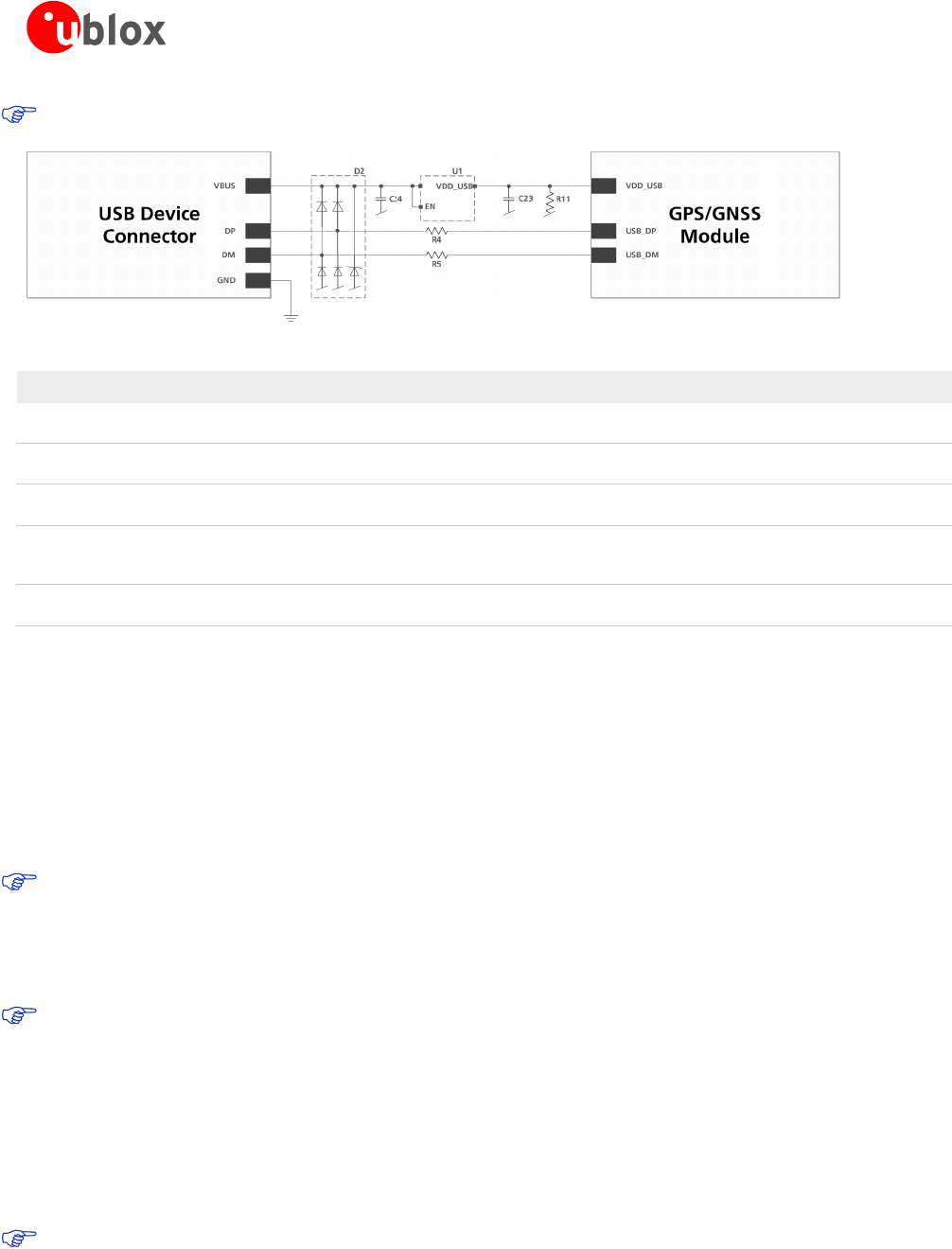
A USB version 2.0 FS (Full Speed, 12 Mb/s) compatible interface is available for communication as an alternative
to the UART. The USB_DP integrates a pull-up resistor to signal a full-speed device to the host. The VDD_USB
pin supplies the USB interface.
u-blox provides Microsoft® certified USB drivers for Windows Vista, and Windows 7 operating systems (also
Windows 8 compatible). These drivers are available at our website at www.u-blox.com
USB external components
The USB interface requires some external components to implement the physical characteristics required by the
USB 2.0 specification. These external components are shown in Figure 2 and listed in Table 1. To comply with
USB specifications, VBUS must be connected through an LDO (U1) to pin VDD_USB on the module.
The USB device is self-powered, the power supply (VCC) can be turned off and the digital block is not
powered. In this case, since VBUS is still available, the USB host would still receive the signal indicating that the
device is present and ready to communicate. This should be avoided by disabling the LDO (U1) using the enable
signal (EN) of the VCC-LDO or the output of a voltage supervisor. Depending on the characteristics of the LDO
(U1), it is recommended to add a pull-down resistor (R11) at its output to ensure VDD_USB is not floating if the
LDO (U1) is disabled or the USB cable is not connected, i.e. VBUS is not supplied.
LEA-M8S / LEA-M8T - Hardware Integration Manual
UBX-13003140 - R08 Production Information Hardware description
Page 6 of 31
USB bus powered is not supported.
Figure 2: USB Interface
Name Component Function Comments
U1 LDO Regulates VBUS (4.4 …5.25 V)
down to a voltage of 3.3 V.
Almost no current requirement (~1 mA)
C23,
C24
Capacitors Required according to the specification of LDO U1
D2 Protection
diodes
Protect circuit from overvoltage
/ ESD when connecting.
Use low capacitance ESD protection such as ST Microelectronics USBLC6-2.
R4, R5 Serial
termination
resistors
Establish a full-speed driver
impedance of 28…44 Ω
A value of 27 Ω is recommended.
R11 Resistor 100 kΩ is recommended for USB self-powered setup. For bus-powered setup,
R11 can be ignored.
Table 1: Summary of USB external components
1.4.3 Display Data Channel (DDC)
An I2C compatible Display Data Channel (DDC) interface is available for serial communication with an external
host CPU. The interface only supports operation in slave mode (master mode is not supported). The DDC
protocol and electrical interface are fully compatible with the Fast-Mode of the I2C industry standard. DDC pins
SDA and SCL have internal pull-up resistors.
For more information about the DDC implementation, see the u-blox M8 Receiver Description Including Protocol
Specification [3]. For bandwidth information, see the LEA-M8S Data Sheet [1]. For timing parameters, consult the
I2C-bus specification [8].
The u-blox M8 DDC interface supports serial communication with u-blox cellular modules. See the
specification of the applicable cellular module to confirm compatibility.
1.4.4 SPI (LEA-M8T ONLY)
An SPI interface is available for communication to a host CPU with LEA-M8T module.
SPI is not available in the default configuration, because its pins are shared with the UART and DDC
interfaces. The SPI interface can be enabled by connecting D_SEL to ground. For speed and clock
frequency, see the NEO/LEA-M8T Data Sheet [2]
1.4.5 TX Ready signal
The TX Ready signal indicates that the receiver has data to transmit. A listener can wait on the TX Ready signal
instead of polling the DDC or SPI interfaces. The UBX-CFG-PRT message lets you configure the polarity and the
number of bytes in the buffer before the TX Ready signal goes active. The TX Ready signal can be mapped to
UART TXD (PIO 06). The TX Ready function is disabled by default.
The TX-ready functionality can be enabled and configured by AT commands sent to the involved u-blox
cellular module supporting the feature. For more information, see the GPS Implementation and Aiding
Features in u-blox wireless modules [9].

LEA-M8S / LEA-M8T - Hardware Integration Manual
UBX-13003140 - R08 Production Information Hardware description
Page 7 of 31
1.5 I/O pins
RESET_N: Reset input
Driving RESET_N low activates a hardware reset of the system. Use this pin only to reset the module. Do not use
RESET_N to turn the module on and off, since the reset state increases power consumption. With LEA-M8S and
LEA-M8T modules RESET_N is an input only.
RESET_N should be used only in critical situations to recover the system. The Real-Time Clock (RTC) will
also be reset and thus immediately afterwards the receiver cannot perform a Hot Start.
EXTINT: External interrupt
EXTINT is an external interrupt pin with fixed input voltage thresholds with respect to VCC (see the LEA-M8S
Data Sheet [1] or the NEO/LEA-M8T Data Sheet [2] for more information). It can be used for wake-up functions
in Power Save Mode on all u-blox M8 modules and for aiding. Leave open if unused.
SAFEBOOT_N
If the SAFEBOOT_N pin is “low” at start up, the u-blox M8 module starts in Safe Boot Mode and doesn’t begin
GNSS operation. The Safe Boot Mode can be used to recover from situations where the Flash has become
corrupted.
D_SEL: Interface select (LEA-M8T ONLY)
The D_SEL pin selects the available interfaces. SPI cannot be used simultaneously with UART/DDC.
If open, UART and DDC are available. If pulled low, the SPI interface is available. See the NEO/LEA-M8T Data
Sheet [2].
Antenna Short circuit detection
The LEA-M8S and LEA-M8T modules include internal short circuit antenna detection. For more information, see
section 2.4.
Antenna open circuit detection
The LEA-M8S and LEA-M8T modules provide antenna open circuit detection (OCD) functionality over the
AADET_N pin.
AADET_N is an input pin used to report whether an external circuit has detected an external antenna or not.
Low means an antenna has been detected (antenna consumes current), while high means no external antenna
has been detected (no current drawn). This functionality is by default disabled. See section 2.4.2.
TIMEPULSE 1
A configurable time pulse signal is available with all u-blox M8 modules. By default, the time pulse signal is
configured to 1 pulse per second. For more information, see the u-blox M8 Receiver Description Including
Protocol Specification [3].
TIMEPULSE 2 (LEA-M8T only)
A configurable time pulse 2 signal is available on LEA-M8T module only. For more information see the u-blox M8
Receiver Description Including Protocol Specification [3].
LEA-M8S / LEA-M8T - Hardware Integration Manual
UBX-13003140 - R08 Production Information Hardware description
Page 8 of 31
Electromagnetic interference on I/O lines
Any I/O signal line with a length greater than approximately 3 mm can act as an antenna and may pick up
arbitrary RF signals transferring them as noise into the GNSS receiver. This specifically applies to unshielded lines,
in which the corresponding GND layer is remote or missing entirely, and lines close to the edges of the printed
circuit board.
If, for example, a cellular signal radiates into an unshielded high-impedance line, it is possible to generate noise
in the order of volts and not only distort receiver operation but also damage it permanently.
On the other hand, noise generated at the I/O pins will emit from unshielded I/O lines. Receiver performance
may be degraded when this noise is coupled into the GNSS antenna (see Figure 19).
To avoid interference by improperly shielded lines, it is recommended to use resistors (e.g. R>20 Ω), ferrite beads
(e.g. BLM15HD102SN1) or inductors (e.g. LQG15HS47NJ02) on the I/O lines in series. These components should
be chosen with care because they will affect also the signal rise times.
Figure 3 shows an example of EMI protection measures on the RX/TX line using a ferrite bead. More information
can be found in section 4.3.
Figure 3: EMI Precautions
TX
RX
GNSS
Receiver
FB
FB
BLM15HD102SN1
>10mm
LEA-M8S / LEA-M8T - Hardware Integration Manual
UBX-13003140 - R08 Production Information Design
Page 9 of 31
2 Design
2.1 Pin description
Function PIN No I/O Description Remarks
Power VCC 6 I Supply Voltage Provide clean and stable supply.
GND 7, 13, 14,
15, 17
- Ground Assure a good GND connection to all GND pins of the
module
VCC_OUT 8 O Output Voltage (VCC) Leave open if not used.
V_BCKP 11 I Backup Supply Voltage It is recommended to connect a backup supply voltage to
V_BCKP in order to enable Warm and Hot Start features on
the positioning modules. Otherwise, connect to VCC.
VDD_USB 24 I USB Power Supply To use the USB interface connect this pin to 3.0 – 3.6V.
If no USB serial port used connect to GND.
Antenna RF_IN 16 I GNSS signal input
from antenna
Use a controlled impedance transmission line of 50 Ω to
connect to RF_IN.
VCC_RF 18 O Output Voltage RF
section
Can be used to power external LNA or an external active
antenna (VCC_RF connected to V_ANT with 10
Ω
). The
max power consumption of the antenna must not exceed
the datasheet specification of the module.
Leave open if not used.
V_ANT 19 I Antenna Bias voltage Connect to GND (or leave open) if passive antenna is used. If
an active antenna is used, add a 10 Ω resistor in front of
V_ANT input to the Antenna Bias Voltage or VCC_RF
EXTINT1/
AADET_N
20 I Ext. Interrupt /Active
Antenna Detect
Ext. Interrupt Pin. Int. pull-up resistor to VCC./ Input pin for
optional antenna supervisor circuitry. Leave open if not used.
UART TxD (LEA-M8S) 3
TxD / SPI MISO
(LEA-M8T)
O Serial Port Communication interface can be programmed as TX Ready
for DDC interface. Leave open if not used.
O
TxD
SPI MISO
Serial Port if D_SEL =1(or open)
SPI MISO if D_SEL = 0
RxD (LEA-M8S) 4
RxD /SPI MOSI
(LEA-M8T)
I Serial Port
Serial port input with internal pull-up resistor to VCC. Leave
open if not used. Do not use external pull up resistor.
I
RxD
SPI MOSI
Serial Port if D_SEL =1(or open)
SPI MOSI if D_SEL = 0
USB USB_DM 25 I/O USB I/O line
USB2.0 bidirectional communication pin. Leave open if
unused. Implementations see section 1.4
USB_DP 26 I/O USB I/O line
System RESET_N 10 I Hardware Reset
(Active Low)
Leave open if not used. Do not drive high.
TIMEPULSE 1 28 O Timepulse 1 Configurable Timepulse signal (one pulse per second by
default). Leave open if not used.
SAFEBOOT_N / 12
TIMEPULSE 2
(LEA-M8T)
SAFEBOOT_N (LEA-M8S)
I/O Safeboot_N /
Timepulse 2
Configurable Timepulse signal. Must not be held LO during
start-up.
I/O Safeboot_N Must not be held LO during start-up
EXTINT0 27 I Ext. Interrupt Ext. Interrupt Pin. Int. pull-up resistor to VCC. Leave open if
unused.
SDA (LEA-M8S) 1
SDA /SPI CS_N
(LEA-M8T)
I/O
DDC Pins
DDC Data. Leave open if not used.
I/O
SDA
SPI CS_N
DDC Data if D_SEL =1 (or open)
SPI Chip Select if D_SEL = 0
SCL (LEA-M8S) 2
SCL / SPI CLK
(LEA-M8T)
I DDC Pins DDC Clock. Leave open if not used.
I/O
SCL
SPI CLK
DDC Clock if D_SEL =1 (or open)
SPI Clock if D_SEL = 0
D_SEL (LEA-M8T) 5
Reserved(LEA-M8S)
I
Interface Select
D_SEL = 0 -> SPI, D_SEL =1 (or open) -> DDC
- Reserved Leave open
Reserved 9, 21, 22,
23
- Reserved Leave open
Table 2: Pinout LEA-M8S / LEA-M8T
LEA-M8S / LEA-M8T - Hardware Integration Manual
UBX-13003140 - R08 Production Information Design
Page 10 of 31
2.2 Minimal design
This is a minimal setup for a GNSS receiver with a LEA-M8S / LEA-M8T module:
• Passive antenna used
• No backup battery
• UART for communication
Figure 4: LEA-M8S / LEA-M8T passive antenna design
For active antenna design, see section 2.4
2.3 Footprint and paste mask
Figure 5 describes the footprint and provides recommendations for the paste mask for the LEA-M8S and
LEA-M8T modules. These are recommendations only and not specifications. Note that the copper and solder
masks have the same size and position.
To improve the wetting of the half vias, reduce the amount of solder paste under the module and increase the
volume outside of the module by defining the dimensions of the paste mask to form a T-shape (or equivalent)
extending beyond the copper mask. For the stencil thickness, see Figure 6.
LEA-M8S / LEA-M8T - Hardware Integration Manual
UBX-13003140 - R08 Production Information Design
Page 11 of 31
17.0 mm [669 mil]
22.4 mm [881.9 mil]
1.0 mm
[39 mil]
0.8 mm
[31.5 mil]
2.45 mm
[96.5 mil]
1.1 mm
[43 mil]
3.0 mm
[118 mil]
2.15 mm
[84.5 mil]
0.8 mm
[31.5 mil]
Figure 5: LEA-M8S / LEA-M8T footprint
Figure 6: LEA-M8S / LEA-M8T paste mask
2.4 Antenna and Antenna supervision
2.4.1 Antenna design with passive antenna
A design using a passive antenna requires more attention to the layout of the RF section. Typically, a passive
antenna is located near electronic components; therefore, care should be taken to reduce electrical noise that
may interfere with the antenna performance. Passive antennas do not require a DC bias voltage and can be
directly connected to the RF input pin RF_IN. Sometimes they may also need a passive matching network to
match the impedance to 50 Ω.
Minimal setup with a good patch antenna
Figure 7 shows a minimal setup for a design with a good GNSS patch antenna.
Figure 7: Module design with passive antenna (for exact pin orientation see the LEA-M8S Data Sheet [1] and the NEO/LEA-M8T
Data Sheet [2])
LEA-M8S / LEA-M8T - Hardware Integration Manual
UBX-13003140 - R08 Production Information Design
Page 12 of 31
Setup for best performance with passive antenna
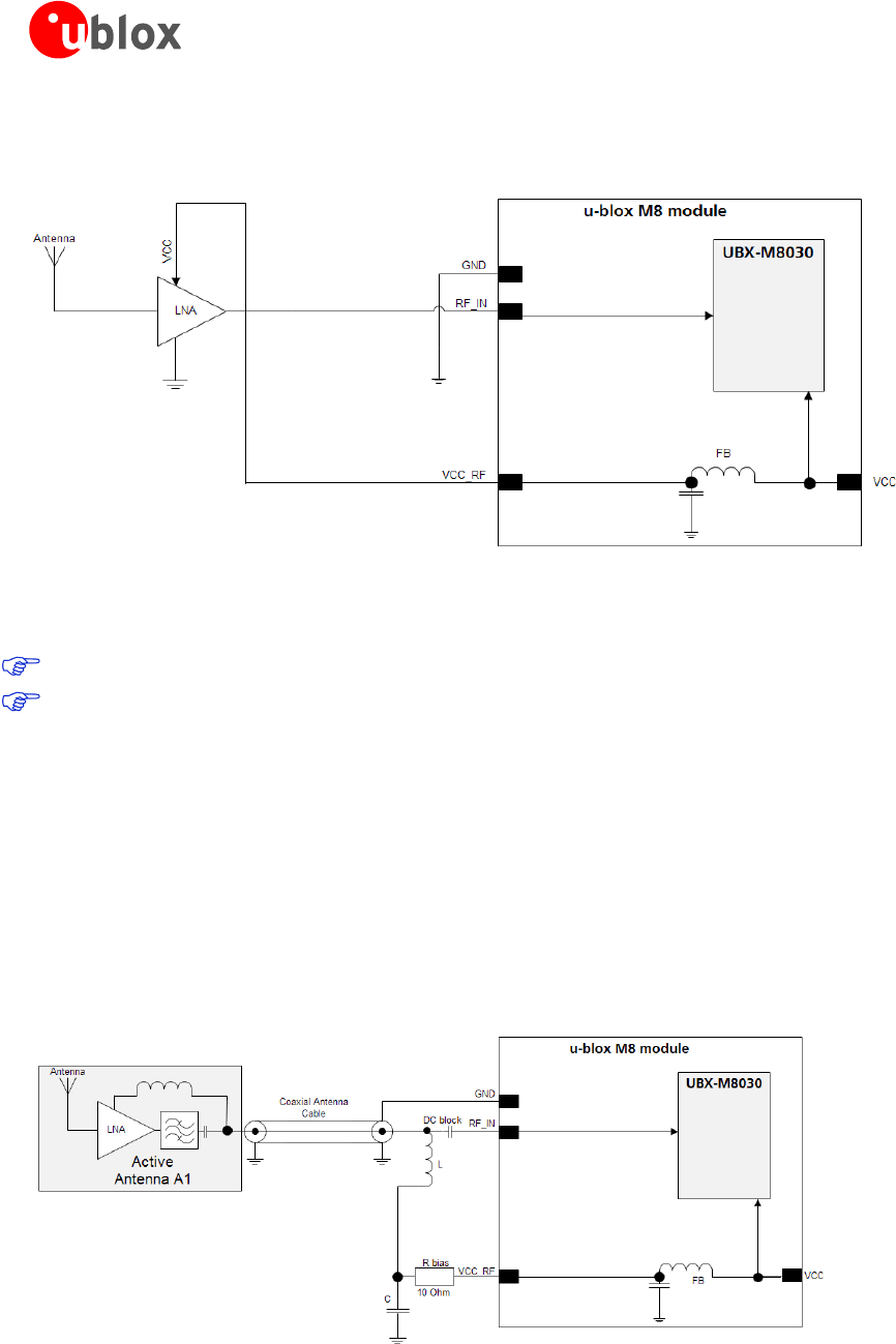
Figure 8 shows a design using an external LNA to increase the sensitivity for best performance with passive
antenna.
Figure 8: Module design with passive antenna and an external LNA (for exact pin orientation see the LEA-M8S Data Sheet [1]
and the NEO/LEA-M8T Data Sheet [2].)
The VCC_RF output can be used to supply the LNA with a filtered supply voltage.
For recommended parts, see Appendix
A standard GNSS LNA has enough bandwidth to amplify GPS / GLONASS and BeiDou signals.
2.4.2 Active antenna design
Active antennas have an integrated low-noise amplifier. Active antennas require a power supply that will
contribute to the total GNSS system power consumption budget with additional 5 to 20 mA typically.
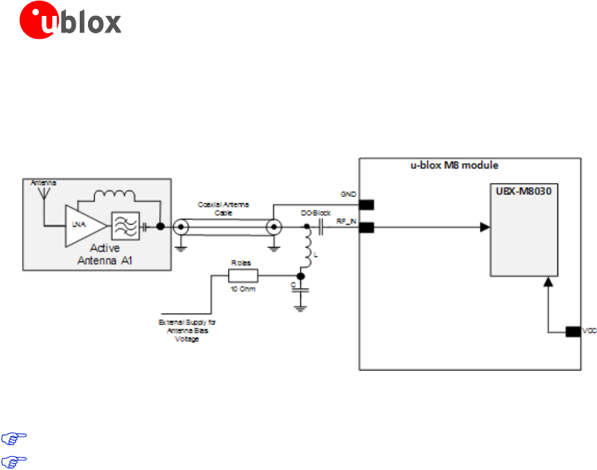
If the customers do not want to make use of the internal antenna supervisor and the supply voltage of the LEA-
M8S / LEA-M8T module matches the supply voltage of the antenna (e.g. 3.0 V), they can use the filtered supply
voltage VCC_RF output to supply the antenna (See Figure 9). This design is used for modules in combination
with active antenna.
In case of different supply voltage, use a filtered external supply, see Figure 10.
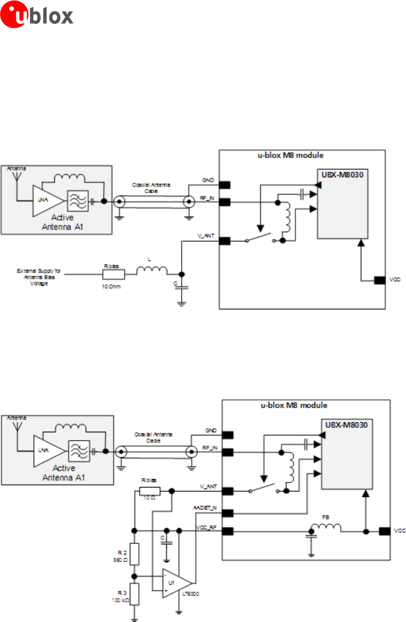
Active antenna design using VCC_RF pin to supply the active antenna
Figure 9: Active antenna design, external supply from VCC_RF (for exact pin orientation see the LEA-M8S Data Sheet [1])
LEA-M8S / LEA-M8T - Hardware Integration Manual
UBX-13003140 - R08 Production Information Design
Page 13 of 31
Active antenna design powered from external supply
Figure 10 shows a design with direct externally powered active antenna.
This circuit has to be used if the active antenna has a different supply voltage than the VCC_RF (for example if a
5 V active antenna is used).
Figure 10: Active antenna design, direct external supply (for exact pin orientation see the LEA-M8S Data Sheet [1] and the
NEO/LEA-M8T Data Sheet [2])
For recommended parts, see Appendix.
In case VCC_RF voltage does not match with the antenna supply voltage, use a filtered external supply
as shown in Figure 10.
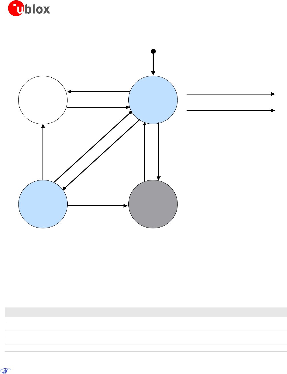
Antenna design with active antenna using antenna supervisor
An active antenna supervisor provides the means to check the antenna for open and short circuits and to shut
off the antenna supply if a short circuit is detected. The Antenna Supervisor is configured using serial port UBX
binary protocol message. Once enabled, the active antenna supervisor produces status messages, reporting in
NMEA and/or UBX binary protocol. These indicate the particular state of the antenna supervisor shown in the
state diagram (see Figure 11).
LEA-M8S / LEA-M8T - Hardware Integration Manual
UBX-13003140 - R08 Production Information Design
Page 14 of 31
The current active antenna status can be determined by polling the UBX-MON-HW monitor command. If an
antenna is connected, the initial state after power-up is “Active Antenna OK.”
No
Super-
vision
Active
Antenna
OK
Open
Circuit
detected
Short
Circuit
detected
Powerup
Events AADET0_N
User controlled events
Disable Supervision
Enable Supervision
Short Circuit
detected
Disable
Supervision
Antenna
connected
Short Circuit
detected
open circuit
detected,given
OCD enabled
Periodic
reconnection
attempts
Figure 11: State diagram of active antenna supervisor
The module firmware supports an active antenna supervisor circuit, which is connected to the AADET_N pin. For
an example of an open circuit detection circuit, see Figure 14. High on AADET_N means that an external
antenna is not connected.
Status reporting
At startup, and on every change of the antenna supervisor configuration, the LEA-M8S and LEA-M8T modules
will output an NMEA ($GPTXT) or UBX (INF-NOTICE) message with the internal status of the antenna supervisor
(disabled, short detection only, enabled).
Abbreviation Description
AC Antenna Control (e.g. the antenna will be switched on/ off controlled by the GNSS receiver)
SD Short Circuit Detection Enabled
SR Short Circuit Recovery Enabled
OD Open Circuit Detection Enabled
PdoS Power Down on short
Table 3: Active Antenna Supervisor Message on startup (UBX binary protocol)
To activate the antenna supervisor use the UBX-CFG-ANT message. For further information, refer to the
u-blox M8 Receiver Description Including Protocol Specification [3].
Similar to the antenna supervisor configuration, the status of the antenna supervisor will be reported in an
NMEA ($GPTXT) or UBX (INF-NOTICE) message at start-up and on every change.
LEA-M8S / LEA-M8T - Hardware Integration Manual
UBX-13003140 - R08 Production Information Design
Page 15 of 31
Message Description
ANTSTATUS=DONTKNOW Active antenna supervisor is not configured and deactivated.
ANTSTATUS=OK Active antenna connected and powered
ANTSTATUS=SHORT Antenna short
ANTSTATUS=OPEN Antenna not connected or antenna defective
Table 4: Active antenna supervisor message on startup (NMEA protocol)
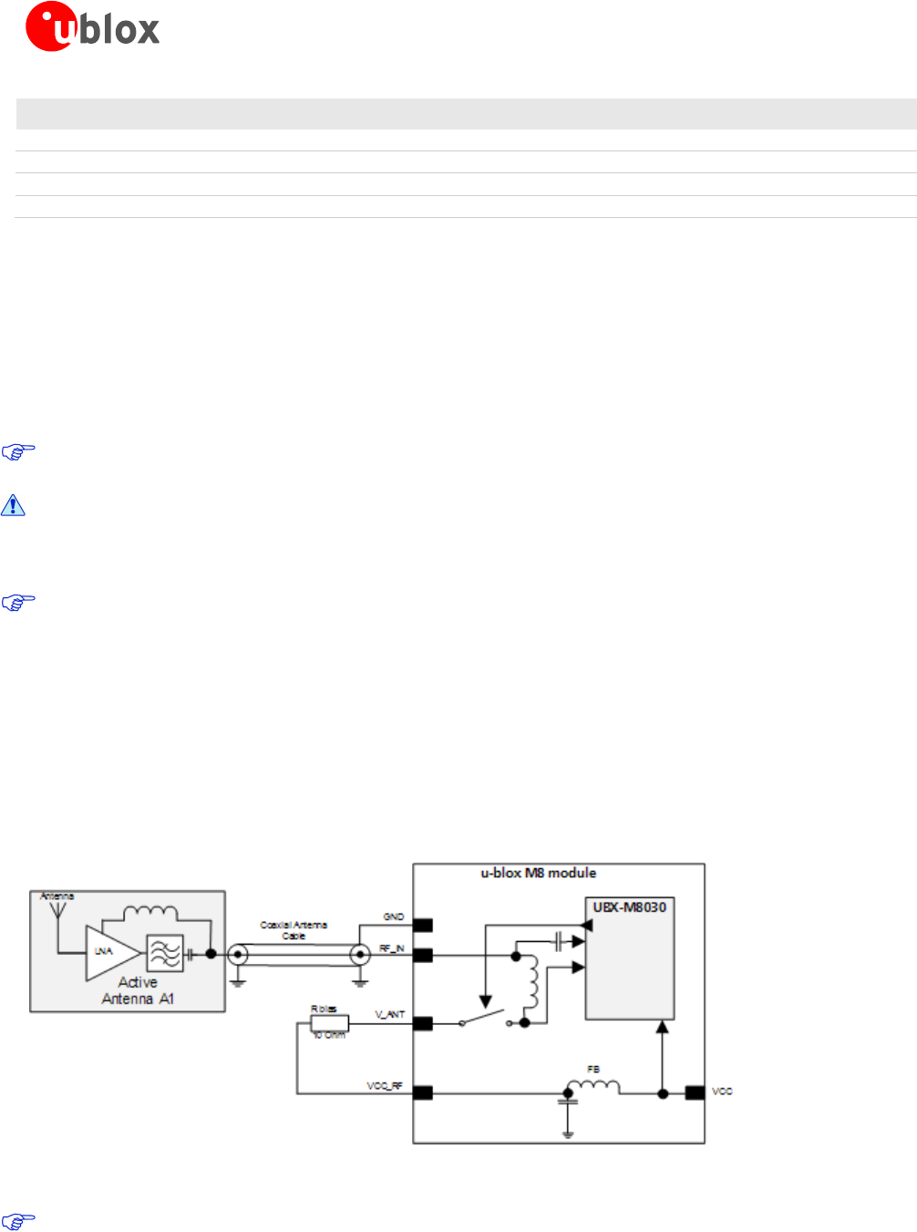
Module design with active antenna, short circuit protection / detection
If a suitably dimensioned R_BIAS series resistor is placed in front of the V_ANT pin, a short circuit can be
detected in the antenna supply. The detection happens inside the u-blox M8 module, after which the antenna
supply voltage will be immediately shut down. Afterwards, periodic attempts to re-establish antenna power are
made by default.
An internal switch (under control of the receiver) can turn off the supply to the external antenna whenever it is
not needed. This feature helps to reduce power consumption in power save mode.
To configure the antenna supervisor use the UBX-CFG-ANT message. For further information, see the
u-blox M8 Receiver Description Including Protocol Specification [3].
Short circuits on the antenna input without limitation (R_BIAS) of the current can result in
permanent damage to the receiver! Therefore, it is mandatory to implement an R_BIAS in all
risk applications, such as situations where the antenna can be disconnected by the end-user or
that have long antenna cables.
In case VCC_RF voltage does not match with the antenna supply voltage, use a filtered external supply
as shown in Figure 13.
Supply from VCC_RF
Figure 12 shows an active antenna supplied from the LEA-M8S and LEA-M8T modules.
LEA-M8S and LEA-M8T modules includes a built in antenna bias supply for nominal 3V antennas enabled by
linking the filtered VCC_RF supply output pin to the V_ANT antenna supply input pin with a 10 Ohm resistor in
series. The module then controls the power supply to the antenna, applying power whenever the receiver is
active and removing power during power-save idle times and if a short-circuit is detected. Short-circuit is
detected if the voltage at the antenna supply falls close to zero and is indicated as an alarm in message MON-
HW
Figure 12: Module design with active antenna, internal supply from VCC_RF (for exact pin orientation see the LEA-M8S Data
Sheet [1] and the NEO/LEA-M8T Data Sheet [2].)
For recommended parts, see Appendix.
LEA-M8S / LEA-M8T - Hardware Integration Manual
UBX-13003140 - R08 Production Information Design
Page 16 of 31
External supply
Figure 13 shows an externally powered active antenna design.
Since the external bias voltage is fed into the most sensitive part of the receiver (i.e. the RF input), this supply
should be free of noise. Usually, low frequency analog noise is less critical than digital noise of spurious
frequencies with harmonics up to the GPS/QZSS band of 1.575 GHz, GLONASS band of 1.602 GHz and BeiDou
band at 1.561 GHz. Therefore, it is not recommended to use digital supply nets to feed the V_ANT pin.
Figure 13: Module design with active antenna, external supply (for exact pin orientation see the LEA-M8S Data Sheet [1] and
the NEO/LEA-M8T Data Sheet [2])
Antenna supervision with open circuit detection (OCD)
Optionally the AADET_N pin may be reassigned to antenna supervision allowing an external circuit to indicate to
the module that the antenna is open-circuit. This condition is then reported by the module in message MON-
HW. Calculate the threshold current using Equation 1.
Figure 14: Schematic of open circuit detection (for exact pin orientation see the LEA-M8S Data Sheet [1] and the NEO/LEA-M8T
Data Sheet [2].)

LEA-M8S / LEA-M8T - Hardware Integration Manual
UBX-13003140 - R08 Production Information Design
Page 17 of 31
RFVcc
Rbias
RR
R
I_
32
2
•
+
=
Equation 1: Calculation of threshold current for open circuit detection
If the antenna supply voltage is not derived from VCC_RF, do not exceed the maximum voltage rating of
AADET_N.
For recommended parts, see Appendix
LEA-M8S / LEA-M8T - Hardware Integration Manual
UBX-13003140 - R08 Production Information Migration to u-blox M8 modules
Page 18 of 31
3 Migration to u-blox M8 modules
3.1 Migrating u-blox 6 designs to a u-blox M8 module
u-blox is committed to ensuring that products in the same form factor are backwards compatible over several
technology generations. Utmost care has been taken to ensure there is no negative impact on function or
performance and to make u-blox M8 modules as fully compatible as possible with previous generations modules.
If using BeiDou, check the bandwidth of the external RF components and the antenna. For information about
power consumption, see the LEA-M8S Data Sheet [1] and the NEO/LEA-M8T Data Sheet [2]. It is highly advisable
that customers consider a design review with the u-blox support team to ensure the compatibility of key
functionalities.
3.2 Hardware migration LEA-6N -> LEA-M8S
Pin
LEA-6N LEA-M8S Remarks for Migration
Pin Name Typical Assignment Pin Name Typical Assignment
1 SDA DDC Data SDA DDC Data No difference
2 SCL DDC Clock SCL DDC Clock No difference
3 TxD Serial Port TxD Serial Port No difference
4 RxD Serial Port RxD Serial Port No difference
5 NC Not Connected Reserved Not Connected No difference
6 VCC Supply voltage VCC Supply voltage No difference
7 GND Ground (digital) GND Ground (digital) No difference
8 VCC_OUT Output voltage VCC_OUT Output voltage No difference
9 NC Not Connected Reserved Not Connected No difference
10 RESET_N External Reset RESET_N External Reset No difference
11 V_BCKP Backup voltage supply V_BCKP Backup voltage supply
If this was connected to GND
on u-blox 6 module, OK to
do the same on u-blox M8.
12 Safeboot_N Do not drive low Safeboot_N Do not drive low No difference
13 GND Ground GND Ground No difference
14 GND Ground GND Ground No difference
15 GND Ground GND Ground No difference
16 RF_IN GNSS signal input RF_IN GNSS signal input No difference
17 GND Ground GND Ground No difference
18 VCC_RF Output Voltage RF section VCC_RF Output Voltage RF section No difference
19 V_ANT Antenna Bias voltage V_ANT Antenna Bias voltage No difference
20 AADET_N Active Antenna Detect AADET_N Active Antenna Detect No difference
21 Reserved Not Connected Reserved Not Connected No difference
22 Reserved Not Connected Reserved Not Connected No difference
23 Reserved Not Connected Reserved Not Connected No difference
24 VDD_USB USB Supply VDD_USB USB Supply No difference
25 USB_DM USB Data USB_DM USB Data No difference
26 USB_DP USB Data USB_DP USB Data No difference
27 EXTINT0 External Interrupt Pin EXTINT0 External Interrupt Pin No difference
28 TIMEPULSE Timepulse (1PPS) TIMEPULSE Timepulse (1PPS) No difference
Table 5: Pin-out comparison LEA-6N vs. LEA-M8S
LEA-M8S / LEA-M8T - Hardware Integration Manual
UBX-13003140 - R08 Production Information Migration to u-blox M8 modules
Page 19 of 31
3.3 Hardware migration LEA-6T -> LEA-M8T
Pin
LEA-6T LEA-M8T Remarks for Migration
Pin Name Typical Assignment Pin Name Typical Assignment
1 SDA DDC Data SDA DDC Data No difference
2 SCL DDC Clock SCL DDC Clock No difference
3 TxD Serial Port TxD Serial Port No difference
4 RxD Serial Port RxD Serial Port No difference
5 NC Not Connected D_SEL D_SEL =1(or open) Do not drive low
6 VCC Supply voltage VCC Supply voltage No difference
7 GND Ground (digital) GND Ground (digital) No difference
8 VCC_OUT Output voltage VCC_OUT Output voltage No difference
9 TIMEPULSE2 2nd Timepulse Not Connected Reserved
Time Pulse 2 is now
available on pin 12
(Safeboot_N / Time Pulse 2)
10 RESET_N External Reset RESET_N External Reset No difference
11 V_BCKP Backup voltage supply V_BCKP Backup voltage supply
If this was connected to GND
on u-blox 6 module, OK to do
the same on u-blox M8.
12 Safeboot_N Safeboot_N Safeboot_N/
TIMEPULSE2 Safeboot_N /Timepulse 2 Must not be held LO during
start-up.
13 GND Ground GND Ground No difference
14 GND Ground GND Ground No difference
15 GND Ground GND Ground No difference
16 RF_IN GNSS signal input RF_IN GNSS signal input No difference
17 GND Ground GND Ground No difference
18 VCC_RF Output Voltage RF section VCC_RF Output Voltage RF
section No difference
19 V_ANT Antenna Bias voltage V_ANT Antenna Bias voltage No difference
20 AADET_N Active Antenna Detect EXTINT1/AADET_N External Interrupt Pin/
Active Antenna Detect
21 Reserved Not Connected Reserved Not Connected No difference
22 Reserved Not Connected Reserved Not Connected No difference
23 Reserved Not Connected Reserved Not Connected No difference
24 VDD_USB USB Supply VDD_USB USB Supply No difference
25 USB_DM USB Data USB_DM USB Data No difference
26 USB_DP USB Data USB_DP USB Data No difference
27 EXTINT0 External Interrupt Pin EXTINT0 External Interrupt Pin No difference
28 TIMEPULSE1 Timepulse (1PPS) TIMEPULSE1 Timepulse (1PPS) No difference
Table 6: Pin-out comparison LEA-6T vs. LEA-M8T
3.4 Software migration
For overall description of the module software operation, see the u-blox M8 Receiver Description
Including Protocol Specification [3].
All features requiring a flash on LEA-6N are not supported on LEA-M8S. (AssistNow offline / save config)

LEA-M8S / LEA-M8T - Hardware Integration Manual
UBX-13003140 - R08 Production Information Product handling
Page 20 of 31
4 Product handling
4.1 Packaging, shipping, storage and moisture preconditioning
For information pertaining to reels and tapes, Moisture Sensitivity levels (MSL), shipment and storage
information, as well as drying for preconditioning see the LEA-M8S Data Sheet [1] and the NEO/LEA-M8T Data
Sheet [2].
Population of Modules
When populating the modules, make sure that the pick and place machine is aligned to the copper pins
of the module and not on the module edge.
4.2 Soldering
Soldering paste
Use of “No Clean” soldering paste is strongly recommended, as it does not require cleaning after the soldering
process has taken place. The paste listed in the example below meets these criteria.
Soldering Paste: OM338 SAC405 / Nr.143714 (Cookson Electronics)
Alloy specification: Sn 95.5/ Ag 4/ Cu 0.5 (95.5% Tin/ 4% Silver/ 0.5% Copper)
Melting Temperature: 217 °C
Stencil Thickness: See Figure 6.
The final choice of the soldering paste depends on the approved manufacturing procedures.
The paste-mask geometry for applying soldering paste should meet the recommendations.
The quality of the solder joints on the connectors (’half vias’) should meet the appropriate IPC
specification.
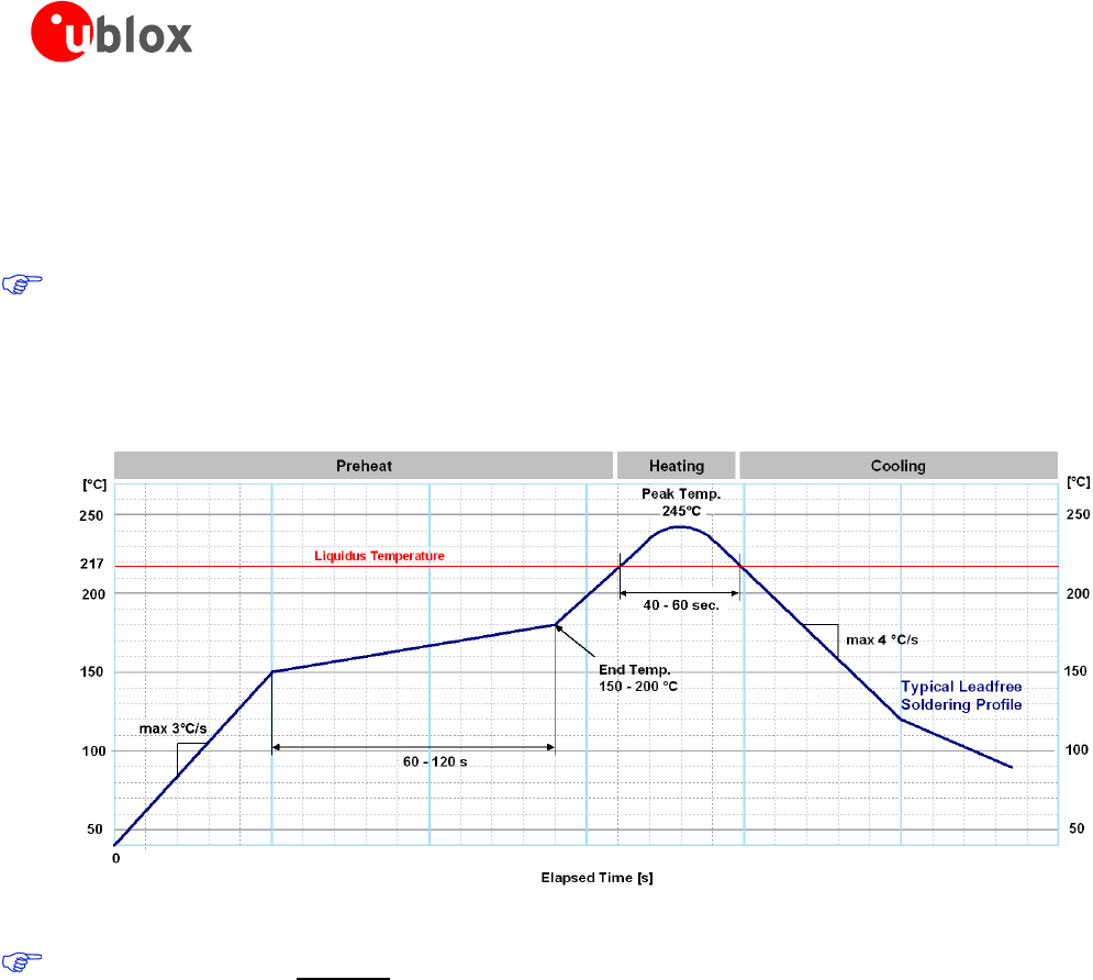
Reflow soldering
A convection type-soldering oven is highly recommended over the infrared type radiation oven.
Convection heated ovens allow precise control of the temperature, and all parts will heat up evenly, regardless
of material properties, thickness of components and surface color.
As a reference, see the “IPC-7530 Guidelines for temperature profiling for mass soldering (reflow and wave)
processes”, published in 2001.
Preheat phase
During the initial heating of component leads and balls, residual humidity will be dried out. Note that this
preheat phase will not replace prior baking procedures.
• Temperature rise rate: max. 3 °C/s. If the temperature rise is too rapid in the preheat phase it may cause
excessive slumping.
• Time: 60 – 120 s. If the preheat is insufficient, rather large solder balls tend to be generated. Conversely, if
performed excessively, fine balls and large balls will be generated in clusters.
• End Temperature: 150 – 200 °C. If the temperature is too low, non-melting tends to be caused in areas
containing large heat capacity.
Heating/ Reflow phase
The temperature rises above the liquidus temperature of 217°C. Avoid a sudden rise in temperature as the slump
of the paste could become worse.
• Limit time above 217 °C liquidus temperature: 40 – 60 s
• Peak reflow temperature: 245 °C
LEA-M8S / LEA-M8T - Hardware Integration Manual
UBX-13003140 - R08 Production Information Product handling
Page 21 of 31
Cooling phase
A controlled cooling avoids negative metallurgical effects (solder becomes more brittle) of the solder and
possible mechanical tensions in the products. Controlled cooling helps to achieve bright solder fillets with a good
shape and low contact angle.
• Temperature fall rate: max 4 °C/s
To avoid falling off, the u-blox M8 GNSS module should be placed on the topside of the motherboard
during soldering.
The final soldering temperature chosen at the factory depends on additional external factors like choice of
soldering paste, size, thickness and properties of the baseboard, etc. Exceeding the maximum soldering
temperature in the recommended soldering profile may permanently damage the module.
Figure 15: Recommended soldering profile
u-blox M8 modules must not be soldered with a damp heat process.
Optical inspection
After soldering the u-blox M8 module, consider an optical inspection step to check whether:
• The module is properly aligned and centered over the pads
• All pads are properly soldered
• No excess solder has created contacts to neighboring pads, or possibly to pad stacks and vias nearby
Cleaning
In general, cleaning the populated modules is strongly discouraged. Residues underneath the modules cannot be
easily removed with a washing process.
• Cleaning with water will lead to capillary effects where water is absorbed in the gap between the baseboard
and the module. The combination of residues of soldering flux and encapsulated water leads to short circuits
or resistor-like interconnections between neighboring pads.
• Cleaning with alcohol or other organic solvents can result in soldering flux residues flooding into the two
housings, areas that are not accessible for post-wash inspections. The solvent will also damage the sticker
and the ink-jet printed text.
• Ultrasonic cleaning will permanently damage the module, in particular the quartz oscillators.
The best approach is to use a “no clean” soldering paste and eliminate the cleaning step after the soldering.

LEA-M8S / LEA-M8T - Hardware Integration Manual
UBX-13003140 - R08 Production Information Product handling
Page 22 of 31
Repeated reflow soldering
Only single reflow soldering processes are recommended for boards populated with u-blox M8 modules. u-blox
M8 modules should not be submitted to two reflow cycles on a board populated with components on both sides
in order to avoid upside down orientation during the second reflow cycle. In this case, the module should always
be placed on that side of the board, which is submitted into the last reflow cycle. The reason for this (besides
others) is the risk of the module falling off due to the significantly higher weight in relation to other
components.
Two reflow cycles can be considered by excluding the above described upside down scenario and taking into
account the rework conditions described in section 4.
Repeated reflow soldering processes and soldering the module upside down are not recommended.
Wave soldering
Baseboards with combined through-hole technology (THT) components and surface-mount technology (SMT)
devices require wave soldering to solder the THT components. Only a single wave soldering process is
encouraged for boards populated with u-blox M8 modules.
Hand soldering
Hand soldering is allowed. Use a soldering iron temperature-setting equivalent to 350 °C. Place the module
precisely on the pads. Start with a cross-diagonal fixture soldering (e.g. pins 1 and 15), and then continue from
left to right.
Rework
The u-blox M8 module can be unsoldered from the baseboard using a hot air gun. When using a hot air gun for
unsoldering the module, a maximum of one reflow cycle is allowed. In general, we do not recommend using a
hot air gun because this is an uncontrolled process and might damage the module.
Attention: use of a hot air gun can lead to overheating and severely damage the module.
Always avoid overheating the module.
After the module is removed, clean the pads before placing and hand soldering a new module.
Never attempt a rework on the module itself, e.g. replacing individual components. Such
actions immediately terminate the warranty.
In addition to the two reflow cycles, manual rework on particular pins by using a soldering iron is allowed.
Manual rework steps on the module can be done several times.
Conformal coating
Certain applications employ a conformal coating of the PCB using HumiSeal® or other related coating products.
These materials affect the HF properties of the GNSS module and it is important to prevent them from flowing
into the module. The RF shields do not provide 100% protection for the module from coating liquids with low
viscosity; therefore, care is required in applying the coating.
Conformal Coating of the module will void the warranty.
Casting
If casting is required, use viscose or another type of silicon pottant. The OEM is strongly advised to qualify such
processes in combination with the u-blox M8 module before implementing this in the production.
Casting will void the warranty.
LEA-M8S / LEA-M8T - Hardware Integration Manual
UBX-13003140 - R08 Production Information Product handling
Page 23 of 31
Grounding metal covers
Attempts to improve grounding by soldering ground cables, wick or other forms of metal strips directly onto the
EMI covers is done at the customer’s own risk. The numerous ground pins should be sufficient to provide
optimum immunity to interferences and noise.
u-blox makes no warranty for damages to the u-blox M8 module caused by soldering metal cables or
any other forms of metal strips directly onto the EMI covers.
Use of ultrasonic processes
Some components on the u-blox M8 module are sensitive to Ultrasonic Waves. Use of any Ultrasonic Processes
(cleaning, welding etc.) may cause damage to the GNSS Receiver.
u-blox offers no warranty against damages to the u-blox M8 module caused by any Ultrasonic Processes.
4.3 EOS/ESD/EMI precautions
When integrating GNSS positioning modules into wireless systems, careful consideration must be given to
electromagnetic and voltage susceptibility issues. Wireless systems include components that can produce
Electrical Overstress (EOS) and Electro-Magnetic Interference (EMI). CMOS devices are more sensitive to such
influences because their failure mechanism is defined by the applied voltage, whereas bipolar semiconductors
are more susceptible to thermal overstress. The following design guidelines are provided to help in designing
robust yet cost effective solutions.
To avoid overstress damage during production or in the field it is essential to observe strict
EOS/ESD/EMI handling and protection measures.
To prevent overstress damage at the RF_IN of your receiver, never exceed the maximum input
power (see the LEA-M8S Data Sheet [1] and the NEO/LEA-M8T Data Sheet [2]).
Electrostatic discharge (ESD)
Electrostatic discharge (ESD) is the sudden and momentary electric current that flows between
two objects at different electrical potentials caused by direct contact or induced by an
electrostatic field. The term is usually used in the electronics and other industries to describe
momentary unwanted currents that may cause damage to electronic equipment.
ESD handling precautions
ESD prevention is based on establishing an Electrostatic Protective Area (EPA). The EPA can be a small working
station or a large manufacturing area. The main principle of an EPA is that there are no highly charging materials
near ESD sensitive electronics, all conductive materials are grounded, workers are grounded, and charge build-up
on ESD sensitive electronics is prevented. International standards are used to define typical EPA and can be
obtained for example from International Electrotechnical Commission (IEC) or American National Standards
Institute (ANSI).
GNSS positioning modules are sensitive to ESD and require special precautions when handling. Particular care
must be exercised when handling patch antennas, due to the risk of electrostatic charges. In addition to
standard ESD safety practices, the following measures should be taken into account whenever handling the
receiver.
• Unless there is a galvanic coupling between the local GND (i.e. the
work table) and the PCB GND, then the first point of contact when
handling the PCB must always be between the local GND and PCB
GND.
• Before mounting an antenna patch, connect ground of the device
LEA-M8S / LEA-M8T - Hardware Integration Manual
UBX-13003140 - R08 Production Information Product handling
Page 24 of 31
• When handling the RF pin, do not come into contact with any
charged capacitors and be careful when contacting materials that
can develop charges (e.g. patch antenna ~10 pF, coax cable ~50 –
80 pF/m, soldering iron, …)
• To prevent electrostatic discharge through the RF input, do not
touch any exposed antenna area. If there is any risk that such
exposed antenna area is touched in non ESD protected work area,
implement proper ESD protection measures in the design.
• When soldering RF connectors and patch antennas to the receiver’s
RF pin, make sure to use an ESD safe soldering iron (tip).
Failure to observe these precautions can result in severe damage to the GNSS module!
ESD protection measures
GNSS positioning modules are sensitive to Electrostatic Discharge (ESD). Special precautions
are required when handling.
For more robust designs, employ additional ESD protection measures. Using an LNA with appropriate
ESD rating can provide enhanced GNSS performance with passive antennas and increases ESD
protection.
Most defects caused by ESD can be prevented by following strict ESD protection rules for production and
handling. When implementing passive antenna patches or external antenna connection points, then additional
ESD measures can also avoid failures in the field as shown in Figure 16.
Small passive antennas (<2 dBic and
performance critical)
Passive antennas (>2 dBic or performance
sufficient)
Active antennas
A
RF_IN
GNSS
Receiver
LNA
B
L
RF_IN
GNSS
Receiver
C
D
RF_IN
GNSS
Receiver
LNA with appropriate ESD rating
Figure 16: ESD Precautions
Protection measure A is preferred because it offers the best GNSS performance and best level of ESD
protection.
Electrical Overstress (EOS)
Electrical Overstress (EOS) usually describes situations when the maximum input power exceeds the maximum
specified ratings. EOS failure can happen if RF emitters are close to a GNSS receiver or its antenna. EOS causes
damage to the chip structures. If the RF_IN is damaged by EOS, it is hard to determine whether the chip
structures have been damaged by ESD or EOS.
LEA-M8S / LEA-M8T - Hardware Integration Manual
UBX-13003140 - R08 Production Information Product handling
Page 25 of 31
EOS protection measures
For designs with GNSS positioning modules and wireless (e.g. GSM/GPRS) transceivers in close proximity,
ensure sufficient isolation between the wireless and GNSS antennas. If wireless power output causes the
specified maximum power input at the GNSS RF_IN to be exceeded, employ EOS protection measures to
prevent overstress damage.
For robustness, EOS protection measures, as shown in Figure 17, are recommended for designs combining
wireless communication transceivers (e.g. GSM, GPRS) and GNSS in the same design or in close proximity.
Small passive antennas (<2 dBic and
performance critical)
Passive antennas (>2 dBic or
performance sufficient)
Active antennas (without internal filter which need the
module antenna supervisor circuits)
D
RF_IN
GNSS
Receiver
LNA
GPS
Bandpass
Filtler
E
RF_IN
GNSS
Receiver
L
GPS
Bandpass
Filtler
F
LNA with appropriate ESD rating and
maximum input power
GNSS Band pass Filter: SAW or
Ceramic with low insertion loss and
appropriate ESD rating
Figure 17: EOS and ESD Precautions
Electromagnetic interference (EMI)
Electromagnetic interference (EMI) is the addition or coupling of energy causing a spontaneous reset of the
GNSS receiver or resulting in unstable performance. In addition to EMI degradation due to self-jamming (see
section 1.5) any electronic device near the GNSS receiver can emit noise that can lead to EMI disturbances or
damage.
The following elements are critical regarding EMI:
• Unshielded connectors (e.g. pin rows etc.)
• Weakly shielded lines on PCB (e.g. on top or bottom layer and especially at the border of a PCB)
• Weak GND concept (e.g. small and/or long ground line connections)
EMI protection measures are recommended when RF emitting devices are near the GNSS receiver. To minimize
the effect of EMI a robust grounding concept is essential. To achieve electromagnetic robustness follow the
standard EMI suppression techniques.
http://www.murata.com/products/emc/knowhow/index.html
http://www.murata.com/products/emc/knowhow/pdf/4to5e.pdf
Improved EMI protection can be achieved by inserting a resistor or better yet a ferrite bead or an inductor (see
Table 7) into any unshielded PCB lines connected to the GNSS receiver. Place the resistor as close as possible to
the GNSS receiver pin.
Alternatively, feed-thru capacitors with good GND connection can be used to protect e.g. the VCC supply pin
against EMI. A selection of feed-thru capacitors are listed in Table 7.
LEA-M8S / LEA-M8T - Hardware Integration Manual
UBX-13003140 - R08 Production Information Product handling
Page 26 of 31
4.4 Applications with cellular modules
GSM uses power levels up to 2 W (+33 dBm). Consult the LEA-M8S Data Sheet [1] and the NEO/LEA-M8T Data
Sheet [2] for the absolute maximum power input at the GNSS receiver.
See the GPS Implementation and Aiding Features in u-blox wireless modules [9].
Isolation between GNSS and GSM antenna
In a handheld type design, an isolation of approximately 20 dB can be reached with careful placement of the
antennas. If such isolation cannot be achieved, e.g. in the case of an integrated GSM/GNSS antenna, an
additional input filter is needed on the GNSS side to block the high energy emitted by the GSM transmitter.
Examples of these kinds of filters would be the SAW Filters from Epcos (B9444 or B7839) or Murata.
Increasing interference immunity
Interference signals come from in-band and out-band frequency sources.
In-band interference
With in-band interference, the signal frequency is very close to the GNSS constellation frequency used, e.g. GPS
frequency of 1575 MHz (see Figure 18). Such interference signals are typically caused by harmonics from
displays, micro-controller, bus systems, etc.
1525 1550 1625
GPS input filter
characteristics
1575 1600
0
-110
J ammi n
g signal
1525 1550 1625
Frequency [MHz]
Power [dBm]
GPS input filter
characteristics
1575 1600
0
J ammi n g
signal
GPS
signals
GPS Carrier
1575.4 MHz
Figure 18: In-band interference signals
Figure 19: In-band interference sources
LEA-M8S / LEA-M8T - Hardware Integration Manual
UBX-13003140 - R08 Production Information Product handling
Page 27 of 31
Measures against in-band interference include:
• Maintaining a good grounding concept in the design
• Shielding
• Layout optimization
• Filtering
• Placement of the GNSS antenna
• Adding a CDMA, GSM, WCDMA band pass filter before handset antenna
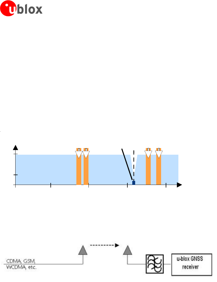
Out-band interference
Out-band interference is caused by signal frequencies that are different from the GNSS carrier (see Figure 20).
The main sources are wireless communication systems such as GSM, CDMA, WCDMA, Wi-Fi, BT, etc.
0500 1000 1500 2000
GPS input filter
characteristics
0
-110
0500 1500 2000
Frequency [MHz]
GSM
900
GSM
1800
GSM
1900
Power [dBm]
GPS input filter
characteristics
GPS
1575
0
-110
GPS
signals
GSM
950
Figure 20: Out-band interference signals
Measures against out-band interference include maintaining a good grounding concept in the design and
adding a SAW or band pass ceramic filter (as recommend in section 4) into the antenna input line to the GNSS
receiver (see Figure 21).
Figure 21: Measures against in-band interference
LEA-M8S / LEA-M8T - Hardware Integration Manual
UBX-13003140 - R08 Production Information Appendix
Page 28 of 31
Appendix
Recommended parts
Recommended parts are selected on data sheet basis only. Other components may also be used.
Manufacturer Part ID Remarks Parameters to consider
Diode ON
Semiconductor
ESD9R3.3ST5G Standoff Voltage>3.3 V Low Capacitance < 0.5 pF
ESD9L3.3ST5G Standoff Voltage>3.3 V Standoff Voltage > Voltage for active antenna
ESD9L5.0ST5G Standoff Voltage>5 V Low Inductance
SAW TDK/ EPCOS B8401: B39162-B8401-P810 GPS+GLONASS High attenuation
TDK/ EPCOS B3913: B39162B3913U410 GPS+GLONASS+BeiDou For automotive application
TDK/ EPCOS B4310: B39162B4310P810 GPS+GLONASS Compliant to the AEC-Q200 standard
ReyConns NDF9169 GPS+ BeiDou Low insertion loss, Only for mobile application
muRata SAFFB1G56KB0F0A GPS+GLONASS+BeiDou Low insertion loss, Only for mobile application
muRata SAFEA1G58KB0F00 GPS+GLONASS Low insertion loss, only for mobile application
muRata SAFEA1G58KA0F00 GPS+GLONASS High attenuation, only for mobile application
muRata SAFFB1G58KA0F0A GPS+GLONASS High attenuation, only for mobile application
muRata
SAFFB1G58KB0F0A
GPS+GLONASS
Low insertion loss, Only for mobile application
TAI-SAW TA1573A GPS+GLONASS Low insertion loss
TAI-SAW TA1343A GPS+GLONASS+BeiDou Low insertion loss
TAI-SAW TA0638A GPS+GLONASS+BeiDou Low insertion loss
LNA JRC NJG1143UA2 LNA Low noise figure, up to 15 dBm RF input
power
Avago ALM-GN001 LNA Low noise figure, with pre-LNA filter,
concurrent GNSS
Avago ALM-GN002 LNA Very low noise figure, with post-LNA filter,
concurrent GNSS
Inductor Murata LQG15HS27NJ02 L, 27 nH Impedance @ freq GNSS > 500 Ω
Capacitor Murata GRM1555C1E470JZ01 C, 47 pF DC-block
Ferrite
Bead
Murata BLM15HD102SN1 FB High IZI @ fGSM
Feed thru
Capacitor
for Signal
Murata NFL18SP157X1A3 Monolithic Type For data signals, 34 pF load capacitance
NFA18SL307V1A45 Array Type For data signals, 4 circuits in 1 package
Feed thru
Capacitor
Murata NFM18PC ….
NFM21P….
0603 2A
0805 4A
Rs < 0.5
Ω
Resistor 10 Ω ± 10%, min 0.250 W R
bias
560 Ω ± 5% R2
100 kΩ ± 5% R3, R4
Table 7: Recommended parts
Recommended antennas
Manufacturer
Order No. Comments
Hirschmann (www.hirschmann-car.com) GLONASS 9 M GPS+GLONASS active
Taoglas (www.taoglas.com ) AA.160.301111 36*36*4 mm, 3-5V 30mA active
Taoglas (www.taoglas.com ) AA.161.301111 36*36*3 mm, 1.8 to 5.5V / 10mA at 3V active
INPAQ (www.inpaq.com.tw) B3G02G-S3-01-A 2.7 to 3.9 V / 10 mA active
Amotech (www.amotech.co.kr) B35-3556920-2J2 35x35x3 mm GPS+GLONASS passive
Amotech (www.amotech.co.kr) A25-4102920-2J3 25x25x4 mm GPS+GLONASS passive
Amotech (www.amotech.co.kr) A18-4135920-AMT04 18x18x4 mm GPS+GLONASS passive
Amotech (www.amotech.co.kr) Amotech AGA363913-
S0-A1
GPS+GLONASS+ BeiDou active
INPAQ (www.inpaq.com.tw) ACM4-5036-A1-CC-S 5.2 x 3.7 x 0.7 mm GPS+GLONASS passive
Additional antenna Manufacturer: Allis Communications, Tallysman Wireless
Table 8: Recommend antenna
LEA-M8S / LEA-M8T - Hardware Integration Manual
UBX-13003140 - R08 Production Information Appendix
Page 29 of 31
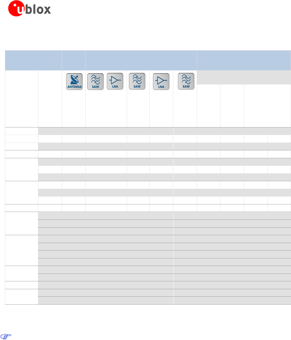
A.1 Design-in recommendations in combination with cellular operation
Product
Receiver Chain Cellular and GNSS
Simultaneous operation
Family
Variant
Antenna
SAW LNA
On-chip LNA
SAW
Passive GNSS
Antenna
Active GNSS
Antenna
SAW
2G cellular
3G/4G cellular
2G/3G/4G
cellular
MAX-6 Any • •
NEO-6 Any • •
LEA-6 Any • •
EVA-7 M •
MAX-7
C •
W •
Q •
NEO-7
N • •
M •
P • •
EVA-M8 M •
MAX-M8
C •
W •
Q •
NEO-M8
N • •
M •
Q • •
T • •
LEA-M8 S • •
T • •
PAM-7 Q • • • •
CAM-M8 C • • •
Q • • •
• = integrated = optimal performance
Table 9: Combinations of u-blox GNSS modules with different cellular technologies (2G/3G/4G).
See the GPS Implementation and Aiding Features in u-blox wireless modules [9].
LEA-M8S / LEA-M8T - Hardware Integration Manual
UBX-13003140 - R08 Production Information Appendix
Page 30 of 31
Related documents
[1] LEA-M8S Data Sheet, Docu. No. UBX-14001841
[2] NEO/LEA-M8T Data Sheet Docu. No. UBX-14006196
[3] u-blox M8 Receiver Description Including Protocol Specification (Public version), Docu. No.
UBX-13003221
[4] GNSS Firmware 2.01 for u-blox M8 Release Note, Docu. No. UBX-13004697
[5] GPS Antenna Application Note, Docu. No. GPS-X-08014
[6] UBX-M8030 Data Sheet, Docu. No. UBX-13001634
[7] GPS Compendium, Docu. No. GPS-X-02007
[8] I2C-bus specification, Version 2.1, Jan 2000,
http://www.nxp.com/acrobat_download/literature/9398/39340011_21.pdf
[9] GPS Implementation and Aiding Features in u-blox wireless modules, Docu. No. GSM.G1-CS-09007
For regular updates to u-blox documentation and to receive product change notifications please register
on our homepage (http://www.u-blox.com)
Revision history
Revision Date Name Status / Comments
R01 29-Jan-2014 jfur Objective Specification
R02 2-Jul-2014 jfur Advance Information. Updated Table 8 (added Amotech GPS+GLONASS+ BeiDou
active antenna); added Table 9: Combinations of u-blox GNSS modules with
different cellular technologies (2G/3G/4G).
R03 02-Sep-2014 julu Early Production Information
R04 28-Oct-2014 jfur Added LEA-M8T variant, updated EXTINT1/AADET_N (Pin 20) in Table 2, added
SAFEBOOT_N pin description in Figure 4, Table 2, Table 5 and Table 6.
R05 07-Jan-2015 julu Production Information
R06 20-Apr-2015 amil/jfur Updated Section 1.3 (power), updated Table 7 (Recommended parts) and Table 9,
LEA-M8T PCN FW TIMRAW 1.02
R07 02-Jun-2015 julu Updated section 1.5 (added Electromagnetic interference on I/O lines).
R08 21-Oct-2015 julu Updated product type number to LEA-M8S-0-01 and added relevant PCN reference

LEA-M8S / LEA-M8T - Hardware Integration Manual
UBX-13003140 - R08 Production Information Contact
Page 31 of 31
Contact
For complete contact information, visit us at www.u-blox.com
u-blox Offices
North, Central and South America
u-blox America, Inc.
Phone: +1 703 483 3180
E-mail: info_us@u-blox.com
Regional Office West Coast:
Phone: +1 408 573 3640
E-mail: info_us@u-blox.com
Technical Support:
Phone: +1 703 483 3185
E-mail: support_us@u-blox.com
Headquarters
Europe, Middle East, Africa
u-blox AG
Phone: +41 44 722 74 44
E-mail: info@u-blox.com
Support: support@u-blox.com
Asia, Australia, Pacific
u-blox Singapore Pte. Ltd.
Phone: +65 6734 3811
E-mail: info_ap@u-blox.com
Support: support_ap@u-blox.com
Regional Office Australia:
Phone: +61 2 8448 2016
E-mail: info_anz@u-blox.com
Support: support_ap@u-blox.com
Regional Office China (Beijing):
Phone: +86 10 68 133 545
E-mail: info_cn@u-blox.com
Support: support_cn@u-blox.com
Regional Office China (Chongqing):
Phone: +86 23 6815 1588
E-mail: info_cn@u-blox.com
Support: support_cn@u-blox.com
Regional Office China (Shanghai):
Phone: +86 21 6090 4832
E-mail: info_cn@u-blox.com
Support: support_cn@u-blox.com
Regional Office China (Shenzhen):
Phone: +86 755 8627 1083
E-mail: info_cn@u-blox.com
Support: support_cn@u-blox.com
Regional Office India:
Phone: +91 959 1302 450
E-mail: info_in@u-blox.com
Support: support_in@u-blox.com
Regional Office Japan (Osaka):
Phone: +81 6 6941 3660
E-mail: info_jp@u-blox.com
Support: support_jp@u-blox.com
Regional Office Japan (Tokyo):
Phone: +81 3 5775 3850
E-mail: info_jp@u-blox.com
Support: support_jp@u-blox.com
Regional Office Korea:
Phone: +82 2 542 0861
E-mail: info_kr@u-blox.com
Support: support_kr@u-blox.com
Regional Office Taiwan:
Phone: +886 2 2657 1090
E-mail: info_tw@u-blox.com
Support: support_tw@u-blox.com
