ECEN 454/714 Lab7: Fall 2017 Lab 7 Manual
User Manual: Pdf
Open the PDF directly: View PDF ![]() .
.
Page Count: 13

Texas A & M University
1
ECEN 454/714 Lab7: Fall 2017
Purpose: Design Vision is the graphical interface to the Synopsys family of logic synthesis tools. Internally it runs
design compiler. This lab is to familiarize you with the basics of synthesis using Design Vision through a simple
example "cruise control design". After synthesis, you will do pre-layout static timing analysis of your synthesized
design. You will define constraints for your design and check the timing of all the paths in the design. In the final part
of this lab we will use the synthesized Verilog netlist that you will generate for the cruise control logic to “Place and
Route” the circuit on a die.
PART A: LOGIC SYNTHESIS
In this case we need to synthesize the logic with a certain specific library for 180nm technology. The Synopsys
database format (db) file for a typical 180nm technology is put up on the Google drive. We need to ensure that the
synthesis is performed according to this library file (see below for procedure). What this means is that the
optimization (power, timing, area etc.) will be performed according to the characteristics of the standard cells given
in this file.
1. Procedure to link the given library with the synthesis process:
Download the "iit018_stdcells.db" and "iit018_stdcells.lib" file from the lab website and
Save a copy in the ~/synthesis folder.
After you begin design_vision, choose "File > Setup > Defaults". A window pops up.
Fill in iit018_stdcells.db in "Link Library" and "Target Library".
Fill in generic.sdb in the "Symbol Library"
Click Ok.
The target library is the actual library which the synthesis will use to optimize. The link library includes the target
library and any other libraries for macros you may have in the design. Now place the Verilog behavioral code of the
Cruise Control Logic in the ~/synthesis/verilog folder and repeat the same procedure as above to optimize the logic
and generate the synthesized Verilog netlist.
2. Starting design analyzer:
source /softwares/setup/synopsys/setup.ecen454.bash
To start design analyzer, go to the ~/synthesis/ directory, using the command: >design_vision
You will find that in the window, there is a design_vision prompt. Type the following command in that prompt.
source .synopsys_dctcl.setup
The command should work if you invoked design_vision from the synthesis directory. To see if the script
sourced properly, type
echo $target_library
It should yield the result “class.db”
3. Load a design: Analyze, elaborate and read are commands provided by Design Compiler.
The analyze command reads a VHDL or Verilog file, checks for proper syntax and synthesizable logic,
and stores the design in an intermediate format.
The elaborate command creates a design from the intermediate format produced by analyze. It replaces
the HDL operators with synthetic operators. Mainly it translates the Verilog code to Synopsys internal
generic library called gtech.
The read command is used to load files in formats other than HDL formats, such as db, pla and other
formats supported by Design Compiler.
Detailed procedure:
a. Analyze the design
Select “File > Analyze”. The Analyze File window appears. Click ADD and change to the verilog
directory. Select the cruisecontrol.v file and Click Ok.
b. Elaborate the design

Texas A & M University
2
ECEN 454/714 Lab7: Fall 2017
Select “File > Elaborate”. The Elaborate Design window appears. Choose the library WORK in the
Library list. Ignore the warnings about the symbol library.
Check if Reanalyze Out-Of-Date Libraries is set to on.
Click Ok.
c. Read in the design
Select “File > Read”. Change to the verilog directory and select the cruisecontrol.v file and Click
Ok.
d. Save the design and your attribute settings
Select design in the logical hierarchy window.
Select “File > Save As”. Change to your synthesis/db/ directory.
Enter ccs_attributes.ddc in the File Name field to save the file to db directory.
Remember to always save your design work in case the machine crashes.
e. Set attributes for the design
Attributes are values set on a design that control or affect the optimization process. For example,
attributes can specify the operating environment of the design, the constraints for optimization,
as well as many other design parameters.
f. Select TOP design.
Click the create symbol view button (you should find an icon below the menus which should read
“create symbol view” when you move the cursor over it). The created symbol should appear on
the screen showing inputs and outputs.
g. Set the Drive Strength on Input Ports
The drive strength is used to set a finite transition time for the input signals. Otherwise, the input
signals to the design will be ideal which is unfortunately not realistic.
set_load 0.0335 [all_inputs]
h. Set the Load on Output Ports
Load values are used to model the capacitive load on the output ports.
set_load 3 [all_outputs]
i. Set the Operating Conditions
Operating conditions are the temperature, process and voltage in which the design operates.
The target library defines operating conditions. Library vendors define default operating
conditions, which can differ from one vendor to another.
set_operating_conditions -library iit018_stdcells typical
j. Save the design and your attribute settings
Select “File > Save As”.
Change to your synthesis/db/ directory.
Enter ccs_attributes_db.ddc in the File Name field to save the file to db directory.
Check the Save All Designs in Hierarchy option.
Click Ok.
k. Set the Optimization Goals
The Optimization goals or constraints include timing, area and power that you set for a design.
Design Compiler checks your optimization goals during optimization and tries to meet them while
synthesizing the design using the technology library.
l. Set Clock Constraints:
create_clock -name "clk" -period 25 -waveform { 12.5 25 } { clk }

Texas A & M University
3
ECEN 454/714 Lab7: Fall 2017
m. Set Delay Constraints:
Input/output delays model the external delays arriving/leaving at the input/output ports of the
constrained module. In this Cruise-control design, the input delay is zero. We need to set the
output delay.
Select the all three output ports of cruisecontrol in the symbol view window.
Select “Attributes > Operating Environment > Output Delay”.
In the Relative to clock list, select clk or whatever name you gave for the clock in the previous step.
Enter 5 in the Max Rise. The Max Fall should copy the same value.
Click Apply.
Click Ok to dismiss the Output delay window.
The input and output delays are usually set for each clock domain. Usually, there is a need for
many IOs in large designs and designers sometimes use the same IO for multiple applications.
Hence when you set the IO constraints it is also necessary to specify the clock domain.
n. Run check_design
Check_design is one of the most important commands for sanity check before synthesis.
Though it doesn’t do anything on the design, it is very important to verify its result before
progressing further.
Select “Design > Check Design”.
Click Ok.
In the design_vision prompt, type uniquify
When you have instantiated a module multiple times, uniquify creates separate or unique module
names for each instance. In this way, the instances are referenced by different modules though
they are functionally equivalent.
Save the Design and run check_design again.
Select “File > Save As”.
Change to your synthesis/db/ directory.
Enter ccs_attributes_b4_compile.db in the File Name field to save the file to db directory.
Check the Save All Designs in Hierarchy option.
Click Ok.
o. Optimize the Design
After setting constraints & attributes on the alarm clock design and running check_design, the
design is ready to be optimized with the compile command. Optimizing is the step in the synthesis
process that attempts to implement a combination of library cells that meets the functional, area
and speed requirements of the design.
Select design cruisecontrol.
Select “Design > Compile Design”.
Note the default settings. Map Design in Mapping options, and Exact map in Compile options is set
to on. Map Effort is set to Medium. This is the CPU effort used to map a design. For this design, the
defaults are sufficient to meet defined constraints.
Set Allow Boundary Conditions in Compile options to on. This enables boundary optimization
Press Ok.
p. Evaluate and Interpret the Design:
Generate reports to determine whether the design goals are met. Using Design vision you can
select and generate any number of attribute and analysis reports, which send output to a report
window or a file you designate.
Select TOP in the symbol view window.
Generate Analysis Reports
i. Choose “Design > Report Constraints”
ii. Select show all violators and verbose options.

Texas A & M University
4
ECEN 454/714 Lab7: Fall 2017
iii. Choose “To file” and enter a file name to direct the output to.
iv. The report_constraints command reports all violations of any constraints you have for
your design (timing, transition etc).
To get the area report
i. Choose “Design > Report Area”.
ii. This gives the cell count and percentage of combinational and sequential area.
q. Save the optimized Verilog netlist
After completion of optimization save the design in the form a Verilog netlist.
Use “File > Save As” and choose VERILOG(v) in the Format list and save a copy of the TOP design
in the Verilog folder as “cruisecontrol_netlist.v”.
r. Report Requirements:
Print the analysis reports of area and constraints from your cruise control logic.
Print out the final synthesized Verilog netlist of the cruise control logic.
Report the register count.

Texas A & M University
5
ECEN 454/714 Lab7: Fall 2017
PART B: STATIC TIMING ANALYSIS
Timing analysis is to check the timing requirement of the circuit. You can do timing analysis at
different design stages – pre-layout with wire-load models or post-layout with actual wires.
PrimeTime® (PT) is the static timing analysis (STA) tool from Synopsys. It is the most widely used
STA engine.
Though Design compiler has its own timing engine, it cannot come close to Primetime’s accuracy.
Moreover, primetime can also consider signal integrity effects like coupling noise due to cross talk
and analysis of complex interconnect structures.
Using PrimeTime
a. Environment Setup:
Make sure you have the iit018_stdcells.db and iit018_stdcells.lib files in the same folder. If not,
download the same from the lab website.
The iit018_stdcells.db is the timing library file in Synopsys format and iit018_stdcells.lib is the same
timing library file in ASCII format. Browse through the iit018_stdcells.lib file and you will find the
timing information of each standard cell in table format. If not specified, PrimeTime uses these
tables to compute gate delays in the circuit.
Circuit: Make sure you have the synthesized Verilog netlist in the same folder
b. Running primetime
Type "primetime" in your terminal, then the primetime console window appears.
If you can't find this command, try to run the command for sourcing the synopsys tools at the start
of the lab.
c. Read the libraries
In the console window, type
set search_path "."
set link_path {* iit018_stdcells.db}
This is to indicate PrimeTime that the libraries with the specified names are to be found in the
current directory. Please note in primetime console window you will see the corresponding
messages about what you did. Note that if there are message in red color, it means there are errors
in the operation.
d. Setup the design
read_verilog cruise_ctrl_netlist.v
current_design cruisecontrol
link_design cruisecontrol
e. Set Capacitance for output ports
The output ports of your design are to be connected to other blocks. Therefore you need to set
the load capacitance for the outputs. In such a case, we select output ports and set the max value
to be 3.
set_capacitance 3 [ get_ports {speed[7] speed[6] speed[5] speed[4] speed[3] speed[2] speed[1]
speed[0] cruisespeed[7] cruisespeed[6] cruisespeed[5] cruisespeed[4] cruisespeed[3]
cruisespeed[2] cruisespeed[1] cruisespeed[0] cruisecontrol } ]
f. Set driving strength for input ports:
You need to provide driving strength to the input ports of your design. You may do it by choosing
the input ports and choose cell "BUFX2" as the driving cell.
set_driving_cell -lib_cell BUFX2 -library iit018_stdcells -pin Y -from_pin A [ get_ports {clk reset
throttle set accel coast cancel resume brake } ]

Texas A & M University
6
ECEN 454/714 Lab7: Fall 2017
g. Set Clock Details:
Choose the clock source pin in your design, and set the period of the clock to 10.
create_clock -period 10.000000 -waveform {0.000000 5.000000} {clk }
h. Check timing
After setting the clock details you intend to perform a check_timing command before you begin
the timing analysis. The check_timing command shows possible timing constraints related
problems for the design. For example, if you have not defined a clock, some flip flops will not have
any clock information. There may then be unconstrained paths in the design which will not get
reported as violating paths. The chip may fail!
To type in the command use the space at the bottom of the console. You may type in the command
“check_timing” next to the space after "pt_shell > “.
After the command is executed you will see there are a few warnings that may appear on the
console window. The warnings may say There are * ports with no clock-relative input delay
specified and there are * endpoints which are not constrained for maximum delay. This is because
you have not specified the required arrival time for the signals at the input and output pins relative
to the clock signal.
i. Input and output delay
Input delay
i. To specify the arrival time for the input signals (except clock) relative to the clock, set the
Maximum Rise as 4 and Minimum Rise delay as 0 and ensure that the Reference Clock
refers to the name of the clock symbol in your design.
ii. set_input_delay -clock clk -max 4.000000 [get_ports {reset throttle set accel coast
cancel resume brake }]
iii. set_input_delay -clock clk -min 0.000000 [get_ports {reset throttle set accel coast cancel
resume brake }]
Output delay
i. To specify the arrival time for the output signals relative to the clock, set 5 for the
Maximum Rise and Minimum Rise times and also ensure that the Reference Clock refers
to the name of the clock symbol in your design.
ii. set_output_delay -clock clk -rise 5.000000 [get_ports {speed[7] speed[6] speed[5]
speed[4] speed[3] speed[2] speed[1] speed[0] cruisespeed[7] cruisespeed[6]
cruisespeed[5] cruisespeed[4] cruisespeed[3] cruisespeed[2] cruisespeed[1]
cruisespeed[0] cruisectrl }]
j. Perform check_timing
Now execute the check_timing command again and you must be able to get a clean output on the
console window.
k. Reports
Next you check if there is are any setup time violations on any of the cells in the circuit.
You do this by typing in the following command:
report_constraint -all_violators -verbose -max_delay
You can redirect it to a file by typing:
report_constraint -all_violators -verbose -max_delay > output_file_name
If you have any violations then you will be able to see the details on the console window. To report
the hold time violations on any of the cells use the following command:
report_constraint -all_violators -verbose -min_delay
Next, you will learn how to generate path-based timing reports. The report_timing command with
no options reports the longest path in the design. Make a note of the slack that is displayed on the
window after the command is executed. This is the least possible slack on your design considering

Texas A & M University
7
ECEN 454/714 Lab7: Fall 2017
only max (setup) paths. Now let us generate the top three critical paths with respect to the setup
time. To do this use the following command:
report_timing -max_paths 3 > max_paths.txt
The results will not appear on the console window but get stored in the file max_paths.txt
Similarly, obtain the top three critical min (hold time) paths by using the following command:
report_timing -max_paths 3 -delay min > min_paths.txt
This will store the three most critical minpaths in the min_paths.txt file.
l. Report Requirements:
Print out the files "max_paths.txt" and "min_paths.txt"

Texas A & M University
8
ECEN 454/714 Lab7: Fall 2017
PART C: Automatic place and route
In the previous lab section we generated the synthesized netlist of the cruise control circuit of a vehicle. We now
intend to use this netlist along with the standard cell libraries to place and route the circuit on a die. The same
standard cell library that was used to generate the synthesized netlist will be used here too.
You must observe here that we do not use Custom Layout design as we practiced in the first 6 lab sessions. You will
notice in this lab that the cruise control circuit will use many more standard cells than the 4 bit pipelined adder that
you previously designed. It will be extremely difficult to manually draw the layout and perform routing on the
standard cells. Hence we use a library with predefined standard cells (defined in terms of area, delay and power
consumption) to generate the layout of the circuit by using automatic place and route procedures. The disadvantage
with this automatic flow is that sometimes we do not get the desired level of optimization.
a. Starting Soc Encounter
You just need to type following commands consecutively.
source /softwares/setup/cadence/setup.edi142.bash
encounter -64
b. Place and Route with Soc Encounter
Create a new folder called “cru_con” in root directory.
mkdir ~/cru_con
We intend to save all the required files in this folder.
In this folder, make a copy of the synthesized Verilog netlist that you generated for the Cruise
Control circuit using Design Vision.
c. Download the following files from the lab drive into the “cru_con” folder.
iit018_stdcells.lef: This file provides the spacing rules for the given technology and internal cells.
It also defines the corner cells (of pad frame) and I/O pads.
iit018_stdcells.tlf: TLF (Timing Library Format) is an ASCII representation of the timing and power
parameters associated with any cell for a particular technology. A TLF library is used as an input to
Cadence timing tools.
iit018_stdcells.lib: The lib file again stores the timing and power parameters of the library standard
cells in an open source format called liberty.
encounter.conf: This is the configuration file that we will use to load the library details into
encounter.
d. Modify the Configuration file encounter.conf
Open enocounter.conf using any text editor. Make the following required changes.
Replace cru_con on line 10 of the file (set my_toplevel cru_con) with the name of the top level
module in your synthesized verilog netlist.
set my_toplevel your_top_module_name
Do the same on line 21 of the file (set rda_Input (ui_topcell) cru_con).
set rda_Input (ui_topcell) your_top_module_name
Also on line 19 replace cru_con.vh with the name of your verilog netlist. You should save the netlist
in the same folder.
set rda_Input(ui_netlist) your_netlist.v
Note: On lines 31 and 40, you note that the timing library format and library exchange format point
to files called the iit018_stdcells.tlf and iit018_stdcells.lef respectively.
Hence make sure copies of these files in the very same folder.
Make sure you are currently in folder cru_con/ and type encounter at the prompt. Make sure there
is no “&” after the command because running encounter in the background locks up the shell
which is required by the tool.
Texas A & M University
9
ECEN 454/714 Lab7: Fall 2017
cd ~/cru_con
encounter -64
The above command starts Soc Encounter. You will notice that the terminal where you execute
this command gets a “encounter 1 > ” command prompt. We can actually execute the required
place and route operation commands on the terminal. But for now we shall concentrate on how
to perform Place and Route using the GUI.
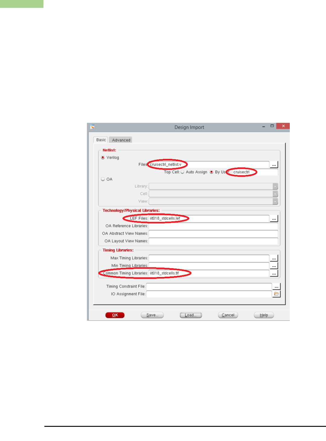
e. Importing the design
First we import the design into encounter. On the menu bar select “Design > Import Design ”.
Select Load button at the bottom of the window. In the list of files, choose the encounter.conf and
press Open button. Observe that the timing library (tlf), lef file and the Verilog netlist along with
its top cell details are loaded. Now click Ok.
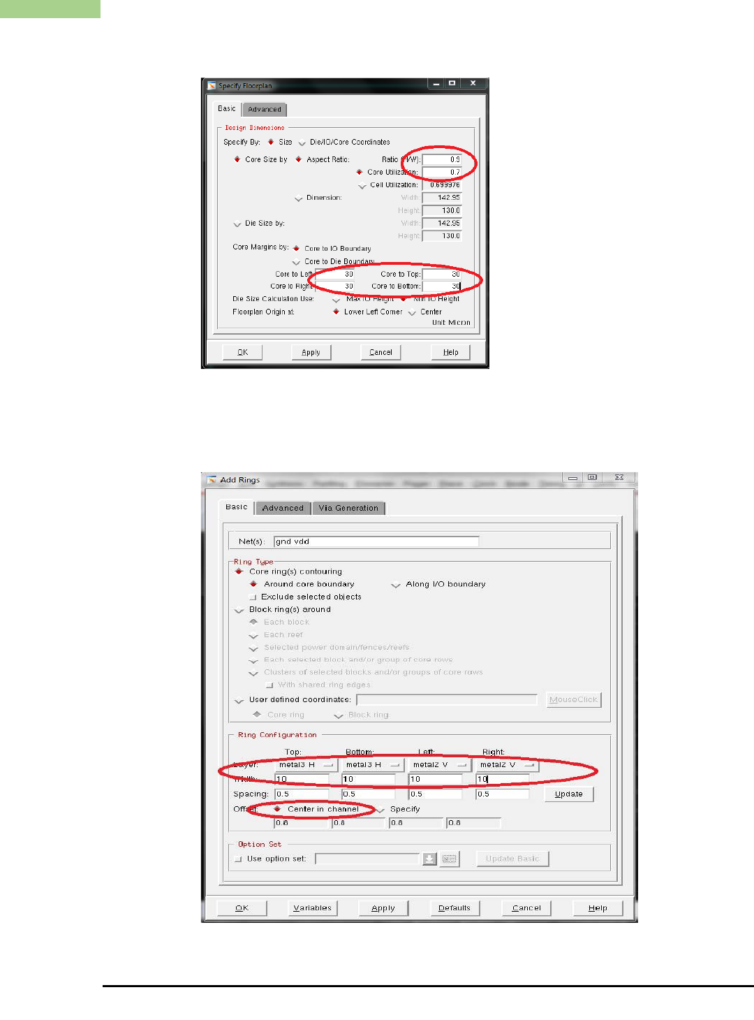
f. Floorplan
The GUI is filled with a rectangle indicating the die area on which the circuit will be placed and
routed. Next we specify the Floor plan details. Select “Floorplan > Specify Floorplan”. We next
specify the design dimensions by specifying the core size using Aspect Ratio of 0.9 and Core
Utilization of 0.7 (70%). (The lesser the core utilization the more sparse the design will be and the
routing congestion will be lesser too but the obvious disadvantage is that it will lead to an increase
in circuit area...which in the chip world means more costly).
Also specify the Core Margins by filling in 30 for each of the four “Core to Left”, “Core to Top”,
“Core to Right” and “Core to Bottom”. This will leave sufficient space for the power railings to
surround the die. Click Ok.
Texas A & M University
10
ECEN 454/714 Lab7: Fall 2017
g. Power planning
Next we place the power rails around the die. Select “Power > Power Planning > Add Ring”. Choose
metal3 in the Ring Configuration for the Top and Bottom Layers and let the Left and the Right
remain at the metal2. Also modify all the metal width to 10 and change the Offset to Center in
Channel. The details are shown below.
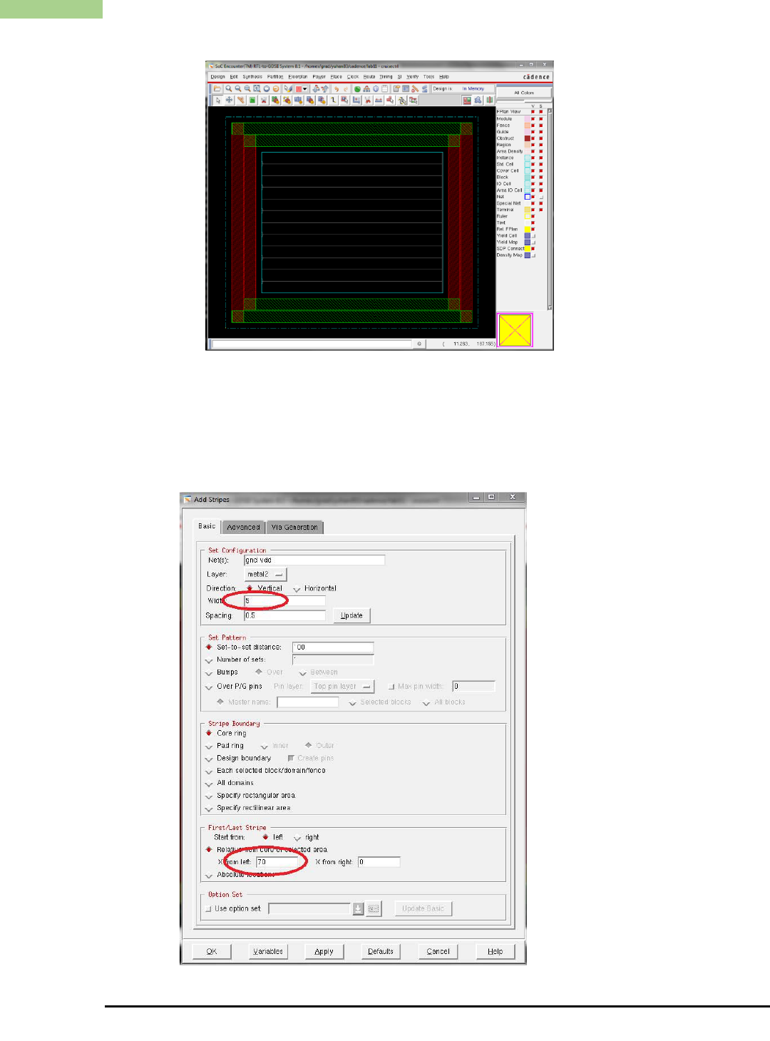
Click Ok. After the power rails are placed, the die figure in the GUI looks as follows.
Texas A & M University
11
ECEN 454/714 Lab7: Fall 2017
Next we need to add Power Stripes through the die to create a power grid. Select “Power > Power
Planning > Add Stripes”. Let the Direction in the Set Configuration remain Vertical. Change the
Width of the Stripes in the Set Configuration to 5.
Retain the other default values, except in the sub section of First/Last Shape change the X from
left to 60~80 which is roughly half the size of the width of the die. Click Ok. This creates Vertical
stripes in metal2 at 80um from the left edge.
Texas A & M University
12
ECEN 454/714 Lab7: Fall 2017
h. Routing
To see the physical view with all standard cells and nets, click on the right most of the three icons
along the top right corner of the floor-plan. It should read physical view.
Next we route the power grid entirely through the die. Choose “Route > Special Route”. A window
pops up. Retain all the default values set in it. Click Ok.
Now we next place the standard cells into the die. Select “Place > Standard Cells”.
Retain the Run Full Placement and Include Pre-Placement Optimization. Click Ok.
Observe the terminal (the same one with the encounter shell). It goes through a number of
iterations before the placement is complete. Before the iterations begin the details of the design
are mentioned in the terminal, one of them being the number of standard cells. Note down the
number of standard cells used in your design.
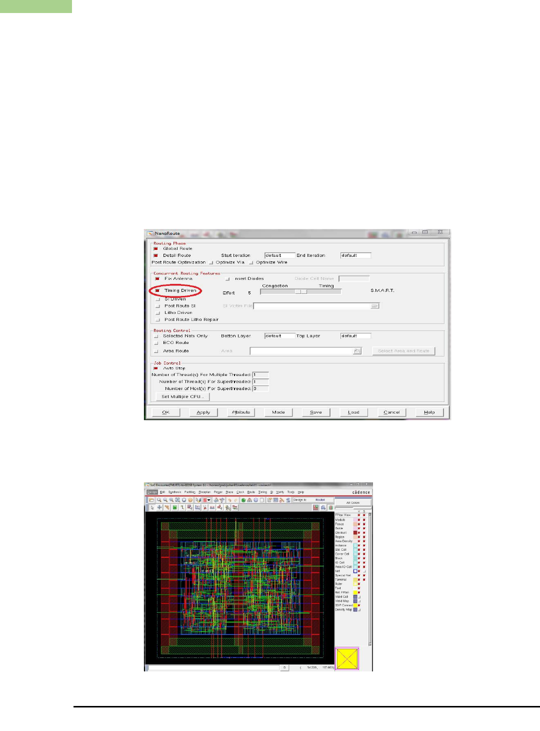
After the placement is complete we have to route the required wires to complete the design.
Choose “Route > Nanoroute > Route”. In the Concurrent Routing Features subsection choose
Timing Driven and then click Ok. This procedure performs the global and detailed routing of the
design.
All the routing details are displayed on the terminal and also saved in the latest “encounter.log”
file generated. Make a note of the total wire length and the total number of vias used in Detail
Routing. Make a copy of “encounter.log”.
Now, the automatic place & route is done, and the die figure in the GUI looks as follows.

Texas A & M University
13
ECEN 454/714 Lab7: Fall 2017
After the routing goes through completely save the design by choosing “Design > Save Design As”.
The design will be stored as a “*.enc” file. Give it any appropriate name of your choice.
sAlso extract the SPEF (Standard Parasitic Exchange Format) file which stores the parasitic
information of the nets used in the layout. This file can later be used to generate more accurate
timing analysis results. Choose “Timing > Extract RC” and enable the tag Save SPEF. Just remember
that SPEF contains the parasitic information which can be used to do post layout static timing
analysis.
i. Report Requirements:
In the Detail Routing section of “encounter.log”, find the total wirelength that is used for the Detail
Routing along with the number of vias that are used. Also note the number of standard cells your
design used.
Print out a copy of the layout generated by performing a screen dump. (“Tools > Screen Capture >
Dump to GIF file”).
