Lab 2 Introduction To Structural Source Code And Benches Manual
User Manual: Pdf
Open the PDF directly: View PDF ![]() .
.
Page Count: 17
- 1. Lab Exercises
- 2. Postlab Exercises (Building Blocks Design)

ASIC Design Lab Lab 2 Spring 2018
1
ASIC Design Lab 2:
Introduction to Various Styles of Verilog Source Code and
Design Test Benches
In this lab, you will:
• Create and Test Verilog code for the STRUCTURAL model of the Sensor Error Detector System
using ModelSim (sensor_s.sv)
• Create and Test Verilog code for the DATAFLOW model of the Sensor Error Detector System
using ModelSim (sensor_d.sv)
• Create and Test Verilog code for the BEHVIORAL model of the Sensor Error Detector System
using ModelSim (sensor_b.sv)
• Modify the Makefile to optimize the 3 versions of the design that you are examining
• Create and Test Verilog code for a 1-bit Full Adder using Modelsim (adder_1bit.sv)
• Create and Test Verilog code for a 4-bit Ripple Carry Adder using Modelsim (adder_4bit.sv)
• Create and Test Verilog code for a parameterized N-bit Ripple Carry using Modelsim
(adder_nbit.sv)
• Create and Test Verilog code for two Synchronizers using Modelsim (sync_low.sv & sync.high.sv)
NOTE: For this class you must name the Verilog source code file the same name as the module name, plus
the ".sv" extension. For example, if the module name is "sensor_d", then the file name should be
“sensor_d.sv”. Also, all module, port, and filenames must be all lowercase in this class.
1. Lab Exercises
1.1. Lab Setup
In a UNIX terminal window, issue the following commands, to setup your Lab 2 workspace:
mkdir –p ~/ece337/Lab2
cd ~/ece337/Lab2
dirset
setup2
The setup2 command is an alias to a script file that will check your Lab 2 directory structure and give you
file needed for starting the lab. If you have trouble with this step please ask for assistance from your
TA.
Make sure to add this new workspace into your 337 Repository, like you did in Lab1. This way, you will
always have the original copy in storage.
ASIC Design Lab Lab 2 Spring 2018
2
1.2. Sensor Error Detector Design
1.2.1. Structural Style Sensor Error Detector Design
1.2.1.1. Structural Style Sensor Error Detector Specifications
The required module name is: sensor_s
The required filename is: sensor_s.sv
The module must have only the following ports (case-sensitive port names):
input wire [3:0] sensors
output wire error
Create the source file using the following ‘ch’ script command from your Lab2 folder:
ch sensor_s.sv
1.2.1.2. Structural Coding of Sensor Error Detector
A structural model for a Verilog model is much like what would be consider a pure netlist description of
the cell. A netlist is essentially a text representation that describes a circuit in terms of the explicit
interconnections between sub-blocks. This explicit description describes what signals are input to a sub-
block and what signals are outputs from this sub-block and how they interact with the other sub-blocks in
the design. This is the style that is probably the easiest to understand and create a design in. This is the case
because it is relatively easy to map a K-Map derived expression for a logic function into this style of
Verilog. Therefore, this is the Verilog style that will seem the most logical to most students; however, this
style is not the most powerful of the design styles for Verilog. The structural model is one that lends itself
to directly illustrating a hierarchal design in Verilog. A hierarchal design is one in which you use several
smaller designs to create a larger design. An example of a hierarchal design would be a 16-bit adder that is
built from a combination of 1-bit adders. In this design, you would have 16 instantiations of the 1-bit adder
design that are interconnected in order to perform the function of a 16-bit adder.
The hierarchal design methodology is what is employed in industry. This should make sense to you simply
from a design point of view. The majority of the designs being done in industry are at such a degree of
complexity that no one person on the design team knows every detail of the overall system. Instead, the
overall system is divided into units which are divided into blocks, which are divided into sub-blocks. These
sub-blocks are relatively easy to manage aspects of the overall project that one engineer or a small group
can be responsible for. Even these sub-blocks have a hierarchal aspect to them. For instance, one portion
of the design may be highly optimized because it is the most critical portion of the sub-block. This optimized
portion of the sub-block is then encapsulated in a symbol and placed into schematic at a higher level in the
sub-blocks internal hierarchy.
This hierarchal design methodology has an additional benefit in terms of testability of a design also.
Logically, small blocks are able to be more thoroughly tested than larger blocks. This statement is derived
from the fact that smaller blocks generally have fewer inputs, so it is possible to run a small block through
its entire range of input values to make sure it is functioning correctly. However, as one moves up the levels
in the design hierarchy the ability to thoroughly test a design becomes more difficult. In the case of
microprocessors, thoroughly and completely simulating a design is simply not a feasible option. In order to
test a microprocessor all its possible input vectors would require an enormous amount of compute cycles,
not to mention the incredible amount of engineer hours it would require to generate the test vectors and
ensure that the person designing the test vectors also determines the correct response that should be
generated from each test vector. From this, one should see that it is imperative that the lower levels in the
hierarchy be tested thoroughly to ensure that they function properly. Ensuring that the lowest levels in the
ASIC Design Lab Lab 2 Spring 2018
3
hierarchy function correctly allows the top-level design testing process to be an attainable goal, as opposed
to an insurmountable goal.
In lab 1’s post lab, you derived a logic expression from a K-Map for the Sensor Error Detector circuit. This
logical expression that you derived was in the SUM OF PRODUCTS form. You are now going to
implement this logic equation using the structural Verilog coding style. The list of 2-input logic cells (and
their ports) that you might need from the standard cell library is as follows:
Logic Cell Function
Logic Cell Module Declaration
2-Input AND Gate
AND2X1 (input A, input B, output Y)
Inverter
INVX1 (input A, output Y)
2-Input NAND Gate
NAND2X1 (input A, input B, output Y)
2-Input NOR Gate
NOR2X1 (input A, input B, output Y)
2-Input OR Gate
OR2X1 (input A, input B, output Y)
2-Input XOR Gate
XOR2X1 (input A, input B, output Y)
2-Input XNOR Gate
XNOR2X1 (input A, input B, output Y)
For example, the following line of code creates an instance of a 2-input AND gate with a label of ‘A1’,
with signals ‘a’ and ‘b’ connected to its inputs, and signal ‘int_and1’ connected to its output.
AND2X1 A1 (.Y(int_and1), .A(a), .B(b));
Utilizing this information, the specifications in section 1.2.1.1, your sum-of-products equation from lab 1’s
postlab, and any Verilog code syntax references, create the structural style sensor detector code in your lab
2 source folder.
1.2.1.3. Testing of the structural style Sensor Error Detector
Part of what the setup2 script did was give you a copy of a Verilog code file (tb_sensor_s.sv), which is what
we call a test bench file. This code file is a module that creates an instance of the design file it is used to
test and controls the values of this instance’s inputs in order to force the design being tested through a
variety of test cases that were implemented with the test bench module. This is the way all designs for the
rest of the course will be tested, as it is much more powerful and more efficient than using force statements
like you did in lab 1. To simplify the usage of test benches for testing designs, the makefile provided by
dirset also has simulation targets for simulating test benches of single file designs. To simulate the provided
test bench for the structural sensor detector module, execute the following command from your lab 2 folder.
make tbsim_sensor_s_source
This make target compiles both the test bench file tb_sensor_s.sv and the design file sensor_s.sv if needed
and then starts a simulation of the tb_sensor_s test bench module. Once the simulation has loaded, add the
design’s port signals and the signal named ‘test_number’ to the waves window and then tell ModelSim to
run for 200 ns. At this point have your TA verify your Waveforms window.
ASIC Design Lab Lab 2 Spring 2018
4
Now check the design’s output for correctness for each test case (‘test_number’ should always increment
when a new test case starts). If an incorrect output is found, make corrections to your design’s code,
recompile the design (this can be done easily from within modelsim by right clicking on the design instance
in the “source_work” library and selecting recompile), and restart the simulation (“restart –f”), and rerun
the simulation.
After a fully correct source simulation, synthesize the design and simulate the mapped design with the same
provided test bench to check for any errors during design synthesis. The command for simulating the
mapped design with its test bench is
make tbsim_sensor_s_mapped
Once you have a fully working design proceed to the next section.
1.2.1.4. Automated Grading of the Structural Sensor Error Detector
In this class all design code will be graded via a set of grading scripts and custom grading test benches that
are run during via submission commands. To submit your structural sensor detector design for grading,
issue the following command at the terminal (can be from anywhere).
submit Lab2s
1.2.2. Dataflow Style Sensor Error Detector Design
1.2.2.1. Dataflow Style Sensor Error Detector Specifications
The required module name is: sensor_d
The required filename is: sensor_d.sv
The module must have only the following ports (case-sensitive port names):
input wire [3:0] sensors
output wire error
Create the source file using the following ‘ch’ script command from your Lab2 folder:
ch sensor_d.sv
1.2.2.2. Dataflow Coding of Sensor Error Detector
Utilizing the dataflow syntax examples from the lab 1 manual, lab notes, and other Verilog references,
create a dataflow style design according to the requirements in section 1.2.2.1. Remember that a purely
dataflow style design cannot have any procedural blocks and all value assignments must be done with the
‘assign’ syntax. Additionally the setup2 script has provided you with a test bench module for the dataflow
style sensor detector as well (tb_sensor_d.sv). Make sure that the design is fully working before proceeding
to the next section and submitting it for grading.
Also, as a reminder of the use of the makefile’s pattern rules for simulation, the make targets for simulating
the dataflow source and mapped versions respectively are
make tbsim_sensor_d_source
and
make tbsim_sensor_d_mapped
1.2.2.3. Automated Grading of the Dataflow Sensor Error Detector
To submit your dataflow sensor detector design for grading, issue the following command at the terminal
(can be from anywhere).
submit Lab2d
ASIC Design Lab Lab 2 Spring 2018
5
1.2.3. Behavioral Style Sensor Error Detector Design
1.2.3.1. Behavioral Style Sensor Error Detector Specifications
The required module name is: sensor_b
The required filename is: sensor_b.sv
The module must have only the following ports (case-sensitive port names):
input wire [3:0] sensors
output reg error
Create the source file using the following ‘ch’ script command from your Lab2 folder:
ch sensor_b.sv
1.2.3.2. Behavioral Coding of Sensor Error Detector
Utilizing the dataflow syntax examples from the lab 1 manual, lab notes, and other Verilog references,
create a behavioral style design according to the requirements in section1.2.3.1. Remember that a purely
behavioral style design cannot have any functional/logic code outside of the procedural blocks, and the
combinational logic should be handled inside an ‘always’ block with each of its input signals in the
sensitivity list. Also, for this class initial blocks are forbidden inside design modules, and are only allowed
to be used in test benches. Additionally the setup2 script has provided you with a test bench module for the
dataflow style sensor detector as well (tb_sensor_b.sv). Make sure that the design is fully working in its
mapped/synthesized form before proceeding to the next section and submitting it for grading.
Also, as a reminder of the use of the makefile’s pattern rules for simulation, the make targets for simulating
the behavioral source and mapped versions respectively are
make tbsim_sensor_b_source
and
make tbsim_sensor_b_mapped
1.2.3.3. Automated Grading of the Behavioral Sensor Error Detector
To submit your structural sensor detector design for grading issue the following command at the terminal
(can be from anywhere).
submit Lab2b

ASIC Design Lab Lab 2 Spring 2018
6
1.3. Design Schematics for Synthesized Design Code
In this section you will be viewing schematic representations of the gate net lists synthesized from your 3
sensor detector implementations.
1.3.1. Viewing the Structural Style Schematic
In your terminal, in your Lab 2 directory, bring up the Design Compiler GUI (yes, our synthesis tool has a
GUI, called Design Vision, but we won’t be using it much) by typing
dv
In the window that comes up, select:
File → Read
Open the file “mapped/sensor_s.v” and select OK.
At the very right of the toolbar below the menu is a box where can choose the current design.
Make sure that the top-level module name is selected (sensor_s). Now go to the menu and select
Schematic → New Design Schematic View
If you zoom in (View → Zoom) you can see the component types and names, as well as signal names. If
your design has sub-components (though this design probably won’t), you can see their schematics by
selecting them with the LMB and selecting Schematic → Move Down. You can return to the top level by
selecting Schematic → Move Up.
Once you have generated a schematic view using Design Vision, have a TA check off your work up
to this point.
1.3.2. Viewing the Dataflow Style Schematic
Analyze the schematic of your mapped dataflow implementation (mapped/sensor_d.v) with Design Vision,
as before.
Once you have generated the schematic in Design Vision, have a TA check off your work up to this
point.
1.3.3. Viewing the Behavioral Style Schematic
Use Design Vision to examine the schematic for you mapped behavioral implementation
(mapped/sensor_b.v), remembering that you can view internal blocks in the design hierarchy by moving up
or down in the schematic. Once you have a clean schematic (no extraneous wires), have a TA check off
your work up to this point. Also, make sure to update the versions of your sensor code in Git using
the checkin (‘ci’) command.
ASIC Design Lab Lab 2 Spring 2018
7
1.3.4. Design Synthesis Optimization
The designs you just synthesized are incredibly simply hardware systems and so will be naturally very fast
and easy for the tools to optimize. This will likely result in your three design schematics looking either
identical or very similar. When working with more complex designs such as the provide 16-bit adder design
it may become necessary to utilize different synthesis commands in order to guide, and sometimes force,
the tools to optimize the design further than initial synthesis attempts in order to meet either area or timing
constraints for the design usage.
Therefore, you are going to alter your “SYN_CMDS” variable in the makefile so that it will cause Synopsys
to perform two compilation passes. In modifying your makefile to accommodate a second compilation
pass, you will add a timing constraint to the compile options and instruct Synopsys to allow the
mapped design to be restructured. In order to apply the timing constraint, you will have to use the
command 'set_max_delay’, which has the following syntax:
set_max_delay <Delay> -from "<Input>" -to "<Output>"
where:
• <Delay> is the numerical value of the delay you wish to obtain
• <Input> is the name of the input signal from which the path starts
• <Output> is the name of the output signal on which the path terminates
The values for <Delay>, <Input>, and <Output> can be found by examining the report file generated for
the adder_16 design (reports/adder_16.rep), specifically you should examine the critical path report that
was generated. It should be noted that <Input> is equivalent to Startpoint and <Output> is equivalent to
Endpoint. The Delay value should be set to something at least 10% smaller than the data arrival time (full
circuit delay) of the non-optimized pass.
In addition to adding the above constraint to your script, you will need to add the following command in
order to instruct Synopsys to restructure your design:
set_structure true -design <Design_Name> -boolean true
-boolean_effort medium
Where <Design_Name> is the name of the design(s) which you wish to restructure.
Note: the above command is long and needs two lines in this document but must be a single line in your
makefile.
The first command, set_structure, instructs Synopsys on how to approach the structure of a Verilog Design.
It allows you to customize what type of structuring is used in the design. By default, DC Shell uses timing-
driven structure. That is, it structures the designs so as to find optimal timing. However, the above command
is changing the structuring method in order to use Boolean optimization.
A note about accessing the documentation for Synopsys should be stated right now. With these tools you
have 2 ways of accessing documentation on the tools and the options. Inside DC Shell you can get help on
any command by changing you shell to DC Shell by using the command dc_shell-t and issuing the
following command at the dc_shell-t prompt:
man <command>
Where <Command> is the DC Shell function that you wish to receive help on.
ASIC Design Lab Lab 2 Spring 2018
8
You can also issue the 'help' command in DC Shell to obtain a list of all available commands and options
available in DC Shell. You can use `man' in association with 'help' by typing 'help', finding a command you
want to know more about, then issuing the 'man' command on that function or option in order to obtain a
detailed description of the command.
You can also bring up the online documentation for Synopsys tools at a UNIX prompt by typing:
sold &
This will bring up an Adobe Acrobat Reader session that has all the documentation for the Synopsys tools.
To exit the DC Shell and return to your native shell, just use the command quit.
At this time you may find it useful to bring up the man pages on the command 'compile' (in DC Shell)
because for the second compilation pass in the makefile you will be required to change the mapping
effort to HIGH and set the option to allow BOUNDARY OPTIMIZATION.
Now you are ready to begin editing your makefile. As stated above you will need to add a timing constraint
to the commands variable, add the command to allow for Boolean optimization and alter your compile
statement for the second compile pass so that it uses a HIGH mapping effort and allows BOUNDARY
OPTIMIZATIONS. When you finish modifying your makefile, its SYN_CMDS variable definition should
look like the following:
Define SYN_CMDS
‘# Step 1: Read in the source file
analyze -format sverilog -lib WORK {$(DEP_SUB_FILES) $(MAIN_FILE)}
elaborate $(MOD_NAME)-lib WORK
uniqify
# Step 2: Set design constraints
# Uncomment below to set timing, area, power, etc. constraints
# set_max_delay <delay> -from "<input>" -to "<output>"
# set_max_area <area>
# set_max_total_power <power> mW
$(if $(and $(CLOCK_NAME), $(CLOCK_PERIOD)), create_clock
"$(CLOCK_NAME)" -name "$(CLOCK_NAME)" -period $(CLOCK_PERIOD))
# Step 3: Compile the design
compile -map_effort medium
# Step 4: Output reports
report_timing -path full -delay max -max_paths 1 -nworst 1 >
reports/$(MOD_NAME).rep
report_area >> reports/$(MOD_NAME).rep
report_power -hier >> reports/$(MOD_NAME).rep
# Step 5: Output final Verilog and Verilog files
write_file -format verilog -hierarchy -output "mapped/$(MOD_NAME).v”
# Second Compilation Run. Repeat Steps 2-5
# Step 2: Put the max delay constrains in the second pass only.
set_max_delay <delay> -from "<input>" -to "<output>"

ASIC Design Lab Lab 2 Spring 2018
9
# Step 3: Compile the design
set_structure true -design $(MOD_NAME) -boolean true -boolean_effort
medium
compile <You Supply Options for Compile>
# Step 4: Output reports
report_timing -path full -delay max -max_paths 1 -nworst 1 >
reports/$(MOD_NAME)_1.rep
report_area >> reports/$(MOD_NAME)_1.rep
report_power -hier >> reports/$(MOD_NAME)_1.rep
# Step 5: Output final Verilog and Verilog files
write_file -format verilog -hierarchy -output "mapped/$(MOD_NAME)_1.v”
echo "\nScript Done\n"
echo "\nChecking Design\n"
check_design
exit’
endef
At this point it should be stated that ‘MOD_NAME’ is a make variable that holds the name of the design it
is currently synthesizing. You can obtain the value of 'MOD_NAME' by enclosing it in '$()'. Thus for the
adder_16.sv design file, $(MOD_NAME) results in 'adder_16' being substituted in for the
'$(MOD_NAME)’ statement.
Once you have modified your makefile and resynthesized the adder_16 design so that your second pass of
the design produces a timing result that is improved relative to the first pass, have a TA check off your
work up to this point.
Next, please answer the following questions on your Evaluation sheet.
For the adder_16 with the modified makefile, what is the Critical Path Delay and Area of the circuit
resulting from the first compilation pass?
For the adder_16 with the modified makefile, what is the Critical Path Delay and Area of the circuit
resulting from the second compilation pass?
Which Style of Verilog Code: DATAFLOW, STRUCTURAL, or BEHAVIORAL is the easiest to modify
if the number of bits in the input data bus were altered? Why?
Do not forget to check your work back into the GIT Repository.
ASIC Design Lab Lab 2 Spring 2018
10
2. Postlab Exercises (Building Blocks Design)
2.1. 1-bit Full Adder Design
Design (code and verify) a 1-bit Full Adder module with the following specifications:
The required module name is: adder_1bit
The required filename is: adder_1bit.sv
The module must have exactly the following ports (case-sensitive port names):
Signal
Direction
Description
a
input
One of two primary inputs
b
input
Second of two primary inputs
carry_in
input
The overflow value carried in from a prior addition column
sum
output
The computed sum value
carry_out
output
The overflow value sent to the next addition column
In case you don’t remember, the equations for calculating the sum and carryout values are below:
s = c_in xor (a xor b)
c_out = ((not c_in) and b and a) or (c_in and (b or a))
To submit your working 1-bit Adder for grading use the ‘submit Lab2adder1’command.
2.2. Connecting 1-Bit Adder components to make a 4-Bit Adder
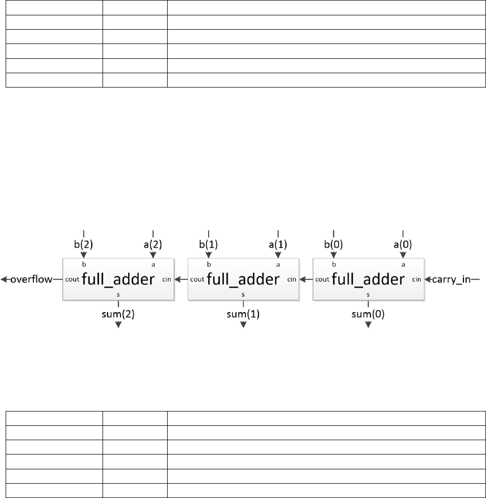
The next step is to create the 4-Bit Ripple Carry Adder. Figure 1 illustrates how a 3-Bit ripple carry adder
can be constructed from three 1-Bit full adders.
Figure 1: 3-bit Ripple Carry Adder Diagram
The required module name is: adder_4bit
The required filename is: adder_4bit.sv
The module must have exactly the following ports (case-sensitive port names):
Signal
Direction
Description
a[3:0]
input
One of two primary inputs
b[3:0]
input
Second of two primary inputs
carry_in
input
The overflow value carried in from a prior addition column
sum[3:0]
output
The computed sum value
overflow
output
The overflow value from the calculation
ASIC Design Lab Lab 2 Spring 2018
11
We would like you to use the structural style of coding to create the 4-Bit adder from your 1-bit Full Adder
design you made. At simulation time, ModelSim will look for matching module declarations in the work
library used and any additional libraries specified with the vsim command. The makefile will take care of
specifying the additional libraries for mapped version gates and provided course IP modules. Although it
would still be a good idea to investigate how the makefile does that for you.
For this lab, an intermediate signal you will use is the one that connects the carrys between adders and/or
output pins. Declare this signal and give it an appropriate name (we will use the name carrys, 4 bits in size,
to illustrate our point). After you declare the intermediate signal(s) you will need, you can start connecting
the components. The following code is an example of how you would port map the first three 1-bit adder
instances:
adder_1bit I00 (.a(a[0], .b(b[0], .carry_in(carry_in), .sum(sum[0]),
.carry_out(carrys[0]));
adder_1bit I01 (.a(a[1], .b(b[1], .carry_in(carrys[0]), .sum(sum[1]),
.carry_out(carrys[1]));
adder_1bit I02 (.a(a[2], .b(b[2], .carry_in(carrys[1]), .sum(sum[2]),
.carry_out(carrys[2]));
Now based on the limited Verilog syntax that shown so far, one may think that it is necessary to directly
type out (or copy, paste, and modify) each 1-bit adder instance. However, there is a powerful syntax to
simplify repetitive structural/dataflow tasks such as this. It’s known as a generate loop and results in far
more efficiently written code, and fewer port mapping typographical errors. Below is an example of how
one can use the generate syntax to exploit the iterative pattern for the 1-bit adder port maps to save a lot of
time and frustration.
wire [4:0] carrys;
genvar i;
assign carrys[0] = carry_in;
generate
for(i = 0; i <= 3; i = i + 1)
begin
adder_1bit IX (.a(a[i]), .b(b[i]), .carry_in(carrys[i]),
.sum(sum[i]), .carry_out(carrys[i+1]));
end
endgenerate
assign overflow = carrys[4];
After you have finished creating your generate based 4-bit adder version, extend the exhaustive test bench
provided for the 1-bit adder to exhaustively test your 4-bit adder for verifying your design. The simulation
commands you have been using previously will only work for designs with only one source file, and one
test bench involved. In order to simulate multi-file designs, referred to as hierarchical designs, you will
need to use the ‘full’ commands (sim_full_source and sim_full_mapped) instead and populate the following
variables in the makefile:
• The “TOP_LEVEL_FILE” variable in your makefile must contain the filename of your 4-bit adder
design (not including the source folder)
• The “COMPONENT_FILES” variable in your makefile must contain the filename of your 1-bit
and design (not including the source folder)
To submit your working 4-bit adder and exhaustive test bench for grading use the ‘submit
Lab2adder4’command.
ASIC Design Lab Lab 2 Spring 2018
12
2.3. Creating a Scalable Ripple Carry Adder Design with Parameters
2.3.1. Verilog Parameters
Verilog parameters are effectively constants that are specific to a module instead of being a global constant
like “`define” constants. They are rather similar to the ‘const’ in C. One difference between Verilog
parameters and C ‘const’ is that there are two classes of parameters in Verilog. The first class is ‘localparam’
which is pretty much the same as a C ‘const’, as it is a constant local to namespace (the module) in which
it’s declared/defined and can’t be modified. The second class is ‘parameter’ which is a constant that is local
to the namespace (the module) in which it’s declared/defined, but its value can be modified on a per instance
level during the via the instance’s port map. This allows us to be able to design the code of a module around
a ‘parameter’ and then simply choose the value of the parameter at the instance’s port map or use the
‘default’ value if we don’t want to set the parameter’s value during the port map. Both types of parameters
are declared/defined in the same way, as shown below.
parameter <name> = <default value>;
localparam <name> = <value>;
However, since parameters are intended to have their value modified and will often be used to scale internal
data sizes and corresponding port sizes, they should be declared inside the module declaration as follows.
module <module name>
#(
<parameter declaration>,
…
<parameter declaration>
)
(
<port declaration>,
…
<port declaration>
);
When creating module definitions for a parameterized design it often is necessary to have one or more
port(s) scale based on a parameter. Doing this is as simple as directly using the parameter to determine the
port dimensions. Below is a simple example:
module example_scalable_design
#(
parameter NUM_BITS = 4
)
(
input wire [(NUM_BITS – 1):0] operand_a,
…
);

ASIC Design Lab Lab 2 Spring 2018
13
2.3.2. Creating a Parameterized Ripple Carry Adder Design
Using the above discussion of parameters and your generate syntax based 4-bit Ripple Carry Adder, create
a parameterized Ripple Carry Adder with a parameter called ‘BIT_WIDTH’ that determines the number of
bit pairs added and the size of the ‘a’ and ‘b’ ports. The default value for this parameter must be 4.
The required module name is: adder_nbit
The required filename is: adder_nbit.sv
The module must have exactly the following ports (case-sensitive port names):
Signal
Direction
Description
a[#:0]
input
One of two primary inputs. The actual port declaration should use
the BIT_WIDTH parameter value to determine the value of the ‘#’.
b[#:0]
input
Second of two primary inputs. The actual port declaration should use
the BIT_WIDTH parameter value to determine the value of the ‘#’.
carry_in
input
The overflow value carried in from a prior addition column
sum[#:0]
output
The computed sum value. The actual port declaration should use the
BIT_WIDTH parameter value to determine the value of the ‘#’.
overflow
output
The overflow value from the calculation
When verifying your parameterized version, you should be able to use it with a copy of your 4-bit test bench
to test the unscaled (default value sized) source and mapped functionality with only updating the design
port map in the test bench to be for your ‘adder_nbit’ design instead of your ‘adder_4bit’ design.
2.3.3. Mapped testing of your Scaled/Parameterized Ripple Carry Adder Design
Only source versions of designs can be scaled or modified by parameters. Therefore in order to test the
mapped functionality of the scaled version (where something other than the default value is used) you will
need to use a wrapper file that includes your scalable design and then overrides the parameter size locally.
Then this wrapper file must be synthesized together with the flexible design’s source code in order to create
the full scaled size mapped design file that can be compiled and tested. A template 8-bit adder file
(adder_8bit.sv) has been provided to you via the setup2 script to aid you in this task. The module declaration
has been defined for you in, but you must insert the proper port map code for using your scalable ripple
carry adder.
Be sure to update the make variables used for hierarchical designs to match your new system:
• When testing your N-bit adder directly using it’s default values:
• The “TOP_LEVEL_FILE” variable in your makefile must contain the filename of your n-bit adder
design (not including the source folder)
• The “COMPONENT_FILES” variable in your makefile must contain the filename of your 1-bit
adder design (not including the source folder)
• When testing your mapped scaled 8-bit adder:
• The “TOP_LEVEL_FILE” variable in your makefile must contain the filename of your 8-bit
wrapper file (not including the source folder)
• The “COMPONENT_FILES” variable in your makefile must contain the filename of your 1-bit
and n-bit adder designs (not including the source folder)
To submit your working scalable Ripple Carry Adder, 8-bit adder wrapper file, and exhaustive 8-bit adder
test bench for grading use the ‘submit Lab2addern’command.
ASIC Design Lab Lab 2 Spring 2018
14
2.4. Synchronizer Design
2.4.1. Verilog Syntax for Describing Flip-Flops
Flip-Flops are the basic synchronous storage cell for CMOS designs and form the basis for all ‘registers’.
The most common is the D-Flip-Flop with Set and Reset signals that allow the design to be
cleared/reset/initialized to a known operating state. The syntax for describing a Flip-Flop is rather simple
and straight-forward but is different than the combinational logic that you have been working with primarily
so far. The most common Flip-Flip used in designs and the primary one used for any designs in this course
is a rising-edge sensitive Flip-Flop with an active low reset, which has the following syntax:
always_ff @ (posedge clk, negedge n_rst)
begin [: <block tag name>]
if(1’b0 == n_rst)
begin
<Flip-Flop Signal Name> <= <reset value>;
end
else
begin
<Flip-Flop Signal Name> <= <Flip-Flop input signal>;
end
end
This syntax implements a Flip-Flop due to the nature of how the sensitivity list is used and the “always_ff”
tells the compiler that you intend for it to be flip-flop so it should give error messages if the code is not
correct for a flip-flop. One can also use the “always_comb” block instead of the “always” block for
combination logic for similar purpose as the “always_ff” block for flip-flops/registers.
ASIC Design Lab Lab 2 Spring 2018
15
2.4.2. Synchronizer Design Specifications
2.4.2.1. Reset to Logic Low Synchronizer
Design (code and verify) the synchronizer module you diagramed in lab 1’s postlab with the following
specifications:
The required module name is: sync_low
The required filename is: sync_low.sv
The module must have only the following ports (case-sensitive port names):
Signal
Direction
Description
clk
input
The system clock. (1 GHz)
n_rst
input
This is an asynchronous, active-low system reset. When this line is
asserted (logic ‘0’), all registers/flip-flops in the device must reset to
an initial value of logic ‘0’.
async_in
input
This is the asynchronous input port (the original signal which is not
synchronized to the supplied clock signal).
sync_out
output
This is the synchronous output port (the form of the input that is now
synchronized with the supplied clock signal).
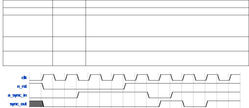
Figure 2: Timing waveform for 2-stage synchronizer for an active high input
ASIC Design Lab Lab 2 Spring 2018
16
2.4.2.2. Reset to Logic High Synchronizer
Design (code and verify) a simple modified versions of the synchronizer module you diagramed in lab 1’s
postlab with the following specifications:
The required module name is: sync_high
The required filename is: sync_high.sv
The module must have only the following ports (case-sensitive port names):
Signal
Direction
Description
clk
input
The system clock. (1 GHz)
n_rst
input
This is an asynchronous, active-low system reset. When this line is
asserted (logic ‘0’), all registers/flip-flops in the device must reset to
an initial value of logic ‘1’.
async_in
input
This is the asynchronous input port (the original signal which is not
synchronized to the supplied clock signal).
sync_out
output
This is the synchronous output port (the form of the input that is now
synchronized with the supplied clock signal).
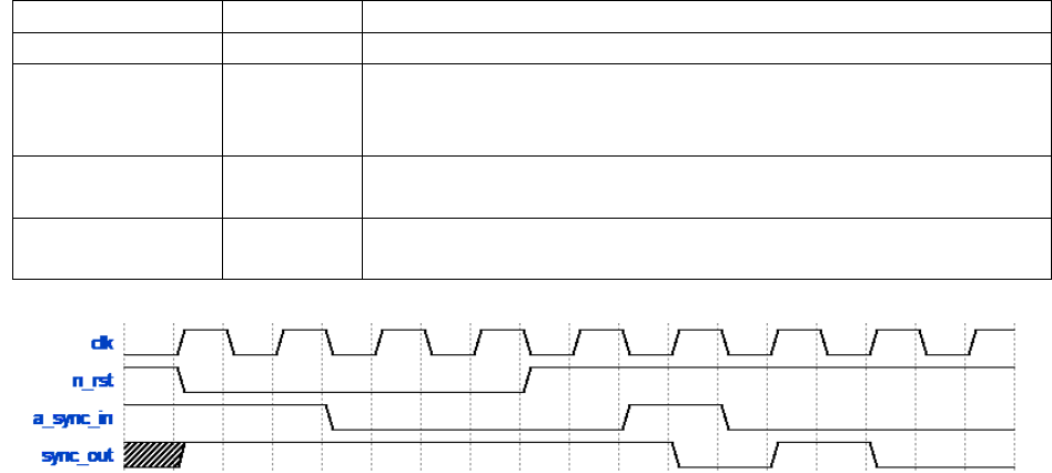
Figure 3: Timing waveform for 2-stage synchronizer for an active low input
ASIC Design Lab Lab 2 Spring 2018
17
2.4.3. Synchronizer Design Testing
Unlike you prior designs, which were purely combinational, the synchronizers are sequential designs which
mean that input timing combinations now become important instead of just value combinations. However,
it is possible to effectively exhaustively test a design as simple as a synchronizer, one just has to focus on
the classes of input timings that are important for the design. In this case there are three major timing classes
with respect to the clock and a data input value: setup time violations, hold time violations, and nominal
timings. Within each of these input timing classes, the behavior of a synchronizer will be the same for all
different timing combinations, so one only needs to create a single scenario for each class in order to
effectively exhaustively test those three classes of design behavior. To aid you in your testing you have
been provided with a starter test bench for the synchronizer which has test cases for all three timing classes
for the clock signal and one data input value, as well as reset conditions. You will need to extend it to cover
the three timing cases for the other data input value. Also, pay attention to the behavior of the stored/output
values of the flip-flops involved during the timing violation cases and compare that to what you know about
the role of a synchronizer in a system and the discussion of metastability in prior digital design classes.
Since the purpose of a synchronizer is to filter out metastability from an input directly or indirectly via
timing violations source simulations are not really useful outside of verifying nominal operations. This is
because source simulations do not model timing information for any aspect of the system which is a critical
part of the non-ideal behavior for synchronizers. Additionally, since source simulations do not involve
actual gate or flip-flop models they do not even approximate the analog load characteristics of the flip-flops
that actually cause the synchronizer to work. Therefore, source simulations of the provided test bench and
any proper synchronizer test benches will have erroneous behavior and should fail any non-ideal test cases.
For these reasons, the only want to test a synchronizer in non-ideal test cases effectively is to use mapped
simulations where the flip-flop loads and behaviors are at least approximated.
To submit your working synchronizer designs and exhaustive test benches for grading use the ‘submit
Lab2sync’command.
Note: Only submit once you have both synchronizers and their respective test benches working correctly
as they are graded as a group.
