M8SL2 00 002 812 T800/M8SL2 Slimline Manual/M8SL2
T800/M8SL2-00-002-812 Slimline Manual/M8SL2-00-002-812 M8SL2-00-002-812
User Manual: Pdf T800/M8SL2-00-002-812 Slimline Manual/M8SL2-00-002-812
Open the PDF directly: View PDF ![]() .
.
Page Count: 383 [warning: Documents this large are best viewed by clicking the View PDF Link!]
- M8SL2-00-002-812
- Part A Introduction To Servicing
- Part B T855 Receiver
- 1 T855 General Information
- 2 T855 Circuit Operation
- 3 T855 Initial Tuning and Adjustment
- 4 T855 Functional Testing
- 5 T855 Fault Finding
- 6 T855 PCB Information
- Part C T854 Transmitter
- 1 T854 General Information
- 2 T854 Circuit Operation
- 3 T854 Initial Tuning and Adjustment
- 4 T854 Functional Testing
- 5 T854 Fault Finding
- 6 T854 PCB Information
- Part D T803-02-9000 Tone Remote
- Part E T850 VCO PCB Information
- Part F T800-23-0011 Power Supply
- Part G Installation and Configuration
- 1 T800 SL2 Installation
- 2 T854 Optional Features
- 3 Talk Through Repeater
- 4 Line Controlled Base without Talk Through
- 5 DC Line Keying
- 6 X800-56-PCB3 PCB Information
- Part H T800 Ancillary Equipment
M8SL2-00-002-812 1
© Copyright Tait Electronics Limited August 2004. All rights reserved.
T800 SL2
Base Station Equipment
400 to 520MHz 25 Watt Continuous
Service Manual
August 2004
M8SL2-00-002-812

2M8SL2-00-002-812
© Copyright Tait Electronics Limited August 2004. All rights reserved.
TEL Contact Information
Corporate Head Office
Tait Electronics Ltd
175 Roydvale Avenue
P.O. Box 1645
Christchurch
New Zealand
Technical Support Enquiries
Phone: 64 3 357 9991
Fax: 64 3 358 0320
E-mail: support@taitworld.com
Internet
http://www.taitworld.com
New Zealand
Tait Communications Ltd
540 Wairakei Road
P. O. Box 11 8 5
Christchurch
Phone: 64 3 357 2750
Fax: 64 3 358 2029
E-mail: headoffice@tcl.tait.co.nz
Australia
Tait Electronics (Aust) Pty Ltd
186 Granite Street
Geebung
Queensland 4034
P. O. B o x 67 9
Virginia
Queensland 4014
Australia
Phone: 61 7 3865 7799
Toll Free: 1 300 304 344
Fax: 61 7 3865 7990
E-mail: australia@taitworld.com
North America
Regional Head Office
Canada
Tait Mobile Radio Inc.
Unit 5, 158 Anderson Avenue
Markham
Ontario L6E 1A9
Canada
Phone: 1 905 472 1100
Toll Free: 1 800 890 TAIT (8248)
Fax: 1 905 472 5300
E-mail: canada@taitworld.com
USA
Toll Free: 1 800 890 TAIT (8248)
E-mail: usa@taitworld.com
Latin America
E-mail: latinamerica@taitworld.com
North Asia
Regional Head Office
Hong Kong
Tait Mobile Radio (HK) Ltd
Unit 2216, North Tower
Concordia Plaza
No. 1 Science Museum Road
Tsim Sha Tsui East
Kowloon
Phone: 852 2369 3040
Fax: 852 2369 3009
E-mail: hongkong@taitworld.com
Beijing
Tait Mobile Radio (HK) Ltd
Beijing Representative Office
Room 610, Tower 2
Beijing Henderson Centre
No. 18 Jianguomennei Da Jie
Doncheng District
Beijing
China 100005
Phone: 86 10 6518 6290
Fax: 86 10 6518 6296
E-mail: beijing@taitworld.com
Ta i w an
Tait Mobile Radio (Taiwan) Ltd
5Fl., No. 159, Keelung Road
Sec. 1
Taipei 110
Taiwan
Phone: 886 2 2768 6600
Fax: 886 2 2761 9970
E-mail: taiwan@taitworld.com
South East Asia
Regional Head Office
Singapore
Tait Electronics (Far East) Pte Ltd
491B River Valley Road
#09-02 Valley Point Office Tower
Singapore 248373
Phone: 65 471 2688
Fax: 65 479 7778
E-mail: singapore@taitworld.com
Thailand
Tait Mobile Radio Ltd
14/1 Suwan Tower
Third Floor
North Sathorn Road
Soi Saladaeng 1
Bangrak
Bangkok 10500
Thailand
Phone: 662 267 6290
Fax: 662 267 6293
E-mail: thailand@taitworld.com
Europe
Regional Head Office
United Kingdom
Tait Europe Ltd
Ermine Business Park
Ermine Road
Huntingdon
Cambridgeshire PE29 6WT
United Kingdom
Phone: 44 1480 52 255
Fax: 44 1480 411 996
E-mail: unitedkingdom@taitworld.com
France
Antenne Française
E-mail: france@taitworld.com
Germany
Zweigstelle Deutschland
E-mail: germany@taitworld.com
T800
T800

M8SL2-00-002-812 3
© Copyright Tait Electronics Limited August 2004. All rights reserved.
About This Manual
Scope This manual contains general, technical and servicing informa-
tion on T800 SL2 25W continuous base station which comprise
the following equipment:
Format We have published this manual in a ring binder so that “revision
packages” containing additional information pertaining to new
issues of PCBs can be added as required.
PCB Information PCB information is provided for all current issue PCBs, and is
grouped according to PCB. Thus, you will find the parts list,
grid reference index (if necessary), PCB layouts and circuit dia-
gram(s) for each individual PCB grouped together.
Errors If you find an error in this manual, or have a suggestion on how
it might be improved, please do not hesitate to contact Technical
Support, Tait Electronics Ltd, Christchurch, New Zealand (full
contact details are on page 2).
Updating Equipment and Manuals
In the interests of improving performance, reliability or servicing, Tait Electronics Ltd
reserve the right to update their equipment and/or manuals without prior notice.
Copyright
All information contained in this manual is the property of Tait Electronics Ltd. All
rights are reserved. This manual may not, in whole or part, be copied, photocopied,
reproduced, translated stored or reduced to any electronic medium or machine readable
form without prior written permission from Tait Electronics Ltd.
Ordering Tait Service Manuals
You can order additional copies of this service manual from your nearest Tait Dealer or
Customer Service Organisation. When ordering, make sure you quote the correct Tait
product code (“M” number). Note that only the latest issue of the manual will be availa-
ble for order.
T800 SL2 25W base
station
T855 receiver
T854 25W continuous transmitter
T803-02 tone remote (optional)
T800-23-0011 Power supply

4M8SL2-00-002-812
© Copyright Tait Electronics Limited August 2004. All rights reserved.
Publication Information
T800 SL2 Service Manual
Publication Date Product Code
June 2002
August 2004
M8SL2-00-001-812
M8SL2-00-002-812
M8SL2-00-002-812 5
© Copyright Tait Electronics Limited August 2004. All rights reserved.
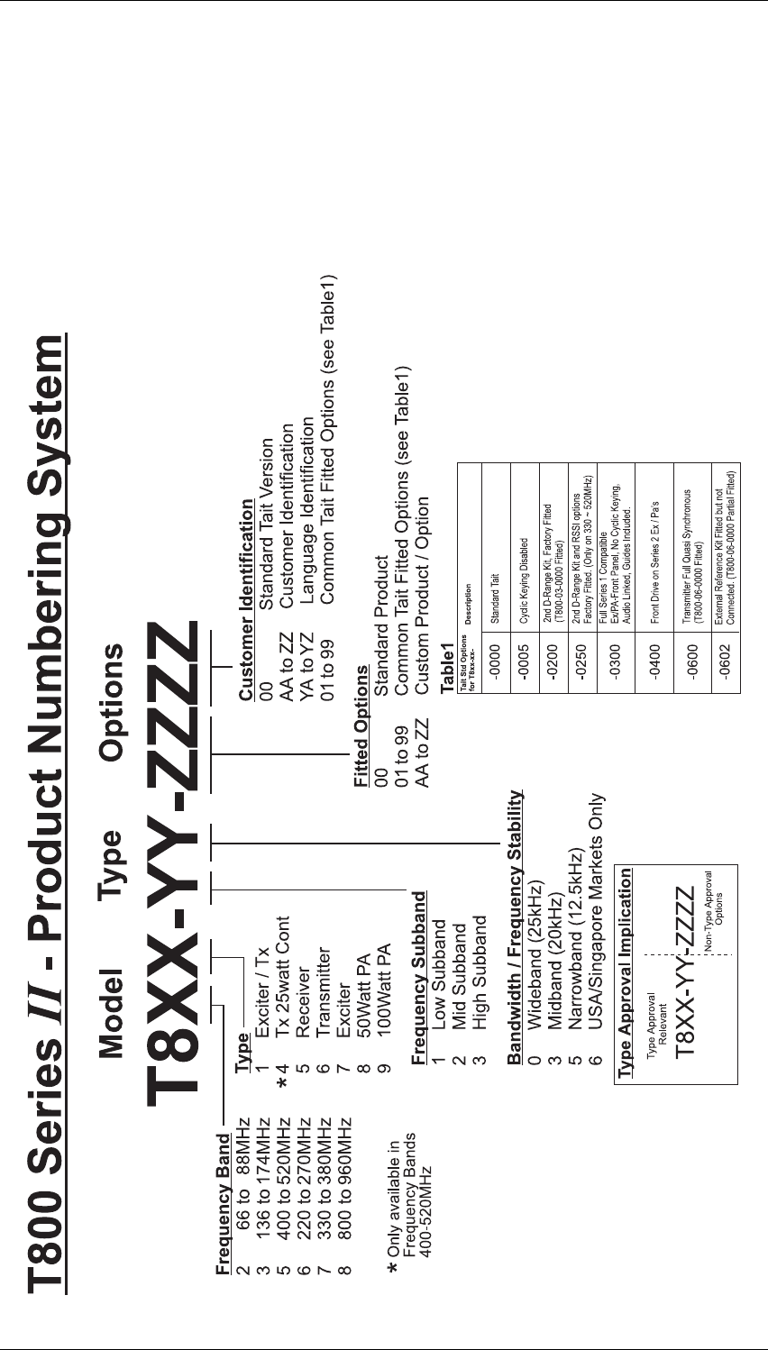
1 T800 Product Codes
The T800 product code provides information about the model, type and options fitted,
according to the conventions described below
You can identify the unit’s type by checking the product code printed on a label on the
rear of the chassis (Figure 1.1 in Part A shows typical labels). You can further verify the
type by checking the placement of an SMD resistor in the table that is screen printed
onto the PCB..
6M8SL2-00-002-812
© Copyright Tait Electronics Limited August 2004. All rights reserved.
2 T800 SL2 Product Range
The following table lists the range of standard T800 types (i.e. no options fitted) availa-
ble at the time this manual was published. Consult your nearest Tait Dealer or Customer
Service Organisation for more information
T800 SL BSM Conventional Ordering Number System 18/11/02
L A 1 W B 0 0
System
Type
Frequency
Band
RF Output
Power
Channel
Spacing
Power
Supply
Coaxial
Relay /
Duplexer
Ancillary
Options
L = T800 SL BSM (T800-56-X0XX)
1 =
4 =
*5 =
25 Watts
5 Watts
25 Watts (Cont)
0 =
4 =
6 =
7 =
8 =
9 =
No Ancillary Option
Multi-Channel Option (10 CH)
Cabinet Desktop 3U (Blk)
Cabinet Desktop 4U (Blk)
Cabinet Transportable 6U (Blk)
Tone Remote Module
(T992-03-0002)
(T992-04-0002)
(T992-06-0002)
(T803-00-0000)
0 =
1 =
2 =
No Duplexer Fitted
50 Watt Duplexer Kit (T991-09-0001)+(T993-XX)
Coaxial Relay Kit (T800-09-0002)
If Duplexer item code is set to (1), then Base/Repeater/
Slimline Requirement sheet must be completed. This is
required so correct Duplexer Frequency and Spacing can be
calculated.
T991-09-0001 is a 1U 19" Tray for Duplexer fitting.
N =
M =
W =
12.5 kHz
20 kHz
25 kHz
A =
B =
C =
D =
E =
F =
P =
Q =
R =
66 - 88
136 - 156
148 - 174
400 - 440
440 - 480
480 - 520
800 - 870
860 - 910
890 - 960
(T82x-xx-02xx)
(T83x-1x-02xx)
(T83x-2x-02xx)
(T85x-1x-02xx)
(T85x-2x-02xx)
(T85x-3x-02xx)
(T88x-1x-02xx)
(T88x-2x-02xx)
(T88x-3x-02xx)
MHz
MHz
MHz
MHz
MHz
MHz
MHz
MHz
MHz
*
*
= Not Available for US Market
B =
D =
BSM Kit with Power Supply
BSM Kit with External DC
(T800-56-X0X2)
(T800-56-X0X4)
1
1
2
2
3
3
4
7
5
6
5
67
4
* Only Available in Frequency
Bands
400-520Mhz

M8SL2-00-002-812 7
© Copyright Tait Electronics Limited August 2004. All rights reserved.
Table of Contents
This manual is divided into nine parts as listed below, with each part being further sub-
divided into sections. There is a detailed table of contents at the start of each part and/
or section.
Part Title
A Introduction To Servicing
B T855 Receiver
C T854 Transmitter
D T803-02-9000 Tone Remote
E T850 VCO PCB Information
F T800-23-0011 Power Supply
G Installation and Configuration
H T800 Ancillary Equipment

8M8SL2-00-002-812
© Copyright Tait Electronics Limited August 2004. All rights reserved.

M8SL2-00-002-812 AI
© Copyright Tait Electronics Limited August 2004. All rights reserved.
Part A Introduction To Servicing
This part of the manual is divided into the sections listed below. These sections provide
some general and advisory information on servicing procedures.
Section Title Page
1
1.1
1.2
1.3
1.4
General
Additional Technical Information
Caution: CMOS Devices
Caution: Aerial Load
Caution: Beryllium Oxide and Power Transistors
1.1
1.1
1.1
1.2
1.2
2
2.1
2.2
2.3
2.3.1
2.4
Mechanical
Torx Recess Head Screws
Pozidriv and Philips Recess Head Screws
Disassembly/Reassembly
Receivers/Transmitters
Cover Screw Torques
2.1
2.1
2.2
2.3
2.3
2.3
3
3.1
3.1.1
3.1.2
3.2
3.3
Component Replacement
Leaded Components
Desoldering Iron Method
Component Cutting Method
Surface Mount Devices
Cased Mica Capacitors
3.1
3.1
3.1
3.1
3.2
3.2
Figure Title Page
1.1
1.2
2.1
2.2
Typical Product Code and Serial Number Labels
Typical Anti-static Bench Set-up
Torx Screw Identification
Pozidriv and Philips Screw and Screwdriver Identification
1.1
1.2
2.1
2.2

AII M8SL2-00-002-812
© Copyright Tait Electronics Limited August 2004. All rights reserved.
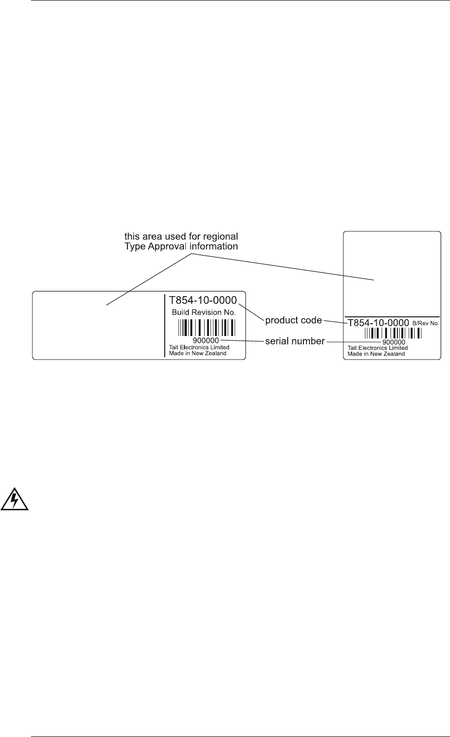
M8SL2-00-002-812 General A1.1
© Copyright Tait Electronics Limited August 2004. All rights reserved.
1 General
1.1 Additional Technical Information
If you have any questions about this manual or the equipment it describes, please con-
tact your nearest Tait Dealer or Customer Service Organisation. If necessary, you can get
additional technical help from Technical Support, Tait Electronics Ltd, Christchurch,
New Zealand (full contact details are on page 2).
When requesting information, please quote either the manual product code (e.g.
M8SL2-00-002-812), or the equipment product code, build revision number and serial
number which are printed on a label on the back of the product (as shown in Figure 1.1).
Figure 1.1 Typical Product Code and Serial Number Labels
If you require information about a particular PCB, please quote the full PCB internal
part number (IPN) which is screen printed onto the top side of the board (refer to the
appropriate PCB Information section in this manual for more details).
1.2 Caution: CMOS Devices
This equipment contains devices which are susceptible to damage from static charges.
You must handle these devices carefully and according to the procedures described in
the manufacturers’ data books.
We recommend you purchase an antistatic bench kit from a reputable manufacturer and
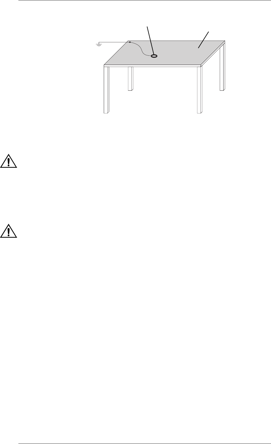
install and test it according to the manufacturer’s instructions. Figure 1.2 shows a typi-
cal antistatic bench set-up.
You can obtain further information on antistatic precautions and the dangers of electro-
static discharge (ESD) from standards such as ANSI/ESD S20.20-1999 or
BS EN 100015-4 1994.
A1.2 General M8SL2-00-002-812
© Copyright Tait Electronics Limited August 2004. All rights reserved.
Figure 1.2 Typical Anti-static Bench Set-up
1.3 Caution: Aerial Load
The equipment has been designed to operate safely under a wide range of aerial loading
conditions. However, we strongly recommend that the transmitter should always be
operated with a suitable load to prevent damage to the transmitter output power stage.
1.4 Caution: Beryllium Oxide and Power Transistors
The RF power transistors in current use all contain some beryllium oxide. This sub-
stance, while perfectly harmless in its normal solid form, can become a severe health
hazard when it has been reduced to dust. For this reason the RF power transistors
should not be broken open, mutilated, filed, machined, or physically damaged in any
way that can produce dust particles.
Common point ground
(building ground or
mains ground via
1MΩ series resistor)
conductive wrist strap dissipative rubber
bench mat

M8SL2-00-002-812 Mechanical A2.1
© Copyright Tait Electronics Limited August 2004. All rights reserved.
2Mechanical
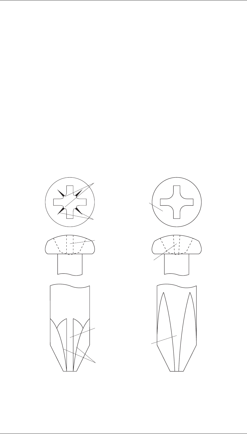
2.1 Torx Recess Head Screws
Torx recess head screws are becoming the standard screw head type in all T800 SL2
equipment, with Pozidriv and Philips recess head screws being used in fewer applica-
tions.
The Torx recess head has the advantage of improved screwdriver tip location, reducing
the chances of screw head damage caused by the driver tip rotating within the recess. In
addition, using a ball-tip Torx screwdriver allows you to drive a Torx head screw with
the driver on a slight angle, which can be useful in situations where access is restricted.
It is important that you use the correct Torx screwdriver tip:
M3 screws T10
M4 screws T20
Figure 2.1 below shows a typical Torx recess head screw (actual hardware may differ
slightly from this illustration due to variations in manufacturing techniques).
Figure 2.1 Torx Screw Identification
"star” shaped recess with
six internal notches
A2.2 Mechanical M8SL2-00-002-812
© Copyright Tait Electronics Limited August 2004. All rights reserved.
2.2 Pozidriv and Philips Recess Head Screws
Pozidriv and Philips recess head screws will continue to be used in T800 SL2 equipment
in a few special applications. It is important that you use the correct type and size
screwdriver for each screw type to avoid damaging the screw head.
It is particularly important that you do not use Philips screwdrivers on Pozidriv screw
heads as the tapered driving flutes of the Philips screwdriver do not engage correctly
with the parallel-sided slots in the Pozidriv screw head. This can result in considerable
damage to the screw head if the screwdriver tip turns inside the recess.
Note: If you find you need excessive downwards pressure to keep the screwdriver
tip in the Pozidriv screw head, you are probably using the wrong type and/
or size screwdriver.
Figure 2.2 below shows the main differences between typical Pozidriv and Philips screw
heads and screwdriver tips (actual hardware may differ slightly from these illustrations
due to variations in manufacturing techniques).
Figure 2.2 Pozidriv and Philips Screw and Screwdriver Identification
driving flutes with
parallel sides
driving flutes with
tapered sides
Pozidriv Philips
internal notches
"star" markings
between slots
no special markings
slots with parallel sides
slots with tapered sides
ridges between
driving flutes

M8SL2-00-002-812 Mechanical A2.3
© Copyright Tait Electronics Limited August 2004. All rights reserved.
2.3 Disassembly/Reassembly
2.3.1 Receivers/Transmitters
To carry out alignment or change option links, you need to remove only the top cover,
i.e. the one on the opposite side to the main D-range connector (D-range 1/PL100).
You need to remove the bottom cover to:
• access transmitter RF power transistors and many SMD components
• change solder blob links
• fit test leads to circuit block access points.
2.4 Cover Screw Torques
Receivers/Transmitters … 1.36Nm/12in.lbf.

A2.4 Mechanical M8SL2-00-002-812
© Copyright Tait Electronics Limited August 2004. All rights reserved.

M8SL2-00-002-812 Component Replacement A3.1
© Copyright Tait Electronics Limited August 2004. All rights reserved.
3 Component Replacement
3.1 Leaded Components
Whenever you are doing any work on the PCB that involves removing or fitting compo-
nents, you must take care not to damage the copper tracks. The two satisfactory meth-
ods of removing components from plated-through hole (PTH) PCBs are detailed below.
Note: The first method requires the use of a desoldering station, e.g. Philips SBC
314 or Pace MBT-100E.
3.1.1 Desoldering Iron Method
Place the tip over the lead and, as the solder starts to melt, move the tip in a circu-
lar motion.
Start the suction and continue the movement until 3 or 4 circles have been com-
pleted.
Remove the tip while continuing suction to ensure that all solder is removed from
the joint, then stop the suction.
Before pulling the lead out, ensure it is not stuck to the plating.
If the lead is still not free, resolder the joint and try again.
Note: The desoldering iron does not usually have enough heat to desolder leads
from the ground plane. Additional heat may be applied by holding a solder-
ing iron on the tip of the desoldering iron (this may require some additional
help).
3.1.2 Component Cutting Method
Cut the leads on the component side of the PCB.
Heat the solder joint sufficiently to allow easy removal of the lead by drawing it
out from the component side: do not use undue force.
Fill the hole with solder and then clear with solderwick.

A3.2 Component Replacement M8SL2-00-002-812
© Copyright Tait Electronics Limited August 2004. All rights reserved.
3.2 Surface Mount Devices
Caution: Surface mount devices (SMDs) require special storage, handling,
removal and replacement techniques. This equipment should be serv-
iced only by an approved Tait Dealer or Customer Service Organisa-
tion equipped with the necessary facilities. Repairs attempted with
incorrect equipment or by untrained personnel may result in perma-
nent damage. If in doubt, contact your nearest Tait Dealer or Customer
Service Organisation.
3.3 Cased Mica Capacitors
Cased mica capacitors can be removed by heating the top with a heavy-duty soldering
iron and gently lifting the capacitor off the PCB with a solder-resistant spike or equiva-
lent.

M8SL2-00-002-812 BI
© Copyright Tait Electronics Limited August 2004. All rights reserved.
Part B T855 Receiver
This part of the manual is divided into six sections, as listed below. There is a detailed
table of contents at the start of each section.
Section Title
1 General Information
2 Circuit Operation
3 Initial Tuning and Adjustment
4 Functional Testing
5 Fault Finding
6 PCB Information

BII M8SL2-00-002-812
© Copyright Tait Electronics Limited August 2004. All rights reserved.

M8SL2-00-002-812 T855 General Information B1.1
© Copyright Tait Electronics Limited August 2004. All rights reserved.
1 T855 General Information
This section provides a brief description of the T855 receiver, along with detailed speci-
fications.
The following topics are covered in this section.
Section Title Page
1.1 Introduction 1.5
1.2
1.2.1
1.2.2
1.2.3
1.2.4
1.2.4.1
1.2.4.2
1.2.4.3
1.2.5
1.2.6
1.2.6.1
1.2.6.2
1.2.6.3
Specifications
Introduction
General
RF Section
Audio Section
General
CTCSS
Mute Operation
Microprocessor Controller
Test Standards
European Telecommunication Standard (ETS)
DTI CEPT Recommendation T/R-24-01
Telecommunications Industry Association
1.6
1.6
1.7
1.7
1.9
1.9
1.9
1.10
1.10
1.10
1.10
1.11
1.11
Figure Title Page
1.1
1.2
T855 Main Circuit Block Identification
T855 Front Panel Controls
1.3
1.4

B1.2 T855 General Information M8SL2-00-002-812
© Copyright Tait Electronics Limited August 2004. All rights reserved.
M8SL2-00-002-812 T855 General Information B1.3
© Copyright Tait Electronics Limited August 2004. All rights reserved.
Figure 1.1 T855 Main Circuit Block Identification
1
234
5
C
6
8
9
A
B
710
Key: 1
2
3
4
5
6
7
low pass filter
receiver front end
receiver IF
audio processor
VCO
regulators
synthesiser
8
9
10
A
B
C
microcontroller and CTCSS
duct for cabling to extra D-range (if fitted)
D-range
RF input
D-range connector (“D-range 1”) incl. audio out and DC in
(refer to Section 1.5 in Part G)
microcontroller
B1.4 T855 General Information M8SL2-00-002-812
© Copyright Tait Electronics Limited August 2004. All rights reserved.
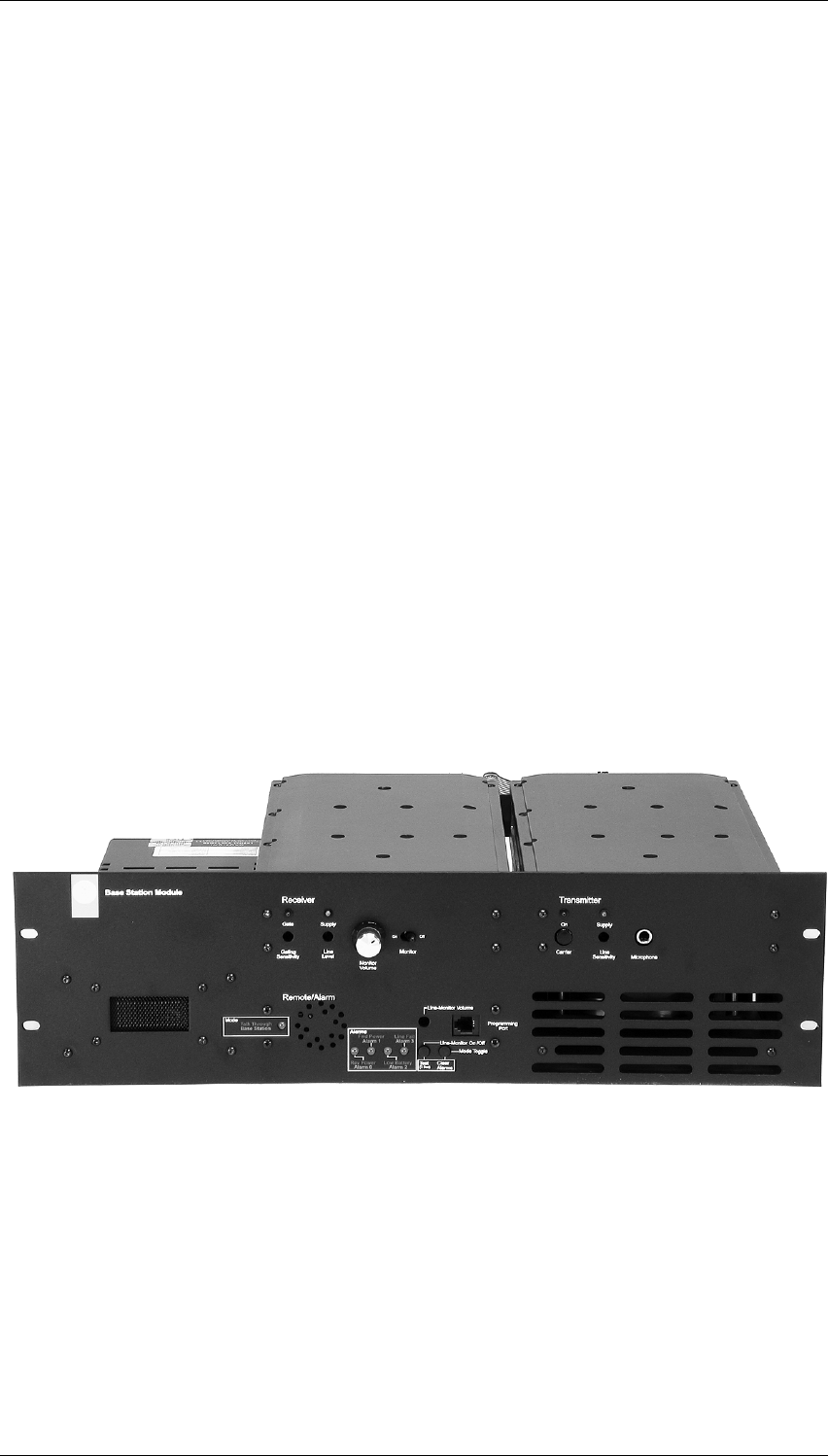
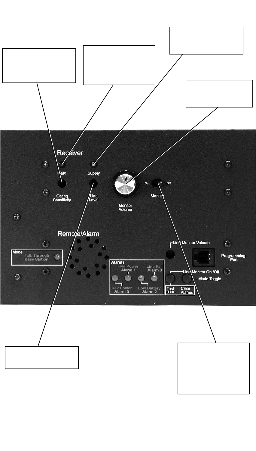
Figure 1.2 T855 Front Panel Controls
Gate LED
The Gate LED indicates the sta-
tus of the mute circuit. The LED
is lit when a signal above the
mute threshold is received.
Gating Sensitivity
Sets the RF signal level required
to open the mute gate and allow
audio to pass to the output.
Supply LED
The Supply LED is lit when DC
power is supplied to the receiver.
Line Level
Sets the audio output line level.
Monitor Volume
Adjusts the speaker volume if
a speaker is connected.
Monitor
This switch opens the mute,
allowing continuous monitoring
of the audio signal:
On audio unmuted
Off audio muted.

M8SL2-00-002-812 T855 General Information B1.5
© Copyright Tait Electronics Limited August 2004. All rights reserved.
1.1 Introduction
The T855 is a high performance microprocessor controlled FM base station receiver
designed for single or multichannel operation in the 400 to 530MHz frequency range1.
The receiver is a dual conversion superhet with a synthesised local oscillator. The first IF
is 45.0MHz, allowing exceptionally high spurious signal rejection to be achieved in the
receiver front end. The second IF section (455kHz) combines amplitude limiting, detec-
tion and audio preamplification within a single integrated circuit. It also drives carrier
and noise level detectors for signal strength indication and gating the audio output.
RSSI can be used to drive a carrier mute for audio output gating (link selectable) when
the optional T800-04-0000 RSSI PCB is fitted.
The audio section output can be adjusted to deliver >+10dBm to a 600Ω balanced out-
put, and 1W to a local monitor speaker. A flat or de-emphasised audio response is link
selectable.
The synthesiser frequency is programmed via the serial communications port. Eight
channel select lines are accessible via an additional D-range connector (D-range 2 –
T800-03-0000) at the rear of the set.
All components except those on the VCO board are mounted on a single PCB. This is
secured to a die-cast chassis which is divided into compartments to individually shield
each section of circuitry. Access to both sides of the main PCB is obtained by removing
each of the two chassis covers. There is provision within the chassis to mount small
option PCBs.
The front panel controls include gating sensitivity, line level, monitor volume and a
monitor mute switch.
1. Although capable of operating over the 400 to 530MHz frequency range, the T855 has a
5MHz switching range (see Section 1.2.3 and Section 3.1).

B1.6 T855 General Information M8SL2-00-002-812
© Copyright Tait Electronics Limited August 2004. All rights reserved.
1.2 Specifications
1.2.1 Introduction
The performance figures given are minimum figures, unless otherwise indicated, for
equipment tuned with the maximum switching range and operating at standard room
temperature (+22°C to +28°C) and standard test voltage (13.8VDC).
Where applicable, the test methods used to obtain the following performance figures
are those described in the EIA and ETS specifications. However, there are several
parameters for which performance according to the CEPT specification is given. Refer to
Section 1.2.6 for details of test standards.
Details of test methods and the conditions which apply for Type Approval testing in all
countries can be obtained from Tait Electronics Ltd.
The terms “wide bandwidth”, “mid bandwidth” and “narrow bandwidth” used in this
and following sections are defined in the following table.
Sensitivity and distortion figures are stated for standard operating conditions which
includes audio de-emphasis. Note that the sensitivity and distortion figures will be
degraded when flat audio is selected.
Channel Spacing Modulation
100% Deviation
Receiver
IF Bandwidth
Wide Bandwidth 25kHz ±5.0kHz 15.0kHz
Mid Bandwidth 20kHz ±4.0kHz 12.0kHz
Narrow Bandwidth 12.5kHz ±2.5kHz 7.5kHz
Link PL210a
a. The letters in this column refer to the identification letters screen printed onto the PCB be-
side each set of links.
Link PL220a
De-emphasised Audio 1-2 (A-B) 2-3 (E-F)
Flat Audio 2-3 (B-C) 1-2 (D-E)

M8SL2-00-002-812 T855 General Information B1.7
© Copyright Tait Electronics Limited August 2004. All rights reserved.
1.2.2 General
Number Of Channels … 128 (standard)1
Supply Voltage:
Operating Voltage … 10.8 to 16VDC
Standard Test Voltage … 13.8VDC
Polarity … negative earth only
Polarity Protection … crowbar diode
Supply Current:
Standby … 350mA
Full Audio … 800mA
Operating Temperature Range … –20°C to +60°C
1.2.3 RF Section
Frequency Range … 400 to 530MHz
Type … dual conversion superheterodyne
Frequency Increment … 5 or 6.25kHz
Switching Range … 5MHz (i.e. ±2.5MHz from the centre
frequency)
Input Impedance … 50Ω
Frequency Stability … ±1ppm, –20°C to +60°C
Signal Strength Indicator … –115dBm to –70dBm, 0 to 5V
(RSSI optional) at approx. 10dB/V
1. Additional channels may be factory programmed. Contact your nearest Tait Dealer or
Customer Service Organisation.

B1.8 T855 General Information M8SL2-00-002-812
© Copyright Tait Electronics Limited August 2004. All rights reserved.
IF Amplifiers:
Frequencies … 45MHz and 455kHz
Bandwidths
Narrow Bandwidth (NB) … 7.5kHz
Mid Bandwidth (MB) … 12kHz
Wide Bandwidth (WB) … 15kHz
Sensitivity (De-emphasised Response):
Single Channel … –117dBm
Bandspread (12dB Sinad) … –115dBm (across switching range)
Sensitivity (Flat Response):
Single Channel … –111dBm
Bandspread (12dB Sinad) … –109dBm (across switching range)
Signal+Noise To Noise Ratio (Typical):
De-emphasised Flat
RF Level –107dBm … 30dB (WB) 20dB (WB)
25dB (NB) 15dB (NB)
RF Level –83dBm (CEPT) … 54dB (MB) 49dB (MB)
50dB (NB) 45dB (NB)
RF Level –57dBm (EIA) … 55dB (WB) 55dB (WB)
Selectivity:
Narrow Bandwidth (±12.5kHz) … 83dB minimum, 85dB typical (CEPT)
Mid Bandwidth (±20kHz) … 87dB minimum, 90dB typical (CEPT)
Wide Bandwidth (±25kHz) … 87dB minimum, 90dB typical (CEPT)
Offset Selectivity (Canada only) … 20dB
Spurious Response Attenuation … 100dB (typical)
Intermodulation Response Attenuation:
Narrow Bandwidth … 80dB CEPT (typical)
Mid Bandwidth … 75dB CEPT (typical)
Wide Bandwidth … 85dB EIA (typical)
Blocking … 100dB
Co-channel Rejection … 6dB
Amplitude Characteristic … 3dB
Spurious Emissions:
Conducted … –90dBm to 4GHz
Radiated … –57dBm to 1GHz
–47dBm to 4GHz

M8SL2-00-002-812 T855 General Information B1.9
© Copyright Tait Electronics Limited August 2004. All rights reserved.
1.2.4 Audio Section
1.2.4.1 General
Outputs Available … line and monitor
Frequency Response … flat or de-emphasised (750µs)
(link selectable)
Flat Response:
Bandwidth … 67 to 3400Hz
Response … within +1, –2dB of output level
at 1kHz
De-emphasised Response:
Bandwidth … 300 to 3400Hz
Response … within +1, –3dB of a –6dB/octave
de-emphasis characteristic (ref. 1kHz)
Line Output:
Power … adjustable to >+10dBm
Load Impedance … 600Ω
Distortion (at –70dBm signal level):
De-emphasised Flat
Wide Bandwidth … ≤2% ≤2%
Mid and Narrow Bandwidth … ≤2% ≤4%
Monitor Output:
Power … 1W
Speaker Impedance … 4Ω
Distortion … ≤3%
(at –70dBm signal level, links set to de-emphasis)
1.2.4.2 CTCSS
Linkable High Pass Filter:
Bandwidth … 350 to 3400Hz
Response … within +1, –3dB of level at 1kHz
Hum And Noise … 30dB min. at 250.3Hz
(1kHz at 60% system deviation 35dB typical (67 to 240Hz)
CTCSS at 10% system deviation)
Ton e Detect:
Tone Squelch Opening … better than 6dB sinad
3dB sinad at 250.3Hz (typical)
4dB sinad at 100Hz (typical)
Tone Detect Bandwidth … ±2.1Hz accept (typical)
±3.0Hz reject (typical)
Response Time … 150ms open and close (typical)

B1.10 T855 General Information M8SL2-00-002-812
© Copyright Tait Electronics Limited August 2004. All rights reserved.
1.2.4.3 Mute Operation
Systems Available … noise mute and carrier mute
Noise Mute:
Operating Range … 6 to 20dB sinad
Hysteresis … 1.5 to 6dB
Threshold … adjustable to –105dBm
Opening Time … 20ms
Closing Time … 50ms
Carrier Mute (Optional):
Operating Range … –115 to –80dBm
Hysteresis … 2 to 10dB
Opening Time … 5ms
Closing Time … 50ms
Note: The opening and closing times given above are for the standard setup
(SL210 linked and SL220 not linked. Refer to Section 3.8).
1.2.5 Microprocessor Controller
Auxiliary Ports:
Open Drain Type … capable of sinking 2.25mA via 2k2Ω
Vds max. … 5V
1.2.6 Test Standards
Where applicable, this equipment is tested in accordance with the following standards.
1.2.6.1 European Telecommunication Standard
ETS 300 086 January 1991
Radio equipment and systems; land mobile service; technical characteristics and test
conditions for radio equipment with an internal or external RF connector intended pri-
marily for analogue speech.
ETS 300 113 March 1996
Radio equipment and systems; land mobile service; technical characteristics and test
conditions for radio equipment intended for the transmission of data (and speech) and
having an antenna connector.
ETS 300 219 October 1993
Radio equipment and systems; land mobile service; technical characteristics and test
conditions for radio equipment transmitting signals to initiate a specific response in the
receiver.

M8SL2-00-002-812 T855 General Information B1.11
© Copyright Tait Electronics Limited August 2004. All rights reserved.
ETS 300 279 February 1996
Radio equipment and systems; electromagnetic compatibility (EMC) standard for pri-
vate land mobile radio (PMR) and ancillary equipment (speech and/or non-speech).
1.2.6.2 DTI CEPT Recommendation T/R-24-01
Annex I: 1988
Technical characteristics and test conditions for radio equipment in the land mobile
service intended primarily for analogue speech.
Annex II: 1988
Technical characteristics of radio equipment in the land mobile service with regard to
quality and stability of transmission.
1.2.6.3 Telecommunications Industry Association
ANSI/TIA/EIA-603-1992
Land mobile FM or PM communications equipment measurement and performance
standards.

B1.12 T855 General Information M8SL2-00-002-812
© Copyright Tait Electronics Limited August 2004. All rights reserved.

M8SL2-00-002-812 T855 Circuit Operation B2.1
© Copyright Tait Electronics Limited August 2004. All rights reserved.
2 T855 Circuit Operation
This section provides a basic description of the circuit operation of the T855 receiver.
Note: Unless otherwise specified, the term “PGM800Win” used in this and follow-
ing sections refers to version 4.02 and later of the software.
Refer to Section 6 where the parts lists, grid reference index and diagrams will provide
detailed information on identifying and locating components and test points on the
main PCB. The parts list and diagrams for the VCO PCB are in Part E.
The following topics are covered in this section.
Section Title Page
2.1 Introduction 2.3
2.2 Receiver Front End 2.4
2.3 Mixer 2.5
2.4 IF Circuitry 2.5
2.5 Noise Mute (Squelch) 2.6
2.6 Carrier Mute 2.6
2.7 Audio Processor 2.7
2.8 Power Supply And Regulators 2.8
2.9 Microcontroller 2.9
2.10 Synthesised Local Oscillator 2.10
2.11 VCO 2.11
2.12 Received Signal Strength Indicator (RSSI) 2.12
Figure Title Page
2.1
2.2
2.3
2.4
2.5
2.6
2.7
T855 High Level Block Diagram
T855 Front End, IF and Mute Block Diagram
T855 Audio Processor Block Diagram
T855 Power Supply And Regulators Block Diagram
T855 Microcontroller Block Diagram
T855 Synthesiser Block Diagram
T855 RSSI Block Diagram (T800-04-0000 RSSI PCB)
2.3
2.4
2.7
2.8
2.9
2.10
2.12

B2.2 T855 Circuit Operation M8SL2-00-002-812
© Copyright Tait Electronics Limited August 2004. All rights reserved.

M8SL2-00-002-812 T855 Circuit Operation B2.3
© Copyright Tait Electronics Limited August 2004. All rights reserved.
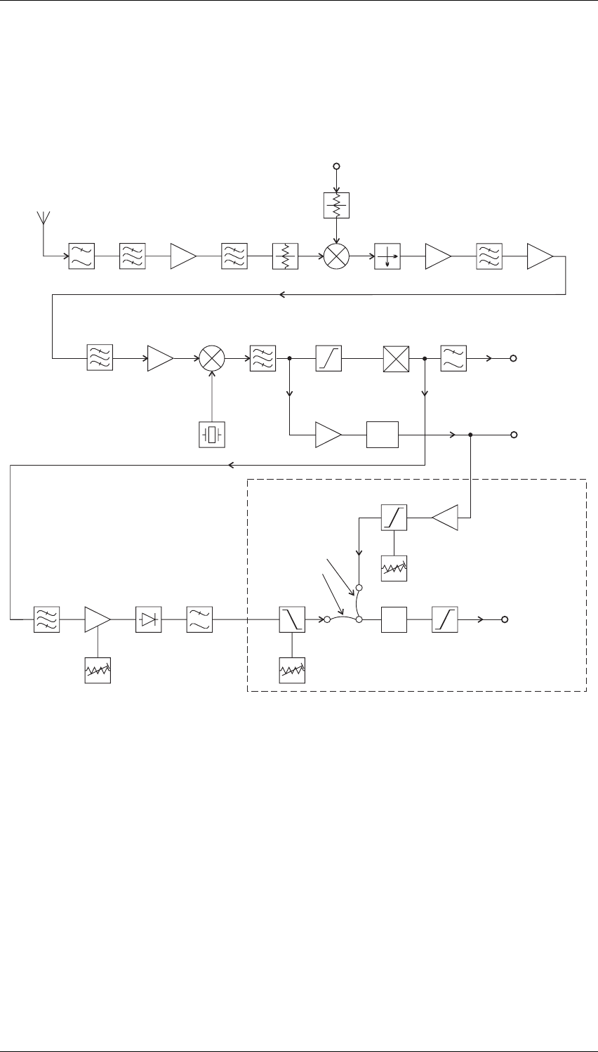
2.1 Introduction
Figure 2.1 T855 High Level Block Diagram
The T855 receiver consists of a number of distinct stages:
•front end
•mixer
• synthesised local oscillator
•IF
• audio processor
• mute (squelch)
• regulator circuits
• received signal strength indicator (RSSI).
These stages are clearly identifiable in Figure 2.1. Refer to the circuit diagrams in Section
6 for further detail.
45MHz
IF
455kHz
IF
Carrier
Mute
RSSI
Noise
Mute
Front
End
12.8MHz
Master
Oscillator
Audio
Processor
Mixer Mixer Limiter
FM
Detector
Synthesised
Local
Oscillator
Second
Local
Oscillator
Speaker
}
600Ω
Line
B2.4 T855 Circuit Operation M8SL2-00-002-812
© Copyright Tait Electronics Limited August 2004. All rights reserved.
2.2 Receiver Front End
(Refer to the front end, IF section and audio processor circuit diagrams (sheets 4, 3 and 2
respectively) in Section 6.3.)
Figure 2.2 T855 Front End, IF and Mute Block Diagram
The incoming signal from the N-type antenna socket is fed through a 9-pole, low pass
filter with a cut frequency of approximately 600MHz. This low loss filter (typically less
than 0.5dB over 400 to 530MHz) provides excellent immunity to interference from high
frequency signals.
The signal is then further filtered, using a high performance helical resonator doublet
(FL410) which provides exceptional image rejection, before being amplified by approxi-
mately 8dB (Q410). The signal is then passed through a further helical filter doublet
(FL420) before being presented to the mixer via a 2dB attenuator pad.
Each sub-block within the front end has been designed with 50Ω terminations for ease
of testing and fault finding. The overall gain from the antenna socket to the mixer input
is approximately 2dB.
t∆
Mixer
Comparator
RF In
400-530MHz
Harmonic
Filter
Helical
Filter
Helical
Filter
2dB
Pad
RF
Amp
Local Oscillator
(From Synthesiser)
Diplexer
Post
Mixer
Amp
4-Pole
Crystal
Filter
IF
Amp
4dB Pad
45MHz
2-Pole
Crystal
Filter
45MHz
Mixer
(MC3361)
Ceramic
Filter
IF
Amp
455kHz
2nd LO
44.545MHz
Active
Filter
LF
Amp
Diode
Detector
Smoothing
Filter
Gain
Adjust
Mute
Adjust
Gating
Delays
Comparator
Comparator
Mute
Adjust
Buffer
Amp
Rx Gate Out
(To Audio
Processor)
Audio Section
Link:
Low
Pass
Filter
Buffer
Amp
RSSI
Limiter
(MC3361)
FM
Detector
(MC3361)
RSSI Output
Voltage
(To D-Rang
e
Connector)
Audio
(To Audio
Processor)
Carrier Mute
Noise Mute

M8SL2-00-002-812 T855 Circuit Operation B2.5
© Copyright Tait Electronics Limited August 2004. All rights reserved.
2.3 Mixer
(Refer to the front end circuit diagram (sheet 4) in Section 6.3 and Figure 2.2.)
IC410 is a high level mixer requiring a local oscillator (LO) drive level of +17dBm (nom-
inal). The voltage controlled oscillator (VCO) generates a level of +21dBm (typical) and
this is fed to the mixer via a 5dB attenuator pad. A diplexer terminates the IF port of the
mixer in a good 50Ω, thus preventing unnecessary intermodulation distortion.
2.4 IF Circuitry
(Refer to the IF section circuit diagram (sheet 3) in Section 6.3 and Figure 2.2.)
Losses in the mixer are made up for in a tuned, common gate, post mixer amplifier
(Q310). Several stages of amplification and filtering are employed in the IF circuitry. The
first crystal filter is a 4-pole device (&XF300) which is matched into 50Ω on both its
input and output ports. This stage is followed by a common base amplifier (Q320)
whose output is matched into a 2-pole crystal filter (&XF301). The signal is then ampli-
fied using a high gain MOSFET amplifier (Q350), after which the signal is mixed down
to 455kHz with the second crystal local oscillator (44.5455MHz).
The 455kHz signal is filtered using a 6-pole ceramic filter (&XF302) before being limited
and detected. Q340 provides a buffered 455kHz output for use with the optional RF
level detector (RSSI)
The second IF mixer, limiter and detector is in a 16-pin IC (IC310). Quadrature detection
is employed, using L390, and the recovered audio on pin 9 of IC310 is typically 1Vpp for
60% system deviation.

B2.6 T855 Circuit Operation M8SL2-00-002-812
© Copyright Tait Electronics Limited August 2004. All rights reserved.
2.5 Noise Mute (Squelch)
(Refer to the audio processor and IF section circuit diagrams (sheets 2 and 3 respec-
tively) in Section 6.3 and Figure 2.2.)
The noise mute operates on the detected noise outside the audio bandwidth. An opera-
tional amplifier in IC310 is used as an active band pass filter centred on 70kHz to filter
out audio components. The noise spectrum is then further amplified in a variable gain,
two-stage amplifier (Q350 and Q360) with additional filtering. The noise is then recti-
fied (D310) and filtered to produce a DC voltage proportional to the noise amplitude.
The lowest average DC voltage corresponds to a high RF signal strength and the highest
DC voltage corresponds to no signal at the RF input.
The rectified noise voltage is compared with a threshold voltage set up on RV230, the
front panel “Gating Sensitivity” potentiometer. Hysteresis is provided by the feedback
resistor (R267) to prevent the received message from being chopped when the average
noise voltage is close to the threshold. R281 and R280 determine the mute opening and
closing times and, in combination with solder links SL210 and SL220, provide three time
delay options (SL210 is linked as standard. Refer to Section 3.8). The mute control signal
at pin 7 of IC270 is used to disable the speaker and line audio outputs. The speaker out-
put can be separately enabled for test purposes by operating the front panel mute disa-
ble switch, SW201.
2.6 Carrier Mute
(Refer to the audio processor and IF section circuit diagrams (sheets 2 and 3 respec-
tively) in Section 6.3 and Figure 2.2.)
A high level carrier mute facility is also available. The RSSI (refer to Section 2.12) pro-
vides a DC voltage proportional to the signal strength. This voltage is compared with a
preset level, set up on RV235, and may be linked into the mute timing circuit using
PL250. PL250 selects either the noise mute or the carrier mute. From this point both the
noise and carrier mute circuits operate in the same manner, using common circuitry.
M8SL2-00-002-812 T855 Circuit Operation B2.7
© Copyright Tait Electronics Limited August 2004. All rights reserved.
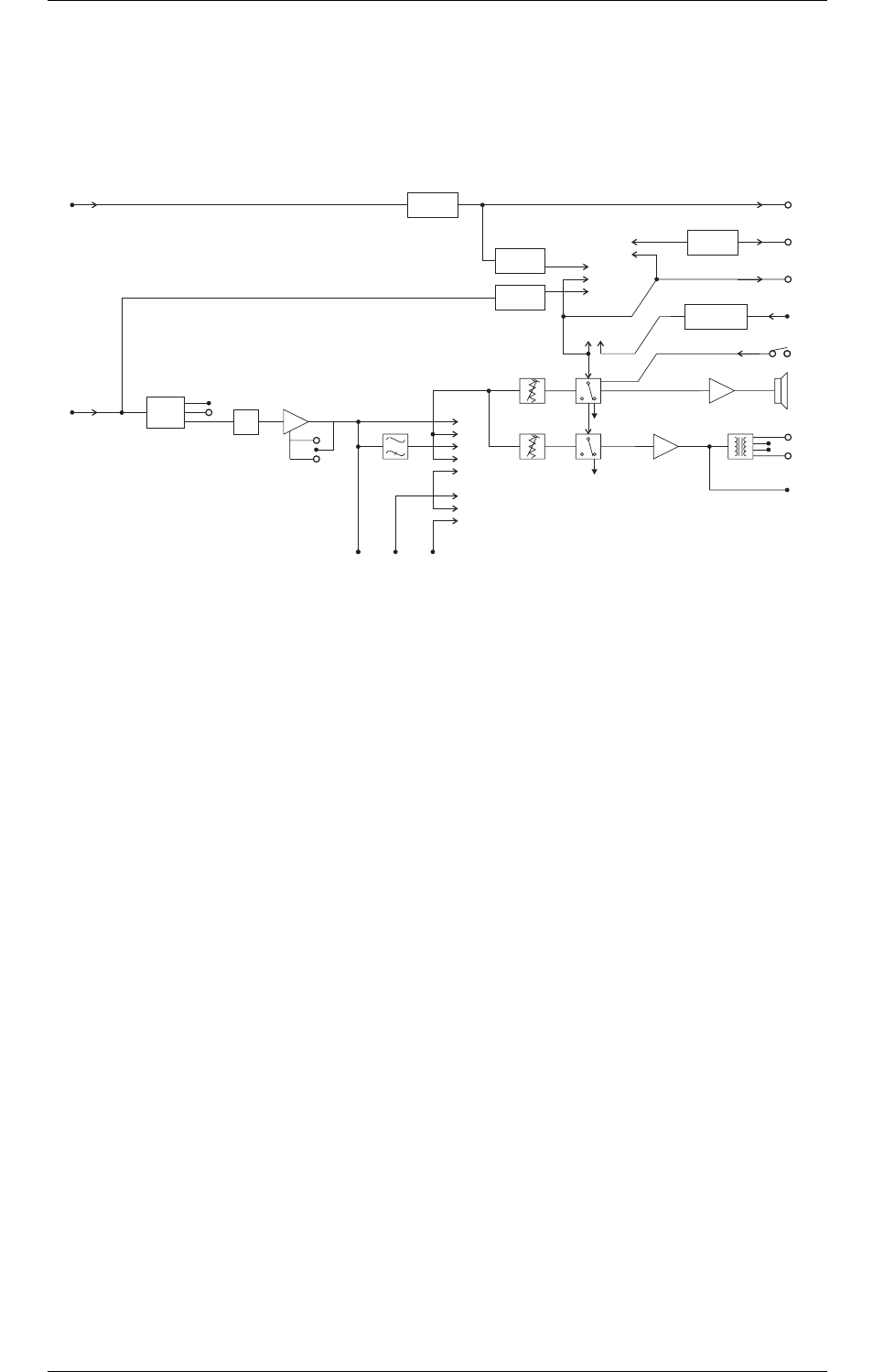
2.7 Audio Processor
(Refer to the audio processor circuit diagram (sheet 2) in Section 6.3.)
Figure 2.3 T855 Audio Processor Block Diagram
The recovered audio on pin 9 of IC310 is passed through a compensation network and
processed in a third order elliptic active filter to give the required response. Linking
(PL220 and PL210) is available to give either a flat or de-emphasised audio response,
with de-emphasis giving a –6dB/octave roll off. The output of IC210 is split to provide
separate paths for the speaker and line outputs. The “Audio 1”, Audio 2” and “Speech”
lines allow access to the receiver’s audio path for external signalling purposes (refer to
Section 3.5).
The signals are passed to audio drive amplifiers IC240 and IC260. Under muted condi-
tions the inputs of these amplifiers are shunted to ground via transistors Q230 and Q290
respectively. The audio output of IC240 has a DC component which is removed by C249,
and this then drives a speaker directly. The output of IC260 is fed into a line transformer
to provide a balanced 2-wire or 4-wire, 600Ω output.
The speaker volume is set using the front panel “Monitor Volume” knob (RV205) and
the line level is set using the recessed “Line Level” potentiometer (RV210).
The red front panel “Gate” LED (D250) indicates the status of the mute circuit. When a
signal above the mute threshold is received, the LED is illuminated. The “Monitor”
switch (SW201) on the front panel opens the mute, allowing continuous monitoring of
the audio signal (on = audio unmuted; off = audio muted).
The mute control line is available on pad 234 ("RX GATE OUT") for control of external
circuitry. A high (9V) on pad 234 indicates that the audio is disabled and a low (0V) indi-
cates that a signal above the mute threshold level is being received.
From
IF Stage
Demodulated
Signal
(*IF Audio
Compensation
Circuit)
Driver Amp
Line Output
12V
Relay
Speech
Audio 1
Output
Audio 2
Input
High Pass
Filter
Speaker
Mute
Line
Mute
Carrier
Mute
RSSI
(Optional)
Rx Disable
Timer
Noise
Mute
PL260
PL250
PL270
RSSI Output
Mute Relay
Gate Output
Rx Disable
(Optional Pad)
Mute Disable
Speaker Output
Line Monitor
12
1
2
2
1
3
1
5
2
2
3
3
4
1
PL240
PL230
Driver Amp
Flat/De-
emphasis
LPF
PL210
2
3
Flat/De-
emphasis
Amplifier
PL220
1
2
3
*IF
Comp
Monitor
Volume
Line
Level

B2.8 T855 Circuit Operation M8SL2-00-002-812
© Copyright Tait Electronics Limited August 2004. All rights reserved.
The audio can also be disabled using the “RX-DISABLE” inputs, pads 225 or 228, having
connected the “RX-DISABLE” link between pins 1 and 2 of PL260. An adjustable time
delay (RV220) is provided on these lines. In order to disable the audio, either pad must
be pulled to 0V.
An undedicated relay is provided (RL210) for transmitter keying or other functions and
this can be operated from the mute line by linking PL270.
2.8 Power Supply And Regulators
(Refer to the regulators circuit diagram (sheet 6) in Section 6.3.)
Figure 2.4 T855 Power Supply And Regulators Block Diagram
The T855 is designed to operate off a 10.8 to 16VDC supply (13.8V nominal). A 5.3V reg-
ulator (IC630) runs directly from the 13.8V rail, driving much of the synthesiser cir-
cuitry. It is also used as the reference for a DC amplifier (IC640, Q630 and Q620) which
provides a medium current capability 9V supply.
A switching power supply, based on Q670 and Q660, runs off the 9V supply and pro-
vides a low current capability +20V supply. This is used to drive the synthesiser loop fil-
ter (IC740), giving a VCO control voltage of up to 20V.
The 13.8V supply drives both output audio amplifiers without additional regulation. A
separate 5V regulator (IC610) drives the microprocessor and associated digital circuitry.
The output of this regulator is monitored by the Low Voltage Interrupt (LVI) circuit
(IC650).
A crowbar diode is fitted for protection against connection to a power supply of incor-
rect polarity. It also provides transient overvoltage protection.
Note: A fuse must be fitted in the power supply line for the diode to provide effec-
tive protection.
LVI
LVI
5V
Reg
DC
Amp Switching
PS
5V Dig
Reg µP
Reset
13.8V
Nom.
5V 5V Dig9V 20V
13.8V Nom.
From Rear
D-Range 1
Crowbar
Diode

M8SL2-00-002-812 T855 Circuit Operation B2.9
© Copyright Tait Electronics Limited August 2004. All rights reserved.
2.9 Microcontroller
(Refer to the microcontroller circuit diagram (sheet 8) in Section 6.3.)
Figure 2.5 T855 Microcontroller Block Diagram
Overall system control of the T855 is accomplished by the use of a member of the 80C51
family of microcontrollers (IC810) which runs from internal ROM and RAM. Four ports
are available for input/output functions.
Non-volatile data storage is achieved by serial communication with a 16kBit EEPROM
(IC820). This serial bus is also used by the microcontroller to program the synthesiser
(IC740).
The main tasks of the microcontroller are as follows:
•program the synthesiser;
•interface with the PGM800Win programming software at 9600 baud via the
serial communication lines on D-range 1 (PL100) and D-range 2;
•monitor channel change inputs from D-range 2;
•generate timing waveforms for CTCSS detection;
•coordinate and implement timing control of the receiver;
•control the front panel “Supply” LED (refer to Section 5.3).
Channel
Select
Port
Auxiliary
Output
Port
Microcontroller
12.8MHz
Clock
Microcontroller Cavity
Audio In
Speech
External
Serial
Port
EEPROM Synthesiser
CTCSS
Decoder
Converter
5V Reset
5V Digital
Regulator
Watchdog Timer
& LVI
Watchdog

B2.10 T855 Circuit Operation M8SL2-00-002-812
© Copyright Tait Electronics Limited August 2004. All rights reserved.
2.10 Synthesised Local Oscillator
(Refer to the synthesiser circuit diagram (sheet 7) in Section 6.3 and the VCO circuit dia-
gram in Part E.)
Figure 2.6 T855 Synthesiser Block Diagram
The synthesiser (IC740) employs a phase-locked loop (PLL) to lock a voltage controlled
oscillator (VCO) to a given reference frequency. The synthesiser receives the divider
information from the control microprocessor via a 3-wire serial bus (clock, data, enable).
When the data has been latched in, the synthesiser processes the incoming signals from
the VCO buffer (fin) and the reference oscillator (fref).
A reference oscillator at 12.8MHz (IC700) is buffered (IC710) and divided down to
6.25kHz or 5kHz within the synthesiser IC (IC740).
A buffered output of the VCO is divided with a prescaler and programmable divider
which is incorporated into the synthesiser chip (IC740). This signal is compared with the
reference signal at the phase detector (also part of the synthesiser chip). The phase
detector outputs drive a balanced charge pump circuit (Q760, Q770, Q775, Q780, Q785)
and active loop filter (IC750, Q790) which produces a DC voltage between 0V and 20V
to tune the VCO. This VCO control line is further filtered to attenuate noise and other
spurious signals. Note that the VCO frequency increases with increasing control volt-
age.
12.8MHz
Reference
Oscillator
Serial
Bus
/R
Reference
Divider
Phase
Detector
Charge
Pump
Loop
Filter
VCO PCB
FREQUENCY SYNTHESISER IC
VCO Buffer
Output
Buffer
+22dBm
L.O.
Clk
Data
En Controller
Buffer
fin
fref
/N
Programmable
Divider
64/65
Prescaler

M8SL2-00-002-812 T855 Circuit Operation B2.11
© Copyright Tait Electronics Limited August 2004. All rights reserved.
2.11 VCO
(Refer to the VCO circuit diagram in Part E.)
The VCO transistor (Q1) operates in a common emitter, and uses a transmission line res-
onator (TL1). The transmission line is used in a two port configuration with varicaps
positioned at one end. The VCO control voltage from the loop filter (IC750) is applied to
the varicaps (D1 and D2) to facilitate tuning. The VCO output is coupled into a cascode
amplifier stage (Q2 and Q3) which supplies +10dBm (nominal) output. Further amplifi-
cation in Q5 brings the output drive level to +20dBm to drive the mixer.
A low level “sniff” is taken from the input to Q5 to drive the divider buffer to the syn-
thesiser (IC740).
The VCO operates at the actual frequency required by the first mixer, i.e. there are no
multiplier stages.
The VCO frequency spans from 355 to 395MHz, 395 to 435MHz or 435 to 485MHz
according to product type. The VCO is tuned to 45MHz below the desired receive fre-
quency (low side injection) to produce a 45MHz IF signal at the output of the mixer.
B2.12 T855 Circuit Operation M8SL2-00-002-812
© Copyright Tait Electronics Limited August 2004. All rights reserved.
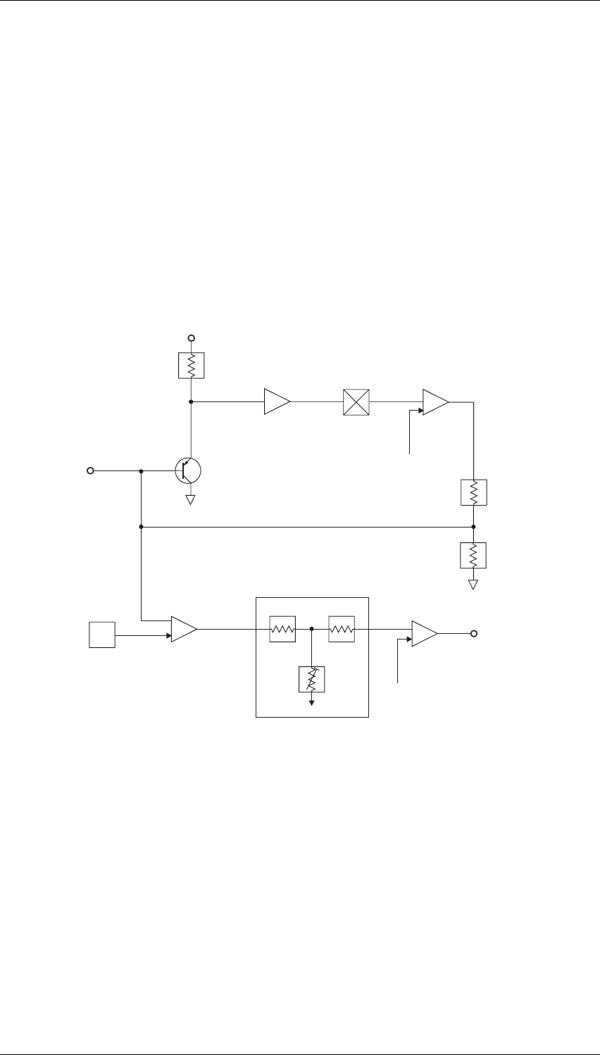
2.12 Received Signal Strength Indicator (RSSI)
(Refer to the T800-04-0000 RSSI PCB circuit diagram in Section 6.2 and the IF section cir-
cuit diagram (sheet 3) in Section 6.3.)
The RSSI option PCB plugs directly into the main PCB (support circuitry being fitted as
standard). It is fitted to the T855 whenever receiver signal strength monitoring is
required, e.g. trunking or voting. Its function is to provide a DC voltage proportional to
the signal level at the receiver input. The DC voltage is available at D-range 1 (PL100
pin 5).
The RSSI also provides the capability for high level signal strength muting, which may
be selected on PL250 (refer to Section 3.5). The mute threshold may be set between
–115dBm and –70dBm by RV235.
Figure 2.7 T855 RSSI Block Diagram (T800-04-0000 RSSI PCB)
The variable gain stage (Q1A) is a common emitter amplifier with its emitter grounded
and the AGC control loop voltage applied to its base. Since the AGC loop will maintain
a constant signal level at the collector, the gain of Q1 must be proportional to the incom-
ing 455kHz signal level. The gain of Q1 is linearly proportional to its collector current
which itself is exponentially related to the base-emitter voltage. Thus there is a logarith-
mic relationship between the base-emitter voltage and the gain. The circuit therefore
produces a feedback voltage, and an output voltage, logarithmically related to the RF
input signal.
The AGC loop is followed by a DC amplifier which provides level shifting, temperature
compensation and gain to give a nominal 1V/10dB at the RSSI output. RV320 on the
main PCB is used to set the RSSI voltage to a fixed value at a given RF input signal
strength.
+V
Amp Detector Error Amp
Q1C Q1A &
Q1B
VDC
Variable
Gain Stage
Q1E
RSSI
Input
Temp Comp
NTC
DC Amp
(Gain= x33)
Temp
Comp
Q1D
DC Offset
(Ref)
RSSI Output
1V/10dB

M8SL2-00-002-812 T855 Initial Tuning and Adjustment B3.1
© Copyright Tait Electronics Limited August 2004. All rights reserved.
3 T855 Initial Tuning and Adjustment
Caution: This equipment contains CMOS devices which are susceptible to dam-
age from static charges. Refer to Section 1.2 in Part A for more informa-
tion on anti-static procedures when handling these devices.
The following section describes both short and full tuning and adjustment procedures
and provides information on:
•channel programming
•selecting the required audio links
•synthesiser alignment
•receiver front end and IF alignment
•noise and carrier level mute adjustment
•setting the line and monitor output levels
•setting up the RSSI.
Note: Unless otherwise specified, the term “PGM800Win” used in this and follow-
ing sections refers to version 4.02 and later of the software.
Refer to Figure 4.3 which shows the location of the main tuning and adjustment con-
trols. Refer also to Section 6 where the parts lists, grid reference index and diagrams will
provide detailed information on identifying and locating components and test points on
the main PCB. The parts list and diagrams for the VCO PCB are in Part E.
Section Title Page
3.1 Introduction 3.3
3.2 Channel Programming 3.3
3.3 Test Equipment Required 3.4
3.4
3.4.1
3.4.2
3.4.3
3.4.4
3.4.4.1
3.4.4.2
3.4.5
3.4.6
3.4.6.1
3.4.6.2
3.4.6.3
3.4.7
Short Tuning Procedure
Introduction
Synthesiser Alignment
Front End Alignment
Mute Adjustment
Noise Mute
Carrier Level Mute
Line Amplifier Output
CTCSS
Decoder Operation
Opening Sinad
High Pass Filter
RSSI (If Fitted)
3.5
3.5
3.5
3.5
3.6
3.6
3.6
3.6
3.7
3.7
3.7
3.7
3.8

B3.2 T855 Initial Tuning and Adjustment M8SL2-00-002-812
© Copyright Tait Electronics Limited August 2004. All rights reserved.
3.5
3.5.1
3.5.2
Audio Processor Links
General
Audio Processor Linking Details For CTCSS
3.8
3.8
3.9
3.6 Synthesiser Alignment 3.10
3.7 Alignment Of Receiver Front End And IF 3.10
3.8 Gating Delay 3.12
3.9 Noise Mute Adjustment 3.12
3.10 Carrier Level Mute 3.12
3.11
3.11.1
3.11.2
Audio Processor
Line Amplifier Output
Monitor Amplifier Output (Speaker Output)
3.13
3.13
3.13
3.12
3.12.1
3.12.2
3.12.3
CTCSS
Decoder Operation
Opening Sinad
High Pass Filter
3.13
3.13
3.13
3.14
3.13 RSSI 3.14
Figure Title Page
3.1
3.2
T855 Test Equipment Set-up For Short Tuning Procedure
T855 Test Equipment Set-up For Full Tuning and Adjustment
Procedure
3.4
3.4
Section Title Page

M8SL2-00-002-812 T855 Initial Tuning and Adjustment B3.3
© Copyright Tait Electronics Limited August 2004. All rights reserved.
3.1 Introduction
When you receive your T855 receiver it will be run up and working on a particular fre-
quency (the “default channel")1. If you want to switch to a frequency that is within the
5MHz switching range (i.e. ±2.5MHz from the factory programmed frequency), you
should only need to reprogram the receiver with the PGM800Win software (refer to the
PGM800Win programming kit and Section 3.2 below).
However, if you want to switch to a frequency outside the 5MHz switching range, you
will have to reprogram and re-tune the receiver to ensure correct operation. In this case
you should carry out the short tuning procedure described in Section 3.4.
If you have carried out repairs or other major adjustments, you must carry out the full
tuning and adjustment procedure described in this section (except for Section 3.4).
3.2 Channel Programming
You can program up to 128 channel frequencies into the receiver’s EEPROM memory
(IC820) by using the PGM800Win software package and a PC. You can also use
PGM800Win to select the receiver’s current operating frequency (or “default channel").
You can program the receiver via the programming port in the front panel. However,
you can also program the receiver before it is installed in a rack frame as follows:
•by using a T800-01-0010 calibration test unit;
•via D-range 1;
•via D-range 2 (standard T800-03-0000 auxiliary D-range only);
•via SK805 (internal Micromatch connector).
If you do not use the T800-01-0010, you will have to connect the PC to the receiver via a
module programming interface (such as the T800-01-0004).
For a full description of the channel programming procedure, refer to the PGM800Win
programming software user’s manual.
Note: When an auxiliary D-range kit (D-range 2 – T800-03-0000) is fitted, you can
also select a channel with an external switch, such as the DIP switch on a
backplane PCB. Consult your nearest Tait Dealer or Customer Service
Organisation for further details.
1. Use the “Read Module” function in PGM800Win to find out what the default channel
is.
B3.4 T855 Initial Tuning and Adjustment M8SL2-00-002-812
© Copyright Tait Electronics Limited August 2004. All rights reserved.
3.3 Test Equipment Required
You will need the following test equipment:
•computer with PGM800Win installed
•T800 programming kit
•module programming interface (e.g. T800-01-0004 – optional)
•13.8V power supply
•digital multimeter
•audio signal generator
•RF signal generator
•audio voltmeter
•sinad meter
•oscilloscope
•distortion meter
•T800-01-0010 calibration test unit (optional)
•4Ω speaker (not needed if the calibration test unit is used)
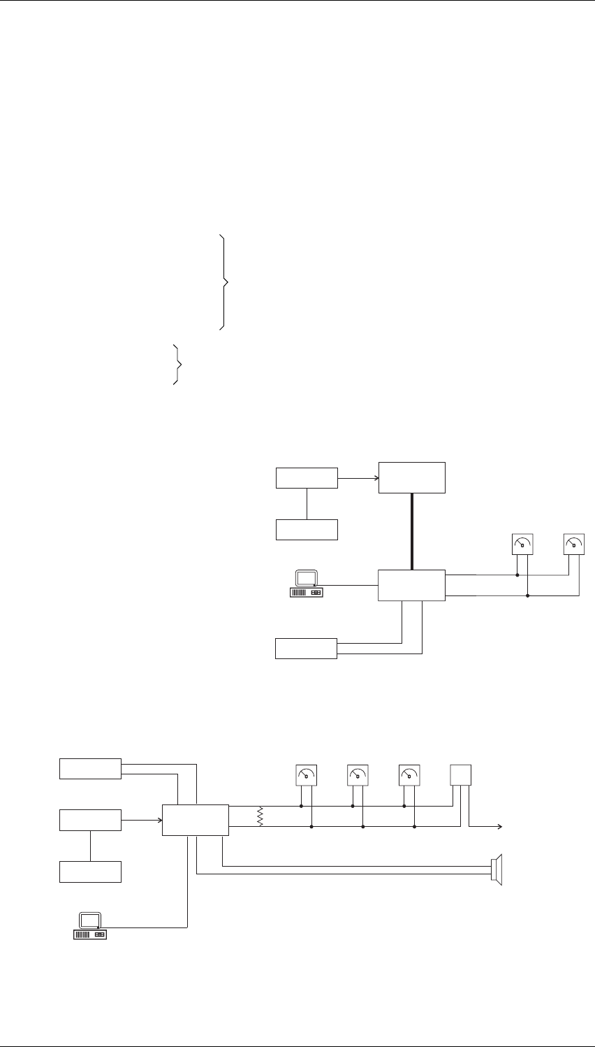
Figure 3.1 T855 Test Equipment Set-up For Short Tuning Procedure
Figure 3.2 T855 Test Equipment Set-up For Full Tuning and Adjustment Procedure
or RF test set (optional)
not needed for short tuning procedure
Receiver
RF In
RF Signal
Generator
Audio Signal
Generator
PSU
+13.8V
-Ve
External
Modulation Sinad
Meter
Audio
Voltmeter
Line
Line
T800
Calibration
Test Unit
PGM800Win
Figure 3.1 and Figure 3.2 show
typical test equipment set-ups
(with and without a T800-01-0010
calibration test unit).
Receiver
RF In
RF Signal
Generator
Audio Signal
Generator
PSU
+13.8V
-Ve
External
Modulation GND
Distortion
Meter
Sinad
Meter
Audio
Voltmeter Oscilloscope
Line
Line 600Ω
Speaker
Output
Probe
4ΩSpeaker
(Or 4ΩResistor)
CH1
CH2
GND
PGM800Win
Serial
Com
via module programming interface
(e.g. T800-01-0004)

M8SL2-00-002-812 T855 Initial Tuning and Adjustment B3.5
© Copyright Tait Electronics Limited August 2004. All rights reserved.
3.4 Short Tuning Procedure
Use this procedure only if you want to reprogram the receiver to a frequency outside the
5MHz switching range and do not intend to carry out any other major adjustments or
repairs.
3.4.1 Introduction
Reprogram the operating frequency as described in the PGM800Win program-
ming kit (refer to Section 3.2).
Remove the top cover.
Set up the test equipment as described in Section 3.3.
Set the links in the audio processor section as required (refer to Section 3.5).
3.4.2 Synthesiser Alignment
•Connect a high impedance voltmeter to the long lead of L1 in the VCO (this meas-
ures the synthesiser loop voltage).
•Single Channel Tune VCO trimmer C6 for a synthesiser loop voltage of
10V.
Multichannel Tune VCO trimmer C6 for a synthesiser loop voltage of
10V on the middle channel.
If there is no middle channel, tune C6 so that the channels
are symmetrically placed around a loop voltage of 10V.
All channels should lie within the upper and lower limits
of 16V and 3V respectively.
Do not attempt to program channels with a greater fre-
quency separation than the specified switching range of
5MHz.
3.4.3 Front End Alignment
Note 1: In this and following sections deviation settings are given first for wide
bandwidth sets, followed by settings in brackets for mid bandwidth sets ( )
and narrow bandwidth sets [ ].
Note 2: For multichannel operation align the receiver on a frequency in the middle
of the required band.
Set RV230 (front panel gating sensitivity) fully clockwise.
Inject a strong on-channel RF signal with ±3kHz deviation (±2.4kHz) [±1.5kHz] at

B3.6 T855 Initial Tuning and Adjustment M8SL2-00-002-812
© Copyright Tait Electronics Limited August 2004. All rights reserved.
1kHz into the antenna socket and adjust the helical resonators #FL410 and #FL420
to give best sinad.
Continually decrease the RF level to maintain 12dB sinad.
Readjust FL410 and FL420 to give best sinad.
With PL210 and PL220 connected for de-emphasised audio response, the receiver
sensitivity should be better than –117dBm, assuming that the audio levels are not
being overdriven (refer to Section 3.4.5).
3.4.4 Mute Adjustment
3.4.4.1 Noise Mute
Connect pins 1 and 2 of PL250 to enable the noise mute.
Set the RF level to –105dBm with ±3kHz deviation (±2.4kHz) [±1.5kHz] at 1kHz.
Set RV230 (front panel gating sensitivity) fully anticlockwise.
Adjust RV310 (noise mute gain) fully clockwise to close the mute (if necessary
turn off the RF signal and then turn it on again).
Rotate RV310 anticlockwise until the mute just opens.
Reset the signal generator for the required opening sinad and adjust RV230 clock-
wise until the mute just opens.
3.4.4.2 Carrier Level Mute
Connect pins 2 and 3 of PL250 to enable the carrier mute and disable the noise
mute.
Apply an on-channel signal from the RF generator at the required mute opening
level with ±3kHz deviation (±2.4kHz) [±1.5kHz] at ±1kHz.
Adjust RV235 (carrier mute) anticlockwise to close the mute (if necessary, momen-
tarily turn off the RF), then slowly adjust it clockwise until the mute just opens.
The mute should now open at this preset level.
3.4.5 Line Amplifier Output
Apply an on-channel signal from the RF generator at a level of –70dBm with
±3kHz deviation (±2.4kHz) [±1.5kHz] at 1kHz.
Adjust RV210 (front panel line level) to set the line level to the required output
level.

M8SL2-00-002-812 T855 Initial Tuning and Adjustment B3.7
© Copyright Tait Electronics Limited August 2004. All rights reserved.
3.4.6 CTCSS
3.4.6.1 Decoder Operation
Program a CTCSS tone on the default channel using PGM800Win.
Set the RF signal generator output to –70dBm.
Modulate the generator with both:
•a 1kHz tone at ±3kHz deviation (±2.4kHz) [±1.5kHz]
•and a CTCSS tone at the programmed frequency at ±500Hz deviation (±400Hz)
[±300Hz].
Check that the receiver gate opens and the front panel “Gate” LED is on.
3.4.6.2 Opening Sinad
Adjust RV230 (front panel gating sensitivity) fully clockwise.
Reduce the RF signal level to –110dBm.
Observe the sinad meter and reduce the RF level until the receiver mute closes.
Slowly increase the signal level until the receiver mute just opens and stays open.
With PL240 pins 1 and 2 linked (G–H; high pass filter bypassed), check that the
sinad is less than 6dB.
Reset the signal generator for the required opening sinad, adjust RV230 fully anti-
clockwise, then clockwise until the mute just opens.
3.4.6.3 High Pass Filter
Set the audio processor links as follows:
Reset the RF signal generator output to –70dBm and note the line level (measure-
ment A).
Reduce the 1kHz generator to zero output and measure the line level again (meas-
urement B).
Check that measurement B is at least 30dB below measurement A.
Plug Link Function
PL210 1 – 2A – B de-emphasised response
PL230 2 – 3N – P audio from internal CTCSS speech filter
PL240 4 – 5K – L audio input via PL230 or I/O pad

B3.8 T855 Initial Tuning and Adjustment M8SL2-00-002-812
© Copyright Tait Electronics Limited August 2004. All rights reserved.
3.4.7 RSSI (If Fitted)
The T800-04-0000 RSSI is an optional PCB which adds signal strength monitoring and
high level mute facilities to the basic receiver.
Ensure the T800-04-0000 PCB is fitted in SK320 and SK330 in the IF compartment.
Apply an on-channel signal from the RF generator at a level of –110dBm with
±3kHz deviation (±2.4kHz) [±1.5kHz] at 1kHz.
Adjust RV320 (RSSI level) to give 2.0V RSSI output on pin 5 of D-range 1 (PL100)
when measured with a high impedance DMM.
3.5 Audio Processor Links
3.5.1 General
Use the following table to set up the audio processor to the configuration you require.
You should set the audio processor links before carrying out the receiver alignment. The
factory settings are shown in brackets [ ].
Plug Linka
a. The letters in this column and in the table in Section 3.5.2 below refer to the identification
letters screen printed onto the PCB beside each set of pins.
Function
PL210 [1 – 2]
2 – 3
[A – B]
B – C
de-emphasised response
flat response
PL220 1 – 2
[2 – 3]
D – E
[E – F]
flat response
de-emphasised response
PL230b
b. Refer to Section 3.5.2 for further details.
1 – 2
[2 – 3]
3 – 4
M – N
[N – P]
P – Q
audio input via AUDIO-2 pad
audio from internal CTCSS speech filter
audio input via I/O pad P250
PL240b
1 – 2
[2 – 3]
or
3 – 4
4 – 5
G – H
[H – J]
or
J – K
K – L
bypass high pass filter
300Hz high pass filter in circuit
audio input via PL230 or I/O pad
PL250 [1 – 2]
2 – 3
[R – S]
S – T
noise mute
carrier mute
PL260 1 – 2
[2 – 3]
U – V
[V – W]
RX-DISABLE link
not connected
PL270 [1 – 2]
2 – 3
[X – Y]
Y – Z
relay link
not connected

M8SL2-00-002-812 T855 Initial Tuning and Adjustment B3.9
© Copyright Tait Electronics Limited August 2004. All rights reserved.
3.5.2 Audio Processor Linking Details For CTCSS
You must connect the audio processor links correctly according to the CTCSS option
used, as shown in the table below.
The conditions stated in the above table are defined as follows:
•standard, no CTCSS –no CTCSS or other sub-audio signalling used
–audio bandwidth 300Hz to 3kHz
–hum and noise –55dB
•received CTCSS tone –tone and speech transmitted down 600Ω line
+ speech to line output –audio bandwidth 10Hz to 3kHz
–hum and noise –45dB
•high pass filtered speech –400Hz to 3kHz
+ internal CTCSS detection –hum and noise –30dB with 250.3Hz tone present
•external CTCSS detection –decoding performed through the receiver (but
externally)
–speech injected back into receiver via “AUDIO-2"
and sent down 600Ω line
Note 1: AUDIO-2 is available on D-range 1 (PL100) pin 7 via the link resistor R160.
Although PL100 pin 7 is already assigned to SERIAL-COM, this can be disa-
bled by removing R808.
Note 2: External CTCSS units can connect in series with the audio chain via
AUDIO-1 and AUDIO-2.
CTCSS Option PL230 PL240
standard, no CTCSS 2 – 3N – P2 – 3H – J
received CTCSS + speech
passed to line output 3 – 4P – Q1 – 2G – H
high pass filtered speech,
internal CTCSS detection 2 – 3N – P4 – 5K – L
external CTCSS detection 1 – 2M – N4 – 5K – L

B3.10 T855 Initial Tuning and Adjustment M8SL2-00-002-812
© Copyright Tait Electronics Limited August 2004. All rights reserved.
3.6 Synthesiser Alignment
•Ensure that the receiver has been programmed with the required frequencies
using the PGM800Win software.
•Connect a high impedance voltmeter to the long lead of L1 in the VCO (this meas-
ures the synthesiser loop voltage).
•Single Channel Tune VCO trimmer C6 for a synthesiser loop voltage of
10V.
Multichannel Tune VCO trimmer C6 for a synthesiser loop voltage of
10V on the middle channel.
If there is no middle channel, tune C6 so that the channels
are symmetrically placed around a loop voltage of 10V.
All channels should lie within the upper and lower limits
of 16V and 3V respectively.
Do not attempt to programme channels with a greater fre-
quency separation than the specified switching range of
5MHz.
•The TCXO =(IC700) output frequency should be trimmed when the IF is tuned.
Refer to Section 3.7.
3.7 Alignment Of Receiver Front End And IF
Note: In this and following sections deviation settings are given first for wide
bandwidth sets, followed by settings in brackets for mid bandwidth sets ( )
and narrow bandwidth sets [ ].
Align the synthesiser as instructed in Section 3.6. For multichannel operation align
the receiver on a frequency in the middle of the required band.
Set RV230 (front panel gating sensitivity) fully clockwise.
Inject a strong on-channel RF signal with ±3kHz deviation (±2.4kHz) [±1.5kHz] at
1kHz into the antenna socket and adjust the helicals (#FL410 and #FL420) to give
the best sinad.
Continually decrease the RF level to maintain 12dB sinad.
Roughly tune IF coils L310, L320, L330, L340, L350, L360, L370, L380, L385 and
L390 for best sinad.
While maintaining a low level unmodulated RF input to the receiver, loosely cou-
ple into the first IF an additional high level signal at 45MHz, you will hear a beat
note.
Trim the synthesiser TCXO (=IC710) for zero beat.

M8SL2-00-002-812 T855 Initial Tuning and Adjustment B3.11
© Copyright Tait Electronics Limited August 2004. All rights reserved.
While maintaining the low level RF input to the receiver, loosely couple into the
second IF an additional high level signal at 455kHz, you will hear a beat note.
Tune L385 for zero beat.
Note: If a second oscillator is not available, you can connect a frequency counter to
IC710 pin 8 (i.e. after the TCXO buffer) via an oscilloscope probe to measure
the TCXO frequency directly (12.8MHz). At this point the voltage level is
approximately 4Vpp.
Readjust the front end helicals (#FL410 and #FL420) to give the best sinad.
Change the RF signal level to –75dBm and modulate with ±3kHz deviation
(±2.4kHz) [±1.5kHz] at 1kHz.
Connect an oscilloscope probe to SK320 pin 3 (RSSI 455kHz input) and connect
plugs PL210 and PL220 to give a flat audio response (refer to Section 3.5).
Readjust L310, L320, L330, L340, L350, L360, L370 and L380 to give a maximum
amplitude response on the oscilloscope with minimal amplitude modulation.
Note: If you would like a more accurate method of tuning the IF, refer to the
sweep tuning method described in Section 5.5.5.
Further adjust these coils, along with L390, for minimum audio distortion, ensur-
ing that the 455kHz level (on the oscilloscope) does not fall significantly.
Check that the distortion reading is:
wide bandwidth ≤2%
mid and narrow bandwidth ≤4%.
If required, reconnect plugs PL210 and PL220 to give a de-emphasised audio
response and check that the distortion reading is ≤2% (all bandwidths).
Reduce the RF level until 12dB sinad is reached. The receiver sensitivity should be
better than –117dBm (de-emphasised) or –111dBm (flat), assuming that the audio
levels are not being overdriven (refer to Section 3.11).

B3.12 T855 Initial Tuning and Adjustment M8SL2-00-002-812
© Copyright Tait Electronics Limited August 2004. All rights reserved.
3.8 Gating Delay
Two solder links (SL210 and SL220) are provided on the bottom of the PCB to allow
three gate delay time options, as shown in the table below.
*Factory setting.
3.9 Noise Mute Adjustment
Connect pins 1 and 2 of PL250 to enable the noise mute.
Align the receiver as instructed in Section 3.6 and Section 3.7.
Set the RF level to –105dBm with ±3kHz deviation (±2.4kHz) [±1.5kHz] at 1kHz.
Set RV230 (front panel gating sensitivity) fully anticlockwise.
Adjust RV310 (noise mute gain) fully clockwise to close the mute (if necessary
turn off the RF signal and then turn it on again).
Rotate RV310 anticlockwise until the mute just opens.
Reset the signal generator for the required opening sinad and adjust RV230 clock-
wise until the mute just opens.
3.10 Carrier Level Mute
Connect pins 2 and 3 of PL250 to enable the carrier mute and disable the noise
mute.
Apply an on-channel signal from the RF generator at the required mute opening
level with ±3kHz deviation (±2.4kHz) [±1.5kHz] at ±1kHz.
Adjust RV235 (carrier mute) anticlockwise to close the mute (if necessary, momen-
tarily turn off the RF), then slowly adjust it clockwise until the mute just opens.
The mute should now open at this preset level.
SL210 SL220 Closing Delay
linked not linked <50ms*
not linked linked <25ms
not linked not linked <20ms

M8SL2-00-002-812 T855 Initial Tuning and Adjustment B3.13
© Copyright Tait Electronics Limited August 2004. All rights reserved.
3.11 Audio Processor
3.11.1 Line Amplifier Output
Apply an on-channel signal from the RF generator at a level of –70dBm with
±3kHz deviation (±2.4kHz) [±1.5kHz] at 1kHz.
Adjust RV210 (front panel line level) to give an output of +10dBm on the 600Ω
line.
Check for any clipping or distortion on the oscilloscope.
Set the line level to the required output level.
3.11.2 Monitor Amplifier Output (Speaker Output)
Adjust RV205 (front panel monitor volume) to give an output of 2Vrms into a 4Ω
resistive load.
Check for any clipping or distortion on the oscilloscope.
Switch to a 4Ω speaker and adjust RV205 to the required level.
3.12 CTCSS
3.12.1 Decoder Operation
Program a CTCSS tone on the default channel using PGM800Win.
Set the RF signal generator output to –70dBm.
Modulate the generator with both:
•a 1kHz tone at ±3kHz deviation (±2.4kHz) [±1.5kHz]
•and a CTCSS tone at the programmed frequency at ±500Hz deviation (±400Hz)
[±300Hz].
Check that the receiver gate opens and the front panel “Gate” LED is on.
3.12.2 Opening Sinad
Adjust RV230 (front panel gating sensitivity) fully clockwise.
Reduce the RF signal level to –110dBm.

B3.14 T855 Initial Tuning and Adjustment M8SL2-00-002-812
© Copyright Tait Electronics Limited August 2004. All rights reserved.
Observe the sinad meter and reduce the RF level until the receiver mute closes.
Slowly increase the signal level until the receiver mute just opens and stays open.
With PL240 pins 1 and 2 linked (G – H; high pass filter bypassed), check that the
sinad is less than 6dB.
Reset the signal generator for the required opening sinad, adjust RV230 fully anti-
clockwise, then clockwise until the mute just opens.
3.12.3 High Pass Filter
Set the audio processor links as follows:
Reset the RF signal generator output to –70dBm and note the line level (measure-
ment A).
Reduce the 1kHz generator to zero output and measure the line level again (meas-
urement B).
Check that measurement B is at least 30dB below measurement A.
3.13 RSSI
The T800-04-0000 RSSI is an optional PCB which adds signal strength monitoring and
high level mute facilities to the basic receiver.
Ensure the T800-04-0000 PCB is fitted in SK320 and SK330 in the IF compartment.
Align the receiver as instructed in Section 3.6 and Section 3.7.
Apply an on-channel signal from the RF generator at a level of –110dBm with
±3kHz deviation (±2.4kHz) [±1.5kHz] at 1kHz.
Adjust RV320 (RSSI level) to give 2.0V RSSI output on pin 5 of D-range 1 (PL100)
when measured with a high impedance DMM.
Plug Link Function
PL210 1 – 2A – B de-emphasised response
PL230 2 – 3N – P audio from internal CTCSS speech filter
PL240 4 – 5K – L audio input via PL230 or I/O pad
M8SL2-00-002-812 T855 Functional Testing B4.1
© Copyright Tait Electronics Limited August 2004. All rights reserved.
4 T855 Functional Testing
Caution: This equipment contains CMOS devices which are susceptible to dam-
age from static charges. Refer to Section 1.2 in Part A for more informa-
tion on anti-static procedures when handling these devices.
The following test procedures will confirm that the T855 has been tuned and adjusted
correctly and is fully operational.
Note 1: In this and following sections deviation settings are given first for wide
bandwidth sets, followed by settings in brackets for mid bandwidth sets ( )
and narrow bandwidth sets [ ].
Note 2: Unless otherwise specified, the term “PGM800Win” used in this and follow-
ing sections refers to version 4.02 and later of the software.
Refer to Figure 4.3 for the location of the main tuning and adjustment controls, and to
Section 3.3 for the test equipment set-up. Refer also to Section 6 where the parts lists,
grid reference index and diagrams will provide detailed information on identifying and
locating components and test points on the main PCB. The parts list and diagrams for
the VCO PCB are in Part E.
The following topics are covered in this section.
Section Title Page
4.1 Current Consumption 4.3
4.2 Sensitivity 4.3
4.3 Switching Range 4.3
4.4 Audio Distortion 4.4
4.5 Ultimate Signal-To-Noise Ratio 4.4
4.6 De-emphasised Audio Frequency Response 4.5
4.7 Noise Mute (If Linked In) 4.6
4.8 RSSI (If Fitted) 4.6
4.9 Carrier Level Mute (RSSI Fitted and Carrier Mute Linked
In)
4.7
Figure Title Page
4.1
4.2
4.3
T855 De-emphasised Audio Frequency Response
T855 RSSI Voltage vs Signal Strength
T855 Main Tuning and Adjustment Controls
4.5
4.6
4.9

B4.2 T855 Functional Testing M8SL2-00-002-812
© Copyright Tait Electronics Limited August 2004. All rights reserved.

M8SL2-00-002-812 T855 Functional Testing B4.3
© Copyright Tait Electronics Limited August 2004. All rights reserved.
4.1 Current Consumption
Connect the T855 to a 13.8V power supply.
Rotate RV230 (front panel gating sensitivity) anticlockwise until the “Gate” LED is
extinguished.
Set switch SW201 (front panel monitor mute) to the on position.
Check that the current in the 13.8V power cable is less than 350mA.
Rotate the RV230 clockwise until the “Gate” LED is lit.
Rotate RV210 (front panel line level) and RV205 (front panel monitor volume) to
give maximum outputs.
Check that the current is less than 800mA.
Reset the front panel controls to the required settings.
4.2 Sensitivity
If CTCSS is enabled, disable the CTCSS tone by either programming the T855 for
“No Tone” on the set channel, or by pulling pin 10 of D-range 2 (CTCSS ENABLE)
low.
Apply an on-channel signal from the RF generator with ±3kHz deviation
(±2.4kHz) [±1.5kHz] at 1kHz.
Adjust the RF level to give 12dB audio sinad.
Check that the sensitivity is –117dBm or better.
4.3 Switching Range
Apply an on-channel signal from the RF generator at various frequencies within
the 5MHz switching range (front end bandwidth), corresponding to pre-pro-
grammed channels.
Measure the sensitivity at each frequency as described in Section 4.2.
Ensure that the sensitivity is –115dBm or better across the whole switching range.

B4.4 T855 Functional Testing M8SL2-00-002-812
© Copyright Tait Electronics Limited August 2004. All rights reserved.
4.4 Audio Distortion
The level of distortion measured at the line output (refer to Figure 1.3 in Part G) gives an
indication of the accuracy of the IF alignment.
Apply an accurate on-channel signal from the RF generator at a level of –70dBm
with ±3kHz deviation (±2.4kHz) [±1.5kHz] at 1kHz.
Adjust RV210 (front panel line level) to give +10dBm into 600Ω.
Check that the distortion is approximately 1% THD.
Note: For a flat response, the distortion should always be better than 2% for wide
bandwidth sets or 4% for mid and narrow bandwidth sets.
Adjust RV205 (front panel monitor volume) to give 2Vrms into a 4Ω resistive load.
Check that the distortion at the monitor output is better than 2% THD.
Reset the controls before proceeding to the next set of tests.
4.5 Ultimate Signal-To-Noise Ratio
Apply a signal from the RF generator at a level of –57dBm with ±3kHz deviation
(±2.4kHz) [±1.5kHz] at 1kHz.
Select de-emphasis on the links provided in the audio processor (refer to Section
3.5), and link pins 2 and 3 of PL240 to include the 300Hz filter.
Adjust RV210 (front panel line level) to provide +10dBm output.
Switch off the modulation, checking that the residual noise is lower than –45dBm
(–43dBm) [–39dBm] at the line output (this corresponds to S/N of 55dB (53dB)
[49dB] and is in accordance with EIA measurement conditions).
Note: You can make the measurement without the 300Hz high pass filter, but the
result will be 10dB worse.
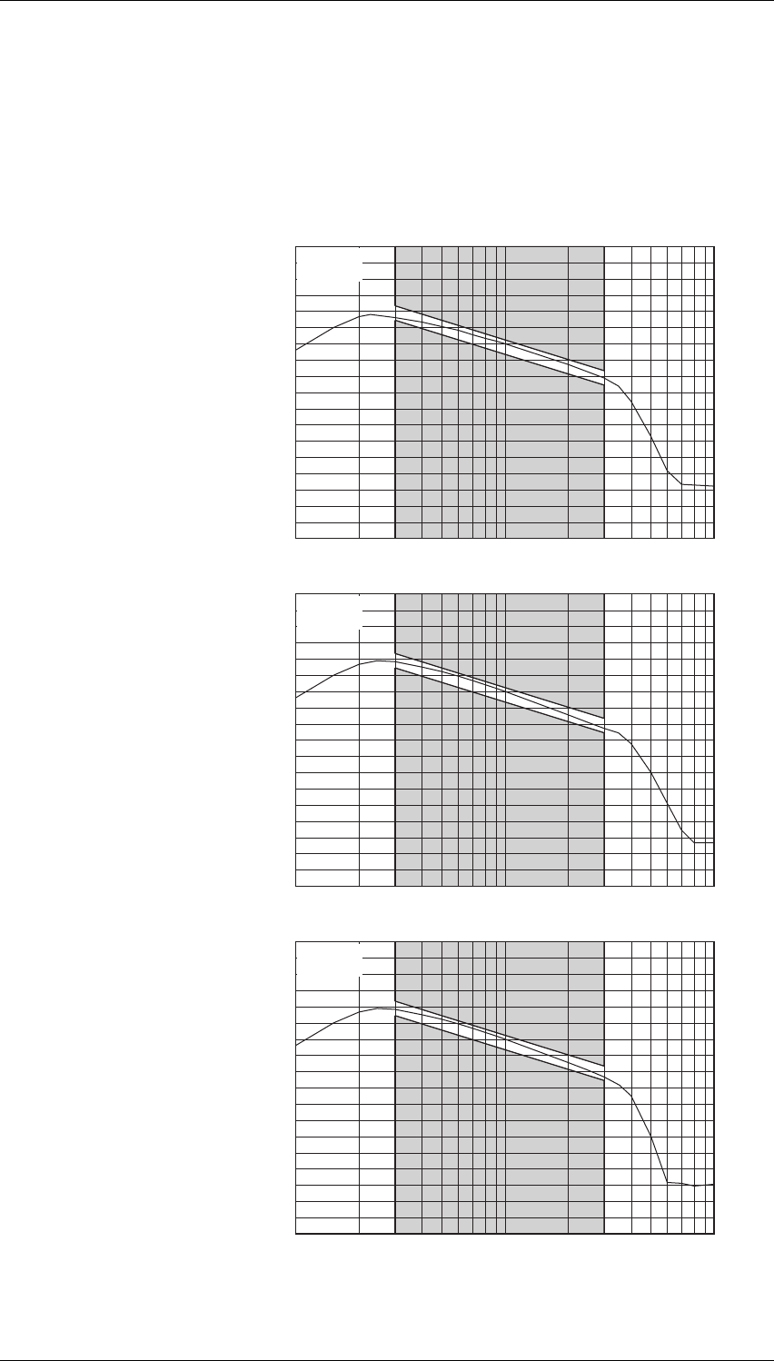
M8SL2-00-002-812 T855 Functional Testing B4.5
© Copyright Tait Electronics Limited August 2004. All rights reserved.
4.6 De-emphasised Audio Frequency Response
Set RV210 (front panel line level) to provide 0dBm output at 1kHz modulating fre-
quency.
Sweep the modulating frequency, checking that the line audio response closely
follows that shown in Figure 4.1 – the limits should not be exceeded.
Figure 4.1 T855 De-emphasised Audio Frequency Response
Wide Bandwidth
Narrow Bandwidth
+25
+20
Audio Level (dB ref. to O/P @ 1kHz)
+15
+10
+5
+0
-5
-10
-15
-20
-25
-30
-35
-40
-45
-50
-55
100 200 300 500 1k 2k 3k 5k 10k
Frequency (Hz)
25°C 13.8V
Ref. audio power:
+0.0dBm @ 1kHz
+25
+20
Audio Level (dB ref. to O/P @ 1kHz)
+15
+10
+5
+0
-5
-10
-15
-20
-25
-30
-35
-40
-45
-50
-55
100 200 300 500 1k 2k 3k 5k 10k
Frequency (Hz)
25°C 13.8V
Ref. audio power:
-2.2dBm @ 1kHz
Mid Bandwidth
+25
+20
Audio Level (dB ref. to O/P @ 1kHz)
+15
+10
+5
+0
-5
-10
-15
-20
-25
-30
-35
-40
-45
-50
-55
100 200 300 500 1k 2k 3k 5k 10k
Frequency (Hz)
25°C 13.8V
Ref. audio power:
-2.5dBm @ 1kHz

B4.6 T855 Functional Testing M8SL2-00-002-812
© Copyright Tait Electronics Limited August 2004. All rights reserved.
4.7 Noise Mute (If Linked In)
Rotate RV230 (front panel gating sensitivity) fully anticlockwise.
Apply an on-channel signal from the RF generator at a level of –110dBm with
±3kHz deviation (±2.4kHz) [±1.5kHz] at 1kHz.
Increase the RF level in 1dB steps, checking that the mute opens for an RF input
level of approximately –105dBm.
Turn the RF off and check that the mute closes.
Rotate RV230 clockwise and check that the mute opens.
Reset RV230 to give the required opening sinad.
Caution: Some RF generators can cause a false opening of the mute because the
generator produces a burst of noise when the attenuation range
changes. To correct the problem you will have to change generators.
4.8 RSSI (If Fitted)
Apply an on-channel signal from the RF generator at a level of –110dBm with
±3kHz deviation (±2.4kHz) [±1.5kHz] at 1kHz.
Using a high impedance DMM, check that the RSSI output voltage on pin 5 of
D-range 1 (PL100) is 2V (nominal).
Vary the RF level in 5dB steps and check that the RSSI output voltage changes at a
rate of approximately 10dB/V over the range of –115dBm to –70dBm (refer to Fig-
ure 4.2 for RSSI voltage vs signal strength).
Figure 4.2 T855 RSSI Voltage vs Signal Strength
RF Level (dBm)
-130 -120 -110 -100 -90 -80 -70 -60
1
2
3
4
5
6
7
8
RSSI Voltage

M8SL2-00-002-812 T855 Functional Testing B4.7
© Copyright Tait Electronics Limited August 2004. All rights reserved.
4.9 Carrier Level Mute (RSSI Fitted and Carrier Mute
Linked In)
Apply an on-channel signal from the RF generator at a level of –120dBm with
±3kHz deviation (±2.4kHz) [±1.5kHz] at 1kHz.
Increase the RF level in 2dB steps and check that the mute opens at an RF level
which corresponds with the preset level on RV235 (carrier mute), i.e. between
–115dBm and –70dBm.
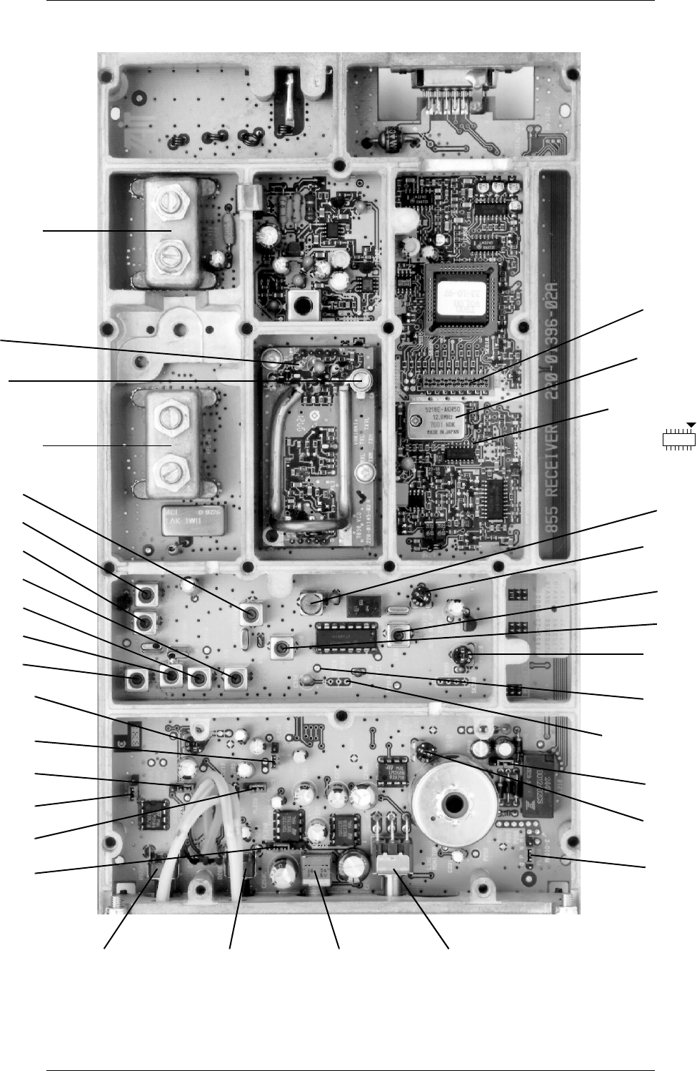
B4.8 T855 Functional Testing M8SL2-00-002-812
© Copyright Tait Electronics Limited August 2004. All rights reserved.
Figure 4.3 T854 Main Tuning and Adjustment Controls
#FL410
#FL420
C6
L1
L340
RV310
L320 noise mute gain
RV220
RX-DISABLE
PL210
PL260
PL250
PL220
PL240
RV230
gating sensitivity RV210
line level RV205
monitor volume SW201
monitor mute
SK320 pin 3
PL230
PL270
RV320
RSSI level
TP314
L385
=IC700
TCXO
SK805
L330
L350
L370
L310
L360
L380
L390
IC710 pin 8
TCXO frequency
measurement
RV235
carrier mute

M8SL2-00-002-812 T855 Fault Finding B5.1
© Copyright Tait Electronics Limited August 2004. All rights reserved.
5 T855 Fault Finding
Caution: This equipment contains CMOS devices which are susceptible to dam-
age from static charges. Refer to Section 1.2 in Part A for more informa-
tion on anti-static procedures when handling these devices.
The following test procedures and fault finding flow charts may be used to help locate a
hardware problem, however they are by no means a complete fault finding procedure.
If you still cannot trace the fault after progressing through them in a logical manner,
contact your nearest Tait Dealer or Customer Service Organisation. If necessary, you can
get additional technical help from Technical Support, Tait Electronics Ltd, Christchurch,
New Zealand (full contact details are on page 2).
Note 1: In this and following sections deviation settings are given first for wide
bandwidth sets, followed by settings in brackets for mid bandwidth sets ( )
and narrow bandwidth sets [ ].
Note 2: Unless otherwise specified, the term “PGM800Win” used in this and follow-
ing sections refers to version 4.02 and later of the software.
Refer to Section 6 where the parts lists, grid reference index and diagrams will provide
detailed information on identifying and locating components and test points on the
main PCB. The parts list and diagrams for the VCO PCB are in Part E.
The following topics are covered in this section.
Section Title Page
5.1 Visual Checks 5.3
5.2 Component Checks 5.3
5.3 Front Panel LED Indicator 5.3
5.4
5.4.1
5.4.2
5.4.3
DC Checks
Power Rails
VCO Locking
Mute Operation
5.4
5.4
5.4
5.4
5.5
5.5.1
5.5.2
5.5.3
5.5.3.1
5.5.3.2
5.5.4
5.5.5
RF Checks
VCO Frequency
RF Sensitivity
Oscillator Stability
TCXO
Second IF
Demodulator Output
IF Distortion
5.5
5.5
5.5
5.6
5.6
5.6
5.6
5.6

B5.2 T855 Fault Finding M8SL2-00-002-812
© Copyright Tait Electronics Limited August 2004. All rights reserved.
5.6 PGM800Win Generated Errors 5.8
5.7
5.7.1
5.7.1.1
5.7.1.2
5.7.1.3
5.7.2
5.7.3
5.7.4
5.7.5
5.7.6
5.7.7
Fault Finding Charts
Microcontroller (IC810)
Basic Checks
Serial Communication
CTCSS Decode
Regulator
Synthesiser
Noise Mute
Carrier Mute
Receiver
Audio
5.9
5.9
5.9
5.10
5.11
5.12
5.13
5.16
5.17
5.18
5.19
Figure Title Page
5.1
5.2
5.3
RF Test Cable
IF Swept Response
Ceramic Filter Swept Response
5.5
5.7
5.7
Section Title Page

M8SL2-00-002-812 T855 Fault Finding B5.3
© Copyright Tait Electronics Limited August 2004. All rights reserved.
5.1 Visual Checks
Remove the covers from the T855 and inspect the PCB for damaged or broken compo-
nents, paying particular attention to the surface mounted devices (SMDs).
Check for defective solder joints. If repair or replacement of components is considered
necessary, refer to Section 3 of Part A.
5.2 Component Checks
If you suspect a transistor is faulty, you can assess its performance by measuring the for-
ward and reverse resistance of the junctions. Unless the device is completely desol-
dered, first make sure that the transistor is not shunted by some circuit resistance. Use a
good quality EVM (e.g. Fluke 75) for taking the measurements (or a 20kΩ/V or better
multimeter, using only the medium or low resistance ranges).
The collector current drawn by multi-junction transistors is a further guide to their per-
formance.
If an IC is suspect, the most reliable check is to measure the DC operating voltages. Due
to the catastrophic nature of most IC failures, the pin voltages will usually be markedly
different from the recommended values in the presence of a fault. The recommended
values can be obtained from either the circuit diagram or the component data catalogue.
5.3 Front Panel LED Indicator
The green “Supply” LED on the front panel will flash according to the conditions
described in the following table:
Where two or more conditions occur at the same time, the precedence is in the order
shown above (i.e. receiver linked has the highest priority, followed by VCO error, then
internal error).
Flash Rate Condition
fast (1s on/1s off
approx.)
receiver is linked with
PGM800Win
slow (1s on/1s off
approx.)
VCO is out of lock –
refer to Section 5.4.2
unequal (1s on/1s off
approx.)
microcontroller has detected an
internal communications error –
refer to Section 5.7.1

B5.4 T855 Fault Finding M8SL2-00-002-812
© Copyright Tait Electronics Limited August 2004. All rights reserved.
5.4 DC Checks
5.4.1 Power Rails
Refer to the test points and options diagrams in Section 6 for test point locations, and to
the regulator fault finding chart (Section 5.7.2) for fault diagnosis.
Check the 9V (TP602) and 13.8V (TP601) power supply test points in the regulator
compartment with a DMM.
Check the 20V regulator output at the test point (TP603) in the regulator compart-
ment.
Check the 5V regulator output at the test point (TP604) in the regulator compart-
ment and on IC310 pin 4.
Check the 5V digital regulator output at the junction of C611A (+) and IC610 pin 2
in the regulator compartment.
5.4.2 VCO Locking
Using a DMM, monitor the VCO control voltage on the long lead of L1 on the
VCO PCB.
If the synthesiser is locked and the VCO aligned, the voltage at this point should
be between 3 and 16V.
If the VCO is not locked, refer to the synthesiser fault finding charts (Section 5.7.3).
5.4.3 Mute Operation
The front panel “Gate” LED will show the status of the mute circuitry and will turn on
when a signal is received above the threshold level.
Check that PL250 is linked correctly:
noise mute 1–2
carrier mute 2–3.
Check that the mute gate opens as follows:
noise mute rotate RV230 (front panel gating sensitivity) fully clock-
wise and check that the front panel “Gate” LED turns on;
carrier mute rotate RV235 (carrier mute) fully clockwise and check that
the front panel “Gate” LED turns on.
If the mute fails to operate correctly, refer to the noise mute fault finding chart (Section
5.7.4) or the carrier mute fault finding chart (Section 5.7.5).

M8SL2-00-002-812 T855 Fault Finding B5.5
© Copyright Tait Electronics Limited August 2004. All rights reserved.
5.5 RF Checks
5.5.1 VCO Frequency
Check that the VCO is phase locked (refer to Section 5.4.2).
Connect a frequency counter (level +20dBm) to the VCO input to the mixer
(IC410).
Monitor the local oscillator frequency and check that it is 45MHz below the
required receive frequency.
Refer to the synthesiser fault finding charts (Section 5.7.3) for further information.
5.5.2 RF Sensitivity
Ensure that the VCO is on the correct frequency and the receiver correctly aligned.
Check that the 12dB sinad sensitivity into the front end is as follows:
–117dBm (de-emphasised response)
–111dBm (flat response).
If the sensitivity is poor, you can trace the fault by measuring the sensitivity into
successive circuit blocks. Prepare a test cable by connecting a 1nF capacitor to the
end of a length of coax cable as shown in Figure 5.1.
Figure 5.1 RF Test Cable
Note: Before using the test cable, ensure the coax braid is connected to an earth
point on the PCB.
Using the RF test cable, apply a modulated 45MHz signal to the test breaks in the
IF section, or an on-channel RF signal to the front end test breaks.
Check that the sensitivity at each test break is within 2dB of the levels shown on
the circuit diagram.
Poor sensitivity indicates a fault in one of the circuit blocks following the test break.
Note: Poor sensitivity into the mixer can be caused by lack of drive level from the
VCO (the drive level should be >+17dBm).
Refer to the receiver fault finding charts (Section 5.7.6) for further information.
1nF
Coax
To Test Cable
Connect To Earth

B5.6 T855 Fault Finding M8SL2-00-002-812
© Copyright Tait Electronics Limited August 2004. All rights reserved.
5.5.3 Oscillator Stability
5.5.3.1 TCXO
While maintaining a low level unmodulated RF input to the receiver, loosely cou-
ple into the first IF an additional high level signal at 45MHz. You should now hear
a constant low frequency beat note.
Tap the TCXO with a finger and replace it if the beat note permanently changes.
5.5.3.2 Second IF
While maintaining a low level unmodulated RF input to the receiver, loosely cou-
ple into the second IF an additional high level signal at 455kHz. You should now
hear a constant low frequency beat note.
Adjust L385 for “zero beat".
5.5.4 Demodulator Output
Apply an on-channel RF signal modulated by 1kHz with ±3kHz (±2.4kHz)
[±1.5kHz] deviation at an amplitude of –65dBm.
Connect an oscilloscope probe (DC coupled) to TP314 (audio output).
Check that an audio signal of approximately 800mV peak to peak is present.
Optimum tuning of the quad coil (L390) for minimum audio distortion (with a “flat”
audio response) should coincide with maximum audio amplitude and a DC level of
approximately 1.7V.
5.5.5 IF Distortion
If the audio distortion is still high after careful IF alignment (Section 3.7), sweep the IF to
investigate the bandpass response.
Apply an on-channel RF signal modulated at 10Hz (sine wave) with ±12kHz
(±9kHz) [±6kHz] deviation at an amplitude of –80dBm.
Connect the modulating 10Hz audio signal to the “X” input of an oscilloscope and
observe the 455kHz IF input to SK320 pin 3 via a suitable RF probe on the “Y”
input. Alternatively, if you have an RSSI PCB fitted, use an oscilloscope probe for
the “Y” input to monitor the RSSI output voltage at pad P238 (RSSI test point) or
pin 5 of D-range 1 (PL100). This will give a demodulated log response and only
the top half of the wave forms shown in Figure 5.2 and Figure 5.3 will be dis-
played on the oscilloscope screen.
Note: The “X” input should be DC coupled.
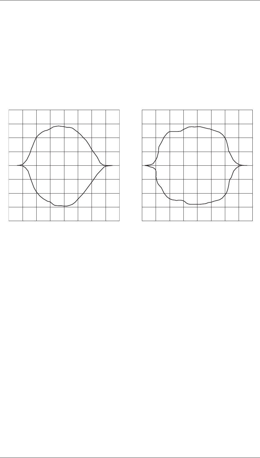
M8SL2-00-002-812 T855 Fault Finding B5.7
© Copyright Tait Electronics Limited August 2004. All rights reserved.
Check that the swept response has a rounded top and no sharp non-linearities
(refer to Figure 5.2).
Increase the RF level to –50dBm; the trace will now show the shape of the 455kHz
ceramic filter (&XF302).
Check that the response has no sharp non-linearities.
If sharp non-linearities do occur, replace the filter and sweep again to confirm a
satisfactory solution (refer to Figure 5.3).
Figure 5.2 IF Swept Response Figure 5.3 Ceramic Filter Swept Response

B5.8 T855 Fault Finding M8SL2-00-002-812
© Copyright Tait Electronics Limited August 2004. All rights reserved.
5.6 PGM800Win Generated Errors
The following errors are those most likely to occur using PGM800Win. Refer to the
PGM800Win software user’s manual for a complete list of error messages.
Channel Switch Set
The (programmed) default channel change was not accepted by the base station because
a channel is selected externally. Try turning the external channel switch off to change the
default channel in PGM800Win.
Synth Out Of Lock
The synthesiser received incorrect data, or the data was corrupted. Enter a frequency
within the VCO switching range, or tune the VCO.
Internal Error
Data could not be read from the base station due to an internal error. Check for shorts or
open circuits on the SDA, SCK, SYNTH and EPOT lines. The SDA, SCK and SYNTH are
normally high.
Write/Read To An Unlinked Module
The link to the module does not exist. Undefined error.

M8SL2-00-002-812 T855 Fault Finding B5.9
© Copyright Tait Electronics Limited August 2004. All rights reserved.
5.7 Fault Finding Charts
Note: The standard test point designations used in this section are as follows:
TP601 13.8V
TP602 9V
TP603 20V
TP604 5V
5.7.1 Microcontroller (IC810)
5.7.1.1 Basic Checks
Pulsing Check state
of pin 35.
Y
Is pin 30
pulsing?
High or open circuit
Y
Static high/low
Check state of
pins 36 to 43.
Low/floating
High
Is the 12.8MHz clock
present on IC810 pin 21
(microcontroller)?
N
Replace
IC810.
*digital storage oscilloscope
Replace IC810.
Check the
state of
pin 10.
N Pulsing
Low
Replace
IC810.
Use a DSO* to check
operation of IC650
(i.e. active high
pulse at power up).
Replace
IC650.
Correct the fault causing
pin 35 to be low/floating.
Check IC710.
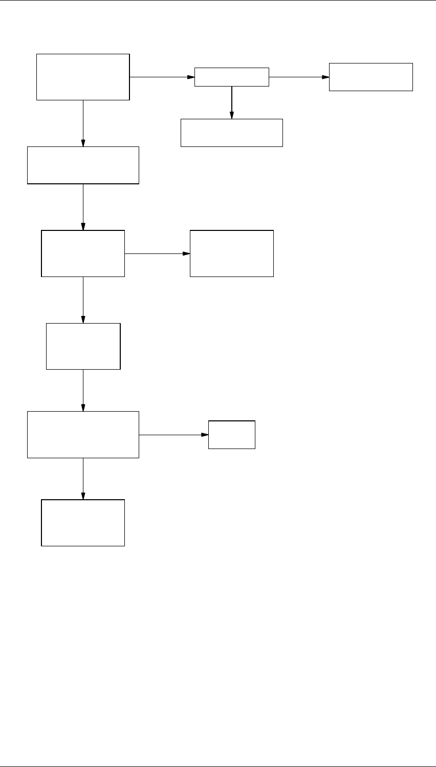
B5.10 T855 Fault Finding M8SL2-00-002-812
© Copyright Tait Electronics Limited August 2004. All rights reserved.
5.7.1.2 Serial Communication
Check pin state.
Y
Low/floating
N
Noise
on pin
Disconnect the
programming lead.
Is IC810 pin 11 high?
(microcontroller)
Y*digital storage
oscilloscope
Use PGM800Win
to send a POLL
command to the
radio.
Check the transistor
interface circuitry
and/or replace the
programming lead.
Check the SERIAL-COM
and AUDIO-1/2 links.
Replace
IC810.
Check the transistor
interface circuitry
and/or replace the
programming lead.
Check the transistor
interface circuitry.
Check IC810 pin 13
with a DSO. Is there
a response from IC810 after
a poll command is sent?
N
Y
Connect the programming
lead and use PGM800Win
to read the rack/radio.
Check I/O pad P810
with a DSO*.
Does it swing from
0 to 5V?
N
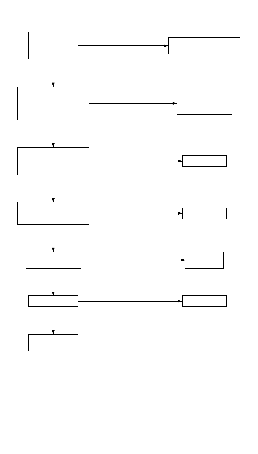
M8SL2-00-002-812 T855 Fault Finding B5.11
© Copyright Tait Electronics Limited August 2004. All rights reserved.
5.7.1.3 CTCSS Decode
Y
No square wave or
uneven mark/space ratio
Use PGM800Win to
select a channel
with a CTCSS tone
programmed.
Check serial communications.
(See separate flow chart).
Cannot select a channel
Check IC810 pins 24 & 26
(microcontroller).
Are there 5V square waves at
the CTCSS frequency?
Y
Check IC850 pins 1 & 14.
Are there 9V square waves at
the CTCSS frequency?
Replace IC850.
Y
Is IC850 pin 7 low and
Q845 collector high?
Replace IC850
or Q845.
N
Y
Is IC810 pin 31 low? Replace IC810.
N
Y
Check the receiver
mute circuit.
Set test equipment to correct
channel/CTCSS tone.
Check IC830 pin 7.
Is there a square wave at
the CTCSS input frequency?
Replace IC810.
No square waves or
uneven mark/space ratio
No square waves or
uneven mark/space ratio
Check the input filter
is operating correctly
(IC830 pin 8).
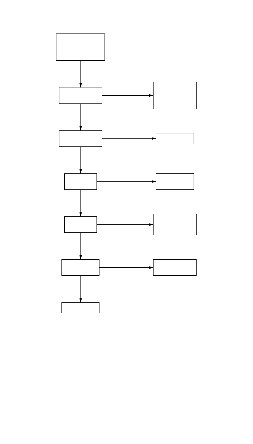
B5.12 T855 Fault Finding M8SL2-00-002-812
© Copyright Tait Electronics Limited August 2004. All rights reserved.
5.7.2 Regulator
Check for
overheating
components &
short circuits.
13.8V present on
IC630 pin 3?
5.3V present on
IC630 pin 1?
Check Q620,
Q630 & IC640.
Check Q660 is
switching at
approx. 180kHz.
Replace IC630.
Check R615.
Replace IC610.
Check continuity
from D-range
connector pin 9.
(D-range 1)
N
Y
N
Y
N
Y
N
Y
N
Regulators OK.
Y
20V present
on TP603?
9.0V present
on TP602?
5V present on
IC610 pin 1?
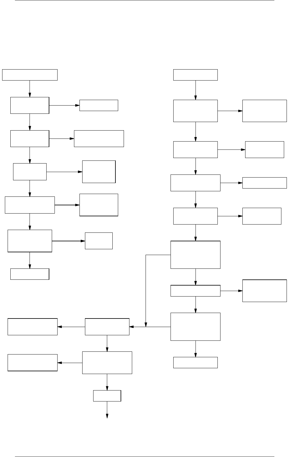
M8SL2-00-002-812 T855 Fault Finding B5.13
© Copyright Tait Electronics Limited August 2004. All rights reserved.
5.7.3 Synthesiser
Refer to the synthesiser circuit diagram (sheet 7) in Section 6 and the VCO circuit dia-
gram in Part E.
NCheck biasing
resistors, Q4 & Q5.
Check 9V reg.
N
Y
N
8.3V present
at VCO?
DC V present
at Q4 & Q5?
9V present at
VCO Q4/Q5?
Check Q4 C
multiplier
(synth).
No VCO RF output.
Y
DC V present at
VCO, Q1, Q2 & Q3?
Check biasing
resistors, Q1,
Q2 & Q3.
Y
N
Capacitors OK?
Check for cracks,
shorts, etc.
N
Y
Replace VCO.
Replace
if faulty.
Y
Y
N
N
N
Y
Y
Check biasing
resistors & Q1.
DC V present
on Q795 emitter?
Check 9V supply.
9V present on
Q795 divider buffer?
20V inverter
supply faulty.
20V present
on IC750 pin 8?
Check 5V reg. &
supply resistor
to each IC.
VCO out of lock.
Y
Y
Y
Continued on the next page
Y
VCO freq. correct?
Synthesiser OK.
VCO trimmer
freq. range OK?
Check VCO tuning
caps & trimmer.
VCO OK.
N
N
NN
N
Y
Y
Recheck
programming
via PGM800Win.
+5V present
at IC700, IC710
& IC740?
Does VCO trimmer
adjust for stable
control line between
3 & 16V?
Does VCO trimmer
adjust for required
frequency range
between 3 & 16V?
Is 8MHz VCO range
achieved between
3 & 16V?
N
Check #C1, L1, L2,
D1 & D2 in VCO.
AB
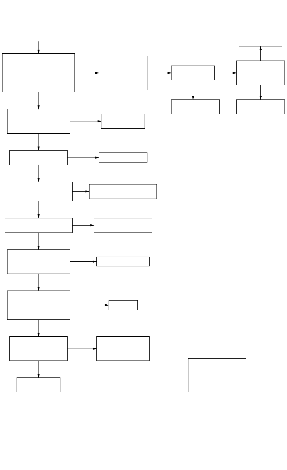
B5.14 T855 Fault Finding M8SL2-00-002-812
© Copyright Tait Electronics Limited August 2004. All rights reserved.
Programming and
serial bus OK?
Is reference
clock present
at IC740 pin 20
(12.8MHz >1.5Vpp)?
Check programming.
Check serial bus
when programming
i.e. clock/data/enable
activity (IC740 pins
18, 19 & 17). N
N
Check loop filter components
R775, C774, C776, R510,
C505, IC750. Is the supply
to IC750 +20V +4, -2V?
Check regulator circuitry.
Check C772, R774, R772,
C770, R763 & Q790.
Check Q760, Q780,
R766 & C765.
Check charge pump components
(Q775 & Q780) and Q790.
Check R762 & C762.
Check the signal path from
the VCO to synthesiser.
Measure the frequency from
the VCO at IC740 pin 11 using
a frequency counter.
Is the level >-10dBm?
Does the frequency adjust
as the VCO trimmer is
adjusted (out of lock)?
Check VCO.
Y
Y
Y
Signal
Y
Y
Y
No signal
Replace synthesiser
(IC740).
Y
N Y
Y
N
N
N
N
Check phase detector output
pins (IC740 pins 3 & 4).
Are there very narrow pulses
(~50ns) at the reference frequency?
(i.e. 5kHz : 200µs period
6.25kHz : 160µs period)
*See Note below.
Is the charge pump bias
voltage at the base of
Q760 & Q780 between
3.5 and 5V? (5V when locked)
N
Is the voltage on C762,
R760, and R758 9V ±0.2V?
Is the loop filter reference
voltage at C772 (+) 6.5V ±0.2V?
N
Check divider buffer
circuit (Q795) and bias
voltages on Q795 emitter
(1.3V ±0.2V).
*Note:
When locked, both of these
are very narrow (~50ns).
If unlocked, one will be
very narrow (~50ns),
and the other wide (>15µs).
Check microcontroller
section (IC810).
Check TCXO (IC700)
and buffers (IC710).
Replace synthesiser
(IC740).
Continued from previous page
B
Is the charge pump voltage
on Q790 gate between
3 and 8.5V? (6.5V ±0.2V locked)
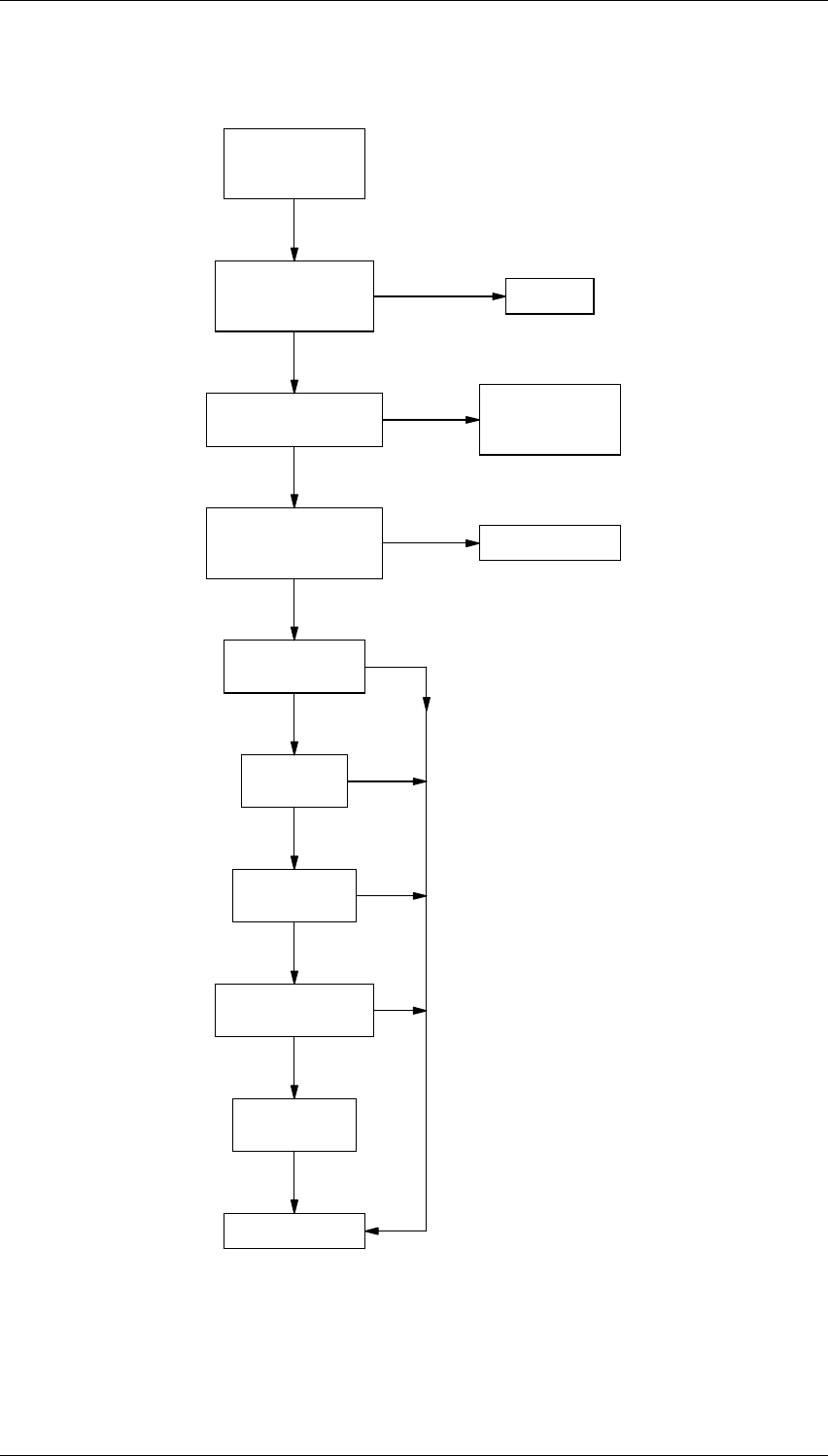
M8SL2-00-002-812 T855 Fault Finding B5.15
© Copyright Tait Electronics Limited August 2004. All rights reserved.
Y
N
Y
Y
Y
Y
N
Y
Y
Y
C
Noisy synth; poor
selectivity &/or
poor residual FM.
Correct DC V
present on Q1 VCO?
Change trimmer;
still noisy?
Change Q1;
still noisy?
Change TCXO;
still noisy?
Change varactors;
still noisy?
Replace VCO
assembly.
Synthesiser OK.
N
N
N
N
Check inductors,
biasing resistors
& Q1.
Replace if faulty.
Go to B.
Loop filter &
components around
op. amp. (IC750) OK?
N
VCO phase locked?
3-16V present on
control line?
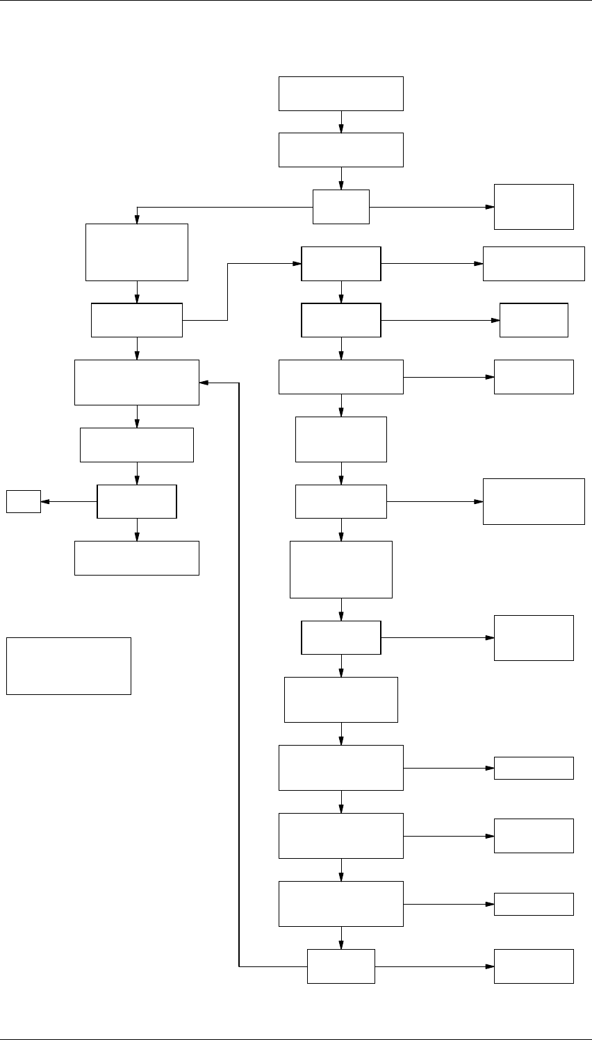
B5.16 T855 Fault Finding M8SL2-00-002-812
© Copyright Tait Electronics Limited August 2004. All rights reserved.
5.7.4 Noise Mute
Refer to audio
fault finding chart.
Ensure PL250 is set
for noise mute operation.
Check Q340
& Q350.
Check D310 is
rectifying noise.
Vary RF level &
observe voltage
on pad 236.
Pad 236 voltage
varies 0-1.8V?
Check 9V rail &
resistors R264,
R265 & R284.
Replace IC270.
Check/replace
IC270 & D240.
Replace Q250.
NY
N
Y
N
Y
Y
N
Y
Y
Y
Y
N
Refer to
receiver fault
finding chart.
Check components
around active filter.
Mutable audio
on outputs?
Y
Voltage varies
0-2.5V?
N
OK
Does "Gate" LED
toggle on/off?
N
Check Q230, Q245 &
Q290 for operation.
Y
Adjust RV230
(gating sensitivity)
& observe voltage
on IC270 pin 3.
Set RF signal level to
-117dBm. Rotate
RV230 c/w & cc/w.
Monitor voltage on
IC270 pin 1. Switching
0-8V as RV230 rotated?
Monitor voltage on
IC270 pin 7. Switching
0-8V as RV230 rotated?
Monitor voltage on
pad 234. Switching
0-8V as RV230 rotated?
N
N
N
Does "Gate"
LED toggle?
Check/replace
Q255 & D250.
Y
YN
Check RV330
adjustment
(noise mute gain).
Approx. 0.6V DC rect-
ified noise on pad 236?
N
Switch SW201 (monitor
mute) to ensure
mute is enabled.
Rotate RV230
(gating sensitivity)
c/w & cc/w & view
"Gate" LED.
Note:
c/w = clockwise
cc/w = counterclockwise
or anticlockwise
Audio on
TP314?
Noise on
IC310 pin 11?
Amplified noise
on C380?
Apply on channel signal
@ -117dBm* to receiver.
*Modulated by 1kHz signal with
±3kHz (±2.4kHz) [±1.5kHz] deviation
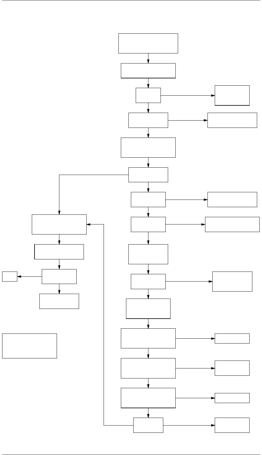
M8SL2-00-002-812 T855 Fault Finding B5.17
© Copyright Tait Electronics Limited August 2004. All rights reserved.
5.7.5 Carrier Mute
Approx. 5V on
RSSI pad 238?
Approx. 5V on
IC280 pin 1?
Check/replace IC280
& adjoining components.
Check Q230, Q245 &
Q290 for operation.
Adjust RV235 &
observe voltage
on IC280 pin 6.
Switch SW201
(monitor mute) to ensure
mute is enabled.
Y
N
N
N
Y
Y
Does "Gate" LED
toggle on/off?
Refer to
receiver fault
finding chart.
N
Y
Y
Voltage varies
0-6V?
Check 9V rail &
resistors R275,
R277 & RV235.
Y
N
Set RF signal level
to -95dBm. Rotate
RV235 c/w & cc/w.
Monitor voltage on
IC280 pin 7. Switching
0-8V as RV235 rotated?
Replace IC280.
N
Y
Monitor voltage on
IC270 pin 7. Switching
0-8V as RV235 rotated?
Check/replace
IC270 & D240.
N
Y
Monitor voltage on
pad 234. Switching
0-8V as RV235 rotated?
Replace Q250.
N
Y
Does "Gate"
LED toggle?
Check/replace
Q255 & D250.
YN
Mutable audio
on outputs?
OK
N
Y
Refer to audio
fault finding chart.
Note:
c/w = clockwise
cc/w = counterclockwise
or anticlockwise
Rotate RV235
(carrier mute) c/w & cc/w
& view "Gate" LED.
Apply on channel signal
@ -110dBm* to receiver.
Audio on
TP314?
*Modulated by 1kHz signal with
±3kHz (±2.4kHz) [±1.5kHz] deviation.
Approx. 2V at
D-Range 1 pin 5?
N
Ensure PL250 is set
for carrier mute operation,
and the RSSI PCB is fitted.
Check for short circuits
and/or replace IC310.
Check Q340 and
adjoining components.
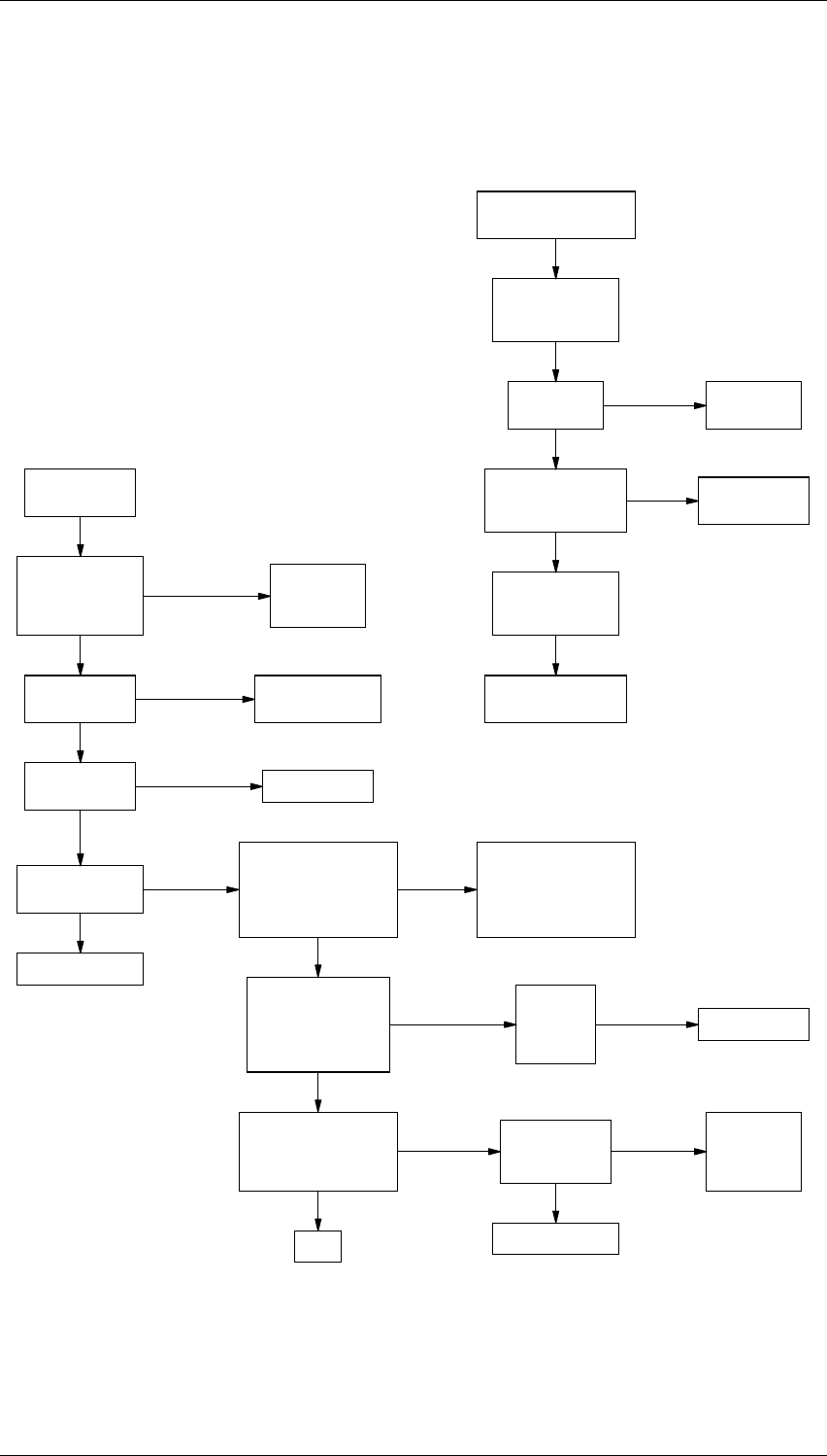
B5.18 T855 Fault Finding M8SL2-00-002-812
© Copyright Tait Electronics Limited August 2004. All rights reserved.
5.7.6 Receiver
Refer to the receiver IF and front end circuit diagrams (sheets 3 and 4) in Section 6.
High audio
distortion.
B
Check VCO
frequency OK?
Readjust TCXO
frequency.
Check IF
alignment OK? Adjust IF coils.
Fault find audio.
OK
Check
sensitivity
into each
IF stage.
Repair stage.
Replace TCXO.
Refer to
synthesiser
fault finding
charts.
Check TCXO
stability OK?
(see 5.5.3)
N
Y
N
Y
N
Y
N
Y
N
Y
N
Y
NY
Y
Y
Ensure VCO, RF
front end & IF
correctly aligned.
High audio
distortion?
Check/repair faulty
stage or component.
Check DC
conditions OK?
(see cct diagrams)
Check sensitivity
into each stage
(see 5.5.2)
See Chart B
(below).
Replace
faulty device.
Y
N
N
Y
Poor sensitivity:
worse than -117dBm.
A
Quad coil L390
tuned for min.
distortion (flat
audio response)?
Adjust L390.
Retune all
IF coils.
Check distortion
TP314 OK?
Inject on-channel
RF into mixer TP411.
Measure distortion.
OK?
Check distortion
TP314,
injecting 45MHz
@ -47dBm into TP310
at Q320 input. OK?
Inject 45MHz
after mixer IF
output TP412.
Measure distortion.
OK?
Fault in IC310,
&XF302, Q330,
Q320, &XF301 or
surrounding circuitry.
Check/replace.
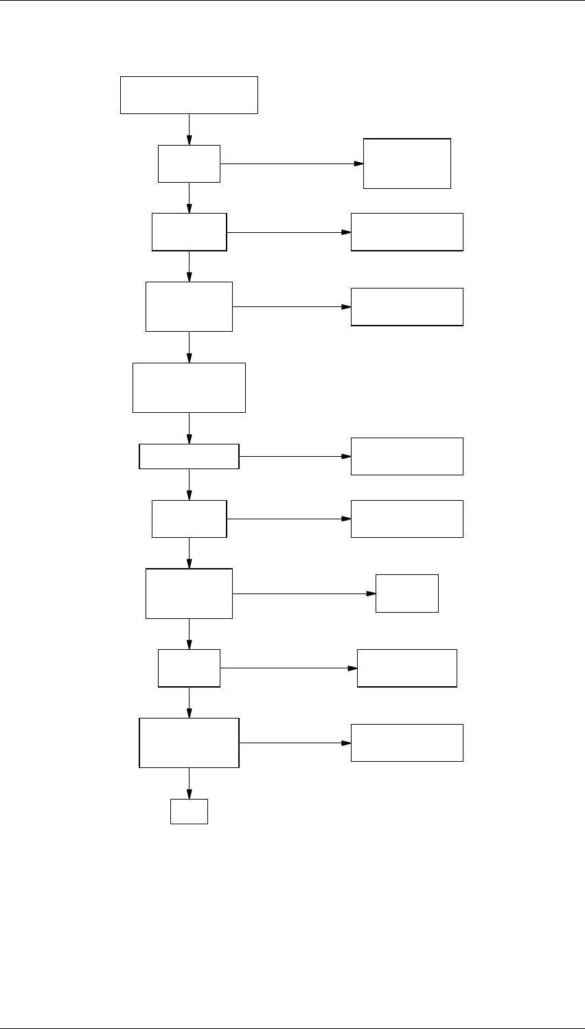
M8SL2-00-002-812 T855 Fault Finding B5.19
© Copyright Tait Electronics Limited August 2004. All rights reserved.
5.7.7 Audio
Audio on
IC210 pin 1?
Check components
around IC210.
Apply on channel signal
@ -117dBm* to receiver.
Refer to
receiver fault
finding chart.
Ensure RV230
(gating sensitivity)
fully clockwise.
"Gate" LED on? Refer to mute
fault finding charts.
Y
N
N
Y
N
Y
N
Y
Audio on
speaker?
Audio on
C238/C259?
Audio on
IC240 pin 2 &
IC260 pin 2?
Replace C249 &
check continuity.
Audio on line
monitor (pad 284)
& line output?
Refer to mute
fault finding charts.
OK
Check/replace
output components.
N
Y
N
Y
N
Y
N
Y
Audio on
TP314?
Audio at
top of RV205
& RV210?
Check C233.
Check link PL240.
Replace
faulty IC.
*Modulated by 1kHz signal with
±3kHz (±2.4kHz) [±1.5kHz] deviation.

B5.20 T855 Fault Finding M8SL2-00-002-812
© Copyright Tait Electronics Limited August 2004. All rights reserved.
M8SL2-00-002-812 T855 PCB Information B6.1.1
© Copyright Tait Electronics Limited August 2004. All rights reserved.
6 T855 PCB Information
Caution: This equipment contains CMOS devices which are susceptible to damage from
static charges. Refer to Section 1.2 in Part A for more information on anti-static
procedures when handling these devices.
This section provides the following information on the T855 receiver:
•parts lists
•grid reference indexes
•mechanical assembly drawings
•PCB layouts
•test points and options connections drawings
•circuit diagrams.
Section Title IPN Page
6.1 Introduction 6.1.3
6.2 T800-04-0000 RSSI PCB 220-01138-03 6.2.1
6.3 T855 Receiver PCB 220-01396-02
220-01396-03
6.3.1
6.3.31

B6.1.2 T855 PCB Information M8SL2-00-002-812
© Copyright Tait Electronics Limited August 2004. All rights reserved.

M8SL2-00-002-812 T855 PCB Information B6.1.3
© Copyright Tait Electronics Limited August 2004. All rights reserved.
6.1 Introduction
Product Type Identification
You can identify the receiver type by checking the product code printed on a label on the rear of the
chassis (product codes are explained in Section 1 in the front matter of this manual, and Figure 1.1
in Part A shows typical labels). You can further verify the product type by checking the placement
of an SMD resistor in the table that is screen printed onto the top side of the PCB, similar to the
example drawn below. In this example, the resistor indicates that the product was built as a
T855-10-XXXX.
Note: The only function of this resistor is to indicate the product type. It has no effect on the
circuitry or operation of the receiver.
PCB Identification
All PCBs are identified by a unique 10 digit “internal part number” (IPN), e.g. 220-01390-02, which
is screen printed onto the PCB (usually on the top side), as shown in the example below:
The last 2 digits of this number define the issue status, which starts at 00 and increments through 01,
02, 03, etc. as the PCB is updated. Some issue PCBs never reach full production status and are there-
fore not included in this manual. A letter following the 10 digit IPN has no relevance in identifying
the PCB for service purposes.
Note: It is important that you identify which issue PCB you are working on so that you can
refer to the appropriate set of PCB information.
855-30 PRODUCT TYPE
855-35 855-10 855-20
855- 855-13 855-23
PRODUCT TYPE 855-15 855-25

B6.1.4 T855 PCB Information M8SL2-00-002-812
© Copyright Tait Electronics Limited August 2004. All rights reserved.
Parts Lists
The 10 digit numbers (000-00000-00) in this Parts List are “internal part numbers” (IPNs). We can
process your spare parts orders more efficiently and accurately if you quote the IPN and provide a
brief description of the part.
The components listed in this parts list are divided into two main types: those with a circuit refer-
ence (e.g. C2, D1, R121, etc.) and those without (miscellaneous and mechanical).
Those with a circuit reference are grouped in alphabetical order and then in numerical order within
each group. Each component entry comprises three or four columns, as shown below:
The miscellaneous and mechanical section lists the variant and common parts in IPN order.
Variant Components
A variant component is one that has the same circuit reference but different value or specification in
different product types. Where two products share the same PCB, the term “variant” is also used to
describe components unplaced in one product. Variant components have a character prefix, such as
“&”, “=” or “#”, before the circuit reference (e.g. &R100).
The table below explains the variant prefixes used in T800 SL2 products:
If the variant prefix is. . . the component will. . .
& change according to channel spacing
= change according to frequency stability
# change according to frequency range
% change or be placed/unplaced for special applications
*be unplaced in one product
(where two products share the same PCB)
circuit re
f
erence -
lists components
in alphanumeric
order
variant column -
indicates that this is
a variant component
which is fitted only to
the product type listed
Internal Part Number -
order the component
b
y
this number
description -
gives a brief description
of the component
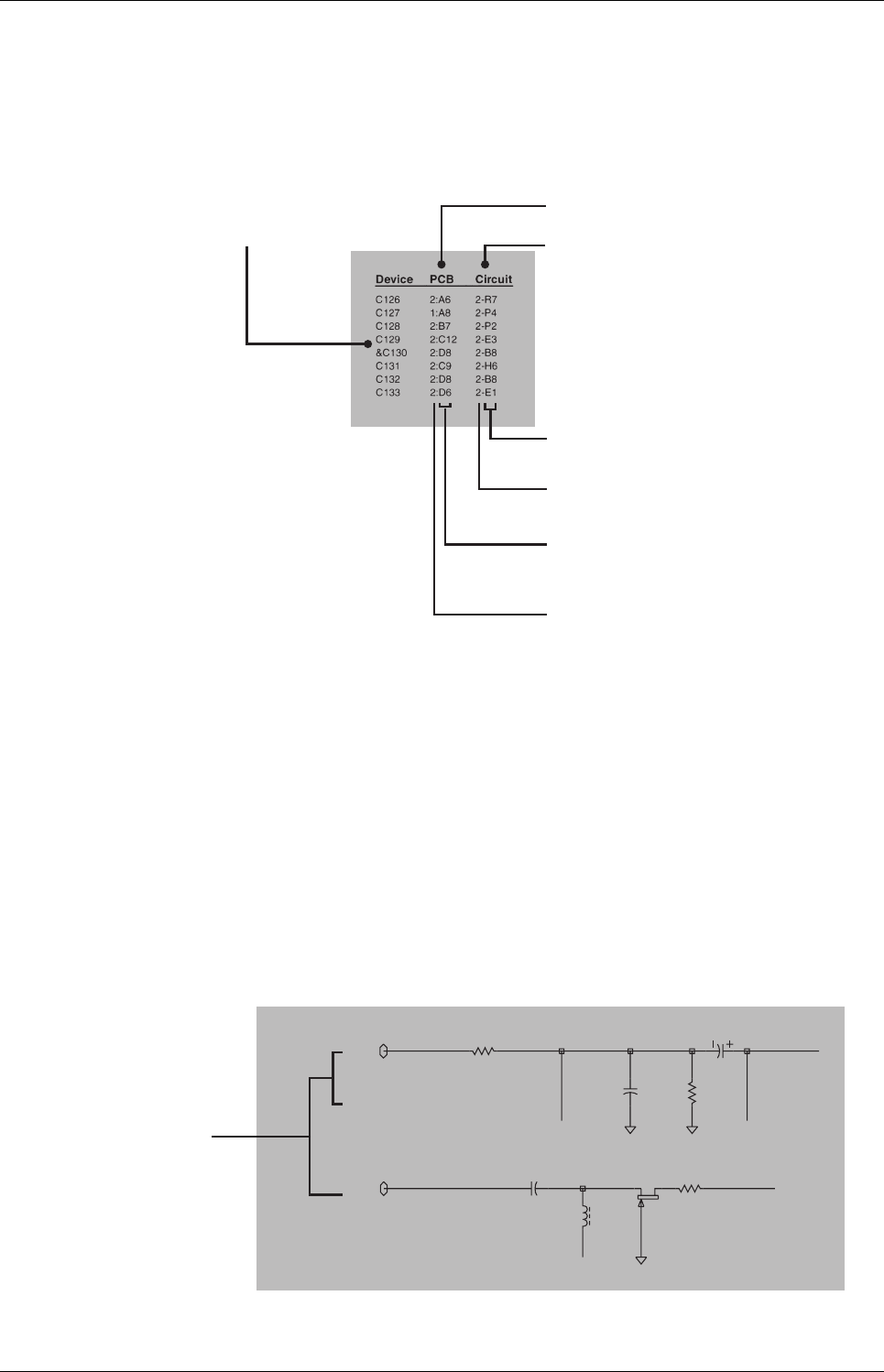
M8SL2-00-002-812 T855 PCB Information B6.1.5
© Copyright Tait Electronics Limited August 2004. All rights reserved.
Grid Reference Index
This section contains a component grid reference index to help you find components and labelled
pads on the PCB layouts and circuit diagrams. This index lists the components and pads in alpha-
numeric order, along with the appropriate alphanumeric grid references, as shown below:
Using CAD Circuit Diagrams
Reading a CAD circuit diagram is similar to reading a road map, in that both have an alphanumeric
border. The circuit diagrams in this manual use letters to represent the horizontal axis, and numbers
for the vertical axis. These circuit diagram “grid references” are useful in following a circuit that is
spread over two or more sheets.
When a line representing part of the circuitry is discontinued, a reference will be given at the end of
the line to indicate where the rest of the circuitry is located, as shown below. The first digit refers to
the sheet number and the last two characters refer to the location on that sheet of the continuation of
the circuit (e.g. 1R3).
circuit diagram
reference
P
C
B layout
reference
components listed
in alphanumeric order
layer number -
1 = top side layer
2 = bottom side layer
component location
on the layer
sheet number
component location
on the sheet
C301
4N7
R303
12
D
S
G
L310
33U
IF-SIG
4R4
C369
100P
C371
10U
R339
100K
%R338
100
DISCRIMINATOR
1R3
2R9
2R9
8A2
t
hese grid references
s
how where the circuit
i
s continued

B6.1.6 T855 PCB Information M8SL2-00-002-812
© Copyright Tait Electronics Limited August 2004. All rights reserved.

M8SL2-00-002-812 T800-04-0000 RSSI PCB Information B6.2.1
© Copyright Tait Electronics Limited August 2004. All rights reserved.
6.2 T800-04-0000 RSSI PCB
This section contains the following information.
IPN Section Page
220-01138-03 Parts List
PCB Layout – Top Side
PCB Layout – Bottom Side
Circuit Diagram
6.2.3
6.2.5
6.2.6
6.2.7

B6.2.2 T800-04-0000 RSSI PCB Information M8SL2-00-002-812
© Copyright Tait Electronics Limited August 2004. All rights reserved.

IPN 220-01138-03
M8SL2-00-002-812 T800-04-0000 RSSI PCB Information B6.2.3
© Copyright Tait Electronics Limited August 2004. All rights reserved.
Ref Var IPN Description Ref Var IPN Description
T800-04-0000 Parts List (IPN 220-01138-03)
How To Use This Parts List
The components listed in this parts list are grouped in alphabetical order and then in numerical order within each group. Each compo-
nent entry comprises three or four columns: the circuit reference, variant (if applicable), IPN and description. A number in the variant
column indicates that this is a variant component which is fitted only to the product type listed.
This parts list is correct at the time of publishing, but is subject to change without notification. An up to date parts list can be obtained
from your local Customer Service Organisation
C1 015-24100-08 Cap Cer 0805 1n 10% X7r 50v
C2 015-24100-08 Cap Cer 0805 1n 10% X7r 50v
C3 015-23330-08 Cap Cer 0805 330p 10% X7r 50v
C4 015-25100-08 Cap Cer 0805 10n 10% X7r 50v
C5 015-24100-08 Cap Cer 0805 1n 10% X7r 50v
C6 015-25100-08 Cap Cer 0805 10n 10% X7r 50v
C7 015-24470-08 Cap Cer 0805 4n7 10% X7r 50v
C8 015-25100-08 Cap Cer 0805 10n 10% X7r 50v
C9 015-24100-08 Cap Cer 0805 1n 10% X7r 50v
D1 001-10000-99 Diode SMD BAV99 D-Sw SOT23
IC1 002-10003-24 IC SMD 324 4x 0-Amp S014
Q1 002-10033-46 IC SMD MC3346D Xst Aray S014
R3 036-14100-10 Res M/F SMD 0805 1k 1%
R4 036-14220-00 Res M/F SMD 0805 2k2 5%
R5 036-15560-10 Res M/F SMD 0805 56k 1%
R6 036-15390-10 Res M/F SMD 0805 39k 1%
R7 036-15100-10 Res M/F SMD 0805 10k 1%
R8 036-13680-10 Res M/F SMD 0805 680e 1%
R9 036-14820-10 Res M/F SMD 0805 8k2 1%
R10 036-16220-00 Res M/F SMD 0805 220k 5%
R11 036-13470-00 Res M/F SMD 0805 470e 5%
R12 036-16330-00 Res M/F SMD 0805 330k 5%
R13 036-16100-10 Res M/F SMD 0805 100k 1%
R14 036-16180-00 Res M/F SMD 0805 180k 5%
R15 036-15220-00 Res M/F SMD 0805 22k 5%
R16 036-17100-10 Res M/F SMD 0805 1M 1%
R17 036-15330-10 Res M/F SMD 0805 33k 1%
R18 036-14100-10 Res M/F SMD 0805 1k 1%
R19 036-15100-10 Res M/F SMD 0805 10k 1%
R20 036-15100-10 Res M/F SMD 0805 10k 1%
R21 036-16330-00 Res M/F SMD 0805 330k 5%
R22 036-14470-10 Res M/F SMD 0805 4k7 1%
R23 036-15100-10 Res M/F SMD 0805 10k 1%
R24 036-16150-00 Res M/F SMD 0805 150k 5%
R25 036-16180-00 Res M/F SMD 0805 180k 5%
R26 036-15820-00 Res M/F SMD 0805 82k 5%
R29 036-14470-10 Res M/F SMD 0805 4k7 1%
R30 036-15100-10 Res M/F SMD 0805 10k 1%
R31 036-15220-00 Res M/F SMD 0805 22k 5%
R32 036-14470-10 Res M/F SMD 0805 4k7 1%
369-00020-36 Tape Vinyl Foam 2Side 25.4*3mm
220-01138-03 PCB T700 RSSI Brd
356-00010-52 Pin Edge Mtg 0.8mm PCB Wako

B6.2.4 T800-04-0000 RSSI PCB Information M8SL2-00-002-812
© Copyright Tait Electronics Limited August 2004. All rights reserved.

T800-04-0000 PCB (IPN 220-01138-03) - Top Side
© Copyright Tait Electronics Limited August 2004. All rights reserved.
IPN 220-01138-03
M8SL2-00-002-812 T800-04-0000 RSSI PCB Information B6.2.5
220-01138-03 A220-01138-03 A
IPN 220-01138-03
B6.2.6 T800-04-0000 RSSI PCB Information M8SL2-00-002-812
© Copyright Tait Electronics Limited August 2004. All rights reserved.
T800-04-0000 PCB (IPN 220-01138-03) - Bottom Side
BBADMARK
C1 C2
C3
C4 C5
C6
C7
C8 C9
D1
IC1
P1P2
Q1
R10
R11
R12
R13
R14
R15
R16
R17
R18
R19
R20
R21
R22
R23
R24
R25
R26
R29
R3
R30
R31
R32
R4
R5R6
R7
R8
R9
IPN 220-01138-00
M8SL2-00-002-812 T800-04-0000 RSSI PCB Information B6.2.7
© Copyright Tait Electronics Limited August 2004. All rights reserved.
T800-04-0000 RSSI
220-01138-00
0
1
2
3
4
5
6
7
8
9
0
1
2
3
4
5
6
7
8
9
ABCDEFGHJ KLM
REV/ISS AMENDMENTS DATEAPVDD.O.CHKDDRAWN
NO.SHEETS:FILE NAME:
TAIT ELECTRONICS
IPN:
FILE DATE:
ISSUE: ID:.
2.SC.
PROJECT: DESIGNER:
1
1
T800-04-0000
RSSI BOARD
113803a
220-01138-03
24-Aug-99
A
T700 M.HALL
1A ECO 770163 - MIGRATED TO UNICAD. M.HALL M.HALL M.HALL JACKSON 12/05/99
2A ECO 740091 MJ/TB M.HALL M.HALL JACKSON 24/06/99
3A ECO 770177 M.HALL
C1
1N0
C2
1N0
C3
330P
C4
10N
C5
1N0
C6
10N
C7
4N7
C8
10N
C9
1N0
D1
BAV99
2
3
D1
BAV99
3
1
IC1
LM324D
V-
11
V+
4
+
-
IC1
LM324D
3
2
1
+
-
IC1
LM324D
5
6
7
+
-
IC1
LM324D
10
9
8
+
-
IC1
LM324D
12
13
14
P1
4 EDGE CONN PINS
P2
3 EDGE CONN PINS
Q1
3346
12
13
14
Q1
3346
6
7
8
Q1
3346
4
3
5
Q1
3346
2
3
1
Q1
3346
9
10
11
R10
220K
R11
470
R12
330K
R13
100K
R14
180K
R15
22K
R16
1M0
R17
33K
R18
1K0
R19
10K
R20
10K
R21
330K
R22
4K7
R23
10K
R24
150K
R25
180K
R26
82K
R29
4K7
R3
1K0
R30
10K
R31
22K
R32
4K7
R4
2K2
R5
56K
R6
39K
R7
10K
R8
680
R9
8K2
BBADMARK
BADMARK
P1 GND
4
P1 NTC
3
P1 O/P
2
P1 REF
1
P2
+9V-SW 1
P2
INPUT 3
P2
GND 2
+9V-SW
+9V-SW
+9V-SW
IPN 220-01138-00
B6.2.8 T800-04-0000 RSSI PCB Information M8SL2-00-002-812
© Copyright Tait Electronics Limited August 2004. All rights reserved.

M8SL2-00-002-812 T855 PCB Information B6.3.1
© Copyright Tait Electronics Limited August 2004. All rights reserved.
6.3 T855 Receiver PCB
This section contains the following information.
IPN Section Page
220-01396-03 Parts List
Mechanical and Miscellaneous Parts
Mechanical Assembly
Grid Reference Index
PCB Layout – Top Side
PCB Layout – Bottom Side
Test Points and Options Connections – Top Side
Test Points and Options Connections – Bottom Side
Receiver Overview Diagram
Audio Processor Circuit Diagram
IF Section Circuit Diagram
Front End Circuit Diagram
VCO Section Circuit Diagram
Regulators Circuit Diagram
Synthesiser Circuit Diagram
Microcontroller Circuit Diagram
Harmonic Filter Circuit Diagram
6.3.3
6.3.8
6.3.9
6.3.11
6.3.15
6.3.16
6.3.17
6.3.18
6.3.19
6.3.20
6.3.21
6.3.22
6.3.23
6.3.24
6.3.25
6.3.26
6.3.27

B6.3.2 T855 PCB Information M8SL2-00-002-812
© Copyright Tait Electronics Limited August 2004. All rights reserved.

IPN 220-01396-03
M8SL2-00-002-812 T855 PCB Information B6.3.3
© Copyright Tait Electronics Limited August 2004. All rights reserved.
Ref Var IPN Description Ref Var IPN Description
T855 Parts List (IPN 220-01396-03)
How To Use This Parts List
The components listed in this parts list are grouped in alphabetical order and then in numerical order within each group. Each compo-
nent entry comprises three or four columns: the circuit reference, variant (if applicable), IPN and description. A number in the variant
column indicates that this is a variant component which is fitted only to the product type listed.
This parts list is correct at the time of publishing, but is subject to change without notification. An up to date parts list can be obtained
from your local Customer Service Organisation
C201 020-08100-04 CAP ELE RA 10M 16V 4X7MM
&C203 10 015-25100-08 CAP CER 0805 10N 10% X7R 50V
&C203 13 015-25100-08 CAP CER 0805 10N 10% X7R 50V
&C203 15 015-24470-08 CAP CER 0805 4N7 10% X7R 50V
&C203 20 015-25100-08 CAP CER 0805 10N 10% X7R 50V
&C203 23 015-25100-08 CAP CER 0805 10N 10% X7R 50V
&C203 25 015-24470-08 CAP CER 0805 4N7 10% X7R 50V
&C203 30 015-25100-08 CAP CER 0805 10N 10% X7R 50V
&C203 35 015-24470-08 CAP CER 0805 4N7 10% X7R 50V
&C205 10 015-24470-08 CAP CER 0805 4N7 10% X7R 50V
&C205 13 015-24470-08 CAP CER 0805 4N7 10% X7R 50V
&C205 15 015-25100-08 CAP CER 0805 10N 10% X7R 50V
&C205 20 015-24470-08 CAP CER 0805 4N7 10% X7R 50V
&C205 23 015-24470-08 CAP CER 0805 4N7 10% X7R 50V
&C205 25 015-25100-08 CAP CER 0805 10N 10% X7R 50V
&C205 30 015-24470-08 CAP CER 0805 4N7 10% X7R 50V
&C205 35 015-25100-08 CAP CER 0805 10N 10% X7R 50V
C207 020-07100-02 CAP ELE RA 1M 50V 5X11MM
C209 020-08470-02 CAP ELE RA 47M 16V 6X11MM
C210 015-24100-08 CAP CER 0805 1N 10% X7R 50V
C211 015-24470-08 CAP CER 0805 4N7 10% X7R 50V
C213 015-25470-08 CAP CER 0805 47N 10% X7R 50V
C215 015-21220-01 CAP CER 0805 2P2+-1/4P NPO 50V
C217 015-22470-01 CAP CER 0805 47P 5% NPO 50V
C219 015-24470-08 CAP CER 0805 4N7 10% X7R 50V
C221 015-24100-08 CAP CER 0805 1N 10% X7R 50V
C222 020-08100-04 CAP ELE RA 10M 16V 4X7MM
C223 015-06100-08 CAP CER 1206 100N 10% X7R 50V
C225 015-06100-08 CAP CER 1206 100N 10% X7R 50V
C227 015-23100-01 CAP CER 0805 100P 5% NPO 50V
C229 020-08100-04 CAP ELE RA 10M 16V 4X7MM
C231 020-08100-04 CAP ELE RA 10M 16V 4X7MM
C233 020-08100-04 CAP ELE RA 10M 16V 4X7MM
C235 015-24100-08 CAP CER 0805 1N 10% X7R 50V
C237 015-24100-08 CAP CER 0805 1N 10% X7R 50V
C238 015-06100-08 CAP CER 1206 100N 10% X7R 50V
C239 020-09100-03 CAP ELE RA 100M 16V 8X11MM
C240A 015-24100-08 CAP CER 0805 1N 10% X7R 50V
C240B 015-06100-08 CAP CER 1206 100N 10% X7R 50V
C240C 020-09220-01 CAP ELE RA 220M 16V 10X12.5MM
C249 020-09470-05 CAP ELE RAD 470M 16V 10X12.5MM
C251 015-06100-08 CAP CER 1206 100N 10% X7R 50V
C253 020-09100-03 CAP ELE RA 100M 16V 8X11MM
C255 015-24100-08 CAP CER 0805 1N 10% X7R 50V
C257 015-24100-08 CAP CER 0805 1N 10% X7R 50V
C259 015-06100-08 CAP CER 1206 100N 10% X7R 50V
C260A 015-24100-08 CAP CER 0805 1N 10% X7R 50V
C260B 015-06100-08 CAP CER 1206 100N 10% X7R 50V
C260C 020-09220-01 CAP ELE RA 220M 16V 10X12.5MM
C261 020-09100-03 CAP ELE RA 100M 16V 8X11MM
C262 020-09100-03 CAP ELE RA 100M 16V 8X11MM
C264 015-06100-08 CAP CER 1206 100N 10% X7R 50V
C266 020-07470-91 CAP ELE RA 4M7 63V 6X11MM BI-P
C268 020-07470-91 CAP ELE RA 4M7 63V 6X11MM BI-P
C270 015-06100-08 CAP CER 1206 100N 10% X7R 50V
C272 015-25100-08 CAP CER 0805 10N 10% X7R 50V
C274 015-06100-08 CAP CER 1206 100N 10% X7R 50V
C276 015-25470-08 CAP CER 0805 47N 10% X7R 50V
C278 015-06100-08 CAP CER 1206 100N 10% X7R 50V
C280 015-25470-08 CAP CER 0805 47N 10% X7R 50V
C286 015-24470-08 CAP CER 0805 4N7 10% X7R 50V
C302 015-23100-01 CAP CER 0805 100P 5% NPO 50V
C306 015-24470-08 CAP CER 0805 4N7 10% X7R 50V
C308 015-24100-08 CAP CER 0805 1N 10% X7R 50V
C310 015-25100-08 CAP CER 0805 10N 10% X7R 50V
C312 020-58100-03 CAP ELE AI RDL 10M 50V 5X11MM
C314 015-24470-08 CAP CER 0805 4N7 10% X7R 50V
C316 015-22150-01 CAP CER 0805 15P 5% NPO 50V
&C318 10 015-21820-01 CAP CER 0805 8P2+-1/4P NPO 50V
&C318 13 015-21820-01 CAP CER 0805 8P2+-1/4P NPO 50V
&C318 15 015-21820-01 CAP CER 0805 8P2+-1/4P NPO 50V
&C318 20 015-21820-01 CAP CER 0805 8P2+-1/4P NPO 50V
&C318 23 015-21820-01 CAP CER 0805 8P2+-1/4P NPO 50V
&C318 25 015-21820-01 CAP CER 0805 8P2+-1/4P NPO 50V
&C318 30 015-21820-01 CAP CER 0805 8P2+-1/4P NPO 50V
&C318 35 015-21820-01 CAP CER 0805 8P2+-1/4P NPO 50V
&C320 10 015-21390-01 CAP CER 0805 3P9+-1/4P NPO 50V
&C320 13 015-21390-01 CAP CER 0805 3P9+-1/4P NPO 50V
&C320 15 015-21390-01 CAP CER 0805 3P9+-1/4P NPO 50V
&C320 20 015-21390-01 CAP CER 0805 3P9+-1/4P NPO 50V
&C320 23 015-21390-01 CAP CER 0805 3P9+-1/4P NPO 50V
&C320 25 015-21390-01 CAP CER 0805 3P9+-1/4P NPO 50V
&C320 30 015-21390-01 CAP CER 0805 3P9+-1/4P NPO 50V
&C320 35 015-21390-01 CAP CER 0805 3P9+-1/4P NPO 50V
&C322 10 015-22150-01 CAP CER 0805 15P 5% NPO 50V
&C322 13 015-22150-01 CAP CER 0805 15P 5% NPO 50V
&C322 15 015-22150-01 CAP CER 0805 15P 5% NPO 50V
&C322 20 015-22150-01 CAP CER 0805 15P 5% NPO 50V
&C322 23 015-22150-01 CAP CER 0805 15P 5% NPO 50V
&C322 25 015-22150-01 CAP CER 0805 15P 5% NPO 50V
&C322 30 015-22150-01 CAP CER 0805 15P 5% NPO 50V
&C322 35 015-22150-01 CAP CER 0805 15P 5% NPO 50V
&C324 10 015-21390-01 CAP CER 0805 3P9+-1/4P NPO 50V
&C324 13 015-21390-01 CAP CER 0805 3P9+-1/4P NPO 50V
&C324 15 015-21390-01 CAP CER 0805 3P9+-1/4P NPO 50V
&C324 20 015-21390-01 CAP CER 0805 3P9+-1/4P NPO 50V
&C324 23 015-21390-01 CAP CER 0805 3P9+-1/4P NPO 50V
&C324 25 015-21390-01 CAP CER 0805 3P9+-1/4P NPO 50V
&C324 30 015-21390-01 CAP CER 0805 3P9+-1/4P NPO 50V
&C324 35 015-21390-01 CAP CER 0805 3P9+-1/4P NPO 50V
&C326 10 015-21820-01 CAP CER 0805 8P2+-1/4P NPO 50V
&C326 13 015-21820-01 CAP CER 0805 8P2+-1/4P NPO 50V
&C326 15 015-21820-01 CAP CER 0805 8P2+-1/4P NPO 50V
&C326 20 015-21820-01 CAP CER 0805 8P2+-1/4P NPO 50V
&C326 23 015-21820-01 CAP CER 0805 8P2+-1/4P NPO 50V
&C326 25 015-21820-01 CAP CER 0805 8P2+-1/4P NPO 50V
&C326 30 015-21820-01 CAP CER 0805 8P2+-1/4P NPO 50V
&C326 35 015-21820-01 CAP CER 0805 8P2+-1/4P NPO 50V
C328 015-24470-08 CAP CER 0805 4N7 10% X7R 50V
C330 015-24100-08 CAP CER 0805 1N 10% X7R 50V
C331 015-21220-01 CAP CER 0805 2P2+-1/4P NPO 50V
C332 015-24470-08 CAP CER 0805 4N7 10% X7R 50V
&C334 10 015-22470-01 CAP CER 0805 47P 5% NPO 50V
&C334 13 015-22470-01 CAP CER 0805 47P 5% NPO 50V
&C334 15 015-24470-08 CAP CER 0805 4N7 10% X7R 50V
&C334 20 015-22470-01 CAP CER 0805 47P 5% NPO 50V
&C334 23 015-22470-01 CAP CER 0805 47P 5% NPO 50V
&C334 25 015-24470-08 CAP CER 0805 4N7 10% X7R 50V
&C334 30 015-22470-01 CAP CER 0805 47P 5% NPO 50V
&C334 35 015-24470-08 CAP CER 0805 4N7 10% X7R 50V
&C336 10 015-22120-01 CAP CER 0805 12P 5% NPO 50V
&C336 13 015-22120-01 CAP CER 0805 12P 5% NPO 50V
&C336 15 015-22100-01 CAP CER 0805 10P+-1/2P NPO 50V
&C336 20 015-22120-01 CAP CER 0805 12P 5% NPO 50V
&C336 23 015-22120-01 CAP CER 0805 12P 5% NPO 50V
&C336 25 015-22100-01 CAP CER 0805 10P+-1/2P NPO 50V
&C336 30 015-22120-01 CAP CER 0805 12P 5% NPO 50V
&C336 35 015-22100-01 CAP CER 0805 10P+-1/2P NPO 50V
&C338 10 015-22120-01 CAP CER 0805 12P 5% NPO 50V
&C338 13 015-22120-01 CAP CER 0805 12P 5% NPO 50V
&C338 15 015-22120-01 CAP CER 0805 12P 5% NPO 50V
&C338 20 015-22120-01 CAP CER 0805 12P 5% NPO 50V
&C338 23 015-22120-01 CAP CER 0805 12P 5% NPO 50V
&C338 25 015-22100-01 CAP CER 0805 10P+-1/2P NPO 50V
&C338 30 015-22120-01 CAP CER 0805 12P 5% NPO 50V
&C338 35 015-22120-01 CAP CER 0805 12P 5% NPO 50V
&C340 10 015-22470-01 CAP CER 0805 47P 5% NPO 50V
&C340 13 015-22470-01 CAP CER 0805 47P 5% NPO 50V
&C340 15 015-24470-08 CAP CER 0805 4N7 10% X7R 50V
&C340 20 015-22470-01 CAP CER 0805 47P 5% NPO 50V
&C340 23 015-22470-01 CAP CER 0805 47P 5% NPO 50V
&C340 25 015-24470-08 CAP CER 0805 4N7 10% X7R 50V
&C340 30 015-22470-01 CAP CER 0805 47P 5% NPO 50V
&C340 35 015-24470-08 CAP CER 0805 4N7 10% X7R 50V
C342 015-24470-08 CAP CER 0805 4N7 10% X7R 50V
C344 015-24470-08 CAP CER 0805 4N7 10% X7R 50V
C346 015-24470-08 CAP CER 0805 4N7 10% X7R 50V
C347 015-24470-08 CAP CER 0805 4N7 10% X7R 50V
C348 015-24470-08 CAP CER 0805 4N7 10% X7R 50V
C349 015-21270-01 CAP CER 0805 2P7+-1/4P NPO 50V
C350 015-24470-08 CAP CER 0805 4N7 10% X7R 50V
C352 015-22270-01 CAP CER 0805 27P 5% NPO 50V
C354 025-08100-04 (L) CAP10M 35V 10%TANT2.5L/S
C355 025-08100-04 (L) CAP10M 35V 10%TANT2.5L/S
C356 015-22120-01 CAP CER 0805 12P 5% NPO 50V
C357 015-25100-08 CAP CER 0805 10N 10% X7R 50V

IPN 220-01396-03
B6.3.4 T855 PCB Information M8SL2-00-002-812
© Copyright Tait Electronics Limited August 2004. All rights reserved.
Ref Var IPN Description Ref Var IPN Description
C358 015-25470-08 CAP CER 0805 47N 10% X7R 50V
C359 025-08100-04 (L) CAP10M 35V 10%TANT2.5L/S
C360 015-24470-08 CAP CER 0805 4N7 10% X7R 50V
C361 015-26100-08 CAP CER 0805 100N 10% X7R 50V
C362 015-25100-08 CAP CER 0805 10N 10% X7R 50V
C364 015-22390-01 CAP CER 0805 39P 5% NPO 50V
C366 015-22390-01 CAP CER 0805 39P 5% NPO 50V
C367 015-25100-08 CAP CER 0805 10N 10% X7R 50V
C368 015-05470-08 CAP CER 1206 47N 10% X7R 50V
C370 015-24470-08 CAP CER 0805 4N7 10% X7R 50V
C372 015-05470-08 CAP CER 1206 47N 10% X7R 50V
C374 015-24470-08 CAP CER 0805 4N7 10% X7R 50V
C376 015-23120-01 CAP CER 0805 120P 5% NPO 50V
C378 015-23120-01 CAP CER 0805 120P 5% NPO 50V
C380 015-25100-08 CAP CER 0805 10N 10% X7R 50V
C382 020-58100-03 CAP ELE AI RDL 10M 50V 5X11MM
C384 015-05470-08 CAP CER 1206 47N 10% X7R 50V
C386 015-05470-08 CAP CER 1206 47N 10% X7R 50V
C388 015-24470-08 CAP CER 0805 4N7 10% X7R 50V
C390 025-08100-02 CAP TANT BEAD 10M 10% 16V
C392 015-24470-08 CAP CER 0805 4N7 10% X7R 50V
C394 015-05470-08 CAP CER 1206 47N 10% X7R 50V
C410 015-21180-01 CAP CER 0805 1P8+-1/4P NPO 50V
C420 015-22470-01 CAP CER 0805 47P 5% NPO 50V
C430 015-23100-01 CAP CER 0805 100P 5% NPO 50V
C440 020-58100-03 CAP ELE AI RDL 10M 50V 5X11MM
C450 015-22470-01 CAP CER 0805 47P 5% NPO 50V
C470 015-22100-01 CAP CER 0805 10P+-1/2P NPO 50V
C480 015-22560-01 CAP CER 0805 56P 5% NPO 50V
C505 015-06100-08 CAP CER 1206 100N 10% X7R 50V
C515 015-06100-08 CAP CER 1206 100N 10% X7R 50V
C530 014-08220-01 (L)CAP TANT 22UF10V276MSER
C535 015-06100-08 CAP CER 1206 100N 10% X7R 50V
C610A 015-25100-08 CAP CER 0805 10N 10% X7R 50V
C610B 020-09100-04 CAP ELE RA 100M 10V 6.3X9MM
C611A 020-09100-04 CAP ELE RA 100M 10V 6.3X9MM
C611B 015-25100-08 CAP CER 0805 10N 10% X7R 50V
C623 015-23120-01 CAP CER 0805 120P 5% NPO 50V
C625 020-09470-07 CAPEL470M16V20%V 8*20 3.5L.ESR
C626 015-24470-08 CAP CER 0805 4N7 10% X7R 50V
C628 015-24100-08 CAP CER 0805 1N 10% X7R 50V
C630 015-06100-08 CAP CER 1206 100N 10% X7R 50V
C631A 015-06100-08 CAP CER 1206 100N 10% X7R 50V
C631B 025-08100-02 CAP TANT BEAD 10M 10% 16V
C637 015-23120-01 CAP CER 0805 120P 5% NPO 50V
C640 015-24100-08 CAP CER 0805 1N 10% X7R 50V
C651 015-06100-08 CAP CER 1206 100N 10% X7R 50V
C658 015-06100-08 CAP CER 1206 100N 10% X7R 50V
C660 015-06100-08 CAP CER 1206 100N 10% X7R 50V
C665 020-58100-03 CAP ELE AI RDL 10M 50V 5X11MM
C670 025-07330-01 CAP TANT BEAD 3M3 35V
C673 015-24470-08 CAP CER 0805 4N7 10% X7R 50V
C677 020-07100-02 CAP ELE RA 1M 50V 5X11MM
C681 015-06100-08 CAP CER 1206 100N 10% X7R 50V
C684 025-08100-02 CAP TANT BEAD 10M 10% 16V
C687 015-24100-08 CAP CER 0805 1N 10% X7R 50V
C690 015-06100-08 CAP CER 1206 100N 10% X7R 50V
C693 025-08100-02 CAP TANT BEAD 10M 10% 16V
C700 015-06100-08 CAP CER 1206 100N 10% X7R 50V
C702 015-24100-08 CAP CER 0805 1N 10% X7R 50V
C703 015-24100-08 CAP CER 0805 1N 10% X7R 50V
C705 015-21820-01 CAP CER 0805 8P2+-1/4P NPO 50V
C707 015-22470-01 CAP CER 0805 47P 5% NPO 50V
C708 015-22470-01 CAP CER 0805 47P 5% NPO 50V
C709 015-22100-01 CAP CER 0805 10P+-1/2P NPO 50V
C710A 014-07470-00 CAP TANT CHIP 4U7 3.5 X 2.8MM
C710B 015-06100-08 CAP CER 1206 100N 10% X7R 50V
C710C 015-25100-08 CAP CER 0805 10N 10% X7R 50V
C711 015-22220-01 CAP CER 0805 22P 5% NPO 50V
C712 015-22220-01 CAP CER 0805 22P 5% NPO 50V
C713 015-25100-08 CAP CER 0805 10N 10% X7R 50V
C735 015-22470-01 CAP CER 0805 47P 5% NPO 50V
C736 015-22470-01 CAP CER 0805 47P 5% NPO 50V
C740A 015-24100-08 CAP CER 0805 1N 10% X7R 50V
C740B 015-25100-08 CAP CER 0805 10N 10% X7R 50V
C741A 014-07470-00 CAP TANT CHIP 4U7 3.5 X 2.8MM
C741B 015-25100-08 CAP CER 0805 10N 10% X7R 50V
C742A 015-06100-08 CAP CER 1206 100N 10% X7R 50V
C742B 015-25100-08 CAP CER 0805 10N 10% X7R 50V
C743 015-22470-01 CAP CER 0805 47P 5% NPO 50V
C745 015-23120-01 CAP CER 0805 120P 5% NPO 50V
C750 025-08100-03 CAP 10M 35V 20% TANT 5MM L/S
C757 015-25100-08 CAP CER 0805 10N 10% X7R 50V
C759 015-25100-08 CAP CER 0805 10N 10% X7R 50V
C761 015-25100-08 CAP CER 0805 10N 10% X7R 50V
C762 014-08220-01 (L)CAP TANT 22UF10V276MSER
C764 015-25100-08 CAP CER 0805 10N 10% X7R 50V
C765 014-07470-00 CAP TANT CHIP 4U7 3.5 X 2.8MM
C767 015-24100-08 CAP CER 0805 1N 10% X7R 50V
C769 015-24100-08 CAP CER 0805 1N 10% X7R 50V
C770 014-08220-01 (L)CAP TANT 22UF10V276MSER
C772 014-08220-01 (L)CAP TANT 22UF10V276MSER
C774 022-06100-16 CAP METAL POLY 100N +-10% 100V
C776 015-24680-08 CAP CER 0805 6N8 10% X7R 50V
C782 015-23120-01 CAP CER 0805 120P 5% NPO 50V
C784 015-23120-01 CAP CER 0805 120P 5% NPO 50V
C786 015-06100-08 CAP CER 1206 100N 10% X7R 50V
C788 015-23120-01 CAP CER 0805 120P 5% NPO 50V
C791 015-21820-01 CAP CER 0805 8P2+-1/4P NPO 50V
C792 015-23120-01 CAP CER 0805 120P 5% NPO 50V
C810 015-25100-08 CAP CER 0805 10N 10% X7R 50V
C812 015-23100-01 CAP CER 0805 100P 5% NPO 50V
C813 015-24100-08 CAP CER 0805 1N 10% X7R 50V
C814 015-24100-08 CAP CER 0805 1N 10% X7R 50V
C815 015-05100-07 CAP 1206 CHIP NPO 10nF 25V
C816 015-25100-08 CAP CER 0805 10N 10% X7R 50V
C818 015-25100-08 CAP CER 0805 10N 10% X7R 50V
C819 015-22330-01 CAP CER 0805 33P 5% NPO 50V
C820 015-23220-01 CAP CER 0805 220P 5% NPO 50V
C822 015-25220-08 CAP CER 0805 22N 10% X7R 50V
C824 015-25470-08 CAP CER 0805 47N 10% X7R 50V
C826 015-05100-07 CAP 1206 CHIP NPO 10nF 25V
C828 015-05100-07 CAP 1206 CHIP NPO 10nF 25V
C830 015-25470-08 CAP CER 0805 47N 10% X7R 50V
C832 016-07100-01 CAP EL 6X4 1M 20% 50V
C833 015-25220-08 CAP CER 0805 22N 10% X7R 50V
C834 015-25100-08 CAP CER 0805 10N 10% X7R 50V
C836 015-05100-07 CAP 1206 CHIP NPO 10nF 25V
C837 015-05100-07 CAP 1206 CHIP NPO 10nF 25V
C838 015-05100-07 CAP 1206 CHIP NPO 10nF 25V
C840 015-25470-08 CAP CER 0805 47N 10% X7R 50V
C842 016-07100-01 CAP EL 6X4 1M 20% 50V
C844 016-07100-01 CAP EL 6X4 1M 20% 50V
C846 016-07100-01 CAP EL 6X4 1M 20% 50V
C848 016-07100-01 CAP EL 6X4 1M 20% 50V
C850 015-25470-08 CAP CER 0805 47N 10% X7R 50V
C873 015-25220-08 CAP CER 0805 22N 10% X7R 50V
C876 020-09100-04 CAP ELE RA 100M 10V 6.3X9MM
C879 020-08100-04 CAP ELE RA 10M 16V 4X7MM
C910 015-21330-01 CAP CER 0805 3P3+-1/4P NPO 50V
C920 015-21680-01 CAP CER 0805 6P8+-1/4P NPO 50V
C930 015-21820-01 CAP CER 0805 8P2+-1/4P NPO 50V
C940 015-21680-01 CAP CER 0805 6P8+-1/4P NPO 50V
C950 015-21330-01 CAP CER 0805 3P3+-1/4P NPO 50V
D111 001-00011-60 S) DIODE MR750 OR SR2607
D220 001-10000-56 S) DIODE SMD BAW56 D-SW SOT23
D230 001-10000-70 S) DIODE SMD BAV70 D-SW SOT23
D240 001-10000-99 S) DIODE SMD BAV99 D-SW SOT23
D250 008-00014-79 S)LED 3MM RED WITH WIRE
D260 001-10084-33 S)DIODE ZENSMD BZX84C3V3 SOT23
D270 001-10000-70 S) DIODE SMD BAV70 D-SW SOT23
D280 008-00014-80 S)LED 3MM GREEN WITH WIRE
D285 001-00011-70 S) DIODE 1N4001 1A/50V
D289 001-00011-70 S) DIODE 1N4001 1A/50V
D290 001-00011-70 S) DIODE 1N4001 1A/50V
D295 001-00011-70 S) DIODE 1N4001 1A/50V
D310 001-10000-56 S) DIODE SMD BAW56 D-SW SOT23
D350 001-10000-17 S) DIODE SMD DUAL BAT-17 SOT23
D610 001-10000-99 S) DIODE SMD BAV99 D-SW SOT23
D640 001-10000-70 S) DIODE SMD BAV70 D-SW SOT23
D730 001-10065-00 DIODE SHTKY SOD123 BAT65 BAT54
D740 001-10065-00 DIODE SHTKY SOD123 BAT65 BAT54
D820 001-10065-00 DIODE SHTKY SOD123 BAT65 BAT54
D860 001-10000-70 S) DIODE SMD BAV70 D-SW SOT23
D880 001-10000-70 S) DIODE SMD BAV70 D-SW SOT23
#FL410 10 051-00576-00 COIL HELIC 400-440MHz T855SII
#FL410 13 051-00576-00 COIL HELIC 400-440MHz T855SII
#FL410 15 051-00576-00 COIL HELIC 400-440MHz T855SII
#FL410 20 051-00577-00 COIL HELIC 440-480MHz T855SII
#FL410 23 051-00577-00 COIL HELIC 440-480MHz T855SII
#FL410 25 051-00577-00 COIL HELIC 440-480MHz T855SII
#FL410 30 051-00578-00 COIL HELIC 480-530MHz T855SII
#FL410 35 051-00578-00 COIL HELIC 480-530MHz T855SII
#FL420 10 051-00576-00 COIL HELIC 400-440MHz T855SII
#FL420 13 051-00576-00 COIL HELIC 400-440MHz T855SII
#FL420 15 051-00576-00 COIL HELIC 400-440MHz T855SII
#FL420 20 051-00577-00 COIL HELIC 440-480MHz T855SII
#FL420 23 051-00577-00 COIL HELIC 440-480MHz T855SII
#FL420 25 051-00577-00 COIL HELIC 440-480MHz T855SII
#FL420 30 051-00578-00 COIL HELIC 480-530MHz T855SII
#FL420 35 051-00578-00 COIL HELIC 480-530MHz T855SII
IC210 002-00012-40 S) IC 358 DUAL O-AMP
IC240 002-00014-05 S) IC TDA7231 1.6W AF PWR
IC260 002-00014-05 S) IC TDA7231 1.6W AF PWR
IC270 002-00012-40 S) IC 358 DUAL O-AMP
IC280 002-00012-40 S) IC 358 DUAL O-AMP
IC310 002-00014-73 S) IC MC3361CP IF AMP
IC320 002-00014-58 S) IC 78L05 5V 100MA REG TO92
IC410 002-00022-01 S)MIXER DBLE TAK BLNCD2-750MHZ
IC610 002-00014-58 S) IC 78L05 5V 100MA REG TO92
IC630 002-00014-62 S) IC 317L 100MA REG 3TER TO92
IC640 002-10003-58 S) IC SMD LM358 DUAL O-AMP
IC650 002-10012-32 SMD DS1232LPS-2 LP RESET&W-DOG
=IC700 539-00010-50 TCXO 12.8MHZ +-1PPM -20 +70C
IC710 002-74900-04 S) IC SMD 74HC04D 6X INV BUFFD
IC740 002-14519-10 S) IC MC145191F SMD SYNTH
IC750 002-10330-78 S) IC MC33078D 2X AMP LO NOISE
IC810 002-08951-20 S) IC AT89C51 PLCC44 MIC 12MHZ
IC820 002-12416-00 S)IC SMD AT24C16N-10SC EEPROM
IC830 002-10003-24 S) IC SMD 324 4X O-AMP SO14
IC840 002-10040-53 S)MC14053B SMD BREAK B4 MAKE
IC850 002-10003-24 S) IC SMD 324 4X O-AMP SO14

IPN 220-01396-03
M8SL2-00-002-812 T855 PCB Information B6.3.5
© Copyright Tait Electronics Limited August 2004. All rights reserved.
Ref Var IPN Description Ref Var IPN Description
L230 056-00021-02 IND FXD 100UH AX
L310 050-00016-22 COIL TAIT NO 622 20-120M
L320 050-00016-22 COIL TAIT NO 622 20-120M
L330 050-00016-22 COIL TAIT NO 622 20-120M
L340 050-00016-22 COIL TAIT NO 622 20-120M
L350 050-00016-22 COIL TAIT NO 622 20-120M
L360 050-00016-22 COIL TAIT NO 622 20-120M
L370 050-00016-22 COIL TAIT NO 622 20-120M
L380 050-00016-22 COIL TAIT NO 622 20-120M
L385 050-00016-22 COIL TAIT NO 622 20-120M
L390 050-00016-31 COIL TAIT NO 631 455KHZ
L420 056-00021-04 IND FXD 330NH AX
L440 056-00021-04 IND FXD 330NH AX
L740 052-08125-15 COIL A/W 1.5T/2.5MM HOR 0.8MM
L910 052-08125-25 COIL A/W 2.5T/2.5MM HOR 0.8MM
L920 052-08140-15 COIL A/W 1.5T/4.0MM HOR 0.8MM
L930 052-08140-15 COIL A/W 1.5T/4.0MM HOR 0.8MM
L940 052-08125-25 COIL A/W 2.5T/2.5MM HOR 0.8MM
PL200 240-00020-72 HEADER 2W PCB MG ULTREX
PL210 240-00020-59 HEADER 3 W 1 R PCB MTG
PL220 240-00020-59 HEADER 3 W 1 R PCB MTG
PL230 240-00020-63 HEADER 4 W X1R PCB MTG
PL240 240-00020-58 HEADER 5 WX1 R PCB MTG
PL250 240-00020-59 HEADER 3 W 1 R PCB MTG
PL260 240-00020-59 HEADER 3 W 1 R PCB MTG
PL270 240-00020-59 HEADER 3 W 1 R PCB MTG
Q210 000-10008-48 S) XSTR SMD BCW60 NPN SOT23 SS
Q220 000-10008-48 S) XSTR SMD BCW60 NPN SOT23 SS
Q230 000-10008-48 S) XSTR SMD BCW60 NPN SOT23 SS
Q240 000-10008-57 S) XSTR SMD BCW70 PNP SOT23 SS
Q245 000-10008-57 S) XSTR SMD BCW70 PNP SOT23 SS
Q250 000-10008-48 S) XSTR SMD BCW60 NPN SOT23 SS
Q255 000-10008-57 S) XSTR SMD BCW70 PNP SOT23 SS
Q260 000-10008-48 S) XSTR SMD BCW60 NPN SOT23 SS
Q270 000-10008-17 S) XSTR SMD BC817-25 NPN SOT23
Q280 000-10008-48 S) XSTR SMD BCW60 NPN SOT23 SS
Q290 000-10008-48 S) XSTR SMD BCW60 NPN SOT23 SS
Q310 000-50020-18 S) XSTR AI BF247A JFETTO92 VHF
Q320 000-10008-92 S) XSTR SMD BFS17 NPN SOT23
Q350 000-10009-91 S) XSTR SMD BF991 DG MFET
Q340 000-10008-48 S) XSTR SMD BCW60 NPN SOT23 SS
Q350 000-10008-48 S) XSTR SMD BCW60 NPN SOT23 SS
Q360 000-10008-48 S) XSTR SMD BCW60 NPN SOT23 SS
Q410 000-10057-10 S) XSTR SMD BR571 NPN SOT23
Q540 000-10008-48 S) XSTR SMD BCW60 NPN SOT23 SS
Q620 000-00012-15 S) XSTR BD234 PNP AF PWR TO126
Q630 000-50011-30 S) XSTR AI BC557B PNP TO92 AF
Q660 000-10008-17 S) XSTR SMD BC817-25 NPN SOT23
Q670 000-10008-57 S) XSTR SMD BCW70 PNP SOT23 SS
Q750 000-10008-07 S) XSTR SMD BC807 PNP SOT23 AF
Q760 000-10008-48 S) XSTR SMD BCW60 NPN SOT23 SS
Q770 000-10008-57 S) XSTR SMD BCW70 PNP SOT23 SS
Q775 000-10008-57 S) XSTR SMD BCW70 PNP SOT23 SS
Q780 000-10008-48 S) XSTR SMD BCW60 NPN SOT23 SS
Q785 000-10008-57 S) XSTR SMD BCW70 PNP SOT23 SS
Q790 000-10003-12 S) XSTR SMD BFR31 N JFET SOT23
Q795 000-10057-10 S) XSTR SMD BR571 NPN SOT23
Q810 000-10008-17 S) XSTR SMD BC817-25 NPN SOT23
Q820 000-10008-57 S) XSTR SMD BCW70 PNP SOT23 SS
Q840 000-10008-57 S) XSTR SMD BCW70 PNP SOT23 SS
Q850 000-10008-48 S) XSTR SMD BCW60 NPN SOT23 SS
Q860 000-10008-57 S) XSTR SMD BCW70 PNP SOT23 SS
Q870 000-10008-48 S) XSTR SMD BCW60 NPN SOT23 SS
Q880 000-10008-48 S) XSTR SMD BCW60 NPN SOT23 SS
Q890 000-10008-48 S) XSTR SMD BCW60 NPN SOT23 SS
Q895 000-10008-48 S) XSTR SMD BCW60 NPN SOT23 SS
R160 036-12100-00 RES M/F 0805 10E 5%
R201 036-14470-00 RES M/F 0805 4K7 5%
&R202 10 036-14470-00 RES M/F 0805 4K7 5%
&R202 13 036-14470-00 RES M/F 0805 4K7 5%
&R202 15 036-14330-00 RES M/F 0805 3K3 5%
&R202 20 036-14470-00 RES M/F 0805 4K7 5%
&R202 23 036-14470-00 RES M/F 0805 4K7 5%
&R202 25 036-14330-00 RES M/F 0805 3K3 5%
&R202 30 036-14470-00 RES M/F 0805 4K7 5%
&R202 35 036-14330-00 RES M/F 0805 3K3 5%
R204 036-15100-00 RES M/F 0805 10K 5%
R205 036-16220-00 RES M/F 0805 220K 5%
R207 036-14820-00 RES M/F 0805 8K2 5%
&R209 10 036-15220-00 RES M/F 0805 22K 5%
&R209 13 036-15220-00 RES M/F 0805 22K 5%
&R209 15 036-15180-00 RES M/F 0805 18K 5%
&R209 20 036-15220-00 RES M/F 0805 22K 5%
&R209 23 036-15220-00 RES M/F 0805 22K 5%
&R209 25 036-15180-00 RES M/F 0805 18K 5%
&R209 30 036-15220-00 RES M/F 0805 22K 5%
&R209 35 036-15180-00 RES M/F 0805 18K 5%
R210 036-15150-00 RES M/F 0805 15K 5%
R211 036-15390-00 RES M/F 0805 39K 5%
R213 036-14270-00 RES M/F 0805 2K7 5%
R215 036-15150-00 RES M/F 0805 15K 5%
R218 036-14390-00 RES M/F 0805 3K9 5%
&R219 10 036-14820-00 RES M/F 0805 8K2 5%
&R219 13 036-14820-00 RES M/F 0805 8K2 5%
&R219 15 036-14470-00 RES M/F 0805 4K7 5%
&R219 20 036-14820-00 RES M/F 0805 8K2 5%
&R219 23 036-14820-00 RES M/F 0805 8K2 5%
&R219 25 036-14470-00 RES M/F 0805 4K7 5%
&R219 30 036-14820-00 RES M/F 0805 8K2 5%
&R219 35 036-14470-00 RES M/F 0805 4K7 5%
R221 036-15470-00 RES M/F 0805 47K 5%
R222 036-16100-00 RES M/F 0805 100K 5%
%R223 036-12100-00 RES M/F 0805 10E 5%
R224 036-14390-00 RES M/F 0805 3K9 5%
R225 036-13470-00 RES M/F 0805 470E 5%
R227 036-14100-00 RES M/F 0805 1K 5%
R229 036-14470-00 RES M/F 0805 4K7 5%
R230 036-14470-00 RES M/F 0805 4K7 5%
R232 036-15470-00 RES M/F 0805 47K 5%
R233 036-14820-00 RES M/F 0805 8K2 5%
R234 036-15470-00 RES M/F 0805 47K 5%
R236 036-15470-00 RES M/F 0805 47K 5%
R238 036-11470-00 RES M/F 0805 4E7 10%
R239 036-14100-00 RES M/F 0805 1K 5%
R241 036-14100-00 RES M/F 0805 1K 5%
R242 036-13100-00 RES M/F 0805 100E 5%
R244 036-14680-00 RES M/F 0805 6K8 5%
R245 036-14100-00 RES M/F 0805 1K 5%
R247 036-14220-00 RES M/F 0805 2K2 5%
R249 036-15100-00 RES M/F 0805 10K 5%
R251 036-15390-00 RES M/F 0805 39K 5%
R252 036-14470-00 RES M/F 0805 4K7 5%
R254 036-14820-00 RES M/F 0805 8K2 5%
R255 036-15470-00 RES M/F 0805 47K 5%
R256 036-14470-00 RES M/F 0805 4K7 5%
R258 036-15470-00 RES M/F 0805 47K 5%
R260 036-11470-00 RES M/F 0805 4E7 10%
R261 036-13150-00 RES M/F 0805 150E 5%
R262 036-14100-00 RES M/F 0805 1K 5%
R264 036-15270-00 RES M/F 0805 27K 5%
R265 036-13100-00 RES M/F 0805 100E 5%
R266 036-15220-00 RES M/F 0805 22K 5%
R267 036-16330-00 RES M/F 0805 330K 5%
R269 036-14220-00 RES M/F 0805 2K2 5%
R271 036-16100-00 RES M/F 0805 100K 5%
R272 036-15470-00 RES M/F 0805 47K 5%
R273 036-15150-00 RES M/F 0805 15K 5%
R275 036-13100-00 RES M/F 0805 100E 5%
R277 036-14560-00 RES M/F 0805 5K6 5%
R278 036-16220-00 RES M/F 0805 220K 5%
R280 036-16100-00 RES M/F 0805 100K 5%
R281 036-14470-00 RES M/F 0805 4K7 5%
R282 036-16100-00 RES M/F 0805 100K 5%
R284 036-13100-00 RES M/F 0805 100E 5%
R285 036-15470-00 RES M/F 0805 47K 5%
R287 036-15100-00 RES M/F 0805 10K 5%
R288 036-14470-00 RES M/F 0805 4K7 5%
R289 036-14680-00 RES M/F 0805 6K8 5%
R290 036-14100-00 RES M/F 0805 1K 5%
R292 036-14680-00 RES M/F 0805 6K8 5%
R293 036-13560-00 RES M/F 0805 560E 5%
R294 036-14100-00 RES M/F 0805 1K 5%
R295 036-14680-00 RES M/F 0805 6K8 5%
R296 036-14120-00 RES M/F 0805 1K2 5%
R297 030-52100-20 RES FILM AI 10E 5% 0.4W 4X1.6
R298 036-15470-00 RES M/F 0805 47K 5%
R299 036-15470-00 RES M/F 0805 47K 5%
R302 036-12390-00 RES M/F 0805 39E 5%
R304 036-14270-00 RES M/F 0805 2K7 5%
R306 036-12100-00 RES M/F 0805 10E 5%
R308 036-12100-00 RES M/F 0805 10E 5%
R310 036-10000-00 RES M/F 0805 ZERO OHM
R312 036-14330-00 RES M/F 0805 3K3 5%
R314 036-14470-00 RES M/F 0805 4K7 5%
R316 036-12470-00 RES M/F 0805 47E 5%
R318 036-15100-00 RES M/F 0805 10K 5%
R320 036-14390-00 RES M/F 0805 3K9 5%
R322 036-14820-00 RES M/F 0805 8K2 5%
R323 036-15100-00 RES M/F 0805 10K 5%
R324 036-15220-00 RES M/F 0805 22K 5%
R326 036-15100-00 RES M/F 0805 10K 5%
R328 036-14100-00 RES M/F 0805 1K 5%
R330 036-12470-00 RES M/F 0805 47E 5%
R332 036-13330-00 RES M/F 0805 330E 5%
R334 045-03150-01 RES NTC 150E 0.5W 5MM DISC
R336 036-13470-00 RES M/F 0805 470E 5%
R337 036-13220-00 RES M/F 0805 220E 5%
R338 036-14100-00 RES M/F 0805 1K 5%
R339 036-15100-00 RES M/F 0805 10K 5%
R340 036-10000-00 RES M/F 0805 ZERO OHM
R341 036-10000-00 RES M/F 0805 ZERO OHM
&R344 10 036-15560-00 RES M/F 0805 56K 5%
&R344 13 036-15560-00 RES M/F 0805 56K 5%
&R344 15 036-15820-00 RES M/F 0805 82K 5%
&R344 20 036-15560-00 RES M/F 0805 56K 5%
&R344 23 036-15560-00 RES M/F 0805 56K 5%
&R344 25 036-15820-00 RES M/F 0805 82K 5%
&R344 30 036-15560-00 RES M/F 0805 56K 5%
&R344 35 036-15820-00 RES M/F 0805 82K 5%
R346 036-12100-00 RES M/F 0805 10E 5%
R348 036-13220-00 RES M/F 0805 220E 5%
R350 036-15180-00 RES M/F 0805 18K 5%
R351 036-15100-00 RES M/F 0805 10K 5%

IPN 220-01396-03
B6.3.6 T855 PCB Information M8SL2-00-002-812
© Copyright Tait Electronics Limited August 2004. All rights reserved.
Ref Var IPN Description Ref Var IPN Description
R352 036-16390-00 RES M/F 0805 390K 5%
R353 036-10000-00 RES M/F 0805 ZERO OHM
R354 036-17100-00 RES M/F 0805 1M 5%
R356 036-13180-00 RES M/F 0805 180E 5%
R358 036-12470-00 RES M/F 0805 47E 5%
R360 036-15150-00 RES M/F 0805 15K 5%
R362 036-14330-00 RES M/F 0805 3K3 5%
R364 036-14100-00 RES M/F 0805 1K 5%
R365 036-16150-00 RES M/F 0805 150K 5%
R366 036-14330-00 RES M/F 0805 3K3 5%
R367 036-16150-00 RES M/F 0805 150K 5%
R368 036-15220-00 RES M/F 0805 22K 5%
R370 036-16100-00 RES M/F 0805 100K 5%
R372 036-14270-00 RES M/F 0805 2K7 5%
R374 036-14100-00 RES M/F 0805 1K 5%
R376 036-10000-00 RES M/F 0805 ZERO OHM
R378 036-16100-00 RES M/F 0805 100K 5%
R380 036-15100-00 RES M/F 0805 10K 5%
R382 036-15470-00 RES M/F 0805 47K 5%
R384 036-15470-00 RES M/F 0805 47K 5%
R386 036-15120-00 RES M/F 0805 12K 5%
R388 036-15100-00 RES M/F 0805 10K 5%
R390 045-05100-01 RES NTC 10K 5% 5MM DISC
R392 036-10000-00 RES M/F 0805 ZERO OHM
R393 036-15100-00 RES M/F 0805 10K 5%
R394 036-12470-00 RES M/F 0805 47E 5%
R395 036-10000-00 RES M/F 0805 ZERO OHM
R396 036-13390-00 RES M/F 0805 390E 5%
R397 036-13820-00 RES M/F 0805 820E 5%
R398 036-14220-00 RES M/F 0805 2K2 5%
R399 045-05100-01 RES NTC 10K 5% 5MM DISC
R405 036-10000-00 RES M/F 0805 ZERO OHM
R410 036-10000-00 RES M/F 0805 ZERO OHM
R415 036-13330-00 RES M/F 0805 330E 5%
R420 036-12100-00 RES M/F 0805 10E 5%
R425 036-14100-00 RES M/F 0805 1K 5%
R430 036-13150-00 RES M/F 0805 150E 5%
R435 036-12100-00 RES M/F 0805 10E 5%
R440 036-10000-00 RES M/F 0805 ZERO OHM
R445 036-13470-00 RES M/F 0805 470E 5%
R450 036-12100-00 RES M/F 0805 10E 5%
R455 036-13470-00 RES M/F 0805 470E 5%
R460 036-13180-00 RES M/F 0805 180E 5%
R465 036-12330-00 RES M/F 0805 33E 5%
R470 036-13180-00 RES M/F 0805 180E 5%
R475 036-12470-00 RES M/F 0805 47E 5%
R510 036-14220-00 RES M/F 0805 2K2 5%
R515 036-12560-00 RES M/F 0805 56E 5%
R555 036-13470-00 RES M/F 0805 470E 5%
R615 036-13100-00 RES M/F 0805 100E 5%
R617 036-10000-00 RES M/F 0805 ZERO OHM
R619 032-31100-00 RES M/F PWR 1E0 5% 1W 12X4.5MM
R621 032-31100-00 RES M/F PWR 1E0 5% 1W 12X4.5MM
R625 036-14100-00 RES M/F 0805 1K 5%
R629 032-33270-00 RES M/F PWR 270E 5% 1W 12X4.5
R633 036-14680-00 RES M/F 0805 6K8 5%
R636 036-12330-00 RES M/F 0805 33E 5%
R637 036-12330-00 RES M/F 0805 33E 5%
R641 036-14150-00 RES M/F 0805 1K5 5%
R645 036-13470-00 RES M/F 0805 470E 5%
R649 036-14470-00 RES M/F 0805 4K7 5%
R653 036-15100-00 RES M/F 0805 10K 5%
R681 036-13100-00 RES M/F 0805 100E 5%
R685 036-15150-00 RES M/F 0805 15K 5%
R689 036-12100-00 RES M/F 0805 10E 5%
R693 036-16100-00 RES M/F 0805 100K 5%
R696 036-15560-00 RES M/F 0805 56K 5%
R701 036-12220-00 RES M/F 0805 22E 5%
R702 036-17100-00 RES M/F 0805 1M 5%
R703 036-17100-00 RES M/F 0805 1M 5%
R706 036-15150-00 RES M/F 0805 15K 5%
R707 036-15470-00 RES M/F 0805 47K 5%
R708 036-13100-00 RES M/F 0805 100E 5%
R709 036-13100-00 RES M/F 0805 100E 5%
R710 036-13100-00 RES M/F 0805 100E 5%
R711 036-13100-00 RES M/F 0805 100E 5%
R712 036-12100-00 RES M/F 0805 10E 5%
R742 036-13150-00 RES M/F 0805 150E 5%
R743 036-13150-00 RES M/F 0805 150E 5%
R744 036-12220-00 RES M/F 0805 22E 5%
R746 036-12220-00 RES M/F 0805 22E 5%
R747 036-12220-00 RES M/F 0805 22E 5%
R748 036-15470-00 RES M/F 0805 47K 5%
R749 036-15470-00 RES M/F 0805 47K 5%
R750 036-12220-00 RES M/F 0805 22E 5%
R752 036-12220-00 RES M/F 0805 22E 5%
R753 036-17100-00 RES M/F 0805 1M 5%
R754 036-14100-00 RES M/F 0805 1K 5%
R756 036-16470-00 RES M/F 0805 470K 5%
R757 036-16470-00 RES M/F 0805 470K 5%
R758 036-14120-00 RES M/F 0805 1K2 5%
R759 036-13330-00 RES M/F 0805 330E 5%
R760 036-13180-00 RES M/F 0805 180E 5%
R762 036-13100-00 RES M/F 0805 100E 5%
R763 036-13100-00 RES M/F 0805 100E 5%
R765 036-13680-00 RES M/F 0805 680E 5%
R766 036-14100-00 RES M/F 0805 1K 5%
R767 036-13680-00 RES M/F 0805 680E 5%
R769 036-13180-00 RES M/F 0805 180E 5%
R771 036-14820-00 RES M/F 0805 8K2 5%
R772 036-15220-00 RES M/F 0805 22K 5%
R774 036-14820-00 RES M/F 0805 8K2 5%
R775 036-15180-00 RES M/F 0805 18K 5%
R780 036-12680-00 RES M/F 0805 68E 5%
R782 036-12180-00 RES M/F 0805 18E 5%
R784 036-13120-00 RES M/F 0805 120E 5%
R785 036-14330-00 RES M/F 0805 3K3 5%
R786 036-12100-00 RES M/F 0805 10E 5%
R787 036-12100-00 RES M/F 0805 10E 5%
R790 036-13390-00 RES M/F 0805 390E 5%
R791 036-14100-00 RES M/F 0805 1K 5%
R804 036-15470-00 RES M/F 0805 47K 5%
R805 036-13470-00 RES M/F 0805 470E 5%
R808 036-12100-00 RES M/F 0805 10E 5%
R809 036-14470-00 RES M/F 0805 4K7 5%
R810 036-14470-00 RES M/F 0805 4K7 5%
R811 036-14470-00 RES M/F 0805 4K7 5%
R812 036-14470-00 RES M/F 0805 4K7 5%
R813 036-14470-00 RES M/F 0805 4K7 5%
R815 036-15470-00 RES M/F 0805 47K 5%
R816 036-16150-00 RES M/F 0805 150K 5%
R818 036-14470-00 RES M/F 0805 4K7 5%
R819 036-14470-00 RES M/F 0805 4K7 5%
R820 036-15470-00 RES M/F 0805 47K 5%
R821 036-15470-00 RES M/F 0805 47K 5%
R822 036-15470-00 RES M/F 0805 47K 5%
R823 036-15470-00 RES M/F 0805 47K 5%
R824 036-14220-00 RES M/F 0805 2K2 5%
R825 036-14220-00 RES M/F 0805 2K2 5%
R826 036-14220-00 RES M/F 0805 2K2 5%
R827 036-14220-00 RES M/F 0805 2K2 5%
R828 036-14220-00 RES M/F 0805 2K2 5%
R829 036-14220-00 RES M/F 0805 2K2 5%
R830 036-14220-00 RES M/F 0805 2K2 5%
R831 036-14220-00 RES M/F 0805 2K2 5%
R832 036-14220-00 RES M/F 0805 2K2 5%
R833 036-14220-00 RES M/F 0805 2K2 5%
R835 036-14220-00 RES M/F 0805 2K2 5%
R836 036-14220-00 RES M/F 0805 2K2 5%
R837 036-14220-00 RES M/F 0805 2K2 5%
R840 036-14220-00 RES M/F 0805 2K2 5%
R841 036-14220-00 RES M/F 0805 2K2 5%
R842 036-14220-00 RES M/F 0805 2K2 5%
R843 036-14220-00 RES M/F 0805 2K2 5%
R844 036-15470-00 RES M/F 0805 47K 5%
R845 036-16150-00 RES M/F 0805 150K 5%
R846 036-14470-00 RES M/F 0805 4K7 5%
R847 036-14470-00 RES M/F 0805 4K7 5%
R848 036-13470-00 RES M/F 0805 470E 5%
R849 036-13470-00 RES M/F 0805 470E 5%
R850 036-13470-00 RES M/F 0805 470E 5%
R851 036-13470-00 RES M/F 0805 470E 5%
R852 036-14470-00 RES M/F 0805 4K7 5%
R853 036-13470-00 RES M/F 0805 470E 5%
R854 036-16330-00 RES M/F 0805 330K 5%
R855 036-15470-00 RES M/F 0805 47K 5%
R856 036-16150-00 RES M/F 0805 150K 5%
R857 036-16150-00 RES M/F 0805 150K 5%
R858 036-15270-10 RES M/F 0805 27K 1%
R859 036-17120-10 RES MF 0805 CHIP 1M2 1%
R860 036-16820-10 RES MF 0805 CHIP 820K 1%
R861 036-14510-10 RES MF 0805 CHIP 5K1 1%
R863 036-14470-00 RES M/F 0805 4K7 5%
R865 036-14270-00 RES M/F 0805 2K7 5%
R866 036-16820-00 RES M/F 0805 820K 5%
R867 036-16820-00 RES M/F 0805 820K 5%
R868 036-14470-00 RES M/F 0805 4K7 5%
R869 036-15270-10 RES M/F 0805 27K 1%
R870 036-17120-10 RES MF 0805 CHIP 1M2 1%
R871 036-16820-10 RES MF 0805 CHIP 820K 1%
R872 036-14510-10 RES MF 0805 CHIP 5K1 1%
R873 036-14220-00 RES M/F 0805 2K2 5%
R875 036-14470-00 RES M/F 0805 4K7 5%
R876 036-16100-00 RES M/F 0805 100K 5%
R877 036-16100-00 RES M/F 0805 100K 5%
R878 036-16100-00 RES M/F 0805 100K 5%
R879 036-16100-00 RES M/F 0805 100K 5%
R881 036-15470-00 RES M/F 0805 47K 5%
R882 036-15470-00 RES M/F 0805 47K 5%
R884 036-16150-00 RES M/F 0805 150K 5%
R885 036-16150-00 RES M/F 0805 150K 5%
R886 036-15100-10 RES M/F 0805 10K 1%
R887 036-14100-10 RES M/F 0805 CHIP 1K 1%
R888 036-14820-10 RES M/F 0805 8K2 1%
R889 036-16100-00 RES M/F 0805 100K 5%
R890 036-16150-00 RES M/F 0805 150K 5%
R891 036-16100-00 RES M/F 0805 100K 5%
R892 036-16330-00 RES M/F 0805 330K 5%
R894 036-14470-00 RES M/F 0805 4K7 5%
R895 036-15100-00 RES M/F 0805 10K 5%
R897 036-15100-00 RES M/F 0805 10K 5%
R898 036-16470-00 RES M/F 0805 470K 5%
RL210 237-00010-22 RELAY 12V DPDT 8PIN DIL PCB MT
RV205 040-05100-22 POT 10K LOG DUAL PCB 6 OD SFT

IPN 220-01396-03
M8SL2-00-002-812 T855 PCB Information B6.3.7
© Copyright Tait Electronics Limited August 2004. All rights reserved.
Ref Var IPN Description IPN Legend Description
RV210 040-05100-23 POT 10K LOG PCB 15MM SLOT SFT
RV220 042-05100-06 RES PRE 10K CAR 6MM FLAT
RV230 040-05100-21 POT 10K LIN PCB 15MM SLOT SFT
RV235 042-05100-06 RES PRE 10K CAR 6MM FLAT
RV310 042-04220-06 RES PRE 2K2 CAR 6MM FLAT
RV320 042-04220-06 RES PRE 2K2 CAR 6MM FLAT
SHLD610 062-00010-13 CAN 10MM SQ X 11MM CAN A4M1017
SK320 240-04020-64 SKT JACK 0.98MM PCB MTG 64 WAY
SK330 240-04020-64 SKT JACK 0.98MM PCB MTG 64 WAY
SK501 240-04021-77 SKT JACK 1.3 PCB MT 64W
SK502 240-04021-77 SKT JACK 1.3 PCB MT 64W
SK503 240-04021-77 SKT JACK 1.3 PCB MT 64W
SK504 240-04021-77 SKT JACK 1.3 PCB MT 64W
SK505 240-04021-77 SKT JACK 1.3 PCB MT 64W
SK513 240-04021-77 SKT JACK 1.3 PCB MT 64W
SK522 240-04021-77 SKT JACK 1.3 PCB MT 64W
SK531 240-04021-77 SKT JACK 1.3 PCB MT 64W
SK532 240-04021-77 SKT JACK 1.3 PCB MT 64W
SK533 240-04021-77 SKT JACK 1.3 PCB MT 64W
SK534 240-04021-77 SKT JACK 1.3 PCB MT 64W
SK535 240-04021-77 SKT JACK 1.3 PCB MT 64W
SK805 240-10000-07 CONN SMD SKT 16W 2R M-MATCH
SK810 240-04020-42 SKT 44 PIN SMD PLCC
SW201 230-00010-30 SWITCH TOG SPDT R-ANG PCB MTG
T210 053-00010-17 XFMR T4030 LINE MATCH POTCORE
T610 050-00016-50 COIL TAIT NO 650 455KHZ
&XF300A 10 276-00010-58 FLTR XTAL 45MHZ 15K 4POLE 1PR
&XF300A 13 276-00010-58 FLTR XTAL 45MHZ 15K 4POLE 1PR
&XF300A 15 276-00010-57 FLTR XTAL 45MHZ 7.5K 4POLE 1PR
&XF300A 20 276-00010-58 FLTR XTAL 45MHZ 15K 4POLE 1PR
&XF300A 23 276-00010-58 FLTR XTAL 45MHZ 15K 4POLE 1PR
&XF300A 25 276-00010-57 FLTR XTAL 45MHZ 7.5K 4POLE 1PR
&XF300A 30 276-00010-58 FLTR XTAL 45MHZ 15K 4POLE 1PR
&XF300A 35 276-00010-57 FLTR XTAL 45MHZ 7.5K 4POLE 1PR
&XF300B 10 276-00010-58 FLTR XTAL 45MHZ 15K 4POLE 1PR
&XF300B 13 276-00010-58 FLTR XTAL 45MHZ 15K 4POLE 1PR
&XF300B 15 276-00010-57 FLTR XTAL 45MHZ 7.5K 4POLE 1PR
&XF300B 20 276-00010-58 FLTR XTAL 45MHZ 15K 4POLE 1PR
&XF300B 23 276-00010-58 FLTR XTAL 45MHZ 15K 4POLE 1PR
&XF300B 25 276-00010-57 FLTR XTAL 45MHZ 7.5K 4POLE 1PR
&XF300B 30 276-00010-58 FLTR XTAL 45MHZ 15K 4POLE 1PR
&XF300B 35 276-00010-57 FLTR XTAL 45MHZ 7.5K 4POLE 1PR
&XF301 10 276-00010-56 FLTR XTAL 45MHZ 14KHZ BW 2 P
&XF301 13 276-00010-56 FLTR XTAL 45MHZ 14KHZ BW 2 P
&XF301 15 276-00010-54 FLTR XTAL 45MHZ 7.5KHZ 2POLE
&XF301 20 276-00010-56 FLTR XTAL 45MHZ 14KHZ BW 2 P
&XF301 23 276-00010-56 FLTR XTAL 45MHZ 14KHZ BW 2 P
&XF301 25 276-00010-54 FLTR XTAL 45MHZ 7.5KHZ 2POLE
&XF301 30 276-00010-56 FLTR XTAL 45MHZ 14KHZ BW 2 P
&XF301 35 276-00010-54 FLTR XTAL 45MHZ 7.5KHZ 2POLE
&XF302 10 276-00010-14 FLTR CER 455KHZ E 15KHZ B/W
&XF302 13 276-00010-76 FLTR CER 455KHZ F 12KHZ B/W
&XF302 15 276-00010-13 FLTR CER 455KHZ G 9KHZ B/W
&XF302 20 276-00010-14 FLTR CER 455KHZ E 15KHZ B/W
&XF302 23 276-00010-76 FLTR CER 455KHZ F 12KHZ B/W
&XF302 25 276-00010-13 FLTR CER 455KHZ G 9KHZ B/W
&XF302 30 276-00010-14 FLTR CER 455KHZ E 15KHZ B/W
&XF302 35 276-00010-13 FLTR CER 455KHZ G 9KHZ B/W
X310 274-00010-22 XTAL 44.545MHZ TE/22 HC45/U
T855 Mechanical and Miscellaneous Parts
(220-01396-03)
066-00010-20 1 SLUG BRASS A4M764 HELIC RESNTR
070-01001-00 15/28 D-RANGE 15 WAY COMPL T800
070-02001-00 LED RED COMPL T800 RX/TX/EX
070-02002-00 LED GREEN COMPL T800 RX/TX/EX
200-00010-04 WIRE T/C 0.7
220-01145-02 2 PCB T855/856/857 VCO
220-01396-02 3 PCB T855 SERIES II
230-00010-31 4 SWITCH COVER FOR 230-00010-30
240-02100-06 5 SKT COAX N TYPE PNL MTG OP-TER
240-04020-62 SKT 2 W RECEP SHORTING LINK
PL210/220/230/240/250/260/270
303-11169-03 6 CHASSIS PAINTED T800 SERIES
303-23118-00 7 COVER A3M2247 D RANGE T855/7
303-50074-00 8 CLIP A3M2246 SPRING CLAMP T857
308-01007-01 9 HANDLE BASE STATION SERIES II
308-01048-00 10 HOUSING A3M2378 DOUBLET H/RES
311-01015-00 11 KNOB 15MM & SKIRT 6MM SFT
312-01052-01 12 LID TOP PNTD A1M2364 T800
312-01053-01 13 LID BOTTOM PNTD A1M2364 T800
316-06622-00 14 PNL FRT RX T800 SL2
345-00040-10 16 SCRW M3X6MM P/POZ ST BZ
349-00020-36 17 LIM)SCREW TT M3X8m PANTORX BLK
349-00020-43 18 SCRW T/T M4X12MM P/POZ BZ
349-00020-45 19 SCRW T/T M4X20MM P/POZ BZ
350-00016-42 20 SPACER 5MM HI 8MM ST 2.5MM HO
352-00010-08 21 NUT M3 COLD FORM HEX ST BZ
352-00010-29 22 NUT M4 NYLOC HEX
352-00010-54 23 NUT BRASS HEX 1/4” UNF 3MM
353-00010-10 24 WSHR M3 FLAT 7MMX0.6MM ST BZ
353-00010-13 25 WSHR M3 S/PROOF INT BZ
356-00010-03 TAG SOLDER 3MM LONG M614/3.2
Main PCB to chassis earth strap (via D-range
shield).
362-00010-23 26 GASKET SIL TO-220 CLIP MTG.
362-00010-33 27 GROMMET LED MTG 3MM
365-00011-53 LABEL 104X37MM
365-00100-09 LABEL WHITE VINYL 15X11MM S/A
365-00100-20 LABEL WHITE S/A 28X11MM
365-01541-00 LABEL TX/RX/EX TYPE APR/SER NO
399-00010-51 BAG PLASTIC 75X100MM
410-01081-01 CRT T800 SL2
410-01082-01 CRTN 10 T800 KIWI 423X410X360

B6.3.8 T855 PCB Information M8SL2-00-002-812
© Copyright Tait Electronics Limited August 2004. All rights reserved.
IPN 220-01396-03
M8SL2-00-002-812 T855 PCB Information B6.3.9
© Copyright Tait Electronics Limited August 2004. All rights reserved.
T855 Mechanical Assembly
220-01396-03
Key
The upper number is the component
identification number which appears in the
“Legend” column of the Mechanical and
Miscellaneous Parts on the facing page.
The lower number indicates how many of
this component are used in this location or
function.
33
2
IPN 220-01396-03
B6.3.10 T855 PCB Information M8SL2-00-002-812
© Copyright Tait Electronics Limited August 2004. All rights reserved.

IPN 220-01396-03
M8SL2-00-002-812 T855 PCB Information B6.3.11
© Copyright Tait Electronics Limited August 2004. All rights reserved.
Device PCB Circuit Device PCB CircuitDevice PCB Circuit Device PCB Circuit
T855 Grid Reference Index (IPN 220-01396-03)
How To Use This Grid Reference Index
The first digit in the PCB layout reference is a “1” or “2”, indicating the top or bottom side layout respectively, and the last two charac-
ters give the location of the component on that diagram.
The first digit in the circuit diagram reference is the sheet number, and the last two characters give the location of the component on
that sheet.
C201 1:D7 2-B9
&C203 2:C6 2-B8
&C205 2:C6 2-B8
C207 1:D6 2-C8
C209 1:C7 2-E8
C210 2:C7 2-C7
C211 2:C7 2-D7
C213 2:C7 2-E7
C215 2:C7 2-E7
C217 2:C7 2-E7
C219 2:C6 2-H6
C221 2:C6 2-H6
C222 1:C6 2-J9
C223 2:C6 2-J8
C225 2:C6 2-J8
C227 2:C6 2-J8
C229 1:C6 2-K8
C231 1:B3 2-K8
C233 1:B7 2-J7
C235 2:C5 2-M6
C237 2:C6 2-M5
C238 2:C5 2-N7
C239 1:C5 2-P6
C240A 2:B5 2-Q8
C240B 2:B5 2-R8
C240C 1:C5 2-R8
C249 1:B5 2-Q7
C251 2:A5 2-R7
C253 1:C8 2-G5
C255 2:B7 2-L2
C257 2:B6 2-M2
C259 2:B6 2-M3
C260A 2:B6 2-P4
C260B 2:B6 2-P4
C260C 1:B6 2-P4
C261 1:C6 2-N2
C262 1:B5 2-P3
C264 2:B5 2-P2
C266 1:D2 2-R3
C268 1:D3 2-R3
C270 2:B8 2-E3
C272 2:B8 2-D1
C274 2:B8 2-E1
C276 2:C4 2-B0
C278 2:C4 2-C0
C280 2:C4 2-F1
C286 2:B8 2-F1
C302 2:F8 3-C9
C304 2:F8 3-C9
C306 2:F8 3-D8
C308 2:F8 3-E8
C310 2:F8 3-E8
C312 1:F7 3-F8
C314 2:F8 3-F8
C316 2:F9 3-F9
&C318 2:E8 3-A5
&C320 2:E8 3-B5
&C322 2:E8 3-C5
&C324 2:E7 3-E5
&C326 2:E7 3-E5
C328 2:E7 3-F5
C330 2:F7 3-F6
C331 2:F7 3-H5
C332 2:E7 3-G4
&C334 2:F7 3-H5
&C336 2:E7 3-H5
&C338 2:E7 3-J5
&C340 2:E7 3-J5
C342 2:E6 3-K5
C344 2:E6 3-K6
C346 2:E6 3-L5
C347 2:E4 3-M5
C348 2:E6 3-M5
C349 2:E6 3-L6
C350 2:E6 3-M6
C351 2:E4 3-M6
C352 2:E4 3-N5
C354 1:F5 3-N6
C355 1:F4 3-P6
C356 2:E5 3-N6
C357 2:E5 3-Q5
C358 2:F5 3-Q6
C359 1:F4 3-P6
C360 2:F4 3-R6
C361 2:F5 3-Q6
C362 2:E6 3-R4
C364 2:E5 3-A2
C366 2:E5 3-B2
C367 2:E5 3-Q5
C368 2:F5 3-C2
C370 2:E4 3-C1
C372 2:F3 3-E1
C374 2:F3 3-D3
C376 2:E3 3-E2
C378 2:F3 3-E2
C380 2:E3 3-F2
C382 1:F3 3-G3
C384 2:E4 3-H2
C386 2:E4 3-J2
C388 2:E5 3-M2
C390 1:E6 3-M2
C392 2:E4 3-N2
C394 2:F3 3-P2
C410 2:L8 4-E4
C420 2:L8 4-F5
C430 2:L8 4-G6
C440 1:M7 4-H6
C450 2:K8 4-G5
%C460 2:K8 4-H4
C470 2:G7 4-P5
C480 2:G8 4-Q5
C505 1:K6 5-L8
C515 1:H5 5-F3
C530 1:K5 5-K1
C535 1:K5 5-L1
C610A 1:M5 6-C8
C610B 1:M5 6-D8
C611A 1:L5 6-E8
C611B 1:M5 6-F8
C623 1:M6 6-N8
C625 1:M6 6-Q8
C626 1:M6 6-R8
C628 1:M6 6-R8
C630 1:M5 6-K4
C631A 1:M5 6-M6
C631B 1:N5 6-M6
C637 1:M6 6-P5
C640 1:M5 6-R5
C651 1:M5 6-M4
C658 1:M5 6-J1
C660 1:L5 6-K1
C665 1:L5 6-K1
C670 1:L6 6-L1
C673 1:L5 6-P2
C677 1:M6 6-P1
C681 1:M5 6-R3
C684 1:M6 6-R3
C687 1:L6 6-Q1
C690 1:L6 6-R1
C693 1:L6 6-R1
C700 1:J4 7-A8
C702 1:J4 7-B8
C703 1:J3 7-B7
C705 1:J3 7-B7
C707 1:J3 7-B5
C708 1:J3 7-B5
C709 1:H3 7-C5
C710A 1:H3 7-D8
C710B 1:H4 7-D8
C710C 1:J3 7-F8
C711 1:J2 7-E7
C712 1:H2 7-E7
C713 1:H2 7-F7
C735 1:J2 7-A1
C736 1:J2 7-B1
C740A 1:H2 7-B4
C740B 1:H2 7-B3
C741A 1:H2 7-C4
C741B 1:G2 7-C3
C742A 1:H2 7-D4
C742B 1:H3 7-D3
C743 1:H2 7-B1
C745 1:G3 7-D1
C750 1:H4 7-H7
C757 1:G4 7-G5
C759 1:G4 7-G4
C761 1:H3 7-J4
C762 1:G3 7-J4
C764 1:H3 7-J2
C765 1:G3 7-J2
C767 1:H3 7-K3
C769 1:H4 7-M4
C770 1:H3 7-N4
C772 1:G4 7-M2
C774 1:H4 7-N2
C776 1:H4 7-N1
C782 1:G2 7-N0
C784 1:G2 7-Q1
C786 1:G2 7-R1
C788 1:G3 7-P0
C791 1:G4 7-Q0
C792 1:G4 7-R0
C810 1:L4 8-K8
C812 1:K2 8-E5
C813 1:J3 8-H5
C814 1:L2 8-Q4
C815 1:N3 8-B2
C816 1:N3 8-B2
C818 1:N3 8-C1
C819 1:N3 8-D1
C820 1:N4 8-E1
C822 1:N3 8-D2
C824 1:N3 8-D2
C826 1:N3 8-D0
C828 1:N3 8-D0
C830 1:M4 8-F1
C832 1:M3 8-G2
C833 1:M4 8-G1
C834 1:M3 8-H2
C836 1:M3 8-G0
C837 1:M3 8-G0
C838 1:N4 8-H0
C840 1:M2 8-K1
C842 1:N2 8-L0
C844 1:N3 8-L0
C846 1:M2 8-M0
C848 1:N2 8-M0
C850 1:M2 8-N0
C873 1:M4 8-N2
C876 1:M4 8-P2
C879 1:M3 8-Q0
C910 2:P6 9-E6
C920 2:P6 9-F6
C930 2:P7 9-G6
C940 2:P7 9-H6
C950 2:N8 9-J6
D111 1:P4 1-R1
D220 2:D8 2-E4
D220 2:D8 2-E4
D230 2:C6 2-J4
D230 2:C6 2-J5
D240 2:C8 2-D2
D240 2:C8 2-D3
D250 1:B7 2-H1
D260 2:A7 2-H1
D270 2:B7 2-H1
D270 2:B7 2-J1
D280 1:B7 2-K1
D285 1:D2 2-L1
D289 1:C2 2-K0
D290 1:C2 2-L0
D295 1:C2 2-L0
D310 2:E4 3-G2
D310 2:E4 3-G1
D350 2:E4 3-M4

IPN 220-01396-03
B6.3.12 T855 PCB Information M8SL2-00-002-812
© Copyright Tait Electronics Limited August 2004. All rights reserved.
Device PCB Circuit Device PCB CircuitDevice PCB Circuit Device PCB Circuit
D350 2:E4 3-M4
D610 1:N5 6-L6
D610 1:N5 6-M6
D640 1:L5 6-M1
D640 1:L5 6-M2
D730 1:H3 7-H1
D730A 1:H3 7-G0
D740 1:H3 7-J2
D740A 1:H3 7-H0
D820 1:J3 8-B7
D820A 1:J3 8-N0
D860 1:M2 8-N0
D860 1:M2 8-N0
D880 1:M2 8-R2
D880 1:M2 8-R2
#FL410 1:M8 4-C5
#FL420 1:J8 4-K5
IC210 1:C7 2-C7
IC210 1:C7 2-F7
IC210 1:C7 2-G7
IC240 1:B5 2-P7
IC260 1:B6 2-N2
IC270 1:B8 2-F3
IC270 1:B8 2-E2
IC270 1:B8 2-B2
IC280 1:C4 2-E1
IC280 1:C4 2-B0
IC280 1:C4 2-D0
IC310 1:E5 3-Q5
IC310 1:E5 3-N5
IC310 1:E5 3-B2
IC320 1:F3 3-N2
IC410 1:G7 4-P5
IC610 1:M5 6-D8
IC630 1:N5 6-K5
IC640 1:M5 6-N5
IC640 1:M5 6-J0
IC640 1:M5 6-Q5
IC650 1:L5 6-E5
=IC700 1:J3 7-A8
IC710 1:H3 7-D7
IC710 1:H3 7-J0
IC710 1:H3 7-C6
IC710 1:H3 7-D6
IC710 1:H3 7-D6
IC710 1:H3 7-C6
IC710 1:H3 7-E8
IC740 1:H2 7-D1
IC750 1:H4 7-M3
IC750 1:H4 7-H6
IC750 1:H4 7-H5
IC820 1:L4 8-N5
IC830 1:N4 8-J0
IC830 1:N4 8-F1
IC830 1:N4 8-F0
IC830 1:N4 8-H2
IC830 1:N4 8-E2
IC840 1:M2 8-L0
IC850 1:M3 8-N1
IC850 1:M3 8-M2
IC850 1:M3 8-Q2
IC850 1:M3 8-M0
IC850 1:M3 8-M2
L230 1:D2 2-K2
L310 1:F8 3-D9
L320 1:F8 3-E8
L330 1:E8 3-B5
L340 1:E8 3-C5
L350 1:E7 3-D5
L360 1:F6 3-G5
L370 1:E7 3-J5
L380 1:E6 3-L6
L385 1:E4 3-M6
L390 1:F5 3-R6
L410 2:L9 4-F5
L420 1:M7 4-F6
L430 2:K8 4-H5
L440 1:G8 4-Q5
L740 1:G3 7-Q0
L910 1:P6 9-E7
L920 1:P6 9-F7
L930 1:P7 9-G7
L940 1:P8 9-H7
P100 1:Q6 1-R8
P160 1:P2 1-Q4
P170 1:P2 1-R4
P201 1:D4 2-A9
P204 1:D7 2-A9
P207 1:D6 2-A8
P210 1:D6 2-C7
P213 1:D3 2-A7
P216 1:B2 2-A7
P219 1:D7 2-A7
P222 1:C5 2-A6
P225 1:C8 2-A4
P228 1:D8 2-A4
P231 1:C7 2-A4
P234 1:B7 2-A3
P236 1:C8 2-A1
P238 1:D3 2-A1
P240 1:C8 2-G2
P242 1:C7 2-G1
P244 1:C7 2-G8
P246 1:C6 2-H9
P248 1:C6 2-H9
P250 1:B3 2-K8
P252 1:B2 2-L9
P254 1:B2 2-L9
P256 1:B2 2-L8
P258 1:D3 2-P8
P260 1:D3 2-P7
P263 1:B2 2-R6
P266 1:D2 2-R5
P268 1:B2 2-R5
P270 1:B2 2-R5
P280 1:B2 2-R4
P282 1:B2 2-R4
P284 1:B3 2-R4
P287 1:B2 2-R0
P810 1:K2 8-A5
P815 1:L4 8-C4
P820 1:K4 8-M8
P825 1:K4 8-M8
P830 1:K4 8-M8
P835 1:K4 8-M7
P840 1:K4 8-M7
PL100 1:P3 1-F0
PL200 1:A3 2-R7
PL210 1:C6 2-B8
PL220 1:C6 2-H7
PL230 1:B2 2-L8
PL240 1:B6 2-K7
PL250 1:C8 2-C2
PL260 1:C8 2-H3
PL270 1:C2 2-L1
Q210 2:C6 2-J8
Q220 2:C5 2-M6
Q230 2:C5 2-N6
Q240 2:C8 2-H4
Q245 2:B6 2-J4
Q250 2:B8 2-G2
Q255 2:B7 2-H2
Q260 2:B7 2-K0
Q270 2:C2 2-K0
Q280 2:B7 2-L2
Q290 2:B6 2-M2
Q310 1:F9 3-D9
Q320 2:F7 3-F5
Q350 2:E6 3-L5
Q340 2:E5 3-P5
Q350 2:F4 3-D2
Q360 2:E3 3-F2
Q410 2:L8 4-G5
Q540 1:K5 5-K2
Q620 1:N6 6-P8
Q630 1:M6 6-P5
Q660 1:L5 6-N1
Q670 1:L6 6-Q2
Q750 1:G4 7-G3
Q760 1:G3 7-H3
Q770 1:H3 7-H1
Q775 1:H3 7-K3
Q780 1:H3 7-K3
Q785 1:H3 7-K2
Q790 1:H4 7-L3
Q795 1:G3 7-P0
Q810 1:K2 8-C5
Q820 1:K2 8-C6
Q840 1:K2 8-F5
Q850 1:L2 8-G5
Q860 1:K4 8-B4
Q870 1:L4 8-C4
Q880 1:L2 8-L5
Q890 1:L4 8-K3
Q895 1:M3 8-P2
R160 1:P2 1-Q4
R201 2:D6 2-B8
&R202 2:D6 2-B7
R204 2:C6 2-C9
R205 2:C7 2-C8
R207 2:C7 2-D8
&R209 2:C7 2-D8
R210 2:C7 2-D8
R211 2:C7 2-E8
R213 2:C7 2-G6
R215 2:C6 2-G9
R218 2:C7 2-G8
&R219 2:C7 2-G7
R221 2:C7 2-H7
R222 2:C7 2-H7
%R223 2:D6 2-J9
R224 2:C6 2-J8
R225 2:C6 2-J8
R227 2:B7 2-J7
R229 2:C5 2-L6
R230 2:C6 2-M5
R232 2:B5 2-M7
R233 2:C5 2-M7
R234 2:C5 2-N7
R236 2:B5 2-N7
R238 2:A5 2-R6
R239 2:B5 2-R7
R241 2:D8 2-F5
R242 2:C8 2-F4
R244 2:C8 2-G4
R245 2:C8 2-G5
R247 2:B7 2-J4
R249 2:B6 2-J3
R251 2:B7 2-L3
R252 2:B7 2-L3
R254 2:B7 2-L3
R255 2:B6 2-M3
R256 2:B6 2-M3
R258 2:B6 2-N3
R260 2:B5 2-P2
R261 2:B4 2-Q3
R262 2:B3 2-Q3
R264 2:B8 2-A3
R265 2:B8 2-A2
R266 2:B8 2-B2
R267 2:C8 2-C3
R269 2:C8 2-B1
R271 2:D3 2-A0
R272 2:C4 2-B1
R273 2:C4 2-C1
R275 2:C4 2-C1
R277 2:C4 2-C0
R278 2:C4 2-C1
R280 2:C8 2-D3
R281 2:C8 2-D2
R282 2:B8 2-E2
R284 2:C8 2-F3
R285 2:B8 2-F2
R287 2:B8 2-F2
R288 2:B8 2-F1
R289 2:B7 2-G3
R290 2:B7 2-G3
R292 2:C8 2-G2
R293 2:B7 2-H1
R294 2:C3 2-H0
R295 2:B7 2-J1
R296 2:A7 2-K1
R297 1:B2 2-M0
R298 2:D7 2-J0
R299 2:C7 2-J0
R302 2:F8 3-D8
R304 2:F8 3-E9
R306 2:F8 3-E8
R308 2:F7 3-F8
R310 2:E9 3-A5
R312 2:F7 3-F5
R314 2:E7 3-F4
R316 2:F7 3-G6
R318 2:F7 3-G5
R320 2:F7 3-G5
R322 2:E7 3-K5
R323 2:E6 3-K5
R324 2:E6 3-K5
R326 2:E6 3-K6
R328 2:E6 3-L6
R330 2:E6 3-M7
R332 2:E6 3-L5
R334 1:E6 3-L4
R336 2:E6 3-M4
R337 2:E4 3-M5
R338 2:F4 3-N6
R339 2:E5 3-N5
R340 2:F5 3-N5
R341 2:F5 3-Q5
&R344 2:F5 3-R6
R346 2:F5 3-R7
R348 2:E6 3-R5
%R349 2:E6 3-R4
R350 2:E5 3-A2
R351 2:E6 3-A2
R352 2:E5 3-B2
R353 2:F4 3-N6
R354 2:E5 3-B2
R356 2:F4 3-C2
R358 2:F3 3-D3
R360 2:F3 3-D2
R362 2:E4 3-D1
R364 2:F3 3-D1
R365 2:E5 3-Q4
R366 2:F3 3-D2
R367 2:E5 3-Q4
R368 2:E4 3-E1
R370 2:E3 3-E2
R372 2:E3 3-F3
R374 2:E4 3-F2
R376 2:E4 3-F1
R378 2:E3 3-G3
R380 2:E4 3-G2
R382 2:E4 3-H2
R384 2:E4 3-H2
R386 2:E5 3-L3
R388 2:E5 3-L3

IPN 220-01396-03
M8SL2-00-002-812 T855 PCB Information B6.3.13
© Copyright Tait Electronics Limited August 2004. All rights reserved.
Device PCB Circuit Device PCB Circuit Device PCB CircuitDevice PCB Circuit
R390 1:E5 3-L2
R392 2:E5 3-L2
R393 2:E5 3-P3
R394 2:E5 3-M2
R395 2:F3 3-N2
R396 2:E3 3-P2
R397 2:E3 3-Q2
R398 2:E3 3-Q1
R399 1:E3 3-P1
R405 2:N8 4-B5
R410 2:L8 4-E5
R415 2:L8 4-F4
R420 2:L8 4-G4
R425 2:L8 4-G5
R430 2:L8 4-G6
R435 2:M7 4-G6
R440 2:K8 4-J5
R445 2:H8 4-N4
R450 2:H8 4-N5
R455 2:H8 4-N4
R460 2:G7 4-P6
R465 2:G7 4-P6
R470 2:G7 4-P6
R475 2:G7 4-P4
R510 1:K6 5-J9
R515 1:H6 5-J5
R555 1:K5 5-K1
R615 1:M5 6-C9
R617 1:M5 6-F8
R619 1:M6 6-L8
R621 1:M6 6-L8
R625 1:N6 6-L7
R629 1:M5 6-P6
R633 1:M5 6-Q8
R636 1:N5 6-K6
R637 1:N5 6-K5
R641 1:N5 6-L4
R645 1:N5 6-L5
R649 1:M5 6-M5
R653 1:M5 6-Q4
R681 1:L5 6-L2
R685 1:L5 6-N2
R689 1:L6 6-Q3
R693 1:L6 6-Q1
R696 1:L6 6-Q1
R701 1:J4 7-A9
R702 1:J4 7-C9
R703 1:J4 7-C8
R706 1:J3 7-B6
R707 1:J3 7-C7
R708 1:J2 7-D7
R709 1:H2 7-E7
R710 1:J3 7-B6
R711 1:H3 7-B6
R712 1:J4 7-E9
R742 1:H2 7-B4
R743 1:H2 7-C5
R744 1:G2 7-D4
R746 1:H3 7-E4
R747 1:H3 7-E5
R748 1:J2 7-A1
R749 1:J2 7-B1
R750 1:H4 7-H7
R752 1:G4 7-F5
R753 1:G4 7-F3
R754 1:G3 7-F3
R756 1:G3 7-G5
R757 1:G4 7-H4
R758 1:H3 7-H4
R759 1:H3 7-J4
R760 1:H3 7-K4
R762 1:H3 7-K4
R763 1:H4 7-L4
R765 1:H3 7-H2
R766 1:G3 7-J3
R767 1:H3 7-K2
R769 1:H3 7-K3
R771 1:H4 7-L3
R772 1:G4 7-L2
R774 1:H4 7-L2
R775 1:H4 7-N2
R780 1:G2 7-P1
R782 1:G3 7-P0
R784 1:G3 7-P1
R785 1:G3 7-Q1
R786 1:G2 7-R1
R787 1:G2 7-R1
R790 1:G3 7-P0
R791 1:G3 7-Q0
R804 1:J3 8-C7
R805 1:J3 8-C7
R808 1:K2 8-B6
R809 1:K2 8-C6
R810 1:L2 8-D6
R811 1:L2 8-D6
R812 1:K2 8-C6
R813 1:K2 8-C5
R815 1:K2 8-E4
R816 1:K2 8-F4
R818 1:K2 8-F5
R819 1:L2 8-F5
R820 1:K4 8-B4
R821 1:L4 8-C4
R822 1:L4 8-D3
R823 1:L4 8-D4
R824 1:K4 8-L8
R825 1:K4 8-L8
R826 1:K4 8-L8
R827 1:K4 8-L7
R828 1:K4 8-L7
R829 1:K4 8-P9
R830 1:K3 8-P9
R831 1:K3 8-P9
R832 1:K3 8-P8
R833 1:K3 8-P8
R835 1:K3 8-P8
R836 1:K3 8-P8
R837 1:K3 8-P7
R840 1:K3 8-P7
R841 1:K3 8-P7
R842 1:K3 8-P6
R843 1:K3 8-P6
R844 1:L2 8-M5
R845 1:L2 8-M5
R846 1:L4 8-L6
R847 1:L4 8-M6
R848 1:L4 8-Q5
R849 1:J2 8-Q5
R850 1:J2 8-Q4
R851 1:L4 8-Q4
R852 1:L2 8-N4
R853 1:L2 8-Q4
R854 1:N3 8-C1
R855 1:N3 8-C2
R856 1:N3 8-D2
R857 1:N4 8-D2
R858 1:N3 8-C0
R859 1:N3 8-D0
R860 1:N3 8-E0
R861 1:M3 8-F0
R863 1:N3 8-F2
R865 1:M3 8-G2
R866 1:M3 8-H2
R867 1:M3 8-G1
R868 1:N4 8-G0
R869 1:M3 8-G0
R870 1:M3 8-H0
R871 1:N3 8-H0
R872 1:N4 8-H0
R873 1:N4 8-K0
R875 1:M4 8-J1
R876 1:M3 8-K1
R877 1:M2 8-K1
R878 1:M2 8-K0
R879 1:M2 8-K0
R881 1:M4 8-K2
R882 1:M4 8-L3
R884 1:M3 8-N3
R885 1:M3 8-N2
R886 1:M3 8-P3
R887 1:M3 8-P3
R888 1:M3 8-P2
R889 1:M3 8-M1
R890 1:M3 8-N1
R891 1:M2 8-M1
R892 1:M2 8-N0
R894 1:M2 8-P0
R895 1:M2 8-Q1
R897 1:M2 8-Q1
R898 1:M2 8-Q2
RL210 1:C2 2-P4
RL210 1:C2 2-K1
RL210 1:C2 2-P5
RV205 1:B5 2-M7
RV210 1:B7 2-K3
RV220 1:D7 2-F5
RV230 1:B8 2-A2
RV235 1:C4 2-C0
RV310 1:F4 3-E1
RV320 1:E3 3-Q2
SHLD610 1:L6 6-J3
SK320 1:E5 3-L1
SK330 1:E3 3-Q1
SK501 1:G6 5-D6
SK502 1:G6 5-D5
SK503 1:G6 5-D4
SK504 1:G5 5-D3
SK505 1:G5 5-D2
SK513 1:H5 5-G3
SK522 1:H6 5-K5
SK531 1:K6 5-N6
SK532 1:K5 5-N5
SK533 1:K5 5-N4
SK534 1:K5 5-N3
SK535 1:K5 5-N2
SK805 1:K3 8-Q9
SK805 1:K3 8-Q9
SK805 1:K3 8-Q7
SK805 1:K3 8-Q8
SK805 1:K3 8-Q6
SK805 1:K3 8-Q8
SK805 1:K3 8-Q6
SK805 1:K3 8-Q8
SK805 1:K3 8-Q7
SK805 1:K3 8-Q8
SK805 1:K3 8-Q7
SK805 1:K3 8-Q5
SK805 1:K3 8-Q7
SK805 1:K3 8-Q6
SK805 1:K3 8-Q9
SK805 1:K3 8-Q6
SK810 1:L3 8-H5
SL210 2:B8 2-E2
SL220 2:B8 2-D2
SW201 1:B4 2-A6
T210 1:C3 2-Q2
T610 1:L6 6-N2
TP201 1:D3 2-P8
TP202 1:D7 2-D9
TP309 1:E9 3-A5
TP310 1:E7 3-E5
TP311 1:E4 3-M6
TP313 1:E4 3-J2
TP314 1:E5 3-R5
TP408 2:N8 4-B5
TP409 2:L7 4-D5
TP410 2:J8 4-J5
TP411 2:H8 4-M5
TP412 1:G8 4-Q5
TP601 1:N5 6-K9
TP602 1:L6 6-R9
TP603 1:L5 6-J2
TP604 1:L4 6-N6
TP607 1:L4 6-F9
TP710 1:H4 7-J5
X310 1:F4 3-M6
&XF300A 1:E8 3-C5
&XF300B 1:E8 3-D5
&XF301 1:E7 3-J5
&XF302 1:F5 3-P5

IPN 220-01396-03
B6.3.14 T855 PCB Information M8SL2-00-002-812
© Copyright Tait Electronics Limited August 2004. All rights reserved.
IPN 220-01396-03
M8SL2-00-002-812 T855 PCB Information B6.3.15
© Copyright Tait Electronics Limited August 2004. All rights reserved.
T855 PCB Layout – Top Side
220-01396-03
LFG
7
1
2
3
4
6
5
PKHCB E N
9
A
8
MJD
#FL410#FL420
&XF300A&XF300B
&XF301
&XF302
=IC700
C201
C207
C209
C222
C229
C231
C233
C239
C240C
C249
C253
C260C
C261
C262
C266
C268
C312
C354
C355
C359
C382
C390
C440
C505
C515
C530
C535
C610A
C610B
C611A
C611B
C623
C625
C626
C628
C630
C631A
C631B
C637
C640
C651
C658
C660
C665
C670
C673
C677
C681
C684
C687
C690
C693
C700
C702
C703
C705
C707
C708
C709
C710A
C710B
C710C
C711
C712
C713
C735
C736
C740A
C740B
C741A
C741B
C742A
C742B
C743
C745
C750
C757
C759
C761
C762
C764
C765
C767
C769
C770
C772
C774
C776
C782
C784
C786
C788 C791
C792
C810
C812
C813
C814
C815
C816
C818
C819
C820
C822
C824
C826
C828
C830
C832
C833
C834
C836
C837
C838
C840
C842
C844
C846 C848
C850
C873
C876
C879
D111
D250
D280
D285
D289
D290
D295
D610
D640
D730
D730A
D740
D740A
D820
D820A
D860
D880
IC210
IC240
IC260
IC270
IC280
IC310
IC320
IC410
IC610
IC630
IC640
IC650
IC710
IC740
IC750
IC820
IC830
IC840
IC850
L230
L310
L320
L330
L340
L350
L360
L370
L380
L385
L390
L420
L440
L740
L910
L920 L930
L940
P100
P160
P170
P201
P204
P207
P210
P213
P216
P219
P222
P225
P228
P231P234
P236
P238
P240
P242 P244
P246 P248
P250
P252
P254P256
P258
P260
P263
P266
P268
P270
P280
P282
P284
P287
P810
P815
P820
P825
P830
P835 P840
PL100
PL200
PL210
PL220
PL230
PL240
PL250
PL260
PL270
Q310
Q540
Q620
Q630
Q660
Q670
Q750
Q760
Q770
Q775
Q780
Q785
Q790
Q795
Q810
Q820
Q840
Q850
Q860
Q870
Q880
Q890
Q895
R160
R297
R334
R390
R399
R510
R515
R555
R615
R617
R619
R621
R625
R629
R633
R636
R637
R641 R645
R649
R653
R681
R685
R689
R693
R696
R701
R702
R703
R706
R707
R708
R709
R710
R711
R712
R742
R743
R744
R746
R747
R748
R749
R750
R752
R753
R754
R756
R757
R758
R759
R760
R762
R763
R765
R766
R767
R769
R771
R772
R774 R775
R780
R782
R784
R785
R786
R787
R790
R791
R804
R805
R808
R809
R810 R811
R812
R813
R815
R816
R818
R819
R820
R821
R822
R823
R824
R825
R826
R827
R828
R829
R830
R831
R832
R833
R835
R836
R837
R840
R841
R842
R843
R844
R845
R846
R847
R848
R849R850
R851
R852
R853
R854
R855
R856
R857
R858
R859
R860
R861
R863
R865
R866
R867
R868
R869
R870
R871
R872R873
R875
R876
R877
R878
R879
R881
R882
R884
R885
R886
R887
R888
R889
R890
R891
R892
R894
R895R897
R898
RL210
RV205
RV210
RV220
RV230
RV235
RV310
RV320
SHLD610
SK320
SK330
SK501
SK502
SK503
SK504
SK505
SK513
SK522 SK531
SK532
SK533
SK534
SK535
SK805
SK810
SW201
T210
T610
T855
T855-
T85510
T85513
T85515
T85520
T85523
T85525
T855_
TOPFIDA
TOPFIDB
TOPHOLE
TOPSLOT
TP201
TP202
TP309
TP310
TP311
TP313
TP314
TP412
TP601
TP602
TP603
TP604
TP607
TP710
X310
The darker shading shows the
outline of the chassis.
IC810
IPN 220-01396-03
B6.3.16 T855 PCB Information M8SL2-00-002-812
© Copyright Tait Electronics Limited August 2004. All rights reserved.
T855 PCB Layout – Bottom Side
220-01396-03
A
TP411
TP409
TP410
TP408
DD
D
C
C
B
B
C
B
A
A
C
D
B
A
NP D
2
3
4
7
5
6
M
1
HGK CLJ EF AB
8
%C460
%R223
%R349
&C203
&C205
&C318
&C320
&C322
&C324
&C326
&C334
&C336
&C338
&C340
&R202
&R209
&R219
&R344
BOTFIDA
BOTFIDB
BOTHOLE
BOTSLOT
C210
C211
C213 C215
C217
C219
C221
C223
C225
C227
C235
C237
C238
C240A
C240B
C251
C255 C257
C259
C260A
C260B
C264
C270
C272
C274
C276
C278
C280
C286
C302
C304
C306
C308
C310
C314
C316
C328
C330
C331
C332
C342
C344
C346 C347
C348
C349
C350
C351
C352
C356
C357
C358
C360
C361
C362
C364
C366
C367
C368
C370
C372
C374
C376
C378
C380
C384
C386
C388
C392
C394
C410
C420
C430
C450
C470
C480
C910
C920
C930
C940
C950
D220
D230
D240
D260
D270
D310
D350
L410
L430
Q210
Q220 Q230
Q240
Q245
Q250
Q255
Q260
Q270
Q280
Q290
Q320
Q330
Q340
Q350
Q360
Q410
R201
R204R205
R207R210
R211
R213
R215
R218
R221
R222
R224
R225
R227
R229
R230
R232
R233 R234
R236
R238
R239
R241
R242
R244
R245
R247 R249
R251
R252
R254
R255
R256
R258
R260
R261
R262
R264
R265
R266
R267 R269
R271
R272
R273
R275 R277
R278
R280
R281
R282
R284
R285
R287
R288
R289
R290
R292
R293
R294
R295
R296
R298
R299
R302
R304 R306
R308
R310
R312
R314
R316
R318
R320
R322
R323
R324
R326
R328
R330
R332
R336
R337
R338
R339
R340
R341
R346
R348
R350
R351
R352
R353
R354
R356
R358
R360
R362
R364
R365
R366
R367
R368 R370
R372
R374
R376 R378
R380 R382
R384
R386
R388
R392R393
R394
R395
R396 R397
R398
R405 R410
R415
R420
R425
R430
R435
R440
R445
R450
R455
R460
R465
R470
R475
SL210SL220
TP408
TP409
TP410
TP411
The darker shading shows the
footprint of the bottom cover.
These link wires are positioned according to frequency range and
should not be moved as their position is optimised in the factory.
IPN 220-01396-03
M8SL2-00-002-812 T855 PCB Information B6.3.17
© Copyright Tait Electronics Limited August 2004. All rights reserved.
T855 Test Points and Options Connections – Top Side
220-01396-03
The darker shading shows the
outline of the chassis.
P238
PL200
IPN 220-01396-03
B6.3.18 T855 PCB Information M8SL2-00-002-812
© Copyright Tait Electronics Limited August 2004. All rights reserved.
T855 Test Points and Options Connections – Bottom Side
220-01396-03
The darker shading shows the
footprint of the bottom cover.
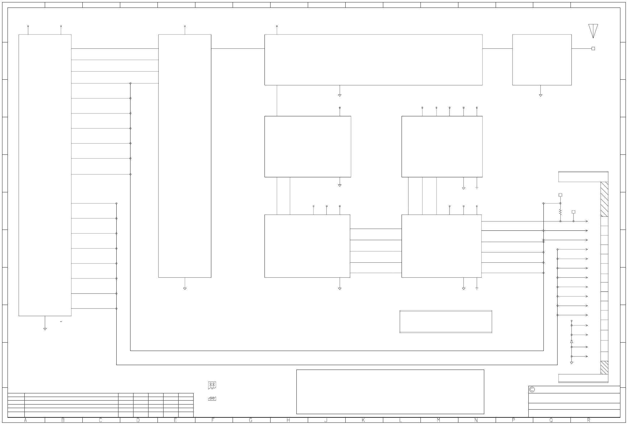
IPN 220-01396-03
M8SL2-00-002-812 T855 PCB Information B6.3.19
© Copyright Tait Electronics Limited August 2004. All rights reserved.
Sheet 1 – T855 Receiver Overview
220-01396-03
0
1
2
3
4
5
6
7
8
9
0
1
2
3
4
5
6
7
8
9
ABCDEFGHJ KL MNPQR
REV/ISS AMENDMENTS DATEAPVDD.O.CHKDDRAWN
NO.SHEETS:FILE NAME:
TAIT ELECTRONICS
IPN:
FILE DATE:
ISSUE: ID:.
2.SC.
PROJECT: DESIGNER:
1
10
T855
RECEIVER
1396_03B
220-01396-03
02-02-99
03B
T855RX BENC
0A ORIGINAL DAVES
1A UPDATE DAVES SLH DE RORY 22-08-97
2A C/N 710167 DAVES
3A C/N 710540 BENC 08-06-98
3B UPDATE CAD=BAAN BENC 02-02-99
PROCESSOR
SHEET 2
AUDIO
LINE-O/P-1
LINE-O/P-2
LINE-O/P-3
LINE-O/P-4
SPEAKER-O/P
GATE-O/P-1
RELAY-COM-1
RELAY-NO-1
RSSI
MUTE
AUDIO-2
AUDIO
RECT-NOISE
SPEECH
AUDIO-1
LED
RX-DISABLE
DISCRIMINATOR
SHEET 3
I-F
I-F-SIG
AUDIO
RECT-NOISE
SHEET 4
FRONT-END
VCO-O-P
SECTION
VCO
SHEET 5
CNTRL-VOLT
DIV-BUFFER
REGULATOR
SHEET 6
SYNTH
SHEET 7
LOCK-DETECT
SDA
SCK
SYNTH
MCU-CLOCK
P100
I/OPAD
R160
10
P170
I/OPAD
P160
I/OPAD
D111
SR2607
PL100
15 WAY R-ANGLE DRANGE PLUG
MICRO
SHEET 8
SYNTH
MCU-CLOCK
SCK
AUDIO-1
MUTE
LOCK-DETECT
LED
SERIAL-COM
SDA
RX-DISABLE
RESET
SPEECH
WATCHDOG
NOT-RESET
HARMONIC-FILTER
SHEET 9
ANTENNA
F-END-SIG
OUT-OF-CIRCUIT-DATA
SHEET 10
+9V+9V
+9V +5V +5V +5VDIG+9V
PL100
LINE-O/P-1
1
PL100
LINE-O/P-2
2
PL100
LINE-O/P-3
3
PL100
LINE-O/P-4
4
PL100
RSSI
5
PL100
AUDIO-1
6
PL100
SERIAL-COM
7
PL100
SPEAKER-O/P
8
PL100
+13V8
9
PL100
+13V8
10
PL100
GATE-O/P-1
11
PL100
RELAY-COM-1
12
PL100
RELAY-NO-1
13
PL100
GND
14
PL100
GND
15
+13V8 +9V
+13V8
+9V +5VDIG +20V +13V8 +9V +5V
+20V
DRANGE 1
PL100
7
6
5
13
12
11
8
4
3
2
1
10
9
14
15
DGND & GND ARE JOINED
THROUGH R617 ON SHEET 6
RELAY-NO-1
RELAY-COM-1
GATE-O/P-1
SPEAKER-O/P
LINE-O/P-4
LINE-O/P-3
LINE-O/P-2
LINE-O/P-1
LINE-O/P-1
LINE-O/P-2
LINE-O/P-3
LINE-O/P-4
SPEAKER-O/P
GATE-O/P-1
RELAY-COM-1
RELAY-NO-1
AUDIO-2
AUDIO-1
RSSI
RX-DISABLE
SPEECH
MUTE
LED
LED
MUTE
SPEECH
RX-DISABLE
AUDIO-1
AUDIO-2
RSSI
This sheet shows how the T855 circuitry is divided into separate sections which are
contained within separate cavities in the chassis. It is laid out to show the approximate
location of each section of circuitry on the PCB. The circuitry for each section is shown
on separate numbered sheets, and all components on the PCB are numbered to match
the sheet on which they appear. For example, all audio components appear on sheet 2
and are numbered between 200 and 299, all IF section components are on sheet 3 and
are numbered between 300 and 399, and so on.
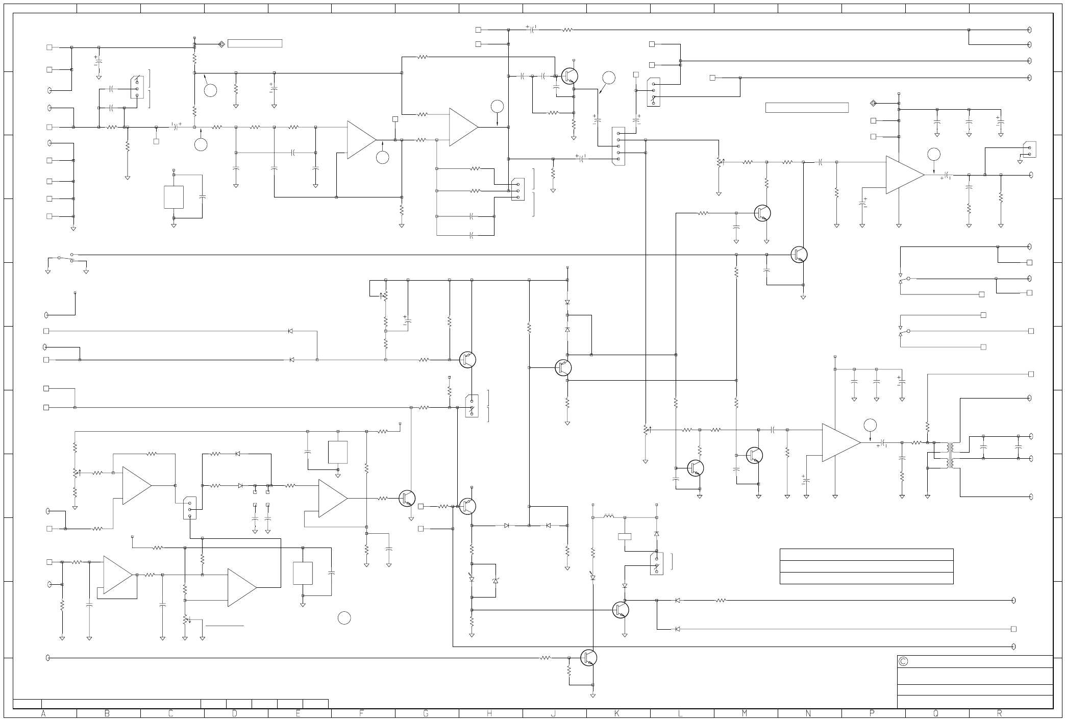
IPN 220-01396-03
B6.3.20 T855 PCB Information M8SL2-00-002-812
© Copyright Tait Electronics Limited August 2004. All rights reserved.
Sheet 2 – T855 Audio Processor
220-01396-03
0
1
2
3
4
5
6
7
8
9
0
1
2
3
4
5
6
7
8
9
ABCDEFGHJ KL MNPQR
REV/ISS AMENDMENTS DATEAPVDD.O.CHKDDRAWN
NO.SHEETS:FILE NAME:
TAIT ELECTRONICS
IPN:
FILE DATE:
ISSUE: ID:.
2.SC.
PROJECT: DESIGNER:
2
10
T855
AUDIO PROCESSOR
1396_03B
220-01396-03
02-02-99
03B
T855RX BENC
4V1
4V1
4V1
4V1
3V
6V4
6V4
&C203
10N
&R209
22K
&R219
8K2
&R202
4K7
C207
1U0
C211
4N7
C209
47U
C213
47N
C215
2P2
C274
100N
C217
47P
C286
4N7
C210
1N0
C253
100U
C219
4N7
C233
10U
C257
1N0
C237
1N0
C238
100N
C259
100N
C239
100U
C261
100U
C240A
1N0
C260A
1N0
C240B
100N
C249
470U
C260B
100N
C262
100U
C240C
220U
C251
100N
C260C
220U
C264
100N
C270
100N
C221
1N0
&C205
4N7
C280
47N
C266
4U7 NP
C268
4U7 NP
C235
1N0
C255
1N0
C278
100N
C223
100N
C225
100N
C229
10U
C276
47N
BAV99
D240
3
1
BAV99
D240
23
BAW56
D220
3
1
BAW56
D220
3
2
BAV70
D270
1
3
BAV70
D270
23
BAV70
D230
1
3
BAV70
D230
2
3
D280
GREEN
D285
1N4001
D290
1N4001
D295
1N4001
IC270
358
V-
4
V+
8
+
-
IC270
358
3
2
1
+
-
IC270
358
5
6
7
IC210
358
V-
4
V+
8
+
-
IC210
358
5
6
7
+
-
IC210
358
3
2
1
OP
IC240
TDA7231
+
4
-
3
V-
5
V+
1
OUT
2
OP
IC260
TDA7231
+
4
-
3
V-
5
V+
1
OUT
2
IC280
358
V-
4
V+
8
+
-
IC280
358
5
6
7
+
-
IC280
358
3
2
1
L230
100UH
P228
I/OPAD
P234
I/OPAD
P287
I/OPAD
P260
+13V8-FILT
I/OPAD
P270
NO2
I/OPAD
P282
NC2
I/OPAD
P268
NC-1
I/OPAD
P280
COMMON-2
I/OPAD
P207
I/OPAD
P222
I/OPAD
P225
I/OPAD
P236
I/OPAD
P238
I/OPAD
P240
I/OPAD
P284
LINE-MONITOR
I/OPAD
P201
I/OPAD
P246
I/OPAD
P250
I/OPAD
P219
I/OPAD
P254
AUDIO-2
I/OPAD
P242
I/OPAD
P231
I/OPAD
P248
I/OPAD P252
I/OPAD
RL210
12V RELAY
1
8
RL210
12V RELAY
3
42
RL210
12V RELAY
6
57
CW
RV230
10K LIN
2
3
1
CW RV220
10K
2
3
1
CW
RV210
10K LOG
2
3
1
CW
RV205
10K
1
3
2
CW
RV235
10K
2
3
1
R264
27K
R265
100
R269
2K2
R266
22K
R204
10K
R205
220K
R267
330K
R207
8K2
R210
15K
R280
100K
R281
4K7
R211
39K
R282
100K
R288
4K7
R213
2K7
R242
100
R285
47K
R287
10K
R218
3K9
R241
1K0
R244
6K8
R289
6K8
R245
1K0
R221
47K
R222
100K
R293
560
R294
1K0
R247
2K2
R227
1K0
R295
6K8
R296
1K2
R251
39K
R254
8K2
R255
47K
R232
47K
R230
4K7
R256
4K7
R233
8K2
R234
47K
R236
47K
R258
47K
R238
4R7
R260
4R7
R239
1K0
R261
150
R262
1K0
R284
100
R290
1K0
R201
4K7
R249
10K
R275
100
R273
15K
R277
5K6
R278
220K
R229
4K7
R252
4K7
R292
6K8
R271
100K
R272
47K
R215
15K
R224
3K9
R225
470
SW201
SPDT
12
3
T210
T4030
1
2
3
4
8
7
6
5
C201
10U
C227
100P
P204
I/OPAD
P213
I/OPAD
P216
I/OPAD
P263
I/OPAD
P210
I/OPAD
P244
I/OPAD
P256
SPEECH
I/OPAD
P266
I/OPAD
D289
1N4001
R298
47K
R299
47K
SL210SL220
C272
10N
C231
10U
D260
3V3
PL270
1X3 WAY
PL260
1X3 WAY
PL250
1X3 WAY
D250
RED
P258
+13V8-FILT I/OPAD
TP201
TP202
PL210
1X3 WAY
PL220
1X3 WAY
PL240
1X5 WAY PLUG
PL230
1X4 WAY
C222
10U
Q210
BC848
Q220
BC848
Q230
BC848
Q280
BC848
Q290
BC848
Q260
BC848
Q270
BC817
Q250
BC848
Q240
BC857
Q245
BC857
Q255
BC857
R297
10
%R223
10
PL200
2 WAY PLUG
+13V8
+13V8-FILT
+13V8-FILT
+13V8-FILT
+9V
+9V
+9V
+9V
+9V
+9V
+9V
+9V
GND
1R0
1R0
3A1
4A7
5A5
6B1
7A4
8A0
9C6
RELAY-COM-1
1R3
RELAY-NO-1
1R3
LINE-O/P-4
1R2
LINE-O/P-3
1R2
LINE-O/P-2
1R1
LINE-O/P-1
1R1
SPEAKER-O/P
1R2
+9V
3R8
4A8
5B7
6B3
7A5
8A1
RX-DISABLE
8Q6
RECT-NOISE
3K2
RSSI
1R3
3R1
MUTE
8A4
GATE-O/P-1
1R2
+13V8
1R1
1R1
6B2
+13V8
SPEECH
8R0
AUDIO-2
AUDIO-1
1R3
3R4
8A2
LED
8R4
AUDIO
3R5
DISCRIMINATOR
1R3
3R4
8A2
MUTE-DISABLE
DE-EMPHASIS
FLAT
DE-EMPHASIS
FLAT
RX
DISABLE
LINK
GATE
SENSITIVITY
RX-DISABLE
LINE LEVEL
MONITOR VOLUME
GREEN
SUPPLY
RELAY
LINK
MUTE
DC CONDITIONS (VOLTS)
CARRIER MUTE
6B4
6B2
6B3
+13V8-FILT_TESTPOINT
+9V-TESTPOINT
A
B
C
D
E
F
G
H
J
K
N
L
P
Q
M
R
S
T
U
V
W
X
Y
Z
RX-DISABLE-A
RX-GATE-OUT
RX-DISABLE-B
VARIANT COMPONENTS
&C203 &C205 &R202 &R209 &R219
Refer to the parts list for the values for each product type.
IPN 220-01396-03
M8SL2-00-002-812 T855 PCB Information B6.3.21
© Copyright Tait Electronics Limited August 2004. All rights reserved.
Sheet 3 – T855 IF Section
220-01396-03
0
1
2
3
4
5
6
7
8
9
0
1
2
3
4
5
6
7
8
9
ABCDEFGHJ KL MNPQR
REV/ISS AMENDMENTS DATEAPVDD.O.CHKDDRAWN
NO.SHEETS:FILE NAME:
TAIT ELECTRONICS
IPN:
FILE DATE:
ISSUE: ID:.
2.SC.
PROJECT: DESIGNER:
3
10
T855
I-F
1396_03B
220-01396-03
02-02-99
03B
T855RX BENC
2V0
2V8
9V0
6V8
9V0
2V0
2V6
1V8
4V2
4V8
5V0
0V75
8V5
1V0
1V7
&C318
8P2
&C326
8P2
&C336
12P
&C338
12P
&C322
15P
&C334
47P
&C340
47P
&R344
56K
C364
39P
&C320
3P9
C366
39P
C368
47N
C374
4N7
C378
120P
&C324
3P9
C372
47N
C376
120P
C380
10N
C330
1N0
C332
4N7
C382
10U
C384
47N
C342
4N7
C346
4N7
C302
100P
C348
4N7
C304
2P7
C350
4N7
C388
4N7
C390
10U
C306
4N7
C392
4N7
C308
1N0
C352
27P
C394
47N
C316
15P
C312
10U
C356
12P
C314
4N7
TANT
C354
10U
C357
10N
C358
47N
C360
4N7
C362
10N
C344
4N7
C310
10N
C370
4N7
C386
47N
C328
4N7
L330
#622
2
3
1
L340
#622
2
3
1
L350
#622
2
3
1
L360
#622
2
3
1
L370
#622
2
3
1
L310
#622
2
3
1
L320
#622
2
3
1
L385
#622
2
3
1
L390
#631
2
36
14
CW RV310
2K2
2
3
1
CW
RV320
2K2
23
1
R350
18K
R351
10K
R352
390K
R358
47
R362
3K3
R360
15K
R366
3K3
R364
1K0
R370
100K
R368
22K
R372
2K7
R312
3K3
R314
4K7
R374
1K0
R316
47
R318
10K
R378
100K
R380
10K
R320
3K9
R382
47K
R384
47K
R322
8K2
R323
10K
R326
10K
R324
22K
R386
12K
-T
R390
10K
R392
0
R332
330
R388
10K
R328
1K0
R330
47
R302
39E
R395
0
R304
2K7
R338
1K0
R339
10K
R396
390
R308
10
R397
820
R398
2K2
-T
R399
10K
R348
220
R310
0
R306
10
R393
10K
R354
1M0
R356
180
R346
10
R376
0
-T
R334
150
R336
470
R394
47
TP310
TP311
TP313
TP314
TP309
X310
44.545M
D
S
G
Q310
BF247
XF
GND
I/O
&XF300B
45M
1
2
3
XF
GND
I/O
&XF300A
45M
1
2
3
Q320
BFS17
BPF
&XF301
14M
IN
1
GND
2
OUT 3
BF991
Q330
OSC
IC310
3361CP
IN
IN OUT
OUT
IF
IC310
3361CP
LIM
GND
BP1 BP2 QCIN VCC
AF
BPFIN OUT
&XF302
CFW455E
1
234
5
Q340
BC848
CTL
SW
SQUELCH
IC310
3361CP
IN
OUT CTL
SC
SW
Q350
BC848
Q360
BC848
BAW56
D310
3
2
BAW56
D310
3
1
VREG
IC320
78L05
VIN
3
GND
1
VOUT
2
SK320
1X3 WAY
SK330
1X4 WAY
R341
0
R340
0
%R349 100
R353
0
C351
1P0
C331
2P2
C349
2P7
R337
220
TANT
C355
10U
TANT
C359
10U
C367
10N
C361
100N
R365
150K
R367
150K
L380
#622
2
3
1
C347
4N7
BAT17DS
D350
2
3
BAT17DS
D350
3
1
+5V-REG
+9V
+9V
+9V
+9V
+9V
I-F-SIG
4R5
+9V
2A8
4A8
5B7
6B3
7A5
8A1
+9V
GND
1R0
1R0
2A7
4A7
5A5
6B1
7A4
8A0
9C6
RSSI
1R3
2A0
AUDIO
2A8
RECT-NOISE
2A2
+5V-REG
DISCRIMINATOR
1R3
2R9
2R9
8A2
+5VIF
+5VIF
+5VIF
RSSI SET UP
MUTE SET UP
-115
-115
-100
SENSITIVITY
DC CONDITIONS (VOLTS)
A
C
RECT-NOISE_TESTPOINT
6B3
6B1
VARIANT COMPONENTS
&C318
&C320
&C322
&C324
&C326
&C334
&C336
&C338
&C340
&R344 &XF300A
&XF300B
&XF301
&XF302
Refer to the parts list for the values for each product type.
IPN 220-01396-03
B6.3.22 T855 PCB Information M8SL2-00-002-812
© Copyright Tait Electronics Limited August 2004. All rights reserved.
Sheet 4 – T855 Front End
220-01396-03
0
1
2
3
4
5
6
7
8
9
0
1
2
3
4
5
6
7
8
9
ABCDEFGHJ KL MNPQR
REV/ISS AMENDMENTS DATEAPVDD.O.CHKDDRAWN
NO.SHEETS:FILE NAME:
TAIT ELECTRONICS
IPN:
FILE DATE:
ISSUE: ID:.
2.SC.
PROJECT: DESIGNER:
4
10
T855
FRONT-END
1396_03B
220-01396-03
02-02-99
03B
T855RX BENC
1V0
0V28
4V3
C410
1P8
C420
47P
C450
47P
C430
100P
C440
10U
C470
10P
C480
56P
#FL410
HELICAL FILTER
13 2
#FL420
HELICAL FILTER
13 2
L420
330N
L440
330N
R405
0
R410
0
R415
330
R435
10
R425
1K0
R430
150
R420
10
R440
0
R445
470
R450
10
R455
470
R465
33
R460
180
R470
180
R475
47
TP412
TP408
TP409
TP410
TP411
Q410
MMBR571
GND
IF
LO
RF
IC410
MIXER
1
2567
8
3
4
L410
PRINTED
L430
PRINTED
%C460
2P7
F-END-SIG
9K7
I-F-SIG
3A9
+9V
2A8
3R8
5B7
6B3
7A5
8A1
GND
1R0
1R0
2A7
3A1
5A5
6B1
7A4
8A0
9C6
+9V
VCO-O-P
5F2
+9V
6B4
6B2
-118
-117
-110 -111
-118
MICROSTRIP
MICROSTRIP
MICROSTRIP
MICROSTRIP
IPN 220-01396-03
M8SL2-00-002-812 T855 PCB Information B6.3.23
© Copyright Tait Electronics Limited August 2004. All rights reserved.
Sheet 5 – T855 VCO Section
220-01396-03
0
1
2
3
4
5
6
7
8
9
0
1
2
3
4
5
6
7
8
9
ABCDEFGHJ KL MNPQR
REV/ISS AMENDMENTS DATEAPVDD.O.CHKDDRAWN
NO.SHEETS:FILE NAME:
TAIT ELECTRONICS
IPN:
FILE DATE:
ISSUE: ID:.
2.SC.
PROJECT: DESIGNER:
5
10
T855
VCO SECTION
1396_03B
220-01396-03
02-02-99
03B
T855RX BENC
SK505
1 WAY SOCKET
RF-OUT
SK504
1 WAY SOCKET
GND
SK503
1 WAY SOCKET
GND
SK502
1 WAY SOCKET
GND
SK501
1 WAY SOCKET
GND
SK535
1 WAY SOCKET
+9V-VCO
SK534
1 WAY SOCKET
GND
SK533
1 WAY SOCKET
GND
SK532
1 WAY SOCKET
GND
SK531
1 WAY SOCKET
CV-OUT
SK513
1 WAY SOCKET
VCO-BUFFER
SK522
1 WAY SOCKET
DIV-BUFFER
C505
100N
R510
2K2
R555
470
C535
100N
TANT
C530
22U
Q540
BC848
C515
100N
R515
56E
+9V
CNTRL-VOLT
7R3
VCO-O-P
4R7
DIV-BUFFER
7R0
+9V
2A8
3R8
4A8
6B3
7A5
8A1
GND
1R0
1R0
2A7
3A1
4A7
6B1
7A4
8A0
9C6
+9V
+9V
1
2
3
4
5
1
2
3
4
5
6B2
6B4
The circuit diagram for the
VCO PCB is in Part E.
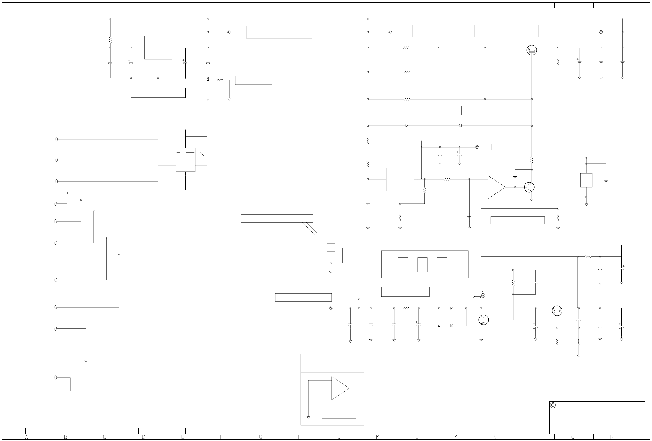
IPN 220-01396-03
B6.3.24 T855 PCB Information M8SL2-00-002-812
© Copyright Tait Electronics Limited August 2004. All rights reserved.
Sheet 6 – T855 Regulators
220-01396-03
0
1
2
3
4
5
6
7
8
9
0
1
2
3
4
5
6
7
8
9
ABCDEFGHJ KL MNPQR
REV/ISS AMENDMENTS DATEAPVDD.O.CHKDDRAWN
NO.SHEETS:FILE NAME:
TAIT ELECTRONICS
IPN:
FILE DATE:
ISSUE: ID:.
2.SC.
PROJECT: DESIGNER:
6
10
T855
REGULATORS
1396_03B
220-01396-03
02-02-99
03B
T855RX BENC
C665
10U
C690
100N
TANT
C693
10U
C630
100N
TANT
C631B
10U
C631A
100N
C640
1N0
C625
470U
C626
4N7
C628
1N0
TANT
C670
3U3
C673
4N7
C677
1U0
TANT
C684
10U
C637
120P
C623
120P
C687
1N0
C660
100N
C681
100N
C651
100N
R681
100
R689
10
R637
33
R649
4K7
R625
1K0
R629
270
R621
1E0
R619
1E0
R633
6K8
R653
10K
R693
100K
R685
15K
R696
56K
R641
1K5
R645
470
T610
#650
2
36
14
VREG
IC610
78L05
VIN
3
GND
1
VOUT
2
C611A
100U
C610B
100U
C610A
10N
C611B
10N
R617
0
C658
100N
BAV70
D640
23
BAV70
D640
13
VREG
IC630
LM317L
VIN
3
ADJ
2
VOUT
1
R636
33
IC640
358D
V-
4
V+
8
+
-
IC640
358D
3
2
1
+
-
IC640
358D
5
6
7
Q660
BC817
Q620
BD234
Q630
BC557
Q670
BC857
SHLD610
10MM SQ * 11MM
TP604
TP603
R615
100
IC650
LOW PWR MON
PBRST 1
TD 2
TOL 3
GND
4
+V
8
ST
7
RST
6
RST
5
D610
BAV99
23 D610
BAV99
31
TP602
TP601
TP607
+13V8
+5V
+9V
+9V
GND
1R0
1R0
2A7
3A1
4A7
5A5
7A4
8A0
9C6
+13V8
1R1
1R1
2A5
+9V
2A8
3R8
4A8
5B7
7A5
8A1
+5V
7A5
8A1
+20V
7A4
+20V
+13V8
+5V
+9V
+13V8
+20V
+5VDIG
+9V +5VDIG
+5VDIG
8A9
+5VDIG
DGND
8A0
RESET
8A8
WATCHDOG
8R5
NOT-RESET
7A2
8R4
8R4
+20V SUPPLY
+5V REGULATOR
+9V REGULATOR
SPARE GATE
IC640
CAN TO SHIELD T610
+5V TESTPOINT
+20V TESTPOINT
+5VDIG-SUPPLY
DGND CONNECTS GND
THROUGH R617
+5VDIG TESTPOINT +13V8-TESTPOINT +9V-TESTPOINT
240KHz
24vpp
IPN 220-01396-03
M8SL2-00-002-812 T855 PCB Information B6.3.25
© Copyright Tait Electronics Limited August 2004. All rights reserved.
Sheet 7 – T855 Synthesiser
220-01396-03
0
1
2
3
4
5
6
7
8
9
0
1
2
3
4
5
6
7
8
9
ABCDEFGHJ KL MNPQR
REV/ISS AMENDMENTS DATEAPVDD.O.CHKDDRAWN
NO.SHEETS:FILE NAME:
TAIT ELECTRONICS
IPN:
FILE DATE:
ISSUE: ID:.
2.SC.
PROJECT: DESIGNER:
7
10
T855
SYNTHESISER
1396_03B
220-01396-03
02-02-99
03B
T855RX BENC
IC740
145191
REF IN 20
REF OUT 1
LD 2
OR 3
OV 4
RX 8
TEST1 9
FIN 10
GND
7
VPD
5
VCC
12
VDD
14
PDOUT
6
DATA
19
CLK
18
ENABLE
17
OUT A
16
OUT B
15
TEST2
13
FIN
11
R787
10
R785
3K3
R784
120
C784
120P
C788
120P
R791
1K0
C791
8P2
C782
120P
R701
22
12.8M
=IC700
GND OUT
VCC FM R703
1M0
R702
1M0
C700
100N
C710B
100N
C710C
10N
C705
8P2
R706
15K
R707
47K
R712
10
C703
1N0
R711
100
TANT
C710A
4U7
C776
6N8
C713
10N
C741B
10N
R744
22
C740B
10N
R742
150
R746
22
R747
22
C742B
10N
C742A
100N
TANT
C741A
4U7
R767
680
R754
1K0
R753
1M0
R752
22
C757
10N
R750
22
TANT
C750
10U
R757
470K
R756
470K
C759
10N
C764
10N
TANT
C765
4U7
R766
1K0
R765
680
R760
180
R758
1K2
C761
10N
TANT
C762
22U
C767
1N0
R769
180
R762
100
R771
8K2
R763
100
TANT
C770
22U
TANT
C772
22U
C769
1N0
R774
8K2
R772
22K
R775
18K
C774
100N
R790
390
C786
100N
C743
47P
C736
47P
C735
47P
R748
47K
R786
10
C792
120P
C745
120P
R749
47K
R743
150
C740A
1N0
R709
100
IC710
74HC04
34
IC710
74HC04
13 12
IC710
74HC04
11 10
IC710
74HC04
98
IC710
74HC04
56
C702
1N0
IC710
74HC04
V-
7
V+
14
C711
22P
C712
22P
R708
100
IC710
74HC04
12
TP710
+
-
IC750
33078D
3
2
1
+
-
IC750
33078D
5
6
7
IC750
33078D
V-
4
V+
8
Q760
BC848
Q780
BC848
Q795
MMBR571
Q750
BC807
Q770
BC857
Q785
BC857
Q775
BC857
D
S
GQ790
BFR31
L740
1.5T/2.5
R780
68
R782
18
D730
BAT65
D740
BAT65
R759
330
C709
10P
C708
47P
C707
47P
R710
100
D730A
SOD-323
D740A
SOD-323
+9V
+5V +5V
+5V
+5V
+5V
+9V
+5V
+5V
+9V
+20V
+20V
CNTRL-VOLT
5B9
DIV-BUFFER
5J5
LOCK-DETECT
8A7
SCK
6B6
8R4
8R4
SYNTH
8R5
SDA
8R4
+5V
6B4
8A1
+20V
6B2
GND
1R0
1R0
2A7
3A1
4A7
5A5
6B1
8A0
9C6
+9V
2A8
3R8
4A8
5B7
6B3
8A1
MCU-CLOCK
8A3
AA1_OV AB21_1
AB3_1AA1_OR
AB21_1
AA1_OV
AB3_1
AA1_OR
SPARE GATES
IC710
6B2
6B4
6B4
LOCK-DETECT TESTPOINT
LOCKEDLOW
6B6
8R4
5V
3V3
0V2
2V8
6V6
+5V TO + 15V LOCKED
8V5
2V
1V4
VARIANT
DEVICES
LOCK-DETECT
IPN 220-01396-03
B6.3.26 T855 PCB Information M8SL2-00-002-812
© Copyright Tait Electronics Limited August 2004. All rights reserved.
Sheet 8 – T855 Microcontroller
220-01396-03
0
1
2
3
4
5
6
7
8
9
0
1
2
3
4
5
6
7
8
9
ABCDEFGHJ KL MNPQR
REV/ISS AMENDMENTS DATEAPVDD.O.CHKDDRAWN
NO.SHEETS:FILE NAME:
TAIT ELECTRONICS
IPN:
FILE DATE:
ISSUE: ID:.
2.SC.
PROJECT: DESIGNER:
8
10
T855
MICROCONTROLLER
1396_03B
220-01396-03
02-02-99
03B
T855RX BENC
R822
47K
R811
4K7
R810
4K7
R824 2K2
R825 2K2
R826 2K2
R827 2K2
R828 2K2
R840 2K2
R841 2K2
R842 2K2
R813
4K7
R812
4K7
R805
470
R823
47K
C813
1N0
IC820
24C16
A0
1
A1
2
A2
3
GND
4
+V
8
SCL 6
SDA 5
WP7
R849 470
R850 470
R851 470
R809
4K7
R843 2K2
R804
47K
C850
47N
R808
10
P810
I/OPAD
R837 2K2
R836 2K2
R835 2K2
R833 2K2
R832 2K2
R831 2K2
R830 2K2
R829 2K2
SK805
2X8 WAY TOP ENTRY SMD SKT
1
SK805
2X8 WAY TOP ENTRY SMD SKT
2
SK805
2X8 WAY TOP ENTRY SMD SKT
3
SK805
2X8 WAY TOP ENTRY SMD SKT
4
SK805
2X8 WAY TOP ENTRY SMD SKT
5
SK805
2X8 WAY TOP ENTRY SMD SKT
6
SK805
2X8 WAY TOP ENTRY SMD SKT
7
SK805
2X8 WAY TOP ENTRY SMD SKT
8
SK805
2X8 WAY TOP ENTRY SMD SKT
9
SK805
2X8 WAY TOP ENTRY SMD SKT
10
SK805
2X8 WAY TOP ENTRY SMD SKT
11
SK805
2X8 WAY TOP ENTRY SMD SKT
12
SK805
2X8 WAY TOP ENTRY SMD SKT
13
SK805
2X8 WAY TOP ENTRY SMD SKT
14
SK805
2X8 WAY TOP ENTRY SMD SKT
15
SK805
2X8 WAY TOP ENTRY SMD SKT
16
P820
I/OPAD
P825
I/OPAD
P830
I/OPAD
P835
I/OPAD
R854
330K
R855
47K
R858
27K 1%
C815
10N
C826
10N
C828
10N
R859
1M2 1%
R860
820K 1%
C818
10N
R856
150K
R857
150K
C819
33P
C820
220P
C824
47N
C822
22N
+
-
IC830
LM324D
10
9
8
+
-
IC830
LM324D
5
6
7
C834
10N
R866
820K
IC850
LM324D
V-
11
V+
4
+
-
IC830
LM324D
3
2
1
R861
5K1 1%
R868
4K7
C836
10N
R869
27K 1%
C837
10N
R870
1M2 1%
C838
10N
R871
820K 1%
+
-
IC830
LM324D
12
13
14
R872
5K1 1%
R873
2K2
IC840
4053BD
INH 6
A11
B10
C9
X0 12
X1 13
Y0 2
Y1 1
Z0 5
Z1 3
GND
8
VREF
7
+V
16
Z
4
X
14
Y
15
R877
100K
R878
100K
R876
100K
R879
100K
C842
1U0
C844
1U0
C846
1U0
C848
1U0
R891
100K
+
-
IC850
LM324D
10
9
8
+
-
IC850
LM324D
3
2
1
+
-
IC850
LM324D
12
13
14
+
-
IC850
LM324D
5
6
7
R892
330K
BAV70
D860
23
R889
100K
R890
150K
R898
470K
R897
10K
R895
10K
C879
10U
R884
150K
R885
150K
C873
22N
C876
100U
R888
8K2 1%
R887
1K0 1%
R886
10K 1%
IC830
LM324D
V-
11
V+
4
R821
47K
R820
47K
C816
10N
R863
4K7
BAV70
D860
13
R894
4K7
R852
4K7
R881
47K
R882
47K
R875
4K7
R844
47K
R845
150K
C830
47N
P815
I/OPAD
R846
4K7
R847
4K7
Q810
BC817
Q870
BC848
Q890
BC848
Q880
BC848
Q895
BC848
Q860
BC857
Q820
BC857
SK810
80C51
P1.7
9
P1.6
8
P1.5
7
P1.4
6
P1.3
5
P1.2
4
P1.1
3
P1.0
2
P3.7/RD
19
P3.6/WR
18
P3.5/T1
17
P3.4/T0
16
P3.3/INT1
15
P3.2/INT0
14
P3.1/TXD
13
P3.0/RXD
11
VSS
22
XTL1
21
XTL2
20
RST
10
VCC
44
P0.7 36
P0.6 37
P0.5 38
P0.4 39
P0.3 40
P0.2 41
P0.1 42
P0.0 43
EA 35
ALE 33
PSEN 32
P2.7 31
P2.6 30
P2.5 29
P2.4 28
P2.3 27
P2.2 26
P2.1 25
P2.0 24
C840
47N
C810
10N
R848 470
Q840
BC857
Q850
BC848
R815
47K
R819
4K7
C812
100P
R818
4K7
R816
150K
R865
2K7
C832
1U0
R867
820K
C833
22N
C814
1N0
R853
470
P840
I/OPAD
BAV70
D880
2
3
BAV70
D880
1
3
D820
BAT65
D820A
SOD-323
+5VDIG
+9V
+5VDIG
+5VDIG
MCU-CLOCK
7A6
SYNTH
7A2
SCK
6B6
7A2
AUDIO-1
1R3
2R9
2R9
3R4
MUTE
2R0
LOCK-DETECT
7R5
LED
2A0
+5V
SERIAL-COM
1R4
+5V
6B4
7A5
+9V
2A8
3R8
4A8
5B7
6B3
7A5
+5V
+9V
SDA
7A2
RX-DISABLE
2A4
GND
1R0
1R0
2A7
3A1
4A7
5A5
6B1
7A4
9C6
+5VDIG
RESET
6B5
DGND
6B0
+5VDIG
6B4
+5VDIG
+4V2
+9V +4V2
+9V
+9V+4V2
+4V2
+5VDIG
SPEECH
2R8
+9V WATCHDOG
6B6
+5VDIG
+9V
NOT-RESET
6B6
7A2
+5VDIG
+5VDIG
LOCK-DETECT
AB24_2
LOCK-DETECT AB24_2
MICROMATCH
CHANNEL SELECT TO MICRO BUS
1
2
3
4
5
6
7
8
9
10
11
12
13
14
15
16
6B2
6B4
6B4
12.8MHz
0V
5V
5V
4V2
4V2
4V2
4V2
3V8
D-RANGE2
1
2
3
4
5
6
7
11
NC
15
14
13
10
12
9
8
PIN PIN
MICROMATCH TO D-RANGE2 CONNECTIONS
WHEN DETECTING TONE3V7
VARIANT
DEVICES
CH-SLCT-0
CH-SLCT-1
CH-SLCT-2
CH-SLCT-3
CH-SLCT-4
CH-SLCT-5
CH-SLCT-6
CH-SLCT-7
CH-SLCT-2
CH-SLCT-3
CH-SLCT-4
CH-SLCT-5
CH-SLCT-6
CH-SLCT-7
CH-SLCT-1
CH-SLCT-0
RESET
MCU-CLOCK
SERIAL_COM-1
CTCSS_MSB
CTCSS_LSB
CTCSS_RX
SYNTH_LOCK_DETECT
CTCSS_ENABLE
SYNS
LED_FLASH
SCK
WATCHDOG
SDA
DCS_INPUT
MUTE_OUT
MUTE_OUT
IPN 220-01396-03
M8SL2-00-002-812 T855 PCB Information B6.3.27
© Copyright Tait Electronics Limited August 2004. All rights reserved.
Sheet 9 – T855 Harmonic Filter
220-01396-03
0
1
2
3
4
5
6
7
8
9
0
1
2
3
4
5
6
7
8
9
ABCDEFGHJ KLM
REV/ISS AMENDMENTS DATEAPVDD.O.CHKDDRAWN
NO.SHEETS:FILE NAME:
TAIT ELECTRONICS
IPN:
FILE DATE:
ISSUE: ID:.
2.SC.
PROJECT: DESIGNER:
9
10
T855
HARMONIC-FILTER
1396_03B
220-01396-03
02-02-99
03B
T855RX BENC
AA
K
SOT23
DIODES
KA
KA
SOT23
DIODES
KK
A
SOT23
DIODES
BE
C
SOT23
PNP
BE
C
SOT23
NPN
TO-92
PNP
B
C
E
TO-92
FET
S
G
D
TO-126
PNP
E
C
B
DS
G
SOT23
FET
CHIP
TANTALUMS
C930
8P2
C940
6P8
C950
3P3
L930
1.5T/4.0
L940
2.5T/2.5
L920
1.5T/4.0
C920
6P8
C910
3P3
L910
2.5T/2.5
ANTENNA
GND
1R0
1R0
2A7
3A1
4A7
5A5
6B1
7A4
8A0
F-END-SIG
4A5
6B2
1R8
BAV70 BAV99
BAT17DS
DIODE PHYSICAL PIN OUTS
BAW56 BC857
BC807
BC848
BC817
MMBR571
MMBR951L
BC557 BF247 BD234BFR31
TRANSISTOR PHYSICAL PIN OUTS
TANTALUMS
HARMONIC-FILTER
IPN 220-01396-03
B6.3.28 T855 PCB Information M8SL2-00-002-812
© Copyright Tait Electronics Limited August 2004. All rights reserved.

M8SL2-00-002-812 CI
© Copyright Tait Electronics Limited August 2004. All rights reserved.
Part C T854 Transmitter
This part of the manual is divided into six sections, as listed below. There is a detailed
table of contents at the start of each section.
Section Title
1 General Information
2 Circuit Operation
3 Initial Tuning and Adjustment
4 Functional Testing
5 Fault Finding
6 PCB Information

CII M8SL2-00-002-812
© Copyright Tait Electronics Limited August 2004. All rights reserved.

M8SL2-00-002-812 T854 General Information C1.1
© Copyright Tait Electronics Limited August 2004. All rights reserved.
1 T854 General Information
This section provides a brief description of the T854 transmitter, along with detailed
specifications and a list of types available.
The following topics are covered in this section.
Section Title Page
1.1 Introduction 1.5
1.2
1.2.1
1.2.2
1.2.3
1.2.4
1.2.4.1
1.2.4.2
1.2.4.3
1.2.5
1.2.6
1.2.6.1
1.2.6.2
1.2.6.3
Specifications
Introduction
General
RF Section
Audio Processor
Inputs
Modulation Characteristics
CTCSS
Microcontroller
Test Standards
European Telecommunication Standard
DTI CEPT Recommendation T/R-24-01
Telecommunications Industry Association
1.6
1.6
1.6
1.7
1.8
1.9
1.9
1.9
1.10
1.10
1.10
1.10
1.10
Figure Title Page
1.1 T854 Main Circuit Block Identification 1.2
1.2 T854 Front Panel Controls 1.3

C1.2 T854 General Information M8SL2-00-002-812
© Copyright Tait Electronics Limited August 2004. All rights reserved.
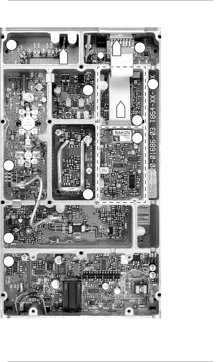
M8SL2-00-002-812 T854 General Information C1.3
© Copyright Tait Electronics Limited August 2004. All rights reserved.
Figure 1.1 T854 Main Circuit Block Identification
Key: 1
2
3
4
5
6
7
low pass filter
PA
exciter drive amplifier
audio processor
VCO
regulators
synthesiser
8
9
10
A
B
C
microcontroller and CTCSS
duct for cabling to extra D-range (if fitted)
D-range
RF output
D-range connector (“D-range 1”) incl. audio in and DC in
(refer to Section 1.5 in Part G)
microcontroller
1
234
5 6
7 8
A
B
C
9
10
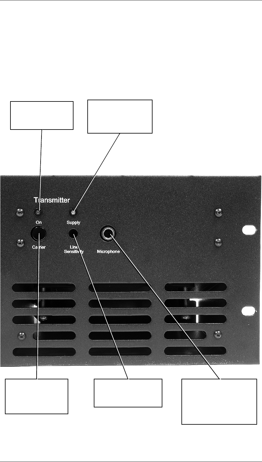
C1.4 T854 General Information M8SL2-00-002-812
© Copyright Tait Electronics Limited August 2004. All rights reserved.
Figure 1.2 T854 Front Panel Controls
On LED
The On LED is lit when the
T854 is transmitting.
Carrier Switch
Keys the transmitter (while
disabling the 600Ω line and
microphone audio).
Supply LED
The Supply LED is lit when
DC power is supplied to the
transmitter.
Line Sensitivity
Sets the gain of the 600Ω line
input of the audio processor.
Microphone Socket
For connecting a T800-80 micro-
phone to allow local control of
the transmitter. The 600Ω line is
disabled when the PTT button is
pressed.

M8SL2-00-002-812 T854 General Information C1.5
© Copyright Tait Electronics Limited August 2004. All rights reserved.
1.1 Introduction
The T854 is a synthesised, microprocessor controlled FM base station transmitter
designed for single or multichannel operation in the 400 to 520MHz frequency range1
with a standard power output of 25W. The RF section of the transmitter comprises a fre-
quency synthesiser which provides 100mW of frequency modulated RF drive to a two
stage, wide band driver stage followed by a 25W power amplifier. A thermal shutdown
feature is provided in the T854 in case operating temperatures exceed acceptable levels.
The T854 is rated for a continuous output power of 25W at +60°C. This is achieved via a
high capacity heatsink, electric fan and shroud. The fan forces air across the heatsink to
dissipate the heat. The heatsink replaces one of the usual T800 covers.
A wide selection of audio characteristics may be obtained from the audio processor.
Optional circuit blocks are an audio compressor and a pre-emphasis stage. They can be
bypassed or linked to one or both audio inputs, and then back into the remaining audio
circuitry in almost any combination. All audio processor options are link selectable.
The synthesiser frequency is programmed via the serial communications port. Eight
channel select lines are accessible via an optional D-range connector (D-range 2 –
T800-03-0000) at the rear of the set.
All components except those of the VCO are mounted on a single PCB. This is secured
to a die-cast chassis which is divided into compartments to individually shield each sec-
tion of circuitry. Access to the PCB is primarily through the top cover of the radio, as all
components are mounted on the top side of the PCB. There is provision within the chas-
sis to mount small option PCBs.
The front panel controls include line sensitivity, microphone socket and carrier switch.
This switch turns on the carrier (unmodulated) as an aid to servicing.
1. Although capable of operating over the 400 to 520MHz frequency range, the T854 has
an 8MHz switching range (see Section 1.2.3 and Section 3.1).

C1.6 T854 General Information M8SL2-00-002-812
© Copyright Tait Electronics Limited August 2004. All rights reserved.
1.2 Specifications
1.2.1 Introduction
The performance figures given are minimum figures, unless otherwise indicated, for
equipment tuned with the maximum switching range and operating at standard room
temperature (+22°C to +28°C) and standard test voltage (13.8VDC).
Where applicable, the test methods used to obtain the following performance figures
are those described in the EIA and ETS specifications. However, there are several
parameters for which performance according to the CEPT specification is given. Refer to
Section 1.2.6 for details of test standards.
Details of test methods and the conditions which apply for Type Approval testing in all
countries can be obtained from Tait Electronics Ltd.
The terms “wide bandwidth”, “mid bandwidth” and “narrow bandwidth” used in this
and following sections are defined in the following table.
1.2.2 General
Number Of Channels …128 (standard)
Supply Voltage:
Operating Voltage …10.8 to 16VDC
Standard Test Voltage …13.8VDC
Polarity …negative earth only
Polarity Protection …crowbar diode
Line Keying Supply (if required) …–50VDC
Supply Current:
Transmit – T854 …5.5A (typical)
Standby – T854 …150mA (typical)
Operating Temperature Range …–30°C to +60°C
Time-Out Timer (optional) …0 to 10 minutes adjustable in 10 sec-
ond steps
Channel Spacing Modulation
100% Deviation
Receiver
IF Bandwidth
Wide Bandwidth 25kHz ±5.0kHz 15.0kHz
Mid Bandwidth 20kHz ±4.0kHz 12.0kHz
Narrow Bandwidth 12.5kHz ±2.5kHz 7.5kHz

M8SL2-00-002-812 T854 General Information C1.7
© Copyright Tait Electronics Limited August 2004. All rights reserved.
Tail Timer …0 to 5 seconds adjustable in 20ms
steps
Transmit Key Time …Typically 35ms
Transmit Lockout Timer …0 to 1 minute adjustable in 10 second
steps
1.2.3 RF Section
Frequency Range …400 to 520MHz
Modulation Type …FM
Frequency Increment …5 or 6.25kHz
Switching Range …8MHz (i.e. ±4MHz from the centre
frequency)
Load Impedance …50Ω
Frequency Stability …±1ppm, –30°C to +60°C
Adjacent Channel Power (full deviation):
Wide Bandwidth (WB) …–75dBc
(±25kHz/15kHz B/W)
Mid Bandwidth (MB) …–70dBc
(±20kHz/12kHz B/W)
Narrow Bandwidth (NB) …–65dBc
(±12.5kHz/7.5kHz B/W)
Transmitter Switching …complies with ETS 300 113

C1.8 T854 General Information M8SL2-00-002-812
© Copyright Tait Electronics Limited August 2004. All rights reserved.
Transmitter Side Band Noise:
(no modulation, 15kHz bandwidth)
At ±25kHz …–95dBc
At ±1MHz …–105dBc
Intermodulation …–40dBc with interfering signal of
–30dBc
…–70dBc with 25dB isolation
and interfering signal of –30dBc
(PA with output isolator)
T854 Mismatch Capability:
Ruggedness …refer to your nearest Tait Dealer or
Customer Service Organisation
Stability …3:1 VSWR (all phase angles)
Radiated Spurious Emissions:
Transmit …–36dBm to 1GHz
–30dBm 1GHz to 4GHz
Standby …–57dBm to 1GHz
–47dBm 1GHz to 4GHz
Conducted Spurious Emissions: (T854 Only)
Transmit …–36dBm to 1GHz
–30dBm 1GHz to 4GHz
Standby …–57dBm to 1GHz
–47dBm 1GHz to 4GHz
Power Output:
T854 – Rated Power …25W
– Range Of Adjustment …5 to 25W
Duty Cycle …100% at 25W at +60°C
1.2.4 Audio Processor
1.2.4.1 Inputs
Inputs Available …line, microphone and CTCSS
Line Input:
Impedance …600Ω (balanced)
Sensitivity (60% modulation at 1kHz)
With Compressor …–50dBm
Without Compressor …–30dBm
Microphone Input:
Impedance …600Ω

M8SL2-00-002-812 T854 General Information C1.9
© Copyright Tait Electronics Limited August 2004. All rights reserved.
Sensitivity (60% modulation at 1kHz)
With Compressor …–70dBm
Without Compressor …–50dBm
1.2.4.2 Modulation Characteristics
Frequency Response …flat or pre-emphasised (optional)
(below limiting)
Line And Microphone Inputs:
Pre-emphasised Response
Bandwidth …300Hz to 3kHz (WB and MB)
…300Hz to 2.55kHz (NB)
Below Limiting …within +1, –3dB of a 6dB/octave
pre-emphasis characteristic
Flat Response …within +1, –2dB of output at 1kHz
Above Limiting Response …within +1, –2dB of a flat response
(ref. 1kHz)
Distortion …2% max.
Hum And Noise:
Wide Bandwidth …–55dB (300Hz to 3kHz [EIA]) typical
Mid Bandwidth …–54dB (CEPT)(typical)
Narrow Bandwidth …–50dB (CEPT)(typical)
Compressor (optional):
Attack Time …10ms
Decay Time …800ms
Range …50dB
1.2.4.3 CTCSS
Standard Tones …all 37 EIA group A, B and C tones
plus 13 commonly used tones
Frequency Error …0.08% max.
(from EIA tones)
Generated Tone Distortion …1.2% max.
Generated Tone Flatness …flat across 67 to 250.3Hz to within 1dB
Modulation Level …adjustable
Modulated Distortion …<5%

C1.10 T854 General Information M8SL2-00-002-812
© Copyright Tait Electronics Limited August 2004. All rights reserved.
1.2.5 Microcontroller
Auxiliary Ports:
Open Drain Type …capable of sinking 2.25mA via 2.2kΩ
Vds max. …5V
1.2.6 Test Standards
Where applicable, this equipment is tested in accordance with the following standards.
1.2.6.1 European Telecommunication Standard
ETS 300 086 January 1991
Radio equipment and systems; land mobile service; technical characteristics and test
conditions for radio equipment with an internal or external RF connector intended pri-
marily for analogue speech.
ETS 300 113 March 1996
Radio equipment and systems; land mobile service; technical characteristics and test
conditions for radio equipment intended for the transmission of data (and speech) and
having an antenna connector.
ETS 300 219 October 1993
Radio equipment and systems; land mobile service; technical characteristics and test
conditions for radio equipment transmitting signals to initiate a specific response in the
receiver.
ETS 300 279 February 1996
Radio equipment and systems; electromagnetic compatibility (EMC) standard for pri-
vate land mobile radio (PMR) and ancillary equipment (speech and/or non-speech).
1.2.6.2 DTI CEPT Recommendation T/R-24-01
Annex I: 1988
Technical characteristics and test conditions for radio equipment in the land mobile
service intended primarily for analogue speech.
Annex II: 1988
Technical characteristics of radio equipment in the land mobile service with regard to
quality and stability of transmission.
1.2.6.3 Telecommunications Industry Association
ANSI/TIA/EIA-603-1992
Land mobile FM or PM communications equipment measurement and performance
standards.

M8SL2-00-002-812 T854 Circuit Operation C2.1
© Copyright Tait Electronics Limited August 2004. All rights reserved.
2 T854 Circuit Operation
This section provides a basic description of the circuit operation of the T854 transmitter.
Note: Unless otherwise specified, the term “PGM800Win” used in this and follow-
ing sections refers to version 4.02 and later of the software.
Refer to Section 6 where the parts lists, grid reference index and diagrams will provide
detailed information on identifying and locating components and test points on the
main PCB. The parts list and diagrams for the VCO PCB are in Part E.
The following topics are covered in this section.
Section Title Page
2.1 Introduction 2.3
2.2 Microcontroller 2.4
2.3
2.3.1
Synthesised Local Oscillator
Two Point Modulation
2.5
2.6
2.4
2.4.1
VCO
VCO Supply
2.7
2.7
2.5
2.5.1
2.5.2
2.5.3
2.5.4
2.5.5
Audio Processor
General
Audio Inputs
Keying Inputs
Compressor (Automatic Level Control (ALC))
Outputs To Modulators
2.8
2.8
2.8
2.9
2.9
2.9
2.6 Power Supply and Regulator Circuits 2.10
2.7 Transmit Timers 2.11
2.8 T854 Drive Amplifier, Fan Control and PA 2.12

C2.2 T854 Circuit Operation M8SL2-00-002-812
© Copyright Tait Electronics Limited August 2004. All rights reserved.
Figure Title Page
2.1
2.3
2.4
2.5
2.6
2.7
2.8
T854 High Level Block Diagram
T854 Microcontroller Block Diagram
T854 Synthesiser Block Diagram
T854 Two Point Modulation
T854 Audio Processor Block Diagram
T854 Power Supply and Regulators Block Diagram
T854 Transmit Timers
2.3
2.4
2.5
2.6
2.8
2.10
2.11
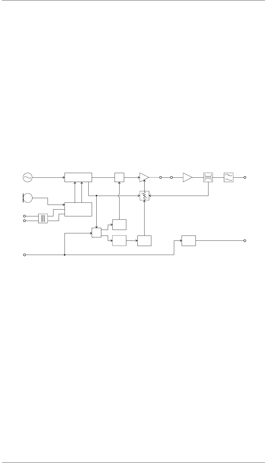
M8SL2-00-002-812 T854 Circuit Operation C2.3
© Copyright Tait Electronics Limited August 2004. All rights reserved.
2.1 Introduction
The individual circuit blocks which make up the T854 are:
•synthesiser
•VCO
•audio processor
•drive amplifier
•voltage regulators.
Each of these circuit blocks is set in its own shielded compartment, formed as an inte-
gral part of the main chassis.
The configuration of the circuit blocks may be seen on a functional level in Figure 2.1 .
Refer to the circuit diagrams in Section 6.2 for more detail.
Figure 2.1 T854 High Level Block Diagram
Ramp
Gen.
Time
Delay
Time
Delay
Time
Delay
Audio
Processor
Synthesiser +22dBm
Reference
Oscillator
12.8MHz
Microphone
Line
Transformer
Lock
Detect
PIN
Switch
Power
Control
Drive
Amp. PA
VCO
Gate
Directional
Coupler
Low Pass
Filter
Exciter
Output
(+30dBm to
+33dBm) Transmitter
Output
(25W)
Tx Reg
&

C2.4 T854 Circuit Operation M8SL2-00-002-812
© Copyright Tait Electronics Limited August 2004. All rights reserved.
2.2 Microcontroller
Refer to the microcontroller circuit diagram (Sheet 8 – T854 Microcontroller) in Section
6.2
Figure 2.2 T854 Microcontroller Block Diagram
Overall system control of the T854 is accomplished by the use of a member of the 80C51
family of microcontrollers (IC810). It runs from internal ROM and RAM, thus leaving all
four ports free for input/output functions.
Non-volatile data storage is achieved by serial communication with a 16kBit EEPROM
(IC820). This serial bus is also used by the microcontroller to program the synthesiser
(IC740) and deviation control EPOTS (IC220).
The main tasks of the microcontroller are as follows:
•program the synthesiser and EPOT;
•interface with the PGM800Win programming software at 9600 baud via the
serial communication lines on D-range 1 (PL100) and D-range 2;
•monitor channel change inputs from D-range 2;
•generate timing waveforms for CTCSS encoding;
•coordinate and implement timing control of the transmitter.
•control the front panel “Supply” LED (refer to Section 5.3).
5V Reset
5V Digital
Regulator
Watchdog
Reset
Channel
Select
Port
Auxiliary
Output
Port
Microcontroller
12.8MHz
Clock
Microcontroller Cavity
CTCSS Tone
External
Serial
Port
EEPROM Synthesiser
Dual Digital
Potentiometer
CTCSS
Encoder
Converter

M8SL2-00-002-812 T854 Circuit Operation C2.5
© Copyright Tait Electronics Limited August 2004. All rights reserved.
2.3 Synthesised Local Oscillator
Refer to the synthesiser circuit diagram (Sheet 7 – T854 Synthesiser) in Section 6.2 and
the VCO circuit diagram in Part E.
Figure 2.3 T854 Synthesiser Block Diagram
The synthesiser (IC740) employs a phase-locked loop (PLL) to lock a voltage controlled
oscillator (VCO) to a given reference frequency. The synthesiser receives the divider
information from the control microprocessor via a 3 wire serial bus (clock, data, enable).
When the data has been latched in, the synthesiser processes the incoming signals from
the VCO buffer (fin) and the phase modulator (fref).
A reference oscillator at 12.8MHz (=IC700) is buffered (IC710 pins 3 and 4) and divided
down to 200kHz (IC730). This 200kHz square wave is then summed with the modulat-
ing audio and passed to an integrator (IC720 pins 9 and 8, Q710, Q720). This produces a
ramping waveform which is centred around a DC level determined by the incoming
audio. IC720 pins 5 and 6 perform as a comparator, ultimately producing a phase-mod-
ulated 200kHz square wave. This is followed by another phase shifting stage (IC720
pins 3 and 4, Q730, Q740), before being divided down to 6.25kHz or 5kHz within the
synthesiser IC (IC740).
A buffered output of the VCO (Q795) is divided with a prescaler and programmable
divider which is incorporated into the synthesiser chip (IC740). This signal is compared
with the phase modulated reference signal at the phase detector (also part of the synthe-
siser chip). The phase detector outputs drive a balanced charge pump circuit (Q760,
Q770, Q775, Q780, Q785) and active loop filter (IC750 pins 5, 6 and 7, Q790) which pro-
duces a DC voltage between 0V and 20V to tune the VCO. This VCO control line is fur-
ther filtered to attenuate noise and other spurious signals. Note that the VCO frequency
increases with increasing control voltage.
If the synthesiser loop loses lock, a pulsed signal appears at LD (pin 2) of IC740. This
signal is filtered and buffered by IC750 pins 1, 2 and 3, producing the Lock-Detect signal
used to shut off the power supply to the drive amplifier. IC750 pin 1 is at 20V when the
synthesiser is out of lock.
/R
Reference
Divider
12.8MHz
Reference
Oscillator
Fixed
Divider
/64
Phase
Modulator
Ref
Mod
Phase
Detector
Charge
Pump
Loop
Filter
FREQUENCY SYNTHESISER IC
Serial
Bus
Clk
Data
En Controller
/N
Programmable
Divider
64/65
Prescaler
VCO PCB
VCO
Modulation
VCO Buffer
Output
Buffer
+22dB
m
L.O.
Divider Buffer
fref
fin
Σ
C2.6 T854 Circuit Operation M8SL2-00-002-812
© Copyright Tait Electronics Limited August 2004. All rights reserved.
2.3.1 Two Point Modulation
Frequency modulation occurs by modulating both the VCO input and the synthesiser
reference input. This process is called two point modulation and ensures a flat modula-
tion response from 67Hz to 3kHz (2.55kHz for narrow bandwidth).
The PLL has a fast response time, allowing a Tx key-up time of <30ms. Because of this
fast response time the PLL sees lower modulation frequencies superimposed on the
VCO as an error and corrects for it, resulting in no modulation on the carrier. At modu-
lation frequencies greater than 300Hz the loop cannot correct fast enough and modula-
tion is seen on the carrier. The response of the loop to VCO modulation is shown by f2 in
Figure 2.4 below.
To achieve low frequency modulation, the reference oscillator is also modulated so that
the phase detector of IC740 detects no frequency error under modulation. Thus, the syn-
thesiser loop will not attempt to correct for modulation and the audio frequency
response of the transmitter remains unaffected. The response of the loop to reference
frequency modulation is shown by f1 in Figure 2.4.
The reference modulation is controlled by a 256-step 10k electronic potentiometer
(EPOT) which is adjustable via PGM800Win. The EPOT is made up of 256 resistive sec-
tions (representing approximately 39Ω each) which can be individually addressed by
the microcontroller. Each section can be switched in or out of circuit to achieve the
required total resistance, thus giving control of the reference modulation.
Figure 2.4 T854 Two Point Modulation
12
ff
TCXO VCO
Deviation
Frequency

M8SL2-00-002-812 T854 Circuit Operation C2.7
© Copyright Tait Electronics Limited August 2004. All rights reserved.
2.4 VCO
(Refer to the VCO circuit diagram in Part E.)
The VCO transistor (Q1) operates in a common emitter configuration, with an LC tank
circuit coupled between its gate and drain to provide the feedback necessary for oscilla-
tion. The VCO control voltage from the loop filter (IC750) is applied to the varicaps (D1
and D2) to facilitate tuning within an 8MHz band of frequencies. A trimcap (C6) is used
for coarse tuning of the VCO. The output from the oscillator circuit drives a cascode
amplifier stage (Q2, Q3) which supplies +10dBm (typically) to a further stage of amplifi-
cation, Q5. This is the final amplifier on the VCO PCB, and delivers +20dBm (typically)
to the exciter drive amplifier.
A low level “sniff” is taken from the input to Q5 and used to drive the divider buffer for
the synthesiser (IC740).
The VCO operates at the actual output frequency of the exciter, i.e. there are no multi-
plier stages. It is modulated by superimposing the audio signal onto the control voltage
and by phase modulating the reference signal.
2.4.1 VCO Supply
The VCO is supplied from two switched +9V supplies under the control of the Tx-Reg.
supply.
The VCO and buffer amplifier are supplied from one +9V switched supply by Q540 via
the C multiplier (Q550, C530 on the T854 and C550 on the T857).
The output amplifier is supplied from the other +9V supply by Q520, Q530, and Q510.
A delay circuit holds the VCO on for a short time after the Tx-Reg. supply has been
switched off. This is to allow the RF power circuits (both exciter and PA) to ramp down
in the correct manner before the VCO is switched off.
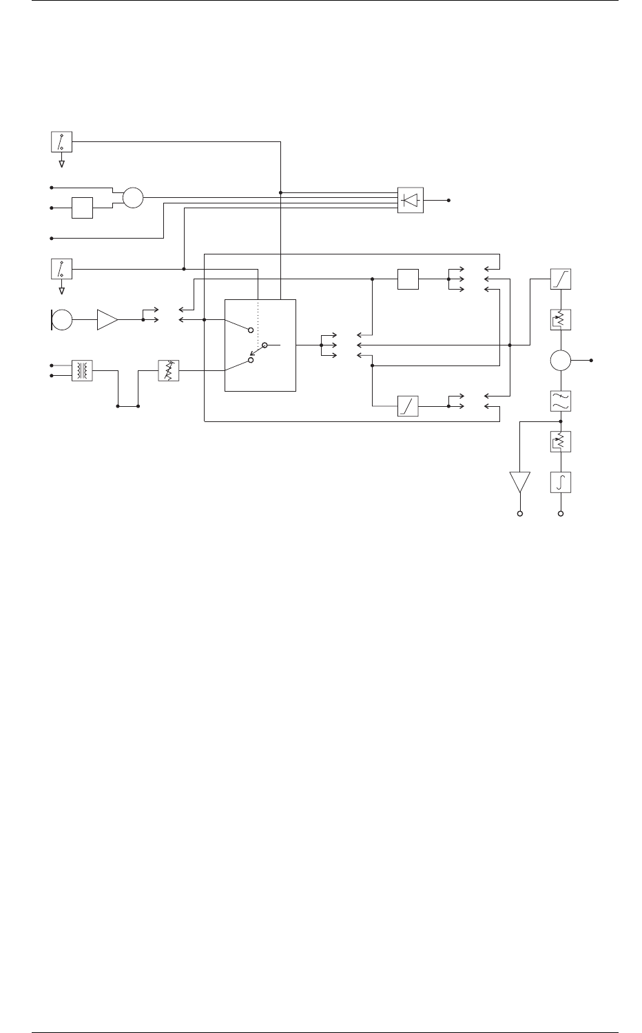
C2.8 T854 Circuit Operation M8SL2-00-002-812
© Copyright Tait Electronics Limited August 2004. All rights reserved.
2.5 Audio Processor
Refer to the audio processor circuit diagram (Sheet 2 – T854 Audio Processor) in Section
6.2.
Figure 2.5 T854 Audio Processor Block Diagram
2.5.1 General
The audio processor comprises several link selectable circuit blocks which may be con-
figured in a variety of combinations to suit individual requirements. The pre-emphasis
network and compressor may be linked individually or cascaded between either or both
audio inputs and the limiter.
Refer to Section 3.5.1 for linking details.
2.5.2 Audio Inputs
Two audio inputs are available: one from a 600Ω balanced (or unbalanced) line, and the
other from a local microphone. The microphone signal is passed first to a pre-amplifier
(Q210) and ultimately to a multiplexer (IC240), but in between may pass through the
compressor (depending on the linking details). The line transformer is also connected to
the multiplexer and is disabled by the microphone PTT switch.
A third input for external CTCSS tones is also provided.
Pre-
emphasis
34
6
B
C
5
14
2
910
8
13
1
11
3
5
910
6
N
H
M
I
E
L
J
D
12
4
7
mic.
line
Multiplexer
Inputs
Output
Output
Inhibit
Audio 1 Audio 2
Compressor
Link
Link
Link
Tx Enable
Σ
Carrier
Opto-Key
Tx Key
PTT
Microphone
Input
Line Input
Microphone
Pre-amp.
Opto-coupler
Link
PL201
PL202
PL201
PL202
Limiter
Set Deviation
CTCSS
Low Pass
Filter
Ref. Mod. Adjust
Integrator
Digital Pot. (EPOT)
Digital Pot. (EPOT)
Buffer
Output
To VCO
Ref.
Mod.
Constant Current Sink
+
_

M8SL2-00-002-812 T854 Circuit Operation C2.9
© Copyright Tait Electronics Limited August 2004. All rights reserved.
2.5.3 Keying Inputs
There are four ways to key the exciter:
•pulling the Tx-Key line low (pin 13 on D-range 1 [PL100]) at the rear of the set);
•pushing the “Carrier” button on the front panel – this will inhibit all audio;
•using the PTT button on the local microphone, disabling audio from the line;
•via the opto-key inputs (pins 11 and 12 on D-range 1 [PL100]) when electrical
isolation is required. This features a constant current sink (Q270) to ensure reli-
able activation of the opto-coupler (IC250) at low keying voltages.
2.5.4 Compressor (Automatic Level Control (ALC))
The input signal is fed via a current controlled attenuator (Q230, Q220) to a high gain
stage (IC230) from which the output signal is taken. This signal is passed to a compara-
tor (IC230) which toggles whenever the audio signal exceeds a DC threshold deter-
mined by RV220. Thus, the comparator produces a square wave whose mark-space ratio
is determined by the amplitude of the audio signal. This square wave pumps up the res-
ervoir capacitor (C233) which controls the attenuator (Q230, Q220), thus completing the
feedback loop.
The compression level is set by adjustment of the comparator threshold (RV220).
Note: Although the high dynamic range of the compressor allows the use of very
low audio signal levels, such conditions will be accompanied by a degrada-
tion of the signal-to-noise ratio. Very low audio input levels should therefore
be avoided where possible.
2.5.5 Outputs To Modulators
The output signal from the limiter (IC210, IC230) is summed with a CTCSS tone at a
summing amplifier (IC260). The signal is then low pass filtered (IC260) and split to sup-
ply the two modulators.
Since the VCO modulator is a true frequency modulator, its audio is simply buffered
(IC260). The reference modulator, however, is a phase modulator and its audio must
first be integrated (IC210).
It is vital that the audio levels to the modulators are accurately set, relative to each
other. Hence the inclusion of level adjustment in the reference modulator path. Once
set, adjustments to absolute deviation may be made only by IC220, a 256-step 10k elec-
tronic potentiometer (EPOT), which is controlled via PGM800Win. The EPOT is made
up of 256 resistive sections (representing approximately 39Ω each) which can be indi-
vidually addressed by the microcontroller. Each section can be switched in or out of cir-
cuit to achieve the required total resistance, thus adjusting the absolute deviation level.

C2.10 T854 Circuit Operation M8SL2-00-002-812
© Copyright Tait Electronics Limited August 2004. All rights reserved.
2.6 Power Supply and Regulator Circuits
Refer to the regulators circuit diagram (Sheet 6 – T854 Regulators) in Section 6.2.
Figure 2.6 T854 Power Supply and Regulators Block Diagram
The T854 is designed to operate from a 10.8 to 16VDC supply (13.8V nominal). A 5.3V
regulator (IC630) runs directly from the 13.8V rail, driving much of the synthesiser cir-
cuitry. It is also used as the reference for a DC amplifier (IC640, Q630, Q620) which
provides a medium current capability 9V supply. The T854 has a regulator (IC370)
which produces 9V for use in the exciter and audio circuits.
A switching power supply (Q660, Q670) runs from the 9V supply and provides a low
current capability +20V supply. This is used to drive the synthesiser loop filter (IC750),
giving a VCO control voltage range of up to 20V.
Ultimate control of the transmitter is via the Tx-Reg. supply, switched from 9V by Q610.
This is enabled via the Tx-Enable signal from the audio processor, and microprocessor.
A crowbar diode is fitted for protection against connection to a power supply of incor-
rect polarity. It also provides transient overvoltage protection.
Note: A fuse must be fitted in the power supply line for the diode to provide effec-
tive protection.
Crowbar
Diode LVI
5V
Reg
DC
Amp Switching
PS
5V Dig
Reg
Power
Switch
13.8V
Nom.
5V 5V Dig9V 20V
13.8V Nom.
From Rear
D-Range
Tx Enable
Buffer
Tx Reg.
+9V
µP
Watchdog
Timer
Micro-
controller
µP
Reset
9v Reg
IC 370 9v Ex
M8SL2-00-002-812 T854 Circuit Operation C2.11
© Copyright Tait Electronics Limited August 2004. All rights reserved.
2.7 Transmit Timers
The transmit tail timer, transmit timeout timer and transmit lockout timer can all be set
from PGM800Win. The fields for setting these are found on the system information
page. These three timers operate as follows (refer also to Figure 2.7):
Figure 2.7 T854 Transmit Timers
Timer Function Adjustment
Transmit Tail Sets the tail time during which the
transmitter stays keyed after the exter-
nal key source has been removed.
0 to 5 seconds in
20ms steps
Transmit Timeout Sets the maximum continuous trans-
mission time. Once the timer has
timed out, the transmitter must be
keyed again, unless prevented by the
transmit lockout timer.
0 to 600 seconds in
10 second steps
Transmit Lockout Sets the period of time that must
elapse after a timeout before the trans-
mitter can re-transmit. Once the timer
has timed out, the transmitter can be
keyed again.
0 to 60 seconds in 10
second steps
On
Lockout Time
Timeout
Time
On
Tail Time
Tx-Enable
Tx-Reg.
Tx-Enable
Tx-Reg.

C2.12 T854 Circuit Operation M8SL2-00-002-812
© Copyright Tait Electronics Limited August 2004. All rights reserved.
2.8 T854 Drive Amplifier, Fan Control and PA
Refer to Figure 2.1 and the exciter and PA circuit diagrams (sheets 3 and 4) in Section
6.2.
The output power of the PA is maintained at a constant level via a power control loop
applied to the two-stage, wide band exciter amplifier (Q337, Q336). The forward and
reverse RF power levels are sensed via a dual directional coupler and detector diodes
(D440, D420 in the PA cavity). The detected DC signals are buffered (IC330 pins 3 and 5)
and then summed with the ‘power control’ level and fed to the control integrator (IC350
pin 6).
Note: Forward and reflected power signals are summed so that, under high
VSWR, the power control will turn the output RF level down.
To reduce the spurious output level when the synthesiser is out-of-lock, the Tx-Reg. and
Lock-Detect signals are gated to inhibit the PA control circuit and to switch off the RF
signal at the input to the drive amplifier. This is achieved by a PIN switch attenuator
(D340, D380, D360).
Cyclic keying control is provided by additional circuitry consisting of several time
delay, ramp and gate stages:
•Q330, IC350 power ramping
•Q326, Q325, Q341 Tx-Reg. and Lock-Detect gate
•Q335, Q340, Q345 delay and PIN switch drive.
This is to allow the RF power circuits (both exciter and PA) to ramp up and down in a
controlled manner so that minimal adjacent channel interference is generated during
the transition.
The output of the wide band amplifier is approximately 1W (+30dBm) for an input of
100mW (+20dBm) from the VCO, when the power control is set to maximum.
A temperature sensor (R481) in the PA cavity presents a voltage to the comparators of
IC340 pin 2 and IC350 pin 2. The fan is switched on and off by the comparator of IC340
and the power fold-back is enabled by the comparator of IC350. Power fold-back
reduces the output power to a preset level that protects the PA semiconductors from
excessive temperatures. Under normal operating conditions, the fan will be activated
before power fold-back can occur and it will prevent the temperature from reaching
damaging levels. The voltage divider ratio of R311 and R312 sets the the temperature at
which the fan is switched on and off. R306 and R340 set the temperature at which power
is reduced. Depending on ambient temperature and ventilation, it may take several
minutes of continuous operation for the fan to be activated.
#R517, #R518 and #R519 form an attenuator to provide good VCO/exciter isolation as
well as the correct exciter drive level.
The attenuator (#R395, #R396 and #R397) aids in producing the correct exciter drive
level to the PA over the three frequency ranges.

M8SL2-00-002-812 T854 Circuit Operation C2.13
© Copyright Tait Electronics Limited August 2004. All rights reserved.
The RF output from the exciter is fed to the driver stage (Q410) and then to the final
(Q420). DC is fed to the final via a low pass filter with special low frequency decoupling.
CV475 tunes the output matching across the entire band.

C2.14 T854 Circuit Operation M8SL2-00-002-812
© Copyright Tait Electronics Limited August 2004. All rights reserved.

M8SL2-00-002-812 T854 Initial Tuning and Adjustment C3.1
© Copyright Tait Electronics Limited August 2004. All rights reserved.
3 T854 Initial Tuning and Adjustment
Caution: This equipment contains CMOS devices which are susceptible to dam-
age from static charges. Refer to Section 1.2 in Part A for more informa-
tion on anti-static procedures when handling these devices.
The following section describes both short and full tuning and adjustment procedures
and provides information on:
•channel programming
•selecting required audio links
•synthesiser alignment
•PA alignment
•modulator adjustment
•limiter adjustment
•setting line level
•compressor adjustment
•timer adjustment.
Note: Unless otherwise specified, the term “PGM800Win” used in this and follow-
ing sections refers to version 4.02 and later of the software.
Refer to Figure 4.4 which show the location of the main tuning and adjustment controls.
Refer also to Section 6 where the parts lists, grid reference index and diagrams will pro-
vide detailed information on identifying and locating components and test points on
the main PCB. The parts list and diagrams for the VCO PCB are in Part E.
Section Title Page
3.1 Introduction 3.3
3.2 Channel Programming 3.3
3.3 Test Equipment Required 3.4
3.4
3.4.1
3.4.2
3.4.3
3.4.4
3.4.5
3.4.6
3.4.7
Short Tuning Procedure
Introduction
Synthesiser Alignment
Output Power Adjustment
Two Point Modulation Adjustment
CTCSS Encoder (If Used)
FM Deviation (Limiter) Adjustment
Line-in Level Adjustment
3.5
3.5
3.5
3.5
3.6
3.7
3.7
3.7

C3.2 T854 Initial Tuning and Adjustment M8SL2-00-002-812
© Copyright Tait Electronics Limited August 2004. All rights reserved.
3.5
3.5.1
3.5.2
Audio Processor Links
Link Details
Typical Options
3.8
3.8
3.8
3.6 Synthesiser Alignment 3.9
3.7 PA Alignment 3.10
3.8 Thermal Shutdown 3.10
3.9
3.9.1
3.9.2
3.9.3
3.9.4
3.9.5
3.9.6
3.9.6.1
3.9.6.2
3.9.6.3
Audio Processor and CTCSS
Two Point Modulation
Modulator Adjustment
CTCSS Encoder (If Used)
Limiter Adjustment
Line Level Without Compressor
Compressor
Compressor On Line Input Only
Compressor On Microphone Input Only
Compressor On Both Line and Microphone Inputs
3.11
3.11
3.11
3.12
3.12
3.13
3.13
3.13
3.13
3.14
3.10
3.10.1
3.10.1.1
3.10.1.2
3.10.2
3.10.2.1
3.10.2.2
Power Alarms (if used)
T1500-52-0000 Tx Alarm/Multi-channel Kit
Installation
T1500-52-0000 Testing/Alignment
T800-10-0520 Tx-Alarm/Channel-Select Kit
Installation
T800-10-0520 Testing/Alignment
3.14
3.15
3.15
3.17
3.18
3.19
3.20
Figure Title Page
3.1
3.2
T854 Test Equipment Set-up With T800-01-0010
T854 Test Equipment Set-up Without T800-01-0010
3.4
3.4
Section Title Page

M8SL2-00-002-812 T854 Initial Tuning and Adjustment C3.3
© Copyright Tait Electronics Limited August 2004. All rights reserved.
3.1 Introduction
When you receive your T854 transmitter it will be run up and working on a particular
frequency (the “default channel")1. If you want to switch to a frequency that is within
the 8MHz switching range (i.e. ±4MHz from the factory programmed frequency), you
should only need to reprogram the transmitter with the PGM800Win software (refer to
the PGM800Win programming kit and Section 3.2 below).
However, if you want to switch to a frequency outside the 8MHz switching range, you
will have to reprogram and re-tune the transmitter to ensure correct operation. In this
case you should carry out the short tuning procedure described in Section 3.4.
If you have carried out repairs or other major adjustments, you must carry out the full
tuning and adjustment procedure described in this section (except for Section 3.4).
3.2 Channel Programming
You can program up to 128 channel frequencies into the transmitter’s EEPROM memory
(IC820) by using the PGM800Win software package and a PC. You can also use
PGM800Win to select the transmitter’s current operating frequency (or “default chan-
nel").
If the transmitter is installed in a rack frame, you can program it via the programming
port in the speaker panel. However, you can also program the transmitter before it is
installed in a rack frame as follows:
•by using a T800-01-0010 calibration test unit;
•via D-range 1;
•via D-range 2 (standard T800-03-0000 auxiliary D-range only);
•via SK805 (internal Micromatch connector).
If you do not use the T800-01-0010, you will have to connect the PC to the transmitter
via a module programming interface (such as the T800-01-0004).
For a full description of the channel programming procedure, refer to the PGM800Win
programming software user’s manual.
Note: When an auxiliary D-range kit (D-range 2 – T800-03-0000) is fitted, you can
also select a channel with an external switch, such as the DIP switch on a
backplane PCB. Refer to your nearest Tait Dealer or Customer Service
Organisation for further details.
1. Use the “Read Module” function in PGM800Win to find out what the default channel
is.
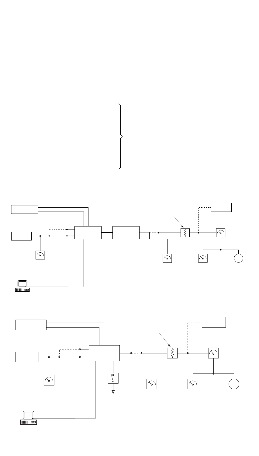
C3.4 T854 Initial Tuning and Adjustment M8SL2-00-002-812
© Copyright Tait Electronics Limited August 2004. All rights reserved.
3.3 Test Equipment Required
You will need the following test equipment:
•computer with PGM800Win installed
•T800 programming kit
•module programming interface (e.g. T800-01-0004 – optional)
•13.8V power supply
•digital multimeter
•audio signal generator
•RF power meter
•audio voltmeter x 2
•modulation meter
•oscilloscope (digital preferred)
•20dB or 40dB pad
•T800-01-0010 calibration test unit (optional)
Figure 3.1 and Figure 3.2 show typical test equipment set-ups.
Figure 3.1 T854 Test Equipment Set-up With T800-01-0010
Figure 3.2 T854 Test Equipment Set-up Without T800-01-0010
or RF test set (optional)
Frequency
Counter
Audio
Voltmeter
RF Power
Meter
Oscilloscope
AF O/P
Modulation
Meter
20dB pad: exciter
40dB pad: transmitter
RF O/P
PGM800Win
PSU
+13.8V
-Ve
Audio
Generator
Line I/P
CTCSS I/P
600
Audio
Voltmeter
Exciter/
Transmitter
T800-01-0010
Calibration
Test Unit
P
G
M
800
Win
Serial
Com
PSU
+13.8V
-Ve
Frequency
Counter
Audio
Voltmeter
RF Power
Meter
Oscilloscope
AF O/P
Modulation
Meter
20dB pad: exciter
40dB pad: transmitter
Audio
Generator
Line I/P
CTCSS I/P
Ω600
Audio
Voltmeter
Key
RF O/P
Exciter/
Transmitter
via module programming interface
(e.g. T800-01-0004)

M8SL2-00-002-812 T854 Initial Tuning and Adjustment C3.5
© Copyright Tait Electronics Limited August 2004. All rights reserved.
3.4 Short Tuning Procedure
Use this procedure only if you want to reprogram the T854 to a frequency outside the
8MHz switching range and do not intend to carry out any other major adjustments or
repairs.
3.4.1 Introduction
Reprogram the operating frequency as described in the PGM800Win program-
ming kit (refer to Section 3.2).
Remove the top cover.
Set up the test equipment as described in Section 3.3.
Set the links in the audio processor section as required (refer to Section 3.5).
3.4.2 Synthesiser Alignment
•Connect a high impedance voltmeter to the long lead of L1 in the VCO (this meas-
ures the synthesiser loop voltage).
•Key the transmitter by earthing the Tx-Key line.
•Single Channel Tune VCO trimmer C6 for a synthesiser loop voltage of
10V.
Multichannel Tune VCO trimmer C6 for a synthesiser loop voltage of
10V on the middle channel.
If there is no middle channel, tune C6 so that the channels
are symmetrically placed around a loop voltage of 10V.
All channels should lie within the upper and lower limits
of 16V and 3V respectively.
Do not attempt to program channels with a greater fre-
quency separation than the specified switching range of
8MHz.
3.4.3 Output Power Adjustment
Connect an RF power meter with suitable attenuation to the output socket and
key the transmitter.
Turn RV310 (power control) fully clockwise.
Tune #CV475 (output power trim) for maximum output power and check that this
is >30W.
Adjust RV310 for the required output power (between 5 and 25W).
Readjust #CV475 to reduce the supply current by up to 0.5A.

C3.6 T854 Initial Tuning and Adjustment M8SL2-00-002-812
© Copyright Tait Electronics Limited August 2004. All rights reserved.
3.4.4 Two Point Modulation Adjustment
Note 1: In this and following sections deviation settings are given first for wide
bandwidth sets, followed by settings in brackets for mid bandwidth sets ( )
and narrow bandwidth sets [ ].
Note 2: The reference modulation and limiter adjustments are controlled by 256-
step electronic potentiometers (EPOTs), which are adjusted via the “Refer-
ence Modulation” and “Deviation” settings in PGM800Win. This allows the
two point modulation and deviation settings to be adjusted for each chan-
nel.
Note 3: To optimise the modulation response across the switching range, repeat
steps 1 to 4 below for each channel that will be used (usually needed only
for data applications). In applications where the modulation response is less
critical (e.g. voice use only), carry out steps 1 to 4 below on the middle chan-
nel and use the “EPOT Fill” option1 in PGM800Win to copy the value to the
other channels.
Note 4: If you are using an RF test set, turn the low pass filter off and set the high
pass filter to 15kHz before beginning this procedure.
1. Inject an audio signal of 300Hz 1.5Vrms (+5dBm) into the CTCSS input (D-range 1
(PL100) pin 8).
Key the transmitter by earthing the Tx-Key line.
2. Adjust the output from the audio generator to obtain ±3kHz (±2.4kHz) [±1.5kHz]
deviation at 300Hz.
3. Change the input frequency to 100Hz and, using PGM800Win, adjust the value of
the “Reference Modulation” EPOT setting for the current channel to obtain ±3kHz
(±2.4kHz) [±1.5kHz] deviation (you can use either the mouse or up and down
arrow keys).
4. Change the input frequency back to 300Hz.
Repeat steps 2 and 3 above until the deviations achieved at the two input frequen-
cies are within 0.2dB of each other. You will need to do this at least four times.
5. Sweep the audio between 50 and 300Hz for peaks.
Note: A peak between 50 and 300Hz will indicate a fault condition, i.e:
– incorrect set-up
or – modulation circuitry fault.
The specification window is ±1dB relative to 150Hz from 67 to 260Hz.
1. Use the “EDIT FILL” button on the tool bar or go to “Edit”, “Fill”, “Epot Settings” on
the menu bar.

M8SL2-00-002-812 T854 Initial Tuning and Adjustment C3.7
© Copyright Tait Electronics Limited August 2004. All rights reserved.
3.4.5 CTCSS Encoder (If Used)
Program a CTCSS tone on the default channel using PGM800Win.
If you are using an RF test set, turn off the 300Hz high pass filter.
Key the T854 with the front panel “Carrier” switch.
Adjust RV805 (CTCSS level adjust) to give ±500Hz (±350Hz) [±250Hz] deviation.
Set the maximum deviation as per Section 3.4.6.
3.4.6 FM Deviation (Limiter) Adjustment
Note: If the T854 will be used over the whole 8MHz switching range, you must set
the deviation for each channel. However, if the module will be used on fre-
quencies that cover only a 1MHz (or less) switching range, you can set the
deviation on the middle channel and use this value for all other channels
with the “EPOT Fill” option in PGM800Win.
Inject 1kHz at –10dBm into the line input (D-range 1 (PL100) pins 1 and 4; pins 2
and 3 shorted; refer to Section 1.5 of Part G).
Adjust RV210 (line sensitivity) fully clockwise and key the transmitter by earthing
the Tx-Key line. Using PGM800Win, adjust the value of the “Deviation” EPOT set-
ting for the current channel to obtain a deviation limit of ±4.7kHz (±3.8kHz)
[±2.3kHz] (you can use either the mouse or up and down arrow keys).
Sweep the audio frequency from 100Hz to 4kHz and ensure that the maximum
deviation does not exceed ±4.7kHz (±3.8kHz) [±2.3kHz]. Readjust “Deviation” if
necessary via PGM800Win.
3.4.7 Line-in Level Adjustment
Remove the CTCSS signal (if used).
Set the injected signal at the line input to the required line level (typically –10 to
–20dBm).
Adjust RV210 (line sensitivity) to provide ±3kHz (±2.4kHz) [±1.5kHz] deviation.
Reapply the CTCSS signal (if required).

C3.8 T854 Initial Tuning and Adjustment M8SL2-00-002-812
© Copyright Tait Electronics Limited August 2004. All rights reserved.
3.5 Audio Processor Links
3.5.1 Link Details
Use the following table to set up the audio processor to the configuration you require.
You should set the audio processor links before carrying out any of the tuning and
adjustment procedures.
3.5.2 Typical Options
Plug Linka
a The letters in this column refer to the letters printed on the PCB beside each pair of pins.
Note that the link names and pin numbers are different to earlier products. The lettering A
to N is however the same.
Function
PL201
1–2
3–4b
5–6
b Factory Setting
A
B
C
not connected
microphone pre-amp output to compressor input
microphone pre-amp output to multiplexer input
7–8
9–10b
11 –12
13–14
D
E
F
G
pre-emphasis output to multiplexer input
pre-emphasis output to limiter input
not connected
not connected
PL202
1–2b
3–4
5–6
7–8
H
I
J
K
compressor output to multiplexer input
compressor output to limiter input
compressor output to pre-emphasis input
not connected
9–10b
11 –12
13–14
L
M
N
multiplexer output to pre-emphasis input
multiplexer output to limiter input
multiplexer output to compressor input
microphone pre-amp line input PL201a
a The letters in this table refer to the letters printed on the PCB beside each pair of pins.
PL201 PL202 PL202
compressed and
pre-emphasised
pre-emphasised Bb
b Factory Setting
EbHbLb
unprocessed B D J M
compressed and
pre-emphasised CE JN
compressed and
flat response
flat response BFHM

M8SL2-00-002-812 T854 Initial Tuning and Adjustment C3.9
© Copyright Tait Electronics Limited August 2004. All rights reserved.
3.6 Synthesiser Alignment
1. Ensure that the T854 has been programmed with the required frequencies using
PGM800Win software.
2. Single Channel Select a channel using PGM800Win.
Multichannel Select the middle channel via PGM800Win.
3. Connect a high impedance voltmeter to the long lead of L1 in the VCO (this meas-
ures the synthesiser loop voltage).
4. Key the transmitter by earthing the Tx-Key line.
Single Channel Tune VCO trimmer C6 for a synthesiser loop voltage of
10V.
Multichannel Tune VCO trimmer C6 for a synthesiser loop voltage of
10V on the middle channel.
If there is no middle channel, tune C6 so that the channels
are symmetrically placed around a loop voltage of 10V.
All channels should lie within the upper and lower limits
of 16V and 3V respectively.
Do not attempt to program channels with a greater fre-
quency separation than the specified switching range
(8MHz).
5. Measure the exciter output frequency and adjust the TCXO (=IC700) trimmer if
required.
Caution: This trimmer is susceptible to physical damage. Do not exert a down-
ward force of more than 500g (1lb) when adjusting.

C3.10 T854 Initial Tuning and Adjustment M8SL2-00-002-812
© Copyright Tait Electronics Limited August 2004. All rights reserved.
3.7 PA Alignment
1. Check that the exciter is connected to the PA with the coaxial link.
2. Connect an RF power meter to the PA output (use an appropriate attenuator as
necessary).
3. Turn RV310 (power control) fully clockwise.
4. Key the transmitter by earthing the Tx-Key line.
5. Tune #CV475 until maximum power is obtained. Check that the power exceeds
30W.
6. Adjust RV310 (power control) to 25W.
7. Readjust #CV475 to reduce the supply current by up to 0.5A.
3.8 Thermal Shutdown
1. Key the transmitter by earthing the Tx-Key line and set the output power to 25W
as described in Section 3.7.
2. Short L481 to ground.
3. Set RV330 (shutdown power level) for an output power of 5W.

M8SL2-00-002-812 T854 Initial Tuning and Adjustment C3.11
© Copyright Tait Electronics Limited August 2004. All rights reserved.
3.9 Audio Processor and CTCSS
3.9.1 Two Point Modulation
The T854 utilises two point modulation to obtain a wide audio bandwidth independent
of the synthesiser loop filter response. This is achieved by simultaneously frequency
modulating the VCO and phase modulating the synthesiser reference frequency. The
relative signal levels fed to the two modulators are quite critical and cause interaction
when setting up.
Both modulating signals require readjustment when the exciter is shifted in frequency
greater than the switching range (i.e. ∆F>±4MHz).
Note 1: In this and following sections deviation settings are given first for wide
bandwidth sets, followed by settings in brackets for mid bandwidth sets ( )
and narrow bandwidth sets [ ].
Note 2: The reference modulation and limiter adjustments are controlled by 256-
step electronic potentiometers (EPOTs), which are adjusted via the “Refer-
ence Modulation” and “Deviation” settings in PGM800Win. This allows the
two point modulation and deviation settings to be adjusted for each chan-
nel.
Note 3: To optimise the modulation response across the switching range, repeat
steps 1 to 4 below for each channel that will be used (usually needed only
for data applications). In applications where the modulation response is less
critical (e.g. voice use only), carry out steps 1 to 4 below on the middle chan-
nel and use the “EPOT Fill” option1 in PGM800Win to copy the value to the
other channels.
Note 4: If you are using an RF test set, turn the low pass filter off and set the high
pass filter to 15kHz before beginning this procedure.
3.9.2 Modulator Adjustment
1. Inject an audio signal of 300Hz 1.5Vrms (+5dBm) into the CTCSS input (D-range 1
(PL100) pin 8).
Key the transmitter by earthing the Tx-Key line.
2. Adjust the output from the audio generator to obtain ±3kHz (±2.4kHz) [±1.5kHz]
deviation at 300Hz.
3. Change the input frequency to 100Hz and, using PGM800Win, adjust the value of
the “Reference Modulation” EPOT setting for the current channel to obtain ±3kHz
(±2.4kHz) [±1.5kHz] deviation (you can use either the mouse or up and down
arrow keys).
1. Use the “EDIT FILL” button on the tool bar or go to “Edit”, “Fill”, “Epot Settings” on
the menu bar.

C3.12 T854 Initial Tuning and Adjustment M8SL2-00-002-812
© Copyright Tait Electronics Limited August 2004. All rights reserved.
4. Change the input frequency back to 300Hz.
Repeat steps 2 and 3 above until the deviations achieved at the two input frequen-
cies are within 0.2dB of each other. You will need to do this at least four times.
5. Sweep the audio between 50 and 300Hz for peaks.
Note: A peak between 50 and 300Hz will indicate a fault condition, i.e:
– incorrect set-up
or – modulation circuitry fault.
The specification window is ±1dB relative to 150Hz from 67 to 260Hz.
3.9.3 CTCSS Encoder (If Used)
1. Program a CTCSS tone on the default channel using PGM800Win.
2. If you are using an RF test set, turn off the 300Hz high pass filter.
3. Key the T854 with the front panel “Carrier” switch.
4. Adjust RV805 (CTCSS level adjust) to give ±500Hz (±350Hz) [±250Hz] deviation.
5. Set the maximum deviation as per Section 3.9.4.
3.9.4 Limiter Adjustment
Note: If the T854 will be used over the whole 8MHz switching range, you must set
the deviation for each channel. However, if the module will be used on fre-
quencies that cover only a 1MHz (or less) switching range, you can set the
deviation on the middle channel and use this value for all other channels
with the “EPOT Fill” option in PGM800Win.
1. Set the links in the audio processor section as required (refer to Section 3.5).
2. Inject 1kHz at –10dBm into the line input (D-range 1 (PL100) pins 1 and 4; and
pins 2 and 3 shorted; refer to Section 1.5 of Part G).
3. Adjust RV210 (line sensitivity) fully clockwise and key the transmitter by earthing
the Tx-Key line. Using PGM800Win, adjust the value of the “Deviation” EPOT set-
ting for the current channel to obtain a deviation limit of ±4.7kHz (±3.8kHz)
[±2.3kHz] (you can use either the mouse or up and down arrow keys).
4. Sweep the audio frequency from 100Hz to 4kHz and ensure that the maximum
deviation does not exceed ±4.7kHz (±3.8kHz) [±2.3kHz]. Readjust “Deviation” if
necessary via PGM800Win.

M8SL2-00-002-812 T854 Initial Tuning and Adjustment C3.13
© Copyright Tait Electronics Limited August 2004. All rights reserved.
3.9.5 Line Level Without Compressor
This section assumes that the compressor is not used. If the compressor is required, refer
to Section 3.9.6.
1. Remove the CTCSS signal (if used).
2. Adjust the line sensitivity as follows:
•set the injected signal at the line input to the required line level (typically –10 to
–20dBm)
•adjust RV210 (line sensitivity) to provide ±3kHz (±2.4kHz) [±1.5kHz] deviation
3. Reapply the CTCSS signal (if required).
3.9.6 Compressor
The compressor may be used on the line input only, the microphone input only, or on
both the line and microphone inputs. If the compressor is used, refer to one of the fol-
lowing sections as appropriate.
3.9.6.1 Compressor On Line Input Only
1. Set RV210 (line sensitivity) fully clockwise and key the transmitter by earthing the
Tx-Key line.
2. Reduce the line level to –50dBm at 1kHz and set RV220 (compression level) fully
clockwise.
3. Check that ±3kHz deviation (±2.4kHz) [±1.5kHz] is still available.
4. Slowly increase the audio input level until the demodulated waveform shows sig-
nificant signs of clipping (approximately ±4.5kHz (±3.6kHz) [±2.3kHz] deviation).
5. Adjust RV220 anticlockwise until the demodulated waveform is just clipping
(approximately ±4kHz (±3.2kHz) [±2kHz] deviation).
6. Increase the input level to –10dBm and check that the test tone is still held just into
clipping. The input line level should be typically –10 to –20dBm.
3.9.6.2 Compressor On Microphone Input Only
1. Key the transmitter by earthing the Tx-Key line and plug a microphone jack into
the front panel socket.
2. Adjust RV220 (compression level) fully clockwise.
3. Acoustically couple the microphone to a tone box (1kHz) and close the PTT
switch.

C3.14 T854 Initial Tuning and Adjustment M8SL2-00-002-812
© Copyright Tait Electronics Limited August 2004. All rights reserved.
4. Increase the audio level until the demodulated waveform shows significant signs
of clipping (approximately ±4.5kHz (±3.6kHz) [±2.3kHz] deviation).
5. Adjust RV220 anticlockwise until the demodulated waveform is just clipping
(approximately ±4kHz (±3.2khz) [±2kHz] deviation).
6. Increase the audio level by 10dB and verify that the test tone is held just into clip-
ping.
7. Whistle steadily into the microphone, checking that approximately ±4kHz
(±3.2khz) [±2kHz] deviation is produced. The modulated waveform should be
basically sinusoidal.
8. Speak into the microphone, checking that the modulation peaks reach about
±5kHz (±4kHz) [±2.5kHz] deviation.
9. As the line is to be used without compression, set RV210 (line sensitivity) as
described in Section 3.9.5.
3.9.6.3 Compressor On Both Line and Microphone Inputs
Set up as described in Section 3.9.6.1.
3.10 Power Alarms (if used)
When fitted to the T854 transmitter an alarm board monitors the transmitter output
power and generates a low forward-power and/or high reverse-power alarm as appro-
priate.
This is achieved by monitoring the output voltages of the transmitters forward and
reverse power directional coupler. A comparison between these voltage levels and user
defined reference voltages generates alarm conditions accordingly. The low forward
power output signal is also gated with the Tx-enable input to ensure that no alarm is
generated when the transmitter is not transmitting. The high reverse power alarm out-
put is not gated. The alarm signal is output on the T854 Aux D-range.
There are two alarms boards currently available, the recently introduced and improved
T800-10-0520 Tx-Alarm/Channel Select board and the older T1500-52-0000, which it
replaces. The alarm outputs of both the these boards are compatible with the
T1511-20-0000 CCM module and the T803-02 Tone Remote and Alarm interface.

M8SL2-00-002-812 T854 Initial Tuning and Adjustment C3.15
© Copyright Tait Electronics Limited August 2004. All rights reserved.
The following table indicates the SL2 backplane configuration required.
3.10.1 T1500-52-0000 Tx Alarm/Multi-channel Kit
When fitted, the T1500-52-0000 Tx alarm PCB monitors the transmitter output power
and generates a low forward and/or high reverse power alarm signal as appropriate.
Alarm outputs are compatible with the T1511-20-0000 CCM module. On-board LED
indication of alarms is also provided for trouble shooting and setup purposes.
Parts Supplied
The T1500-52-0000 should contain:
•T1500-52-0000 Alarm PCB and mounting screws.
•D-range and PCB interface.
3.10.1.1 Installation
To install this kit you will require the following tools:
•T1500-52-0000 Tx alarm/Multi-channel alarm kit
•Philips screwdriver
•Soldering iron
•Small sidecutters
Alarm board
SL2 Backplane
Notes
Link 9 Link 10
T1500-52-0000
(PCB 220-01426-04)
2 – 32 – 3 See Section 3.10.1 T1500-52-
0000 Tx Alarm/Multi-channel
Kit
T800-10-0520 (plug-in alarm
board)
2 – 32 – 3 See Section 3.10.2 T800-10-0520
Tx-Alarm/Channel-Select Kit
No internal alarm board fitted
but FWD and REV power
sense voltages output directly
on T854 Aux D-range. Could
be used for an externally fitted
RF power indicator/alarm.
1 – 21 – 2 Cannot be used to trigger
T803-02 RF power alarms.
On the T854 for S/N 13098764
or earlier:
– remove R840 and R841
– fit R308 and R310 (both 10kΩ)
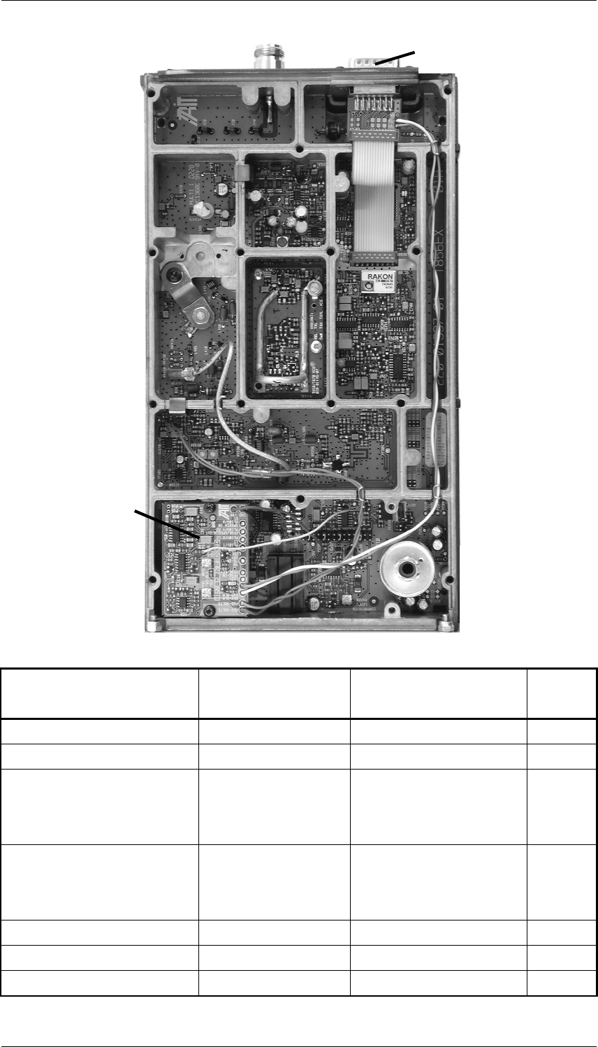
C3.16 T854 Initial Tuning and Adjustment M8SL2-00-002-812
© Copyright Tait Electronics Limited August 2004. All rights reserved.
Figure 3.3 Example Transmitter (T856) Fitted with Alarm Kit
T800 connection pads
T1500-52-0000 PCB
connection pads
Rear D-range pin
number and PCB label
Wire
colour
+9V P230 +9V — Red
GND P259 GND — Black
Fwd Pwr TP
T826: R302
(via end)
T836: TP310
T854/T856: TP306
Fwd Volts — Green
Rev Pwr TP
T826: R301
(via end)
T836: TP309
T854/T856: TP307
Rev Volts — Orange
— Fwd pwr alarm Pin 13 – Fwd Blue
— Rev pwr alarm Pin 14 – Rev White
Tx Enb D240 pin 3 PTT — Yellow
Auxiliary
D-range
Alarm
PCB

M8SL2-00-002-812 T854 Initial Tuning and Adjustment C3.17
© Copyright Tait Electronics Limited August 2004. All rights reserved.
1. Remove the top and bottom cover from the T854 transmitter.
2. Remove the Aux D-range and replace with the supplied D-range socket.
3. Connect the T1500-52-0000 wires to the D-range PCB, audio processor and exciter
compartments as shown in the table above.
4. Fit cable clamps to all points where wires pass through the radio’s chassis.
5. Fit the wire clamp to the forward and reverse voltage input wires at the point
were they cross over between compartments.
6. Mount the T1500-52-0000 component side up on the chassis lugs provided in the
audio compartment, at the top (Carrier button) end.
Note: Take care not to knock the T1500-52-0000 PCB while the covers are off. A
sharp knock on the SMD electro capacitors will damage the board.
7. Fit a ribbon cable if multi-channel operation is required.
8. Run up the board according to the test section below.
9. Ensure that the cable clamps hold down all wires safely so that they will not be
pinched. Replace both covers.
3.10.1.2 T1500-52-0000 Testing/Alignment
Equipment required
•50Ω power meter
•3 or 6dB attenuator as needed.
Forward alarm
1. Connect the power meter to the transmitter output.
2. Key up the transmitter and set the output power to the desired low forward
power alarm threshold point.
3. Adjust the “Fwd-alarm adjust” preset until the forward alarm LED just comes
ON.
4. Reset the output power to the operational output level. Check the alarm output is
now OFF.
5. Turn the transmitter OFF.

C3.18 T854 Initial Tuning and Adjustment M8SL2-00-002-812
© Copyright Tait Electronics Limited August 2004. All rights reserved.
Reverse alarm
1. Connect the power meter to the transmitter output.
2. Key up the transmitter and set the output power level to the operational output
level.
3. Replace the power meter with the appropriate valued open ended attenuator. This
should generate the desired return loss/reflected power for the desired high
reverse power alarm threshold point.
4. Adjust the “Rev-alarm adjust” preset until the alarm LED just comes ON.
5. Turn the transmitter OFF.
3.10.2 T800-10-0520 Tx-Alarm/Channel-Select Kit
When fitted to a T854 transmitter, the T800-10-0520 Tx-Alarm/Channel-Select plug-in
board provides the following features:
•The plug-in board monitors the transmitter’s output power, and generates a
low forward-power and/or high reverse-power alarm as appropriate.
•The plug-in board also includes channel select switches that enables the user to
manually set the operational channel of the T854.
The plug-in board provides the same alarm outputs as the T1500-52-0000:
•Forward Power Alarm: Aux D-range pin 13
•Reverse Power Alarm: Aux D-range pin 14
Note: AUX-OUT-0 is disabled when the plug-in board is installed.
The Tx-Alarm function is achieved by comparing the output voltages of the transmit-
ter’s directional coupler to user-defined reference levels.
The low forward-power alarm output is gated with the Tx-Enable input, to ensure that
no alarm is generated when the transmitter is not transmitting. The high reverse-power
alarm is not gated.
Note: The plug-in board does not require additional wiring. It can be set up on the
bench. This is possible because the Tx-Enable line is accessed from inside the
T854, rather than from the backplane PCB (as on the T1500-52-0000).
Parts Supplied
T800-10-0520 Tx-Alarm/Channel-Select Kit should contain the following:
•T800-10-0520 plug-in board
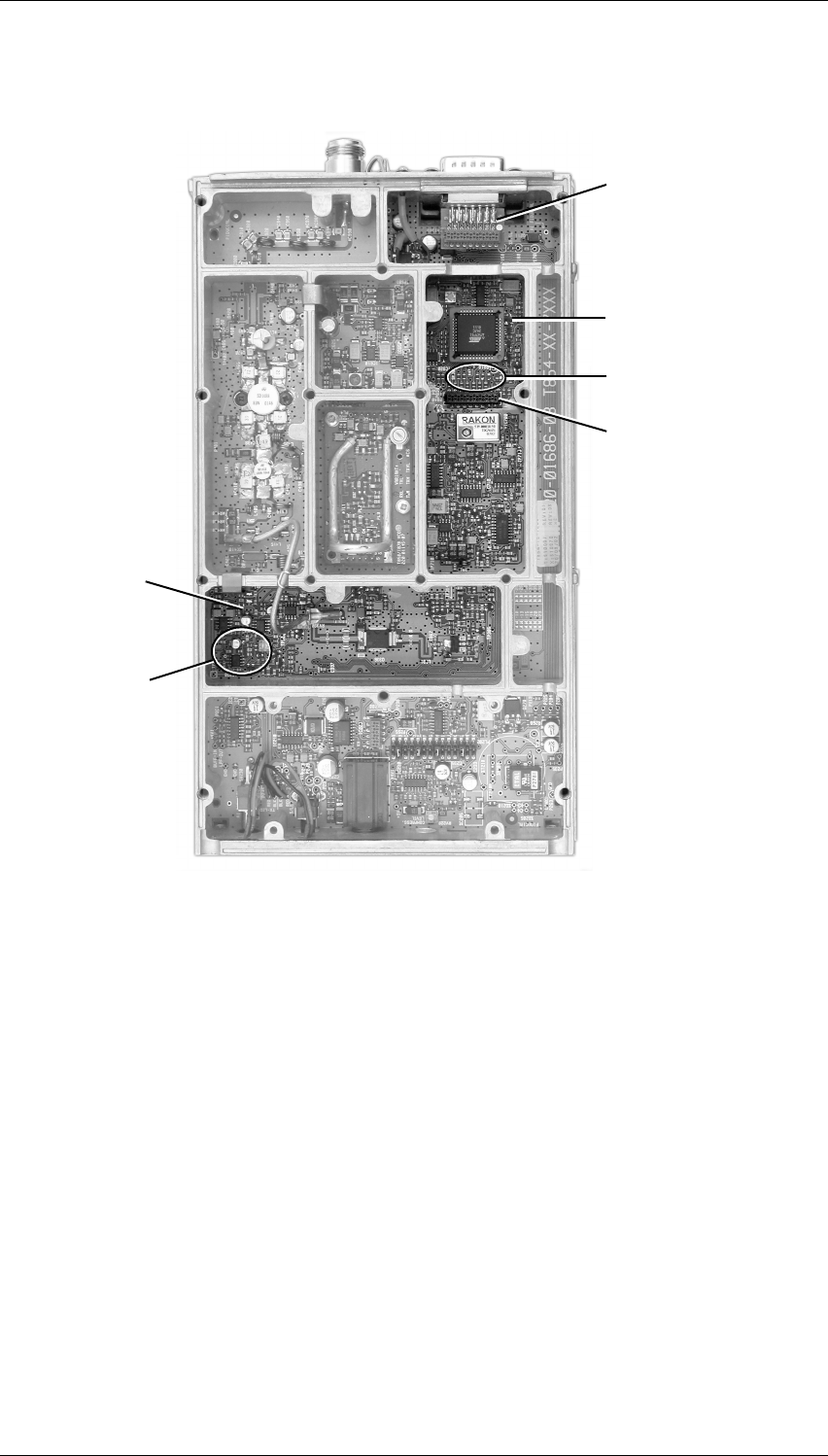
M8SL2-00-002-812 T854 Initial Tuning and Adjustment C3.19
© Copyright Tait Electronics Limited August 2004. All rights reserved.
3.10.2.1 Installation
To install this kit you will require a small flat-bladed screwdriver or similar.
1. Remove the top cover from the T854 Transmitter.
2. The auxiliary D-Range board is connected to the microcontroller cavity by a rib-
bon-cable. Remove the ribbon-cable.
3. For T854 transmitters with a serial number of 13098764 or earlier:
These transmitters are not by default configured to work with the plug-in board.
The directional coupler voltages must be routed to SK805.
Note:This step disables AUX-OUT-1 and AUX-OUT-2.
Auxiliary
D-range
board
Microcontroller
cavity
Exciter
cavity
SK805
See step 3A
See
step 3B
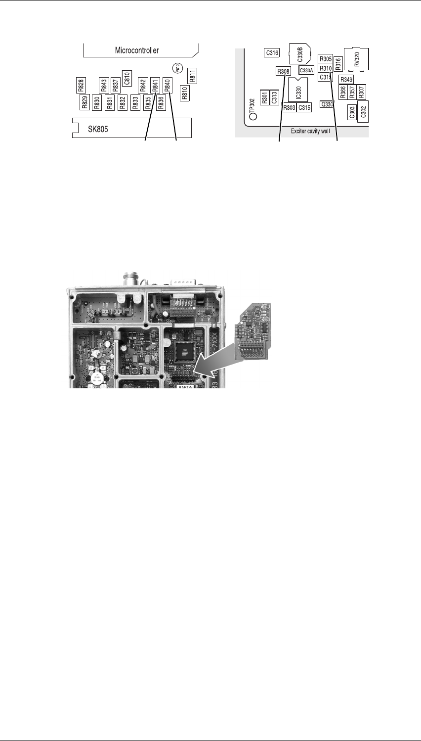
C3.20 T854 Initial Tuning and Adjustment M8SL2-00-002-812
© Copyright Tait Electronics Limited August 2004. All rights reserved.
Remove and fit the following resistors:
4. Double-sided tape is attached to the bottom side of the plug-in board. Remove the
protective film from the double-sided tape to expose its adhesive surface.
5. The plug-in board is mounted in the T854 microcontroller cavity. Plug J1, the con-
nector on the bottom side of the plug-in board, into SK805 on the T854 main
board.
6. Firmly press down on the edges of the plug-in board so that the double sided tape
bonds to the top of the microcontroller.
7. Connect the ribbon-cable between J2 on the plug-in board, and the auxiliary
D-Range board.
3.10.2.2 T800-10-0520 Testing/Alignment
Equipment required
•50Ω power meter
•Suitable attenuator, e.g. 3dB.
Forward alarm
1. Connect the power meter to the transmitter output.
2. Key up the transmitter and set the output power to the desired low forward-
power alarm threshold-point.
3. Adjust RV2, the forward-power alarm preset, until the forward alarm LED (DS2)
just turns ON.
3B: Fit %R308 and %R310 in
the exciter cavity. Use 10kΩ
SMD0805 (IPN: 036-15100-10).
3A: Remove R841 and R840
from the microcontroller cavity.
Fit the plug-in
board into the
microcontroller
cavity.

M8SL2-00-002-812 T854 Initial Tuning and Adjustment C3.21
© Copyright Tait Electronics Limited August 2004. All rights reserved.
4. Reset the power to the operational output level. Verify that the alarm output is
now OFF.
5. Turn the transmitter OFF.
Reverse alarm
1. Connect the power meter to the transmitter output.
2. Key up the transmitter and set the output power level to the operational output
level.
3. Unkey the transmitter.
4. Replace the power meter with the appropriate valued open-ended attenuator.
This should generate the desired return loss/reflected power for the desired high
reverse-power alarm threshold-point.
5. Key up the transmitter.
6. Adjust RV1, the reverse-power alarm preset, until the reverse alarm LED (DS1)
just comes ON.
7. Turn the transmitter OFF.
Channel Select Setup
In the default state of the plug-in board, no channel is selected (channel select disabled).
1. The desired channel can be selected by S1. Set the switches on S1 to the desired
channel number, in binary format.
Note: The switch on position is a binary ‘0’ and the off position a binary ‘1’.
2. To disable channel select, set all switches back to the off position.

C3.22 T854 Initial Tuning and Adjustment M8SL2-00-002-812
© Copyright Tait Electronics Limited August 2004. All rights reserved.
M8SL2-00-002-812 T854 Functional Testing C4.1
© Copyright Tait Electronics Limited August 2004. All rights reserved.
4 T854 Functional Testing
Caution: This equipment contains CMOS devices which are susceptible to dam-
age from static charges. Refer to Section 1.2 in Part A for more informa-
tion on anti-static procedures when handling these devices.
The following test procedures will confirm that the T854 has been tuned and adjusted
correctly and is fully operational.
Note 1: In this and following sections deviation settings are given first for wide
bandwidth sets, followed by settings in brackets for mid bandwidth sets ( )
and narrow bandwidth sets [ ].
Note 2: Unless otherwise specified, the term “PGM800Win” used in this and follow-
ing sections refers to version 4.02 and later of the software.
Refer to Figure 4.4 for the location of the main tuning and adjustment controls, and to
Section 3.3 for the test equipment set-up. Refer also to Section 6 where the parts lists,
grid reference index and diagrams will provide detailed information on identifying and
locating components and test points on the main PCB. The parts list and diagrams for
the VCO PCB are in Part E.
The following topics are covered in this section.
Section Title Page
4.1 Current Consumption 4.3
4.2 Output Power 4.3
4.3 Output Frequency 4.3
4.4 Timers 4.4
4.5 Frequency Response 4.5
4.6 Audio Level Input Sensitivity 4.8
Figure Title Page
4.1
4.2
4.3
4.4
T854 Transmit Timers
T854 Pre-emphasis Response
T854 Limiting Response
T854 Main Tuning and Adjustment Controls
4.4
4.6
4.7
4.9

C4.2 T854 Functional Testing M8SL2-00-002-812
© Copyright Tait Electronics Limited August 2004. All rights reserved.

M8SL2-00-002-812 T854 Functional Testing C4.3
© Copyright Tait Electronics Limited August 2004. All rights reserved.
4.1 Current Consumption
1. Connect the T854 to a 13.8V power supply.
2. Connect an RF power meter to the T854 output socket.
3. Check that the current in the 13.8V power cable is less than 150mA.
4. Key the T854 by earthing the Tx-Key line (the carrier “On” LED should light).
5. Adjust RV310 (power control) to obtain 25W output power.
6. Check that the current is less than 5.5A
4.2 Output Power
1. Connect an RF power meter with suitable attenuation to the T854 output socket.
2. Key the T854 by earthing the Tx-Key line.
3. Check that the output power adjusts to ≥25W with RV310 (power control) turned
fully clockwise
4.3 Output Frequency
Connect the T854 output to a frequency counter via a 40dB attenuator pad. Measure the
output frequency and, if necessary, adjust the TCXO (=IC700) to trim to the nominal fre-
quency (±100Hz).
C4.4 T854 Functional Testing M8SL2-00-002-812
© Copyright Tait Electronics Limited August 2004. All rights reserved.
4.4 Timers
The transmit tail timer, transmit timeout timer and transmit lockout timer can all
be set from PGM800Win. The fields for setting these are found on the system
information page. These three timers operate as follows (refer also to Figure 4.1):
Figure 4.1 T854 Transmit Timers
Timer Function Adjustment
Transmit Tail Sets the tail time during which the
transmitter stays keyed after the exter-
nal key source has been removed.
0 to 5 seconds in
20ms steps
Transmit Timeout Sets the maximum continuous trans-
mission time. Once the timer has
timed out, the transmitter must be
keyed again, unless prevented by the
transmit lockout timer.
0 to 300 seconds in
20 second steps
Transmit Lockout Sets the period of time that must
elapse after a timeout before the trans-
mitter can re-transmit. Once the timer
has timed out, the transmitter can be
keyed again.
0 to 60 seconds in 10
second steps
On
Lockout Time
Timeout
Time
On
Tail Time
Tx-Enable
Tx-Reg.
Tx-Enable
Tx-Reg.

M8SL2-00-002-812 T854 Functional Testing C4.5
© Copyright Tait Electronics Limited August 2004. All rights reserved.
4.5 Frequency Response
If the T854 has been correctly adjusted, the pre-emphasis and limiting responses should
closely match those shown in Figure 4.2 and Figure 4.3 respectively.
Note: The limits shown on these graphs should not be exceeded.
1. If you are using an RF test set, turn off all filters.
2. Measure the pre-emphasis response as follows:
Reduce the line level to give ±1kHz (±0.8kHz) [±0.5kHz] deviation at 1kHz.
Sweep the modulation frequency.
The response should closely match that shown in Figure 4.2.
3. Measure the limiting response as follows:
Set the line level to give ±3kHz (±2.4kHz) [±1.5kHz] deviation at 1kHz.
Increase the line level 20dB and sweep the modulation frequency.
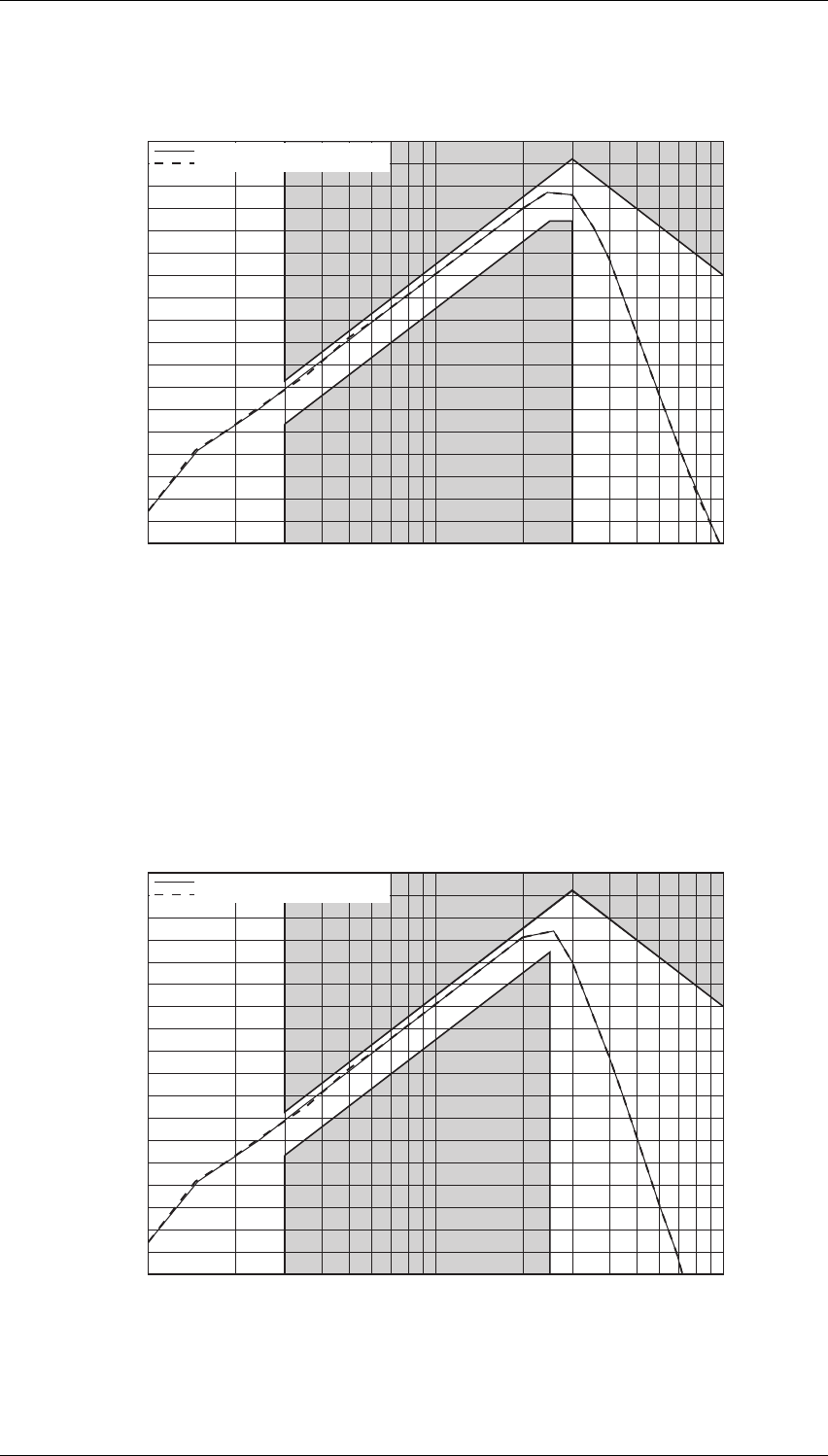
C4.6 T854 Functional Testing M8SL2-00-002-812
© Copyright Tait Electronics Limited August 2004. All rights reserved.
The response should closely match that shown in Figure 4.3.
Figure 4.2 T854 Pre-emphasis Response
Wide Bandwidth
Narrow Bandwidth
Mid Bandwidth
The mid bandwidth graph is the same shape as the wide bandwidth graph. The devia-
tion figures are as follows:
peak + max. deviation = +0.8kHz
peak – max. deviation = –0.8kHz.
+10
+8
Modulation Level (dB ref. to dev. @ 1kHz)
+6
+4
+2
+0
-2
-4
-6
-8
-10
-12
-14
-16
-18
-20
-22
100 200 300 500 1k 2k 3k 5k 10k
Frequency (Hz)
Peak + max. dev. = +1.0kHz @ 1000Hz
Peak - max. dev. = -1.0kHz @ 1000Hz
+10
+8
Modulation Level (dB ref. to dev. @ 1kHz)
+6
+4
+2
+0
-2
-4
-6
-8
-10
-12
-14
-16
-18
-20
-22
100 200 300 500 1k 2k 3k 5k 10k
Frequency (Hz)
Peak + max. dev. = +0.5kHz @ 1000Hz
Peak - max. dev. = -0.5kHz @ 1000Hz
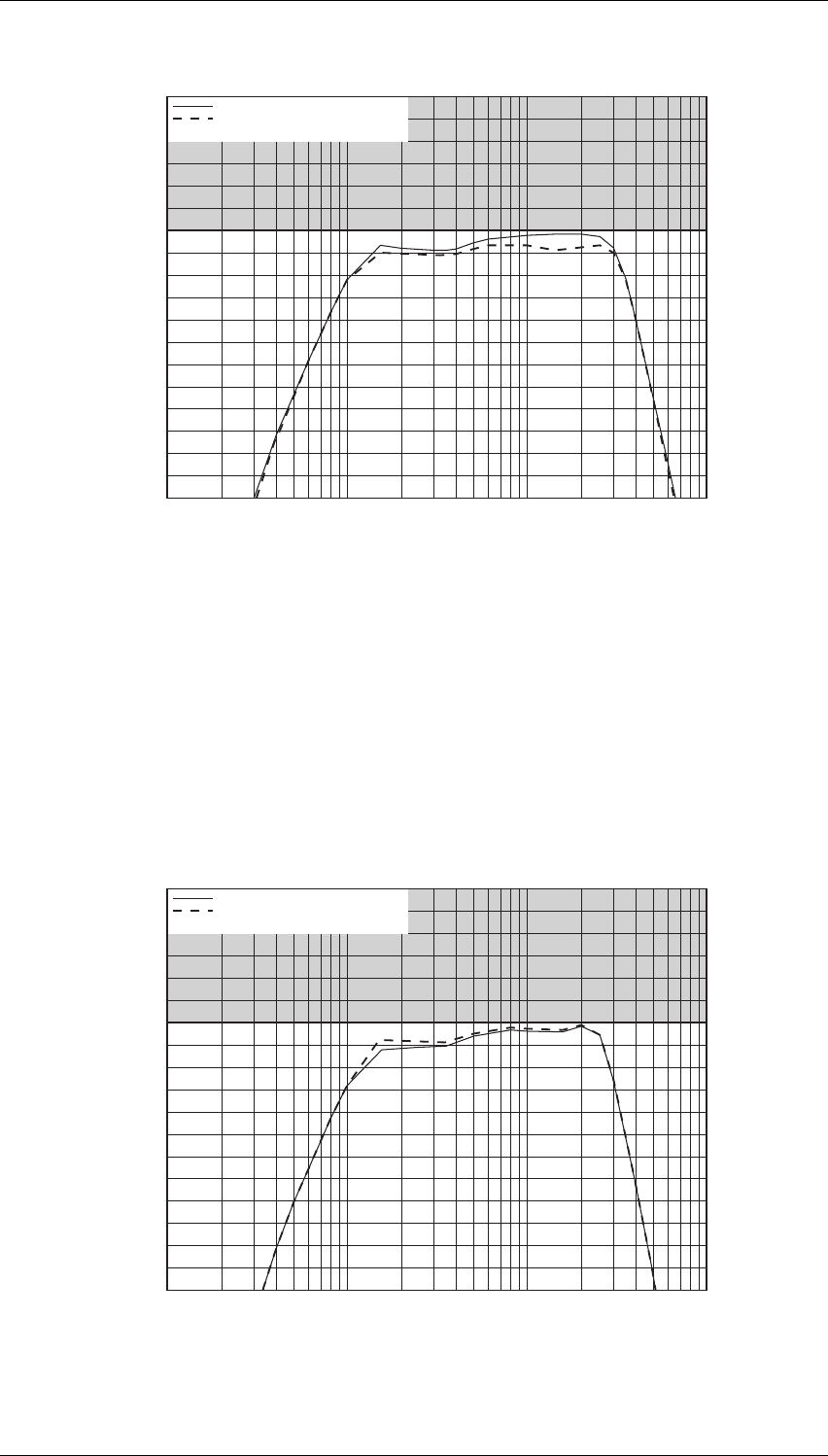
M8SL2-00-002-812 T854 Functional Testing C4.7
© Copyright Tait Electronics Limited August 2004. All rights reserved.
Figure 4.3 T854 Limiting Response
Wide Bandwidth
Narrow Bandwidth
100 500300 5k50
+10
+8
Modulation Level (dB ref. to max. dev.)
+6
+4
+2
+0
-2
-4
-6
-8
-10
-12
-14
-16
-18
-20
-22
10 20 30 200 1k 2k 3k 10k
Frequency (Hz)
Peak + max. dev. = +4.9kHz @ 1500Hz
Peak - max. dev. = -4.4kHz @ 2500Hz
Above limiting (steady-state)
Mid Bandwidth
The mid bandwidth graph is the same shape as the wide bandwidth graph. The devia-
tion figures are as follows:
peak + max. deviation = +4kHz
peak – max. deviation = –4kHz.
100 500300 5k50
+10
+8
Modulation Level (dB ref. to max. dev.)
+6
+4
+2
+0
-2
-4
-6
-8
-10
-12
-14
-16
-18
-20
-22
10 20 30 200 1k 2k 3k 10k
Frequency (Hz)
Peak + max. dev. = +2.4kHz @ 2000Hz
Peak - max. dev. = -2.5kHz @ 2000Hz
Above limiting (steady-state)

C4.8 T854 Functional Testing M8SL2-00-002-812
© Copyright Tait Electronics Limited August 2004. All rights reserved.
4.6 Audio Level Input Sensitivity
1. Adjust RV210 (line sensitivity) fully clockwise.
2. Check that the input sensitivities are better than those specified below:
Note: A degraded signal to noise ratio can be expected with the compressor
selected. The extent of the degradation is dependent on the audio input
level.
Line Input 600Ω, ±3kHz (±2.4kHz) [±1.5kHz] deviation at 1kHz:
with compressor –50dBm
without compressor –30dBm
Microphone Input 600Ω, ±3kHz (±2.4kHz) [±1.5kHz] deviation at 1kHz:
with compressor –75dBm
without compressor –55dBm
CTCSS Input 1kHz deviation at 150Hz 500mVrms
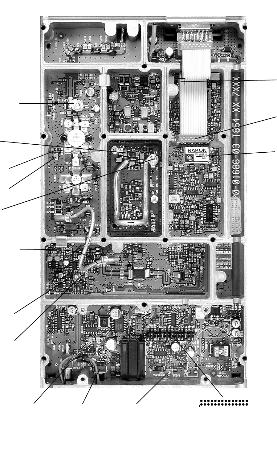
M8SL2-00-002-812 T854 Functional Testing C4.9
© Copyright Tait Electronics Limited August 2004. All rights reserved.
Figure 4.4 T854 Main Tuning and Adjustment Controls
R481
#CV475
C6
L1
RV320
shutdown
RV210
line sensitivity
SW230
carrier
=IC700
TCXO
L481
RV310
power control
RV220
compression level
RV805
CTCSS
level adjust
PL201 PL202
SK805
temperature
RV330
shutdown
power level

C4.10 T854 Functional Testing M8SL2-00-002-812
© Copyright Tait Electronics Limited August 2004. All rights reserved.
M8SL2-00-002-812 T854 Fault Finding C5.1
© Copyright Tait Electronics Limited August 2004. All rights reserved.
5 T854 Fault Finding
Caution: This equipment contains CMOS devices which are susceptible to dam-
age from static charges. Refer to Section 1.2 in Part A for more informa-
tion on anti-static procedures when handling these devices.
The following test procedures and fault finding flow charts may be used to help locate a
hardware problem, however they are by no means a complete fault finding procedure.
If you still cannot trace the fault after progressing through them in a logical manner,
contact your nearest Tait Dealer or Customer Service Organisation. If necessary, you can
get additional technical help from Technical Support, Tait Electronics Ltd, Christchurch,
New Zealand (full contact details are on page 2).
Note 1: In this and following sections deviation settings are given first for wide
bandwidth sets, followed by settings in brackets for mid bandwidth sets ( )
and narrow bandwidth sets [ ].
Note 2: Unless otherwise specified, the term “PGM800Win” used in this and follow-
ing sections refers to version 4.02 and later of the software.
Refer to Section 6 where the parts lists, grid reference index and diagrams will provide
detailed information on identifying and locating components and test points on the
main PCB. The parts list and diagrams for the VCO PCB are in Part E.
The following topics are covered in this section
Section Title Page
5.1 Visual Checks 5.3
5.2 Component Checks 5.3
5.3 Front Panel LED Indicator 5.3
5.4
5.4.1
5.4.2
DC Checks
Power Rails
VCO Locking
5.4
5.4
5.4
5.5
5.5.1
5.5.2
5.5.3
RF Checks
T854 Drive Power
T854 PA Output Power
Audio And Modulation
5.5
5.5
5.5
5.5
5.6 PGM800Win Generated Errors 5.6

C5.2 T854 Fault Finding M8SL2-00-002-812
© Copyright Tait Electronics Limited August 2004. All rights reserved.
5.7
5.7.1
5.7.1.1
5.7.1.2
5.7.1.3
5.7.2
5.7.3
5.7.4
5.7.5
5.7.7
Fault Finding Charts
Microcontroller
Basic Checks
Serial Communications
CTCSS Encode
Regulator
Synthesiser
T854 Drive Amplifier
T854 PA and Power Control
Audio Processor
5.7
5.7
5.7
5.8
5.9
5.10
5.11
5.14
5.15
5.16
5.8 To Replace The T854 PA Transistors (Q410 and Q420) 5.17
Figure Title Page
5.1
5.2
RF Diode Probe Circuit
Typical Transistor/Capacitor Spacing (Not To Scale)
5.5
5.17
Section Title Page

M8SL2-00-002-812 T854 Fault Finding C5.3
© Copyright Tait Electronics Limited August 2004. All rights reserved.
5.1 Visual Checks
Remove the top cover from the T854 and inspect the PCB for damaged or broken com-
ponents, paying particular attention to the surface mounted devices (SMDs).
Check for defective solder joints. If repair or replacement is considered necessary, refer
to Section 3 of Part A.
5.2 Component Checks
If you suspect a transistor is faulty, you can assess its performance by measuring the for-
ward and reverse resistance of the junctions. Unless the device is completely desol-
dered, first make sure that the transistor is not shunted by some circuit resistance. Use a
good quality EVM (e.g. Fluke 75) for taking the measurements (or a 20kΩ/V or better
multimeter, using only the medium or low resistance ranges).
The collector current drawn by multi-junction transistors is a further guide to their per-
formance.
If an IC is suspect, the most reliable check is to measure the DC operating voltages. Due
to the catastrophic nature of most IC failures, the pin voltages will usually be markedly
different from the recommended values in the presence of a fault. The recommended
values can be obtained from either the circuit diagram or the component data catalogue.
5.3 Front Panel LED Indicator
The green “Supply” LED on the T854 front panel will flash according to the conditions
described in the following table:
Where two or more conditions occur at the same time, the precedence is in the order
shown above (i.e. T854 linked has the highest priority, followed by internal error).
Flash Rate Condition
fast ( 1
/
3s on/ 1
/
3s off
approx.)
T854 is linked with PGM800Win
unequal ( 1
/
3s on/1s off
approx.)
microcontroller has detected an
internal communications error –
refer to Section 5.7.1

C5.4 T854 Fault Finding M8SL2-00-002-812
© Copyright Tait Electronics Limited August 2004. All rights reserved.
5.4 DC Checks
5.4.1 Power Rails
Refer to the test points and options diagrams in Section 6 for test point locations, and to
the regulator fault finding chart (Section 5.7.2) for fault diagnosis.
Check the 13.8V (TP601) and 9V (TP602) supplies at their test points in the regula-
tor compartment with a DMM.
Check the 5V (TP604) and 20V (TP603) rails at their respective test points in the
regulator compartment.
Check that Tx-Reg. (TP305 in the exciter compartment) comes up to 8.8V when the
exciter is keyed.
Check the +5V digital regulator output (TP607 in the regulator compartment).
Check the 9V supply (IC370 pin 1) with a DMM.
Check for short circuits.
5.4.2 VCO Locking
Key the exciter.
Using a DMM, monitor the VCO control voltage between between L1 and PL14
pin1 on the VCO PCB.
If the synthesiser is locked and the VCO aligned, the voltage at this point should
be between 3 and 16V.
If the VCO is not locked, refer to the synthesiser fault finding chart (Section 5.7.3).

M8SL2-00-002-812 T854 Fault Finding C5.5
© Copyright Tait Electronics Limited August 2004. All rights reserved.
5.5 RF Checks
In-circuit RF levels may be measured with an RF probe on which the earth lead has been
shortened to a minimum (i.e. 13mm). Refer to the circuit diagrams for typical levels.
Figure 5.1 shows a suitable RF probe circuit.
Figure 5.1 RF Diode Probe Circuit
5.5.1 T854 Drive Power
Refer to the drive amplifier fault finding chart (Section 5.7.4).
Ensure that the VCO locks (refer to Section 5.4.2).
Connect the drive output to a power meter and key the transmitter.
Check that the exciter output power (SK310) is >1.5W.
Note: If the synthesiser is out of lock, the lock detector (synthesiser IC740 and
comparator IC750) will prevent the RF signal from reaching the PA by
switching the supply to the exciter amplifier (Q336, Q337).
5.5.2 T854 PA Output Power
Reconnect the drive output to the PA input.
Connect the PA to a power meter and key the transmitter.
Check that the output power is >30W with RV310 (power control) adjusted fully
clockwise.
5.5.3 Audio And Modulation
Refer to the audio processor fault finding chart (Section 5.7.6).
Set up the audio processor as described in Section 3.9.
100k
10k
1n
1n
1N6263
Coax
Probe
Earthing Clip
DC to DVM or
Oscilloscope
This unit is not suitable for use on high power RF circuits.

C5.6 T854 Fault Finding M8SL2-00-002-812
© Copyright Tait Electronics Limited August 2004. All rights reserved.
Check that the demodulated RF output has the frequency response referred to in
Section 4.5 with at least ±5kHz (±4kHz) [±2.5kHz] deviation available at 1kHz
modulating frequency.
If the above result is not achieved, either the dual point modulation is incorrectly
adjusted or a fault condition exists.
5.6 PGM800Win Generated Errors
The following errors are those most likely to occur using PGM800Win. Refer to the
PGM800Win software user’s manual for a complete list of error messages.
Channel Switch Set
The programmed default channel change was not accepted by the base station because a
channel is selected externally. Try turning the external channel switch off to change the
default channel in PGM800Win.
Synth Out Of Lock
The synthesiser received incorrect data, or the data was corrupted. Enter a frequency
within the VCO switching range, or tune the VCO.
Internal Error
Data could not be read from the base station due to an internal error. Check for shorts or
open circuits on the SDA, SCK, SYNTH and EPOT lines. The SDA, SCK and SYNTH are
normally high, and the EPOT is normally low.
Write/Read To An Unlinked Module
The link to the module does not exist. Undefined error.
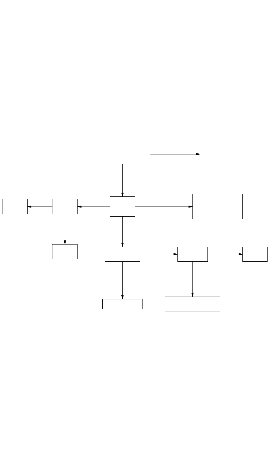
M8SL2-00-002-812 T854 Fault Finding C5.7
© Copyright Tait Electronics Limited August 2004. All rights reserved.
5.7 Fault Finding Charts
Note: The standard test point designations used in this section are as follows:
TP601 13.8V
TP602 9V
TP603 20V
TP604 5V
5.7.1 Microcontroller (IC810)
5.7.1.1 Basic Checks
Pulsing Check state
of pin 35.
Y
Is pin 30
pulsing?
High or open circuit
Y
Static high/low
Check state of
pins 36 to 43.
Low/floating
High
Is the 12.8MHz clock
present on IC810 pin 21
(microcontroller)?
N
Replace
IC810.
*digital storage oscilloscope
Replace IC810.
Check the
state of
pin 10.
N Pulsing
Low
Replace
IC810.
Use a DSO* to check
operation of IC650
(i.e. active high
pulse at power up).
Replace
IC650.
Correct the fault causing
pin 35 to be low/floating.
Check IC710.

C5.8 T854 Fault Finding M8SL2-00-002-812
© Copyright Tait Electronics Limited August 2004. All rights reserved.
5.7.1.2 Serial Communication
Check pin state.
Y
Low/floating
N
Noise
on pin
Disconnect the
programming lead.
Is IC810 pin 11 high?
(microcontroller)
Y*digital storage
oscilloscope
Use PGM800Win
to send a POLL
command to the
radio.
Check the transistor
interface circuitry
and/or replace the
programming lead.
Check the SERIAL-COM
and AUDIO-1/2 links.
Replace
IC810.
Check the transistor
interface circuitry
and/or replace the
programming lead.
Check the transistor
interface circuitry.
Check IC810 pin 13
with a DSO. Is there
a response from IC810 after
a poll command is sent?
N
Y
Connect the programming
lead and use PGM800Win
to read the rack/radio.
Check I/O pad P810
with a DSO*.
Does it swing from
0 to 5V?
N
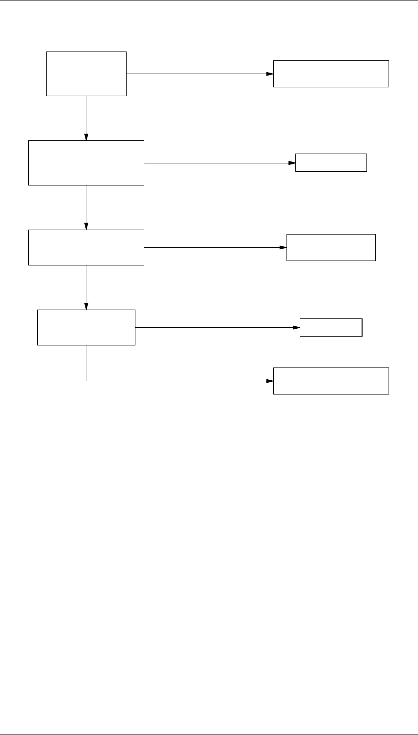
M8SL2-00-002-812 T854 Fault Finding C5.9
© Copyright Tait Electronics Limited August 2004. All rights reserved.
5.7.1.3 CTCSS Encode
Y
Y
Y
Replace IC810.
Use PGM800Win to
select a channel
with a CTCSS tone
programmed.
Check serial communications.
(See separate flow chart).
Cannot select a channel
Check IC810 pins 24, 25
& 26 (microcontroller).
Are there 5V square waves at
the CTCSS frequency?
Check IC830 pins 1, 7 & 14.
Are there 9V square waves at
the CTCSS frequency?
Check IC830 pin 8.
Is there a sine wave
at the CTCSS frequency?
Check RV805.
No tone
Check the filter circuit for bias
problems and/or short circuits.
Distorted tone
No square waves or
uneven mark/space ratio
No square waves or
uneven mark/space ratio Check IC830 circuitry
and repair/replace.
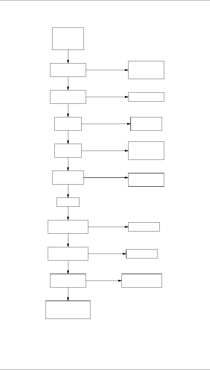
C5.10 T854 Fault Finding M8SL2-00-002-812
© Copyright Tait Electronics Limited August 2004. All rights reserved.
5.7.2 Regulator
N
Y
Check for
overheating
components &
short circuits.
N
Y
Check Q630,
Q620 & IC640.
N
Y
9.0V present
on TP602?
Check Q660 is
switching at
approx. 150kHz.
N
Y
20V present
on TP603?
Check R615.
Replace IC610.
N
Y
Key Tx.
Y
Regulators OK.
N
8.8V present
on Tx reg. TP305?
Replace Q610.
Y
N
0V present
on Q860 collector?
Check Q860 and
associated circuitry.
Y
0.6V present on
Q860 base?
N
Regulators OK.
Check microcontroller
section.
Check continuity
from pin 9 of
D-range 1.
13.8V present on
IC630 pin 3?
5.3V present on
IC630 pin 1? Replace IC630.
+5V present on
IC610 pin 1?
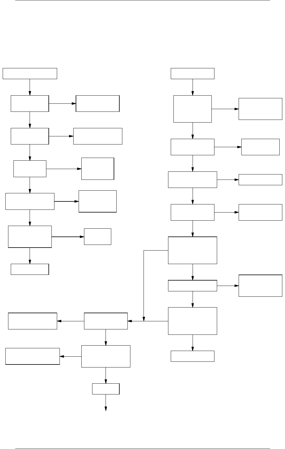
M8SL2-00-002-812 T854 Fault Finding C5.11
© Copyright Tait Electronics Limited August 2004. All rights reserved.
5.7.3 Synthesiser
Refer to the synthesiser circuit diagram (sheet 7) in Section 6 and the VCO circuit dia-
gram in Part E.
N
A B
Check biasing
resistors, Q4 & Q5.
N
Y
N
8.3V present
at VCO?
DC V present
at Q4 & Q5?
9V present at
VCO Q4/Q5?
No VCO RF output.
Y
DC V present at
VCO, Q1, Q2 & Q3?
Check biasing
resistors, Q1,
Q2 & Q3.
Y
N
Capacitors OK?
Check for cracks,
shorts, etc.
N
Y
Replace VCO.
Replace
if faulty.
Y
N
Y
N
N
N
Y
Y
DC V present
on Q795 emitter?
Check 9V supply.
9V present on
Q795 divider buffer?
20V inverter
supply faulty.
20V present
on IC750 pin 8?
Check 5V reg. &
supply resistor
to each IC.
+5V present at
IC700, IC710,
IC740, IC720
& IC730?
VCO out of lock.
Y
Y
Y
Continued on the next page
Y
VCO freq. correct?
Synthesiser OK.
VCO trimmer
freq. range OK?
Check VCO tuning
caps & trimmer.
VCO OK.
N
N
NN
N
Y
Y
Recheck
programming
via PGM800Win.
Check Q5 C
multiplier
(synth).
Check biasing
resistors & Q795.
Check Tx reg.,
Q610 & 9V reg.
Does VCO trimmer
adjust for stable
control line
between 3 & 16V?
Does VCO trimmer
adjust for required
frequency range
between 3 & 16V?
Check #C1, #C7, #C8,
C6 & D1-D2 in VCO.
Is 8MHz VCO range
achieved between
3 & 16V?
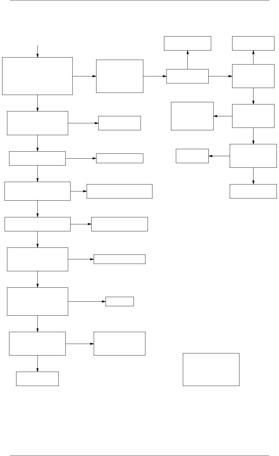
C5.12 T854 Fault Finding M8SL2-00-002-812
© Copyright Tait Electronics Limited August 2004. All rights reserved.
Programming and
serial bus OK?
Check programming.
Check serial bus
when programming
i.e. clock/data/enable
activity (IC740 pins
18, 19 & 17).
N
Check loop filter components
R775, C774, C776, R510,
C505, IC750. Is the supply
to IC750 +20V +4, -2V?
Check regulator circuitry.
Check C772, R774, R772,
C770, R763 & Q790.
Check Q760, Q780,
R766 & C765.
Check charge pump components
(Q775 & Q780) and Q790.
Check R762 & C762.
Check the signal path from
the VCO to synthesiser.
Measure the frequency from
the VCO at IC740 pin 11 using
a frequency counter.
Is the level >-10dBm?
Does the frequency adjust
as the VCO trimmer is
adjusted (out of lock)?
Check VCO.
Y
Y
Y
Signal
Y
Y
Y
No signal
Replace synthesiser
(IC740).
Y
N Y
Y
N
N
N
N
Check phase detector output
pins (IC740 pins 3 & 4).
Are there very narrow pulses
(~50ns) at the reference frequency?
(i.e. 5kHz : 200µs period
6.25kHz : 160µs period)
*See Note below.
Is the charge pump bias
voltage at the base of
Q760 & Q780 between
3.5 and 5V? (5V when locked)
N
Is the voltage on C762,
R760, and R758 9V ±0.2V?
Is the loop filter reference
voltage at C772 (+) 6.5V ±0.2V?
N
Check divider buffer
circuit (Q795) and bias
voltages on Q795 emitter
(1.3V ±0.2V).
*Note:
When locked, both of these
are very narrow (~50ns).
If unlocked, one will be
very narrow (~50ns),
and the other wide (>15µs).
Replace synthesiser
(IC740).
Continued from previous page
B
Is the charge pump voltage
on Q790 gate between
3 and 8.5V? (6.5V ±0.2V locked)
Is reference
clock present
at IC740 pin 20
(200kHz >4.5Vpp)?
Check microcontroller
section (IC810).
N
Is reference
clock present
at IC730 pin 12
(200kHz >4.5Vpp)?
Is reference
clock present
at IC730 pin 1
(12.8MHz >4.0Vpp)?
Check TCXO (IC700)
and buffers (IC710).
N
N
Y
Y
Check phase
modulator sections:
IC720, Q710, Q720,
D710, Q730, Q740,
D720.
Check divider
IC730.
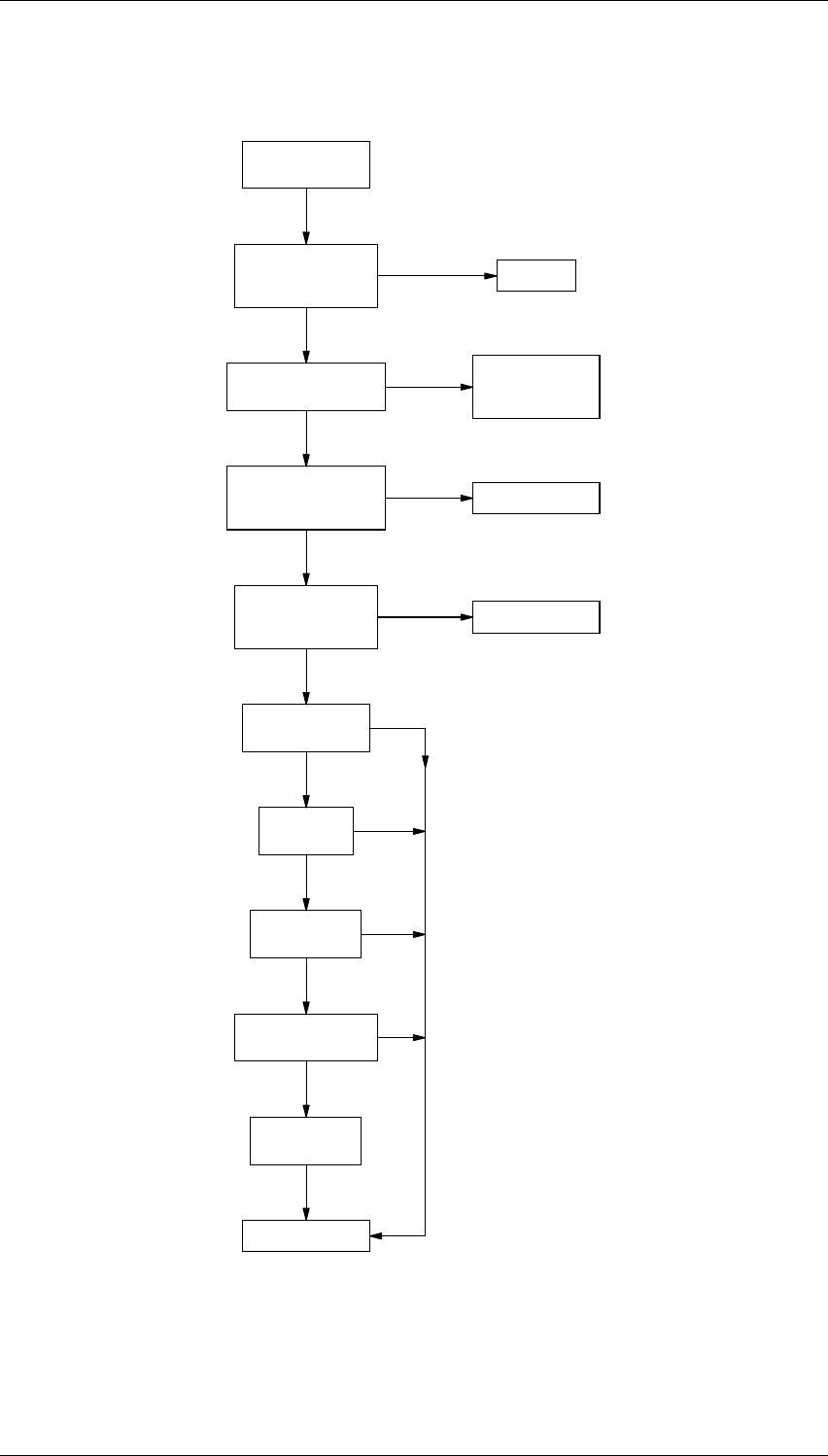
M8SL2-00-002-812 T854 Fault Finding C5.13
© Copyright Tait Electronics Limited August 2004. All rights reserved.
Y
N
Y
Y
Correct DC V
present on Q1 VCO?
N
Check inductors,
biasing resistors
& Q1.
Replace if faulty.
Go to B.
Loop filter &
components around
op. amp. (IC750) OK?
N
Noisy synth;
poor residual FM.
C
Isolate audio
modulation on VCO;
still noisy?
Trace audio fault.
Y
Y
N
Y
Y
Y
Change trimmer;
still noisy?
Change Q1;
still noisy?
Change TCXO;
still noisy?
Change varactors;
still noisy?
Replace VCO
assembly.
Synthesiser OK.
N
N
N
N
Y
VCO phase locked?
3-16V present on
control line?
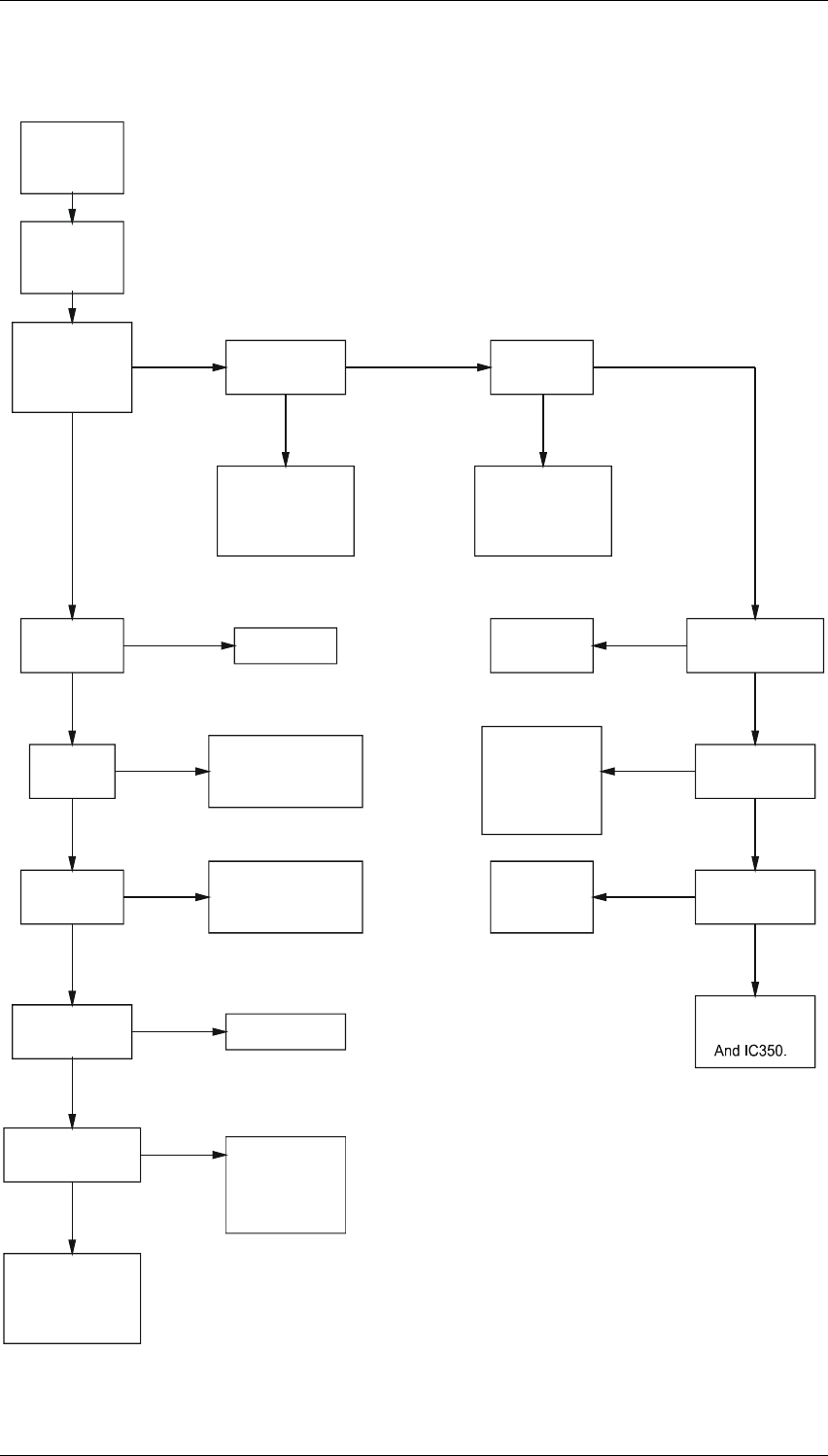
C5.14 T854 Fault Finding M8SL2-00-002-812
© Copyright Tait Electronics Limited August 2004. All rights reserved.
5.7.4 T854 Drive Amplifier
12.9V on Q334
collector?
Check continuity
of power rails
& DC paths to
Q333 & Q332.
Exciter OK
Replace coaxial
Link and go to
PA flow chart
Key exciter
& lock
synthesiser.
NN
YY
Y
Check VCO.
N
Y
Y
N
Y
Y
N
Y
Check 9V &
13.8V supplies.
Check
regulators.
Check temp.
shutdown
circuit.
N
Y
N
Y
N
Y
3.3V on Q337
collector?
13.6V on Q336
collector?
11.5V on
IC350 pin 7?
N
Check lock det.
path back to
synth. IC740,
IC750, Q325.
Check TP305
>+8V.
Check TP320
<0.6V.
Check Q330,
Q325 Q326
>2V RF at
VCO output?
>1V RF
at R381?
NCheck attenuator
pad #R517, #R518,
#R519.
>0.5V RF at
Q337 base?
Check C355, C358,
C360, Q350, D340,
D380, D360, L320.
N
Check Q350.
>2.5W at
Sk310? Check Q336.
>5V RF at
C361
Key exciter
& lock
synthesiser.
Check
Q334 Q3814a
paths between
Ic350 Q334
And Q326.
& signal path.
From collector
To Sk310
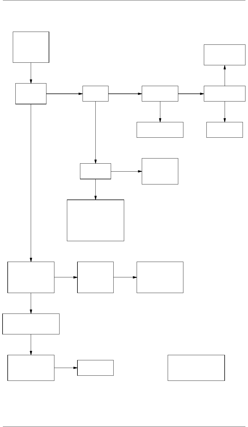
M8SL2-00-002-812 T854 Fault Finding C5.15
© Copyright Tait Electronics Limited August 2004. All rights reserved.
5.7.5 T854 PA and Power Control
Check IC330,
Q310, Q315
& circuitry,
+13.8V supply.
Refer to Drive Amp.
Fault Finding Chart.
Check supply
circuitry.
Tx delivering
full power
(>30W)?
Set RV320
(power adjust)
fully clockwise;
synth. locked;
key Tx.
Y
NY
NN
Y
N
Y
N
NY
Y
Y
Y
Power control
circuitry OK.
Note:
c/w = clockwise
cc/w = counterclockwise
or anticlockwise
Check Q410,
Q420 & circuitry,
LP filter.
10.8V
at L310?
Check drive at
SK310 >1.5W.
Check +13.8V at
Q410 & Q420.
<2V on
IC350 pin 6?
Turn RV310 ccw.
Check power
drops to zero
slowly in a
controlled manner.
Does variation
of RV310
cause either
full power
or no power?
Check for break
in power sense
circuitry; directional
coupler D420,
D440 & circuitry.
Set RV310 so that
output power = 25W;
check L310 approx. 7.5V.
Momentarily remove
Tx load. Voltage at
L310 decreases to
approx. 5V?
Check lock det. circuit;
TP305 should be >8V.
Check temp. shutdown
circuit (IC350);
TP320 should be <0.6V.
Check Q320, RV330.
Normal operating conditions:
Forward power = 4.7V approx.
Reverse power = 0.7V approx.
IC350 pin 6 = 2.02V
IC350 pin 5 = 2V
IC350 pin 7 = 8.63V
C5.16 T854 Fault Finding M8SL2-00-002-812
© Copyright Tait Electronics Limited August 2004. All rights reserved.
5.7.6 Audio Processor
N
IC240 pin 6
at 9V?
Key exciter &
lock synthesiser.
Connect 1kHz audio
to external CTCSS input.
Does exciter
modulate?
Audio output at
IC260 pin 8?
NY
Check audio path to
VCO control line.
Check alignment
of modulators.
YN
Audio output at
IC260 pin 1?
YCheck buffer IC260
pins 8, 9 & 10.
N
Audio output at
IC260 pin 7?
Check low pass
filter stage IC260
pins 1, 2 & 3.
Y
Check stage IC260
pins 5, 6 & 7.
N
Demodulated audio
frequency response
flat between 50 & 300Hz?
Y
Check low
pass filter
stage IC260
pins 1, 2 & 3.
N
N
Y
Audio frequency
response IC260
pin 1 flat 300Hz
to 2kHz?
Audio frequency
response IC210
pin 8 6dB/octave
slope?
Check integrator
IC210 pins 8, 9, & 10.
N
Y
Audio superimposed
on 200kHz signal
IC720 pins 9 & 3 (synth)?
Check audio path
between integrator
& phase modulator.
N
Y
200kHz clipped
triangle wave at
IC720 pins 8 & 4?
Check IC720, Q710, Q720,
Q730, Q740, D710, D720,
C727, C729, C724 & C725
N
Y
Check loop filter
(IC750, pins 5, 6 & 7)
& associated
components.
Select standard
audio configuration.
Check pre-emphasis
network IC230 pins 12,
13 & 14 &/or low pass
filter IC260 pins 1, 2 & 3.
N
Y
Connect audio
to line input;
key exciter.
Does exciter
modulate?
YN
Demodulated
audio frequency
response as per
Section 4.5?
Audio processor
OK.
Audio signal at
IC210 pin 14?
Y
N
Audio signal at
IC230 pin 1?
N
Audio signal at
IC230 pin 14?
Y
N
Audio signal at
IC240 pin 4?
Y
N
Y
Check Q260 is not faulty or
being turned on inadvertently.
Y
Check audio path between
limiter IC210 pin 14 &
summing amp. IC260 pin 7.
Check IC210
pins 12, 13 & 14.
Check IC230 pins 1, 2 & 3 or
audio path between pre-
emphasis network & limiter.
Check IC230 pins 12, 13 & 14
or audio path between multiplexer
& pre-emphasis network.
Check IC240 or audio
path between line trans-
former & multiplexer.
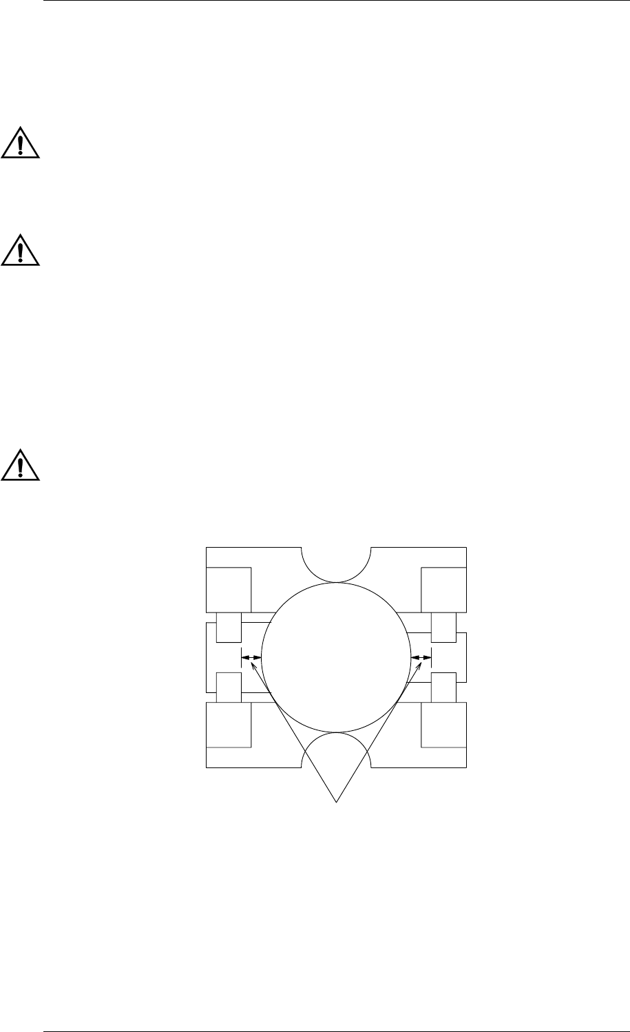
M8SL2-00-002-812 T854 Fault Finding C5.17
© Copyright Tait Electronics Limited August 2004. All rights reserved.
5.8 To Replace The T854 PA Transistors
(Q410 and Q420)
Caution: Failure to comply with the following procedure can result in failure of
the device due to poor heatsinking, or worse, can endanger the health
of the assembler if the beryllium oxide die carrier is smashed during
assembly.
Caution: As the location of certain components in the PA is critical to perform-
ance, it is important that any components removed or disturbed are
refitted in exactly the same position.
Before attempting to remove a transistor, measure the distance
between the capacitors and transistor body to the nearest 0.5mm (meas-
urement “A” in Figure 5.2) so that the capacitors can be replaced in
exactly the same position. These measurements are shown in Figure
5.2 for the 6LFL package, however the same procedure applies for the
SOE (stud) package.
Caution: Do not apply too much heat or pressure to the PCB pads and tracks as
you may damage them or lift them from the PCB, causing permanent
damage to the transmitter.
Figure 5.2 Typical Transistor/Capacitor Spacing (Not To Scale)
Desolder and remove the components from around the transistor.
Q420 Only: Desolder and remove the two solder tags.
Desolder the transistor tabs by heating with a soldering iron and lifting away
from the PCB with a screwdriver or thin stainless steel spike, then remove the
device.
base collector
measurement A

C5.18 T854 Fault Finding M8SL2-00-002-812
© Copyright Tait Electronics Limited August 2004. All rights reserved.
Q410 Only: Unscrew the transistor stud nut and remove the device.
Remove any excess solder from the PCB pads with solder wick.
Trim the tabs of the replacement transistor so that the device sits neatly on the
PCB pads provided.
Lightly tin the underside of the transistor tabs. Remove any excess solder to leave
a thin, even layer on the tabs.
Apply a small amount of heatsink compound (Dow-Corning 340 or equivalent) to
the transistor mounting surface. Sufficient compound should be used to ensure an
even film over the entire mounting surface.
Place the transistor on the PCB in the correct orientation and ensure the tabs are
flush to the surface.
Q410 Only: Lightly solder one tab to the PCB, then torque down the retain-
ing nut to the correct torque (0.7Nm/6in.lbf.).
Caution: Do not solder all the tabs before torquing down otherwise the device
may be broken.
Q420 Only: Refit the solder tags.
Solder all transistor tabs to the PCB.
Replace each component in exactly the same position as noted previously.
M8SL2-00-002-812 T854 PCB Information C6.1.1
© Copyright Tait Electronics Limited August 2004. All rights reserved.
6 T854 PCB Information
Caution: This equipment contains CMOS devices which are susceptible to damage from
static charges. Refer to Section 1.2 in Part A for more information on anti-static
procedures when handling these devices.
This section provides the following information on the T854 transmitter:
•parts lists
•grid reference indexes
•mechanical assembly drawings
•PCB layouts
•test points and options connections drawings
•circuit diagrams.
Section Title IPN Page
6.1 Introduction 6.1.3
6.2 T854 Transmitter PCB 220-01397-01 6.2.1

C6.1.2 T854 PCB Information M8SL2-00-002-812
© Copyright Tait Electronics Limited August 2004. All rights reserved.
M8SL2-00-002-812 T854 PCB Information C6.1.3
© Copyright Tait Electronics Limited August 2004. All rights reserved.
6.1 Introduction
Product Type Identification
You can identify the transmitter type by checking the product code printed on a label on the rear of
the chassis (product codes are explained in Section 1 of the front matter in this manual, and Figure
1.1 in Part A shows typical labels). You can further verify the product type by checking the place-
ment of an SMD resistor in the table that is screen printed onto the top side of the PCB, similar to the
example drawn below. In this example, the resistor indicates that the product was built as a
T854-10-XXXX.
Note: The only function of this resistor is to indicate the product type. It has no effect on the
circuitry or operation of the transmitter.
PCB Identification
All PCBs are identified by a unique 10 digit “internal part number” (IPN), e.g. 220-01390-02, which
is screen printed onto the PCB (usually on the top side), as shown in the example below:
The last 2 digits of this number define the issue status, which starts at 00 and increments through 01,
02, 03, etc. as the PCB is updated. Some issue PCBs never reach full production status and are there-
fore not included in this manual. A letter following the 10 digit IPN has no relevance in identifying
the PCB for service purposes.
Note: It is important that you identify which issue PCB you are working on so that you can
refer to the appropriate set of PCB information.
854-30 PRODUCT TYPE
854-35 854-10 854-20
854- 854-13 854-23
PRODUCT TYPE 854-15 854-25
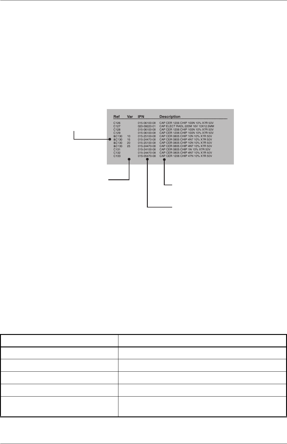
C6.1.4 T854 PCB Information M8SL2-00-002-812
© Copyright Tait Electronics Limited August 2004. All rights reserved.
Parts Lists
The 10 digit numbers (000-00000-00) in this Parts List are “internal part numbers” (IPNs). We can
process your spare parts orders more efficiently and accurately if you quote the IPN and provide a
brief description of the part.
The components listed in this parts list are divided into two main types: those with a circuit refer-
ence (e.g. C2, D1, R121, etc.) and those without (miscellaneous and mechanical).
Those with a circuit reference are grouped in alphabetical order and then in numerical order within
each group. Each component entry comprises three or four columns, as shown below:
The miscellaneous and mechanical section lists the variant and common parts in IPN order.
Variant Components
A variant component is one that has the same circuit reference but different value or specification in
different product types. Where two products share the same PCB, the term “variant” is also used to
describe components unplaced in one product. Variant components have a character prefix, such as
“&”, “=” or “#”, before the circuit reference (e.g. &R100).
The table below explains the variant prefixes used in T800 SL2 products:
If the variant prefix is. . . the component will. . .
& change according to channel spacing
= change according to frequency stability
# change according to frequency range
% change or be placed/unplaced for special applications
*be unplaced in one product
(where two products share the same PCB)
circuit re
f
erence -
lists components
in alphanumeric
order
variant column -
indicates that this is
a variant component
which is fitted only to
the product type listed
Internal Part Number -
order the component
b
y
this number
description -
gives a brief description
of the component

M8SL2-00-002-812 T854 PCB Information C6.1.5
© Copyright Tait Electronics Limited August 2004. All rights reserved.
Grid Reference Index
This section contains a component grid reference index to help you find components and labelled
pads on the PCB layouts and circuit diagrams. This index lists the components and pads in alpha-
numeric order, along with the appropriate alphanumeric grid references, as shown below:
Using CAD Circuit Diagrams
Reading a CAD circuit diagram is similar to reading a road map, in that both have an alphanumeric
border. The circuit diagrams in this manual use letters to represent the horizontal axis, and numbers
for the vertical axis. These circuit diagram “grid references” are useful in following a circuit that is
spread over two or more sheets.
When a line representing part of the circuitry is discontinued, a reference will be given at the end of
the line to indicate where the rest of the circuitry is located, as shown below. The first digit refers to
the sheet number and the last two characters refer to the location on that sheet of the continuation of
the circuit (e.g. 1R3).
circuit diagram
reference
P
C
B layout
reference
components listed
in alphanumeric order
layer number -
1 = top side layer
2 = bottom side layer
component location
on the layer
sheet number
component location
on the sheet
C301
4N7
R303
12
D
S
G
L310
33U
IF-SIG
4R4
C369
100P
C371
10U
R339
100K
%R338
100
DISCRIMINATOR
1R3
2R9
2R9
8A2
t
hese grid references
s
how where the circuit
i
s continued

C6.1.6 T854 PCB Information M8SL2-00-002-812
© Copyright Tait Electronics Limited August 2004. All rights reserved.

M8SL2-00-002-812 T854 PCB Information C6.2.1
© Copyright Tait Electronics Limited August 2004. All rights reserved.
6.2 T854 Transmitter PCB
This section contains the following information.
IPN Section Page
220-01397-01 Parts List
Mechanical and Miscellaneous Parts
Mechanical Assembly
Grid Reference Index
PCB Layout – Top Side
PCB Layout – Bottom Side
Test Points and Options Connections – Top Side
Test Points and Options Connections – Bottom Side
Transmitter Overview Diagram
Audio Processor Circuit Diagram
Exciter Circuit Diagram
PA Circuit Diagram
VCO Section Circuit Diagram
Regulators Circuit Diagram
Synthesiser Circuit Diagram
Microcontroller Circuit Diagram
Harmonic Filter Circuit Diagram
6.2.3
6.2.10
6.2.11
6.2.13
6.2.17
6.2.18
6.2.19
6.2.20
6.2.21
6.2.22
6.2.23
6.2.24
6.2.25
6.2.26
6.2.27
6.2.28
6.2.29

C6.2.2 T854 PCB Information M8SL2-00-002-812
© Copyright Tait Electronics Limited August 2004. All rights reserved.

M8SL2-00-002-812 T854 PCB Information C6.2.3
© Copyright Tait Electronics Limited August 2004. All rights reserved.
Ref Var IPN Description Ref Var IPN Description
T854 Parts List (IPN 220-01686-03)
How To Use This Parts List
The components listed in this parts list are grouped in alphabetical order and then in numerical order within each group. Each compo-
nent entry comprises three or four columns: the circuit reference, variant (if applicable), IPN and description. A number in the variant
column indicates that this is a variant component which is fitted only to the product type listed.
This parts list is correct at the time of publishing, but is subject to change without notification. An up to date parts list can be obtained
from your local Customer Service Organisation
C100 015-23150-01CAP CER 0805 150P 5% NPO 50V
C101 016-08470-01CAP ELEC SMD 47UF 6*4 16V
C102 016-08470-01CAP ELEC SMD 47UF 6*4 16V
C103 015-24100-08CAP CER 0805 1N 10% X7R 50V
C201 016-07470-06CAP ELEC SMD BI-P 4U7 50V 20%
C202 016-07470-06CAP ELEC SMD BI-P 4U7 50V 20%
%C203A 015-25150-08CAP CER 0805 15N 10% X7R 50V
%C203B 015-25150-08CAP CER 0805 15N 10% X7R 50V
C207 014-07470-01CAP TANT SMD 4U7 25V 10% B
C209 015-25470-08CAP CER 0805 47N 10% X7R 50V
C210 015-26100-08CAP CER 0805 100N 10% X7R 50V
C211 015-26100-08CAP CER 0805 100N 10% X7R 50V
C213 014-08100-00CAP TANT SMD 10U 16V 20% 267C
C215 014-08220-01CAP TANT SMD 22U 10V 10% C
C217 015-24220-08CAP CER 0805 2N2 10% X7R 50V
C219 015-24100-08CAP CER 0805 1N 10% X7R 50V
C221 014-08220-01 CAP TANT SMD 22U 10V 10% C
C223 015-26100-08 CAP CER 0805 100N 10% X7R 50V
C225 015-26100-08 CAP CER 0805 100N 10% X7R 50V
C227 015-26100-08 CAP CER 0805 100N 10% X7R 50V
C229 015-23150-01 CAP CER 0805 150P 5% NPO 50V
C230 015-26100-08 CAP CER 0805 100N 10% X7R 50V
C232 015-23150-01 CAP CER 0805 150P 5% NPO 50V
C233 016-08470-01 CAP ELEC SMD 47UF 6*4 16V
C235 015-24100-08 CAP CER 0805 1N 10% X7R 50V
C237 014-07100-02 CAP TANT SMD 1U0 16V 20% A
C239 016-07470-06 CAP ELEC SMD BI-P 4U7 50V 20%
C240 015-23150-01 CAP CER 0805 150P 5% NPO 50V
C241 015-26100-08 CAP CER 0805 100N 10% X7R 50V
C242 014-08100-00 CAP TANT SMD 10U 16V 20% 267C
C243 015-24100-08 CAP CER 0805 1N 10% X7R 50V
C245 015-23150-01 CAP CER 0805 150P 5% NPO 50V
C247 015-23150-01 CAP CER 0805 150P 5% NPO 50V
C249 015-24100-08 CAP CER 0805 1N 10% X7R 50V
C251 015-24100-08 CAP CER 0805 1N 10% X7R 50V
C253 015-24100-08 CAP CER 0805 1N 10% X7R 50V
C255 015-24100-08 CAP CER 0805 1N 10% X7R 50V
C257 015-22470-01 CAP CER 0805 47P 5% NPO 50V
C259 015-25470-08 CAP CER 0805 47N 10% X7R 50V
C260 015-26100-08 CAP CER 0805 100N 10% X7R 50V
C261 014-07470-01 CAP TANT SMD 4U7 25V 10% B
C263 016-09100-05 CAP ELEC SMD 100U 25V 20%
%C265 016-07470-06 CAP ELEC SMD BI-P 4U7 50V 20%
C267 015-24470-08 CAP CER 0805 4N7 10% X7R 50V
&C269 10 015-21150-01 CAP CER 0805 1P5+-0.25 NPO 50V
&C269 13 015-21150-01 CAP CER 0805 1P5+-0.25 NPO 50V
&C269 15 015-21470-01 CAP CER 0805 4P7+-0.25 NPO 50V
&C269 16 015-21470-01 CAP CER 0805 4P7+-0.25 NPO 50V
&C269 20 015-21150-01 CAP CER 0805 1P5+-0.25 NPO 50V
&C269 23 015-21150-01 CAP CER 0805 1P5+-0.25 NPO 50V
&C269 25 015-21470-01 CAP CER 0805 4P7+-0.25 NPO 50V
&C269 26 015-21470-01 CAP CER 0805 4P7+-0.25 NPO 50V
&C269 30 015-21150-01 CAP CER 0805 1P5+-0.25 NPO 50V
&C269 35 015-21470-01 CAP CER 0805 4P7+-0.25 NPO 50V
&C269 36 015-21470-01 CAP CER 0805 4P7+-0.25 NPO 50V
&C271 10 015-22470-01 CAP CER 0805 47P 5% NPO 50V
&C271 13 015-22470-01 CAP CER 0805 47P 5% NPO 50V
&C271 15 015-22470-01 CAP CER 0805 47P 5% NPO 50V
&C271 16 015-22560-01 CAP CER 0805 56P 5% NPO 50V
&C271 20 015-22470-01 CAP CER 0805 47P 5% NPO 50V
&C271 23 015-22470-01 CAP CER 0805 47P 5% NPO 50V
&C271 25 015-22470-01 CAP CER 0805 47P 5% NPO 50V
&C271 26 015-22560-01 CAP CER 0805 56P 5% NPO 50V
&C271 30 015-22470-01 CAP CER 0805 47P 5% NPO 50V
&C271 35 015-22470-01 CAP CER 0805 56P 5% NPO 50V
&C271 36 015-22560-01 CAP CER 0805 47P 5% NPO 50V
C273 015-25470-08 CAP CER 0805 47N 10% X7R 50V
C275 015-23150-01 CAP CER 0805 150P 5% NPO 50V
C277 015-25100-08 CAP CER 0805 10N 10% X7R 50V
C279 015-24100-08 CAP CER 0805 1N 10% X7R 50V
C281 015-25220-08 CAP CER 0805 22N 10% X7R 50V
C283 015-21470-05 CAP CER 0805 4P7+-0.1PF 200V
C285 015-21470-05 CAP CER 0805 4P7+-0.1PF 200V
C287 016-09100-05 CAP ELEC SMD 100U 25V 20%
&C289 10 015-25470-08 CAP CER 0805 47N 10% X7R 50V
&C289 13 015-25470-08 CAP CER 0805 47N 10% X7R 50V
&C289 15 015-25470-08 CAP CER 0805 47N 10% X7R 50V
&C289 16 015-26100-08 CAP CER 0805 100N 10% X7R 50V
&C289 20 015-25470-08 CAP CER 0805 47N 10% X7R 50V
&C289 23 015-25470-08 CAP CER 0805 47N 10% X7R 50V
&C289 25 015-25470-08 CAP CER 0805 47N 10% X7R 50V
&C289 26 015-26100-08 CAP CER 0805 100N 10% X7R 50V
&C289 30 015-25470-08 CAP CER 0805 47N 10% X7R 50V
&C289 35 015-25470-08 CAP CER 0805 47N 10% X7R 50V
&C289 36 015-26100-08 CAP CER 0805 100N 10% X7R 50V
C291 014-08220-01 CAP TANT SMD 22U 10V 10% C
C293 015-27100-10 CAP CER 0805 1M+80-20% Y5V 16V
%C294 015-22470-01 CAP CER 0805 47P 5% NPO 50V
%C295 013-06470-00 CAP SMD POLY 470N 63V 10%
C300 015-24100-08 CAP CER 0805 1N 10% X7R 50V
C301 015-24100-08 CAP CER 0805 1N 10% X7R 50V
C302 015-06100-08 CAP CER 1206 100N 10% X7R 50V
C303 015-23150-01 CAP CER 0805 150P 5% NPO 50V
C305 015-23150-01 CAP CER 0805 150P 5% NPO 50V
C306 015-26100-08 CAP CER 0805 100N 10% X7R 50V
C307 015-25100-08 CAP CER 0805 10N 10% X7R 50V
C311 015-23150-01 CAP CER 0805 150P 5% NPO 50V
C313 015-23150-01 CAP CER 0805 150P 5% NPO 50V
C315 015-23150-01 CAP CER 0805 150P 5% NPO 50V
C316 015-23150-01 CAP CER 0805 150P 5% NPO 50V
C319 015-23150-01 CAP CER 0805 150P 5% NPO 50V
C325 015-23150-01 CAP CER 0805 150P 5% NPO 50V
C327 015-23150-01 CAP CER 0805 150P 5% NPO 50V
C330A 015-23150-01 CAP CER 0805 150P 5% NPO 50V
C330B 016-07100-01 CAP ELEC SMD 1M 6*4 20% 50V
C331 015-24100-08 CAP CER 0805 1N 10% X7R 50V
C332 015-24100-08 CAP CER 0805 1N 10% X7R 50V
C333 015-23150-01 CAP CER 0805 150P 5% NPO 50V
C334 015-24100-08 CAP CER 0805 1N 10% X7R 50V
C335 015-25470-08 CAP CER 0805 47N 10% X7R 50V
C337 015-23150-01 CAP CER 0805 150P 5% NPO 50V
C338 015-23150-01 CAP CER 0805 150P 5% NPO 50V
C339 015-23150-01 CAP CER 0805 150P 5% NPO 50V
C340A 015-23150-01 CAP CER 0805 150P 5% NPO 50V
C340B 016-07100-01 CAP ELEC SMD 1M 6*4 20% 50V
C341 015-24100-08 CAP CER 0805 1N 10% X7R 50V
C342 015-23150-01 CAP CER 0805 150P 5% NPO 50V
C343 015-24100-08 CAP CER 0805 1N 10% X7R 50V
C344 015-26100-08 CAP CER 0805 100N 10% X7R 50V
C345 015-23150-01 CAP CER 0805 150P 5% NPO 50V
C346 015-24100-08 CAP CER 0805 1N 10% X7R 50V
C347 015-23150-01 CAP CER 0805 150P 5% NPO 50V
C348 015-23150-01 CAP CER 0805 150P 5% NPO 50V
C349 015-06100-08 CAP CER 1206 100N 10% X7R 50V
C350A 015-23150-01 CAP CER 0805 150P 5% NPO 50V
C350B 016-07100-01 CAP ELEC SMD 1M 6*4 20% 50V
C351 015-23150-01 CAP CER 0805 150P 5% NPO 50V
C352 015-24100-08 CAP CER 0805 1N 10% X7R 50V
C353 015-23150-01 CAP CER 0805 150P 5% NPO 50V
C354 015-22220-01 CAP CER 0805 22P 5% NPO 50V
C355 015-23150-01 CAP CER 0805 150P 5% NPO 50V
C356 015-23150-01 CAP CER 0805 150P 5% NPO 50V
C361 015-23150-01 CAP CER 0805 150P 5% NPO 50V
C362 015-23150-01 CAP CER 0805 150P 5% NPO 50V
C364 015-22120-01 CAP CER 0805 12P 5% NPO 50V
C365 10 015-22330-01 CAP CER 0805 33P 5% NPO 50V
C365 13 015-22330-01 CAP CER 0805 33P 5% NPO 50V
C365 15 015-22330-01 CAP CER 0805 33P 5% NPO 50V
C365 16 015-22330-01 CAP CER 0805 33P 5% NPO 50V
C365 20 015-22330-01 CAP CER 0805 33P 5% NPO 50V
C365 23 015-22330-01 CAP CER 0805 33P 5% NPO 50V
C365 25 015-22330-01 CAP CER 0805 33P 5% NPO 50V
C365 26 015-22330-01 CAP CER 0805 33P 5% NPO 50V
C365 30 015-22270-01 CAP CER 0805 27P 5% NPO 50V
C365 35 015-22270-01 CAP CER 0805 27P 5% NPO 50V
C365 36 015-22270-01 CAP CER 0805 27P 5% NPO 50V
C367 015-23150-01 CAP CER 0805 150P 5% NPO 50V
C368 015-21470-05 CAP CER 0805 4P7+-0.1PF 200V
C370A 015-23150-01 CAP CER 0805 150P 5% NPO 50V
C370B 015-06100-08 CAP CER 1206 100N 10% X7R 50V
C370C 014-07470-01 CAP TANT SMD 4U7 25V 10% B
C371 015-25100-08 CAP CER 0805 10N 10% X7R 50V
C372 014-07470-01 CAP TANT SMD 4U7 25V 10% B
C373 015-06100-08 CAP CER 1206 100N 10% X7R 50V
C374 015-02330-06 CAP CER 1210 33P NPO 500V
C375 015-02330-06 CAP CER 1210 33P NPO 500V

IPN 220-01686-03
C6.2.4 T854 PCB Information M8SL2-00-002-812
© Copyright Tait Electronics Limited August 2004. All rights reserved.
Ref Var IPN Description Ref Var IPN Description
C376 015-22220-01 CAP CER 0805 22P 5% NPO 50V
C377 015-22270-01 CAP CER 0805 27P 5% NPO 50V
C378 10 015-22120-01 CAP CER 0805 12P 5% NPO 50V
C378 13 015-22120-01 CAP CER 0805 12P 5% NPO 50V
C378 15 015-22120-01 CAP CER 0805 12P 5% NPO 50V
C378 16 015-22120-01 CAP CER 0805 12P 5% NPO 50V
C378 20 015-22120-01 CAP CER 0805 12P 5% NPO 50V
C378 23 015-22120-01 CAP CER 0805 12P 5% NPO 50V
C378 25 015-22120-01 CAP CER 0805 12P 5% NPO 50V
C378 26 015-22120-01 CAP CER 0805 12P 5% NPO 50V
C378 30 015-21820-02 CAP 0805 8P2 0.1 NPO 50V
C378 35 015-21820-02 CAP 0805 8P2 0.1 NPO 50V
C378 36 015-21820-02 CAP 0805 8P2 0.1 NPO 50V
C380 015-22680-01 CAP CER 0805 68P 5% NPO 50V
C381 015-23150-01 CAP CER 0805 150P 5% NPO 50V
C382 015-26100-08 CAP CER 0805 100N 10% X7R 50V
C383 015-23150-01 CAP CER 0805 150P 5% NPO 50V
C384 015-23150-01 CAP CER 0805 150P 5% NPO 50V
C385 015-23150-01 CAP CER 0805 150P 5% NPO 50V
C386 015-24100-08 CAP CER 0805 1N 10% X7R 50V
C387 015-26100-08 CAP CER 0805 100N 10% X7R 50V
C388 015-26100-08 CAP CER 0805 100N 10% X7R 50V
C389 015-23150-01 CAP CER 0805 100N 10% X7R 50V
C391 015-23150-01 CAP CER 0805 150P 5% NPO 50V
C392 015-23150-05 CAP 0805 150P 1% 200V GRM40
C393 015-26100-08 CAP CER 0805 100N 10% X7R 50V
C405 10 015-22120-01 CAP 0805 12P 5% NPO 50V
C405 13 015-22120-01 CAP 0805 12P 5% NPO 50V
C405 15 015-22120-01 CAP 0805 12P 5% NPO 50V
C405 16 015-22120-01 CAP 0805 12P 5% NPO 50V
C405 20 015-21820-02 CAP 0805 8P2 0.1 NPO 50V
C405 23 015-21820-02 CAP 0805 8P2 0.1 NPO 50V
C405 25 015-21820-02 CAP 0805 8P2 0.1 NPO 50V
C405 26 015-21820-02 CAP 0805 8P2 0.1 NPO 50V
C405 30 015-21680-02 CAP 0805 6P8 0.1 NPO 50V
C405 35 015-21680-02 CAP 0805 6P8 0.1 NPO 50V
C405 36 015-21680-02 CAP 0805 6P8 0.1 NPO 50V
#C410 10 029-02390-02 CAP MICA 5MM CASE 39P 5%
#C410 13 029-02390-02 CAP MICA 5MM CASE 39P 5%
#C410 15 029-02390-02 CAP MICA 5MM CASE 39P 5%
#C410 16 029-02390-02 CAP MICA 5MM CASE 39P 5%
#C410 20 029-02390-02 CAP MICA 5MM CASE 39P 5%
#C410 23 029-02390-02 CAP MICA 5MM CASE 39P 5%
#C410 25 029-02390-02 CAP MICA 5MM CASE 39P 5%
#C410 26 029-02390-02 CAP MICA 5MM CASE 39P 5%
#C410 30 029-02240-02 CAP MICA 5MM CASE 24P 5%
#C410 35 029-02240-02 CAP MICA 5MM CASE 24P 5%
#C410 36 029-02240-02 CAP MICA 5MM CASE 24P 5%
C415 10 029-02330-02 CAP MICA 5MM CASE 33P 5%
C415 13 029-02330-02 CAP MICA 5MM CASE 33P 5%
C415 15 029-02330-02 CAP MICA 5MM CASE 33P 5%
C415 16 029-02330-02 CAP MICA 5MM CASE 33P 5%
C415 20 029-02330-02 CAP MICA 5MM CASE 33P 5%
C415 23 029-02330-02 CAP MICA 5MM CASE 33P 5%
C415 25 029-02330-02 CAP MICA 5MM CASE 33P 5%
C415 26 029-02330-02 CAP MICA 5MM CASE 33P 5%
C415 30 029-02240-02 CAP MICA 5MM CASE 24P 5%
C415 35 029-02240-02 CAP MICA 5MM CASE 24P 5%
C415 36 029-02240-02 CAP MICA 5MM CASE 24P 5%
C418 015-06100-08 CAP CER 1206 100N 10% X7R 50V
C419 015-06100-08 CAP CER 1206 100N 10% X7R 50V
C420 015-23150-01 CAP CER 0805 150P 5% NPO 50V
C421 015-06100-08 CAP CER 1206 100N 10% X7R 50V
C430 015-24100-08 CAP CER 0805 1N 10% X7R 50V
C435 016-08470-01 CAP ELEC SMD 47UF 6*4 16V
C438 029-02680-02 CAP MICA 5MM CASE 68P 5%
#C439 10 015-04100-06 CAP CER 1210 1NF NPO200V GRM42
#C439 13 015-04100-06 CAP CER 1210 1NF NPO200V GRM42
#C439 15 015-04100-06 CAP CER 1210 1NF NPO200V GRM42
#C439 16 015-04100-06 CAP CER 1210 1NF NPO200V GRM42
#C439 20 not fitted
#C439 23 not fitted
#C439 25 not fitted
#C439 26 not fitted
#C439 30 not fitted
#C439 35 not fitted
#C439 36 not fitted
#C440 10 029-02390-02 CAP MICA 5MM CASE 39P 5%
#C440 13 029-02390-02 CAP MICA 5MM CASE 39P 5%
#C440 15 029-02390-02 CAP MICA 5MM CASE 39P 5%
#C440 16 029-02390-02 CAP MICA 5MM CASE 39P 5%
#C440 20 029-02390-02 CAP MICA 5MM CASE 39P 5%
#C440 23 029-02390-02 CAP MICA 5MM CASE 39P 5%
#C440 25 029-02390-02 CAP MICA 5MM CASE 39P 5%
#C440 26 029-02390-02 CAP MICA 5MM CASE 39P 5%
#C440 30 029-02330-02 CAP MICA 5MM CASE 33P 5%
#C440 35 029-02330-02 CAP MICA 5MM CASE 33P 5%
#C440 36 029-02330-02 CAP MICA 5MM CASE 33P 5%
#C445 10 029-02390-02 CAP MICA 5MM CASE 39P 5%
#C445 13 029-02390-02 CAP MICA 5MM CASE 39P 5%
#C445 15 029-02390-02 CAP MICA 5MM CASE 39P 5%
#C445 16 029-02390-02 CAP MICA 5MM CASE 39P 5%
#C445 20 029-02330-02 CAP MICA 5MM CASE 33P 5%
#C445 23 029-02330-02 CAP MICA 5MM CASE 33P 5%
#C445 25 029-02330-02 CAP MICA 5MM CASE 33P 5%
#C445 26 029-02330-02 CAP MICA 5MM CASE 33P 5%
#C445 30 029-02330-02 CAP MICA 5MM CASE 33P 5%
#C445 35 029-02330-02 CAP MICA 5MM CASE 33P 5%
#C445 36 029-02330-02 CAP MICA 5MM CASE 33P 5%
C450 015-03100-02 CAP CER 1210 100P NPO5%200VHIQ
C455 016-07470-04 CAP ELEC SMD 4U7 50V 20%
#C460 10 029-02220-02 CAP MICA 5MM CASE 22P 5%
#C460 13 029-02220-02 CAP MICA 5MM CASE 22P 5%
#C460 15 029-02220-02 CAP MICA 5MM CASE 22P 5%
#C460 16 029-02220-02 CAP MICA 5MM CASE 22P 5%
#C460 20 029-02270-02 CAP MICA 5MM CASE 27P 5%
#C460 23 029-02270-02 CAP MICA 5MM CASE 27P 5%
#C460 25 029-02270-02 CAP MICA 5MM CASE 27P 5%
#C460 26 029-02270-02 CAP MICA 5MM CASE 27P 5%
#C460 30 029-02220-02 CAP MICA 5MM CASE 22P 5%
#C460 35 029-02220-02 CAP MICA 5MM CASE 22P 5%
#C460 36 029-02220-02 CAP MICA 5MM CASE 22P 5%
#C465 10 029-02220-02 CAP MICA 5MM CASE 22P 5%
#C465 13 029-02220-02 CAP MICA 5MM CASE 22P 5%
#C465 15 029-02220-02 CAP MICA 5MM CASE 22P 5%
#C465 16 029-02220-02 CAP MICA 5MM CASE 22P 5%
#C465 20 029-02270-02 CAP MICA 5MM CASE 27P 5%
#C465 23 029-02270-02 CAP MICA 5MM CASE 27P 5%
#C465 25 029-02270-02 CAP MICA 5MM CASE 27P 5%
#C465 26 029-02270-02 CAP MICA 5MM CASE 27P 5%
#C465 30 029-02220-02 CAP MICA 5MM CASE 22P 5%
#C465 35 029-02220-02 CAP MICA 5MM CASE 22P 5%
#C465 36 029-02220-02 CAP MICA 5MM CASE 22P 5%
C470 015-03100-03 CAP CER 100P 5% 500VHIQ GRM111
#C480 10 not fitted
#C480 13 not fitted
#C480 15 not fitted
#C480 16 not fitted
#C480 20 015-01470-02 CAP CER 1210 4P7 NPO5% 200VHIQ
#C480 23 015-01470-02 CAP CER 1210 4P7 NPO5% 200VHIQ
#C480 25 015-01470-02 CAP CER 1210 4P7 NPO5% 200VHIQ
#C480 26 015-01470-02 CAP CER 1210 4P7 NPO5% 200VHIQ
#C480 30 015-01470-02 CAP CER 1210 4P7 NPO5% 200VHIQ
#C480 35 015-01470-02 CAP CER 1210 4P7 NPO5% 200VHIQ
#C480 36 015-01470-02 CAP CER 1210 4P7 NPO5% 200VHIQ
C481 015-23150-01 CAP CER 0805 150P 5% NPO 50V
C485 015-23150-01 CAP CER 0805 150P 5% NPO 50V
C490 015-23150-01 CAP CER 0805 150P 5% NPO 50V
C493 015-03100-03 CAP CER 100P 5% 500VHIQ GRM111
C496 015-23150-01 CAP CER 0805 150P 5% NPO 50V
C499 015-23150-01 CAP CER 0805 150P 5% NPO 50V
C503 015-24470-08 CAP CER 0805 4N7 10% X7R 50V
C504 015-23150-01 CAP CER 0805 150P 5% NPO 50V
C505 015-25470-08 CAP CER 0805 47N 10% X7R 50V
C507 015-06100-08 CAP CER 1206 100N 10% X7R 50V
C508 015-23150-01 CAP CER 0805 150P 5% NPO 50V
C509 015-23150-01 CAP CER 0805 150P 5% NPO 50V
C510 015-25470-08 CAP CER 0805 47N 10% X7R 50V
C511 015-24470-08 CAP CER 0805 4N7 10% X7R 50V
C512 015-26100-08 CAP CER 0805 100N 10% X7R 50V
C513 015-23150-01 CAP CER 0805 150P 5% NPO 50V
C514 015-23150-01 CAP CER 0805 150P 5% NPO 50V
C515 015-25100-08 CAP CER 0805 10N 10% X7R 50V
C516 015-25100-08 CAP CER 0805 10N 10% X7R 50V
C517 015-23150-01 CAP CER 0805 150P 5% NPO 50V
C518 015-26100-08 CAP CER 0805 100N 10% X7R 50V
C519 015-23150-01 CAP CER 0805 150P 5% NPO 50V
C525 015-23150-01 CAP CER 0805 150P 5% NPO 50V
C530 014-08220-01 CAP TANT SMD 22U 10V 10% C
C535 015-06100-08 CAP CER 1206 100N 10% X7R 50V
C536 015-26100-08 CAP CER 0805 100N 10% X7R 50V
C537 015-23150-01 CAP CER 0805 150P 5% NPO 50V
C605 015-23150-01 CAP CER 0805 150P 5% NPO 50V
C607 015-24100-08 CAP CER 0805 1N 10% X7R 50V
C608 015-24100-08 CAP CER 0805 1N 10% X7R 50V
C610A 015-25100-08 CAP CER 0805 10N 10% X7R 50V
C610B 014-09100-00 CAP TANT SMD 100U 16V 20% E
C611A 014-09100-00 CAP TANT SMD 100U 16V 20% E
C611B 015-25100-08 CAP CER 0805 10N 10% X7R 50V
C623 015-23150-01 CAP CER 0805 150P 5% NPO 50V
C625 020-09470-07 CAP ELEC RDL 470M 16V 20%
C626 015-24470-08 CAP CER 0805 4N7 10% X7R 50V
C628 015-24100-08 CAP CER 0805 1N 10% X7R 50V
C630 015-26100-08 CAP CER 0805 100N 10% X7R 50V
C631A 015-26100-08 CAP CER 0805 100N 10% X7R 50V
C634 014-08100-00 CAP TANT SMD 10U 16V 20% 267C
C636 015-26100-08 CAP CER 0805 100N 10% X7R 50V
C638 015-23150-01 CAP CER 0805 150P 5% NPO 50V
C640 015-24100-08 CAP CER 0805 1N 10% X7R 50V
C655 015-24100-08 CAP CER 0805 1N 10% X7R 50V
C660 015-26100-08 CAP CER 0805 100N 10% X7R 50V
C665 014-08100-03 CAP TANT SMD 10U 35V 20% D
C670 014-07330-10 CAP TANT SMD 3U3 35V 10% C
C673 015-24100-08 CAP CER 0805 1N 10% X7R 50V
C677 014-07100-02 CAP TANT SMD 1U0 16V 20% A
C681 015-26100-08 CAP CER 0805 100N 10% X7R 50V
C684 014-08100-00 CAP TANT SMD 10U 16V 20% 267C
C687 015-23150-01 CAP CER 0805 150P 5% NPO 50V
C690 015-26100-08 CAP CER 0805 100N 10% X7R 50V
C693 014-08100-00 CAP TANT SMD 10U 16V 20% 267C
C700 015-26100-08 CAP CER 0805 100N 10% X7R 50V
C703 015-24100-08 CAP CER 0805 1N 10% X7R 50V
C706 015-22470-01 CAP CER 0805 47P 5% NPO 50V
C708 014-07470-01 CAP TANT SMD 4U7 25V 10% B
C709 015-26100-08 CAP CER 0805 100N 10% X7R 50V
C710 015-25100-08 CAP CER 0805 10N 10% X7R 50V

IPN 220-01686-03
M8SL2-00-002-812 T854 PCB Information C6.2.5
© Copyright Tait Electronics Limited August 2004. All rights reserved.
Ref Var IPN Description Ref Var IPN Description
C711 015-21820-02 CAP 0805 8P2 0.1 NPO 50V
C712 015-22470-01 CAP CER 0805 47P 5% NPO 50V
C714 014-07470-01 CAP TANT SMD 4U7 25V 10% B
C719 014-07470-01 CAP TANT SMD 4U7 25V 10% B
C720 015-26100-08 CAP CER 0805 100N 10% X7R 50V
C722 015-26100-08 CAP CER 0805 100N 10% X7R 50V
C724 014-08220-01 CAP TANT SMD 22U 10V 10% C
C725 014-08220-01 CAP TANT SMD 22U 10V 10% C
C726 015-25100-08 CAP CER 0805 10N 10% X7R 50V
C727 015-23100-01 CAP CER 0805 100P 5% NPO 50V
C729 015-23100-01 CAP CER 0805 100P 5% NPO 50V
%C733 015-23470-08 CAP CER 0805 470P 10% X7R 50V
C735 015-22470-01 CAP CER 0805 47P 5% NPO 50V
C736 015-22470-01 CAP CER 0805 47P 5% NPO 50V
C740A 015-24100-08 CAP CER 0805 1N 10% X7R 50V
C740B 015-25100-08 CAP CER 0805 10N 10% X7R 50V
C741A 014-07470-01 CAP TANT SMD 4U7 25V 10% B
C741B 015-25100-08 CAP CER 0805 10N 10% X7R 50V
C742A 015-26100-08 CAP CER 0805 100N 10% X7R 50V
C742B 015-25100-08 CAP CER 0805 10N 10% X7R 50V
C743 015-22470-01 CAP CER 0805 47P 5% NPO 50V
C745 015-23150-01 CAP CER 0805 150P 5% NPO 50V
C750 014-08100-03 CAP TANT SMD 10U 35V 20% D
C757 015-25220-08 CAP CER 0805 22N 10% X7R 50V
C759 015-25470-08 CAP CER 0805 47N 10% X7R 50V
C761 015-25100-08 CAP CER 0805 10N 10% X7R 50V
C762 014-08220-01 CAP TANT SMD 22U 10V 10% C
C764 015-25100-08 CAP CER 0805 10N 10% X7R 50V
C765 014-07470-01 CAP TANT SMD 4U7 25V 10% B
C767 015-24100-08 CAP CER 0805 1N 10% X7R 50V
C769 015-24100-08 CAP CER 0805 1N 10% X7R 50V
C770 014-08220-01 CAP TANT SMD 22U 10V 10% C
C772 014-08220-01 CAP TANT SMD 22U 10V 10% C
C774 013-06100-10 CAP SMD PPS 100N 50VDC 10%
C776 015-24470-08 CAP CER 0805 4N7 10% X7R 50V
C782 015-23150-01 CAP CER 0805 150P 5% NPO 50V
C784 015-23150-01 CAP CER 0805 150P 5% NPO 50V
C785 015-23150-01 CAP CER 0805 150P 5% NPO 50V
C786 015-26100-08 CAP CER 0805 100N 10% X7R 50V
C788 015-23150-01 CAP CER 0805 150P 5% NPO 50V
C790 015-21820-02 CAP 0805 8P2 0.1 NPO 50V
C792 015-23150-01 CAP CER 0805 150P 5% NPO 50V
C810 015-25470-08 CAP CER 0805 47N 10% X7R 50V
C812 015-23100-01 CAP CER 0805 100P 5% NPO 50V
C813 015-24100-08 CAP CER 0805 1N 10% X7R 50V
C822 014-07470-01 CAP TANT SMD 4U7 25V 10% B
C823 015-25220-08 CAP CER 0805 22N 10% X7R 50V
C824 015-25470-08 CAP CER 0805 47N 10% X7R 50V
C826 015-23220-01 CAP CER 0805 220P 5% NPO 50V
C827 015-22330-01 CAP CER 0805 33P 5% NPO 50V
C828 015-25100-08 CAP CER 0805 10N 10% X7R 50V
C830 015-25470-08 CAP CER 0805 47N 10% X7R 50V
C838 014-09100-00 CAP TANT SMD 100U 16V 20% E
C841 014-09100-00 CAP TANT SMD 100U 16V 20% E
C844 015-25100-08 CAP CER 0805 10N 10% X7R 50V
C880 015-23150-01 CAP CER 0805 150P 5% NPO 50V
#C900 10 015-01560-06 CAP CER 1210 5P6 NPO 500VGRM42
#C900 13 015-01560-06 CAP CER 1210 5P6 NPO 500VGRM42
#C900 15 015-01560-06 CAP CER 1210 5P6 NPO 500VGRM42
#C900 16 015-01560-06 CAP CER 1210 5P6 NPO 500VGRM42
#C900 20 015-01390-06 CAP CER 1210 3P9 NPO 500VGRM42
#C900 23 015-01390-06 CAP CER 1210 3P9 NPO 500VGRM42
#C900 25 015-01390-06 CAP CER 1210 3P9 NPO 500VGRM42
#C900 26 015-01390-06 CAP CER 1210 3P9 NPO 500VGRM42
#C900 30 015-01390-06 CAP CER 1210 3P9 NPO 500VGRM42
#C900 35 015-01390-06 CAP CER 1210 3P9 NPO 500VGRM42
#C900 36 015-01390-06 CAP CER 1210 3P9 NPO 500VGRM42
#C910 10 015-01390-06 CAP CER 1210 3P9 NPO 500VGRM42
#C910 13 015-01390-06 CAP CER 1210 3P9 NPO 500VGRM42
#C910 15 015-01390-06 CAP CER 1210 3P9 NPO 500VGRM42
#C910 16 015-01390-06 CAP CER 1210 3P9 NPO 500VGRM42
#C910 20 015-01390-06 CAP CER 1210 3P9 NPO 500VGRM42
#C910 23 015-01390-06 CAP CER 1210 3P9 NPO 500VGRM42
#C910 25 015-01390-06 CAP CER 1210 3P9 NPO 500VGRM42
#C910 26 015-01390-06 CAP CER 1210 3P9 NPO 500VGRM42
#C910 30 015-01390-06 CAP CER 1210 3P9 NPO 500VGRM42
#C910 35 015-01390-06 CAP CER 1210 3P9 NPO 500VGRM42
#C910 36 015-01390-06 CAP CER 1210 3P9 NPO 500VGRM42
#C920 10 015-01470-06 CAP CER 1210 4P7 NPO 500VGRM42
#C920 13 015-01470-06 CAP CER 1210 4P7 NPO 500VGRM42
#C920 15 015-01470-06 CAP CER 1210 4P7 NPO 500VGRM42
#C920 16 015-01470-06 CAP CER 1210 4P7 NPO 500VGRM42
#C920 20 015-01330-06 CAP CER 1210 3P3 NPO500VGRM42
#C920 23 015-01330-06 CAP CER 1210 3P3 NPO500VGRM42
#C920 25 015-01330-06 CAP CER 1210 3P3 NPO500VGRM42
#C920 26 015-01330-06 CAP CER 1210 3P3 NPO500VGRM42
#C920 30 015-01330-06 CAP CER 1210 3P3 NPO500VGRM42
#C920 35 015-01330-06 CAP CER 1210 3P3 NPO500VGRM42
#C920 36 015-01330-06 CAP CER 1210 3P3 NPO500VGRM42
#C940 10 015-01560-06 CAP CER 1210 5P6 NPO 500VGRM42
#C940 13 015-01560-06 CAP CER 1210 5P6 NPO 500VGRM42
#C940 15 015-01560-06 CAP CER 1210 5P6 NPO 500VGRM42
#C940 16 015-01560-06 CAP CER 1210 5P6 NPO 500VGRM42
#C940 20 015-01470-06 CAP CER 1210 4P7 NPO500VGRM42
#C940 23 015-01470-06 CAP CER 1210 4P7 NPO500VGRM42
#C940 25 015-01470-06 CAP CER 1210 4P7 NPO500VGRM42
#C940 26 015-01470-06 CAP CER 1210 4P7 NPO500VGRM42
#C940 30 015-01470-06 CAP CER 1210 4P7 NPO500VGRM42
#C940 35 015-01470-06 CAP CER 1210 4P7 NPO500VGRM42
#C940 36 015-01470-06 CAP CER 1210 4P7 NPO500VGRM42
#C950 10 015-01560-06 CAP CER 1210 5P6 NPO 500VGRM42
#C950 13 015-01560-06 CAP CER 1210 5P6 NPO 500VGRM42
#C950 15 015-01560-06 CAP CER 1210 5P6 NPO 500VGRM42
#C950 16 015-01560-06 CAP CER 1210 5P6 NPO 500VGRM42
#C950 20 015-01470-06 CAP CER 1210 4P7 NPO500VGRM42
#C950 23 015-01470-06 CAP CER 1210 4P7 NPO500VGRM42
#C950 25 015-01470-06 CAP CER 1210 4P7 NPO500VGRM42
#C950 26 015-01470-06 CAP CER 1210 4P7 NPO500VGRM42
#C950 30 015-01560-06 CAP CER 1210 5P6 NPO 500VGRM42
#C950 35 015-01560-06 CAP CER 1210 5P6 NPO 500VGRM42
#C950 36 015-01560-06 CAP CER 1210 5P6 NPO 500VGRM42
#C970 10 015-01390-06 CAP CER 1210 3P9 NPO 500VGRM42
#C970 13 015-01390-06 CAP CER 1210 3P9 NPO 500VGRM42
#C970 15 015-01390-06 CAP CER 1210 3P9 NPO 500VGRM42
#C970 16 015-01390-06 CAP CER 1210 3P9 NPO 500VGRM42
#C970 20 015-01390-06 CAP CER 1210 3P9 NPO 500VGRM42
#C970 23 015-01390-06 CAP CER 1210 3P9 NPO 500VGRM42
#C970 25 015-01390-06 CAP CER 1210 3P9 NPO 500VGRM42
#C970 26 015-01390-06 CAP CER 1210 3P9 NPO 500VGRM42
#C970 30 015-01390-06 CAP CER 1210 3P9 NPO 500VGRM42
#C970 35 015-01390-06 CAP CER 1210 3P9 NPO 500VGRM42
#C970 36 015-01390-06 CAP CER 1210 3P9 NPO 500VGRM42
#C980 10 015-01470-06 CAP CER 1210 4P7 NPO500VGRM42
#C980 13 015-01470-06 CAP CER 1210 4P7 NPO500VGRM42
#C980 15 015-01470-06 CAP CER 1210 4P7 NPO500VGRM42
#C980 16 015-01470-06 CAP CER 1210 4P7 NPO500VGRM42
#C980 20 015-01390-06 CAP CER 1210 3P9 NPO 500VGRM42
#C980 23 015-01390-06 CAP CER 1210 3P9 NPO 500VGRM42
#C980 25 015-01390-06 CAP CER 1210 3P9 NPO 500VGRM42
#C980 26 015-01390-06 CAP CER 1210 3P9 NPO 500VGRM42
#C980 30 015-01390-06 CAP CER 1210 3P9 NPO 500VGRM42
#C980 35 015-01390-06 CAP CER 1210 3P9 NPO 500VGRM42
#C980 36 015-01390-06 CAP CER 1210 3P9 NPO 500VGRM42
#C990 10 015-01330-06 CAP CER 1210 3P3 NPO 500VGRM42
#C990 13 015-01330-06 CAP CER 1210 3P3 NPO 500VGRM42
#C990 15 015-01330-06 CAP CER 1210 3P3 NPO 500VGRM42
#C990 16 015-01330-06 CAP CER 1210 3P3 NPO 500VGRM42
#C990 20 015-01390-06 CAP CER 1210 3P9 NPO 500VGRM42
#C990 23 015-01390-06 CAP CER 1210 3P9 NPO 500VGRM42
#C990 25 015-01390-06 CAP CER 1210 3P9 NPO 500VGRM42
#C990 26 015-01390-06 CAP CER 1210 3P9 NPO 500VGRM42
#C990 30 015-01390-06 CAP CER 1210 3P9 NPO 500VGRM42
#C990 35 015-01390-06 CAP CER 1210 3P9 NPO 500VGRM42
#C990 36 015-01390-06 CAP CER 1210 3P9 NPO 500VGRM42
#CV475 10 028-02160-00 CAP TRIM VERT 1.9P~16.1P
#CV475 13 028-02160-00 CAP TRIM VERT 1.9P~16.1P
#CV475 15 028-02160-00 CAP TRIM VERT 1.9P~16.1P
#CV475 16 028-02160-00 CAP TRIM VERT 1.9P~16.1P
#CV475 20 028-02100-11 CAP TRIM VERT 1.6P~11.4P
#CV475 23 028-02100-11 CAP TRIM VERT 1.6P~11.4P
#CV475 25 028-02100-11 CAP TRIM VERT 1.6P~11.4P
#CV475 26 028-02100-11 CAP TRIM VERT 1.6P~11.4P
#CV475 30 028-02100-11 CAP TRIM VERT 1.6P~11.4P
#CV475 35 028-02100-11 CAP TRIM VERT 1.6P~11.4P
#CV475 36 028-02100-11 CAP TRIM VERT 1.6P~11.4P
D111 001-10015-50 DIODE SMD 1.5SMC22AT3 TVS/ZEN
D211 008-00014-80 LED 3MM GRN W/WIRE
D212 008-00014-79 LED 3MM RED W/WIRE
D220 001-10000-99 DIODE SMD BAV99 D-SW SOT23
D230 001-10010-40 DIODE SMD BZG03-C33 33V ZEN
D240 001-10000-56 DIODE SMD BAW56 D-SW SOT23
D245 001-10000-56 DIODE SMD BAW56 D-SW SOT23
D250 001-10000-56 DIODE SMD BAW56 D-SW SOT23
D260 001-10000-56 DIODE SMD BAW56 D-SW SOT23
D270 001-10000-99 DIODE SMD BAV99 D-SW SOT23
D340 001-10000-18 DIODE SMD BAT18 S-SW SOT23
D360 001-10000-18 DIODE SMD BAT18 S-SW SOT23
D380 001-10000-18 DIODE SMD BAT18 S-SW SOT23
D381 001-10084-51 DIODE SMD BZX84C5V1 ZEN SOT23
D420 001-10066-00 DIODE HSMS2815 SCH
D440 001-10066-00 DIODE HSMS2815 SCH
D510 001-10000-70 DIODE SMD BAV70 D-SW SOT23
D610 001-10000-99 DIODE SMD BAV99 D-SW SOT23
D620 001-10000-70 DIODE SMD BAV70 D-SW SOT23
D630 001-10000-70 DIODE SMD BAV70 D-SW SOT23
D640 001-10000-70 DIODE SMD BAV70 D-SW SOT23
D645 001-10010-40 DIODE SMD BZG03-C33 33V ZEN
D710 001-10000-99 DIODE SMD BAV99 D-SW SOT23
D720 001-10000-99 DIODE SMD BAV99 D-SW SOT23
D730 001-10165-00 DIODE BAT165 SCH SOD323
D732 001-10165-00 DIODE BAT165 SCH SOD323
D810 001-10165-00 DIODE BAT165 SCH SOD323
D635A 001-10165-00 DIODE BAT165 SCH SOD323
IC210 002-10003-24 IC SMD 324 4X 0-AMP SO14
IC220 002-10126-70 IC SMD DS1267S10K 2XDIG POT
IC230 002-10003-24 IC SMD 324 4X 0-AMP SO14
IC240 002-10040-53 IC SMD 4053B BREAK B4 MAKE
IC250 002-10020-50 IC SMD 4N25A OPTO-C
IC260 002-10003-24 IC SMD 324 4X 0-AMP SO14
IC330 002-10003-58 IC SMD LM358 DUAL 0-AMP
IC340 002-10003-58 IC SMD LM358 DUAL 0-AMP
IC350 002-10003-58 IC SMD LM358 DUAL 0-AMP
IC370 002-12951-00 IC SMD LP2951CM ADJ VLTGE REG

IPN 220-01686-03
C6.2.6 T854 PCB Information M8SL2-00-002-812
© Copyright Tait Electronics Limited August 2004. All rights reserved.
Ref Var IPN Description Ref Var IPN Description
IC610 002-10078-05 IC SMD 78L05 5V REG
IC630 002-12523-17 IC LM317L REG TO252 0.5A
IC640 002-10003-58 IC SMD LM358 DUAL 0-AMP
IC650 002-10012-32 IC DS1232LPS-2 LO-P RESET&WDOG
0 539-00010-50 TCXO 12.8MHZ +-1PPM -30 +70C
IC710 002-74900-04 IC SMD 74HC04D 6X INV BUFFD
IC720 002-74910-04 IC SMD 74HCU04 6X INV
IC730 002-10045-20 IC SMD 74HC4520T 2XCTR 4BIT
IC740 002-14519-30 IC MC145193F SMD SYNTH
IC750 002-10330-78 IC MC33078D 2X AMP LO-N
IC810 002-08951-20 IC AT89C51 PLCC44 MIC 12MHZ
IC820 002-12416-00 IC SMD AT24C16N-10SC EEPROM
IC830 002-10003-24 IC SMD 324 4X 0-AMP SO14
L302 057-10120-03 IND 0805 120E@100M .2 EMI SUPR
L304 052-57320-30 COIL A/W SMD 3T/2MM .57MM
L305 059-16330-05 IND SMD 0805CS 330NH 5%
L320 056-10330-02 IND SMD 1210 330NH 10% SIMID02
L326 059-16270-10 IND SMD 1008CS 270NH 5%
L327 065-10004-20 BEAD FER SMD CBD 4.6/3/3-4S2
L328 057-10120-03 IND 0805 120E@100M .2 EMI SUPR
L333 057-10120-03 IND 0805 120E@100M .2 EMI SUPR
L334 057-10120-03 IND 0805 120E@100M .2 EMI SUPR
L405 052-08125-15 COIL A/W 1.5T/2.5MM HOR 0.8MM
L410 052-08160-15 COIL A/W 1.5T/6.0MM HOR 0.8MM
L415 065-10004-20 BEAD FER SMD CBD 4.6/3/3-4S2
L420 065-10009-20 BEAD FER SMD BDS3/3/8.9-4S2
L425 052-08340-50 COIL A/W SMD 5T/4.0MM 0.8MM
L430 065-10004-20 BEAD FER SMD CBD 4.6/3/3-4S2
L435 052-08160-15 COIL A/W 1.5T/6.0MM HOR 0.8MM
L445 052-08130-35 COIL A/W 3.5T/3.0MM HOR 0.8MM
L450 065-10004-20 BEAD FER SMD CBD 4.6/3/3-4S2
L460 065-10004-20 BEAD FER SMD CBD 4.6/3/3-4S2
L465 051-00005-53 COIL TAIT#553 A/W 10MM LNK
L475 051-00005-56 COIL#556 13MM FRMD CU STIRP
L480 056-10330-02 IND SMD 1210 330NH 10% SIMID02
L481 056-10330-02 IND SMD 1210 330NH 10% SIMID02
L485 056-10330-02 IND SMD 1210 330NH 10% SIMID02
L520 057-10120-03 IND 0805 120E@100M .2 EMI SUPR
L521 057-10120-03 IND 0805 120E@100M .2 EMI SUPR
L522 057-10120-03 IND 0805 120E@100M .2 EMI SUPR
L601 057-10120-03 IND 0805 120E@100M .2 EMI SUPR
L750 052-08125-15 COIL A/W 1.5T/2.5MM HOR 0.8MM
#L910 10 052-08155-15 COIL A/W 1.5T/5.5MM HOR 0.8MM
#L910 13 052-08155-15 COIL A/W 1.5T/5.5MM HOR 0.8MM
#L910 15 052-08155-15 COIL A/W 1.5T/5.5MM HOR 0.8MM
#L910 16 052-08155-15 COIL A/W 1.5T/5.5MM HOR 0.8MM
#L910 20 052-08155-15 COIL A/W 1.5T/5.5MM HOR 0.8MM
#L910 23 052-08155-15 COIL A/W 1.5T/5.5MM HOR 0.8MM
#L910 25 052-08155-15 COIL A/W 1.5T/5.5MM HOR 0.8MM
#L910 26 052-08155-15 COIL A/W 1.5T/5.5MM HOR 0.8MM
#L910 30 052-08150-15 COIL A/W 1.5T/5.0MM HOR 0.8MM
#L910 35 052-08150-15 COIL A/W 1.5T/5.0MM HOR 0.8MM
#L910 36 052-08150-15 COIL A/W 1.5T/5.0MM HOR 0.8MM
#L920 10 052-08155-15 COIL A/W 1.5T/5.5MM HOR 0.8MM
#L920 13 052-08155-15 COIL A/W 1.5T/5.5MM HOR 0.8MM
#L920 15 052-08155-15 COIL A/W 1.5T/5.5MM HOR 0.8MM
#L920 16 052-08155-15 COIL A/W 1.5T/5.5MM HOR 0.8MM
#L920 20 052-08155-15 COIL A/W 1.5T/5.5MM HOR 0.8MM
#L920 23 052-08155-15 COIL A/W 1.5T/5.5MM HOR 0.8MM
#L920 25 052-08155-15 COIL A/W 1.5T/5.5MM HOR 0.8MM
#L920 26 052-08155-15 COIL A/W 1.5T/5.5MM HOR 0.8MM
#L920 30 052-08145-15 COIL A/W 1.5T/4.5MM HOR 0.8MM
#L920 35 052-08145-15 COIL A/W 1.5T/4.5MM HOR 0.8MM
#L920 36 052-08145-15 COIL A/W 1.5T/4.5MM HOR 0.8MM
#L930 10 052-08155-15 COIL A/W 1.5T/5.5MM HOR 0.8MM
#L930 13 052-08155-15 COIL A/W 1.5T/5.5MM HOR 0.8MM
#L930 15 052-08155-15 COIL A/W 1.5T/5.5MM HOR 0.8MM
#L930 16 052-08155-15 COIL A/W 1.5T/5.5MM HOR 0.8MM
#L930 20 052-08155-15 COIL A/W 1.5T/5.5MM HOR 0.8MM
#L930 23 052-08155-15 COIL A/W 1.5T/5.5MM HOR 0.8MM
#L930 25 052-08155-15 COIL A/W 1.5T/5.5MM HOR 0.8MM
#L930 26 052-08155-15 COIL A/W 1.5T/5.5MM HOR 0.8MM
#L930 30 052-08145-15 COIL A/W 1.5T/4.5MM HOR 0.8MM
#L930 35 052-08145-15 COIL A/W 1.5T/4.5MM HOR 0.8MM
#L930 36 052-08145-15 COIL A/W 1.5T/4.5MM HOR 0.8MM
#L940 10 052-08150-15 COIL A/W 1.5T/5.0MM HOR 0.8MM
#L940 13 052-08150-15 COIL A/W 1.5T/5.0MM HOR 0.8MM
#L940 15 052-08150-15 COIL A/W 1.5T/5.0MM HOR 0.8MM
#L940 16 052-08150-15 COIL A/W 1.5T/5.0MM HOR 0.8MM
#L940 20 052-08150-15 COIL A/W 1.5T/5.0MM HOR 0.8MM
#L940 23 052-08150-15 COIL A/W 1.5T/5.0MM HOR 0.8MM
#L940 25 052-08150-15 COIL A/W 1.5T/5.0MM HOR 0.8MM
#L940 26 052-08150-15 COIL A/W 1.5T/5.0MM HOR 0.8MM
#L940 30 052-08140-15 COIL A/W 1.5T/4.0MM HOR 0.8MM
#L940 35 052-08140-15 COIL A/W 1.5T/4.0MM HOR 0.8MM
#L940 36 052-08140-15 COIL A/W 1.5T/4.0MM HOR 0.8MM
P100 240-02100-06 SKT COAX N TYPE PNL MTG OPNTRM
PL100 070-01001-00 DRNG 15WAY CMPLT T800
PL201 240-00021-03 HDR 2X7W SMD
PL202 240-00021-03 HDR 2X7W SMD
Q100 000-10029-55 XSTR SMD MJD2955 PNP 20W
Q101 000-10008-17 XSTR SMD BC817-25 NPN SOT23
Q102 000-10008-57 XSTR SMD BC857 PNP SOT23 SS
Q210 000-10008-47 XSTR SMD BC847B NPN SOT23
Q211 006-13000-00 SID P0300 ITU/UL/IEC DO214
Q220 000-10008-17 XSTR SMD BC817-25 NPN SOT23
Q230 000-10008-47 XSTR SMD BC847B NPN SOT23
Q240 000-10008-47 XSTR SMD BC847B NPN SOT23
Q250 000-10008-17 XSTR SMD BC817-25 NPN SOT23
Q260 000-10008-57 XSTR SMD BC857 PNP SOT23 SS
Q270 000-10004-10 XSTR SMD MJD41C NPN SW DPAK
Q320 000-10008-47 XSTR SMD BC847B NPN SOT23
Q325 000-10008-47 XSTR SMD BC847B NPN SOT23
Q326 000-10008-47 XSTR SMD BC847B NPN SOT23
Q330 000-10008-07 XSTR SMD BC807 PNP SOT23 AF
Q331 000-10085-70 XSTR BC856 PNP DUAL SOT363
Q332 000-10008-07 XSTR SMD BC807 PNP SOT23 AF
Q333 000-00011-91 XSTR BD139 NPN AF PWR TO126
Q334 000-10008-47 XSTR SMD BC847B NPN SOT23
Q335 000-10008-07 XSTR SMD BC807 PNP SOT23 AF
Q336 000-10055-03 XSTR PD55003 3W 12.5V SO10RF
Q337 000-10059-10 XSTR SMD BFG591 7G NPN SOT223
Q340 000-10008-07 XSTR SMD BC807 PNP SOT23 AF
Q341 000-10008-47 XSTR SMD BC847B NPN SOT23
Q345 000-10008-07 XSTR SMD BC807 PNP SOT23 AF
Q410 000-00022-75 XSTR SD1433 NPN SMTG 10W
Q420 000-00022-80 XSTR SD1488 NPN 6LFL 40W
Q505 000-10008-47 XSTR SMD BC847B NPN SOT23
Q510 000-10008-07 XSTR SMD BC807 PNP SOT23 AF
Q520 000-10008-07 XSTR SMD BC807 PNP SOT23 AF
Q530 000-10008-07 XSTR SMD BC807 PNP SOT23 AF
Q540 000-10008-07 XSTR SMD BC807 PNP SOT23 AF
Q550 000-10008-47 XSTR SMD BC847B NPN SOT23
Q610 000-10008-07 XSTR SMD BC807 PNP SOT23 AF
Q620 000-00033-12 XSTR BD242 TO220 PNP ISO
Q630 000-10003-00 XSTR SMD BSR30 PNP AF SOT89
Q660 000-10008-17 XSTR SMD BC817-25 NPN SOT23
Q670 000-10008-57 XSTR SMD BC857 PNP SOT23 SS
Q710 000-10008-47 XSTR SMD BC847B NPN SOT23
Q720 000-10008-57 XSTR SMD BC857 PNP SOT23 SS
Q730 000-10008-47 XSTR SMD BC847B NPN SOT23
Q740 000-10008-57 XSTR SMD BC857 PNP SOT23 SS
Q750 000-10008-07 XSTR SMD BC807 PNP SOT23 AF
Q760 000-10008-47 XSTR SMD BC847B NPN SOT23
Q770 000-10008-57 XSTR SMD BC857 PNP SOT23 SS
Q775 000-10008-57 XSTR SMD BC857 PNP SOT23 SS
Q780 000-10008-47 XSTR SMD BC847B NPN SOT23
Q785 000-10008-57 XSTR SMD BC857 PNP SOT23 SS
Q790 000-10003-12 XSTR SMD BFR31 N JFET SOT23
Q795 000-10009-30 XSTR SMD BFR93A NPN SOT23
Q810 000-10008-47 XSTR SMD BC847B NPN SOT23
Q820 000-10008-17 XSTR SMD BC817-25 NPN SOT23
Q830 000-10008-57 XSTR SMD BC857 PNP SOT23 SS
Q840 000-10008-57 XSTR SMD BC857 PNP SOT23 SS
Q850 000-10008-47 XSTR SMD BC847B NPN SOT23
Q860 000-10008-47 XSTR SMD BC847B NPN SOT23
R100 036-01100-10 RES 2512 1E 5% 1W
R101 036-15120-00 RES M/F SMD 0805 12K 5%
R102 036-14390-10 RES M/F SMD 0805 3K9 1%
R103 036-15120-00 RES M/F SMD 0805 12K 5%
R160 036-12100-10 RES M/F SMD 0805 10E 1%
R202 036-14100-10 RES M/F SMD 0805 1K 1%
%R203B 036-10000-00 RES M/F SMD 0805 0E 0.125W
%R203E 036-13560-10 RES M/F SMD 0805 560E 1%
R204 036-14220-00 RES M/F SMD 0805 2K2 5%
R205 036-13220-10 RES M/F SMD 0805 220E 1%
R206 036-14100-10 RES M/F SMD 0805 1K 1%
R207 036-14390-10 RES M/F SMD 0805 3K9 1%
R208 036-13560-10 RES M/F SMD 0805 560E 1%
R209 036-15100-10 RES M/F SMD 0805 10K 1%
R210 036-14220-00 RES M/F SMD 0805 2K2 5%
%R211 036-10000-00 RES M/F SMD 0805 0E 0.125W
R212 036-16100-10 RES M/F SMD 0805 100K 1%
R213 036-15100-10 RES M/F SMD 0805 10K 1%
R214 036-14820-10 RES M/F SMD 0805 8K2 1%
R215 036-16100-10 RES M/F SMD 0805 100K 1%
R216 036-16100-10 RES M/F SMD 0805 100K 1%
R217 036-14100-10 RES M/F SMD 0805 1K 1%
R218 036-16150-00 RES M/F SMD 0805 150K 5%
R219 036-14220-00 RES M/F SMD 0805 2K2 5%
%R220 036-10000-00 RES M/F SMD 0805 0E 0.125W
R221 036-14150-10 RES M/F SMD 0805 1K5 1%
R223 036-17100-10 RES M/F SMD 0805 1M 1%
R224 036-14680-10 RES M/F SMD 0805 6K8 1%
R225 036-17100-10 RES M/F SMD 0805 1M 1%
R226 036-15100-10 RES M/F SMD 0805 10K 1%
R227 036-14220-00 RES M/F SMD 0805 2K2 5%
R229 036-16470-00 RES M/F SMD 0805 470K 5%
R230 036-16100-10 RES M/F SMD 0805 100K 1%
R231 036-15100-10 RES M/F SMD 0805 10K 1%
R232 036-16330-00 RES M/F SMD 0805 330K 5%
R233 036-16100-10 RES M/F SMD 0805 100K 1%
R235 036-14470-10 RES M/F SMD 0805 4K7 1%
R236 036-10000-00 RES M/F SMD 0805 0E 0.125W
R237 036-15470-10 RES M/F SMD 0805 47K 1%
R238 036-15470-10 RES M/F SMD 0805 47K 1%
R239 036-14150-10 RES M/F SMD 0805 1K5 1%
R240 036-10000-00 RES M/F SMD 0805 0E 0.125W
R241 036-14470-10 RES M/F SMD 0805 4K7 1%
R242 036-14220-00 RES M/F SMD 0805 2K2 5%
R243 036-10000-00 RES M/F SMD 0805 0E 0.125W
R244 036-15100-10 RES M/F SMD 0805 10K 1%

IPN 220-01686-03
M8SL2-00-002-812 T854 PCB Information C6.2.7
© Copyright Tait Electronics Limited August 2004. All rights reserved.
Ref Var IPN Description Ref Var IPN Description
R245 036-16100-10 RES M/F SMD 0805 100K 1%
R247 036-15100-10 RES M/F SMD 0805 10K 1%
R248 036-16100-10 RES M/F SMD 0805 100K 1%
R249 036-16100-10 RES M/F SMD 0805 100K 1%
R251 036-16100-10 RES M/F SMD 0805 100K 1%
R253 036-16100-10 RES M/F SMD 0805 100K 1%
R254 036-16100-10 RES M/F SMD 0805 100K 1%
R255 036-15100-10 RES M/F SMD 0805 10K 1%
R256 036-15560-10 RES M/F SMD 0805 56K 1%
R257 036-16560-00 RES M/F SMD 0805 560K 5%
R258 036-16150-00 RES M/F SMD 0805 150K 5%
R259 036-15220-00 RES M/F SMD 0805 22K 5%
R260 036-15470-10 RES M/F SMD 0805 47K 1%
R262 036-15470-10 RES M/F SMD 0805 47K 1%
R263 036-14470-10 RES M/F SMD 0805 4K7 1%
&R264 10 036-15220-00 RES M/F SMD 0805 22K 5%
&R264 13 036-15220-00 RES M/F SMD 0805 22K 5%
&R264 15 036-15270-10 RES M/F SMD 0805 27K 1%
&R264 16 036-15180-10 RES M/F SMD 0805 18K 1%
&R264 20 036-15220-00 RES M/F SMD 0805 22K 5%
&R264 23 036-15220-00 RES M/F SMD 0805 22K 5%
&R264 25 036-15270-10 RES M/F SMD 0805 27K 1%
&R264 26 036-15180-10 RES M/F SMD 0805 18K 1%
&R264 30 036-15220-00 RES M/F SMD 0805 22K 5%
&R264 35 036-15270-10 RES M/F SMD 0805 27K 1%
&R264 36 036-15180-10 RES M/F SMD 0805 18K 1%
&R265 10 036-15150-10 RES M/F SMD 0805 15K 1%
&R265 13 036-15150-10 RES M/F SMD 0805 15K 1%
&R265 15 036-15180-10 RES M/F SMD 0805 18K 1%
&R265 16 036-15150-10 RES M/F SMD 0805 15K 1%
&R265 20 036-15150-10 RES M/F SMD 0805 15K 1%
&R265 23 036-15150-10 RES M/F SMD 0805 15K 1%
&R265 25 036-15180-10 RES M/F SMD 0805 18K 1%
&R265 26 036-15150-10 RES M/F SMD 0805 15K 1%
&R265 30 036-15150-10 RES M/F SMD 0805 15K 1%
&R265 35 036-15180-10 RES M/F SMD 0805 18K 1%
&R265 36 036-15150-10 RES M/F SMD 0805 15K 1%
&R266 10 036-15470-10 RES M/F SMD 0805 47K 1%
&R266 13 036-15470-10 RES M/F SMD 0805 47K 1%
&R266 15 036-15560-10 RES M/F SMD 0805 56K 1%
&R266 16 036-15470-10 RES M/F SMD 0805 47K 1%
&R266 20 036-15470-10 RES M/F SMD 0805 47K 1%
&R266 23 036-15470-10 RES M/F SMD 0805 47K 1%
&R266 25 036-15560-10 RES M/F SMD 0805 56K 1%
&R266 26 036-15470-10 RES M/F SMD 0805 47K 1%
&R266 30 036-15470-10 RES M/F SMD 0805 47K 1%
&R266 35 036-15560-10 RES M/F SMD 0805 56K 1%
&R266 36 036-15470-10 RES M/F SMD 0805 47K 1%
R267 036-14220-00 RES M/F SMD 0805 2K2 5%
R268 036-13100-10 RES M/F SMD 0805 100E 1%
R269 036-15100-10 RES M/F SMD 0805 10K 1%
R270 036-14120-00 RES M/F SMD 0805 1K2 5%
R271 036-17100-10 RES M/F SMD 0805 1M 1%
R272 036-13560-10 RES M/F SMD 0805 560E 1%
R273 036-15120-00 RES M/F SMD 0805 12K 5%
R274 036-15150-10 RES M/F SMD 0805 15K 1%
R275 036-14270-10 RES M/F SMD 0805 2K7 1%
R276 036-10000-00 RES M/F SMD 0805 0E 0.125W
R277 036-16100-10 RES M/F SMD 0805 100K 1%
%R278 036-16100-10 RES M/F SMD 0805 100K 1%
R279 036-17100-10 RES M/F SMD 0805 1M 1%
R280 036-15100-10 RES M/F SMD 0805 10K 1%
R282 036-15560-10 RES M/F SMD 0805 56K 1%
R283 036-15560-10 RES M/F SMD 0805 56K 1%
R284 036-17100-10 RES M/F SMD 0805 1M 1%
R285 036-10000-00 RES M/F SMD 0805 0E 0.125W
R286 036-14220-00 RES M/F SMD 0805 2K2 5%
R287 036-15100-10 RES M/F SMD 0805 10K 1%
R288 036-15180-10 RES M/F SMD 0805 18K 1%
R289 036-16100-10 RES M/F SMD 0805 100K 1%
&R290 10 036-13560-10 RES M/F SMD 0805 560E 1%
&R290 13 036-13560-10 RES M/F SMD 0805 560E 1%
&R290 15 036-13560-10 RES M/F SMD 0805 560E 1%
&R290 16 036-13680-10 RES M/F SMD 0805 680E 1%
&R290 20 036-13560-10 RES M/F SMD 0805 560E 1%
&R290 23 036-13560-10 RES M/F SMD 0805 560E 1%
&R290 25 036-13560-10 RES M/F SMD 0805 560E 1%
&R290 26 036-13680-10 RES M/F SMD 0805 680E 1%
&R290 30 036-13560-10 RES M/F SMD 0805 560E 1%
&R290 35 036-13560-10 RES M/F SMD 0805 560E 1%
&R290 36 036-13680-10 RES M/F SMD 0805 680E 1%
%R291 036-10000-00 RES M/F SMD 0805 0E 0.125W
R292 036-14470-10 RES M/F SMD 0805 4K7 1%
R293 036-15470-10 RES M/F SMD 0805 47K 1%
R294 036-14470-10 RES M/F SMD 0805 4K7 1%
R295 036-14270-10 RES M/F SMD 0805 2K7 1%
R296 036-14100-10 RES M/F SMD 0805 1K 1%
R297 036-14560-00 RES M/F SMD 0805 5K6 5%
%R298 036-16100-10 RES M/F SMD 0805 100K 1%
R299 036-14270-10 RES M/F SMD 0805 2K7 1%
R300 036-14100-10 RES M/F SMD 0805 1K 1%
R301 036-15100-10 RES M/F SMD 0805 10K 1%
R302 036-14100-10 RES M/F SMD 0805 1K 1%
R303 036-15100-10 RES M/F SMD 0805 10K 1%
R304 036-15470-10 RES M/F SMD 0805 47K 1%
R305 036-15330-10 RES M/F SMD 0805 33K 1%
R306 036-16100-10 RES M/F SMD 0805 100K 1%
R307 036-15100-10 RES M/F SMD 0805 10K 1%
R309 036-16220-00 RES M/F SMD 0805 220K 5%
R311 036-16100-10 RES M/F SMD 0805 100K 1%
R312 036-15150-10 RES M/F SMD 0805 15K 1%
R313 036-16470-00 RES M/F SMD 0805 470K 5%
R316 036-16270-00 RES M/F SMD 0805 270K 5%
R319 036-15470-10 RES M/F SMD 0805 47K 1%
R320 036-14470-10 RES M/F SMD 0805 4K7 1%
R323 036-13220-10 RES M/F SMD 0805 220E 1%
R324 036-13100-10 RES M/F SMD 0805 100E 1%
R325 036-14100-10 RES M/F SMD 0805 1K 1%
R326 036-11330-00 RES M/F SMD 0805 3E3 5%
R327 036-12220-00 RES M/F SMD 0805 22E 5%
R328 036-12820-00 RES M/F SMD 0805 82E 5%
R329 036-13470-00 RES M/F SMD 0805 470E 5%
R330 036-13220-10 RES M/F SMD 0805 220E 1%
R331 036-12180-00 RES M/F SMD 0805 18E 5%
R332 036-13330-00 RES M/F SMD 0805 330E 5%
R334 036-12680-00 RES M/F SMD 0805 68E 5%
R336 036-10000-00 RES M/F SMD 0805 0E 0.125W
R337 036-12100-10 RES M/F SMD 0805 10E 1%
R338 036-13120-00 RES M/F SMD 0805 120E 5%
R339 036-14100-10 RES M/F SMD 0805 1K 1%
R340 036-14560-00 RES M/F SMD 0805 5K6 5%
R341 036-16220-00 RES M/F SMD 0805 220K 5%
R342 036-12470-00 RES M/F SMD 0805 47E 5%
R343 036-15100-10 RES M/F SMD 0805 10K 1%
R344 036-14150-10 RES M/F SMD 0805 1K5 1%
R345 036-14680-10 RES M/F SMD 0805 6K8 1%
R346 036-14330-10 RES M/F SMD 0805 3K3 1%
R347 036-16150-00 RES M/F SMD 0805 150K 5%
R348 036-12100-10 RES M/F SMD 0805 10E 1%
R349 036-14330-10 RES M/F SMD 0805 3K3 1%
R350 036-13220-10 RES M/F SMD 0805 220E 1%
R351 036-16100-10 RES M/F SMD 0805 100K 1%
R352 036-12680-00 RES M/F SMD 0805 68E 5%
R353 036-15100-10 RES M/F SMD 0805 10K 1%
R355 036-14150-10 RES M/F SMD 0805 1K5 1%
R356 036-16100-10 RES M/F SMD 0805 100K 1%
R357 036-15470-10 RES M/F SMD 0805 47K 1%
R359 036-15470-10 RES M/F SMD 0805 47K 1%
R360 036-14150-10 RES M/F SMD 0805 1K5 1%
R361 036-12680-00 RES M/F SMD 0805 68E 5%
R362 036-16180-00 RES M/F SMD 0805 180K 5%
R363 036-15470-10 RES M/F SMD 0805 47K 1%
R364 036-15470-10 RES M/F SMD 0805 47K 1%
R365 036-15560-10 RES M/F SMD 0805 56K 1%
R366 036-15100-10 RES M/F SMD 0805 10K 1%
R367 036-15100-10 RES M/F SMD 0805 10K 1%
R368 036-15220-00 RES M/F SMD 0805 22K 5%
R369 036-16100-10 RES M/F SMD 0805 100K 1%
R370 036-12100-10 RES M/F SMD 0805 10E 1%
R371 036-16100-10 RES M/F SMD 0805 100K 1%
R372 036-14680-10 RES M/F SMD 0805 6K8 1%
R373 036-13820-00 RES M/F SMD 0805 820E 5%
R374 036-14120-00 RES M/F SMD 0805 1K2 5%
R376 036-14150-10 RES M/F SMD 0805 1K5 1%
R378 036-00220-10 RES 1206 0E22 1% 0.25W
R379 036-13100-10 RES M/F SMD 0805 100E 1%
R380 036-11180-10 RES M/F SMD 0805 1E8 1%
R381 036-14150-10 RES M/F SMD 0805 1K5 1%
R382 036-12470-00 RES M/F SMD 0805 47E 5%
R383 036-15150-10 RES M/F SMD 0805 15K 1%
R384 036-13560-10 RES M/F SMD 0805 560E 1%
R387 036-13330-00 RES M/F SMD 0805 330E 5%
#R410 10 036-00120-05 RES 2010 0E12 1% 0.5W METAL ST
#R410 13 036-00120-05 RES 2010 0E12 1% 0.5W METAL ST
#R410 15 036-00120-05 RES 2010 0E12 1% 0.5W METAL ST
#R410 16 036-00120-05 RES 2010 0E12 1% 0.5W METAL ST
#R410 20 036-00120-05 RES 2010 0E12 1% 0.5W METAL ST
#R410 23 036-00120-05 RES 2010 0E12 1% 0.5W METAL ST
#R410 25 036-00120-05 RES 2010 0E12 1% 0.5W METAL ST
#R410 26 036-00120-05 RES 2010 0E12 1% 0.5W METAL ST
#R410 30 036-00120-05 RES 2010 0E12 1% 0.5W METAL ST
#R410 35 036-00120-05 RES 2010 0E12 1% 0.5W METAL ST
#R410 36 036-00120-05 RES 2010 0E12 1% 0.5W METAL ST
#R430 10 036-00120-05 RES 2010 0E12 1% 0.5W METAL ST
#R430 13 036-00120-05 RES 2010 0E12 1% 0.5W METAL ST
#R430 15 036-00120-05 RES 2010 0E12 1% 0.5W METAL ST
#R430 16 036-00120-05 RES 2010 0E12 1% 0.5W METAL ST
#R430 20 036-00120-05 RES 2010 0E12 1% 0.5W METAL ST
#R430 23 036-00120-05 RES 2010 0E12 1% 0.5W METAL ST
#R430 25 036-00120-05 RES 2010 0E12 1% 0.5W METAL ST
#R430 26 036-00120-05 RES 2010 0E12 1% 0.5W METAL ST
#R430 30 036-00120-05 RES 2010 0E12 1% 0.5W METAL ST
#R430 35 036-00120-05 RES 2010 0E12 1% 0.5W METAL ST
#R430 36 036-00120-05 RES 2010 0E12 1% 0.5W METAL ST
R450 036-03130-10 RES 2512 30E 5% 1W
#R451 10 036-03118-10 RES 2512 18R 5% 1W
#R451 13 036-03118-10 RES 2512 18R 5% 1W
#R451 15 036-03118-10 RES 2512 18R 5% 1W
#R451 16 036-03118-10 RES 2512 18R 5% 1W
#R451 20 not fitted
#R451 23 not fitted
#R451 25 not fitted
#R451 26 not fitted
#R451 30 not fitted
#R451 35 not fitted
#R451 36 not fitted

IPN 220-01686-03
C6.2.8 T854 PCB Information M8SL2-00-002-812
© Copyright Tait Electronics Limited August 2004. All rights reserved.
Ref Var IPN Description Ref Var IPN Description
R460 036-14470-10 RES M/F SMD 0805 4K7 1%
R470 036-13100-10 RES M/F SMD 0805 100E 1%
R471 015-23150-01 CAP CER 0805 150P 5% NPO 50V
R472 036-13560-10 RES M/F SMD 0805 560E 1%
R473 036-13470-00 RES M/F SMD 0805 470E 5%
R480 036-13100-10 RES M/F SMD 0805 100E 1%
R481 045-04470-00 RES NTC SMD 4K7 5% 20MW
R490 036-14470-10 RES M/F SMD 0805 4K7 1%
R501 036-15100-10 RES M/F SMD 0805 10K 1%
R502 036-15100-10 RES M/F SMD 0805 10K 1%
R503 036-14560-00 RES M/F SMD 0805 5K6 5%
R504 036-13330-00 RES M/F SMD 0805 330E 5%
R505 036-15150-10 RES M/F SMD 0805 15K 1%
R510 036-14150-10 RES M/F SMD 0805 1K5 1%
R513 036-15100-10 RES M/F SMD 0805 10K 1%
R514 036-12330-00 RES M/F SMD 0805 33E 5%
R515 036-12560-00 RES M/F SMD 0805 56E 5%
#R517 10 036-13150-10 RES M/F SMD 0805 150E 1%
#R517 13 036-13150-10 RES M/F SMD 0805 150E 1%
#R517 15 036-13150-10 RES M/F SMD 0805 150E 1%
#R517 16 036-13150-10 RES M/F SMD 0805 150E 1%
#R517 20 036-13330-00 RES M/F SMD 0805 330E 5%
#R517 23 036-13330-00 RES M/F SMD 0805 330E 5%
#R517 25 036-13330-00 RES M/F SMD 0805 330E 5%
#R517 26 036-13330-00 RES M/F SMD 0805 330E 5%
#R517 30 036-13330-00 RES M/F SMD 0805 330E 5%
#R517 35 036-13330-00 RES M/F SMD 0805 330E 5%
#R517 36 036-13330-00 RES M/F SMD 0805 330E 5%
#R518 10 036-12330-00 RES M/F SMD 0805 33E 5%
#R518 13 036-12330-00 RES M/F SMD 0805 33E 5%
#R518 15 036-12330-00 RES M/F SMD 0805 33E 5%
#R518 16 036-12330-00 RES M/F SMD 0805 33E 5%
#R518 20 036-12180-00 RES M/F SMD 0805 18E 5%
#R518 23 036-12180-00 RES M/F SMD 0805 18E 5%
#R518 25 036-12180-00 RES M/F SMD 0805 18E 5%
#R518 26 036-12180-00 RES M/F SMD 0805 18E 5%
#R518 30 036-12180-00 RES M/F SMD 0805 18E 5%
#R518 35 036-12180-00 RES M/F SMD 0805 18E 5%
#R518 36 036-12180-00 RES M/F SMD 0805 18E 5%
#R519 10 036-13150-10 RES M/F SMD 0805 150E 1%
#R519 13 036-13150-10 RES M/F SMD 0805 150E 1%
#R519 15 036-13150-10 RES M/F SMD 0805 150E 1%
#R519 16 036-13150-10 RES M/F SMD 0805 150E 1%
#R519 20 036-13330-00 RES M/F SMD 0805 330E 5%
#R519 23 036-13330-00 RES M/F SMD 0805 330E 5%
#R519 25 036-13330-00 RES M/F SMD 0805 330E 5%
#R519 26 036-13330-00 RES M/F SMD 0805 330E 5%
#R519 30 036-13330-00 RES M/F SMD 0805 330E 5%
#R519 35 036-13330-00 RES M/F SMD 0805 330E 5%
#R519 36 036-13330-00 RES M/F SMD 0805 330E 5%
R520 036-13150-10 RES M/F SMD 0805 150E 1%
R523 036-16120-10 RES M/F SMD 0805 120K 1%
R525 036-15470-10 RES M/F SMD 0805 47K 1%
R530 036-15220-00 RES M/F SMD 0805 22K 5%
R535 036-15100-10 RES M/F SMD 0805 10K 1%
R540 036-14220-00 RES M/F SMD 0805 2K2 5%
R545 036-14470-10 RES M/F SMD 0805 4K7 1%
%R550 036-14120-00 RES M/F SMD 0805 1K2 5%
R555 036-14470-10 RES M/F SMD 0805 4K7 1%
R560 036-13470-00 RES M/F SMD 0805 470E 5%
R609 036-14100-10 RES M/F SMD 0805 1K 1%
R613 036-13560-10 RES M/F SMD 0805 560E 1%
R615 036-13100-10 RES M/F SMD 0805 100E 1%
R617 036-10000-00 RES M/F SMD 0805 0E 0.125W
R619 036-01100-10 RES 2512 1E 5% 1W
R621 036-01100-10 RES 2512 1E 5% 1W
R625 036-14100-10 RES M/F SMD 0805 1K 1%
R629 036-03270-10 RES 2512 270E 5% 1W
R633 036-14680-10 RES M/F SMD 0805 6K8 1%
R637 036-12220-00 RES M/F SMD 0805 22E 5%
R638 036-12220-00 RES M/F SMD 0805 22E 5%
R640 036-12100-10 RES M/F SMD 0805 10E 1%
R641 036-14150-10 RES M/F SMD 0805 1K5 1%
R645 036-13470-00 RES M/F SMD 0805 470E 5%
R649 036-14470-10 RES M/F SMD 0805 4K7 1%
R651 036-10000-00 RES M/F SMD 0805 0E 0.125W
R652 036-10000-00 RES M/F SMD 0805 0E 0.125W
R653 036-15100-10 RES M/F SMD 0805 10K 1%
R657 036-15100-10 RES M/F SMD 0805 10K 1%
R661 036-15100-10 RES M/F SMD 0805 10K 1%
R665 036-16100-10 RES M/F SMD 0805 100K 1%
R669 036-15470-10 RES M/F SMD 0805 47K 1%
R673 036-16100-10 RES M/F SMD 0805 100K 1%
R677 036-15470-10 RES M/F SMD 0805 47K 1%
R681 036-13100-10 RES M/F SMD 0805 100E 1%
R685 036-15150-10 RES M/F SMD 0805 15K 1%
R689 036-12100-10 RES M/F SMD 0805 10E 1%
R693 036-16100-10 RES M/F SMD 0805 100K 1%
R696 036-15560-10 RES M/F SMD 0805 56K 1%
R701 036-12220-00 RES M/F SMD 0805 22E 5%
R702 036-15470-10 RES M/F SMD 0805 47K 1%
R703 036-15470-10 RES M/F SMD 0805 47K 1%
%R704 036-10000-00 RES M/F SMD 0805 0E 0.125W
R706 036-15150-10 RES M/F SMD 0805 15K 1%
R707 036-16100-10 RES M/F SMD 0805 100K 1%
R708 036-16470-00 RES M/F SMD 0805 470K 5%
R709 036-12100-10 RES M/F SMD 0805 10E 1%
R710 036-13100-10 RES M/F SMD 0805 100E 1%
R711 036-13100-10 RES M/F SMD 0805 100E 1%
R712 036-12100-10 RES M/F SMD 0805 10E 1%
R713 036-10000-00 RES M/F SMD 0805 0E 0.125W
%R715 036-14100-10 RES M/F SMD 0805 1K 1%
R717 036-14270-10 RES M/F SMD 0805 2K7 1%
R718 036-15270-10 RES M/F SMD 0805 27K 1%
R719 036-15270-10 RES M/F SMD 0805 27K 1%
R720 036-15390-10 RES M/F SMD 0805 39K 1%
R721 036-15100-10 RES M/F SMD 0805 10K 1%
R722 036-15100-10 RES M/F SMD 0805 10K 1%
R723 036-14270-10 RES M/F SMD 0805 2K7 1%
R725 036-15390-10 RES M/F SMD 0805 39K 1%
%R726 036-13100-10 RES M/F SMD 0805 100E 1%
R727 036-15100-10 RES M/F SMD 0805 10K 1%
R728 036-15100-10 RES M/F SMD 0805 10K 1%
R730 036-13470-00 RES M/F SMD 0805 470E 5%
R731 036-13470-00 RES M/F SMD 0805 470E 5%
R732 036-13470-00 RES M/F SMD 0805 470E 5%
R742 036-13150-10 RES M/F SMD 0805 150E 1%
R743 036-13150-10 RES M/F SMD 0805 150E 1%
R744 036-12220-00 RES M/F SMD 0805 22E 5%
R746 036-12220-00 RES M/F SMD 0805 22E 5%
R747 036-12220-00 RES M/F SMD 0805 22E 5%
R748 036-15470-10 RES M/F SMD 0805 47K 1%
R749 036-15470-10 RES M/F SMD 0805 47K 1%
R750 036-12220-00 RES M/F SMD 0805 22E 5%
R752 036-12220-00 RES M/F SMD 0805 22E 5%
R753 036-17100-10 RES M/F SMD 0805 1M 1%
R754 036-14100-10 RES M/F SMD 0805 1K 1%
R756 036-16100-10 RES M/F SMD 0805 100K 1%
R757 036-16100-10 RES M/F SMD 0805 100K 1%
R758 036-14120-00 RES M/F SMD 0805 1K2 5%
R759 036-13330-00 RES M/F SMD 0805 330E 5%
R760 036-13180-00 RES M/F SMD 0805 180E 5%
R762 036-13100-10 RES M/F SMD 0805 100E 1%
R763 036-13100-10 RES M/F SMD 0805 100E 1%
R765 036-13680-10 RES M/F SMD 0805 680E 1%
R766 036-14100-10 RES M/F SMD 0805 1K 1%
R767 036-13680-10 RES M/F SMD 0805 680E 1%
R769 036-13180-00 RES M/F SMD 0805 180E 5%
R771 036-14820-10 RES M/F SMD 0805 8K2 1%
R772 036-15220-00 RES M/F SMD 0805 22K 5%
R774 036-14820-10 RES M/F SMD 0805 8K2 1%
R775 036-15180-10 RES M/F SMD 0805 18K 1%
R777 036-14220-00 RES M/F SMD 0805 2K2 5%
R780 036-12680-00 RES M/F SMD 0805 68E 5%
R782 036-12180-00 RES M/F SMD 0805 18E 5%
R784 036-13120-00 RES M/F SMD 0805 120E 5%
R785 036-14330-10 RES M/F SMD 0805 3K3 1%
R786 036-12100-10 RES M/F SMD 0805 10E 1%
R787 036-12100-10 RES M/F SMD 0805 10E 1%
R790 036-13390-10 RES M/F SMD 0805 390E 1%
R791 036-14100-10 RES M/F SMD 0805 1K 1%
R801 036-16150-00 RES M/F SMD 0805 150K 5%
R802 036-15470-10 RES M/F SMD 0805 47K 1%
R808 036-12100-10 RES M/F SMD 0805 10E 1%
R809 036-14470-10 RES M/F SMD 0805 4K7 1%
R810 036-14470-10 RES M/F SMD 0805 4K7 1%
R811 036-14470-10 RES M/F SMD 0805 4K7 1%
R812 036-14470-10 RES M/F SMD 0805 4K7 1%
R813 036-14470-10 RES M/F SMD 0805 4K7 1%
R815 036-15470-10 RES M/F SMD 0805 47K 1%
R816 036-16150-00 RES M/F SMD 0805 150K 5%
R818 036-14470-10 RES M/F SMD 0805 4K7 1%
R819 036-14470-10 RES M/F SMD 0805 4K7 1%
R821 036-15470-10 RES M/F SMD 0805 47K 1%
R822 036-15470-10 RES M/F SMD 0805 47K 1%
R824 036-14220-00 RES M/F SMD 0805 2K2 5%
R825 036-14220-00 RES M/F SMD 0805 2K2 5%
R826 036-14220-00 RES M/F SMD 0805 2K2 5%
R827 036-14220-00 RES M/F SMD 0805 2K2 5%
R828 036-14220-00 RES M/F SMD 0805 2K2 5%
R829 036-14220-00 RES M/F SMD 0805 2K2 5%
R830 036-14220-00 RES M/F SMD 0805 2K2 5%
R831 036-14220-00 RES M/F SMD 0805 2K2 5%
R832 036-14220-00 RES M/F SMD 0805 2K2 5%
R833 036-14220-00 RES M/F SMD 0805 2K2 5%
R835 036-14220-00 RES M/F SMD 0805 2K2 5%
R836 036-14220-00 RES M/F SMD 0805 2K2 5%
R837 036-14220-00 RES M/F SMD 0805 2K2 5%
R840 036-14220-00 RES M/F SMD 0805 2K2 5%
R841 036-14220-00 RES M/F SMD 0805 2K2 5%
R842 036-14220-00 RES M/F SMD 0805 2K2 5%
R843 036-14220-00 RES M/F SMD 0805 2K2 5%
R845 036-13470-00 RES M/F SMD 0805 470E 5%
R847 036-13470-00 RES M/F SMD 0805 470E 5%
R848 036-14470-10 RES M/F SMD 0805 4K7 1%
R849 036-13470-00 RES M/F SMD 0805 470E 5%
R850 036-13470-00 RES M/F SMD 0805 470E 5%
R853 036-14470-10 RES M/F SMD 0805 4K7 1%
R854 036-14470-10 RES M/F SMD 0805 4K7 1%
R855 036-14470-10 RES M/F SMD 0805 4K7 1%
%R857 036-10000-00 RES M/F SMD 0805 0E 0.125W
R859 036-16150-00 RES M/F SMD 0805 150K 5%
R861 036-16150-00 RES M/F SMD 0805 150K 5%
R863 036-16150-00 RES M/F SMD 0805 150K 5%
R865 036-16100-10 RES M/F SMD 0805 100K 1%
R867 036-16100-10 RES M/F SMD 0805 100K 1%

IPN 220-01686-03
M8SL2-00-002-812 T854 PCB Information C6.2.9
© Copyright Tait Electronics Limited August 2004. All rights reserved.
Ref Var IPN Description Ref Var IPN Description
R871 036-15470-10 RES M/F SMD 0805 47K 1%
R872 036-14470-10 RES M/F SMD 0805 4K7 1%
R873 036-15330-10 RES M/F SMD 0805 33K 1%
R874 036-14470-10 RES M/F SMD 0805 4K7 1%
R875 036-15470-10 RES M/F SMD 0805 47K 1%
R876 036-14470-10 RES M/F SMD 0805 4K7 1%
R877 036-14470-10 RES M/F SMD 0805 4K7 1%
R879 036-15100-10 RES M/F SMD 0805 10K 1%
R880 036-14470-10 RES M/F SMD 0805 4K7 1%
R882 036-13470-00 RES M/F SMD 0805 470E 5%
R325A 036-14100-10 RES M/F SMD 0805 1K 1%
R340C 036-13220-10 RES M/F SMD 0805 220E 1%
%RV210 040-05100-23 POT 10K LOG PCB 15MM SSHAFT
RV220 042-05500-05 RES PRE SMD 50K CER 4MM SQ
RV320 042-05100-05 RES PRE SMD 10K CER 4MM SQ
RV330 042-06500-05 RES PRE SMD 500K CER 4MM SQ
RV805 042-05200-05 RES PRE SMD 20K CER 4MM SQ
SK200 240-10000-05 CONN SMD 8W 2R SKT M/MATCH
SK205 240-02020-05 SKT STEREO PH JACK PCB MTG
SK310 240-02100-44 SKT COAX MINI ANGLED PCB MTG
SK410 240-02100-44 SKT COAX MINI ANGLED PCB MTG
SK501 240-04021-77 SKT 64W JACK 1.3 PCB MTG
SK502 240-04021-77 SKT 64W JACK 1.3 PCB MTG
SK503 240-04021-77 SKT 64W JACK 1.3 PCB MTG
SK504 240-04021-77 SKT 64W JACK 1.3 PCB MTG
SK505 240-04021-77 SKT 64W JACK 1.3 PCB MTG
SK513 240-04021-77 SKT 64W JACK 1.3 PCB MTG
SK522 240-04021-77 SKT 64W JACK 1.3 PCB MTG
SK531 240-04021-77 SKT 64W JACK 1.3 PCB MTG
SK532 240-04021-77 SKT 64W JACK 1.3 PCB MTG
SK533 240-04021-77 SKT 64W JACK 1.3 PCB MTG
SK534 240-04021-77 SKT 64W JACK 1.3 PCB MTG
SK535 240-04021-77 SKT 64W JACK 1.3 PCB MTG
SK536 240-04021-77 SKT 64W JACK 1.3 PCB MTG
SK805 240-10000-07 CONN SMD 16W 2R SKT M/MATCH
SK810 240-04020-42 SKT 44 PIN SMD PLCC
SW230 232-00010-26 SW PUSH SPDT RA PCB MTG
%T210B 054-00010-18 XFMR LINE SMD 600 OHM P2781
T610 050-15119-52 COIL SMD 680UH XFMR 5119-T052

IPN 220-01686-03
C6.2.10 T854 PCB Information M8SL2-00-002-812
© Copyright Tait Electronics Limited August 2004. All rights reserved.
IPN Legend Description IPN Legend Description
T854 Mechanical and Miscellaneous Parts
012-04100-05 1 CAP F/THRU 1N SUPN FLTR SMTG
070-01002-00 DRNG STD AUX T800 SII
201-00030-02 WIRE T/C 7/0.2MM PVC RED
219-02605-00 COAX 120MM 2 MINI PIN CRIMP
219-02638-00 SII AUX DRNG LOOM ASSY
220-01686-03 PCB T854 25W CONTINUOUS
232-00020-26 SW BUTT 232-00010-26
240-00026-32 PLG 32W 1ROW PCB MTG
240-04020-62 SKT 2W 0.1” RECEP SHORTING LNK
258-00010-08 2 FAN 12V 119 X 119 X 25 PAPST
302-05204-00 3 BRKT A3M2314 F/THRU MTG T859
302-05258-00 4 BRKT FAN INTAKE 25W T800 PA
302-05259-00 5 BRKT FAN MTG 25W CONN T800 PA
303-11226-00 CHASS 25W CONN T800 PA
303-50074-00 CLIP SPRING XSTR CLAMP T857
303-50078-00 CLIP 0.1 SPRING WIRE CBL CLAMP
308-13142-00 6 HSINK T800 25U CONTINUOUS
349-00020-09 SCRW 4-40*3/8” T/T P/P BLK
349-00020-36 8 SCRW M3*8MM T/T P/T BLK
349-00020-49 9 SCRW M4*35MM T/T P/P BZ
349-20430-00 10 SCRW M4*12MM T/T P/T BLK
352-00010-08 NUT M3 COLD FORM HEX S/T BZ
352-00010-35 NUT 8-32 UNC HEX XSTR MTG
353-00010-13 WSHR M3 S/PROOF INT BZ
356-00010-01 TAG SOLDER 3MM SHORT M6132/3.2
362-00010-23 INSULR GSK SIL CLIP MTG TO-220
369-00010-14 TIE CBL NYLON 100*2.6MM
400-00020-07 SLEEVING 2MM SIL RUBBER
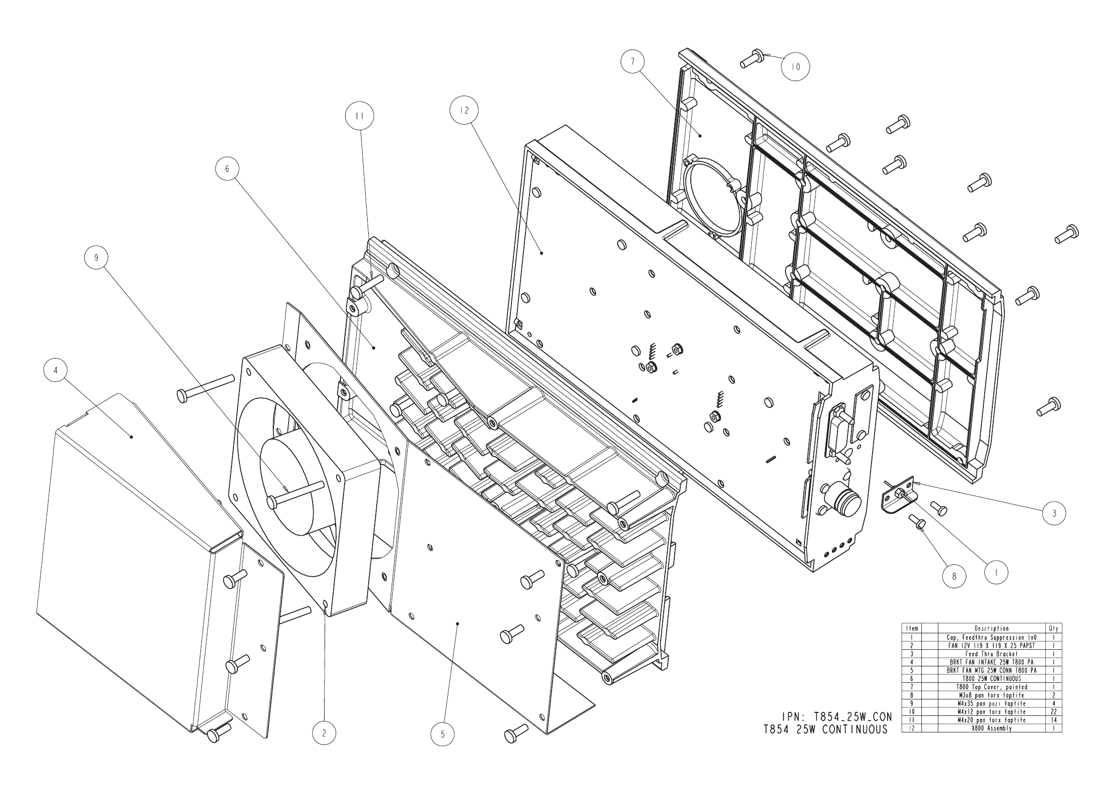
IPN 220-01686-03
M8SL2-00-002-812 T854 PCB Information C6.2.11
© Copyright Tait Electronics Limited August 2004. All rights reserved.
T854 Mechanical Assembly
220-01686-03
IPN 220-01686-03
C6.2.12 T854 PCB Information M8SL2-00-002-812
© Copyright Tait Electronics Limited August 2004. All rights reserved.

IPN 220-01686-03
M8SL2-00-002-812 T854 PCB Information C6.2.13
© Copyright Tait Electronics Limited August 2004. All rights reserved.
Device PCB Circuit Device PCB CircuitDevice PCB Circuit Device PCB Circuit
T854 Grid Reference Index (IPN 220-01686-03)
How To Use This Grid Reference Index
The first digit in the PCB layout reference is a “1” or “2”, indicating the top or bottom side layout respectively, and the last two charac-
ters give the location of the component on that diagram.
The first digit in the circuit diagram reference is the sheet number, and the last two characters give the location of the component on
that sheet.
C100 1:P5 1-A0
C101 1:P5 1-A0
C102 1:P4 1-C1
C103 1:P5 1-B0
C201 1:C1 2-B3
C202 1:C1 2-C3
%C203A 1:C1 2-B2
%C203B 1:A2 2-D2
%C204 1:B3 2-F3
%C205 1:A3 2-E3
C207 1:C7 2-G0
C209 1:C6 2-T0
C210 1:C7 2-J0
C211 1:B7 2-H3
C213 1:A6 2-C5
C215 1:A6 2-D5
C217 1:B6 2-C5
C219 1:B6 2-C5
C221 1:C5 2-L8
C223 1:D4 2-J6
C225 1:B3 2-N7
C227 1:B4 2-O6
C229 1:B4 2-O6
C230 1:B4 2-J0
C232 1:B4 2-P6
C233 1:B3 2-P7
C235 1:B5 2-N5
C237 1:B4 2-N5
C239 1:B4 2-O4
C240 1:D2 2-T6
C241 1:B4 2-P5
C242 1:B4 2-P5
C243 1:B4 2-R5
C245 1:C5 2-B5
C247 1:C5 2-B5
C249 1:D4 2-E6
C251 1:C4 2-C9
C253 1:D3 2-E8
C255 1:D3 2-E8
C257 1:D4 2-C8
C259 1:C7 2-J2
C260 1:C8 2-I0
C261 1:C7 2-K2
C263 1:D6 2-M2
%C265 1:D8 2-M1
C267 1:C8 2-O2
&C269 1:C8 2-O2
&C271 1:C8 2-P2
C273 1:C8 2-P2
C275 1:C3 2-E7
C277 1:B4 2-I4
C279 1:B5 2-I4
C281 1:B5 2-I3
C283 1:B5 2-J2
C285 1:C7 2-K2
C287 1:C6 2-L3
&C289 1:C8 2-Q2
C291 1:C7 2-T2
C293 1:D7 2-T2
%C294 1:C7 2-U2
%C295 1:C7 2-U2
C300 1:F8 3-B8
C301 1:F9 3-B7
C302 1:E8 3-A6
C303 1:E8 3-A6
C305 1:F7 3-E5
C306 1:F7 3-F7
C307 1:F7 3-F7
C311 1:E7 3-B3
C313 1:E9 3-C8
C315 1:E8 3-C7
C316 1:E9 3-E9
C319 1:E8 3-E8
C325 1:E7 3-D4
C327 1:F7 3-C4
C330A 1:E8 3-G8
C330B 1:E8 3-G8
C331 1:F3 3-B2
C332 1:F8 3-B4
C333 1:F3 3-B0
C334 1:F7 3-C4
C335 1:F7 3-F5
%C336 1:F7 3-F5
C337 1:E6 3-J2
C338 1:E7 3-G3
C339 1:E7 3-G3
C340A 1:E8 3-L8
C340B 1:F8 3-L8
C341 1:E7 3-H3
C342 1:E7 3-H3
C343 1:F3 3-J3
C344 1:F3 3-J4
C345 1:F3 3-K4
C346 1:F3 3-K4
C347 1:F3 3-L4
C348 1:F3 3-M4
C349 1:F3 3-M4
C350A 1:F7 3-J8
C350B 1:F7 3-J8
C351 1:F4 3-E1
C352 1:F4 3-F0
C353 1:F4 3-G0
C354 1:F4 3-G0
C355 1:F4 3-G1
C356 1:F3 3-H2
C361 1:E4 3-K1
C362 1:E3 3-J1
C363 1:E4 3-K1
C364 1:E4 3-L1
C365 1:E4 3-L1
C366 1:E4 3-M1
C367 1:E4 3-L1
C368 1:E5 3-M1
C369 1:E6 3-P1
C370A 1:F8 3-K7
C370B 1:F8 3-L7
C370C 1:F8 3-L7
C371 1:F8 3-N7
C372 1:F9 3-P7
C373 1:F9 3-P7
C374 1:E6 3-P1
C375 1:E6 3-P1
C376 1:E6 3-Q1
C377 1:E6 3-Q1
C378 1:F6 3-R1
C380 1:F6 3-R1
C381 1:E3 3-M2
C382 1:E3 3-M2
C383 1:F3 3-B2
C384 1:F5 3-N3
C385 1:F3 3-C0
C386 1:F5 3-P3
C387 1:E4 3-H5
C388 1:F5 3-K5
C389 1:F5 3-K6
C390 1:F8 3-H7
C391 1:F8 3-H7
C392 1:F5 3-P2
C393 1:F5 3-P2
C394 1:F5 3-J5
C405 1:H8 4-D4
#C410 1:J8 4-E3
C415 1:J7 4-F3
C418 1:G7 4-C6
C419 1:G8 4-C6
C420 1:G8 4-D6
C421 1:G8 4-E6
C430 1:J7 4-H6
C435 1:M7 4-J6
C438 1:K8 4-G4
#C439 1:J8 4-F5
#C440 1:K8 4-H4
#C445 1:K7 4-J4
C450 1:L7 4-K5
C455 1:M7 4-L5
#C460 1:L7 4-K4
#C465 1:L8 4-L4
C470 1:L8 4-M4
#C480 1:M8 4-N4
C481 1:K8 4-P7
C485 1:M9 4-M5
C490 1:M9 4-N5
C493 1:M8 4-N4
C496 1:N7 4-P3
C499 1:N7 4-Q3
C503 1:K6 5-L9
C504 1:K6 5-M6
C505 1:K6 5-N7
C507 1:K6 5-B5
C508 1:K6 5-C0
C509 1:K6 5-D0
C510 1:J5 5-D1
C511 1:J5 5-D0
C512 1:J5 5-D1
C513 1:J5 5-H1
C514 1:J5 5-J1
C515 1:K5 5-H0
C516 1:H5 5-H4
C517 1:H5 5-H4
C518 1:H5 5-J3
C519 1:H5 5-J5
C525 1:K4 5-K5
C530 1:K5 5-L4
C535 1:K5 5-L2
C536 1:K5 5-N2
C537 1:K5 5-N2
C605 1:L6 6-C8
C607 1:L6 6-D8
C608 1:L6 6-D8
C610A 1:M5 6-F8
C610B 1:L5 6-F8
C611A 1:M6 6-H8
C611B 1:M5 6-H8
C623 1:N6 6-P7
C625 1:M6 6-Q6
C626 1:M6 6-Q6
C628 1:M6 6-Q6
C630 1:M5 6-J5
C631A 1:N5 6-L6
C634 1:N5 6-L5
C636 1:M5 6-M5
C638 1:M5 6-N5
C640 1:M5 6-R4
C655 1:M4 6-C1
C660 1:L5 6-Q1
C665 1:L5 6-P1
C670 1:L5 6-N1
C673 1:L5 6-K2
C677 1:L6 6-K1
C681 1:L6 6-J2
C684 1:L6 6-H2
C687 1:L6 6-J1
C690 1:L6 6-J1
C693 1:L6 6-H1
C700 1:K4 7-A8
C703 1:J3 7-B7
C706 1:J2 7-A5
C708 1:J2 7-D9
C709 1:K4 7-E9
C710 1:J3 7-D8
C711 1:J3 7-B7
C712 1:H2 7-D7
%C713 1:H2 7-E6
C714 1:J2 7-E8
C719 1:J4 7-F8
C720 1:J4 7-F8
C722 1:J4 7-G8
C724 1:J4 7-H6
C725 1:J3 7-J6
C726 1:J4 7-J6
C727 1:J3 7-K8
C729 1:J3 7-M8
%C733 1:H2 7-E3
C735 1:J2 7-A1
C736 1:J2 7-B1
C740A 1:H2 7-B4

IPN 220-01686-03
C6.2.14 T854 PCB Information M8SL2-00-002-812
© Copyright Tait Electronics Limited August 2004. All rights reserved.
Device PCB Circuit Device PCB CircuitDevice PCB Circuit Device PCB Circuit
C740B 1:H2 7-B3
C741A 1:H2 7-C4
C741B 1:G2 7-C3
C742A 1:H2 7-D4
C742B 1:H3 7-D3
C743 1:H2 7-B1
C745 1:G3 7-D1
C750 1:G4 7-K0
C757 1:G4 7-F4
C759 1:G4 7-F5
C761 1:G3 7-K4
C762 1:G3 7-K4
C764 1:H3 7-K2
C765 1:G3 7-K2
C767 1:H3 7-L3
C769 1:H4 7-M4
C770 1:H4 7-N4
C772 1:G4 7-M2
C774 1:H4 7-N2
C776 1:H4 7-N2
C782 1:G2 7-P1
C784 1:G2 7-Q1
C785 1:G3 7-P1
C786 1:G2 7-R1
C788 1:G3 7-P0
C790 1:G3 7-Q0
C792 1:G4 7-R1
C810 1:L3 8-H8
C812 1:L2 8-D5
C813 1:K2 8-G5
C822 1:N2 8-Q1
C823 1:M3 8-Q1
C824 1:M2 8-Q1
C826 1:N3 8-P0
C827 1:N3 8-P1
C828 1:N3 8-P0
C830 1:N3 8-J0
C838 1:N4 8-N0
C841 1:N2 8-K2
C844 1:M2 8-J2
C880 1:M2 8-K3
#C900 1:N8 9-C6
#C910 1:P8 9-D6
#C920 1:P8 9-E6
C930 2:P8 9-E7
#C940 1:P7 9-F6
#C950 1:P7 9-G6
C960 2:P7 9-G7
#C970 1:P7 9-H6
#C980 1:P6 9-J6
#C990 1:P6 9-K6
CTCSSM 1:D8 2-M1
#CV475 1:M8 4-M4
D111 1:P4 1-R1
%D205 1:B2 2-D3
%D210 1:B2 2-D3
D211 1:B7 2-U6
D212 1:B7 2-T5
D220 1:B4 2-R5
D220 1:B4 2-R7
D230 1:B7 2-U5
D240 1:D4 2-E7
D240 1:D4 2-E7
D245 1:D4 2-H7
D245 1:D4 2-H7
D250 1:D3 2-E8
D250 1:D3 2-E8
D260 1:C2 2-C8
D260 1:C2 2-B8
D270 1:C2 2-C7
D270 1:C2 2-B7
D340 1:F4 3-F1
D360 1:F4 3-F1
D380 1:F4 3-G1
D381 1:F5 3-J5
D420 1:M8 4-Q5
D420 1:M8 4-N5
D440 1:N7 4-P4
D440 1:N7 4-P4
D510 1:K6 5-K9
D510 1:K6 5-K8
D610 1:N6 6-N7
D610 1:N6 6-N7
D620 1:N4 6-B1
D620 1:N4 6-B1
D630 1:M5 6-E2
D630 1:M5 6-E2
D635A 1:M5 6-F2
D640 1:L5 6-N1
D640 1:L5 6-N1
D645 1:M5 6-R4
D710 1:J3 7-L8
D710 1:J3 7-L8
D720 1:J3 7-N8
D720 1:J3 7-N8
D730 1:H3 7-J1
D732 1:H3 7-K2
D810 1:M2 8-B2
IC210 1:C7 2-J0
IC210 1:C7 2-U2
IC210 1:C7 2-G0
IC210 1:C7 2-K1
IC210 1:C7 2-K2
IC220 1:C6 2-T2
IC220 1:C6 2-T0
IC220 1:C6 2-L3
IC230 1:B4 2-I0
IC230 1:B4 2-I4
IC230 1:B4 2-I2
IC230 1:B4 2-Q5
IC230 1:B4 2-O5
IC240 1:C4 2-J5
IC250 1:D3 2-D7
IC260 1:C8 2-S2
IC260 1:C8 2-H0
IC260 1:C8 2-T3
IC260 1:C8 2-P2
IC260 1:C8 2-N2
IC330 1:E8 3-D8
IC330 1:E8 3-D7
IC330 1:E8 3-H8
IC340 1:F8 3-B3
IC340 1:F8 3-M8
IC340 1:F8 3-M8
IC350 1:F7 3-F6
IC350 1:F7 3-C5
IC350 1:F7 3-K8
IC370 1:F9 3-M6
IC610 1:L5 6-G8
IC630 1:N5 6-K5
IC640 1:M5 6-M5
IC640 1:M5 6-Q4
IC640 1:M5 6-E1
IC650 1:L5 6-C4
=IC700 1:K3 7-A8
IC710 1:J2 7-D8
IC710 1:J2 7-C6
IC710 1:J2 7-D7
IC710 1:J2 7-D5
IC710 1:J2 7-E6
IC710 1:J2 7-C5
IC710 1:J2 7-D6
IC720 1:H3 7-N6
IC720 1:H3 7-J0
IC720 1:H3 7-M7
IC720 1:H3 7-L7
IC720 1:H3 7-K7
IC720 1:H3 7-E8
IC720 1:H3 7-J0
IC730 1:J4 7-H8
IC730 1:J4 7-G7
IC740 1:H2 7-D1
IC750 1:H4 7-M3
IC750 1:H4 7-G5
IC750 1:H4 7-K0
IC820 1:L4 8-K5
IC830 1:N3 8-L0
IC830 1:N3 8-H0
IC830 1:N3 8-L0
IC830 1:N3 8-Q0
IC830 1:N3 8-L1
L302 1:F9 3-B5
L303 1:F8 3-L8
L304 1:E4 3-K2
L305 1:E3 3-J1
L320 1:F4 3-G2
L321 1:E4 3-L1
L322 1:E5 3-M1
L323 1:E6 3-P1
L324 1:E6 3-Q1
L325 1:E7 3-Q1
L326 1:F6 3-P2
L327 1:F6 3-P3
L328 1:F8 3-H7
L333 1:E7 3-H4
L334 1:F3 3-B0
L405 1:H8 4-C3
L410 1:H7 4-D4
L415 1:H7 4-D3
L418 1:H8 4-F4
L420 1:G8 4-D6
L425 1:G7 4-C6
L430 1:J7 4-G6
L435 1:J7 4-F6
L440 1:K8 4-G4
L445 1:K7 4-G4
L450 1:J7 4-G3
L455 1:K8 4-J4
L460 1:M7 4-J6
L465 1:L7 4-J5
L470 1:L8 4-K4
L475 1:L8 4-L4
L480 1:M9 4-N6
L481 1:K8 4-Q7
L485 1:N7 4-Q4
L520 1:K6 5-C1
L521 1:K5 5-M3
L522 1:H5 5-J4
L601 1:L6 6-D8
L701 1:G3 7-Q1
#L910 1:P8 9-C8
#L920 1:P8 9-E8
#L930 1:P7 9-G8
#L940 1:P6 9-J8
LINK1 1:B2 2-E3
P100 1:Q6 1-R8
P150 1:P2 1-Q4
P160 1:P2 1-Q4
P170 1:P2 1-Q3
P204 1:D1 2-A3
P208 1:D1 2-A3
P215 1:D4 2-A7
P217 1:D4 2-A7
P219 1:D2 2-A8
P225 1:D2 2-A7
P230 1:B5 2-M9
P231 1:D7 2-M9
P233 1:C1 2-F3
P235 1:C1 2-F3
P237 1:B7 2-G3
P239 1:B6 2-M9
P240 1:B7 2-M9
P245 1:B8 2-S5
P249 1:B7 2-V5
P251 1:B7 2-V5
P255 1:C4 2-L1
P257 1:C2 2-L1
P259 1:B8 2-L0
P261 1:B8 2-L0
P263 1:B1 2-L0
P267 1:C9 2-Q2
P269 1:C9 2-S3
P271 1:C9 2-R2
P273 1:C9 2-S3
P275 1:C7 2-U2
P290 1:D5 2-R1
P291 1:D5 2-S1
P805 1:M2 8-A2
P810 1:L3 8-B6
P820 1:L4 8-J8
P825 1:L4 8-J8
P830 1:L4 8-J8
P835 1:L4 8-J7
P840 1:L4 8-J7
PL100 1:P3 1-E1
PL201 1:C4 2-K5
PL202 1:C3 2-K4
Q100 1:N4 1-B0
Q101 1:N4 1-B0
Q102 1:P4 1-C1
Q210 1:B6 2-D5
Q211 1:P2 2-B3
Q220 1:B4 2-O6
Q230 1:B4 2-P7
Q240 1:B7 2-U6
Q250 1:B7 2-U5
Q260 1:C4 2-C9
Q270 1:D2 2-D7
Q320 1:E7 3-D4
Q325 1:E7 3-F3
Q326 1:E7 3-G3
Q330 1:E8 3-F4
Q331 1:F5 3-J6
Q331 1:F5 3-K6
Q332 1:F6 3-J6
Q333 1:F8 3-H6
Q334 1:F5 3-J5
Q335 1:F3 3-K4
Q336 1:E5 3-N1
Q337 1:E3 3-J1
Q340 1:F3 3-L4
Q341 1:E3 3-K3
Q345 1:F3 3-M3
Q410 1:J8 4-F4
Q420 1:K8 4-J4
Q505 1:J6 5-K8
Q510 1:J5 5-E1
Q520 1:H5 5-J4
Q530 1:K5 5-H1
Q540 1:K5 5-L3
Q550 1:K5 5-L4
Q610 1:L6 6-D8
Q620 1:N6 6-P6
Q630 1:M6 6-N5
Q660 1:L5 6-M1
Q670 1:L6 6-K1
Q710 1:J3 7-K8
Q720 1:J4 7-K8
Q730 1:J3 7-M8
Q740 1:J3 7-M8
Q750 1:G4 7-F4
Q760 1:H3 7-J3
Q770 1:H3 7-J1
Q775 1:H3 7-K3
Q780 1:H3 7-K3
Q785 1:H3 7-K2
Q790 1:H3 7-M3
Q795 1:G3 7-P1
Q810 1:M2 8-C3

IPN 220-01686-03
M8SL2-00-002-812 T854 PCB Information C6.2.15
© Copyright Tait Electronics Limited August 2004. All rights reserved.
Device PCB Circuit Device PCB Circuit Device PCB CircuitDevice PCB Circuit
Q820 1:L2 8-C5
Q830 1:L2 8-C6
Q840 1:L2 8-E5
Q850 1:M2 8-E5
Q860 1:L4 8-B3
R100 1:P5 1-B1
R101 1:P4 1-C1
R102 1:P4 1-B0
R103 1:N3 1-C0
%R150 1:P2 1-R4
R160 1:P2 1-R3
%R200 1:B2 2-C3
%R200A 1:B2 2-C4
%R201 1:B3 2-E3
R202 1:C1 2-F3
%R203 1:B3 2-C2
%R203A 1:B3 2-C2
%R203B 1:C3 2-B2
%R203C 1:D1 2-B3
%R203D 1:D1 2-B3
%R203E 1:A2 2-F3
R204 1:C7 2-F0
R205 1:C7 2-H0
R206 1:B6 2-D6
R207 1:B6 2-D5
R208 1:B6 2-C5
R209 1:B6 2-C5
R210 1:B6 2-D5
%R211 1:B2 2-E3
R212 1:C4 2-I6
R213 1:D4 2-L8
R214 1:D4 2-L8
R215 1:C4 2-J6
R216 1:B4 2-N7
R217 1:B4 2-P7
R218 1:B3 2-P7
R219 1:B3 2-Q7
%R220 1:B2 2-E3
R221 1:B7 2-U6
%R222 1:B7 2-H3
R223 1:B4 2-N5
R224 1:B4 2-N5
R225 1:B4 2-O5
R226 1:B4 2-O4
R227 1:B4 2-O4
%R228 1:A2 2-E3
R229 1:A4 2-P6
R230 1:B4 2-P6
R231 1:B4 2-P5
R232 1:B4 2-P5
R233 1:B4 2-P5
%R234 1:B7 2-H3
R235 1:B4 2-Q5
R236 1:C5 2-J5
R237 1:B7 2-U6
R238 1:B7 2-U6
R239 1:B8 2-T5
R240 1:D2 2-B8
R241 1:B8 2-T5
R242 1:B7 2-T5
R243 1:D2 2-B7
R244 1:C6 2-B5
R245 1:D4 2-J6
%R246 1:D9 2-P1
R247 1:C3 2-B9
R248 1:C3 2-C9
R249 1:D4 2-C9
R251 1:C4 2-K6
R253 1:C7 2-K2
R254 1:C6 2-K2
R255 1:C7 2-L1
R256 1:D8 2-M2
R257 1:D8 2-M1
R258 1:D8 2-M1
R259 1:D8 2-M1
R260 1:C8 2-M2
R262 1:D8 2-N2
R263 1:D8 2-N2
&R264 1:C8 2-O2
&R265 1:C8 2-O2
&R266 1:C8 2-P2
R267 1:C8 2-Q2
R268 1:C2 2-C7
R269 1:C2 2-C8
R270 1:C3 2-D8
R271 1:C3 2-D7
R272 1:C4 2-I4
R273 1:B4 2-I5
R274 1:B5 2-I4
R275 1:B5 2-J5
R276 1:D4 2-F7
%R276A 1:D2 2-B4
R277 1:B5 2-I3
R278 1:B5 2-I2
R279 1:B5 2-J2
R280 1:B5 2-J2
R282 1:D7 2-J3
R283 1:C7 2-J3
R284 1:C7 2-K2
R285 1:C9 2-R2
R286 1:C7 2-K3
R287 1:C8 2-S2
R288 1:C6 2-L3
R289 1:C9 2-R2
&R290 1:C8 2-Q2
%R291 1:C9 2-R2
R292 1:C9 2-S3
R293 1:C9 2-S3
R294 1:D8 2-T3
R295 1:D8 2-U3
R296 1:D6 2-T2
R297 1:C7 2-T2
%R298 1:C7 2-U2
R299 1:C6 2-V2
R300 1:F8 3-B9
R301 1:E9 3-C8
R302 1:F9 3-B7
R303 1:E8 3-C7
R304 1:E8 3-E9
R305 1:E8 3-E7
R306 1:E7 3-B6
R307 1:E8 3-B6
%R308 1:E8 3-E9
R309 1:F8 3-F7
%R310 1:E8 3-E8
R311 1:E8 3-B3
R312 1:E7 3-B3
R313 1:E7 3-B3
R316 1:E8 3-E6
R319 1:F7 3-E5
R320 1:F6 3-J5
R323 1:E3 3-J1
R324 1:F7 3-F5
R325 1:F8 3-G5
R325A 1:F6 3-H5
R326 1:E5 3-M1
R327 1:E4 3-H1
R328 1:E3 3-H1
R329 1:E3 3-J2
R330 1:E8 3-H9
R331 1:F4 3-H1
R332 1:F4 3-H1
R334 1:F3 3-B1
R336 1:E3 3-M2
R337 1:F5 3-Q2
R338 1:F9 3-B5
R339 1:E7 3-B5
R340 1:E7 3-B4
R340C 1:F8 3-M9
R341 1:F7 3-D4
R342 1:E5 3-N3
R343 1:F7 3-D5
R344 1:F5 3-N3
R345 1:F5 3-K5
R346 1:F5 3-K6
R347 1:F7 3-E3
R348 1:E3 3-H5
R349 1:E8 3-F3
R350 1:F8 3-K9
R351 1:E7 3-H2
R352 1:F3 3-B2
R353 1:E7 3-G3
R354 1:F3 3-C2
R355 1:E7 3-F3
R356 1:D7 3-G3
R357 1:E8 3-F4
R359 1:E7 3-H3
R360 1:F3 3-J3
R361 1:E7 3-H3
R362 1:F3 3-J4
R363 1:F3 3-J4
R364 1:E3 3-K3
R365 1:F3 3-J3
R366 1:E8 3-F4
R367 1:F3 3-K4
R368 1:F4 3-L3
R369 1:F3 3-L4
R370 1:F8 3-K8
R371 1:E8 3-N7
R372 1:E8 3-N7
R373 1:E8 3-N7
R374 1:E9 3-N6
R376 1:F3 3-L2
R378 1:F6 3-K7
R379 1:F5 3-J7
R380 1:F8 3-J7
R381 1:F4 3-E1
R382 1:F4 3-F1
R383 1:F4 3-F0
R384 1:F4 3-G1
R387 1:E4 3-H1
#R410 1:H8 4-B4
#R420 1:H8 4-B3
#R430 1:H8 4-B4
#R440 1:H8 4-C3
R450 1:H7 4-D3
#R451 1:J8 4-F5
R460 1:M8 4-P5
R470 1:N8 4-P5
R471 1:N8 4-Q5
R472 1:N8 4-Q5
R473 1:N8 4-R6
R480 1:M8 4-N4
R481 1:K8 4-P7
R490 1:N7 4-P3
R501 1:J6 5-J8
R502 1:J6 5-J8
R503 1:J6 5-K8
R504 1:K6 5-K9
R505 1:K6 5-L8
R510 1:K6 5-L8
R513 1:J5 5-G1
R514 1:K6 5-N6
R515 1:H6 5-H5
#R517 1:G5 5-F2
#R518 1:G5 5-F3
#R519 1:G5 5-G2
R520 1:K6 5-C1
R523 1:J5 5-D1
R525 1:J5 5-D1
R530 1:J5 5-E1
R535 1:J5 5-F1
R540 1:H5 5-K4
R545 1:K5 5-H0
%R550 1:K5 5-K2
%R551 1:K5 5-L2
R555 1:K5 5-L3
R560 1:K4 5-L5
R609 1:L6 6-B8
R613 1:L6 6-C8
R615 1:M5 6-F9
R617 1:M5 6-H8
R619 1:N6 6-P7
R621 1:N6 6-P7
R625 1:N6 6-P7
R629 1:M6 6-N6
R633 1:M5 6-P5
R637 1:M5 6-J6
R638 1:M5 6-J6
R640 1:M5 6-Q4
R641 1:N5 6-K5
R645 1:N5 6-L5
R649 1:M5 6-M5
R651 1:L4 6-B4
R652 1:L4 6-B4
R653 1:M5 6-P5
R657 1:M5 6-C1
R661 1:M5 6-D2
R665 1:M5 6-D1
R669 1:M5 6-D2
R673 1:M5 6-D0
R677 1:M4 6-F2
R681 1:L5 6-P1
R685 1:L5 6-L2
R689 1:L6 6-J3
R693 1:L5 6-N1
R696 1:L5 6-N0
R701 1:K4 7-A9
R702 1:K4 7-B9
R703 1:K4 7-B8
%R704 1:J4 7-G8
=R705 1:K3 7-A7
R706 1:J3 7-B6
R707 1:H3 7-C7
R708 1:J3 7-B6
R709 1:J3 7-D9
R710 1:H2 7-D7
R711 1:J2 7-B5
R712 1:K4 7-E9
R713 1:J4 7-F8
%R714 1:J4 7-F8
%R715 1:K4 7-H6
%R716 1:J4 7-F7
R717 1:H4 7-H7
R718 1:J4 7-H7
R719 1:J3 7-J7
R720 1:H3 7-K7
R721 1:J3 7-K9
R722 1:J4 7-K8
R723 1:J3 7-L7
R725 1:J3 7-M7
%R726 1:H3 7-M6
R727 1:J3 7-M9
R728 1:J3 7-M8
R730 1:K2 7-A2
R731 1:K2 7-A2
R732 1:K2 7-A2
R742 1:H2 7-C4
R743 1:H2 7-C4
R744 1:G2 7-D4
R746 1:H3 7-D4
R747 1:H3 7-D4
R748 1:J2 7-A1
R749 1:J2 7-B1
R750 1:H4 7-K0
R752 1:G4 7-F4
R753 1:G4 7-F4
R754 1:G3 7-F4
R756 1:G3 7-F5
R757 1:G4 7-F5
R758 1:H3 7-J4
R759 1:H3 7-J4
R760 1:H3 7-K4

IPN 220-01686-03
C6.2.16 T854 PCB Information M8SL2-00-002-812
© Copyright Tait Electronics Limited August 2004. All rights reserved.
Device PCB Circuit Device PCB CircuitDevice PCB Circuit Device PCB Circuit
R762 1:H3 7-L4
R763 1:H3 7-L4
R765 1:H3 7-J2
R766 1:G3 7-K3
R767 1:H3 7-K2
R769 1:H3 7-L3
R771 1:H4 7-M3
R772 1:G4 7-M2
R774 1:H4 7-M3
R775 1:H4 7-N2
R777 1:H4 7-Q2
R780 1:G2 7-P1
R782 1:G3 7-P1
R784 1:G3 7-P1
R785 1:G3 7-Q1
R786 1:G2 7-Q1
R787 1:G2 7-R2
R790 1:G3 7-P0
R791 1:G3 7-Q0
R801 1:M2 8-C3
R802 1:M2 8-C2
R808 1:M2 8-B5
R809 1:L2 8-C6
R810 1:L3 8-C6
R811 1:L2 8-D6
R812 1:L2 8-C5
R813 1:L2 8-C5
R815 1:L2 8-D5
R816 1:L2 8-D5
R818 1:M2 8-E5
R819 1:M2 8-E4
R821 1:L4 8-B3
R822 1:M4 8-C3
R824 1:L4 8-J8
R825 1:L4 8-J8
R826 1:L4 8-J8
R827 1:L4 8-J7
R828 1:L4 8-J7
R829 1:L4 8-P9
R830 1:L3 8-P9
R831 1:L3 8-P9
R832 1:L3 8-P8
R833 1:L3 8-P8
R835 1:L3 8-P8
R836 1:L3 8-P8
R837 1:L3 8-P7
R840 1:L3 8-M7
R841 1:L3 8-M7
R842 1:L3 8-P6
R843 1:L3 8-P6
R845 1:M4 8-R4
R847 1:L2 8-R3
R848 1:L2 8-K3
R849 1:L2 8-R3
R850 1:K2 8-R3
R853 1:M4 8-L6
R854 1:M4 8-L6
R855 1:M2 8-Q0
%R856 1:M4 8-R2
%R857 1:M4 8-Q2
R859 1:N2 8-P1
R861 1:N2 8-P1
R863 1:N3 8-N1
R865 1:N4 8-N0
R867 1:N3 8-N1
R871 1:N3 8-M2
R872 1:M4 8-L1
R873 1:N3 8-M1
R874 1:N3 8-L0
R875 1:N3 8-M0
R876 1:N3 8-L0
R877 1:N2 8-K2
R879 1:N2 8-J2
R880 1:M4 8-J6
R881 1:M4 8-L6
R882 1:M2 8-K3
%RV210 1:B7 2-G3
RV220 1:A4 2-P6
RV320 1:E8 3-F3
RV330 1:F7 3-D5
RV805 1:N4 8-N1
SK200 1:C5 2-R1
SK205 1:B5 2-A5
SK310 1:F6 3-R1
SK410 1:G8 4-A4
SK501 1:G6 5-E7
SK502 1:G6 5-E6
SK503 1:G6 5-E5
SK504 1:G5 5-E4
SK505 1:G5 5-E3
SK513 1:H5 5-H3
SK522 1:H6 5-L6
SK531 1:K6 5-P7
SK532 1:K5 5-P6
SK533 1:K5 5-P5
SK534 1:K5 5-P4
SK535 1:K5 5-P3
SK536 1:P5 1-A0
=SK710 1:K3 7-A7
SK805 1:K3 8-Q5
SK805 1:K3 8-Q9
SK805 1:K3 8-Q9
SK805 1:K3 8-Q9
SK805 1:K3 8-Q6
SK805 1:K3 8-Q6
SK805 1:K3 8-Q6
SK805 1:K3 8-Q6
SK805 1:K3 8-Q7
SK805 1:K3 8-Q7
SK805 1:K3 8-Q7
SK805 1:K3 8-Q7
SK805 1:K3 8-Q8
SK805 1:K3 8-Q8
SK805 1:K3 8-Q8
SK805 1:K3 8-Q8
SK810 1:M3 8-G5
SL501 1:J4 5-G1
SL810 1:M2 8-B3
SW230 1:B8 2-B9
%T210 1:B2 2-C3
%T210A 1:B2 2-D2
%T210B 1:B2 2-D1
T610 1:L6 6-M2
T85410 1:F2 1-F0
T85413 1:F2 1-F0
T85415 1:F2 1-G0
T85416 1:F2 1-G0
T85420 1:F2 1-H0
T85423 1:F2 1-H0
T85425 1:F2 1-H0
T85426 1:F2 1-J0
T85430 1:F2 1-J0
T85433 1:F2 1-K0
T85435 1:F2 1-K0
T85436 1:F2 1-L0
TP206 1:B5 2-M8
TP302 1:D9 3-A7
TP305 1:E3 3-J4
TP306 1:F9 3-B8
TP307 1:F8 3-B9
TP310 1:D7 3-D2
TP312 1:F9 3-A5
TP313 1:F4 3-L3
TP314 1:F4 3-L3
TP320 1:E7 3-C5
TP401 1:M7 4-G7
TP402 1:L9 4-P6
TP601 1:N5 6-J6
TP602 1:M6 6-Q6
TP603 1:L5 6-Q1
TP604 1:L4 6-L6
TP607 1:L5 6-J9
TP710 1:G4 7-G5
TP715 1:J2 7-B5
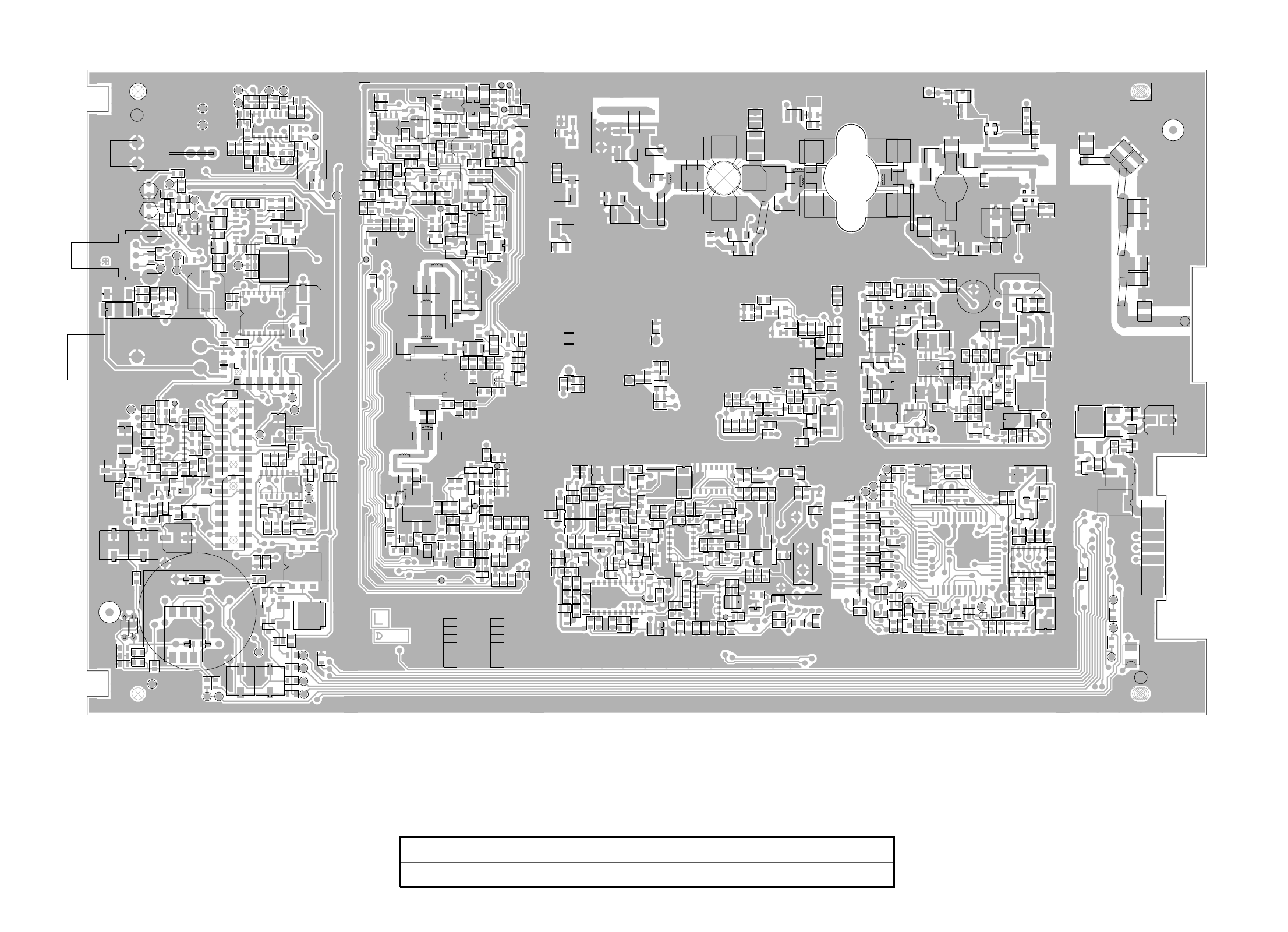
IPN 220-01686-03
M8SL2-00-002-812 T854 PCB Information C6.2.17
© Copyright Tait Electronics Limited August 2004. All rights reserved.
T854 PCB Layout – Top Side
220-01686-03
A LBDCE J NKMHGF PQ
1
2
3
4
5
6
7
8
9
#C410
#C439
#C440
#C445 #C460
#C465
#C480 #C900
#C910
#C920
#C940
#C950
#C970
#C980
#C990
#CV475
#L910
#L920
#L930
#L940
#R410
#R420
#R430
#R440
#R451
#R517
#R518
#R519
%C203A
%C203B
%C204%C205
%C265
%C294
%C295
%C336
%C713
%C733
%D205
%D210
%R150
%R200
%R200A
%R201
%R203
%R203A %R203B
%R203C
%R203D
%R203E
%R211
%R220
%R222
%R228
%R234
%R246
%R276A
%R291
%R298
%R308
%R310
%R550
%R551
%R704
%R714
%R715
%R716
%R726
%R856
%R857
%RV210
%T210
%T210A
%T210B
&C269
&C271
&C289
=IC700
=R705
=SK710
AIFIDA
AIFIDB
C100
C101
C102
C103
C201 C202
C207
C209
C210
C211
C213
C215
C217
C219
C221
C223
C225
C227
C229
C230
C232
C233
C235
C237
C239
C240
C241
C242
C243
C245 C247
C249
C251
C253
C255
C257
C259
C260
C261
C263
C267
C273
C275
C277
C279
C281 C283
C285
C287
C291
C293
C300
C301
C302
C303
C305
C306
C307
C311
C313
C315
C316
C319
C325
C327
C330A
C330B
C331
C332
C333
C334
C335
C337
C338
C339
C340A
C340B
C341
C342
C343
C344
C345
C346
C347
C348
C349
C350A
C350B
C351
C352
C353
C354
C355
C356
C361
C362
C363 C364
C365 C366
C367
C368
C369
C370A
C370B
C370C
C371
C372
C373
C374 C375
C376C377
C378 C380
C381
C382
C383
C384
C385
C386
C387
C388
C389
C390
C391
C392
C393
C394
C405
C415
C418
C419
C420
C421
C430
C435
C438
C450
C455
C470
C481
C485
C490
C493
C496
C499
C503
C504
C505
C507
C508
C509
C510
C511
C512
C513
C514
C515
C516
C517
C518
C519
C525
C530
C535
C536
C537
C605
C607
C608
C610A
C610B
C611A
C611B
C623
C625
C626
C628
C630
C631A
C634
C636
C638
C640
C655
C660
C665
C670
C673
C677
C681
C684
C687
C690
C693
C700
C703
C706
C708
C709
C710
C711
C712
C714
C719
C720
C722
C724
C725
C726
C727
C729
C735
C736
C740A
C740B
C741A
C741B
C742A
C742B
C743
C745
C750
C757
C759
C761
C762
C764
C765
C767
C769
C770
C772
C774
C776
C782
C784
C785
C786
C788
C790
C792
C810
C812
C813
C822
C823C824
C826
C827
C828
C830
C838
C841
C844
C880
CTCSSM
D111
D211
D212
D220
D230
D240
D245
D250
D260
D270
D304D360
D380
D381
D420
D440
D510
D610
D620
D630
D635A
D640
D645
D710
D720
D730
D732
D810
IC210
IC220
IC230
IC240
IC250
IC260
IC330
IC340
IC350
IC370
IC610
IC630
IC640
IC650
IC710
IC720
IC730
IC740
IC750
IC820
IC830
L302
L303
L304
L305
L320
L321
L322
L323
L324
L325
L326
L327
L328
L333
L334
L405
L410
L415
L418
L420
L425
L430
L435
L440
L445
L450
L455
L460
L465
L470
L475
L480
L481
L485
L520
L521
L522
L601
L701
LINK1
P100
P150
P160
P170
P204
P208
P215
P217
P219
P225
P230
P231
P233P235
P237 P239
P240
P245
P249
P251
P255
P257
P259
P261
P263
P267
P269
P271 P273
P275
P290
P291
P805
P810
P820
P825
P830
P835
P840
PL100
PL201PL202
Q100
Q101
Q102
Q210
Q211
Q220
Q230
Q240
Q250
Q260
Q270
Q320
Q325
Q326
Q330
Q331
Q332
Q333
Q334
Q335
Q336
Q337
Q340
Q341
Q345
Q410 Q420
Q505
Q510
Q520
Q530
Q540
Q550
Q610
Q620
Q630
Q660
Q670
Q710
Q720
Q730
Q740
Q750
Q760
Q770
Q775
Q780
Q785
Q790
Q795
Q810
Q820
Q830
Q840 Q850
Q860
R100
R101
R102
R103
R160
R202
R204
R205
R206
R207
R208
R209
R210
R212
R213
R214
R215
R216
R217
R218
R219
R221
R223
R224
R225
R226
R227
R229
R230
R231
R232
R233
R235
R236
R237
R238
R239
R240
R241
R242
R243
R244
R245
R247
R248
R249
R251
R253
R254
R255
R256
R257
R258
R259
R260
R262
R263
R264
R265 R266
R267
R268
R269
R270
R271
R272
R273
R274
R275
R276
R277
R278
R279
R280
R282
R283
R284
R285
R286
R287
R288
R289
R290
R292
R293
R294
R295
R296
R297
R299
R300
R301 R302
R303
R304
R305
R306
R307
R309
R311
R312
R313
R316
R319
R320
R323
R324
R325
R325A
R326
R327
R328
R329
R330
R331
R332
R334
R336
R337
R338
R339
R340
R340C
R341
R342
R343
R344
R345 R346
R347
R348
R349
R350
R351
R352
R353
R354
R355
R356
R357
R359
R360
R361
R362
R363
R364 R365
R366
R367
R368
R369
R370
R371
R372 R373 R374
R376
R378
R379
R380
R381
R382
R383R384
R387
R450
R460
R470 R471
R472 R473
R480
R481
R490
R501
R502
R503
R504
R505
R510
R513
R514
R515
R520
R523
R525
R530
R535
R540
R545
R555
R560
R609
R613
R615
R617
R619
R621
R625
R629
R633
R637R638
R640
R641
R645
R649
R651
R652
R653
R657
R661
R665
R669
R673
R677
R681
R685
R689
R693
R696
R701
R702
R703
R706
R707
R708
R709
R710
R711
R712
R713
R717
R718
R719
R720
R721
R722
R723
R725
R727
R728
R730
R731
R732
R742
R743
R744
R746
R747
R748
R749
R750
R752
R753
R754
R756 R757
R758
R759
R760
R762
R763
R765
R766
R767
R769
R771
R772
R774
R775
R776
R780 R782
R784
R785R786
R787
R790
R791
R801
R802
R808
R809
R810
R811
R812
R813
R815
R816
R818
R819
R821
R822
R824
R825
R826
R827
R828
R829
R830
R831
R832
R833
R835
R836
R837
R840
R841
R842
R843
R845
R847
R848
R849
R850
R853
R854
R855
R859
R861
R863
R865
R867
R871
R872
R873R874 R875
R876
R877
R879
R880
R881
R882
RV220
RV320
RV330
RV805
SK200
SK205
SK310
SK410
SK501
SK502
SK503
SK504
SK505
SK513
SK522 SK531
SK532
SK533
SK534
SK535
SK536
SK805
SK810
SL501
SL810
SW230
T610
T85410
T85413
T85415
T85416
T85420
T85423
T85425
T85426
T85430
T85433
T85435
T85436
TOPFIDA
TOPFIDB
TOPHOLE
TOPSLOT
TP206
TP302
TP305
TP306
TP307
TP310
TP312
TP313
TP314
TP320
TP401
TP402
TP601
TP602
TP603
TP604
TP607
TP710
TP715
TAIT ELECTRONICS
T854-XX-7XXX PCB LAYOUT - TOP SIDE
IPN: ISS: ID: DATE:
220-01686-03 A 1.TA 1 Mar 2002
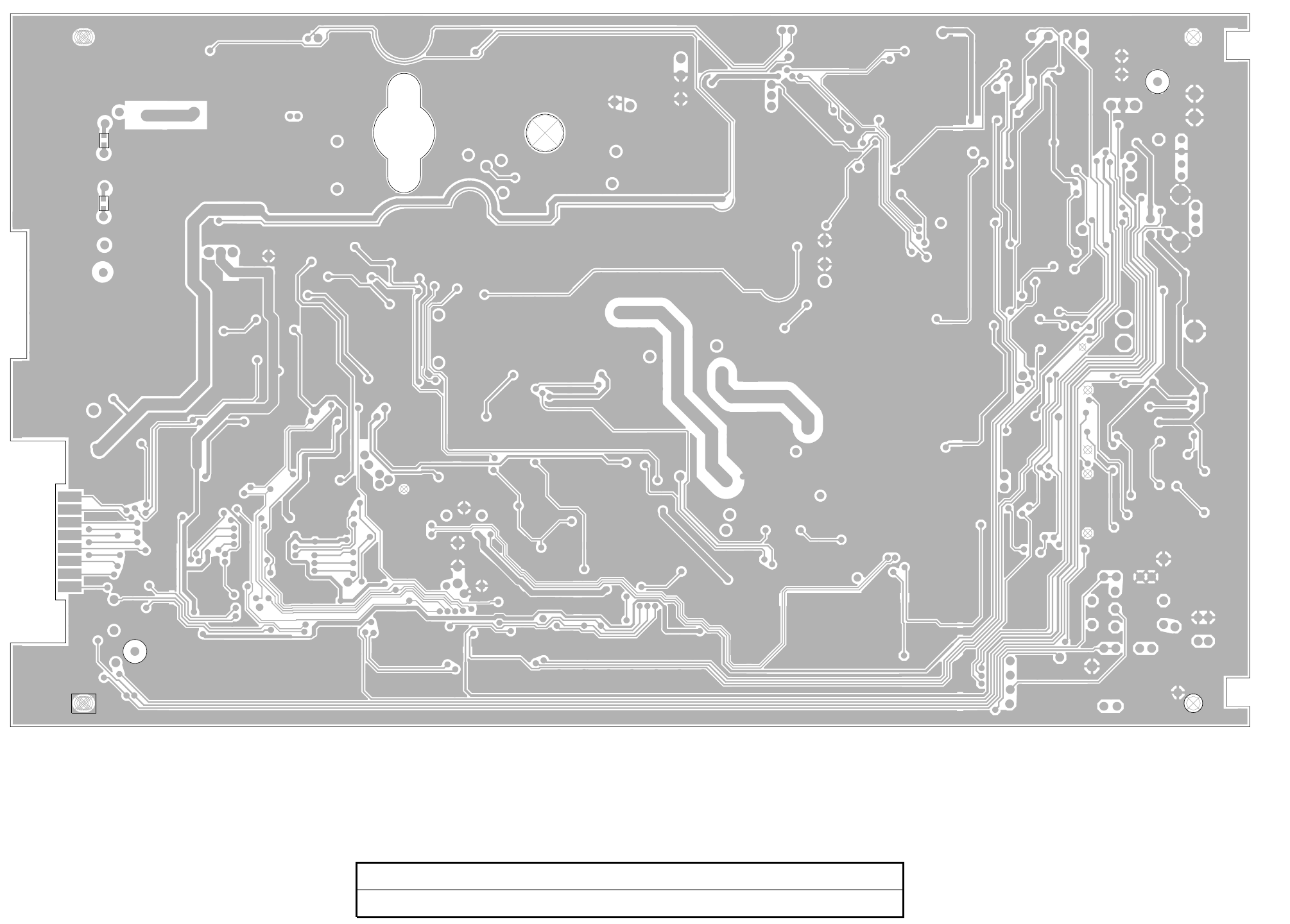
IPN 220-01686-03
C6.2.18 T854 PCB Information M8SL2-00-002-812
© Copyright Tait Electronics Limited August 2004. All rights reserved.
T854 PCB Layout – Bottom Side
220-01686-03
ECDBK AP LMN JHGF
Q
1
2
3
4
5
6
7
8
9
BOTFIDA
BOTFIDB
BOTHOLE
BOTSLOT
C930 C960
TAIT ELECTRONICS
T854-XX-7XXX PCB LAYOUT - BOTTOM SIDE
IPN: ISS: ID: DATE:
220-01686-03 A 2.BA 1 Mar 2002
S l 121 R t ti 0 d
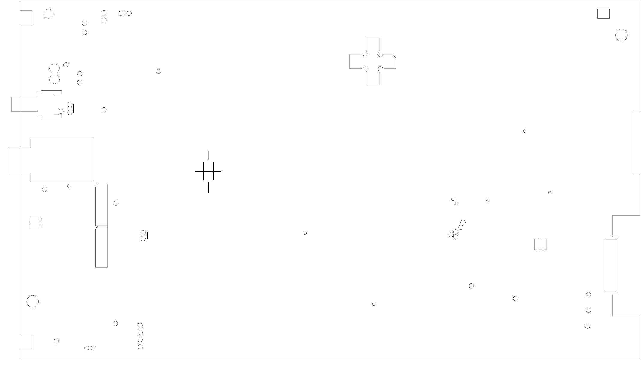
IPN 220-01686-03
M8SL2-00-002-812 T854 PCB Information C6.2.19
© Copyright Tait Electronics Limited August 2004. All rights reserved.
T854 Test Points & Options Connections – Top Side
220-01686-03
A LBDCE J NKMHGF P
1
2
3
4
5
6
7
8
9
D212
D211
AUDIO 1
LINE IP2
AUDIO 1
RV220
P217
CTCSS
OPTO KEY (+)
P275
AUDIO-2
P240
LINE IP3
OPTO KEY (-)
TP607
SK200
PL201
+9V
P255
TX EN OPT
AB22_CNTRL-VOLT
P245
TX-REG
P219
P805
COMPRESSION LEVEL
LOCK-DETECT
TP710
+9V
TP300
+4V1
TP501
P257
P810
108624 97531
TP601
TP206
+9V POCR
SUPPLY LED
P215
P160
LED AN
GND
TX LED
+4V1
TP603
LPF OUT
P230
POCIBUFF IN
TX REG
P269
+9V
12.8MHZ
RV805
AUX OUT
SK805
16 SERIAL COM
15
14 13
12 11
10 9
87
65
43
21AUX OUT 4
AUX OUT 3 AUX OUT 5
AUX OUT 6
AUX OUT 7
TP604
P263
+13V8
AUDIO-1
P170
CTCSS LEVEL
+20V
PL202
TP715
TP602
+5VDIG
P233
P231
P230
P235
P208
+5V
P204
P231
P263
GND
P225
P239
P219
CTCSS
GND
P257
P273
P150
SERIAL-COM
P160
P170
AUDIO-2
P237 P275
P805
P245
P810
P255

IPN 220-01686-03
C6.2.20 T854 PCB Information M8SL2-00-002-812
© Copyright Tait Electronics Limited August 2004. All rights reserved.
T854 Test Points & Options Connections – Bottom Side
220-01686-03
ECDBK AP LMN JHGF
1
2
3
4
5
6
7
8
9
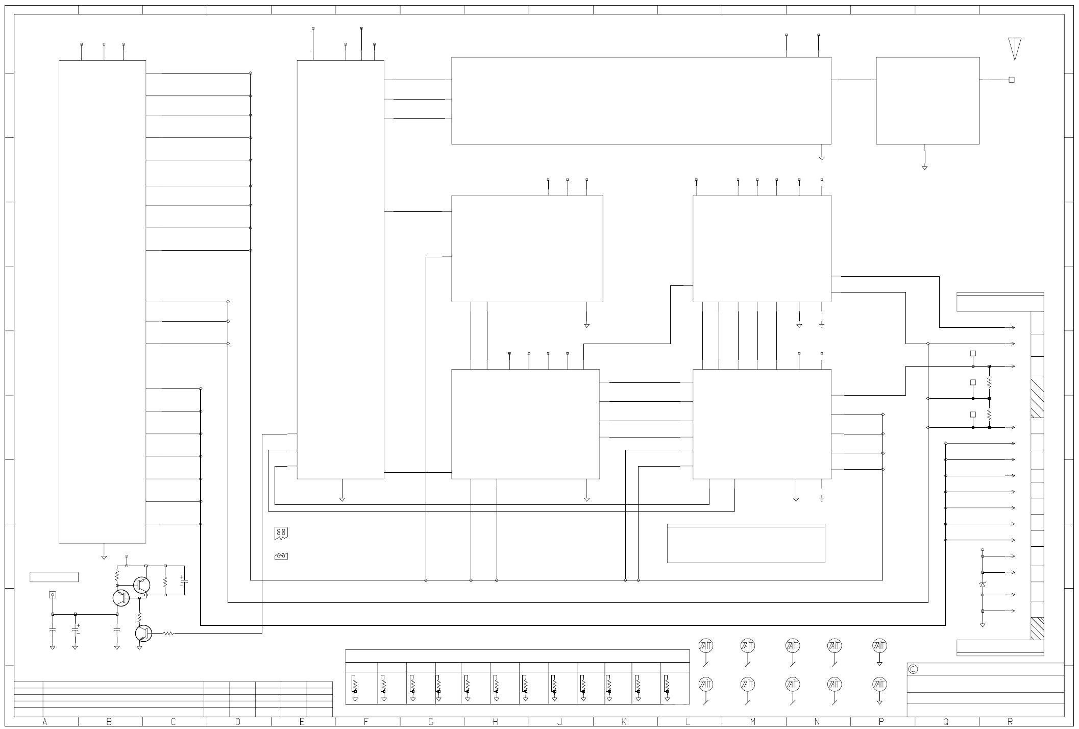
IPN 220-01686-03
M8SL2-00-002-812 T854 PCB Information C6.2.21
© Copyright Tait Electronics Limited August 2004. All rights reserved.
Sheet 1 – T854 Transmitter Overview
220-01686-03
0
1
2
3
4
5
6
7
8
9
0
1
2
3
4
5
6
7
8
9
ABCDEFGHJ KL MNPQR
REV/ISS AMENDMENTS DATEAPVDD.O.CHKDDRAWN
NO.SHEETS:FILE NAME:
TAIT ELECTRONICS
IPN:
FILE DATE:
ISSUE: ID:.
2.SC.
PROJECT: DESIGNER:
1
9
T854-XX-7XXX
TRANSMITTER
168603b
220-01686-03
18-Mar-02
B
T854 BRD
01A ORIGINAL BRD 26-07-01
02A DCO NO. 1686-001 BRD 19-12-01
03A DCO NO. 1686-002 BRD 01-03-02
03B DESG CHANGES TO MATCH BAAN BRD 18-03-02
PL100
15 WAY R-ANGLE DRANGE PLUG
P100
I/OPAD
AUDIO
SHEET 2
P150
SERIAL-COM
I/OPAD
P170
AUDIO-2
I/OPAD
P160
AUDIO-1
I/OPAD %R150
10E 1%
R160
10E 1%
D111
22V
2
1
T85410
0
T85413
0
T85416
0
T85420
0
TOPHOLE
HOLE
TOPSLOT
SLOT
TOPFIDA
FIDUCIAL
TOPFIDB
FIDUCIAL
EXCITER
SHEET 3
LOCK-DETECT
VCO-O-P
GND
FWD-PWR
REV-PWR
TEMP-SENSE
REV
FWD
FAN
SHEET 4
PA
FILTER
FWD-PWR
REV-PWR
+13V8
GND
TEMP-SENSE
+13V8-FILT-2
SUB-ASSY
VCO
SHEET 5
GND
DIV-BUFFER
VCO-O-P
CNTRL-VOLT
VCO-MOD
REGULATOR
SHEET 6
+13V8
TX-REG
+9V
TX-CONT
TX-ENABLE
TX-KEY
+5V
+20V
TX-ENB
+5VDIG
RESET
WATCHDOG
NOT-RESET
SYNTH
SHEET 7
GND
MCU-CLOCK
SDA
SCK
SYNTH
REF-MOD
+9V
+5V
+20V
LOCK-DETECT
DIV-BUFFER
CNTRL-VOLT
TX-REG
MICRO
SHEET 8
SYNTH
SCK
SERIAL-COM
SDA
SDAP
SCKP
REV
FWD
HARMONIC-FILTER
SHEET 9
ANTENNA
GND
FILTER
C100
150P
C101
47U
C103
1N0
Q100
MJD2955
R100
1
R102
3K9
Q101
BC817
R103
12K
R101
12K
AIFIDA
HOLE
AIFIDB
HOLE
BOTFIDA
FIDUCIAL
BOTFIDB
FIDUCIAL
BOTSLOT
SLOT
BOTHOLE
HOLE
T85415
0
T85423
0
SK536
1 WAY SOCKET
Q102
BC857
C102
47U
T85425
0
T85426
0
T85430
0
T85435
0
T85436
0
T85433
0
PL100
GND
14
PL100
GND
15
PL100
+13V8
9
PL100
+13V8
10
PL100
SERIAL-COM
7
PL100
TX-ENABLE
5
PL100
TX-KEY
13
PL100
AUDIO-2
6
PL100
OPTO-KEY-
12
PL100
OPTO-KEY+
11
PL100
LINE-I/P-4
4
PL100
LINE-I/P-3
3
PL100
LINE-I/P-2
2
PL100
LINE-I/P-1
1
PL100
CTCSS
8
+9V-EX +5V
+20V +9V +5V +9V
+20V
+5V+13V8
+9V
TX-REG-FILT-2
+5VDIG
+5VDIG
+13V8
TX-REG
+13V8-FILT-2 TX-REG-FILT-1
TX-REG-FILT-2
TX-REG+9VTX-REG-FILT-1
+13V8-FILT-2 +13V8
TX-REG
+9V-EX
+13V8
PROCESSOR
DRANGE 1
PL100
7
6
5
13
12
11
8
4
3
2
1
10
9
14
15
DGND & GND ARE JOINED
THROUGH R617 ON SHEET 6
PRODUCT INDICATORS
-10 -13 -16 -20
+wire to fan
-15 -23 -25 -26 -30 -35 -36
-33
TX-RELAY-DRV
LED
E-P
CTCSSM
SCKP
SDAP
DUAL_POINT_IND
REF-MOD
VCO-MOD
SCKP
SDAP
CTCSSM
E-P
LED
TX-RELAY-DRV
DUAL_POINT_IND
REF-MOD
VCO-MOD
AUDIO-1
AUDIO-2
TX-ENABLE
AUDIO-2
AUDIO-1
TX-ENABLE
OPTO-KEY-
OPTO-KEY+
CTCSS
LINE-I-P-4
LINE-I-P-3
LINE-I-P-2
LINE-I-P-1
LINE-I-P-1
LINE-I-P-2
LINE-I-P-3
LINE-I-P-4
CTCSS
OPTO-KEY+
OPTO-KEY-
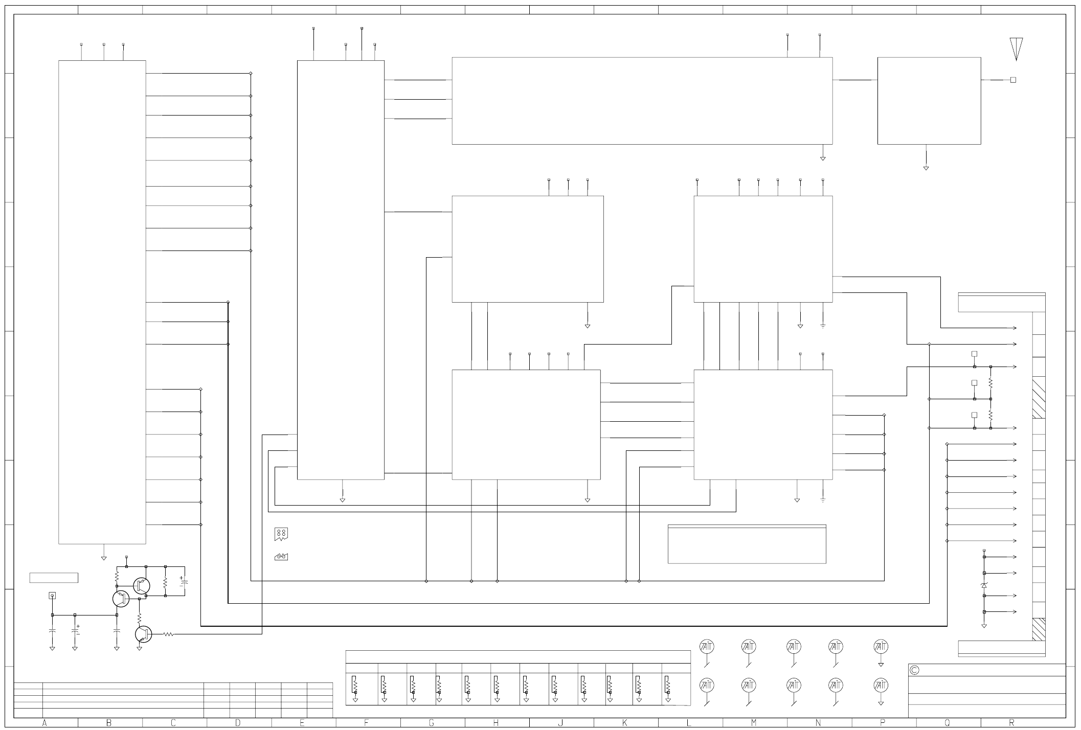
IPN 220-01686-03
C6.2.22 T854 PCB Information M8SL2-00-002-812
© Copyright Tait Electronics Limited August 2004. All rights reserved.
Sheet 1 – T854 Transmitter Overview
220-01686-03
0
1
2
3
4
5
6
7
8
9
0
1
2
3
4
5
6
7
8
9
ABCDEFGHJ KL MNPQR
REV/ISS AMENDMENTS DATEAPVDD.O.CHKDDRAWN
NO.SHEETS:FILE NAME:
TAIT ELECTRONICS
IPN:
FILE DATE:
ISSUE: ID:.
2.SC.
PROJECT: DESIGNER:
1
9
T854-XX-7XXX
TRANSMITTER
168603b
220-01686-03
18-Mar-02
B
T854 BRD
01A ORIGINAL BRD 26-07-01
02A DCO NO. 1686-001 BRD 19-12-01
03A DCO NO. 1686-002 BRD 01-03-02
03B DESG CHANGES TO MATCH BAAN BRD 18-03-02
PL100
15 WAY R-ANGLE DRANGE PLUG
P100
I/OPAD
AUDIO
SHEET 2
P150
SERIAL-COM
I/OPAD
P170
AUDIO-2
I/OPAD
P160
AUDIO-1
I/OPAD %R150
10E 1%
R160
10E 1%
D111
22V
2
1
T85410
0
T85413
0
T85416
0
T85420
0
TOPHOLE
HOLE
TOPSLOT
SLOT
TOPFIDA
FIDUCIAL
TOPFIDB
FIDUCIAL
EXCITER
SHEET 3
LOCK-DETECT
VCO-O-P
GND
FWD-PWR
REV-PWR
TEMP-SENSE
REV
FWD
FAN
SHEET 4
PA
FILTER
FWD-PWR
REV-PWR
+13V8
GND
TEMP-SENSE
+13V8-FILT-2
SUB-ASSY
VCO
SHEET 5
GND
DIV-BUFFER
VCO-O-P
CNTRL-VOLT
VCO-MOD
REGULATOR
SHEET 6
+13V8
TX-REG
+9V
TX-CONT
TX-ENABLE
TX-KEY
+5V
+20V
TX-ENB
+5VDIG
RESET
WATCHDOG
NOT-RESET
SYNTH
SHEET 7
GND
MCU-CLOCK
SDA
SCK
SYNTH
REF-MOD
+9V
+5V
+20V
LOCK-DETECT
DIV-BUFFER
CNTRL-VOLT
TX-REG
MICRO
SHEET 8
SYNTH
SCK
SERIAL-COM
SDA
SDAP
SCKP
REV
FWD
HARMONIC-FILTER
SHEET 9
ANTENNA
GND
FILTER
C100
150P
C101
47U
C103
1N0
Q100
MJD2955
R100
1
R102
3K9
Q101
BC817
R103
12K
R101
12K
AIFIDA
HOLE
AIFIDB
HOLE
BOTFIDA
FIDUCIAL
BOTFIDB
FIDUCIAL
BOTSLOT
SLOT
BOTHOLE
HOLE
T85415
0
T85423
0
SK536
1 WAY SOCKET
Q102
BC857
C102
47U
T85425
0
T85426
0
T85430
0
T85435
0
T85436
0
T85433
0
PL100
GND
14
PL100
GND
15
PL100
+13V8
9
PL100
+13V8
10
PL100
SERIAL-COM
7
PL100
TX-ENABLE
5
PL100
TX-KEY
13
PL100
AUDIO-2
6
PL100
OPTO-KEY-
12
PL100
OPTO-KEY+
11
PL100
LINE-I/P-4
4
PL100
LINE-I/P-3
3
PL100
LINE-I/P-2
2
PL100
LINE-I/P-1
1
PL100
CTCSS
8
+9V-EX +5V
+20V +9V +5V +9V
+20V
+5V+13V8
+9V
TX-REG-FILT-2
+5VDIG
+5VDIG
+13V8
TX-REG
+13V8-FILT-2 TX-REG-FILT-1
TX-REG-FILT-2
TX-REG+9VTX-REG-FILT-1
+13V8-FILT-2 +13V8
TX-REG
+9V-EX
+13V8
PROCESSOR
DRANGE 1
PL100
7
6
5
13
12
11
8
4
3
2
1
10
9
14
15
DGND & GND ARE JOINED
THROUGH R617 ON SHEET 6
PRODUCT INDICATORS
-10 -13 -16 -20
+wire to fan
-15 -23 -25 -26 -30 -35 -36
-33
TX-RELAY-DRV
LED
E-P
CTCSSM
SCKP
SDAP
DUAL_POINT_IND
REF-MOD
VCO-MOD
SCKP
SDAP
CTCSSM
E-P
LED
TX-RELAY-DRV
DUAL_POINT_IND
REF-MOD
VCO-MOD
AUDIO-1
AUDIO-2
TX-ENABLE
AUDIO-2
AUDIO-1
TX-ENABLE
OPTO-KEY-
OPTO-KEY+
CTCSS
LINE-I-P-4
LINE-I-P-3
LINE-I-P-2
LINE-I-P-1
LINE-I-P-1
LINE-I-P-2
LINE-I-P-3
LINE-I-P-4
CTCSS
OPTO-KEY+
OPTO-KEY-
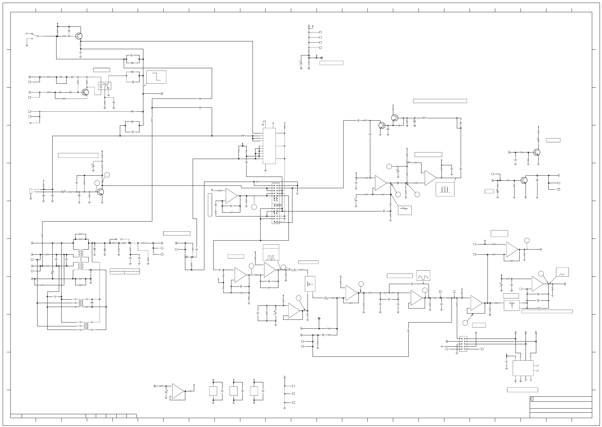
IPN 220-01686-03
M8SL2-00-002-812 T854 PCB Information C6.2.23
© Copyright Tait Electronics Limited August 2004. All rights reserved.
Sheet 2 – T854 Audio Processor
220-01686-03
0
1
2
3
4
5
6
7
8
9
ABCDEFGHI J KL MNOPQRSTUVW
0
1
2
3
4
5
6
7
8
9
ABCDEFGHI J KL MNOPQRSTUVW
REV/ISS AMENDMENTS DATEAPVDD.O.CHKDDRAWN
NO.SHEETS:FILE NAME:
TAIT ELECTRONICS
IPN:
FILE DATE:
ISSUE: ID:
2.SC.
PROJECT: DESIGNER:
2
9
T854-XX-7XXX
AUDIO PROCESSOR
168603b
220-01686-03
18-Mar-02
B
T854 BRD
IC240
4053BD
INH
INH
A
A
B
B
C
C
X0
X0
X1
X1
Y0
Y0
Y1
Y1
Z0
Z0
Z1
Z1
GND
GND
VREF
VREF
+V
+V
ZZ
XX
YY
CW
%RV210
10K LOG
2
3
1
C211
100N
SK205
STEREO SKT
1
3
2
SW230
SPDT
SW COM
SW NO
SW NC
R268
100E
R269
10K
R270
1K2
IC250
4N25A
EN/CCATH
COLLA
BAW56
D260
AA G1,G2 K G2
BAW56
D260
AA G1,G2K G1
R271
1M
C275
150P
BAW56
D250
AA G1,G2K G2
C255
1N0
BAW56
D240
AA G1,G2K G2
BAW56
D250
AA G1,G2K G1
BAW56
D240
AA G1,G2K G1
C249
1N0
C253
1N0
C257
47P
R248
100K
R249
100K
R244
10K
R247
10K
C251
1N0
R245
100K
TANT
C213
10U
R208
560E
P237
AUDIO-2
I/OPAD
C219
1N0
R210
2K2
R209
10K
C217
2N2
R207
3K9
R206
1K0
TANT
C215
22U
C223
100N
R214
8K2
TANT
C221
22U
R215
100K
R212
100K
R213
10K
R251
100K
R272
560E
C277
10N
+
-
IC230
LM324D
G4 +
G4 -
G4 O/P
R273
15K
C279
1N0
R274
15K
R275
2K7
P259 GND
I/OPAD
P261 GND
I/OPAD
P263 GND
I/OPAD
C225
100N
R216
100K
C227
100N
R223
1M
C235
1N0
+
-
IC230
LM324D
G3 +
G3 -
G3 O/P
R224
6K8
R225
1M
R226
10K
R227
2K2
C239
4U7BP
C241
100N
R231
10K
TANT
C242
10U
R232
330K
R233
100K
+
-
IC230
LM324D
G2 +
G2 -
G2 O/P
R230
100K
CW
RV220
50K
MIN
MAX
WIPER
R229
470K
C229
150P
R218
150K
C232
150P
R217
1K0
R219
2K2
R235
4K7
C243
1N0
C245
150P
C247
150P
P215
TX-ENB-OPT
I/OPAD
P219
OPTO-KEY+
I/OPAD
P217
TX-ENB-OPT
I/OPAD
P225
OPTO-KEY-
I/OPAD
Q210
BC847B
Q220
BC817
Q230
BC847B
Q260
BC857
Q270
MJD41
D270
BAV99
A G1AK G1 G2
D270
BAV99
AK G1 G2K G2
D220
BAV99
A G1
AK G1 G2
D220
BAV99
AK G1 G2
K G2
TP206
TANT
C237
1U0
C233
47U
PL201
14 WAY PLUG
1 2
3 4
5 6
7 8
910
11 12
13 14
PL202
14 WAY PLUG
1 2
3 4
5 6
7 8
910
11 12
13 14
+
-
IC210
LM324D
G3 +
G3 -
G3 O/P
%R298
100K
IC220
DS1267
MAX
G1 MAX MIN G1 MIN
WIPER G1 WIPER
R296
1K0
R257
560K
+
-
IC260
LM324D
G4 +
G4 -
G4 O/P
R256
47K
C281
22N
R277
100K
+
-
IC230
LM324D
G1 +
G1 -
G1 O/P
R278
120K
C283
4P7
R279
1M
R280
10K
R282
56K
+
-
IC210
LM324D
G4 +
G4 -
G4 O/P
R283
56K
C285
4P7
R284
1M
R286
2K2
C287
100U
R288
15K
IC220
DS1267
MAX G2 MAX
MIN
G2 MIN
WIPER
G2 WIPER
C259
47N
R253
100K
TANT
C261
4U7
+
-
IC210
LM324D
G2 +
G2 -
G2 O/P
R254
100K
R255
10K
%C295
470N
R287
10K
%R291
0
&C289
47N
R299
2K7
C293
1U0
R297
5K6
TANT
C291
22U
&R290
560E
R293
47K
R294
4K7
+
-
IC260
LM324D
G3 +
G3 -
G3 O/P
R295
2K7
R292
4K7
+
-
IC260
LM324D
G1 +
G1 -
G1 O/P
R267
2K2
&R266
47K 1%
&R265
15K
&C269
1P5
C267
4N7
&C271
47P
&R264
22K
+
-
IC260
LM324D
G2 +
G2 -
G2 O/P
R262
47K
R260
47K
R258
150K
R259
22K
%C265
4U7BP
R263
4K7
C273
47N
P255
CTCSS
I/OPAD
P271 BUF-IN
I/OPAD
P269
+4V1
I/OPAD
P267 LPF-OUT
I/OPAD
C263
100U
P257
CTCSS
I/OPAD
P273
POCI
I/OPAD
P275
POCR
I/OPAD
%C294
47P
R289
100K
R285
0
IC220
DS1267
GND
GND
VB
VB
NC
N.C.
NC
N.C.
+V
+V
-RST
RST
DQ
DQ
CLK
CLK
COUT COUT
SOUT SOUT
C209
47N
%D205
1N4531
%D210
1N4531
%C204
4U7BP
%C205
4U7BP
C201
4U7BP
C202
4U7BP
%R201
560E
R202
1K0
R205
220E
+
-
IC210
LM324D
G1 +
G1 -
G1 O/P
R204
2K2
TANT
C207
4U7
P245
TX-REG
I/OPAD
P249 RELAY
I/OPAD
P251 RELAY
I/OPAD
R239
1K5
R241
4K7
D230
33V
1
2
R242
2K2
R237
47K
R238
47K
P239 +9V
I/OPAD
R221
1K5
P240 +9V
I/OPAD
P233 AUDIO-1
I/OPAD
P235 AUDIO1
I/OPAD
P204
LINE-I-P-3
I/OPAD
P208
LINE-I-P-2
I/OPAD
%T210
T4030
1
2
3
4
8
7
6
5
Q240
BC847B
Q250
BC817
%R203
0
%R200
0
%R211
470
%R220
470
%R228
120
LINK1
C240
150P
IC230
LM324D
V-
-V
V+
+V
IC210
LM324D
V-
-V
V+
+V
IC260
LM324D
V-
-V
V+
+V
C230
100N
C210
100N
C260
100N
P231 +9V
I/OPAD
P230 +9V
I/OPAD
P290
I/OPAD
P291
I/OPAD
SK200
SKT 2X4WAY TOP ENT
D211
GREEN
KA
D212
RED
KA
CTCSSM
P1
P3
S1
S2
S3
%T210A
600/600
1
3
6
5
4
P1
P3
S1
S2
S3
%T210B
P2782
1
3
6
5
4
%R203A
0
%R200A
0
%C203A
15N
%C203B
15N
%R203B
0
%R203E
0
%R222
4K7
%R234
4K7
R236
0
%R246
0
R276
0
D245
BAW56
AA G1 G2 K G1
D245
BAW56
AA G1 G2 K G2
%R276A
0
%R203D
0
%R203C
0
R243
0
R240
0
Q211
P0300SA
+9V-EX
AUDIO-2
1R3
OPTO-KEY+
1R3
OPTO-KEY-
1R3
TX-ENABLE
1R4
6B1
+9V-EX
+9V-EX
+9V-EX
+4V1
+9V-EX
+9V-EX
+9V-EX
GND
1R0
1R0
3Q7
4R1
5A4
6B0
7A0
8A0
9B7
+4V1
+4V1
TX-ENB-OPT
2R1
+4V1
VCO-MOD
5A9
REF-MOD
7B7
CTCSS
1R2
CTCSSM
8R1
+4V1
+4V1
+4V1
+4V1
+4V1
+5VFILT
+4V1
SCKP
8R3
E-P
8R3
SDAP
8R3
+5VFILT
+5V
6B7
7C0
LED
8R3
LINE-I-P-1
1R1
LINE-I-P-4
1R2
LINE-I-P-3
1R2
LINE-I-P-2
1R2
TX-RELAY-DRV
8P6
TX-REG-FIT-2
3D1
AUDIO-1
+5VFILT
+9V-EX
+9V-EX +9V-EX+9V-EX
+9V-EX
3Q8
DUAL_POINT_IND
7R2
+9V-EX
TX-ENB-OPT
2A7
+9V-EX
+4V1
CARRIER SWITCH
MIC/PRESSEL
LINE_SENSITIVITY
COMPRESSON-LEVEL
OPTO-KEY-S/L
OPTO-KEY+S/L
6B0
+4V1-TESTPOINT
AUTOMATIC LEVEL CONTROL(COMPRESSON)
Tx-on
+9V
0V6
PRE-EMPHASIS
4V1
MICROPHONE PREAMPLIFIER
0V6
3V6
3V6
4V1 3V5 ALC PULSES
0.2Vpp
WITH ALC
A
B
C
D
E
F
G
H
I
J
K
L
M
N
4V1 4V1
LIMITER-1
7V2pp IN
LIMITING
LIMITER-2
BUFFER
4V1
4V1
REFERENCE
MOD-EPOT
REFERENCE-MODULATION-INTEGRATOR
VCO-MOD
1KHZ IN
LIMITING
ATTENUATOR
2V7
DEVIATION EPOT
LOW PASS FILTER
SUMMING
AMPLIFIER
4V1
4V1
1KHz IN
LIMITING
4V1
DIGITAL-POTENTIOMETER
LINE-I-P-3-S/L
LINE-I-P-2-S/L
LINE-LIMITER:OPTIONAL
%D205 %D210
OPTO-KEY
MICRO MATCH TO PAGING BRD CON
TX LED
SUPPLY LED
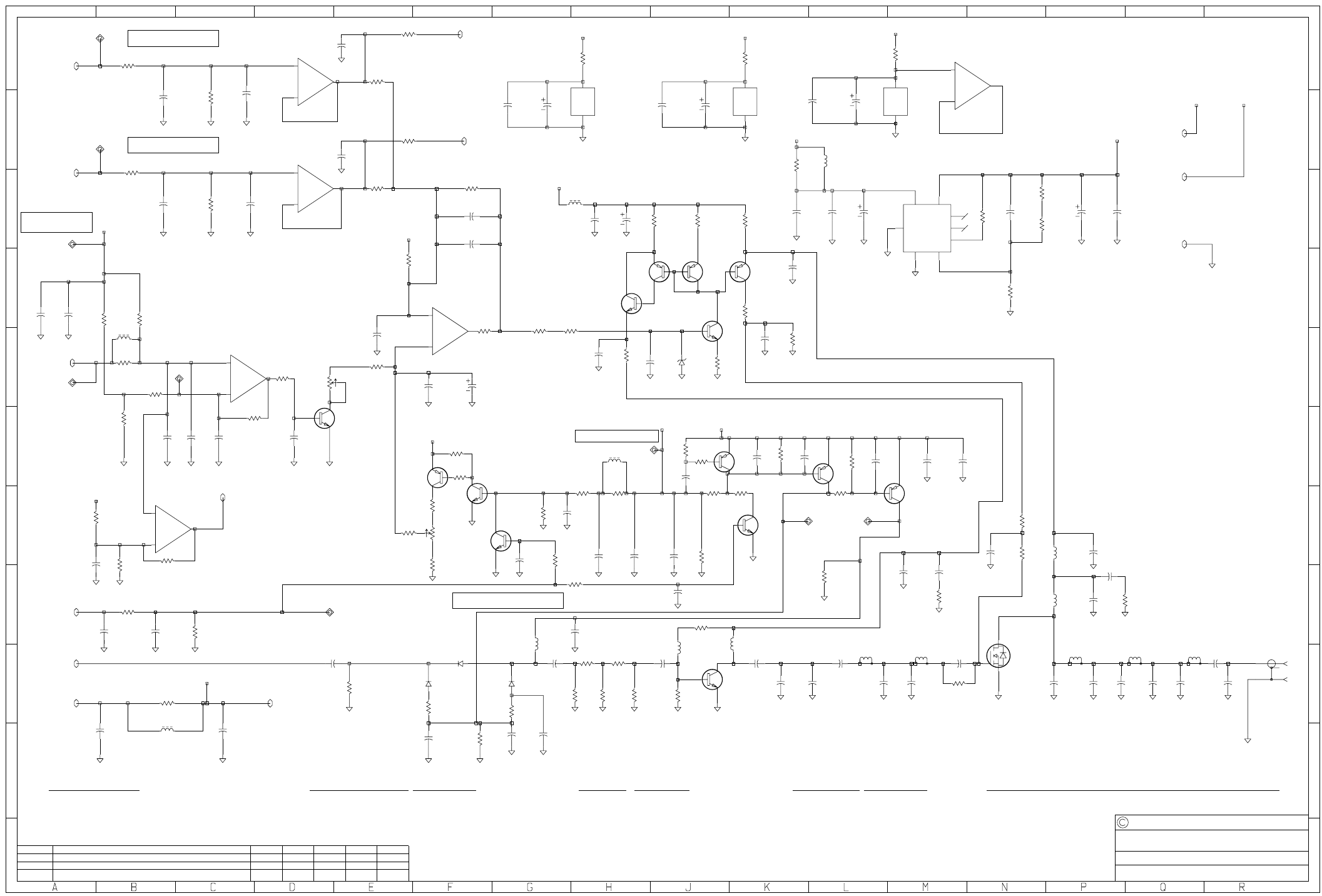
IPN 220-01686-03
C6.2.24 T854 PCB Information M8SL2-00-002-812
© Copyright Tait Electronics Limited August 2004. All rights reserved.
Sheet 3 – T854 Exciter
220-01686-03
0
1
2
3
4
5
6
7
8
9
0
1
2
3
4
5
6
7
8
9
ABCDEFGHJ KL MNPQR
REV/ISS AMENDMENTS DATEAPVDD.O.CHKDDRAWN
NO.SHEETS:FILE NAME:
TAIT ELECTRONICS
IPN:
FILE DATE:
ISSUE: ID:.
2.SC.
PROJECT: DESIGNER:
3
9
T854-XX-7XXX
EXCITER
168603b
220-01686-03
18-Mar-02
B
T854 BRD
0A
1A
2A
C380
68P
C353
150P
C354
22P
C355
150P
C356
150P
C344
47N
C342
150P
C345
150P
C347
150P
C351
150P
C303
150P
C332
1N0
C334
1N0
C337
150P
C335
47N
C306
100N
C338
150P
CW
RV330
500K
MIN
MAX
WIPER
R381
1K5
R382
47
R384
560E
R362
100K R363
47K
R365
56K
R367
10K
R383
15K
R368
22K
R376
1K5
R306
100K
R339
1K0
R307
4K7
R341
220K
R343
10K
R325
1K0
R353
10K
R351
100K
C325
150P
R319
47K
R347
120K
R349
3K3
R355
1K5
R357
47K
R359
47K
R360
1K5
R305
33K
R304
47K
SK310
SIDE ENTRY COAX SKT
TP302
TP305
+
-
IC350
358D
G1 +
G1 -
G1 O/P
Q320
BC847B
IC350
358D
V-
-V
V+
+V
Q325
BC847B
Q330
BC807
+
-
IC350
358D
G2 +
G2 -
G2 O/P
Q335
BC807
Q340
BC807
Q345
BC807
TP307
TP306
C350A
150P
C350B
1U0
R350
220E
L320
330NH
C307
10N
C305
150P
C339
150P
C341
1N0
TANT
%C336
4U7
R324
100E
C302
100N
R369
100K
C348
150P
C349
100N
C346
1N0
R302
1K0
R303
10K
C301
1N0
+
-
IC330
358D
G2 +
G2 -
G2 O/P
+
-
IC330
358D
G1 +
G1 -
G1 O/P
C300
1N0
R301
10K
R300
1K0
IC330
358D
V-
-V
V+
+V
C330A
150P
C330B
1U0
R330
220E
R370
10
C370B
100N
TANT
C370C
4U7
R352
68
R354
0805
C331
1N0
C352
1N0
C370A
150P
L303
0805
IC370
LP2951
V OUT
1
SENSE 2
SD
3
GND
4
ERROR 5
VTAP 6
FB
7
V IN
8
C371
10N
R371
100K
R372
6K8
R374
1K2
TANT
C372
4U7
C373
100N
R361
68
C343
1N0
L333
M21A
R373
820
C333
150P
R334
68
L334
M21A
R338
120
L302
M21A
TP310
C313
150P
C315
150P
C327
150P
TP312
C383
150P
C385
150P
TP320
R340
5K6
R316
270K
%R308
10K
%R310
10K
C316
150P
C319
150P
TP313
TP314
CW RV320
10K
MIN
MAX
WIPER
Q326
BC847B
R364
47K
Q341
BC847B
D340
BAT18
D380
BAT18
D360
BAT18
+
-
IC340
358D
G1 +
G1 -
G1 O/P
+
-
IC340
358D
G2 +
G2 -
G2 O/P
R313
470K
R311
100K
R312
15K
C311
150P
IC340
358D
V-
-V
V+
+V
R340C
220E
C340B
1U0
C340A
150P
R309
220K
R356
100K
R332
330
R387
330
R331
18
C362
150P
Q337
BFG591
L304
3.0T/2.0
C363
0805
C364
12P
C367
150P
L321
PRINTED
C365
33P
C366
0805
L322
PRINTED
R326
3R3
C368
4P7
G
D
S
Q336
PD55003
23
1
C369
1210
C374
33P
C375
33P
L323
PRINTED
L324
PRINTED
C376
22P
C377
27P
L325
PRINTED
C378
12P
L326
270NH
C392
150P
R337
10E 1%
C393
100N
L327
4S2
C386
1N0
R342
47
C384
150P
R344
1K5
C381
150P
C382
100N
R336
10E 1%
L328
M21A
C391
150P
TANT
C390
4U7
R380
1R8
R379
100E
R378
E22
C389
150P
Q331
BC856S
Q331
BC856S
Q332
BC807
Q333
BD139
R348
10E
C387
150P
C394
0805
D381
5V1
3
2
Q334
BC847B
R320
4K7
R346
3K3
C388
1N0
R345
6K8
R366
10K
R325A
1K0
C361
150P
R329
470E
L305
330NH
R327
22
R328
82
R323
220E
+13V8-FILT-2
4A6
TX-REG-FILT-1
5A2
+13V8-FILT-2
GND
1R0
1R0
2K0
4R1
5A4
6B0
7A0
8A0
9B7
FWD-PWR
4R6
REV-PWR
4R4
+13V8-FILT-2
+9V-EX
+9V-EX
TX-REG-FILT-2
LOCK-DETECT
7R5
VCO-O-P
5G3
TEMP-SENSE
4R7
+13V8-FILT-2
+13V8-FILT-2 +9V-EX
TX-REG-FILT-2
2S5
TX-REG-FILT-2
+9V-EX
+9V-EX
+9V-EX
2L9
+9V-EX
+9V-EX
+13V8-FILT-2
REV
8M8
FWD
8N8
FAN
+13V8-FILT-2
SHUTDOWN
POWER
LEVEL
SHUTDOWN
TEMPERATURE
LOW POWER TEMP CONTROL POWER_CONTROL EXCITER
RF PIN SWITCH
FWD-PWR-TESTPOINT
REV-PWR-TESTPOINT
+9V-TESTPOINT
TX-REG_TESTPOINT
COAX_TO_PA
LOCK-DETECT_TESTPOINT
6B0
SHUTDOWN
TEMP
N.F.
N.F.
N.F.
IPN 220-01686-03
M8SL2-00-002-812 T854 PCB Information C6.2.25
© Copyright Tait Electronics Limited August 2004. All rights reserved.
Sheet 4 – T854 PA
220-01686-03
0
1
2
3
4
5
6
7
8
9
0
1
2
3
4
5
6
7
8
9
ABCDEFGHJ KL MNPQR
REV/ISS AMENDMENTS DATEAPVDD.O.CHKDDRAWN
NO.SHEETS:FILE NAME:
TAIT ELECTRONICS
IPN:
FILE DATE:
ISSUE: ID:.
2.SC.
PROJECT: DESIGNER:
4
9
T854-XX-7XXX
PA
168603b
220-01686-03
18-Mar-02
B
T854 BRD
#CV475
2/10P
#C410
39P
#C440
39P
#C445
33P
#C460
27P
#C465
27P
#C480
4P7
#R420
470E
#R410
10E
#R430
10E
#R440
470E
C405
12P
C415
33P
C438
68P
C419
100N
C430
1N0
C435
47U
C450
100P
C455
4U7
C470
100P
C485
150P
C490
150P
C496
150P
C499
150P
C420
150P
C493
100P
R450
30E
R480
100E
R470
100E
R490
4K7
R460
4K7
SK410
SIDE ENTRY COAX SKT
TP401
Q410
SD1433
L418
PRINTED
L440
PRINTED
Q420
SD1488
L455
PRINTED
L470
PRINTED
D420
RF2815
D440
RF2815
L415
4S2
L450
4S2
L430
4S2
L460
4S2
C481
150P
-T
R481
4K7
L405
1.5T/2.5
L410
1.5T/6.0
L425
5.0T/4.0
L435
1.5T/6.0
L445
3.5T/3.0
L465
10MM COIL
L475
#556
L480
330NH
L485
330NH
L481
330NH
L420
4S2-3T
C421
100N
C418
100N
D420
RF2815
D440
RF2815
R471
150P
R472
560E
R473
470
#C439
150P
#R451
240E
TP402
FILTER
9B8
FWD-PWR
3A7
REV-PWR
3A9
+13V8
1R1
1R1
6C7
GND
1R0
1R0
2K0
3Q7
5A4
6B0
7A0
8A0
9B7
+13V8
+13V8
+13V8-FILT-2
TEMP-SENSE
3A5
+13V8-FILT-2
3Q7
+13V8-FILT-2 +13V8
+13V8
POWER AMPLIFIER DIRECTIONAL COUPLER
COUPLER
+13V8 TESTPOINT
TEMP-SENSE
+13V8-FILTERED-2 SUPPLY
6B0
6B5
IPN 220-01686-03
C6.2.26 T854 PCB Information M8SL2-00-002-812
© Copyright Tait Electronics Limited August 2004. All rights reserved.
Sheet 5 – T854 VCO Section
220-01686-03
0
1
2
3
4
5
6
7
8
9
0
1
2
3
4
5
6
7
8
9
ABCDEFGHJ KL MNPQR
REV/ISS AMENDMENTS DATEAPVDD.O.CHKDDRAWN
NO.SHEETS:FILE NAME:
TAIT ELECTRONICS
IPN:
FILE DATE:
ISSUE: ID:.
2.SC.
PROJECT: DESIGNER:
5
9
T854-XX-7XXX
VCO
168603b
220-01686-03
18-Mar-02
B
T854 BRD
R523
120K
C510
47N
R525
47K
R535
10K
R530
22K
SL501
R540
2K2
R545
4K7
%R550
1K2
R555
4K7
R560
470
TANT
C530
22U
C516
10N
C535
100N
C503
4N7
R505
15K
R504
330
R515
56E
R510
1K5
C505
47N
Q520
BC807
Q530
BC807
Q510
BC807
Q540
BC807
Q550
BC847B
#R518
18
#R519
330
#R517
330
R514
33
Q505
BC847B
BAV70
D510
A G1KK G1,G2
BAV70
D510
A G2KK G1,G2
R503
5K6
R502
10K
R501
10K
C525
150P
%R551
4K7
C537
150P
C507
100N
C504
150P
C517
150P
C519
150P
C513
150P
C514
150P
R520
150E
C509
150P
L520
M21A
C508
150P
C511
4N7
R513
10K
C515
10N
L521
M21A
C536
100N
C518
100N
L522
M21A
SK501
1 WAY SOCKET
SK502
1 WAY SOCKET
SK503
1 WAY SOCKET
SK504
1 WAY SOCKET
SK505
1 WAY SOCKET
SK513
1 WAY SOCKET
SK522
1 WAY SOCKET
SK531
1 WAY SOCKET
SK532
1 WAY SOCKET
SK533
1 WAY SOCKET
SK534
1 WAY SOCKET
SK535
1 WAY SOCKET
C512
100N
GND
1R0
1R0
2K0
3Q7
4R1
6B0
7A0
8A0
9B7
VCO-O-P
3A1
DIV-BUFFER
7R1
VCO-MOD
2U3
CNTRL-VOLT
7R3
+9V
+9V
6C7
7B0
8B9
TX-REG
6E8
7C0
+9V
+9V
+9V
TX-REG-FILT-1
3A1
1
2
3
4
5
1
2
3
4
5
FAST-KEY-OPTION/B
6B0
6B6
+9V Tx-on
8V4
Tx-off
+8V Tx-on
Tx-off
IPN 220-01686-03
M8SL2-00-002-812 T854 PCB Information C6.2.27
© Copyright Tait Electronics Limited August 2004. All rights reserved.
Sheet 6 – T854 Regulators
220-01686-03
0
1
2
3
4
5
6
7
8
9
0
1
2
3
4
5
6
7
8
9
ABCDEFGHJ KL MNPQR
REV/ISS AMENDMENTS DATEAPVDD.O.CHKDDRAWN
NO.SHEETS:FILE NAME:
TAIT ELECTRONICS
IPN:
FILE DATE:
ISSUE: ID:.
2.SC.
PROJECT: DESIGNER:
6
9
T854-XX-7XXX
REGULATOR
168603b
220-01686-03
18-Mar-02
B
T854 BRD
C690
100N
TANT
C693
10U
C630
100N
TANT
C634
10U
C631A
100N
C655
1N0
C640
1N0
C625
470U
C626
4N7
C628
1N0
C673
1N0
TANT
C684
10U
C638
150P
C623
150P
C687
150P
C660
100N
C681
100N
C636
100N
R681
100E
R689
10E 1%
R637
22
R649
4K7
R625
1K0
R629
270
R621
1
R619
1
R633
6K8
R653
10K
R657
10K
R665
100K
R673
100K
R693
100K
R685
15K
R696
56K
R661
10K
R641
1K5
R645
470
T610
680uH
2
36
14
IC640
358D
V-
-V
V+
+V
+
-
IC640
358D
G2 +
G2 -
G2 O/P
+
-
IC640
358D
G1 +
G1 -
G1 O/P
R613
560E
C605
150P
R609
1K0
BAV70
D630
A G1 KK G1,G2
BAV70
D620
A G2
KK G1,G2
BAV70
D620
A G1
KK G1,G2
R669
47K
R677
47K
BAV70
D630
A G2 KK G1,G2
BAV70
D640
A G2 KK G1,G2
BAV70
D640
A G1 KK G1,G2
C610A
10N
C611B
10N
R617
0
Q610
BC807
Q620
BD242FP
TP604
Q660
BC817
Q670
BC857
D610
BAV99
A G1
AK G1 G2
D610
BAV99
AK G1 G2
K G2
D635A
BAT165
R615
100E
IC650
LOW PWR MON
PBRST 1
TD 2
TOL 3
GND
4
RST
5
RST
6
ST
7+V
8
TP601
TP602
TP607
TP603
R640
10E 1%
D645
33V
1
2
R652
0
R651
0
TANT
C610B
100U
TANT
C611A
100U
VIN
N/C
VOUT
N/C
GROUND
IC610
78L05
V IN
NC
GNDGNDGNDGND
V OUT
NC
TANT
C665
10U
Q630
BSR30
R638
22
TANT
C670
3U3
TANT
C677
1U0
C607
1N0
C608
1N0
L601
M21A
VREG
IC630
LM317MDT
VIN
3
ADJ
1
VOUT
2
+13V8
+5V
+9V
GND
1R0
1R0
2K0
3Q7
4R1
5A4
7A0
8A0
9B7
+13V8
1R1
1R1
4R8
+9V
5A5
7B0
8B9
TX-REG
5A1
7C0
TX-CONT
8A4
TX-KEY
1R5
TX-ENABLE
1R4
2F7
+9V
+5V
2F0
7C0
+20V
7C0
+5V
+9V
+20V
+13V8
+5V +9V +13V8 +20V
TX-ENB
8A3
+5VDIG
+9V +5VDIG
+5VDIG
8A9
+5VDIG
DGND
8A0
RESET
8A8
WATCHDOG
8R4
NOT-RESET
8R2
+9V
+13V8
PBRST
7A5
7A5
8A2
+20V SUPPLY
+5V REGULATOR
+9V REGULATOR
+20V TESTPOINT
+5V TESTPOINT
+5VDIG SUPPLY
DGND CONNECTS GND
THROUGH R617
DS1232
+13V8 TESTPOINT
+5VDIG
TESTPOINT
+9V-TESTPOINT
+5V
+1V3
Tx-off Tx-off
5V
24vpp
240KHz
+9V
0V(Tx)
+9V-Tx on
0V
Tx-on
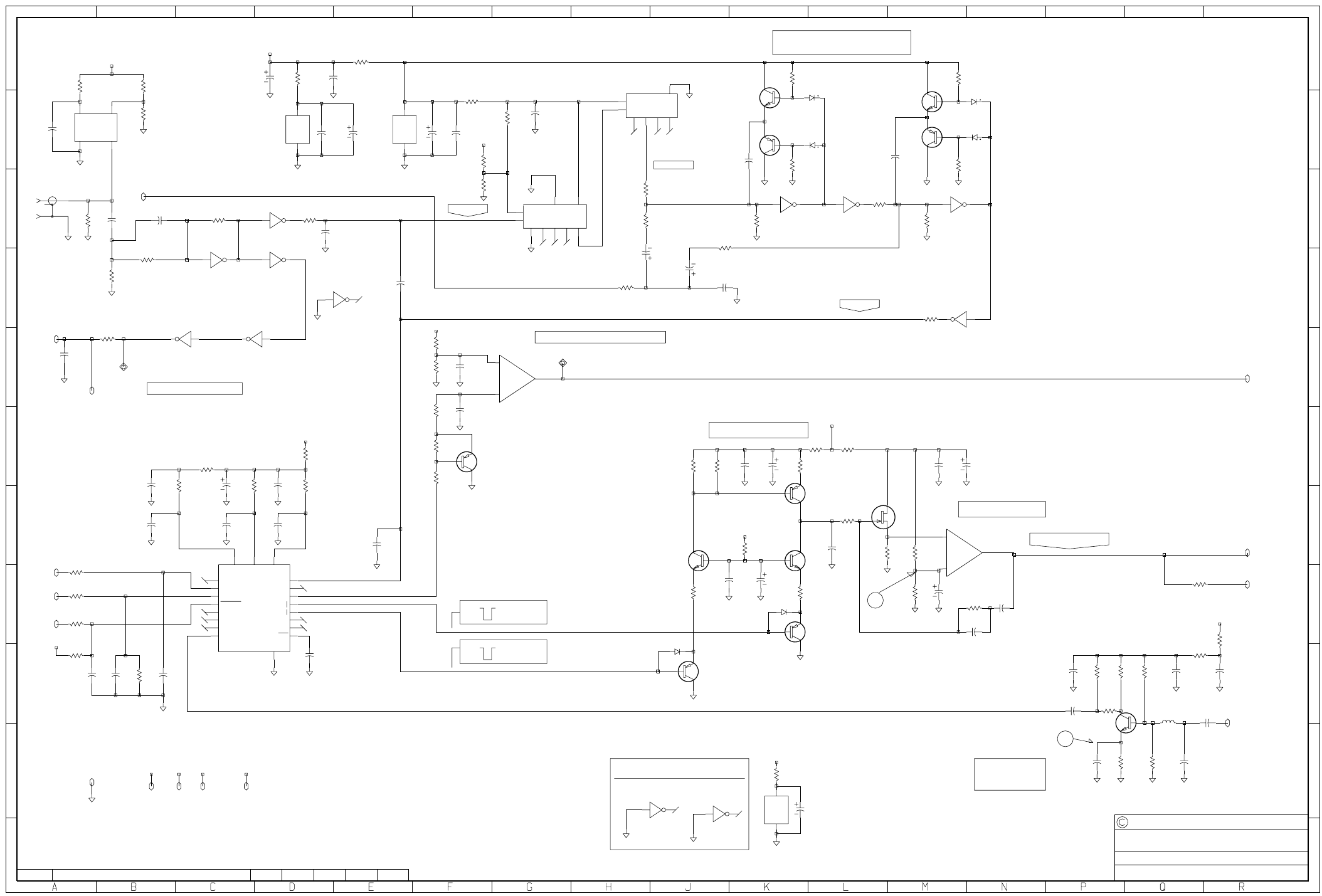
IPN 220-01686-03
C6.2.28 T854 PCB Information M8SL2-00-002-812
© Copyright Tait Electronics Limited August 2004. All rights reserved.
Sheet 7 – T854 Synthesiser
220-01686-03
0
1
2
3
4
5
6
7
8
9
0
1
2
3
4
5
6
7
8
9
ABCDEFGHJ KL MNPQR
REV/ISS AMENDMENTS DATEAPVDD.O.CHKDDRAWN
NO.SHEETS:FILE NAME:
TAIT ELECTRONICS
IPN:
FILE DATE:
ISSUE: ID:.
2.SC.
PROJECT: DESIGNER:
7
9
T854-XX-7XXX
SYNTHESISER
168603b
220-01686-03
18-Mar-02
B
T854 BRD
IC740
145191
REF IN REF IN
REF OUT REF OUT
LD LD
OR 0R
OV 0V
RX RX
TEST1 TEST1
FIN -FIN
GND
GND
VPD
VPD
VCC
VCC
VDD
VDD
PDOUT
PD OUT
DATA
DATA
CLK
CLK
ENABLE
-ENABLE
OUT A
OUT A
OUT B
OUT B
TEST2
TEST2
FIN
FIN R787
10E 1%
R785
3K3
R780
68
C784
150P
C788
150P
R791
1K0
C790
8P2
C782
150P
R701
22
12.8M
=IC700
GND OUT
VCC FM
R703
1M
R702
1M
C700
100N
C709
100N
C710
10N
R712
10E 1%
C703
1N0
IC710
74HC04
V-
-V
V+
+V
IC710
74HC04
G1 I/P G1 O/P
IC710
74HC04
G6 I/P G6 O/P
IC73074HC4520
EN
2
CLKA
1
GND
8
Q0
3
Q1
4
Q2
5
Q3
6
RST
7
VDD
16
IC730
74HC4520
EN
10
CLKB
9
Q0
11
Q1
12
Q2
13
Q3
14
RST
15
R711
100E
C722
100N
R713
0
TANT
C708
4U7
R717
2K7
R718
150K
C727
220P
R721
10K
R722
10K
R723
2K7
C729
220P
R728
10K
IC750
33078D
V-
-V
V+
+V
+
-
IC750
33078D
G2 +
G2 -
G2 O/P
C776
4N7
%C713
10N
%R715
1K0
C741B
10N
R744
22
C740B
10N
R742
150E
R746
22
R747
22
C742B
10N
C742A
100N
TANT
C741A
4U7
R767
680
R754
1K0
R753
1M
R752
22
C757
22N
R750
22
R757
100K
R756
100K
C759
47N
TP710
C764
10N
TANT
C765
4U7
R766
1K0
R765
680
R760
180
R759
330
C761
10N
TANT
C762
22U
C767
1N0
R769
180
R762
100E
R771
8K2
R763
100E
TANT
C770
22U
TANT
C772
22U
C769
1N0
R774
8K2
R772
22K
R775
18K
C774
100N
R790
390E
C786
100N
C743
47P
C736
47P
C735
47P
R748
47K
R719
150K
C726
10N
R727
10K
%R726
100E
%C733
470P
R786
10E 1%
C792
150P
C745
150P
R749
47K
TANT
C724
22U
=R705
47
=SK710
SIDE ENTRY COAX SKT
IC710
74HC04
G4 I/PG4 O/P
IC720
74HCU04T
V-
-V
V+
+V
IC710
74HC04
G3 I/P G3 O/P
IC720
74HCU04T
G6 I/P G6 O/P
IC720
74HCU04T
G5 I/P G5 O/P
IC720
74HCU04T
G4 I/P G4 O/P
IC720
74HCU04T
G3 I/PG3 O/P
+
-
IC750
33078D
G1 +
G1 -
G1 O/P
R743
150E
C740A
1N0
IC710
74HC04
G5 I/PG5 O/P
R710
100E
IC710
74HC04
G2 I/P G2 O/P
IC720
74HCU04T
G1 I/P G1 O/P
IC720
74HCU04T
G2 I/P G2 O/P
C720
100N
Q710
BC847B
Q720
BC857
Q730
BC847B
Q740
BC857
Q750
BC807
Q770
BC857
Q760
BC847B
Q780
BC847B
Q785
BC857
Q775
BC857
D
S
GQ790
BFR31
Q795 BFR93A
D710
BAV99
A G1 AK G1 G2 D720
BAV99
A G1 AK G1 G2
D710
BAV99
AK G1 G2K G2
D720
BAV99
AK G1 G2K G2
D730
BAT165
D732
BAT165
C712
47P
TANT
C725
22U
R720
39K 1%
R725
39K 1%
R758
1K2
TP715
C706
47P
R782
18
R784
120
R708
470K
R709
10E 1%
TANT
C719
4U7
TANT
C750
10U
TANT
C714
4U7
R706
15K
R707
100K
C711
8P2
R730
470
R731
470
R732
470
C785
150P
R777
2K2
L701
1.5T/2.5
%R704
0
%R714
39K
%R716
47K
+9V
+5V
+5V
+5V
+5V
+5V
+9V
+5V
GND
1R0
1R0
2K0
3Q7
4R1
5A4
6B0
8A0
9B7
MCU-CLOCK
6B5
8A2
SDA
8R3
SCK
8R2
SYNTH
8R3
REF-MOD
2V2
+5V
2F0
6B7
+9V
5A5
6C7
8B9
+20V
6C7
+5V+9V
+20V
+20V
LOCK-DETECT
3A2
DIV-BUFFER
5H6
CNTRL-VOLT
5A8
DUAL_POINT_IND
2R1
TX-REG
TX-REG
5A1
6E8
TX-REG
PBRST
6B5
8A2
SPARE GATES
LOCK-DETECT TESTPOINT
LOCKED-LOW
EXTERNAL
REFERENCE
OPTION
6B6
6B0
2A7
6B4
8R3
12.8MHz TESTPOINT
LOOP-FILTER
DIVIDER
BUFFER
CHARGE-PUMP
PHASE-MODULATOR
1V4
6V6
12.8MHz
200KHz
200KHz
+5V TO +15V LOCKED
50ns WHEN
+5V
0V LOCKED
50ns WHEN
+5V
0V LOCKED
N.F.
LOCK-DETECT
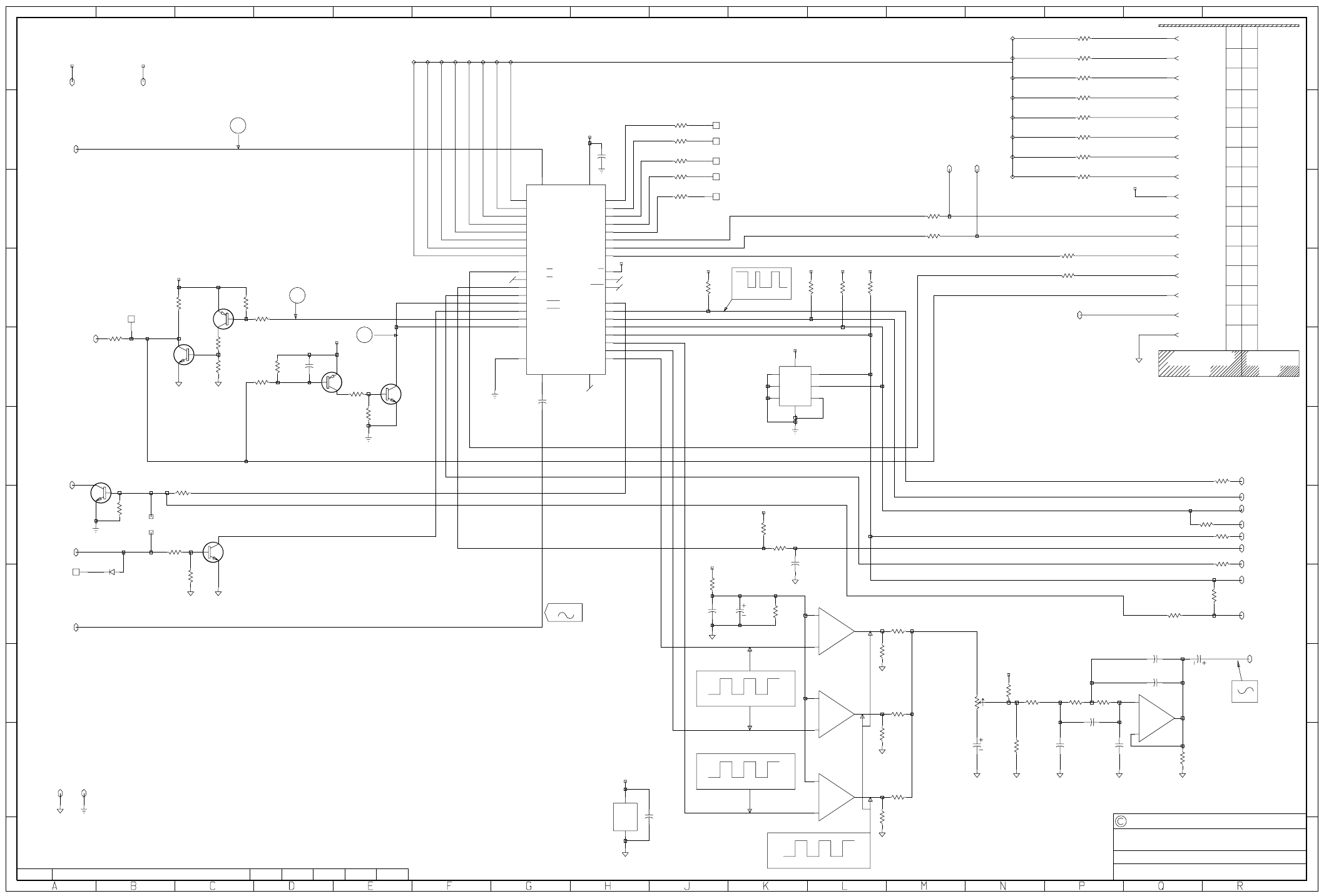
IPN 220-01686-03
M8SL2-00-002-812 T854 PCB Information C6.2.29
© Copyright Tait Electronics Limited August 2004. All rights reserved.
Sheet 8 – T854 Microcontroller
220-01686-03
0
1
2
3
4
5
6
7
8
9
0
1
2
3
4
5
6
7
8
9
ABCDEFGHJ KL MNPQR
REV/ISS AMENDMENTS DATEAPVDD.O.CHKDDRAWN
NO.SHEETS:FILE NAME:
TAIT ELECTRONICS
IPN:
FILE DATE:
ISSUE: ID:.
2.SC.
PROJECT: DESIGNER:
8
9
T854-XX-7XXX
MICROPROCESSOR
168603b
220-01686-03
18-Mar-02
B
T854 BRD
R821
47K
R811
4K7
R810
4K7
R824
2K2
R825
2K2
R826
2K2
R827
2K2
R828
2K2
R840
2K2
R841
2K2
R842
2K2
R813
4K7
R812
4K7
R879
10K
R877
4K7
IC830
LM324D
V-
-V
V+
+V
+
-
IC830
LM324D
G2 +
G2 -
G2 O/P
+
-
IC830
LM324D
G4 +
G4 -
G4 O/P
+
-
IC830
LM324D
G1 +
G1 -
G1 O/P
R871
47K
R875
47K
R873
33K
R859
150K
R861
150K
R863
150K
R865
100K
R867
100K
+
-
IC830
LM324D
G3 +
G3 -
G3 O/P
C823
22N
C824
47N
C826
220P
C828
10N
CW
RV805
20K
MIN
MAX
WIPER
SK810
80C51
P1.7
9
P1.6
8
P1.5
7
P1.4
6
P1.3
5
P1.2
4
P1.1
3
P1.0
2
P3.7/RD
19
P3.6/WR
18
P3.5/T1
17
P3.4/T0
16
P3.3/INT1
15
P3.2/INT0
14
P3.1/TXD
13
P3.0/RXD
11
VSS
22
XTL1
21
XTL2
20
RST
10
VCC
44
P0.7 36
P0.6 37
P0.5 38
P0.4 39
P0.3 40
P0.2 41
P0.1 42
P0.0 43
EA 35
ALE 33
PSEN 32
P2.7 31
P2.6 30
P2.5 29
P2.4 28
P2.3 27
P2.2 26
P2.1 25
P2.0 24
R822
47K
TANT
C841
100U
TANT
C838
100U
C844
10N
C813
1N0
IC820
24C16
A0
A0
A1
A1
A2
A2
GND
GND
+V
+V
SCL SCL
SDA SDA
WPNC
C827
33P
R847
470
R845
470
R854
4K7
R853
4K7
R849
470
R809
4K7
R855
4K7
R843
2K2
SL810
P805
AUX_OUT
I/OPAD
C830
47N
R850
470
R808
10E 1%
P810 SERIAL-COM-1
I/OPAD
R837
2K2
R836
2K2
R835
2K2
R833
2K2
R832
2K2
R831
2K2
R830
2K2
R829
2K2
P820 AUX-OUT-7
I/OPAD
P825 AUX-OUT-6
I/OPAD
P830 AUX-OUT-5
I/OPAD
P835 AUX-OUT-4
I/OPAD
R801
150K
R802
47K
R872
4K7
R874
4K7
R876
4K7
R848
4K7
C810
47N
Q810
BC847B
Q860
BC847B
Q820
BC817
Q830
BC857
TANT
C822
4U7
R815
47K
R816
150K
C812
100P
R818
4K7
R819
4K7
Q850
BC847B
Q840
BC857
D810
BAT165
P840 AUX-OUT-3
I/OPAD
R880
4K7
R881
4K7
R882
470
C880
150P
%R856
0805
%R857
0
SK805
SKT 16-WAY MICROMATCH
CH-SLCT-0
1
SK805
SKT 16-WAY MICROMATCH
CH-SLCT-1
3
SK805
SKT 16-WAY MICROMATCH
CH-SLCT-2
5
SK805
SKT 16-WAY MICROMATCH
CH-SLCT-3
7
SK805
SKT 16-WAY MICROMATCH
CH-SLCT-4
9
SK805
SKT 16-WAY MICROMATCH
CH-SLCT-5
11
SK805
SKT 16-WAY MICROMATCH
CH-SLCT-6
13
SK805
SKT 16-WAY MICROMATCH
CH-SLCT-7
6
SK805
SKT 16-WAY MICROMATCH
+5VDIG
16
SK805
SKT 16-WAY MICROMATCH
AUX-OUT-2
14
SK805
SKT 16-WAY MICROMATCH
AUX-OUT-1
12
SK805
SKT 16-WAY MICROMATCH
AUX-OUT-0
10
SK805
SKT 16-WAY MICROMATCH
CTCSS-DISABLE
4
SK805
SKT 16-WAY MICROMATCH
SERIAL-COM-1
8
SK805
SKT 16-WAY MICROMATCH
TX-RELAY-DRV
2
SK805
SKT 16-WAY MICROMATCH
GND
15
+9V
+9V
+5VDIG
+5VDIG
+5VDIG
MCU-CLOCK
6B5
7A5
7A5
SYNTH
7A2
SCK
7A2
E-P
2T1
CTCSSM
2L1
TX-CONT
6B8
TX-ENB
6F2
LED
2T6
SERIAL-COM
1R4
+9V
5A5
6C7
7B0
+9V
SDA
7A2
TX-RELAY-DRV
2V5
GND
1R0
1R0
2K0
3Q7
4R1
5A4
6B0
7A0
9B7
+5VDIG
RESET
6B4
DGND
6B9
+5VDIG
6B7
+5VDIG
+5VDIG
NOT-RESET
6B4
WATCH-DOG
6B5
+5VDIG
+5VDIG
+9V
SDAP
2U1
SCKP
2U1
+5VDIG +5VDIG +5VDIG +5VDIG
REV
3F9
FWD
3F8
CHANNEL SELECT TO MICRO BUS
CTCSS LEVEL
ADJUST
MICRO-BYPASS
6B6
6B0
12.8MHz
+5V
0V
CTCSSM FREQUENCY
+5V
0V
CTCSSM FREQUENCY
+9V
0V
CTCSSM FREQUENCY
5V
5V
0V
VARIABLE
MICROMATCH
PIN
1
2
3
4
5
6
7
8
9
10
11
12
13
14
15
16
D-RANGE2
PIN
1
2
3
4
5
6
7
11
NC
15
14
13
10
12
9
8
MICROMATCH TO D-RANGE2 CONNECTIONS
MCU-CLOCK
SDA
SYNTH
EPOTS
WATCHDOG
CTCSS_DISABLE
TX_KEY_IN
LED_FLASH
CTCSS_MSB
CTCSS_RX
CTCSS_LSB
TX_KEY_OUT
SERIAL-COM-1
CH-SLCT-0
CH-SLCT-1
CH-SLCT-2
CH-SLCT-3
CH-SLCT-4
CH-SLCT-5
CH-SLCT-6
CH-SLCT-7
CH-SLCT-7
CH-SLCT-6
CH-SLCT-5
CH-SLCT-4
CH-SLCT-3
CH-SLCT-2
CH-SLCT-1
CH-SLCT-0
SCK.
IPN 220-01686-03
C6.2.30 T854 PCB Information M8SL2-00-002-812
© Copyright Tait Electronics Limited August 2004. All rights reserved.
Sheet 9 – T854 Harmonic Filter
220-01686-03
0
1
2
3
4
5
6
7
8
9
0
1
2
3
4
5
6
7
8
9
ABCDEFGHJ KLM
REV/ISS AMENDMENTS DATEAPVDD.O.CHKDDRAWN
NO.SHEETS:FILE NAME:
TAIT ELECTRONICS
IPN:
FILE DATE:
ISSUE: ID:.
2.SC.
PROJECT: DESIGNER:
9
9
T854-XX-7XXX
HARMONIC-FILTER
168603b
220-01686-03
18-Mar-02
B
T854 BRD
#C920
3P3
#C940
4P7
#C950
4P7
#C970
3P9
#C980
3P9
#C900
3P9
#C910
3P9
#C990
3P9
C930
1P0
C960
1P0
#L910
1.5T/5.5
#L920
1.5T/5.5
#L930
1.5T/5.5
#L940
1.5T/5.0
FILTER
4R4
GND
1R0
1R0
2K0
3Q7
4R1
5A4
6B0
7A0
8A0
ANTENNA
1R8
HARMONIC-FILTER
6B0

M8SL2-00-002-812 DI
© Copyright Tait Electronics Limited August 2004. All rights reserved.
Part D T803-02-9000 Tone Remote
This part of the manual is divided into four sections as listed below. There is a detailed
table of contents at the start of each section.
Section Title
1 General Information
2 Circuit Operation
3 Installation and Configuration
4 T803 PCB Information

DII M8SL2-00-002-812
© Copyright Tait Electronics Limited August 2004. All rights reserved.

M8SL2-00-002-812 General Information D1.1
© Copyright Tait Electronics Limited August 2004. All rights reserved.
1 General Information
This section provides a brief description of the T803 tone remote, along with detailed
specifications and information on system configuration.
The following topics are covered in this section.
Section Title Page
1.1
1.1.1
1.1.2
1.1.3
1.1.4
1.1.5
1.1.5.1
1.1.5.2
Introduction
Tone Remote
Alarm Monitoring and Confirmations
Voting Ton es
Other Features
Front Panel Operating Controls
Mode LED
Alarm LEDs
1.3
1.3
1.4
1.4
1.4
1.5
1.5
1.6
1.2
1.2.1
1.2.2
1.2.3
1.2.3.1
1.2.3.2
1.2.4
1.2.5
1.2.6
1.2.7
1.2.8
1.2.9
1.2.10
Specifications
Introduction
General
Line
Input levels
Output levels
Radio Levels
Tone Remote
Audio Response
Alarms
Morse Code
Voting
Miscellaneous
1.7
1.7
1.7
1.7
1.7
1.7
1.8
1.8
1.8
1.9
1.9
1.10
1.10
1.3
1.3.1
System Configuration
Product Codes
1.11
1.12

D1.2 General Information M8SL2-00-002-812
© Copyright Tait Electronics Limited August 2004. All rights reserved.
1.4
1.4.1
1.4.2
1.4.2.1
1.4.3
1.4.4
1.4.5
1.4.6
1.4.7
Regulatory Information
Canada
United States Of America
Facility Interface and Service Order Codes
Europe
New Zealand
Australia
Hong Kong
Singapore
1.12
1.12
1.12
1.14
1.14
1.15
1.16
1.16
1.16
Figure Title Page
1.1
1.2
1.3
Front Panel Layout
T803 System Configuration
Single and double turn of line through filter
1.5
1.11
1.15
Section Title Page

M8SL2-00-002-812 General Information D1.3
© Copyright Tait Electronics Limited August 2004. All rights reserved.
1.1 Introduction
The T803-02 is a tone-operated Remote Controller otherwise known as a Tone Remote.
Features include alarm monitoring, voting tone generation and simple high site control.
It interfaces either a 2-wire or 4-wire line circuit to the T800 SL2 Base Station and thus
enables a dispatch console (also known as a desktop controller) to monitor and control
the remote basestation. The T803-02 interfaces with the SL2 receiver and transmitter via
the backplane PCB (X800-56-PCB3) and two small flat cable looms plugged into the D-
ranges on the back. The T803 is configured using the Tait PGM800Win programming
software (V4.02 and later) on a PC.
1.1.1 Tone Remote
The T803 tone remote enables a remotely located user to:
•key the transmitter
•defeat the receiver’s CTCSS mute (to monitor a channel)
•change the set channel (up to 256 channels)
•change between base station and repeater modes (repeater knockdown)
•monitor and cancel alarms
•turn repeater site equipment on or off (highsite control)
•loop back line audio (4-wire line interface only)
This is achieved using three industry-standard tone signalling plans for ease of integra-
tion into existing control systems and choice of vendor for office/control room equip-
ment. These plans are:
•EIA tone remote using a single function tone.
In this system when the control room user presses the transmit key, the line con-
trol equipment sends a 120ms long burst of high level guard tone (HLGT – usually
2175Hz at +10dBM to line). This is followed by a single 40ms function tone at
0dBm to line. The available tone set is 650Hz to 2050Hz in 100Hz steps. This func-
tion tone can change channel, monitor the radio channel (defeat receiver CTCSS)
or a variety of other functions. Following these initial tone bursts a low level
guard tone (LLGT – usually 2175Hz at –20dBm) is sent to line and speech is gated
onto line (at approx 0dBm peak level). This continues until the user releases the
transmit key. This removes speech from the line and low level guard tone ceases.
•EIA enhanced tone remote using two function tones.
This is a variant of the above system where two function tones are sent one after
the other in the period between the high level guard tone and the low level guard
tone. The tone set is also expanded (650Hz to 2050Hz in 100Hz steps) to give 225
possible combinations which can be allocated to various actions. The duration of
both high level guard tone and function tones can be varied.
• Simple Transmitter keying using low level guard tone.
This is used where complex functionality is not required. One application is to key
a link transmitter where the high level guard tone, the function tones, speech and
low level guard tones are transparently carried to an end base station. Note that in

D1.4 General Information M8SL2-00-002-812
© Copyright Tait Electronics Limited August 2004. All rights reserved.
this application the notch filters (which ordinarily remove the key tone from the
audio path) must be turned off using PGM800Win so that the keying signal is
propagated to the end transmitter.
1.1.2 Alarm Monitoring and Confirmations
The T803 monitors three T800 sub-rack alarms (transmitter forward and reverse power,
and low battery/power supply), one line alarm (line fail indication) and four external
closure alarms. If alarms are triggered the T803 can be programmed to generate tone
sequences (DTMF, Selcall or function tones) and/or enable auxiliary outputs, to alert
system users of a problem. The tone sequences can be sent to line and/or radio.
Additionally the T803-02 can be programmed to respond to as many as eight different
non-alarm triggers. These can be used as confirmation that an event has occurred. Con-
firmations can be programmed to occur in the event of power-up, channel change and/
or the detection of up to six user defined function tones. In the same way as for alarms,
the T803 can generate tone sequences and/or enable auxiliary outputs as a response to a
confirmation.
1.1.3 Voting Tones
The T803 can also generate voting tones where a 4-wire line interface is used. Voting
systems are used where several base station receivers are tuned to the same radio chan-
nel and located at different sites, sending audio back to a central control where the best
quality audio must be selected or “voted upon”. Tone on Idle or Sliding Voting Tones
can be generated to interface a T800 sub-rack to a wide variety of industry standard
Radio Voting systems.
In Tone on Idle applications, a tone (normally the same frequency as LLGT) is transmit-
ted to line when the T800 receiver is muted. When the tone disappears, control room
equipment can perform signal to noise measurements on incoming audio lines and
select the best for feeding to the control room user.
In Sliding Voting Tone systems, a tone is transmitted to line whose frequency is propor-
tional to the T800 receiver’s RSSI. Control room equipment determines which receiver
has the highest RSSI and thus selects which line carries the highest quality incoming
audio.
1.1.4 Other Features
•Programmable Morse Code Encoder for automatic station identification (CWID)
•User programmable Line levels
•Programmable Transmit and Receive audio path delays
•Programmable (on/off) notch filtering.
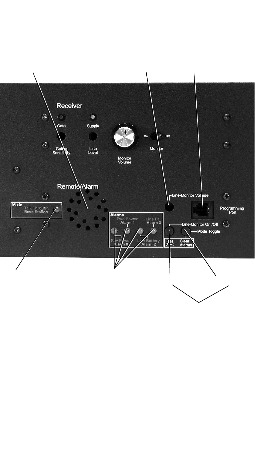
M8SL2-00-002-812 General Information D1.5
© Copyright Tait Electronics Limited August 2004. All rights reserved.
1.1.5 Front Panel Operating Controls
Figure 1.1 Front Panel Layout
1.1.5.1 Mode LED
The colour of the Mode LED on the front panel indicates the T803 mode of operation:
•Green = Base station mode
•Red = Repeater (talk through) mode
or clear alarms
Green = base station mode
Red = repeater mode
Speaker
Speaker on/off Change mode
Adjust speaker volume
Plug in programming
cable from PC with
PGM800Win
Plug in test microphone
to talk to despatcher or
radios
Green = auxiliary alarm
Red = rack alarm
Flashing see below
Flashing see below
Press together to enter test modes

D1.6 General Information M8SL2-00-002-812
© Copyright Tait Electronics Limited August 2004. All rights reserved.
The LED flashes in different ways, depending on the particular condition.
Where two or more conditions occur at the same time, the precedence is in the order
shown above (i.e. module linked has the highest priority, followed by microcontroller
error, then speaker on).
1.1.5.2 Alarm LEDs
The alarm LED turns on only when its alarm condition has been latched. The colour of
the LED indicates the source of the alarm trigger:
•Green = Auxiliary alarm
•Red = Rack alarm
The LED flashes in different ways as indicated below.
Press the Monitor and Mode Toggle buttons together to reset all alarms.
Flash Rate Condition
equal
0.3s on/ 0.3s off
Module is linked with
PGM800Win
long flash
1 s on/0.3 s off
Microcontroller has detected an
internal communications error
short off
0.3 s on/0.08 s off
Speaker is on.
Flash Rate and Colour Alarm
green very short off
0.32s on/0.01s off
Rack
red short off
0.32s on/0.1s off
Auxiliary
alternating red and green
0.32s on/0.1s off/
0.32s on/0.1s off
Rack and Auxiliary

M8SL2-00-002-812 General Information D1.7
© Copyright Tait Electronics Limited August 2004. All rights reserved.
1.2 Specifications
1.2.1 Introduction
The performance figures given are minimum figures, unless otherwise indicated, for
equipment operating at standard room temperature (+22°C to +28°C) and standard test
voltage (13.8VDC).
Details of test methods and the conditions which apply for Type Approval testing in all
countries can be obtained from Tait Electronics Ltd.
1.2.2 General
Supply Voltage:
Operating Voltage …10.8 to 16VDC
Standard Test Voltage …13.8VDC
Polarity …negative earth only
Supply Current …250mA max.
Operating Temperature Range …–30 to +60°C.
1.2.3 Line
1.2.3.1 Input levels
Line-In (Level required to produce a transmitter output at 60% full system deviation):
Programmable …–27dBm to +3dBm
Maximum input peak …+7dB relative to programmed level
1.2.3.2 Output levels
Line-Out (Radio receiver level to T803 must be 230mVrms)
Programmable …–27dBm to –1dBm
Dynamic range …+7dB relative to programmed level
Maximum output peak …+5.5dBm
For compliance with TIA/EIA-IS-968, CS-03 (Canada), PTC200 (New Zealand) and
HKTA 2023 (Hong Kong):
Programmable Line Output level must be set to ≤ –10dBm.
For compliance with ACA TS002 (Australia):
Programmable Line Output level must be set to ≤ –11dBm.

D1.8 General Information M8SL2-00-002-812
© Copyright Tait Electronics Limited August 2004. All rights reserved.
For compliance with TS PSTN1 (Singapore):
Programmable Line Output level must be set to ≤ –7dBm.
1.2.4 Radio Levels
From Radio Receiver …230mVrms at input of T803
(for 1kHz tone at 60% full system deviation)
(Note: This input of theT803 is high impedance)
To Radio Transmitter:
From Line-In …–4.4dBm
From Radio Receiver …–4.4dBm
(With receiver level to T803 set to
230mVrms)
1.2.5 Tone Remote
Keytone Sensitivity …29dB less than programmed Line-In
level
Keytone Accept Bandwidth …±0.75% typical (±16Hz at 2175Hz)
(Speech at –10dBm,
keytone at –30dBm)
Talkoff
(Max. difference between speech and keytone)
2-wire mode …32dB typical
4-wire mode …35dB typical
Programmable Guardtone Frequencies …1950, 2100, 2175, 2325, 2500, 2600,
2800, 2900, 2970, 3000 and 3100Hz
Programmable High Level Guard Tone Duration …60 to200ms
Function Tone Frequencies …650Hz to 2050Hz in 100Hz steps
Function Tone Accept Bandwidth …±24Hz typical
Maximum Number of Function Tones …2
Programmable Function Tone Duration …20 to 100ms
1.2.6 Audio Response
Frequency Response …±1dB 300Hz to 3kHz except at
notch frequency

M8SL2-00-002-812 General Information D1.9
© Copyright Tait Electronics Limited August 2004. All rights reserved.
Notch Filter Bandwidth at –38dB …±0.6% typical (±13Hz at 2175Hz)
Notch Filter Bandwidth at –3dB …±1.28% typical (±28Hz at 2175Hz)
Notch Filter Attenuation …38dB
Audio Distortion:
From Line …<2.5%
From Receiver …<2%
Programmable Audio Delay:
Minimum …0ms
Maximum …500ms
Step …1ms
1.2.7 Alarms
Supply Voltage Alarm Threshold
Firmware up to version 2.10 …10.7V ±0.05V
Firmware version 2.11 or later …programmable 10.7V to 14.1V
(0.2V steps)
RF Power Alarm Thresholds …adjusted inside transmitter or PA
Line Fail Alarm Timer …off or 1 minute to 4 hours
Auxiliary Alarm
Input Trigger …First and subsequent falling edges
Input Threshold …<1.5V (or to 0V via 3.3KΩ resistor)
Maximum Input Voltage …5V
Alarm/Confirmation Sequence …0 to 14 tones to radio and/or line
(and/or Aux output when enabled)
Programmable Signalling Standards …Selcall (CCIR, EIA, EEA, ZVEI, and
DZVEI) DTMF and EIA Tone Remote
function tone format.
Tone Carrier Deviation …70% nom. system deviation at 1kHz
(for test tone set at 60%)
Alarm Pip Tone Frequency/Duration …600Hz/200ms on tail of audio
1.2.8 Morse Code
Sending Speed …20 words per minute (PARIS)
Maximum Code Length …15.36 seconds

D1.10 General Information M8SL2-00-002-812
© Copyright Tait Electronics Limited August 2004. All rights reserved.
Tone Frequency …1200Hz
Valid Station ID …alphanumeric only
Repetition Rate …off or 1 to 60 minutes
Carrier Deviation …20% nominal system deviation
(for test tone set at 60%)
1.2.9 Voting
Programmable Tone-On-Idle Frequencies …1950, 2100, 2175, 2325, 2500, 2600,
2800, 2900, 2970, 3000 and 3100Hz
Programmable Sliding Voting Tone
Frequencies …2700 to 3500Hz
Voting Tone Level To Line …–40dBr to –1dBr
(Adjustable relative to Line-Out
setting)
1.2.10 Miscellaneous
Auxiliary Output Rating …open collector, 50V, 250mA (at25°C)
Momentary Monitor (CTCSS Defeat) Time …off or 1 to 20 seconds
M8SL2-00-002-812 General Information D1.11
© Copyright Tait Electronics Limited August 2004. All rights reserved.
1.3 System Configuration
The following flow chart will help you to configure your T800 SL2 system to utilise the
features of the T803 Tone Remote. Refer to Section 1.3.1 for details on the product types
mentioned in this chart.
Figure 1.2 T803 System Configuration
See Section 3.10Part C,
See SectionPart B, 6.2

D1.12 General Information M8SL2-00-002-812
© Copyright Tait Electronics Limited August 2004. All rights reserved.
1.3.1 Product Codes
The following table provides a brief description of the products mentioned in Figure 1.2.
Consult your nearest Tait Dealer or Customer Service Organisation for more informa-
tion on these products.
1.4 Regulatory Information
1.4.1 Canada
This product meets:
•Industry Canada Telecommunications Apparatus Compliance Specification
CS-03. Registration No. 737A-10118A.
•Canadian ICES-003 (Radiated and conducted emissions, and electromagnetic sus-
ceptibility specifications) for Class A digital apparatus.
1.4.2 United States Of America
A copy of the Declaration of Conformity is available at www.taitworld.com
This equipment complies with TIA/EIA/IS-968, Part 15 Class A of 47CFR and Part 68 of
47CFR as detailed below.
•TIA/EIA/IS-968 (Telecommunications - Telephone Terminal Equipment - Techni-
cal Requirements). Adopted criteria of the Administrative Council on Terminal
Attachments (ACTA).
•Part 15 Class A of 47CFR (Radiated and conducted emissions, and electromag-
netic susceptibility specifications) of the FCC rules for the United States. Opera-
tion is subject to the following conditions:
1. This device may not cause harmful interference, and
2. This device must not accept any interference received, including interfer-
ence that may cause undesired operation.
Product Code Description
T800-04-0000 T800 UHF RSSI kit.
T800-80-0001 T803 test microphone. Used for line intercom and to talk on air.
T1500-52-0000 Tx alarm and multichannel kit (wired connection).
T800-10-0520 Tx Alarm kit (plug in).

M8SL2-00-002-812 General Information D1.13
© Copyright Tait Electronics Limited August 2004. All rights reserved.
Warning:
This equipment has been tested and found to comply with the limits for a Class A
digital device, pursuant to Part 15 of the FCC Rules. These limits are designed to
provide a reasonable protection against harmful interference when the equipment
is operated in a commercial enviroment. This equipment generates, uses, and can
radiate radio frequency energy and, if not installed and used in accordance with
this manual, may cause harmful interference to radio communications. Operation
of this equipment in a residential area is likely to cause harmful interference in
which case the user will be required to correct the interference at their own
expense.
•Part 68 of 47CFR (Connection of terminal equipment to the telephone network) of
the Federal Communications Commission (FCC) rules and the requirements
adopted by ACTA. On the rear face of this equipment is a label that contains,
among other information, the product identifier i.e. US: 6FPNZL-34203-OT-N. If
requested this number must be provided to the telephone company.
Warnings:
If this equipment, T803 Tone remote and Alarm Interface, causes harm to the tele-
phone network, the telephone company will notify you in advance that temporary
discontinuance of service may be required. But if advance notice isn't practical,
the telephone company will notify the customer as soon as possible. Also, you
will be advised of your right to file a complaint with the FCC if you believe it is
necessary.
The telephone company may make changes in its facilities, equipment, operations
or procedures that could effect the operation of the equipment. If this happens the
telephone company will provide advance notice in order for you to make neces-
sary modifications to maintain uninterrupted service.
Connection to party line service is subject to state tariffs. Contact the state public
utility commission, public service commission or corporation commission for
information
If trouble is experienced with this equipment, T803 Tone remote and Alarm Interface,
for repair or warranty information, please contact:
Tait North America Inc
Building 1, Suite 450
15740 Park Row
Houston, Texas, 77084, USA
Phone: 0800 320 4037
Fax: 281 829-3320
Mobile: 713-703-4991
Only approved Tait Dealer or Customer Service Organisations equipped with the
necessary facilities should perform any servicing. Repairs attempted with incor-
rect equipment or untrained personnel may result in permanent damage. If the
equipment, T803 Tone Remote and Alarm Interface, is causing harm to the telephone
network, the telephone company may request that you disconnect the equipment
until the problem is resolved.

D1.14 General Information M8SL2-00-002-812
© Copyright Tait Electronics Limited August 2004. All rights reserved.
1.4.2.1 Facility Interface and Service Order Codes
1.4.3 Europe
For Declaration of Conformity refer to eudocs.taitworld.com
According to the requirements of the EC Council Directive:
1999/5/EC Radio Equipment and Telecommunications Terminal Equipment Directive,
The T803-02-0000 Tone Remote and Alarm Interface complies with;
•EN60950 : 2000 Electrical Safety
•EN 301 489-5 Radiated and conducted emissions, and electromagnetic susceptibil-
ity specifications. Compliance to this standard is subject to the fitting of an addi-
tional EMC filter to the 2-wire/4-wire line interface. For more information see the
following section.
1.4.3.1 Additional EMC filter fitting instructions
Applicability
In order for the T803-02 to comply with the RF electromagnetic field immunity require-
ments of the EMC standard EN 301 489-05 (07-2000), an additional filter must be fitted
to the 2-wire or 4-wire line when the unit is installed. This filter, a clamp-on ferrite,
helps prevent electromagnetic energy from being coupled into the product.
Required Component
The T803-02 Tone Remote and Alarm Interface unit is supplied together with the follow-
ing separate EMC Filter:
Unit Configuration Function
USOC
Jack type RENa
a. Ringer Equivalence Number
FICb
b. Facility Interface Code
SOCc
c. Service Order Code
T803 2-wire 2-wire leased line RJ-11C —Metallic 7.0Y
T803 4-wire 4-wire leased line RJ61X —Metallic 7.0Y
IPN 069-00010-31
Description Clamp-on ferrite EMC filter for 13mm diameter cable
Manufacturer and part number Fair-Rite Part No. 0431 164181

M8SL2-00-002-812 General Information D1.15
© Copyright Tait Electronics Limited August 2004. All rights reserved.
Instructions
1. The clamp-on ferrite must be located on the 2-wire or 4-wire line as close as possi-
ble to the T803. If the ferrite is not located within 10cm of the line socket, there is
no guarantee that the T803 complies with the EMC standards.
2. Only one turn of the 2-wire or 4-wire line is required through the ferrite. However,
two turns are recommended (see Figure 1.3) as this provides extra immunity
while also securing the ferrite in position.
3. Ensure that the 2-wire or 4-wire line does not impede the closing of the ferrite
clamp.
Figure 1.3 Single and double turn of line through filter
Technical Support
Contact your local Tait Electronics agent or Customer Service Organisation or visit Tait
Electronics Technical Support at support.taitworld.com.
1.4.4 New Zealand
This product complies with the following standards:
•PTC200 Requirements for analogue telecommunications equipment.
•AS/NZS 3548 Class A Radiated and conducted emissions specifications
Warning:
T803-02-0000 for use in New Zealand
“The grant of a Telepermit for any item of terminal equipment indicates only that Tele-
com New Zealand has accepted that the item complies with minimum conditions for
connection to its network. It indicates no endorsement of the product by Telecom New
Zealand, nor does it provide any sort of warranty. Above all, it provides no assurance
that any item will work correctly in all respects with another item of Telepermitted
equipment of a different make or model, nor does it imply that any product is compati-
ble with all Telecom New Zealand's Network services.”
“This equipment does not fully met Telecom New Zealand's impedance requirements.
Performance limitations may occur when used in conjunction with some parts of the
Single turn Double turn

D1.16 General Information M8SL2-00-002-812
© Copyright Tait Electronics Limited August 2004. All rights reserved.
network. Telecom New Zealand will accept no responsibility should difficulties arise in
such circumstances.”
1.4.5 Australia
This product complies with the following standards:
•AS/ACIF S006 - 2001 Telecommunications technical standard
•AS/ NZS 3260 Electrical safety
•AS/NZS 3548 Class A Radiated and conducted emissions specifications
1.4.6 Hong Kong
This product complies with the Network Connection specification HKTA 2023
1.4.7 Singapore
This product complies with the Type Approval specification IDA TS PSTN1

M8SL2-00-002-812 Circuit Operation D2.1
© Copyright Tait Electronics Limited August 2004. All rights reserved.
2 Circuit Operation
This section provides a description of the circuit and operation of the T803-02 tone
remote.
Note: Unless otherwise specified, the term “PGM800Win” used in this and follow-
ing sections refers to version 4.02 or later of the programming software.
Refer to Section 4 where the parts lists, grid reference index and diagrams will provide
detailed information on identifying and locating components and test points on the
main PCB.
The following topics are covered in this section.
Section Title Page
2.1 Circuit Overview 2.3
2.2 Tone Detection 2.4
2.3
2.3.1
Alarm Monitoring
Alarm Triggers
2.5
2.6
2.4 Confirmations 2.7
2.5 Clearing Alarms and Confirmations 2.7
2.6 Voting Tone Operation 2.8
Figure Title Page
2.1
2.2
High Level Block Diagram
Signal Flow
2.3
2.9

D2.2 Circuit Operation M8SL2-00-002-812
© Copyright Tait Electronics Limited August 2004. All rights reserved.

M8SL2-00-002-812 Circuit Operation D2.3
© Copyright Tait Electronics Limited August 2004. All rights reserved.
2.1 Circuit Overview
Figure 2.1 High Level Block Diagram
The T803 is connected to a leased line from control room equipment by means of an
RJ45 connector. 600R transformers are used to couple the audio into and out of the T803.
On the secondary of these line matching transformers are analogue transmission
switches which configure the line interface as either 2-wire or 4-wire compatible. Audio
from line is passed through a programmable electronic potentiometer (e-pot) level con-
trol circuit before entering a CODEC where it is digitised. Audio to line is output from
the same line CODEC, via a second programmable e-pot level control circuit.
The line CODEC is connected to a digital signal processor (DSP) which is also connected
to a similar radio CODEC (the CTCSS CODEC is not used in this application). The radio
CODEC receives audio from the T800 receiver and sends audio to the T800 transmitter
to which it is connected via the special backplane PCB. Receiver audio is low frequency
filtered to extend the radio CODEC’s effective frequency range.
The DSP processes the digitised audio streams from the CODECs in accord with instruc-
tions sent to it by the T803’s microcontroller. The DSP can:
•detect high level guard tone, low level guard tone and function tones coming
from line, notch filter line in and receiver audio (used to eliminate low level
guard tone from line out and transmitter audio);
•generate Selcall DTMF/function tone alarms and pip tones to Line-Out and
transmitter audio;
•generate voting tones to Line-Out;
•generate morse code to transmitter audio;
•cross connect line and radio audio paths;
•adjusts the Line-In and Line-Out levels;
Digital
Signal
Processor
Radio Codec
Micro
Controller
Test Mic
CTCSS Defeat
Power Alarm I/Ps
Channel Select
Tx KeyTx Key
Rx Mute
Aux I/Ps
Aux O/Ps
PGM800Win Interface
RAM
A/D
RSSI
Voltage Sense
Speaker
2W/4W
Select Line Codec
LINE
Front Panel
LEDs & Switches
EEPROM
RX Audio
TX Audio
Progammable
e-pot level
control
Progammable
e-pot level
control

D2.4 Circuit Operation M8SL2-00-002-812
© Copyright Tait Electronics Limited August 2004. All rights reserved.
•mute audio from Line-In and receiver;
•delay the audio.
The microcontroller boot loads the DSP, interfaces with the user via the front panel
switches and LEDs, interfaces with PGM800Win and runs the T803 state machines
(alarm monitoring, alarm tone generation, high level guard tone/function tone/low
level guard tone timing, RSSI/voting tone conversion etc.).
2.2 Tone Detection
In the quiescent state, audio on the Line-In pair is passed through the DSP (IC300) unfil-
tered to the T803 loudspeaker (which is connected to Tx audio – TP203). The audio is
bandpass filtered to detect guard tone. In normal operation (keytone and function tone
operation) the tone detector threshold is set for high level guard tone (HLGT).
If HLGT is detected, the DSP signals this detection to the micro using the
TONE_DETECT line (TP300 is pulled low). The micro instructs the DSP, using the asyn-
chronous serial communications connection (TP306) between them, to switch on the in
line guard tone notch filter, lower the threshold of the guard tone detector (so that it can
detect low level guard tone – LLGT) and turn on the function tone detectors.
Where the T803 is operating in 2-wire mode and receiver audio (RX audio) is being
gated to line, the micro will soft mute the RX audio first). The micro then starts an inter-
nal timer, the duration of which is set by the HLGT and function tone times pro-
grammed by PGM800Win.
If a function tone is detected, the DSP signals the micro using the CALL_UP line (TP301
pulled low). The micro then interrogates the DSP via the serial communications connec-
tion to find out what frequency was detected.
If no tones are detected and the timer expires, the micro resets the DSP to its quiescent
state. If two different frequencies are detected or if only one function tone frequency is
decoded and the timer expires, the micro decodes them/it into an action by reading
data programmed into the EEPROM (IC312) by PGM800Win. The micro then keys on
the transmitter (PTT line) and instructs the DSP to turn off the function tone detectors
and the talk-through gate (if it was on). If the function tone sequence decodes into a
channel number that is different from the currently set channel, the micro will output
the channel number on CH0 – CH7 for 250ms. This change may be latched into the T800
radios providing the sub-rack PCB channel select switches do not create a conflict.
As long as the DSP is detecting LLGT (indicated by a low level on TP300) the micro will
keep the transmitter keyed on. When the DSP fails to detect LLGT the micro turns off
the transmitter key and returns the DSP to the quiescent state.
When the T803 is programmed for keytone-only operation, the micro keying of the
transmitter follows the state of the TONE_DETECT line from the DSP.
In the quiescent state when the receiver mute line (RX_MUTE) goes low, the micro
instructs the DSP to gate audio from the receiver to Line-Out. If the line interface is 2-
wire, Line-In and Line-Out are joined and the Rx audio will pass through the line inter-

M8SL2-00-002-812 Circuit Operation D2.5
© Copyright Tait Electronics Limited August 2004. All rights reserved.
nally to the loudspeaker. It will therefore also reach the guard tone detector. Rx audio is
therefore notch filtered at the guard tone frequency to prevent false guard tone detec-
tion. If the line interface is 4-wire this filtering is unnecessary but the talk-through gate
must be turned on to send Rx audio to the loudspeaker. If the T803 is in repeater mode
the transmitter is keyed and will remain so until the RX_MUTE line goes high. Note that
the T803 will not key the transmitter if the receiver’s CTCSS is defeated (CD_OUT is
low) to prevent receiver channel noise being transmitted.
From the description above of the keytone/function tone detection it can be seen that
keying from line has priority over repeater mode keying and audio gating.
2.3 Alarm Monitoring
The T803 microprocessor monitors eight alarm sources:
•Transmitter forward power
•Transmitter reverse power
•low battery
•line fail
•four external closure alarms
When an alarm is triggered it is latched as indicated by the corresponding LED on the
front panel. If the T803 is keying the transmitter or sending receiver audio to the line the
latched alarm is ignored. Once the T803 re-enters the idle state the latched alarms are
actioned. The microprocessor reads the EEPROM to determine what tone sequence the
user programmed and instructs the DSP accordingly. If the tone sequence is to be sent to
the transmitter, it is keyed 500ms before the tones are generated. Additionally the user
may program any of the 4 auxiliary output ports as a response to an alarm event. The
micro will activate (pull low) these outputs if enabled. If several alarms are latched
together they are actioned in the order of priority:
1. External closure alarms 0 to 3
2. Reverse power
3. Forward power
4. Low battery
5. Line fail
If the programmed alarm action is a pip tone, the micro will instruct the DSP to append
200ms burst of 600Hz tone to each transmission (to line and/or radio).
Note: Sub-rack alarms (Fwd and Rev Power, Low battery or Line fail) cannot be
re-triggered until they are cleared. The 4 external closure alarms however
will re-send any user programmed tone sequence if re-triggered when
already latched.

D2.6 Circuit Operation M8SL2-00-002-812
© Copyright Tait Electronics Limited August 2004. All rights reserved.
2.3.1 Alarm Triggers
The alarms are triggered according to their type.
Table 2.1 Alarm Summary Table
External Closure Alarm (Auxiliary Input Alarms)
The 8 bit input latch (IC202) is sampled every 50ms. If two successive samples are the
same value then the state of the closure alarms is tested (This has the effect of debounc-
ing the alarm inputs). If any alarm is low then those alarms are latched.
RF Power Alarm
The forward and reverse power alarms are only tested when the T803 is keying the
transmitter. The alarms must be active (low) for two seconds before they are latched.
The two seconds sampling period allows for settling time inherent in some older T800
PA designs. Note that if a Transmitter fitted with a T1500-52-0000 PCB is being used,
rack backplane links LK1 and LK2 must be fitted at power up.
Low Battery Alarm
The 13.8V supply line voltage is measured by the A/D converter (IC208) every 50ms. If
the voltage is below the programmed alarm threshold (±0.05V) for more than 25 sec-
onds of a 30 second sampling period, the alarm is latched. The long sampling period
allows for load fluctuation effects on the supply.
Programmable low voltage threshold is only available in T803 firmware version 2.11 or
later. Prior to this, the threshold was fixed at 10.7V ±0.05V.
Line Fail Alarm
If no keying from line occurs within the period programmed by the user from
PGM800Win, the microprocessor latches this alarm, saves the mode status and puts the
T803 into repeater mode. Note that programming zero as the line fail time disables this
alarm.
Priority Alarm Type Trigger Type Re-triggerable
when latched
LED
colour
1Auxiliary Input 0
to Input 3
External closure. Sampled
every 50ms Yes Green
2 Reverse Power Sampled every 50ms
while the T803 is keying
the transmitter. Incoro-
rates a 2s settling time.
No Red
3 Forward Power
4Low Battery
Voltage must be belo w
the programmed thresh-
old for 25s of a 30s period.
No Red
5Line Fail Programmable non-activ-
ity time period No Red

M8SL2-00-002-812 Circuit Operation D2.7
© Copyright Tait Electronics Limited August 2004. All rights reserved.
2.4 Confirmations
Additional to alarms the T803 microprocessor also monitors eight non-alarm triggers
known as Confirmations:
•Power-up
•Channel change
•Up to six user defined function tone inputs
The T803 micro responds to a confirmation trigger in the same way as it does to an
alarm trigger – depending on what has been programmed into the EEPROM, a tone
sequence may be sent, an auxiliary output enabled and/or a pip tone enabled. These are
all actioned by the micro with the same rules as for alarm triggers. The only difference is
that there are no LEDs associated with confirmations.
If several confirmations are triggered together they are actioned in the following order
of priority: Power-up, Channel change and then User Confirmation 0 to 5. If several
alarms and confirmations are triggered together the Power-up confirmation, if enabled,
is always actioned first, followed by any alarms and then any other confirmations, both
in their normal priority order.
Note: Confirmations will re-send any user programmed tone sequence if re-trig-
gered.
2.5 Clearing Alarms and Confirmations
The alarms can be cleared by either pressing both front panel switches together or send-
ing the T803 a correctly programmed (“Clear Alarms”) function tone. All alarms are
cleared together. Clearing alarms turns off all LEDs, cancels any associated pip tones
and resets auxiliary outputs. If an alarm condition is still valid when it is cleared, it will
be re-latched and the user-programmed action will be executed. If required, pip tones
can be cleared separately (leaving alarms latched) by using a “Clear Alarm/Confirma-
tion Pip tones” function tone.
When the Line fail alarm is cleared, the T803 will revert to the mode it was in (Basesta-
tion or Repeater) before the alarm was triggered. A keying sequence from line can also
clear this alarm in the same way except that the pip tone will not be cleared if used by
other latched alarms. Line fail is the only alarm that can be cleared individually in this
way.
Confirmations can not be cleared by a single command like the Alarms. Confirmation
pip tones are cancelled by using a “Clear Alarm/Confirmation Pip tones” programmed
function tone and the auxiliary outputs are individually reset by using a “Turn OFF
Auxiliary output (x)” function tone.
It is possible to have more than one Alarm or Confirmation using the pip tone. In this
situation the clearing behaviour must be carefully considered:
•Line Fail Pip – Cleared by line keying-sequence only if pip tone is not ‘active’
for other Alarms and/or Confirmations.

D2.8 Circuit Operation M8SL2-00-002-812
© Copyright Tait Electronics Limited August 2004. All rights reserved.
•Alarm Pips (including Line Fail) – Cleared by “Clear Alarms” command only if
confirmation pips are not ‘active’. Always cleared by “Clear Alarm/Confirma-
tion Pip tones“ command.
•Confirmation Pips – Cleared by “Clear Alarm/Confirmation Pip tones” com-
mand.
Additionally, it is also possible to have a single auxiliary output assigned to more than
one alarm or confirmation. However, be aware that any command that resets auxiliary
outputs, such as “Clear Alarms” or “Toggle Auxiliary Output (x)”, will not make any
check for multiple use – auxiliary outputs will be reset regardless.
2.6 Voting Tone Operation
When the T803 is programmed to generate a tone on idle, the microprocessor monitors
the receiver Mute-In signal. When it is high (receiver muted) the DSP is instructed to
generate a voting tone to Line-Out. When receiver Mute-In is low the voting tone is
turned off. To prevent false detection of the idle tone at the far end voting equipment,
the DSP filters energy at the idle tone frequency from the receiver audio transmitted to
Line-Out.
If the T803 is programmed to generate a Sliding (or Simoco compatible) Voting Tone the
microprocessor reads the receiver RSSI level every 6ms using the A/D converter and
sends this value to the DSP. The DSP generates a voting tone to Line-Out. The tone fre-
quency is proportional to the RSSI level. To prevent incorrect operation of the far end
voting equipment, the DSP low pass filters the receiver audio transmitted to Line-Out.
M8SL2-00-002-812 Circuit Operation D2.9
© Copyright Tait Electronics Limited August 2004. All rights reserved.
Figure 2.2 Signal Flow
D/A Numeric
Scaling
Guard Tone
Notch Filter
Soft
Mute
Numeric
Scaling
A/D
Soft
Mute
Voting Tone
Generator
Test Tone
Generator
5Tone/Pip Tone
Generator
D/A
A/D
2w/4w
Select
Numeric
Scaling
5Tone/Pip Tone
Generator
Test Tone
Generator
Morse Code
Generator
Radio Codec
DSP
Line Codec
2W/4W Select
Line
TX Audio
State Machine Control
Micro
Numeric
Scaling
RX Audio
BandPass
Filter
Guard Tone Detect
Function Tone
Detection
Gain
Gain
Audio
Delay
Line Loopback Guard Tone
Notch Filter 2W
4W
Tone on Idle
Notch Filter
No Voting
Tone on
Idle
Sliding
Voting
Voting Tone
Lowpass Filter
Audio
Delay
Talk Through
Tone Detect
High Speed Serial Coms
Tasklist/Data
Serial Coms
Data
Call Micro

D2.10 Circuit Operation M8SL2-00-002-812
© Copyright Tait Electronics Limited August 2004. All rights reserved.

M8SL2-00-002-812 Installation and Configuration D3.1
© Copyright Tait Electronics Limited August 2004. All rights reserved.
3 Installation and Configuration
Caution: This equipment contains CMOS devices which are susceptible to dam-
age from static charges. Refer to Section 1.2 in Part A for anti-static pro-
cedures for handling these devices.
This section of the manual describes how to install and configure the T803 in a T800 SL2
sub-rack and test that it is functioning correctly. It also provides a brief fault finding pro-
cedure.
Note: Unless otherwise specified, the term “PGM800Win” used in this and follow-
ing sections refers to version 4.02 or later of the programming software.
Refer to Section 4 where the parts lists, grid reference index and diagrams will provide
detailed information on identifying and locating components and test points on the
main PCB.
The following topics are covered in this section.
Section Title Page
3.1
3.1.1
3.1.2
3.1.2.1
3.1.2.2
3.1.3
Installation
Backplane Configuration
Auxiliary Inputs/Outputs
Auxiliary Alarms Inputs
Auxiliary Control Outputs
Line Interface
3.3
3.3
3.5
3.6
3.6
3.6
3.2
3.2.1
3.2.2
3.2.3
3.2.4
3.2.4.1
3.2.4.2
3.2.4.3
3.2.4.4
T803 Configuration
Equipment Setup for Level Configuration.
Use of Test Microphone
Test Modes
Level Configuration
Tx Audio – Audio Level from T803 to Transmitter
Line-In Level
Rx Audio – Audio Level from Receiver to T803
Line-Out Level
3.7
3.8
3.8
3.9
3.10
3.11
3.11
3.12
3.15
3.3
3.3.1
Fault Finding
Troubleshooting
3.15
3.16


M8SL2-00-002-812 Installation and Configuration D3.3
© Copyright Tait Electronics Limited August 2004. All rights reserved.
3.1 Installation
3.1.1 Backplane Configuration
To support the T803-02 Tone Remote an X800-56-PCB3 backplane should be fitted to the
T800 SL2. The backplane should be configured as described in the following table.
These are the default factory settings (for SL2 with T803).
Link Setting Function Notes
LN1 and LN2 Not fitted as standard Talk-through audio path (balanced)
LN3 Not fitted as standard Talk-through Rx-gate to Tx-Key
LN4 Link pins 2 – 3 For Serial Comms with the T803 See SW2 settings below
LN5 and LN12 Not required for T803 Associated with TX-Relay-Driver out-
put from transmitter
LN6 Not required for T803 Determines I/O on pin 11 of SK6 See Section 6.2 in Part G
LN7 Not required for T803 External CTCSS Audio to Transmitter
LN8
Link pins 1 – 2
Unbalanced Rx Audio (‘Audio1’) to
T803. Not to be used when CTCSS is
present on RX audio as internal CTCSS
filtering cannot be applied to this path.
For CTCSS use the option below.
Adjust level using RV2.
Level to T803 independ-
ent of Rx Line Level
control. See Section
3.2.4.3
Link Pins 2 – 3 and Pins 4
– 5 (recommended)
Changes the balanced Rx Line audio
output to unbalanced for the T803. This
option should be used when CTCSS is
present on RX audio so that the internal
CTCSS filtering can be applied.
Level to T803 controlled
by RX Line Level con-
trol. Note: Balanced Rx
to TX audio becomes
unavailable with this
setup. See Section
3.2.4.3
LN9 Link pins 2 – 3 FWD power alarm signal to T803. Internal alarm board
must be fitted to T854.
See Section 3.10 in Part
C
LN10 Link pins 2 – 3 REV power alarm signal to T803.
LN11 Fitted RX CTCSS disable See Section 6.2 in Part G
D3.4 Installation and Configuration M8SL2-00-002-812
© Copyright Tait Electronics Limited August 2004. All rights reserved.
Note: For correct power alarm operation these links should be correctly set before
power-up.
Figure 3.1 X800-56-PCB3 backplane connectors, links and switches
Switch Setting Function Notes
SW1 Set all switches to OFF Channel select via T803 and or PGM800Win
SW2 Set switch 4 and 5 to ON For Serial Comms with the Tx, Rx and T803 See LN4 settings
above
SW3
Set switch 1 to ON Rx Audio to T803 See LN8 settings
Set switch 2 and 3 to ON Balanced audio from T803 to transmitter
Set switch 4 to ON RSSI from receiver to T803
Set switch 5 to ON Tx-Key from T803
Set switch 6 to ON Rx-Gate to T803

M8SL2-00-002-812 Installation and Configuration D3.5
© Copyright Tait Electronics Limited August 2004. All rights reserved.
3.1.2 Auxiliary Inputs/Outputs
The 15-way female D-range connector (SK13) located on the X800-56-PCB3 backplane
board allows for external connection to a number of T803 inputs and outputs. These
include the four T803 alarm inputs and the four T803 auxiliary outputs. Refer to Section
6.2 in Part G for backplane circuit and overlay diagrams.
The table below indicates the pin assignments of SK13
Pin Name Signal path Logic Description and specifications
1 +13.8V Output —+13.8VDC output. Maximum current = 900mA
2 RX-AUDIO-1-1
Receiver output –
with SW3-1 in ON
position (normal)
—
Unbalanced audio output from the receiver.
Should only be used with high impedance
loads (>10kW )
T803 input – with
SW3-1 in OFF posi-
tion
—
Unbalanced high impedance audio input
(>10kW ) to the T803. Level required for cor-
rect T803 operation = 230mVrms
3 TX_EX LINE1_1 T803 output —Parallel connection to the 600Ω balanced Tx
Audio path between the T803 and the Trans-
mitter. Connection to these lines must be done
using a high impedance load to not upset the
match/levels. Output level = –4.4dBm (when
the T803 Line-In level is properly set-up or
when the T803 is in Test Mode).
4 TX_EX LINE4_1 —
5TONE REMOTE
ALARM 0
T803 input 5V CMOS 0V =
active
T803 Alarm Input0.
Maximum input voltage = 5V
6TONE REMOTE
ALARM 1
T803 Alarm Input1.
Maximum input voltage =5V
7TONE REMOTE
ALARM 2
T803 Alarm Input2.
Maximum input voltage =5V
8TONE REMOTE
ALARM 3
T803 Alarm Input3.
Maximum input voltage =5V
9RX-GATE-1
Receiver output
with SW3-6 in ON
position (normal).
Open collector 0V
= audio
Max applied voltage = 40V
Maximum sink current = 150mA
T803 input with
SW3-6 in OFF posi-
tion.
5V logic < 1.5V =
audio Maximum applied voltage = 5V
10 TX_KEY_1 T803 output Open collector 0V
= active
Maximum applied voltage = 50V
Maximum sink current = 250mA
11 TONE REMOTE
AUX0
T803 output Open collector 0V
= active
T803 Auxiliary Output 0.
Maximum applied voltage = 50V
Maximum sink current = 250mA
12 TONE REMOTE
AUX1
T803 Auxiliary Output 1.
Maximum applied voltage = 50V
Maximum sink current = 250mA
13 TONE REMOTE
AUX2
T803 Auxiliary Output 2.
Maximum applied voltage = 50V
Maximum sink current = 250mA
14 TONE REMOTE
AUX3
T803 Auxiliary Output 3.
Maximum applied voltage = 50V
Maximum sink current = 250mA
15 GND ——Ground

D3.6 Installation and Configuration M8SL2-00-002-812
© Copyright Tait Electronics Limited August 2004. All rights reserved.
3.1.2.1 Auxiliary Alarms Inputs
The T803-02 has 4 closure alarm inputs. On every falling edge the associated alarm is
(re)triggered, and sent when the T803 becomes idle. Alarm0 has higher priority than
Alarm3, in that the alarm will be actioned first.
Maximum input voltage = 5V
Note: The behaviour is different from the T803-00 as it will resend any user pro-
grammed tone sequence if re-triggered when already latched.
3.1.2.2 Auxiliary Control Outputs
The 4 Auxiliary outputs are of common collector type (they will only sink current), and
are rated to a maximum of 50V and 250mA. The outputs can be controlled via a function
tone sequence (Enable, Toggle, or Disable) or enabled on an alarm or confirmation.
3.1.3 Line Interface
The following table describes the pin configuration for interfacing with the T803 on
4-wire and 2-wire networks.
The T803 accommodates an input signal range of 28dB. Normally this is sufficient, how-
ever by shorting JP200 (found on the T803 PCB) an extra 15dB gain is added.
RJ45 pins 4-Wire 2-Wire
3LineOut+NC
4 LineIn+ Line-In/Out
5 LineIn- Line-In/Out
6LineOut-NC
M8SL2-00-002-812 Installation and Configuration D3.7
© Copyright Tait Electronics Limited August 2004. All rights reserved.
3.2 T803 Configuration
Before using the T803, line input (the level from the receiver) and output level (the level
presented to the radio transmitter) need to be properly configured.
Figure 3.2 T803 setup
The Line-In/Line-Out levels can be set up using either the programming application
(PGM800Win) or the test modes of the T803 (accessed via the buttons on the front panel.
See Section 3.2.3). The advantage of the test mode method is that it can provide a direct
test of the system. The programming method is required when access to the dispatch
console is difficult.
Using the test modes, the T803 levels are set up using actual signals present on the line.
For the Line-In level, the test tone and keytone, are generated by the dispatch console
and sent to the T803 via the leased line (or an audio generator could be used with the
line loss simulated). For the Line-Out level, the test tone is generated by the T803.
Programming the Line-In/Line-Out levels using PGM800Win does not require any con-
nection to the line. However, input/output specifications of the dispatch console and
actual line loss must be known so that the T803 levels can be properly calculated and
programmed.
Setting up receiver and transmitter levels can only be done using T803 test modes and/
or measurement. These levels are not programmable.
Line in
Line out
Line In configured using
PGM800Win or T803 Test mode.
Line Out configured using
PGM800Win or T803 Test mode.
Dispatch
Console
Audio level from Rx to T803 adjusted
using RV2 on backplane or Line
Level control on Rx. (230mV )
See Section 3.2.4.3.
rms
Tx
T803
Audio level from T803 to Tx adjusted
using Line Sensitivity control.
(for 60% full system deviation)
Rx
Base Station
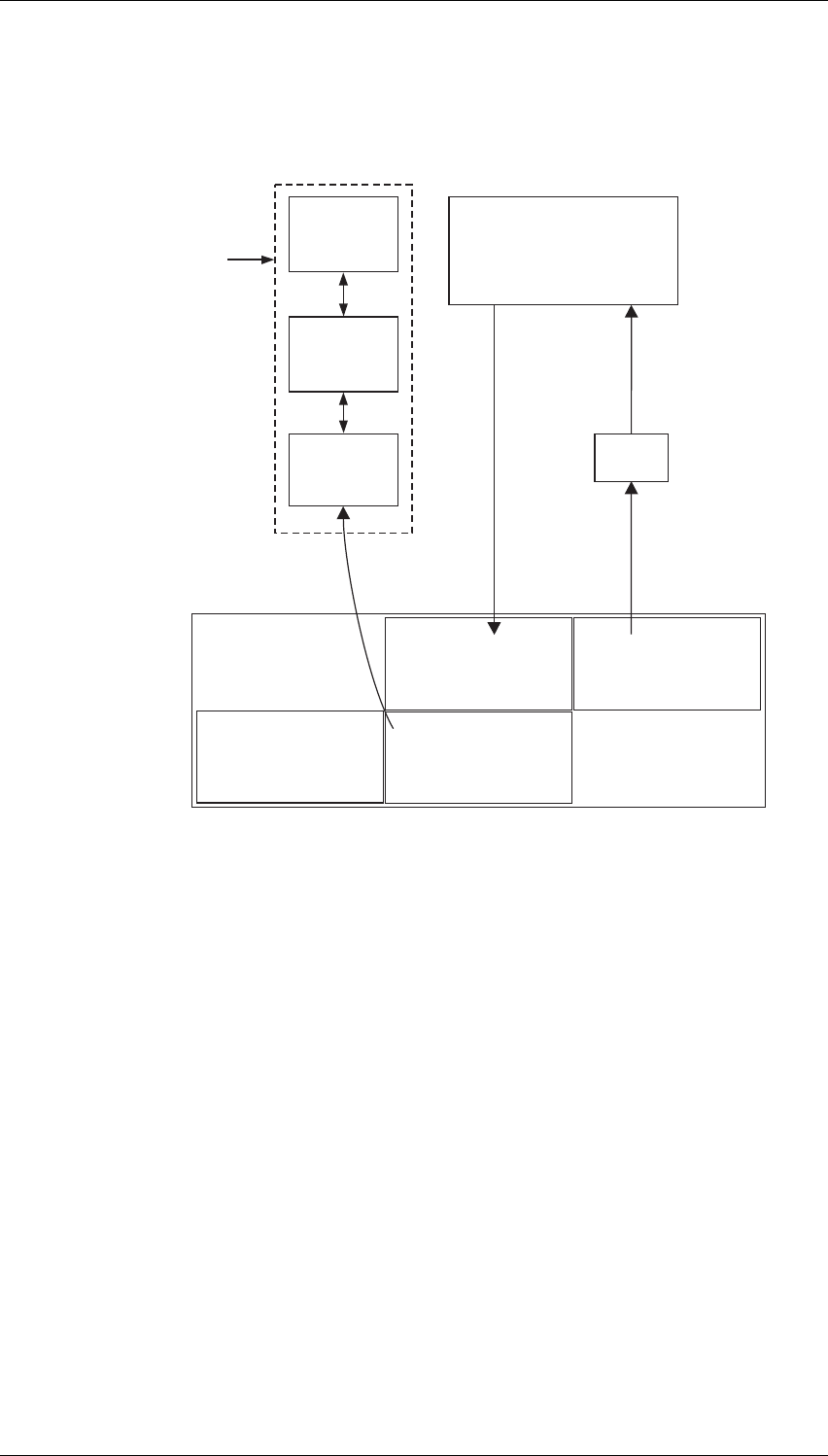
D3.8 Installation and Configuration M8SL2-00-002-812
© Copyright Tait Electronics Limited August 2004. All rights reserved.
3.2.1 Equipment Setup for Level Configuration.
Configuring the T803 Line levels (using PGM800Win or Test Mode) and radio receiver
or transmitter levels requires the sub-rack and test equipment to be set up as shown
below.
Figure 3.3 Rack and test equipment setup
Remove any coaxial relay or duplexer in the T800 modules’ RF path and connect them
directly to an RF Test Set. Ensure that transmitter or PA RF output is sufficiently attenu-
ated to prevent damage to the test set.
Run up the receiver and transmitter as instructed in Part B and C of this manual.
3.2.2 Use of Test Microphone
The T803 test microphone is used to communicate both on air to radios and down the
line to dispatch consoles. It plugs into the RJ11 connector on the front panel which dou-
bles as a programming port. It is electrically connected in parallel with the receiver
(microphone with receiver audio and PTT button with receiver mute).
Most dispatch consoles are equipped with an intercom facility whereby speech can be
sent to line without a keytone. This enables the dispatcher to talk to service personnel at
the repeater site using the T803’s built in speaker without broadcasting speech to air.
The service personnel can talk back to the dispatcher using the T803 test microphone
(the PTT must be pressed to gate microphone speech).
T803
T856
RX
T854
TX
T800-23
PSU
TB8SL2
Line
matching
Line Loss
(simulated
or actual)
Audio meter
or
Remote
Controller
RF TEST SET
Output Input
Attn
This test equipment is
required for the Test Mode
method. It is optional for
the PGM800Win method.

M8SL2-00-002-812 Installation and Configuration D3.9
© Copyright Tait Electronics Limited August 2004. All rights reserved.
Note: If the T803 is in repeater mode, PTT on the test microphone will key-on the
transmitter and thus broadcast test speech to air.
3.2.3 Test Modes
The T803 has three test modes to assist with setting levels:
•Test Tone Mode
•Line-In Level Configuration Mode
•Line-Out Level Configuration Mode1
To enter the test modes, press the Monitor and Mode Toggle buttons on the front panel
simultaneously for three seconds. The alarm LEDs will start flashing colours and travel-
ling up and down the display to indicate Test Tone Mode. The T803 will key-on the
transmitter and encode a 1kHz test tone to the transmitter for one minute. The test tone
can also be heard on the T803 speaker.
While still in Test Tone Mode, simultaneously pressing the Monitor and Mode Toggle
buttons briefly will change the mode to Line-In Level Configuration Mode. All the
LEDs will be on — either entirely red or entirely green.
•Green = Keytone present. T803 will key-on the transmitter.
•Red = No keytone present
While still in Line-In Level Configuration Mode, simultaneously pressing the Monitor
and Mode Toggle buttons again will change the mode to Line-Out Configuration
Mode1. To indicate this, all the LEDs will be orange.
Note: After entering each mode, a one to two second pause is required before
attempting the simultaneous press to enter the next mode (or to exit).
While in Line-In or Line-Out Configuration Mode, the Monitor and Mode Toggle but-
tons operate as ‘gain’ adjust buttons. A short press on the Monitor button will increase
the Line-In/Line-Out gain and toggle the top alarm LED on or off, indicating a level
increase. The LED will no longer toggle (it will stay on) when the top of the range has
been reached. Conversely the Mode Toggle button will decrease the gain and toggle the
bottom alarm LED. Again, the LED stays on when the bottom of the range has been
reached. In both of these modes Line-In audio can be heard on the monitor speaker.
To exit Line-Out Configuration Mode, briefly press both buttons again. Alternatively,
the unit will automatically return to normal operation mode after one minute. (This
occurs in all three test modes).
Note: These levels are always preserved on exit. Take care not to change them
unintentionally during simultaneous button press.
1. Line-Out Configuration Mode is only available in T803 firmware version 2.07 or later.
For firmware versions prior to 2.07, a simultaneous button press while in Line-In Con-
figuration Mode will exit Test Mode .

D3.10 Installation and Configuration M8SL2-00-002-812
© Copyright Tait Electronics Limited August 2004. All rights reserved.
Figure 3.4 Cycle of switching between the modes
3.2.4 Level Configuration
Before proceeding with any level configuration the transmitter and receiver must be
run-up and configured for the application. Also, ensure that the equipment has been set
up correctly as indicated in Section 3.2.1. It is important that the T800 Transmitter out-
put is connected to the Test Set (through an attenuator as required) because it will often
be keyed during these level setting procedures.
The following levels need to be set:
•Tx Audio – Audio level from T803 to transmitter (balanced)
•Line-In level
•Rx Audio – Audio level from receiver to T803 (unbalanced)
•Line-Out level
The only consideration of order is that the Tx Audio level needs to be configured before
the Line-In level can be done.
Normal
Operating
Mode
Time out (1 min)
Monitor & Mode pressed
or time out (1 min)
Monitor & Mode pressed simultaneously
Monitor = Monitor On/Off
Mode = Base Station/Repeater
Monitor = Monitor On/Off
Mode = Base station/Repeater
Monitor & Mode
held (3 sec)
Test Tone
(Flashing LED’s)
Line-In Level Configuration
(Green LED = Keytone,
Red LED = No keytone)
Monitor = Increase level
Mode = Decrease level
Line-Out Level Configuration
(LED = Orange)
Monitor = Increase level
Mode = Decrease level
Time out (1 min)
Monitor & Mode pressed simultaneously (v2.07+)

M8SL2-00-002-812 Installation and Configuration D3.11
© Copyright Tait Electronics Limited August 2004. All rights reserved.
3.2.4.1 Tx Audio – Audio Level from T803 to Transmitter
The level of audio received from the T803 is adjusted at the input of the transmitter.
1. Set the T803 into Test Tone Mode (See Section 3.2.3)
2. Adjust the Line Sensitivity Control on the front panel of the transmitter to give a
reading on the RF Test Set of 60% full system deviation (compensate for any
CTCSS tone deviation).
3.2.4.2 Line-In Level
The Line-In level can be set up in two ways:
•On the T803 in Level Configuration Mode
•Using PGM800Win programming software.
Using Level Configuration Mode:
Note: The Tx audio level must be set up before starting this procedure (Section
3.2.4.1).
1. Set the T803 into Line-In Level Configuration Mode (See Section 3.2.3).
2. Connect a dispatch console to the far end of the line, or simulate the console and
line loss using an audio generator.
3. Press the PTT on the dispatch console. This will send a keytone to the T803.
Ensure the console also sends a test tone at speech level to line (this tone is
required for this method of configuring the Line-In level).
4. The alarm LEDs on the front panel of the T803 should change to green (indicating
that a keytone has been detected) for as long as the PTT is pressed.
5. Adjust the Line-In level by pressing the Monitor button (increases the level) or the
Mode Toggle button (decreases the level) until the transmitter deviation reading,
monitored on the RF Test Set, indicates 60% full system deviation (compensate for
any CTCSS tone deviation).
6. Press the PTT on the dispatch console again, but this time use speech instead of
the test tone. Ensure the LEDs on the T803 remain constant on green during
speech transmission. If not see Section 3.3.1 (point 7) on how to troubleshoot for
Talkoff.
Narrow Band Wide Band
Channel Spacing 12.5kHz 25kHz
Maximum deviation (specifications) 2.5kHz 5kHz
60% of maximum deviation 1.5kHz 3.0kHz

D3.12 Installation and Configuration M8SL2-00-002-812
© Copyright Tait Electronics Limited August 2004. All rights reserved.
Note: The monitor speaker is forced on in this mode so that the test-microphone
may be used as an intercom to communicate to the dispatcher room (See
Section 3.2.2).
Using PGM800 software:
1. Determine the output level of the console. This may be a preset or default value
specified in the console’s manual or a value programmed by the operator.
2. Determine the actual line-loss between the console and the T803.
3. Calculate T803 Line-In Level as follows:
T803 Line-In Level = console output level (dBm) – Line-loss (dB)
4. Program the T803 with the calculated level.
Example case:
Console output level =–13dBm
Measured Line loss = 6.5dBm
T803 Line-In level =–13 – 6.5 = –19.5dBm
3.2.4.3 Rx Audio – Audio Level from Receiver to T803
The Rx Audio level is adjusted using either the Line Level control on the front of the
receiver or the RV2 potentiometer on the backplane, depending on the configuration of
the link LN8 on the backplane.
The recommended (and default) configuration of LN8 is with pins 2–3 and 4–5
linked. With this configuration the balanced audio from the receiver (Rx-Line-1 and Rx-
Line-4 ) is changed to unbalanced audio for the T803 (this means the Rx Line output can
no longer be used as direct balanced audio to the transmitter). The level to the T803 is
adjusted using the Line Level control on the front of the receiver. The advantage of
using this path is that it allows CTCSS filtering to be applied (using the receiver’s inter-
nal CTCSS filter. See Section 3.5 in Part B).
Alternatively if CTCSS is not used, the receiver unbalanced audio output (Rx-Audio-1)
can be used to provide audio to the T803 by linking pins 1–2 on LN8. In this case the
level to the T803 is adjusted using the RV2 potentiometer on the backplane. This audio
path is not suitable for CTCSS systems because complete CTCSS filtering cannot be
applied. The only filtering directly available is the optional receiver de-emphasis filter-
ing. See Section 3.5 in Part B. The T803 does however apply a 160Hz to 3kHz high pass
filter resulting in an overall audio response for this path very similar to the default high
pass filtered receiver balanced Line output. See the table below.

M8SL2-00-002-812 Installation and Configuration D3.13
© Copyright Tait Electronics Limited August 2004. All rights reserved.
The table above shows that configuring LN8 with links 2–3 and 4–5 could be used for
systems with or without CTCSS. Configuring LN8 with link 1–2 in normally only used
with systems without CTCSS on the Rx audio.
Procedure
Before commencing this procedure set up the receiver audio processing, such as de-
emphasis and CTCSS filtering, as required for the application. See Section 3.5 in Part B.
This is important for the T803 Telecom line compliance. See the Caution below.
CAUTION: The Rx audio level must not exceed 230mVrms at 60% full system devia-
tion. This will ensure that the actual T803 Line-Out level corresponds
to the programmed value and thus ensures levels do not exceed the
power level requirements of the Telecommunications line.
There are three possible ways to monitor the Rx Audio level during adjustment:
•Direct measurement of receiver audio on the backplane
•Indirectly, using transmitter deviation
•Indirectly, using the T803 Line-Out level
Direct measurement of receiver audio on the backplane:
1. Use the RF Test Set to generate an on-channel signal to un-mute the receiver.
2. Modulate the RF carrier with a 1020Hz tone1 at 60% full system deviation, adding
CTCSS tone for a CTCSS system (ensure that CTCSS filtering is applied in the
receiver as required for the application. See Section 3.5 in Part B).
3. Monitor the audio level from the receiver on the X800-56-PCB3 backplane at pin2
of LN8, with the links (jumpers) in place as directed in Section 3.1.1. Use a high
impedance meter such as an oscilloscope for the measurement.
Receiver/T803
system
Backplane
links (LN8)
Adjustment of Rx
Audio to T803 Audio Frequency Response
With CTCSS on
Rx audio
Link pins 2–3
and pins 4–5
Line Level control on the
front of the Receiver
Receiver internal CTCSS filter should
be included in the path (see Section
3.5 in Part B)
400Hz to 3kHz
No CTCSS on Rx
audio
Link pins 2–3
and pins 4–5
Line Level control on the
front of the receiver
Receiver internal CTCSS filter not in
path but high pass filter in path (Rx
default setup)
220Hz to 3kHz
No CTCSS on Rx
audio
Link pins 1–2 RV2 on the backplane T803 high pass filter only
160Hz to 3kHz
1. A 1020Hz tone is used (rather than 1kHz) because some Test Sets can produce unstable
deviation readings

D3.14 Installation and Configuration M8SL2-00-002-812
© Copyright Tait Electronics Limited August 2004. All rights reserved.
4. For LN8 with pins 2–3 and 4–5 linked, adjust the line level control on the front of
the receiver for an audio level of 230mVrms.
For LN8 with pins 1–2 linked, adjust RV2 on the backplane for an audio level of
230mVrms.
Using transmitter deviation:
This method is not suitable for simplex configured repeaters.
1. Use the RF Test Set to generate an on-channel signal to un-mute the receiver.
2. Modulate the RF carrier with a 1020Hz tone1 at 60% full system deviation, adding
CTCSS tone for a CTCSS system (ensure that CTCSS filtering is applied in the
receiver as required for the actual working system. See Section 3.5 in Part B).
3. Put the T803 unit into Talk Through Mode (also known as Repeater Mode) using
the Mode Toggle button1. The Mode LED should be red, constant or flashing, and
the transmitter should be keyed on.
4. For LN8 with pins 2–3 and 4–5 linked, adjust the Line Level control on the front
of the receiver to produce 60% full system deviation at the transmitter RF output
as measured on the test set.
5. For LN8 with pins 1–2 linked, adjust RV2 on the backplane to produce 60% full
system deviation at the transmitter RF output as measured on the test set.
Note: De-Emphasis should be off on the test set receiver.
Using the T803 Line-Out level:
1. Use the RF test set to generate an on-channel signal to un-mute the receiver.
2. Modulate the RF carrier with a 1020Hz tone2 at 60% full system deviation, adding
CTCSS tone for a CTCSS system (ensure that CTCSS filtering is applied in the
receiver as required for the actual working system. See Section 3.5 in Part B).
3. Put the T803 into Base Station Mode using the Mode Toggle button1. The Mode
LED should be green (constant or flashing).
4. For LN8 with pins 2–3 and 4–5 linked, monitor the T803 Line-Out level (600Ω bal-
anced audio) and by adjusting the Line Level control on the front of the receiver,
set this level to equal the programmed ‘Line-Out Level’ as set in PGM800Win.
For LN8 with pins 1–2 linked, monitor the T803 Line-Out level (600Ω balanced
audio) and by adjusting RV2 on the backplane, set this level to equal the pro-
grammed ‘Line-Out Level’ as set in PGM800Win.
1. The Mode Toggle button may be disabled from PGM800Win
2. A 1020Hz tone is used (rather than 1kHz) because some Test Sets can produce unstable
deviation readings

M8SL2-00-002-812 Installation and Configuration D3.15
© Copyright Tait Electronics Limited August 2004. All rights reserved.
3.2.4.4 Line-Out Level
The Line-Out Level can be set up in two ways:
•On the T803 in Level Configuration Mode
•Using PGM800Win programming software (version 4.02 or later).
Using Level Configuration Mode (T803 firmware version 2.07 or later):
1. Set the T803 into Line-Out Level Configuration Mode (See Section 3.2.3).
2. Use the RF Test Set to generate an on-channel signal to un-mute the receiver.
3. Modulate the RF carrier with a 1020Hz tone at 60% full system deviation, adding
CTCSS tone if necessary (ensure that CTCSS tone is removed from the receiver
audio output by selecting the correct links inside the receiver).
4. Monitor the T803 Line-Out level and adjust by pressing the Monitor button
(increases the level) or the Mode Toggle button (decreases the level) until the level
is acceptable at the dispatch console.
Note: The monitor speaker is forced on in this mode so the test-microphone may
be used as an intercom to communicate to the dispatcher room (See Section
3.2.2).
Using PGM800Win software:
1. Determine the input level required at the dispatch console. This may be a preset or
default value specified in the console’s manual or a value programmed by the
operator.
2. Determine the actual line-loss between the console and the T803.
3. Calculate T803 Line-Out Level as follows:
T803 Line-Out Level = console input level (dBm) + Line-loss (dB)
4. Program the T803 with the calculated level.
Example case:
Console input level = –13dBm
Measured Line loss = 6.5dBm
T803 Line-Out level = –13 + 6.5 = –6.5dBm
3.3 Fault Finding
1. Connect the T803 to its companion dispatch console via the leased line. Check that
speech sent from the console can be heard on the T803 speaker (un-mute speaker
if required).

D3.16 Installation and Configuration M8SL2-00-002-812
© Copyright Tait Electronics Limited August 2004. All rights reserved.
One possible cause of incorrect operation is that the line connections have become
transposed in the wiring network or that the dispatch terminal uses different
Send/Receive pairs.
2. Use the dispatch console to key-on the transmitter. If the transmitter does not key-
on, check that the console and T803 have been compatibly programmed.
•check 2-wire or 4-wire
•check the keytone frequency
•check if function tones are used
•check high level guard tone and function tone periods (if used) are the same
Finally check that the console is sending appropriate signal levels and that tone
durations are correct (which are often variable), and that the line is not causing
unacceptable attenuation or distortion.
3. If the console can key the transmitter but not change Repeater/Basestation Mode,
auxiliary outputs, receiver defeat or cancel alarms, carry out the checks in Step 2
above, but pay particular attention to the function tone programming.
If changing channels is a problem check that the appropriate channel selection
DIP switches (SW1) on the rack backplane are off.
3.3.1 Troubleshooting
1. Sometimes misses function tone command
Set up the Line-In level so that the function tones are about 2Vpp at TP204.
2. Misses function tone sequence on very fast key repetition
A minimum of 200ms pause is required between pressing buttons on the console. Some
consoles do not limit the maximum keying rate.
3. PGM800Win: “Warning: the Firmware version is not compatible. Data read
maybe incorrect”
This warning occurs when reading the T803 with an old version of PGM800Win.
This can be ignored as the T803 unit is backwards compatible. However, it is recom-
mended to use the latest PGM800Win with full T803 support.
4. Loop-Line functionality (also known as Loopback)
Loopback can be enabled in PGM800Win. It is then activated by sending the T803 the
programmed function tones.

M8SL2-00-002-812 Installation and Configuration D3.17
© Copyright Tait Electronics Limited August 2004. All rights reserved.
5. While in Line-In Level Configuration Mode, the LEDs flash green only briefly
when the dispatch console PTT is pressed
The Line-In level is too low. The T803 is only detecting the high-level guard tone
(HLGT).
While still in Line-In Level Configuration Mode, activate the console PTT and adjust the
Line-In level by pressing the Monitor button (increases the Line-In level) until the LEDs
remain constant green. The top alarm LED will toggle on and off, indicating a level
increase until the top of the range is reached (may be as many as 65 presses). If this still
fails, open up the unit and add JP200, and try again.
6. When the PTT is pressed, a pulsing sound can be heard from the speaker
The Line-In level is too high. The function tones can not be decoded properly hence it
keys off.
While still in Line-In Level Configuration Mode, activate the console PTT and adjust the
Line-In level by pressing the Mode button. The bottom alarm LED will toggle on and
off, indicating a level decrease until the bottom of the range is reached. Using an oscillo-
scope measure the signal on TP204 – the function tone level should be about half the
level of the high level guard tone.
7. The console keys the transmitter correctly except when speech is present
This is known as ‘Talkoff ’ and occurs when the difference between the keytone level
and speech peak level exceeds specification (32dB in 2-wire mode and 35dB in 4-wire
mode), causing the keytone detection to fail.
For reliable operation, the keytone level should be no more than 35dB lower than peak
speech level.
If it is not possible to adjust the levels at the console, decrease the programmed Line-In
level of the T803 until talkoff is eliminated. This requires that the audio level from T803
to transmitter will also need to be re-adjusted (using the transmitter’s Line Sensitivity
control) to maintain 60% full system deviation for the test tone sent from the console.
Adjust the relative audio levels (keytone and speech) sent from the dispatch console.
8. Keytone Falsing in 2-wire mode
When operating in 2-wire mode with lossy lines (i.e. significant separation required
between T803 Line-In and Line-Out levels) the keytone detector can become de-sensi-
tised by noise.
•Check to ensure that the input level from the receiver is correctly set up at
230mVrms (See Section 3.2.4.3).
•Check the receiver mute open level (squelch). If necessary adjust the receiver Gat-
ing Sensitivity control on the front panel of the receiver, so that the receiver mute
opens at a higher SINAD level (12dB or preferably greater). This has the effect of
reducing the noise on the line input of the T803 in 2-wire mode.

D3.18 Installation and Configuration M8SL2-00-002-812
© Copyright Tait Electronics Limited August 2004. All rights reserved.
•If there is still a problem after the squelch gating level has been adjusted as much
as practicable, it becomes necessary to reduce the separation between the T803
Line-In and Line-Out levels. This separation may need to be reduced to less than
8dB for 12dB receiver audio SINAD (or less then 12dB for 14dB receiver audio
SINAD). To achieve this, adjust the relative input and output levels of the dispatch
console. Again, this has the effect of reducing the noise on the line input of the
T803.
If the above solutions do not help resolve the problem, the 2-wire line loss may be too
severe and unacceptable for normal 2-wire T803 operation. In this case an external hard-
ware solution involving a notch filter fitted to the receiver audio path (TA1086-01) and a
2-wire/4-wire hybrid fitted across the line may be required. This solution has been veri-
fied and documentation is available detailing how to install the TA1086-01. Contact
your your nearest Tait Dealer or Customer Service Organisation for more information.
M8SL2-00-002-812 T803 PCB Information D4.1.1
© Copyright Tait Electronics Limited August 2004. All rights reserved.
4 T803 PCB Information
Caution: This equipment contains CMOS devices which are susceptible to damage from
static charges. Refer to Section 3.1 for more information on anti-static procedures
when handling these devices.
This section provides the following information on the T803.
•parts list
•grid reference index
•PCB layouts
•circuit diagrams.
Section Title IPN Page
4.1 Introduction 4.1.3
4.2 T803 Main and Front Panel PCBs 220-01581-01 4.2.1

D4.1.2 T803 PCB Information M8SL2-00-002-812
© Copyright Tait Electronics Limited August 2004. All rights reserved.

M8SL2-00-002-812 T803 PCB Information D4.1.3
© Copyright Tait Electronics Limited August 2004. All rights reserved.
4.1 Introduction
PCB Identification
All PCBs are identified by a unique 10 digit “internal part number” (IPN), e.g. 220-12345-00, which
is screen printed onto the PCB (usually on the top side), as shown in the example below:
The last 2 digits of this number define the issue status, which starts at 00 and increments through 01,
02, 03, etc. as the PCB is updated. Some issue PCBs never reach full production status and are there-
fore not included in this manual. A letter following the 10 digit IPN has no relevance in identifying
the PCB for service purposes.
Note: It is important that you identify which issue PCB you are working on so that you can
refer to the appropriate set of PCB information.
Parts Lists
The 10 digit numbers (000-00000-00) in this Parts List are “internal part numbers” (IPNs). We can
process your spare parts orders more efficiently and accurately if you quote the IPN and provide a
brief description of the part.
The components listed in this parts list are divided into two main types: those with a circuit refer-
ence (e.g. C2, D1, R121, etc.) and those without (miscellaneous and mechanical).
Those with a circuit reference are grouped in alphabetical order and then in numerical order within
each group. Each component entry comprises three or four columns, as shown below:
The mechanical and miscellaneous section lists the variant and common parts in IPN order.
circuit reference -
lists components
in alphanumeric
order
variant column -
indicates that this is
a variant component
which is fitted only to
the product type listed
Internal Part Number -
order the component
b
y
this number
description -
gives a brief description
of the component

D4.1.4 T803 PCB Information M8SL2-00-002-812
© Copyright Tait Electronics Limited August 2004. All rights reserved.
Grid Reference Index
This section contains a component grid reference index to help you find components and labelled
pads on the PCB layouts and circuit diagrams. This index lists the components and pads in alpha-
numeric order, along with the appropriate alphanumeric grid references, as shown below:
Using CAD Circuit Diagrams
Reading a CAD circuit diagram is similar to reading a road map, in that both have an alphanumeric
border. The circuit diagrams in this manual use letters to represent the horizontal axis, and numbers
for the vertical axis. These circuit diagram “grid references” are useful in following a circuit that is
spread over two or more sheets.
When a line representing part of the circuitry is discontinued, a reference will be given at the end of
the line to indicate where the rest of the circuitry is located, as shown below. The first digit refers to
the sheet number and the last two characters refer to the location on that sheet of the continuation of
the circuit (e.g. 1R3).
circuit diagram
reference
P
C
B layout
reference
components listed
in alphanumeric order
layer number -
1 = top side layer
2 = bottom side layer
component location
on the layer
sheet number
component location
on the sheet
C301
4N7
R303
12
D
S
G
L310
33U
IF-SIG
4R4
C369
100P
C371
10U
R339
100K
%R338
100
DISCRIMINATOR
1R3
2R9
2R9
8A2
t
hese grid references
s
how where the circuit
is continued

M8SL2-00-002-812 T803 PCB Information D4.2.1
© Copyright Tait Electronics Limited August 2004. All rights reserved.
4.2 T803 Main and Front Panel PCBs
This section contains the following information.
IPN Section Page
220-01581-04 Parts List
Mechanical and Miscellaneous Parts
Grid Reference Index
PCB Layout – Top Side
PCB Layout – Bottom Side
Overview and Front Panel Circuit Diagram
Interface Circuit Diagram
Control and Processing Circuit Diagram
P100 PI Filters Circuit Diagram
SK100 PI Filters Circuit Diagram
SK102 PI Filters Circuit Diagram
4.2.3
4.2.6
4.2.7
4.2.9
4.2.10
4.2.11
4.2.12
4.2.13
4.2.14
4.2.15
4.2.16

D4.2.2 T803 PCB Information M8SL2-00-002-812
© Copyright Tait Electronics Limited August 2004. All rights reserved.

IPN 220-01581-04
M8SL2-00-002-812 T803 PCB Information D4.2.3
© Copyright Tait Electronics Limited August 2004. All rights reserved.
Ref Var IPN Description Ref Var IPN Description
T803 Parts List (IPN 220-01581-04)
How To Use This Parts List
The components listed in this parts list are grouped in alphabetical order and then in numerical order within each group. Each compo-
nent entry comprises three or four columns: the circuit reference, variant (if applicable), IPN and description. A number in the variant
column indicates that this is a variant component which is fitted only to the product type listed.
This parts list is correct at the time of publishing, but is subject to change without notification. An up to date parts list can be obtained
from your local Customer Service Organisation
C1 015-24100-08 CAP CER 0805 1N 10% X7R 50V
C128 015-24100-08 CAP CER 0805 1N 10% X7R 50V
C145 015-24100-08 CAP CER 0805 1N 10% X7R 50V
C162 016-08470-01 CAP ELEC SMD 47UF 6*4 16V
C163 016-08100-01 CAP ELEC SMD 10M 4*5.2 16V 20%
C164 015-24100-08 CAP CER 0805 1N 10% X7R 50V
C165 015-24100-08 CAP CER 0805 1N 10% X7R 50V
C166 015-24100-08 CAP CER 0805 1N 10% X7R 50V
C167 016-08470-01 CAP ELEC SMD 47UF 6*4 16V
C168 016-08100-01 CAP ELEC SMD 10M 4*5.2 16V 20%
C170 015-24100-08 CAP CER 0805 1N 10% X7R 50V
C172 015-25100-08 CAP CER 0805 10N 10% X7R 50V
C173 015-25100-08 CAP CER 0805 10N 10% X7R 50V
C174 015-25100-08 CAP CER 0805 10N 10% X7R 50V
C2 016-08100-01 CAP ELEC SMD 10M 4*5.2 16V 20%
C202 015-25100-08 CAP CER 0805 10N 10% X7R 50V
C203 016-07470-06 CAP ELEC SMD BI-P 4U7 50V 20%
C204 016-07470-06 CAP ELEC SMD BI-P 4U7 50V 20%
C205 015-25220-08 CAP CER 0805 22N 10% X7R 50V
C206 015-25220-08 CAP CER 0805 22N 10% X7R 50V
C207 015-24470-08 CAP CER 0805 4N7 10% X7R 50V
C208 015-24470-08 CAP CER 0805 4N7 10% X7R 50V
C210 015-25100-08 CAP CER 0805 10N 10% X7R 50V
C211 015-23470-08 CAP CER 0805 470P 10% X7R 50V
C212 015-05330-08 CAP CER 1206 33N 10% X7R 50V
C213 015-05330-08 CAP CER 1206 33N 10% X7R 50V
C214 015-23470-08 CAP CER 0805 470P 10% X7R 50V
C215 015-23470-08 CAP CER 0805 470P 10% X7R 50V
C216 015-23470-08 CAP CER 0805 470P 10% X7R 50V
C217 015-25100-08 CAP CER 0805 10N 10% X7R 50V
C218 015-27100-10 CAP CER 0805 1M+80-20% Y5V 16V
C219 015-25100-08 CAP CER 0805 10N 10% X7R 50V
C220 015-27100-10 CAP CER 0805 1M+80-20% Y5V 16V
C222 015-24100-08 CAP CER 0805 1N 10% X7R 50V
C224 015-27100-10 CAP CER 0805 1M+80-20% Y5V 16V
C225 015-26100-08 CAP CER 0805 100N 10% X7R 50V
C226 015-24470-08 CAP CER 0805 4N7 10% X7R 50V
C227 015-26100-08 CAP CER 0805 100N 10% X7R 50V
C232 015-26100-08 CAP CER 0805 100N 10% X7R 50V
C233 015-24100-08 CAP CER 0805 1N 10% X7R 50V
C235 015-26100-08 CAP CER 0805 100N 10% X7R 50V
C236 015-26100-08 CAP CER 0805 100N 10% X7R 50V
C238 015-26100-08 CAP CER 0805 100N 10% X7R 50V
C239 015-25100-08 CAP CER 0805 10N 10% X7R 50V
C240 015-25100-08 CAP CER 0805 10N 10% X7R 50V
C242 015-26100-08 CAP CER 0805 100N 10% X7R 50V
C3 015-24100-08 CAP CER 0805 1N 10% X7R 50V
C300 015-25100-08 CAP CER 0805 10N 10% X7R 50V
C301 015-25100-08 CAP CER 0805 10N 10% X7R 50V
C302 015-25100-08 CAP CER 0805 10N 10% X7R 50V
C303 015-25100-08 CAP CER 0805 10N 10% X7R 50V
C304 015-25100-08 CAP CER 0805 10N 10% X7R 50V
C305 015-22270-01 CAP CER 0805 27P 5% NPO 50V
C306 015-22270-01 CAP CER 0805 27P 5% NPO 50V
C307 015-25100-08 CAP CER 0805 10N 10% X7R 50V
C308 015-25100-08 CAP CER 0805 10N 10% X7R 50V
C310 015-25100-08 CAP CER 0805 10N 10% X7R 50V
C311 015-25100-08 CAP CER 0805 10N 10% X7R 50V
C312 015-24100-08 CAP CER 0805 1N 10% X7R 50V
C313 015-25100-08 CAP CER 0805 10N 10% X7R 50V
C314 015-22270-01 CAP CER 0805 27P 5% NPO 50V
C315 015-25100-08 CAP CER 0805 10N 10% X7R 50V
C316 015-25100-08 CAP CER 0805 10N 10% X7R 50V
C317 015-25100-08 CAP CER 0805 10N 10% X7R 50V
C318 015-25100-08 CAP CER 0805 10N 10% X7R 50V
C319 015-25100-08 CAP CER 0805 10N 10% X7R 50V
C320 015-25100-08 CAP CER 0805 10N 10% X7R 50V
C4 015-26100-08 CAP CER 0805 100N 10% X7R 50V
C400 015-24100-08 CAP CER 0805 1N 10% X7R 50V
C401 015-24100-08 CAP CER 0805 1N 10% X7R 50V
C402 015-24100-08 CAP CER 0805 1N 10% X7R 50V
C403 015-24100-08 CAP CER 0805 1N 10% X7R 50V
C404 015-24100-08 CAP CER 0805 1N 10% X7R 50V
C405 015-24100-08 CAP CER 0805 1N 10% X7R 50V
C406 015-24100-08 CAP CER 0805 1N 10% X7R 50V
C407 015-24100-08 CAP CER 0805 1N 10% X7R 50V
C408 015-24100-08 CAP CER 0805 1N 10% X7R 50V
C409 015-24100-08 CAP CER 0805 1N 10% X7R 50V
C410 015-24100-08 CAP CER 0805 1N 10% X7R 50V
C411 015-24100-08 CAP CER 0805 1N 10% X7R 50V
C412 015-24100-08 CAP CER 0805 1N 10% X7R 50V
C413 015-24100-08 CAP CER 0805 1N 10% X7R 50V
C414 015-24100-08 CAP CER 0805 1N 10% X7R 50V
C415 015-24100-08 CAP CER 0805 1N 10% X7R 50V
C416 015-24100-08 CAP CER 0805 1N 10% X7R 50V
C417 015-24100-08 CAP CER 0805 1N 10% X7R 50V
C418 015-24100-08 CAP CER 0805 1N 10% X7R 50V
C419 015-24100-08 CAP CER 0805 1N 10% X7R 50V
C420 015-24100-08 CAP CER 0805 1N 10% X7R 50V
C421 015-24100-08 CAP CER 0805 1N 10% X7R 50V
C422 015-24100-08 CAP CER 0805 1N 10% X7R 50V
C423 015-24100-08 CAP CER 0805 1N 10% X7R 50V
C424 015-24100-08 CAP CER 0805 1N 10% X7R 50V
C425 015-24100-08 CAP CER 0805 1N 10% X7R 50V
C426 015-24100-08 CAP CER 0805 1N 10% X7R 50V
C427 015-24100-08 CAP CER 0805 1N 10% X7R 50V
C428 015-24100-08 CAP CER 0805 1N 10% X7R 50V
C429 015-24100-08 CAP CER 0805 1N 10% X7R 50V
C430 015-24100-08 CAP CER 0805 1N 10% X7R 50V
C431 015-24100-08 CAP CER 0805 1N 10% X7R 50V
C432 015-24100-08 CAP CER 0805 1N 10% X7R 50V
C433 015-24100-08 CAP CER 0805 1N 10% X7R 50V
C434 015-24100-08 CAP CER 0805 1N 10% X7R 50V
C435 015-24100-08 CAP CER 0805 1N 10% X7R 50V
C436 015-24100-08 CAP CER 0805 1N 10% X7R 50V
C437 015-24100-08 CAP CER 0805 1N 10% X7R 50V
C438 015-24100-08 CAP CER 0805 1N 10% X7R 50V
C439 015-24100-08 CAP CER 0805 1N 10% X7R 50V
C440 015-24100-08 CAP CER 0805 1N 10% X7R 50V
C441 015-24100-08 CAP CER 0805 1N 10% X7R 50V
C442 015-24100-08 CAP CER 0805 1N 10% X7R 50V
C443 015-24100-08 CAP CER 0805 1N 10% X7R 50V
C444 015-24100-08 CAP CER 0805 1N 10% X7R 50V
C445 015-24100-08 CAP CER 0805 1N 10% X7R 50V
C446 015-24100-08 CAP CER 0805 1N 10% X7R 50V
C447 015-24100-08 CAP CER 0805 1N 10% X7R 50V
C448 015-24100-08 CAP CER 0805 1N 10% X7R 50V
C449 015-24100-08 CAP CER 0805 1N 10% X7R 50V
C450 015-24100-08 CAP CER 0805 1N 10% X7R 50V
C451 015-24100-08 CAP CER 0805 1N 10% X7R 50V
C452 015-24100-08 CAP CER 0805 1N 10% X7R 50V
C453 015-24100-08 CAP CER 0805 1N 10% X7R 50V
C454 015-24100-08 CAP CER 0805 1N 10% X7R 50V
C455 015-24100-08 CAP CER 0805 1N 10% X7R 50V
C5 016-08470-01 CAP ELEC SMD 47UF 6*4 16V
C500 015-22270-01 CAP CER 0805 27P 5% NPO 50V
C501 015-22270-01 CAP CER 0805 27P 5% NPO 50V
C502 015-22270-01 CAP CER 0805 27P 5% NPO 50V
C503 015-24100-08 CAP CER 0805 1N 10% X7R 50V
C504 015-24100-08 CAP CER 0805 1N 10% X7R 50V
C505 015-24100-08 CAP CER 0805 1N 10% X7R 50V
C506 015-24100-08 CAP CER 0805 1N 10% X7R 50V
C507 015-22270-01 CAP CER 0805 27P 5% NPO 50V
C508 015-22270-01 CAP CER 0805 27P 5% NPO 50V
C509 015-22270-01 CAP CER 0805 27P 5% NPO 50V
C510 015-24100-08 CAP CER 0805 1N 10% X7R 50V
C511 015-24100-08 CAP CER 0805 1N 10% X7R 50V
C512 015-24100-08 CAP CER 0805 1N 10% X7R 50V
C513 015-24100-08 CAP CER 0805 1N 10% X7R 50V
C514 015-22270-01 CAP CER 0805 27P 5% NPO 50V
C515 015-24100-08 CAP CER 0805 1N 10% X7R 50V
C516 015-24100-08 CAP CER 0805 1N 10% X7R 50V
C517 015-24100-08 CAP CER 0805 1N 10% X7R 50V
C518 015-24100-08 CAP CER 0805 1N 10% X7R 50V
C519 015-24100-08 CAP CER 0805 1N 10% X7R 50V
C520 015-24100-08 CAP CER 0805 1N 10% X7R 50V
C521 015-22270-01 CAP CER 0805 27P 5% NPO 50V
C522 015-24100-08 CAP CER 0805 1N 10% X7R 50V
C523 015-24100-08 CAP CER 0805 1N 10% X7R 50V
C524 015-24100-08 CAP CER 0805 1N 10% X7R 50V
C525 015-24100-08 CAP CER 0805 1N 10% X7R 50V
C526 015-24100-08 CAP CER 0805 1N 10% X7R 50V
C527 015-24100-08 CAP CER 0805 1N 10% X7R 50V
C6 016-08470-01 CAP ELEC SMD 47UF 6*4 16V
C600 015-24100-08 CAP CER 0805 1N 10% X7R 50V
C601 015-22270-01 CAP CER 0805 27P 5% NPO 50V

IPN 220-01581-04
D4.2.4 T803 PCB Information M8SL2-00-002-812
© Copyright Tait Electronics Limited August 2004. All rights reserved.
Ref Var IPN Description Ref Var IPN Description
C602 015-24100-08 CAP CER 0805 1N 10% X7R 50V
C603 015-24100-08 CAP CER 0805 1N 10% X7R 50V
C604 015-22270-01 CAP CER 0805 27P 5% NPO 50V
C605 015-24100-08 CAP CER 0805 1N 10% X7R 50V
C606 015-24100-08 CAP CER 0805 1N 10% X7R 50V
C607 015-22270-01 CAP CER 0805 27P 5% NPO 50V
C608 015-22270-01 CAP CER 0805 27P 5% NPO 50V
C609 015-24100-08 CAP CER 0805 1N 10% X7R 50V
C610 015-24100-08 CAP CER 0805 1N 10% X7R 50V
C611 015-22270-01 CAP CER 0805 27P 5% NPO 50V
C612 015-22270-01 CAP CER 0805 27P 5% NPO 50V
C613 015-24100-08 CAP CER 0805 1N 10% X7R 50V
C7 015-27100-10 CAP CER 0805 1M+80-20% Y5V 16V
D1 008-00014-81 LED 5MM RED/GRN BICOLOR
D2 008-00014-81 LED 5MM RED/GRN BICOLOR
D207 001-18410-00 DIODE SMD BZX84C10V ZEN SOT23
D3 008-00014-81 LED 5MM RED/GRN BICOLOR
D4 008-00014-81 LED 5MM RED/GRN BICOLOR
D5 008-00014-81 LED 5MM RED/GRN BICOLOR
D6 001-10084-62 DIODE SMD BZX84C6V2 ZEN SOT23
IC1 002-10078-00 IC SMD MC78M05CDT5V REG0.5A
IC100 002-10078-00 IC SMD MC78M05CDT5V REG0.5A
IC101 002-10078-00 IC SMD MC78M05CDT5V REG0.5A
IC2 002-74905-95 IC SMD 74HC595 SHIFT REG
IC200 002-74905-95 IC SMD 74HC595 SHIFT REG
IC201 002-12003-00 IC SMD ULN2003AD 7-DARL 16P S0
IC202 002-10140-21 IC MC14021BDR2 8B SREG S016
IC203 002-74905-95 IC SMD 74HC595 SHIFT REG
IC204 002-74940-53 IC SMD 74HC4053 S016
IC205 002-11454-80 IC SMD MC145480DW PCM
%IC206 002-11454-80 IC SMD MC145480DW PCM
IC208 002-10832-00 IC TLC0832 8BIT A/D 8PIN S0
IC209 002-74940-53 IC SMD 74HC4053 S016
IC210 002-10126-71 IC SMD DS1868 DGTL POT TSOP20
IC3 002-10854-10 IC TDA8541T 1W AUDIO AMP
IC300 002-10203-00 IC TMS320C203 80MHZ PQFP100
IC301 002-74940-53 IC SMD 74HC4053 S016
IC303 002-74900-00 IC SMD 74HC00 4X 2 I/P NAND
IC307 002-00090-00 IC SRAM 64KX16 15*5 44SOJ
IC310 002-74905-73 IC SMD 74HC573D 8X 3STATE
%IC311 240-04020-42 SKT 44 PIN SMD PLCC
IC312 002-12416-00 IC SMD AT24C16N-10SC EEPROM
IC313 002-10012-32 IC DS1232LPS-2 LO-P RESET&WDOG
JP302 036-10000-00 RES M/F SMD 0805 0E 0.125W
JP303 036-10000-00 RES M/F SMD 0805 0E 0.125W
JP307 036-10000-00 RES M/F SMD 0805 0E 0.125W
L1 057-10120-03 IND 0805 120E@100M .2 EMI SUPR
L114 057-10120-03 IND 0805 120E@100M .2 EMI SUPR
L131 057-10120-03 IND 0805 120E@100M .2 EMI SUPR
L132 057-10120-03 IND 0805 120E@100M .2 EMI SUPR
L200 057-10120-03 IND 0805 120E@100M .2 EMI SUPR
L201 057-10120-03 IND 0805 120E@100M .2 EMI SUPR
L202 057-10120-03 IND 0805 120E@100M .2 EMI SUPR
L203 057-10120-03 IND 0805 120E@100M .2 EMI SUPR
L400 057-10120-03 IND 0805 120E@100M .2 EMI SUPR
L401 057-10120-03 IND 0805 120E@100M .2 EMI SUPR
L402 057-10120-03 IND 0805 120E@100M .2 EMI SUPR
L403 057-10120-03 IND 0805 120E@100M .2 EMI SUPR
L404 057-10120-03 IND 0805 120E@100M .2 EMI SUPR
L405 057-10120-03 IND 0805 120E@100M .2 EMI SUPR
L406 057-10120-03 IND 0805 120E@100M .2 EMI SUPR
L407 057-10120-03 IND 0805 120E@100M .2 EMI SUPR
L408 057-10120-03 IND 0805 120E@100M .2 EMI SUPR
L409 057-10120-03 IND 0805 120E@100M .2 EMI SUPR
L410 057-10120-03 IND 0805 120E@100M .2 EMI SUPR
L411 057-10120-03 IND 0805 120E@100M .2 EMI SUPR
L412 057-10120-03 IND 0805 120E@100M .2 EMI SUPR
L413 057-10120-03 IND 0805 120E@100M .2 EMI SUPR
L414 057-10120-03 IND 0805 120E@100M .2 EMI SUPR
L415 057-10120-03 IND 0805 120E@100M .2 EMI SUPR
L416 057-10120-03 IND 0805 120E@100M .2 EMI SUPR
L417 057-10120-03 IND 0805 120E@100M .2 EMI SUPR
L418 057-10120-03 IND 0805 120E@100M .2 EMI SUPR
L419 057-10120-03 IND 0805 120E@100M .2 EMI SUPR
L420 057-10120-03 IND 0805 120E@100M .2 EMI SUPR
L421 057-10120-03 IND 0805 120E@100M .2 EMI SUPR
L422 057-10120-03 IND 0805 120E@100M .2 EMI SUPR
L423 057-10120-03 IND 0805 120E@100M .2 EMI SUPR
L424 057-10120-03 IND 0805 120E@100M .2 EMI SUPR
L425 057-10120-03 IND 0805 120E@100M .2 EMI SUPR
L426 057-10120-03 IND 0805 120E@100M .2 EMI SUPR
L427 057-10120-03 IND 0805 120E@100M .2 EMI SUPR
L500 057-10120-03 IND 0805 120E@100M .2 EMI SUPR
L501 057-10120-03 IND 0805 120E@100M .2 EMI SUPR
L502 057-10120-03 IND 0805 120E@100M .2 EMI SUPR
L503 057-10120-03 IND 0805 120E@100M .2 EMI SUPR
L504 057-10120-03 IND 0805 120E@100M .2 EMI SUPR
L505 057-10120-03 IND 0805 120E@100M .2 EMI SUPR
L506 057-10120-03 IND 0805 120E@100M .2 EMI SUPR
L507 057-10120-03 IND 0805 120E@100M .2 EMI SUPR
L508 057-10120-03 IND 0805 120E@100M .2 EMI SUPR
L509 057-10120-03 IND 0805 120E@100M .2 EMI SUPR
L510 057-10120-03 IND 0805 120E@100M .2 EMI SUPR
L511 057-10120-03 IND 0805 120E@100M .2 EMI SUPR
L512 057-10120-03 IND 0805 120E@100M .2 EMI SUPR
L513 057-10120-03 IND 0805 120E@100M .2 EMI SUPR
L600 057-10120-03 IND 0805 120E@100M .2 EMI SUPR
L601 057-10120-03 IND 0805 120E@100M .2 EMI SUPR
L602 057-10120-03 IND 0805 120E@100M .2 EMI SUPR
L603 057-10120-03 IND 0805 120E@100M .2 EMI SUPR
L604 057-10120-03 IND 0805 120E@100M .2 EMI SUPR
L605 057-10120-03 IND 0805 120E@100M .2 EMI SUPR
L606 057-10120-03 IND 0805 120E@100M .2 EMI SUPR
P1 240-04020-72 SKT HSNG 2W CORD MTG ULTREX
P100 240-00026-34 PLG 15W DRNG DUAL PORT
Q203 000-10008-47 XSTR SMD BC847B NPN SOT23
R1 036-12100-10 RES M/F SMD 0805 10E 1%
R10 036-13220-10 RES M/F SMD 0805 220E 1%
R100 036-10000-00 RES M/F SMD 0805 0E 0.125W
R12 036-13330-00 RES M/F SMD 0805 330E 5%
R13 036-13220-10 RES M/F SMD 0805 220E 1%
R14 036-13330-00 RES M/F SMD 0805 330E 5%
R15 036-13220-10 RES M/F SMD 0805 220E 1%
R2 036-14470-10 RES M/F SMD 0805 4K7 1%
R201 036-14100-10 RES M/F SMD 0805 1K 1%
R202 036-14100-10 RES M/F SMD 0805 1K 1%
R203 036-14100-10 RES M/F SMD 0805 1K 1%
R204 036-14100-10 RES M/F SMD 0805 1K 1%
R205 036-14100-10 RES M/F SMD 0805 1K 1%
R206 036-14100-10 RES M/F SMD 0805 1K 1%
R207 036-14100-10 RES M/F SMD 0805 1K 1%
R208 036-14100-10 RES M/F SMD 0805 1K 1%
R209 036-14470-10 RES M/F SMD 0805 4K7 1%
R210 036-14100-10 RES M/F SMD 0805 1K 1%
R211 036-14100-10 RES M/F SMD 0805 1K 1%
R212 036-14100-10 RES M/F SMD 0805 1K 1%
R213 036-14100-10 RES M/F SMD 0805 1K 1%
R214 036-14100-10 RES M/F SMD 0805 1K 1%
R215 036-14100-10 RES M/F SMD 0805 1K 1%
R216 036-15100-10 RES M/F SMD 0805 10K 1%
R217 036-14120-00 RES M/F SMD 0805 1K2 5%
R218 036-15100-10 RES M/F SMD 0805 10K 1%
R219 036-14560-00 RES M/F SMD 0805 5K6 5%
R220 036-15100-10 RES M/F SMD 0805 10K 1%
R221 036-15100-10 RES M/F SMD 0805 10K 1%
R223 036-15100-10 RES M/F SMD 0805 10K 1%
R224 036-15100-10 RES M/F SMD 0805 10K 1%
R225 036-15100-10 RES M/F SMD 0805 10K 1%
R226 036-15100-10 RES M/F SMD 0805 10K 1%
R227 036-14220-00 RES M/F SMD 0805 2K2 5%
R228 036-12100-10 RES M/F SMD 0805 10E 1%
R229 036-12390-00 RES M/F SMD 0805 39E 5%
R230 036-13470-00 RES M/F SMD 0805 470E 5%
R231 036-15470-10 RES M/F SMD 0805 47K 1%
R232 036-13470-00 RES M/F SMD 0805 470E 5%
R234 036-15100-10 RES M/F SMD 0805 10K 1%
R235 036-13470-00 RES M/F SMD 0805 470E 5%
R236 036-15100-10 RES M/F SMD 0805 10K 1%
R237 036-15100-10 RES M/F SMD 0805 10K 1%
R239 036-13220-10 RES M/F SMD 0805 220E 1%
R240 036-14150-10 RES M/F SMD 0805 1K5 1%
R243 036-14100-10 RES M/F SMD 0805 1K 1%
R244 036-14560-00 RES M/F SMD 0805 5K6 5%
R246 036-15100-10 RES M/F SMD 0805 10K 1%
R247 036-15470-10 RES M/F SMD 0805 47K 1%
R250 036-14560-00 RES M/F SMD 0805 5K6 5%
R251 036-14470-10 RES M/F SMD 0805 4K7 1%
R254 036-15100-10 RES M/F SMD 0805 10K 1%
R257 036-14680-10 RES M/F SMD 0805 6K8 1%
R258 036-15100-10 RES M/F SMD 0805 10K 1%
R259 036-16100-10 RES M/F SMD 0805 100K 1%
R261 036-15470-10 RES M/F SMD 0805 47K 1%
R262 036-15100-10 RES M/F SMD 0805 10K 1%
R264 036-12220-00 RES M/F SMD 0805 22E 5%
R266 036-15330-10 RES M/F SMD 0805 33K 1%
R267 036-12100-10 RES M/F SMD 0805 10E 1%
R268 036-12100-10 RES M/F SMD 0805 10E 1%
R269 036-15100-10 RES M/F SMD 0805 10K 1%
R271 036-15100-10 RES M/F SMD 0805 10K 1%
R272 036-14220-00 RES M/F SMD 0805 2K2 5%
R273 036-14470-10 RES M/F SMD 0805 4K7 1%
R274 036-14470-10 RES M/F SMD 0805 4K7 1%
R275 036-14470-10 RES M/F SMD 0805 4K7 1%
R276 036-14470-10 RES M/F SMD 0805 4K7 1%
R277 036-14470-10 RES M/F SMD 0805 4K7 1%
R280 036-15100-10 RES M/F SMD 0805 10K 1%
R3 036-13470-00 RES M/F SMD 0805 470E 5%
R301 036-14220-00 RES M/F SMD 0805 2K2 5%
R302 036-14220-00 RES M/F SMD 0805 2K2 5%
R303 036-14470-10 RES M/F SMD 0805 4K7 1%
R310 036-15100-10 RES M/F SMD 0805 10K 1%
R311 036-15100-10 RES M/F SMD 0805 10K 1%
R312 036-15100-10 RES M/F SMD 0805 10K 1%
R313 036-15100-10 RES M/F SMD 0805 10K 1%
R314 036-15100-10 RES M/F SMD 0805 10K 1%
R317 036-15100-10 RES M/F SMD 0805 10K 1%
R318 036-15100-10 RES M/F SMD 0805 10K 1%
R320 036-15100-10 RES M/F SMD 0805 10K 1%
R321 036-14470-10 RES M/F SMD 0805 4K7 1%

IPN 220-01581-04
M8SL2-00-002-812 T803 PCB Information D4.2.5
© Copyright Tait Electronics Limited August 2004. All rights reserved.
Ref Var IPN Description Ref Var IPN Description
R322 036-14180-00 RES M/F SMD 0805 1K8 5%
R323 036-14180-00 RES M/F SMD 0805 1K8 5%
R324 036-14180-00 RES M/F SMD 0805 1K8 5%
R325 036-14180-00 RES M/F SMD 0805 1K8 5%
R326 036-14180-00 RES M/F SMD 0805 1K8 5%
R327 036-14180-00 RES M/F SMD 0805 1K8 5%
R328 036-14180-00 RES M/F SMD 0805 1K8 5%
R330 036-14180-00 RES M/F SMD 0805 1K8 5%
R331 036-14180-00 RES M/F SMD 0805 1K8 5%
R332 036-14180-00 RES M/F SMD 0805 1K8 5%
R333 036-14180-00 RES M/F SMD 0805 1K8 5%
R334 036-14180-00 RES M/F SMD 0805 1K8 5%
R335 036-14180-00 RES M/F SMD 0805 1K8 5%
R336 036-15100-10 RES M/F SMD 0805 10K 1%
R341 036-15100-10 RES M/F SMD 0805 10K 1%
R342 036-15100-10 RES M/F SMD 0805 10K 1%
R343 036-15100-10 RES M/F SMD 0805 10K 1%
R344 036-15100-10 RES M/F SMD 0805 10K 1%
R345 036-15100-10 RES M/F SMD 0805 10K 1%
R346 036-15100-10 RES M/F SMD 0805 10K 1%
R347 036-15100-10 RES M/F SMD 0805 10K 1%
R348 036-15100-10 RES M/F SMD 0805 10K 1%
R351 036-15100-10 RES M/F SMD 0805 10K 1%
R352 036-14150-10 RES M/F SMD 0805 1K5 1%
R353 036-15100-10 RES M/F SMD 0805 10K 1%
R4 036-13330-00 RES M/F SMD 0805 330E 5%
R5 036-13220-10 RES M/F SMD 0805 220E 1%
R7 036-13330-00 RES M/F SMD 0805 330E 5%
R8 036-13220-10 RES M/F SMD 0805 220E 1%
R9 036-13330-00 RES M/F SMD 0805 330E 5%
RV1 042-05100-10 RES PRE 10K CER 9.5MM SQ FLAT
S1 230-00010-38 SW EXTENDER CAP 19MM
S2 230-00010-38 SW EXTENDER CAP 19MM
SK1 240-10000-07 CONN SMD 16W 2R SKT M/MATCH
SK100 240-04021-80 SKT 8W RJ45 HOR MTG
SK101 240-10000-07 CONN SMD 16W 2R SKT M/MATCH
SK2 240-04021-60 SKT 6W MODR PH VRT T-ENT
T200 054-00010-16 XFMR LINE 600 OHM 1:1 P1200
T201 054-00010-16 XFMR LINE 600 OHM 1:1 P1200
XL300 274-00010-59 XTAL 18.432MHZ HC49/U

IPN 220-01581-04
D4.2.6 T803 PCB Information M8SL2-00-002-812
© Copyright Tait Electronics Limited August 2004. All rights reserved.
IPN Legend Description IPN Legend Description
T803 Mechanical and Miscellaneous Parts (220-01581-04)
002-00021-03 IC W78LE54 PLCC44 MICRO 24MHZ
069-00010-31 CLAMP FER FOR 13MM CBL DIA
201-00030-08 WIRE T/C 7/0.2MM PVC GREY
201-00030-10 WIRE T/C 7/0.2MM PVC BLK
219-02685-00 T0NE RMT RBBN CBL LOOM
220-01581-04 PCB T803 T0NE RMT/T805-08 QS
230-00020-38 SW SPNO THRU HOLE PCB MTG
240-00020-72 HDR 2W PCB MTG ULTREX
240-04020-76 SKT HSNG 4W RECEP CRIMP ULTREX
252-00010-55 MIC SPKR 40MM 0.5W 16E FOSTER
303-23149-00 CVR SIDE T1511-20-0000
308-01007-02 HANDLE BS SII INT THREAD
316-06706-00 PNL FRT SUB CHASS 14MM
316-06707-01 PNL FRT T803-00-0000
316-21252-00 PNL REAR T803-00-0000 RJ45
318-01037-00 RAIL CHASS T1511-20 EXTRA AL
345-00040-08 SCRW M3*12MM P/P S/T BZ
345-00040-09 SCRW M3*6MM CSK POZI TRUNCATE
345-00050-04 SCRW M4*10MM CSK POZI S/T BZ
349-00020-09 SCRW 4-40*3/8" T/T P/P BLK
349-00020-08 SCRW 4-40*3/8" T/T CSK POZI BZ
349-00020-55 SCRW M3*8MM T/T P/P BZ
369-01039-00 ADH RING 40MM T/ORCA SPKR

IPN 220-01581-04
M8SL2-00-002-812 T803 PCB Information D4.2.7
© Copyright Tait Electronics Limited August 2004. All rights reserved.
Device PCB Circuit Device PCB CircuitDevice PCB Circuit Device PCB Circuit
T803 Grid Reference Index (IPN 220-01581-04)
How To Use This Grid Reference Index
The first digit in the PCB layout reference is a “1” or “2”, indicating the top or bottom side layout respectively, and the last two charac-
ters give the location of the component on that diagram.
The first digit in the circuit diagram reference is the sheet number, and the last two characters give the location of the component on
that sheet.
C1 1:Q10 1-N3
C2 1:Q11 1-O3
C3 1:Q11 1-O3
C4 1:S11 1-P3
C5 1:S11 1-Q3
C6 1:S7 1-Q4
C7 1:S7 1-R3
C128 1:H5 1-A0
C145 1:H5 1-B0
C162 1:H5 1-B0
C163 1:H8 1-C0
C164 1:H8 1-D0
C165 1:H3 1-E0
C166 1:H3 1-F0
C167 1:H4 1-F0
C168 1:H4 1-G0
C170 1:G4 1-G0
C172 1:G5 1-H0
C173 1:G5 1-H0
C174 1:G5 1-I0
C202 1:F5 2-E2
C203 1:C12 2-E9
C204 1:C9 2-E8
C205 1:C12 2-F9
C206 1:C9 2-F8
C207 1:C12 2-F9
C208 1:C9 2-F8
C210 1:F4 2-G4
C211 1:F10 2-G9
C212 1:F11 2-G9
C213 1:F9 2-G8
C214 1:F9 2-G7
C215 1:F10 2-H9
C216 1:F9 2-H7
C217 1:F7 2-H5
C218 1:C15 2-K5
C219 1:F10 2-J9
C220 1:D15 2-L5
@C221 1:D15 2-L4
C222 1:F8 2-N2
C224 1:C14 2-M4
C225 1:D15 2-M4
C226 1:E15 2-M5
C227 1:D14 2-N4
@C228 1:E13 2-N8
#C230 1:D14 2-N5
@C231 1:G13 2-N4
C232 1:E15 2-N7
C233 1:F7 2-O1
#C234 1:G15 2-N2
C235 1:F13 2-P8
C236 1:E13 2-P5
#C237 1:H13 2-O4
C238 1:F11 2-R9
C239 1:F8 2-O2
C240 1:E15 2-K5
C242 1:F13 2-M7
C300 1:L15 3-A9
C301 1:M15 3-B9
C302 1:K13 3-D9
C303 1:M14 3-D9
C304 1:K14 3-D9
C305 1:K14 3-G4
C306 1:K14 3-G4
C307 1:K11 3-I4
C308 1:L11 3-J4
C310 1:H9 3-L8
C311 1:K10 3-M6
C312 1:K15 3-H7
C313 1:L10 3-M6
C314 1:H9 3-P3
C315 1:L6 3-P6
C316 1:L8 3-P7
C317 1:K9 3-Q7
C318 1:M8 3-Q7
C319 1:H12 3-F3
C320 1:J5 3-Q2
C400 1:D7 4-H8
C401 1:E8 4-H8
C402 1:D6 4-H7
C403 1:D6 4-H6
C404 1:D7 4-H6
C405 1:D4 4-H5
C406 1:D3 4-H4
C407 1:D5 4-H3
C408 1:D6 4-H3
C409 1:D5 4-H2
C410 1:D4 4-H1
C411 1:D4 4-H1
C412 1:D6 4-H0
C413 1:D8 4-H8
C414 1:E8 4-H8
C415 1:D6 4-H7
C416 1:D6 4-H6
C417 1:D7 4-H6
C418 1:D4 4-H5
C419 1:D3 4-H4
C420 1:D5 4-H3
C421 1:D5 4-H3
C422 1:D5 4-H2
C423 1:D4 4-H1
C424 1:D3 4-H1
C425 1:D6 4-H0
C426 1:D7 4-J9
C427 1:D8 4-J8
C428 1:D7 4-J7
C429 1:D7 4-J7
C430 1:D6 4-J6
C431 1:D7 4-J5
C432 1:D4 4-J4
C433 1:D3 4-J4
C434 1:C3 4-J3
C435 1:D6 4-J2
C436 1:D5 4-J2
C437 1:D4 4-J1
C438 1:D5 4-J0
C439 1:D4 4-J0
C440 1:D8 4-J9
C441 1:D8 4-J8
C442 1:D7 4-J7
C443 1:D7 4-J7
C444 1:D6 4-J6
C445 1:D7 4-J5
C446 1:D3 4-J4
C447 1:D3 4-J4
C448 1:C3 4-J3
C449 1:D5 4-J2
C450 1:D5 4-J2
C451 1:D4 4-J1
C452 1:D5 4-J0
C453 1:D4 4-J0
C454 1:B3 4-J0
C455 1:B3 4-J0
C500 1:M6 5-E8
C501 1:M5 5-E7
C502 1:M5 5-E6
C503 1:M4 5-E5
C504 1:M4 5-E3
C505 1:M3 5-E2
C506 1:M3 5-E1
C507 1:M5 5-F8
C508 1:M5 5-F7
C509 1:M4 5-F6
C510 1:M4 5-F5
C511 1:M4 5-F3
C512 1:M3 5-F2
C513 1:M3 5-F1
C514 1:M6 5-G8
C515 1:M5 5-G7
C516 1:M5 5-G6
C517 1:M4 5-G5
C518 1:M4 5-G4
C519 1:M3 5-G3
C520 1:M3 5-G2
C521 1:M5 5-G8
C522 1:M5 5-G7
C523 1:M4 5-G6
C524 1:M4 5-G5
C525 1:M4 5-G4
C526 1:M3 5-G3
C527 1:M3 5-G2
C600 1:J4 6-E6
C601 1:K4 6-E5
C602 1:L4 6-E4
C603 1:J4 6-F6
C604 1:K4 6-F5
C605 1:L4 6-F4
C606 1:J4 6-F6
C607 1:J4 6-F5
C608 1:K4 6-F4
C609 1:L4 6-F3
C610 1:J4 6-G6
C611 1:K4 6-G5
C612 1:K4 6-G4
C613 1:L4 6-G3
D1 2:T9 1-T2
D1 2:T9 1-S2
D2 2:T8 1-T2
D2 2:T8 1-S2
D3 2:T7 1-S2
D3 2:T7 1-T2
D4 2:T6 1-S1
D4 2:T6 1-T1
D5 2:S14 1-S0
D5 2:S14 1-T0
D6 1:Q3 1-O0
@D200 1:B12 2-E9
@D201 1:B9 2-E8
@D202 1:F11 2-H9
@D203 1:F11 2-H9
@D204 1:F9 2-H8
@D205 1:F9 2-H8
D207 1:E8 2-M2
FID1 1:T3 1-I0
FID2 1:B15 1-I0
IC1 1:R12 1-O3
IC2 1:S9 1-P1
IC3 1:R7 1-R3
IC100 1:H6 1-C0
IC101 1:G3 1-F0
IC200 1:F4 2-F1
IC201 1:E3 2-F3
IC202 1:F6 2-G4
IC203 1:F3 2-H3
IC204 1:F10 2-J8
IC205 1:F14 2-O7
%IC206 1:D14 2-O4
#IC207 1:G14 2-O2
IC208 1:F8 2-P1
IC209 1:G11 2-S0
IC210 1:F12 2-R8
IC210 1:F12 2-K8
IC210 1:F12 2-M8
IC300 1:L14 3-B9
IC300 1:L14 3-F5
IC301 1:G12 3-F2
IC303 1:H9 3-I8
IC303 1:H9 3-K8
IC303 1:H9 3-I9
IC303 1:H9 3-I8
IC303 1:H9 3-J8
IC307 1:L11 3-J1
IC310 1:L9 3-M5
%IC311 1:L7 3-P5
IC312 1:K6 3-Q1
IC313 1:G9 3-R3
JP200 1:F15 2-L8
JP201 1:E13 2-M8
JP300 1:K15 3-F7
JP301 1:J15 3-E5
JP302 1:J15 3-F5
JP303 1:J15 3-E4

IPN 220-01581-04
D4.2.8 T803 PCB Information M8SL2-00-002-812
© Copyright Tait Electronics Limited August 2004. All rights reserved.
Device PCB Circuit Device PCB CircuitDevice PCB Circuit Device PCB Circuit
JP304 1:J15 3-F4
JP306 1:H9 3-P3
JP307 1:H9 3-P3
L1 1:Q11 1-O3
L114 1:J5 1-B0
L131 1:H3 1-E0
L132 1:G5 1-H0
L200 1:C12 2-E9
L201 1:C12 2-E8
L202 1:C9 2-E8
L203 1:C9 2-E8
L400 1:E8 4-H8
L401 1:E8 4-H8
L402 1:D6 4-H7
L403 1:E6 4-H6
L404 1:D7 4-H6
L405 1:D4 4-H5
L406 1:D3 4-H4
L407 1:D5 4-H4
L408 1:D5 4-H3
L409 1:E5 4-H2
L410 1:E4 4-H1
L411 1:E3 4-H1
L412 1:D6 4-H0
L413 1:D8 4-J9
L414 1:E8 4-J8
L415 1:E7 4-J7
L416 1:E7 4-J7
L417 1:E6 4-J6
L418 1:D7 4-J5
L419 1:D3 4-J5
L420 1:E3 4-J4
L421 1:C3 4-J3
L422 1:E5 4-J2
L423 1:E5 4-J2
L424 1:E4 4-J1
L425 1:D5 4-J0
L426 1:D4 4-J0
L427 1:B3 4-J0
L500 1:M5 5-F8
L501 1:M5 5-F7
L502 1:M5 5-F6
L503 1:M4 5-F5
L504 1:M4 5-F4
L505 1:M3 5-F3
L506 1:M3 5-F2
L507 1:N5 5-G8
L508 1:N5 5-G7
L509 1:N5 5-G6
L510 1:N4 5-G5
L511 1:N4 5-G4
L512 1:N3 5-G3
L513 1:N3 5-G2
L600 1:J3 6-E6
L601 1:K3 6-E5
L602 1:L3 6-E4
L603 1:J3 6-G6
L604 1:K3 6-G5
L605 1:K3 6-G4
L606 1:L3 6-G3
P1 2:Q5 1-T3
P100 1:B5 1-B3
P101 1:P9 1-U8
P101 1:P9 1-U6
#P300 1:P14 3-H3
#P301 1:K4 3-R0
Q203 1:J5 2-G0
R1 1:Q3 1-O0
R2 1:S7 1-S3
R3 1:R7 1-T3
R4 1:S9 1-S2
R5 1:S9 1-T2
R7 1:S8 1-S2
R8 1:S9 1-T2
R9 1:S8 1-S2
R10 1:S8 1-T2
R12 1:S7 1-S1
R13 1:S8 1-T1
R14 1:R13 1-S0
R15 1:R13 1-T0
R100 1:F5 1-H0
R201 1:F5 2-E2
R202 1:E5 2-E2
R203 1:E5 2-E2
R204 1:E5 2-E1
R205 1:E4 2-E1
R206 1:E4 2-E1
R207 1:E4 2-E1
R208 1:E4 2-E1
R209 1:H11 2-E1
R210 1:E6 2-E5
R211 1:E6 2-E5
R212 1:E6 2-E5
R213 1:E7 2-E5
R214 1:G6 2-E5
R215 1:G6 2-E5
R216 1:E6 2-E5
R217 1:F8 2-M2
R218 1:E6 2-F5
R219 1:F8 2-N2
R220 1:E6 2-F5
R221 1:E7 2-F5
R223 1:G6 2-F5
R224 1:G6 2-F5
R225 1:G7 2-G5
R226 1:E7 2-G5
R227 1:G6 2-H5
R228 1:F13 2-L8
R229 1:F9 2-H8
R230 1:F10 2-I8
R231 1:F12 2-J8
R232 1:F13 2-L8
R234 1:C15 2-L5
R235 1:F15 2-L8
R236 1:D15 2-L5
R237 1:D15 2-L5
@R238 1:C15 2-L5
R239 1:F11 2-K8
R240 1:E15 2-L8
@R242 1:D15 2-L4
R243 1:F13 2-L8
R244 1:D15 2-M5
R246 1:D15 2-M4
R247 1:F15 2-M8
R250 1:E15 2-M5
R251 1:D13 2-M5
#R253 1:G15 2-M3
R254 1:C14 2-M4
#R255 1:G13 2-M3
R257 1:E13 2-N8
R258 1:D13 2-N5
R259 1:F12 2-N7
#R260 1:G15 2-M3
R261 1:E15 2-N5
R262 1:F7 2-N1
#R263 1:G13 2-M3
R264 1:D14 2-N4
#R265 1:G15 2-N3
R266 1:F8 2-O1
R267 1:G13 2-O9
R268 1:E13 2-O6
R269 1:H10 2-R0
#R270 1:H13 2-O4
R271 1:J5 2-G0
R272 1:K5 2-G0
R273 1:G12 2-S7
R274 1:G12 2-S5
R275 1:G12 2-S3
R276 1:H11 2-S1
R277 1:G11 2-T1
R280 1:E15 2-L5
R301 1:L15 3-E6
R302 1:J13 3-E5
R303 1:H12 3-E3
R310 1:K15 3-F7
R311 1:L15 3-G3
R312 1:M15 3-G4
R313 1:H9 3-H9
R314 1:J10 3-H8
R317 1:L13 3-I2
R318 1:K12 3-K4
R320 1:K13 3-K3
R321 1:K15 3-H7
R322 1:K9 3-M4
R323 1:L9 3-M4
R324 1:K9 3-M4
R325 1:L9 3-M4
R326 1:K9 3-M4
R327 1:L9 3-M4
R328 1:K9 3-M4
R330 1:L9 3-M4
R331 1:J7 3-M4
R332 1:J7 3-M4
R333 1:J6 3-M4
R334 1:J7 3-M4
R335 1:J7 3-M4
R336 1:K13 3-L3
R341 1:N10 3-P4
R342 1:N10 3-P4
R343 1:G10 3-P4
R344 1:N10 3-P4
R345 1:J8 3-P4
R346 1:J8 3-P4
R347 1:L6 3-O2
R348 1:L5 3-P2
R349 1:G7 3-P4
R351 1:G9 3-Q3
R352 1:H9 3-Q3
R353 1:M8 3-R6
RV1 2:R6 1-S3
S1 2:T5 1-T1
S2 2:T4 1-S1
#S300 1:G8 3-R3
@SG200 1:B12 2-D9
@SG201 1:B9 2-D8
SK1 1:R8 1-M2
SK2 2:S2 1-T0
SK100 1:B11 1-B9
SK101 1:P4 1-K2
#SK102 1:K3 1-L3
T200 1:D12 2-G9
T201 1:D10 2-G8
TP200 1:F12 2-L8
TP201 1:G12 2-L3
TP203 1:C14 2-M5
TP204 1:G12 2-M8
TP205 1:E12 2-Q4
TP206 1:H12 2-Q2
TP207 1:F13 2-T9
TP208 1:H12 2-P3
TP209 1:J13 2-L3
TP211 1:G12 2-R8
TP212 1:G12 2-R5
TP213 1:H12 2-R3
TP214 1:F11 2-K9
TP215 1:F11 2-K9
TP216 1:E13 2-N9
TP300 1:J12 3-C5
TP301 1:J12 3-C5
TP302 1:H13 3-C4
TP303 1:J13 3-G5
TP304 1:J13 3-G4
TP305 1:J12 3-E3
TP306 1:H12 3-G3
XL300 1:J14 3-G4
XXX1000 nil 1-E4
IPN 220-01581-04
M8SL2-00-002-812 T803 PCB Information D4.2.9
© Copyright Tait Electronics Limited August 2004. All rights reserved.
T803 PCB Layout – Top Side
220-01581-04
SIMPLY THE BESTSIMPLY THE BESTSIMPLY THE BEST
1
2
3
4
5
6
7
8
9
10
11
12
13
14
15
16
17
ABCDEFGHJ KL MNPQRST
#C230
#C234
#C237
#IC207
#P300
#P301
#R253
#R255
#R260
#R263
#R265
#R270
#S300
#SK102
%IC206
%IC311
@C221
@C228
@C231
@D200
@D201
@D202
@D203
@D204
@D205
@R238
@R242
@SG200
@SG201
C1
C128
C145
C162
C163
C164
C165
C166
C167
C168
C170
C172
C173
C174
C2
C202
C203
C204
C205C206
C207C208
C210
C211
C212
C213
C214
C215
C216
C217
C218
C219
C220
C222
C224
C225
C226
C227
C232
C233
C235
C236
C238
C239
C240
C242
C3
C300
C301
C302
C303
C304
C305 C306
C307
C308
C310
C311
C312
C313
C314
C315
C316
C317
C318
C319
C320
C4
C400
C401
C402
C403
C404
C405
C406
C407
C408
C409
C410
C411
C412
C413
C414
C415
C416
C417
C418
C419
C420
C421
C422
C423
C424
C425
C426
C427
C428
C429
C430
C431
C432
C433
C434
C435
C436
C437
C438
C439
C440
C441
C442
C443
C444
C445
C446
C447
C448
C449
C450
C451
C452
C453
C454
C455
C5
C500
C501
C502
C503
C504
C505
C506
C507
C508
C509
C510
C511
C512
C513
C514
C515
C516
C517
C518
C519
C520
C521
C522
C523
C524
C525
C526
C527
C6
C600
C601
C602
C603
C604
C605
C606
C607
C608
C609
C610
C611
C612
C613
C7
D207
D6
FID1
FID2
IC1
IC100
IC101
IC2
IC200
IC201
IC202
IC203
IC204
IC205
IC208
IC209
IC210
IC3
IC300
IC301
IC303
IC307
IC310
IC312
IC313
JP200
JP201
JP300
JP301 JP302
JP303 JP304
JP306
JP307
L1
L114
L131
L132
L200 L201L202L203
L400
L401
L402
L403
L404L405L406 L407 L408
L409L410L411
L412 L413
L414L415L416L417
L418L419
L420
L421
L422
L423L424
L425L426
L427
L500L501L502L503L504L505L506
L507L508L509L510L511L512L513
L600 L601 L602L603 L604 L605 L606
P100
P101
Q203
R1
R10
R100
R12
R13
R14
R15
R2
R201
R202
R203
R204
R205
R206
R207
R208
R209
R210
R211
R212
R213
R214
R215
R216
R217
R218
R219
R220
R221
R223
R224
R225
R226
R227
R228
R229
R230
R231
R232
R234
R235
R236
R237
R239
R240
R243
R244
R246
R247
R250
R251
R254
R257
R258
R259
R261
R262
R264
R266
R267
R268
R269
R271
R272
R273
R274
R275
R276
R277
R280
R3
R301
R302
R303
R310
R311
R312
R313
R314
R317
R318
R320
R321
R322 R323
R324 R325
R326 R327
R328 R330
R331
R332
R333
R334
R335
R336
R341
R342
R343
R344
R345R346
R347
R348
R349
R351
R352
R353
R4
R5
R7
R8
R9
SK1
SK100
SK101
T200
T201
THOLE
TP200 TP201
TP203
TP204TP205 TP206
TP207
TP208
TP209
TP211TP212 TP213
TP214
TP215
TP216
TP300TP301
TP302 TP303
TP304
TP305TP306
TSLOT
XL300
TAIT ELECTRONICS
T803 / T805 PCB LAYOUT - TOP SIDE
IPN: ISS: ID: DATE:
220-01581-04 A 1.TA 1 Mar 2002
Scale:1.5:1 ; Rotation: 0 de
g
rees
IPN 220-01581-04
D4.2.10 T803 PCB Information M8SL2-00-002-812
© Copyright Tait Electronics Limited August 2004. All rights reserved.
T803 PCB Layout – Bottom Side
220-01581-04
1
1
1
15
30
16
9
IPN
2
8
23
24
1
15
16
12
13 14
1
26
D4
S2
S1
D2
D1
1
1
1
D5
1
1 BOT 25BOT
220-01581-04
RV1
1
SK2
P1
D3
1
1
SIMPLY THE BEST
1
1
GREEN
COMMON
RED
1
1
1
1
SIMPLY THE BEST
1
1
GREEN
COMMON
RED
1
1
1
1
SIMPLY THE BEST
1
2
3
4
5
6
7
8
9
10
11
12
13
14
15
16
ABCDEFGHJKLMNPQRST
BHOLE
BSLOT
D1
D2
D3
D4
D5
P1
RV1
S1
S2
SK2
TAIT ELECTRONICS
T803 / T805 PCB LAYOUT - BOTTOM SIDE
IPN: ISS: ID: DATE:
220-01581-04 A 4.BA 1 Mar 2002
Scale:1.5:1 ; Rotation: 0 degrees
IPN 220-01581-04
M8SL2-00-002-812 T803 PCB Information D4.2.11
© Copyright Tait Electronics Limited August 2004. All rights reserved.
Sheet 1 – T803 Overview and Front Panel
220-01581-04
0
1
2
3
4
5
6
7
8
9
ABCDEFGHI J KL MNOPQRSTUVW
0
1
2
3
4
5
6
7
8
9
ABCDEFGHI J KL MNOPQRSTUVW
REV/ISS AMENDMENTS DATEAPVDD.O.CHKDDRAWN
NO.SHEETS:FILE NAME:
TAIT ELECTRONICS
IPN:
FILE DATE:
ISSUE: ID:
2.SC.
PROJECT: DESIGNER:
1
6
T803-00-0000/T805-08-0000
TONE REMOTE/QS
158104a
220-01581-04
1-Mar-02
A
T803 TONY S
00A ORIGINAL CRAIG M.
01A IC307 PACKAGE, ADDED GND TO F.P. CRAIG M.
02A UPDATED FOR T805 PAUL G 11/2/00
02B MINOR UPDATES PAUL G 13/4/00
03A PCB UPDATE PAUL G 17/4/00
04A FIT DUAL DIGIPOT DS1868 TONY S 01/03/02
18
SK100
8WAY R-ANG RJ45
P100
15-15 WAY R-ANGLE DUAL DRANGE
VREG
IC101
78M05CDT
VIN
1
GND
2
VOUT
3
C167
47U
C165
1N0
C168
10U
C170
1N0
VREG
IC100
78M05CDT
VIN
1
GND
2
VOUT
3
C162
47U
C145
1N0
C163
10U
C164
1N0
L132
M21A
R100
0
C172
10N
C173
10N
C174
10N
INTERFACE
SHEET 2
3
4
5
6
DGND
RX_MUTE_IN
TA0
TA1
RA1
CTCSS
RX_SIG
AL0
AL1
AL2
AL3
FP
RP
CH7
AX0
AX1
AX2
AX3
CD_OUT
PTT_OUT
CH6
CH5
CH4
CH3
CH2
CH1
CH0
CODEC_CLK
TO_CODEC
FROM_CODEC
CD
PTT
LINE_CODEC
RADIO_CODEC
CTCSS_CODEC
PORT_EN
/RESET
SDA
SCK
/WE_UP
POT_DATA
RX_MUTE
SDI
SER_COMS
VCC V_ANA +13V8
REPEATER
SHIFT_DATA
LINE_BASE
SPEAKER
MUTE
PB1
MIC
PB2
2WIRE_4WIRE
GND
AUX_CODEC
SHIFT_MIX
PP_IP
TX_PP
PP_ISOLATE
TP205
TP204
TP206
SHIFT_SYNTH
CODEC_SEL1
CODEC_SEL2
SK101
SKT 16-WAY MICROMATCH
1
2
3
4
5
6
7
8
9
10
11
12
13
14
15
16
SK1
SKT 16-WAY MICROMATCH
1
2
3
4
5
6
7
8
9
10
11
12
13
14
15
16
SHIFT
REG
IC2
74HC595
DI
14
CK
11
LE
12
RST
10
GND
8
OE
13
VCC
16
Q0 15
Q1 1
Q2 2
Q3 3
Q4 4
Q5 5
Q6 6
Q7 7
SQH 9
R5
220E
R8
220E
R10
220E
R13
220E
R4
330
R7
330
R9
330
R12
330
VREG
IC1
78M05CDT
VIN
1
GND
2
VOUT
3
C2
10U
C5
47U
C4
100N
S2
SPNO
S1
SPNO
R15
220E
R14
330
TDA8541
IC3
IN-
4
IN+
3
SVR
2
MODE
1
GND
7
VCC
6
OUT- 5
OUT+ 8
C6
47U
R3
470
L131
M21A
C166
1N0
C128
1N0
L114
M21A
16
SK2
6 WAY VERT PHONE JACK
C3
1N0
D6
6V2
3
2
R1
10
CONTROL
SHEET 3
U_A8
U_A9
U_A10
U_A11
U_A12
2WIRE_4WIRE
SCK
SHIFT_SYNTH
PSEN
ALE
EA_VPP
U_D7
U_D6
U_D5
U_D4
U_D3
U_D2
U_D1
U_D0
CODEC_CLK
WATCHDOG
PP_ISOLATE
PORT_EN
TONE_DETECT
CD
PTT
RX_MUTE
PP_IP
TX_PP
CALL_UP
SDA
/WE_UP
SDI
DGND
CODEC_CLK
TO_CODEC
FROM_CODEC
CD
PTT
PORT_EN
/RESET
SDA
SCK
/WE_UP
POT_DATA
RX_MUTE
SDI
VCC VCC2
2WIRE_4WIRE
CTCSS_CODEC
RADIO_CODEC
LINE_CODEC
RESET
/RESET
TX_PP
PP_IP
PP_ISOLATE
POT_DATA
CODEC_SEL1
CODEC_SEL2
SHIFT_SYNTH
C1
1N0
L1
M21A
#SK102
2X8 WAY TOP ENTRY SKT
1
2
3
4
5
6
7
8
9
10
11
12
13
14
15
16
21
P1
2 WAY PLUG
G
D1LED
2
1
R
D1
LED
2
3
G
D2LED
2
1
R
D2
LED
2
3
G
D3LED
2
1
R
D3
LED
2
3
G
D4LED
2
1
R
D4
LED
2
3
G
D5
LED
2
1
R
D5
LED
2
3
C7
1U0
R2
4K7
P100
SHEET 4
SK101
SHEET 5
SK102
SHEET 6
1
25
P101
2X25 WAY EDGE CONN
26
50
P101
2X25 WAY EDGE CONN
FID1
FIDUCIAL
FID2
FIDUCIAL
THOLE
HOLE
TSLOT
SLOT
BHOLE
HOLE
BSLOT
SLOT
CW
RV1
10K
1
3
2
+13V8 VCCVCC2 V_ANA
P100
TA0_BP 16
P100
TA1_BP 19
P100
RA1_BP 18
P100
CTCSS_BP 17
P100
RX_SIG_BP 20
P100
AL0_BP 29
P100
AL1_BP 21
P100
AL2_BP 22
P100
AL3_BP 23
P100
FP_BP 27
P100
RP_BP 24
P100
AX0_BP 13
P100
AX1_BP 14
P100
AX2_BP 15
P100
AX3_BP 8
P100
CD_OUT_BP 10
P100
PTT_OUT_BP 28
P100
CH7_BP 11
P100
CH6_BP 7
P100
CH5_BP 6
P100
CH4_BP 5
P100
CH3_BP 4
P100
CH2_BP 3
P100
CH1_BP 2
P100
CH0_BP 1
P100
RX_MUTE_IN_BP 26
P100
SER_COMS_BP 12
P100
+13V8 25
P100
DGND 30
+13V8
VCC V_ANA
VCC VCC2
+13V8
+5V
+5V
+5V
+13V8
+13V8
+13V8_FP
VCC
+13V8
P100
DGND 31
VCC
P100
DGND 34
P100
DGND 33
P100
DGND 32
P100
GP_OUT 9
Pins 1-25 need to be
on the Bottom side
going round the edge
clockwise
To Front Panel
REV_PWR ALARM_0
ALARM_1
ALARM_2
ALARM_3
FWD_PWR
LOW_BAT
LINE_FAIL
REPEATER LINE_BASE
SPEAKER_MUTE
FRONT PANEL
&
PROCESSING
From Main Board
To Speaker
PI Filters
PI Filters
PI Filters
POT_DATA
-RESET_
SCK_
+13V8_
PORT_EN_
REPEATER_
SHIFT_DATA_
LINE_BASE_
SPEAKER_
MUTE_
SER_COMS_
PB1_
MIC_
PB2_
RX_MUTE_IN_
IPN 220-01581-04
D4.2.12 T803 PCB Information M8SL2-00-002-812
© Copyright Tait Electronics Limited August 2004. All rights reserved.
Sheet 2 – T803 Interface
220-01581-04
0
1
2
3
4
5
6
7
8
9
ABCDEFGHI J KL MNOPQRSTUVW
0
1
2
3
4
5
6
7
8
9
ABCDEFGHI J KL MNOPQRSTUVW
REV/ISS AMENDMENTS DATEAPVDD.O.CHKDDRAWN
NO.SHEETS:FILE NAME:
TAIT ELECTRONICS
IPN:
FILE DATE:
ISSUE: ID:
2.SC.
PROJECT: DESIGNER:
2
6
T803-00-0000/T805-08-0000
INTERFACE
158104a
220-01581-04
1-Mar-02
A
T803 TONY S
00A ORIGINAL CRAIG M.
01A IC307 PACKAGE, ADDED GND TO F.P. CRAIG M.
02A UPDATED FOR T805 PAUL G 11/2/00
03A PCB UPDATE PAUL G 17/4/00
04A FIT DUAL DIGIPOT DS1868 TONY S 01/03/02
@D200
62V
@D201
62V
L200
M21A
L201
M21A
L202
M21A
L203
M21A
C203
4U7BP
C204
4U7BP
C205
22N
C206
22N
C207
4N7
C208
4N7
T200
600/600
1
3
6
4
T201
600/600
1
3
6
4
C212
33N
C213
33N
C211
470P
C215
470P
C214
470P
C216
470P
@D202
5V1
3
2
@D204
5V1
3
2
@D203
5V1
3
2
R230
470
IC204
4053
INH
6
A
11
B
10
C
9
X0
12
X1
13
Y0
2
Y1
1
Z0
5
Z1
3
GND
8
VREF
7
+V
16
Z4
X14
Y15
R231
47K
R232
470 R228
10
TP200
R243
1K0
R257
6K8
R267
10
R247
47K
R240
1K5
R235
470
C232
100N
TP207
Q203
BC848
1
2
3
R272
2K2
R271
10K
R268
10
C236
100N
R264
22
C227
100N
R254
10K
R258
10KR251
4K7
TP203
R261
47K
C226
4N7
R250
5K6
R244
5K6
R237
10K
@R242
0805
@C221
0805
C225
100N
R246
10K
C224
1U0
@R238
0805
R234
10K
C218
1U0
#R270
10
#C237
100N
#R265
10K
#C234
100N
#R263
10K#R255
10K
TP201
C235
100N
#R260
3K3
#R253
10K
JP200
JP201
TLC0832
IC208
CS 1
CLK 7
DOUT 6
DIN 5
GND
4
VCC
8
CH0
2
CH1
3
C202
10N
SHIFT
D0
D1
D2
D3
D4
D5
D6
D7
DS
CK P/S C GND
VCC
Q6
Q7
Q8
REG
IC202
4021
7
6
5
4
13
14
15
1
11
10 9 8
16
2
12
3
IC201
ULN2003A
1
IN1
2
IN2
3
IN3
4
IN4
5
IN5
6
IN6
7
IN7
8
GND
16
OUT1
15
OUT2
14
OUT3
13
OUT4
12
OUT5
11
OUT6
10
OUT7
9
COM
SHIFT
REG
IC203
74HC595
DI 14
CK 11
LE 12
RST
10
GND
8
OE
13
VCC
16
Q0
15
Q1
1
Q2
2
Q3
3
Q4
4
Q5
5
Q6
6
Q7
7
SQH
9
R227
2K2
R210
1K0
R211
1K0
R212
1K0
R213
1K0
R214
1K0
R215
1K0
R220
10K
R221
10K
R223
10K
R224
10K
R225
10K
R226
10K
R218
10K
R216
10K
R217
1K2
D207
10V
3
2
SHIFT
REG
IC200
74HC595
DI 14
CK 11
LE 12
RST
10
GND
8
OE
13
VCC
16
Q0
15
Q1
1
Q2
2
Q3
3
Q4
4
Q5
5
Q6
6
Q7
7
SQH
9
R201
1K0
R202
1K0
R203
1K0
R204
1K0
R205
1K0
R206
1K0
R207
1K0
R208
1K0
R266
33K
R262
10K C233
1N0
C222
1N0
R275
4K7
R274
4K7
R273
4K7
TP211
TP212
TP213
TP208
C217
10N
C210
10N
TP204
IC205
145480
BCLKR 9
BCLKT 12
MCLK 11
DR 8
DT 13
FSR 7
FST 14
PDI 10
PI
3
GND
15
MU/A 16
+V
6
RO+
1
RO-
2
PO+
5
PO-
4
TG
17 TI-
18 TI+
19
VGA
20
@C228
100N
%IC206
145480
BCLKR 9
BCLKT 12
MCLK 11
DR 8
DT 13
FSR 7
FST 14
PDI 10
PI
3
GND
15
MU/A 16
+V
6
RO+
1
RO-
2
PO+
5
PO-
4
TG
17 TI-
18 TI+
19
VGA
20
TP205
#C230
100N
R236
10K
C220
1U0
#IC207
145480
BCLKR 9
BCLKT 12
MCLK 11
DR 8
DT 13
FSR 7
FST 14
PDI 10
PI
3
GND
15
MU/A 16
+V
6
RO+
1
RO-
2
PO+
5
PO-
4
TG
17 TI-
18 TI+
19
VGA
20
@C231
100N
TP206
C239
10N
@SG200
230V
@SG201
230V
C219
10N
TP209
IC209
4053
INH 6
A11
B10
C9
X0 12
X1 13
Y0 2
Y1 1
Z0 5
Z1 3
GND
8
VREF
7
+V
16
Z
4
X
14
Y
15
R276
4K7
R277
4K7
R209
4K7
R219
5K6
R269
10K
R229
39E
C240
10N
R280
10K
C242
100N
R259
100K
@D205
5V1
3
2
R239
220
MAXMIN
IC210
DS1868E-010
34 5
MAX MIN
IC210
DS1868E-010
15 14
16
IC210
DS1868E-010
GND
10
VB
1
NC
8
NC
9
+V
20
-RST
6
DQ
11
CLK
7
COUT 13
SOUT 17
C238
100N
TP215
TP214
TP216
3
4
5
6
V_ANA V_ANA
VCC VCC
V_ANA
V_ANA
VCCVCC
+13V8
VCC
VCC
V_ANA
RX_MUTE_IN
4K0
5E2
TA0
4K9
TA1
4K8
RA1
4K8
CTCSS
4K8
RX_SIG
4K7
AL0
4K7
AL1
4K7
AL2
4K6
AL3
4K6
FP
4K6
RP
4K5
CH7
4K0
AX0
4K5
AX1
4K5
AX2
4K4
AX3
4K4
CD_OUT
4K4
PTT_OUT
4K3
CH6
4K1
CH5
4K1
CH4
4K1
CH3
4K2
CH2
4K2
CH1
4K2
CH0
4K3
CODEC_CLK
3B3
3U7
TO_CODEC
3B6
FROM_CODEC
3B7
CD
3B0
3U7
PTT
3B0
3U7
LINE_CODEC
3B2
RADIO_CODEC
3B2
CTCSS_CODEC
3B2
PORT_EN
3B0
3U7
5E7
/RESET
3B4
3U5
5E8
SDA
3B0
3U6
6E5
SCK
3B0
3U3
5E8
6E5
/WE_UP
3B4
3U5
POT_DATA
3B4
3U1
RX_MUTE
3B0
3U6
SDI
3B0
3U5
DGND
1B4
1B4
1B4
1B4
1B4
3R0
4M0
5J1
6H1
VCC
3Q0
6E4
V_ANA +13V8
1B4
5E7
6E6
VCC V_ANA +13V8
MIC
5E3
SPEAKER
5E5
PB1
5E3
PB2
5E2
MUTE
5E4
REPEATER
5E6
LINE_BASE
5E5
SHIFT_DATA
5E6
2WIRE_4WIRE
3B0
3U3
AUX_CODEC
6E3
SHIFT_MIX
4G0
6E6
VCC
VCC
VCC
SER_COMS
4K0
5E4
PP_IP
3B3
3U6
TX_PP
3B3
3U6
PP_ISOLATE
3B3
3U7
VCC
TP205
TP204
TP206
VAG
VAG
VAG
GND
VCC
SHIFT_SYNTH
3B0
3U3
6E4
CODEC_SEL1
3U1
CODEC_SEL2
3U1
V_ANA
10dBm Line Loss Compensation
TX Gain Limit
TP_CClk
@ = Not Fitted
To SK100
#
LINE SIDE ISOLATION AREA
# = T805-08
% = T803 VARIANT
MC14583 fitted
on T805-08
CODEC_CLK
TO_CODEC
FROM_CODEC
CODEC_CLK
TO_CODEC
FROM_CODEC
CD
PTT
CODEC_CLK
TO_CODEC
FROM_CODEC
SDA
SDI
/RESET
SCK
CODEC_CLK PORT_EN
TO_CODEC
FROM_CODEC
SHIFT_SYNTH
SCK
SDA
SHIFT_SYNTH
PORT_EN
SCK
PTT
CD
/RESET
PORT_EN
SCK
SDA
SCK
PORT_EN
SDI
IPN 220-01581-04
M8SL2-00-002-812 T803 PCB Information D4.2.13
© Copyright Tait Electronics Limited August 2004. All rights reserved.
Sheet 3 – T803 Control and Processing
220-01581-04
0
1
2
3
4
5
6
7
8
9
ABCDEFGHI J KL MNOPQRST UVW
0
1
2
3
4
5
6
7
8
9
ABCDEFGHI J KL MNOPQRST UVW
REV/ISS AMENDMENTS DATEAPVDD.O.CHKDDRAWN
NO.SHEETS:FILE NAME:
TAIT ELECTRONICS
IPN:
FILE DATE:
ISSUE: ID:
2.SC.
PROJECT: DESIGNER:
3
6
T803-00-0000/T805-08-0000
CONTROL & PROCESSING
158104a
220-01581-04
1-Mar-02
A
T803 TONY S
00A ORIGINAL CRAIG M.
01A IC307 PACKAGE, ADDED GND TO F.P. CRAIG M.
02A UPDATED FOR T805 PAUL G 11/2/00
03A PCB UPDATE PAUL G 17/4/00
04A FIT DUAL DIGIPOT DS1868 TONY S 01/03/02
IC300
TMS320C203
84 CLKR
85 FSR
86 DR
87 CLKX
89 FSX
90 DX
95 RX
93 TX
17 NMI
19 INT2
20 INT3
18 HOLD/INT1
9IO3
8IO2
97 IO1
96 IO0
98 XF
99 BIO
3
DIV1
5
DIV2
13
X1
12
CLKIN/X2
15
CLKOUT1
92
TOUT
76
EMU0
77
EMU1/OFF
78
TCK
79
TRST
82
TDO
81
TMS
80
TDI
2
BOOT
1
TEST
6
HOLDA
10
PLL5V
53
PS
52
IS
51
DS
49
READY
47
R/W
46
STRB
45
RD
44
WE
100
BR
43
RS
22
DO 23
D1 24
D2 26
D3 27
D4 28
D5 29
D6 31
D7 32
D8 33
D9 34
D10 36
D11 38
D12 39
D13 40
D14 41
D15
55
A0 56
A1 57
A2 58
A3 60
A4 61
A5 62
A6 64
A7 66
A8 67
A9 68
A10 69
A11 71
A12 72
A13 73
A14 74
A15
R310
10K
R302
2K2
JP300
JP302
JP304JP303
JP301
XL300
18M432
C305
27P
C306
27P
TP303
TP304
SRAM
IC307
61C3216
IO0 7
IO1 8
IO2 9
IO3 10
IO4 13
IO5 14
IO6 15
IO7 16
IO8 29
IO9 30
IO10 31
IO11 32
IO12 35
IO13 36
IO14 37
IO15 38
44
A0 43
A1 42
A2 27
A3 26
A4 25
A5 24
A6 21
A7 20
A8 19
A9 18
A10 5
A11 4
A12 3
A13 2
A14 1
NC
VSS
12
VSS
34
VCC
33
11
VCC
28 NC
23 NC
22 NC
17 WE
41 OE
6CE
39 LB
40 UB
C308
10N
C307
10N
LATCH
IC310
74HC573
D0 2
D1 3
D2 4
D3 5
D4 6
D5 7
D6 8
D7 9
OE
1
GND
10
LE
11
VCC
20
Q0
19
Q1
18
Q2
17
Q3
16
Q4
15
Q5
14
Q6
13
Q7
12
C311
10N
C313
10N
C310
10N
IC312
24C16
A0 1
A1 2
A2 3
GND
4
+V
8
SCL
6
SDA
5
WP
7
R348
10K
R347
10K
#P301
1X4 WAY
1
2
3
4
R346
10K
R345
10K
R344
10K
R343
10K
R342
10K
C317
10N
C318
10N
C316
10N
#P300
2X7 WAY PLUG
1
2
3
4
5
6
7
8
9
10
11
12
13
14
IC303
74HC00
V-
7
V+
14
IC303
74HC00
9
10
8
IC303
74HC00
12
13
11
IC303
74HC00
4
5
6
IC303
74HC00
1
2
3
R314
10K
R313
10K
IC313
LOW PWR MON
PBRST 1
TD 2
TOL 3
GND
4
RST
5
RST
6
ST
7+V
8
#S300
SPNO
JP307
JP306
R352
1K5
R312
10K
R311
10K
TP300
TP301
C315
10N
%IC311
AT89C52
2P1-0
3P1-1
4P1-2
5P1-3
6P1-4
7P1-5
8P1-6
9P1-7
11 P3-0/RXD
13 P3-1/TXD
14 P3-2/INTO
15 P3-3/INT1
16 P3-4/T0
17 P3-5/T1
18 P3-6/WR
19 P3-7/RD
10 RST
21 XTAL1
20 XTAL2
22
GND
23 NC
44
VCC 43
P0-0/AD0 42
P0-1/AD1 41
P0-2/AD2 40
P0-3/AD3 39
P0-4/AD4 38
P0-5/AD5 37
P0-6/AD6 36
P0-7/AD7
24
P2-0/A8 25
P2-1/A9 26
P2-2/A10 27
P2-3/A11 28
P2-4/A12 29
P2-5/A13 30
P2-6/A14 31
P2-7/A15 33
ALE/PROG 32
PSEN 34
NC 12
NC 1
NC 35
EA/VPP
IC300
TMS320C203
14 21 30 37 48 54
VSS
59 70 83 88 94 42
4 7 11 16 35 50
VDD
63 75 91
2565
C301
10N
C300
10N
C302
10N
C303
10N
C304
10N
R351
10K
R341
10K
R321
4K7
C312
1N0
C314
27P
R317
10K
R322
1K8
R323
1K8
R324
1K8
R325
1K8
R326
1K8
R327
1K8
R328
1K8
R330
1K8
R331
1K8
R332
1K8
R333
1K8
R334
1K8
R335
1K8
R336
10K
R320
10K
R318
10K
R353
10K
C320
10N
IC301
4053
INH
6
A
11
B
10
C
9
X0
12
X1
13
Y0
2
Y1
1
Z0
5
Z1
3
GND
8
VREF
7
+V
16
Z4
X14
Y15
TP306
TP305
C319
10N
R303
4K7
R301
2K2
TP302
R349
10K
U_A8
U_A9
U_A10
U_A11
U_A12
2WIRE_4WIRE
2U9
SCK
2U3
5E8
6E5
SHIFT_SYNTH
2U2
6E4
PSEN
ALE
EA_VPP
U_D7
U_D6
U_D5
U_D4
U_D3
U_D2
U_D1
U_D0
CODEC_CLK
2U6
WATCHDOG
PP_ISOLATE
2U1
PORT_EN
2U3
5E7
TONE_DETECT
CD
2U5
PTT
2U5
RX_MUTE
2U0
PP_IP
2U2
TX_PP
2U1
CALL_UP
SDA
2U4
6E5
/WE_UP
2U2
SDI
2U4
VCC
VCC
VCC
VCC
VCC
VCC2 VCC2
VCC
VCC
VCC
VCC
VCC
VCC VCC
VCC
VCC
VCC
VCC
VCC
DGND
1B4
1B4
1B4
1B4
1B4
2R0
4M0
5J1
6H1
VCC
CODEC_CLK
2U6
TO_CODEC
2U6
FROM_CODEC
2U6
CD
2U5
PTT
2U5
PORT_EN
2U3
5E7
/RESET
2U4
5E8
SDA
2U4
6E5
SCK
2U3
5E8
6E5
/WE_UP
2U2
POT_DATA
2U9
RX_MUTE
2U0
SDI
2U4
VCC2VCC
2S0
6E4
VCC2VCC
VCC
VCC
2WIRE_4WIRE
2U9
VCC
VCC2
VCC
RESET
/RESET
2U4
5E8
CTCSS_CODEC
2U3
RADIO_CODEC
2U5
LINE_CODEC
2U8
TX_PP
2U1
PP_IP
2U2
PP_ISOLATE
2U1
POT_DATA
2U9
CODEC_SEL1
2U9
CODEC_SEL2
2U9
SHIFT_SYNTH
2U2
6E4
Bootload
open
open
closed
closed TP_ClkOut
IIC Connector
<- Pin 1 Adjacent
to PCB edge
@ = Not Fitted
closed
open
# = T805-08
% = T803 Variant
AT89C55 fitted on T805-08
A15
A14
A13
A12
A11
A10
A9
A8
A7
A6
A5
A4
A3
A2
A1
A0
D15
D14
D13
D12
D11
D10
D9
D8
D7
D6
D5
D4
D3
D2
D1
D0
A15
A14
A13
A12
A11
A10
A9
A8
D7
D6
D5
D4
D3
D2
D1
D0
A15
A14
A13
A12
A11
A10 A7
A9 A6
A8 A5
A7 A4
A6 A3
A5 A2
A4 A1
A3 A0
A2
A1
A0
D15
D14
D13
D12
D11
D10
D9
D8
D7
D6
D5
D4
D3
D2
D1
D0
TX_PP
/RESET
18.432MHZ
/WE_UP
CALL_UP
PP_IP
TONE_DETECT
PP_ISOLATE
CODEC_CLK
/WE
/RESET
/RESET
/RD
/WE_UP
DSP_BUS(0:46)
CODEC_CLK
CODEC_PULSE
PP_IP
TX_PP
/RESET
TONE_DETECT
POT_DATA
CODEC_SEL2
CODEC_SEL1
CALL_UP
PP_ISOLATE
TONE_DETECT
CALL_UP
CODEC_PULSE
POT_DATA
18.432MHZ
/RESET
/WE_UP
CODEC_CLK
TX_PP
PP_IP
PP_ISOLATE
TX_PP
CODEC_SEL1
CODEC_SEL2
CODEC_PULSE
PP_IP
/WE
/RD
POT_DATA
CODEC_SEL1
CODEC_SEL2
SHIFT_SYNTH
2WIRE_4WIRE
PORT_EN
SCK
RX_MUTE
SCK
SDI SDA
SDA
PTT
CD
SDA
SCK
RESET
/RESET
WATCHDOG
18.432MHZ
U_A12
U_A11 PTT
U_A10
U_A9 CD
U_A8
U_D7 PORT_EN
U_D6
U_D5 PP_ISOLATE
U_D4
U_D3 WATCHDOG
U_D2
U_D1 CODEC_CLK
U_D0
/RESET
U_D7
U_D6
U_D5
U_D4
U_D3 18.432MHZ
U_D2 RESET
U_D1
U_D0
SDI
/WE_UP
/RESET
ALE RX_MUTE
CALL_UP
TX_PP
PP_IP
SDA
PTT
CD
TONE_DETECT
PORT_EN
PP_ISOLATE
WATCHDOG
CODEC_CLK
TX_PP
/RESET
18.432MHZ
/WE_UP
CALL_UP
PP_IP
TONE_DETECT
PP_ISOLATE
CODEC_CLK
MICRO_BUS(0:35)
CODEC_CLK
WATCHDOG
PP_ISOLATE
PORT_EN
U_D0
U_D1 TONE_DETECT
U_D2
U_D3 CD
U_D4
U_D5 PTT
U_D6
U_D7 SDA
U_A8
U_A9 RESET
U_A10
U_A11 PP_IP
U_A12
2WIRE_4WIRE TX_PP
SCK
SHIFT_SYNTH CALL_UP
ALE
PSEN
RX_MUTE
EA_VPP /RESET
/WE_UP
SDI
U_A8
U_A9
U_A10
U_A11
U_A12
2WIRE_4WIRE
SCK
SHIFT_SYNTH
PSEN
ALE
EA_VPP
U_D7
U_D6
U_D5
U_D4
U_D3
U_D2
U_D1
U_D0
SCK
IPN 220-01581-04
D4.2.14 T803 PCB Information M8SL2-00-002-812
© Copyright Tait Electronics Limited August 2004. All rights reserved.
Sheet 4 – T803 P100 PI filters
220-01581-04
0
1
2
3
4
5
6
7
8
9
0
1
2
3
4
5
6
7
8
9
ABCDEFGHJ KL MNPQR
REV/ISS AMENDMENTS DATEAPVDD.O.CHKDDRAWN
NO.SHEETS:FILE NAME:
TAIT ELECTRONICS
IPN:
FILE DATE:
ISSUE: ID:.
2.SC.
PROJECT: DESIGNER:
4
6
T803-00-0000/T805-08-0000
P100 PI FILTERS
158104a
220-01581-04
1-Mar-02
A
T803 TONY S
00A ORIGINAL CRAIG M.
01A IC307 PACKAGE, ADDED GND TO F.P. CRAIG M.
02A UPDATED FOR T805 PAUL G 11/2/00
03A PCB UPDATE PAUL G 17/4/00
04A FIT DUAL DIGIPOT DS1868 TONY S 01/03/02
L413
M21A
L400
M21A
C400
1N0
L414
M21A
C441
1N0
C427
1N0
L415
M21A
C442
1N0
C428
1N0
L401
M21A
C414
1N0
C401
1N0
L402
M21A
C415
1N0
C402
1N0
L416
M21A
C443
1N0
C429
1N0
L417
M21A
C444
1N0
C430
1N0
L403
M21A
C416
1N0
C403
1N0
L404
M21A
C417
1N0
C404
1N0
L418
M21A
C445
1N0
C431
1N0
L419
M21A
C446
1N0
C432
1N0
L405
M21A
C418
1N0
C405
1N0
L406
M21A
C419
1N0
C406
1N0
L420
M21A
C447
1N0
C433
1N0
L421
M21A
C448
1N0
C434
1N0
L407
M21A
C420
1N0
C407
1N0
L408
M21A
C421
1N0
C408
1N0
L422
M21A
C449
1N0
C435
1N0
L423
M21A
C450
1N0
C436
1N0
L409
M21A
C422
1N0
C409
1N0
L410
M21A
C423
1N0
C410
1N0
L424
M21A
C451
1N0
C437
1N0
L425
M21A
C452
1N0
C438
1N0
L411
M21A
C424
1N0
C411
1N0
L426
M21A
C453
1N0
C439
1N0
L412
M21A
C425
1N0
C412
1N0
C426
1N0
C440
1N0
C413
1N0
L427
M21A
C455
1N0
C454
1N0
TA0_BP
1B8
TA0
2D6
TA1_BP
1B8
RA1_BP
1B8
CTCSS_BP
1B8
RX_SIG_BP
1B8
AL1_BP
1B7
AL3_BP
1B7
FP_BP
1B7
RP_BP
1B7
AX0_BP
1B7
AX2_BP
1B6
AX3_BP
1B6
CH7_BP
1B5
CH6_BP
1B5
CH0_BP
1B6
RX_MUTE_IN_BP
1B5
TA1
2D6
RA1
2D6
RX_SIG
2D6
CTCSS
2D6
AL0
2D5
AL0_BP
1B8
AL1
2D5
AL3
2D5
AL2
2D5
AL2_BP
1B7
FP
2D5
RP
2D5
AX1
2D3
AX0
2D3
AX1_BP
1B7
AX2
2D3
AX3
2D3
PTT_OUT
2D3
CD_OUT
2D3
CD_OUT_BP
1B6
PTT_OUT_BP
1B6
CH0
2D2
CH1
2D2
CH1_BP
1B6
CH3
2D1
CH2
2D2
CH2_BP
1B6
CH3_BP
1B6
CH4
2D1
CH4_BP
1B5
CH5
2D1
CH5_BP
1B5
CH7
2D1
CH6
2D1
SER_COMS
2D0
5E4
SER_COMS_BP
1B5
RX_MUTE_IN
2D0
5E2
DGND
1B4
1B4
1B4
1B4
1B4
2R0
3R0
5J1
6H1
GP_OUT
1B5
SHIFT_MIX
2D3
6E6
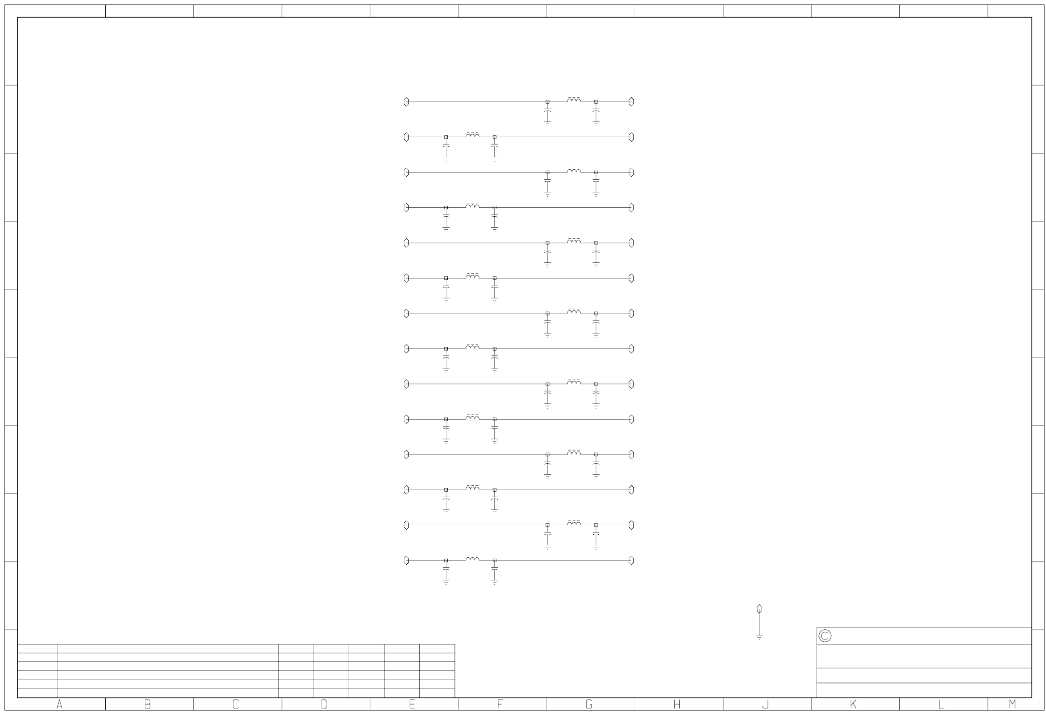
IPN 220-01581-04
M8SL2-00-002-812 T803 PCB Information D4.2.15
© Copyright Tait Electronics Limited August 2004. All rights reserved.
Sheet 5 – T803 SK101 PI Filters
220-01581-04
0
1
2
3
4
5
6
7
8
9
0
1
2
3
4
5
6
7
8
9
ABCDEFGHJ KLM
REV/ISS AMENDMENTS DATEAPVDD.O.CHKDDRAWN
NO.SHEETS:FILE NAME:
TAIT ELECTRONICS
IPN:
FILE DATE:
ISSUE: ID:.
2.SC.
PROJECT: DESIGNER:
5
6
T803-00-0000/T805-08-0000
SK101 PI FILTERS
158104a
220-01581-04
1-Mar-02
A
T803 TONY S
00A ORIGINAL CRAIG M.
01A IC307 PACKAGE, ADDED GND TO F.P. CRAIG M.
02A UPDATED FOR T805 PAUL G 11/2/00
03A PCB UPDATE PAUL G 17/4/00
04A FIT DUAL DIGIPOT DS1868 TONY S 01/03/02
L507
M21A
L500
M21A
C500
27P
L508
M21A
C522
1N0
C515
1N0
L509
M21A
C523
1N0
C516
1N0
L501
M21A
C508
27P
C501
27P
L502
M21A
C509
27P
C502
27P
L510
M21A
C524
1N0
C517
1N0
L511
M21A
C525
1N0
C518
1N0
L503
M21A
C510
1N0
C503
1N0
L504
M21A
C511
1N0
C504
1N0
L512
M21A
C526
1N0
C519
1N0
L513
M21A
C527
1N0
C520
1N0
L505
M21A
C512
1N0
C505
1N0
L506
M21A
C513
1N0
C506
1N0
C514
27P
C521
27P
C507
27P
+13V8_
REPEATER_
PORT_EN_
SHIFT_DATA_
SHIFT_DATA
2D1
LINE_BASE_
MUTE_
SPEAKER_
SPEAKER
2D6
SER_COMS_
PB1_
PB2_
MIC_
PB2
2D5
RX_MUTE_IN_
SCK
2U3
3B0
3U3
6E5
+13V8
1B4
2S0
6E6
PORT_EN
2U3
3B0
3U7
REPEATER
2D3
LINE_BASE
2D2
MUTE
2D3
SER_COMS
2D0
4K0
PB1
2D5
MIC
2D6
RX_MUTE_IN
2D0
4K0
SCK_
/RESET_
-RESET
2U4
3B4
3U5
DGND
1B4
1B4
1B4
1B4
1B4
2R0
3R0
4M0
6H1
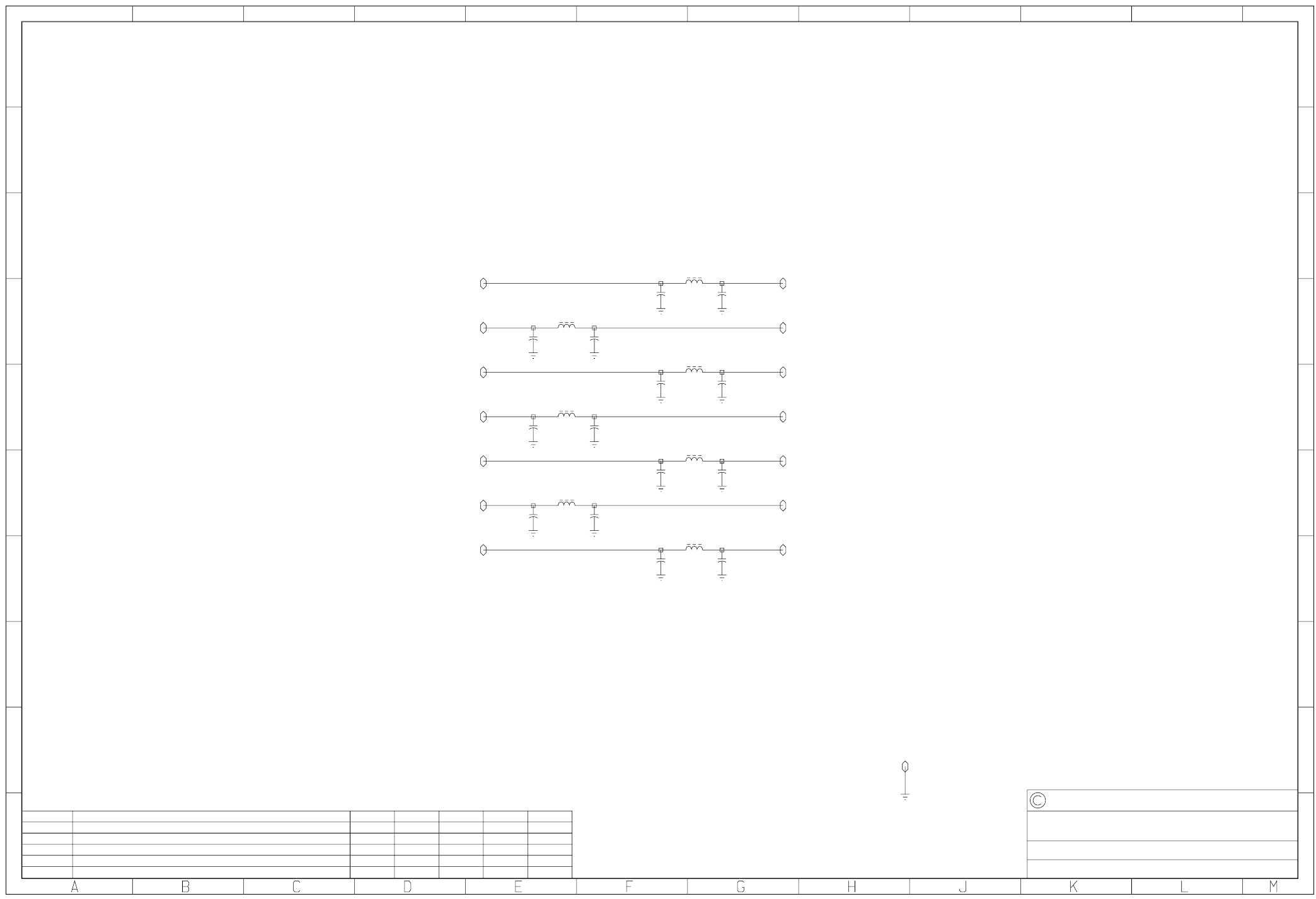
IPN 220-01581-04
D4.2.16 T803 PCB Information M8SL2-00-002-812
© Copyright Tait Electronics Limited August 2004. All rights reserved.
Sheet 6 – T803 SK102 PI Filters
220-01581-04
0
1
2
3
4
5
6
7
8
9
0
1
2
3
4
5
6
7
8
9
ABCDEFGHJ KLM
REV/ISS AMENDMENTS DATEAPVDD.O.CHKDDRAWN
NO.SHEETS:FILE NAME:
TAIT ELECTRONICS
IPN:
FILE DATE:
ISSUE: ID:.
2.SC.
PROJECT: DESIGNER:
6
6
T803-00-0000/T805-08-0000
SK102 PI FILTERS
158104a
220-01581-04
1-Mar-02
A
T803 TONY S
00A ORIGINAL CRAIG M.
01A IC307 PACKAGE, ADDED GND TO F.P. CRAIG M.
02A UPDATED FOR T805 PAUL G 11/2/00
03A PCB UPDATE PAUL G 17/4/00
04A FIT DUAL DIGIPOT DS1868 TONY S 01/03/02
L603
M21A
L600
M21A
C600
1N0
L604
M21A
C611
27P
C607
27P
L605
M21A
C612
27P
C608
27P
L601
M21A
C604
27P
C601
27P
L602
M21A
C605
1N0
C602
1N0
L606
M21A
C613
1N0
C609
1N0
C606
1N0
C610
1N0
C603
1N0
VCC
2S0
3Q0
+13V8
1B4
2S0
5E7
SCK_SM
SHIFT_SYNTH_SM
SDA_SM
VCC_SM
AUX_CODEC_SM
SHIFT_MIX_SM
+13V8_SM
SHIFT_MIX
2D3
4G0
SCK
2U3
3B0
3U3
5E8
SDA
2U4
3B0
3U6
SHIFT_SYNTH
2U2
3B0
3U3
AUX_CODEC
2D6
DGND
1B4
1B4
1B4
1B4
1B4
2R0
3R0
4M0
5J1

M8SL2-00-002-812 EI
© Copyright Tait Electronics Limited August 2004. All rights reserved.
Part E T850 VCO PCB Information
This part of the manual provides the parts list, PCB layouts and circuit diagram for the T850 VCO
PCB. There is a detailed table of contents at the start of Section 2.
Section Title IPN Page
1 Introduction 1.1
2 T850 VCO PCB 220-01145-07 2.1

EII M8SL2-00-002-812
© Copyright Tait Electronics Limited August 2004. All rights reserved.
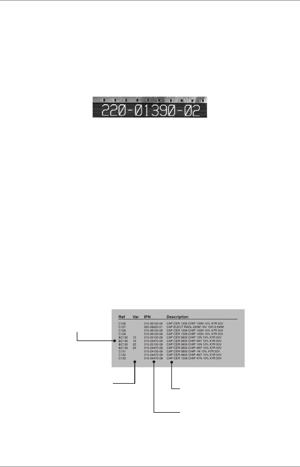
M8SL2-00-002-812 Introduction E1.1
© Copyright Tait Electronics Limited August 2004. All rights reserved.
1 Introduction
PCB Identification
All PCBs are identified by a unique 10 digit “internal part number” (IPN), e.g. 220-12345-00, which
is screen printed onto the PCB (usually on the top side), as shown in the example below:
The last 2 digits of this number define the issue status, which starts at 00 and increments through 01,
02, 03, etc. as the PCB is updated. Some issue PCBs never reach full production status and are there-
fore not included in this manual. A letter following the 10 digit IPN has no relevance in identifying
the PCB for service purposes.
Note: It is important that you identify which issue PCB you are working on so that you can
refer to the appropriate set of PCB information.
Parts Lists
The 10 digit numbers (000-00000-00) in this Parts List are “internal part numbers” (IPNs). We can
process your spare parts orders more efficiently and accurately if you quote the IPN and provide a
brief description of the part.
The components listed in this parts list are divided into two main types: those with a circuit refer-
ence (e.g. C2, D1, R121, etc.) and those without (miscellaneous and mechanical).
Those with a circuit reference are grouped in alphabetical order and then in numerical order within
each group. Each component entry comprises three or four columns, as shown below:
The mechanical and miscellaneous section lists the variant and common parts in IPN order.
circuit reference -
lists components
in alphanumeric
order
variant column -
indicates that this is
a variant component
which is fitted only to
the product type listed
Internal Part Number -
order the component
b
y
this number
description -
gives a brief description
of the component

E1.2 Introduction M8SL2-00-002-812
© Copyright Tait Electronics Limited August 2004. All rights reserved.
Variant Components
A variant component is one that has the same circuit reference but different value or specification in
different product types. Variant components have a character prefix, such as “&”, “=” or “#”, before
the circuit reference (e.g. &R100).

M8SL2-00-002-812 T850 VCO PCB Information E2.1
© Copyright Tait Electronics Limited August 2004. All rights reserved.
2 T850 VCO PCB
This section contains the following information.
IPN Section Page
220-01145-07 Parts List
PCB Layout – Bottom Side
PCB Layout – Top Side
Circuit Diagram
2.3
2.5
2.6
2.7

E2.2 T850 VCO PCB Information M8SL2-00-002-812
© Copyright Tait Electronics Limited August 2004. All rights reserved.

IPN 220-01145-07
M8SL2-00-002-812 T850 VCO PCB Information E2.3
© Copyright Tait Electronics Limited August 2004. All rights reserved.
Ref Var IPN Description Ref Var IPN Description
T850 VCO Parts List (IPN 220-01145-07)
How To Use This Parts List
The components listed in this parts list are grouped in alphabetical order and then in numerical order within each group. Each compo-
nent entry comprises three or four columns: the circuit reference, variant (if applicable), IPN and description. A number in the variant
column indicates that this is a variant component which is fitted only to the product type listed.
This parts list is correct at the time of publishing, but is subject to change without notification. An up to date parts list can be obtained
from your local Customer Service Organisation
#C1 A 015-21120-02 Cap Cer 0805 1p2 1% NPO 50v
#C1 B 015-21120-02 Cap Cer 0805 1p2 1% NPO 50v
#C1 C 015-21150-01 Cap Cer 0805 1p5+-0.25 NPO 50v
#C1 D 015-21150-05 Cap Cer 0805 1p5 +0.1pf 200v
C2 014-08100-00 Cap Tant SMD 10u 16v 20% 267c
C3 015-24100-08 Cap Cer 0805 1n 10% X7r 50v
#C4 A 015-21100-02 Cap Cer 0805 1po 1% NPO 50v
#C4 B 015-21100-02 Cap Cer 0805 1po 1% NPO 50v
#C4 C 015-21100-02 Cap Cer 0805 1po 1% NPO 50v
#C4 D 015-21100-02 Cap Cer 0805 1po 1% NPO 50v
C5 015-06100-08 Cap Cer 1206 100n 10% X7r 50v
#C6 A 028-02111-00 Cap Trim 16pf Piston Prec
#C6 B 028-02111-00 Cap Trim 16pf Piston Prec
#C6 C 028-02111-00 Cap Trim 16pf Piston Prec
#C6 D 028-02111-00 Cap Trim 16pf Piston Prec
#C7 A 015-21330-02 Cap 0805 3p3 +/-0.1p NPO 50v
#C7 B 015-21470-02 Cap 0805 4p7 1% NPO 50v
#C7 C 015-21680-02 Cap 0805 6p8 +/-0.1p NPO 50v
#C7 D 015-21820-02 Cap 0805 8p2 0.1 NPO 50v
#C8 A 015-22220-01 Cap Cer 0805 22p 5% NPO 50v
#C8 B 015-22220-01 Cap Cer 0805 22p 5% NPO 50v
#C8 C 015-22270-01 Cap Cer 0805 27p 5% NPO 50v
#C8 D 015-22330-01 Cap Cer 0805 33p 5% NPO 50v
C9 015-23120-01 Cap Cer 0805 120p 5% NPO 50v
#C10 A 015-21180-02 Cap 0805 1p8 1% NPO 50v
#C10 B 015-21180-02 Cap 0805 1p8 1% NPO 50v
#C10 C 015-21180-02 Cap 0805 1p8 1% NPO 50v
#C10 D 015-21180-02 Cap 0805 1p8 1% NPO 50v
C11 015-21330-02 Cap 0805 3p3 +/-0.1p NPO 50v
C12 015-24100-08 Cap Cer 0805 1n 10% X7r 50v
C13 015-24100-08 Cap Cer 0805 1n 10% X7r 50v
C14 015-23120-01 Cap Cer 0805 120p 5% NPO 50v
C16 015-23120-01 Cap Cer 0805 120p 5% NPO 50v
C17 015-23120-01 Cap Cer 0805 120p 5% NPO 50v
C18 015-22270-01 Cap Cer 0805 27p 5% NPO 50v
C19 015-05470-08 Cap Cer 1206 47n 10% X7r 50v
C21 015-23120-01 Cap Cer 0805 120p 5% NPO 50v
C22 A 015-22100-02 Cap 0805 10p +/-0.1p NPO 50v
C22 B 015-22150-01 Cap Cer 0805 15p 5% NPO 50v
C22 C 015-22150-01 Cap Cer 0805 15p 5% NPO 50v
C22 D 015-23120-01 Cap Cer 0805 120p 5% NPO 50v
C23 015-21820-02 Cap 0805 8p2 0.1 NPO 50v
C24 015-05470-08 Cap Cer 1206 47n 10% X7r 50v
D1 A 001-10015-30 Diode SMD Vcap BB153 SOD323
D1 B 001-10043-90 Diode SMD BB439 Vcap SOD323
D1 C 001-10043-90 Diode SMD BB439 Vcap SOD323
D1 D 001-10043-90 Diode SMD BB439 Vcap SOD323
D2 A 001-10015-30 Diode SMD Vcap BB153 SOD323
D2 B 001-10043-90 Diode SMD BB439 Vcap SOD323
D2 C 001-10043-90 Diode SMD BB439 Vcap SOD323
D2 D 001-10043-90 Diode SMD BB439 Vcap SOD323
L1 056-10330-02 Ind SMD 1210 330nh 10% Simid02
L2 056-10330-02 Ind SMD 1210 330nh 10% Simid02
L3 056-10330-02 Ind SMD 1210 330nh 10% Simid02
L4 056-10330-02 Ind SMD 1210 330nh 10% Simid02
L5 057-00047-10 Ind Fxd 47nh +-5% 1206
#L6 A 056-10015-03 Ind SMD 0805cs 15nh 20%
#L6 B 056-10015-03 Ind SMD 0805cs 15nh 20%
#L6 C 056-10015-03 Ind SMD 0805cs 15nh 20%
#L6 D 056-10015-03 Ind SMD 0805cs 15nh 20%
Q1 000-10009-30 Xstr SMD BFR93A NPN SOT23
Q2 000-10009-30 Xstr SMD BFR93A NPN SOT23
Q3 000-10009-30 Xstr SMD BFR93A NPN SOT23
Q4 000-10008-57 Xstr SMD BC857 PNP SOT23 SS
Q5 000-10050-00 Xstr SMD BLT50 UHF SOT22
R1 036-14390-10 Res M/F SMD 0805 3k9 1%
R2 036-14100-10 Res M/F SMD 0805 1k 1%
R3 036-13100-10 Res M/F SMD 0805 100e 1%
R4 036-12220-00 Res M/F SMD 0805 22e 5%
R5 036-12270-00 Res M/F SMD 0805 27e 5%
#R6 A 036-13100-10 Res M/F SMD 0805 100e 1%
#R6 B 036-13100-10 Res M/F SMD 0805 100e 1%
#R6 C 036-13100-10 Res M/F SMD 0805 100e 1%
#R6 D 036-13100-10 Res M/F SMD 0805 100e 1%
R7 036-14100-10 Res M/F SMD 0805 1k 1%
R8 036-12220-00 Res M/F SMD 0805 22e 5%
R9 036-14270-10 Res M/F SMD 0805 2k7 1%
R10 036-14120-00 Res M/F SMD 0805 1k2 5%
R11 036-13150-10 Res M/F SMD 0805 150e 1%
R12 036-12100-10 Res M/F SMD 0805 10e 1%
R13 A 036-12270-00 Res M/F SMD 0805 27e 5%
R13 B 036-12390-00 Res M/F SMD 0805 39e 5%
R13 C 036-12390-00 Res M/F SMD 0805 39e 5%
R13 D 036-12560-00 Res M/F SMD 0805 56e 5%
R14 036-13330-00 Res M/F SMD 0805 330e 5%
R15 036-12100-10 Res M/F SMD 0805 10e 1%
R17 A 036-14680-10 Res M/F SMD 0805 6k8 1%
R17 B 036-14680-10 Res M/F SMD 0805 6k8 1%
R17 C 036-14680-10 Res M/F SMD 0805 6k8 1%
R17 D 036-14820-10 Res M/F SMD 0805 8k2 1%
R18 036-14180-00 Res M/F SMD 0805 1k8 5%
R19 036-14100-10 Res M/F SMD 0805 1k 1%
R20 036-12180-00 Res M/F SMD 0805 18e 5%
R21 036-13330-00 Res M/F SMD 0805 330e 5%
R22 036-12100-10 Res M/F SMD 0805 10e 1%
#TL1 A 051-00005-43 Reso Tait #543 480-520
#TL1 B 051-00005-42 Reso Tait #542 435-480
#TL1 C 051-00005-41 Reso Tait #541 395-440
#TL1 D 051-00005-40 Reso Tait #540 355-395
240-00026-32 Plg 32w 1row Pcb Mtg
220-01145-07 PCB T855/856/857/870 VCO
345-00040-10 Scrw M3*6mm P/P S/T Bz
350-00016-42 Spcr 5mm Hi 8*M3 Stud 2.5*M3ho
353-00010-13 Wshr M3 S/Proof Int Bz
Variant
Code Description T855
(MHz)
T854
(MHz)
A Tx High — 480 to 500
B Tx Mid/Rx High 480 to 520 440 to 480
C Tx Low/Rx Mid 440 to 480 400 to 440
D Rx Low 400 to 440 —
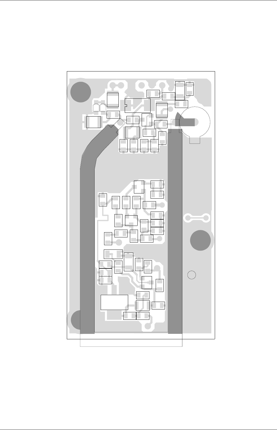
IPN 220-01145-07
E2.4 T850 VCO PCB Information M8SL2-00-002-812
© Copyright Tait Electronics Limited August 2004. All rights reserved.
T850 VCO PCB (IPN 220-01145-07) – Top Side
A
1
2
3
4
5
6
BCDEF
#C1
#C10
#C15
#C4
#C6
#C7
#C8
#L6
#R6
#TL1
C11
C12C13 C14
C16
C17
C18
C19 C2
C21
C22
C23
C24
C3
C5
C9
D1
D2
L1
L2
L3
L4
L5
Q1
Q2
Q3
Q4
Q5
R1
R10
R11
R12
R13
R14
R15
R17
R18
R19
R2
R20
R21
R22
R3
R4 R5
R7
R8
R9
TBADMARK
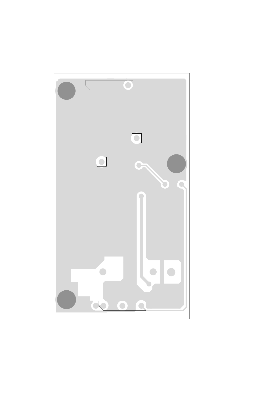
T850 VCO PCB (IPN 220-01145-07) – Bottom Side
© Copyright Tait Electronics Limited August 2004. All rights reserved.
IPN 220-01145-07
M8SL2-00-002-812 T850 VCO PCB Information E2.5
5
1
2
3
4
6
ABCDEF
PL2
PL3
PL4
PL5

E2.6 T850 VCO PCB Information M8SL2-00-002-812
© Copyright Tait Electronics Limited August 2004. All rights reserved.
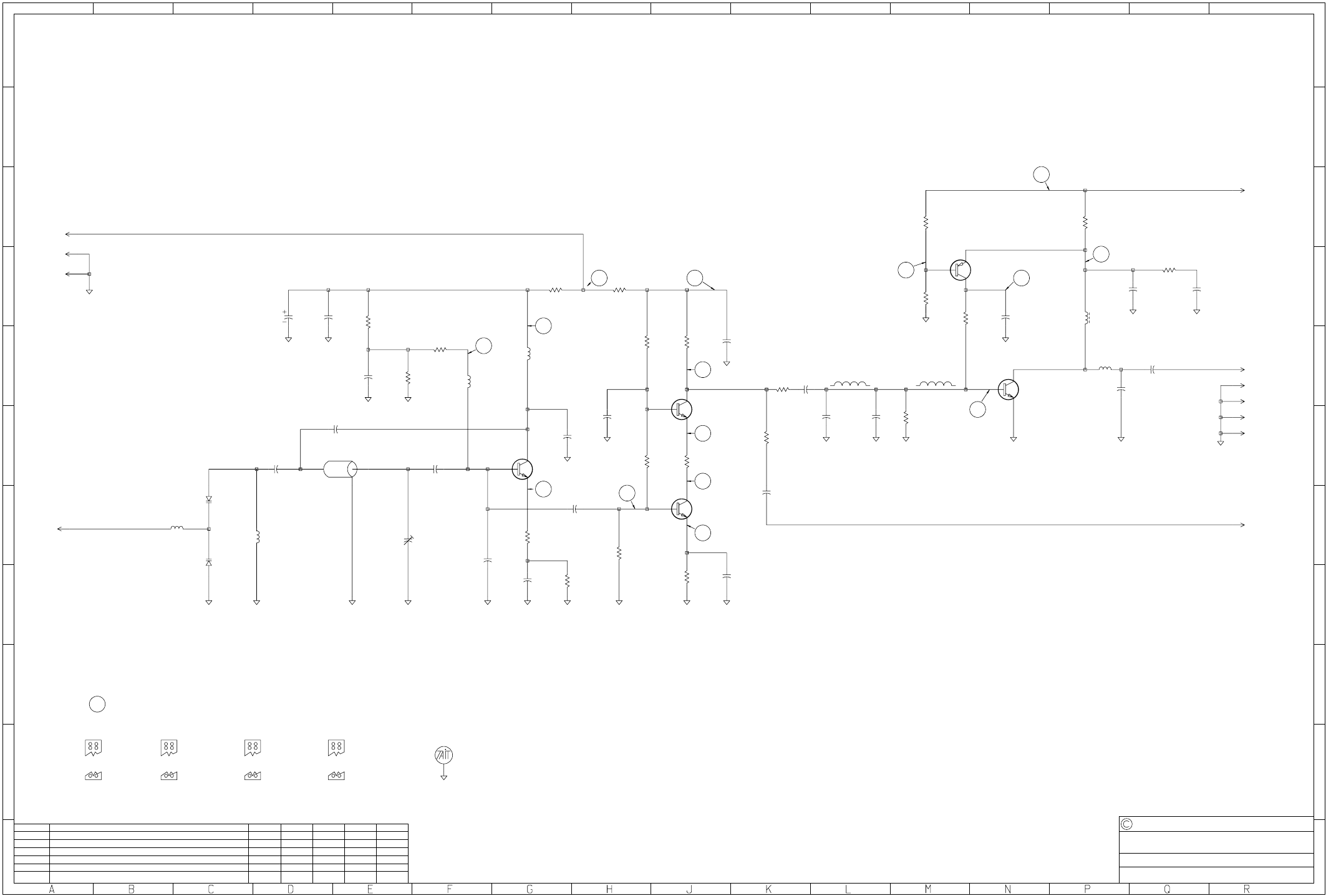
IPN 220-01145-07
M8SL2-00-002-812 T850 VCO PCB Information E2.7
© Copyright Tait Electronics Limited August 2004. All rights reserved.
T850 VCO
220-01145-07
0
1
2
3
4
5
6
7
8
9
0
1
2
3
4
5
6
7
8
9
ABCDEFGHJ KL MNPQR
REV/ISS AMENDMENTS DATEAPVDD.O.CHKDDRAWN
NO.SHEETS:FILE NAME:
TAIT ELECTRONICS
IPN:
FILE DATE:
ISSUE: ID:.
2.SC.
PROJECT: DESIGNER:
1
1
T850/T870 VCO
1145_07b
220-01145-07
10-Jun-03
B
T850 SSAHI
03A CYCLIC KEYING MODIFICATION BENC
04A SMD PARTS ADDED BENC 07-10-99
05A UPDATE SSAHI 05-05-00
06A MINOR UPDATE SSAHI 06-07-00
07A MINOR UPDATE TO THE LAYOUT SSAHI 06-09-00
07B REGENERATED NEW PASTE BRD 10-06-03
#C1
2P2
#C10
1P8
C11
3P3
C12
1N0
C13
1N0
C14
120P
C16
120P
C17
120P
C18
27P
C19
47N
TANT
C2
10U
C21
120P
C22
120P
C23
8P2
C24
47N
C3
1N0
#C4
1P0
C5
100N
#C7
10P
#C8
33P
C9
120P
D1
BB439
1
2
D2
BB439
1
2
L1
330NH
L2
330NH
L3
330NH
L4
330NH
L5
47N
Q1
BFR93A
Q2
941
Q3
941
Q4
BC857
Q5
BLT50
R1
3K9
R10
1K2
R11
150E
R12
10
R13
56E
R14
330
R15
10
R17
6K8
R18
1K8
R19
1K0
R2
1K0
R20
18
R21
330
R22
10
R3
100E
R4
22
R5
27
#R6
100E
R7
1K0
R8
22
R9
2K7
PL5
5 PLUG PINS
PL4
5 PLUG PINS
PL2
1 PIN PLUG
PL3
1 PIN PLUG
TBADMARK
BADMARK
#TL1
#540
#C6
1P0/16P
#L6
15NH
#C15
10P
PL5
1
PL5
2
PL5
3
PL5
4
PL5
5
PL4
1
PL4
2
PL4
4
PL4
5
PL2
DIVIDER-BUFFER
1
PL3
BUFFER+9V
1
+20DBM
VCO-CONTROL
VCO-SUPPLY
VCO-O/P
PRTDPRTD
#-VALUE CHANGES FOR DIFFERENT OPTIONS
9.0
7.8
3.1
7.2
0.6
8.3 7.9
5.8
2.8
2.6
0.8
1.5
1.2
1.5
8.0
= D.C. CONDITIONS (VOLTS)
(USE HIGH IMPEDENCE PROBE)
IPN 220-01145-07
E2.8 T850 VCO PCB Information M8SL2-00-002-812
© Copyright Tait Electronics Limited August 2004. All rights reserved.

M8SL2-00-002-812 FI
© Copyright Tait Electronics Limited August 2004. All rights reserved.
Part F T800-23-0011 Power Supply
This part of the manual provides information on the power supply, and is divided into
six sections as listed below..
Section Title
1 General Information
2 Power Supply Description
3 Installation Guidelines
4 Functional Testing
5 Troubleshooting
6 Service Information

FII M8SL2-00-002-812
© Copyright Tait Electronics Limited August 2004. All rights reserved.

M8SL2-00-002-812 General Information F1.1
© Copyright Tait Electronics Limited August 2004. All rights reserved.
1 General Information
This section provides a brief description of the T800-23-0011 Switch Mode Power Sup-
ply, as well as detailed specifications.
1.1 Introduction
The T800-23-0011 is a switching power supply designed to meet the requirements of the
T800 SL2 25W Continuous Basestation. It is capable of suppling 13.8VDC at up to 14.5A
(see derating information in Section 1.2.4). The unit provides power to the T800 SL2 Bas-
estation modules via a cable assembly (with a 12A fuse) which connects between the DC
output connector on the back of the unit, and the backplane PCB (X800-56-PCB3).
The T800-23-0011 is protected against damage caused by faults in the line or load, or by
temperature variations. (refer to Section 1.2 for specifications). The protection features
include:
•Short circuit protection.
•Overload protection
•Over voltage protection
•Over Temperature protection
Electromagnetic compatibility (EMC) and operator safety are important and critical
requirements for a switching power supply. Refer to Section 1.3.1 and Section 1.3.2 for
specifications.
Caution: To prevent the T800-23-0011 equipment from overheating, do not exceed the
rated current.

F1.2 General Information M8SL2-00-002-812
© Copyright Tait Electronics Limited August 2004. All rights reserved.
1.2 Specifications
1.2.1 Introduction
The performance figures given are minimum figures, unless otherwise indicated, for
equipment operating at standard room temperature (+22°C to +28°C).
Details of test methods and the conditions which apply for Type Approval testing in all
countries can be obtained from Tait Electronics Ltd.
1.2.2 General
Basic Power Supply Concept …switched mode technology pulse
width modulation
Overtemperature Protection …shuts down when PC Board tempera-
ture rises above 95°C ±5°C
Reset: auto recovery
Cooling …convection and forced air (fan)
Efficiency …80%, full load
Temperature Range:
230VAC supply …–10 to +60°C
115VAC supply …–10 to +50°C
Isolation:
Input to Output …3000VAC, 1 minute
Input to Ground/Chassis …1500VAC, 1 minute
Output to Ground/Chassis …500VAC, 1 minute
1.2.3 AC Mains Input
Volta ge : …100 to 130VAC 47–63Hz
200 to 240VAC 47–63Hz
AC Input Current …2.8A maximum
(115VAC at full load)
Maximum Inrush Current …40A maximum
(230VAC at full load)
Connection to mains supply …IEC plug on rear panel

M8SL2-00-002-812 General Information F1.3
© Copyright Tait Electronics Limited August 2004. All rights reserved.
Power Factor at full load:
230VAC supply …>0.96
115VAC supply …>0.98
Note: Exact power factor depends on impedance of mains supply.
Input Fuse (Internal) …5A 250V fast acting
(Littlefuse 217 series)
1.2.4 Output
Output Voltage …13.8VDC
Note: A drop of up to 0.5V may be expected across the wiring from the power sup-
ply to the load.
Vol t ag e R eg u la t i o n …±0.5%
Current
Operation from 200–240VAC supply:
Continuous, –10°C to +50°C…0 to 14.5ADC
Continuous, up to +60°C…0 to 8.5ADC
Operation from 100–130VAC supply:
Continuous, –10°C to +20°C…0 to 14.5ADC
Continuous, +20°C to +50°C…0 to 8.5ADC
Note: Continuous operation from 115VAC supplies in ambient temperatures
exceeding +50°C is not recommended, as this will cause the equipment to
overheat.
Output Overvoltage Protection …14.8 to 19.1VDC
Type: Shu tdown
Reset: Power off and on
Output Hum and Noise …<100mVpp
(At full load, with mains supply volt-
age = 230V)
Current Overload Limit …15.2 to 21.8A
Type: Constant current limiting
Reset: Auto recovery
Output Connector …Molex 6-way receptacle
Note: Refer to Figure 3.1 in Section 3.2 for the output connector pinouts.

F1.4 General Information M8SL2-00-002-812
© Copyright Tait Electronics Limited August 2004. All rights reserved.
1.3 Regulatory Information
1.3.1 EMC Conformity
This equipment complies with:
ETSI EN301 349-1 V1.3.1 (2001-09) “Electromagnetic Compatibility and Radio Spec-
trum Matters (ERM); Electromagnetic Compatibility (EMC) standard for radio equip-
ment and services; Part1: Common technical requirements”.
Tested in accordance to:
•BS EN55022: 1998
•BS EN61000-3-2: 2001
•BS EN61000-3-3: 1995
•IEC 61000-4-2: 1995
•IEC 61000-4-3: 2002
•IEC 61000-4-4: 1995
•IEC 61000-4-5: 1995
•IEC 61000-4-6: 1996
•IEC 61000-4-11: 1994
BS EN55022: 1998 for class B Radiated and conducted emissions, and electromagnetic
susceptibility specifications.
AS/NZS CISPR22: 2002 for class B Radiated and conducted emissions, and electromag-
netic susceptibility specifications.
FCC 47 Part 15: 2001 for class B (Radiated and conducted emissions, and electromag-
netic susceptibility specifications) of the FCC rules for the United States. Operation is
subject to the following two conditions:
1. This device may not cause harmful interference, and
2. This device must not accept any interference received, including interference that
may cause undesired operation.
Warning: This equipment has been tested and found to comply with the limits for a
Class B digital device, pursuant to part 15 of the FCC Rules. These limits are
designed to provide reasonable protection against harmful interference in a
residential installation. This equipment generates, uses and can radiate
radio frequency energy and, if not installed and used in accordance with the
instructions, may cause harmful interference to radio communications.
However, there is no guarantee that interference will not occur in a particu-
lar installation. If this equipment does cause harmful interference to radio or
television reception, which can be determined by turning the equipment off
and on, the user is encouraged to try to correct the interference by one or
more of the following measures:

M8SL2-00-002-812 General Information F1.5
© Copyright Tait Electronics Limited August 2004. All rights reserved.
•Reorient or relocate the receiving antenna.
•Increase the separation between the equipment and receiver.
•Connect the equipment into an outlet on a circuit different from that to
which the receiver is connected.
•Consult the dealer or an experienced radio/TV technician for help.
Modifications not expressly approved by the manufacturer could void the
user's authority to operate the equipment under FCC rules.
1.3.2 Safety Approvals
This equipment complies with:
IEC 60950 : 1999 “Safety of information technology equipment”. All the relevant provi-
sions including AS/NZS and EN deviations.
CAN/CSA-C22.2 No 950-95 “Safety of information technology equipment”.
ANSI/UL Std N0 1950 Third Edition “Safety of information technology equipment”.
Warning: Safety approval will become void if T800-23-0011 components are replaced
with non-equivalent rated or non-certified/approved components. Contact
Tait Electronics Technical Support before replacing components of the
T800-23-0011. See Section 6 for important servicing information.

F1.6 General Information M8SL2-00-002-812
© Copyright Tait Electronics Limited August 2004. All rights reserved.
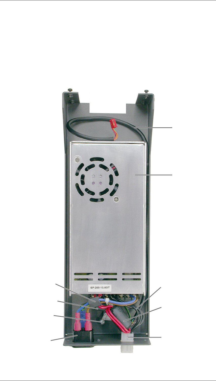
M8SL2-00-002-812 Power Supply Description F2.1
© Copyright Tait Electronics Limited August 2004. All rights reserved.
2 Power Supply Description
2.1 Introduction
The T800-23-0011 power supply consists of a Power Supply Unit (PSU) Module, connec-
tors, and ferrite filters. These components are shown in Figure 2.1 below.
Figure 2.1 T800-23-0011 internal view. See the Parts List in Section 6.2.2 for more detail.
PSU Module
Molex Socket
(DC Output)
IEC Plug
(Mains Input)
Ferrite Sleeve
Ferrite Bead
Chassis grounding point
(Mains Ground filter)
Internal Loom
(Mains Input filter)
(DC Output filter)
Ferrite Bead
using Earth Tag
Feed through loom
from programming
port and speaker on
SL2 front panel to
back plane PCB.

F2.2 Power Supply Description M8SL2-00-002-812
© Copyright Tait Electronics Limited August 2004. All rights reserved.
2.1.1 PSU Module
The PSU module used in the T800-23-0011 power supply has over temperature, current
overload and overvoltage protection. Refer to Section 1.2 for specification details.
Overvoltage applied on the module’s output will cause the module to shutdown. To
reset the module, remove the mains supply to the T800-23-0011, allow 30 seconds for
charges to leak away, and then reconnect the T800-23-0011.
The module is protected from current overload by a voltage foldback method. If the
load on the output starts drawing more current than the specified maximum, the volt-
age will start dropping away. This condition will recover automatically when the load is
removed or returns to normal.
Over temperature will cause the module to shutdown. It will recover automatically
when it has cooled down to an acceptable operational temperature.
Caution: Correct mounting of the T800-23-0011 power supply is important: Refer to
Section 3.3 for ventilation guidelines. Ignoring these conditions may cause
the module to overheat, and consequently, to shut down.
2.1.2 Internal Loom
Mains power to the PSU module is supplied via an IEC plug on the rear panel and then
filtered by a ferrite bead (shown in Figure 2.1). The mains ground line is filtered by a fer-
rite bead and then connected to the T800-23-0011 chassis and to the PSU module’s float-
ing ground contact.
The PSU module’s output is filtered by a ferrite sleeve on the positive line, and then
interfaces to the SL2 backplane via a Molex connector on the T800-23-0011 rear panel.
Additionally a ‘feed-through’ loom is connected to the Molex connector. This loom
forms part of the path for the programming and speaker connection between the SL2
backplane and the SL2 front panel. The external cable connection between the
T800-23-0011 and the SL2 backplane completes this path.
For the wiring diagram, refer to Section 6.2.1.

M8SL2-00-002-812 Installation Guidelines F3.1
© Copyright Tait Electronics Limited August 2004. All rights reserved.
3 Installation Guidelines
The following section gives a brief description of the basic rack mounting and wiring
procedures.
3.1 General
The T800-23-0011 is supplied mounted to the SL2 front panel by four M3x10 button hex
screws.
A small cable extending out of the front of the T800-23-0011 plugs onto to the SL2 front
panel. This cable forms part of the programming and speaker connection between the
SL2 front panel and the backplane. The external cable connection between the
T800-23-0011 and the SL2 backplane provides the DC power supply to the basestation
and also incorporates 3 wires completing the programming and speaker connection.
Warning: FUSE
The cable connecting the T800-23-0011 DC power output to the backplane
also includes a fuse. This fuse is critical to the IEC 60950 safety compliance
of the T800 SL2 Base Station and must be replaced with the same component
or compliance will be voided.
The Fuse is a Bussmann TDC10 Series fast blow fuse rated at 12A (60VAC)
For the AC mains input connection of the T800-23-0011 use only an IEC type detachable
power supply cord (with a moulded IEC connector). Ensure that it has a current rating
of at least 5A.
3.2 Connector Pinouts
The pinouts for the AC mains input connector and the DC output connector on the rear
of the T800-23-0011 are shown in Figure 3.1 below.
Figure 3.1 Connector Pinouts on the T800-23-0011 rear panel.
Ground+13.8VLive
Earth
Neutral
IEC Plug (Mains Input) Molex Socket (DC Output)
Ground
Programming port
(from front panel)
Speaker
(to front panel)

F3.2 Installation Guidelines M8SL2-00-002-812
© Copyright Tait Electronics Limited August 2004. All rights reserved.
3.3 Equipment Cooling
Although the T800-23-0011 is a high efficiency switching power supply, a considerable
amount of heat is generated during normal operation. An adequate flow of cooling air is
therefore essential for reliable operation.
Caution: Do not operate this unit in a completely enclosed cabinet.
It is estimated that the average life expectancy of this unit will double with every 10°C
drop in ambient temperature. It is therefore recommended to:
•Keep the ambient temperature low.
•Ensure that airflow is not restricted.
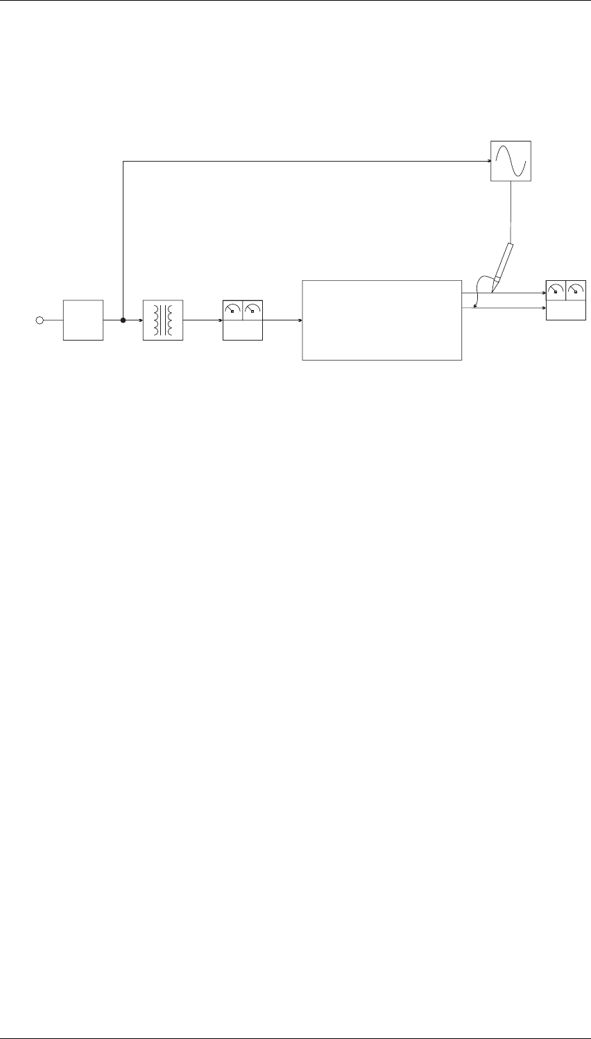
M8SL2-00-002-812 Functional Testing F4.1
© Copyright Tait Electronics Limited August 2004. All rights reserved.
4 Functional Testing
The following test procedures will confirm that the T800-23-0011 has been set up and
adjusted correctly and is fully operational. Refer to Figure 4.1 for test equipment details.
Figure 4.1 Test equipment setup
4.1 Basic Operation
To confirm the basic operation of the power supply, proceed as follows.
•Ensure that the main supply to the T800-23-0011 is switched off. Set up the
test equipment as shown in Figure 4.1.
•Set the output DC load to maximum resistance/minimum current.
•Connect the T800-23-0011 to the mains supply and switch it on.
•Vary the DC load and check that the output voltage and current are within
the specifications (refer to Section 1.2.4).
4.2 Output Current Overload
To confirm the operation of the current overload protection circuitry, proceed as follows.
•Ensure that the main supply to the T800-23-0011 is switched off. Set up the
test equipment as shown in Figure 4.1.
•Set the output DC load to draw approximately 11A.
•Switch on the mains supply and slowly decrease the load resistance, thereby
increasing the current until voltage foldback occurs. The current should not
rise above the Current Overload Limit (refer to Section 1.2.4), but voltage
should drop away.
Earth
Leakage
Circuit
Breaker
VA__
*
Mains
Supply
Isolating
Transformer
1kVA
Variac
0 to 260V
1kVA AC
* True RMS Reading
T800-23-0011 PSU
+
-
AC
Input
Output
VA__
DC Load
0 to 30ADC
Oscilloscope

F4.2 Functional Testing M8SL2-00-002-812
© Copyright Tait Electronics Limited August 2004. All rights reserved.
4.3 Output Noise
To check that output noise is within specification, proceed as follows.
•Ensure that the main supply to the T800-23-0011 is switched off. Set up the
test equipment as shown in Figure 4.1. Connect the T800-23-0011 to the
mains supply and switch it on.
•Connect a digital voltmeter (e.g. Fluke 77) across the load terminals and set
the meter to its lowest AC volts range.
•Check that the reading is less than 100mVpp under all load and line condi-
tions.
Note: A real reading of the level of noise present on the output of a switching
power supply is very difficult to obtain, as low noise levels, common mode
noise paths and ground loops all lead to inaccurate measurement results.
The procedure outlined above will, however, give a good indication of the
output noise.
4.4 Overall Power Supply Stability
To check for overall PSU stability, proceed as follows.
•Ensure that the main supply to the T800-23-0011 is switched off. Set up the
test equipment as shown in Figure 4.1. Connect the T800-23-0011 to the
mains supply and switch it on.
•Connect the oscilloscope across the output.
•Vary the mains voltage and DC load over the full specified range (refer to
Section 1.2).
•Check on the oscilloscope that no oscillations occur.

M8SL2-00-002-812 Troubleshooting F5.1
© Copyright Tait Electronics Limited August 2004. All rights reserved.
5 Troubleshooting
The following is a list of possible power supply fault symptoms and possible causes.
Symptoms Possible Causes and their Solutions
1. No output voltage Mains supply not present
or too low
Check and rectify mains
supply
Equipment has over-
heated and thermal cut-
out has operated
See Symptom 3 below
Defective switching cir-
cuitry
Replace module and
return faulty module for
servicing
2. Output voltage below
specification
Mains supply is to low Check and correct mains
supply problem
Current overload protec-
tion is active
Check for possible causes,
e.g. short-circuits
Defective switching cir-
cuitry
Replace module or return
faulty module for servic-
ing
3. Power Supply over-
heats
Mains supply is to low Check and correct mains
supply problem
Equipment cooling is inef-
ficient due to incorrect
installation of the
T800-23-0011
Refer to Section 3.3 for
installation guidelines
The T800-23-0011 internal
fan has failed
Replace module or return
faulty module for servic-
ing

F5.2 Troubleshooting M8SL2-00-002-812
© Copyright Tait Electronics Limited August 2004. All rights reserved.

M8SL2-00-002-812 Service Information F6.1
© Copyright Tait Electronics Limited August 2004. All rights reserved.
6 Service Information
This section provides specific information on servicing procedures for the T800-23-0011.
6.1 Warnings
6.1.1 Warning: Lethal Voltages
The T800-23-0011 power supply contains voltages that may be lethal.
Disconnect the mains IEC connector and wait for 5 minutes for the internal voltages to
drain away before dismantling.
Servicing should be carried out only by qualified technicians and should be attempted
only when powered through a mains isolating transformer of sufficient rating. It is
strongly recommended that the mains supply to the whole of the repair and test area is
supplied via an earth leakage circuit breaker.
6.1.2 Warning: Fuse
The cable connecting the T800-23-0011 DC power output to the backplane also includes
a fuse. This fuse is critical to the IEC 60950 safety compliance of the T800 SL2 Base Sta-
tion and must be replaced with the same component or compliance will be voided.
The Fuse is a Bussmann TDC10 Series fast blow fuse rated at 12A (60VAC)
6.1.3 Caution: Handle With Care
Although this is a lightweight unit, it contains a number of quite heavy and fragile indi-
vidual components which are mounted directly on the PCB. Severe mechanical shock
may damage the PCB (e.g. solder joints, copper tracks) and/or components (e.g. fragile
ferrite magnetic materials).
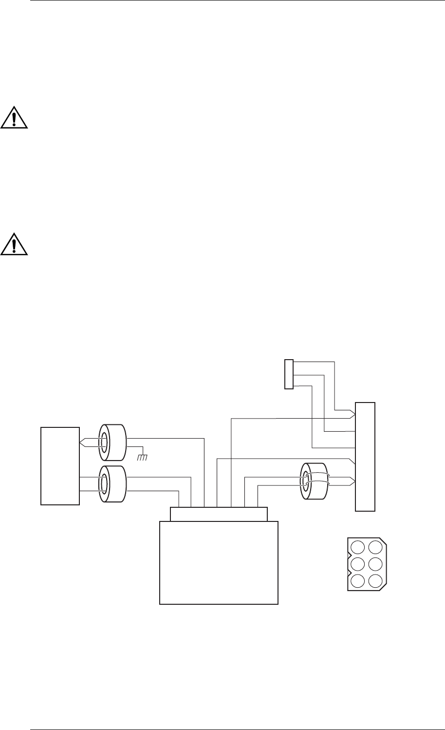
F6.2 Service Information M8SL2-00-002-812
© Copyright Tait Electronics Limited August 2004. All rights reserved.
6.2 Mechanical
This section provides information necessary for replacement of various parts and mod-
ules of the T800-23-0011 power supply.
Warning: Safety approval will become void if T800-23-0011 components are
replaced with non-equivalent rated or non-certified/approved compo-
nents. Contact Tait Electronics Technical Support before replacing compo-
nents of the T800-23-0011.
The power supply module is not a user serviceable item. This module
contains components that operate at voltages that may be lethal. Do not
open this module.
Caution: Disconnect the mains IEC connector and wait for 5 minutes for the internal
voltages to drain away before dismantling the T800-23-0011.
6.2.1 Wiring Diagram
Refer to the diagram below for connection information between the T800-23-0011’s con-
nectors and powers supply module.
Figure 6.1 T800-23-0011 Wiring Diagram
Molex
Connector
1234567
+13.8V
Black
Live
Neutral
Ferrite Sleeve
Ferrite Beads
PSU Module
I
EC Mains
C
onnector
Chassis
Ground
Ground Green&Yellow
Blue
Brown Red
Black
Red
1
2
3
4
5
6
3
2
1
6
5
4
Yellow
Red
Brown
Front panel programming port
and speaker connection
Gnd
Gnd
External view
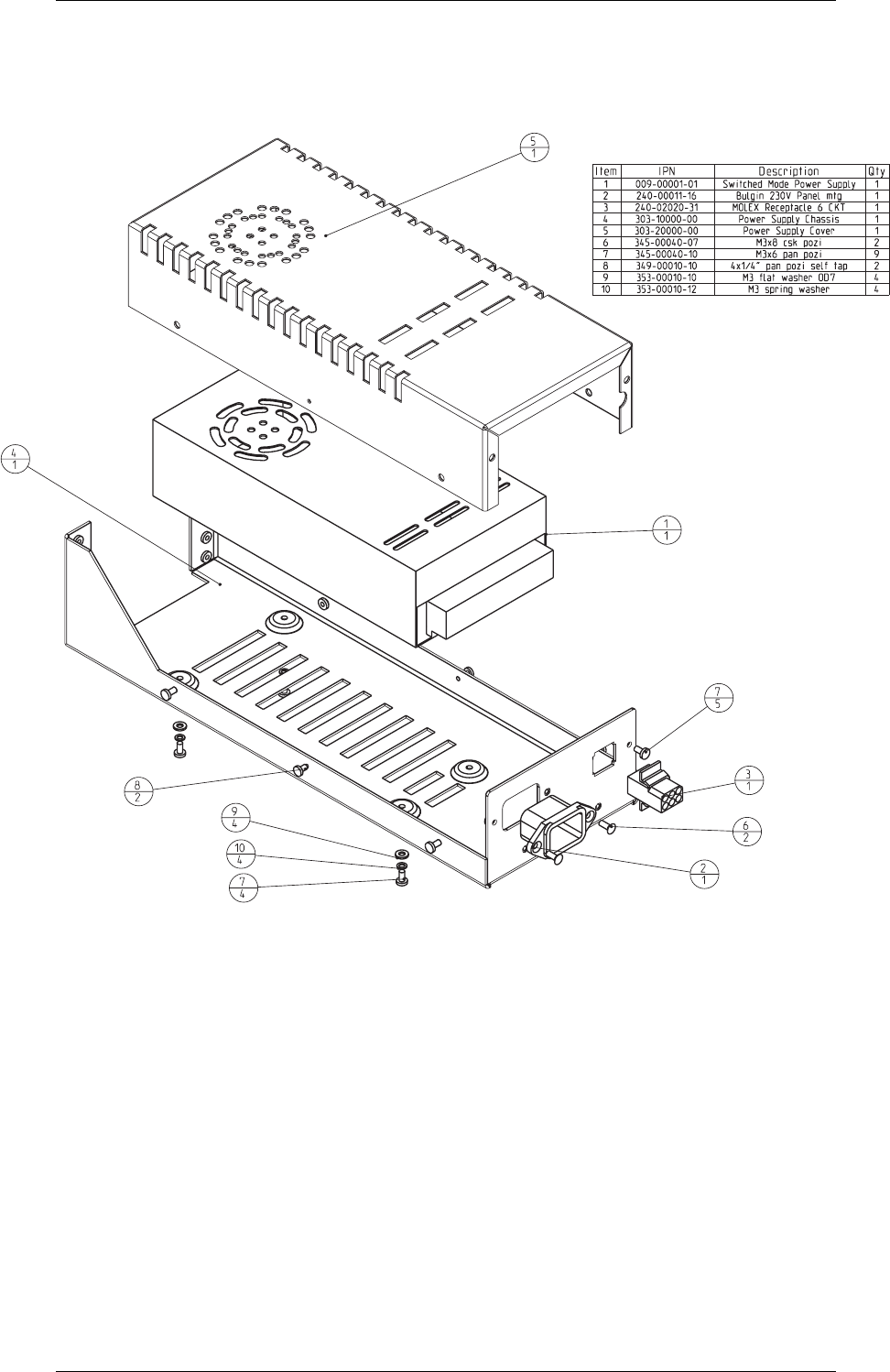

F6.4 Service Information M8SL2-00-002-812
© Copyright Tait Electronics Limited August 2004. All rights reserved.

M8SL2-00-002-812 GI
© Copyright Tait Electronics Limited August 2004. All rights reserved.
Part G Installation and Configuration
This part of the manual is divided into the sections listed below. These sections give a
brief description of the mounting and wiring procedures as well as some brief informa-
tion on basic system types and how to configure T800 SL2 equipment for use in them.
Section Title Page
1
1.1
1.2
1.3
1.4
1.5
1.6
T800 SL2 Installation
Specifications
Mounting
Power Supply
Reverse Polarity and Overvoltage Protection
D-range Wiring
RF Coax Cable and N-Type Connector
1.2
1.2
1.2
1.2
1.3
1.5
1.6
2
2.1
2.1.1
2.1.2
2.2
2.2.1
2.2.2
2.3
2.4
2.5
2.6
2.7
2.8
2.9
2.10
T854 Optional Features
Audio Processor
Link Details
Typical Options
Line Transformer Configuration and Options
Line Limiter Option
Line Attenuator Option
Opto Key
Relay Driver
Local Microphone
Keying With Option PCBs
Transmit Key Time
Local PTT Indication for A800 SIM
Direct input to Buffer option
Line Input Control Replacement
2.1
2.1
2.1
2.2
2.2
2.4
2.4
2.4
2.5
2.5
2.5
2.5
2.6
2.6
2.6
3 Talk Through Repeater 3.1
4
4.11
4.12
Line Controlled Base without Talk Through
General
Transmitter Tail Timer
4.1
4.1
4.2
5 DC Line Keying 5.1
6 X800-56-PCB3 PCB Information 6.1.1

GII M8SL2-00-002-812
© Copyright Tait Electronics Limited August 2004. All rights reserved.
Figure Title Page
1.1
1.2
1.3
1.4
1.5
1.6
1.7
1.8
T855 D-Range 1 Wiring – Rear View
T855 D-Range 2 Wiring – Rear View
T854 D-Range 1 Wiring – Rear View
T854 D-Range 2 Wiring – Rear View
N-Type Plug Assembly Details
T800 SL2 Assembly – with T803 fitted
T800 SL2 Assembly – without T803 fitted
T800 SL2 Assembly – with T803 fitted (rear view)
1.3
1.3
1.4
1.4
1.5
1.7
1.8
1.9
3.1 Talk Through Repeater 3.1
4.2
4.3
4.4
4.5
Basic Configuration
Remote Line Controlled Base Station
4-Wire to 2-Wire Converter
Receiver Disable Time vs Tail Time
4.1
4.1
4.2
4.2
5.6
5.7
5.8
5.9
DC Loop Keying With Common Earth
Isolated Constant Current Loop Current Detector
Isolated Loop Current Switch
Typical System
5.1
5.1
5.2
5.2

M8SL2-00-002-812 G1.1
© Copyright Tait Electronics Limited August 2004. All rights reserved.
1 T800 SL2 Installation
1.1 Specifications
Overall Dimensions:
Height …132mm
Width …480mm
Depth …335mm
Weight with Tone Remote …16kg
Weight without Tone Remote …13kg
1.2 Mounting
The T800SL2 unit is shipped ready assembled for fitting into racks. All that is required is
for the connection of suitable cables.
1.3 Power Supply
The power rating information for the T800SL2 with the Tait supplied power supply
module (T800-23-0011), is provided on the label located on the top cover as visible in
Figures 1.6.
The power rating information for the T800SL2 for use with a customer supplied DC
power source, is provided on the label located on the top rear of the Transmitter mod-
ule.
In order to comply with the safety requirements of EN60950, the power supply module
used with the T800SL2 must be provided with an easily accessible mains disconnect
device compliant with IEC61058, such as a switch or circuit breaker. This provides the
means to rapidly disconnect the mains power in an emergency.
All Tait supplied racks incorporate a power distribution board with a circuit breaker
easily accessible in the back of the rack, on the lower right hand side (viewed from the
rear). The circuit breaker will disconnect the mains to the entire rack. If only one channel
needs to be mains-isolated and the Tait power supply module is T800-23-0011, then it is
acceptable practice to pull the IEC connector directly out of the power supply module.
If a customer supplied power source is used, it must have the following features:
•An easily accessible and safety compliant mains disconnect device.
•The capability to provide enough current to drive the T800 system.
•Free from excessive ripple or noise.
•Meets all EMC and safety regulations for the intended market.

G1.2 M8SL2-00-002-812
© Copyright Tait Electronics Limited August 2004. All rights reserved.
The entire system should be protected by the use of appropriately rated fuses in the
power supply.
Note: It is particularly important when the prime power source is a battery that fuses be
employed in all the supply lines.
Warning: Fuse – DC powered Base Stations
The cable supplied for connecting a DC power source such as a battery to
the backplane of the SL2 Base Station, includes a fuse. This fuse is critical
to the IEC 60950 safety compliance of the T800 SL2 Base Station and must
be used or compliance will be voided. If the fuse has blown it must be
replaced with the same component
The Fuse is a Bussmann TDC10 Series fast blow fuse rated at 12A
(60VAC)
1.4 Reverse Polarity and Overvoltage Protection
A crowbar diode is fitted to all T854 transmitters for protection against connection to a
power supply of incorrect polarity. It also provides overvoltage protection from voltage
transients caused by lightning strikes.
Note: A fuse must be fitted in the power supply line for the diode to provide effec-
tive protection.
M8SL2-00-002-812 G1.3
© Copyright Tait Electronics Limited August 2004. All rights reserved.
1.5 D-range wiring
The T855 and T854 D-range input and output connections are shown in Figure 1.1 to
Figure 1.4..
Figure 1.1 T855 D-Range 1 Wiring – Rear View
Figure 1.2 T855 D-Range 2 Wiring – Rear View
(standard T800-03-0000 kit)
Line O/P1
Speaker
Serial Com
Audio 1
RSSI
Line O/P4
Line O/P3
Line O/P2
Gate O/P
Common 1
N.O. 1
Relay
+13.8V
Gnd Can be configured as
Audio 2 by internal
link resistors if required.
10.8 to 16V DC
Receiver gate,
open collector
Power supply, -ve earth
Adjustable -50 to +10dBm
4.5V = -100dBm
1V/15dB
External/auxiliary
audio processing
Short together for
normal operation
Receiver gate relay
1W into 4Ω
1
2
3
4
5
6
7
8
9
10
11
12
13
14
15 Can be configured as
Audio 2 by internal link
resistors if required.
2.0V = -110dBm
0.5V/5dB
CH_SLCT 0
CH_SLCT 1
CH_SLCT 2
CH_SLCT 3
CH_SLCT 4
CH_SLCT 5
CH_SLCT 6
CH_SLCT 7
GND
RX DISABLE
CTCSS DISABLE
SERIAL COM
AUX-OUT 0
AUX-OUT 1
AUX-OUT 2
1
2
3
4
5
6
7
8
9
10
11
12
13
14
15
Open drain type;
capable of sinking
2.25mA via 2k2Ω;
V max. = 5V
ds
G1.4 M8SL2-00-002-812
© Copyright Tait Electronics Limited August 2004. All rights reserved.
Figure 1.3 T854 D-Range 1 Wiring – Rear View
Line I/P2 and Line I/P3
If %T210A or %T210B is fitted without a centre tapped transformer (usual configura-
tion), these lines can be shorted together or left open to be used as inputs to the audio
cavity.
If %T210A or %T210B is fitted with a centre tapped transformer, these lines must be left
open. Line I/P3 becomes the centre tap on the transformer.
If %T210 is fitted (Pot core type), short these lines together for normal operation.
Figure 1.4 T854 D-Range 2 Wiring – Rear View
(standard T800-03-0000 kit)
Note: Figure 1.4 above shows the standard pin allocations for the T800-03-0000
auxiliary D-range kit. A T800-03 auxiliary D-range kit is also available for
special applications requiring custom internal wiring.
1
2
3
4
5
6
7
8
9
10
11
12
13
14
15
External CTCSS input:
1kHz deviation at150Hz (500mV )
rms
To key transmitter:
high impedance
<0.7V = key
High isolation
keying option:
6 to 50V DC To key PA, open
collector
Can be configured as
Audio 1 by internal
link resistors if required
See details below
Sensitivity: –30dBm
External/auxiliary
audio processing
Power supply, –ve earth
10.8 to 16V DC
Line I/P1
CTCSS
Serial Com
Audio 2
Tx Enable
Line I/P4
Line I/P3
Line I/P2
Opto Key +
Opto Key -
+13.8V
Gnd
Tx Key
Open drain type;
capable of sinking
2.25mA via 2k2k ;
V max = 5V
Ω
ds
1
2
3
4
5
6
7
8
9
10
11
12
13
14
15
CH_SLCT 0
CH_SLCT 1
CH_SLCT 2
CH_SLCT 3
CH_SLCT 4
CH_SLCT 5
CH_SLCT 6
CH_SLCT 7
GND
TX RELAY DRV
CTCSS DISABLE
SERIAL COM
AUX-OUT 0
AUX-OUT 1
AUX-OUT 2
For Forward Power
Signal, remove R841.
Add %R308, 10kΩ
For Reverse Power
Signal, remove R840.
Add %R310, 10kΩ
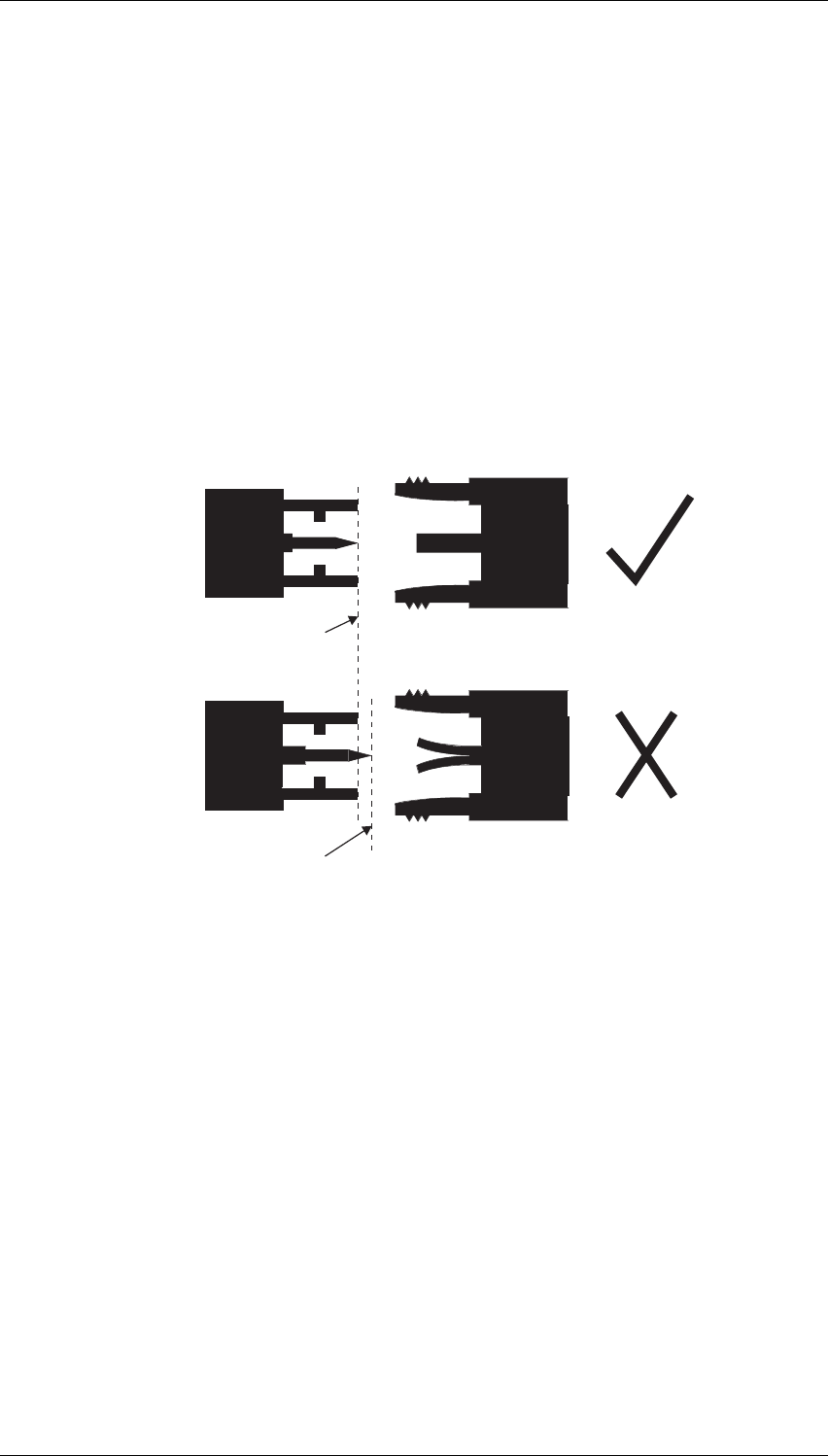
M8SL2-00-002-812 G1.5
© Copyright Tait Electronics Limited August 2004. All rights reserved.
1.6 RF Coax Cable and N-Type Connector
Make sure the RF coax cable to the N-type connector is free from sharp bends or twists.
If access to the rear of the rack frame is restricted, the cable should be long enough to
allow the slimline assembly to be fully withdrawn from the cabinet.
Make sure that any N-type plugs connected to Tait equipment are assembled according
to the manufacturer’s instructions. It is particularly important that the centre pin in the
plug is positioned correctly:
•if the pin is positioned too far back in the plug, it may not make good contact
with the socket;
•if the pin protrudes too far (as shown in Figure 1.5), or is not straight, it may
damage the socket when the plug is screwed in.
Figure 1.5 N-Type Plug Assembly Details
Hand ti
g
hten onl
y
N-Type Plug and Socket Cross-section
Correct pin position No damage to socket
Will damage socket
Extended pin position

G1.6 M8SL2-00-002-812
© Copyright Tait Electronics Limited August 2004. All rights reserved.
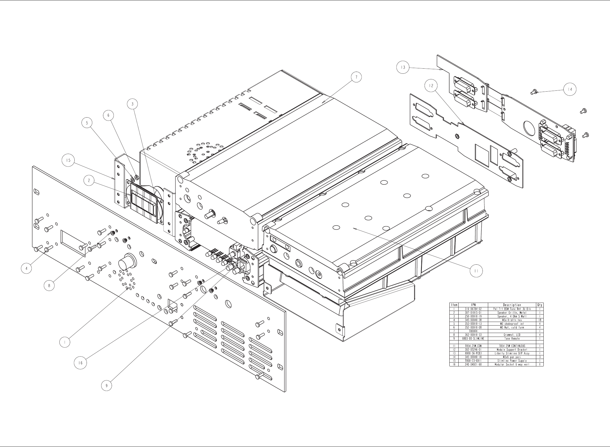
M8SL2-00-002-812 T800 SL2 G1.7
© Copyright Tait Electronics Limited August 2004. All rights reserved.
Figure 1.6 T800 SL2 Assembly
– with T803 fitted
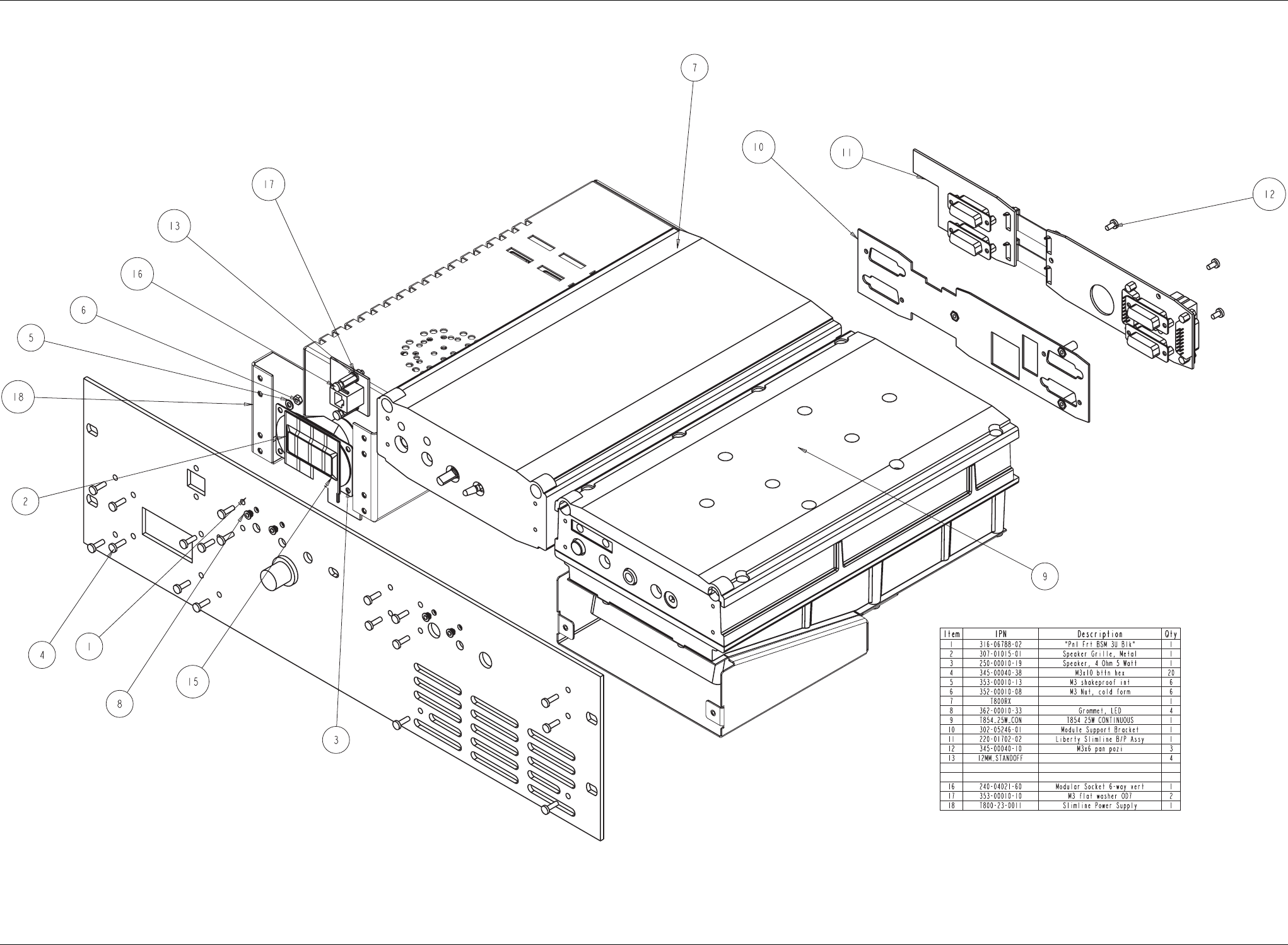
G1.8 T800 SL2 M8SL2-00-002-812
© Copyright Tait Electronics Limited August 2004. All rights reserved.
Figure 1.7 T800 SL2 Assembly
– without T803 fitted
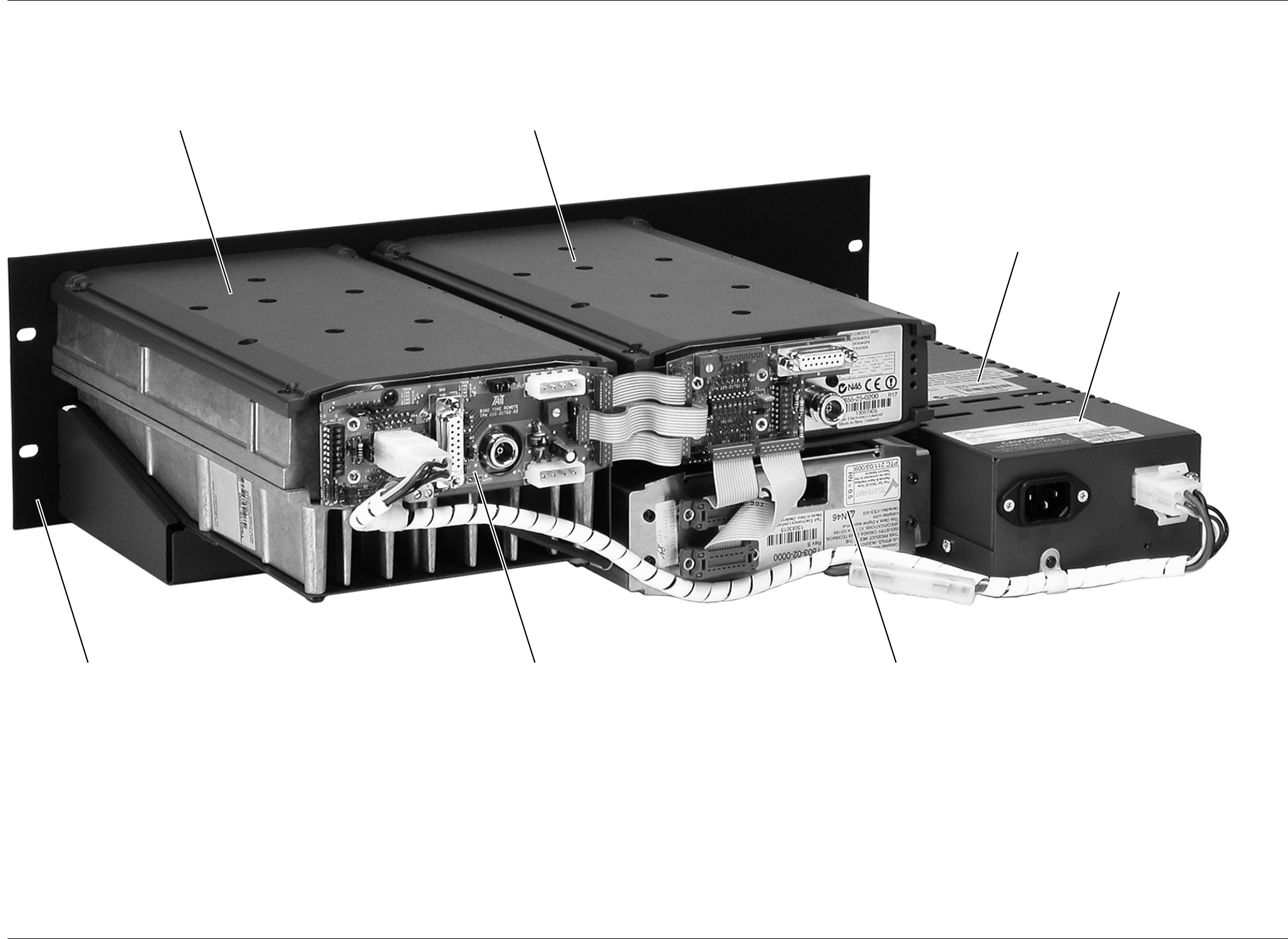
M8SL2-00-002-812 T800 SL2 G1.9
© Copyright Tait Electronics Limited August 2004. All rights reserved.
Figure 1.8 T800 SL2 Assembly
– with T803 fitted (rear view)
Transmitter Receiver
Backplane PCB Tone RemoteFront Panel
Power Supply
Power Rating Label

G1.10 T800 SL2 M8SL2-00-002-812
© Copyright Tait Electronics Limited August 2004. All rights reserved.

M8SL2-00-002-812 T854 Optional Features G2.1
© Copyright Tait Electronics Limited August 2004. All rights reserved.
2 T854 Optional Features
2.1 Audio Processor
The T854 come with a number of link selectable features which give added system flexi-
bility.
Note: The tables in this section are the same as those in Section 3.5 in Part C. They
have been repeated here for ease of reference.
2.1.1 Link Details
Use the following table to set up the audio processor to the configuration you require.
You should set the audio processor links before carrying out any of the tuning and
adjustment procedures.
Plug Linka
a. The letters in this column refer to the letters printed on the PCB beside each pair of pins.
Note that the link names and pin numbers are different to earlier products. The lettering A
to N is however the same.
Function
PL201
1–2
3–4b
5–6
b. Factory Setting
A
B
C
not connected
microphone pre-amp output to compressor input
microphone pre-amp output to multiplexer input
7–8
9–10b
11–12
13–14
D
E
F
G
pre-emphasis output to multiplexer input
pre-emphasis output to limiter input
not connected
not connected
PL202
1–2b
3–4
5–6
7–8
H
I
J
K
compressor output to multiplexer input
compressor output to limiter input
compressor output to pre-emphasis input
not connected
9–10b
11–12
13–14
L
M
N
multiplexer output to pre-emphasis input
multiplexer output to limiter input
multiplexer output to compressor input

G2.2 T854 Optional Features M8SL2-00-002-812
© Copyright Tait Electronics Limited August 2004. All rights reserved.
2.1.2 Typical Options
2.2 Line Transformer Configuration and Options
There are four Line Transformer options.
%T210 original T800 Line transformer T4030, 300/300:300/300
%T210A ETAL P1200 or similar 600:600 non centre-tapped leaded encapsulated Line
transformer
or ETAL P2602 or similar 300/300:600 centre-tapped leaded encapsulated Line
transformer
%T210B ETAL P2781 or similar 600:600 non centre-tapped SMD encapsulated Line
transformer
or ETAL P2782 or similar 300/300:600 centre-tapped SMD encapsulated Line
transformer
No transformer leaded (%R200 and %R203) or SMD (%R200A and %R203A ) by-pass
resistors fitted, and an attenuator pad if necessary.
The default option is %T210B, SMD P2781 or similar 600:600 non centre-tapped SMD
encapsulated Line transformer.
%T210A and %T210B use a standard footprint which allows the use of other similar
transformers with special characteristics, such as the ETAL P3181 ultra-low distortion
V.9 0 S M D.
PL205 PL210 PL215 PL220
microphone pre-amp. compressed
and pre-emphasised;
line input pre-emphasised
(standard set-up)
3–4a
B
a. Factory Setting
1–2a
L
3–4a
H
3–4a
E
microphone pre-amp. compressed
and pre-emphasised;
line input unprocessed
3–4
B
3–4
M
7–8
J
1–2
D
line and microphone compressed
and pre-emphasised
5–6
C
5–6
N
7–8
J
3–4
E
microphone pre-amp. compressed;
line and microphone flat response
3–4
B
3–4
M
3–4
H
5–6
F

M8SL2-00-002-812 T854 Optional Features G2.3
© Copyright Tait Electronics Limited August 2004. All rights reserved.
The line transformer is designed to provide a balanced interface to 600Ω lines, con-
nected between LINE I/P 1 and LINE I/P 4. When %T210 is fitted, the two centre con-
nections (LINE I/P 2 and LINE I/P 3) are shorted together for normal operation. With
the other options these two centre connections are available to the user via P204 and
P208, unless a centre-tapped %T210A or %T210B is used, wired to LINE I/P 3.
The secondary winding of the transformer is connected via 1kΩ (R202) and 10Ω (R160)
resistors to pin 6 (AUDIO-2) of D-range 1 and may be used to monitor audio on the line.
Pin 7 of D-range 1 can be reconfigured as AUDIO-1 by removing R808 and R160, and
placing %R150. Note that this configuration does not allow external programming of
the module
%R203C and %R203D have replaced SL201 and SL202.
To retain the DC loop keying keying facility, there is a centre-tapped version of the
ETAL leaded and SMD transformers, the P2602 and P2782 respectively. This will only
work for Common Earth systems. If full isolated DC loop keying is required, then the
T4030 must still be used. The T4030 must also be used if the Transmitter is to be used as
half of a 2-wire to 4-wire hybrid.
Trans fo r mer T4030 P1200 P2781 No
Trans fo r mer
IPN 053-00010-17 054-00010-16 054-00010-18
Designator %T210 %T210A %T210B
%R200 Not Fitted Not Fitted Not Fitted Not Fitted
%R200A Not Fitted Not Fitted Not Fitted 0Ω
%R203 Not Fitted Not Fitted Not Fitted Not Fitted
%R203A Not Fitted Not Fitted Not Fitted 0Ω
%R203B Not Fitted 0Ω0ΩNot Fitted
%R203C 0ΩNot Fitted Not Fitted Not Fitted
%R203D 0ΩNot Fitted Not Fitted Not Fitted
%R203E Not Fitted 560Ω560Ω560Ω
%R201 560ΩNot Fitted Not Fitted Not Fitted
C201 4U7 BP 4U7 BP 4U7 BP Not Fitted
C202 4U7 BP 4U7 BP 4U7 BP Not Fitted
%C204 4U7 BP Not Fitted Not Fitted Not Fitted
%C205 4U7 BP Not Fitted Not Fitted Not Fitted
%C203A Not Fitted 15nF 15nF Not Fitted
%C203B Not Fitted 15nF 15nF Not Fitted

G2.4 T854 Optional Features M8SL2-00-002-812
© Copyright Tait Electronics Limited August 2004. All rights reserved.
2.2.1 Line Limiter Option
This option should be fitted if no line transformer is installed.
2.2.2 Line Attenuator Option
When enabled this attenuates the line input by approximately 20dB
2.3 Opto Key
The keying circuitry may be completely isolated from the rest of the system by means of
the optocoupler (IC250). A constant current source (Q270) allows keying voltages
between 6 and 50 V.
R240 and R243 have replaced SL203 and SL204, originally on the T856 underside. These
connect the opto key to D-range 1 pins 11 and 12, and when removed free the D-range
pins for alternative use.
Enabled Disabled
%D205 1N4531 Not Fitted
%D210 1N4531 Not Fitted
Enabled Disabled
Link 1 Open Closed
%R211 470ΩNot Fitted
%R220 470ΩNot Fitted
%R228 120ΩNot Fitted
Opto+ to PL100/11 PL100/11 Free
R240 0ΩNot Fitted
Opto- to PL100/12 PL100/12 Free
R243 0ΩNot Fitted

M8SL2-00-002-812 T854 Optional Features G2.5
© Copyright Tait Electronics Limited August 2004. All rights reserved.
2.4 Relay Driver
A dedicated transistor (Q250) is provided for the purpose of switching an external (e.g.
coaxial) relay. The output is open collector and is activated by the Tx-Reg rail. This out-
put is available on pin 9 of the T800-03-0000 auxiliary D-range connector (D-range 2).
2.5 Local Microphone
Use of the local microphone (via the front panel stereo socket) will disable the audio
input from the line. The audio switching occurs when the PTT switch is closed.
2.6 Keying With Option PCBs
If an option PCB is fitted, the exciter may be keyed via the TX-ENB-OPT pad in the
audio processor. The line must be pulled low to key.
2.7 Transmit Key Time
(Refer to the appropriate test points and options connections drawing in Section 6 in
Part C.)
A solder link (SL501) is provided on the bottom of the PCB to allow two transmit key
time options, as shown in the table below.
*In this configuration the standby spurious emissions should be <–65dBm.
Transmit Key Time SL501
standard 30ms (approx.) not linked
short* <5ms linked

G2.6 T854 Optional Features M8SL2-00-002-812
© Copyright Tait Electronics Limited August 2004. All rights reserved.
2.8 Local PTT Indication for A800 SIM
This option allows the use of D-range 1 pin 3 for an external PTT indication when the
mic PTT or carrier switch is activated. Used for A-800 SIM or any other external control
or CTCSS unit.
2.9 Direct input to Buffer option
A direct input for data use. Note that this input will have 4.5V half-rail, and needs isola-
tion unless R289 is also removed. Leaving R291 as 0Ω and removing &R290 may
improve data shape (less overshoot), as &C289 is still in circuit.
2.10 Line Input Control Replacement
The Line Input control can be replaced with fixed resistors if required.
Enabled Disabled
D245 BAW56 BAW57
R276 0Ω0Ω
%R276A 0ΩNot fitted
%R203C Not fitted See transformer option table
Enabled Disabled
%R246 0ΩNot fitted
%R291 Not fitted 0Ω
%C265 Not fitted 4U7 BP
%R259 Not fitted 22K
Enabled Disabled
%R222 4K7 Not fitted
%R234 4K7 Not fitted
%RV210 Not fitted 10K Log
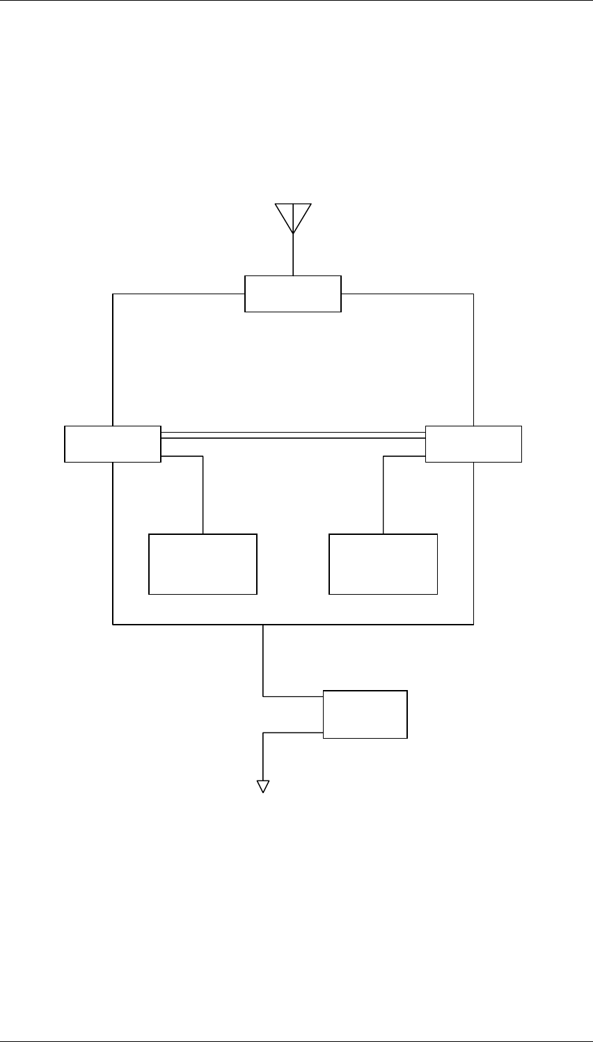
M8SL2-00-002-812 Talk Through Repeater G3.1
© Copyright Tait Electronics Limited August 2004. All rights reserved.
3 Talk Through Repeater
In this configuration the receiver directly keys the transmitter when the signal is
received. The demodulated audio is fed via 600Ω lines to the transmitter to modulate
the carrier. The receiver and transmitter operate simultaneously and must therefore be
on different frequencies. The minimum frequency separation depends on the duplexer
used.
Figure 3.1 Talk Through Repeater
Duplexer
Receiver Transmitter
Monitor
Speaker
Local
Microphone
13.8V
Supply
+
-
Tx Key Out
Line Out Line In
Tx Key In
Antenna
Typical line level -15dBm
Monitor
Out
Mic.
In
Transmit PortReceive Port
RF In
'N' Socket
RF Out
'N' Socket

G3.2 Talk Through Repeater M8SL2-00-002-812
© Copyright Tait Electronics Limited August 2004. All rights reserved.
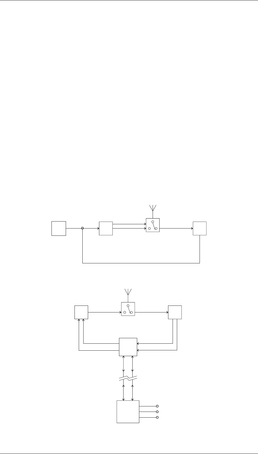
M8SL2-00-002-812 Line Controlled Base without Talk Through G4.1
© Copyright Tait Electronics Limited August 2004. All rights reserved.
4 Line Controlled Base without Talk
Through
4.11 General
This installation contains a transmitter and receiver which may or may not be on the
same frequency, thus simultaneous transmission and reception is not possible. When
the transmitter is keyed, the coaxial relay is also energised. When the relay is in its rest
position, signals from the antenna are passed to the receiver and the demodulated out-
put is fed via 600Ω lines to the RCU.
The receiver is disabled when the transmitter is energised to prevent the receiver mute
opening from RF due to lack of isolation in the relay, direct radiation or the noise skirt of
the dual frequency link.
Since the base station may be controlled via a 2-wire line and a 4-wire to 2-wire hybrid,
there is a possibility of system oscillation if the receiver is not disabled during transmit.
This occurs when the transmit energy enters the receiver and produces an audio
response which can pass from the receive to the transmit audio part of the hybrid
(impedance imbalance, etc).
Figure 4.2 Basic Configuration
Figure 4.3 Remote Line Controlled Base Station
RF Out Coax
Relay
DC
Key
Logic
Tx
Enable
DC Relay
Control
RF In
Tx Rx
Antenna
Rx Disable
Tx AF
RF Out Coax
Relay
RF In
Tx Rx
Antenna
Hybrid
Rx AF
Remote
Control
Microphone
Speaker
PTT
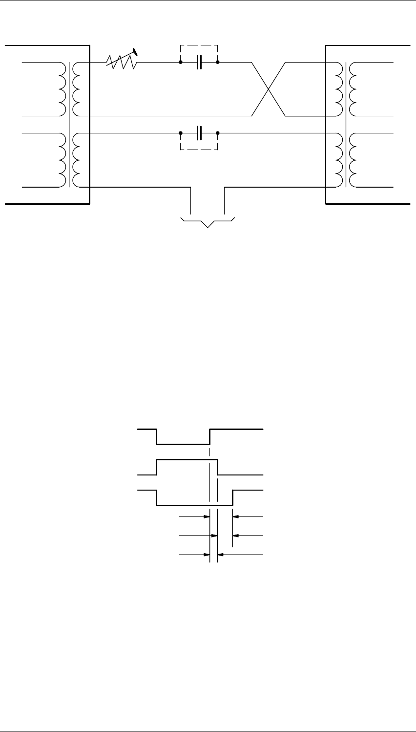
G4.2 Line Controlled Base without Talk Through M8SL2-00-002-812
© Copyright Tait Electronics Limited August 2004. All rights reserved.
Figure 4.4 4-Wire to 2-Wire Converter
Note: This configuration is only possible when transformer %T210 and T4030 are
fitted. Refer to Section 2.2.
4.12 Transmitter Tail Timer
If the transmitter has the tail timer enabled:
•the receiver disable timer must be set so that tRx/Dis > tTx/Tail;
Figure 4.5 Receiver Disable Time vs Tail Time
•if the system configuration also uses an aerial changeover relay as well as the tail
timer, the changeover relay must be driven from the relay driver (Q250) in the
audio processor, rather than by Tx-Key or Tx-Enable; this output is available on
pin 9 of the T800-03-000 auxiliary D-range (D-range 2);
•depending on tail time requirements, it is possible for the transmitter tail time to
exceed the receiver disable time capability; in this situation the receiver disable
line should also be driven from relay driver Q250 (D-range 2 pin 9).
2-Wire Line
C1
C2
TransmitterReceiver
RV1
approx. 2µ
Hybrid Balance
1k
Rx Disable Time
No Tx or Rx
Tail Time
On
Tx Reg.
Rx Off
Tx Enable
& Rx Disable
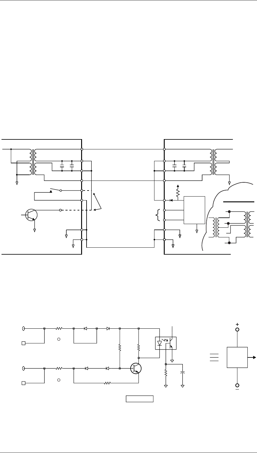
M8SL2-00-002-812 DC Line Keying G5.1
© Copyright Tait Electronics Limited August 2004. All rights reserved.
5 DC Line Keying
Where the transmitter and receiver are separated by only a short distance and DC isola-
tion is not required, DC loop keying may be employed.
Note: This feature is not available with standard line transformer ETAL P2781
(%T201B). Refer to Section 2.2.
A small DC current (usually less than 10mA) can be fed via the balanced 2-wire line to
provide remote control of various functions.
In a duplex system the receiver mute is used to key a transmitter, provided there is a
common earth between the two units (refer to Figure 5.6).
Figure 5.6 DC Loop Keying With Common Earth
Where the receiver and transmitter (or remote control) are distant, DC loop keying is
provided by an isolated supply, driver and detector because an earth cannot be relied on
(refer to Figure 5.7, Figure 5.8 and Figure 5.9).
Figure 5.7 Isolated Constant Current Loop Current Detector
(Opto-key input on T854)
Pin 14
Pin 12
Pin 1 (PL100)
Pin 3
Tx Key Pin 13
Pin 1
Pin 2
Pin 3
Pin 4
Pin 12
Pin 11
Pin 15
Pin 14
C266
8
4
3
5
6
27
1
Audio Out T210
C268
RL210
Pin 13
C202
1
5
6
4
3
7
2
8
T210
C201
Pin 4 (PL100)
Audio
Processor
Keying
Logic
Pin 15
Earth
Pin 2
+
-
Opto Key
+9V
R657
D620
Optional:
Relay contact or
Q270 collector
can be used.
Receiver Transmitter
Short Line
Q270
T210A/B
1
4
3
2
Transmitter
C201, 202, 230A %R203B/C/D
not shown for clarity
OR
Det.
D260 D260
BAW56 BAW56
2331
I/OPAD
P219
OPTO-KEY+
OPTO-KEY-
OPTO-KEY+
OPTO-KEY-
I/OPAD
P225
D270 D270
BAV99 BAV99
13 32
R268
100
OPTO-KEY
Q270
BD139 R271
390K
C275
120P
R269
10K
R270
470
IC250
4N25A
15
264
R240
R243
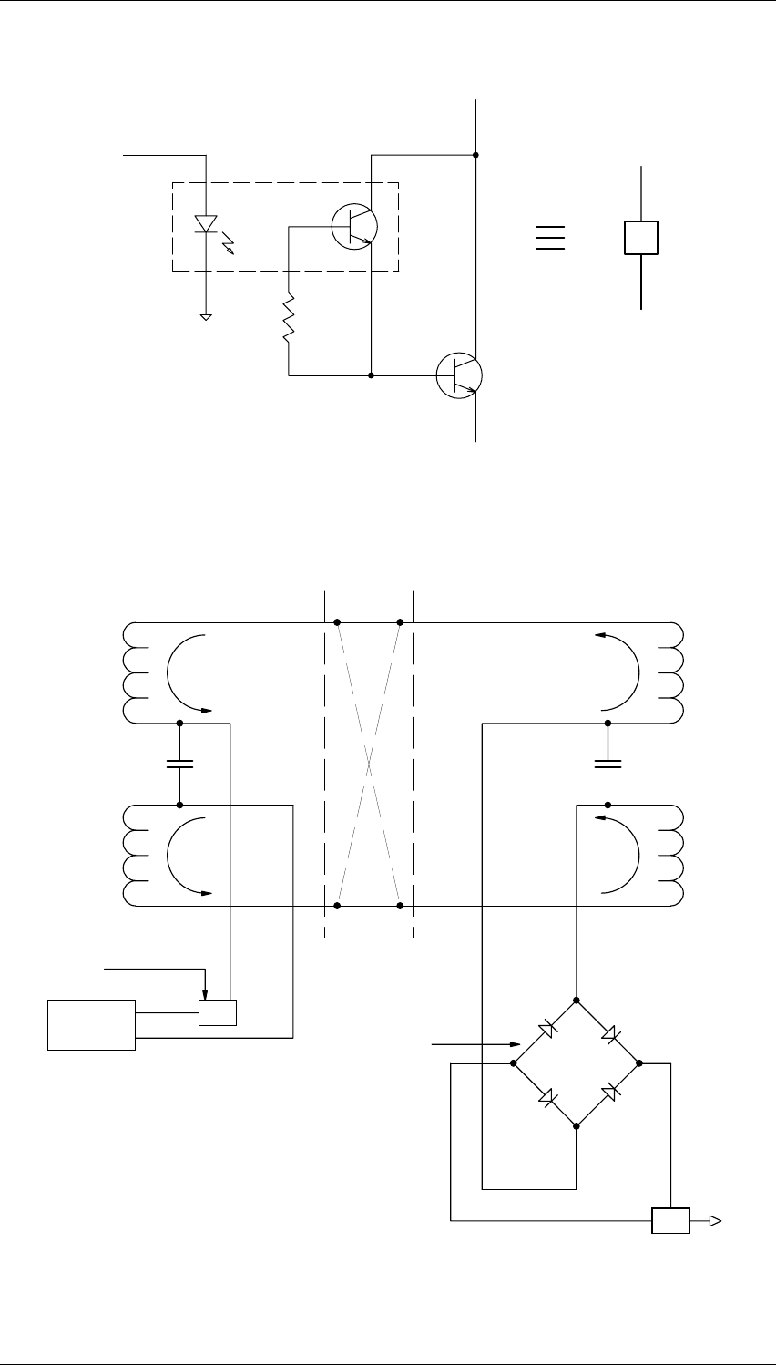
G5.2 DC Line Keying M8SL2-00-002-812
© Copyright Tait Electronics Limited August 2004. All rights reserved.
Figure 5.8 Isolated Loop Current Switch
Figure 5.9 Typical System
O
+
O
O
-
O
+
O
-
SW
SW
Isolated
Supply -
Unit 1 Unit 2
+
Long Line
Det
Optional bridge
to protect against
polarity reversals
(T223 only).

M8SL2-00-002-812 X800-56-PCB3 PCB Information G6.2.1
© Copyright Tait Electronics Limited August 2004. All rights reserved.
6.2 X800-56-PCB3 Backplane PCB
Caution: This equipment contains CMOS devices which are susceptible to damage from
static charges.
This section contains the following information.
IPN Section Page
220-01702-02 Backplane Links and Switches
Parts List
PCB Layout – Top Side
PCB Layout – Bottom Side
Circuit Diagram
6.2.3
6.2.5
6.2.7
6.2.8
6.2.9

M8SL2-00-002-812 X800-56-PCB3 PCB Information G6.1.1
© Copyright Tait Electronics Limited August 2004. All rights reserved.
6 X800-56-PCB3 PCB Information
This part of the manual provides the parts list, PCB layouts and circuit diagram for the
X800-56-PCB3 backplane PCB. There is a detailed table of contents at the start of Section 2.
Section Title IPN Page
1 Introduction 6.1.1
2 X800-56-PCB3 backplane PCB 220-01702-02 6.2.1

G6.1.2 X800-56-PCB3 PCB Information M8SL2-00-002-812
© Copyright Tait Electronics Limited August 2004. All rights reserved.
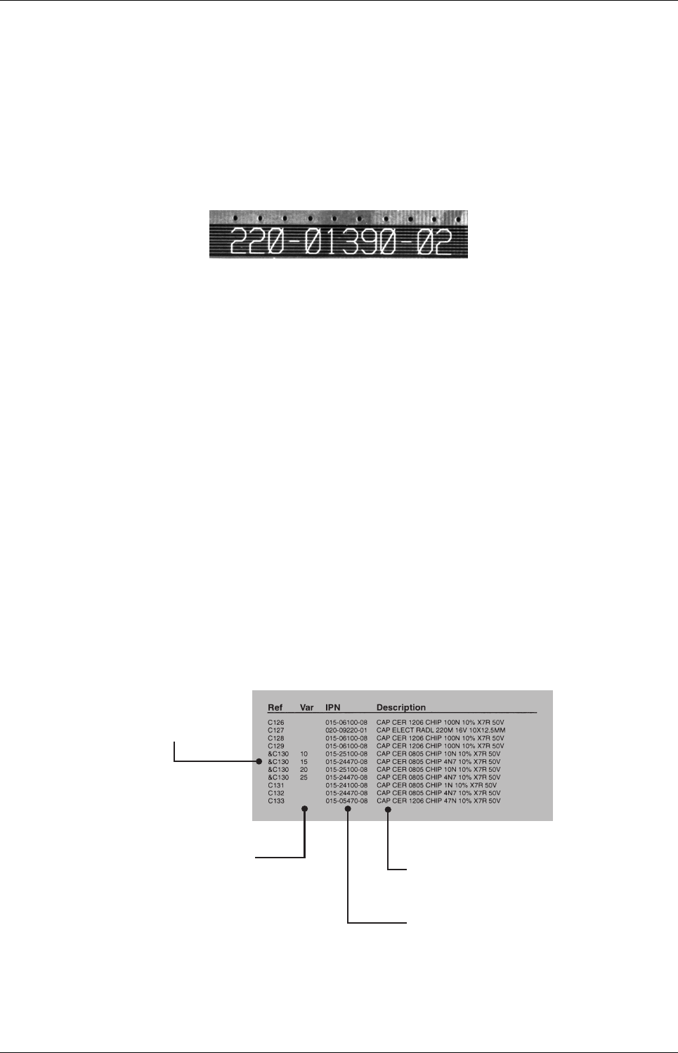
M8SL2-00-002-812 X800-56-PCB3 PCB Information G6.1.3
© Copyright Tait Electronics Limited August 2004. All rights reserved.
6.1 Introduction
PCB Identification
All PCBs are identified by a unique 10 digit “internal part number” (IPN), e.g. 220-12345-00, which
is screen printed onto the PCB (usually on the top side), as shown in the example below:
The last 2 digits of this number define the issue status, which starts at 00 and increments through 01,
02, 03, etc. as the PCB is updated. Some issue PCBs never reach full production status and are there-
fore not included in this manual. A letter following the 10 digit IPN has no relevance in identifying
the PCB for service purposes.
Note: It is important that you identify which issue PCB you are working on so that you can
refer to the appropriate set of PCB information.
Parts Lists
The 10 digit numbers (000-00000-00) in this Parts List are “internal part numbers” (IPNs). We can
process your spare parts orders more efficiently and accurately if you quote the IPN and provide a
brief description of the part.
The components listed in this parts list are divided into two main types: those with a circuit refer-
ence (e.g. C2, D1, R121, etc.) and those without (miscellaneous and mechanical).
Those with a circuit reference are grouped in alphabetical order and then in numerical order within
each group. Each component entry comprises three or four columns, as shown below:
The mechanical and miscellaneous section lists the variant and common parts in IPN order.
circuit reference -
lists components
in alphanumeric
order
variant column -
indicates that this is
a variant component
which is fitted only to
the product type listed
Internal Part Number -
order the component
b
y
this number
description -
gives a brief description
of the component

G6.1.4 X800-56-PCB3 PCB Information M8SL2-00-002-812
© Copyright Tait Electronics Limited August 2004. All rights reserved.
Grid Reference Index
This section contains a component grid reference index to help you find components and labelled
pads on the PCB layouts and circuit diagrams. This index lists the components and pads in alpha-
numeric order, along with the appropriate alphanumeric grid references, as shown below:
Using CAD Circuit Diagrams
Reading a CAD circuit diagram is similar to reading a road map, in that both have an alphanumeric
border. The circuit diagrams in this manual use letters to represent the horizontal axis, and numbers
for the vertical axis. These circuit diagram “grid references” are useful in following a circuit that is
spread over two or more sheets.
When a line representing part of the circuitry is discontinued, a reference will be given at the end of
the line to indicate where the rest of the circuitry is located, as shown below. The first digit refers to
the sheet number and the last two characters refer to the location on that sheet of the continuation of
the circuit (e.g. 1R3).
circuit diagram
reference
P
C
B layout
reference
components listed
in alphanumeric order
layer number -
1 = top side layer
2 = bottom side layer
component location
on the layer
sheet number
component location
on the sheet
C301
4N7
R303
12
D
S
G
L310
33U
IF-SIG
4R4
C369
100P
C371
10U
R339
100K
%R338
100
DISCRIMINATOR
1R3
2R9
2R9
8A2
t
hese grid references
s
how where the circuit
is continued

G6.2.2 X800-56-PCB3 PCB Information M8SL2-00-002-812
© Copyright Tait Electronics Limited August 2004. All rights reserved.

M8SL2-00-002-812 X800-56-PCB3 PCB Information G6.2.3
© Copyright Tait Electronics Limited August 2004. All rights reserved.
Backplane Links and Switches
The tables below explain the functions of each of the links and switches on the X800-56-PCB3 back-
plane.
Table 6.1 X800-56-PCB3 links
Link Function Notes
LN1,
LN2
Connects balanced audio from the receiver to the trans-
mitter. For talk-through operation.
LN3 Connects Rx-Gate to Tx-Key.
LN4 Select between primary serial comms (link pins 2–3) or
secondary (link pins 1–2).
Secondary serial comms is via the receiver and
transmitter Aux connectors (second D-ranges).
LN5 Connects Tx-Relay-Driver output from transmitter to
the coax relay.
LN6 Select between serial comms (link pins 1–2) or RSSI (link
pins 2–3) on pin 11 of SK6 (Auxiliary connector).
LN7 Links external (or T803) CTCSS audio to transmitter. T803 CTCSS audio not available at time of publi-
cation.
LN8
Link pins 1–2. Connects unbalanced Rx audio
(‘Audio1’) to T803. Not to be used when CTCSS is
present on RX audio as internal CTCSS filtering cannot
be applied to this path. For CTCSS use the option below.
Adjust level using RV2. Level to T803 independ-
ent of Rx Line Level control.
Link Pins 2–3 and Pins 4–5. Changes the balanced Rx
Line audio output to unbalanced for the T803. This
option should be used when CTCSS is present on RX
audio so that the internal CTCSS filter can be applied.
Level to T803 controlled by RX Line Level control.
LN9
T854 transmitters (after S/N 13098764):
Select between Transmitter Aux-Out-0 (link pins 2–3) or
direct FWD power sense voltage (link pins1–2). The lat-
ter could be used for an externally fitted RF power indi-
cator or alarm.
If an internal alarm board is fitted Aux-Out-0
(link pins 2–3) becomes FWD power alarm out-
put.
Older T854 transmitters (s/n 13098764 or earlier):
Select between Transmitter Aux-Out-0 (link pins 2–3) or
Aux-Out-1 (link pins 1–2).
LN10
T854 transmitters (after S/N 13098764):
Select between direct FWD power sense voltage (link
pins 2–3) or direct REV power sense voltage (link
pins1–2). Could be used for an externally fitted RF
power indicator or alarm.
If an internal alarm board is fitted direct FWD
power sense voltage (link pins 2–3) becomes REV
power alarm output.
Older T854 transmitters (s/n 13098764 or earlier):
Selection between transmitter Aux-Out-1 (link pins 2–3)
or Aux-Out-2 (link pins1–2).
LN11 Connects RX CTCSS disable from the T803 to the
receiver.
LN12 Connects Tx-Relay-Driver output from the transmitter
to RX-Inhibit on the receiver.
Recommended setting to prevent the receiver
mute from inadvertently opening.

IPN 220-01702-02
G6.2.4 X800-56-PCB3 PCB Information M8SL2-00-002-812
© Copyright Tait Electronics Limited August 2004. All rights reserved.
Figure 6.10 X800-56-PCB3 switches
Switch Function Notes
SW1-1 Hardware selection of channel select 1
Leave OFF for Channel select via
T803 and or PGM800Win
SW1-2 Hardware selection of channel select 2
SW1-3 Hardware selection of channel select 3
SW1-4 Hardware selection of channel select 4
SW1-5 Hardware selection of channel select 5
SW1-6 Hardware selection of channel select 6
SW1-7 Hardware selection of channel select 7
SW1-8 Hardware selection of channel select 8
SW2-1
T854 transmitters (after S/N 13098764 ):
When ON connects transmitter Aux-Out-0 or direct FWD power
sense voltage to ground, depending on the links on LN9. See
description of LN9 in the previous table
Not recommended that direct FWD
power sense voltage is grounded.
For older T854 transmitters (s/n 13098764 or earlier):
When ON connects transmitter Aux-Out-0 or Aux-Out-1 to
ground, depending on the links on LN9. See description of LN9 in
the previous table.
SW2-2
T854 transmitters (after S/N 13098764):
When ON connects direct FWD power sense voltage or direct REV
power sense voltage to ground depending on the links on LN10.
See description of LN10 in the previous table.
Not recommended
For older T854 transmitters (s/n 13098764 or earlier):
When ON connects transmitter Aux-Out-1 or Aux-Out-2 to
ground, depending on the links on LN10. See description of LN10
in the previous table.
SW2-3 When ON connects Serial Comms to Pin 6 of transmitter D-Range1
SW2-4 When ON connects Serial Comms to the transmitter (Tx D-Range1
pin 7) Default = ON
SW2-5 When ON connects Serial Comms to the receiver (Rx D-range1 pin
7) and the T803 Default = ON
SW2-6 Not used
SW2-7 When ON connects Tx-Key to ground
SW2-8 Not used
SW3-1 When ON connects Rx-Audio through to the T803 and the external
Auxiliary connector ( SK13 pin2 )
SW3-2,
SW3-3
When ON connects balanced audio from the T803 or the external
Auxiliary connector ( SK13 pins 3 and 4 ) to the Transmitter.
SW3-4 When ON connects Receiver RSSI through to the T803
SW3-5 When ON connects Tx-Key from the T803 to the Transmitter
SW3-6 When ON connects Rx-Gate to the T803 and the external Auxiliary
connector ( SK13 pin9 )
SW3-7 When ON connects T803 CTCSS audio to the transmitter. T803 CTCSS audio not available at
time of publication.
SW3-8 Not used.

IPN 220-01702-02
M8SL2-00-002-812 X800-56-PCB3 PCB Information G6.2.5
© Copyright Tait Electronics Limited August 2004. All rights reserved.
Ref IPN Description Ref IPN Description
X800-56-PCB3 Parts List/Grid Reference Index (IPN 220-01702-02)
How To Use This Parts List
The components listed in this parts list are grouped in alphabetical order and then in numerical order within each group. Each compo-
nent entry comprises three or four columns: the circuit reference, variant (if applicable), IPN and description. A number in the variant
column indicates that this is a variant component which is fitted only to the product type listed.
This parts list is correct at the time of publishing, but is subject to change without notification. An up to date parts list can be obtained
from your local Customer Service Organisation
C1 020-09120-01 120UF 6.3Dx15H mm
CN1 240-04030-09 SK2TB TERMINAL BLOCK 2WAY SIDE ENTRY
D1 001-50012-05 1N4531 AI SMALL SIGNAL
D2 001-00015-12 BZX79 VOLTAGE REGULATOR
D3 001-00011-70 1N4001 GENERAL PURPOSE
D4 001-00011-70 1N4001 GENERAL PURPOSE
D5 001-00011-70 1N4001 GENERAL PURPOSE
D7 001-00011-70 1N4001 GENERAL PURPOSE
D8 001-00011-60 MR760 HIGH CURRENT CASE 194-04
F1 265-00010-69 900MA RESETABLE 30V 40A
F2 265-00010-69 900MA RESETABLE 30V 40A
LN1 240-00020-68 HEADER PLUG 2WAY WITH SHORTING LINK
LN10 240-00020-59 HEADER PLUG 3WAY WITH SHORTING LINK
LN11 240-00020-68 HEADER PLUG 2WAY WITH SHORTING LINK
LN12 240-00020-68 HEADER PLUG 2WAY WITH SHORTING LINK
LN2 240-00020-68 HEADER PLUG 2WAY WITH SHORTING LINK
LN3 240-00020-68 HEADER PLUG 2WAY WITH SHORTING LINK
LN4 240-00020-59 HEADER PLUG 3WAY WITH SHORTING LINK
LN5 240-00020-68 HEADER PLUG 2WAY WITH SHORTING LINK
LN6 240-00020-59 HEADER PLUG 3WAY WITH SHORTING LINK
LN7 240-00020-68 HEADER PLUG 2WAY WITH SHORTING LINK
LN8 240-00020-58 HEADER PLUG 5WAY WITH SHORTING LINK
LN9 240-00020-59 HEADER PLUG 3WAY WITH SHORTING LINK
MT1 MTG-C420P-35 P3MM5_420C MOUNTING HOLE 3.5MM HOLE
4.2MM PAD
MT2 MTG-C420P-35 P3MM5_420C MOUNTING HOLE 3.5MM HOLE
4.2MM PAD
MT3 MTG-C420P-35 P3MM5_420C MOUNTING HOLE 3.5MM HOLE
4.2MM PAD
PL1 240-00020-58 HEADER PLUG 5WAY WITH SHORTING LINK
PL2 240-02011-20 "HEADER 4WAY 1ROW 200"" PITCH TOP ENT
WITH SHROUD"
PL3 240-02011-20 "HEADER 4WAY 1ROW 200"" PITCH TOP ENT
WITH SHROUD"
PL4 240-00010-64 HEADER PLUG 6WAY 2X3 TOP ENTRY WITH
SHROUD
Q1 000-50010-60 BC327 AI AF POWER
Q2 000-00010-66 BC337 AF POWER
R1 030-02100-00 10 FILM 7X2.5MM
R2 032-05100-00 10K M/F 7X2.5MM
R3 032-04100-00 1K M/F 7X2.5MM
R4 032-04100-00 1K M/F 7X2.5MM
R5 032-04100-00 1K M/F 7X2.5MM
R6 032-04220-00 2.2K M/F 7X2.5MM
R7 030-03270-00 270 FILM 7X2.5MM
R8 030-03270-00 270 FILM 7X2.5MM
R9 030-03270-00 270 FILM 7X2.5MM
RV1 042-05100-10 10K CERMET 9.5mm SQ Top Adjust 3386P
RV2 042-06100-09 100K CERMET 9.5mm SQ Top Adjust 3386P
SK1 240-02020-15 SKT 15WAY DRANGE ASTRON AT-DB500-15-F-A55
SK10 240-00010-79 SKT 10WAY 2X5 AMP MICRO MATCH TOP ENTRY
SK11 240-00010-79 SKT 10WAY 2X5 AMP MICRO MATCH TOP ENTRY
SK12 240-00010-79 SKT 10WAY 2X5 AMP MICRO MATCH TOP ENTRY
SK13 240-02020-15 SKT 15WAY DRANGE ASTRON AT-DB500-15-F-A55
SK14 240-04020-54 SKT 16WAY AMP MICRO MATCH TOP ENTRY
SK15 240-04020-54 SKT 16WAY AMP MICRO MATCH TOP ENTRY
SK2 240-02020-15 SKT 15WAY DRANGE ASTRON AT-DB500-15-F-A55
SK3 240-02020-15 SKT 15WAY DRANGE ASTRON AT-DB500-15-F-A55
SK4 240-02020-15 SKT 15WAY DRANGE ASTRON AT-DB500-15-F-A55
SK5 240-04020-54 SKT 16WAY AMP MICRO MATCH TOP ENTRY
SK6 240-02020-15 SKT 15WAY DRANGE ASTRON AT-DB500-15-F-A55
SK7 240-00010-79 SKT 10WAY 2X5 AMP MICRO MATCH TOP ENTRY
SK8 240-00010-79 SKT 10WAY 2X5 AMP MICRO MATCH TOP ENTRY
SK9 240-00010-79 SKT 10WAY 2X5 AMP MICRO MATCH TOP ENTRY
SW1 230-00010-19 DIP-8 SW X 8 SPST DIP
SW2 230-00010-19 DIP-8 SW X 8 SPST DIP
SW3 230-00010-19 DIP-8 SW X 8 SPST DIP
TP1 UNI-009TP-XX PROBE TESTPOINT WITH A 0.8MM HOLE AND A
1.25MM COPPER PAD
TP2 UNI-009TP-XX PROBE TESTPOINT WITH A 0.8MM HOLE AND A
1.25MM COPPER PAD
TP3 UNI-009TP-XX PROBE TESTPOINT WITH A 0.8MM HOLE AND A
1.25MM COPPER PAD

IPN 220-01702-02
G6.2.6 X800-56-PCB3 PCB Information M8SL2-00-002-812
© Copyright Tait Electronics Limited August 2004. All rights reserved.
IPN 220-01702-02
M8SL2-00-002-812 X800-56-PCB3 PCB Information G6.2.7
© Copyright Tait Electronics Limited August 2004. All rights reserved.
X800-56-PCB3 PCB (IPN 220-01702-02) – Top Side
220-01702-02
IPN 220-01702-02
G6.2.8 X800-56-PCB3 PCB Information M8SL2-00-002-812
© Copyright Tait Electronics Limited August 2004. All rights reserved.
X800-56-PCB3 PCB (IPN 220-01702-02) – Bottom Side
220-01702-02
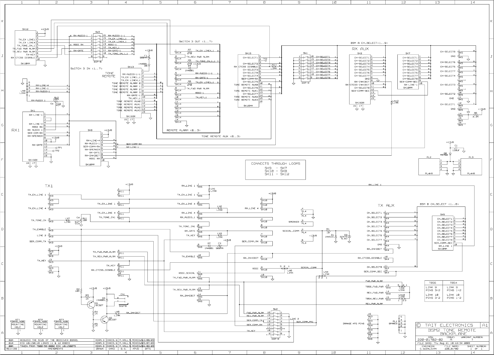
IPN 220-01702-02
M8SL2-00-002-812 X800-56-PCB3 PCB Information G6.2.9
© Copyright Tait Electronics Limited August 2004. All rights reserved.
X800-56-PCB3 circuit diagram
220-01702-02
IPN 220-01702-02
G6.2.10 X800-56-PCB3 PCB Information M8SL2-00-002-812
© Copyright Tait Electronics Limited August 2004. All rights reserved.

M8SL2-00-002-812 HI
© Copyright Tait Electronics Limited August 2004. All rights reserved.
Part H T800 Ancillary Equipment
This part of the manual features a brief description of the major ancillaries that may be
used with T800 SL2 equipment. For a comprehensive list of available ancillary equip-
ment, please contact your nearest Tait Dealer or Customer Service Organisation.
Section Page
Programming Kits 1.1
General Ancillaries 1.2
Paging 1.3
External Frequency Reference 1.4

HII M8SL2-00-002-812
© Copyright Tait Electronics Limited August 2004. All rights reserved.

M8SL2-00-002-812 T800 Ancillary Equipment H1.1
© Copyright Tait Electronics Limited August 2004. All rights reserved.
1 T800 Ancillary Equipment
1.1 Programming Kits
T800-01-0000
The T800-01-0000 kit is used for programming T800 SL2 base station equipment using a
standard IBM (or compatible) PC.
The kit comprises the following items:
PGM800Win programming software user's manual
PGM800Win Windows based programming software on CD
T800-01-0002 programming cable.
T800-01-0001
The T800-01-0001 kit is the same as the T800-01-0000 kit described above, but with the
addition of the T800-01-0004 module programming interface.
T800-01-0002
The T800-01-0002 programming cable connects the PC directly to the programming
socket on the T800 SL2 rack frame speaker panel or backplane PCB, thus enabling T800
SL2 modules to be read or programmed while in the rack frame. It can also connect to
the programming socket on the T800-01-0004 programming module interface if the
module is to be read or programmed while out of the rack frame.
T800-01-0003
The T800-01-0003 programming kit contains a T800-01-0002 programming cable and a
T800-01-0004 programming module interface.
T800-01-0004
The T800-01-0004 programming module interface is designed to allow a PC to connect
directly to a T800 SL2 module. It comprises a small PCB on which is mounted a D-range
socket, a programming socket, a Micromatch socket and a DC input connector.
The T800-01-0004 plugs directly into D-range 1 or D-range 2 (selected by a switch on the
PCB), or into SK805 in the microcontroller compartment via the supplied ribbon cable
loom, and is then connected to the PC with a T800-01-0002 programming cable.
Refer to the T800 Ancillary Equipment Service Manual for more information.

H1.1.2 T800 Ancillary Equipment M8SL2-00-002-812
© Copyright Tait Electronics Limited August 2004. All rights reserved.
1.2 General Ancillaries
T800-09-0001 RF Coaxial Relay
The T800-09-0001 is an RF coaxial relay assembly fitted with three female N-type con-
nectors, and comes complete with a mounting bracket and two coaxial cables termi-
nated in male N-type connectors. It can be used, for example, in base station
applications where the receiver and transmitter share the same antenna, in which case it
can be driven by the T800 SL2 transmitter relay driver (refer to Section 2.4 in Part G for
more information).
T800-01-0010 Calibration Test Unit
The T800-01-0010 provides all inputs and outputs necessary to carry out the full tuning
and adjustment procedure for T800 Series I and II receivers, exciters and transmitters. It
provides a convenient method of connecting test equipment, including a PC and power
supply, to a T800 Series I or II module (via D-range 1) without the need to construct cus-
tom wiring looms.
The T800-01-0010 also has a built-in speaker, a switch for selecting Series I or II modules,
and uses standard BNC and “banana plug” sockets.
T800-03 Auxiliary D-Range
The T800-03 is an additional D-range kit comprising one D-range plug assembly and
two locating pins, nuts and washers. Although originally a T800 Series I ancillary, it can
be used in T800 SL2 products for special applications requiring custom internal wiring.
T800-03-0000 Auxiliary D-Range
The T800-03-0000 is an additional D-range kit (normally fitted as D-range 2) comprising
one D-range plug assembly complete with connecting loom and mounting screws. The
ribbon cable loom connects the D-range PCB to the Micromatch socket (SK805) in the
microcontroller compartment. Typical uses of the T800-03-0000 are in paging applica-
tions and where external channel control is required. Refer to Figure 1.4 in Part G for the
T800-03-0000 pin connections.

M8SL2-00-002-812 T800 Ancillary Equipment H1.3
© Copyright Tait Electronics Limited August 2004. All rights reserved.
T800-04-0000 RSSI
The T800-04 RSSI option PCB plugs directly into the main PCB (support circuitry being
fitted as standard). It is fitted to the T855, T875 and T885 whenever receiver signal
strength monitoring is required, e.g. trunking or voting. Its function is to provide a DC
voltage proportional to the signal level at the receiver input.
T800-10-0000 Channel Select PCB
The T800-10-0000 is a small PCB that plugs into the Micromatch connector (SK805) in
the microcontroller compartment of a T800 SL2 receiver, exciter or transmitter. It is fitted
with an eight-switch DIP switch which allows the manual selection of any one of the
channels already programmed into the module by PGM800Win. The T800-10-0000 is
also fitted with a Micromatch socket to provide access to SK805 for programming pur-
poses.
T800-80-0000 Local Microphone
A 600Ω microphone complete with 300mm cord terminated in a ¼” stereo plug for use
with the T854.
T800-80-0001 T803 Microphone
A 600Ω microphone complete with 300mm cord terminated with a RJ11connector for
use with the T803.

H1.1.4 T800 Ancillary Equipment M8SL2-00-002-812
© Copyright Tait Electronics Limited August 2004. All rights reserved.
1.3 Paging
T800-30-0000 and T800-30-0002 DFSK Modulators
The T800-30-0000 (formerly T800-30) and T800-30-0002 (formerly T800-35) are DFSK
modulators for T800 SL2 transmitters, suitable for POCSAG or similar paging data for-
mats. Analogue transmissions (e.g. tone or speech) are still possible by disabling the
data path via a control line. 512 or 1200 baud data rates are link selectable. The
T800-30-0002 is adapted for use with an external reference oscillator for simulcast trans-
mission. The T800-30-0000 and T800-30-0002 are not designed for use with 66 to 88MHz
equipment.
T800-32-0000 and T800-32-0010 DFSK Modulators
The T800-32-0000 and T800-32-0010 are DFSK modulator PCBs which can be fitted to
T800 SL2 transmitters to enable them to function as low-speed paging transmitters.
These new PCBs have been specifically designed for Series II transmitters and are much
easier to fit into the latest design transmitters.
Both PCBs are suitable for POCSAG or similar paging data formats, but are not
designed for analogue transmissions (e.g. tone or speech). The T800-32-0010 is adapted
for use with an external reference oscillator for simulcast transmission. The
T800-32-0000 and T800-32-0010 are not designed for use with 66 to 88MHz equipment.

M8SL2-00-002-812 T800 Ancillary Equipment H1.5
© Copyright Tait Electronics Limited August 2004. All rights reserved.
1.4 External Frequency Reference
T800-06-0000 External Frequency Reference Kit
The T800-06-0000 kit provides an additional D-range plug/PCB assembly which incor-
porates a miniature RF connector to carry an externally generated 12.8MHz reference
signal into a T800 SL2 module. This enables the use of very high stability external refer-
ence oscillators for special applications.
The D-range PCB is also fitted with a Micromatch socket which can be connected to
SK805 in the microcontroller section via the supplied loom to provide access to the
channel change lines.
The kit comes complete with fitting instructions and all installation hardware.
T800-06-0001 External Frequency Reference Kit
The T800-06-0001 is the same as the T800-06-0000 kit with the addition of a special coax
cable for external frequency reference input. One end of this coax is terminated with a
miniature RF connector which fits into the D-range socket in an appropriate backplane
PCB to connect to a T800 SL2 module fitted with a T800-06-0000 kit. The other end is ter-
minated with a BNC connector which can be mounted on the rack frame.
T801-00 Frequency Reference Module
The T801-00 frequency reference module provides a high stability frequency source to
which the synthesiser within a T800 SL2 base station can be locked. The master standard
within the T801-00 is primarily intended to be rubidium, although high quality oven-
ised crystal oscillators can also be used in applications where more frequent readjust-
ment of frequency is acceptable. The T801-00 converts the output frequency from its
master standard to the 12.8MHz required by the T800 SL2 base station.
Refer to M801-00.
T801-10 OCXO Module
The T801-10 OCXO module provides a high stability frequency source to which the syn-
thesiser within a T800 SL2 base station can be locked. This will provide T800 SL2 trans-
mitters with the frequency stability required for simulcast transmission. The master
standard within the T801-10 is a high quality ovenised crystal oscillator (OCXO). Three
outputs are provided on the rear panel, which allows up to three T800 SL2 transmitters
to be referenced to the source oscillator.
Refer to M801-10.
