MPI_Floppy_Interfacing_Guide_Feb1980 MPI Floppy Interfacing Guide Feb1980
User Manual: Pdf MPI_Floppy_Interfacing_Guide_Feb1980
Open the PDF directly: View PDF ![]() .
.
Page Count: 18
FLEXIBLE
DISK
DRIVE
INTERFACING
GUIDE
MICRO
PERIPHERALS
INC.
REPRESENTED
BY
RSSDEIAIES
14431
MIRANDA
ct
LOS
ALTOS
HILLS
CALIFORNIA
94022
(415)941-4133
PROPRIETARY NOTICE
Information contained
in
this manual
is
copyrighted, and may
not
be duplicated
in
full or
in
part
by any person
without
prior
written approval from Micro Peripherals, Inc. (MP\)
The purpose
of
this manual
is
to
provide the user
of
MPI's Model
51/52
Flexible Disk Drives with adequately detailed documenta-
tion necessary for efficient installation, operation and interfacing
for
the equipment supplied.
Every
effort
has been made
to
keep the information contained
in
this manual
current
and accurate as
of
the date of publication
or
reVISion.
However, no guarantee
is
given or implied
that
the
manual
is
error free, or
that
it
is
accurate with regard
to
any
particular specification.
Published February 1980
MICRO
PERIPHERAlS
INC.
9754 Deering Avenue
Chatsworth, California 91311
(213) 709-4202
TWX: 910-494-1213
Section
Section
2
Section
3
Section
q
TABLE
OF
CONTENTS
Specifications.
. . . . .
Ins t a
11
at
ion • •
Interfacing
Requirements.
Data Encoding and
Recovery.
ii
Page
Page
Page 5
Page
10

SECTION
I
SPEC
I
FI
CAT
I
ONS
1.0
INTRODUCTION
This
section
provides
the
mechanical and
electrical
specifications
for
the
Model
51/52
Flexible
Disk
Drives.
1.1
SPECIFICATIONS
The
mechanical and
electrical
specifications
for
the
Model
51/52
Flexible
Disk
Drives
are
given
in
Table
1-2.
Data
capacity
for
the
Model
51/52
Flexible
Disk
Drives
is
given
in
Table
1-1.
TABLE
1-1
DATA
CAPACITY
UNFORMATTED
(K
BYTES)
PARAMETER
SINGLE
DENSITY
DOUBLE
D~NSITY
(FM)
(MFM.
M
FM)
51
52
51
52
Track
3.13 3.13
6.25
6.25
Disk
125
250 250
500
SECTI
ON
2
INSTALLATION
2.0
INTRODUCTION
This
section
provides
the
information
and
procedures
necessary
for
installing
the
Model
51/52
Flexible
Disk
Drives.
2.1
UNPACKING
During
unpacking,
care
must be
exercised
to
ensure
that
all
tools
are
nonmagnetic
and
do
not
inflict
damage
to
the
unit.
As
the
unit
is
unpacked,
inspect
it
for
possible
shipping
damage. All
claims
for
this
type
of
damage
should
be
filed
promptly
with
the
transporter
involved.
If
a
claim
is
filed
for
damages,
save
the
original
packing
material.
Most
packing
material
may
be
reuseable
if
reasonable
care
is
used in
unpacking.
Unpack
the
drive
as
follows:
A.
B.
C.
D.
Eo
F.
G.
Remove
external
packing
material
carefully.
~
Remove
the
drive
from
the
container.
Remove
internal
packing
materials,
following
instructions
provided
on
the
package.
Ensure
that
front
access
door opens and
closes,
and
that
the
head load
arm
raises
when
door
is
opened.
Ensure
that
bezel
is
secured.
Ensure
that
drive
hub
manually
rotates
freely.
Ensure
that
stepper
motor/head
carriage
assembly
is
not
binding
at
any
point,
by
manually moving
carriage
back and
forth.
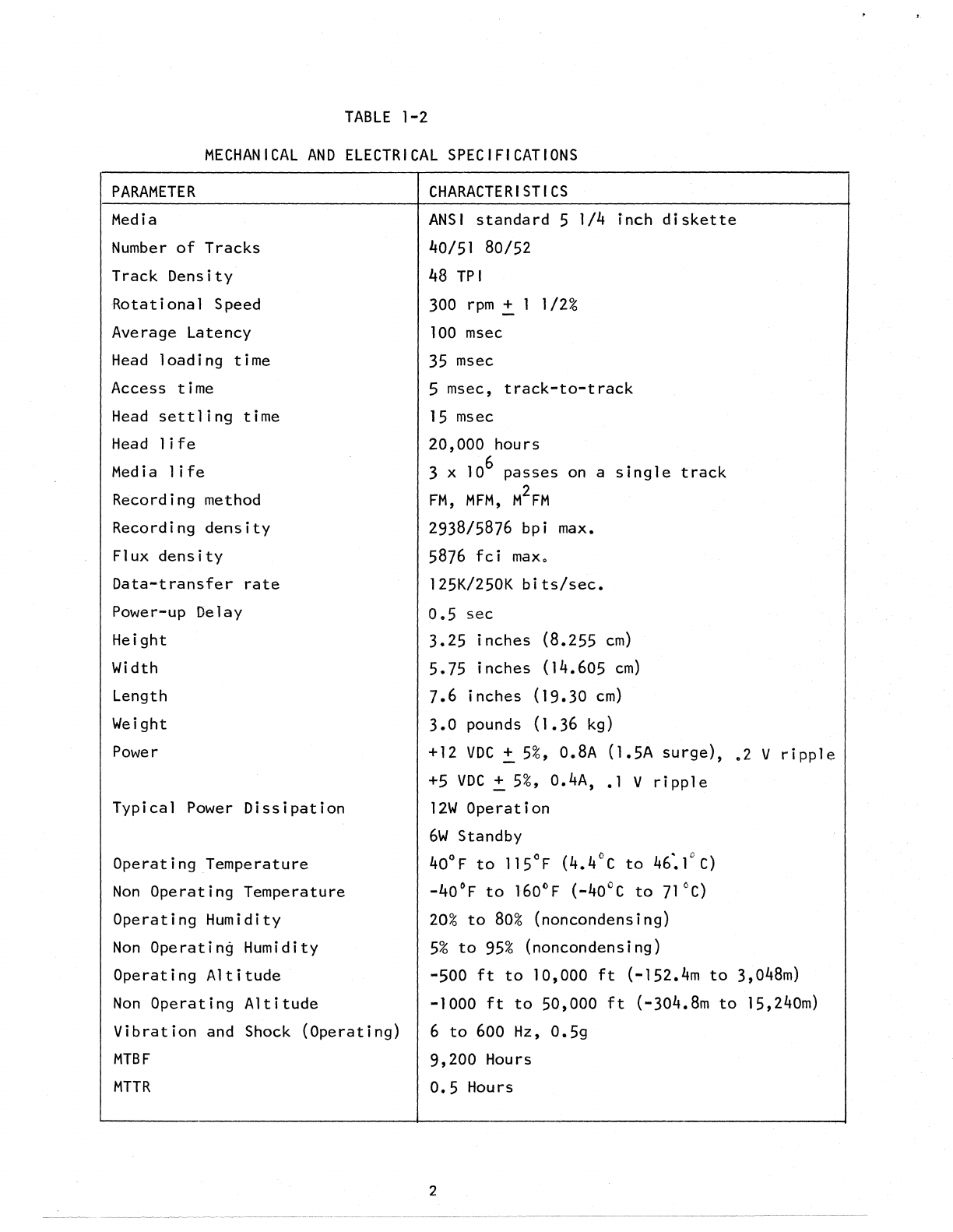
TABLE
1-2
MECHANICAL
AND
ELECTRICAL
SPECIFICATIONS
PARAMETER
Media
Number
of
Tracks
Track
Density
Rotational
Speed
Average Latency
Head
loading
time
Access time
Head
settling
time
Head
life
Media
life
Recording method
Recording
density
Flux
density
Data-transfer
rate
Power-up Delay
Height
Width
Length
Weight
Power
Typical
Power
Dissipation
Operating
Temperature
Non
Operating
Temperature
Operating
Humidity
Non
Operating
Humidity
Operating
Altitude
Non
Operating
Altitude
Vibration
and Shock
(Operating)
MTBF
MTTR
CHARACTERISTICS
ANSI
standard
5
1/4
inch
diskette
40/51 80/52
48
TPI
300 rpm.!. 1
1/2%
100
msec
35
msec
5 msec,
track-to-track
15
msec
20,000 hours
3 x
10
6
passes
on
a
single
track
FM,
MFM,
M2FM
2938/5876 bpi max.
5876
fci
max.
125K/250K
bits/sec.
0.5
sec
3.25
inches
(8.255
cm)
5.75
inches
(14.605
cm)
7.6
inches
(19.30
cm)
3.0
pounds
(1.36
kg)
+12
VDC
!
5%,
0.8A (1.5A
surge),
.2
V
ripple
+5
VDC.!.
5%,
0.4A, .1 V
ripple
12W
Operation
6w
Standby
40°F
to
115°F
(4.4°c
to
46:1°C)
-40°F
to
160°F (-40°C
to
71°C)
20%
to
80%
(noncondensing)
5%
to
95%
(noncondensing)
-500
ft
to
10,000
ft
(-152.4m
to
3,048m)
-1000
ft
to
50,000
ft
(-304.8m
to
15,240m)
6
to
600
Hz,
0.5g
9,200
Hours
0.5
Hours
2
2.2
INSTALLATION
Due
to
its
small
size
and
light
weight,
the
Model
51/52
can be
installed
or
mounted
in
any
convenient
location
or
position.
However,
the
drive
must be
installed
in a
location
that
will
prevent
the
I/O
cable
from
exceeding
10
feet
in
length.
Refer
to
Figure
2-1
for
dimensions
and mounting
provisions.
2.3
HARDWARE
The
flexible
disk
drive
is
a
precision
device
in which
certain
critical
internal
alignments
must be
maintained.
Therefore,
in
keeping
with
rigid
disk
requirements,
it
is
important
that
the
mounting
hardware
does
not
introduce
significant
stress
on
the
drive.
Any
mounting scheme
in
which
the
drive
is
part
of
the
structural
integrity
of
the
enclosure
is
not
permitted.
Since
the
disk
drive
cannot
be
SUbjected
to
signiffcant
stress
when
it
is
slide
mounted,
this
type
of
mounting
generally
satisfies
the
foregoing
requirements.
Mounting schemes
should
allow
for
adjustable
brackets
or
incorporate
resilient
members
to
accommodate
tolerances.
Mounting schemes
involving
more
than
two
hard mounting
points
and a
third
point
should
be
avoided.
2.4
DUST
COVER
Since
the
flexible
disk
drive
is
not
provided
with
a
dust
cover,
the
design
of
an
enclosure
should
incorporate
a means
to
prevent
direct
ingress
of
loose
items,
e.g.,
dust,
paper
punch
waste,
etc.
2.5
COOLING
Heat
dissipation
from a
single
disk
drive
is
normally
12
watts
(32
Btu/Hr).
When
the
drive
is
mounted
so
that
the
components have
access
to
free
flow
of
air,
normal
convection
cooling
allows
operation
over
the
specified
temperature
range.
When
the
drive
is
mounted
in
a
confined
environment,
air
flow
may
have
to
be
provided
to
maintain
specified
air
temperatures
in
the
vicinity
of
the
motors,
PCBA,
and
the
diskette.
2.6
INPUT/OUTPUT
CABLE
Refer
to
Table
2-1
for
cable
connector
part
number and
attachment.
The
maximum
cable
length
from
connector
to
connector
is
10
feet.
All
inputs
and
outputs
are
paired,
one 1
ine
for
function,
one
for
ground.
Figure
3-9
provides
information
relative
to
the
connector
pin/signal
assignments
for
the
t/O
cable.
TYPE
OF
CABLE
Twisted
Pa
i
r,
26
Flat
Cable
TABLE
2-1
RECOMMENDED
CONNECTORS
-PI
CONNECTOR
MANUFACTURER
PIN
AMP
583717-S
3M
··Scotchflex"
3463-0001
3
CONTACT
PIN
1-583616-1
N.A.
~
1
,,-
...
Door
Open Position
'"
1.87
(4.74 cm)
I
~
I
.=\
I~
Bottom View
3.125
(7.94 cm)
\.:1;/
I
h
J=.
6-32 x
.31
deep
(4) mtg. holes
Door
Closed
Position
====-
3.38
(8.59
.06
(.15
n) L
t
IP
~
1.87
:m) (4.74 cm)
::t1
(.79 cm)
3;125
7.6 max (19
Side
View
.125
(.318 cm)
~
5.87
(14.9
o
7cm)
".
1
cm)
.....
L -
•
Top View
1-
l
.....
5.75
(14.6
-1-
frr
-
1 /
yp
(.15 cm) Single Interface
Connector
(J
1)
~
6-32
thru
mtg.
h(
- - .8n
C8
DC
Power Connector (J2)
es
(2
plcs.
each
side)
(2.22 cm)
t NOTE: Unless otherwise stated,
dimensions are in inches.
Tolerances:
.xxx
±.
0.010
.
xx
±.
0.020
Figure
2-1
Outline
and
Mounting Dimensions
1 cm)
2.7
DC
POWER
DC
power
to
the
drive
is
via
connector
J2,
which
is
located
on
the
non-component
side
of
the
PCBA
near
the
spindle
motor.
The
drive
uses
+12V
DC
and
+5V
DC.
Table
1-2.
outl
ines
the
voltage
and
current
requirements.
The
connector
is
an
AMP
Mate-N-Lock
Part
No.
1-480424-0.
SECTION
3
INTERFACING
REQUIREMENTS
3.0
I
NTRODUCT
ION
This
section
contains
the
interfacing
requirements
between
the
host
system
and
the
Model
51/52
Flexible
Disk
Drive.
Communication
is
established
via
two
connectors.
Connector
Jl
establishes
a communication
link
for
all
input/
output
signals.
These
signals
are
TTL
compatible.
Connector J2
provides
DC
power
to
the
device.
3.1
INPUT
LINES
The
input
control
lines
have
A.
B.
3.1.1
True,
Logical Zero
False,
Logical
One
Line
Termination
the
following
electrical
specifications:
=
OV
to
0.4v
(@
lin
=
48
ma
max).
= +2.5V
to
+5V
(open
collector
@
lout
= 250
~a
max).
The
signal
interface
used
by
the
Model
51/52
is
of
the
"bus"
or
"daisy-chain"
type.
Only one 51/52
unit
is
logically
connected
to
the
interface
at
any
given
time.
All
input
signals
are
terminated
directly
by
a
150
ohm
or
a 220/330
ohm
resistor
network.
In
a
daisy-chain
configuration,
only
the
last
device
in
the
daisy
chain
should
have
the
terminating
network;
while
in a
star
configuration,
every
device
should
be
terminated.
3. 1
.2
Programmable Shunt
The
main
function
of
this
device
js
to
assign
the
proper
address
t6
the
drive
in a
multidrive
configuration.
1n
addition,
it
also
determines
when
the
head
load
solenoid
should
be
activated
by
using
either
position
1-14
(with
Select)
or
7-8 (with Motor On).
If
position
5-10
is
left
shorted,
the
drive
is
essentially
always
selected,
but
the
activity
light
will
not
come
on,
and
the
solenoid
will
not
be
activated
until
the
drive
position
is
selected.
The
programmable
shunt
is
AMP
PIN
435704-6
(HPI
PIN
1-79600-0o~).
For
convenience,
the
programmable
shunt
could
be
replaced
by
a
dip
switch,
AMP
PIN
435626-J•
(MPI
PIN
1-7960J-001).
(If
dip
switch
is
used,
maximum
height
is
exceeded
by
;150.)
The
seven
lines
channeled
through
the
shunt
are:
Designator
Pins
a.
Head
Load
w/Select
Tl
1-14
b.
Drive
Select
1
T2
2-13
c.
Drive
Select
2
T3
3-12
d.
Drive
Select
3
T4
4-11
e.
MUX
T5
5-10
f.
Drive
Select
4
T6
6-9
g.
Head
Load
w/Motor
On
T7
7-8
5
3.
1
.3
Drive
Select
1
to
4
The
Drive
Select
lines
provide
a means
of
selecting
and
deselecting
one
of
up
to
four
disk
drives.
When
the
signal
logic
level
is
true,
the
disk
drive
electronics
are
activated,
the
head
is
loaded,
and
the
~rive
is
conditioned
to
respond
to
step
or
read/write
commands.
When
the
logic
level
is
false,
the
input
control
lines
and
output
status
lines
are
disabled.
A
select
line
must remain
stable
in
the
true
state
until
the
execution
of
a
step
or
read/write
command
is
completed.
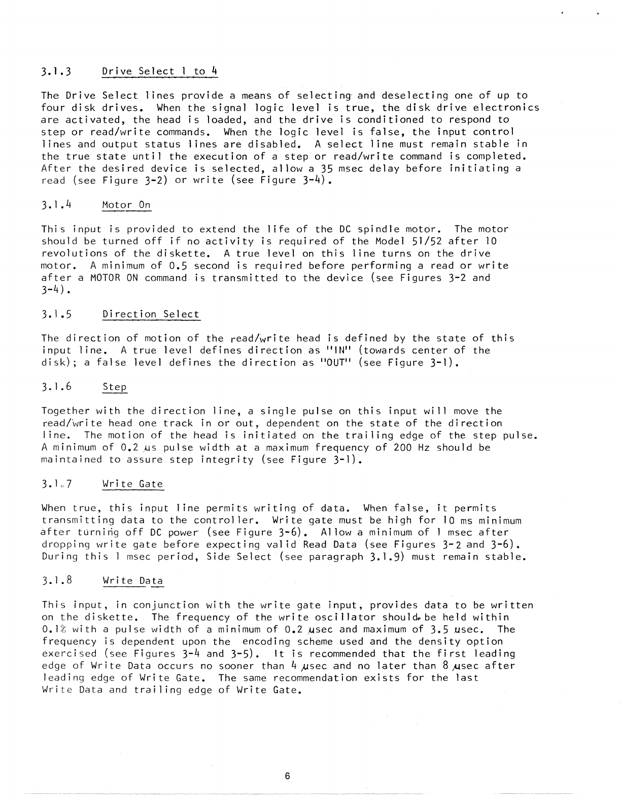
After
the
desired
device
is
selected,
allow
a
35
msec
delay
before
initiating
a
read
(see
Figure
3-2)
or
write
(see
Figure
3-4).
3.1.4
Hotor
On
This
input
is
provided
to
extend
the
life
of
the
DC
spindle
motor.
The
motor
should
be
turned
off
if
no
activity
is
required
of
the
Hodel
51/52
after
10
revolutions
of
the
diskette.
A
true
level
on
this
line
turns
on
the
drive
motor.
A
minimum
of
0.5
second
is
required
before
performing
a
read
or
write
after
a
MOTOR
ON
command
is
transmitted
to
the
device
(see
Figures
3-2
and
3-4)
•
3.1
.5
Direction
Select
The
direction
of
motion
of
the
read/write
head
is
defined
by
the
state
of
this
input
line.
A
true
level
defines
direction
as
"IN"
(towards
center
of
the
disk);
a
false
level
defines
the
direction
as
"OUT"
(see
Figure
3-1).
3. 1
.6
Together
with
the
direction
line,
a
single
pulse
on
this
input
will
move
the
read/~rite
head one
track
in
or
out,
dependent
on
the
state
of
the
direction
line.
The
motion
of
the
head
is
initiated
on
the
trailing
edge
of
the
step
pulse.
A minimum
of
0.2
~s
pulse
width
at
a
maximum
frequency
of
200
Hz
should
be
maintained
to
assure
step
integrity
(see
Figure
3-1).
3.107
Write
Gate
When
true,
this
input
line
permits
writing
of
data.
When
false,
it
permits
transmitting
data
to
the
controller.
Write
gate
must be
high
for
10
ms
minimum
after
tornirig
off
DC
power
(see
Figure
3-6).
Allow a minimum
of
I msec
after
dropping
write
gate
before
expecting
val id Read Data
(see
Figures
3-2
and
3-6).
During
this
1 msec
period,
Side
Select
(see
paragraph
3.1.9)
must remain
stable.
3.
1.8
Write
Data
This
input,
in
conjunction
with
the
write
gate
input,
provides
data
to
be
written
on
the
diskette.
The
frequency
of
the
write
oscillator
shoul~be
held
within
0.1%
with
a
pulse
width
of
a
minimum
of
0.2
~sec
and
maximum
of
3.5
~sec.
The
frequency
is
dependent
upon
the
encoding
scheme used and
the
density
option
exercised
(see
Figures
3-4 and 3-5).
It
is
recommended
that
the
first
leading
edge
of
Write
Data
occurs
no
sooner
than
4
~sec
and no
later
than
8~sec
after
leading
edge
of
Write
Gate.
The same recommendation
exists
for
the
last
Write
Data and
trailing
edge
of
Write
Gate.
6
3.
1.9
Side
Select
This
input
is
used
to
select
either
the
upper.
or
lower
head.
A
true
level
selects
the
upper
head.
a
false
level
selects
the
lower
head.
A
35
~sec
delay
should
be allow.ed
for
the
read
amp
to
recover
after
a head
select
event
occurs.
Only
then
wi.ll
valid
data
be
present.
(For
Model
51,
this
line
should
always
be
high.)
3.1.10
In
Use
(optional
fe~ture)
This
line
is
connected
to
a
driver
which
could
be used
for
an
indicator
light
or
a
solenoid
for
locking
the
drive
door.
3.2
OUTPUT
LINES
The
control
output
signals
are
driven
with
an
open-collector
output
stage
capable
of
sinking
a
maximum
of
48
ma
at
logical
zero
with
maximum
voltage
of
0.4v
measured
at
the
driver.
When
the
output
Is
at
a
logical
one,
the
collector
cutoff
current
is
a
maximum
of
250
~a.
3.2.
1
Track
00
This
output,
when
true,
indicates
that
the
read/write
head(s)
are
located
at
Track
00.
3.2.2
Index/SeCtor
This
output,
when
true,
Indicates
that
an
index
or
sector
hole
in
the
diskette
is
present
at
the
·index
sensor
(see
Figure
3-7
and
3-8).
3.2.3
Write
Protect
This
output,
when
true,
indicates
that
a
write
protected
diskette
is
installed
in
the
drive.
When
an
unprotected
diskette
Is
installed,
this
output
is
false.
When
a
protected
diskette
is
installed,
the
write
and
erase
logic
on
the
PCBA
is
disabled.
By
making a
small
modification
to
the
PCBA
and
using
only
protected
diskettes,
this
output
can be used
as
a
Diskette
[nstalled
Indicator.
3.2.4
Read
Data
This
output
represents
digitized
data
as
detected
by
the
drive
electronfcs.
Information
transmitted
will
be
in
the
encoding
scheme
used.
Pulse
width
of
both
clock
and
data
bits
will
be I
usec
+ 350
nsec.
Maximum
bit
shift
from nominal
for
various
encoding
schemes
is
given
in
table
3-1
(see
Figure
3-3).
TABLE
3-1
BIT
SHIFT
Maximum
bit
shift
(ns)
FM
MFM
M2FM
clock
::.7
00
.!.7
00
.!.475
data
+400
.!.700
.!.7
00
-
7
Drive Select
~--------~,-------------
Out
Direction In
l--.-J
-II--O.l.,min.---!
to.1.,min.
0.3,1ls
min. L
---'
0.2,1.ts
min.
Step
------,suul~
Read
Data
0.2.,
min.
----I
I---
L .
--J
5msmm.
Figure
3-1
Track Access Timing
A
I
A I
A I
A
A - Leading
Edge
of
Bit May
Be
± 700
ns
From its Nominal Position
B - Leading
Edge
of
Bit
May
Be
± 400
ns
From its Nominal Position
DC
Power
Motor
On
Drive Select
Valid Trk. 00 and
Wrt. Prot.
Output
Valid
Index!
Sector
Output
Direction
Step
Write Gate
Write Data
Valid
Read
Data
Figure 3-3 Read Signal Timing
--.J
--1
r100m,min.
---,~~-------------
~0.5secmin.
----t-+---,
I---
O.5,1ls
max.
~~~lJ
-
~
8.us
max. I
10
ms
min.
~..;....-----
I--
20
m'
min.~
1--1
msec
---++-----~~
l--ru--
_____
0.-53!cm~~~~
Figure 3-6 General Control and Data
Timing Requirements (Head Load
Solenoid
is
Activated with Drive Select)
8
Motor
On
-----,L
___________________
_
Drive Select
Step
Write Gate
Valid
Read
Data
1S---
:P.:.min.
Figure 3-2 Read Initiate Timing
Motor
On
----,"'
____________________
_
Drive Select
Step 1.------------
I~----------l------------
J-35
ms
min._
-----1---
...
---J
1--20
m,
min.
i--.
0.5
sec
min.
-
Write Gate
1-1
---l..--J
Write Data
--1 !-s.OO,llS max.
----------~U1fUl~----
Figure 3-4 Write Initiate Timing
Write Data
(FM)
--l
1-1_..:
O
::.
2
:::.':.:m:.::i:.::n·:......·-II
__
..:
8
::.
OO
:::·::'_-l1
4.00.,
I--
3.5,us
max.
±.
40
ns
±.
20
ns
Figure 3-5 Write Data Timing
u U
~
200 ms ± 3.0
ms
- -
--I
Figure 3-7 Index Sector Timing (soft sector)
±.19ms ±.10ms
Figure 3-8 Index Sector Timing (hard sector)
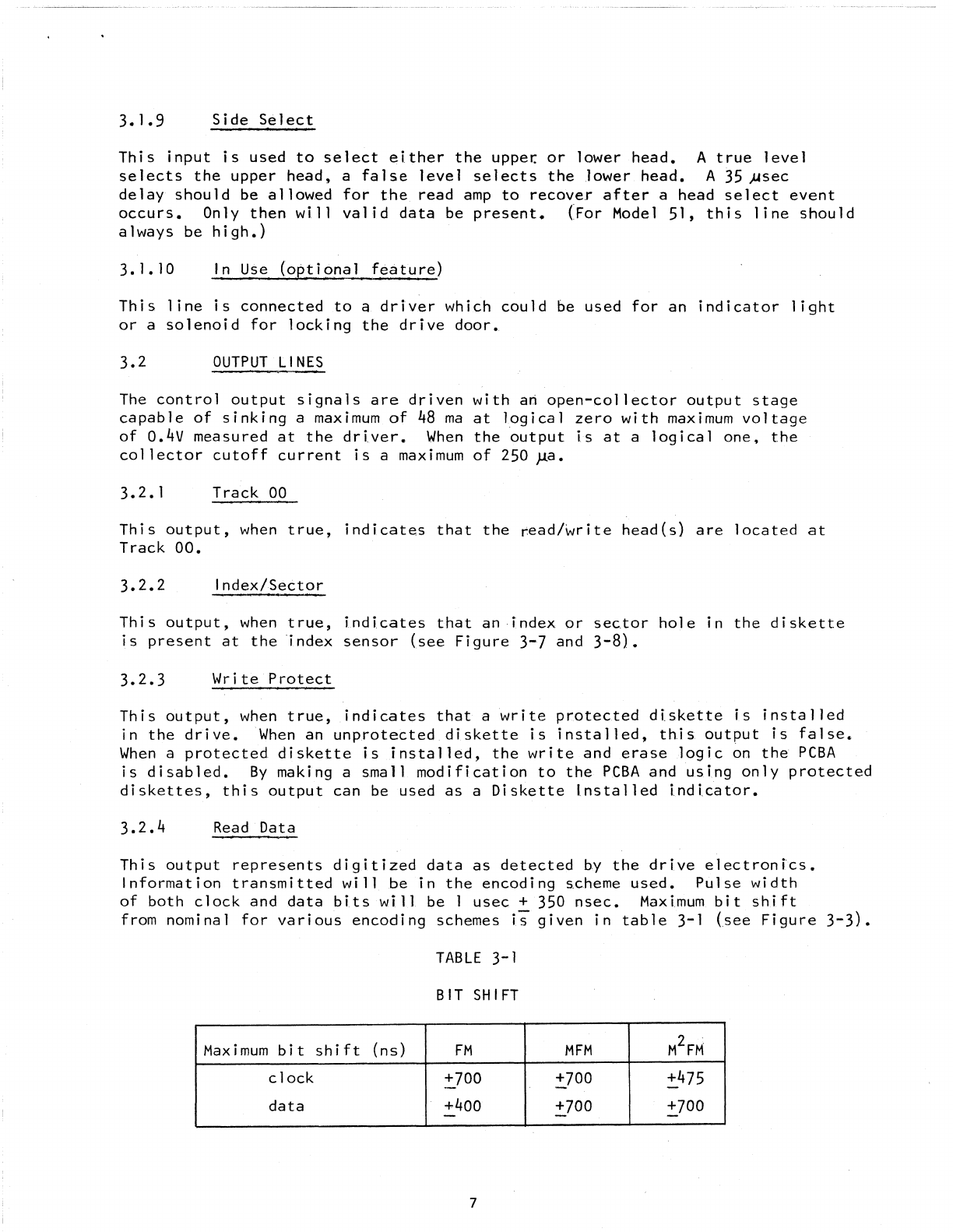
J1
2 SPARE
4 IN USE*
6
DRIVE
SELECT 4
8 INDEX/SECTOR
10
DRIVE
SELECT 1
12
DRIVE
SELECT 2
14
DRIVE
SELECT 3
16 MOTOR ON
51/52
18
DIRECTION
CONTROLLER
20 STEP
22 WRITE
DATA
24
WRITE
GATE
26
TRACK
00
28
WRITE
PROTECT
30
READ
DATA
32 SIDE SELECT
34 RESERVED
ODD PINS
RETURN
(DC GROUND)
POWER
J2
1
+12V
51/52
2
12V
RETURN
CONTROLLER
3
5V
RETURN POWER SUPPLY
4
+5V
*IN
USE
may
be
configured
as
Door Lock or
Activity
Light.
Figure 3-9 Interface Signals -
51/52
Pin
1 +12V
DC
Pin
2 12V Return
Pin
3 5V Return
Pin
4 +5V
DC
BOARD THICKNESS
.06.2!
.007
Figure 3-10
DC
Power Connector,
J2
Figure 3-11
J1
Connector Dimensions
9
3.3
CONNECTOR
J2
The
DC
power
connector
is
located
on
the
non-component
side
of
the
printed
circuit
board.
The recommended mating
connector
is
AMP
PIN
1-480424-0
using
AMP
pins
PIN 60619-1
(see
Figure
3-10).
3.4
CONNECTOR
Jl
Connection
to
Jl
is
through
a
34-pin
PCBA
edge
connector.
Even
numbered
pins
are
located
on
the
component
side
while
odd numbered
pins
are
located
on
the
solder
side.
A key
slot
is
provided
between
pins
4 and
6.
The
recommended
connector
is
3M
Scotchflex
PIN
3463-001,
or
AMP
PIN
583717-5
using
AMP
contacts
PIN
1-583616-1
(see
figure
3-11).
SECTION
4
DATA
ENCODING
AND
RECOVERY
4.0
INTRODUCTION
This
section
provides
applications
information
relevant
to
the
recording
and
recovery
of
data
with
the
Model
51/52
Flexible
Disk
Drives.
4.1
ENCODING
METHODS
The
three
most
common
methods
for
encoding
data
are
described
in
the
following
paragraphs.
Table
4-1 shows a comparison
of
these
encoding
techniques.
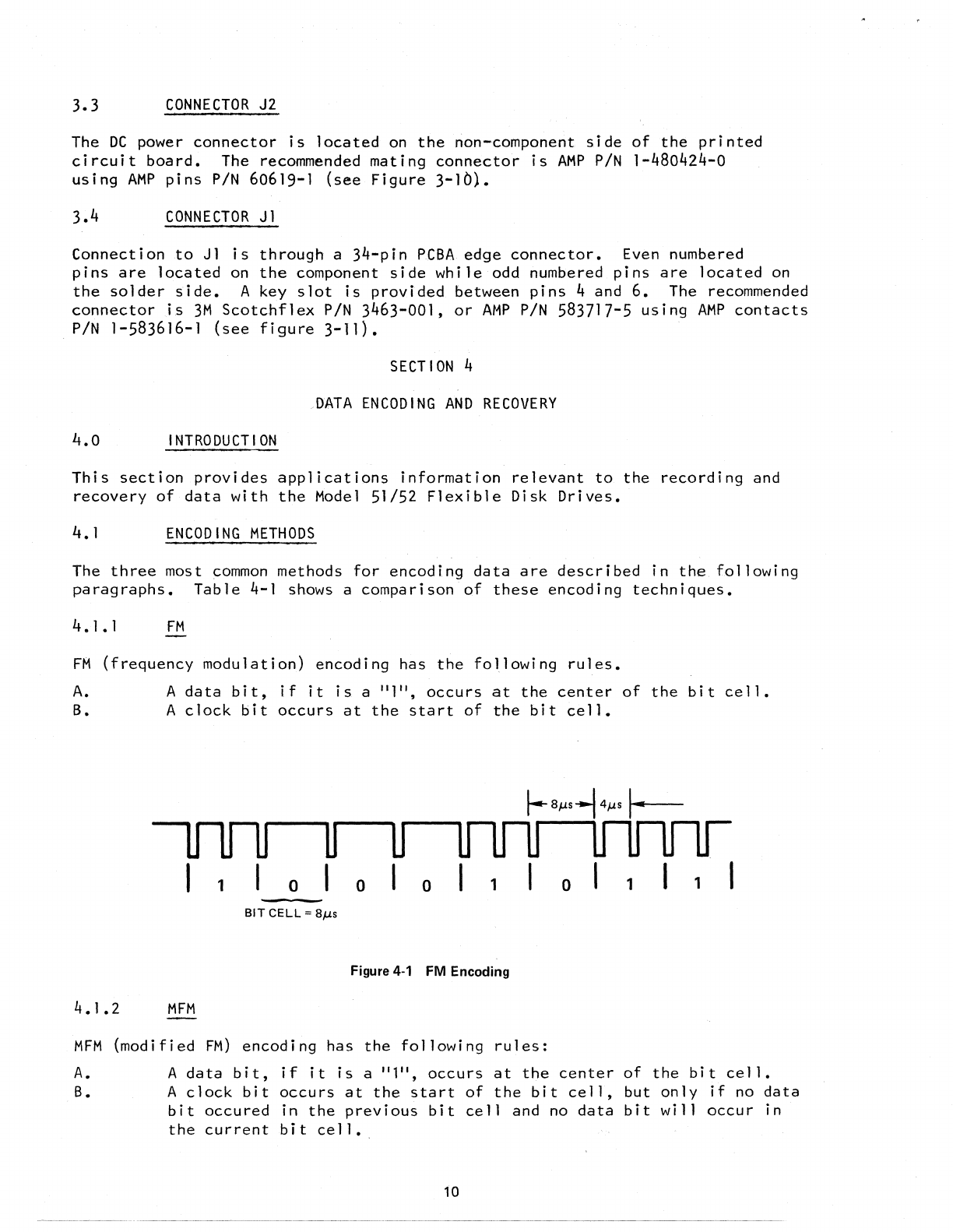
4.
1 • 1
FM
FM
(frequency
modulation)
encoding has
the
following
rules.
A.
A
data
bit,
if
it
is
a
"1",
occurs
at
the
center
of
the
bit
cell.
B.
A
clock
bit
occurs
at
the
start
of
the
bit
cell.
1 o o o 1 o 1 1
BIT
CELL
=
8MS
Figure
4-1
FM Encoding
4.1.2
MFM
MFM
(modified
FM)
encoding
has
the
following
rules:
A.
B.
A
data
bit,
if
it
is
a
"1",
occurs
at
the
center
of
the
bit
cell.
A
clock
bit
occurs
at
the
start
of
the
bit
cell,
but
only
if
no
data
bit
occured
in
the
previous
bit
cell
and
no
data
bit
will
occur
in
the
current
bit
cell
•.
10
---_
...
-------------
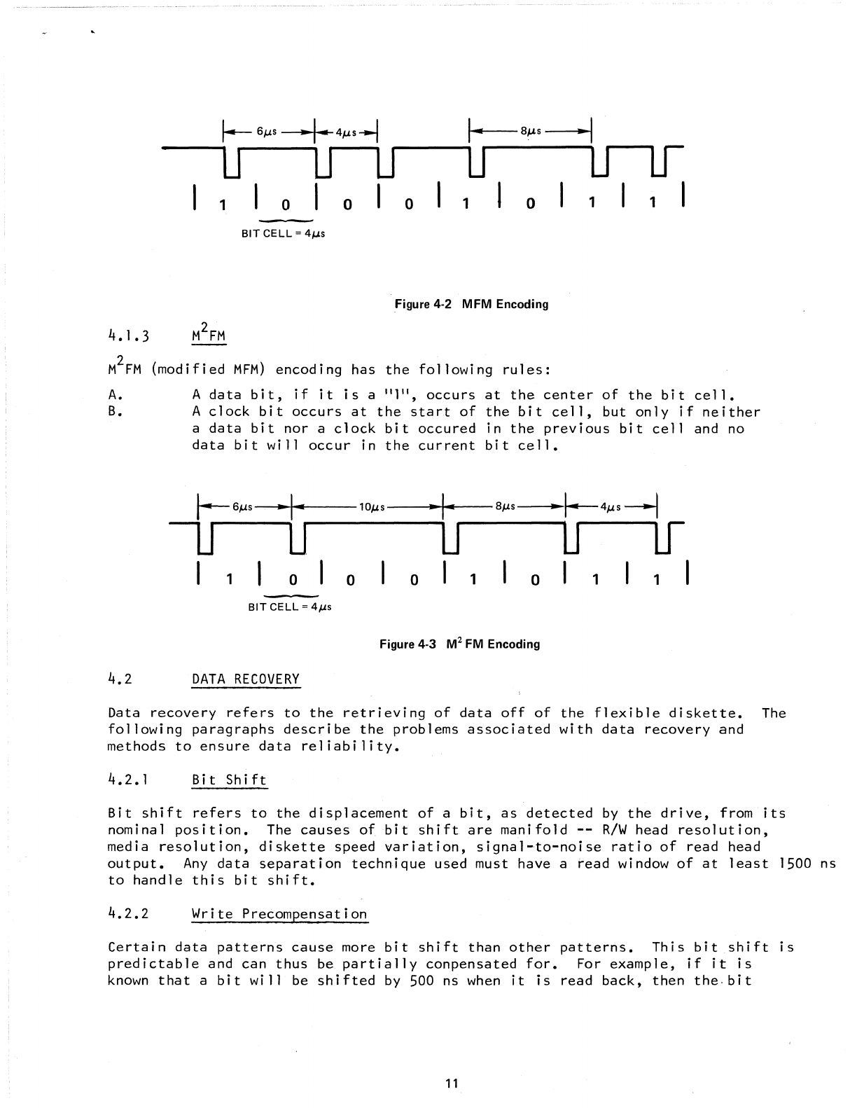
I--
6J..Ls
-I
..
4J..LS--I
~8J..L5-1
U U U U U
Lr
1 0 I 0 I 0 1 0 1 1 I
BIT CELL =
4J..L5
Figure 4·2 MFM Encoding
4.1.3
M2FM
M2FM
(modified
MFM)
encoding
has
the
following
rules:
A.
A
data
bit,
if
it
is
a
"1",
occurs
at
the
center
of
the
bit
cell.
B.
A
clock
bit
occurs
at
the
start
of
the
bit
cell,
but
only
if
neither
a
data
bit
nor
a
clock
bit
occured
in
the
previous
bit
cell
and no
data
bit
will
occur
in
the
current
bit
cell.
/--6J..L5
-I"
10J..L5
-I"
8J..L5
LJ
U.
U
----
..
~14J..LS~
-------flU
if
I 1 0 0 0 I 1 0 I 1 1 I
BIT
CELL =
4J..L5
Figure 4·3
M2
FM
Encoding
4.2
DATA
RECOVERY
Data
recovery
refers
to
the
retrieving
of
data
off
of
the
flexible
diskette.
The
following
paragraphs
describe
the
problems
associated
with
data
recovery
and
methods
to
ensure
data
reliability.
4.2.
I
Bit
Shift
Bit
shift
refers
to
the
displacement
of
a
bit,
as
detected
by
the
drive,
from
its
nominal
position.
The
causes
of
bit
shift
are
manifold
--
R/W
head
resolution,
media
resolution,
diskette
speed
variation,
signal-to-noise
ratio
of
read
head
output.
Any
data
separation
technique
used must have a
tead
window
of
at
least
1500
ns
to
handle
this
bit
shift.
4.2.2
Write
Precompensation
Certain
data
patterns
cause
more
bit
shift
than
other
patterns.
This
bit
shift
is
predictable
and
can
thus
be
partially
conpensated
for.
For
example,
if
it
is
known
that
a
bit
will
be
shifted
by
500 ns
when
it
is
read
back,
then
the·
bit
11
can
be
deliberately
written
200 ns
early.
This
would
give
a
bit
shift
of
about
350 ns
when
it
is
read
back.
This
method
of
reducing
bit
shift
is
called
write
precompensation.
Bit
shift
is
greater
on
the
inner
tracks
of
the
diskette
than
on
the
outer
tracks,
making
write
precompensation
necessary
only
on
the
inner
tracks.
Write
precomp
of
250
to
300
ns
should
be used on
tracks
18
through
39.
If
due
to
controller
limitations,
write
precomp must be used
on
all
tracks,
then
125
to
150 ns
should
be
used.
Table
4-1 shows which
encoding
methods
re'quire;
the
use
of
write
precompensation.
4.2.3
Data
Separation
Data
separation
refers
to
the
separating
of
the
composite
data
coming from
the
drive
into
separate
clock
and
separate
data
bits.
For
FM
recording,
a
one-shot
data
separator
is
quite
sufficient.
For
double
density
recording,
a
phase-lock
oscillator
(PLO)
data
separator
should
be
used.
There
is
another
method
of
data
separation,
the
digital
counter
method.
This
method
is
a
very
poor
approxi,mation
of
a PLO.
It
has
a
theoretical
read
window
of
only
1000 ns
which,
as
per
paragraph
4.2.1,
is
not
sufficient
to
handle
bit
shift.
In
MFM
recording,
data
bits
and
clock
bits
are
subject
to
the
same amount
of
bit
shift.
A
PLO
separator
with
a
50%
data
window and a
50%
clock
window
should
be
used.
In
M2FM
recording,
data
bits
are
subject
to
more
bit
shift
than
clock
bits.
A
PLO
separator
with
a
60%
data
window and a
40%
clock
window
should
be
used
for
best
data
reliability.
It
should
be
noted
that
the
+700 ns
bit
shift
is
meaningful
only
when
associated
wi§h an
error
rate.
The
Model
51/92
drives
have
error
rates
of
1
error
in
10
bits
read.
Thus,
for
every
10
bits,
there
will
be
no
more
than
1
bit
shifted
more
than
~700
ns.
4.3
TRACK
FORMAT
When
determining
the
track
format
to
be
used,
the
following
timing
restraints
should
be
considered
(see
Figure
4-4).
4.3.1
Postamble
The
postamble
period
must be
at
least
3
ms
to
allow
for
spindle
speed
variation
of
+J-!%.
4.3.2
Data
Gap
The
data
gap
period
must be
at
least
1
ms
to
allow
for
tunnel
erase
turn
off
time.
12
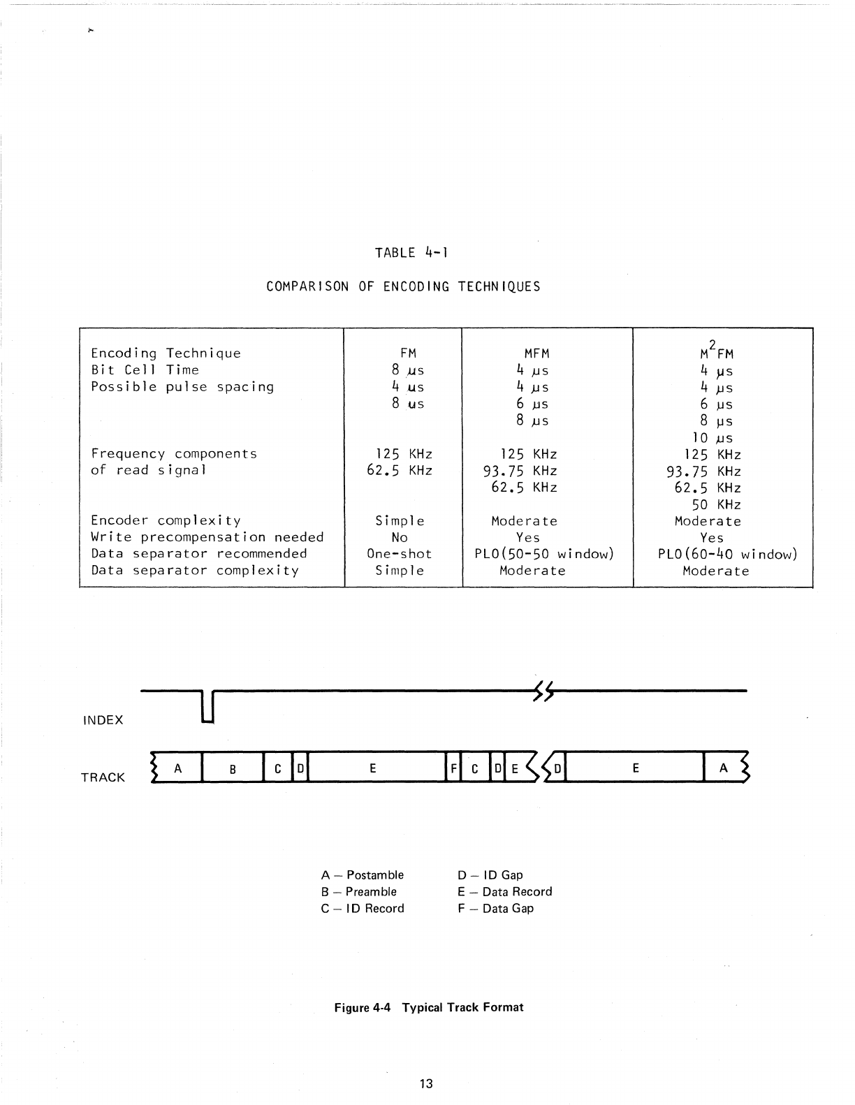
TABLE
4-1
COMPARISON
OF
ENCODING
TECHNIQUES
Encoding
Technique
Bit
Cell Time
Possible
pulse
spacing
Frequency components
of
read
signal
Encoder
complexity
Write
precompensation
needed
Data
separator
recommended
Data
separator
complexity
FM
8
,us
4 ',IJ s
8us
125
KHz
62.5
KHz
Simple
No
One-shot
Simple
MFM
4
.us
4
.u
s
6
,us
8 .us
125
KHz
93.75
KHz
62.5
KHz
Moderate
Yes
PLO(50-50 window)
Moderate
M2FM
4
~S
4
)JS
6
)JS
8
IJS
10
.us
125
KHz
93.75
KHz
62.5
KHz
50
KHz
Moderate
Yes
PLo(60-40 window)
Moderate
INDEX
u~------------~$~~--------
TRACK
B E
A - Postamble
B - Preamble
C
-ID
Record
D -
ID
Gap
E - Data Record
F - Data
Gap
Figure 4-4 Typical Track Format
13

"
