Intelligent Motion Sensing Platform Data Sheet MMA9555L
2017-05-01
: Pdf Mma9555L MMA9555L 2829-101-4607 aftab
Open the PDF directly: View PDF ![]() .
.
Page Count: 132 [warning: Documents this large are best viewed by clicking the View PDF Link!]
- MMA9555L Intelligent Motion-Sensing Pedometer
- Contents
- 1 Intelligent Sensing Platform Offering
- 2 General Description
- 3 Mechanical and Electrical Specifications
- 3.1 Definitions
- 3.2 Pin Groups
- 3.3 Absolute Maximum Ratings
- 3.4 Operating Conditions
- 3.5 Electrostatic Discharge (ESD) and Latch-up Protection Characteristics
- 3.6 General DC Characteristics
- 3.7 Supply Current Characteristics
- 3.8 Accelerometer Transducer Mechanical Characteristics
- 3.9 ADC Characteristics
- 3.10 ADC Sample Rates
- 3.11 AC Electrical Characteristics
- 3.12 General Timing Control
- 3.13 I2C Timing
- 3.14 Slave SPI Timing
- 4 Communication Interface
- 5 Version Application
- 6 Scheduler Application
- 7 GPIO-AppMap Application
- 8 Mailbox Application
- 9 Analog Front End Application
- 10 Data FIFO Application
- 11 Event Queue Application
- 12 Status Register Application
- 13 Sleep/Wake Application
- 14 Reset/Suspend/Clear Control Application
- 15 MBOX Configuration Application
- 16 Pedometer Application
- 17 GPIO Input/Output Application
- 18 Six-Direction Application
- 19 Sample operations
- 19.1 Read pedometer status variables
- 19.2 Read pedometer configuration variables
- 19.3 Write pedometer configuration variables
- 19.4 Read GPIO Input/output status variables
- 19.5 Read GPIO Input/output configuration variables
- 19.6 Write GPIO Input/output configuration variables
- 19.7 Read Six direction status variables
- 19.8 Read Six direction configuration variables
- 19.9 Write Six direction configuration variables
- 19.10 Reset pedometer configuration variables to their defaults
- 19.11 Enable/disable the Pedometer application
- 19.12 Configure the AFE range
- 19.13 Configure output interrupt: Activity change on GPIO6
- 19.14 Configure output interrupt: Step change on GPIO7
- 19.15 Configure output interrupt: Suspend change on GPIO8
- 19.16 Configure output interrupt: Merged flags on GPIO6
- 19.17 Configure output interrupt: Every 10 steps on GPIO7
- 19.18 Configure output interrupt: Device direction change on GPIO6
- 19.19 Wake up from Deep Sleep (Stop No Clock mode)
- 20 Package Information
NXP Semiconductors Document Number: MMA9555L
Data Sheet: Technical Data Rev. 2.3, 8/2016
All information provided in this document is subject to legal disclaimers.
© NXP B.V. 2016. All rights reserved.
MMA9555L Intelligent Motion-
Sensing Pedometer
The MMA9555L intelligent motion-sensing pedometer is an extension of the
MMA955xL intelligent sensor platform. This device incorporates a 3-axis
MEMS accelerometer, signal conditioning, data conversion, and a 32-bit
microcontroller. This intelligent motion-sensing sensor provides sophisticated
pedometer functionality, activity level and six directional orientation monitoring.
The integrated functionality of sensor initialization, calibration, data
compensation, and computation functions off-loads CPU bandwidth from the
system application processor. Therefore, total system power consumption is
significantly reduced, because the application processor stays powered down
until absolutely needed. In addition, the device can be configured for an
autosleep/autowake capability.
MMA9555L is available in a plastic LGA package; the device is guaranteed to
operate over the extended temperature range of –40 °C to +85 °C.
Features
• High resolution 3-axis accelerometer with
16-bit ADC (0.061 mg/LSB @ 2 g)
• Selectable g range (±2/4/8 g) and output data rates (488 Hz–3.8 Hz)
• One slave SPI or I2C interface operating at up to 2 Mbps for communication
with the host processor
• 1.8 V supply voltage low power consumption
•2
µA typical current at stop mode
•117 µA for pedometer running at active and 92 µA at suspend
• 87 µA when six-direction detection mode
• Complete built-in firmware for smart sensing intelligence
• Real time and preemptive application task scheduling
• Command interpreter support command/response and streaming
mode
• Low-power pedometer with rich output information
– Step counting
– Speed, distance, calorie count estimation
– Activity level (rest, walking, jogging, running)
• Six-direction detection output
• Extensive set of power-management features and low-power
mode
• GPIO2–GPIO8 can be used for expanded configurable GPIO
functions
• Minimal external component requirements
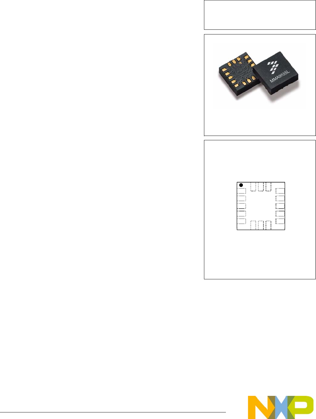
16-pin LGA
3 mm x 3 mm x 1 mm
Case 2094-01
MMA9555L
Top view
Pin Connections
2
3
5
1
4
VDD
BKGD-MS /
RGPIO9
VSS
RGPIO7 / AN1
VSSA
12
11
9
13
10
678
16 15 14
RGPIO8 / PDB_B
VDDA
RGPIO1 / SDA0 / SDI
RGPIO2 / SDO
RGPIO3 / SSB
RESETB
SCL0 / RGPIO0 /
SCLK
RGPIO6 / AN0
RGPIO5 /
PDB_A / INT_O
VSS
RGPIO4/INT

MMA9555L Intelligent Pedometer Data Sheet, Rev. 2.3
2© NXP B.V. 2016. All rights reserved.
Typical Applications
This low-power, intelligent sensor is optimized for use in portable and mobile consumer products such as:
• Pedometers, wearable devices, smart watches, wristband
• Sleep monitoring
• Smart earphone
• Health monitoring
Related Documentation
The MMA9555L device features and operations are described in reference manuals, release notes, and application notes. To
find the most-current versions of these documents:
1. Go to the NXP homepage at: nxp.com.
2. In the Keyword search box at the top of the page, enter the device number MMA9555L.
In the Refine Your Results pane on the left, click on the Documentation link.
Ordering information
Part number Firmware Temperature range Package description Shipping
MMA9555LR1
Pedometer + Six
Directions of Orientation +
GPIO Input/Output
–40 °C to +85 °C LGA-16 Tape and reel

MMA9555L Intelligent Pedometer Data Sheet, Rev. 2.2
© NXP B.V. 2016. All rights reserved. 3
Contents
1 Intelligent Sensing Platform Offering. . . . . . . . . . . . . . . . . . . . . . . . . . . . . . . . . . . . . . . . . . . . . . . . . . . . . . . . . . . . . . .5
2 General Description . . . . . . . . . . . . . . . . . . . . . . . . . . . . . . . . . . . . . . . . . . . . . . . . . . . . . . . . . . . . . . . . . . . . . . . . . . . . .7
2.1 Functional Overview . . . . . . . . . . . . . . . . . . . . . . . . . . . . . . . . . . . . . . . . . . . . . . . . . . . . . . . . . . . . . . . . . . . . . . . 7
2.2 Pinout . . . . . . . . . . . . . . . . . . . . . . . . . . . . . . . . . . . . . . . . . . . . . . . . . . . . . . . . . . . . . . . . . . . . . . . . . . . . . . . . . . 8
2.3 Pin Function Descriptions. . . . . . . . . . . . . . . . . . . . . . . . . . . . . . . . . . . . . . . . . . . . . . . . . . . . . . . . . . . . . . . . . . . 9
2.4 System Connections. . . . . . . . . . . . . . . . . . . . . . . . . . . . . . . . . . . . . . . . . . . . . . . . . . . . . . . . . . . . . . . . . . . . . . 10
3 Mechanical and Electrical Specifications . . . . . . . . . . . . . . . . . . . . . . . . . . . . . . . . . . . . . . . . . . . . . . . . . . . . . . . . . .13
3.1 Definitions. . . . . . . . . . . . . . . . . . . . . . . . . . . . . . . . . . . . . . . . . . . . . . . . . . . . . . . . . . . . . . . . . . . . . . . . . . . . . . 13
3.2 Pin Groups . . . . . . . . . . . . . . . . . . . . . . . . . . . . . . . . . . . . . . . . . . . . . . . . . . . . . . . . . . . . . . . . . . . . . . . . . . . . . 13
3.3 Absolute Maximum Ratings . . . . . . . . . . . . . . . . . . . . . . . . . . . . . . . . . . . . . . . . . . . . . . . . . . . . . . . . . . . . . . . . 13
3.4 Operating Conditions . . . . . . . . . . . . . . . . . . . . . . . . . . . . . . . . . . . . . . . . . . . . . . . . . . . . . . . . . . . . . . . . . . . . . 14
3.5 Electrostatic Discharge (ESD) and Latch-up Protection Characteristics . . . . . . . . . . . . . . . . . . . . . . . . . . . . . . 14
3.6 General DC Characteristics . . . . . . . . . . . . . . . . . . . . . . . . . . . . . . . . . . . . . . . . . . . . . . . . . . . . . . . . . . . . . . . . 14
3.7 Supply Current Characteristics. . . . . . . . . . . . . . . . . . . . . . . . . . . . . . . . . . . . . . . . . . . . . . . . . . . . . . . . . . . . . . 15
3.8 Accelerometer Transducer Mechanical Characteristics . . . . . . . . . . . . . . . . . . . . . . . . . . . . . . . . . . . . . . . . . . . 15
3.9 ADC Characteristics . . . . . . . . . . . . . . . . . . . . . . . . . . . . . . . . . . . . . . . . . . . . . . . . . . . . . . . . . . . . . . . . . . . . . . 15
3.10 ADC Sample Rates. . . . . . . . . . . . . . . . . . . . . . . . . . . . . . . . . . . . . . . . . . . . . . . . . . . . . . . . . . . . . . . . . . . . . . . 16
3.11 AC Electrical Characteristics . . . . . . . . . . . . . . . . . . . . . . . . . . . . . . . . . . . . . . . . . . . . . . . . . . . . . . . . . . . . . . . 16
3.12 General Timing Control. . . . . . . . . . . . . . . . . . . . . . . . . . . . . . . . . . . . . . . . . . . . . . . . . . . . . . . . . . . . . . . . . . . . 17
3.13 I2C Timing. . . . . . . . . . . . . . . . . . . . . . . . . . . . . . . . . . . . . . . . . . . . . . . . . . . . . . . . . . . . . . . . . . . . . . . . . . . . . . 17
3.14 Slave SPI Timing . . . . . . . . . . . . . . . . . . . . . . . . . . . . . . . . . . . . . . . . . . . . . . . . . . . . . . . . . . . . . . . . . . . . . . . . 18
4 Communication Interface . . . . . . . . . . . . . . . . . . . . . . . . . . . . . . . . . . . . . . . . . . . . . . . . . . . . . . . . . . . . . . . . . . . . . . .19
4.1 Overview of Communication Interface . . . . . . . . . . . . . . . . . . . . . . . . . . . . . . . . . . . . . . . . . . . . . . . . . . . . . . . . 19
4.2 Mailbox Interface . . . . . . . . . . . . . . . . . . . . . . . . . . . . . . . . . . . . . . . . . . . . . . . . . . . . . . . . . . . . . . . . . . . . . . . . 19
4.3 Mailbox Usage . . . . . . . . . . . . . . . . . . . . . . . . . . . . . . . . . . . . . . . . . . . . . . . . . . . . . . . . . . . . . . . . . . . . . . . . . . 20
5 Version Application . . . . . . . . . . . . . . . . . . . . . . . . . . . . . . . . . . . . . . . . . . . . . . . . . . . . . . . . . . . . . . . . . . . . . . . . . . . .25
5.1 Reading the version information . . . . . . . . . . . . . . . . . . . . . . . . . . . . . . . . . . . . . . . . . . . . . . . . . . . . . . . . . . . . . 26
6 Scheduler Application . . . . . . . . . . . . . . . . . . . . . . . . . . . . . . . . . . . . . . . . . . . . . . . . . . . . . . . . . . . . . . . . . . . . . . . . . .27
6.1 Scheduler application elements . . . . . . . . . . . . . . . . . . . . . . . . . . . . . . . . . . . . . . . . . . . . . . . . . . . . . . . . . . . . . 27
6.2 Interrupts. . . . . . . . . . . . . . . . . . . . . . . . . . . . . . . . . . . . . . . . . . . . . . . . . . . . . . . . . . . . . . . . . . . . . . . . . . . . . . . 29
6.3 Scheduler configuration registers . . . . . . . . . . . . . . . . . . . . . . . . . . . . . . . . . . . . . . . . . . . . . . . . . . . . . . . . . . . . 29
6.4 Scheduler status registers . . . . . . . . . . . . . . . . . . . . . . . . . . . . . . . . . . . . . . . . . . . . . . . . . . . . . . . . . . . . . . . . . 36
7 GPIO-AppMap Application . . . . . . . . . . . . . . . . . . . . . . . . . . . . . . . . . . . . . . . . . . . . . . . . . . . . . . . . . . . . . . . . . . . . . .37
7.1 Overview of GPIO-AppMap application . . . . . . . . . . . . . . . . . . . . . . . . . . . . . . . . . . . . . . . . . . . . . . . . . . . . . . . 37
7.2 GPIO configuration registers . . . . . . . . . . . . . . . . . . . . . . . . . . . . . . . . . . . . . . . . . . . . . . . . . . . . . . . . . . . . . . . 37
8 Mailbox Application . . . . . . . . . . . . . . . . . . . . . . . . . . . . . . . . . . . . . . . . . . . . . . . . . . . . . . . . . . . . . . . . . . . . . . . . . . . .41
8.1 Overview of Mailbox application . . . . . . . . . . . . . . . . . . . . . . . . . . . . . . . . . . . . . . . . . . . . . . . . . . . . . . . . . . . . . 41
8.2 Mailbox configuration registers. . . . . . . . . . . . . . . . . . . . . . . . . . . . . . . . . . . . . . . . . . . . . . . . . . . . . . . . . . . . . . 41
8.3 Mailbox status registers . . . . . . . . . . . . . . . . . . . . . . . . . . . . . . . . . . . . . . . . . . . . . . . . . . . . . . . . . . . . . . . . . . . 46
8.4 Reading aggregated data (Legacy mode—Quick read) . . . . . . . . . . . . . . . . . . . . . . . . . . . . . . . . . . . . . . . . . . . 46
9 Analog Front End Application. . . . . . . . . . . . . . . . . . . . . . . . . . . . . . . . . . . . . . . . . . . . . . . . . . . . . . . . . . . . . . . . . . . .48
9.1 Overview of Analog Front End application . . . . . . . . . . . . . . . . . . . . . . . . . . . . . . . . . . . . . . . . . . . . . . . . . . . . . 48
9.2 AFE configuration registers . . . . . . . . . . . . . . . . . . . . . . . . . . . . . . . . . . . . . . . . . . . . . . . . . . . . . . . . . . . . . . . . 52
9.3 AFE status registers . . . . . . . . . . . . . . . . . . . . . . . . . . . . . . . . . . . . . . . . . . . . . . . . . . . . . . . . . . . . . . . . . . . . . . 56
10 Data FIFO Application . . . . . . . . . . . . . . . . . . . . . . . . . . . . . . . . . . . . . . . . . . . . . . . . . . . . . . . . . . . . . . . . . . . . . . . . . .62
10.1 Overview of Data FIFO application. . . . . . . . . . . . . . . . . . . . . . . . . . . . . . . . . . . . . . . . . . . . . . . . . . . . . . . . . . . 62
10.2 Modes of operation . . . . . . . . . . . . . . . . . . . . . . . . . . . . . . . . . . . . . . . . . . . . . . . . . . . . . . . . . . . . . . . . . . . . . . . 62
10.3 Reading process. . . . . . . . . . . . . . . . . . . . . . . . . . . . . . . . . . . . . . . . . . . . . . . . . . . . . . . . . . . . . . . . . . . . . . . . . 62
10.4 Data FIFO block diagram . . . . . . . . . . . . . . . . . . . . . . . . . . . . . . . . . . . . . . . . . . . . . . . . . . . . . . . . . . . . . . . . . . 66
10.5 Data FIFO configuration registers. . . . . . . . . . . . . . . . . . . . . . . . . . . . . . . . . . . . . . . . . . . . . . . . . . . . . . . . . . . . 67
10.6 Data FIFO status registers . . . . . . . . . . . . . . . . . . . . . . . . . . . . . . . . . . . . . . . . . . . . . . . . . . . . . . . . . . . . . . . . . 69
11 Event Queue Application. . . . . . . . . . . . . . . . . . . . . . . . . . . . . . . . . . . . . . . . . . . . . . . . . . . . . . . . . . . . . . . . . . . . . . . .71
11.1 Overview of Event Queue application. . . . . . . . . . . . . . . . . . . . . . . . . . . . . . . . . . . . . . . . . . . . . . . . . . . . . . . . . 71
11.2 Event Queue configuration registers . . . . . . . . . . . . . . . . . . . . . . . . . . . . . . . . . . . . . . . . . . . . . . . . . . . . . . . . . 74
11.3 Event Queue status registers . . . . . . . . . . . . . . . . . . . . . . . . . . . . . . . . . . . . . . . . . . . . . . . . . . . . . . . . . . . . . . . 76
12 Status Register Application . . . . . . . . . . . . . . . . . . . . . . . . . . . . . . . . . . . . . . . . . . . . . . . . . . . . . . . . . . . . . . . . . . . . .78
12.1 Overview of Status Register application . . . . . . . . . . . . . . . . . . . . . . . . . . . . . . . . . . . . . . . . . . . . . . . . . . . . . . . 78

MMA9555L Intelligent Pedometer Data Sheet, Rev. 2.2
4© NXP B.V. 2016. All rights reserved.
12.2 Status Register configuration registers. . . . . . . . . . . . . . . . . . . . . . . . . . . . . . . . . . . . . . . . . . . . . . . . . . . . . . . . 78
12.3 Status Register default configuration . . . . . . . . . . . . . . . . . . . . . . . . . . . . . . . . . . . . . . . . . . . . . . . . . . . . . . . . . 82
13 Sleep/Wake Application. . . . . . . . . . . . . . . . . . . . . . . . . . . . . . . . . . . . . . . . . . . . . . . . . . . . . . . . . . . . . . . . . . . . . . . . .83
13.1 Overview of Sleep/Wake application . . . . . . . . . . . . . . . . . . . . . . . . . . . . . . . . . . . . . . . . . . . . . . . . . . . . . . . . . 83
13.2 Sleep/Wake configuration registers . . . . . . . . . . . . . . . . . . . . . . . . . . . . . . . . . . . . . . . . . . . . . . . . . . . . . . . . . . 84
13.3 Sleep/Wake status registers . . . . . . . . . . . . . . . . . . . . . . . . . . . . . . . . . . . . . . . . . . . . . . . . . . . . . . . . . . . . . . . . 87
14 Reset/Suspend/Clear Control Application. . . . . . . . . . . . . . . . . . . . . . . . . . . . . . . . . . . . . . . . . . . . . . . . . . . . . . . . . .88
14.1 Overview of Reset/Suspend/Clear Control application. . . . . . . . . . . . . . . . . . . . . . . . . . . . . . . . . . . . . . . . . . . . 88
14.2 Configuration registers for Reset/Suspend/Clear Control applications. . . . . . . . . . . . . . . . . . . . . . . . . . . . . . . . 89
14.3 Reset/Suspend/Clear status registers . . . . . . . . . . . . . . . . . . . . . . . . . . . . . . . . . . . . . . . . . . . . . . . . . . . . . . . . 94
14.4 Reboot to ROM CI from flash code. . . . . . . . . . . . . . . . . . . . . . . . . . . . . . . . . . . . . . . . . . . . . . . . . . . . . . . . . . . 94
14.5 Reboot to flash code from ROM CI. . . . . . . . . . . . . . . . . . . . . . . . . . . . . . . . . . . . . . . . . . . . . . . . . . . . . . . . . . . 94
15 MBOX Configuration Application . . . . . . . . . . . . . . . . . . . . . . . . . . . . . . . . . . . . . . . . . . . . . . . . . . . . . . . . . . . . . . . . .95
15.1 Overview of MBOX Configuration application. . . . . . . . . . . . . . . . . . . . . . . . . . . . . . . . . . . . . . . . . . . . . . . . . . . 95
15.2 Normal mode . . . . . . . . . . . . . . . . . . . . . . . . . . . . . . . . . . . . . . . . . . . . . . . . . . . . . . . . . . . . . . . . . . . . . . . . . . . 95
15.3 Legacy mode . . . . . . . . . . . . . . . . . . . . . . . . . . . . . . . . . . . . . . . . . . . . . . . . . . . . . . . . . . . . . . . . . . . . . . . . . . . 96
15.4 Configuring mailbox operational mode . . . . . . . . . . . . . . . . . . . . . . . . . . . . . . . . . . . . . . . . . . . . . . . . . . . . . . . . 96
15.5 MBOX Configuration memory map and register. . . . . . . . . . . . . . . . . . . . . . . . . . . . . . . . . . . . . . . . . . . . . . . . . 97
16 Pedometer Application . . . . . . . . . . . . . . . . . . . . . . . . . . . . . . . . . . . . . . . . . . . . . . . . . . . . . . . . . . . . . . . . . . . . . . . . .99
16.1 Background and overview . . . . . . . . . . . . . . . . . . . . . . . . . . . . . . . . . . . . . . . . . . . . . . . . . . . . . . . . . . . . . . . . . 99
16.2 Functional description. . . . . . . . . . . . . . . . . . . . . . . . . . . . . . . . . . . . . . . . . . . . . . . . . . . . . . . . . . . . . . . . . . . . . 99
16.3 Memory-maps and register descriptions. . . . . . . . . . . . . . . . . . . . . . . . . . . . . . . . . . . . . . . . . . . . . . . . . . . . . . 103
16.4 Pedometer application examples . . . . . . . . . . . . . . . . . . . . . . . . . . . . . . . . . . . . . . . . . . . . . . . . . . . . . . . . . . . 111
17 GPIO Input/Output Application . . . . . . . . . . . . . . . . . . . . . . . . . . . . . . . . . . . . . . . . . . . . . . . . . . . . . . . . . . . . . . . . . .114
17.1 Overview of GPIO Input/Output application . . . . . . . . . . . . . . . . . . . . . . . . . . . . . . . . . . . . . . . . . . . . . . . . . . . 114
17.2 Memory maps and register descriptions. . . . . . . . . . . . . . . . . . . . . . . . . . . . . . . . . . . . . . . . . . . . . . . . . . . . . . 114
17.3 GPIO Input/Output configuration register descriptions . . . . . . . . . . . . . . . . . . . . . . . . . . . . . . . . . . . . . . . . . . . 115
17.4 GPIO Input/Output Status register descriptions . . . . . . . . . . . . . . . . . . . . . . . . . . . . . . . . . . . . . . . . . . . . . . . . 116
17.5 GPIO Input/Output application examples . . . . . . . . . . . . . . . . . . . . . . . . . . . . . . . . . . . . . . . . . . . . . . . . . . . . . 117
18 Six-Direction Application. . . . . . . . . . . . . . . . . . . . . . . . . . . . . . . . . . . . . . . . . . . . . . . . . . . . . . . . . . . . . . . . . . . . . . .119
18.1 Overview of the Six-Direction application . . . . . . . . . . . . . . . . . . . . . . . . . . . . . . . . . . . . . . . . . . . . . . . . . . . . . 119
18.2 Memory maps and register descriptions. . . . . . . . . . . . . . . . . . . . . . . . . . . . . . . . . . . . . . . . . . . . . . . . . . . . . . 119
18.3 Six Direction configuration register descriptions. . . . . . . . . . . . . . . . . . . . . . . . . . . . . . . . . . . . . . . . . . . . . . . . 120
18.4 Six Direction Status register descriptions . . . . . . . . . . . . . . . . . . . . . . . . . . . . . . . . . . . . . . . . . . . . . . . . . . . . . 121
19 Sample operations. . . . . . . . . . . . . . . . . . . . . . . . . . . . . . . . . . . . . . . . . . . . . . . . . . . . . . . . . . . . . . . . . . . . . . . . . . . .123
19.1 Read pedometer status variables. . . . . . . . . . . . . . . . . . . . . . . . . . . . . . . . . . . . . . . . . . . . . . . . . . . . . . . . . . . 123
19.2 Read pedometer configuration variables . . . . . . . . . . . . . . . . . . . . . . . . . . . . . . . . . . . . . . . . . . . . . . . . . . . . . 123
19.3 Write pedometer configuration variables . . . . . . . . . . . . . . . . . . . . . . . . . . . . . . . . . . . . . . . . . . . . . . . . . . . . . 123
19.4 Read GPIO Input/output status variables . . . . . . . . . . . . . . . . . . . . . . . . . . . . . . . . . . . . . . . . . . . . . . . . . . . . . 123
19.5 Read GPIO Input/output configuration variables . . . . . . . . . . . . . . . . . . . . . . . . . . . . . . . . . . . . . . . . . . . . . . . 123
19.6 Write GPIO Input/output configuration variables. . . . . . . . . . . . . . . . . . . . . . . . . . . . . . . . . . . . . . . . . . . . . . . . 123
19.7 Read Six direction status variables. . . . . . . . . . . . . . . . . . . . . . . . . . . . . . . . . . . . . . . . . . . . . . . . . . . . . . . . . . 123
19.8 Read Six direction configuration variables . . . . . . . . . . . . . . . . . . . . . . . . . . . . . . . . . . . . . . . . . . . . . . . . . . . . 123
19.9 Write Six direction configuration variables . . . . . . . . . . . . . . . . . . . . . . . . . . . . . . . . . . . . . . . . . . . . . . . . . . . . 124
19.10 Reset pedometer configuration variables to their defaults . . . . . . . . . . . . . . . . . . . . . . . . . . . . . . . . . . . . . . . . 124
19.11 Enable/disable the Pedometer application . . . . . . . . . . . . . . . . . . . . . . . . . . . . . . . . . . . . . . . . . . . . . . . . . . . . 124
19.12 Configure the AFE range . . . . . . . . . . . . . . . . . . . . . . . . . . . . . . . . . . . . . . . . . . . . . . . . . . . . . . . . . . . . . . . . . 124
19.13 Configure output interrupt: Activity change on GPIO6 . . . . . . . . . . . . . . . . . . . . . . . . . . . . . . . . . . . . . . . . . . . 124
19.14 Configure output interrupt: Step change on GPIO7 . . . . . . . . . . . . . . . . . . . . . . . . . . . . . . . . . . . . . . . . . . . . . 124
19.15 Configure output interrupt: Suspend change on GPIO8 . . . . . . . . . . . . . . . . . . . . . . . . . . . . . . . . . . . . . . . . . . 125
19.16 Configure output interrupt: Merged flags on GPIO6 . . . . . . . . . . . . . . . . . . . . . . . . . . . . . . . . . . . . . . . . . . . . . 125
19.17 Configure output interrupt: Every 10 steps on GPIO7 . . . . . . . . . . . . . . . . . . . . . . . . . . . . . . . . . . . . . . . . . . . 125
19.18 Configure output interrupt: Device direction change on GPIO6 . . . . . . . . . . . . . . . . . . . . . . . . . . . . . . . . . . . . 125
19.19 Wake up from Deep Sleep (Stop No Clock mode) . . . . . . . . . . . . . . . . . . . . . . . . . . . . . . . . . . . . . . . . . . . . . . 125
20 Package Information . . . . . . . . . . . . . . . . . . . . . . . . . . . . . . . . . . . . . . . . . . . . . . . . . . . . . . . . . . . . . . . . . . . . . . . . . .126
20.1 Footprint and pattern information . . . . . . . . . . . . . . . . . . . . . . . . . . . . . . . . . . . . . . . . . . . . . . . . . . . . . . . . . . . 126
20.2 Marking. . . . . . . . . . . . . . . . . . . . . . . . . . . . . . . . . . . . . . . . . . . . . . . . . . . . . . . . . . . . . . . . . . . . . . . . . . . . . . . 127
20.3 Tape and reel information . . . . . . . . . . . . . . . . . . . . . . . . . . . . . . . . . . . . . . . . . . . . . . . . . . . . . . . . . . . . . . . . . 128
20.4 Package Description. . . . . . . . . . . . . . . . . . . . . . . . . . . . . . . . . . . . . . . . . . . . . . . . . . . . . . . . . . . . . . . . . . . . . 129

MMA9555L Intelligent Pedometer Data Sheet, Rev. 2.2
© NXP B.V. 2016. All rights reserved. 5
1 Intelligent Sensing Platform Offering
NXP has a broad offering of MMA955xL devices.
The MMA9550L, MMA9551L, MMA9553L, and MMA9555L devices can function immediately as shipped. They have an internal
command interpreter and applications scheduler. These devices can interact directly with the users' host system.
The MMA9550L, MMA9551L, MMA9553L and MMA9559L devices are programmable with additional user application software.
These devices have a variety of user flash and RAM memory space available. The MMA9555L is provided with complete factory
build application specific software, no additional user software programming in the device is needed.
NOTE
The information and specifications provided in this data sheet are specific to the MMA9555L.
Information for the other devices can be found in the MMA955xL collateral and datasheet.
Table 1. NXP Intelligent Sensing Product Comparison
Feature - Device MMA9550L MMA9551L MMA9553L MMA9555L MMA9559L
Key elements Motion sensing Gesture sensing Pedometer
Pedometer
+
six-direction orientation
+
GPIO Input/Output
High flexibility
ADC resolution (bits) 10,12,14,16 bits 10,12,14,16 bits 10,12,14,16 bits 10,12,14,16 bits 10,12,14,16
bits
g measurement ranges 2 g, 4 g, 8 g2 g, 4 g, 8 g2 g, 4 g, 8 g2 g, 4 g, 8 g2 g, 4 g, 8 g
Real-time and preemptive
scheduling Yes Yes Yes Yes No
Event management No No No No Yes
Slave Port Command Interpreter
• Normal mode Yes Yes Yes Yes No
• Legacy mode Yes Yes Yes Yes No
• Streaming mode Yes Yes Yes Yes No
Front-end processing
• 100 Hz BW anti-aliasing Yes Yes Yes Yes No
• 50 Hz BW anti-aliasing Yes Yes Yes Yes No
•g-mode-dependent resolution Yes Yes Yes Yes Yes
• Absolute value Yes Yes Yes Yes No
• Low-pass filter Yes Yes Yes Yes No
• High-pass filter Yes Yes Yes Yes No
• Data-ready interrupt Yes Yes Yes Yes Yes
Gesture applications
• High g/Low gNo Yes No No No
• Tilt No Yes No No No

MMA9555L Intelligent Pedometer Data Sheet, Rev. 2.2
6© NXP B.V. 2016. All rights reserved.
• Portrait/Landscape No Yes No No No
• Programmable orientation No Yes No No No
• Tap/Double-tap No Yes No No No
• Freefall No Yes No No No
•Motion No Yes No No No
Data-storage modules
• Data FIFO Yes Yes Yes Yes No
• Event queue Yes Yes Yes Yes No
• Inter-process FIFO No No No No Yes
Power-control module
• Run and Stop on idle Yes Yes Yes Yes Yes
• Run and No stop Yes Yes Yes Yes Yes
• Stop NC Yes Yes Yes Yes Yes
• Auto-Wake / Auto-Sleep / Doze Yes Yes Yes Yes No
Data-management daemons Yes Yes Yes Yes Yes
Pedometer applications
• Step count No No Yes Yes No
•Distance No No Yes Yes No
• Adaptive distance No No Yes Yes No
• Activity monitor No No Yes Yes No
Six Directional Orientation No No No Yes No
GPIO management No No No Yes No
Table 1. NXP Intelligent Sensing Product Comparison (Continued)
Feature - Device MMA9550L MMA9551L MMA9553L MMA9555L MMA9559L
Functional Overview
MMA9555L Intelligent Pedometer Data Sheet, Rev. 2.2
© NXP B.V. 2016. All rights reserved. 7
2 General Description
2.1 Functional Overview
The MMA9555L is an intelligent motion sensing pedometer, it consists of a 3-axis, MEMS accelerometer and a mixed-signal ASIC
with an integrated, 32-bit CPU. The mixed-signal ASIC can be utilized to measure and condition the outputs of the MEMS accel-
erometer, internal temperature sensor, or a differential analog signal from an external device.
The calibrated, measured sensor outputs can be read via the slave I2C or SPI port and utilized internally within the MMA9555L
to provide advanced intelligent motion detection outputs like pedometer step count, activity level and six directional orientation
detections which can be accessed via the slave I2C or SPI port.
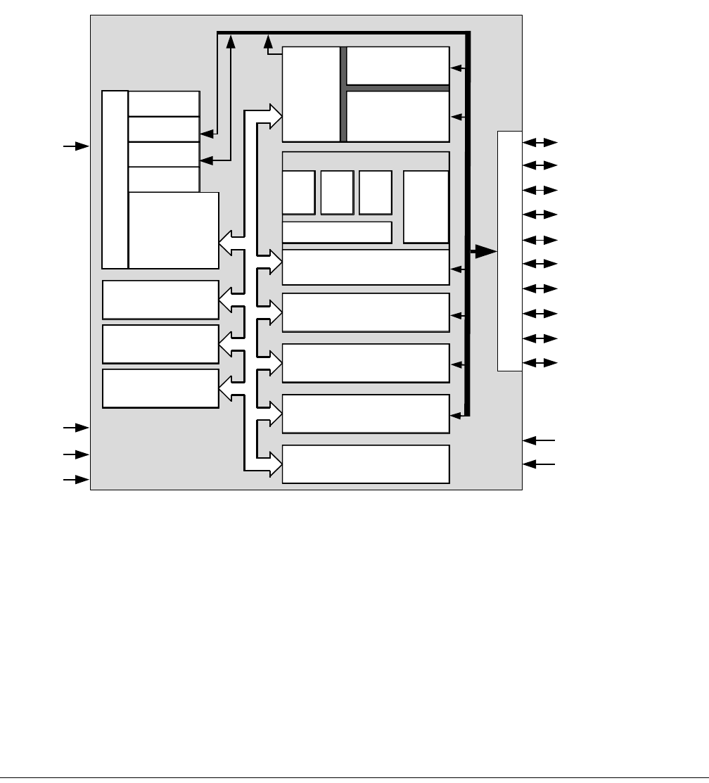
Figure 1. MMA9555L block diagram
A block-level view is shown in Figure 1 with building blocks of devices and built-in applications summarized at a high level. The
analog/mixed-mode subsystem associated with a digital engine is composed of:
• The analog subsystem is composed of:
• A 3-axis transducer that is an entirely passive block including the MEMS structures.
• An Analog Front End (AFE) with the following:
– A capacitance-to-voltage converter
– An analog-to-digital converter
– A temperature sensor
• The digital subsystem is composed of:
• A 32-bit CPU
• Memory: RAM, ROM, and flash
• Rapid GPIO (RGPIO) port-control logic
Analog Front End (AFE)
BDM
INTC
DBG
Flash
ROM
RAM
I
2
C Master
X
axis
C to V
ADC
Temp
Sensor
I
2
C slave
SPI slave
Control
and
mailbox
CLKGEN
Two-channel, 16-bit
Timer / PWM module
16-bit
Modulo timer module
Programmable
delay block
INT_O
Y
axis
Z
axis
V
DD
V
SS
RESET
V
SS
V
DDA
V
SSA
RGPIO
SCL0/RGPIC0/SCLK
SDA0/RGPIO1/SDI
RGPIO2/SCL1/SDO
RGPIO3/SDA1/SSB
RGPIO4/INT
RGPIO5/PDB_A/INT_O
RGPIO6/AN0/TPMCH0
RGPIO7/AN1/TPMCH1
RGPIO8/PDB_B
BKGD/MS/RPGPIO9
AN0
AN1
TPMCH0
TPMCH1
SCL1
SDA1
PDB_A
PDB_B
SCLK
SDI
SDO
SSB
SCL0
SDA0
SIM
BKGD
INT
32 bit CPU
Pinout
MMA9555L Intelligent Pedometer Data Sheet, Rev. 2.2
8© NXP B.V. 2016. All rights reserved.
–I
2C or SPI slave interface
– System Integration Module (SIM)
– Clock-Generation Module
The slave interfaces (either SPI or I2C) operate independently of the CPU subsystem. They can be accessed at any time,
including while the device is in low-power, deep-sleep mode.
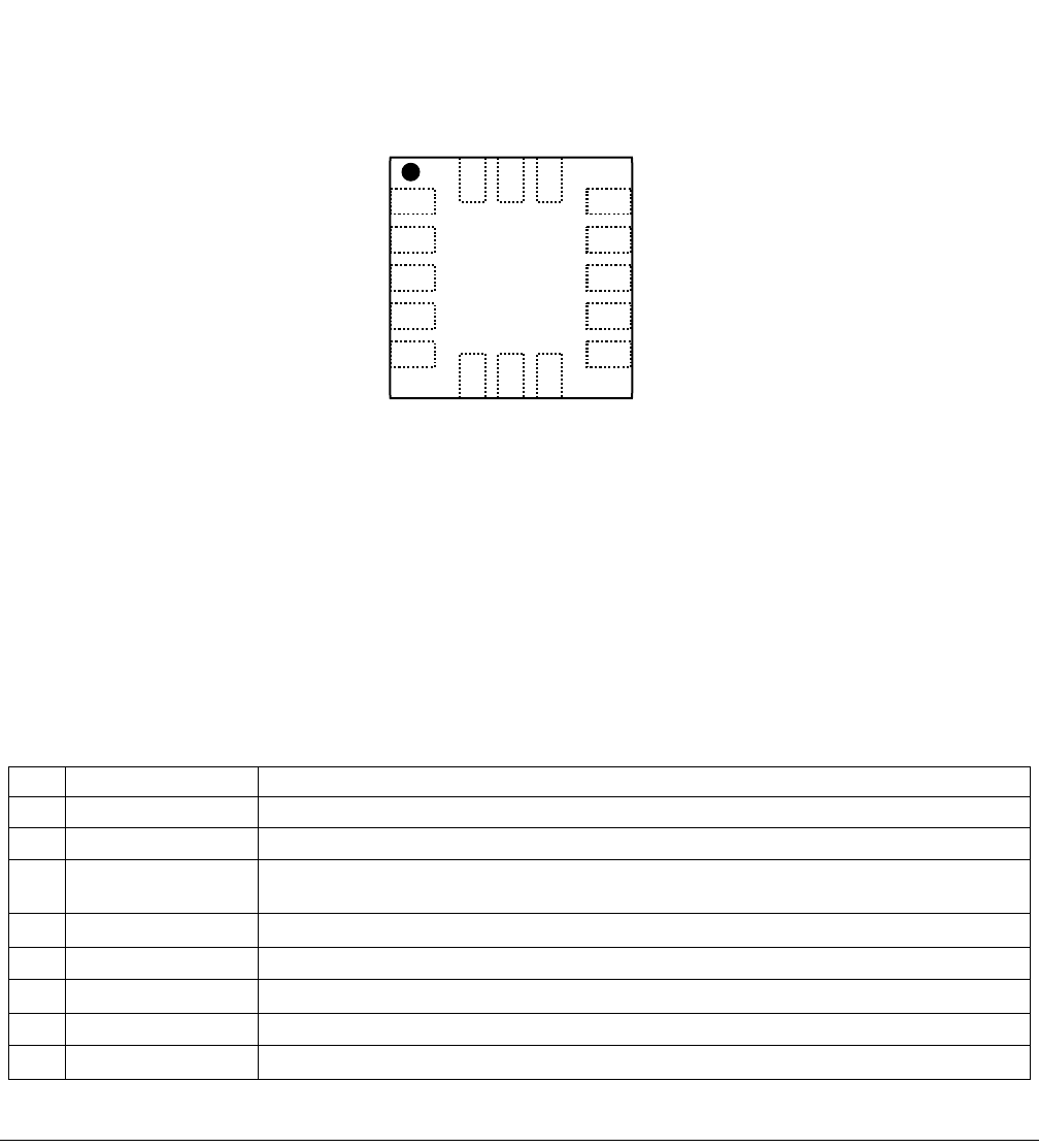
2.2 Pinout
The package pinout definition for this device is designed as a superset of functions on NXP's other MMA955xL offerings. All pins
on the device are utilized and many are multiplexed.
Figure 2. Device pinout (top view)
2.2.1 Pin Functions
The following table summarizes functional options for each pin on this device.
Table 2. Pin functions
Pin # Pin Name Description
1VDD Digital power supply
2BKGD / MS / RGPIO9 Background-debug / Mode select / RGPIO9
3RESETB Active-low reset. RESETB is an open-drain, bidirectional pin. By default, the output function is not on. Must
be pulled to VDD via resistor at startup. After startup, Reset may be asserted low to reset the device.
4SCL0 / RGPIO0 / SCLK Serial clock for slave I2C / RGPIO0 / Serial clock for slave SPI
5VSS Digital ground
6SDA0 / RGPIO1 / SDI Serial data for slave I2C / RGPIO1 / SPI serial data input
7RGPIO2 / SDO RGPIO2 / SPI serial data output
8RGPIO3 / SBB RGPIO3 / SPI slave select. RGPIO3 / SSB = Low at startup selects SPI. High at startup selects I2C.
2
3
5
1
4
V
DD
BKGD-MS / RGPIO9
V
SS
RGPIO7 / AN1
V
SSA
12
11
9
13
10
678
16 15 14
RGPIO8 / PDB_B
V
DDA
RGPIO1 / SDA0 / SDI
RGPIO2 / SDO
RGPIO3 / SSB
RESETB
SCL0 / RGPIO0 / SCLK
RGPIO6 / AN0
RGPIO5 / PDB_A / INT_O
V
SS
RGPIO4/INT

Pin Function Descriptions
MMA9555L Intelligent Pedometer Data Sheet, Rev. 2.2
© NXP B.V. 2016. All rights reserved. 9
2.3 Pin Function Descriptions
This section provides a brief description of the various pin functions available on the MMA9555L pedometer sensor. Ten of the
device pins are multiplexed with Rapid GPIO (RGPIO) functions.
VDD and VSS: Digital power and ground. VDD is nominally 1.8 V.
VDDA and VSSA: Analog power and ground. VDDA is nominally 1.8 V. To optimize performance, the VDDA line can be filtered to
remove any digital noise that might be present on the 1.8 V supply. (See Figure 3 and Figure 4.)
RESETB: The RESETB pin is an open-drain, bidirectional pin with an internal, weak, pullup resistor. At start-up, it is configured
as an input pin, but also can be programmed to become bidirectional. By default, the output function is not on. Using this feature,
the MMA9555L device can reset external devices for any purpose other than power-on reset. Reset must be pulled high at power
up to boot to Application code space. If low, it will boot to ROM code. After startup, Reset may be asserted to reset the device.
The total external capacitance to ground has to be limited when using RESETB-pin, output-drive capability. For more details, see
the “System Integration Module” chapter of the MMA955xL Intelligent, Motion-Sensing Platform Hardware Reference Manual
(MMA955xLHWRM), listed in “Related Documentation” on page 2.
Slave I2C port: SDA0 and SCL0: These are the slave-I2C data and clock signals, respectively. The MMA9555L device can be
controlled via the serial port or via the slave SPI interface.
Analog-to-Digital Conversion: AN0, AN1: The on-chip ADC can be used to perform a differential, analog-to-digital conversion
based on the voltage present across pins AN0(–) and AN1(+). Conversions for these pins are at the same Output Data Rate
(ODR) as the MEMS transducer signals. Input levels are limited to 1.8 V differential.
Rapid General Purpose I/O: RGPIO[9:0]: The Intelligent Pedometer has a feature called Rapid GPIO (RGPIO). This is a 16-bit,
input/output port with single-cycle write, set, clear, and toggle functions available to the CPU. The MMA9555L device brings out
the lower 10 bits of that port as pins of the device. At reset, all of the RGPIO pins are configured as input pins, although pin muxing
does reassign some pins to non-RGPIO function blocks. Pullups are disabled.
RGPIO[9:6] can be set as interrupt pins for most interrupt sources. INT_O can only output interrupts from the COCO bit. For
setting sensor data output interrupts, use RGPIO6–RGPIO9.
RGPIO3 / SBB = Low at startup selects SPI. High at startup selects I2C.
RGPIO[5] or INT_O can only output interrupts from the COCO bit. For setting sensor data output interrupts, use RGPIO6–
RGPIO9.
RGPIO[9] is connected to BKGD/MS.
RGPIO[1:0] SDA0 and SCL0 are connected at reset.
Interrupts: INT: This input pin can be used to wake the CPU from a deep-sleep mode. It can be programmed to trigger on either
rising or falling edge, or high or low level. This pin operates as a Level-7 (high-priority) interrupt.
Debug/Mode Control: BKGD/MS: At start-up, this pin operates as mode select. If this pin is pulled high during start up, the CPU
will boot normally and run code. If this pin is pulled low during start-up, the CPU will boot into active Background-Debug Mode
(BDM). In BDM, this pin operates as a bidirectional, single-wire, background-debug port. It can be used by development tools for
downloading code into on-chip RAM and flash and to debug that code. There is an internal pullup resistor on this pin, therefore,
It may be left floating.
9RGPIO4/INT RGPIO4 / Interrupt input
10 RESERVED Must be connected to VSS ground externally
11 RGPIO5 / INT_O RGPIO5 or INT_O slave-port interrupt output. INT_O can only output interrupts from the COCO bit. For
setting sensor data output interrupts, use RGPIO6–RGPIO9.
12 RGPIO6 / AN0 RGPIO6 / ADC Input 0
13 RGPIO7 / AN1 RGPIO7 / ADC Input 1
14 VDDA Analog power
15 RGPIO8 RGPIO8
16 VSSA Analog ground
Table 2. Pin functions (Continued)
Pin # Pin Name Description

System Connections
MMA9555L Intelligent Pedometer Data Sheet, Rev. 2.2
10 © NXP B.V. 2016. All rights reserved.
Slave SPI Interface: SCLK, SDI, SDO and SBB: These pins control the slave SPI clock, data in, data out, and slave-select
signals, respectively. The MMA9555L platform can be controlled via this serial port or via the slave-I2C interface. SBB has a
special function at startup that selects the Slave interface mode. Low at startup selects SPI and high selects I2C.
INT_O: The slave-port output interrupt pin can be used to flag the host when a response to a command is available to read on
the slave port. INT_O can only output interrupts from the COCO bit. For sensor data output interrupts, use RGPI06–RGPIO9.
2.4 System Connections
2.4.1 Power Sequencing
An internal circuit powered by VDDA provides the device with a power-on-reset signal. In order for this signal to be properly rec-
ognized, it is important that VDD is powered up before or simultaneously with VDDA. The voltage potential between VDD and VDDA
must not be allowed to exceed the value specified in Table 6 on page 14.
2.4.2 Layout Recommendations
• Provide a low-impedance path from the board power supply to each power pin (VDD and VDDA) on the device and from the
board ground to each ground pin (VSS and VSSA).
• Place 0.01 to 0.1 µF capacitors as close as possible to the package supply pins to meet the minimum bypass requirement.
The recommended bypass configuration is to place one bypass capacitor on each of the VDD/VSS pairs. VDDA/VSSA ceramic
and tantalum capacitors tend to provide better tolerances.
• Capacitor leads and associated printed-circuit traces that connect to the chip VDD and VSS (GND) pins must be as short as
possible.
• Bypass the power and ground with a capacitor of approximately 1 µF and a number of 0.1-µF ceramic capacitors.
• Minimize PCB trace lengths for high-frequency signals. This is especially critical in systems with higher capacitive loads that
could create higher transient currents in the VDD and VSS circuits.
• Take special care to minimize noise levels on the VDDA and VSSA pins.
• Use separate power planes for VDD and VDDA and separate ground planes for VSS and VSSA. Connect the separate analog
and digital power and ground planes as close as possible to power supply outputs. If both analog circuit and digital circuits
are powered by the same power supply, it is advisable to connect a small inductor or ferrite bead in series with both the VDDA
and VSSA traces.
• Physically separate the analog components from noisy digital components by ground planes. Do not place an analog trace
in parallel with digital traces. It is also desirable to place an analog ground trace around an analog signal trace to isolate it
from digital traces.
• Provide an interface to the BKGD/MS pin if in-circuit debug capability is desired.
• Ensure that resistors RP1 and RP2, in the following figure, match the requirements stated in the I2C standard. For the shown
configuration, the value of 4.7 kΩ would be appropriate.
2.4.3 MMA9555L Pedometer Sensor as an Intelligent Slave
I2C pullup resistors, and a few bypass capacitors are all that are required to attach this device to a host platform. The basic con-
figurations are shown in the following two figures. In addition, the RGPIO pins can be programmed to generate interrupts to a
host platform in response to the occurrence of real-time application events. In this case, the pins should be routed to the external
interrupt pins of the CPU.
NOTE
Immediately after a device reset, the state of pin number 8 (RGPIO3 / SDA1 / SSB functions) is used to select the slave port
interface mode. This implies important rules in the way the host controller or, more generally, the complete system should be
handling this pin.
First of all, whenever a reset occurs on the MMA9555L, the RGPIO3 pin level shall be consistent with the interface mode of op-
eration. This is particularly important if this pin is driven from external devices. If the RGPIO3 level does not match the current
mode of operation, an alternate mode is selected and communication with the host is lost.
If I2C mode is used, a good practice is to tie RGPIO3 to a pull-up resistor so that it defaults to high level. When using I2C mode
for the slave interface, the RGPIO3 pin plays two roles: RGPIO3 and mode selection. When the MMA9555L is powered on and
the mode selection is I2C, the RGPIO3 pin is released as a GPIO pin. The default setting of RGPIO3 is as an output pin and
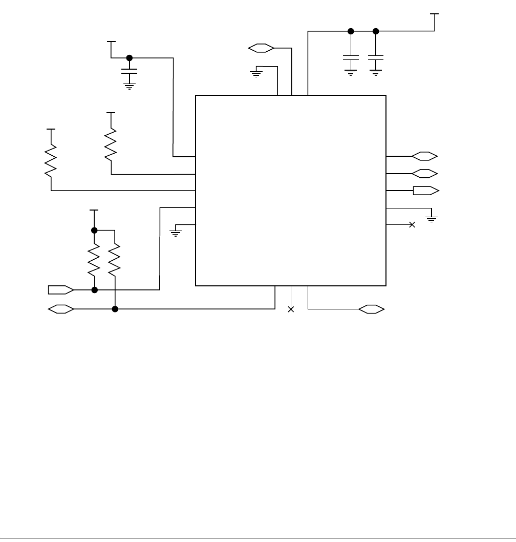
System Connections
MMA9555L Intelligent Pedometer Data Sheet, Rev. 2.2
© NXP B.V. 2016. All rights reserved. 11
output low. In order to reduce the leakage current on the pull-up resistor, a large resistor value can be used or RGPIO3 can be
set as an input pin.
When using SPI mode for the slave interface, the situation is more complex as the same pin plays two roles: SSB and mode
selection. Moreover, after a SPI read or write operation, the SSB line returns to high level. Consequently, if the host is sending a
command to the MMA9555L that induces a subsequent reset, immediately after the write transaction, the host shall force the
SSB line to low level so that SPI mode is still selected after reset. The duration for the SSB line to be kept low typically depends
on the latency between the write transaction and the execution of the reset command. Such latency can be significant for the
MMA9555L pedometer firmware as the Command Interpreter and Scheduler Application are running at 30 Hz which gives a
33 ms typical latency.
The rule obviously applies also when a hardware reset is issued by the host through MMA9555L pin number 3 (RESETB active
low). Again the host has to drive the SSB line low prior to release of the hardware reset line to high level, which triggers immediate
MMA9555L reset and boot sequence. Keeping the SSB line low for a 1 ms duration (after RESETB is released) is enough for the
MMA9555L slave device to re-boot into SPI mode.
Figure 3. MMA9555L Pedometer Sensor as an I2C slave
1.8 V
Quiet VDDA for
best performance
C1*
1 F
C2
0.1 F
13
12
11
10
9
1
2
3
4
5
INT_OUT
I2C_DATA
I2C_CLK
4.7 K
R1
1.8 V
C3
0.1 F
1.8 V
U1
MMA955X
VDD
BKGD / MS / IO9
RESETB
SCL0 / IO0 / SCLK
VSS
IO7 / AN1
IO6 / AN0
* IO5 / PDB_A / INT_O
VSS
IO4 / INT
SDA0 / IO1 / SDI
IO2 / SDO
IO3 / SSB
VSSA
IO8 / PDB_B
VDDA
8*
7
6
14
15
16
4.7 K
R2
1.8 V
4.7 K
R4
1.8 V
4.7 K
R3
* IO5 can only be
configured as
COCO bit interrupt
For most interrupt
sources, use
IO6-IO9.
* C1 is not necessary for
all implementations, but is
recommended as good
design practice for achieving
low noise operation.
*See the NOTE in this section.
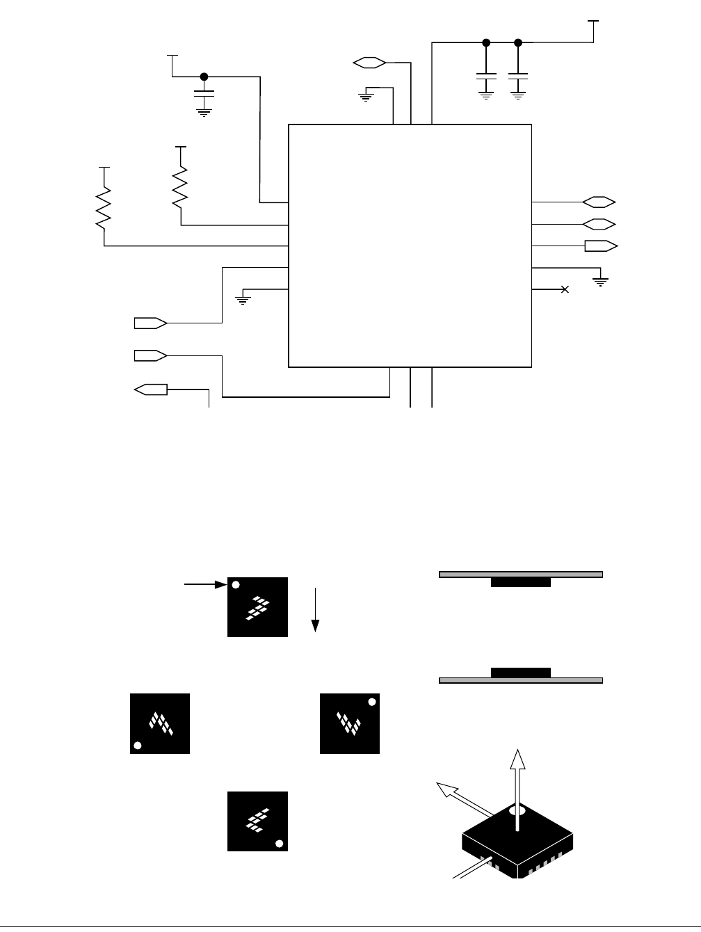
System Connections
MMA9555L Intelligent Pedometer Data Sheet, Rev. 2.2
12 © NXP B.V. 2016. All rights reserved.
Figure 4. MMA9555L Pedometer Sensor as an SPI slave
2.4.4 Sensing Direction and Output Response
Figure 5 shows the device’s default sensing direction when measuring gravity in a static manner from the six standard orientation
modes: portrait up/down, landscape left/right and back/front.
Figure 5. Sensing direction and output response
13
12
11
10
9
1
2
3
4
5
INT_COCO
SPI_DO (MISO)
SPI_DI (MOSI)
SPI_CLK
4.7 K
R1
1.8 V
C3
0.1 F
1.8 V
VDD
BKGD / MS / IO9
RESETB
SCL0 / IO0 / SCLK
VSS
IO7 / AN1
IO6 / AN0
* IO5 / PDB_A / INT_O
VSS
IO4 / INT
SDA0 / IO1 / SDI
IO2 / SDO
IO3 / SSB
8*
7
6
4.7 K
R2
1.8 V
Quiet VDDA for
best performance
C1*
1 F
C2
0.1 F
VSSA
IO8 / PDB_B
VDDA 14
15
16
INT_OUT
1.8 V
U1
MMA955X
* IO5 can only be configured as
COCO bit interrupt. For most
interrupt sources, use IO6-IO9.
* C1 is not necessary for
all implementations, but is
recommended as good
design practice for achieving
low noise operation.
* See the NOTE in this section.
Pin 1
Top view Side view
Landscape Right
Gravity
Landscape Left
Portrait Up
Portrait Down
Back
Front
Xout @ 0 g
Yout @ -1 g
Zout @ 0 g
Xout @ 1 g
Yout @ 0 g
Zout @ 0 g
Xout @ 0 g
Yout @ 1 g
Xout @ -1 g
Yout @ 0 g
Zout @ 0 g
Xout @ 0 g
Yout @ 0 g
Zout @ -1 g
Xout @ 0 g
Yout @ 0 g
Zout @ 1 g
+Z
+Y
+X

Definitions
MMA9555L Intelligent Pedometer Data Sheet, Rev. 2.2
© NXP B.V. 2016. All rights reserved. 13
3 Mechanical and Electrical Specifications
This section contains electrical specification tables and reference timing diagrams for the MMA9555L device, including detailed
information on power considerations, DC/AC electrical characteristics, and AC timing specifications.
3.1 Definitions
Cross-axis sensitivity The proportionality constant that relates a variation of accelerometer output to cross acceleration. This
sensitivity varies with the direction of cross acceleration and is primarily due to misalignment.
Full range The algebraic difference between the upper and lower values of the input range. Refer to the input/
output characteristics.
Hardware compensated Sensor modules on this device include hardware-correction factors for gain and offset errors that are
calibrated during factory test using a least-squares fit of the raw sensor data.
Linearity error The deviation of the sensor output from a least-squares linear fit of the input/output data.
Nonlinearity The systematic deviation from the straight line that defines the nominal input/output relationship.
Pin group The clustering of device pins into a number of logical pin groupings to simplify and standardize elec-
trical data sheet parameters. Pin groups are defined in Section 3.2, “Pin Groups”.
Software compensated NXP’s advanced nonlinear calibration functions that—with the first-order hardware gain and offset cal-
ibration features—improve sensor performance.
Warm-up time The time from the initial application of power for a sensor to reach its specified performance under the
documented operating conditions.
3.2 Pin Groups
The following pin groups are used throughout the remainder of this section.
Group 1 RESETB
Group 2 RESERVED
Group 3 RGPIO[9:0]
3.3 Absolute Maximum Ratings
Absolute maximum ratings are the limits the device can be exposed to without permanently damaging it. Absolute maximum rat-
ings are stress ratings only; functional operation at these ratings is not guaranteed. Exposure to absolute maximum ratings con-
ditions for extended periods may affect reliability.
This device contains circuitry to protect against damage due to high static voltage or electrical fields. It is advised, however, that
normal precautions be taken to avoid application of any voltages higher than maximum-rated voltages to this high-impedance
circuit. Reliability of operation is enhanced if unused inputs are tied to an appropriate logic voltage level (for instance, either VSS
or VDD).
Table 3. Absolute maximum ratings
Rating Symbol Minimum Maximum Unit
Digital supply voltage VDD –0.3 2.0 V
Analog supply voltage VDDA –0.3 2.0 V
Voltage difference, VDD to VDDA VDD – VDDA –0.1 0.1 V
Voltage difference, VSS to VSSA VSS – VSSA –0.1 0.1 V
Input voltage VIn –0.3 VDD + 0.3 V
Input/Output pin-clamp current IC–20 20 mA
Output voltage range (Open-Drain Mode) VOUTOD –0.3 VDD + 0.3 V
Storage temperature Tstg –40 125 °C
Mechanical shock SH — 5k g

Operating Conditions
MMA9555L Intelligent Pedometer Data Sheet, Rev. 2.2
14 © NXP B.V. 2016. All rights reserved.
3.4 Operating Conditions
3.5 Electrostatic Discharge (ESD) and Latch-up Protection
Characteristics
3.6 General DC Characteristics
Table 4. Nominal operating conditions
Rating Symbol Min Typ Max Unit
Digital supply voltage VDD 1.71 1.8 1.89 V
Analog supply voltage VDDA 1.71 1.8 1.89 V
Voltage difference, VDD to VDDA VDD – VDDA –0.1 —0.1 V
Voltage difference, VSS to VSSA VSS – VSSA –0.1 —0.1 V
Input voltage high VIH 0.7 * VDD — VDD+0.1 V
Input voltage low VIL VSS – 0.3 —0.3*VDD V
Operating temperature TA–40 25 85 °C
Table 5. ESD and latch-up protection characteristics
Rating Symbol Value Unit
Human Body Model (HBM) VHBM ±2000 V
Machine Model (MM) VMM ±200 V
Charge Device Model (CDM) VCDM ±500 V
Latch-up current at 85 °C ILAT ±100 mA
Table 6. DC characteristics(1)
1. All conditions at nominal supply: VDD = VDDA = 1.8 V.
Characteristic Symbol Condition(s)(2)
2. Pin groups are defined in “Pin Groups” on page 13.
Min Typ Max Unit
Output voltage high
• Low-drive strength
• High-drive strength
VOH
Pin Groups 1 and 3
ILOAD = –2 mA
ILOAD = –3 mA
VDD – 0.5 — — V
Output voltage low
• Low-drive strength
• High-drive strength
VOL
Pin Groups 1 and 3
ILOAD = 2 mA
ILOAD = 3 mA
——0.5V
Output-low current
Max total IOL for all ports IOLT ———24mA
Output-high current
Max total IOH for all ports IOHT ———24mA
Input-leakage current |IIN|Pin Group 2
Vin = VDD or VSS —0.1 1 µA
Hi-Z (off-state) leakage current |IOZ|
Pin Group 3 input
resistors disabled
Vin = VDD or VSS
—0.1 1 µA
Pullup resistor RPU when enabled 17.5 — 52.5 kΩ
Power-on-reset voltage VPOR — — 1.50 — V
Power-on-reset hysteresis VPOR–hys ——100—mV
Input-pin capacitance CIN ——7—pF
Output-pin capacitance COUT ——7—pF

Supply Current Characteristics
MMA9555L Intelligent Pedometer Data Sheet, Rev. 2.2
© NXP B.V. 2016. All rights reserved. 15
3.7 Supply Current Characteristics
3.8 Accelerometer Transducer Mechanical Characteristics
3.9 ADC Characteristics
Table 7. Supply current characteristics(1)
1. All conditions at nominal supply: VDD = VDDA = 1.8 V.
Characteristic Symbol Condition(s) Min Typ Max Unit
Supply current in STOPNC mode IDD–SNC Internal clocks disabled — 2 — µA
Supply current in STOPSC mode IDD–SSC Internal clock in
slow-speed mode —15—µA
Supply current in RUN mode(2)
2. Total current with the analog section active, 16 bits ADC resolution selected, MAC unit used and all peripheral clocks enabled.
IDD–R Internal clock in
fast mode —3.1—mA
Table 8. Accelerometer characteristics
Characteristic Symbol Condition(s) Min Typ Max Unit
Full range AFR
2 g±1.8 ±2 ±2.2
g4 g±3.6 ±4 ±4.4
8 g±7.2 ±8 ±8.8
Sensitivity/resolution ASENS
2 g— 0.061 —
mg/LSB4 g— 0.122 —
8 g— 0.244 —
Zero-g level offset accuracy
(Pre-board mount) OFFPBM
2 g
–100 — +100 mg4 g
8 g
Nonlinearity
Best fit straight line ANL
2 g—±0.25—
% AFR
4 g—±0.5—
8 g—±1—
Sensitivity change vs.temperature TCSA 2 g—±0.17— %/°C
Zero-g level change vs. temperature(1)
1. Relative to 25 °C.
TCOff ——±1.9—mg/°C
Zero-g Level offset accuracy
(Post-board mount) OFFBM
2 g
–100 — +100 mg4 g
8 g
Output data bandwidth BW — — ODR/2 — Hz
Output noise Noise 2 g, ODR = 488 Hz — 100 — µg/sqrt(Hz)
8 g, ODR = 488 Hz — 120 — µg/sqrt(Hz)
Cross-axis sensitivity — — –5 — 5 %
Table 9. ADC characteristics(1)
Characteristic Symbol Condition(s) Min Typ Max Unit
Input voltage VAI Voltage at AN0 or AN1 0.2 — 1.1 V
Differential input voltage VADI AN1 – AN0 –0.9 — 0.9 V
Full-scale range VFS ——1.8—V
Programmable resolution RES —101416Bits
ADC Sample Rates
MMA9555L Intelligent Pedometer Data Sheet, Rev. 2.2
16 © NXP B.V. 2016. All rights reserved.
3.10 ADC Sample Rates
The MMA9555L internal ADC supports the following sample output rates, while the pedometer application uses 30.52 fps as
default:
• 488.28 frames per second (fps)
• 244.14 fps
• 122.07 fps
• 61.04 fps
• 30.52 fps
• 15.26 fps
• 7.63 fps
• 3.81 fps
3.11 AC Electrical Characteristics
Tests are conducted using the input levels specified in Table 4 on page 14. Unless otherwise specified, propagation delays are
measured from the 50-percent to 50-percent point. Rise and fall times are measured between the 10-percent and 90-percent
points, as shown in the following figure.
Figure 6. Input signal measurement references
The subsequent figure shows the definitions of the following signal states:
• Active state, when a bus or signal is driven and enters a low-impedance state
• Three-stated, when a bus or signal is placed in a high-impedance state
• Data Valid state, when a signal level has reached VOL or VOH
• Data Invalid state, when a signal level is in transition between VOL and VOH
Figure 7. Signal states
Conversion time @ 14-bits resolution
(Three-sample frame) tc——207—µs
Integral nonlinearity INL Full scale — ±15 — LSB
Differential nonlinearity DNL — — ±2 — LSB
Input leakage IIA ———±2µA
1. All conditions at nominal supply: VDD = VDDA = 1.8 V and RES = 14, unless otherwise noted.
Table 9. ADC characteristics(1) (Continued)
Characteristic Symbol Condition(s) Min Typ Max Unit
VIH
VIL
Fall Time
Input Signal
Note: The midpoint is VIL + (VIH – VIL)/2.
Midpoint1
Low High
90%
50%
10%
Rise Time
Data Invalid State
Data1
Data
3-stated
Data3 Valid
Data2 Data3
Data1 Valid
Data Active Data Active
Data1 Valid
General Timing Control
MMA9555L Intelligent Pedometer Data Sheet, Rev. 2.2
© NXP B.V. 2016. All rights reserved. 17
3.12 General Timing Control
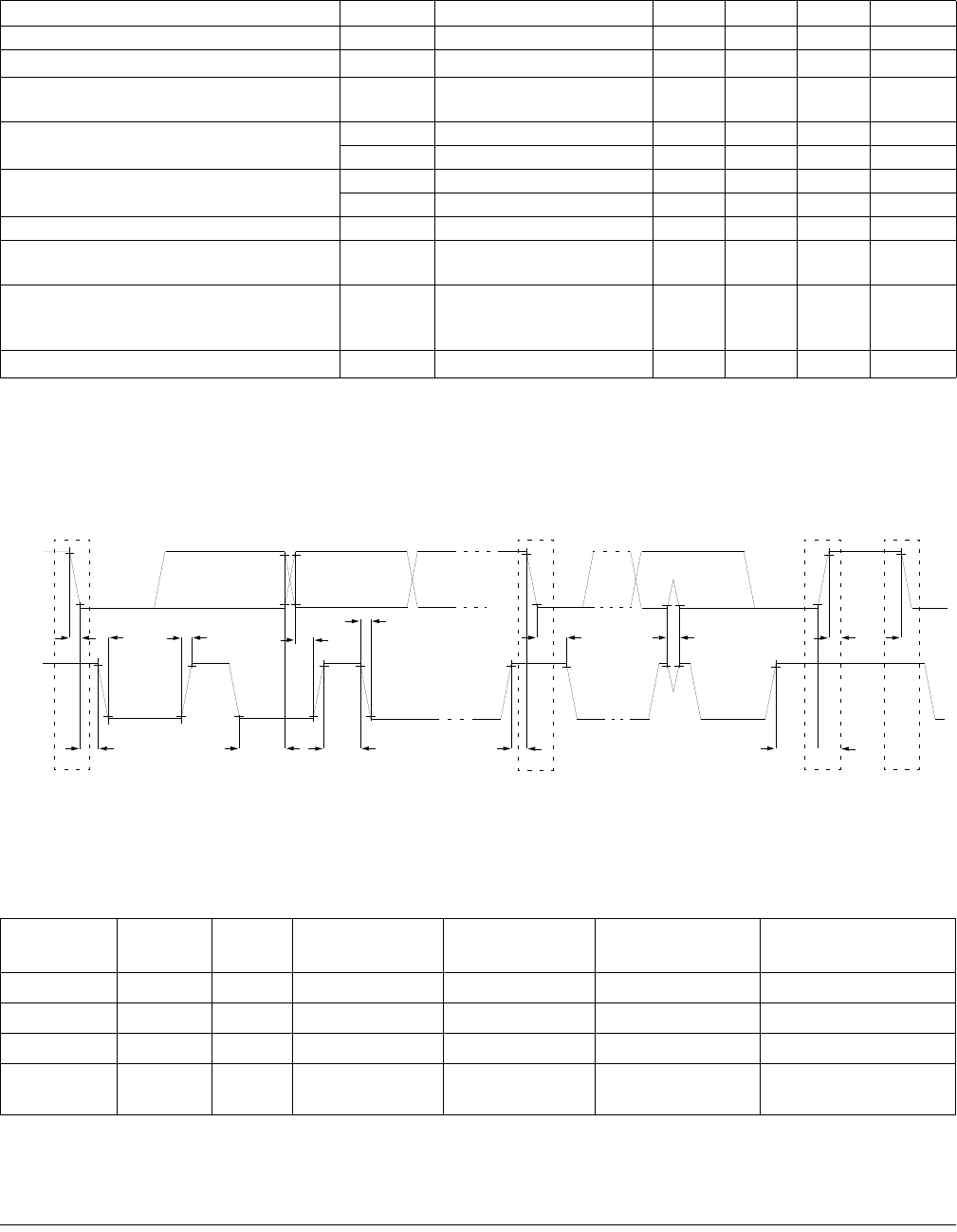
3.13 I2C Timing
This device includes a slave I2C module that can be used to control the sensor and can be active 100 percent of the time.
Figure 8. I2C standard and fast-mode timing
3.13.1 Slave I2C
Table 10. General timing characteristics(1)
1. All conditions at nominal supply: VDD = VDDA = 1.8 V
Characteristic Symbol Condition(s) Min Typ Max Unit
VDD rise time Trvdd 10% to 90% — — 1 ms
POR release delay(2)
2. This is the time measured from VDD = VPOR until the internal reset signal is released.
TPOR Power-up 0.35 1.5 ms
Warm-up time TWU From STOPNC —7—
sample
periods
Frequency of operation FOPH Full Speed Clock — 8 — MHz
FOPL Slow Clock — 62.5 — KHz
System clock period tCYCH Full Speed Clock — 125 — ns
tCYCL Slow Clock — 16 — μs
Full/Slow clock ratio — — — 128 —
Oscillator frequency absolute accuracy @
25 °C — Full Speed Clock –5 — +5 %
Oscillator frequency variation over
temperature
(–40 °C to 85 °C vs. ambient) — Slow Clock –6 — +6 %
Minimum RESET assertion duration tRA —4T(3)
3. In the formulas, T = 1 system clock cycle. In full speed mode, T is nominally 125 ns. In slow speed mode, T is nominally 16 μs.
—— —
Table 11. I2C Speed Ranges
Mode Max Baud
Rate (fSCL)Min
Bit Time
Min SCL Low
(tLOW)Min SCL High
(tHIGH)Min Data setup Time
(tSU; DAT)Min/Max Data Hold Time
(tHD; DAT)
Standard 100 kHz 10 μs4.7 μs4 μs 250 ns 0 μs/3.45 μs(1)
1. The maximum tHD; DAT must be at least a transmission time less than tVD;DAT or tVD;ACK. For details, see the I2C standard.
Fast 400 kHz 2.5 μs1.3 μs0.6 μs 100 ns 0 μs/0.9 μs(1)
Fast + 1 MHz 1 μs 500 ns 260 ns 50 ns 0 μs/0.45 μs(1)
High-speed
supported 2.0 MHz 0.5 μs 200 ns 200 ns 10 ns(2)
2. Timing met with IFE = 0, DS = 1, and SE = 1. Refer to the chapter titled Port Controls in the MMA955xL Intelligent, Motion-Sensing Platform Hardware
Reference Manual (MMA955xLHWRM), listed in “Related Documentation” on page 2.
0 ns/70 ns (100 pf)(1)
SDA
SCL
tHD; STA tHD; DAT
tLOW
tSU; DAT
tHIGH
tSU; STA SR PS
S
tHD; STA tSP
tSU; STO
tBUF
tftr
tftr
Slave SPI Timing
MMA9555L Intelligent Pedometer Data Sheet, Rev. 2.2
18 © NXP B.V. 2016. All rights reserved.
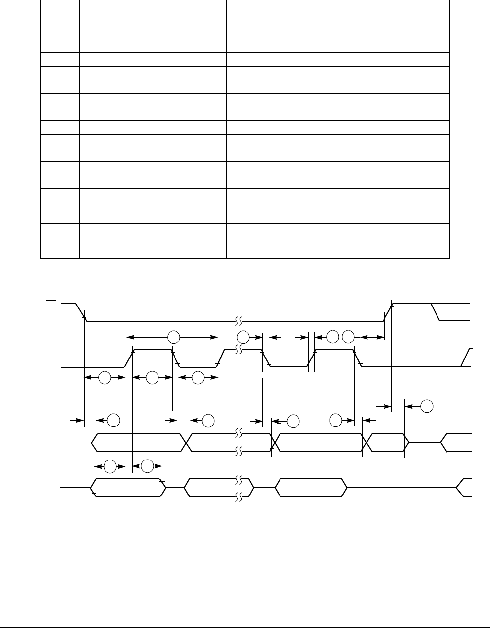
3.14 Slave SPI Timing
Figure 9. SPI slave timing
Table 12. Slave SPI timing
Time
Period
(1)
1. Time period from Figure 9.
Function Symbol Min Max Unit
— Operating frequency fop 0F
OPH/4 Hz
1 SCLK period tSCLK 4—t
CYCH
2 Enable lead time tLead 0.5 — tCYCH
3 Enable lag time tLag 0.5 — tCYCH
4 Clock (SCLK) high or low time tWSCLK 200 — ns
5 Data-setup time (inputs) tSU 15 — ns
6 Data-hold time (inputs) tHI 25 — ns
7 Access time ta—25ns
8 SDO-disable time tdis —25ns
9 Data valid (after SCLK edge) tv—25ns
10 Data-hold time (outputs) tHO 0—ns
11 Rise time
Input
Output tRI
tRO
—
—25
25 ns
ns
12 Fall time
Input
Output tFI
tFO
—
—25
25 ns
ns
SCLK
(INPUT)
SDI
(INPUT)
SDO
(OUTPUT)
SS
(INPUT)
MSB IN
BIT 6 . . . 1
LSB IN
MSB OUT SLAVE LSB OUT
BIT 6 . . . 1
NOTE:
SLAVE SEE
NOTE
1. Not defined but normally MSB of character just received.
121
<
11 3
424
7
56
9
8
10
10
Overview of Communication Interface
MMA9555L Intelligent Pedometer Data Sheet, Rev. 2.2
© NXP B.V. 2016. All rights reserved. 19
4 Communication Interface
4.1 Overview of Communication Interface
All access to the MMA9555L is made via the slave, serial Communication Interface that is part of the hardware and firmware
infrastructure of the platform. The communication occurs in Command/Response (Normal) or Quick Read (Legacy) mode.
Commands are sent from the host and through the slave communications port (either SPI or I2C). The Communication Interface
interprets the command and sends the data to the correct application. The application executes the command and returns with
data, if requested with the command response. It also responds with error codes when appropriate.
The Communications Interface works with the Mailbox application to implement the command and response. The mailboxes’
functionality is configured with two applications: the MBOX Configuration application (APP_ID = 0x18) and the MBOX application
(APP_ID = 0x04).
4.2 Mailbox Interface
Commands are received through a set of 32 mailboxes that are 32 registers arranged consecutively to provide addressable
memory regions. Each mailbox can hold one byte of data.
After a command has completed, the Communication Interface writes the results to the mailboxes and the results (response out)
are retrieved by the host via the SPI or the I2C slave interface.
The following figure shows the structure of the data packet when writing one byte into a specific mailbox.
If the transaction contains more than one data byte, the internal-destination mailbox address is automatically incremented so that
the incoming byte is placed in the next mailbox. For mailbox addresses greater than 31 bytes or for transactions where the
mailbox address auto-increments past mailbox 31, the destination address wraps back to the start of the mailbox addresses.
S10011000AA7 A6 A5 A4 A3 A2 A1 A0 A D7 D6 D5 D4 D3 D2 D1 D0 A P
Figure 10. I2C interface writing one byte of information to a mailbox
StopDestination Mailbox Address Data Byte
R/WDevice Address = 0x4C
Start Acknowledge
Acknowledge Acknowledge
Mailbox Usage
MMA9555L Intelligent Pedometer Data Sheet, Rev. 2.2
20 © NXP B.V. 2016. All rights reserved.
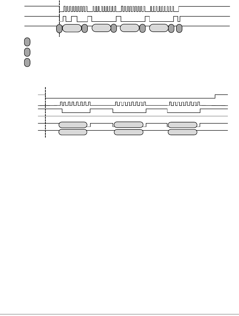
4.2.1 Mailbox Timing
Figure 11. I2C timing diagram
Figure 12. SPI timing diagram
4.3 Mailbox Usage
Commands to the MMA9555L consist of a write followed by one or more reads. It may take some time to complete the command
and a flag can be checked to determine if the command has completed. That flag is the Command Complete (COCO) bit, the
seventh bit of the read data in the second mailbox. (See Table 16 on page 23.)
On a read operation, the COCO bit indicates if the command has been processed. The host processor can determine the status
of the command’s processing by repeatedly reading or polling the second mailbox until the COCO bit is set. Alternatively, the
Clock
Data
Data
values
SA A A A P
S
A
P
98 00 00 00
Start
Acknowledge
Stop
80
Enable
Clock
MOSI
MISO
MOSI values
MISO values FF
00
FF
00
FF
MISO: SPI Master In, Slave Out
MOSI: SPI Master Out, Slave In
SPI: Serial, Peripheral Interface

Mailbox Usage
MMA9555L Intelligent Pedometer Data Sheet, Rev. 2.2
© NXP B.V. 2016. All rights reserved. 21
MMA9555L can be configured to assert an interrupt signal at the completion of a command. If configured, the INT_O interrupt
will be set immediately after the COCO bit has been set.
For more information, see “Configuring mailbox operational mode” on page 96.
4.3.1 Mailbox Command Format for a Write
Commands written to the MMA9555L are sent in the format shown in the following table. Mailboxes are filled with data, depending
on the target application. All commands start with the APP_ID, the command, the destination offset, and the number of data bytes
to write.
All commands must be written in a single, I2C/SPI transaction starting at Mailbox 0, but the response can be read from any subset
of the mailbox registers.
For a write-request command, the first four mailboxes must be written with enough bytes to hold the requested number of bytes.
The format of the data bytes is specific to the targeted application. (Applications are described in Table 15.)
The following table gives the details of the different parts of the data packet for a Write command.
Table 13. Mailbox commands formats
Offset76543210
0x00 Application ID (APP_ID)
0x01 0 Command Byte offset (upper 4 bits)
0x02 Byte offset (lower 8 bits)
0x03 Requested number of bytes to read/write
0x04 Write data 0
0x05 Write data 1
0x06 Write data 2
…. Write data n
Table 14. Mailbox command format details
Block Description
Application ID Application targeted for the issued command, see Table 15.
Command
Command to be performed:
• 0: Read application fixed bytes (version information)
• 1: Read application configuration bytes
• 2: Write application configuration bytes
• 3: Read application status or output
Byte offset Sets the offset of the first byte to be accessed, counting from the start of the register space. This enables
a subset of the registers to be accessed by setting the start location to something other than zero.
Requested number
of bytes Number of bytes requested to be read or written.
Write data The data being written.

Mailbox Usage
MMA9555L Intelligent Pedometer Data Sheet, Rev. 2.2
22 © NXP B.V. 2016. All rights reserved.
4.3.2 Application IDs, names, and descriptions
The following table gives the names and IDs of the NXP applications associated with MMA9555L.
Table 15. Application descriptions
Application ID Application Name Description
0x00 Version Returns a 12-byte pack with the device identifier number and the version
numbers of the ROM, firmware, and hardware.
(For more details, see Chapter 5, “Version Application”.)
0x01 Scheduler Configures the system, applications, and the MMA9555L infrastructure to run
at specific sample rates. Additionally, the identifier reads the number of times
each task has been executed.
0x02 Reserved
0x03 GPIO-AppMap Configures the GPIO application to map a specific application output bit to
specific GPIO pins. (For more details, see Chapter 7, “GPIO-AppMap
Application”) The GPIO pins are limited to GPIO6 through 9.
0x04 Mailbox
Configures an internal mailbox table to map which output bytes from specific
application identifiers will be accessible in the Normal mode and the Legacy
mode’s Quick-Read registers mailboxes. The application identifier can perform
a table reset to reinstall the default values when the MMA9555L resets.
0x05 Reserved
0x06 Analog Front End Configures different parameters of the AFE and reads XYZ data from the
accelerometer. For further details, see Chapter 9, “Analog Front End
Application”.
0x0C–0x0D Reserved
0x0F Data FIFO Configures parameters of the Data-FIFO application and reads the output
bytes from its output structure and the contents of the FIFO buffer.
0x10 Event queue Configures parameters of the Event-queue application and reads the output
bytes from its output structure and the contents of the Event-queue buffer.
0x11 Status register Provides access to the MMA9555L system-status information.
0x12 Wake/Sleep Configures the power-control modes of the accelerometer. The application has
three modes of operation: Run, Doze, and Sleep.
0x13–0x14 Reserved
0x15 Pedometer Application that can detect the step count.
0x16 Reserved
0x17 Reset/suspend/clear Controls the Reset/Suspend/Clear functions of the MMA9555L.
0x18 Mailbox mode config Configures different operation modes of the mailbox and provides the status
value of the mailbox when Stream mode is running.
0x19 GPIO Input/Output Controls GPIO2–GPIO8 as input or output pins.
0x1B–0x1F Reserved
0x20–0xFF Reserved Indicates an invalid application index.

Mailbox Usage
MMA9555L Intelligent Pedometer Data Sheet, Rev. 2.2
© NXP B.V. 2016. All rights reserved. 23
4.3.3 Mailbox command format for a read
Though all commands must be written in a single I2C/SPI transaction starting at Mailbox 0, the response can be read from any
subset of the mailbox registers. When the MMA9555L is configured to stream data (as in FIFO mode), the read commands must
be constructed as multiples of 32 bytes in order to trigger the internal transfer of the next set of data to the mailboxes.
A read-request command requires a write to the first four mailboxes.
The format of the information returned from the MMA9555L is shown in Table 16. Similar to the command format, the response
format follows the specific application’s format.
Mailboxes are filled with data depending on the target application.
All responses start with the responding APP_ID, the COCO the ERROR STATUS, the actual data count, and the requested data
count.
The format of the remaining data bytes is specific to the responding application.
Table 17 describes the details of the different parts and fields of a response message.
Table 16. Mailbox response formats
Mailbox76543210
0x00 Application ID (APP_ID)
0x01 COCO Error code
0x02 Actual number of bytes read/written
0x03 Requested number of bytes to read/write
0x04 Read data 0
0x05 Read data 1
0x06 Read data 2
…. Read data n
Table 17. Mailbox response format details
Block Description
Application ID
(APP_ID) The ID of the application that is responding. (See Table 16 on page 23.)
COCO Command complete.
This bit must be set to 0b when a command is written and is set to 1b by the MMA9555L platform, when
the command has been processed. The other registers do not contain valid results until this bit is set.
Error code The seven bytes that store the error code of the command. A zero indicates there was no error. (For more
information, see Table 18.)
Actual number of
bytes
Actual number of bytes read or written.
This block reports back the actual number of bytes that were read or written. It is normally the same as
the requested number of bytes, but it will be reduced if the requested number of bytes plus the Byte Offset
exceeds the number of bytes in the requested block’s data structure.
Requested number
of bytes Number of bytes requested to be read or written.
Read data The data that was read.

Mailbox Usage
MMA9555L Intelligent Pedometer Data Sheet, Rev. 2.2
24 © NXP B.V. 2016. All rights reserved.
Table 18 describes the status or error-code results returned in Mailbox 0x01.
Table 18. Error-Status codes returned in Mailbox 0x01
Error Code Name Description
0x00 MCI _ERROR_NONE Command completed with no errors.
0x04 MCI _ERROR_PARAM Incorrect input parameter.
Error may be due to an incorrect application ID, an incomplete command,
or an incorrect offset.
0x19 MCI _INVALID_COUNT Returned when the command COUNT is greater than the output structure
size.
0x1C MCI_ERROR_COMMAND Returned any time that the command interpreter does not recognize a
command code.
0x21 MCI_ERROR_INVALID_LENGTH Returned when the host sends a number of bytes with a wrong payload.
MMA9555L checks any mismatches between the amount of bytes
received and the actual payload sent by the host.
0x22 MCI_ERROR_FIFO_BUSY FIFO is busy performing a push operation and it is not possible to execute
any other function.
0x23 MCI_ERROR_FIFO_ALLOCATED
Returned when the host tries to reconfigure the FIFO module. The FIFO
application configuration can only be written once. In order to reconfigure
the FIFO, the whole device must be reset. This is because the FIFO
application requests RAM and RAM can only be allocated once.
0x24 MCI_ERROR_FIFO_OVERSIZE Returned when the host wants to set a FIFO buffer size out of the memory
boundaries within the MMA9555L device.

MMA9555L Intelligent Pedometer Data Sheet, Rev. 2.2
© NXP B.V. 2016. All rights reserved. 25
5 Version Application
The MMA9555L device's system-version information is stored in a 12-byte packet and
contains system-identity information including device-hardware ID; the versions of the ROM
bootloader, primary firmware, and hardware; and the system-build information.
Table 19 describes the system-version packet and its corresponding mailbox alignment.
Table 20 describes the Build Major and Build Minor version-number fields.
Table 19. Version command description bytes
Mailbox
number Description Byte
4 Device identifier 31:24
5 Device identifier 24:16
6 Device identifier 15:8
7 Device identifier 7:0
8 ROM major version number 7:0
9 ROM minor version number 7:0
10 Firmware major version number 7:0
11 Firmware minor version number 7:0
12 Hardware major version number 7:0
13 Hardware minor version number 7:0
14 Build major version number 7:0
15 Build minor version number 7:0
Table 20. Version application, Build major and minor bytes
Byte Address Description Bit fields
3 0x1FD Build major version number
• 7–3 Build’s day of the month
Range, 1 to 31
• 2–0 Year of build, from 2010
Range, 0 to 7.
4 0x1FC Build minor version number
• 7 — Release
– 1 Engineering version
– 0 Production release
• 6–4 Build number
• 3–0 Month of build
Range, 1 to 12
Application
ID 0x00
Default speed Always
available.
Configuration
registers None.
Status
registers None.

Reading the version information
MMA9555L Intelligent Pedometer Data Sheet, Rev. 2.2
26 © NXP B.V. 2016. All rights reserved.
5.1 Reading the version information
To read the MMA9555L's version information, send the following command packets to the mailboxes:
1. MB0: Set APP_ID to 0x00.
2. MB1: Command to 0x00.
Reads version information.
3. MB2: Set offset to zero 0x00.
Starts reading at offset 0.
4. MB3: Set count field to 0x0C.
Reads12 bytes of data.
Bytes to Send: 0x00, 0x00, 0x00, 0x0C.
The expected response to these commands is given in the following example.
NOTE
The current Firmware Build information reflects the framework build and not the pedometer
or directional features of the MMA9555L.
Example 1.
00 80 0C 0C 2F 33 48 B8 01 01 02 02 01 06 03 41
MB0: APP_ID = 0x00
MB1: STATUS = 0x80 Command Complete, no errors
MB2: RequestedData count= 0xC
MB3: Actual Data Count= 0xC
MB4-7: Device ID = 0x2F3348B8
MB8-9: ROM Version = 01.01
MB10-11: Firmware Version = 02.02
MB12-13: Hardware Version = 01.06
MB14-15: Firmware Build = 03.41 (Production #3, 4 Mar 2011)

Scheduler application elements
MMA9555L Intelligent Pedometer Data Sheet, Rev. 2.3
© NXP B.V. 2016. All rights reserved. 27
6 Scheduler Application
A simple task scheduler manages execution of the applications of the MMA9555L. Based
on a run-to-completion scheme, the scheduler features very low cycle and memory
overhead.
The scheduler is tightly coupled with the Analog Front End's sampling rate and is triggered
at the start of every sample interval. The system is designed such that all applications must
complete their processing within the sample interval. The scheduler is used in the defined
applications.
A priority scheme allows short-duration, high-priority tasks, such as data sampling and
filtering, to preempt long-duration, low-priority tasks.
The scheduler scans serially through the list of applications, looking for applications that
have the same priority as the scheduler's current priority. When there is a priority match, an
activity level is checked to determine if the application should be run in the current
scheduler's interval.
An application’s activity mask can be set to High, Low, Both, or None. This feature allows an application to run during high activity,
low activity, both, or not at all. The Sleep/Wake application defines the thresholds of activity between Sleep and Wake, or High
and Low activity.
Priorities from 16 to 23 are linked directly to the frame execution rate, see Table 21. The lower-priority levels provide a range of
values for managing applications in the user system.
The scheduler automatically executes all the applications with a priority corresponding to the scheduler's current running priority
level.
Once the scheduler has identified an application to run, it does a context switch to that application. When the application
completes, context is returned to the scheduler and it looks for more applications with the same priority.
For additional information, contact NXP Sensors Applications Engineering.
6.1 Scheduler application elements
Each MMA9555L application is assigned an application code, a priority and an activity level. The priority and activity level
parameters determine when the scheduler runs the application.
6.1.1 Priority levels
A priority scheme allows short-duration, high-priority applications—such as data sampling and filtering—to preempt long-
duration, low-priority applications.
The scheduler supports 24 unique priorities, from 0x00 to 0x17 (0 to 23, in decimal). The larger the number, the higher the
priority—higher-numbered applications run before lower-numbered applications. Multiple applications can be assigned the same
priority level.
The priority level for each application is encoded by the lower six bits in the scheduler_parameters registers. See “Scheduler
parameters register” on page 33.
Priorities from 0 to 15 (0x00 to 0x0F) can trigger an application when an interrupt occurs. Priorities 16 to 23 (0x10 to 0x17) are
linked to the Analog Front End (AFE) execution rate. All applications with a priority of 16 to 23 are automatically software-triggered
by the Scheduler.
Application
ID 0x01
Default speed (Runs all the
time.)
Configuration
registers Start on page
29.
Status
registers Start on page
36.

Scheduler application elements
MMA9555L Intelligent Pedometer Data Sheet, Rev. 2.3
28 © NXP B.V. 2016. All rights reserved.
6.1.2 Activity levels
The MMA9555L uses an activity level attribute to indicate how physically active the device is. The measured physical acceleration
and motion actions of the device are classified into two ranges: high activity and low activity.
The activity level is used with the priority level to determine which applications run first. Applications can be set to run during
these conditions:
• Always run
• Run during high activity
• Run during low activity
• Never run
Table 21. Priorities descriptions
Priority Level Description
0x17 Applications with this priority run at 488 Hz
0x16 Applications with this priority run at 244 Hz
0x15 Applications with this priority run at 122 Hz
0x14 Applications with this priority run at 61 Hz
0x13 Applications with this priority run at 30 Hz
0x12 Applications with this priority run at 15 Hz
0x11 Applications with this priority run at 7 Hz
0x10 Applications with this priority run at 3 Hz
0x0F Highest user assignable priority level (lower than 3 Hz)
0x0E
User-assignable priority levels
0x0D
0x0C
0x0B
0x0A
0x09
0x08
0x07
0x06
0x05
0x04
0x03
0x02
0x01
0x00 Lowest user assignable priority level

Interrupts
MMA9555L Intelligent Pedometer Data Sheet, Rev. 2.3
© NXP B.V. 2016. All rights reserved. 29
The activity level for each application is encoded in the upper two bits of the scheduler_parameters registers. See “Scheduler
parameters register” on page 33.
The Sleep/Wake application alone determines the activity level, therefore high/low activity is entirely a function of the sleep/wake
threshold parameters. When in run mode, the scheduler only executes applications with the high activity parameter bit set.
Similarly, when in doze mode, the scheduler only executes applications with the low activity parameter bit set. Since these bits
are separate, an application has the option to set both to run regardless of the activity level.
The low activity level parameter is like a filter that skips applications normally run after each AFE sample interval. The idea is that
when the sensor is not moving, such as sitting on your desk, you can save power by not running applications, for example portrait
landscape.
6.2 Interrupts
Interrupts immediately divert execution from any application or the idle state into dedicated interrupt handlers. The scheduler is
not invoked, so the interrupt returns without redirection.
All interrupt handlers disable interrupts, so application ready, communication, and pin interrupts divert execution only from
applications or the idle state.
Interrupts are never nested.
The MMA9555L supports the interrupts listed in the Table 22. Each supported interrupt can be associated with zero or more
priorities. When the interrupt occurs, the scheduler triggers all the applications associated with the priorities configured for that
interrupt.
The priorities for each interrupt are configured in the scheduler configuration parameter structure.
Interrupts are assigned to an application in the Interrupt Assignment registers. See “Interrupt assignment registers” on page 32.
6.3 Scheduler configuration registers
The scheduler has the following three groups of configuration registers:
• request_to_start register
• interrupt assignment registers
• scheduler parameters registers
Table 22. Supported interrupts (1)
1. For more information, see the MMA955xL Intelligent, Motion-Sensing Platform Hardware Reference Manual (MMA955xLHWRM), listed in “Related
Documentation” on page 2.
Name Description
SFD Start of Digital Frame interrupt.
This interrupt occurs when the start of frame signal is asserted.
COCO Conversion-complete interrupt.
This interrupt occurs when the AFE cycle has completed and all ADC conversions are complete and
ready to be used.
IRQ IRQ pin interrupt.
This interrupt occurs when the selected input pin detects the configured condition (rising edge/high
level or falling edge/low level).

Scheduler configuration registers
MMA9555L Intelligent Pedometer Data Sheet, Rev. 2.3
30 © NXP B.V. 2016. All rights reserved.
The configuration and status registers are listed in the following table.
The request_to_start register is a way to run the applications under scheduler control. The interrupt assignment registers connect
applications to interrupt events. The scheduler parameter registers assign activity levels and priorities to the applications.
In the event that an application does not complete before it is triggered again, the first instance of the application runs to
completion before the second instance starts. If a third trigger occurs before the first instance of the application completes, the
application misses an instance and is marked in the timeout register.
By checking the timeout_status register, the user can determine which priority application was missed. The corresponding bit of
the timeout is set in the timeout_status register.
6.3.1 request_to_start register
An application can be scheduled to run by setting the bit corresponding to the application's APP_ID in the request_to_start
register. The scheduler manages starting applications, depending on priority and activity.
When an application finishes and returns, the scheduler clears the corresponding bit in the request_to_start register.
The request_to_start register enables a user to trigger one or more applications via the slave-port command. When modifying
this register, the user must logically OR the current value with the new value (with a read/modify/write access) to prevent the
erasure of the task waiting to be started.
Table 23. Scheduler configuration and status registers
Register type Address Width (bits) Register Name
Configuration
0x00–0x03 32 Request_to_start
0x04–0x07 32 SFD Interrupt_AppIDs
0x08–0x0B 32 AFE COCO Interrupt_AppIDs
0x0C–0x0F 32 IRQ Interrupt_AppIDs
0x10–0x13 32 Reserved
0x14–0x17 32 Reserved
0x18–0x1B 32 Reserved
0x1C–0x1F 32 Reserved
0x20–0x23 32 Reserved
0x24–0x27 32 Reserved
0x28–0x2B 32 Reserved
0x2C 8 sched_parms_APP_ID_0x00
0x2D–0x4A 8 each sched_parms_APP_ID_0x01 through 0x1E(1)
1. Shaded rows indicate the compressed registers.
0x4B 8 sched_parms_APP_ID_0x1F
Status Address Width (bits) Register Name
0x00–0x03 32 Timeout Status

Scheduler configuration registers
MMA9555L Intelligent Pedometer Data Sheet, Rev. 2.3
© NXP B.V. 2016. All rights reserved. 31
The host controller may issue a command through the slave communications port to trigger the running of an application. To do
this, the host controller does a read/modify/write to the request_to_start configuration register and sets the appropriate bit
associated with the application that the host wants to start.
Regardless of which mechanism triggers the Scheduler application to start—a hardware interrupt, a slave port command, or an
internal trap interrupt—it always executes the highest-priority applications first. As a result, a slave-port command could trigger
a low-priority application, but some time may occur before that application actually executes.
6.3.2 request_to_start register configuration example
To configure the request_to_start register, send this command, read the register and modify it, and write it back.
Example 2.
1. MB0: Set the Scheduler application identifier (0x01).
2. MB1: Set the Command: Read Config application identifier (0x10).
3. MB2: Set the Offset to Zero field (0x00) to point to the request_to_start configuration register.
4. MB3: Set the Count field (0x04) to request four bytes.
Bytes to send: 0x01, 0x10, 0x00, 0x04.
5. Read back the mailboxes.
The current value of the request_to_start register is stored in MB4–MB7.
6. Modify the value as needed:
7. MB0: Set the Scheduler application identifier (0x01).
8. MB1: Set the Command: Write Config application identifier (0x20).
9. MB2: Set the Offset to Zero field (0x00) to point to the request_to_start configuration register.
10. MB3: Set the Count field (0x04) to writing four bytes.
11. MB4: Set the DATA value to 0xAA.
12. MB4: Set the DATA value to 0xBB.
13. MB4: Set the DATA value to 0xCC.
14. MB4: Set the DATA value to 0xDD.
Table 24. request_to_start register
Offset 0x00(MSB) 0x01
Bit 7654321076543210
Field request_to_start [31:24] request_to_start [23:16]
Reset 0x00 0x00
Offset 0x02 0x03(LSB)
Bit 7654321076543210
Field request_to_start [15:8] request_to_start [7:0]
Reset 0x00 0x00
Table 25. request_to_start description
Field Description
31:0
request_to_start
Indicates which APP_IDs are marked for starting at the beginning of the next scheduler interval. Each bit
corresponds to an APP_ID. It is important that the user do a read/modify/write type of access to ensure that
the contents of the resister are logically ORed with the new value to avoid erasing the request_to_start bit of
the other APP_IDs that are waiting to start. Setting the bit will mark the APP_ID for starting in the next
scheduler loop.
Units: None.
Range of valid values: 0 to 0xFFFFFFF.

Scheduler configuration registers
MMA9555L Intelligent Pedometer Data Sheet, Rev. 2.3
32 © NXP B.V. 2016. All rights reserved.
Bytes to send: 0x01, 0x20, 0x00, 0x04, 0xAA, 0xBB, 0xCC, 0xDD.
6.3.3 Interrupt assignment registers
There are 10 possible interrupts in the MMA955xL platform, among these interrupts three are accessible in MMA9555L from the
host system. Each interrupt is assigned to an application through the user_interrupt parameter registers. When an interrupt
happens, the scheduler handler logically ORs the contents of the user_interrupt register with the request_to_start parameter
register.
The scheduler runs the appropriate application the next time the application’s priority is runable.
The scheduler uses the interrupt vector to determine which application-ready interrupt occurred and sets a bit in the
request_to_start register. In the bit vector, each bit corresponds to a task and the bit position indicates the priority of the
application.
The appropriate interrupt is acknowledged to the hardware, usually by clearing a flag bit in the peripheral’s memory-mapped
status register. In the special case that an AFE, results-ready interrupt occurred, supervisor-only AFE registers are copied into
user-mode shadow registers.
Table 26. user_interrupt registers
Offset 0x04(MSB) 0x05
Bit 7654321076543210
Field SFD Interrupt_AppIDs [31:24] SFD Interrupt_AppIDs [23:16]
Reset 0x00 0x00
Offset 0x06 0x07(LSB)
Bit 7654321076543210
Field SFD Interrupt_AppIDs [15:8] SFD Interrupt_AppIDs [7:0]
Reset 0x00 0x00
Offset 0x08(MSB) 0x09
Bit 7654321076543210
Field AFE_COCO Interrupt_AppIDs [31:24 AFE_COCO Interrupt_AppIDs [23:16]
Reset 0x00 0x00
Offset 0x0A 0x0B(LSB)
Bit 7654321076543210
Field AFE_COCO Interrupt_AppIDs [15:8] AFE_COCO Interrupt_AppIDs [7:0]
Reset 0x00 0x00

Scheduler configuration registers
MMA9555L Intelligent Pedometer Data Sheet, Rev. 2.3
© NXP B.V. 2016. All rights reserved. 33
6.3.3.1 Interrupt_App_IDs register configuration example
In this example, the user has an external interrupt source that wants to run application APP_ID = 0x19. This requires setting the
0x19 bit position in the IRQ_interrupt_APP_IDs register at offset 0x0C–0x0F.
Example 3.
1. MB0: Set the Scheduler application identifier (0x01).
2. MB1: Set the “Command: Write Config” application identifier (0x20).
3. MB2: Set the Offset to Zero field (0x0C) to point to the IRQ_interrupt_APP_IDs register.
4. MB3: Set the Count field (0x04) to write four bytes.
5. MB4: Set the DATA value to 0x20.
This bit is the 0x19th bit in this 32 bit register.
6. MB4: Set the DATA value to 0x00.
7. MB4: Set the DATA value to 0x00.
8. MB4: Set the DATA value to 0x00.
Command to send for write: 0x01, 0x20, 0x0C, 0x04, 0x20, 0x00, 0x00, 0x00.
6.3.4 Scheduler parameters register
The sched_parms registers structure is shown in Table 28. For more information on the (Activity) and (Priority) bits, see Table 29
on page 34.
Offset 0x0C(MSB) 0x0D
Bit 7654321076543210
Field IRQ Interrupt_AppIDs [31:24] IRQ Interrupt_AppIDs [23:16]
Reset 0x00 0x00
Offset 0x0E 0x0F(LSB)
Bit 7654321076543210
Field IRQ Interrupt_AppIDs [15:8] IRQ Interrupt_AppIDs [7:0]
Reset 0x00 0x00
Table 27. user_interrupt bit descriptions
Field Description
31:0
Interrupt_AppIDs
Bit vector indicating the tasks that start after the interrupt. Each bit corresponds to a task and the bit position
indicates the task’s priority. This 32-bit parameter should match the priority of the task that is executing when
the interrupt occurs.
Units: None.
Range of valid values: 0 to 0xFFFFFF.
Table 28. sched_parms register structure
Bit 76543210
Field (Activity) (Priority)
Table 26. user_interrupt registers (Continued)

Scheduler configuration registers
MMA9555L Intelligent Pedometer Data Sheet, Rev. 2.3
34 © NXP B.V. 2016. All rights reserved.
The variable data for the sched_parms registers include the register name, offset, and reset. Each of the possible application IDs
(0x00–0x1F) is associated with a scheduler parameter register. The following table shows the APP_IDs and their associated
register offsets and reset values.
Table 29. sched_parms_APP_ID bit descriptions
Field Description
7:6
(Activity)
Scheduler parameters for each task, this value allows accelerometer activity (motion) to determine whether
a task should run.
High and low activity thresholds are defined with the Sleep/Wake application. (See Chapter 13, “Sleep/Wake
Application”.)
Units: None.
Range of valid values:
• 0x03: ALWAYS // execute application during high and low activity
• 0x02: ACTIVE // execute application only during high activity
• 0x01: INACTIVE // execute application only during low activity
• 0x00: NEVER // never execute application
5:0
(Priority)
Scheduler parameters for each task, this value determine the priority of the application.
Units: None.
Range of valid values:
• 0x17: TASK488HZ // task running at 488 Hz
• 0x16:TASK244HZ // task running at 244 Hz
• 0x15: TASK122HZ // task running at 122 Hz
• 0x14: TASK61HZ // task running at 61 Hz
• 0x13: TASK30HZ // task running at 30 Hz
• 0x12: TASK15HZ // task running at 15 Hz
• 0x11: TASK7HZ // task running at 7 Hz
• 0x10: TASK3HZ // task running at 3 Hz
• 0x0F: PRIORITY15
• 0x0E: PRIORITY14
• 0x0D: PRIORITY13
• 0x0C: PRIORITY12
• 0x0B: PRIORITY11
• 0x0A: PRIORITY10
• 9: PRIORITY9
• 8: PRIORITY8
• 7: PRIORITY7
• 6: PRIORITY6
• 5: PRIORITY5
• 4: PRIORITY4
• 3: PRIORITY3
• 2: PRIORITY2
• 1: PRIORITY1
• 0: PRIORITY0
Table 30. sched_parms registers’ differentiating values
Register Resets
Offset Name Application Bits 7:6 Bits 5:0
0x2C sched_parms_APP_ID_0x00 Version 0x00 0x00
0x2D sched_parms_APP_ID_0x01 Scheduler 0x00 0x17
0x2E sched_parms_APP_ID_0x02 Communications 0x03 0xD7

Scheduler configuration registers
MMA9555L Intelligent Pedometer Data Sheet, Rev. 2.3
© NXP B.V. 2016. All rights reserved. 35
0x2F sched_parms_APP_ID_0x03 GPIO-AppMap 0x03 0xD7
0x30 sched_parms_APP_ID_0x04 Mailbox 0x03 0x17
0x31 sched_parms_APP_ID_0x05 Reserved — —
0x32 sched_parms_APP_ID_0x06 AFE 0x03 0xD7
0x33 sched_parms_APP_ID_0x07 Reserved 0x00 0x00
0x34 sched_parms_APP_ID_0x08 Reserved 0x00 0x00
0x35 sched_parms_APP_ID_0x09 Reserved 0x00 0x00
0x36 sched_parms_APP_ID_0x0A Reserved 0x00 0x00
0x37 sched_parms_APP_ID_0x0B Reserved 0x00 0x00
0x38 sched_parms_APP_ID_0x0C Reserved 0x00 0x00
0x39 sched_parms_APP_ID_0x0D Reserved 0x00 0x00
0x3A sched_parms_APP_ID_0x0E Reserved 0x00 0x00
0x3B sched_parms_APP_ID_0x0F Data FIFO 0x03 0xD7
0x3C sched_parms_APP_ID_0x10 Event Queue 0x03 0xD7
0x3D sched_parms_APP_ID_0x11 Status Register 0x03 0xD7
0x3E sched_parms_APP_ID_0x12 Wake/Sleep 0x03 0xD7
0x3F sched_parms_APP_ID_0x13 Reserved 0x00 0x00
0x40 sched_parms_APP_ID_0x14 Reserved 0x00 0x00
0x41 sched_parms_APP_ID_0x15 Reserved 0x00 0x00
0x42 sched_parms_APP_ID_0x16 Reserved 0x00 0x00
0x43 sched_parms_APP_ID_0x17 Reset/Suspend/Clear 0x03 0xD7
0x44 sched_parms_APP_ID_0x18 Mailbox Configuration 0x00 0x00
0x45 sched_parms_APP_ID_0x19 GPIO Input/Output 0x00 0x00
0x46 sched_parms_APP_ID_0x1A 6 Directions Detection 0x00 0x00
0x47 sched_parms_APP_ID_0x1B Reserved 0x00 0x00
0x48 sched_parms_APP_ID_0x1C Reserved 0x00 0x00
0x49 sched_parms_APP_ID_0x1D Reserved 0x00 0x00
0x4A sched_parms_APP_ID_0x1E Reserved 0x00 0x00
0x4B sched_parms_APP_ID_0x1F Reserved 0x00 0x00
Table 30. sched_parms registers’ differentiating values (Continued)
Register Resets
Offset Name Application Bits 7:6 Bits 5:0

Scheduler status registers
MMA9555L Intelligent Pedometer Data Sheet, Rev. 2.3
36 © NXP B.V. 2016. All rights reserved.
6.4 Scheduler status registers
The scheduler applications contain a set of output or status registers. Status registers can be read by a host processor, through
the I2C/SPI slave-port read-data commands, or by internal applications, through direct reads.
The scheduler status is a 32-bit register that gives the priority levels for applications that have timed out. Applications time out
when their priority level is the one that is currently running and they have been marked with request_to_start. Such an application
has not finished running before it needs to start again.
6.4.1 Timeouts
A timeout condition indicates that the scheduler has been compromised by an application.
Table 31. Scheduler status register
Offset 0x00(MSB) 0x01
Bit 7654321076543210
Field timeout_status[31:24] timeout_status[23:16]
Reset 0x00 0x00
Offset 0x02 0x03(LSB)
Bit 7654321076543210
Field timeout_status[16:8] timeout_status[7:0]
Reset 0x00 0x00
Table 32. sched_parms_APP_ID bit descriptions
Field Description
31:0
timeout_status
Indicates the priority level of the task that has timed out, one or more times.
The register sets the corresponding priority-level bit when a task is timed out (currently running and being
marked request_to_start). This bit must be monitored to verify that no user task is compromising the
scheduler execution.
Units: None.
Range of valid values: 0 to 0xFFFFFFFF.

Overview of GPIO-AppMap application
MMA9555L Intelligent Pedometer Data Sheet, Rev. 2.2
© NXP B.V. 2016. All rights reserved. 37
7 GPIO-AppMap Application
7.1 Overview of GPIO-AppMap application
The GPIO-AppMap application assigns a bit from an application’s status register to a
specific GPIO pin. The configuration registers contain the application ID and the bit number
of the output byte for each GPIO pin.
The GPIO-AppMap application connects the MMA955xL platform’s GPIO pins to status bits
in an application’s status registers. The GPIO-AppMap application can control four physical
GPIO pins. Each of the four GPIO pins (GPIO6, 7, 8, and 9) has an associated APP_ID
register and an SR_bit register.
The GPIO-AppMap application also has a general polarity register where the GPIO pins can
be set to be active high or active low. The default or start-up condition of the GPIO pins are
unassigned.
The GPIO pins that can be mapped are described in Table 33.
7.2 GPIO configuration registers
The GPIO-AppMap application’s configurations registers consist of 10 eight-bit registers. This includes two registers for each of
the four GPIO pins and two registers for setting the polarity of the GPIO pin. Each GPIO pin is assigned to an APP_ID and as an
output bit from the assigned application.
The following table gives the bit descriptions for the GPIO-AppMap application’s registers. The application’s registers are shown
in Table 35 through Table 43.
The bit descriptions are given in Table 45 on page 40.
7.2.1 GPIO register tables
Table 33. GPIO pin names, numbers and functions
Name Pin number
GPIO6 12
GPIO7 13
GPIO8 15
GPIO9 2
Table 34. APP_ID GPIO6 register
Offset 0x00
Bit 76543210
Field APP_ID GPIO6
Reset 0xFF
Application
ID 0x03
Default speed 30 Hz.
Configuration
registers Start on page
37.
Status
registers None.

GPIO configuration registers
MMA9555L Intelligent Pedometer Data Sheet, Rev. 2.2
38 © NXP B.V. 2016. All rights reserved.
Table 35. SR_bitnum GPIO6 register
Offset 0x01
Bit 76543210
Field SR_bitnum GPIO6
Reset 0x00
Table 36. APP_ID GPIO7 register
Offset 0x02
Bit 76543210
Field APP_ID GPIO7
Reset 0xFF
Table 37. SR_bitnum GPIO7 register
Offset 0x03
Bit 76543210
Field SR_bitnum GPIO7
Reset 0x00
Table 38. APP_ID GPIO8 register
Offset 0x04
Bit 76543210
Field APP_ID GPIO8
Reset 0xFF
Table 39. SR_bitnum GPIO8 register
Offset 0x05
Bit 76543210
Field SR_bitnum GPIO8
Reset 0x00
Table 40. APP_ID GPIO9 register
Offset 0x06
Bit 76543210
Field APP_ID GPIO9
Reset 0xFF

GPIO configuration registers
MMA9555L Intelligent Pedometer Data Sheet, Rev. 2.2
© NXP B.V. 2016. All rights reserved. 39
7.2.2 GPIO polarity configuration
Table 41. SR_bitnum GPIO9 register
Offset 0x07
Bit 76543210
Field SR_bitnum GPIO9
Reset 0x00
Table 42. GPIO_pol MSB register
Offset 0x08(MSB)
Bit 76543210
Field Reserved GPIO9 GPIO8
Reset 0x00 0 0
Table 43. GPIO_pol LSB register
Offset 0x09(LSB)
Bit 76543210
Field GPIO7 GPIO6 Reserved
Reset 0 0 0x00
Table 44. GPIO output, depending on polarity configuration and bit value
Input Bits Output Bit
GPIO_POLARITY SR_bit x VAL GPIO x
000
011
101
110

GPIO configuration registers
MMA9555L Intelligent Pedometer Data Sheet, Rev. 2.2
40 © NXP B.V. 2016. All rights reserved.
7.2.3 GPIO application bit descriptions
Table 45. GPIO application bit descriptions
Field Description
7:0
APP_ID GPIOx
The application identifier (APP_ID) of the application assigned to the GPIO pin. A value of 0xFF indicates
there is no application assigned.
After a reset, no application output bits are mapped to a GPIO.
Units: None.
Range of valid values: [0:31] and 0xFF.
7:0
SR_bitnum GPIOx
The bit number of the application status registers being assigned to the GPIO pin.
The bit number depends of the amount of output bytes and the position of the bit in the register.
Units: None.
Range of valid values: [0:255]
GPIO_polx
Defines the output polarity of the GPIO pin designated by the n variable in the field name.
This register uses negative logic 0 to configure active high and 1 for active low. Table 34 on page 37
indicates which pin of the register corresponds to each GPIO.
Units: None.
Range of valid values:
0: Output is active high (output bit = high → high on GPIO pin).
1: Output is active low (output bit = high → low on GPIO pin).
Reserved Indicates that the bit is reserved.

Overview of Mailbox application
MMA9555L Intelligent Pedometer Data Sheet, Rev. 2.2
© NXP B.V. 2016. All rights reserved. 41
8 Mailbox Application
8.1 Overview of Mailbox application
The Mailbox (MBOX) application gathers output data from other applications and puts that
data into the mailbox registers. This enables users to customize and group up to 28
applications’ specific data bytes for quick reads.
Normally, the host may need to read the status and output data from many applications. This
requires multiple, serial-slave-port transactions. Using the mailbox application enables the
host to read all necessary data in one serial, I2C or SPI transaction.
The MBOX application provides a shortcut for the user to read different pieces of data from
different applications by combining the data for reading in one I2C or SPI read transaction.
The MBOX application is different than the hardware mailboxes used by the Communication Interface application. The MBOX
application combines selected data bytes from specific applications and loads them into the Communications Interface
mailboxes.
In order to properly configure the system Communications Interface, the MBOX Configuration and Mailbox applications also must
be properly configured. The MBOX Configuration application controls how the mailboxes behave and the Mailbox application
controls what is placed in the mailboxes.
8.2 Mailbox configuration registers
The Mailbox application’s registers are described in the following table. The registers’ bit descriptions are given in “MBOX bit
descriptions” on page 45.
Each response mailbox (MB4 to MB31) has two associated configuration registers: APP_ID register and Byte_ID register. When
the Mailbox application runs, it copies the data at the Byte_ID from the specified APP_ID and puts that value in the associated
mailbox.
Users can configure mailboxes 4 through 31. Mailboxes 20 through 31 have a special function in Legacy mode. They are updated
automatically in the Legacy/Quick-Read mode.
Table 46. MBOX registers
Offset 0x00 0x01
Bit 7654321076543210
Field APP_ID MBOX_4 Byte_ID MBOX_4
Reset 0x00 0x00
Offset 0x02 0x03
Bit 7654321076543210
Field APP_ID MBOX_5 Byte_ID MBOX_5
Reset 0x00 0x00
Offset 0x04 0x05
Bit 7654321076543210
Field APP_ID MBOX_6 Byte_ID MBOX_6
Reset 0x00 0x00
Application
ID 0x04
Default speed 30 Hz.
Configuration
registers Start on page
41.
Status
registers None.

Mailbox configuration registers
MMA9555L Intelligent Pedometer Data Sheet, Rev. 2.2
42 © NXP B.V. 2016. All rights reserved.
Offset 0x06 0x07
Bit 7654321076543210
Field APP_ID MBOX_7 Byte_ID MBOX_7
Reset 0x00 0x00
Offset 0x08 0x09
Bit 7654321076543210
Field APP_ID MBOX_8 Byte_ID MBOX_8
Reset 0x00 0x00
Offset 0x0A 0x0B
Bit 7654321076543210
Field APP_ID MBOX_9 Byte_ID MBOX_9
Reset 0x00 0x00
Offset 0x0C 0x0D
Bit 7654321076543210
Field APP_ID MBOX_10 Byte_ID MBOX_10
Reset 0x00 0x00
Offset 0x0E 0x0F
Bit 7654321076543210
Field APP_ID MBOX_11 Byte_ID MBOX_11
Reset 0x00 0x00
Offset 0x10 0x11
Bit 7654321076543210
Field APP_ID MBOX_12 Byte_ID MBOX_12
Reset 0x00 0x00
Offset 0x12 0x13
Bit 7654321076543210
Field APP_ID MBOX_13 Byte_ID MBOX_13
Reset 0x00 0x00
Offset 0x14 0x15
Bit 7654321076543210
Field APP_ID MBOX_14 Byte_ID MBOX_14
Reset 0x00 0x00
Table 46. MBOX registers (Continued)

Mailbox configuration registers
MMA9555L Intelligent Pedometer Data Sheet, Rev. 2.2
© NXP B.V. 2016. All rights reserved. 43
Offset 0x16 0x17
Bit 7654321076543210
Field APP_ID MBOX_15 Byte_ID MBOX_15
Reset 0x00 0x00
Offset 0x18 0x19
Bit 7654321076543210
Field APP_ID MBOX_16 Byte_ID MBOX_16
Reset 0x00 0x00
Offset 0x1A 0x1B
Bit 7654321076543210
Field APP_ID MBOX_17 Byte_ID MBOX_17
Reset 0x00 0x00
Offset 0x1C 0x1D
Bit 7654321076543210
Field APP_ID MBOX_18 Byte_ID MBOX_18
Reset 0x00 0x00
Offset 0x1E 0x1F
Bit 7654321076543210
Field APP_ID MBOX_19 Byte_ID MBOX_19
Reset 0x00 0x00
Offset 0x20 0x21
Bit 7654321076543210
Field APP_ID MBOX_20 Byte_ID MBOX_20
Reset 0x11 (Defaults to Status Register application) 0x00 (Status application - MSB)
Offset 0x22 0x23
Bit 7654321076543210
Field APP_ID MBOX_21 Byte_ID MBOX_21
Reset 0x11 (Defaults to Status Register application) 0x01 (Status application - LSB)
Offset 0x24 0x25
Bit 7654321076543210
Field APP_ID MBOX_22 Byte_ID MBOX_22
Reset 0x10 (Defaults to Event Queue application) 0x03 (Event Queue Status)
Table 46. MBOX registers (Continued)

Mailbox configuration registers
MMA9555L Intelligent Pedometer Data Sheet, Rev. 2.2
44 © NXP B.V. 2016. All rights reserved.
Offset 0x26 0x27
Bit 7654321076543210
Field APP_ID MBOX_23 Byte_ID MBOX_23
Reset 0x0F (Defaults to Data FIFO application) 0x03 (FIFO status)
Offset 0x28 0x29
Bit 7654321076543210
Field APP_ID MBOX_24 Byte_ID MBOX_24
Reset 0x06 (Defaults to Analog Front End application) 0x28 (Analog Front End Frame Counter - MSB)
Offset 0x2A 0x2B
Bit 7654321076543210
Field APP_ID MBOX_25 Byte_ID MBOX_25
Reset 0x06 (Defaults to Analog Front End application) 0x29 (Analog Front End Frame Counter - LSB)
Offset 0x2C 0x2D
Bit 7654321076543210
Field APP_ID MBOX_26 Byte_ID MBOX_26
Reset 0x06 (Defaults to Analog Front End application) 0x00 Analog Front End Stage 0 - X MSB
Offset 0x2E 0x2F
Bit 7654321076543210
Field APP_ID MBOX_27 Byte_ID MBOX_27
Reset 0x06 (Defaults to Analog Front End application) 0x01 (Analog Front End Stage 0 - X LSB)
Offset 0x30 0x31
Bit 7654321076543210
Field APP_ID MBOX_28 Byte_ID MBOX_28
Reset 0x06 (Defaults to Analog Front End application) 0x02 (Analog Front End Stage 0 - Y MSB)
Offset 0x32 0x33
Bit 7654321076543210
Field APP_ID MBOX_29 Byte_ID MBOX_29
Reset 0x04 (Analog Front End Stage 0 - Z MSB) 0x03 (Analog Front End Stage 0 - Y LSB)
Offset 0x34 0x35
Bit 7654321076543210
Field APP_ID MBOX_30 Byte_ID MBOX_30
Reset 0x06 (Defaults to Analog Front End application) 0x04 (Analog Front End Stage 0 - Z MSB)
Table 46. MBOX registers (Continued)

Mailbox configuration registers
MMA9555L Intelligent Pedometer Data Sheet, Rev. 2.2
© NXP B.V. 2016. All rights reserved. 45
8.2.1 MBOX bit descriptions
8.2.2 Configuring XYZ data
The MBOX application aggregates application data and presents it in the mailboxes.
The AFE application (APP_ID 0x06) provides the XYZ accelerometer data with output registers 0 through 5 containing the
FRONTEND_Stage_0 XYZ data. The following example shows what a host would send to the MMA9555L device to create the
configuration to set up quick-read mailboxes 4–9 to contain the following, FRONTEND_Stage_0_XYZ data:
• Data X to mailboxes 4 and 5
• Data Y to mailboxes 6 and 7
• Data Z to mailboxes 8 and 9
Example 4.
MBOX0 = 0x04 /* Host communicating to MBOX Application */
MBOX1 = 0x20 /* CONFIG_W command */
MBOX2 = 0x00 /* Starting at Offset 0 which is the config for MB4 */
MBOX3 = 0x0C /* Number of bytes to write 12 bytes */
MBOX4 = 0x06 /* APP_ID_MBOX4 0x06 - AFE APP_ID = 0x06 */
MBOX5 = 0x00 /* Byte_ID_MBOX4 Data - X MSB */
MBOX6 = 0x06 /* APP_ID_MBOX5 */
MBOX7 = 0x01 /* Byte_ID_MBOX5 Data - X LSB */
MBOX8 = 0x06 /* APP_ID_MBOX6 */
MBOX9 = 0x02 /* Byte_ID_MBOX6 Data - Y MSB */
MBOX10 = 0x06 /* APP_ID_MBOX7 */
MBOX11 = 0x03 /* Byte_ID_MBOX7 Data - Y LSB */
MBOX12 = 0x06 /* APP_ID_MBOX8 */
MBOX13 = 0x04 /* Byte_ID_MBOX8 Data - Z MSB */
MBOX14 = 0x06 /* APP_ID_MBOX9 */
MBOX15 = 0x05 /* Byte_ID_MBOX9 Data Z - LSB */
Offset 0x36 0x37
Bit 7654321076543210
Field APP_ID MBOX_31 Byte_ID MBOX_31
Reset 0x06 (Defaults to Analog Front End application) 0x05 (Analog Front End Stage 0 - Z LSB)
Table 47. MBOX bit descriptions
Field Description
7:0
APP_ID MBOX_x
Specifies the application to provide the output byte, using the application identifier.
Units: None.
Range of valid values: 1 to 31. Values outside this range or values for a nonexistent application may cause
unexpected system behavior.
7:0
Byte_ID MBOX_x
Indicates the byte number of the application’s status or output registers that are being sent to this mailbox.
The most-significant byte for a specific application’s output is identified as Byte 0 and the least-significant
byte is Byte x.
Units: Nondimensional.
Range of valid values: 0 to 255.
Table 46. MBOX registers (Continued)

Mailbox status registers
MMA9555L Intelligent Pedometer Data Sheet, Rev. 2.2
46 © NXP B.V. 2016. All rights reserved.
8.3 Mailbox status registers
There are no status registers for this application.
8.4 Reading aggregated data (Legacy mode—Quick read)
Once the MBOX application is configured and the device is set to Legacy communication mode, the aggregated data can be read.
Assuming that the MBOX application was set up as shown in Section 8.2.2, “Configuring XYZ data”, the X, Y, and Z acceleration
data output will be available in mailboxes 4 through 9, through the normal command/response Communications Interface.
If the host needs to just read the data without the finer control of the command/response model, the MMA9555L can be put into
Legacy mode. This assigns the desired data to registers in the Quick-Read section of the Mailbox registers (MB20–MB31).
In Legacy mode, the lower mailbox registers continue to operate in the command/response mode and the upper registers operate
in the Quick-Read mode. The data in the Quick-Read registers is automatically updated, so a read-request command is not
required before reading the data form the upper mailboxes.
The following examples show how to wake up the device, configure it for quick-reading the low-passed-filtered XYZ data, enable
the Legacy mode, and read the data.
The MMA9555L platform comes out of reset in the Low-Power or Sleep mode. In order to start the AFE application and start
collecting samples, the MMA9555L must be brought out of Sleep mode and into Run mode
This example shows how to disable Sleep mode and enable Wake mode.
Example 5.
MBOX0 = 0x12 /* Host communicating to Sleep/Wake Application */
MBOX1 = 0x20 /* CONFIG_Write command */
MBOX2 = 0x06 /* Starting at Offset 0x6 */
MBOX3 = 0x01 /* Number of bytes to write 1 byte */
MBOX4 = 0x00 /* Write 0x00 which wakes up the device */
Bytes to Send: 0x12, 0x20, 0x06, 0x01, 0x00
The AFE application (APP_ID 0x06) provides the XYZ accelerometer data with output registers 0 through 5 containing the
FRONTEND_Stage_0 XYZ data. By default, the Quick-Read registers (MB26–MB31) are assigned 0x00 Analog Front End Stage
0 - X MSB.
The AFE application, however, provides XYZ, low-pass-filtered data in registers 0x18 through 0x1D
(FRONTEND_488_100_LPF). To quickly read this data, the Quick-Read mailbox registers would have to be configured so that
they are populated with the low-passed-filtered, XYZ data.
The following example shows how a host would direct the MMA9555L device to set up quick-read mailboxes to contain the
following, FRONTEND_488_100_LPG XYZ data:
• Data X to mailboxes 26 and 27
• Data Y to mailboxes 28 and 29
• Data Z to mailboxes 30 and 31
Example 6.
MBOX0 = 0x04 /* Host communicating to MBOX Application */
MBOX1 = 0x20 /* CONFIG_W command */
MBOX2 = 0x2C /* Starting at Offset 0x2C, the configuration starting point for MB26 */
MBOX3 = 0x0C /* Number of bytes to write 12 bytes */
MBOX4 = 0x06 /* APP_ID_MBOX26 = 0x06 - AFE APP_ID = 0x06 */
MBOX5 = 0x18 /* Byte_ID_MBOX26 = 0x18 - LPF Data starts at register 0x18 - X MSB */
MBOX6 = 0x06 /* APP_ID_MBOX27 */
MBOX7 = 0x19 /* Byte_ID_MBOX27 Data - X LSB */
MBOX8 = 0x06 /* APP_ID_MBOX28 */
MBOX9 = 0x1A /* Byte_ID_MBOX28 Data - Y MSB */
MBOX10 = 0x06 /* APP_ID_MBOX29 */

Reading aggregated data (Legacy mode—Quick read)
MMA9555L Intelligent Pedometer Data Sheet, Rev. 2.2
© NXP B.V. 2016. All rights reserved. 47
MBOX11 = 0x1B /* Byte_ID_MBOX29 Data - Y LSB */
MBOX12 = 0x06 /* APP_ID_MBOX30 */
MBOX13 = 0x1C /* Byte_ID_MBOX30 Data - Z MSB */
MBOX14 = 0x06 /* APP_ID_MBOX31 */
MBOX15 = 0x1D /* Byte_ID_MBOX31 Data Z - LSB */
Bytes to send: 0x04, 0x20, 0x2C, 0x0C, 0x06, 0x18, 0x06, 0x19, 0x06, 0x1A, 0x06, 0x1B, 0x06, 0x1C, 0x06, 0x1D.
The host then must configure the Mailbox application to operate in Legacy mode, as shown in the following example.
Example 7.
1. MB0 = 0x18.
Sets the “APP_ID: Mailbox Mode Config” application identifier (0x18).
2. MB1 = 0x20.
Sets the “Command: Write Config” (0x20).
3. MB2 = 0x00.
Sets the Offset to Zero field (0x00) to point to the configuration register.
4. MB3 = 0x01.
Sets the Count field to 0x01 because only one data byte needs to be sent.
5. MB4 = 0x10.
Sets the DATA value to 0x10, which sets the LEGACY field to 1b or Legacy mode.
Bytes to send: 0x18, 0x20, 0x00, 0x01, 0x10.
The MMA9555L platform now is set to Legacy mode and the Quick-Read registers are being constantly updated with the low-
pass-filtered, AFE data.
All that remains is the issuing of a command to read the six bytes starting at MB26, which contains the XYZ data in constant-read
mode.
In the following example, “0x__ ” represents the data that is sent back to the host.
Example 8.
MBOX0 = 0x04 /* Host communicating to MBOX Application */
MBOX1 = 0x30 /* Read Output Data command */
MBOX2 = 0x1A /* Starting at Offset 0x1A, the hexadecimal offset for mailbox 26 */
MBOX3 = 0x06 /* Number of bytes to read 6 bytes two bytes each for X, Y, andZ*/
MBOX4 = 0x__ /* MSB - X */
MBOX5 = 0x__ /* LSB - X */
MBOX6 = 0x__ /* MSB - Y */
MBOX7 = 0x__ /* LSB - Y */
MBOX8 = 0x__ /* MSB - Z */
MBOX9 = 0x__ /* LSB - Z*/
Bytes to send: 0x04, 0x30, 0x1A, 0x06, 0x__ , 0x__ , 0x__ , 0x__ , 0x__ , 0x__ .
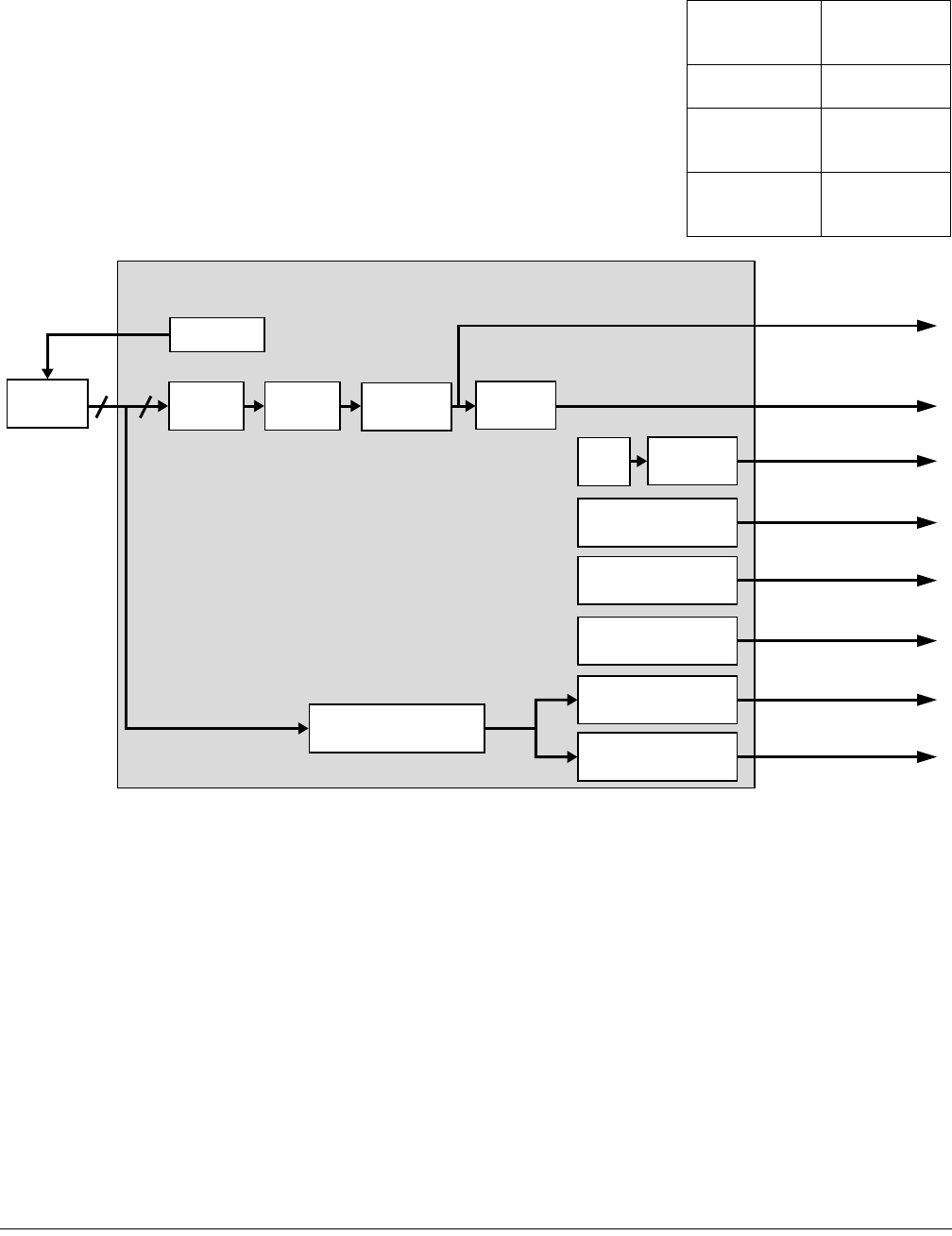
Overview of Analog Front End application
MMA9555L Intelligent Pedometer Data Sheet, Rev. 2.2
© NXP B.V. 2016. All rights reserved. 48
9 Analog Front End Application
9.1 Overview of Analog Front End application
The Analog Front End application (AFE) samples raw accelerometer data from the analog-
to-digital converter (ADC) at the execution rate of the application, applies factory and user
trim-correction terms, and filters data to several configurable bandwidths.
For the proper operation of the Pedometer, it is recommended that any change to any of the
configuration registers of the AFE Application be avoided unless the outcome is well
understood.
Figure 13. Front-end signal processing
9.1.1 Sample rate
The rate at which the ADC samples the accelerometer data is defined by the sfd_rate register, which is offset 0x0C in the
configuration registers of this application. The sample rate can be changed from 488 Hz to 3.81 Hz by setting the appropriate
value in the sfd_rate register. For more details, see Table 59 and Table 60 on page 55.
NOTE
Although the sample rate can be changed in the hardware, it is recommended that the 30 Hz
sample rate not be changed, because the Pedometer application requires 30 Hz and the
MMA9555L runs at 30 Hz after MMA9555L startup.
Application
ID 0x06
Default speed 30 Hz.
Configuration
registers Start on page
52.
Status
registers Start on page
56.
Analog Front End
34
ADC data
Sample rate
Offset
correction
Scale
correction
Anti-aliasing
filter Normalize
Configurable, low-pass
filter
filter
Temperature output
External input
conversion
1:2
Outputs
Raw
488/100 Hz
Configurable,
low-pass filter
ABS
Anti-aliasing
Configurable,
high-pass filter
Normalized
488/100 Hz
Normalized
244/50 Hz
Absolute value
488/100 Hz
Normalized
488 Hz/Low-pass filter
Temperature
External
Normalized
488 Hz/High-pass filter
Overview of Analog Front End application
MMA9555L Intelligent Pedometer Data Sheet, Rev. 2.2
49 © NXP B.V. 2016. All rights reserved.
9.1.2 Offset and scale correction
The AFE’s offset and scale correction stages of the signal chain applies trim offset and scaling correction factors which were
measured at factory calibration and stored inside each device. Since user offsets are defined at 8-g resolution, those offsets are
shifted according to the g mode.
User offsets are used to calibrate and compensate for the physical mounting of the part inside the final product. After board mount
and assembly, the final test process may include a test to fine tune and compensate the accelerometer orientation.
9.1.3 Anti-aliasing filter
After trim correction, the front end uses a sixth-order Chebyshev filter, running up to 488 Hz, to limit the signal bandwidth to
100 Hz.
Figure 14. Frequency response of Analog Front End anti-aliasing filter
The bandwidth of the anti-aliasing filter depends on the sample rate at which the front end application is running. The following
table shows the variation of the filter bandwidth according to the sample rate.
Table 48. Anti-aliasing filter bandwidth for different sample rates
Sample rate Stage-0 anti-aliasing Filter Stage-1 anti-aliasing Filter
Bandwidth (Hz) Bandwidth (Hz)
488.28 100 50
244.17 50 25
122.07 25 12.5
61.04 12.5 6.25
31.52 6.25 3.125
15.26 3.125 1.562
7.63 1.562 0.781
3.81 0.781 0.390

Overview of Analog Front End application
MMA9555L Intelligent Pedometer Data Sheet, Rev. 2.2
© NXP B.V. 2016. All rights reserved. 50
9.1.4 Raw data
The output of the sensor is a 16-bit, signed value. The sensor always uses all the bits for high accuracy. Depending on the range
setting (2-, 4-, or 8-g mode), the output value per g changes.
The following table shows the full scale value at the different g ranges, as well as the value of a measured 1-g acceleration at the
different g ranges.
9.1.5 Normalization
The filtered data is shifted according to the g mode to normalize the resolution to the 8-g range. The normalized data allows for
common handling of the data in the other applications. Data is normalized so that 1-g force acceleration shows output of 0x1000
counts or 4096 decimal counts.
9.1.6 Down-sampling and stage-1, anti-aliasing filter
The output of the normalizer is down-sampled by two to generate data sampled at half of the original sample rate. At 488 Hz, the
previous, sixth-order Chebyshev filter is applied to down-sampled (244 Hz) data, to create a 50-Hz bandwidth data stream.
Table 60 on page 55 provides more details about the varying of the bandwidth, depending of the sample rate of the front-end
application.
9.1.7 Absolute value
The absolute value of the sensor output is computed.
9.1.8 Configurable, low-pass and high-pass filters
First-order, low-pass and high-pass filters—with separate configurable cutoff frequencies at –3 dB—are provided.
Eqn. 1
Eqn. 2
Table 49.Raw accelerometer output, according to g mode
Range Full scale One-g acceleration
+ 2 g+ 32 K 16 K
+ 4 g+ 32 K 8 K
+ 8 g+ 32 K 4 K
Overview of Analog Front End application
MMA9555L Intelligent Pedometer Data Sheet, Rev. 2.2
51 © NXP B.V. 2016. All rights reserved.
Figure 15. Frequency response of configurable, high- and low-pass filters
The two following tables contain the cutoff frequency of the filters, varying with the value of K and the sample rate at which the
front-end application is executed.
Table 50. Cut-off frequency as a function of K and the sample rate for low-pass filter
K
LPF cut-off frequency (Hz)
Sample rate
= 488.28 Sample rate
= 244.14 Sample rate
= 122.07 Sample rate
= 61.04 Sample rate
= 30.52 Sample rate
= 15.26 Sample rate
= 7.63 Sample rate
= 3.81
1 56.13 28.07 14.03 7.02 3.51 1.75 0.88 0.4385
2 22.50 11.25 5.62 2.81 1.40 0.70 0.3516 0.1758
3 10.39 5.19 2.60 1.30 0.65 0.32 0.1623 0.0811
4 5.014 2.51 1.25 0.63 0.31 0.16 0.0783 0.0392
5 2.47 1.23 0.62 0.31 0.15 0.08 0.0385 0.0193
6 1.22 0.6116 0.31 0.15 0.08 0.04 0.0191 0.0096
7 0.61 0.30 0.15 0.08 0.04 0.02 0.0095 0.0048
8 0.30 0.15 0.08 0.04 0.02 0.01 0.0048 0.0024
9 0.15 0.076 0.04 0.02 0.01 0.0047 0.0024 0.0012
10 0.0759 0.038 0.019 0.0095 0.0047 0.0024 0.0012 0.0006
11 0.0379 0.019 0.0095 0.0047 0.0024 0.0012 0.0006 0.0003
12 0.019 0.0095 0.0048 0.0024 0.0012 0.0006 0.0003 0.0001
13 0.0095 0.0048 0.0024 0.0012 0.0006 0.0003 0.0001 0.00007
14 0.0047 0.0024 0.0012 0.0006 0.0003 0.0001 0.0007 0.00004
15 0.0024 0.0012 0.0006 0.0003 0.0002 0.00008 0.00004 0.00002

AFE configuration registers
MMA9555L Intelligent Pedometer Data Sheet, Rev. 2.2
© NXP B.V. 2016. All rights reserved. 52
9.2 AFE configuration registers
9.2.1 afe_csr
Table 51. Cut-off frequency as a function of K and the sample rate for high-pass filter
K
HPF cut-off frequency (Hz)
Sample rate =
488.28 Sample rate =
244.14 Sample rate =
122.07 Sample rate
= 61.04 Sample rate
= 30.52 Sample rate
= 15.26 Sample rate
= 7.63 Sample rate =
3.81
1 31.932 15.966 7.9831 3.9915 1.9958 0.9979 0.4989 0.2495
2 17.405 8.7023 4.3511 2.1756 1.0878 0.5439 0.2719 0.136
3 9.1573 4.5787 2.2893 1.1447 0.5723 0.2862 0.1431 0.0715
4 4.7092 2.3546 1.1773 0.5887 0.2943 0.1472 0.0736 0.0368
5 2.3912 1.1956 0.5978 0.2989 0.1495 0.0747 0.0374 0.0187
6 1.2054 0.6027 0.3014 0.1507 0.0753 0.0377 0.0188 0.0094
7 0.6051 0.3026 0.1513 0.0756 0.0378 0.0189 0.0095 0.0047
8 0.3026 0.1513 0.0757 0.0378 0.0189 0.0095 0.0047 0.0024
9 0.1513 0.0757 0.0378 0.0189 0.0095 0.0047 0.0024 0.0012
10 0.0756 0.0378 0.0189 0.0095 0.0047 0.0024 0.0012 0.0006
11 0.039 0.0195 0.0098 0.0049 0.0024 0.0012 0.0006 0.0003
12 0.0195 0.0098 0.0049 0.0024 0.0012 0.0006 0.0003 0.0002
13 0.0098 0.0049 0.0025 0.0012 0.0006 0.0003 0.0002 8E–05
14 0.0049 0.0025 0.0012 0.0006 0.0003 0.0002 8E–05 4E–05
15 0.0024 0.0012 0.0006 0.0003 0.0002 8E–05 4E–05 2E–05
Table 52. afe_csr registers
Offset 0x00(MSB) 0x01(LSB)
Bit 765 4 321076543210
Field FS Ext
ADC Temp CM Reserved Reserved
Reset 0x00 0 0 0x00 0x00 0x00

AFE configuration registers
MMA9555L Intelligent Pedometer Data Sheet, Rev. 2.2
53 © NXP B.V. 2016. All rights reserved.
9.2.2 user_offset [XYZ]
Often, during the mounting process, the accelerometer sensor is not mounted perfectly flat to the board and might also be rotated
slightly. This register enables a user to make an after-manufacturing calibration correction.
Table 53. afe_csr bit descriptions
Field Description
7:6
FS
Full-scale selection. AFE_CSR[FS] and AFE_BIAS[SC_AAF_EN] are combined to control AFE gain and
trim mode.
Units: None.
Range of values:
Full-scale data range XYZ acceleration scaling (mg/LSB)
00: ±8 g 0.244
01: ±2 g 0.061
10: ±4 g 0.122
11: ±8 g 0.244
5
Ext ADC
Specifies whether an external input will or will not be measured during the next analog acquisition phase.
Note: The ExtADC and Temp bits must not be set at the same time.
Units: None.
• 0: No external input is measured during the next analog acquisition phase.
• 1: Enables the four AFE channels to measure the external analog input during the next analog acquisition phase.
4
Temp
Specifies whether the temperature sensor output will or will not be measured during the next analog
acquisition phase.
Note: The ExtADC and Temp bits must not be set at the same time.
Units: None.
Temperature will change slowly so it can be measured with a very low sample rate (1 Hz or less) by
occasionally replacing an external ADC measurement with the Temperature ADC measurement.
Range of valid values: For valid values for FS and CM parameters, see the Intelligent, Motion-Sensing
Platform Hardware Reference Manual (MMA955xLHWRM), listed in “Related Documentation” on page 2
Accelerometer Reference Manual (MMA955xLRM).
• 0: No temperature sensor output will be measured during the next analog acquisition phase.
• 1: The temperature sensor output will be measured during the next analog acquisition phase.
3:2
CM
Conversion Mode. Controls the ADC resolution/accuracy versus power and conversion time trade-offs.
Units: None
• 00: Conversion complete in 32 cycles
• 01: Conversion complete in 16 cycle
• 10: Conversion complete in eight cycles
• 11: Conversion complete in four cycles
Reserved Bit field reserved.
Table 54. user_offset [XYZ] registers
Offset 0x02(MSB) 0x03(LSB)
Bit 7654321076543210
Field user_offset[X] user_offset[X][
Reset 0xFF 0xFF
Offset 0x04(MSB) 0x05(LSB)
Bit 7654321076543210
Field user_offset[Y] user_offset[Y]

AFE configuration registers
MMA9555L Intelligent Pedometer Data Sheet, Rev. 2.2
© NXP B.V. 2016. All rights reserved. 54
9.2.3 config_k
This register’s bits are shown in the following table.
Reset 0xFF 0xFF
Offset 0x06(MSB) 0x07(LSB)
Bit 7654321076543210
Field user_offset[Z] user_offset[Z]
Reset 0xFF 0xFF
Table 55. user_offset [XYZ] bit descriptions
Field Description
7:0
user_offset[XYZ]
Sets user offsets in the X, Y, and Z axes for the accelerometer, depending on the position on the device in
the user board. These values are considered as post-mount offsets.
Units: 0.244 mg/LSB.
Range of valid values: –32,768 to 32,767.
Reset value: 0xFF which is interpreted as –1.
Table 56. config_k registers
Offset 0x08 0x09
Bit 7654321076543210
Field config_k[HIGHPASS] config_k[LOWPASS]
Reset 0x00 0x00
Offset 0x0A 0x0B
Bit 7654321076543210
Field config_k[TEMP_LPF] config_k[EIC_LPF]
Reset 0x00 0x00
Table 57. config_k bit descriptions
Field Description
7:0
config_k[HIGHPASS]
High-pass filter configurable cutoff.
Units: None.
Range of valid values: 0 to 15.
7:0
config_k[LOWPASS]
Low-pass filter configurable cutoff.
Units: None.
Range of valid values: 0 to 15.
Table 54. user_offset [XYZ] registers (Continued)

AFE configuration registers
MMA9555L Intelligent Pedometer Data Sheet, Rev. 2.2
55 © NXP B.V. 2016. All rights reserved.
9.2.4 sfd_rate
This register’s bits are shown in the following table. The system defaults to 30 Hz; therefore, this document assumes that 30 Hz
is the rate being run. If the user slows down the rate by changing the sfd_rate register, all references to the system frame rate
scale accordingly.
7:0
config_k[TEMP_LPF]
Low-pass filter, configurable cutoff for temperature sensor output.
Units: None.
Range of valid values: 0 to 15.
7:0
config_k[EIC_LPF]
Low-pass filter, configurable cutoff for external input conversion output.
Units: None.
Range of valid values: 0 to 15.
Table 58. sfd_rate register
Offset 0x0C
Bit 76543210
Field sfd_rate
Reset 00000111
Table 59. sfd_rate bit description
Field Description
7:0
sfd_rate
Defines the system frame interval, the time period for each sample or the system sample rate in Hz.
Units: None.
Range of valid values: 7 to 14. Table 60 shows the relation between the register value and the interval
between each frame.
Table 60. Frame interval, according to the sfd_rate value
sfd_rate value Time frame (s) Max frames per second
7 2.05E–3 488.28
8 4.10E–3 244.17
9 8.19E–3 122.07
10 1.64E–2 61.04
11 3.28E–2 30.52
12 6.55E–2 15.26
13 1.31E–1 7.63
14 2.62E–1 3.81
Table 57. config_k bit descriptions
Field Description

AFE status registers
MMA9555L Intelligent Pedometer Data Sheet, Rev. 2.2
© NXP B.V. 2016. All rights reserved. 56
9.3 AFE status registers
9.3.1 output[FRONTEND_Stage_0][XYZ]
These registers’ bits are shown in the following table.
9.3.2 output[FRONTEND_Stage_1][XYZ]
These registers’ bits are shown in the following table.
Table 61. output[FRONTEND_Stage_0][XYZ] registers
Offset 0x00(MSB) 0x01(LSB)
Bit 7654321076543210
Field output[FRONTEND_Stage_0][X] output[FRONTEND_Stage_0][X]
Reset 0x00 0x00
Offset 0x02(MSB) 0x03(LSB)
Bit 7654321076543210
Field output[FRONTEND_Stage_0][Y] output[FRONTEND_Stage_0][Y]
Reset 0x00 0x00
Offset 0x04(MSB) 0x05(LSB)
Bit 7654321076543210
Field output[FRONTEND_Stage_0][Z] output[FRONTEND_Stage_0][Z]
Reset 0x00 0x00
Table 62. output[FRONTEND_Stage_0][XYZ] bit description
Field Description
7:0
output[FRONTEND_Stage_0][XYZ]
Normalized accelerometer data sampled at the default rate with complete bandwidth.
Units: 0.244 mg/LSB.
Range of valid values: –32,768 to 32,767.
Table 63. output[FRONTEND_Stage_1][XYZ] registers
Offset 0x06(MSB) 0x07(LSB)
Bit 7654321076543210
Field output[FRONTEND_Stage_1][X] output[FRONTEND_Stage_1][X]
Reset 0x00 0x00
Offset 0x08(MSB) 0x09(LSB)
Bit 7654321076543210
Field output[FRONTEND_Stage_1][Y] output[FRONTEND_Stage_1][Y]
Reset 0x00 0x00

AFE status registers
MMA9555L Intelligent Pedometer Data Sheet, Rev. 2.2
57 © NXP B.V. 2016. All rights reserved.
9.3.3 output[FRONTEND_Stage_0_ABS][XYZ]
These registers’ bits are shown in the following table.
Offset 0x0A(MSB) 0x0B(LSB)
Bit 7654321076543210
Field output[FRONTEND_Stage_1][Z] output[FRONTEND_Stage_1][Z]
Reset 0x00 0x00
Table 64. output[FRONTEND_Stage_1][XYZ] bit description
Field Description
7:0
output[FRONTEND_Stage_1][XYZ]
Normalized accelerometer data sampled at the default rate of half bandwidth.
Units: 0.244 mg/LSB.
Range of valid values: –32,768 to 32,767.
Table 65. output[FRONTEND_Stage_0_ABS][XYZ] registers
Offset 0x0C(MSB) 0x0D(LSB)
Bit 7654321076543210
Field output[FRONTEND_Stage_0_ABS][X] output[FRONTEND_Stage_0_ABS][X]
Reset 0x00 0x00
Offset 0x0E(MSB) 0x0F(LSB)
Bit 7654321076543210
Field output[FRONTEND_Stage_0_ABS][Y] output[FRONTEND_Stage_0_ABS][Y]
Reset 0x00 0x00
Offset 0x10(MSB) 0x11(LSB)
Bit 7654321076543210
Field output[FRONTEND_Stage_0_ABS][Z] output[FRONTEND_Stage_0_ABS][Z]
Reset 0x00 0x00
Table 66. output[FRONTEND_Stage_0_ABS][XYZ] bit description
Field Description
7:0
output[FRONTEND_Stage_0_ABS][XYZ]
Absolute value normalized accelerometer data sampled at the default rate of
complete bandwidth.
Units: 0.244 mg/LSB.
Range of valid values: 0 to 32,767.
Table 63. output[FRONTEND_Stage_1][XYZ] registers (Continued)

AFE status registers
MMA9555L Intelligent Pedometer Data Sheet, Rev. 2.2
© NXP B.V. 2016. All rights reserved. 58
9.3.4 output[FRONTEND_Stage_0_GM][XYZ]
These registers’ bits are shown in the following table.
9.3.5 output[FRONTEND_Stage_0_LPF][XYZ]
These registers’ bits are shown in the following table.
Table 67. output[FRONTEND_Stage_0_GM][XYZ] registers
Offset 0x12(MSB) 0x13(LSB)
Bit 7654321076543210
Field output[FRONTEND_Stage_0_GM][X] output[FRONTEND_Stage_0_GM][X]
Reset 0x00 0x00
Offset 0x14(MSB) 0x15(LSB)
Bit 7654321076543210
Field output[FRONTEND_Stage_0_GM][Y] output[FRONTEND_Stage_0_GM][Y]
Reset 0x00 0x00
Offset 0x16(MSB) 0x17(LSB)
Bit 7654321076543210
Field output[FRONTEND_Stage_0_GM][Z] output[FRONTEND_Stage_0_GM][Z]
Reset 0x00 0x00
Table 68. output[FRONTEND_Stage_0_GM][XYZ] bit description
Field Description
7:0
output[FRONTEND_Stage_0_GM][XYZ]
Raw accelerometer data sampled at the default rate with complete bandwidth. The
resolution depends on the g-mode setting configured by afe_csr[fs].
Units:
•±2 g mode: 0.061 mg/LSB
•±4 g mode: –0.122 mg/LSB
•±8 g mode: 0.244 mg/LSB
Range of valid values:
•±2 g mode: 0.061 mg/LSB = –32768 to 32767
•±4 g mode: 0.122 mg/LSB = –8192 to 8192
•±8 g mode: 0.244 mg/LSB = –4096 to 4096
Table 69. output[FRONTEND_Stage_0_LPF][XYZ] registers
Offset 0x18(MSB) 0x19(LSB)
Bit 7654321076543210
Field output[FRONTEND_Stage_0_LPF][X] output[FRONTEND_Stage_0_LPF][X]
Reset 0x00 0x00
Offset 0x1A(MSB) 0x1B(LSB)
Bit 7654321076543210
Field output[FRONTEND_Stage_0_LPF][Y] output[FRONTEND_Stage_0_LPF][Y]
Reset 0x00 0x00

AFE status registers
MMA9555L Intelligent Pedometer Data Sheet, Rev. 2.2
59 © NXP B.V. 2016. All rights reserved.
9.3.6 output[FRONTEND_Stage_0_HPF][XYZ]
These registers’ bits are shown in the following table.
Offset 0x1C(MSB) 0x1D(LSB)
Bit 7654321076543210
Field output[FRONTEND_Stage_0_LPF][Z] output[FRONTEND_Stage_0_LPF][Z]
Reset 0x00 0x00
Table 70. output[FRONTEND_Stage_0_LPF][XYZ] bit description
Field Description
7:0
output[FRONTEND_Stage_0_LPF][XYZ]
Normalized accelerometer data sampled at the default rate, with configurable,
low-pass filter cutoff.
Units: 0.244 mg/LSB.
Range of valid values: –32,768 to 32,767.
Table 71. output[FRONTEND_Stage_0_HPF][XYZ] registers
Offset 0x1E(MSB) 0x1F(LSB)
Bit 7654321076543210
Field output[FRONTEND_Stage_0_HPF][X] output[FRONTEND_Stage_0_HPF][X]
Reset 0x00 0x00
Offset 0x20(MSB) 0x21LSB)
Bit 7654321076543210
Field output[FRONTEND_Stage_0_HPF][Y] output[FRONTEND_Stage_0_HPF][Y]
Reset 0x00 0x00
Offset 0x22(MSB) 0x23(LSB)
Bit 7654321076543210
Field output[FRONTEND_Stage_0_HPF][Z] output[FRONTEND_Stage_0_HPF][Z]
Reset 0x00 0x00
Table 72. output[FRONTEND_Stage_0_HPF][XYZ] bit description
Field Description
7:0
output[FRONTEND_Stage_0_HPF][XYZ]
Normalized accelerometer data sampled at the default rate, with configurable,
high-pass filter cutoff.
Units: 0.244 mg/LSB.
Range of valid values: –32,768 to 32,767.
Table 69. output[FRONTEND_Stage_0_LPF][XYZ] registers (Continued)

AFE status registers
MMA9555L Intelligent Pedometer Data Sheet, Rev. 2.2
© NXP B.V. 2016. All rights reserved. 60
9.3.7 output_temp
This register’s bits are shown in the following table.
9.3.8 output_EIC
This register’s bits are shown in the following table.
Table 73. output_temp registers
Offset 0x24(MSB) 0x25(LSB)
Bit 7654321076543210
Field output_temp output_temp
Reset 0x00 0x00
Table 74. output_temp bit description
Field Description
7:0
output_temp
Temperature sensor output measurement.
Units: ADC counts.
output_temp(in count) = –51.4T + 1146, where T is temperature in °C
Note that this is only a typical characteristic example. User shall perform minimal calibration to adjust
at least the offset.
Range of valid values: –32,768 to 32,767.
Table 75. output_EIC registers
Offset 0x26(MSB) 0x27(LSB)
Bit 7654321076543210
Field output_EIC output_EIC
Reset 0x00 0x00
Table 76. output_EIC bit description
Field Description
7:0
output_EIC
Output of the external, analog-input conversion value.
Units: ADC counts.
output_EIC(in count) = 29570 (AN0–AN1) – 122, where AN0–AN1 is in V.
Note that this equation is only a typical example, with ADC conversion in 16-bit mode.
Range of valid values: –32,768 to 32,767.

AFE status registers
MMA9555L Intelligent Pedometer Data Sheet, Rev. 2.2
61 © NXP B.V. 2016. All rights reserved.
9.3.9 frame_counter
This register’s bits are shown in the following table.
Table 77. frame_counter registers
Offset 0x28(MSB) 0x29(LSB)
Bit 7654321076543210
Field frame_counter frame_counter
Reset 0x00 0x00
Table 78. output_EIC bit description
Field Description
7:0
frame_counter
Provides the number of frames processed at the configured sample rate. It is not a real-time
representation because the time that the device remains in the stop mode is not taken into account.
The frame counter will restart at zero when it reaches 65,535.
Units: Nondimensional.
Range of valid values: 0 to 65,535.

Overview of Data FIFO application
MMA9555L Intelligent Pedometer Data Sheet, Rev. 2.2
© NXP B.V. 2016. All rights reserved. 62
10 Data FIFO Application
10.1 Overview of Data FIFO application
The Data FIFO (First In First Out) application is a buffer intended to store the output data
from an application. Every scheduler interval, the Data FIFO application gathers the output
data from an application and stores it until the host processor reads the data.
The FIFO application uses the mailboxes differently than other applications—operating in
the streaming mode. In streaming mode, the host continues reading data until a maximum
of up to 255 bytes is read per host request. The host must read all the data that it requested.
The FIFO can be connected to one application and can collect packets of data in different
sizes (one, two, four, or six bytes).
The Data FIFO has two different modes of operation: Stop on Overflow and Free Run.
The application’s status register displays current status values such as overflow condition, watermark reached, and buffer empty.
These conditions have a flag that is asserted individually each time one of these conditions occurs.
The user can configure the FIFO buffer size by writing to the fifo_size word within the configuration registers. The buffer size can
be configured only once and is limited by the amount of RAM available. The amount of available RAM can be impacted by the
Event Queue Application which also can be configured to use large amounts of RAM.
NOTE
Before configuring the Data FIFO application, it is recommended that the Data FIFO
Application be suspended. After the parameter is configured, remove the application from
suspend. A suspend is done with the Reset/Suspend/Clear Application (APP_ID 0x17).
10.2 Modes of operation
This section examines the modes of operation of the FIFO buffer.
10.2.1 Stop-on-overflow
The FIFO stores data from an application, every single frame (a scheduler interval), as long as the FIFO is enabled. In this mode,
the FIFO stores data until an overflow condition is reached. At an overflow condition, the overflow flag is set.
The host asynchronously reads payload packets from the Data FIFO application. Reading payload packets frees up slots for new
entries into the FIFO. If the host reads data faster than the applications put data into the FIFO, the overflow condition will never
happen.
The overflow condition occurs when the available buffer memory is full and there is no space available for another packet.
10.2.2 Free-run
The FIFO behaves as a circular buffer that stores data from the configured channel, every single frame, as long as the FIFO is
enabled. In this mode, the FIFO never stops storing data, even though the overflow condition is reached and the overflow flag is
set.
When the FIFO becomes full, the oldest data in the buffer will be overwritten first.
10.3 Reading process
To read the data FIFO, the host sends a read-data command to the MMA9555L device that calls the Data FIFO application, stores
the requested data within the FIFO into a buffer, and returns the number of bytes read. The data FIFO does not tag each entry
with a timestamp, only storing a timestamp for the last entry.
When the reading process is performed, the Data FIFO application calculates the timestamp for the first group of requested data
and appends the timestamp to the data. If the host requests N bytes and that is bigger than the entry size, the pop routine will
Application
ID 0x0F
Default speed 30 Hz.
Configuration
registers Start on page
67.
Status
registers Start on page
69.

Reading process
MMA9555L Intelligent Pedometer Data Sheet, Rev. 2.2
63 © NXP B.V. 2016. All rights reserved.
append the timestamp only for the first entry that fits in the N bytes requested. The host must calculate the timestamps for the
extra entries requested within the N bytes.
The host can request to read up to 255 bytes at a time. Assuming the AFE is providing data, this is exactly 36 packets of AFE data.
Each host, FIFO-read transaction includes a status byte and a timestamp word. These three bytes are prefixed to the payload
data.
Payload data is prefixed with the APP_ID of the application that has provided the data. In the AFE case, the APP_ID is 0x06.
(255 – 3 (status and timestamp) ) / 7 (APP_ID + 6 byte XYZ data) = 36
Reading the FIFO example
The device powers up in Sleep mode, but it may become necessary to wake the MMA9555L device.
Waking the device uses the following mailboxes:
MB0: 0x12, App_ID = 0x12; Power Controller modes
MB1: 0x20, Command 0x20 = Write configuration; Offset = 0
MB2: 0x06, Offset = 0x06
MB3: 0x01, Count of data to write
MB4: 0x00, Actual Data Value; Clears sleep bit
Bytes to Send: 0x12, 0x20, 0x06, 0x01, 0x00.
Example 9.
To configure for FIFO operation, write the following transaction to the Data-FIFO application:
1. MB0: Set APP_ID to (0x0F).
Selects the Data-FIFO application.
2. MB1: Command to (0x20).
Command is a Write Configuration space.
3. MB2: Set offset to zero (0x00).
Start writing configuration values at register 0.
4. MB3: Set count field to (0x0A).
Sends nine bytes.
5. MB4: Send Data (0x0C).
Sends six bytes, free-run mode.
6. MB5: Send Data (0x00).
7. MB6: Send Data (0x00).
8. MB7: Send Data (0x00).
9. MB8: Send Data (0x00).
10. MB6: Send Data (0x3C).
Reserves 60 bytes—10 packets of six bytes each.
11. MB7: Send Data (0x06).
Associates APP ID = AFE – .
12. MB5: Send Data (0x00).
13. MB6: Send Data (0x00).
14. MB7: Send Data (0x00).
Bytes to Send: 0x0F, 0x20, 0x00, 0x0A, 0x0C, 0x00, 0x00, 0x00, 0x00, 0x3C, 0x06, 0x00, 0x00, 0x00.
The configuration registers can only be written once. To reconfigure the FIFO, the device first must be reset.
Read the FIFO applications status register to get the data.

Reading process
MMA9555L Intelligent Pedometer Data Sheet, Rev. 2.2
© NXP B.V. 2016. All rights reserved. 64
Send the following command to set up for reading the status register.
Example 10.
1. MB0: Set APP_ID to (0x0F).
Selects the Data-FIFO application.
2. MB1: Command to (0x30).
Sends a Read Status space command.
3. MB2: Set offset to zero (0x03).
Starts reading the configuration values from register 0x03.
4. MB3: Set count field to (0x0A).
Reads 10 bytes (three status bytes, one APP_ID, and six bytes of data).
Bytes to Send: 0x0F, 0x30, 0x03, 0x0A.
This results in the following response.
0F 80 0A 0A 05 83 13 06 00 81 FF EA 11 0C
The last six bytes are the AFE data: X, Y, and Z.
This response was with the device flat, in the Face-Up orientation. The X and Y data are close to 0x0000, or 0 g, and the Z data
is close to 0x1000, or 1 g.
MB0: APP_ID = 0x0F; FIFO application
MB1: STATUS = 0x80; Command Complete, no errors
MB2: RequestedData count = 0x0A; 10 bytes of data
MB3: Actual Data Count = 0x0A; 10 bytes of data
MB4: 0x05 = FIFO Status; Watermark and Overflow flag is set
MB5–MB6: = 0x8313; Timestamp
MB7: APP ID of the application providing the actual data = 0x06; AFE application
MB8–MB9: AFE X data; 0x0081
MB10–MB11: AFE Y data; 0xFFEA
MB12–MB13: AFE Z Data; 0x110C
The read size for one (1+6 byte) payload is 10 bytes. The size for two payloads is 17 bytes, 3 = 24 bytes.
Reading three payloads
Send the following command to set up for reading the status register.
Example 11.
1. MB0: Set APP_ID to (0x0F).
Selects the Low-g application.
2. MB1: Command to (0x30)
Sends a Write Configuration space command.
3. MB2: Set offset to zero (0x03).
Starts writing configuration values at register 0.
4. MB3: Set count field to (0x18)
Reads 24 bytes (3 status byes + 3x(APP_ID+6 data)).
Bytes to Send: 0x0F, 0x30, 0x03, 0x18.
The response is below:
0F 80 18 18 05 33 53 06 00 93 00 7F 11 06 06 00 A2 00 7D 11 08 06 00 9C 00 79 11 07

Reading process
MMA9555L Intelligent Pedometer Data Sheet, Rev. 2.2
65 © NXP B.V. 2016. All rights reserved.
The last six bytes are the AFE data, X, Y, and Z.
This response was with the device flat, in the Face-Up orientation. The X and Y data are close to 0x0000—or 0-g—and the Z
data is close to 0x1000—or 1-g.
MB0: APP_ID = 0x0F; FIFO application
MB1: STATUS = 0x80; Command Complete, no errors
MB2: Requested data count = 0x18; 24 bytes of data
MB3: Actual Data Count = 0x18; 24 bytes of data
MB4: 0x05 = FIFO Status; Watermark and Overflow flag is set
MB5-6: = 0x3353; Timestamp
MB7: APP ID of the application providing the actual data = 0x06; The AFE application
MB8-9: AFE X data; 0x0093
MB10-11: AFE Y data; 0x007F
MB12-13: AFE Z Data; 0x1106
MB14: APP ID of the application providing the actual data = 0x06; the AFE application
MB15-16: AFE X data; 0x00A1
MB17-18: AFE Y data; 0x007D
MB19-20: AFE Z Data; 0x1108
MB21: APP ID of the application providing the actual data = 0x06; the AFE application
MB22-23: AFE X data; 0x009C
MB24-25: AFE Y data; 0x0079
MB26-27: AFE Z Data; 0x1107
To read data stored by the data FIFO application, the host must send a Read Data command along with a specific offset value.
This process has three conditions:
• The offset must be fixed to three
• The number of bytes to read must be larger than one and a multiple of the entry size
• The host must add three bytes to de-count the total bytes to read
Failure to adhere to the three conditions above could cause the data FIFO to enter into an error state and be unable to pop
coherent data. To recover the data FIFO, reset the flag in the Reset_control byte (APP_ID 0x17).
When the command is sent, the first four bytes that the MMA9555L device returns correspond to the response of the command.
The next byte gives the status of the data FIFO application module and the following two bytes represent the timestamp; thus the
three-byte offset.
These bytes are part of those requested by the host, so it is very important that the user add three bytes to the number of bytes
to read. The data stored in the data FIFO comes after these seven bytes.
If the module is storing data at the exact moment that a read is issued by the host, the MMA9555L device will return an error
condition (A2). When this occurs, the host must retry reading the data. If any other error is returned, the host must take the proper
action.
Data FIFO block diagram
MMA9555L Intelligent Pedometer Data Sheet, Rev. 2.2
© NXP B.V. 2016. All rights reserved. 66
10.4 Data FIFO block diagram
Figure 16. Data FIFO model
Figure 16 shows the block-level model of the data FIFO. The application is driven by the watermark and mode inputs that
configure the functionality.
The watermark level helps the host prevent data loss by raising a warning just before the overflow condition occurs. When the
number of bytes in the buffer approaches its capacity, the data FIFO asserts the watermark flag in the status register. The
watermark level is user-configurable. If the level of 0 is configured, the watermark is disabled.
The channel has its own data format code (DFC) bit field that configures the payload to be stored (one, two, four, or six bytes).
A NULL or zero value in the APP_ID Channel register means the channel is disabled. Any valid APP_ID value means the channel
is enabled.
The data FIFO has a status register in its output structure that contains status flags such as watermark, overflow, and buffer
empty. These flags can be mapped to the GPIO pins to generate an interrupt to the host.
The output also has an Entry Size register that shows the size, in bytes, of each entry that the data FIFO calculated, according
to its payload configuration. A Records Number register records the number of entries stored in the data FIFO. Both registers
help the host to calculate how many bytes to request, so that it can dump the entire FIFO buffer. A simple multiplication of those
two registers’ value gives the total number of bytes stored in the FIFO.
TimeStamp register
FIFO buffer
(Host decides the size
in bytes)
Entry
size Records
number
GPIO mapping logic
Frame
counter
APP_ID =
nn Watermark
level
Mode
FIFO size
•Stop on overflow
•Free run
Interrupt
WM OvF Empty
flag flag flag
Data FIFO configuration registers
MMA9555L Intelligent Pedometer Data Sheet, Rev. 2.2
67 © NXP B.V. 2016. All rights reserved.
10.4.1 Entries format
Channel enabled
Figure 17. FIFO-entry formats, when channel enabled
10.5 Data FIFO configuration registers
This section contains the FIFO configuration registers. These registers can only be written once. To reconfigure the FIFO, the
device must be reset. This is because the FIFO application requests RAM and RAM can only be allocated once.
10.5.1 FIFO configuration byte
Table 79. FIFO Config Byte register
Offset 0x00
Bit 76543210
Field Reserved DFC1 Mode
Reset 0x00 0x00 0x00
Table 80. FIFO Config Byte bit descriptions
Field Description
Reserved Bit field reserved.
3:2
DFC1
(Data Format Code)
Configures the payload size of the channel.
Units: None.
Range of valid values: 0 to 3.
• 00: One byte.
• 01: Two bytes.
• 10: Four bytes
• 11: Six bytes.
1:0
Mode
Configures the FIFO mode.
Units: None.
Range of valid values:
• 00: Free Run.
• 01: Stop On Overflow.
APP_ID (1 byte) Payload (Nbytes)
APP_ID (1 byte) Payload (Nbytes)
APP_ID (1 byte) Payload (Nbytes)
Entry 1
Entry 2
•
•
•
Entry M
Size defined by DFC1
(1, 2, 4, or 6 bytes)

Data FIFO configuration registers
MMA9555L Intelligent Pedometer Data Sheet, Rev. 2.2
© NXP B.V. 2016. All rights reserved. 68
10.5.2 FIFO size word
10.5.3 FIFO APP_ID
10.5.4 Watermark
Table 81. FIFO-size word registers
Offset 0x04(MSB) 0x05(LSB)
Bit 7654321076543210
Field FIFO Size Word 1 FIFO Size Word 2
Reset 0x00 0x00
Table 82. FIFO-size word bit description
Field Description
7:0
FIFO Size Word
Reserves the maximum size (in bytes) that the FIFO can use. This is limited by the available RAM.
Units: Bytes.
Range of valid values: 0 to available RAM.
0x1C8 (decimal, 456) is the maximum amount of RAM that can be requested from the MMA9555L device.
The RAM is shared by multiple applications, so be careful not to set the FIFO to use more memory than
is physically available. That will cause unknown and undesirable results.
Table 83. FIFO Channel APP_ID register
Offset 0x06
Bit 76543210
Field FIFO Ch APP_ID
Reset 0x00
Table 84. FIFO Channel APP_ID bit description
Field Description
7:0
FIFO Ch APP_ID The APP_ID of the application that supplied data to be buffered by the FIFO.
Range of valid values: 0 to 0xFF.
Table 85. Watermark registers
Offset 0x08(MSB) 0x09(LSB)
Bit 7654321076543210
Field Watermark Watermark
Reset 0x00 0x00

Data FIFO status registers
MMA9555L Intelligent Pedometer Data Sheet, Rev. 2.2
69 © NXP B.V. 2016. All rights reserved.
10.6 Data FIFO status registers
10.6.1 Records number
10.6.2 Entry size
Table 86. Watermark bit description
Field Description
7:0
Watermark
Sets the count, in bytes, for the FIFO to set or clear the watermark flag.
Units: Bytes.
Range of valid values: 0–available RAM.
Table 87. Records-number register
Offset 0x00(MSB) 0x01(LSB)
Bit 7654321076543210
Field Records Number Records Number
Reset 0x00 0x00
Table 88. Records-number bit description
Field Description
7:0
Records Number
This word stores the current number of records in the FIFO buffer.
A record is the payload packet of data comprised of an APP_ID and the actual data—which could be one,
two, four, or six bytes long. A record can be two, three, four, or seven bytes long.
Units: Number of entries in the Data FIFO (entry size in bytes = Ch APP_ID+ DFC1).
Range of valid values: 0 to available oxFFFF.
Table 89. Entry-size register
Offset 0x02
Bit 76543210
Field Entry Size
Reset 0x00
Table 90. FIFO config-byte/bit description
Field Description
7:0
Entry Size
This byte shows the size in bytes of each entry that the data FIFO has stored, that calculation based on
its configuration.
Units: Bytes.
Range of valid values: 0 to 6.

Data FIFO status registers
MMA9555L Intelligent Pedometer Data Sheet, Rev. 2.2
© NXP B.V. 2016. All rights reserved. 70
10.6.3 FIFO_Status
Table 91. FIFO_Status register
Offset 0x03
Bit 76543210
Field on_going_push on_going_pop Reserved ovf_flag empty_ flag wmrk_ flag
Reset 0x00 0x00 0x00 0 0 0
Table 92. FIFO_Status bit descriptions
Field Description
7
fifo_on_going_push
Indicates that a push operation is being executed—the is FIFO receiving data from the application.
Units: Nondimensional.
Range of valid values: 0 to 1.
• 0: A push is not being executed.
• 1: A push is being executed.
6
fifo_on_going_pop
Indicates that a pop operation is being executed. The FIFO is sending out data and it is being read.
Units: Nondimensional.
Range of valid values: 0 to 1.
• 0: A pop operation is not being executed.
• 1: A pop operation is being executed.
5:3
Reserved Bit field reserved.
2
fifo_ovf_flag
Indicates that FIFO buffer has reached the maximum number of entries allowed. This meaning can vary
depending of the mode of operation.
Units: Nondimensional.
Range of valid values:
• 0: Not overflow condition.
• 1: Overflow condition.
1
fifo_empty_flag
Indicates whether the FIFO buffer is empty.
Units: Nondimensional.
Range of valid values:
• 0: FIFO buffer is not empty.
• 1: FIFO buffer is empty.
0
fifo_wmrk_flag
Indicates when the entries in the FIFO buffer have reached the watermark count.
Units: Nondimensional..
Range of valid values:
• 0: Watermark not reached.
• 1: Watermark reached.

Overview of Event Queue application
MMA9555L Intelligent Pedometer Data Sheet, Rev. 2.2
© NXP B.V. 2016. All rights reserved. 71
11 Event Queue Application
11.1 Overview of Event Queue application
This application manages a queue of asynchronous events. The size of the queue is flexible
and can be configured by writing to the queue_size word within the configuration registers
of the Event Queue Application.
The size of the Event Queue is limited by the available RAM. The amount of RAM may be
reduced by the Data FIFO Application which also can be configured to use the RAM.
Some applications inside the MMA9555L platform have an eight-bit event-mask register
within configuration-registers structure that selects the specific event to be stored into the
Event Queue. The user can set an application’s event-mask bit to enable or prevent that
application’s events from being added to the Event Queue.
When the selected event happens, Event Queue Application calls a routine with the following prototype to push the application’s
event into the Event Queue:
void eventQueue_push(void *data, uint8_t size)
With these variables:
• Data: Pointer to the first element of the data to be stored into the queue. The data must have the order: APP_ID + Payload
bytes.
• Size: Amount of data (in bytes) to be stored into the queue.
Each entry into the Event Queue is of fixed size and has the following format:
Figure 18. Entry format for the Event Queue
If an application’s payload is less than three bytes, the Event Queue will store the data and complete the entry padding with zeros.
If the application has a payload more than three bytes, the Event Queue will calculate the number of entries that this payload
needs to be successfully stored, split in the format shown in Figure 18.
If an application tries to push data into the Event Queue and there is not enough space to store it, the Event Queue will ignore
the attempt. This will be transparent for the application since there is no communication between the application and the Event
Queue.
11.1.1 Modes of operation
The Event Queue works only in one mode. It stores data and stops when the end of the queue is reached and asserts an overflow
flag. The queue is not circular.
The application has a configurable watermark that asserts a flag when entries have reached the configured point.
11.1.2 Reading process
To read the Event Queue, the host sends a read-status command to the MMA9555L device, calling the Event Queue application
that stores the data within the queue into a buffer and returns the number of bytes read. If the number of requested bytes is not
a multiple of the entry size, the pop routine ignores the extra bytes and tells the host how many effective bytes were popped.
To read data stored by the Event Queue application, the host must send a Read Data command along with a specific offset value.
The following examples show the command for reading the data stored by the Event Queue Application.
Application
ID 0x10
Default speed 30 Hz.
Configuration
registers Start on page
74.
Status
registers Start on page
76.
Frame Counter APP ID Payload
Six bytes per entry

Overview of Event Queue application
MMA9555L Intelligent Pedometer Data Sheet, Rev. 2.2
72 © NXP B.V. 2016. All rights reserved.
Reading Event Queue example
The following example shows how to configure the Event Queue application.
Example 12.
1. MB0: Set APP_ID to (0x10).
Selects the Data-FIFO application.
2. MB1: Command to (0x20).
Sends a Write Configuration space command.
3. MB2: Set offset to zero (0x00).
Starts writing configuration values at register 0.
4. MB3: Set count field to (0x06).
Sends nine bytes.
5. MB4: Send Data (0x00).
Sets Queue size.
6. MB5: Send Data (0x50).
7. MB6: Send Data (0x00).
Watermark
8. MB7: Send Data (0x05).
9. MB8: Send Data (0x00).
Timeout.
10. MB6: Send Data (0x00).
Bytes to Send: 0x10, 0x20, 0x00, 0x06, 0x00, 0x50, 0x00, 0x05, 0x00, 0x00.
The configuration registers can only be written once. If the Event Queue must be reconfigured, the device must be reset and the
configuration rewritten.
Some data now must be sent to the event queue. In this example, the Low-g application is configured to send an event.
Example 13.
1. MB0: Set APP_ID to (0x09).
Specifies the Low-g application.
2. MB1: Command to (0x20).
Sends a Write Configuration space command.
3. MB2: Set offset to zero (0x09).
4. Start writing configuration values at Register 9.
5. MB3: Set count field to (0x01).
Sends nine bytes.
6. MB4: Send Data (0x08) – Event Mask Register.
Enables Low-g events.
Bytes to Send: 0x09, 0x20, 0x09, 0x01, 0x08.
In this example, all other Low-g configuration register values are at the reset default values.
The device powers up in Sleep mode, but it may become necessary to wake the part. That process is done in the following
example.
Example 14.
1. MB0: Set App_ID to (0x12).
Selects the Power Controller modes.
2. MB1: Command to (0x20).
Sends a write configuration, with offset = 0.
3. MB2: Set offset to (0x06).
4. MB3: Set count field to (0x01).

Overview of Event Queue application
MMA9555L Intelligent Pedometer Data Sheet, Rev. 2.2
© NXP B.V. 2016. All rights reserved. 73
5. MB4: Send the data value (0x00).
Bytes to Send: 0x12, 0x20, 0x06, 0x01, 0x00.
The device is enabled and configured to have an event Queue and send Low-g events to the Event Queue.
To cause a Low-g event that can be measured on the X, Y, and Z axes, toss the board into the air. Read the Event Queue
applications status register to get the data.
To set up for reading the status register, send the command in the following example.
Example 15.
1. MB0: Set APP_ID to (0x10).
Selects the Event Queue application.
2. MB1: Command to (0x30).
Sends a Read Status space command.
3. MB2: Set offset to zero (0x03).
Start reading status values at register 0.
4. MB3: Set count field to (0x20).
Reads 10 bytes (3 status + APP_ID+6 data)
Bytes to Send: 0x10, 0x30, 0x03, 0x20.
The following response is returned:
10 80 13 20 09 95 AC 09 0F 00 00 95 BE 09 0F 00 00 95 D0 09 0F 00 00
MB0: APP_ID = 0x10; Event Queue application
MB1: STATUS = 0x80; Command Complete, no errors
MB3: Actual Data Count = 0x13; 10 bytes of data
MB2: Requested Data count = 0x20; 10 bytes of data
MB4: 0x09 = Event Queue Status; Watermark and Overflow flags are set
MB5–MB6: = 0x95AC; Timestamp
MB7: APP ID of the application providing the actual data = 0x09; the AFE application
MB8–MB10: 0x0F0000 = 0x0F is the status register from the Low-g applications; 0x0F indicates a Low-g event on all axes.
MB5–MB6: = 0x95BE; Timestamp
MB7: APP ID of the application providing the actual data = 0x09; the AFE application
MB8–MB10: 0x0F0000
MB5–MB6: = 0x95D0; Timestamp
MB7: APP ID of the application providing the actual data = 0x09; the AFE applications
MB8–MB10: 0x0F0000
The offset is fixed to three bytes.
Event Queue configuration registers
MMA9555L Intelligent Pedometer Data Sheet, Rev. 2.2
74 © NXP B.V. 2016. All rights reserved.
When the command is sent, the first four bytes that the MMA9555L device returns correspond to the response of the command.
The fifth byte is the status from the Event Queue application. This byte is part of the bytes requested by the host, therefore it is
very important that the user adds one byte to the number of bytes to be read.
Due to the application’s read functionality, if the application is storing data at the exact moment a read is issued by the host, the
MMA9555L device will return an error condition. When this occurs, the host must retry reading the data. If any other error is
returned, the host must take the proper action.
11.1.3 Event Queue block diagram
The following figure shows the Event Queue Data Flow Model that receives the Application ID and the N size of the payload from
a specific application. The Event Queue logic appends the frame counter with this data and pushes the entry (six bytes in size)
into the queue. If the queue is full, the logic will ignore the push request.
Figure 19. Event Queue data flow
11.2 Event Queue configuration registers
The Event Queue application’s configuration can only be written once. In order to reconfigure the Event Queue, the whole device
must be reset. This is because the Event Queue application requests RAM and RAM can only be allocated once.
APP (AP_ID)
Queue processing
Data Array
Host decides
the size
(in bytes)
Frame
Counter GPIO mapping
logic
Event_Queue_Flag Register
AP_ID – Payload N
Event_Queue_Mask Register
Event_Queue_Flag Register
Various elements in the application
can set or clear bits in this register.
Logical AND
Payload N
Config command can
Modify this register.
Config command can
modify this table.
Command calls a
pop routine to dump
the memory.
Full WM First entry (after reset)
Interrupt
Push
subroutine
16-bit frame count AP_ID Payload

Event Queue configuration registers
MMA9555L Intelligent Pedometer Data Sheet, Rev. 2.2
© NXP B.V. 2016. All rights reserved. 75
11.2.1 queue_size
11.2.2 queue_wmrk
11.2.3 queue_timeout
Table 93. queue_size registers
Offset 0x00(MSB) 0x01(LSB)
Bit 7654321076543210
Field queue_size
Reset
Table 94. queue_size bit description
Field Description
7:0
queue_size
Defines the size in bytes that the Event Queue will reserve, in order to store the data sent by any
application.
Units: Bytes
Range of valid values: 0–available RAM.
0x1C8 (decimal 456) is the maximum amount of RAM that can be requested from the MMA9555L device.
The RAM is shared by multiple applications, so be careful not to set the FIFO to use more memory than
is physically available. That will cause unknown and undesirable results.
Table 95. queue_wmrk registers
Offset 0x02(MSB) 0x03(LSB)
Bit 7654321076543210
Field queue_wmrk
Reset
Table 96. queue_wmrk bit description
Field Description
7:0
queue_wmrk
Sets the count, in bytes, for the Event Queue to set or clear the watermark flag.
Units: Bytes.
Range of valid values: 0 to available bytes in the buffer.
Table 97. queue_timeout registers
Offset 0x04(MSB) 0x05(LSB)
Bit 7654321076543210
Field queue_timeout
Reset

Event Queue status registers
MMA9555L Intelligent Pedometer Data Sheet, Rev. 2.2
76 © NXP B.V. 2016. All rights reserved.
11.3 Event Queue status registers
11.3.1 records_number
11.3.2 entry_size
Table 98. queue_timeout bit description
Field Description
7:0
queue_timeout
Sets the count, in cycles, for the Event Queue to set or clear the time-out flag.
Units: Time; [queue_timeout] * [1/SRqueue] ).
Range of valid values: 0 to 65,535.
SR_queue is the sample rate of the Event Queue application, which defaults to 30 Hz.
Table 99. records_number registers
Offset 0x00(MSB) 0x01(LSB)
Bit 7654321076543210
Field records_number
Reset
Table 100. records_number bit description
Field Description
7:0
records_number
Shows the current number of entries or records stored in the queue.
Units: Entries (Entry = six bytes).
Range of valid values: 0 to 65,535. Typically, this number should not be more than the available RAM
divided by the payload size.
Table 101. entry_size registers
Offset 0x02
Bit 76543210
Set-bit values 00000110
Field entry_size
Reset 00000110
Table 102. entry_size bit description
Field Description
7:0
entry_size
Shows the size in bytes of each entry or record in the queue. This value is six bytes fixed and is not user-
configurable.
Units: Bytes.
Range of valid values: Fixed to six.

Event Queue status registers
MMA9555L Intelligent Pedometer Data Sheet, Rev. 2.2
© NXP B.V. 2016. All rights reserved. 77
11.3.3 queue_status
Table 103. queue_status registers
Offset 0x03
Bit 76543210
Field on_going_push on_going_pop Reserved to_flag ovf_flag empty_flag wmrk_flag
Reset
Table 104. queue_status bit descriptions
Field Description
7
on_going_push
Indicates that a push operation is being executed.
Units: Nondimensional.
Range of valid values: 0 to 1.
6
on_going_pop
Indicates that a pop operation is being executed.
Units: Nondimensional..
Range of valid values: 0 to 1.
5:4
Reserved Bit field reserved.
3
to_flag
Indicates when the Event Queue has not been read for the time configured by the queue_TimeOut
parameter once the overflow marker has been reached.
Units: Nondimensional.
Range of valid values: 0 to 1.
2
ovf_flag
Indicates when the Event Queue is full and no more entries can be stored.
Units: Nondimensional.
Range of valid values: 0 to 1.
1
empty_flag
Indicates when the Event Queue is empty, no records or entries having been stored.
Units: Nondimensional.
Range of valid values: 0 to 1.
0
wmrk_flag
Indicates when the number of bytes within the Event Queue has reached the watermark.
Units: Nondimensional.
Range of valid values: 0 to 1.

Overview of Status Register application
MMA9555L Intelligent Pedometer Data Sheet, Rev. 2.2
© NXP B.V. 2016. All rights reserved. 78
12 Status Register Application
12.1 Overview of Status Register application
The Status Register Application provides a simple way for users to combine specific status
information bits from multiple applications and read that combined information from one
place.
The Status Register Application configures the output of its status register by mapping a
specific status register bit to a specific output bit of a specific application. This enables the
Status Register Application to provide a combined status from the selected bits of user-
specified applications.
There are eight, user-configurable bits in the Status Register. Each bit mirrors an output bit
in the related application.
12.2 Status Register configuration registers
The following tables show the configuration registers for the Status Register Application. The bit descriptions are given in
Table 122 on page 82.
12.2.1 APP_ID SR_00
12.2.2 Output_Bit_ID SR_00
12.2.3 APP_ID SR_01
Table 105. APP_ID SR_00 register
Offset 0x00
Bit 76543210
Field APP_ID SR_00
Reset 0x07
Table 106. Output_Bit_ID SR_00 register
Offset 0x01
Bit 76543210
Field Output_Bit_ID SR_00
Reset 0x00
Table 107. APP_ID SR_01 register
Offset 0x02
Bit 76543210
Field APP_ID SR_01
Reset 0x07
Application
ID 0x11
Default speed 30 Hz.
Configuration
registers Start on page
78.
Status
registers Start on page
82.

Status Register configuration registers
MMA9555L Intelligent Pedometer Data Sheet, Rev. 2.2
79 © NXP B.V. 2016. All rights reserved.
12.2.4 Output_Bit_ID SR_01
12.2.5 APP_ID SR_02
12.2.6 Output_Bit_ID SR_02
12.2.7 APP_ID SR_03
Table 108. Output_Bit_ID SR_01 register
Offset 0x03
Bit 76543210
Field Output_Bit_ID SR_01
Reset 0x01
Table 109. APP_ID SR_02 register
Offset 0x04
Bit 76543210
Field APP_ID SR_02
Reset 0x07
Table 110. Output_Bit_ID SR_02 register
Offset 0x05
Bit 76543210
Field Output_Bit_ID SR_02
Reset 0x02
Table 111. APP_ID SR_03 register
Offset 0x06
Bit 76543210
Field APP_ID SR_03
Reset 0x07

Status Register configuration registers
MMA9555L Intelligent Pedometer Data Sheet, Rev. 2.2
© NXP B.V. 2016. All rights reserved. 80
12.2.8 Output_Bit_ID SR_03
12.2.9 APP_ID SR_04
12.2.10 Output_Bit_ID SR_04
12.2.11 APP_ID SR_05
Table 112. Output_Bit_ID SR_03 register
Offset 0x07
Bit 76543210
Field Output_Bit_ID SR_03
Reset 0x03
Table 113. APP_ID SR_04 register
Offset 0x08
Bit 76543210
Field APP_ID SR_04
Reset 0x07
Table 114. Output_Bit_ID SR_04 register
Offset 0x09
Bit 76543210
Field Output_Bit_ID SR_04
Reset 0x04
Table 115. APP_ID SR_05 register
Offset 0x0A
Bit 76543210
Field APP_ID SR_05
Reset 0x00

Status Register configuration registers
MMA9555L Intelligent Pedometer Data Sheet, Rev. 2.2
81 © NXP B.V. 2016. All rights reserved.
12.2.12 Output_Bit_ID SR_05
12.2.13 APP_ID SR_06
12.2.14 Output_Bit_ID SR_06
12.2.15 APP_ID SR_07
Table 116. Output_Bit_ID SR_05 register
Offset 0x0B
Bit 76543210
Field Output_Bit_ID SR_05
Reset 0x00
Table 117. APP_ID SR_06 register
Offset 0x0C
Bit 76543210
Field APP_ID SR_06
Reset 0x07
Table 118. Output_Bit_ID SR_06 register
Offset 0x0D
Bit 76543210
Field Output_Bit_ID SR_06
Reset 0x06
Table 119. APP_ID SR_07 register
Offset 0x0E
Bit 76543210
Field APP_ID SR_07
Reset 0x00
Table 120. APP_ID SR_07 register description
Field Description
7:0
APP_ID (APP_ID SR_n)
The application identifier. Zero value and 0xFF are reserved.
Units: None.
Range of valid values: [0 to 31] and 0xFF, realistically up to 0x1F, refer to the App-ID table

Status Register default configuration
MMA9555L Intelligent Pedometer Data Sheet, Rev. 2.2
© NXP B.V. 2016. All rights reserved. 82
12.2.16 Output_Bit_ID SR_07
12.3 Status Register default configuration
After reset, the status register configuration registers contain the Data Ready and Command Complete bits.
NOTE
The upper two bits in the upper byte are fixed, but the lower eight bits in the lower byte can
be remapped by the user to any application and bits.
Table 121. Output_Bit_ID SR_07 register
Offset 0x0F
Bit 76543210
Field Output_Bit_ID SR_07
Reset 0x00
Table 122. Output_Bit_ID SR_07 register description
Field Description
7:0
Bit_ID (Output_Bit_ID SR_n)
The bit number to be mapped on the Status Register bit n.
Units: None.
Range of valid values: [0 to 255], refer to the register memory map of each application
Table 123. Status Register MSB
Offset 0x00
Bit 15 14 13 12 11 10 9 8
Field Command
Complete Data
Ready N/A N/A N/A N/A N/A N/A
Reset
Table 124. Status Register LSB
Offset 0x01
Bit 76543210
Field Unassigned Reserved Unassigned Reserved
Reset
Overview of Sleep/Wake application
MMA9555L Intelligent Pedometer Data Sheet, Rev. 2.2
© NXP B.V. 2016. All rights reserved. 83
13 Sleep/Wake Application
13.1 Overview of Sleep/Wake application
This application configures and controls the power-control modes of the accelerometer
provides configuration flexibility for minimizing power consumption.
The application has three modes of operation: Run, Doze, and Sleep. The Sleep/Wake
module puts the accelerometer into Doze mode automatically when no movement is
detected. When a change in orientation or movement above the threshold is detected for the
specified time period, the application returns to the Run mode.
To save a significant amount of power, only run the calculation-intensive applications when
the accelerometer is in motion.
Using the activity level settings, some tasks may easily be bypassed when the accelerometer is sleeping. For example, it may
not be necessary to run the Pedometer application while the device is sitting undisturbed flat on a desktop.
13.1.1 Run mode
In Run mode, all applications are scheduled to run at their maximum established frame rate. An application enters Run mode if
the following conditions are met:
• The GPIO interrupt is asserted (RGPIO4/INT)
• A write command is issued from the host to the MMA9555L
• Movement above the threshold is detected and the previous state was Doze mode
Figure 20. MMA9555L’s power modes state diagram
Application
ID 0x12
Default speed 30 Hz.
Configuration
registers Start on page
84.
Status
registers Start on page
87.
Sleep mode,
nothing done
Run mode,
application
executing
Doze mode,
short time between
AFE samples
Doze mode,
long time between
AFE samples
Sleep = 1
Sleep = 0
Sleep = 1
Some movement
detected
No movement or
host command
for the short
configured time
Movement
above threshold
detected
No movement or host
command for the short
configured time
Average sample rate
0 Hz SR 1/(long time) Hz SR 30 Hz SR
Pedometer
1/(short time) Hz SR

Sleep/Wake configuration registers
MMA9555L Intelligent Pedometer Data Sheet, Rev. 2.2
84 © NXP B.V. 2016. All rights reserved.
13.1.2 Doze mode
In Doze mode, the application only executes four AFE samples at a sample rate defined by the user. The user can configure two
sample rate values: long time and short time. These parameters are configured in the long_time_off and short_time_off
registers, respectively.
The short-time sample rate is used when the sensor detects some movement, but not enough to change to Run mode.
The long-time sample rate is used when the Sleep/Wake module detects no movement in the accelerometer.
The application enters Doze mode when the Sleep/Wake module detects no movement in the accelerometer for a specified
period of time. The amount of time is configured in the doze_thresh register.
13.1.3 Sleep mode
In Sleep mode, the MMA9555L device does nothing and remains in the lowest power mode. The device can enter this mode only
when the user sets the SNCEN bit from the cfg configuration register or when the application starts. Since the SNCEN bit is set
by default, the application starts in Sleep mode.
To exit the Sleep mode, the user must clear the SNCEN bit from the cfg configuration register. This is done by issuing the
corresponding write configuration command through the slave communications interface.
13.2 Sleep/Wake configuration registers
The following sections give the configuration registers for the Sleep/Wake application.
13.2.1 sensitivity_thresh
13.2.2 doze_time_thresh
Table 125. sensitivity_thresh registers
Offset 0x00(MSB) 0x01(LSB)
Bit 7654321076543210
Field sensitivity_thresh sensitivity_thresh
Reset 0x00 10100000
Table 126. sensitivity_thresh bit description
Field Description
7:0
sensitivity_thresh
Configures the movement threshold of the application to change from Doze to Run mode.
Units: None.
Range of valid values: 120 to 300.
Table 127. doze_time_thresh registers
Offset 0x02 (MSB) 0x03 (LSB)
Bit 7654321076543210
Field doze_thresh doze_thresh
Reset 0000111110100000

Sleep/Wake configuration registers
MMA9555L Intelligent Pedometer Data Sheet, Rev. 2.2
© NXP B.V. 2016. All rights reserved. 85
13.2.3 long_time_off
13.2.4 short_time_off
Table 128. doze_time_thresh bit description
Field Description
7:0
doze_thresh
Configures the time that the device must be still before entering Doze mode.
For example, if the system sample rate if 488 Hz, then to set a time of 1 second, write 488 (0x1EB) to this
register.
Units: Algorithm cycles (Time = [Algorithm cycles] * [1/SRPWRCTRL]).
Range of valid values: 1 to 65,535
Table 129. long_time_off registers
Offset 0x04
Bit 76543210
Field Reserved long_time_off [3:0]
Reset 0x00 0 1 1 1
Table 130. long_time_off bit description
Field Description
7:4
Reserved Bit field reserved.
3:0
long_time_off
Configures the long-time interval between AFE samples when the application is in Doze mode.
Units: Time.
Range of valid values: from 0 to 10.
Long-time values Time (seconds)
• 0........................................ 4.1 ms
• 1...................................... 8.19 ms
• 2...................................... 16.4 ms
• 3......................................... 32 ms
• 4...................................... 65.5 ms
• 5....................................... 131 ms
• 6....................................... 162 ms
• 7....................................... 524 ms
• 8......................................... 1.05 s
• 9........................................... 2.1 s
• 10....................................... 4.19 s
Table 131. short_time_off register
Offset 0x05
Bit 76543210
Field Reserved short_time_off [3:0]
Reset 0x00 0 1 1 0

Sleep/Wake configuration registers
MMA9555L Intelligent Pedometer Data Sheet, Rev. 2.2
86 © NXP B.V. 2016. All rights reserved.
13.2.5 cfg
Table 132. short_time_off bit description
Field Description
7:4
Reserved Bit field reserved.
3:0
short_time_off
Configures the short-time interval between AFE samples when the application is in Doze mode.
Units: Time.
Range of valid values: 0 to 10.
Long-time values Time (seconds)
• 0........................................ 4.1 ms
• 1...................................... 8.19 ms
• 2...................................... 16.4 ms
• 3......................................... 32 ms
• 4...................................... 65.5 ms
• 5....................................... 131 ms
• 6....................................... 162 ms
• 7....................................... 524 ms
• 8......................................... 1.05 s
• 9........................................... 2.1 s
• 10....................................... 4.19 s
Table 133. cfg register
Offset 0x06
Bit 76543210
Field Reserved Stop_DIS IRQ_EN SCHEN FLEEN SNCEN
Reset 0x00 00001
Table 134. cfg bit descriptions
Field Description
7:5
Reserved Bit field reserved.
4
Stop_DIS
Disables or enables the low-power mode. If this bit is set, the device doesn’t execute the STOP assembler
instruction even if the SNCEN, FLEEN, or SCHEN bits are set as 1b.
• 0: Enables STOP mode.
• 1: Disables STOP mode.
3
IRQ_EN
Enables or disables the IRQ interruption in the GPIO4.
• 0: Disables IRQ interruption.
• 1: Enables IRQ interruption.
2
SCHEN
Enables or disables the Doze mode.
• 0: Disables the Doze mode.
• 1: Enables the Doze mode.

Sleep/Wake status registers
MMA9555L Intelligent Pedometer Data Sheet, Rev. 2.2
© NXP B.V. 2016. All rights reserved. 87
13.3 Sleep/Wake status registers
13.3.1 scheduler_mode
1
FLEEN
Controls the use of long and short time between AFE samples when in Doze mode. If this bit is cleared,
the application does not use the long- and short-time values to determine the time between AFE samples.
Instead, the time is fixed as 2.05 ms.
• 0: Time between AFE samples fixed at 2.05 ms.
• 1: Long- and short-time values determine the time between AFE samples.
0
SNCEN
Enables or disables the Sleep mode.
Note: When this bit is set, the device will enter Sleep mode. The device can only exit this mode is by
clearing this bit via a configuration-write command.
• 0: Disables the Sleep mode.
• 1: Enables the Sleep mode.
Table 135. scheduler_mode register
Offset 0x00
Bit 76543210
Field ——————scheduler_mode
Reset 00000000
Table 136. scheduler_mode bit description
Field Description
1:0
scheduler_mode
Shows the scheduler mode when the SCHED and FLEEN bits are set in the cfg register. If those bits are
not set, the value of this register may not reflect the actual scheduler mode.
Units: None.
Range of valid values: 0 to 0x02.
• 00: Doze mode. Frame rate determined by the long_time_off configuration register.
• 01: Doze mode. Frame rate determined by the short_time_off configuration register.
• 10: Run mode.
Table 134. cfg bit descriptions (Continued)
Field Description

Overview of Reset/Suspend/Clear Control application
MMA9555L Intelligent Pedometer Data Sheet, Rev. 2.2
© NXP B.V. 2016. All rights reserved. 88
14 Reset/Suspend/Clear Control Application
14.1 Overview of Reset/Suspend/Clear Control
application
This application provides a way to reset, suspend, and clear the outputs of the applications
in the MMA9555L. The reset and clear functions are implemented in each application as
callback functions. The suspend function is handled in the Scheduler Application.
One of the requirements of an application on the MMA9555L device is that it has a reset
and clear function that can be called by the scheduler or another application. This chapter
describes how an application’s reset and clear callback functions can be called or
triggered.
There are three groups of configuration registers for the Reset/Suspend/Clear Control
application.
14.1.1 Reset
The reset bit, when set, schedules a reset for an application. At the next system cycle, the reset process is handled. The reset
bit is automatically cleared by the Scheduler Application.
When the reset bit for an application is set, the following actions occur:
• The application’s reset callback function is executed. The reset function is part of an application and it typically resets the
application’s outputs and internal variables.
• The reset bit is cleared.
• The scheduled application is executed.
14.1.2 Suspend
The suspend bit, when set, prevents an application from executing while the suspend bit is set. Setting or clearing the suspend
flag is managed by the host through a command.
To preserve data coherency in an application, the suspend flag must be set before attempting to modify an application’s
configuration. The bit then must be cleared after the configuration has been changed.
14.1.3 Clear
The clear bit clears an application’s outputs. The clear flag is automatically cleared by the scheduler.
When an application’s clear bit is set, it causes the following actions:
• The application’s clear callback is executed. This typically resets the application’s outputs.
• The clear flag is cleared.
• The application is executed.
Application
ID 0x17
Default speed 30 Hz.
Configuration
registers Start on page
89.
Status
registers None.

Configuration registers for Reset/Suspend/Clear Control applications
MMA9555L Intelligent Pedometer Data Sheet, Rev. 2.2
89 © NXP B.V. 2016. All rights reserved.
14.2 Configuration registers for Reset/Suspend/Clear Control
applications
14.2.1 Reset configuration register
Table 137. Reset registers
Offset (MSB) 0x00 = reset_bits[31:24]
Bit 31 30 29 28 27 26 25 24
Field Reserved Six-Direction GPIO Input/
Output Reserved
Reset 11111 1 1 1
Offset 0x01 = reset_bits[23:16]
Bit 23 22 21 20 19 18 17 16
Field Rst/Susp/
Clr Reserved Pedometer Reserved Reserved Auto-Wake/
Sleep Status Event FIFO
Reset 01111 1 1 1
Offset 0x02 = reset_bits[15:8]
Bit 15 14 13 12 11 10 9 8
Field Data FIFO Reserved
Reset 11111 1 1 1
Offset (LSB) 0x03 = reset_bits[7:0]
Bit 76543 2 1 0
Field Reserved AFE Reserved MBOX GPIO_AP
PMAP CI Scheduler General Rst
Reset 11111 1 1 1
Table 138. Reset bit descriptions
Field Description
31:27
Reserved Not used.
26
Six Direction • 0: Normal operation.
• 1: Initiates the reset sequence of the Six Direction application.
25
GPIO Input/Output • 0: Normal Operation.
• 1: Initiates the reset sequence of the GPIO Input/Output application.
24
Reserved Not used.
23
Reset/Suspend/Clear • 0: Normal operation.
• 1: Initiates the reset sequence of the Reset/Suspend/Clear application.
22
Reserved Not used.

Configuration registers for Reset/Suspend/Clear Control applications
MMA9555L Intelligent Pedometer Data Sheet, Rev. 2.2
© NXP B.V. 2016. All rights reserved. 90
14.2.2 Suspend configuration register
21
Pedometer • 0: Normal operation.
• 1: Initiates the reset sequence of the Pedometer application.
20:19
Reserved Not used.
18
Auto-Wake/Sleep • 0: Normal operation.
• 1: Initiates the reset sequence of the Auto-Wake/Sleep application.
17
Reserved Not used.
16
Event-FIFO • 0: Normal operation.
• 1: Initiates the reset sequence of the Event-Queue application.
15
Data FIFO • 0: Normal operation.
• 1: Initiates the reset sequence of the Data FIFO application.
14:8
Reserved Reserved
7
Reserved Reserved
6
AFE • 0: Normal operation.
• 1: Initiate the reset sequence of the front-end application.
5
Reserved Reserved
4
Mailbox • 0: Normal operation.
• 1: Initiates the reset sequence of the mailbox application.
3
GPIO_AppMap • 0: Normal operation.
• 1: Initiates the reset sequence of the GPIO AppMap application.
2
Command Interpreter • 0: Normal operation.
• 1: Initiates the reset sequence of the command-interpreter application.
1
Scheduler • 0: Normal operation.
• 1: Initiates the reset sequence of the scheduler-application.
0
General Reset • 0: Normal operation.
• 1: Initiates a system-wide reset sequence of all MMA9555Lapplications.
Table 139. Suspend registers
Offset (MSB) 0x04 = reset_bits[31:24]
Bit 31 30 29 28 27 26 25 24
Field Reserved Six
Direction GPIO Input/
Output Reserved
Reset 1 1111111
Table 138. Reset bit descriptions (Continued)
Field Description

Configuration registers for Reset/Suspend/Clear Control applications
MMA9555L Intelligent Pedometer Data Sheet, Rev. 2.2
91 © NXP B.V. 2016. All rights reserved.
Offset 0x05 = reset_bits[23:16]
Bit 23 22 21 20 19 18 17 16
Field Rst/Susp/Clr Reserved Pedometer Reserved Auto-Wake/
Sleep Status Event FIFO
Reset 0 1111111
Offset 0x06 = reset_bits[15:8]
Bit 15 14 13 12 11 10 9 8
Field Data FIFO Frame
Counter Reserved
Reset 1 1111111
Offset (LSB) 0x07 = reset_bits[7:0]
Bit 7 6543210
Field Reserved AFE Reserved MBOX GPIO CI Scheduler General
Susp
Reset 1 1111111
Table 140. Suspend bit descriptions
Field Description
31:27
Reserved Not used.
26
Six Direction • 0: Normal Operation
• 1: Suspend the Six Direction application.
25
GPIO Input/Output • 0: Normal Operation
• 1: Suspend the GPIO Input/output application.
24
Reserved Not used.
23
Reset/Suspend/Clear • 0: Normal operation.
• 1: Initiates the suspend sequence of the Reset/Suspend/Clear application.
22
Reserved Not used.
21
Pedometer • 0: Normal operation.
• 1: Suspend the Pedometer application.
20:19
Reserved Not used.
18
Auto-Wake/Sleep • 0: Normal Operation
• 1: Initiates the suspend sequence of the Auto-Wake/Sleep application.
17
Reserved Not used.
16
Event-FIFO • 0: Normal Operation
• 1: Initiates the suspend sequence of the Event-Queue application.
Table 139. Suspend registers (Continued)

Configuration registers for Reset/Suspend/Clear Control applications
MMA9555L Intelligent Pedometer Data Sheet, Rev. 2.2
© NXP B.V. 2016. All rights reserved. 92
14.2.3 Clear configuration register
15
Data FIFO • 0: Normal operation.
• 1: Initiates the suspend sequence of the Data FIFO application.
14:8
Reserved • Reserved
6
AFE • 0: Normal Operation
• 1: Initiate the suspend sequence of the front-end application.
5
Reserved Reserved.
4
Mailbox • 0: Normal Operation
• 1: Initiates the suspend sequence of the mailbox application.
3
GPIO AppMap • 0: Normal Operation
• 1: Initiates the suspend sequence of the GPIO AppMap application.
2
Command Interpreter • 0: Normal Operation
• 1: Initiates the suspend sequence of the command-interpreter application.
1
Scheduler • 0: Normal Operation
• 1: Initiates the suspend sequence of the scheduler-application.
0
General Suspend • 0: Normal Operation
• 1: Initiates a system-wide suspend sequence of all MMA9555Lapplications.
Table 141. Clear registers
Offset (MSB) 0x08 = reset_bits[31:24]
Bit 31 30 29 28 27 26 25 24
Field Reserved Six
Direction GPIO Input/
Output Reserved
Reset 1111111 1
Offset 0x09 = reset_bits[23:16]
Bit 23 22 21 20 19 18 17 16
Field Rst/Susp/Clr Reserved Pedometer Reserved Auto-
Wake/
Sleep Status Event FIFO
Reset 0111111 1
Offset 0x10 = reset_bits[15:8]
Bit 15 14 13 12 11 10 9 8
Field Data FIFO Frame
Counter Reserved
Reset 1111111 1
Table 140. Suspend bit descriptions (Continued)
Field Description

Configuration registers for Reset/Suspend/Clear Control applications
MMA9555L Intelligent Pedometer Data Sheet, Rev. 2.2
93 © NXP B.V. 2016. All rights reserved.
Offset (LSB) 0x11 = reset_bits[7:0]
Bit 7654321 0
Field Reserved AFE Reserved MBOX GPIO CI Scheduler General Clear
Reset 1111111 1
Table 142. Clear bit descriptions
Field Description
31:27
Reserved Not used.
26
Six Direction • 0: Normal Operation
• 1: Clear the Six Direction application
25
GPIO Input/Output • 0: Normal Operation
• 1: Clear the GPIO Input/output application
24
Reserved Not used.
23
Reset/Suspend/Clear • 0: Normal operation.
• 1: Clear the Reset/Suspend/Clear application.
22
Reserved Not used.
21
Pedometer • 0: Normal operation.
• 1: Clear sequence of the Pedometer application.
20:19
Reserved Not used.
18
Auto-Wake/Sleep • 0: Normal Operation
• 1: Clear the Auto-Wake/Sleep application.
17
Reserved Not used.
16
Event-FIFO • 0: Normal Operation
• 1: Clear the Event-Queue application.
15
Data FIFO • 0: Normal operation.
• 1: Clear the Data FIFO application.
14:8
Reserved Reserved.
7
AFE Reserved.
6
AFE • 0: Normal Operation
• 1: Clear the front-end application.
5
Reserved Reserved.
4
Mailbox • 0: Normal Operation
• 1: Clear the mailbox application.
Table 141. Clear registers (Continued)

Reset/Suspend/Clear status registers
MMA9555L Intelligent Pedometer Data Sheet, Rev. 2.2
© NXP B.V. 2016. All rights reserved. 94
Once an application has set a flag, it can be reset by one of the following mechanisms:
• Execute a power-on reset.
• Wake the device after a low-power mode.
• Direct the host to write to general, reset/suspend/clear configuration bit.
• Direct the host to write to an application reset/suspend/clear configuration bit.
14.3 Reset/Suspend/Clear status registers
There are no status registers.
14.4 Reboot to ROM CI from flash code
In order to reboot to ROM Command Interpreter, it is necessary to execute the reset callback function of the reset/suspend/clear
application by setting the respective reset flag. The complete command for this operation is:
Example 16.
MBOX0 = 0x17 /*Application ID*/
MBOX1 = 0x20 /*CONFIG_W command*/
MBOX2 = 0x01 /*Offset*/
MBOX3 = 0x01 /*Number of bytes to write*/
MBOX4 = 0x80 /*Data*/
14.5 Reboot to flash code from ROM CI
The operation to reboot into flash code when the ROM Command Interpreter is running can be performed by sending a
CI_RESET command, the mailbox settings for this command is:
Example 17.
MBOX0 = 0x29 /*ROM Command for boot to flash*/
MBOX1 = 0x00 /*Reserved*/
MBOX2 = 0xFF /*CI_PWR*/
MBOX3 = 0xFF /*CI_PWR*/
MBOX4 = 0xFF /*CI_PWR*/
MBOX5 = 0xFF /*CI_PWR*/
For details about the ROM CI commands, see the MMA955xL Intelligent, Motion-Sensing Platform Hardware Reference Manual
(MMA955xLHWRM), listed in “Related Documentation” on page 2.
3
GPIO AppMap • 0: Normal Operation
• 1: Clear the GPIO AppMap application.
2
Command Interpreter • 0: Normal Operation
• 1: Clear the command-interpreter application.
1
Scheduler • 0: Normal Operation
• 1: Clear the scheduler-application.
0
General Clear • 0: Normal Operation
• 1: Clear all MMA9555L applications.
Table 142. Clear bit descriptions (Continued)
Field Description

Overview of MBOX Configuration application
MMA9555L Intelligent Pedometer Data Sheet, Rev. 2.2
© NXP B.V. 2016. All rights reserved. 95
15 MBOX Configuration Application
15.1 Overview of MBOX Configuration
application
The MBOX Configuration application works with the Mailbox application (Chapter 8,
“Mailbox Application”) and the Communications application (Chapter 4, “Communication
Interface”) to provide data back to the host in a way that the host can best use the data.
The MBOX Configuration application configures how the mailboxes behave. The Mailbox
application configures what data is stored in the mailboxes.
By default, the MMA9555L operates in the Command/Response mode, where a host must
issue a write command followed by one or more reads to get data. The MMA9555L can also
be put into a Legacy mode, where the host just issues a read command to get data.
The mailboxes can be accessed in either of two modes: Normal or Legacy. The mailboxes’ default mode is Normal, but the mode
can be changed through this the mailbox configuration application (APP_ID = 0x18).
The following figure shows the differences between the Normal and Legacy modes.
15.2 Normal mode
In Normal mode, only the command/response communications model is supported. In order to read valid data from the
MMA9555L, the host must send a command through the mailboxes and wait for the command to be processed. Then, the host
must read back the mailboxes that now have the data. The host can wait for the command to be processed by polling the
Command Complete (COCO) bit or the host can wait for the INT_O interrupt.
The Normal mode fully supports streaming-read transactions when the response to a command may be more than 32 bytes long.
The following procedure gives the sequence for setting up the interrupt pin to go active after a COCO:
Example 18.
1. MB0: Set the “APP_ID: Communication application” (0x18) application identifier.
2. MB1: Set the “Command: Write Config” (0x20) application identifier.
3. MB2: Set the Offset to Zero field (0x00) to point to the configuration register.
4. MB3: Set the Count field to (0x01).
This is done because only one data byte needs to be sent.
5. MB4: Set the DATA (0x80) bit 7.
This enables the interrupt pin.
Address Normal Mode Legacy Mode
0
Command
/
Response
mailboxes
Command
/
Response
mailboxes
...
19
20
Quick-Read
mailboxes
...
31
Figure 21. Difference between Normal and Legacy modes
Application
ID 0x18
Default speed Always
available.
Configuration
registers See page 97.
Status
registers None.

Legacy mode
MMA9555L Intelligent Pedometer Data Sheet, Rev. 2.2
96 © NXP B.V. 2016. All rights reserved.
Bytes to Send: 0x18, 0x20, 0x00, 0x01, 0x80.
15.3 Legacy mode
In Legacy mode, the lower-address mailboxes operate as described in the Normal mode—in the command/response
communications model. MB20 through MB31, however, are used as Quick-Read registers. These registers are automatically
updated at the end of each sample frame with the latest results from the chosen applications.
The Mailbox application determines what data will appear in the mailboxes.
The quick-read output data is selected with the configuration of the Mailbox application. (For more detail, see “Mailbox
Application” on page 41.)
Quick-Read registers enable the host to quickly and directly read a limited set of data directly from the MMA9555L without first
having to issue a command and wait for the completion of the command processing. This makes support easier for legacy
systems that expect to read sensor data. (In Legacy mode, MB20 to MB31 are reserved for mapping the Quick-Read registers.)
By default, the Quick-Read registers (MB20–MB31) contain the following data:
MB20–MB21 = Status 0,1
MB22 = Event Queue status
MB23 = FIFO status
MB24–MB25 = AFE Frame Counter
MB26–MB27 = AFE, Stage 0; X-axis data
MB28–MB29 = AFE, Stage 0; Y-axis data
MB30–MB31 = AFE, Stage 0; Z-axis data
This data—in the Quick-Read registers in Legacy mode—can be changed with the Mailbox application.
15.4 Configuring mailbox operational mode
The operational mode of the slave communications interface mailbox is configured via the Mailbox Configuration application. This
application allows the host system to configure the slave communications interface functions including the mailbox transaction
interrupt pin mode, mailbox Normal/Legacy modes, and transaction-streaming modes.
The following example shows how to configure the mailbox operating mode from Normal to Legacy
Example 19.
1. MB0: Set the “APP_ID: Mailbox Mode Config” application identifier (0x18).
2. MB1: Set the “Command: Write Config” application identifier (0x20).
3. MB2: Set the Offset to Zero field (0x00) to point to the configuration register.
4. MB3: Set the Count field to 0x01 because only one data byte needs to be sent.
5. MB4: Set the DATA value to 0x10.
This sets the Legacy field to 1b which selects the Legacy mode.
Bytes to send: 0x18, 0x20, 0x00, 0x01, 0x10.

MBOX Configuration memory map and register
MMA9555L Intelligent Pedometer Data Sheet, Rev. 2.2
© NXP B.V. 2016. All rights reserved. 97
15.5 MBOX Configuration memory map and register
15.5.1 MBOX Configuration memory map
15.5.2 MBOX Configuration register
Table 143. memory map
Offset
address Register Access Reset Details
0x00 MBOX Configuration register Read/Write 0x00 Section 15.5.2
Table 144. MBOX Configuration register
Offset 0x00
Bit 76543210
Field INT_O_EN INT_O_POL INT_O_
FRAME_EN LEGACY UPDMODES — —
Reset 0000 00 00
Table 145. Communications configuration register field descriptions
Field Description
7
INT_O_EN
Enables or disables the assertion of the INT_O signal every time a mailbox command is been
processed.
Range of valid values:
0 Disables the assertion of the INT_O signal.
1 Enables the assertion of the INT_O signal.
6
INT_O_POL
Configures the polarity of the INT_O signal when it is asserted.
Range of valid values:
0 Active high.
1 Active low.
5
INT_O_FRAME_EN
If enabled, generates the INT_O interrupt on completion of the AFE sample—once each frame. If not
enabled, the INT_O signal is generated on a command-complete basis.
This bit was added to support synchronization between the host and the MMA9555L device. Data will
be ready on a frame basis.
Range of valid values:
0: Interrupt not generated.
1: Interrupt generated on completion of AFE sample.

MBOX Configuration memory map and register
MMA9555L Intelligent Pedometer Data Sheet, Rev. 2.2
98 © NXP B.V. 2016. All rights reserved.
4
LEGACY
Selects between Normal and Legacy mode.
Range of valid values:
0: Normal mode.
1: Legacy mode.
3
UPDMODES
When in Legacy mode, configures how and when the Quick-Read registers are updated.
This field is valid only if the Mailbox is operating in Legacy mode. See Bit 4.
Range of valid values:
00 Mode 0: Updates the Quick–Read registers (QR) whether the slave port is active or inactive.
01 Mode 1: Updates the QR registers only if the slave port is inactive. If the slave port is active, the
update takes no action and waits until the slave port is inactive.
10 Mode 2: Updates the QR registers if the slave port is inactive. If the slave port is active (I2C
transactions are running), this mode will enable a receive interrupt in the slave port to be triggered
immediately after the transaction ends. After this, the QR register is immediately updated and the
receive interrupt disabled.
1:0
Reserved Reserved.
Table 145. Communications configuration register field descriptions (Continued)
Field Description
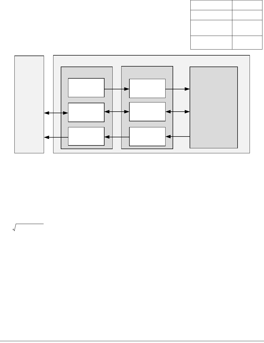
Background and overview
MMA9555L Intelligent Pedometer Data Sheet, Rev. 2.2
© NXP B.V. 2016. All rights reserved. 99
16 Pedometer Application
16.1 Background and overview
The MMA9555L’s major application is the pedometer.The pedometer has calculations for
step-counting, speed, distance, activity-monitoring, and calorie-counting, as well as
autonomous sleep functionality to minimize current consumption.
The following figure illustrates the hardware and software components and interactions in
the MMA9555L.
Figure 22. Pedometer Data Flow Diagram
16.2 Functional description
16.2.1 Step detection
Step detection is based solely on detecting step impact, without taking into consideration the consumer’s height, weight, or
gender.
The algorithm operates by keeping track of momentary acceleration, defined as:
where X, Y, and Z represent a single accelerometer reading, normalized by dividing by 1 g.
The values of A are accumulated over a fixed period of time (0.19 seconds). At every reading, the average A for that period is
calculated and saved. The algorithm detects steps by analyzing the spread of the accumulated average A values. The spread is
the difference between minimum and maximum of the calculated values.
For a step to be reported, the spread in the buffer of average values of A has to exceed a fixed threshold (0.13 g) and stay above
that threshold for at least the fixed value of 0.07 seconds. If the spread falls below the threshold sooner than 0.07 seconds, the
motion is ignored.
The STEPCNT variable contains the number of steps detected since the last reset. That count is updated every time a step is
detected.
Application ID 0x15
Default speed 30 Hz.
Configuration
registers Start on
page 104.
Status registers Start on
page 108.
Host
processor
Platform
Device MMA9555L firmware Pedometer firmware
Analog Front End
Slave port
RGPIO
Analog Front End
application
Command
Interpreter
RGPIO
application
AX
2Y2Z2
++=

Functional description
MMA9555L Intelligent Pedometer Data Sheet, Rev. 2.2
100 © NXP B.V. 2016. All rights reserved.
16.2.2 Distance estimation
The distance estimation begins with the Base Stride Length (BSL), the estimated stride length for this consumer. The BSL is
calculated as follows:
where Height is the consumer’s height and GenderFactor is 0.415 for males or 0.413 for females. For more information about
Height, see “Height/Weight register” on page 106. For more information on GenderFactor, see “Filter register” on page 106.
If no consumer information is provided, BSL is set to 0, and the resulting distance values are 0. If there is a need to update the
BSL without consumer information, the configuration structure can be used to set a fixed stride length.
The estimated stride length is calculated by adjusting the BSL for step rate (steps/second). Stride length for a particular step is
calculated as follows:
The StepRateFactor values are shown in the following table:
The overall distance is calculated as the sum of estimated stride lengths for all steps detected since the last reset.
The DISTANCE variable contains the value of overall distance and is updated every time a step is detected.
16.2.3 Speed calculation
Speed is calculated over a sliding time window as:
where Distance is the total distance covered by all steps detected within the time window. Time is the length of the window and
can be configured by the SPDPRD variable.
For more information, see:
• Speed: “Speed register” on page 110
• Distance: “Distance register” on page 110
•Time: “Filter register” on page 106
• SPDPRD variable: “Speed Period/Step Threshold register” on page 107
The SPEED variable contains the current speed value and is updated every time a step is detected or once per second if there
are no steps. If there are no steps, the speed may not necessarily fall to zero even if the activity level, which is described in the
following section, falls to Rest. The activity level is reset to Rest if there are no steps for a certain amount of time. The speed
calculation does not include a similar reset when there are no steps. Therefore, it may conflict with the activity level. In this
scenario, the user should disregard the speed if the activity level is Rest.
Table 146. StepRateFactor calculation
Step rate, S
(steps/sec) StepRateFactor
S < 1.6 (very slow) 0.88
1.6 ≤ S < 1.8 (slow) 0.95
1.8 ≤ S < 2.35 (normal) 1.00
2.35 ≤ S < 2.8 (fast) 1.30
S ≥ 2.8 (very fast) 2.30
BSL Height centimeters()GenderFactor 1.1××=
Stride BSL StepRateFactor×=
Speed Distance (meters)
Time
--------------------------------------------
=

Functional description
MMA9555L Intelligent Pedometer Data Sheet, Rev. 2.2
© NXP B.V. 2016. All rights reserved. 101
16.2.4 Activity-level calculation
The activity-level calculation is based on the speed value. The activity-level value is assigned according to the following table.
The ACTIVITY variable contains the current activity level and is updated every time a step is detected or once per second if there
are no steps. Additionally, if no steps are detected for the previous 2.5 seconds, the activity level is reset to Rest.
16.2.5 Calorie-expenditure calculation
The estimated amount of calories burned by a single step is calculated as:
where StepRate is calculated as described in “Distance estimation” on page 100, Weight is the consumer’s weight in kilograms,
and MetabolicFactor is calculated according to the following table:
For more information, see:
— StepRate: “Filter register” on page 106
— Weight: “Height/Weight register” on page 106
The CALS variable contains the total amount of calories burned since the last reset. The value is updated every time a step is
detected.
16.2.6 Debounce count
The debounce_count() function implements a debounce counter as defined in application note Motion and Free fall Detection
Using the MMA8450Q (AN3917), listed in “Related Documentation” on page 2.
If the input condition is satisfied, the count is incremented by one up to the threshold. Otherwise, the count is decremented or
cleared depending on the debounce counter mode.
The debounce counter’s behavior is shown in Figure 23.
Table 147. Activity-level calculation
Latest speed, S
(Km/h) Activity level
S ≥ 10.5 Running
6.5 ≤ S < 10.5 Jogging
1.0 ≤ S < 6.5 Walking
S < 1.0 Rest
Table 148. MetabolicFactor calculation
Step Rate, S
(steps/sec) MetabolicFactor
S < 1.6 (very slow) 2.0
1.6 ≤ S < 1.8 (slow) 2.5
1.8 ≤ S < 2.35 (normal) 3.8
2.35 ≤ S < 2.8 (fast) 8.0
S ≥ 2.8 (very fast) 12.5
Calories MetabolicFactor 0.00029×
StepRate
----------------------------------------------------------------------Weight×=
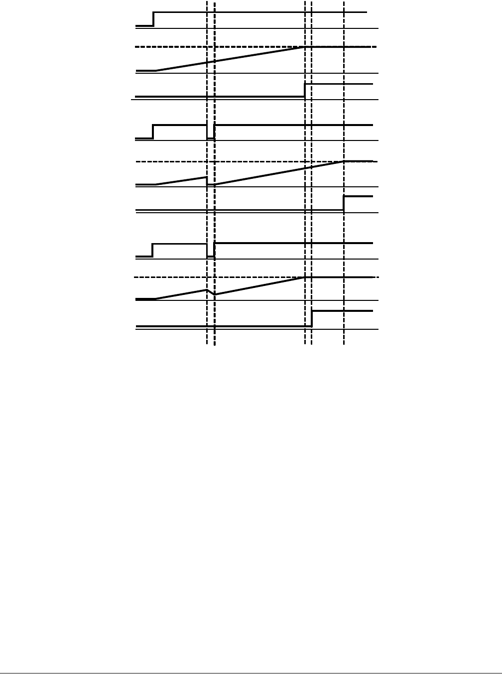
Functional description
MMA9555L Intelligent Pedometer Data Sheet, Rev. 2.2
102 © NXP B.V. 2016. All rights reserved.
Figure 23. Debounce counter behavior
16.2.7 Autonomous suspend
The pedometer uses the acceleration vector magnitude squared, (X2 + Y2 + Z2), to determine if the device is stationary. It is
designed to suspend the pedometer conservatively and wake the pedometer aggressively to avoid missing any steps.
The autonomous-suspend function compares the acceleration vector magnitude to the configurable minimum and maximum
thresholds (SLEEPMIN and SLEEPMAX) and passes the boolean result to a debounce counter. If the thresholds are satisfied for
at least SLEEPTHD samples, the pedometer autonomously suspends. The thresholds are satisfied if the output of the debounce
counter is asserted.
If the thresholds are not satisfied for at least SLEEPTHD samples, the pedometer executes normally.
The parameters SLEEPMIN, SLEEPMAX, SLEEPTHD, and SLP_DBCNTM configure the behavior. The SLEEPMAX
parameter’s reset value disables the autonomous suspend function by default.
For more information, see:
• SLEEPMIN: “Sleep Minimum register” on page 104
• SLEEPMAX: “Sleep Maximum register” on page 104
• SLEEPTHD: “Sleep Count Threshold register” on page 105
• SLP_DBCNTM: “Configuration/Step Length register” on page 105
If custom sleep functionality is desired, a user may disable the pedometer’s autonomous-suspend functionality and instead use
the MMA9555L’s Reset/Suspend/Clear application to enable or disable the pedometer. For an example, see “Enable/disable the
Pedometer application” on page 124.
Low-g event
on all three axes
(Freefall)
Count threshold
FF_MT
counter value
EA FF
Low-g event
on all three axes
(Freefall)
(a)
EA FF
DBCNTM = 1
(b)
EA FF
DBCNTM = 0
(c)
Count threshold
FF_MT
counter value
Low-g event
on all three axes
(Freefall)
Count threshold
FF_MT
counter value

Memory-maps and register descriptions
MMA9555L Intelligent Pedometer Data Sheet, Rev. 2.2
© NXP B.V. 2016. All rights reserved. 103
16.3 Memory-maps and register descriptions
The Pedometer Application running in the MMA9553L device has eight configuration registers and six status or data registers.
The configuration registers allow the user to customize and control the behavior of the pedometer application. The status
registers report back the measured and calculated data.
All status registers are shown as 16-bits wide. They are byte-accessible, but should be read 16 bits (two bytes) or more at a time
with a single command, if the user wishes to read them atomically.
Similarly, configuration registers are shown as 16-bits wide but are also byte-accessible. Most fields defined within the
configuration registers are 8-bits or less and are byte-aligned, so they can be written one byte at a time if desired. All bytes should
be written using a single command if the user wishes to modify them atomically.
16.3.1 Pedometer memory maps
Table 149. Configuration registers
Offset
address Register Access Reset Details
0x0 Sleep Minimum register R/W 0x0000 “Sleep Minimum register” on page 104
0x2 Sleep Maximum register R/W 0x0000 “Sleep Maximum register” on page 104
0x4 Sleep Count Threshold register R/W 0x0001 “Sleep Count Threshold register” on page 105
0x6 Config/Step Length register R/W 0x0000 “Configuration/Step Length register” on page 105
0x8 Height/Weight register R/W 0xAF50 “Height/Weight register” on page 106
0xA Filter register R/W 0x0403 “Filter register” on page 106
0xC Speed Period register R/W 0x0582 “Speed Period/Step Threshold register” on page 107
0xE Activity Count Threshold
register R/W 0x0000 “Activity Count Threshold register” on page 107
0x10 Step Coalesce register R/W 0x01 “Step Coalesce register” on page 107
Table 150. Status registers
Offset
address Register Access Reset Details
0x0 Status register R 0x0002 “Status register” on page 108
0x2 Step count register R 0x0000 “Step Count register” on page 109
0x4 Distance register R 0x0000 “Distance register” on page 110
0x6 Speed register R 0x0000 “Speed register” on page 110
0x8 Calories register R 0x0000 “Calories register” on page 110
0xA Sleep Count register R 0x0000 “Sleep Count register” on page 111

Memory-maps and register descriptions
MMA9555L Intelligent Pedometer Data Sheet, Rev. 2.2
104 © NXP B.V. 2016. All rights reserved.
16.3.2 Pedometer configuration-register descriptions
16.3.2.1 Sleep Minimum register
16.3.2.2 Sleep Maximum register
Table 151. Sleep Minimum register
Bit 1514131211109876543210
Read SLEEPMIN
Write
Reset 0x0000
Table 152. Sleep Minimum register field descriptions
Field Description
15:0
SLEEPMIN
Minimum acceleration vector magnitude for autonomous suspend.
The acceleration vector magnitude must be greater than SLEEPMIN and less than SLEEPMAX to satisfy the
autonomous suspend condition(1). At rest, the acceleration vector magnitude measures approximately 1 g.
Therefore, SLEEPMIN and SLEEPMAX are expected to be set to values near 1 g (4096 at 0.244 mg/LSB
resolution).
Valid range: 0x0000:0xFFFF (uint16). Units: 0.244 mg/LSB
1. This condition must be satisfied for SLEEPTHD samples for the pedometer to autonomously suspend. See Table 156 on page 105.
Table 153. Sleep Maximum register
Bit 1514131211109876543210
Read SLEEPMAX
Write
Reset 0x0000
Table 154. Sleep Maximum register field descriptions
Field Description
15:0
SLEEPMAX
Maximum acceleration vector magnitude for autonomous suspend.
The acceleration vector magnitude must be greater than SLEEPMIN and less than SLEEPMAX to satisfy the
autonomous suspend condition(1). At rest, the acceleration vector magnitude measures approximately 1 g.
Therefore, SLEEPMIN and SLEEPMAX are expected to be set to values near 1 g (4096 at 0.244 mg/LSB
resolution).
Set to SLEEPMAX 0 to disable autonomous suspend.
Valid range: 0x0000:0xFFFF (uint16).
Units: 0.244 mg/LSB
1. This condition must be satisfied for SLEEPTHD samples for the pedometer to autonomously suspend. See Table 156 on page 105.

Memory-maps and register descriptions
MMA9555L Intelligent Pedometer Data Sheet, Rev. 2.2
© NXP B.V. 2016. All rights reserved. 105
16.3.2.3 Sleep Count Threshold register
16.3.2.4 Configuration/Step Length register
Table 155. Sleep Count Threshold register
Bit 1514131211109876543210
Read SLEEPTHD
Write
Reset 0x0001
Table 156. Sleep Count Threshold register field descriptions
Field Description
15:0
SLEEPTHD
Autonomous suspend debounce count threshold.
The autonomous suspend condition(1) must be satisfied for SLEEPTHD samples for the pedometer to
autonomously suspend.
Valid range: 0x0000:0xFFFF (uint16).
1. The acceleration vector magnitude must be greater than SLEEPMIN and less than SLEEPMAX to satisfy this condition. For more information on
SLEEPMIN and SLEEPMAX, see “Sleep Minimum register” and “Sleep Maximum register”.
Table 157. Configuration/Step Length register
Bit 1514131211109876543210
Read
CONFIG
ACT_DBCNTM
SLP_DBCNTM
— STEPLEN
Write
Reset 000 00000 0x00
= Unimplemented or reserved
Table 158. Configuration/Step Length register field descriptions
Field Description
15
CONFIG
(Re)initializes the pedometer with current configuration values.
Modifications to other pedometer configuration registers will not take effect until this bit is set. It is
automatically cleared after the (re)initialization completes.
0: Do not (re)initialize the pedometer
1: (Re)initialize the pedometer with current configuration values
14
ACT_DBCNTM
Activity debounce counter mode.
0: Decrement the count when the activity level changes
1: Clear the count when the activity level changes
13
SLP_DBCNTM
Autonomous suspend debounce counter mode.
0: Decrement the count when the device is in motion
1: Clear the count when the device is in motion
12:8
—Reserved.
Set to 0.
7:0
STEPLEN
Step length in centimeters.
Set to 0 to automatically estimate the consumer’s step length based on gender and height.
Valid range: 0x00:0xFF (uint8)

Memory-maps and register descriptions
MMA9555L Intelligent Pedometer Data Sheet, Rev. 2.2
106 © NXP B.V. 2016. All rights reserved.
16.3.2.5 Height/Weight register
16.3.2.6 Filter register
Table 159. Height/Weight register
Bit 1514131211109876543210
Read HEIGHT WEIGHT
Write
Reset 0xAF 0x50
Table 160. Height/Weight register field descriptions
Field Description
15:8
HEIGHT
Height in centimeters.
Used to estimate step length, if STEPLEN = 0.
Valid range: 0x00:0xFF (uint8)
Default = 0xAF (175 centimeters).
7:0
WEIGHT
Weight in kilograms.
Used to estimate step length, if STEPLEN = 0.
Valid range: 0x00:0xFF (uint8)
Default = 0x50 (80 kilograms).
Table 161. Filter register
Bit 1514131211109876543210
Read FILTSTEP MALE FILTTIME
Write
Reset 0x04 0 0x03
Table 162. Filter register field descriptions
Field Description
15:8
FILTSTEP
Number of steps that must occur within FILTTIME for the pedometer to decide the consumer is making steps.
Set to 0 to disable step filtering. If the value specified is greater than 6, then 6 will be used.
Valid range: 0x00:0x06 (uint8).
Default = 0x04.
7
MALE
Gender
0: Female
1: Male
6:0
FILTTIME
Number of seconds in which filter steps must occur.
Set to 0 to disable step filtering.
Valid range: 0x00:0x7F (uint8)
Default = 0x03.

Memory-maps and register descriptions
MMA9555L Intelligent Pedometer Data Sheet, Rev. 2.2
© NXP B.V. 2016. All rights reserved. 107
16.3.2.7 Speed Period/Step Threshold register
16.3.2.8 Activity Count Threshold register
16.3.2.9 Step Coalesce register
Table 163. Speed Period register
Bit 1514131211109876543210
Read SPDPRD STEPTHRESHOLD
Write
Reset 0x05 0x82
Table 164. Speed Period/Step Threshold register field descriptions
Field Description
15:8
SPDPRD
Number of seconds in which to compute speed.
If set to a value greater than 5, then 5 will be used.
Valid range: 0x02:0x05.
Warning: Do not set SPDPRD to 0 or 1 as this may cause undesirable behavior.
7:0
STEPTHRESHOLD
Magnitude acceleration threshold to detect a step. Large values make the pedometer less sensitive;
small values make the pedometer more sensitive and may lead to false positives.
Units: 1 mg/LSB
Valid range: 0x00:0xFF (uint8)
Default: 0x82 (0.13 g)
Table 165. Activity Count Threshold register
Bit 1514131211109876543210
Read ACTTHD
Write
Reset 0x0000
Table 166. Activity Count Threshold register field descriptions
Field Description
15:0
ACTTHD
Activity debounce count threshold.
The internal activity level must be stable for ACTTHD samples before ACTIVITY is updated.
Valid range: 0x0000:0xFFFF (uint16)
0: The activity debouncer is effectively bypassed.(1)
1: The current internal activity level must equal the previous internal activity level in order to update ACTIVITY.
1. For more information on the activity debouncer, see Table 158 on page 105.
Table 167. Step Coalesce register
Bit 76543210
Read STEPCOALESCE
Write
Reset 0X01

Memory-maps and register descriptions
MMA9555L Intelligent Pedometer Data Sheet, Rev. 2.2
108 © NXP B.V. 2016. All rights reserved.
16.3.3 Pedometer status-register descriptions
16.3.3.1 Status register
Table 168. Activity Count Threshold register field descriptions
Field Description
7:0
STEPCOALESCE
Number of steps to coalesce before asserting STEPCHG.
0: Disables STEPCHG.
1: Asserts STEPCHG after every step. The default.
Valid range: 0x00:0xFF (uint8).
Table 169. Status register
Bit 1514131211109876543210
Read
MRGFL
SUSPCHG
STEPCHG
ACTCHG
SUSP
ACTIVITY
VERSION
Write
Reset 00000 000 0x02
= Unimplemented or reserved
Table 170. Status register field descriptions
Field Description
15
MRGFL
Merged status change flags.
This bit is the logical OR of the SUSPCHG, STEPCHG, and ACTCHG flags. It can be routed to a pin to
enable a single, merged-output interrupt using the MMA955xL GPIO application(1).
The host can trigger an interrupt on rising edges to receive notification when at least one of the status
change flags is asserted. The host is responsible for resolving the source if desired. That can be done by
comparing the STEPCNT to a previous value to determine that a STEPCNT change caused the MRGFL
assertion.
0: None of the status change flags are asserted
1: At least one of the status change flags (SUSPCHG, STEPCHG, ACTCHG) is asserted
14
SUSPCHG
Indicates a change in the SUSP bit.
This bit is transient and only asserts during frames in which the SUSP bit changes from the previous frame.
A frame is one 30-Hz period. This bit can be routed to a pin to enable output interrupts using the
MMA9555L GPIO AppMap application(1). The host can trigger an interrupt on rising edges to receive
notification when the pedometer suspends or resumes.
0: No change in the SUSP bit since the last pedometer call.
1: The SUSP bit changed since the last pedometer call.
13
STEPCHG
Indicates a change in STEPCNT by STEPCOALSCE steps.
This bit is transient and only asserts during frames in which STEPCNT changed from the previous frame.
A frame is one 30-Hz period. This bit can be routed to a pin to enable output interrupts using the
MMA9555L GPIO AppMap application(1). The host can trigger an interrupt on rising edges to receive
notification after every step.
0: The step count has not been incremented by STEPCOALESCE steps since the last STEPCHG
assertion or the pedometer was last initialized.
1: The step count has been incremented by STEPCOALESCE steps since the last STEPCHG assertion
or the pedometer was last initialized.

Memory-maps and register descriptions
MMA9555L Intelligent Pedometer Data Sheet, Rev. 2.2
© NXP B.V. 2016. All rights reserved. 109
16.3.3.2 Step Count register
12
ACTCHG
Indicates a change in activity level.
This bit is transient and only asserts during frames in which ACTIVITY changed from the previous frame.
A frame is one 30-Hz period. This bit can be routed to a pin to enable output interrupts using the
MMA9555L GPIO AppMap application(1). The host can trigger an interrupt on rising edges to receive
notification when the activity level is changed.
0: No change in activity level since last pedometer call
1: New activity level since last pedometer call
11
SUSP
Indicates whether the pedometer is active or has been autonomously suspended.
This bit can be routed to a pin to enable output interrupts using the MMA9555L GPIO AppMap
application(1). The host can trigger an interrupt on rising edges to receive notification when the pedometer
is autonomously suspended and trigger an interrupt on falling edges to receive notification when the
pedometer resumes.
0: Pedometer is active
1: Pedometer is suspended
10:8
ACTIVITY
Activity level:
000: Unknown
001: Rest
010: Walking
011: Jogging
100: Running
101–111: Reserved
7:0
VERSION
Version number of the pedometer application, incremented by one for each new release.
0: R1.32
1: R1.33
2: R1.34
1. For more information on the GPIO AppMap application, see Chapter 7, “GPIO-AppMap Application”.
Table 171. Step Count register
Bit 1514131211109876543210
Read STEPCNT
Write
Reset 0x0000
= Unimplemented or reserved
Table 172. Step Count register field descriptions
Field Description
15:0
STEPCNT The total step count since the pedometer was last reset.
Valid range: 0x0000:0xFFFF (uint16)
Table 170. Status register field descriptions
Field Description

Memory-maps and register descriptions
MMA9555L Intelligent Pedometer Data Sheet, Rev. 2.2
110 © NXP B.V. 2016. All rights reserved.
16.3.3.3 Distance register
16.3.3.4 Speed register
If there are no steps, the speed may not necessarily fall to zero even if the activity level falls to rest. See 16.2.3, “Speed
calculation” on page 100 for more information.
16.3.3.5 Calories register
Table 173. Distance register
Bit 1514131211109876543210
Read DIST
Write
Reset 0x0000
= Unimplemented or reserved
Table 174. Distance register field descriptions
Field Description
15:0
DIST The total distance in meters since the pedometer was last reset.
Valid range: 0x0000:0xFFFF (uint16).
Table 175. Speed register
Bit 1514131211109876543210
Read SPEED
Write
Reset 0x0000
= Unimplemented or reserved
Table 176. Speed register field descriptions
Field Description
15:0
SPEED Average speed in meters per hour over SPDPRD(1).
Valid range: 0x0000:0xFFFF (uint16)
1. For information on SPDPRD, see Table 164 on page 107.
Table 177. Calories register
Bit 1514131211109876543210
Read CALS
Write
Reset 0x0000
= Unimplemented or reserved

Pedometer application examples
MMA9555L Intelligent Pedometer Data Sheet, Rev. 2.2
© NXP B.V. 2016. All rights reserved. 111
16.3.3.6 Sleep Count register
16.4 Pedometer application examples
16.4.1 Pedometer application configuration example
To write all the pedometer configuration registers, the following command packet shall be sent from the host to the device
mailboxes. The most significant byte of a register (MSB) is written in the lowest-numbered mailbox.
NOTE
The question marks represent placeholders for the application specific values. Please
replace the question marks with values for the application.
MB0 = 0x15: Set the Pedometer Application Identifier (0x15)
MB1 = 0x20: Set the Command: Write Config command, with zero offset (0x20)
MB2 = 0x00: Set the Offset to point to the first configuration register
MB3 = 0x11: Set the Count field to declare writing 17 bytes
MB4–MB5 = 0x????: Value for Sleep Min Register
MB6–MB7 = 0x????: Value for Sleep Max Register
MB8–MB9 = 0x????: Value for Sleep Count Threshold
MB10–MB11 = 0x????: Value for Config / Step Length Register
MB12–MB13 = 0x????: Value for Height / Weight
MB14–MB15 = 0x????: Set the Filter Register
MB16–17 = 0x????: Set the Speed Period / Step Threshold Register
MB18–19 = 0x????: Set the Activity Count
MB20 = 0x??: Set the Step Coalesce
Bytes to send: 0x15, 0x20, 0x00, 0x11, 0x??, 0x??, 0x??, 0x??, 0x??, 0x??, 0x??, 0x??, 0x??, 0x??, 0x??, 0x??, 0x??, 0x??,
0x??, 0x??, 0x??
Table 178. Calories register field descriptions
Field Description
15:0
CALS Total calorie count since the pedometer was last reset.
Valid range: 0x0000:0xFFFF (uint16)
Table 179. Sleep Count register
Bit 1514131211109876543210
Read SLEEPCNT
Write
Reset 0x0000
= Unimplemented or reserved
Table 180. Sleep Count register field descriptions
Field Description
15:0
SLEEPCNT Current value of the autonomous suspend debounce counter.
Valid range: 0x0000:0xFFFF (uint16)

Pedometer application examples
MMA9555L Intelligent Pedometer Data Sheet, Rev. 2.2
112 © NXP B.V. 2016. All rights reserved.
To read all the pedometer configuration registers, send the following command packet from the host to the device mailboxes.
This can be used as a device identification command, allowing a host to differentiate the MMA9555L from the MMA955xL.
MB0: 0x15 = pedometer application ID
MB1: 0x10 = opcode to read configuration
MB2: 0x00 = offset into pedometer configuration register map
MB3: 0x11 = number of bytes to read
The MMA9555L response will be:
MB0: 0x15 = pedometer application ID
MB1: 0x80 = COCO=1, error code=0
MB2: 0x11 = actual number of bytes read
MB3: 0x11 = requested number of bytes to read
MB4: sleep minimum MSB
MB5: sleep minimum LSB
MB6: sleep maximum MSB
MB7: sleep maximum LSB
MB8: sleep count threshold MSB
MB9: sleep count threshold LSB
MB10: config
MB11: step length MB12: height
MB13: weight
MB14: filter step
MB15: male, filter time
MB16: speed period
MB17: step threshold
MB18: activity count threshold MSB
MB19: activity count threshold LSB
MB20: step coalesce

Pedometer application examples
MMA9555L Intelligent Pedometer Data Sheet, Rev. 2.2
© NXP B.V. 2016. All rights reserved. 113
16.4.2 Pedometer application read example
To read all the pedometer status registers, send the following command packet from the host to the device mailboxes:
MB0 = 0x15: Set the Pedometer Application Identifier (0x15)
MB1 = 0x30: Set the Command: Read Status command, with zero offset (0x30)
MB2 = 0x00: Set the Offset (0x00) to point to the first status register
MB3 = 0x0C: Set the Count field to (12) to declare reading 12 bytes
Read back the mailboxes, when the COCO (Command Complete) bit is set the status data will be in the mailbox registers.
Bytes to send: 0x15, 0x30, 0x00, 0x0C
The response to this command will be:
MB0: 0x15 = pedometer application ID
MB1: 0x80 = COCO=1, error code=0
MB2: 0x0C = actual number of bytes read
MB3: 0x0C = requested number of bytes to read
MB4: pedometer status register MSB
MB5: pedometer status register LSB
MB6: step count MSB
MB7: step count LSB
MB8: distance MSB
MB9: distance LSB
MB10: speed MSB
MB11: speed LSB
MB12: calories MSB
MB13: calories LSB
MB14: sleep count MSB
MB15: sleep count LSB

Overview of GPIO Input/Output application
MMA9555L Intelligent Pedometer Data Sheet, Rev. 2.2
© NXP B.V. 2016. All rights reserved. 114
17 GPIO Input/Output Application
17.1 Overview of GPIO Input/Output application
The GPIO input/output application provides a function that can control seven physical GPIO
pins of MMA9555L. It can set the direction GPIOs as input or output, control the pin level
when the pin is set as an output pin and read the pin level through its status register. It also
has a mask register, called the Enable Configuration Register, to avoid conflict with the GPIO
AppMap application APP-ID 0x03.
The GPIO pins that are available to this application are described in Table 181.
17.2 Memory maps and register descriptions
The GPIO Input/Output Application has three configuration registers and one status register. The configuration registers allow
the user to customize and control the behavior of the GPIO Input/Output application. The status registers report back the level of
the GPIO2–GPIO9. The status register is 8 bits wide.
Similarly, configuration registers are 8 bits wide. They can be written one byte at a time if desired. All bytes should be written
using a single command if the user wishes to modify them atomically.
17.2.1 GPIO Input/Output memory maps
Table 181. GPIO pin names, numbers and functions
Name Pin number
GPIO2 7
GPIO3 8
GPIO4 9
GPIO5 11
GPIO6 12
GPIO7 13
GPIO8 15
GPIO9 2
Table 182. Configuration Registers
Offset
address Register Access Reset Details
0x00 GPIO input/output direction register R/W 0x0F “GPIO input/output direction register” on page 115
0x01 GPIO input/output enable register R/W 0x0F “GPIO input/output enable register” on page 115
0x02 GPIO input/output data register R/W 0x05 “GPIO input/output data register” on page 116
Table 183. Status register
Offset
address Register Access Reset Details
0x00 GPIO input/output Status register R 0x05 “GPIO Input/Output Status register” on page 116
Application
ID 0x19
Default speed 30 Hz.
Configuration
registers Start on page
115.
Status
registers Start on page
116.

GPIO Input/Output configuration register descriptions
MMA9555L Intelligent Pedometer Data Sheet, Rev. 2.2
115 © NXP B.V. 2016. All rights reserved.
17.3 GPIO Input/Output configuration register descriptions
17.3.1 GPIO input/output direction register
17.3.2 GPIO input/output enable register
Table 184. GPIO input/output direction register
Bit 76543210
Read DIR8 DIR7 DIR6 DIR5 DIR4 DIR3 DIR2
Write
Reset 0x0F
= Unimplemented or reserved
Table 185. GPIO input/output direction register field description
Field Description
6:0
DIR8–DIR2
GPIO data direction. The value of this register is shifted and then copied to the hardware register RGPIO_DIR.
0: Configured as an input
1: Configured as an output
Table 186. GPIO input/output enable register
Bit 76543210
Read EN8 EN7 EN6 EN5 EN4 EN3 EN2
Write
Reset 0x0F
= Unimplemented or reserved
Table 187. GPIO input/output enable register description
Field Description
6:0
EN8–EN2
GPIO enable. The value of this register is shifted and then copied to the hardware register RGPIO_EN.
0: Disable the pin in this application
1: Enable the pin in this application

GPIO Input/Output Status register descriptions
MMA9555L Intelligent Pedometer Data Sheet, Rev. 2.2
© NXP B.V. 2016. All rights reserved. 116
17.3.3 GPIO input/output data register
17.4 GPIO Input/Output Status register descriptions
17.4.1 GPIO Input/Output Status register
NOTE
Though GPIO9 cannot be set in the configuration registers, the pin level can be detected in
the status register when GPIO9 is set as interrupt pin in APP-ID 0x03.
Table 188. GPIO input/output data register
Bit 76543210
Read DATA8 DATA7 DATA6 DATA5 DATA4 DATA3 DATA2
Write
Reset 0x05
= Unimplemented or reserved
Table 189. GPIO input/output data register description
Field Description
6:0
EN8–EN2
GPIO data output. The value of this register is shifted and then copied to the hardware register RGPIO_DATA.
0: Output low on the pin
1: Output high on the pin
Table 190. GPIO input/output status register
Bit 76543210
Read DATA9 DATA8 DATA7 DATA6 DATA5 DATA4 DATA3 DATA2
Write
Reset 0x05
= Unimplemented or reserved
Table 191. GPIO input/output status register description
Field Description
7:0
DATA9–DATA2
GPIO data output. The value of this register is read from hardware register RGPIO_DATA.
0: A properly enabled RGPIO output pin is driven with a logic 0, or a properly enabled RGPIO input pin was read
as a logic 0
1: A properly enabled RGPIO output pin is driven with a logic 1, or a properly enabled RGPIO input pin was read
as a logic 1

GPIO Input/Output application examples
MMA9555L Intelligent Pedometer Data Sheet, Rev. 2.2
117 © NXP B.V. 2016. All rights reserved.
17.5 GPIO Input/Output application examples
17.5.1 GPIO Input/Output application configuration example
To write all the GPIO Input/Output configuration registers, the following command packet should be sent from the host to the
device mailboxes. The most significant byte of a register (MSB) is written in the lowest-numbered mailbox.
NOTE
The question marks represent placeholders for the application specific values. Please
replace the question marks with the values for the application.
MB0 : 0x19= Set the GPIO Input/Output Application Identifier (0x19)
MB1 : 0x20= Set the Command: Write Config command, with zero offset (0x20)
MB2 : 0x00= Set the Offset to point to the first configuration register
MB3 : 0x03= Set the Count field to declare writing 3 bytes
MB4 : 0x??= Value for GPIO input/output direction register
MB5 : 0x??= Value for GPIO input/output enable register
MB6 : 0x??= Value for GPIO input/output data register
Bytes to send: 0x19, 0x20, 0x00, 0x03, 0x??, 0x??, 0x??
To read all the GPIO Input/Output configuration registers, the following command packet should be sent from the host to the
device mailboxes.
MB0: 0x19= GPIO Input/Output application ID
MB1: 0x10= opcode to read configuration
MB2: 0x00= offset into GPIO Input/Output configuration register map
MB3: 0x03= number of bytes to read
The MMA9555L response will be:
MB0: 0x19 = GPIO Input/Output application ID
MB1: 0x80 = COCO=1, error code=0
MB2: 0x03 = actual number of bytes read
MB3: 0x03 = requested number of bytes to read
MB4: Value of GPIO input/output direction register
MB5: Value of GPIO input/output enable register
MB6: Value of GPIO input/output data register
17.5.2 GPIO Input/Output application read example
To read the GPIO Input/Output status register, the following command packet is sent from the host to the device mailboxes:
MB0 : 0x19 = Set the GPIO Input/Output Application Identifier (0x19)
MB1 : 0x30 = Set the Command: Read Status command, with zero offset (0x30)
MB2 : 0x00 = Set the Offset (0x00) to point to the first status register
MB3 : 0x01= Set the Count field to (1) to declare reading 1 byte
Bytes to send: 0x19, 0x30, 0x00, 0x01
To read the mailboxes, when the COCO (Command Complete) bit is set, the status data are in the mailbox registers.
The response to this command is:
MB0: 0x19 = GPIO Input/Output application ID

GPIO Input/Output application examples
MMA9555L Intelligent Pedometer Data Sheet, Rev. 2.2
© NXP B.V. 2016. All rights reserved. 118
MB1: 0x80 = COCO=1, error code=0
MB2: 0x01 = actual number of bytes read
MB3: 0x01 = requested number of bytes to read
MB4: GPIO input/output Status register

Overview of the Six-Direction application
MMA9555L Intelligent Pedometer Data Sheet, Rev. 2.2
© NXP B.V. 2016. All rights reserved. 119
18 Six-Direction Application
18.1 Overview of the Six-Direction application
The Six-Direction application detects six major directional orientations of the device in three-
dimensional space. It determines the primary axis that the device is oriented: +X, –X, +Y,
–Y, +Z or –Z, with reference opposite to the direction of gravity. It uses the coordinate system
as defined in Figure 5 on page 12.
When the absolute g value of the current direction is less than half g, the application detects
which axis has the largest absolute g value. If this axis is kept as the largest and the
debounce count meets the count threshold, it updates the status of the direction. When the
absolute g value of the current direction is larger than half g, it keeps current direction.
18.2 Memory maps and register descriptions
The Six-Direction Application running in the MMA9555L device has two configuration registers and two status registers. The
configuration registers allow the user to customize and control the behavior of the Six-Direction application. The status registers
report current direction status, status change flag and debounce count status.
The status registers are 8 bits wide. They are byte-accessible, but should be read two bytes at a time with a single command, if
the user wishes to read them atomically.
Similarly, configuration registers are 8 bits wide. They can be written one byte at a time if desired. All bytes should be written
using a single command if the user wishes to modify them atomically.
18.2.1 Six Direction register memory maps
Table 192. Configuration registers
Offset
address Register Access Reset Details
0x00 SixDir Count Threshold register R/W 0x1E “SixDir Count Threshold register” on page 120
0x01 SixDir Debounce mode register R/W 0x01 “SixDir Debounce mode register” on page 120
Table 193. Status register
Offset
address Register Access Reset Details
0x00 SixDir Current Status register R/W 0x06 “SixDir Current Status register” on page 121
0x01 SixDir Debounce count register R/W 0x00 “SixDir Debounce count register” on page 121
Application
ID 0x1A
Default speed 30 Hz.
Configuration
registers Start on page
120.
Status
registers Start on page
121.

Six Direction configuration register descriptions
MMA9555L Intelligent Pedometer Data Sheet, Rev. 2.2
120 © NXP B.V. 2016. All rights reserved.
18.3 Six Direction configuration register descriptions
18.3.1 SixDir Count Threshold register
Table 195. SixDir Count Threshold register description
18.3.2 SixDir Debounce mode register
Table 197. SixDir Debounce mode register description
Table 194. SixDir Count Threshold register
Bit 76543210
Read
Write SDTHD
Reset 0x30
= Unimplemented or reserved
Field Description
7:0
SDTHD
SixDir debounce count threshold.
The status of the direction is not changed until the debounce count meets this threshold.
Valid range: 0x00:0xFF (uint8).
Table 196. SixDir Debounce mode register
Bit 76543210
Read
Write SDM
Reset 0x01
= Unimplemented or reserved
Field Description
0
SDM
SixDir debounce counter mode.
0: Decrement the count when the device changes direction
1: Clear the count when the device changes direction

Six Direction Status register descriptions
MMA9555L Intelligent Pedometer Data Sheet, Rev. 2.2
© NXP B.V. 2016. All rights reserved. 121
18.4 Six Direction Status register descriptions
18.4.1 SixDir Current Status register
Table 199. SixDir Current Status register description
18.4.2 SixDir Debounce count register
Table 201. SixDir Debounce count register description
18.4.3 Six Direction application configuration example
To write all the Six-Direction configuration registers, the host should send the following command packet to the mailboxes. The
most significant byte of a register (MSB) is written in the lower numbered mailbox.
Table 198. SixDir Current Status register
Bit 76543210
Read
Write SC_FLG AXIS_POS AXIS
Reset 0x06
= Unimplemented or reserved
Field Description
7
SC_FLG
Direction Status change flag.
0: Direction has not changed
1: Direction changed. The bit is cleared when the register is read.
2
AXIS_POS
Sign of the direction of the axis detected
0 : Negative Direction
1: Positive direction
1:0
AXIS
Direction is on which axis.
00: X axis
01: Y axis
10: Z axis
Table 200. SixDir Debounce count register
Bit 76543210
Read
Write SDCNT
Reset 0x00
= Unimplemented or reserved
Field Description
7:0
SDCNT The total debounce count since the direction status was last reset.
Valid range: 0x00:0xFF (uint8)

Six Direction Status register descriptions
MMA9555L Intelligent Pedometer Data Sheet, Rev. 2.2
122 © NXP B.V. 2016. All rights reserved.
NOTE
The question marks represent placeholders for the application-specific values. Please
replace the question marks with the desired values for the application.
MB0 : 0x1A= Set the Six-Direction Application Identifier (0x1A)
MB1 : 0x20= Set the Command: Write Config command, with zero offset (0x20)
MB2 : 0x00= Set the Offset to point to the first configuration register
MB3 : 0x02= Set the Count field to declare writing 2 bytes
MB4 : 0x??= Value for SixDir Count Threshold register
MB5 : 0x??= Value for SixDir Debounce mode register
Bytes to send: 0x1A, 0x20, 0x00, 0x02, 0x??, 0x??
To read all the Six-Direction configuration registers, the following command packet is sent from the host to the device mailboxes.
MB0: 0x1A= Six-Direction application ID
MB1: 0x10= opcode to read configuration
MB2: 0x00= offset into Six-Direction configuration register map
MB3: 0x02= number of bytes to read
The MMA9555L response will be:
MB0: 0x1A = Six-Direction application ID
MB1: 0x80 = COCO=1, error code=0
MB2: 0x02 = actual number of bytes read
MB3: 0x02 = requested number of bytes to read
MB4: Value of SixDir Count Threshold register
MB5: Value of SixDir Debounce mode register
18.4.4 Six Direction application read example
To read the Six-Direction status register, the following command packet is sent from the host to the device mailboxes:
MB0 : 0x1A = Set the Six-Direction Application Identifier (0x1A)
MB1 : 0x30 = Set the Command: Read Status command, with zero offset (0x30)
MB2 : 0x00 = Set the Offset (0x00) to point to the first status register
MB3 : 0x02= Set the Count field to (2) to declare reading 2 bytes
Bytes to send: 0x1A, 0x30, 0x00, 0x02
To read the mailboxes, when the COCO (Command Complete) bit is set, the status data is in the mailbox registers.
The response to this command is:
MB0: 0x1A= Six-Direction application ID
MB1: 0x80 = COCO=1, error code=0
MB2: 0x02 = actual number of bytes read
MB3: 0x02 = requested number of bytes to read
MB4: Value of SixDir Current Status register
MB5: Value of SixDir Debounce count register

Read pedometer status variables
MMA9555L Intelligent Pedometer Data Sheet, Rev. 2.2
© NXP B.V. 2016. All rights reserved. 123
19 Sample operations
This section provides sample slave-port commands to read and modify application variables.
19.1 Read pedometer status variables
This command reads all 12 bytes of the status variables from the Pedometer application (APP_ID=0x15), starting at byte offset 0.
15 30 00 0C
19.2 Read pedometer configuration variables
This command reads all 16 bytes of the configuration variables from the Pedometer application (APP_ID=0x15), starting at byte
offset 0.
15 10 00 10
19.3 Write pedometer configuration variables
This command writes all 16 bytes of the configuration variables to the Pedometer application (APP_ID=0x15), starting at byte
offset 0.
15 20 00 10 00 11 22 33 44 55 66 77 88 99 AA BB CC DD EE FF
19.4 Read GPIO Input/output status variables
This command reads the status variable from the GPIO input/output application (APP_ID=0x19), starting at byte offset 0.
19 30 00 01
19.5 Read GPIO Input/output configuration variables
This command reads all 3 bytes of the configuration variables from the GPIO input/output application (APP_ID=0x19), starting
at byte offset 0.
19 10 00 03
19.6 Write GPIO Input/output configuration variables
This command writes all 3 bytes of the configuration variables to the GPIO input/output application (APP_ID=0x19), starting at
byte offset 0.
19 20 00 03 xx xx xx
19.7 Read Six direction status variables
This command reads the two status variables from the Six Direction application (APP_ID=0x1A), starting at byte offset 0.
1A 30 00 02
19.8 Read Six direction configuration variables
This command reads all 2 bytes of the configuration variables from the Six Direction application (APP_ID=0x1A), starting at byte
offset 0.
1A 10 00 02

Write Six direction configuration variables
MMA9555L Intelligent Pedometer Data Sheet, Rev. 2.2
124 © NXP B.V. 2016. All rights reserved.
19.9 Write Six direction configuration variables
This command writes all 3 bytes of the configuration variables to the Six Direction application (APP_ID=0x19), starting at byte
offset 0.
1A 20 00 02 xx xx
19.10 Reset pedometer configuration variables to their defaults
This command writes one byte of configuration variable to the Reset/Suspend/Clear application (APP_ID=0x17) starting at byte
offset 1.
This causes the scheduler to invoke the pedometer's reset function, pedometer_reset().
17 20 01 01 20
19.11 Enable/disable the Pedometer application
This command writes one byte of configuration variable to the Reset/Suspend/Clear application (APP_ID=0x17) starting at byte
offset 5.
This causes the scheduler to suspend the Pedometer application, even if the device is not stationary.
17 20 05 01 20 (disable)
17 20 05 01 00 (enable)
19.12 Configure the AFE range
This command writes one byte of the configuration variable to the AFE application (APP_ID=0x06), starting at byte offset 0. Since
the pedometer uses a normalized acceleration output provided by the AFE application, the g mode only affects the saturation
level and noise.
Regardless of what g mode the AFE is configured to, for or by other applications, the resolution seen by the Pedometer
application is always 8 g.
06 20 00 01 40 (2 g mode)
06 20 00 01 80 (4 g mode)
06 20 00 10 00 (8 g mode)
For more information on configuring the AFE range, see the "AFE configuration registers" section.
19.13 Configure output interrupt: Activity change on GPIO6
This command writes two bytes of the configuration variable to the GPIO application (APP_ID=0x03), starting at byte offset 0.
This causes the GPIO application to copy the pedometer's ACTCHG status bit to GPIO6 after every new accelerometer sample.
The host processor can trigger an interrupt on rising edges of this pin to receive notification when the activity level changes.
03 20 00 02 15 04
19 20 01 01 (AB & 6F)
19.14 Configure output interrupt: Step change on GPIO7
This command writes two bytes of the configuration variable to the GPIO application (APP_ID=0x03), starting at byte offset 2.
This causes the GPIO application to copy the pedometer's STEPCHG status bit to GPIO7 after every new accelerometer sample.
The host processor can trigger an interrupt on rising edges of this pin to receive notification when the step count changes.
03 20 02 02 15 05
19 20 01 01 (AB & 5F)

Configure output interrupt: Suspend change on GPIO8
MMA9555L Intelligent Pedometer Data Sheet, Rev. 2.2
© NXP B.V. 2016. All rights reserved. 125
19.15 Configure output interrupt: Suspend change on GPIO8
This command writes two bytes of the configuration variable to the GPIO application (APP_ID=0x03) starting at byte offset 4.
This causes the GPIO application to copy the pedometer's SUSPCHG status bit to GPIO8 after every new accelerometer sample.
The host processor can trigger an interrupt on rising edges of this pin to receive notification when the pedometer autonomously
suspends or resumes.
03 20 04 02 15 06
19 20 01 01 (AB & 3F)
19.16 Configure output interrupt: Merged flags on GPIO6
This command writes two bytes of the configuration variable to the GPIO application (APP_ID=0x03) starting at byte offset 0.
This causes the GPIO application to copy the pedometer's MRGFL status bit to GPIO6 after every new accelerometer sample.
The host processor can trigger an interrupt on rising edges of this pin to receive notification the activity-level, step-count, or
suspend-state changes.
03 20 00 02 15 07
19 20 01 01 (AB & 6F)
19.17 Configure output interrupt: Every 10 steps on GPIO7
The first command writes one byte of configuration variable to the Pedometer application (APP_ID = 0x15), starting at byte offset
13. This causes the pedometer to coalesce steps and assert STEPCHG once every 10 steps.
The second command writes two bytes of configuration variables to the GPIO application (APP_ID = 0x03), starting at byte offset
2. This causes the GPIO application to copy the pedometer's STEPCHG status bit to GPIO7 after every new accelerometer
sample.
15 20 0D 01 0A
03 20 02 02 15 05
19 20 01 01 (AB & 5F)
19.18 Configure output interrupt: Device direction change on GPIO6
This command writes two bytes of the configuration variable to the GPIO application (APP_ID=0x03), starting at byte offset 0.
This causes the GPIO application to copy the Six-Direction's SC_FLG status bit to GPIO6 after every new accelerometer sample.
The host processor can trigger an interrupt on rising edges of this pin to receive notification when the activity level changes.
03 20 00 02 1A 07
19 20 01 01 (AB & 6F)
19.19 Wake up from Deep Sleep (Stop No Clock mode)
By default, the MMA955xL initializes all applications after a hardware reset and then falls into Deep Sleep mode where all system
clocks are stopped. A slave-port command can be used to wake up the clocks, enable the accelerometer, and execute the
pedometer.
This command writes one byte of configuration variable to the sleep/wake application (APP_ID=0x12) starting at byte offset 6.
12 20 06 01 00
Footprint and pattern information
MMA9555L Intelligent Pedometer Data Sheet, Rev. 2.2
© NXP B.V. 2016. All rights reserved. 126
20 Package Information
The MMA9555L uses a 16-lead LGA package, case number 2094. Use the following link for the latest diagram of the package:
www.nxp.com/files/shared/doc/package_info/98ASA00287D.pdf
20.1 Footprint and pattern information
Figure 24. Package bottom view
Figure 25. Package overlaid on PCB footprint diagram (top view)
Package pad size
0.24 mm x 0.35 mm
Pin 16
Pin 1 ID
Pin 1
Package size (Measurements in mm)
PCB land extension
From the edge of the package
PCB land pad
PCB pad distance
to package edge
Marking
MMA9555L Intelligent Pedometer Data Sheet, Rev. 2.2
127 © NXP B.V. 2016. All rights reserved.
Figure 26. Recommended PCB footprint
20.2 Marking
Solder mask opening
0.777 mm x 1.377 mm
(PCB land + 0.0637 mm larger all around.
Remove slivers between pads.)
PCB land pad size
0.65 mm x 0.25 mm
Solder stencil opening
0.62 mm x 0.22 mm
(PCB land – 0.015 mm smaller all around)
Top View
263
9555
ALYW
Traceability date code
Assembly site
Lot code
Work week
Part number
NXP code
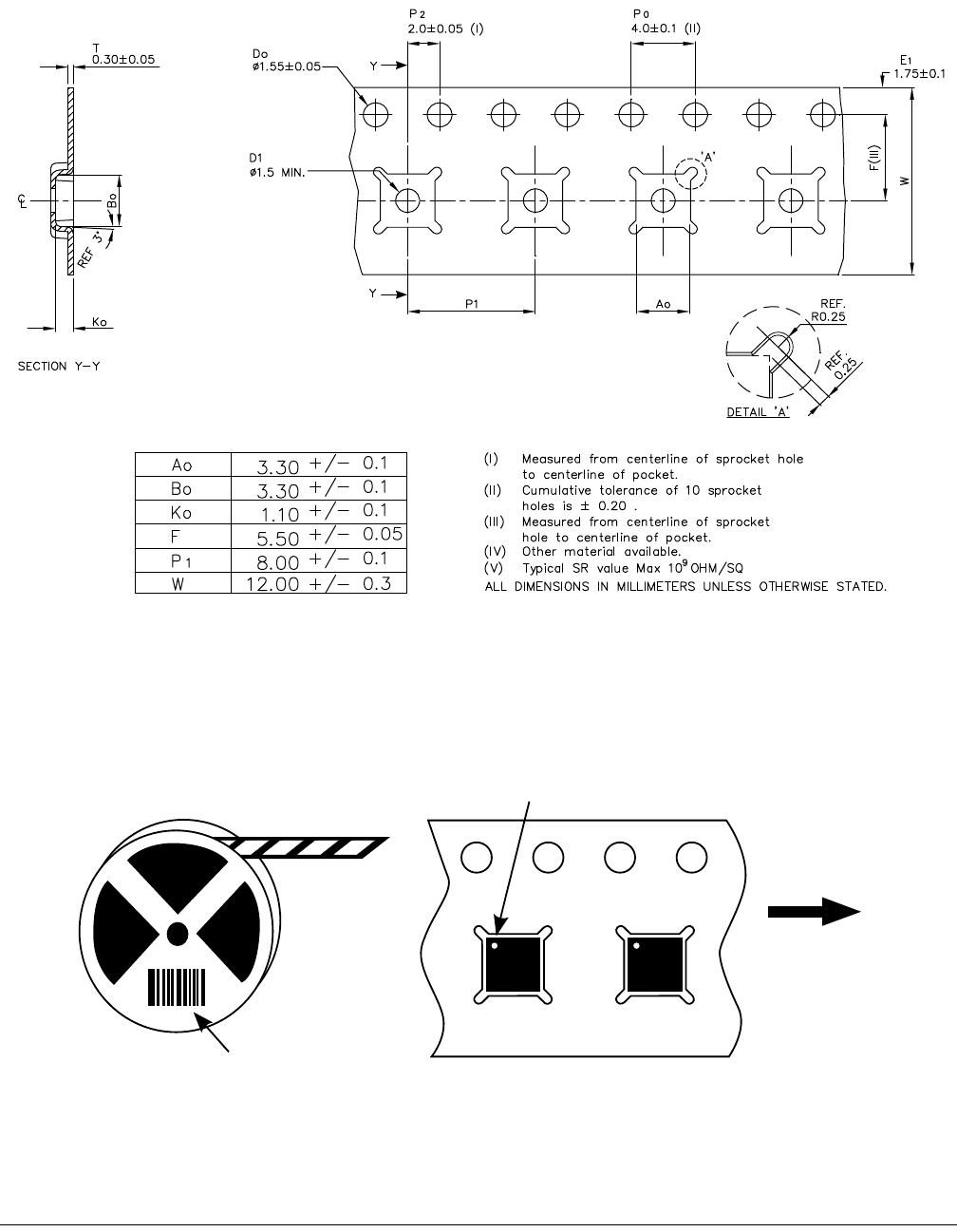
Tape and reel information
MMA9555L Intelligent Pedometer Data Sheet, Rev. 2.2
© NXP B.V. 2016. All rights reserved. 128
20.3 Tape and reel information
Figure 27. Tape dimensions
The devices are oriented on the tape as shown in Figure 28. The dot marked on each device indicates pin 1.
Figure 28. Tape and reel orientation
Barcode label
side of reel
Pin 1
Direction
to unreel
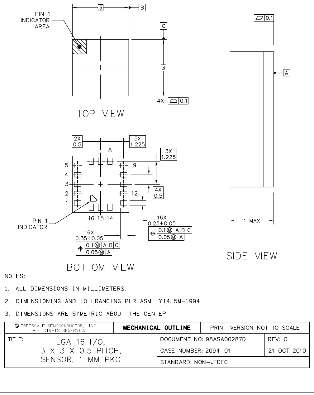

MMA9555L Intelligent Pedometer Data Sheet, Rev. 2.2
© NXP B.V. 2016. All rights reserved. 130
Revision History
Revision
number Revision
date Description of changes
1.0 10/2014 Initial release of document.
2.0 3/2015
Features, 117 µA for pedometer... was 190 µA for pedometer
Figure 2, Device pinout
Changed pin 6 from RGPIO/SDA0/SDI to RGPIO1/SDA0/SDI
Changed pin 8 from RGPIO3/SBB to RGPIO3/SSB
Figures 3 and 4
Changed pin 7 from IO2/SCL1/SDO to IO2/SDO
Changed pin 8 from IO3/SDA1/SSB to IO3/SSB
Added Sections 4–10.
Section 16.3.2.7, added Step Threshold
Table 167, Version Reset changed from 0x01 to 0x02
Table 168, 7:0, VERSION, added 2: R1.34
Section 16.4.1, To write all the pedometer configuration registers,...
MB3 = 0x11: Set the Count field to declare writing 17 bytes
was
MB3 = 0x10: Set the Count field to declare writing 16 bytes
MB16-17 = 0x????: Set the Speed Period / Step Threshold Register
was
MB16–MB17 = 0x????: Set the Speed Period
Added MB20 = 0x??: Set the Step Coalesce
Bytes to send: 0x15, 0x20, 0x00, 0x11, 0x??, 0x??, 0x??, 0x??, 0x??, 0x??, 0x??, 0x??, 0x??,
0x??, 0x??, 0x??, 0x??, 0x??, 0x??, 0x??, 0x??
was
Bytes to send: 0x15, 0x20, 0x00, 0x10, 0x??, 0x??, 0x??, 0x??, 0x??, 0x??, 0x??, 0x??,
0x??, 0x??, 0x??, 0x??, 0x??, 0x??, 0x??, 0x??
Section 16.4.1, To read all the pedometer configuration registers,...
MB3: 0x11=number of bytes to read
was
MB3: 0x10=number of bytes to read
MB2: 0x11 = actual number of bytes read
was
MB2: 0x10 = actual number of bytes read
MB3: 0x11 = requested number of bytes to read
was
MB3: 0x10 = requested number of bytes to read
MB15: male, filter time
was
MB15: male, filter time MB16: step period
Added MB16: speed period
MB17: step threshold
was
MB17: step coalesce
Added MB20: step coalesce
Deleted
Added Section 19.3.2.9, Step Coalesce register
Section 19.6, Write GPIO Input/output configuration variables was Write pedometer configuration variables
Section 19.13, 19 20 01 01 (AB & 6F) was 19 20 01 01
Section 19.14, added 19 20 01 01 (AB & 5F)
Section 19.15, 19 20 01 01 (AB & 3F) was 19 20 01 01
Section 19.16, 19 20 01 01 (AB & 6F) was 19 20 01 01
Section 19.17, 19 20 01 01 (AB & 5F) was 19 20 01 01
Section 19.18, 19 20 01 01 (AB & 6F) was 19 20 01 01
2.1 5/2015
Section 2.4.3, Note, deleted “Note that such a connection exists when the Master I2C interface is used (SDA1
function for pin 8).”
Figure 3, changed resistor from R2 to R4
Table 150, Status register, changed Reset from 0x0001 to 0x0002

MMA9555L Intelligent Pedometer Data Sheet, Rev. 2.2
131 © NXP B.V. 2016. All rights reserved.
2.2 6/2015 •Table 146 StepRateFactor value changed to 1.30
•Section 16.2.5, “Calorie-expenditure calculation,” on page 101 corrected Calorie-expenditure equation to
match the calculation.
2.3 8/2016 • Section 16.3.1, “Pedometer memory maps,” on page 103, changed Step Coalesce register offset address
from 0xF to 0x10
Revision
number Revision
date Description of changes

Document Number: MMA9555L
Rev. 2.3
8/2016
Information in this document is provided solely to enable system and software implementers to use NXP
products. There are no expressed or implied copyright licenses granted hereunder to design or fabricate
any integrated circuits based on the information in this document. NXP reserves the right to make changes
without further notice to any products herein.
NXP makes no warranty, representation, or guarantee regarding the suitability of its products for any
particular purpose, nor does NXP assume any liability arising out of the application or use of any product
or circuit, and specifically disclaims any and all liability, including without limitation, consequential or
incidental damages. "Typical" parameters that may be provided in NXP data sheets and/or specifications
can and do vary in different applications, and actual performance may vary over time. All operating
parameters, including "typicals," must be validated for each customer application by the customer's
technical experts. NXP does not convey any license under its patent rights nor the rights of others. NXP
sells products pursuant to standard terms and conditions of sale, which can be found at the following
address:
http://www.nxp.com/terms-of-use.html.
How to Reach Us:
Home Page:
nxp.com
Web Support:
nxp.com/support
NXP, the NXP logo, Freescale, the Freescale logo, and SMARTMOS are trademarks of NXP B.V. All other
product or service names are the property of their respective owners. All rights reserved.
© 2016 NXP B.V.
