OSD335x_Schematic_Checklistx OSD335x_Schematic_Checklist OSD335x Schematic Checklist
User Manual: Pdf OSD335x_Schematic_Checklist
Open the PDF directly: View PDF ![]() .
.
Page Count: 14

OSD335x Schematic Checklist
Rev.1 5/18/2018
!
!
Octavo!Systems!LLC!
Copyright!2018!
1 Introduction
!
This!document!provides!a!checklist!to!help!users!review!OSD335x-BAS/IND!or!OSD335x-BSM/ISM!
designs.!Going!through!this!checklist!before!or!during!the!schematic!design!phase!will!help!avoid!some!
common!pitfalls.!This!checklist!targets!a!generic!embedded!system!designed!using!the!OSD335x!family!
of!devices!and!is!not!exhaustive.!
!
!
ITEM%
SECTION%
SCHEMATIC%CHECKLIST%TOPIC%
þ!
1!
3!
Prepared%to%check%your%Power%Design?%!!
Minimum!Signals!-!Power!Budget!!!-!!!Test!Points!!!-!!!Clamping!Circuit!!!-
Power!Input!!!-!!!I/O!Pin!Group!!-!!!Level!Shifters!
þ!
2!
4!
Adding%an%Oscillator?%!!
Does!your!design!have!clock!design!that!satisfies!this!section!on!Clocks?!
Main!Oscillator!!!-!!!RTC!Oscillator!
þ!
3!
5!
Ready%to%Reset?%!!
Check!your!Reset!circuit!against!three!Best!Practices.!
WARMRESETN!as!input!!!-!!!WARMRESETN!driven!by!PWRONRSTN!!!-
WARMRESTN!as!output!
þ!
4!
6!
Prepping%for%Pinmux?%!!
Leaving!off!some!peripherals?!!Let's!check!your!IO!in!this!section.!
Pinmux!Settings!!!-!!!Unused!IO!!!-!!!ADC!unused!!!-!!!USB!unused!
þ!
5!
7!
Planning%for%Peripheral%Success?%!!
Check!your!I2C,!UART,!SPI,!USB!and!more!in!this!section.!
MMC!!!-!!!I2C!!!-!!!UART!!!-!!!SPI!!!-!!!USB_ID!!!-!!!USBx_DP!or!_DM!!!-
USBx_CE!!!-!!!USBx_DRVVBUS!!!-!!!USBx_VBUS!!!-!!!TX!&!RX!Resistors!!!-
Cape!Headers!
þ!
6!
7.1!
Best%Boot%Configuration%Settings?!
Walk!through!these!steps!to!check!everything.!
Boot!Configuration!!!-!!!Resistors!!!-!!!Muxing!Boot!Pins!!!-!!!Boot!Interface!
þ!
7!
7.2!
Enabling%eMMC?!
Check!to!make!sure!you!are!following!the!standards!for!your!circuitry.!
þ
8!
7.3!
Ready%to%Juggle%JTAG?!
Check!for!a!properly!connected!JTAG!to!be!a!great!debug!resource.!
Connecting!JTAG!!!-!!!JTAG!Header!
þ
9
7.4
Excited%about%EEPROM?!
Let's!check!your!EEPROM!WP!pin.!
þ
10!
7.5!
Have%you%used%your%good-luck%charm?!
(Having!ten!things!on!a!list!made!marketing!happy.)!
!
Note!that!this!checklist!covers!both!OSD335x-BAS/IND!and!OSD335x-BSM/ISM!devices.!Unless!a!specific!
device!is!mentioned,!the!checklist!item!relates!to!both!devices.!A!pin!mapping!between!OSD335x-

2!
OSD335x Schematic Checklist
Rev.1 5/18/18!
!
!
Octavo!Systems!LLC!
Copyright!2018!
BAS/IND,!OSD335x-BSM/ISM!and!AM335x!can!be!found!in!the!application!note:!OSD335x-SM!Pin!
Assignments!Mapped!to!AM335x!!(https://octavosystems.com/app_notes/osd335x-family-pin-
assignments/)!!
Notice:!The!information!provided!within!this!document!is!for!informational!use!only.!Octavo!Systems!
provides!no!guarantees!or!warranty!to!the!information!contained.!

3!
OSD335x Schematic Checklist
Rev.1 5/18/18
!
Octavo!Systems!LLC!
Copyright!2018!
Table of Contents
1!Introduction!..........................................................................................................................................!1!
2!Revision!History!.....................................................................................................................................!4!
3!Essential!Signals!and!Power!Design!.......................................................................................................!5!
4!Clocks!....................................................................................................................................................!8!
5!Reset!Circuit!..........................................................................................................................................!9!
6!Other!General!Recommendations!........................................................................................................!9!
7!Peripherals!..........................................................................................................................................!10!
7.1!Boot!Configuration!Settings!.........................................................................................................!11!
7.2!eMMC!...........................................................................................................................................!12!
7.3!JTAG!..............................................................................................................................................!13!
7.4!EEPROM!WP!(OSD335x-SM!only)!.................................................................................................!13!
8!References!...........................................................................................................................................!14!
!

4!
OSD335x Schematic Checklist
Rev.1 5/18/18!
!
!
Octavo!Systems!LLC!
Copyright!2018!
2 Revision History
Revision!Number!
Revision!Date!
Changes!
Author!
1!
5/10/2018!
Initial!Release!
!
Neeraj!Dantu!
!
5!
OSD335x Schematic Checklist
Rev.1 5/18/18
!
Octavo!Systems!LLC!
Copyright!2018!
3 Essential Signals and Power Design
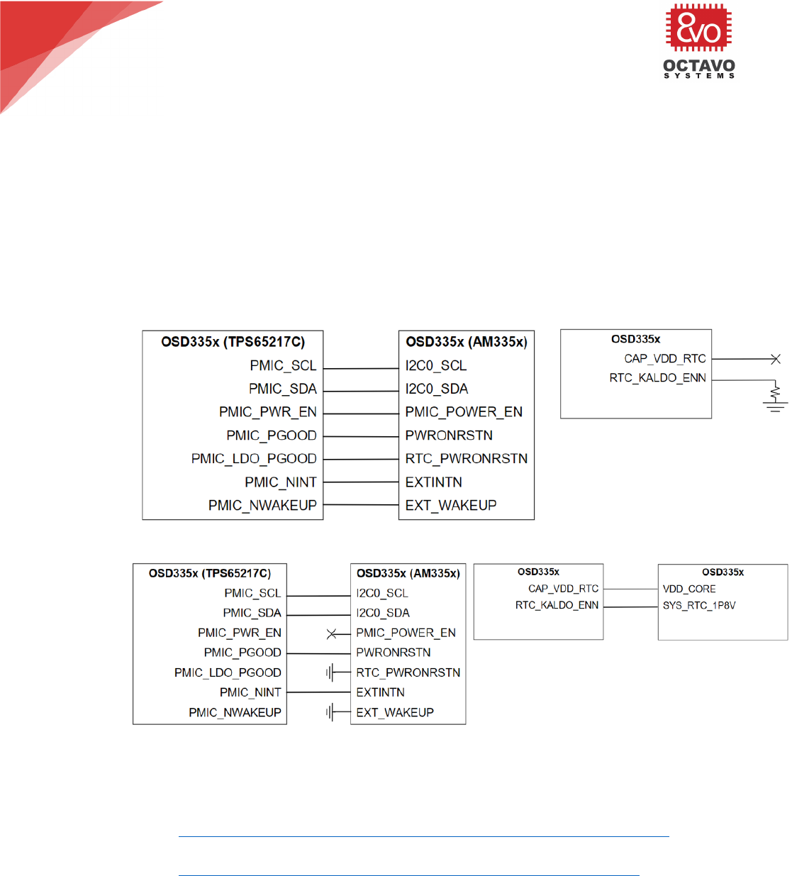
1. There!is!a!minimum!set!of!connections!that!are!required!for!the!OSD335x!family!of!devices!to!
function!properly.!These!signals!are!the!interface!between!the!TPS65217C!PMIC!and!AM335x!
processor!and!are!used!to!properly!configure!and!sequence!the!voltage!rails.!There!are!two!use!
cases!for!hooking!up!these!signals.!First,!the!minimum!connections!required!when!the!RTC!
subsystem!within!the!AM335x!needs!to!be!enabled!is!shown!in!Figure!1.!Second,!the!set!of!
connections!when!the!RTC!subsystem!within!the!AM335x!is!disabled!is!shown!in!Figure!2.!Most!
designs!use!the!connections!shown!in!Figure!1!even!when!the!RTC!subsystem!is!not!used!by!the!
system.!This!is!done!to!future!proof!designs!and!will!enable!the!internal!AM335x!1.8V!LDO!
instead!of!providing!power!directly!from!the!PMIC.!
!
Figure'1.'Minimum'set'of'connections'when'RTC'subsystem'is'enabled'
!
Figure'2.'Minimum'set'of'connections'when'RTC'Subsystem'is'disabled'
2. Make!a!power!budget!that!balances!power!consumption!against!the!various!voltage!supply!rails.!
Please!refer!to!the!following!resources:!
• Power!Application!Note!for!OSD335x-BSM/ISM:!
https://octavosystems.com/app_notes/osd335x-sm-power-application-note/!!
• Power!Application!Note!for!OSD335x-BAS/IND:!!
http://octavosystems.com/app_notes/osd335x-power-application-note/!!
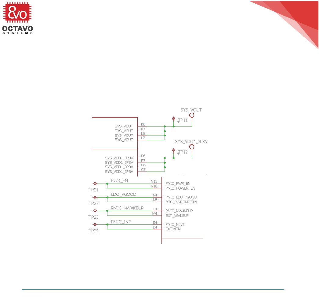
3. If!there!is!space!in!layout,!put!test!points!on!each!power!rail!and!each!signal!between!the!PMIC!
and!AM335x!processor.!!This!will!provide!good!visibility!for!board!debug!during!bring-up.!An!
example!is!shown!in!Figure!3.!A!list!of!recommended!pins!and!signals!are!give!below:!
• Boot!Signals:!!PMIC_POWER_EN,!RTC_PWRONRSTN,!EXT_WAKEUP,!and!EXTINTN!!
!
• Reset!Signals:!!PWRONRSTN,!and!WARMRSTN!
6!
OSD335x Schematic Checklist
Rev.1 5/18/18!
!
!
Octavo!Systems!LLC!
Copyright!2018!
!
• Output!Power!Rails:!!SYS_VOUT,!SYS_VDD1_3P3V,!SYS_VDD2_3P3V,!SYS_RTC_1P8V,!
SYS_VDD3_3P3V!and!SYS_VDD_1P8V!!
!
• !!!!Internal!Power!Rails:!!VDDS_DDR,!VDD_CORE,!VDDS_PLL,!and!VDD_MPU!
!
!
!
!
Figure'3:'Example'test'points'for'signals'involved'in'bootup'and'power'rails'
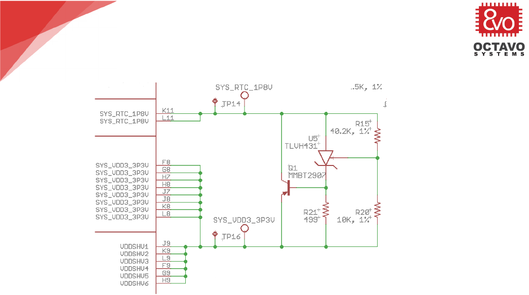
4. Based!on!the!application,!a!clamping!circuit!may!be!needed!between!the!VDDS!and!the!
VDDSHVx!signals!(see!documentation!in!the!application!note!!
https://octavosystems.com/app_notes/osd335x-design-tutorial/bare-minimum-boot/clamping-
circuit/).!VDDS!is!internally!connected!to!SYS_RTC_1P8V!on!the!OSD335x/OSD335x-SM.!The!
VDDSHVx!signals!are!internally!connected!to!VDDSHV_3P3V!on!the!OSD335x!but!are!external!
pins!on!the!OSD335x-SM!and!could!potentially!be!connected!to!SYS_VDD3_3P3V.!If!included,!
make!sure!that!clamping!circuit!is!between!the!correct!voltage!rails!and!has!the!correct!
components.!Figure!4!shows!the!clamping!circuit!design!on!OSD3358-SM-RED.!
7!
OSD335x Schematic Checklist
Rev.1 5/18/18
!
Octavo!Systems!LLC!
Copyright!2018!
!
Figure'4:'Clamping'circuit'between'SYS_RTC_1P8V'and'SYS_VDD3_3P3V'in'OSD3358-SM-RED'schematic'
5. If!you!do!not!plan!to!use!VIN_USB/VIN_BAT!power!inputs,!you!can!follow!section!9.2.2.2!“5-V!
Operation!Without!a!Battery”!in!the!TPS65217!datasheet!
(http://www.ti.com/product/TPS65217).!The!connections!for!this!use!case!are!listed!below:!!
• Ground!VIN_USB!!
• Connect!VIN_BAT!and!PMIC_BAT_SENSE!together;!and!!
• Leave!PMIC_TS!unconnected!
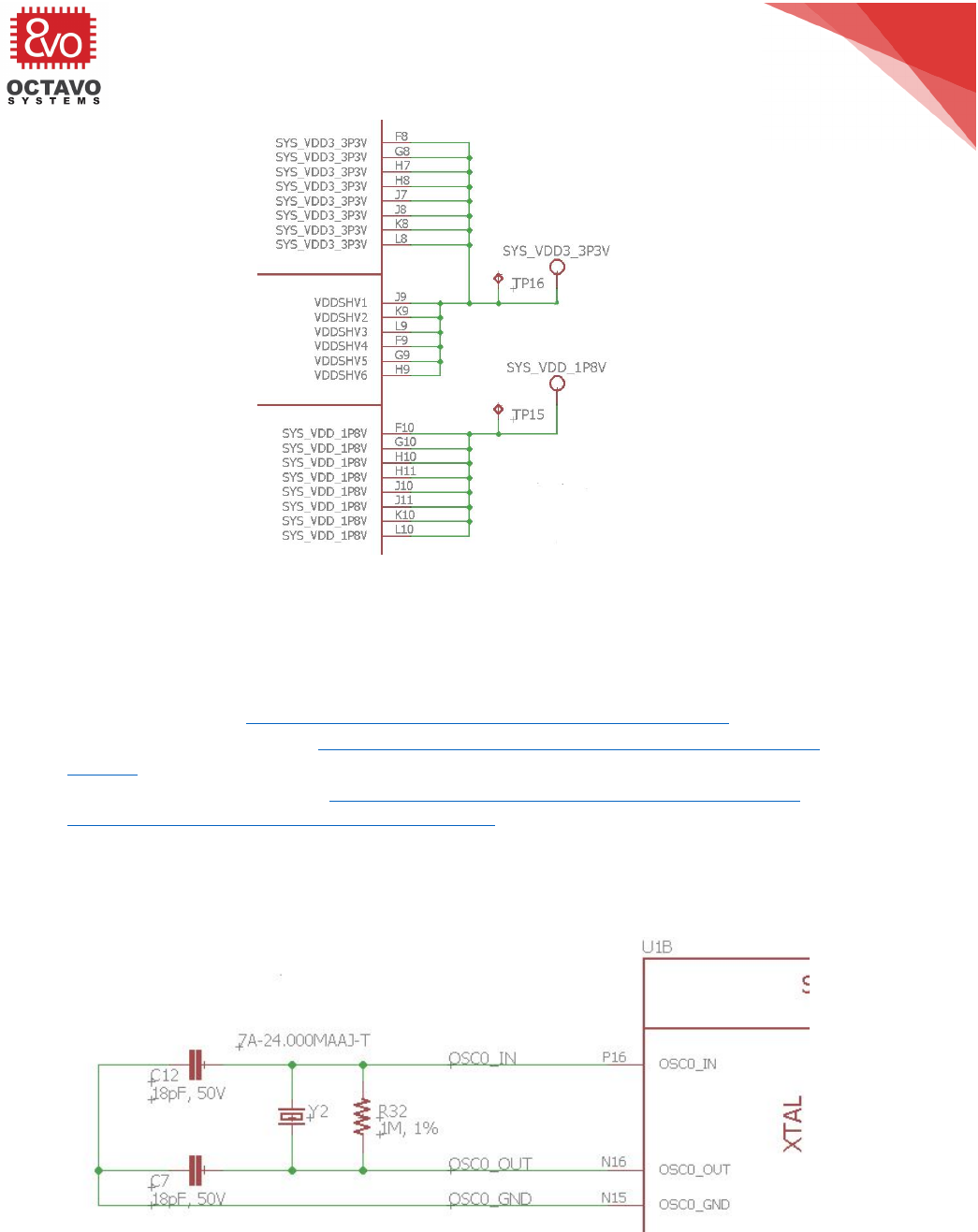
6. The!I/O!pins!of!the!OSD335x-BSM/ISM!are!divided!into!6!voltage!domains.!Each!I/O!pin!group!
can!be!set!as!either!a!3.3!Volt!level!I/O!or!a!1.8!Volt!level!I/O.!Each!of!the!VDDSHVx!pins!need!to!
be!connected!either!a!3.3V!or!a!1.8V!rail!depending!on!the!application.!An!example!where!all!
the!I/O!pin!groups!are!set!to!a!3.3V!level!I/O!is!shown!in!Figure!5.!
7. For!OSD335x-BAS/IND!devices,!the!IO!voltage!level!is!set!to!3.3V!internally.!So,!level!shifters!
would!be!necessary!if!a!different!IO!voltage!level!is!required.!!
8!
OSD335x Schematic Checklist
Rev.1 5/18/18!
!
!
Octavo!Systems!LLC!
Copyright!2018!
!
Figure'5:'Setting'Voltage'level'for'IO'pin'groups'
!
More!information!regarding!power!design!can!be!found!in!the!following!places:!
• OSD335x-BAS/IND!Datasheet:!https://octavosystems.com/docs/osd335x-datasheet/!!
• OSD335x!Design!Tutorial:!https://octavosystems.com/docs/osd335x-design-tutorial/OSD335x-
BSM/ISM!Datasheet:!https://octavosystems.com/docs/osd335x-sm-datasheet/!
• OSD335x-SM!Design!Tutorial:!https://octavosystems.com/app_notes/osd335x-sm-design-
tutorial/!!
• OSD335x!Power!Management:!https://octavosystems.com/app_notes/osd335x-design-
tutorial/bare-minimum-boot/power-management/!!
4 Clocks
1. The!recommended!oscillator!circuit!is!shown!in!the!following!figure.!!This!will!allow!tuning!of!the!
crystal!oscillator!if!needed!and!ensure!proper!operation.!!
!
Figure'6:'Example'crystal'circuit'
9!
OSD335x Schematic Checklist
Rev.1 5/18/18
!
Octavo!Systems!LLC!
Copyright!2018!
2. If!the!RTC!within!the!AM335x!is!not!used,!pins!OSC1_IN,!OSC1_OUT!can!be!left!unconnected!
while!OSC1_GND!should!be!connected!system!ground.!
More!information!regarding!clock!circuit!can!be!found!in!the!following!places:!
• OSD335x-SM!design!tutorial!–!Clock!Circuitry:!https://octavosystems.com/app_notes/osd335x-
design-tutorial/bare-minimum-boot/clock-circuitry/!!
• Section!“Clock!Specifications”!in!AM335x!Datasheet:!
http://www.ti.com/lit/ds/symlink/am3358.pdf!!
5 Reset Circuit
1. There!are!in!general,!3!ways!to!build!the!reset!mechanism!for!OSD335x!devices!covering!a!
majority!of!use!cases.!They!are!described!below:!
• WARMRESETN!used!as!input!and!to!be!asserted!after!stable!power!up:!In!this!use!case,!
the!WARMRESETN!signal!is!pulled!up!to!a!stable!3.3V!rail!that!will!allow!pulling!the!
processor!out!of!reset!once!the!voltage!rail!is!alive.!
• WARMRESETN!used!as!input!driven!by!PWRONRSTN:!In!this!use!case,!either!an!open!
drain!buffer!to!translate!between!1.8V!and!3.3V!or!a!reset!supervisor!are!used.!
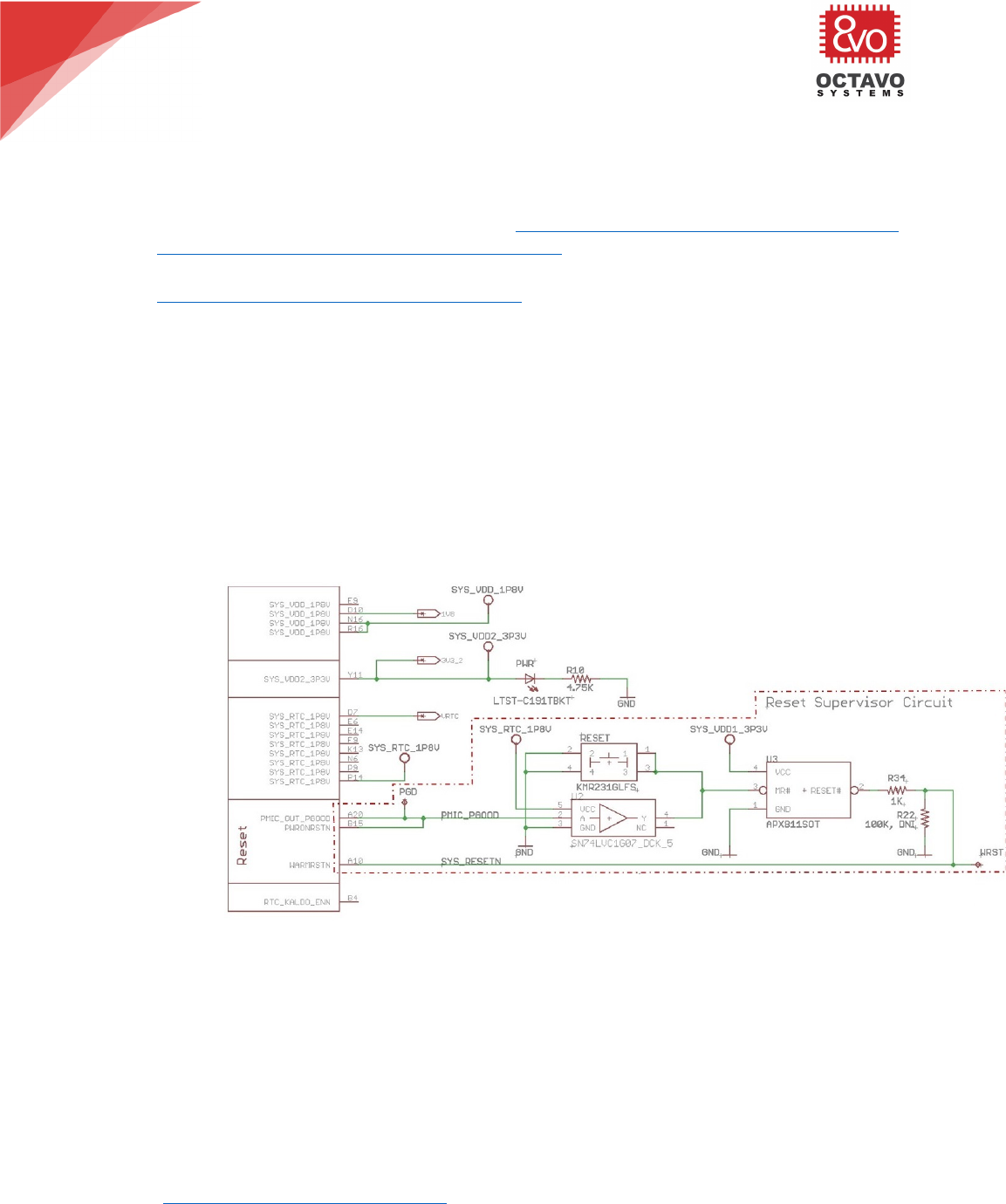
Additionally,!a!reset!button!with!filter!debounce!can!be!added!for!user!input!reset!
function.!This!is!demonstrated!on!OSD3358-SM-RED!and!is!shown!in!Figure!7.!
!
Figure'7:'OSD3358-SM-RED'reset'mechanism'
• WARMRESTN!used!as!output:!In!this!use!case,!the!WARMRESETN!pin!can!be!used!as!an!
output!to!reset!external!devices.!The!signal!output!is!held!low!for!a!period!of!time!after!
cold!reset.!So,!it!can!be!used!to!hold!external!devices!in!reset!a!little!longer!than!the!
processor.!!
6 Other General Recommendations
1. All!pinmux!settings!should!be!verified.!Not!all!pin!combinations!are!valid!for!a!given!peripheral.!!
To!ensure!proper!operation,!all!the!pins!of!a!peripheral!must!belong!to!the!same!I/O!set.!The!
pinmux!settings!can!be!verified!using!the!pinmux!tool!from!Texas!Instruments!
(http://www.ti.com/tool/pinmuxtool).!While!a!given!I/O!has!the!same!functionality!between!the!

10!
OSD335x Schematic Checklist
Rev.1 5/18/18!
!
!
Octavo!Systems!LLC!
Copyright!2018!
AM335x!and!OSD335x!family!of!device,!the!location!of!the!I/O!may!be!different.!!The!location!
mapping!between!the!AM335x,!the!OSD335x-BSM!and!the!OSD335x-BAS!can!be!found!in!the!
application!note!:!OSD335x-SM!Pin!Assignments!Mapped!to!AM335x!
(https://octavosystems.com/app_notes/osd335x-family-pin-assignments/)!!%
2. Unused!IO!peripheral!pins!can!generally!be!left!unconnected!unless!specified!in!the!datasheet.!!
3. If!the!ADC!module!is!not!used,!connect!VREFP,!VREFN,!AIN[7:0]!and!VSSA_ADC!terminals!to!
system!ground.!
4. If!a!USB!interface!is!not!used,!the!corresponding!VBUS,!ID,!DP,!and!DM!terminals!may!be!
connected!to!ground!or!left!floating.!The!CE!terminal!should!be!left!floating.!
7 Peripherals
1. It!is!recommended!to!include!a!22ohm!series!resistor!on!MMCx_CLK!signals,!where!“x”!indicates!
which!MMC!interface!is!used,!0,!1!or!2.!!The!resistor!should!be!placed!as!close!to!the!processor!
as!possible.!The!MMCx_CLK!signal!is!used!as!an!input!on!read!transactions!and!the!resistor!will!
eliminate!possible!reflections!on!the!signal!which!can!cause!false!clock!transitions.!Also!the!
RXACTIVE!bit!in!the!pinmux!configuration!for!the!MMC_CLK!signal!should!be!set!to!‘1’.!When!
connecting!a!device,!such!as!an!SD!card!or!eMMC,!10k!pullups!should!be!included!on!RST#,!
CMD,!and!all!DAT!signals.!Additional!information!regarding!eMMC!connections!is!provided!in!
Section!3.5.2!“eMMC”.!
2. All!I2C!busses!should!be!pulled!up.!!Exception:!!The!I2C0!pins!that!must!be!connected!to!the!
PMIC!I2C!bus!have!4.7K!Ohm!pullups!internal!to!the!OSD335x.!!If!there!are!more!than!2!or!3!
external!devices!on!the!I2C0!bus,!it!is!recommended!to!put!external!pull!up!resistor!footprints!in!
case!the!pull!up!needs!to!be!stronger.!
3. UART!/!RS232!busses!should!have!a!Null!Modem!implemented!between!the!devices!(i.e.!TX!->!
RX;!RX!->!TX;!CTS!->!RTS;!RTS!->!CTS;!DTR!->!DSR;!DSR!->!DTR)!
4. SPI!busses!should!have!the!MISO!lines!connected!together!and!the!MOSI!lines!connected!
together.!!Each!SPI!device!should!have!its!own!chip!select!(CS).!
5. The!USB_ID!pin!should!either!be!pulled!low!to!ground!(host!mode),!left!unconnected!
(peripheral/client!mode)!or!connected!to!a!USB!connector!(OTG!mode).!
6. The!USBx_DP!and!USBx_DM!should!never!have!any!series!resistors!or!capacitance!on!these!
signals.!These!signals!should!be!length!matched!traces!to!the!connector!or!device!with!no!stubs!
or!test!points.!
7. USBx_CE!can!be!used!if!the!device!is!a!peripheral/client!that!supports!charging.!This!signal!
would!be!connected!to!the!enable!of!a!charging!source!for!the!battery.!
8. In!host!mode,!if!an!external!power!regulator!is!being!used!to!provide!power!to!the!USB!
peripherals,!then!the!USBx_DRVVBUS!should!be!connected!to!the!enable!of!the!regulator!so!
that!it!can!be!controlled!by!the!processor.!
9. USBx_VBUS!should!be!connected!to!a!5V!power!rail!for!the!USB!peripheral!to!be!used!as!USB!
host.!
10. While!no!series!resistors!are!required!for!MII/RMII/RGMII,!it!is!prudent!include!Zero-Ohm!
options!for!the!TX!and!RX!lines.!Ideally,!these!optional!resistors!should!be!as!small!as!possible!
(0402!or!smaller!recommended)!and!should!be!placed!as!close!to!the!transmitter!as!possible.!
11. If!a!design!does!not!need!to!be!compatible!with!the!BeagleBoard.org®!BeagleBone®!Cape!
Headers,!there!is!no!need!to!the!resistor!MUXes!on!GPMC_A0!and!GPMC_CSN3!or!
ECAP0_IN_PWM0_OUT!and!MCASP0_ACLKR.!!!

11!
OSD335x Schematic Checklist
Rev.1 5/18/18
!
Octavo!Systems!LLC!
Copyright!2018!
7.1 Boot Configuration Settings
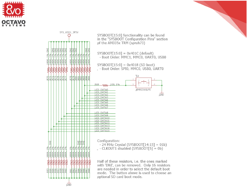
1. Validate!Boot!configuration!settings!
a. SYSBOOT[15:14]!should!be!set!to!match!the!oscillator!frequency!of!OSC0!
b. SYSBOOT[5]!should!be!pulled!high!if!CLKOUT1!is!used.!!Otherwise!it!should!be!pulled!low!
to!disable!CLKOUT1!by!default!and!reduce!system!noise.!
c. SYSBOOT[4:0]!should!be!set!to!select!a!boot!mode!for!the!given!boot!peripheral!
connections!within!the!design!
d. Other!SYSBOOT!pins!should!be!set!based!on!whether!they!are!needed.!!All!un-needed!
SYSBOOT!pins!should!be!pulled!low!and!not!left!floating.!!!
2. Boot!configuration!pins!should!be!generally!pulled!high!or!low!with!weak!(~100K!Ohm)!resistors.!!
However,!stronger!resistors!are!ok!if!needed!by!the!design.!
3. If!SYSBOOT!pins!are!used!as!general!purpose!IO!to!control!other!aspects!of!the!design,!check!
a. There!are!no!stronger!pull-ups!/!pull-downs!in!the!opposite!direction!on!other!parts!of!
the!design..!!!
b. That!the!default!value!generated!by!the!pull-up!/!pull-down!does!not!cause!system!
issues.!
4. Verify!that!the!boot!interface!set!by!the!boot!configuration!pins!uses!the!peripheral!pins!
specified!by!AM335x!Technical!Reference!Manual!Section!Initialization.!Example!boot!
configuration!using!SYSBOOT!pins!is!shown!in!Figure!8.!
More!information!about!boot!configuration!can!be!found!in!the!following!places:!
• AM335x!TRM!“SYSBOOT!Configuration!Pins”:!https://www.ti.com/lit/ug/spruh73p/spruh73p.pdf!!
• OSD335x!Peripheral!Circuitry!tutorial:!https://octavosystems.com/app_notes/osd335x-design-
tutorial/bare-minimum-boot/power-management/!!
12!
OSD335x Schematic Checklist
Rev.1 5/18/18!
!
!
Octavo!Systems!LLC!
Copyright!2018!
!
Figure'8:'Boot'configuration'example(OSD3358-SM-RED)'
7.2 eMMC
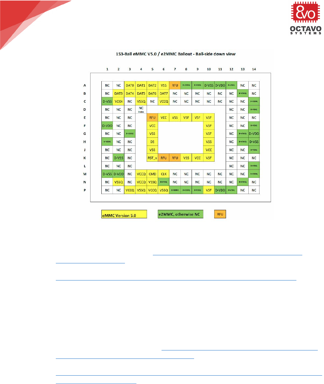
1. The!AM335x!has!a!MMC!v4.3!interface.!!While!there!are!still!eMMC!modules!that!support!MMC!
v4.x,!it!is!more!common!to!see!eMMC!modules!that!support!the!newer!MMC!v5.x!standard,!
which!is!backward!compatible!with!v4.x.!!The!MMC!v4.x!standard!declared!some!pins!as!
“Reserved!for!Future!Use”!(RFU).!!Unfortunately,!in!many!eMMC!v4.x!symbols,!the!RFU!pins!are!
marked!as!“No!Connect”!(NC),!which!have!no!electrical!connection!and!can!be!routed!through!in!
layout.!!Given!the!scarcity!in!the!eMMC!market,!it!is!recommended!to!use!the!eMMC!v5.x!
pinout!(see!the!yellow!and!orange!pins!in!Figure!9)!and!only!connect!the!MMC!v4.x!signals!so!
that!layout!can!be!done!to!support!both!eMMC!types!(i.e.!all!MMC!v5.x!and!RFU!signals!are!not!
routed!through).!
!
13!
OSD335x Schematic Checklist
Rev.1 5/18/18
!
Octavo!Systems!LLC!
Copyright!2018!
!
Figure'9'eMMC'v5.x'pinout'
More!information!about!eMMC!hook-up!is!provided!in!the!following!places:!
• OSD335x!eMMC!Application!Note:!https://octavosystems.com/app_notes/designing-for-
flexibility-around-emmc/!!
• OSD335x!Design!Tutorial!Lesson!2:!Adding!Non-Volatile!Storage:!
https://octavosystems.com/app_notes/osd335x-lesson-2-adding-non-volatile-storage/!!
7.3 JTAG
1. To!properly!connect!JTAG,!EMU0!and!EMU1!pins!must!be!connected!to!the!JTAG!emulator.!!!
2. For!the!standard!20!pin!compact!JTAG!header,!it!is!recommended!to!only!connect!EMU2,!EMU3!
and!EMU4!if!you!plan!to!use!advanced!JTAG!features!(HS-RTDX,!Core!Trace,!System!Trace,!etc.)!
of!higher!end!debuggers.!
More!information!on!JTAG!can!be!found!at!the!following!places:!
• OSD335x!Peripheral!Circuitry!tutorial:!https://octavosystems.com/app_notes/osd335x-design-
tutorial/bare-minimum-boot/peripheral-circuitry/!!
• Texas!Instruments!JTAG!resource:!
http://dev.ti.com/tirex/#/?link=Development%20Tools%2FDebug%20Probes%2FXDS%2FDocum
ents%2FJTAG%20Connectors!!
7.4 EEPROM WP (OSD335x-SM only)
1. The!EEPROM!WP!pin!is!pulled!high!within!the!OSD335x-SM.!!To!program!the!EEPROM,!the!
EEPROM_WP!pin!must!be!pulled!low.!Therefore,!this!pin!should!be!connected!to!a!controller!or!
brought!out!to!a!test!point!or!to!a!header.!!

14!
OSD335x Schematic Checklist
Rev.1 5/18/18!
!
!
Octavo!Systems!LLC!
Copyright!2018!
8 References
For!additional!information,!please!refer!to!the!following!links:!
!
1.!OSD335x!Datasheet:!https://octavosystems.com/docs/osd335x-datasheet/!
2.!OSD335x-SM!Datasheet:!https://octavosystems.com/docs/osd335x-sm-datasheet/!!
3.!AM335x!Schematic!Checklist:!
http://processors.wiki.ti.com/index.php/AM335x_Schematic_Checklist!!
4.!OSD335x!Power!Application!Note:!
!https://octavosystems.com/app_notes/osd335x-sm-power-application-note/!!
5.!OSD335x!Design!Tutorial!Series:!
!https://octavosystems.com/app_notes/osd335x-design-tutorial/!!
6.!AM335x!Datasheet:!http://www.ti.com/lit/ds/symlink/am3358.pdf!!
7.!TPS65217C!PMIC!Datasheet:!http://www.ti.com/lit/ds/symlink/tps65217.pdf!!
8.!Powering!AM335x!with!TPS65217x:!http://www.ti.com/lit/ug/slvu551i/slvu551i.pdf!!
9.!Designing!for!Flexibility!around!eMMC:!!
https://octavosystems.com/app_notes/designing-for-flexibility-around-emmc/!!
!
!
Please!contact!us!on!the!forums!for!assistance!with!any!checklist!items.!!
https://octavosystems.com/forums/!
!
*****!
!
!
