OV7670_IG (1.0) OV7670 Implementation Guide (V1.0)
OV7670OV7171%20CMOS%20VGA%20(640x480)%20CameraChip%20Implementation%20Guide
OV7670%20Implementation%20Guide%20(V1.0)
OV7670%20Implementation%20Guide%20(V1.0)
OV7670%20Implementation%20Guide%20(V1.0)
OV7670%20Implementation%20Guide%20(V1.0)
User Manual: Pdf
Open the PDF directly: View PDF ![]() .
.
Page Count: 64
- 1 Introduction
- 2 Image Sensor Array
- 3 Timing Generator
- 4 Analog Signal Processor
- 5 Digital Signal Processor (DSP)
- 6 Image Scaler
- 7 Digital Video Port
- 8 SCCB Interface
- 9 Prototyping and Evaluation Modules
- 10 Lens selection
- 11 OV7670/OV7171 Bug List
- Appendix A Reference SCCB Settings
APPLICATION NOTE
This document is provided "as is" with no warranties whatsoever, including any warranty of merchantability, non-in-
fringement, fitness for any particular purpose, or any warranty otherwise arising out of any proposal, specification, or
sample.
OmniVision Technologies, Inc. disclaims all liability, including liability for infringement of any proprietary
rights, relating to the use of information in this document. No license, expressed or implied, by estoppel
or otherwise, to any intellectual property rights is granted herein.
* Third-party brands, names, and trademarks are the property of their respective owners.
Note:
The information contained in this document is considered proprietary to OmniVision Technologies, Inc. This
information may be distributed only to individuals or organizations authorized by OmniVision Technologies, Inc. to
receive said information. Individuals and/or organizations are not allowed to re-distribute said information.
O
mni ision
®
OV7670/OV7171 CMOS VGA (640x480) CameraChip™
Implementation Guide
Last Modified: 2 September 2005
Document Version: 1.0
Revision Number Date Revision
1.0 09/02/05 Initial Release

2Proprietary to OmniVision Technologies Version 1.0, September 2, 2005
OV7670/OV7171 CMOS VGA (640x480) CameraChip™ Omni ision
00Table of Contents
Section 1, Introduction . . . . . . . . . . . . . . . . . . . . . . . . . . . . . . . . . . . . . . . . . . . . . . . . . . . . . . . . . . . . . 7
1.1 Function Description . . . . . . . . . . . . . . . . . . . . . . . . . . . . . . . . . . . . . . . . . . . . . . . . 7
Section 2, Image Sensor Array. . . . . . . . . . . . . . . . . . . . . . . . . . . . . . . . . . . . . . . . . . . . . . . . . . . . . . 8
2.1 Resolution Formats . . . . . . . . . . . . . . . . . . . . . . . . . . . . . . . . . . . . . . . . . . . . . . . . . 8
Section 3, Timing Generator . . . . . . . . . . . . . . . . . . . . . . . . . . . . . . . . . . . . . . . . . . . . . . . . . . . . . . . 12
3.1 Array Control. . . . . . . . . . . . . . . . . . . . . . . . . . . . . . . . . . . . . . . . . . . . . . . . . . . . . . 12
3.2 Frame Rate Timing. . . . . . . . . . . . . . . . . . . . . . . . . . . . . . . . . . . . . . . . . . . . . . . . . 12
3.2.1 Clock Pre-scalar. . . . . . . . . . . . . . . . . . . . . . . . . . . . . . . . . . . . . . . . . . . 12
3.2.2 Dummy Pixel Adjustment . . . . . . . . . . . . . . . . . . . . . . . . . . . . . . . . . . . 13
3.2.3 Dummy Row Adjustment . . . . . . . . . . . . . . . . . . . . . . . . . . . . . . . . . . . 13
3.3 Exposure Control . . . . . . . . . . . . . . . . . . . . . . . . . . . . . . . . . . . . . . . . . . . . . . . . . . 14
3.3.1 Exposure Time . . . . . . . . . . . . . . . . . . . . . . . . . . . . . . . . . . . . . . . . . . . . 14
3.3.2 Banding Filter . . . . . . . . . . . . . . . . . . . . . . . . . . . . . . . . . . . . . . . . . . . . . 15
3.3.3 Manual Exposure Control . . . . . . . . . . . . . . . . . . . . . . . . . . . . . . . . . . . 16
3.3.4 Automatic Exposure Control Mode (AEC) . . . . . . . . . . . . . . . . . . . . . 16
3.4 External Timing Output . . . . . . . . . . . . . . . . . . . . . . . . . . . . . . . . . . . . . . . . . . . . . 20
3.4.1 Sync Signal . . . . . . . . . . . . . . . . . . . . . . . . . . . . . . . . . . . . . . . . . . . . . . . 20
3.4.2 Strobe Signal . . . . . . . . . . . . . . . . . . . . . . . . . . . . . . . . . . . . . . . . . . . . . 21
Section 4, Analog Signal Processor. . . . . . . . . . . . . . . . . . . . . . . . . . . . . . . . . . . . . . . . . . . . . . . . . 25
4.1 Gain Control . . . . . . . . . . . . . . . . . . . . . . . . . . . . . . . . . . . . . . . . . . . . . . . . . . . . . . 25
4.1.1 Manual Gain Control . . . . . . . . . . . . . . . . . . . . . . . . . . . . . . . . . . . . . . . 25
4.1.2 Automatic Gain Control (AGC). . . . . . . . . . . . . . . . . . . . . . . . . . . . . . . 27
4.2 Black Level Calibration . . . . . . . . . . . . . . . . . . . . . . . . . . . . . . . . . . . . . . . . . . . . . 28
4.2.1 Automatic Black Level Calibration (ABLC) . . . . . . . . . . . . . . . . . . . . . 28
4.2.2 Manual Black Level Calibration . . . . . . . . . . . . . . . . . . . . . . . . . . . . . . 28
Section 5, Digital Signal Processor (DSP) . . . . . . . . . . . . . . . . . . . . . . . . . . . . . . . . . . . . . . . . . . . 29
5.1 White Balance Control. . . . . . . . . . . . . . . . . . . . . . . . . . . . . . . . . . . . . . . . . . . . . . 29
5.1.1 Automatic White Balance Control . . . . . . . . . . . . . . . . . . . . . . . . . . . . 30
5.1.2 Manual White Balance . . . . . . . . . . . . . . . . . . . . . . . . . . . . . . . . . . . . . 30
5.2 Gamma Control . . . . . . . . . . . . . . . . . . . . . . . . . . . . . . . . . . . . . . . . . . . . . . . . . . . 31
5.2.1 Gamma Slope Calculation . . . . . . . . . . . . . . . . . . . . . . . . . . . . . . . . . . 32

Version 1.0, September 2, 2005 Proprietary to OmniVision Technologies 3
Omni ision
5.3 Color Matrix. . . . . . . . . . . . . . . . . . . . . . . . . . . . . . . . . . . . . . . . . . . . . . . . . . . . . . . 32
5.3.1 Color Matrix Control. . . . . . . . . . . . . . . . . . . . . . . . . . . . . . . . . . . . . . . . 32
5.4 Sharpness Control . . . . . . . . . . . . . . . . . . . . . . . . . . . . . . . . . . . . . . . . . . . . . . . . . 34
5.5 De-Noise . . . . . . . . . . . . . . . . . . . . . . . . . . . . . . . . . . . . . . . . . . . . . . . . . . . . . . . . . 34
5.6 Auto Color Saturation Adjustment . . . . . . . . . . . . . . . . . . . . . . . . . . . . . . . . . . . . 35
5.7 Defect Pixel Correction . . . . . . . . . . . . . . . . . . . . . . . . . . . . . . . . . . . . . . . . . . . . . 35
5.8 Lens Correction . . . . . . . . . . . . . . . . . . . . . . . . . . . . . . . . . . . . . . . . . . . . . . . . . . . 35
5.9 Brightness and Contrast Control . . . . . . . . . . . . . . . . . . . . . . . . . . . . . . . . . . . . . 37
Section 6, Image Scaler. . . . . . . . . . . . . . . . . . . . . . . . . . . . . . . . . . . . . . . . . . . . . . . . . . . . . . . . . . . 38
6.1 Image Scaling . . . . . . . . . . . . . . . . . . . . . . . . . . . . . . . . . . . . . . . . . . . . . . . . . . . . . 38
6.2 Pixel Clock Divider . . . . . . . . . . . . . . . . . . . . . . . . . . . . . . . . . . . . . . . . . . . . . . . . . 40
6.3 Pixel Clock Delay . . . . . . . . . . . . . . . . . . . . . . . . . . . . . . . . . . . . . . . . . . . . . . . . . . 40
6.4 Horizontal/Vertical Scaling Ratio . . . . . . . . . . . . . . . . . . . . . . . . . . . . . . . . . . . . . 40
6.5 Windowing. . . . . . . . . . . . . . . . . . . . . . . . . . . . . . . . . . . . . . . . . . . . . . . . . . . . . . . . 41
6.6 Data Formatting . . . . . . . . . . . . . . . . . . . . . . . . . . . . . . . . . . . . . . . . . . . . . . . . . . . 42
Section 7, Digital Video Port . . . . . . . . . . . . . . . . . . . . . . . . . . . . . . . . . . . . . . . . . . . . . . . . . . . . . . . 43
7.1 Drive Current. . . . . . . . . . . . . . . . . . . . . . . . . . . . . . . . . . . . . . . . . . . . . . . . . . . . . . 43
7.2 Tri-state Enable . . . . . . . . . . . . . . . . . . . . . . . . . . . . . . . . . . . . . . . . . . . . . . . . . . . 43
Section 8, SCCB Interface. . . . . . . . . . . . . . . . . . . . . . . . . . . . . . . . . . . . . . . . . . . . . . . . . . . . . . . . . 44
8.1 Control Functions . . . . . . . . . . . . . . . . . . . . . . . . . . . . . . . . . . . . . . . . . . . . . . . . . . 44
8.1.1 Register Reset . . . . . . . . . . . . . . . . . . . . . . . . . . . . . . . . . . . . . . . . . . . . 44
8.1.2 Standby Mode Enable . . . . . . . . . . . . . . . . . . . . . . . . . . . . . . . . . . . . . . 44
8.2 Register Set . . . . . . . . . . . . . . . . . . . . . . . . . . . . . . . . . . . . . . . . . . . . . . . . . . . . . . 45
Section 9, Prototyping and Evaluation Modules. . . . . . . . . . . . . . . . . . . . . . . . . . . . . . . . . . . . . . . 63
9.1 OV7670/OV7171EAA Prototyping Module . . . . . . . . . . . . . . . . . . . . . . . . . . . . . 63
9.2 OV7670/OV7171ECX USB 2.0 Evaluation Module. . . . . . . . . . . . . . . . . . . . . . 63
Section 10, Lens selection. . . . . . . . . . . . . . . . . . . . . . . . . . . . . . . . . . . . . . . . . . . . . . . . . . . . . . . . . 63
Section 11, OV7670/OV7171 Bug List. . . . . . . . . . . . . . . . . . . . . . . . . . . . . . . . . . . . . . . . . . . . . . . 63
Appendix A, Reference SCCB Settings. . . . . . . . . . . . . . . . . . . . . . . . . . . . . . . . . . . . . . . . . . . . . . 64

4Proprietary to OmniVision Technologies Version 1.0, September 2, 2005
OV7670/OV7171 CMOS VGA (640x480) CameraChip™ Omni ision
00List of Figures
Figure 1-1 OV7670/OV7171 Functional Block Diagram . . . . . . . . . . . . . . . . . . . . . . . . . . . . . . . 7
Figure 3-1 Average-based AEC/AGC . . . . . . . . . . . . . . . . . . . . . . . . . . . . . . . . . . . . . . . . . . . . . . 17
Figure 3-2 Histogram-Based AEC Control . . . . . . . . . . . . . . . . . . . . . . . . . . . . . . . . . . . . . . . . . . 18
Figure 3-3 Xenon Flash Mode . . . . . . . . . . . . . . . . . . . . . . . . . . . . . . . . . . . . . . . . . . . . . . . . . . . . 22
Figure 3-4 LED 1 Mode – One Pulse Output. . . . . . . . . . . . . . . . . . . . . . . . . . . . . . . . . . . . . . . . 23
Figure 3-5 LED 1 Mode – Multiple Pulse Output. . . . . . . . . . . . . . . . . . . . . . . . . . . . . . . . . . . . . 23
Figure 3-6 LED 2 Mode. . . . . . . . . . . . . . . . . . . . . . . . . . . . . . . . . . . . . . . . . . . . . . . . . . . . . . . . . . 24
Figure 5-1 Gamma Curve . . . . . . . . . . . . . . . . . . . . . . . . . . . . . . . . . . . . . . . . . . . . . . . . . . . . . . . . 31
Figure 5-2 Lens Correction. . . . . . . . . . . . . . . . . . . . . . . . . . . . . . . . . . . . . . . . . . . . . . . . . . . . . . . 35
Figure 6-1 Image Scaling Circuit . . . . . . . . . . . . . . . . . . . . . . . . . . . . . . . . . . . . . . . . . . . . . . . . . . 38
Figure 6-2 Example of Windowing . . . . . . . . . . . . . . . . . . . . . . . . . . . . . . . . . . . . . . . . . . . . . . . . 41
Figure 6-3 MSB/LSB Output Data Swap . . . . . . . . . . . . . . . . . . . . . . . . . . . . . . . . . . . . . . . . . . . 42

Version 1.0, September 2, 2005 Proprietary to OmniVision Technologies 5
Omni ision
00List of Tables
Table 2-1 OV7670/OV7171 Output Formats . . . . . . . . . . . . . . . . . . . . . . . . . . . . . . . . . . . . . . . . 8
Table 2-2 Resolution Register Settings. . . . . . . . . . . . . . . . . . . . . . . . . . . . . . . . . . . . . . . . . . . . . 9
Table 3-1 Scan Direction Control . . . . . . . . . . . . . . . . . . . . . . . . . . . . . . . . . . . . . . . . . . . . . . . . . 12
Table 3-2 Clock Pre-Scalar Control . . . . . . . . . . . . . . . . . . . . . . . . . . . . . . . . . . . . . . . . . . . . . . . 13
Table 3-3 VGA Frame Rate . . . . . . . . . . . . . . . . . . . . . . . . . . . . . . . . . . . . . . . . . . . . . . . . . . . . . 13
Table 3-4 Dummy Pixel and Row. . . . . . . . . . . . . . . . . . . . . . . . . . . . . . . . . . . . . . . . . . . . . . . . . 14
Table 3-5 Exposure and Banding Filter. . . . . . . . . . . . . . . . . . . . . . . . . . . . . . . . . . . . . . . . . . . . 15
Table 3-6 Exposure Control Mode . . . . . . . . . . . . . . . . . . . . . . . . . . . . . . . . . . . . . . . . . . . . . . . . 17
Table 3-7 Average-based AEC/AGC Registers . . . . . . . . . . . . . . . . . . . . . . . . . . . . . . . . . . . . . 17
Table 3-8 Histogram-based AEC Related Registers. . . . . . . . . . . . . . . . . . . . . . . . . . . . . . . . . 18
Table 3-9 Histogram-based AEC Algorithm Adjustment Controls. . . . . . . . . . . . . . . . . . . . . . 19
Table 3-10 Sync Signal Related Registers . . . . . . . . . . . . . . . . . . . . . . . . . . . . . . . . . . . . . . . . . . 20
Table 3-11 Flashlight Modes. . . . . . . . . . . . . . . . . . . . . . . . . . . . . . . . . . . . . . . . . . . . . . . . . . . . . . 21
Table 3-12 Xenon Flash Pulse Width Control . . . . . . . . . . . . . . . . . . . . . . . . . . . . . . . . . . . . . . . 22
Table 4-1 Total Gain to Control Bit Correlation. . . . . . . . . . . . . . . . . . . . . . . . . . . . . . . . . . . . . . 26
Table 4-2 AGC General Controls . . . . . . . . . . . . . . . . . . . . . . . . . . . . . . . . . . . . . . . . . . . . . . . . . 27
Table 4-3 ABLC Control Registers. . . . . . . . . . . . . . . . . . . . . . . . . . . . . . . . . . . . . . . . . . . . . . . . 28
Table 5-1 White Balance Control Registers . . . . . . . . . . . . . . . . . . . . . . . . . . . . . . . . . . . . . . . . 29
Table 5-2 AWB Control Registers . . . . . . . . . . . . . . . . . . . . . . . . . . . . . . . . . . . . . . . . . . . . . . . . 30
Table 5-3 Gamma Related Registers and Parameters. . . . . . . . . . . . . . . . . . . . . . . . . . . . . . . 31
Table 5-4 Color Matrix Related Registers and Parameters . . . . . . . . . . . . . . . . . . . . . . . . . . . 33
Table 5-5 Sharpness Control Registers . . . . . . . . . . . . . . . . . . . . . . . . . . . . . . . . . . . . . . . . . . . 34
Table 5-6 De-Noise Related Registers and Parameters . . . . . . . . . . . . . . . . . . . . . . . . . . . . . 34
Table 5-7 Auto Color Saturation Adjustment Related Registers . . . . . . . . . . . . . . . . . . . . . . . 35
Table 5-8 Lens Shading Correction Registers and Parameters . . . . . . . . . . . . . . . . . . . . . . . 36
Table 5-9 Brightness and Contrast Related Registers . . . . . . . . . . . . . . . . . . . . . . . . . . . . . . . 37
Table 6-1 Image Scaling Control Related Registers and Parameters . . . . . . . . . . . . . . . . . . 39
Table 6-2 Down Sampling Control Related Registers and Parameters . . . . . . . . . . . . . . . . . 39
Table 6-3 Pixel Clock Divider . . . . . . . . . . . . . . . . . . . . . . . . . . . . . . . . . . . . . . . . . . . . . . . . . . . . 40
Table 6-4 Windowing Control Registers . . . . . . . . . . . . . . . . . . . . . . . . . . . . . . . . . . . . . . . . . . . 41

6Proprietary to OmniVision Technologies Version 1.0, September 2, 2005
OV7670/OV7171 CMOS VGA (640x480) CameraChip™ Omni ision
Table 6-5 RGB555 and RGB565 Output Format Controls . . . . . . . . . . . . . . . . . . . . . . . . . . . . 42
Table 7-1 Output Drive Current . . . . . . . . . . . . . . . . . . . . . . . . . . . . . . . . . . . . . . . . . . . . . . . . . . 43
Table 7-2 Tri-State Enable . . . . . . . . . . . . . . . . . . . . . . . . . . . . . . . . . . . . . . . . . . . . . . . . . . . . . . 43
Table 8-1 SCCB Control Functions . . . . . . . . . . . . . . . . . . . . . . . . . . . . . . . . . . . . . . . . . . . . . . . 44
Table 8-2 Device Control Register List . . . . . . . . . . . . . . . . . . . . . . . . . . . . . . . . . . . . . . . . . . . . 45
Introduction
Version 1.0, September 2, 2005 Proprietary to OmniVision Technologies 7
Omni ision
1 Introduction
This general application note is provided as a brief overview of the settings required for
programming the OV7670/OV7171 CAMERACHIPTM. The Implementation Guide supplies the design
engineer with quick-start tips for successful design solutions.
The OV7670/OV7171 Datasheet provides complete information on the features, pin descriptions,
and registers of the OV7670/OV7171. The Implementation Guide is intended to complement the
OV7670/OV7171 Datasheet with considerations for PCB layout, register configurations, and timing
parameters for rapid product design and deployment.
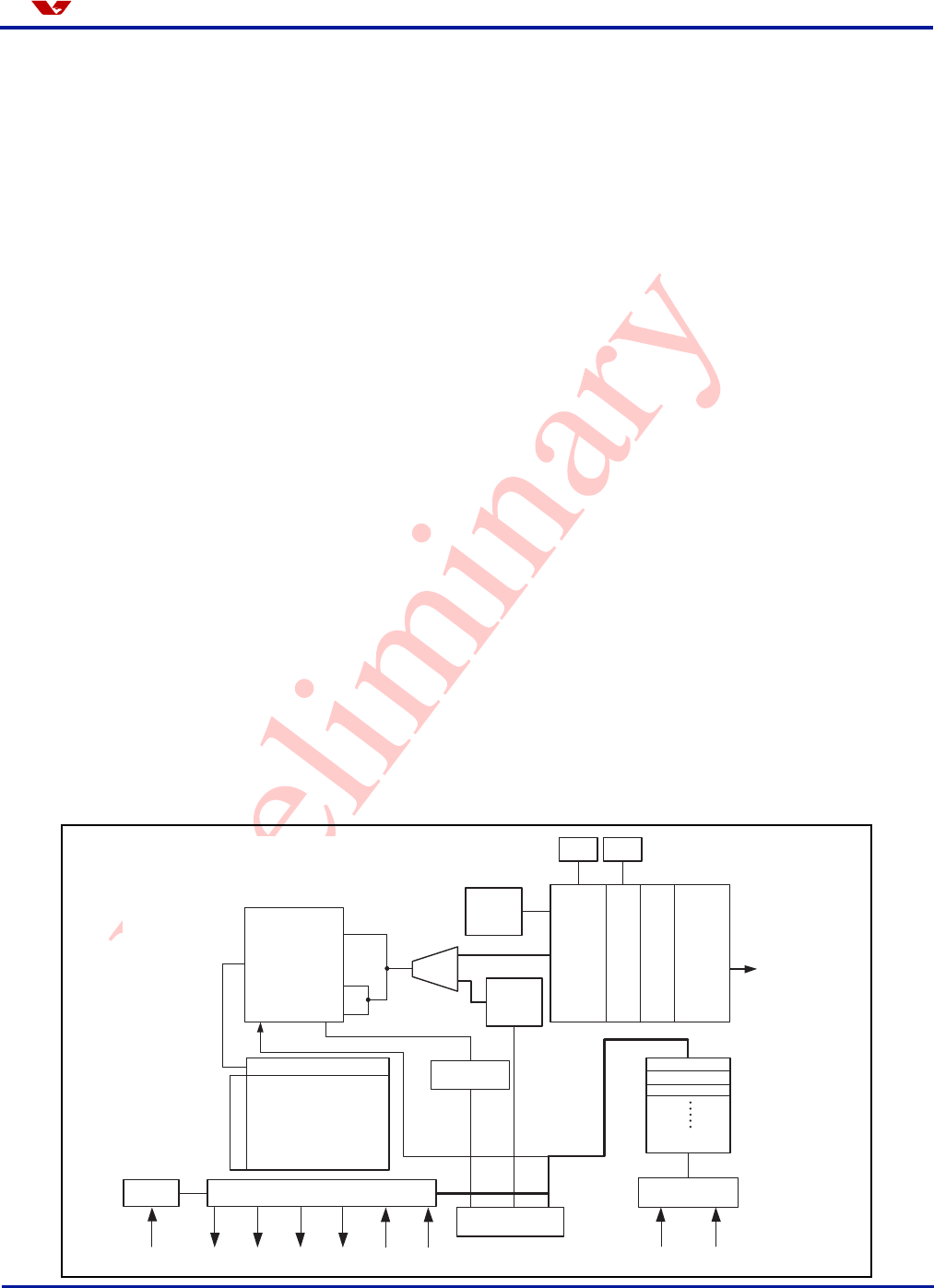
1.1 Function Description
Figure 1-1 shows the functional block diagram of the OV7670/OV7171 image sensor. The
OV7670/OV7171 includes:
•Image Sensor Array (656 x 488 pixels total, including dummy pixels)
•Analog Signal Processor
• A/D Converters
•Digital Signal Processor (DSP)
•Timing Generator
• Light Frequency Auto Detection
• Test Pattern Generator
•Image Scaler
•Digital Video Port
• Exposure/Gain Control
•SCCB Interface
Figure 1-1 OV7670/OV7171 Functional Block Diagram
A/D
G
D[7:0]
B
R50/60 Hz
Auto
Detect
Test
Pattern
Generator
Video
Port
Image
Scaler
DSP
Buffer Buffer
(Lens shading
correction,
de-noise, white/
black pixel
correction, auto
white balance,
etc.)
FIFO
Analog
Processing
Image Array
(656 x 488)
Column Sense Amp Exposure/Gain
Detect
Exposure/Gain
Control
SCCB
Interface
Registers
Video Timing GeneratorClock
SIO_C SIO_D
STROBE PWDNRESETVSYNCPCLKHREFXCLK
Row Select
8Proprietary to OmniVision Technologies Version 1.0, September 2, 2005
OV7670/OV7171 CMOS VGA (640x480) CameraChip™ Omni ision
2 Image Sensor Array
The OV7670/OV7171 CAMERACHIPS has an image array size of 656 columns by 488 rows (320,128
pixels).
The pixel cells themselves are identical, but have RGB color filters arranged in a row-alternating
BG/GR Bayer Pattern. The final YUV/YCbCr image uses this filter pattern to interpolate each pixel's
BG or GR color from the light striking the cell directly, as well as from the light striking the
surrounding cells. The 'Raw Bayer RGB' image does not have any image processing.
The OV7670/OV7171 supports Raw Bayer RGB, processed Bayer RGB, YUV/CbCr, GRB, and
RGB555/565 format. GRB and RGB555/565 formats are converted from YUV/YCbCr. Table 2-1
lists all OV7670/OV7171 output formats.
2.1 Resolution Formats
In Raw Bayer RGB format, the OV7670/OV7171 CAMERACHIP supports VGA resolution. In
Processed Bayer RGB format, the OV7670/OV7171 CAMERACHIP supports VGA and QVGA
resolution. In YUV/YCbCr, GRB and RGB555/565 format, the OV7670/OV7171 CAMERACHIP
supports VGA (640x480) and any resolution below CIF using the Image Scaler.
The OV7670/OV7171 CAMERACHIP also has a set of pre-defined Scaler settings for QVGA, CIF and
QCIF resolutions. Setting registers COM7[4] (0x12), COM7[5], and COM7[3] to 1 selects these
pre-defined resolution, respectively. To manually change the pre-defined scalar settings, set
registers COM14[3] (0x3E) and SCALING_PCLK_ DELAY[7] (0xA2). After selecting the desired
resolution, the output window settings (registers HSTART (0x17), HSTOP (0x18), HREF[5:0]
(0x32), VSTRT (0x19), VSTOP (0x1A) and VREF[3:0] (0x03)) must be adjusted appropriately. To
adjust these settings, set register TSLB[0] (0x3A) to 0.
Table 2-2 provides the Scaler settings for most common resolutions. Refer to the section “Image
Scaler” on page 38 for more details.
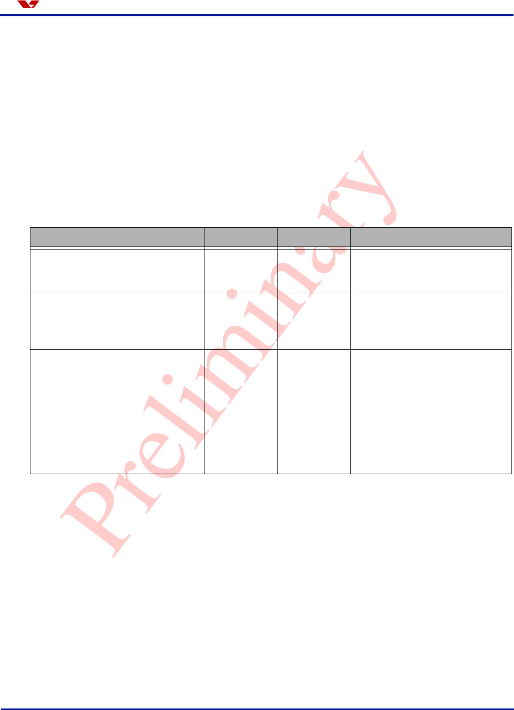
Table 2-1. OV7670/OV7171 Output Formats
Format Pixel Data Output
Register Settings
COM7[2] COM7[0] COM15[5] COM15[4]
Raw Bayer RGB 8-bit R or 8-bit G or 8-bit B 0 1 x 0
Processed Bayer
RGB 8-bit R or 8-bit G or 8-bit B 1 1 x 0
YUV/YCbCr 4:2:2 8-bit Y, 8-bit U or 8-bit Y, 8-bit V 0 0 x 0
GRB 4:2:2 8-bit G, 8-bit R or 8-bit G, 8-bit B 1 0 x 0
RGB565 5-bit R, 6-bit G, 5-bit B 1 0 0 1
RGB555 5-bit R, 5-bit G, 5-bit B 1 0 1 1

Image Sensor Array
Version 1.0, September 2, 2005 Proprietary to OmniVision Technologies 9
Omni ision
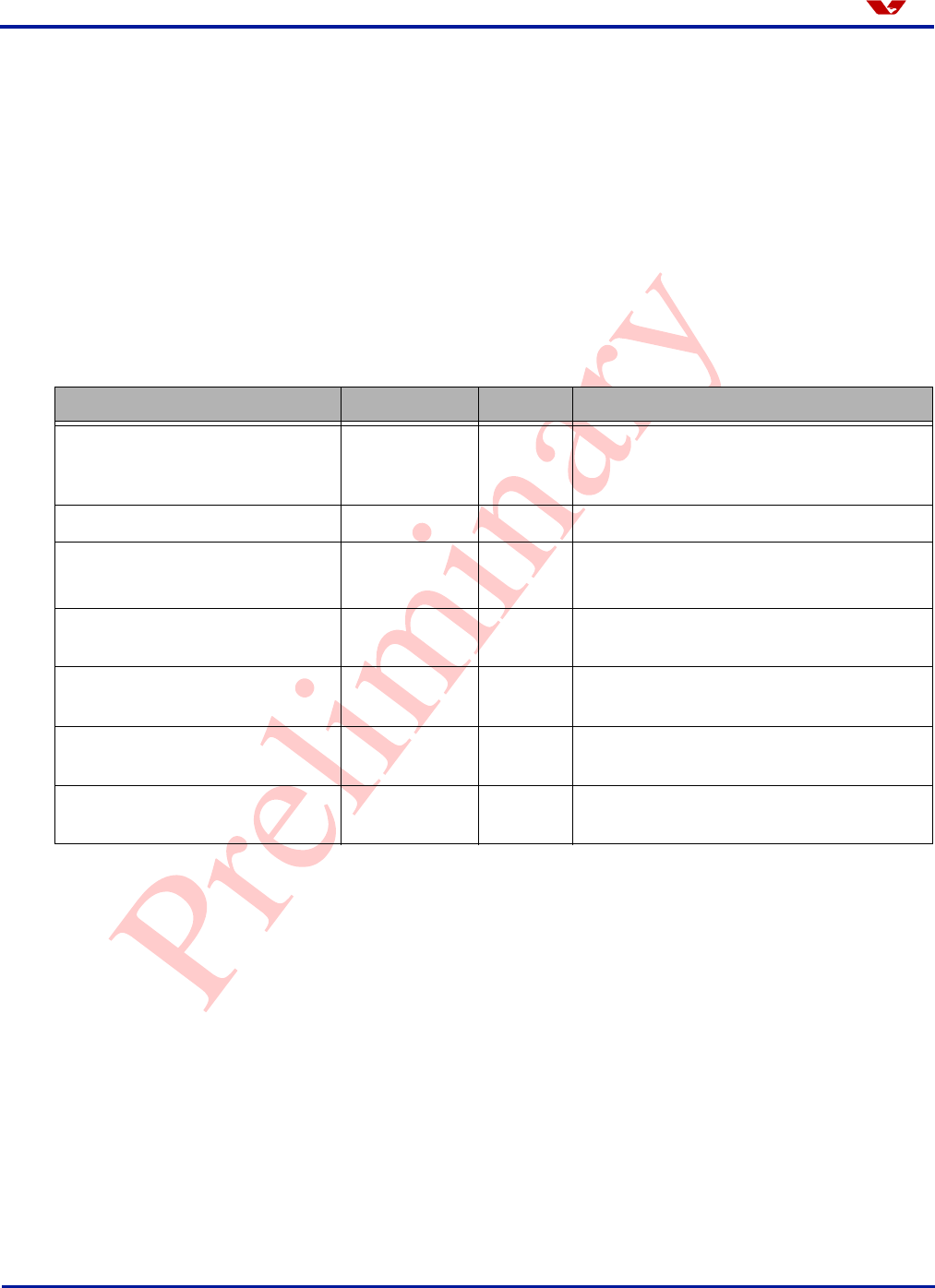
Table 2-2. Resolution Register Settings (Sheet 1 of 3)
Resolution Register Address Value Description
(24 MHz Input Clock)
VGA
CLKRC 0x11 0x01
30 fps VGA YUV mode
COM7 0x12 0x00
COM3 0x0C 0x00
COM14 0x3E 0x00
SCALING_XSC 0x70 0x3A
SCALING_YSC 0x71 0x35
SCALING_DCWCTR 0x72 0x11
SCALING_PCLK_DIV 0x73 0xF0
SCALING_PCLK_ DELAY 0xA2 0x02
QVGA
CLKRC 0x11 0x01
30 fps QVGA YUV mode
COM7 0x12 0x00
COM3 0x0C 0x04
COM14 0x3E 0x19
SCALING_XSC 0x70 0x3A
SCALING_YSC 0x71 0x35
SCALING_DCWCTR 0x72 0x11
SCALING_PCLK_DIV 0x73 0xF1
SCALING_PCLK_ DELAY 0xA2 0x02
QQVGA
CLKRC 0x11 0x01
30 fps QQVGA YUV mode
COM7 0x12 0x00
COM3 0x0C 0x04
COM14 0x3E 0x1A
SCALING_XSC 0x70 0x3A
SCALING_YSC 0x71 0x35
SCALING_DCWCTR 0x72 0x22
SCALING_PCLK_DIV 0x73 0xF2
SCALING_PCLK_ DELAY 0xA2 0x02

10 Proprietary to OmniVision Technologies Version 1.0, September 2, 2005
OV7670/OV7171 CMOS VGA (640x480) CameraChip™ Omni ision
CIF
CLKRC 0x11 0x01
30 fps CIF YUV mode
COM7 0x12 0x00
COM3 0x0C 0x08
COM14 0x3E 0x11
SCALING_XSC 0x70 0x3A
SCALING_YSC 0x71 0x35
SCALING_DCWCTR 0x72 0x11
SCALING_PCLK_DIV 0x73 0xF1
SCALING_PCLK_ DELAY 0xA2 0x02
QCIF
CLKRC 0x11 0x01
30 fps QCIF YUV mode
COM7 0x12 0x00
COM3 0x0C 0x0C
COM14 0x3E 0x11
SCALING_XSC 0x70 0x3A
SCALING_YSC 0x71 0x35
SCALING_DCWCTR 0x72 0x11
SCALING_PCLK_DIV 0x73 0xF1
SCALING_PCLK_ DELAY 0xA2 0x52
QQCIF
CLKRC 0x11 0x01
30 fps QQCIF YUV mode
COM7 0x12 0x00
COM3 0x0C 0x0C
COM14 0x3E 0x12
SCALING_XSC 0x70 0x3A
SCALING_YSC 0x71 0x35
SCALING_DCWCTR 0x72 0x22
SCALING_PCLK_DIV 0x73 0xF2
SCALING_PCLK_ DELAY 0xA2 0x2A
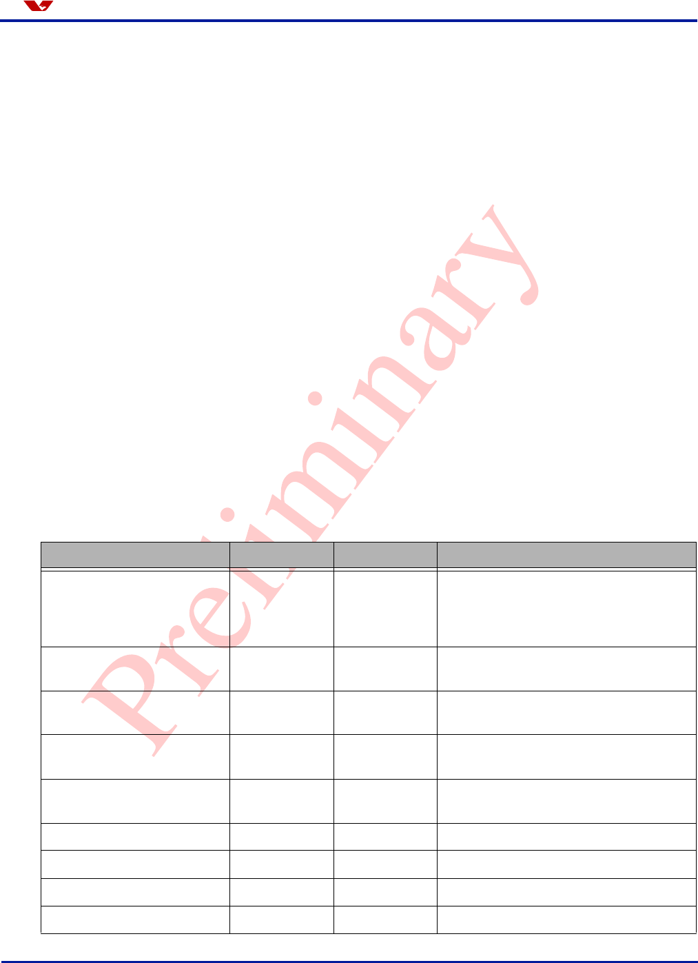
Table 2-2. Resolution Register Settings (Sheet 2 of 3)
Resolution Register Address Value Description
(24 MHz Input Clock)
Image Sensor Array
Version 1.0, September 2, 2005 Proprietary to OmniVision Technologies 11
Omni ision
VGA
CLKRC 0x11 0x01
30 fps VGA Raw Bayer
RGB mode
COM7 0x12 0x01
COM3 0x0C 0x00
COM14 0x3E 0x00
SCALING_XSC 0x70 0x3A
SCALING_YSC 0x71 0x35
SCALING_DCWCTR 0x72 0x11
SCALING_PCLK_DIV 0x73 0xF0
SCALING_PCLK_ DELAY 0xA2 0x02
QVGA
CLKRC 0x11 0x01
30 fps QVGA Processed
Bayer RGB mode
COM7 0x12 0x11
COM3 0x0C 0x04
COM14 0x3E 0x1A
SCALING_XSC 0x70 0x3A
SCALING_YSC 0x71 0x35
SCALING_DCWCTR 0x72 0x11
SCALING_PCLK_DIV 0x73 0xF9
SCALING_PCLK_ DELAY 0xA2 0x02
Table 2-2. Resolution Register Settings (Sheet 3 of 3)
Resolution Register Address Value Description
(24 MHz Input Clock)
12 Proprietary to OmniVision Technologies Version 1.0, September 2, 2005
OV7670/OV7171 CMOS VGA (640x480) CameraChip™ Omni ision
3Timing Generator
In general, the timing generator controls the following functions:
•Array Control
•Frame Rate Timing
•Exposure Control
• External timing outputs (VSYNC, HREF/HSYNC, PCLK, and STROBE)
3.1 Array Control
The OV7670/OV7171 CAMERACHIP progressively scans the array in which rows are sequentially
read and transferred out to the Analog Processing Block (APB). The 'Raw Bayer RGB' and
'Processed Bayer RGB' output preserves the Bayer Filter pattern, so odd rows follow the pattern
(BG) and even rows follow the pattern (GR). The sensor array always outputs VGA resolution and
all resolutions below VGA are down-scaled from VGA in digital domain.
The scan direction is controlled by register MVFP[5:4] (0x1E) as shown in Tab le 3 -1.
3.2 Frame Rate Timing
The OV7670/OV7171 offers three methods of frame rate adjustment:
•Clock Pre-scalar
•Dummy Pixel Adjustment
•Dummy Row Adjustment
3.2.1 Clock Pre-scalar
The OV7670/OV7171 CAMERACHIP pumps up the input clock by a PLL multiplier first, then divides
the clock by Pre-scalar. The PLL multiplier is controlled by register DBLV[7:6] (0x6B) and the clock
pre-scalar is set by register CLKRC[5:0] (0x11) as shown in Table 3-2.
Table 3-1. Scan Direction Control
Function Register Address Description
Horizontal Mirror MVFP[5] 0x1E 0: Normal
1: Mirrored
Vertical Flip MVFP[4] 0x1E 0: Normal
1: Flipped
Timing Generator
Version 1.0, September 2, 2005 Proprietary to OmniVision Technologies 13
Omni ision
The internal clock frequency, fINT CLK, can be calculated from the input clock frequency, fCLK, using
the following equation:
fINT CLK = fCLK × PLL_Multiplier / (2 x (CLKRC[5:0] + 1))
The internal clock period, tINT CLK, can be calculated from the input clock period, tCLK, using the
following equation:
tINT CLK = tCLK x 2 x (CLKRC[5:0] + 1) / PLL_Multiplier
The frame rate can be adjusted by the clock pre-scalar. Table 3-3 gives the maximum frame rate,
pixel clock rate of VGA resolution at a given input clock frequency and clock pre-scalar. When other
resolutions are down-scaled from VGA, the frame rate is the same as VGA; however, the pixel clock
rate (PCLK) is dependent on the scaling setting. When the pre-scalar changes, calculating the
frame rate is straight forward based on Ta bl e 3 -3 .
3.2.2 Dummy Pixel Adjustment
The OV7670/OV7171 CAMERACHIP can adjust the frame rate by inserting dummy pixels in the
horizontal blanking period while leaving the pixel clock rate unchanged. The dummy pixel is inserted
in the array output. Refer to Table 3-4 for the details.
3.2.3 Dummy Row Adjustment
The OV7670/OV7171 CAMERACHIP can adjust the frame rate by inserting dummy rows while
leaving the pixel rate and row interval unchanged. The dummy row is inserted in array output.
The dummy row can be manually inserted using registers {DM_LNH (0x93), DM_LNL (0x92)} or
automatically inserted by the AEC. To insert dummy rows automatically, set register COM11[7]
(0x3B) to 1 and limit the maximum number of dummy rows with register COM11[6:5] (0x3B). Refer
to Table 3-4 for details.
Table 3-2. Clock Pre-Scalar Control
Function Register Address Description
PLL Multiplier DBLV[7:6] 0x6B
00: Bypass PLL
01: PLL times the input clock by 4
10: PLL times the input clock by 6
11: PLL times the input clock by 8
Vertical Flip CLKRC[5:0] 0x11 Clock Pre-scalar, the divider is
2 × (CLKRC[5:0] + 1)
Table 3-3. VGA Frame Rate
Format fCLK DBLV[7:6]
(0x6B)
CLKRC[5:0]
(0x11)
fINT CLK PCLK Frame
Rate
VGA YUV/YCbCr 24 MHz 1 1 24 MHz 24 MHz 30 fps
VGA Bayer RGB 24 MHz 1 1 24 MHz 12 MHz 30 fps
14 Proprietary to OmniVision Technologies Version 1.0, September 2, 2005
OV7670/OV7171 CMOS VGA (640x480) CameraChip™ Omni ision
3.3 Exposure Control
The OV7670/OV7171 CAMERACHIP supports both automatic and manual exposure control modes.
The exposure time is defined as the interval from the cell pre-charge to the end of the photo-induced
current measurement and can be controlled manually or by using the AEC function. This exposure
control uses a 'rolling' shutter, which means the exposure time is set on a row-by-row basis rather
than on a frame-by-frame basis.
3.3.1 Exposure Time
Exposure time unit is the interval of row as shown below:
tEXPOSURE = AEC[15:0] x tROW INTERVAL
where AEC[15:0] is set by registers AECHH (0x07), AECH (0x10), and COM1[1:0] (0x04).
Table 3-4. Dummy Pixel and Row
Function Register Address Description
Dummy Pixel {EXHCH[7:4],
EXHCL[7:0]}
{0x2A,
0x2B} 1 digital count is equal to 1/784 row period
Dummy Row {DM_LNH[7:0],
DM_LNL[7:0]}
{0x93,
0x92} 1 digital count is equal to 1/510 frame period
Dummy Row Position DM_POS[7] 0x4D
0: Dummy row is inserted before active
row
1: Dummy row is inserted after active row
Auto Frame Rate Adjustment
(inserting dummy rows during
VSYNC period)
COM11[7] 0x3B
0: Disable - set registers ADVFH (0x2E)
and ADVFL (0x2D) to 0
1: Enable - the number of dummy rows are
saved in registers ADVFH (0x2E) and
ADVFL (0x2D). The number of dummy
rows should be a multiple of N. See
dummy row selection for N.
Auto Frame Rate Adjustment
Range COM11[6:5] 0x3B
00: Do not insert dummy row
01: Insert 0 or N dummy rows
10: Insert N or 3N dummy rows
11: Insert N or 3N or 7N dummy rows
Auto Frame Rate Adjustment
Dummy Row Number
Selection
NT_CTRL[3] 0xA4
0: N is equal to the maximum exposure
time less than frame period which may
be different from the number of rows per
frame when banding filter is enabled
1: N is equal to the number of rows per
frame
Auto Frame Rate Adjustment
Switch Point NT_CTRL[1:0] 0xA4
00: Insert dummy row at 2x gain
01: Insert dummy row at 4x gain
10: Insert dummy row at 8x gain
11: Insert dummy row at 16x gain

Timing Generator
Version 1.0, September 2, 2005 Proprietary to OmniVision Technologies 15
Omni ision
AEC[15:0] = {AECHH[5:0] (0x07), AECH[7:0] (0x10), COM1[1:0] (0x04)}
The OV7670/OV7171 array always outputs VGA resolution so the row interval is:
tROW INTERVAL = 2 x (784 + Dummy Pixels) x tINT CLK
and AEC[15:0] is limited by the number of rows of VGA resolution plus the number of dummy rows.
3.3.2 Banding Filter
In 50 or 60 Hz flicker light, the exposure time must be a multiple of the flicker interval to avoid
banding shown on the image. For 50Hz light, the exposure time must be:
tEXPOSURE = N / 100
and for 60 Hz light, the exposure must be:
tEXPOSURE = N / 120
where N is a positive integer.
Since the exposure time AEC[15:0] is based on row interval, AEC needs to know 1/100 second and
1/120 second is equal to how many rows. Banding filter registers, BD50ST(0x9D) and BD60ST
(0x9E), are used to set 1/100 and 1/120 second. The banding filter can be calculated by:
where Maximum Exposure is equal to the number of rows per frame plus the number of dummy
rows minus 2.
The OV7670/OV7171 CAMERACHIP can also disable the banding filter to allow any exposure time
value. When the banding filter is enabled, the OV7670/OV7171 also allows the exposure time less
than 1/120 or 1/100 second in strong light conditions by setting register COM11[1] (0x3B) to 1.
Table 3-5 summarizes the registers used to control exposure time and how to set the banding filter.
Table 3-5. Exposure and Banding Filter (Sheet 1 of 2)
Function Register Address Description
Exposure Time
{AECHH[5:0],
AECH[7:0],
COM1[1:0]}
{0x07, 0x10,
0x04} Unit is tROW INTERVAL
Banding Filter Enable COM8[5] 0x13
0: Disable banding filter - the exposure
time can be any number
1: Enable banding filter - the exposure
time must be N/100 or N/120 second.
120
Frame Rate x Maximum Exposure
Banding Filter Value = 1 / (120 x tROW INTERVAL) = for 60 Hz
100
Frame Rate x Maximum Exposure
Banding Filter Value = 1 / (100 x tROW INTERVAL) = for 50 Hz
16 Proprietary to OmniVision Technologies Version 1.0, September 2, 2005
OV7670/OV7171 CMOS VGA (640x480) CameraChip™ Omni ision
3.3.2.1 Automatic 50/60 Hz Banding Detection
The OV7670/OV7171 CAMERACHIP supports automatic 50/60Hz banding detection function, where
the OV7670/OV7171 detects light frequency and automatically adjusts the exposure time.
Please contact your local OmniVision FAE for automatic 50/60 Hz banding detection settings.
3.3.3 Manual Exposure Control
The OV7670/OV7171 CAMERACHIP works in manual exposure mode when register COM8[0] (0x13)
is low. In manual exposure control mode, the companion backend processor can fully control the
OV7670/OV7171 exposure time. The companion backend processor may write exposure values to
AEC[15:0] according to its corresponding Automatic Exposure Control (AEC) algorithm.
The companion backend processor also must set the correct exposure time to avoid banding in
flickering light. Refer to Section 3.3.1 and Section 3.3.2 for the exposure time calculation.
3.3.4 Automatic Exposure Control Mode (AEC)
The AEC function allows for the CAMERACHIP to adjust the exposure without external command or
control. The OV7670/OV7171 CAMERACHIP supports two different AEC algorithms,
Histogram-based and Average-based, as shown in Tabl e 3 -6 . Note that both AEC and AGC
functions are controlled by the same algorithm and share the registers that control the algorithm
parameters. In general, the AEC is the primary control and will be adjusted before the AGC (AGC
acts to adjust and center the AEC).
Banding Filter for 50 Hz BD50ST 0x9D
Banding Filter for 60 Hz BD60ST[7] 0x9E
Banding Filter Selection COM11[4:3] 0x3B
00: Select the value of register BD60ST
(0x9E)
01: Select the value of register BD60ST
(0x9E)
1x: Banding filter is selected based on
50/60 Hz auto detection
Exposure time less than
1/100 or 1/120 COM11[1] 0x3B
0: Limit the minimum exposure time to
1/100 or 1/120 second in any light
condition when banding filter is
enabled
1: Allow exposure time to be less than
1/100 or 1/120 second in strong light
condition when banding filter is
enabled
Table 3-5. Exposure and Banding Filter (Sheet 2 of 2)
Function Register Address Description
Timing Generator
Version 1.0, September 2, 2005 Proprietary to OmniVision Technologies 17
Omni ision
Both histogram-based AEC/AGC and average-based AEC/AGC define the fast operating region in
which the AEC/AGC adjusts the image luminance very fast by increasing the exposure time and
gain adjustment.
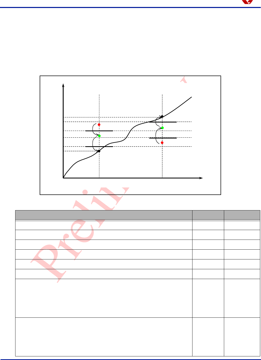
3.3.4.1 Average-based AEC/AGC
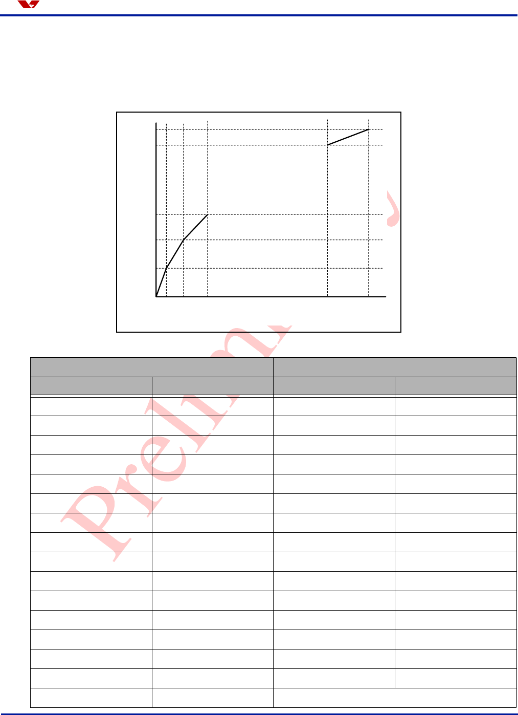
As shown in Figure 3-1, the average-based AEC/AGC algorithm changes the luminance average
value step by step until it converges with Stable Operating Region. Outside the Control Zone, the
AEC/AGC adjusts exposure time and gain in large steps to change the luminance level fast. Once
inside the Control Zone but still outside the Stable Operating range, the AEC/AGC adjusts exposure
time and gain in smaller steps to make the luminance level converge with the Stable Operating
Region smoothly. When finally inside the Stable Operating Region, the AEC/AGC no longer adjusts
the exposure time and gain. Table 3-7 summarizes the control registers of average based
AEC/AGC.
Figure 3-1 Average-based AEC/AGC
Table 3-6. Exposure Control Mode
Function Register Address Description
AEC Enable COM8[0] 0x13 0: Disable AEC
1: Enable AEC
AEC Speed COM8[7] 0x13 0: Normal speed
1: Fast speed
AEC Algorithm Selection NALG[7] 0xAA 0: Average-based AEC algorithm
1: Histogram-based AEC algorithm
Table 3-7. Average-based AEC/AGC Registers
AEC/AGC Algorithm Selection Register Address Description
Stable Operating Region – Upper Limit AEW[7:0] 0x24
Stable Operating Region – Lower Limit AEB[7:0] 0x25
Control Zone – Upper Limit high nibble VPT[7:4] 0x26 Upper limit is {VPT[7:4], 4’h0}
Control Zone – Lower Limit high nibble VPT[3:0] 0x26 Lower limit is {VPT[3:0], 4’h0}
Average luminance calculation window
(effective for both average and
histogram-based AEC/AGC)
COM4[5:4] 0x0D
00: Full frame
01: Center half frame
1x: Center quarter frame
Control Zone Stable Operating Region
Desired
Convergence
18 Proprietary to OmniVision Technologies Version 1.0, September 2, 2005
OV7670/OV7171 CMOS VGA (640x480) CameraChip™ Omni ision
3.3.4.2 Histogram-based AEC/AGC
As shown in Figure 3-2, histogram-based AEC/AGC algorithm adjusts the luminance histogram of
step by step until the desired distribution is reached. The probability of luminance level l, p(l), is
defined as the normalized percentage of the pixel count with luminance l0<= l, i.e.,
p(l) = 255 x Pixel count with luminance l0 ≤ l / Total pixel count
Figure 3-2 Histogram-Based AEC Control
Table 3-8. Histogram-based AEC Related Registers
Function Register Address
LRL – Low Reference Luminance LRL[7:0] 0xA0
HRL – High Reference Luminance HRL[7:0] 0x9F
LPH – Lower Limit of Probability for HRL, after exposure/gain stabilizes LPH[7:0] 0xA6
UPL – Upper Limit of Probability for LRL, after exposure/gain stabilizes UPL[7:0] 0xA7
TPL – Probability Threshold for LRL to control AEC/AGC speed TPL[7:0] 0xA8
TPH – Probability Threshold for HRL to control AEC/AGC speed TPH[7:0] 0xA9
TLH – High nibble of Luminance High Threshold for AEC/AGC speed control
If p(LRL) is greater than TPL and the average luminance is less than
16 x TLL, AEC/AGC increases luminance at fast speed; otherwise,
AEC/AGC works at normal speed.
The average luminance is the same as average-based AEC/AGC.
AEW[7:4] 0x24
TLL – High nibble of Luminance Low Threshold for AEC/AGC speed control
If p(HRL) is less than TPH and the average luminance is greater than
16 x TLH, AEC/AGC reduces luminance at fast speed; otherwise, AEC/AGC
works at normal speed.
The average luminance is the same as average based AEC/AGC.
AEB[7:4] 0x25
l
P(l) = Probability(l0 < l)
Luminance
LRL HRL
LPH
P
(HRL)
P
(LRL)
UPL
TPH
TPL
Fast
Fast
Normal
Normal
Timing Generator
Version 1.0, September 2, 2005 Proprietary to OmniVision Technologies 19
Omni ision
Table 3-9 lists all the registers that control the Histogram-based AEC adjustments.
Table 3-9. Histogram-based AEC Algorithm Adjustment Controls
Control Selection Registers
Luminance Saturation Control
More saturated Decrease both LPH (0xA6) and UPL (0xA7)
values
Less saturated Increase both LPH (0xA6) and UPL (0xA7)
values
Image Brightness Control
Brighter image Increase both LRL (0xA0) and HRL (0x9F)
values
Darker image Decrease both LRL (0xA0) and HRL (0x9F)
values
AEC Speed Controlled by TLH and TLL
Higher speed
Decrease TLH (AEW[7:4] (0x24)) but not less
than target image luminance and increase TLL
(AEB[7:4] (0x25)) but not bigger than target
luminance.
TLH should be bigger than 1.2x target image
luminance and TLL should be less than 0.8x
target image luminance.
Lower speed Increase TLH (AEW[7:4] (0x24)) and decrease
TLL (AEB[7:4] (0x25))
AEC Speed Controlled by TPL and TPH
Higher speed
Decrease TPL (0xA8) but not less than UPL
and increase TPH (0xA9) but not bigger than
LPH
Lower speed Increase TPL (0xA8) and decrease TPH (0xA9)
AEC Flickering versus LRL and HRL
HRL should be bigger than LRL
The relationship between these two values is shown below:
HRL > 1.07 x LRL
AEC Flickering versus LPH and UPL
LPH should be bigger than UPL
If the difference (LPH - UPL) is big, AEC flickering can occur.
The recommended relationship between these two values is
shown below:
LPH < 1.07 x UPL
20 Proprietary to OmniVision Technologies Version 1.0, September 2, 2005
OV7670/OV7171 CMOS VGA (640x480) CameraChip™ Omni ision
3.4 External Timing Output
3.4.1 Sync Signal
The OV7670/OV7171 CAMERACHIP supplies two output sync signals: VSYNC and HREF. The
vertical sync signal (VSYNC) is output from pin D1. The horizontal reference signal (HREF) is output
from pin D2. The HSYNC signal is available on pin D2 (shares with HREF) when register COM10[6]
(0x15) is set to ’1’.
VSYNC and HSYNC signals are continuous. The HREF signal is only valid when there is output
data. If there is no output data, the HREF signal will remain at either high or low, depending on the
polarity selection. VSYNC, HSYNC, HREF and PCLK polarity are controlled by register COM10[1]
(0x15), COM10[0], COM10[3] and COM10[4], respectively. Usually, the application uses the rising
edge of PCLK to capture data when HREF is high.
PCLK signal is free running by default. Setting register COM10[5] (0x15) to high gates PCLK by
HREF.
The OV7670/OV7171 CAMERACHIP also supports CCIR656 format. Instead of using HREF to define
each row, the ITU-656 standard inserts a 4-byte header before and after the row data.
Header Footer: [FF] [00] [00] [Sync Byte]
Setting register COM1[6] (0x04) high turns on CCIR656 format. OmniVision suggests using the
output range control register COM15[7:6] (0x40) to limit image data range so that the image data
does not contain 0x00 and 0xFF.
Table 3-10 summarizes the registers related to the sync signal.
Table 3-10. Sync Signal Related Registers
Function Register Address Description
HSYNC/VSYNC Polarity COM10[1:0] 0x15 1: Negative
HREF Polarity COM10[3] 0x15 1: Negative
Pixel Delay Select PSHFT[7:0] 0x1B
PCLK Reference Edge COM10[4] 0x15 0: Data update at falling edge
1: Data update at rising edge
ITU-656 Format Enable COM1[6] 0x04 1: Enable
Output Full Range Enable COM15[7:6] 0x40
00: 0x10 to 0xF0
01: 0x10 to 0xF0
10: 0x01 to 0xFE
11: 0x00 to 0xFF
Output HSYNC on HREF Pin Enable COM10[6] 0x15 0: HREF
1: HSYNC
PCLK Output Gated by HREF Enable COM10[6] 0x15 0: Free running PCLK
1: PCLK gated by HREF
HSYNC Rising Edge Delay MSB: EXHCH[1:0]
LSB: HSYST[7:0]
0x2A
0x30
HSYNC Rising Edge Delay MSB: EXHCH[3:2]
LSB: HSYEN[7:0]
0x2A
0x31
Timing Generator
Version 1.0, September 2, 2005 Proprietary to OmniVision Technologies 21
Omni ision
3.4.2 Strobe Signal
To achieve the best image quality possible in low light conditions, the use of a strobe flash is
recommended. To avoid the need for a mechanical shutter and release the loading of a backend
companion processor, the OV7670/OV7171 CAMERACHIP provides a strobe signal, which is
synchronized with the internal rolling shutter, to control the external flashlight.
The strobe signal is programmable. It supports both LED and Xenon mode. The polarity of the pulse
is adjustable. The strobe signal is initiated (turned high/low depending on the pulse's polarity) by
setting register STR-OPT[7] (0xAC) to 1. To exit strobe mode, set register STR-OPT[7] (0xAC) to
0. Flash modules are typically triggered to the rising edge (falling edge, if signal polarity is changed).
It supports following flashlight modes.
In flashlight mode, to adjust the exposure and gain, the backend processor can turn OFF AEC/AGC
by setting registers COM8[2] and COM8[0] (0x13) to 0. To adjust the color gain, the backend
processor can set register STR-OPT[6] (0xAC) to 1 and set the color gain with registers
STR_R (0xAD), STR_G (0xAE), and STR_B (0xAF). After exiting from flashlight mode, AEC/AGC
will start from these new values.
Table 3-11. Flashlight Modes
Function Register Address Description
Flashlight Mode Select STR-OPT[1:0] 0xAC
00: Xenon mode
01: LED 1
1x: LED 2
Strobe Request STR-OPT[7] 0xAC 0: Exit strobe mode
1: Enter strobe mode
Color Gain Control Enable STR-OPT[6] 0xAC 0: Disable
1: Enable
Red Gain in Flashlight Mode STR_R 0xAD
Green Gain in Flashlight Mode STR_G 0xAE
Blue Gain in Flashlight Mode STR_B 0xAF
Strobe Signal Polarity Control STR-OPT[2] 0xAC 0: Active high
1: Active low
22 Proprietary to OmniVision Technologies Version 1.0, September 2, 2005
OV7670/OV7171 CMOS VGA (640x480) CameraChip™ Omni ision
3.4.2.1 Xenon Flash Control
After a strobe request is submitted, the strobe pulse will be activated at the beginning of the third
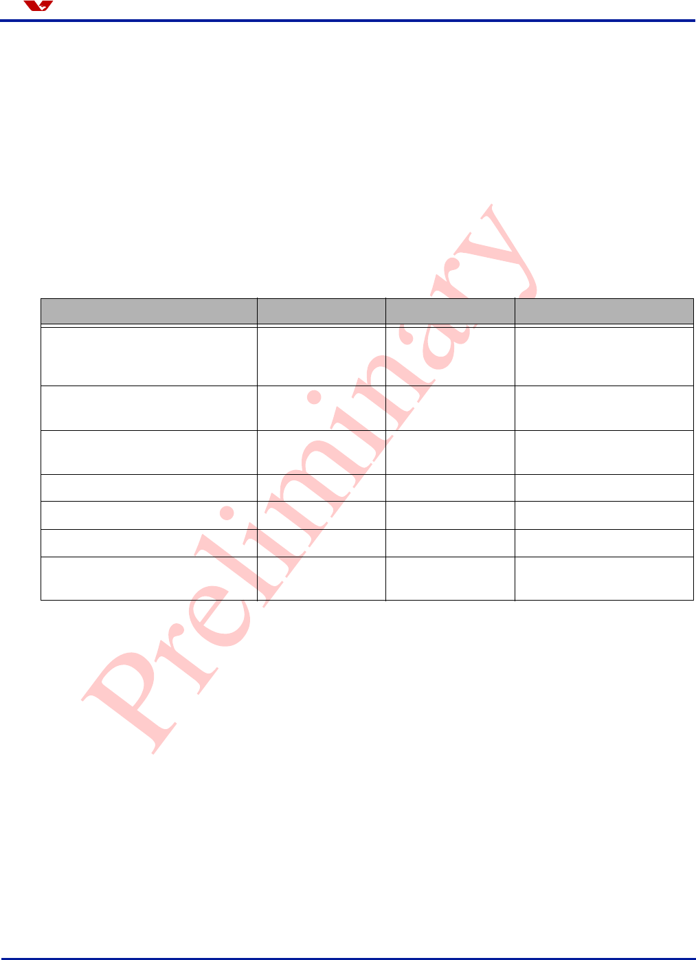
frame. The third frame will be correctly exposed. The pulse width is programmable from 1Trow to
4Trow, where Trow is the row period (see Tabl e 3- 12). Figure 3-3 shows the timing.
Figure 3-3 Xenon Flash Mode
Table 3-12. Xenon Flash Pulse Width Control
Function Register Address Description
Xenon Flash Pulse Width STR-OPT[5:4] 0xAC
00: 1 row
01: 2 rows
10: 3 rows
11: 4 rows
Exposure
time
Data out
Request here
Vertical
blanking
1 H
zoomed
Strobe pulse
Strobe pulse
Strobe request
Correctly exposed frame
Timing Generator
Version 1.0, September 2, 2005 Proprietary to OmniVision Technologies 23
Omni ision
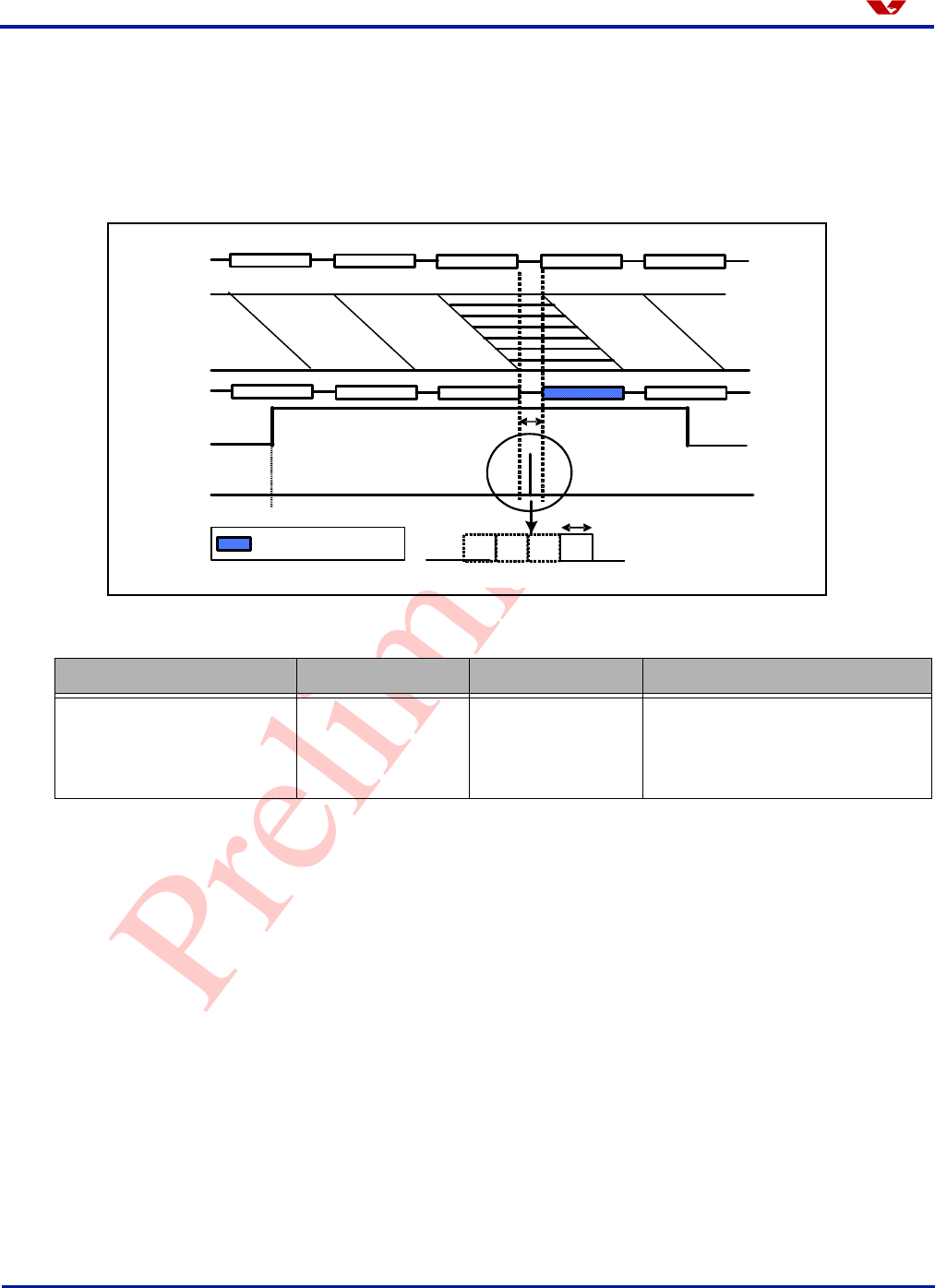
3.4.2.2 LED 1 Mode
Two frames after the strobe request is submitted, the third frame is correctly exposed. The strobe
pulse will be activated only one time if the strobe end request is set correctly (see Figure 3-4). If the
end request is not sent, the strobe signal is activated intermittently until the strobe end request is
set (see Figure 3-5). The number of skipped frames is programmable.
Figure 3-4 LED 1 Mode – One Pulse Output
Figure 3-5 LED 1 Mode – Multiple Pulse Output
Data Out
Exposure
Time
Strobe
Request
Strobe Pulse
Vertical
Blanking
The no of skipped frames is programmable
start end
Request here
Frame in is skipped
Correctly exposed frame
Vertical
blanking
Exposure
time
Data Out
Strobe Pulse
Strobe request
The no of skipped frames is programmable
start
Request here
Frames in are skipped
Correctly exposed frame
24 Proprietary to OmniVision Technologies Version 1.0, September 2, 2005
OV7670/OV7171 CMOS VGA (640x480) CameraChip™ Omni ision
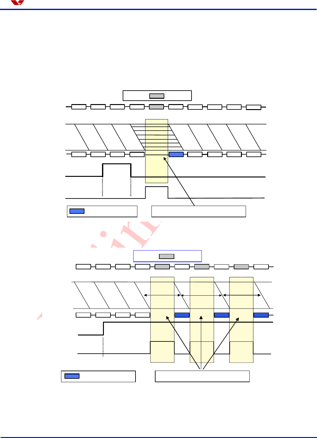
3.4.2.3 LED 2 Mode
In LED 2 mode, the strobe signal stays active until the strobe end request is sent (see Figure 3-5).
Figure 3-6 LED 2 Mode
Data Out
Exposure
time
Strobe
Request
Strobe signal
Vertical
blanking
Request here
start end
Request here
Correctly exposed frame

Analog Signal Processor
Version 1.0, September 2, 2005 Proprietary to OmniVision Technologies 25
Omni ision
4 Analog Signal Processor
This block performs all analog image functions including gain control, black level calibration, and
other image manipulation functions
4.1 Gain Control
The OV7670/OV7171 CAMERACHIP provides support for both Automatic Gain Control (AGC) and
manual gain control modes.
4.1.1 Manual Gain Control
The manual gain control mode allows for the companion backend processor to control the
OV7670/OV7171 gain value. The companion backend processor can write gain values to register
GAIN[7:0] (0x00) and VREF[7:6] (0x03) according to its gain control algorithm. The formula to
calculate the gain from register value is:
Gain = (VREF[7]+1) × (VREF[6]+1) × (GAIN[7]+1) × (GAIN[6]+1) × (GAIN[5]+1) × (GAIN[4]+1) ×
(GAIN[3:0]/16 + 1)
The gain to register value correlation is shown in Tab l e 4- 1 .

26 Proprietary to OmniVision Technologies Version 1.0, September 2, 2005
OV7670/OV7171 CMOS VGA (640x480) CameraChip™ Omni ision
Note: To achieve the best image quality, using "maximum" exposure and "minimum" gain for the
highest S/N ratio is recommended. When operating in low-light condition, use the strobe flash.
Table 4-1. Total Gain to Control Bit Correlation
Registers VREF[7:6] (0x03), GAIN[7:0] (0x00) Gain dB
00 00000000 10
00 00000001 1 + 1/16 .375
00 00000010 1 + 2/16 .75
00 00000011 1 + 3/16 1.125
00 00000100 1 + 4/16 1.5
00 00000101 1 + 5/16 1.875
00 00000110 1 + 6/16 2.25
00 00000111 1 + 7/16 2.625
00 00001000 1 + 8/16 3
00 00001001 1 + 9/16 3.375
00 00001010 1 + 10/16 3.75
00 00001011 1 + 11/16 4.125
00 00001100 1 + 12/16 4.5
00 00001101 1 + 13/16 4.875
00 00001110 1 + 14/16 5.25
00 00001111 1 + 15/16 5.625
00 00010000 2 × (1 + 0/16) 6
00 00110000 4 × (1 + 0/16) 12
00 01110000 8 × (1 + 0/16) 18
00 11110000 16 × (1 + 0/16) 24
01 11110000 32 × (1 + 0/16) 30
11 11110000 64 × (1 + 0/16) 36
11 11111111 64 × (1 + 15/16) ~42
Analog Signal Processor
Version 1.0, September 2, 2005 Proprietary to OmniVision Technologies 27
Omni ision
4.1.2 Automatic Gain Control (AGC)
The AGC function allows the OV7670/OV7171 CAMERACHIP to adjust image luminance by changing
gain without external command or control. Register setting COM8[2] (0x13) enables or disables the
AGC function. When the AGC function is enabled, gain is automatically adjusted and the result is
saved in register {VREF[7:6] (0x03), GAIN[7:0] (0x00)}. The maximum gain is limited by the gain
ceiling (see Table 4-2). When AGC function is disabled, the gain control is still active and the user
can change the gain setting.
The AGC uses the same algorithm as the AEC and shares most of the control registers with the
AEC. Tab le 4 -2 summarizes the general controls for the AGC. To achieve the best image quality,
the sensor should always increase exposure time prior to gain and reduce gain prior to exposure
time.
Table 4-2. AGC General Controls
Function Register Address Description
AGC Enable COM8[2] 0x13
0: Disable AGC function, gain
control function is still active
1: Enable AGC function
Gain Setting VREF[7:6]
GAIN[7:0]
0x03
0x00
Gain setting. Read-only when
AGC is enabled. When AGC is
disabled, these registers can be
programmed manually.
Gain Ceiling Select COM9[6:4] 0x14
Sets the upper limit of the gain
value
000: 2x
001: 4x
010: 8x
011: 16x
100: 32x
101: 64x
110: 128x
111: 128x
28 Proprietary to OmniVision Technologies Version 1.0, September 2, 2005
OV7670/OV7171 CMOS VGA (640x480) CameraChip™ Omni ision
4.2 Black Level Calibration
Black Level Calibration (BLC) compensates for the dark current induced by temperature and
exposure changes. BLC can work in manual or automatic mode.
4.2.1 Automatic Black Level Calibration (ABLC)
The OV7670/OV7171 CAMERACHIP uses the true optical black pixel for Automatic Black Level
Calibration (ABLC). Setting register ABLC1[3] (0xB1) to 1 turns on the ABLC function. ABLC adjusts
the black level compensation for each channel so that the black level is within the stable range set
by registers THL_ST (0xB3) and THL_DLT (0xB5). Tab l e 4- 3 lists the ABLC control registers.
4.2.2 Manual Black Level Calibration
The black level compensation, registers AD-CHB (0xBE) to AD-CHGr (0xC1), can be also adjusted
for manual black level calibration. To do this, disable the ABLC function first.
Table 4-3. ABLC Control Registers
Function Register Address Description
ABLC Enable ABLC1[2] 0xB1
0: Disable ABLC function, BLC function
is still active
1: Enable ABLC function
Lower Limit of Black Level + 0x80 THL_ST 0xB3
Stable Range of Black Level THL_DLT 0xB5 The upper limit of black level is:
THL_ST (0xB3) + THL_DLT (0xB5) + 0x80
Blue Channel Black Level
Compensation AD-CHB[6:0] 0xBE AD-CHB[6] is the sign bit where 0 means
addition and 1 means subtraction.
Red Channel Black Level
Compensation AD-CHR[6:0] 0xBF AD-CHR[6] is the sign bit where 0 means
addition and 1 means subtraction.
Gb Channel Black Level
Compensation AD-CHGb[6:0] 0xC0 AD-CHGb[6] is the sign bit where 0 means
addition and 1 means subtraction.
Gr Channel Black Level
Compensation AD-CHGr[6:0] 0xC1 AD-CHGr[6] is the sign bit where 0 means
addition and 1 means subtraction.
Digital Signal Processor (DSP)
Version 1.0, September 2, 2005 Proprietary to OmniVision Technologies 29
Omni ision
5 Digital Signal Processor (DSP)
The following subsections describe the controls for white balance, gamma, color matrix, sharpness,
de-noise, defect pixel correction, and other functions controlled by the Digital Signal Processor
(DSP).
5.1 White Balance Control
The OV7670/OV7171 CAMERACHIP supports the automatic white balance (AWB) function. The
AWB circuit automatically adjusts red, green, and blue gain to make the white target be white
regardless of the lighting. The OV7670/OV7171 builds two AWB algorithms - normal AWB and
advanced AWB. Normal AWB makes the average of red, green and blue equal. Advanced AWB
detects the color temperature of the light and adjusts the color gain based on the color temperature.
When AWB function is disabled, the user can also manually adjust red, green and blue gain to make
the image white balanced. The following is a summary of the three White Balance modes.
• Manual mode – Red, Green, and Blue gain are set manually
• Normal AWB mode – Red, green, and blue gain are controlled by the AWB circuit. The AWB circuit
adjusts the gain to make red, green, and blue average values equal
• Advanced AWB mode – Red, green, and blue gain are controlled by the AWB circuit. The AWB circuit
adjusts the gain based on color temperature.
In addition to the color gain that is controlled by the AWB circuit or the user, the OV7670/OV7171
also supports pre-gain for each color channel. Tab le 5- 1 lists the common control registers used for
white balance.
Table 5-1. White Balance Control Registers
Function Register Address Description
AWB Enable COM8[1] 0x13
0: Disable AWB, White Balance is in
manual mode
1: Enable AWB, White Balance is in
auto mode
AWB Mode Select AWBCTR0[0] 0x6F 0: Advanced AWB mode
1: Normal AWB mode
AWB Adjustment Control AWBCTR0[3] 0x6F 0: AWB adjusts R and B gain only
1: AWB adjusts R, G, and B gain
Maximum Color Gain AWBCTR0[2] 0x6F 0: Maximum color gain is 2x
1: Maximum color gain is 4x
AWB Gain Enable COM16[3] 0x41 0: Bypass AWB gain
1: Enable AWB gain
Blue Channel Gain BLUE[7:0] 0x01
Red Channel Gain RED[7:0] 0x02
Green Channel Gain GGAIN[6:0] 0x6A Both Gr and Gb
AWB B Gain Range B_LMT 0x5F {(B_LMT[7:4], 4’hF), (4’h0, B_LMT[3:0])}
30 Proprietary to OmniVision Technologies Version 1.0, September 2, 2005
OV7670/OV7171 CMOS VGA (640x480) CameraChip™ Omni ision
5.1.1 Automatic White Balance Control
Table 5-2 lists the control registers for the Automatic White Balance function.
5.1.2 Manual White Balance
In manual mode, the companion backend processor can control the OV7670/OV7171 internal Red,
Green, and Blue register values to achieve white balance. The gain is calculated using the equation
shown below:
Gain = Register Value / 0x40 when the maximum gain is set to 4x
or
Gain = Register Value / 0x80 when the maximum gain is set to 2x
The gain is digital gain so always set the minimum gain of the three channels to 1x and do not apply
less than 1x gain to any channel.
AWB R Gain Range R_LMT 0x60 {(R_LMT[7:4], 4’hF), (4’h0, R_LMT[3:0])}
AWB G Gain Range G_LMT 0x61 {(G_LMT[7:4], 4’hF), (4’h0, G_LMT[3:0])}
AWB Pre-Gain
Gr channel pre-gain
Gb channel pre-gain
Red channel pre-gain
Blue channel pre-gain
GFIX[7:6]
GFIX[5:4]
GFIX[3:2]
GFIX[1:0]
0x69
00: 1x
01: 1.25x
10: 1.5x
11: 1.75x
Table 5-2. AWB Control Registers
Function Register Address Description
Advanced AWB Control
Parameters
AWBC1 to AWBC6,
AWBC7 to AWBC12
0x43 to 0x48,
0x59 to 0x5E
These parameters depend on the lens.
Contact your local OmniVision FAE for
these AWB settings.
??? AWBCTR1 0x6E
Table 5-1. White Balance Control Registers
Function Register Address Description
Digital Signal Processor (DSP)
Version 1.0, September 2, 2005 Proprietary to OmniVision Technologies 31
Omni ision
5.2 Gamma Control
The OV7670/OV7171 gamma curve is composed of approximately 16 linear lines as shown in
Figure 5-1 and Table 5-3.
Figure 5-1 Gamma Curve
Table 5-3. Gamma Related Registers and Parameters
Gamma Segments Start Point Gamma Segments Horizontal Reference
Name Register Name Value
GAM1 0x7B XREF1 4
GAM2 0x7C XREF2 8
GAM3 0x7D XREF3 16
GAM4 0x7E XREF4 32
GAM5 0x7F XREF5 40
GAM6 0x80 XREF6 48
GAM7 0x81 XREF7 56
GAM8 0x82 XREF8 64
GAM9 0x83 XREF9 72
GAM10 0x84 XREF10 80
GAM11 0x85 XREF11 96
GAM12 0x86 XREF12 112
GAM13 0x87 XREF13 144
GAM14 0x88 XREF14 176
GAM15 0x89 XREF15 208
SLOP 0x7A SLOP = (256 - GAM15) x 40/30
GAM1
GAM2
GAM3
GAM15
255
0
XREF1
XREF2
XREF3
XREF15
255
SLOP

32 Proprietary to OmniVision Technologies Version 1.0, September 2, 2005
OV7670/OV7171 CMOS VGA (640x480) CameraChip™ Omni ision
5.2.1 Gamma Slope Calculation
Gamma control also needs the slope of the16th segment (register SLOP (0x7A)), which can be
calculated by the following equation:
5.3 Color Matrix
The color matrix is used to eliminate the cross talk induced by the micro-lens and color filter
process. It also compensates for lighting and temperature effects. Hue, color saturation, color space
conversion from RGB to YUV/YCbCr can also be controlled by the color matrix.
5.3.1 Color Matrix Control
The OV7670/OV7171 has a 3x3 color matrix circuit inside. This color matrix performs color
correction and RGB to YUV/YCbCr conversion. Also, because of the Matrix linear algebra
characteristic, it can also do color saturation and hue control as shown below:
The OV7670/OV7171 CAMERACHIP matrix circuit is active in YUV/YCbCr and other formats derived
from YUV/YCrCb are shown below:
The Y signal is not from color matrix. The sensor generates the Y signal from the original RGB
directly. The color matrix performs the color correction, RGB to YUV/YCbCr conversion, hue and
color saturation control. Though the Y signal is not from the color matrix, the calculation should be
done by 3x3 matrix to get the combined matrix as shown below:
CombinedMatrix = SaturationMatrix x HueMatrix x ConversionMatrix x CorrectionMatrix
and then take the two rows for UV/CbCr as the final color matrix.
Table 5-4 lists all the color matrix related registers. Each matrix element has 9 bits, 1 sign bit and 8
data bits. The register value equals up to 128 times the real color matrix value.
SLOP = (255 - GAM15 + 1) x 40/30
=
B
G
R
xColorMatri
Cb
Cr
or
U
V
654
321
MTXMTXMTX
MTXMTXMTX
where ColorMatrix =
Digital Signal Processor (DSP)
Version 1.0, September 2, 2005 Proprietary to OmniVision Technologies 33
Omni ision
5.3.1.1 Color Correction Matrix
Below is the recommended color correction matrix for the OV7670/OV7171:
5.3.1.2 RGB to YUV Conversion Matrix
The color conversion matrix can be derived from the standard equations below:
Y = 0.59G + 0.31R + 0.11B
U = B – Y
V = R – Y
Cr = 0.713 (R – Y)
Cb = 0.563 (B – Y)
5.3.1.3 Hue Control
Below is the hue matrix for α:
5.3.1.4 Color Saturation
Table 5-4. Color Matrix Related Registers and Parameters
Name Register Address Reset Value
MTX1 MTX1 0x4F 0x40
MTX2 MTX2 0x50 0x34
MTX3 MTX3 0x51 0x0C
MTX4 MTX4 0x52 0x17
MTX5 MTX5 0x53 0x29
MTX6 MTX6 0x54 0x40
Sign Bit MTXS[5:0] - for MTX6 through MTX1, respectively 0x58 0x1E
MTX Doubler
COM16[1]
0: Directly use color Matrix
1: Double color Matrix
0x41 0
×
−−
−−
−−
=
B
G
R
B
G
R
59.155.004.0
12.032.120.0
06.03.036.1
0
0
0
×
−=
00
00
or
or
cossin0
sincos0
001
or
or
CrV
CbU
Y
CrV
CbU
Y
αα
αα
×
=
00
00
or
or
00
00
001
or
or
CrV
CbU
Y
gain
gain
CrV
CbU
Y
34 Proprietary to OmniVision Technologies Version 1.0, September 2, 2005
OV7670/OV7171 CMOS VGA (640x480) CameraChip™ Omni ision
5.4 Sharpness Control
The OV7670/OV7171 CAMERACHIP sharpness control enhances the sharpness of YUV/YCbCr or
derived format. The sharpness function works in automatic or manual mode, depending on register
COM16[5] (0x41). In automatic mode, sharpness changes with the gain (the higher the gain, the
lower the sharpness). In automatic mode, the upper limit of sharpness is set by register REG75[4:0]
(0x75) and the lower limit is set by register REG76[4:0] (0x76). Tabl e 5- 5 lists the sharpness related
registers.
5.5 De-Noise
The OV7670/OV7171 CAMERACHIP has a built-in de-noise function to reduce noise level. The
de-noise function works in automatic or manual mode, depending on register COM16[4] (0x41). In
automatic mode, the de-noise strength changes with the gain (the higher the gain, the stronger the
de-noise). In automatic mode, the offset of the de-noise strength is set by register REG77 (0x77).
Table 5-6 lists de-noise related registers.
The de-noise function works in of YUV/YCbCr or derived format, and processed Bayer RGB format.
Table 5-5. Sharpness Control Registers
Function Register Address Description
Sharpness Mode Select COM16[5] 0x41
0: Manual mode, sharpness is set by register
EDGE (0x3F)
1: Automatic mode, sharpness is adjusted
automatically and saved in register EDGE
(0x3F)
Sharpness EDGE[4:0] 0x3F
In auto mode, this register is updated
automatically.
In manual mode, this register is set by the user.
Lower Limit of Sharpness REG76[4:0] 0x76 Effective in automatic mode
Upper Limit of Sharpness REG75[4:0] 0x75 Effective in automatic mode
Table 5-6. De-Noise Related Registers and Parameters
Function Register Address Description
De-noise Mode Selection COM16[4] 0x41
0: Manual mode, de-noise strength is set by
register DNSTH (0x4C)
1: Automatic mode, de-noise strength is
adjusted automatically and saved in
register DNSTH (0x4C)
De-noise Threshold DNSTH[7:0] 0x4C
In automatic mode, this register is updated
automatically.
In manual mode, this register is set by the user
De-noise Offset REG77[7:0] 0x77 Effective in automatic mode
Digital Signal Processor (DSP)
Version 1.0, September 2, 2005 Proprietary to OmniVision Technologies 35
Omni ision
5.6 Auto Color Saturation Adjustment
The OV7670/OV7171 CAMERACHIP can automatically adjust color saturation based on gain (the
higher the gain, the weaker the color). Table 5-7 lists the auto color saturation adjustment related
registers.
5.7 Defect Pixel Correction
The OV7670/OV7171 CAMERACHIP has a built-in white and black defect pixel correction circuit to
correct white and black pixels. Setting register REG76[6:5] (0x76) will enable the white and black
pixel correction function.
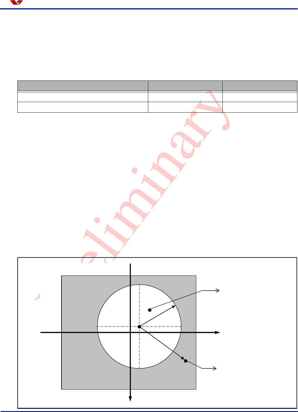
5.8 Lens Correction
Due to the lens roll off, the pixels along the edge and corner areas receive much less light than the
pixels in the center area, resulting in an image that is darker at the edges and corner areas. The
lens correction function amplifies pixel output based on the distance from the pixel to the lens’
optical center to achieve a uniform image. Figure 5-2 shows the lens correction of the
OV7670/OV7171 CAMERACHIP and Tabl e 5- 8 lists lens correction related registers.
Figure 5-2 Lens Correction
Table 5-7. Auto Color Saturation Adjustment Related Registers
Function Register Address
Color Saturation Lower Limit SATCTR[7:4] 0xC9
Current Color Saturation Level SATCTR[3:0] 0xC9
(LCC1, LCC2)
y
x
R = LCC4
Inside circular area, do
not apply compensation
Outside circular area,
apply compensation
based on r
r
Array center
Lens center
36 Proprietary to OmniVision Technologies Version 1.0, September 2, 2005
OV7670/OV7171 CMOS VGA (640x480) CameraChip™ Omni ision
Table 5-8. Lens Shading Correction Registers and Parameters
Function Register Address Note
X Coordinate of Lens Correction
Center Relative to Array Center LCC1 0x62
Bit[7]
0: Coordinate is - LCC1[6:0] (0x62)
1: Coordinate is + LCC1[6:0] (0x62)
Y Coordinate of Lens Correction
Center Relative to Array Center LCC2 0x63
Bit[7]
0: Coordinate is - LCC2[6:0] (0x62)
1: Coordinate is + LCC2[6:0] (0x62)
Radius of the circular section where
no compensation applies LCC4 0x65
G Channel Compensation Coefficient
when LCC5 (0x66) is 1
R, G, and B Channel Compensation
Coefficient when LCC5 (0x66) is 0
LCC3 0x64
Lens Correction Control LCC5 0x66
Bit[2]
0: Apply same coefficient to R, G,
and B channels
1: Apply different coefficient to R, G,
and B channels
Bit[0]
0: Disable lens correction function
1: Enable lens correction function
B Channel Compensation Coefficient LCC6 0x94 Effective only when LCC5 (0x66) is 1
R Channel Compensation Coefficient LCC7 0x95 Effective only when LCC5 (0x66) is 1
Digital Signal Processor (DSP)
Version 1.0, September 2, 2005 Proprietary to OmniVision Technologies 37
Omni ision
5.9 Brightness and Contrast Control
The OV7670/OV7171 has a built-in brightness and contrast function to easily control brightness and
contrast. Tab le 5 - 9 lists the related registers and parameters.
Table 5-9. Brightness and Contrast Related Registers
Function Register Address Description
Brightness Level BRIGHT 0x55
Bit[7]: Sign bit
0: Positive
1: Negative
Value of 0x00 and 0x80 means no
brightness adjustment
Contrast Level CONTRAS 0x56
The bigger this value, the higher the
contrast. Default value is 0x40,
meaning no contrast adjustment.
Center Luminance for
Contrast Control CONTRAS-CENTER 0x57
This register is automatically updated
by the contrast function when register
MTXS[7] (0x58) is 1; otherwise, the
center luminance level is fixed to the
value of this register which can be
manually changed by the user.
Center Luminance
Control Selection MTXS[7] 0x58
0: Center luminance level is set
manually using register
CONTRAS-CENTER (0x57)
1: Center luminance level is
controlled automatically and
saved in register
CONTRAS-CENTER (0x57)
38 Proprietary to OmniVision Technologies Version 1.0, September 2, 2005
OV7670/OV7171 CMOS VGA (640x480) CameraChip™ Omni ision
6 Image Scaler
The OV7670/OV7171 CAMERACHIP allows outputs VGA and all other resolutions are scaled from
VGA by the Image Scaler in digital domain.
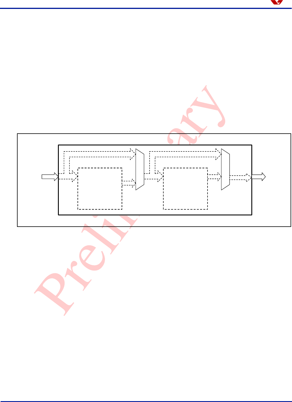
6.1 Image Scaling
The Image Scaling circuit is composed of two blocks, Down Sampling and Digital Zoom Out, as
shown in Figure 6-1. Down Sampling supports 1/2N scaling ratio and Digital Zoom Out performs
fractional scaling. Due to the buffer size, the maximum size that Digital Zoom Out can support is
CIF. Combining the scaling ratio of down sampling and digital zoom out, the OV7670/OV7171
CAMERACHIP can support VGA, CIF, and almost any size below CIF.
Figure 6-1 Image Scaling Circuit
For example, to get a 256 x128 image, Down Sampling down samples VGA input to 320 x 240 by
1/2x ratio in both horizontal and vertical direction. Then, the Digital Zoom Out scales the 320x240
input to 125x128 by a scaling ratio of 0.8 horizontally and 0.53 vertically.
Table 6-1 lists all the image scaling related registers and Tabl e 6- 2 lists all the down sampling
control related registers.
Down Sampling
1/2
1/4
1/8
Digital Zoom Out
From 1x to 1/2x
Image Scaler
Version 1.0, September 2, 2005 Proprietary to OmniVision Technologies 39
Omni ision
Table 6-1. Image Scaling Control Related Registers and Parameters
Function Register Address Description
Digital Zoom Enable Bit COM3[3] 0x0C 0: Bypass
1: Enable
Down Sampling Enable Bit COM3[2] 0x0C 0: Disable
1: Enable
Down Sampling Related Control
Register SCALING_DCWCTR[7:0] 0x72 See Ta b le 6 - 2
Pixel Clock Divider SCALING_PCLK_DIV[3:0] 0x73
DSP Output Clock Divider
Bit [3]:
0: Bypass
1: Enable
Bit [2:0]:
000: Divider = 1
001: Divider = 2
010: Divider = 4
011: Divider = 8
100: Divider = 16
101: Divider = 32
110: Divider = 64
111: Divider = Not allowed
Horizontal Scaling Ratio REG74[6:0] 0x74
From 1x (0x20) to 0.5x (0x40)
Horizontal Scaling Ratio =
0x20 / (REG74[6:0])
Vertical Scaling Ratio REG75[6:0] 0x75
From 1x (0x20) to 0.5x (0x40)
Vertical Scaling Ratio =
0x20 / (REG75[6:0])
Pixel Clock Delay SCALING_PCLK_ DELAY[3:0] 0xA2 Original H size /
Pixel clock divider - New H size
Table 6-2. Down Sampling Control Related Registers and Parameters
Function Register Address Description
Option for Vertical Average
Calculation SCALING_DCWCTR[7] 0x72 0: Vertical truncation
1: Vertical rounding
Option for Vertical Down Sampling SCALING_DCWCTR[6] 0x72 0: Vertical truncation
1: Vertical rounding
Vertical Down Sampling Rate SCALING_DCWCTR[5:4] 0x72
00: No vertical down sampling
01: Vertical down sample by 2
10: Vertical down sample by 4
11: Vertical down sample by 8
Option for Horizontal Average
Calculation SCALING_DCWCTR[3] 0x72 0: Horizontal truncation
1: Horizontal rounding
Option for Horizontal Down
Sampling SCALING_DCWCTR[2] 0x72 0: Horizontal truncation
1: Horizontal rounding
Horizontal Down Sampling Rate SCALING_DCWCTR[1:0] 0x72
00: No horizontal down sampling
01: Horizontal down sample by 2
10: Horizontal down sample by 4
11: Horizontal down sample by 8
40 Proprietary to OmniVision Technologies Version 1.0, September 2, 2005
OV7670/OV7171 CMOS VGA (640x480) CameraChip™ Omni ision
6.2 Pixel Clock Divider
Because the new size of the image requires new timing, the Pixel Clock Divider adjusts the timing
of the new size image. Its timing can be calculated as shown in Table 6- 3.
6.3 Pixel Clock Delay
In case a new scaled size (horizontally) is not a multiple number of the original sensor array
resolution, there will be some timing offset (delay) in sending out a new size of the image with the
original sensor array resolution clock. The pixel clock delay adjusts this timing offset (delay).
Its approximate value can be calculated using the equation shown below:
Pixel clock delay = Horizon pixel number of original sensor array/ Pixel clock divider - Horizontal
pixel number of new scaled image
6.4 Horizontal/Vertical Scaling Ratio
Registers SCALING_XSC[6:0] (0x70) and SCALING_YSC[6:0] (0x71) indicate horizontal/vertical
scaling ratio in the digital zoom out circuit. A value of 0x20 or below indicates 1x scaling ratio and
a value of 0x40 or higher indicates 0.5x scaling ratio. Its value can be calculated using the equation
shown below:
Scaling ratio = 0x20 x Image Size from Down sampling circuit / New image size
Table 6-3. Pixel Clock Divider
Horizontal Scaling Factor Required Pixel Clock Value For Register
SCALING_PCLK_DIV[3:0] (0x73)
From 1x to 1/2x 1 Pixel Clock / Byte 0’b0000
From 1/2x to 1/4x 2 Pixel Clock / Byte 0’b0001
From 1/4x to 1/8x 4 Pixel Clock / Byte 0’b0010
1/8x to 1/16x 8 Pixel Clock / Byte 0’b0011
Image Scaler
Version 1.0, September 2, 2005 Proprietary to OmniVision Technologies 41
Omni ision
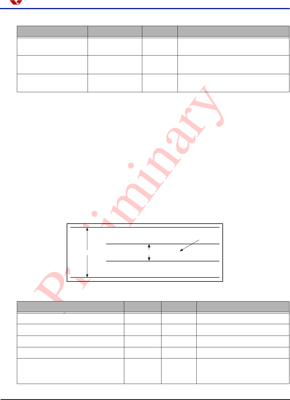
6.5 Windowing
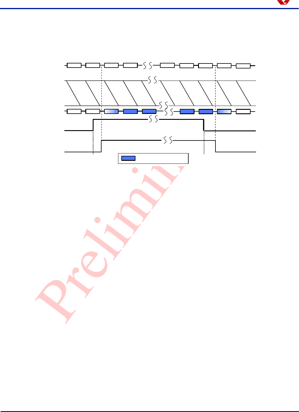
The OV7670/OV7171 CAMERACHIP windowing feature allows the user to select the window of
interest. Selecting the Start/Stop Row/Column addresses (modifying window size and/or position)
does not change the frame or data rate. When windowing is enabled, the HREF signal is asserted
to be consistent with the programmed ’active’ horizontal and vertical region. Table 6-4 lists the
control registers
Figure 6-2 shows an example of a windowed frame.
Figure 6-2 Example of Windowing
Table 6-4. Windowing Control Registers
Function Register Addresses
Horizontal Frame (HREF Column) Start HSTART[7:0], HREF[2:0] 0x17, 0x32
Horizontal Frame (HREF Column) Stop HSTOP[7:0], HREF[5:3] 0x18, 0x32
Vertical Frame (Row) Start VSTRT[7:0], VREF[2:0] 0x19. 0x03
Vertical Frame (Row) Stop VSTOP[7:0], VREF[5:3] 0x1A, 0x03
NOTE: The default output window is 640 x 480.
Selected Frame
HREF
Selected
Rows
Selected
Columns
Row Data #240
(320 Columns)
Selected
Frame Data
(240 Rows)
480 Rows
640 Columns
42 Proprietary to OmniVision Technologies Version 1.0, September 2, 2005
OV7670/OV7171 CMOS VGA (640x480) CameraChip™ Omni ision
6.6 Data Formatting
RGB565 and RGB555 are alternate output formats where each color is represented by different
D[7:0] bit widths (see Table 6-5).
This format uses an odd/even byte pair to express the color for each pixel:
•RGB565
•RGB555
See Figure 6-3 for details of MSB/LSB swap.
Figure 6-3 MSB/LSB Output Data Swap
Table 6-5. RGB555 and RGB565 Output Format Controls
Format
D[7:0]
Red Green Blue
RGB565 RRRR Rxxx GGGG GGxx BBBB Bxxx
RGB555 RRRR Rxxx GGGG Gxxx BBBB Bxxx
Bytes D7 D6 D5 D4 D3 D2 D1 D0
Even R7 R6 R5 R4 R3 G7 G6 G5
Odd G4G3G2B7B6B5B4B3
Bytes D7 D6 D5 D4 D3 D2 D1 D0
Even 00 R7 R6 R5 R4 R3 G7 G6
Odd G5G4G3B7B6B5B4B3
Default 8-bit Connection Swapped 8-bit Connection
MSB D7
D6
D5
D4
D3
D2
D1
LSB D0
D7 MSB
D6
D5
D4
D3
D2
D1
D0 LSB
Y7
Y6
Y5
Y4
Y3
Y2
Y1
Y0
OV7670
(OV7171) External
Device
LSB D0
D1
D2
D3
D4
D5
D6
MSB D7
D7 MSB
D6
D5
D4
D3
D2
D1
D0 LSB
Y7
Y6
Y5
Y4
Y3
Y2
Y1
Y0
OV7670
(OV7171) External
Device
Digital Video Port
Version 1.0, September 2, 2005 Proprietary to OmniVision Technologies 43
Omni ision
7 Digital Video Port
7.1 Drive Current
The two bits shown in Table 7-1 are used to increase IOL/IOH drive current and can be adjusted as
a function of the customer’s D[9:0], HREF, VSYNC, and PCLK loading.
7.2 Tri-state Enable
The digital video port can be tri-stated as shown in Table 7-2, which is useful in dual camera
applications.
Table 7-1. Output Drive Current
Function Register Address Description
Output Drive Capability COM2[1:0] 0x09
Drive current:
00: 1x IOL/IOH Enable
01: 2x IOL/IOH Enable
10: 3x IOL/IOH Enable
11: 4x IOL/IOH Enable
Table 7-2. Tri-State Enable
Function Register Address Description
Tri-State Enable COM3[5] 0x0C
Tri-state PCLK, HREF/HSYNC,
VSYNC, and STROBE in
power-down mode, active low.
Tri-State Enable COM3[4] 0x0C Tri-state data bus D[7:0] in
power-down mode, active low.
44 Proprietary to OmniVision Technologies Version 1.0, September 2, 2005
OV7670/OV7171 CMOS VGA (640x480) CameraChip™ Omni ision
8 SCCB Interface
The OmniVision Serial Camera Control Bus (SCCB) Functional Specification is available at
http://www.ovt.com. The Functional Specification provides complete information for using the SCCB
to control the features of an OmniVision CAMERACHIP.
The OV7670/OV7171 CAMERACHIP uses the SCCB protocol to control the features noted in this
document via the companion backend processor. The device slave addresses of the
OV7670/OV7171 CAMERACHIP are: 0x42 for write and 0x43 for read. The first command in the
SCCB transmission must be a register reset, as most registers will rely on the default value setting.
8.1 Control Functions
Table 8-1 lists the SCCB control functions.
8.1.1 Register Reset
All registers can be reset to their default values by using the RESET pin (RESET to VDD_IO) or by
using the SCCB interface (see register COM7[7] (0x12)). OmniVision suggests putting the reset
register setting (set register COM7 (0x12) to 0x80) at the beginning of the sensor initialization. After
software reset, wait 1 ms for the next register access (there is no limitation for other register
settings).
8.1.2 Standby Mode Enable
The OV7670/OV7171 CAMERACHIP can be placed in Standby mode by using the PWDN pin (PWDN
to VDD_IO) or by using the SCCB interface (see register COM2[4] (0x09)). Note that using the
PWDN pin results in lower Standby current (see Electrical Characteristics in the OV7670/OV7171
Datasheet).
8.1.2.1 Standby Mode Using the PWDN Pin
Internal device clock is halted and all internal counters are reset to their default values and all SCCB
registers remain unchanged.
8.1.2.2 Standby Mode Using the SCCB Interface
Suspends internal circuit activity but does not halt the device clock.
Table 8-1. SCCB Control Functions
Function Register Address Description
Register Reset COM7[7] 0x12 0: Normal operation
1: Resets all registers, this bit is also reset to 0
Standby Mode Enable COM2[4] 0x09 0: Disable standby mode
1: Enable standby mode
SCCB Interface
Version 1.0, September 2, 2005 Proprietary to OmniVision Technologies 45
Omni ision
8.2 Register Set
Table 8-2 provides a list and description of the Device Control registers contained in the
OV7670/OV7171. For all register Enable/Disable bits, ENABLE = 1 and DISABLE = 0. The device
slave addresses for the OV7670/OV7171 are 0x42 for write and 0x43 for read.
For factory-recommended settings, contact your local OmniVision FAE.
Note: All registers shown as reserved have no function or are very
sensitive analog circuit references. Use OmniVision reference values
(not default values).
Table 8-2. Device Control Register List
Address
(Hex)
Register
Name
Default
(Hex) R/W Description
00 GAIN 00 RW
AGC – Gain control gain setting
Bit[7:0]: AGC[7:0] (see VREF[7:6] (0x03) for AGC[9:8])
• Range: [00] to [FF]
01 BLUE 80 RW AWB – Blue channel gain setting
• Range: [00] to [FF]
02 RED 80 RW AWB – Red channel gain setting
• Range: [00] to [FF]
03 VREF 03 RW
Vertical Frame Control
Bit[7:6]: AGC[9:8] (see GAIN[7:0] (0x00) for AGC[7:0])
Bit[5:4]: Reserved
Bit[3:2]: VREF end low 2 bits (high 8 bits at VSTOP[7:0]
Bit[1:0]: VREF start low 2 bits (high 8 bits at VSTRT[7:0]
04 COM1 00 RW
Common Control 1
Bit[7]: Reserved
Bit[6]: CCIR656 format
0: Disable
1: Enable
Bit[5:2]: Reserved
Bit[1:0]: AEC low 2 LSB (see registers AECHH for AEC[15:10]
and AECH for AEC[9:2])
05 BAVE 00 RW U/B Average Level
Automatically updated based on chip output format
06 GbAVE 00 RW Y/Gb Average Level
Automatically updated based on chip output format
07 AECHH 00 RW
Exposure Value - AEC MSB 5 bits
Bit[7:6]: Reserved
Bit[5:0]: AEC[15:10] (see registers AECH for AEC[9:2] and COM1
for AEC[1:0])
08 RAVE 00 RW V/R Average Level
Automatically updated based on chip output format
46 Proprietary to OmniVision Technologies Version 1.0, September 2, 2005
OV7670/OV7171 CMOS VGA (640x480) CameraChip™ Omni ision
09 COM2 01 RW
Common Control 2
Bit[7:5]: Reserved
Bit[4]: Soft sleep mode
Bit[3:2]: Reserved
Bit[1:0]: Output Drive Capability
00: 1x
01: 2x
10: 3x
11: 4x
0A PID 76 R Product ID Number MSB (Read only)
0B VER 70 R Product ID Number LSB (Read only)
0C COM3 00 RW
Common Control 3
Bit[7]: Reserved
Bit[6]: Output data MSB and LSB swap
Bit[5]: Tri-state option for output clock (PCLK, HREF/HSYNC,
VSYNC, and STROBE) at power-down period
0: Tri-state at this period
1: No tri-state at this period
Bit[4]: Tri-state option for output data (D[7:0]) at power-down
period
0: Tri-state at this period
1: No tri-state at this period
Bit[3]: Scale enable
0: Disable
1: Enable - if set to a pre-defined format (see
COM7[5:3]), then COM14[3] must be set to 1 for
manual adjustment.
Bit[2]: DCW enable
0: Disable
1: Enable - if set to a pre-defined format (see
COM7[5:3]), then COM14[3] must be set to 1 for
manual adjustment.
Bit[1:0]: Reserved
0D COM4 40 RW
Common Control 4
Bit[7:6]: Reserved
Bit[5:4]: Average option (must be same value as COM17[7:6])
00: Full window
01: 1/2 window
10: 1/4 window
11: 1/4 window
Bit[3:0]: Reserved
0E COM5 01 RW Common Control 5
Bit[7:0]: Reserved
Table 8-2. Device Control Register List (Continued)
Address
(Hex)
Register
Name
Default
(Hex) R/W Description

SCCB Interface
Version 1.0, September 2, 2005 Proprietary to OmniVision Technologies 47
Omni ision
0F COM6 43 RW
Common Control 6
Bit[7]: Output of optical black row option
0: Disable HREF at optical black
1: Enable HREF at optical black
Bit[6:2]: Reserved
Bit[1]: Reset all timing when format changes
0: No reset
1: Resets timing
Bit[0]: Reserved
10 AECH 40 RW
Exposure Value
Bit[7:0]: AEC[9:2] (see registers AECHH for AEC[15:10] and
COM1 for AEC[1:0])
11 CLKRC 80 RW
Internal Clock
Bit[7]: Reserved
Bit[6]: Use external clock directly (no clock pre-scale available)
Bit[5:0]: Internal clock pre-scalar
F(internal clock) = F(input clock)/(Bit[5:0]+1)
• Range: [0 0000] to [1 1111]
12 COM7 00 RW
Common Control 7
Bit[7]: SCCB register reset
0: No change
1: Resets all registers to default values
Bit[6]: Reserved
Bit[5]: Output format - CIF selection
Bit[4]: Output format - QVGA selection
Bit[3]: Output format - QCIF selection
Bit[2]: Output format - RGB selection (see below)
Bit[1]: Color bar
0: Disable
1: Enable
Bit[0]: Output format - Raw RGB (see below)
COM7[2] COM7[0]
YUV 0 0
RGB 1 0
Raw Bayer RGB 0 1
Processed Bayer RGB 1 1
Table 8-2. Device Control Register List (Continued)
Address
(Hex)
Register
Name
Default
(Hex) R/W Description

48 Proprietary to OmniVision Technologies Version 1.0, September 2, 2005
OV7670/OV7171 CMOS VGA (640x480) CameraChip™ Omni ision
13 COM8 8F RW
Common Control 8
Bit[7]: Enable fast AGC/AEC algorithm
Bit[6]: AEC - Step size limit
0: Step size is limited to vertical blank
1: Unlimited step size
Bit[5]: Banding filter ON/OFF - In order to turn ON the banding
filter, BD50ST (0x9D) or BD60ST (0x9E) must be set to a
non-zero value.
0: ON
1: OFF
Bit[4:3]: Reserved
Bit[2]: AGC Enable
Bit[1]: AWB Enable
Bit[0]: AEC Enable
14 COM9 4A RW
Common Control 9
Bit[7]: Reserved
Bit[6:4]: Automatic Gain Ceiling - maximum AGC value
000: 2x
001: 4x
010 8x
011: 16x
100: 32x
101 64x
110: 128x
111: Not allowed
Bit[3:1]: Reserved
Bit[0]: Freeze AGC/AEC
15 COM10 00 RW
Common Control 10
Bit[7]: Reserved
Bit[6]: HREF changes to HSYNC
Bit[5]: PCLK output option
0: Free running PCLK
1: PCLK does not toggle during horizontal blank
Bit[4]: PCLK reverse
Bit[3]: HREF reverse
Bit[2]: VSYNC option
0: VSYNC changes on falling edge of PCLK
1: VSYNC changes on rising edge of PCLK
Bit[1]: VSYNC negative
Bit[0]: HSYNC negative
16 RSVD XX – Reserved
17 HSTART 11 RW Output Format - Horizontal Frame (HREF column) start high 8-bit (low
3 bits are at HREF[2:0])
18 HSTOP 61 RW Output Format - Horizontal Frame (HREF column) end high 8-bit (low
3 bits are at HREF[5:3])
Table 8-2. Device Control Register List (Continued)
Address
(Hex)
Register
Name
Default
(Hex) R/W Description
SCCB Interface
Version 1.0, September 2, 2005 Proprietary to OmniVision Technologies 49
Omni ision
19 VSTRT 03 RW Output Format - Vertical Frame (row) start high 8-bit (low 2 bits are at
VREF[1:0])
1A VSTOP 7B RW Output Format - Vertical Frame (row) end high 8-bit (low 2 bits are at
VREF[3:2])
1B PSHFT 00 RW
Data Format - Pixel Delay Select (delays timing of the D[7:0] data
relative to HREF in pixel units)
• Range: [00] (no delay) to [FF] (256 pixel delay which accounts for
whole array)
1C MIDH 7F R Manufacturer ID Byte – High (Read only = 0x7F)
1D MIDL A2 R Manufacturer ID Byte – Low (Read only = 0xA2)
1E MVFP 00 RW
Mirror/VFlip Enable
Bit[7:6]: Reserved
Bit[5]: Mirror
0: Normal image
1: Mirror image
Bit[4]: VFlip enable
0: Normal image
1: Vertically flip image
Bit[3]: Reserved
Bit[2]: Black sun enable
Bit[1:0]: Reserved
1F LAEC 00 RW Reserved
20 ADCCTR0 04 RW
ADC Control
Bit[7:4]: Reserved
Bit[3]: ADC range adjustment
0: 1x range
1: 1.5x range
Bit[2:0]: ADC reference adjustment
000: 0.8x
100: 1x
111: 1.2x
21 ADCCTR1 02 RW Bit[7:0]: Reserved
22 ADCCTR2 01 RW Bit[7:0]: Reserved
23 ADCCTR3 80 RW Bit[7:0]: Reserved
24 AEW 75 RW AGC/AEC - Stable Operating Region (Upper Limit)
25 AEB 63 RW AGC/AEC - Stable Operating Region (Lower Limit)
26 VPT D4 RW
AGC/AEC Fast Mode Operating Region
Bit[7:4]: High nibble of upper limit of fast mode control zone
Bit[3:0]: High nibble of lower limit of fast mode control zone
Table 8-2. Device Control Register List (Continued)
Address
(Hex)
Register
Name
Default
(Hex) R/W Description
50 Proprietary to OmniVision Technologies Version 1.0, September 2, 2005
OV7670/OV7171 CMOS VGA (640x480) CameraChip™ Omni ision
27 BBIAS 80 RW
B Channel Signal Output Bias (effective only when COM6[3] = 1)
Bit[7]: Bias adjustment sign
0: Add bias
1: Subtract bias
Bit[6:0]: Bias value of 10-bit range
28 GbBIAS 80 RW
Gb Channel Signal Output Bias (effective only when COM6[3] = 1)
Bit[7]: Bias adjustment sign
0: Add bias
1: Subtract bias
Bit[6:0]: Bias value of 10-bit range
29 RSVD XX – Reserved
2A EXHCH 00 RW
Dummy Pixel Insert MSB
Bit[7:4]: 4 MSB for dummy pixel insert in horizontal direction
Bit[3:2]: HSYNC falling edge delay 2 MSB
Bit[1:0]: HSYNC rising edge delay 2 MSB
2B EXHCL 00 RW Dummy Pixel Insert LSB
8 LSB for dummy pixel insert in horizontal direction
2C RBIAS 80 RW
R Channel Signal Output Bias (effective only when COM6[3] = 1)
Bit[7]: Bias adjustment sign
0: Add bias
1: Subtract bias
Bit[6:0]: Bias value of 10-bit range
2D ADVFL 00 RW LSB of insert dummy rows in vertical direction (1 bit equals 1 row)
2E ADVFH 00 RW MSB of insert dummy rows in vertical direction
2F YAVE 00 RW Y/G Channel Average Value
30 HSYST 08 RW HSYNC Rising Edge Delay (low 8 bits)
31 HSYEN 30 RW HSYNC Falling Edge Delay (low 8 bits)
32 HREF 80 RW
HREF Control
Bit[7:6]: HREF edge offset to data output
Bit[5:3]: HREF end 3 LSB (high 8 MSB at register HSTOP)
Bit[2:0]: HREF start 3 LSB (high 8 MSB at register HSTART)
33 CHLF 08 RW Array Current Control
Bit[7:0]: Reserved
34 ARBLM 03 RW Array Reference Control
Bit[7:0]: Reserved
35-36 RSVD XX – Reserved
37 ADC 04 RW ADC Control
Bit[7:0]: Reserved
Table 8-2. Device Control Register List (Continued)
Address
(Hex)
Register
Name
Default
(Hex) R/W Description
SCCB Interface
Version 1.0, September 2, 2005 Proprietary to OmniVision Technologies 51
Omni ision
38 ACOM 12 RW ADC and Analog Common Mode Control
Bit[7:0]: Reserved
39 OFON 00 RW ADC Offset Control
Bit[7:0]: Reserved
3A TSLB 0C RW
Line Buffer Test Option
Bit[7:6]: Reserved
Bit[5]: Negative image enable
0: Normal image
1: Negative image
Bit[4]: UV output value
0: Use normal UV output
1: Use fixed UV value set in registers MANU and MANV
as UV output instead of chip output
Bit[3]: Output sequence (use with register COM13[1] (0x3D))
TSLB[3], COM13[1]:
00: Y U Y V
01: Y V Y U
10: U Y V Y
11: V Y U Y
Bit[2:1]: Reserved
Bit[0]: Auto output window
0: Sensor DOES NOT automatically set window after
resolution change. The companion backend
processor can adjust the output window immediately
after changing the resolution
1: Sensor automatically sets output window when
resolution changes. After resolution changes, the
companion backend processor must adjust the
output window after the next VSYNC pulse.
Table 8-2. Device Control Register List (Continued)
Address
(Hex)
Register
Name
Default
(Hex) R/W Description
52 Proprietary to OmniVision Technologies Version 1.0, September 2, 2005
OV7670/OV7171 CMOS VGA (640x480) CameraChip™ Omni ision
3B COM11 00 RW
Common Control 11
Bit[7]: Night mode
0: Night mode disable
1: Night mode enable - The frame rate is reduced
automatically while the minimum frame rate is limited
by COM11[6:5]. Also, ADVFH and ADVFL will be
automatically updated.
Bit[6:5]: Minimum frame rate of night mode
00: Same as normal mode frame rate
01: 1/2 of normal mode frame rate
10: 1/4 of normal mode frame rate
11: 1/8 of normal mode frame rate
Bit[4]: D56_Auto
0: Disable 50/60 Hz auto detection
1: Enable 50/60 Hz auto detection
Bit[3]: Banding filter value select (effective only when
COM11[4] = 0)
0: Select BD60ST[7:0] (0x9E) as Banding Filter Value
1: Select BD50ST[7:0] (0x9D) as Banding Filter Value
Bit[2]: Reserved
Bit[1]: Exposure timing can be less than limit of banding filter
when light is too strong
Bit[0]: Reserved
3C COM12 40 RW
Common Control 12
Bit[7]: HREF option
0: No HREF when VSYNC is low
1: Always has HREF
Bit[6:0]: Reserved
3D COM13 99 RW
Common Control 13
Bit[7]: Gamma enable
Bit[6]: UV saturation level - UV auto adjustment. Result is saved
in register SATCTR[3:0] (0xC9)
Bit[5:2]: Reserved
Bit[1]: UV swap (use with register TSLB[3] (0x3A))
TSLB[3], COM13[1]:
00: Y U Y V
01: Y V Y U
10: U Y V Y
11: V Y U Y
Bit[0]: Reserved
Table 8-2. Device Control Register List (Continued)
Address
(Hex)
Register
Name
Default
(Hex) R/W Description

SCCB Interface
Version 1.0, September 2, 2005 Proprietary to OmniVision Technologies 53
Omni ision
3E COM14 0E RW
Common Control 14
Bit[7:5]: Reserved
Bit[4]: DCW and scaling PCLK enable
0: Normal PCLK
1: DCW and scaling PCLK, controlled by register
COM14[2:0] and SCALING_PCLK_DIV[3:0] (0x73))
Bit[3]: Manual scaling enable for pre-defined resolution modes
such as CIF, QCIF, and QVGA
0: Scaling parameter cannot be adjusted manually
1: Scaling parameter can be adjusted manually
Bit[2:0]: PCLK divider (only when COM14[4] = 1)
000: Divided by 1
001: Divided by 2
010 Divided by 4
011: Divided by 8
100: Divided by 16
101~111: Not allowed
3F EDGE 88 RW
Edge Enhancement Adjustment
Bit[7:5]: Reserved
Bit[4:0]: Edge enhancement factor
40 COM15 C0 RW
Common Control 15
Bit[7:6]: Data format - output full range enable
0x: Output range: [10] to [F0]
10: Output range: [01] to [FE]
11: Output range: [00] to [FF]
Bit[5:4]: RGB 555/565 option (must set COM7[2] = 1 and
COM7[0] = 0)
x0: Normal RGB output
01: RGB 565
11: RGB 555
Bit[3:0]: Reserved
Table 8-2. Device Control Register List (Continued)
Address
(Hex)
Register
Name
Default
(Hex) R/W Description

54 Proprietary to OmniVision Technologies Version 1.0, September 2, 2005
OV7670/OV7171 CMOS VGA (640x480) CameraChip™ Omni ision
41 COM16 10 RW
Common Control 16
Bit[7:6]: Reserved
Bit[5]: Enable edge enhancement auto-adjustment for YUV
output (result is saved in register EDGE[4:0] (0x3F) and
range is controlled by registers REG75[4:0] (0x75) and
REG76[4:0] (0x76))
0: Disable
1: Enable
Bit[4]: De-noise auto-adjustment (result is saved in register
DNSTH (0x4C) and range is controlled by register
REG77[7:0] (0x77))
0: Disable
1: Enable
Bit[3]: AWB gain enable
Bit[2]: Reserved
Bit[1]: Color matrix coefficient double option
0: Original matrix
1: Double of original matrix
Bit[0]: Reserved
42 COM17 08 RW
Common Control 17
Bit[7:6]: AEC window must be the same value as COM4[5:4])
00: Normal
01: 1/2
10: 1/4
11: 1/4
Bit[5:4]: Reserved
Bit[3]: DSP color bar enable
0: Disable
1: Enable
Bit[2:0]: Reserved
43 AWBC1 14 RW AWB Control 1
44 AWBC2 F0 RW AWB Control 2
45 AWBC3 45 RW AWB Control 3
46 AWBC4 61 RW AWB Control 4
47 AWBC5 51 RW AWB Control 5
48 AWBC6 79 RW AWB Control 6
49-4A RSVD XX – Reserved
4B REG4B 00 RW
Register 4B
Bit[7:1]: Reserved
Bit[0]: UV average enable
4C DNSTH 00 RW De-noise Strength
Table 8-2. Device Control Register List (Continued)
Address
(Hex)
Register
Name
Default
(Hex) R/W Description
SCCB Interface
Version 1.0, September 2, 2005 Proprietary to OmniVision Technologies 55
Omni ision
4D DM_POS 00 RW
Bit[7]: Dummy row position
0: Dummy row is inserted before active row
1: Dummy row is inserted after active row
Bit[6:0]: Reserved
4E RSVD XX – Reserved
4F MTX1 40 RW Matrix Coefficient 1
50 MTX2 34 RW Matrix Coefficient 2
51 MTX3 0C RW Matrix Coefficient 3
52 MTX4 17 RW Matrix Coefficient 4
53 MTX5 29 RW Matrix Coefficient 5
54 MTX6 40 RW Matrix Coefficient 6
55 BRIGHT 00 RW Brightness Control
56 CONTRAS 40 RW Contrast Control
57 CONTRAS-
CENTER 80 RW Contrast Center
58 MTXS 1E RW
Matrix Coefficient Sign for coefficient 5 to 0
Bit[7]: Auto contrast center enable
0: Disable, center is set by register
CONTRAS-CENTER (0x57)
1: Enable, register CONTRAS-CENTER is updated
automatically
Bit[6]: Reserved
Bit[5:0]: Matrix coefficient sign
0: Plus
1: Minus
59 AWBC7 91 RW AWB Control 7
5A AWBC8 94 RW AWB Control 8
5B AWBC9 AA RW AWB Control 9
5C AWBC10 71 RW AWB Control 10
5D AWBC11 8D RW AWB Control 11
5E AWBC12 0F RW AWB Control 12
5F B_LMT F0 RW AWB B Gain Range
{B_LMT[7:4], 4’hF}, {4’h0, B_LMT[3:0]}
60 R_LMT F0 RW AWB R Gain Range
{R_LMT[7:4], 4’hF}, {4’h0, R_LMT[3:0]}
61 G_LMT F0 RW AWB G Gain Range
{G_LMT[7:4], 4’hF}, {4’h0, G_LMT[3:0]}
Table 8-2. Device Control Register List (Continued)
Address
(Hex)
Register
Name
Default
(Hex) R/W Description
56 Proprietary to OmniVision Technologies Version 1.0, September 2, 2005
OV7670/OV7171 CMOS VGA (640x480) CameraChip™ Omni ision
62 LCC1 00 RW Lens Correction Option 1 - X Coordinate of Lens Correction Center
Relative to Array Center
63 LCC2 00 RW Lens Correction Option 2 - Y Coordinate of Lens Correction Center
Relative to Array Center
64 LCC3 10 RW
Lens Correction Option 3
G Channel Compensation Coefficient when LCC5[2] (0x66) is 1
R, G, and B Channel Compensation Coefficient when LCC5[2] (0x66) is
0
65 LCC4 80 RW Lens Correction Option 4 - Radius of the circular section where no
compensation applies
66 LCC5 00 RW
Lens Correction Control
Bit[7:3]: Reserved
Bit[2]: Lens correction control select
0: R, G, and B channel compensation coefficient is set
by register LCC3
1: R, G, and B channel compensation coefficient is set
by registers LCC6, LCC3, and LCC7, respectively
Bit[1]: Reserved
Bit[0]: Lens correction enable
0: Disable
1: Enable
67 MANU 80 RW Manual U Value (effective only when register TSLB[4] is high)
68 MANV 80 RW Manual V Value (effective only when register TSLB[4] is high)
69 GFIX 00 RW
Fix Gain Control
Bit[7:6]: Fix gain for Gr channel
00: 1x
01: 1.25x
10: 1.5x
11: 1.75x
Bit[5:4]: Fix gain for Gb channel
00: 1x
01: 1.25x
10: 1.5x
11: 1.75x
Bit[3:2]: Fix gain for R channel
00: 1x
01: 1.25x
10: 1.5x
11: 1.75x
Bit[1:0]: Fix gain for B channel
00: 1x
01: 1.25x
10: 1.5x
11: 1.75x
6A GGAIN 00 RW G Channel AWB Gain
Table 8-2. Device Control Register List (Continued)
Address
(Hex)
Register
Name
Default
(Hex) R/W Description

SCCB Interface
Version 1.0, September 2, 2005 Proprietary to OmniVision Technologies 57
Omni ision
6B DBLV 3A RW
Bit[7:6]: PLL control
00: Bypass PLL
01: Input clock x4
10: Input clock x6
11: Input clock x8
Bit[5]: Reserved
Bit[4]: Regulator control
0: Enable internal regulator
1: Bypass internal regulator
Bit[3:0]: Clock divider control for DSP scale control (valid only
when COM14[3] = 1)
6C AWBCTR3 02 RW AWB Control 3
6D AWBCTR2 55 RW AWB Control 2
6E AWBCTR1 00 RW AWB Control 1
6F AWBCTR0 9A RW AWB Control 0
70 SCALING_
XSC 4A RW
Bit[7]: Test_pattern[0] - works with test_pattern[1] test_pattern
(SCALING_XSC[7], SCALING_YSC[7]):
00: No test pattern output
01: Shifting "1"
10: 8-bar color bar
11: Fade to gray color bar
Bit[6:0]: Horizontal scale factor
71 SCALING_
YSC 35 RW
Bit[7]: Test_pattern[1] - works with test_pattern[0] test_pattern
(SCALING_XSC[7], SCALING_YSC[7]):
00: No test pattern output
01: Shifting "1"
10: 8-bar color bar
11: Fade to gray color bar
Bit[6:0]: Vertical scale factor
Table 8-2. Device Control Register List (Continued)
Address
(Hex)
Register
Name
Default
(Hex) R/W Description

58 Proprietary to OmniVision Technologies Version 1.0, September 2, 2005
OV7670/OV7171 CMOS VGA (640x480) CameraChip™ Omni ision
72 SCALING_
DCWCTR 11 RW
DCW Control
Bit[7]: Vertical average calculation option
0: Vertical truncation
1: Vertical rounding
Bit[6]: Vertical down sampling option
0: Vertical truncation
1: Vertical rounding
Bit[5:4]: Vertical down sampling rate
00: No vertical down sampling
01: Vertical down sample by 2
10: Vertical down sample by 4
11: Vertical down sample by 8
Bit[3]: Horizontal average calculation option
0: Horizontal truncation
1: Horizontal rounding
Bit[2]: Horizontal down sampling option
0: Horizontal truncation
1: Horizontal rounding
Bit[1:0]: Horizontal down sampling rate
00: No horizontal down sampling
01: Horizontal down sample by 2
10: Horizontal down sample by 4
11: Horizontal down sample by 8
73 SCALING_
PCLK_DIV 00 RW
Bit[7:4]: Reserved
Bit[3]: Bypass clock divider for DSP scale control
0: Enable clock divider
1: Bypass clock divider
Bit[2:0]: Clock divider control for DSP scale control (valid only
when COM14[3] = 1). Should change with COM14[2:0].
000: Divided by 1
001: Divided by 2
010: Divided by 4
011: Divided by 8
100: Divided by 16
101~111: Not allowed
74 REG74 00 RW
Bit[7:5]: Reserved
Bit[4]: Digital gain control select
0: Digital gain control by VREF[7:6]
1: Digital gain control by REG74[1:0]
Bit[3:2]: Reserved
Bit[1:0]: Digital gain manual control
00: Bypass
01: 1x
10: 2x
11: 4x
75 REG75 0F RW
Register 75
Bit[7:5]: Reserved
Bit[4:0]: Edge enhancement lower limit
Table 8-2. Device Control Register List (Continued)
Address
(Hex)
Register
Name
Default
(Hex) R/W Description

SCCB Interface
Version 1.0, September 2, 2005 Proprietary to OmniVision Technologies 59
Omni ision
76 REG76 01 RW
Register 76
Bit[7]: Reserved
Bit[6]: White pixel correction enable
0: Disable
1: Enable
Bit[5]: Black pixel correction enable
0: Disable
1: Enable
Bit[4:0]: Edge enhancement higher limit
77 REG77 10 RW Register 77
Bit[7:0]: Offset, de-noise range control
78-79 RSVD XX – Reserved
7A SLOP 18 RW Gamma Curve Highest Segment Slop - calculated as follows:
SLOP[7:0] = (0x100 - GAM15[7:0]) x 4/3
7B GAM1 02 RW Gamma Curve 1st Segment Input End Point 0x04 Output Value
7C GAM2 07 RW Gamma Curve 2nd Segment Input End Point 0x08 Output Value
7D GAM3 1F RW Gamma Curve 3rd Segment Input End Point 0x10 Output Value
7E GAM4 49 RW Gamma Curve 4th Segment Input End Point 0x20 Output Value
7F GAM5 5A RW Gamma Curve 5th Segment Input End Point 0x28 Output Value
80 GAM6 6A RW Gamma Curve 6th Segment Input End Point 0x30 Output Value
81 GAM7 79 RW Gamma Curve 7th Segment Input End Point 0x38 Output Value
82 GAM8 87 RW Gamma Curve 8th Segment Input End Point 0x40 Output Value
83 GAM9 94 RW Gamma Curve 9th Segment Input End Point 0x48 Output Value
84 GAM10 9F RW Gamma Curve 10th Segment Input End Point 0x50 Output Value
85 GAM11 AF RW Gamma Curve 11th Segment Input End Point 0x60 Output Value
86 GAM12 BB RW Gamma Curve 12th Segment Input End Point 0x70 Output Value
87 GAM13 CF RW Gamma Curve 13th Segment Input End Point 0x90 Output Value
88 GAM14 EE RW Gamma Curve 14th Segment Input End Point 0xB0 Output Value
89 GAM15 EE RW Gamma Curve 15th Segment Input End Point 0xD0 Output Value
8A-91 RSVD XX – Reserved
92 DM_LNL 00 RW Dummy Row low 8 bits
93 DM_LNH 00 RW Dummy Row high 8 bits
94 LCC6 50 RW Lens Correction Option 6 (effective only when LCC5[2] is high)
95 LCC7 50 RW Lens Correction Option 7 (effective only when LCC5[2] is high)
96-9C RSVD XX – Reserved
Table 8-2. Device Control Register List (Continued)
Address
(Hex)
Register
Name
Default
(Hex) R/W Description
60 Proprietary to OmniVision Technologies Version 1.0, September 2, 2005
OV7670/OV7171 CMOS VGA (640x480) CameraChip™ Omni ision
9D BD50ST 99 RW 50 Hz Banding Filter Value
(effective only when COM8[5] is high and COM11[3] is high)
9E BD60ST 7F RW 60 Hz Banding Filter Value
(effective only when COM8[5] is high and COM11[3] is low)
9F HRL C0 RW High Reference Luminance
A0 LRL 90 RW Low Reference Luminance
A1 DSPC3 03 RW DSP Control 3
A2
SCALING_
PCLK_
DELAY
02 RW Pixel Clock Delay
A3 RSVD XX – Reserved
A4 NT_CTRL 00 RW
Bit[7:4]: Reserved
Bit[3]: Auto frame rate adjustment dummy row selection
0: N is equal to the maximum exposure, time less than
frame period when banding filter is enabled
1: N is equal to the number of rows per frame
Bit[2]: Reserved
Bit[1:0]: Auto frame rate adjustment switch point
00: Insert dummy row at 2x gain
01: Insert dummy row at 4x gain
10: Insert dummy row at 8x gain
A5 AECGMAX 0F RW Maximum Banding Filter Step
A6 LPH F0 RW Lower Limit of Probability for HRL, after exposure/gain stabilizes
A7 UPL C1 RW Upper Limit of Probability for LRL, after exposure/gain stabilizes
A8 TPL F0 RW Probability Threshold for LRL to control AEC/AGC speed
A9 TPH C1 RW Probability Threshold for HRL to control AEC/AGC speed
AA NALG 14 RW
Bit[7]: AEC algorithm selection
0: Average-based AEC algorithm
1: Histogram-based AEC algorithm
Bit[6:0]: Reserved
AB RSVD XX – Reserved
Table 8-2. Device Control Register List (Continued)
Address
(Hex)
Register
Name
Default
(Hex) R/W Description

SCCB Interface
Version 1.0, September 2, 2005 Proprietary to OmniVision Technologies 61
Omni ision
AC STR-OPT 00 RW
Register AC
Bit[7]: Strobe enable
Bit[6]: R / G / B gain controlled by STR_R (0xAD) / STR_G
(0xAE) / STR_B (0xAF) for LED output frame
Bit[5:4]: Xenon mode option
00: 1 row
01: 2 rows
10: 3 rows
11: 4 rows
Bit[3:2]: Reserved
Bit[1:0]: Mode select
00: Xenon
01: LED 1
1x: LED 2
AD STR_R 80 RW R Gain for LED Output Frame
AE STR_G 80 RW G Gain for LED Output Frame
AF STR_B 80 RW B Gain for LED Output Frame
B0 RSVD XX – Reserved
B1 ABLC1 00 RW
Bit[7:3]: Reserved
Bit[2]: ABLC enable
0: Disable ABLC function, BLC function is still active
1: Enable ABLC function
Bit[1:0]: Reserved
B2 RSVD XX – Reserved
B3 THL_ST 80 RW ABLC Target
B4 RSVD XX – Reserved
B5 THL_DLT 04 RW ABLC Stable Range
B6-BD RSVD XX – Reserved
BE AD-CHB 00 RW
Blue Channel Black Level Compensation
Bit[7]: Reserved
Bit[6]: Sign bit
Bit[5:0]: Blue channel black level compensation
BF AD-CHR 00 RW
Red Channel Black Level Compensation
Bit[7]: Reserved
Bit[6]: Sign bit
Bit[5:0]: Red channel black level compensation
C0 AD-CHGb 00 RW
Gb Channel Black Level Compensation
Bit[7]: Reserved
Bit[6]: Sign bit
Bit[5:0]: Gb channel black level compensation
Table 8-2. Device Control Register List (Continued)
Address
(Hex)
Register
Name
Default
(Hex) R/W Description
62 Proprietary to OmniVision Technologies Version 1.0, September 2, 2005
OV7670/OV7171 CMOS VGA (640x480) CameraChip™ Omni ision
C1 AD-CHGr 00 RW
Gr Channel Black Level Compensation
Bit[7]: Reserved
Bit[6]: Sign bit
Bit[5:0]: Gr channel black level compensation
C2-C8 RSVD XX – Reserved
C9 SATCTR C0 RW
Saturation Control
Bit[7:4]: UV saturation control minimum
Bit[3:0]: UV saturation control result
NOTE: All other registers are factory-reserved. Please contact OmniVision Technologies for reference register settings.
Table 8-2. Device Control Register List (Continued)
Address
(Hex)
Register
Name
Default
(Hex) R/W Description

Prototyping and Evaluation Modules
Version 1.0, September 2, 2005 Proprietary to OmniVision Technologies 63
Omni ision
9 Prototyping and Evaluation Modules
OmniVision Technologies Inc. supplies prototyping and evaluation modules to demonstrate
operation of the associated CAMERACHIP products, as well as to demonstrate associated
companion backend processor, where required.
9.1 OV7670/OV7171EAA Prototyping Module
The OV7670/OV7171EAA prototyping module is used for general design-in and evaluation
purposes. The module provides a simple 32-pin header-connector interface to the relevant I/O and
control registers in the OV7670/OV7171 CAMERACHIP. The module includes the necessary sensor,
lens/holder, a few capacitors, and resistors.
The OV7670/OV7171EAA prototyping module can be directly connected to any companion
backend processor solution or system interface. The header-connector interface allows for access
to the 10-bit digital output data, PCLK, vertical sync, horizontal sync and SCCB signals. The
backend interface can use the Serial Camera Control Bus (SCCB) interface software to adjust the
control register values.
9.2 OV7670/OV7171ECX USB 2.0 Evaluation Module
The OV7670/OV7171ECX USB2.0 evaluation module is provided so that potential customers may
evaluate both the live video function of the CAMERACHIP as well as the SCCB control interface
software. The OV7670/OV7171 CAMERACHIP output is a RGB raw data or YUV stream connected
to a USB 2.0 controller operating at a high-speed bus data rate (480 Mbps).
Using a high performance computer system with a USB 2.0 host (cannot guarantee for every
system), the OV7670/OV7171 USB module will stream video in VGA format (640x480 at 30 fps) or
in QVGA format (320x240 at 60 fps). This configuration requires a Windows®2000 or XP operating
system. Additionally, the SCCB software allows the evaluator to adjust the image characteristics in
real-time.
10 Lens selection
The OV7670/OV7171 is a one-sixth-inch format CAMERACHIP that is compatible with numerous
lenses in the market. The key considerations in lens selection are lens quality and resultant cost.
OmniVision Technologies, Inc. has qualified several lens suppliers for the various formats, sizes,
and quality of lenses available. OmniVision has developed a Lens Supplier Partner List to
complement our CAMERACHIP products. This listing is available at http://www.ovt.com on the
Partners page. Contact your local OmniVision FAE for recommended OV7670/OV7171 lenses.
11 OV7670/OV7171 Bug List
None as of this revision.

64 Proprietary to OmniVision Technologies Version 1.0, September 2, 2005
OV7670/OV7171 CMOS VGA (640x480) CameraChip™ Omni ision
Appendix A Reference SCCB Settings
Contact your local OmniVision FAE for updated reference register settings.
