PIC18F87J50 FS USB Plug In Module User's Guide Users
PIC18F87J50_FS_USB%20Users%20Guide
PIC18F87J50_FS_USB%20Users%20Guide
User Manual: Pdf
Open the PDF directly: View PDF ![]() .
.
Page Count: 28

© 2007 Microchip Technology Inc. DS51678A
PIC18F87J50 FS USB
Plug-In Module
User’s Guide

DS51678A-page ii © 2007 Microchip Technology Inc.
Information contained in this publication regarding device
applications and the like is provided only for your convenience
and may be superseded by updates. It is your responsibility to
ensure that your application meets with your specifications.
MICROCHIP MAKES NO REPRESENTATIONS OR
WARRANTIES OF ANY KIND WHETHER EXPRESS OR
IMPLIED, WRITTEN OR ORAL, STATUTORY OR
OTHERWISE, RELATED TO THE INFORMATION,
INCLUDING BUT NOT LIMITED TO ITS CONDITION,
QUALITY, PERFORMANCE, MERCHANTABILITY OR
FITNESS FOR PURPOSE. Microchip disclaims all liability
arising from this information and its use. Use of Microchip
devices in life support and/or safety applications is entirely at
the buyer’s risk, and the buyer agrees to defend, indemnify and
hold harmless Microchip from any and all damages, claims,
suits, or expenses resulting from such use. No licenses are
conveyed, implicitly or otherwise, under any Microchip
intellectual property rights.
Trademarks
The Microchip name and logo, the Microchip logo, Accuron,
dsPIC, KEELOQ, KEELOQ logo, microID, MPLAB, PIC,
PICmicro, PICSTART, PRO MATE, rfPIC and SmartShunt are
registered trademarks of Microchip Technology Incorporated
in the U.S.A. and other countries.
AmpLab, FilterLab, Linear Active Thermistor, Migratable
Memory, MXDEV, MXLAB, SEEVAL, SmartSensor and The
Embedded Control Solutions Company are registered
trademarks of Microchip Technology Incorporated in the
U.S.A.
Analog-for-the-Digital Age, Application Maestro, CodeGuard,
dsPICDEM, dsPICDEM.net, dsPICworks, dsSPEAK, ECAN,
ECONOMONITOR, FanSense, FlexROM, fuzzyLAB,
In-Circuit Serial Programming, ICSP, ICEPIC, Mindi, MiWi,
MPASM, MPLAB Certified logo, MPLIB, MPLINK, PICkit,
PICDEM, PICDEM.net, PICLAB, PICtail, PowerCal,
PowerInfo, PowerMate, PowerTool, REAL ICE, rfLAB, Select
Mode, Smart Serial, SmartTel, Total Endurance, UNI/O,
WiperLock and ZENA are trademarks of Microchip
Technology Incorporated in the U.S.A. and other countries.
SQTP is a service mark of Microchip Technology Incorporated
in the U.S.A.
All other trademarks mentioned herein are property of their
respective companies.
© 2007, Microchip Technology Incorporated, Printed in the
U.S.A., All Rights Reserved.
Printed on recycled paper.
Note the following details of the code protection feature on Microchip devices:
• Microchip products meet the specification contained in their particular Microchip Data Sheet.
• Microchip believes that its family of products is one of the most secure families of its kind on the market today, when used in the
intended manner and under normal conditions.
• There are dishonest and possibly illegal methods used to breach the code protection feature. All of these methods, to our
knowledge, require using the Microchip products in a manner outside the operating specifications contained in Microchip’s Data
Sheets. Most likely, the person doing so is engaged in theft of intellectual property.
• Microchip is willing to work with the customer who is concerned about the integrity of their code.
• Neither Microchip nor any other semiconductor manufacturer can guarantee the security of their code. Code protection does not
mean that we are guaranteeing the product as “unbreakable.”
Code protection is constantly evolving. We at Microchip are committed to continuously improving the code protection features of our
products. Attempts to break Microchip’s code protection feature may be a violation of the Digital Millennium Copyright Act. If such acts
allow unauthorized access to your software or other copyrighted work, you may have a right to sue for relief under that Act.
Microchip received ISO/TS-16949:2002 certification for its worldwide
headquarters, design and wafer fabrication facilities in Chandler and
Tempe, Arizona; Gresham, Oregon and design centers in California
and India. The Company’s quality system processes and procedures
are for its PIC® MCUs and dsPIC® DSCs, KEELOQ® code hopping
devices, Serial EEPROMs, microperipherals, nonvolatile memory and
analog products. In addition, Microchip’s quality system for the design
and manufacture of development systems is ISO 9001:2000 certified.

© 2007 Microchip Technology Inc. DS51678A-page iii
PIC18F87J50 FS USB
PLUG-IN MODULE
USER’S GUIDE
Table of Contents
Preface ........................................................................................................................... 1
Chapter 1. Introduction and Overview ......................................................................... 5
1.1 Introduction ..................................................................................................... 5
1.2 Highlights ........................................................................................................ 5
1.3 PIC18F87J50 FS USB Plug-In Module Kit Contents ...................................... 5
1.4 Overview of the PIC18F87J50 Family USB Capabilities ................................ 6
1.5 Using the Preprogrammed Firmware ............................................................. 6
Chapter 2. Important Notes and Migration Tips .......................................................... 7
2.1 Highlights ........................................................................................................ 7
2.2 Using the PIM with the HPC Explorer Board .................................................. 7
2.3 Programming the Microcontroller ................................................................... 8
2.4 Migrating to the PIC18F87J50 Family ............................................................ 8
Chapter 3. Hardware Configuration/Jumper Settings .............................................. 11
3.1 Highlights .......................................................................................................11
3.2 Hardware Features ........................................................................................11
3.3 Crystal .......................................................................................................... 12
3.4 Linear Regulator/Power Management .......................................................... 13
3.5 LEDs ............................................................................................................. 14
3.6 Push Buttons ................................................................................................ 14
3.7 Jumpers ........................................................................................................ 14
3.8 Hardware Considerations for Compliance Testing ....................................... 15
Chapter 4. Demo Code/Reference Firmware ............................................................. 17
Appendix A. PIC18F87J50 FS USB Plug-In Module Schematics ............................. 19
A.1 Schematics .................................................................................................. 19
Index ............................................................................................................................. 23
Worldwide Sales and Service .................................................................................... 24

PIC18F87J50 FS USB Plug-In Module User’s Guide
DS51678A-page iv © 2007 Microchip Technology Inc.
NOTES:

© 2007 Microchip Technology Inc. DS51678A-page 1
PIC18F87J50 FS USB
PLUG-IN MODULE
USER’S GUIDE
Preface
INTRODUCTION
This chapter contains general information that will be useful to know before using the
PIC18F87J50 FS USB Plug-In Module. Items discussed in this chapter include:
• Document Layout
• Conventions Used in this Guide
• Recommended Reading
• The Microchip Web Site
• Development Systems Customer Change Notification Service
• Customer Support
• Document Revision History
DOCUMENT LAYOUT
This document describes how to use the PIC18F87J50 FS USB Plug-In Module. The
manual layout is as follows:
•Chapter 1. “Introduction and Overview”
•Chapter 2. “Important Notes and Migration Tips”
•Chapter 3. “Hardware Configuration/Jumper Settings”
•Chapter 4. “Demo Code/Reference Firmware”
•Appendix A. “PIC18F87J50 FS USB Plug-In Module Schematics”
NOTICE TO CUSTOMERS
All documentation becomes dated, and this manual is no exception. Microchip tools and
documentation are constantly evolving to meet customer needs, so some actual dialogs
and/or tool descriptions may differ from those in this document. Please refer to our web site
(www.microchip.com) to obtain the latest documentation available.
Documents are identified with a “DS” number. This number is located on the bottom of each
page, in front of the page number. The numbering convention for the DS number is
“DSXXXXXA”, where “XXXXX” is the document number and “A” is the revision level of the
document.
For the most up-to-date information on development tools, see the MPLAB® IDE on-line help.
Select the Help menu, and then Topics to open a list of available on-line help files.

PIC18F87J50 FS USB Plug-In Module User’s Guide
DS51678A-page 2 © 2007 Microchip Technology Inc.
CONVENTIONS USED IN THIS GUIDE
This manual uses the following documentation conventions:
DOCUMENTATION CONVENTIONS
Description Represents Examples
Arial font:
Italic characters Referenced books MPLAB® IDE User’s Guide
Emphasized text ...is the only compiler...
Initial caps A window the Output window
A dialog the Settings dialog
A menu selection select Enable Programmer
Quotes A field name in a window or
dialog
“Save project before build”
Underlined, italic text with
right angle bracket
A menu path File>Save
Bold characters A dialog button Click OK
A tab Click the Power tab
N‘Rnnnn A number in verilog format,
where N is the total number of
digits, R is the radix and n is a
digit.
4‘b0010, 2‘hF1
Text in angle brackets < > A key on the keyboard Press <Enter>, <F1>
Courier New font:
Plain Courier New Sample source code #define START
Filenames autoexec.bat
File paths c:\mcc18\h
Keywords _asm, _endasm, static
Command-line options -Opa+, -Opa-
Bit values 0, 1
Constants 0xFF, ‘A’
Italic Courier New A variable argument file.o, where file can be
any valid filename
Square brackets [ ] Optional arguments mcc18 [options] file
[options]
Curly brackets and pipe
character: { | }
Choice of mutually exclusive
arguments; an OR selection
errorlevel {0|1}
Ellipses... Replaces repeated text var_name [,
var_name...]
Represents code supplied by
user
void main (void)
{ ...
}

Preface
© 2007 Microchip Technology Inc. DS51678A-page 3
RECOMMENDED READING
This user's guide describes how to use PIC18F87J50 FS USB Plug-In Module. Other
useful documents are listed below. The following Microchip documents are available
and recommended as supplemental reference resources.
PIC18F87J50 Family Data Sheet (DS39775)
MCHPFSUSB Firmware User’s Guide (DS51679)
PICDEM™ FS USB Demonstration Board User’s Guide (DS51526)
USB related application notes, firmware and other resources will be posted at the
Microchip full-speed USB design center:
http://www.microchip.com/usb/ (click on the “Full-Speed USB Solutions” link)
Schematics and other support materials for the HPC Explorer board can be obtained at:
http://www.microchip.com/HPCExplorer
In addition to Microchip documents, the official USB 2.0 specifications are of particular
interest. These can be obtained from the USB Implementer’s Forum:
http://www.usb.org
Chapter 9 of the official USB 2.0 specifications is especially important, as it strongly
influences the development of USB firmware.
THE MICROCHIP WEB SITE
Microchip provides online support via our web site at www.microchip.com. This web
site is used as a means to make files and information easily available to customers.
Accessible by using your favorite Internet browser, the web site contains the following
information:
•Product Support – Data sheets and errata, application notes and sample
programs, design resources, user’s guides and hardware support documents,
latest software releases and archived software
•General Technical Support – Frequently Asked Questions (FAQs), technical
support requests, online discussion groups, Microchip consultant program
member listing
•Business of Microchip – Product selector and ordering guides, latest Microchip
press releases, listing of seminars and events, listings of Microchip sales offices,
distributors and factory representatives

PIC18F87J50 FS USB Plug-In Module User’s Guide
DS51678A-page 4 © 2007 Microchip Technology Inc.
DEVELOPMENT SYSTEMS CUSTOMER CHANGE NOTIFICATION SERVICE
Microchip’s customer notification service helps keep customers current on Microchip
products. Subscribers will receive e-mail notification whenever there are changes,
updates, revisions or errata related to a specified product family or development tool of
interest.
To register, access the Microchip web site at www.microchip.com, click on Customer
Change Notification and follow the registration instructions.
The Development Systems product group categories are:
•Compilers – The latest information on Microchip C compilers and other language
tools. These include the MPLAB C18 and MPLAB C30 C compilers; MPASM™
and MPLAB ASM30 assemblers; MPLINK™ and MPLAB LINK30 object linkers;
and MPLIB™ and MPLAB LIB30 object librarians.
•Emulators – The latest information on Microchip in-circuit emulators.This
includes the MPLAB ICE 2000 and MPLAB ICE 4000.
•In-Circuit Debuggers – The latest information on the Microchip in-circuit
debugger, MPLAB ICD 2.
•MPLAB® IDE – The latest information on Microchip MPLAB IDE, the Windows®
Integrated Development Environment for development systems tools. This list is
focused on the MPLAB IDE, MPLAB SIM simulator, MPLAB IDE Project Manager
and general editing and debugging features.
•Programmers – The latest information on Microchip programmers. These include
the MPLAB PM3 and PRO MATE® II device programmers and the PICSTART®
Plus and PICkit™ 1 development programmers.
CUSTOMER SUPPORT
Users of Microchip products can receive assistance through several channels:
• Distributor or Representative
• Local Sales Office
• Field Application Engineer (FAE)
• Technical Support
Customers should contact their distributor, representative or field application engineer
(FAE) for support. Local sales offices are also available to help customers. A listing of
sales offices and locations is included in the back of this document.
Technical support is available through the web site at: http://support.microchip.com
DOCUMENT REVISION HISTORY
Revision A (July 2007)
• Initial Release of this Document.

© 2007 Microchip Technology Inc. DS51678A-page 5
PIC18F87J50 FS USB
PLUG-IN MODULE
USER’S GUIDE
Chapter 1. Introduction and Overview
1.1 INTRODUCTION
The PIC18F87J50 FS USB Plug-In Module (PIM) Demonstration Board and Kit is
designed as an easy-to-use evaluation platform for Microchip's Full-Speed USB
PIC18F87J50 family of microcontrollers. The PIM may be operated either stand-alone,
or in conjunction with the HPC Explorer board (microchipDIRECT part number
DM183022).
These devices fully support USB 2.0 full-speed and low-speed serial communications
at signaling speeds of 12 Mbit/s or 1.5 Mbit/s. The demonstration kit provides all of the
hardware and software needed to develop officially compliant USB communication
solutions.
1.2 HIGHLIGHTS
Items discussed in this chapter include:
• PIC18F87J50 FS USB Plug-In Module Kit Contents
• Overview of the PIC18F87J50 Family USB Capabilities
• Using the Preprogrammed Firmware
1.3 PIC18F87J50 FS USB PLUG-IN MODULE KIT CONTENTS
The Demonstration Kit contains the following items:
1. The PIC18F87J50 FS USB Plug-In Module demonstration board,
preprogrammed with USB Human Interface Device (HID) class mouse
demonstration firmware.
2. A standard USB mini-B cable for power and communication.
3. The PICDEM™ FS USB Starter Kit CD-ROM, containing USB firmware projects,
Microchip's custom class USB driver and USB-specific documentation, such as
this user's guide.

PIC18F87J50 FS USB Plug-In Module User’s Guide
DS51678A-page 6 © 2007 Microchip Technology Inc.
1.4 OVERVIEW OF THE PIC18F87J50 FAMILY USB CAPABILITIES
The PIC18F87J50 microcontroller is the “superset” device in the PIC18F87J50 micro-
controller family. The PIC18F87J50 has the highest memory and pin count in the family,
but otherwise shares an identical feature set (except features which require pins not
present on 64-pin devices) compared to the other devices. All of the devices in the fam-
ily are code-compatible with each other and share the same USB capabilities:
• USB 2.0 compliance
• Full-speed (12 Mbit/s) and low-speed (1.5 Mbit/s) operation
• Support of control, interrupt, bulk and isochronous transfers
• Support of up to 32 endpoints
• 3.9 Kbytes of dual access RAM for USB or general purpose use
• On-chip features for a single chip USB implementation, including:
- USB Serial Interface Engine (SIE)
- USB transceiver
- USB pull-up resistors
- D+ and D- driver output impedance matching resistors
1.5 USING THE PREPROGRAMMED FIRMWARE
The PIC18F87J50 FS USB Plug-In Module comes preprogrammed with HID class
firmware. Upon plugging in the USB cable to a Windows® operating system based host
PC, the device should automatically enumerate as a HID class mouse. The mouse
cursor should promptly begin moving around in a continuous circular pattern, and the
red LEDs on the PIM should begin blinking in an alternate manner. To stop the mouse
cursor from moving, simply press the “S4” push button located in the lower right corner
of the PIM. If the LEDs fail to illuminate, the device fails to enumerate or the mouse
does not move in a circle, verify that jumpers, JP4 and JP5, are installed. See
Figure 3-1 for the locations of these components.

© 2007 Microchip Technology Inc. DS51678A-page 7
PIC18F87J50 FS USB
PLUG-IN MODULE
USER’S GUIDE
Chapter 2. Important Notes and Migration Tips
2.1 HIGHLIGHTS
This chapter discusses:
• Using the PIM with the HPC Explorer Board
• Programming the Microcontroller
• Migrating to the PIC18F87J50 Family
2.2 USING THE PIM WITH THE HPC EXPLORER BOARD
If the PIM will be used with the HPC Explorer board, be sure to set switch, S3, on the
HPC Explorer to the “ICE” position PRIOR TO INSTALLING THE PIM. When the
switch is in the ICE position, the MCLR line on the PIC18F8722 microcontroller, located
on the HPC Explorer, will be held low. Additionally, VDD will not be connected to the
PIC18F8722. This is intended to prevent simultaneous code execution on both the
microcontroller located on the HPC Explorer board and on the PIM. Almost all of the
I/O pins on the PIM are directly connected to the same I/O pins on the PIC18F8722 of
the HPC Explorer board. For example, when the two boards are connected together,
microcontroller pin, RD0 on the PIC18F87J50 FS USB PIM, is directly connected to the
RD0 pin on the PIC18F8722, as well as one of the green LEDs on the HPC Explorer
board.
If both microcontrollers could execute code simultaneously, I/O pins configured as out-
puts could easily result in I/O pin contention and possible device damage. To prevent
this potential condition, the S3 switch on the HPC Explorer board should always be in
the “ICE” position when a PIM is installed.
The “P4” pin on the PIC18F87J50 FS USB Plug-In Module is intended to physically
interfere with switch, S3, on the HPC Explorer board. If the switch is not in the correct
position, the PIM will not sit fully seated. To avoid physically damaging the PIM or the
HPC Explorer board, never use excessive force when installing the PIM, and always
check that switch S3 on the HPC Explorer board is in the correct position.
The PIC18F87J50 FS USB PIM has been specifically designed to work either
stand-alone or while plugged into the HPC Explorer board, revision 5. HPC Explorer
revision 4 boards will also work, although capacitor, C3, may be too tall to allow the PIM
to sit fully seated. The interference should not be enough to prevent electrical con-
nectivity, but if it does, it is recommended to replace C3 with a physically smaller
capacitor. The HPC Explorer revision number can be found etched in the copper on the
bottom side of the PCB just underneath the 9-pin serial port connector.

PIC18F87J50 FS USB Plug-In Module User’s Guide
DS51678A-page 8 © 2007 Microchip Technology Inc.
2.3 PROGRAMMING THE MICROCONTROLLER
The PIC18F87J50 microcontroller located on the PIM may be reprogrammed in excess
of 10,000 cycles. The PIM is too small to feature a full size RJ11 jack used on most
Microchip demonstration boards. Instead, the PIM uses a 6-pin right angle male header
(J5) which is electrically compatible with common Microchip programmers, such as the
MPLAB® ICD 2 and the MPLAB REAL ICE™ in-circuit emulator.
When the PIM is mated to the HPC Explorer board, it may be reprogrammed and
debugged directly through the modular RJ11 jack found on the HPC Explorer board.
When operated stand-alone, the PIM can be reprogrammed/debugged with program-
mers like the ICD 2 or REAL ICE in-circuit emulator via a modular RJ11 to ICSP™
(6-pin female header) adapter board. This adapter board can be ordered online from
www.microchipDIRECT.com, part number AC164110. This adapter board also comes
as part of the REAL ICE In-Circuit Emulator Performance Pak, microchipDIRECT part
number AC244002. When plugging the adapter board into the PIM, the silk screen
layer on both boards should face up. On the silk screens of each board, a small square
surrounds pin 1 (MCLR pin) on both the adapter board and PIM; these should line up.
2.4 MIGRATING TO THE PIC18F87J50 FAMILY
The PIC18F87J50 family of microcontrollers offers a number of enhancements and
new features compared to previous PIC18 devices. Most changes require no modifica-
tions to user firmware, however, this section highlights key items that deserve special
attention.
2.4.1 Special Function Register Addressing
The PIC18F87J50 family devices are very peripheral rich and consequently have more
Special Function Registers (SFRs) than will fit in the access portion of Bank 15. Some
of the new SFRs have been placed in the non-access portion of Bank 15 (addresses:
F40h to F5Fh inclusive). Some of the USB Control registers are located in the
non-access portion of Bank 15. See Section 5.3 “Data Memory Organization” in the
“PIC18F87J50 Family Data Sheet” (DS39775) for more details regarding these
changes.
In addition to the new Bank 15 SFRs, some of the new SFRs have been located in a
shadow space sharing the same addresses as other access bank SFRs. These
shadow space registers are only accessible when the WDTCON<ADSHR> bit has
been configured correctly.
When attempting to access the shadow space registers in either assembly or C18,
user firmware should be careful to keep track of, and manually control, the
WDTCON<ADSHR> bit.
When using Microchip’s C18 compiler, no source code changes will be needed to
address the non-access Bank 15 SFRs. The C18 compiler has awareness of these
new SFR locations and will automatically use the proper addressing modes to access
these registers.
The USB module on the PIC18F87J50 family of microcontrollers is compatible with
previous full-speed USB products, such as the PIC18F4550 family and PIC18F4450
family. The USB registers and bits within those registers retain the same names across
these families, so USB firmware can be ported between the devices with little or no
changes.

Important Notes and Migration Tips
© 2007 Microchip Technology Inc. DS51678A-page 9
2.4.2 Oscillator Configuration
The PIC18F87J50 family devices use the same 96 MHz PLL found in prior full-speed
USB microcontrollers, such as the PIC18F4550, but the implementation of the surround-
ing clock structure is slightly different. When migrating up to the PIC18F87J50 family of
devices, the most important change is the PLL does not automatically start when the
microcontroller is powered on, even if it is programmed to use one of the PLL-enabled
modes (e.g., HS+PLL). This allows the microcontroller to start up at less than the
maximum operating frequency. This can potentially be advantageous when running from
a decaying power source (such as a battery), where the applied voltage may not be
adequate for maximum frequency operation. For applications such as these, the
WDTCON<LVDSTAT> bit can be polled to determine if firmware can safely switch to
maximum frequency operation.
After the Power-up Timer expires and the microcontroller begins code execution, the
OSCTUNE<PLLEN> bit must be set by user firmware to activate the PLL (in
PLL-enabled modes). The PLL requires up to 2 ms to lock, during which time, the
microcontroller continues to execute code at the PLL-disabled frequency. User firm-
ware should not attempt to enable the USB module by setting the UCON<USBEN> bit
until after the PLL has locked (unless the PLL is not being used to derive the USB
module clock).
2.4.3 Input Buffer Selection
The PIC18F87J50 family of microcontrollers offers more flexibility compared to
previous PIC18 devices when selecting which I/O pins should use analog input buffers,
and which ones should use digital input buffers. Previous PIC18 microcontrollers used
the ADCON1 register to control this function, but the PIC18F87J50 family devices use
two new registers, ANCON0 and ANCON1, for this purpose. These new registers allow
the PIC18F87J50 family of microcontrollers to individually and independently select
which ANx pins should use digital or analog input buffers. See the Analog-to-Digital
converter chapter in the device data sheet for more details.

PIC18F87J50 FS USB Plug-In Module User’s Guide
DS51678A-page 10 © 2007 Microchip Technology Inc.
NOTES:

© 2007 Microchip Technology Inc. DS51678A-page 11
PIC18F87J50 FS USB
PLUG-IN MODULE
USER’S GUIDE
Chapter 3. Hardware Configuration/Jumper Settings
3.1 HIGHLIGHTS
This chapter discusses:
• Hardware Features
•Crystal
• Linear Regulator/Power Management
•LEDs
• Push Buttons
•Jumpers
• Hardware Considerations for Compliance Testing
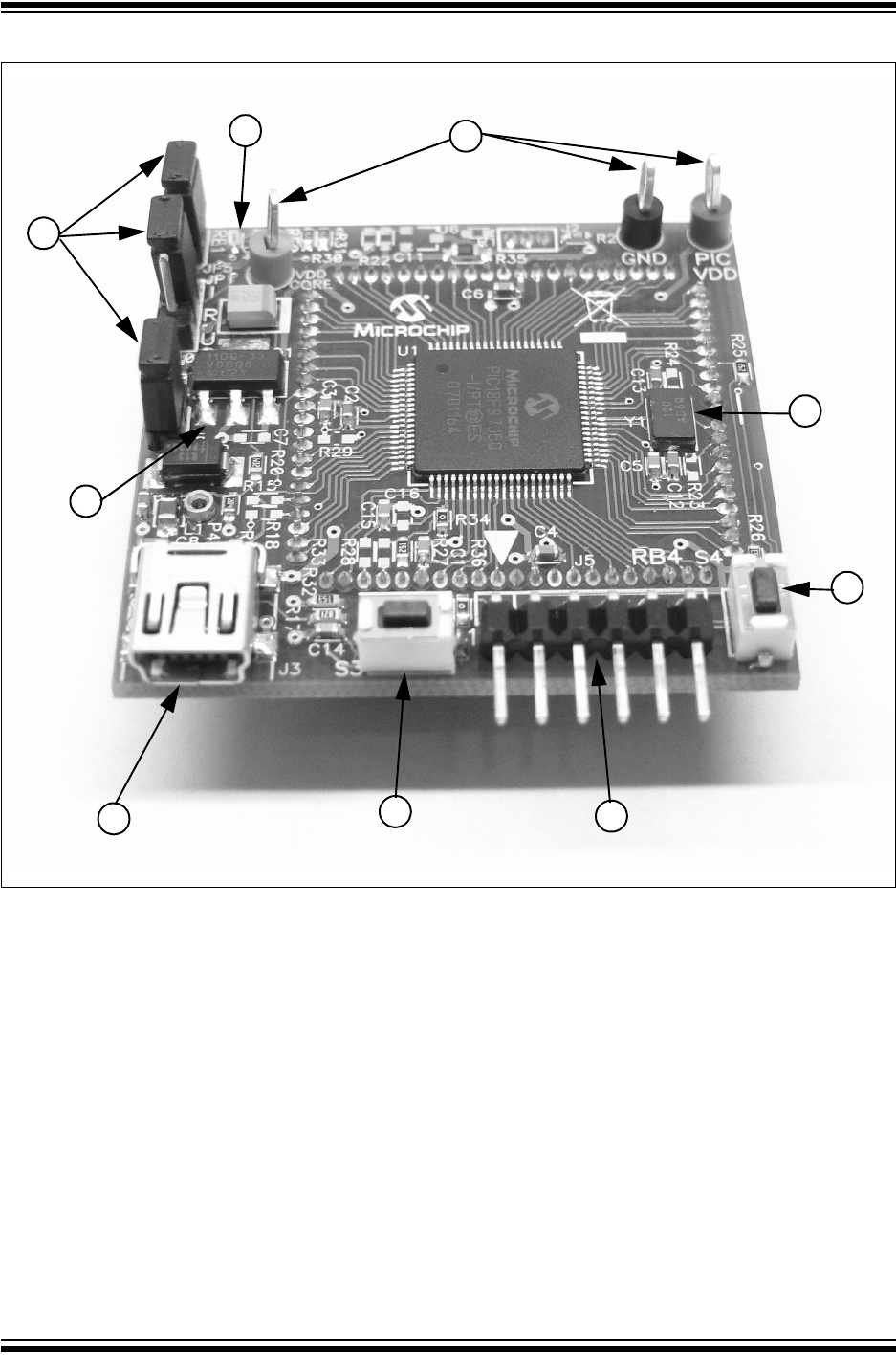
3.2 HARDWARE FEATURES
The PIC18F87J50 FS USB PIM has a number of hardware features intended to
make it useful as an initial development platform and demonstration board. Refer to
Appendix A. “PIC18F87J50 FS USB Plug-In Module Schematics” for schematics of
the PIM. The board offers the following hardware features:
1. 12 MHz miniature surface-mounted crystal.
2. 3.3V low IQ LDO linear regulator.
3. 2 bright red miniature LEDs (attached to I/O pins, RE0 and RE1).
4. MCLR push button for convenient device Reset.
5. General purpose push button (attached to I/O pin, RB4).
6. ICSP™ programming and debug 6-pin header.
7. USB mini-B connector.
8. Jumpers for added configurability (JP1, JP4, JP5).
9. Test points for convenient VDD, VDDCORE and GND measurements.
Figure 3-1 shows where these key components are located on the PIM with item
numbers corresponding to the above list.
PIC18F87J50 FS USB Plug-In Module User’s Guide
DS51678A-page 12 © 2007 Microchip Technology Inc.
FIGURE 3-1: KEY COMPONENT LOCATIONS
3.3 CRYSTAL
In order to use the USB module on the PIC18F87J50 family of microcontrollers, the
module requires a fixed 48 MHz or 6 MHz clock for use in Full-Speed or Low-Speed
modes, respectively. These clock frequencies can be derived from the internal 96 MHz
PLL, and the microcontroller core need not run at the same frequency as the USB
module. In order to use the 96 MHz PLL, a clock source which is an integer multiple of
4 MHz is required. A 12 MHz crystal is included on the board for this purpose.
On the PIC18F87J50 microcontroller, the oscillator pins (RA6 and RA7) route directly
to the 12 MHz crystal. Unlike most other I/O pins, these do not route directly to the “ICE
Module” female headers. Two resistor pads can be used to connect RA6 and RA7 to
the female header pins, but by default, these are left unpopulated. This is done to
prevent “crystal contention” between the 12 MHz crystal on the PIM and the 10 MHz
crystal on the HPC Explorer board.
9
3
8
2
746
5
1
JP5
JP1
JP4

Hardware Configuration/Jumper Settings
© 2007 Microchip Technology Inc. DS51678A-page 13
3.4 LINEAR REGULATOR/POWER MANAGEMENT
The USB interface provides +5V (nominal) at up to 500 mA (only 100 mA can be
ensured) for use by USB peripheral devices. In order to take advantage of this bus
provided power, a 3.3V low drop out, low quiescent current linear regulator
(TC1108-3.3VDB) has been included on the PIM. This enables the PIM to be purely bus
powered, providing power to both the PIM and the HPC Explorer board if connected.
Alternatively, when used in conjunction with the HPC Explorer, the PIM may obtain
power from the HPC board. When a suitable power source is connected to power jack,
J1 on the HPC Explorer board, the board will natively produce a regulated 5V provided
by the on-board adjustable linear regulator. When a PIM requiring 3.3V (such as the
PIC18F87J50 FS USB PIM) is plugged in, resistor, R2, located on the PIM alters the
feedback circuit of the adjustable linear regulator and configures it to produce 3.3V.
Therefore, no soldering or other modification is required to either the HPC Explorer or
the PIC18F87J50 FS USB PIM when they are used together.
Jumper, JP4, on the PIM serves two main purposes. JP4 is located in series with the
+5V VBUS supply from the USB cable to the rest of the PIM board (see Figure A-1 for
exact electrical location). In this location, the jumper cap can be removed, and a digital
current meter can be inserted across the posts of the header. This can be quite useful
during development, as it offers a means of determining how much current the applica-
tion (both the PIM and the HPC Explorer board if connected) is actively consuming from
the USB port. This is especially important when developing bus powered USB
applications that are intended to be fully USB compliant.
All USB devices are supposed to implement a low-power USB Suspend mode. The
host PC may, at its own discretion, halt all USB traffic (including Start-of-Frame
packets) to your device for more than 3 ms. Upon detecting this condition, the USB
peripheral device should drop to a low-power suspend state, whereby it draws no more
than 500 μA (or in some cases, 2.5 mA; see the USB 2.0 specifications section 7.2.3)
from the +5V VBUS supply. Two USB interrupts, UIR<IDLEIF> and UIR<ACTVIF>, are
useful for detecting when the low-power suspend condition is supposed to begin and
when it ends. The TC1108-3.3VDB linear regulator was chosen for its low dropout, low
quiescent current consumption and good transient response capability.

PIC18F87J50 FS USB Plug-In Module User’s Guide
DS51678A-page 14 © 2007 Microchip Technology Inc.
In addition to providing a convenient location for installing a digital current meter, JP4
also serves another purpose. In some cases, it may be undesirable to consume power
from the USB port, for example, when developing end applications that are always
self-powered or consume more than 300 mA (the maximum rating for the regulator). In
these cases, jumper cap, JP4, can be removed, and the PIM can obtain power from the
HPC Explorer board or directly from the test points.
Diode, D2, prevents the PIM from ever sourcing current onto the +5V VBUS pin of the
USB cable. The USB 2.0 specifications require that USB peripherals should never
source current onto the +5V VBUS line under any condition.
3.5 LEDs
Two high-efficiency, red LEDs have been included on the PIM. The LEDs are
connected to I/O pins, RE0 and RE1, and may be used for general purpose indication.
The LEDs are connected such that they turn on when the I/O pin controlling them is
driven high. Alternatively, if the I/O pin loading is undesirable (each LED consumes
approximately 1 mA when turned on), jumper cap covering, JP5, may be removed. This
will effectively disconnect both LEDs from their respective I/O pins.
3.6 PUSH BUTTONS
Two miniature push buttons are included on the PIM. Switch, S3 on the PIM, connects
to MCLR. It may be used to reset the microcontroller when the PIM is used either
stand-alone or while connected to the HPC Explorer board.
Pin, RB4 on the PIC18F87J50 microcontroller, is pulled up to VDD through a 15 kOhm
resistor (R26 on the PIM). If push button, S4 on the PIM, is pressed, it will pull RB4 low.
This push button may be used for any general purpose user interfacing purposes.
When the PIM is plugged into the HPC Explorer board, the RB0 push button on the
HPC Explorer will also work and can be used for additional general purpose user input.
3.7 JUMPERS
The PIM has three jumper headers on it to provide additional flexibility for
experimentation and development purposes.
JP1 – This is a three-pin header with the labels, ‘I’, ‘R’ and ‘U’. The ‘R’ is an abbreviation
referring to microcontroller pin, RB5. ‘I’ is an abbreviation referring to the “ICE” female
header pin for the RB5 signal. ‘U’ is an abbreviation for the USB VBUS line.
When the jumper is in the ‘R’ to ‘I’ position, the RB5 pin connects only to the ICE female
header pin, just like most of the other general purpose I/O pins. When the jumper is in
the ‘R’ to ‘U’ position, RB5 (which is 5.5V tolerant) can be used to sense when the USB
cable has been attached to the host, and when the host is actively providing power to
the +5V VBUS line. According to the USB 2.0 specifications, no device should ever pull
the D+ or D- lines high (such as with the D+ or D- pull-up resistor) until the host actively
powers the +5V VBUS line. This is intended to prevent self-powered peripherals from
ever sourcing even small amounts of power to the host when the host is not powered.
Small amounts of current could potentially prevent the host (and possibly other USB
peripherals connected to that host) from fully becoming depowered, which may cause
problems during power-up and initialization.

Hardware Configuration/Jumper Settings
© 2007 Microchip Technology Inc. DS51678A-page 15
Self-powered peripherals should periodically monitor the +5V VBUS line and detect
when it is driven high. Only when it is powered should user firmware enable the USB
module and turn on the D+ (for full speed) or D- (for low speed) pull-up resistor, signal-
ing device attach to the host. The recommended method of monitoring the +5V VBUS
line is to connect it to one of the microcontroller’s 5.5V tolerant I/O pins through a large
value resistor (such as 100 kOhms). The resistor serves to improve the ESD rugged-
ness of the circuit as well as to prevent microcontroller damage if user firmware should
ever unintentionally configure the I/O pin as an output.
Peripherals which are purely bus powered obtain all of their power directly from the +5V
VBUS line itself. For these types of devices, it is unnecessary to monitor when the VBUS
is powered, as the peripheral will not be able to source current on the D+, D- or VBUS
lines when the host is not powered.
JP4 – This jumper is located in series with the +5V VBUS power supply line from the
USB connector. When the jumper is removed, a current meter may be placed between
the header pins to measure the board current which is being drawn from the USB port.
Additionally, by removing the jumper cap altogether, JP4 provides a means of prevent-
ing the board from consuming USB power. See Section 3.4 “Linear Regulator/Power
Management” for more details.
JP5 – This jumper provides a means of removing the LED pin loading on the RE0 and
RE1 pins.
3.8 HARDWARE CONSIDERATIONS FOR COMPLIANCE TESTING
When developing USB applications that must pass the official USB compliance testing
process, it is recommended to select the USB cable and connector carefully. In order
to make a USB compliant application, the USB-IF requires that important USB building
blocks, such as cables and connectors, should also be individually compliant. For
example, if a standard USB B or mini-B connector is used on the application circuit
board, it should be capable of passing compliance tests specific for USB connectors.
USB building blocks which have officially gone through the compliance testing process
will have a Test ID (TID) number associated with them.
Microchip’s USB microcontrollers, such as the PIC18F87J50, have TID numbers
associated with them, and these numbers can be found at the USB design center:
http://www.microchip.com/usb (click on the “Full-Speed USB Solutions” link)
When developing products using standard USB cables and connectors, it is recom-
mended to know the TID number for those components prior to including them in the
design.

PIC18F87J50 FS USB Plug-In Module User’s Guide
DS51678A-page 16 © 2007 Microchip Technology Inc.
NOTES:

© 2007 Microchip Technology Inc. DS51678A-page 17
PIC18F87J50 FS USB
PLUG-IN MODULE
USER’S GUIDE
Chapter 4. Demo Code/Reference Firmware
To assist in the development of USB applications, Microchip provides a number of
demonstration firmware projects (such as HID, CDC, etc.), and other support materials,
such as application notes. The USB demonstration projects use the same basic USB
framework, which is referred to as the “MCHPFSUSB Firmware”. Documentation for
this firmware can be found in the “MCHPFSUSB Firmware User’s Guide” (DS51679).
The firmware projects are contained in an executable setup file which can be found
either on the CD-ROM disc, which distributes with the PIM, or at the Microchip USB
design center:
http://www.microchip.com/usb
Once the MCHPFSUSB Firmware has been installed, the MPLAB® IDE project contain-
ing the source code and hex file for the HID class, mouse like demonstration firmware,
that comes preprogrammed on the PIC18F87J50, can be found in the following
directory:
C:\MCHPFSUSB\fw\HID\Mouse
By default, the MPLAB IDE projects are configured to work with the PICDEM™ FS USB
Demo Board, which uses the PIC18F4550 microcontroller. Refer to the MCHPFSUSB
Firmware release notes for details on how to switch the projects over for use with the
PIC18F87J50.

PIC18F87J50 FS USB Plug-In Module User’s Guide
DS51678A-page 18 © 2007 Microchip Technology Inc.
NOTES:

© 2007 Microchip Technology Inc. DS51678A-page 19
PIC18F87J50 FS USB
PLUG-IN MODULE
USER’S GUIDE
Appendix A. PIC18F87J50 FS USB Plug-In Module Schematics
A.1 SCHEMATICS
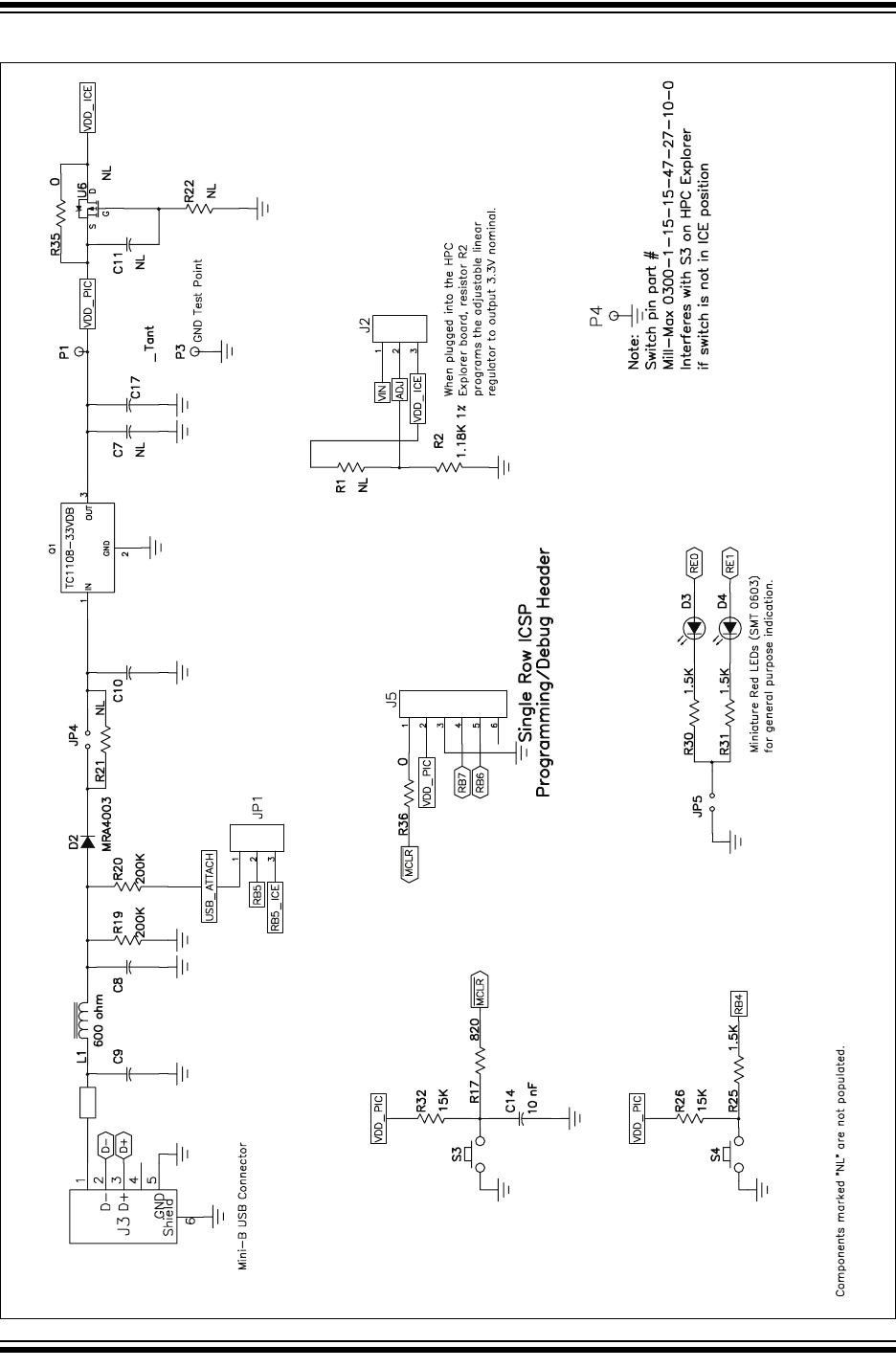
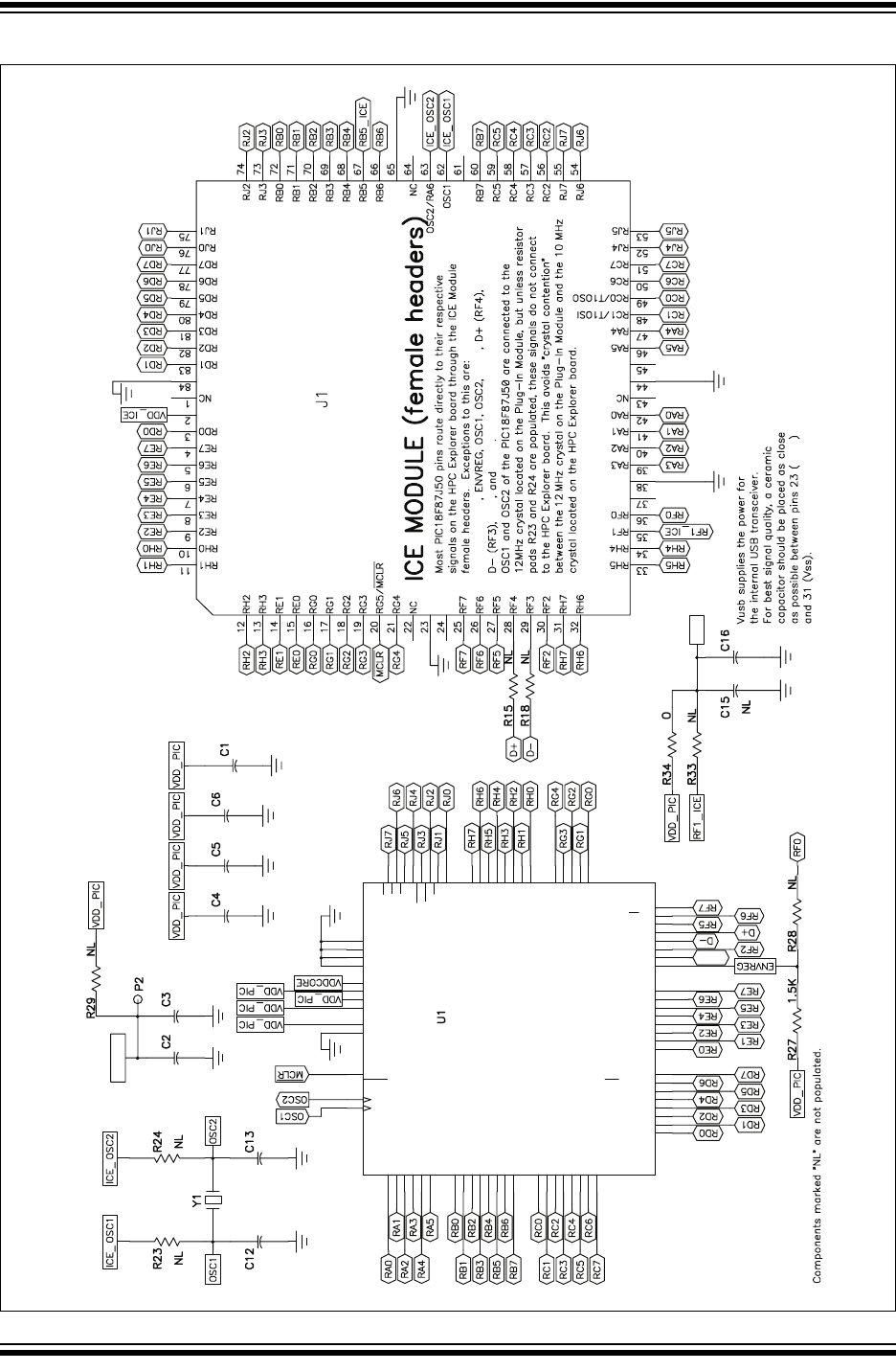
The PIC18F87J50 FS USB Plug-In Module schematics are shown in Figure A-1 and
Figure A-2. By default, the PIM ships from the factory with the PIC18F87J50
pre-installed in location U1. The PIC18F87J50 is the superset part in the device family,
and is therefore, a good starting point for developing USB applications that will
eventually use one of the other devices in the device family.
However, the pads of U1 have been designed to accommodate any of the products in
the PIC18F87J50 family of microcontrollers, both the 80-pin TQFP and 64-pin TQFP.
For example, if the PIC18F87J50 is carefully desoldered using hot air, and the pads are
cleaned using solder wick, it is possible to install the 64-pin TQFP PIC18F65J50 in its
place. This is possible since the pin pitch is the same between the 64-pin and 80-pin
TQFP packages, and the functionality is the same for pins which share the same loca-
tions between the two packages. Effectively, the 80-pin TQFP pads of U1 overlap with
the standard 64-pin TQFP pads.
The board revision number can be found etched into the copper on the bottom side of
the PCB underneath the programming header. The board revision number is the last
number in the line and is located inside the rectangular box.
PIC18F87J50 FS USB Plug-In Module User’s Guide
DS51678A-page 20 © 2007 Microchip Technology Inc.
FIGURE A-1: PIC18F87J50 FS USB PIM REV. 1 SCHEMATICS (SHEET 1 OF 2)
VBUS VBUS
1MF
.1 MF1MF2.2 MF
VDD Test Point
TM
PIC18F87J50 FS USB Plug-In Module Schematics
© 2007 Microchip Technology Inc. DS51678A-page 21
FIGURE A-2: PIC18F87J50 FS USB PIM REV. 1 SCHEMATICS (SHEET 2 OF 2)
49
OSC1/CLKI/RA7
32
VDD
23 VUSB 70
VSS
16 RF4/D+ 11
VSS
13 RF7/SS
72 RD0/AD0
67 RD3/AD3
64 RD6/AD6/SCK2/SCL2
78 RE2/AD10
75 RE5/AD13
7
RG2/RX2/DT2
80
RH1/A17
22
RH4/AN12
19
RH7/AN15
62
RJ0/ALE
59
RJ3/WRH
41
RJ6/LB
9
MCLR
26
AVSS
71
VDD
25
AVDD
48
VDD
17 RF3/D-
6
RG1/TX2/CK2
10
RG4/CCP5
5
RG0/ECCP3
8
RG3/CCP4
2
RH3/A19
20
RH6/AN14
1
RH2/A18
21
RH5/AN13
61
RJ1/OE
31
VSS
39
RJ4/BA0
42
RJ7/UB
40
RJ5/CE
69 RD1/AD1
68 RD2/AD2
66 RD4/AD4/SDO2
65 RD5/AD5/SDA2
63 RD7/AD7/SS2
77 RE3/AD11
74 RE6/AD14
76 RE4/AD12
4RE0/AD8
3RE1/AD9
73 RE7/AD15
15 RF5/AN10/CVREF
14 RF6/AN11
79
RH0/A16
60
RJ2/WRL
18 RF2/AN7
50
OSC2/CLKO/RA6
12
VDDCORE/VCAP
46 RC5/SDO1
43 RC2/CCP1
52 RB6/KBI2PGC
55 RB3/INT3/CCP2
58 RB0/INT0
33 RA5/AN4
28 RA2/AN2/VREF-
37 RC6/TX1/CK1
36 RC0/T1OSO/T13CKI
38 RC7/RX1/DT1
35 RC1/T1OSI/CCP2
44 RC3/SCK1/SCL1
45 RC4/SDI1/SDA1
47 RB7/KBI3/PGD
57 RB1/INT1
56 RB2/INT2
54 RB4/KBI0/PMA1
53 RB5/KBI1/PMA0
51
VSS
27 RA3/AN3/VREF+
30 RA0/AN0
29 RA1/AN1
34 RA4/T0CKI
24 ENVREG
VSS
VDD
VSS
VDD
.1 MF
.1 MF
.1 MF
.1 MF
.1 MF
4.7 MF
18 pF
VDDCORE Test Point
VDDCORE
18 pF
12 MHz
PIC18F87J50
.1 MF
VUSB
VDD
VDDCORE/VCAP
AVDD
VUSB
VUSB
AVDD
AVSS
VDD
VSS VSS
VDD
VUSB

PIC18F87J50 FS USB Plug-In Module User’s Guide
DS51678A-page 22 © 2007 Microchip Technology Inc.
NOTES:

© 2007 Microchip Technology Inc. DS51678A-page 23
PIC18F87J50 FS USB
PLUG-IN MODULE
USER’S GUIDE
Index
C
Crystal...................................................................... 12
Customer Notification Service.................................... 4
Customer Support...................................................... 4
D
Demo Code/Reference Firmware ............................ 17
Documentation
Conventions........................................................ 2
Layout ................................................................. 1
H
Hardware
Features............................................................ 11
Hardware Considerations for
Compliance Testing.............................................. 15
HPC Explorer Board
Use with the PIM................................................. 7
I
Input Buffer Selection................................................. 9
Internet Address......................................................... 3
J
Jumpers ................................................................... 14
JP1.................................................................... 14
JP4.................................................................... 15
JP5.................................................................... 15
K
Kit Contents ............................................................... 5
CD-ROM ............................................................. 5
PIC18F87J50 FS USB Plug-In Module
Demo Board ......................................... 5
USB mini-B Cable............................................... 5
L
LEDs ........................................................................ 14
Linear Regulator....................................................... 13
M
Microchip Internet Web Site ....................................... 3
Migrating to the PIC18F87J50 Family........................ 8
O
Oscillator Configuration.............................................. 9
Overview of PIC18F87J50 USB Capabilities ............. 6
P
Power Management ................................................. 13
Programming the MCU .............................................. 8
Push Buttons............................................................ 14
R
Reading, Recommended ........................................... 3
S
Schematics............................................................... 19
Special Function Register Addressing ....................... 8
U
Using the Preprogrammed Firmware ......................... 6
W
WWW Address........................................................... 3

DS51678A-page 24 © 2007 Microchip Technology Inc.
AMERICAS
Corporate Office
2355 West Chandler Blvd.
Chandler, AZ 85224-6199
Tel: 480-792-7200
Fax: 480-792-7277
Technical Support:
http://support.microchip.com
Web Address:
www.microchip.com
Atlanta
Duluth, GA
Tel: 678-957-9614
Fax: 678-957-1455
Boston
Westborough, MA
Tel: 774-760-0087
Fax: 774-760-0088
Chicago
Itasca, IL
Tel: 630-285-0071
Fax: 630-285-0075
Dallas
Addison, TX
Tel: 972-818-7423
Fax: 972-818-2924
Detroit
Farmington Hills, MI
Tel: 248-538-2250
Fax: 248-538-2260
Kokomo
Kokomo, IN
Tel: 765-864-8360
Fax: 765-864-8387
Los Angeles
Mission Viejo, CA
Tel: 949-462-9523
Fax: 949-462-9608
Santa Clara
Santa Clara, CA
Tel: 408-961-6444
Fax: 408-961-6445
Toronto
Mississauga, Ontario,
Canada
Tel: 905-673-0699
Fax: 905-673-6509
ASIA/PACIFIC
Asia Pacific Office
Suites 3707-14, 37th Floor
Tower 6, The Gateway
Harbour City, Kowloon
Hong Kong
Tel: 852-2401-1200
Fax: 852-2401-3431
Australia - Sydney
Tel: 61-2-9868-6733
Fax: 61-2-9868-6755
China - Beijing
Tel: 86-10-8528-2100
Fax: 86-10-8528-2104
China - Chengdu
Tel: 86-28-8665-5511
Fax: 86-28-8665-7889
China - Fuzhou
Tel: 86-591-8750-3506
Fax: 86-591-8750-3521
China - Hong Kong SAR
Tel: 852-2401-1200
Fax: 852-2401-3431
China - Qingdao
Tel: 86-532-8502-7355
Fax: 86-532-8502-7205
China - Shanghai
Tel: 86-21-5407-5533
Fax: 86-21-5407-5066
China - Shenyang
Tel: 86-24-2334-2829
Fax: 86-24-2334-2393
China - Shenzhen
Tel: 86-755-8203-2660
Fax: 86-755-8203-1760
China - Shunde
Tel: 86-757-2839-5507
Fax: 86-757-2839-5571
China - Wuhan
Tel: 86-27-5980-5300
Fax: 86-27-5980-5118
China - Xian
Tel: 86-29-8833-7252
Fax: 86-29-8833-7256
ASIA/PACIFIC
India - Bangalore
Tel: 91-80-4182-8400
Fax: 91-80-4182-8422
India - New Delhi
Tel: 91-11-4160-8631
Fax: 91-11-4160-8632
India - Pune
Tel: 91-20-2566-1512
Fax: 91-20-2566-1513
Japan - Yokohama
Tel: 81-45-471- 6166
Fax: 81-45-471-6122
Korea - Daegu
Tel: 82-53-744-4301
Fax: 82-53-744-4302
Korea - Seoul
Tel: 82-2-554-7200
Fax: 82-2-558-5932 or
82-2-558-5934
Malaysia - Penang
Tel: 60-4-646-8870
Fax: 60-4-646-5086
Philippines - Manila
Tel: 63-2-634-9065
Fax: 63-2-634-9069
Singapore
Tel: 65-6334-8870
Fax: 65-6334-8850
Taiwan - Hsin Chu
Tel: 886-3-572-9526
Fax: 886-3-572-6459
Taiwan - Kaohsiung
Tel: 886-7-536-4818
Fax: 886-7-536-4803
Taiwan - Taipei
Tel: 886-2-2500-6610
Fax: 886-2-2508-0102
Thailand - Bangkok
Tel: 66-2-694-1351
Fax: 66-2-694-1350
EUROPE
Austria - Wels
Tel: 43-7242-2244-39
Fax: 43-7242-2244-393
Denmark - Copenhagen
Tel: 45-4450-2828
Fax: 45-4485-2829
France - Paris
Tel: 33-1-69-53-63-20
Fax: 33-1-69-30-90-79
Germany - Munich
Tel: 49-89-627-144-0
Fax: 49-89-627-144-44
Italy - Milan
Tel: 39-0331-742611
Fax: 39-0331-466781
Netherlands - Drunen
Tel: 31-416-690399
Fax: 31-416-690340
Spain - Madrid
Tel: 34-91-708-08-90
Fax: 34-91-708-08-91
UK - Wokingham
Tel: 44-118-921-5869
Fax: 44-118-921-5820
WORLDWIDE SALES AND SERVICE
06/25/07
