PIC32MX FRM Section 34. Controller Area Network (CAN) PIC32 Family Reference Manual, Sect. 34
PIC32%20Family%20Reference%20Manual%2C%20Sect.%2034%20Controller%20Area%20Network%20(CAN)
User Manual: Pdf
Open the PDF directly: View PDF ![]() .
.
Page Count: 102 [warning: Documents this large are best viewed by clicking the View PDF Link!]
- Section 34. Controller Area Network (CAN)
- 34.1 Introduction
- 34.2 CAN Message Formats
- 34.3 CAN Registers
- 34.3.1 Module and CAN Bit Rate Configuration Registers
- 34.3.2 Interrupt and Status Registers
- 34.3.3 Mask and Filter Configuration Registers
- 34.3.4 FIFO Control Registers
- Table 34-1: CAN Controller Register Summary
- Register 34-1: CiCON: CAN Control Register(1,2,3)
- Register 34-2: CiCFG: CAN Baud Rate Configuration Register(1,2,3,4)
- Register 34-3: CiINT: CAN Interrupt Register(1,2,3)
- Register 34-4: CiVEC: CAN Interrupt Code Register(1,2,3)
- Register 34-5: CiTREC: CAN Transmit/Receive Error Count Register(1,2,3)
- Register 34-6: CiFSTAT: CAN FIFO Status Register(1,2,3)
- Register 34-7: CiRXOVF: CAN Receive FIFO Overflow Status Register(1,2,3)
- Register 34-8: CiTMR: CAN Timer Register(1,2,3,4,5)
- Register 34-9: CiRXMn: CAN Acceptance Filter Mask n Register (n = 0, 1, 2 or 3)(1,2,3,4)
- Register 34-10: CiFLTCON0: CAN Filter Control Register 0(1,2,3,4)
- Register 34-11: CiFLTCON1: CAN Filter Control Register 1(1,2,3,4)
- Register 34-12: CiFLTCON2: CAN Filter Control Register 2(1,2,3,4)
- Register 34-13: CiFLTCON3: CAN Filter Control Register 3(1,2,3,4)
- Register 34-14: CiFLTCON4: CAN Filter Control Register 4(1,2,3,4)
- Register 34-15: CiFLTCON5: CAN Filter Control Register 5(1,2,3,4)
- Register 34-16: CiFLTCON6: CAN Filter Control Register 6(1,2,3,4)
- Register 34-17: CiFLTCON7: CAN Filter Control Register 7(1,2,3,4)
- Register 34-18: CiRXFn: CAN Acceptance Filter n Register (n = 0 through 31)(1,2,3,4)
- Register 34-19: CiFIFOBA: CAN Message Buffer Base Address Register(1,2,3,4)
- Register 34-20: CiFIFOCONn: CAN FIFO Control Register (n = 0 through 31)(1,2,3)
- Register 34-21: CiFIFOINTn: CAN FIFO Interrupt Register (n = 0 through 31)(1,2,3)
- Register 34-22: CiFIFOUAn: CAN FIFO User Address Register (n = 0 through 31)(1,2,3,4)
- Register 34-23: CiFIFOCIn: CAN Module Message Index Register (n = 0 through 31)(1,2,3)
- 34.4 Enabling and Disabling the CAN Module
- 34.5 CAN Module Operating Modes
- 34.6 CAN Message Handling
- 34.7 Transmitting a CAN Message
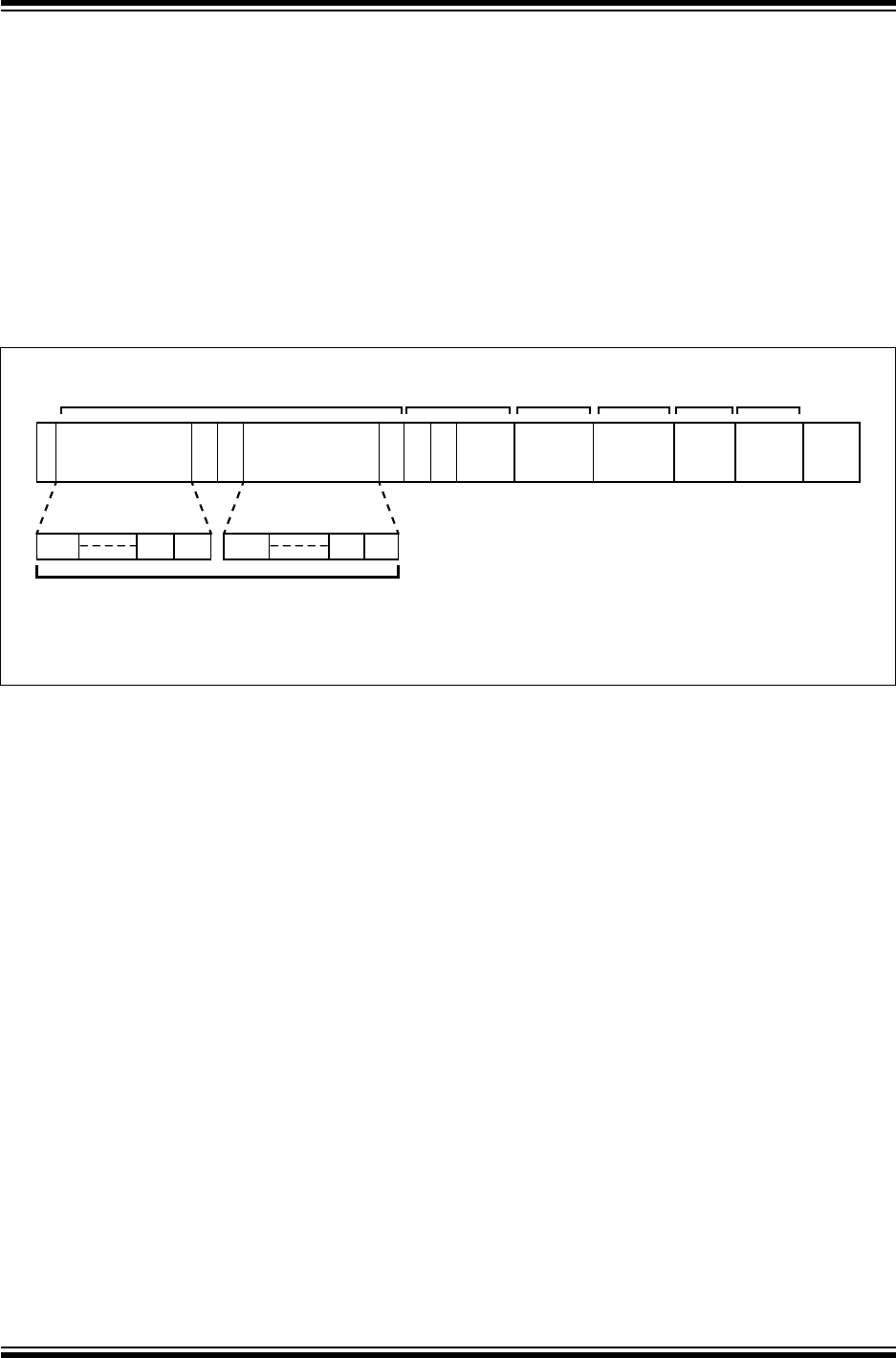
- 34.7.1 Format of Transmit Message Buffer
- Table 34-2: Transmit Message Buffer Format as Stored in System Memory
- Figure 34-11: Format of CMSGSID
- Figure 34-12: Format of CMSGEID
- Figure 34-13: Format of CMSGDATA0
- Figure 34-14: Format of CMSGDATA1
- Example 34-6: Implementing a CAN Message Buffer in Memory
- Example 34-7: Example Usage of the Data Structure
- 34.7.2 Requesting Transmit of a Message
- 34.7.3 Transmit Message Priority
- 34.7.4 Aborting Transmission of a Queued Message
- 34.7.5 Remote Transmit Request
- 34.7.6 Example Message Transmission FIFO Behavior
- Figure 34-16: FIFO Configuration for Example FIFO Behavior
- Figure 34-17: FIFO1 at Start
- Figure 34-18: FIFO1 - First Write
- Figure 34-19: FIFO1 - First Message Transmitted
- Figure 34-20: FIFO1 - Seventh Write About to Fill
- Figure 34-21: FIFO1 - Eighth Write Buffer Full
- Figure 34-22: FIFO1 - Fully Transmitted
- 34.7.1 Format of Transmit Message Buffer
- 34.8 CAN Message Filtering
- 34.9 Receiving a CAN Message
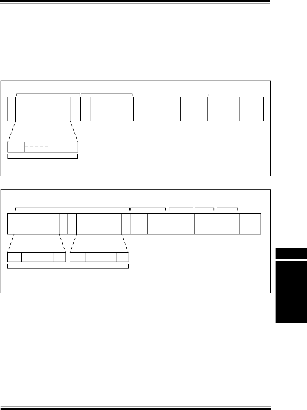
- Table 34-5: Receive Message Format as Stored in RAM - CiCON.CANCAP = 1, CFIFOCON.DONLY = 0
- Figure 34-26: Format of CMSGSID
- Figure 34-27: Format of CMSGEID
- Figure 34-28: Format of CMSGDATA0
- Figure 34-29: Format of CMSGDATA1
- Example 34-13: Implementing a CAN Full Receive Message Buffer in Memory
- Example 34-14: Example Usage of the Data Structure
- 34.9.1 Data-Only Receive Messages
- 34.9.2 Processing a Received Message
- 34.9.3 Example Receive FIFO Behavior
- 34.10 Bit Timing
- 34.11 CAN Error Management
- 34.12 CAN Interrupts
- 34.13 CAN Received Message Time Stamping
- 34.14 Low-Power Modes
- 34.15 Related Application Notes
- 34.16 Revision History

© 2009 Microchip Technology Inc. Preliminary DS61154A-page 34-1
Controller Area
Network (CAN)
34
Section 34. Controller Area Network (CAN)
HIGHLIGHTS
This section of the manual contains the following topics:
34.1 Introduction.............................................................................................................. 34-2
34.2 CAN Message Formats ........................................................................................... 34-4
34.3 CAN Registers......................................................................................................... 34-9
34.4 Enabling and Disabling the CAN Module .............................................................. 34-52
34.5 CAN Module Operating Modes.............................................................................. 34-53
34.6 CAN Message Handling ....................................................................................... 34-55
34.7 Transmitting a CAN Message................................................................................ 34-62
34.8 CAN Message Filtering.......................................................................................... 34-74
34.9 Receiving a CAN Message.................................................................................... 34-80
34.10 Bit Timing............................................................................................................... 34-88
34.11 CAN Error Management ........................................................................................ 34-91
34.12 CAN Interrupts....................................................................................................... 34-94
34.13 CAN Received Message Time Stamping............................................................... 34-98
34.14 Low-Power Modes................................................................................................. 34-98
34.15 Related Application Notes ................................................................................... 34-100
34.16 Revision History................................................................................................... 34-101
PIC32MX Family Reference Manual
DS61154A-page 34-2 Preliminary © 2009 Microchip Technology Inc.
34.1 INTRODUCTION
The PIC32MX Controller Area Network (CAN) module implements the CAN 2.0B protocol, which
is used primarily in industrial and automotive applications. This asynchronous serial data
communication protocol provides reliable communications in electrically noisy environments.
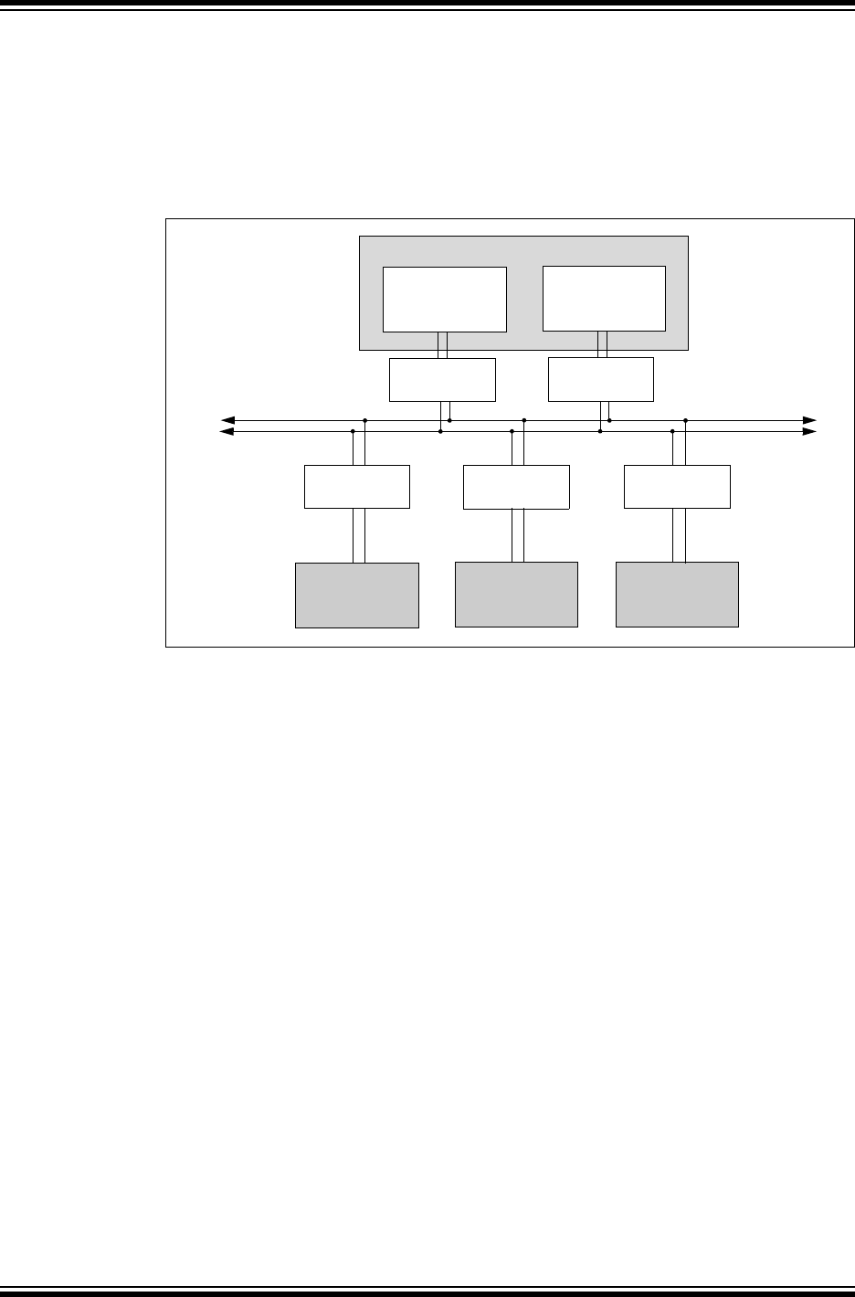
The PIC32MX device family integrates up to two CAN modules. Figure 34-1 illustrates a typical
CAN bus topology.
Figure 34-1: Typical CAN Bus Network
The CAN module supports the following key features:
• Standards Compliance:
- Full CAN 2.0B compliance
- Programmable bit rate up to 1 Mbps
• Message Reception and Transmission:
- 32 message FIFOs
- Each FIFO can have up to 32 messages for a total of 1024 messages
- FIFO can be a transmit message FIFO or a receive message FIFO
- User-defined priority levels for message FIFO’s used for transmission
- 32 acceptance filters for message filtering
- Four acceptance filter mask registers for message filtering
- Automatic response to Remote Transmit Request
- DeviceNet™ addressing support
• Additional Features:
- Loop-back, Listen All Messages and Listen Only modes for self-test, system
diagnostics, and bus monitoring
- Low-power operating modes
- CAN module is a bus master on the PIC32MX system bus
- Use of DMA is not required
- Dedicated time stamp timer
- Data-only Message Reception mode
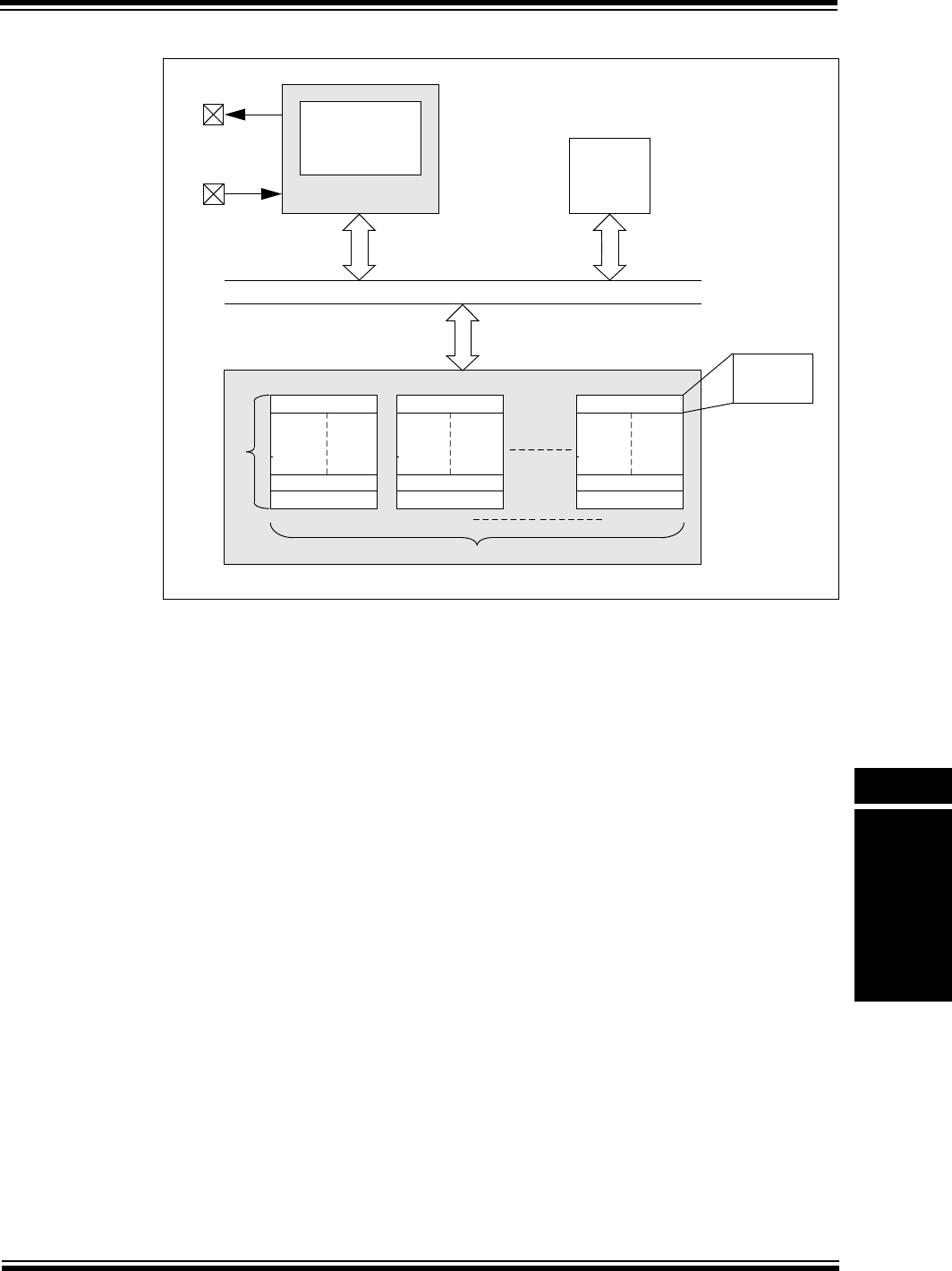
Figure 34-2 illustrates the general structure of the CAN module.
CAN
bus
CAN1
PIC®
with Integrated
ECAN
CAN
Transceiver
dsPIC33F
with Integrated
ECAN™
dsPIC30F
with Integrated
CAN
Transceiver
CAN Transceiver
CAN
Transceiver
CAN
CAN2
CAN
Transceiver
PIC32MX
© 2009 Microchip Technology Inc. Preliminary DS61154A-page 34-3
Section 34. Controller Area Network (CAN)
Controller Area
Network (CAN)
34
Figure 34-2: PIC32MX CAN Module Block Diagram
The CAN module consists of a protocol engine, message acceptance filters and message
assembly buffers. The protocol engine transmits and receives messages to and from the CAN
bus (as per CAN Bus 2.0B protocol). A received message is received in the receive message
assembly buffer. The received message is then filtered by the message acceptance filters. The
transmit message assembly buffer holds the message to be transmitted as it is processed by the
protocol engine.
The CAN message buffers reside in system RAM. There are no CAN message buffers in the
CAN module. Therefore, all messages are stored in system RAM. The CAN module is a bus
master on the PIC32MX system bus and will read and write data to system RAM as required. The
CAN module does not use the DMA for its operation. The CAN module will fetch messages from
the system RAM without DMA or CPU intervention.
Message Buffer 31
Message Buffer 1
Message Buffer 0
Message Buffer 31
Message Buffer 1
Message Buffer 0
Message Buffer 31
Message Buffer 1
Message Buffer 0
FIFO0 FIFO1 FIFO31
System RAM
Up to 32 Message Buffers
CAN Message FIFO (up to 32 FIFOs)
Message
Buffer Size
2 or 4 Words
System Bus
CPU
CAN Module
32 Filters
4 Masks
CxTX
CxRX

PIC32MX Family Reference Manual
DS61154A-page 34-4 Preliminary © 2009 Microchip Technology Inc.
34.2 CAN MESSAGE FORMATS
The CAN bus protocol uses asynchronous communication. Information is passed from
transmitters to receivers in data frames, which are composed of byte fields that define the
contents of the data frame, as shown in Figure 34-3.
Each frame begins with a Start-of-Frame (SOF) bit and terminates with an End-of-Frame (EOF)
bit field. The SOF is followed by arbitration and control fields, which identify the message type,
format, length and priority. This information allows each node on the CAN bus to respond
appropriately to the message. The data field conveys the message content and is of variable
length, ranging from 0 to 8 bytes. Error protection is provided by the Cyclic Redundancy Check
(CRC) and acknowledgement (ACK) fields.
Figure 34-3: CAN Bus Message Frame
The CAN bus protocol supports four frame types:
•Data Frame – carries data from transmitter to the receivers
•Remote Frame – transmitted by a node on the bus, to request transmission of a data
frame with the same identifier from another node
•Error Frame – transmitted by any node when it detects an error
•Overload Frame – provides an extra delay between successive Data or remote frames
•Interframe Space – provides a separation between successive frames
The CAN 2.0B specification defines two additional data formats:
•Standard Data Frame – intended for standard messages that use 11 identifier bits
•Extended Data Frame – intended for extended messages that use 29 identifier bits
There are three versions of CAN bus specifications:
•2.0A – considers 29-bit identifier as error
•2.0B Passive – ignores 29-bit identifier messages
•2.0B Active – handles both 11-bit and 29-bit identifier
The PIC32MX CAN module is compliant with the CAN 2.0B active specification while providing
enhanced message filtering capabilities.
Note: Refer to the Bosch CAN bus specification for detailed information on the CAN
protocol.
S
O
F
ARBITRATION CONTROL DATA
E
O
F
ACKCRC

© 2009 Microchip Technology Inc. Preliminary DS61154A-page 34-5
Section 34. Controller Area Network (CAN)
Controller Area
Network (CAN)
34
34.2.1 Standard Data Frame
The standard data frame message begins with a Start-of-Frame bit followed by a 12-bit
arbitration field, as shown in Figure 34-4. The arbitration field contains an 11-bit identifier and the
Remote Transmit Request (RTR) bit. The identifier defines the type of information contained in
the message and is used by each receiving node to determine if the message is of interest. The
RTR bit distinguishes a data frame from a remote frame. For a standard data frame, the RTR bit
is clear.
Following the arbitration field is a 6-bit control field, which provides more information about the
contents of the message. The first bit in the control field is an Identifier Extension (IDE) bit, which
distinguishes the message as either a standard or extended data frame. A standard data frame
is indicated by a dominant state (logic level ‘0’) during transmission of the IDE bit. The second
bit in the control field is a reserved (RB0) bit, which is in the dominant state (logic level ‘0’). The
last 4 bits in the control field represent the Data Length Code (DLC), which specifies the number
of data bytes present in the message.
The data field follows the control field. This field carries the message data – the actual payload
of the data frame. This field is of variable length, ranging from 0 to 8 bytes. The number of bytes
is user-selectable.
The data field is followed by the Cyclic Redundancy Check (CRC) field, which is a 15-bit CRC
sequence with one delimiter bit.
The acknowledgement (ACK) field is sent as a recessive bit (logic level ‘1’) and is overwritten as
a dominant bit by any receiver that has received the data correctly. The message is
acknowledged by the receiver regardless of the result of the acceptance filter comparison.
The last field is the End-of-Frame field, which consists of 7 recessive bits that indicate the end of
message.
Figure 34-4: Format of the Standard Data Frame
SID10 SID1
S
O
F
IDENTIFIER
11 Bits
R
T
R
I
D
E
RB0 DLC
4 Bits
DATA
8 Bytes
CRC
16 Bits
ACK
2 Bits
EOF
7 Bits
IFS
3 Bits
SID0
9/19/2006 - 9/26/2006
11-bit Identifier
Interframe Space
9/19/2006 - 9/26/2006 9/19/2006 - 9/26/2006
Data
9/19/2006 - 9/26/2006
9/19/2006 - 9/26/2006
9 - 9/26/2006
Frame Interframe Space
9/19/2006 - 9/26/2006
IDE is Dominant (Logical ‘0’)
RTR is Dominant (Logical ‘0’)
RB0 is Dominant (Logical ‘0’)
/19/
Arbitration
Field
Control
Field
Field
CRC
Field
ACK
Field
End-of-
PIC32MX Family Reference Manual
DS61154A-page 34-6 Preliminary © 2009 Microchip Technology Inc.
34.2.2 Extended Data Frame
The extended data frame begins with an SOF bit followed by a 31-bit arbitration field, as shown
in Figure 34-5. The arbitration field for the extended data frame contains 29 identifier bits in two
fields separated by a Substitute Remote Request (SRR) bit and an IDE bit. The SRR bit
determines if the message is a remote frame. SRR = 1 for extended data frames. The IDE bit
indicates the data frame type. For the extended data frame, IDE = 1.
The extended data frame Control field consists of 7 bits. The first bit is the RTR. For the extended
data frame, RTR = 0. The next two bits, RB1 and RB0, are reserved bits that are in the dominant
state (logic level ‘0’). The last 4 bits in the Control field are the Data Length Code, which specifies
the number of data bytes present in the message.
The remaining fields in an extended data frame are identical to a standard data frame.
Figure 34-5: Format of the Extended Data Frame
SID10 SID1
S
O
F
IDENTIFIER
11 Bits
S
R
R
I
D
E
R
T
R
DLC
4 BITS
CRC
16 BITS
ACK
2 BITS
EOF
7 BITS
IFS
3 BITS
SID0
Field
29-bit Identifier
9/19/2006 - 9/26/2006
Control
9/19/2006 - 9/26/2006
CRC
9/19/2006 - 9/26/2006
IDENTIFIER
18 BITS
EID17 EID1 EID0
R
B
1
R
B
0
IDE is Recessive (Logical ‘1’)
SRR is Recessive (Logical ‘1’)
RTR is Dominant (Logical ‘0’)
RB0 is Dominant (Logical ‘0’)
RB1 is Dominant (Logical ‘0’)
9/19/2006 - 9/26/2006
ACK End-of-
Frame
9/19/2006 - 9/26/20069/19/2006 - 9/26/2006
Data
DATA
8 Bytes
Arbitration
Field Field Field Field
© 2009 Microchip Technology Inc. Preliminary DS61154A-page 34-7
Section 34. Controller Area Network (CAN)
Controller Area
Network (CAN)
34
34.2.3 Remote Frame
A node expecting to receive data from another node can initiate transmission of the respective
data by the source node by sending a remote frame. A remote frame can be in standard format
(Figure 34-6) or extended format (Figure 34-7).
A Remote frame is similar to a data frame, with the following exceptions:
• The RTR bit is recessive (RTR = 1)
• There is no Data field (DLC = 0)
Figure 34-6: Format of the Standard Remote Frame
Figure 34-7: Format of the Extended Remote Frame
SID10 SID1
S
O
F
IDENTIFIER
11 Bits
R
T
R
I
D
E
DLC
4 Bits
CRC
16 Bits
ACK
2 Bits
EOF
7 Bits
IFS
3 Bits
SID0
11-bit Identifier
RB0
IDE is Dominant (Logical ‘0’)
RTR is Recessive (Logical ‘1’)
RB0 is Dominant (Logical ‘0’)
Arbitration Field Control Field CRC Field ACK Field End-of-Frame
SID10 SID0
S
O
F
IDENTIFIER
11 Bits
S
R
R
I
D
E
R
T
R
DLC
4 Bits
CRC
16 Bits
ACK
2 Bits
EOF
7 Bits
IFS
3 Bits
SID1
Arbitration Field
29-bit Identifier
Control Field CRC Field
IDENTIFIER
18 Bits
EID17 EID1 EID0
R
B
1
R
B
0
IDE is Recessive (Logical ‘1’)
SRR is Recessive (Logical ‘1’)
RTR is Recessive (Logical ‘1’)
RB0 is Dominant (Logical ‘0’)
RB1 is Dominant (Logical ‘0’)
ACK Field
End-of-
Frame

PIC32MX Family Reference Manual
DS61154A-page 34-8 Preliminary © 2009 Microchip Technology Inc.
34.2.4 Error Frame
An error frame is generated by any node that detects a bus error. An error frame consists of an
error flag field followed by an error delimiter field. The error delimiter consists of 8 recessive bits
and allows the bus nodes to restart communications cleanly after an error has occurred. There
are two types of error flag fields, depending on the error status of the node that detects the error:
•Error Active Flag – contains 6 consecutive dominant bits, which forces all other nodes on
the network to generate error echo flags, thereby resulting in a series of 6 to 12 dominant
bits on the bus.
•Error Passive Flag – contains 6 consecutive recessive bits, with the result that unless the
bus error is detected by the transmitting node, the transmission of an error passive flag will
not affect the communications of any other node on the network.
34.2.5 Overload Frame
An overload frame can be generated by a node either when a dominant bit is detected during
interframe space or when a node is not yet ready to receive the next message (for example, if it
is still reading the previous received message). An overload frame has the same format as an
error frame with an active error flag, but can only be generated during Interframe space. It
consists of an overload flag field with 6 dominant bits followed by an overload delimiter field with
8 recessive bits. A node can generate a maximum of two sequential overload frames to delay the
start of the next message.
34.2.6 Interframe Space
Interframe space separates successive frames being transmitted on the CAN bus. It consists of
at least 3 recessive bits, referred to as intermission. The interframe space allows nodes time to
internally process the previously received message before the start of the next frame. If the
transmitting node is in the Error Passive state, an additional 8 recessive bits will be inserted in
the interframe space before any other message is transmitted by the node. This period is called
a suspend transmit field and allows time for other transmitting nodes to take control of the bus.

© 2009 Microchip Technology Inc. Preliminary DS61154A-page 34-9
Section 34. Controller Area Network (CAN)
Controller Area
Network (CAN)
34
34.3 CAN REGISTERS
The CAN module registers can be classified by their function into the following groups:
• Module and CAN bit rate Configuration registers
• Interrupt and Status Registers
• Mask and Filter Configuration registers
• FIFO Control registers
34.3.1 Module and CAN Bit Rate Configuration Registers
•CiCON: CAN Control Register
This register is used to set up the CAN module operational mode and DeviceNet addressing.
•CiCFG: CAN Baud Rate Configuration Register
This register contains control bits to set the period of each time quantum, using the baud rate
prescaler, and specifies Synchronization Jump Width (SJW) in terms of time quanta. It is
also used to program the number of time quanta in each CAN bit segment, including the
propagation and phase segments 1 and 2.
34.3.2 Interrupt and Status Registers
•CiINT: CAN Interrupt Register
This register allows various CAN module interrupt sources to be enabled and disabled. It
also contains interrupt status flags.
•CiVEC: CAN Interrupt Code Register
This register provides status bits which provide information on CAN module interrupt source
and message filter hits. These values can be used to implement a jump table for handling
different cases.
•CiTREC: CAN Transmit/Receive Error Count Register
This register provides information on Transmit and Receive Error Counter values. It also has
bits which indicate various warning states.
•CiFSTAT: CAN FIFO Status Register
This register contains interrupt status flag for all the FIFOs.
•CiRXOVF: CAN Receive FIFO Overflow Status Register
This register contains overflow interrupt status flag for all the FIFOs.
•CiTMR: CAN Timer Register
This register contains CAN Message Timestamp timer and a Prescaler.
34.3.3 Mask and Filter Configuration Registers
•CiRXMn: CAN Acceptance Filter Mask n Register (n = 0, 1, 2 or 3)
These registers allow the configuration of the filter masks. A total of four masks are
available.
• CiFLTCONn: CAN Acceptance Filter Control Register n (n = 0 through 7)
These registers allow the association of FIFO and Masks with a filter. A Filter can be
associated with any one mask. It also contains a filter enable/disable bit.
•CiRXFn: CAN Acceptance Filter n Register (n = 0 through 31)
These registers specify the filter to be applied to the received message. A total of 32 filters
are available.
Note: The ‘i’ shown in the register identifier refers to CAN1 or CAN2

PIC32MX Family Reference Manual
DS61154A-page 34-10 Preliminary © 2009 Microchip Technology Inc.
34.3.4 FIFO Control Registers
•CiFIFOBA: CAN Message Buffer Base Address Register
This register holds the base (start) address of the CAN message buffer area. This is a
physical address.
•CiFIFOCONn: CAN FIFO Control Register (n = 0 through 31)
These registers allow the control and configuration of CAN Message FIFOs.
•CiFIFOINTn: CAN FIFO Interrupt Register (n = 0 through 31)
These registers allow the individual FIFO interrupt sources to be enabled or disabled. They
also contain interrupt status bits.
•CiFIFOUAn: CAN FIFO User Address Register (n = 0 through 31)
These registers provide the address of the memory location in the CAN message FIFO from
where the next message can be read or where the next message should be written to.
•CiFIFOCIn: CAN Module Message Index Register (n = 0 through 31)
These registers provide the message buffer index (in the message FIFO) of the next
message that the CAN module will transmit or where the next received message will be
saved.
Table 34-1 provides a summary of all CAN-related registers. Corresponding registers appear
after the summary, followed by a detailed description of each register. All unimplemented
registers and/or bits within a register read as zeros.

© 2009 Microchip Technology Inc. Preliminary DS61154A-page 34-11
Section 34. Controller Area Network (CAN)
Controller Area
Network (CAN)
34
Table 34-1: CAN Controller Register Summary
Address
Offset Name Bit
Range
Bit
31/2315/7
Bit
30/22/14/6
Bit
29/21/13/5
Bit
28/20/12/4
Bit
27/19/11/3
Bit
26/18/10/2
Bit
25/17/9/1
Bit
24/16/8/0
0x00 CiCON(1,2,3) 31:24 ———— ABAT REQOP<2:0>
23:16 OPMOD<2:0> CANCAP — — — —
15:8 ON —SIDLE— CANBUSY — — —
7:0 ——— DNCNT<4:0>
0x10 CiCFG(1,2,3) 31:24 — — — — — — — —
23:16 — WAKFIL — — — SEG2PH<2:0>
15:8 SEG2PHTS SAM SEG1PH<2:0> PRSEG<2:0>
7:0 SJW<1:0> BRP<5:0>
0x20 CiINT(1,2,3) 31:24 IVRIE WAKIE CERRIE SERRIE RBOVIE — — —
23:16 — — — — MODIE CTMRIE RBIE TBIE
15:8 IVRIF WAKIF CERRIF SERRIF RBOVIF — — —
7:0 — — — — MODIF CTMRIF RBIF TBIF
0x30 CiVEC(1,2,3) 31:24 — — — — — — — —
23:16 — — — — — — — —
15:8 ———FILHIT<4:0>
7:0 — ICOD<6:0>
0x40 CiTREC(1,2,3) 31:24 — — — — — — — —
23:16 —— TXBO TXBP RXBP TXWARN RXWARN EWARN
15:8 TEC<7:0>
7:0 REC<7:0>
0x50 CiFSTAT(1,2,3) 31:24 FIFOIP31 FIFOIP30 FIFOIP29 FIFOIP28 FIFOIP27 FIFOIP26 FIFOIP25 FIFOIP24
23:16 FIFOIP23 FIFOIP22 FIFOIP21 FIFOIP20 FIFOIP19 FIFOIP18 FIFOIP17 FIFOIP16
15:8 FIFOIP15 FIFOIP14 FIFOIP13 FIFOIP12 FIFOIP11 FIFOIP10 FIFOIP9 FIFOIP8
7:0 FIFOIP7 FIFOIP6 FIFOIP5 FIFOIP4 FIFOIP3 FIFOIP2 FIFOIP1 FIFOIP0
0x60 CiRXOVF(1,2,3) 31:24 RXOVF31 RXOVF30 RXOVF29 RXOVF28 RXOVF27 RXOVF26 RXOVF25 RXOVF24
23:16 RXOVF23 RXOVF22 RXOVF21 RXOVF20 RXOVF19 RXOVF18 RXOVF17 RXOVF16
15:8 RXOVF15 RXOVF14 RXOVF13 RXOVF12 RXOVF11 RXOVF10 RXOVF9 RXOVF8
7:0 RXOVF7 RXOVF6 RXOVF5 RXOVF4 RXOVF3 RXOVF2 RXOVF1 RXOVF0
0x70 CiTMR(1,2,3) 31:24 CANTS<15:8>
23:16 CANTS<7:0>
15:8 CANTSPRE<15:8>
7:0 CANTSPRE<7:0>
0x80 CiRXM0(1,2,3) 31:24 SID<10:3>
23:16 SID<2:0> -— MIDE — EID<17:16>
15:8 EID<15:8>
7:0 EID<7:0>
0x90 CiRXM1(1,2,3) 31:24 SID<10:3>
23:16 SID<2:0> -— MIDE — EID<17:16>
15:8 EID<15:8>
7:0 EID<7:0>
0xA0 CiRXM2(1,2,3) 31:24 SID<10:3>
23:16 SID<2:0> -— MIDE — EID<17:16>
15:8 EID<15:8>
7:0 EID<7:0>
Note 1: This register has an associated Clear register at an offset of 0x4 bytes. These registers have the same name with CLR appended to the
end of the register name (e.g., CiCONCLR). Writing a ‘1’ to any bit position in the Clear register will clear valid bits in the associated
register. Reads from the Clear register should be ignored.
2: This register has an associated Set register at an offset of 0x8 bytes. These registers have the same name with SET appended to the end
of the register name (e.g., CiCONSET). Writing a ‘1’ to any bit position in the Set register will set valid bits in the associated register.
Reads from the Set register should be ignored.
3: This register has an associated Invert register at an offset of 0xC bytes. These registers have the same name with INV appended to the
end of the register name (e.g., CiCONINV). Writing a ‘1’ to any bit position in the Invert register will invert valid bits in the associated
register. Reads from the Invert register should be ignored.

PIC32MX Family Reference Manual
DS61154A-page 34-12 Preliminary © 2009 Microchip Technology Inc.
0xB0 CiRXM3(1,2,3) 31:24 SID<10:3>
23:16 SID<2:0> -— MIDE — EID<17:16>
15:8 EID<15:8>
7:0 EID<7:0>
0xC0 CiFLTCON0(1,2,3) 31:24 FLTEN3 MSEL3<1:0> FSEL3<4:0>
23:16 FLTEN2 MSEL2<1:0> FSEL2<4:0>
15:8 FLTEN1 MSEL1<1:0> FSEL1<4:0>
7:0 FLTEN0 MSEL0<1:0> FSEL0<4:0>
0xD0 CiFLTCON1(1,2,3) 31:24 FLTEN7 MSEL7<1:0> FSEL7<4:0>
23:16 FLTEN6 MSEL6<1:0> FSEL6<4:0>
15:8 FLTEN5 MSEL5<1:0> FSEL5<4:0>
7:0 FLTEN4 MSEL4<1:0> FSEL4<4:0>
0xE0 CiFLTCON2(1,2,3) 31:24 FLTEN11 MSEL11<1:0> FSEL11<4:0>
23:16 FLTEN10 MSEL10<1:0> FSEL10<4:0>
15:8 FLTEN9 MSEL9<1:0> FSEL9<4:0>
7:0 FLTEN8 MSEL8<1:0> FSEL8<4:0>
0xF0 CiFLTCON3(1,2,3) 31:24 FLTEN15 MSEL15<1:0> FSEL15<4:0>
23:16 FLTEN14 MSEL14<1:0> FSEL14<4:0>
15:8 FLTEN13 MSEL13<1:0> FSEL13<4:0>
7:0 FLTEN12 MSEL12<1:0> FSEL12<4:0>
0x100 CiFLTCON4(1,2,3) 31:24 FLTEN19 MSEL19<1:0> FSEL19<4:0>
23:16 FLTEN18 MSEL18<1:0> FSEL18<4:0>
15:8 FLTEN17 MSEL17<1:0> FSEL17<4:0>
7:0 FLTEN16 MSEL16<1:0> FSEL16<4:0:
0x110 CiFLTCON5(1,2,3) 31:24 FLTEN23 MSEL23<1:0> FSEL23<4:0>
23:16 FLTEN22 MSEL22<1:0> FSEL22<4:0>
15:8 FLTEN21 MSEL21<1:0> FSEL21<4:0>
7:0 FLTEN20 MSEL20<1:0> FSEL20<4:0>
0x120 CiFLTCON6(1,2,3) 31:24 FLTEN27 MSEL27<1:0> FSEL27<4:0>
23:16 FLTEN26 MSEL26<1:0> FSEL26<4:0>
15:8 FLTEN25 MSEL25<1:0> FSEL25<4:0>
7:0 FLTEN24 MSEL24<1:0> FSEL24<4:0>
0x130 CiFLTCON7(1,2,3) 31:24 FLTEN31 MSEL31<1:0> FSEL31<4:0>
23:16 FLTEN30 MSEL30<1:0> FSEL30<4:0>
15:8 FLTEN29 MSEL29<1:0> FSEL29<4:0>
7:0 FLTEN28 MSEL28<1:0> FSEL28<4:0>
0x140 CiRXFn(1,2,3)
(n = 0 through 31)
31:24 SID<10:3>
23:16 SID<2:0> -— EXID — EID<17:16>
15:8 EID<15:8>
7:0 EID<7:0>
0x340 CiFIFOBA(1,2,3) 31:24 CiFIFOBA<31:24>
23:16 CiFIFOBA<23:16>
15:8 CiFIFOBA<15:8>
7:0 CiFIFOBA<7:0>
0x350 CiFIFOCONn(1,2,3)
(n = 0 through 31)
31:24 — — — — — — — —
23:16 ———FSIZE<4:0>
15:8 — FRESET UINC DONLY — — — —
7:0 TXEN TXABAT TXLARB TXERR TXREQ RTREN TXPRI<1:0>
Table 34-1: CAN Controller Register Summary (Continued)
Address
Offset Name Bit
Range
Bit
31/2315/7
Bit
30/22/14/6
Bit
29/21/13/5
Bit
28/20/12/4
Bit
27/19/11/3
Bit
26/18/10/2
Bit
25/17/9/1
Bit
24/16/8/0
Note 1: This register has an associated Clear register at an offset of 0x4 bytes. These registers have the same name with CLR appended to the
end of the register name (e.g., CiCONCLR). Writing a ‘1’ to any bit position in the Clear register will clear valid bits in the associated
register. Reads from the Clear register should be ignored.
2: This register has an associated Set register at an offset of 0x8 bytes. These registers have the same name with SET appended to the end
of the register name (e.g., CiCONSET). Writing a ‘1’ to any bit position in the Set register will set valid bits in the associated register.
Reads from the Set register should be ignored.
3: This register has an associated Invert register at an offset of 0xC bytes. These registers have the same name with INV appended to the
end of the register name (e.g., CiCONINV). Writing a ‘1’ to any bit position in the Invert register will invert valid bits in the associated
register. Reads from the Invert register should be ignored.

© 2009 Microchip Technology Inc. Preliminary DS61154A-page 34-13
Section 34. Controller Area Network (CAN)
Controller Area
Network (CAN)
34
0x360 CiFIFOINTn(1,2,3)
(n = 0 through 31)
31:24 ————— TXNFULLIE TXHALFIE TXEMPTYIE
23:16 ———— RXOVFLIE RXFULLIE RXHALFIE RXNEMPTYIE
15:8 ————— TXNFULLIF TXHALFIF TXEMPTYIF
7:0 ———— RXOVFLIF RXFULLIF RXHALFIF RXNEMPTYIF
0x370 CiFIFOUAn(1,2,3)
(n = 0 through 31)
31:24 CiFIFOUA<31:24>
23:16 CiFIFOUA<23:16>
15:8 CiFIFOUA<15:8>
7:0 CiFIFOUA<7:0>
0x380 CiFIFOCIn(1,2,3)
(n = 0 through 31)
31:24 — — — — — — — —
23:16 — — — — — — — —
15:8 — — — — — — — —
7:0 ——— CiFIFOCI<4:0>
Table 34-1: CAN Controller Register Summary (Continued)
Address
Offset Name Bit
Range
Bit
31/2315/7
Bit
30/22/14/6
Bit
29/21/13/5
Bit
28/20/12/4
Bit
27/19/11/3
Bit
26/18/10/2
Bit
25/17/9/1
Bit
24/16/8/0
Note 1: This register has an associated Clear register at an offset of 0x4 bytes. These registers have the same name with CLR appended to the
end of the register name (e.g., CiCONCLR). Writing a ‘1’ to any bit position in the Clear register will clear valid bits in the associated
register. Reads from the Clear register should be ignored.
2: This register has an associated Set register at an offset of 0x8 bytes. These registers have the same name with SET appended to the end
of the register name (e.g., CiCONSET). Writing a ‘1’ to any bit position in the Set register will set valid bits in the associated register.
Reads from the Set register should be ignored.
3: This register has an associated Invert register at an offset of 0xC bytes. These registers have the same name with INV appended to the
end of the register name (e.g., CiCONINV). Writing a ‘1’ to any bit position in the Invert register will invert valid bits in the associated
register. Reads from the Invert register should be ignored.

PIC32MX Family Reference Manual
DS61154A-page 34-14 Preliminary © 2009 Microchip Technology Inc.
Register 34-1: CiCON: CAN Control Register(1,2,3)
U-0 U-0 U-0 U-0 S/HC-0 R/W-1 R/W-0 R/W-0
— — — —ABAT REQOP<2:0>
bit 31 bit 24
R-1 R-0 R-0 R/W-0 U-0 U-0 U-0 U-0
OPMOD<2:0> CANCAP — — — —
bit 23 bit 16
R/W-0 r-0 R/W-0 U-0 R-0 U-0 U-0 U-0
ON(4) —SIDLE— CANBUSY — — —
bit 15 bit 8
U-0 U-0 U-0 R/W-0 R/W-0 R/W-0 R/W-0 R/W-0
— — — DNCNT<4:0>
bit 7 bit 0
Legend: HC = Hardware Clear S = Settable bit r =Reserved
R = Readable bit W = Writable bit U = Unimplemented bit, read as ‘0’
-n = Value at POR ‘1’ = Bit is set ‘0’ = Bit is cleared x = Bit is unknown
bit 31-28 Unimplemented: Read as ‘0’
bit 27 ABAT: Abort All Pending Transmissions bit
1 = Signal all transmit buffers to abort transmission
0 = Module will clear this bit when all transmissions aborted
bit 26-24 REQOP<2:0>: Request Operation Mode bits
111 = Set Listen All Messages mode
110 = Reserved - Do not use
101 = Reserved - Do not use
100 = Set Configuration mode
011 = Set Listen Only mode
010 = Set Loopback mode
001 = Set Disable mode
000 = Set Normal Operation mode
Note 1: This register has an associated Clear register (CiCONCLR) at an offset of 0x4 bytes. Writing a ‘1’ to any
bit position in the Clear register will clear valid bits in the associated register. Reads from the Clear register
should be ignored.
2: This register has an associated Set register (CiCONSET) at an offset of 0x8 bytes. Writing a ‘1’ to any bit
position in the Set register will set valid bits in the associated register. Reads from the Set register should
be ignored.
3: This register has an associated Invert register (CiCONINV) at an offset of 0xC bytes. Writing a ‘1’ to any
bit position in the Invert register will invert valid bits in the associated register. Reads from the Invert
register should be ignored.
4: If the user application clears this bit it may take a number of cycles before the CAN module completes the
current transaction and responds to this request. The user application should poll the CANBUSY bit to
verify that the request has been honored.

© 2009 Microchip Technology Inc. Preliminary DS61154A-page 34-15
Section 34. Controller Area Network (CAN)
Controller Area
Network (CAN)
34
bit 23-21 OPMOD<2:0>: Operation Mode Status bits
111 = Module is in Listen All Messages mode
110 = Reserved
101 = Reserved
100 = Module is in Configuration mode
011 = Module is in Listen Only mode
010 = Module is in Loopback mode
001 = Module is in Disable mode
000 = Module is in Normal Operation mode
bit 20 CANCAP: CAN Message Receive Time Stamp Timer Capture Enable bit
1 = CANTMR value is stored on valid message reception and is stored with the message
0 = Disable CAN message receive time stamp timer capture and stop CANTMR to conserve power
bit 19-16 Unimplemented: Read as ‘0’
bit 15 ON: CAN On bit(4)
1 = CAN module is enabled
0 = CAN module is disabled
bit 14 Reserved: Do not use
bit 13 SIDLE: CAN Stop in Idle bit
1 = CAN Stops operation when system enters Idle mode
0 = CAN continues operation when system enters Idle mode
bit 12 Unimplemented: Read as ‘0’
bit 11 CANBUSY: CAN Module is Busy bit
1 = The CAN module is active
0 = The CAN module is completely disabled
bit 10-5 Unimplemented: Read as ‘0’
bit 4-0 DNCNT<4:0>: Device Net Filter Bit Number bits
10011-11111 = Invalid Selection (compare up to 18-bits of data with EID)
10010 = Compare up to data byte 2 bit 6 with EID17 (CiRXFn<17>)
•
•
•
00001 = Compare up to data byte 0 bit 7 with EID0 (CiRXFn<0>)
00000 = Do not compare data bytes
Register 34-1: CiCON: CAN Control Register(1,2,3) (Continued)
Note 1: This register has an associated Clear register (CiCONCLR) at an offset of 0x4 bytes. Writing a ‘1’ to any
bit position in the Clear register will clear valid bits in the associated register. Reads from the Clear register
should be ignored.
2: This register has an associated Set register (CiCONSET) at an offset of 0x8 bytes. Writing a ‘1’ to any bit
position in the Set register will set valid bits in the associated register. Reads from the Set register should
be ignored.
3: This register has an associated Invert register (CiCONINV) at an offset of 0xC bytes. Writing a ‘1’ to any
bit position in the Invert register will invert valid bits in the associated register. Reads from the Invert
register should be ignored.
4: If the user application clears this bit it may take a number of cycles before the CAN module completes the
current transaction and responds to this request. The user application should poll the CANBUSY bit to
verify that the request has been honored.

PIC32MX Family Reference Manual
DS61154A-page 34-16 Preliminary © 2009 Microchip Technology Inc.
Register 34-2: CiCFG: CAN Baud Rate Configuration Register(1,2,3,4)
U-0 U-0 U-0 U-0 U-0 U-0 U-0 U-0
— — — — — — — —
bit 31 bit 24
U-0 R/W-0 U-0 U-0 U-0 R/W-0 R/W-0 R/W-0
—WAKFIL— — — SEG2PH<2:0>(5,8)
bit 23 bit 16
R/W-0 R/W-0 R/W-0 R/W-0 R/W-0 R/W-0 R/W-0 R/W-0
SEG2PHTS(5) SAM(6) SEG1PH<2:0> PRSEG<2:0>
bit 15 bit 8
R/W-0 R/W-0 R/W-0 R/W-0 R/W-0 R/W-0 R/W-0 R/W-0
SJW<1:0>(7) BRP<5:0>
bit 7 bit 0
Legend:
R = Readable bit W = Writable bit U = Unimplemented bit, read as ‘0’
-n = Value at POR ‘1’ = Bit is set ‘0’ = Bit is cleared x = Bit is unknown
bit 31-23 Unimplemented: Read as ‘0’
bit 22 WAKFIL: CAN Bus Line Filter Enable bit
1 = Use CAN bus line filter for wake up
0 = CAN bus line filter is not used for wake up
bit 21-19 Unimplemented: Read as ‘0’
bit 18-16 SEG2PH<2:0>: Phase Buffer Segment 2 bits(5,8)
111 = Length is 8 x TQ
•
•
•
000 = Length is 1 x TQ
Note 1: This register has an associated Clear register (CiCFGCLR) at an offset of 0x4 bytes. Writing a ‘1’ to any
bit position in the Clear register will clear valid bits in the associated register. Reads from the Clear register
should be ignored.
2: This register has an associated Set register (CiCFGSET) at an offset of 0x8 bytes. Writing a ‘1’ to any bit
position in the Set register will set valid bits in the associated register. Reads from the Set register should
be ignored.
3: This register has an associated Invert register (CiCFGINV) at an offset of 0xC bytes. Writing a ‘1’ to any
bit position in the Invert register will invert valid bits in the associated register. Reads from the Invert
register should be ignored.
4: This register can only be modified when the CAN module is in Configuration mode (OPMOD<2:0>
(CiCON<23:21>) = 100).
5: SEG2PH ≤SEG1PH. If SEG2PHTS is clear, SEG2PH will be set automatically.
6: 3 Time bit sampling is not allowed for BRP < 2.
7: SJW ≤SEG2PH.
8: The Time Quanta per bit must be greater than 7 (i.e., TQBIT > 7).

© 2009 Microchip Technology Inc. Preliminary DS61154A-page 34-17
Section 34. Controller Area Network (CAN)
Controller Area
Network (CAN)
34
bit 15 SEG2PHTS: Phase Segment 2 Time Select bit(5)
1 = Freely programmable
0 = Maximum of SEG1PH or Information Processing Time, whichever is greater
bit 14 SAM: Sample of the CAN Bus Line bit(6)
1 = Bus line is sampled three times at the sample point
0 = Bus line is sampled once at the sample point
bit 13-11 SEG1PH<2:0>: Phase Buffer Segment 1 bits(8)
111 = Length is 8 x TQ
•
•
•
000 = Length is 1 x TQ
bit 10-8 PRSEG<2:0>: Propagation Time Segment bits(8)
111 = Length is 8 x TQ
•
•
•
000 = Length is 1 x TQ
bit 7-6 SJW<1:0>: Synchronization Jump Width bits(7)
11 = Length is 4 x TQ
10 = Length is 3 x TQ
01 = Length is 2 x TQ
00 = Length is 1 x TQ
bit 5-0 BRP<5:0>: Baud Rate Prescaler bits
111111 = TQ = (2 x 64)/FSYS
111110 = TQ = (2 x 63)/FSYS
•
•
•
000001 = TQ = (2 x 2)/FSYS
000000 = TQ = (2 x 1)/FSYS
Register 34-2: CiCFG: CAN Baud Rate Configuration Register(1,2,3,4) (Continued)
Note 1: This register has an associated Clear register (CiCFGCLR) at an offset of 0x4 bytes. Writing a ‘1’ to any
bit position in the Clear register will clear valid bits in the associated register. Reads from the Clear register
should be ignored.
2: This register has an associated Set register (CiCFGSET) at an offset of 0x8 bytes. Writing a ‘1’ to any bit
position in the Set register will set valid bits in the associated register. Reads from the Set register should
be ignored.
3: This register has an associated Invert register (CiCFGINV) at an offset of 0xC bytes. Writing a ‘1’ to any
bit position in the Invert register will invert valid bits in the associated register. Reads from the Invert
register should be ignored.
4: This register can only be modified when the CAN module is in Configuration mode (OPMOD<2:0>
(CiCON<23:21>) = 100).
5: SEG2PH ≤SEG1PH. If SEG2PHTS is clear, SEG2PH will be set automatically.
6: 3 Time bit sampling is not allowed for BRP < 2.
7: SJW ≤SEG2PH.
8: The Time Quanta per bit must be greater than 7 (i.e., TQBIT > 7).

PIC32MX Family Reference Manual
DS61154A-page 34-18 Preliminary © 2009 Microchip Technology Inc.
Register 34-3: CiINT: CAN Interrupt Register(1,2,3)
R/W-0 R/W-0 R/W-0 R/W-0 R/W-0 U-0 U-0 U-0
IVRIE WAKIE CERRIE SERRIE RBOVIE — — —
bit 31 bit 24
U-0 U-0 U-0 U-0 R/W-0 R/W-0 R/W-0 R/W-0
— — — — MODIE CTMRIE RBIE TBIE
bit 23 bit 16
R/W-0 R/W-0 R/W-0 R/W-0 R/W-0 U-0 U-0 U-0
IVRIF WAKIF CERRIF SERRIF(4) RBOVIF — — —
bit 15 bit 8
U-0 U-0 U-0 U-0 R/W-0 R/W-0 R/W-0 R/W-0
— — — — MODIF CTMRIF RBIF TBIF
bit 7 bit 0
Legend:
R = Readable bit W = Writable bit U = Unimplemented bit, read as ‘0’
-n = Value at POR ‘1’ = Bit is set ‘0’ = Bit is cleared x = Bit is unknown
bit 31 IVRIE: Invalid Message Received Interrupt Enable bit
1 = Interrupt request enabled
0 = Interrupt request not enabled
bit 30 WAKIE: CAN Bus Activity Wake-up Interrupt Enable bit
1 = Interrupt request enabled
0 = Interrupt request not enabled
bit 29 CERRIE: CAN Bus Error Interrupt Enable bit
1 = Interrupt request enabled
0 = Interrupt request not enabled
bit 28 SERRIE: System Error Interrupt Enable bit
1 = Interrupt request enabled
0 = Interrupt request not enabled
bit 27 RBOVIE: Receive Buffer Overflow Interrupt Enable bit
1 = Interrupt request enabled
0 = Interrupt request not enabled
bit 26-20 Unimplemented: Read as ‘0’
Note 1: This register has an associated Clear register (CiINTCLR) at an offset of 0x4 bytes. Writing a ‘1’ to any bit
position in the Clear register will clear valid bits in the associated register. Reads from the Clear register
should be ignored.
2: This register has an associated Set register (CiINTSET) at an offset of 0x8 bytes. Writing a ‘1’ to any bit
position in the Set register will set valid bits in the associated register. Reads from the Set register should
be ignored.
3: This register has an associated Invert register (CiINTINV) at an offset of 0xC bytes. Writing a ‘1’ to any bit
position in the Invert register will invert valid bits in the associated register. Reads from the Invert register
should be ignored.
4: This bit can only be cleared by turning the CAN module Off and On by clearing or setting the ON bit
(CiCON<15>).

© 2009 Microchip Technology Inc. Preliminary DS61154A-page 34-19
Section 34. Controller Area Network (CAN)
Controller Area
Network (CAN)
34
bit 19 MODIE: Mode Change Interrupt Enable bit
1 = Interrupt request enabled
0 = Interrupt request not enabled
bit 18 CTMRIE: CAN Timestamp Timer Interrupt Enable bit
1 = Interrupt request enabled
0 = Interrupt request not enabled
bit 17 RBIE: Receive Buffer Interrupt Enable bit
1 = Interrupt request enabled
0 = Interrupt request not enabled
bit 16 TBIE: Transmit Buffer Interrupt Enable bit
1 = Interrupt request enabled
0 = Interrupt request not enabled
bit 15 IVRIF: Invalid Message Received Interrupt Flag bit
1 = An invalid messages interrupt has occurred
0 = An invalid message interrupt has not occurred
bit 14 WAKIF: CAN Bus Activity Wake-up Interrupt Flag bit
1 = A bus wake-up activity interrupt has occurred
0 = A bus wake-up activity interrupt has not occurred
bit 13 CERRIF: CAN Bus Error Interrupt Flag bit
1 = A CAN bus error has occurred
0 = A CAN bus error has not occurred
bit 12 SERRIF: System Error Interrupt Flag bit(4)
1 = A system error occurred (typically an illegal address was presented to the system bus)
0 = A system error has not occurred
bit 11 RBOVIF: Receive Buffer Overflow Interrupt Flag bit
1 = A receive buffer overflow has occurred
0 = A receive buffer overflow has not occurred
bit 10-4 Unimplemented: Read as ‘0’
bit 3 MODIF: CAN Mode Change Interrupt Flag bit
1 = A CAN module mode change has occurred (OPMOD<2:0> has changed to reflect REQOP)
0 = A CAN module mode change has not occurred
bit 2 CTMRIF: CAN Timer Overflow Interrupt Flag bit
1 = A CAN timer (CANTMR) overflow has occurred
0 = A CAN timer (CANTMR) overflow has not occurred
bit 1 RBIF: Receive Buffer Interrupt Flag bit
1 = A receive buffer interrupt is pending
0 = A receive buffer interrupt is not pending
bit 0 TBIF: Transmit Buffer Interrupt Flag bit
1 = A transmit buffer interrupt is pending
0 = A transmit buffer interrupt is not pending
Register 34-3: CiINT: CAN Interrupt Register(1,2,3) (Continued)
Note 1: This register has an associated Clear register (CiINTCLR) at an offset of 0x4 bytes. Writing a ‘1’ to any bit
position in the Clear register will clear valid bits in the associated register. Reads from the Clear register
should be ignored.
2: This register has an associated Set register (CiINTSET) at an offset of 0x8 bytes. Writing a ‘1’ to any bit
position in the Set register will set valid bits in the associated register. Reads from the Set register should
be ignored.
3: This register has an associated Invert register (CiINTINV) at an offset of 0xC bytes. Writing a ‘1’ to any bit
position in the Invert register will invert valid bits in the associated register. Reads from the Invert register
should be ignored.
4: This bit can only be cleared by turning the CAN module Off and On by clearing or setting the ON bit
(CiCON<15>).

PIC32MX Family Reference Manual
DS61154A-page 34-20 Preliminary © 2009 Microchip Technology Inc.
Register 34-4: CiVEC: CAN Interrupt Code Register(1,2,3)
U-0 U-0 U-0 U-0 U-0 U-0 U-0 U-0
— — — — — — — —
bit 31 bit 24
U-0 U-0 U-0 U-0 U-0 U-0 U-0 U-0
— — — — — — — —
bit 23 bit 16
U-0 U-0 U-0 R-0 R-0 R-0 R-0 R-0
— — — FILHIT<4:0>
bit 15 bit 8
U-0 R-1 R-0 R-0 R-0 R-0 R-0 R-0
— ICOD<6:0>(4)
bit 7 bit 0
Legend:
R = Readable bit W = Writable bit U = Unimplemented bit, read as ‘0’
-n = Value at POR ‘1’ = Bit is set ‘0’ = Bit is cleared x = Bit is unknown
bit 31-13 Unimplemented: Read as ‘0’
bit 12-8 FILHIT<4:0>: Filter Hit Number bit
11111 = Filter 31
11110 = Filter 30
•
•
•
00001 = Filter 1
00000 = Filter 0
bit 7 Unimplemented: Read as ‘0’
Note 1: This register has an associated Clear register (CiVECCLR) at an offset of 0x4 bytes. Writing a ‘1’ to any
bit position in the Clear register will clear valid bits in the associated register. Reads from the Clear register
should be ignored.
2: This register has an associated Set register (CiVECSET) at an offset of 0x8 bytes. Writing a ‘1’ to any bit
position in the Set register will set valid bits in the associated register. Reads from the Set register should
be ignored.
3: This register has an associated Invert register (CiVECINV) at an offset of 0xC bytes. Writing a ‘1’ to any
bit position in the Invert register will invert valid bits in the associated register. Reads from the Invert
register should be ignored.
4: These bits are only updated for enabled interrupts.

© 2009 Microchip Technology Inc. Preliminary DS61154A-page 34-21
Section 34. Controller Area Network (CAN)
Controller Area
Network (CAN)
34
bit 6-0 ICOD<6:0>: Interrupt Flag Code bits(4)
1001000-1111111 = Reserved
1001000 = Invalid message received (IVRIF)
1000111 = CAN module mode change (MODIF)
1000110 = CAN timestamp timer (CTMRIF)
1000101 = Bus bandwidth error (SERRIF)
1000100 = Address error interrupt (SERRIF)
1000011 = Receive FIFO overflow interrupt (RBOVIF)
1000010 = Wake-up interrupt (WAKIF)
1000001 = Error Interrupt (CERRIF)
1000000 = No interrupt
0100000-0111111 = Reserved
0011111 = FIFO31 Interrupt (CiFSTAT<31> set)
0011110 = FIFO30 Interrupt (CiFSTAT<30> set)
•
•
•
0000001 = FIFO1 Interrupt (CiFSTAT<1> set)
0000000 = FIFO0 Interrupt (CiFSTAT<0> set)
Register 34-4: CiVEC: CAN Interrupt Code Register(1,2,3) (Continued)
Note 1: This register has an associated Clear register (CiVECCLR) at an offset of 0x4 bytes. Writing a ‘1’ to any
bit position in the Clear register will clear valid bits in the associated register. Reads from the Clear register
should be ignored.
2: This register has an associated Set register (CiVECSET) at an offset of 0x8 bytes. Writing a ‘1’ to any bit
position in the Set register will set valid bits in the associated register. Reads from the Set register should
be ignored.
3: This register has an associated Invert register (CiVECINV) at an offset of 0xC bytes. Writing a ‘1’ to any
bit position in the Invert register will invert valid bits in the associated register. Reads from the Invert
register should be ignored.
4: These bits are only updated for enabled interrupts.

PIC32MX Family Reference Manual
DS61154A-page 34-22 Preliminary © 2009 Microchip Technology Inc.
Register 34-5: CiTREC: CAN Transmit/Receive Error Count Register(1,2,3)
U-0 U-0 U-0 U-0 U-0 U-0 U-0 U-0
— — — — — — — —
bit 31 bit 24
U-0 U-0 R-0 R-0 R-0 R-0 R-0 R-0
—— TXBO TXBP RXBP TXWARN RXWARN EWARN
bit 23 bit 16
R-0 R-0 R-0 R-0 R-0 R-0 R-0 R-0
TEC<7:0>
bit 15 bit 8
R-0 R-0 R-0 R-0 R-0 R-0 R-0 R-0
REC<7:0>
bit 7 bit 0
Legend:
R = Readable bit W = Writable bit U = Unimplemented bit, read as ‘0’
-n = Value at POR ‘1’ = Bit is set ‘0’ = Bit is cleared x = Bit is unknown
bit 31-22 Unimplemented: Read as ‘0’
bit 21 TXBO: Transmitter in Error State Bus Off (TEC ≥ 256)
bit 20 TXBP: Transmitter in Error State Bus Passive (TEC ≥ 128)
bit 19 RXBP: Receiver in Error State Bus Passive (REC ≥ 128)
bit 18 TXWARN: Transmitter in Error State Warning (128 > TEC ≥ 96)
bit 17 RXWARN: Receiver in Error State Warning (128 > REC ≥ 96)
bit 16 EWARN: Transmitter or Receiver is in Error State Warning
bit 15-8 TEC<7:0>: Transmit Error Counter
bit 7-0 REC<7:0>: Receive Error Counter
Note 1: This register has an associated Clear register (CiTRECCLR) at an offset of 0x4 bytes. Writing a ‘1’ to any
bit position in the Clear register will clear valid bits in the associated register. Reads from the Clear register
should be ignored.
2: This register has an associated Set register (CiTRECSET) at an offset of 0x8 bytes. Writing a ‘1’ to any bit
position in the Set register will set valid bits in the associated register. Reads from the Set register should
be ignored.
3: This register has an associated Invert register (CiTRECINV) at an offset of 0xC bytes. Writing a ‘1’ to any
bit position in the Invert register will invert valid bits in the associated register. Reads from the Invert
register should be ignored.

© 2009 Microchip Technology Inc. Preliminary DS61154A-page 34-23
Section 34. Controller Area Network (CAN)
Controller Area
Network (CAN)
34
Register 34-6: CiFSTAT: CAN FIFO Status Register(1,2,3)
R-0 R-0 R-0 R-0 R-0 R-0 R-0 R-0
FIFOIP31 FIFOIP30 FIFOIP29 FIFOIP28 FIFOIP27 FIFOIP26 FIFOIP25 FIFOIP24
bit 31 bit 24
R-0 R-0 R-0 R-0 R-0 R-0 R-0 R-0
FIFOIP23 FIFOIP22 FIFOIP21 FIFOIP20 FIFOIP19 FIFOIP18 FIFOIP17 FIFOIP16
bit 23 bit 16
R-0 R-0 R-0 R-0 R-0 R-0 R-0 R-0
FIFOIP15 FIFOIP14 FIFOIP13 FIFOIP12 FIFOIP11 FIFOIP10 FIFOIP9 FIFOIP8
bit 15 bit 8
R-0 R-0 R-0 R-0 R-0 R-0 R-0 R-0
FIFOIP7 FIFOIP6 FIFOIP5 FIFOIP4 FIFOIP3 FIFOIP2 FIFOIP1 FIFOIP0
bit 7 bit 0
Legend:
R = Readable bit W = Writable bit U = Unimplemented bit, read as ‘0’
-n = Value at POR ‘1’ = Bit is set ‘0’ = Bit is cleared x = Bit is unknown
bit 31-0 FIFOIP<31:0>: FIFOn Interrupt Pending bits
1 = One or more enabled FIFO interrupts are pending
0 = No FIFO interrupts are pending
Note 1: This register has an associated Clear register (CiFSTATCLR) at an offset of 0x4 bytes. Writing a ‘1’ to any
bit position in the Clear register will clear valid bits in the associated register. Reads from the Clear register
should be ignored.
2: This register has an associated Set register (CiFSTATSET) at an offset of 0x8 bytes. Writing a ‘1’ to any
bit position in the Set register will set valid bits in the associated register. Reads from the Set register
should be ignored.
3: This register has an associated Invert register (CiFSTATINV) at an offset of 0xC bytes. Writing a ‘1’ to any
bit position in the Invert register will invert valid bits in the associated register. Reads from the Invert
register should be ignored.

PIC32MX Family Reference Manual
DS61154A-page 34-24 Preliminary © 2009 Microchip Technology Inc.
Register 34-7: CiRXOVF: CAN Receive FIFO Overflow Status Register(1,2,3)
R-0 R-0 R-0 R-0 R-0 R-0 R-0 R-0
RXOVF31 RXOVF30 RXOVF29 RXOVF28 RXOVF27 RXOVF26 RXOVF25 RXOVF24
bit 31 bit 24
R-0 R-0 R-0 R-0 R-0 R-0 R-0 R-0
RXOVF23 RXOVF22 RXOVF21 RXOVF20 RXOVF19 RXOVF18 RXOVF17 RXOVF16
bit 23 bit 16
R-0 R-0 R-0 R-0 R-0 R-0 R-0 R-0
RXOVF15 RXOVF14 RXOVF13 RXOVF12 RXOVF11 RXOVF10 RXOVF9 RXOVF8
bit 15 bit 8
R-0 R-0 R-0 R-0 R-0 R-0 R-0 R-0
RXOVF7 RXOVF6 RXOVF5 RXOVF4 RXOVF3 RXOVF2 RXOVF1 RXOVF0
bit 7 bit 0
Legend:
R = Readable bit W = Writable bit U = Unimplemented bit, read as ‘0’
-n = Value at POR ‘1’ = Bit is set ‘0’ = Bit is cleared x = Bit is unknown
bit 31-0 RXOVF<31:0>: FIFOn Receive Overflow Interrupt Pending bit
1 = FIFO has overflowed
0 = FIFO has not overflowed
Note 1: This register has an associated Clear register (CiRXOVFCLR) at an offset of 0x4 bytes. Writing a ‘1’ to
any bit position in the Clear register will clear valid bits in the associated register. Reads from the Clear
register should be ignored.
2: This register has an associated Set register (CiRXOVFSET) at an offset of 0x8 bytes. Writing a ‘1’ to any
bit position in the Set register will set valid bits in the associated register. Reads from the Set register
should be ignored.
3: This register has an associated Invert register (CiRXOVFINV) at an offset of 0xC bytes. Writing a ‘1’ to any
bit position in the Invert register will invert valid bits in the associated register. Reads from the Invert
register should be ignored.

© 2009 Microchip Technology Inc. Preliminary DS61154A-page 34-25
Section 34. Controller Area Network (CAN)
Controller Area
Network (CAN)
34
Register 34-8: CiTMR: CAN Timer Register(1,2,3,4,5)
R/W-0 R/W-0 R/W-0 R/W-0 R/W-0 R/W-0 R/W-0 R/W-0
CANTS<15:8>
bit 31 bit 24
R/W-0 R/W-0 R/W-0 R/W-0 R/W-0 R/W-0 R/W-0 R/W-0
CANTS<7:0>
bit 23 bit 16
R/W-0 R/W-0 R/W-0 R/W-0 R/W-0 R/W-0 R/W-0 R/W-0
CANTSPRE<15:8>
bit 15 bit 8
R/W-0 R/W-0 R/W-0 R/W-0 R/W-0 R/W-0 R/W-0 R/W-0
CANTSPRE<7:0>
bit 7 bit 0
Legend:
R = Readable bit W = Writable bit U = Unimplemented bit, read as ‘0’
-n = Value at POR ‘1’ = Bit is set ‘0’ = Bit is cleared x = Bit is unknown
bit 31-16 CANTS<15:0>: CAN Time Stamp Timer bits
This is a free-running timer that increments every CANTSPRE system clocks when the CANCAP bit
(CiCON<20>) is set.
bit 15-0 CANTSPRE<15:0>: CAN Time Stamp Timer Prescaler bits
65535 = CAN time stamp timer (CANTS) increments every 65,535 system clocks
•
•
•
0 = CAN time stamp timer (CANTS) increments every system clock
Note 1: This register has an associated Clear register (CiTMRCLR) at an offset of 0x4 bytes. Writing a ‘1’ to any
bit position in the Clear register will clear valid bits in the associated register. Reads from the Clear register
should be ignored.
2: This register has an associated Set register (CiTMRSET) at an offset of 0x8 bytes. Writing a ‘1’ to any bit
position in the Set register will set valid bits in the associated register. Reads from the Set register should
be ignored.
3: This register has an associated Invert register (CiTMRINV) at an offset of 0xC bytes. Writing a ‘1’ to any
bit position in the Invert register will invert valid bits in the associated register. Reads from the Invert reg-
ister should be ignored.
4: CiTMR will be frozen when CANCAP = 0.
5: The CiTMR prescaler count will be reset on any write to CiTMR (CANTSPRE will be unaffected).

PIC32MX Family Reference Manual
DS61154A-page 34-26 Preliminary © 2009 Microchip Technology Inc.
Register 34-9: CiRXMn: CAN Acceptance Filter Mask n Register (n = 0, 1, 2 or 3)(1,2,3,4)
R/W-0 R/W-0 R/W-0 R/W-0 R/W-0 R/W-0 R/W-0 R/W-0
SID<10:3>
bit 31 bit 24
R/W-0 R/W-0 R/W-0 U-0 R/W-0 U-0 R/W-0 R/W-0
SID<2:0> —MIDE — EID<17:16>
bit 23 bit 16
R/W-0 R/W-0 R/W-0 R/W-0 R/W-0 R/W-0 R/W-0 R/W-0
EID<15:8>
bit 15 bit 8
R/W-0 R/W-0 R/W-0 R/W-0 R/W-0 R/W-0 R/W-0 R/W-0
EID<7:0>
bit 7 bit 0
Legend:
R = Readable bit W = Writable bit U = Unimplemented bit, read as ‘0’
-n = Value at POR ‘1’ = Bit is set ‘0’ = Bit is cleared x = Bit is unknown
bit 31-21 SID<10:0>: Standard Identifier bits
1 = Include bit SIDx in filter comparison
0 = Bit SIDx is ‘don’t care’ in filter operation
bit 20 Unimplemented: Read as ‘0’
bit 19 MIDE: Identifier Receive Mode bit
1 = Match only message types (standard/extended address) that correspond to the EXID bit in filter
0 = Match either standard or extended address message if filters match (i.e., if (Filter SID) = (Message
SID) or if (FILTER SID/EID) = (Message SID/EID))
bit 18 Unimplemented: Read as ‘0’
bit 17-0 EID<17:0>: Extended Identifier bits
1 = Include bit EIDx in filter comparison
0 = Bit EIDx is ‘don’t care’ in filter operation
Note 1: This register has an associated Clear register (CiRXMnCLR) at an offset of 0x4 bytes. Writing a ‘1’ to any
bit position in the Clear register will clear valid bits in the associated register. Reads from the Clear register
should be ignored.
2: This register has an associated Set register (CiRXMnSET) at an offset of 0x8 bytes. Writing a ‘1’ to any
bit position in the Set register will set valid bits in the associated register. Reads from the Set register
should be ignored.
3: This register has an associated Invert register (CiRXMnINV) at an offset of 0xC bytes. Writing a ‘1’ to any
bit position in the Invert register will invert valid bits in the associated register. Reads from the Invert
register should be ignored.
4: This register can only be modified when the CAN module is in Configuration mode (OPMOD<2:0>
(CiCON<23:21>) = 100).

© 2009 Microchip Technology Inc. Preliminary DS61154A-page 34-27
Section 34. Controller Area Network (CAN)
Controller Area
Network (CAN)
34
Register 34-10: CiFLTCON0: CAN Filter Control Register 0(1,2,3,4)
R/W-0 R/W-0 R/W-0 R/W-0 R/W-0 R/W-0 R/W-0 R/W-0
FLTEN3 MSEL3<1:0> FSEL3<4:0>
bit 31 bit 24
R/W-0 R/W-0 R/W-0 R/W-0 R/W-0 R/W-0 R/W-0 R/W-0
FLTEN2 MSEL2<1:0> FSEL2<4:0>
bit 23 bit 16
R/W-0 R/W-0 R/W-0 R/W-0 R/W-0 R/W-0 R/W-0 R/W-0
FLTEN1 MSEL1<1:0> FSEL1<4:0>
bit 15 bit 8
R/W-0 R/W-0 R/W-0 R/W-0 R/W-0 R/W-0 R/W-0 R/W-0
FLTEN0 MSEL0<1:0> FSEL0<4:0>
bit 7 bit 0
Legend:
R = Readable bit W = Writable bit U = Unimplemented bit, read as ‘0’
-n = Value at POR ‘1’ = Bit is set ‘0’ = Bit is cleared x = Bit is unknown
bit 31 FLTEN3: Filter 3 Enable bit
1 = Filter is enabled
0 = Filter is disabled
bit 30-29 MSEL3<1:0>: Filter 3 Mask Select bits
11 = Acceptance Mask 3 selected
10 = Acceptance Mask 2 selected
01 = Acceptance Mask 1 selected
00 = Acceptance Mask 0 selected
bit 28-24 FSEL3<4:0>: FIFO Selection bits
11111 = Message matching filter is stored in FIFO buffer 31
11110 = Message matching filter is stored in FIFO buffer 30
•
•
•
00001 = Message matching filter is stored in FIFO buffer 1
00000 = Message matching filter is stored in FIFO buffer 0
bit 23 FLTEN2: Filter 2 Enable bit
1 = Filter is enabled
0 = Filter is disabled
Note 1: This register has an associated Clear register (CiFLTCON0CLR) at an offset of 0x4 bytes. Writing a ‘1’ to
any bit position in the Clear register will clear valid bits in the associated register. Reads from the Clear
register should be ignored.
2: This register has an associated Set register (CiFLTCON0SET) at an offset of 0x8 bytes. Writing a ‘1’ to
any bit position in the Set register will set valid bits in the associated register. Reads from the Set register
should be ignored.
3: This register has an associated Invert register (CiFLTCON0INV) at an offset of 0xC bytes. Writing a ‘1’ to
any bit position in the Invert register will invert valid bits in the associated register. Reads from the Invert
register should be ignored.
4: The bits in this register can only be modified if the corresponding filter enable (FLTENn) bit is ‘0’.

PIC32MX Family Reference Manual
DS61154A-page 34-28 Preliminary © 2009 Microchip Technology Inc.
bit 22-21 MSEL2<1:0>: Filter 2 Mask Select bits
11 = Acceptance Mask 3 selected
10 = Acceptance Mask 2 selected
01 = Acceptance Mask 1 selected
00 = Acceptance Mask 0 selected
bit 20-16 FSEL2<4:0>: FIFO Selection bits
11111 = Message matching filter is stored in FIFO buffer 31
11110 = Message matching filter is stored in FIFO buffer 30
•
•
•
00001 = Message matching filter is stored in FIFO buffer 1
00000 = Message matching filter is stored in FIFO buffer 0
bit 15 FLTEN1: Filter 1 Enable bit
1 = Filter is enabled
0 = Filter is disabled
bit 14-13 MSEL1<1:0>: Filter 1 Mask Select bits
11 = Acceptance Mask 3 selected
10 = Acceptance Mask 2 selected
01 = Acceptance Mask 1 selected
00 = Acceptance Mask 0 selected
bit 12-8 FSEL1<4:0>: FIFO Selection bits
11111 = Message matching filter is stored in FIFO buffer 31
11110 = Message matching filter is stored in FIFO buffer 30
•
•
•
00001 = Message matching filter is stored in FIFO buffer 1
00000 = Message matching filter is stored in FIFO buffer 0
bit 7 FLTEN0: Filter 0 Enable bit
1 = Filter is enabled
0 = Filter is disabled
bit 6-5 MSEL0<1:0>: Filter 0 Mask Select bits
11 = Acceptance Mask 3 selected
10 = Acceptance Mask 2 selected
01 = Acceptance Mask 1 selected
00 = Acceptance Mask 0 selected
bit 4-0 FSEL0<4:0>: FIFO Selection bits
11111 = Message matching filter is stored in FIFO buffer 31
11110 = Message matching filter is stored in FIFO buffer 30
•
•
•
00001 = Message matching filter is stored in FIFO buffer 1
00000 = Message matching filter is stored in FIFO buffer 0
Register 34-10: CiFLTCON0: CAN Filter Control Register 0(1,2,3,4) (Continued)
Note 1: This register has an associated Clear register (CiFLTCON0CLR) at an offset of 0x4 bytes. Writing a ‘1’ to
any bit position in the Clear register will clear valid bits in the associated register. Reads from the Clear
register should be ignored.
2: This register has an associated Set register (CiFLTCON0SET) at an offset of 0x8 bytes. Writing a ‘1’ to
any bit position in the Set register will set valid bits in the associated register. Reads from the Set register
should be ignored.
3: This register has an associated Invert register (CiFLTCON0INV) at an offset of 0xC bytes. Writing a ‘1’ to
any bit position in the Invert register will invert valid bits in the associated register. Reads from the Invert
register should be ignored.
4: The bits in this register can only be modified if the corresponding filter enable (FLTENn) bit is ‘0’.

© 2009 Microchip Technology Inc. Preliminary DS61154A-page 34-29
Section 34. Controller Area Network (CAN)
Controller Area
Network (CAN)
34
Register 34-11: CiFLTCON1: CAN Filter Control Register 1(1,2,3,4)
R/W-0 R/W-0 R/W-0 R/W-0 R/W-0 R/W-0 R/W-0 R/W-0
FLTEN7 MSEL7<1:0> FSEL7<4:0>
bit 31 bit 24
R/W-0 R/W-0 R/W-0 R/W-0 R/W-0 R/W-0 R/W-0 R/W-0
FLTEN6 MSEL6<1:0> FSEL6<4:0>
bit 23 bit 16
R/W-0 R/W-0 R/W-0 R/W-0 R/W-0 R/W-0 R/W-0 R/W-0
FLTEN5 MSEL5<1:0> FSEL5<4:0>
bit 15 bit 8
R/W-0 R/W-0 R/W-0 R/W-0 R/W-0 R/W-0 R/W-0 R/W-0
FLTEN4 MSEL4<1:0> FSEL4<4:0>
bit 7 bit 0
Legend:
R = Readable bit W = Writable bit U = Unimplemented bit, read as ‘0’
-n = Value at POR ‘1’ = Bit is set ‘0’ = Bit is cleared x = Bit is unknown
bit 31 FLTEN7: Filter 7 Enable bit
1 = Filter is enabled
0 = Filter is disabled
bit 30-29 MSEL7<1:0>: Filter 7 Mask Select bits
11 = Acceptance Mask 3 selected
10 = Acceptance Mask 2 selected
01 = Acceptance Mask 1 selected
00 = Acceptance Mask 0 selected
bit 28-24 FSEL7<4:0>: FIFO Selection bits
11111 = Message matching filter is stored in FIFO buffer 31
11110 = Message matching filter is stored in FIFO buffer 30
•
•
•
00001 = Message matching filter is stored in FIFO buffer 1
00000 = Message matching filter is stored in FIFO buffer 0
bit 23 FLTEN6: Filter 6 Enable bit
1 = Filter is enabled
0 = Filter is disabled
Note 1: This register has an associated Clear register (CiFLTCON1CLR) at an offset of 0x4 bytes. Writing a ‘1’ to
any bit position in the Clear register will clear valid bits in the associated register. Reads from the Clear
register should be ignored.
2: This register has an associated Set register (CiFLTCON1SET) at an offset of 0x8 bytes. Writing a ‘1’ to
any bit position in the Set register will set valid bits in the associated register. Reads from the Set register
should be ignored.
3: This register has an associated Invert register (CiFLTCON71INV) at an offset of 0xC bytes. Writing a ‘1’
to any bit position in the Invert register will invert valid bits in the associated register. Reads from the Invert
register should be ignored.
4: The bits in this register can only be modified if the corresponding filter enable (FLTENn) bit is ‘0’.

PIC32MX Family Reference Manual
DS61154A-page 34-30 Preliminary © 2009 Microchip Technology Inc.
bit 22-21 MSEL6<1:0>: Filter 6 Mask Select bits
11 = Acceptance Mask 3 selected
10 = Acceptance Mask 2 selected
01 = Acceptance Mask 1 selected
00 = Acceptance Mask 0 selected
bit 20-16 FSEL6<4:0>: FIFO Selection bits
11111 = Message matching filter is stored in FIFO buffer 31
11110 = Message matching filter is stored in FIFO buffer 30
•
•
•
00001 = Message matching filter is stored in FIFO buffer 1
00000 = Message matching filter is stored in FIFO buffer 0
bit 15 FLTEN5: Filter 5 Enable bit
1 = Filter is enabled
0 = Filter is disabled
bit 14-13 MSEL5<1:0>: Filter 5 Mask Select bits
11 = Acceptance Mask 3 selected
10 = Acceptance Mask 2 selected
01 = Acceptance Mask 1 selected
00 = Acceptance Mask 0 selected
bit 12-8 FSEL5<4:0>: FIFO Selection bits
11111 = Message matching filter is stored in FIFO buffer 31
11110 = Message matching filter is stored in FIFO buffer 30
•
•
•
00001 = Message matching filter is stored in FIFO buffer 1
00000 = Message matching filter is stored in FIFO buffer 0
bit 7 FLTEN4: Filter 4 Enable bit
1 = Filter is enabled
0 = Filter is disabled
bit 6-5 MSEL4<1:0>: Filter 4 Mask Select bits
11 = Acceptance Mask 3 selected
10 = Acceptance Mask 2 selected
01 = Acceptance Mask 1 selected
00 = Acceptance Mask 0 selected
bit 4-0 FSEL4<4:0>: FIFO Selection bits
11111 = Message matching filter is stored in FIFO buffer 31
11110 = Message matching filter is stored in FIFO buffer 30
•
•
•
00001 = Message matching filter is stored in FIFO buffer 1
00000 = Message matching filter is stored in FIFO buffer 0
Register 34-11: CiFLTCON1: CAN Filter Control Register 1(1,2,3,4) (Continued)
Note 1: This register has an associated Clear register (CiFLTCON1CLR) at an offset of 0x4 bytes. Writing a ‘1’ to
any bit position in the Clear register will clear valid bits in the associated register. Reads from the Clear
register should be ignored.
2: This register has an associated Set register (CiFLTCON1SET) at an offset of 0x8 bytes. Writing a ‘1’ to
any bit position in the Set register will set valid bits in the associated register. Reads from the Set register
should be ignored.
3: This register has an associated Invert register (CiFLTCON71INV) at an offset of 0xC bytes. Writing a ‘1’
to any bit position in the Invert register will invert valid bits in the associated register. Reads from the Invert
register should be ignored.
4: The bits in this register can only be modified if the corresponding filter enable (FLTENn) bit is ‘0’.

© 2009 Microchip Technology Inc. Preliminary DS61154A-page 34-31
Section 34. Controller Area Network (CAN)
Controller Area
Network (CAN)
34
Register 34-12: CiFLTCON2: CAN Filter Control Register 2(1,2,3,4)
R/W-0 R/W-0 R/W-0 R/W-0 R/W-0 R/W-0 R/W-0 R/W-0
FLTEN11 MSEL11<1:0> FSEL11<4:0>
bit 31 bit 24
R/W-0 R/W-0 R/W-0 R/W-0 R/W-0 R/W-0 R/W-0 R/W-0
FLTEN10 MSEL10<1:0> FSEL10<4:0>
bit 23 bit 16
R/W-0 R/W-0 R/W-0 R/W-0 R/W-0 R/W-0 R/W-0 R/W-0
FLTEN9 MSEL9<1:0> FSEL9<4:0>
bit 15 bit 8
R/W-0 R/W-0 R/W-0 R/W-0 R/W-0 R/W-0 R/W-0 R/W-0
FLTEN8 MSEL8<1:0> FSEL8<4:0>
bit 7 bit 0
Legend:
R = Readable bit W = Writable bit U = Unimplemented bit, read as ‘0’
-n = Value at POR ‘1’ = Bit is set ‘0’ = Bit is cleared x = Bit is unknown
bit 31 FLTEN11: Filter 11 Enable bit
1 = Filter is enabled
0 = Filter is disabled
bit 30-29 MSEL11<1:0>: Filter 11 Mask Select bits
11 = Acceptance Mask 3 selected
10 = Acceptance Mask 2 selected
01 = Acceptance Mask 1 selected
00 = Acceptance Mask 0 selected
bit 28-24 FSEL11<4:0>: FIFO Selection bits
11111 = Message matching filter is stored in FIFO buffer 31
11110 = Message matching filter is stored in FIFO buffer 30
•
•
•
00001 = Message matching filter is stored in FIFO buffer 1
00000 = Message matching filter is stored in FIFO buffer 0
bit 23 FLTEN10: Filter 10 Enable bit
1 = Filter is enabled
0 = Filter is disabled
Note 1: This register has an associated Clear register (CiFLTCON2CLR) at an offset of 0x4 bytes. Writing a ‘1’ to
any bit position in the Clear register will clear valid bits in the associated register. Reads from the Clear
register should be ignored.
2: This register has an associated Set register (CiFLTCON2SET) at an offset of 0x8 bytes. Writing a ‘1’ to
any bit position in the Set register will set valid bits in the associated register. Reads from the Set register
should be ignored.
3: This register has an associated Invert register (CiFLTCON2INV) at an offset of 0xC bytes. Writing a ‘1’ to
any bit position in the Invert register will invert valid bits in the associated register. Reads from the Invert
register should be ignored.
4: The bits in this register can only be modified if the corresponding filter enable (FLTENn) bit is ‘0’.

PIC32MX Family Reference Manual
DS61154A-page 34-32 Preliminary © 2009 Microchip Technology Inc.
bit 22-21 MSEL10<1:0>: Filter 10 Mask Select bits
11 = Acceptance Mask 3 selected
10 = Acceptance Mask 2 selected
01 = Acceptance Mask 1 selected
00 = Acceptance Mask 0 selected
bit 20-16 FSEL10<4:0>: FIFO Selection bits
11111 = Message matching filter is stored in FIFO buffer 31
11110 = Message matching filter is stored in FIFO buffer 30
•
•
•
00001 = Message matching filter is stored in FIFO buffer 1
00000 = Message matching filter is stored in FIFO buffer 0
bit 15 FLTEN9: Filter 9 Enable bit
1 = Filter is enabled
0 = Filter is disabled
bit 14-13 MSEL9<1:0>: Filter 9 Mask Select bits
11 = Acceptance Mask 3 selected
10 = Acceptance Mask 2 selected
01 = Acceptance Mask 1 selected
00 = Acceptance Mask 0 selected
bit 12-8 FSEL9<4:0>: FIFO Selection bits
11111 = Message matching filter is stored in FIFO buffer 31
11110 = Message matching filter is stored in FIFO buffer 30
•
•
•
00001 = Message matching filter is stored in FIFO buffer 1
00000 = Message matching filter is stored in FIFO buffer 0
bit 7 FLTEN8: Filter 8 Enable bit
1 = Filter is enabled
0 = Filter is disabled
bit 6-5 MSEL8<1:0>: Filter 8 Mask Select bits
11 = Acceptance Mask 3 selected
10 = Acceptance Mask 2 selected
01 = Acceptance Mask 1 selected
00 = Acceptance Mask 0 selected
bit 4-0 FSEL8<4:0>: FIFO Selection bits
11111 = Message matching filter is stored in FIFO buffer 31
11110 = Message matching filter is stored in FIFO buffer 30
•
•
•
00001 = Message matching filter is stored in FIFO buffer 1
00000 = Message matching filter is stored in FIFO buffer 0
Register 34-12: CiFLTCON2: CAN Filter Control Register 2(1,2,3,4) (Continued)
Note 1: This register has an associated Clear register (CiFLTCON2CLR) at an offset of 0x4 bytes. Writing a ‘1’ to
any bit position in the Clear register will clear valid bits in the associated register. Reads from the Clear
register should be ignored.
2: This register has an associated Set register (CiFLTCON2SET) at an offset of 0x8 bytes. Writing a ‘1’ to
any bit position in the Set register will set valid bits in the associated register. Reads from the Set register
should be ignored.
3: This register has an associated Invert register (CiFLTCON2INV) at an offset of 0xC bytes. Writing a ‘1’ to
any bit position in the Invert register will invert valid bits in the associated register. Reads from the Invert
register should be ignored.
4: The bits in this register can only be modified if the corresponding filter enable (FLTENn) bit is ‘0’.

© 2009 Microchip Technology Inc. Preliminary DS61154A-page 34-33
Section 34. Controller Area Network (CAN)
Controller Area
Network (CAN)
34
Register 34-13: CiFLTCON3: CAN Filter Control Register 3(1,2,3,4)
R/W-0 R/W-0 R/W-0 R/W-0 R/W-0 R/W-0 R/W-0 R/W-0
FLTEN15 MSEL15<1:0> FSEL15<4:0>
bit 31 bit 24
R/W-0 R/W-0 R/W-0 R/W-0 R/W-0 R/W-0 R/W-0 R/W-0
FLTEN14 MSEL14<1:0> FSEL14<4:0>
bit 23 bit 16
R/W-0 R/W-0 R/W-0 R/W-0 R/W-0 R/W-0 R/W-0 R/W-0
FLTEN13 MSEL13<1:0> FSEL13<4:0>
bit 15 bit 8
R/W-0 R/W-0 R/W-0 R/W-0 R/W-0 R/W-0 R/W-0 R/W-0
FLTEN12 MSEL12<1:0> FSEL12<4:0>
bit 7 bit 0
Legend:
R = Readable bit W = Writable bit U = Unimplemented bit, read as ‘0’
-n = Value at POR ‘1’ = Bit is set ‘0’ = Bit is cleared x = Bit is unknown
bit 31 FLTEN15: Filter 15 Enable bit
1 = Filter is enabled
0 = Filter is disabled
bit 30-29 MSEL15<1:0>: Filter 15 Mask Select bits
11 = Acceptance Mask 3 selected
10 = Acceptance Mask 2 selected
01 = Acceptance Mask 1 selected
00 = Acceptance Mask 0 selected
bit 28-24 FSEL15<4:0>: FIFO Selection bits
11111 = Message matching filter is stored in FIFO buffer 31
11110 = Message matching filter is stored in FIFO buffer 30
•
•
•
00001 = Message matching filter is stored in FIFO buffer 1
00000 = Message matching filter is stored in FIFO buffer 0
bit 23 FLTEN14: Filter 14 Enable bit
1 = Filter is enabled
0 = Filter is disabled
Note 1: This register has an associated Clear register (CiFLTCON3CLR) at an offset of 0x4 bytes. Writing a ‘1’ to
any bit position in the Clear register will clear valid bits in the associated register. Reads from the Clear
register should be ignored.
2: This register has an associated Set register (CiFLTCON3SET) at an offset of 0x8 bytes. Writing a ‘1’ to
any bit position in the Set register will set valid bits in the associated register. Reads from the Set register
should be ignored.
3: This register has an associated Invert register (CiFLTCON3INV) at an offset of 0xC bytes. Writing a ‘1’ to
any bit position in the Invert register will invert valid bits in the associated register. Reads from the Invert
register should be ignored.
4: The bits in this register can only be modified if the corresponding filter enable (FLTENn) bit is ‘0’.

PIC32MX Family Reference Manual
DS61154A-page 34-34 Preliminary © 2009 Microchip Technology Inc.
bit 22-21 MSEL14<1:0>: Filter 14 Mask Select bits
11 = Acceptance Mask 3 selected
10 = Acceptance Mask 2 selected
01 = Acceptance Mask 1 selected
00 = Acceptance Mask 0 selected
bit 20-16 FSEL14<4:0>: FIFO Selection bits
11111 = Message matching filter is stored in FIFO buffer 31
11110 = Message matching filter is stored in FIFO buffer 30
•
•
•
00001 = Message matching filter is stored in FIFO buffer 1
00000 = Message matching filter is stored in FIFO buffer 0
bit 15 FLTEN13: Filter 13 Enable bit
1 = Filter is enabled
0 = Filter is disabled
bit 14-13 MSEL13<1:0>: Filter 13 Mask Select bits
11 = Acceptance Mask 3 selected
10 = Acceptance Mask 2 selected
01 = Acceptance Mask 1 selected
00 = Acceptance Mask 0 selected
bit 12-8 FSEL13<4:0>: FIFO Selection bits
11111 = Message matching filter is stored in FIFO buffer 31
11110 = Message matching filter is stored in FIFO buffer 30
•
•
•
00001 = Message matching filter is stored in FIFO buffer 1
00000 = Message matching filter is stored in FIFO buffer 0
bit 7 FLTEN12: Filter 12 Enable bit
1 = Filter is enabled
0 = Filter is disabled
bit 6-5 MSEL12<1:0>: Filter 12 Mask Select bits
11 = Acceptance Mask 3 selected
10 = Acceptance Mask 2 selected
01 = Acceptance Mask 1 selected
00 = Acceptance Mask 0 selected
bit 4-0 FSEL12<4:0>: FIFO Selection bits
11111 = Message matching filter is stored in FIFO buffer 31
11110 = Message matching filter is stored in FIFO buffer 30
•
•
•
00001 = Message matching filter is stored in FIFO buffer 1
00000 = Message matching filter is stored in FIFO buffer 0
Register 34-13: CiFLTCON3: CAN Filter Control Register 3(1,2,3,4) (Continued)
Note 1: This register has an associated Clear register (CiFLTCON3CLR) at an offset of 0x4 bytes. Writing a ‘1’ to
any bit position in the Clear register will clear valid bits in the associated register. Reads from the Clear
register should be ignored.
2: This register has an associated Set register (CiFLTCON3SET) at an offset of 0x8 bytes. Writing a ‘1’ to
any bit position in the Set register will set valid bits in the associated register. Reads from the Set register
should be ignored.
3: This register has an associated Invert register (CiFLTCON3INV) at an offset of 0xC bytes. Writing a ‘1’ to
any bit position in the Invert register will invert valid bits in the associated register. Reads from the Invert
register should be ignored.
4: The bits in this register can only be modified if the corresponding filter enable (FLTENn) bit is ‘0’.

© 2009 Microchip Technology Inc. Preliminary DS61154A-page 34-35
Section 34. Controller Area Network (CAN)
Controller Area
Network (CAN)
34
,4
Register 34-14: CiFLTCON4: CAN Filter Control Register 4(1,2,3,4)
R/W-0 R/W-0 R/W-0 R/W-0 R/W-0 R/W-0 R/W-0 R/W-0
FLTEN19 MSEL19<1:0> FSEL19<4:0>
bit 31 bit 24
R/W-0 R/W-0 R/W-0 R/W-0 R/W-0 R/W-0 R/W-0 R/W-0
FLTEN18 MSEL18<1:0> FSEL18<4:0>
bit 23 bit 16
R/W-0 R/W-0 R/W-0 R/W-0 R/W-0 R/W-0 R/W-0 R/W-0
FLTEN17 MSEL17<1:0> FSEL17<4:0>
bit 15 bit 8
R/W-0 R/W-0 R/W-0 R/W-0 R/W-0 R/W-0 R/W-0 R/W-0
FLTEN16 MSEL16<1:0> FSEL16<4:0>
bit 7 bit 0
Legend:
R = Readable bit W = Writable bit U = Unimplemented bit, read as ‘0’
-n = Value at POR ‘1’ = Bit is set ‘0’ = Bit is cleared x = Bit is unknown
bit 31 FLTEN19: Filter19 Enable bit
1 = Filter is enabled
0 = Filter is disabled
bit 30-29 MSEL19<1:0>: Filter 19 Mask Select bits
11 = Acceptance Mask 3 selected
10 = Acceptance Mask 2 selected
01 = Acceptance Mask 1 selected
00 = Acceptance Mask 0 selected
bit 28-24 FSEL19<4:0>: FIFO Selection bits
11111 = Message matching filter is stored in FIFO buffer 31
11110 = Message matching filter is stored in FIFO buffer 30
•
•
•
00001 = Message matching filter is stored in FIFO buffer 1
00000 = Message matching filter is stored in FIFO buffer 0
bit 23 FLTEN18: Filter 18 Enable bit
1 = Filter is enabled
0 = Filter is disabled
Note 1: This register has an associated Clear register (CiFLTCON4CLR) at an offset of 0x4 bytes. Writing a ‘1’ to
any bit position in the Clear register will clear valid bits in the associated register. Reads from the Clear
register should be ignored.
2: This register has an associated Set register (CiFLTCON4SET) at an offset of 0x8 bytes. Writing a ‘1’ to
any bit position in the Set register will set valid bits in the associated register. Reads from the Set register
should be ignored.
3: This register has an associated Invert register (CiFLTCON4INV) at an offset of 0xC bytes. Writing a ‘1’ to
any bit position in the Invert register will invert valid bits in the associated register. Reads from the Invert
register should be ignored.
4: The bits in this register can only be modified if the corresponding filter enable (FLTENn) bit is ‘0’.

PIC32MX Family Reference Manual
DS61154A-page 34-36 Preliminary © 2009 Microchip Technology Inc.
bit 22-21 MSEL18<1:0>: Filter 18 Mask Select bits
11 = Acceptance Mask 3 selected
10 = Acceptance Mask 2 selected
01 = Acceptance Mask 1 selected
00 = Acceptance Mask 0 selected
bit 20-16 FSEL18<4:0>: FIFO Selection bits
11111 = Message matching filter is stored in FIFO buffer 31
11110 = Message matching filter is stored in FIFO buffer 30
•
•
•
00001 = Message matching filter is stored in FIFO buffer 1
00000 = Message matching filter is stored in FIFO buffer 0
bit 15 FLTEN17: Filter 17 Enable bit
1 = Filter is enabled
0 = Filter is disabled
bit 14-13 MSEL17<1:0>: Filter 17 Mask Select bits
11 = Acceptance Mask 3 selected
10 = Acceptance Mask 2 selected
01 = Acceptance Mask 1 selected
00 = Acceptance Mask 0 selected
bit 12-8 FSEL17<4:0>: FIFO Selection bits
11111 = Message matching filter is stored in FIFO buffer 31
11110 = Message matching filter is stored in FIFO buffer 30
•
•
•
00001 = Message matching filter is stored in FIFO buffer 1
00000 = Message matching filter is stored in FIFO buffer 0
bit 7 FLTEN16: Filter 16 Enable bit
1 = Filter is enabled
0 = Filter is disabled
bit 6-5 MSEL16<1:0>: Filter 16 Mask Select bits
11 = Acceptance Mask 3 selected
10 = Acceptance Mask 2 selected
01 = Acceptance Mask 1 selected
00 = Acceptance Mask 0 selected
bit 4-0 FSEL16<4:0>: FIFO Selection bits
11111 = Message matching filter is stored in FIFO buffer 31
11110 = Message matching filter is stored in FIFO buffer 30
•
•
•
00001 = Message matching filter is stored in FIFO buffer 1
00000 = Message matching filter is stored in FIFO buffer 0
Register 34-14: CiFLTCON4: CAN Filter Control Register 4(1,2,3,4) (Continued)
Note 1: This register has an associated Clear register (CiFLTCON4CLR) at an offset of 0x4 bytes. Writing a ‘1’ to
any bit position in the Clear register will clear valid bits in the associated register. Reads from the Clear
register should be ignored.
2: This register has an associated Set register (CiFLTCON4SET) at an offset of 0x8 bytes. Writing a ‘1’ to
any bit position in the Set register will set valid bits in the associated register. Reads from the Set register
should be ignored.
3: This register has an associated Invert register (CiFLTCON4INV) at an offset of 0xC bytes. Writing a ‘1’ to
any bit position in the Invert register will invert valid bits in the associated register. Reads from the Invert
register should be ignored.
4: The bits in this register can only be modified if the corresponding filter enable (FLTENn) bit is ‘0’.

© 2009 Microchip Technology Inc. Preliminary DS61154A-page 34-37
Section 34. Controller Area Network (CAN)
Controller Area
Network (CAN)
34
Register 34-15: CiFLTCON5: CAN Filter Control Register 5(1,2,3,4)
R/W-0 R/W-0 R/W-0 R/W-0 R/W-0 R/W-0 R/W-0 R/W-0
FLTEN23 MSEL23<1:0> FSEL23<4:0>
bit 31 bit 24
R/W-0 R/W-0 R/W-0 R/W-0 R/W-0 R/W-0 R/W-0 R/W-0
FLTEN22 MSEL22<1:0> FSEL22<4:0>
bit 23 bit 16
R/W-0 R/W-0 R/W-0 R/W-0 R/W-0 R/W-0 R/W-0 R/W-0
FLTEN21 MSEL21<1:0> FSEL21<4:0>
bit 15 bit 8
R/W-0 R/W-0 R/W-0 R/W-0 R/W-0 R/W-0 R/W-0 R/W-0
FLTEN20 MSEL20<1:0> FSEL20<4:0>
bit 7 bit 0
Legend:
R = Readable bit W = Writable bit U = Unimplemented bit, read as ‘0’
-n = Value at POR ‘1’ = Bit is set ‘0’ = Bit is cleared x = Bit is unknown
bit 31 FLTEN23: Filter 23 Enable bit
1 = Filter is enabled
0 = Filter is disabled
bit 30-29 MSEL23<1:0>: Filter 23 Mask Select bits
11 = Acceptance Mask 3 selected
10 = Acceptance Mask 2 selected
01 = Acceptance Mask 1 selected
00 = Acceptance Mask 0 selected
bit 28-24 FSEL23<4:0>: FIFO Selection bits
11111 = Message matching filter is stored in FIFO buffer 31
11110 = Message matching filter is stored in FIFO buffer 30
•
•
•
00001 = Message matching filter is stored in FIFO buffer 1
00000 = Message matching filter is stored in FIFO buffer 0
bit 23 FLTEN22: Filter 22 Enable bit
1 = Filter is enabled
0 = Filter is disabled
Note 1: This register has an associated Clear register (CiFLTCON5CLR) at an offset of 0x4 bytes. Writing a ‘1’ to
any bit position in the Clear register will clear valid bits in the associated register. Reads from the Clear
register should be ignored.
2: This register has an associated Set register (CiFLTCON5SET) at an offset of 0x8 bytes. Writing a ‘1’ to
any bit position in the Set register will set valid bits in the associated register. Reads from the Set register
should be ignored.
3: This register has an associated Invert register (CiFLTCON5INV) at an offset of 0xC bytes. Writing a ‘1’ to
any bit position in the Invert register will invert valid bits in the associated register. Reads from the Invert
register should be ignored.
4: The bits in this register can only be modified if the corresponding filter enable (FLTENn) bit is ‘0’.

PIC32MX Family Reference Manual
DS61154A-page 34-38 Preliminary © 2009 Microchip Technology Inc.
bit 22-21 MSEL22<1:0>: Filter 22 Mask Select bits
11 = Acceptance Mask 3 selected
10 = Acceptance Mask 2 selected
01 = Acceptance Mask 1 selected
00 = Acceptance Mask 0 selected
bit 20-16 FSEL22<4:0>: FIFO Selection bits
11111 = Message matching filter is stored in FIFO buffer 31
11110 = Message matching filter is stored in FIFO buffer 30
•
•
•
00001 = Message matching filter is stored in FIFO buffer 1
00000 = Message matching filter is stored in FIFO buffer 0
bit 15 FLTEN21: Filter 21 Enable bit
1 = Filter is enabled
0 = Filter is disabled
bit 14-13 MSEL21<1:0>: Filter 21 Mask Select bits
11 = Acceptance Mask 3 selected
10 = Acceptance Mask 2 selected
01 = Acceptance Mask 1 selected
00 = Acceptance Mask 0 selected
bit 12-8 FSEL21<4:0>: FIFO Selection bits
11111 = Message matching filter is stored in FIFO buffer 31
11110 = Message matching filter is stored in FIFO buffer 30
•
•
•
00001 = Message matching filter is stored in FIFO buffer 1
00000 = Message matching filter is stored in FIFO buffer 0
bit 7 FLTEN20: Filter 20 Enable bit
1 = Filter is enabled
0 = Filter is disabled
bit 6-5 MSEL20<1:0>: Filter 20 Mask Select bits
11 = Acceptance Mask 3 selected
10 = Acceptance Mask 2 selected
01 = Acceptance Mask 1 selected
00 = Acceptance Mask 0 selected
bit 4-0 FSEL20<4:0>: FIFO Selection bits
11111 = Message matching filter is stored in FIFO buffer 31
11110 = Message matching filter is stored in FIFO buffer 30
•
•
•
00001 = Message matching filter is stored in FIFO buffer 1
00000 = Message matching filter is stored in FIFO buffer 0
Register 34-15: CiFLTCON5: CAN Filter Control Register 5(1,2,3,4) (Continued)
Note 1: This register has an associated Clear register (CiFLTCON5CLR) at an offset of 0x4 bytes. Writing a ‘1’ to
any bit position in the Clear register will clear valid bits in the associated register. Reads from the Clear
register should be ignored.
2: This register has an associated Set register (CiFLTCON5SET) at an offset of 0x8 bytes. Writing a ‘1’ to
any bit position in the Set register will set valid bits in the associated register. Reads from the Set register
should be ignored.
3: This register has an associated Invert register (CiFLTCON5INV) at an offset of 0xC bytes. Writing a ‘1’ to
any bit position in the Invert register will invert valid bits in the associated register. Reads from the Invert
register should be ignored.
4: The bits in this register can only be modified if the corresponding filter enable (FLTENn) bit is ‘0’.

© 2009 Microchip Technology Inc. Preliminary DS61154A-page 34-39
Section 34. Controller Area Network (CAN)
Controller Area
Network (CAN)
34
Register 34-16: CiFLTCON6: CAN Filter Control Register 6(1,2,3,4)
R/W-0 R/W-0 R/W-0 R/W-0 R/W-0 R/W-0 R/W-0 R/W-0
FLTEN27 MSEL27<1:0> FSEL27<4:0>
bit 31 bit 24
R/W-0 R/W-0 R/W-0 R/W-0 R/W-0 R/W-0 R/W-0 R/W-0
FLTEN26 MSEL26<1:0> FSEL26<4:0>
bit 23 bit 16
R/W-0 R/W-0 R/W-0 R/W-0 R/W-0 R/W-0 R/W-0 R/W-0
FLTEN25 MSEL25<1:0> FSEL25<4:0>
bit 15 bit 8
R/W-0 R/W-0 R/W-0 R/W-0 R/W-0 R/W-0 R/W-0 R/W-0
FLTEN24 MSEL24<1:0> FSEL24<4:0>
bit 7 bit 0
Legend:
R = Readable bit W = Writable bit U = Unimplemented bit, read as ‘0’
-n = Value at POR ‘1’ = Bit is set ‘0’ = Bit is cleared x = Bit is unknown
bit 31 FLTEN27: Filter 27 Enable bit
1 = Filter is enabled
0 = Filter is disabled
bit 30-29 MSEL27<1:0>: Filter 27 Mask Select bits
11 = Acceptance Mask 3 selected
10 = Acceptance Mask 2 selected
01 = Acceptance Mask 1 selected
00 = Acceptance Mask 0 selected
bit 28-24 FSEL27<4:0>: FIFO Selection bits
11111 = Message matching filter is stored in FIFO buffer 31
11110 = Message matching filter is stored in FIFO buffer 30
•
•
•
00001 = Message matching filter is stored in FIFO buffer 1
00000 = Message matching filter is stored in FIFO buffer 0
bit 23 FLTEN26: Filter 26 Enable bit
1 = Filter is enabled
0 = Filter is disabled
Note 1: This register has an associated Clear register (CiFLTCON6CLR) at an offset of 0x4 bytes. Writing a ‘1’ to
any bit position in the Clear register will clear valid bits in the associated register. Reads from the Clear
register should be ignored.
2: This register has an associated Set register (CiFLTCON6SET) at an offset of 0x8 bytes. Writing a ‘1’ to
any bit position in the Set register will set valid bits in the associated register. Reads from the Set register
should be ignored.
3: This register has an associated Invert register (CiFLTCON6INV) at an offset of 0xC bytes. Writing a ‘1’ to
any bit position in the Invert register will invert valid bits in the associated register. Reads from the Invert
register should be ignored.
4: The bits in this register can only be modified if the corresponding filter enable (FLTENn) bit is ‘0’.

PIC32MX Family Reference Manual
DS61154A-page 34-40 Preliminary © 2009 Microchip Technology Inc.
bit 22-21 MSEL26<1:0>: Filter 26 Mask Select bits
11 = Acceptance Mask 3 selected
10 = Acceptance Mask 2 selected
01 = Acceptance Mask 1 selected
00 = Acceptance Mask 0 selected
bit 20-16 FSEL26<4:0>: FIFO Selection bits
11111 = Message matching filter is stored in FIFO buffer 31
11110 = Message matching filter is stored in FIFO buffer 30
•
•
•
00001 = Message matching filter is stored in FIFO buffer 1
00000 = Message matching filter is stored in FIFO buffer 0
bit 15 FLTEN25: Filter 25 Enable bit
1 = Filter is enabled
0 = Filter is disabled
bit 14-13 MSEL25<1:0>: Filter 25 Mask Select bits
11 = Acceptance Mask 3 selected
10 = Acceptance Mask 2 selected
01 = Acceptance Mask 1 selected
00 = Acceptance Mask 0 selected
bit 12-8 FSEL25<4:0>: FIFO Selection bits
11111 = Message matching filter is stored in FIFO buffer 31
11110 = Message matching filter is stored in FIFO buffer 30
•
•
•
00001 = Message matching filter is stored in FIFO buffer 1
00000 = Message matching filter is stored in FIFO buffer 0
bit 7 FLTEN24: Filter 24 Enable bit
1 = Filter is enabled
0 = Filter is disabled
bit 6-5 MSEL24<1:0>: Filter 24 Mask Select bits
11 = Acceptance Mask 3 selected
10 = Acceptance Mask 2 selected
01 = Acceptance Mask 1 selected
00 = Acceptance Mask 0 selected
bit 4-0 FSEL24<4:0>: FIFO Selection bits
11111 = Message matching filter is stored in FIFO buffer 31
11110 = Message matching filter is stored in FIFO buffer 30
•
•
•
00001 = Message matching filter is stored in FIFO buffer 1
00000 = Message matching filter is stored in FIFO buffer 0
Register 34-16: CiFLTCON6: CAN Filter Control Register 6(1,2,3,4) (Continued)
Note 1: This register has an associated Clear register (CiFLTCON6CLR) at an offset of 0x4 bytes. Writing a ‘1’ to
any bit position in the Clear register will clear valid bits in the associated register. Reads from the Clear
register should be ignored.
2: This register has an associated Set register (CiFLTCON6SET) at an offset of 0x8 bytes. Writing a ‘1’ to
any bit position in the Set register will set valid bits in the associated register. Reads from the Set register
should be ignored.
3: This register has an associated Invert register (CiFLTCON6INV) at an offset of 0xC bytes. Writing a ‘1’ to
any bit position in the Invert register will invert valid bits in the associated register. Reads from the Invert
register should be ignored.
4: The bits in this register can only be modified if the corresponding filter enable (FLTENn) bit is ‘0’.

© 2009 Microchip Technology Inc. Preliminary DS61154A-page 34-41
Section 34. Controller Area Network (CAN)
Controller Area
Network (CAN)
34
Register 34-17: CiFLTCON7: CAN Filter Control Register 7(1,2,3,4)
R/W-0 R/W-0 R/W-0 R/W-0 R/W-0 R/W-0 R/W-0 R/W-0
FLTEN31 MSEL31<1:0> FSEL31<4:0>
bit 31 bit 24
R/W-0 R/W-0 R/W-0 R/W-0 R/W-0 R/W-0 R/W-0 R/W-0
FLTEN30 MSEL30<1:0> FSEL30<4:0>
bit 23 bit 16
R/W-0 R/W-0 R/W-0 R/W-0 R/W-0 R/W-0 R/W-0 R/W-0
FLTEN29 MSEL29<1:0> FSEL29<4:0>
bit 15 bit 8
R/W-0 R/W-0 R/W-0 R/W-0 R/W-0 R/W-0 R/W-0 R/W-0
FLTEN28 MSEL28<1:0> FSEL28<4:0>
bit 7 bit 0
Legend:
R = Readable bit W = Writable bit U = Unimplemented bit, read as ‘0’
-n = Value at POR ‘1’ = Bit is set ‘0’ = Bit is cleared x = Bit is unknown
bit 31 FLTEN31: Filter 31 Enable bit
1 = Filter is enabled
0 = Filter is disabled
bit 30-29 MSEL31<1:0>: Filter 31 Mask Select bits
11 = Acceptance Mask 3 selected
10 = Acceptance Mask 2 selected
01 = Acceptance Mask 1 selected
00 = Acceptance Mask 0 selected
bit 28-24 FSEL31<4:0>: FIFO Selection bits
11111 = Message matching filter is stored in FIFO buffer 31
11110 = Message matching filter is stored in FIFO buffer 30
•
•
•
00001 = Message matching filter is stored in FIFO buffer 1
00000 = Message matching filter is stored in FIFO buffer 0
bit 23 FLTEN30: Filter 30 Enable bit
1 = Filter is enabled
0 = Filter is disabled
Note 1: This register has an associated Clear register (CiFLTCON7CLR) at an offset of 0x4 bytes. Writing a ‘1’ to
any bit position in the Clear register will clear valid bits in the associated register. Reads from the Clear
register should be ignored.
2: This register has an associated Set register (CiFLTCON7SET) at an offset of 0x8 bytes. Writing a ‘1’ to
any bit position in the Set register will set valid bits in the associated register. Reads from the Set register
should be ignored.
3: This register has an associated Invert register (CiFLTCON7INV) at an offset of 0xC bytes. Writing a ‘1’ to
any bit position in the Invert register will invert valid bits in the associated register. Reads from the Invert
register should be ignored.
4: The bits in this register can only be modified if the corresponding filter enable (FLTENn) bit is ‘0’.

PIC32MX Family Reference Manual
DS61154A-page 34-42 Preliminary © 2009 Microchip Technology Inc.
bit 22-21 MSEL30<1:0>: Filter 30 Mask Select bits
11 = Acceptance Mask 3 selected
10 = Acceptance Mask 2 selected
01 = Acceptance Mask 1 selected
00 = Acceptance Mask 0 selected
bit 20-16 FSEL30<4:0>: FIFO Selection bits
11111 = Message matching filter is stored in FIFO buffer 31
11110 = Message matching filter is stored in FIFO buffer 30
•
•
•
00001 = Message matching filter is stored in FIFO buffer 1
00000 = Message matching filter is stored in FIFO buffer 0
bit 15 FLTEN29: Filter 29 Enable bit
1 = Filter is enabled
0 = Filter is disabled
bit 14-13 MSEL29<1:0>: Filter 29 Mask Select bits
11 = Acceptance Mask 3 selected
10 = Acceptance Mask 2 selected
01 = Acceptance Mask 1 selected
00 = Acceptance Mask 0 selected
bit 12-8 FSEL29<4:0>: FIFO Selection bits
11111 = Message matching filter is stored in FIFO buffer 31
11110 = Message matching filter is stored in FIFO buffer 30
•
•
•
00001 = Message matching filter is stored in FIFO buffer 1
00000 = Message matching filter is stored in FIFO buffer 0
bit 7 FLTEN28: Filter 28 Enable bit
1 = Filter is enabled
0 = Filter is disabled
bit 6-5 MSEL28<1:0>: Filter 28 Mask Select bits
11 = Acceptance Mask 3 selected
10 = Acceptance Mask 2 selected
01 = Acceptance Mask 1 selected
00 = Acceptance Mask 0 selected
bit 4-0 FSEL28<4:0>: FIFO Selection bits
11111 = Message matching filter is stored in FIFO buffer 31
11110 = Message matching filter is stored in FIFO buffer 30
•
•
•
00001 = Message matching filter is stored in FIFO buffer 1
00000 = Message matching filter is stored in FIFO buffer 0
Register 34-17: CiFLTCON7: CAN Filter Control Register 7(1,2,3,4) (Continued)
Note 1: This register has an associated Clear register (CiFLTCON7CLR) at an offset of 0x4 bytes. Writing a ‘1’ to
any bit position in the Clear register will clear valid bits in the associated register. Reads from the Clear
register should be ignored.
2: This register has an associated Set register (CiFLTCON7SET) at an offset of 0x8 bytes. Writing a ‘1’ to
any bit position in the Set register will set valid bits in the associated register. Reads from the Set register
should be ignored.
3: This register has an associated Invert register (CiFLTCON7INV) at an offset of 0xC bytes. Writing a ‘1’ to
any bit position in the Invert register will invert valid bits in the associated register. Reads from the Invert
register should be ignored.
4: The bits in this register can only be modified if the corresponding filter enable (FLTENn) bit is ‘0’.

© 2009 Microchip Technology Inc. Preliminary DS61154A-page 34-43
Section 34. Controller Area Network (CAN)
Controller Area
Network (CAN)
34
Register 34-18: CiRXFn: CAN Acceptance Filter n Register (n = 0 through 31)(1,2,3,4)
R/W-x R/W-x R/W-x R/W-x R/W-x R/W-x R/W-x R/W-x
SID<10:3>
bit 15 bit 8
R/W-x R/W-x R/W-x U-0 R/W-0 U-0 R/W-x R/W-x
SID<2:0> — EXID — EID<17:16>
bit 23 bit 16
R/W-x R/W-x R/W-x R/W-x R/W-x R/W-x R/W-x R/W-x
EID<15:8>
bit 15 bit 8
R/W-x R/W-x R/W-x R/W-x R/W-x R/W-x R/W-x R/W-x
EID<7:0>
bit 7 bit 0
Legend:
R = Readable bit W = Writable bit U = Unimplemented bit, read as ‘0’
-n = Value at POR ‘1’ = Bit is set ‘0’ = Bit is cleared x = Bit is unknown
bit 31-21 SID<10:0>: Standard Identifier bits
1 = Message address bit SIDx must be ‘1’ to match filter
0 = Message address bit SIDx must be ‘0’ to match filter
bit 20 Unimplemented: Read as ‘0’
bit 19 EXID: Extended Identifier Enable bits
1 = Match only messages with extended identifier addresses
0 = Match only messages with standard identifier addresses
bit 18 Unimplemented: Read as ‘0’
bit 17-0 EID<17:0>: Extended Identifier bits
1 = Message address bit EIDx must be ‘1’ to match filter
0 = Message address bit EIDx must be ‘0’ to match filter
Note 1: This register has an associated Clear register (CiRXFnCLR) at an offset of 0x4 bytes. Writing a ‘1’ to any
bit position in the Clear register will clear valid bits in the associated register. Reads from the Clear register
should be ignored.
2: This register has an associated Set register (CiRXFnSET) at an offset of 0x8 bytes. Writing a ‘1’ to any bit
position in the Set register will set valid bits in the associated register. Reads from the Set register should
be ignored.
3: This register has an associated Invert register (CiRXFnINV) at an offset of 0xC bytes. Writing a ‘1’ to any
bit position in the Invert register will invert valid bits in the associated register. Reads from the Invert
register should be ignored.
4: This register can only be modified when the filter is disabled (FLTENn = 0).

PIC32MX Family Reference Manual
DS61154A-page 34-44 Preliminary © 2009 Microchip Technology Inc.
Register 34-19: CiFIFOBA: CAN Message Buffer Base Address Register(1,2,3,4)
R/W-0 R/W-0 R/W-0 R/W-0 R/W-0 R/W-0 R/W-0 R/W-0
CiFIFOBA<31:24>
bit 31 bit 24
R/W-0 R/W-0 R/W-0 R/W-0 R/W-0 R/W-0 R/W-0 R/W-0
CiFIFOBA<23:16>
bit 23 bit 16
R/W-0 R/W-0 R/W-0 R/W-0 R/W-0 R/W-0 R/W-0 R/W-0
CiFIFOBA<15:8>
bit 15 bit 8
R/W-0 R/W-0 R/W-0 R/W-0 R/W-0 R/W-0 R-0(5) R-0(5)
CiFIFOBA<7:0>
bit 7 bit 0
Legend:
R = Readable bit W = Writable bit U = Unimplemented bit, read as ‘0’
-n = Value at POR ‘1’ = Bit is set ‘0’ = Bit is cleared x = Bit is unknown
bit 31-0 CiFIFOBA<31:0>: CAN FIFO Base Address bits
Defines the base address of all message buffers. Individual message buffers are located based on the
size of the previous message buffers. This address is a physical address. Note that bits <1:0> are
read-only and read ‘0’, forcing the messages to be 32-bit work-aligned in system RAM.
Note 1: This register has an associated Clear register (CiFIFOBACLR) at an offset of 0x4 bytes. Writing a ‘1’ to
any bit position in the Clear register will clear valid bits in the associated register. Reads from the Clear
register should be ignored.
2: This register has an associated Set register (CiFIFOBASET) at an offset of 0x8 bytes. Writing a ‘1’ to any
bit position in the Set register will set valid bits in the associated register. Reads from the Set register
should be ignored.
3: This register has an associated Invert register (CiFIFOBAINV) at an offset of 0xC bytes. Writing a ‘1’ to
any bit position in the Invert register will invert valid bits in the associated register. Reads from the Invert
register should be ignored.
4: This register can only be modified when the CAN module is in Configuration mode (OPMOD<2:0>
(CiCON<23:21>) = 100).
5: This bit is unimplemented and will always read ‘0’, which forces word-alignment of messages.

© 2009 Microchip Technology Inc. Preliminary DS61154A-page 34-45
Section 34. Controller Area Network (CAN)
Controller Area
Network (CAN)
34
Register 34-20: CiFIFOCONn: CAN FIFO Control Register (n = 0 through 31)(1,2,3)
U-0 U-0 U-0 U-0 U-0 U-0 U-0 U-0
— — — — — — — —
bit 31 bit 24
U-0 U-0 U-0 R/W-0 R/W-0 R/W-0 R/W-0 R/W-0
— — —FSIZE<4:0>
(4)
bit 23 bit 16
U-0 R/W-0 R/W-0 R/W-0 U-0 U-0 U-0 U-0
— FRESET UINC DONLY(4) — — — —
bit 15 bit 8
R/W-0 R/W-0 R/W-0 R/W-0 R/W-0 R/W-0 R/W-0 R/W-0
TXEN TXABAT(5) TXLARB(6) TXERR(6) TXREQ RTREN TXPR<1:0>
bit 7 bit 0
Legend:
R = Readable bit W = Writable bit U = Unimplemented bit, read as ‘0’
-n = Value at POR ‘1’ = Bit is set ‘0’ = Bit is cleared x = Bit is unknown
bit 31-21 Unimplemented: Read as ‘0’
bit 20-16 FSIZE<4:0>: FIFO Size bits(4)
11111 = FIFO is 32 messages deep
•
•
•
00010 = FIFO is 3 messages deep
00001 = FIFO is 2 messages deep
00000 = FIFO is 1 message deep
bit 15 Unimplemented: Read as ‘0’
bit 14 FRESET: FIFO Reset bits
1 = FIFO will be reset when bit is set, cleared by hardware when FIFO is reset. The user should poll
this bit is clear before taking any action
0 = No effect
Note 1: This register has an associated Clear register (CiFIFOCONnCLR) at an offset of 0x4 bytes. Writing a ‘1’
to any bit position in the Clear register will clear valid bits in the associated register. Reads from the Clear
register should be ignored.
2: This register has an associated Set register (CiFIFOCONnSET) at an offset of 0x8 bytes. Writing a ‘1’ to
any bit position in the Set register will set valid bits in the associated register. Reads from the Set register
should be ignored.
3: This register has an associated Invert register (CiFIFOCONnINV) at an offset of 0xC bytes. Writing a ‘1’
to any bit position in the Invert register will invert valid bits in the associated register. Reads from the Invert
register should be ignored.
4: These bits can only be modified when the CAN module is in Configuration mode (OPMOD<2:0>
(CiCON<23:21>) = 100).
5: This bit is updated when a message completes (or aborts) or when the FIFO is reset.
6: This bit is reset on any read of this register or when the FIFO is reset.

PIC32MX Family Reference Manual
DS61154A-page 34-46 Preliminary © 2009 Microchip Technology Inc.
bit 13 UINC: Increment Head/Tail bit
TXEN = 1: (FIFO configured as a Transmit FIFO)
When this bit is set the FIFO head will increment by a single message
TXEN = 0: (FIFO configured as a Receive FIFO)
When this bit is set the FIFO tail will increment by a single message
bit 12 DONLY: Store Message Data Only bit(1)
TXEN = 1: (FIFO configured as a Transmit FIFO)
This bit is not used and has no effect.
TXEN = 0: (FIFO configured as a Receive FIFO)
1 = Only data bytes will be stored in the FIFO
0 = Full message is stored, including identifier
bit 11-8 Unimplemented: Read as ‘0’
bit 7 TXEN: TX/RX Buffer Selection bit
1 = FIFO is a Transmit FIFO
0 = FIFO is a Receive FIFO
bit 6 TXABAT: Message Aborted bit(5)
1 = Message was aborted
0 = Message completed successfully
bit 5 TXLARB: Message Lost Arbitration bit(6)
1 = Message lost arbitration while being sent
0 = Message did not loose arbitration while being sent
bit 4 TXERR: Error Detected During Transmission bit(6)
1 = A bus error occured while the message was being sent
0 = A bus error did not occur while the message was being sent
bit 3 TXREQ: Message Send Request
TXEN = 1: (FIFO configured as a Transmit FIFO)
Setting this bit to ‘1’ requests sending a message.
The bit will automatically clear when all the messages queued in the FIFO are successfully sent
Clearing the bit to ‘0’ while set (‘1’) will request a message abort.
TXEN = 0: (FIFO configured as a Receive FIFO)
This bit has no effect.
bit 2 RTREN: Auto RTR Enable bit
1 = When a remote transmit is received, TXREQ will be set
0 = When a remote transmit is received, TXREQ will be unaffected
bit 1-0 TXPR<1:0>: Message Transmit Priority bits
11 = Highest Message Priority
10 = High Intermediate Message Priority
01 = Low Intermediate Message Priority
00 = Lowest Message Priority
Register 34-20: CiFIFOCONn: CAN FIFO Control Register (n = 0 through 31)(1,2,3) (Continued)
Note 1: This register has an associated Clear register (CiFIFOCONnCLR) at an offset of 0x4 bytes. Writing a ‘1’
to any bit position in the Clear register will clear valid bits in the associated register. Reads from the Clear
register should be ignored.
2: This register has an associated Set register (CiFIFOCONnSET) at an offset of 0x8 bytes. Writing a ‘1’ to
any bit position in the Set register will set valid bits in the associated register. Reads from the Set register
should be ignored.
3: This register has an associated Invert register (CiFIFOCONnINV) at an offset of 0xC bytes. Writing a ‘1’
to any bit position in the Invert register will invert valid bits in the associated register. Reads from the Invert
register should be ignored.
4: These bits can only be modified when the CAN module is in Configuration mode (OPMOD<2:0>
(CiCON<23:21>) = 100).
5: This bit is updated when a message completes (or aborts) or when the FIFO is reset.
6: This bit is reset on any read of this register or when the FIFO is reset.

© 2009 Microchip Technology Inc. Preliminary DS61154A-page 34-47
Section 34. Controller Area Network (CAN)
Controller Area
Network (CAN)
34
Register 34-21: CiFIFOINTn: CAN FIFO Interrupt Register (n = 0 through 31)(1,2,3)
U-0 U-0 U-0 U-0 U-0 R/W-0 R/W-0 R/W-0
— — — — — TXNFULLIE TXHALFIE TXEMPTYIE
bit 31 bit 24
U-0 U-0 U-0 U-0 R/W-0 R/W-0 R/W-0 R/W-0
———— RXOVFLIE RXFULLIE RXHALFIE RXNEMPTYIE
bit 23 bit 16
U-0 U-0 U-0 U-0 U-0 R-0 R-0 R-0
— — — — — TXNFULLIF(4) TXHALFIF TXEMPTYIF(4)
bit 15 bit 8
U-0 U-0 U-0 U-0 R/W-0 R-0 R-0 R-0
———— RXOVFLIF RXFULLIF(4) RXHALFIF(4) RXNEMPTYIF(4)
bit 7 bit 0
Legend:
R = Readable bit W = Writable bit U = Unimplemented bit, read as ‘0’
-n = Value at POR ‘1’ = Bit is set ‘0’ = Bit is cleared x = Bit is unknown
bit 31-27 Unimplemented: Read as ‘0’
bit 26 TXNFULLIE: Transmit FIFO Not Full Interrupt Enable bit
1 = Interrupt enabled for FIFO not full
0 = Interrupt disabled for FIFO not full
bit 25 TXHALFIE: Transmit FIFO Half Full Interrupt Enable bit
1 = Interrupt enabled for FIFO half full
0 = Interrupt disabled for FIFO half full
bit 24 TXEMPTYIE: Transmit FIFO Empty Interrupt Enable bit
1 = Interrupt enabled for FIFO empty
0 = Interrupt disabled for FIFO empty
bit 23-20 Unimplemented: Read as ‘0’
bit 19 RXOVFLIE: Overflow Interrupt Enable bit
1 = Interrupt enabled for overflow event
0 = Interrupt disabled for overflow event
bit 18 RXFULLIE: Full Interrupt Enable bit
1 = Interrupt enabled for FIFO full
0 = Interrupt disabled for FIFO full
Note 1: This register has an associated Clear register (CiFIFOINTnCLR) at an offset of 0x4 bytes. Writing a ‘1’ to
any bit position in the Clear register will clear valid bits in the associated register. Reads from the Clear
register should be ignored.
2: This register has an associated Set register (CiFIFOINTnSET) at an offset of 0x8 bytes. Writing a ‘1’ to
any bit position in the Set register will set valid bits in the associated register. Reads from the Set register
should be ignored.
3: This register has an associated Invert register (CiFIFOINTnINV) at an offset of 0xC bytes. Writing a ‘1’ to
any bit position in the Invert register will invert valid bits in the associated register. Reads from the Invert
register should be ignored.
4: This bit is read-only and reflects the status of the FIFO.

PIC32MX Family Reference Manual
DS61154A-page 34-48 Preliminary © 2009 Microchip Technology Inc.
bit 17 RXHALFIE: FIFO Half Full Interrupt Enable bit
1 = Interrupt enabled for FIFO half full
0 = Interrupt disabled for FIFO half full
bit 16 RXNEMPTYIE: Empty Interrupt Enable bit
1 = Interrupt enabled for FIFO not empty
0 = Interrupt disabled for FIFO not empty
bit 15-11 Unimplemented: Read as ‘0’
bit 10 TXNFULLIF: Transmit FIFO Not Full Interrupt Flag bit(4)
TXEN = 1: (FIFO configured as a Transmit Buffer)
1 = FIFO is not full
0 = FIFO is full
TXEN = 0: (FIFO configured as a Receive Buffer)
Unused, reads ‘0’
bit 9 TXHALFIF: FIFO Transmit FIFO Half Empty Interrupt Flag bit(4)
TXEN = 1: (FIFO configured as a Transmit Buffer)
1 = FIFO is ≤ half full
0 = FIFO is > half full
TXEN = 0: (FIFO configured as a Receive Buffer)
Unused, reads ‘0’
bit 8 TXEMPTYIF: Transmit FIFO Empty Interrupt Flag bit(4)
TXEN = 1: (FIFO configured as a Transmit Buffer)
1 = FIFO is empty
0 = FIFO is not empty, at least 1 message queued to be transmitted
TXEN = 0: (FIFO configured as a Receive Buffer)
Unused, reads ‘0’
bit 7-4 Unimplemented: Read as ‘0’
bit 3 RXOVFLIF: Receive FIFO Overflow Interrupt Flag bit
TXEN = 1: (FIFO configured as a Transmit Buffer)
Unused, reads ‘0’
TXEN = 0: (FIFO configured as a Receive Buffer)
1 = Overflow event has occurred
0 = No overflow event occured
bit 2 RXFULLIF: Receive FIFO Full Interrupt Flag bit(4)
TXEN = 1: (FIFO configured as a Transmit Buffer)
Unused, reads ‘0’
TXEN = 0: (FIFO configured as a Receive Buffer)
1 = FIFO is full
0 = FIFO is not full
Register 34-21: CiFIFOINTn: CAN FIFO Interrupt Register (n = 0 through 31)(1,2,3) (Continued)
Note 1: This register has an associated Clear register (CiFIFOINTnCLR) at an offset of 0x4 bytes. Writing a ‘1’ to
any bit position in the Clear register will clear valid bits in the associated register. Reads from the Clear
register should be ignored.
2: This register has an associated Set register (CiFIFOINTnSET) at an offset of 0x8 bytes. Writing a ‘1’ to
any bit position in the Set register will set valid bits in the associated register. Reads from the Set register
should be ignored.
3: This register has an associated Invert register (CiFIFOINTnINV) at an offset of 0xC bytes. Writing a ‘1’ to
any bit position in the Invert register will invert valid bits in the associated register. Reads from the Invert
register should be ignored.
4: This bit is read-only and reflects the status of the FIFO.

© 2009 Microchip Technology Inc. Preliminary DS61154A-page 34-49
Section 34. Controller Area Network (CAN)
Controller Area
Network (CAN)
34
bit 1 RXHALFIF: Receive FIFO Half Full Interrupt Flag bit(4)
TXEN = 1: (FIFO configured as a Transmit Buffer)
Unused, reads ‘0’
TXEN = 0: (FIFO configured as a Receive Buffer)
1 = FIFO is ≥ half full
0 = FIFO is < half full
bit 0 RXNEMPTYIF: Receive Buffer Not Empty Interrupt Flag bit(4)
TXEN = 1: (FIFO configured as a Transmit Buffer)
Unused, reads ‘0’
TXEN = 0: (FIFO configured as a Receive Buffer)
1 = FIFO is not empty, has at least 1 message
0 = FIFO is empty
Register 34-21: CiFIFOINTn: CAN FIFO Interrupt Register (n = 0 through 31)(1,2,3) (Continued)
Note 1: This register has an associated Clear register (CiFIFOINTnCLR) at an offset of 0x4 bytes. Writing a ‘1’ to
any bit position in the Clear register will clear valid bits in the associated register. Reads from the Clear
register should be ignored.
2: This register has an associated Set register (CiFIFOINTnSET) at an offset of 0x8 bytes. Writing a ‘1’ to
any bit position in the Set register will set valid bits in the associated register. Reads from the Set register
should be ignored.
3: This register has an associated Invert register (CiFIFOINTnINV) at an offset of 0xC bytes. Writing a ‘1’ to
any bit position in the Invert register will invert valid bits in the associated register. Reads from the Invert
register should be ignored.
4: This bit is read-only and reflects the status of the FIFO.

PIC32MX Family Reference Manual
DS61154A-page 34-50 Preliminary © 2009 Microchip Technology Inc.
5
Register 34-22: CiFIFOUAn: CAN FIFO User Address Register (n = 0 through 31)(1,2,3,4)
R-x R-x R-x R-x R-x R-x R-x R-x
CiFIFOUAn<31:24>
bit 31 bit 24
R-x R-x R-x R-x R-x R-x R-x R-x
CiFIFOUAn<23:16>
bit 23 bit 16
R-x R-x R-x R-x R-x R-x R-x R-x
CiFIFOUAn<15:8>
bit 15 bit 8
R-x R-x R-x R-x R-x R-x R-0(5) R-0(5)
CiFIFOUAn<7:0>
bit 7 bit 0
Legend:
R = Readable bit W = Writable bit U = Unimplemented bit, read as ‘0’
-n = Value at POR ‘1’ = Bit is set ‘0’ = Bit is cleared x = Bit is unknown
bit 31-0 CiFIFOUAn<31:0>: CAN FIFO User Address bits
TXEN = 1: (FIFO configured as a Transmit Buffer)
A read of this register will return the address where the next message is to be written (FIFO head).
TXEN = 0: (FIFO configured as a Receive Buffer)
A read of this register will return the address where the next message is to be read (FIFO tail).
Note 1: This register has an associated Clear register (CiFIFOUAnCLR) at an offset of 0x4 bytes. Writing a ‘1’ to
any bit position in the Clear register will clear valid bits in the associated register. Reads from the Clear
register should be ignored.
2: This register has an associated Set register (CiFIFOUAnSET) at an offset of 0x8 bytes. Writing a ‘1’ to any
bit position in the Set register will set valid bits in the associated register. Reads from the Set register
should be ignored.
3: This register has an associated Invert register (CiFIFOUAnINV) at an offset of 0xC bytes. Writing a ‘1’ to
any bit position in the Invert register will invert valid bits in the associated register. Reads from the Invert
register should be ignored.
4: This register is not guaranteed to read correctly in Configuration mode, and should only be accessed when
the module is not in Configuration mode.
5: This bit will always read ‘0’, which forces byte-alignment of messages.

© 2009 Microchip Technology Inc. Preliminary DS61154A-page 34-51
Section 34. Controller Area Network (CAN)
Controller Area
Network (CAN)
34
Register 34-23: CiFIFOCIn: CAN Module Message Index Register (n = 0 through 31)(1,2,3)
U-0 U-0 U-0 U-0 U-0 U-0 U-0 U-0
— — — — — — — —
bit 31 bit 24
U-0 U-0 U-0 U-0 U-0 U-0 U-0 U-0
— — — — — — — —
bit 23 bit 16
U-0 U-0 U-0 U-0 U-0 U-0 U-0 U-0
— — — — — — — —
bit 15 bit 8
U-0 U-0 U-0 R-0 R-0 R-0 R-0 R-0
— — — CiFIFOCI<4:0>
bit 7 bit 0
Legend:
R = Readable bit W = Writable bit U = Unimplemented bit, read as ‘0’
-n = Value at POR ‘1’ = Bit is set ‘0’ = Bit is cleared x = Bit is unknown
bit 31-5 Unimplemented: Read as ‘0’
bit 4-0 CiFIFOCIn<4:0>: CAN Side FIFO Message Index bits
TXEN = 1: (FIFO configured as a Transmit Buffer)
A read of this register will return an index to the message that the FIFO will next attempt to transmit.
TXEN = 0: (FIFO configured as a Receive Buffer)
A read of this register will return an index to the message that the FIFO will use to save the next
message.
Note 1: This register has an associated Clear register (CiFIFOCInCLR) at an offset of 0x4 bytes. Writing a ‘1’ to
any bit position in the Clear register will clear valid bits in the associated register. Reads from the Clear
register should be ignored.
2: This register has an associated Set register (CiFIFOCInSET) at an offset of 0x8 bytes. Writing a ‘1’ to any
bit position in the Set register will set valid bits in the associated register. Reads from the Set register
should be ignored.
3: This register has an associated Invert register (CiFIFOCInINV) at an offset of 0xC bytes. Writing a ‘1’ to
any bit position in the Invert register will invert valid bits in the associated register. Reads from the Invert
register should be ignored.

PIC32MX Family Reference Manual
DS61154A-page 34-52 Preliminary © 2009 Microchip Technology Inc.
34.4 ENABLING AND DISABLING THE CAN MODULE
When the CAN module is Off, the entire CAN module is held in reset, with only the CAN module
Special Function Registers (SFRs) being user-accessible. The CAN module can be enabled by
setting the ON (CiCON<15>) bit in the CAN Control register. When the ON bit is set, the module
is active and the CAN module will request priority on the CAN TX (CiTX) and RX (CiRX) pins.
Turning the module Off will place the module into reset and release device control of the CiTX
and CiRX pins. All message FIFOs are reset when the CAN module is turned off.
It may take a number of clocks for the CAN module to fully turn off. The CANBUSY bit
(CiCON<11>) gives a status of the module. The user should poll the CANBUSY bit to ensure that
the module has been turned off. In addition, it is important to ensure that the module is in
Configuration mode (see 34.5 “CAN Module Operating Modes”) before turning the module off.
This prevents bus errors caused by the CAN module being turned off in the middle of transmitting
a message.
Example 34-1 demonstrates the necessary steps to switch the CAN1 module OFF.
Example 34-1: Disabling the CAN1 Module
/* Place the CAN module in configuration mode. */
C1CONbits.REQOP = 4;
while(C1CONbits.OPMOD != 4);
/* Switch the CAN module off. */
C1CONCLR = 0x00008000; /*Clear the ON bit */
while(C1CONbits.CANBUSY == 1);

© 2009 Microchip Technology Inc. Preliminary DS61154A-page 34-53
Section 34. Controller Area Network (CAN)
Controller Area
Network (CAN)
34
34.5 CAN MODULE OPERATING MODES
The CAN module can operate in one of several modes selected by the user application. These
modes are:
• Configuration mode
• Normal Operation mode
• Listen Only mode
• Listen All Messages mode
• Loopback mode
• Disable mode
Operating modes are requested by the application writing to the Request Operation Mode
(REQOP<2:0>) bits in the CAN Control (CiCON<26:24>) register. The CAN module
acknowledges entry into the requested mode by the Operation Mode (OPMOD<2:0>) bits
(CiCON<23:21>). Mode transition is performed in synchronization with the CAN network.
The application can select to be interrupted when a requested mode change has occurred by
enabling the Mode Change Interrupt (MODIE) bit in the CAN Interrupt (CiINT<19>) register.
When the new mode has been successfully applied, a CAN interrupt will be generated.
Alternatively the user can elect to poll OPMOD<2:0> bits to determine when the CAN module
has successfully switched modes (current operation mode matches the requested operation
mode).
34.5.1 Configuration Mode
After a device reset, the CAN module is in Configuration mode (OPMOD<2:0> (CiCON<23:21>)
= 100). The error counters are cleared and all registers contain the reset values. The CAN
module can be configured or initialized only in Configuration mode. Configuration mode is
requested by programming the REQOP<2:0> bits to ‘100’. The application should wait till the
CAN module is actually in Configuration mode. This is done by polling the OPMOD<2:0> bits for
a value of ‘100’. The following registers and bits can be modified in Configuration mode only:
• CAN configuration (CiCFG) register
• CAN FIFO Base Address (CiFIFOBA) register
• CAN Acceptance Filter Mask (CiRXMn) register
• FIFO Size (FSIZE) bits and the DONLY bit in the CAN FIFO Control (CiFIFOCONn) register
This protects the user from accidentally violating the CAN protocol through programming errors.
34.5.2 Normal Operation Mode
In Normal Operation mode, the CAN module will be on the CAN bus and can transmit and receive
CAN messages. Normal Operation mode is requested after initialization by programming the
REQOP<2:0> bits to ‘000’. When OPMOD<2:0> = 000 the module proceeds with normal
operation.
34.5.3 Listen Only Mode
Listen Only mode is a variant of Normal Operation mode. If Listen Only mode is activated, the
module is present on the CAN bus but is passive. It will receive messages but not transmit. The
CAN module will not generate error flags and will not acknowledge signals. The error counters
are deactivated in this state. Listen Only mode can be used for detecting the baud rate on the
CAN bus. For this to occur, it is necessary that at least two other nodes are present that
communicate with each other. The baud rate can be detected empirically by testing different
values. This mode is also useful as a bus monitor as the CAN bus does not influence the data
traffic.

PIC32MX Family Reference Manual
DS61154A-page 34-54 Preliminary © 2009 Microchip Technology Inc.
34.5.4 Listen All Messages Mode
Listen All Messages mode is a variant of Normal Operation mode. If Listen All Messages mode
is activated, transmission and reception operate the same as normal operation mode with the
exception that if a message is received with an error, it will be transferred to the receive buffer as
if there was no error. The receive buffer will contain data that was received up to the error. The
filters still need to be enabled and configured.
34.5.5 Loopback Mode
Loopback mode is used for self-test to allow the CAN module to receive its own message. In this
mode, the CAN module transmit path is connected internally to the receive path. A “dummy”
Acknowledge is provided thereby eliminating the need for another node to provide the
Acknowledge bit. The CAN message is not actually transmitted on the CAN bus.
34.5.6 Disable Mode
Disable mode is similar to Configuration mode, except that the CAN module error counters are
not reset. The module is placed in Disable mode by setting the REQOP<2:0> bits to ‘001’. In
Disable mode, the CAN module’s internal clock will stop unless the module is receiving or
transmitting a message. The CAN module will not be allowed to enter disable mode while a
transmission or reception is taking place to prevent the module causing errors on the system bus.
The module will enter Disable mode when the current message completes. The OPMOD<2:0>
(CiCON<23:21>) bits indicate whether the module successfully went into Disable mode. The
CAN module Transmit (CiTX) pin will stay in the recessive state while the module is in Disable
mode to prevent inadvertent CAN bus errors.
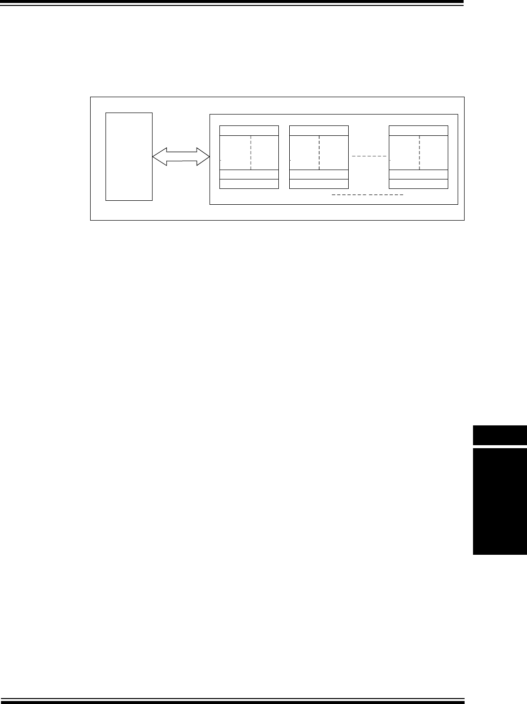
© 2009 Microchip Technology Inc. Preliminary DS61154A-page 34-55
Section 34. Controller Area Network (CAN)
Controller Area
Network (CAN)
34
34.6 CAN MESSAGE HANDLING
The CAN module uses device RAM for storing CAN messages that need to be transmitted or are
received. The module by itself does not have user-accessible message buffers. Figure 34-8
shows the organization of the CAN module buffer memory in device RAM.
Figure 34-8: CAN Message Buffers and Device RAM Organization
As seen in Figure 34-8, the CAN module organizes message buffers as FIFOs. A total of 32
distinct FIFOs are available, which have the following characteristics:
• Minimum size of one CAN message buffer and a maximum size of 32 CAN message
buffers.
• Independent configurable size
• Configurable to be a transmit message or a receive message FIFO
• User-readable head and tail pointer
• Independently configurable interrupts
• Status bits to provide the status of the FIFO as messages are transmitted or received
• Can be a transmit or receive FIFO, but not both (therefore, if a FIFO is configured for
transmit operation, all messages in the FIFO are considered for transmission)
• Can be configured to be a transmit or receive FIFO independent of each other and can be
configured in any order
Each of the 32 message FIFOs has the following associated registers:
• CAN FIFO Control (CiFIFOCONn) register (Register 34-20)
• CAN FIFO Interrupt (CiFIFOINTn) register (Register 34-21)
• CAN FIFO User Address (CiFIFOUAn) register (Register 34-22)
• CAN FIFO Message Index (CiFIFOCIn) register (Register 34-23)
The CAN module only needs to know the start address of the first message buffer in the FIFO.
The CAN FIFO Base Address (CiFIFOBA) register should point to the start address of this
message buffer. The CAN module automatically calculates the address of message buffers in
each of the FIFO based on the configuration of the individual FIFOs. The individual FIFOs will be
arranged contiguously, with all the message buffers being packed. This produces a CAN
message buffer memory without any gaps. While the CiFIFOUAn register provides the address
of the next read/write CAN Message Buffer that the application must use, the CiFIFOCIn register
provides the corresponding CAN Message Buffer Index of the next message buffer to be
transmitted or written to by the CAN module.
FIFO related interrupts along with other CAN module interrupts are discussed in Section 34.12
“CAN Interrupts”.
Message Buffer 31
Message Buffer 1
Message Buffer 0
Message Buffer 31
Message Buffer 1
Message Buffer 0
Message Buffer 31
Message Buffer 1
Message Buffer 0
CAN
Module
FIFO0 FIFO1 FIFO31
Device RAM
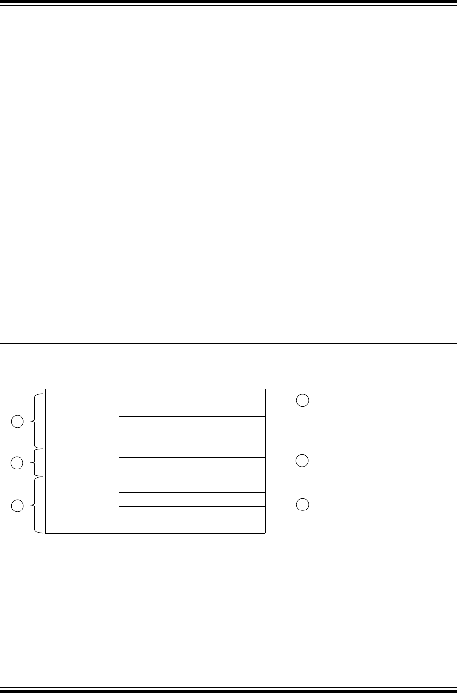
PIC32MX Family Reference Manual
DS61154A-page 34-56 Preliminary © 2009 Microchip Technology Inc.
34.6.1 Message FIFO Configuration
The user application must allocate device RAM space for CAN message buffering. The
requirements of each type of message buffer are as follows:
• A CAN Transmit message buffer requires 4 words (16 bytes) of memory
• A CAN receive message buffer will require 4 words (16 bytes) of memory if entire message
(time stamp plus data plus message ID) is stored - (full receive message)
• A CAN receive message buffer will require 2 words (8 bytes) of memory only if the data is
stored - (data-only receive message)
The application must design the size of each message FIFO. The FIFO size is controlled via the
FIFO size (FSIZE<4:0>) bits in the corresponding CAN FIFO Control (CiFIFOCONn<20:16>)
register. All FIFOs have a default size of at least one message buffer. The total memory to be
allocated is then obtained by counting the total number of buffers across FIFOs while accounting
for the memory size of each buffer.
For optimal use of the CAN FIFO message buffering model, the user application should configure
the required number of FIFOs starting from FIFO0, and then configuring FIFO1, FIFO2, FIFO3,
and so on in order.
For example, an application requires 29 FIFOs and configures FIFO0, FIFO1 and FIFO5 through
FIFO31. FIFO2, FIFO3 and FIFO4 are not configured. FIFO2, FIFO3 and FIFO4, although not
configured, still occupy 4 words of RAM each. The CAN module will not use these FIFOs, but
accounts for their presence while computing the address of FIFO5. In this example, the user
application must allocate memory for all 32 FIFOs. The memory occupied by FIFO2, FIFO3 and
FIFO4 could be used by the application.
An optimal way to accomplish this is to configure FIFO0 through FIFO28 and not configure
FIFO29, FIFO30 and FIFO31. In this way, the user application must only allocate space for 29
FIFOs. An example is shown in Figure 34-9.
Figure 34-9: Example of CAN Message Buffer FIFO Configuration (Including Data-only RX Message Buffers)
FIFO Number Message Buffer
Start Address Message Buffer
FIFO
(Transmit FIFO)
0x00001000 MB0
0x00001010 MB1
0x00001020 MB2
0x00001030 MB3
FIFO1
(Data-only RX
Message)
0x00001040 MB0
0x00001048 MB1
FIFO3
(Full Receive
Message)
0x00001050 MB0
0x00001060 MB1
0x00001070 MB2
0x00001080 MB3
A
B
C
A
B
C
C1FIFOCON0.TXEN = 1
C1FIFOCON0.FSIZE = 3
C1FIFOCON1. TXEN = 0
C1FIFOCON1.DONLY = 1
C1FIFOCON1.FSIZE = 1
C1FIFOONC3.TXEN = 0
C1FIFOCON3.DONLY = 0
C1FIFOCON3.FSIZE = 3
CAN1FIFO Configuration
C1FIFOBA = 0x00001000
(Start address of MB0 in FIFO0)
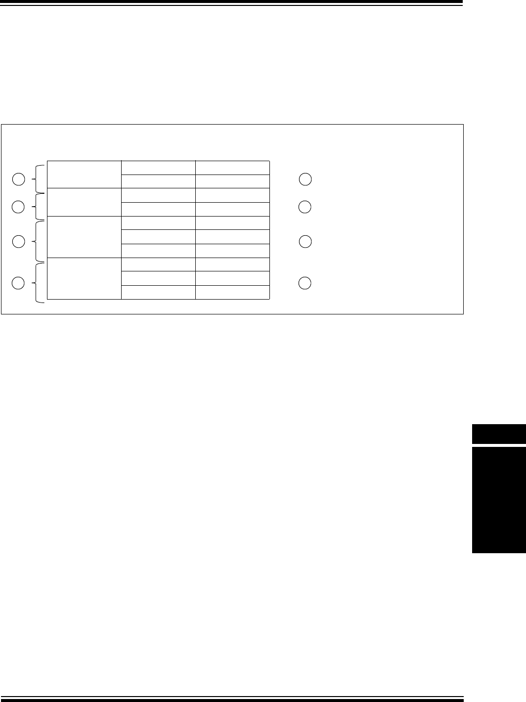
© 2009 Microchip Technology Inc. Preliminary DS61154A-page 34-57
Section 34. Controller Area Network (CAN)
Controller Area
Network (CAN)
34
For the CAN1 message buffer FIFO configuration shown in Figure 34-9, FIFO0 has four transmit
buffers, which would require a total of 16 (4 buffers x 4 words per buffer) words. FIFO1 has two
data-only receive buffers, which would require a total of four (2 buffers x 2 words per buffer)
words. FIFO3 has four full receive buffers, which would require a total of 16 (4 buffers x 4 words
per buffer) words. Therefore, a total of 36 (16 + 4 + 16) words of memory needs to be allocated.
Consider another example application shown in Figure 34-10, which requires a total of four
FIFOs.
Figure 34-10: Example of CAN FIFO Configuration
FIFO0 and FIFO1 have two message buffers each and are configured to be CAN message
transmit FIFOs. FIFO2 and FIFO3 have three message buffers each and are configured to be
CAN message receive FIFOs. FIFO0 and FIFO1 will require a total of 16 (2 FIFOs x 2 message
buffers per FIFO x 4 words per message buffer) words of memory. FIFO2 and FIFO3 will require
a total of 24 (2 FIFOs x 3 message buffers per FIFO x 4 words per message buffer) words of
memory. Therefore, a total of 40 (16 + 24) words of memory needs to be allocated.
The following steps can be used to configure the CAN Module FIFOs:
1. Allocate memory for the CAN message buffer FIFOs.
2. Place the module into Configuration mode (OPMOD<2:0> = 100).
3. Update the CAN FIFO Base Address (CiFIFOBA) register with the base address of the
FIFO. This should be the physical start address of Message Buffer 0 of FIFO0.
4. Update the FIFO control register with the FIFO size (FSIZE<4:0> in CiFIFOCONn).
5. Select whether the FIFO is to be a transmit or receive FIFO (TXEN bit in CiFIFOCONn).
6. Place the module into Normal Operation mode (OPMOD<2:0> = 000).
These steps are shown in code Example 34-2. This code example illustrates the coding steps for
setting up the CAN message FIFO as shown in Example 34-10.
FIFO Number Message Buffer
Start Address Message Buffer
FIFO0 0x00002000 MB0
0x00002010 MB1
FIFO1 0x00002020 MB0
0x00002030 MB1
FIFO2
0x00002040 MB0
0x00002050 MB1
0x00002060 MB2
FIFO3
0x00002070 MB0
0x00002080 MB1
0x00002090 MB2
A
B
C
D
C1FIFOCON0.TXEN = 1
C1FIFOCON0.SIZE = 1
C1FIFOCON1.TXEN = 1
C1FIFOCON1.SIZE = 1
C1FIFOCON2.TXEN = 0
C1FIFOCON2.SIZE = 2
C1FIFOCON3.TXEN = 0
C1FIFOCON3.SIZE = 2
CAN1FIFO Configuration
C1FIFOBA = 0x00002000
A
B
C
D

PIC32MX Family Reference Manual
DS61154A-page 34-58 Preliminary © 2009 Microchip Technology Inc.
Example 34-2: Setting Up the CAN Message FIFO
/* This code snippet illustrates the steps required to configure the */
/* PIC32 CAN Message FIFOs. The FIFO configuration example shown in */
/* Figure 34-5 will be used in this example. */
/* FIFO0 - Transmit - 2 MESSAGE BUFFERS */
/* FIFO1 - Transmit - 2 MESSAGE BUFFERS */
/* FIF02 - Receive - 3 MESSAGE BUFFERS */
/* FIF03 - Receive - 3 MESSAGE BUFFERS */
/* FIFO4 - FIFO31 - Not used */
/* Allocate a total of 40 words.
unsigned int CanFifoMessageBuffers[40];
/* Request CAN to switch to configuration mode and wait until it has switched */
C1CONbits.REQOP = 100
while(C1CONbits.OPMOD != 100);
/* Initialize C1FIFOBA register with physical address of CAN message Buffer */
C1FIFOBA = KVA_TO_PA(CanFifoMessageBuffers); ;
/* Configure FIFO0 */
C1FIFOCON0bits.FSIZE = 1;
C1FIFOCON0SET = 0x80; /* Set the TXEN bit */
/* Configure FIFO1 */
C1FIFOCON1bits.FSIZE = 1;
C1FIFOCON1SET = 0x80; /* Set the TXEN bit */
/* Configure FIFO2 */
C1FIFOCON2bits.FSIZE = 2;
C1FIFOCON2CLR = 0x80; /* Clear the TXEN bit */
/* Configure FIFO3 */
C1FIFOCON3bits.FSIZE = 2;
C1FIFOCON3CLR = 0x80; /* Clear the TXEN bit */
/* The CAN module can now be placed into normal mode if no further */
/* configuration is required. */
C1CONbits.REQOP = 0;
while(C1CONbits.OPMOD != 0);

© 2009 Microchip Technology Inc. Preliminary DS61154A-page 34-59
Section 34. Controller Area Network (CAN)
Controller Area
Network (CAN)
34
34.6.2 Loading Messages to be Transmitted into the FIFO
In order to use a FIFO to transmit data, it must be configured as a transmit FIFO. This is done by
setting the TX/RX Buffer Selection (TXEN) bit in the CAN FIFO Control (CiFIFOCONn<7>)
register.
The CAN FIFO User Address (CiFIFOUAn) register gives the physical address of the next
message buffer in FIFO where the application should store the message (also referred to as the
FIFO head location). The CAN message should be loaded, starting at the location given by
CiFIFOUAn register.
The application should set the Increment Head/Tail (UINC) bit (CiFIFOCONn<13>) after loading
one message buffer in the FIFO. This will cause the CAN module to increment the address
contained in CiFIFOUAn register by 16 (thereby pointing to the next message buffer). The
message is then ready to be transmitted. The CiFIFOUAn register rolls over to the start of the
FIFO when it has reached the end of the FIFO.
Consequently, the application need not track the FIFO head location and can use the CiFIFOUAn
register for this purpose. The following coding steps could be followed to load a message for
transmission into a transmit FIFO:
1. Read the CiFIFOUAn register and store one message (16 bytes) at this address.
2. Set the UINC (CiFIFOCONn<13>) bit to update the CiFIFOUAn register.
3. Set the TXREQ (CiFIFOCONn<3>) bit to transmit the message.
4. Perform steps 2 and 3 for the number of messages to be queued and the size of the FIFO.
Code Example 34-3 illustrates these coding steps. In this example four messages are loaded into
FIFO0 of the CAN1 module.
Example 34-3: Loading a Transmit Message FIFO
/* This code snippet illustrates the steps to load a transmit message FIFO. */
/* This example uses the CAN1 module. */
/* Four messages to be transmitted using transmit FIFO0 */
int message; /* Tracks the message buffer */
unsigned int * currentMessageBuffer; /* Points to message buffer to be written */
message = 0;
for(message = 0; message <= 3; message ++)
{
/* Get the address of the message buffer to write to from the C1FIFOUA0 */
/* register. Convert this physical address to virtual address. */
currentMessageBuffer = PA_TO_KVA1(C1FIF0UA0);
/* This procedure will load the message
* buffer with the message to be transmitted. */
LoadMessageBuffer(currentMessageBuffer);
C1FIFOCON0SET = 0x2008; /* Set the UINC and TXREQ bit */
}
/* At this point the messages are loaded in FIFO0 */

PIC32MX Family Reference Manual
DS61154A-page 34-60 Preliminary © 2009 Microchip Technology Inc.
34.6.3 Accessing Received Messages In the FIFO
In order to use the FIFO to receive data, the FIFO must be configured as a receive FIFO. This is
done by clearing the TXEN (CiFIFOCONn<7>) bit. After a message is received, the application
should obtain the physical start address of the first message buffer to read (also called the FIFO
tail pointer) from the CiFIFOUAn register. The message can then be read from this address
onward.
After processing the message from the FIFO, the application should signal the CAN module that
the message has been processed and can be overwritten by setting the UINC bit
(CiFIFOCONn<13>). This will increment the tail pointer and increase the address pointed to by
CiFIFOUAn by 4 words or 2 words, depending on the value of DONLY bit in the CiFIFOCONn
register. The CiFIFOUAn register rolls over to start of the FIFO when it has reached the end of
the FIFO.
Consequently, the application need not track the FIFO tail location and can use the CiFIFOUAn
register for this purpose. The following coding steps could be followed to process a message in
a receive FIFO:
1. Use any of the available interrupts to determine if there is a message in the FIFO.
2. Read the CiFIFOUAn register and process one message (16 bytes) from this address.
3. Set the UINC bit (CiFIFOCONn<13>) to update the CiFIFOUAn register.
4. Perform steps 1 and 2 until the interrupt condition clears up.
The code in Example 34-4 illustrates the above steps. In this code example, FIFO1 of the CAN
1 module is configured for receive operation. The example reads the FIFO until it is empty.
Example 34-4: Reading Received Messages from the FIFO
/* This code snippet illustrates the steps to read messages from receive */
/* message FIFO. This example uses the CAN1 module.*/
/* FIFO1 size is 4 messages and each message is 4 words long. */
unsigned int * currentMessageBuffer; /* Points to message buffer to be read */
while(1)
{
/* Keep reading till the FIFO is empty. */
while(C1FIFOINT1bits.RXNEMPTYIF == 1)
{
/* Get the address of the message buffer to read from the C1FIFOUA1 */
/* register. Convert this physical address to virtual address. */
currentMessageBuffer = PA_TO_KVA1(C1FIF0UA1);
ProcessReceivedMessage(currentMessageBuffer);
/* Set the UINC bit to tell the CAN module that
* a message has been read. */
C1FIFOCON0SET = 0x2000;
}
}

© 2009 Microchip Technology Inc. Preliminary DS61154A-page 34-61
Section 34. Controller Area Network (CAN)
Controller Area
Network (CAN)
34
34.6.4 Resetting the FIFO
The FIFO can be reset by any of the following methods:
• Setting the FRESET (CiFIFOCONn<14>) bit
• Placing the CAN module into Configuration mode (OPMOD<2:0> (CiCON<23:21>) = 100)
• Turning the CAN module off (CiCON<15> = 0)
Resetting the FIFO will reset the head and tail pointers, the interrupt flags, and the TXABAT,
TXLARB, and TXERR status bits in the CiFIFOCONn register.
The following should be taken into account before resetting a FIFO using the FRESET bit:
• If the FIFO is a transmit FIFO, no transmissions should be pending
• If the FIFO is a receive FIFO, it should not be pointed to by any active filters
An application may typically reset the FIFO after coming out of Disable mode. While resetting the
FIFO using the FRESET bit, the application must poll the bit to ensure that the reset operation
has completed. This is shown in Example 34-5.
Example 34-5: Resetting a Message FIFO
/* This code snippet shows how to reset a message FIFO. This example */
/* uses FIFO0 of the CAN1 module. */
C1FIFOCON0SET = 0x00004000; /* Set the FRESET bit */
while(C1FIFOCON0bits.FRESET == 1);
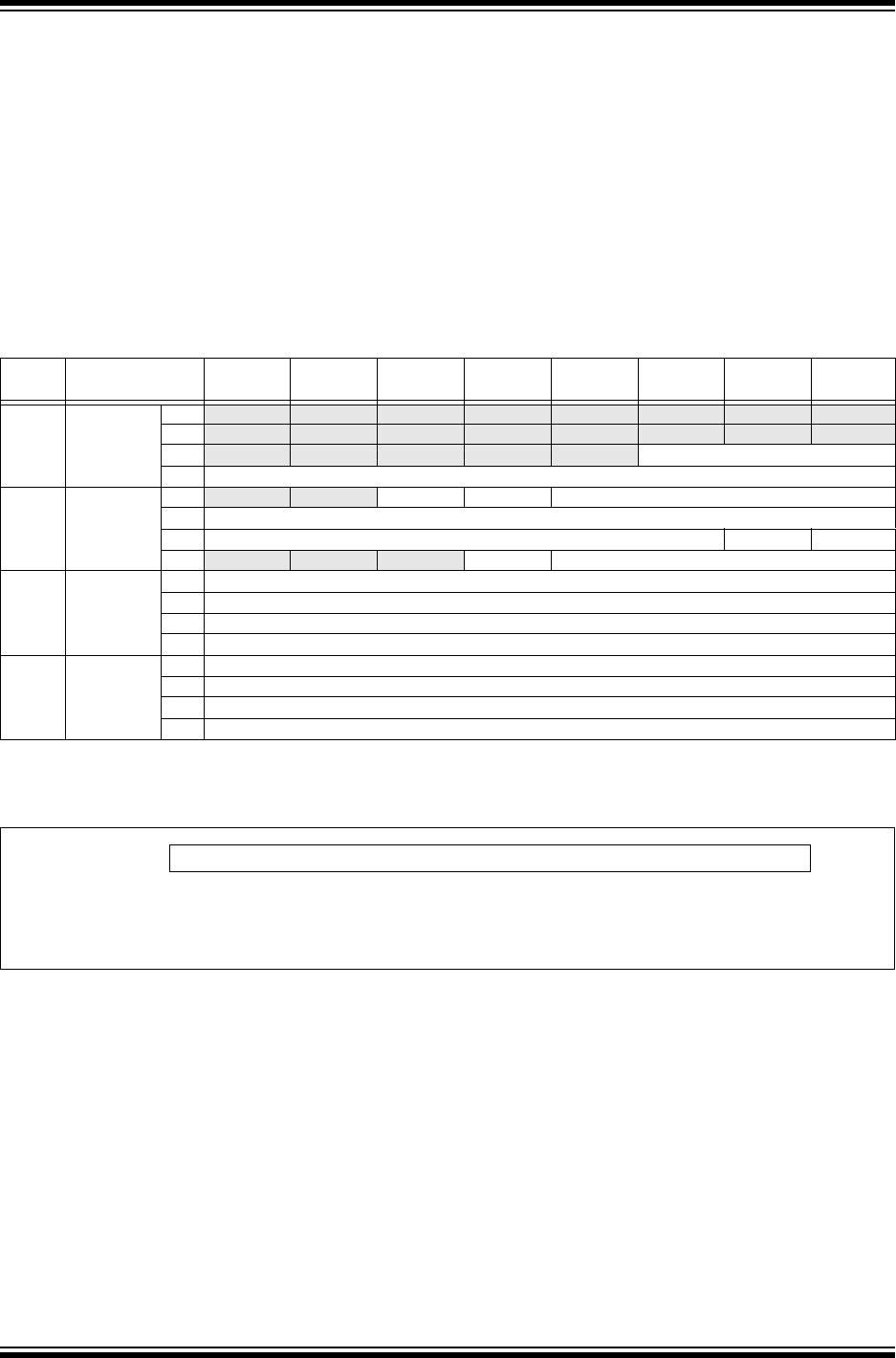
PIC32MX Family Reference Manual
DS61154A-page 34-62 Preliminary © 2009 Microchip Technology Inc.
34.7 TRANSMITTING A CAN MESSAGE
The CAN module will transmit messages that are loaded in a transmit FIFO. Refer to section
34.6.1 “Message FIFO Configuration” and 34.6.2 “Loading Messages to be Transmitted
into the FIFO” for detailed descriptions on configuring a message FIFO for transmit operation.
34.7.1 Format of Transmit Message Buffer
The transmit message FIFO can hold up to 32 CAN transmit message buffers. A transmit
message buffer is 4 words (16 bytes) long and has a fixed format as described in Table 34-2. It
contains four words: CMSGnSID, CMSGnEID, CMSGnDATA0 and CMSGnDATA1. The bits in
these registers have a one-to-one correspondence to bit fields in the CAN message as defined
by the CAN bus specification. The application must ensure that every message buffer in the
transmit FIFO conforms to the formats shown in Figure 34-11 through Figure 34-14.
Figure 34-11: Format of CMSGSID
Table 34-2: Transmit Message Buffer Format as Stored in System Memory
Address
Offset Name Bit
31/2315/7
Bit
30/22/14/6
Bit
29/21/13/5
Bit
28/20/12/4
Bit
27/19/11/3
Bit
26/18/10/2
Bit
25/17/9/1
Bit
24/16/8/0
00 CMSGSID 31:24 -— -— -— -— -— -— -— -—
23:16 -— -— -— -— -— -— -— -—
15:8 -— -— -— -— -— SID<10:8>
7:0 SID<7:0>
04 CMSGEID 31:24 -— -— SRR IDE EID<17:14>
23:16 EID<13:6>
15:8 EID<5:0> RTR RB1
7:0 -— -— --— RB0 DLC<3:0>
08 CMSGDATA0 31:24 Transmit Buffer Data Byte 3
23:16 Transmit Buffer Data Byte 2
15:8 Transmit Buffer Data Byte 1
7:0 Transmit Buffer Data Byte 0
0C CMSGDATA1 31:24 Transmit Buffer Data Byte 7
23:16 Transmit Buffer Data Byte 6
15:8 Transmit Buffer Data Byte 5
7:0 Transmit Buffer Data Byte 4
Legend: Shaded bits should be set to ‘0’.
Note 1: The CAN transmit message is stored in system RAM and does not have SET/CLR/INV registers associated with it.
SID<10:0>
bit 10-0 SID<10:0>: Standard Identifier

© 2009 Microchip Technology Inc. Preliminary DS61154A-page 34-63
Section 34. Controller Area Network (CAN)
Controller Area
Network (CAN)
34
Figure 34-12: Format of CMSGEID
Figure 34-13: Format of CMSGDATA0
Figure 34-14: Format of CMSGDATA1
— SRR IDE EID<17:0> RTR RB1 — RB0 DLC<3:0>
bit 31-30 Unimplemented: Read as ‘0’
bit 29 SRR: Substitute Remote Request
In case of a standard message format (IDE = 0), this bit is don’t care.
In case of an extended message format (IDE = 1), this bit should always be set.
bit 28 IDE: Extended Identifier
1 = Message will transmit extended identifier
0 = Message will transmit standard identifier
bit 27-10 EID<17:0>: Extended Identifier
bit 9 RTR: Remote Transmission Request
1 = Message is a remote transmission request
0 = Message is not a remote transmission request
bit 8 RB1: Reserved Bit 1
The user application must set this bit to ‘0’ per the CAN bus specification.
bit 7-5 Unimplemented: Read as ‘0’
bit 4 RB0: Reserved Bit 0
The user application must set this bit to ‘0’ per the CAN bus specification.
bit 3-0 DLC<3:0>: Data Length Code
1xxx = Module will transmit 8 bytes
0111 = 7 bytes of data will be transmitted
•
•
•
0001 = 1 byte of data will be transmitted
0000 = 0 bytes of data will be transmitted
Note 1: This register is in system memory outside the CAN module.
DATA3<7:0> DATA2<7:0> DATA1<7:0> DATA0<7:0>
bit 31-24 DATA3<7:0>: Data Byte 3
bit 23-16 DATA2<7:0>: Data Byte 2
bit 15-8 DATA1<7:0>: Data Byte 1
bit 7-0 DATA0<7:0>: Data Byte 0
Note 1: This register is in system memory outside the CAN module.
DATA7<7:0> DATA6<7:0> DATA5<7:0> DATA4<7:0>
bit 31-24 DATA7<7:0>: Data Byte 7
bit 23-16 DATA6<7:0>: Data Byte 6
bit 15-8 DATA5<7:0>: Data Byte 5
bit 7-0 DATA4<7:0>: Data Byte 4
Note 1: This register is in system memory outside the CAN module.

PIC32MX Family Reference Manual
DS61154A-page 34-64 Preliminary © 2009 Microchip Technology Inc.
The code in Example 34-6 shows an example data structure for implementing a CAN message
buffer in memory. An example of using this structure is provided in Example 34-7.
Example 34-6: Implementing a CAN Message Buffer in Memory
/* This code snippet shows an example of data structure to implement a CAN */
/* message buffer. */
/* Define the sub-components of the data structure as specified in Table 34-2 */
/* Create a CMSGSID data type. */
typedefstruct
{
unsigned SID:11;
unsigned :21;
}txcmsgsid;
/* Create a CMSGEID data type. */
typedef struct
{
unsigned DLC:4;
unsigned RB0:1;
unsigned :3;
unsigned RB1:1;
unsigned RTR:1;
unsigned EID:18;
unsigned IDE:1;
unsigned SRR:1;
unsigned :2;
}txcmsgeid;
/* Create a CMSGDATA0 data type. */
typedef struct
{
unsigned Byte0:8;
unsigned Byte1:8;
unsigned Byte2:8;
unsigned Byte3:8;
}txcmsgdata0;
/* Create a CMSGDATA1 data type. */
typedefstruct
{
unsigned Byte4:8;
unsigned Byte5:8;
unsigned Byte6:8;
unsigned Byte7:8;
}txcmsgdata1;
/* This is the main data structure. */
typedef union uCANTxMessageBuffer {
struct
{
txcmsgsid CMSGSID;
txcmsgeid CMSGEID;
txcmsgdata0 CMSGDATA0;
txcmsgdata0 CMSGDATA1;
};
int messageWord[4];
}CANTxMessageBuffer;
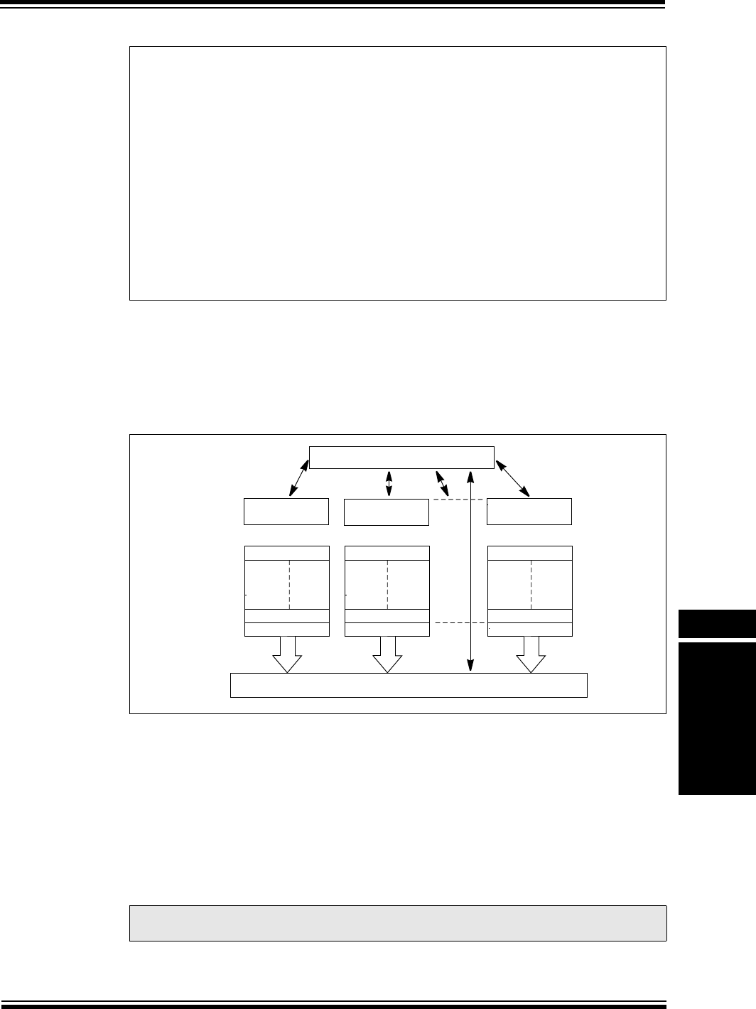
© 2009 Microchip Technology Inc. Preliminary DS61154A-page 34-65
Section 34. Controller Area Network (CAN)
Controller Area
Network (CAN)
34
Example 34-7: Example Usage of the Data Structure
34.7.2 Requesting Transmit of a Message
Table 34-15 shows the CAN module transmission process. The application must configure the
FIFO for transmit operation. Message transmission and priority are controlled by bits in the
CiFIFOCONn register (Register 34-20). The CAN module will then select the next message to
be transmitted based on readiness and priority, and will process this message for transmission.
Figure 34-15: CAN Message Transmission
Once a message has been loaded into the FIFO and is ready to be transmitted, the user
application can initiate a transmission by setting the Message Send Request (TXREQ) bit in the
CAN FIFO Control (CiFIFOCONn<3>) register. When this bit is set, the contents of the FIFO will
be queued for transmission according to the message priority, and the CAN module will transmit
all the messages in the FIFO. When all messages have been transmitted, the TXREQ bit will be
cleared. An application could load all of the transmit FIFOs and set the TXREQ bit for all of these
FIFOs. Alternately, the application could load one transmit FIFO, set the associated TXREQ bit,
and then load the next FIFO while the previous FIFO is being processed.
Messages can be appended to the FIFO while a message is being transmitted. The application
should use the CiFIFOUAn register to get the FIFO head pointer and should store the message
at this address. Appended messages will be queued for transmission.
Note: It is recommended that the application set the TXREQ bit after every message is
loaded into the FIFO (after the UINC bit is set).
/* Example usage of data structure shown in Example 34-6. This example sets */
/* up a message buffer in FIFO1 */
CANTxMessageBuffer * buffer;
buffer = (CANTxMessageBuffer *)(PA_TO_KVA1(C1FIFOUA1));
/* Clear the message buffer. */
buffer->messageWord[0] = 0;
buffer->messageWord[1] = 0;
buffer->messageWord[2] = 0;
buffer->messageWord[3] = 0;
buffer->CMSGSID.SID = 0x100;/* Message SID */
buffer->CMSGEID.DLC = 0x2;/* Data Length is 2 */
buffer->CMSGDATA0.Byte0 = 0xAA;/* Byte 0 Data */
buffer->CMSGDATA0.Byte1 = 0xbb;/* Byte 1 Data */
Message Buffer 31
Message Buffer 1
Message Buffer 0
Message Buffer 31
Message Buffer 1
Message Buffer 0
Message Buffer 31
Message Buffer 1
Message Buffer 0
FIFO0 FIFO1 FIFO31
Message Queue and Priority Control
Message Assembly Buffer
CiFOFOCON0 CiFOFOCON1 CiFOFOCON31

PIC32MX Family Reference Manual
DS61154A-page 34-66 Preliminary © 2009 Microchip Technology Inc.
The following coding steps can be used to transmit CAN messages:
1. Configure the desired number of FIFOs for transmit operation.
2. If desired, set the priority of the individual FIFOs.
3. Create a transmit message using the format shown in Table 34-2.
4. Read the CiFIFOUAn register and store the message at the address provided.
5. Set the UINC bit.
6. Set the TXREQ bit.
7. Repeat steps 3 through 6 for the number of messages to be transmitted across the
desired number of FIFOs.
8. The transmit FIFO interrupts can be used to monitor the status of the FIFO.
Code Example 34-8 provides the steps required to transmit a CAN message using the CAN1
module to transmit four messages. Message 0 and 1 are standard ID CAN messages. Message
2 and 3 are extended ID messages. FIFO1 is used and its length is 3.

© 2009 Microchip Technology Inc. Preliminary DS61154A-page 34-67
Section 34. Controller Area Network (CAN)
Controller Area
Network (CAN)
34
Example 34-8: Transmitting Standard and Extended ID Messages
/* This code example illustrates how to transmit standard and extended */
/* ID messages with the PIC32 CAN module. */
/* The code example uses CAN1, FIFO0. FIFO0 size is 4 */
/* Four CAN message have to be transmitted. */
/* Msg 0: SID - 0x100 Data - 0x12BC1245 */
/* Msg 1: SID - 0x102 Data - 0x12BC124512BC1245 */
/* Msg 2: SID - 0x100 EID - 0xC000 Data - 0x12BC1245 */
/* Msg 3: SID - 0x102 EID - 0xC000 Data - 0x12BC124512BC1245 */
/* Pointer to CAN Message Buffer */
CANTxMessageBuffer * transmitMessage;
/* This array is the CAN FIFO and message buffers. FIF0 has 4 message */
/* buffers. All other buffers are default size. */
unsigned int CANFIFO[16];
/* Place CAN module in configuration mode */
C1CONbits.REQOP = 4;
while(C1CONbits.OPMOD != 4);
/* Initialize the C1FIFOBA with the start address of the CAN FIFO message */
/* buffer area. */
C1FIFOBA = KVA_TO_PA(CANFIFO);
/* Set FIFO0 size to 3 messages. All other FIFOs at default size. */
/* Configure FIFO0 for transmit.*/
C1FIFOCON0bits.FSIZE = 2
C1FIFOCON0SET = 0x00000080; /* Set the TXEN bit - Transmit FIFO */
/* Place the CAN module in Normal mode. */
C1CONbits.REQOP = 0;
while(C1CONbits.OPMOD != 0);
/* Get the address of the message buffer to write to. Load the buffer and */
/* then set the UINC bit. Set the TXREQ bit next to send the message. */
/* Message 0 SID - 0x100 Data - 0x12BC1245*/
transmitMessage = (CANTxMessageBuffer *)(PA_TO_KVA1(C1FIFOUA1));
transmitMessage->CMSGSID.SID = 0x100; /* CMSGSID */
transmitMessage->CMSGEID.IDE = 0;
transmitMessage->CMSGEID.DLC = 0x4;
transmitMessage->messageWord[2] = 0x12BC1245; /* CMSGDAT0 */
C1FIFOCON1SET = 0x00002000; /* Set the UINC bit */
C1FIFOCON1SET = 0x00000008; /* Set the TXREQ bit */
/* Message 1 SID - 0x102 Data - 0x12BC124512BC1245 */
transmitMessage = (CANTxMessageBuffer *)(PA_TO_KVA1(C1FIFOUA1));
transmitMessage->CMSGSID.SID = 0x102; /* CMSGSID */
transmitMessage->CMSGEID.IDE = 0;
transmitMessage->CMSGEID.DLC = 0x8;
transmitMessage->messageWord[2] = 0x12BC1245; /* CMSGDAT0 */
transmitMessage->messageWord[3] = 0x12BC1245; /* CMSGDAT1 */
C1FIFOCON1SET = 0x00002000; /* Set the UINC bit */
C1FIFOCON1SET = 0x00000008; /* Set the TXREQ bit */

PIC32MX Family Reference Manual
DS61154A-page 34-68 Preliminary © 2009 Microchip Technology Inc.
Example 34-8: Transmitting Standard and Extended ID Messages (Continued)
34.7.3 Transmit Message Priority
The CAN module allows the application to control the priority of transmit message buffers. Prior
to sending a message SOF, the CAN module compares the priority of all buffers that are ready
for transmission. The transmit message buffer with the highest priority will be sent first. For
example, if transmit FIFO0 has a higher priority setting than transmit FIFO1, all messages in
FIFO0 will be sent first. In a case where the priority of a FIFO is changed while another FIFO is
being processed, the CAN module will reassess the priority of all FIFOs after it has completed
transmitting the current message. This allows the change in FIFO priority to take effect at the
earliest opportunity.
The priority levels are controlled by TXPRI<1:0> (CiFIFOCONn<1:0>) bits. There are four levels
of transmit priority as defined by the TXPRI bits. The selections are as follows:
•11 = This FIFO has the highest priority
•10 = This FIFO has an intermediate high priority
•01 = This FIFO has an intermediate low priority
•00 = This FIFO has the lowest priority
If two FIFOs have the same priority setting, the FIFO with the highest natural order is sent. The
natural order of transmission if all FIFOs have the same priority is:
• FIFO0 - lowest natural priority
• FIFO1 - higher natural priority
.
.
.
• FIFO31 - highest natural priority
/* Message 2 SID - 0x100 EID - 0xC000 Data - 0x12BC1245*/
transmitMessage = (CANTxMessageBuffer *)(PA_TO_KVA1(C1FIFOUA1));
transmitMessage->CMSGSID.SID = 0x100; /* CMSGSID */
transmitMessage->CMSGEID.SID = 0xC000; /* CMSGEID */
transmitMessage->CMSGEID.IDE = 1;
transmitMessage->CMSGEID.DLC = 0x4;
transmitMessage->messageWord[2] = 0x12BC1245; /* CMSGDAT0 */
C1FIFOCON1SET = 0x00002000; /* Set the UINC bit */
C1FIFOCON1SET = 0x00000008; /* Set the TXREQ bit */
/* Message 3 SID - 0x102 EID - 0xC000 Data - 0x12BC124512BC1245*/
transmitMessage = (CANTxMessageBuffer *)(PA_TO_KVA1(C1FIFOUA1));
transmitMessage->CMSGSID.SID = 0x102; /* CMSGSID */
transmitMessage->CMSGEID.SID = 0xC000; /* CMSGEID */
transmitMessage->CMSGEID.IDE = 1;
transmitMessage->CMSGEID.DLC = 0x8;
transmitMessage->messageWord[2] = 0x12BC1245; /* CMSGDAT0 */
transmitMessage->messageWord[3] = 0x12BC1245; /* CMSGDAT1 */
C1FIFOCON1SET = 0x00002000; /* Set the UINC bit */
C1FIFOCON1SET = 0x00000008; /* Set the TXREQ bit */
}

© 2009 Microchip Technology Inc. Preliminary DS61154A-page 34-69
Section 34. Controller Area Network (CAN)
Controller Area
Network (CAN)
34
34.7.4 Aborting Transmission of a Queued Message
A message that has been queued to be transmitted can be aborted by clearing the TXREQ bit
(CiFIFOCONn<3>). If TXREQ is cleared, the module will attempt to abort the transmission.
If the message aborts successfully, the TXABT (CiFIFOCONn<2>) bit will be set by hardware.
TXREQ will remain set until the message either aborts or is successfully transmitted.
If the message is successfully transmitted, the FIFO pointers will be updated as normal. If the
message is successfully aborted, the FIFO pointers will not change. The user can then use the
internal index (CFIFOCI) to determine which messages have already been transmitted if
required.
To reset the FIFO pointers and erase all pending messages, the user application can set the
FRESET (CiFIFOCONn<14>) bit. The FIFO can then be re-enabled and loaded with new
messages to be transmitted.
34.7.5 Remote Transmit Request
As discussed in 34.7.2 “Requesting Transmit of a Message”, the CAN bus system has a
method for allowing a node to request data from another node. The requesting node sends a
message with the RTR bit set. The message contains no data, only an address to trigger a filter
match.
The filter that is configured to respond to a remote transmit request will point to a FIFO that is
configured for transmission. The FIFO must also be enabled to reply to remote transmission
requests by setting the RTREN = 1.
Remote transmit requests can be handled without CPU intervention. If a transmit FIFO is
configured properly, when a filter matches and that filter points to the FIFO, the buffer will be
queued for transmission. The FIFO must be configured as follows:
1. Set FIFO to Transmit mode by setting the TXEN (CiFIFOCONn<7>) bit to ‘1’.
2. A filter must be enabled and loaded with a matching message identifier.
3. The buffer pointer register for that filter must point to the transmit buffer (note that although
a filter normally points to a receive FIFO, in this case it must point to the transmit FIFO).
4. The RTREN (CiFIFOCONn<2>) bit must be set to ‘1’ to enable RTR.
5. The FIFO must be preloaded with at least one message to be sent.
When a remote transmit request message is received, and it matches a filter pointing to the
properly configured transmit buffer, the TXREQ (CiFIFOCONn<3>) bit is automatically set. The
message buffers in the FIFO are then transmitted in priority order. If no messages are available
in the transmit buffer when a request for a remote transmission occurs, the event will be treated
as a FIFO overflow and the Receive FIFO Overflow Interrupt Flag (RXOVFLIF) bit in the CAN
FIFO Interrupt (CiFIFOINTn<3>) register will be set. Code Example 34-9 shows an example of
how a node can request data from remote node. Code Example 34-10 shows how a node can
be configured to respond to a Remote Transmit Request.
Example 34-9: Remote Transmit Request
/* This code snippet shows an example of a Remote Transmit Request. The */
/* node in this case will request a transmission from an application (or */
/* node) with an SID of 0x100. */
CANMessageBuffer * rtrMessage;
rtrMessage = (CANMessageBuffer *)(PA_TO_KVA1(C1FIFOUA1));
/* Clear the message. */
rtrMessage->messageWord[0] = 0x0;
rtrMessage->messageWord[1] = 0x0;
rtrMessage->messageWord[2] = 0x0;
rtrMessage->messageWord[3] = 0x0;
rtrMessage->CMSGSID.SID = 0x100;
rtrMessage->CMSGEID.IDE = 0;
rtrMessage->CMSGEID.RTR = 1;
rtrMessage->CMSGEID.DLC = 0;
C1FIFOCON SET = 0x00002000; /* Set the UINC bit */
/* The Remote Transmit Request message (rtrMessage) is now ready to be sent.*/

PIC32MX Family Reference Manual
DS61154A-page 34-70 Preliminary © 2009 Microchip Technology Inc.
Example 34-10: Responding to a Remote Transmit Request
/* This code example shows how to configure the CAN1 module to respond */
/* to a remote transmit request. */
/* In this case, FIFO1 is configured to respond to the a remote request */
/* on SID = 0x100. */
/* Allocate CAN FIFO memory. */
unsigned int CANFIFO[140];
/* This is the pointer to the reply message. */
CANMessageBuffer * rtrReply;
/* Place CAN Module in configuration mode.*/
C1CONbits.REQOP = 4;
while(C1CONbits.OPMOD != 4);
/* Configure FIFO1 for transmit operation, 4 message buffers and enable */
/* Auto Remote Transmit. */
C1FIFOCON1SET = 0x00000080; /* Set the TXEN bit */
C1FIFOCON1SET = 0x00000004; /* Enable RTR */
C1FIFOCON1bits.FSIZE = 4;
/* Configure a filter to accept a message with SID = 0x100. Refer to */
/* Section 34.8 “CAN Message Filtering” for more details on configuring */
/* filters. In this case, Filter 0 and Mask0 are used. */
C1FLTCON0bits.FSEL0 = 1; /* Point to FIF01 */
C1FLTCON0bits.MSEL0 = 0; /* Select Mask 0 */
C1RXF0bits.SID = 0x100; /* Configure Filter 0. */
C1RXF0bits.EXID = 0;
C1RXM0bits.SID = 0x1FF; /* Configure Mask 0. */
C1RXM0bits.MIDE = 1;
C1FLTCON0SET = 0x00000080; /* Enable the filter. */
/* Assign FIFO memory to CAN module */
C1FIFOBA = KVA_TO_PA(CANFIFO);
/* Place CAN Module in normal mode.*/
C1CONbits.REQOP = 0;
while(C1CONbits.OPMOD != 0);
/* Form the remote reply message. */
rtrReply = (CANMessageBuffer *)(PA_TO_KVA1(C1FIFOUA1));
rtrReply->messageWord[0] = 0;
rtrReply->messageWord[1] = 0;
rtrReply->messageWord[2] = 0;
rtrReply->messageWord[3] = 0;
rtrReply->CMSGSID.SID = 0x100; /* CMSGSID */
rtrReply->CMSGEID.IDE = 0;
rtrReply->CMSGEID.DLC = 0x4;
rtrReply->messageWord[2] = 0x12BC1245; /* CMSGDAT0 */
C1FIFOCON1bits.UINC = 1;
/* FIFO is now ready to respond to RTR. */
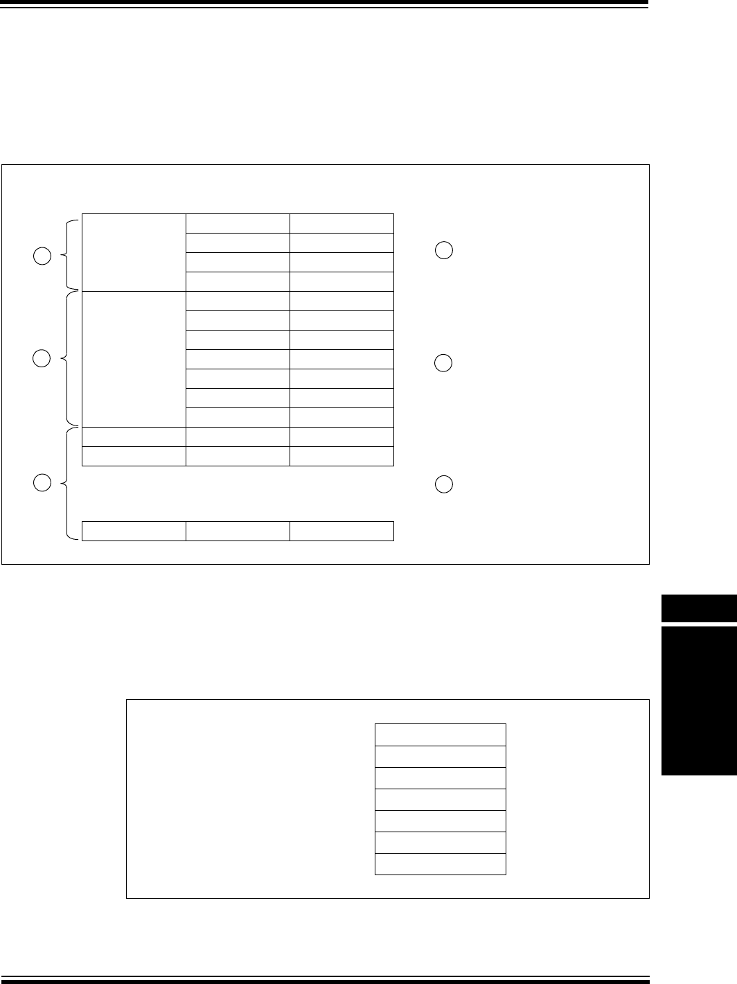
© 2009 Microchip Technology Inc. Preliminary DS61154A-page 34-71
Section 34. Controller Area Network (CAN)
Controller Area
Network (CAN)
34
34.7.6 Example Message Transmission FIFO Behavior
Consider an application example that uses two FIFOs, FIFO0 and FIFO1, of the CAN1 module.
FIFO0 has four message buffers configured for CAN message reception. FIFO1 has seven
message buffers and is configured for message transmission. FIFO2 through FIFO31 are left in
a default state. The CAN message buffer starts at physical address 0x00000100. This value is
loaded in the C1FIFOBA register. Figure 34-16 shows this application configuration.
Figure 34-16: FIFO Configuration for Example FIFO Behavior
The start address of FIFO1 can be calculated from the base address of the CAN message buffer
(0x00000100) and the byte size of FIFO0 (4 message buffers * 16 = 0x40). The physical start
address of FIFO1 is 0x00000140. The remainder of this discussion focuses on transmit FIFO1.
Figure 34-17 shows the case where FIFO1 is empty and no messages have been written. The
FIFO Transmit Not Full Interrupt Flag (TXNFULLIF), FIFO Transmit Half Empty interrupt flag
(TXHALFIF), and FIFO Transmit Empty Interrupt Flag (TXEMPTYIF) are set.
Figure 34-17: FIFO1 at Start
FIFO Number Message Buffer
Start Address Message Buffer
FIFO0
(Full Receive
Message)
0x00000100 MB0
0x00000110 MB1
0x00000120 MB2
0x00000130 MB3
FIFO1
(Transmit FIFO)
0x00000140 MB0
0x00000150 MB1
0x00000160 MB2
0x00000170 MB3
0x00000180 MB4
0x00000190 MB5
0x000001A0 MB6
FIFO2 0x000001B0 MB0
FIFO4 0x000001C0 MB0
•
•
•
•
•
•
•
•
•
FIFO31 0x00000380 MB0
A
B
C
C1FIFOCON0.TXEN = 1
C1FIFOCON0.FSIZE = 3
C1FIFOCON1.TXEN = 1
C1FIFOCON1.SIZE = 6
FIFO2 - FIFO31 are not
configured
CAN1FIFO Configuration
C1FIFOBA = 0x00000100
A
B
C
MB2
MB1
MB0
MB6
MB5
MB4
MB3
CFIFOBA = 0x00000100
CFIFOUA = 0x00000140
TXNFULLIF - 1
TXHALFIF - 1
TXEMPTYIF - 1
TXREQ - 0
CFIFOCI = 0x00000000
PIC32MX Family Reference Manual
DS61154A-page 34-72 Preliminary © 2009 Microchip Technology Inc.
Figure 34-18 shows FIFO1 after the first message has been loaded to the FIFO. Note that the
first message buffer (MB) in FIFO1, MB0, contains data. The application sets the UINC
(C1FIFOCON1<13>) bit, which causes the FIFO head (C1FIFOUA1) to advance and point to the
next empty message buffer, MB1. The TXEMPTYIF flag is cleared since the FIFO is not empty.
The application at this point has requested a transmission by setting the TXREQ
(C1FIFOCON1<3>) bit.
Figure 34-18: FIFO1 - First Write
Figure 34-19 shows FIFO1 after the first message has been transmitted from MB0. TXREQ has
been cleared and TXEMPTYIF is set once again. Note that the CAN module Message Index
register, C1FIFOCI1, now points to the second message buffer, MB1 at address 0x00000150.
Figure 34-19: FIFO1 - First Message Transmitted
Figure 34-20 shows the FIFO after six more messages have been loaded into MB1 through MB6.
The application will have read C1FIFOUA1 when loading the messages to get the address
location of the next message buffer to write to. The TXHALFIF flag is cleared and the application
has not requested the data be transmitted (TXREQ = 0).
Figure 34-20: FIFO1 - Seventh Write About to Fill
MB2
MB1
MB0/MSG0
MB6
MB5
MB4
MB3
CFIFOBA = 0x00000100
CFIFOUA = 0x00000150
TXNFULLIF - 1
TXHALFIF - 1
TXEMPTYIF - 0
TXREQ - 1
CFIFOCI = 0x00000000
MB2
MB1
MB0
MB6
MB5
MB4
MB3
CFIFOBA = 0x00000100
CFIFOUA = 0x00000150
TXNFULLIF - 1
TXHALFIF - 1
TXEMPTYIF - 1
TXREQ - 0
CFIFOCI = 0x00000001
MB2/MSG2
MB1/MSG1
MB0
MB6/MSG6
MB5/MSG5
MB4/MSG4
MB3/MSG3
CFIFOBA = 0x00000100
CFIFOUA = 0x00000140
TXNFULLIF - 1
TXHALFIF - 0
TXEMPTYIF - 0
TXREQ - 0
CFIFOCI = 0x00000001
© 2009 Microchip Technology Inc. Preliminary DS61154A-page 34-73
Section 34. Controller Area Network (CAN)
Controller Area
Network (CAN)
34
Figure 34-21 shows the FIFO after an eighth message has been loaded, this time into MB0. The
TXNFULLIF and TXHALFIF flags are both clear. The FIFO head now points to MB1. The FIFO
at this stage is full. The application has also requested that the message be transmitted
(TXREQ = 1).
Figure 34-21: FIFO1 - Eighth Write Buffer Full
Figure 34-22 shows the FIFO empty once again. The CAN module has transmitted all 7
messages in the FIFO. TXEMPTYIF is set once again, and TXREQ has been cleared by
hardware. The C1FOCI1 has wrapped all the way round and once again points at MB1.
Figure 34-22: FIFO1 - Fully Transmitted
MB2/MSG2
MB1/MSG1
MB0/MSG7
MB6/MSG6
MB5/MSG5
MB4/MSG4
MB3/MSG3
CFIFOBA = 0x00000100
CFIFOUA = 0x00000150
TXNFULLIF - 0
TXHALFIF - 0
TXEMPTYIF - 0
TXREQ - 1
CFIFOCI = 0x00000001
MB2
MB1
MB0
MB6
MB5
MB4
MB3
CFIFOBA = 0x00000100
CFIFOUA = 0x00000150
TXNFULLIF - 1
TXHALFIF - 1
TXEMPTYIF - 1
TXREQ - 0
CFIFOCI = 0x00000001
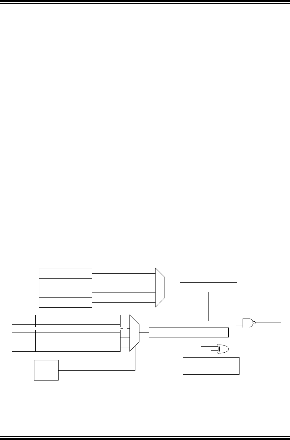
PIC32MX Family Reference Manual
DS61154A-page 34-74 Preliminary © 2009 Microchip Technology Inc.
34.8 CAN MESSAGE FILTERING
The CAN network is a broadcast type of network. A message transmitted by one node is received
by all nodes in the network. Individual CAN nodes require a filtering mechanism to receive
messages of interest. This filtering mechanism is provided by the CAN message acceptance
filters and mask registers. Filtering is performed on the ID field of the CAN message.
The PIC32MX CAN module has a total of 32 acceptance filters and four mask registers. The
application configures the specific filter to receive a message with a given identifier by setting a
filter to match the identifier of the message to be received.
Each filter is controlled by its own CAN Filter Control (CiFLTCONn) register. This register has the
following bits for each filter:
• FLTENn (n = 0 through 31) - Filter Enable bit enables/disable the filter
• MSELn (n = 0 through 31)<1:0> - Mask Select defines which mask is applied in the filter
comparison
• FSELn<4:0> (n = 0 thorough 31) - Buffer Pointer defines the destination FIFO of a
message whose ID matches the filter
As messages are received by the module, the message identifier is compared with the
corresponding bits in the filters. If the identifier matches the filter configured by the user, the
message will be stored into the FIFO pointed to by the FIFO Selection (FSELn<4:0>) bits in the
CAN Filter Control n (CiFLTCONn<4:0>) registers.
The acceptance masks can be used to ignore selected bits of the identifier as they are received.
These bits will not be compared with the bits in the filter as the message is received. For example
if the user would like to receive all messages with identifiers 0, 1, 2 and 3, the user would mask
out the lower 2 bits of the identifier. There are four mask register available. A filter can have any
one of the four masks associated with it.
Figure 34-23 shows a schematic representation of how filtering works. After a message is
received, the CAN module loops through all of the filters. As each filter is selected, the
appropriate mask is also selected using the MSELn<1:0> bits. The message in the Message
Assembly Buffer (MAB) is compared to the filter (XOR). Any bits that should be excluded from
the filtering is excluded using the selected mask. If all the conditions match, an ID match occurs
and the CAN module will move the contents of the MAB into the appropriate FIFO, pointed to by
the FSELn<4:0> bits.
Figure 34-23: CAN Message Filtering
In the example shown in Figure 34-23, the received message has an ID of 01234567 and the
closest match is Filter 1, which has an ID of 01234566. Note that these two match completely
except for the Least Significant bit (LSb). A match still occurs because the mask selected (Mask
2) is set to ignore the least significant bit of the message. Since Filter 2 has its FSELn bits set to
2, the CAN module will then store the message in FIFO2.
RXF31 Filter = 2A2B3FD
RXF1 Filter = 01234566
RXF0 Filter = 01234565
MASK3 = 00000000
MASK2 = FFFFFFFE
MASK1 = FFFF0FFF
MASK0 = FFFFFFFF
MSEL=1
MSEL=2
MSEL=0
Current Filter = 01234566
MSEL
Message Assembly Buffer
Current Mask = FFFFFFFE
ID Match = 1
CAN
FSM
Filter Select = 1 (MAB) = 01234567
FSEL31 = 9
FSEL1 = 2
FSEL0 = 10

© 2009 Microchip Technology Inc. Preliminary DS61154A-page 34-75
Section 34. Controller Area Network (CAN)
Controller Area
Network (CAN)
34
34.8.1 Enabling and Modifying Filters
Filters can be turned on or off using the Filter Enable (FLTENn) bit in the CiFLTCONn register.
Clearing the bit turns the appropriate filter Off and setting it turns the filter on. Filters can be
modified when the CAN module is in Configuration mode (OPMOD<2:0> = 100), Normal
Operation mode (OPMOD<2:0> = 000) or Disable mode (OPMOD<2:0> = 001).
The CAN module will hold Off disabling a filter when a received message is being processed.
The FLTENn bit will remain set until the filtering is complete. If a message hits this filter during
filtering, the message received will be written to the buffer pointed to by the filter. The filter is
disabled after the message has been processed.
The user application should poll the FLTENn bit to ensure that the filter has been disabled before
modifying the filter. Writes to the filter registers are blocked when the filter is enabled.
34.8.2 Extended and Standard Identifiers
A CAN message can have an 11-bit Standard Identifier or 29-bit Extended Identifier. The
SID<11:0> bits and the EID<17:0> bits in the CAN Acceptance Filter Mask n (CiRXFn) registers
should be configured to match the SID or SID and EID of the desired message. Setting the
Extended Identifier Enable (EXID) bit (CiRXFn<19>) will enable the filter to match messages with
extended identifiers. Clearing the EXID bit in the CiRXFn register will enable the filter to match
messages with standard identifiers. If the mask Identifier Receive Mode (MIDE) bit
(CiRXMn<19>) is clear, this type of message will be ignored and all message types that match
the filter will be accepted.
34.8.3 Acceptance Mask
There are four dedicated mask registers in the CAN module, Mask Register 0, 1, 2 and 3. Any
filter can select one of four mask options:
• Mask Register 0
• Mask Register 1
• Mask Register 2
• Mask Register 3
Selection of the mask for an acceptance filter is controlled by MSELm<1:0> bits corresponding
to the filter in the appropriate CiFLTCONn register. The mask register cannot be modified when
the filter using the mask is enabled. The filter should be disabled before modifying the mask. If
no masking is desired on a given filter, then corresponding mask bits should be set to one. This
will cause the filtering logic to consider all filter bits while performing the filtering operation.
Table 34-3 shows a truth table for various combinations of IDE bit in the CAN Message, EXID bit
in CiRXFn register and the MIDE bit in the CiRXMn register.
Note: The CiRXMn register can only be modified when the CAN module is in
Configuration mode.
Table 34-3: Standard/Extended Message Reception Truth Table
Message
IDE bit
Filter
EXID bit
Mask
MIDE bit Comment Message
Accepted
001
Standard Message, Filter Specifies Standard Only, SID matches Yes
Standard Message, Filter Specifies Standard Only, SID does not match No
111Extended Message, Filter Specifies Extended Only, SID and EID match Yes
Extended Message, Filter Specifies Extended Only, Either SID or EID
do not match
No
101Extended Message, Filter Specifies Standard Only No
011Standard Message, Filter Specifies Extended Only No
0x0Standard Message, Filter Specifies Ignoring Type, SID matches Yes
Standard Message, Filter Specifies Ignoring Type, SID does not match No
1x0Extended Message, Filter Specifies Ignoring Type, SID and EID match Yes
Extended Message, Filter Specifies Ignoring Type, Either SID or EID do
not match
No
Legend: x = don’t care
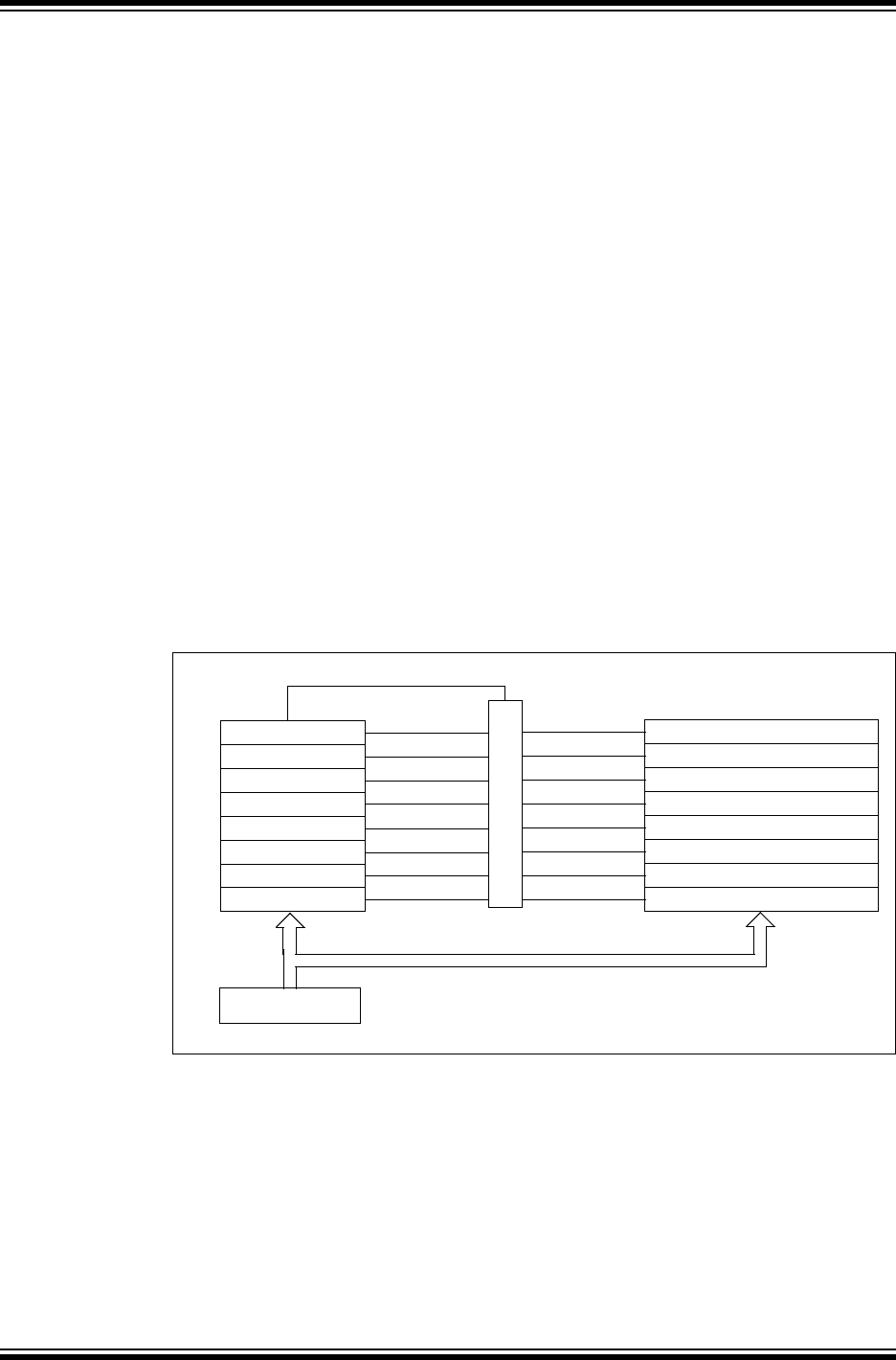
PIC32MX Family Reference Manual
DS61154A-page 34-76 Preliminary © 2009 Microchip Technology Inc.
34.8.4 Buffer Pointer
Associated with the acceptance filter’s control register are the FIFO pointer (FSELn) bits. This
serves as an address pointer for the corresponding filter. As the identifier comes in and if a match
occurs, the FSELn output corresponding to that filter is enabled and latched into an address
pointer for the receive FIFO memory. After the message has been assembled in the MAB, it is
written into the selected FIFO. The address of the filter that matched the message is loaded into
the FILHIT bits within the receive buffer.
The use of a buffer pointer means that any filter can be made to point to any FIFO, and any FIFO
can have multiple filters pointed to it. An example of how this can be used in a system would be
to have all receive messages with a low priority be placed in one large FIFO, which is serviced
infrequently by the CPU, and high priority messages placed into a second FIFO, which is
serviced as the messages arrive.
34.8.5 Handling Messages with the Same ID
With the message filtering and masking options available in the module, it is possible that one
message may match more than one filter. When two or more filters match a message received
and point to different receive buffer registers, only one receive buffer register will be loaded. The
receive buffer register to be loaded will be determined by the filter number and buffer availability.
The lower number filter will always have priority over a higher number filter. For example, Filter
0 will always take precedence over Filter 1. If the receive buffer register that Filter 0 points to is
full, then the message will be loaded into the next available FIFO associated to a matching filter.
Figure 34-24 shows an example of the prioritization of multiple filter hits. The message in the
MAB matches Filters 1, 2, 4 and 7. Filter 1 has the highest natural priority, but the associated
FIFO is full, as is Filter 2. Filter 4 has the next highest priority and has room. The message is
stored in FIFO4.
Figure 34-24: Prioritizing Multiple Filter Hits
Message = 3A8E924
MAB
Filter 7 ID = 3AxE924 FSEL = 7
Filter 6 ID = 9902B37 FSEL = 6
Filter 5 ID = 62C74E9 FSEL = 5
Filter 4 ID = #a8Ex24 FSEL = 4
Filter 3 ID = 05092B3 FSEL = 3
Filter 2 ID = 3A8E9x4 FSEL = 2
Filter 1 ID = 3A8E92X FSEL = 1
Filter 0 ID = 23D34A8 FSEL = 0
MATCH = 1
MATCH = 0
MATCH = 0
MATCH = 1(1)
MATCH = 0
MATCH = 1
MATCH = 1
MATCH = 0
FULL = 0
FULL = 0
FULL = 0
FULL = 0(1)
FULL = 0
FULL = 1
FULL = 1
FULL = 0
FIFO7
FIFO6
FIFO5
FIFO4
FIFO3
FIFO2
FIFO1
FIFO0
SELECTED FSEL = 4
X(2)
X(2)
Note 1: The match that is considered by the CAN module.
2: Filter values that are masked out.

© 2009 Microchip Technology Inc. Preliminary DS61154A-page 34-77
Section 34. Controller Area Network (CAN)
Controller Area
Network (CAN)
34
34.8.6 Configuring a Filter
The following steps should be followed for configuring a filter for Standard ID CAN messages:
1. Update the SID<10:0> bits of the CiRXFn register (n is the desired filter) with the SID of
the required CAN message.
2. Clear the EXID bit in the CiRXFn register. This will cause the filter to match Standard ID
messages only.
3. Create a mask for the filter. Load the appropriate value in the CiRXMn register. Set the
MIDE bit to match only Standard ID messages
4. Identify the CiFLTCONn register which controls the selected filter. Set the value of the
FSELn bits to point to the receive FIFO. Set the MSELn bits to use the mask configured
in step 3.
5. Enable the filter by setting the FLTENn bit in the CiFLTCONn Register.
Code Example 34-11 shows an example of configuring the CAN module message acceptance
filter for standard IDs.
Example 34-11: Configuring a Filter to Match a SID CAN Message
The following steps should be followed for configuring a filter for Extended ID CAN messages:
1. Update the SID<10:0> bits of the CiRXFn register (n is the desired filter) with the SID of
the required CAN message. Update the EID<17:0> bits of the CiRXFn register with the
EID of the required CAN message
2. Set the EXID bit in the CiRXFn register. This will cause the filter to match Extended ID
messages only.
3. Create a mask for the filter. Load the appropriate value in the CiRXMn register. Set the
MIDE bit to match only Extended ID messages.
4. Identify the CiFLTCONn register which controls the selected filter. Set the value of the
FSELn bits to point to the receive FIFO. Set the MSELn bits to use the mask configured
in step 3.
5. Enable the filter by setting the FLTENn bit in the CiFLTCONn register.
Code Example 34-12 shows an example of configuring the CAN module message acceptance
filter for extended IDs.
/* This code example shows how to configure a filter to match a Standard */
/* Identifier (SID) CAN message. */
/* In this example, Filter 3 is set up to accept messages with a SID range */
/* of 0x100 to 103. Accepted messages will be stored in FIFO5. Mask 1 is */
/* used to implement the filter address range. */
C1FLTCON0bits.FSEL3 = 5; /* Store messages in FIFO5 */
C1FLTCON0bits.MSEL3 = 1; /* Use Mask 1 */
C1RXF3bits.SID = 0x100; /* Filter 3 SID */
C1RXF3bits.EXID = 0; /* Filter only SID messages */
C1RXM1bits.SID = 0x7FC; /* Ignore last 2 bits in comparison */
C1RXM1bits.MIDE = 1; /* Match only message types. */
C1FLTCON0bits.FLTEN3 = 1; /* Enable the filter */
/* Filter is now configured. */
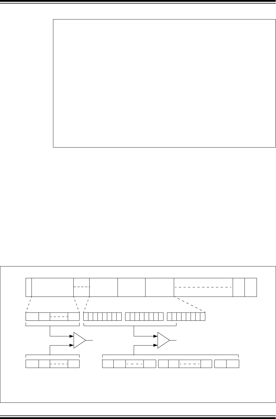
PIC32MX Family Reference Manual
DS61154A-page 34-78 Preliminary © 2009 Microchip Technology Inc.
Example 34-12: Configuring a Filter to Match an EID CAN Message
34.8.7 DeviceNet™ Filtering
The DeviceNet filtering feature is based on the CAN 2.0A protocol, in which up to 18 bits of the
data field can be compared with the Extended Identifier (EID) of the message acceptance filter in
addition to the Standard Identifier (SID).
The DeviceNet feature is enabled or disabled by the DeviceNet Filter Bit Number (DNCNT<4:0>)
control bits in the CAN Control Register (CiCON<4:0>). The value specified in the DNCNT field
determines the number of data bits to be used for comparison with the EID bits of the message
acceptance filter. If the CiCON (DNCNT<4:0>) bits are cleared, the DeviceNet feature is
disabled.
For a message to be accepted, the 11-bit SID must match the SID<10:0> bits in the message
acceptance filter and the first ‘n’ data bits in the message should match the EID<17:0> bits in the
message acceptance filter. For example, as shown in Figure 34-25, the first 18 data bits of the
received message data payload are compared with the corresponding extended identifier bits of
the message acceptance filter (CiRXFn<17:0>). The IDE bit of the received message must be ‘0’.
Figure 34-25: CAN Operation with DeviceNet™ Filtering
/* This code example shows how to configure a filter to match an */
/* Extended Identifier CAN message. */
/* In this example, Filter 3 is set up to accept messages with SID = 0x53 */
/* and EID = 0x1C498. Accepted message will be stored in FIFO5. Mask 1 is */
/* used. */
C1FLTCON0bits.FSEL3 = 5; /* Store messages in FIFO5 */
C1FLTCON0bits.MSEL3 = 1; /* Use Mask 1 */
C1RXF3bits.SID = 0x100; /* Filter 3 SID */
C1RXF3bits.EID = 0x1C498; /* Filter 3 EID */
C1RXF3bits.EXID = 1; /* Filter only SID messages */
C1RXM1bits.SID = 0x7FF; /* Consider all bits in */
C1RXM1bits.EID = 0x3FFFF; /* in the filter comparison. */
C1RXM1bits.MIDE = 1; /* Match only message types. */
C1FLTCON0bits.FLTEN3 = 1; /* Enable the filter */
/* Filter is now configured. */
SID10 SID9
S
O
F
IDENTIFIER
11 Bits
EOF
7 Bits 3 Bits
SID0
Accept/Reject Message
IFS
DATA BYTE 0 DATA BYTE 1 DATA BYTE 2
7654 321 0 76543210 76543210
Data Byte 0 Data Byte 1 Data Byte 2MESSAGE SID<10:0>
SID10 SID9 SID0
EID17 EID16 EID10
EID9 EID8 EID2 EID1 EID0
STANDARD MESSAGE DATA FRAME
MESSAGE ACCEPTANCE FILTER
SID<10:0>
MESSAGE ACCEPTANCE FILTER
EID<0:17>
Note: The DeviceNet™ filtering configuration shown for EID bits is DNCNT<4:0> = 10010.

© 2009 Microchip Technology Inc. Preliminary DS61154A-page 34-79
Section 34. Controller Area Network (CAN)
Controller Area
Network (CAN)
34
34.8.7.1 FILTER COMPARISONS
Table 34-4 shows the filter comparisons configured by the CiCON (DNCNT<4:0>) control bits.
For example, if DNCNT<4:0> = 00011, only a message in which the 11-bit Standard Identifier
matches the SID acceptance filter (SID<10:0>) and bits 7, 6 and 5 of Data Byte 0 match the
Extended Identifier filter (EID<0:2>) is accepted.
34.8.7.2 SPECIAL CASES
There may be special cases when the message contains fewer data bits than are called for by
the DeviceNet filter configuration.
•Case 1 – If DNCNT <4:0> is greater than 18, indicating that the user application selected a
number of bits greater than the total number of EID bits, the filter comparison terminates
with the eighteenth bit of the data (bit 6 of data byte 2). If the SID and all 18 data bits match,
the message is accepted.
•Case 2 – If DNCNT<4:0> is greater than 16, and the received message Data Length Code
(DLC) is 2 (indicating a payload of two data bytes), the filter comparison terminates with the
sixteenth bit of data (bit 0 of data byte 1). If the SID and all 16 bits match, the message is
accepted.
•Case 3 – If DNCNT<4:0> is greater than 8, and the received message has DLC = 1 (indi-
cating a payload of one data byte), the filter comparison terminates with the 8th bit of data
(bit 0 of data byte 0). If the SID and all 8 bits match, the message is accepted.
•Case 4 – If DNCNT<4:0> is greater than 0, and the received message has DLC = 0, indi-
cating no data payload, the filter comparison terminates with the Standard Identifier. If the
SID matches, the message is accepted.
Table 34-4: DeviceNet™ Filter Bit Configurations
DeviceNet™ Filter
Configuration
(DNCNT<4:0>)
Received Message Data Bits to be Compared
(Byte<bits>)
EID Bits Used for
Acceptance
Filter
00000 No comparison No comparison
00001 Data Byte 0<7> EID<17>
00010 Data Byte 0<7:6> EID<17:16>
00011 Data Byte 0<7:5> EID<17:15>
00100 Data Byte 0<7:4> EID<17:14>
00101 Data Byte 0<7:3> EID<17:13>
00110 Data Byte 0<7:2> EID<17:12>
00111 Data Byte 0<7:1> EID<17:11>
01000 Data Byte 0<7:0> EID<17:10>
01001 Data Byte 0<7:0> and Data Byte 1<7> EID<17:9>
01010 Data Byte 0<7:0> and Data Byte 1<7:6> EID<17:8>
01011 Data Byte 0<7:0> and Data Byte 1<7:5> EID<17:7>
01100 Data Byte 0<7:0> and Data Byte 1<7:4> EID<17:6>
01101 Data Byte 0<7:0> and Data Byte 1<7:3> EID<17:5>
01110 Data Byte 0<7:0> and Data Byte 1<7:2> EID<17:4>
01111 Data Byte 0<7:0> and Data Byte 1<7:1> EID<17:3>
10000 Data Byte 0<7:0> and Data Byte 1<7:0> EID<17:2>
10001 Byte 0<7:0> and Byte 1<7:0> and Byte 2<7> EID<17:1>
10010 Byte 0<7:0> and Byte 1<7:0> and Byte 2<7:6> EID<17:0>
10011 to 11111 Invalid Selection Invalid Selection
PIC32MX Family Reference Manual
DS61154A-page 34-80 Preliminary © 2009 Microchip Technology Inc.
34.9 RECEIVING A CAN MESSAGE
The CAN module continually monitors messages on the CAN bus. As messages are received by
the CAN module the message identifier is compared to the filter/mask combinations that are
presently configured. If a match occurs, the module will store the message in the FIFO pointed
to by FSELn. Once the message has been received and stored in the FIFO, the following bits will
be updated:
• The CFIFOCI<4:0> bits in the CiFIFOCIn register will updated
• The Receive FIFO Overflow interrupt flag (RXOVFLIF), Receive FIFO Full interrupt flag
(RXFULLIF), Receive FIFO Not Empty interrupt flag (RXNEMPTYIF) and the Receive FIFO
Half Full interrupt flag (RXHALFIF) in the CiFIFOINTn register will be updated as
appropriate
• The FIFO Interrupt Pending Flag (FIFOIPn) in the CiFSTAT register will be updated as
appropriate
• An interrupt will be generated if enabled
The CAN Module Interrupt Code (ICOD<6:0>) bits (CiVEC<6:0>) in the register and the Filter Hit
Number (FILHIT<4:0>) bits (CiVEC<12:8>) in the CAN Interrupt Code (CiVEC) register will also
be updated.
The accepted CAN message is stored in the message buffer using the format shown in
Table 34-5. The CAN module uses the formatting shown in Figure 34-26 through Figure 34-29.
Note: The application must enable at least one message acceptance filter and one mask
register in order to receive messages.
Table 34-5: Receive Message Format as Stored in RAM - CiCON.CANCAP = 1, CFIFOCON.DONLY = 0
Address
Offset Name Bit
31/2315/7
Bit
30/22/14/6
Bit
29/21/13/5
Bit
28/20/12/4
Bit
27/19/11/3
Bit
26/18/10/2
Bit
25/17/9/1
Bit
24/16/8/0
0x00 CMSGSID 31:24 CMSGTS<15:8>
23:16 CMSGTS<7:0>
15:8 FILHIT<4:0> SID<10:8>
7:0 SID<7:0>
0x04 CMSGEID 31:24 -— -— SRR IDE EID<17:14>
23:16 EID<13:6>
15:8 EID<5:0> RTR RB1
7:0 -— -— --— RB0 DLC<3:0>
0x08 CMSGDATA0 31:24 Receive Buffer Data Byte 3
23:16 Receive Buffer Data Byte 2
15:8 Receive Buffer Data Byte 1
7:0 Receive Buffer Data Byte 0
0x0C CMSGDATA1 31:24 Receive Buffer Data Byte 7
23:16 Receive Buffer Data Byte 6
15:8 Receive Buffer Data Byte 5
7:0 Receive Buffer Data Byte 4
Legend: Shaded bits read as ‘0’.
Note 1: The CAN receive message is stored in system RAM and does not have SET/CLR/INV registers associated with it.

© 2009 Microchip Technology Inc. Preliminary DS61154A-page 34-81
Section 34. Controller Area Network (CAN)
Controller Area
Network (CAN)
34
Figure 34-26: Format of CMSGSID
Figure 34-27: Format of CMSGEID
CMSGTS<15:0> FILHIT<4:0> SID<10:0>
bit 31-16 CMSGTS<15:0>: CAN Message Timestamp
Value of the CANTMR when the message is successfully received. If CANCAP = 0, these bits will
read as ‘0’.
bit 15-11 FILHIT<4:0>: Filter Hit Code
Encodes the number of the filter that resulted in writing this buffer.
11111 = Message was accepted by Filter 31
•
•
•
00000 = Message was accepted by Filter 0
bit 10-0 SID<10:0>: Standard Identifier of Received Message
— SRR IDE EID<17:0> RTR RB1 — RB0 DLC<3:0>
bit 31-30 Unimplemented: Read as ‘0’
bit 29 SRR: Substitute Remote Request
In case of a standard message frame (IDE = 0), this bit is don’t care.
In case of an extended message frame (IDE = 1), this bit is always ‘1’.
bit 28 IDE: Extended Identifier
1 = Message received has extended identifier
0 = Message received has standard identifier
bit 27-10 EID<17:0>: Extended Identifier
bit 9 RTR: Remote Transmission Request
1 = Message sender requested a remote transmission
0 = Normal message received
bit 8 RB1: Reserved Bit 1
The user application must set this bit to ‘0’ per the CAN bus specification.
bit 7-5 Unimplemented: Read as ‘0’
bit 4 RB0: Reserved Bit 0
The user application must set this bit to ‘0’ per the CAN bus specification.
bit 3-0 DLC<3:0>: Data Length Code
1xxx = Message received contains 8 bytes of data
0111 = Message received contains 7 bytes of data
•
•
•
0001 = Message received contains 1 byte of data
0000 = Message received contains 0 bytes of data
Note 1: This register is in system memory outside the CAN module.

PIC32MX Family Reference Manual
DS61154A-page 34-82 Preliminary © 2009 Microchip Technology Inc.
Figure 34-28: Format of CMSGDATA0
Figure 34-29: Format of CMSGDATA1
DATA3<7:0> DATA2<7:0> DATA1<7:0> DATA0<7:0>
bit 31-24 DATA3<7:0>: Data Byte 3
bit 23-16 DATA2<7:0>: Data Byte 2
bit 15-8 DATA1<7:0>: Data Byte 1
bit 7-0 DATA0<7:0>: Data Byte 0
Note 1: This register is in system memory outside the CAN module.
DATA7<7:0> DATA6<7:0> DATA5<7:0> DATA4<7:0>
bit 31-24 DATA7<7:0>: Data Byte 7
bit 23-16 DATA6<7:0>: Data Byte 6
bit 15-8 DATA5<7:0>: Data Byte 5
bit 7-0 DATA4<7:0>: Data Byte 4
Note 1: This register is in system memory outside the CAN module.

© 2009 Microchip Technology Inc. Preliminary DS61154A-page 34-83
Section 34. Controller Area Network (CAN)
Controller Area
Network (CAN)
34
The code in Example 34-13 shows an example data structure for implementing a CAN full
receive message buffer. An example of using this structure is provided in Example 34-14.
Example 34-13: Implementing a CAN Full Receive Message Buffer in Memory
/* This code snippet shows an example of data structure to implement a CAN */
/* full receive message buffer.*/
/* Define the sub-components of the data structure as specified in Table 34-5 */
/* Create a CMSGSID data type. */
typedefstruct
{
unsigned SID:11;
unsigned FILHIT:5;
unsigned CMSGTS:16;
}rxcmsgsid;
/* Create a CMSGEID data type. */
typedef struct
{
unsigned DLC:4;
unsigned RB0:1;
unsigned :3;
unsigned RB1:1;
unsigned RTR:1;
unsigned EID:18;
unsigned IDE:1;
unsigned SRR:1;
unsigned :2;
}rxcmsgeid;
/* Create a CMSGDATA0 data type. */
typedef struct
{
unsigned Byte0:8;
unsigned Byte1:8;
unsigned Byte2:8;
unsigned Byte3:8;
}rxcmsgdata0;
/* Create a CMSGDATA1 data type. */
typedefstruct
{
unsigned Byte4:8;
unsigned Byte5:8;
unsigned Byte6:8;
unsigned Byte7:8;
}rxcmsgdata1;
/* This is the main data structure. */
typedef union uCANRxMessageBuffer {
struct
{
rxcmsgsid CMSGSID;
rxcmsgeid CMSGEID;
rxcmsgdata0 CMSGDATA0;
rxcmsgdata0 CMSGDATA1;
};
int messageWord[4];
}CANRxMessageBuffer;

PIC32MX Family Reference Manual
DS61154A-page 34-84 Preliminary © 2009 Microchip Technology Inc.
Example 34-14: Example Usage of the Data Structure
34.9.1 Data-Only Receive Messages
The PIC32 CAN module provides a special receive mode where only the data payload section of
the received message is stored in the message buffer. The module will discard the identifier,
reserved bits and DLC bits. The time stamp value is not stored even if time stamping is enabled.
This mode can be enabled by setting the (DONLY) bit (CiFIFOCONn<12>).
Note that 8 bytes of data are stored, regardless of the value of the DLC field in the CAN message.
Unused bytes are filled with 0x00. One possible use of this mode is to concatenate messages
whose data spans multiple messages. For example, transmitting a string across the CAN bus.
34.9.2 Processing a Received Message
The user application can either use polling methods or use the CAN module interrupt to track
message reception. The CAN module provides notification about different Receive FIFO events.
The application can be notified when the Receive FIFO is not empty, is half-full or is full.
Applications should read the receive FIFO frequently to ensure that there is no FIFO overflow.
Regardless of the technique used (polling or interrupts), the following steps can be used to read
the message from the FIFO:
1. Read the value of the CiFIFOUAn register. This provides a 32-bit physical address pointer
to the receive message buffer that the application should read.
2. In case of the Data-Only receive message type, process two words from the message buffer.
3. In case of Full receive message type, process four words from the message buffer.
4. After processing the message buffer, set the UINC bit in the associated CiFIFOCONn
register.
/* Example usage of code provided in Example 34-13. */
CANRxMessageBuffer * buffer;
/* When a message have been received and read, the individual fields of */
/* the received message can be queried as such. */
buffer = (CANRxMessageBuffer *)(PA_TO_KVA1(C1FIFOUA1));
if(buffer->CMSGEID.DLC == 4)
{
/* If the length of the received message is 4 then do something. */
}
Table 34-6: Data-Only Receive Message Format as Stored in RAM
Address
Offset Name Bit
31/2315/7
Bit
30/22/14/6
Bit
29/21/13/5
Bit
28/20/12/4
Bit
27/19/11/3
Bit
26/18/10/2
Bit
25/17/9/1
Bit
24/16/8/0
0x00 CMSG0DATA0 31:24 Receive Buffer Data Byte 3
23:16 Receive Buffer Data Byte 2
15:8 Receive Buffer Data Byte 1
7:0 Receive Buffer Data Byte 0
0x04 CMSG0DATA1 31:24 Receive Buffer Data Byte 7
23:16 Receive Buffer Data Byte 6
15:8 Receive Buffer Data Byte 5
7:0 Receive Buffer Data Byte 4
Note 1: The messages are stored in system memory.
2: As a result there are no set/clr/inv registers associated with these registers.

© 2009 Microchip Technology Inc. Preliminary DS61154A-page 34-85
Section 34. Controller Area Network (CAN)
Controller Area
Network (CAN)
34
Code Example 34-15 shows an example of copying a CAN message.
Example 34-15: Copying a Message from a Receive FIFO
34.9.3 Example Receive FIFO Behavior
Consider an application where FIFO0 of the CAN1 module is configured as a receive message
FIFO. Figure 34-30 shows the FIFO before the first message arrives and is placed in the FIFO.
The CAN FIFO Base Address Register C1FIFOBA is set 0x00000100. Messages received will
be placed in system RAM (Physical address 0x00000100). Note that CFIFOUA initially points to
the start of the FIFO. The example tracks the Receive FIFO Overflow Interrupt Flag (RXOVFLIF),
Receive FIFO Full Interrupt Flag (RXFULLIF), Receive FIFO Half Full Interrupt Flag (RXHALFIF)
and Receive FIFO Not Empty Interrupt Flag (RXNEMPTYIF). This configuration is shown in
Figure 34-30.
Figure 34-30: FIFO - At Start
/* This code example shows how to process a message from a receive FIFO. */
/* In this example CAN1 and FIF01 are used. */
CANRxMessageBuffer rxMessage;
unsigned int * bufferToRead;
/* Check if there is a message available to read. */
if(C1FIFOINT1bits.RXNEMPTYIF == 1)
{
/* Get the address of the buffer to read */
bufferToRead = PA_TO_KVA1(C1FIFOUA1);
/* This is an example process (Copying the buffer). The application */
/* could process this buffer in place. */
bufferToRead[0] = rxMessage->messageWord[0];
bufferToRead[1] = rxMessage->messageWord[1];
bufferToRead[2] = rxMessage->messageWord[2];
bufferToRead[3] = rxMessage->messageWord[3];
/* Update the message buffer pointer. */
C1FIFOCON1bits.UINC = 1;
}
MB2
MB1
MB0
MB6
MB5
MB4
MB3
CFIFOBA = 0x00000100
CFIFOUA = 0x00000100
RXOVFLIF - 0
RXFULLIF - 0
RXHALFIF - 0
RXNEMPTYIF - 0
CFIFOCI = 0x00000000
PIC32MX Family Reference Manual
DS61154A-page 34-86 Preliminary © 2009 Microchip Technology Inc.
Figure 34-31 shows the FIFO after the first message has been received and written to the FIFO.
Note that while the first message buffer in the FIFO (MB0) contains data, CFIFOUA still points to
the base address of the FIFO because the user has not read this location. Note the CAN index
(CFIFOCI) has incremented showing that the next received message will be placed in MB1. The
RXNEMPTYIF flag is set indicating that FIFO is not empty.
Figure 34-31: FIFO - First Write
Figure 34-32 shows the FIFO after another five messages have been received. As before
CFIFOUA has not been modified. The buffer half full flag (RXHALFIF) was set after the reception
of the fourth message.
Figure 34-32: FIFO - Sixth Write
Figure 34-33 shows the FIFO after the first message has been read from MB0. Once the
application has read this message, it should set UINC bit in the CiFIFOCONn register. This will
cause the CFIFOUA register to change to 0x0000110 (which is the address of the next message
buffer the application must read).
Figure 34-33: FIFO - First Read
MB2
MB1
MB0/MSG0
MB6
MB5
MB4
MB3
CFIFOBA = 0x00000100
CFIFOUA = 0x00000100
RXOVFLIF - 0
RXFULLIF - 0
RXHALFIF - 0
RXNEMPTYIF - 1
CFIFOCI = 0x00000001
MB2/MSG2
MB1/MSG1
MB0/MSG0
MB6
MB5/MSG5
MB4/MGG4
MB3/MSG3
CFIFOBA = 0x00000100
CFIFOUA = 0x00000100
RXOVFLIF - 0
RXFULLIF - 0
RXHALFIF - 1
RXNEMPTYIF - 1
CFIFOCI = 0x00000006
MB2/MSG2
MB1/MSG1
MB0
MB6
MB5/MSG5
MB4/MSG4
MB3/MSG3
CFIFOBA = 0x00000100
CFIFOUA = 0x00000110
RXOVFLIF - 0
RXFULLIF - 0
RXHALFIF - 1
RXNEMPTYIF - 1
CFIFOCI = 0x00000006

© 2009 Microchip Technology Inc. Preliminary DS61154A-page 34-87
Section 34. Controller Area Network (CAN)
Controller Area
Network (CAN)
34
Figure 34-34 shows the FIFO after receiving a seventh message.
Figure 34-34: FIFO - Seventh Write About to Fill
Figure 34-35 shows the FIFO in a full state. Note that the RXFULLIF flag is set.
Figure 34-35: FIFO - Eighth Write FIFO Full
Figure 34-36 shows the FIFO receiving an additional message, with the FIFO full which
overflows the FIFO. Note that RXOVFLIF flag is set. Note that the CAN index (CiCIFOCI) has
not moved and that the message (MSG8) has been lost.
Figure 34-36: FIFO - Ninth Write FIFO Overflow
MB2/MSG2
MB1/MSG1
MB0
MB6/MSG6
MB5/MSG5
MB4/MSG4
MB3/MSG3
CFIFOBA = 0x00000100
CFIFOUA = 0x00000110
RXOVFLIF - 0
RXFULLIF - 0
RXHALFIF - 1
RXNEMPTYIF - 1
CFIFOCI = 0x00000000
MB2/MSG2
MB1/MSG1
MB0/MSG7
MB6/MSG6
MB5/MSG5
MB4/MSG4
MB3/MSG3
CFIFOBA = 0x00000100
CFIFOUA = 0x00000110
RXOVFLIF - 0
RXFULLIF - 1
RXHALFIF - 1
RXNEMPTYIF - 1
CFIFOCI = 0x00000001
MB2/MSG2
MB1/MSG1
MB0/MSG7
MB6/MSG6
MB5/MSG5
MB4/MSG4
MB3/MSG3
CFIFOBA = 0x00000100
CFIFOUA = 0x00000110
RXOVFLIF - 1
RXFULLIF - 1
RXHALFIF - 1
RXNEMPTYIF - 1
CFIFOCI = 0x00000001
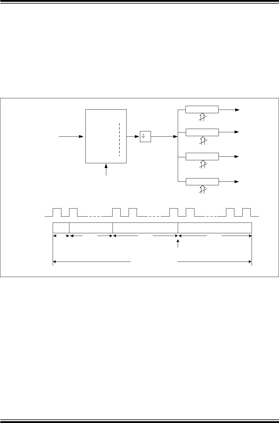
PIC32MX Family Reference Manual
DS61154A-page 34-88 Preliminary © 2009 Microchip Technology Inc.
34.10 BIT TIMING
The nominal bit rate is the number of bits per second transmitted on the CAN bus.
Nominal bit time = 1 ÷ Nominal Bit Rate.
There are four time segments in a bit time to compensate for any phase shifts due to oscillator
drifts or propagation delays. These time segments do not overlap each other and are represented
in terms of Time Quantum (TQ). One TQ is a fixed unit of time derived from the oscillator clock.
The total number of time quanta in a nominal bit time must be programmed between 8 and 25 TQ.
Figure 34-37 shows how the time quanta clock (FTQ) is obtained from the system clock and also
how the different time segments are programmed.
Figure 34-37: CAN™ Bit Timing
34.10.1 Bit Segments
Each bit transmission time consists of four time segments:
•Synchronization Segment – This time segment synchronizes the different nodes con-
nected on the CAN bus. A bit edge is expected to be within this segment. Based on CAN
protocol, the Synchronization Segment is assumed to be one Time Quantum.
•Propagation Segment – This time segment compensates for any time delay that may
occur due to the bus line or due to the various transceivers connected on that bus.
•Phase Segment 1 – This time segment compensates for errors that may occur due to
phase shift in the edges. The time segment may be lengthened during resynchronization to
compensate for the phase shift.
•Phase Segment 2 – This time segment compensates for errors that may occur due to
phase shift in the edges. The time segment may be shortened during resynchronization to
compensate for the phase shift. The Phase Segment 2 time can be configured to be either
programmable or specified by the Phase Segment 1 time.
CAN Nominal Bit Time
Time Quanta
Time Segments Propagation Segment Phase Segment 1 Phase Segment 2
Sync
Seg
1T
Q1-8 TQ1-8 TQ1-8 TQ
Sample Point
BAUD RATE
PRESCALER
FSYS 2
Prop Seg
Phase Seg1
Phase Seg2
Sync Seg
FTQ
Time Quanta
CiCFG<BRP>
CiCFG<PRSEG>
CiCFG<SEG1PH>
CiCFG<SEG2PH>
CiCFG<SJW>
1-8 TQ
1:1
1:2
1:64
(TQ)
1-8 TQ
1-8 TQ
1 TQ
8-25 TQ

© 2009 Microchip Technology Inc. Preliminary DS61154A-page 34-89
Section 34. Controller Area Network (CAN)
Controller Area
Network (CAN)
34
34.10.2 Sample Point
The sample point is the point in a CAN bit time interval where the sample is taken and the bus
state is read and interpreted. It is situated between Phase Segment 1 and Phase Segment 2.
The CAN bus can be sampled once or thrice at the sample point, as configured by the Sample
CAN bus Line (SAM) bit in CAN Baud Rate Configuration Register (CiCFG<14>).
• If CiCFG<SAM> = 1, the CAN bus is sampled three times at the sample point. The most
common of the three samples determines the bit value.
• If CiCFG<SAM> = 0, the CAN bus is sampled only once at the sample point.
34.10.3 Synchronization
Two types of synchronization are used – Hard Synchronization and Resynchronization. A Hard
Synchronization occurs once at the start of a frame. Resynchronization occurs inside a frame.
•Hard synchronization takes place on the recessive-to-dominant transition of the start bit.
The bit time is restarted from that edge.
•Resynchronization takes place when a bit edge does not occur within the Synchronization
Segment in a message. One of the Phase Segments is shortened or lengthened by an
amount that depends on the phase error in the signal. The maximum amount that can be
used is determined by the Synchronization Jump Width parameter (CiCFG<SJW>).
The length of Phase Segment 1 and Phase Segment 2 can be changed depending on oscillator
tolerances of the transmitting and receiving node. Resynchronization compensates for any
phase shifts that may occur due to the different oscillators used by the transmitting and receiving
nodes.
•Bit Lengthening – If the transmitting node in CAN has a slower oscillator than the
receiving node, the next falling edge, and therefore, the sample point, can be delayed by
lengthening Phase Segment 1 in the bit time.
•Bit Shortening – If the transmitting node in CAN has a faster oscillator than the receiving
node, then the next falling edge, and therefore, the sample point of the next bit, can be
reduced by shortening the Phase Segment 2 in the bit time.
•Synchronization Jump Width (SJW) – The SJW <1:0> bits in CAN Baud Rate
Configuration Register (CiCFG<7:6>) determine the synchronization jump width by limiting
the amount of lengthening or shortening that can be applied to the Phase Segment 1 and
Phase Segment 2 time intervals. This segment should not be longer than Phase Segment
2 time. The width can be 1-4 TQ.
34.10.4 CAN Bit Time Calculations
The steps that need to be performed by the user application to configure the bit timing for the
CAN module are described below, with examples.
34.10.4.1 STEP 1: CALCULATE THE TIME QUANTUM FREQUENCY (FTQ)
• Select the Baud Rate for the CAN Bus (FBAUD).
• Select the number of time quanta in a bit time, based on your system requirements.
The Time Quantum Frequency (FTQ) is given by Equation 34-1.
Equation 34-1:
FTQ = N * FBAUD
Note 1: The total number of time quanta in a nominal bit time must be programmed between
8 TQ and 25 TQ. Therefore the Time Quantum Frequency (FTQ) is between 8 to 25
times baud rate (FBAUD).
2: Make sure that FTQ is an integer multiple of FBAUD to get precise bit time. If not, the
oscillator input frequency or baud rate may need to be changed.

PIC32MX Family Reference Manual
DS61154A-page 34-90 Preliminary © 2009 Microchip Technology Inc.
34.10.4.2 STEP 2: CALCULATE THE BAUD RATE PRESCALER (CiCFG<BRP>)
The baud rate prescaler is given by Equation 34-2.
Equation 34-2:
34.10.4.3 STEP 3: SELECT THE INDIVIDUAL BIT TIME SEGMENTS
The Individual Bit Time Segments are selected using the CiCFG register
Bit Time = Sync Segment + Propagation Segment + Phase Segment 1 + Phase Segment 2
Example 34-16: CAN Bit Timing Calculation Example
Code Example 34-17 illustrates code for configuring CAN bit timing code.
Example 34-17: Configuring the CAN Module to Obtain a Specific Bit Rate
CiCFG<BRP> = (FSYS/(2 * FTQ)) – 1
Note 1: (Propagation Segment + Phase Segment 1) must be greater than or equal to the
length of Phase Segment 2.
2: Phase Segment 2 must be greater than Synchronous Jump Width.
Step 1: Calculate the time quantum frequency.
•If F
BAUD = 1 Mbps, and number of time quanta N = 10, then FTQ = 20 MHz.
Step 2: Calculate the baud rate prescaler (if FSYS = 80000000).
• CiCFG1<BRP> = ( 80000000/(2 * FTQ) ) - 1 = 3.
Step 3: Select the individual bit time segments.
• Synchronization Segment = 1 TQ (constant).
• Based on system characteristics, suppose the Propagation Delay = 3 TQ.
• Suppose the sample point is to be at 70% of Nominal Bit Time. Phase Segment 2 = 30%
of Nominal Bit Time = 3 TQ.
• Then, Phase Segment 1 = 10 TQ - (1 TQ + 3 TQ + 3 TQ) = 3 TQ.
/* This code example shows how to configure the CAN module to obtain a */
/* specific bit rate. */
/* This example implements the configuration shown in Example 34-16. */
/* Fsys = System Clock Frequency = 80000000; */
/* Fbaud = CAN bit rate = 1000000; */
/* N = Time Quanta (Tq) per bit = 10; */
/* Prop Segment = 3Tq */
/* Phase Seg 1 = 3Tq */
/* Phase Seg 2 = 3Tq */
/* Sync Jump Width = 2Tq */
/* Ensure the CAN module is in configuration mode.*/
C1CONbits.REQOP = 4
while(C1CONbits.OPMOD != 4);
C1CFGbits.SEG2PHTS = 1;/* Phase seg 2 is freely programmable */
C1CFGbits.SEG2PH = 2;/* Phase seg 2 is 3Tq. */
C1CFGbits.SEG1PH = 2;/* Phase seg 1 is 3Tq. */
C1CFGbits.PRSEG = 2;/* Propagation seg 2 is 3Tq. */
C1CFGbits.SAM = 1;/* Sample bit 3 times. */
C1CFGbits.SJW = 2;/* Sync jump width is 2 Tq */
C1CFGbits.BRPVAL = 3;/* BRP value as calculated in example 34-11 */
/* CAN bit rate configuration complete. */

© 2009 Microchip Technology Inc. Preliminary DS61154A-page 34-91
Section 34. Controller Area Network (CAN)
Controller Area
Network (CAN)
34
34.11 CAN ERROR MANAGEMENT
34.11.1 CAN Bus Errors
The CAN protocol defines five different ways of detecting errors.
•Bit error
• Acknowledge error
• Form error
• Stuffing error
• CRC error
The bit error and the acknowledge error occur at the bit level; the other three errors occur at the
message level.
34.11.1.1 BIT ERROR
A node that is sending a bit on the bus also monitors the bus. A bit error is detected when the bit
value that is monitored is different from the bit value that is sent. An exception is when a
recessive bit is sent during the stuffed bit stream of the Arbitration field or during the ACK slot. In
this case, no bit error occurs when a dominant bit is monitored. A transmitter sending a passive
error frame and detecting a dominant bit does not interpret this as a bit error.
34.11.1.2 ACKNOWLEDGE ERROR
In the Acknowledge field of a message, the transmitter checks if the Acknowledge Slot (which it
has sent out as a recessive bit) contains a dominant bit. If not, this implies that no other node has
received the frame correctly. An acknowledge error has occurred, and as a result, the message
must be repeated. No error frame is generated in this case.
34.11.1.3 FORM ERROR
A form error is detected when a fixed-form bit field (End-Of-Frame, Inter-frame Space,
Acknowledge Delimiter or CRC Delimiter) contains one or more illegal bits. For a receiver, a
dominant bit during the last bit of End-of-Frame is not treated as a form error.
34.11.1.4 STUFFING ERROR
A stuffing error is detected at the bit time of the sixth consecutive equal bit level in a message
field that should be coded by the method of bit stuffing.
34.11.1.5 CRC ERROR
The node transmitting a message computes and transmits the CRC corresponding to the trans-
mitted message. Every receiver on the bus performs the same CRC calculation as the transmit-
ter. A CRC error is detected if the calculated result is not the same as the CRC value obtained
from the received message.
34.11.2 Fault Confinement
Every CAN controller on a bus tries to detect the errors outlined above within each message. If
an error is found, the discovering node transmits an error frame, thus destroying the bus traffic.
The other nodes detect the error caused by the error frame (if they have not already detected the
original error) and take appropriate action (i.e., discard the current message).
The CAN module maintains two error counters:
• Transmit Error Counter (TEC) - CiTREC<15:8>
• Receive Error Counter (REC) - CiTREC<7:0>
There are several rules governing how these counters are incremented and/or decremented. In
essence, a transmitter detecting a fault increments its transmit error counter faster than the
listening nodes will increment their receive error counter. This is because there is a good chance
that it is the transmitter that is at fault.
Note: The error counters are modified according to the CAN 2.0B specification.
PIC32MX Family Reference Manual
DS61154A-page 34-92 Preliminary © 2009 Microchip Technology Inc.
A node starts out in Error Active mode. When any one of the two Error Counters equals or
exceeds a value of 127, the node enters a state known as Error Passive. When the Transmit
Error Counter exceeds a value of 255, the node enters the Bus Off state.
• An Error Active node transmits an Active Error Frame when it detects errors.
• An Error Passive node transmits a Passive Error Frame when it detects errors.
• A node that is Bus Off transmits nothing on the bus.
In addition, the CAN module employs an error warning feature that warns the user application
(when the Transmit Error Counter equals or exceeds 96) before the node enters error passive
state, as illustrated in Figure 34-38.
Figure 34-38: Error Modes
34.11.2.1 TRANSMITTER IN ERROR PASSIVE STATE
The Transmitter Error Passive (TXBP) bit (CiTREC<20>) is set when the Transmit Error Counter
equals or exceeds 128 and generates an error interrupt (CiINT<CERRIF>) upon entry into Error
Passive state. The Transmit Error Passive flag is cleared automatically by the hardware if the
Transmit Error Counter becomes less than 128.
34.11.2.2 RECEIVER IN ERROR PASSIVE STATE
The Receiver Error Passive (RXBP) bit (CiTREC<19>) is set when the Receive Error Counter
equals or exceeds 128 and generates an error interrupt (CiINT<CERRIF>) upon entry into Error
Passive state. The Receive Error Passive flag is cleared automatically by the hardware if the
Receive Error Counter becomes less than 128.
34.11.2.3 TRANSMITTER IN BUS OFF STATE
The Transmitter Bus Off (TXBO) bit (CiTREC<21>) is set when the Transmit Error Counter
equals or exceeds 256 and generates an error interrupt (CiINT<CERRIF>)
34.11.2.4 TRANSMITTER IN ERROR WARNING STATE
The Transmitter Error Warn (TXWARN) bit (CiTREC<18>) is set when the Transmit Error Coun-
ter equals or exceeds 96 and generates an error interrupt (CiINT<CERRIF>) upon entry into
Error Warn state. The Transmit Error Warn flag is cleared automatically by the hardware if the
Transmit Error Counter becomes less than 96.
Bus
Off
Error
Active
Error
Passive
REC > 127 or
TEC > 127
REC < 127 or
REC < 127
TEC > 255
128 occurrences of
11 consecutive
“recessive” bits
Reset

© 2009 Microchip Technology Inc. Preliminary DS61154A-page 34-93
Section 34. Controller Area Network (CAN)
Controller Area
Network (CAN)
34
34.11.2.5 RECEIVER IN ERROR WARNING STATE
The Receiver Error Warn (RXWARN) bit (CiTREC<17>) is set when the Receive Error Counter
equals or exceeds 96 and generates an error interrupt (CiINT<CERRIF>) upon entry into Error
Warn state. The Receive Error Warn flag is cleared automatically by the hardware if the Receive
Error Counter becomes less than 96.
Additionally, there is an Error State Warning flag (EWARN) bit (CiTREC<16>), which is set if at
least one of the error counters equals or exceeds the error warning limit of 96. EWARN is Reset
if both error counters are less than the error warning limit.
PIC32MX Family Reference Manual
DS61154A-page 34-94 Preliminary © 2009 Microchip Technology Inc.
34.12 CAN INTERRUPTS
Interrupts in the PIC32 CAN module can be classified into three layers. Lower layer interrupts
propagate to higher layers where they are multiplexed into single interrupts. Therefore, the layer
1 interrupt is multiplex of a multiple interrupts in layer 2. Some of the interrupts in layer 2 are a
multiplex of interrupts in layer 3 (see Figure 34-39).
Figure 34-39: Multiple Interrupt Multiplex
At layer 1, the CAN module generates one interrupt to the CPU called the CANx interrupt. The
interrupt is caused by any of the layer 2 interrupts. The CANx Interrupts can be enabled or
disabled via the PIC32 Interrupt Controller. Refer to Section 8. “Interrupts” (DS61108) in the
“PIC32MX Family Reference Manual” for more details on enabling and configuring CPU
interrupts on the PIC32 device.
Each of the layer 2 and layer 3 interrupts has an Interrupt Enable bit (IE) bit and Interrupt Status
Flag (IF) bit associated with it. The CAN module will set an IF bit when an interrupt event occurs.
If the application has set IE bit, then the event will propagated to the next Interrupt layer.
Applications can either poll the IF bits or enable interrupts to become aware of the CAN module
events.
The Interrupt Code (ICOD<6:0>) bits will contain the code for the latest interrupts. These bits can
be used in combination with a jump table for efficient handling of interrupts.
34.12.1 Layer 2 Interrupts
The CAN module has nine interrupts at layer 2.
• TBIF – Transmit FIFO Interrupt
• RBIF – Receive FIFO Interrupt
• CTMRIF – CAN Timestamp Timer Rollover Interrupt
• MODIF – CAN Operation Mode Change Interrupt
• RBOVIF – Receive FIFO Overflow Interrupt
• SERRIF – CAN System Error Interrupt
• CERRIF – CAN Bus Error Interrupt
• WAKIF – CAN Wake-up Interrupt
• IVRIF – Invalid CAN Message Interrupt.
RXEMPTYIF
RXHALFIF
RXFULLIF
FIFO0
FIFO1
FIFO31
FIFO0
FIFO1
FIFO31
TXEMPTYIF
TXHALFIF
TXNFULLIF
RBIF
RBOVIF
TBIF
WAKIF
CTMRIF
IVRIF
SERRIF
CERRIF
MODIF
Third Layer Interrupts Second Layer Interrupts First Layer Interrupt
CAN Interrupt to
CPU
RXEMPTYIE
RXHALFIE
RXFULLIE
TXEMPTYIE
TXHALFIE
TXNFULLIE
RXOVLIE
RXOVLIF
FIFO31
RXOVF
FIFO1
FIFO0
CiFSTAT Register
CiRXOVF Register
All of these Interrupts sources
have corresponding enable bits
(not shown here for clarity)

© 2009 Microchip Technology Inc. Preliminary DS61154A-page 34-95
Section 34. Controller Area Network (CAN)
Controller Area
Network (CAN)
34
Of the above interrupts, the Invalid Message Received (IVRIF), the Wake-up (WAKIF), CAN
Timer (CTMRIF) and CAN Mode Change (MODIF) interrupts have a single source. The FIFO
(TBIF/RBIF), FIFO overflow (RBOVIF), CAN Bus Error (CERRIF) and System Error (SERRIF)
interrupts have multiple sources.
34.12.1.1 INVALID MESSAGE RECEIVED INTERRUPT (IVRIF)
The Invalid Message Received Interrupt (IVRIF) occurs when some type of error has occurred in
the last message transmitted or received. The specific error that occurred is not available to the
application software. To clear the interrupt, the flag bit must be cleared.
34.12.1.2 WAKE-UP INTERRUPT (WAKIF)
The Wake-up Interrupt (WAKIF) occurs when CAN bus-activity is detected while the CAN module
is in sleep mode. To clear the interrupt, the flag must be cleared.
34.12.1.3 CAN BUS ERROR INTERRUPT (CERRIF)
The CAN Bus Error Interrupt (CERRIF) occurs when there is an error on the CAN bus. The bit is
set every time there is change in the current error state of the CAN module with respect to the
CAN network. The error states are tracked by the CiTREC register. To clear the interrupt, the flag
bit must be cleared. The CERRIF bit will be set once each time Transmit Error Counter
(TEC<7:0>) bits or Receive Error Counter (REC<7:0>) bits cross a threshold. For example if
TEC<7:0> goes from 95 to 96, then CERRIF will be set. If this bit is cleared, it will remain clear
even if TEC<7:0> remains above 96. It will be set again if TEC<7:0> drops below 96 and rises
above 95 again, or if TEC<7:0> goes above 127.
34.12.1.4 SYSTEM ERROR INTERRUPT (SERRIF)
A System Error Interrupt (SERRIF) can occur due to two types of system errors, addressing
errors and bandwidth errors. Both of these errors are fatal and the CAN module will be stopped.
Once the error occurs the user should wait till the CAN module stops, by polling the BUSY bit in
the CiCON register. Once the module has stopped, SERRIF can be cleared by clearing ON bit
in the CiCON register.
34.12.1.5 ADDRESSING ERRORS
There are two sources of Addressing errors. Both of these have the same ICOD values
(ICOD = 100 0100).
• An addressing error will occur if a FIFO is configured with an invalid base address. This
error will most commonly occur when the FIFO points to an unimplemented address.
• An addressing error will occur if the message destination is illegal, such as attempting to
write a received message to program flash, which is not directly writable.
34.12.1.6 BUS BANDWIDTH ERROR
A Bus Bandwidth Error will occur when the CAN module is unable to write a received CAN
message to the location in system memory before the next CAN message arrives. This condition
is represented by ICOD = 100 0101. This may occur if some other PIC32 system bus initiator
with a higher priority than the CAN module uses the system bus up for an extended period of time
thereby preventing the CAN module from storing the received CAN message. The overflow bit in
the corresponding FIFO Interrupt register will be set.
Note: A error condition which caused the System Error Interrupt (SERRIF) can only be
resolved by turning the CAN module off (by clearing ON bit in the CiCON register).
Clearing the SERRIF bit will not clear this error condition.

PIC32MX Family Reference Manual
DS61154A-page 34-96 Preliminary © 2009 Microchip Technology Inc.
34.12.1.7 RECEIVE FIFO OVERRUN INTERRUPT (RBOVIF)
The Receive FIFO Overrun Interrupt occurs when the CAN module has received a message but
the designated Receive FIFO is full. The CAN module will set the RXOVFLIF flag in the
CiFIFOINTn register corresponding to the affected Receive FIFO. This is also reflected in CAN
Receive FIFO Overflow Status (CiRXOVF) register if the Receive FIFO Overflow Interrupt
Enable (RXOVFLIE) bit is set in the CiFIFOINTn register.
The RBOVIF bit in CiINT register is the OR reduction of all the bits in the CiRXOVF register. The
RBOVIF bit and the RXOVIFn bits in the CiRXOVF register are not directly clearable. These need
to be cleared by clearing the appropriate RXOVFLIF in the CiFIFOINTn register.
34.12.1.8 CAN MODE CHANGE INTERRUPT (MODIF)
The CAN Mode Change Interrupt (MODIF) occurs when the CAN module OPMOD<2:0> bits
change indicating a change in the operating mode of the CAN module. The ICOD bits will indicate
a mode change condition. To clear the interrupt, the flag bit must be cleared.
34.12.1.9 CAN TIMESTAMP TIMER INTERRUPT (CTMRIF)
The CAN Timestamp Timer Interrupt (CMTRIF) occurs when CAN Timestamp timer overflows.
The ICOD bits will indicate a timestamp timer overflow. To clear the interrupt, the flag bit must be
cleared.
34.12.1.10 CAN TRANSMIT FIFO INTERRUPT (TBIF)
The CAN Transmit FIFO interrupt (TBIF) occurs when there is a change in the status of the
Transmit FIFO. This interrupt has multiple layer 3 interrupt sources.
• Transmit FIFO Not Full Interrupt (TXNFULLIF)
• Transmit FIFO Half Full Interrupt (TXHALFIF)
• Transmit FIFO Empty Interrupt (TXEMPTYIF)
The TBIF interrupt cannot be cleared by the application. The interrupt will be cleared when all of
the source interrupt conditions terminate.
34.12.1.11CAN RECEIVE FIFO INTERRUPT (RBIF)
The CAN Receive FIFO interrupt (RBIF) occurs when there is change in the status of the Receive
FIFO. This interrupt has multiple layer 3 interrupt source
• Receive FIFO Full Interrupt (RXFULLIF)
• Receive FIFO Half Full Interrupt (RXHALFIF)
• Receive FIFO Not Empty Interrupt (RXNEMPTYIF)
The RBIF interrupt cannot be cleared by the application. The interrupt will be cleared when all of
the source interrupt conditions terminate.
34.12.2 Layer 3 Interrupts
The CAN Module has following Layer 3 interrupts.
• Transmit FIFO Not Full Interrupt (TXNFULLIF)
• Transmit FIFO Not Half Full Interrupt (TXNHALFIF)
• Transmit FIFO Not Empty Interrupt (TXNEMPTYIF)
• Receive FIFO Full Interrupt (RXFULLIF)
• Receive FIFO Half Full Interrupt (RXHALFIF)
• Receive FIFO Empty Interrupt (RXEMPTYIF)
• Receive FIFO Overflow Interrupt (RXOVLIF)
These interrupts reflect the current status of the Transmit and Receive FIFOs.

© 2009 Microchip Technology Inc. Preliminary DS61154A-page 34-97
Section 34. Controller Area Network (CAN)
Controller Area
Network (CAN)
34
34.12.3 Interrupt Persistency
The CAN module provides interrupts which indicate the operational status of message FIFOs.
These interrupts are persistent, in that they are present till the interrupt causing condition has
cleared. The interrupts flags themselves cannot be cleared directly by the application. For
example the Receive FIFO Not Empty Interrupt (RXNEMPTYIF) will remain set as long as there
is at least one message in the Receive FIFO. The following CAN interrupts are persistent:
• Transmit FIFO (TBIF) Interrupt (CiINT<0>)
• Receive FIFO (RBIF) Interrupt (CiINT<1>)
• FIFO Status (FIFOIPx) Interrupt (CiFSTAT<31:0>)
• Transmit FIFO Not Full (TXNFULLIF) Interrupt (CiFIFOINTn<10>)
• Transmit FIFO Half Full (TXHALFIF) Interrupt (CiFIFOINTn<9>)
• Transmit FIFO Empty (TXNEMPTYIF) Interrupt (CiFIFOINTn<8>)
• Receive FIFO Full (RXFULLIF) Interrupt (CiFIFOINTn<10>)
• Receive FIFO Half Full (RXHALFIF) Interrupt (CiFIFOINTn<9>)
• Receive FIFO Not Empty (RXNEMPTYIF) Interrupt (CiFIFOINTn<8>)
Note that the Receive FIFO Overflow (RXOVFLIF) Interrupt (CiFIFOINTn<11>) is sticky and is
user-clearable.
34.12.4 CAN FIFO Status Register (CiFSTAT)
The CAN FIFO Status (CiFSTAT) Register is an indication register. The FIFOIPn bits in the
CiFSTAT register get set when interrupts are enabled in corresponding CiFIFOINTn registers
and when any of the following interrupt conditions occur:
• Transmit FIFO Not Full (TXNFULLIF) Interrupt (CiFIFOINTn<10>)
• Transmit FIFO Half Full (TXHALFIF) Interrupt (CiFIFOINTn<9>)
• Transmit FIFO Empty (TXNEMPTYIF) Interrupt (CiFIFOINTn<8>)
• Receive FIFO Full (RXFULLIF) Interrupt (CiFIFOINTn<10>)
• Receive FIFO Half Full (RXHALFIF) Interrupt (CiFIFOINTn<9>)
• Receive FIFO Not Empty (RXNEMPTYIF) Interrupt (CiFIFOINTn<8>)
The FIFOIPn bits by themselves are not interrupt sources. The ICOD bits (CiVEC<6:0>) will
reflect value of the FIFOIPn bits which are set.
34.12.5 CAN Receive FIFO Overflow Register (CiRXOVF)
The RXOVFn bits in CAN Receive FIFO Overflow Register (CiRXOVF) gets set when a Receive
FIFO overflow occurs and when the Receive FIFO Overflow Interrupt Enable (RXOVFLIE) bit
(CiFIFOINTn<19>) is set. The RXOVFn bits are source interrupts to the RBOVIF (CiINT<11>)
Interrupt. The bits in the CiRXOVF register are not directly clearable, and can be cleared by
clearing the RXOVFLIF (CiFIFOINTn<3>) bit.
34.12.6 Interrupt Code (ICOD) bits
The Interrupt Code (ICOD) bits in the CAN Interrupt Code (CiVEC) register (CiVEC<6:0>) will
reflect the highest interrupt that is still pending in the CAN module. The higher the ICOD value,
the higher the natural priority of the pending interrupt. The ICOD events are persistent. If an
interrupt with a higher natural priority occurs, masking the lower priority in the ICOD register, the
lower priority will be shown as soon as the higher priority interrupt is cleared.
For example, consider this application case:
• FIFO0 causes an interrupt - ICOD = 000 0000
• Buffer 5 also has an event that causes an interrupt, causing ICOD to be set to ‘000 0101’.
• The user enters the CAN interrupt handler, services buffer 5 and clears the interrupt.
• ICOD will now read ‘000 0000’, indicating that buffer 0 still has an interrupt pending, which
can then be serviced before returning from the Interrupt Service Routine (ISR).
34.12.7 CAN Filter Hit bits (FILHIT)
The CAN Filter Hit (FILHIT) bits in the CAN Interrupt Code (CiVEC) register (CiVEC<12:8>)
contain the value of the filter that last matched a receiving message. Unlike the ICOD bits
(CiVEC<6:0>), the FILHIT bits have no history and are only updated when a message is
received.

PIC32MX Family Reference Manual
DS61154A-page 34-98 Preliminary © 2009 Microchip Technology Inc.
34.13 CAN RECEIVED MESSAGE TIME STAMPING
The CAN module can provide a time value of when a message is received. This time stamp will
be stored with the received message if the CAN Receive Message Timer Capture Event Enable
(CANCAP) bit in the CAN Control (CiCON<20>) register is set. The CAN module will write a
timestamp to the CMSGTS bits of CMSGOSID field (CMSG0SID<31:16>) in the Receive
Message Buffer. The CAN module obtains the timestamp by capturing the value of CAN Time
Stamp Timer (CANTS) bits in CiTMR register (CiTMR<31:16>) whenever a valid frame has been
received. Because the CAN specification defines a frame to be valid if no errors occurred before
the EOF field has been transmitted successfully, the value of CANTS will be captured right after
the EOF.
All received messages will be time stamped, even messages that the module transmits and
receives itself.
The application can configure the CAN Time stamp time interval in terms of system clocks
through the CAN Time Stamp Timer Prescaler (CANSTPRE) bits in the CiTMR register
(CiTMR<15:0>).
34.14 LOW-POWER MODES
34.14.1 Sleep Mode
The user application must ensure that the module is not active when the CPU goes into Sleep
mode. To protect the CAN bus system from fatal consequences due to violations of the above
rule, the module drives the TXCAN pin into the recessive state while sleeping. The recom-
mended procedure is to bring the module into Disable mode before the CPU is put into Sleep
mode.
34.14.2 Idle Mode
When the CPU is in Idle mode, the module powers down if the Stop in Idle Mode (SIDLE) bit in
the CAN Control (CiCON<13>) register is ‘1’. The user application must ensure that the module
is not active when the CPU goes into Idle mode and the SIDLE bit is set. To protect the CAN bus
system from fatal consequences due to violations of the above rule, the module drives the CiTX
pin into the recessive state while the CPU is in Idle mode and the SIDLE bit is set.
34.14.3 Wake-up Functions
The CAN module will monitor the CAN receive (CiRX) pin for activity while the module is
sleeping. The module will be sleeping when:
• the device is in Sleep mode
• the device is in Idle mode and the SIDLE bit is set
While in this mode, the CAN module will generate an interrupt if Bus Wake Up Activity Interrupt
Enable (WAKIE) bit in the CAN Interrupt (CiINT) Register (CiINT<30>) is set and bus activity is
detected.
The module can be programmed to apply a low-pass filter function to the CiRX line while Disable
mode or Sleep/Idle . This feature can be used to protect the module from wake-up due to short
glitches on the CAN bus lines. The CAN Bus Line Filter Enable (WAKFIL) bit in the CAN
Configuration (CiCFG) register (CICFG<22>) enables or disables the filter while the module
sleeping.
Note that while the CAN module generates the interrupt, the state of the CAN module itself will
be not affected by the interrupt.

© 2009 Microchip Technology Inc. Preliminary DS61154A-page 34-99
Section 34. Controller Area Network (CAN)
Controller Area
Network (CAN)
34
The following steps describe the recommended procedure for using the wake-up interrupt
feature with the PIC32 device Sleep mode.
1. The WAKIE bit should be set in order to enable the wake-up on bus activity feature.
2. Before placing the device into Sleep mode, switch the CAN operation mode to Disable and
wait until the CAN module has entered Disable mode.
3. Put the PIC32 device into Sleep mode.
4. During Sleep, if there is CAN bus activity, the PIC32 device will wake from Sleep mode. If
the CAN CPU interrupt is enabled, the CPU will execute the CAN Interrupt Service
Routine.
5. In the ISR, check whether the WAKIF bit is set and switch the CAN operation mode to Nor-
mal. When the switch is complete, the CAN module will be able to receive messages
(clear the WAKIF bit). Note that the CAN message that woke the device will be lost.

PIC32MX Family Reference Manual
DS61154A-page 34-100 Preliminary © 2009 Microchip Technology Inc.
34.15 RELATED APPLICATION NOTES
This section lists application notes that are related to this section of the manual. These
application notes may not be written specifically for the PIC32MX device family, but the concepts
are pertinent and could be used with modification and possible limitations. The current
application notes related to the Controller Area Network (CAN) module are:
Title Application Note #
No related application notes at this time N/A
Note: Visit the Microchip web site (www.microchip.com) for additional application notes
and code examples for the PIC32MX family of devices.

© 2009 Microchip Technology Inc. Preliminary DS61154A-page 34-101
Section 34. Controller Area Network (CAN)
Controller Area
Network (CAN)
34
34.16 REVISION HISTORY
Revision A (July 2009)
This is the initial released version of this document.

PIC32MX Family Reference Manual
DS61154A-page 34-102 Preliminary © 2009 Microchip Technology Inc.
NOTES:
