PMOD SF Pmodsf Rm Reference Manual
User Manual: Pdf
Open the PDF directly: View PDF ![]() .
.
Page Count: 2
1300 Henley Court
Pullman, WA 99163
509.334.6306
www.digilentinc.com
PmodSF™ Reference Manual
Revised May 24, 2016
This manual applies to the PmodSF rev. C
DOC#: 502-103
Copyright Digilent, Inc. All rights reserved.
Other product and company names mentioned may be trademarks of their respective owners.
Page 1 of 2
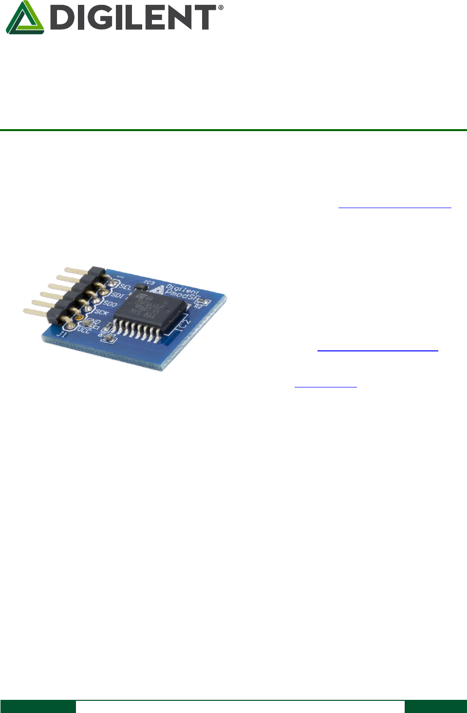
Overview
The PmodSF provides users with 16Mbit of non-volatile memory through the use of ST Microelectronics M25P16.
By using the SPI protocol, users can both write to and read from the flash memory.
1 Functional Description
The PmodSF utilizes ST Microelectronics M25P16 which provides 16 Mbits of flash memory that can be accessed
through the SPI protocol. Although this amount of memory is very small compared to modern flash drives, the
PmodSF is a great way to get introduced to controlling non-volatile memory and can be easily incorporated into
projects that need a way to store some information without using the USB interface.
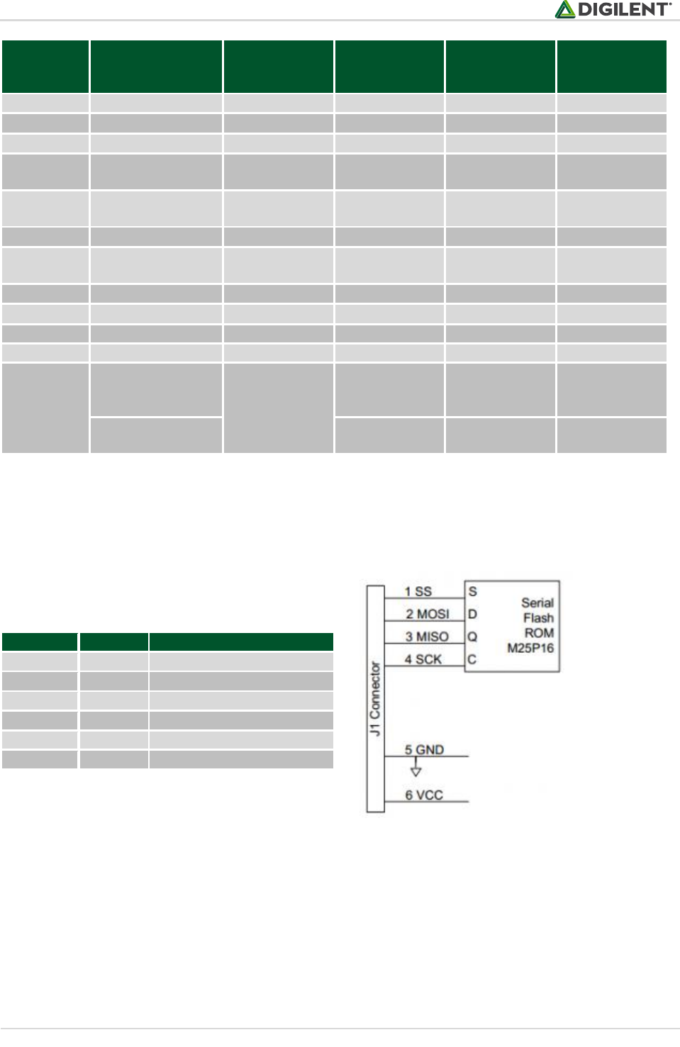
2 Interfacing with the Pmod
The PmodSF communicates with the host board via the SPI protocol. By bringing the Chip Select (CS) line low, users
are able to issue a variety of read, write, and erase commands to the memory chip. A table of the available
commands for the M25P16 from its respective datasheet is provided below:
The PmodSF.
16Mbit serial Flash memory
Data retention greater than 20 years
Small PCB size for flexible designs 1.0“ ×
20/8” (2.5 cm × 2.0 cm)
6-pin Pmod connector with SPI interface
Follows Digilent Interface Specification Type
2
Library and example code available
in resource center
Features include:
PmodSF™ Reference Manual
Copyright Digilent, Inc. All rights reserved.
Other product and company names mentioned may be trademarks of their respective owners.
Page 2 of 2
Instruction
Description
One-Byte
Instruction
Code
Number of
Address Bytes
Number of
Dummy Bytes
Number of Data
Bytes
WREN
Write Enable
0x06
0
0
0
WRDI
Write Disable
0x04
0
0
0
RDID
Read Identification
0x9F
0
0
1 to 3
RDSR
Read Status
Register
0x05
0
0
1 to ∞
WRSR
Write Status
Register
0x01
0
0
1
READ
Read Data Bytes
0x03
3
0
1 to ∞
FAST_READ
Read Data Bytes at
Higher Speed
0x0B
3
1
1 to ∞
PP
Page Program
0x02
3
0
1 to 256
SE
Sector Erase
0xD8
3
0
0
BE
Bulk Erase
0xC7
0
0
0
DP
Deep Power-down
0xB9
0
0
0
RES
Release from DP
and Read Electronic
Signature
0xAB
0
3
1 to ∞
Release from DP
0
0
0
The address bits range from 0x000000 to 0x1FFFFF, with the first two hexadecimal bits indicating which memory
sector the data is located in. Thankfully, users do not have to explicitly worry about writing to and reading from the
memory module, as there is a library that takes care of these commands for us.
Pin
Signal
Description
1
~CS
Chip Select
2
MOSI
Master-Out-Slave-In
3
MISO
Master-In-Slave-Out
4
SCK
Serial Clock
5
GND
Power Supply Ground
6
VCC
Positive Power Supply (3.3V)
Any external power applied to the PmodSF must be within 2.7V and 3.6V; it is recommended that the Pmod is
operated at 3.3V.
2 Physical Dimensions
The pins on the pin header are spaced 100 mil apart. The PCB is 1 inch long on the sides parallel to the pins on the
pin header and 0.8 inches long on the sides perpendicular to the pin header. .
