Quectel GSM Module Audio Design Guide V3.0
Quectel_GSM_Module_Audio_Design_Guide_V3.0
User Manual: Pdf
Open the PDF directly: View PDF ![]() .
.
Page Count: 36
- About the document
- Contents
- Table Index
- Figure Index
- 1 Introduction
- 2 Audio Circuit Design
- 3 Description and Suggestion
- 4 Appendix A
GSM Module
Audio Design Guide
GSM/GPRS Series
Version: GSM_Module _Audio_Design_Guide_V3.0
Date: 2013-05-24
www.quectel.com

GSM/GPRS Modules
GSM Module Audio Design Guide
GSM Module Audo Design Guide Confidential/Release 1 / 35
Our aim is to provide customers with timely and comprehensive service. For any
assistance, please contact our company headquarter:
Quectel Wireless Solutions Co., Ltd.
Room 501, Building 13, No.99, Tianzhou Road, Shanghai, China, 200233
Tel: +86 21 5108 6236
Mail: info@quectel.com
Or our local office, for more information, please visit:
http://www.quectel.com/support/salesupport.aspx
For technical support, to report documentation errors, please visit:
http://www.quectel.com/support/techsupport.aspx
GENERAL NOTES
QUECTEL OFFERS THIS INFORMATION AS A SERVICE TO ITS CUSTOMERS. THE INFORMATION
PROVIDED IS BASED UPON CUSTOMERS’ REQUIREMENTS. QUECTEL MAKES EVERY EFFORT
TO ENSURE THE QUALITY OF THE INFORMATION IT MAKES AVAILABLE. QUECTEL DOES NOT
MAKE ANY WARRANTY AS TO THE INFORMATION CONTAINED HEREIN, AND DOES NOT ACCEPT
ANY LIABILITY FOR ANY INJURY, LOSS OR DAMAGE OF ANY KIND INCURRED BY USE OF OR
RELIANCE UPON THE INFORMATION. ALL INFORMATION SUPPLIED HEREIN ARE SUBJECT TO
CHANGE WITHOUT PRIOR NOTICE.
COPYRIGHT
THIS INFORMATION CONTAINED HERE IS PROPRIETARY TECHNICAL INFORMATION OF
QUECTEL CO., LTD. TRANSMITTABLE, REPRODUCTION, DISSEMINATION AND EDITING OF THIS
DOCUMENT AS WELL AS UTILIZATION OF THIS CONTENTS ARE FORBIDDEN WITHOUT
PERMISSION. OFFENDERS WILL BE HELD LIABLE FOR PAYMENT OF DAMAGES. ALL RIGHTS
ARE RESERVED IN THE EVENT OF A PATENT GRANT OR REGISTRATION OF A UTILITY MODEL
OR DESIGN.
Copyright © Quectel Wireless Solutions Co., Ltd. 2013. All rights reserved.
Quectel
Confidential
GSM/GPRS Modules
GSM Module Audio Design Guide
GSM Module Audo Design Guide Confidential/Release 2 / 35
About the document
History
Revision
Date
Author
Description
1.0
2009-11-02
Tracy Zhang
Initial version
1.1
2009-11-20
Tracy Zhang
1. Added some acronym.
2. Added a Audio Power Amplitude manufacturer.
3. Added a solution to TDD noise.
4. Modified cover.
1.2
2010-11-20
Roy Chen
1. Added a diagram of audio channel
3.0
2013-05-24
Jerry You
1. Added reference design of audio circuit
(M1x, M95, M80).
2. Added AT command AT+QAPS.
Quectel
Confidential

GSM/GPRS Modules
GSM Module Audio Design Guide
GSM Module Audo Design Guide Confidential/Release 3 / 35
Contents
About the document ................................................................................................................................... 2
Contents ....................................................................................................................................................... 3
Table Index ................................................................................................................................................... 5
Figure Index ................................................................................................................................................. 6
1 Introduction .......................................................................................................................................... 7
1.1. Summary ...................................................................................................................................... 7
1.2. Safety Information ........................................................................................................................ 7
2 Audio Circuit Design ........................................................................................................................... 9
2.1. Audio Circuit Reference ............................................................................................................. 10
2.1.1. M1x ................................................................................................................................. 10
2.1.1.1. Microphone Reference Circuit .............................................................................. 10
2.1.1.2. Receiver Reference Circuit....................................................................................11
2.1.1.3. Headset Reference Circuit ................................................................................... 13
2.1.2. M95................................................................................................................................. 13
2.1.3. Microphone Reference Circuit ....................................................................................... 13
2.1.3.1. Receiver Reference circuit ................................................................................... 14
2.1.3.2. Headset Reference Circuit ................................................................................... 14
2.1.3.3. SPK Reference Circuit .......................................................................................... 15
2.1.4. M80................................................................................................................................. 16
2.1.4.1. Microphone Reference Circuit .............................................................................. 16
2.1.4.2. Receiver Reference Circuit................................................................................... 16
2.1.4.3. Headset Reference Circuit ................................................................................... 18
2.1.4.4. SPK Reference Circuit .......................................................................................... 18
2.2. Ringtone ..................................................................................................................................... 19
2.3. Hands-free Application at Channel AIN1/AOUT1 ...................................................................... 20
2.4. Suggestion for Audio Layout ...................................................................................................... 21
2.5. TDD Noise Solution.................................................................................................................... 21
2.6. Suggestion for Mechanical Design ............................................................................................ 22
2.7. Component of SPK .................................................................................................................... 25
2.8. Component of Microphone......................................................................................................... 26
3 Description and Suggestion ............................................................................................................. 27
3.1. AT Command ............................................................................................................................. 27
3.1.1. AT+QAUDCH ................................................................................................................. 27
3.1.2. How to Modify Volume ................................................................................................... 28
3.1.2.1. AT+QMIC .............................................................................................................. 28
3.1.2.2. AT+CLVL ............................................................................................................... 29
3.1.2.3. AT+QSIDET .......................................................................................................... 30
3.1.3. Echo Algorithm ............................................................................................................... 31
3.1.3.1. Description of Par0, Par2 and Par12 ................................................................... 33
3.1.3.2. Recommended Application Field .......................................................................... 34
Quectel
Confidential


GSM/GPRS Modules
GSM Module Audio Design Guide
GSM Module Audo Design Guide Confidential/Release 5 / 35
Table Index
TABLE 1: AUDIO HARDWARE CONFIGURATION ......................................................................................... 9
TABLE 2: REFERENCE DOCUMENT ........................................................................................................... 35
TABLE 3: DESCRIPTION OF ECHO AND TDD NOISE ................................................................................ 35
Quectel
Confidential

GSM/GPRS Modules
GSM Module Audio Design Guide
GSM Module Audo Design Guide Confidential/Release 6 / 35
Figure Index
FIGURE 1:MICROPHONE REFERENCE CIRCUIT FOR AIN1&AIN2 ........................................................... 10
FIGURE 2: RECEIVER REFERENCE CIRCUIT FOR AOUT1 .......................................................................... 11
FIGURE 3: RECEIVER REFERENCE CIRCUIT WITH AUDIO POWER AMPLIFIER FOR AOUT1 ................. 11
FIGURE 4:SPK REFERENCE CIRCUIT FOR AOUT2 ................................................................................... 12
FIGURE 5:RECEIVER REFERENCE CIRCUIT WITH AUDIO POWER AMPLIFIER FOR AOUT2 .............. 12
FIGURE 6:HEADSET REFERENCE CIRCUIT............................................................................................... 13
FIGURE 7:MICROPHONE REFERENCE CIRCUIT FOR AIN1&AIN2 ........................................................... 13
FIGURE 8:RECEIVER REFERENCE CIRCUIT FOR AOUT1 ........................................................................ 14
FIGURE 9:HEADSET REFERENCE CIRCUIT............................................................................................... 14
FIGURE 10:SPK REFERENCE CIRCUIT ...................................................................................................... 15
FIGURE 11:MICROPHONE REFERENCE CIRCUIT FOR AIN1&AIN2 ......................................................... 16
FIGURE 12:RECEIVER REFERENCE CIRCUIT FOR AOUT1 ...................................................................... 16
FIGURE 13:SPK REFERENCE CIRCUIT FOR AOUT2 ................................................................................. 17
FIGURE 14:SPK REFERENCE CIRCUIT WITH AUDIO POWER AMPLIFIER FOR AOUT2 ........................ 17
FIGURE 15:HEADSET REFERENCE CIRCUIT............................................................................................. 18
FIGURE 16:SPK REFERENCE CIRCUIT ...................................................................................................... 18
FIGURE 17:HANDS-FREE REFERENCE CIRCUIT AT CHANNEL AIN1/AOUT1 ......................................... 20
FIGURE 18:LAYOUT OF AUDIO .................................................................................................................... 21
FIGURE 19:FIVE ECHO PATHS ..................................................................................................................... 22
FIGURE 20:MICROPHONE SOCKET DESIGN ............................................................................................. 23
FIGURE 22:SPK FREQUENCY RESPONSE................................................................................................. 25
FIGURE 23:SPK THD ..................................................................................................................................... 26
Quectel
Confidential

GSM/GPRS Modules
GSM Module Audio Design Guide
GSM Module Audo Design Guide Confidential/Release 7 / 35
1 Introduction
1.1. Summary
This document provides reference and suggestion on audio circuit design and audio parameter selection
for Quectel M1x, M95 and M80 modules.
1.2. Safety Information
The following safety precautions must be observed during all phases of the operation, such as usage,
service or repair of any cellular terminal or mobile incorporating module. Manufacturers of the cellular
terminal should send the following safety information to users and operating personnel and to incorporate
these guidelines into all manuals supplied with the product. If not so, Quectel does not take on any liability
for customer failure to comply with these precautions.
Full attention must be given to driving at all times in order to reduce the risk of an
accident. Using a mobie while driving (even with a handsfree kit) cause distraction
and can lead to an accident. You must comply with laws and regulations restricting
the use of wireless devices while driving.
Switch off the cellular terminal or mobile before boarding an aircraft. Make sure it
switched off. The operation of wireless appliances in an aircraft is forbidden to
prevent interference with communication systems. Consult the airline staff about
the use of wireless devices on boarding the aircraft, if your device offers a Fight
Mode which must be enabled prior to boarding an aircraft.
Switch off your wireless device when in hospitals or clinics or other health care
facilities. These requests are desinged to prevent possible interference with
sentitive medical equipment.
Quectel
Confidential
GSM/GPRS Modules
GSM Module Audio Design Guide
GSM Module Audo Design Guide Confidential/Release 8 / 35
GSM cellular terminals or mobiles operate over radio frequency signal and cellular
network and cannot be guaranteed to connect in all conditions, for example no
mobile fee or an invalid SIM card. While you are in this condition and need
emergent help, please remember using emergency call. In order to make or
receive call, the cellular terminal or mobile must be switched on and in a service
area with adequate cellular signal strength.
Your cellular terminal or mobile contains a transmitter and receiver. When it is ON ,
it receives and transmits radio frequency energy. RF interference can occur if it is
used close to TV set, radio, computer or other electric equipment.
In locations with potencially explosive atmospheres, obey all posted signs to turn
off wireless devices such as your phone or other cellular terminals. Areas with
potencially exposive atmospheres including fuelling areas, below decks on boats,
fuel or chemical transfer or storage facilities, areas where the air contains
chemicals or particles such as grain, dust or metal powders.
Quectel
Confidential
GSM/GPRS Modules
GSM Module Audio Design Guide
GSM Module Audo Design Guide Confidential/Release 9 / 35
2 Audio Circuit Design
M1x and M95 have two hardware audio channels except M80. Three audio channels are defined in
software. AT+QAUDCH is used to read and set the software audio channel. This chapter provides audio
interface circuit and some solutions to resolve TDD noise and ECHO issues.
Table 1:Audio Hardware Configuration
Module
(AIN1/AOUT1)
(AIN2/AOUT2)
AOUT3
MIC
SPK
MIC
SPK
SPK
M1x
Differential &
Internal Bias
Differential
Differential &
Internal Bias
Signal-end
/
M95
Differential &
Internal Bias
Differential
Differential &
Internal Bias
Differential
/
M80
Differential &
Internal Bias
Differential
Differential &
Internal Bias
Signal-end
Differential
1. M95 module has built-in class AB amplifier and also supports voice and ringtone at channel AOUT2.
2. M80 module supports voice and ringtone at channel AOUT2. AOUT1 and AOUT3 can also output
ringtone but via AT+QRCH=1(only used at M80).
3. M80 module has built-in class AB amplifier at channel AOUT3, and the maximum power is 800mW.
Notes
Quectel
Confidential
GSM/GPRS Modules
GSM Module Audio Design Guide
GSM Module Audo Design Guide Confidential/Release 10 / 35
2.1. Audio Circuit Reference
2.1.1. M1x
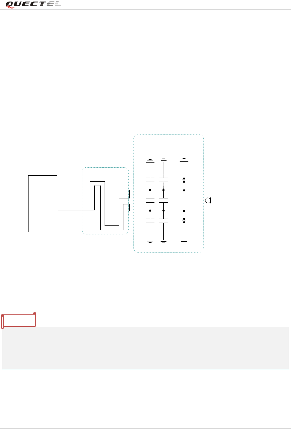
2.1.1.1. Microphone Reference Circuit
M1x module provides electrets-microphone bias voltage for AIN1 and AIN2. Microphone reference circuit
is shown as below:
10pF 33pF
33pF
33pF
Close to Microphone
MICxP
MICxN
Differential layout
Electret
Microphone
GND
GND
10pF
10pF ESD
ESD
Module
Figure 1:Microphone Reference Circuit for AIN1&AIN2
1. To avoid TDD noise issue during voice, capacitors is recommended to add close to microphone and
SPK.
2. TVS components are used to protect microphone and receiver from ESD damage. It has to close to
audio device and audio interface.
Notes
Quectel
Confidential
GSM/GPRS Modules
GSM Module Audio Design Guide
GSM Module Audo Design Guide Confidential/Release 11 / 35
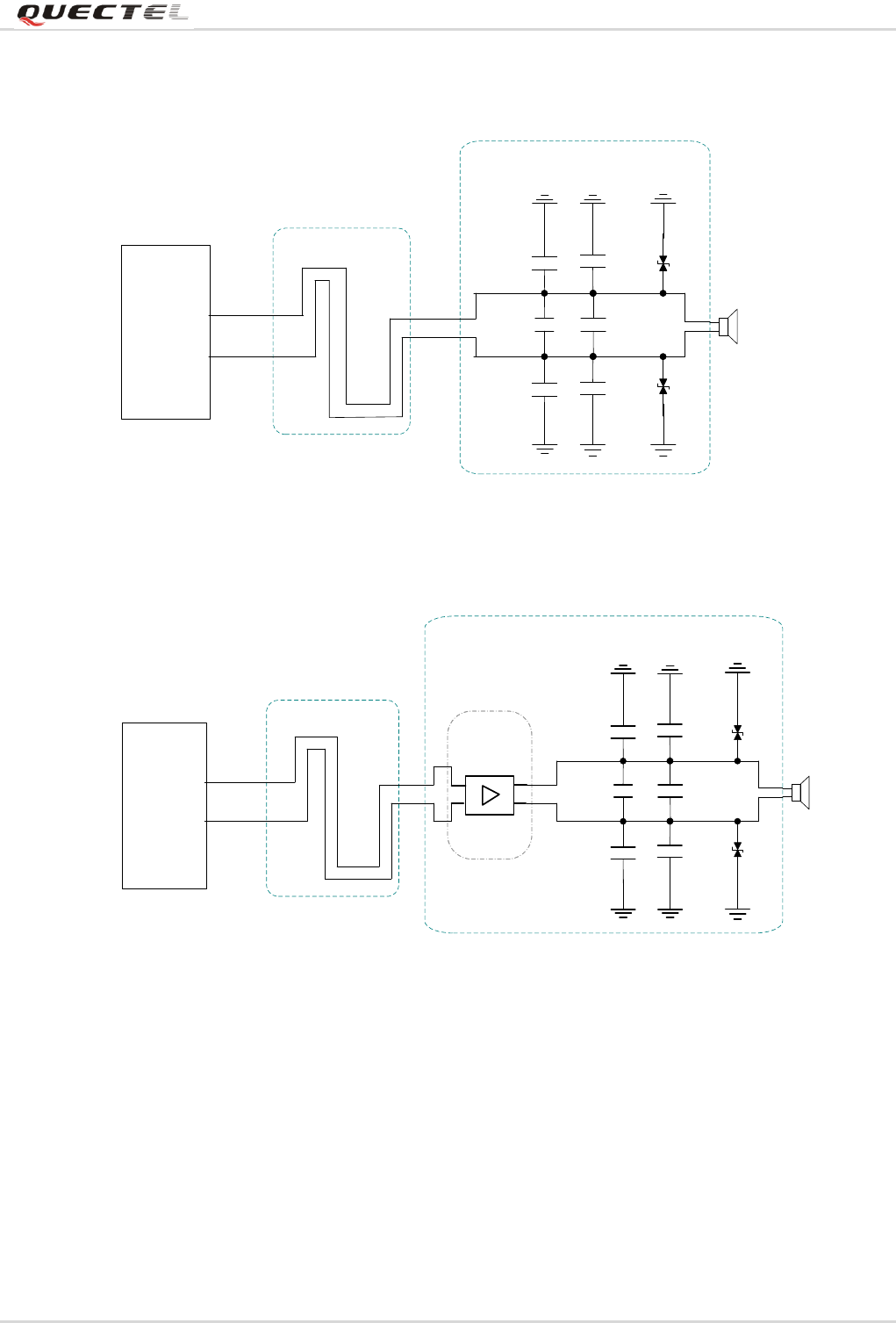
2.1.1.2. Receiver Reference Circuit
SPK1P
SPK1N
Differential layout
10pF
10pF
33pF
33pF
33pF
Close to speaker
GND
GND
10pF
Module ESD
ESD
Figure 2: Receiver Reference Circuit for AOUT1
SPK1P
SPK1N
Differential layout
Amplifier
circuit
10pF
10pF
33pF
33pF
33pF
Close to speaker
GND
GND
10pF
Module
ESD
ESD
Figure 3: Receiver Reference Circuit with Audio Power Amplifier for AOUT1
Quectel
Confidential

GSM/GPRS Modules
GSM Module Audio Design Guide
GSM Module Audo Design Guide Confidential/Release 12 / 35
SPK2P
AGND
Differential layout
10pF 33pF
Close to speaker
GND
Module 22uF
ESD
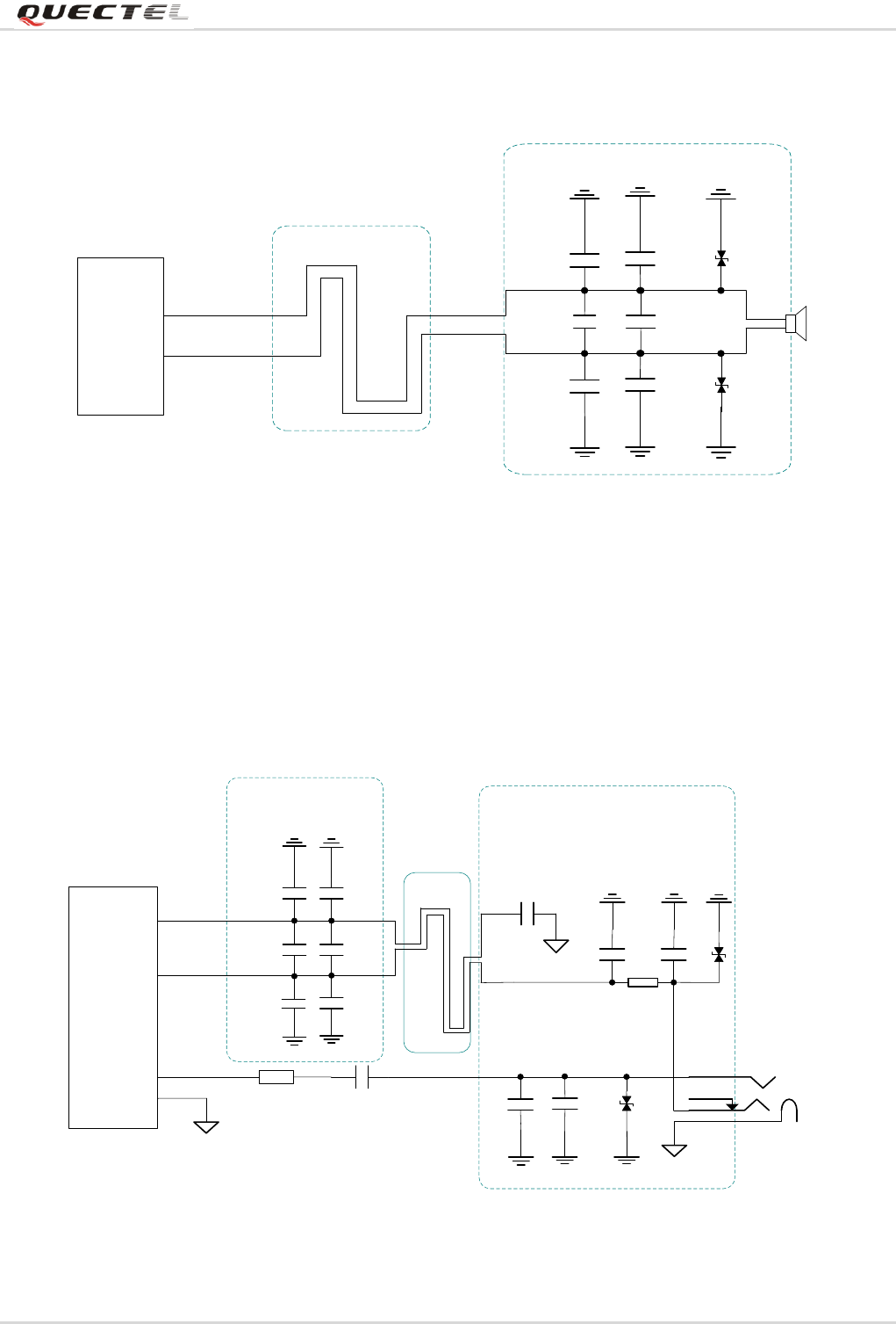
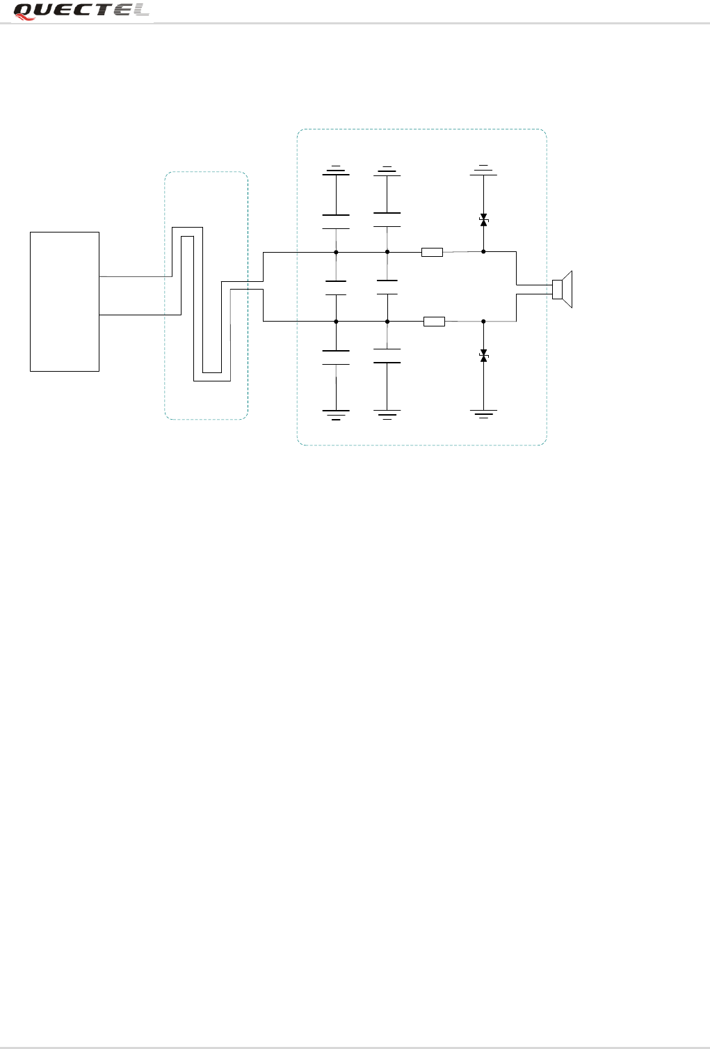
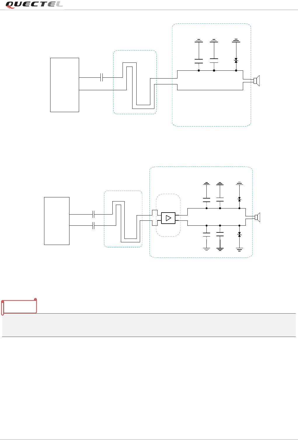
Figure 4:SPK Reference Circuit for AOUT2
Module
SPK2P
AGND
Differential layout
Amplifier
circuit
10pF
10pF
33pF
33pF
Close to speaker
GND
GND
C2
C1
ESD
ESD
Figure 5:Receiver Reference Circuit with Audio Power Amplifier for AOUT2
For the value of C1 and C2, please refer to input impedance of audio power amplifier.
Note
Quectel
Confidential
GSM/GPRS Modules
GSM Module Audio Design Guide
GSM Module Audo Design Guide Confidential/Release 13 / 35
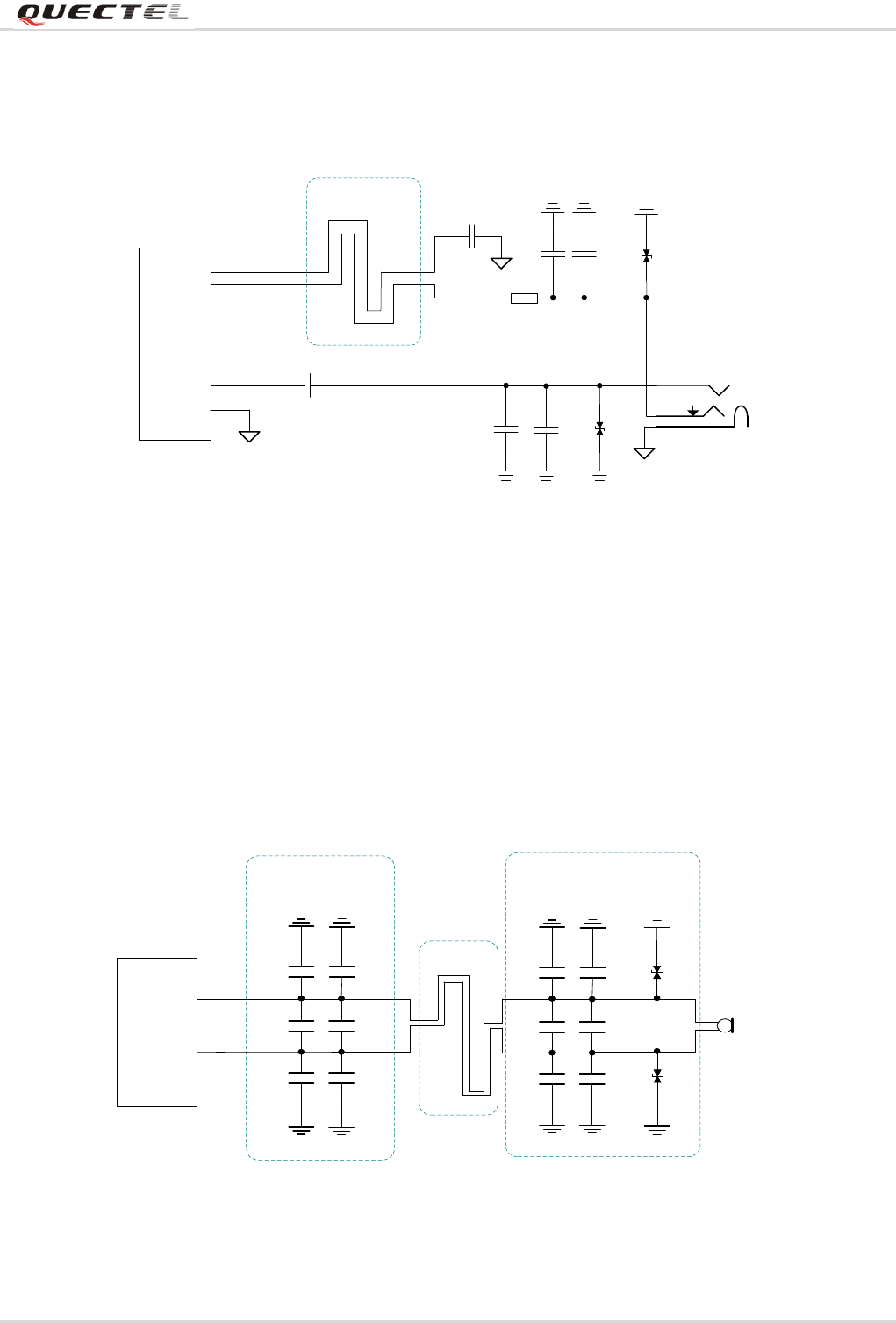
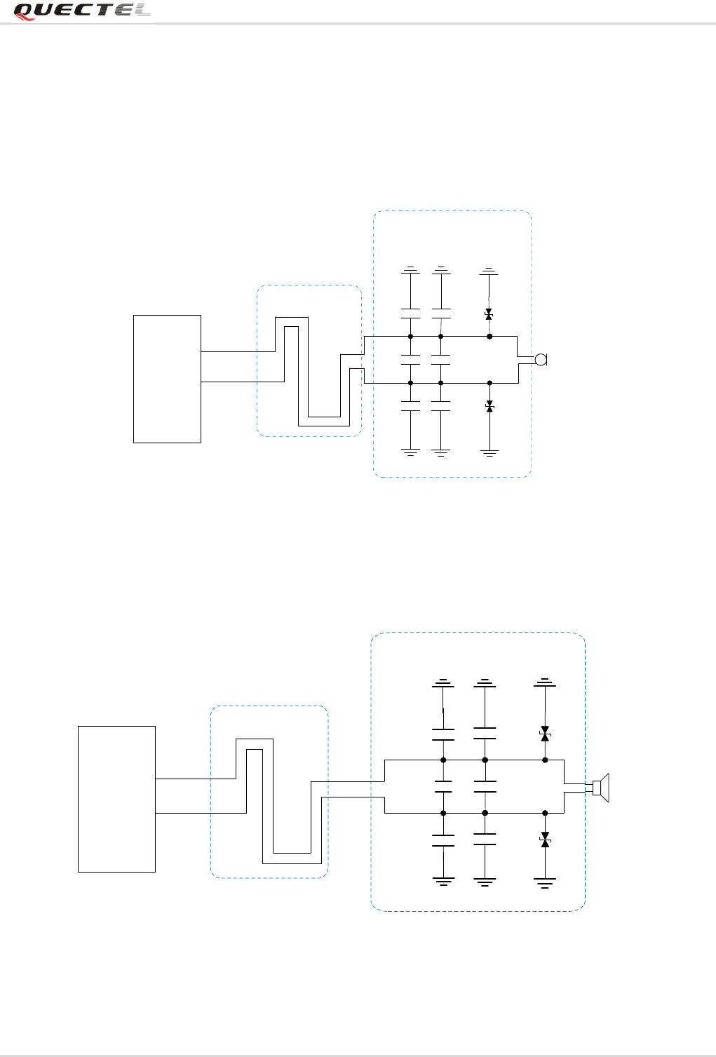
2.1.1.3. Headset Reference Circuit
Amphenol
9001-8905-
050
1
2
4
3
SPK2P
MIC2N
MIC2P
22uF
68R
AGND
Close to Socket
Differential
layout
AGND
Module
4.7uF
ESD
GND
33pF
10pF
33pF
GND
10pF
ESD
Figure 6:Headset Reference Circuit
2.1.2. M95
2.1.3. Microphone Reference Circuit
M95 module provides electrets-microphone bias voltage for AIN1 and AIN2. Reference circuit for
microphone is shown as bellow:
MICxP
Differential
layout
Module
10pF 33pF
33pF
33pF
Electret
Microphone
GND
GND
10pF
10pF ESD
ESD
33pF
10pF
Close to Module
MICxN
GND
GND
GND
GND
10pF 33pF
33pF
10pF
Close to MIC
Figure 7:Microphone Reference Circuit for AIN1&AIN2
Quectel
Confidential
GSM/GPRS Modules
GSM Module Audio Design Guide
GSM Module Audo Design Guide Confidential/Release 14 / 35
2.1.3.1. Receiver Reference circuit
SPK1P
SPK1N
Differential layout
10pF
10pF
33pF
33pF
33pF
GND
10pF
ESD
ESD
Module
Close to Receiver
GND
Figure 8:Receiver Reference Circuit for AOUT1
2.1.3.2. Headset Reference Circuit
1
2
4
3
Amphenol
9001-8905-050
MIC2P
22uF
68R
33pF
GND
AGND
Close to Socket
33pF
AGND
33pF 10pF
GND
Module
4.7uF
LOUDSPKP
Close to Module
GND
GND
GND
GND
10pF 33pF
33pF
10pF
Differential
layout
33pF
10pF
MIC2N
0R
ESD
ESD
Figure 9:Headset Reference Circuit
Quectel
Confidential
GSM/GPRS Modules
GSM Module Audio Design Guide
GSM Module Audo Design Guide Confidential/Release 15 / 35
2.1.3.3. SPK Reference Circuit
LOUDSPKN
ESD
ESD
0R
0R
LOUDSPKP
8 ohm
Module
GND
Close to Speaker
10pF 33pF
33pF10pF
10pF 33pF
GND
Differential
layout
Figure 10:SPK Reference Circuit
Quectel
Confidential
GSM/GPRS Modules
GSM Module Audio Design Guide
GSM Module Audo Design Guide Confidential/Release 16 / 35
2.1.4. M80
2.1.4.1. Microphone Reference Circuit
M80 provides electrets-microphone bias voltage for AIN1 and AIN2. Reference circuit for microphone is
illustrated as following figure.
10pF 33pF
33pF
33pF
Close to Microphone
MICxP
MICxN
Differential layout
Module
Electret
Microphone
GND
GND
10pF
10pF ESD
ESD
Figure 11:Microphone Reference Circuit for AIN1&AIN2
2.1.4.2. Receiver Reference Circuit
SPK1P
SPK1N
Differential layout
10pF
10pF
33pF
33pF
33pF
Close to speaker
GND
10pF
ESD
ESD
Module
GND
Figure 12:Receiver Reference Circuit for AOUT1
Quectel
Confidential
GSM/GPRS Modules
GSM Module Audio Design Guide
GSM Module Audo Design Guide Confidential/Release 17 / 35
SPK2P
AGND
Differential layout
10pF 33pF
Close to speaker
ESD
Module 22uF
GND
Figure 13:SPK Reference Circuit for AOUT2
SPK2P
AGND
Differential
layout Amplifier
circuit 10pF
10pF 33pF
33pF
Close to speaker
ESD
ESD
Module
C2
C1
GND
GND
Figure 14:SPK Reference Circuit with audio power amplifier for AOUT2
TPA6205A1 from TEXAS INSTRUMENTS is recommended, which is a audio power amplifier device and
can driver a 8Ωspeaker impedance.
Note
Quectel
Confidential
GSM/GPRS Modules
GSM Module Audio Design Guide
GSM Module Audo Design Guide Confidential/Release 18 / 35
2.1.4.3. Headset Reference Circuit
1
2
4
3
Amphenol
9001-8905-050
SPK2P
MIC2N
MIC2P
22uF
68R
33pF
GND
AGND
Close to Socket
Differential
layout
33pF
AGND
33pF 10pF
GND
Module
4.7uF
ESD
ESD
Figure 15:Headset Reference Circuit
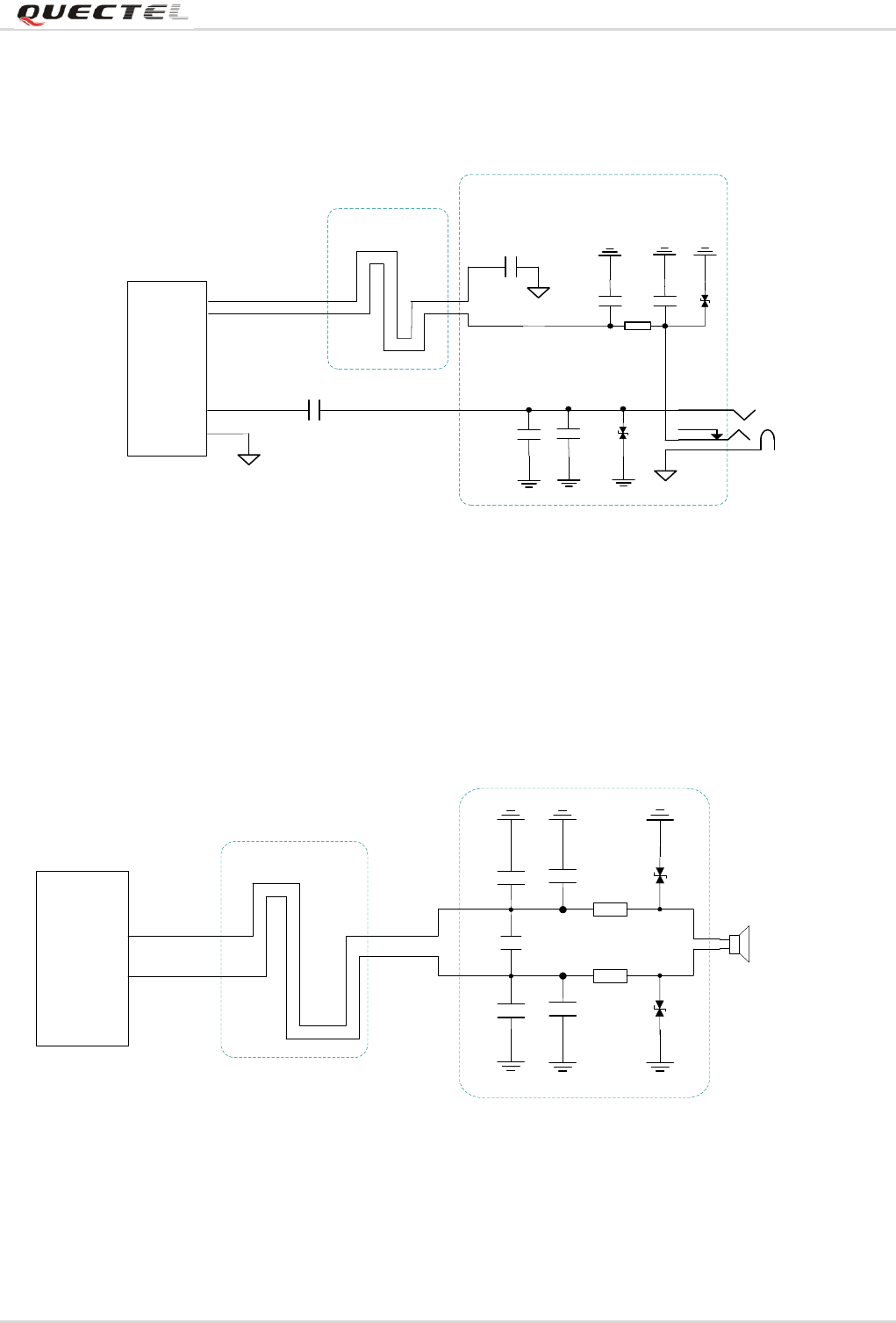
2.1.4.4. SPK Reference Circuit
LOUDSPKP
LOUDSPKN
Differential layout
10pF
10pF 33pF
33pF
Close to speaker
GND
100pF
ESD
Module 0R
0R
ESD
GND
Figure 16:SPK Reference Circuit
Quectel
Confidential
GSM/GPRS Modules
GSM Module Audio Design Guide
GSM Module Audo Design Guide Confidential/Release 19 / 35
1. Capacitors have to place close to audio component or audio interface and layout must be short.
2. Antenna interface must be stay away from audio components and layout of audio circuit. Layout of
power supply must be stay away from audio and cannot be parallel.
3. Differential audios have to meet the rule of layout.
2.2. Ringtone
M1x does not support ringtone via channel AOUT1, but support to output ringtone via channel AOUT2.
M95 outputs ringtone via channel AOUT2 by default.
M80 outputs ringtone via channel AOUT2 by default; channel AOUT1 can output ringtone via
AT+QAUDCH=0 and AT+QRCH=1. Please refer to AT command description for detailed information
about AT+QRCH.
Parameter
AT+QRCH
Test Command
AT+QRCH=?
Response
+QRCH: (0,1)
OK
Read Command
AT+QRCH?
Response
+QRCH: <n>
OK
Write Command
AT+QRCH=<n>
Response
OK
If error is related to ME functionality:
+CME ERROR: <err>
Reference
<n> 0 Default output channel is AOUT2. (M80’s default audio channel is
AOUT2/AOUT3.
1 Output ringtone at any audio channel which is decided by AT+QAUDCH. (e.g. if
Notes
Quectel
Confidential
GSM/GPRS Modules
GSM Module Audio Design Guide
GSM Module Audo Design Guide Confidential/Release 20 / 35
2.3. Hands-free Application at Channel AIN1/AOUT1
Channel AIN1/AOUT1 could be used as hands-free function, because input audio signal is differential
circuit and it is a good way to suppress common-mode noise.
SPK circuit is recommended as following:
IN-
IN+
SHUT_DOWN
BYPASS
VO+
VO-
GND
VDD
C312
10pF
C311
10pF
10pF
C313 C4
33pF
C2
33pF
C3
33pF
VBAT
FB301
FB302
Close to speaker
C19
10uF
C20
33uF
5
8
SPK1N
SPK1P
C308
C309
100nF
100nF
R308
R309
20K
20K
R310
100K
C310
220nF
R313 100K
R314 100K
GPIO_SHUTDOWN
4
3
1
2
6
7
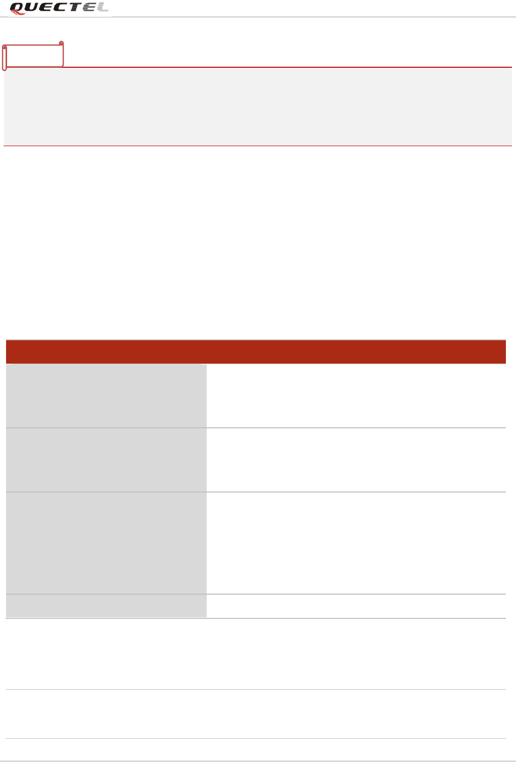
Figure 17:Hands-free Reference Circuit at Channel AIN1/AOUT1
GPIO_SHUTDOWN is controlled by I/O of external chip.
AT+QAUDCH=0, ringtone will output via AOUT1)
Note
Quectel
Confidential
GSM/GPRS Modules
GSM Module Audio Design Guide
GSM Module Audo Design Guide Confidential/Release 21 / 35
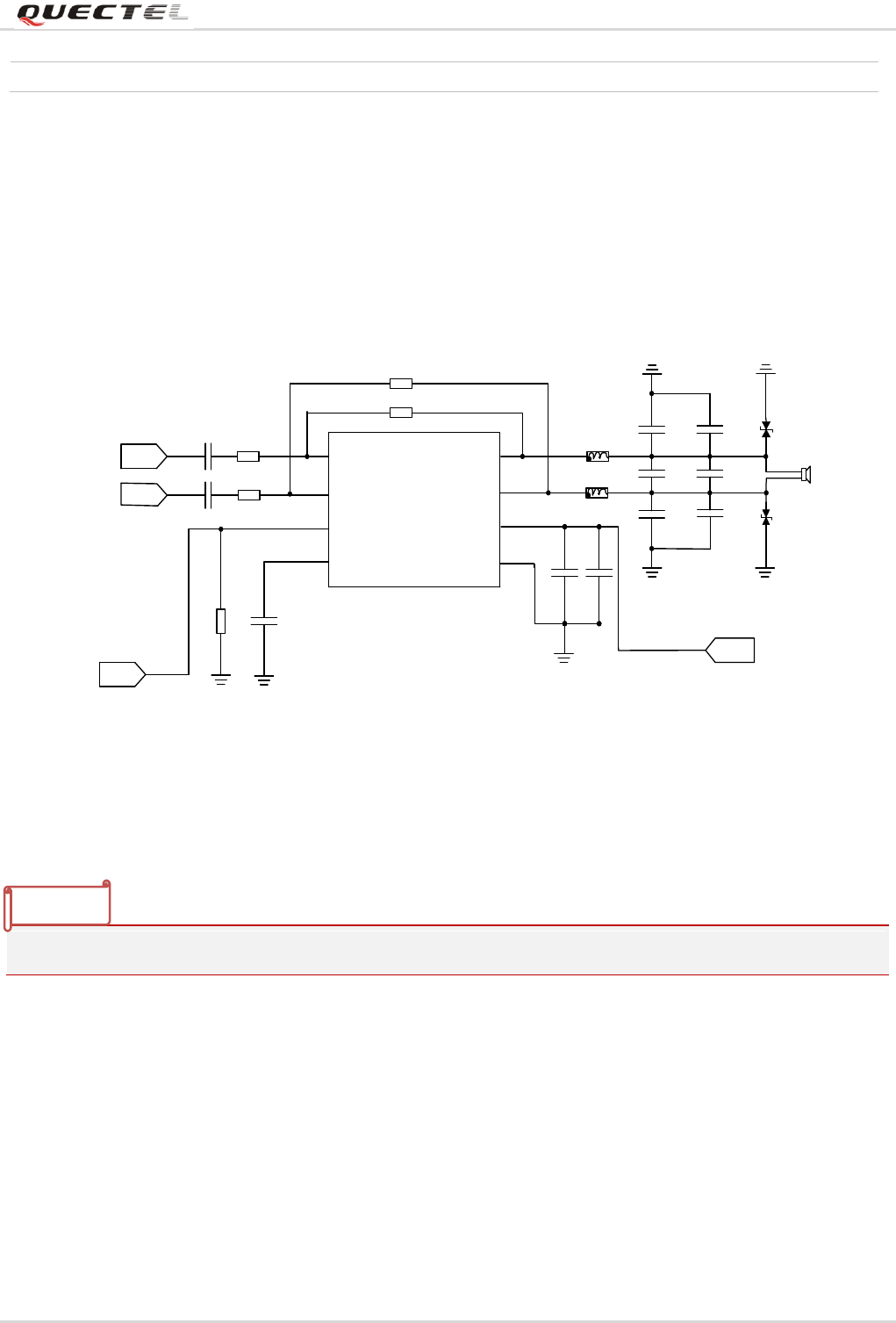
2.4. Suggestion for Audio Layout
Power supply ripple, unbalanced ground and RF burst radiation have negative effect to audio layout.
Layout of MIC1P/MIC1N, SPK1P/SPK1N must meet the rule of differential signal. Moreover, these two
pairs of signals should be separated from each other by flooding ground to avoid echo issue from SPK
signal to MIC signal. Figure 18 shows an example.
Figure 18:Layout of Audio
2.5. TDD Noise Solution
It is important to avoid or reduce TDD noise in audio circuit design and layout. This chapter provides
some solution to resolve it.
1. It is strongly recommended to add an electrets-microphone within two capacitors (10pF and 33pF) in
handset and hands-free application. These two capacitors could largely suppress coupling TDD
noise from RF interference.
2. Capacitors have to place close to audio component or audio interface, layout must be short.
3. Flood ground area should be as large as possible to reduce the ground impedance and improve
ground integrality.
Quectel
Confidential
GSM/GPRS Modules
GSM Module Audio Design Guide
GSM Module Audo Design Guide Confidential/Release 22 / 35
4. Reduce power voltage ripple, especially the power supply in audio circuits. A wide layout is used from
power source (like adapter interface, battery connector, or LDO output pin) to audio power supply.
Good antenna matching is also important to reduce power ripple.
5. The filtering capacitors and ESD protection devices should be connected to main digital ground, and
other audio components should use AGND from the module interface. Please be noted that the
AGND pin should not be connected with main digital ground at PCB, or else, it could lead to TDD
noise.
6. Antenna must be stay away from audio components and layout of audio circuit. Keep the distance at
least 5cm from antenna to microphone.
7. Layout of power supply must be stay away from audio and cannot be parallel.
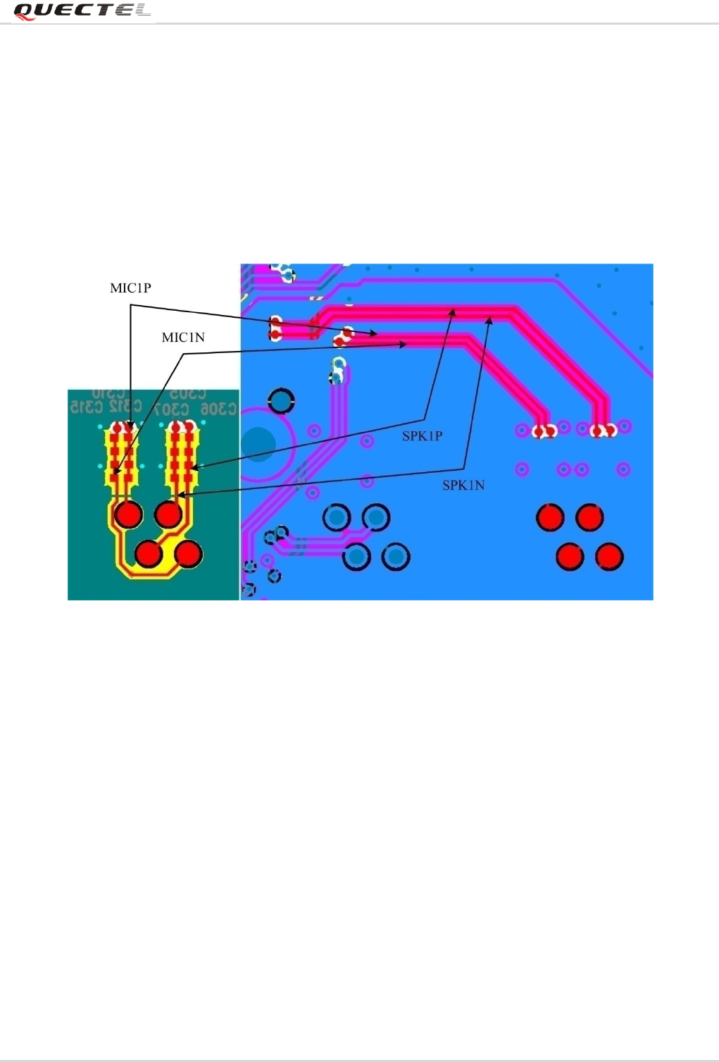
2.6. Suggestion for Mechanical Design
It is important to consider how to suppress echo in the equipment with hands-free function or in an
application which microphone and speaker are very close to each other.
The mechanical structure design has significant impact on echo issue. If it is not properly designed, the
echo suppressing arithmetic in software could not make up echo issue caused by bad mechanical
structure, and even force to redesign.
Echo issue could be generated by several paths as shown in Figure 19.
Figure 19:Five Echo Paths
Quectel
Confidential
GSM/GPRS Modules
GSM Module Audio Design Guide
GSM Module Audo Design Guide Confidential/Release 23 / 35
In these five paths, internal air-path and direct air-path are the first influential factors. Other three factors
(vibrations through casework, vibrations through PCB, distant echoes) are secondary.
How to deal with echo issue from internal air-path:
Separating microphone from internal space of chassis by foam or rubber ring can effectively suppress the
inner echo interference. Figure 20 shows recommended design for microphone socket.
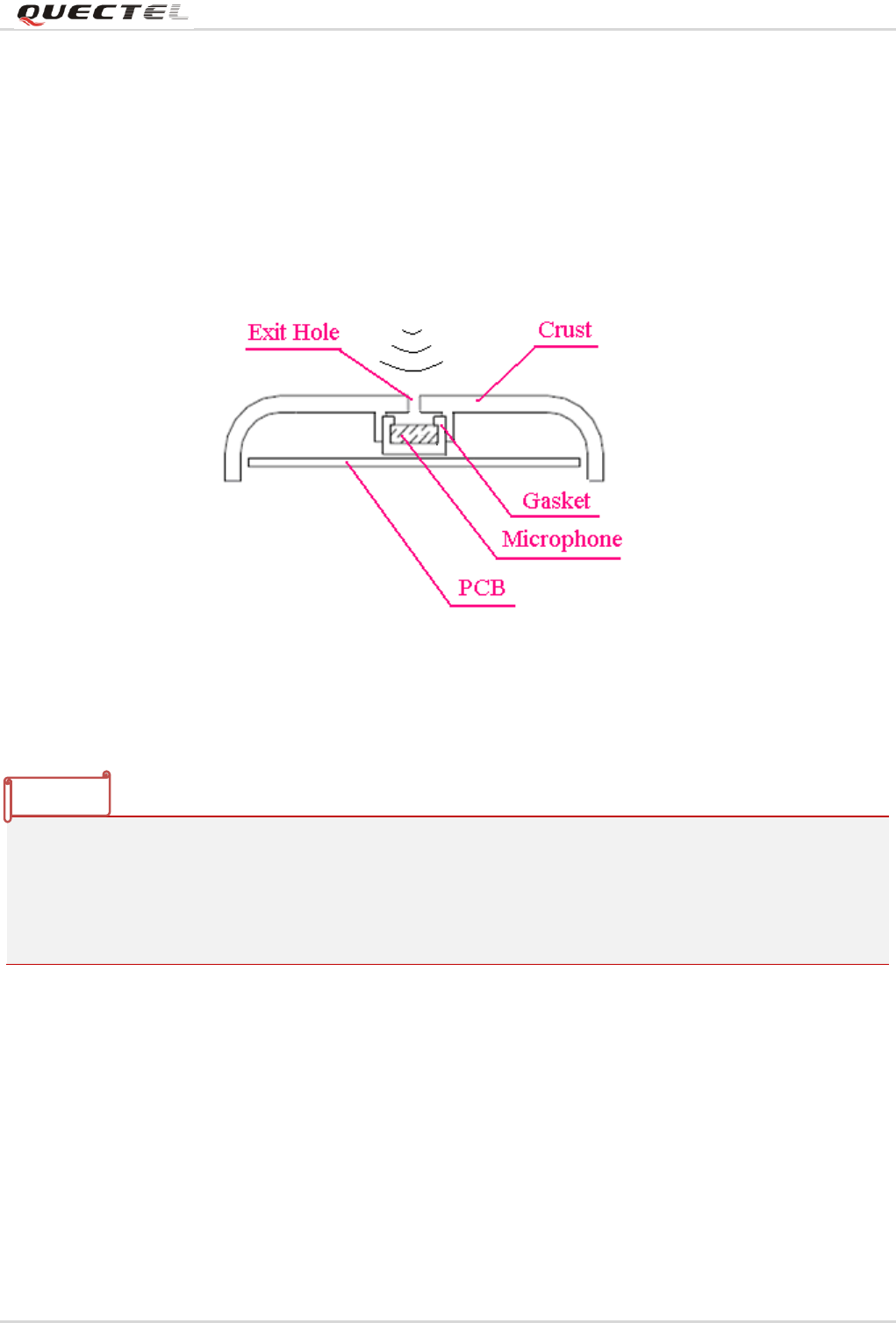
Figure 20:Microphone Socket Design
The best installation way of microphone socket is to encase microphone by silicone cover except for front
cavity, and design a cylindrical hole whose center is the exit hole inside the chassis, make the microphone
with silicone cover just fit the cylindrical hole, so as to only let voice enter into microphone from the exit
hole, and not from leak of chassis interior. Certain air space room should be reserved in the front cavity of
microphone as it is necessary for good microphone performance.
Note
Quectel
Confidential
GSM/GPRS Modules
GSM Module Audio Design Guide
GSM Module Audo Design Guide Confidential/Release 24 / 35
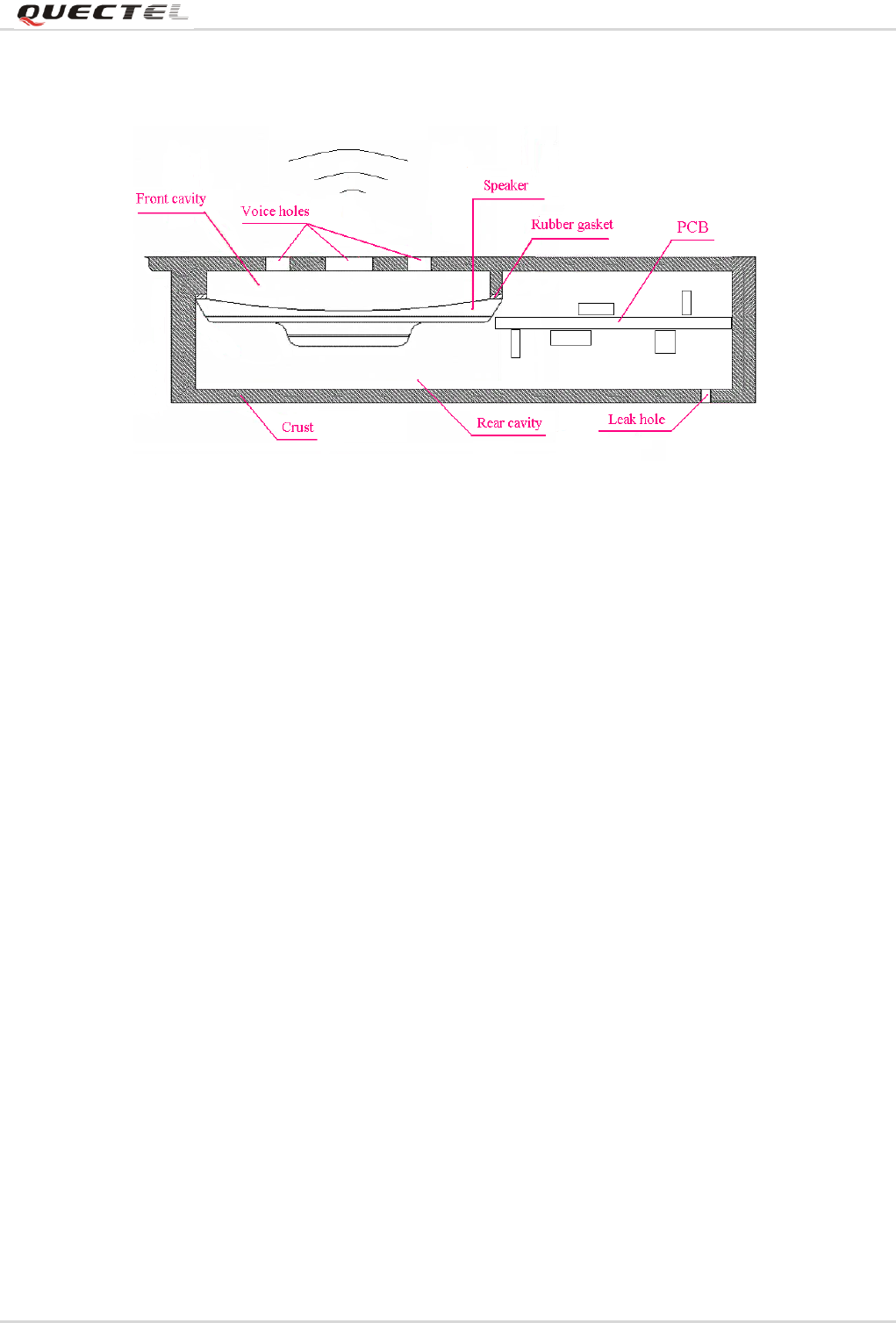
Figure 21 shows recommended design for speaker socket.
Figure 21:Speaker socket design
A good way to suppress the internal echo path is to seal the rear cavity of receiver, which is usually
expensive. The rear cavity of receiver and speaker is important for good voice quality. A sealed rear cavity
with sufficient space could produce a good voice output. An 8Ω speaker is often big and difficult to give an
independently sealed rear cavity for it. However, sealing microphone socket in chassis is always useful.
Furthermore, the whole chassis must be sealed as far as possible. If there is any unavoidable leak hole,
keep it far away from microphone. If the leak hole is close to microphone, the voice coming from the hole
could be picked up by MIC, and then leads to echo at the far end. If the leak hole is close to speaker, the
output voice quality could be aggravated at certain extent.
Quectel
Confidential
GSM/GPRS Modules
GSM Module Audio Design Guide
GSM Module Audo Design Guide Confidential/Release 25 / 35
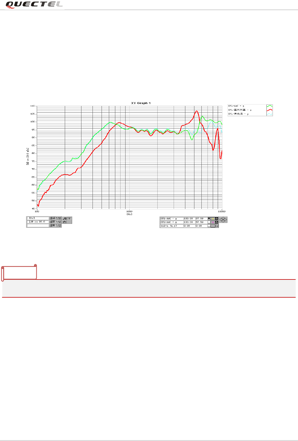
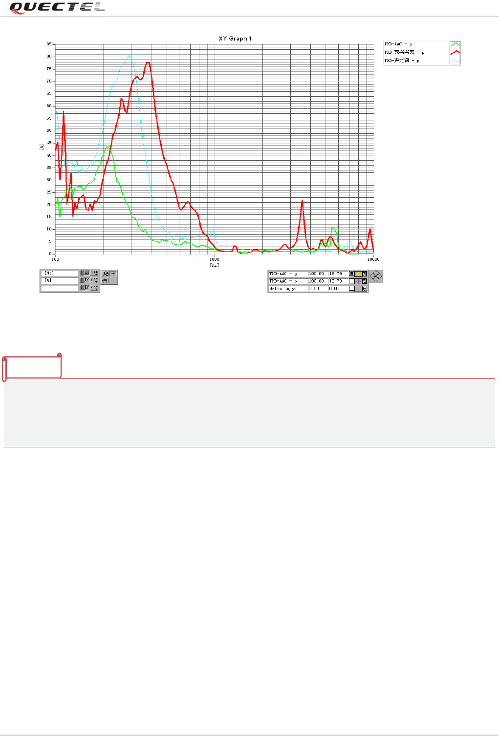
2.7. Component of SPK
A SPK and receiver with higher sensitivity, flatter frequency response, less THD and impedance of
32Ω(receiver), 16Ω(receiver) or 8Ω(speaker) is recommended. These technical data are often shown in
data sheet of SPK and receiver. For SPK, its frequency response and THD performance can be tested by
speaker test system. SPK frequency and THD response are shown in Figure 22 and Figure 23.
Figure 22:SPK Frequency Response
Horizontal axis is frequency, longitudinal axis is loudness and unit is dB.
Note
Quectel
Confidential
GSM/GPRS Modules
GSM Module Audio Design Guide
GSM Module Audo Design Guide Confidential/Release 26 / 35
Figure 23:SPK THD
1. Horizontal axis is frequency, longitudinal axis is distortion and unit is %
2. Figure 23, the three colors represent three venders’ products. After comprehensive comparison, the
green one performs the best, and the blue one is second, and the red one is the worst.
2.8. Component of Microphone
It is recommended to use an electret microphone with a sensitivity of -42±3dB/Pa @ 2V(not less than
-44±3dB)and impedance of 2.2kΩ. If RF TDD noise is detected at the MIC, please contact MIC vendor
for product with better RF suppression capability. Furthermore, the microphone channel circuit can be
optimized to decrease TDD issue at MIC side.
Note
Quectel
Confidential

GSM/GPRS Modules
GSM Module Audio Design Guide
GSM Module Audo Design Guide Confidential/Release 27 / 35
3 Description and Suggestion
M1x, M95 has two audio channels in hardware, named AIN1/AOUT1 and AIN2/AOUT2. Three channels
are defined in software, named channel 0, channel 1 and channel 2. Software channel 0 is applied in
hardware channel AIN1/AOUT1, software channel 1 and channel 2 are applied as hardware channel
AIN2/AOUT2. Headset application is used at software channel 1. Software channel 2 is designed for
hands-free application of hardware channel AIN2/AOUT2.
M80 has three audio channels in hardware, named AIN1/AOUT1, AIN2/AOUT2 and AOUT3. Channel
AOUT3 is used as output of hands-free application. Software channel 0 is applied as hardware channel
AIN1/AOUT1. Software channel 1 is applied as hardware channel AIN1/AOUT1.
3.1. AT Command
Audio parameters will be introduced as following chapter and audio parameters can be set via AT
command.
3.1.1. AT+QAUDCH
AT+QAUDCH is used to read and set audio software channel. How to read and set audio software
channel via AT+QAUDCH is shown as following:
AT+QAUDCH
Test Command
AT+QAUDCH=?
Response
+QAUDCH: (list of supported <n>s)
OK
Read Command
AT+QAUDCH?
Response
+QAUDCH: <n>
OK
Write Command
AT+QAUDCH=[<n>]
Response
OK
If error is related to ME functionality:
+CME ERROR: <err>
Quectel
Confidential

GSM/GPRS Modules
GSM Module Audio Design Guide
GSM Module Audo Design Guide Confidential/Release 28 / 35
Parameter
3.1.2. How to Modify Volume
3.1.2.1. AT+QMIC
AT+QMIC is used to modify the analog gain of microphone. It can increase or reduce the gain of
microphone.
Parameter
Reference
<n> 0 Normal audio channel (default)
1 Headset audio channel
2 Loudspeaker audio channel
AT+QMIC a
Test Command
AT+QMIC=?
Response
+QMIC: (list of supported <channel>s), (list of supported
<gain-level>s)
OK
Read Command
AT+QMIC?
Response
+QMIC:
<gainlevel(Normal_Mic)>,<gainlevel(Headset_Mic)>,<gai
nlevel(Loudspeaker_Mic)>
OK
Write Command
AT+QMIC=<channel>,<gain-level>
Response
OK
If error is related to ME functionality:
+CME ERROR: <err>
Reference
<channel> 0 Normal microphone
1 Headset microphone
2 Loudspeaker microphone
Quectel
Confidential
GSM/GPRS Modules
GSM Module Audio Design Guide
GSM Module Audo Design Guide Confidential/Release 29 / 35
3.1.2.2. AT+CLVL
AT+CLVL is used to modify the analog gain of receiver. It can increase or reduce loudness of downlink
speech.
Parameter
If the gain-level is too high, receiving distortion would happen.
<gain-level> Range is 0 - 15
AT+CLVL
Test Command
AT+CLVL=?
Response
+CLVL: (list of supported <level>s)
OK
Read Command
AT+CLVL?
Response
+CLVL: <level>
OK
Write Command
AT+CLVL=<level>
Response
OK
If error is related to ME functionality:
+CME ERROR: <err>
Reference
GSM 07.07
<level> Integer type value (0-100) with manufacturer specific range (Smallest value represents
the lowest sound level)
Note
Quectel
Confidential
GSM/GPRS Modules
GSM Module Audio Design Guide
GSM Module Audo Design Guide Confidential/Release 30 / 35
3.1.2.3. AT+QSIDET
AT+QSIDET is used to adjust the side tone gain.
Parameters:
Side tone is disabled and cannot be adjusted in hands-free application.
AT+QSIDET
Test Command
AT+QSIDET=?
Response
+QSIDET: (list of supported <gainlevel>s)
OK
Read Command
AT+QSIDET?
Response
+QSIDET(NORMAL_AUDIO): <gainlevel>
OK
+QSIDET(HEADSET_AUDIO): <gainlevel>
OK
Write Command
AT+QSIDET=<gainlevel>
Response
OK
If error is related to ME functionality:
+CME ERROR: <err>
Reference
GSM 07.07
<gainlevel> Gain level of side tone.
Value range: 0~255
Disable: 0
Note
Quectel
Confidential

GSM/GPRS Modules
GSM Module Audio Design Guide
GSM Module Audo Design Guide Confidential/Release 31 / 35
3.1.3. Echo Algorithm
AT+QAPS is used to modify echo algorithm parameters of all three software audio channels.
Parameters:
AT+QAPS
Set Command
AT+QAPS=<mode>,<type>,<channel>
,<setting>
Response
+QAPS: <op>,<para1>[,<para2>[,<para3>]][,<setting>]
OK
Set Command
AT+QAPS=<op>,<para1>[,<para2>[,<
para3>]][,<setting>]
Response
If <op> is read,
+QAPS:<result list>
OK
If <op> is write,
OK
If format is error, response
+CME ERROR: <err>
<op> Operation
0 Get old value
1 Set new value
<para1> Type of parameters
0 Input FIR Coeffs
1 Output FIR Coeffs
2 FIR output Index
3 Speech Common Para
4 Speech Mode Para
<para2> Group/mode of parameters
When para1=0/1/4, para2 is a must.
Ranges from 0~2, corresponding to the audio mode.
0 Normal mode
1 Headset mode
2 Loudspeaker mode
See detailed information in notes below.
<para3> Batch number of parameters.
Quectel
Confidential
GSM/GPRS Modules
GSM Module Audio Design Guide
GSM Module Audo Design Guide Confidential/Release 32 / 35
<setting>
Par0:( AEC)Acoustic echo control NLP control word
Par1:( AEC)AEC control word
Par2:( AEC)Echo suppressor control word
Par3:NDC
Par4:NDC
Par5:NDC
Par6:NDC
Par7:DGA Digital gain control word
Par8:NDC
Par8:NDC
Par9:NDC
Par10:NDC
Par11:NDC
Par12:AES Aggressive echo suppression
Par13:DMNR
Par14:DMNR
Par15:N/A
For example:
Read:
AT+QAPS=0,4,0 // Read audio parameters of normal audio mode (software channel 0).
+QAPS: 4,0,"96.253.16388.31.57351.31.400.0.80.4325.99.0.20488.0.0.8192"
OK
AT+QAPS=0,4,1 // Read audio parameters of headset audio mode (software channel 1).
+QAPS: 4,1,"96.253.10756.31.57351.31.400.0.80.4325.99.0.16392.0.0.0"
OK
AT+QAPS=0,4,2 // Read audio parameters of loudspeaker audio mode (software channel 2).
+QAPS: 4,2,"254.224.3208.31.57351.24607.400.132.80.4325.99.0.16392.0.0.0"
OK
Write and Save:
//Write and save audio parameters of normal audio mode (software channel 0).
When para1=0/1, para3 is a must and 10 elements consist one batch.
<setting> List of integers, with dot (“.”) separated.
Note
Quectel
Confidential
GSM/GPRS Modules
GSM Module Audio Design Guide
GSM Module Audo Design Guide Confidential/Release 33 / 35
AT+QAPS=1,4,0, "96.253.16388.31.57351.31.400.0.80.4325.99.0.20488.0.0.8192"
OK
//Write and save audio parameters of loudspeaker audio mode (software channel 2).
AT+QAPS=1,4,2, "254.224.3208.31.57351.24607.400.132.80.4325.99.0.16392.0.0.0"
OK
Quectel module has configured default parameters in software. For some special applications, such as
AIN1/AOUT1 being applied in hands-free, or echo issue caused by bad circuits or mechanical structure.
Some of parameters can be modified to fix echo issue. Advices of audio parameters in different
application are provided in the next section.
3.1.3.1. Description of Par0, Par2 and Par12
- Par0-(AEC) NLP control word
Value range: 0~256
Disable: 0
The large value has a positive effect on ECHO issue.
- Par2-(AEC)Echo suppressor control word
Value range: 32512~0
Disable: 32512
The smaller value has a positive effect on ECHO issue.
- Par12- AES Aggressive echo suppression
Value range: 32513~0
Disable: 32513
The smaller value has a positive effect on ECHO issue.
\
Par0, Par2, Par12 have the most significant effect on ECHO issue.
Note
Note
Quectel
Confidential

GSM/GPRS Modules
GSM Module Audio Design Guide
GSM Module Audo Design Guide Confidential/Release 34 / 35
3.1.3.2. Recommended Application Field
There are some recommended parameters when module works in voice or DTMF application, shown as
below:
Voice
AT+QAPS=1,4,0,"96.253.10756.31.57351.31.400.0.80.4325.99.0.20488.0.0.8192"
AT+QAPS=1,4,0,"128.253.10756.31.57351.31.400.0.80.4325.99.0.16392.0.0.8192"
AT+QAPS=1,4,0,"192.253.10756.31.57351.31.400.0.80.4325.99.0.16392.0.0.8192"
AT+QAPS=1,4,0,"192.253.10756.31.57351.31.400.0.80.4325.99.0.8223.0.0.8192"
AT+QAPS=1,4,0,"192.253.5256.31.57351.31.400.0.80.4325.99.0.8223.0.0.8192"
AT+QAPS=1,4,0,"192.253.2218.31.57351.31.400.0.80.4325.99.0.8223.0.0.8192"
AT+QAPS=1,4,0,"248.253.2218.31.57351.31.400.0.80.4325.99.0.8223.0.0.8192"
DTMF
AT+QAPS=1,4,2,"128.224.2218.31.57351.24607.400.132.80.4325.99.0.8223.0.0.0"
AT+QAPS=1,4,2,"192.224.750.31.57351.24607.400.132.80.4325.99.0.2079.0.0.0"
AT+QAPS=1,4,2,"224.224.511.31.57351.24607.400.132.80.4325.99.0.513.0.0.0"
AT+QAPS=1,4,2,"128.253.2218.31.57351.24607.400.132.80.4325.99.0.8223.0.0.0"
AT+QAPS=1,4,2,"192.253.750.31.57351.24607.400.132.80.4325.99.0.2079.0.0.0"
AT+QAPS=1,4,2,"224.253.511.31.57351.24607.400.132.80.4325.99.0.513.0.0.0"
Quectel
Confidential
GSM/GPRS Modules
GSM Module Audio Design Guide
GSM Module Audo Design Guide Confidential/Release 35 / 35
4 Appendix A
Table 2: Reference Document
NO.
Name
Remark
[1]
M1x_AT_Commands_Manual
AT Commands Manual
[2]
Mxx_Hardware_Design
Hardware Design
Table 3: Description of ECHO and TDD noise
Noun
Explanation
ECHO
Talking quality can be obviously affected when echo problem is present.
Description of ECHO issue: The far end could hear its own voice from the
module side (the near end) in talking.
ECHO issue can be caused by the near end of some reasons, such as
receiving circuit coupling to the microphone circuit, unsealed mechanical
structure, high SPK loud voice, or high sensitivity microphone. ECHO issue
has a negative effect on talking.
TDD noise
TDD noise could be present at the far end of the near end while talking. RF
power aptitude generates a burst keeping 576us in every 4.615ms. It could
be coupling to audio circuit. The envelope curve of the RF burst could be
present due to filtering effect and make a noise in the audio circuit path as a
constant pulse at 217Hz and its harmonic frequencies. Another of the reason
is from the power supply. The burst consumption of current can cause
obvious ripple at the supply voltage at 217Hz. If the ripple at the supply
voltage conducts to audio circuit through power supply or ground, TDD noise
could be present at the far end or the near end.
Quectel
Confidential
